
Semiconductor Optics
803
Semiconductor Optics
-
Upload
khangminh22 -
Category
Documents
-
view
0 -
download
0
Transcript of Semiconductor Optics

Semiconductor Optics

Advanced Texts in PhysicsThis program of advanced texts covers a broad spectrum of topics which are ofcurrent and emerging interest in physics. Each book provides a comprehensiveand yet accessible introduction to a field at the forefront of modern research. Assuch, these texts are intended for senior undergraduate and graduate studentsat the MS and PhD level; however, research scientists seeking an introduction toparticular areas of physics will also benefit from the titles in this collection.

Claus Klingshirn
Semiconductor Optics
Second Edition
With 380 Figures and 20 Tables
123

Professor Claus KlingshirnUniversity of KarlsruheInstitute of Applied PhysicsWolfgang-Gaede-Str. 176131 Karlsruhe, Germany
Chapter 27 by R. v. Baltz was taken from Landolt-Börnstein, Group III, Volume 34 / Subvolume C1:‘‘Semiconductor Quantum Structures−Optical Properties’’ (edited by C. Klingshirn), 2001, Springer-VerlagHeidelberg.
Library of Congress Control Number: 2004107246
ISSN 1439-2674
ISBN 3-540-21328-7 Springer Berlin Heidelberg New York
ISBN 3-540-61687-X 1st Ed. Corr. Printing Springer Berlin Heidelberg New York
This work is subject to copyright. All rights are reserved, whether the whole or part of the material isconcerned, specifically the rights of translation, reprinting, reuse of illustrations, recitation, broadcasting,reproduction on microfilm or in any other way, and storage in data banks. Duplication of this publication orparts thereof is permitted only under the provisions of the German Copyright Law of September 9, 1965, inits current version, and permission for use must always be obtained from Springer. Violations are liable forprosecution under the German Copyright Law.
Springer is a part of Springer Science+Business Media
springeronline.com
c© Springer-Verlag Berlin Heidelberg 2005Printed in Germany
The use of general descriptive names, registered names, trademarks, etc. in this publication does not imply,even in the absence of a specific statement, that such names are exempt from the relevant protective laws andregulations and therefore free for general use.
Production and typesetting: LE-TEX Jelonek, Schmidt & Vöckler GbR, LeipzigCover production: design & production GmbH, Heidelberg
Printed on acid-free paper SPIN: 10798841 56/3141/YL 5 4 3 2 1 0

To my parents, my wife and my children
Wahrheit und Klarheit sind komplementar.E. Mollwo
This aphorism was coined in the nineteen-fifties by E. Mollwo, Professorof Physics at the Institut fur Angewandte Physik of the Universitat Erlangenduring a discussion with W. Heisenberg. The author hopes that, with respectto his book, the deviations from exact scientific truth (Wahrheit) and perfectunderstandability (Klarheit) are in a reasonable balance.
Just as an illustration of the above statement, the attention of the authorhas been drawn to the fact, that the same statement has been reported evenin German language also from Niels Bohr. See Steven Weinberg, Dreams ofa Final Theory, Vintage Books, New York (1994) p. 74.

Preface to the Second Edition
The book on Semiconductor Optics has been favourably received by the stu-dents and the scientific community worldwide. After the first edition, whichappeared in 1995 several reprints became necessary starting from 1997, oneof them for the Chinese market. They contained only rather limited updatesof the material and corrections.
In the meantime scientific progress brought a lot of new results, whichnecessitate a new, seriously revised edition. This progress includes bulk semi-conductors, but especially structures of reduced dimensionality. These newtrends and results are partly included in existing chapters e.g. for phonons orfor time-resolved spectroscopy, partly new chapters have been introduced likethe ones on cavity polaritons and photonic structures.
We based the description of the optical properties again on the simple andintuitively clear model of the Lorentz-oscillators and the concept of polaritonsas the quanta of light in matter. But since there is presently a trend to describeat least the optical properties of the electronic system of semiconductors bythe optical or the semiconductor Bloch equations, a chapter has been addedon this topic written by Prof. Dr. R. v. Baltz (Karlsruhe) to familiarize thereader with this concept, too, which needs a bit more quantum mechanicscompared the approach used here. The chapter on group theory has beenrevised by Prof.Dr. K. Hummer (Karlsruhe/Forchheim)
Karlsruhe, C.F. KlingshirnSeptember 2004

Preface to the First Edition
One of the most prominent senses of many animals and, of course, of humanbeings is sight or vision. As a consequence, all phenomena which are connectedwith light and color, or with the optical properties of matter, have been focalpoints of interest throughout the history of mankind. Natural light sourcessuch as the Sun, the Moon and stars, or fire, were worshipped as gods orgodesses in many ancient religions. Fire, which gives light and heat, was formany centuries thought to be one of the four elements – together with earth,water, and air. In alchemy, which marks the dawn of our modern science, theSun and the Moon appeared as symbols of gold and silver, respectively, andmany people tried to produce these metals artificially. Some time later, Jo-hann Wolfgang von Goethe (1749–1832) considered his “Farbenlehre” as moreimportant than his poetry. In the last two centuries a considerable fraction ofmodern science has been devoted to the investigation and understanding oflight and the optical properties of matter. Many scientists all over the worldhave added to our understanding of this topic. As representatives of the manywe should like to mention here only a few of them: I. Newton (1643–1727),J.C. Maxwell (1831–1879), M. Planck (1858–1947), A. Einstein (1879–1955),N. Bohr (1885–1962), and W. Heisenberg (1901–1976).
The aim of this book is more modest. It seeks to elucidate one of the nu-merous aspects in the field of light and the optical properties of matter, namelythe interaction of light with semiconductors, i.e., semiconductor optics. Theinvestigation of the properties of semiconductors has, in turn, its own history,which has been summarized recently by H.J. Queisser [85Q1]. In Queisser’sbook one can find early examples of semiconductor optics, namely the ob-servation of artificially created luminescence by V. Cascariolo in Bologna atthe beginning of the 17th century, or by K.F. Braun (1850–1918), inventor ofthe “Braun’sche Rohre” (Braun’s tube) now usually called CRT (cathode raytube), at the beginning of this century.
Another root of semiconductor optics comes from the investigation of theoptical properties of insulators, especially of the color (Farb- or F-) centersin alkali halides. This story has been written down recently by J. Teich-

XII Preface to the First Edition
mann [88T1]. It is inseparably connected with names such as Sir NelvilleMott and A. Smakula, but especially with R.W. Pohl (1884–1976) and hisschool in Gottingen.
Together with J. Franck (1882–1964) and M. Born (1882–1970) R.W. Pohlwas one of the outstanding physicists of the “golden years of physics” atGottingen before 1933 [77B1,84M1,88H1]. The present author considers him-self a scientific grandson of Pohl, with E. Mollwo (1909–1993), F. Stockmann(1918–1998) and W. Martienssen (*1926) as the intermediate generation, andhe owes to them a large part of his scientific education.
Scientific interest in semiconductor optics comprises both fundamental andapplied research. It has been an extremely lively, rapidly developing area ofresearch for the last five decades and more, as can be seen from the con-tributions to the series of International Conferences on the Physics of Semi-conductors [50I1] and on Luminescence [81I1] or on Non-linear Optics andExcitation Kinetics [87N1]. It does not need much of a prophetic gift to pre-dict that semiconductor optics will continue to be a major topic of solid statephysics far into the next century. Many applications of semiconductor opticsare known from everyday life such as light-emitting diodes (LED) in displays,laser diodes in compact-disk (CD) players, laser printers and laser scannersor solar cells.
Karlsruhe, C.F. KlingshirnFebruary 1995
References
[50I1] The Series of Int’l Conferences on the Physics of Semiconductors (ICPS) wasstarted in 1950 in Reading. Proceedings of the more recent ones are
a. 12th ICPS, Stuttgart (1974), ed. by M.H. Pilkuhn (Teubner, Stuttgart1974)
b. 13th ICPS, Rome (1976), ed. by F.G. Fumi (Tipographia Marves, Rome1976)
c. 14th ICPS, Edinburgh (1978), ed. by B.L.H. Wilson (The Institute ofPhysics, Bristol 1979)
d. 15th ICPS, Kyoto (1980), ed. by S. Tanaka, Y. Toyozawa: J. Phys. Soc.Jpn. 49, Suppl. A (1980)
e. 16th ICPS, Montpellier (1982), ed. by M. Averous: Physica B 117 + 118(1983)
f. 17th ICPS, San Francisco (1984), ed. by J.M. Chadi, W.A. Harrison(Springer, Berlin, Heidelberg 1984)
g. 18th ICPS, Stockholm (1986), ed. by O. Engstrom (World Scientific, Sin-gapore 1987)
h. 19th ICPS, Warsaw (1988), ed. by W. Zawadzki (The Institute of Physics,Polish Academy of Sciences, 1988)

References XIII
i. 20th ICPS, Thessaloniki (1990), ed. by E.M. Anastassakis,J.D. Joannopoulos (World Scientific, Singapore 1990)
j. 21st ICPS, Beijing (1992), ed. by Ping Jiang, Hou-Zhi Zheng (WorldScientific, Singapore 1993)
k. 22nd ICPS, Vancouver (1994) D.J. Loockwood ed. (World Scientific, Sin-gapore, 1995)
l. 23rd ICPS, Berlin (1996), M. Scheffler and R. Zimmermann (eds.), WorldScientific, Singapore (1996)
m. 24th ICPS, Jerusalem (1998), D. Gershoni (ed.), World Scientific, Singa-pore (1999)
n. 25th ICPS, Osaka (2000), N. Miura and T. Ando (eds.), Springer Proc.In Physics 87, Springer, Berlin (2001)
o. 26th ICPS, Edinburgh (2002), A.R. Long and J.H. Davies (eds.), Instituteof Physics Conf. Series 171, (2003)
p. 27th ICPS, Flagstaff (2004)
[77B1] A.D. Beyerchen: Scientists under Hitler, (Yale Univ. Press, New Haven 1977)[84M1] E. Mollwo: Physik in unserer Zeit 15, 110 (1984)[85Q1] H.-J. Queisser: Kristallene Krisen (Piper, Munchen 1985)[88H1] F. Hund, H. Maier-Leibnitz, E. Mollwo: Eur. J. Phys. 9, 188 (1988)[88T1] J. Teichmann: Zur Geschichte der Festkorperphysik-Farbzentrenforschung bis
1940 (Steiner, Wiesbaden 1988)[81I1] The proceedings of the Series of Int’l Conferences of Luminescence (ICL) are
published in J. Lumin. The more recent ones were
a. ICL, Berlin (1981), ed. by I. Broser, H.-E. Gumlich, R. Broser: J. Lumi.24/25 (1981)
b. ICL, Madison (1984), ed. by W.M. Yen, J.C. Wright: J. Lumin. 31/32(1984)
c. ICL, Beijing (1987), ed. by Xu Xurong: J. Lumin. 40/41 (1987)d. ICL, Lisbon (1990), ed. by S.J. Formosinho, M.D. Sturge: J. Lumin.
48/49 (1990)e. ICL, Storrs (1993) ed. by D.S. Hamilton, R.S. Meltzer and M.D. Sturge:
J. Lumi. 60/61 (1995)f. ICL, Prague (1996) ed. J. Hala, P. Reinecker, J. Lumin. 72–74 (1997)g. ICL, Osaka (1999) ed by K. Cho, J. Lumin 87–89 (2000)h. ICL Budapest (2002), ed by S. Speiser, J. Lumin 102–103 (2003)
[87N1] The Series of International conferences/workshops on Nonlinear Optics andExcitation Kinetics ( NOEKS ) has been started in the former German Demo-cratic Republic (DDR) and continued successfully after the reunification ofGermany. The proceedings have so far been published in
a. NOEKS I Nov. 1987, Bad Stuer phys. stat. sol. (b) 146 and 147 (1988)b. NOEKS II Dez. 1989, Bad Stuer phys. stat. sol. (b) 159 (1) (1990)c. NOEKS III Mai 1992, Bad Honnef phys. stat. sol. (b) 173 (1) (1992)d. NOEKS IV Nov. 1994, Gosen phys. stat. sol. (b) 188 (1) (1995)e. NOEKS V Sept. 1997, Graal-Muritz phys. stat. sol. (b) 206 (1) (1998)f. NOEKS VI April 2000, Marburg phys. stat. sol. (b) 221 (1) (2000)g. NOEKS VII Feb. 2003, Karlsruhe phys. stat. sol. (c) 0 (5) (2003)

Acknowledgements
This book is based on various lectures given by the author at the Universi-ties of Karlsruhe, Frankfurt am Main and Kaiserslautern, at Harvard Uni-versity and the University of Metz and on contributions given at several ofthe Summer Schools on Atomic and Molecular Spectroscopy organised byProf. Dr. B. Di Bartolo in Erice, Sicily.
The sources of the scientific information presented here are partly the ref-erences given. Of equal importance, however, is the physics, which I learnedfrom my academic teachers during my studies and PhD work at the Univer-sity of Erlangen, my post-doc time at the Laboratoire de Spectroscopie etd’Optique du Corps Soilide in Strasbourg and my Habilitation at the Univer-sity of Karlsruhe, and later on from fruitful discussions with many colleguesand co-workers at the places where I was or still am as Professor (Frankfurtam Main, Kaiserslautern and Karlsruhe) and abroad including guest scien-tists in my group. Without trying to be complete, I should like to mention myacademic teachers Profs. Drs. R. Fleischmann (), H. Volz (), E. Mollow (),R. Helbig and K. Hummer (Erlangen) and F. Stockmann (), W. Ruppel andW. Stoßel (Karlsruhe).
From the colleagues I should like to mention with great pleasure fruitfuland stimulating discussions e.g. with Profs. Drs. H. Haug, W. Martienssen,E. Mohler and L. Banyai (Frankfurt am Main), J.B. Grun, B. Honerlage andR. Levy (Strasbourg), B. Stebe (Metz), U. Rossler (Regensburg), E. Gobel,S.W. Koch, S. Schmitt-Rink () and P. Thomas (Marburg), J.M. Hvam(Lyngby), D.S. Chemla (Berkeley), K.P. O’Donnel (Glasgow), E. Mazur(Cambridge), I. Bar-Joseph and R. Reisfeld (Israel), I. Broser, R. Zimmer-mann and F. Henneberger (Berlin), H. Stolz and K. Henneberger (Rostock),A. Reznitsky, A. Klochikhin and S. Permogorov (St. Petersburg), V. Lyssenko(Chernogolovka), O. Gogolin and E. Tsitisishvili (Tiblissi), M. Brodyn andS. Shevel () (Kiev), S. Gaponenko and A. Apanasevich (Minsk), H. Kalt,M. Wegener, R. v. Baltz and K. Busch (Karlsruhe), U. Woggon (Dortmund),H. Giessen (Bonn) and last but not least B. Di Bartolo (Boston), also for

XVI Acknowledgements
running the school in Erice and the special and comfortable atmosphere hecreates there for all participants.
My special thanks are due to all my former and present students andco-workers, who produced their Diplom, PhD or Habilitation thesis in myresearch group and many of the fine results presented in this book and whopartly hold in the meantime professorships or equivalent positions of theirown (H. Kalt (Karlsruhe), M. Wegener (Karlsruhe), U. Woggon (Dortmund).H. Giessen (Bonn), M. Kuball (Bristol) and W. Langbein (Cardiff)). Beyondthat I do not want to give names here, because they are too many and I amafraid to forget somebody.
In this context the financial support for my research is gratefully acknowl-edged especially from the Deutsche Forschungsgemeinschaft, the Lander Hes-sen, Rheinland-Pfalz and Baden-Wurttemberg, the Stiftung Volkswagenwerk,the Bundesministerium fur Bildung und Forschung (BMBF) and the Euro-pean Community.
Especially for this second edition I thank Prof. Dr. Ralph von Baltz(Karlsruhe) for his tremendous help in preparing the chapter on the Blochequations as well as for his constructive discussions on many other topicsof this book. Equally vivid thanks are due to Prof. Dr. Kurt Hummer (Karl-sruhe/Forchheim) for his help and improvement of the chapter on group theoryand his lucent comments on crystal optics.
A lot of thanks also to all, who tried to solve “the final problem” inSect. 27.5 of the first edition. Among these were several of my formerand present co-workers. To mention at least a few I should like to nameProfs. Drs. Ulrike Woggon, Harald Giessen, Drs. Alexander Jolk, AlexanderDinger and Markus Goppert. Considerable help to solve “the final Problem”came also from colleagues from abroad, who partly used this book for theirlectures like Prof. Dr. Carl G. Ribbing (Uppsala), Prof. Dr. B. Stebe (Metz)or Dr. Alexander G. Umnov (at that time at Kawasaki – City) to name justa few.
Last but not least, I should like to thank my secretary Ms MonikaBrenkmann for careful and patient typing of corrections and Ms Ursula Bolzfor new drawing as well as the Publishing House Springer and there espe-cially Drs. J. Koelsch and Th. Schneider for the excellent cooperation in theproduction of this new edition.
Karlsruhe, Claus F. KlingshirnSeptember 2004

Contents
1 Introduction . . . . . . . . . . . . . . . . . . . . . . . . . . . . . . . . . . . . . . . . . . . . . . . 11.1 Aims and Concepts . . . . . . . . . . . . . . . . . . . . . . . . . . . . . . . . . . . . . . 11.2 Outline of the Book and a lot of References . . . . . . . . . . . . . . . . . 21.3 Some Personal Thoughts . . . . . . . . . . . . . . . . . . . . . . . . . . . . . . . . . 41.4 Problems . . . . . . . . . . . . . . . . . . . . . . . . . . . . . . . . . . . . . . . . . . . . . . . 5References to Chap. 1 . . . . . . . . . . . . . . . . . . . . . . . . . . . . . . . . . . . . . . . . 5
2 Maxwell’s Equations, Photons and the Density of States . . . 112.1 Maxwell’s Equations . . . . . . . . . . . . . . . . . . . . . . . . . . . . . . . . . . . . . 112.2 Electromagnetic Radiation in Vacuum . . . . . . . . . . . . . . . . . . . . . 142.3 Electromagnetic Radiation in Matter; Linear Optics . . . . . . . . . 172.4 Transverse, Longitudinal and Surface Waves . . . . . . . . . . . . . . . . 212.5 Photons and Some Aspects of Quantum Mechanics
and of Dispersion Relations . . . . . . . . . . . . . . . . . . . . . . . . . . . . . . . 222.6 Density of States and Occupation Probabilities . . . . . . . . . . . . . . 262.7 Problems . . . . . . . . . . . . . . . . . . . . . . . . . . . . . . . . . . . . . . . . . . . . . . . 33References to Chap. 2 . . . . . . . . . . . . . . . . . . . . . . . . . . . . . . . . . . . . . . . . 34
3 Interaction of Light with Matter . . . . . . . . . . . . . . . . . . . . . . . . . . . 373.1 Macroscopic Aspects for Solids . . . . . . . . . . . . . . . . . . . . . . . . . . . . 37
3.1.1 Boundary Conditions . . . . . . . . . . . . . . . . . . . . . . . . . . . . . . 373.1.2 Laws of Reflection and Refraction . . . . . . . . . . . . . . . . . . . 403.1.3 Noether’s Theorem and Some Aspects
of Conservation Laws . . . . . . . . . . . . . . . . . . . . . . . . . . . . . . 423.1.4 Reflection and Transmission at an Interface
and Fresnel’s Formulae . . . . . . . . . . . . . . . . . . . . . . . . . . . . . 443.1.5 Extinction and Absorption of Light . . . . . . . . . . . . . . . . . . 483.1.6 Transmission Through a Slab of Matter
and Fabry Perot Modes . . . . . . . . . . . . . . . . . . . . . . . . . . . . 493.1.7 Birefringence and Dichroism . . . . . . . . . . . . . . . . . . . . . . . . 533.1.8 Optical Activity . . . . . . . . . . . . . . . . . . . . . . . . . . . . . . . . . . . 61

XVIII Contents
3.2 Microscopic Aspects . . . . . . . . . . . . . . . . . . . . . . . . . . . . . . . . . . . . . 613.2.1 Absorption, Stimulated and Spontaneous Emission,
Virtual Excitation . . . . . . . . . . . . . . . . . . . . . . . . . . . . . . . . . 623.2.2 Perturbative Treatment of the Linear Interaction
of Light with Matter . . . . . . . . . . . . . . . . . . . . . . . . . . . . . . . 653.3 Problems . . . . . . . . . . . . . . . . . . . . . . . . . . . . . . . . . . . . . . . . . . . . . . . 71References to Chap. 3 . . . . . . . . . . . . . . . . . . . . . . . . . . . . . . . . . . . . . . . . 72
4 Ensemble of Uncoupled Oscillators . . . . . . . . . . . . . . . . . . . . . . . . 734.1 Equations of Motion and the Dielectric Function . . . . . . . . . . . . 744.2 Corrections Due to Quantum Mechanics and Local Fields . . . . . 774.3 Spectra of the Dielectric Function
and of the Complex Index of Refraction . . . . . . . . . . . . . . . . . . . . 794.4 The Spectra of Reflection and Transmission . . . . . . . . . . . . . . . . . 844.5 Interaction of Close Lying Resonances . . . . . . . . . . . . . . . . . . . . . . 884.6 Problems . . . . . . . . . . . . . . . . . . . . . . . . . . . . . . . . . . . . . . . . . . . . . . . 89References to Chap. 4 . . . . . . . . . . . . . . . . . . . . . . . . . . . . . . . . . . . . . . . . 90
5 The Concept of Polaritons . . . . . . . . . . . . . . . . . . . . . . . . . . . . . . . . . 915.1 Polaritons as New Quasiparticles . . . . . . . . . . . . . . . . . . . . . . . . . . 925.2 Dispersion Relation of Polaritons . . . . . . . . . . . . . . . . . . . . . . . . . . 935.3 Polaritons in Solids, Liquids and Gases
and from the IR to the X-ray Region . . . . . . . . . . . . . . . . . . . . . . . 995.3.1 Common Optical Properties of Polaritons . . . . . . . . . . . . 995.3.2 How the k-vector Develops . . . . . . . . . . . . . . . . . . . . . . . . . 103
5.4 Coupled Oscillators and Polaritonswith Spatial Dispersion . . . . . . . . . . . . . . . . . . . . . . . . . . . . . . . . . . 1075.4.1 Dielectric Function and the Polariton States
with Spatial Dispersion . . . . . . . . . . . . . . . . . . . . . . . . . . . . 1095.4.2 Reflection and Transmission
and Additional Boundary Conditions . . . . . . . . . . . . . . . . 1115.5 Real and Imaginary Parts of Wave Vector and Frequency . . . . . 1155.6 Surface Polaritons . . . . . . . . . . . . . . . . . . . . . . . . . . . . . . . . . . . . . . . 1165.7 Problems . . . . . . . . . . . . . . . . . . . . . . . . . . . . . . . . . . . . . . . . . . . . . . . 119References to Chap. 5 . . . . . . . . . . . . . . . . . . . . . . . . . . . . . . . . . . . . . . . . 120
6 Kramers–Kronig Relations . . . . . . . . . . . . . . . . . . . . . . . . . . . . . . . . . 1236.1 General Concepts . . . . . . . . . . . . . . . . . . . . . . . . . . . . . . . . . . . . . . . . 1236.2 Problem . . . . . . . . . . . . . . . . . . . . . . . . . . . . . . . . . . . . . . . . . . . . . . . . 127References to Chap. 6 . . . . . . . . . . . . . . . . . . . . . . . . . . . . . . . . . . . . . . . . 127
7 Crystals, Lattices, Lattice Vibrations and Phonons . . . . . . . . 1297.1 Adiabatic Approximation . . . . . . . . . . . . . . . . . . . . . . . . . . . . . . . . . 1297.2 Lattices and Crystal Structures in Real and Reciprocal Space . 1317.3 Vibrations of a String . . . . . . . . . . . . . . . . . . . . . . . . . . . . . . . . . . . . 1367.4 Linear Chains . . . . . . . . . . . . . . . . . . . . . . . . . . . . . . . . . . . . . . . . . . . 138

Contents XIX
7.5 Three-Dimensional Crystals . . . . . . . . . . . . . . . . . . . . . . . . . . . . . . . 1447.6 Quantization of Lattice Vibrations:
Phonons and the Concept of Quasiparticles . . . . . . . . . . . . . . . . . 1457.7 The Density of States and Phonon Statistics . . . . . . . . . . . . . . . . 1487.8 Phonons in Alloys . . . . . . . . . . . . . . . . . . . . . . . . . . . . . . . . . . . . . . . 1517.9 Defects and Localized Phonon Modes . . . . . . . . . . . . . . . . . . . . . . 1527.10 Phonons in Superlattices and in other Structures
of Reduced Dimensionality . . . . . . . . . . . . . . . . . . . . . . . . . . . . . . . 1557.11 Problems . . . . . . . . . . . . . . . . . . . . . . . . . . . . . . . . . . . . . . . . . . . . . . . 158References to Chap. 7 . . . . . . . . . . . . . . . . . . . . . . . . . . . . . . . . . . . . . . . . 159
8 Electrons in a Periodic Crystal . . . . . . . . . . . . . . . . . . . . . . . . . . . . 1618.1 Bloch’s Theorem . . . . . . . . . . . . . . . . . . . . . . . . . . . . . . . . . . . . . . . . 1628.2 Metals, Semiconductors, Insulators . . . . . . . . . . . . . . . . . . . . . . . . 1668.3 An Overview of Semiconducting Materials . . . . . . . . . . . . . . . . . . 1688.4 Electrons and Holes in Crystals as New Quasiparticles . . . . . . . 1728.5 The Effective-Mass Concept . . . . . . . . . . . . . . . . . . . . . . . . . . . . . . 1748.6 The Polaron Concept
and Other Electron–Phonon Interaction Processes . . . . . . . . . . . 1778.7 Some Basic Approaches to Band Structure Calculations . . . . . . 1808.8 Bandstructures of Real Semiconductors . . . . . . . . . . . . . . . . . . . . 1898.9 Density of States, Occupation Probability and Critical Points . 1968.10 Electrons and Holes in Quantum Wells and Superlattices . . . . . 2008.11 Growth of Quantum Wells and of Superlattices . . . . . . . . . . . . . . 2098.12 Quantum Wires . . . . . . . . . . . . . . . . . . . . . . . . . . . . . . . . . . . . . . . . . 2158.13 Quantum Dots . . . . . . . . . . . . . . . . . . . . . . . . . . . . . . . . . . . . . . . . . . 2178.14 Defects, Defect States and Doping . . . . . . . . . . . . . . . . . . . . . . . . 2208.15 Disordered Systems and Localization . . . . . . . . . . . . . . . . . . . . . . . 2248.16 Problems . . . . . . . . . . . . . . . . . . . . . . . . . . . . . . . . . . . . . . . . . . . . . . . 235References to Chap. 8 . . . . . . . . . . . . . . . . . . . . . . . . . . . . . . . . . . . . . . . . 236
9 Excitons, Biexcitons and Trions . . . . . . . . . . . . . . . . . . . . . . . . . . . . 2419.1 Wannier and Frenkel Excitons . . . . . . . . . . . . . . . . . . . . . . . . . . . . . 2429.2 Corrections to the Simple Exciton Model . . . . . . . . . . . . . . . . . . . 2479.3 The Influence of Dimensionality . . . . . . . . . . . . . . . . . . . . . . . . . . . 2509.4 Biexitonns and Trions . . . . . . . . . . . . . . . . . . . . . . . . . . . . . . . . . . . . 2549.5 Bound Exciton Complexes . . . . . . . . . . . . . . . . . . . . . . . . . . . . . . . . 2569.6 Excitons in Disordered Systems . . . . . . . . . . . . . . . . . . . . . . . . . . . 2579.7 Problems . . . . . . . . . . . . . . . . . . . . . . . . . . . . . . . . . . . . . . . . . . . . . . . 259References to Chap. 9 . . . . . . . . . . . . . . . . . . . . . . . . . . . . . . . . . . . . . . . . 260
10 Plasmons, Magnons and some Further ElementaryExcitations . . . . . . . . . . . . . . . . . . . . . . . . . . . . . . . . . . . . . . . . . . . . . . . . 26310.1 Plasmons, Pair Excitations
and Plasmon-Phonon Mixed States . . . . . . . . . . . . . . . . . . . . . . . . 26310.2 Magnons and Magnetic Polarons . . . . . . . . . . . . . . . . . . . . . . . . . . 268

XX Contents
10.3 Problems . . . . . . . . . . . . . . . . . . . . . . . . . . . . . . . . . . . . . . . . . . . . . . . 270References to Chap. 10 . . . . . . . . . . . . . . . . . . . . . . . . . . . . . . . . . . . . . . . 271
11 Optical Properties of Phonons . . . . . . . . . . . . . . . . . . . . . . . . . . . . . 27311.1 Phonons in Bulk Semiconductors . . . . . . . . . . . . . . . . . . . . . . . . . . 273
11.1.1 Reflection Spectra . . . . . . . . . . . . . . . . . . . . . . . . . . . . . . . . . 27311.1.2 Raman Scattering . . . . . . . . . . . . . . . . . . . . . . . . . . . . . . . . . 27511.1.3 Phonon Polaritons . . . . . . . . . . . . . . . . . . . . . . . . . . . . . . . . . 27711.1.4 Brillouin Scattering . . . . . . . . . . . . . . . . . . . . . . . . . . . . . . . . 27811.1.5 Surface Phonon Polaritons . . . . . . . . . . . . . . . . . . . . . . . . . . 27911.1.6 Phonons in Alloys . . . . . . . . . . . . . . . . . . . . . . . . . . . . . . . . . 28011.1.7 Defects and Localized Phonon Modes . . . . . . . . . . . . . . . . 281
11.2 Phonons in Superlattices . . . . . . . . . . . . . . . . . . . . . . . . . . . . . . . . . 28211.2.1 Backfolded Acoustic Phonons . . . . . . . . . . . . . . . . . . . . . . . 28211.2.2 Confined Optic Phonons . . . . . . . . . . . . . . . . . . . . . . . . . . . 28311.2.3 Interface Phonons . . . . . . . . . . . . . . . . . . . . . . . . . . . . . . . . . 284
11.3 Phonons in Quantum Dots . . . . . . . . . . . . . . . . . . . . . . . . . . . . . . . 28511.4 Problems . . . . . . . . . . . . . . . . . . . . . . . . . . . . . . . . . . . . . . . . . . . . . . . 285References to Chap. 11 . . . . . . . . . . . . . . . . . . . . . . . . . . . . . . . . . . . . . . . 286
12 Optical Properties of Plasmons,Plasmon-Phonon Mixed States and of Magnons . . . . . . . . . . . . 28712.1 Surface Plasmons . . . . . . . . . . . . . . . . . . . . . . . . . . . . . . . . . . . . . . . . 28812.2 Plasmon-Phonon Mixed States . . . . . . . . . . . . . . . . . . . . . . . . . . . . 28912.3 Plasmons in Systems of Reduced Dimensionality . . . . . . . . . . . . 29112.4 Optical Properties of Magnons . . . . . . . . . . . . . . . . . . . . . . . . . . . . 29212.5 Problems . . . . . . . . . . . . . . . . . . . . . . . . . . . . . . . . . . . . . . . . . . . . . . . 292References to Chap. 12 . . . . . . . . . . . . . . . . . . . . . . . . . . . . . . . . . . . . . . . 292
13 Optical Properties of Intrinsic Excitonsin Bulk Semiconductors . . . . . . . . . . . . . . . . . . . . . . . . . . . . . . . . . . . 29513.1 Excitons with strong Oscillator Strength . . . . . . . . . . . . . . . . . . . 295
13.1.1 Exciton–Photon Coupling . . . . . . . . . . . . . . . . . . . . . . . . . . 29513.1.2 Consequences of Spatial Dispersion . . . . . . . . . . . . . . . . . . 29813.1.3 Spectra of Reflection, Transmission
and Luminescence . . . . . . . . . . . . . . . . . . . . . . . . . . . . . . . . . 30013.1.4 Spectroscopy in Momentum Space . . . . . . . . . . . . . . . . . . . 31413.1.5 Surface-Exciton Polaritons . . . . . . . . . . . . . . . . . . . . . . . . . . 32113.1.6 Excitons in Organic Semiconductors
and in Insulators . . . . . . . . . . . . . . . . . . . . . . . . . . . . . . . . . . 32113.1.7 Optical Transitions Above the Fundamental Gap
and Core Excitons . . . . . . . . . . . . . . . . . . . . . . . . . . . . . . . . . 32513.2 Forbidden Exciton Transitions . . . . . . . . . . . . . . . . . . . . . . . . . . . . 331
13.2.1 Direct Gap Semiconductors . . . . . . . . . . . . . . . . . . . . . . . . . 33113.2.1.1 Triplet States and Related Transitions . . . . . . . . 33113.2.1.2 Parity Forbidden Band-to-Band Transitions . . . 332

Contents XXI
13.2.2 Indirect Gap Semiconductors . . . . . . . . . . . . . . . . . . . . . . . 33513.3 Intraexcitonic Transitions . . . . . . . . . . . . . . . . . . . . . . . . . . . . . . . . . 33813.4 Problems . . . . . . . . . . . . . . . . . . . . . . . . . . . . . . . . . . . . . . . . . . . . . . . 341References to Chap. 13 . . . . . . . . . . . . . . . . . . . . . . . . . . . . . . . . . . . . . . . 341
14 Optical Properties of Boundand Localized Excitons and of Defect States . . . . . . . . . . . . . . . 34514.1 Bound-Exciton and Multi-exciton Complexes . . . . . . . . . . . . . . . 34514.2 Donor–Acceptor Pairs and Related Transitions . . . . . . . . . . . . . . 35314.3 Internal Transitions and Deep Centers . . . . . . . . . . . . . . . . . . . . . 35514.4 Excitons in Disordered Systems . . . . . . . . . . . . . . . . . . . . . . . . . . . 35614.5 Problems . . . . . . . . . . . . . . . . . . . . . . . . . . . . . . . . . . . . . . . . . . . . . . . 361References to Chap. 14 . . . . . . . . . . . . . . . . . . . . . . . . . . . . . . . . . . . . . . . 361
15 Optical Properties of Excitons in Structuresof Reduced Dimensionality . . . . . . . . . . . . . . . . . . . . . . . . . . . . . . . . 36515.1 Qantum Wells . . . . . . . . . . . . . . . . . . . . . . . . . . . . . . . . . . . . . . . . . . 36515.2 Coupled Quantum Wells and Superlattices . . . . . . . . . . . . . . . . . . 37515.3 Quantum Wires . . . . . . . . . . . . . . . . . . . . . . . . . . . . . . . . . . . . . . . . . 38215.4 Quantum Dots . . . . . . . . . . . . . . . . . . . . . . . . . . . . . . . . . . . . . . . . . . 38615.5 Problems . . . . . . . . . . . . . . . . . . . . . . . . . . . . . . . . . . . . . . . . . . . . . . . 397References to Chap. 15 . . . . . . . . . . . . . . . . . . . . . . . . . . . . . . . . . . . . . . . 398
16 Excitons Under the Influence of External Fields . . . . . . . . . . . 40516.1 Magnetic Fields . . . . . . . . . . . . . . . . . . . . . . . . . . . . . . . . . . . . . . . . . 405
16.1.1 Nonmagnetic Bulk Semiconductors . . . . . . . . . . . . . . . . . . 40716.1.2 Diluted Magnetic Bulk Semiconductors . . . . . . . . . . . . . . 41216.1.3 Semiconductor Structures of Reduced Dimensionality . . 414
16.2 Electric Fields . . . . . . . . . . . . . . . . . . . . . . . . . . . . . . . . . . . . . . . . . . 41616.2.1 Bulk Semiconductors . . . . . . . . . . . . . . . . . . . . . . . . . . . . . . 41716.2.2 Semiconductor Structures of Reduced Dimensionality . . 420
16.3 Strain Fields . . . . . . . . . . . . . . . . . . . . . . . . . . . . . . . . . . . . . . . . . . . . 42216.3.1 Bulk Semiconductors . . . . . . . . . . . . . . . . . . . . . . . . . . . . . . 42316.3.2 Structures of Reduced Dimensionality . . . . . . . . . . . . . . . . 426
16.4 Problems . . . . . . . . . . . . . . . . . . . . . . . . . . . . . . . . . . . . . . . . . . . . . . . 427References to Chap. 16 . . . . . . . . . . . . . . . . . . . . . . . . . . . . . . . . . . . . . . . 428
17 From Cavity Polaritons to Photonic Crystals . . . . . . . . . . . . . . 43317.1 Cavity Polaritons . . . . . . . . . . . . . . . . . . . . . . . . . . . . . . . . . . . . . . . . 433
17.1.1 The Empty Resonator . . . . . . . . . . . . . . . . . . . . . . . . . . . . . 43317.1.2 Cavity Polaritons . . . . . . . . . . . . . . . . . . . . . . . . . . . . . . . . . . 436
17.2 Photonic Crystals and Photonic Band Gap Structures . . . . . . . . 43817.2.1 Introduction to the Basic Concepts . . . . . . . . . . . . . . . . . . 43817.2.2 Realization of Photonic Crystals and Applications . . . . . 442
17.3 Photonic Atoms, Molecules and Crystals . . . . . . . . . . . . . . . . . . . 445

XXII Contents
17.4 Further Developments of Photonic Crystals . . . . . . . . . . . . . . . . . 44917.5 Problems . . . . . . . . . . . . . . . . . . . . . . . . . . . . . . . . . . . . . . . . . . . . . . . 450References to Chap. 17 . . . . . . . . . . . . . . . . . . . . . . . . . . . . . . . . . . . . . . . 451
18 Review of the Linear Optical Properties . . . . . . . . . . . . . . . . . . . 45318.1 Review of the Linear Optical Properties . . . . . . . . . . . . . . . . . . . . 45318.2 Problem . . . . . . . . . . . . . . . . . . . . . . . . . . . . . . . . . . . . . . . . . . . . . . . . 456References to Chap. 18 . . . . . . . . . . . . . . . . . . . . . . . . . . . . . . . . . . . . . . . 456
19 High Excitation Effects and Nonlinear Optics . . . . . . . . . . . . . . 45919.1 Introduction and Definition . . . . . . . . . . . . . . . . . . . . . . . . . . . . . . . 45919.2 General Scenario for High Excitation Effects . . . . . . . . . . . . . . . . 46819.3 Beyond the χ(n) Approximations . . . . . . . . . . . . . . . . . . . . . . . . . . 47119.4 Problems . . . . . . . . . . . . . . . . . . . . . . . . . . . . . . . . . . . . . . . . . . . . . . . 472References to Chap. 19 . . . . . . . . . . . . . . . . . . . . . . . . . . . . . . . . . . . . . . . 472
20 The Intermediate Density Regime . . . . . . . . . . . . . . . . . . . . . . . . . 47520.1 Two-Photon Absorption by Excitons . . . . . . . . . . . . . . . . . . . . . . . 47520.2 Elastic and Inelastic Scattering Processes . . . . . . . . . . . . . . . . . . . 47620.3 Biexcitons and Trions . . . . . . . . . . . . . . . . . . . . . . . . . . . . . . . . . . . . 478
20.3.1 Bulk Semiconductors . . . . . . . . . . . . . . . . . . . . . . . . . . . . . . 47920.3.2 Structures of Reduced Dimensionality . . . . . . . . . . . . . . . . 489
20.4 Optical or ac Stark Effect . . . . . . . . . . . . . . . . . . . . . . . . . . . . . . . . 49520.5 Excitonic Bose–Einstein Condensation . . . . . . . . . . . . . . . . . . . . . 497
20.5.1 Basic Properties . . . . . . . . . . . . . . . . . . . . . . . . . . . . . . . . . . . 49820.5.2 Attempts to find BEC in Bulk Semiconductors . . . . . . . . 50020.5.3 Structures of Reduced Dimensionality . . . . . . . . . . . . . . . . 50520.5.4 Driven Excitonic Bose–Einstein Condensations . . . . . . . . 50820.5.5 Excitonic Insulators and Other Systems . . . . . . . . . . . . . . 50920.5.6 Conclusion and Outlook . . . . . . . . . . . . . . . . . . . . . . . . . . . . 510
20.6 Photo-thermal Optical Nonlinearities . . . . . . . . . . . . . . . . . . . . . . 51020.7 Problems . . . . . . . . . . . . . . . . . . . . . . . . . . . . . . . . . . . . . . . . . . . . . . . 512References to Chap. 20 . . . . . . . . . . . . . . . . . . . . . . . . . . . . . . . . . . . . . . . 512
21 The Electron–Hole Plasma . . . . . . . . . . . . . . . . . . . . . . . . . . . . . . . . 52121.1 The Mott Density . . . . . . . . . . . . . . . . . . . . . . . . . . . . . . . . . . . . . . . 52121.2 Band Gap Renormalization and Phase Diagram . . . . . . . . . . . . . 52321.3 Electron–Hole Plasmas in Bulk Semiconductors . . . . . . . . . . . . . 529
21.3.1 Indirect Gap Materials . . . . . . . . . . . . . . . . . . . . . . . . . . . . . 52921.3.2 Electron–Hole Plasmas in Direct-Gap Semiconductors . . 533
21.4 Electron–Hole Plasma in Structuresof Reduced Dimensionality . . . . . . . . . . . . . . . . . . . . . . . . . . . . . . . 542
21.5 Inter-subband Transitions in Unipolar and Bipolar Plasmas . . . 54521.5.1 Bulk Semiconductors . . . . . . . . . . . . . . . . . . . . . . . . . . . . . . 54521.5.2 Structures of Reduced Dimensionality . . . . . . . . . . . . . . . . 546

Contents XXIII
21.6 Problems . . . . . . . . . . . . . . . . . . . . . . . . . . . . . . . . . . . . . . . . . . . . . . . 548References to Chap. 21 . . . . . . . . . . . . . . . . . . . . . . . . . . . . . . . . . . . . . . . 548
22 Stimulated Emission and Laser Processes . . . . . . . . . . . . . . . . . . 55322.1 Excitonic Processes . . . . . . . . . . . . . . . . . . . . . . . . . . . . . . . . . . . . . . 55422.2 Electron–Hole Plasmas . . . . . . . . . . . . . . . . . . . . . . . . . . . . . . . . . . . 56222.3 Basic Concepts of Laser Diodes
and Present Research Trends. . . . . . . . . . . . . . . . . . . . . . . . . . . . . . 56322.4 Problems . . . . . . . . . . . . . . . . . . . . . . . . . . . . . . . . . . . . . . . . . . . . . . . 567References to Chap. 22 . . . . . . . . . . . . . . . . . . . . . . . . . . . . . . . . . . . . . . . 567
23 Time Resolved Spectroscopy . . . . . . . . . . . . . . . . . . . . . . . . . . . . . . . 57123.1 The Basic Time Constants . . . . . . . . . . . . . . . . . . . . . . . . . . . . . . . . 57223.2 Decoherence and Phase Relaxation . . . . . . . . . . . . . . . . . . . . . . . . 578
23.2.1 Determination of the Phase Relaxation Times . . . . . . . . . 57823.2.1.1 Four-Wave Mixing Experiments . . . . . . . . . . . . . 57823.2.1.2 Other Techniques and Coherent Processes . . . . 596
23.2.2 Quantum Coherence, Coherent Controland Non-Markovian Decay . . . . . . . . . . . . . . . . . . . . . . . . . 61223.2.2.1 Markovian versus Non-Markovian Damping . . . 61223.2.2.2 Damping by LO Phonon Emission
and Other Processes . . . . . . . . . . . . . . . . . . . . . . . 61423.2.2.3 Rabi Oscillations . . . . . . . . . . . . . . . . . . . . . . . . . . 617
23.3 Intra-Subband and Inter-Subband Relaxation . . . . . . . . . . . . . . . 62023.3.1 Formation Times of Various Collective Excitations . . . . . 62123.3.2 Intraband and Inter-subband Relaxation . . . . . . . . . . . . . 62223.3.3 Transport Properties . . . . . . . . . . . . . . . . . . . . . . . . . . . . . . . 627
23.4 Interband Recombination . . . . . . . . . . . . . . . . . . . . . . . . . . . . . . . . . 62823.5 Problems . . . . . . . . . . . . . . . . . . . . . . . . . . . . . . . . . . . . . . . . . . . . . . . 636References to Chap. 23 . . . . . . . . . . . . . . . . . . . . . . . . . . . . . . . . . . . . . . . 636
24 Optical Bistability, Optical Computing, Spintronics andQuantum Computing . . . . . . . . . . . . . . . . . . . . . . . . . . . . . . . . . . . . . . 64524.1 Optical Bistability . . . . . . . . . . . . . . . . . . . . . . . . . . . . . . . . . . . . . . . 645
24.1.1 Basic Concepts and Mechanisms . . . . . . . . . . . . . . . . . . . . 64624.1.2 Dispersive Optical Bistability . . . . . . . . . . . . . . . . . . . . . . . 64724.1.3 Optical Bistability Due to Bleaching . . . . . . . . . . . . . . . . . 65024.1.4 Induced Absorptive Bistability . . . . . . . . . . . . . . . . . . . . . . 65224.1.5 Electro-Optic Bistability . . . . . . . . . . . . . . . . . . . . . . . . . . . 65624.1.6 Nonlinear Dynamics . . . . . . . . . . . . . . . . . . . . . . . . . . . . . . . 658
24.2 Device Ideas, Digital Optical Computing and Why It Failed . . 66524.3 Spintronics . . . . . . . . . . . . . . . . . . . . . . . . . . . . . . . . . . . . . . . . . . . . . 66924.4 Quantum Computing . . . . . . . . . . . . . . . . . . . . . . . . . . . . . . . . . . . . 66924.5 Problems . . . . . . . . . . . . . . . . . . . . . . . . . . . . . . . . . . . . . . . . . . . . . . . 670References to Chap. 24 . . . . . . . . . . . . . . . . . . . . . . . . . . . . . . . . . . . . . . . 671

XXIV Contents
25 Experimental Methods . . . . . . . . . . . . . . . . . . . . . . . . . . . . . . . . . . . . 67525.1 Linear Optical Spectroscopy . . . . . . . . . . . . . . . . . . . . . . . . . . . . . . 676
25.1.1 Equipment for Linear Spectroscopy . . . . . . . . . . . . . . . . . . 67725.1.2 Techniques and Results . . . . . . . . . . . . . . . . . . . . . . . . . . . . 680
25.2 Nonlinear Optical Spectroscopy . . . . . . . . . . . . . . . . . . . . . . . . . . . 68525.2.1 Equipment for Nonlinear Optics . . . . . . . . . . . . . . . . . . . . . 68525.2.2 Experimental Techniques and Results . . . . . . . . . . . . . . . . 688
25.2.2.1 One Beam Methods . . . . . . . . . . . . . . . . . . . . . . . . 68825.2.2.2 Pump-and-Probe Beam Spectroscopy . . . . . . . . . 69025.2.2.3 Four-Wave Mixing
and Laser-Induced Gratings . . . . . . . . . . . . . . . . . 69225.3 Time-Resolved Spectroscopy . . . . . . . . . . . . . . . . . . . . . . . . . . . . . . 697
25.3.1 Equipment for Time-Resolved Spectroscopy . . . . . . . . . . . 69725.3.2 Experimental Techniques and Results . . . . . . . . . . . . . . . . 701
25.3.2.1 Lifetime Measurements . . . . . . . . . . . . . . . . . . . . . 70225.3.2.2 Intraband and Intersubband Relaxation . . . . . . 70325.3.2.3 Coherent Processes . . . . . . . . . . . . . . . . . . . . . . . . 704
25.4 Spatially Resolved Spectroscopy . . . . . . . . . . . . . . . . . . . . . . . . . . . 70625.4.1 Equipment for Spatially Resolved Spectroscopy . . . . . . . 70725.4.2 Experimental Techniques and Results . . . . . . . . . . . . . . . . 709
25.5 Spectroscopy Under the Influence of External Fields . . . . . . . . . 71125.5.1 Equipment for Spectroscopy Under the Influence
of External Fields . . . . . . . . . . . . . . . . . . . . . . . . . . . . . . . . . 71225.5.2 Experimental Techniques and Results . . . . . . . . . . . . . . . . 713
25.6 Problems . . . . . . . . . . . . . . . . . . . . . . . . . . . . . . . . . . . . . . . . . . . . . . . 716References to Chap. 25 . . . . . . . . . . . . . . . . . . . . . . . . . . . . . . . . . . . . . . . 716
26 Group Theory in Semiconductor Optics . . . . . . . . . . . . . . . . . . . 72526.1 Introductory Remarks . . . . . . . . . . . . . . . . . . . . . . . . . . . . . . . . . . . . 72526.2 Some Aspects of Abstract Group Theory for Crystals . . . . . . . . 726
26.2.1 Some Abstract Definitions . . . . . . . . . . . . . . . . . . . . . . . . . . 72726.2.2 Classification of the Group Elements . . . . . . . . . . . . . . . . . 72726.2.3 Isomorphism and Homomorphism of Groups . . . . . . . . . . 72826.2.4 Some Examples of Groups . . . . . . . . . . . . . . . . . . . . . . . . . . 728
26.3 Theory of Representations and of Characters . . . . . . . . . . . . . . . . 73326.4 Hamilton Operator and Group Theory . . . . . . . . . . . . . . . . . . . . . 73826.5 Applications to Semiconductors Optics . . . . . . . . . . . . . . . . . . . . . 74126.6 Some Selected Group Tables . . . . . . . . . . . . . . . . . . . . . . . . . . . . . . 75126.7 Problems . . . . . . . . . . . . . . . . . . . . . . . . . . . . . . . . . . . . . . . . . . . . . . . 757References to Chap. 26 . . . . . . . . . . . . . . . . . . . . . . . . . . . . . . . . . . . . . . . 758
27 Semiconductor Bloch Equations . . . . . . . . . . . . . . . . . . . . . . . . . . . 75927.1 Dynamics of a Two-Level System . . . . . . . . . . . . . . . . . . . . . . . . . . 760
27.1.1 Wave-Function Description . . . . . . . . . . . . . . . . . . . . . . . . . 76127.1.2 Polarization and Inversion as State Variables . . . . . . . . . . 763

Contents XXV
27.1.3 Pseudo-Spin Formulation . . . . . . . . . . . . . . . . . . . . . . . . . . . 76427.1.4 Linear Response of a Two Level System . . . . . . . . . . . . . . 765
27.2 Optical Bloch Equations . . . . . . . . . . . . . . . . . . . . . . . . . . . . . . . . . 76627.2.1 Interband susceptibility . . . . . . . . . . . . . . . . . . . . . . . . . . . . 767
27.3 Semiconductor Bloch Equations . . . . . . . . . . . . . . . . . . . . . . . . . . . 76827.3.1 Excitons . . . . . . . . . . . . . . . . . . . . . . . . . . . . . . . . . . . . . . . . . 769
27.4 Coherent Processes . . . . . . . . . . . . . . . . . . . . . . . . . . . . . . . . . . . . . . 77227.4.1 Pump-Probe . . . . . . . . . . . . . . . . . . . . . . . . . . . . . . . . . . . . . . 77227.4.2 Four-Wave Mixing . . . . . . . . . . . . . . . . . . . . . . . . . . . . . . . . . 77327.4.3 Photon Echo . . . . . . . . . . . . . . . . . . . . . . . . . . . . . . . . . . . . . . 773
27.5 Problems . . . . . . . . . . . . . . . . . . . . . . . . . . . . . . . . . . . . . . . . . . . . . . . 777References to Chap. 27 . . . . . . . . . . . . . . . . . . . . . . . . . . . . . . . . . . . . . . . 778
Subject Index . . . . . . . . . . . . . . . . . . . . . . . . . . . . . . . . . . . . . . . . . . . . . . . . . 781

1
Introduction
This introductory chapter consists of an outline of the fundamental conceptsand ideas on which the text is based, including the rather limited prerequisitesso that the reader can follow it and, finally, some hints about its contents.
1.1 Aims and Concepts
The aim of this book is to explain the optical properties of semiconductors,e.g., the spectra of transmission, reflection and luminescence, or of the com-plex dielectric function in the infrared, visible and near-ultraviolet part ofthe electromagnetic spectrum. We want to evoke in the reader a clear andintuitive understanding of the physical concepts and foundations of semicon-ductor optics and of some of their numerous applications. To this end, wetry to keep the mathematical apparatus as simple and as limited as possi-ble in order not to conceal the physics behind mathematics. We give amplereferences for those who want to enter more deeply into the mathematicalconcepts [62F1, 74B1, 75Z1, 76A1, 81M1, 88Z1, 91D1, 91L1, 93B1, 93H1, 93O1,95I1, 95M1,96S1,97B1,02S1].
Though many devices are based on the optical properties of semiconduc-tors like photodiodes and solar cells or light emitting and laser diodes, wewill not go into the details of such devices except for laser diodes, which areshortly treated in Chap. 22. Information on these topics can be found, e.g.,in [65S1,85P1,86P1,92E1,94C1,97E1,97N1,99B1,00I1, 02C1,02S2].
In this spirit, this present textbook is not only suitable for graduate andpostgraduate students of physics, but also for students of neighboring disci-plines, such as material science and electronics.
The prerequisites for the reader are an introductory or undergradu-ate course in general physics and some basic knowledge in atomic physicsand quantum mechanics. The reader should know, for example, what theSchrodinger equation is, what the words eigen- (or proper-) state and eigenenergy mean, and what quantum mechanics predicts about plane waves, the
2 1 Introduction
hydrogen atom or the harmonic oscillator, how to calculate transition proba-bilities e.g., by Fermi’s golden rule. Some basic knowledge of solid state physicswill facilitate reading of this book, although the basic concepts will always beoutlined here.
At the end of every chapter we give several problems which can be solvedwith the information given in the text, combined with some basic knowledgeof physics, some thinking and some creativity. For fields which are actuallyrather active we give at the end of the corresponding sections references withonly short explanations, which allow the reader to enter such a field of researche.g. in the preparation of a PhD thesis.
1.2 Outline of the Book and a lot of References
In the first part of this book (Chaps. 2–18 we shall present the linearoptical properties of semiconductors. We start in Chap. 2 with Maxwell’sequations, photons and the density of states and introduce in Chap. 3the basic concepts of the interaction of light with matter. In Chaps. 4–6a model system of oscillators is treated with respect to the optical prop-erties which can be expected for such a system. Chapters 7–10 are usedto introduce the elementary excitations or quasiparticles in semiconductors,followed by a presentation of the linear optical properties resulting fromthe interaction of these quasiparticles with light in Chaps. 11–17. Chap-ter 18 gives a short resume of the linear optical properties of semiconduc-tors. We include in Chaps. 7–17 modern concepts of semiconductor opticssuch as the properties of systems of reduced dimensionality, e.g. quantumwells, microcavities, photonic crystals or disordered systems which lead tolocalization.
At present, more than 600 different semiconductor materials are known.Many of them and their properties are listed in several volumes of Landolt–Bornstein [82L1,01L1]. We shall concentrate here on the most important ones.They are usually tetrahedrally coordinated and comprise, e.g. the group IVelements Si and Ge, the III–V compounds such as GaAs, the IIb–VI semi-conductors such as CdS or ZnSe, and the Ib–VII materials such as the Cuhalides.
Chapters 19–24 contain the main aspects of the nonlinear optical proper-ties of semiconductors including optical gain and lasing as an example for anapplication of nonlinear optical properties.
In Chaps. 25–27, which can be considered as a kind of appendix, we shalloutline some experimental techniques of semiconductor spectroscopy and someelements of group theory which are relevant for the description of semicon-ductor optics and a pedestrian approach to semiconductor Bloch equationsincluding some applications of this concept.
In the sections on the linear and on the nonlinear optical properties ofsemiconductors, the main emphasis is placed on those properties which are

1.2 Outline of the Book and a lot of References 3
connected with excitations in the electronic system of semiconductors, sincethese aspects have obtained the widest interest both in fundamental and ap-plied research as can be seen from an inspection of the conference series men-tioned in the preface. However, we give also broad information on phononsand other quasiparticles or elementary excitations in semiconductors and ontheir optical properties.
In most chapters or sections a selection of references will be given forfurther reading which penetrate deeper into the topic, consider some furtheraspects, or give a more detailed theoretical description. Since the number oforiginal publications, conference proceedings or summer schools on the top-ics covered here is “close to infinite”, it is definitely only possible to citea very small fraction of them, the choice of which is partly arbitrary anddetermined by the author’s research interest. Furthermore, we shall not givereferences at all for things which can be considered to belong to the “gen-eral education or culture” in physics but we give references to the sources oforiginal data in the figures. These figures have all been redrawn and generallymodified for the didactic purpose of this textbook. We apologize for thesedeficiencies.
The present book thus complements the textbooks like [75B1,77L1,86L1,89L1, 90K1, 91D1, 03T1] which concentrate more on atomic and molecularspectroscopy and on solid state spectroscopy in general. A rather remarkableseries of books on various aspects of optical properties of solids, with someemphasis on insulators, results from the International Schools on “Atomicand Molecular Spectroscopy” held every two years in Erice (Sicily) [81A1].Other series, which contain a lot of information on solid state optics are listedin [55S1,62F1,66S1,82M1].
A selection of textbooks on general solid state physics are available [73H1,75Z1,76A1,81H1,81M1,89K1,93K1,95A1,95C1,95W1,00M1]. Semiconductorphysics is treated generally, e.g., in [80N1,91E1,91S1,92E2,93O1,96Y1,97S1,99G1,00L1,01H2,01S1,02D1], general optics in [01H3,95L1], optical propertiesof solids in [59M1,69O1,72W1,75B1,77L1,86L1,89L1,90K1,91D1], includingsome older work.
For semiconductor optics, semiconductor structures of reduced dimen-sionality or semiconductor growth, including some specialized topics see,e.g., [59M1,84H1,86U1,88Z1,90G1,91L1,92L1,92S1,93B1,93H1,93O1,93P1,93S1,94C1,95C1,96K1,96O1,96S2,97B1,97W1,98D1,98G1,98J1,98R1,98S1,99B1,99M1,00A1,01C1,01H1,02R1,02S1].
For various aspects of nonlinear optics and spectroscopy see, e.g., [77L1,84S1,86L1,88Z1,89L1,93O1,95M1,96H1,96S2,98M1,02S1,04O1].
Recent data collections on bulk semiconductors and on optical propertiesof quantum structures are compiled in [82L1, 01L1]. The Volumes III 17a,34C1 and 41A1 also contain condensed treatments of the underlying physicsand of experimental techniques.
Complimentary information on the optical properties of metals, which areobviously not a topic of this book, can be found in [72W1,90K1,02D1].

4 1 Introduction
1.3 Some Personal Thoughts
At the end of this introduction we want to consider some more general, partlyhistoric or even philosophic aspects in connection with semiconductor optics.We mentioned in the preface of the first edition, that semiconductor opticswill be an active and exciting field of research well into the next (now thepresent) century. We want to dwell on this aspect here a little bit longer. Thequantum mechanical understanding of the electronic system of matter startedfrom atoms and developed over molecules to three-dimensional solid, resultingin the beautiful concepts of quasi particles, band structures, etc., which we willoutline in a didactic fashion in the following chapters. When these conceptswere established, an opposite trend appeared, namely to go backwards fromthree-dimensional semiconductors (or more generally solids) to structures ofreduced dimensionality like quasi two-dimensional quantum wells, quasi one-dimensional quantum wires and finally quasi zero-dimensional quantum dotsalso known as artificial atoms. We shall also treat these aspects in this bookin detail. Presently, a repetition of this development is starting in the sensethe that quantum dots are assembled to form one-, two- or three-dimensionalarrays and photonic atoms are put together to form photonic crystals in oneor two dimensions.
In this sense one has the impression that the field of semiconductor sci-ence, including optics, tends towards maturity. It seems difficult to reduce thequasi dimensionality of semiconductor quantum structures below zero, or todo spectroscopy with laser pulses, which are shorter than one or a few cyclesof light or with intensities or fluences exceeding those which are sufficient tomelt or to evaporate the sample.
On the other hand, at the time of the finishing of this manuscript (end of2003) there were many open, somewhat controversially discussed and rapidlydeveloping fields of basic and applied semiconductor research, which include,e.g., excitonic Bose–Einstein condensation, photonic crystals (or ∼band gapmaterials), understanding of the spin properties, THz spectroscopy, organicsemiconductors or the development of reliable, long lived semiconductor laserdiodes for the whole visible spectrum including the near UV and IR for displaypurposes, data storage or optical (glass) fiber communication.
Furthermore, one can expect that the spectroscopic techniques developedin semiconductor optics and the theoretical concepts (especially those whichare not based on the translational invariance of a crystal) can be used effi-cently to contribute to the exploration and understanding of materials otherthan conventional inorganic semiconductors like macromolecules, soft matter,organic semiconductors or (nano-) biophysics, just to mention some of the keywords that are presently en vogue.
The author himself has been doing research in semiconductor optics to-gether with his co-workers for more than 30 years.
During this time he has noticed that many topics are in style for sometime and then disappear, partly because they are understood, partly because

References to Chap. 1 5
they are too difficult to be understood or handled and partly simply becausesomething new is being developed.
Strangely enough, the “old” topics tend to reappear after ten or 20 yearsas something terribly new or modern. To mention only a few recent exampleswe recall excitonic Bose–Einstein condensation, biexcitons in quantum dotsin glass or organic matrices or on the material side GaN or ZnO, which arepresently seeing a renaissance. Generally, a new aspect is indeed added, likea reduced dimensionality or a better spatial or temporal resolution. However,often there is a mere reinvention of things that are already known and thenew generation of scientists claims some “firsts” because they are not awareof the older work. When this is done not by ignorance, but deliberately, it isespecially annoying.
When the author was himself a young PhD student and he or other mem-bers of the institute approached their “Doktorvater” Prof. Dr.E. Mollwo withsome terribly exciting new results, he often used to state, “Ich wundere mich,aber ich wundere mich nicht sehr” (I am surprised, but I am not very muchsurprised) and recall some similiar or related phenomenon, which had been in-vestigated some twenty or forty years ago. The author is presently at a stage ofage (or possibly wisdom) that he can appreciate this attitude. In this contextone could also mention Ben Akiba who cited “Es geschieht nichts Neues unterder Sonne” (There is nothing new under the sun) or more simply phrased,“Alles schon mal da gewesen”. This experience should however by no meansdiscourage young (or old) scientists from enthusiastically following their re-search projects to develop new ideas and concepts and to venture into newfields.
1.4 Problems
1. What are the basic conservation laws in nature?2. Try to remember some of the basic concepts of quantum mechanics:
– What is the Hamiltonian in classical and in quantum mechanics?– Write down the time-independent and the time-dependent Schrodinger
equation for a single particle.– What are the eigenenergies and eigenfunctions of a one-dimensional har-
monic oscillator and of the hydrogen atom?– What can you calculate with time-independent perturbation theory?– What does Fermi’s golden rule say about transition probabilities?– Did you hear terms like density matrix formalism or second quantization?
If yes, what do they mean?
References to Chap. 1
[55S1] Solid State Physics, Academic Press, Boston. This series started in 1955and reached until now approx. 60 Volumes

6 1 Introduction
[59M1] T.S. Moss, Optical Properties of Semiconductors, Butterworth, London(1959)
[62F1] The series Festkorperprobleme/Advances in Solid State Physics, Vol. 1–44(1962–2005) published by Vieweg (Braunschweig) and recently by Springer,Berlin, contains invited contributions from the Spring Meeting of the Ger-man Physical Society
[65S1] E. Spenke, Elektronische Halbleiter, 2nd ed., Springer, Berlin (1965)[66S1] Semiconductor and Semimetals, Academic Press, Boston. This series started
in 1966 and reached until now approx. 75 Volumes[69O1] Optical Properties of Solids, S. Nudelman and S.S. Mitra eds., NATO ASI
series, Plenum Press, New York (1969)[72W1] F. Wooten, Optical Properties of Solids, Academic Press, New York (1972)[73H1] H. Haken, Quantenfeldtheorie des Festkorpers, Teubner, Stuttgart (1973)[74B1] G.L. Bir and G.E. Pikus, Symmetry and Strain Induced Effects in Semicon-
ductors, Wiley, New York (1974)[75B1] F. Bassani, G.P. Paravicini, Electronic States and Optical Transitions in
Solids, Pergamon, Oxford (1975)[75Z1] J.M. Ziman, Prinzipien der Festkorpertheorie, Harry Deutsch, Zurich (1975)
and Principles of the Theory of Solids, 2nd ed. Cambridge University Press,Cambridge (1992)
[76A1] N.W. Ashcroft and N.D. Mermin, Solid State Physics, Holt-Saunders, NewYork (1976)
[77L1] V.S. Letokhov and V.P. Chebotayev, Nonlinear Laser Spectroscopy,Springer Series in Optical Sciences 4, Springer, Berlin (1977)
[80N1] S. Nakajima, Y. Toyozawa and R. Abe, The Physics of Elementary Excita-tions, Springer Series in Solid State Sciences 12, Springer Berlin (1980)
[81A1] The proceedings of the International School on ,,Atomic and MolecularSpectroscopy” are held every two years in Erice (Sicily), are edited byB. Di Bartolo (Boston) and are actually devoted to optical properties ofsolids. Some of the recent topics are:
a. Collective Excitations in Solids (1981), NATO ASI Ser. B 88, PlenumPress, New York (1983)
b. Energy Transfer Processes in Condensed Matter (1983), NATO ASISer. B 114, Plenum Press, New York (1984)
c. Spectroscopy of Solid-State Laser Type Materials (1985), Ettrore Ma-jorana Int. Sci. Ser. 30, Plenum Press, New York (1987)
d. Disordered Solids: Structures and Processes (1987), Ettore MajoranaInt. Sci. Ser. 46, Plenum Press, New York (1989)
e. Advances in Nonradiative Processes in Solids (1989), NATO ASI Ser.B 249, Plenum Press, New York (1991)
f. Optical Properties of Excited States in Solids (1991), NATO ASI Ser.B 301, Plenum Press, New York (1994)
g. Nonlinear Spectroscopy of Solids: Advances and Application (1993),NATO ASI Ser. B 339, Plenum Press, New York (1994)
h. Spectroscopy and Dynamics of Collective Excitations in Solids (1995),NATO ASI Ser. B 356, Plenum Press, New York (1997)
i. Ultrafast Dynamics of Quantum Systems (1997), NATO ASI Ser.B 372, Plenum Press, New York (1998)
j. Advances in Energy Transfer Processes (1999), World Scientific,Hongkong (2001)

References to Chap. 1 7
k. Spectroscopy of Systems with Spatially Confined Structures (2001),NATO Science Series II 90, Kluwer, Dordrecht (2002)
l. Frontiers of Optical Spectroscopy (2003), Kluwer, Dordrecht, in press(2004)
m. New Developments in Optic and Related Fields: Modern Techniques,Materials and Applications (2005) to be published by Kluver
[81H1] K.-H. Hellwege, Einfuhrung in die Festkorperphysik, 2nd ed., Springer,Berlin (1981)
[81M1] O. Madelung, Introduction to Solid State Theory, Springer Series in SolidState Sciences 2, Springer, Berlin (1981)
[81S1] S.M. Sze, Physics of Semiconductor Devices, John Wiley and Sons, NewYork (1981) and Semiconductor Devices, 2nd ed. ibid. (2002)
[82L1] Landolt–Bornstein, New Series, Group III, Vol. 17 a to i, 22 a and b, 41A to D, ed. by O. Madelung and U. Rossler, Springer, Berlin (1982–2001)
[82M1] Some further series contain valuable information on semiconductor opticse.g. Modern Problems in Condensed Matter Sciences; V.M. Agranovich andA.A. Maradudin eds., North Holland, Amsterdam, The series started in1982. We mention here especially the volumesa. Vol. 1 Surface Polaritons, V.M. Agranovich and D.L. Mills eds.b. Vol. 2 Excitons, E.I. Rashba and M.D. Sturge eds.c. Vol. 6 Electron-Hole Droplets in Semiconductors, C.D. Jeffries and
L.V. Keldysh eds.d. Vol. 9 Surface Excitations, V.M. Agranovich and R. Landon eds.e. Vol. 10 Electron-Electron Interactions in Disordered Systems, A.L. Efros
and M. Pollak eds.f. Vol. 16 Non equilibrium Phonons in Nonmetallic Crystals, W. Eisen-
menger and A.A. Kaplyanski eds.g. Vol. 22 Spin Waves and Magnetic Excitations, A.S. Borovic-Romanov
and S.K. Sinha eds.h. Vol. 23 Optical Properties of Mixed Crystals, R.J. Elliott and I.P. Ipa-
tova eds.i. Vol. 24 The Dielectric Function of Condensed Systems, L.V. Keldysh,
D.A. Kirzhnitz and A.A. Maradudin eds.[84H1] H. Haug, S. Schmitt-Rink, Prog. Quantum Electron. 9, 3 (1984)[84S1] Y.R. Shen, The Principles of Nonlinear Optics, Wiley, New York (1984)[85P1] R. Paul, Optoelektronische Halbleiterbauelemente, Teubner, Stuttgart
(1985)[86L1] Laser Spectroscopy of Solids, 2nd ed. Ed. By W.M. Yen, P.M. Seltzer, Topics
Appl. Phys. 49, Springer, Berlin, Heidelberg (1986)[86P1] R. Paul, Elektronische Halbleiterbauelemente, Teubner, Stuttgart (1986)[86U1] M. Ueta, H. Kazanki, K. Kobayashi, Y. Toyozawa, E. Hanamura, Excitonic
Processes in Solids, Springer Ser. Solid State Sci. Vol. 60, Springer, Berlin,Heidelberg (1986)
[88Z1] R. Zimmermann, Many-Particle Theory of Highly Excited Semiconductors,Teubner Texte Phys. 18, Teubner, Leipzig (1988)
[89K1] K. Kopitzky, Einfuhrung in die Festkorperphysik, Teubner, Stuttgart (1989)[89L1] Laser Spectroscopy of Solids II, ed. By W.M. Yen, Topics Appl. Phys. 65,
Springer, Berlin (1989)[90G1] Growth and Characterisation of Semiconductors, R.A. Stradling and
P.C. Klipstein eds., Adam Hilger, Bristol (1990)

8 1 Introduction
[90K1] H. Kuzmany, Festkorperspektroskopie Springer, Berlin, Heidelberg (1990)[91D1] W. Demtroder, Laserspektroskopie, 2nd edn. Springer, Berlin, Heidelberg
(1991)[91E1] Electronic Structure and Properties of Semiconductors: R.W. Cahn,
P. Haasen, E.J. Kramer (eds.), Materials Science and Technology, Vol. 4,VCH, Weinheim (1991)
[91L1] P.T. Landsberg, Recombination in Semiconductors Cambridge Univ. Press,Cambridge (1991)
[91S1] H. Schaumburg, Halbleiter, B.G. Teubner, Stuttgart (1991)[92E1] K.J. Ebeling, Integrierte Optoelektronik, 2nd ed., Springer, Berlin (1992)[92E2] R. Enderlein and A. Schenk, Grundlagen der Halbleiter-Physik, Akademie
Verlag, Berlin (1992)[92L1] Low-Dimensional Electronic Systems, G. Bauer, F. Kuchar and H. Heinrich
eds., Springer Series in Solid State Sciences 111, Springer, Berlin (1992)[92S1] The Spectroscopy of Semiconductors and Semimetals 36, D.G. Seiler and
Ch.L. Littler eds., Academic Press, Boston (1992)[93B1] L. Banyai and S.W. Koch, Semiconductor Quantum Dots, World Scientific,
Singapore (1993)[93H1] H. Haug and S.W. Koch: Quantum Theory of the Optical and Electronic
Properties of Semiconductors, 2nd ed. World Scientific, Singapore (1993)[93K1] Ch. Kittel, Festkorperphysik 10th ed., Oldenbourg, Wien (1993)[93O1] Optics of Semiconductor Nanostructures, F. Henneberger, S. Schmitt-Rink
and E.O. Gobel eds., Academic Press, Berlin (1993)[93P1] N. Peyghambarian, S.W. Koch and A. Mysyrowicz, Introduction to Semi-
conductor Optics, Prentice Hall, Englewood Cliffs, NJ (1993)[93S1] J. Singh, Physics of Semiconductors and their Heterostructures, Mc Graw-
Hill Inc., New York (1993)[94C1] W.W. Chow, S.W. Koch and M. Sargent III, Semiconductor Laser Physics,
Springer, Berlin (1994)[95A1] An-Ban Chen and A. Sher, Semiconductor Alloys, Plenum Press, New York
(1995)[95C1] J.R. Christman, Festkorperphysik 2nd ed., Oldenbourg, Munchen (1995)[95I1] H. Ibach and H. Luth, Ferstkorperphysik, 4th ed., Springer, Berlin (1995)[95I2] E.L. Ivchenko and G. Pikus, Superlattices and other Heterostructures,
Springer Series in Solid State Sciences 110 (1995)[95L1] S.G. Lipson, H.S. Lipson and D.S. Tannhauser, Optical Physics 3rd ed.,
Cambridge University Press, Cambridge (1995) and Optik, Springer, Berlin,Heidelberg, New York (1997)
[95M1] S. Mukamel, Principles of Nonlinear Optical Spectroscopy, Oxford Univer-sity Press, Oxford (1995)
[95W1] Ch. Weißmantel and C. Hamann, Grundlagen der Festkorperphysik, 4th ed.,Johann Ambrosius Barth, Heidelberg (1995)
[96H1] H. Haug and A.-P. Jauho, Quantum Kinetics in Transport and Opticsof Semiconductors, Springer Series in Solid State Sciences 123, Springer,Berlin (1996)
[96K1] H. Kalt, Optical Properties of III–V Semiconductors, Springer Series inSolid State Sciences 120 (1996)
[96O1] Optical Characterization of Epitaxial Semiconductor Layers, G. Bauer andW. Richter eds., Springer, Berlin (1996)

References to Chap. 1 9
[96S1] A.P. Sutton, Elektronische Struktur in Materialien, VCH, Weinheim (1996)[96S2] J. Shah, Ultrafast Spectroscopy of Semiconductors and of Semiconductor
Nanostructures, Springer Series in Solid State Sciences 115 (1996).[96Y1] P.Y. Yu and M. Cardona, Fundamentals of Semiconductors, Springer, Berlin
(1996)[97B1] P.K. Basu, Theory of Optical Processes in Semiconductors, Clarendon Press,
Oxford (1997)[97E1] R. Enderlein and N.J.M. Horing, Fundamentals of Semiconductor Physics
and Devices, World Scientific, Singapore (1997)[97N1] S. Nakamura and G. Fasol, The Blue Laser Diode, Springer, Berlin (1997)[97S1] K. Seeger, Semiconductor Physics, 6th ed., Springer Series on Solid State
Sciences 40, Springer, Berlin (1997)[97W1] U. Woggon, Optical Properties of Semiconductor Quantum Dots, Springer
Tracts in Modern Phyiscs 136, Springer, Berlin (1997)[98D1] J.H. Davis, The Physics of Low-Dimensional Semiconductors, Cambridge
University Press, Cambridge (1998)[98E1] S.R. Elliot, The Physics and Chemistry of Solids, Wiley, New York (1998)[98G1] S.V. Gaponenko, Optical Properties of Semiconductor Nanocrystals, Cam-
bridge University Press, Cambridge (1998)[98J1] L. Jacah, P. Hawrylak and A. Wojs, Quantum Dots, Springer, Berlin (1998)[98M1] D.L. Mills, Nonlinear Optics 2nd ed., Springer, Berlin (1998)[98R1] T. Ruf, Phonon Raman Scattering in Semiconductors Quantum Wells and
Superlattices, Springer Tracts in Modern Physics 142, Springer, Berlin(1998)
[98S1] A. Shik, Quantum Wells, World Scientific, Singapore (1998)[99B1] K.F. Brennan, The Physics of Semiconductors Applied to Optoelectronic
Devices, Cambridge University Press, Cambridge (1999)[99B2] G. Bastard, Wave Mechanics Applied to Semiconductor Heterostructures,
Les editons de Physique, Les Ulis (1999)[99G1] H.T. Grahn, Introduction to Semiconductor Physics, World Scientific, Sin-
gapore (1999)[99M1] V.V. Mitin, V.A. Kochelap and M.A. Stroscio, Quantum Heterostructures
and Optoelectronics, Cambridge University Press, Cambridge (1999)[00A1] H. van Amerongen, R. van Grondelle and L. Valkunas, Photosynthetic Ex-
citons, World Scientific, Singapore (2000)[00I1] Introduction to Nitride Semiconductor Blue Lasers and Light Emitting
Diodes, S. Nakamura and S.F. Chichibu eds., Taylor and Francis, London(2000)
[00L1] M.E. Levinshtein and G.S. Simin, Getting to know Semiconductors, WorldScientific, Singapore (2000)
[00M1] M.P. Marder, Condensed Matter Physics (corrected printing), Wiley, NewYork (2000)
[01C1] D.S. Chemla, J. Shah, Nature 411, 549 (2001)[01H1] P. Harrison, Quantum Wells, Wires and Dots, John Wiley and Sons, New
York (2001)[01H2] Ch. Hamaguchi, Basic Semiconductor Physics, Springer, Berlin (2001)[01H3] E. Hecht, Optik, 3rd (ed.), Oldenbourg, Munchen (2001) and Optics, Addi-
son Wesley Longman, (1998)[01L1] Landolt–Bornstein, New Series, Group III, Vol. 34C, Parts 1 and 2, ed. by
C. Klingshirn, Springer Berlin (2001) and (2004) and Part 3 in preparation

10 1 Introduction
[01S1] U. Schumacher, Halbleiter, 2nd ed., Publicis MCD Corporate Publishing,Erlangen (2001)
[02C1] J.P. Colinge, Physics of Semiconductor Devices, Kluwer, Dordrecht (2002)[02D1] M. Dressel and G. Gruner, Electrodynamics of Solids, Optical Properties of
Electrons in Matter, Cambridge University Press, Cambridge (2002)[02R1] E. Runge and V. May (eds.), phys. stat. sol. (b) 234, (1) (2002)[02S1] W. Schafer and M. Wegener, Semiconductor Optics and Transport Pheno-
mena, Springer, Berlin (2002)[02S2] S.M. Sze Semiconductor Device, Physics and Technology, 2nd ed. J. Wiley
and Sons, New York (2002)[03T1] Y. Toyozawa, Optical Processes in Solids, Cambridge, University Press,
Cambridge (2003)[04O1] Optics of Semiconductors and Their Nanostructures, H. Kalt and M. Het-
terich (eds.), Springer Series in Solid State Sciences 146, (2004)

2
Maxwell’s Equations, Photons and the Densityof States
In this chapter we consider Maxwell’s equations and what they reveal aboutthe propagation of light in vacuum and in matter. We introduce the conceptof photons and present their density of states. Since the density of states isa rather important property in general and not only for photons, we approachthis quantity in a rather general way. We will use the density of states lateralso for other (quasi-) particles including systems of reduced dimensionality.In addition, we introduce the occupation probability of these states for variousgroups of particles.
It should be noted, that we shall approach the concept of photons on anelementary level only, in correspondence with the concept of this book. Wedo not delve into present research topics on photon physics itself like photon-correlation and -statistics, squeezed light, photon anti-bunching, entangledphoton states, etc., but give some introductory references for those interestedin these fields [89S1, 92M1, 94A1, 01M1, 01T1, 01T2, 02B1, 02D1, 02G1, 02L1,02Y1]. Einstein, who obtained the Nobel prize for physics in 1921 for theexplanation of the photo-electric effect (not for the theory of relativity!), oncestated: “Was das Licht sei, das weiß ich nicht” (What the light might be, I donot know). So there still seems to be ample place for research in these fields.
2.1 Maxwell’s Equations
Maxwell’s equations can be written in different ways. We use here the macro-scopic Maxwell’s equations in their differential form. Throughout this bookthe internationally recommended system of units known as SI (systeme inter-national) is used. These equations are given in their general form in (2.1a–f), where bold characters symbolize vectors and normal characters scalarquantities.
∇ · D = ρ , ∇ · B = 0 , (2.1a,b)
∇× E = −B , ∇× H = j + D , (2.1c,d)
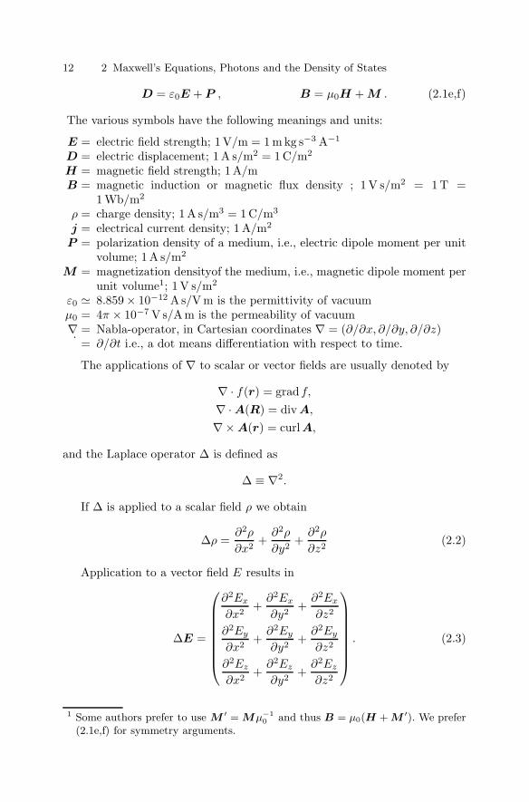
12 2 Maxwell’s Equations, Photons and the Density of States
D = ε0E + P , B = µ0H + M . (2.1e,f)
The various symbols have the following meanings and units:
E = electric field strength; 1 V/m = 1 m kg s−3 A−1
D = electric displacement; 1 A s/m2 = 1 C/m2
H = magnetic field strength; 1 A/mB = magnetic induction or magnetic flux density ; 1 V s/m2 = 1 T =
1 Wb/m2
ρ = charge density; 1 A s/m3 = 1 C/m3
j = electrical current density; 1 A/m2
P = polarization density of a medium, i.e., electric dipole moment per unitvolume; 1 A s/m2
M = magnetization densityof the medium, i.e., magnetic dipole moment perunit volume1; 1 V s/m2
ε0 8.859 × 10⁻¹² As/V m is the permittivity of vacuumµ0 = 4π × 10−7 V s/Am is the permeability of vacuum∇ = Nabla-operator, in Cartesian coordinates ∇ = (∂/∂x, ∂/∂y, ∂/∂z)˙ = ∂/∂t i.e., a dot means differentiation with respect to time.
The applications of ∇ to scalar or vector fields are usually denoted by
∇ · f(r) = grad f,∇ · A(R) = div A,
∇× A(r) = curl A,
and the Laplace operator ∆ is defined as
∆ ≡ ∇2.
If ∆ is applied to a scalar field ρ we obtain
∆ρ =∂2ρ
∂x2+∂2ρ
∂y2+∂2ρ
∂z2(2.2)
Application to a vector field E results in
∆E =
⎛⎜⎜⎜⎜⎜⎜⎜⎝
∂2Ex
∂x2+∂2Ex
∂y2+∂2Ex
∂z2
∂2Ey
∂x2+∂2Ey
∂y2+∂2Ey
∂z2
∂2Ez
∂x2+∂2Ez
∂y2+∂2Ez
∂z2
⎞⎟⎟⎟⎟⎟⎟⎟⎠. (2.3)
1 Some authors prefer to use M ′ = Mµ−10 and thus B = µ0(H + M ′). We prefer
(2.1e,f) for symmetry arguments.

2.1 Maxwell’s Equations 13
Further rules for the use of ∇ and of ∆ and their representations in otherthan Cartesian coordinates (polar or cylindrical coordinates) are found incompilations of mathematical formulae [84A1,91B1,92S1].
Equations (2.1a,b) show that free electric charges ρ are the sources of theelectric displacement and that the magnetic induction is source-free. Equa-tions (2.1c,d) demonstrate how temporally varying magnetic and electric fieldsgenerate each other. In addition, the H field can be created by a macro-scopic current density j. Equations (2.1e,f) are the material equations intheir general form. From them we learn that the electric displacement isgiven by the sum of electric field and polarization, while the magnetic fluxdensity is given by the sum of magnetic field and magnetization. Some au-thors prefer not to differentiate between H and B. This leads to difficulties,as can be easily seen from the fact that B is source-free (2.1b) but H isnot, as follows from the inspection of the fields of every simple permanentmagnet.
By applying ∇· to (2.1d) we obtain the continuity equation for the electriccharges
div j = − ∂
∂tρ , (2.4)
which corresponds to the conservation law of the electric charge in a closedsystem.
The integral forms of (2.1) can be obtained from the differential forms byintegration and the use of the laws of Gauss or Stokes resulting in∫
ρ(r)dV =∮
D · df (2.5a)
− ∂
∂t
∫B · df =
∮E · ds (2.5b)
where dV , df and ds give infinitesimal elements of volume, surface or areaand line, respectively.
In their microscopic form, Maxwells equations contain all charges assources of the electric field Emicro including all electrons, protons bound inatoms as ρbound and not only the free space charges ρ. By analogy, not onlythe microscopic current density j has to be used as a source of Hmicro butall spins and l = 0 orbits of charged particles have to be included as “bound”current density jbound. The transition to macroscopic quantities can then beperformed by averaging over small volumes (larger than an atom but smallerthan the wavelength of light) and replacing ρbound by −−→∇ · P and jbound byP + curlM/µ0. For more details see [98B1,98D1] or Chap. 27.
Concerning the units, some theoreticians still prefer the so-called c g s(cm, g, second) system. Though it has only marginal differences in me-chanics to the SI system, which is based on the units 1 m, 1 kg, 1 s, 1 A,1 K, 1 mol and 1 cd, the c g s system produces strange units in electro-dynamics like the electrostatic units (esu), which contain square roots of

14 2 Maxwell’s Equations, Photons and the Density of States
mass and are therefore unphysical and even ill-defined. For conversion tablessee [96L1].
2.2 Electromagnetic Radiation in Vacuum
In vacuum the following conditions are fulfilled
P = 0 ; M = 0 ; ρ = 0 ; j = 0. (2.6)
With the help of (2.1e,f) this simplifies (2.1c,d) to
∇× E = −µ0H and ∇× H = ε0E (2.7a,b)
Applying ∇× to (2.7a) and ∂/∂t to (2.7b) yields
∇× (∇× E) = −µ0∇× H and ∇× H = ε0E . (2.8)
From (2.8) we find with the help of the properties of the ∇ operator
−µ0ε0E = ∇× (∇× E) = ∇(∇ · E) −∇2E. (2.9)
With (2.6), (2.3) and (2.1a) we see that
∇E = 0 (2.10)
and (2.9) reduces to the usual wave equation, written here for the electric field
∇2E − µ0ε0E = 0 . (2.11)
An analogous equation can be obtained for the magnetic field strength. Solu-tions of this equation are all waves of the form
E(r, t) = E0f(kr − ωt). (2.12)
E0 is the amplitude, f is an arbitrary function whose second derivateexists. As can be shown by inserting the ansatz (2.12) into (2.11) the wavevector k and the angular frequency ω obey the relation
ω
k=(
1µ0ε0
)1/2
= c with k = |k| = 2π/λv. (2.13)
In the following we use for simplicity only the term “frequency” for ω =2π/T where T is the temporal period of the oscillation.
In (2.13), c is the vacuum speed of light and λv is the wavelength invacuum. From all possible solutions of the form (2.12) we shall concentratein the following on the most simple ones, namely on plane harmonic waves,which can be written as
E(r, t) = E0 exp[i(kr − ωt)]. (2.14)

2.2 Electromagnetic Radiation in Vacuum 15
For all waves (not only those in vacuum), the phase and group velocitiesvph and vg are given by
vph =ω
k; vg =
∂ω
∂k= gradkω, (2.15)
where vph gives the velocity with which a certain phase propagates, (e.g.,a maximum of a monochromatic wave) while vg gives the speed of the centerof mass of a wave packet with middle frequency ω and covering a small fre-quency interval dω as shown schematically in Figs. 2.1a,b, respectively. Theformulas (2.15) are of general validity. The gradk on the r.h.s. of (2.15) meansa differentiation with respect to k; in the sense of ∇k = (∂/∂kx, ∂/∂ky, ∂/∂kz)and has to be used instead of the more simple expression ∂ω/∂k in anisotropicmedia. For the special case of electromagnetic radiation in vacuum we findfrom (2.13), (2.15)
vph = vg = c = (µ0ε0)−1/2 (2.16)
Fig. 2.1. A harmonic wave (a) and a wave packet (b) shown at two different timest and t + ∆t to illustrate the concepts of phase and group velocity, respectively

16 2 Maxwell’s Equations, Photons and the Density of States
Now we want to see what constraints are imposed by Maxwell’s equationson the various quantities such as E0 and k. Inserting (2.12) or (2.14) into(2.10) gives
∇ · E = iE0 · k exp[i(kr − ωt)] = 0. (2.17)
This means thatE0 ⊥ k (2.18)
or, in other words, the electromagnetic wave is transverse in E. What can welearn from Maxwell’s equations for the other fields? From (2.7) we have forplane waves
H = (ωµ0)−1k × E = H0 exp[i(kr − ωt)] (2.19a)
withH0 = (ωµ0)−1k × E0. (2.19b)
Furthermore we have with (2.1e,f) and (2.6)
D = D0 exp[i(kr − ωt)] = ε0E0 exp[i(kr − ωt)], (2.19c)
B = B0 exp[i(kr − ωt)] = ω−1k × E0 exp[i(kr − ωt)]. (2.19d)
The electromagnetic wave is, according to (2.19b), also transverse in Band the electric and magnetic fields are perpendicular to each other, that is,we have in general
D ⊥ k ⊥ B ⊥ D. (2.19e)
In vacuum and isotropic media one has in addition
E ‖ D and H ‖ B. (2.19f)
As we shall see later in connection with (2.17) and (2.43),(2.44) one hasin matter usually transverse waves, which obey (2.19e) but additionally, lon-gitudinal waves exist under certain conditions.
The momentum density Π of the electromagnetic field is given by
Π = D × B, Π ‖ k (2.20)
and the energy flux density by the Poynting vector S
S = E × H (2.21)
with S ‖ Π in vacuum and isotropic materials.S is a rapidly oscillating function of space and time. The average value
〈S〉 is usually called the intensity I or the energy flux density The intensity isproportional to the amplitude squared for all harmonic waves. For the planemonochromatic waves treated here, we obtain
〈S〉 =12|E0 × H0| =
12
1cµ0
E20 =
12c
µ0B2
0 =12cµ0H
20 . (2.22)
Equations (2.20) and (2.21) are also valid in matter.

2.3 Electromagnetic Radiation in Matter; Linear Optics 17
2.3 Electromagnetic Radiation in Matter; Linear Optics
Now we treat Maxwell’s equations in matter. Doing so we have in principleto use the equations in their general from (2.1). However we will still make inseveral steps some assumptions which are reasonable for semiconductors: weassume first that there are no macroscopic free space charges i.e. ρ = 0. Thena treatment of (2.1) in analogy with (2.7)–(2.11) results in
∇2E − µ0ε0E = µ0P + µ0j + ∇× M , (2.23)
Actually, there also occurs in the derivation of (2.23) a term ∇(∇P ) or∇(∇E). This term vanishes for transverse waves and is therefore neglected ifnot mentioned otherwise.
This equation is the inhomogeneous analogue of (2.11) telling us that thesources of an electro-magnetic radiation field can be
– A dipole moment p or a polarization P with a non-vanishing second timederivative
– A temporally varying current density– The curl of a temporally varying magnetization
Again a similar equation can be obtained for the magnetic field. We continuenow with the application of further simplifications and assume that we havea nonmagnetic material, i.e., that the third term on the r.h.s. of (2.23) van-ishes. Actually, all matter has some diamagnetism. But this is a rather smalleffect of the order of 10−6 so it can be neglected for our purposes. Param-agnetic and especially ferromagnetic contributions can be significantly largerfor low frequencies. However, even these contributions diminish rapidly forhigher frequencies. Consequently the assumption of a nonmagnetic materialis a good approximation over a wide range of the electromagnetic spectrumstarting in the IR even for ferromagnetic materials. Furthermore, the morecommon semiconductors are not ferro-, ferri- or antiferromagnetic and haveonly a small concentration of paramagnetic centres which may be seen in elec-tron paramagnetic resonance (EPR), but which have negligible influence onthe optical properties. The only exceptions are semiconductors which containa considerable amount of e.g., Mn or Fe ions as does Zn1−yMnySe. We referthe reader to [88D1,91O1,92G1,92Y1,94D1,94G1,96H1,03D1] or to Sect. 16.1and references therein for this class of materials.
The current term j in (2.1d) deserves some more consideration. The cur-rent is driven by the electric field
j = σE, (2.24)
where σ is the conductivity. For intrinsic or weakly doped semiconductors,the carrier density is small and consequently σ is as well. Then the followinginequality holds
|j| = |σE| |D|. (2.25)
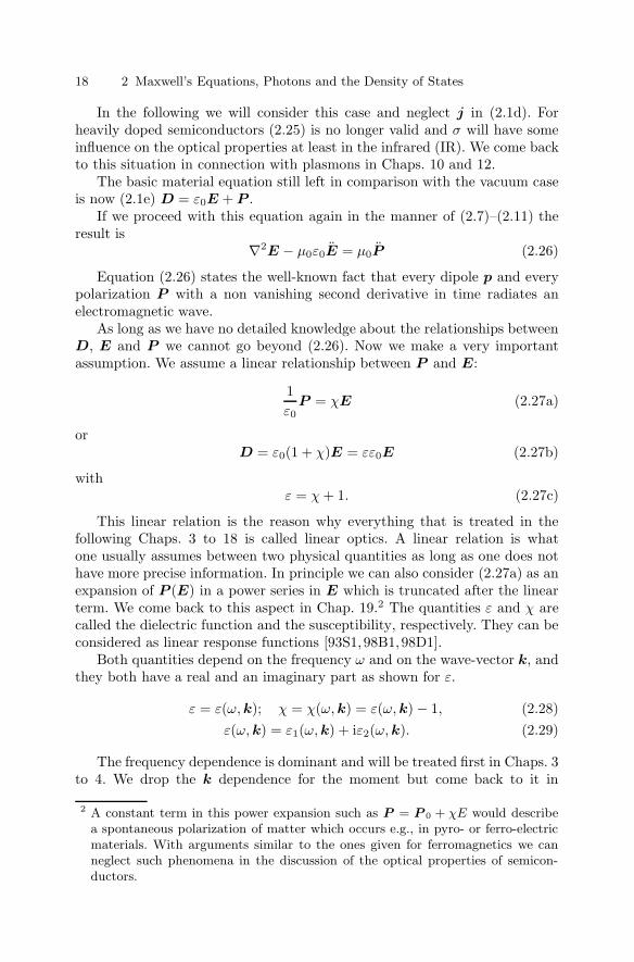
18 2 Maxwell’s Equations, Photons and the Density of States
In the following we will consider this case and neglect j in (2.1d). Forheavily doped semiconductors (2.25) is no longer valid and σ will have someinfluence on the optical properties at least in the infrared (IR). We come backto this situation in connection with plasmons in Chaps. 10 and 12.
The basic material equation still left in comparison with the vacuum caseis now (2.1e) D = ε0E + P .
If we proceed with this equation again in the manner of (2.7)–(2.11) theresult is
∇2E − µ0ε0E = µ0P (2.26)
Equation (2.26) states the well-known fact that every dipole p and everypolarization P with a non vanishing second derivative in time radiates anelectromagnetic wave.
As long as we have no detailed knowledge about the relationships betweenD, E and P we cannot go beyond (2.26). Now we make a very importantassumption. We assume a linear relationship between P and E:
1ε0
P = χE (2.27a)
orD = ε0(1 + χ)E = εε0E (2.27b)
withε = χ+ 1. (2.27c)
This linear relation is the reason why everything that is treated in thefollowing Chaps. 3 to 18 is called linear optics. A linear relation is whatone usually assumes between two physical quantities as long as one does nothave more precise information. In principle we can also consider (2.27a) as anexpansion of P (E) in a power series in E which is truncated after the linearterm. We come back to this aspect in Chap. 19.2 The quantities ε and χ arecalled the dielectric function and the susceptibility, respectively. They can beconsidered as linear response functions [93S1,98B1,98D1].
Both quantities depend on the frequency ω and on the wave-vector k, andthey both have a real and an imaginary part as shown for ε.
ε = ε(ω,k); χ = χ(ω,k) = ε(ω,k) − 1, (2.28)ε(ω,k) = ε1(ω,k) + iε2(ω,k). (2.29)
The frequency dependence is dominant and will be treated first in Chaps. 3to 4. We drop the k dependence for the moment but come back to it in
2 A constant term in this power expansion such as P = P 0 + χE would describea spontaneous polarization of matter which occurs e.g., in pyro- or ferro-electricmaterials. With arguments similar to the ones given for ferromagnetics we canneglect such phenomena in the discussion of the optical properties of semicon-ductors.

2.3 Electromagnetic Radiation in Matter; Linear Optics 19
connection with spatial dispersion in Chap. 5. In Chap. 6 we discuss theproperties of ε as a function of frequency and wave vector or as a function oftime and space.
The value of ε(ω) for ω 0 is usually called the dielectric constant.In general ε and χ are tensors. For simplicity we shall consider them to be
scalar quantities if not stated otherwise, e.g., in connection with birefringencein Sect. 3.1.7.
Using the linear relations of (2.27) we can transform (2.23) into
∇2E − µ0ε0ε(ω)E = 0, (2.30a)
where we assumed also that ε(ω) is spatially constant on a length scale of theorder of the wavelength of light. Deviations of this assumption are treated inSects. 17.2–4.
If magnetic properties are to be included, a corresponding linear approachwould lead to
∇2E − µ0µ(ω)ε0ε(ω)E = 0, (2.30b)
where µ(ω) is the magnetic permeability. As outlined above we have in thevisible for most semiconductors µ(ω) 1.
As for (2.12) the solutions of (2.30) are again all functions of the type
E = E0f(kr − ωt), (2.31)
or for our present purposes, i.e. again for the case of plane harmonic waves
E = E0 exp[i(kr − ωt)]. (2.32)
The relationship between k and ω is however now significantly differentfrom (2.13). It follows again from inserting the ansatz (2.31 or 32) into (2.30)and now reads:
c2k2
ω2= ε(ω). (2.33)
This relation appears in Chap. 5 again under the name “polariton equa-tion”. It can also be written in other forms:
k =ω
cε1/2(ω) =
2πλvε1/2(ω) = kvε
1/2(ω), (2.34)
where λv and kv refer to the vacuum values of the light wave.For the square root of ε we introduce for simplicity a new quantity n(ω)
which we call the complex index of refraction
n(ω) = n(ω) + iκ(ω) = ε1/2(ω). (2.35)
The equations (2.13) and (2.33–35) can be interpreted in the followingway. In vacuum an electromagnetic wave propagates with a wave vector kv
which is real and given by (2.13). In matter, light propagates with a wave
20 2 Maxwell’s Equations, Photons and the Density of States
vector k which can be a complex quantity given by (2.34), or, with the helpof (2.35), by
k =ω
cn(ω) =
ω
cn(ω) + i
ω
cκ(ω) =
2πλvn(ω) = kvn. (2.36)
We should notice that k is for complex n not simply |k| since |k| is alwaysa positive, real quantity. Here k means just neglecting the vector character ofk but k can still be a real, imaginary or complex quantity according to (2.36).The direction of the real part of k, which describes the oscillatory part of thewave, is still parallel to D × B as in (2.20).
Writing the plane wave explicitly we have:
E0 exp[i(kr − ωt)] = E0 expi[ωcn(ω)kr − ωt
]exp
[−ωcκ(ω)kr
], (2.37)
where k is the unit vector in the direction of k, i.e., in the direction of prop-agation.
Obviously n(ω) describes the oscillatory spatial propagation of light inmatter; it is often called the refractive index in connection with Snells’ law ofrefraction. This means that the wavelength λ in a medium is connected withthe wavelength λv in vacuum by
λ = λvn−1(ω). (2.38)
In (2.37) κ(ω) describes a damping of the wave in the direction of propa-gation. This effect is usually called absorption or, more precisely, extinction.We give the precise meaning of these two quantities in Sect. 3.1.5. Here wecompare (2.37) with the well-known law of absorption for the light intensityI of a parallel beam propagating in z-direction
I(z) = I(z = 0)e−αz (2.39)
where α(ω) is usually called the absorption coefficient, especially in Anglo-Saxon literature. In German literature α(ω) is also known as “Absorptions-konstante” (absorption constant) and dimensionless quantities proportional toκ(ω) are called “Absorptionskoeffizient” or “Absorptions index” (absorptioncoefficient or absorption index). So some care has to be taken regarding whatis meant by one or the other of the above terms.
Bearing in mind that the intensity is still proportional to the amplitudesquared (2.24), a comparison between (2.37) and (2.39) yields
α(ω) =2ωcκ(ω) =
4πλvκ(ω). (2.40)
The phase velocity of light in a medium is now given by (2.15)
vph =ω
Rek = cn−1(ω). (2.41)

2.4 Transverse, Longitudinal and Surface Waves 21
For the group velocity we can get rather complicated dependencies origi-nating from
vg =∂ω
∂k. (2.42)
We return to this aspect later.
2.4 Transverse, Longitudinal and Surface Waves
The only solution of (2.9) for light in vacuum is a transverse electromagneticwave (2.19). This solution exists for light in matter as well. However (2.9) hasnow with the use of (2.27) the form
∇ · D = ∇ε0ε(ω)E = 0 (2.43)
Apart from the above-mentioned transverse solution with E ⊥ k there isa new solution which does not exist in vacuum (εvac ≡ 1), namely
ε(ω) = 0. (2.44a)
This means that we can find longitudinal solutions at the frequencies atwhich ε(ω) vanishes. We call these frequencies correspondingly ωL and notethat for
ε(ωL) = 0; E ‖ k is possible (2.44b)Now let us consider the other fields for this longitudinal wave in matter.
From (2.27) we see immediately that we have for the longitudinal modes
D = 0 and E = − 1ε0
P . (2.45)
In matter, the Maxwell’s equation ∇× E = −B is still valid. This leads forplane waves in nonmagnetic material to
H0 = (ωµ0)−1k × E0. (2.46)
For the longitudinal wave it follows from (2.44) that
H = 0 and B = µ0H = 0 (2.47)
The longitudinal waves which we found in matter are not electromagneticwaves but pure polarization waves with E and P opposed to each other withvanishing D, B and H.
Until now we were considering the properties of light in the bulk ofa medium. The boundary of this medium will need some extra consideratione.g., the interface between vacuum (air) and a semiconductor. This interfaceis crucial for reflection of light and we examine this problem in Sects. 3.1.1–4;5.4.2 and 5.6. Here we only want to state that the boundary conditions al-low a surface mode, that is, a wave which propagates along the interface andhas field amplitudes which decay exponentially on both sides. These wavesare also known as surface polaritons for reasons discussed in more detail inSect. 5.6.

22 2 Maxwell’s Equations, Photons and the Density of States
2.5 Photons and Some Aspects of Quantum Mechanicsand of Dispersion Relations
Maxwell’s equations are the basis of the classical theory of light. They de-scribe problems like light propagation and the diffraction at a slit or a gratinge.g., in the frame of Huygen’s principle or of Fourier optics [93S1].
In the interaction of light with matter, its quantum nature becomes ap-parent, e.g., in the photoelectric effect which shows that a light field of fre-quency ω can exchange energy with matter only in quanta ω. Therefore,the proper description of light is in terms of quantum mechanics or of quan-tum electrodynamics. However, we shall not go through these theories herein detail nor do we want to address the aspects of quantum statistics of co-herent and incoherent light sources, but we present in the following someof their well-known results and refer the reader to the corresponding litera-ture [85G1, 92M1, 94A1, 94B1, 01M1, 01T1, 02B1, 02D1, 02G1, 02L1, 02Y1] fora comprehensive discussion.
The electromagnetic fields can be described by their potentials A and φ by
E = −gradφ− A; B = ∇× A . (2.48)
where A is the so-called vector potential. Since ∇ · (∇×A) ≡ 0 the notationof (2.48) fulfills automatically ∇ · B = 0 and reduces the six components ofE and B to four.
The vector potential A is not exactly defined by (2.48). A gradient ofa scalar field can be added. We can choose the so-called Coulomb gauge
∇ · A = 0 . (2.49)
In this case φ is the usual electrostatic potential obeying the Poisson equation:
∇2φ = − ρ
ε0ε(ω). (2.50)
In vacuum we still have ρ = 0 and we assume the same for the description ofthe optical properties of matter.
Now we should carry out the procedure of second quantization, for sim-plicity again for plane waves. A detailed description of how one begins withMaxwell’s equations and arrives at photons within the framework of secondquantization is beyond the scope of this book see [55S1, 71F1, 73H1, 76H1,80H1,85G1,92M1,94A1,94B1]. On the other hand we want to avoid that thecreation and annihilation operators appear like a “deus ex machina”. There-fore we try at least to outline the procedure.
First we have to write down the classical Hamilton function H which isthe total energy of the electromagnetic field using A and φ. Then we mustfind some new, suitable quantities pk,s and qk,s which are linear in A andwhich fulfill the canonic equations of motion
∂H
∂qk,s= −pk,s,
∂H
∂pk,s= −qk,s (2.51)

2.5 Photons and Dispersion Relations 23
and are thus canonically conjugate variables. Here k is the wave vector of ourplane electromagnetic or A-wave and s the two possible transverse polariza-tions. The Hamilton function reads in these variables:
H =12
∑k,s
(p2k,s) + ω2kq
2k,s (2.52)
This is the usual form of the harmonic oscillator. The quantization condi-tion
pk,sqk,s − qk,spk,s =
i(2.53)
for all k and s = 1, 2 gives then the well-known result for the harmonic oscil-lator: The electromagnetic radiation field has for every k and polarization senergy steps
Ek =(nk +
12
)ωk with nk = 0, 1, 2 . . . (2.54)
It can exchange energy with other systems only in units of ω. These energyunits or quanta are called photons. The term ω/2 in (2.54) is the zero-pointenergy of every mode of the electromagnetic field.
The so-called particle-wave dualism, that is, the fact that light propagateslike a wave showing, e.g., diffraction or interference and interacts with mattervia particle-like quanta, can be solved by the simple picture that light is anelectromagnetic wave, the amplitude of which can have only discrete valuesso that the energy in the waves just fulfills (2.54).
From the above introduced, or better, postulated quantities pk,s and qk,s
we can derive by linear combinations operators a†k,s and ak,s with the followingproperties: If ak,s acts on a state which contains nk,s quanta of momentum kand polarization s it produces a new state with nk,s − 1 quanta. Correspond-ingly, a†k,s increases nk,s by one. We call therefore ak,s and a†k,s annihilationand creation operators, respectively. Since the operators ak,s and a†k,s describebosons (see below), their permutation relation is
ak,sa†k,s − a†k,sak,s = 1. (2.55a)
This holds for equal k and s. The commutator is zero otherwise.The operator a†k,sak,s acting on a photon state gives the number of photons
nk,s times the photon state and is therefore called the number operator. Sum-ming over all possible k-values and polarizations s gives finally the Hamiltonoperator
H =∑k,s
ωk,sa†k,sak,s. (2.55b)
It is clear to the author that the short outline given here is not sufficientto explain the procedure to a reader who is not familiar with it. However,
24 2 Maxwell’s Equations, Photons and the Density of States
since the intent is not to write a textbook on quantum electrodynamics, wewant to stress here only that the electromagnetic radiation field in vacuumcan be brought into a mathematical form analogous to that of the harmonicoscillator, and that quantum mechanics gives for every harmonic oscillatorthe energetically equidistant terms of (2.54).
The harmonic oscillator is one of the fundamental systems, which has beeninvestigated in physics and is understood in great detail. In theoretical physicsa problem can be considered as “solved” if it can be rewritten in the formof the harmonic oscillator. Apart from the electromagnetic radiation field invacuum, we will come across some other systems which are treated in this way.For those readers who are not familiar with the concept of quantization andwho wish to study the procedure in a quiet hour by themselves, we recommendthe above given references.
Here are some more results: The two basic polarizations of single quantaof the electromagnetic field, – of the photons – are left and right circular σ−
and σ+, respectively. A linearly polarized wave can be considered as a coherentsuperposition of a left and right circularly polarized one with equal frequen-cies and wave vector k. The term coherent means that two light beams havea fixed-phase relation relative to each other. The component of the angularmomentum s in the direction of the quantization axis which is parallel to kis for photons thus
s‖ = ±. (2.56)
This means that photons have integer spin and are bosons. The third possi-bility s‖ = 0 expected for spin one particles is forbidden, because longitudinalelectromagnetic waves do not exist at least in vacuum.
Photons in thermodynamic equilibrium are described by Bose-statistics.The occupation probability fBE of a state with frequency ω is given by
fBE = [exp(ω/kBT ) − 1]−1, (2.57)
where T is the absolute temperature and kB is Boltzmann’s constant.The chemical potential µ which could appear in (2.57) is zero in thermal
equilibrium, since the number of photons is not conserved.An approach to describe non-thermal photon fields e.g. luminescence by
a non-vanishing µ and Kirchhoff’s law in the sense of a generalized Planck’slaw is found in [82W1,92S2,95D1].
The momentum p of a photon with wave vector k is given, as for all quantaof harmonic waves, by
p = k. (2.58)
where k is the real part of the wave vector, which describes as already men-tioned the oscillatory, propagating aspect of the plane wave.
To summarize, we can state that photons are bosons with spin ±, en-ergy ω and momentum k which propagate according to the wave equations.
A very important property of particles in quantum mechanics is their dis-persion relation. By this we mean the dependence of energy E or frequency ω

2.5 Photons and Dispersion Relations 25
on the wave vector k i.e., the E(k) or ω(k) relation. For photons in vacuumwe find the classical relation given already in (2.13)
E = ω = ck. (2.59)
The dispersion relation for photons in vacuum is thus a linear functionwith slope c as shown in Fig. 2.2. Correspondingly we find again both forphase and group velocity with (2.15)
vph = vg = c . (2.60)
We conclude this subsection with an explanation of energy units. In theSI system the energy unit is 1 N m = 1 kgm2/s2 with the following identityrelations
1 N m = 1 m kg s−2 = 1 V A s = 1 W s = 1 J . (2.61a)
Since the energies of the quanta in optical spectroscopy are much smaller,we frequently use the unit 1 eV. This is the energy that an electron gains if itpasses, in vacuum, through a potential difference of one volt, resulting in
1 eV = 1.60217733× 10⁻¹⁹ J ≈ 1.6 × 10⁻¹⁹ J . (2.61b)
In spectroscopy another measure of energy is frequently used the wavenumber. The definition is as follows. One expresses the energy of a (quasi-)particle by the number of wavelengths per cm of a photon with the sameenergy. So
1 eV = 8065.4 cm−1 or 104 cm−1 = 1.23986 eV (2.61c)
Another quantity that is sometimes confused with the wave number, whichgives the energy and is therefore a scalar quantity, is the wave vector, since ithas also the dimension 1/length.
The amount of the (real part of the) wave vector is given by k = 2π/λ,where λ is the wavelength of the corresponding quantum or particle (electron,
Fig. 2.2. The dispersion relation ofphotons in vacuum

26 2 Maxwell’s Equations, Photons and the Density of States
phonon, photon, etc.). The direction of k is the direction of propagation, i.e., kis normal to the wave-front, in the case of light in vacuum or in matter normalto D×B. The quantity k is very closely related to the (quasi-)momentum ofthe (quasi-)particle p through
p = k . (2.58)
For the discussion of the concept of quasi-momentum see, e.g., Sects. 5.2,3 and 5 or [98B2]. The dispersion relation of (quasi-) particles is thus givenby E(k). The wave vector of light is in the visible in vacuum, falling in therange of a few times 104 cm−1 while the border of the first Brillouin zone (seeSect. 7.2) is of the order of 108 cm−1.
It is obvious, that a quantity like a wave-number vector (Wellenzahlvektor)is ill-defined and does not exist!
2.6 Density of States and Occupation Probabilities
A quantity which is crucial in quantum mechanics for the properties of parti-cles is their density of states. It enters, e.g., in Fermi’s golden rule which allowsone to calculate transition probabilities. We want to discuss this problem ina general way for systems of different dimensionalities d = 3, 2 and 1. We shallneed these results later on for low-dimensional semiconductor structures. Thediscussion of the density of states, especially in various dimensions, is not socommonly treated as the harmonic oscillator, and so we shall spend some timeon this problem and dwell more on the details. At the end of this section weshall also state the occupation probability in thermodynamic equilibrium forclassical particles, for fermions and bosons.
If we consider a particle which is described by a wave function3 φ(r) thenthe probability w to find it in a small element of space dτ = dxdydz aroundr is
w(r)τ = φ∗(r)φ(r)dτ (2.62a)
Since the particle has to be somewhere in the system, w(r) has to be“normalized”, that is,∫
system
w(r)dτ =∫
system
φ∗(r)φ(r)dτ = 1. (2.62b)
Here, the functions φ(r) are of the form exp(ikr). For normalization purposesa factor has to be added
φ(r) = Ω−1/2 exp(ikr). (2.63)3 The letter φ has been already used for the electrostatic potential e.g., in (2.50).
Since there are more different physical quantities than letters of the alphabet,we sometimes use the same letter for different quantities, but from the context itshould be clear what is meant.

2.6 Density of States and Occupation Probabilities 27
The normalization condition (2.62b) results in
Ω−1
∫system
exp(−ikr) exp(ikr)dτ = Ω−1
∫system
dτ = Ω−1Vsystem = 1,
(2.64)where Vsystem is the volume of our physical system. Consequently Ω is justthe volume of the system. To avoid a factor of zero in front of the plane-waveterm, one assumes that the system is so big that it contains all physicallyrelevant parts, but that it is not infinite. The simplest choice is a box oflength L, or, more precisely speaking, a cube in three dimensions, a squarein two, and an interval in one. This procedure is known as “normalization ina box”. Consequently we have
Vsystem = Ld with d = dimensionality of the system (2.65)
andΩ1/2 = Ld/2 for d = 3, 2, 1. (2.66)
The wave vectors which can exist in such a box are limited by the boundaryconditions.
If we assume that we have an infinitely high potential barrier aroundthe box, then the wavefunction must have nodes at the walls (Fig. 2.3a).Consequently the components ki of k must fulfill
ki = niπ
L; ni = 1, 2, 3, . . . ; i = 1, . . . , d, (2.67)
where the index i runs over all dimensions.Such a wave is a standing wave, i.e., a coherent superposition of two waves
with k and −k and equal amplitudes. In the following we must considertherefore only positive values of k. The various modes are distributed equallyspaced over the ki-axes with a spacing ∆ki,
∆ki =π
L. (2.68)
In other words, every state (or mode) needs a volume Vk in k-space given by
Vk =(πL
)d
. (2.69)
Another approach is to impose periodic boundary conditions. Then theplane wave should have equal amplitude and slope on opposite sides of thecube according to Fig. 2.3b. In this case one can fill the infinite space byadding boxes in all dimensions and one finds:
ki = n′i2πL
; n′i = ±1,±2,±3 . . . (2.70)
This means for ∆ki

28 2 Maxwell’s Equations, Photons and the Density of States
Fig. 2.3. Plane waves which have nodes at the boundaries (a) or which obey periodicboundary conditions (b)
∆k′i =2πL. (2.71)
In contrast to the case of standing waves, we now have to consider positiveand negative values of ni separately. This procedure results finally in the samedensity of states.
As a consequence we find that plane waves have in Cartesian coordinatesin k-space a constant density on all axes.
2.6 Density of States and Occupation Probabilities 29
This result can also be derived qualitatively from the uncertainty principle.If a particle is confined to a length L in direction i its momentum has anuncertainly ∆pi = ∆ki ≥ /L. Consequently two states, which should bedistinguishable or “different”, must have ki values, which differ by roughly1/L.
Often one wants to know the number of states in a shell between k andk + dk independent of the direction of k. This question can be answeredby introducing polar coordinates in k-space. The differential volume dVk ofa shell of thickness dk in a d-dimensional k-space is given by
dVk = 2dk for d = 1,
dVk = 2πkdk for d = 2,
dVk = 4πk2 dk for d = 3.
(2.72)
Depending on the boundary condition we have to take into account onlypositive (2.67), or positive and negative (2.70), values of k or ni with corre-sponding modifications of the prefactors in (2.72).
The number D(k) of states in k-space found between k and k + dk inpolar coordinates is given by dividing dVk by the volume for each state andby multiplying by gs. The quantity gs considers degeneracies such as the spindegeneracy. For photons we have gs = 2 according to the σ+ and σ− polar-izations (see above). The results are
D(k)dk = gsL
πdk for d = 1,
D(k)dk = gsL2
2πkdk for d = 2,
D(k)dk = gsL3
2π2k2 dk for d = 3.
(2.73)
The derivation of this result is depicted for d = 2 in Fig. 2.4. If we neglectconstant prefactors and divide by dk we find
D(k) ∝ gsLdkd−1, d = 1, 2, 3 . . . . (2.74)
If we consider not the number of states in the box of volume Ld but thedensity of states D(k) per unit of space (e.g., per cm3 or m3) the term Ld in(2.74) disappears yielding
D(k) ∝ gskd−1 (2.75)
The concept of periodic boundary conditions yields the same result.This result has to be expected since the density of states per unit volume
must be independent of the size of the box which we have in mind providedthe box is sufficiently large.
We want to stress here that we assumed only plane waves but did notmake any specific assumptions about which type of particles are represented

30 2 Maxwell’s Equations, Photons and the Density of States
Fig. 2.4. A two-dimensional k-space in which the states are equally spaced on thekx-and ky-axes to derive (2.73) for d = 2
by these plane waves – photons, electrons etc. Therefore this result is validfor all particles described by plane waves.
The next step is now to calculate the density of states on the energy axis,i.e.,
D(E)dE. (2.76)
This quantity gives the number of states in the energy interval from E toE + dE. To calculate this quantity we need the specific dispersion relationE(k) and its inverse k(E) as seen from the identity (2.77):
D(E)dE = D[k(E)]dkdE
· dE = D[k(E)]1
|gradkE(k)| dE. (2.77)
The term on the right-hand side of (2.77) gives the generalized equationwhich is also valid for anistropic cases.
In particular for photons in vacuum we have with (2.59)
k =E
c=ω
c;
dkdE
=1c
(2.78)
Inserting this result in (2.77), for the case d = 3 we find
D(E)dE =E2
π2(c)3dE
orD(ω)dω ∝ ω2 dω (2.79a)

2.6 Density of States and Occupation Probabilities 31
For massive particles, i.e. particles the dispersion relation of which can bedescribed by an (effective) mass m according to
E(k) =2k2
2m(2.79b)
we obtain with (2.77) for a d-dimensional space
D(E)dE ∝ gsEd2−1 dE . (2.79c)
This formula includes the well-known square root density of states for massiveparticles in three dimensions.
We repeat again that the density in k-space is constant on all Cartesianaxes in a d-dimensional space for all particles, which can be described bya plane wave, but the density of states depends on the individual dispersionrelation when plotted as a function of energy.
The next quantity, which we need is the occupation probability of thestates discussed above. We restrict ourselves in the following to thermody-namic equilibrium. There are three types of statistics which can be considered:
For classical, distinguishable particles, Boltzmann statistics apply:
fB = exp[−(E − µ)/kBT ]. (2.80a)
For bosons, i.e., indistinguishable particles with integer spin, photons beingan example, one must use the Bose–Einstein statistics
fBE = exp[(E − µ)/kBT ]− 1−1. (2.80b)
Fermions, or indistinguishable particles with half-integer spin e.g., elec-trons obey the Fermi–Dirac statistics fFD
fFD = exp[−(E − µ)/kBT ] + 1−1. (2.80c)
The Boltzmann constant is kB and the chemical potential is µ which gives theaverage energy necessary to add one more particle to the system. For fermionsµ is also known as the Fermi energy EF. The probability to find a particle inthe interval from E to E + dE is then given by the product of the density ofstates D(E) and the occupation probability f
D(E)f(E, T, µ)dE (2.81)
In Fig. 2.5 we plot fB, fBE and fFD as a function of (E − µ)/kBT .The Boltzmann statistics shows the well-known exponential dependence.
The Fermi–Dirac statistics never exceeds one, realizing thus Pauli’s exclusionprinciple. The Bose–Einstein statistics has a singularity for E = µ. This givesrise to Bose–Einstein condensation, or in other words, a macroscopic popu-lation of a single state, if µ touches a region with a finite density of states.In this case the species with energies E = µ and those with E > µ must be

32 2 Maxwell’s Equations, Photons and the Density of States
Fig. 2.5. The Boltzmann,Bose–Einstein and Fermi–Dirac distribution func-tions versus (E − µ)/kBT
considered separately. Furthermore it is obvious from Fig. 2.5 that fBE andfFD converge to fB for (E − µ)/kT > 1.
In Sects. 7.7, 8.2 and 9 or 20.5 we discuss, when classical Boltzmannstatistics is a good approximation and when the use of Fermi–Dirac or Bose–Einstein statistics is obligatory.
The chemical potential µ is zero in thermodynamic equilibrium for quantawhose number is not conserved, for e.g., photons or phonons. We introducethis topic in Chap. 7.
If the number N or density n of particles in a system is known, as is thecase for electrons at non-relativistic energies, then µ is well defined by (2.82).∫
D(E)f(E, µ, T )dE = n, (2.82)
which says that the density of particles is equal to the integral over the productof the density of states and the probability that a state is occupied.
As an example, we apply now the above statements to photons in a three-dimensional box in thermodynamic equilibrium. With (2.79b) and (2.80b),(2.83) is obtained.
N(ω)dω = D(ω)fBE(ω, T )dω ∝ ω2
[exp
(ω
kBT
)− 1
]−1
dω . (2.83)
For the energy content U(T ) of the radiation field, the result is
U(T ) =
∫ ∞
0
ωN(ω)dω ∝∫ ∞
0
ω3
[exp
(ω
kBT
)− 1
]−1
dω . (2.84)
Equation (2.83) is nothing other than Planck’s law of black-body radiation.By substituting x for the variable ω/kBT in (2.84) we immediately find the

2.7 Problems 33
Stefan–Boltzmann T 4 law
U(T ) ∝ T 4
∫ ∞
0
x3(expx− 1)−1 dx = T 4A , (2.85)
where A is a constant.
2.7 Problems
1. The intensity of the sunlight falling on the earth is, for normal incidenceand before its passage through the atmosphere, about 1.5 kW m−2. Cal-culate the electric-field strength.
2. Pulsed high power lasers can be easily focussed to a power density I of10 GW/cm2. Calculate the E andB fields. Compare them with the electricfield in an H atom at a distance of one Bohr radius, and the magneticfield on the surface of the earth, respectively.
3. Calculate the number of photon modes in the visible part of the spectrum(≈ 400 nm λv 800 nm) in a box of 1 cm3.
4. Calculate the momentum and energy of a photon with λv = 500nm. Atwhich acceleration voltage has an electron the same momentum?
5. Show qualitatively the B, H and M fields of a homogeneously mag-netized, brick-shaped piece of iron and for a hollow sphere with innerradius R0 and outer radius R0+∆R, which is radially magnetized. Use es-pecially for the second case symmetry considerations together with (2.1).
6. Check whether the maximum of N(ω) in (2.83) shifts in proportion toT (Wien’s law), originally formulated as λmax ∝ T−1.
7. Compare the contribution of the electric conductivity of a typical semicon-ductor to that of the polarisation in (2.23) or (2.25). For which frequenciesdoes the second one dominate?
8. Write down the time and space dependence of a spherical wave. Notethat the energy flux density varies usually like the amplitude squared. Isit possible to create a spherical vector wave?
9. Inspect (with the help of a textbook or a computer program) the electricfield of a static electric dipole and the near and far fields of an oscillatingelectric dipole. Note that in the near field the electric and magnetic fieldsare not orthogonal.
10. Show that the definition vg = 1
gradkE(k) leads, for massive and masslessparticles, directly to the relation (quasi-)momentum p = k.
11. How does the density of states as a function of energy vary for a lineardispersion relation (like photons) in 3, 2 and 1 dimensional systems?
12. Consider or find in a textbook the pattern of the collective motion ofthe H2O molecules in a surface water wave. Which effects contribute tothe restoring force? Are water waves harmonic waves? What happens ata seashore, where the depth of the water decreases gradually? Is therea net transport of matter? Assume that the particles have an electric

34 2 Maxwell’s Equations, Photons and the Density of States
charge and move relative to a fixed background of opposite charge. Whichcharge pattern do you expect close to the surface? Compare with Fig. 4.4b.
References to Chap. 2
We give here and in the following chapters all (co-) authors of a publication toa maximum of three. For papers with four and more (co-)authors we give only thefirst followed by et al.
[55S1] L.I. Schiff: Quantum Mechanics, 2nd edn. Adv. Solid State Phys. McGraw-Hill, New York (1955)
[71F1] A.L. Fetter, J.D. Walecka: Quantum Theory of Many Particle Systems Mc-Graw Hill, New York (1971)
[73H1] H. Haken: Quantenfeldtheorie des Festkorpers Teubner, Stuttgart (1973)[76H1] H. Haken: Quantum Field Theory of Solids North Holland, Amsterdam
(1976)[80H1] H. Haken, H.C. Wolf: Atom- und Quantenphysik Springer, Berlin, Heidel-
berg (1980)[82W1] P. Wurfel: J. Phys. C 15, 3967 (1982)[84A1] M. Abramowitz, J.A. Stegun (eds): Pocket Book of Mathematical Functions
Deutsch, Thun (1984)[85G1] W. Greiner: Theoretische Physik, Vols 1–10 Deutsch, Frankfurt (1985)[88D1] Diluted Magnetic Semiconductors, J.K. Furdyna, J. Kossut (eds), Semicond.
Semimet. 25 (1988)[89S1] Squeezed and Nonclassical Light, P. Tombesi ed., NATO ASI Series B 190,
Plenum Press, New York (1989)[91B1] I.N. Bronstein, K.A. Semendjajew: Taschenbuch der Mathematik, 25th edn.
Teubner, Stuttgart (1991)[91O1] M. von Ortenberg: Festkorperprobleme/Adv. Solid State Phys. 31, 261
(1991)[92G1] O. Goede, W. Heimbrodt: Adv. Solid State Phys. 32, 237 (1992)[92M1] P. Meystre, M. Sargent III: Elements of Quantum Optics, 2nd ed. Springer,
Berlin, Heidelberg (1992)[92S1] H. Stocker (ed.): Taschenbuch Mathematischer Formeln und Moderner Ver-
fahren (Deutsch, Frankfurt (1992)[92S2] K. Schick et al. Appl. Phys. A 54, 109 (1992)[92Y1] D.R. Yakovlev: Festkorperprobleme/Adv. Solid State Phys. 32, 251 (1992)[93S1] W. Stoßel: Fourieroptik, Springer, Berlin (1993)[94A1] I. Abraham and J.A. Levenson in [81A1]g of Chap. 1 p 251[94B1] B. Bowlby: in [81A1]g of Chap. 1 p 385[94D1] T. Dietl: Diluted Magnetic Semiconductors, Handbook of Semiconductors
38, North Holland, New York (1994)[94G1] J.A. Gaj et al.: Phys. Rev. B. 50, 5512 (1994)[95D1] E. Daub and P. Wurfel: Phys. Rev. Lett. 74, 1020 (1995)[96H1] R. Hellmann et al.: J. Crystal Growth 159, 976 (1996)[96L1] Leitfaden fur den Gebrauch des Internationalen Einheitensystems,
Physikalisch Technische Bundesanstalt (PTB), Braunschweig (1996) or var-ious textbooks on physics
References to Chap. 2 35
[98B1] R. v.Baltz in [81A1]i of Chap. 1 p 303[98B2] R. v.Baltz and C. Klingshirn in [81A1]i of Chap. 1p 381[98D1] B. Di Bartolo in [81A1]i of Chap. 1, p 1[98O1] H. Ohno: Science 281, 951 (1998)[01M1] G. Messin et al.: Optics Lett. 26, 1891 (2001)[01T1] Tao-Hua et al.: Acta Optica Sinica 21, 1486 (2001)[01T2] W. Tittel and W. Martienssen: Physikal. Blatter 57, Heft 7/8, p. 81 (2001)[02B1] G. Bayer et al.: Physica E 12, 900 (2002)[02D1] G.A. Durkin, C. Simon, D. Bouwmeester: Phys. Rev. Lett. 88, 187902
(2002)[02G1] O. Gywat, G. Burkard, D. Loss: Phys. Rev. B 65, 205329 (2002)[02L1] A.S. Lenihan et al.: Phys. Rev. Lett. 88, 223601 (2002)[02Y1] Ye-Liu, Guo-Guangcan: Acta Optica Sinica 22, 407 (2002)[03D1] T. Dietl, Europhys. News 34, 216 (2003)

3
Interaction of Light with Matter
In the next two sections we present some basic interaction processes of lightwith matter from two different points of view. First we consider matter asa homogeneous medium described by the complex dielectric function ε(ω) orby the complex index of refraction n(ω) (Sect. 3.1). We concentrate especiallyon the reflection and transmission of light at the plane interface between twomedia. As an especially simple case we investigate the boundary of matter andvacuum. In the later Sect. 3.2 we will discuss the interaction of the radiationfield with individual atoms. In this case quantum mechanics must be used.We will employ what we have explored in Chap. 2.
3.1 Macroscopic Aspects for Solids
3.1.1 Boundary Conditions
Let us start with the macroscopic description of the optical properties ofsemiconductors. In Fig. 3.1 we show the wave vectors and field amplitudes inthe vicinity of the interface between two media for two linear polarizations.In Fig. 3.1a the electric field Ei of the incident beam is polarized parallel tothe plane of incidence, which is defined by the wave vector of the incidentlight ki and the normal to the plane interface en. As we will see later from theboundary conditions, the wave vectors and the electric fields of transmittedand reflected beams (indices tr and r, respectively) are in the same plane; themagnetic fields according to (2.19) perpendicular to it. In Fig. 3.1b we havejust the opposite situation for E and H.
One often assumes for simplicity that the medium I is vacuum (or air), i.e.,εI(ω) = nI(ω) ≡ 1. We do not use this approximation here but we still assumethat media I and II are isotropic. This means εI(ω) and εII(ω) are scalarfunctions and n(ω) does not depend on orientation. Phenomena which appearif we drop this assumption are dealt with later. Furthermore, we assume thatthere is only one reflected and one transmitted beam. This assumption seems

38 3 Interaction of Light with Matter
trivial and it is indeed for reflection. In transmission there may be more thanone propagating beam, as we shall discuss in Chap. 5. What we first wantto know are the dependences of the angles αr and αtr on αi i.e., the laws ofreflection and refraction. We then want to know the coefficients of reflection rand transmission t of the interface between media I and II. We can definethese coefficients for the field amplitudes E0.
r‖ =E0r
E0i; t‖ =
E0tr
E0i(3.1a)
for the configuration of Fig. 3.1a or
r⊥ =E0r
E0i; t⊥ =
E0tr
E0i(3.1b)
for the configuration of Fig. 3.1b. However, what is usually measured is thereflectivity R and transmittivity T of an interface for the intensities. We have
R⊥,‖ =| r⊥,‖ |2 (3.2)
because incident and reflected beams propagate in the same medium. For thetransmission see Fig. 3.7. In order to calculate all the quantities given abovewe need the corresponding number of equations. They can be deduced fromMaxwell’s equations as boundary conditions which must be fulfilled at theinterface. To do so, we need two general laws of vector analysis which areknown as the laws of Gauß and of Stokes, respectively. They read for a givenvector field A. ∫
volume
∇ · Adτ =∮
surface
A · df (3.3a)
and ∫surface
(∇× A) · df =∮
line
A · ds (3.3b)
Starting with (2.1)a, with the help of (3.3a), we obtain∫v
divDdτ =∮
D · df =∫
v
ρdτ. (3.4)
We choose the integration volume in the form of a tiny (differentially small)cylinder which contains the interface and has its top and bottom in the mediaI and II, respectively (Fig. 3.2). Furthermore it is assumed that the ratio ofthe height to the radius of this cylinder is also infinitesimally small, so thatthe contribution to the whole integral from the lateral surface of the cylinderis negligible. Then the middle and right-hand-side terms of (3.4) yield
(DI − DII) · df = (Dn,I −Dn,II)df = ρs df, (3.5)
where the index n means the normal component and ρs a surface chargedensity. The contribution of a volume charge density ρv goes to zero with

3.1 Macroscopic Aspects for Solids 39
Fig. 3.1. The E and H fields and the wave vectors k for incident, transmittedand reflected beams at an interface between two isotropic media for two different,orthogonal, linear polarizations (a) and (b) respectively
decreasing height of the cylinder as compared to a possible contibution ofa two-dimensional surface charge density ρs.
Since we assumed that there are no free charges ρ at all (Sect. 2.3) andconsequently no surface charges, the right-hand side of (3.5) vanishes and wefind as a boundary condition that the normal component of D is continuousacross the interface:
DIn = DII
n . (3.6a)
Starting from (2-1)b we find in the same way
BIn = BII
n . (3.6b)
Using (2.1c,d) and (3.3b) we get in an analogous way requirements for thetangential components of E and H .
EIt = EII
t . (3.7a)
HIt = HII
t . (3.7b)
Equations (3.6) and (3.7) represent the boundary conditions for electricand magnetic fields. Actually only two of them are independent, the other onesfollow directly with the linear approaches (2.27). This is enough to calculatefor a given incident beam the properties of the reflected and refracted ones. Inorder to do so the boundary conditions must be applied to a specific problem.For the configuration of Fig. 3.1 this reads for the incident, reflected andtransmitted electric fields
en × Ei − en × Er = en × Etr, (3.8)

40 3 Interaction of Light with Matter
Fig. 3.2. Schematic drawing of the infinitesimally small cylinder used to deducewith (3.4) the boundary condition (3.6)
since the vector products of the various Es with the unit vector en normalto the interface generate just the tangential components. Using another oneof the set of equations (3.7),(3.8) allows one to calculate the properties of thereflected and transmitted beams. This procedure involves some basically sim-ple but lengthy algebra and does not give further insight into the physics. Inaccordance with the concept of this book, we consequently skip these calcula-tions which can be found in the literature, (See e.g. [76P1, 77B1, 87H1, 97L1]and references therein) but present the results giving some cross-links to otherphysical approaches to obtain them.
3.1.2 Laws of Reflection and Refraction
The first, not too surprising, result from the above-mentioned procedure is
ωi = ωr = ωtr. (3.9)
This means all three beams have the same frequency. This becomes clearfrom classical physics, as we shall see in Chap. 4 since atoms perform forcedoscillations with frequency ωi under the influence of the incident field andcan therefore radiate, according to the linear approach (2.27), only at thisfrequency. The relation (3.9) is also intelligible from the point of view ofquantum mechanics, bearing in mind the law of energy conservation and thefact that a single photon has energy ω and can be either reflected or refracted.
The next results are the laws of reflection and Snell’s law of refraction.The first one states
αi = αr (3.10a)
and;ki,kr and en are in one plane , (3.10b)
namely in the above-introduced plane of incidence. The second one reads
sin αi
sin αtr=nII
nI; ki,kr and en are in one plane. (3.10c)

3.1 Macroscopic Aspects for Solids 41
Fig. 3.3. The evanescent wave in the case of total internal reflection (a) and thearrangement for the “optical tunneling” effect or attenuated total reflection (b)
In Fig. 3.1 we manifest the situation for nI < nII, i.e., the refraction froman optically thinner into an optically thicker medium. In the opposite case,one reaches a critical angle αc
i for which αtr = 90o given by the condition
αci = arcsin
nII
nI. (3.11)
For αi ≥ αci there is a totally reflected beam but no longer a transmit-
ted one. However, the boundary conditions (3.6) and (3.7) require finite fieldamplitudes in medium II. Inspection of the boundary conditions shows thata so-called evanescent wave exists in medium II which propagates parallel tothe surface. Its field-amplitudes decay exponentially in the direction normal tothe interface over a distance of a few wavelengths, as shown schematically inFig. 3.3a. The reflected wave has under these conditions the same intensity asthe incident one. Correspondingly the phenomen is known as total (internal)reflection.
If medium II has only a thickness of the order of a wavelength and isthen covered by material I again, then the evanescent wave couples into thismedium giving rise to a propagating refracted wave (Fig. 3.3b). Consequentlythe intensity of the reflected wave decreases. This phenomenon is called at-tenuated, or frustrated, total reflection (ATR) or the optical tunnel effect inanalogy to the quantum-mechanical tunnel effect.
The laws (3.10),(3.11) can be also deduced from the principle of Mauper-tius or Fermat , which says that for geometrical optics the optical path length,i.e., the product of the geometrical path length and the refractive index n be-tween two points A and B is an extremum, generally a minimum. This isshown schematically for the case of refraction in Fig. 3.4. From all in principlepossible ways to travel from A to B,the light propagation is along the one forwhich (3.12) holds.
δ
∫nds = δ(nIAC + nIICB) = 0 , (3.12)
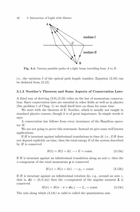
42 3 Interaction of Light with Matter
Fig. 3.4. Various possible paths of a light beam travelling from A to B
i.e., the variation δ of the optical path length vanishes. Equation (3.10) canbe deduced from (3.12).
3.1.3 Noether’s Theorem and Some Aspects of Conservation Laws
A third way of deriving (3.9),(3.10) relies on the law of momentum conserva-tion. Since conservation laws are essential in other fields as well as in physics(See problem 1 of Chap. 1) we shall dwell here on them for some time.
We start with the theorem of E. Noether, which is usually not taught instandard physics courses, though it is of great importance. In simple words itsays:
A conservation law follows from every invariance of the Hamilton opera-tor H .
We are not going to prove this statement. Instead we give some well knownapplications.
If H is invariant against infinitesimal translations in time dt, i.e., if H doesnot depend explicitly on time, then the total energy E of the system describedby H is conserved
H(t) = H(t+ dt) −→ E = const. (3.13a)
If H is invariant against an infinitesimal translation along an axis x, then thex-component of the total momentum p is conserved
H(x) = H(x+ dx) −→ px = const. (3.13b)
If H is invariant against an infinitesimal rotation dφ, e.g., around an axis z,that is, dφ = (0, 0, dφ) then the z-component of the angular moment L isconserved
H(r) = H(r − r × dφz) −→ Lz = const. (3.13c)
The axis along which (3.13c) is valid is called the quantization axis.

3.1 Macroscopic Aspects for Solids 43
For the problem of light reflection and refraction at an interface, (3.13a)is still valid, resulting in energy conservation which we used, e.g., in con-nection with (3.9). Concerning (3.13b) the problem is only invariant againstinfinitesimal translation parallel to the interface. Correspondingly only themomentum parallel to this interface is conserved. We learned with (2.58) thatthe momentum of photons (and of all other free particles) is k. Consequentlyat the interface the conservation laws must be fufilled.
ki‖ = kr‖ , (3.14a)
ki‖ = ktr‖ . (3.14b)
Since incident and reflected beams propagate in the same medium, the lengthsof the wave vectors are equal, too.
|ki| = |kr| , (3.15)
The only solution for (3.14a) and (3.15) is then obviously the law of reflection(3.10). For the relation of ki and kt we find accordingly in addition to (3.15)
kj = kvacnj =ω
cnj ; j = I, II. (3.16)
The simultaneous solution of (3.15) and of (3.16) gives just (3.10c).When we describe damping by a complex wave vector (2.36),(2.37) then
the above conservation laws applied to the real, i.e., oscillatory parts of k. Forclarity, the situation is depicted (again) in Fig. 3.5.
The conservation law (3.13c) still holds for a quantization axis perpendic-ular to the interface.
Fig. 3.5. The momenta k of incident, reflected and refracted beams at an interface

44 3 Interaction of Light with Matter
3.1.4 Reflection and Transmission at an Interfaceand Fresnel’s Formulae
Continuing to exploit the boundary conditions (3.6),(3.7) we give now theresults for the transmission t and the reflection r of an interface for the sim-plifying assumption that both media are transparent. This means that theimaginary part κ of the complex index of refraction n is negligible, i.e., muchsmaller than the real part n. This is the case of weak absorption.
|κ| |n| 1 weak absorption, |κ| |n| 1 strong absorption. (3.17)
The resulting equations are known as the Fresnel formulae for the regimeof weak absorption. They read, according to [76P1,77B1,87H1,97L1] (as usualour treatment is for non-magnetic materials)
r⊥ =nIcosαi − nIIcosαtr
nIcosαi + nIIcosαtr= − sin(αi − αtr)
sin(αi + αtr), (3.18a)
r‖ =−nIIcosαi + nIcosαtr
nIcosαtr + nIIcosαi= − tan(αi − αtr)
tan(αi + αtr), (3.18b)
t⊥ =2nIcosαi
nIcosαi + nIIcosαtr=
2sinαtrcosαi
sin(αi + αtr)(3.18c)
t‖ =2nIcosαi
nIcosαtr + nIIcosαi=
2sinαtrcosαi
sin(αi + αtr)cos(αi − αtr). (3.18d)
The relation between αi and αtr according to (3.10c) is used to progressfrom one set of formula to the other. The signs in (3.18) depend on the wayin which we defined the field amplitudes in Fig. 3.1. However it is obviousfrom (3.18a,b), that there is for normal incidence (αi = 0) a phase shift of 0or of π between the incident and reflected field for reflection at the opticallythinner or thicker medium, respectively, i.e.,
r‖,⊥(αi = 0) =nI − nII
nI + nII; t‖,⊥(αi = 0) =
2nI
nI + nII. (3.18e)
These signs are, however, not a serious problem since it is usually not possibleto measure directly the field amplitudes in the optical regime but only theintensities I = 〈S〉.[See (2.21),(2.22)]
We display in Fig. 3.6 formulae (3.18) graphically and the phase shiftbetween the various reflected components, assuming that the incident onesare “in phase”. Furthermore we show the results for strong absorption notcovered by (3.18).
The experimentally accessible quantities are R and T which can be calcu-lated from (2.22),(3.2).
We discuss first the reflectivity R. For the orientation R⊥, R increasesmonotonically with αi. The limiting values for αi = 0 and αi = 90 are givenin (3.19).

3.1 Macroscopic Aspects for Solids 45
Fig. 3.6. The reflection coefficient r for the (electric) field amplitudes according to(3.18) and the phase difference between the reflected amplitudes for the orientationsr⊥ and r‖, and reflection at an optically thicker (a) and thinner (b) medium andfor reflection at a strongly absorbing medium (c). According to [76P1]
For weak absorption (n κ)
R(αi = 0) =(nII − nI
nII + nI
)2
(3.19a)
For nI = 1 the answer, again for weak absorption, is
R(αi = 0) =(nII − 1nII + 1
)2
; (3.19b)
and for strong absorption and nI = 1
R(αi = 0) =(nII − 1)2 + κ2
II
(nII + 1)2 + κ2II
, (3.19c)
while for grazing incidence
R(αi = 90o) = 1 (3.19d)
in all cases.R⊥ increases monotonically with increasing αi in all cases. In contrast R‖
goes through a minimum at a certain angle αB with
R‖(α = αB) = 0 (3.20)

46 3 Interaction of Light with Matter
for the case of weak absorption. The angle αB is known as Brewster’s angleor the polarization angle. For α = αB only the component polarized perpen-dicularly to the plane of incidence is reflected. So this angle can be used topolarize light, if unpolarized light is directed to the interface. Note that thetransmitted beam is not strictly polarized, but has only some preference forthe orientation parallel to the plane of incidence.
The condition which comes from (3.18b) for r‖ = 0 is
nIIcosαi = nIcosαtr or tan(αi + αtr) = ∞. (3.21)
Equation (3.21) has, apart from the trivial solution (no interface → nI = nII;αi = αtr), the solution
αi + αtr = 90o , (3.22)
i.e., the reflected and refracted beams propagate perpendicularly to each other.This fact can be easily understood. As we shall see in Chap. 4 the reflectedbeam is radiated from the forced oscillations of the atoms close to the surfacewhich forms the optically thicker medium (assuming for the moment thatmedium I is vacuum). Since dipoles do not radiate in the direction of their axis,and since the polarization in the medium is perpendicular to ktr (transversewave) we find directly (3.22).
For the case nII < nI we also find the critical angle αc for total internalreflection in Fig. 3.6b which we mentioned already earlier.
If we send light on the interface polarized differently than E‖ or E⊥ tothe plane of incidence, we can decompose it always into two components withthe above orientations, we calculate their reflected or transmitted amplitudeswith (3.18) or Fig. 3.6 and superpose them again, taking into account therelative phase shifts given in Fig. 3.6. In the general case of a phase shiftdifferent from 0o or 180o the reflected light will be elliptically polarized fora linearly polarized incident beam. However, in experimental investigationsof the optical properties of semiconductors, one tries to avoid this additionalcomplication, usually by choosing the simplest geometries.
For strong absorption,R does not reach zero for any polarization (Fig. 3.6c),and starts already for αi = 0 rather close to one. This leads to a statementwhich may seem contradictory in itself at first glance: strongly absorbing ma-terials absorb only a small fraction of the incident light. The solution is clear,since the bigger fraction is reflected. The smaller fraction which actually entersthe medium is absorbed however over a short distance. In a weakly absorbingmedium, the major portion of the light is transmitted through the surface andmay be completely absorbed if the medium is thick enough. Indian ink is inthe sense of (3.17) a weakly absorbing medium, metals are strongly absorbingover wide spectral ranges and have R close to unity.
With increasing αi, R⊥ increases monotonically while R‖ goes througha shallow minimum as seen in Fig. 3.6c. The principle angle of incidence αp
is defined by some authors as the αi for which the slopes of the curves R‖(αi)and R⊥(αi) are equal. Other authors prefer to use the minimum of R⊥ as
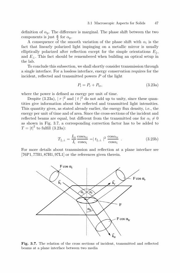
3.1 Macroscopic Aspects for Solids 47
definition of αp. The difference is marginal. The phase shift between the twocomponents is just π
2 for αp.A consequence of the smooth variation of the phase shift with αi is the
fact that linearly polarized light impinging on a metallic mirror is usuallyelliptically polarized after reflection except for the simple orientations E‖,and E⊥. This fact should be remembered when building an optical setup inthe lab.
To conclude this subsection, we shall shortly consider transmission througha single interface. For a lossless interface, energy conservation requires for theincident, reflected and transmitted powers P of the light
Pi = Pr + Ptr, (3.23a)
where the power is defined as energy per unit of time.Despite (3.23a), | r |2 and | t |2 do not add up to unity, since these quan-
tities give information about the reflected and transmitted light intensities.This quantity gives, as stated already earlier, the energy flux density, i.e., theenergy per unit of time and of area. Since the cross-sections of the incident andreflected beams are equal, but different from the transmitted one for αi = 0as shown in Fig. 3.7, a corresponding correction factor has to be added toT = |t|2 to fulfill (3.23a):
T‖,⊥ =ItrIi
cosαtr
cosαi=| t‖,⊥ |2 cosαtr
cosαi. (3.23b)
For more details about transmission and reflection at a plane interface see[76P1,77B1,87H1,97L1] or the references given therein.
Fig. 3.7. The relation of the cross sections of incident, transmitted and reflectedbeams at a plane interface between two media

48 3 Interaction of Light with Matter
3.1.5 Extinction and Absorption of Light
Until now we have considered mainly what happens in the immediate sur-roundings of a plane interface between two media. Now we shall spend a fewminutes on the propagation of a beam within a medium, continuing the dis-cussion in Sect. 2.3 in connection with (2.37).
If light propagates in a medium other than vacuum, its intensity or field am-plitude decreases in most cases with increasing distance, even if we (un-physic-ally) assume a strictly parallel beam and neglect all diffraction losses connectedwith its finite diameter. In reality, both assumptions above can be fulfilled onlyto a good approximation but never in a strict, mathematical sense. The decayis usually exponential with increasing distance d [See (2.37)–(2.40)].
I = I0e−α(ω)d . (3.24)
If energy is pumped into a suitable material and in a suitable way α(ω)may even become negative for a certain range of frequencies and consequentlylight is amplified. We call these materials active, laser or inverted materialsin contrast to passive materials with α ≥ 0.
The attenuation of light according to (3.24) is called “extinction”. It com-prises two groups of phenomena:
αextinction(ω) = αabsorption(ω) + αscattering(ω) (3.25)
Extinction is the more comprehensive term. It enters in the damping γ inChap. 4 or in the phase relaxation time T2 discussed in more detail in Chap. 23via γ = 2T2
−1 and contains two contributions. Absorption is the transfor-mation of the energy of the light field into other forms of energy like heat,chemical energy or electromagnetic radiation which is not coherent and gener-ally also frequency shifted with respect to the incident beam. This latter phe-nomenon is usually called (photo-) luminescence. The other contribution toextinction is attenuation by (coherent) scattering of light. The unshifted com-ponent is called Rayleigh Scattering and requires some disorder in the medium.We come back to this phenomenon in Chap. 23. The frequency shifted (co-herent) parts are known as Raman- or Brillouin Scattering. See Chap. 11 forthese effects or [75C1]. If the scattering particles do not show absorption inthe visible and have typical sizes large compared to the wavelength of thelight λ, the material usually looks white. Examples are the powder of ZnO(just to start with a semiconductor), ground sugar and salt, clouds, snow, thefoam of beer, milky quartz or the bark of a birch tree. The reason is thatthe scattering of light at the interfaces by reflection and refraction is roughlywavelength independent and thus the same for all colors.
If the particles are small compared to λ, the scattering at these particlesbecomes wavelength dependent. Often one finds an ω4 law
IscatterIincident
∝ ω4 (3.26)

3.1 Macroscopic Aspects for Solids 49
This relation follows from a combination of (2.26) and (2.22). It explainsthat the sunlight propagating through clear atmosphere preferentially loosesthe high frequencies, i.e., short wavelength or blue parts of its spectrum byscattering from N2, O2 and other molecules of the atmosphere. Consequentlythe sun itself looks yellow to red depending on the thickness of air throughwhich the sunlight has to travel and the sky appears blue from the scatteredlight. The above mentioned disorder necessary for this type of Rayleigh scat-tering comes from density fluctuations of the particles constituting the airwithin the coherence volume of (sun-) light. For more details of light scatter-ing, including particles with sizes comparable to the wavelength (the so-calledMie-scattering) see e.g. [77B1,87H1,97L1].
If the scattering or absorbing particles are diluted and do not interact witheach other, one finds proportionality between their concentration np and α
α(ω) = npαs(ω), (3.27)
where αs is the specific extinction constant. Equation (3.27) is also known asBeer’s law. Sometimes not the proportionality between α and np is denotedas Beer’s or Lambert–Beer’s law, but the exponential dependence of the lightintensity on the distance (3.24).
Though there is evidently a rather clear definition of the terms “extinction”and “absorption”, one uses often in “every day” language in the lab and alsoin many books including this one the word absorption instead of extinction,sometimes for convenience, and sometimes because it is not always clear whichgroup of phenomena is responsible for the attenuation of a light beam alongits path through matter.
3.1.6 Transmission Through a Slab of Matterand Fabry Perot Modes
We discuss now in connection with Figs. 3.8 and 3.9 the transmission andreflection of a plane-parallel slab of matter of geometrical thickness d withideal, lossless surfaces. The surrounding material I is air or vacuum (nI = 1,κI = 0). The total transmission T or reflection R does not only depend onmaterial II and on the angle αi but also on the properties of the incidentlight field, e.g., on its polarization and on its coherence length lc, i.e., thedistance over which there is a fixed phase-relation. We can discuss here onlysome limiting cases. See also e.g. [76P1, 77B1, 85C1, 87H1, 97L1] or [82L1] ofChap. 1, especially Vol. 17a p 11.
For strong absorption in the sense discussed in connection with (3.18) itis easily possible to detect the beam reflected from the front surface. Thetransmitted beam is strongly attenuated for d λ 0.5µm in the vis-ible part of the spectrum, i.e., for an optical density α(ω)d 1. Conse-quently R reduces to R given for normal incidence by (3.19c). T is difficultto measure since sufficiently thin samples are often not easily available and

50 3 Interaction of Light with Matter
Fig. 3.8. Multiple reflection of an incident light beam in a plane-parallel slab ofmatter
sometimes have optical properties different from the bulk material. Similarstatements for R are true for α(ω)d 1 even if α(ω) is small. This can beexpressed by
R(ω) = R(ω) for α(ω)d 1 . (3.28)
The most convenient regime in which to measure α(ω) is 1 α(ω)d 5. Thereflection has to be taken into account only once at the front and rear surfacessince multiply reflected beams are very weak due to the absorption. We findwith Fig. 3.8
T (ω) =[1 −RI→II(ω, αi)
]exp
[−α(ω)dcos−1αtr
]× [
1 −RII→I(ω, αtr)]. (3.29a)
This simplifies for normal incidence to (3.29b) bearing in mind that RI→II =RII→I = R(ω) for weakly absorbing material (See (3.19a)).
T (ω) [1 −R(ω)]2 e−α(ω)d. (3.29b)
For the conditions of (3.28) we can write
R(ω) R(ω) +[1 −R(ω)2
]R(ω)e−2α(ω)d R(ω) . (3.29c)
For materials with an optical density α(ω)d ≤ 1 things become more com-plicated again, because we must consider multiple reflection. The behaviordepends strongly on the relation of the optical pathlength and the coherence

3.1 Macroscopic Aspects for Solids 51
Fig. 3.9. Transmission T (b, d) through and reflection R (a, c) from a Fabry–Perotresonator as a function of the phase shift δ for one half round trip for various valuesof the reflectivity R of a single surface or the optical density αd of the medium inthe resonator
length lc of the light beam. For dl−1c 1 we have to add intensities resulting
in (in this case, for normal incidence)
T (ω) [1 −R(ω)]2 e−α(ω)d
1 −R2(ω)e−2α(ω)d [1 −R(ω)]2 e−α(ω)d for αd 1. (3.29d)
For long coherence lengths, the field amplitudes interfere with approriatephases and the two plane-parallel interfaces form a Fabry–Perot resonator.There are two limiting cases: in one case all partial waves reflected at thetwo surfaces interfere constructively in the resonator. This condition is ful-filled if an integer number m of half waves fits in the resonator, expressedmathematically as
λm =d2n(ω)m
or ωm =mπc
dn(ωm)or km = m
π
dwith m = 1, 2, 3 . . . . (3.30)
In this case we have a large field amplitude in the resonator which maysurpass even the amplitude of the incident beam, a total transmission Tclose to unity and correspondingly a weak total reflection R (even if Ris close to unity!). In the opposite case of mainly destructive interferenceof the partial waves in the resonator, we find just the opposite situation,

52 3 Interaction of Light with Matter
that is, R ≤ 1; T 1. Such a device is called etalon or Fabry–Perot res-onator (or FP resonator). Sometimes the two names Fabry and Perot areinterchanged.
The general formula for the FP resonator reads approximately [85C1]
T =A
1 + F sin2 δ, R =
B + F sin2 δ
1 + F sin2 δ(3.31a)
withF =
4Rα
(1 −Rα)2,
A =e−αd(1 −RF)(1 −RB)
(1 −Rα)2,
B =RF(1 −Rα/RF)
(1 −Rα)2,
(3.31b)
RF: reflectivity of front surface of the Fabry–Perot resonator;RB: reflectivity of back surface of the Fabry–Perot resonator;Rα = (RFRB)1/2e−αd; δ = n(ω)kvacd = n(ω)ωd/c.
One often has RF = RB = R. For this condition and αd = 0 one has thesimplification A = 1, B = 1.
For a lossless medium α = 0, and normal incidence these expressionsreduce to 1
T =1
1 + F ′ sin2 δ, (3.32a)
R =F ′ sin2 δ
1 + F ′sin2δ= 1 − T . (3.32b)
with the phase shift δ given in (3.31) and the finesse F ′ given by
F ′ =4R
(1 −R)2. (3.32c)
In Fig. 3.9 we show T and R as a function of δ for various values of Rand αd. For vanishing damping T (ω) reaches unity and R(ω) zero for the con-ditions of (3.32). Increasing F ′ makes the FP resonances narrower. T and Ralways add up to unity. For finite damping or α this is no longer the case. T re-mains below unity and the height of the resonance decreases with decreasingF ′, i.e., increasing α for constant values of R. Sometimes lossless, high finesseFabry–Perot etalons are used as high resolution monochromators. In this casenot only the width of the resonance is of importance, but also the spectraldistance between the resonances, the so-called free spectral range given byδ = π. A more detailed treatment of the Fabry–Perot and of related problemslike dielectric single and multilayer coatings is beyond the scope of this bookand [76P1, 77B1, 85C1, 87H1, 89T1, 97L1] are suggested for further reading.We shall come back to Fabry–Perot resonator including oblique incidence inChap. 17.

3.1 Macroscopic Aspects for Solids 53
3.1.7 Birefringence and Dichroism
Until now we have assumed, for the sake of simplicity, that our sample isisotropic, i.e., that ε(ω) is a scalar function and that means with (2.20),(2.21)and (2.27) that D and E as well as S and Π are parallel. Later on we shallin general use this assumption again. Here we want to have a short look atwhat happens if we have an anisotropic material. Indeed, many crystals areanisotropic, including the hexagonal wurtzite structure of several semiconduc-tors. Even cubic crystals can show a weak anisotropy for a finite wave vectork = 0 since cubic symmetry is lower in symmetry than spherical symmetry,see also [96T1] and Chap. 26. This latter aspect will not be considered for themoment. In the mechanical model which we shall treat in Chap. 4, we canalready understand such anisotropies if we assume that some oscillators canbe excited (i.e., elongated) only in one direction, e.g., in the x-direction butnot in the others. Such an oscillator would react only on the component ofan incident electric field polarized E ‖ x. In the microscopic model the sameapproach means that the oscillator strength f introduced also in Chap. 4 de-pends on the direction of polarization and is, e.g., finite for light polarizedparallel to a crystallographic axis and zero perpendicular to it. Indeed it isalready sufficient that the oscillator strength is different for different orienta-tions of the polarization with respect to the crystallographic axis in order toobtain birefringence.
To describe such situations it is necessary to remember that the dielectricfunction ε(ω) is generally a tensor. It describes the connection between thetwo vectors D and E.
Di = ε0∑
j
εijEj ; i, j = x, y, z (3.33)
In principle the ε-tensor has nine components. It can be shown ( [77B1,83K1, 87H1, 97L1] and [74B1] of Chap. 1) that the conservation law for theelectromagnetic field energy requires εij = εji so we are left with a maximumof six independent components. Furthermore, it can be shown that every sym-metric 3 × 3 tensor can be brought into diagonal form by a suitable rotationof the cartesian coordinate system. If we choose this coordinate system, theεij = 0 for i = j and we are left with the three elements on the main diago-nal εxx, εyy, εzz, which are all different in the general case, i.e., for so-calledbiaxial crystals (see below).
Usually one tries to align the cartesian coodinates for ε(ω) in a simple waywith respect to the crystallographic axes. In uniaxial systems one identifiesthe z-axis with the crystallographic c-axis and the x-y plane with the (usuallyalmost isotropic) plane perpendicular to c.
If transformed on these main axes, the tensor ε(ω) has therefore in themain diagonal two equal elements
εxx(ω) = εyy(ω) = εzz(ω) (3.34a)
and zeros otherwise.

54 3 Interaction of Light with Matter
For biaxial systems of even lower symmetry, such simple connections areoften no longer possible and one finds
εxx(ω) = εyy(ω) = εzz(ω) = εxx(ω) . (3.34b)
For cubic crystals one finds for k = 0: εxx(ω) = εyy(ω) = εzz(ω). Thissituation allows us to treat ε(ω) as a scalar quantity. For k = 0 birefringenceand dichroism (though weak) may appear for certain orientations as alreadymentioned [96T1].
Since all of the important semiconductors crystallize either in cubic sys-tems (diamond structure with point-group Oh, zincblende structure Td orhexagonal ones (wurtzite structure C6v)) we will not go below uniaxial sym-metry and refer the reader for these problems to books on crystal optics[76P1,77B1,84A1,97L1] or on crystallography [83K1]. The meaning of “pointgroups” will be explained Chap. 26.
The consequences of the tensor character of ε(ω) are birefringence anddichroism. We briefly outline both effects below. Dichroism means literallythat a crystal has two different colors depending on the direction of obser-vation. In a more general sense one describes with the word dichroism ev-ery dependence of the absorption spectra on the direction of polarization. InFig. 3.10 we show schematically transmission spectra for a dichroitic, uniaxialmaterial of a certain thickness. The sample is transparent for both polariza-tions below ω1. The resonance at ω1 is assumed to couple more stronglyto the light field (i.e., to have larger “oscillator strength”) for the orientationE ⊥ c than for E ‖ c. Above ω2 light is absorbed almost completely for bothorientations. The dichroitic region obviously lies between ω1 and ω2.
In some materials this region covers a wide spectral range, in some casesthe whole visible part of the spectrum. In such a case this material can be usedas a polarizer. As an example polaroid films contain long organic moleculeswhich are oriented parallel to each other by the stretching of the film duringthe manufacturing process. These molecules absorb radiation polarized paral-lel to the chain, and transmit for the perpendicular orientation over most ofthe visible spectrum. Another material which is known for its dichroism aresome colored varieties of tourmaline. In many semiconductors the dichroiticspectral range is rather narrow and amounts often only to a few tens of meV.These materials are, of course, of no use as commercial polarizers, but theinvestigation of the dichroism gives very important information on the sym-metries and selection rules of the resonances. We will see some examples ofthis effect in Chap. 13.
If we assume that the eigenfrequencies and/or oscillator strengths of someresonance(s) depend on polarization, then we know immediately from theKramers-Kronig relations, presented in Chap. 6, that the real part of the re-fractive index n(ω) depends also on the orientation of E relative to c, i.e.,the material is birefringent. We can even state that every dichroitic mate-rial must show birefringence and that birefringent material must have somespectral range in which dichroism occurs. For uniaxial materials (e.g., crystals

3.1 Macroscopic Aspects for Solids 55
with uniaxial symmetry C6v or as a prototype calcite with point group D3d)an incident light beam can always be decomposed into two components of theelectric field polarized parallel and perpendicular to the main section. Themain section is the plane defined by the crystallographic axis and the incidentwave vector. The beam polarized perpendicular to the main section is calledthe ordinary (o) beam. Its refraction is described by Snells’ law and the re-fractive index n(ω) is independent of orientation. This fact can be understoodsince the ordinary beam is always polarized perpendicular to the c-axis and weassume that uniaxial materials are isotropic in the plane ⊥ c. This is strictlycorrect only for vanishing wave vectors (and corresponds just to the situationfor the dipole approximation in Sect. 3.2.2 and to a very good approximationfor small but finite k values. The so-called extraordinary beam (eo), the po-larization of which falls in the main section, has components E ‖ c and E ⊥ cthe weights of which depend on the angle γ = ∠(k, c). It is not surprisingthat the refractive index experienced by the extraordinary beam depends anγ, since the relative coupling to the oscillators active for the orientations ‖ cor ⊥ c changes with γ. For a general direction of incidence an unpolarized(or elliptically polarized) beam will be decomposed into two beams polarizedperpendicular to each other – the ordinary and the extraordinary ones - whichwill be separated in space, as shown schematically in Fig. 3.11. This is theconcept, which allows us to use birefringent materials as polarizers. We notehere already that the wave vector k and the Poynting vector S of the eobeam are not necessarily parallel to each other. The reason will be given inconnection with Fig. 3.13. In the case of Fig. 3.11 the refractive index of the
Fig. 3.10. Schematic drawing of the transmission spectra of a dichroitic materialfor two different polarizations of light with respect to the crystallographic axis

56 3 Interaction of Light with Matter
Fig. 3.11. Birefringence for an unpolarized beam falling on a birefringent materialat a given angle with the crystallographic axis c parallel to the interface
ordinary beam is greater than that of the extraordinary one. This situation iscalled negative-uniaxial birefringence, the opposite situation corrrespondinglypositive-uniaxial birefringence, since ∆n is defined as
∆n := neo − no (3.34c)
where the indices o and eo stand for ordinary and extraordinary.There are two limiting orientations which result in rather clear and simple
situations. Therefore these orientations are usually investigated in semicon-ductor optics. One situation is k ‖ c. In this case the E field can be onlyperpendicular to c, this means one observes the ordinary beam only, indepen-dent of the polarization of the incident beam. The other clear orientation isk ⊥ c. In this case one can choose by a polarizer the orientation E ⊥ c for theordinary beam or E ‖ c for the extraordinary beam. In the latter situation,the E field acts only on oscillators which can be elongated parallel to c.
Oblique incidence on a surface cut parallel or perpendicular to c or normalincidence on a surface cut under an arbitrary angle (Fig. 3.12) with respect toc are much more complicated to evaluate concerning the spectra of reflectionor transmission. The worst situation is, of course, oblique incidence on a planeat an arbitrary angle to the c-axis. Scientists working on semiconductor opticsusually try to avoid these situations, scientists devoting their work to crystaloptics find it challenging and even prefer biaxial systems to others.
A situation which allows us to discuss various aspects of birefringence isperpendicualr incidence on a plane at an oblique angle with respect to c. Weshall dwell a few minutes on this topic.
The experimental result is shown in Fig. 3.12. The incident beam is splitinto two when entering the birefringent material. The ordinary beam contin-ues to propagate normal to the surface as expected from Snells’ law (3.10b)

3.1 Macroscopic Aspects for Solids 57
Fig. 3.12. Same as Fig. 3.11 but for normal incidence on a surface cut under anarbitrary angle with respect to c
or from the conservation of momentum parallel to the surface (3.14). Theextraordinary one seems to violate these two rules. Since a violation of thelaw of momentum conservation would be very serious, not only for physics,we have to look more closely at this problem.
There are two rather simple ways to present birefringence. One, which weshall outline towards the end of this subsection is in terms of the indicatrix. Inthe other method, one uses in polar coordinates a plot which gives the phasevelocity vph = cn−1(ω). This is basically the inverse of the real part of n(ω)as a function of the direction of propagation. In a uniaxial system, the figuresproduced when we include all directions are a sphere for the ordinary beamand a figure with rotational symmetry with respect to c for the extraordinaryone. They touch for propagation of light parallel to the crystallographic axisas shown in Fig. 3.13 since there are only o-waves for this orientation, asmentioned above. Now recall Huygens’ principle for the propagation of lightwhich says that every point illuminated by an incident primary wave frontbecomes the source of a secondary wavelet such that the primary wavefrontat a later time results from the superposition of the amplitudes of all wavelets.In addition, we must discard the back-travelling waves in the way shown byFresnel and Kirchhoff which would appear otherwise from the above givenprinciple. With this amendment we can construct wavefronts when we identifythe shape of the wavelets with Fig. 3.13. For more details see e.g. [83K1,96T1,02T1] and references given therein.
Shown in Fig. 3.12 are the S,Π ,k,E and D vectors. The vectors k and Πare always parallel to each other. The magnetic vectors B and H are parallelto each other and normal to the electric vectors and are, in this context, ofno further interest since we are dealing with nonmagnetic material.
In Fig. 3.14a the situation is shown for the o-beam. The wavelets arespheres, the resulting wave front is parallel to the vacuum-medium inter-face. The vectors of energy-flux density S = E × H, of momentum density

58 3 Interaction of Light with Matter
Fig. 3.13. The phase velocity of light in an optically uniaxial material shown forone frequency ω in polar coordinates for positive (a) and negative (b) birefringencefor the ordinary (o) and extraordinary (eo) beams
Π = D × B and the wavevector k (= momentum k) are parallel. (Diffrac-tion effects caused by the finite beam diameter are neglected here, thoughthey are obviously also described by Huygens’ principle.) The situation forthe eo-beam is presented in Fig. 3.14b. The wave front produced by the su-perposition (or interference) of the wavelets, and constructed as the tangent tothe wavelets, is still parallel to the interface. This wave front describes the Dfield because we know from Maxwell’s equations and the boundary conditionsof Sect. 3.1.1 that the boundary condition for D is that the normal compo-nent Dn is continuous over the interface. In our case, Dn = 0 on both sides.As a consequence, the classical momentum density Π and the momentum kof the light quanta are still perpendicular to the interface, as required by theconservation of the momentum component parallel to the interface, which ishere obviously zero.
On the other hand, we can see that the whole wave front is shifting side-ways with continuing propagation into the medium. This shift is described bythe Poynting vector S = E × H. The direction of this vector is just given bythe origin of the wavelet and the point where the tangent touches it. The Efield is necessarily perpendicular to S. As required by the boundary conditionfor E as deduced from Maxwell’s equations, the tangential component Et,must be the same on both sides of the interface (including incident, refractedand reflected beams). The normal component of E can change, and that iswhat happens in the orientation of Fig. 3.14b. To summarize, we observe thatthere are no violations of any conservation laws. The tangential componentsof the momentum are conserved at the interface and for this quantity Snells’law is still valid. However, the direction of energy propagation given by Schanges, but there are no conservation laws for this direction. The law of en-ergy conservation itself has, of course, to be fulfilled, this means in this case

3.1 Macroscopic Aspects for Solids 59
Fig. 3.14. The construction of the wave fronts of the ordinary (a, c) and theextraordinary (b, d) beams for various geometries using Fig. 3.13
that the total amount of energy falling per unit time on the interface equalsthe sum of transmitted and reflected energies.
Figures 3.14c and d finally shows schematically the general situation i.e.,oblique incidence on a surface cut at an arbitrary angle with respect to c.The construction simply uses the size of the wavelets around point A whenthe incident wave front just reaches the interface at point B. We see that therefractive index for k is different for both polarisations and that the directionsof ktr and Str differ for the eo beam.
The basic idea of the representation of birefringence by the indicatrix isexplained in connection with Fig. 3.15. We plot from the origin lines in alldirections with a length equal to the refractive index n(ω) of a wave with Dpolarized in this direction. In doing so, we get a sphere for an isotropic material(Fig. 3.15a) and ellipsoids with rotational symmetry for uniaxial materials. InFigs. 3.15b and c we show the situation for positively and negatively birefrigentuniaxial crystals, respectively. The rotation axis coincides in this case with thecrystallographic c-axis.

60 3 Interaction of Light with Matter
Fig. 3.15. The indicatrix for isotropic (a) uniaxial (b, c) and biaxial materials (d)according to [83K1,87H1]
For crystals of even lower symmetry, all three axes of the indicatrix have dif-ferent lenghts (Fig. 3.15d) in agreement with the situation for ε(ω) in (3.34b).
The use of the indicatrix is now the following: For a given direction of prop-agation k one cuts the indicatrix with a plane normal to k which contains theorigin. In general, this cross section is an ellipse except for isotropic materials.The distance from the origin to this ellipse in a certain direction gives the re-fractive index of a beam with D polarized in this direction and propagating inthe direction of k. The optical axes are for anisotropic materials (Figs. 3.15b–d) now defined as those directions of propagation for which the cross sectionof the indicatrix is a circle. For the uniaxial materials in Figs. 3.15b and cthere is obviously only one optical axis, which coincides with the c-axis asstated already above. For systems of lower symmetry, where all three mainaxes of the indicatrix (and all three εii(ω), i = x, y, z of the dielectric tensor)are different, one finds two optical axes, which generally do not coincide withany of the cartesian coordinates (Fig. 3.15d) and the direction of which caneven vary with ω.
It should be mentioned that birefringence can be created in non-birefringentmaterials, e.g., by the application of electric- or strain-fields. These phenomenaare known as Pockels and Kerr effect and as mechanical or stress birefringenceor “photoelasticity”, respectively. The Pockels effect occurs in crystals with-out centers of inversion and the effects vary proportially with E. The Kerreffect occurs in isotropic solids like glass, in fluids like nitrobenzol and variestherefore proportionally with E2. While these effects are often deliberatelyinvestigated, especially the last ones can produce unwanted, spurious effectsif a sample is not mounted strain-free, e.g., in a cryostat.
All the phenomena of birefringence which we discussed here for a uniaxialmaterial are as mentioned at the beginning of this subsection, simply due

3.2 Microscopic Aspects 61
to the fact that the dielectric function ε(ω) is a tensor for crystallographicsystems of symmetry lower than cubic and that D and E need thereforeno longer be parallel to each other. More information on the topic of thissubsection is found in [75C1,76P1,77B1,83K1,84A1,87H1,96T1,97L1,02T1]and references therein.
3.1.8 Optical Activity
The last aspect we want to mention in this first subchapter on macroscopicoptical properties is optical activity. In this case a linearly polarized lightbeam remains linearly polarized when propagating through an optically activemedium but the direction of polarization rotates slowly by an amount δrot thatvaries with increasing distance l, which is the distance the light travels throughthe medium, i.e.
δrot = al (3.35)
where a depends on the material and on ω.While a birefringent material splits an incident beam in two, orthogonally
polarized ones, which propagate with different phase velocities through thesample and thus accumulate a phase shift with increasing distance (see prob-lem 8 in Sect. 3.3). An optically active material splits a linearly polarizedincident beam into a left (σ−) and right (σ+) circularly polarized one withequal amplitude. Again both components travel with different phase veloci-ties. A superposition after a certain distance results again in linearly polarizedlight as long as there is no difference in the absorption for σ+ and σ− polarizedlight, but with a tilted direction of polarization.
This phenomenon already occurs in amorphous solids including liquidsand gases if they contain molecules with a well defined chirality or handinesslike dextrose or laevulose which have both the chemical composition C6H12O6.In crystalline solids, including semiconductors, optical activity occurs if eitherthe molecules in the unit cell have a chirality or if atoms or isotropic moleculesare arranged in the unit cell in such a way that a screw-axis appears. Examplesare quartz or wurtzite-type crystals parallel to their c-axes, which are bothessentially built from tetrahedrons, but are arranged in a way that a shift anda rotation along the axis transforms the crystal into itself.
The optical activity induced in a material by a magnetic field in the direc-tion of light propagation is known as the Faraday effect. In magnetic dichroismone investigates the difference in the absorption spectra for σ+ and σ− polar-ized light induced by the B-field.
3.2 Microscopic Aspects
In contrast to the preceding section, we present now the basic interactionprocesses between light and matter from a microscopic point of view. We use

62 3 Interaction of Light with Matter
here the perturbative or weak coupling approach for the interaction betweenlight and matter, which is in most cases sufficient for dilute systems such asgases. For solids the strong coupling approach is often necessary, which leadsto the concept of polaritons and which is introduced in Chap. 5. We describefirst in words the basic interaction mechanisms between light and matter,namely absorption, spontaneous and stimulated emission (Sect. 3.2.1), thenwe proceed to the treatment of linear optical properties in the framework ofperturbation theory (Sect. 3.2.2). Since these topics are also treated in manytextbooks (e.g. References [81M1,90K1,93H1,96Y1] of Chap. 1 or [55S1,71F1,73H1, 76H1, 92M1] of Chap. 2) it is not necessary to go into too much detailhere.
3.2.1 Absorption, Stimulated and Spontaneous Emission,Virtual Excitation
For simplicity we assume that we have a certain number of two-level “atoms”as shown in Fig. 3.16. Every atom has one electron which can be either in theground or in the excited state. Later we will extend the model from a two-level system to bands in semiconductors, but the basic interaction processesremain the same.
In Fig. 3.16a an incident photon hits an atom in its ground state. Witha certain probability the photon is annihilated and the electron gains enoughenergy to reach the excited state. For reasons of energy conservation, thephoton has to fulfill the condition
ω = Eex − Eg , (3.36)
where Eex−Eg is the energy difference between the ground and excited states.We call this process absorption in agreement with the definition in Sect. 3.1.5 ifthe energy of the photon is soon converted into other forms of energy, that is, ifthe electron undergoes some scattering processes, which destroy its coherenceor more precisely the coherence of the electric polarization connected with thistransition to the incident light field. See Chap. 23. The electron eventuallyreturns to its ground state and looses its energy e.g., as phonons i.e., as heator as a photon which is not coherent with the incident one.
If an incident photon hits an atom with its electron in the excited stateit can induce with a certain probability a transition of the electron from theexcited to the ground state. In this process a second photon is created whichis identical in momentum, energy, polarization and phase to the incident one.This process is called induced or stimulated emission. This process can beused to amplify a photon field. It is therefore the basic mechanism for alllasers (Light Amplification by Stimulated Emission of Radiation). Absorptionand stimulated emission are closely related events (Fig. 3.16b).
An electron in the excited state can also with a certain probability reenterthe ground state by itself, either by emitting a photon (Fig. 3.16c) or by

3.2 Microscopic Aspects 63
loosing the transition energy through phonons or collisions. In the presentcontext, the first mechanism is of interest. It is called spontaneous emissionor spontaneous radiative recombination, while the second possibility is knownas non-radiative recombination. Spontaneous emission can also be understoodin another way. In Sect. 2.5 we saw in connection with (2.54) that photonsare similar to harmonic oscillators and have consequently a zero-point energy.This zero-point energy exists for all photon modes. It cannot be absorbedbecause a harmonic oscillator does not have any states below the zero-pointenergy, but it can induce a transition in the way as discussed in connectionwith Fig. 3.16b. So we can consider spontaneous emission as a process inducedby the zero-point vibrations of the electro-magnetic field, which are also calledvacuum fluctuations (Fig. 3.16c).
The last process presented here is virtual excitation. Understanding thisphenomenon often causes some problems for students. So we develop thistopic slowly and try to explain it from various points of view in context withFig. 3.16d. Virtual excitation means the creation of a state with the samewave function as the excited state, but with an energy which is different fromthe eigenenergy of this excited state. This process becomes possible throughthe uncertainty principle of quantum mechanics which can be written in spaceand momentum coordinates.
∆xi∆pi ≥ h for i = 1, 2, 3 . (3.37a)
A similar relation exists for energy and time
∆E∆t ≈ . (3.37b)
We need here (3.37b). It says that it is possible to violate energy conserva-tion by an amount ∆E up until a maximum time ∆t which fulfills the abovecondition. Or, in other words, if we want to define the energy with a cer-tain precision ∆E, the state has to exist at least for a time ∆t. In principle(3.37b) is valid also in simple classical wave theory (e.g., acoustics) and is very
Fig. 3.16. Schematic representations of various interaction processes of light withmatter namely absorption (a), stimulated emission (b), spontaneous emission (c)and virtual excitation (d)

64 3 Interaction of Light with Matter
well known from Fourier transformations. A harmonic oscillation with centralfrequency ω which lasts only for a time ∆t, has a spectral width ∆ω given by
∆ω∆t ≥ 1 . (3.37c)
The connection between (3.37b) to (3.37c) comes simply from the relation
E = ω . (3.37d)
It should be mentioned that a similar set of arguments holds for (3.37a),too. If we send now a photon with energy ω′ to the atom, we can excite theelectron for a maximum time ∆t given by (3.37b) or for our specific case by
∆t ≈ [| (Eex − Eg) − ω′ |]−1 . (3.38)
At the latest after the time ∆t has elapsed, the excited state must col-lapse. The simplest way to collapse is to emit a photon identical to the onewhich caused the virtual excitation. This “new” photon has however a cer-tain phase delay with respect to the incident photon, because the energy wasstored for a maximum time ∆t in the atom. As a consequence, an electro-magnetic wave propagates with a lower phase-velocity through an ensembleof atoms than through vacuum. The same effect is described phenomeno-logically by the refractive index n(ω). (See (2.15) and (2.41).) So we geta first hint of how n(ω) can be understood and calculated in quantum me-chanics. Obviously ∆t increases if we approach the resonance condition in(3.38) and consequently wave propagation through a material will deviatemore strongly from that through vacuum. This is indeed the case, as we shallsee in Sect. 4.3.
If the virtually excited state emits a photon ω′ in a direction differentfrom the incident one, we have a scattering process as discussed in connectionwith (3.26). If ω′ approaches the resonance energy, this scattering process isalso known as resonance fluorescence.
In connection with this scattering, we may ask how can light propagateat all in a clear or transparent medium? The answer is that we have in densemedia many scattering atoms or centers in the coherence volume of light, in-dependent of whether it is light from an incandescent lamp, a laser or anothersource. As a consequence, every scattered wave finds another one which hasa phase difference, resulting in destructive interference. The only way that allscattered waves interfere constructively is just the usual propagating wave.The explanation for blue sky, which we gave in Sect. 3.1.5 fulfills, apart fromthe condition that the diameter of the scattering centers is small comparedto the wavelength of the scattered radiation, another condition, namely thatthere are only a few scattering centers i.e., gas molecules, density fluctuationsor other inhomogenities per coherence volume of sunlight, so that the mutuallydestructive interference of the scattered waves is not complete. For a detaileddiscussion of spatial and temporal coherence see e.g. [93S1] of Chap. 2.

3.2 Microscopic Aspects 65
If the virtually excited state disappears under simultaneous emission ofa photon and the creation or annihilation of a phonon (i.e., a quantum ofthe lattice vibrations, as in Sect. 11.1), energy conservation for the emittedphoton ωR implies
ωR = ω′ ± Ωphonon . (3.39)
This phenomenon is called Raman scattering for optical phonons, andBrillouin scattering for acoustic phonons. The “−” sign gives the Stokes andthe “+” sign the anti-Stokes emission. Similar processes are also possible withmore than one phonon or with excitations in the electronic or spin system ofthe semiconductor.
From the few phenomena outlined briefly above which involve virtual exci-tation, it is obvious that this mechanism is of some importance for the opticalproperties of matter. Therefore we want to examine it from another pointof view and outline the well-known classical analog of the virtually excitedstates. In addition this analogy gives some justification for the calculation ofthe dielectric function used in Chap. 4.
Virtual excitation in quantum mechanics corresponds to a driven or forcedoscillation in classical mechanics. If we have an oscillator of eigen frequency ω0
(corresponding to the energetic differences Eex − Eg in quantum mechanics)and if we excite it with an external frequence ω, it will oscillate with frequencyω after a short damped transient feature of oscillations with ω0. The ampli-tude of these steady oscillations increases with decreasing detuning |ω − ω0|depending on the properties of the oscillator, e.g., its damping. This increaseof the amplitude of the classical oscillator corresponds to the increase of ∆t in(3.39) in the picture of virtual excitation, and it is qualitatively understand-able that we will get the strongest deviations of ε(ω) or n(ω) from the vacuumvalue ε = n = 1 in the vicinity of the resonance ω0. We elaborate this conceptin detail in Chap. 4.
However, before doing so, we shall demonstrate how the various transitionsshown in Fig. 3.16 and some others can be treated quantitatively in quantummechanics by perturbation theory.
3.2.2 Perturbative Treatment of the Linear Interaction of Lightwith Matter
In this section we present first the Hamiltonian of the system elaborating theperturbation terms. Then we outline shortly how a perturbation causes tran-sitions between various eigenstates. Finally we join these two things togetherending with an understanding of the theoretical description of absorption andstimulated or spontaneous transitions.
The Hamiltonian of the total system consisting of the electron states inFig. 3.16 of the two level atoms (or of the bands of the semiconductor), theradiation field and the interaction of these two systems can be written as
H = Hel +Hrad +Hinterac . (3.40)

66 3 Interaction of Light with Matter
In the picture of second quantization outlined in Sect. 2.5 Hinterac containsterms which describe, e.g., the annihilation of a photon and of an electronin the ground state and the creation of an electron in the excited state forthe process shown in Fig. 3.16a, weighted with a factor which contains thetransition matrix element.
The exact solution of the total Hamiltonian leads to the polariton concept(Chap. 5) in the field of linear optics and describes among other things thechanges of the electronic states introduced by the presence of the radiation innonlinear optics for which we will see some examples in Sects. 20.1 to 20.4.
For our present purposes we follow an approach which is widely usedand which treats the radiation field as a small perturbation, that is, we as-sume that the eigenstates ϕ and the eigenenergies En of Hel, do not changemuch in the presence of the electromagnetic field, and that the eigenstatesof Hrad are the photons described already in Sect. 2.5. The approximationwhich we use now is known as the semiclassical treatment of radiation. Itconsists of replacing the canonical conjugate momentum p in the Hamiltonfunction by
p → p − eA , (3.41)
where A is the vector potential (2.48).If we replace p by its operator
p =
i∇ (3.42)
the single particle Hamiltonian reads
H =1
2m
(
i∇− eA
)2
+ V (r) (3.43)
including any electrostatic potential into V (r). Making use of the Coulombgauge (2.49) we can evaluate (3.43) to obtain
H = − 2
2m∇2 + V (r) − e
mA
i∇ +
e2
2mA2 , (3.44)
H = Hel − e
mA
i∇ +
e2
2mA2 , (3.45)
H = Hel +H(1) +H(2) . (3.46)
In (3.46) there are two perturbation terms H(1) and H(2). If we assumethat A and thus the light intensity are small, and in the regime of lin-ear optics they are small by definition, then H(1) is a perturbation termof first order and H(2) is small of second order. Consequently H(1) mustbe used in first-order perturbation theory. In the second-order approxima-tion we have to use H(1) in second-order perturbation theory and H(2) in

3.2 Microscopic Aspects 67
first-order perturbation theory, etc. We shall come back to this latter aspectin Chap. 19.
In order to arrive at Fermi’s golden rule for the transition rate wji froman initial state i (e.g., the ground state g in Fig. 3.16) to another state j (e.g.,the excited state ex in Fig. 3.16) one uses the time-dependent Schrodingerequation
Hψ = i∂ψ
∂t(3.47a)
with the stationary solutions when H = H0
ψn(r, t) = ϕn(r)e−i(En/)t . (3.47b)
For the solution in the presence of a perturbation H(1) we make the ansatz
ψ(r, t) =∑n
an(t)ϕn(r)e−i(En/)t . (3.48)
We assume that the perturbation is switched on at t = 0. Before the systemis in state i, i.e.,
ai(t) = 1an =i(t) = 0
for t ≤ 0 . (3.49)
For t > 0 the an =i(t) start to grow and under these conditions the transitionrate wij of Fermi’s golden rule becomes
wij =2π
∣∣∣H(1)ij
∣∣∣2D(E) , (3.50a)
where D(E) is the density of the final states modified by momentum conser-vation if applicable. H(1)
ij is the transition matrix element given by
H(1)ij =
∫ψ∗
j (r)H(1)ψi(r) dτ =:< ψj | H(1) | ψi > (3.50b)
For a non-degenerate two level system D(E) is simply one per atom. Thesquare of the transition matrix element |Hij |2 is known as the transition prob-ability. Later on we will assume, for simplicity of writing, that some constantfactors as the term 2π/ are incorporated in this |Hij |2. Transition proba-bilities are given apart from some coefficients by the square of the respectivetransition matrix elements of (3.50) in the case of first order perturbation andby the terms (3.51) for second order.
The transition rate wij is proportional to the transition probability mul-tiplied by the square of the amplitude of the perturbation H(1), i.e., here by|A0|2 ∼ I where I is the light intensity, i.e. as already mentioned the energyflux per unit of area and time.
68 3 Interaction of Light with Matter
If the first-order perturbation term (3.50b) vanishes, then according towhat we stated above the second-order contribution reads
w(2)ij =
2π
∣∣∣∣∣∣∑
k =i,j
H(1)jk H
(1)ki
Ei − Ek+H
(2)ij
∣∣∣∣∣∣2
D(E) . (3.51)
We restrict ourselves for the moment to the first order according to (3.50)and discuss the term H
(1)ij in some more detail for the perturbations of (3.45).
With the vector potential A
A = A0ei(kr−ωt) (3.52a)
we find, e.g., for the absorption process (3.50)
wg→ex =2π
∣∣∣∣−e
imA0 ·
∫ϕ∗
ex(r)ei(Eex/)teA ei(kr−ωt)∇ϕg(r)e−i(Eg/)tdτ
∣∣∣∣2D(Eg + ω)
∝ |A0 < ϕex|H(1) |ϕg >|2 D(Eg + ω) =:
A20 | H
(1)eg |2 D(Eg + ω) , (3.52b)
where eA is the unit vector in the direction of A. We also give in (3.52) a gen-erally used abreviation for the integral. A significant transition rate occursonly if the time dependent exponential functions vanish, or, mathematically
Eex − Eg − ω = 0 . (3.53a)
This is again the law of energy conservation. If the ϕi have plane-wave char-acter and are described by a wave vector k, a similar argument results in kconservation.
kex − kg − k = 0 (3.53b)
This is not the case for the two-level atoms discussed here but is true for mostof the eigenstates of crytalline semiconductors.
We see that the transition rate is proportional to A20, and thus to the light
intensity I = 〈S〉 or the density of photons Nph(ω) in a certain mode:
wij ∝ A20
∣∣∣H(1)eg
∣∣∣2 ∝ I∣∣∣H(1)
eg
∣∣∣2 ∝ Nph
∣∣∣H(1)eg
∣∣∣2 . (3.54)
By partial integration using the fact that the eigenfunctions form an othonor-mal set, or that the H(1) is Hermitian adjoint, or by the argument of themicroscopic reversibility of a transitions from state i → j and from j → iinduced by some perturbation H(1), we find that∣∣∣∣∫ ϕ∗
jH(1)ϕi dτ
∣∣∣∣2 =∣∣∣∣∫ ϕ∗
iH(1)ϕj dτ
∣∣∣∣2 . (3.55)
We see that the probabilities for induced emission and absorption are the sameand that the rates differ only by factors containing the number of atoms in

3.2 Microscopic Aspects 69
the upper and lower states. This fact is the basis for the relation between theEinstein coefficients. See Problem 10 in Sect. 3.3. Spontaneous emission hasto be treated in the sense mentioned above as emission stimulated by the zerofield. We return to this aspect in a moment. First the interaction operatorH(1) should be simplified to reach the so-called dipole approximation.
We note that the radius of an atom (r 0.1 nm) and the distance betweenneighboring atoms in a solid (a 0.3 nm) are small compared to the wave-length in the visible (λ 500 nm). Therefore there is practically no phaseshift of the electromagnetic radiation over one atom or between one atom andits neighbors. Thus we can expand the term eikr in (3.52) in a power seriesand stop after the constant term
eikr = 1 +ikr
1!+
ikr2
2!+ . . . 1 . (3.56)
This is the first step towards the dipole approximation. It means, that themomentum of the photon k in (3.53b) is negligible.
The matrix element H(1)ij still contains the momentum operator p =
i ∇
H(1)ij ∼ 〈ϕi |p|ϕi〉 =: 〈pi,j〉 .
With the semiclassical relation
i∇ = p = mr (3.57)
and some arguments of plausibility (See e.g. [55S1] of Chap. 2), we find that∫ϕ∗
j
i∇ϕi dτ = m
i
(Ei − Ej)∫ϕ∗
jrϕi dτ = mω
∫ϕ∗
jrϕi dτ . (3.58)
For a detailed derivation of this relation actually some knowledge of the wavefunctions is required. (For details see e.g. [55S1,85G1,92M1] of Chap. 2).
We note that in this so-called dipole approximation (3.56) to (3.59) thetransition rate is given by
wij ∼ Iω2 |eA < erij >|2D(E) = Iw2∣∣HD
ij
∣∣2D(E) . (3.59)
This result can also be obtained in a more intuitive way if we rememberthat the energy of a dipole er in an electric field E = A is given by
er · E = H(1) (3.60)
Using this approach in combination with (3.50) yields directly (3.59).From now on we will call
∣∣HDij
∣∣2 the dipole-transition probability and theoperator er the dipole operator HD.
This result can be obtained still in another way using for A a suitable gaugedifferent from the Coulomb gauge (∇ · A = 0) (see (2.49)) via A′ = A + ∇χ

70 3 Interaction of Light with Matter
and Φ′ = Φ − χ where χ is a scalar field with existing second derivative. Itcan be shown that A′ results in identical electric and magnetic fields as A.The choice χ(r, t) = iω−1rE = iω−1r · E0 exp [i(kr − ωt)] results for H(1)
directly in (3.60).Transitions using higher terms in (3.44), (3.51), (3.56) correspond to
quadrupole, octupole and higher order transitions.To conclude this section, we calculate the net rate of the transitions shown
in Fig. 3.16a–c.We assume that we have a density of photons Nph which populate only
one mode in the sense used for the calculation of the density of states inSect. 2.6 that is, all photons have the same wave vector k, polarization eA
and energy ω.Furthermore ω fulfills the energy conservation law according to (3.54).
The density of identical two-level atoms is NA where a fraction αg is in theground state and correspondingly (1 − αg) are in the excited state. The netrate of the change of Nph with time is then given using (3.54,59)
∂Nph
∂t= −NAαgNph
∣∣HDg→e
∣∣2 +NA(1 − αg)(1 +Nph)∣∣HD
g→e
∣∣2 . (3.61)
The first term on the r.h.s. describes the absorption of photons, the secondone the spontaneous and stimulated emission in the factor (1 +Nph).
From (3.55) we see that∣∣HDg→e
∣∣2 =∣∣HD
e→g
∣∣2 =∣∣HD
∣∣2 (3.62)
and hence
1
|HD|2∂Nph
∂t= Nph ·NA(1 − 2αg) +NA(1 − αg) . (3.63)
The first term on the right-hand side depends linearly on Nph and describesthe net rate of absorption and stimulated emission. The second terms givesthe spontaneous emission since it is independent of Nph.
There is net absorption for αg > 1/2 (absorption coefficient α(ω) > 0 or∂Nph/∂t < 0) and amplification or optical gain for αg < 1/2, i.e., for gain,more than half of the atoms have to be in the upper state. This situationcannot be reached in thermal equilibrium, but only under the influence ofa suitable source of pump power. Usually one or more additional energy levelsare required (three- and four-level lasers). This fact can be easily elucidatedwith the following argument. We start with a situation where all atoms arein the ground state i.e., αg(t = 0) = 1. If we send for t > 0 a photon fieldwith frequency ω fulfilling (3.52a) into the system we initially have absorptionsince α(ω) is given by
−α(ω) ∼ NA(1 − 2αg) . (3.64)
With increasing time and pump power α(ω) decreases because αg decreases.For the situation αg = 1/2 the absorption vanishes and the material becomes

3.3 Problems 71
transparent. This means no more pumping is possible under (quasi-) station-ary excitation to reach αg > 1/2. In Chaps. 21 to 23 we will reexamine theabove considerations using the proper statistics introduced in Sect. 2.6. InChaps. 23 and 27 we shall see further that without dephasing processes orfor sufficiently intense pulses shorter than the dephasing time it is possible todrive the system periodically from the ground state to the completely invertedstate (αg = 0) and back again. This process is known as Rabi flopping.
3.3 Problems
1. Consider the interface between vacuum (or air) and glass (n = 1.45) ata wavelength λvac of 0.5µm.Calculate for an angle of incidence αi = 45o the incident, reflected, andtransmitted wave vectors, and the transmitted and reflected intensitiesfor both polarizations.Calculate Brewster’s angle for the transition air→glass and glass→air andthe angle for the onset of total internal reflection.
2. Find a piece of polarizing material (polaroid) and observe the light re-flected from a nicely polished floor or scattered from the blue sky usingdifferent orientations of the light propagation and of the polarization. Donot look into the sun! Try to explain your findings.
3. Play with a piece of clear calcite and the polaroid.4. From Figs. 3.11 and 3.12 one can understand that a birefringent crystal
can be used as a polarizer if the lateral diameter of the beams is smallerthan their lateral displacement after the passage. Usually one uses slightlymore complex arrangements known as Glan-Thomson or Taylor polariz-ers. Make yourself familiar with the way of operation of these opticalcomponents. What can happen if you use them under oblique incidenceor with a di- or convergent light beam with large angle of aperture?
5. Derive the laws of reflection and refraction from the principle of Mauper-tins (see Fig. 3.4) and from momentum conservation (3.16). Does this lawalso hold if you kick a soccer ball against a wall?
6. Consider Fig. 3.9c. Explain in words why only in this diagram the threecurves intersect, i.e., why zero absorption gives both the highest maximaand the lowest minima in reflectance.
7. Verify the energy conservation law (3.23a) with the help of (3.23b) and(3.18).
8. What is a quarter (λ/4) or half (λ/2) wave plate? How thick is it? Whatis the state of polarisation of the transmitted light beam, when the in-cident beam is linearly polarized? Does it depend on the orientation ofthe incident linear polarization with respect to the crystallographic axis.Make a simple sketch. (Generally one uses a uniaxial material and normalincidence for theses devices.) What is a low order λ/4 plate? Why areachromatic λ/4 plates rather expensive?

72 3 Interaction of Light with Matter
9. Make a simple sketch tomake yourself familiarwith optical activity.Canyouimagine, that the absorption can be different for σ+ and σ− polarized light?
10. Find in a textbook the definition and meaning of Einstein’s coefficients.11. Inform yourself on time independent perturbation theory. The perturbed
wave function contains in first order virtually excited states and the per-turbed energy in second order. Inspect time dependent perturbation the-ory for virtual excitations. Derive Fermi’s golden rule.
12. Verify some of the prominent features in Fig. 3.6 with (3.18), e.g., normaland grazing incidence, αB or αtot.
References to Chap. 3
[75C1] R. Claus, L. Merten, J. Brandmuller: Light Scattering by Phonon Polari-tons, Springer Tracts, Mod. Phys. Vol. 75, Springer, Berlin, Heidelberg(1975)
[76P1] R.W. Pohl: Optik und Atomphysik, 13th edn., Springer, Berlin, Heidelberg(1976)
[77B1] M. Born, E. Wolf: Principles of Optics, Pergamon, Oxford (1977)[83K1] W. Kleber: Einfuhrung in die Kristallographie, 16th edn., VEB Verlag Tech-
nik, Berlin (1983) or more recent editions[84A1] V.M. Agranovich, V.L. Ginzburg: Crystal Optics with Spatial Dispersion
and Excitons, Springer Ser. Solid-State Sci. 42, 2nd ed., Springer, Berlin,Heidelberg (1984)
[85C1] D. Craig: et al. IEEE J. QE-21, 1363 (1985)[87H1] E. Hecht: Optics, 2nd edn., Addison-Wesley, Reading (1987)[89T1] A. Thelen: Design of Optical Interference Coatings, McGraw Hill, New York
(1989)[96T1] E. Tsitsishvili, Applied Physics A 62, 255 (1996) and Solid State Commun.
100, 541 (1996)[97L1] S.G. Lipson, H.S. Lipson, D.S. Tannhauser: Optik, Springer, Berlin (1997)[02T1] E. Tisitishvili in Ref [81A1]k of Chap. 1, p 357 (2002)

4
Ensemble of Uncoupled Oscillators
The optical properties of matter are determined by the coupling of varioustypes of oscillators in matter to the electromagnetic radiation field. In otherwords, an incident electromagnetic field will cause these oscillators to per-form driven or forced oscillations. The amplitude of these driven oscillationsdepends on the angular frequency ω of the incident field, on the eigenfre-quency ω0 of the oscillators, on the coupling strength f between electromag-netic field and oscillator, and on its damping γ. In semiconductors these oscil-lators or resonances include optical phonons, excitons including their ionisa-tion continuum and higher band-to-band transitions or plasmons. They willbe explained in some detail in Chaps. 7–10. We can anticipate that many ba-sic features of the optical properties of these resonances are similar. Thereforeit is reasonable to discuss first, in a general way, the optical properties of anensemble of model oscillators. By using the results of Chaps. 4–6 we shall ob-tain in Chaps. 11–15 a quite simple and straightforward access to the opticalproperties of semiconductors.
It turns out that a treatment of the optical properties of an ensemble ofmodel oscillators in terms of classical mechanics and electrodynamics yieldsresults which are, in many respects, very close to reality see Chap. 27. This isespecially true for the spectra of the complex dielectric function or refractiveindex, or of the spectra of reflection and transmission. All four are closelyconnected (Chap. 6). We shall therefore follow this classical approach forsome while, and explain at the appropriate places what modifications appearif quantum mechanics is applied.
These model oscillators are known as Lorentz oscillators. A treatment ofthese Lorentz oscillators, or if a finite electrical conductivity σ(ω) is included[see, e.g., (2.24)] of the Drude–Lorentz model, is found in many textbooks onoptics and solid state physics like those mentioned in Chaps. 1 and 2. Seealso [63H1,72W1].
As mentioned in the preface to this second edition, there is presentlya trend to describe the optical properties, especially those of the electronicsystem of semiconductors, by the optical or the semiconductor Bloch equa-

74 4 Ensemble of Uncoupled Oscillators
tions. In this approach, there is a great risk that the physics is concealedbehind a rather complex mathematical formalism or it disappears partly innumerical solutions. We start therefore with the simple and intuitively clearconcept of the Lorentz oscillators, but present the other concept in Chap. 27so that the reader can familiarize himself with it.
We will now consider the optical properties of an ensemble of oscillators.We begin with the simplest case of uncoupled oscillators and refine the conceptin various steps up to Chap. 8.
4.1 Equations of Motion and the Dielectric Function
We assume that we have an ensemble of identical uncoupled harmonic os-cillators. For simplicity we choose a periodic one-dimensional array in thedirection of light propagation with a lattice-constant a as shown in Fig. 4.1a.These harmonic oscillators all have the same eigenfrequency ω′
0. If we neglectdamping for the moment, then ω′
0 can be expressed in a mechanical model bythe mass m and the force constant β of the springs as
ω′20 = βm−1. (4.1)
If we elongate the oscillators in phase (Fig. 4.1b) the whole ensemble os-cillates with ω′
0 and the same will be true if we excite neighboring oscillatorsin antiphase (Fig. 4.1c). The first case corresponds to
λ = ∞ or k = 0, (4.2a)
and the second one to
λmin = 2a or kmax =π
a. (4.2b)
The point k = 0 is usually called the Γ -point in k-space and the condition(4.2b) gives the boundary of the first Brillouin zone for a simple linear chain orcubic lattice. The values given by (4.2b) are the shortest physically meaningfulwavelength and the largest k-vector in our system. The eigenfrequency willalso be ω′
0 for all λ or k-values in between and so we get the horizontaldispersion relation for our system in Fig. 4.2a, i.e., the width of the band ofeigenfrequencies is zero (so-called flat band). A wave packet created in oursystem by elongating only one oscillator (Fig. 4.1d) will not propagate, sincethere is no coupling to the neighboring oscillators. In agreement we find from(2.15) that the group velocity ∂ω/∂k is zero.
What we have seen here is an example of the general rule that in an ensem-ble of identical oscillators [or of atoms or of other (quasi-) particles] a finitecoupling between neighbors results in a finite bandwidth and a non-vanishinggroup velocity while vanishing coupling results in vanishing bandwidth andgroup velocity

4.1 Equations of Motion and the Dielectric Function 75
Fig. 4.1. A part of a periodic array of uncoupled oscillators in their equilibriumposition (a); elongated with a wavelength λ ⇒ ∞ (b); with the shortest physicallymeaningful wavelength λmin (c), and a non-propagating wave packet (d). After[63H1]
zero coupling ←→ zero bandwidth ←→ vg = 0, Fig.4.2afinite coupling ←→ finite bandwidth ←→ vg = 0. Fig.4.2b (4.3)
We will discuss the implications of relaxing the assumption ”uncoupled”later on, proceeding to the more realistic assumption of coupled oscillators inSect. 5.4.
In the next step we couple the independent oscillators to the electric fieldof the electromagnetic radiation given by
E = (E0, 0, 0) exp [i(kzz − ωt)] . (4.4a)
This means that the light wave propagates in the z-direction and is po-larized in the x-direction, parallel to the elongation of the oscillators. Byconsidering the oscillator at z = 0 or making use of the dipole approximationof (3.56−60) (i.e., a λ) we can drop the spatial variation in (4.4a) to obtain
E = (E0, 0, 0) e−iωt . (4.4b)
For the coupling, we assume that the mass m of every oscillator carriesa charge e. For neutrality reasons, we need then a charge −e fixed at theequilibrium position of every mass. E will then exert a force on the oscillator,and the elongation x is connected with an electric dipole moment via
px = ex. (4.5)

76 4 Ensemble of Uncoupled Oscillators
Fig. 4.2. The dispersion relation of an ensemble of uncoupled (a) and of coupled(b) oscillators
This or similar models and/or the resulting equations for ε(ω), go byvarious names such as Lorentz or Selmaier oscillator, Helmholtz–Ketteler orKramers–Heisenberg formula.
The equation of motion is given by
mx+ γmx+ βx = eE0 e−iωt, (4.6)
where we have included a phenomenological damping constant γ. For a moreelaborate theory e.g. in the frame of the fluctuation-dissipation theorem or forthe aspect of Markov-damping used here compared to non-Markovian damp-ing see e.g. [67K1, 85C1, 01W1, 02S1] or to some extend Sect. 23.2 and thereferences given there. Equation (4.6) is a linear, inhomogeneous differentialequation of second order. The general solution is a sum of the general solutionof the corresponding homogeneous equation and of a special solution of theinhomogeneous one. Correspondingly we use the following ansatz:
x(t) = x0 exp[−i(ω′2
0 − γ2/4)1/2
t]exp (−tγ/2) + xp e−iωt . (4.7)
The first term on the right-hand side is the solution of the homogeneousequation and describes a transient feature. For
ω′20 − γ2/4 > 0 , (4.8)
one finds a damped oscillation with a damping-dependent eigenfrequency(ω′2
0 − γ2/4)1/2. The inequality (4.8) defines the regime of weak damping.
For stronger damping one gets essentially an exponentially decaying term.This transient feature disappears in any case after t > γ−1. It is thus of
importance for (ultra-) fast, time-resolved spectroscopy treated in Chap. 23.For the stationary, linear optics regime, in which we are presently interested,

4.2 Corrections Due to Quantum Mechanics and Local Fields 77
we may safely omit this term. What is then left is a forced oscillation withamplitude xp. Inserting the ansatz (4.7) into (4.6) we find
xp =eE0
m
(ω′2
0 − ω2 − iωγ)−1
, (4.9)
i.e., the usual resonance term.This oscillation is connected with a dipole moment at every oscillator of
px = exp (4.10)
and a polarizability a(ω). The hat on a and the prime on ω′0 indicate that we
shall introduce two corrections here and in Sect. 4.2
a(ω) =exp
E0=e2
m
(ω′2
0 − ω2 − iωγ)−1
. (4.11)
If we use a three-dimensional array of oscillators with density N , the result isthe same and we shall get a preliminary polarization density P
P = NaE0 =Ne2
m
(ω′2
0 − ω2 − iωγ)−1
E0 . (4.12)
This means that we describe the ensemble of oscillators as an effec-tive medium, an approach which is well justified for a λ. See (4.4b) orRef. [97W1] of Chap. 1 and [97S1] of Chap. 5.
From (4.12) and (2.27) we get the following expressions for the dielectricdisplacement D, the dielectric function ε(ω), and the susceptibility χ(ω).
D = ε0E + P = ε0
[1 +
Ne2
ε0m
(ω′2
0 − ω2 − iωγ)−1
]E (4.13)
and
ε(ω) = 1 +Ne2
ε0m
(ω′2
0 − ω2 − iωγ)−1
= χ(ω) + 1 . (4.14)
where N is the number of oscillators per unit volume. Now we want to ad-dress two corrections to the above set of equations in order to obtain the finalexpression for ε(ω).
4.2 Corrections Due to Quantum Mechanicsand Local Fields
The term Ne2m−1, e.g., in (4.12) gives the coupling strength of the electro-magnetic field to the oscillators in our mechanical model.
In quantum mechanics, this coupling is given by the transition matrix ele-ment squared. For dipole-allowed transitions this reads, as mentioned alreadyin Sect. 3.2.2, Eqs. (3.58)–(3.60):∣∣HD
ij
∣∣2 =∣∣〈j ∣∣HD
∣∣ i〉∣∣2 . (4.15)

78 4 Ensemble of Uncoupled Oscillators
where i and j stand for initial and final state andHD for the dipole operator eror ex. For dipole-forbidden transitions, magnetic dipole or electric quadrupolematrix elements can become relevant. They are usually orders of magnitudesmaller. There are different conventions for introducing the transition matrixelement into the dielectric function:
Some authors define a dimensionless quantity f = 2mω′0
e
∣∣HDij
∣∣2, call it theoscillator strength, and use it to multiply the term Ne2m−1ε−1
0 . Others callthe whole numerator oscillator strength f ; i.e.,
f =2Nω′
0
ε0
∣∣HDij
∣∣2 (4.16)
We follow the second way for simplicity of notation, but stress that there isno physical difference between the methods. We obtain
ε(ω) = 1 +f
ω′20 − ω2 − iωγ
. (4.17)
For the next correction to (4.17) we have to consider what is the electricfield E [e.g., in (4.6)] acting on the oscillators. For dilute systems, E is justthe external incident field and we can use (4.17) as it is. For dense systems,i.e., systems with a high density N of oscillators, the local field Eloc actingon the oscillators consists of two parts, namely the external field and the fieldcreated by all the other dipoles. Taking into account this effect leads for cubicor amorphous materials to the so-called Clausius–Mosotti or Lorenz–Lorentzequation, which relates the polarizability a to ε(ω) through
ε(ω) − 1ε(ω) + 2
=Na(ω)
3ε0=
13N
e2
mε0
ω′20 − ω2 − iωγ
. (4.18a)
See also [02B1]. Obviously (4.18a) recovers the form (4.17) for dilute sys-tems (small N) for whichNa is small and ε(ω) deviates only a little from unity.If this approximation is not valid, ε(ω) can be rewritten for small damping inthe form (4.17) but with a shifted eigenfrequency
ω20 = ω′2
0 − Ne2
3mε0= ω′2
0 − f/3 . (4.18b)
resulting in
ε(ω) = 1 +f
ω20 − ω2 − iωγ
. (4.19)
This formula now incorporates local field effects and the quantum mechan-ical transition probabilities. The new eigenfrequency ω0 is the only physicallyrelevant and experimentally accessible one. Therefore only this quantity ap-pears in experiments. A similar procedure is also valid for crystal symmetriesother than the cubic one, but in these cases the tensor character of ε(ω) comesinto play (see Sect. 3.1.7), resulting in parameters f , ω0 and γ depending onthe orientation of the electric field relative to the crystal axes.

4.3 Spectra of the Dielectric Functionand of the Complex Index of Refraction 79
4.3 Spectra of the Dielectric Functionand of the Complex Index of Refraction
As we shall see later, a semiconductor contains not only one type of oscillatorsand one resonance frequency ω0, but many of them – like phonons, excitonsetc. In linear optics, i.e. in linear response theory, we can just to sum over allresonances leading to
ε(ω) = 1 +∑
j
fj
ω20j − ω2 − iωγj
. (4.20a)
This is essentially the so-called Helmholtz–Ketteler formula or Kramers–Heisenberg dielectric function.
If the eigenfrequencies ω0 form a continuous band, like in the ionisationcontinuum of the excitons or in an inhomogeneously broadened system whereevery oscillator has a slightly different frequency ω0, then the Σ in (4.20a) isbetter replaced by an integral over these contributions∫
f(ω0)ω0 − ω2 − iωγ(ω0)
dω0 (4.20b)
where f(ω0) is a oscillator strength per frequency interval.We keep this in mind, but for simplicity of writing use the form (4.20a) in
the following text.We now want to discuss the contribution of an isolated resonance at ω0j′
in (4.20a) which allows some simplification. For closely spaced resonances thewhole formula (4.20a) has to be used. We discuss this situation seperately inSect. 4.5. For the present purposes a single resonance well seperated from allother resonances, we note that the contribution of a single resonance at ω0j′ ,is constant for ω ω0j′ with a contribution to ε(ω)
fj′
ω20j′
= const (4.21)
and tends to zero for ω ω0j′ .This means that in the vicinity of a resonance ω0j′ we can neglect the
contributions from all lower resonances ω0j ω0j′ and the constant contri-butions of all higher resonances ω0j ω0j′ can be summarized in a so-calledbackground dielectric constant εb. Obviously εb is unity for the highest reso-nance in the system, i.e. in the sum of (4.20a). For our purposes this highestresonance would be in the X-ray regime connected e.g. with the K absorptionedge. So we finally get the simplified expression in the spectral surroundingsof ω0j′
ε(ω) = εb +fj′
ω20j′ − ω2 − iωγj′
(4.22a)

80 4 Ensemble of Uncoupled Oscillators
In the following we drop the index j′. Equation (4.22a) can be separated intoreal and imaginary parts
ε(ω) = εb
(1 +
f(ω20 − ω2)
(ω20 − ω2)2 + ω2γ2
+ iωγf
(ω20 − ω2)2 + ω2γ2
)= ε1(ω) + iε2(ω) . (4.22b)
For vanishing damping γ ⇒ 0 and in the vicinity of ω0 (4.22a) can besimplified by noting (ω2
0 − ω2) = (ω0 + ω)(ω0 − ω) ≈ 2ω0(ω0 − ω) to
ε(ω) = εb +f
2ω0
1ω0 − ω
(4.22c)
In Fig. 4.3 we show the real and imaginary parts of ε(ω). For negligibledamping γ → 0 we find a pole in Reε(ω), and Imε(ω) converges to a δfunction at ω0. Finite damping results in a broadening of Imε(ω) to theLorentzian lineshape of (4.22b) and a smooth connection of the two branchesof Reε(ω).
We concentrate now on the case of small damping. One of the two frequen-cies of special interest for ε(ω) is the eigenfrequency ω0, which is connectedwith the singularity. The other one corresponds to the point at which Reε(ω)crosses zero. Going back to (2.17) and (2.43) we find
∇ · D = ε0∇ · ε(ω) · E = 0 . (4.23)
As already discussed, this equation is usually used to argue that electro-magnetic waves are transverse, since ∇·E = 0 is zero for this case. The othersolution ε(ω = ωL) = 0 gives the frequency of a longitudinal mode. This modeis a pure polarization mode with ε0E = −P , i.e., antiparallel polarization andelectric field (see Sect. 2.4).
For γ ⇒ 0 we find
ε(ω = ωT ≡ ω0) = ∞,
ε(ω = ωL) = 0. (4.24)
The relation between these two frequencies is given by
ω2L − ω2
T = f/εb ∼ ∣∣HDij
∣∣2 , (4.25)
and we can make the following statements. A finite oscillator strength f is nec-essarily connected with a finite longitudinal-transverse splitting energy ∆LT
and vice versa.∣∣HDij
∣∣2 = 0 ⇔ f = 0 ⇔ ∆LT = (ωL − ωT) = 0 . (4.26)
The physical reason for this energy splitting is that the longitudinal po-larisation wave produces, in contrast to the transverse wave a longitudinal

4.3 Spectra of the Dielectric Functionand of the Complex Index of Refraction 81
Fig. 4.3. The real (a) and imaginary(b) parts of the dielectric function forzero and finite damping
electric field (2.45), which acts as an additional restoring force and increasesthe longitudinal eigenfrequency ωL above the transverse eigenfrequency. Thisis illustrated in Fig. 4.4a for a slab of matter with finite thickness. In the caseof Fig. 4.4b no additional restoring force results from the surface polarizationcharges in contrast to Fig. 4.4a. The polarisation charges in Fig. 4.4b givesrather rise to a surface mode, to which we come back to in Sect. 5.6. Thespreading of the field lines of this surface mode on both sides of the inter-face explain qualitatively the fact that the frequency of the surface mode issituated between ω0 and ωL. See Sects. 2.4 and 5.6.
If we call the roughly constant value of ε(ω) well below ω0 the staticdielectric constant εs and the value above εb, as already mentioned, we find
εs = εb + f/ω0 (4.27)
and the Lyddane-Sachs-Teller relation
εsεb
=ω2
L
ω20
> 1 for f > 0. (4.28)

82 4 Ensemble of Uncoupled Oscillators
Fig. 4.4. The polarisation charges and the resulting electric and polarisation fields(solid and dashed arrows, respectively) in a slab of matter for a longitudinal (a) anda transversal wave (b)
Furthermore we can make the slightly tricky statement that the back-ground dielectric constant εb of a resonance ω0j is simultaneously the staticdielectric constant for the next higher resonance ω0j+1.
Finally we can define the term “small damping” already used several timesabove by
γ < −1∆LT = ωL − ωT (4.29)
and frequencies ω far above or below ω0 means
|ω − ω0| ∆LT. (4.30)
Now we concentrate on the complex index of refraction n(ω) = n(ω) +iκ(ω), which is connected to the dielectric function via (2.35)
n(ω) = ε1/2(ω) (4.31)
and consequently
ε1(ω) = n2(ω) − κ2(ω)ε2(ω) = 2n(ω)κ(ω)
or
n(ω) =(
12
ε1(ω) +
[ε21(ω) + ε22(ω)
]1/2)1/2
κ(ω) =(
12
−ε1(ω) +
[ε21(ω) + ε22(ω)
]1/2)1/2
. (4.32)

4.3 Spectra of the Dielectric Functionand of the Complex Index of Refraction 83
In Fig. 4.5 we show the real and imaginary parts of n for vanishing andfor finite γ.
When approaching the resonsance from the low-frequency side, one seesthat both Ren = n and thus also the real part of k = ω
c n(ω) increasedrastically. Between ω0 and ωL we find
ω0 ≤ ω ≤ ωL
⎧⎨⎩n = 0 for γ = 0n 1 for γ = 0κ > n
(4.33)
The imaginary part of n(ω); i.e. κ(ω) starts with a singularity at ω = ω0
for γ = 0 and then drops to small values for ω approaching ωL.This means that for γ = 0 there is no propagating, i.e., no spatially oscil-
lating or wave-like solution in the medium for the spectral region addressedin (4.33). Instead we have only a spatially exponentially decaying amplitudesimilar to the type known for total reflection in the medium with the lowerindex of refraction. For finite γ we get a small real part of n which meansthat some light can penetrate into the medium, but this light is damped over
Fig. 4.5. Real (a) and imaginary (b) parts of the complex index of refraction forzero and finite damping

84 4 Ensemble of Uncoupled Oscillators
a distance shorter than the wavelength in the medium since we have κ > ni.e., “strong absorption” according to (3.17).
If all oscillators have the same eigenfrequency and the broadening in ε2(ω)results only from a finite damping γ, the system is said to be homogenouslybroadened and ε2(ω) shows the usual Lorentzian shape. If the system con-tains many oscillators with slightly different frequencies ω0, the system issaid to be inhomogeneously broadened. The shape of ε1(ω) and ε2(ω) isthen determined by the distribution function of eigenfrequencies and/or ofoscillator strengths in (4.20b). The width of ε2(ω) is then a convolution ofa Lorentzian L(ω) for every single oscillator and of the distribution. In thecase of a Gaussian G(ω) this convolution leads to a Voigt lineshape in thesense of (4.34)
V (ω) =
+∞∫−∞
L(ω − ω′)G(ω′)dω′ =
1(2π)3/2
+∞∫−∞
Γ
σ
exp− (ω′−ω0)
2
2σ2
(ω − ω′)2 +
(Γ2
)2 dω′
(4.34)where σ and Γ give the inhomogeneous and homogenous broadening, respec-tively.
It should also be noted that even for homogeneously broadened resonancesκ(ω) and α(ω) do not exhibit intrinsically a Lorentzian lineshape in contrastto ε2(ω). See, e.g., Fig. 4.4b or (4.32). However for small oscillator strengthand/or concentration of the oscillators and finite damping, α(ω) can recovera Lorentz-like lineshape. See, e.g., [76P1] of Chap. 3.
4.4 The Spectra of Reflection and Transmission
With a knowledge of n(ω) we can now discuss the spectra of reflection andtransmission. We start with the reflectivity R(ω) of a single interface betweenvacuum (or air) and the medium. We discuss only the situation of normalincidence [see Sect. 3.1.4 and (3.19)].
R(ω) =IrIi
=[n(ω) − 1]2 + κ2(ω)[n(ω) + 1]2 + κ2(ω)
(4.35a)
Oblique incidence is described by the Fresnel formula (3.18).R(ω) is plotted in Fig. 4.6. First we discuss the situation for γ = 0. When
approaching the resonance from the low frequency side, R starts with analmost constant value determined from (3.19b) and (4.27), (4.28):
R =
(ε1/2s − 1
)2
(ε1/2s + 1
)2 for ω0 − ω 1∆LT . (4.35b)

4.4 The Spectra of Reflection and Transmission 85
Fig. 4.6. The reflection spec-trum of a single resonancewith zero and finite dampingfor normal incidence
Above ωL, the reflectivity converges towards a lower constant value
R =
(ε1/2b − 1
)2
(ε1/2b + 1
)2 for ω − ω0 −1∆LT . (4.35c)
For vanishing damping, the reflectivity R increases just below ω0 andreaches the value R = 1 for ω = ω0. Between ω0 and ωL we have R = 1.For ω > ωL R drops rapidly and reaches zero at the frequency wheren(ω) = 1. Then R increases again towards a constant value given by (4.35c).We see now that all light is reflected in the region where we have no prop-agating mode in the medium in agreement with the discussion of (4.33).Such a band is also called stop-band because the light is “stopped” andsent back.
An alternative approach to understanding the stop-band is via total inter-nal reflection. See (3.18) or Fig. 3.6b. For vacuum we have n ≡ 1. Betweenω0 and ωL the value of n is below unity. Consequently, matter is optically“thinner” than a vacuum. In such a situation, the total “internal” reflectionoccurs for angles of incidence exceeding αc.
In general, αc is defined such that sinαc cannot be larger than unity re-sulting in (3.10c) in the general case of
sinαc =nII
nIfor nII < nI (4.36)
where nI ≡ 1. For nII → 0 we find αc → 0 resulting in total internal reflectionalready for normal incidence.
For finite γ the reflection spectrum is smoothed out due to the finite valuesof n(ω) for ω0 ≤ ω ≤ ωL and of κ(ω) for ω ≤ ω0 and for ωL ≤ ω. It should benoted, that the reflection minimum occurs also for weak damping only slightlyabove ωL, but the reflection maximum is no longer related to ω0. We shallsee in Sect. 5.4 that this is even true for γ = 0 in the case of resonances withspatial dispersion.

86 4 Ensemble of Uncoupled Oscillators
Fig. 4.7. An arrangement for mul-tiple reflection from a medium (a)and the resulting “Reststrahlban-de” (b)
The spectral region between ω0 and ωL is often called “Reststrahlbande”1
for the following reason. If we send a light beam with a broad, essentially flat,spectral distribution of the intensity around ω0 onto a sample and allow itto be reflected several times, e.g., in the configuration given in Fig. 4.7, thensignificant intensity will remain as a “rest” only in the region ω0 ≤ ω ≤ ωL.It should be noted that we do not assume any coherent superposition of thebeams, i.e., the Reststrahlbande comes only from ε(ω) and has nothing todo with Fabry–Perot resonators (Sect. 3.1.6) or a Lummer–Gehrke plate. See[76P1] of Chap. 3 for this device.
Up to now we have discussed the reflectivity of a single interface. In experi-ments it is usually easier to handle semiconductor plates with two surfaces anda geometrical thickness d rather than samples filling a semi-infinite half-space.To handle this problem, we use the results of Sect. 3.1.6.
In the vicinity of the resonance the reflection spectrum will remain thesame as in Fig. 4.6 since multiple reflection is suppressed due to the largevalue of κ and thus of the absorption coefficient (2.40)
α(ω) = 2ω
cκ(ω). (4.37)
Away from the resonance we have to consider for the total transmission Tcontributions due to multiple reflections at the two surfaces. There are twocases, as already discussed in Sect. 3.1.6; if d is longer than the coherencelength of the light source, or if the two surfaces of the slab are not exactlyplane-parallel (e.g., due to steps on the surfaces or due to a small angle betweenthem) we have to add intensities. This results in a total transmission T andreflection R of the slab given by (3.29).1 This term has been introduced in 1987 by H. Rubens and is used also in the
english literature as a synonym for stop-band.

4.4 The Spectra of Reflection and Transmission 87
Fig. 4.8. The reflectivity R of a thin slab of matter in the vicinity of a resonancefor the cases where intensities (a) or field amplitudes (b) have to be added and thetransmission (b) for the case where amplitudes add
In Fig. 4.8a we show R for this situation. We start with a reflectivitygiven by the combined contributions of front and rear side. Approaching theresonance, R drops first slightly because the absorption reduces the influenceof the rear side. The reflection around the resonance remains the same asabove in Fig. 4.6. If the sample becomes transparent above the resonance, weagain find a contribution from the rear side to the reflectivity.
In Figs. 4.8b and c we give an example for the T and R spectra for thesecond case when the sample forms a FP resonator using the set of equa-tions (3.31),(3.32). We see that the finesse F is reduced close to the resonancedue to increasing absorption. The spectral spacing between the resonances de-creases as the resonance is approached from lower frequencies, due to the steepincrease of n(ω) or of k. Above resonance, the FP mode structure reappeares.
Every directional dependence of the quantities ω0, f and γ which describea resonance will lead to a directional dependence of n(ω) and κ(ω), i.e., tobirefringence and dichroism, discussed in Sect. 3.1.7. In Chap. 5 we shall seethat a dependence of the dispersion ω0(k) can lead to a weak birefringence,and indeed this effect is observed. For a cubic crystal with point group Td
(see Chap. 26) one finds that light propagating with k parallel to the [110]direction may display slightly different optical properties when the electricfield is polarized in the directions [110] and [001].

88 4 Ensemble of Uncoupled Oscillators
We will not consider the spectra of luminescence in this section since theyrequire more detailed knowledge of the excitations in the semiconductor andespecially of the radiative and nonradiative decay channels. Examples will begiven in Chaps. 14 and 15.
4.5 Interaction of Close Lying Resonances
Until now we have considered a single resonance, well separated from oth-ers. Now we discuss what happens for two close-lying resonances. Sucha situation occurs, for instance, for the A and B Γ5 excitons in ZnO. See[81K1, 93F1, 02B1] and references therein. To this end we consider two reso-nances with equal oscillator strength f and slightly different eigenfrequenciesωA < ωB. For simplicity we neglect damping and spatial dispersion, whichwe introduce only in Sect. 5.4, but which would be adequate for excitonresonances.
The equations displayed graphically in Fig. 4.9 are
εA (ω) = εb +f
2 (ω2A − ω2)
, (4.37a)
εB (ω) = εb +f
2 (ω2B − ω2)
, and (4.38a)
εtot (ω) = εb +f
2 (ω2A − ω2)
+f
2 (ω2B − ω2)
(4.38b)
= εA (ω) + εB (ω) − εb . (4.38c)
We see in Fig. 4.9a and b what we expect already from Fig. 4.3a. Especiallywe see that the longitudinal transverse splitting ∆LT is about 5 meV, thesame for both resonances, because we used the same oscillator strength f andbackground dielectric constant εb for both resonances.
The situation becomes significantly different for (4.38c) shown in Fig. 4.9c.Though the oscillator strengths are still the same for both resonances, thevalue of ∆LT is now smaller for resonance A and larger for resonance B,as indicated by the arrows while the singularities ωA and ωB did not shift.∆LT decreased to about 2 meV for the resonance A and increased to about8 meV for resonance B. This is a first example of level repulsion, which wewill encounter more frequently in the following chapters of this book. The“moral of the story” is, that one cannot deduce from ∆LT or the spectralwidth of the stop-band, in a straight-forward way, the oscillator strengths oftwo close-lying resonances, but has to go through a careful analysis. As anoutlook to Sect. 13.1.3 we state here that the AΓ5 and BΓ5 exciton resonancesof CdS are sufficiently separated spectrally, i.e., several times ∆LT to treatthem to a good approximation as independent resonances, while those of ZnOare not.

4.6 Problems 89
Fig. 4.9. The real part of ε (ω) for two resonances separately (a, b) and for twoclose lying resonances (c). Numbers on the x-axis refer roughly to ZnO
4.6 Problems
1. Study for the case of weak damping, some reflection spectra in the in-frared (optical phonons) of at least partly ionic bound semiconductors,and compare with the data for ω0 and ωL given there.

90 4 Ensemble of Uncoupled Oscillators
2. Calculate the spectra of reflection for a single surface for weak and forstrong damping with otherwise constant parameters. Compare the shiftof the reflection maxima and minima with respect to the transverse andlongitudinal eigenenergies ω0 and ωL, respectively. Which quantity can bededuced with reasonable accuracy from a first inspection of the reflectionspectra?
3. Make a qualitative sketch of the electric fields for normal incidence oflight on a medium with higher or lower index of refraction and weak orvanishing absorption, for strong absorption and for frequency ω0 < ω < ωL
and vanishing damping.
References to Chap. 4
[63H1] J.J. Hopfield, D.G. Thomas: Phys. Rev. 132, 563 (1963).[67K1] R. Kubo: Dynamical Processes in Solid State Optics, Syokabo, Tokyo (1967)
and further textbooks by this author.[72W1] F. Wooten, Optical Properties of Solids, Academic Press, New York (1972)[81K1] R. Kuhnert, R. Helbig, K.Hummer: phys. stat. sol. (b) 107, 83 (1981).[85C1] H.B. Callen: Thermodynamics and an Introduction to Thermostatistics, 2nd
ed., Wiley, New York (1985).[93F1] M. Fiebig, D. Frohlich, Ch. Pahlke-Lerch: phys. stat. sol. (b) 177, 187
(1993).[01G1] B. Gil: Phys. Rev. B 64, 201310 (R) (2001).[01W1] M. Wegener, in [81A1]j, p. 215 (2001).[02B1] Broadband Dielectric Spectroscopy, F. Kremer and A. Schonhals (eds.),
(Springer, Berlin 2002).[02S1] W. Schafer and M. Wegener, Semiconductor Optics and Transport Phenom-
ena, Springer, Berlin (2002)

5
The Concept of Polaritons
Here we want to discuss in more detail what is actually propagating when“light” travels through matter. In vacuum the situation was quite clear onour present level of understanding in Sect 2.2. Light in vacuum is a transverseelectromagnetic wave, the quanta of which are known as photons.
There are two levels at which one can describe the interaction of lightwith matter. One is the so-called perturbative treatment or weak couplingcase. In this approach, which we used in Sect. 3.2, the electromagnetic fieldand the excitations of the matter are treated as independent quantities.As shown in Fig. 3.16a a photon is absorbed and the matter goes fromthe ground state to the excited state, and that’s it. This approach is suffi-cient for many purposes but, if we look closer, we see that this is not thewhole story. The optically excited state of the matter is necessarily connectedwith some polarization P . Otherwise the transition would be optically for-bidden, i.e., it would not couple to the electromagnetic field e.g. via thedipole-operator. On the other hand, we know that every oscillating polar-ization emits an electromagnetic wave, which may act back onto the inci-dent electromagnetic field. This interplay will lead us in the following to thestrong coupling limit between light and matter and to the concept of po-laritons, see [58H1, 63H1, 75C1, 84A1, 85H1, 98K1] and references therein. Inlater chapters we shall see that many of the experimentally observed phe-nomena can be described quantitatively only in the strong coupling limit. Inthis chapter we introduce the concept of polaritons including the aspects ofspatial dispersion and of surface polaritons. The concept of polaritons wasoriginally introduced for crystalline solids [63H1], but it can be easily gen-eralized to non-crystalline materials including gases. We want to stress herethe general concept and give examples from different fields, which are other-wise not the topic of this book. A large number of examples from the fieldof semiconductor optics can be found in later chapters, e.g., for phonon-,plasmon or exciton polaritons including systems of reduced dimensionality,cavity (i.e. Fabry–Perot) polaritons or photonic crystals (see Chaps. 11–13,15, 17).

92 5 The Concept of Polaritons
5.1 Polaritons as New Quasiparticles
Due to the relation (2.28) repeated here:
P = ε0 [ε(ω) − 1] E, (5.1)
the electric field in matter is always accompanied by a polarization wave. Thisstatement is true as long as ε(ω) or n(ω) deviate from one, and holds in thewhole spectral range from ω = 0 well beyond the highest eigenfrequencies ofthe system. These highest eigenfrequencies are actually situated in the X-rayregion, for example, the K or L absorption edges. Above this region ε(ω) andn(ω) approach unity from below according to (4.19). In other words, we canstate that, for the whole spectral range discussed in this book, i.e., for the IR,VIS and UV, light travelling in a solid is always a mixture or superpositionof an electromagnetic wave and a “mechanical” polarization wave and this isnot only true for semiconductors, but also for other dense media like metals,insulators and liquids and close to resonance even for gases. This mixed stateof electromagnetic and polarization waves is quantized (see below) in the sensethat it can exchange energy with other systems, including the photon–field invacuum only by integer multiples of ω.
The name of these energy quanta is polariton. This name is composed ofpolarization and photon, thus directly describing what it is, especially sincethe ending -on is generally used for (quasi-) particles (for an explanation of“quasi-” see Sect. 7.6) like photon, electron, gluon, proton, meson, plasmon,phonon and many others, but with a few exceptions (neutrino, quark). As weshall later see, these polarization waves include motions of different ions ina semiconductor relative to each other, two particle, i.e., electron–hole pairexcitations, and collective motions of the electron cloud with respect to thenuclei and the inner filled electron shells. Later (Chaps. 7–10), we shall discussthese excitations in more detail and see that they can also be quantized toform quasiparticles with energy ω and momentum k in a similar way asfor photons. The names of these quanta, or quasiparticles, are phonons, exci-tons and plasmons, respectively. We can therefore repeat the above statementabout what is propagating as “light” in matter, namely that it is a mixtureof photons and other quasiparticles that describe the quanta of the polar-ization field, with the new aspect, that the mixed state is quantized, not itsconstituents.
In the mechanical model used in Chap. 4 we would describe this phe-nomenon as follows: an incident electromagnetic wave excites the oscillators.This oscillation is connected with a polarization which itself radiates again anelectromagnetic wave; this in turn excites the oscillators, etc.
In the following we outline shortly the concept of polaritons in the pictureof second quantization for a crystal in which k is a good quantum number.
Anyone who is not familiar with the concept of second quantization cansimply skip the following treatment. There will be no problems in understand-ing the rest of the book. It must just be remembered that light propagating
5.2 Dispersion Relation of Polaritons 93
in matter is a mixture of an electromagnetic and a polarization wave. Thismixed wave can be quantized and the energy quanta are known as polaritons.They are the quasiparticles of “light” in matter.
The Hamiltonian, which, in the picture of second quantization, describesthe interacting system of the photons and other quasiparticles (or excitationsof matter) reads according to e.g. [93H1,93P1] of Chap. 1.
H =∑
k
ωka+k ak +
∑k′E(k′)B+
k′Bk′ + i∑
k
gk
(B+
k ak + h.c.). (5.2)
The first two terms on the right-hand side contain the number opera-tors a+
k ak and B+k′Bk′of the photons and of the other quasiparticles (see also
(2.55b)) which are in most cases also bosons, and represent the Hamiltonianof the non-interacting systems. The third term describes the interaction, e.g.,the annihilation of a photon ak and creation of another quasiparticle B+
k (un-der momentum conservation) or vice versa. The prefactors gk simply containthe transition matrix elements Hij discussed in Sect. 3.2.2. If we use theseterms as a perturbation, we arrive back at the weak-coupling limit.
The crucial point now is that the whole Hamiltonian (5.2) can be diagonal-ized by a proper choice of linear combinations pk of creation and annihilationoperators of photons and of the quasiparticles representing the matter. Inthe following, we merely outline briefly this Bogoliubov-transformation-likeprocedure. For details the reader is referred again to [93H1,93P1] of Chap. 1.
The above procedure brings the Hamiltonian of (5.2) into the followingform:
H =∑
k
Ekp+k pk (5.3)
with suitable coefficients uk and vk:
pk = ukBk + vkak. (5.4)
The pk and p+k are the annihilation and creation operators for the quantaof the mixed state of photon and polarization wave with wave vector k, whichare consequently called polaritons and E(k) is their energy and dispersionrelation.
5.2 Dispersion Relation of Polaritons
All wave-like excitations can be described by two quantities, namely their(angular) frequency ω which is connected with the quantum energy simply byE = ω and their wave vector k which gives the (quasi-) momentum k. Therelation which connects ω and k is usually called dispersion relation E(k) orω(k)
The dispersion relations E(k) which we have encountered until now werevery simple. For photons in vacuum it was a straight line with slope c

94 5 The Concept of Polaritons
(Fig. 2.2) and for the polarization wave of an ensemble of uncoupled oscilla-tors a horizontal line (Fig. 4.2a). The relation between ω and k for polaritons,i.e., for the light quanta in matter, can be derived from classical physics andagrees with the results of the quantum-mechanical treatment outlined above.
We remember that the wave vector in matter k is connected with the wavevector in vacuum kv by the complex refractive index n(ω) (2.36). To get ridof the vector character, we consider the squares
k2 = k2 = n2(ω)k2v (5.5)
Now we also recall (2.35), (2.13) saying that n2(ω) = ε(ω) and k2v =
(2π/λv)2 = (ω/c)2 and obtain again (2.33)
c2k2
ω2= ε(ω). (5.6)
This is the so-called polariton equation. On the other hand, we know ε(ω)which is given in the vicinity of a single resonance by (4.20), (4.22). Putting(5.6) and (4.22) together we find
c2k2
ω2= εb +
f
ω20 − ω2 + iωγ
. (5.7)
This is an implicit representation of ω(k) for the polaritons. For the sim-plest case, namely vanishing damping γ and no dependence of ω0 or f onk, it is quite easy to calculate k(ω) and ω(k). We do not give the formu-las here because they bring no further physical insight, but in Fig. 5.1 wegive the dispersion relation for the case just mentioned including only one
Fig. 5.1. The polariton dispersion in the vicinity of a single resonance for vanishingdamping (solid lines) and finite damping (dashed lines) for εb = 1. The dashed-dotted line gives the disperson of photons in vacuum (a); real and imaginary partsof n(ω) for vanishing damping (b) and the creation of the polariton dispersion (solidlines) from those of excitons and photons (dashed lines) and the non-crossing rule;(εb > 1) (c)

5.2 Dispersion Relation of Polaritons 95
resonance. For several resonances the r.h.s. of (4.22) has to be replaced by(4.20). The dispersion relation starts for ω = 0 and k = 0 as a straight line.This part is called the lower polariton branch (LPB). Since the dispersionof photons in vacuum is also a straight line, but with a slope c instead ofcε
−1/2s , the dispersion relation is said to be “photon-like” as long as it is
a straight line.It bends over when we approach the resonance frequency ω0, and in this
region the polariton dispersion is called phonon-like or exciton-like, dependingon whether the resonance corresponds to a phonon or an exciton, respectively.Between the transverse and longitudinal eigenfrequencies there is no propa-gating mode for the present approximation of uncoupled oscillators and forvanishing damping, i.e., we have again the stop-band or Reststrahlbande dis-cussed in Sect. 4.4. There may be a longitudinal branch at ωL, which doesusually not couple to the electromagnetic field. At ωL also the upper polari-ton branch (UPB) begins. This bends upwards again displaying a photon-likebehaviour, but now with a slope cε
−1/2b compared to cε
−1/2s for the LPB.
Between ωT and ωL, k is purely imaginary since n(ω) is imaginary in thisrange; the consequences for the optical properties were discussed already inSect. 4.4 above.
Actually, the dispersion relation shown in Fig. 5.1a is not so surprisingas it looks at first glance. If we take the spectral dependences of n(ω) andof κ(ω), i.e., of the real and imaginary parts of n(ω), from Fig. 4.4, turn theω-axis from the x-direction into the y-direction (see Fig. 5.1b) and multiplyn(ω) and κ(ω) by ωc−1, i.e., essentially by a straight line through the origin,according to
Rek = n(ω)ωc−1; Imk = κ(ω)ωc−1, (5.8)
we obtain Fig. 5.1a.The dispersion relation of the polariton can also be deduced from the
quantum-mechanical “non-crossing rule”. This non-crossing rule says roughlythe following: There are two energy levels E1 and E2, which depend onsome parameter p. This parameter can be the wave vector, a particle den-sity, a constant electric or magnetic field, a strain field, etc. We assumethat these two levels cross as a function of the parameter as sketched inFig. 5.2 by the dashed lines. If there is any coupling between these two lev-els, then the cross-over point disappears, and the two levels repel each otherin the way shown by the solid lines in Fig. 5.2. The splitting at the formercross-over point is just proportional to the coupling strength between the twolevels.
Actually this behaviour is not new or characteristic for quantum me-chanics. It is basically only the splitting of the eigenfrequencies of twocoupled identical pendula (or more generally of two harmonic oscillators)caused by a weak coupling found in every undergraduate textbook on clas-sic mechanics including the beating if both eigenfrequencies are excited.In [98J1] it has been shown in detail that the classical and the quantum-

96 5 The Concept of Polaritons
Fig. 5.2. A sketch to illustrate thequantum-mechanical non-crossing rulefor two non-interacting (dashed line)and interacting (solid line) energy lev-els
mechanical splitting of coupled oscillators are indeed governed by the someset of equations.
We now apply the general knowledge obtained above and with Fig. 5.2to the polariton problem. See Fig. 5.1c. The “parameter” in Fig. 5.2 is nowobviously the k vector. We have the horizontal dispersion of the ensembleof uncoupled oscillators and the steep straight line for the photons. If theensemble of oscillators does not couple to the electromagnetic photon field,the dashed lines already describe the system. If there is, however, a finitecoupling (e.g., a non-vanishing dipole or quadrupole coupling matrix element)the crossing is avoided and the solid lines describe the dispersion relation ofthe coupled system. Note that (apart from a possible longitudinal branch, notshown in Fig. 5.1c for clarity) the solid lines in Fig. 5.1c are the only states ofthis system. There is no state at ω0 for k = 0, as we shall see later in variousrealistic examples.
If we relax the assumption of vanishing damping, the polariton dispersionis changed as shown in Fig. 5.1a by the dashed line. Now the propagatingmodes below ωT and above ωL experience damping too. Between ωT andωL there appears a region with negative group velocity dω/dk < 0. At firstglance, this situation seems unphysical in the sense that a light pulse movesout of a sample (vg < 0) when we send it onto the sample. A first way out ofthis dilemma is given by the strong absorption which is necessarily connectedwith the region of negative vg. It allows one to interpret the negative vg in thisspectral region as a wave that is damped out faster than it can propagate.
Another interpretation can be found later in Sect. 5.4, where we take intoaccount spatial dispersion. For this more general case, the problem of negativevg essentially disappears and we obtain in addition an understanding, why e.g.the TO-phonon branch can be observed by inelastic neutron scattering overthe whole Brillouin zone, though the dashed line in Fig. 5.1a turns around forrather small k-values already.
For a discussion of the fact, that both the phase- and group velocities canexceed for some frequencies the vacuum speed of light see [94R1]. It should benoted, however, that the signal and energy transport velocities never exceed c.

5.2 Dispersion Relation of Polaritons 97
We have stated several times that at ωL, i.e., at the frequency whereε(ω = ωL) = 0, a longitudinal branch may exist. We want to give now someinsight into when this will be the case with the help of Fig. 5.3. In Fig. 5.3a weassume that the ensemble of oscillators can be excited with the same eigen-frequency in all directions of space. This situation frequently occurs to a goodapproximation in cubic materials. If a light beam is shone on the sample, e.g.,in the direction kx, then the oscillators oriented along y and z couple to thelight field and form a twofold degenerate, transverse upper and lower polari-ton branch, while the oscillators oriented in the x direction are parallel to kx
and give rise to a singly degenerate longitudinal branch.If we have a uniaxial material, we frequently find oscillators, which can
either be excited with the same eigenfrequency in the xy plane normal to thecrystallographic c ≡ z axis or with another eigenfrequency parallel to z only.In the first of these two cases shown in Fig. 5.2b, we obtain only a twofolddegenerate upper and lower polariton branch, but no longitudinal branch fork‖ z since both oscillators in the xy plane are then transversal. For k in xyplane, e.g., k‖ x there is a nondegenerate transverse polariton branch for E‖ yand a longitudinal branch from the x-oriented oscillators. For k‖ x and E‖ zthe oscillators do not couple and we obtain intersecting dispersion curves.
Finnally, if we consider an oscillator that can be elongated only in onedirection (e.g., z) we obtain only one nondegenerate transverse lower andupper polariton branch for k⊥z and E‖ z, an intersecting longitudinal branchfor k‖ z and no interaction at all for k⊥z, E⊥z.
If a light beam propagates with angle α different from 0 or 90 relativeto the c-axis in a uniaxial material, we obtain the ordinary beam for E per-pendicular to the plane defined by k and z, since E is then always in the xyplane, i.e., normal to the main section and couples to the oscillators. For E⊥kbut in the plane defined by k and z we obtain the extraordinary beam withan orientation dependent refractive index. (See Sect. 3.1.7).
In the language of polaritons this is called a mixed-mode polariton for thefollowing reason. The “quantization axis” for the light field is the crystallo-graphic c or z axis. For a light beam propagating under an angle α to thec axis is different from 0 and 90 the electric field can be decomposed intotwo components E‖c and E⊥c, the relative strength of which depends on α.For the situation of Fig. 5.3b only the component E⊥c couples to the oscil-lators and in Fig. 5.3c only E‖c. In Fig. 5.3d we show the dispersion of thesemixed mode polaritons for an ensemble of oscillators, which can be excitedonly in the c direction, and light polarized linearly in the k , z plane. The os-cillator strength and thus the L−T splitting depend on the ratio E‖c/E⊥c.It is maximal for β = ∠(E, z) = 0 corresponding to the situation on the l.h.s.of Fig. 5.3c and is zero for ∠(E, z) = 90 corresponding to the middle one. Inbetween the oscillator strength and ∆LT vary according to
∆LT(β) = ∆LT(β = 0) cos2 β . (5.9)

98 5 The Concept of Polaritons
It should be noted there that we always used the angles α and β of kand E relative to c in the medium, i.e., the Snellius law with a β-dependentrefractive index has to be used in addition when considering the externalangles.
For biaxial materials the situation becomes even more complex, but asstated in Sect. 3.1.7, this leads to crystal optics, which is beyond the scope ofthis book.
Similarly to the dielectric function in Fig. 4.9 the polariton dispersion ismodified in the case of two close-lying resonances, i.e., the transition matrixelement cannot be deduced directly from the width of the stopband.
Fig. 5.3. Sketches of the polariton dispersion and of possible longitudinal branchesfor various orientations and an ensemble of oscillators that can be excited with thesame eigenfrequency and oscillator strength in all three directions of space (a) onlyin the xy plane (b) and only along z = c (c). The angle-dependent mixed-modepolariton dispersion for the situation as in (c) is shown in (d)

5.3 Polaritons in Solids, Liquids and Gases 99
5.3 Polaritons in Solids, Liquids and Gasesand from the IR to the X-ray Region
We shall see in later chapters many examples for polaritons in semiconductorsin the infrared (IR) part of the spectrum (phonon-, magnon- or plasmon-polaritons) and in the visible (VIS) and near ultraviolet (exciton-, cavity-and plasmon-polaritons). Here we want to stress that the polariton concept isby no means an academic problem or restricted to semiconductors. It workswell for the description of the optical properties of insulators or metals, butalso for disordered systems like amorphous solids, liquids and gases, and it isalso valid for any resonance coupling to the electromagnetic field, includingintranuclear transitions in the X or γ-ray region.
5.3.1 Common Optical Properties of Polaritons
To demonstrate that a spectrum of the refractive index as shown, e.g., inFig. 5.4 is not a characterisation of solids we present an 100-year-old exam-ple for Na vapor in Fig. 5.4. See [02W1, 03L1, 09M1] or [76P1] from Chap. 3and references therein. If a continuous spectrum (a so-called white light spec-trum) is transmitted through a cell filled with Na vapor of homogenous density(Fig. 5.4a,b) one finds the transmitted light absorption bands. One of the mostprominent bands corresponds to the well-known yellow emission (and absorp-tion) line with is actually a double line at 589.35930nm and 588.99631nm cor-responding to the 2.1 eV range. The absorption process is due to the transitionof the outer electron from 2S1/2 to 2P3/2 and 2P1/2, respectively. See [91D1]of Chap. 1. The emission is just the reverse process. If the white light beamis sent through a prism of Na vapor, the light is defected around this reso-nance as shown in Fig. 5.4c,d. The behavior is just the one we expect for therefractive index and the polariton dispersion in the vicinity of a resonance.When we approach the resonance from lower photon energies, n and k in-crease rapidly. At the resonance absorption occurs and above the refractiveindex
√εb approaches from below, explaining the deflection of light in oppo-
site directions for ω < ω0 and ω > ωL, respectively. In contrast to solids, gasesand vapors are very dilute. Consequently, the oscillator strength is small andn deviates considerably from unity only in the very vicinity of the resonance.Similar experiments have been performed with many other vapors of, e.g., Sr,Ca, Ba [02W1, 03L1, 09M1]. The results allowed to develop and to verify theconcept of the Lorentz oscillators. At that time neither the concept of photonsnor of polaritons was known. The quantization of the electromagnetic field inphotons was first introduced by Planck in 1905 and allowed him to explainblack body radiation [see (2.85)]. Later on it was beautifully confirmed in theexplanation of the (external) photoelectric effect by Einstein, which had beenearlier observed by Milikan and Hertz.
From our present point of view, it is clear that the light field in Na vaporis also quantized in energy packets of ω. The fact that the dispersion relation

100 5 The Concept of Polaritons
Fig. 5.4. Absorption and dispersion of Na vapour in the vicinity of the yellowsodium line. Schematic arrangement for the absorption (a) in a homogeneous vapourand the resulting absorption spectrum (b). Deflection in a “prism” of Na vapor (c)and the dispersion relation (d). The energy axis is normal to the paper in (a) and(c); (b) and (d) are photographic positives ( [00K1] and [76P1] of Chapt. 3 andreferences therein)
ω(k) and the refractive index deviate in the vicinity of the resonance clearlyfrom ω = ck and n = 1, respectively, is proof that these quanta consist notonly of electromagnetic radiation, but that they are necessarily accompaniedby a polarisation wave. Therefore it is straightforward to generalize the con-cept of polaritons beyond ordered or crystalline systems. One point which hasto be considered, however, is the wave vector. We come back to this aspect inSect. 5.3.2.
To conclude the discussion of Fig. 5.4 it should be noted that the vaporprisms were generally not obtained by keeping the Na vapor in a prism shapedcell, but that a concentration gradient has been created laterally over the lightbeam by a transverse temperature gradient and results in a density gradientwhich in turn gives a gradient in oscillator strength and finally a variation ofthe optical path length across the beam in a similar way as a usual (glass)prism does.
Now we present beautiful experiments that further prove the validity ofthe polariton concept in seemingly completely different systems.
The basic idea is illustrated in Fig. 5.5a where we show the polaritondispersion in the vicinity of a resonance. We now send a short light pulse on thesample. The duration of the pulse τP is assumed to be so short that its spectralwidth ∆ω covers the vicinity of the resonance via τP ·∆ω ≈ 1 and ∆ω > ∆LT.We can now discuss the propagation of this pulse through the medium indifferent ways. We know, that a pulse propagates with its group velocity υg =∂ω/∂k [see (2.15)]. Evidently we find on the lower and the upper polaritonbranches pairs of states with equal υg, i.e., equal slope as shown for one case inFig. 5.5a. Since these states are both excited coherently by the incident pulseand since they have slightly different frequencies, they accumulate a relative

5.3 Polaritons in Solids, Liquids and Gases 101
phase shift, which increases linearly with time and traveling distance andchanges the superposition periodically from constructive to destructive andback again. This is nothing but the well know beating phenomenon. Dependingon the sample thickness and υg, some of the polariton pairs will arrive atthe end of the sample with constructive interference, and adjacent pairs willarrive in a destructive superposition, the next with a constructive one, etc.The consequence is that there will be no simple pulse at the end of the samplebut one will find an envelope of the amplitude and intensity of the transmittedbeam oscillating in time. The period of this oscillation increases with time,since the polariton pairs with large υg, i.e., a steep slope arrives first. Theyhave a bigger frequency difference and consequently a faster beating period.The pairs with smaller υg also have a smaller beat period and arrive later.This is exactly the behavior observed for an incident ns pulse centered aroundthe yellow resonance in Na vapor (Fig. 5.5b and [84R1]) and propagatingthrough a cell with Na vapor with a length of 40 mm. The temporal decay ofthe transmitted signal is governed by the damping of the resonance and by theenergy density per frequency interval of the incident pulse. The experimentin Fig. 5.5b thus confirms again the validity of the polariton concept in thissystem.
An alternative way to describe the experiment is to Fourier transform theincident pulse from the time to the frequency domain (see e.g. [99B1]). Thenone allows each frequency component to propagate through the sample accord-ing to its complex index of refraction n(ω) = n(ω) + iκ(ω) resulting for eachfrequency ω after the sample in a well-defined phase and amplitude. All com-ponents are then coherently superimposed and this sum is back transformedto the time domain, resulting in a very good description of the experimentalfinding. Actually the theoretical curve shown in Fig. 5.5b has been calculatedalong these lines.
With Fig. 5.5c,d we demonstrate that identical results have been obtainedwith completely different systems. Figure 5.5c shows these propagation quan-tum beats for the well known exciton resonance in the yellow spectral rangeof Cu2O. (More precisely, in the 1s ortho exciton of the yellow series, whichis only quadrupole allowed. For details see Sect. 13.2.) The spectral region isapproximately the same as for Na vapor, but Cu2O is a crystalline solid moreprecisely a semiconductor.
The third example in Fig. 5.5d from [99B1] is, by contrast, in a completelydifferent spectral rage. The resonance is the 14.4 keV Mosbauer transition of57Fe. The resonance is not even in the electronic system of the solid, but inthe nucleus and the light pulse has been produced in a synchrotron. Never-theless the phenomenon is identical, revealing that the polariton concept isalso applicable in this spectral range of X or γ-rays.
A further common feature of the polariton dispersion is the dramatic de-crease of the slope of the dispersion curve just below ω0. Consequently, thegroup velocity should also obtain in this spectral region, values considerablybelow the vacuum speed of light c ≈ 3 × 10⁸ m/s. Indeed this phenomenon

102 5 The Concept of Polaritons
Fig. 5.5. The schematic explanation for the occurrence of propagation quantumbeats (a) and their observation in Na vapor (b) in the ortho exciton resonance of theyellow series in Cu2O (c) and in an ensemble of 57Fe nuclei (d) ([84R1,91F1,99B1])
has been observed, e.g., for the exciton polariton in CuCl, GaAs or InSe withvalues of υg down to 104 m/s. See Sect. 13.1 or [79M1, 79U1, 81I1, 97N1] andmore recently also in Cu2O [04F1]. In the vicinity of the Mosbauer transitionof 57Fe nuclei at 14.4 keV, even values down to the 10 m/s range have beenobserved [99B1]. Comparably low values and even a complete stop of light fora short time have been found in Na vapor [99H1,99K1,01K1]. In the latter casean additional trick has been used, namely excitation induced transparency ina small spectral interval of the upper of the two yellow Na lines, which resultsvia Kramers–Kronig relations in a very steep structure in the group-velocityspectrum.

5.3 Polaritons in Solids, Liquids and Gases 103
5.3.2 How the k-vector Develops
In nature, there are several conservation laws. See also Sect. 3.1.3. The mostbasic ones state that in a closed system (c.s.), i.e., a system that has no inter-action with the surroundings whatsoever, the sum of all energies (includingthe rest-mass energies m0c
2), of all momenta p, of all angular momenta L(including spins) and of all electric charges ρ are constant. The sum of allentropies Si is either constant, if there are no or only reversible processes, orit increases in the case of an irreversible processes. These conservation lawsare presented in (5.10). ∑
c.s.
Ei = const (5.10a)
∑c.s.
P i = const (5.10b)
∑c.s.
Li = const (5.10c)
∑c.s.
ρi = const (5.10d)
∑c.s.
Si ≥ const (5.10e)
These conservation laws are facts of experience that cannot be proven fromfirst principles, but can be traced back to symmetries as outlined already inSect. 3.1.4.
The only closed system in a strict sense is the whole universe. But muchsmaller parts on a laboratory scale are frequently a very good approximation ofclosed systems as we use them, e.g., in the lectures or practice to demonstrateelastic and inelastic scattering processes.
We have already used a subsystem in the above sense, without mentioningit, in derivation of the law of reflection and refraction in Sect. 3.1.4.
As a preparation for what follows, we show in Fig. 5.6 the reflection ordiffraction of a single photon at a plane interface between the vacuum andmatter repeating in Fig. 3.5.
In Sect. 3.1.4 we argued that energy conservation requires ωi = ωr =ωtr and that there is only translational invariance along the interface plane,consequently only the parallel component of k is conserved. This argument iscorrect for the considered subsystem. If we consider the whole closed system,the total momentum has to be conserved. This means that momentum istransferred to the matter, namely 2ki normal in the case of reflection and (ki normal − ktr, normal) for refraction. The energy transfer to the matterconnected with this momentum transfer is completely negligible, however,due to the mass of the matter M , which is many orders of magnitude largerthan the “mass” of the photon ωc−2.

104 5 The Concept of Polaritons
Fig. 5.6. Reflection and refraction of a single photon at an interface between vacuumand matter
So it is safe to say for the subsystem that the matter can “take up” mo-mentum without energy transfer or to restrict ourselves to the subsystem“interface” with the restricted translational symmetry. For a more detaileddiscussion of this aspect see [98B1] and the references given therein.
Now we want to use a similar set of arguments to show how k conservationdevelops in optics or the law that a light beam propagates along a straightline in a homogenous medium.
We start with the situation of light scattering at a single atom in Fig. 5.7.An incident plane electromagnetic wave with k in hits an atom. In classical
physics this atom performs a forced oscillation with an amplitude that dependson the detuning between ωi and the resonance frequency ω0 of the atom andon damping. This oscillation is connected with an oscillating dipole, radiatinga dipole wave as shown schematically in Fig. 5.7. Evidently, the emission goesinto all directions with the angular dependent amplitude of an oscillating
Fig. 5.7. Schematic drawing of the wave fronts in a light scattering event at a singleatom or oscillator ([98J1]).

5.3 Polaritons in Solids, Liquids and Gases 105
dipole. This means that there is nothing like a straight propagation of thelight beam in the interaction with a single atom.
The same result is obtained in the quantum mechanical description.A photon comes in with ki, ωi and virtually excites the atom. Aftera time ∆t, limited by (ωi − ω0)∆t ≤ , where ω0 is now a transitionenergy in the atom, the atom again radiates a photon ks, ωs in an ar-bitrary direction. If we repeat this experiment many times, the integratedangular intensity distribution will be the one of a radiating dipole. Theprocess is known as light scattering or if ωi approaches ω0 as resonancefluorescence.
Momentum conservation can now be discussed in the two ways outlinedabove. We can either state that space with a single atom, e.g., at the origin ofour coordinate system, no longer has translational invariance. Consequently,there is no longer momentum conservation and an incident photon ki can bescattered in any direction ks.
The law of global momentum conservation can be satisfied by stating thatthe atom takes over some momentum patom
patom = (ki − ks) . (5.11a)
The energy transfer connected with this momentum transfer
Ei = p2atom/2M (5.11b)
is in the neV regime for the visible and therefore for most practical purposescompletely negligible, except for laser cooling of atoms. So we are again safewith both statements that either the atom takes up momentum but no energyor that the translational invariance is broken by the presence of the atom andmomentum conservation is violated. This situation may change if we go tothe X or γ-ray regime, where k increases. In the case of extremely narrowresonances, the frequency shift in the scattering process can be measurable.See problem 5.7.4.
Now we discuss the transition to a dense medium.When we have a few of such atoms in the coherence volume of the in-
cident light, like in a dilute gas, the scattered waves interfere constructivelyor destructively as a function of their direction dependent relative phases.So we obtain (momentarily) a rather complex scattering pattern, similar toa Speckle pattern, but is averaged out over time if the scattering centers movestatistically as the atoms in a dilute gas do. The coherence volume of lightis the volume over which the light wave has a well defined phase relation.The coherence volume depends on the light source and is generally smallerfor incandescent light as compared to laser light. For details see, e.g., refer-ences [93S1] of Chap. 2 or [98B2] of Chap. 1.
The situation becomes simpler again if we have many oscillators or atomsin the coherence volume of light. It can be shown, that all scattered wavesinterfere essentially destructively except for the forward scattered waves. This

106 5 The Concept of Polaritons
means that the straight propagation of a light beam, which implies k con-servation, is trivial in vacuum and develops in matter again with increasingdensity of oscillators N .
A lower limit for the coherence volume of light Vcoh is given by the wave-length λ
Vcoh ≥ λ3 . (5.12a)
The condition to have many oscillators in the coherence volume of light isfulfilled in any case if we have
N · λ3 1 . (5.12b)
This is equivalent with the statement that the average distance d betweenthe atoms or oscillators is small compared to the wavelength
d λ . (5.12c)
Consequently the light field cannot “resolve” the individual oscillators anda description in the sense of an effective medium is adequate [97S1] or reference[97W1] of Chap. 1. Equation (5.12) can be also used as a definition of a “dense”medium. See also the derivation of the dipole approximation in Sect. 3.2.2.
To summarize we can state that in a dense medium, k conservation isrecovered, including its application in the laws of reflection and refraction atthe boundary of a dense medium, and the electromagnetic wave propagatingin this medium is accompanied by a polarization wave, bringing us back againto the polariton concept.
If the medium is completely ordered, i.e., a defect-free crystal, then there isonly the straight propagating beam, since in such a situation we recover trans-lational invariance modulo integer multiples of the reciprocal lattice vectors,(see Sect. 7.2).
If there are any inhomogeneities like defects in a crystal or inhomogeneousstrain or fluctuations of N in a gas, there is always a small amount of lightthat is scattered without frequency shift, the so-called Rayleigh scattering.We come back to this topic in Sect. 23.2.
While k conservation (modulo reciprocal lattice vector G see Sect. 7.2) isa strict law in perfect crystals the situation is different in disordered systemslike gases, liquids, amorphous solids or alloys as outlined below.
For waves with a wavelength λ that fulfills (5.12), holds the law ofk conservation and we make use of it whenever we look through a glasswindow, onto a clear lake or through atmosphere. If we go to shorter andshorter wavelengths, however, the conditions (5.12) are less and less fulfilledand k conversation is more and more relaxed. This transition can be nicelyfollowed by comparing, e.g., crystalline quartz (c-SiO2) on one side and amor-phous fused silica (a-SiO2) or glass on the other.
In the visible, (5.12) is fulfilled in both cases, light propagates alonga straight line, k conservation holds and we have well-defined laws of reflectionand refraction at the surface.

5.4 Coupled Oscillators and Polaritons with Spatial Dispersion 107
If we go to the X-ray regime we have
λ ≤ a . (5.13)
For the c-SiO2 k conservation modulo reciprocal, lattice vectors is still validfor elastic scattering, resulting in the Ewald’s-construction and well-defineddiffraction spots fulfilling
ki − ks = G; ωi = ωs ⇒ |ki| = |ks| . (5.14)
In contrast in this regime for a-SiO2 we obtain only blurred ring structures,indicating a substantial relaxation of k conversation at these short wave-lengths.
So we can state that k conservation is valid in disordered systems if (5.12)is fulfilled, but is increasingly relaxed if we approach the condition (5.13).
5.4 Coupled Oscillators and Polaritonswith Spatial Dispersion
For our model system we have assumed until now zero coupling between neigh-boring oscillators as shown in Fig. 4.1. The consequence of this assumption wasa dispersion relation which is simply a horizontal line (Fig. 4.2a). We now re-lax this assumption by using a concept introduced in [58H1,62P1,63H1,74A1]and elaborated in detail e.g. in [75C1,75L1,78B1,78H1,78S1,79B1,79S1,81B1,81L1, 81S1, 82O1, 82R1, 82S1, 83M1, 84A1, 84H1, 84S1, 85H1, 89R1, 91R1] andconsider a more realistic coupling between neighboring oscillators realized,e.g., by weak springs, as shown schematically in Fig. 5.8. The most importantconsequence of this coupling is that the eigenfrequency is now a function ofk as shown in Fig. 4.2b. For very long wavelength, i.e., k → 0, neighboringoscillators are still in phase and the coupling springs are not elongated. There-fore they still oscillate with the same frequency as the uncoupled ones. Fordecreasing wavelength, the coupling springs are elongated and increase the“effective” spring constant. As a consequence, ω0 increases with increasing k.The resulting band width 2B indicated in Fig. 4.2b is directly proportional tothe coupling strength between neighboring oscillators. A wave packet createdby elongating one or a few oscillators, as in Fig. 4.1d, will now propagate witha finite group velocity vg = dω/dk and will show some dispersion. This meansthat the width of the spatial envelope of the wave packet will increase withtime as indicated in Fig. 2.1b. This phenomenon can be easily observed bythrowing a stone onto the still surface of a lake. The expanding ring-like wavestructure shows a drastic increase of the width of its envelope function duringpropagation. The detailed shape of ω(k) depends on the physical nature ofthe oscillators and the coupling mechanism.
For our model system, ω0 increases with k and we shall see that this isalso true, e.g., for excitons. For optical phonons one has usually a decrease of

108 5 The Concept of Polaritons
Fig. 5.8. An ensemble of coupled oscilla-tors. Compare with Fig. 4.1. After [63H1]
the eigenfrequency with increasing k. These points will be presented in moredetail in Chaps. 7, 9 to 13. For the following discussion of our model systemwe shall use the dispersion relation of Fig. 4.2b, but the conclusions will alsobe qualitatively valid for other dependences of ω0(k).
The fact that the eigenfrequency ω0 of some excitation of a solid dependson k is often called “spatial dispersion”, for reasons given later. However, theω(k) dependence of the photons themselves, or of the polaritons, is not usuallyclassed as spatial dispersion.
Since we have used the word dispersion now in various connections, weshall summarize the meanings here:
The term “dispersion relation” or simply “dispersion” means the relationE(k) or ω(k) for all wave-like excitations independent of the functional de-pendence. It can be simply a horizontal line, a linear or parabolic relation, orsomething more complicated. Every excitation which has a wave-like characterhas a dispersion relation.
The term “spatial dispersion” means that the eigenfrequency of one of theelementary excitations in a solid depends on k and is not just a horizontalline (Fig. 4.2a,b).
In technical optics, dispersion often refers more specifically to the depen-dence of the refractive index n on the wavelength. Materials such as the glassused to make lenses, generally have a decreasing refractive index with increas-ing wavelength i.e., dn/dλ < 0. This behavior is called “normal dispersion”and is the usual behavior in the transparent spectral region, while an anormaldispersion, i.e., dn/dλ > 0 is limited to strongly absorbing regions (Fig. 4.4).
Finally, the word dispersion is also used for the fact that the envelope ofa wavepacket, e.g., of a short light pulse in matter, becomes spatially broaderwith time.
The last two meanings of the word dispersion are actually consequences orspecial examples of the general definition of the term given first. If not statedotherwise, we use the term dispersion (-relation) in this book to mean theE(k) or ω(k) relation.

5.4 Coupled Oscillators and Polaritons with Spatial Dispersion 109
5.4.1 Dielectric Function and the Polariton Stateswith Spatial Dispersion
The dielectric function given in (4.22) for the simple case of an isolated res-onance has to be modified if we want to take spatial dispersion effects intoaccount. The eigenfrequency ω0 has to be replaced by ω0(k) and the oscillatorstrength f and the damping γ may also depend on k resulting in
ε(ω,k) = εb =f(k)
ω20(k) − ω2 − iωγ(k)
(5.15)
The most significant change is the fact that ε is now a function of twoindependent variables, ω and k.
Along with the transverse eigenfrequency ω0(k) the longitudinal eigen-frequency ωL defined as ε(ωL) = 0 also becomes k-dependent, i.e., ωL =ωL(k). The same is true for the longitudinal-transverse splitting ∆LT which isconnected with f(k). In principle all of the above quantities have to be givenas a function of k.
What one usually does is to give – if possible – an analytic expression forω0(k) and to still consider f and γ as k-independent. Though there is clearexperimental evidence that f and γ depend on k(see e.g. [82O1, 83M1, 84S1,85K1,89R1,91R1] and references therein), these dependences are usually lesscritical for the correct description of the optical properties of semiconductorsthan the k-dependence of ω0 and will be neglected in the following. For ω0(k)we again use for simplicity a parabolic relation, which monitors nicely theonset of the dispersion relation in Fig. 4.2b but also that of excitons (seeChap. 9). But we stress once more that the consequences are qualitativelysimilar for other relations. We have
ε(ω,k) = εb +f(k)
ω20 + 2ω0Ak2 − ω2 − iωγ
. (5.16a)
with
ω20(k) =
(ω0 +Ak2
)2= ω2
0 + 2ω0Ak2 +A2k4 ≈ ω20 + 2ω0Ak2
for |k| π/a . (5.16b)
The approximation used in (5.16b) is usually valid for massive and foreffective mass particles (see Sect. 8.5) like excitons.
To determine the dispersion relation of the polariton we must again com-bine the polariton equation with the dielectric function resulting again in animplicit relation for ω0(k):
c2k2
ω2= εb +
f
ω20 + 2ω0Ak2 − ω2 − iωγ
. (5.16c)
We consider first the case of vanishing damping in Fig. 5.9a and startwith the real part of k. The transverse lower polariton branch starts (LPB)

110 5 The Concept of Polaritons
photon-like and then bends over to asymptotically approach the parabolicdispersion relation of the resonance. If there is a constant ∆LT, i.e., f = f(k),then the longitudinal branch shown by the dashed line in Fig. 5.9a starts atωL and is then essentially parallel to the exciton-like part of the LPB. AtωL the transverse upper polariton branch (UPB) also begins, going over intoa photon-like (i.e., linear) dispersion relation with slightly steeper slope, asshown already in Fig. 5.1a. The imaginary part of k starts at ωL and bendsdownwards to reach asymptotically a curve which is produced by reflecting thetransverse eigenfrequency ω0(k) through the point (ω0,k = 0). This meansthat the UPB has a purely imaginary continuation below ωL.
If we include a small but finite damping, we end up with the situationshown in Fig. 5.9b. Compare to Fig. 5.1a without spatial dispersion. It canbe seen that the LPB and the UPB now extend over the whole energy range.They have both a real and an imaginary part at all frequencies. The imagi-nary part of the LPB is very small below ω0, peaks between ω0 and ωL, and
Fig. 5.9. The real and imaginaryparts of a polariton dispersion re-lation in the vicinity of a reso-nance with spatial dispersion forvanishing (a) small Γ < ∆LT)(b) and strong Γ ≈ ∆LT) damp-ing (c). After [83M1]

5.4 Coupled Oscillators and Polaritons with Spatial Dispersion 111
decreases gradually for higher energies. The UPB has a very small imaginarypart above ωL which increases continuously below, but there is also a smallreal part of the UPB below ωL. The problem of negative group velocity in thespectral region of the resonance, mentioned already in Sect. 5.2, has becomeless severe and appears only in the form of a small hump in the dispersionrelation for finite damping. For the case of strong damping shown in Fig. 5.9cthe role of the LPB is gradually taken over by the UPB below ω0 [83M1]and one approaches a situation similar to the case without spatial dispersion(compare with Fig. 5.1a). In other words this means that one can describe theoptical properties of a strongly damped resonance by neglecting the influenceof spatial dispersion. However, it should be stressed, that this effect is stillpresent in principle, but the strong damping is what dominates the opticalproperties.
Even with strong damping there remains at least one transversal branchthat extends over the whole Brillouin zone in contrast to Fig. 5.1a for γ = 0and possibly also a longitudinal one.
These branches are the ones observed, e.g., in inelastic neutron scatteringwhen determining the dispersion relation of TO- and LO-phonons in the wholeBrillouin zone.
5.4.2 Reflection and Transmissionand Additional Boundary Conditions
From the polariton dispersion with spatial dispersion shown in Fig. 5.9 we caneasily recover the real and imaginary parts of n by just reversing the proceduregiven in (5.8). We will not spend time on this procedure (See e.g. the formulaegiven in [75L1, 78B1, 78H1, 78S1, 79B1, 81L1, 82R1, 82S1] but discuss directlythe optical spectra, especially the consequences of spatial dispersion on thereflection as compared to the situation of Fig. 4.5 where spatial dispersionwas still neglected. The two most important points are, first, that there isno more strict stop-band, i.e., there is at least one propagating mode forevery frequency ω (with and without damping) and, second, that in somespectral regions there is more than one propagating mode. This second pointis especially obvious for ω > ωL in Fig. 5.9a.
We now want to discuss the consequences of these two new phenomenaarising from spatial dispersion on the optical spectra, especially on the reflec-tion spectrum.
The fact that we have at least one propagating mode – generally with realand imaginary part – for all frequencies even between ωT and ωL, means thatthe reflectivity for (normal) incidence no longer reaches unity, even for thecase of vanishing damping, as sketched in Fig. 5.10.
The fact that we have more than one mode (propagating or evanescent,i.e., Im(k) Re(k) or Im(k) Re(k) respectively, in the solid for one fre-quency means that the two independent boundary conditions deduced fromMaxwell’s equations in connection with (3.6), (3.7) and Figs. 3.1, 3.2 are no

112 5 The Concept of Polaritons
longer sufficient. For a given incident wave we could deduce the amplitudesof one reflected and one transmitted wave. If there are two or even morestates in the medium at the same frequency coupling to the incident field, weneed one or more additional boundary conditions (abc). To make the situa-tion clear, we show in Fig. 5.11 the wave vectors for such a case for normaland oblique incidence. The incident and reflected beams obey the usual lawof reflection, their components parallel to the surface are equal. The sameis true for the transmitted beams, but the total length of the wave vectorson the LPB and the UPB are different, in agreement with Fig. 5.9. Obvi-ously the two beams are travelling in different spatial directions and this isa reason why the k-dependence of ω0 is called “spatial dispersion”. ThoughFig. 5.11 has some similarity with the picture for birefringence (See Sect. 3.1.7)we point out that the reasons are quite different. In Fig. 3.12 the o and eobeams have orthogonal polarization and the phenomenon needs uniaxial orlower symmetry. Spatial dispersion occurs independent of the symmetry andeven for cubic symmetry and the two beams are polarized in the same di-rection. Spatial dispersion also occurs for crystals of lower symmetry whichthen may show birefringence in addition. In this case the dispersion curves ofFig. 5.9 have to be drawn twice with different parameters for the o and theeo beams.
As already mentioned, the abc cannot be deduced from Maxwell’s equa-tions. Their capacity is exhausted with one reflected and one transmittedbeam. Since the complex index of refraction around the resonance is ratherdifferent for the LPB and the UPB, which therefore contribute differently tothe reflection spectrum according to (3.20), the abc should contain informa-tion about the “branching ratio”, i.e., which fractions of the incident beamcouple in the medium to the LPB and to the UPB as a function of frequency.
The abc are somewhat arbitrary (we shall explain later on why) and arebased mainly on arguments of physical plausibility. On the vacuum side of the
Fig. 5.10. Sketch of the reflectionspectrum in the vicinity of a resonancewith spatial dispersion and withoutdamping. Compare with Fig. 4.5. Af-ter [82R1]

5.4 Coupled Oscillators and Polaritons with Spatial Dispersion 113
interface the polarization is trivially zero. To avoid an unphysical discontinuityin the polarization, one possible abc is that the polarization of the mediummust be zero at the interface
P (z = 0) = 0 . (5.17a)
Another argument says that the polarization should vary smoothly acrossthe interface, implying that the derivative with respect to the normal directionhas to vanish, resulting in
dP
dz
∣∣∣∣z=0
= 0 . (5.17b)
Some authors favor a linear combination of the two conditions:
P |z=0 + β∂P
∂z
∣∣∣∣z=0
= 0 with − 1 ≤ β ≤ +1 . (5.17c)
The reflection spectrum shown in Fig. 5.10 is actually calculated for anexciton resonance using the material parameters of CdS and the abc (5.10),the so-called Pekar–Hopfield abc. See also Chap. 13 and [62P1, 74A1, 75L1,78B1,78H1,78S1,79B1,79S1,81B1,81L1,81S1,82O1,82R1,82S1,83M1,84H1,84S1,85H1,89R1,91R1] for further details of the abc.
It turns out that experimentally observed spectra, e.g., of exciton res-onances, can be fitted with all the above-mentioned abc, but with slightlydifferent values for the other parameters, such as f and γ, that describe theresonance.
Fig. 5.11. The wave vectors of a resonance with spatial dispersion for ω > ωL. Notethat there is more than one propagating wave in the medium

114 5 The Concept of Polaritons
As a rule of thumb, one can state for all abc and weak damping that thelight propagating in matter at frequencies ω sufficiently below the transverseeigenfrequency and above the longitudinal one travels almost completely onthe LPB and on the UPB, respectively. “Sufficiently” means in this context
|ω − ωT,L| 10∆LT . (5.18)
The crucial spectral range where spatial dispersion and the problem of abcare of importance is thus the resonance and its vicinity.
Now let us have a look at the transmission, including spatial dispersion.Since both the LPB and the UPB have substantial imaginary parts in thevicinity of the resonance, we again expect a dip in the transmission in theregion around the resonance. At considerably lower frequencies, the light cou-ples almost completely to the LPB – which has an almost negligible imag-inary part in this region – so that the sample is transparent. The same istrue significantly above ωL for the UPB, at least if there are no other res-onances. The shape of the effective absorption coefficient α(ω) or of κ(ω)can look somewhat different from Fig. 4.4 possibly developing a spike at thelongitudinal eigenfrequency, as indicated in Fig. 5.12. In addition, one cansee from Fig. 5.9 that the imaginary parts of k and thus κ or α are dif-ferent for the two polariton branches. The amplitudes and light intensitiesof each polariton branch therefore decay exponentially with thickness, butthe sum of both, which is the only experimentally accessible quantity, mayshow a non-exponential decay with sample thickness. Furthermore the damp-ing may in some cases be higher close to the surface compared to the bulkof the sample due to imperfections introduced into the lattice close to thesurface.
Strong damping, i.e., γ ≥ ∆LT, reduces the importance of the influenceof spatial dispersion on the optical spectra as already mentioned above. Theresonance in the reflection spectrum is then already so strongly washed outby damping that the details, whose description relies on spatial dispersion,are no longer observable.
Fig. 5.12. A possible spec-trum of the effective absorp-tion coefficient in the vicinityof a resonance with spatialdispersion ([82R1])

5.5 Real and Imaginary Parts of Wave Vector and Frequency 115
It is physically not completely satisfying that the choice of the abc is tosome extent arbitrary (5.17a–c). The parameters of the resonance deducedwith the use of different abc are (slightly) different. On the other hand, thevalue of quantities such as f cannot depend on the abc chosen by the physi-cist running the fitting program. The answer is that the problem of the abc isan artificial one. The dielectric function ε(ω,k) describes the optical prop-erties in the bulk of the sample. In our derivation of ε(ω,k) in Chap. 4no surface was included. Later on, however, we use this dielectric functionto describe the optical properties of the interface between two semi-infinitehalf-spaces, one usually being vacuum, the other the semiconductor underconsideration. The price we have to pay for this “improper” use of the di-electric function is the problem of the abc. If we were to calculate the opticalproperties of a half-space from the outset, the problem of the abc could beavoided. Indeed, some calculations have used this idea [79S1,81B1,81S1,82S1]or [98H1,99H2]. However, this procedure has its own problems. For example,the band-structure and the exciton states have to be calculated for the half-space, which means that we can in principle no longer use Bloch’s theoremfor the direction normal to the interface. This causes complications whichcan be overcome only with difficulty and by using various approximationsand simplifications. Therefore most authors prefer to use the bulk dielectricfunction and some of the abc to evaluate the optical spectra. More infor-mation about the problem of abc and the rather lengthy formulas for calcu-lating the spectra of reflection can be found in the references given alreadyabove.
More recently a very interesting solution to the problem of abc’s was putforward by [98H1], which triggered some discussion [99H2], but allows one toavoid the abc-problem.
5.5 Real and Imaginary Parts of Wave Vectorand Frequency
Until now, we have assumed that we can describe the light wave or polaritonwave propagating in matter by a real frequency and a wave vector which hasa real and an imaginary part according to the complex index of refraction.In principle, however, one could take k to be real and introduce a complexfrequency ω by including the damping term iωγ as in (4.14), (4.22):
ω = ω − iγ (5.19)
At first glance, there is no reason to prefer one approach over the other.Actually both approaches are possible and it is the experiments performedthat decide which model is the more appropriate one.
If we shine a monochromatic wave with well-defined frequency ω (e.g.,a spectrally narrow laser beam) on the sample, or if we select such a fre-quency with a monochromator, then we have the situation of (4.14), (4.32)

116 5 The Concept of Polaritons
i.e., a forced oscillation, and here we have to use a purely real ω, but a com-plex k to describe the decrease in amplitude of the polariton wave as it travelsthrough the crystal.
If, on the other hand, we could by some means create at a certain time(e.g., t = 0), a polariton wave in the sample with constant amplitude every-where and let it evolve for t > 0, then the amplitude would decay with time,but would remain the same everywhere in space. This is just the situation de-scribed by a real k only and a complex ω. The reader might think that a wavewith constant amplitude from −∞ to +∞ in space is highly unphysical, but infact this approximation is as valid as that of a strictly monochromatic wave,which necessarily endures from t = −∞ to t = +∞. Everything with a finitetemporal duration has a finite spectral halfwidth.
These are just consequences of the fact that the time t and frequency ωdomains and the space r and wave vector k domains are connected with eachother by one and three-dimensional Fourier transforms, respectively.
Multiplication of ω or k with then immediately gives the “uncertaintyrelations” for energy and time or momentum and space (3.37).
Since the experimental situation discussed first is much more frequentlyused than the second one, we will restrict ourselves for the rest of this bookto the situation of complex k and real ω. Bearing in mind, however, thatthere is a third uncertainty relation for truth and understandability of a textas stated at the beginning of the book, we should inform the reader that,in principle, one needs to use both a complex k and a complex ω since allexcitations usually have a finite lifetime or phase relaxation time. Chapter 23gives further details on this topic.
5.6 Surface Polaritons
For almost every wave-like excitation in the bulk of a solid or even liquidsample, there exists a surface or interface mode including Rayleigh-waves inearthquakes or the usual waves on the surface of water. There are, e.g., surfaceacoustic phonons, surface plasmons, etc. For recent reviews see, e.g., [82M1]aof Chap. 1 or [98B2] and the references therein.
Here we want to say a few more words about the surface polaritons alreadymentioned briefly in Sect. 2.4.
Surface polaritons are also quanta or quasiparticles of the mixed state ofan electromagnetic and a polarization wave. They are distinguished from bulkmodes by the fact that they can only propagate along the interface betweentwo different media. The amplitudes decay exponentially with distance fromthe interface on both sides, as shown schematically in Fig. 5.13a, i.e., surfacepolaritons are evanescent waves on both sides of the interface, in contrastto the one-sided evanescent wave in the case of total internal reflection ofFig. 3.3a. See also Fig 4.4. For every volume polariton there exists a surfacepolariton.

5.6 Surface Polaritons 117
We want now to discuss the conditions for which surface polaritons canexist. For simplicity we restrict ourselves to the case of vanishing damping andno spatial dispersion: γ = 0 and A = 0 in (5.16). We assume that the interfaceis formed by an essentially non-dispersive medium I described by a constantreal index of refraction n2
I = εI on one side (for vacuum nI = 1) and themedium under consideration with ε(ω) = n2(ω) on the other (medium II). Ifthe surface polariton cannot propagate into medium I or II, there must besome physical reasons preventing its decay by radiating into the halfspaces Iand II.
As a first condition we may state that in medium II there are no prop-agating waves between the transverse and longitudinal eigenfrequencies ωT
and ωL, as discussed for example in connection with Figs. 4.4, 4.5 and 5.1a.The propagation into medium I can be excluded if the wave vector ks of thesurface polariton, which is directed parallel to the interface, is larger than kI
of any wave propagating in medium I. Under such a condition the conservationlaw for k parallel to the interface results with Fig. 5.13b in
k2s + k2
⊥ = k2I and k2
s > k2I ⇒ k2
⊥ < 0. (5.20)
The r.h.s of (5.20) simply says that k⊥ is purely imaginary and this iswhat we need for an evanescent wave normal to the interface.
We can summarize these arguments by saying that surface polaritons canbe expected in the spectral region given by
ω0 ≡ ωT ≤ ωs ≤ ωL in medium II and (5.21a)
ks ≥ nIωc−1, in medium I (5.21b)
orReεII(ω) < 0 and |ReεII(ω)| > εI. (5.21c)
Fig. 5.13. Schematicdrawing of the decay ofthe amplitudes of a sur-face polariton propagatingalong an interface (a) anda sketch to illustrate thederivation of (5.20) (b)

118 5 The Concept of Polaritons
The dispersion relation of surface polaritons ωs(ks) can be deduced forthe present assumptions from the boundary conditions given by Maxwell’sequations. We will not go through the procedure here, but merely give theresult and refer the reader for its derivation to the literature e.g. [82M1]a,d ofChap. 1 or [74O1,81L1] and references therein.
ks =(εI · εII(ω)εI + εII(ω)
)1/2ω
c. (5.22)
We should note that εII(ω) is negative in the region of (5.21a). In order toget a real value of ks we evidently have, in addition to (5.21a,b) to fulfill also(5.21c).
The polarization of the surface polaritons is as follows. If the interface isthe xy-plane and the surface wave propagates in the x-direction, i.e., ks ‖xthen the electric field is in the xz-plane and the magnetic induction is alongthe y-axis.
For large ks one finds that the surface polariton occurs at a frequency ωs
whereRe εII (ωs) = −1 for ks ω
cand εI = 1 . (5.23)
In the case of a simple plasmon we have
ε(ω) = εb +ω2
PL
−ω2 − iωγ(5.24)
as will be shown later in Chap. 10. For simplifying conditions, γ ⇒ 0 andεb = 1 (the latter being realistic only for some simple metals), we find from(5.24) the frequently given relation [80R1,88R1]
ωs = ωPL/√
2 for large ks . (5.25)
In Fig. 5.14 we show as a summary of this chapter the dispersion of po-laritons and of surface polariton for a resonance without (a), and with (b),spatial dispersion and vanishing damping. In the latter case the calculateddispersion relation ωs(ks) is slightly influenced by the abc used. The con-dition (5.23) is reached for large ks generally slightly below the longitudi-nal branch as seen, e.g., in Fig. 4.3. The dispersion relation for large ks
is parallel to the longitudinal branch without reaching it. For more detailssee [74O1,81L1].
To conclude this section we should briefly stress one point. Since surfacepolaritons cannot propagate into medium I (generally vacuum) they cannotbe created by shining light of an appropriate frequency on the sample. Thesame is true for the other side. As a consequence, it is not possible to excitesurface polaritons directly. A frequently used method involves attenuated totalreflection. This technique will be outlined briefly in Sects. 11.1.5, 12.2, 13.1.5and 25.1.

5.7 Problems 119
Fig. 5.14. The dispersion of the surface polariton for a resonance without (a), andwith (b), spatial dispersion. The damping is assumed to be negligible in both cases.
5.7 Problems
1. What dispersion relations would you expect for the polariton resultingfrom oscillators with the dispersion relations of Figs. 4.2a and b? Do notforget that a finite coupling between photons and the oscillator necessarilyimplies a finite ∆LT.Check if you were right when you come to the chapters on phonon andon exciton polaritons.
2. Calculate the frequency shift a photon experiences when it is scatteredoff an atom in a backward direction. Compare with the homogenous line-width of luminescence lines in semiconductor optics, which hardly fallbelow 0.1 meV.
3. Inform yourself about the possibility of cooling atoms by absorption andemission of photons.
4. What is the Mosbauer effect? How does it work?5. In Na vapor it is possible to slow light down to an almost complete stop.
Inform yourself with the help of some literature. Effects apart from theextremely flat dispersion relation for large k-vectors contribute to thisphenomenon.
6. Calculate the dispersion relation ω(k) from (5.7) for vanishing damping.What changes if ω0 = ω0(k) and/or if a small but finite damping γ areintroduced?
7. Write down the equations of motion of two coupled harmonic oscillatorsand try to solve them. Find or imagine examples in classical physics andin quantum mechanical systems.

120 5 The Concept of Polaritons
8. Which dependence of ∆LT(k) do you expect for a transition that is dipoleforbidden but allowed in quadrupole approximation.
9. Can you give an intuitive explanation as to why a photon with spin ±
can excite a quadrupole transition, e.g., from an atomic s state to a d (ors) state? Hint: Place the atom in the origin of the coordinate system andvary the impact parameter of the photon.
10. Sketch the dispersion of a polariton resonance with spatial dispersion andan oscillator strength which increases with k. (Assume for simplicity zerodamping). Does ∆LT then also depend on k?
11. Sketch the dispersion of the polariton for two close lying resonances Aand B, with and without spatial dispersion for an order of the energies atk = 0 ωA
0 < ωAL < ωB
0 < ωBL . Is it possible for a single orientation of
the polarization to have the sequence ωA0 < ωB
0 < ωAL < ωB
L ?12. Find out something about the method of attenuated total reflection
(ATR) from Chap. 26. Compare this method with the ”optical tunneleffect” of Fig. 3.3b.
13. Apart from the use of ATR methods, it is possible to excite surface po-laritons optically if a periodic structure, i.e., a grating, is formed at theinterfaces. What is the principle behind this? Compare this with the state-ments about momentum conservation in Sects. 3.1.3 and 9.2.
References to Chap. 5
[02W1] J. Wood: Phil. Mag. 3, 128 (1902) and Phys. Zeitschrift 3, 230 (1902)[03L1] O. Lummer, E. Pringsheim: Phys. Zeitschrift 4, 430 (1903)[09M1] Muller-Pouillets: Lehrbuch der Physik und Meteorologie 2. Band, 3. Buch
p 227 Vieweg, Braunschweig (1909) and references given therein[58H1] J.J. Hopfield: Phys. Rev. 112, 1555 (1958)[62P1] S.J. Pekar: Sov. Phys. Sol. State 4, 953 (1962)[63H1] J.J. Hopfield, D.G. Thomas: Phys. Rev. 132, 563 (1963)[74A1] G.S. Agarwal: Phys. Rev. B 10, 1447 (1974)[74O1] A. Otto: Festkorperprobleme/Adv. Solid State Phys. 14, 1 (1974)[75C1] R. Claus, L. Merten, J. Brandmuller: Light Scattering by Phonon Polari-
tons, Springer Tracts Mod. Phys. 75, Springer, Berlin, Heidelberg (1975)[75L1] J. Lagois, K. Hummer: phys. stat. sol. (b) 72, 393 (1975)[78B1] I. Broser et al.: phys. stat. sol. (b) 90, 77 (1978)[78H1] K. Hummer, P. Gebhardt: phys. stat. sol (b) 85, 271 (1978)[78S1] W. Stossel, H.J. Wagner: phys. stat. sol. (b) 89, 403 (1978)[79B1] I. Broser, M. Rosenzweig: phys. stat. sol. (b) 95, 141 (1979)[79M1] Y. Masumoto et al.: J. Phys. Soc. Japan 47, 1844 (1979)[79S1] A. Stahl, Ch. Uhilein: Festkorperprobleme/Adv. Solid State Phys. XIX,
159 (1979)[79U1] R.G. Ulbrich, G.W. Fehrenbach: Phys. Rev. Lett. 43, 963 (1979)[80B1] I. Broser, M. Rosenzweig: Phys. Rev. B 22, 2000 (1980)[80R1] H. Raether: Excitation of Plasmons and Interband Transitions by Electrons,
Springer Tracts in Mod. Phys. 88 (1980)

References to Chap. 5 121
[81B1] I. Balslev: Phys. Rev. B 23, 3977 (1981)[81I1] T. Itho et al.: Solid State Commun. 37, 925 (1981)[81L1] J. Lagois: Phys. Rev. B 23, 5511 (1981)[81L2] J. Lagois: Oberflachenpolaritonen, Habilitation Thesis, Erlangen (1981) and
references therein[81S1] A. Stahl: phys. stat. sol.(b) 106, 575 (1981)[82O1] Y. Onodera: J. Phys. Soc. Jpn. 51, 2194 (1982)[82R1] M. Rosenzweig: Excitonische Polaritonen – optische Eigenschaften raumlich
dispersiver Medien, Dissertation, Berlin (1982)[82S1] A. Stahl, I. Balslev: phys. stat. sol. (b) 111, 531 (1982) and ibid. 113, 583
(1982)[82S2] T. Skettrup: phys. stat. sol. (b) 109, 663 (1982)[83M1] M. Matsushito, J. Wicksted, H.Z. Cummins: Phys. Rev. B 29, 3362 (1983)[83S1] Y. Segawa et al.: J. Phys. Soc. Japan 52, 3664 (1983)[84A1] V.M. Agranovich, V.L. Ginzburg: Crystal Optics with Spatial Dispersion
and Excitons, Springer Ser. Solid-State Sci. 42, 2nd edn., Springer, BerlinHeidelberg (1984)
[84H1] P. Halevi, R. Fuchs: J. Phys. C. 17, 3869 and 3889 (1984)[84R1] J.E. Rothenberg, D. Grischkovsky, A.C. Balant: Phys. Rev. Lett. 53, 552
(1984)[84S1] T. Shigenari, X.Z. Lu, H.Z. Cummins: Phys. Rev. B 30, 1962 (1984)[85H1] B. Honerlage et al.: Phys. Rep. 124, 161 (1985)[88R1] H. Raether: Surface Plasmons on Smooth and Rough Surfaces and on Grat-
ings, Springer Tracts in Modern Physics 111, Springer Berlin (1988)[89R1] V. Ya Reznichenko, M.I. Strashnikova, V.V. Cherny: phys. stat. sol. (b)
152, 675 (1989)[91F1] D. Frohlich et al.: Phys. Rev. Lett 67, 2343 (1991)[91R1] V. Ya Reznichenko, M.I. Strashnikova, V.V. Cherny: phys. stat. sol.(b) 167,
311 (1991)[94R1] G. Raithel: Phys. Bl. 50, 1149 (1994) and references given therein[96H1] T. Ha et al.: Phys. Rev. Lett. 77, 3979 (1996)[97N1] S. Nusse et al.: Phys. Rev. B 55, 4620 (1997)[97S1] A.J. Sievers: in [81A1]h of Chap. 1, p 227[98B1] R. v. Baltz, C. Klingshirn in [81A1]i of Chap. 1, p 381[98B2] G. Benedek in [81A1]i of Chap. 1, p 295[98H1] T. Ha et al.: Phys. Rev. Lett. 80, 2093 (1998)[98H2] K. Henneberger: Phys. Rev. Lett. 80, 2889 (1998)[98J1] A. Jolk, C. Klingshirn, R. v. Baltz in [81A1]i of Chap. 1 p 397[98K1] C. Klingshirn, in [81A1]i of Chap. 1, p 143[99B1] U. van Burck: Hyperfine Interaction 123/124, 483 (1999) and in Nuclear
Resonant Scattering of Synchrotron Radiation, E. Gerdau and H. de Waavel,eds, Baltzer, Oxford (1999)
[99H1] L.V. Hau et al.: Nature 397, 594 (1999)[99H2] K. Henneberger: Phys. Rev. Lett. 83, 1265 (1999)[99K1] M.M. Kash et al.: Phys. Rev. Lett. 82, 5229 (1999)[99N1] D.F. Nelson, B. Chen: Phys. Rev. Lett. 83, 1263 (1999)[99Z1] R. Zeyher: Phys. Rev. Lett. 83, 1264 (1999)[00K1] C. Klingshirn: Physik in unserer Zeit 31, Issue 4, p 144 (2000)[01K1] O. Kocharovskaya, Y. Rostovtsev, M.O. Scully: Phys. Rev. Lett. 86, 628
(2001)[04F1] D. Frohlich et al., Solid State Communications, to be published (2004)

6
Kramers–Kronig Relations
In this chapter we want to investigate some general relations between the realand imaginary parts of n or ε. For more details see e.g. [72A1, 78H1, 95P1]or [72W1,82L1,90K1,96Y1] of Chap. 1 and further references given therein.
6.1 General Concepts
We stated in Sect. 2.3 that the susceptibility χ and the dielectric functionε = χ+ 1 are response functions of the medium which describe the response(in this case the polarization) to a stimulus (in this case the incident electricfield) for the special case of an incident monochromatic wave with frequency ω.We now leave ω- and k-space for a moment and go to t and r space, i.e., totime and real space.
The most general expression for a linear response function is
1ε0
P (r, t) =
+∞∫−∞
+∞∫−∞
χ (r, r′, t, t′)E (r′, t′) dt′dr′. (6.1)
This means that the polarization P at point r and time t depends on theelectric field at all other places and at all times.
Similar arguments can be given for the current density j (r, t) replacingthe susceptibility by the electric conductivity σ (r, r′, t, t′). We are now goingto simplify (6.1) in various steps.
First we assume that the sample is homogeneous in time, i.e., its prop-erties do not depend on t explicitly. Then χ depends only on the time dif-ference t − t′. Since our medium consists of atoms, it is not homogenous inspace, but if we assume that all wavelengths present in E (r′, t′) are muchlonger than the lattice constant, then an analogous approach holds for r− r′.This is essentially the same assumption as made in the dipole approxima-tion (3.2).

124 6 Kramers–Kronig Relations
Equation (6.1) then transforms into
1ε0
P (r, t) =
+∞∫−∞
+∞∫−∞
χ (r − r′, t− t′)E (r′, t′) dt′ dr′. (6.2)
The response function χ is said to be non-local, i.e., the polarization at ralso depends on the electric field at other places r′. In other words, a polar-isation created at one place r′ by the electric field at this place contributesat a later time to the polarisation at another place r′. The finite propagationtime is known as retardation.
This is just the phenomenon of spatial dispersion, as becomes clear byinspecting the models of Fig. 4.1 or of Sect. 5.2.
The integral (6.1),(6.2) is a convolution both in space and in time. It sim-plifies to a product under Fourier transformation (see [98B1,98D1] of Chap. 2)that is one dimensional in time and three dimensional in space. Executing thisFourier transform we obtain
1ε0
P (k, ω) = χ (k, ω)E (k, ω) . (6.3)
We now simplify the expression (6.3) in various steps.First we neglect spatial dispersion, i.e., we go from the situation in Fig. 5.8
back to Fig. 4.1. In this case the response function is local, i.e., P(r) dependsonly on E(r), reducing the dependence on r − r′ in (6.2) to a δ functionδ (r − r′) and simplifying
χ (k, ω) ⇒ χ (ω) (6.4)
or (6.5)
1ε0
P (t) =
+∞∫−∞
χ(t− t′)E(t′)dt′ . (6.5)
Now we use a very important physical argument, namely causality. Thisargument is, in this context, valid both in classical physics and in quantummechanics and means that the response P cannot come before the stimulusand thus
χ(t− t′) ≡ 0 for t′ > t (6.6)
or1ε0
P (t) =
t∫−∞
χ(t− t′)E(t′)dt′ . (6.7)
We now execute the above mentioned Fourier transform with respect totime, resulting in
P (ω) =
+∞∫−∞
P (t)eiωt dt , (6.8a)

6.1 General Concepts 125
E(ω) =
+∞∫−∞
E(t)eiωt dt , (6.8b)
χ(ω) =
+∞∫−∞
χ(t− t′)eiω(t−t′) dt . (6.8c)
Here we see that a complex χ(ω) results from a real χ(t − t′). Inserting(6.7) into (6.8a) results in
1ε0
P (ω) =
+∞∫−∞
eiωt
⎡⎣ t∫−∞
χ(t− t′)E(t′)dt′
⎤⎦ dt . (6.9)
Introducing1 = e−iωt′ eiωt′ (6.10)
in the inner integral and rearranging the terms gives
1ε0
P (ω) =∫
E(t′)eiωt′[∫
χ(t− t′)eiω(t−t′) dt]
dt′ = χ(ω)E(ω) . (6.11)
This is identical to (2.27),(2.28).With the knowledge of (6.11) we can apply Cauchy’s theorem, which con-
nects the real and imaginary parts of the Fourier transforms of analytic func-tions. This theorem leads us to
ε1(ω) − 1 =1πP
+∞∫−∞
ε2(ω′)ω′ − ω
dω′
and
ε2(ω) = − 1π
+∞∫−∞
ε1(ω′) − 1ω′ − ω
dω′, (6.12)
where P in front of the integral means the principal value. Equation (6.12)can be rewritten as
ε1(ω) − 1 = Reχ(ω) =2πP
∞∫0
ω′ε2(ω)ω′2 − ω2
dω′
and
ε2(ω) = Imχ(ω) = −2ωπP
∞∫0
ε1(ω′) − 1ω′2 − ω2
dω′. (6.13)
since ε(ω) = ε∗(−ω).

126 6 Kramers–Kronig Relations
Similar relations hold for the phase φ(ω) and amplitude ρ(ω) of the reflec-tivity r(ω) given for normal incidence by
r⊥(ω) =n(ω) − 1 + iκ(ω)n(ω) + 1 + iκ(ω)
= ρ(ω)eiφ(ω). (6.14)
Compare (6.14) with the expression for R⊥ in (3.19).
lnρ(ω) =1πP
+∞∫−∞
φ(ω′)ω′ − ω
dω′,
φ(ω) = − 1πP
+∞∫−∞
ln ρ(ω′)ω′ − ω
dω′ =−2ωπ
P
∞∫0
ln ρ(ω′)ω′2 − ω2
dω′. (6.15)
Relations between n(ω) and κ(ω), i.e., between the real and imaginaryparts of n(ω) can be deduced from the relations
Imχ(ω) = ε2(ω) = 2n(ω)κ(ω)
Reχ(ω) = ε1(ω) − 1 = n2(ω) − κ2(ω) − 1 . (6.16)
For systems, where χ(ω) is small compared to unity, the following approx-imate relations hold
n(ω) − 1 =2πP
∞∫0
ω′κ(ω′)ω′2 − ω2
dω′
κ(ω) = −2ωπP
∞∫0
nr(ω′)ω′2 − ω2
dω′ . (6.17)
Furthermore, the following relations hold [95P1].
n(ω) =1 − ρ2(ω)
1 + ρ2(ω) − 2ρ(ω) cosφ(ω)
κ(ω) =2 − ρ(ω) sinφ(ω)
1 + ρ2(ω) − 2ρ(ω) cosφ(ω)and
f =2π
∞∫0
ωε2(ω)dω . (6.18)
The transverse and longitudinal eigenfrequencies can be deduced from themaxima of ε2(ω) and of the so-called loss function Im
− 1
ε(ω)
, respectively.
See also [80R1,88R1] of Chap. 5.The relations (6.12),(6.13),(6.15),(6.17) are known as Kramers–Kronig re-
lations. They are of very general nature and rely only on causality and locality

References to Chap. 6 127
of the response. The two most important consequences are first, that if ε1(ω)or n(ω) deviate in some frequency range from 1, then there must necessar-ily be absorption structures somewhere, i.e. spectral regions must exist withε2(ω) = 0 or κ(ω) = 0 and vice versa and, second, that if either the real orimaginary part of ε(ω), n(ω) or r(ω) is known over the whole spectral range,then the other part can be calculated. Due to the denominator it is in practicesufficient to know the real or imaginary part over only a finite but not toosmall region around ω to be able to calculate the other part.
If spatial dispersion i.e. a non local response are included, the Kramer–Kronig relations become more complicated. This topic is beyond the scope ofthis book and for further details we refer the reader to [78H1] or [98B1,98D1]of Chap. 2 and references therein.
We now leave the subject of ensembles of oscillators and proceed to con-sider the elementary excitations characteristic of semiconductors. They willlater replace the model oscillators considered so far.
6.2 Problem
If you are interested in the analysis of complex functions, derive the Kramers-Kronig relations from the properties of analytic complex functions f(z) withz ∈ C and give the restrictions imposed on f(z).
References to Chap. 6
[72A1] abc Physik (Brockhaus, Leipzig 1972)[78H1] K. Hummer: Exczitonische Polaritonen in einachsigen Kristallen, Habilita-
tion Thesis, Erlagen (1978)[95P1] C. Porter, D.B. Tanner: Lab Programs, Dept. of Physics, University of
Florida (1995)

7
Crystals, Lattices, Lattice Vibrationsand Phonons
In this chapter we start to discuss topics that are specific to crystalline solidsand, starting with Chap. 8, to semiconductors. We shall inspect the elementaryexcitations and quasi particles in semiconductors in Chaps. 7 to 10. Thesewill be needed to describe and understand the linear optical properties inChaps. 11 to 18. More details about these elementary excitations are foundin textbooks on solid state physics; see for examples the References given inChap. 1 like [81A1]a and h or [75Z1,81M1,89K1,93K1,95C1,95I1, 97S1] andmany others.
7.1 Adiabatic Approximation
If we want to describe a semiconductor, all we have to do in principle, isto solve the Schrodinger equation for the problem. It depends on the co-ordinates of the ion cores, consisting of the nucleus and the tightly boundelectrons in the inner shells and the outer or valence electrons with coor-dinates Rj and ri, and masses Mj and m0, respectively. The Hamiltonianreads:
H = − 2
2
M∑j=1
1Mj
∆Rj−
2
2m0
N∑i=1
∆ri+
14πε0
×⎛⎝∑
j>j′
e2ZjZj′
|Rj − Rj′ | +∑i>i′
e2
|ri − ri′ | +∑i,j
e2Zj
|Rj − ri|
⎞⎠ . (7.1)
Zj is the effective charge of the ion core j and the indices j and i run overall M ion cores and N electrons, respectively.
We want to stress here that out of the four fundamental interactions sofar known, namely strong, electromagnetic, weak, and gravitational interac-tion, only the electromagnetic one is of importance for all chemical prop-

130 7 Crystals, Lattices, Lattice Vibrations and Phonons
erties including binding and thus also for the typical properties of semi-conductors such as the transport and the optical properties discussed inthis book. Within the electromagnetic interaction we restrict ourselves hereto the electric ones (including exchange interaction) since electric interac-tions are usually much stronger than magnetic ones, basically since elec-tric interactions begin with monopole-monopole (i.e., Coulomb) interaction,whereas magnetic interactions start only with dipole-dipole interactions, dueto the absence of magnetic monopoles [see (2.1a)]. Magnetic interactions,however, do have a certain subtle importance e.g. in (dilluted) magneticsemiconductors.
The wavefunction solving (7.1) depends on all coordinates Rj and ri in-cluding spins.
Hφ(ri,Rj) = Eφ(ri,Rj) (7.2)
Since the indices j and i running from one to M and N , respectively,both count of the order of 1023 particles per cm3 of semiconductor, it isobvious that there is at present no realistic chance of solving (7.1),(7.2) thougha proper solution would, in principle, contain all information about a givensemiconductor. If we do not want to get stuck at this point we must use someapproximations to simplify (7.1). The most important one is the so-calledadiabatic or Born–Oppenheimer approximation. It starts from the fact thatthe mass of an ion core is three to five orders of magnitude heavier than a freeelectron, i.e.,
Mj 1836 ·Ajm0 (7.3)
where Aj is the mass number of ion j. Since the electric forces that bind theouter electrons to the atom, and which can be described by a force constant β,are comparable to the ones which bind neighboring atoms or ions, we can easilysee, even from classical arguments, that the highest resonance frequencies Ωwith which ions can oscillate are much lower than the corresponding values ωfor electrons
Ω (βM−1
j
)1/2 ω =(βm−1
0
)1/2. (7.4)
Consequently, the electrons can practically instantaneously follow the mo-tion of the ion cores, but not vice versa. This is the essence of the adiabaticapproximation. On this basis we can separate φ(ri,Rj) into a product ofa wavefunction which depends only on the Rj and describes the motion ofthe ion cores, and another one which gives the wavefunction of the electronsystem depending on the momentary values of the Rj . In a next step wewill further assume that all ions are fixed at their equilibrium positions Rj0
resulting finally inφ(ri,Rj) = φ(ri)φ(Rj0) , (7.5)
and treating both the interaction between electrons and the deviation of theions from their equilibrium positions in perturbation theory.
Before we start to inspect both factors of (7.5), we shall briefly outlinehow we describe a periodic lattice.

7.2 Lattices and Crystal Structures in Real and Reciprocal Space 131
7.2 Lattices and Crystal Structuresin Real and Reciprocal Space
In most cases we shall consider crystalline semiconductors. Disordered oramorphous systems will be mentioned explicitly. Crystalline solids have a pe-riodic spatial arrangement of atoms, i.e., they show long-range order. Wecan define in such a case three non-coplanar elementary translation vectorsai(i = 1, 2, 3) with the property that if we start at a special atom, e.g., a Gaatom in a GaAs crystal, we reach an identical atom if we move by a vector Rgiven by
R = nia1 + n2a2 + n3a3 (7.6)
with ni = 0,±1,±2, . . .The vector R is called a translation vector of the lattice. If we shift the
lattice by R it comes to a position which is identical to the starting one.The vectors a, define a parallelepiped which is called the unit cell (see also
Figs. 7.1,2). The whole volume of a crystal is completely filled with identicalunit cells. The unit cell and the vectors ai are called primitive if the unit cellhas the minimum possible volume. This definition is not unique as we explainfor a two-dimensional cubic lattice in Fig. 7.1, where we show a non-primitiveunit cell and two primitive ones. By convention, a special primitive unit cellis agreed upon. In our case the one defined by a1 and a2.
The vectors R evidently form for an infinite crystal an Abelian groupwhich is called the translational group (Chap. 26). The positions of the atomsin the unit cell are given by the so-called basis. In Fig. 7.1 the basis consistsof two atoms, one atom A at (0, 0) and one atom B at (1/2a1, 1/2a2). Thetranslation vectors ai and the basis is all that we need to describe a crystalstructure.
The translation vectors ai define an abstract, translation invariant lattice,the basis gives the information where the atoms are really located in the prim-itive unit cell. The lattice and the basis define together the crystal structure.
Apart from the translational group there is another type of symmetryoperation which transforms the lattice into itself, but for which at least onepoint is kept fixed. These symmetry operations also form a group which iscalled the point group. The elements of this group are for example reflectionsat mirror planes, rotations around axes with two-, three-, four- or six-foldsymmetry or the inversion through the origin.
Furthermore there may be screw axes or glide planes, which combine eithera rotation axis or a mirror plane with a translation by a rational fraction ofthe ai. The abstract translation lattices can be grouped into 14 Bravais latticesnamely one triclinic, two monoclinic, four orthorhombic, two tetragonal, threecubic, one trigonal (rhombohedral) and one hexagonal lattice.
If we include the positions of the atoms and the translational invariancewe find from all possible combinations of the symmetry operations which

132 7 Crystals, Lattices, Lattice Vibrations and Phonons
Fig. 7.1. Two primitive (r.h.s) and a non-primitive (l.h.s.) unit cells in a two-dimensional cubic lattice with a basis consisting of two different atoms per primitiveunit cell
transform an infinite crystal into itself a total of 230 so-called space groups, outof which 73 can be written as a product of the translation group and the pointgroup. For details see Chap. 26 and the references therein. The most importantpoint groups for semiconductors are Oh (realized e.g. in the crystal structuresof diamond, Si, Ge, Cu2O or NaCl), Td (realized e.g. in the zincblende typecrystal structure of ZnS, ZnSe, GaAs, InP, CuCl or AgBr) and C6v (realizede.g. in the wurtzite type crystal structure of ZnS, ZnO, CdS or GaN). We givein Fig. 7.2 the crystal structures of diamond, zinblende and wurtzite. Thediamond crystal structure consist of C atoms occupying the lattice points oftwo face-centered cubic lattices shifted by 1/4 of the space diagonal of thecubic unit cell. For zincblende one has the same principle, however one ofthe two sublattices is occupied by atoms A, the other by B. The wurtzitecrystal structure is hexagonal with a polar crystallographic c-xis. In all threecases, one atom is surrounded tetrahedrally by its four nearest neighbours.The difference between zincblende and wurtzit structures is in the positionsof the next nearest neighbours only. Therefore several of the above mentionedcompound semiconductors can crystallize in both structures like ZnS (whichis notorious for these two polytypes), CdS or GaN. It is recommended thatthe reader visualizes these differences using some crystal models.
The chemical binding of the semiconductors is covalent for the elements (C,Si, Ge) with sp3 hybridization, and acquires an increasing and finally dominantionic admixture when going to the III–V, IIb–VI and Ib–VII compounds.
Now we want to introduce the so-called reciprocal lattice. It is defined byits elementary translation vectors bi in the same way as the lattice in realspace. The bi are given by:
b1 =2πVuc
a2 × a3 (7.7)

7.2 Lattices and Crystal Structures in Real and Reciprocal Space 133
Fig. 7.2. The unit cells for the diamond and zinc-blende-type crystal structures (a)and of the wurtzite crystal structures (b) (see [82L1] of Chap. 1)
and cyclic permutations of the indices Vuc is the volume of the unit cell given by
Vuc = a1(a2 × a3). (7.8)
A general translation vector of the reciprocal lattice is usually called G
G = l1b1 + l2b2 + l3b3 li = 0,±1,±2, . . . i = 1, 2, 3 . (7.9)
Without trying to be complete, we give some properties of the reciprocallattice and its connections with the real one.
Every periodic function in real space which is sufficiently smooth and hasa periodicity given by f(r +R) = f(r) and R defined by (7.6) can be writtenas a Fourier series summing over all vectors of the reciprocal lattice
f(r) =∑G
fG eiGr (7.10)
withfG = V −1
uc
∫uc
f(r)e−iGr dτ .
The scalar product of R and G always fulfills
R · G = 2πm; m = 0,±1,±2, . . . (7.11)
As a consequence, we can choose to describe effects occurring in periodiclattices in real space or in reciprocal space. The latter is the appropriate space

134 7 Crystals, Lattices, Lattice Vibrations and Phonons
for wave vectors k or (quasi-)momenta k. The “translation” from one spaceinto the other is given by the three-dimensional Fourier series of (7.10).
In a crystal lattice we no longer have invariance with respect to infinites-imal translations in space (Sect. 3.1.3) but only invariance with respect totranslations by integer multiples of ai. The conservation law for the mo-mentum k which follows from an invariance with respect to infinitesimaltranslations according to Noether’s theorem (3.14b) is modified for a pe-riodic lattice so that k is conserved only to within integer mupltiples ofthe bi, i.e., we can add to a given k-vector a vector from the reciprocallattice G:
k k + G . (7.12)
This is a very important statement which forms, together with energyconservation, the basis, for example, of Ewald’s construction for the diffractionof X-rays or neutrons from a periodic lattice.
From (7.12) it is clear that we do not have to consider the whole k-space,but can restrict ourselves to a “unit-cell” defined by the vectors bi. Every k-vector that is outside the unit cell can be shifted inside the unit cell by addingan appropriate G. Usually one does not work in reciprocal space with unitcells defined as in Fig. 7.1 or 7.2, but uses another construction explained inFig. 7.3 for the two-dimensional case. One constructs the planes perpendicu-larly bisecting the lines connecting one point of the reciprocal lattice, whichis chosen as the origin, with all others. The figure thereby enclosed aroundthe origin is called the first Brillouin zone; the equivalent pieces which arenext together form the second Brillouin zone, and so on. All Brillouin zoneshave equal area or volume in two or three dimensions, respectively. All higherBrillouin zones can be shifted into the first one by adding appropriate G vec-tors. The Brillouin zones also form a type of elementary cells, but constructed
Fig. 7.3. The first Brillouin zones of a two-dimensional, hexagonal lattice

7.2 Lattices and Crystal Structures in Real and Reciprocal Space 135
according to Fig. 7.3 and not according to Fig. 7.1. The first cell constructedin real space according to Fig. 7.3 is known as a Wigner–Seitz cell. The namesof points and lines of high symmetry in the first Brillouin zone are indicatedin Fig. 7.4.
For a simple cubic lattice with
a1 = (a, 0, 0), a2 = (0, a, 0), a3 = (0, 0, a) , (7.13)
the bi are also orthogonal with
b1 =[2πa, 0, 0
], b2 =
[0,
2πa, 0], b3 =
[0, 0,
2πa
], (7.14)
and the first Brillouin zone is a cube which extends in all three directions from
−πa≤ ki ≤ +
π
a, i = x, y, z . (7.15)
In Fig. 7.4 we give the first Brillouin zones for this simple cubic lattice andfor the point groups Td, 0h and C6v using the primitive unit cell includingthe notation for some special points and directions. The center of the firstBrillouin zone k = (0, 0, 0) is always called the Γ -point, other points of highsymmetry are labelled by capital Latin letters and directions of high symmetryby capital Greek letters. As an example: in Td symmetry, when leaving theΓ -point in the Σ-direction one arrives in at the point K at the border of thefirst Brillouin zone.
The quantity k of an excitation in a periodic lattice is usually calledquasi-momentum if one wants to stress the difference compared to the mo-mentum p = k of a free particle in vacuum, e.g., a photon or an electron,where, in contrast to (7.12) no reciprocal lattice vector may be added. Actu-ally it is possible to make a transition from one case to the other: if the lattice
Fig. 7.4. The first Brillouin zones for a simple cubic lattice (a), of the diamond andzinc-blende-type structures (point groups 0h, and Td, respectively) (b) and of thehexagonal wurtzite-type structure (C6v) (c). The names of points and of directionsof high symmetry are indicated. According e.g. to Reference [82L1] of Chap. 1

136 7 Crystals, Lattices, Lattice Vibrations and Phonons
constant a goes to zero, the system regains translational invariance with re-spect to infinitessimally small shifts in real space. On the other hand, the bi
go to infinity in this limit (7.7) and the first Brillouin zone fills the wholek-space, so that reciprocal lattice vectors become physically meaningless. Fora more detailed discussion of the term “quasi”-momentum see e.g. Sect. 7.6or [98B1] of Chap. 2.
7.3 Vibrations of a String
In Sects. 7.3 to 7.6 we treat the lattice vibrations and the resulting quanta, thephonons, in the way adopted in many textbooks, i.e., we start with a homo-geneous string, proceed to monatomic and diatomic chains and finally arriveat the three-dimensional solid.
Let us first consider a quasi one-dimensional string, as shown schematicallyin Fig. 7.5. Two types of waves can propagate along it, transverse and longi-tudinal ones. The direction of the elongation is perpendicular to the directionof propagation, i.e., in the x–y plane, or parallel to it, i.e., in the z-direction,respectively. We start with the latter case. The mass density of the string is ρits cross-section A, and the elongation of an infinitesimally small piece dz ofthe string at z from its equilibrium position is u(z). Then, Newton’s equationof motion reads
dm∂2u
∂t2= ρA · dz · ∂
2u
∂t2= F . (7.16)
The force F is connected to the elasticity modulus E via
F = A · E∂2u
∂z2. (7.17)
The appearance of the second derivative in (7.17) is for some studentssurprising, bearing in mind Hooke’s law. However, we must consider that thestress σ is indeed given by
σ(z) = E∂u
∂z. (7.18)
If the stress is the same on both sides of the infinitesimal element oflength dz, the resulting forces at z and z + dz compensate each other tozero. The restoring force F is therefore given by dσ/dz leading to (7.17).
Fig. 7.5. A piece of a string as a model to explain the derivation of (7.19)

7.3 Vibrations of a String 137
Putting (7.16) and (7.17) together leads to the standard harmonic waveequation
ρ∂2u
∂t2= E
∂2u
∂z2. (7.19)
With the ansatzu = u0 exp [i(kz − ωt)] (7.20)
for a plane wave we find the dispersion relation for longitudinal waves
ωL = (E/ρ)1/2k . (7.21)
This is a linear relation as shown in Fig. 7.6. Consequently phase andgroup velocity are constant and equal, namely, with (2.13):
vLph = vL
g = (E/ρ)1/2 . (7.22)
For the two degenerate, transverse waves we find in a similar way
ωT = (G/ρ)1/2k (7.23)
orvTph = vT
g = (G/ρ)1/2 . (7.24)
where G is the shear or torsion modulus.Since it is known from the theory of elasticity that
G ≤ E , (7.25)
we findvTph ≤ vL
ph , (7.26)
a result comparable to (4.28).
Fig. 7.6. The dispersion relation of waves on a homogeneous string

138 7 Crystals, Lattices, Lattice Vibrations and Phonons
7.4 Linear Chains
We now should consider the regime of validity of the above calculation. Weassumed a homogeneous string, neglecting the fact that a solid is made up fromatoms. Therefore the above approximation can only be valid for wavelengthsmuch longer than the lattice constant or for wave vectors close to the centerof the first Brillouin zone, i.e.,
λ a or k π
a. (7.27)
For shorter wavelengths we have to consider the atomic structure of solids.The interaction potential between neighboring atoms as a function of the lat-tice constant a looks approximately like Fig. 7.7 for all types of binding,e.g., covalent, ionic or metallic. For sufficiently large lattice constants thereis no interaction between the atoms, i.e., V = 0; then comes an attractiveregime (without which there would be no solids); and this is finally followedby a steep repulsive increase due to Pauli’s exclusion principle when the filledinner shells of neighboring atoms start to overlap. Different analytic approx-imations to V (a) are known for example the Born-Mayer or Lennard-Jonespotentials. These details have at present no relevance for us. We note thata crystal left to itself will come to a state close to the energetic minimum,i.e., to the equilibrium position a0. In the vicinity of a0, V (a) can be approx-imated by a parabola, that is by a harmonic potential, shown by the dashedline. It is at least qualitatively clear that this harmonic approximation is validonly very close to a0. For larger deviations from a0 significant anharmonicities(i.e., deviations from the harmonic potential) have to be expected. The an-harmonicities are characteristic for lattice vibrations and manifest themselves,among other things, in the thermal expansion of solids and in phonon–phononinteraction.
For the moment, however, the harmonic approximation is good enoughand we consider a linear model solid in which every atom with mass M isconnected to its neighbors by a “spring” with a force constant D, representingthe harmonic potential, leading to the linear-chain model of Fig. 7.8a in which
Fig. 7.7. Sketch of the potential V between neighboring atoms in a solid as a func-tion of the lattice constant a

7.4 Linear Chains 139
Fig. 7.8. The linear chain model for the cases of one atom per unit cell (a) and twoatoms per unit cell (b)
we indicate also the lattice constant a. Evidently we have a basis consistingof one atom per primitive unit cell. At this point it is important to stress thedifference between the models of Figs. 4.1 and 5.8 on one side and of Fig. 7.8on the other side. In the first case we had independent oscillators, and a weakcoupling between them was introduced only to simulate spatial dispersion.Here, in Sect. 7.4, the coupling springs from the only forces acting on theatoms. We introduce now the displacement of atom un from the equilibriumposition and obtain the equation of motion, again for the longitudinal mode
M∂2un
∂t2= D [(un+1 − un) − (un − un−1)] = D(un+1 − 2un + un−1) . (7.28)
Instead of the second differential quotient in the homogeneous approximationwe are now left with a second order difference equation.
As a solution of (7.28) we again try a plane wave which reads, in thisdiscrete case,
un = un,0 exp [i(kna− ωt)] (7.29a)
un±1 = un±1,0 exp i [k(n± 1)a− ωt] . (7.29b)
For a plane wave we conclude that the amplitudes of the various atomsare equal, i.e.,
un,0 = un+1,0 = un−1,0 . (7.29c)
Inserting (7.29a,b,c) into (7.28) gives
−Mω2 = D(e−ika − 2 + eika
)= −2D (1 − cos ka) (7.30)
or
ω =(
4DM
)1/2 ∣∣∣∣sin ka2∣∣∣∣ . (7.31)
The dispersion relation according to (7.31) is shown in Fig. 7.9 togetherwith the phase and group velocities in the first Brillouin zone.

140 7 Crystals, Lattices, Lattice Vibrations and Phonons
Fig. 7.9. The dispersion relation and the phase and group velocities of the longi-tudinal vibrations of the monatomic chain of Fig. 7.8a
As can be expected from the discussion in Sect. 7.2, the dispersion relationoutside the first Brillouin zone repeats just what is inside, or, in other words,the branches inside and outside can be shifted into each other by adding orsubtracting reciprocal lattice vectors l · 2π/a, where l is a positive or negativeinteger.
The fact that there is nothing new outside the first Brillouin zone can beeasily elucidated for the case of lattice vibrations in connection with Fig. 7.10.
If adjacent atoms are displaced in antiphase, we end up with the shortestphysically meaningful wavelength (solid line) λmin by
λmin = 2a→ kmax =2πλmin
=π
a. (7.32)
Of course we can define a shorter wavelength as indicated by the dashedline resulting here in k = 3π/a. But this definition is physically meaninglesssince we have no atoms at the positions between z = na and z = (n + 1)a.On the other hand, k = 3π/a corresponds to π/a by just adding G = −2π/a.
Fig. 7.10. A vibration of the linear chain of Fig. 7.8a with a wave vector inside andoutside the first Brillouin zone

7.4 Linear Chains 141
We now inspect vph and vs in the first Brillouin zone. Except at k = 0 thetwo quantities are no longer equal and change with k. Consequently a wavepacket will become broader during propagation, i.e., it will show “dispersion”in the sense discussed in Chap. 5. The fact that the dispersion relation ishorizontal at the border of the first Brillouin zone in the direction normal tothis border is generally the case.
Since most semiconductors have more than one atom per primitive unitcell, we address this situation with Fig. 7.8b where we evidently have a basisconsisting of two atoms with masses M and m. The lattice constant is now a′.
Using the nomenclature of Fig. 7.8b we obtain the following equations ofmotion in analogy to (7.28):
M∂2u2n
∂t2= D (u2n+1 − 2u2n + u2n−1) , (7.33a)
m∂2u2n+1
∂t2= D (u2n+2 − 2u2n+1 + u2n) . (7.33b)
Using again the ansatz
u2n = u2n,0 exp [i(2nak − ωt)] , (7.34a)
u2n+1 = u2n+1,0 exp i [(2n+ 1)ak − ωt] , (7.34b)
and noting again that the amplitudes of equal masses are equal
u2n,0 = u2n+2,0 = AM , (7.35a)
u2n+1,0 = u2n−1,0 = Am , (7.35b)
we get the following set of linear equations
(2D − ω2M)AM − 2D cos(ka)Am = 0 ,−2D cos(ka)AM + (2D − ω2m)Am = 0 .
(7.36)
These have a non-trivial solution (i.e., one other than AM = Am = 0)only if the determinant of the coefficients vanishes. The dispersion relationresulting from the corresponding secular equation reads:
ω2 = D
(1m
+1M
)±D
[(1m
+1M
)2
− 4Mm
sin2 ka′
2
]1/2
(7.37)
The dispersion relation has now two branches, as shown in Fig. 7.11, wherewe give also the values at some special points. The lower branch is usuallycalled the acoustic branch since sound waves propagate according to its modes.The upper branch is called the optical one, for reasons given below.
We can enter the solution (7.37) into (7.36) and calculate the ratioAM/Am. The procedure is straightforward but lengthy and so we present
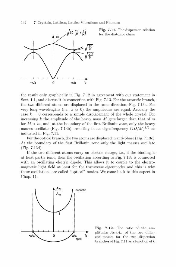
142 7 Crystals, Lattices, Lattice Vibrations and Phonons
Fig. 7.11. The dispersion relationfor the diatomic chain
the result only graphically in Fig. 7.12 in agreement with our statement inSect. 1.1, and discuss it in connection with Fig. 7.13. For the acoustic branch,the two different atoms are displaced in the same direction, Fig. 7.13a. Forvery long wavelengths (i.e., k 0) the amplitudes are equal. Actually thecase k = 0 corresponds to a simple displacement of the whole crystal. Forincreasing k the amplitude of the heavy mass M gets larger than that of mfor M > m, and, at the boundary of the first Brillouin zone, only the heavymasses oscillate (Fig. 7.13b), resulting in an eigenfrequency (2D/M)1/2 asindicated in Fig. 7.11.
For the optical branch, the two atoms are displaced in anti-phase (Fig. 7.13c).At the boundary of the first Brillouin zone only the light masses oscillate(Fig. 7.13d).
If the two different atoms carry an electric charge, i.e., if the binding isat least partly ionic, then the oscillation according to Fig. 7.13c is connectedwith an oscillating electric dipole. This allows it to couple to the electro-magnetic light field at least for the transverse eigenmodes and this is whythese oscillations are called “optical” modes. We come back to this aspect inChap. 11.
Fig. 7.12. The ratio of the am-plitudes AM/Am of the two differ-ent masses for the two dispersionbranches of Fig. 7.11 as a function of k

7.4 Linear Chains 143
Fig. 7.13. Sketch of the displacements of the atoms on the acoustic (a, b) and theoptical branches for two different wave vectors (c, d)
Here we have discussed in detail only the longitudinal modes, but it isobvious that both for the monatomic and the diatomic chain, for every wavevector and every branch, two (degenerate) transverse oscillations also exist.
The dispersion relation of Fig. 7.11 can also be deduced in another waystarting from the one of Fig. 7.9, i.e., from the monatomic chain which we re-peat in Fig. 7.14a. Now we imagine that we paint the atoms of the monatomicchain in two different alternating colors, but without changing their physicalproperties. As a consequence we have increased the length of the primitiveunit cell by a factor of two and the new lattice constant a′ is given by
a′ = 2a (7.38)
and this in turn reduces the length of the first Brillouin zone by one-half asshown in Fig. 7.14a,b. Consequently, we can shift the outer parts of the dis-persion relation by vectors of the new reciprocal lattice into the first Brillouinzone. This situation is shown in Fig. 7.14b. Since the atoms are still identical,the two branches cross at the border of the first Brillouin zone. If we nowalso introduce differences in the physical properties of the atoms, for examplegiving them different masses, then we end up with the situation of Fig. 7.14cwhich is identical to Fig. 7.11. We shall use this set of arguments again inconnection with superlattices later on in Sect. 8.10. First we want to extendthis discussion of the lattice vibrations of three-dimensional systems.

144 7 Crystals, Lattices, Lattice Vibrations and Phonons
Fig. 7.14. The transition from the monatomic (a) to the diatomic (c) chain. (Seetext for explanation)
7.5 Three-Dimensional Crystals
If we consider a three-dimensional crystal, not too much changes with respectto the chain model of Sect. 7.4, at least for the dispersion relations. The atomsare connected with nearest (and possibly next-nearest) neighbors in the three-dimensional crystal stucture. The set of equations analogous to (7.28) or (7.33)will become correspondingly more complex, but the result will be qualitativelythe same. There are still the acoustic branches and, in addition, optical onesif we have more than one atom in the primitive unit cell. There are alwaysthree acoustic branches, namely one longitudinal and two transverse ones forevery k-vector and 3s− 3 optic ones:
number of acoustic branches: 3number of optical branches: 3s− 3
(7.39)
where s is the number of atoms per primitive unit cell.
Fig. 7.15. Sketch of the dispersion re-lation of lattice vibrations for a three-dimensional anisotropic crystal withpartly ionic binding and two atoms perprimitive unit cell
7.6 Phonons and the Concept of Quasiparticles 145
If the crystal is anisotropic the dispersion relations will be different fordifferent directions in the Brillouin zone and the degeneracy between the twotransverse modes for every k may be lifted. We show such a situation schemat-ically in Fig. 7.15.
7.6 Quantization of Lattice Vibrations:Phonons and the Concept of Quasiparticles
If we look again at (7.28) or (7.33) for the un(t) we see that these equationsare rather similar to the equation of motion for an harmonic oscillator
m∂2vn
∂t2= −Dvn . (7.40)
The only difference are the terms with indices n± 1, i.e., the off-diagonalterms in the language of matrix representation. It is now possible to findappropriate linear combinations of the un, so-called normal coordinates vn
vn =∑n′an′un′ (7.41)
such that the vn obey equations like (7.40) or (2.52) or, in other words, todiagonalize the problem. In doing so one usually closes the linear chain (orthe three-dimensional equivalent) to a huge ring in order to close the set ofdifferential equations.
On the other hand a quantum mechanical treatment of the harmonic os-cillator leads to discrete energy levels given by
En = ωn
(n+
12
), n = 0, 1, 2, 3 . . . . (7.42)
It is now important to note that the dispersion relation shown for examplein Fig. 7.15 is not influenced by a linear transformation of the coordinates.
As a consequence we may say that the lattice vibrations (more preciselythe vibrations of the crystal structure) consist of quanta according to (7.42)for each wave vector k and branch i. The total energy of the lattice vibrationscan be written as
E =∑k,i
ωk,i
(nk,i +
12
)(7.43)
in analogy to (2.55b) or (5.3), where the index i labels the various branches.In the framework of second quantization it is possible to define creation
and annihilation operators b+k,i and bk,i respectively, and the Hamiltonian can

146 7 Crystals, Lattices, Lattice Vibrations and Phonons
then again be written in terms of the number operator, in a similar way tothat used already for photons
H =∑k,i
ωk,i
(b+k,ib
+k,i +
12
). (7.44)
Obviously there is a close analogy between the quanta or particles of theelectromagnetic radiation in vacuum, the photons, and the quanta of the lat-tice vibrations. The quanta of the lattice vibrations are called phonons andare considered as quasi-particles. The attribute “quasi” has two reasons. Incontrast to “real” particles like photons, electrons or protons, phonons can ex-ist only in matter and not in vacuum. They are characterized by their energyand momentum k but, in contrast to vacuum, k is a “quasi-momentum”which is defined only modulo integer multiplies of the elementary translationvectors bi of the reciprocal lattice for a crystalline solid (Sect. 7.2). The con-cept of quasi-particles, which as been introduced by Landau about 50 yearsago, is a very important one for the understanding of solids. In the next chap-ters we shall become familiar with several other quasi-particles in solids. Thephonons are just the first example.
The existence and the dispersion relation of phonons can be investigatedby inelastic neutron scattering. An incident neutron from a mono-energeticbeam with
Ei =
2k2i
2mn(7.45)
is scattered under creation or annihilation of a phonon, resulting in a neutronin the final state with Ef, kf, which are given via the conservation laws ofenergy and quasi-momentum
Ef =
2k2f
2mn= Ei ± ωPhonon
andkf = ki ± kPhonon + G (7.46)
By measuring the properties of the incident and scattered neutrons it ispossible to prove the existence of phonons and to determine their dispersionrelation. Note that the scattering probability for the neutrons may dependon G.
Figure 7.16 shows the dispersion relation of the phonons in two differentsemiconductors, Si and CdS, for various directions in k-space (see Fig. 7.4).All well-known semiconductors, including the elemental ones like Si and Ge,have more than one atom per unit cell and therefore support both acousticand optical branches. Si has only covalent binding in contrast to CdS whichhas a mixed ionic-covalent binding. Therefore the Si atoms do not carry anelectric charge and, as a result, even the optical phonons do not couple directlyto the radiation field, resulting at k = 0 in an oscillator strength f = 0 andconsequently in ∆LT = 0 as a result of (4.26).
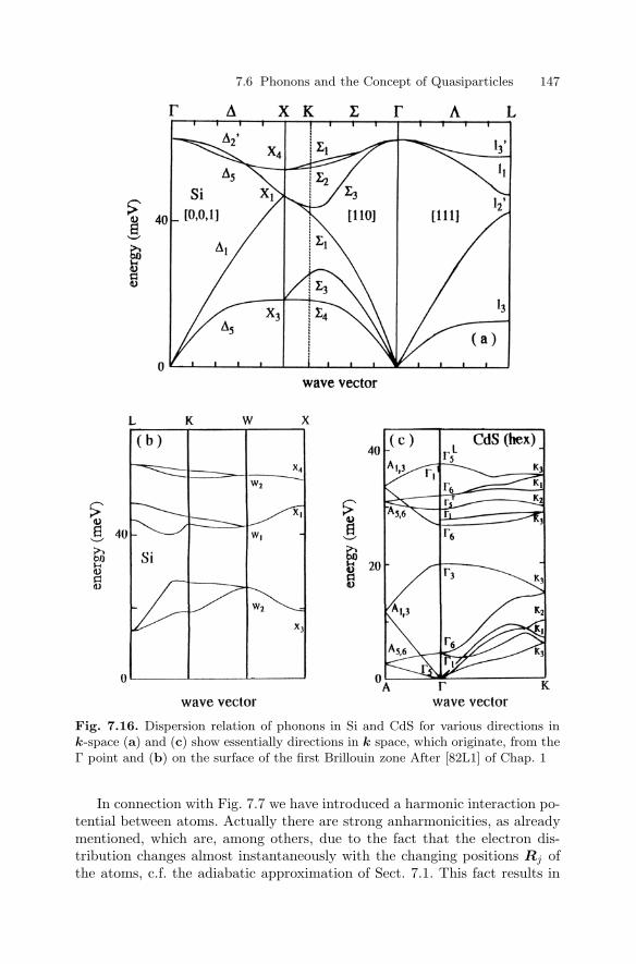
7.6 Phonons and the Concept of Quasiparticles 147
Fig. 7.16. Dispersion relation of phonons in Si and CdS for various directions ink-space (a) and (c) show essentially directions in k space, which originate, from theΓ point and (b) on the surface of the first Brillouin zone After [82L1] of Chap. 1
In connection with Fig. 7.7 we have introduced a harmonic interaction po-tential between atoms. Actually there are strong anharmonicities, as alreadymentioned, which are, among others, due to the fact that the electron dis-tribution changes almost instantaneously with the changing positions Rj ofthe atoms, c.f. the adiabatic approximation of Sect. 7.1. This fact results in

148 7 Crystals, Lattices, Lattice Vibrations and Phonons
a variation of the “spring-constant” D with the lattice constant a, i.e., in ananharmonicity.
The resulting anharmonicity manifests itself, for example, in scatteringprocesses between phonons. We show some of them schematically in Fig. 7.17.However, one should bear in mind that all combination possibilities are ex-hausted only when the three-dimensional k-space is considered.
In (a) a TO phonon decays under energy and momentum conservation intotwo acoustic phonons in (b) two transverse acoustic phonons combine to forma longitudinal acoustic phonon. Energy and momentum conservation read e.g.for (a) and (b):
(a) ωi = ωf1 + ωf2, ki = kf1 + kf2 (7.47a)
(b) ωi1 + ωi2 = ωf, ki1 = ki2 + kf . (7.47b)
These are so-called n or normal processes. In the decay process (c) we endup in the second Brillouin zone with one phonon and fold the phonon backwith a vector of the reciprocal lattice G.
ωi = ωf1 + ωf2; ki = kf1 + kf2 + G . (7.47c)
The situation of (c) is known as a u or Umklapp process.
7.7 The Density of States and Phonon Statistics
Now we want to calculate the density of states of phonons as a first applicationof what we have learned in Sect. 2.6 for a three-dimensional crystal.
Fig. 7.17. Sketch of three possible decay or fusion processes of phonons

7.7 The Density of States and Phonon Statistics 149
Fig. 7.18. Schematic drawing of the density of states of a three-dimensional,isotropic semiconductor with two atoms per unit cell and degenerate optical andacoustic branches
We assume for simplicity that we have two atoms per unit cell and thatthe resulting three acoustic and optical branches are degenerate i.e. transverseand longitudinal branches coincide. Furthermore we assume an isotropic semi-conductor. This results in Fig. 7.18 where we plot on one side of the x-axis kand on the other the density of states D(ω). As stated in Sect. 2.6 we needthe dispersion relation to calculate D(ω). In the linear part of the acousticbranch we have
ω = vsk , (7.48)
where vs is the constant velocity of sound. This linear relation results imme-diately in
D(ω) = const · ω2 (7.49)
i.e., a parabolic density of states similar to that for photons in vacuum. Thedifference is only in the proportionality factor of (7.48),(7.49).
When deviations from the linear dispersion relation start, the calculationsget more lengthy and we will not go into details. The denominator on theright of (2.77) tells us, however, that the density of states has in principlea singularity and in practice a steep maximum when we have a horizontalslope of the ω(k) relation, as indicated in Fig. 7.18.
Note that the situation is in reality more complex than in in Fig. 7.18 dueto the facts, that the dispersion relation may depend in the direction of k, thetransverse and longitudinal branches are not degenerate, and that the firstBrillouin zone is not a sphere but a polyhedron, with the consequence, thatthe range of k vectors depends on the direction in the Brillouin zone. Forrealistic densities of states see e.g. [82L1] of Chap. 1.

150 7 Crystals, Lattices, Lattice Vibrations and Phonons
If we want to know the number of phonons we must integrate over thedensity of states weighted with the probability that the state is populated.The commutation relations for phonons obey[
bk,i, b+k′,i′
]−= ∂k,k′∂i,i′ (7.50)
where i is the label of the branch. This means that phonons are bosons. Sowe have in thermal equilibrium to use Bose–Einstein statistics (2.80b)
fBE(ω, T ) = exp [(ω − µ)/kBT ]− 1−1 (7.51)
Since the number of phonons is not conserved, due e.g., to phonon–phononinteraction (see above), the chemical potential µ is zero in thermal equilibrium(Sect. 2.6). For the total number of phonons, N(T ), we obtain
N(T ) =
∞∫0
D(ω) [exp(ω/kBT ) − 1]−1 dω (7.52a)
and for the energy of the phonon system
U(T ) =
∞∫0
ωD(ω) [exp(ω/kBT ) − 1]−1 dω . (7.52b)
Starting from (7.52b) it is easy to calculate the specific heat of the phononsystem
cp cv =∂U
∂T(7.53)
if appropriate approximations are made for D(ω). Einstein assumed thatall phonons have the same frequency ωE i.e., he approximated D(ω) by a δ-function
D(ω) = δ(ω − ωE)3Ns , (7.54a)
and Debye continued the linear part of the dispersion relation up to a fre-quency which is also chosen to accommodate all 3Ns degrees of freedom ofthe atoms, where N is the number of unit cells and s the number of atomsper unit cell
3Ns =
ωD∫0
D(ω)dω with D(ω) ∝ ω2 . (7.54b)
For high temperatures (i.e., kBT > ωD or ωE) both approximations givethe classical limit, namely the law of Dulong and Petit
cv = 3NskB (7.55)

7.8 Phonons in Alloys 151
and a continuous approach to zero for T → 0. In the case of Debye’s approx-imation one finds the well-known T 3 law:
cv ∼ (T/θ)3 with kBθ = ωD and T < θ . (7.56)
Since the discussion of specific heat cv is outside the scope of this book,we do not take it any further, having introduced it simply to illustrate theapplicability of the concept of the density of states, and mention only thatthe approach in (7.52b),(7.54b) is, apart from some constants and ωD → ∞identical to the one used to describe Planck’s law of blackbody radiation asseen by comparing with (2.84).
Finally, we want to point out the following. Since phonons are bosons,processes which involve phonons can be stimulated in the same way as wasdiscussed in connection with photons in Sect. 3.2.1, i.e., we get in transitionsinvolving the emission of a phonon in a certain mode, apart from other terms,a factor like
Wi→f ∼ (NkPh + 1) (7.57)
To get a feeling we assume a lattice temperture of 77 K (i.e., liquid N2)and an acoustic phonon with an energy around 0.2 meV (such phonons will beused in Brillouin scattering in Sect. 13.3) and find for these conditions with(7.51)
NkPh 30 1 . (7.58)
This means that the occupation number is much larger than one and processeswhich involve the emission of phonons with energies smaller than the thermalenergy are stimulated by the phonons. Depending on the process under con-sideration, it is however necessary to consider the reverse process, too, whichdepends on Nk
Ph.
7.8 Phonons in Alloys
An alloy is a random binary, ternary or higher mixture of atoms. In con-trast to amorphous materials, the atoms in an alloy are still sitting on welldefined, periodically arranged lattice sites. Two very widely investigated semi-conductor alloys are Al1−yGayAs or CdS1−xSex. The first one cristallizes inthe cubic zinc-blende structure the second usually in the hexagonal wurtzitetype. However the two different kations Al and Ga or the two anions S and Seare randomly distributed over the respective sublattice with an average con-centration y or x. See for the concept of the virtual crystal approach Sect. 8.15.
What are the consequences of alloying for the phonons.For long-wavelenth acoustic phonons the situation is generally rather sim-
ple. The dispersion relation starts linear as in Figs. 7.9, 7.11 or 7.14 witha slope or velocity of sound which is a weighted average of the two parentcomponents. Long wavelength means large compared to the interatomic dis-tance. When approaching the boarder of the first Brillouin zone, things become

152 7 Crystals, Lattices, Lattice Vibrations and Phonons
less clear. Since only one sublattice is elongated (see Fig. 7.13b) the phononfrequency may be broadened depending on which type of atom oscillates dueto their different masses and “spring constants” to their neighbours. In thissense even a chemically pure crystal, containing however different isotopes ofthe same element, has to be considered as an alloy. For details of this topicsee e.g. [94C1,94R1].
For the optical phonons, two different situations may arise. If the bands ofe.g. the LO-phonons overlap energetically in the two parent materials as is thecase e.g. in Zn1−yCdyS one finds the so called amalgamation type behaviour,i.e. the LO eigenfrequency shifts continuously with the composition y fromthe one of AB to the one of AC in an alloy AB1−xCx as shown in Fig. 7.19a.
If the bands do not overlap energetically an AB oscillation mode doesnot find a resonant partner of AC modes for any k vector and vice versaand the alloys exhibit generally the so-called persistent mode behaviour. Thismeans, that the eigenfrequencies of the pure AB and AC modes vary onlymarginally under alloying as a function of x, but their relative weights oroscillator strengths change as shown schematically in Fig. 7.19b.
Examples of the optical properties will be given in Chap. 11.
7.9 Defects and Localized Phonon Modes
In our discussion of phonons (and of our model substance in Chaps. 4and 5), we assumed until now a perfect arrangement of atoms. In fact,every real semiconductor contains a lot of crystal or lattice defects. Thereare point defects, one-dimensional defects like dislocations, two-dimensional
Fig. 7.19. Composition dependence of the LO phonon energies in alloys for the casesof amalgamation type (a) and persistent mode type (b) behaviour of the phonons

7.9 Defects and Localized Phonon Modes 153
defects like stacking faults and (small angle) grain boundaries, or three-dimensional ones like precipitates or voids. In the present context the mostimportant are the point defects. For an introduction to this topic see e.g.textbooks on solid state physics like [75Z1, 81H1, 81M1, 93K1, 95C1, 95I1,95W1] of Chap. 1. Point defects include vacancies, interstitital and sub-stitutional atoms. We give some examples for a compound semiconductorAB in Fig. 7.20. We come back to this topic when we discuss electronstates in semiconductors. What we need here is the fact that a point de-fect may have a different mass m′ and/or chemical binding, i.e., spring con-stant D′ as compared to the atom which would be at this place in a perfectlattice.
A consequence of such a point defect is that a localized phonon modemay appear. This is a mode which cannot propagate through the samplewith a plane-wave factor as in ((7.29a,b) or (7.34)). Instead the amplitudehas a maximum at the place of the defect and decays exponentially withincreasing distance from it. Obvisouly such a mode is localized at or in thevicinity of the point defect.
If the eigenfrequency ωloc of such a localized phonon mode falls into thebands of the intrinsic acoustic or optic modes and couples to them, it will notproduce a big effect. Once such a localized mode is excited, it decays rapidlyinto bulk modes. The situation is different if ωloc falls either in a spectralregion where the pure material has no eigenfrequences at all, or couples onlyweakly to the bulk modes. Then the localized mode can produce, for example,an additional absorption band or Raman satellite. We come to this point later.The situation
ωloc > ωLObulk (7.59)
Fig. 7.20. The lattice of a semiconductor AB containing various types of pointdefects
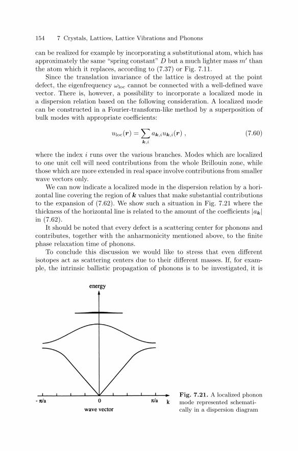
154 7 Crystals, Lattices, Lattice Vibrations and Phonons
can be realized for example by incorporating a substitutional atom, which hasapproximately the same “spring constant”D but a much lighter massm′ thanthe atom which it replaces, according to (7.37) or Fig. 7.11.
Since the translation invariance of the lattice is destroyed at the pointdefect, the eigenfrequency ωloc cannot be connected with a well-defined wavevector. There is, however, a possibility to incorporate a localized mode ina dispersion relation based on the following consideration. A localized modecan be constructed in a Fourier-transform-like method by a superposition ofbulk modes with appropriate coefficients:
uloc(r) =∑k,i
ak,iuk,i(r) , (7.60)
where the index i runs over the various branches. Modes which are localizedto one unit cell will need contributions from the whole Brillouin zone, whilethose which are more extended in real space involve contributions from smallerwave vectors only.
We can now indicate a localized mode in the dispersion relation by a hori-zontal line covering the region of k values that make substantial contributionsto the expansion of (7.62). We show such a situation in Fig. 7.21 where thethickness of the horizontal line is related to the amount of the coefficients |ak|in (7.62).
It should be noted that every defect is a scattering center for phonons andcontributes, together with the anharmonicity mentioned above, to the finitephase relaxation time of phonons.
To conclude this discussion we would like to stress that even differentisotopes act as scattering centers due to their different masses. If, for exam-ple, the intrinsic ballistic propagation of phonons is to be investigated, it is
Fig. 7.21. A localized phononmode represented schemati-cally in a dispersion diagram

7.10 Phonons in Superlattices and in other Structures 155
desirable to use materials which consist of one isotope only. For more infor-mation of this topic see Ref. [81A1]g of Chap. 1 or [94C1] and references giventherein.
7.10 Phonons in Superlatticesand in other Structures of Reduced Dimensionality
Until now we were mainly considering homogeneous, three-dimensional semi-conductors. For the phonons, however, we started with a one-dimensionalchain, but we stated that the dimensionality does not have significant influ-ence on the dispersion relation but it does on the density of states, accordingto what we learned in Sect. 2.6. For the regime of a linear dispersion relation,i.e., for acoustic phonons with not too large wave vectors see Figs. 7.15 – 7.18we get with (2.77)
D(ω) ∼ ωd−1 (7.61)
where d is the dimensionality of the system.Now we want to address in the context of phonons for the first time a rather
modern topic in semiconductor physics, namely superlattices.A superlattice is a man-made periodic structure which consists of thin
alternating layers of two different materials, as shown in Fig. 7.22. The dif-ferent layers are only a few lattice constants thick and can be preparedby various techniques like molecular-beam epitaxy (MBE), metal-organicchemical vapor-phase deposition (MOCVD), hot-wall epitaxy (HWE) oratomic layer epitaxy (ALE). A description of these methods is beyond thescope of this book, but we give some references for the interested reader,e.g., [80M1, 89H1, 89R1]. See also Sects. 8.11 – 8.13. Especially well-suitedmaterials for growing superlattices are the III–V compounds GaAs, AlAs
Fig. 7.22. A superlattice consisting of alternating thin layers of two different ma-terials

156 7 Crystals, Lattices, Lattice Vibrations and Phonons
and their alloys Al1−y, GayAs, since the lattice constant is almost inde-pendent of y. Other systems under investigation involve the two elementalsemiconductors Si and Ge or ZnSe and ZnS1−xSex. Due to their differentlattice constants, the fabrication of superlattices is in this case more diffi-cult and the layers are strained (strained layer superlattice). For other struc-tures of reduced dimensionality like quantum wells, ∼wires or ∼dots see againSects. 8.11 – 8.13.
The formation of a superlattice results in strong modifications of the dis-persion relation for phonons in the growth direction, i.e. normal to the planes,while the in-plane dispersion is generally at least not quantitatively modified.We concentrate therefore on this direction, which is frequently identified withthe z-direction.
As can be seen from Fig. 7.22 we created a new artificial periodicity lzwhich is an integer multiple of the (strained) lattice constants of materialsA and B
lz = n1aA + n2aB (7.62)
This is why such structures are called (artificial) superlattices. Now we usea similar argument as in connection with Fig. 7.14.
The Brillouin zone in the z-direction extends no longer from −π/a ≤ kz ≤π/a but only from
− πlz
≤ kz ≤ π
lz(7.63a)
All parts of the dispersion curve outside this interval can be shifted into thefirst mini-Brillouin zone by vectors of the new reciprocal lattice
Gz = l32πlz
; l3 = 0,±1,±2, . . . (7.63b)
For a single acoustic phonon branch this procedure results in a disper-sion relation like in Fig. 7.23, where we show the first few of these so-calledbackfolded acoustic phonon branches.
The dispersion relation which enters is an average of the dispersion rela-tions of the two materials, weighted by their relative thicknesses (the so-calledRytov-model) [89J1,96G1,98G1,01D1].
Usually one can observe only the few lowest, backfolded acoustic phononbranches. The higher ones are broadened and washed out e.g. due to thickness-fluctuations of the layers.
For the optical phonon branches two different things can happen. If thebranches in the two different materials overlap energetically, one obtains ina similar way as for the acoustic phonons mentioned above backfolded opticphonons.
If the do not overlap energetically, TO or LO optical phonon oscillationin one material do not find a resonant partner in the other (and vice versa)similarly to the case of alloys. Consequently the phonons become localized orconfined to the respective layer. The elongation-pattern of the atoms has nodes
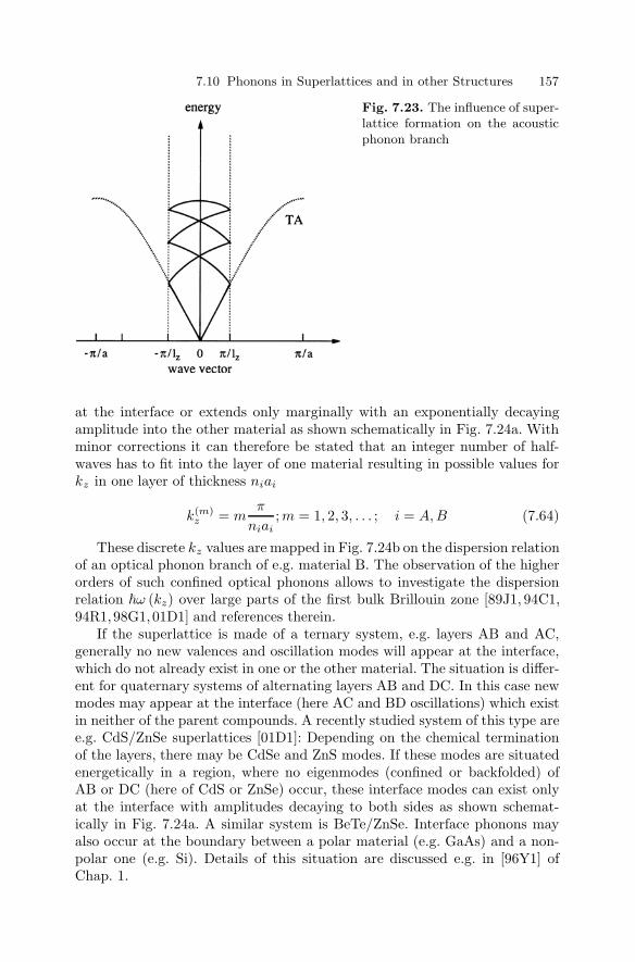
7.10 Phonons in Superlattices and in other Structures 157
Fig. 7.23. The influence of super-lattice formation on the acousticphonon branch
at the interface or extends only marginally with an exponentially decayingamplitude into the other material as shown schematically in Fig. 7.24a. Withminor corrections it can therefore be stated that an integer number of half-waves has to fit into the layer of one material resulting in possible values forkz in one layer of thickness niai
k(m)z = m
π
niai;m = 1, 2, 3, . . . ; i = A,B (7.64)
These discrete kz values are mapped in Fig. 7.24b on the dispersion relationof an optical phonon branch of e.g. material B. The observation of the higherorders of such confined optical phonons allows to investigate the dispersionrelation ω (kz) over large parts of the first bulk Brillouin zone [89J1, 94C1,94R1,98G1,01D1] and references therein.
If the superlattice is made of a ternary system, e.g. layers AB and AC,generally no new valences and oscillation modes will appear at the interface,which do not already exist in one or the other material. The situation is differ-ent for quaternary systems of alternating layers AB and DC. In this case newmodes may appear at the interface (here AC and BD oscillations) which existin neither of the parent compounds. A recently studied system of this type aree.g. CdS/ZnSe superlattices [01D1]: Depending on the chemical terminationof the layers, there may be CdSe and ZnS modes. If these modes are situatedenergetically in a region, where no eigenmodes (confined or backfolded) ofAB or DC (here of CdS or ZnSe) occur, these interface modes can exist onlyat the interface with amplitudes decaying to both sides as shown schemat-ically in Fig. 7.24a. A similar system is BeTe/ZnSe. Interface phonons mayalso occur at the boundary between a polar material (e.g. GaAs) and a non-polar one (e.g. Si). Details of this situation are discussed e.g. in [96Y1] ofChap. 1.

158 7 Crystals, Lattices, Lattice Vibrations and Phonons
Fig. 7.24. Schematic representation of the envelope of an optical phonon modeconfined to material B in a superlattice and of an interface phonon (a) and thediscrete values of kz on an optical phonon branch of material B. (b)
As a result, we may summarize that in superlattices there may be asnew phenomena backfolded or confined phonon modes as well as interfacemodes.
To conclude this subsection we mention that in the extreme confine-ment case of phonons in all three directions of space, which may occur inso called quantum dots (also known as quantum boxes, nano-crystallites ornano-islands, depending partly on the way of creation (see Sect. 8.13), thedispersion relation of the phonons breaks up into a series of discrete modes,which is governed by the boundary conditions (e.g. free or clamped). Seee.g. [92N1,93T1,95O1,96W1,98A1] and references therein.
7.11 Problems
1. Inspect or build some lattice and crystal models to become familiar withthe topics presented in Sect. 7.2.
2. Show that the reciprocal lattice of a face-centered cubic (fcc) lattice isa body centered cubic (bcc) lattice and vice versa.
3. Calculate and draw the unit cell and the Wigner-Seitz cell in real spaceand the first three Brillouin zones in reciprocal space for a simple cubicand a hexagonal two-dimensional lattice.
4. Study with the data found in [82L1] of Chap. 1 the transverse and longi-tudinal eigen-frequencies of optical phonons of a series of semiconductorslike ZnO, ZnS, ZnSe, and ZnTe, or of a similar series with the same anionand different cations. What do you conclude?
5. Compare the longitudinal-transverse splitting at k = 0 for Ge and thecorresponding III–V, II–VI and I–VII compounds on the same line of
References to Chap. 7 159
the periodic table of the elements. Can you qualitatively explain thefindings?
6. Inspect a model of a cubic crystal (e.g. zinc-blende). Find the non primi-tive cubic unit cell and the primitive one. Explain qualitatively that sucha crystal should be optically isotropic for light propagating (k = 0!) e.g.in the directions (100) or (111) but not in (110).
References to Chap. 7
[80M1] Molecular Beam Epitaxy, B.R. Pamplin (ed.), Pergamon, Oxford (1980)[89H1] M.A. Hermann, H. Sitter, Molecular Beam Epitaxy, Springer, Berlin, Hei-
delberg (1989)[89J1] B. Jusserand and M. Cardona, in Topics in Applied Physics 66, Springer,
Berlin (1989)[89R1] M. Razeghi: The MOCVD Challenge, Hilger, Bristol (1989) and references
therein[92N1] S. Nomara, T. Kobayashi, Solid State Commun. 82, 335 (1992)[93T1] A. Tomaka, S. Onari and T. Arai, Phys. Rev. B 47, 1237 (1993)[94C1] M. Cardona, Festkorperprobleme/Advances in Solid State Physics 34, 35
(1994)[94R1] T. Ruf et al., Festkorperprobleme/Advances in Solid State Physics 34, 237
(1994)[95O1] S. Okamoto, Y. Masumot, J. Luminesc. 64, 253 (1995)[96G1] J. Geurts, Progr. Cryst. Growth Charact. 32, 185 (1996)[96W1] U. Woggon et al., Phys. Rev. B 54, 1506 (1996)[98A1] A.P. Alivisatos et al., J. Chem. Phys. 89, 4001 (1998)[98G1] M. Goppert et al., Phys. Rev. B 57, 13068 (1998)[01D1] A. Dinger et al., Phys. Rev. B 64, 245310 (2001)

8
Electrons in a Periodic Crystal
Let us now return for a moment to the Hamiltonian (7.1) which describesa crystal. By introducing the phonons we have treated the motion of theatoms. We now assume that the atoms are fixed at their equilibrium positions,i.e., that no phonons are excited. Then the sum over the potentials of allatoms forms a periodic potential for the electrons; but we are still left witha Hamiltonian for about 1023 interacting outer electrons per cubic centimeter,which should be properly treated in a many particle formalism. Unfortunatelyit is extremely difficult to handle this approach. Instead one generally usesa so-called one-electron approximation. The idea is the following: One assumesthat the periodically arranged atoms and all interaction potentials betweenelectrons together form a periodic potential V (r) with
V (r + R) = V (r) . (8.1)
where R is a translation vector of the lattice (see Sect. 7.2).This is a valid approach especially for semiconductors or simple metals.
In semiconductors there is only a low density (generally between 109 and1019 cm−3) of free electrons (or holes) that can react easily on their mutualinteraction. In simple metals the density of free carriers is higher, but thedensity of those reacting on their mutual interaction is limited to the fractionsituated in an interval of width ∆E ≈ 4kBT <<< EF energetically aroundthe Fermi energy. It must be noted that there are other systems in which themutual interaction between carriers plays a crucial role like in the Hubbardmodel, in heavy Fermion systems or in connection with the Kondo effect.These topics are, however, beyond the scope of this book but we providesome references for the interested reader [93F1,93H1].
We return now to the approximation (8.1). One calculates the eigenstatesfor one electron of the corresponding Schrodinger equation and populates thesestates with electrons according to Fermi–Dirac statistics until all electronshave been accommodated. The potential V (r) should ideally be calculated ina self-consistent way e.g. by Hartree or Hartree–Fock approaches. But simpler

162 8 Electrons in a Periodic Crystal
and more feasible approaches are often used such as a periodic arrangementof screened Coulomb potentials or a “muffin-tin” potential.
It is beyond the scope of this book to present details of band structurecalculations. There are excellent reviews and (text)books on this topic withvarious degrees of sophistication, some of which were already cited in Chap. 1like [75B1, 75Z1, 81M1, 81S1, 91E1, 93K1, 95C1, 95I1, 96S1, 96Y1, 97S1, 99B1,01H2,01S1] in addition to [70M1,88C1,88R1,91E1] of this chapter, from whichmuch of the following material has been taken. On the other hand, the topic iscrucial for the understanding of the optical properties of the electronic subsys-tem of semiconductors. Therefore we first summarize in the following the mainresults and explain the existence of metals, semiconductors and insulators forthose who do not want to go deeper into details, then we give an overview onthe various approaches to the bandstructure calculations starting, e.g., fromfree electrons or from atomic orbitals and including the basic concept of k · ptheory. The next sections are devoted to consequences of the band structure ofsemiconductors like the concepts of crystal electrons and holes as new quasi-particles, the effective mass approach, realistic semiconductor band structuresand others, before we concentrate on structures of reduced dimensionality.
8.1 Bloch’s Theorem
There are essentially two approaches to the problem of band structure cal-culations. In one case one starts with free electrons, which have the simpleparabolic dispersion relation in the non-relativistic regime
E(k) =p2
2m0=
2k2
2m0(8.2)
shown in Fig. 8.1a by the dashed line. One introduces a weak periodic (see(8.1)) potential as a perturbation. These techniques include the “empty lat-tice”, the nearly-free-electron (NFE), augmented plane wave (APW) and or-thogonalized plane wave (OPW) approaches. In the last two cases, terms areadded to make sure that the plane waves are orthogonal to the deeper atomiclevels. These terms are treated as potentials and are known as pseudo poten-tials. These pseudo potentials may be energy dependent.
The introduction of such a weak periodic potential does not alter thedispersion relation very much, but results in the formation of energy gaps atthe boarders of the Brillouin zones in which no stationary electron states exist(see Fig. 8.1a). We will explain this point in more detail in Sect. 8.7.
The other group of methods starts with the atomic orbitals of the atomsforming the solid or more specifically the semiconductor. They involve thesummation over one or more atomic orbitals placed at every atom site in thecrystal and treat the interaction between the orbitals at neighbouring sites,i.e., the wave function overlap as perturbation. These techniques include, e.g.,

8.1 Bloch’s Theorem 163
Fig. 8.1. The reduced-zone scheme (b) of electronic energy bands in a crystallinesolid reached either starting from (nearly) free electrons (a) or from atomic orbitals(c, d)
the tight-binding approximation, the linear combination of atomic orbitals(LCAO) or the extended Huckel method (see Fig. 8.1c,d).
This interaction between atoms leads to a splitting of the atomic level in asmany states as there are atoms (Fig. 8.1c,d) similarly as in classical mechan-ics where coupling between two identical oscillators leads to two close-lyingeigenfrequencies, three oscillators to three eigenfrequencies and 1023 oscilla-tors to 1023 eigenfrequencies. The level spacing is so small that for all practicalpurposes the result is a continuous energy band. For some more details alsosee Sect. 8.7.
The first group of band structure calculation methods is usually more suit-able for conduction band states of semiconductors the second one for valenceband states. For the meaning of these two terms in the context of semicon-ductors see Sect. 8.2.
Furthermore, there is an increasing trend to start less with intuitive phys-ical considerations but to trust more the increasing power of computers tohandle many particle problems.
Independent from the individual approach, one finds in all cases that elec-tron states in a periodic potential are energetically arranged in energy bandsof a certain width, which may be separated by gaps in which no stationaryeigenstates exist (Fig. 8.1). The electron eigenstates of a periodic potentialare so-called Bloch waves φk,i(r),
φk,i(r) = eikruk,i(r) , (8.3a)
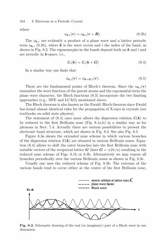
164 8 Electrons in a Periodic Crystal
whereuk,i(r) = uk,i(r + R) . (8.3b)
The φk,i are evidently a product of a plane wave and a lattice periodicterm uk,i (8.3b), where k is the wave vector and i the index of the band, asshown in Fig. 8.2. The eigenenergies in the bands depend both on k and i andare periodic in k-space, i.e.,
Ei(k) = Ei(k + G) (8.4)
In a similar way one finds that
φk,i(r) = φk+G,i(r) . (8.5)
These are the fundamental points of Bloch’s theorem. Since the uk,i(r)remember the wave function of the parent atoms and the exponential term theplane wave character, the Bloch functions (8.3) incorporate the two limitingapproaches (e.g., NFE and LCAO) mentioned above.
The Bloch theorem is also known as the Ewald–Bloch theorem since Ewaldhas found almost identical rules for the propagation of X-rays in crystals (seetextbooks on solid state physics).
The statement of (8.4) once more allows the dispersion relation E(k) tobe reduced to the first Brillouin zone (Fig. 8.1a,b) in a similar way as forphonons in Sect. 7.4. Actually there are various possibilities to present theelectronic band structure, which are shown in Fig. 8.3. See also Fig. 8.5.
Figure 8.3a shows the extended zone scheme in which various branchesof the dispersion relation E(k) are situated in various Brillouin zones. Equa-tion (8.4) allows to shift the outer branches into the first Brillouin zone withsuitable vectors of the reciprocal lattice G (here G = ±2π/a) resulting in thereduced zone scheme of Figs. 8.1b or 8.3b. Alternatively we may repeat allbranches periodically over the various Brillouin zones as shown in Fig. 8.3c.
Usually one uses the reduced scheme of Fig. 8.3b. The extrema of thevarious bands tend to occur either at the centre of the first Brillouin zone,
Fig. 8.2. Schematic drawing of the real (or imaginary) part of a Bloch wave in onedimension

8.1 Bloch’s Theorem 165
Fig. 8.3. The extended (a) the reduced (b) and the periodic band structure (c)
i.e., at k = 0 (the so-called Γ -point) or at the boarders of the Brillouin zoneas shown in Fig. 8.3b, but as we shall see later, extrema may also occursomewhere else on the interval 0 ≤ |k| < π/a. The bands tend to be to a goodapproximation parabolic in the vicinity of the extrema but the positive ornegative curvature can be different at every extremum and may even dependon the direction of k in systems of higher dimensionality than one includingthree. When approaching the boarder of the Brillouin zone, the slope of E(k)normal to this boarder is generally zero.
With increasing energy the width of the allowed bands tends to increase,while the width of the forbidden gaps decreases. It is even possible that variousbands overlap energetically.
Fig. 8.4. The representation of bands in k-space (a) and in real space (b)

166 8 Electrons in a Periodic Crystal
We will give some arguments for this behavior later in this chapter.To conclude this section we want to mention that the bands are usu-
ally represented in one of two different ways. The first is the dispersion re-lation (Figs. 8.1b, 8.3, 8.4a). In the other case one plots the width of thebands and of the gaps between them as a function of the space coordinater (Fig. 8.4b). The latter is especially useful to demonstrate spatial inho-mogeneities or localized states. We shall meet some examples of both caseslater.
8.2 Metals, Semiconductors, Insulators
Having obtained a first insight into the electronic bandstructure in the abovesection, we now want to make the second step and put all electrons intothe bands using, of course, Fermi–Dirac statistics. We further assume zerotemperature.
Some of the energetically lower-lying bands will be completely filled. Wecall bands which are completely filled at T = 0 K “valence bands”, while allpartly filled or empty bands are “conduction bands”.
The important region for our purposes is that around the highest valenceand the lowest conduction bands. This region determines not only the opticalproperties around the fundamental absorption edge, but also the magneticproperties and the electronic contributions to the conductivities of electricityand of heat.
If the filling procedure of the bands ends in such a way that, at T = 0 Kthere are one or more partly-filled conduction bands (Fig. 8.5a,b), we havea metal. This situation arises for example if the atomic orbital which formsthe band is itself only partly occupied (e.g., the outer s-level of the alkalimetals Li, Na . . . ) (Fig. 8.5a) or if a completely filled orbital forms a bandwhich overlaps with a band stemming from an empty atomic orbital, as is thecase in the rare earth metals (Ca, Mg . . . ) in Fig. 8.5b. If, on the other hand,the filling procedure gives one or more completely-filled valence bands whichare separated by a gap Eg from completely empty conduction bands, we havea semiconductor for
0 < Eg ≤ 4 eV (8.6a)
and an insulator forEg ≥ 4 eV . (8.6b)
The ”boarder line” of 4 eV is set by convention and is not sharp.Diamond has, e.g., a gap of 5.5 eV, but is still considered to be a semicon-
ductor, especially because it can be n or p doped.Materials with
Eg = 0 , (8.7a)
i.e., materials in which the lowest conduction and uppermost valence band“touch” each other but do not overlap are called semimetals.

8.2 Metals, Semiconductors, Insulators 167
Fig. 8.5. Occupation of the bands for a metal (a,b) a semiconductor (c) and aninsulator (d)
Semiconductors with0 < Eg ≤ 0.5 eV (8.7b)
are called narrow gap semiconductors.In the range
0.5 eV < Eg ≤ 2 eV
we find the usual semiconductors, from which many are of wide technicalimportance like Ge, Si or GaAs. The regime
2 eV < Eg ≤ 4 eV (8.7c)
characterizes the wide gap semiconductors, which lead continuously to theinsulators.
To conclude this section we want to introduce the terms “direct” and “in-direct” gap semiconductors. A semiconductor is said to have a direct gap,or to be a direct semiconductor, if the global maximum of the highest va-lence band and the global minimum of the lowest conduction band occur atthe same point of the first Brillouin zone in the reduced zone scheme as inFig. 8.4a. This point is frequently but not necessarily the Γ -point (i.e., k = 0).There are also direct gap semiconductors where the gap occurs at a specificpoint on the boarder of the Brillouin zone. Semiconductors, in which the twoabove-mentioned extrema occur at different k values in the Brillouin zonehave an indirect gap or are called indirect semiconductors. The reason forthis terminology comes from optical transitions between the band extrema.

168 8 Electrons in a Periodic Crystal
A photon with an energy equivalent to the typical width of a semiconductorband gap has (almost) vanishing momentum on the scale of the first Brillouinzone. Optical transitions are in this sense vertical in a E(k) relation. If theband extrema occur at the same point in k-space, a transition between theextrema is directly possible by absorption (or emission) of a photon. In theother case this transition is forbidden by the k-conservation law and only in-direct transitions are possible, which also involve the absorption or emissionof a phonon for momentum conservation.
We shall see examples for both cases in Sect. 8.8.
8.3 An Overview of Semiconducting Materials
We now understand that semiconductors are solids that have at T = 0 Ka series of completely filled valence bands. The uppermost band is separatedby an energy gap Eg from the empty conduction bands.
Since a crystal can be considered a huge molecule, we should also givethe terms used in chemistry. The uppermost valence band is known in thisscientific discipline as highest occupied molecular orbital (HOMO). The low-est conduction band is called consequently the lowest unoccupied molec-ular orbital (LUMO). If not stated explicitly otherwise, when we use va-lence and conduction band we always mean the highest and lowest ones,respectively.
Presently more than 600 element and compound semiconductors areknown. They are listed with their propeties in the volumes by Landolt–Bornstein ( [82L1] of Chap. 1).
With the help of the periodic Table 8.1 we try to localize the most impor-tant semiconductors. In the first two lines we give the current internationallyrecommended numbering system for the columns used by chemists, whichruns from 1 to 18, and the old one, which we and most other semiconductorphysicists use. It runs from I o VIII and has subclassifications such as IIA
and IIB.The technically most important semiconductor is Si. It is found in col-
umn IVA. Conduction and valence bands are formed from the antibondingand bonding sp3 hybrid orbitals. The binding is completely covalent and Eg
is around 1.1 eV at room temperature. See, e.g., Table 8.2 where we givesome data, which we partly explain later. Silicon crystallizes in the diamondstructure with point group 0h. The modification diamond of carbon is a semi-conductor as well as Ge.
Tin is usually a metal, but there exists a modification, which is a semimetalnamely grey tin, which also crystallizes in the diamond structure. Lead, finally,is a metal.
We can already see a general trend, namely that the width of the bandgap decreases if one goes down the columns. SiC also belongs to the group IVsemiconductors. SiC is notorious for forming many different polytypes. The

8.3 An Overview of Semiconducting Materials 169
Table 8.1. Periodic table of the elements. The names of elements 104 to 110 mightchange and others may be discovered in the future.
indirect band gaps of all of them are around 3 eV, i.e., they lie between thegaps of diamond and Si.
Carbon has two further modifications namely graphite and fullerene (C60).Graphite is a semimetal with rather strong covalent sp2 hybrid binding withinthe hexagonal layers and weak van der Waals binding between the layers. C60
is a semiconductor with Eg ≈ 2.2 eV.

170 8 Electrons in a Periodic Crystal
In the diamond structure every atom is tetrahedrally surrounded by itsnearest neighbors. See Fig. 7.2. We can now replace, e.g., the Ge atoms onone sublattice by Ga, which has one outer electron less, and the others by As,which has one electron more than Ge, leaving the total number of electrons perunit unchanged, but adding a little bit of ionic binding to the still dominantcovalent one. This procedure leads to the so-called zincblende type crystalstructure with point group Td and to the group of III–V semiconductors. Tothis group of semiconductors belong the compounds of B, Al, Ga or In withN, P, As or Sb. We see again the general trend of the band gap with BN beingan insulator, AlN, GaN being wide gap semiconductors while InSb is a narrowgap semiconductor.
The group III nitrides crystallize preferentially in the hexagonal wurtzitetype structure (point group C6v). In this case every atom of one type is stilltetrahedrally surrounded by the others, but the arrangement of the next-nearest neighbours is such, that a hexagonal structure evolves (see Fig. 7.2).
If we repeat this step, which leads from the group IV semiconductors to theIII–V compounds, once more or even twice more, we come to the II–VI (moreprecisely IIB–VIA) and I–VII (more precisely IB–VIIA) semiconductors, withincreasing and finally dominating ionic binding, but still generally tetrahedralcoordination. The IIA–VIA and IA–VIIA components are usually insulators.
The II–VI semiconductors comprise the compounds of Zn, Cd or Hg withO, S, Se or Te. The gap generally decreases when going down the columns ZnS,ZnO and CdS are wide gap semiconductors, while the mercury compounds areusually semimetals. The II–VI semiconductors usually crystallize in zincblendeor wurtzite type structures with a few exceptions. Both structures are partlypossible with only minor energetic differences, as is the case for ZnS.
Some compounds have other structures like CdO (rocksalt structure), HgO(rhombohedral). HgS is a semimetal in the zincblende structure but a semicon-ductor with a gap around 2.2 eV in the trigonal modification (red cinnabar).
The main I–VII compounds are listed in Table 8.1. Not much is knownabout the fluorides or the Au+ halides concerning their properties as semi-conductors.
Until now the list included only elements or binary compounds. In a similarway as above one can come to ternary semiconductors like CuGaSe2 or evento quaternary ones like Ag2CdGeS4.
Furthermore, some of the elements and many of the binary compounds par-tially form alloys even without a miscibility gap like Si1−xGex, Ga1−yAlyAs,CdS1−xSex, ZnSe1−xTex or Cd1−yHgyTe. In an alloy one still has, in prin-ciple, nice crystals with a periodic lattice structure, but the lattice sites ofone sublattice are randomly occupied by the two different atoms (Si1−xGex),anions (e.g., CdS1−xSex) or cations (e.g., Ga1−yAlyAs). However, on a mi-croscopic scale, the concentration fluctuations of the composition x introducesome disorder.
Some alloys tend to form ordered structures for compositions close to 0.5like Ga0.5In0.5P adopting the so-called CuPt structure [95C1].

8.3 An Overview of Semiconducting Materials 171
Table
8.2
.V
alu
esof
the
band
gap
ener
gy
of
som
egro
up
IV,
III–
V,
II–V
Iand
I–V
IIse
mic
onduct
ors
(SC
)at
low
tem
per
atu
re(T
10
K),
Sy:Sym
met
ry(p
oin
tgro
up).
Acc
ord
ing
to[8
2L1]ofC
hap.1
Gro
up
IVG
roup
III–
VG
roup
II–V
IG
roup
I–V
II
SC
Sy
Eg
(eV
)dir
/in
dir
SC
Sy
Eg
(eV
)dir
/in
dir
SC
Sy
Eg
(eV
)dir
/in
dir
SC
Sy
Eg
(eV
)dir
/in
dir
CO
h5.4
8i
AlN
C6v
6.2
8d
ZnO
C6v
3.4
37
dC
uC
lT
d3.3
95
dSi
Oh
1.1
7i
AlP
Td
2.5
3i
ZnS
C6v
3.9
1d
CuB
rT
d3.0
77
dG
eO
h0.7
44
iA
lAs
Td
2.2
28
iZnS
Td
3.7
8d
CuI
Td
3.1
15
dgre
ySn
Oh
0se
mim
etal
AlS
bT
d1.6
96
iZnSe
Td
2.8
2d
AgC
lT
d3.2
49
iG
aN
C6v
3.5
03
dZnTe
Td
2.3
91
dA
gB
rT
d2.6
84
iG
aP
Td
2.3
50
iC
dO
Oh
0.8
iA
gI
C6v
3.0
24
dG
aA
sT
d1.5
18
dC
dS
C6v
2.5
83
dG
aSb
Td
0.8
12
dC
dSe
C6v
1.8
41
dIn
NC
6v
2.2
dC
dTe
Td
1.6
0d
InP
Td
1.4
24
dH
gS
Td
0d
InA
sT
d0.4
18
dH
gSe
Td
0d
InSb
Td
0.2
37
dH
gTe
Td
0d

172 8 Electrons in a Periodic Crystal
Alloying is also possible on both sublattices like in Ga1−yInyNxAs1−x.Most of the examples in the rest of this book will be taken from these
more common semiconductors, but there are many more, some of which wemention below.
The IV–VI compounds (also known as lead salts) include the compoundsof Pb or Sn with S, Se and Te. They serve partly as IR laser diodes.
There are further elemental semiconductors like S, Se, Te some modifica-tions of P or I (As and Sb are considered semimetals). There exist various ox-ides as semiconductors apart from the group IIB oxides like GeO2, SnO2 (SiO2
= quartz is an insulator); Cu2O; TiO2 in its various modifications (anatase,rutil, brookit) or the highly poisonous Tl–halides. To conclude this sectionwe mention organic semiconductors like crystals of anthracene (C14H10), pen-tacene (C22H14), dibenzothiophene C12H8S and hexathiophene. Organic semi-conductors do not fall within the focus of this book, but we will occasionallygive examples of their optical properties.
There is a general trend that the band gap of semiconductors decreaseswith increasing temperature. The decrease Eg(T = 0) − Eg(T ) = ∆Eg(T )tends to vary quadratically with temperature at lower temperatures (T ≤ 100K)and linearly above. This behavior is often described by the Varshni for-mula [67V1]
∆Eg (T ) =αT 2
β + γT. (8.8)
More complex formula were recently suggested, e.g., in [94A1,02G1,03G1]and references therein.
Some semiconductors like CuCl or some lead salts also show an increasein Eg with increasing temperature, for some others like CuBr Eg(T ) goesthrough a maximum with increasing temperature. For data see, e.g., in [82L1]of Chap. 1 and references therein.
8.4 Electrons and Holes in Crystalsas New Quasiparticles
As we shall see later, the optical properties of the electronic system of semicon-ductors are largely determined by transitions of electrons between the uppervalence bands and the lower conduction bands.
The bandstructure as presented until now, i.e., in connection with Figs. 8.1 –8.5, describes the so-called N ± 1 particle problem in the following sense: ifwe consider a semiconductor with a completely filled valence band containingN electrons per cm3
N 1022 − 1023 cm−3 (8.9)
and a completely empty conduction band and add one more electron, we findthat this electron can be placed into exactly the conduction band states. If
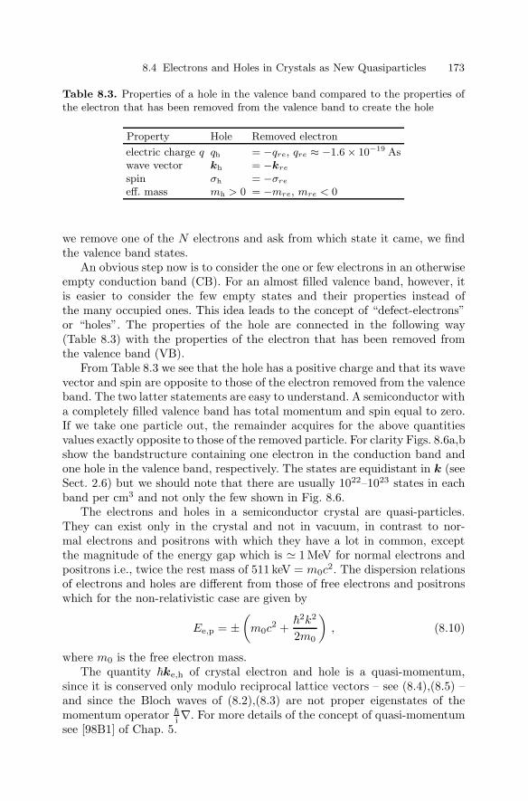
8.4 Electrons and Holes in Crystals as New Quasiparticles 173
Table 8.3. Properties of a hole in the valence band compared to the properties ofthe electron that has been removed from the valence band to create the hole
Property Hole Removed electron
electric charge q qh = −qre, qre ≈ −1.6 × 10⁻¹⁹ Aswave vector kh = −kre
spin σh = −σre
eff. mass mh > 0 = −mre, mre < 0
we remove one of the N electrons and ask from which state it came, we findthe valence band states.
An obvious step now is to consider the one or few electrons in an otherwiseempty conduction band (CB). For an almost filled valence band, however, itis easier to consider the few empty states and their properties instead ofthe many occupied ones. This idea leads to the concept of “defect-electrons”or “holes”. The properties of the hole are connected in the following way(Table 8.3) with the properties of the electron that has been removed fromthe valence band (VB).
From Table 8.3 we see that the hole has a positive charge and that its wavevector and spin are opposite to those of the electron removed from the valenceband. The two latter statements are easy to understand. A semiconductor witha completely filled valence band has total momentum and spin equal to zero.If we take one particle out, the remainder acquires for the above quantitiesvalues exactly opposite to those of the removed particle. For clarity Figs. 8.6a,bshow the bandstructure containing one electron in the conduction band andone hole in the valence band, respectively. The states are equidistant in k (seeSect. 2.6) but we should note that there are usually 1022–1023 states in eachband per cm3 and not only the few shown in Fig. 8.6.
The electrons and holes in a semiconductor crystal are quasi-particles.They can exist only in the crystal and not in vacuum, in contrast to nor-mal electrons and positrons with which they have a lot in common, exceptthe magnitude of the energy gap which is 1 MeV for normal electrons andpositrons i.e., twice the rest mass of 511 keV = m0c
2. The dispersion relationsof electrons and holes are different from those of free electrons and positronswhich for the non-relativistic case are given by
Ee,p = ±(m0c
2 +
2k2
2m0
), (8.10)
where m0 is the free electron mass.The quantity ke,h of crystal electron and hole is a quasi-momentum,
since it is conserved only modulo reciprocal lattice vectors – see (8.4),(8.5) –and since the Bloch waves of (8.2),(8.3) are not proper eigenstates of themomentum operator
i ∇. For more details of the concept of quasi-momentumsee [98B1] of Chap. 5.

174 8 Electrons in a Periodic Crystal
Fig. 8.6. One electron in the conduction band (a) and one hole in the valence band(b). Full circles: occupied states; open circles: empty states
One should note that the energy of a hole increases if it is brought deeperinto the valence band.
8.5 The Effective-Mass Concept
If we want to describe the motion of an electron or hole in a semiconductorunder the influence of an external field (e.g., an electric or magnetic field) itis intuitively clear that we ought to consider a wave packet rather than theinfinitely extended Bloch waves. To describe such a wave packet we super-pose Bloch waves of a certain range of k-vectors around a k0 as describedschematically in (8.11)
φk0(r) =∑
k
ak eik·ruk(r) . (8.11)
These types of wave packet are known as Wannier-functions. In order tokeep the k-vector reasonably well defined, we localize the wavefunction onlyto a volume larger than a unit cell. Due to the uncertainty relation we wouldneed wavefunctions from the whole Brillouin zone if we wanted to localize anelectron to within one unit cell.
An external force F changes the energy of the wave packet according to
dE(k) = F · ds = F · vg dt (8.12)
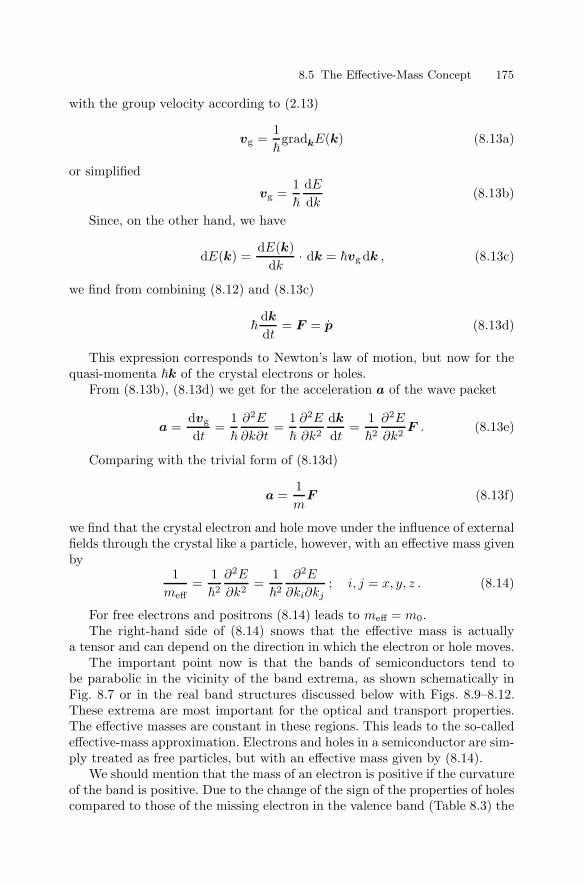
8.5 The Effective-Mass Concept 175
with the group velocity according to (2.13)
vg =1gradkE(k) (8.13a)
or simplified
vg =1
dEdk
(8.13b)
Since, on the other hand, we have
dE(k) =dE(k)
dk· dk = vg dk , (8.13c)
we find from combining (8.12) and (8.13c)
dk
dt= F = p (8.13d)
This expression corresponds to Newton’s law of motion, but now for thequasi-momenta k of the crystal electrons or holes.
From (8.13b), (8.13d) we get for the acceleration a of the wave packet
a =dvg
dt=
1
∂2E
∂k∂t=
1
∂2E
∂k2
dk
dt=
12
∂2E
∂k2F . (8.13e)
Comparing with the trivial form of (8.13d)
a =1m
F (8.13f)
we find that the crystal electron and hole move under the influence of externalfields through the crystal like a particle, however, with an effective mass givenby
1meff
=12
∂2E
∂k2=
12
∂2E
∂ki∂kj; i, j = x, y, z . (8.14)
For free electrons and positrons (8.14) leads to meff = m0.The right-hand side of (8.14) snows that the effective mass is actually
a tensor and can depend on the direction in which the electron or hole moves.The important point now is that the bands of semiconductors tend to
be parabolic in the vicinity of the band extrema, as shown schematically inFig. 8.7 or in the real band structures discussed below with Figs. 8.9–8.12.These extrema are most important for the optical and transport properties.The effective masses are constant in these regions. This leads to the so-calledeffective-mass approximation. Electrons and holes in a semiconductor are sim-ply treated as free particles, but with an effective mass given by (8.14).
We should mention that the mass of an electron is positive if the curvatureof the band is positive. Due to the change of the sign of the properties of holescompared to those of the missing electron in the valence band (Table 8.3) the

176 8 Electrons in a Periodic Crystal
mass of the hole is positive at the maximum where the curvature is actuallynegative.
The explanation behind the effective masses of electrons and holes is basi-cally the following. The forces which act on an electron are the ones from theother ions and electrons in the crystal and the externally applied ones. Forsimplicity, we condensed the first of these forces to yield the periodic potentialof (8.1) using the one-electron approximation. Then we chose to consider onlythe external forces acting on the electrons and the price we have to pay isthe fact that the electrons and holes react with an effective mass. This massis fortunately, in some regions at least, constant, allowing the effective-massapproximation mentioned above, but it can change as a function of k andbecome negative or infinite, as can be seen in Fig. 8.7.
It is important to note that an increasing curvature of a band is neces-sarily connected with an increasing width of the band. Therefore we find thequalitative relation:
electron easy to move and accelerate ←→ low effective mass←→ large curvature of the band ←→ large band width←→ strong coupling between adjacent atoms and vice versa . (8.15)
Thus we have here another example of the more general discussion given inthe introduction to Sect. 5.4.
Furthermore it can be stated as a trend that a large band width leaves lessspace on the energy scale for gaps. Therefore we can also state as a rule ofthumb, that narrow gap semiconductors tend to have small effective massesand wide gap semiconductors tend to have carriers with larger effective masses.
Fig. 8.7. Schematic dispersion (a) of a conduction band and the resulting effectivemass (b). After [95I1] of Chap. 1

8.6 The Polaron Concept and Other Electron–Phonon Interaction Processes 177
In the rest of this book we shall use the effective-mass approximation ifnot stated otherwise, including the polaron correction discussed in the nextsection.
We will in future omit the prefix “crystal” when talking about electronsand holes in semiconductors and we indicate the effective masses by indices eand h:
me = effective mass of electron ,mh = effective mass of hole , (8.16)
sometimes with an additional index to distinguish different bands, but wealways remember, that these charge carriers are quasi-particles, characterizedby their band index, energy and (quasi-!) momentum.
It should be mentioned that the Fermi energy is often situated in metalswith partly-filled bands in regions where the band structure E(k) is no longerparabolic. On the other hand, the electrons close to the Fermi energy arein metals the relevant ones for many physical properties like the electricalconductivity, the specific heat or the paramagnetic behavior of the electrongas. Therefore the use of the effective mass concept as given with (8.14) isless frequently used in metal physics and replaced by another concept that isbased on the fact that the first derivative gradkE(k) vanishes per definitionclose to the extrema of the conduction and valence bands of semiconductorsbut usually not around EF in a metal.
One can then define a “momentum effective mass” mi in contrast to the“force effective mass” meff in (8.13) via
k = p = mv (8.17)
resulting in vg = 1gradkE(k) in the vicinity of EF(kF) in
1mi
=1
kFgradkE (k = kF) . (8.18)
8.6 The Polaron Conceptand Other Electron–Phonon Interaction Processes
Before proceeding to some basic concepts of bandstructure calculations andto the band structures of real semiconductors, we shall discuss here variousaspects of electron–phonon interaction (see also [69R1,76C1,77P1,79T1,80M1,80P1]).
If we introduce an electron or a hole into a semiconductor which has at leastpartially ionic binding, the additional charge carrier will polarize the latticeprovided we relax the assumption that the ions are “fixed” at their latticesites. An electron will attract atoms with a positive charge and repel thosewith a negative one (Fig. 8.8). For holes, the situation is just the opposite.

178 8 Electrons in a Periodic Crystal
We can describe this lattice distortion as a superposition of preferentiallylongitudinal optical phonons, i.e., a free carrier is accompanied by a “phononcloud”. The entity of charge carrier plus phonon cloud is called a polaron.In semiconductors, the radius of the phonon cloud is larger than the latticeconstant, resulting in a so-called “large polaron” in contrast to the “smallpolaron” which occurs in ionic insulators and may lead to self-localizationwithin a unit cell. The effective mass me,h of a polaron is greater than thatof an electron in a rigid lattice mr.l.
e,h See e.g. [69R1, 70M1, 77P1, 79T1, 80M1,80P1,88C1] or [75Z1,76A1,81M1,82L1,99B1] of Chap. 1.
me,h mr.l.e,h
(1 +
αe,h
6
), (8.19a)
where the index r.l. stands for ”rigid lattice” and α is a dimensionless quantitywhich describes the Frohlich coupling of carriers to the LO phonons. One finds
αe,h =e2
8πε0ωLO
(2mr.l.
e,hωLO
)1/2(1εb
− 1εs
). (8.19b)
where εs and εb are the low-and high-frequency values of the dielectric functionbelow and above the optical phonon resonances, respectively; see also Chaps. 4and 12.
Obviously semiconductors without an ionic binding contribution have εb =εs [see (4.26), (4.28)] and thus α = 0. For all normal semiconductors one finds
α ≤ 1 . (8.19c)
Additionally the lattice relaxation leads to a decrease of the width of thegap by an amount ∆Eg with contributions for electrons and holes
∆Ee,hg = αe,hωLO . (8.19d)
Fig. 8.8. The lattice distortion around a carrier in a (partly) ionic semiconductorillustrating the polaron concept

8.6 The Polaron Concept and Other Electron–Phonon Interaction Processes 179
The radius of the phonon cloud in the polaron rp is finally given by
re,hp =(/2mr.l.
e,hωLO
)1/2. (8.19e)
Basically it is very difficult to ”fix the atoms at their lattice sites”. There-fore all common experimental techniques to determine the effective masses ofelectrons and holes, e.g., by cyclotron resonance, or the value of the gap, e.g.,by optical spectroscopy, will give polaron values. We therefore continue touse the effective mass approximation and simply bear in mind that all valuesgiven for me,h or Eg are actually polaron values.
Apart from the renormalization of mass and energy there are other con-sequences of carrier–phonon interaction, the most important being scatteringphenomena. An electron or hole can be scattered inelastically, e.g., by emittingor absorbing a phonon under energy and momentum conservation.
Eie = Ef
e ± ωPhonon , (8.20a)
kie = kf
e ± kPhonon(+G) . (8.20b)
The interaction Hamiltonian which describes such processes can have variousorigins as shown e.g. in [73H1,82L1,96Y1] of Chap. 1.
Optical phonons are often accompanied by an electric field (Sect. 7.4, 7.5and 11.1). The interaction of carriers with the electric field of preferentiallylongitudinal optical phonons is known as the Frohlich interaction.
Since the width of the gap depends on the lattice constant and on thearrangement of the atoms in the basis, a change of these quantities will in-fluence the bandstructure. On the other hand, a phonon can be consideredas a periodic deformation of the arrangement of atoms, and the carriers“feel” the resulting modulation of the bands. The resulting interactionbetween carriers and phonons is called deformation-potential scattering.The deformation potential scattering occurs for both acoustic and opticalphonons. The deformation potential Ξ connects usually the relative dis-placement ∆a/a of an atom with a = lattice constant with the energeticshift of a band ∆E resulting schematically in
∆E = Ξ∆aa
(8.21)
Typical values of deformation potentials are in the range of 5 to 10 eV.Note that (8.21) is valid only for ∆a/a <<< 1.
Finally, it is known that many non-centrosymmetric crystals show thepiezo-electric effect, i.e., the appearance of an electric field as a conse-quence of strain, i.e., of lattice distortion. Again we can consider an acous-tic (or optical) phonon as a periodic modulation of the lattice parameters,which produces, via the piezo-electric effect, a varying electric field whichinteracts with the electrons and holes. This effect is the so-called piezo(acoustic) coupling.

180 8 Electrons in a Periodic Crystal
More details about the polaron concept and on carrier-phonon couplingcan be found in the references given above.
In the so-called semimagnetic semiconductors, usually II–VI compoundsin which the cations are partly replaced by Mn or Fe ions, one finds so-calledmagnetic polarons, i.e., a spin alignment of the paramagnetic ions in thevicinity of a carrier. For details see e.g. references given in Chap. 16
8.7 Some Basic Approachesto Band Structure Calculations
In this section we will take a closer look at band structure calculations. Sincethis topic is already treated in many (text)books and review articles, it doesnot make too much sense to simply write it down here again. Instead we wantto present the basic concepts and ideas but we are not aiming towards a strin-gent mathematical treatment of the topic. For this aspect we refer the readerrather to the literature like the textbooks on solid state and semiconductorphysics of Chap. 1 and references given therein.
We start with the concept of nearly free electrons, proceed to the approachstarting from atomic orbitals and finish this section with the so-called k · pperturbation theory, which is very useful to calculate band structures in thevicinity of the extrema.
As already stated, the dispersion relation of a free electron in vacuum isa parabola in the nonrelativistic regime as shown in Fig. 8.9a or 8.1a, i.e.,
E (k) =2k2
2m0(8.22)
We start, for simplicity, with a one-dimensional system and represent therelation (8.22) for this case in Fig. 8.9a.
Next we introduce a very weak periodic potential as shown schematicallyin Fig. 8.10 with a periodicity a. Weak means, in this context, that the dis-persion relation of Fig. 8.9a is only marginally influenced by this potential.Nevertheless, we have introduced a periodicity by this potential in real space,which evokes the (Ewald–)Bloch theorem. As a consequence, the dispersionrelation can be repeated in k-space by shifting it by integer multiples of 2π/aresulting in the extended zone scheme of Fig. 8.9b (dashed lines). Comparewith Fig. 8.1. In the limit that the amplitude of the periodic potential goesto zero, this is all. If the potential is small but finite, a further modificationoccurs. Small gaps open at the borders of the Brillouin zones as shown by thesolid lines. There are various possibilities to explain the appearance of thesegaps and the fact that two different energy eigenvalues exist for the samek-vector at the Brillouin zone boundary.
In a first argumentation this splitting can be considered as an exampleof the non-crossing rule already discussed in Sect. 5.1. The coupling between

8.7 Some Basic Approaches to Band Structure Calculations 181
Fig. 8.9. The (one-dimensional) dispersion relation of a free electron in vacuum(a) in a weak periodic potential (b) and the resulting reduced zone scheme (c)
the degenerate states at k = nπ/a is mediated by the periodic potential. In-deed it can be shown that the width of the band gap is determined by theFourier component of the periodic potential (see, e.g., (7.10)) with the recip-rocal lattice vector G, which couples the bands that intersect for vanishingpotential.
Another set of arguments works as follows. Assume a plane electron wave isimpinging on the periodic potential. Then the potential will produce scatteredwaves. For an arbitrary k-vector, i.e., wavelength and (in dimensions higherthan one) direction of incidence, the scattered waves will have various phaseshifts relative to each other and will essentially cancel. However, there arespecial wave vectors, namely just the ones at the borders of the Brillouin zones(in our present one-dimension model k = ±nπ/a) where all scattered wavesinterfere constructively to form a backscattered wave with large amplitude,i.e., an incident wave with, e.g., ki = π/a creates a backscattered wave withkb = −π/a (and ki − kb = 2π/a = G). Since the backscattered wave withkb scatters again off the periodic potential contributing to the wave with ki
we end up under stationary conditions with two counterpropagating waves ofequal amplitudes and ki = −kb. As is well known, the superposition of twowaves with k and −k and equal amplitudes produces a standing wave. Thisfact has in our context two consequences:
A wave packet built up from a standing wave and its surroundings ink-space has zero group velocity. Consequently the slope of the dispersionrelation must be zero, normal to the border of the Brillouin zone.
The standing wave can be the sine- or the cosine-type with the samewavelength and k-vector as shown in Fig. 8.10, where the probabilities areplotted. These two waves have their maxima at the positions of the maxima

182 8 Electrons in a Periodic Crystal
or of the minima of the periodic potential, respectively. Consequently theysee different average potential energies but have equal kinetic energy. Thisfact results in the energy splitting, i.e., in the appearance of the gaps atthe borders of the Brillouin zones.
We proceed now, still in the context of nearly free electrons, to two- andthree-dimensional potentials.
In Fig. 8.11a we show the parabolic dispersion relation of (8.22) over a twodimensional k-space assuming a hexagonal, two-dimensional lattice but van-ishing potential. The differently hatched areas in the kx, ky plain correspondto the different Brillouin zones. Figure 8.11a thus corresponds to the extendedzone scheme. Figure 8.11b shows the resulting reduced zone scheme, which isobtained by shifting the parts outside the first Brillouin zone by suitable vec-tors G of the reciprocal lattice into the first zone. The various energy surfacesor bands should touch, e.g., at the border of the first Brillouin zone for van-ishing potentials like in Fig. 8.9b for the one-dimensional case, but have beendisplaced in Fig. 8.11b and c for clarity along the energy axis to allow an“insight” into the first Brillouin zone.
In Fig. 8.11c a weak potential has been switched on. As we expect fromour knowledge from the one dimensional case the overall appearance of theE(k) relation does not change very much but kinks are smoothed out, energygaps open, e.g., at the boarder or the center of the first Brillouin zone and theslope of the dispersion relation vanishes at the zone boundary in the directionnormal to it. Figure 8.11d finally gives the dispersion relation along various di-rections in the two-dimensional k-space for vanishing and for weak potentials.
In Fig. 8.12a and b we finally go through the same procedure as inFig. 8.11d, but now for a real three-dimensional crystal structure, namelythat for diamond (point group Oh).
Fig. 8.10. Schematic drawing of two Bloch waves with equal k-vector but differentpotential energies at the boundary of the first Brillouin zone over a periodic potentialV (x)

8.7 Some Basic Approaches to Band Structure Calculations 183
The case of the empty lattice in Fig. 8.12a already shows a rather complexband structure and we understand that the complexity of a three-dimensionalband structure comes to a large extent from the back-folding of the parabolicdispersion into the first Brillouin–zone.
Actually there is a possibility to test various band structure calculations,the so-called empty lattice datetest. One runs any type of band structurecalculation but with vanishing potential. Since the solution is known exactly,e.g., for the diamond structure in Fig. 8.12a the band structure calculationmust give this result. If it fails, something might be wrong, at least for thecalculation of the bands arising from the outer, weakly bound atomic orbitals.
In Fig. 8.12b a realistic band structure calculation is shown for Si whichcrystallizes in the diamond structure, as already mentioned in Sect. 8.3, butstill neglecting spin. The dispersion relation is given for the direction from theΓ -point towards the X and L points as in Fig. 7.4b, but also from Γ along theΣ direction to the U, K points and from there along the surface of the firstBrillouin zone to the X point. The indirect band-gap in Si occurs between the
Fig. 8.11. The parabolic disper-sion relation of free electrons overa two-dimensional k-space, assuminga hexagonal lattice with vanishing po-tential (the so-called empty lattice)(a) the resulting reduced zone schemefor vanishing (b) and weak but finitepotential (c) and the E(k) relationalong various lines of high symmetryfor both cases (d). In b and c thebands are displaced vertically for clar-ity ([81M1] of Chap. 1)

184 8 Electrons in a Periodic Crystal
Fig. 8.12. Band structure for the three dimensional diamond structure. For vanish-ing potential (a) and a realistic band structure calculation for Si (b). The numbersat Γ give the irreducible representations (see Sect. 26.4 to 6), still neglecting spin:According to [76A1,81M1,96Y1] of Chap. 1
maximum of the valence band at the Γ point, set here as energy zero and theminimum of the conduction band close to the X point.
While we stressed, in the nearly free electron approach, the plane wavefactor of the Bloch–wave and assumed that the lattice periodic part is essen-tially a constant, we now start from the opposite side, by placing one or moreatomic orbitals at every atom site as shown, e.g., in Fig. 8.3 for simple 1s likeatomic orbitals.
Now we translate this concept into an equation assuming, for simplicity,that we have a three-dimensional simple-cubic lattice with one atom per unitcell and a nondegenerate normalized atomic orbital ϕi(r−Ri) at every latticesite Ri.
In the linear combination of atomic orbitals (LCAO), or tight bindingapproximation, the total wave function ψ(r) is then given by
ψk (r) =∑
i
Ck,iϕi (r − Ri) . (8.23a)
The fact that this form has to be of the Bloch–type determines the Ck,i
to beCk,i = N− 1
2 eikRi (8.23b)
where N−12 is the normalization factor for a crystal consisting of N atoms.
Inserting (8.23b) in (8.23a) results in the LCAO wave function
|k〉 = ψk (r) = N− 12
∑i
eikRiϕ (r − Ri) . (8.24a)

8.7 Some Basic Approaches to Band Structure Calculations 185
The energy belonging to these wave functions can be calculated in firstorder with the help of the Hamiltonian H which contains, apart from thekinetic energy terms, the sum over the atomic potentials via
E (k) =〈k |H |k〉 = N−1∑
i
∑j
eik(Ri−Rj)
×∫ϕ · (r − Ri)Hϕ (r − Ri) d3r . (8.24b)
Since only relative distances enter, we simplify (8.23b) by introducingRm = Ri − Rj and obtain
E (k) = 〈k |H |k〉 =∑m
eikRm
∫ϕ · (r − Rm)Hϕ (r) d3r . (8.24c)
The next simplification is to assume realistically that in the sum only theterms with Rm = 0 and contribution for nearest neighbors Rn in the overlapintegral give considerable contributions. With the abbreviations∫
ϕ∗ (r)Hϕ (r) d3r = −A (8.25)
and ∫ϕ∗ (r −Rn)Hϕ (r) d3r = −B (8.26)
we obtainE (k) = 〈k |H |k〉 = −A−B
∑n
eikRn (8.27)
where the sum now runs only over the nearest neighbors.The term −A is close to but generally slightly lower in energy than the
eigenenergy of the parent atomic orbital ϕ(r) since the Hamiltonian containsnot only the potential of a single atom but the sum over them as stated above.
For the simple-cubic lattice, which we consider, Rn adapts the followingsix values
Rn = (±a, 0, 0); (0,±a, 0); (0, 0,±a) . (8.28)
This finally results in a simple band structure of width 12B centered ar-ound −A:
E(k) = −A− 2B(cos kxa+ cos kya+ cos k2a) . (8.29)
We see from (8.29) that the overlap between atomic orbitals leads to theformation of bands out of sharp atomic levels while the nearly free electronmethods explained the appearance of gaps in the simple parabolic dispersionrelation (see again Fig. 8.1).
Physically the formation of bands by the overlap described by B in (8.29)is nothing but the splitting of the eigenenergies of coupled harmonic oscillatorsas already mentioned in Sect. 8.1.
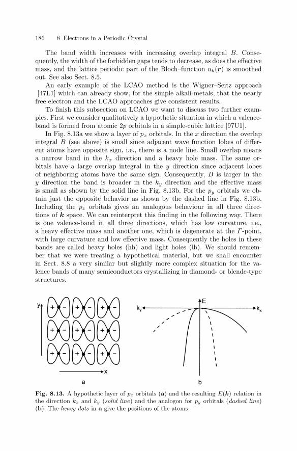
186 8 Electrons in a Periodic Crystal
The band width increases with increasing overlap integral B. Conse-quently, the width of the forbidden gaps tends to decrease, as does the effectivemass, and the lattice periodic part of the Bloch–function uk(r) is smoothedout. See also Sect. 8.5.
An early example of the LCAO method is the Wigner–Seitz approach[47L1] which can already show, for the simple alkali-metals, that the nearly
free electron and the LCAO approaches give consistent results.To finish this subsection on LCAO we want to discuss two further exam-
ples. First we consider qualitatively a hypothetic situation in which a valence-band is formed from atomic 2p orbitals in a simple-cubic lattice [97U1].
In Fig. 8.13a we show a layer of px orbitals. In the x direction the overlapintegral B (see above) is small since adjacent wave function lobes of differ-ent atoms have opposite sign, i.e., there is a node line. Small overlap meansa narrow band in the kx direction and a heavy hole mass. The same or-bitals have a large overlap integral in the y direction since adjacent lobesof neighboring atoms have the same sign. Consequently, B is larger in they direction the band is broader in the ky direction and the effective massis small as shown by the solid line in Fig. 8.13b. For the py orbitals we ob-tain just the opposite behavior as shown by the dashed line in Fig. 8.13b.Including the pz orbitals gives an analogous behaviour in all three direc-tions of k space. We can reinterpret this finding in the following way. Thereis one valence-band in all three directions, which has low curvature, i.e.,a heavy effective mass and another one, which is degenerate at the Γ -point,with large curvature and low effective mass. Consequently the holes in thesebands are called heavy holes (hh) and light holes (lh). We should remem-ber that we were treating a hypothetical material, but we shall encounterin Sect. 8.8 a very similar but slightly more complex situation for the va-lence bands of many semiconductors crystallizing in diamond- or blende-typestructures.
Fig. 8.13. A hypothetic layer of px orbitals (a) and the resulting E(k) relation inthe direction kx and ky (solid line) and the analogon for py orbitals (dashed line)(b). The heavy dots in a give the positions of the atoms

8.7 Some Basic Approaches to Band Structure Calculations 187
As a last example we discuss with Fig. 8.14 the tight binding approach forSi (or diamond or Ge) as a function of the lattice constant a. Si has a filled Neconfiguration plus 3s23p2, i.e., four electrons in the outer nB = 3 shell, whichare responsible for the chemical binding, while the lower electron states (1s2,2s2, 2p6) form deeper valence bands, which are presently of no interest.
For a large lattice constant the overlap integral vanishes and one startswith the atomic 3s and 3p levels. With decreasing distance the levels shift tolower energy and broaden since both A and B in (8.29) depend on the latticeconstant. For further decreasing distance the two bands start to overlap. Thisis the distance between the atoms at which the sp3 hybrid orbitals start toform. For even smaller values the bands split again. In contrast to the twofold degenerate 3s and six-fold degenerate 3p levels, two four-fold degeneratebands form the binding and the antibinding states of the sp3 hybrids. Sincethere are two Si-atoms in the primitive unit cell, the valence band originatingfrom the HOMO (see Sect. 8.2) accommodates eight electrons and the con-duction band (LUMO) also has place for eight electrons per unit cell. Thebinding orbitals of the sp3 hybrid point towards the corners of a tetrahe-dron giving rise to the tetrahedral coordination of many semiconductors (seeSect. 7.2).
The minimum of the total free energy gives the equilibrium distance r0,which is indicated in Fig. 8.14. For even smaller values of a the bands shift tohigher energies, again due to the action of Pauli’s principle, and the increasingkinetic energy of the wave functions.
Fig. 8.14. The bands originating from the 3s and 3p levels of Si as a function of thelattice constant a or the distance between atoms ([95I1] of Chap. 1). The numbersin the circles give the number of electrons per atom in the respective state or band.

188 8 Electrons in a Periodic Crystal
To conclude this section we give a few introductory remarks to the widelyused k · p perturbation theory, which is very valuable to calculate the bandstructure in the vicinity of band extrema but by extrapolation allows one toobtain an idea about the band structure over the whole Brillouin zone. Formore details see again the textbooks on solid state physics and on semicon-ductor physics cited in Chap. 1 and in this chapter.
We assume in the following that the band extrema are situated at k0 andintroduce the further simplification that k0 = 0. If this is not the case, thefollowing considerations are valid for k′ = k − k0.
We start again with the one-electron approximation and the periodic po-tential V (r) = V (r + R). The Hamiltonian reads
H =p2
2m0+ V (r) . (8.30)
We insert the Bloch-wave ansatz of Sect. 8.1 into (8.30) and obtain (8.31a)where n is the band index, m0 the free electron mass and p =
i ∇:(p2
2m0+
2k · pm0
+
2k2
2m0+ V (r)
)unk (r) = En (k)unk (r) . (8.31a)
For the case k = k0 = 0 (8.31a) simplifies to(p2
2m0+ V (r)
)un0 (r) = En (k = 0)un0 (r) = En,0un,0 (r) . (8.31b)
We now assume, that the solution of (8.31b) is known. Then we can use theterms 2kp/m0 (this is the reason for the name of this method) and 2k2/2m0
in (8.31a) as perturbations of the first and second order in k.For the simple case of a nondegenerate band (or a two-fold spin degenerate
one) we obtain for the lattice periodic part of the eigenfunctions unk(r)
unk (r) = un0 (r) +
m0
∑n′ =n
〈uno |k · p|un′0〉En0 − En′0
un′0 (r) . (8.32a)
The above-mentioned situation of nondegeneracy frequently holds for thelowest conduction band of semiconductors.
The dispersion relation is then given by
En (k) = En,0 +
2k2
2m0+
2
m20
∑n′ =n
|〈un0 |k · p|un′0〉|2En0 − En′0
(8.32b)
From (8.32b) we can easily deduce the effective mass of e.g. the conductionband n
1me
=1m0
+2
m20k
2
∑n′ =n
|〈uno |k · p|un′0〉|2En0 − En′0
(8.32c)

8.8 Bandstructures of Real Semiconductors 189
The coupling between various bands, which influences me, depends essen-tially on the momentum matrix element, which in turn is closely related tothe dipole-matrix element (see Sect. 3.2.2) and can at least in principle bededuced from optical absorption spectra.
The knowledge, which of the matrix elements vanish and which are non-zero, can be obtained from group theory (see Chap. 26).
As already stated various times above, the effective electron mass decreaseswith decreasing width of the gap En0 − En′0 if the dominant term in (8.32c)comes from the coupling between conduction- and valence band.
Since the k · p theory starts for all bands with the free electron mass(see (8.31a)) the appearance of effective masses can be considered again asa consequence of level repulsion, e.g., between conduction and valence bandin the way indicated schematically by the arrows in Fig. 8.15. The couplingbetween the bands arises in this model from the k · p term (also see theKane-model [57K1]).
The treatment of degenerate bands, especially of the upper valence bandsin k ·p theory is more complicated, and beyond the scope of this chapter. Werefer the reader to the above-mentioned literature for details and formula butmention that we shall meet results in the next section on band structures ofreal semiconductors.
8.8 Bandstructures of Real Semiconductors
In this section we present band structures of real semiconductors.As already mentioned the upper valence bands frequently arise, in the case
of ionic binding, from the highest occupied atomic p-levels of the anions with
Fig. 8.15. Conduction and valence bandwith free electron mass m0 (dashed lines)and the modifications (arrows) resulting fromlevel repulsion (solid lines)

190 8 Electrons in a Periodic Crystal
Fig. 8.16. An overview of the band structures of some cubic semiconductors [70M1]
a more-or-less pronounced admixture of d-levels, or from the bonding statesof the sp3 hybrid orbitals for covalent binding. The lowest conduction bandscome from the lowest empty s-levels of the cations or the antibonding sp3
hybrid, respectively. In Fig. 8.16 we give the essentials of the bandstructurefor cubic semiconductors like diamond, Si or Ge (point groupOh) or the III–V,II–VI and I–VII compounds crystallizing in zincblende (Td) structure.
The valence band has its maximum at the Γ point, i.e., at k = 0. Itis six-fold degenerate including spin corresponding to the parent p orbitals.In Sect. 8.7 we stated that eight levels form the bonding sp3 hybrid statesince there are two atoms in a unit cell. Six of them, which are treatedin the following, form the top of the valence band and the other two therather low lying Γ1 (with spin Γ6) level seen, e.g., in Fig. 8.14b. This band isnot included in the following. The upper valence band splits due to spin–orbit coupling at k = 0 into a two-fold degenerate band (symmetry Γ+
7
in Oh or Γ7 in Td) and a four-fold degenerate band (symmetry Γ+8 in Oh
or Γ8 in Td). Usually the Γ (+)8 band is the upper and the Γ (+)
7 the lowerone. The spin–orbit splitting increases in atoms with increasing charge Zof the nucleus and this also applies in the semiconductor. In CuCl the or-dering of the valence bands is inverted due to the influence of close-lyingd levels.

8.8 Bandstructures of Real Semiconductors 191
The Γ (+)8 valence band splits for k = 0 into two bands which have different
curvature and are therefore known as heavy- and light-hole bands. All bandshave cubic symmetry, which is lower than spherical symmetry. As a con-sequence the dispersion and thus the hole masses depend on the directionof k. This phenomenon is known as band-warping. The valence bands are fre-quently treated in k · p perturbation theory. The theory has been developed,e.g., by Kane, Luttinger, Cardona, Pollack and many others (see [57K1,87B1]or [96Y1] of Chap. 1) and is briefly outlined in Sect. 8.7.
Basically one has to start with the 16 bonding and antibonding statesresulting from two atoms per primitive unit cell. Often one considers thelowest two-fold degenerate conduction band (symmetry Γ6) separately, e.g.,in the way described in Sect. 8.7 and is then left with eight valence bandstates. Since the lowest Γ1 (or Γ6) state is energetically rather far away, ithas only minor influence and may be neglected in the treatment of the uppervalence bands. The remaining six states in the Γ8 and Γ7 valence bands canbe treated in a 6 × 6 matrix. If the spin-orbit coupling is large, it is, how-ever, often possible to treat the Γ8 band alone resulting in a 4 × 4 matrix,which can be solved analytically. The resulting band structure is frequentlydescribed by the so-called Luttinger parameters γ1, γ2 and and γ3 accord-ing to
E1,2 =E0 +
2
2m0
[γ1k
2 ± 2[γ2
(k4
x + k4y + k4
z
)+3
(γ23 − γ2
2
) (k2
xk2y + k2
yk2z + k2
zk2x
)]1/2]
(8.33a)
where γ−11 describes the average effective mass and γ2 and γ3 the splitting
into heavy- and light-hole bands and the warping via the term 3(γ23 − γ2
2
). If
warping is negligible (i.e. γ2 = γ3) the light and heavy hole effective massesare given by
mhh =m0
γ1 − 2γ2; mlh =
m0
γ1 + 2γ2(8.33b)
The conduction band has a minimum at the Γ point and other minima in thedirection ∆ close to the X points and at the L points.
If the minimum of the Γ point is the deepest one, the semiconductor issaid to have a “direct gap” since transitions between the global maximum ofthe valence band and the global minimum of the conduction band are directlypossible with photons, having kphoton 0. In other cases, the semiconductoris called “indirect” since a momentum-conserving phonon is involved in thetransitions between the band extrema.
Examples of indirect semiconductors are diamond, Si and Ge, some of theIII–V compounds such as AlAs and GaP, and some of the I–VII compoundslike AgBr. Direct gap semiconductors include some of the III–V compoundslike GaAs or InP, the II–VI compounds ZnS, ZnSe, ZnTe and CdTe, and I–VIImaterials like CuCl, CuBr and CuI. See also Table 8.1.

192 8 Electrons in a Periodic Crystal
The conduction band minimum at the Γ point is usually, to a very goodapproximation, isotropic and parabolic. Only some narrow-gap materials likeInSb show significant nonparabolicities in the vicinity of k = 0 (Fig. 8.16).
The minima of the L points of Ge or in the ∆ direction of Si are parabolicbut highly anisotropic (Fig. 8.16). The dispersion relation around the mini-mum at k0 can consequently be expressed by
E(k) = Eg +2
2
((kx − k0x)2
ml+
(ky − k0y)2
mt+
(kz − k0z)2
mt
). (8.34)
Here ml is the effective mass for k-components in the direction from Γ tok0 and mt that for the two directions perpendicular to it.
In GaAs the minimum at the Γ point is the deepest, but other minima atdifferent points of the Brillouin zone are close in energy, e.g., in the ∆ directiongiving rise to the Gunn effect, which arises from the transfer of electrons underthe influence of a strong electric field from the minimum at k = 0 with loweffective mass to side minima with higher effective masses.
The direct gap semiconductors are also called “single-valley”, and the in-direct ones “multi-valley” semiconductors because they have several (6 for Siand 8 · 1/2 for Ge) equivalent conduction-band minima.
Semiconductors with hexagonal wurtzite structure (point group C6v) areusually “direct”. They are found preferentially among the II–VI compoundssuch as ZnO, ZnS, CdS and CdSe, but also among the III–V materials likeGaN.
The upper six valence band states of the C6v semiconductors are split byspin–orbit coupling and by the hexagonal crystal field into three subbandswhich are usually labelled from higher to lower energies as A, B and C bandswith symmetries Γ9, Γ7 and Γ7 (Fig. 8.17a). In ZnO, the symmetries of thetwo upper bands are most probably inverted as in the case of CuCl. Somereferences on this presently again ongoing discussion are e.g. [69R1, 82B1,02W1] or [01G1] of Chap. 4. The effective masses of the valence bands areoften strongly anisotropic in these compounds, m⊥ usually being smaller thanm‖ where the indices refer to k-vectors perpendicular and parallel to the polarcrystallographic c-axis:
mvb⊥ mvb
‖ for C6v , (8.35a)
mDOS = (m2⊥m‖)1/3 . (8.35b)
If one restricts oneself to the four states in the A and B bands k · p theorypredicts for negligible warping, i.e., γ2 = γ3 = γ for the effective masses [92E1]
mA‖ =m0
γ1 − 2γ;mA⊥ =
m0
γ1 + γ(8.36a)
mB‖ =m0
γ1 + 2γ;mB⊥ =
m0
γ1 − γ. (8.36b)

8.8 Bandstructures of Real Semiconductors 193
The effective mass that enters in the calculation of the density of statesmDOS is given in (8.35b). A pecularity of the states of Γ7 symmetry is thatthey can have a term linear in k in the dispersion relation for k⊥ c asshown in Fig. 8.17b. This term has some influence on the optical proper-ties. In principle, it can also occur for the Γ7 conduction band, but is muchsmaller there and usually neglected. The same is true for the hexagonal warp-ing which is, in principle, possible for C6v symmetry in the plane normalto c.
As already mentioned, the crystal structures of zincblende and of wurtziteare rather similar and differ only in the arrangements of the next-nearestneighbors. The unit cell of the wurtzite structure is in one direction twice aslong as the primitive unit cell of the zinkblende structure. As a consequencethe first Brillouin zone is only half as long in one direction. The resultingfolding back of the dispersion is shown schematically in Fig. 8.18 neglectingspin [69R1] for the two lowest conduction bands and the highest valence band.Obviously the number of bands doubles in this procedure, as does the numberof states at the Γ point. This is in agreement with the fact that diamond andzincblende structures have two atoms in the basis of the primitive unit cellbut wurtzite has four.
Due to the p- and s-type character of valence and conduction bands, forthe more ionic bound semiconductors and of the binding and antibinding sp3
states close to the fundamental gap, respectively, the band-to-band transi-tion is dipole allowed – possibly with some additional selection rules for thehexagonal symmetry.
Fig. 8.17. Details of the band structure of hexagonal semiconductors around the Γpoint. The splitting into three valence bands (a) and the influence of a term linearin k (b)

194 8 Electrons in a Periodic Crystal
Fig. 8.18. The relation between the band structure of semiconductors withzinkblende and wurtzite type structures along the corresponding direction in k-space, neglecting spin [69R1]
In Table 8.4 we summarize some band parameters of semiconductors. Anexhaustive list is found in [82L1] of Chap. 1. See as additional informationTable 8.2
It is beyond the scope of this book to review all types of semiconductors.Instead we give only some selected examples beyond those mentioned alreadyabove.
The lead salts (PbS, PbSe, PbTe) are narrow-gap semiconductors crys-tallizing in the NaCl structure. They have a direct gap. In contrast to the

8.8 Bandstructures of Real Semiconductors 195
Table 8.4. Effective masses of some selected semiconductors. From [82L1] of Chap. 1
SC Sy dir/ind me/m0 mhh/m0 mlh/m0 mA⊥ ‖ /m0
C Td i 2.18 0.7
Si Td i
⊥0.19‖ 0.92
0.54 0.15
Ge Td i
⊥0.081‖ 1.6
0.3 0.043
AlAs Td i
⊥1.56, 5.8‖ 0.19
0.76 0.15
AlSb Td i
⊥0.26‖ 1.0
0.94 0.11
GaN C6v d 0.22 ≈ 0.8
GaP Td i
⊥0.25‖ 7.25; 2.2
0.6 0.17
GaAs Td d 0.066 0.47 0.07
GaSb Td d 0.042 0.35 0.05
ZnO C6v d 0.28
⊥0.45‖ 0.59
ZnS C6v d 0.28 0.5
ZnSe Td d 0.15 0.8 0.145
ZnTe Td d 0.12 0.6
CdS C6v d 0.2
⊥0.7‖ 2.5
CdSe C6v d 0.13
⊥0.45‖ 1.1
CdTe Td d 0.1 0.4
CdCl Td d 0.4 2.4
CuBr Td d 0.25 1.4
CdI Td d 0.3 ≈ 2
above-mentioned direct semiconductors, the band extrema are situated at theL points. Some semiconductors, such as the IV–VI compounds TiO2 (rutil)and SnO2 or the I–VI compound Cu2O have a direct gap. The transitionsbetween the band extrema are, in contrast to the other materials mentionedabove, dipole forbidden because of their equal parity. The symmetry groups ofthese materials contain inversion as an element and parity is therefore a goodquantum number. This feature has significant consequences for the opticalproperties.
A last example is shown in Fig. 8.19 where we demonstrate the transition ofthe alloy system Cd1−yHgyTe from a normal semiconductor (y = 0) to a nar-row gap material 0 < y < 0.85, and finally to a semimetal for 1 ≥ y ≥ 0.85.

196 8 Electrons in a Periodic Crystal
Fig. 8.19. The transition from a semiconductor (a) to a semimetal (c) for the alloyCd1−y ,Hgy,.Te (b) as a function of the composition y [70M1]
8.9 Density of States, Occupation Probabilityand Critical Points
We start now to consider the density of states D(E) for crystal electrons andholes using simple parabolic bands in the effective mass approximation, i.e.,
conduction band (CB) : E(ke) = Eg +2k2
e
2me, (8.37a)
valence band (VB) : E(kh =
2k2h
2mh, (8.37b)
where we take into account that the energy of a hole increases if it is broughtdeeper into the valence band.
With the help of (2.79) we find that the density of states depends on theenergy in the conduction and valence bands according to
CB : D(E) = (E − Eg)d/2−1 ; E > Eg (8.38a)
VB : D(E) =Ed/2−1 ; E > 0 ; d = dimensionality (8.38b)
for three-, two- and one-dimensional systems. This situation is shown schemat-ically in Fig. 8.20 where we also include a set of δ-functions for the density ofstates in a quasi-zero-dimensional system.
The appearance of the various subbands for d < 3 will be explained in thenext section.

8.9 Density of States, Occupation Probability and Critical Points 197
The statistics with which we describe the occupation probability are theFermi–Dirac statistics, as already mentioned. It reads for electrons and holes
electrons : fFD(E) =(
e(E−EeF)/(kBT ) + 1
)−1
(8.39a)
holes : fFD(E) = 1 −(
e(E−EhF)/(kBT ) + 1
)−1
=(
e−(E−EhF)/(kBT ) + 1
)−1
. (8.39b)
The Fermi energies (or chemical potentials) for electrons and holes Ee,hF
are non-zero, unlike the situation for phonons or photons, since there isa conservation law for the number of electrons. The Fermi energies dependon the concentrations of electrons (and holes), on the temperature of theelectron gas, and on material parameters such as Eg, me, or mh as shownbelow.
Since electrons can be exchanged between the valence and conductionbands, for example by thermal excitation and recombination, it follows that
Fig. 8.20. Schematic drawing of the density of states as a function of energy forthree-, and quasi-two-, one- and zero-dimensional systems in the effective massapproximation. The dashed line corresponds to disorder-induced localized states(Sect. 8.15)

198 8 Electrons in a Periodic Crystal
in thermodynamic equilibrium
EeF = Eh
F = EF (8.40a)
or, in other words, the chemical potential of the electron–hole pair system µeh
is zeroµeh = Ee
F − EhF = 0 . (8.40b)
We shall come back to this point later.The density of electrons in a certain energy range, say in the conduction
band, is then given by the integral over the density of states weighted by theoccupation probability. For parabolic bands with a degeneracy g we find ford = 3 and for the total density of electrons in the conduction band n:
n =N
L3=
∞∫Eg
ge1
2π2
(2me
2
)3/2
(E − Eg)1/2
(e(E−EF)/(kBT ) + 1
)−1
dE ,
(8.41)where we have used our knowledge from Sect. 2.6 and the dispersion relation(8.37). Equation (8.41) leads to the Fermi integral which cannot be solvedanalytically but can be found in mathematical tables.
Very often EF lies in the gap. In this case the electron gas is said to benon-degenerate and the part of the Fermi function which overlaps with a finitedensity of states can be approximated quite well by the Boltzmann function,as can be seen in Fig. 2.5 where we compare Fermi–Dirac, Bose–Einstein andBoltzmann statistics.
With this assumption the Fermi–Dirac statistics (8.41) can be replacedby classical Boltzmann statistics and the integral can be solved analyticallygiving
n = ge
(mekBT
2π2
)3/2
e(E−EF)/(kBT ) . (8.42a)
The term in front of the exponential is the so-called effective density of statesneff depending on T and on material parameters. So we can write
n = neff (T,me) e(Eg−EF)/(kBT ) . (8.42b)
If the electron gas is degenerate, i.e., if EF is situated in the conductionband, we have to use the full (8.41) except for T → 0 where the Fermi functionconverges to a step function and n is given by
n =2
6π2g
(2me
2
)3/2
(EF − Eg)3/2 for T = 0 K . (8.42c)
In analogy we find for a three-dimensional non-degenerate gas of holes
p = peff e−EF/kBT (8.42d)

8.9 Density of States, Occupation Probability and Critical Points 199
with
peff = gh
(mhkBT
2π2
)3/2
. (8.42e)
We should mention here that in thermodynamic equilibrium, i.e., when(8.40a) is valid, one finds that the product np is independent of EF in thenon-degenerate case, i.e.,
np = neff peff e−EF/kBT =: n2i (T ) . (8.43)
where ni(T ) is the intrinsic carrier density.Out of thermal equilibrium, a situation that occurs, e.g., under optical
pumping or via carrier injection in a p-n junction, one frequently has a ther-mal distribution of the carriers within their bands with some effective carriertemperature Te,h, which may be higher than the lattice temperature TL. Inthis case, the distribution of the carriers in their respective bands can bedescribed by Fermi-functions, which contain separate quasi-Fermi levels forelectrons and holes. In this case one has
n · p = n2i (T ) (8.44a)
and in contrast to (8.40b)
µeh = EeF − Eh
F = 0 (8.44b)
The occupation of donor or acceptor levels situated in the forbidden gapor of localized tail states can be also covered by the concept of Fermi–Diracoccupation probabilities. For defect states degeneracy factors appear in theFermi statistics which take care, e.g., of the fact that an unoccupied simpledonor in a direct gap semiconductor offers two empty, spin degenerate states.But if one electron sits on the donor, the other electron level is shifted to higherenergies due to Coulomb interaction. For details of this topic see, e.g., [87B1].
The last aspect we want to discuss in this section are the so-called criticalpoints or van Hove singularities. One type of these critical points has alreadybeen treated. If a parabolic band starts at energy E0 (e.g., a conduction band)we have above a density of states given by (8.45a) and zero below, i.e., in a ddimensional system
D (E) ∼
(E − E0)d2 − 1 for E ≥ E0
0 for E < E0. (8.45a)
This is a so-called M0 critical point in three dimensions.If a parabolic band ends at a certain energy E0 like a valence band, we
have the inverse situation, i.e.,
D (E) ∼
(E0 − E)d2 − 1 for E ≤ E0
0 for E > E0
. (8.45b)
200 8 Electrons in a Periodic Crystal
The name of this type of critical point is Md where d is the dimensionality.In three dimensions we can additionally have a situation where the curva-
ture of E(k) is positive in two orthogonal directions and negative in the thirdone or vice versa. These so-calledM1 andM2 critical points exhibit a constantdensity of states D0 (similar to a two-dimensional system) on the energy sideof E0 where two branches exist and a dependence
D (E) ∼(
1 −A (E − E0)1/2)
(8.45c)
on the other side.A saddle point or M1 critical point in a two dimensional system finally
gives a logarithmic singularity on both sides of E0
D (E) ∼ − ln (|E − E0|) . (8.45d)
For details see, e.g, [96Y1] of Chap. 1.Critical points are also important in the optical properties of vertical band-
to-band transitions. In this case not the density of states in each of the twobands is important, but rather the joint or combined density of states ofconduction and valence band separated in their E(k) dispersion vertically bythe photon energy ω.
8.10 Electrons and Holes in Quantum Wellsand Superlattices
We have already introduced structures of reduced dimensionality in connec-tion with the discussion of phonons in Sect. 7.10.
This topic is presently of even much wider relevance for the charge carriersin semiconductors, both concerning basic and applied research. Therefore weshall spend some time (or pages) here to explain the main ideas in somedetail, trying again to stress the physical and intuitive understanding of thebasic concepts and we refer the reader for more theory oriented treatments,e.g., to [86B1,87P1,87W1,88G1,88R1,99B1,99B2,00B1,02K1] or [92L1,93H1,93S1,95I1, 96O1,98D1,98G1,98S1,99B1,01C1,01H1,01L1,02S1] of Chap. 1.
A quasi two-dimensional electron system can be realized, if the motion ofthe carriers is confined in one dimension by a suitable potential on a lengthscale comparable to or smaller than the de Broglie wavelength of these par-ticles, or the mean distance between scattering events in the sense of a re-laxation time approach. For typical semiconductors this limit is reached forthe width of the confining potential below a few tens of nm at least at lowtemperatures.
In the plane normal to this confining potential the electron is assumed tomove freely as a Bloch wave or as a plane wave in the sense of the effectivemass approximation.

8.10 Electrons and Holes in Quantum Wells and Superlattices 201
One of the first realizations was via simple heterostructures, where twodifferent semiconductors where grown on top of each other. If the band-discontinuity at the heterointerface and the position of the Fermi levels aresuitable, an arrangement of the bottom of the conduction band may appearas depicted schematically in Fig. 8.21.
In thermodynamic equilibrium the Fermi energy is constant across theinterface. The bottom of the conduction band forms a roughly triangularpotential (of finite height only) for the electrons. The electrons can move freelyin the plane of the interface but are quantized in their motion normal to it. Theenvelope functions of the first two quantized states are shown schematically.
In effective mass approximation the wave function can be written as
Ψn
(r,k ‖
)= exp i (kxx+ kyy)χn (z) (8.46a)
with
En
(k||)
= En +2(k2
x + k2y
)2me
. (8.46b)
The so-called envelope function χn(z) with quantization-energy En is ob-tained as the solution of the given potential. For the solution of the potential
Fig. 8.21. Conduction and valence band edges around a heterojunction betweentwo different semiconductors, forming a quasi-two-dimensional electron gas at theinterface. EF: Fermi level

202 8 Electrons in a Periodic Crystal
of Fig. 8.21 the first two quantized states are shown schematically. At everyvalue En starts a quasi-two-dimensional band with constant density of statesas already discussed in Sect. 2.6 and shown in Fig. 8.20.
In the situation of Fig. 8.21 it is assumed that EF is situated slightly aboveE1 so that a quasi-two-dimensional electron gas exists in the first subbandalready without excitation or carrier injection.
Note that this structure does not provide any confining potential forthe holes.
The single heterostructures of Fig. 8.21 play an important role for elec-tronic devices like field-effect transistors. There and especially in (electro) op-tic devices and structures, however one much more frequently uses so-calledquantum wells. They consist of two close-lying heterointerfaces as shown inFig. 8.22a for the conduction band only. We come back to the valence bandin a few pages.
The band discontinuities at the two interfaces form, in the simplest ap-proximation, a one-dimensional square well potential of finite depth. An ide-alization with infinitely high barriers is shown in Fig. 8.22b. If we define thepotential at the bottom of the well as zero and the zero of the z-axis in themiddle of the well, we find as the solutions of this textbook problem withincreasing energy wavefunctions alternating between even and odd parity ofthe cosine- and sine-type, i.e., for even nz
Ψn (r) = χn (z) eik‖r‖ = V − 12 ei(kxx+kyy) cos
(nzπ
lzz
)(8.47a)
and an analogous expression with sine for odd nz and
En
(k‖)
=
2k2‖
2me+ Enz =
2k2
‖2me
+2π2n2
z
2mel2z=
2
2me
(k2
‖ + n2z
π2
l2z
)(8.47b)
with nz = 1, 2, 3, . . ..
Fig. 8.22. The confining potential for electrons in a quantum well (a) and theidealization with infinitely high barriers (b) and the density of states (c)

8.10 Electrons and Holes in Quantum Wells and Superlattices 203
This means we have an infinite number of quantized states Enz and atevery Enz a new subband starts with constant density of states as shown inFig. 8.22c.
For the more realistic case of a finite potential V 0 (Fig. 8.22a) the wavefunctions penetrate exponentially decaying into the barrier.
Since the problem has inversion symmetry, the wave functions again haveeven or odd parity. From the Schrodinger equation we obtain for the envelopefunction in z direction:
−2
2∂
∂z
(1
me(z)∂
∂z
)χnz(z) + V (z)χnz (z) = Enzχ(z) (8.48a)
with
V (z) =
0 for |z| ≤ lz/2V0 for |z| > lz/2
(8.48b)
The term me(z) allows to include different effective masses in well (mate-rial I) and barrier (material II).
The ansatz for the wave function χnz (z) is
χn (z) =
⎧⎪⎪⎨⎪⎪⎩±B exp(κz) for z ≤ −lz/2A
cossin
(kz) for − lz/2 ≤ z ≤ lz/2
B exp −κz for z ≥ lz/2
(8.48c)
with
k =
√2mI
eEnz
2; κ =
√2mII
e (V0 − E)2
, (8.48d)
which fulfils the necessity for normalizability.The boundary conditions at the interfaces require the steadiness of both
the wave function and the current for stationary solutions, i.e., of
χ (z) and1me
∂
∂zχ (z) . (8.48e)
This leads to a transcendental equation, which can be solved graphicallyor numerically as detailed in the above references.
The main results are that there exists only a finite number of quantizedstates as shown schematically in Fig. 8.22a and a continuum of states above V0.
The first few quantized states also follow, to a good approximation, a n2z
law, but with a slightly smaller prefactor than in (8.47b) due to the finitebarrier height.
We have seen in Sect. 8.8 that the top of the valence band is usually morecomplex around the Γ -point than the conduction band minimum. Even if weneglect the spin–orbit split-off band we are left with heavy and light holebands in cubic semiconductors and the crystal field split A and B valencebands in wurtzite type materials.

204 8 Electrons in a Periodic Crystal
In the first approximation we expect that the heavy and light hole sub-bands form two different series of subbands due to their different effectivemasses and the resulting different quantization energies as can be deduced,e.g., from (8.48). This is shown schematically in Fig. 8.23 where we plot thevalence band maximum for a quantum well and the envelope functions of thefirst four quantized levels.
The next complication is that the wave function of the heavy hole in z di-rection (which results in the quantization energies Enzhh) exhibits a lighthole dispersion in the plane of the well and vice versa as we have explainedschematically for px,y,z orbitals with Fig. 8.13 (instead of the real sp3 hybridwave functions). Consequently, the in-plane dispersion relations tend to crossfor finite k‖. In fact, this crossing is avoided due to the coupling between thevarious subbands, resulting in a rather complex in-plane dispersion relation asshown in Fig. 8.24 for a GaAs quantum well embedded between Al1−yGayAsbarriers. As can be seen, the dispersion relation sometimes deviates stronglyfrom a parabolic one and may in some intervals of k even obtain the oppo-site curvature. Consequently there will be deviations from the constant two-dimensional density of states expected in the effective mass approximation.Due to these corrections, the 1hh dispersion in the plane fortunately showsa dispersion that comes close to mhh while the 2hh states obtain an in-planeeffective mass, which is even smaller than the light hole mass.
The above consideration is valid if the quantum well is grown on a (100)plane. For high-index planes, things may get even more complicated as de-tailed in [95I1] of Chap. 1 and [96T1] of Chap. 3.
Until now we have treated only single quantum wells (SQW) and thesituation for electrons and holes separately. Now we want to introduce theterms multiple quantum well (MQW), coupled quantum wells and superlattice(SL) and discuss the various types of band alignment.
In Fig. 8.25a we assume, that the band discontinuities of CB and VB aresuch that electrons and holes are confined in the same material. This is a so-
Fig. 8.23. The first two quantized levels for heavy and light holes (schematic)

8.10 Electrons and Holes in Quantum Wells and Superlattices 205
called type I band alignment. If the width of the barrier is so large, that thewave functions of the first quantized electron states of adjacent wells do notoverlap as in Fig. 8.25a we speak of a multiple quantum well (MQW). Thedensity of states still increases as a sum over Heavyside functions at everyEnz only the prefactor grows in proportion to the number of identical QW inthe MQW.
If we now start to make the thickness of the barriers thinner and thinnerwe come to a regime, where the exponential tails of the wave functions in thebarriers start to overlap as shown in Fig. 8.25b.
If we couple only a few, e.g., two quantum wells in this way we obtainevidently coupled quantum wells. If they are identical, the ground state splitsinto a symmetric and an anti-symmetric wave function, which is slightly higherin energy as shown in Fig. 8.26a.
For coupled wells of different width as in Fig. 8.26b parity is no longera good quantum number and the lowest states of the wide and the narrowwell tend to obtain a slight admixture of the other wave function.
Fig. 8.24. The in-plane dispersion relation of the first three valence subbands ina GaAs/Al1−yGayAs quantum well without (- - -) and with (—) intersubband in-teraction ( [86B1] or [01L1] of Chap. 1)

206 8 Electrons in a Periodic Crystal
Fig. 8.25. The spatial variation of CB and VB extrema of a multiple quantum well(MQW) (a) and of a superlattice (SL) (b)
If we couple many identical quantum wells via sufficiently narrow barriersas shown in Fig. 8.25b we obtain in the z direction a new periodicity d = lz+lband the structure is known as a (one-dimensional) superlattice (SL). Ideallyd is given by a sum of integer multiple monolayers of materials I and II.
We can now apply what we have learned before e.g. in Sect. 4.1, 5.1 or7.10. We obtain in the kz direction a Brillouin zone extending from
−π/d ≤ kz ≤ π/d (8.49)
much smaller than the extension in the kx and ky direction, and a seriesof mini bands in this mini Brillouin zone with a finite curvature as shownschematically in Fig. 8.27a,b for k‖ = 0. These bands arise from the quanti-zation levels Enz in the uncoupled (M)QW. The width of the mini-bands istypically a few meV and increases with increasing band index and decreasingbarrier width since the coupling, which determines the bandwidth, increasesin both cases (Fig. 8.27c).
The curvature and shape of the bands in the kx, ky plane remains essen-tially the one of the QW. In Fig. 8.26d,e we finally compare the density ofstates for a SL with the one of a MQW. Instead of a sum of Heavyside func-tions starting at Enz we obtain a steady variation of DOS(E), starting with
Fig. 8.26. Two coupled identical (a) and different (b) quantum wells and theenvelope functions of the lowest states (schematic)

8.10 Electrons and Holes in Quantum Wells and Superlattices 207
a square-root behavior of a M0 critical point and reaching the constant 2ddensity of states in a M1 type behavior (see Sect. 8.9).
Similar mini bands can form for the various quantized hole states. If thehole mass is heavier, the penetration of the wave function into the barrier andthe width of the bands are smaller.
If the band discontinuities and the band alignment is such that electronsand holes are confined in the same material as shown, e.g., in Fig. 8.28a, wespeak of a type I band alignment.
If the arrangements of the band edges are as in Fig. 8.27b we speak of typeII staggered. The electrons are confined in material I and the holes are essen-tially confined to material II. The transition is said to be spatially indirect.In Sect. 9.3 or 15.2 we shall see an example for a type I → type II transitionas a function of layer thickness in GaAs/AlAs superlattices.
The arrangement of Fig. 8.28c where the bottom of the conduction bandof material I falls below the top of the valence band of material II is knownas type II misaligned. The combination of a semiconductor (Eg > 0) witha semimetal (Eg ≈ 0) forms a type III structure (Fig. 8.28d). Examples forthe various cases can be found, e.g., in [01L1] of Chap. 1 or in the next sections.
It should be mentioned that it is also possible to produce almost parabolicconfinement potentials by a suitable and continuous spatial variation of the
Fig. 8.27. Mini bands in the z direction (kx = ky = 0) of a SL (a, b) the widthand position of these mini bands as a function of the superlattice period (c) and thedensity of states (e) compared to the one of MQW (d). According to [99B1, 01L1]of Chap. 1

208 8 Electrons in a Periodic Crystal
composition x(z) from the well, e.g., GaAs towards the barrier Al1−x(z)Gax(z)
As. In this case the energetic spacing between the first few quantized levelsEnz is almost constant as can be expected for the parabolic harmonic oscillatorpotential.
An almost parabolic confinement potential is also obtained in so-called nipistructures or doping superlattices. These structures do not contain abrupt orcontinuous hetero junctions but are made from one material but with alter-nating n and p doping. Usually the differently doped layers are separated byundoped intrinsic layers explaining the name nipi structure. Electrons fromthe donors (see Sect. 8.14) and the holes from the acceptors recombine, leav-ing the space-charge layers of D+ and A− behind. By solving the Poissonequation for the electrostatic potential φ( r)
∇2ϕ (r) = −ϕ (r)εε0
(8.50)
one obtains in growth direction a periodic modulation of the conduction andvalence band edges as shown in Fig. 8.29.
The effective band gap of the spatially indirect transition indicated inFig. 8.29 is much smaller than that of the parent material. The confinementpotential is parabolic in the vicinity of the extrema resulting in energeticallyequidistant subband levels for electrons and holes.
The spatial overlap between the wave functions in the first confined statesof electrons and holes is small. Consequently their lifetime is long. This makessuch structures very sensitive, but slow photodetectors.
Fig. 8.28. Various band alignments in MQW or SL: type I (a), type II staggered(b), type II misaligned (c), type III (d)

8.11 Growth of Quantum Wells and of Superlattices 209
Fig. 8.29. The band alignment in a doping superlattice or nipi structure
In some cases MQW structures are incorporated into nipi structures forspecial purposes. For more details see, e.g., [86D1,92M1].
8.11 Growth of Quantum Wells and of Superlattices
The growth of SQWs, MQWs and SLs presently is not a topic of this bookbut since structures of reduced dimensionality form a large fraction of theresearch in semiconductor optics (and physics) we give a short outline of themost widely used techniques for the epitaxy of quantum wells and superlatticesand later on in this chapter for quantum wires and quantum dots. For moredetailed information the reader is referred to [90G1, 01L1] of Chap. 1 andreferences given therein.
The two most important ways to grow thin (quantum)films and related(nano)structures are molecular beam epitaxy (MBE) and metal-organic chem-ical vapour deposition (MOCVD) also known as metal-organic vapour phaseepitaxy (MOVPE) (see Fig. 8.30).
In MBE one creates, in an ultra-high vacuum chamber, atomic or molecularbeams of the constituents of the semiconductor layers to be grown from heatedeffusion cells with mechanical shutters. By simultaneously or alternativelyopening the shutters of, e.g., Ga and As cells it is possible to grow a GaAslayer on a suitable, heated, monocrystalline substrate and with the Al andAs cells an AlAs layer, respectively. Doping atoms can be incorporated withfurther cells, e.g., Si or Be for n and p doping of III–V compounds. In II–VIepitaxy one sometimes also uses compound sources, e.g., for CdS.
Some modifications of the MBE process are known as atomic layer eptiaxy(ALE) or migration enhanced epitaxy (MEE), which allow one to grow layerscontrolled on a monolayer scale.

210 8 Electrons in a Periodic Crystal
In MBE the atomic or molecular beams propagate collision-free from theeffusion cells through the ultrahigh vacuum to the substrate where they arephysisorbed and then either chemisorbed and integrated in the growing surfaceor desorbed again. This is a technique where one grows far from thermody-namic equilibrium.
In hot-wall (beam) epitaxy (HWE or HWBE) one grows, in contrast, closeto equilibrium. In this technique the substrate is mounted directly on top ofthe effusion cell or very close to it. The source is kept at a temperature T so,the walls at higher temperature Tw > Tso to avoid condensation of the sourcematerial at the walls and the substrate is kept at slightly lower temperatureTsub < Tso, to allow a net flow of material from the source to the substrate.In this case, growth occurs close to thermodynamic equilibrium.
In MOCVD so-called precursors like AsH3 and Ga(CH3)3 are brought withan inert gas like N2 as a carrier into the reactor. A chemical reaction ideallytakes place directly on the heated substrate in our case, e.g.,
AsH3 + Ga(CH3)3 → GaAs + 3CH4 (8.51)
resulting in the deposition of GaAs.It should be noted that many of the materials used in MBE or MOCVD are
highly poisonous and some of them cancerogen. Therefore, safety precautionshave to be used when opening a MBE chamber or in conditioning the exhaustgas of a MOCVD reactor. It should be noted further that epitaxy is, similarlyto crystal growing in general, a highly developed art that demands a lot ofexperience and skill to be mastered.
The next topic we address in this subsection is which materials can begrown epitaxially on top of each other with good quality? The materials shouldbe similar, in other words, they should have:
Fig. 8.30. The schematics of a MBE chamber (a) and of a MOCVD reactor (b)

8.11 Growth of Quantum Wells and of Superlattices 211
Equal or similar crystal structures, e.g., both should crystallize in thezincblende structure or should show at least the same coordination likea tetrahedral one in diamond, zincblende and wurtzite structures.
Almost identical lattice constants. Below we discuss consequences resultingfrom a lattice misfit.
The same valences, which means that III–V semiconductors are more easyto grow on a III–V substrate than on II–VI or group IV substrates andvice versa.
Similar types of chemical binding, e.g., either preferentially covalent orionic.
The trivial way to fulfil these conditions is homoepitaxy, i.e., to growon a substrate the same material. This partly allows one to produce highquality, e.g., chemically very pure layers on a less perfect substrate of thesame material.
In contrast, substrate and growing layers are different in heteroepitaxy. Ascan be seen in Fig. 8.31 the system GaAs, AlAs and their alloys Ga1−yAlyAs,which exist for all values 0 ≤ y ≤ 1, fulfil these conditions in an almost idealmanner. The band alignment is of type I where GaAs forms the well withabout 60% of the band discontinuity in the conduction band. GaAs is a directgap semiconductor, AlAs an indirect one. The transition occurs in the alloyfor y ≈ 0.43 (see [96K1] of Chap. 1). To avoid complications by combininga direct gap material with an indirect one, one usually limits y to values0.3 ≤ y ≤ 0.4.
Since GaAs substrates are available in the highest quality compared to allother substrate materials, one tries to use it and to choose the compositionsof the layers in a way to match the lattice constants like in In0.51Al0.49P,AlAs0.96P0.04 or Ga0.51In0.49P. InP is another widely used substrate to whichIII–V alloys can be lattice matched like Al0.48In0.52As, GaAs0.5Sb0.5 orGa0.47In0.53As. Quaternary alloys like In1−yGayAs1−xPx allow one to varythe lattice constant and the gap to some extent independently as can be seenfrom the border lines.
A further III–V system, which has become rather popular in recent yearsdue to the success of building blue- and UV-light emitting and laser diodes, isGaN including its alloys with InN and AlN. Due to the huge lattice mismatchto GaAs, this system is usually grown on SiC, ZnO or Al2O3, in contrast tothe ZnSe based blue-green emitting structures, which are in most cases grownon GaAs due to the almost perfect lattice match and in spite of the problemsresulting from the interface between a III–V and a II–VI compound.
A type-I system, which was and is still intensely investigated becauseof possible applications of laser diodes in the blue-green to yellow spectralrange are ZnSe-based structures including Zn1−yCdySe or ZnSe1−xTex wellsor Zn1−yMgySe1−xSx barriers.
In many cases it is unavoidable to grow materials on each other, that havedifferent lattice constants, e.g., for In1−yGayAs on GaAs, ZnSe1−xTex wells on

212 8 Electrons in a Periodic Crystal
Fig. 8.31. Width of the band gaps as a function of the lattice constant for varioussemiconductors and their alloys. Solid lines: direct gap; dashed lines: indirect gap.Note that this Figure gives information about the band gap only, but not about therelative alignment, i.e., whether the combination will be of type I, II or III. Datafrom [82L1,01L1] of Chap. 1
ZnSe or for type II CdS/ZnSe or CdSe/CdS superlattices. Another presentlywidely investigated strained layer superlattice system is formed by the groupV elements C, Si and Ge.
Such a lattice misfit has consequences for the growing layer. If the growinglayer wets the substrate, it will start to grow as a tensile or compressivelystrained layer, depending on the sign of the lattice mismatch. In additiontensile in-plane strain usually results in a uniaxial compressive distortion ofthe lattice in growth direction and vice versa.
The elastic energy stored in the strained layer increases with layer thick-ness until the lattice relaxes at a critical thickness lc to its own lattice con-stant. This relaxation can result in the formation of dislocations like in CdSon GaAs [94G1,97H1]. The formation of dislocations is highly undesirable be-cause they form scattering and nonradiative recombination centres, degradingthe in plane carrier mobility and the luminescence efficiency. The formation(and multiplication) of dislocations in strained ZnSe-based laser diode struc-tures (still) limits their lifetime to values unacceptable for commercial de-vices [82P1].

8.11 Growth of Quantum Wells and of Superlattices 213
Fig. 8.32. Schematic drawing of the lhh–lh splitting, of the spin orbit splittingand of the change of the band gap under two-dimensional compressive (εxx < 0) ortensile strain (εxx > 0) [93T1]
The other possibility is that the growing layer starts to form on the wettinglayer small islands, in which it can relax to its own lattice constant. Thisgrowth mode is known as Stranski-Krastanov growth mode [99B1].
In contrast the ideal two-dimensional layer by layer growth is known asFrank-Van der Merwe mode, and the direct formation of island without wet-ting layer is called Vollmer-Weber growth mode.
We come back to the Stranski-Kastanov growth mode in Sect. 8.13. Asa consequence, strained layers are usually grown only below the critical thick-ness lc in (M)QW or SL. Superlattices with many periods (e.g., 50 to 100) mayadapt, after a few periods, an intermediate lattice constant which results intwo-dimensional compressive and tensile strain in the two different materials,respectively, with a complementary uniaxial distortion normal to the layers.These are so-called free standing superlattices.
The strain also has consequences for the band structure. The width of thegap depends on strain via the deformation potentials, and the heavy and lighthole bands split under the influence of strain already at k = 0. This effectcomes in addition to the splitting of these bands by quantization as alreadydiscussed in Sect. 8.10.
The usual behavior under tensile and compressive strain is shown inFig. 8.32.
For compressive strain the band gap widens and the hh valence band iscloser to the conduction band. For tensile strain the situation the opposite.
Depending on the sign of the strain this splitting may either enhance orpartly compensate the splitting induced by quantization.

214 8 Electrons in a Periodic Crystal
Fig. 8.33. Thickness fluctuations of a quantum well with two different length scaleson both sides (schematic)
To conclude this section we briefly mention some complications encoun-tered in real quantum wells and superlattices.
In spite of all progress in epitaxy, real quantum wells exhibit, at bothinterfaces fluctuations of at least one monolayer height as shown schematicallyin Fig. 8.33.
The length scale of the fluctuations may be different, e.g., compared tothe excitonic Bohr radius and it may even depend on the growth sequence,i.e., if GaAs is grown an AlAs or vice versa.
The next problem is that the interfaces are usually not sharp but washedout by diffusion and segregation. These effects are, e.g., well known for InAswells in GaAs or for CdSe wells in ZnSe. See, e.g., [97W1] or [01L1] of Chap. 1and the references given therein. They can be influenced to some extent bythe growth parameters.
In the caption of Fig. 8.31 we noted that it gives the band gap of thevarious compounds, but not the band alignment. The band alignment dependstrivially on the two materials but is often not very precisely known (see, e.g.,[01L1] of Chap. 1). In the case of alloys in wells or barriers the offset ratio ofthe conduction and valence band may depend on the composition of the alloy.It depends further on strain, on the crystallographic orientation of the twomaterials, on well and barrier thicknesses, on the termination of the interfacesespecially in case of quaternary systems AB/CD without common anion orcation, on the presence of dipole-layers at the interface, on intermixing (seeabove) and even on the growth sequence, i.e., if material I is grown on top ofmaterial II or vice versa, the so-called non-commutativity.
It should be emphasised that all these types of disorder – like well-widthfluctuations, intermixing or alloy formations – result in the formation of lo-calized states, as will be explained in more detail in Sect. 8.15.
These statements show that quantum-structures give, in addition to theconfinement effects themselves, ample place for problems, research, well-thought-out experiments and controversial interpretations.

8.12 Quantum Wires 215
8.12 Quantum Wires
If we confine the motion of the carriers in a second direction the y direction, bya suitable potential, e.g., a discontinuity of the band gap in a heterostructureor the transition to vacuum or air, there remains only free motion in onedirection. Consequently, such structures are called quasi-one-dimensional orquantum wires.
The energies of the carriers are given in an effective mass approximation by
E (kx) = Eni,nj +
2k2x
2me,h(8.52)
where we assume that the only remaining direction of free motion is along thex-axis. At every energy level Eni,nj starts a quasi-one-dimensional subband.The singularities of the density of states according to Fig. 8.20 expected atthe edge of the energy subband is more or less smeared out by wire-widthfluctuations, interdiffusion or segregation as already discussed for quantumwells in the preceding section.
The quantization energy Eni,nj depends on the cross section, of the wire.As we shall see below, these cross sections may be rather complex.
The first attempts to create quantum wires was by lithographical andetching of quantum wells as shown in Fig. 8.34a.
For this rectangular cross section the confinement in two directions is theone of the well Enz. In the y-direction the confinement comes from the transi-tion to vacuum (air) or, if the structure is overgrown by some barrier materialto reduce the density of surface states, by the transition to the overgrown bar-rier material. In this case, the confinement energies are simply additive, i.e.,
Eni,nj = Enz + Eny . (8.53)
Fig. 8.34. Various possibilities to create quasi-one-dimensional quantum wires. Pho-tolithography and etching of quantum wells (a) growth in V-grooves (b) on ridges(c) or T-shaped quantum wires occurring at the junction of two orthogonal quantumwells. In all cases the wire extends normal to the paper

216 8 Electrons in a Periodic Crystal
A problem in these structures is that the width of the quantum well lztypically has values between 3 and 10 nm while the best values, which canbe reached by lithography and dry or wet etching are usually in the range of20 nm ≤ ly ≤ 50 nm. Since the quantization energy varies roughly with l−2
i
one finds that usually
Enz Eny for nz = ny . (8.54)
Often it is already considered as a success and an argument for two-dimensional confinement if, e.g., the excitonic transition energies are blue-shifted by a few meV compared to the quantum well. We shall see examplesin Sect. 15.3. Therefore many different alternatives to form quantum wireshave been invented. We show three of them in Fig. 8.34b–d.
By means of lithography and selective etching it is possible to create pre-patterned substrates with either V grooves (Fig. 8.34b) or ridges (Fig. 8.34c).If a quantum well is now grown on these pre-patterned substrates, generallyby MOCVD on the V-grooves and by MBE on the ridges, this quantum well isthicker on the bottom of the V-groove or on the top surface of the ridge, thanon the side flanks of the structures or on the flat parts of the substrate. Sincethe confinement energy increases quadratically with decreasing well widththis effect produces a confinement potential along the curved quantum well inaddition to the potential step normal to it. Both confining potentials producetogether the confinement in two, here usually not orthogonal, directions andleaving a free motion of the carriers only in x-direction.
In the case of V-grooves it is possible to stack several identical quantumwires on top of each other leading to quantum wire superlattices. For moredetails see, e.g., [99B2,00B1,02K1].
The last method to produce wires that we want to discuss in some detailis shown in Fig. 8.34d. One first grows a quantum well. The sample is cleavedin ultra high vacuum normal to this quantum well and another quantum wellis grown on this cleaved surface followed by barrier material. This techniqueis known as cleaved-edge overgrowth. In the region, where the two quantumwells meet, the “average width” of the confining potential is wider than ineach of the two quantum wells. This again produces a confining potential intwo directionns. If one starts from a multiple quantum well or a superlatticeone obtains by the cleaved edge overgrowth an array of uncoupled or coupledquantum wires, respectively.
We mention briefly that on highly indexed planes, like [311], corrugatedlayers can be grown that have periodically modulated thickness. Actually ithas been found that one interface is intermixed and the other is corrugated.For more details of these structures, which were also known as quantum wellwire superlattices (QWWSL) and are now generally called corrugated super-lattices see, e.g., [98L1] or [96K1,01L1] of Chap. 1.
To conclude this section we mention the increasing interest in growing thincolumnar crystals, so-called nanorods, with several µm length and a few tens

8.13 Quantum Dots 217
of nm thickness preferentially from ZnO [01H1, 01P1, 03L1, 03Z1, 04Z1] (seeSect 15.3).
8.13 Quantum Dots
The ultimate limit in reducing the quasi-dimension is confinement in all threedirections of space leaving no more possibility for free propagation of the car-riers. The resulting quasi zero-dimensional structures are known as quantumdots, quantum boxes, artificial atoms and nano crystals.
The energy levels in a single quantum dot are discrete (see Fig. 8.20), i.e.,
E = Enk,nj,nk (8.55)
like in atoms below the ionization threshold. If a sample contains many quan-tum dots one usually has some size fluctuations, which lead to an inhomoge-neous broadening of the energy spectrum. This statement is generally true,independent of how these quantum dots have been formed.
In the following we give together with Fig. 8.35 some of the many possibili-ties to produce quantum dots (QD). For more details, including various growthtechniques, see, e.g., [88F1, 89H1, 89P1, 90B1, 90P1, 91B1, 91E1, 92H1, 93D1,93E1,93M1,93P1,93R1,93W1,94I1,95G1,95W1,97H3,99B1,99G1,01S1,03K1]or [93B1,96K1,98G1,98J1,01L1] of Chap. 1 and references given therein.
The first possibility we mention is again the micro- or nanostructuringof a quantum well by lithography and etching as shown schematically inFig. 8.35a. As for the wires, the lateral dimensions of the dots are usuallyconsiderably larger than the thickness of the well, leading to pancake-shapeddots, with the consequence that the quantization energy from lateral confine-ment is usually small compared to the one from the parent quantum wellitselfs, (see e.g. [93D1,93P1,94I1, 95G1]).
Fig. 8.35. Various possibilities to form quantum dots by microstructuring of quan-tum wells (a), by precipitation in glasses or organic solutions (b) and by “self-assembly” (c, d) (schematic)

218 8 Electrons in a Periodic Crystal
The other possibility is to grow QDs by an annealing procedure in glassesdoped with the constituents of a semiconductor. This technique is widely usedfor II–VI compounds such as CdS1−xSex including the cases x = 0 and x = 1,for CdTe or for the Cu halides. The commercially available glass edge filters aremade in this way. The average diameter of the dots increases with annealingtime and temperature. We show schematically in Fig. 8.35b a high-resolutiontransmission electron (HRTEM) micrograph of a single dot in a silicate glassmatrix. The lattice planes within the almost spherical nano crystallite arealready visible [95W1].
Other techniques involve chemical precipitation of, for example, CdS in(organic) liquids or gels [88F1,89H1,89P1,90B1,91B1,91E1,93E1,93M1,93R1].These techniques have the advantage of giving dots that are almost sphericaland have a high barrier, but the disadvantage is that one always gets a dis-tribution of the dot radii with a certain width that is rarely below 10%. Sincethe quantization energy depends on the radius, this gives one contribution tothe inhomogeneous broadening of the ideal δ-function density of states. Stillanother possibility is to grow the dots in the voids of zeolithe crystals or ofsynthetic opals [99G1].
A topic that has recently gained interest is “self-assembled” quantum dotsor thickness fluctuations occurring, e.g., for Ga1−yIny as wells under suitableconditions.
As we have seen in Sect. 8.11 there is, in strongly lattice misfit systems(strong means a lattice misfit beyond about 5%), apart from the formationof misfit dislocations, the possibility of so-called Stranski-Krastanov growthmode, where small hillocks form on a wetting layer. In theses hillocks or smallpyramids the growing layer relaxes towards its own lattice constant. Thesepyramids have been observed, e.g., by scanning microscopy (see Fig. 8.35c)[97W1, 99B1, 00K1, 00R1, 01S1] and a lot of effort has been invested in cal-culating the electron and hole eigenstates and energies in these structuresincluding the spatially varying strain.
The preferential systems in which these so-called self-organized quantumdots or better quantum islands (because of their rather flat island-like shape)are investigated are In1−yGayAs/GaAs including y = 0 and CdSe/ZnSe.
Then there come some drawbacks. It has been found by HRTEM inves-tigations in both systems that during overgrowth a substantial intermixingbetween well and carrier material frequently occurs, with the consequencethat the quantum islands consist in most cases of more pronounced thick-ness or composition fluctuations than well-defined pyramids after overgrowth,where they are no longer directly accessible to scanning microscopy. We givean example in Fig. 8.35d. Furthermore it has been found that in some casesthe pyramids even do not have the expected chemical composition. On ZnSethese pyramids formed, e.g., in air even in the absence of CdSe [97H1, 97R1]and in the CdSe/CdS system scanning microscopy revealed also islands, whichare more likely some Se precipitates [89G1]. However, recently it became pos-

8.13 Quantum Dots 219
sible to create quantum islands, which contain, at least in their center, almostpure InAs and CdSe, respectively.
Presently there is no clear criterion from where on a localization site ina quantum well caused by thickness or composition fluctuations should becalled a quantum island or a dot. It is more a case of personal taste, of sales-strategy when fundraising, of semantics or of the personality of the scientist,if he called a deep localization site a quantum dot or vice versa.
Maybe one can speak about islands (which, by the way, exist, e.g., inthe CdSe/ZnSe system in different sizes [00K1]) if one tries to create themintentionally and about localization sites if they occur unintentionally.
In spite of these draw backs there has also been some progress in the field.Especially it becomes possible to stack these quantum islands on top of eachother if the barrier layer in multiple quantum well (or island) systems wasthin enough that the (n+ 1)th layer feels the lattice distortion of the islandsin the nth layer below. For examples of the InAs/GaAs and the CdSe/ZnSesystems, see, e.g., [99B1,00K1,01S1].
To conclude this section we want to mention briefly some further possibil-ities of dot formation.
If the cleaved edge overgrowth mentioned in Sect. 8.12 is applied a secondtime in a way that three orthogonal quantum wells meet at one point, onehas with the same arguments as above a potential minimum that may confinea carrier in all three dimensions of space.
Another possibility is so-called stressors. These are small areas of a non-lattice matched material grown on top of a thin barrier layer over a quantumwell. The strain exerted by the stressors on the quantum well material mustbe in way to reduce the band gap in the well below the stressor and to createin this way a confining lateral potential.
A further method, which is used less in optical spectroscopy but frequentlyin transport experiments, is to define a dot by applying suitable electrostaticpotentials to micro electrode structures deposited on the barrier material overa quantum well. Keywords are, e.g., Coulomb blockade, single electron tun-neling, or electron turn style. For some reviews of these topics, which do notfall into the realm of this book see, e.g., [95H1, 95K1, 95P1, 97P1]. The sameholds for quantum dot or antidot arrays [90M1,93M1].
Still another method uses the growth on prepatterned surfaces containinginstead of V-grooves or ridges, corner-cube holes or pyramids [97H3,02K1].
Presently there is also some effort seen to arrange QDs in three dimensionallattices to create an artificial bulk material [97H1,97R1,99A1,01A1].
This is one of the examples where history repeats itself to some extend.At the beginning of the century one started to understand the discrete en-ergy level scheme of atoms, then of molecules, and finally one assembled theatoms to bulk crystalline solids resulting, e.g., in the band structure and theEwald–Bloch theorem presented in Sects. 8.1 – 8.9. Then one started to reducethe dimensionality until one arrived at artificial atoms, which have again dis-crete energy levels caused, however, by a confining potential different from

220 8 Electrons in a Periodic Crystal
the (screened) Coulomb potential of atoms. Now one starts again to assemblethese artificial atoms to three-dimensional solids. One does not need much ofa prophetic gift to predict that one will again find some type of band structureprovided that the artificial atoms are sufficiently uniform in size and shapeand provide enough electronic coupling between them. A similar approach isused in photonic crystals as will be detailed in Sects. 17.2 – 17.4.
8.14 Defects, Defect States and Doping
In connection with local phonon modes, we have already mentioned the im-perfections which are present in all real crystals. Here we outline the electronicstates connected with defects and concentrate again on point defect neglect-ing thus one dimensional defects like dislocations, two dimensional ones likestacking faults, grain boundaries, surfaces or interfaces or three dimensionalones like precipitates or voids. These are present, even in good materials,with densities of up to 1013 – 1017 cm−3. Values of 109 – 1013 cm−3 which aregiven in literature, usually refer only to “electrically active” defects and thismeans the difference between the concentrations of ionized donors and ac-ceptors (see below) and neglecting defects, which are electrically not activebut which may act still as scattering or recombination centers. The density ofdislocations ranges from zero to some 104 per cm2 in high quality materials.
In Fig. 7.21 we classified the point defects according to the way in whichthey are incorporated in the lattice, e.g., as interstitials or -substitutionals.Now we consider their electronic properties and present donors, acceptors,isoelectronic traps and recombination centers in Fig. 8.36. A donor is a shallowcenter which has an energy level just below the conduction band and can easilygive an electron, e.g., by thermal ionization, to this band
D0 D+ + e . (8.56a)
Donors are often formed by substitutional atoms situated in the periodic tableone column to the right of the atom which they replace, like N or P in Ge orSi, Si on Ga site in GaAs, or Cl on Se sites in ZnSe, Ga or In on Zn site in Znetc. Furthermore, donors can be formed by interstitials which have a weaklybound electron such as H, Li or Na, in a II–VI compound.
In analogy, acceptors can easily accommodate an electron from the valenceband, i.e., they emit a hole into it
A0 A− + h . (8.56b)
Acceptors may be formed by substitutional atoms which have one electronless than the one which they replace. Thus these impurities are often foundin the periodic table to the left of the atom which they replace, for example,Ga or B in Si and Ge, Li or Na on the cation site and N on the anion site inII–VI compounds, or Si on the As or Be on Ga site in GaAs.

8.14 Defects, Defect States and Doping 221
It is clear from some of the above-mentioned examples that the same atomcan act as donor or acceptor depending on the way it is introduced into thelattice. This is one possibility for self-compensation. Another arises from thefact that some vacancies or interstitials can act as donors or as acceptorsor that the incorporation of an acceptor (donor) in one of the II–VI com-pounds, which are notoriously n-type (p-type) like ZnSe, CdS or ZnO (ZnTe)triggers in thermodynamic equilibrium rather the formation of another de-fect, which acts as a donor (acceptor) instead of shifting the Fermi-levelclose to the valence (conduction) band to produce p-type (n-type) conduc-tivity [88W1,95F1]. Actually the recent success of p-doping of ZnSe is basedentirely on freezing in a non-equilibrium substitutional N occupation on Sesites created during growth. A material which has a higher concentration ofdonors (acceptors) is called n-type (p-type) and we recall that np = n2
i (T )in thermodynamic equilibrium. The ability to choose the type and concentra-tion of carriers over a wide range by doping with donors and/or acceptorsis the basis for the widespread and important application of semiconduc-tors in electronic devices like diodes, transistors, thyristors, etc. This topicis beyond the scope of this book and we refer the reader to text books onthe physics of semiconductor devices, like [65S1, 81S1, 85P1, 86P1, 92E1] ofChap. 1.
A shallow donor (acceptor) can be considered as a positively (negatively)charged center to which an electron (hole) is bound by Coulomb interaction.So we are faced with a problem similar to that of a hydrogen atom, leading,in the simplest approximation, to a series of states with binding energy
ED,Ab = Ry
me,h
m0
1ε2
1n2
B
(8.57a)
where Ry is the Rydberg energy of the H atom (Ry = 13.6 eV), nB the mainquantum number and ε a dielectric constant. In Fig. 8.36 we show only the
Fig. 8.36. Schematic drawing of various impurity levels in semiconductors

222 8 Electrons in a Periodic Crystal
states for nB = 1. Depending on the material parameters, one usually findsvalues for the donor and acceptor binding energies of
5 meV ≤ EDb ≤ 50 meV , (8.57b)
20 meV ≤ EDb ≤ 200meV, . (8.57c)
For a listing of various donor and acceptor binding energies in various semi-conductors, center see e.g. [81S1,82L1] of Chap. 1.
The radius of the nB = 1 state is given by
alattice < aD,A = aBεm0
me,h(8.57d)
ranging from 1 to 20 nm depending again on the material parameters. Thefact that these values are larger than the lattice constant justifies the use ofthe effective mass approximation. Details concerning which value of ε has tobe used are similar to those for excitons, as discussed in Sect. 9.2. In addition,there is some smaller influence of the chemical nature of the atom forming thedonor or acceptor which is known as the central-cell correction or chemicalshift.
Similar to the localized phonon modes, the wave function of a shallowdonor (or acceptor) can be described as a superposition of Bloch states
φ(r) =∑
k
akφCBk (r) . (8.58)
The range of k from which significant contributions can be expected increaseswith decreasing radius in (8.57d).
The occupation probability of donors and/or acceptors in thermodynamicequilibrium is again governed by Fermi statistics. However, some correctionterms appear
fD/A =1
1 + 1/gi exp(ED/A ∓ EF
)/kBT
(8.59)
where the gi describe the degeneracy of the level and take care of the fact,that, e.g., an ionized donor D+ offers two states for electrons with oppositespin in the ground state. However, if this state is occupied by one electron, thelevel for the second one is considerably blue shifted due to Coulomb repulsion.For details see, e.g., [87B1].
Pairs of donors and acceptors that are so close in space that their wave-functions overlap are known as donor–acceptor pairs. As we shall see later inSect. 14.2, they give rise to a characteristic emission feature.
Donors and acceptors exist in bulk semiconductors, but also in quantumstructures, possibly with the complication that the binding energy, e.g., of anelectron to a donor also depends on the position of this donor relative to theinterfaces to the barrier material.

8.14 Defects, Defect States and Doping 223
In connection with (M)QW two special methods of doping should be men-tioned:
δ-doping means the introduction of a two-dimensional sheet of dopingatoms during epitaxial growth. The concentration in the growth directionthen has an almost δ-function-like profile.
Modulation doping means introducing the doping atoms into the barriersof a (M)QW. The electrons (holes) are thermally ionized into the conduc-tion (valence) band of the barrier, reach the well by thermal diffusion, andare captured in it. This allows the production of high two-dimensional carrierdensities in the well with high mobility, since the charged impurities are sepa-rated spatially from the mobile carriers, partly even by an additional undopedbarrier layer between the doped barrier and the quantum well, thus reducingthe scattering with them. The space charges of the ionized doping atoms andof the free carriers lead to a characteristic curvature of the bands which canbe calculated by solving the Poisson equation
−∆φ =ρ
εε0, (8.60)
where φ is the electrostatic potential and ρ the space charge as shown schemat-ically in Fig. 8.37. Modulation doping is the basis of devices called high-electron-mobility transistors (HEMT) or modulation-doped field-effect tran-sistors (MODFET). The binding energy of donors and acceptors in SL and(M)QW depends in addition to the parameters (8.57) on the distance fromthe barrier.
Apart from the shallow donor and acceptors there are deep donors andacceptors and a variety of other deep centers. These are atoms which have oneor more energy levels somewhere around the middle of the gap. See e.g. [82L1]of Chap. 1 or [01H1].
Fig. 8.37. The curvature of the band edges in the case of symmetric modulationdoping of a MQW (schematic) including the first quantized electron level

224 8 Electrons in a Periodic Crystal
For deep centers an approach as in (8.57) is not adequate. The wave func-tion is better described by the parent atomic orbitals, modified by the influenceof the surrounding atoms, i.e., by the symmetry of the arrangements of theneighbors. Copper, nickel, iron, chromium and other elements can give rise tosuch deep levels.
Some deep centers can exchange carriers with both the conduction andthe valence band (in contrast to the donors and acceptors). In this casethey are called recombination centers. The recombination can be radiativeor non-radiative and some centers provide fast channels of for de-excitationof electron–hole pairs.
A group of (deep) centers is often formed by so-called isoelectronic traps.These are frequently atoms of the same column of the periodic table as theone which they substitute, i.e., they have the same electron configuration inthe outer shell. An example of an isoelectronic trap would be Te replacing Sor Se in ZnS or ZnSe.
Some centers have various levels in the forbidden gap and so transi-tions within the center can be investigated as in Cu, Ni or other ions.Since the chance of having various levels in the gap increases with increas-ing width of the gap, such internal transitions are best investigated in widegap semiconductors and in insulators. Carriers in deep centers can some-times couple strongly to bulk and/or localized phonon modes giving riseto very broad emission (and absorption) features with Huang-Rhys factorsS significantly larger than 1. This topic however leads beyond the scope ofthis book and we refer the reader to [81A1]b,c,f of Chap. 1 and referencestherein.
To summarize this section we show schematically in Fig. 8.38 the densityof states including some impurity centers, the occupation probability in ther-modynamic equilibrium and the resulting density of electrons and holes perunit energy.
More information on defects in bulk materials and in MQW structures isgiven e.g. in [88P1,91E2] and references therein.
8.15 Disordered Systems and Localization
In this section we will first outline briefly what is new in disordered sys-tems and then we present some examples of how disorder can be realized insemiconductors. More exhaustive treatments of these topics, from which thefollowing facts were largely extracted, are [79M1,79Z1,83Z1,84S1,85K1,85S1,86L1, 00A1] or [81A1]d of Chap. 1. Furthermore we mention the pioneeringwork [58A1].
In Fig. 8.39a we show schematically a periodic potential. It is known asthe Kronig–Penney potential. Due to the tunneling of the wavefunction intothe barriers, we get finite overlap integrals and consequently a band of Blochstates with a certain width B.
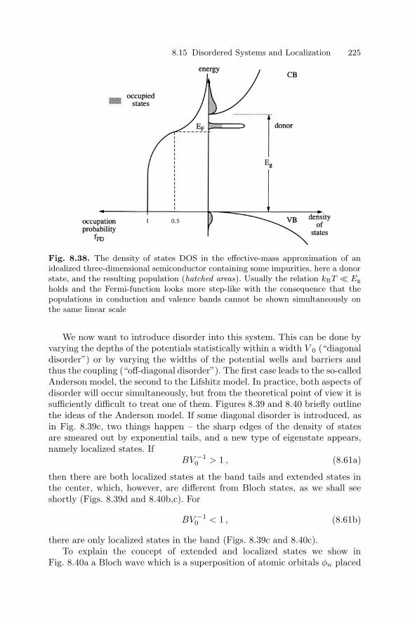
8.15 Disordered Systems and Localization 225
Fig. 8.38. The density of states DOS in the effective-mass approximation of anidealized three-dimensional semiconductor containing some impurities, here a donorstate, and the resulting population (hatched areas). Usually the relation kBT Eg
holds and the Fermi-function looks more step-like with the consequence that thepopulations in conduction and valence bands cannot be shown simultaneously onthe same linear scale
We now want to introduce disorder into this system. This can be done byvarying the depths of the potentials statistically within a width V 0 (“diagonaldisorder”) or by varying the widths of the potential wells and barriers andthus the coupling (“off-diagonal disorder”). The first case leads to the so-calledAnderson model, the second to the Lifshitz model. In practice, both aspects ofdisorder will occur simultaneously, but from the theoretical point of view it issufficiently difficult to treat one of them. Figures 8.39 and 8.40 briefly outlinethe ideas of the Anderson model. If some diagonal disorder is introduced, asin Fig. 8.39c, two things happen – the sharp edges of the density of statesare smeared out by exponential tails, and a new type of eigenstate appears,namely localized states. If
BV −10 > 1 , (8.61a)
then there are both localized states at the band tails and extended states inthe center, which, however, are different from Bloch states, as we shall seeshortly (Figs. 8.39d and 8.40b,c). For
BV −10 < 1 , (8.61b)
there are only localized states in the band (Figs. 8.39c and 8.40c).To explain the concept of extended and localized states we show in
Fig. 8.40a a Bloch wave which is a superposition of atomic orbitals φn placed

226 8 Electrons in a Periodic Crystal
at every lattice site Ri with a proper long-range phase correlation, corre-sponding to the LCAO method mentioned in Sect. 8.7:
φBlochk (r) =
∑i
eik·Riφn(r − Ri)
= eik·r ∑i
e−ik·(r−Ri)φn(r − Ri) = eik·ruk(r) . (8.62a)
In an extended state in a disordered system (Fig. 8.40b) we lose the long-rangephase correlation resulting in
φext(r) =∑
i
ciφn(r − Ri) (8.62b)
and for a localized state we obtain an envelope which is centered around a lo-calization site r0 and which decays exponentially with a localization length ξ(Fig. 8.40c)
φloc(r) =∑
i
diφn(r − Ri)e−|r−r0|/ξ . (8.62c)
The energy which separates extended from localized states is called themobility edge. If the carriers were to have an infinite phase-relaxation time T 2
in their states and thus also an infinite lifetime, it is easy to show that the
Fig. 8.39. A periodic potential (a) and the resulting band, represented by its densityof states (b), a disordered system (c) and bands with localized and delocalized states(d) and with localized states only (e)

8.15 Disordered Systems and Localization 227
Fig. 8.40. Schematic drawing of the real part of the wave function for a periodicpotential (a) and for a disordered system an extended state (b) and a localizedone (c)
mobility edge is sharp: if extended and localized states were to coexist ina certain energy range, then the slightest perturbation would mix these statesand consequently every localized state would obtain some admixture of anextended wave function (and vice versa) transforming it to an extended state.Since the T 2 times of the carriers in their states are limited, the mobility edgeis usually a transition region of a certain width.
Another important consequence of disorder is the following. A disorderedsystem is no longer invariant with respect to translations. As a consequence,the wave vector is no longer a good quantum number and the dispersionrelation E(k) loses, strictly speaking, its meaning. A disordered system is inprinciple characterized only by its density of states D(E).
As usual, there are exceptions to this rule: excitations with a wavelengthλ long compared to the typical length scale of the disorder fluctuations “av-erage” over the disorder and can be characterized by a wave vector k inthe sense of a continuum approximation. This is fulfilled for example forlong wavelength (acoustic) phonons or photons. The latter case is easilychecked by looking through a glass window or into clear water. See alsoSect. 5.3.2.
228 8 Electrons in a Periodic Crystal
Weak disorder, e.g., as defined by (8.61a), will produce some localizedstates at the band edges (1016 – 1018 cm−3) but the extended states in theband (1022 – 1023 cm−3) will be close to Bloch-type waves. See Fig. 8.40.
A crucial property for localization effects is the dimensionality of the sys-tem. It has been shown by general arguments that the slightest disorder willin principle localize all states for dimensions d ≤ 2. However the localizationlength [ξ in (8.62c)] can be extremely long and in many cases exceeds thelength of the sample used. As a consequence these considerations are largelyof theoretical interest and only to a limited extent of practical relevance.
After characterizing briefly some properties of disordered systems we nowproceed to the inspection of realizations of disorder in semiconductors. Wediscuss, in roughly increasing magnitude of disorder, heavily doped semicon-ductors, alloy semiconductors, well-width fluctuations, and amorphous semi-conductors.
In Fig. 8.41a, we show the density of states for the conduction band ofa semiconductor containing donors of variable concentration. If the concen-tration of donors is so low that the wavefunctions do not overlap, i.e.,
a3BND 1 , (8.63)
whereND is the concentration of donors and aB the radius of the wave functionaccording to (8.57d), then their density of states is δ-function-like. We show inFig. 8.41a, for simplicity, for the donor with one electron only the state withnB = 1. A donor may bind a second electron with opposite spin. As a result ofthe Coulomb interaction the energy for the two electrons will be higher. Thisis indicated by the second peak. The states with nB > 1, which the electroncould also occupy, are again neglected.
If ND is increased, the wave functions of the donors start to overlap andthis again results in the formation of a so-called impurity band. Its widthincreases with ND and eventually merges with the conduction band, formingan (exponential) tail of the density of states. Depending on the doping andpossibly on compensation through acceptors, the Fermi level can be situatedfor T → 0 above or below the mobility edge. In the first case, the systemis called a metal, since it has finite conductivity at T → 0, in the second itis an insulator. The transition from an insulator to a metal with increasingdoping is also known as a Mott transition and there was a long discussion as towhether this transition is continuous or not, i.e., whether there is somethinglike minimum metallic conductivity in the second case. Experiments, e.g.,with phosphorous-doped silicon (Si:P), indicate that there is no minimumconductivity, [84S1,85K1,86L1].
The next case of disorder are alloy semiconductors like Ga1−yAlyAs,CdS1−xSex, ZnSe1−x Tex or Zn1−yCdyS. Many, but not all of them can allbe grown for every value of x or y between 0 and 1, others like Ga1−yInyN orGaAs1−xNx have a miscibility gap. They usually have a well-defined crystalstructure (e.g., of the zincblende or of the wurtzite type). The disorder is in-

8.15 Disordered Systems and Localization 229
Fig. 8.41. The appearance of tails of localized states due to increasing doping (a),potential fluctuations, e.g., in an alloy (b, c) or in amorphous semiconductors (d)
troduced by the statistically distributed occupation of anion (or cation) siteswith the two different atoms.
Though an alloy has no translational invariance one can create it artifi-cially in the so-called virtual crystal approach. One assumes that the unit cellcontains atoms with a mixture of the properties according to x or y. Thisapproach explains for example the often observed continuous shift of Eg withcomposition (Fig. 8.31). This shift can be described by
Eg(x) = Eg(x = 0) + [Eg(x = 1) − Eg(x = 0)][(1 − b)x+ bx2
](8.64)
where the usually small “bowing” or “bending” parameter b describes thedeviation from a linear relation. In some cases, like in In1−yGayAs1−xNx thebowing parameter is so large, that the system goes with increasing x througha band gap minimum which is situated considerably below that of x = 0 or 1.
The fluctuations now arise from the fact that the composition has fluc-tuations on a microscopic scale (e.g., the exciton radius, see below). InCdS1−xSex, for example, there is in some places a little more S, in othersmore Se. This compositional disorder results frequently in the more ionicsystems in preferential fluctuation of the valence band for anion substitutedmaterials like CdS1−xSex, or of the conduction band for cation-substituted
230 8 Electrons in a Periodic Crystal
materials like Zn1−yCdyS. In the more covalent materials like Al1−yGayAsboth bands fluctuate with composition. These fluctuations can again lead tolocalized states. The “tailing parameter” E0, which describes the exponentialtail in
D(E) =N0
E0e−E/E0 , (8.65)
where N0 is the total number of tail states, depends on the material para-meters and on the composition. It is obvious that E0 disappears for x, y = 1and x, y = 0, that it increases for increasing Eg(x = 1) − Eg(x = 0) andfor decreasing effective mass of the particle which is localized. The latterpoint depends on the fact that in three dimensions a potential well must havea certain width R and depth V to localize or bind a particle of mass in mwith
V R2 ≥ 2
me,h(8.66)
and explains why holes are more easily localized than electrons.For the dependence of E0 on x one finds different but similar formulas in
literature. We give here one according to [78B1]. For more recent discussionsof this topic concerning also excitons see [78B1,84S1,91K1,92P1,99K1,00P1].
E0 =1
178β4x2 (1 − x)2m3
e,h
(
6N2)−1
, (8.67)
where N is the density of atoms and β the derivative of the position of theedge of the band with respect to x. Often one finds from experiment a slightlyasymmetric behavior of E0(x) caused by the term β and other effects.
We now consider disorder in systems of reduced dimensionality like MQW.Actually there are two origins of disorder. One is the alloy “broadening” ordisorder felt by the carriers if the well or the barrier or both are made from analloy or if an alloy forms at the boundary due to interdiffusion or segregation.Another is due to well-width fluctuations. Though great progress has beenmade in growing atomically flat interfaces by modern epitaxial techniques,fluctuations of lz of at least the order of one atomic (or molecular) layer arehardly avoidable. Due to the dependence of the quantization energy on lz,carriers (and excitons) can be localized or trapped at regions with larger lz.
The continuous transition from these localization sites to so-called assem-bled quantum islands has already been mentioned in Sects. 8.10 and 8.13. Forexamples of localization in two dimensions see, e.g., [85K1, 86L1, 00P1] andreferences therein.
The strongest disorder occurs in amorphous semiconductors, the promi-nent example being amorphous or α-Si. In these systems only short-range or-der remains (e.g., a tetrahedral coordination of most but not of all Si atoms)but no long-range order at all caused by the facts that the coordination ofsome atoms is different from the one in a perfect crystal and that the bondlengths and the angles between the bonds show some fluctuations. If we start

8.15 Disordered Systems and Localization 231
in a CdS1−xSex crystal at a S atom and proceed by a lattice vector R we willhit an atom. We are not sure, however, whether it will be S or Se. In an α-Sithere is only an average bond length but nothing like a lattice “constant” andif we move from a Si atom by a vector R of crystalline Si we are not even surewhether we will find an atom at all.
To illustrate this concept, we show in Fig. 8.42 a hypothetic two-dimen-sional crystal with hexagonal structure and threefold coordinaton and in (b)the corresponding amorphous material in which some five and seven atomrings occur and also some dangling bonds.
This strong disorder leads to substantial exponential tails of the densitiesof states both for conduction and valence bands, which cover the whole “for-bidden gap” (Fig. 8.41d). Unsaturated covalent bonds in Si, so-called “dan-gling” bonds, form states situated energetically close to the center of the gap(Fig. 8.41d) since it is undetermined whether they would form a bonding oran antibonding orbital with the next Si. The states of the dangling bonds canbe saturated by hydrogen doping, opening interesting technological applica-tions for α-Si:H. A short selection of books and conference proceedings for theproperties of amorphous semiconductors is [74A1,84H1,84T1].
Fig. 8.42. A hypothetical two-dimensional crystalline (a) and amorphous (b) ma-terial

232 8 Electrons in a Periodic Crystal
Fig. 8.43. Various possibilities for a particle to come from A to B or to be backscat-tered from C to C. The open dots symbolize scattering centers
To conclude this section, we now outline the concepts of weak localisa-tion by enhanced backscattering and of percolation. We come back to theseapproaches in Sect. 14.4.
In the first case we consider an otherwise perfect crystal which containsrandomly distributed elastic scattering centers. See Fig. 8.43.
To obtain the probability wA→Bthat a particle, e.g., a carrier starting fromA reaches B we have to sum over the amplitudes aA→B
i of all possible waysto come from A to B and to square the sum
wA→B ∼∣∣∣∣∣∑
i
aA→Bi
∣∣∣∣∣2
=∑∣∣aA→B
i
∣∣2 +∑i,j
aA→Bi aA→B
j ≈∑∣∣aA→B
i
∣∣2 .(8.68a)
The mixed terms all have different relative phases and cancel essentially asa sum. In the case of backscattering we have to start in the same way, i.e.,
wC→C =
∣∣∣∣∣∑i
aC→Ci
∣∣∣∣∣2
=∑
i
∣∣aC→Ci
∣∣2 +∑i,j
aC→Ci aC→C
j . (8.68b)
What is different from (8.68a) is that there not only remains the term∣∣∣∣∑i
aC→Ci
∣∣∣∣2but also those of the mixed terms, which are made up from aC→Ci
and their time-reversed parts shown for one case in Fig. 8.43, since the totalphase shift encountered in both directions and assuming, that only elasticscattering occurs, is equal. As a consequence we obtain
wC→C = 2
∣∣∣∣∣∑i
aC→Ci .
∣∣∣∣∣2
(8.68c)

8.15 Disordered Systems and Localization 233
This result means that backscattering is by a factor of two more probablethan scattering from A → B = A.
It should be noted that similar arguments can also be formulated ink-space. Due to elastic scattering only the length of k remains constant andthe scattering from an initial ki to kf = −ki is again by a factor of two moreprobable that scattering to any other kf = ki.
This enhanced backscattering is obviously a beginning of localization. Theconcept has been verified for scattering of photons from small polysystemespheres [85A1, 85W1, 86A1, 86S1] and in electric conductivity. In the lattercase there are also considerable contributions from inelastic carrier scatteringto the resistivity. The part due to enhanced backscattering can be identifiedby applying a magnetic field B, since the simple time reversal argument is nolonger valid for B = 0. For more details see, e.g., [84B1].
The concept of percolation will be explained with a simple-cubic lattice inFig. 8.44.
Some of the unit cells are randomly painted black. All neighboring cellsthat are painted black are said to belong to one cluster.
We see in Fig. 8.44 clusters consisting of one, two, three and seven unitcells. With increasing occupation probability (i.e., increasing number of blackunit cells) of the average cluster size growths. Eventually a cluster appearsthat extends from −∞ → +∞. This is the percolating cluster that corre-sponds to an extended state, while finite clusters are “localized”. The occu-pation probability at which the first percolating cluster appears is the criticaloccupation fc.
Fig. 8.44. Cluster formation in a simple cubic lattice in two dimensions

234 8 Electrons in a Periodic Crystal
Fig. 8.45. Clusters of overlapping spheres
It is easy to understand that fc depends on the dimensionality (in a one-dimensional case fc is trivially equal to unity) on the type of lattice e.g. cubic,hexagonal, or triangular and on the fact if we consider site or bond percolation.For details see, e.g., [85S1].
One possibility to make the percolation model more realistic is e.g. the fol-lowing one, which has been used with some more sophistication to successfullyexplain the optical properties of excitons in alloys like CdS1−xSex (see [99K1]and Sect. 9.6).
We assume that a localized state like the hole state in Fig. 8.41b is causedby a cluster of Se atoms in CdS1−xSex and that the wave function localizedat this Se cluster has a spherical shape as indicated in a two-dimensionalanalogue (which corresponds to quantum wells [00P1]) in Fig. 8.45.
Wave functions that overlap spatially form a cluster. At a certain densityof spheres a percolating cluster will appear that corresponds to an extendedstate while finite clusters again correspond to localized ones. The density andthe size of the spheres can be influenced, e.g., by varying the energy in thetail of the density of states. The appearance of a percolating cluster withincreasing energy corresponds then to the mobility edge.
An experiment showing localization in a disordered chain of macroscopic,coupled pendula has been described and verified experimentally in [89K1].
We will end the discussion of the properties of electronic states in semicon-ductors here and concentrate in the next section on electron–hole pairs, whichare actually the relevant complexes for optical properties, but which cannotbe understood without knowledge of the properties of electrons and holes.

8.16 Problems 235
8.16 Problems
1. Try to find the highest and lowest values for effective electron and holemasses in group-IV materials and in binary III–V, II–VI and I–VIIsemiconductors. (Use a compilation of semiconductor data from the li-brary). What is the trend of the dependence of the effective masseson Eg?
2. Calculate the effective density of states, i.e., the onset of degeneracy,for electrons and holes at 10 K and at room temperature in bulk GaAsand ZnSe.
3. Calculate the effective density of states per unit volume at 300K forelectrons and holes in bulk GaAs and the density of states per unitarea in a GaAs QW. Calculate the corresponding density per volume forlz = 10 nm.
4. Calculate the density of states and the effective densities of states fora nondegenerate three-, two- or one-dimensional electron gas in the effec-tive mass approximation.
5. What is the minimum power consumption per unit area required to keepa degenerate electron and hole population at room temperature in ZnSeand in GaAs for a lifetime of 0.3 ns and layers with lz = 1 µm, 0.2 µm, and10 nm thickness? (The first two cases can be considered as bulk materialthe third one as quasi-two-dimensional).
6. Calculate the binding energy of electrons (holes) to donors (acceptors)for some of the materials mentioned in the first problem. Compare withexperimental data such as that given in [82L1] of Chap. 1. Deduce theorder of magnitude of the central cell correction. Check the ratio of thebinding energy and of the energy of the LO phonon, and try to anticipatethe consequence for the choice of ε.
7. Calculate the Bohr radii of acceptors and donors for the extreme valuesfound in the first problem. How many unit cells or atoms are containedin the volume of a donor?
8. Make a sketch of surfaces of constant energy in a two- (or even three-) di-mensional k-space for spherical, simple cubic, and hexagonal (plane k⊥c)symmetries. Is spherical symmetry compatible with cubic and hexagonalsymmetry?
9. Show that the wave vectors for which the scattered waves interfere con-structively in one- and two-dimensional square lattices in the concept ofnearly free electrons are just the borders of the Brillouin zones.
10. Identify the various branches of the 2d electron band structure of Fig. 8.11in the reduced zone scheme with the corresponding ones in the extendedscheme and the G-vectors that have been used to shift them into the firstBrillouin zone.
11. Verify that (8.23a) fulfils the Bloch criterion, i.e., that the wave func-tion is transformed onto itself under a translation Ri apart from a phasefactor.

236 8 Electrons in a Periodic Crystal
12. Calculate the positions of the first three quantized electron levels fora GaAs quantum well assuming infinitely high barriers and the realisticband discontinuity to Al0.40Ga0.60As and compare them.
13. Make a sketch and calculate approximately the electrostatic potential as-suming a single QW (width 10 nm) with an n-type modulation doping of1017 cm−3 on both sides in a layer of 20 nm thickness and buffer layersof 10 nm (me = 0.1m0) and assuming that all donor electrons are col-lected by the QW. What is the minimum height of the conduction bandoffset necessary to avoid substantial parallel conductivity of well and bar-rier?
14. Occupy a one-, two- and three-dimensional simple cubic lattice withsix places in every dimension by throwing dies. Indicate the percola-tion threshold for this finite lattice and compare with data in litera-ture.
15. What is a dislocation? Which types of dislocations do you know or canyou find in textbooks?
References to Chap. 8
[47L1] F.C. von der Lage and H.A. Bethe, Phys. Rev. 71, 612 (1947)[57K1] E.O. Kane, J. Phys. Chem. Sol. 1, 249 (1957)[58A1] P.W. Anderson, Phys. Rev. 109, 1492 (1958)[67V1] Y. Varshni, Physica 34, 149 (1967)[69R1] U. Rossler, Phys. Rev. 184, 733 (1969)[70M1] O. Madelung, Grundlagen der Halbleiterphysik, Heidelberger Taschen-
bucher 71, Springer, Berlin (1970)[74A1] Amorphous and Liquid Semiconductors, J. Stuke and W. Brenig (eds.) Tay-
lor and Trancis, London (1974) and (1990)[76C1] M.L. Cohen and J.R. Chelikowsky, Phys. Rev. B 14, 556 (1976)[77P1] J. Pollmann and H. Buttner, Phys. Rev. B 16, 4480 (1977)[78B1] S.D. Baranovskii and A.L. Efros, Sov. Phys. Semicond. 12, 1328 (1978)[79M1] N.F. Mott and E.A. Davies, Electronic Processes in Non-Crystalline Mate-
rials, 2nd edn., Clarendon, Oxford (1979)[79T1] H.R. Trebin, phys. stat. sol. (b) 92, 601 (1979)[79Z1] J.M. Ziman, Models of Disorder, Cambridge Univ. Press, Cambridge (1979)[80M1] M. Matsuura and H. Buttner, Solid State Commun. 36, 81 (1980)[80P1] B. Pertzsch and U. Rossler, phys. stat. sol. (b) 101, 197 (1980)[82B1] G. Blattner, et al., Phys. Rev. B 25, 7413 (1982)[82P1] This topic can be nicely followed since 1990 in the Proceeding of the In-
ternational Conferences on II–VI compounds, published so far in J. Crys-tal Growth 59 (1982), 72 (1985), 86 (1988), 101 (1990), 117 (1992), 138(1994), 159 (1996), 184/185 (1998), 214/215 (2000), in phys. stat. sol b229 (2002), and phys. stat. sol. c 1 Issue 4 (2004)
[83Z1] R. Zallen, Physics of Amorphous Solids, Wiley, New York (1983)[84B1] G. Bergmann, Physics Reports 107, 1 (1984)[84H1] W. Heywang, Amorphe and Polykristalline Halbleiter, Springer, Berlin
(1984)

References to Chap. 8 237
[84S1] B.I. Shklovskii and A.L. Efros, Electronic Properties of Doped Semiconduc-tors, Springer Ser. Solid-State Sci. 45 Springer, Berlin, Heidelberg (1984)
[84T1] The Physics of Hydrogenated Amorphous Silicon, J.D. Jonnopoulos (ed.)Springer, Berlin (1984)
[85A1] M.P. Albada and A. Lagendijk, Phys. Rev. Lett. 55, 2692 (1985)[85K1] B. Kramer, G. Bergmann and Y. Bruynserade (eds.), Localization, Interac-
tion and Transport Phenomena, Springer Ser. Solid-State Sci. 61, Springer,Berlin, Heidelberg (1985)
[85S1] D. Stauffer, Introduction to Percolation Theory, Taylor and Francis, London(1985)
[85W1] P.E. Wolf and G. Maret, Phys. Rev. Lett. 55, 26969 (1985)[86A1] E. Akkermans, P.W. Wolf and R. Maynard, Phys. Rev. Lett. 56, 1471 (1986)[86B1] G. Bastard, J.A. Brum, IEEE J. QE-22, 1625 (1986)[86D1] G.H. Dohler, IEEE J. QE 22, 1682 (1986)[86L1] Localization and Interaction, D.M. Finlayson (ed.), SUSSP, Edinburgh
(1986)[86S1] M. Stephen, Phys. Rev. Lett. 56, 1809 (1986)[87B1] J.S. Blakemore, Semiconductor Statistics, Dover Publication, Dover (1987)[87P1] Physics and Applications of Quantum Wells and Superlattices, E.E. Mendez,
K. v. Klitzing (eds.), NATO ASI Ser. 170, Plenum Press, New York (1987)[87W1] C. Weisbuch, in Semicond. Semimet. Vol. 24, Academic Press, London
(1987)[88C1] M.L. Cohen, J.R. Chelikowsky, Electronic Structure and Optical Proper-
ties of Semiconductors, Springer Series Solid-State Sci. 75, Springer, Berlin(1988)
[88F1] Ch. Flytzains, D. Ricard and Ph. Roussignol, NATO ASI Ser. B 194, 181(1988)
[88G1] Growth and Optical Properties of Wide-Gap II–VI Low Dimensional Semi-conductors, T.C. McGill, C.M. Sotomayor Torres, W. Gebhardt (eds.),NATO ASI Ser. B 200, Plenum, New York (1988)
[88P1] Properties of Impurity States in Superlattice Semiconductors, C.Y. Fong,I.P. Batra and S. Ciraci (eds.), NATO ASI Series B 183, Plenum, New York(1988)
[88R1] U. Rossler, F. Malcher and A. Ziegler, in NATO ASI series B 183, 219,Plenum, New York (1988)
[88W1] W. Walukiewizc, Phys. Rev. B 37, 4760 (1988)[89H1] A. Henglein, Chem. Rev. 89, 1861 (1989)[89K1] C. Klingshirn in [81A1]d of Chap. 1 p. 111[89P1] N. Peyghambarian, et al., IEEE J. QE-25, 2516 (1989)[90B1] M.G. Bawendi, M.L. Steigerwald and L.E. Brus, Annual Rev. Phys. Chem.
41, 477 (1990)[90M1] U. Merkt, Festkorperprobleme / Advances in Solid State Physics, Vol. 30,
77 (1990)[90P1] S.H. Park et al., J. Opt. Soc. Am. B 7, 2097 (1990)[91B1] L.E. Brus, Appl. Phys. A 53, 465 (1991)[91E1] Electronic Structure and Properties of Semiconductors, W. Schroter (ed.),
Materials Science and Technology 4, VCH, Weinheim (1991)[91E2] A.I. Ekimov, Phys. Scr. T 39, 217 (1991)[91K1] A.A. Klochikhin and S.G. Ogloblin, Sov. Phys. JETP 73, 1122 (1991)

238 8 Electrons in a Periodic Crystal
[92E1] A.L. Efros, Phys. Rev. B 46, 7448 (1992)[92H1] F. Henneberger et al., Adv. Solid State Phys./ Festkorperprobleme 32, 279
(1992)[92M1] S. Malzer et al., phys. stat. sol. (b) 173, 459 (1992)[92P1] S. Permogorov and A. Reznitsky, J. Lumin. 52, 201 (1992)[93D1] F. Daiminger et al., Proc. 21th ICPS, Beijing (1992), Ping Jiang and Hou-
Zhi Zeng (eds.) p 1293 World Scientific, Singapore (1993)[93E1] A.I. Ekimov et al., J. Opt. Soc. Am. B 10, 100 (1993)[93F1] P. Fulde, Electron Correlations in Molecules and Solids, Springer Series in
Solid State Science 100, 2nd, ed. Springer, Berlin (1993)[93H1] A.C. Hewson, The Kondo Problem to Heavy Fermions, Cambridge Studies
in Magnetism, Cambridge University, Press, Cambridge (1993)[93K1] A.A. Klochikhin et al., Phys. Rev. B 48, 3100 (1993)[93M1] C.B. Murray, D.J. Norris and M.G. Bawendi, J. Am. Chem. Soc. 115, 8706
(1993)[93M2] U. Merkt et al., Physica B 189, 165 (1993)[93P1] K. Ploog, R. Notzel and O. Brandt, Proc. 21th ICPS, Beijing (1992), Ping
Jiang and Hou-Zhi Zeng (eds.) p. 1297 World Scientific, Singapore (1993)[93R1] M.A. Reed, Scientific American, January issue p. 98 (1993)[93T1] T. Taguchi, Y. Kawakami and Y. Yamada, Physica B 191, 23 (1993)[93W1] U. Woggon et al., Phys. Rev. B 47, 3684 (1993)[94A1] A. Abounadi et al., Phys. Rev. B 50, 11677 (1994)[94G1] M. Grun et al., J. Crystal Growth 138, 150 (1994)[94I1] M. Illing et al., J. Crystal Growth 138, 638 (1994)[95C1] A.-B. Chen and A. Sher, Semiconductor Alloys, Plenum Press, New York
(1995)[95F1] W. Faschinger, Material Science Forum 182-184, 29 (1995)[95G1] M. Grundmann et al., J. of Nonlinear Optical Physics and Materials 4, 99
(1995)[95H1] F. Hofmann and D.A. Wharam, Festkorperprobleme / Advances in Solid
State Physics Vol. 35, 197 (1995)[95K1] J. Konig et al., Festkorperprobleme / Advances in Solid State Physics Vol.
35, 215 (1995)[95P1] D. Pfannkuche and S.E. Ulloa, Festkorperprobleme / Advances in Solid
State Physics, Vol. 35, 65 (1995)[95W1] U. Woggon and S.V. Gaponenko, phys. stat. sol. (b) 189, 285 (1995)[96B1] H.R. Blick et al., Phys. Rev. B 53, 78999 (1996)[97H1] M. Hetterich et al., Phys. Rev. B 56, 12369 (1997)[97H2] D. Hommel et al., phys. stat. sol. (b) 202, 835 (1997)[97H3] A. Hartmann et al., Appl. Phys. Lett. 71, 1314 (1997)[97P1] T. Pohjola et al., Europhys. Lett. 40, 189 (1997)[97R1] M. Rabe et al., phys. stat. sol. (b) 202, 817 (1997)[97U1] R. Ulbrich, private communication (1997)[97W1] U. Woggon et al., Appl. Phys. Lett. 71, 377 (1997)[98G1] M. Grun et al., Appl. Phys. Lett. 73, 1343 (1998)[98L1] D. Luerßen et al., Phys. Rev. B 57, 1631 (1998)[99A1] M.V. Artemyev et al., Phys. Rev. B 60, 1504 (1999) and references therein[99B1] D. Bimberg, N. Grundmann and N.N. Ledentsov, Quantum Dot Het-
erostructures, John Wiley and Sons, Chicester (1999)

References to Chap. 8 239
[99B2] G. Biasiol and E. Kapon, J. Crystal Growth 201/202, 62 (1999)[99G1] S.V. Gaponenko et al., IEEE J. Lightwave Techn. 17, 2128 (1999)[99K1] A. Klochikhin et al., Phys. Rev. B 59, 12947 (1999)[00A1] D. ben Avraham and S. Havlin, Diffusion and Reactions in Fractals and
Disordered Systems, Cambridge University Press, Cambridge (2000)[00B1] G. Biasiol, K. Leifer and E. Kapon, Phys. Rev. B 61, 7223 (2000)[00K1] E. Kurtz et al., Thin Solid Films 367, 68 (2000) and ibid. 412, 89 (2002), J.
Crystal Growth 214/215, 712 (2000), phys. stat. sol. (b) 229, 519 (2001)[00P1] S. Permogorov et al., J. Crystal Growth 215/215, 1158 (2000)[00R1] A. Rosenauer et al., Thin Solid Films 357, 18 (2000) and Phys. Rev. B 61,
8276 (2000)[01A1] M.V. Artemyev et al., phys. stat. sol. (b) 224, 393 (2001)[01H1] Q. Huang et al., J. Crystal Growth 227/228, 117 (2001)[01H2] M.H. Huang et al., Science 292, 1897 (2001)[01P1] Z.W. Pan, Z.R. Dai and Z.L. Wang, Science 291, 1947 (2001)[01S1] R.L. Sellin et al., Appl. Phys. Lett. 78, 1207 (2001)[02G1] O. Gogolin et al., Solid State Commun. 122, 511 (2002)[02K1] E. Kapon in [81A1]k of Chap. 1, p. 243[02W1] R.L. Walter et al., Phys. Rev. B 65, 075207 (2002)[03G1] O. Gogolin et al., J. Lumin. 102/103, 414 and 451 (2003)[03K1] S.N. Khanna and A.W. Castleman, Quantum Phenomena in Clusters and
Nanostructures, Springer, Berlin, Heidelberg (2003)[03L1] J.Y. Lao et al., Nano Letters 3, 235 (2003)[03Z1] B.P. Zhang et al., Appl. Phys. Lett. 83, 1635 (2003)[04Z1] B.P. Zhang et al., Appl. Phys. Lett. 84, 4098 (2004) and J. Appl. Phys. 96,
340 (2004)
9
Excitons, Biexcitons and Trions
In Chap. 8 we defined the bandstructure for electrons and holes as the solu-tions to the (N ± 1)-particle problem and later we saw that the number ofelectrons in a band can be increased or decreased by donors and acceptors, re-spectively (Sect. 8.14). In contrast, the number of electrons remains constantin the case of optical excitations with photon energies in the eV or band gapregion. What we can do, however, is to excite an electron from the valenceto the conduction band by absorption of a photon. In this process, we bringthe system of N electrons from the ground state to an excited state. What weneed for the understanding of the optical properties of the electronic systemof a semiconductor an insulator or even a metal is therefore a description ofthe excited states of the N particle problem. The quanta of these excitationsare called “excitons” in semiconductors and insulators.
We can look at this problem from various points of view.The ground state of the electronic system of a perfect semiconductor is
a completely filled valence band and a completely empty conduction band.We can define this state as the “zero” energy or “vacuum” state. In additionit has total momentum K = 0, angular momentum L = 0 and spin S = 0.From this point E = 0, K = 0 we will start later on to consider the dispersionrelation of the excitons in connection with Fig. 9.1b.
Another point of view is the following. If we start from the above-definedgroundstate and excite one electron to the conduction band, we simultaneouslycreate a hole in the valence band (Fig. 9.1a). In this sense an optical excitationis a two-particle transition. The same is true for the recombination process. Anelectron in the conduction band can return radiatively or non-radiatively intothe valence band only if there is a free place, i.e., a hole. Two quasiparticlesare annihilated in the recombination process.
This concept of electron–hole pair excitation is also used successfully inother disciplines of physics. If one excites, e.g., an electron in a (larger) atomor a neutron or proton in a nucleus from a deeper lying occupied state intoa higher, empty one, a quantitative description concerning the transitionsenergies is obtained only if one takes into account both the particle in the
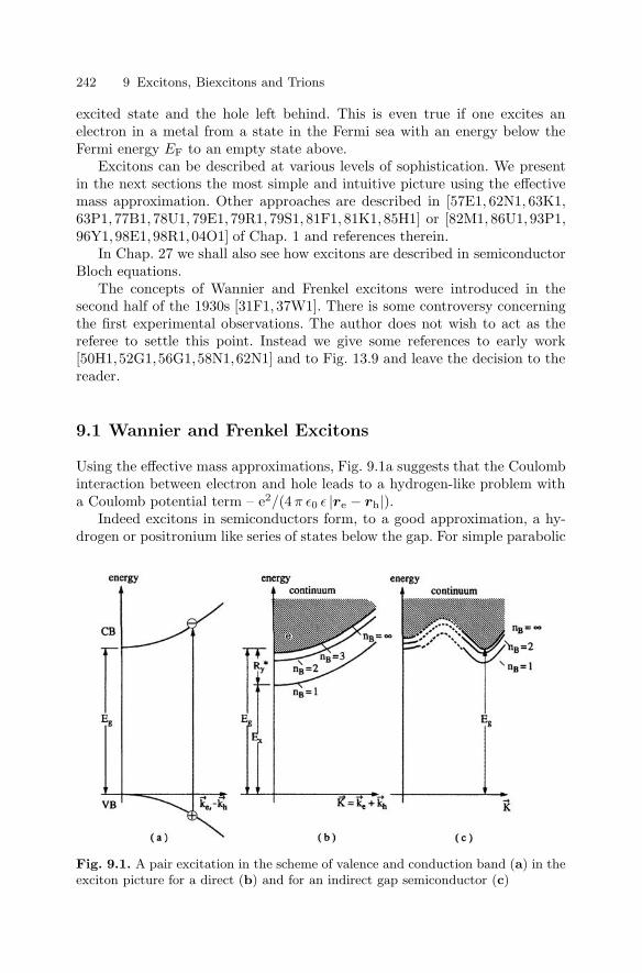
242 9 Excitons, Biexcitons and Trions
excited state and the hole left behind. This is even true if one excites anelectron in a metal from a state in the Fermi sea with an energy below theFermi energy EF to an empty state above.
Excitons can be described at various levels of sophistication. We presentin the next sections the most simple and intuitive picture using the effectivemass approximation. Other approaches are described in [57E1, 62N1, 63K1,63P1, 77B1, 78U1, 79E1, 79R1, 79S1, 81F1, 81K1, 85H1] or [82M1, 86U1, 93P1,96Y1,98E1,98R1,04O1] of Chap. 1 and references therein.
In Chap. 27 we shall also see how excitons are described in semiconductorBloch equations.
The concepts of Wannier and Frenkel excitons were introduced in thesecond half of the 1930s [31F1, 37W1]. There is some controversy concerningthe first experimental observations. The author does not wish to act as thereferee to settle this point. Instead we give some references to early work[50H1,52G1,56G1,58N1,62N1] and to Fig. 13.9 and leave the decision to thereader.
9.1 Wannier and Frenkel Excitons
Using the effective mass approximations, Fig. 9.1a suggests that the Coulombinteraction between electron and hole leads to a hydrogen-like problem witha Coulomb potential term – e2/(4 π ε0 ε |re − rh|).
Indeed excitons in semiconductors form, to a good approximation, a hy-drogen or positronium like series of states below the gap. For simple parabolic
Fig. 9.1. A pair excitation in the scheme of valence and conduction band (a) in theexciton picture for a direct (b) and for an indirect gap semiconductor (c)

9.1 Wannier and Frenkel Excitons 243
bands and a direct-gap semiconductor one can separate the relative motionof electron and hole and the motion of the center of mass. This leads to thedispersion relation of excitons in Fig. 9.1b.
Eex(nB,K) = Eg − Ry∗ 1n2
B
+
2K2
2M(9.1a)
withnB = 1, 2, 3 . . . principal quantum number ,
Ry∗ = 13.6 eVµ
m0
1ε2
exciton Rydberg energy , (9.1b)
M = me +mh, K = ke + kh translational mass andwave vector of the exciton . (9.1c)
For the moment, we use a capital K for the exciton wave vector to distinguishthis two-particle state from the one-particle states. When we are more familiarwith the exciton as a new quasi-particle we shall return to k.
µ =memh
me +mhreduced exciton mass , (9.1d)
aexB = aH
Bεm0
µexcitonic Bohr radius . (9.1e)
The radii of higher states can be considered on various levels of complexity.If one only takes into account the exponential term exp Zr/naH
B in the radialpart of the wave function of the hydrogen problem appearing as the envelopefunction in (9.4a) and defines the (excitonic) Bohr radius by the decrease ofthis term to 1/e, one obtains with Z = 1 for excitons
aB (nB) = aHB ε
m0
µnB , (9.2a)
i.e., a linear increase with nB.If, on the other hand, one takes the full radial function into account, i.e.,
also including the factorρl L2l + 1
nB + l(ρ) (9.2b)
where l is the angular quantum number and ρ = 2Z r/nB · aHB and L2l + 1
n0B + l
are the Laguerre polynomials and calculates the average distance betweenelectron and proton or hole, respectively, one obtains [55S1,94L1]
〈r (nB)〉 =aB
2[3n2
B − l (l + 1)]
(9.2c)
i.e., for the nBS states (i.e. l = 0) a quadratic dependence starting with 3 aB/2for nB = 1.

244 9 Excitons, Biexcitons and Trions
The series of exciton states in (9.1a) has an effective Rydberg energy Ry∗
modified by the reduced mass of the electron and hole and the dielectric“constant” of the medium in which these particles move; nB is the principalquantum number. The kinetic energy term in (9.1a) involves the translationalmass M and the total wave vector K of the exciton. The radius of the excitonequals the Bohr radius of the H atom again modified by ε and µ. Using thematerial parameters for typical semiconductors one finds
1 meV ≤ Ry∗ ≤ 200meV Eg (9.3a)
and
50 nm aB ≥ 1 nm > alattice . (9.3b)
This means that the excitonic Rydberg energy Ry∗ is usually much smallerthan the width of the forbidden gap and the Bohr radius is larger than thelattice constant. This second point is crucial. It says that the “orbits” ofelectron and hole around their common center of mass average over manyunit cells and this in turn justifies the effective mass approximation in a self-consistent way. These excitons are called Wannier excitons [37W1].
In this limit, excitons can usually also be described in the frame of semicon-ductor Bloch equations, but finer details or corrections to this simple model,which we shall treat in Sect. 9.2 and which are necessary to understand opticalspectra, are usually not incorporated in the semiconductor Bloch equationsof Chap. 27.
It should be mentioned that in insulators like NaCl, or in organic crys-tals like anthracene, excitons also exist with electron–hole pair wavefunctionsconfined to one unit cell. These so-called Frenkel excitons [31F1] cannot bedescribed in the effective mass approximation. As a rule of thumb, one canstate that in all semi-conductors the inequalities (9.3a,b) hold, so that wealways deal with Wannier excitons.
A series of conferences devoted both to excitons in anorganic semicon-ductors and in organic ones as well as in anorganic and organic insulators isEXCON (excitonic process in condensed matter). The proceedings have beenpublished in [94E1]
To get an impression of the wavefunction, we form wave packets for elec-trons and holes φe,h(re,h) in the sense of the Wannier function of (8.10) andobtain schematically for the exciton wavefunction
φ(K , nB, l,m) = Ω−1/2eiK·Rφe(re)φh(rh)φenvnB,l,m(re − rh) , (9.4a)
with the center of mass R
R = (me re +mh rh)/(me +mh) , (9.4b)
where Ω−1/2 is the normalization factor. The plane-wave factor describes thefree propagation of a Wannier exciton through the periodic crystal similarly as

9.1 Wannier and Frenkel Excitons 245
for the Bloch waves of Sect. 8.1, and the hydrogen-atom-like envelope functionφenv describe the relative motion of electron and hole.
The quantum numbers l andm, with l < nB and −l ≤ m ≤ l have the samemeaning as for the hydrogen atom in the limit that the angular momentumis a good quantum number in a solid (see Chap. 26).
As for the H atom, the exciton states converge for nB → ∞ to the ioniza-tion continuum, the onset of which coincides with Eg.
Excitons features are especially strong for regions of the electron and holedispersions, where the group velocities of electrons and holes υe
g and υhg are
equal e.g. zero. See e.g. [96Y1] of Chap. 1. This means, that in direct gapsemiconductors excitons form preferentially around K = 0 if the direct gapoccurs at the Γ point.
In indirect gap semiconductors exciton states form preferentially with thehole around kh = 0 and the electron in its respective minimum, as shown inFig. 9.1c schematically e.g. for Ge where the conduction band has minimaat ke = 0 and ke = 0. Electrons and holes with different group velocitiesstill “see” their mutual Coulomb interaction, but the dashed continuation ofexciton dispersion from the indirect to the direct gap is an oversimplification,among others because the states away from the band extrema are stronglydamped and their binding energy varies. See e.g. again [96Y1] of Chap. 1.
The discrete and continuum states of the excitons will be the resonances oroscillators which we have to incorporate into the dielectric function of Chaps.4 and 5.
For direct semiconductors with dipole allowed band-to-band transitions,one finds an oscillator strength for excitons in discrete states with S(l = 0)envelope function proportional to the band-to-band dipole transition matrixelement squared and to the probability of finding the electron and hole inthe same unit cell. For the derivation of this relation see [57E1]. This lattercondition leads to the n−3
B dependence of the oscillator strength for three-dimensional systems.
fnB ∝ |HDcv|2
1n3
B
. (9.5)
These fnB result in corresponding longitudinal–transverse splitting asshown in connection with (4.26). Equation ((9.5)) holds for so-called singletexcitons with antiparallel electron and hole spin. Triplet excitons involve a spinflip, in their creation which significantly reduces their oscillator strength (spinflip forbidden transitions).
Since the singlet and triplet pair or exciton states will play some role inlater chapters (see, e.g., Chaps. 13 to 16) we give some simplified informationon this topic here.
The crystal ground state, i.e., completely filled valence bands and com-pletely empty conduction bands, has, as already mentioned above, angularmomentum L, spin S and total angular momentum J equal to zero. If weexcite optically an electron from the valence band to the conduction band,

246 9 Excitons, Biexcitons and Trions
e.g., by an electric dipole transition, the spin of the excited electron doesnot change because the electric field of the light does not act on the spin.Consequently, the simultaneously created hole has a spin opposite to theone of the excited electron and the total spin S of the electron–hole pairstate is still zero. Consequently, the electron–hole pair, and likewise the ex-citon, is said to be in a spin singlet state. The spin S = 1 of the photonis accommodated by the spatial part of the band-to-band matrix element in((9.5)) or by the envelope function of the exciton (see (9.4a) and [96Y1] ofChap. 1).
If the spin flips in the transition, e.g., by interaction with the magneticcomponent of the light field, one ends up with a total spin S = 1 correspondingto spin triplet (exciton) state. The triplet state is situated energetically belowthe singlet state and the splitting is due to a part of the electron–hole exchangeinteraction, essentially the so-called short-range or analytic (for K → 0) partof the exchange interaction. There are names other than triplet and singletused for certain materials like para and ortho exciton (e.g., for Cu2O) or darkand bright excitons (in quantum dots). The last pair of names reflects the factthat triplet excitons have small oscillator strength because they are “spin-flipforbidden.” Since spin and angular momentum are, strictly speaking, no goodquantum numbers in a crystal (see Chap. 26) it is not obligatory that thetriplet exciton is threefold degenerate and the singlet is not degenerate. Thereare cases where the triplet or para exciton is nondegenerate, as in Cu2O,and the singlet is threefold degenerate, as in many zinc-blende type crystalslike CuCl or ZnSe or GaAs. This is possibly the reason that in some older,especially French, literature the names singlet and triplet exciton states areinterchanged.
The oscillator strength of the continuum states is influenced by the so-called Sommerfeld enhancement factor. We come back to this point later in(9.3) and in Chaps. 13 and 15, when we discuss the optical properties.
In the picture of second quantization, we can define creation operators forelectrons in the conduction band and for holes in the valence band α+
keand
β+kh
, respectively. The combination of both gives creation operators for elec-tron hole pairs α+
keβ+
kh. The exciton creation operator B+ can be constructed
via a sum over electron–hole pair operators (see [81K1] or [93H1] of Chap. 1).
B+K =
∑k′
ekh
δ[K − (ke + kh)]αke,khα+keβ+
kh; (9.6)
the expansion coefficients ake,kh correspond, in principle, to those also used inan (slightly old-fashioned) expansion into Slater determinantes of the manyparticle problem, which contains either all valence band states ϕkh
(ri,h) forthe ground state or always has one line being replaced by a conduction bandstate [63K1].
It can be shown that the B+K , BK , obey Bose commutation relations
with a density-dependent correction term which increases with the number

9.2 Corrections to the Simple Exciton Model 247
of electrons and holes contained in the volume of one exciton 4π(aexB )3/3
[77H2,81K1].This has two consequences: in thermodynamic equilibrium for low densities
and not too low temperatures, the excitons can be well described by Boltz-mann statistics with a chemical potential ruled by their density and temper-ature similar to (8.43). For higher densities they deviate more and more fromideal bosons until they end up in an electron–hole plasma made up entirelyfrom fermions (see Sect. 20.5). This makes the creation of a Bose-condensedstate of excitons (or of biexcitons) a very complicated problem. Though the-ory predicts a region in the temperature density plane where an excitonicBose–Einstein condensed state could occur [77H2], there are currently manyhints but no generally accepted, clearcut observation of a spontaneous Bosecondensation of excitons. There are some experiments that prove the Bosecharacter of excitons [76L1,83H1,83M1,83P1,84W1,87F1]. We come back tothis problem in Sect. 20.5 where we shall discuss also more recent results.
9.2 Corrections to the Simple Exciton Model
The simple model outlined in the preceeding section is, as already mentioned,adequate for non-degenerate, parabolic bands. We keep these assumptions forthe moment and inspect a first group of corrections which are relevant for theparameters ε and µ entering in (9.1a–e). We already know from Chaps. 4–7that ε is a function of ω, resulting in the question of which value should beused.
As long as the binding energy of the exciton Ebex is small compared to the
optical phonon energies and, consequently, the excitonic Bohr radius ((9.1e))larger than the polaron radius (8.16)
Ebex < ωLO; aB > aPol ⇒ ε = εs , (9.7a)
we can use for ε the static value εs below the phonon resonances and thepolaron masses and polaron gap. This situation is fulfilled for some semi-conductors for all values of nB, e.g., for GaAs where Ry∗ 5 meV andωLO 36 meV.
In many other semiconductors including especially the wide gap semicon-ductors (see Fig. 9.3) the inequality (9.7a) holds only for the higher statesnB ≥ 2, while for the ground state exciton (nB = 1) we find
Ebex ωLO; aB aPol −→ εs ≥ ε ≥ εb . (9.7b)
Examples are CdS, ZnO, CuCl or Cu2O.In this situation a value for ε between εs and εb seems appropriate, because
the polarization of the lattice can only partly follow the motion of electronand hole. A useful approach is the so-called Haken potential [55H1] whichinterpolates between εs and εb depending on the distance between electron

248 9 Excitons, Biexcitons and Trions
and hole, where reh, rpe and rhp are the distances between electron and hole,and the polaran radii of electron and hole, respectively:
1ε(re,h)
=1εb
−(
1εb
− 1εs
)(1 − exp(−reh/r
pe ) + exp(−reh/r
ph)
2
). (9.8)
The next correction concerns the effective masses. The polarization cloudsof the polarons (Sect. 8.6) have different signs for electron and hole. If bothparticles are bound together in an exciton state fulfilling (9.7b) the polaronrenormalization is partly quenched, with the consequence that values for theeffective masses will lie somewhere between the polaron values and the onesfor a rigid lattice. The gap “seen” by the exciton in the 1S state will likewisebe situated between the two above extrema. Fortunately, the above effectstend to partly compensate each other. A transition from the polaron gap tothe larger rigid lattice gap shifts the exciton energy to larger photon energies.A transition from εs to εb and a increase of the effective masses increasesthe binding energy and shift the 1S exciton to lower photon energies. Asa consequence one finds, even for many semiconductors for which inequality(9.7b) holds, that the 1S exciton fits together with the higher exciton statesreasonably well into the hydrogen-like series of (9.1). We shall use this ap-proach in the future if not stated otherwise. In other cases like Cu2O or CuCl,the higher states with nB ≥ 2 follow a hydrogen-like n−2
B series convergingto the polaron gap, but the 1S exciton shows, with respect to the polarongap, a binding energy Eb
ex, which differs from and is generally larger thanthe excitonic Rydberg energy deduced from the higher states. We call theexperimentally observed energetic distance between the 1S exction and thepolaron gap the exciton binding energy Eb
ex, in contrast to Ry∗ in (9.1). Thisdiscrepancy introduces some ambiguity when comparing theoretical resultswith experimental data, since in theory one often normalizes energies withthe excitonic Rydberg energy Ry∗, but the 1S exciton has a different valuefor Eb
ex.There is a general trend of the material parameters meff and ε with Eg
which results in an increase of the exciton binding energy with increasing Eg
as shown in Fig. 9.3.This is an analogous consequence of increasing the band width or in other
words decreasing effective mass with decreasing width of the gap as described,e.g., in the band structure model of Sect. 8.5.
The next complication comes from the band structure. If the bands aredegenerate, as is the Γ8 valence band in Td symmetry, it is no longer possibleto separate the relative and the center of mass motion – they are coupledtogether. Similar effects stem from k-linear terms and other sources. We getlight- and heavy-hole exciton branches and splittings, e.g., between the 2Sand 2P exciton states partly induced by the envelope function. An examplefor Cu2O will be given in Sect. 13.2.
Furthermore it should be mentioned, without going into details, that thesplitting between singlet and triplet excitons ∆st and the splitting of the

9.2 Corrections to the Simple Exciton Model 249
singlet state into a transverse and a longitudinal one ∆LT, are both due toexchange interaction between electron and hole caused by their Coulomb in-teraction [73D1, 88F1, 03G1] if we consider the N -electron problem in theform of Slater’s determinant where the ground state consists only of valence-band states and the excited state of a sum of determinants in each of whichone valence-band state is replaced by a conduction-band state. This aspect istreated in detail in [73D1] or in [93H1,93P1] of Chap. 1.
Usually the following relation holds for Wannier excitons
∆st ∆LT with 0.1 meV ∆LT 15 meV. (9.9)
For the AΓ5-excitons in CdS or ZnO one finds, e.g., ∆CdSLT = 1.8 meV,
∆CdSst = 0.2 meV and ∆ZnO
LT = 1.2 meV, ∆ZnOst = 0.17meV. Since the
short range interaction increases with decreasing exciton radius as a−3B the
situation begins to change for 1S excitons with a value of aexB exceeding only
slightly the lattice constant, and leading thus also to the limit of the conceptWannier excitons. One finds, e.g., for CuCl or Cu2O, ∆CuCL
LT = 5.5 meV,∆CuCl
st = 2.5 meV, ∆Cu2OLT ≈ 50 µeV, ∆Cu2O
st = 12 meV (see [85H1]). Theextremely low value of ∆LT in Cu2O comes from the fact, that the band-to-band transition is parity forbidden and the 1S singlet or ortho exciton is onlyallowed in quadrupole approximation (see Sect. 13.2).
The singlet-triplet splitting is even enhanced by the compression of theexcitonic wave function in quantum wells and especially in quantum dots (see,e.g., [98F1,03G1]). We come back to this aspect in Sect. 9.3 and Chap. 15.
Fig. 9.2. The splitting of the 1S exciton with the notation of the various contri-butions to exchange splitting for bulk samples (a) and in a quantum dot (b). Theabreviations have the following meanings: S = singlet, T = triplet, ∆lr = long rangeor nanoanalytic (for k → 0) part of the exchange interaction, ∆sr = short range oranalytic part of the exchange interaction [03G1]

250 9 Excitons, Biexcitons and Trions
Fig. 9.3. The exciton bind-ing energy Eb
ex as a functionof the band-gap for various di-rect gap semiconductors ([82L1,93H1,93P1] of Chap. 1)
It should be mentioned that the excitation of an optically (dipol-) allowedexciton is accompanied by a polarization as detailed in Chaps. 5 and 27 onpolaritons and on (semiconductor) Bloch equations, respectively.
The concept of exciton-phonon boundstates has been introduced in [68T1,72K1,02B1].
Finally we mention that excitons can also be formed with holes in deepervalence bands. These so-called “core-excitons” are usually situated in the VUVor X-ray region of the spectrum and have a rather short lifetime. An exampleand further references are given in Sect. 13.1.7 and [87C1,88K1].
9.3 The Influence of Dimensionality
If we consider the exciton again as an effective mass particle with parabolicdispersion relations, as given by (9.1), we expect a first influence of the di-mensionality on the density of states analogous to the situation shown in Fig.8.20 for every exciton branch nB = 1, 2, 3 . . .
Another effect of the dimensionality manifests itself in the binding energy,the Rydberg series and the oscillator strength. We consider an exciton, forwhich the motion of electron and hole is restricted to a two-dimensional plane,but the interaction is still a 3d one, i.e., proportional to e2/|re − rh| andfind (9.10a), (9.10b) in comparison to the 3d case of (9.1) (see e.g. [93H1] ofChap. 1):
3d: E(K, nB) = Eg − Ry∗ 1n2
B
+2(K2
x +K2y +K2
z )2M
(9.10a)
and for the oscillator strength f for the principal quantum number nB in thelimit of (9.2a):
f(nB) ∝ n−3B ; aB ∝ aH
BnB; nB = 1, 2, 3 . . . . (9.10b)

9.3 The Influence of Dimensionality 251
2d: E(K, nB) = Eg + EQ − Ry∗ 1(nB − 1
2 )2+
2(K2x +K2
y)2M
(9.10c)
with EQ quantization energy
f(nB) ∝(nB − 1
2
)−3
; aB ∝ aHB
(nB − 1
2
), nB = 1, 2, 3 . . . . (9.10d)
Essentially nB has to be replaced by nB − 1/2 when going from 3d to2d systems and the quantization energies EQ of electrons and holes mustbe considered. Actually EQ diverges for confinement in a mathematically 2dplane, see Sect. 8.10. The excitonic Rydberg Ry∗ is the same in both cases withthe consequence that the binding energy of the 1S exciton is Ry∗ in three, and4Ry∗ in two dimensions. The oscillator strength increases and the excitonicBohr radius decreases when going from three- to two-dimensional systems.
The usual realization of quasi-2d excitons is via (M)QW of type I. In thiscase the motion in the z-direction is quantized, but the width of the quantumwell lz is non-zero.
In Fig. 9.4 we show the exciton binding energy for GaAs as a function oflz for infinitely high barriers, where the curve reaches 4Ry∗ for lz = 0 and forfinite barrier height, where the binding energy converges to the value of thebarrier material for lz = 0 passing through a maximum of about 2 to 3 timesRy∗ depending on the material parameters.
It is possible to describe the binding energy of the exciton in the quasitwo-dimensional case of a QW in terms of an “effective” dimensionality deff
that ranges between three and two and interpolates thus between the limitingcases of (9.10a) and (9.10c) by [91H1,92M1].
Ebex (1S) =
Ry∗(1 + deff − 3
2
)2 (9.10e)
with deff = 3 − exp(−LW
2aβ
)(9.10f)
where aβ is the three-dimensional excitonic Bohr radius and LW the widthof the quantum well increased by the penetration depth of electron and holeinto the barrier.
The increase of the oscillator strength of the 1S exciton comes from the factthat the quantization in the z-direction increases both the overlap betweenelectron and hole and their attraction, which results in turn in a reduction ofthe two-dimensional Bohr radius.
The Sommerfeld factor F , which describes the enhancement of the os-cillator strength of the continuum states and which arises from the residualelectron–hole correlation, depends also on the dimensionality [66S1, 91O1].It reads
3d: F3d =π
W 1/2
eπW 1/2
sinh(πW 1/2)with W = (E − Eg)Ry∗−1 ; (9.11a)

252 9 Excitons, Biexcitons and Trions
Fig. 9.4. The calculated bind-ing energy of nz = 1hh excitonsin AlGaAs/GaAs quantum wellsas a function of the well thick-ness lz ([81M1,84G1,88K2])
2d: F2d =eπW 1/2
cosh(πW 1/2)with W = (E − Eg + EQ)Ry∗−1 . (9.11b)
In the three-dimensional case it has a square-root singularity at Eg anddecreases gradually to unity for E > Eg. In two dimensions it decays only fromtwo to one with increasing energy and in a one-dimensional system it is evenbelow unity above the gap quenching thus the singularity in the (combined)density of states. We shall see the consequences in Chap. 13.
The corrections which we mentioned in Sect. 9.2 hold partly also in thequasi-2d case. The 2d valence band structure may be even more complex,than the 3d one, comparing e.g. Figs. 8.17 and Fig. 8.24. However, it shouldbe noted that the most widely investigated (M) QW are based on AlGaAsand InGaAs, which fulfill the inequality (9.6).
The most striking feature of excitons in quasi-two-dimensional systemsand in systems of even lower dimensionality, however, are the facts, that ex-citon series (nB = 1 . . .∞) exist for every combination of electron- and holesubband, though partly with small or vanishing oscillator strength and thatthe exciton splits into light- and heavy-hole excitons which results from thecorresponding splitting of the valence-band states (Figs. 8.23 and 8.24). Todescribe the exciton states we thus need more quantum numbers. Apart fromthe principal quantum number nB in (9.1) or (9.10a), we must state whichof the quantized conduction- and valence-band states are involved. The sim-

9.3 The Influence of Dimensionality 253
plest optical interband selection rule is ∆nz = 0, so that we shall see in opticalspectra mainly excitons which obey this rule. Finally we must specify whetherwe are speaking of the light- or the heavy-hole series. Complete informationmight thus be the nh
z = 2hh, nez = 2, nB = 1 exciton state. Usually one uses
the abbreviation nz = 2hh exciton involving the above selection rule and thefact that excitons in MQW with nB > 1 are usually difficult to resolve due tobroadening effects. For examples see Sect. 15.1.
As already discussed with one particle states in Sect. 8.10, minibands alsoform for excitons in superlattices.
In type II structures, the Coulomb interaction is decreased due to the spa-tial separation of electrons and holes in the two materials with wave functionoverlap reduced to the interface region. Excitons in such structures are alsosaid to be indirect in real space.
In strictly one- and zero-dimensional cases the binding energy for the ex-citon diverges. So it is not possible to give general formulas like (9.10c) forthese situations. One is always limited to numerical calculations which have toexplicitly include the finite dimensions of the quantum wire or quantum dot.
The various possibilities to produce quantum wells, superlattices, quan-tum wires and dots have been discussed already in Sects. 8.11 to 8.13. In thefollowing, we give some information relevant for approximately spherical quan-tum dots, as they occur frequently for semiconductor nanocrystals in glass ororganic matrices. For details see e.g. [93B1,97W1,98G1,98J1] of Chap. 1.
Three regimes of quantization are usually distinguished in quantum dotsin which the crystallite radius R is compared with the Bohr radius of theexcitons or related quantities:
weak confinement: R aB, EQ < Ry∗ ; (9.12a)
medium or intermediate confinement: aeB ≥ R ≥ ah
B; EQ ≈ Ry∗ , (9.12b)
with ae,hB = aH
Bεm0
me,h
strong confinement: R ≤ ahB; EQ > Ry∗ . (9.12c)
In the first case (9.12a) the quantum dot (QD) is larger than the exciton. Asa consequence the center-of-mass motion of the exciton, which is described in(9.1a) and (9.4a) by the term eiK·R, is quantized while the relative motionof electron and hole given by the envelope function φnB,l,m(re − rh) is hardlyaffected. This situation is found, e.g., for the Cu halides where aB is small, orfor CdSe QD with R ≥ 10 nm. In the second case (9.12b) R has a value be-tween the radii of the electron orbit and the hole orbit around their commoncenter of mass. As a consequence, the electron state is quantized and the holemoves in the potential formed by the dot and the space charge of the quan-tized electron. This case is the most demanding from the theoretical point ofview since Coulomb effects and quantization energies are of the same order ofmagnitude. However,it is often realized for QD of II–VI semiconductors. Theregime given by (9.12c) becomes easier again. The Coulomb energy increases

254 9 Excitons, Biexcitons and Trions
roughly with R−1, and the quantization energy with R−2, so that for suffi-ciently small values of R one should reach a situation where the Coulomb termcan be neglected. However, recent investigation showed that EQ Ry∗ holdsonly for R values which are comparable with the lattice constant. In this casethe applicability of the effective mass approximation becomes questionable,and the dot may be better considered as a huge molecule. The increase ofthe electron–hole exchange energy with decreasind dot radius has alredy beenaddressed in Sect. 9.2 with Fig. 9.2.
In addition to the above-mentioned difficulties, there are some others whichlead to an inhomogeneous broadening of the spectra as compared to the δ-like density of states in Fig. 8.20 as well as other complications. The dotsusually have a certain spread of R values, as already mentioned, which directlyinfluences the quantization and the Coulomb energies. Though the “gap” ofthe surrounding amorphous glass matrix is usually much larger than that ofthe semiconductor.
ESCg < Eglass
g (9.13)
there is no abrupt, infinitely high barrier. Interface states may appear, whichdepend both on the surrounding matrix and on the growth regime of the QD;image forces have to be considered in quantitative calculations, since the di-electric functions of semiconductor and glass are different; deviations of theQD from an ideal sphere are obvious from TEM investigations but usuallyneglected; the coupling of excitions to phonons is enhanced, especially in theregime of (9.12b), since the different radial distributions of the electron andhole wavefunctions give rise to a dipole layer. Finally a realistic bandstructurehas to be taken into account at least as long as the effective mass approxima-tion is still valid.
Presently, a lot of work is devoted to so-called quantum dots or, their bettername, quantum islands, which form in a self-organized way in quantum wellsin the form of pronounced thickness or composition fluctuations. Such islands,the diameter of which is usually much larger than their height, form especiallyin the strained systems InAs/GaAs and CdSe/ZnSe. In addition to the aboveproblems, theses islands show, apart from their more pancake like shape, com-plications due to alloying and spatially inhomogeneous compositions, due tostrain distributions within the island and due to the strong anisotropy of theconfinement potential in the plane of the QW and normal to it. For more de-tails of the structures of reduced dimensionality see e.g. [03O1] or [93B1,93H1,93P1, 93O1, 93S1, 95I1, 96S2, 97W1, 98D1, 98G1, 98J1, 98R1, 98S1, 99B1, 99B2,99G1,99M1,01H1,01L1,02S1,03T1,04O1] of Chap. 1 and references therein.
9.4 Biexitonns and Trions
When introducing the concept of excitons, we stated that they can be un-derstood on a certain level of sophistication as the analogue to the hydrogen

9.4 Biexitonns and Trions 255
atom or – even better – to the positronium atom. This analogy can be evenpushed further. It is well known that two hydrogen atoms with opposite elec-tron spin can bind to a form a hydrogen molecule. In the same sense it hasbeen calculated, that two positronium atoms can form a positronium moleculeas bound state.
So the idea was not far away, that two excitons could bind to form a newquasiparticle, the so-called biexciton or excitonic molecule [58L1,58M1].
It has been found theoretically that the biexciton should form a boundstate for all ratios of effective electron and hole masses and dimensionali-ties of the sample. The biexciton binding energy expressed in units of theexcitonic Rydberg energy (see the discussion in Sect. 9.2) starts for bulksamples for σ = me/mh ⇒ 0 at Eb
biex/Ry∗ ≈ 0.3 corresponding to the
value of a hydrogen molecule and then drops monotonically until σ = 1,reaching values of 0.027 or 0.12 for σ = 1 [72A1, 72B1, 73H1, 81K1]. Itapproaches for σ ⇒ ∞ again the value of σ = 0, since the four-particle problem is symmetric against the exchange of electrons and holes,i.e., σ ⇒ 1/σ.
The dispersion relation is given in the simplest case by
Ebiex (k) = 2(Eg − Eb
ex
) − Ebbiex +
2k2
4Mex(9.14)
assuming that the effective mass of the biexciton is just twice that of theexciton.
Many of the complications mentioned for excitons in Sect. 9.2 also applyhere. As we shall see in Sect. 20.3 biexcitons have indeed been observed ex-perimentally in a wide variety of bulk semiconductors with both direct andindirect band gaps.
Biexcitons also form bound states in quantum wells, wires and dots againin agreement with experiments. The enhancement of the exciton binding en-ergy in structures of reduced dimensionality also shows up in an increasingbiexciton binding energy with increasing confinement [83K1,96S1,99D1].
In [96S1] it has been calculated, that the biexciton binding energy in quan-tum wells should be approximately 22% of the corresponding exciton bindingenergy independent of the well width. Though doubts have been raised con-cerning the theoretical model, it was found to be in good agreement withexperiment.
Furthermore it has been predicted theoretically [76S1, 97S1] and verifiedexperimentally, at least for quantum structures [95F1, 97S2], that trions alsoform bound states contributing to the luminescence below the free excitonenergy. Trions are charged excitons or biexcitons, i.e., quasiparticles consistingof two electrons and one hole or vice versa. As we shall see, in Sect. 20.3their observation is favored by a moderate n or p (modulation) doping ofquantum well structures. Localization effects (see Sect. 9.6) may play a role.See e.g. [04K2]

256 9 Excitons, Biexcitons and Trions
9.5 Bound Exciton Complexes
Similar to the way that free carriers can be bound to (point-) defects, it isfound that excitons can also be bound to defects.
We discuss first shallow impurities. The binding energy of an exciton (X)is highest for a neutral acceptor (A0X complex), lower for a neutral donor(D0X) and lower still for an ionized donor (D+X). An ionized acceptor doesnot usually bind an exciton since a neutral acceptor and a free electron areenergetically more favorable, because the hole mass is usually considerablyheavier than the reduced mass of electron and hole. The absorption and emis-sion lines of A0X, D0X and D+X are often labelled I1, I2 and I3 lines, re-spectively. The binding energy of an exciton to a neutral donor (acceptor)is usually much smaller than the binding energy of an electron (hole) to thedonor (acceptor). The ratio of the two energies depends only weakly on thematerial parameters and amounts approximately to 0.1 . This fact is knownas Heynes rule [60H1,77H1].
The binding energy of the exciton to the complex depends also on thechemical nature of the complex (known as chemical shift or central cell cor-rections) and on the surroundings, leading in high resolution spectroscopy toa splitting of the Ii lines. Furthermore, bound exciton complexes may havea certain manifold of excited states due to the various mutual arrangementsand envelope functions of the two electrons (holes) and the hole (electron)in the D0X(A0X) complex [79D1, 81B1]. We shall meet some examples inSect. 14.1.
The wavefunctions of excitons bound to shallow centers can be describedby a superposition of free exciton wavefunctions in a similar way to that shownin (8.14) for free carriers.
To conclude this section on bound exciton complexes we give mentionexcitons bound to point defects other than single shallow donors or acceptorslike deep centers formed partly by isoelectronic traps (see (8.14)).
Donor–acceptor pairs (Fig. 8.36) can be considered as “polycentric” boundexcitons. On the other hand, it has been found that one center can, undercertain conditions, bind several excitons. The formation of such multi-excitoncomplexes is especially favored in indirect semiconductors due to the highdegeneracy of the multivalley conduction band and the fourfold degenerateΓ+
8 valence band [78T1,89G1]. A review of bound exciton complexes is foundin [76D1,79D1,04M1].
Finally, it should be mentioned that such complexes also exist in quantumwells. In this case, the energy of the bound exciton depends in addition on thespatial position of the impurity relative to the barriers. The binding energyusually decreases if the impurity is located not in the center of the well butcloser to one of the barriers because the wavefunction is pushed away fromthe impurity [88F1]. This phenomenon results in an additional inhomogeneousbroadening of the absorption and emission lines, which then often merge withthe tail-states caused by disorder (see below) and/or with the free-exciton line.

9.6 Excitons in Disordered Systems 257
9.6 Excitons in Disordered Systems
In our discussion of disordered systems in Sect. 8.15 we saw that disorderleads to the appearance of localized electron and/or hole states.
In a similar way the two-particle complex exciton can be localized in a dis-ordered semiconductor.
If we look to the potential wells and barriers in the valence band e.g., ofCdS1−xSex (Fig. 8.4) we can envisage two different mechanisms of localization.In very deep potential wells for holes, such a quasiparticle can be localized,and the electron is bound to the localized hole by Coulomb interaction. Theother possibility is that we have a wide potential well with dimensions largerthan the excitonic Bohr radius. In this case the exciton is localized as a whole.As mentional already in Sect. 8.15, approaches based on percolation theoryare used to describe carrier or exciton localization.
In Fig. 9.5 we show schematically the density of localized exciton states fornB = 1. At low energies we start with excitons for which one carrier is localizedand the other bound to it by Coulomb attraction. With increasing energy thereis a continuous transition to excitons which are localized as a whole, whichin turn ends at the transition region to extended exciton states known asthe mobility “edge”. Above this there are the extended exciton states withproperties approaching those of free excitons in ordered materials.
In principle, pictures similar to Fig. 9.5 should hold also for nB > 1. Dueto the significant inhomogeneous broadening of the nB = 1 state, however,there is not much chance of identifying higher states of the Rydberg seriesby optical spectroscopy. Therefore usually only the exciton ground states areconsidered.
As long as the tailing parameters E0 (8.64) describing the localized exci-tons is much smaller than Eg, we can use the effective mass approximation forlocalized excitons to give the following rules of thumb. Since heavier particlesare easier to localize according to (8.64), we will find significant features oflocalized excitons more frequently in those ionic semiconductors with alloy-
Fig. 9.5. The density of excitonstates for nB = 1 in a disorderedsemiconductor

258 9 Excitons, Biexcitons and Trions
ing in the anions that form the valence band like CdS1−xSex or ZnSe1−xTexthan in cation-substituted materials such as Zn1−yCdySe. In semiconductorswith more covalent binding, localization occurs both in the conduction andvalence bands, as in α-Si or in Ga1−yAlyAs. However, especially in the latterexample, both the electron and hole masses are relatively low and, as a con-sequence, it is difficult to localize excitons, i.e., the tailing parameter E0 andthe total number of localized exciton states N0 are small. Another aspectof the same feature is the following: Due to the low effective masses men-tioned above, the exciton Bohr radius is much larger in Al1−yGayAs than inCdS1−xSex. This means that the exciton averages over a larger volume, thusdiminishing the effective fluctuation and reducing the tail of localized excitonstates.
As a consequence, in CdS1−xSex or ZnSe1−xTex for x around 0.1 to 0.4, thetail of localized exciton states contains roughly 1018 to 1019 states per cm3,while this number may be one or two orders of magnitude smaller for theAl1−yGayAs system (or for cation-substituted materials). More informationon localized excitons is given in [85H1, 91C1, 92S1, 92S2, 93C1, 93K1, 01R1,01T1,01W1,04K1,04K2].
Recently, a very successful model has been developed for the description ofexciton localization in bulk semiconductor alloys, which can also be extendedfor systems of reduced dimensionality. See, e.g. [04K1] and [99K1, 00P1] ofChap. 8. The idea is based on the percolation theory already mentioned inSect. 8.15 and above. Clusters of atoms of the lower gap material form localiza-tion sites. If the wave function of excitons in neighboring clusters overlap, theyare assumed to form superclusters. The absorption is governed by ground andexcited states of all isolated and superclusters and their phonon side bands.The low temperature and density luminescence is, in contrast, only emittedfrom the ground states of isolated and/or superclusters. Taking state filling,hopping and relaxation processes into account as well as electrons and holesin the same or in different (super) clusters (so-called distant pairs) this modelallows one to describe quantitatively the cw absorption and emission spectraand the dynamics of the latter after pulsed excitation. The model describesqualitatively the S-shaped temperature dependence of the emission maximumobserved in many disordered systems [01K1,01R1,01T1,01W1,04K1].
In quantum wells various types of disorder can contribute to the formationof tails of localized exciton states as already discussed for one-particle states:
alloy disorder if the well and/or the barrier material is an alloy. The firstcase obviously has a stronger influence since the probability of finding theelectron and hole in the well of a type I structure is larger than that offinding it in the barrier.
interface roughness, i.e., well-width fluctuations. Usually quantum wellscan only be grown with well-width fluctuations of at least one monolayer.These fluctuations of lz influence the exciton energy via the lz-dependenceof the quantization energy, and via the lz-dependence of the exciton bind-

9.7 Problems 259
ing energy (Fig. 9.4). Usually the first effect is the dominant one. For somerecent reviews of this topic see [85H1,93K1,04K1] and references therein.
For quantum wells a remarkable evolution has been observed over the lastdecades concerning the question of exciton localization. In the first euphoricyears, many authors claimed that the excitonic features in the emission andabsorption spectra are all due to free excitons, because the (MBE-grown)structures are “so pure and the structures so perfect” despite of the facts thatit was well-known that the low-temperature luminescence of even the bestparent bulk materials was generally dominated by bound exciton complexesand that the low-temperature widths of absorption and emission feature werein the quantum wells frequently in the 5 to 10 meV range, a value far too highto be understood without involving impurity-bound or localized excitons.
Later on, one learned about localization by the various disorder effects inquantum wells mentioned above and presently there is a trend to sell the local-ization sites as quantum dots. Indeed there is – as already mentioned in (8.15)– no clear and generally accepted criterion to distinguish between a localiza-tion site and a quantum island formed by an especially pronounced thicknessand/or composition fluctuation of a quantum well. Instead the transition issmooth. But it seems fair to call, e.g., some Zn1−xCdxSe or GaxIn1−xAs re-gions with x close to unity and considerably larger than of the embeddingquantum well (or wetting layer) between ZnSe or GaAs barriers quantum is-lands, though the lateral in-plane confinement is usually much smaller than thenormal confinement caused by the quantum well (see also [01L1] of Chap. 1).
Similar statements and arguments for localization also hold for quantumwires, though localization is less intensively studied in quasi 1d structures.For some examples see, e.g., [91C1,93C1] or Sect. 15.3.
For systems that are confined in all three dimensions, i.e., quantum dots,the question of localization is irrelevant.
9.7 Problems
1. Calculate the Rydberg energy and the Bohr radius of excitons for someof the semiconductors for which you found the material parameters in theproblems of Chap. 8. Compare these with the experimentally determinedbinding energies and lattice constants, respectively.
2. How many (different) exciton states can be constructed in a semiconductorwith zinc-blende (Td) structure for the principal quantum numbers nB =1, 2 and 3?
3. Compare the magnitude of the relative splitting between 2s and 2p statesin a hydrogen atom (what are the physical reasons?) with the 2s–2p split-ting of excitons.
4. Plot the Rydberg series of an idealized three- and two-dimensional excitonand indicate the oscillator strengths.
260 9 Excitons, Biexcitons and Trions
5. Calculate the (combined) density of states in the continuum of a three- anda two-dimensional exciton in the effective mass approximation. Multiplyby the corresponding Sommerfeld enhancement factor.
6. Find in the literature data for the binding energies of the exciton groundstate and of the higher states (i.e. nBS or nBP states with nB ≥ 2), e.g.,for GaAs, ZnO, CuCl and Cu2O and determine for which ones the 1Sstate fits into the hydrogen series with higher states.
7. Show by a semiquantitative guess that the A−X complex is usually un-bound.
References to Chap. 9
[31F1] J. Frenkel: Phys. Rev. 37, 1276 (1931) and Phys. Z. Sowjetunion 9, 158(1936)
[37W1] G.H. Wannier: Phys. Rev. 52, 191 (1937)[50H1] M. Hayashi and K. Katsuk: J. Phys. Soc. Japan 5, 380 (1950) and ibid. 7,
599 (1952)[52G1] E.F. Gross and N.A. Karryev: Doklady Academii Nauk USSR 84, 261 and
471 (1952)[55H1] H. Haken: Halbleiterprobleme IV, 1 (1955) and Nuovo Cimento 3, 1230
(1956)[55S1] L.I. Schiff: Quantum Mechanics, 2nd ed. Mc Graw Hill, New York (1955)[56G1] E.F. Gross: Nuovo Cimento Supl. 3 (4), 672 (1956) and Sov. Physics Uspekhi
5, 195 (1962)[57E1] R.J. Elliot: Phys. Rev. 108, 1384 (1957)[58L1] M.A. Lampert: Phys. Rev. Lett. 1, 450 (1958)[58M1] S.A. Moskalenko: Opt. and Spectros. 5, 147 (1958)[58N1] S. Nikitine: J. Chem. Phys. 55, 621 (1958) and Progress in Semiconductors
6, 235 (1962)[60H1] J.R. Haynes: Phys. Rev. Lett. 4, 361 (1960)[62N1] S. Nikitine: Progr. Semicond. 6, 233, 269 (1962)[63K1] R.S. Knox: Theory of Excitons, Solid State Phys., Suppl 5, Academic, New
York (1963)[63K2] C.G. Kuper, G.D. Whitfield eds.: Polarons and Excitons, Plenum, New York
(1963)[66S1] M. Shinada, S. Sugano: J. Phys. Soc. Jpn. 21, 1936 (1966)[68T1] Y. Toyozawa and J. Hermanson, Phys. Rev. Lett. 21, 1637 (1968)[72A1] O. Akimoto, E. Hanamura: J. Phys. Soc. Japan 33, 1537 (1972) and Solid
State Commun. 10, 253 (1972)[72B1] W.F. Brinkman, T.M. Rice and B. Bell: Phys. Rev. B 8, 1570 (1972)[72K1] L. Kalok and J. Treusch, phys. stat. sol. A 52, K 125 (1972)[73D1] M.M. Denisov and V.P. Makarov: phys. stat. solidi (b) 56 9 (1973)[73H1] W.T. Huang: phys. stat. sol. (b) 60, 309 (1973)[76D1] P.J. Dean, D.C. Herbert, D. Bimberg, W.J. Choyke: Phys. Rev. Lett. 37,
1635 (1976)[76L1] R. Levy et al.: phys. stat. sol. (b) 77, 381 (1976)[76S1] B. Stebe, C. Conte: Solid State Commun. 19, 1237 (1976)
References to Chap. 9 261
[77B1] D. Bimberg: Festkorperprobleme / Adv. Solid State Phys. 17, 195 (1977)[77H1] B. Honerlage, U. Schroder: Phys. Rev. B 16, 3608 (1977)[77H2] H. Haug and E. Hanamura, Phys. Rep. 33C, 209 (1977)[78T1] M.L.W. Thewalt: Solid State Commun. 25, 513 (1978) and references
therein[78U1] R.G. Ulbrich, C. Weisbuch: Festkorperprobleme / Adv. Solid State Phys.
18, 217 (1978)[79D1] P.J. Dean, D.C. Herbert: in [79E1] p. 55[79E1] Excitons, K. Cho ed.: Topics Curr. Phys. Vol. 14 (Springer, Berlin, Heidel-
berg 1979)[79R1] U. Rossler: Festkorperprobleme / Adv. Solid State Phys. 19, 77 (1979)[79S1] A. Stahl, Ch. Uihlein: Festkorperprobleme / Adv. Solid State Phys. 19, 159
(1979)[81B1] G. Blattner et al.: Phys. stat. sol. (b) 107, 105 (1981)[81F1] D. Frohlich: Festkorperprobleme / Adv. Solid State Phys. 21, 363 (1981)[81K1] C. Klingshirn, H. Haug: Phys. Rep. 70, 315 (1981)[81M1] R.C. Miller et al.: Phys. Rev. B 24, 1134 (1981)[83H1] H. Haug and H.H. Kranz: Z. Phys. B 53, 151 (1983)[83K1] D.A. Kleinman: Phys. Rev. B 28, 871 (1983)[83M1] A. Mysyrowicz et al.: Phys. Rev. B 27, 2562 (1983)[83P1] N. Peyghambarian, L.L. Chase and A. Mysyrowicz: Phys. Rev. B 27, 2325
(1983)[84G1] R.L. Greene, K.K. Bajaj: Phys. Rev. B 29, 1807 (1984)[84W1] J.P. Wolfe and A. Mysyrowicz: Sci. Am. 250(3) p. 70 (1984)[85H1] B. Honerlage et al.: Phys. Rep. 124, 161 (1985)[85H2] J. Hegarty, M.D. Sturge: J. Opt. Soc. Am. B 2, 1143 (1985)[87C1] R.D. Carson, S.E. Schnatterly: Phys. Rev. Lett. 59, 319 (1987)[87F1] D. Frohlich, K. Reimann and R. Wille: Europhys. Lett. 33, 853 (1987)[88F1] C.Y. Fong, I.P. Batra, S. Ciraci (eds.): Properties of Impurity States in
Superlattice Semicondcutors, NATO ASI Ser. B, 183, Plenum, New York(1988)
[88K1] M. Krause, H.-E. Gummlich, U. Becker: Phys. Rev. B 37, 6336 (1988)[88K2] E.S. Koteles, J.Y. Chi: Phys. Rev. B. 37, 6332 (1988)[89G1] J. Gutowski: NATO ASI Ser. B. 200, p. 139 (1989) and references therein[91C1] R. Cingolani et al.: Phys. Rev. Lett. 67, 891 (1991)[91H1] X.-F. He, Phys. Rev. B 43, 2063 (1991)[91O1] T. Ogawa, T. Takagahara: Phys. Rev. B 44, 8138 (1991)[92M1] H. Mathieu, P. Lefebvre, P. Christol: J. Appl. Phys. 72, 300 (1992) and
Phys. Rev. B 46, 4092 (1992)[92S1] H. Schwab et al.: phys. stat. sol. (b) 172, 479 (1992)[92S2] U. Siegner et al.: Phys. Rev. B 46, 4564 (1992)[93C1] R. Cingolani: Phys. Scr. T 49 B, 470 (1993)[93K1] H. Kalt et al.: Physica B 191, 90 (1993)[94E1] EXCON ’94, Darwin, Australien SPIE Proc 2362 (1995), EXCON ’96,
Gohrisch, Germany, M. Schreiber ed., Dresden University Press, Dresden(1996) and Pure and Applied Chemistry 69 (6) (1997), EXCON ’98, BostonUSA, R.T. Williams and W.M. Yen eds., Electrochemical Society, Penning-ton (1998), EXCON ’00, Osaka, Japan, K. Cho and A. Matsui eds., WorldScientific, Singapore (2001), EXCON ’02, Darwin, Australia, T. Kobayashied., Nonlinear Optics B 29 (4 to 12) (2002), EXCON ’04, Crarow, Poland,P. Petelenz ed., J. Lumin., in press

262 9 Excitons, Biexcitons and Trions
[94L1] A. Lindner: Grundkurs Theoretische Physik, Teubner, Stuttgart (1994)[94R1] A. Reznitsk et al.: phys. stat. sol. (b) 184, 159 (1994)[95F1] G. Finkelstein, H. Shtrikman and I. Bar Joseph: Phys. Rev. Lett. 74, 976
(1995), Phys. Rev. B 53, 12593 and R1709 (1996)[96S1] J. Singh et al: Phys. Rev. B 53, 15909 (1996)[97S1] B. Stebe, et al.: Phys. Rev. B 56, 12454 (1997)[97S2] A.J. Shields et al.: Phys. Rev. B 55, R1970 (1997)[98F1] A. Franceschetti, L.W. Wang and A. Zunger: Phys. Rev. B 58, 13367 (1998)[99D1] R. Denschlag, R. v.Baltz: phys. stat. sol. b 215, 287 (1999)[01K1] E. Kurtz et al.: Appl. Phys. Lett. 79, 1118 (2001)[01R1] A. Reznitsky et al.: Proc. 9th Intern. Symp. On Nanostructures, St. Peters-
burg, A.F. Ioffe Institute, Russia, (NANO 2001), p. 538 (2001)[01T1] S.A. Tarasenko et al.: Semiconductor Science and Techn. 16, 486 (2001)[01W1] S. Wachter et al., phys. stat. sol. (b) 224, 437 (2001)[02B1] M. Betz et al., phys. stat. sol. b 231, 181 (2002)[03G1] O. Gogolin et al.: J. Luminesc.102/103, 414 and 451 (2003)[03O1] Optical Properties of 2D Systems with Interacting Electrons, W. Ossau and
R. Suris eds. NATO Science Series II 119, Kluwer, Dordrecht (2003)[04K1] A. Klochikhin et al.: Phys. Rev. B 69, 085308 (2004)[04K2] A. Klochikhin et al., 27th ICPS, Flagstaff, USA, to be published[04M1] B.K. Meyer et al., Phys. Stat. Sol. b 241, 231 (2004)

10
Plasmons, Magnonsand some Further Elementary Excitations
Here we will briefly address some other collective excitations in semiconduc-tors and the quasi-particles which result from the quantization of these exci-tations like plasmons or magnons.
10.1 Plasmons, Pair Excitations and Plasmon-PhononMixed States
The excitons presented in Chap. 9 are the energetically lowest elementary exci-tations of the electronic system of an ideal semiconductor (or insulator). How-ever, if we produce in a semiconductor a large density of free electrons and/orholes, e.g., by doping (Sect. 8.1) or by high (photo-) excitation (Chap. 21),other elementary excitations appear in the electronic system which are partlywell known in metals like plasmons.
We consider in the following a semiconductor which contains a large num-ber of electrons (say 1017 – 1019 cm−3). Analogous results are found for holes.
The gas of free electrons can perform collective oscillations relative to thepositive background of ionized donors. We consider in Fig. 10.1a the three-dimensional situation. A displacement of the electron gas of density n by anamount ∆x produces a surface charge density ρs
ρs = ne∆x (10.1a)
and an electric field, according to (2.1a)
Ex =ne∆xεε0
(10.1b)
provided we can neglect boundary effects in the y and z directions.This electric field acts back on the electrons, leading to an equation of
motion

264 10 Plasmons, Magnons and some Further Elementary Excitations
Fig. 10.1. Schematic drawing of a displacement of the electron system in a plasmaoscillation in a three- (a), two- (b) and one-dimensional semiconductor (c)
eEx =e2n∆xεε0
= me∂2
∂t2(∆x) . (10.1c)
The solution of ((10.1c)) is a harmonic oscillation with frequency
ω0PL =
(e2n
meε0ε
)1/2
= ωL, ωT = 0 . (10.1d)
The dielectric “constant” ε which enters (10.1a–d) is εs provided ω0PL ωL0.
What happens if this condition does not hold will be discussed in a few mo-ments.
The oscillations described by (10.1a–d) are known as plasma oscillations.Their quantization leads to new quasiparticles which obey Bose statistics andwhich are known as plasmons. In gases, including the electron gas consid-ered here, only longitudinal oscillations can propagate since gases have a non-vanishing compression but no shear stiffness. See also Sects. 4.1 and 4.3 or5.6.
Consequently the value of ω0PL in (10.1d) gives the longitudinal eigen-
frequency for λ ⇒ ∞ or k ⇒ 0. The transverse one is zero. If we go toshorter wavelengths we find a weak parabolic dispersion for the plasmons.See [97B1,80R1,88R1] or [02D1] in Chap. 1:
ωPL(k) = ω0PL(1 + ak2 + · · · ) (10.2)
shown in Fig. 10.2a.For the densities mentioned above, ω0
PL, is situated in the range 10 −100 meV for typical semiconductors, i.e., in the (F)IR. This situation is dif-ferent in metals, where the plasma frequency is usually situated in the VISor UV part of the spectrum and causes the high reflectivity of this class ofmaterials which extends from the IR up to ωPL.

10.1 Plasmons, Pair Excitations and Plasmon-Phonon Mixed States 265
For large k-vectors, the plasmon modes are strongly damped because theyfall in the continuum of one-particle (or, as shown below more precisely, two-particle) intraband excitations. These excitations are shown in Fig. 10.3 wherewe give the dispersion relation of the conduction band filled up to the Fermienergy EF by a degenerate electron gas and, for simplicity, T = 0. We canproduce excitations in this “Fermi sea” of electrons by lifting an electronfrom a state below EF into a state above, actually by simultaneously cre-ating a hole in the Fermi sea, below EF, again resulting in a two particleexcitation. In contrast to the two particle excitations in semiconductors andinsulators across the gap, this two-particle state occurs in one band. Addi-tionally the Coulomb interaction is substantially screened by the free car-riers. We come back to this aspect in connection with electron–hole plas-mas in Chap. 21. The excitation energies range from zero to values given bythe width of the band, i.e., several eV . Small excitation energies can be cre-ated for all wave vectors between zero and 2kF if the k-space is at least twodimensional. For finite excitation energies the shaded range in Fig. 10.2 isaccessible.
For strictly two- and one-dimensional systems, the restoring electric fieldE is not constant but decreases for long wavelengths as λ−1 or λ−2, re-spectively. As a consequence the dispersion of plasmons starts for k =0 at zero energy as shown in Fig. 10.2b, but plasmons in MQW or SLshow rather the 3d dispersion relation, if the electrons are displaced inphase for many adjacent wells. For details see [90M1,98P1,99A1,99F1,00J1,01O1].
The dielectric function of plasmons can be deduced in different ways, herefor bulk materials. We can either use the dielectric function of a Lorentz
Fig. 10.2. The plasmon dispersion and the range of two-particle excitations ina three- (a) and a two-dimensional system (b) (schematic)

266 10 Plasmons, Magnons and some Further Elementary Excitations
Fig. 10.3. Two-particle excitations within one band with degenerate population
oscillator but setting ω0 = ωT = 0 resulting in
ε (ω) = εb +ne2
ε0m
−ω2 − iωγ(10.3)
where n is now the density of free carriers and γ = 1/τ .Equation (10.3) again reproduces for vanishing damping the longitudinal
plasma frequency of (10.1d) by setting ε (ωL) = 0.The so-called Drude–Lorentz model considers bound and unbound charges
separately. For bound charges the Lorentz-oscillator model of Chap. 4 is usedwhile the equation of motion reads for free carriers for an electric field in thex-direction
mx+m
τx = Fx = eEx = eE0
xe−iωt (10.4a)
where τ = 1/γ is the relaxation time, i.e., the time between collisions resultingin a frequency-dependent electrical conductivity σ (ω)
σ (ω) = σ01
1 − iωτ(10.4b)
and to a total dielectric function
εtotal (ω) = εLorentz (ω) + χfree carrier (ω) . (10.4c)
With the help of Maxwells equations.
∇× H = j + D = σE + ε0εLorentzE , (10.4d)
we obtain for χfree carrier (ω)

10.1 Plasmons, Pair Excitations and Plasmon-Phonon Mixed States 267
χfree carrier (ω) =iε0ω
σ (ω) (10.4e)
and for the total dielectric function
εtotal (ω) = εLorentz (ω) +iε0ω
σ (ω) = εLorentz (ω) +ω02
PL
−ω2 − iω/τ. (10.4f)
The k-dependence of ωPL, or in other words the spatial dispersion of thisresonance (see Sect. 5.4.1), can be neglected in a good approximation forbulk materials but is crucial for systems of lower dimensionality as seen fromFig. 10.2b.
If all Lorentz oscillators are situated at frequencies much higher (lower)than ωPL, their influence on the plasmon resonance can be approximated bytheir static (background) dielectric constant εs (εb).
We show in Fig. 10.4 the dielectric function of a plasmon resonance forsuch a situation for vanishing damping and the resulting reflection spectrum.Compare with Fig. 4.3 and 4.6 for ω0 = 0.
In this way we can incorporate a finite conductivity into a total dielectricfunction. Evidently, the real (dissipative) part of the conductivity contributesto the imaginary part of ε (ω) and vice versa. In some disciplines it is alsocommon to include all contributions in the total conductivity, but the authorhas strong semantic problems to speak about the complex conductivity ofphonons or excitons and recommends speaking of conductivity only whencarriers can move freely through the sample.
Surface plasmon modes exist in agreement with the statements in Sect. 5.6at the frequency for which ε (ω) = −1.
Quantized (surface) plasmon modes exist in small metal spheres or colloids.They are, e.g., responsible for the beautiful color of gold-ruby glasses.
The plasmon energy increases with the square-root of the carrier density.What happens when ω0
PL approaches the energies of the optical phonons is
Fig. 10.4. The dielectric function of a plasmon resonance (a) and the resultingreflection spectrum (b) for vanishing damping

268 10 Plasmons, Magnons and some Further Elementary Excitations
Fig. 10.5. The eigenenergies ofthe plasmon–phonon mixed state asa function of the square-root of thecarrier density n
shown in Fig. 10.5. Plasmons and phonons interact with each other due to theirelectric fields. This interaction results in another example of the quantum-mechanical non-crossing rule (Chap. 5) here as a function of the carrier densityn. The plasmon frequency bends over to the transverse optical phonon branchand reappears above the longitudinal one. These two new branches are usuallyknown as ω− and ω+ modes of this plasmon phonon mixed state, respectively.For examples see e.g. [00N1,02N1] or Sect. 12.3.
This behavior can also be understood classically in the frame of linearoptics by just adding the susceptibilities of a plasmon resonance and (forsimplicity) of one single Lorentz oscillator, again neglecting spatial dispersion
ε (ω) = εb +f
ω20 − ω2 − iωγ
+ω02
PL
−ω2 − iω/τ. (10.5)
We show in Fig. 10.6 the contribution of both parts separately and theirsum for vanishing damping, which explains the appearance of the ω−modefor situations when ω0
PL < ω0. Care has to be taken to introduce εb in (10.5)only once.
For plasmon frequencies considerably above those of longitudinal opticalphonons, the background dielectric constant εb has to be used in (10.1d). Formore details see. e.g. [97B1].
Finally it should be mentioned that there are also valenceband plasmonsconnected with collective excitations of the electron system of a filled valenceband. Their eigenfrequencies are situated at energies much larger than Eg.Therefore they are not further considered. For details of this aspect see [85E1].
10.2 Magnons and Magnetic Polarons
We discuss next the collective excitations of the spin system, the so-calledmagnons, existing in ferro-, ferri- and antiferromagentic materials. Semicon-

10.2 Magnons and Magnetic Polarons 269
ductor examples are NiO and MnSe. See, e.g., ref [81M1] of Chapt. 1 andother textbooks on solid state physics.
The material examples show, that magnetic semiconductors are not themost widely used ones, but might become interesting in the future in “spin-electronics” or, i.e., “spintronics.” See, e.g., [90M1, 98P1, 99A1, 99F1, 00J1,01O1] and Chap. 24.
The trivial excitation of a ferromagnetic spin system would be to tilt onespin by an amount off the magnetization direction. Due to the (exchange)interaction with the other (surrounding) spins and magnetic moments, thisexcitation has a finite energy. The nontrivial possibility is to tilt every spinby a small amount in a correlated way so that the total angular momentum isalso reduced by an amount . This results in a collective excitation, the quantaof which are called magnons. The dispersions relation starts with zero energyfor infinite wavelength, i.e., E(k = 0) = 0 and shows a parabolic disper-sion see Fig. 10.7a. In antiferromagnetic or ferrimagnetic materials there arevarious magnon branches due to in-phase or antiphase excitation of the spinsubsystems. In analogy to phonons, the lowest branch is called the “acoustic”magnon branch, the higher ones “optic” magnon branches though magnonsexhibit generally weak or vanishing coupling to the light field. The dispersionrelation of magnons is usually investigated by inelastic neutron scattering.
To complete the zoo of quasiparticles relevant to semiconductors, we in-troduce the concept of magnetic polarons. These are analogous to the usual orphonon polarons of Sect.8.6. Free carriers, i.e., electrons or holes that are ac-companied by a magnetization cloud of paramagnetic ions (mostly Mn or Fe)incorporated with a concentration of up to several percent in a nonmagneticsemiconductor, generally II–VI materials like Cd1−xMnxTe or Zn1−xMnxSe,
Fig. 10.6. The (undamped) dielectric functions of a Lorentz oscillator (- - -) ofa plasma resonance (− · − · −·) and of the sum of both (—–) (schematic).

270 10 Plasmons, Magnons and some Further Elementary Excitations
Fig. 10.7. The schematic dispersion relation of magnons in a ferromagnet (a) andan antiferromagnet (b)
but also III–V compounds like Ga1−xMnxAs. In the latter group the incor-poration of Mn2+ results simultaneously in a (usually unwanted) p-type dop-ing. Consequently G1−yMnyAs tends to be a metal i.e. it has finite electricalconductivity at T ⇒ 0 K. See Sect. 8.2. The p-doping can be compensatedby a codoping with donors. This group of materials is known as diluted orsemimagnetic semiconductors (DMS). The idea is the following. While MnSeshows a antiferromagnetic ordering, an alloy with a small percentage of Mn2+
or Fe3+ does not develop a spontaneous magnetic ordering due to the largerdistance of the magnetic centers, but behaves as a paramagnet with very highsusceptibility resulting, e.g., in excitonic Zeeman splitting several orders ofmagnitude larger than in nonmagnetic materials. In some cases the magneticfield resulting from the magnetic moment of a free carrier, e.g., an electron,is able to align the magnetic moments of the surrounding Mn2+ ions. Theelectron can still move freely through the lattice, but it carries with it a mag-netization cloud. Therefore these charge carriers are called magnetic polarons.
Some further quasiparticles in solids are, e.g., fluxons, skirmions and com-posite fermions, but they are of minor importance for the optical propertiesof semiconductors and therefore not treated here.
10.3 Problems
1. Calculate the plasmon energy ω0PL for a typical three-dimensional semi-
conductor (me = 0.1 m0) and n = 1016, 1017 and 1018 cm−3. Comparewith the eigenenergies of optical phonons.
2. Calculate ω0PL for a metal (n ≈ 1022 − 1023 cm3). Using the knowledge
of Chap. 4, consider which value should be taken for the dielectric “con-stant” ε?

References to Chap. 10 271
3. What is the origin of the color of some metals like gold or copper? Remem-ber that there are, apart from plasmons, interband-transitions in metals.
4. Why are radio waves in the short wave range (KW) reflected by the upperlayers of the atmosphere but not ultrashort waves (UKW)?
5. Would you expect differences in the diffraction pattern of a crystal usingX-rays or (thermal) neutrons if these materials are dia-, para-, ferro- orantiferromagnetic?
6. Qualitatively, what would be the temperature dependence of the satura-tion magnetisation of a ferromagnet if magnons do exist or do not exist?Compare your hypothesis with the information in a textbook.
7. Why are surface plasmons important for the spectral efficiency of a metal-covered diffraction grating?
8. Make a sketch of the dielectric function of plasmon-phonon mixed statesfor ω0
PL > ω0.
References to Chap. 10
[82H1] R. Hopfel et al., Surf. Science 113, 118 (1982)[83P1] A. Pinczuk and J.M. Worlock, Physica 117/118 B, 637 (1983)[85E1] E. Egri, Phys. Rep. 119, 363 (1985)[86H1] D. Heitmann, Surface Science 170, 332 (1986)[89H1] M. Helm et al., Phys. Rev. Lett. 63, 74 (1989)[90M1] U. Merkt, Festkorperprobleme/Advances in Solid State Physics 30, 70
(1990)[91E1] Th. Egeler, Festkorperprobleme/Advances in Solid State Physics 31, 315
(1991)[97B1] R.v. Baltz in [81A1]h of Chap. 1 p. 303 and textbooks on solid state physics
listed also in Chap. 1[98P1] G.A. Prinz, Science 282, 1660 (1998)[99A1] D.D. Awschalom and J.M. Kikkawa, Physics Today, June 1999, 33[99F1] R. Fiederling et al., Nature 402, 6783 (1999)[00J1] C. Joachim, J.K. Gimzewski and A. Aviram, Nature 408, 541 (2000)[00N1] M. Nagai and M. Kuwata-Gonokami, Phys. Stat. Sol. b 221, 261(2000)
and J. Luminesc. 233 (2002)[02N1] M. Nagai, K. Ohkawa and M. Kuwata-Gonokami, Appl. Phys. Lett. 81,
484 (2002)[01O1] M. Oestreich et al., Festkorperprobleme/Advances in Solid State Physics
41, 173 (2001)

11
Optical Properties of Phonons
Having presented the optical properties of a system of model oscillators andthe elementary excitations in semiconductors, we shall now start to put thesetwo parts together. As a first example we investigate the optical properties ofphonons. We start with the properties of bulk materials.
11.1 Phonons in Bulk Semiconductors
As already mentioned, optical phonons can couple strongly to the electromag-netic field if the solid has at least partly ionic binding. The k dependence ofthe eigenfrequency is rather weak and covers generally only some ten meVor even less over the whole Brillouin zone. It is completely negligible if weconcentrate on the region of k vectors reached in the IR or VIS part of thespectrum, i.e., k < 106 cm−1 as seen from Figs. 7.15, 7.16, bearing in mindthat the first Brillouin zone extends up to k values of around 108 cm−1.
We can therefore treat the phonon polariton according to Chaps. 4 and 5,neglecting spatial disperison remembering, however, that due to the small butfinite spatial dispersion, a transverse branch extends over the hole Brillouinzone and, if appropriate (see Fig. 5.3), also a longitudinal one.
11.1.1 Reflection Spectra
In Fig. 11.1a we show the reflection spectrum of CdS in the IR around thephonon resonance. Spectra of other more or less ionic materials look verysimilar. For further examples see e.g. [81M1,82L1,90K1,96Y1,98R1] of Chap. 1and the references given therein. We can clearly see the reststrahlbande i.e.the stop band between ωT and ωL as we predicted in Fig. 4.6. The reflectivityreaches values above 0.9 at room temperature and for the polarization E ‖ cwhere the Γ1 phonons are dipole allowed (see Fig. 11.1a). The spectrum of thereststrahlenbande around 250 cm−1 looks very similar to the one calculatedfor the model of Lorentz oscillators without spatial dispersion in Fig. 4.6 (the

274 11 Optical Properties of Phonons
Fig. 11.1. (a) The reflection spectrum of the phonon stop band (reststrahlbande)in CdS at room temperature for E ‖ c (b) Real and imaginary parts of the complexindex of refraction (c) Real and imaginary parts of the dielectric function (c) Theloss function Im−1/ε(ω) [97G1]
small feature around 203 cm−1 is a multi-phonon resonance). In Fig. 11.1bwe show also the real and imaginary parts of the complex index of refractionn (ω) = n (ω) + iκ (ω) (b), the real and imaginary parts of the dielectricfunction ε (ω) = ε1 (ω)+ iε2 (ω) (c) and the so-called loss function Im−1/ε(ω)(d), which describes the energy loss of electrons transmitted through a thinsample. The transverse and longitudinal eigenfrequencies coincide very wellwith the maxima of ε2 (ω) and Im−1/ε(ω), respectively.
The spectra in Fig. 11.1b to d have been deduced from the reflectionspectrum with the help of the Kramers–Kronig relations and other formulaegiven in Chap. 6.
Also, these curves coincide nicely with the results of our model calculationsin Figs. 4.4 and 4.5. Transmission spectra of thin samples also agree with

11.1 Phonons in Bulk Semiconductors 275
Fig. 11.1as shown, e.g., in [97G1]. This agreement allows us to claim goodunderstanding of the optical properties of phonons. It should be rememberedhere, that optical phonons in semiconductors with purely covalent bindinglike Si or Ge have, at k = 0, zero longitudinal-transverse splitting and zerooscillator strength, as shown in Fig. 7.16. Furthermore, it should be noted thatin samples with (partly) ionic binding, optical phonon modes may exist, whichdo not carry a dipole moment and therefore do not couple to the radiationfield, i.e., they are not optically active.
Coherent optical phonon packets have been reported in [98B1].
11.1.2 Raman Scattering
Raman scattering with phonons is the inelastic scattering of light underemission or absorption of an optical phonon or a phonon polariton forthe case, that the phonon mode under consideration is both Raman andIR active. Raman active phonons modulate the polarizability of the crys-tal while infrared active phonons modulate the electric dipole moment.In crystals with inversion symmetry, optical phonons are either Ramanor IR active. The selection rules thus complement each other. In sampleswithout inversion symmetry, optical phonons may be both Raman and IRactive.
In the weak coupling picture one can also say that a photon creates virtu-ally an excition or an electron–hole band-to-band transition and is scatteredby emission or absorption of an optical phonon, but this model fails in somerespects as we shall see below.
In the Raman-scattering process energy and (quasi-)momentum have tobe conserved, i.e.,
ωR = ωi ± ΩPh ,kR = ki ± kPh , (11.1)
where the index i stands for the initial or incident light quantum, e.g., a(phonon- or excitonlike) exciton polariton, R for the Raman signal and Ph forthe created or annihilated phonon (polariton). Usually one chooses ωi and ωR
in the transparent spectral region of the semiconductor well above the phononresonance and below the exciton resonances. Often ωi is determined by theemission lines of a readily available laser such as an Ar+ laser.
Equation (11.1) results in values around 105 cm−1 for ki and kR. In a back-ward or 90 scattering geometry kPh is also around 10
5cm−1 and thus clearly
lies on the phonon-like part of the dispersion relation (see e.g., Fig. 11.2) oron the longitudinal branch. In Fig. 11.2a we plot the dispersion of acousticphonons, of transverse optical phonon polaritons and of a longitudinal opticalphonon from the position of the incident (exciton-) polariton ωi; ki to theleft (backward scattering) and into the negative energy direction (represent-ing the “–” sign in Stokes emission). In Fig. 11.2 we also give typical Ramanspectra.

276 11 Optical Properties of Phonons
Fig. 11.2. Schematic drawing of energy and momentum conservation in (11.1) fora Raman scattering process (Stokes emission) in a backscattering configuration (a),and typical spectra for Raman (b) and Brillouin scattering (c). Note the differentscales on the x-axes in (b) and (c) [71M1,80B1,94C1]
This case is covered by the weak-coupling picture. The selection rules aregiven in a classical description by the Raman tensor (see, e.g., [90K1,96Y1] ofChap. 1) and in quantum mechanics by the transition matrix elements. Thegroup theory presented in Chap. 26 gives in this case preliminary informationabout which transitions are allowed and which are not. We do not want to gointo details on this topic which is treated at length, e.g., in the above citedreferences but cite here only the easily intelligible formula for the intensityratio of Stokes to anti-Stokes emission, i.e., scattering under emission or ab-sorption of a phonon and assuming that the density of final states for Stokesand anti-Stokes emissions are practically identical
IsIa
=(ωi − ΩPh
ωi + ΩPh
)4
· NPh + 1NPh
=(ωi − ΩPh
ωi + ΩPh
)4
· exp
ΩPh
kBT
, (11.2)
which just reflects the fact that the phonon emission is proportional to(Nph + 1) and the absorption proportional to NPh, where NPh is the phononoccupation number of the respective mode.
The first term incorporates the emission probability proportional to ω4.This factor is usually close to unity because ωi ΩPh.

11.1 Phonons in Bulk Semiconductors 277
11.1.3 Phonon Polaritons
If we go now from a backward (or 90) Raman scattering geometry to forwardscattering we see that kPh can become small and can fall for IR and Ramanactive modes into the transition region from phonon-like to photon-like polar-itoris. Measurements in this geometry allow one to measure the dispersion ofthe phonon polariton rather directly. Beautiful experiments of this type, de-scribed, e.g., in [65H1,75C1,80C1], are performed by collecting the scatteredlight on the entrance slit of a spectrometer so that the height on the slit isa measure of ki −kR (Fig. 11.3a). The wavelength dispersion of the spetrom-eter then gives the Ω axis. We show an example schematically in Fig. 11.3b.Figure 11.4 gives the dispersion relation for the phonon polariton in GaP re-constructed from this type of experiments, which of course, has to take intoaccount the refraction of the beams at the surface of the sample in contrastto the simplifications in Fig. 11.3a. These experiments can obviously only beunderstood in the strong-coupling or polariton picture.
In another group of experiments, the dispersion of phonon polaritons hasbeen investigated or verified by an inelastic scattering of two light quanta inwhich the differences of the wave vectors and of the quantum energies matcha point on the dispersion curve of the phonon polariton [98B1, 99R1, 01W1,02C1].
To conclude our discussion of Raman scattering in bulk semiconductors,we want to mention that Raman processes are also possible in which twophonons are created (or annihilated), e.g., due to the strong anharmonicityof the potential between atoms resulting in phonon–phonon interaction men-tioned in connection with (7.47a–c). If this is a two-step process, in the sensethat the Raman polariton ωR in (13.1) undergoes a second Raman scatteringprocess, then both phonons have small wavevector compared to the size ofthe Brillouin zone. If, on the other hand, both phonons are emitted simulta-neously, only the sum of the phonon wavevectors has to fulfill (13.1b). Theindividual phonon can come from any part of the Brillouin zone. Consequently
Fig. 11.3. Schematics of a Raman scattering experiment in the forward directionwith a spectrometer (a) and the visualization of the relation between Θ and Ω ofa in the output plane of the spectrometer (b)

278 11 Optical Properties of Phonons
Fig. 11.4. The dispersion of the phonon polariton in GaP, measured by the methodshown in Fig. 11.3 [65H1]
the Raman spectrum then reflects to a certain extent the density of states ofthe phonons. Details of such processes are given in [79S1,94C1,03H1].
For the direct observation of the THz emission of optical phonons see[92K1] and references therein and for the influence of isotopes [93C1].
11.1.4 Brillouin Scattering
Brillouin scattering is the analog of Raman scattering for acoustic phonons.Because of the rather flat dispersion relation of acoustic phonons, with a slopegiven by the velocity of sound (instead of c/n), one finds even in a back cat-tering configuration only much smaller (anti-) Stokes shifts, which are usually≤ 1 meV (Fig. 11.2c). Since the coupling of acoustic phonons to photon-likeexciton polaritons is also much weaker than for optical phonons, some high-resolution techniques and an efficient suppression of stray light are necessaryto detect Brillouin scattering, as can be seen by comparing the abscissa ofFigs. 11.2b and c. Since the dispersion relation of acoustic phonons is linearin the range of interest, (11.1) can be rewritten for Brillouin scattering ina backscattering configuration as
ΩLA,TAPh
vLA,TAs
=ωi − ωLA,TA
R
vLA,TAs
= 2ωi
cn(ωi) (11.3)
if we assume that we are so far away from the exciton resonance that thereal part of the refractive index n(ω) does not change significantly over theBrillouin shift. In this case either n(ω) or vs can be determined from Brillouin

11.1 Phonons in Bulk Semiconductors 279
scattering if the other quantity is known. If ωi approaches the resonance ofthe exciton polariton, Brillouin scattering is an efficient means of k-spacespectroscopy of these resonances. We come back to this aspect in Sect. 13.1.4
11.1.5 Surface Phonon Polaritons
We already mentioned in Sect. 5.6 that surface polariton modes exist in therange between the transverse and longitudinal eigenmodes. These modes canbe observed by attenuated total reflection (ATR), i.e., by coupling the evanes-cent wave of Fig. 3.3 to the material under investigation. More details of thistechnique are given in Chap. 25.
Here we show in Fig. 11.5a ATR spectra and in b the dispersion relationof the surface phonon polariton in GaP. The agreement with the schematicdrawing of Fig. 5.14a is obvious. For more details see [74B1] and referencesgiven therein.
Fig. 11.5. Spectra of attenuated total reflection (a) in the region of the opticalphonon resonances of GaP and the resulting dispersion relation of the surface phononpolariton (b). Compare with Fig. 11.4 for the bulk modes. According to [72M1]

280 11 Optical Properties of Phonons
11.1.6 Phonons in Alloys
Many semiconductors form alloys like Ga1−yAlyAs, CdS1−xSex or Zn1−yMgy
S1−xSex. See, e.g., [95C1] of Chap. 1 or Sects. 7.8 and 8.15. In some casesthe alloys exist for the whole range 0 ≤ x, y ≤ 1. In other cases, thereis a miscibility gap. We concentrate here on ternary alloys of two binarycompounds. There is a simple rule of thumb for how the phonon modes behavein an alloy: If the equivalent branches of the two parent binary compounds,e.g., the LA or the TO, overlap energetically, there is a smooth transitionof the phonon properties from one limiting case (e.g., x = 0) to the other(x = 1). This is the so-called amalgamation type. If, on the other hand,the two equivalent branches do not overlap energetically, the phonon modesremain essentially as they are in the two parent binary compounds, e.g., CdSand CdSe, but their weights, e.g., their oscillator strengths, vary continuouslywith x or y. This is the so-called persistent mode type. The reason for thisrule is essentially the coupling between oscillators with approximately equalor clearly different resonance frequencies.
The acoustic phonons start in all materials at k = 0 and E = 0 so they arealways of the amalgamation type, i.e., the longitudinal and transverse soundvelocities vary in alloys continuously with composition.
For optical phonons both cases can appear. CdS1−xSex belongs to the per-sistent mode type concerning the optical phonons. We show in Fig. 11.6a thecomposition dependence of the TO and LO eigenenergies. One sees clearly thatthe frequencies remain essentially unchanged but the longitudinal-transversalsplitting ∆LT which is proportional to the oscillator strength varies contin-uously and complementary with composition. Figure 11.6 shows data for
Fig. 11.6. The composition dependence of the optical phonon frequencies for a per-sistent mode, type alloy, here CdS1−xSe (a) and an amalgamation, type alloy, hereZn1−yCdyS (b) [68C1]

11.1 Phonons in Bulk Semiconductors 281
Cd1−yZny. The TO and LO phonon energies shift continuously with com-position corresponding to the amalgamation type. Data have been deducedfrom Raman and IR spectroscopy.
Isotopes of one element have per definition different masses. For phonons,the eigenfrequencies depend on the mass of the atoms (see Sect. 7.1). Thusisotope mixtures in a solid already present some (weak) alloying or disor-der, contributing to a broadening of phonon resonances. The narrowing ofthese resonances by materials containing only one isotope has been beauti-fully demonstrated in [93C1,94C2].
11.1.7 Defects and Localized Phonon Modes
As a last example of the optical properties of phonons in bulk materials weconsider the observation of localized phonon modes e.g. in absorption. Theexample is a GaAs crystal doped with Si which can occupy Ga or As sites asSiGa and SiAs and thereby act as donor or acceptor, respectively. Addition-ally the samples have been codoped with Li to keep the concentration of freecarriers low since the Si acceptors and donors do not compensate completely.The absorption spectrum of this system in the energy range above the opticalbulk phonon modes is shown in Fig. 11.7. Most of the peaks can be identifiedas local phonon modes of the centers or complexes indicated by arrows. SinceSi and Li have considerably lower atomic masses than Ga or As and sincethe force constants are not too much lower, it is not surprising that the local-ized phonon modes appear at frequencies above the bulk modes. The isotopeshift introduced by 7Li and 8Li is clearly visible in further data of [71S1].More information on this topic may be found in [89J1,94R1,02K1] and refer-ences given therein. Localized phonon modes can also be observed in Ramanscattering or in luminescence or absorption in the visible as side-bands. See,e.g., [81A1]a of Chap. 1.
Fig. 11.7. Absorption spectrum of a GaAs: Si, Li, doped sample, showing localizedphonon modes [71S1]

282 11 Optical Properties of Phonons
11.2 Phonons in Superlattices
Phonons in heterostructures like superlattices have been investigated for manysystems including AlAs/GaAs or CdS/CdSe. See, e.g., [01L1] of Chap. 1or [72C1, 79S1, 97C1, 98G1, 99D1, 01D1] and references given therein. We se-lect here as an example the quaternary system CdS/ZnSe since backfoldedacoustic, confined optic and interface phonons have been observed.
11.2.1 Backfolded Acoustic Phonons
The rules for backfolding or confinement of phonons in a superlattice areessentially the same as for amalgamation and persistent mode type in alloys(see Sect. 11.1.6 above and Sect. 7.9).
Consequently, backfolding always applies for acoustic phonons. For theabove-mentioned CdS/ZnSe system we show in Fig. 11.8 the calculated dis-persion of backfolded longitudinal acoustic phonons, which can be observedin the geometry used in [99D1, 01D1] for two different samples and the firstthree backfolded LA modes (so-called FLAPS) in the corresponding Ramanspectra. The experimental data are compared in Fig. 11.8 with calculateddispersion relations. Excellent agreement has been found.
Under favorable conditions it is even possible to observe backfolded acous-tic phonons directly in the IR. An example of a CdS/CdSe SL is givenin [98G1]. References for backfolded acoustic phonons in other systems likeGaAs/AlAs or CdS/ZnS superlattices are found, e.g., in [72C1,93R1,99D1].
Fig. 11.8. Raman spectra of the first three backfolded longitudinal acoustic phonons(FLAPS) in two different CdS/ZnSe superlattices (a) and their calculated dispersionrelation together with the data points from (a) (b) [01D1]

11.2 Phonons in Superlattices 283
11.2.2 Confined Optic Phonons
The CdS/ZnSe system is a persistent mode type. Consequently there are con-fined optical phonon modes in the two different sublattices. In Fig 11.9a thedisplacement patterns of the first two confined LO phonon modes are shownfor the CdS and for the ZnSe layers. Due to the mismatch of the eigenfrequen-cies, the amplitudes decay extremely fast beyond the boundary. In the Ramanspectrum are well-resolved the first two confined LO phonon modes in ZnSe,while those in CdS are more broadened and the corresponding structure iswashed out. The polarization-dependent selection rules are obvious, i.e. theodd confined phonon modes are seen preferentially in off-diagonal polarisa-
Fig. 11.9. Calculated atomic displacement patterns for the first two confined lon-gitudinal optical phonon modes in a (CdS)6/(ZnSe)5 superlattice and of the ZnSinterface mode (a) and the Raman spectra for parallel (diagonal) and orthogonal(off-diagonal) polarization with the calculated frequencies indicated by dashed ver-tical lines (b) [01D1]
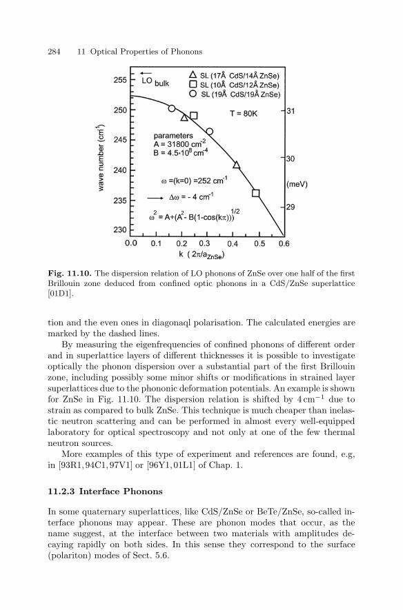
284 11 Optical Properties of Phonons
Fig. 11.10. The dispersion relation of LO phonons of ZnSe over one half of the firstBrillouin zone deduced from confined optic phonons in a CdS/ZnSe superlattice[01D1].
tion and the even ones in diagonaql polarisation. The calculated energies aremarked by the dashed lines.
By measuring the eigenfrequencies of confined phonons of different orderand in superlattice layers of different thicknesses it is possible to investigateoptically the phonon dispersion over a substantial part of the first Brillouinzone, including possibly some minor shifts or modifications in strained layersuperlattices due to the phononic deformation potentials. An example is shownfor ZnSe in Fig. 11.10. The dispersion relation is shifted by 4 cm−1 due tostrain as compared to bulk ZnSe. This technique is much cheaper than inelas-tic neutron scattering and can be performed in almost every well-equippedlaboratory for optical spectroscopy and not only at one of the few thermalneutron sources.
More examples of this type of experiment and references are found, e.g,in [93R1,94C1,97V1] or [96Y1,01L1] of Chap. 1.
11.2.3 Interface Phonons
In some quaternary superlattices, like CdS/ZnSe or BeTe/ZnSe, so-called in-terface phonons may appear. These are phonon modes that occur, as thename suggest, at the interface between two materials with amplitudes de-caying rapidly on both sides. In this sense they correspond to the surface(polariton) modes of Sect. 5.6.

11.4 Problems 285
In the CdS/ZnSe system, two bonds can appear at the interface, whichare not present in either of the two compounds, namely CdSe and ZnS bonds.While CdSe interface phonon modes are difficult to detect since their fre-quency is rather low due to the heavy masses of Cd and Se and they mightconsequently merge in some other confined or backfolded modes, the situa-tion is different for the ZnS mode, which involves the light cation and anionmasses. The peak with the highest energy in the Raman spectrum of Fig. 11.9bis attributed to this interface mode. The displacement pattern is shown inFig. 11.7a and the excellent coincidence of the calculated and measured ener-gies supports this interpretation.
11.3 Phonons in Quantum Dots
In quantum dots, phonons may be confined in all three directions of space sim-ilarly to charge carriers or excitons. One peculiar consequence is that acousticphonons show a discrete energy spectrum starting at finite energy. There aremodes where, e.g., one half of a spherical quantum dot rotates against theother and others where a sphere oscillates adopting the shape of an Americanfootball. The appearance of the various modes is obviously closely linked tothe boundary conditions of the dot. For details see, e.g., [92N1,93W1,96W1].These modes can be observed, e.g., as satellites in resonant photoluminescenceor photoluminescence excitation spectroscopy.
The confined acoustic phonons shift in energy according to R−1 where R isthe dot radius and can thus be distinguished from other splitting mechanismswith a comparable order of magnitude but a different size dependence. Thesinglet-triplet splitting also observed in [96W1] varies, e.g., with powers R−2.5
to R−3.
11.4 Problems
1. Try to find more reflection spectra like that in Fig. 11.1b in the litera-ture. Deduce ωT, ∆LT, εs and εb from these spectra and compare withvalues in the literature.
2. Show that the (eventually only weak) dependence of ω on k is importantto explain the experimental fact that the TO and LO phonon modescan be followed through the whole Brillouin zone by neutron scattering.Compare for the explanation with Fig. 5.1 and (6.2) for vanishing andfinite damping.
3. Why is the phonon spectrum of high Tc superconductors so complex?4. Which trend would you expect for the zone boundary LA and TA
phonons when going from ZnO via ZnS and ZnSe to ZnTe. Comparewith data in the literature. What do you expect for zone center opticphonons?

286 11 Optical Properties of Phonons
5. Can you give qualitative arguments for why the optical phonons inCdS1−xSex and Zn1−yCdyS are of the persistent and amalgamationtype, respectively? Consider the atomic masses of the oscillating atoms.
References to Chap. 11
[65H1] Ch. Henry and J.J. Hopfield, Phys. Rev. Lett. 15, 964 (1965)[68C1] I.F. Chang and S.S. Mitra, Phys. Rev. B 172, 924 (1968)[71M1] R.M. Martin and T.C. Damen, Phys. Rev. Lett. 26, 86 (1971)[71S1] W.G. Spitzer, Festkorperprobleme / Adv. Solid State Phys. 11, 1 (1971)[72C1] C. Colvard et al., Rev. Lett. 28, 811 (1972)[72M1] N. Marshall and B. Fischer, Phys. Rev. Lett. 28, 811 (1972)[74B1] G. Borstl, H.J. Falge and A. Otto, Surface and Bulk Phonon Modes Ob-
served by Attenuated Total Reflection, Springer Tracts in Modern Physics74, Springer, Berlin, Heidelberg (1974)
[75C1] R. Claus, L. Merten and J. Brandmuller, Light Scattering by Phonon-Polaritons, Springer Tracts Modern Phys. 75, Springer, Berlin, Heidelberg(1975)
[79S1] R.L. Schmidt et al., Phys. Rev. B 20, 3345 (1979)[80B1] I. Broser et al., J. Phys. Soc. 49, Suppl. A, 401 (1980)[80C1] R. Claus, phys. stat. sol. (b) 100, 9 (1980)[89J1] B. Jusserand and M. Cardona, Light Scattering in Solids V, Topics in
Applied Physics 66, 49, Springer Heidelberg (1989)[92K1] W. Kutt, Festkorperprobleme / Adv. Solid State Phys. 32, 133 (1992)[92N1] S. Nomura and T. Kobayashi, Solid State Commun. 82, 335 (1992)[93C1] M. Cardona et al., J. Phys. Condensed Matter 5A, 61 (1993)[93R1] T. Ruf et al., Phys. Rev. Lett. 71, 3035 (1993)[93W1] P.D. Wang and C.M. Sotomayor Torres, Phonons in Semiconductor Nanos-
tructures, Kluwer Academic Publishers, Dordrecht (1993), Solid StateCommun. 88, 63 (1993), and J. Appl. Phys. 74, 5047 (1993)
[94C1] M.P. Chamberlain, C. Trallero-Giner and M. Cardona, Phys. Rev. B 50,1611 (1994)
[94C2] M. Cardona, Festkorperprobleme / Adv. Solid State Phys., 34, 35 (1994)[94R1] T. Ruf et al., Festkorperprobleme / Adv. Solid State Phys. 34, 237 (1994)[96W1] U. Woggon et al., Phys. Rev. B 54, 1506 (1996)[97C1] F. Comas, C. Trallero-Giner and M. Cardona, Phys. Rev. B 56, 4115 (1997)[97G1] M. Goppert, Diplom Thesis, Karlsruhe (1997)[97V1] R.V. Velasco and F. Garcia-Moliner, Surf. Science Rep. 28, 123 (1997)[98B1] H.J. Bakker, S. Hunsche and H. Kurz, Rev. Mod. Phys. 70, 523 (1998)[98G1] M. Goppert et al., Phys. Rev. B 57, 13068 (1998)[99D1] A. Dinger et al., phys. stat. sol. (b) 215, 413 (1999)[99R1] V. Romero-Rochin et al., J. Chem. Phys. 111, 3559 (1999)[01D1] A. Dinger et al., Phys. Rev. B 64, 245310 (2001)[01W1] T. Watanuki et al., J. Phys. Soc. Japan 70, 2784 (2001)[02C1] T.F. Crimmins, N.S. Stoyanov and K.A. Nelson, J. Chem. Phys. 117, 2882
(2002)[02K1] A. Kaschner et al., Appl. Phys. Lett. 80, 1909 (2002)[03H1] U. Haboeck et al., Phys. Stat. Sol. c 0 (6), 1710 (2003)

12
Optical Properties of Plasmons,Plasmon-Phonon Mixed States and of Magnons
Plasmons as collective excitations of the carriers in a partly filled band donot usually exist in pure semiconductors under thermodynamic equilibrium,since the probability of thermal excitation across the forbidden gap is almostnegligible, except for narrow gap semiconductors or for semimetals.
There are, however, two conditions under which plasmons can be observed,and these are either highly doped semiconductors or highly excited ones. Un-der high doping and in thermodynamic equilibrium one has (see Sects. 8.9,14)
np = n2i (T ) = N e
effNheffe−Eg/kBT (12.1)
Fig. 12.1. The reflection spectrum inthe vicinity of the plasmon resonancein doped InSb samples [57S1]

288 12 Optical Properties of Plasmons and Magnons
i.e., one has a high density either of electrons or of holes, and the data of themajority carriers have to be used in the calculation of ωP1 according to (10.1).
Under high excitation an electron–hole plasma can be formed, which con-sists of electrons and holes (for details see Chap. 21). In this case the reducedmass of electron and hole enters in (10.1).
In Fig. 12.1 we show the IR reflection spectra of InSb samples with differ-ent n-doping. In agreement with our statements that the transverse eigenfre-quency of plasmons is zero, we see reflectivity close to one from zero up to theplasma frequency, which is, as we remember, the longitudinal eigenfrequency.The reflection minimum corresponds to the frequency at which the refractiveindex of the upper polariton branch is unity. Above the minimum R reachesa value determined by the background dielectric constant of the plasma reso-nance. The shift of the reflection minimum with increasing doping reflects then1/2 dependence of the plasmon frequency.
12.1 Surface Plasmons
Adapting Fig. 5.14 to the situation ωT = 0 we expect, for the case of plasmons,that surface plasmon modes exist in the whole frequency range between zeroand ωPL (Fig. 12.2). These surface plasmons can be investigated either byattenuated total reflection (see Sects. 11.1 or 25.1) or by another methodwhich we will now outline briefly, since it has been used to obtain the datain Fig. 12.2. If a grating with spacing Λ is engraved in the surface, then theparallel component of the wave vector is conserved only modulo reciprocalvectors of this surface grating (see Sect. 3.1.3), i.e., modulo
Fig. 12.2. The dispersion of the surface plasmon mode in n-doped InSb [71M1]

12.2 Plasmon-Phonon Mixed States 289
G‖ =2πΛm; m = 0,±1,±2 . . . . (12.2)
Adding such G‖ values to the wave vectors of the incident light beam allowscoupling to the surface polariton modes for m = 0. By varying the frequencyand the angle of the incident light beam and thus
ω,k‖ + G‖ (12.3)
independently, it is possible to measure the dispersion of the surface plasmonpolariton.
By changing the doping concentration (or the pump power in the case ofan electron–hole plasma or the current in forward direction in a p-n junction)it is possible to deliberately vary the carrier concentration in a semiconductorand thus the plasmon frequency.
12.2 Plasmon-Phonon Mixed States
Eventually we encounter conditions where ωPL ≈ ωLO and plasmon-phononmixed states develop (see Sect. 10.1). Depending on the selection rule, theymay be detected in Raman scattering and/or in IR reflection spectroscopy.We give examples for both cases. In Fig. 12.3. the longitudinal modes ω−and ω+ of Fig. 10.5 have been detected in an electron–hole plasma as a func-tion of electron–hole pair density confirming nicely the concept developed inSect. 10.1.
Fig. 12.3. The dependence of the plasmon-phonon mixed mode on the electron–holepair density in highly photon-excited GaAs [84N1]

290 12 Optical Properties of Plasmons and Magnons
Fig. 12.4. Reflection spectra of n-doped ZnO:Ga samples with two different dopinglevels (note the different abscissas) (a,b) and the various transverse and longitudinaleigenenergeis of the plasmon-phonon mixed states as a function of carrier density(c) [97G1]
In [00N1,02N1] of Chapt. 10 the plasmon-phonon mixed states have beenobserved in transient time-resolved reflection spectroscopy in various semicon-ductors after pulsed excitation.
In Fig. 12.4a,b we show reflection spectra of ZnO:Ga with various n-typedoping levels and in Fig. 12.4c the resulting transverse and longitudinaleigenenergies. One can nicely see that in Fig. 12.4a, the plasma resonanceoccurs below 15 meV, but in Fig. 12.4b the density of 2.3 × 1019 cm−3 givesωPL around 400meV.
The alternating stopbands starting at the various transverse eigenfrequen-cies (ωT,PL = 0; ωTO) and the reflection minima, occurring at the longitu-dinal eigenfrequencies ω− and ω+, respectively, can be nicely seen.

12.3 Plasmons in Systems of Reduced Dimensionality 291
In simple metals the plasma frequency occurs in the 5 to 15 eV range,i.e., they show R 1 over the whole IR and visible spectral range up to theUV. The colour of some metals like Cu, Au or the dip in the reflectivity ofAg in the near UV are due to a superposition of the plasmon resonance andband-to-band transitions in a similar way as the plasmon-phonon interactionin semiconductors in the IR [81N1].
12.3 Plasmons in Systems of Reduced Dimensionality
As already explained in Sect. 10.1 the plasma frequency starts at k = 0, i.e.,λ = ∞ in two- and one-dimensional systems at ωPL = 0. This holds, e.g.,for single quantum wells and multiple quantum wells as long as the couplingbetween them is negligible.
In Fig. 12.5 we show such a situation for two different modulation-dopedGaAs/Al1−yGayAs samples. The data points have been deduced from angle-resolved Raman scattering, which allows variation of k‖.
If the quantum wells couple in a MQW sample one can also define a trans-verse wavelength or k⊥.
A dispersion for ωPL
(k‖, k⊥
)taking such effects into account is given,
e.g., by [82O1]
ωPL =
2πne2
εMm∗eff
k‖sin k‖d
cosh k‖d− cos k⊥d
1/2
(12.4)
with n being the two-dimensional carrier density in every quantum well, m*the effective mass of the carriers, d the distance between quantum wells andεM the dielectric constant of the barriers.
Fig. 12.5. The in-plane dispersion rela-tion of plasmons in two different modu-lation doped GaAs/Al1−yGayAs samples[82O1]

292 12 Optical Properties of Plasmons and Magnons
The solid lines have been calculated with (12.4) and the dashed lines arelinear approximations.
Obviously, various branches can be expected for various values of k⊥. Ad-ditionally, a coupling to phonon resonances or to intersubband transitions maycomplicate things. Examples are found, e.g., in [86F1,89Z1,93S1] or in [01L1]of Chapt. 1.
Just as an addendum we mention again that the beautiful red color ofgold ruby glasses results from surface plasmon excitation of gold colloids (orquantum dots) in the glass matrix [95K1].
12.4 Optical Properties of Magnons
As already mentioned in Sect. 10.2 only few semiconductors show magneticordering like the antiferromagnet MnSe.
One of the very few examples for the observation of magnon polaritonshas been reported for antiferromagnetic FeF2 in [97J1]. The optical magnonshave been observed in reflection and the corresponding surface polaritons byattenuated total reflection, both in a narrow spectral range around 52.5 cm−1
(6.5 meV).An example the difficulty to assign spectral features to plasmons see the
references in [96G1,96R1].The optical properties of diluted (or semimagnetic) semiconductors (DMS)
will be treated in Sect. 16.1.2.
12.5 Problems
1. Calculate the plasmon energy for n- (or p-) doped GaAs and carrier con-centrations of 1010, 1015 and 1020 cm−3.
2. Calculate the density of electrons at which ωPL = ΩLO for ZnO andInAs. Up to which temperatures are the electron gases degenerate.
3. Show that a treatment of the optical properties of free carriers like theDrude model outlined in (10.3 to 5) results in similar optical propertiesto those discussed above.
4. Which interband transition are responsible, together with the plasmonreststrahlbande for the color of Cu and Au?
References to Chap. 12
[57S1] G.W. Spitzer and H.Y. Fan, Phys. Rev. 106, 882 (1957)[71M1] N. Marshall, B. Fischer and H.-J. Queisser, Phys. Rev. Lett. 27, 95 (1971)[81N1] U. Nowak, W. Richter and G. Sachs, phys. stat. sol. (b) 108, 131 (1981)[82O1] D. Olego et al., Phys. Rev. B 25, 7867 (1982)

References to Chap. 12 293
[84N1] H. Nather and L.G. Quagliano, Solid State Commun. 50, 75 (1984)[86F1] G. Fasol et al., Phys. Rev. Lett. 56, 2517 (1986)[89Z1] T. Zettler et al., Phys. Rev. B 39, 3931 (1989)[93S1] L.C.O Suilleabhain et al., Solid State Comun. 87, 517 (1993)[95K1] U. Kreibig and R. Vollmer, Optical Properties of Metal Clusters, Springer
Series in Material Sciences 25, Springer, Berlin (1995)[96G1] M. Gruninger et al., Europhys. Lett. 35, 55 (1996)[96R1] D. Reznik et al., Phys. Rev. B 53, R 14741 (1996)[97G1] M. Goppert et al., J. Luminesc. 72-74, 430 (1997)[97J1] M.F.R. Jensen et al., Phys. Rev. B 55, 2745 (1997)

13
Optical Properties of Intrinsic Excitonsin Bulk Semiconductors
Having treated the optical properties of phonons, plasmons and magnons, wecome in this and the following chapters to the essence of semiconductor optics,namely the optical properties of excitons.
Phonons are necessary to describe the optical properties of semiconductorsand of insulators in the IR; plasmons determine the optical properties ofmetals from the IR through the visible to the near UV, and in semiconductors,if present at all, they contribute along with the phonons to the IR spectra.Excitons, on the other hand, determine together with their continuum statsor the band-to-band transition the optical properties around the band gap,i.e., in the visible including the near UV and IR in the case of semiconductorsand in the (V)UV for insulators. Although inorganic insulators like the alkalihalides and organic ones such as anthracene have specific optical properties,many of the aspects presented in the following for excitons in semiconductorsalso apply to them.
13.1 Excitons with strong Oscillator Strength
We concentrate in this chapter on the intrinsic linear optical properties ofexcitons in bulk semiconductors starting from semiconductors with a dipole-allowed, direct band-to-band transition because they exhibit dipole-allowedexcitons with the highest oscillator strength. Values of their longitudinal–transverse splitting ∆LT range from 0.1 to beyond 10 meV.
It should be mentioned, however, that not all excitons in this group ofsemiconductors have high oscillator strength and that some excitons in semi-conductors with dipole-forbidden band-to-band transitions may be dipole al-lowed, but with considerably lower oscillator strength. We come back to thesecases in Sect. 13.2, ending with indirect gap materials.
13.1.1 Exciton–Photon Coupling
In semiconductors with dipole-allowed direct band-to-band transitions, exci-tons occur, which couple strongly to the radiation field. As a consequence

296 13 Optical Properties of Intrinsic Excitons in Bulk Semiconductors
many optical properties can be understood quantitatively only in the strong-coupling or polariton picture. Thus we use this occasion to elucidate oncemore for this particular case the concept of weak and of strong coupling tothe radiation field, heeding the classical dogma “repetitio est mater studio-rum”.
In Sects. 2.1–2.4 we introduced the electromagnetic radiation field, andin Sect. 2.5 the photons as its quanta. In Chaps. 9–11 we presented theproperties of various elementary excitations. The interaction between the twocan be treated in perturbation theory. This is the so-called weak couplingapproach. The one-photon absorption coefficient α(ω) is then at resonanceproportional to the dipole matrix element squared in (13.1a), i.e., by firstorder-perturbation theory with the initial and final state:
α(ω) ∝ |〈f |HD | i〉|2 δ (Ei − Ef + ω) . (13.1a)
The refractive index is obtained at this level of approximation either bya Kramers–Kronig transformation of α(ω) or, away from the resonance, bysecond-order perturbation theory according to
n2(ω) − 1 ∝∑
z
〈i|HD|z〉 〈z|HD|i〉Ez − Ei − ω
(13.1b)
A photon ω creates virtually an excited intermediate state |z〉 undermomentum conservation, which, after a time ∆t limited by
∆E∆t = (Ez − Ei − ω)∆t , (13.2)
emits again a photon which is identical to the incident one, while the electronicsystem returns to the initial state |i〉. The time ∆t during which the energy is“stored” in the virtually excited state reduces the phase velocity of the lightand thus evidently describes an n(ω) which increases when ω approaches theresonance energy Ez − Ei from below, since ∆E goes to zero and ∆t can bevery long, in agreement with Fig. 4.4.
In the polariton concept, on the other hand, one quantizes the mixed stateof the electromagnetic radiation and the excitation of the medium, i.e., thepolarization wave. We already introduced this concept in Chap. 5. Since it isa very important one we want to demonstrate it here again for the excitonpolariton.
For readers who are not satisfied with the simple statement that the po-laritons are the quanta of the mixed states of electromagnetic radiation andexcitation (or polarization), we give two other approaches. The first is justa diagrammatic representation of what was said before.
In Fig. 13.1 an incident photon creates an electron–hole pair, which recom-bines again to give a photon, and so on. The Coulomb interaction betweenelectron and hole, which is responsible for the formation of the exciton, isrepresented by a virtual exchange of photons between electron and hole, i.e.,

13.1 Excitons with strong Oscillator Strength 297
by the vertical lines. Consequently the whole diagram of Fig. 13.1 can beconsidered as a representation of the exciton polariton.
In the other approach, which follows [93H1] of Chap. 1, we start with theelectron and hole operators, construct from them the exciton and finally theexciton polariton. (see also Sect. 9.1)
We start with the creation and annihilation operators for excitons:
B+v,k ; Bv,k . (13.3)
The index v stands for the quantum numbers nB, l,m.It can be shown that the Bv,k deviate from the commutator relations of
ideal bosons by a term proportional to the mean number of electron–holepairs, n, contained in the volume of an exciton ad
B (see e.g. [93H1, 93P1] ofChap. 1)
〈[B 0 , 0, B+0 , 0]
−〉 = 1 − O (nadB) , (13.4)
where d is the dimensionality of the system. The Hamiltonian of a non-interacting exciton gas is then
H =∑v,k
E (v,k)B+v,kBv,k . (13.5)
Using an analogous expression for the photons with the number opera-tor c+k ck, for the interacting system of excitons and photons considering theleading, i.e., resonant terms around a specific resonance only, we obtain
H =∑
k
[∑v
EvkB+vk Bvk + ωk c
+k ck − i
∑v
gvk (B+vk ck − h.c.)
].
(13.6)The coupling coefficients gvk contain the transition matrix elements as in (13.1).
If we consider the third term on the right-hand side of (13.6) as a pertur-bation, we are back once more to the weak coupling limit.
The polariton concept is obtained if we diagonalize the whole Hamiltonian(13.6) by a suitable linear combination of the Bvk and the ck, leading to thepolariton operator Pk
Pk = uvkBv,k − vk ck (13.7)
with |uvk|2 + |vk|2 = 1 . (13.8)
Fig. 13.1. Diagrammatic representation of an exciton polariton

298 13 Optical Properties of Intrinsic Excitons in Bulk Semiconductors
Fig. 13.2. The energydependence of the uv,k
and vk of (13.7) for theupper polariton branch.According to [93H1] ofChap. 1
The uvk give the exciton-like character of the polaritons. They are closeto one around the exciton energy Ev,0 and decrease on the upper and lowerpolariton branches with decreasing energetic distance from the resonance.The vk give the photon-like part and, according to (13.8), show the oppositebehavior. In Fig. 13.2 we give an example for the upper polariton branch.As a rule of thumb we can state that the polariton wavefunction containsconsiderable exciton-like parts over energies
| ω − Eex | 10 ∆LT . (13.9)
It is interesting to note that the dispersion relation that we obtain fromthis approach is identical to the one obtained from the set of classical coupledoscillators treated in Chaps. 4 and 5.
13.1.2 Consequences of Spatial Dispersion
In contrast to that of optical phonons, the k dependence of the exciton energyis significant. For k vectors in the transition region from the photon-like tothe exciton-like part of the dispersion relation, the so-called bottle-neck, thekinetic energy term in (9.1a) becomes comparable to the longitudinal trans-verse splitting ∆LT. The consequences of spatial dispersion have already beenoutlined in connection with Figs. 5.3–5.5, so that we can restrict ourselves tojust recalling them here. For all frequencies there is at least one propagating

13.1 Excitons with strong Oscillator Strength 299
mode. This fact reduces the reflectivity in the reststrahlbande to values be-low 1, even in the case of negligible damping. For frequencies above ωL thereare several propagating modes, and below it there is at least one propagat-ing mode and one or more evanescent ones. This situation is not covered bythe boundary conditions deduced from Maxwell’s equations and additionalboundary conditions (abc) have to be introduced containing the informationabout what fraction of the energy transmitted through the interface travelson which polariton branch. Since this “branching” ratio is ω-dependent andsince the imaginary parts of the various branches differ, the decay of the in-tensity into the depth of the sample can be nonexponential. This means the“effective” absorption coefficient can be thickness dependent. Furthermore itlooks more complex (Fig. 5.5) than Fig. 4.4.
The abc which have been introduced by Pekar and by Hopfield [58H1,62H1, 62P1, 63H1, 64M1] assume that the excitonic part of the polarizationat the surface vanishes, or its derivative normal to the surface, or a linearcombinations of both. See Sect. 5.4 and e.g. [74A1, 75L1, 78B1, 78H1, 78S1,79B1,79S1,80B1,81B1,81L1,81S1,82O1,82R1,82S1,83M1,84H1,84S1,85H1]of Chap. 5. In [98H1] a way out of this abc problem has been shown. Foreven more recent approaches see [00T1, 01S1]. Furthermore one can assumethat excitons do not “leak out” of the semiconductor into vacuum and thatthere should consequently be an exciton-free surface layer (dead layer), the
Fig. 13.3. The problem of reflection for a semiconductor in the vicinity of an excitonresonance for normal incidence including multiple reflection in a dead layer and twopropagating modes due to spatial dispersion

300 13 Optical Properties of Intrinsic Excitons in Bulk Semiconductors
optical properties of which are described by εb and which has a minimumthickness of the excitonic Bohr radius. Electric fields, which occur often atsurfaces normal to them, can ionize, i.e., destroy the exciton and lead to anincrease in the thickness of the dead layer. The problem which thus has to besolved to calculate a reflection spectrum is shown in Fig. 13.3. An incidentbeam passes first the dead layer in which multiple reflection occurs and thenenters the semiconductor in which several modes can be excited. Sometimesscientists apply even more complex models assuming, e.g., that the dampingand/or the eigenfrequencies are depth dependent [79E1,81L1,82S1].
The formulas to calculate the spectra are rather complex and we do notgive them here but refer the reader to [75L1, 78S1, 79E1, 80B1, 81L1, 82B1,82S1, 84R1, 85H1, 93K1, 95B1] or the references from Chap. 5 given above.Instead we give in the next section examples of reflection, transmission, andluminescence spectra of the exciton polariton in bulk semiconductors withdirect, dipole-allowed band-to-band transitions.
13.1.3 Spectra of Reflection, Transmission and Luminescence
In Fig. 13.4a we show the bandstructure of CdS in part b the dispersion of theexciton polariton for the orientation k ⊥ c,E ⊥ c and including the nB = 1excitons involving a hole either in the A or in the B valence band. The A exci-ton is a rather simple resonance for this orientation, comparable to our modelsystem in Sect. 5.2. The k-linear term of the B valence band (Sect. 8.8) mixesthe singlet and triplet states for k⊥ = 0 (see Sect. 13.2.1.1) and gives rise to anadditional polariton branch. Figure 13.4c finally gives the reflection spectra ofthe two resonances for E ⊥ c and E ‖ c and of some higher states (nB ≥ 2).The combination of the Γ1 (S-) envelope function for nB = 1 with the symme-tries of the electron Γ7 and the holes (AΓ9, BΓ7) gives excitons of symmetriesAΓ5 and AΓ6 and BΓ1, BΓ2, BΓ5 as explained in more detail in Chap. 26. TheΓ6 and Γ2 states are triplets which couple only weakly to the radiation fieldsince they are spin-flip and dipole-forbidden and do not show up in reflection(see Sect. 13.2.1.1). Γ5 and Γ1, states couple to the radiation field for the ori-entations E ⊥ c and E ‖ c, respectively. These selection rules show up clearlyin the reflection spectra, the nB = 1 A excitons being seen only in E ⊥ c.
A fit to the reflection spectra (not shown here) using spatial dispersion,an exciton-free layer and some abc coincides with experiments within a fewpercent.
The AΓ5 resonance is quite simple, as already mentioned. R remains sig-nificantly below 1 due to spatial dispersion as predicted above. For smalleroscillator strength or longitudinal-transverse splitting, the maximum almostdisappears and only a narrow dip close to the longitudinal eigenfrequencyremains, as shown in Fig. 13.5 for ZnTe.
The small spike around AΓL5 in Fig. 13.4c is partly caused by the onset of
the UPB but mainly by the dead layer. An increase of its thickness increasesthe importance of the spike due to multiple reflections (Fig. 13.3) and may

13.1 Excitons with strong Oscillator Strength 301
Fig. 13.4. The bandstructure of CdS around the Γ -point (a); the dispersion of thenB = 1 A and B exciton polariton resonances (b); and the reflection spectra for thepolarizations E ⊥ c and E ‖ c (c). According to [82B1,85H1,93K1]
even lead to an “inversion” of the usual reflection spectrum, i.e., to a dip atlow energies and a maximum above. A set of calculated spectra showing thisphenomenon is given in Fig. 13.6.
The BΓ1 exciton resonance is again a simple one, but the BΓ5 has a smalldip stemming from the additional polariton branch shown in Fig. 13.4b, whichat this energy reaches exactly n = 1.
While the A and BΓ5 excitons have in CdS for E ⊥ c roughly equal oscilla-tor strength and ∆LT [85H1], the situation changes for close lying resonancesas occurs for ZnO [85H1]. In this case the longitudinal transverse splitting

302 13 Optical Properties of Intrinsic Excitons in Bulk Semiconductors
Fig. 13.5. A reflection spectrum forZnTe. According to [83M1]. For thedispersion of the exciton polariton seeSect. 16.1.1
∆LT of the AΓ5 exciton is reduced and that of the BΓ5 increased as discussedalready in Sect. 4.5. Only the sum of ∆LTAΓ5 and ∆LTBΓ5 has to be constantand equal to ∆LTCΓ1 [60H1]. See also Fig. 13.21
At higher energies we see nB ≥ 2 exciton states which split into sev-eral sublevels due to the various L and/or Lz values of the envelope func-tion. The reflection signal of these higher states decreases due to the n−3
B
dependence of the oscillator strength. In the band-to-band transition regionthe reflection spectra are usually flat and structureless. The C-excitons ex-pected from Fig. 13.4a are situated around 2.61 eV and are off the scaleof Figs. 13.4b, c. These resonances are washed out even at low tempera-ture because the C-exciton is situated in the continuum of the A- and B-excitons and thus has a rather short phase relaxation time T2, i.e., strongdamping.
With increasing lattice temperature the exciton resonances are broadeneddue to increasing scattering with phonons. Sometimes they are hardly visibleat RT as shown in Fig. 13.7 for CdS. A similar washing out of the excitonresonance can occur even at low temperatures in samples with high impuritycontent and/or lower crystalline quality or for increasing excitation desenty.
To summarize, we can state that the reflection spectra of semiconduc-tors are determined around the gap by exciton polaritons. The longitudinaleigenenergy can be reasonably well determined from the reflection minimumwhich corresponds to n = 1 on the UPB and is therefore situated only slightly

13.1 Excitons with strong Oscillator Strength 303
Fig. 13.6. A set of calculated exciton reflection spectra of CdS for 45 incidenceand for various thicknesses of the exciton-free layer with all other parameters keptconstant. According to [82R1]
(< 1 meV) above ωL. The transverse eigenenergy, the oscillator strength, thedamping, and the effective mass of the exciton can be extracted only with thehelp of a rather complicated line-shape analysis.
For uniaxial, hexagonal materials like CdS or ZnO it can be shown fromgroup-theoretical considerations that the Γ5-excitons are the resonances forthe ordinary beam (Sect. 3.1.7) because the polarization E ⊥ c can be realizedfor all angles between k and c. The Γ1 resonances have dipoles oriented parallelto c. As a consequence they have maximum coupling to the radiation field forE ‖ c and k ⊥ c, but develop as extraordinary or mixed-mode polaritons tothe longitudinal state if the angle ∠(k, c) is continuously changed from k ⊥ cto k ‖ c. In Fig. 13.8 we show the dispersion of the CΓ1 exciton polariton inZnO, which has an oscillator strength varying according to
∆LT = ∆0LT sin2 ∠(k, c) . (13.10)
Experimental data for mixed mode polaritons can be found in [72W1,75L1]. The small refection spike seen at BΓ5L in [03C1] might similarly wellbe due to a mixed mode polariton due to the finite angle of aperture of theincident beam.

304 13 Optical Properties of Intrinsic Excitons in Bulk Semiconductors
Fig. 13.7. A set of reflection spectra of the A- and B-exciton resonances of CdS forvarious lattice temperatures. According to [80B2]
The absorption spectra of nB = 1 polariton resonances are usually dif-ficult to measure quantitatively, since in the resonance region the effectiveabsorption, or rather extinction, coefficient reaches values in the range
104 cm−1 αeff 106 cm−1 . (13.11)
As a consequence for samples with d 1 µm, the transmitted light intensitygoes to “zero”, i.e., to values comparable to or smaller than the stray lightof the spectrometer. We show in Fig. 13.9a an absorption spectrum of a ZnOlayer at RT. The layer is of polycrystalline nature, produced by evaporatingZn on a substrate of quartz glass and subsequent oxidation [43M1]. The crys-tallites have their c axis oriented perpendicular to the substrate. The peak at3.3 eV is due to the close lying and thermally broadened AΓ5 and BΓ5 excitonresonances ([75L1,78H1,80B1,81L1,82B1,85H1,03C1] and references therein).This is possibly one of the first experimental observations of a Wannier exci-ton in absorption, though the author of [43M1] was most probably not awareof this fact. See also Sect. 9.1. In Fig. 13.9b experimental transmission spectraare shown A and BΓ5 resonance of a thin CdS platelet type sample. Thereare Fabry–Perot modes (see Sect. 3.1.6) in the transparent region due to thenatural reflectivity of the surfaces of the as-grown platelet type sample. A de-
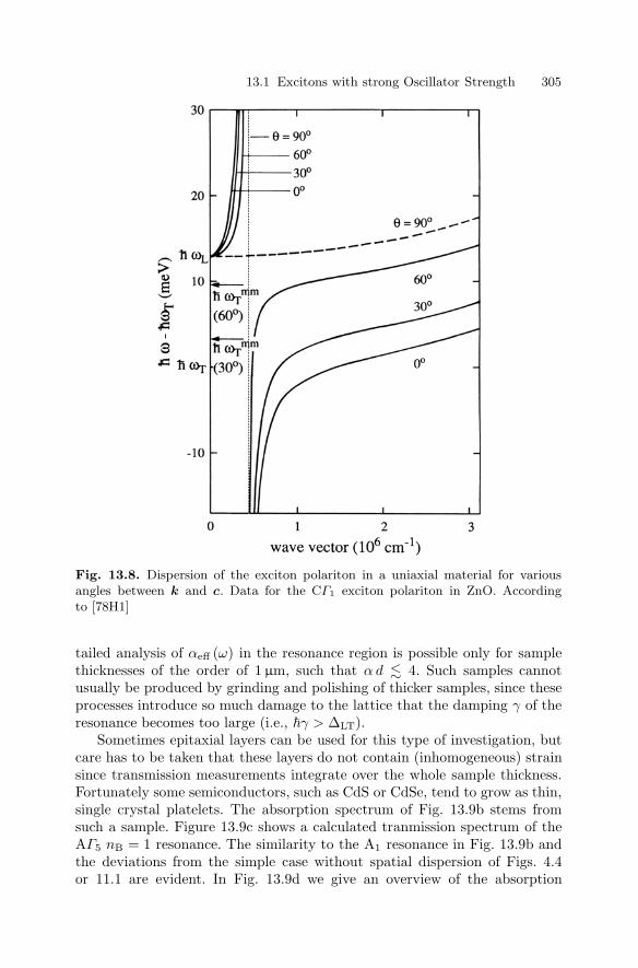
13.1 Excitons with strong Oscillator Strength 305
Fig. 13.8. Dispersion of the exciton polariton in a uniaxial material for variousangles between k and c. Data for the CΓ1 exciton polariton in ZnO. Accordingto [78H1]
tailed analysis of αeff (ω) in the resonance region is possible only for samplethicknesses of the order of 1 µm, such that α d 4. Such samples cannotusually be produced by grinding and polishing of thicker samples, since theseprocesses introduce so much damage to the lattice that the damping γ of theresonance becomes too large (i.e., γ > ∆LT).
Sometimes epitaxial layers can be used for this type of investigation, butcare has to be taken that these layers do not contain (inhomogeneous) strainsince transmission measurements integrate over the whole sample thickness.Fortunately some semiconductors, such as CdS or CdSe, tend to grow as thin,single crystal platelets. The absorption spectrum of Fig. 13.9b stems fromsuch a sample. Figure 13.9c shows a calculated tranmission spectrum of theAΓ5 nB = 1 resonance. The similarity to the A1 resonance in Fig. 13.9b andthe deviations from the simple case without spatial dispersion of Figs. 4.4or 11.1 are evident. In Fig. 13.9d we give an overview of the absorption

306 13 Optical Properties of Intrinsic Excitons in Bulk Semiconductors
spectrum of a thin GaAs sample. GaAs has, in comparison to CdS or ZnO,a much lower oscillator strength due to the larger value of aB (see Sect. 9.1);(∆LT GaAs ≈ 0.1 meV). Therefore it is easier to measure the absorption of thenB = 1 exciton. We can see in this figure similarly as for CdS in Fig. 13.9balso the nB = 2 and 3 levels with S-envelope function. Even higher states(nB > 3) merge with the continuum. The decrease of the oscillator strengthwith n−3
B [57E1] is at least qualitatively confirmed by this spectrum.The rather constant value of α (ω) in the region of the continuum states
comes from the product of the square root combined density of states (thedashed line gives the calculated absorption spectrum for a simple band-to-band transition without Coulomb effects for comparison) and the Sommerfeldfactor, already discussed in Sect. 9.1,3 for d = 3.
At higher temperatures, the excitons develop an absorption tail to lowerphoton energies, which is described by the so-called Urbach or Urbach–Martienssen rule [53U1,57M1,58D1,71K1,71S1,72D1,85L1]
α(ω) = α0 exp [−σ (T ) (E0 − ω)/ kB T ] , (13.12)
ω < E0
whereα0 andE0 arematerial parameters.E0 is an energy situated several 10meVabove the energy of the lowest free exciton at TL = 0 K. σ is a function varyingonly weakly with temperature. An example is given in Fig. 13.10 for CdS.
The temperature dependence of the band gap, which can also be nicelyseen in Figs. 13.7 or 13.10, is already incorporated in (13.12) since the excitonpeak shifts in parallel to the gap.
The reason for the behavior described by (13.12), which is of rather uni-versal nature in semiconductors and insulators, is the interaction of excitonswith optical phonons. Two effects are usually discussed in theory: a momen-tary localization of the excitons in the randomly fluctuating field of opticalphonons, or an ionization in their electric field. These two effects seem to con-tribute with a weight that depends on the material parameters. Details aboutthe theory can be found in [71S1,72D1,85L1] and references therein.
The absorption of direct excitons in indirect materials will be addressedin Sect. 13.2.2.
The investigation of the luminescence from excitons or more preciselyexciton polaritons is a rather difficult task. For early investigations see[72B2, 72W2]. The emission from these states is generally very weak even atlow temperatures even in high quality sampels. This has various reasons: thetotal luminescence yield η lum of semiconductors is often very low. Frequentlyone finds, even for direct gap materials,
10−1 η lum 10−3 , (13.13)
i.e., the main recombination channel is non-radiative involving defect centers.A large part of the emission stems from phonon replica and, especially at

13.1 Excitons with strong Oscillator Strength 307
Fig. 13.9. An experimental absorbtion spectrum of ZnO at RT (a), an experimentaltransmission spectrum of CdS for the orientation E ⊥ c in the region of the A andB exciton resonances (b); a calculated one for the AΓ5 resonance for nB = 1 (c);and an absorption spectrum for a thin GaAs sample (d). According to [43M1] to[79V1,82R1] and to [91U1], respectively

308 13 Optical Properties of Intrinsic Excitons in Bulk Semiconductors
Fig. 13.10. The absorption edge of CdS for various temperatures and the polariza-tion E ‖ c. According to [76S1]
low temperatures, from bound-exciton complexes, donor–acceptor pairs, orother defect centers which are considered in Chap. 14. Furthermore, the directemission from free exciton polaritons is limited by various effects: One is theinternal reflection, another the small escape depth. These points will be furtherclarified below.
If we excite an electron–hole pair, e.g., in the continuum states, it will relaxto lower energies and thermalize by emission of phonons, as described in moredetail in Chap. 23. At very low temperatures (kBT < ∆LT) the excitons endup on the LPB where they further relax by acoustic phonon emission. Sincethe scattering matrix element and the density of final states both decrease inthe transition region between exciton- and photon-like dispersion, the excitonsaccumulate there. This is the reason why this region is called a bottle-neck.At higher temperatures the excitons reach essentially a Boltzmann-like distri-bution on the exciton-like part of the LPB, on the longitudinal branch, and onthe UPB. In the polariton picture the luminescence from these states cannotbe described as a “recombination” of the exciton polariton with emission ofa photon, since the photon will be immediately reabsorbed to form an exciton,or in other words, since we are considering the quanta of the mixed state ofexciton and photon.
The proper description is the following: The exciton polariton moves withits group velocity through the sample. It can be scattered by impurities orphonons or be trapped. Eventually it reaches the surface. In most cases it

13.1 Excitons with strong Oscillator Strength 309
will be reflected back into the sample. The limiting angle for total internalreflections αTR is, e.g., for n = 5 – a typical value on the LPB in the bottleneck region as shown in Sect. 13.1.4, only about 13. Of the excitons impingingunder an angle smaller than αTR, a considerable fraction are also reflectedback into the sample, as becomes clear if one considers the formulas for thereflection under normal incidence or if one integrates over Fresnel formula ofSect. 3.1.4.
Furthermore, the luminescence yield of free-exciton polaritons is limitedby the small escape depth lesc, i.e., the depth from which they can reachthe surface. If one excites in the band-to-band transition region, the excitinglight penetrates about 0.1–1µm into the sample corresponding to α-valuesof 104–105 cm−1 in this spectral range. By diffusion, the excitons spread outover a region of 1–2 µm. The depth from which they can reach the surface ismuch less than this. A rough estimate can be obtained either from the inverseeffective absorption coefficient in the exciton resonance or from the productof phase-relaxation time T2 (Sect. 23.1) and the group velocity in the excitonresonance (Sect. 13.4):
α−1eff = (104 − 106 cm−1)−1 = 0.01− 1 µm (13.14a)
lesc = vgT2 = (10−3 − 10−5 · c) (10− 40 ps) = 10− 0.03 µm . (13.14b)
In spite of all these difficulties it was possible to observe the emission from theexciton polariton in many semiconductors and we give an example for ZnOin Fig. 13.11. On the left the dispersion relation of the A-exciton is shownfor k ⊥ c and k ‖ c. Since the Γ7 and Γ9 valence bands are most probablyinverted in ZnO as compared to CdS, see Sect. 8.8, the k-linear term appearsin the A-exciton for the orientation k ⊥ c. The influences of the resultingadditional polariton branch, of the longitudinal branch, and of the UPB areseen by comparison with the orientation k ‖ c where the longitudinal branchand the k-linear term are missing. A luminescence polarized E ‖ c in theA exciton resonance has been observed in [03C1] possibly indicative for theweak AΓ1 contribution according to [60H1]. Some other examples for thepolariton luminescence including also other materials, both as bulk samplesand epitaxial layers are found e.g. in [68V1, 77V1, 79P1, 80D1, 95S1, 97N1,97N2,98M1,99R1,00T1,01R1,01S1].
A luminescence channel of the exciton polaritons with higher lumines-cence yield in semiconductors with strong exciton-LO phonon coupling arethe LO-phonon replicas. In this case a polariton on the exciton-like part ofthe dispersion relation or in the bottleneck is scattered onto the photon-likebranch by emission of one or more longitudinal optical phonons. The cou-pling with this type of phonon is stronger than with transverse optical oracoustic phonons since the lattice distortion of the polaron (Sect. 8.6) canbe described largely as a superposition of longitudinal optical phonons. Oncethe polariton is on the photon-like branch, it travels over long distances withalmost negligible damping and is transmitted through the surface into vac-

310 13 Optical Properties of Intrinsic Excitons in Bulk Semiconductors
uum with quite high probability, since n 2 in the corresponding spectralrange.
In Fig. 13.12 we show the appearance of the LO-phonon satellites schemat-ically. If we neglect the bottleneck region for the moment, we can deducewith the Boltzmann occupation probability the distribution of the excitons asa function of their kinetic energy Ekin
N(Ekin) ∝E
1/2kin exp −Ekin/kBT for Ekin ≥ 0
0 otherwise
with Ekin =
2k2
2M. (13.15a)
The lineshape of the luminescence of the m-th LO-phonon replica is thengiven by [82P1]:
Fig. 13.11. The dispersion of the nB = 1 A-exciton resonance in ZnO for the polar-izations E ⊥ c (Γ5) and E ‖ c (Γ1) (a, c) and the observed polariton luminescence(b, d). According to [78H1,81K1]
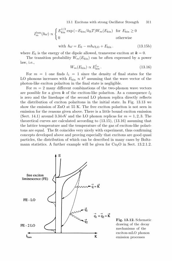
13.1 Excitons with strong Oscillator Strength 311
I lumm (ω) ∝
E
1/2kin exp (−Ekin/kBT )Wm(Ekin) for Ekin ≥ 0
0 otherwise
with ω = E0 −mωLO + Ekin . (13.15b)
where E0 is the energy of the dipole allowed, transverse exciton at k = 0.The transition probability Wm(Ekin) can be often expressed by a power
law, i.e.,Wm(Ekin) ∝ Elm
kin . (13.16)
For m = 1 one finds l1 = 1 since the density of final states for theLO phonons increases with Ekin ∝ k2 assuming that the wave vector of thephoton-like exciton polariton in the final state is negligible.
For m = 2 many different combinations of the two-phonon wave vectorsare possible for a given k of the exciton-like polariton. As a consequence l2is zero and the lineshape of the second LO phonon replica directly reflectsthe distribution of exciton polaritons in the initial state. In Fig. 13.13 weshow the emission of ZnO at 55 K. The free exciton polariton is not seen inemission for the reasons given above. There is a little bound exciton emission(Sect. 14.1) around 3.34 eV and the LO phonon replicas for m = 1, 2, 3. Thetheoretical curves are calculated according to (13.15), (13.16) assuming thatthe lattice temperature and the temperature of the gas of exciton-like polari-tons are equal. The fit coincides very nicely with experiment, thus confirmingconcepts developed above and proving especially that excitons are good quasiparticles, the distribution of which can be described in many cases by Boltz-mann statistics. A further example will be given for Cu2O in Sect. 13.2.1.2.
Fig. 13.12. Schematicdrawing of the decaymechanisms of theexciton-mLO phononemission processes

312 13 Optical Properties of Intrinsic Excitons in Bulk Semiconductors
The small tail on the low energy side comes from the population in the bot-tleneck which is not considered in (13.15), (13.16) and from a homogeneousbroadening of the excitons increasing with temperature. From (13.15), (13.16)one can deduce that the ratio of the integrated intensities of the first and thesecond LO-phonon replica is proportional to T
Q1,2 =∫I lum1 (ω) dω∫I lum2 (ω) dω
∝ T . (13.17)
In Fig. 13.14 we give experimental data for Q1,2 in ZnO for volume exci-tation and surface excitation. The first case has been realized by two-photonexcitation with a ruby laser, which allows relatively homogeneous excitationof samples up to thicknesses in the mm range, and the second by UV excita-tion in the continuum states where the excitation depth is limited mainly bydiffusion to values of the order of µm as discussed above.
Up to temperatures of 100K the points follow nicely the predictions of(13.17), then they drop. This deviation is due to reabsorption effects causedby the absorption tail described by (13.12), which starts to influence the escapedepth of the polaritons also in the m = 1 range at higher temperatures. Thiseffect is evidently more pronounced for volume excitation than for surfaceexcitation. In semiconductors with less polar coupling, such as GaAs, theLO-phonon replicas are less pronounced.
For those who work on luminescent ions in insulators and are thereforefamiliar with the concept of the Huang–Rhys factor S, it should be mentionedthat for free excitons in most semiconductors S is below one. The large ratioof first to zero phonon intensity seen in Fig. 13.13 is not connected with a largevalue of S but with other processes that reduce the zero phonon emission, asoutlined above (See e.g. [68V1,79P1]).
LO-phonon replicas do not only appear in the excitonic luminescencespectra on the low energy side, but may also appear in case of sufficientlystrong exciton LO-phonon coupling in the absorption spectra on the highenergy side, extending into the continuum. Examples for one- and two-
Fig. 13.13. LO-phonon replica in the luminescence spectrum of ZnO at 55 K.According to [75K1]

13.1 Excitons with strong Oscillator Strength 313
Fig. 13.14. The ratio of the integrated intensities of first and second LO-phononreplica in ZnO as a function of temperature for two different excitation conditions.According to [75K1]
photon absorption in Cu halides are found, e.g., in [66R1, 72B1] and forPbI2 in [94W1]. The term exciton-phonon bound state was introduced in[68T1,72K1].
The interaction of excitons and photons with acoustic phonons in Cu2Oleads to the introduction of the concept of phonoritons [00H1].
It should be mentioned that excitons can also be scattered also by emissionof quasiparticles other than phonons onto the photon-like part of the polaritonbranch. Examples can be found, e.g., in Sect. 20.2 and we mention here scat-tering by magnons, which may occur in (anti) ferromagnetic semiconductorslike RbMnF3 or Cr2O3 [76S2,99D1].
To conclude this discussion of free exciton luminescence, it should be men-tioned, that a recent calculation [98K1] predicts, that a luminescence featuremay occur at the position of the free exciton resonance, resulting, however,from the recombination of an electron–hole plasma (see Chap. 21) going underemission of a photon from a state containing n electron–hole pairs to one with(n − 1) pairs. Though these calculations do by no means rule out the exis-tence of excitons as good quasi-particles, a luminescence feature at the excitonenergy alone is not necessarily a proof of their existence. The observation ofadditional features, like intra excitonic transitions (see Sect. 13.3 and [03K1])can help to clarify possible discrepancies.
As a rule of thumb it can be stated that the formation of excitons islikely for resonant and low or intermediate exciton densities (see Chap. 20). Ifthe thermal energy kBT is comparable to or larger than the exciton binding

314 13 Optical Properties of Intrinsic Excitons in Bulk Semiconductors
energy Ebx the excitons will be thermally ionized with time. Under band-
to-band excitation, exciton formation is likely for kbT Ebx and for exciton
formation times shorter than the exciton lifetime. The formation time is short,if the exess energy can be dissipated by LO-phonon emission especially inpolar materials, while acoustic phonon emission is slower, especially in lesspolar materials. We come back to this topic in Chaps. 15 and 23.
13.1.4 Spectroscopy in Momentum Space
It is clear from the above discussion that the concept of exciton polaritonsallows one to understand the spectra of reflection, transmission, and lumi-nescence, but that a quantitative interpretation of the data usually involvesa rather elaborate theoretical fit. Therefore various techniques have been de-veloped which allow more or less directly the spectroscopy of exciton polari-tons in momentum space, i.e., they provide the possibility of measuring thedispersion relation E(k) more directly.
In this section we therefore recall briefly the consequences of “spatial dis-persion”, i.e., of the dependence of ω0 on k, and then present various methodsof k- or momentum-space spectroscopy.
As mentioned earlier in Chap. 5, the combination of the dielectric functionε(ω,k) (6.1) and the polariton equation forms an implicit representation of thepolariton dispersion. For ω > ω0,L we get two propagating modes in the sampleor even more if the dispersion relation is complex (Fig. 13.4b or Fig. 13.11)or if the longitudinal branch couples to the radiation field as may occur fork = 0 or for oblique incidence in uniaxial crystals. Since the k vectors of thevarious modes in the sample are different, the diffracted beams propagate indifferent directions, thus giving some meaning to the term “spatial dispersion”.Below ω0,L we have at least one propagating and one evanescent mode, whichhowever, for finite damping also acquires a small real part. The consequencesof this fact for the reflection spectra have already been discussed above.
The first method of k-space spectroscopy uses the analysis of the Fabry–Perot modes introduced in Sect. 3.1.6, which appear for example in as-grown,thin, platelet type samples with plane-parallel surface. For an example seeFig. 13.9b. As already pointed out there, transmission maxima occur when aninteger number of half-waves fit into the resonator, i.e.,
km(ωm) = mπ
d, m = 1, 2, 3 . . . , (13.18)
where d is the geometrical thickness of the sample and k is the real part ofthe wave vector in the medium. If ωm and km are known for one m1 then thedispersion relation can be reconstructed from (13.18) by reading the ωm fromthe transmission spectrum and by progressing in steps of πd−1 on the k-axis.In Fig. 13.15 we show the dispersion of the nB = 1 A-Γ5-exciton polaritonin CdSe, together with a measured and a calculated reflection spectrum. The

13.1 Excitons with strong Oscillator Strength 315
Fig. 13.15. The polariton dispersion in CdSe with an equidistant ruling of the k-axis(a) and the observed (b) and calculated structure (c) of the resulting Fabry–Perotmodes. According to [75K2]
condition for the reflection minima coincides with that for the transmissionmaxima in (13.18).
The equidistance on the k-axis is clearly visible and the good agreementof theory and experiment is obvious. Above ω0L one can clearly see closelyspaced modes of the LPB and superimposed widely spaced ones from thepart of the light travelling on the UPB. The fact that the small modulationdecreases with increasing photon energy indicates that the fraction of lighttravelling on the LPB through the sample decreases with increasing energyabove ω0L.
Similar data have also been found in CdS and CuCl [80M1,84M1,93K1].The next method is resonant Brillouin scattering. We introduced this scat-
tering process with acoustic phonons in Sect. 11.1.4 and know that the Bril-louin shift is directly proportional to the transfer of momentum due to thelinear dispersion relation of acoustic phonons around the Γ point.
Figure 13.16 shows schematically the Brillouin scattering in the resonanceregion of an exciton polariton in a backward scattering configuration. Theeffect has been observed in GaAs, CdS, ZnSe and CuBr [78U1, 79S1, 80B3,

316 13 Optical Properties of Intrinsic Excitons in Bulk Semiconductors
Fig. 13.16. Schematic drawing of Brillouin scattering in backward geometry in theresonance of an exciton polariton [78U1] (a) and experimental data for GaAs [78U1](c) and for CdS [84M1,84W1] (b)

13.1 Excitons with strong Oscillator Strength 317
80K1, 81C1, 84M1, 84S1, 84W1]. In Fig. 13.16b and c we give data for CdSand GaAs partly involving TA and LA phonons. The soild lines have beencalculated in a fit procedure with the parameters in the inset; these of course,also allow the calculation of the polariton dispersion itself.
A close inspection of the Brillouin line shape shows that the dampingconstant is energy or k-dependent [84S1]. This result has also been obtainedin CuCl from nondegenerate four-wave mixing [85H1]. See Sect. 20.2 and25.2 for this technique. Similarly one finds that ∆LT is also a function ofk [82O1,85H1].
It is well known that refraction from a prism can be used to determinethe real part of n and thus of k. If sufficiently thin (d 1 µm), prism-shapedsamples are available, it is also possible to extend this technique to the res-onance region of the exciton polariton. Fortunately some CdS platelets growin the desired form, presumably involving a small-angle grain boundary.
Figure 13.17 gives two examples for CdS, where n is given and not k,but where both quantities are simply connected with each other according toRe k = ω/cRe n, see (2.36). In Fig. 13.17a one sees again the birefringenceand dichroism for the polarizations E ⊥ c (i.e., Γ5) and E ‖ c (i.e., Γ1) ofthe nB = 1 A-exciton resonance known already from the reflection spectraof Fig. 13.4. In Fig. 13.17b the dispersion of the LPB can be followed up ton ≈ 20 corresponding to ε1 = 400 or k = 2.5 × 106 cm−1.
If one compares the time of flight of a picosecond pulse through a sam-ple with its propagation through vacuum one can deduce the group veloc-ity vg and, with (2.13)b, the slope of the dispersion relation. In Fig. 13.18bexperimental values are given for vg at the lowest exciton polariton reso-nance in CuCl, together with a curve deduced from the dispersion relation ofFig. 13.18a. The excellent agreement between experiment and theory againproves the validity of the polariton concept. One can see from Fig. 13.18b thatin CuCl vg can be as low as 5× 10⁻⁵c. In the region above ω0L two pulses arecreated in the medium from one incident pulse due to the different group ve-locities on the LPB and the UPB. The spatial distance between them increaseswith sample thickness and this is another reason to call the k-dependence ofω0 “spatial dispersion”. Similar experiments have been performed in GaAs,CdSe and CdS [79U1,81I1, 83S1].
We conclude this subsection with two nonlinear methods of k-space spec-troscopy, namely two-photon spectroscopy or absorption (TPA) and two-photon (or hyper-) Raman scattering (TPRS, HRS), anticipating some of theresults of Sect. 20.3. In TPA two laser beams are directed onto the sample,sometimes with a finite angle between them. They have energies ω1,2 andmomenta k1,2. A TPA signal, i.e., a signal which occurs only if both beamsare on, is observed only if the sum of energies and momenta coincide in thesample with those of an excited state, i.e., (see Fig 13.19a)
ω1 + ω2 = Ef ,
k1 + k2 = kf . (13.19)

318 13 Optical Properties of Intrinsic Excitons in Bulk Semiconductors
Fig. 13.17. Dispersion re-lations of the A- and B-exciton resonances deter-mined with the thin-prismmethod [81B1,84L1]
Due to the curvature of the LPB it is only possible with TPA to reachstates on the longitudinal exciton branch or on the UPB. The selection rulesare usually different from those of one-photon absorption and depend in ad-dition on the polarizations of the beams relative to each other and to thecrystallo-graphic axes. Examples will be given in Sect. 20.1. More recently,even three-photon spectroscopy has been used to determine the exciton po-lariton branches in various semiconductors and insulators [93F1,94F1].
In HRS one or two incident laser beams create in the sample two (gen-erally photon-like) polaritons. This two polariton state decays under energyand momentum conservation into a photon-like polariton ωR , which is ob-served as a Raman-like emission, and another final state particle ωf whichcan be photon- or exciton-like. If a single incident beam is used to deliver

13.1 Excitons with strong Oscillator Strength 319
Fig. 13.18. The dispersion relation of the lowest free exciton resonance in CuCl (a)and the group velocity determined from the time-of-flight of picosecond laser pulsesand from the dispersion relation (b) [79M1]
both incident quanta, i.e., ω1 = ω2, this process reads
2ω1 = ωR + ωf
2k1 = kR + kf . (13.20)
Usually one aims to have one or both of the incident quanta almost in res-onance with the exciton and/or the biexciton state (see below). This choiceenhances the transition probability due to the small resonance denominatorsappearing in perturbation theory. In Fig. 13.19 we show schematically TPAand the HRS processes where in both cases the longitudinal state has beenreached. Figure 13.20 shows the polariton dispersion in CuCl around the low-est nB = 1, Γ5-resonance and the states reached by two photon absorptionand by HRS.
A large number of semiconductors have been investigated by TPA andHRS. TPA has also been used to detect higher states (nB > 1). For recentreviews see, e.g. [71F1,81K2,85H1]. Three-photon absorption has proved thevalidity of the polariton concept also in insulators like KCl [85B1,94F1].
A slightly more involved observation of the polariton dispersion with shortand thus spectrally broad pulses (∆LT < ∆Pulse) has been already addressedin Sect. 5.3 in the context of propagation quantum beats between lower andupper branch polaritons. The example of the dipole-forbidden direct gap semi-conductor for Cu2O can be complemented by data for dipole-allowed ones, likeZnSe or InSe [96N1,97N1].
The investigation of the properties of exciton polaritons came to a tem-porary stop, when structures of reduced dimensionality moved into the fo-cus of interest, mainly quantum wells. At the beginning, these structures

320 13 Optical Properties of Intrinsic Excitons in Bulk Semiconductors
Fig. 13.19. Two-photon transition from the crystal ground state to the longitudinalexciton branch (a) and the hyper-Raman process which is almost resonant with theexciton and the biexciton state (b)
Fig. 13.20. The polariton dispersion of the lowest Γ5-exciton resonance in CuClmeasured by two-photon absorption and by hyper-Raman scattering [71F1, 81K2,85H1]
exhibited such strong inhomogeneous broadening of the exciton resonances,that details of the polariton concept could not be observed. In the mean-time, the concept of exciton polaritons has been developed for quantum

13.1 Excitons with strong Oscillator Strength 321
wells and wires (see Chap. 15) and it has been extended to cavity polari-tons. See Chap 17. Even more recently, exciton polaritons were discussedagain for materials like ZnO (see the references in Sect. 8.8 and Figs.in this chapter including [03C1]), GaN [99R1, 01R1, 02L1, 02P1] or GaAs[00T1,01S1].
13.1.5 Surface-Exciton Polaritons
As already mentioned in Sect. 5.6, one also finds surface-exciton polaritonsin the spectral region between the LPB and the longitudinal exciton. Theirdispersion can be measured by attenuated (or frustrated) total internal re-flection (ATR). A light beam is sent into a prism in such a way that totalinternal reflection occurs at its base (Fig. 13.21a). Under these conditionsan evanescent wave leaks into the vacuum as is indicated schematically (seealso Fig. 3.3). The frequency of this wave can be tuned trivally, and its wavevector k‖ by varying the angle of incidence. If a semiconductor is broughtclose enough to the base of the prism, the evanescent wave can couple tothe surface-exciton polariton modes in the semiconductors if both ω and k‖coincide. “Close enough” means distances of the order of λ, i.e., fractions ofa µm and the realization of this condition involves some experimental skill.The coupling to the surface-exciton polariton mode attenuates the total reflec-tion. In Fig. 13.21b measured and calculated ATR spectra are shown for thenB = 1CΓ1-exciton resonance in ZnO, which has a rather large ∆LT splittingof about 12 meV. The calculated dispersion relation of the surface-exciton po-lariton is given in Fig. 13.21c together with the states reached by ATR. Goodagreement between experiment and theory can be claimed in both Figs. 13.21band c. More details about surface-exciton polaritons can be found in [78L1]or in [82M1]a,d of Chap. 1.
13.1.6 Excitons in Organic Semiconductors and in Insulators
The number of well-characterized organic semiconductors is much smaller thanthat of inorganic ones. In [82L1] of Chap. 1 roughly 600 inorganic semicon-ductors are listed but only a dozen or so organic ones, with anthracene beinga model substance.
On the other hand, research on organic semiconductors has increasedgreatly in recent years. It is hoped that applications as cheap, large arealuminescence devices and as electronic devices like field-effect transistors willbe developed.
Crystalline organic semiconductors usually contain several molecules perunit cell, anthracene, e.g., four molecules of C14H10. Correspondingly complexis the spectrum of lattice vibrations. Sometimes it is possible to distinguishbetween phonons or intermolecular modes, i.e., modes where the molecules inthe unit cell oscillate relative to each other in the sense of acoustic and optic

322 13 Optical Properties of Intrinsic Excitons in Bulk Semiconductors
modes and vibrons or intramolecular modes, where the atoms oscillate withinone molecule. Obviously there may be some coupling between these two typesof modes.
Fig. 13.21. The principle of the experimental technique of attenuated total reflec-tion (ATR) (a) experimental and calculated ATR spectra for the nB = 1CΓ1-excitonin ZnO (b) and the resulting dispersion of the surface and volume polaritons (c).According to [78L1]
13.1 Excitons with strong Oscillator Strength 323
Concerning the electrons, there are valence bands (highest occupied molec-ular orbitals, HOMO) and conduction bands (lowest unoccupied molecularorbitals, LUMO) with a gap between them.
The bands are usually rather narrow, due to the small electronic overlapbetween molecules, resulting in large effective masses of the charge carriers(electrons and holes) and low mobilities ranging from 1 to 10 cm2/V s.
The interband excitations in the electronic system form excitons, how-ever with some characteristic differences from the (Wannier) excitons in mostinorganic semiconductors.
One usually deals in organic semiconductors and especially in the widegap ones with Frenkel excitons, i.e., electrons and holes reside in the samemolecule. This close spatial confinement results in singlet-triplet splittingswhich can easily exceed 1 eV. See again, e.g., [82L1] of Chap. 1 and below.The triplet states have low oscillator strength, low luminescence yield andlong lifetime in the ms range. The singlet states have high oscillator strengthand a short life time in the ns-range and a tendency to relax into the lowerlying triplet states.
Depending on the nature of the chemical bonding, coupling of excitonsto (Raman- and/or IR-active) phonons may be strong, possibly leading toself-trapping.
Furthermore there are charge transfer (CT) excitons, in which the twocarriers (i.e., electron and hole) reside in adjacent molecules forming, e.g.,a pair of a positively and a negatively charged anthracene molecules.
Excitons with large oscillator strength form polaritons in sufficiently purematerials in a similar way as in inorganic semiconductors.
Below we give two examples of the optical properties of excitons in organicsemiconductors.
In Fig. 13.22a,b we give an overview of the absorption spectra of an-thracene and tetracene. One can see the transitions from the crystal groundstates (S0) to triplet (T1) and singlet (S1) excitons. The oscillator strength ofthe first transition is too low to observe it directly in absorption.
Therefore, the photoluminescence excitation spectra (see Chap. 25) of thedelayed triplet fluorescence are plotted. The singlet states have, as alreadymentioned, a high oscillator strength resulting in values of the absorptioncoefficients exceeding 3 × 10105
cm−1. CT stands for charge transfer exciton,IPC for the intrinsic photoconductivity threshold and EPE for the externalphotoemission threshold. The crystals are anisotropic, therefore the spectraare given for the polarizations parallel and perpendicular to the crystallo-graphic b axis.
Figure 13.22c shows a close-up of the absorption spectrum of the singuletexciton polariton absorption, measured here with the technique of photo-current excitation spectroscopy (see Chap. 25).
In recent years oligothiophenes and especially α-hexathiophene are underintensive investigation concerning both their optical properties and their (con-

324 13 Optical Properties of Intrinsic Excitons in Bulk Semiconductors
troversial) applications in optoelectronic devices like field effect transistors orluminescence diodes. See, e.g., [00F1,01F1].
Fig. 13.22. Overview of the absorption spectra of anthracene (a) and tetracene (b)and photocurrent excitation spectra (PCE) of the singulet exciton in anthracene.According to [77C1,79S2] and [82L1] of Chap. 1

13.1 Excitons with strong Oscillator Strength 325
These two papers also contain together with [82L1] of Chap. 1 references tovarious (text)books on the properties of organic semiconductors. For furtherrecent publications of optical properties of organic and inorganic insulatorsand organic semiconductors see e.g. [04P1] or [94E1] of Chap. 9.
As an example of the exciton polariton dispersion in an inorganic insulator,namely KI, we show the dispersion relation obtained from three-photon sumand difference frequency spectroscopy in Fig. 13.23. Note the high value of∆LT ≈ 100 meV. Further information including similar compounds, is found,e.g., in [85B1]. More information on excitons in insulators, including self trap-ping or solid rare gases can be found, e.g., in [64K1,67K1,67O1,78G1,83G1]or in [94E1] of Chap.9.
13.1.7 Optical Transitions Above the Fundamental Gapand Core Excitons
So far, this chapter has concentrated on electronic transitions in semiconduc-tors close to the fundamental gap. But transitions from deeper valence bandsand/or into higher conduction bands are also possible. The structures con-nected with these transitions are obviously found at ω > Eg, i.e., in the(V)UV part of the spectrum.
The absorption in the exciton continuum is influenced by the Sommerfeldenhancement as discussed in [91O1] and shown in Fig. 13.9d. Its importance,i.e., the dependence on the transition energy of this Sommerfeld factor de-
Fig. 13.23. The exciton polari-ton dispersion in KI obtained fromthree-photon spectroscopy includ-ing the lower and upper polaritonbranches and the longitudinal ex-citon. According to [94F1]

326 13 Optical Properties of Intrinsic Excitons in Bulk Semiconductors
creases with increasing energy above the onset of the excitonic ionizationcontinuum, (the band gap) and we are left more or less with band-to-bandtransitions. We therefore discuss their properties here and show various ex-amples, but return later to the influence of electron–hole interaction.
We introduced in Sect. 8.9 the concept of critical points in the band struc-ture and their consequences for the density of states. For band to band tran-sitions it is not the density of states in a single band that determines thespectral shape of the optical properties, i.e., of the reflectivity R(ω), of thecomplex dielectric function ε(ω) = ε1(ω) + ε2(ω) or of the complex index ofrefraction n(ω) = n(ω) + iκ(ω), but the so-called combined density of states.This concept will be explained with the schematic band structure of Fig. 13.24.
We show vertical transitions between a filled valence band and an emptyconduction band for a one-dimensional k-space. We assume as in the dipoleapproximation, that the wave vector of the photon is negligible. At an ar-bitrary photon energy (indicated by arrow ‘a’) there is only one transitionpossibility for a given photon energy, i.e., only one point in k-space for whichtransitions between the bands are possible (in a 2-dimensional k-space actu-ally along a line etc.). If the two bands are parallel it is possible for transitionswith the same energy to occur over a small interval in k-space and we can
Fig. 13.24. Band-to-band transitions at an arbitrary point of the Brillouin zone(a) and at critical points of the combined density of states where the two bands areparallel (b, c)

13.1 Excitons with strong Oscillator Strength 327
expect a distinct structure in the absorption spectrum at this photon energy.Such a situation occurs if either the gradkEj(k) of both bands is zero as shownin Fig. 13.24 for the Γ -point or if the distance between the bands is constant,i.e., they are parallel, having the same value of gradkEj(k).
If we go from the one-dimensional k-space of Fig. 13.24 to the usual three-dimensional one, the situation remains qualitatively similar. This means, thatwe can expect structures, whenever
gradk[Ei(k) − Ej(k)] = 0 , (13.21)
where the indices i and j stand for valence and conduction bands, respec-tively. If we insert (13.21) into (2.77) we get the so-called combined density ofstates, which is the one relevant for the description of optical band-to-bandtransitions. If we further make the generally realistic assumption that thetransition matrix element varies only smoothly with the transition energy, weexpect in the band-to-band absorption spectra features, that look similar to
Fig. 13.25. The band structure of Ge (a), the spectra of ε2 for Ge (b), of n and κ ofGe (c) and of ε1 and ε2 of GaAs (d). According to [90K1] of Chap. 1 (a), [90K1,96Y1]of Chap. 1 (b), [76P1] of Chap. 3 (c), and [96Y1] of Chap. 1 and [83A1] (d)

328 13 Optical Properties of Intrinsic Excitons in Bulk Semiconductors
the (combined) density of states in Sect. 8.9 for various critical points (andvarious quasi dimensions of the system).
In experiments, one usually measures the reflection spectrum from ω ≈ Eg
up to higher energies and applies Kramers–Kronig relations (Chap. 6) to de-duce from R(ω) either ε1(ω) and ε2(ω) or n(ω) and κ(ω).
Another possibility is to use ellipsometry to determine these quantities.See Chap. 25
In Fig. 13.25 we show various examples for higher energy transitionsstarting from the band-structure of Ge. Other examples may be found in[80H1,83M3,93M1,96T1] or in [82L1,90K1,96Y1] of Chap. 1.
The various transitions at critical points and the type of the critical pointin the combined three-dimensional density of states (Mi = 0, 1, 2, 3) are indi-cated. In Fig. 13.25b we show the spectra of ε2, where the various transitionsare labeled. Theory is able to reproduce these experimental data reasonablywell, and tend, however, to vary slightly from author to author (compare e.g.data for Ge in [90K1, 96Y1] of Chap. 1). In Fig. 13.25c we show rather olddata for n and κ, again for Ge and in Fig. 13.25d finally ε1 and ε2 for GaAs.In c and d the absorptive and dispersive behavior of the real and imaginaryparts is obvious. It is remarkable that at these energy scales neither the low-
Fig. 13.26. The (combined) density of states for the three-dimensional criticalpoints M0 to M3. See also Sect. 8.9.

13.1 Excitons with strong Oscillator Strength 329
est M0 critical point, which results in the beautiful exciton spectra shown forGaAs in Fig. 13.9c, nor the indirect transition (e.g., at the indirect gap ofGe) contribute significantly to the overall spectra. The two peaks occurringaround 2 eV and 5 eV are usually called E1 and E2. They are dominated byM1 and M2 critical points.
The fact that the structures in Fig. 13.25 look generally more like peaksand less like Fig. 13.26 is to a large extent due to the neglect of the electron–hole Coulomb interaction in the latter. The resulting excitons, which are re-sponsible for the rich variety of phenomena discussed in the preceding part ofthis chapter, also modify the optical properties of the higher energy transi-tions (core excitons, saddle-point excitons). However, these excitons are oftennot resolved as individual structures, even at low temperatures, because thedamping of these states is too high (or the phase-relaxation time too short)since they can decay rapidly into lower energy states.
To illustrate this statement, we give in Fig. 13.27 an example for CdTe. Thedirect gap is at 1.4 eV. The E1 feature is located around 3.5 eV. The dashed lineshows the expected spectrum for ε2 bearing in mind the M1 critical point inthe combined density of states. The measured spectrum deviates significantly,but coincides nicely with a model calculation taking, in addition to the M1
critical point, the Coulomb interaction between electron and hole, i.e. excitoniceffects into account.
If we got to even higher photon energies than those shown in Fig. 13.25we come to the X-ray regime. There we expect the K, L, . . . absorp-tion edges of the elements forming the semiconductor [93M1, 96T1]. Thesedeep core levels are influenced only slightly by the chemical binding, butthe absorption spectrum is still influenced by the position and proper-
Fig. 13.27. The imaginary part of ε1 in the region of the E1 feature in CdTe com-pared with two calculations taking electron–hole Coulomb correlations into accountor not. According to [69K1,70W1] and [96Y1] of Chap. 1

330 13 Optical Properties of Intrinsic Excitons in Bulk Semiconductors
ties of the conduction band since the electron has to be brought to anempty state, or in other words, by the interference of excited electronsscattered from neighboring atoms. These facts are exploited in EXAFS(extended X-ray absorption fine structure) and XANES (X-ray absorptionnear edge structure). The absorption coefficient may still reach consider-able values in the X-ray regime, but has an overall tendency to decreasewith increasing photon energy as shown in Fig. 13.28. The imaginary partof n is in contrast rather small in this region and the real part is veryclose to unity, approaching this value above the highest resonance from be-low.
In Fig. 13.28 we show these trends for NaCl. This is an insulator butthis does not matter to much in the present context. The data compiled inFig. 13.28 are remarkable, because they cover eight orders of magnitude inphoton energy and show nicely the optical phonon resonance in the IR, theexciton and band edge in the UV slightly below 10 eV leading to the elementspecific absorption edges in the X-ray regime.
More information about core excitons and related topics can be foundin [65C1, 65C2, 93M1, 94J1, 96T1] or [90K1] of Chap. 1 and references giventherein.
Fig. 13.28. The spectra of the absorption coefficient of NaCl (a) and of the realand imaginary parts of n (b). According to [76P1] of Chap. 3

13.2 Forbidden Exciton Transitions 331
13.2 Forbidden Exciton Transitions
In the preceding section, we treated the optical properties of exciton res-onances with large oscillator strength, requiring the polariton concept fora quantitative description. There are also intrinsic excitons which, for vari-ous reasons, couple only weakly to the radiation field. In this case the weakcoupling approach is usually but not always sufficient for their description.
Reasons why excitons can have low oscillator strength include spin-flips,dipole-forbidden transitions, or the necessity to involve a third particle, e.g.,a phonon in their creation. We give some examples in the following.
13.2.1 Direct Gap Semiconductors
We start with direct gap semiconductors.
13.2.1.1 Triplet States and Related Transitions
Even in direct gap semiconductors with dipole-allowed band-to-band tran-sitions there are exciton states with very small oscillator strength, so-calledforbidden transitions. Among them there are spin triplet states (see Sect. 9.2),which involve a spin-flip, longitudinal excitons, and states whose symmetryforbids the transition in the dipole approximation (Sect. 26.5). The latter sit-uation can occur e.g. for nB ≥ 2 and L or Lz = 1, 2 . . . . Such exciton statescan sometimes be observed in one-photon transitions in higher-order pertur-bation theory, e.g. as electric quadrupole or magnetic dipole transitions. This,however, is only possible if no strong one-photon transition occurs in the samespectral range, which masks the weak transition. An example is again CdS.We have already stated that the nB = 1 A-excitons are dipole allowed onlyfor the polarization E ⊥ c, i.e., Γ5. For E ‖ c one can weakly see the AΓ6
triplet or the AΓL5 . In the latter case the finite angle of aperture of every real
light beam plays a role because small deviations from k ⊥ c lead to a smalloscillator strength of mixed-mode states according to (13.10). In Fig. 13.29we show a transmission spectrum of CdS around the nB = 1 A-exciton statesfor the orientation E ‖ c; k ⊥ c, where the AΓ6 triplet and the AΓL
5 statesare seen. A further example for ZnO will be given in Sect. 16.1.
The other way of reaching some of these states is via two-photon absorp-tion (TPA). The selection rules for TPA differ from those for one-photonabsorption as will be outlined in Sect. 26.5.
A first example has already been presented in Fig. 13.20, where the longi-tudinal branch of the Γ5 exciton is seen in TPA. Another example for stateswith nB ≥ 2 will be given in Sect. 16.1, where we discuss the influence ofmagnetic fields on excitons.

332 13 Optical Properties of Intrinsic Excitons in Bulk Semiconductors
13.2.1.2 Parity Forbidden Band-to-Band Transitions
There is a group of semiconductors that have a direct gap at the Γ point. Butthe transition between the uppermost valence band and the lowest conductionband is dipole forbidden because both bands have the same parity. The bestinvestigated material of this group is Cu2O, but there are many others such asSnO2, TiO2, and GeO2. In these materials exciton states with an S envelope(i.e., L = 0) are all dipole forbidden.
For nB ≥ 2 there are also envelope functions with L = 1, which have oddparity. Via their envelope, these states acquire a weak oscillator strength andcan be seen in absorption.
Figure 13.30 gives an example of the “yellow” exciton series in Cu2O,where the one- and two-photon absorption spectra are compared. The nB = 1states of the yellow and green exciton series have been found by two-photonabsorption. Their positions are indicated. These states do not fit into then−2
B series, for the reasons discussed already in Sect. 9.2. However, even forthe tiny quadrupole oscillator strength of this nB = 1 S-exciton, it has beenshown that the polariton effect exists and can be measured. See [91F1] andthe polariton propagation quantum beats discussed in Sect. 5.3.
The 1S ortho exciton of the yellow series, to which we concentrate inthe following, has a binding energy of 140meV while the nP (n > 1) statesfollow a hydrogen series with Ry∗ = 93.26meV. See, e.g., [98J1] and referencestherein.
Due to the small exciton Bohr radius in Cu2O of about 0.53 nm the singlet-triplet (or ortho-para) splitting is much larger than in usual semiconductorsand amounts to 12 meV. The lower lying para-exciton is optically forbid-
Fig. 13.29. A transmission spectrum of CdS in the resonance region of the nB = 1A-exciton for the orientation k ⊥ c showing the dipole-forbidden transitions AΓ6 andAΓL
5 . According to [82B1]

13.2 Forbidden Exciton Transitions 333
den to all orders of perturbation theory. Its position has been deduced byapplying magnetic (or strain) fields, which mix ortho and para states, andby extrapolating to zero field [79M1]. Additionally, it has been claimed thata weak Γ−
5 phonon replica of the para-exciton occurs in luminescence around2.01 eV [78B1].
Since Cu2O is a kind of model substance and textbook example for excitonsand brings after several decades of intense research still new and excitingresults (also see Sect. 20.5) we dwell a little bit longer and give in Fig. 13.31some further examples of the optical properties of its yellow exciton series.
The 1s ortho exciton states around k = 0 show up only weakly in ab-sorption or luminescence as seen in Figs. 13.30a and 13.31a,c, respectively.But the LO phonon replica reproduce nicely the square root density of statesof this effective mass particle. The onset of this Γ−
12 LO-phonon absorptionband is shown together with a calculated square-root function in Fig. 13.31a.This is one of the few cases, where this square root DOS shows up directly inexperiment.
Superimposed on this absorption band (also including higher bands) is theabsorption of the nP ortho-excitons as shown in Fig. 13.31b. Their line shapeis asymmetric resulting from the constructive and destructive interference ofthe transition amplitudes on both sides of the resonance, respectively, withthe LO-phonon continuum in the sense of a Fano type resonance.
The exciton luminescence is similarly dominated by the phonon replicas asseen in Fig. 13.31c showing both Stokes and anti-Stokes emissions. The longexciton lifetime results in thermalization of the excitons with the lattice. Thetheoretical curves in this figure are calculated essentially as a product of the
Fig. 13.30. The absorption of the forbidden “yellow” exciton series in CuO2 in oneand two absorption (OPA and TPA, respectively). According to [81U1]

334 13 Optical Properties of Intrinsic Excitons in Bulk Semiconductors
!
Fig. 13.31. Absorp-tion (a, b) and lumi-nescence spectra (c)of Cu2O. Accordingto [98J1]

13.2 Forbidden Exciton Transitions 335
square root DOS and a Bose–Einstein or Boltzmann occupation probability.The exciton temperatures deduced from this fit and from the ratio of Stokesand anti-Stokes emission agree very well with the lattice temperature. Thisalso holds for temperatures down to or even below 5 K [98J1].
Further recent topics in Cu2O exciton spectroscopy include the deter-mination of the absolute luminescence yield as a function of temperature[99J1,01J1], the observation of the excitonic Lyman series (see Sect. 13.3), thediscussion about Bose–Einstein condensation or of superfluid exciton trans-port (see Sect. 20.5), the observation of the coupling of exciton polaritonswith acoustic phonons, the so-called phonoritons [00H1], the observation ofextremely narrow 1s absorption peaks [03D1], the investigation of the effectivemasses of ortho- and para-excitons, which become different and direction de-pendent du to exchange interaction [04D1], or of extremely weak LO-phononassisted absorption below the exciton resonance deduced from luminescenceand generalized Planck’s law [99J1].
13.2.2 Indirect Gap Semiconductors
Many semiconductors, some of great technological importance such as Si orGe, but also GaP or AgBr, have an indirect band structure, as explainedin Sect. 8.8. Consequently, the lowest free excitons occur at k = 0, as out-lined in Sect. 9.2. Due to momentum-conservation, these states cannot cou-ple directly to the radiation field. In both absorption and emission processesa third, momentum conserving particle has to be involved, usually a phonon.At low temperature only photon absorption with the creation (i.e., emission)of one or more phonons is possible. At higher temperatures, when the relevantphonon states are populated thermally with finite probability, absorption oflight quanta is possible with both phonon emission and absorption.
Figure 13.32a shows schematically the process of absorption accompaniedby the creation or emission of a phonon, and in Fig. 13.32b, as an example,the absorption spectrum of GaP at low temperature. The exciton states donot appear as peaks as in direct gap materials (Fig. 13.9) but instead asonset energies, since the participation of phonons allows one to reach thewhole density of states. Thus the absorption spectra are given in the simplestapproximation by sums of expressions like
αem(ω) ∝ α0[ω − Eex(k0) + ωph]1/2(1 +Nph) , (13.22a)
αabs(ω) ∝ α0[ω − Eex(k0) − ωph]1/2Nph , (13.22b)
where α0 contains the transition matrix element squared, which is assumednot to depend (or only weakly) on the momentum of the phonon. Eex(k0)is the exciton energy at the indirect minimum, ωph the phonon energy fork ≈ k0, and Nph is the number for the phonons in a given mode.
The photon energy in the square root term, which describes the density ofstates of the excitons above Eex(k0), has to be chosen so that the argumentis positive. For other values of ωph, αem and αabs are zero.

336 13 Optical Properties of Intrinsic Excitons in Bulk Semiconductors
Fig. 13.32. The creation of an exciton in an indirect gap semiconductor accompa-nied by reation or annihilation of a momentum-conserving phonon (a). The absorp-tion spectrum of GaP (b). According to [70M1]
The participation of the phonon makes the transition probability for ab-sorption in indirect-gap semiconductors several orders of magnitude smallerthan that for direct, dipole-allowed transitions. Typical values of the “indi-rect” absorption coefficient are in the range
1 cm−1 ≤ αind ≤ 102 cm−1 . (13.22c)
These values are so low that no significant structures appear in the reflec-tion spectra.

13.2 Forbidden Exciton Transitions 337
Fig. 13.33. The spectra of the square of the absorption coefficient of the phonon-assisted absorption onset in Ge and its wavelength modulated signal. Accordingto [75F1]
In Fig. 13.33 we show the onset of the phonon assisted exciton absorp-tion band of Ge (actually α2 (ω)) and the wavelength modulated spectrum∆α (ω), exhibiting some structures due to the mass reversal of the exciton,i.e. a change of the curvature, and to the anisotropy of its dispersion close tothe L-point (see Sect. 8.8).
The absorption process under absorption of phonons is even weaker at lowtemperatures, i.e., at kB T < ωPhonon. Nevertheless, it was possible to deducethe absorption spectra, e.g., in Si down to α = 10−17 cm−1 at 90 K fromthe luminescence spectra, from Kirchhoff’s law and the generalized Planckequation [95D1,95W1].
Above the indirect exciton, there can also be direct excitons which showabsorption structures of the type already discussed in the preceding section.
We give an example in Fig. 13.34 for Ge. Since the direct exciton can decayrapidly into lower states, it is strongly damped, preventing the observation offinestructure such as states with nB > 1.
The luminescence of free excitons in indirect-gap materials involves – asdoes the absorption – one or more phonons (Fig. 13.32a). Consequently theexcitonic emission is red-shifted with respect to Eex(k0). In Fig. 13.35 we showan example for Ge where one sees the contributions of the various phonons.
Due to the participation of a third particle, the luminescence yield ofindirect-gap materials is much smaller than that of direct ones. This makesthe application of bulk Si in light emitting devices impossible. On the otherhand, the lifetime of excitons (or carriers) is rather long in indirect materialsand ranges from less than 1 µs to many µs depending on the purity of thematerial, while the lifetime in direct-gap materials is in the (sub-) ns rangeas will be demonstrated later.

338 13 Optical Properties of Intrinsic Excitons in Bulk Semiconductors
Fig. 13.34. Absorption around the direct exciton in Ge. According to [83S2]
13.3 Intraexcitonic Transitions
Excitons are frequently compared to hydrogen or positronium atoms, essen-tially with modifications of the masses of the two charge carriers and of thedielectric constant of the embedding medium. We have also used this ap-proach, e.g., in Sect. 9.1 and 9.2.
Concerning the spectroscopy of excitons described, e.g., in this chapterso far and of H atoms, there is a crucial difference. If we do, e.g., absorptionspectroscopy on H atoms, the H atoms are there already before we send a lightbeam on them, and with the light beam we measure, e.g., the transitions fromthe 1s state to the nBp states (nB = 2, 3, . . .), i.e., the Lyman series.
In a semiconductor, in contrast, there is no exciton before the light isswitched on, i.e., a “vacuum” state and the incident light beam creates theexcitons, e.g., in the nBs states (nB = 1, 2, 3, . . .).
A further difference resulting from the a priori presence of H atoms is thefact that the 1s → 2p transitions are usually Doppler broadened, while theexcitons can be resonantly created on a well-defined point on their dispersionrelation.
The question is now if it is possible to observe the Lyman series also forexcitons? The answer is yes! What one needs is a certain density of 1s excitonsin the semiconductor created, e.g., by optical pumping from the vacuum intosome exciton states including their continuum.

13.3 Intraexcitonic Transitions 339
Fig. 13.35. A luminescence spectrum of Ge showing various phonon satellites.According to [76T1]
With a probe beam in the suitable spectral range one tries to detect thechanges in the transmission induced by the created excitons. This so-calledpump-and-probe or differential transmission spectroscopy is, after two-photonabsorption and hyper-Raman scattering, in Sect. 13.1.4, a further example ofnonlinear optical spectroscopy. We will see more examples for these techniquesin Chaps. 19 to 24.
Early examples of such transitions between excitonic sublevels, also knownas intra excitonic transitions, have been given for the indirect gap materialsSi and Ge [76T2,78T1,88L1].
We give here an example for Si in Fig. 13.36. The sample is cw pumped bya laser and the induced absorption is plotted. The three main features rangingfrom 10 to 12 meV are attributed to the transitions from the 1s exciton state tovarious 2p states split by the anisotropy and degeneracy of the band structureof Si at the ∆-point, including the interaction of the carrier spins and theangular momentum of the envelope function.
Though there is a clear signature of these transitions, there are not toomany reports of bulk materials for the following reason: The transition ener-gies fall in the range of a few to over 100meV depending on the exciton bindingenergy necessitating Fourier spectroscopy or other means of THz spectroscopy.The transition energy should not coincide with some phononic absorption fea-

340 13 Optical Properties of Intrinsic Excitons in Bulk Semiconductors
Fig. 13.36. The 1s → 2p transitions in an optically-pumped Si crystal at 8 K. (a)and in Cu2O (b). According to [78T1,04J1].
tures and, finally, the lifetime of the excitons should be long, so that it is possi-ble to accumulate a sufficiently high density n of excitons under cw pumping,which should exceed e.g. the density of bound exciton sites (see Sect. 14.1).
Apart from the indirect gap semiconductors like Si or Ge mentioned above,Cu2O fulfils the requirements because it has a direct but dipole forbiddenband-to-band transition, as detailed in Sect. 13.2, which results in ratherlong lifetimes. Indeed signatures of 1s → 2p transitions have been reported.See [03J1] and references therein. However, contributions from defect states,from biphonons or from phonon overtones can not be ruled out in these data[04J1, 04K2]. The transition from the 1s para exciton to 2p states has beenidentified [04J1,04K1,04K3].
We show an example in Fig. 13.36b. Thought the total feature looks tempt-ingly similar to the calculated induced absorption spectrum of a Bose con-dened gas of para excitons [01J1] (see Sect. 20.5) a detailed analysis shows,that the peak at 129 eV is due to a 1s para → 2s para transition in a classicalBoltzmann exciton gas while the narrow line at 127meV is probably due toa similar transition in a bound exciton complex (see Sect. 14.1)
The fast development of time resolved spectroscopy with THz probe pulsesin recent years (see Chap. 23 and 25) allows one to observe the 1s → 2ptransition in GaAs under resonant exciton creation and to follow the rather

References to Chap. 13 341
slow relaxation of excitons from the continuum states into their 1s groundstate in this material [03K1].
13.4 Problems
1. Make a plot of the longitudinal-transverse splitting of nB = 1 excitonresonances as a function of the exciton binding energy. Include only semi-conductors with direct, dipole-allowed band-to-band transitions. Comparewith similar Figs. in Chap. 9.
2. Consider a band-to-band transition in a direct-gap semiconductor neglect-ing the Coulomb interaction between electron and hole and calculate theabsorption spectrum for a dipole-allowed and a dipole-forbidden transi-tion, i.e. for a transition with a matrix element varying linearly with k.
3. Consider the nB = 1 AΓ5-polariton resonances in CdS (Fig. 13.4b) anddetermine for a light beam incident at 45 to the surface (E ⊥ c, k ⊥ c)the length and direction of the wave vectors of the propagating modes inthe sample and their phase and group velocities. Select a few characteristicphoton energies. Explain the term “spatial dispersion”.
4. Explain the differences between the concepts of polaritons, of spatial dis-persion and of birefringence.
5. Can the transition energy of a dipole-allowed intraexcitonic transition 1s→ 2p coincide with the energy of a dipole-allowed TO phonon?
References to Chap. 13
[43M1] E. Mollwo, Reichsber. der Physik 1, 1 (1943) see also G. Heiland, E. Mollwoand F. Stockmann, Solid State Physics 8, 191 (1959)
[53U1] F. Urbach, Phys. Rev. 92, 1324 (1953)[57E1] R.J. Elliot, Phys. Rev. 108, 1384 (1957) and in Ref [63P1] p 269[57M1] W. Martienssen, J. Phys. Chem. Solids 2, 257 (1957)[58D1] D. Dutton, Phys. Rev. 112, 785 (1958)[58H1] J.J. Hopfield, Phys. Rev. 112, 1555 (1958)[59M1] W. Martienssen, J. Phys. Chem. Solids 8, 294 (1959)[60H1] J.J. Hopfield, J. Phys. Chem. Sol. 15, 97 (1960)[62H1] J.J. Hopfield and D.G. Thomas, Phys. Rev. 128, 2135 (1962)[62P1] S.J. Pekar, Sov. Phys. Sol. State 4, 953 (1962)[63H1] J.J. Hopfield and D.G. Thomas, Phys. Rev. 132, 563 (1963)[63P1] Polares and Excitons, C.G. Kupper and G.D. Whitfield eds., Oliver and
Boyd, Edinburg (1963)[64K1] M.N. Kabler, Phys. Rev. A 136, 1296 (1964)[64M1] G.D. Mahan and J.J. Hopfield, Phys. Rev. A 135, 428 (1964)[65C1] M. Cardona and G. Harbeke, Phys. Rev. A 137, 1467 (1965)[65C2] M. Cardona, M. Weinstein and G.A. Wolff, Phys. Rev. A 140, 633 (1965)[66R1] J. Ringeissen, Physics Lett. 22, 571 (1996)

342 13 Optical Properties of Intrinsic Excitons in Bulk Semiconductors
[67K1] M.N. Kabler and D.S. Patterson, Phys. Rev. Lett. 19, 652 (1967)[67O1] Y. Onodera and Y. Toyozawa, J. Phys. Soc. Japan. 22, 833 (1967)[68T1] Y. Toyozawa and J. Hermanson, Phys. Rev. Lett. 21, 1637 (1968)[68V1] J. Voigt and F. Spiegelberg, phys. stat. sol. (b) 30, 659 (1968)[69K1] E.O. Kane, Phys. Rev. 180, 852 (1969)[70M1] O. Madelung, Grundlagen der Halbleiterphysik, Heidelberger Taschen-
bucher, 71, Springer, Berlin, Heidelberg (1970)[70W1] J.P. Walter et al., Phys. Rev. B 1, 2661 (1970)[71F1] D. Frohlich, E. Mohler and P. Wiesner, Phys. Rev. Lett. 26, 554 (1971)[71K1] M.V. Kurik, phys. stat. sol. (a) 8, 9 (1971)[71S1] H. Sumi and Y. Toyozawa, J. Phys. Soc. Jpn. 31, 342 (1971)[72B1] A. Bivas et al., Optics Commun. 6, 142 (1972)[72B2] H.B. Bebb and E.W. Williams, Semicond. and Semimetals 8, 182 (1972)[72D1] J.D. Dow and D. Redfield, Phys. Rev. 85, 94 (1972)[72K1] L. Kalok and J. Treusch, Phys. Stat. Sol. A 52, K125 (1972)[72W1] R.L. Weiher and W.C. Tait, Phys. Rev. B 5, 623 (1972)[72W2] E.W. Williams and H.B. Bebb, Semicond. and Semimetals 8, 321 (1972)[75F1] A. Frova et al., Phys. Rev. Lett. 34, 1572 (1975)[75K1] C. Klingshirn, phys. stat. sol. (b) 71, 547 (1975)[75K2] V.A. Kiselev, B.S. Razbirin and I.N. Uraltsev, phys. stat. sol. (b) 72, 161
(1975) and references therein[75L1] J. Lagois and K. Hummer, phys. stat. sol. (b) 72, 393 (1975)[76S1] F. Spiegelberg, E. Gutsche, and J. Voigt, phys. stat. sol. (b) 77, 233 (1976)[76S2] E. Strauss, V. Gerhardt and H. Riederer, J. Luminesc. 12/13, 239 (1976)[76T1] G.A. Thomas and M. Capizzi, in Proc. 13th Int. Conf. Phys. Semicond.,
ed. by F.G. Fumi, Rome, p. 915 (1976)[76T2] T. Timusk et al., Phys. Rev. B 13, 3511 (1976)[77C1] A. Coret and A. Fort, Il Nuovo Cimento 39B, 544 (1977)[77V1] H. Venghaus, S. Suga and K. Cho, Phys. Rev. B 16, 4419 (1977)[77W1] G. Winterling, E.S. Koteles and M. Cardona, Phys. Rev. Lett. 39, 1286
(1977)[78B1] P.D. Bloch and C. Schwab, Phys. Rev. Lett. 41, 514 (1978)[78G1] G.G. Grosso et al., Solid State Commun. 25, 435 (1978)[78H1] K. Hummer, Habilitation Thesis, Erlangen (1978)[78L1] J. Lagois and B. Fischer, Festkorperprobleme / Adv. Solid State Phys. 18,
197 (1978)[78S1] W. Stoßel and H.J. Wagner, phys. stat. sol. (b) 89, 403 (1978)[78T1] T. Timusk et al., Solid State Commun. 25, 217 (1978)[78U1] R.G. Ulbrich and C. Weisbuch, Festkorperprobleme / Adv. Solid State
Phys. 28, 217 (1978)[79E1] W. Ekardt, K. Losch, and D. Bimberg, Phys. Rev. B 20, 3303 (1979)[79M1] Y. Masumoto et al., J. Phys. Soc. Jpn. 47, 1844 (1979)[79M2] A. Mysyrowicz, D. Hulin and A. Antonetti, Phys. Rev. Lett. 43, 1123
(1979)[79P1] J. Puls and J. Voigt, phys. stat. sol. (b) 94, 199 (1979)[79S1] B. Sermage and G. Fishman, Phys. Rev. Lett. 43, 1043 (1979)[79S2] E. Swenberg and N. Geacintov, Organic Molecular Photophysics 1, 489
(1979)[79U1] R.G. Ulbrich and G.W. Fehrenbach, Phys. Rev. Lett. 43, 963 (1979)

References to Chap. 13 343
[79V1] J. Voigt, F. Spiegelberg and M. Senoner, phys. stat. sol. (b) 91, 189 (1979)[80B1] I. Broser and M. Rosenzweig, Phys. Rev. B 22, 2000 (1980)[80B2] K. Bohnert, G. Schmieder and C. Klingshirn, phys. stat. sol. (b) 98, 175
(1980)[80B3] I. Broser and M. Rosenzweig, Solid State Commun. 36, 1027 (1980)[80D1] W. Dreybrodt et al., Phys. Rev. B 21, 4692 (1980) and references therein[80H1] W. Hanke and L.J. Sham, Phys. Rev. B 21, 4656 (1980)[80K1] E.S. Koteles and G. Winterling, Phys. Rev. Lett. 44, 948 (1980)[80M1] I.V. Makarenko, I.N. Uraltsev and V.A. Kiselev, phys. stat. sol. (b) 98,
773 (1980)[81B1] I. Broser et al., Solid State Commun. 39, 1209 (1981)[81C1] K. Cho and Y. Yamane, Solid State Commun. 40, 121 (1981)[81I1] T. Itho et al., Solid State Commun. 37, 925 (1981)[81K1] R. Kuhnert, R. Helbig and K. Hummer, phys. stat. sol. (b) 107, 83 (1981)[81K2] C. Klingshirn and H. Haug, Phys. Rep. 70, 315 (1981)[81L1] J. Lagois, Phys. Rev. B 23, 5511 (1981)[81U1] Ch. Uihlein, D. Frohlich and R. Kenklies, Phys. Rev. B 23, 2731 (1981)[82B1] G. Blattner et al., Phys. Rev. B 25, 7413 (1982)[82O1] Y. Onodera and T. Oshikiri, J. Phys. Soc. Japan 49, 1845 (1980) and ibid.
51, 2194 (1982)[82P1] S. Permogorov, in Excitons, ed. by E.I. Rasha, M.D. Sturge, Mod. Probl.
Cond. Mat. Sci., Vol. 2, p. 177, North Holland, Amsterdam (1982)[82R1] M. Rosenzweig, PhD Thesis TU Berlin (1982)[82S1] T. Skettrup, phys. stat. sol. (b) 109, 663 (1982)[83A1] D.E. Aspnes and A.A. Studna, Phys. Rev. B 27, 985 (1983)[83G1] R. Grasser and R. Scharmann, NATO ASI Series B 88, 317 (1983)[83M1] W. Maier, G. Schmieder and C. Klingshirn, Z. Phys. B 50, 193 (1983)[83M2] Y. Masumoto, S. Shionya and T. Takagahara, Phys. Rev. Lett. 51, 923
(1983)[83M3] N. Meskini, H.J. Mattausch and W. Hanke, Solid State Commun. 48, 807
(1983)[83S1] Y. Segawa, Y. Aoyagi and S. Namba, J. Phys. Soc. Jpn. 52, 3664 (1983)[83S2] H. Schweizer et al., Phys. Rev. Lett. 51, 698 (1983)[84L1] M.V. Lebedev et al., JETP Lett. 39, 366 (1984)[84M1] M. Matsushita, J. Wicksted and H.Z. Cummins, Phys. Rev. B 29, 3362
(1984)[84M2] T. Mita and N. Nagasawa, Solid State Commun. 44, 1003 (1984)[84R1] R. Ruppin, Phys. Rev. B 29, 2232 (1984)[84S1] T. Shigenari, X.Z. Lu and H.Z. Cummins, Phys. Rev. B 30, 1962 (1984)[84W1] J. Wicksted et al., Phys. Rev. B 29, 3350 (1984)[85B1] F. Beerwerth and D. Frohlich, Phys. Rev. Lett. 55, 2603 (1985)[85H1] B. Honerlage et al., Phys. Rep. 124, 161 (1985)[85L1] J.G. Liebler, S. Schmitt-Rink and H. Haug, J. Lumin. 34, 1 (1985)[86B1] F. Beerwerth and D. Frohlich, Phys. Rev. Lett. 57, 1344 (1986)[88L1] D. Labrie et al., Phys. Rev. Lett. 61, 1882 (1988)[91F1] D. Frohlich et al., Phys. Rev. Lett. 67, 2343 (1991)[91O1] T. Ogawa and T. Takagahara, Phys. Rev. B 43, 14325 (1991)[91U1] R. Ulbrich, in Materials Science and Technology, ed. by W. Schroter, VCH,
Weinheim, Vol. 4, p. 65 (1991)

344 13 Optical Properties of Intrinsic Excitons in Bulk Semiconductors
[93F1] M. Fiebig, D. Frohlich and Ch. Pahlke-Lerch, phys. stat. sol. (b) 177, 187(1993)
[93K1] C. Klingshirn, NATO ASI Ser. B 301, 119 (1993)[93M1] Y. Ma et al., Phys. Rev. Lett. 71, 3725 (1993)[94F1] D. Frohlich in [81A1] [81A1] g of Chater 1, p. 289 and references therein[94J1] C. Janowitz et al., Phys. Rev. B 50, 2181 (1994)[94W1] M. Watanabe and T. Hayashi, J. Phys. Soc. Japan 63, 785 (1994)[95B1] F. Bassani, G. Czajkowski and A. Terdicucci, Z. Physik B 98, 39 (1995)[95D1] E. Daub and P. Wurfel, Phys. Rev. Lett. 74, 1020 (1995)[95S1] H. Schneider and K. Kohler, Phys. Rev. B 52, R14364 (1995)[95W1] P. Wurfel, S. Finkbeiner and E. Daub, Appl. Phys. A 60, 67 (1995)[96N1] U. Neukirch et al., phys. stat. sol. (b) 196, 473 (1996)[96T1] S. Tanaka and Y. Kayanuma, Solid State Commun. 100, 77 (1996)[97N1] S. Nusse et al., Phys. Rev. B 55, 4620 (1997)[97N2] U. Neukirch et al., Phys. Rev. B 55, 15408 (1997) and ibid. 57, 9208 (1998)[98H1] K. Henneberger, Phys. Rev. Lett. 80, 2889 (1998)[98J1] A. Jolk and C. Klingshirn, phys. stat. sol. (b) 206, 841 (1998)[98K1] M. Kira, F. Jahnke and S.W. Koch, Phys. Rev. Lett. 81, 3263 (1998)[99D1] J.S. Dodge et al., Phys. Rev. Lett. 83, 4650 (1999)[99J1] A. Jolk et al., Proc. 24th Intern. Conf. Phys. Semiconductors, Jerusalem
(1998), CD, File II C4 (1999)[99R1] A.V. Rodina et al., Phys. Stat. Sol. B 216, 21 (1999)[00F1] V.V. Frolov et al., Chem. Phys. Lett. 326, 558 (2000)[00H1] L. Hanke et al., phys. stat. sol. (b) 221, 287 (2000)[00T1] J. Tignon et al., Phys. Rev. Lett. 84, 3382 (2000)[01F1] V.V. Frolov et al., Phys. Rev. B 63, 205203 (2001)[01J1] M. Jorger et al., Phys. Rev. B 64, 113204 (2001)[01J2] K. Johnsen and G.M. Kavoulakis, Phys. Rev. Lett. 86, 858 (2001)[01R1] A.V. Rodina et al., Phys. Rev. B 64, 115204 (2001)[01S1] H.C. Schneider et al., Phys. Rev. B 63, 045202 (2001)[02L1] Low-Dimensional Nitride Semiconductors, B. Gil, ed., Oxford University
Press, Oxford (2002)[02P1] Proc. Intern. Workshop on Nitride Semiconductors, A. Hoffmann and
A. Rizzi, eds., phys. stat. sol. C 0, Issue 1 (2002)[03C1] S.F. Chichibu et al., J. Appl. Phys. 93, 756 (2003)[03D1] G. Dasbach et al., phys. stat. sol. (b) 238, 541 (2003)[03J1] M. Jorger et al., phys. stat. sol. (b) 238, 470 (2003)[03K1] R.A. Kaindl et al., phys. stat. sol. (b) 238, 451 (2003)[04D1] G. Dasbach et al., Phys. Rev. B (2004) in press[04J1] M. Jorger, PhD Thesis, Karlsruhe (2004) and Proc. EXCON 04, Cracow,
J. Luminesc. in press[04K1] M. Kuwata-Gonokami et al., J. Phys. Soc. Japan 73, 1065 (2004) and Proc.
ICSCES, Pittsburgh (2004) Solid State Commun. in press[04K2] K. Karpinska, P.H.M. van Loosdrecht and I.P. Handayani, Proc. ICSCES,
Pittsburgh (2004), Solid State Commun. in press and EXCON 04, Cracow,J. Luminesc. in press
[04K3] C. Klingshirn et al., Proc. ICSCES, Pittsburgh (2004) Solid State Com-mun. in press
[04P1] Physics of Organic Semicond., W. Brutting ed., phys. stat. sol. (a) 201(6), (2004)
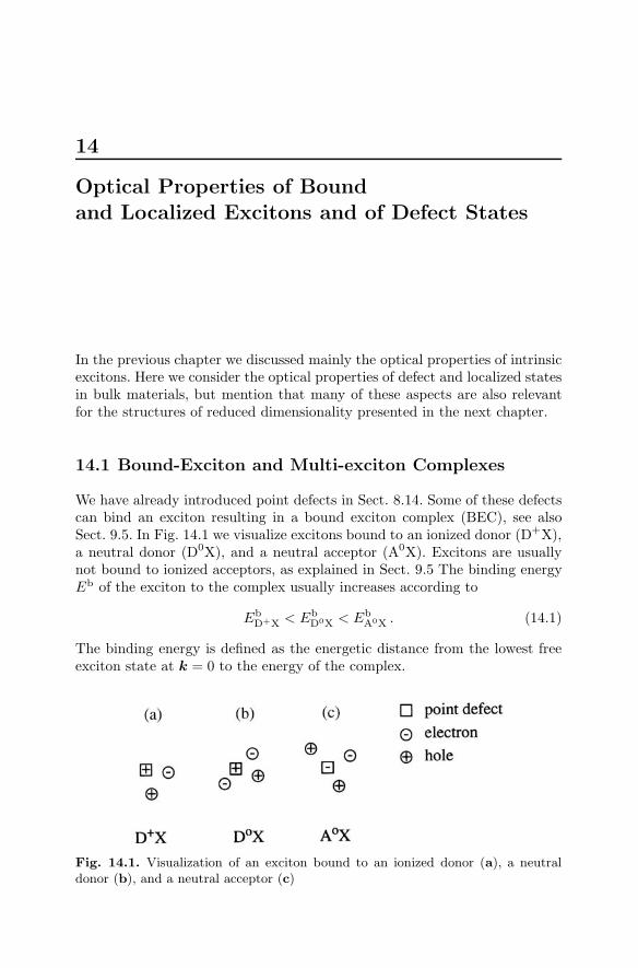
14
Optical Properties of Boundand Localized Excitons and of Defect States
In the previous chapter we discussed mainly the optical properties of intrinsicexcitons. Here we consider the optical properties of defect and localized statesin bulk materials, but mention that many of these aspects are also relevantfor the structures of reduced dimensionality presented in the next chapter.
14.1 Bound-Exciton and Multi-exciton Complexes
We have already introduced point defects in Sect. 8.14. Some of these defectscan bind an exciton resulting in a bound exciton complex (BEC), see alsoSect. 9.5. In Fig. 14.1 we visualize excitons bound to an ionized donor (D+X),a neutral donor (D0X), and a neutral acceptor (A0X). Excitons are usuallynot bound to ionized acceptors, as explained in Sect. 9.5 The binding energyEb of the exciton to the complex usually increases according to
EbD+X < Eb
D0X < EbA0X . (14.1)
The binding energy is defined as the energetic distance from the lowest freeexciton state at k = 0 to the energy of the complex.
Fig. 14.1. Visualization of an exciton bound to an ionized donor (a), a neutraldonor (b), and a neutral acceptor (c)

346 14 Optical Properties of Bound and Localized Excitons and of Defect States
There is a rule of thumb, known as Hayne’s rule, which relates the bindingenergy of the exciton to the neutral complex with the binding of the additionalcarrier to the point defect. For the D0X complex, for example, this says thatthe ratio of Eb
D0X to the binding energy of the electron to the donor EbD
is a constant, depending only on material parameters such as the effectivemasses:
EbD0X/E
bD = const . (14.2)
The constant is often found to have a value around 0.1 to 0.2 (Hayne’srule, see [60H1,77H1,04M1]). Isoelectronic traps (such as a Te on a Se site inZnSe) sometimes form deep centers, with binding energies for excitons exceed-ing those of neutral acceptors. A long-standing and controversially discussedproblem is that of the EL2 luminescence in GaAs. For details including relateddefects see, e.g., [93S1,97S1,98S1] and references therein.
The BEC do not have any degree of freedom for translational motion. Asa consequence BEC often show up in luminescence and absorption spectraas extremely narrow peaks. In Fig. 14.2 we give as examples luminescencespectra of ZnO, ZnSe and GaAs. See also Fig. 13.9d.
Figure 14.2a gives an overview of the low-temperature luminescence ofa high-quality ZnO single crystal from [76H1,76T1]. The interpretation of thevarious groups of emission bands is as follows. FE is the recombination of freeexciton polaritons (see also Chap. 13). Then comes a group of bound excitoncomplexes, the assignment of which is presently reconsidered. According tothe above references the complexes were attributed with decreasing energy,i.e., with increasing binding energy to the defect, to D+X, D0X and A0X,respectively, according to Fig. 14.1. The neutral acceptors were assumed tobe, e.g., Na or Li on Zn sites. Later on, a large fraction of the lines D0Xand A0X has been attributed to excitons bound to neutral acceptors [97G1].Presently, all of the lines labeled D0X in the lower line in Fig. 14.2 are assignedto excitons bound to neutral donors based on the analysis of the two electrontransitions, while hardly any shallow acceptors have been identified [04M1].For the nitrogen acceptor in ZnO:N see [02Z1,04W1].
Independently of the detailed interpretation of the various lines, we seewithin one group a splitting of the lines caused by the chemical nature of thebinding atom. This effect is known as chemical shift or central cell correction.Similar shifts or splittings can be caused by the presence of other defects inthe vicinity of the center binding the exciton.
Towards lower energies in Fig. 14.2a we see the luminescence of excitonsbound to deep centers, possibly deep acceptors. Then follows a range of twoelectron transitions (see below) and the LO-phonon replica of free and boundexcitons, denoted as X-LO and BEC-LO, respectively.
In ZnSe or GaAs we find a similar behavior, as can be seen in Fig. 14.2b,c.To conclude this part it can be stated that the low temperature lumines-
cence of high quality samples is generally dominated by defect-(or localiation-)related recombination processes.

14.1 Bound-Exciton and Multi-exciton Complexes 347
Fig. 14.2. Low-temperature and low-excitation luminescence spectra of ZnO (a) oftwo differently grown ZnSe samples (solid line: MBE growth with element sources,dashed line: with a compound source) (b) and of GaAs (c) [76H1,76T1,91V1,03D1]

348 14 Optical Properties of Bound and Localized Excitons and of Defect States
Since k-conservation is relaxed for BEC due to the lack of translationalinvariance, BEC can also couple to acoustic phonons, for example via thedeformation potential or piezoacoustic coupling. This coupling leads to a so-called acoustic wing in the emission or absorption spectra of a BEC. Fig-ure 14.4 shows an example for the I1, line in CdS. Since only few phononstates are thermally populated at low temperature, the emission manifestsitself essentially as a wing on the low energy side according to
EA0X −→ E0A + ω1um + ΩA , (14.3a)
where ΩA is the energy of the emitted acoustic phonon. The shape of thephonon wing is determined by the energy dependence of the coupling of theBEC to the phonons and by their population, especially the ratio of Stokesto anti-Stokes emission. In Fig. 14.3 the influence of the lattice temperatureon the emission line shape is illustrated.
Figure 14.4 shows the acoustic phonon side bands of the I1 and I2 BECin CdS and in addition an absorption spectrum of the same sample. In thisspecial case actually the reabsorption of a rather broad luminescence bandappearing under higher excitation was used. The acoustic wing appears inabsorption on the high energy side of the zero-phonon line according to
EA0 + ωabs −→ EA0X + ΩA . (14.3b)
Another recombination process leaves the point defect in an excited state,this means that the donor electron of a D0X complex is transferred in the
Fig. 14.3. The Stokes and anti-Stokes emission in the vicinity of the I1 BEC inCdS for two lattice temperatures [74D1,74S1]
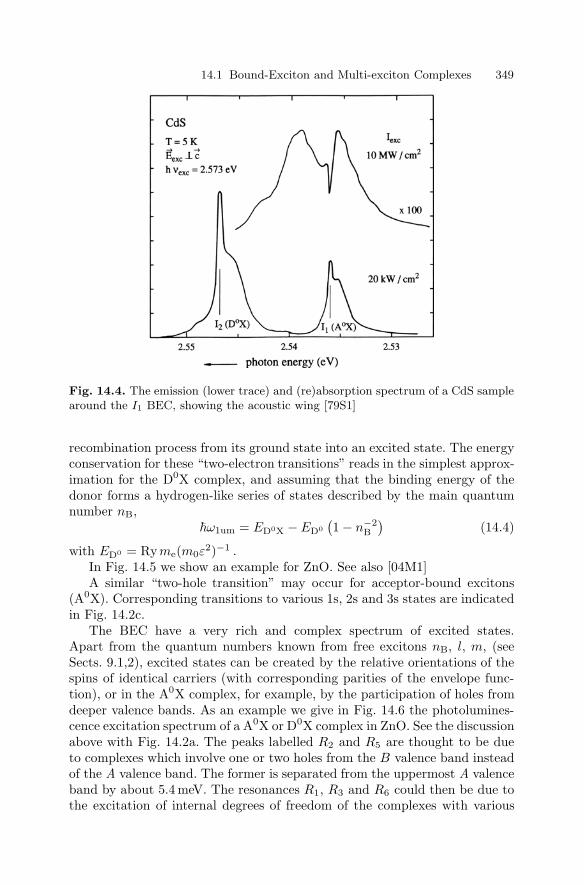
14.1 Bound-Exciton and Multi-exciton Complexes 349
Fig. 14.4. The emission (lower trace) and (re)absorption spectrum of a CdS samplearound the I1 BEC, showing the acoustic wing [79S1]
recombination process from its ground state into an excited state. The energyconservation for these “two-electron transitions” reads in the simplest approx-imation for the D0X complex, and assuming that the binding energy of thedonor forms a hydrogen-like series of states described by the main quantumnumber nB,
ω1um = ED0X − ED0
(1 − n−2
B
)(14.4)
with ED0 = Ryme(m0ε2)−1 .
In Fig. 14.5 we show an example for ZnO. See also [04M1]A similar “two-hole transition” may occur for acceptor-bound excitons
(A0X). Corresponding transitions to various 1s, 2s and 3s states are indicatedin Fig. 14.2c.
The BEC have a very rich and complex spectrum of excited states.Apart from the quantum numbers known from free excitons nB, l, m, (seeSects. 9.1,2), excited states can be created by the relative orientations of thespins of identical carriers (with corresponding parities of the envelope func-tion), or in the A0X complex, for example, by the participation of holes fromdeeper valence bands. As an example we give in Fig. 14.6 the photolumines-cence excitation spectrum of a A0X or D0X complex in ZnO. See the discussionabove with Fig. 14.2a. The peaks labelled R2 and R5 are thought to be dueto complexes which involve one or two holes from the B valence band insteadof the A valence band. The former is separated from the uppermost A valenceband by about 5.4 meV. The resonances R1, R3 and R6 could then be due tothe excitation of internal degrees of freedom of the complexes with various

350 14 Optical Properties of Bound and Localized Excitons and of Defect States
Fig. 14.5. An emission spec-trum of a ZnO sample withan especially pronounced two-electron transition. Accordingto [75K1]. Concerning the iden-tification of the lower BEC seethe discussion above
Fig. 14.6. Photoluminescence excitation spectrum of an BEC complex in ZnO[81B1]

14.1 Bound-Exciton and Multi-exciton Complexes 351
hole configurations. Note that the interpretation for R5 does not work fora D0X complex, which continues only one hole.
A more elaborate treatment of this topic is described in [81B1,86G1,97G1,04M1].
Many defects act as fast nonradiative recombination centers or lumines-cence killers like dislocations [99L1,00F1]. In some cases they give rise, how-ever, to characteristic luminescence features. The so-called Y-emission line inZnSe is, e.g., due to the recombination of an exciton bound to the latticedisortion field of a dislocation. An example is given in Fig. 14.2b.
The use of A0X luminescence in a ZnSe quantum well as a single photonsource has been described in [02S1]
Although we first treat quantum structures in the next section, we want tomention here that BEC also exists in quantum wells. Partly their luminescencemerges with that of the so-called free, i.e., generally disorder broadened intrin-sic emission lines as is often the case in GaAs/Al1−yGayAs structures, partlyit appears as a spectrally separated line. An example is shown in Fig. 14.7 forstructures with different quantum well widths lz, centre-doped with Be accep-tors. For further references see, e.g., [01L1] of Chap. 1. It should be especiallynoted that for quantum structures, the binding energy of the excitons to thecenter additionally depends on its position relative to the barriers.
The bandstructure of some indirect semiconductors allows multiple occu-pation of the conduction band due to the many-valley structure, and of thevalence band due to the four-fold degeneracy of the Γ8 valence-band maxi-mum. In these materials multiple bound-exciton complexes can be formed,i.e., BEC which contain one, two, three or even more electron–hole pairs. Theemission lines are due to transitions of a complex containing m electron–holepairs to one with m− 1 pairs. In Fig. 14.8 we give as an example a lumines-cence spectrum of Si:P. The usual (m = 1) emission line of the phosphorousD0X complex dominates. It is followed at lower energies by a series of lineswith indices m up to 6. The decay of the higher members of the series is obvi-ously faster than of the lower ones, as expected already from simple reactionkinetics. These multiple BEC can be considered as a precursors or nucleationcenters for the electron–hole plasma droplet discussed in Chap. 21. Anothernoteworthy point is that Si is an indirect semiconductor and optical transi-tions usually involve a momentum conserving phonon. Since the k-selectionrule is relaxed for BEC as mentioned above, we can see these lines even with-out phonon participation.
BECs can be best observed at low lattice temperatures. With increasing TL
the BEC disappear depending on the material, often at temperatures between20 and 100K due to thermal dissociation of the exciton from the complex.For an example see Fig. 14.4. Below this temperature the halfwidth of theemission lines increase partly linearly and partly quadratically with TL.
For optimal observation conditions the concentration of the point defectsshould be low enough ( 1016 cm−3) to avoid broadening due to interactionbetween the BEC.

352 14 Optical Properties of Bound and Localized Excitons and of Defect States
Due to this low concentration BEC are usually best observed in lumines-cence or photoluminescence excitation spectroscopy and only partly in ab-sorption see e.g. Fig. 13.9d, and only very rarely do they give rise to reflectionstructures, simply because the modulation of n and/or κ is too small to resultin a significant signal in R(ω). For an exception to this rule see [78B1].
To conclude this section it should be mentioned that BEC are sometimessaid to have a “giant” oscillator strength. This expression is partly the resultof a misconception because the maximum absorption coefficient αmax for thefree excitons per unit cell was compared with the corresponding quantity ofthe BEC per defect center. However, in both cases the (Wannier-) excitonscover many unit cells.
Fig. 14.7. The luminescence of GaAs/Al1−yGayAs structures, of two different wellwidth lz center doped with Be acceptors at low temperature showing the emissionfrom localized intrinsic excitons labelled FE and of acceptor bound excitons (A0X)[89H1]

14.2 Donor–Acceptor Pairs and Related Transitions 353
Fig. 14.8. The zero-phonon luminescence spectra of a multiple-bound-exciton com-plex in Si:P after pulsed excitation, normalized to the a1 line [78T1]
For some reviews on bound exciton complexes in bulk materials and quan-tum wells see e.g. [79D1,97G1,04M1] or Ref. [82L1,01L1] in Chap. 1 and thereferences given therein or in Sect. 9.5.
14.2 Donor–Acceptor Pairs and Related Transitions
Until now we have assumed that the BEC involves only one defect center.Actually one can also imagine poly-centric bound-exciton complexes, whichinvolve two or more close-lying centers.
The simplest such defect combination is the donor–acceptor pair. InFig. 14.9 we show schematically an electron on a donor and a hole on anacceptor. If their wavefunctions overlap, they can recombine. The energy ofthe photon resulting from radiative recombination is given by
ωDA = Eg − EbD0 − Eb
A0 +e2
4πεε0rDA−mωLO (14.5)

354 14 Optical Properties of Bound and Localized Excitons and of Defect States
Fig. 14.9. A donor–acceptor pair (a) and a free-to-bound recombination process (b)
Fig. 14.10. Donor–acceptor pair luminescence in CdS including some phononreplica [79B1]
for singly charged centers if we neglect the energetic shift caused by the overlapof the wavefunctions of the neutral donor and acceptor. Eb
D0A0 are the bindingenergies of electron and hole to their respective centers.
The forth term on the rhs of (14.5), which depends on the distance rDA
of the centers, reflects the Coulomb energy of the ionized centers after therecombination. The last term describes LO phonon replica. We give examplesin Figs. 14.2b and 14.10.
If the donors and acceptors are introduced substitutionally in a rathersimple (e.g., cubic) lattice, then only discrete, well-defined values for rDA arepossible, to nearest neighbors and next-nearest neighbors, etc. Consequentlyunder high resolution one sometimes observes that the zero-phonon band con-sists of discrete lines corresponding to the discrete values of rDA [79C1,79D1].

14.3 Internal Transitions and Deep Centers 355
With increasing pump intensity, the number of occupied donor and accep-tor centers increases and their average distance rDA necessarily decreases. Asa consequence one finds that the emission maximum of the pair-band shifts tothe blue with increasing excitation due to the Coulomb term in (14.5). Thisis a very characteristic feature of donor–acceptor pair recombination. For anexample in the less commonly investigated semiconductor SnO2 see [80B1].
Another recombination process connected with neutral donors or acceptorsis the so-called free-to-bound transition. In this case a free electron or holerecombines with a neutral acceptor or donor, respectively, as shown schema-tically in Fig. 14.9. The corresponding emission peak is at
ωFB = Eg − EbD0/A0 −mωLO . (14.6)
Obviously ωFB is blue-shifted as compared to ωDA and often both processesoverlap together with their phonon replica in one complex or broadened lumi-nescence spectrum. Exampels are shown in Fig. 14.2c both for donor–acceptorpairs (D0,A0) (the index C means a carbon acceptor) and free electron tobound hole transitions (e, A0).
14.3 Internal Transitions and Deep Centers
Some defects have not only one (or a few) levels close to one band, but theyhave several of them, partly around the middle of the gap. The chance ofencountering such a situation evidently increases with increasing Eg and isthus of higher relevance for insulators, e.g, solid state laser materials, like the(Cr, Ti or Nd) doped ones, than for semiconductors.
Such deep centers can sometimes interact with both the conduction andvalence band and serve then as recombination centers. If this recombinationis fast and non-radiative, these centers are known as “luminescence killers”.They are to a large extent responsible for the low luminescence yield of manysemiconductors. Iron is an example of such a center.
Other deep centers show either also free-to-bound or internal transitionsthat reflect the atomic orbitals. These, however, are perturbed with respect tothe free atom by the environment of neighboring atoms. Examples of this typeof center are copper, sodium, the rare earths, and the transition metals. Theygive rise to the green, orange and red emission bands of wide-gap semiconduc-tors such as CdS, ZnO and ZnS. We give an example in Fig. 14.11 but do notgo into details, but mention, that there is also another green emission bandin ZnO, which is spectrally smooth without the pronounced phonon structureand which is related to an oxygen vacancy [96V1] in addition to ZnO:Cu andciting for ZnO:OH [78G1]. Recently an emission band has been observed inZnO in the orange spectral range, with the unusual property that the lumi-nescence cloud expands after the switching on of cw band-to-band excitationover distances of several mm in some tenths of a second. The effect can be

356 14 Optical Properties of Bound and Localized Excitons and of Defect States
Fig. 14.11. Deep center emission of ZnO:Cu [81K1]
observed at temperatures from 70 K to 150K. It has been attributed ten-tatively to a (possibly thermally activated) Forster or Foster–Dexter energytransfer [04D1].
As already mentioned above, the topic of deep centers is much more im-portant for insulators. Ample information for this group of materials andfor semiconductors can be found in [75O1, 81H1, 90K1] or in [81A1] b,c,e ofChap. 1.
14.4 Excitons in Disordered Systems
In Sect. 8.15 we outlined the appearance of localized tail states with increasingdoping, for alloy semiconductors and in amorphous materials. In quantumwells the fluctuations of lz may also result in the formation of localized tailstates because of the dependence of the quantization energy on lz as mentionedearlier.
If we create electron–hole pairs in such systems, they may be localized, too,in the energetic regime below the mobility “edge” which is usually a transitionregion of finite width.
Whole excitons can be localized in potential fluctuations of sufficient depthand with diameters larger than their Bohr radius. In other cases, only one ofthe carriers is localized–usually the hole, because of its heavier mass–and bindsthe other carrier to it by Coulomb attraction. For a more detailed discussion oflocalization, including a percolation approach, see Sects. 8.15 and 9.6, [03E1]

14.4 Excitons in Disordered Systems 357
and the references therein. For localization in various quantum structuressee [02R1] and for organic alloys see [76K1] and for amorphous semiconductors[03S2].
The typical shape of the absorption spectrum of a strongly disordered(e.g., amorphous) system is shown in Fig. 14.12.
In region I the absorption is weak and is caused by impurities in the alloyor amorphous semiconductor, i.e., atoms of a different chemical nature.
Then region II follows where the absorption coefficient increases exponen-tially with photon energy. This regime is also known as the “Urbach tail”in analogy to Fig. 13.10 and (13.12). Its origin in disordered semiconduc-tors is, however, not the interaction with phonons, but simply the exponen-tial tail of the density of states of localized excitons which can be reachedwithout k-selection. Above follows region III comprising the absorption via
Fig. 14.12. The various regimes of the absorption coefficient in disordered semi-conductors [72W1]

358 14 Optical Properties of Bound and Localized Excitons and of Defect States
transitions into extended states. An extrapolation of this part to lower ener-gies, e.g., with a (E′ − E0)
2 law, allows one to define an optical or mobilitygap. For this so-called Tauc-regime see, e.g., [89S1, 89T1]. The latter quan-tity can also be found by excitation-spectroscopy of the photo-current. Ab-sorption spectra corresponding to the schematic drawing of Fig. 14.12 havebeen found in amorphous Si, in chalcogenide glasses, and in alloy semicon-ductors such as CdS1−xSex and ZnSe1−xTex. Examples are presented, e.g.,in [72W1,89T1,99R1,04K1].
The gradual increase of the absorption, and via Kramers–Kronig analy-sis also of the real part of the reflective index, in many cases prevents theobservation of discrete exciton resonances in reflection.
The analysis of the “Urbach” part of the absorption spectrum gives thetailing parameter εloc describing the density of localized states below themobility edge EME.
N(E) =N0
εloce−E/εloc E < EME (14.7)
In Fig. 14.13 we show εloc for CdS1−xSex as a function of x. This quantitynecessarily vanishes for the ordered binary compounds x = 0 and x = 1, seealso Sects. 8.15 and 9.6. In between it goes through a maximum with a shapethat is not symmetric with respect to x = 0.5, partly since the quantitydEg/dx changes with x, which enters in (8.64,67).
Fig. 14.13. The dependence of the tailing parameter [92P1]

14.4 Excitons in Disordered Systems 359
Further information on the localized states can be deduced from the lu-minescence spectra. In Fig. 14.14 we show the luminescence of a CdS1−xSex
crystal under excitation of the extended states and under resonant excitationof the localized ones; see also the spectra in [92P1]. One sees here a ratherbroad zero-phonon line peaking at 2.21 eV and the first LO-phonon replicaaround 2.18 eV. The phonon replicas are resolved under resonant excitationinto the vibrations of CdS and of CdSe, since in this alloy the phonons are ofthe “persistent-mode” type, i.e., they keep approximately the energies corre-sponding to x = 0 and x = 1 and contribute to the emission with a weightchanging with x, while the gap in this case varies continuously with x. SeeSects. 7.8, 11.1.6 and 8.15 and 9.6, respectively.
The high energy edge of the luminescence band can be identified with thetransition region from extended to localized states [92P1, 99R1, 04K1]. Thisstatement can be supported by the following argument: As long as excitonsare in extended states, they “scan” the sample and have a good chance ofhitting one of the fast nonradiative recombination centers mentioned above inSect. 13.1.3. Once it is sitting in a localized state which does not have sucha center within the localization length, the exciton can either recombine ra-diatively or reach a deeper localized state, e.g., by phonon-assisted tunneling.The probability for the latter process decreases with decreasing energy anddensity of the localized states, resulting in increasing luminescence yield. This
Fig. 14.14. Luminescence spectrum of CdS1−xSex under resonant and non-resonantexcitation [93K1]

360 14 Optical Properties of Bound and Localized Excitons and of Defect States
idea has been confirmed by investigations of the phase-relaxation times andof the polarization memory as will be outlined in Chap. 23. For a more recentdiscussion of the absorption and luminescence properties of bulk semiconduc-tor alloys at low temperature involving the ideas of clusters, superclusters andof metastable states introduced in Sect. 8.15 and 9.6 see [99R1,04K1] and thereferences given therein.
At higher lattice temperatures defined by
kBTL ε1oc (14.8)
the majority of the excitons are thermally (re-) excited from the localized intoextended states where they behave similarly to free excitons in ordered crystalsexcept for a rather short phase-relaxation time due to the alloy scattering.This transition is partly connected to a non-monotonous dependence on theemission maximum and also partly on the FWHM of the band as shown fora CdS1−xSex sample in Fig. 14.15, which includes the CdS LO phonon replica.For an earlier example see, e.g., [78K1].
Fig. 14.15. The low excitation photoluminescence spectra of CdS.97Se.03 for variouslattice temperatures Tl [88S1]

References to Chap. 14 361
Such behavior was rediscovered recently in quantum well structures. Wecome back to this topic in the next chapter.
At low temperatures the luminescence yield of localized excitons can comeclose to unity in selected samples [97W1].
Similar results as presented for CdS1−xSex have also been observed inZnSe1−xTex, [92P1] and in Ga1−yA1yAs [92S1]. In the first case the local-ization effects are even more pronounced than in CdS1−xSex. Furthermore,self-trapping of excitons seems to occur for x ≈ 0.01 at single Te atoms or atsmall Te clusters. In the second case, εloc is much smaller, partly due to thesmaller translational exciton mass which makes localization less probable andpartly because of the larger Bohr radius of the exciton which averages overa larger area of the lattice. More recently ZnO based alloys like Zn1−yMgyOor GaN based ones like Ga1−yInyN have been investigated with similar re-sults concerning the optical properties of excitons [01P1, 03S1]. Localisationeffects occur also in group IV alloys like Si1−xGex. For some references see,e.g., [92L1, 92N1, 94T1]. The importance of disorder for Rayleigh scatteringand the appearance of speckles is investigated in [04M1, 04Z1] and will betreated in Sect. 23.2.
For recent reviews on localized excitons in disordered semiconductors see[86L1,89T1,91K1,92S1,92S2,99K1,04K1] and references given in Sects. 8.15and 9.6. As already mentioned localization of excitons in quantum wells andwires will be treated in the next chapter. But we mention here that (quantum-mechanical) level repulsion occurs for states, which are spatially and energet-ically close lying [03Z1] because this effect should also occur in bulk material,but is there much more difficult to observe experimentally.
14.5 Problems
1. For some standard semiconductors, such as Si, Ge, or GaAs, calculate thebinding energy of electrons and holes to donors and acceptors, respectively.Find some data for the binding energies of excitons to these complexesand compare the results with Haynes’ rule.
2. Calculate the shift in energy for the donor–acceptor pair recombinationwhen donor and acceptor are nearest possible neighbors in a zinc-blendelattice, and when they have a separation of three, and of ten lattice con-stants. Can one observe emission from pairs with a separation d aBε
m0mc
References to Chap. 14
[60H1] J.R. Haynes, Phys. Rev. Lett. 4, 361 (1960)[72W1] D.L. Wood and J. Tauc, Phys. Rev. B 5, 3144 (1972)[74D1] A.F. Dite, V.I. Revenko and V.B. Timofeev, Sov. Phys. Solid State 16,
1273 (1974)

362 14 Optical Properties of Bound and Localized Excitons and of Defect States
[74S1] J. Shah, R.F. Leheny and W.F. Brinkmann, Phys. Rev. B 10, 659 (1974)[75K1] C. Klingshirn, phys. stat. sol. (b) 71, 547 (1975)[75O1] Optical Properties of Ions in Solids, B. Di Bartolo (ed.), Plenum, New York
(1975)[76H1] R. Helbig, Habilitation Thesis, Erlangen (1976)[76K1] R. Kapelman, J. Lumin. 12/13, 775 (1976)[76T1] E. Tomzig and R. Helbig, J. Lumines. 14, 403 (1976)[77H1] B. Honerlage and U. Schroder, Phys. Rev. B 16, 3608 (1977)[78B1] K. Bohnert et al., Solid State Commun. 27, 295 (1978)[78G1] F. Gartner and E. Mollwo, phys. stat. sol. (b) 89, 381 and ibid 90, 22
(1978)[78K1] A. Kozanecki et al., phys. stat. sol. (b) 89, 313 (1978)[78T1] M.L.W. Thewalt, Solid State Commun. 25, 513 (1978)[79B1] G. Blattner, Diploma Thesis, Karlsruhe (1979)[79C1] K. Cho (ed.), Excitons, Topics Curr. Phys. Vol. 14, Springer, Berlin, Hei-
delberg (1979)[79D1] P. Dean, in Ref. [79C1], p 11[79S1] H. Schrey, PhD, Karlsruhe (1979)[80B1] G. Blattner, R. Helbig and C. Klingshirn, Solid State Commun. 33, 341
(1980)[81B1] G. Blattner et al., phys. stat. sol. (b) 107, 105 (1981)[81H1] K.H. Hellwege, Einfuhrung in die Festkorperphysik, 2nd edn., Springer,
Berlin, Heidelberg (1981)[81K1] R. Kuhnert and R. Helbig, J. Lumin. 26, 203 (1981)[84S1] B.I. Shkolovskii and A.L. Efros, Electronic Properties of Doped Semicon-
ductors, Springer Ser. Solid-State Sci. 45, Springer, Berlin, Heidelberg(1984)
[86G1] J. Gutowski, Solid State Commun. 58, 523 (1986) and references therein[86L1] Localization and Interaction, D.M. Finlayson (ed.), 31st Scottish Univer-
sities Summer School in Physics, SUSSP, Edinburgh (1986)[88S1] H.-E. Swoboda et al., phys. stat. sol. (b) 150, 749 (1988)[89H1] P.O. Holtz et al., Phys. Rev. B 40, 12338 (1989)[89S1] E.A. Shiff in Ref. [81A1]d, p 153 of Chap. 1[89T1] P.C. Taylor in Ref. [89L1], p 257 of Chap. 1[90K1] M. Kunz et al., Materials Chemistry and Physics 25, 27 (1990)[91K1] A.A. Klochikhin and S.G. Ogloblin, Sov. Phys. JETP 73, 1122 (1991)[91V1] A. Villemaire, T. Steiner and M.L.W. Thewalt, Phys. Rev. B 44, 13426
(1991)[92L1] L.C. Lenchshyn et al., Appl. Phys. Lett. 60, 3174 (1992)[92N1] J.-P. Noel et al., Appl. Phys. Lett. 61, 690 (1992)[92P1] S. Permogorov and A. Reznitsky, J. Lumin. 52, 201 (1992) and references
therein[92S1] U. Siegner et al., Phys. Rev. B 46, 4564 (1992)[92S2] H. Schwab et al., phys. stat. sol. (b) 172, 479 (1992)[93K1] C. Klingshirn, NATO ASI Series B 301, 119 (1993)[93S1] T.W. Steiner et al., Phys. Rev. B 47, 1265 (1993)[94T1] K. Terashima et al., Appl. Phys. Lett. 65, 601 (1994)[96V1] K.A. Vanheusden et al., Appl. Phys. Lett. 68, 403 (1996)[97G1] J. Gutowski, P. Baume and K. Hauke in Properties of Wide Gap II–VI
Semiconductors, R. Bhargava ed., INSPEC, London (1997)

References to Chap. 14 363
[97S1] M.I.N. da Silva et al., J. Appl. Phys. 82, 3346 (1997)[97W1] R. Westphaling et al., J. Luminesc. 72-74, 980 (1997)[98S1] T. Shinagawa and T. Okamure, Jpn. J. Appl. Phys. 37, 1939 (1998)[99K1] A. Klochikhin et al., Phys. Rev. B 59, 12947 (1999)[99L1] D. Luerßen et al., Appl. Phys. Lett. 75, 3944 (1999)[99R1] A. Rezmitsky et al., Phys. Rev. B 59, 10268 (1999)[00F1] G. von Freymann et al., Appl. Phys. Lett. 76, 203 (2000)[01P1] W.I. Park, G.-C. Yi and H.M. Jang, Appl. Phys. Lett. 79, 2022 (2001)[02R1] E. Runge, Solid State Physics 57, H. Ehrenreich and F. Spaepen (eds.),
Academic Press, San Diege (2002)[02S1] S. Stauf et al., Phys. Rev. Lett. 89, 177403 (2002)[02Z1] A. Zeuner et al., phys. stat. sol. b 234, R7 (2002)[03D1] M. Dremel et al., J. Appl. Phys. 93, 6142 (2003)[03E1] Electronic Structure of Alloys, Surfaces and Clusters, A. Mookerjee (ed.),
Taylor and Francis, London (2003)[03S1] M. Strassburg et al., phys. stat. sol. c 0 (6), 1835 (2003)[03S2] J. Singh and K. Simakawa, Advances in Amorphous Semiconductors, Tay-
lor and Francis, London (2003)[03Z1] R. Zimmermann, E. Runge and V. Savona, phys. stat. sol. (b) 238, 478
(2003)[04D1] M. Decker, H. Priller and C. Klingshirn, to be published[04K1] A. Klochikhin et al., Phys. Rev. B 69, 085308 (2004)[04M1] B.K. Meyer et al., phys. stat. sol. (b) 241, 231 (2004)[04M2] G. Mannarini, W. Langbein and R. Zimmermann, phys. stat. sol. c 1 (3),
489 (2004) and Phys. Rev. B 69, 085326 (2004)[04W1] D. Wang et al., J. Physics-Cond. Matter 16, 4635 (2004)[04Z1] R. Zimmermann and E. Runge, Phys. Rev. B 69, 155307 (2004)

15
Optical Properties of Excitons in Structuresof Reduced Dimensionality
As in the presentation of elementary excitations in Chaps. 7–12, we now pro-ceed from bulk materials to the optical properties of excitons in systems ofreduced dimensionality. For some recent reviews see [89S1,90C1,90G1,93C1,01H1, 03R1, 03S1] or, e.g., the following References [81A1h,i,k,l,93B1,93H1,93O1,93P1,93S1,95I1, 96S2,97W1, 98D1,98G1, 98S1, 99B1,01C1,01H1, 01L1,02S1] of Chap. 1.
In Sects. 8.10, 8.13 and 9.3 we outlined the influence of the dimensional-ity on the eigenstates of carriers and of excitons. Now we describe the opti-cal properties of excitons in such structures, starting with quantum wells inSect. 15.1 and proceeding to coupled wells, superlattices and to structures ofeven lower (quasi-) dimensionality in the following sections.
15.1 Qantum Wells
Here we treat transitions between valence– and conduction band (interbandtransitions) and intraexatonic transitions. For intersubband transitions seeSect. 21.5 We start with type–I structures, where the electron and hole arequantized in the same material.
The description will remain almost exclusively in the weak couplinglimit, mainly because the quality of presently available samples in rela-tion to interface roughness or alloy disorder is not sufficient for the finedetails stemming from the polariton concept to be observable. The mostwidely investigated groups of MQW are based on GaAs/Al1−yGayAs andon InP/InGaAs/InAlAs. See Sect. 8.11. In the meantime, considerable in-terest has also arisen in II–VI systems, especially for wide gap materials,like structures based on ZnCdMg/SSeTe, ZnMgCd/O and in new III–V sys-tems like GaAlIn/N and GaInNAs for the blue and IR regions, respectively.The II–VI compounds are covered, e.g., in the corresponding proceedingslike [82P1] in Chap. 8, while data on the nitrides can be found in [97N1,00I1]of Chap. 1.

366 15 Optical Properties of Excitons in Structures of Reduced Dimensionality
In Fig. 15.1 we show how the spectra of a quantum well system developfrom the bulk material.
The layer with lz = 400 nm is almost bulk-like and shows the 1 s exci-ton absorption peak followed by its ionization continuum. Compare this withSect. 13.1.3.
With decreasing quantum well width, the excitons of the various subbandtransitions appear (labelled by nz = 1, 2, . . .) and the splitting into heavy holeand light hole excitons caused by the different, mass dependent quantizationenergies. Some weaker structures appear in between, which are dipole forbid-den, but obtain some oscillator strength, e.g., via internal band bending. Forfurther examples see, e.g., [01L1] of Chap. 1 and the references given therein.
In Fig. 15.2a,b we compare the spectra for GaAs/Al1−yGayAs andIn1−yGayAs/InP multiple quantum well structures MQW.
We see the exciton and the continuum transitions between the first quan-tized heavy- and light-hole levels and the first quantized electron state,nz = 1hh and nz = 1lh, respectively. The peaks are due to the nB = 1state. The higher states nB 2 are usually not visible, due to their rela-
Fig. 15.1. Low temperature absorption spectra of GaAs (quantum) films of variousthicknesses ( [83G1,90G1] or [01L1] of Chap. 1)

15.1 Qantum Wells 367
tively small binding energies and oscillator strengths (see Sect. 9.3) and dueto the broadening mechanisms mentioned above. The absorption coefficientin the continuum states essentially reflects the constant density of states fortwo-dimensional effective-mass particles. It is not influenced much by the Som-merfeld enhancement because it varies only by a factor two. See Sect. 9.3unlike the three-dimensional systems mentioned in Sects. 9.2 and 13.1. Thenext prominent structures are the nz = 2hh and lh excitons. Higher states areusually less clearly seen, among other reasons because the electron states areoften no longer quantized for nz > 3, depending on lz, me and the band offset.
In contrast to the InP system, the GaAs substrate of the AlGaAs MQWis opaque for the exciton resonances. So it has to be removed by selective
Fig. 15.2. The low temperature absorption spectra of multiple quantum well sam-ples of GaAs/Al1−yGayAs (a) and of In1−yGayAs/InP (b) [89S1] and [01L1] ofChap. 1, respectively

368 15 Optical Properties of Excitons in Structures of Reduced Dimensionality
etching [80P1] for the observation of absorption spectra. Before this techniquewas known, scientists often measured the luminescence–excitation spectra, i.e.,they detected the exciton luminescence as a function of the photon energy ofexcitation ωexc for constant incident intensity (or rather constant photon fluxdensity). Similarly, the dependence of the photo current on ωexc can be usedin a pin diode biased in the blocking direction, which contains the (M)QW inthe intrinsic region. The quantities
I lum = f(ωexc)jphoto = f(ωexc)
Iexc = const (15.1)
are related to, but not identical with, the absorption spectrum α(ω). SeeChap. 25. The above-mentioned techniques are still useful if a single quantumwell (SQW) is investigated. The absorption coefficients of two-dimensionalexcitons in the above-mentioned systems are of the order of 104 cm−1. A SQWwith lz = 10 nm therefore gives an optical density of only
lz · α ≈ 10 nm · 104 cm−1 = 10−2 , (15.2)
which is hardly detectable in a simple transmission experiment. The obser-vation of such a small variation needs either highly developed modulationtechniques or photo-luminescence excitation spectroscopy.
The advantage of studying only a SQW is that fluctuations of lz fromone QW to the next can be avoided. Furthermore some (opto-) electronicdevices contain only a SQW, e.g., some field-effect transitors (MOD–FET,HEMT). The additional optical selection rules which arise when the excitonsare confined to a QW are rather simple:
∆nz = 0 . (15.3)
Transitions with odd ∆nz are forbidden by parity and those for even non-zero ∆nz are forbidden for rectangular shaped QW in the limit of infinetlyhigh barriers. Transitions which violate (15.3) can be observed if there aresymmetry breaking perturbations such as external or internal electric fields.Examples will be given in Sect. 16.2.
The luminescence spectra of excitons in QW are often rather broad andpartly Stokes-shifted with respect to the absorption. We give two-rather dif-ferent examples in Fig. 15.3. The effects can be explained by assuming thatthe luminescence is a superposition of the recombination of excitons in ex-tended states at k‖ ≈ 0 (excitons with larger k‖ cannot decay radiativelybecause of momentum conservation), of excitons localized in tail states dueto well-width fluctuations and/or alloy disorder, and finally of excitons boundto impurities such as neutral acceptors or donors. As we saw in Chap. 14, thelatter complexes lead to spectrally very narrow emission bands in 3d systems,but in QW, their energies are strongly inhomogeneously broadened becausethe energy of the complex depends on its positions relative to the barriers.

15.1 Qantum Wells 369
The latter effect can be reduced by deliberately doping only a narrow layer,e.g., in the center of the well, as shown, e.g., earlier in Fig. 14.7.
In samples of very high quality the mechanisms mentioned above are lesspronounced, resulting simultaneously in a reduction of the spectral widths ofabsorption and emission bands and of the Stokes shift. Both quantities arerelated to each other as shown, e.g., in [93Y2, 94G1]. An example is givenin Fig. 15.3. The shoulders in the emission on the low energy side can havevarious origins: fluctuations of lz by one monolayer, recombination of a boundexciton complex, or recombination of a trion or a biexciton (see Sects. 9.4 and20.3 for the latter two processes). Due to the weaker coupling of carriers andexcitons to optical phonons in the III–V compounds compared to the more
Fig. 15.3. A comparison of absorption and luminescence spectra in two samples ofdifferent quality [92O2]

370 15 Optical Properties of Excitons in Structures of Reduced Dimensionality
ionic II–VI semiconductors, LO-phonon replica are hardly detectable in theformer materials.
As an example of a II–VI system we show in Fig. 15.4 the photolumi-nescence (PL) and photoluminescence excitation (PLE) spectra of a ZnSe/ZnS1−xSex MQW sample.
One observes in PL the light and heavy hole exciton, a bound excitoncomplex (BEC) and their LO phonon replica. The PLE spectrum taken atthe position of the hh luminescence shows the lh exciton resonance and abovepeaks spaced by integer multiples of LO phonons. They indicate that electron-hole pairs first form excitons and then relax by LO phonon emission in contrastto, e.g., GaAs systems where the carriers relax individually and an excitonis formed only at the end of the LO-phonon emission cascade [93K2, 95B2,96W3,96W4]. Concerning the discussion to which extend luminescence at theexciton energy is due to excitons or to a Coulomb correlated electron–hole gasor plasma see [02H1,04C1] or [98K1] of Chap. 13. More details on relaxationprocesses will be given in Chap. 23.
In this context it is remarkable that in the early and euphoric times ofquantum well research, most excitonic low temperature absorption and lu-minescence bands have been attributed to free excitons, even if their widthreached or even exceeded 10 meV. Absorption and emission of free, quasi-two-dimensional excitons within the “light cone” k‖ ≤ ω/c would resultin a linewidth of only one or a few hundred µeV, depending on the effec-tive mass. Even if a homogeneous broadening corresponding to dephasing
Fig. 15.4. Photoluminescence (PL) (- - - -) and PL-excitation spectra (——) ofa ZnSe/ZnS1−xSex MQW sample [98K1]

15.1 Qantum Wells 371
times on the order of a few ps is added (see Chap. 23) one has to con-sider low temperature exciton line width exceeding 1 meV as substantiallyinhomogeneously broadened due to the formation of localized states causedby well width and alloy fluctuations and especially in luminescence by con-tributions of bound exciton complexes. Presently we see the opposite trendthat every localization site is considered a quasi zero-dimensional quantumdot. As already mentioned in Sects. 8.13 and 9.3 and discussed in [01L1] ofChap. 1, there is presently no clear and generally accepted set of criteria todecide when a localization site should be called a quantum dot or island andvice versa.
The homogeneous width of excitons localized by well width and alloy fluc-tuations are at low temperatures often rather narrow (< 100 µeV). If onlya small ensemble of such localized states is probed, e.g., in luminescence, thelocalized excitons show up in emission as individual narrow lines while theymerge to an inhomogeneously broadened band if their number increases. Ex-amples are found, e.g., in [98P1,00L1] or [01L1] of Chap. 1. We give an exampleof a CdSe/ZnSe quantum well in Fig. 15.5, showing a macro- and micropho-toluminescence spectrum (resolution 1 µm in the latter case) of a single CdSequantum well in ZnSe.
The nominally deposited amount of CdSe was two monolayers. Due tosegregation and diffusion it is spread over about 10 monolayers and islands ofhigher CdSe are formed resulting in the localization sites.
The relaxation and thermalization of the excitons in localized and extendedstates give rise to a frequently observed so-called S-shape dependence of thespectral position of the emission maximum of the macro-PL with temperature.Actually, it is really an n-shaped dependence, rather than an S-shaped one,but the term is established and is difficult to change.
Fig. 15.5. Macro- and microphotolumi-nescence spectra of a CdSe/ZnSe singlequantum well [01K3]

372 15 Optical Properties of Excitons in Structures of Reduced Dimensionality
Examples of the non-monotonous variation of the emission maximum andof the half-width with temperature are given in Fig. 15.6 and in [98P1,01T1,01W1,02R1,03K2]. The behavior here is very similar to the behavior of local-ized excitons in bulk alloys, as already shown in Sect. 14.3. There are variousapproaches to theoretically model this behavior [01T1,04K1].
If two localization sites of excitons with almost identical energies are spa-tially so close to each other in one quantum well that they interact slightly,a phenomenon occurs that we have already seen several times, namely, levelrepulsion. This level repulsion can be observed if high spatial and spectralresolutions are used simultaneously. For theoretical calculations and experi-mental evidence see, e.g., [03K3,03N1,03Z1] and references therein. A furthereffect, connected with the disorder inherent to quantum wells is (resonant)Rayleigh scattering. See, e.g., [03M1, 03N1] and references therein. We comeback to this topic in Chap. 23.
Presently there is a trend to investigate excitons in individual localizationsites or quantum islands by spatially resolved spectroscopy. See also Sect. 15.4.
At excitations below about 40 K the excitons are trapped, after excitationinto the continuum states, randomly by various localization sites. The individ-ual lines follow the temperature dependence of the band gap. The maximum ofthe macro-PL tends to show a stronger red shift for T between 50 and 100 K.In this regime the excitons undergo thermally activated hopping processes toneighboring, deeper localization sites. At even higher temperatures T > 100Kscattering into extended states dominates, which have a much higher densityof states. Above 150 K the temperature dependence again roughly follows theband gap. The transition from localized to extended states is frequently ac-
Fig. 15.6. The temperature dependences of the band gap of CdSe according toVarshni’s formula, of the narrow emission lines of individual localization sites (o) ofthe maximum of the macrophotoluminescence () and of the FWHM (∆) [01W1]

15.1 Qantum Wells 373
companied by a non-monotonous behavior of the width of the emission bandas shown in Fig. 15.6.
The investigation of the reflection spectra of quantum wells is difficult dueto inhomogeneous broadening and due to the fact that a single layer typically10 nm in width contributes much less to a resonance signal than a bulk sample.
Nevertheless, it became possible to observe excitonic reflection spectrawith improving sample quality. In Fig. 15.7 we give an example of a singleGaAs well embedded between superlattices as barriers.
Under normal incidence, the typical reflectivity is around 30% for theAlGaAs system away from the resonance, and the heavy and light hole ex-citons in the well (A, B) and in the superlattice (C, D) produce only weakstructures. To enhance them, the authors of [88U1] used a nice trick. Theyilluminated the sample with linearly polarized light under oblique incidenceclose to Brewster’s angle (Fig. 15.7c). This procedure reduced the backgroundreflectivity and thus enhanced the exciton resonances. Note the different scalesin Fig. 15.7b and c on the ordinate.
In the meantime good reflection features have also been obtained undernormal incidence in III–V and II–VI quantum wells. For examples see [96S1]or [01L1] of Chap. 1.
Exciton polaritons also exist in quantum well structures, however, theusually strong inhomogeneous broadening prevents the observation of finer
Fig. 15.7. Reflection spectra of a single GaAs quantum well with anAl.32Ga.68As/GaAs superlattice as barrier (a) and the reflection spectra for nor-mal (b) and oblique (c) incidence [88U1]

374 15 Optical Properties of Excitons in Structures of Reduced Dimensionality
details. In Fig. 15.8 we show calculated in-plane polariton dispersions for theheavy and light hole exciton resonances of an ideal single QW without anydisorder using the assumption that the background dielectric constant of thewell is equal to the dielectric constant of the barrier.
The polariton dispersion in the barrier material is shown by the dotted,almost vertical line. There exists a lower polariton branch that looks similar tothe bulk material, with one difference being that the longitudinal-transversesplitting ∆LT depends on the well width lz and on k‖ according to
∆LT ∼ lz · k‖ (15.4)
since there is no coupling of light to excitons in a single well with vanishingthickness, nor for infinite wavelength, i.e., k‖ = 0. The lower polariton branchcorresponds to a guided mode since the refractive index below the resonanceis higher in the well than in the barrier. There is a longitudinal mode but noupper polariton branch in the usual sense, since the refractive index above theresonance is smaller than that of the barrier. Consequently, one has a radiativeor antiguided mode, which looses its amplitude rapidly (typical in 10 ps) byradiating into the barrier. If the background constant off the well exceeds thatof the barrier, an upper polariton branch may appear as well [94J1]. The lighthole resonance shows a splitting in the Γ5 and Γ4 state. The Γ5 hh and lhstates are dipole allowed for E⊥z, where z is the growth direction, and showup in usual transmission spectroscopy, while Γ4 is dipole allowed for E ‖ zonly, and is therefore not seen in the usual geometry k ‖ z; E⊥z.
From the experimental side, time of flight measurements have been per-formed, which show a clear decrease of the group velocity around the reson-ances [90O1], but much less pronounced than for bulk material. See Sect. 13.1.4.
Fig. 15.8. The calculated in-plane polariton dispersion for an ideal 5 nm-widesingle quantum well between Al1−yGayAs barriers for the heavy (a) and light (b)hole exciton. Only dipole allowed states are shown [93J1]

15.2 Coupled Quantum Wells and Superlattices 375
Further information may be found in [90A1, 90T1, 95A1, 95B1, 95C1, 00M2,01K1]. Some further suggestions to observe quantum well polaritons in exper-iment have been presented in [98K2].
For the geometry k ‖ z and E⊥z, a stack of quantum wells acts as an en-semble of localized oscillators with infinite translational mass and with a veryheavy one in the case of a superlattice, in the sense that it is an effectivemedium, as long as the distances between the wells and the well thickness it-self are considerably lower than the wavelength of light. For radiative couplingbetween adjacent quantum wells see, e.g., [90I1, 94C1,96S2,96W1].
The topic of polaritons obtained new interest when quantum wells wereincorporated in a microcavity. We come back to this aspect in Chap. 17.
We mention the inversion between the longitudinal transverse splitting∆LT and the singlet triplet splitting ∆st. For bulk semiconductor samples withdirect, dipole-allowed gaps one finds for the 1 s Wannier exciton (polariton)
∆LT > ∆st (15.5)
while ∆LT decreases with decreasing volume fraction of the material showingthe resonance ∆st increases with increasing confinement. This is already truefor (multiple) quantum wells and even more so for quantum dots. See alsoFig. 9.2.
Intraexcitonic transitions have been observed, e.g., in GaAs/Al1−yGayAsquantum wells in [89O1,96C1,96S3]. For the observation of this transition asa proof for the presence of excitons see [04C1].
15.2 Coupled Quantum Wells and Superlattices
Symmetric and asymmetric coupled double quantum wells show interestingfeatures like level splitting. We show in Fig. 15.9 luminescence spectra of anasymmetric, coupled quantum well consisting of two GaAs wells, which are 9and 18 nm wide and are separated by 3 nm of Al.32G.68As.
With increasing pump power, the exciton gas is heated (the effective exci-ton temperature is given in the inset as a function of pump power) resulting inwider emission bands and increasing importance of the higher states proceed-ing from the hh exciton of the wide well (ww) to the lh exciton of the narrowwell (nw). Coupled quantum wells are an attractive topic for intersubbandspectroscopy. We come back to this aspect in Chap. 21.
Now we concentrate on superlattices, which are characterized by minibandformation in growth direction, as outlined in Sect. 9.3. We first give somegeneral examples and then concentrate on some peculiarities.
The optical properties of type-I superlattices (SL) do not deviate verymuch from those of MQW except for some broadening due to the formationof mini-bands in the direction of periodicity of the SL and the increase ofthe importance of monolayer fluctuations with decreasing lz. In superlattices
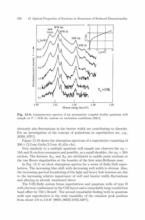
376 15 Optical Properties of Excitons in Structures of Reduced Dimensionality
Fig. 15.9. Luminescence spectra of an asymmetric coupled double quantum wellsample at T = 10 K for various cw excitation conditions [94L1]
obviously also fluctuations in the barrier width are contributing to disorder.For an investigation of the concept of polaritions in superlattices see, e.g.,[95B1,97P1].
Figure 15.10 shows the absorption spectrum of a superlattice consisting of200 × (2.2 nm GaAs/2.5 nm Al.3Ga.7As).
Very similarly to a multiple quantum well sample one observes the nB =1hh and lh exciton resonances and possibly, as a small shoulder, the nB = 2hhexciton. The features Shh and Slh are attributed to saddle point excitons atthe van Hoove singularities at the boarder of the first mini-Brillouin zone.
In Fig. 15.11 we show absorption spectra for a series of ZnSe/ZnS super-lattices. The increasing blue shift with decreasing well width is obvious. Also,the increasing spectral broadening of the light and heavy hole features are dueto the increasing relative importance of well and barrier width fluctuationsand alloying as already mentioned above.
The CdS/ZnSe system forms superlattices and quantum wells of type IIwith electron confinement in the CdS layers and a remarkably large conductionband offset by 750±50meV. The second remarkable finding both in quantumwells and superlattices is the wide tunability of the emission peak positionfrom about 2.0 to 2.6 eV [99D1,00D2,01S3,04P1].

15.2 Coupled Quantum Wells and Superlattices 377
Fig. 15.10. The absorption spectrum of a GaAs/Al1−yGayAs superlattice [90C2]
In the superlattice, the electron and hole wave functions have a strongeroverlap than in single and multiple quantum wells of the same CdS wellwidth due to the confinement of the holes in ZnSe in the first case. Ad-ditionally, the overlap increases in both cases with decreasing width of theCdS well. Consequences are a more strongly pronounced hh exciton-featurein the superlattice compared to quantum wells, a higher oscillator-strengthand a faster luminescence decay time. Peculiarities of single CdS quan-tum wells will be presented in Chap. 23. In quaternary type II systemslike BeTe/ZnSe or CdS/ZnSe the overlap of electron and hole wave func-tions is limited to the interface region. Depending on the type of inter-face the bands can be oriented in (110) or (1-10) directions. Depending onthis orientation the luminescence can be polarized preferentially in one ofthese two directions, although both constituents have cubic symmetry. Exam-ples for the BeTe/ZnSe system are found, e.g., in [00Y1] and for CdS/ZnSein [00S1].
The II–VI compounds usually have a rather strong lattice mismatch, ascan be seen from data of Sec. 8.11. As a consequence only rather thin films(a few mono-layers) can be grown if one is to avoid the formation of misfitdislocations. The results are so-called strained-layer superlattices where thetwo different materials forming the wells and the barriers adapt to a common,intermediate lattice constant.

378 15 Optical Properties of Excitons in Structures of Reduced Dimensionality
Fig. 15.11. Absorption spectra of a series of ZnSe/ZnS superlattices with variouswell (ZnSe) and barrier (ZnS) widths [92O1,92S1]
The strain in superlattices mentioned above produces, via the piezoeffectin the layers, electric fields in the growth direction. The piezoeffect requiresat least partially ionic binding and the absence of inversion symmetry in thecrystal. Both conditions are fulfilled, e.g., for the zincblende- and wurtzite-type III–V and II–VI compounds. Since these built-in fields tilt the bandsand shift the exciton energies, such superlattices are also known as Stark-superlattices.
The piezoeffect is generally stronger in the more ionic II–VI compoundscompared to III–V materials and in wurtzite structure compared to thezincblende one. We present here example data for wurtzite CdSe/CdS su-perlattices from [94G1, 94K1, 94L2, 95L2]. References for other materials arefound, e.g., in [93C2,94K1,95L1].
CdSe/CdS has a slightly type II band alignment with a conduction bandoffset of 100 ± 100meV. In Fig. 15.12a we show the conduction and valenceband edges including the envelope wave functions of electrons and holes in thefirst two minibands at kz = 0, the temporal evolution of the emission spectraafter ps excitation with 2.46 eV photons, a fluence of 0.3 mJ/cm2 and thecalculated shift of the various transitions with time together with experimentaldata of the emission maximum.
The conduction and valence band edges are tilted by alternating piezo-electric fields with a field strength of 2 × 10⁸ V/m. Figure 15.12b gives the

15.2 Coupled Quantum Wells and Superlattices 379
same results calculated self-consistently for a carrier density per layer of1.2 × 109 cm−2. Obviously the carrier separation into the different layersproduces a strong depolarisation field that almost compensates the piezofields under the conditions of Fig. 15.12b. As can be seen by comparingFigs. 15.12a and b both the transition energies and the electron hole over-lap, i.e., the transition matrix element depends strongly on the carrier den-sity. This effect can be nicely seen under pulsed (Fig. 15.12c) or cw excita-tion [94K1].
Fig. 15.12. The conduction and valence band edges of CdSe/CdS superlatticesinfluenced by the piezofield (a) for zero carrier density and for a density of ne =nh = 1.2 × 109 cm−2 (b) the temporal evolution of the luminescence spectra after psexcitation (c) and the experimental and calculated shifts of emission maxima withtime (d) [94K1,95L2]

380 15 Optical Properties of Excitons in Structures of Reduced Dimensionality
Both the decay rate and the position of the emission maxima shift tolower values with increasing time after the excitation pulse, leading to analmost logarithmic dependence, as seen in Fig. 15.12d. The temporal evolutionof various calculated inter-band transitions are compared to the one of theemission maximum.
In addition, the position of the chemical potential µ of the electron holepair system is given, i.e., the energetic distance between the quasi-Fermi levelsof electrons and holes. At the beginning, it reaches values in the miniband, i.e.,one has population inversion. Indeed stimulated emission has been observedfrom the transition e2 → hhl, which has a larger oscillator strength than thee1 → hhl process [95L2].
A good review of the present state of the art of II–VI epitaxy and of theiroptical properties is found in the proceedings of recent conferences on thistopic ([82P1] of Chap. 8 or [91T1]).
Since the luminescence tail of excitons localized by well-width fluctuationsin II–VI superlattices is sometimes spectrally broader than the energy of theoptical phonons, and since the coupling of the excitons to the phonons isstronger than in the III–V system AlGaAs, one can observe interesting phe-nomena related to the relaxation or “freezing” of excitons in these tail states.More information about this topic and about the magnetic polaron effectswhich appear for II–VI SL containing Mn can be found in [93H1,93J2,93K1].
We come back to this topic in the sections of magnetic field effects(Sect. 16.1) and on time-resolved spectroscopy Sect. 23.3.
Corrugated superlattices have been grown on highly indexed substrate sur-faces like (113). For some time the aspect of quantum well-wire superlatticeshas been discussed for this type of structure. However, more recently it hasbeen found that the quantum wire aspect in these structures is marginal orcompletely absent [96L1].
The transition from a type-I to type-II band alignment can be observed inshort period GaAs/AlAs SL.
The generally used nomenclature is (GaAs)m(AlAs)n where m and n givethe number of respective monolayers. GaAs is a direct gap material and AlAsan indirect one with a larger gap. If the width of the GaAs barrier is madesmaller and smaller, then the k = 0 nz = 1 conduction band state shifts tohigher and higher energies until it is situated above the indirect conductionband state in AlAs. This situation is shown schematically in Fig. 15.13.
In contrast to the type-II GaSb/AlAs SL, the short period GaAs/AlAs SLare indirect in real space and in k-space. The peculiarities of absorption inthe well, relaxation of the electrons into the “barrier”, and subsequent recom-bination are discussed in detail in [90G1]. An example is shown in Fig. 15.13,where the photoluminescence excitation spectra and the luminescence spectraare given for a type-I and a type-II GaAs/AlAs SL.
In the case of a type-II arrangement, the optical matrix element from thedirect maximum in the valence band of GaAs to the indirect minimum in theconduction band of AlAs is so small that the transition hardly shows up in

15.2 Coupled Quantum Wells and Superlattices 381
the absorption spectrum. The thermal population factor is responsible for thefact that the low-temperature luminescence nevertheless originates essentiallyfrom this transition (Fig. 15.13c).
We mention that efforts are also being made to grow strained Ge/Si SL,though there are considerable technical problems in growing good qualitysamples due to the different lattice constants. The idea is that a similar folding-back mechanism as outlined in connection with phonons, in Sects. 7.10 and11.2 should yield a direct electronic bandstructure which would allow thehighly developed Si technology to be used also for light-emitting devices.
For recent publications and reviews of this topic see, e.g., [92N1, 92V1,92W1,93A1,93M1,93V1,94H1,95F1,95L1,95Z1,96L2,96O1,97K1,00G1,00P1]
Fig. 15.13. The band alignment of a (GaAs)m(AlAs)n short-period superlattice oftype II showing the conduction and valence band edges at Γ (——), the conductionband edge at X (- - - -) and the quantized electron and hole states (a), PL and PLEfor a type I (b) and a type II superlattice (c) [90G1]

382 15 Optical Properties of Excitons in Structures of Reduced Dimensionality
Fig. 15.14. Luminescence spectra ofa nipi structure compared to the RTabsorption edge of bulk GaAs [86D1,92M1]. Compare with Fig. 15.12c
and references therein, which partly indicate that even this approach is un-likely to result in extremely high luminescence yields.
To conclude this section we briefly return to the concept of nipi structuresor doping superlattices introduced in Sect. 8.11. The probability of transitionsbetween electron states in the conduction-band minima and holes in the va-lence band maxima is low because of the “spatially indirect” bandstructure.Consequently strong absorption sets in only around the energy of the “di-rect” gap, i.e., at an energy corresponding to that between the bands at thesame place, modified by the Coulomb interaction. The carriers are spatiallyseparated after their creation resulting in a very long lifetime. The radiativerecombination which can nevertheless occur due to the small overlap betweenelectron and hole wavefunctions in their respective spatial band minima isstrongly Stokes-shifted with respect to the spatially direct absorption edge.We give an example in Fig. 15.14, which shows the emission spectra for twodifferent pump intensities and the position of the absorption edge of bulkGaAs. An analogous shift of the emission with excitation is also seen in piezo-superlattices see Fig. 15.12 or [93C2, 94K1, 95L2]. The nipi structures havequite amazing nonlinear optical properties [86D1,92M1].
15.3 Quantum Wires
As already mentioned in Sects. 8.12 and 9.3 there are various possibilities toproduce quantum wires, e.g., by laterally structuring quantum wells, by grow-ing in V-groves or on ridges, by cleaved edge overgrowth producing T-shapedstructures or by growing free standing, whisker-like needles, also known asnanorods. See, e.g., [90C1,90G1,93C1,93D1,93P1,02K1,03Y1] and referencestherein.

15.3 Quantum Wires 383
In the following, we present a few examples.The problem encountered in lateral structuring is that the quantization
length lz in the growth direction of the QW is usually much smaller than thelength ly of the subsequent lateral structuring. Typical values are
lz ≈ 10 nm ,ly ≈ 50 − 100 nm .
(15.6)
Consequently, the confinement energies resulting from confinement in the twodirections are very different. Usually one observes only a narrow modulation ofthe luminescence or photoluminescence excitation spectra due to quantizationin the y-direction.
We provide examples for the confinement in the second direction inFigs. 15.15 and 15.16.
Figure 15.15 shows PLE spectra of a 8 nm-wide GaAs quantum well be-tween Al1−yGayAs barriers in the upper trace, showing the well-known heavyand light hole excitons.
In the PLE spectrum of the quantum wires these two resonances areslightly blue shifted according to the lateral confinement and for the heavyhole exciton even the first two laterally confined states could be resolved,labeled hh11 and hh12. The PLE spectra have been taken at the spectralpositions indicated by the vertical arrows.
The progress in nanolithography is obvious when comparing the data inFig. 15.16 for InAs wells.
Fig. 15.15. PLE spectra of a 8 nm-wide GaAs/Al1−yGayAs multiple quantum wellsample (upper trace) and of 65 nm-wide quantum wires patterned from this sample(lower trace) [95S2]
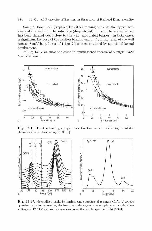
384 15 Optical Properties of Excitons in Structures of Reduced Dimensionality
Samples have been prepared by either etching through the upper bar-rier and the well into the substrate (deep etched), or only the upper barrierhas been thinned down close to the well (modulated barrier). In both cases,a significant increase of the exciton binding energy from the value of the wellaround 8 meV by a factor of 1.5 or 2 has been obtained by additional lateralconfinement.
In Fig. 15.17 we show the cathodo-luminescence spectra of a single GaAsV-groove wire.
Fig. 15.16. Exciton binding energies as a function of wire width (a) or of dotdiameter (b) for InAs samples [98B2]
Fig. 15.17. Normalized cathode-luminescence spectra of a single GaAs V-groovequantum wire for increasing electron beam density on the sample at an accelerationvoltage of 12.5 kV (a) and an overview over the whole spectrum (b) [95G1]

15.3 Quantum Wires 385
The overview spectrum shows, at the lower energy side, the emission fromthe quantum wire (QWR) at the bottom of the V-groove. At the higher energyside it shows the emission from the quantum wells (QW) at the side flanksof V-groove, which are considerably narrower, and therefore the form lateralconfining potential of the wire-states though have higher quasi dimensionalityd = 2. The emission VQW finally results from a vertical quantum well whichforms unintentionally in the middle of the V-groove.
The lateral confining potential of the V-groove is not as abrupt as, e.g.,quantum wires formed by nanolithography, but rather smooth. Therefore thehigher states, which are populated at higher excitation current and are seenin luminescence, are in first approximation as equally spaced as in a harmonicoscillator. They are labeled in Fig. 15.17a by n = 1, 2, 3 .
As a last example we show in Fig. 15.18 the luminescence spectra of twodifferent T-shaped quantum wires formed by cleaved edge overgrowth. Theiremission is again red shifted with respect to the emission from the quantumwells on the (001) and (110) surfaces.
For recent data both for GaAs and In1−yGayAs based structures see, e.g.,[88H1,96L4,98L1,99F1,00D1,00K1] and references therein.
For localization in quantum wires see, e.g., [97R1,98V1].The dispersion relations of quantum wire polaritons are calculated for vari-
ous cross-sections, e.g., [92T1,93C1,93K1,93Y1,99C1] yielding partly differentresults. For experimental data see, e.g., [88K1].
For the optical properties of nanorods see the above references and [97S1,01H2,02K3,04P2,04L1].
Fig. 15.18. Low-temperature photoluminescence spectra of two different T-shapedquantum wires [96L3]

386 15 Optical Properties of Excitons in Structures of Reduced Dimensionality
15.4 Quantum Dots
As already explained in Sects. 8.13 and 9.3 there are many different ways toproduce quantum dots or islands.
We present here some selected examples of “real” dots or nanocrystalsthat are embedded in glass or polymer matrices with high barrier ener-gies in the eV range and almost spherical shape and for quantum islandsformed in quantum wells by generally more oblate insertions of low-band-gapmaterial.
The most frequently used groups of semiconductors for the first type ofquantum dots are Cu-halides and II–VI compounds and to a much lowerdegree III–V materials. For the latter group, examples are found in [96G1,97B1] and for the two former groups in [93B1,97W1,98G1,01L1] of Chap. 1.
The research on epitaxially-grown quantum islands started essentially withthe III–V system In(Ga)As/GaAs followed by the II–VI material combinationCdSe/ZnSe.
A limited selection of textbooks, monographs and review articles on thistopic is: [81A1 g,k,l, 93B1, 97W1, 98G1, 01H1] of Chap. 1 and [86B1, 87S1,90M1, 92P1, 93W1, 95P1, 95W1, 00K2, 00L2, 01K1, 01K2, 01K3]. In these ref-erences some comments can also be found on the history of this field. Actu-ally, II–VI semiconductor doped glasses have been used as color- and edgefilters from the IR to the near UV from the 1930s. It was also known thatthese glasses obtain their color only during an annealing process and thatthe absorption edges shifts to the red with increasing annealing time andtemperature. The fact that this is a consequence of quantum confinement innanocrystallites was mentioned explicitly only in the beginning of the 1980s,e.g., by [82E1,82H1,83J1].
A rather recent development in this field is nanostructures grown in in-verted tetrahedral pyramids [98H1,00K2,00L2] and references therein.
One distinguishes three quantization regimes. Below we give some formulaefor the quantization energies assuming spherical dots, simple isotropic andparabolic conduction and valence bands and infinite barriers. As outlinedalready in Sects. 8.13 and 9.3 the regime I is obtained for dots larger thanthe excitonic Bohr radius;
regime I: R aB . (15.7a)
In this case, only the center of mass motion of the exciton is quantized, whilethe relative motion of electron and hole are hardly affected. The quantizationenergy is given, in the above approximations of a spherical dot with infinitelyhigh barriers and neglecting the difference in the dielectric properties of themicrocrystallite and the surrounding matrix, by
∆EIQ =
2π2
2MR2, (15.7b)

15.4 Quantum Dots 387
where M = me + mh is the translationed mass of the exciton. Regime II isgiven by
regime II: aeB > R > ah
B , (15.7c)
where ae,hB are the respective radii of the electron and hole orbits in the exciton
around their common center of mass.In this case the motion of the electron is quantized and the hole moves in
the potential of the QD and of the space-charge of the electron for the usualsituation me mh .
Continuing to use the above-mentioned approximations, and neglectingthe Coulomb energy between electron and hole, one finds
∆EIIQ = CRy∗
(aBπ
R
)2
; with C = 0.67 . (15.7d)
Regime III is defined by
regime III: R ae,hB . (15.7e)
Since the quantization energy scales with R−2 and the Coulomb energywith R−1, for this regime one can ww.mozilla.org/start/1.7/ expect as a firstguess
2π2
2µR2= EIII
Q EIIICoulomb (15.7f)
where µ is the reduced mass of electron and hole. The influence of the Coulombenergy is still partly incorporated, e.g., in a formula used in [97M1]
∆E(R) =2π2
2µR2− 1.78e2
εR+ 0.752ERy . (15.7g)
Slightly different formulae can be found, e.g., in [86S1, 91E1] or in [01L1] ofChap. 1.
The values of R where (15.7e,f) hold are comparable to the lattice con-stant. In this situation, the whole effective mass concept breaks down anda description of the dot in terms of molecular orbitals becomes more appro-priate. An exhaustive list of references for calculations using the full valenceband structure of cubic and hexagonal quantum dots and of calculations forvery small clusters where tight binding methods are more appropriate is givenin [01L1] of Chap. 1.
Recently it became obvious that the size of the dots is not the only rel-evant quantity affecting their linear and especially nonlinear optical proper-ties. The three different growth regimes of the dots which occur during theannealing process of the glasses, namely nucleation, normal growth of the dotsand growth through coalescence, result is significantly different properties of,among other things, the interface states between glass matrix and semicon-ductor dot. Furthermore, the capping of dots plays a crucial role. In glass ororganic matrices one generally has a lot of surface and interface states, the

388 15 Optical Properties of Excitons in Structures of Reduced Dimensionality
number of which can be significantly decreased by capping with hydrogen ororganic ligands, which saturate the dangling bonds, or with similar semicon-ductors with a higher band gap of type-I band alignment. For recent reviewssee [88H2,90K1,91E1,93G1,93W1] and the above mentioned references.
From our considerations of the density of states in Sects. 7.7 and 8.9 wewould expect QD to have an absorption spectrum consisting of a series of δ-functions or of Lorentians, if some homogeneous broadening is included. Suchbehavior is not observed in reality for ensembles of dots since various processescontribute to a broadening of the resonances, e.g., the size distribution of thecrystallites considered in Fig. 15.19, the coupling to optical phonons, whichmay be enhanced in the quantum dots as compared to the bulk material,and the influence of impurity, surface, or interface states; see [91E1, 93G1,93W1,95W1,96W1] and again references of Sects. 8.13 and 9.3 and referencestherein.
The range of the size distribution for nanocrystallites in glass matricesis typically in the range of 10 to 30%. In organic solvents it can be reducedby size selective precipitation to a few percent [95W1]. The size distributionof quantum dots produced by nanolithography is, especially for the smallestdots, which show substantial lateral confinement effects, also in the range
Fig. 15.19. Calculated spectra of the optical density of quantum dots for variousrelative widths of thier size distribution [90K1]

15.4 Quantum Dots 389
of (20 ± 10)%. Quantum islands in MBE-grown layers usually show strongsize and composition fluctuations. Ways out of the resulting inhomogeneousbroadening are single dot spectroscopy and site- or size-selective spectroscopy,including spectral hole burning.
In Fig. 15.19 we present calculated absorption spectra, with a simplifiedenergy level scheme, showing the influence of inhomogeneous broadening. InFigs.15.16, 15.20 and 15.21 we show experimental data.
Regime I is usually realized for QD made from the copper halides CuCl,CuBr and CuI since the values of aB for these materials are in the range of1 nm. Figure 15.20a shows an example for CuBr which clearly illustrates theblue-shift of the nB = 1 exciton resonances from the two uppermost valencebands with decreasing R.
In Fig. 15.20b we show the blue-shift of the absorption edge of glassescontaining CdSe QD with decreasing values of R. The calculated transitionenergies and their oscillator strengths are given by the positions and heightsof the vertical lines. For more data see also [92K1].
The luminescence is usually considerably Stokes-shifted with respect tothe absorption, in Fig. 15.21 by roughly 200 meV. This shift can be partlyattributed to a relaxation of the carriers into defect or surface states, andpartly to stronger phonon coupling resulting in Huang-Rhys factors SQD inthe QD of around 1, which is larger than for the corresponding bulk materials.For CdS1−xSexQD, for example, one finds
0.2 ≈ Sbulk < SQD ≈ 1 . (15.8)
In Fig. 15.22a,b we show for CdSe dots in an organic solvent, the energyof the lowest electron-hole pair state as a function of the dot radius, and theenergy spacing to higher states as a function of the energy of the lowest state.Good agreement between experiment and theory is observed.
Further examples for other materials are found in [97W1,01L1] of Chap. 1.Transitions between the various electron-hole pair states in the IR under
optical excitation across the band gap have been reported for CdSe in [98G1]and for ZnO dots in [00H1].
To demonstrate the relation of inhomogeneous broadening of the spec-trum of a dot ensemble and to the homogeneous broadening of a single dot,we show corresponding luminescence spectra of CdSe dots capped with ZnSin Fig. 15.23. Capping with larger gap semiconductors or with organic lig-ands tends to reduce the homogeneous line width compared to QD in sim-ple (boro–silikate) glass matrix. The satellite shifted by 25.6 meV is the LOphonon replica.
The absolute photo-luminescence quantum efficiency can be rather high,reaching values of 0.1 to 0.9 [95N1].
The homogeneous width Γ (T ) increases with temperature typically witha function like [99R1]
Γ (T ) = Γ0 +Γel–phon
exp ΩLO/kBT − 1(15.9)

390 15 Optical Properties of Excitons in Structures of Reduced Dimensionality
Fig. 15.20. A set of absorption spectra of CuBr quantum dots with different averageradii R (a) and a set of measured absorption spectra together with the calculatedpositions of the optical transitions in CdSe QD (b) [88H1,93E1]
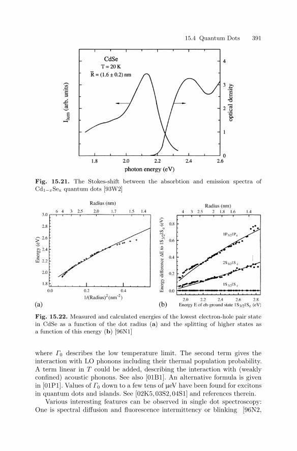
15.4 Quantum Dots 391
Fig. 15.21. The Stokes-shift between the absorbtion and emission spectra ofCd1−xSex quantum dots [93W2]
Fig. 15.22. Measured and calculated energies of the lowest electron-hole pair statein CdSe as a function of the dot radius (a) and the splitting of higher states asa function of this energy (b) [96N1]
where Γ0 describes the low temperature limit. The second term gives theinteraction with LO phonons including their thermal population probability.A term linear in T could be added, describing the interaction with (weaklyconfined) acoustic phonons. See also [01B1]. An alternative formula is givenin [01P1]. Values of Γ0 down to a few tens of µeV have been found for excitonsin quantum dots and islands. See [02K5,03S2,04S1] and references therein.
Various interesting features can be observed in single dot spectroscopy:One is spectral diffusion and fluorescence intermittency or blinking [96N2,

392 15 Optical Properties of Excitons in Structures of Reduced Dimensionality
Fig. 15.23. Luminescence spectra of ZnS-capped CdSe quantum dots for an ensembleof average radius R = 4.5 nm and of a singledot [96E1]
00N1,01S4]. Both effects are attributed to the ionization of carriers from thedot and their capture at the interface or in the surroundings of the dot. Thesecarriers either shift the emission energy by the quantum confined Stark effect,caused by the electric field of the extra carrier, or even bring them into a non-luminescent state. Removal of the carrier by optical or thermal activationbrings the QD back to the original state.
For the mapping of the excitonic wave function in quantum dots by opticalnear field microscopy see, e.g., [01C1,03M3,04K1].
Another interesting phenomenon is the fact that a single dot can emitonly one photon at a time. It then has to be re-excited again before it canemit another photon. As a consequence, the photons emitted from a singledot are anti-correlated. This photon anti-bunching shows up in a dip in thecorrelation function of the photons for zero time delay. Examples are found,e.g., in [00L3,00M3,01M1,02S1,03U1].
A related topic is quantum entanglement of excitons in single or coupledquantum dots [98B1,99Q1,00C1,00R1,01B1,03Z2].
The exciton or electron–hole pair ground state usually shows a fine-structure, due to the exchange splitting. The lower state is the triplet, inquantum dots usually called the dark state, since it is spin flip forbidden.This ordering of the states is the same since it already exists in bulk ma-terials, with the difference that in bulk materials the splitting between thetriplet and the transverse dipole allowed singlet states of Wannier excitonsis much smaller than the transverse-longitudinal splitting of the singlet. Inquantum dots the situation is inverted due to a strong enhancement of the(short-range) exchange interaction caused by three-dimensional confinement,while the oscillator strength is reduced by the dilution of the oscillators, i.e.,the dots in their matrix. See also Fig. 9.2.
In Fig. 15.24 we show data from various authors for the exchange splittingof the excitons in CdSe quantum dots as a function of the dot radius.
Similar data are found for Cu and Ag halogenid dots [00G2,03G1] wherebulk band parameters have also been deduced from dot spectroscopy.

15.4 Quantum Dots 393
The interaction of excitons (i.e., electron–hole pair states) in quantumdots with phonons has already been addressed above in connection withthe homogeneous width. It also shows up in luminescence. An example isgiven in Fig. 15.23. Typically one finds that the spacing of the zero phononline and its one LO phonon replica is slightly smaller than the LO phononenergy in bulk at k = 0. This effect is caused by the facts that the LOphonon mode confined in a quantum dot has an effective k > 0 andthat the dispersion of LO phonons is generally negative, i.e., ELO(k) de-creases with increasing k. See, e.g., [96E2]. Furthermore one observes sur-face phonon modes [99H1] and confined acoustic phonons [96W1, 01P1].For exciton-phonon complexes or exciton-polarons see [04K2] and referencestherein.
The Huang-Rhys factor, which is a measure for the coupling between anelectronic resonance and LO phonons can be deduced from luminescence spec-tra, in contrast to bulk materials, because problems with reabsorption and kselection rules in the zero phonon line are relaxed, which are relevant in thelatter case. The values of the Huang–Rhys factor depend partly on the indi-vidual properties of the dots like capping or surface states and have valuesbetween 0.2 and 0.9. For data see [01L1] of Chap. 1 or [93S1] or the discussionwith (15.8).
The interaction of excitons with single carriers or other excitons will beconsidered in connection with trions and biexcitons in Sect. 20.3.
Quantum dots, especially from the group of II–VI semiconductors, havebeen used as markers attached to organic molecules [98B3, 01D3, 02G1] toimpregnate the voids in photonic crystals [99R2, 02P1] or for incorporationin microcavities [03M3].
It is well known, that the vapor pressure of small droplets increases withdecreasing droplet radius. Consequently their boiling point or temperaturedecreases. A similar phenomenon also occurs for the solid to liquid phase
Fig. 15.24. Exchange splitting as a function of the exciton ground state in CdSedots as a function of the dot radius (data from various authors, [96W1])

394 15 Optical Properties of Excitons in Structures of Reduced Dimensionality
transition of small crystallites. This effect has been known and used sinceancient times for metals like Au, e.g., in granulation techniques. Recently thisphenomenon has also been observed for CdS(e), Si or Cu-halide semiconductorquantum dots [92G1,96G1,99V1,01Z1,03G1].
In Fig. 15.25 we show examples for two glass samples doped with CuClcrystals of different average radii. The optical density in the lowest excitonresonance (compare with Fig. 15.20) is plotted as a function of sample temper-ature. The steep decrease (increase) is attributed to the melting (solidification)of the CuCl dots. Note that these temperatures are below the glass transitiontemperature of the host. One observes two prominent features: a hysteresisin the temperature cycle, as indicated by the arrows, which is characteristicof a first order phase transition, and a shift of this hysteresis loop to temper-atures below the bulk melting temperature TM of CuCl, which is indicatedby the vertical arrow. This shift increases with decreasing dot radius as pre-dicted above.
Quantum dots or islands have also been made from indirect gap semicon-ductors, with an emphasis on Si, which is the dominant material for elec-tronic devices. The hope is that the relaxation of the k-conservation underthree-dimensional confinement might increase the luminescence yield of thismaterial, allowing one to integrate light emitters with other (opto) electronicdevices based on the same material (Si) on one chip. However, at the endof 2004 this aim had only been achieved with limited success for Si basedquantum wells or superlattices.
Various approaches have been used to prepare Si nanocrystals, which arereviewed in, e.g., Chap. 9 and [97W1] of Chap. 1. For more recent data see,e.g., [94K2, 94P1, 96G3, 96M1, 98P2, 99K1, 01Y1, 02Y1, 02Z1] and referencestherein.
Fig. 15.25. Optical density in the exciton resonance of CuCl quantum dots in glassmatrices as function of temperature for two different average dot radii [03G1]
15.4 Quantum Dots 395
A special type of Si nanocrystals is porous silicon (p-Si). In 1984 a visible,low temperature emission was observed in p-Si [84P1,90C3,97C1]. Since thenmore than 1000 papers have appeared on this topic, which is still being con-troversially discussed. Therefore we give here only a very short overview anda few references.
Porous silicon is prepared by anodic oxidation of doped Si, e.g., in HF-ethanol electrolytes. The result is a porous layer on the Si chip, which containsnanocrystals and nanorods with dimensions of a few to several nm. These sam-ples show (photo) luminescence in the visible spectrum from the red-orangeto the blue region depending on the preparation and excitation conditions.
One idea to explain the blue shift and the enhanced intensity of the emis-sion compared to bulk Si is by the above mentioned quantum confinementeffect. However, alternative explanations have been put forward, attributingthe origin of the emission to siloxene (Si6O3H6)n or to Si-oxihydrides or sub-oxides and other Si-related compounds, which may form during the etchingprocess in the porous layer, partly even in the form of surface states or trapsat the nanocrystals. On the other hand, the siloxene usually shows lumines-cence bands comparable to those of p-Si only after a certain heat treatment,during which Si nanocrystals might form.
There seems to be a trend to assume that the blue-shifted absorptionof p-Si and parts of its red-orange luminescence including the polarizationanisotropy might be related to Si nanocrystals or nanorods, while the shorterwavelength emission components might have their origin in the alternativecompounds mentioned above. We cannot currently provide a definite answerto this problem. Instead we give some references for both approaches and leavethe final decision to the reader or to future research [92S2,95S2,97G1,97R2,97R3,99B1,99J1,01D1,02K4].
As already mentioned in the introduction we presently see increasing workto pack quantum dots so closely that the wave functions start to overlap.According to what we have learned for periodic potentials in general and morespecifically for superlattices in Sects. 4.1, 5.4, and in Chap. 8 this interactionwill result in the formation of (mini)bands from the discrete energy levels inisolated dots. If the dots are periodically arranged and if their size distributionand thus their inhomogeneous level broadening are sufficiently small, thesenew bands can be described by a dispersion relation E(k). In the oppositecase, there will be no good quantum number k, but there will be bands inthe density of states, similarly to disordered systems. The first examples ofthis development can be found in the following small selection of references:[92T2,95L3,96K1,98M1,01D2,00L4].
A similar phenomenon is found if fullerene molecules C60, are put togetherto form a solid. Solid C60 crystals are semiconductors with a band gap of about2.2 eV [99M1].
To finish this section on quantum dots we want to give some referencesfor quantum islands or self-assembled quantum dots occurring in thin MBElayers for lattice-mismatched systems. A calculation of the wave functions for
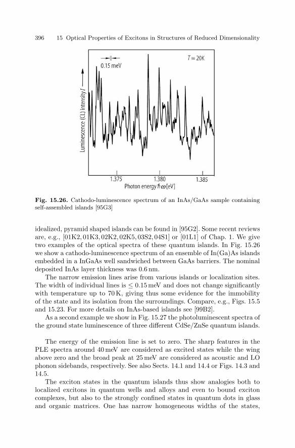
396 15 Optical Properties of Excitons in Structures of Reduced Dimensionality
Fig. 15.26. Cathodo-luminescence spectrum of an InAs/GaAs sample containingself-assembled islands [95G3]
idealized, pyramid shaped islands can be found in [95G2]. Some recent reviewsare, e.g., [01K2, 01K3, 02K2, 02K5, 03S2, 04S1] or [01L1] of Chap. 1. We givetwo examples of the optical spectra of these quantum islands. In Fig. 15.26we show a cathodo-luminescence spectrum of an ensemble of In(Ga)As islandsembedded in a InGaAs well sandwiched between GaAs barriers. The nominaldeposited InAs layer thickness was 0.6 nm.
The narrow emission lines arise from various islands or localization sites.The width of individual lines is ≤ 0.15meV and does not change significantlywith temperature up to 70 K, giving thus some evidence for the immobilityof the state and its isolation from the surroundings. Compare, e.g., Figs. 15.5and 15.23. For more details on InAs-based islands see [99B2].
As a second example we show in Fig. 15.27 the photoluminescent spectra ofthe ground state luminescence of three different CdSe/ZnSe quantum islands.
The energy of the emission line is set to zero. The sharp features in thePLE spectra around 40 meV are considered as excited states while the wingabove zero and the broad peak at 25 meV are considered as acoustic and LOphonon sidebands, respectively. See also Sects. 14.1 and 14.4 or Figs. 14.3 and14.5.
The exciton states in the quantum islands thus show analogies both tolocalized excitons in quantum wells and alloys and even to bound excitoncomplexes, but also to the strongly confined states in quantum dots in glassand organic matrices. One has narrow homogeneous widths of the states,

15.5 Problems 397
Fig. 15.27. PLE spectra of three dif-ferent Cd(Zn)Se/ZnSe islands [01H3]
i.e., long dephasing times (see Chap. 23) and a confinement-enhanced singlet-triplet splitting as in QD doped glasses and organic matrices (Fig. 15.24).See, e.g., [98G2, 01H1] for the system CdS/ZnSe. One can also observe spec-tral diffusion and intermittency [98Z1,00S2] and one tries to build up higherdimensional structures by coupling quantum islands, e.g., in vertical stacksor even in three dimensional ordered structures [99Y1, 01H2, 01K3, 01P1,03K2].
For examples of level repulsion between spatially and energetically closelying states see, e.g., [03G1,03W1] and references therein.
With these examples and the following problems we finish the chapter onexcitonic optical properties of semiconductors quantum structures. We shallmeet reduced dimensionalities again including “photonic dots” in the nextchapters.
15.5 Problems
1. Try to make a simple estimate of the radius of an ideal quantum dot atwhich the quantization energy and the Coulomb energy are equal.
2. In a quantum well with infinitely high barriers one expects an energy levelscheme that depends quadratically on the quantum number nz. Check ifa similar relation holds for the (few) bound exciton states in wells withfinite barriers. Inspect, e.g., data for the system GaAs/AlGaAs.

398 15 Optical Properties of Excitons in Structures of Reduced Dimensionality
3. Make a qualitative sketch of the conduction and valence band edges of anideal, undoped, type I quantum well, of a barrier or a well-doped sampleor of a type II MQW with a slight homogeneous n-doping.
4. Make a rough sketch of the absorption spectrum for the band-to-bandtransition with and without Coulomb interaction of a direct gap, dipoleallowed bulk semiconductor and for quantum wells, wires and dots.
5. Calculate the first few energy levels and wave functions in a spherical anda cubic dot with infinitely high barriers.
References to Chap. 15
[65C1] M. Cardona and G. Harbeke, Phys. Rev. A 137, 1467 (1965)[65C2] M. Cardona, M. Weinstein and G.A. Wolff, Phys. Rev. A 140, 633 (1965)[80P1] J.J. Le Pore, J. Appl. Phys. 51, 6441 (1980)[82E1] Al.L. Efros and A.L. Efros, Sov. Phys. Semicond. 16, 772 (1982)[82H1] A. Henglein et al., Ber. Bunsen, Phys. Chem. 86, 301 (1982)[83G1] A.C. Gossard, Thin Films, Preparation and Properties, Academic Press,
New York (1983)[83J1] R. Jain and R. Lind, J. Opt. Soc. Amer. 73, 647 (1983)[84P1] C. Pickering et al., J. Phys. C 17, 6535 (1984)[86B1] L. Brus, J. Chem. Phys. 90, 2555 (1986) and IEEE J. QE 22, 1909 (1986)[86D1] G.H. Doehler, IEEE J. QE-22, 1682 (1986)[86S1] H.M. Schmidt and H. Weller, Chem. Phys. Lett. 129, 615 (1986)[87S1] S. Schmitt-Rink, D.A.B. Miller and D.S. Miller, Phys. Rev. B 35, 8113
(1987)[88H1] Y. Hirugama et al., Phys. Rev. B 37, 2774 (1988)[88H2] F. Henneberger et al., Appl. Phys. B 46, 19 (1988)[88K1] M. Kohl et al., Phys. Rev. B 37, 10927 (1998)[88U1] I.N. Uraltsev et al., phys. stat. sol. (b) 150, 673 (1988)[89K1] M. Kohl et al., Superlattices and Microstructures 5, 235 (1989)[89O1] M. Olszabier et al., Phys. Rev. Lett. 62, 2997 (1989), Surf. Science 228,
123 (1990) and J. Luminesc. 45, 186 (1990)[89S1] S. Schmitt-Rink, D.S. Chemla and D.A.B. Miller, Adv. Phys. 38, 89 (1989)[90A1] L.C. Andreani and F. Bassani, Phys. Rev. B 41, 7536 (1990)[90C1] R. Cingolani and K. Ploog, Adv. Phys. 40, 535 (1990)[90C2] R. Cingolani, L. Tapfer and K. Ploog, Appl. Phys. Lett. 56, 1233 (1990)[90C3] L.T. Canham, Appl. Phys. Lett. 57, 1046 (1990)[90G1] E.O. Gobel and K. Ploog, Prog. Quantum Electron. 14, 289 (1990)[90I1] E.L. Ivchenko et al., phys. stat. sol. (b) 161, 219 (1990) and Phys. Sol.
State 36, 1156 (1994)[90K1] S.W. Koch, Phys. Bl. 46, 167 (1990)[90M1] U. Merkt, Festkorperprobleme/Adv. Solid State Phys. 30, 77 (1990)[90O1] K. Ogawa, T. Katsuyama and H. Nakamura, Phys. Rev. Lett. 64, 796
(1990)[90T1] F. Tassone, F. Bassani and L. Andreani, Il Nuovo Cimento 12D, 1673
(1990)

References to Chap. 15 399
[91E1] A.I. Ekimov and Al.L. Efros, Acta Phys. Polnica A 79, 5 (1991) and A.L.Ekimov, Physica Scripta 39, 217 (1991)
[91L1] V. Lehmann and U. Goesele, Appl. Phys. Lett. 58, 856 (1991)[91T1] H. Tuffigo et al., Phys. Rev. B 43, 14629 (1991)[92A1] L.C. Andreani and F. Bassani, Phys. Rev. B 45, 6023 (1992)[92G1] A.N. Goldstein et al., Science 256, 1425 (1992)[92K1] S.W. Koch et al., J. Crystal Growth 117, 592 (1992)[92M1] S. Malzer et al., phys. stat. sol. (b) 173, 459 (1992)[92N1] G.A. Northrop et al., Appl. Phys. Lett. 60, 865 (1992)[92O1] D. Oberhauser, Dissertation, Kaiserslautern (1992)[92O2] K.P. O’Donnel et al., J. Cryst. Growth 117, 497 (1992)[92P1] Phyiscs of Nanostructures Proc. 38th Scottish Universities Summer School
in Physics, St. Andrews (1991), SUSSP, Edinburg (1992)[92S1] W. Sack et al., J. Lumin. 53, 409 (1992)[92S2] M. Stutzmann et al., Festkorperprobleme/Advances in Solid State Physics
32, 179 (1992)[92T1] F. Tassone and F. Bassani, Il Nuovo Cimento 14D, 1241 (1992)[92T2] F. Tassone, F. Bassani and L. Andreani, Phys. Rev. B 45, 6023 (1992)[92T3] T. Takagahra, Surf. Science 267, 310 (1992)[92V1] L. Vescan et al., Thin Solid Films 222, 5 (1992)[92W1] M. Wachter et al., Thin Solid Films 222, 10 (1992)[93A1] G. Abstreiter, Physica Scripta T 49, A + B, 42 (1993)[93C1] J. Cibert et al., Phys. Scr. T 49, B, 487 (1993)[93C2] D.S. Citrin, Phys. Rev. B 48, 2535 (1993)[93C3] R. Cingolani, Phys. Scripta T 494, 470 (1993)[93D1] F. Daiminger et al., in Proc. 21st Int’l Conf. Phys. Semicond. p 1293, ed.
by P. Jiang, H.Z. Zheng, World Scientific, Singapore (1993)[93E1] A.I. Ekimov et al., J. Opt. Soc. Am. B 10, 100 (1993)[93G1] S.V. Gaponenko et al., J. Opt. Soc. Am. B 10, 1947 (1993)[93H1] R. Hellmann et al., in Proc. 21st Int’l Conf. Phys. Semicond. p 1008, ed.
by P. Jiang, H.Z. Zheng, World Scientific, Singapore (1993)[93J1] S. Jorda, U. Rossler and D. Broido, Phys. Rev. B 48, 1669 (1993)[93J2] S. Jorda, Solid State Commun. 87, 439 (1993)[93K1] H. Kalt et al., Physica B 191, 90 (1993)[93K2] T. Katsuyama et al., Semicond. Science and Tech. 8, 1226 (1993)[93L1] N. Linder et al., Appl. Phys. Lett. 62, 1916 (1993)[93M1] U. Menczigar et al., Phys. Rev. B 47, 4099 (1993)[93P1] K.G. Ploog, R. Notzel and O. Brandt, in Proc. 21st Int’l Conf. Phys.
Semicond. p 1297, ed. by P. Jiang, H.Z. Zheng, World Scientific, Singapore(1993)
[93S1] J. J. Shiang, S. H. Risbud and A. P. Alivisatos, J. Chem. Phys. 98, 8432(1993)
[93V1] P. Vogl, Physica Scripta T 49, A + B, 476 (1993)[93W1] U. Woggon et al., Phys. Rev. B 47, 3684 (1993)[93W2] O. Wind et al., Adv. Mat. Opt. El. 3, 89 (1993)[93Y1] D.R. Yakovlev et al., in Proc. 21st Int’l Conf. Phys. Semicond. p 1136, ed.
by P. Jiang, H.Z. Zheng, World Scientific, Singapore (1993)[93Y2] F. Yang et al., Phys. Rev. Lett. 70, 323 (1993)[94C1] D.S. Citrin, Solid State Commun. 89, 139 (1994) and Phys. Rev. B 51,
14361 (1995)
400 15 Optical Properties of Excitons in Structures of Reduced Dimensionality
[94G1] M. Gurioli et al., Solid State Commun. 91, 931 (1994)[94G2] M. Grun et al., Superlattices and Microstruct. 15, 463 (1994)[94H1] V. Higgs et al., Appl. Phys. Lett. 64, 607 (1994)[94J1] C. Janowitz et al., Phys. Rev. B 50, 2181 (1994)[94K1] C. Klingshirn et al., J. Crystal Grwoth 138, 191 (1994)[94K2] Y. Kanemitsu et al., J. Luminesc. 60/61, 337 (1994)[94L1] C. Luo et al., Superlattices and Microstructures 15, 221 (1994)[94L2] W. Langbein et al., Appl. Phys. Lett. 65, 2465 (1994)[94P1] Porous Silicon, Z.C. Feng and R. Tsu (eds.), World Scientific, Singapor
(1994)[95A1] L.C. Andreani, phys. stat. sol. (b) 188, 29 (1995)[95B1] F. Bassani, G. Cajkowski and Trediucci, Z. Physik B 98, 41 (1995) and
references therein[95B2] L. Banyai et al., Phys. Rev. Lett. 75, 2188 (1995)[95C1] D.S. Citrin, phys. stat. sol. (b) 188, 43 (1995)[95F1] S. Fakatsu, J. Cryst. Growth 157, 1 (1995)[95G1] A. Gustafsson et al., Appl. Phys. Lett. 67, 3673 (1995)[95G2] M. Grundmann, Festkorperprobleme/Advances in Solid State Physics 35,
123 (1995)[95G3] M. Grundmann et al., Phys. Rev. Lett. 74, 4043 (1995)[95L1] H. Lee et al., J. Appl. Phys. 78, 6327 (1995)[95L2] W. Langbein, M. Hetterich and C. Klingshirn, Phys. Rev. B 51, 9922
(1995)[95L3] R. Leon et al., Science 267, 1966 (1995)[95N1] M. Nirmal et al., Phys. Rev. Lett. 75, 3728 (1995)[95P1] Proc. of the Intern. Conf. on Physics, Chemistry and Application of Nano-
structures, V.E. Borisenko, A.B. Filanov, S.V. Gaponenko and V.S. Gurin(eds.), Minsk, Belarus (1995)
[95S1] Y.P. Song et al., Semicond. Science and Technol. 10, 1404 (1995)[95S2] M. Stutzmann, phys. stat. sol. (b) 192, 273 (1995)[95W1] U. Woggon and S.V. Gaponenko, phys. stat. sol. (b) 189, 285 (1995)[95Z1] A. Zrenner et al., Phys. Rev. B 52, 16608 (1995)[96A1] A.P. Alivisatos, Science 271, 933 (1996) and J. Phys. Chem. 100, 13226
(1996)[96C1] J. Cerne, Phys, Rev. Lett. 77, 1131 (1996)[96E1] S.A. Empedodes, D.J. Norris and M.G. Bawendi, Phys. Rev. Lett. 77, 3873
(1996)[96E2] A. Ekimov, J. Luminesc. 70, 1 (1996)[96G1] A.A. Guzelian et al., Appl. Phys. Lett. 69, 1432 (1996)[96G2] A.N. Goldstein, Appl. Phys. A 62, 33 (1996)[96G3] S.V. Gaponenko et al., J. Lumines. 70, 364 (1996)[96K1] C.R. Kargan, Phys. Rev. Lett. 76, 1517 (1996) and Phys. Rev. B 54, 8633
(1996)[96L1] W. Langbein et al., Phys. Rev. B 54, 10784 (1996)[96L2] X. Lin et al., J. Phys. Cond. Matter 8, 3947 (1996)[96L3] W. Langbein, H. Gislason and J.M. Hvam, Phys. Rev. B 54, 14595 (1996)[96L4] Ch. Lienau, A. Richter and T. Elsasser, Appl. Phys. Lett. 69, 325 (1996)[96M1] K.S. Min et al., Appl. Phys. Lett. 68, 2511 (1996)[96N1] D.J. Norris and M.G. Bawendi, Phys. Rev. B 53, 16338 (1996)

References to Chap. 15 401
[96N2] M. Nirmal et al., Nature 383, 802 (1996)[96O1] L.K. Orlov, J. Appl. Phys. 80, 415 (1996)[96S1] V. Sirinivas, Y.J. Chen and C.E.C. Wood, J. Opt. Soc. Am. 13, 989 (1996)[96S2] T. Stroucken et al., Phys. Rev. B 53, 2026 (1996)[96S3] M.S. Salib et al., Phys. Rev. Lett. 77, 1135 (1996)[96W1] U. Woggon et al., Phys. Rev. B 54, 1506 (1996)[96W2] D. Weber et al., J. Opt. Soc. Am. B 13, 1241 (1996)[96W3] M.U. Wehner et al., J. Opt. Soc. Am. B 13, 977 (1996)[96W4] M.U. Wehner, D. Steinbach and M. Wegener, Phys. Rev. B 54, R5211
(1996)[97B1] U. Banin et al., Phys. Rev. B 55, 7059 (1997)[97C1] R.T. Collins, P.M. Fauchet and M.A. Tischler, Physics Today, p 24, Jan.
(1997)[97G1] J.L. Gole et al., Phys. Rev. B 56, 2137 (1997)[97K1] S. Kim et al., Phys. Rev. B 55, 7130 (1997)[97K2] C. Klingshirn, in [81A1]h of Chap. 1, p 85[97M1] Y. Masumoto and K. Sonobe, Phys. Rev. B 56, 9734 (1997)[97P1] M.F. Pereira et al., phys. stat. sol. (a) 164, 199 (1997)[97R1] A. Richter et al., Phys. Rev. Lett. 79, 2145 (1997)[97R2] M. Rosenbauer and M. Stutzmann, J. Appl. Phys. 82, 4520 (1997)[97R3] M. Rosenbauer et al., Phys. Rev. B 55, 10117 (1997)[97S1] V. Sperling et al., J. Luminesc. 72-74, 395 (1997)[98B1] H. Bonadeo et al., Science 282, 1473 (1998)[98B2] U. Banin et al., J. Chem. Phys. 109, 2306 (1998)[98B3] M. Bayer, S. Walck and T.L. Reinecke, Phys. Rev. B 57, 6584 (1998)[98B4] M. Bruches, Science, 281, 2013 (1998)[98C1] C.P. Collier, T. Vossmeyer and J.R. Heath, Annu. Rev. Phys. Chem. 49,
371 (1998)[98G1] P. Guyot-Sinnoest and M.A. Hines, Appl. Phys. Lett. 72, 680 (1998)[98G2] F. Gindele et al., Solid State Commun. 106, 653 (1998)[98H1] A. Hartmann et al., Appl. Phys. Lett. 73, 2322 (1998)[98K1] H. Kalt et al., J. Crystal Growth 184/185, 795 (1998)[98K2] C. Klingshirn, NATO ASI Series B 372, 143 (1998)[98L1] Ch. Lienau et al., Phys. Rev. B 58, 2045 (1998)[98M1] O.I. Micic et al., J. Chem. Phys. B 102, 9791 (1998)[98P1] W. Petri et al., J. Crystal Growth 184/185, 320 (1998)[98P2] I. Pelant et al., phys. stat. sol. (a) 165, 25 (1998)[98R1] A. Richter et al., Appl. Phys. Lett. 73, 2176 (1998)[98V1] F. Vouilloz et al., Physica E 2, 862 (1998)[98Z1] B.P. Zhang et al., Appl. Phys. Lett. 73, 1266 (1998)[99B1] M.S. Brandt et al., phys. stat. sol. (b) 215, 409 (1999)[99B2] D. Bimberg, M. Grundmann and N.N. Ledentsov, Quantum Dot Het-
erostructures, John Wiley and Sons, Chichester (1999)[99C1] D. Crisinel, M.A. Dupertius and E. Kapon, Optical and Quantum Elec-
tronics 31, 797 (1999)[99D1] A. Dinger et al., Semicond. Science and Technol. 14, 595 (1999)[99F1] C.J. Fall, M.A. Dupertius and E. Kapon, Optical and Quantum Electr.
31, 201 (1999)[99H1] Y. N. Huang, Phys. Rev. B 59 7285 (1999)

402 15 Optical Properties of Excitons in Structures of Reduced Dimensionality
[99J1] R. Janssen, Phys. Rev. B 60, 13561 (1999)[99K1] D. Kovalev et al., phys. stat. sol. (b) 215, 871 (1999)[99M1] K.P. Medletov and V.D. Negrii, phys. stat. sol. (b) 211, 217 (1999)[99O1] A. Ohtomo et al., Appl. Phys. Lett. 75, 980 (1999)[99Q1] L. Quiroga and N.F. Johnson, Phys. Rev. Lett. 83, 2270 (1999)[99R1] L.M. Robinson et al., Phys. Rev. Lett. 73, 2797 (1999)[99R2] A. L. Rochachev et al., J. Phys. Cem. B 103, 3065 (1999)[99V1] P.M. Valov and V.I. Leiman, Phys. of the Solid State 41, 278 (1999)[99Y1] P. Yu et al., Phys. Rev. B 60, 16680 (1999)[00B1] M. Bayer et al., Phys. Rev. B 61, 7273 (2000)[00C1] G. Chen et al., Science 289, 906 (2000)[00D1] M.A. Dupertius et al., Europhys. Lett. 52, 420 (2000)[00D2] A. Dinger et al., J. Crystal Growth 214/215, 660 (2000)[00F1] P.W. Fry et al., Phys. Rev. Lett. 84, 733 (2000)[00F2] C.E. Finlayson, D.S. Ginger and N.C. Greenham, Appl. Phys. Lett. 77,
2500 (2000)[00G1] S. Ghlosh, J. Weber and H. Presting, Phys. Rev. B 61, 15625 (2000)[00G2] O. Gogolin, Phys. Rev. B, 62, 13053 (2000)[00H1] H. Hartmann et al., Phys. Rev. Lett. 84, 5648 (2000)[00K1] C. Konstantin et al., J. Appl. Phys. 88, 141 (2000)[00K2] E. Kapon, in Frontiers of Nano-Optoelectronic Systems, e.d. by L. Pavesi
and E. Buzaneva, p 41, Kluver, Dordrecht (2000)[00L1] K. Leosson et al., Phys. Rev. B 61, 10322 (2000)[00L2] K. Leifer et al., Appl. Phys. Lett. 77, 3923 (2000)[00L3] B. Lounis et al., Chem. Phys. Lett. 329, 399 (2000)[00L4] C.A. Leatherdale et al., Phys. Rev. B 62, 2669 (2000)[00M1] T. Makino et al., Appl. Phys. Lett. 77, 975 (2000)[00M2] G. Malpuech et al., Phys. Rev. Lett. 85, 650 (2000)[00M3] P. Miller et al., Science 290, 2282 (2000) and Nature 406, 968 (2000)[00N1] R.G. Neuhauser et al., Phys. Rev. Lett. 85, 3301 (2000)[00P1] C. Penn et al., Thin Solid Films 369, 394 (2000)[00R1] J.H. Reina, L. Qurioga and N.F. Johnson, Phys. Rev. A 62, 012305 (2000)[00S1] M. Schmidt et al., Appl. Phys. Lett. 77, 85 (2000)[00S2] J. Seufert et al., Appl. Phys. Lett. 76, 1872 (2000)[00Y1] D.R. Yakovlev et al., Phys. Rev. B 61, 2421 (2000)[01A1] M.V. Artemyev et al., Appl. Phys. Lett. 78, 1032 (2001) and Nano Lett.
1, 309 (2001)[01B1] M. Bayer et al., Science 291, 451 (2001)[01B2] L. Besombes et al., Phys. Rev. B 63, 155307 (2001)[01C1] A. Crottini et al., Phys. Rev. B 63, 121313 (2001)[01D1] J. Diener, SPIE Proc. 4355, 137 (2001)[01D2] H. Dollefeld, H. Weller and A. Eychmuller, Nano Letters 1, 267 (2001)[01D3] M. Dahan et al., Optics Lett. 26, 825 (2001)[01H1] K. Hild et al., phys. stat. sol. (b) 224, 379 (2001)[01H2] J. Hu et al., Science, 292, 2060 (2001)[01H3] A. Hundt et al., phys. stat. sol. (b) 224, 159 (2001)[01H4] S.-K. Hong et al., Appl. Phys. Lett. 78, 3349 (2001)[01K1] A.V. Kakovin et al., Solid State Commun. 120, 259 (2001)[01K2] I.L. Krestnikov et al., phys. stat. sol. (a) 183, 207 (2001)

References to Chap. 15 403
[01K3] E. Kurtz et al., J. Crystal Growth 227/228, 630 (2001)[01M1] E. Moreau et al., Appl. Phys. Lett. 79, 2865 (2001)[01M2] G. Messin et al., Optics Lett. 26, 1891 (2001)[01P1] P. Palinginis and H. Wang, Appl. Phys. Lett. 78, 1541 (2001)[01P2] T. Passow, K. Leonardi and D. Hommel, phys. stat. sol. (b) 224, 143 (2001)[01S1] H.D. Sun et al., Appl. Phys. Lett. 78, 2464 (2001)[01S2] M.H. Szymanska, P.B. Littlewood and R.J. Needs, Phys. Rev. B 63, 205317
(2001)[01S3] M. Schmidt et al., phys. stat. sol. (b) 229, 643 (2001)[01S4] K.T. Shimizu et al., Phys. Rev. B 63, 205316 (2001)[01T1] S.A. Tarasenko et al., Semicond. Science and Technol. 16, 486 (2001)[01W1] S. Wachter et al., phys. stat. sol. (b) 224, 437 (2001)[01Y1] A.I. Yakimov et al., Phys. Rev. B 63, 045312 (2001)[01Z1] Z. Zhang, M. Zhao and Q. Jiang, Semicond. Science and Technol. 16, L33
(2001)[02E1] H.J. Eisler, Appl. Phys. Lett. 80, 4614 (2002)[02G1] D. Gerion, J. Am. Chem. Soc., 124, 7070 (2002)[02H1] G.R. Hayes and B. Devaud, phys. stat. sol. (a) 190, 637 (2002)[02K1] E. Kapon, NATO Sciences Series II 90, 256 (2002)[02K2] E. Kurtz et al., NATO Science Series II 90 633 (2002)[02K3] D. Katz et al., Phys. Rev. Lett. 89, 086801 (2002)[02K4] D. Kovalev et al., J. Appl. Phys. 91, 4131 (2002)[02K5] I.L. Krestnikov et al., Phys. Rev. B 66, 155310 (2002)[02P1] W. Park, phys. stat. sol. (b) 229, 949 (2002)[02R1] A. Reznitsky et al., phys. stat. sol. (c) 0, No 1, 280 (2002)[02S1] Ch. Santori et al., Nature 419, 594 (2002) and Phys. Rev. B 66, 045308
(2002)[02Y1] L.X. Yi et al., Appl. Phys. Lett. 81, 4248 (2002)[02Z1] M. Zacharias et al., Appl. Phys. Lett. 80, 661 (2002)[03G1] O. Gogolin et al., J. Luminesc. 102-103, 414 and 451 (2003)[03K1] A.M. Kapitanov et al., phys. stat. sol. (b) 238, 317 (2003)[03K2] E. Kurtz et al., in [81A1]k of Chap. 1, p 633[03K3] G. Kocherscheidt, W. Langbein and V. Savona, phys. stat. sol. (b) 238,
486 (2003)[03M1] G. Mannarini et al., phys. stat. sol. (b) 238, 494 (2003)[03M2] K. Matsuda et al., Phys. Rev. Lett. 91, 177401 (2003)[03M3] B. Moller et al., Appl. Phys. Lett. 83, 2686 (2003)[03N1] U. Neuberth et al., phys. stat. sol. (b) 238, 494 (2003)[03R1] V. Rotello, Nanostructure Science and Technology, Kluwer, Dordrecht
(2003)[03S1] Semiconductor Nanocrystals, A.L. Efros, D.J. Lockwood and L. Tsybeskov
(eds.), Kluwer, Dordrecht (2003)[03S2] M. Strassburg et al., phys. stat. sol. c 0 (6), 1835 (2003)[03U1] S.M. Ulrich et al., Appl. Phys. Lett. 83, 1848 (2003)[03W1] U. Woggon et al., Phys. Rev. B 67, 045204 (2003)[03Y1] M. Yan et al., Appl. Phys. 94, 5240 (2003)[03Z1] R. Zimmermann, E. Runge and V. Savona, phys. stat. sol. (b) 238, 478
(2003)[03Z2] P. Zhang et al., Phys. Rev. A 67, 012312 (2003)

404 15 Optical Properties of Excitons in Structures of Reduced Dimensionality
[04C1] S. Chatterjee et al., Phys. Rev. Lett. 92, 067402 (2004)[04K1] A. Klochikhin et al., Phys. Rev. B 69, 085308 (2004)[04K2] A.M. Kapitonov et al., Phys. Rev. B, submitted (2004)[04L1] N. Le Thomas et al., Phys. Rev. Lett., submitted (2004)[04P1] H. Priller et al., phys. stat. sol. (c) 1 (4), 747 (2004)[04P2] H. Priller et al., Proc. EXCON ’04, Cracow, J. Lumin., in press[04S1] R. Seguin et al., Appl. Phys. Lett. 84, 4023 (2004)

16
Excitons Under the Influenceof External Fields
A technique which reveals fascinating new phenomena as well as providinga powerful tool to detect and probe the properties of excitons is the applicationof external fields. For a rather early treatment see [08V1].
An exhaustive review of this field including the cases of temporally con-stant fields [79E1, 85H1] and of modulation techniques [69C1, 73S1, 04G1]would itself fill a whole book. Therefore, we restrict ourselves here to thepresentation of general features and of some selected topics and examples.
We consider the influence of magnetic, electric and strain fields on theoptical properties of excitons including their continuum states and we proceedagain from bulk materials to structures of lower quasi-dimensionality.
16.1 Magnetic Fields
First we consider magneto-optics, i.e., the influence of a magnetic field Bon excitons. There are two “natural” energy units which can be compared.One is the excitonic Rydberg energy Ry∗ the other the cyclotron energyωc = (eB/µ), where µ is the reduced mass of the exciton. The regime
Ry∗ ωc;⇒ γ = eB
µRy∗ 1 (16.1a)
characterizes the weak field limit. The Coulomb energy dominates and themagnetic field can be treated as a perturbation.
In the strong-field limit
Ry∗ ωc;⇒ γ 1 , (16.1b)
we have to consider first the Landau levels resulting from the free particlestates by the quantization of the motion in the plane perpendicular to B, andthen the Coulomb energy. The intermediate regime γ ≈ 1, which pertains in

406 16 Excitons Under the Influence of External Fields
many semiconductors in typical dc-fields of superconducting or Bitter-typemagnets (Bmax ≈ 40 T) is more complicated to describe quantitatively.
It should be mentioned that a sufficiently strong magnetic field also pro-duces quasi one-dimensional subbands similar to the case of quantum wires,i.e., of quasi one-dimensional systems (Sects. 8.9 and 8.12) according to thefollowing argument. The carriers can move freely only parallel to B, i.e., inone dimension. In the plane perpendicular to B the motion is quantized tocircles in the classical picture resulting in a quantum mechanical descriptionin a harmonic-oscillator-like term level scheme, the so-called Landau levels,
E(nl,k‖
)− E0 =(nl +
12
)ωc +
2k2
‖2meff
, (16.1c)
where nl is the quantum number of the Landau level and E0 the band ex-tremum without magnetic field. The density of states is again as in quantumwires for every subband proportional to (E − Enl,k‖)
−1/2, i.e., one obtainsa similar picture as in Fig. 8.20 for vanishing damping with the main differ-ence that the Landau levels are equidistant in energy. Damping washes thesingularities out (see below). The selection rules for inter-Landau level tran-sition are within one fan of Landau-levels and for simple, parabolic bands∆nl = ±1 and for interband transitions nl,CB − nl,VB = 0 .
In accordance with the philosophy of this book, we present here the maineffects, namely the diamagnetic shift, the Zeeman splitting, and the appear-ance of Landau levels, in a very elementary way and give some examples.References leading deeper into this field are [69C1, 73S1, 79E1, 82A1, 85H1,97P1,01K1,04G1].
If we apply a magnetic field to an exciton, the relative motion of electronand hole is deformed by Lorentz forces. In perturbation theory, this deforma-tion can be described by a weak admixture of other states. If we consider theground-state nB = 1, l = 0, which has an S-like envelope function withoutangular momentum, we can describe this deformation as a small admixtureof l = 1 (or P -) envelope states. The angular momentum resulting from thisadmixture is proportional to B and is oriented according to Lenz’ rule (i.e.,the minus sign in (2.1c)) antiparallel to B. Since the energy of a magneticdipole in a magnetic field also increases linearly with B we obtain in totala quadratic, so-called diamagnetic shift ∆Edia to higher energies
∆Edia = aB2 . (16.2a)
The constant a is a material parameter which is proportional to the squareof the Bohr radius of the exciton or more general, to its cross-section normalto B. The dependence on aB or nB and on the material parameters explainsthat the diamagnetic shift increases with nB. A typical value for the A-excitonsin CdS (aB ≈ 2.8 nm) is a(nB = 1) ≈ 2 × 10⁻⁶ eV T−2, i.e., for 10 T one findsa diamagnetic blue-shift of about 0.2 meV, which is just at the detection limit.

16.1 Magnetic Fields 407
Exciton states that at B = 0 already have a non-vanishing magnetic mo-ment, which can be aligned relative to B, exhibit in addition the linear Zeemansplitting.
This magnetic moment can come from the spins of electron and hole.For singlet and triplet excitons with S envelope the difference or the sum ofelectron and hole g-factors enters, in simpliest approximation,
∆Ez = ±12| ge ± gh | µBB (16.2b)
due to the relative alignment of electron and hole spin. The g-factors of elec-trons and holes can deviate significantly from two, due to influences of thebandstruckture or crystal symmetry. Tables are found e.g. in [82B1, 85H1,02L1] or in Ref. [82L1,01L1] of Chap. 1.
For states with nB 2 there is an additional contribution from the mag-netic moment of the envelope function for l 1, depending on the orienta-tional quantum number m in Sects. 9.1, 9.2.
If the states, which are subject to Zeeman splitting are split for some otherreasons already for B = 0 by an amount ∆, the Zeeman splitting is suppresseduntil ∆Ez becomes according to (16.2b) comparable to ∆. This fact can beeasily seen by solving (or diagonalizing) a 2 × 2 Hamiltonian of the followingtype (
E0 + aB2 + 2k‖2
2m − E − 12µBgB
− 12µBgB E0 + ∆ + aB2 +
2k‖2
2m − E
)(16.3)
For a quantitative calculation, perturbation theory for (almost) degen-erate states has to be used, e.g., in the eight-fold space of nB = 1 ex-citons which can be constructed from the four-fold degenerate Γ8 valenceband and the twofold degenerate Γ6 conduction band in Td symmetry. Theterms describing the diamagnetic shift appear together with the kinetic en-ergy terms, the singlet-triplet and the longitudinal-transverse splitting in themain diagonal of the resulting 8 × 8 matrix, while the Zeeman terms, k-linear terms and others contribute to the off-diagonal elements. A detaileddescription is – as already mentioned – beyond the scope of this book; seee.g., [79E1,82B1,85H1]. Instead we give in the following some results startingwith bulk materials.
16.1.1 Nonmagnetic Bulk Semiconductors
Figure 16.1 shows the behavior of the nB = 1 AΓ5-exciton resonance of CdSwith increasing magnetic field. The splitting is obviously connected with theZeeman effect while the diamagnetic shift is hardly visible (see above).
In Fig. 16.2 we give transmission spectra of ZnO in the spectral regionof the nB = 1 A- and B-exciton resonances, for the polarization E ‖ c. Inthis orientation all transitions have only very weak oscillator strength. Again
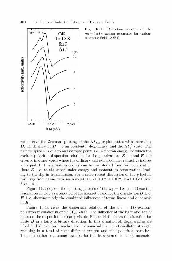
408 16 Excitons Under the Influence of External Fields
Fig. 16.1. Reflection spectra of thenB = 1AΓ5-exciton resonance for variousmagnetic fields [82B1]
we observe the Zeeman splitting of the AΓ1,2 triplet states with increasingB, which show at B = 0 an accidental degeneracy, and the AΓL
5 state. Thenarrow spike S is due to an isotropic point, i.e., a photon energy for which theexciton polariton dispersion relations for the polarizations E ‖ c and E ⊥ ccross or in other words where the ordinary and extraordinary refractive indicesare equal. In this situation energy can be transferred from one polarization(here E ‖ c) to the other under energy and momentum conservation, lead-ing to the dip in transmission. For a more recent discussion of the g-factorsresulting from these data see also [60H1, 60T1, 02L1, 03C2, 04A1, 04M1] andSect. 14.1.
Figure 16.3 depicts the splitting pattern of the nB = 1A- and B-excitonresonances in CdS as a function of the magnetic field for the orientation B ⊥ c,E ⊥ c, showing nicely the combined influences of terms linear and quadraticin B.
Figure 16.4a gives the dispersion relation of the nB = 1Γ5-exciton-polariton resonance in cubic (Td) ZnTe. The influence of the light and heavyholes on the dispersion is clearly visible. Figure 16.4b shows the situation forfinite B in a fairly arbitrary direction. In this situation all degeneracies arelifted and all exciton branches acquire some admixture of oscillator strengthresulting in a total of eight different exciton and nine polariton branches.This is a rather frightening example for the dispersion of so-called magneto-
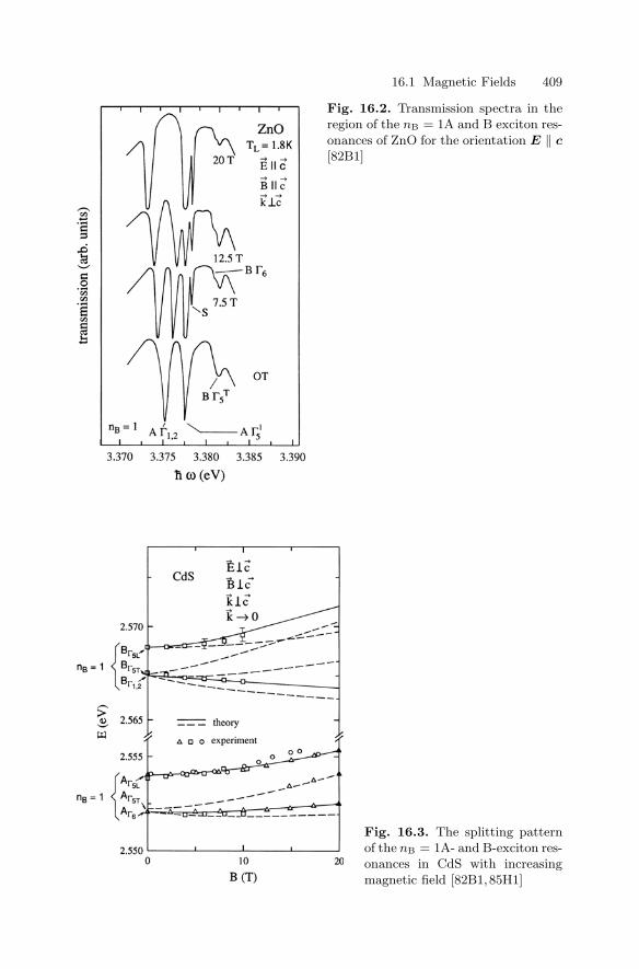
16.1 Magnetic Fields 409
Fig. 16.2. Transmission spectra in theregion of the nB = 1A and B exciton res-onances of ZnO for the orientation E ‖ c[82B1]
Fig. 16.3. The splitting patternof the nB = 1A- and B-exciton res-onances in CdS with increasingmagnetic field [82B1,85H1]
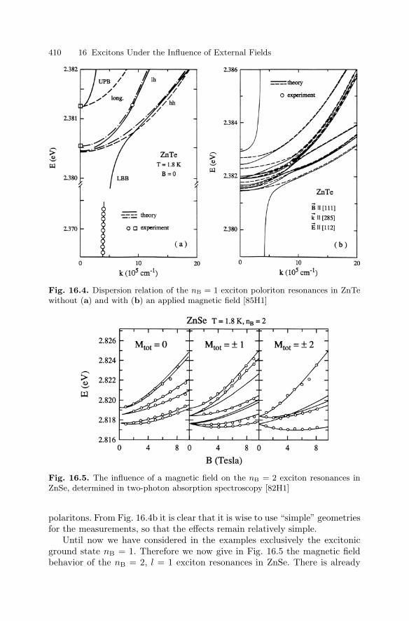
410 16 Excitons Under the Influence of External Fields
Fig. 16.4. Dispersion relation of the nB = 1 exciton poloriton resonances in ZnTewithout (a) and with (b) an applied magnetic field [85H1]
Fig. 16.5. The influence of a magnetic field on the nB = 2 exciton resonances inZnSe, determined in two-photon absorption spectroscopy [82H1]
polaritons. From Fig. 16.4b it is clear that it is wise to use “simple” geometriesfor the measurements, so that the effects remain relatively simple.
Until now we have considered in the examples exclusively the excitonicground state nB = 1. Therefore we now give in Fig. 16.5 the magnetic fieldbehavior of the nB = 2, l = 1 exciton resonances in ZnSe. There is already

16.1 Magnetic Fields 411
a finite splitting for B = 0. For higher fields this splitting increases due toZeeman terms. In addition, there is a pronounced diamagnetic shift due to thelarge radius. The total angular momentum M, consisting of spin and envelopecontributions, could be chosen in the two-photon absorption experiments ofFig. 16.5 by using circular and/or linear polarizations of the two beams (seealso Sects. 19.1 and 25.5).
Similar splitting patterns as for free excitons can also be observed forbound exciton complexes (BEC), where one has to take into account that theB-field influences both the initial and the final state, e.g., in a recombinationprocess from A0X to A0. Examples of the magnetic field behavior of BEC aregiven in [79E1,81B1,82K1,86G1,89G1,04A1,04M1].
At the beginning of this section we noted that the observation of Landaulevels might be difficult, since for most semiconductors the limit γ 1 can bereached only for fields B 102 T, which, if available at all, are usually onlyin pulsed form.
There is, however, a way to overcome this difficulty by investigating thecontinuum states, where the Coulomb interaction still influences the oscillator
Fig. 16.6. The reflectivity in the exciton continuum in ZnO for various magneticfields [73H1]
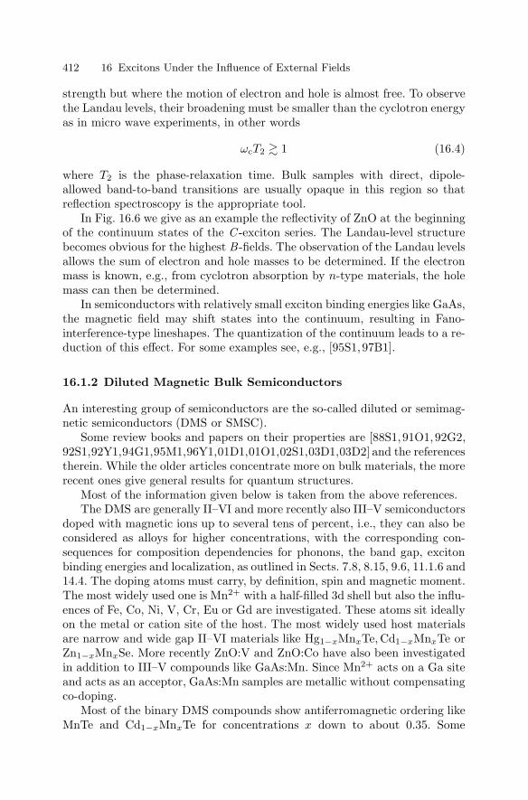
412 16 Excitons Under the Influence of External Fields
strength but where the motion of electron and hole is almost free. To observethe Landau levels, their broadening must be smaller than the cyclotron energyas in micro wave experiments, in other words
ωcT2 1 (16.4)
where T2 is the phase-relaxation time. Bulk samples with direct, dipole-allowed band-to-band transitions are usually opaque in this region so thatreflection spectroscopy is the appropriate tool.
In Fig. 16.6 we give as an example the reflectivity of ZnO at the beginningof the continuum states of the C -exciton series. The Landau-level structurebecomes obvious for the highest B -fields. The observation of the Landau levelsallows the sum of electron and hole masses to be determined. If the electronmass is known, e.g., from cyclotron absorption by n-type materials, the holemass can then be determined.
In semiconductors with relatively small exciton binding energies like GaAs,the magnetic field may shift states into the continuum, resulting in Fano-interference-type lineshapes. The quantization of the continuum leads to a re-duction of this effect. For some examples see, e.g., [95S1,97B1].
16.1.2 Diluted Magnetic Bulk Semiconductors
An interesting group of semiconductors are the so-called diluted or semimag-netic semiconductors (DMS or SMSC).
Some review books and papers on their properties are [88S1,91O1,92G2,92S1,92Y1,94G1,95M1,96Y1,01D1,01O1,02S1,03D1,03D2] and the referencestherein. While the older articles concentrate more on bulk materials, the morerecent ones give general results for quantum structures.
Most of the information given below is taken from the above references.The DMS are generally II–VI and more recently also III–V semiconductors
doped with magnetic ions up to several tens of percent, i.e., they can also beconsidered as alloys for higher concentrations, with the corresponding con-sequences for composition dependencies for phonons, the band gap, excitonbinding energies and localization, as outlined in Sects. 7.8, 8.15, 9.6, 11.1.6 and14.4. The doping atoms must carry, by definition, spin and magnetic moment.The most widely used one is Mn2+ with a half-filled 3d shell but also the influ-ences of Fe, Co, Ni, V, Cr, Eu or Gd are investigated. These atoms sit ideallyon the metal or cation site of the host. The most widely used host materialsare narrow and wide gap II–VI materials like Hg1−xMnxTe,Cd1−xMnxTe orZn1−xMnxSe. More recently ZnO:V and ZnO:Co have also been investigatedin addition to III–V compounds like GaAs:Mn. Since Mn2+ acts on a Ga siteand acts as an acceptor, GaAs:Mn samples are metallic without compensatingco-doping.
Most of the binary DMS compounds show antiferromagnetic ordering likeMnTe and Cd1−xMnxTe for concentrations x down to about 0.35. Some

16.1 Magnetic Fields 413
others are ferromagnetic like Ga1−xMnxAs or Ga1−xMnxN or ZnO:V andZnO:Co [98O1,00D1,02D1,02S2,02S3]. The ferromagnetism can be influencedby the concentration of free carriers e.g. holes in GaAs:Mn. Their density canbe decreased by codoping with a donor. Similarly codoping with a donor likeGa or Al increases the electron density in ZnO:V or ZnO:Co.
At low concentration they are paramagnetic with very high saturationmagnetization and can exhibit spin glass behavior at low T .
We now start to list more of the specific semimagnetic properties forbulk DMS.
The main point is that the exchange interaction occurs between thes- and/or p-type conduction and valence bands of the host and the 3d or-bitals of the magnetic ions, known as sp-d exchange. A free or bound carriercan polarize the magnetic moments of the surroundings, e.g., Mn2+ ions. Thisfact results in extremely high Zeeman splitting and effective g-factors forboth the free or bound carriers and for the excitons. The effective g-factorscan reach values up to 100 and the Zeemann splitting saturates at valuesbetween 10 and 100meV for fields of a few T. Both the splitting values andthe g-factors are thus by one or two orders of magnitude larger than in non-magnetic semiconductors. We give an example in Fig. 16.7 that can be com-pared, e.g., to Figs. 16.1–16.3. These large values of the Zeeman splitting arealso held responsible for the large values of Faraday and Kerr rotation ob-
Fig. 16.7. (a) Zeeman splitting of the exciton of Cd0.9Mn0.1Te as a function ofmagnetic field in the Faraday configuration, i.e., k ‖ B. (b) Saturation Zeemansplitting per average Mn2+ spin per cation site [88G1]

414 16 Excitons Under the Influence of External Fields
served in transmission and reflection geometries, respectively. For examplessee, e.g., [78G1].
Free and even more bound carriers can form so-called magnetic polarons.This is a carrier surrounded by a magnetization cloud of oriented Mn2+ mo-ments in a similar way as a usual carrier can be surrounded by a phonon cloudforming a polaron (see Sect. 8.6). The formation time of a magnetic polaronafter creation of a carrier (e.g., by optical excitation) is finite and in the rangeof 100 ps or longer. The formation of the magnetic polaron cloud lowers theenergy of the carrier. This energy decreases with increasing temperature andincreasing external magnetic field [92Y1,96Y1].
In narrow gap DMS one observes with increasing magnetic field well-resolved Landau-level fans [91O1]. Mn2+ ions in II–VI DMS show an internaltransition resulting in a luminescence band around 2.2 eV, i.e., in the yellowspectral range and absorption features starting at or above this energy whenthe band gap, or better exciton energies, are situated above theses transitions.This is the case for Cd1−xyMnxTe approximately for x > 0.4 [84L1].
For a collection of data see, e.g., [82L1] of Chap. 1.
16.1.3 Semiconductor Structures of Reduced Dimensionality
In quasi two-dimensional systems the transmission spectra are easily measuredif the substrate is transparent or has been removed by selective etching. If bothconditions are not fulfilled, there remain the techniques applicable to bulkmaterials, i.e., photoluminescence, photoexcitation or reflection spectroscopy.
Many properties are similar to bulk samples, e.g., there is a diamagneticshift proportional to the area of the exciton in the quantum well if B isnormal to it, there is a Zeeman splitting, and there are Landau levels. See,e.g., [92B2,92O1,92R1,92S1,95B1,01K1,03S1] or [01L1] of Chap. 1.
It should be noted that the electron and hole states are fully quantized inall three directions for a magnetic field normal to the quantum well.
In Fig. 16.8 we give an example for the development of the Landau-levelsof a GaAs quantum well sample with 8.5 nm-wide wells for magnetic fields upto 12T.
The two features at lowest energy, the heavy and light hole excitons, areonly weakly affected by B but energetical above them beautifully developsthe fan of Landau levels.
Apart from similarities to bulk materials there are also new phenomena:Due to the strong anisotropies of quantum wells and wires, the magnetic
field effects depend not only on its orientation to the crystallographic axesbut also on its orientation relative to the well or wire, e.g., [96O1].
A further effect comes from the well-width dependence of the lateral partof the wavefunctions. With decreasing well width the wave function pene-trates deeper into the barrier. Consequently the influence of the magneticproperties of the barrier, e.g., of its g-factors, grows. In Fig. 16.9 we give twoexamples. The electron g-factor is negative in GaAs and positive in AlAs.

16.1 Magnetic Fields 415
Fig. 16.8. The linear magneto absorption spectra for two different circular polar-izations of the light (a, b) The resulting contour plots (c, d) [91S1,92S1]
Consequently ge increases with decreasing well width of GaAs/Al1−yGayAs(a) or GaAs/AlAs structures and even exhibits a change of sign. Further-more one observes a variation of gh with lz and a dependence on the ori-entation of the magnetic field being either perpendicular or parallel to thequantum well.
For an example of Si/Si0.76Ge0.24 quantum wells see [00P1].In diluted magnetic semiconductors the magnetic ions can be incorpo-
rated into one or both barriers or into the well itself, allowing informationon the interface to be obtained [94G1]. The huge Zeeman splitting and theformation of bound or free magnetic polarons have been investigated, e.g.,in [92G1,92Y1,96Y1]. Due to the huge Zeeman splitting it might even bepossible to change the band alignment from type I to type II by a magnetic

416 16 Excitons Under the Influence of External Fields
Fig. 16.9. Dependence of electron (and hole) g-factors on the well width and onthe orientation of B in GaAs/Al1−yGayAs (a) and GaAs/AlAs structures (b). In(b) the transition from a type I to a type II band alignment is also indicated (seeSect. 15.2) [92I1,95H1]
field if the respective band offset is small [86B1,91J1,94F1,03C1] or [01L1]ofChap. 1.
For biexciton states in diluted magnetic semiconductor quantum wells inhigh magnetic fields see [01M1].
To conclude this section we give some references on excitonic magnetooptics in quantum wires and dots, which allow the reader to become familiarwith this field of research.
For microstructured, V-groove and T-shaped quantum wires see, e.g.,[94P1, 95O1, 96W1, 98B1, 98L1, 00L1, 01K1, 02M1]. For DMS wire structuressee [00O1,00T1,01I1,01K2], for self-organized quantum islands including DMSsee [96R1, 99B1, 99B2, 00K1, 01K1, 02B1, 02M1, 03C1, 03P1] and for quantumdots in insulating matrices see [94N1,97O1,98K1,99G1].
16.2 Electric Fields
In the same way that we know the quadratic (diamagnetic) and linear (Zee-man) effects of a B-field from atomic physics and now also for excitons insemiconductors we can guess what will happen if we apply a static electricfield Es to the exciton resonances in semiconductors. For the ac or opticalStark effect see Sect. 20.4. There will be a Stark effect, i.e., a shift (and split-ting) of the exciton resonances, usually quadratic but possibly also linear inEs. The influence of Es on the band-to-band transitions, i.e., on the con-tinuum states is also known as the Franz–Keldysh effect. The tilting of the

16.2 Electric Fields 417
bands by an applied static electric field Es allows, in this case, the Bloch-typeelectron and hole wave functions to tunnel into the forbidden gap thus re-sulting in a red-shift of the band-to-band absorption tail and the appearanceof an oscillatory structure above, i.e., in the continuum states. The modifica-tions of the absorption spectra due to Es also influence the refractive index inthe transparent spectral region below the exciton resonances according to theKramers–Kronig relations (Chap. 6), resulting in Pockels- or Kerr-effect-likephenomena, which describe the modification of an existing or the introductionof a new birefringence, depending linearly or quadratically on Es, respectively.We shall concentrate here on the influence of Es on the eigenfrequencies.
16.2.1 Bulk Semiconductors
The observation of the Stark effect for excitons in three-dimensional (or bulk)samples is not easy, for the following reason: To get an observable shift of theeigenstates, the “electric field energy” eEsaB should be comparable with thespectral width of the absorption bands, i.e. at low temperatures,
eEsaB ∆LT . (16.5)
Equation (16.5) requires fields of the order of 106 Vm−1 depending on thematerial parameters. On the other hand, such fields broaden or even destroythe exciton resonances due to two effects. One is field ionization of the exciton,by tunneling through the finite Coulomb barrier at finite fields, as illustratedin Fig. 16.10. The other is impact ionization; this means that carriers whichare always present in a semiconductor at finite temperature can gain suchhigh energies in the electric field, that they can ionize an exciton if they hitit, resulting in two more carriers and a collision-broadening of the exciton
Fig. 16.10. The Coulomb potential of a three-dimensional exciton without (a) andwith (b) an applied constant electric field

418 16 Excitons Under the Influence of External Fields
resonance. For the above reason, not too many successful attempts have beenreported to observe the Stark effect for excitons in bulk materials directly.
Instead, small modifications occurring at low fields have usually been usedin modulation spectroscopy [67G1, 69C1, 70H1, 71M1, 73S1, 76H1, 82L1, 84S1,85S1].
Some (early) references for the observation of the Stark effect of excitons ininorganic semiconductors like CdS, CdSe or CuCl are [69H1,70M1,71L1,73R1]and for organic ones [73B1].
Examples for the Franz–Keldysh effect in bulk semiconductors can befound, e.g., in [71S1, 73B2, 76B1] and for the Pockels effect, e.g., in ZnOin [70M1,71M1].
In Fig. 16.11 we show an example for the quadratic Stark effect of thenB = 1 exciton in CdS. The shift and a slight broadening of the excitonicabsorption band are clearly visible.
As mentioned above, the Franz–Keldysh oscillations appear in the band-to-band transition region. The energies of the alternating maxima and minimaEn follow the relation [04G1]
(En − Eg)3/2 ∼ n (16.6)
In Fig 16.12 we show modulation spectra of GaAs samples at 100 K exhibitingthe Franz-Keldysh effect and the verification of (16.6). The Franz–Keldysheffect has been induced by a surface electric field.
In Fig. 16.13 we give results of a rather unusual type of excitation spec-troscopy. A GaSe sample is illuminated with monochromatic light through
Fig. 16.11. Influence of an exter-nal field on the absorption spec-trum of the B, nB = 1 excitonof CdS for various applied electricfields [71L1]

16.2 Electric Fields 419
Fig. 16.12. Franz–Keldysh oscil-lations observed in a GaAs sam-ple (a) and the relation (16.6) (b)[95L1,04G1]
Fig. 16.13. Photovoltage excitation spectra of GaSe. The spectra are normalizedin the continuum regime and shifted for clarity [02G1]

420 16 Excitons Under the Influence of External Fields
a semitransparent Au electrode and the photovoltage that develops betweenthe contacts is measured as a function of the photon energy. This type of pho-tovoltage excitation spectroscopy gave different spectra depending on sampletemperature.
At low temperature one only sees the continuum transitions superimposedby some oscillatory structure, possibly Franz–Keldysh oscillations, which mayresult from the built-in field of the Schottky contact. With increasing tem-peratures these oscillations disappear and the exciton resonance shows up,shifts with the band gap and broadens. The exciton resonance is probablysuppressed at low temperatures by field ionization in the Schottky barrier.Which features dominate depends on the various length scales like the exten-sion of and field strength in the Schottky barrier or the penetration depth ofthe light.
16.2.2 Semiconductor Structures of Reduced Dimensionality
The problem of field ionisation in bulk semiconductors can be overcome byconfining the electron and hole between barriers, e.g., in quantum wells, wiresor dots, as shown schematically in Fig. 16.14. With increasing Es orientedperpendicular to the layers the electron and hole shift into their respective cor-ners, reducing their energetic separation. This results in a roughly quadraticredshift of the gap and thus of the exciton resonance.
The overlap between electron and hole wavefunction is thereby reduced,resulting in a decrease of the oscillator strength and a decrease of the ex-citon binding energy. This latter effect, however, is only a small correctionto the reduction of the energetic separation of the first quantized levels.In addition the selection rule ∆nz = 0 is relaxed because Es mixes stateswith odd and even parity, inducing some transitions which are forbidden forEs = 0. For a detailed elaboration of this so-called quantum-confined Starkeffect (QCSE) see [85M1, 86M1]. All three above-mentioned effects, namelythe redshift of the exciton, the decrease of its oscillator strength, and theappearance of forbidden transitions, are illustrated in Fig. 16.15, where thisquantum-confined Stark effect is shown for an InP1−yGayAs based MQWlocated in the intrinsic region of a reverse-biased pin diode as shown inthe inset.
For the quantum confined Stark effect in Si1−yCy/Si quantum wells see,e.g., [99F1] and the references therein.
If an electron moves in a quantum well in an electric field normal to thewell, the spin of the electron precesses due to spin-orbit coupling. This effectallows the manipulation of the electron spin as shown in [03R1].
The application of an electric field normal to the planes of superlatticesshifts adjacent wells energetically with respect to each other by an amount
∆E = e |Es| · d (16.7)

16.2 Electric Fields 421
where Es is the applied field and d is the superlattice period. This fact de-stroys the origin of the miniband formation namely the overlap of the levelsof adjacent wells with equal energy. Instead one obtains a so-called Wannier–Stark ladder. An example will be shown later in Sect. 23.2 in connection withthe Bloch oscillations. Further examples can be found, e.g., in [93M1, 94Y1]or Ref. [01L1] of Chap. 1
For the observation of the quantum confined Stark effect in quantum wiressee, e.g., [99W1] and the references therein.
The quantum confined Stark and Franz–Keldysh effects are also known forquantum dots in insulating matrices or for (self-assembled) quantum islandsin quantum wells. For references see, e.g., [88M1,90E1,98H1,02W1].
The electric field of charges trapped in the vicinity of quantum dots andislands is also (at least partly) responsible for the abrupt steps in the emissionenergy of single dots. For examples see [89H1,90R1,92N1,93W1,98R1,99E1,01F1,01K3,01K4].
Electroluminescence of quantum dots has been reported in [97A1,02C1].Phenomena like that of Fig. 16.15 lead into the regime of opto-electronics
or electro-optics, to which we shall return briefly in Sect. 24.1.5 and 24.2.
Fig. 16.14. The bandstructure of a quantum well without (a) and with (b) anapplied constant electric field perpendicular to the wells, but neglecting the Coulombinteraction between electrons and holes

422 16 Excitons Under the Influence of External Fields
Fig. 16.15. The quantum-confined Stark effect in InGaAs MQW samples [87B1]
16.3 Strain Fields
The third external perturbation which we shall consider here are mechanicalstrain fields. The crucial quantity which enters here is the dependence of theenergy of the band extrema on the strain, the so-called deformation potential.It is defined for conduction and valance band by (see (8.21))
Ξ = adEc,v
dx(16.8)
where a is the lattice constant, dEc,v is the shift of the band edge caused bya length variation of the unit cell by an amount dx. Deformation potentialsare defined for various types of strain like hydrostatic, uniaxial or shear strain.For details see, e.g., [82L1,96Y1] of Chap. 1 or Sect. 8.6.
For excitons the relevant quantity is the sum of the deformation potentialsof conduction and valence bands. As in the case of magnetic and electric fields,an applied stress changes the eigenenergies of the exciton states and mayalso lead to a splitting of degenerate states, if the resulting strain is orientedsuch that it reduces the symmetry of the crystal. The latter situation is e.g.realized when stress is applied perpendicular to the crystallographic c axis ofa uniaxial material (e.g., the Wurtzite structure) where it lifts the degeneracyin the plane perpendicular to c, but not if the stress acts in the direction of c.This orientation leads only to a shift of eigenenergies but not to a splittingsince the symmetry is not changed. For details see Chap. 26 on group theory.

16.3 Strain Fields 423
16.3.1 Bulk Semiconductors
We now give various examples: Figure 16.16 shows reflection spectra of CdS forzero and finite stress perpendicular to the c axis. The shift and the splitting ofthe nB = 1AΓ5 and BΓ5 exciton resources and the variation of their oscillatorstrengths are obvious. Measurements of this type can be used to determinethe deformation potentials. For materials with zinc-blende structure see [70L1,79T1,79R1].
Since bound exciton complexes (BEC) often have very narrow absorptionand emission bands (Sect. 14.1) one can easily study the influence of magneticor strain fields, which affect both the ground and the excited state as alreadymentioned above. In Fig. 16.17 we give the shift of the luminescence of a BECin ZnO which shows clearly the influence of the strain. According to thestatement given above, a shift but no splitting occurs for the orientation S ‖ cin contrast to the situation of Fig. 16.16. For more details see [68S1].
Recently the influence of strain acquired new importance in the field ofepitaxial growth of heterolayers.
There are two contributions to the “biaxial” strain, which occurs in theplane of epitaxial growth, and which can be considered as a superpositionof a hydrostatic and a uniaxial strain. One contribution to the strain al-ready arises during the growth process if the lattice constants of substrateand layer do not coincide at growth temperature. The first epitaxial lay-
Fig. 16.16. The excitonic reflection spectra of CdS under uniaxial stress [70L1]

424 16 Excitons Under the Influence of External Fields
Fig. 16.17. The shift of a BEC lumines-cence line in ZnO under the influence ofstrain [68S1]
ers will often grow with some strain, trying to match the lattice constantof the substrate. With increasing layer thickness it is energetically morefavorable for the layer to create a dislocation network which relaxes thestrain [85P1, 87D1], or to form islands. This latter growth mode is knownas Stronski–Krastanov mode. See Sect. 8.13. Sometimes a small residualstrain remains, independent of the layer thickness [92W1, 92W2, 92G1]. Thecritical thickness lc for the onset of dislocation formation depends on thelattice misfit, on the elastic constants of the epilayer, on the energy nec-essary to produce the dislocations, on the surface energies etc. It can beas small as a few atomic layers only. The dislocation network explainsthe function of a buffer layer or a short period superlattice, which are of-ten used if two materials of different lattice constant are grown on topof each other. In this case the crystalline quality of the interface is con-siderably poorer than that of the surface of the layer after a thickness ofabout 0.1 µm.
The other part of the biaxial strain arises during the cooling from thegrowth temperature to the temperature at which the (optical) measurementsare performed if the coefficients of thermal expansion are different for sub-strate and layer, as is usually the case. A part of this thermal strain cansometimes be accommodated by modifications in the dislocation network. InFig. 16.18 we show reflection spectra in the region of the nB = AΓ5 and BΓ5
excitons in CdS grown on SrF2.Since the cubic SrF2 substrate was oriented (111), the hexagonal CdS
grows with the c axis perpendicular to the interface. Consequently the C6v

16.3 Strain Fields 425
symmetry is not affected by the biaxial strain, but the eigenenergies areshifted. The bulk values for the longitudinal eigenenergies (or the reflec-tion minima) are given by the vertical lines. In agreement with the discus-sion above, we see that the excitons are shifted and that this shift is dif-ferent at the interface and the surface. Furthermore, the damping is largerat the interface than at the surface due to the dislocations in the formerregion.
In contrast to Fig. 16.18, we show in Fig. 16.19 a luminescence spectrumof the cubic material ZnTe grown on GaAs(00l). In this case, the biaxial strainreduces the cubic Td symmetry of bulk ZnTe and the Γ5 exciton of Sect. 13.1splits into its light and heavy hole components.
Splittings as in Fig. 16.19 also play a role in strained-layer superlattices inaddition to the mass-dependent quantization energies.
The biaxial in-plane tensile strain results essentially from the differentthermal expansion coefficients of the GaAs and ZnTe layers since the ZnTelayer thickness of 2 µ m is well above lc and the ZnTe layer grows with its ownlattice constant.
Inhomogeneous strain can be used to create potential traps for excitons.See, e.g., Sect. 21.3 for Si or Ge and [03N1] for Cu2O. However, strain resultingfrom the fixation of the sample on the holder in a cryostat is usually unwantedand should be avoided.
Fig. 16.18. Reflection spectra of the nB = 1AΓ5 and BΓ5 excitons of a CdS layergrown on SrF2 and measured at the surface and at the interface. The positions ofthe longitudinal eigenenergies in the bulk are indicated by vertical arrows [92B1]

426 16 Excitons Under the Influence of External Fields
Fig. 16.19. Luminescence spectrum of a ZnTe layer grown on GaAs (001), showingthe strain-induced splitting of the light and heavy hole nB = 1 exciton resonances[92G1,92W1,92W2]. Compare with Fig. 16.4a
16.3.2 Structures of Reduced Dimensionality
The above-mentioned strain-induced splitting of the Γ8 valence band is ofspecial importance for strained quantum wells and superlattices whenevera layer is grown with a lattice constant different from that of the substrate.
A two-dimensional tensile strain in the plain of the layer is usually ac-companied by a uniaxial compressive strain normal to it and vice versa. Theresults of this strain on the width of the gap and on the arrangement of thehh and lh valence bands is shown schematically in Fig. 16.20 and verified fortensile strain, e.g., in Fig. 16.19.
In quantum wells and superlattices (and in structures of even lower quasi-dimensionalities) the strain induced effects come in addition to the quantiza-tion energies, which are always larger for the lh exciton compared to the hh.Consequently, strain effects may enhance or reduce the splitting caused byconfinement. For strained superlattices one frequently uses a substrate witha lattice constant situated between the values of the two different layer mate-rials of the superlattice resulting in so-called strain symmetrized superlatticesbecause the layers show alternating compressive and tensile strain. A similarsituation can be reached in “free standing” superlattices, which occur whenthe thickness of the superlattice is so thick that the coherence of its latticeconstant to the substrate is lost, e.g., by the formation of dislocations.
While many III–V systems can be grown lattice-matched to GaAs, InAsor InP substrates, the II–VI and IV–IV systems are usually strained, as seenin Fig. 8.31. Typical examples are, e.g., Si1−yGey/Si superlattices (e.g. [97K1]and references above), CdS/ZnS [97H1] or CdS/ZnSe [99P2,01D1].

16.4 Problems 427
E E E
CB
EgEg
Eg
VB
k k k
lh
lh
lh
hhJz
hh
hh
Jz
=
=
±
±
3
1
_
_
2
2
h
h
Γ8
Γ6
a b c
Fig. 16.20. Schematic drawing of the influence of strain on the alignment of the hhand lh valence bands and on the value of the gap (a) zero strain (b) two-dimensionaltensile strain and normal uniaxial compressive strain (c) and two-dimensional com-pressive strain and normal uniaxial tensile strain. See also Fig. 8.32
For the creation of an inhomogeneous strain, acting as a potential trap forexcitons in quantum wells see, e.g., [99N1].
Phase transitions from zincblende or wurtzite to the rock salt structurecan be induced by high hydrostatic pressures. For examples see [93T1,94T1].
16.4 Problems
1. Typical values of the deformation potential are around 10 eV. What is theshift of the band edges for ∆a/a = 10−3?
2. Do you expect the band-gap shifts due to the lattice deformation by acous-tic and by optical phonons to be identical or not? Why?
3. Calculate the diamagnetic shift at B = 10 T for excitons characterizedby Eb
ex = 5 meV, ε = 15 and by Ebex = 100meV, ε = 6, respectively.
4. Calculate the Zeeman splitting for a spin singlet and a triplet exciton fornB = 1, ge = 1.6 and gh = 2.2. What is the difference if at B = 0 the twostates already show a finite energy splitting δ?
5. Do you expect that the linear Stark effect can occur for nB = 1 and/orfor nB = 2 excitons? Why?
6. Calculate in the simplest approximation the Stark shift for excitons withthe data given in connection with Problem 3 and for an electric fieldstrength E of 103 Vm−1, 106 Vm−1, and 10−2Eb
ex(eaB)−1.7. Calculate the quantum confined Stark effect by perturbation theory for
a quantum well with infinitely high barriers and the other data as for thehh exciton in GaAs or InAs. Compare with experimental data.

428 16 Excitons Under the Influence of External Fields
References to Chap. 16
[08V1] W. Voigt, Magneto- und Elektrooptik, Teubner, Leipzig (1908)[60H1] J.J. Hopfield, J. Phys. Chem. Solids 15, 97 (1960)[60T1] D.G. Thomas, J. Phys. Chem. Solids 15, 86 (1960)[67G1] E. Gutsche and H. Lange, phys. stat. sol. (b) 22, 229 (1967)[68S1] Chr. Solbrig, Z. Phys. 211, 429 (1968)[69C1] M. Cardona, Modulation Spectroscopy, Academic, New York (1969)[69H1] C. Gahwiller and G. Harbeke, Phys. Rev. 185, 1147 (1969)[70H1] N. Hase and M. Onuka, J. Phys. Soc. Jpn. 28, 965 (1970)[70L1] D.W. Langer et al., Phys. Rev. B 2, 4005 (1970)[70M1] E. Mohler, phys. stat. sol. 38, 81 (1970)[71L1] H. Lange, phys. stat. sol. (b) 48, 791 (1971)[71M1] O.W. Madelung and E. Mollow, Z. Physik A 249, 12 (1971)[71S1] B. Stone and Y. Brada, Bull Isr. Phys. Soc. 21 (1971)[73B1] L.M. Blinov and N.A. Kirchenov, Sov. Phys. Sol. State 8, 2163 (1973)[73B2] B.A. Bobylev, A.F. Kravchenko and A.S. Terekhov, Sov. Phys. Semicond.
6, 1635 (1973)[73H1] K. Hummer, phys. stat. sol. (b) 56, 249 (1973)[73R1] B.S. Razbirin, I.N. Uraltsev and A.A. Bogdanov, Sov. Phys. Sol. State 15,
604 (1973)[73S1] B.O. Seraphin, ed., Modulation Spectroscopy, North-Holland, Amsterdam
(1973)[76B1] B. Buckel, U. Birkholz and K. Ziegler, phys. stat. sol. (b) 78, K23 (1976)[76H1] Y. Hamakawa and T. Nishino, in Optical Properties of Solids, New Devel-
opments, ed. by B.O. Seraphim, North-Holland, Amsterdam, p 255 (1976)[78G1] J.A. Gaj et al., Solid State Commun. 28, 193 (1978) and ibid 29, 435
(1979)[79E1] Excitons, K. Cho, ed., Topics Curr. Phys. Vol. 14, Springer, Berlin, Hei-
delberg (1979)[79R1] R. Ranvaud et al., Phys. Rev. B 20, 701 (1979)[79T1] H.-R. Trebin, U. Rossler and R. Ranvaud, Phys. Rev. B 20, 686 (1979)[81B1] G. Blattner et al., phys. stat. sol. (b) 107, 105 (1981)[82A1] Application of High Magnetic Fields in Semiconductor Physics,
G. Landwehr, ed., Lecture Notes Phys. Vol. 177, Springer, Berlin, Hei-delberg (1982)
[82B1] G. Blattner et al., Phys. Rev. B 25, 7413 (1982)[82H1] H.W. Holscher, A. Nothe and Ch. Uihlein, Physica B 117/118, 2379 (1982)[82K1] C. Klingshirn in [82A1], p 214[82L1] M.V. Lebedev and V.G. Lyssenko, Sov. Phys. Sol. State 24, 1721 (1982)[84L1] Y.R. Lee and A.K. Romdas, Solid State Commun. 51, 861 (1984)[84S1] L. Schultheis and J. Lagois, Phys. Rev. B 29, 6784 (1984)[85H1] B. Honerlage et al., Phys. Rep. 124, 161 (1985)[85M1] D.A.B. Miller et al., Phys. Rev. B 32, 1043 (1985)[85P1] R. People and J.C. Bean, Appl. Phys. Lett. 47, 322 (1985)[85S1] L. Schultheis and C.W. Tu, Phys. Rev. B 32, 6978 (1985)[86B1] J.A. Brum, G. Bastard and M. Voos, Solid State Commun. 59, 561 (1986)[86G1] J. Gutowski, Solid State Commun. 58, 523 (1986)[86M1] D.A.B. Miller, D.S. Chemla and S. Schmitt-Rink, Phys. Rev. B 33, 6976
(1986)

References to Chap. 16 429
[87B1] I. Bar-Joseph et al., Appl. Phys. Lett. 50, 1010 (1987)[87D1] B.W. Dodson and J.Y. Tsao, Appl, Phys. Lett. 51, 1325 (1987)[88G1] J.A. Gaj in [88S1], p 275[88M1] D.A.B. Miller, D.S. Chemla and S. Schmitt-Rink, Appl. Phys. Lett. 52,
2154 (1988)[88S1] Semiconductors and Semimetals 25, J.K. Furdyna and J. Kossut, eds.,
Academic Press, New York (1988)[89G1] J. Gutowski, NATO ASI Ser. B 200, 139, Plenum, New York (1989)[89H1] F. Hache, D. Ricard and C. Flytzanis, Appl. Phys. Lett. 55, 1504 (1989)[90E1] A.I. Ekimov et al., Journ. of Luminesc. 46, 83 (1990)[90L1] M.V. Lebedev and V.G. Lyssenko, phys. stat. sol. (b) 161, 395 (1990)[90R1] H. Rossmann et al., phys. stat. sol. (b) 159, 287 (1990)[91J1] B.T. Jonker et al., J. Appl. Phys. 69, 6097 (1991)[91O1] M. v. Ortenberg, Festkorperprobleme/Adv. in Solid State Physics 31, 261
(1991)[91S1] S. Schmitt-Rink et al., Appl. Phys. A 53, 491 (1991)[92B1] U. Becker et al., J. Crystal Growth 125, 384 (1992)[92B2] L.V. Butov, Phys. Rev. B 46, 12765, 13627 and 15156 (1992)[92G1] W. Gebhardt, Mater. Sci. Eng. B 11, 1 (1992)[92G2] O. Goede and W. Heimbrodt, Festkorperprobleme/Adv. in Solid State
Physics 32, 237 (1992)[92I1] E.L. Ivchenko and A.A. Kiselev, Sov. Phys. Semicond. 26, 827 (1992)[92N1] S. Nomura and T. Kobayashi, Phys. Rev. B 45, 1305 (1992)[92O1] D. Oberhauser et al., phys. stat. sol. (b) 173, 53 (1992)[92R1] T. Rappen, G. Mohs and M. Wegener, phys. stat. sol. (b) 173, 77 (1992)[92S1] S. Schmitt-Rink, Festkorperprobleme/Adv. Solid State Phys. 31, 243
(1992)[92W1] H.P. Wagner and H. Leiderer, Festkorperprobleme/Adv. Solid State Phys.
32, 221 (1992)[92W2] H.P. Wagner et al., J. Lumin. 52, 41 (1992)[92Y1] D.R. Yakovlev, Festkorperprobleme/Adv. in Solid State Physics 32, 237
(1992)[93M1] E.E. Mendez in [93O1] of Chap. 1, p 181[93T1] R. Tommasi, M. Lepore and I.M. Catalano, Solid State Commun. 85, 539
(1993)[93W1] U. Woggon et al., Phys. Rev. B 48, 1979 (1993)[94F1] J.K. Furdyna, Solid State Electronics 37, 1065 (1994)[94G1] J.A. Gaj et al., Phys. Rev. B 50, 5512 (1994)[94N1] S. Nomura et al., Phys. Rev. B 49, 13571 (1994)[94P1] A.S. Plan et al., Surf. Science 305, 576 (1994)[94T1] S. Tolbert et al., Phys. Rev. Lett. 73, 3266 (1994)[94Y1] M. Yamaguchi et al., Sol. State Electronics 37, 839 (1994)[95B1] L.V. Butov et al., Phys. Rev. B 52, 12153 (1995)[95H1] R.M. Hannak et al., Solid State Commun. 93, 313 (1995)[95L1] D. Liu, MS Thesis, Boston College (1995)[95M1] Materials Science Forum 182-184, H. Heinrich and J.B. Mullin, eds., Trans
Tech. Publ. (1995)[95M2] H. Mariette et al., Annales de Physique, Colloq. C2, Suppl. au no 3, 20,
C2-143 (1995)

430 16 Excitons Under the Influence of External Fields
[95O1] M. Oestreich et al., Europhys. Lett. 31, 399 (1995)[95S1] U. Siegner et al., phys. stat. sol. (b) 188, 361 (1995) and Phys. Rev. B 51,
495 (1995)[96O1] M. Oestreich, S. Hallstein and S. Ruhle, IEEE J. Selected Topics Quant.
Electr. 2, 747 (1996)[96R1] R. Rinaldi et al., Phys. Rev. Lett. 77, 342 (1996)[96W1] H. Weman et al., Phys. Rev. B 53, 6959 (1996)[96Y1] D.R. Yakovlev, Comments Cond. Mat. Phys. 18, 51 (1996)[97A1] M.V. Artemyev, V. Sperling and U. Woggon, J. Appl. Phys. 81, 6975
(1997)[97B1] S. Bar-Ad, Phys. Rev. Lett. 78, 1363 (1997)[97H1] M. Hetterich et al., Phys. Rev. B 56, 12396 (1997)[97K1] S. Kim et al., Phys. Rev. B 55, 7130 (1997)[97O1] Y. Oka, phys. stat. sol. (b) 202, 795 (1997)[97P1] Proc. Intern. Conf. on High Magnetic Fields in Semiconductors,
G. Landwehr and W. Ossau, eds., Vols. 1 and 2, World Scientific, Sin-gapor (1997)
[97S1] A.A. Sivenko in [97P1], Vol. 2, p 561[98B1] M. Bayer et al., Phys. Rev. B 57, 6584 (1998)[98H1] W. Heller, U. Bockelmann and G. Abstreiter, Phys. Rev. B 57, 6270 (1998)[98K1] M Kuno et al., J. Phys. Chem. B 102, 9245 (1998)[98L1] W. Langbein et al., J. Opt. Soc. Am. 256, 86 (1998)[98O1] H. Ohno, Science 281, 951 (1998)[98R1] S. Raymond et al., Phys. Rev. B 58, R13415 (1998)[99B1] M. Bayer et al., Phys. Rev. Lett. 82, 1748 (1999)[99B2] M. Bayer et al., Phys. Rev. B 60, R8481 (1999)[99E1] S.A. Empedocles et al., Adv. Matr. 11, 1243 (1999)[99F1] S. Fukatsu et al., J. Luminesc. 80, 429 (1999)[99G1] J.A. Gupta, Phys. Rev. B 59, 10421 (1999)[99N1] V. Negoita, D.W. Snoke and K. Eberl, Appl. Phys. Lett. 75, 2059 (1999)
and Phys. Rev. B 60, 2661 (1999)[99P1] J. Puls et al., Phys. Rev. B 60, R16303 (1999)[99P2] S. Petillon et al., J. Crystal Growth 201/202, 453 (1999)[99W1] H. Weman et al., Appl. Phys. Lett. 74, 2334 (1999)[00D1] T. Dietl et al., Science 287, 1019 (2000)[00F1] P.W. Fry et al., Phys. Rev. Lett. 84, 733 (2000)[00K1] M. Keim et al., J. Appl. Phys. 88, 7051 (2000)[00L1] A. Lorenzoni et al., phys. stat. sol. (a) 178, 239 and 243 (2000)[00O1] Y. Oka et al., Proc. SPIE 4086, 62 (2000)[00P1] C. Penn et al., Phys. Rev. B 61, 13055 (2000)[00T1] N. Takahashi et al., J. Appl. Phys. 87, 6569 (2000)[01D1] A. Dinger et al., Phys. Rev. B 64, 225310 (2001)[01F1] J.J. Finley et al., Phys. Rev. B 63, 073307 (2001)[01I1] H. Ikada et al., Physica E 10, 373 (2001)[01K1] R. Kotlyar et al., Phys. Rev. B 63, 085310 (2001)[01K2] F.V. Kyrychenko and J. Kossut, Physica E 10, 378 (2001)[01K3] T.D. Krauss et al., J. Phys. Chem. B 105, 1725 (2001)[01K4] M. Kuno et al., J. Chem. Phys. 115, 1028 (2001)[01M1] H. Mino et al., Physica B 289, 421 (2001)

References to Chap. 16 431
[01O1] M. Oestreich et al., Adv. in Solid State Physics 41, 173 (2001)[02B1] F.J. Brieler et al., Chem. Eur. J. 8, 185 (2002)[02C1] S. Coe et al., Nature 420, 800 (2002)[02D1] T. Dietl, Semicond. Science and Technol. 17, 377 (2002)[02G1] O. Gogolin, M. Schmidt and M. Dremel, private communication (2002)[02L1] W.L. Lambrecht et al., Phys. Rev. B 65, 075207 (2002)[02M1] J.R. Madureira et al., Phys. Rev. B 66, 075332 (2002)[02M2] N. Miura et al., Physica E 13, 263 (2002)[02S1] Semiconductor Spintronics, H. Ohno, ed., Semicond. Science and Technol.
17, Issue 4 (2002)[02S2] S. Sonda, IEEE Trans. Mag. 38, 2859 (2002)[02S3] K. Sato and H. Katayama-Yoshida, Semicond. Science and Technol. 17,
367 (2002)[02W1] O. Wolst et al., Physica E 13, 283 (2002) and ibib. E 17, 554 (2003)[03C1] G.P. Collins, Scientific American 288, March, p 13 (2003)[03C2] S.F. Chichibu et al., J. Appl. Phys. 93, 756 (2003)[03D1] T. Dietl, Europhys. News 34, 216 (2003) and phys. stat. sol. b 240, 433
(2003)[03D2] T. Dietl and H. Ohno, MRS Bull 28, 714 (2003)[03N1] N. Naka and N. Nagasawa, phys. stat. sol. (b) 238, 397 (2003)[03P1] R.T. Phillips et al., phys. stat. sol. (b) 238, 601 (2003)[03R1] E.I. Rashba and A.L. Efros, Appl. Phys. Lett. 83, 5295 (2003)[03S1] R.T. Senger et al., Appl. Phys. Lett. 83, 5425 (2003)[04A1] S. Adachi, EXCON 04, Cracow, to be published in J. Lumin.[04G1] G.J. Goldsmith in [81A1]l of Chap. 1, in press[04M1] B. Meyer et al., phys. stat. sol. (b) 241, 231 (2004)

17
From Cavity Polaritons to Photonic Crystals
In this chapter we return briefly to the concept of a Fabry–Perot resonatorin the form of a (micro) cavity and then proceed to the cavity polaritonsas a mixed state between a resonance in a solid (these are generally excitonresonances in quantum wells, wires or dots) and a cavity resonance. Fromthere we reach, via different paths, the presently very active and potentiallyapplication-relevant field of photonic crystals with a subspecies known as pho-tonic band gap materials.
17.1 Cavity Polaritons
We start from an empty cavity and introduce then the concept of a cavitypolaritons.
17.1.1 The Empty Resonator
A one-dimensional Fabry–Perot resonator, etalon or cavity is, in the simplestcase, an arrangement of two plane-parallel, lossless mirrors with a reflectivityclose to unity, i.e., R ≤ 1 at a distance d (see Fig. 17.1a). Concerning thenomenclature, it can be stated that all the above names mean physicallyessentially the same thing. Sometimes the following distinctions are made.
A Fabry–Perot resonator (also known as Perot–Fabry) often has a lengthof many wavelengths like, e.g., the resonators of many gas, dye or solid-statelasers with a consequently narrow spectral longitudinal mode spacing. A cavityoften has a width of only one or a few multiples of λ/2. An etalon is oftenmade of a plane-parallel slab of transparent matter like Al2O3 with dielectricmirrors on both sides to enhance the reflectivity.
We consider here only the case of plane-parallel surfaces. But Fabry–Perotresonators may also have one or two curved, generally spherical mirrors. Thistopic is generally treated in books or articles on laser physics or laser design.

434 17 From Cavity Polaritons to Photonic Crystals
The cavities may be also (micro)spheres ( [01A1, 02A1, 02M1, 03M2] or Ref.[03W1] of Chap. 15) or even cylinders [02K1].
An incident plane, monochromatic wave will be partly reflected and partlytransmitted at each of the two mirrors. If the coherence length is d, then thepartial waves can interfere. In most cases this interference will be destructive,resulting in a reflectivity of the whole structure Rtot ≈ 1 and a transmissionTtot = 1 − Rtot ≈ 0 and a very low field amplitude in the resonator. SeeFig. 17.1b. There are, as already outlined in Sect. 3.1.6, special situationswhen an integer number of half waves fits into the resonator, i.e., if
mλ
2= d or k⊥ = m
π
dm = 1, 2, 3, . . . . (17.1)
In this case all partial waves in the resonator interfere constructively andthe field amplitude in the resonator can considerably exceed the incident oneand the transmission of the whole arrangement is close to unity, althoughthe reflectivity of every single mirror is also close to unity. If the finesse (seeSect. 3.1.6) is sufficiently high, this constructive interference results in thenarrow spikes (dips) in the spectra of Ttot (Rtot) as shown in Fig. 17.1b. Thissituation is shown for m = 2 in Fig. 17.1a.
Fig. 17.1. (a) Schematic drawings of the incident, internal and transmitted fieldsin a Fabry–Perot resonator for normal incidence. (b) The spectra of total transmis-sion T and reflection R as a function of the phase shift δ per roundtrip. (c) Thedecomposition of the incident and transmitted wave vectors for oblique incidence.(d,e) The construction of the dispersion relation from the light cone [01K1]

17.1 Cavity Polaritons 435
We can reformulate ((17.1)) by saying that these so-called eigenmodes ofa Fabry–Perot resonator or cavity or etalon occur for the normal componentof the incident k-vector
k⊥, m = mπ
d; m = 1, 2, 3, . . . (17.2)
or that the modes are equally spaced on the k⊥ axis with a distance
∆k⊥ = k⊥,m+1 − k⊥,m =π
d. (17.3)
For oblique incidence, the wave vector of the incident beam can be decomposedin components parallel and normal to the resonator as shown in Fig. 17.1c:
k = k‖ + k⊥ . (17.4)
The normal component has to fulfill (17.2) for the resonator modes, whilea conservation law holds for k‖ in reflection and transmission, due to thetranslational invariance of the problem in the plane of the resonator (seeNoether’s theorem in Sect. 3.1.3).
For photons, i.e., for the quanta of light in vacuum, the dispersion is a conewhen we plot ω over a two-dimensional k-plane. The cross section of this conewith a fixed k⊥m is a parabola as shown in Fig. 17.1d. The photon energy ωm
belonging to k⊥m isEm = ωm = ck⊥m . (17.5)
This energy corresponds to the minimum of the dispersion relation of a reso-nator as shown in Fig. 17.1e.
If one tilts a Fabry–Perot resonator in a parallel light beam away fromnormal incidence, i.e., away from k‖ = 0 the photon energy of the transmittedmode shifts of higher values, i.e., to shorter wavelength. This effect is slightlycounterintuitive, but can be easily verified when viewing an incandescent lampthrough a line interference filter and tilting this filter.
If a semiconductor physicist sees a parabolic dispersion relation, the effec-tive mass concept comes immediately to mind. The effective mass connectedwith the curvature is given by (see Sect. 8.5):
1/meff =∂2
∂k2ω (k) (17.6)
and it turns out that meff is something like the “rest mass” of the light quantaof the resonator modes in the sense of (17.7):
meffc2 = ωm,k‖=0 . (17.7)
For a more detailed treatment of this topic, also considering wave guides andresonators with confinement in more than one direction, see [03B1] and thereferences therein.

436 17 From Cavity Polaritons to Photonic Crystals
17.1.2 Cavity Polaritons
In the next step we bring some matter into the resonator, which has an eigen-mode at a certain frequency ωM. Since such a resonance is generally con-nected with some absorption, and since absorption deteriorates the finesse ofa resonator (see, e.g., Sect. 3.1.6), only a small overall oscillator strength isrecommended, e.g., only a thin layer. Therefore one places generally one ora few quantum wells in the resonator at the position(s) of an antinode of theelectric field with an eigenfrequency of the lowest free exciton resonance closeto a resonance frequency of the resonator.
Some early examples for such situations are, e.g., [92W1,94H1]. More re-cent work can be found in [95K1,98Q1,98S1,99K1,03K1,04G1] and the refer-ences given therein. Recently quantum wires and quantum islands have alsobeen incorporated into resonators [99A1, 99C1]. For microsphere resonatorssee, e.g., [01A1,01A2,02K1,02M1,03M1,03M2]. After this short excursion tothe literature, we return to the physics of the planar resonator. In Fig. 17.2awe show schematically the dispersion relation of a resonator mode ωFP
(k‖)
and of an excitation in matter, e.g., of the hh exciton resonance in a quantumwell ωM
(k‖).
The curvature of the latter is negligible compared to the one of ωFP.If both modes do not couple to each other, their dispersion relations maycross as indicated by the dashed lines. If there is a finite coupling, we observeonce again the non- (or avoided) crossing behavior (see Chap. 5) and thedispersion describes mixed states of the resonator or cavity mode with anexciton resonance of the quantum well, the so-called cavity polaritons.
In Fig. 17.2b we show luminescence spectra obtained under band-to-bandexcitation as a function of the angle of observation Θ relative to the normal ofthe cavity. The variation of this angle corresponds to a variation of k‖. Bothbranches of the cavity polariton show up in luminescence. This fact shows,that we really observe the quanta of a mixed polariton state. A resonatoralone would not luminesce at ωFP if illuminated with light of a considerablyhigher photon energy.
In Fig. 17.2d the dispersion relations deduced from the luminescence dataare shown together with the calculation as a dashe-dotted line for three sam-ples with slightly different detuning, together with calculations without cou-pling, beautifully verifying the above statements. Figure 17.2c finally showsschematically the layout of the sample. The cavity has a width of 3λ/2 andthree quantum wells are placed at the positions of the two antinodes. Themirrors are dielectric Bragg mirrors (see below). The calculated buildup ofthe electric field in these Bragg reflectors is also shown.
The above concept is valid if a resonator mode with low index m coincideswith an exciton (or other) resonance.
If the resonator is made wider and wider, the modes start at decreasingphoton energy and their spacing decreases until one approaches a bulk-likesituation. See, e.g., [95U1, 98N1].

17.1 Cavity Polaritons 437
Fig. 17.2. (a) Schematic drawing of the dispersion relation of a microcavity and ofan exciton resonance without (dashed line) and with coupling (solid line) LPB andUPB stand for lower and upper polariton branch. Compare to Chaps. 5, 13 and 15.(b) Experimental luminescence spectra for various external angles of incidence ofthe structure shown in (c) and the measured and calculated data with coupling(-·-·-) and the calculated dispersion witout coupling (- - -). According to [94H1]

438 17 From Cavity Polaritons to Photonic Crystals
If the resonator is, on the other hand, too narrow, its eigenmodes shiftenergetically to above the exciton resonances.
A further necessary prerequisite for the appearance of cavity polaritonsis the following. The dephasing time of the excitation in matter T2 must belonger than the roundtrip time of the resonator. Otherwise, the coupled modescan not develop. Such a situation may occur for increasing excitation (ortemperature), since T2 becomes shorter, e.g., by excitation induced dephasingvia exciton-exciton or exciton-electron collisions (see [99K1, 03H1, 04G1] orChap. 23) or the transition to an electron–hole plasma (see Chap. 21). Itshould be mentioned, however, that lasing from microcavity modes can beobserved. We come back to this point in Chap. 22.
17.2 Photonic Crystalsand Photonic Band Gap Structures
We introduce first the basic concepts of photonic crystals using a certainanalogy between the Schrodinger equation and Maxwell’s equations, then wecontinue with various examples and approaches.
17.2.1 Introduction to the Basic Concepts
The concept of photonic crystals has been introduced by the pioneering pa-pers of Yablonovitch and John [87J1, 87Y1] although the first experimentalrealizations date many years earlier, as it occurs frequently in science and aswe shall see below.
For some recent reviews of the topic see [95J1, 96M1, 96P1, 99B1, 01B1,01S1,03B1,03P1] and the references given therein. Recently scientists startedto use also metals instead of semiconductors in photonic structures. Thoughthis is not a topic of this book we give at least one Ref. [03C1].
A first approach to a one-dimensional photonic crystal or photonic bandgap material can be found via the understanding of dielectric or Bragg mirrors.A photonic band gap material is, in analogy to the band gap for electrons incrystals a material that has in a certain energy interval no propagating lightmodes.
It has been long known that a high reflectivity very close to unity is equi-valent to a gap caused by the absence of a propagating mode and can beachieved over a certain frequency interval (the photonic band gap) if oneproduces a stack of layers of different refractive indices nI and nII, where eachlayer has a thickness di equal to a quarter wavelength, i.e.,
di =λi
4=
cπ
2niω0i = I, II . (17.8)
See also Fig. 17.2d. The partial waves reflected at every interface interfereunder the condition (17.8) in a certain interval ∆ω of frequencies around ω0 in

17.2 Photonic Crystals and Photonic Band Gap Structures 439
a way that high reflectivity occurs and that there is no propagating mode, i.e.,there is a photonic energy gap. The spectral width ∆ω of this photonic bandgap increases with increasing difference of the refractive indices |nI − nII| andthe reflectivity converges to unity with an increasing number of layer pairs,provided that these layers and the interfaces are lossless.
An example of such a structure and its reflectivity are shown schematicallyin Fig. 17.3c,f. These things have been known for decades and can be foundin textbooks like [89T1].
Now, we approach the problem from another point of view, recalling whatwe have learned for the properties of electrons in a periodic potential inChap. 8.
The Schrodinger equation reads in its general form
− 2
2m∆Φ (r, t) + V (r)Φ (r, t) = −
i
∂
∂tΦ (r, t) . (17.9a)
We deduced in Sect. 2.3 from Maxwell’s equations for the electric field strengthE(r, t)
∆E − 1c2ε (ω)µ (ω) E = 0 . (17.9b)
If we consider stationary states with a e−iωt time dependence, real V andε, nonmagnetic material (µ (ω) ≡ 1) and use the approximation of a disper-sionless dielectric function ε = ε (ω) and n2 = ε, which always applies overa sufficiently small frequency interval, we obtain
∆Φ (r) +2m2
(E − V )Φ (r) = 0 (17.9c)
and
∆E (r) +ω2
c2n2E (r) = 0 . (17.9d)
Evidently there is a close analogy between (17.9c) and (17.9d). There is a sec-ond derivative with respect to space. The term E − V corresponds to n2
and since the eigenenergy E is simply a constant for the stationary states, inwhich we are presently only interested in, we can identify in this analogy asessentially the potential V with n2 or ε.
There are, however, differences: Φ (r) is a scalar quantity E(r) a vectorfield, the eigenenergy E = ω appears linearly in (17.9c) while (17.9d) isquadratic in ω. These similarities and differences between the two equationsallow us to predict similar but not identical properties for electrons and light.We consider first the situation of spatially constant V (r) = V0 and n(r) = n0.
Then the solutions are plane waves (for E ≥ V0 or n2 > 0) with thedispersion relations typical for massive and massless particles, as shown inFig. 17.3a,b, i.e.,
E =2k2
2mfor E ≥ V0 (17.10a)

440 17 From Cavity Polaritons to Photonic Crystals
Fig. 17.3. (a) The parabolic dispersion of electrons in a constant potential V0. (b)The linear dispersion of photon-like polaritons in a material with constant refractiveindex n0. (c) The periodic potential of the Kronig-Penney model with a “defect”.(d,e) The resulting dispersion relations and band gaps for electrons and light withoutdefects. (f) The reflectivity of a Bragg mirror and of a Fabry–Perot cavity formed bytwo Bragg mirrors with a cavity (solid and dashed lines, respectively). All drawingsare schematic according to [01K1]

17.2 Photonic Crystals and Photonic Band Gap Structures 441
andE = ω =
c
n0kvac = ck . (17.10b)
The difference comes from the linear and quadratic E or ω dependenciesmentioned above, which in turn go back to the first and second time derivativesin (17.9a,b).
Now we allow for a periodic variation of V (r), e.g., in the sense of a periodicsquare potential (the so-called Kronig–Penney potential) of Fig. 17.3c. Theresults are as known from Chap. 8. The appearance of band gaps, the conceptsof the periodicity of E(k) = E(k + G), the quasi momentum k are shownschematically in Fig. 17.3d.
We now consider the case of a periodic variation of n(r). If we want to use(17.9d) we are limited to small spatially periodic variations of n (e.g., in thesense of nearly free electrons in Sect. 8.7 for the following reason.
In the derivation of (17.9d) one comes across the term
∇× (∇× E) = ∇ (∇ · E) − ∆E . (17.11a)
If and only if ε is spatially constant, we can use the chain of arguments
0 = ρ = ∇D = ∇ (εE)!= ε∇ · E = 0 . (17.11b)
If ε = ε (r) we are either left with an additional term E∇·ε (r), which is onlysmall for small variations of ε (r) (see above), but is in any case also periodic inspace. Furthermore it is possible in one- and twodimensional arrays to selectorientations with E ⊥ ∇ε(r). Otherwise, we have to use the general from(17.11c)
∇× (∇× E (r)) − ω2
c2ε (r)E (r) = 0 (17.11c)
with ∇ (ε (r) E) = 0 , which is correct for every ε (r) but is not Hermitian withrespect to the usual scalar product. Alternatively one can use the equationfor the magnetic field H
∇×(
1ε (r)
∇× H
)− ω2
c2H = 0 (17.11d)
with ∇B = ∇H = 0 since we assumed nonmagnetic materials, i.e., µ = 1.Equation (17.11d) is Hermitian.
If we introduce ε as the spatial average value of ε (r) then the variationsaround this average value are given by ε (r) − ε and we end up with
∇× (∇× E) − ω2
c2(ε (r) − ε) E = −ω
2
c2E , (17.11e)
which makes the analog to the eigenvalue (17.9c) even more plausible:
∇ · ∇Φ (r) − 2mV (r)Φ (r) = EΦ (r) . (17.11f)

442 17 From Cavity Polaritons to Photonic Crystals
The vector character of E(r) compared to the scalar field Φ (r) causes the∇×∇× term in (17.11e) instead of the ∇ · ∇ in (17.11c,i).
It should be noted that E⊥H is still valid, but due to the variations orsteps in ε (r), E is not necessarily perpendicular to k.
Having now played, to some extent, with the equations for E and H, wenow present some analogies and differences assuming a periodic variation ofn2 (r) = ε (r), e.g., as in Fig. 17.3c. The results include again the conceptof quasi momentum k and the periodicity ω (k) = ω (k + G) with G a vec-tor the reciprocal lattice. The differences to the electronic case are a linear(photon-like) increase of the dispersion close to the origin. Furthermore, wehave to calculate the band structure for two orthogonal orientations of E assoon as we deviate from normal incidence on a one-dimensional structure.
As a last aspect of this introductory treatment, we consider the followingpoint.
A defect in the periodic potential as indicated on the right hand side ofthe Kronig–Penney model of Fig. 17.3c may result in an energetically narrow,localized state in the gap if the defect has a suitable shape, e.g., concerningwidth and/or depth.
In a similar way, a “defect” in the periodicity of n(ω) may result in anenergetically narrow defect state in the photonic band gap of a Bragg-mirrorif its parameters are adequately chosen. This defect state is nothing but theFabry–Perot mode, which allows propagation of light in a narrow frequencyinterval (Fig. 17.3f).
The light quanta in a photonic crystal with periodicity
n2 (r) = ε (r) = ε (r + R) (17.12a)
withR = a1n1a1 + n2a2 + n3a3 , (17.12b)
as in Sects. 7.2 and 8.1, are actually also a superposition of a polarization andan electromagnetic wave. Therefore the terms polaritonic crystal and polari-tonic band structure would be more adequate. However, the terms photoniccrystals and band structures have been introduced and are established. Sothere is no sense in trying to change them and we continue to use them here.
17.2.2 Realization of Photonic Crystals and Applications
While dielectric or Bragg mirrors have been known for decades and are nowconsidered an example of a one-dimensional photonic structure, artificial two-and three-dimensional systems have been developed only recently and arebased on the pioneering work mentioned at the beginning of this chapter.This means that we see here the opposite trend as compared to semiconduc-tors where the development started with three-dimensional or bulk materialand proceeded to quasi two-, one- and zero-dimensional structures. However,we shall also see a similar approach in Sect. 17.3, and should mention that

17.2 Photonic Crystals and Photonic Band Gap Structures 443
there is a precious gemstone namely (noble) opal that consists of a three-dimensional periodic array of small SiO2 spheres forming a natural photoniccrystal. We come back to this below but start first with two-dimensionalstructures.
The technology of processing Si is highly developed. Using patterning andselective etching, among other methods, it is possible to produce periodic(hexagonal) arrays of holes in Si that have a spacing or lattice constant onthe order of 1 µm and some are 10 µm deep (see Fig. 17.4). Such structuresform evidently a two-dimensional photonic crystal. This structure has a truetwo-dimensional photonic band gap, i.e., a band gap that exists for all valuesand directions of k‖ centered around a frequency ω0 given by
ω0 ≈ 0.4c2πa
(17.13)
where a and c are the lattice constant and the vacuum speed of light, respec-tively. Obviously, the band structure depends on the polarization of the lightfield and it turns out that the photonic gap is narrower for the electric fieldpolarized parallel to the tubes than for the orthogonal polarization.
Obviously a in (17.13) has to be chosen such that ω0 falls in the trans-parent region of Si, i.e., ω0 < ESi
g .Details of such structures are found, e.g., in [97F1,98B1,99B1,99B2] and
the references therein.Here we concentrate on only a few aspects. A chain of defects, missing
holes, act for frequencies in the photonic gap as a wave guide. The insertin Fig. 17.4a shows a simple linear wave guide. Since the light field cannotradiate from this wave guide into the two-dimensional photonic structure inthe spectral region of the photonic gap, curvatures of wave guides can berealized (Fig. 17.4a) that have much narrower curvatures than classical opticalfibers can have. A realization of a beam splitter is shown in Fig. 17.4b anda resonator in Fig. 17.4c. The central defect “localizes” light field. It is weaklycontacted by the two wave guides.
In a similar way, a ridge wave guide of Si on SiO2 has been convertedin a Fabry–Perot resonator by a periodic arrangement of holes, which act as
Fig. 17.4. (a) A hexagonal periodic array of cylindrical holes in Si with a wave-guide(b) a beam splitter (c) a resonator [98B1,99B2]

444 17 From Cavity Polaritons to Photonic Crystals
Bragg mirrors and the central part as a cavity. See [97F1, 98B1, 98B2, 99B1]and references therein.
The application potential of such structures is obvious, allowing the inte-gration of wave guides with dimensions of only a few tens of µm on a Si chip.The drawback is presently still that these structures have very high insertionlosses. Furthermore, they are much larger than the building blocs in highly in-tegrated electronic chips, despite the fact, that they are smaller than classicalwaveguide structures.
Now we discuss three-dimensional structures that have a true photonicband gap for all polarizations and directions k-vectors within a certain energyinterval.
Different lattices and ways to create them have been proposed and are con-sidered. An early example is the so-called Yablonovite. Three sets of parallelholes are drilled in a solid. The angle between the axes of the holes is 120 andtheir inclination to the normal of the surface is 35.26 . If the refractive indexof the material is sufficiently large, one obtains a photonic gap. For detailssee, e.g., [91Y1].
Drilling of holes under oblique, well-defined directions is not yet possiblefor distances comparable to the wavelength of light, but it has been shown forlonger wavelengths that the concept works.
A modified version uses the interference of three laser beams fallingobliquely on a photoresistant layer together with a reference beam impingingnormal on the surface. The interference creates a three-dimensional intensitypattern that results after development of the photoresistant layer in a photoniccrystal. The present status of this technique is found, e.g., in [03M1].
Still another idea is so-called wood piles. These are semiconductor “rods”(with diameters on the order of 1 µm) placed in subsequent layers orthogonallyon top of each other. Again, one expects a photonic gap for sufficiently highindex contrast |nI − nII| .
A system that is presently under intense theoretical and experimental in-vestigation is inverted opals [98B2,01B2,01R1,02G1,02H1,03B2,03W1]. Anopal itself is a periodic arrangement of SiO2 spheres forming a diamond lattice.The spheres are surrounded by air (or water). The difference of the refractiveindices in opal is too small to obtain a complete gap, as can be seen, e.g., inthe calculated density of states in Fig. 17.5c.
Natural opal, however, has gaps for certain directions in k-space. Theposition and width depends on the orientation of k relative to the lattice.This fact, together with differently oriented domains, explains the changingcolors of opal in different places and for varying viewing angles. The ideaof an inverted opal is now to fill or impregnate the voids between the SiO2
spheres by Si, which below Eg has a rather high refractive index above 3, andto remove then the SiO2 spheres by selective etching, resulting in a periodicarrangement of air-spheres surrounded by Si. The band-structure calculationin Fig. 17.5a shows the gap around ωa/2πc = 0.8. The complexity of theband-structure, similarly to the electron case, is to a large extent due to the

17.3 Photonic Atoms, Molecules and Crystals 445
Fig. 17.5. (a) The calculated photonic band-structure of close-packed air spheresin Si, a so-called inverted opal. (b) The resulting density of states (DOS), showingclearly a gap around ωa/2πc ≈ 0.8 for this system and for (c) SiO2 spheres in aircorresponding to natural opal [99J1]
back folding of the extended scheme into the first Brillouin zone (see Chap. 8).The calculated density of states starts quadratically as expected for a lineardispersion relation in three dimensions, but then develops a rather complexstructure, which is much more “peaky” compared to the one of natural opalin Fig. 17.5c.
17.3 Photonic Atoms, Molecules and Crystals
In this section we present still another approach to photonic crystals, startingin this case with “photonic atoms” i.e., three-dimensional microcavities andcoupling them to create molecules or extended periodic structures. For reviews

446 17 From Cavity Polaritons to Photonic Crystals
and some original work see, e.g., [97R1, 98B3, 98G1, 98G2, 99B3, 99G1, 01B1,01B3,01G1,02G2,03S1].
The concept of a photonic-atom is explained in Fig. 17.6a. A quantumwell is grown in a cavity consisting of two stacks of dielectric Bragg mirrorsas explained above for cavity polaritons. The luminescence is shown in thelowest trace of Fig. 17.6b.
We now see the well-known effect that the emission maximum is shiftedaway from the exciton resonance of the quantum well without a cavity.
Fig. 17.6. (a) A photonic atom consisting of a square mesa prepared from a struc-ture containing a quantum well in a cavity with stacks of Bragg mirrors on bothsides. (b) The luminescence of the mesa with w ⇒ ∞ and for various finite values ofw. (c) The coincidence of the measured and calculated emission peaks as a functionof w [97R1]

17.3 Photonic Atoms, Molecules and Crystals 447
In the next step a three-dimensional resonator is formed by etching a smallsquare (or cylindrical) mesa of width w (see Fig. 17.6a). The natural reflectiv-ity of the side walls resulting from refractive indices around three is sufficientto form a resonator with three-dimensional confinement for light as seen fromthe increasing spacing of the emission peaks, which correspond to the variouscavity modes, with decreasing w in Fig. 17.6b,c.
The name “photonic atom” is coined in analogy to the artificial atoms orquantum dots of Sects. 8.13 and 15.4 in which there is no translational degreeof freedom and the energy level spectrum is discrete as in an atom.
The spectral positions of the emission peaks are given by
ω =c
n
(k20 + k2
x + k2y
)1/2(17.14a)
where k0 is the wave vector defined by the Bragg mirror cavity (see Sect. 17.1)and the discrete values of kx and ky are given by
ki = (mi + 1)π
w, mi = 0, 1, 2, . . . , i = x, y . (17.14b)
Figure 17.6c shows excellent agreement between the experimental data andthe results of (17.14a,b) for various modes.
The next step is to couple two of the photonic atoms to a photonic moleculeby a bridge between them as shown in Fig. 17.7a.
The two lowest modes have even and odd parity in close analogy to thebinding and anti-binding states in an H2 molecule. Increasing coupling, asseen in Fig. 17.7c, by increasing the width of the bridge at constant length of1 µm leads to a splitting of the otherwise degenerate levels with one node linein each photonic dot or atom.
The obvious extension is to couple more and more identical photonicatoms, for simplicity, in a linear array. One observes a splitting in more andmore discrete levels as expected from coupled identical harmonic oscillators.These discrete levels arrange themselves into bands in a similar way as for theperiodic Kronig–Penney model.
In Fig. 17.8 we show the one-dimensional band-structure of a linear arrayof 50 coupled photonic atoms. The formation of bands and of band gaps atthe border of the Brillouin zones (indicated by the vertical dotted lines) isobvious. The absence of a gap at the border of the third Brillouin zone is aneffect of the specific choice of parameters of the sample used in [99B3,01B1].
Now it is possible to introduce a defect in the linear chain of otherwiseidentical photonic atoms, e.g., by incorporating one atom with a different size.Depending on this size, the defect may form a state in the bands, which isnot so interesting, or one in the gap. This latter case corresponds again tothe Fabry–Perot resonator with a spectral narrow transmitting mode in thehigh-reflectivity photonic gap [02G2].
Sometimes these states are called acceptor- or donator-like, if they aresituated energetically just above a (valence) band or just below a (conduction)

448 17 From Cavity Polaritons to Photonic Crystals
Fig. 17.7. (a) A photonic molecule made by coupling of two atoms via a bridge.(b) Calculations of the field distributions of the six lowest coupled states. (c) Theirspectral positions as a function of the bridge width [98B3,01B1]

17.4 Further Developments of Photonic Crystals 449
Fig. 17.8. The dispersion relation of a linear chain of 50 coupled microresonators.The vertical dotted lines give the borders of the one-dimensional Brillouin zones,nπ/a; n = 1, 2, 3, . . . [99B3]
band and a photonic band gap material is referred to as a “semiconductorfor light”. The author feels that this nomenclature is stressing the analogy toelectronic band-structure somewhat too far, since electrons are fermions and itconsequently makes sense to speak about an up most, completely filled valenceband and an empty conduction band. But since light quanta are bosons thereare no such things as a completely filled photonic valence band or an ionizeddonor.
17.4 Further Developments of Photonic Crystals
The investigation of photonic crystals and especially of photonic band gapmaterials is presently a very active field of research into which more and moreinternational research groups are joining.
One aim is of course to improve the quality of the periodic arrays, to verifythe existence of band gaps and to compare to theoretical models.

450 17 From Cavity Polaritons to Photonic Crystals
This field, apart from being a beautiful physical playground, holds promisesfor both fundamental research and applications. We give a few examples.
Imagine that a luminescent atom or an electronic quantum dot is incor-porated into a three-dimensional photonic band gap material such that theemission wavelength of this atom falls into the forbidden photonic gap. Thenthis atom can not radiate. An emitted light quantum cannot propagate awayfrom the radiator but remains confined in the vicinity and will be reabsorbed.This is a chance to test basic questions of quantum electrodynamics. The firstexamples showing at least an increase in the radiative decay time have beenreported, e.g., in [00V1].
An application of this fact could result from the possibility of influencingthe band-structure and the position and/or width of a photonic gap by anexternal electric or magnetic field, e.g., by incorporating liquid crystal ma-terial [99B2] or semimagnetic semiconductors in the photonic structure. Theemission of the above mentioned atom can then be switched, e.g., by an elec-tric field if it shifts the band gap away from the emission wavelength.
The application of photonic structures as wave guides, mirrors, cavities,etc., has already been mentioned and one hopes to build, with the help of suchstructures, microlasers with extremely low threshold and pumping power.
Presently there are (theoretical) attempts to calculate the band-structurefor the case of spectrally strong varying ε (ω, r) as it occurs in the vicinityof resonances or to treat complex dielectric functions that involve absorptionwith the obvious consequence that there are no longer stationary eigenstates.
As has been seen many times in the past, the availability of a new classof materials allows one to repeat experiments done before on simpler sys-tems. In this sense, one can expect to see, in the near future, experimentsof time-resolved and/or nonlinear spectroscopy, like time of flight measure-ments for light pulses through photonic crystals, similar to the data presentedin Sect. 13.1.4, or experiments on nonlinear optics in the simplest case sec-ond harmonic generation or of k-space spectroscopy (see Sect. 13.1.4 andChap. 19).
17.5 Problems
1. Calculate the parabolic dispersion relation of Fig. 17.1e and the effectivemass of (17.7).
2. In connection with disorder, we introduced the concept of enhancedbackscattering. Could this concept also work for elastic scattering of lightby small polystyrol or H2O spheres?
3. Recall the way we calculated the density of states in k- and E-space. Arethere similarities to the mode counting in a Fabry–Perot resonator?
4. Why is a dielectric mirror also called a Bragg mirror?5. Formulate the equations for the magnetic and electric fields for a material
with spatially periodic, but frequency independent, refractive index n.

References to Chap. 17 451
What is different if n = n(ω) ? What would you expect qualitativelyfor a complex index of refraction (or dielectric function) in analogy toa complex potential?
References to Chap. 17
[87J1] S. John, Phys. Rev. Lett. 58, 2486 (1987)[87Y1] E. Yablonovitch, Phys. Rev. Lett. 58, 2059 (1987)[89T1] A. Thelen, The Design of Optical Interference Coatings, Mc Graw Hill,
New York (1989)[91Y1] E. Yablonovitch, T.J. Gnutter, and K.M. Leung, Phys. Rev. Lett. 67, 2295
(1991)[92W1] C. Weisbuch et al., Phys. Rev. Lett. 69, 3314 (1992)[94H1] R. Houdre et al., Phys. Rev. Lett. 73, 2043 (1994)[95J1] J.D. Joannopoulos, R.D. Meade, and J.N. Winn, Photonic Crystals,
Princeton University Press, Princeton (1995)[95K1] P. Kelkar et al., Phys. Rev. B 52, R5491 (1995)[95U1] H. Ubbing et al., Il Nuovo Cimento 17D, 1753 (1995)[96M1] Microcavities and Photonic Band gaps: Physics and Applications, J. Rarity
and C. Weinsbuch, eds., NATO ASI Series E 324 Kluver, Amsterdam(1996)
[96P1] Photonic Bandgap Materials, C.M. Soukoulis, ed. NATO ASI Series E 315Kluver, Amsterdam (1996)
[97F1] J.S. Faresi et al., Nature 390, 143 (1997)[97R1] J.P. Reithmaier et al., Phys. Rev. Lett. 78, 378 (1997)[98B1] K. Busch and S. John, Phys. Rev. E 58, 3896 (1998)[98B2] A. Birner et al., phys. stat. sol. (a) 165, 111 (1998)[98B3] M. Bayer et al., Phys. Rev. Lett. 81, 2582 (1998)[98G1] T. Gutbrod et al., Phys. Rev. B 57, 9950 (1998)[98G2] J.M. Gerard et al., Phys. Rev. Lett. 81, 1110 (1998)[98N1] U. Neukirch et al., Phys. Rev. B 57, 9208 (1998)[98Q1] F. Quochi et al., J. Cryst. Growth 184/185, 754 (1998)[98S1] V. Savona, J. Cryst. Growth 184/185, 737 (1998)[99A1] L.C. Andreani and G. Panzarini, Phys. Rev. B 60, 13276 (1999)[99B1] A. Birner, K. Busch and F. Muller, Physik. Blatter 55, Issue 1, p. 27 (1999)[99B2] K. Busch, Physikal. Blatter 55, Issue 4, p. 27 (1999)[99B3] M. Bayer et al., Phys. Rev. Lett. 83, 5374 (1999)[99C1] C. Constantin et al., Phys. Rev. B 59, R7809 (1999) and Mat. and Science
Engineering B 74, 158 (2000)[99G1] T. Gutbrod et al., Phys. Rev. B 59, 2223 (1999)[99J1] S. John and K. Busch, J. Lightwave Technol. IEEE 17, 1931 (1999)[99K1] G. Khitrova et al., Rev. Mod. Phys. 71, 1591 (1999)[00C1] C. Constantin et al., Mat. and Science Engineering B 74, 158 (2000)[00V1] Yu. Vlasov, J. Appl. Phys. 76, 1627 (2000)[01A1] S. Arnold, American Scientist 89, 414 (2001)[01A2] M.V. Artemyev, U. Woggon, and R. Wannemacher, Appl. Phys. Lett. 78,
1032 (2001)[01B1] M. Bayer, Physik. Blatter 57, Issue 7/8, p. 75 (2001)

452 17 From Cavity Polaritons to Photonic Crystals
[01B2] A. Blanco et al., Appl. Phys. Lett. 78, 3181 (2001)[01B3] M. Bayer et al., Phys. Rev. Lett. 86, 3168 (2001)[01G1] G. Guttroff et al., Phys. Rev. E 63, 36611 (2001)[01K1] C. Klingshirn, in Advances in Energy Transfer Processes, B. Di Bartolo
and X. Chen, eds., World Scientific, Singapore (2001) p. 165[01R1] S.G. Ramanov et al., Appl. Phys. Lett. 79, 731 (2001)[01S1] K. Sakoda, Optical Properties of Phontic Crystals, Springer, Berlin (2001)[02A1] M. Artemyev, U. Woggon and W. Langbein, phys. stat. solidi B 229, 423
(2002)[02G1] V.G. Golubev et al., J. Non-Cryst. Solids 299-302, 1062 (2002)[02G2] G. Guttroff et al., Phys. Rev. B 64, 155313 (2002)[02H1] C. Herrmann and O. Hess, JOSA B 19, 3013 (2002)[02K1] M. Kazes et al., Adv. Materials, 14, 317 (2002)[02M1] B. Moller et al., Appl. Phys. Lett. 80, 3253 (2002) and to be published
(2004)[03B1] R. v. Baltz, NATO Science Series II 90, 91 (2003)[03B2] V. Babin et al., Appl. Phys. Lett. 82, 1553 (2003)[03C1] A. Chist et al., Phys. Rev. Lett. 91, 183901 (2003)[03H1] A. Huynh et al., Phys. Rev. B 68, 165340 (2003)[03K1] A. Kakovin and G. Malpuech, Cavity Polaritons, Elsevier, Amsterdam
(2003)[03M1] Yu.V. Miklayev et al., Appl. Phys. Lett. 82, 12846 (2003)[03M2] B. Moller et al., Appl. Phys. Lett. 83, 2686 (2003)[03P1] Photonic Crystals: Optical Materials for the 21th Century, K. Busch and
R. Wehrspohn eds., phys. Stat. solidi A 197, Issue 3 (2003)[03S1] R.E. Slusher and B.J. Eggleton, Nonlinear Photonic Crystals, Springer,
Berlin, Heidelberg, (2003)[03W1] Z.L. Wang et al., Phys. Rev. E 67, 16612 (2003)[04G1] H.M. Gibbs, Spinger Series in Solid-State Science 146, 189 (2004)

18
Review of the Linear Optical Properties
In this brief chapter, we shall review and summarize some of the aspects ofthe linear optical properties of semiconductors that were presented in thepreceeding chapters in some detail.
18.1 Review of the Linear Optical Properties
In Fig. 18.1 we give a schematic overview of the spectra of the complex di-electric function, of the complex index of refraction and of the reflectivity fora typical direct-gap semiconductor over the whole spectral range from the IRto the UV. For simplicity, we consider one optically active phonon mode, oneexciton resonance, and one further resonance which represents all continuumand band-to-band transitions. We include some damping for every resonancebut neglect details including spatial dispersion. The additive structure of theresonances in the dielectric function is clearly visible. The back ground dielec-tric constant εb of one resonance is simultaneously the “static” one εs for thenext higher resonance.
Figure 18.1a includes contributions which might come from two other ef-fects. The dashed-dotted line gives the modifications introduced by a plasma.[This plasma can be caused either by high doping levels (Sects. 10.1, 12.1)or by high excitation (Chap. 21)]. In the first case it consists of either elec-trons or of holes, in the second case it is a bipolar plasma. If we rememberthat the transverse eigenfrequency of a plasma is zero, we immediately ob-tain the dashed-dotted line in Fig. 18.1. We should mention that the presenceof a plasma also influences the other resonances, e.g., the phonon resonance,due to plasmon–phonon mixed states (Sect. 12.3), or the exciton resonancesby increasing damping, by screening of the Coulomb attraction of electronand hole and by band gap renormalization and band filling (Chap. 21). Theseeffects are not shown in Fig. 18.1 for sake of clarity.
The other contribution to the dielectric function is the so-called orienta-tional polarization shown by the dashed line. It describes the contribution

454 18 Review of the Linear Optical Properties
of freely rotatable permanent electric dipoles to ε(ω), i.e., a para-electriccontribution. Freely rotatable means that the dipoles do not have a restor-ing force, but that an orientation of the dipoles which has been established,e.g., by an external field, decays after switching off of this field with a re-laxation time τ by (thermal) collisions with the surroundings. The contri-bution of the orientational polarization to ε1 is constant for low frequenciesas long as the dipoles can follow the driving field and decays for ωτ 1
Fig. 18.1. A schematic overview from the IR to the UV of the spectra of thereal and imaginary parts of ε(ω) (a), of n(ω) (b), and of the reflectivity (c) fora semiconductor

18.1 Review of the Linear Optical Properties 455
as is usual for relaxation phenomena. The imaginary part has its maximumat ωτ = 1. This is reasonable if we assume that the “friction losses” of therotating dipoles are proportional to the amplitude and the speed ω of therotation. The orientational polarization is a very important effect for polarliquids (e.g., water) and organic solids containing some rotatable radicals. Insemiconductors this effect is less common but is mentioned here for sake ofcompleteness.
Another “summary” of what we have learned up to now is the dispersionrelation in Fig. 18.2, where we again include one phononic and two electronicresonances. For simplicity we consider zero damping and give only the realpart of k, but properly including the spatial dispersion, i.e., the k-dependenceof the eigenfrequencies. The “global” polariton dispersion of Fig. 18.2 showsnicely the various resonances and how, above the highest eigenfrequency, thedispersion asymptotically approaches that of photons in vacuum.
Finally, Fig. 18.3 summarizes the spectra of the dispersion, the absorptioncoefficient, the reflectivity, and the luminescence of a direct-gap semiconductorat low temperature including free and bound excitons and donor–acceptorpairs, all with their LO-phonon replica.
To end this summary, we refer the reader to a small collection of more-or-less recent textbooks covering some aspects of semiconductor optics [69O1,72O1,72W1,75B1,90H1,91K1,91L1,93P1,93O1,95K1,96S1,96Y1,01H1,02D1,02S1,03Q1,04O1]. Further titels are given in the references of Chap. 1. Thesebooks also demonstrate nicely the progress that has been made in this field
Fig. 18.2. A schematic overview of the real part of the dispersion relation of lightin a semiconductor from the IR to the UV, neglecting damping

456 18 Review of the Linear Optical Properties
Fig. 18.3. A schematicdrawing of the dispersion(a), and the spectra of theabsorption (b), reflection(c) and luminescence (d)of a high-quality, direct-gap semiconductor at lowtemperatures in the regionof the exciton resonances
over the last four decades. The author considers all these book of high scientificand didactic value, but enjoys especially [04O1] as becomes clear from itspreface.
18.2 Problem
Try to identify what is sketched on the front cover. Which features are wrong?
References to Chap. 18
[69O1] Optical Properties of Solids, S. Nudelman, S.S. Mitra (eds.) (Plenum, NewYork 1969)
[72O1] Optical Properties of Solids, F. Abeles (ed.) (North-Holland, Amsterdam1972)
[72W1] F. Wooten: Optical Properties of Solids (Academic, New York 1972)[75B1] F. Bassani, G.P. Parravicini: Electronic States and Optical Transitions in
Solids (Pergamon, Oxford 1975)[90H1] H. Haug, S.W. Koch: Quantum Theory of the Optical and Electronic Prop-
erties of Semiconductors (World Sientific, Singapore 1990)

References to Chap. 18 457
[91K1] H. Kuzmany: Festkorperspektroskopie (Springer, Berlin, Heidelberg 1991)[91L1] P.T. Landsberg: Recombination of Semiconductors (Cambridge Univ.
Press, Cambridge 1991)[93P1] N. Peyghambarian, S.W. Koch, A. Mysyrowicz: Introduction to Semicon-
ductor Optics (Prentice Hall, Engelwood Cliffs, NJ 1993)[93O1] Optics of Semiconductor Nanostructures,F. Henneberger, S. Schmitt-Rick,
E.O. Gobel (eds) (Academic, Berlin 1993)[95K1] C.F. Klingshirn (1st ed.): Semiconductor Optics (Springer, Berlin 1995)[96S1] J. Shah: Ultrafast Spectroscopy of Semiconductors and of Semiconductor
Nanostructures (Springer, Series in Solid State Sciences 115 (1996))[96Y1] P.Y. Yu, M. Cardona: Fundamentals of Semiconductors (Springer, Berlin
1996)[01H1] C. Hamaguchi: Basic Semiconductor Physics (Springer, Berlin 2001)[02D1] M. Dressel, G. Gruner: Eletrodynamics of Solids (Cambridge Univ. Press,
Cambridge 2002)[02S1] W. Schafer, M. Wegener: Semiconductor Optics and Transport Phenomena
(Springer, Berlin 2002)[03Q1] Quantum Coherence, Correlation and Decoherence in Semiconductor
Nanostructures, T. Takagahara (ed.) (Academic Press, Amsterdam 2003)[04O1] Optics of Semiconductors and Their Nanostructures, H. Kalt and M. Het-
terich (eds.), Springer Series in Solid-state Science 146 (2004)

19
High Excitation Effects and Nonlinear Optics
In this and in some of the following chapters we shall leave the regime oflinear optics introduced in Sect. 2.3 and proceed to the field of nonlinearoptics. Nonlinear optics including high excitation phenomena, laser emissionand electro-optics, forms together with the investigation of semiconductorsof reduced dimensionality, presently the most active fields in semiconductorscience.
In the next two sections we give the definition and the general scenario. InSect. 19.3 we then present a short outlook to extreme nonlinear optics, whichleads, however, beyond the field of semiconductor optics and thus beyond thescope of this book. Then we continue in Chaps. 20–24 with discussions ofthe most important effects and phenomena contributing to nonlinear opticsin semiconductors including time-resolved spectroscopy.
For a rather early theoretical work on nonlinear optics see [31G1] and forearly experiments and more recent reviews [61K1, 62B1, 62M1, 63F1, 64B1,64B2,65B1,65B2,66K1,71K1] and [75A1,84S1,86E1,89N1,90B1,91M1,95M1,99N1, 00N1, 02S1, 03W1, 04O1], respectively, the references given therein andsome further textbooks given in the references of Chaps. 1 and 20–24. In [00N1]an overview is given among others of various definitions of nonlinear suscepti-bilities and a conversion tables between various units like SI and esu. As can beseen from [31G1], in which Goppert-Mayer predicted two photon absorptionon the basis of perturbation theory, there were early predictions of nonlinearoptical effects, but the field started to develop only after the invention of thelaser in 1960.
19.1 Introduction and Definition
In linear optics we learned how the optical properties of matter depend on thefrequency of the incident radiation field and on the direction of polarization orpropagation relative to the crystallographic axes. But we explicitly assumedthat the optical properties do not depend on the field amplitude(s) Ei (or the

460 19 High Excitation Effects and Nonlinear Optics
intensities, I) of the incident light beam(s). As a consequence, the polarizationof matter oscillates with the same frequency as the incident field(s) and twolight beams can cross each other in matter without mutual interaction.
The regime of nonlinear optics comprises all effects for which the aboveassumptions are no longer valid. As a definition of the term “nonlinear optics”we can thus say that these are all phenomena in which the optical propertieslike ε(ω) or n(ω) depend in a reversible way on the illumination. We stress herethe term “reversible”. This means that the system returns to its initial state,after the illumination has been switched off, possibly after some time delay. Wetherefore exclude from our considerations phenomena like the photographicprocess or simply drilling a hole into a sample by intense laser excitation,a process known also as “laser ablation” “evaporation” or optical breakdown.Some references to this field are found, e.g., in [84S1] and more recently [92B1,97G1, 00H1], which show that these effects may even have some relevancetowards application. An example from every-day life for an optical nonlinearityare phototropic sun-glasses, which are transparent under weak illumination,become dark under the influence of UV radiation, e.g. from sunlight, andbecome transparent again after a few seconds if the illumination is reduced.
There are two limiting approaches to nonlinear optics. In the first we as-sume that the response of the medium to the incident field(s) depends onlyon the instantaneous field amplitudes. This condition is fulfilled if the elec-tronic excitations, on which we shall concentrate in the following, are createdonly virtually using the language of weak coupling (see Sect. 3.2) or, in thelanguage of strong coupling, introduced in Chap. 5 and Sect. 13.1, if we treatonly interactions of coherent polaritons. This approach may also be used, ifthe duration of the exciting laser pulse is shorter than the dephasing time T2
of the excitation.In fact, the weak coupling approach is used in most cases including the
optical- and semiconductor-Block equations treated in Chap. 27 to describeoptical nonlinearities, and we follow this trend here. But we also give some ex-amples and hints for the proper description of the phenomena in the polaritonpicture.
As already stated, we now assume that the dielectric susceptibility dependson the instantaneous field amplitudes, i.e.,
χ(ωi,Ei) = ε(ωi,Ei) − 1 . (19.1)
Since the dependence on Ei is usually not known explicitly we expandχ(ωi,Ei) into a power series of the incident field amplitudes [63F1, 65B1,65B2,84S1]:
1ε0
P i =∑
j
χ(1)ij Ej +
∑j,k
χ(2)ijkEjEk +
∑j,k,l
χ(3)ijklEjEkEl + . . . . (19.2)
If all frequencies are equal, a similar expansion can be formulated for therefractive index using intensities, i.e.,

19.1 Introduction and Definition 461
n(ω, I) = n0(ω) + n2I + . . . (19.3)
where n0 is again the linear refractive index and n2 describes changes inducedby I.
The first term on the right-hand side of (19.2),(19.3) describes the linearoptical properties discussed in Chaps. 2–18. The second term of (19.2) con-taining the phenomenologically introduced parameter χ(2) describes effectslike second-harmonic, sum- and difference-frequency generation or the dc ef-fect, i.e., rectification of the electric field of a light beam.
It immediately becomes clear what is meant by these terms if we directa (laser) light beam with frequency ω onto the sample. The second term thenreads
χ(2)E20 sin2 ωt =
12χ(2)E2
0(1 − cos 2ωt) . (19.4)
The cos 2ωt term in (19.4) tells us that a contribution to the polarization iscreated, which oscillates at 2ω, and is radiated by the sample, the so-calledsecond harmonic generation. The first term in the bracket describes a tem-porally constant polarization, which results in a voltage across the sample asshown schematically in Fig 19.1. This corresponds to a partial rectification ofthe ac field of the light beam. The corresponding effect is therefore also calledthe “dc effect”. The dc effect is, to a good approximation, an inversion of thelinear electro-optic effect as mentioned, e.g., in [71K1,84S1]. If two fields withdifferent frequencies ω1 and ω2 interact in the sample via χ(2) effects, a similarapproach as in (19.4) gives contributions to the polarization which oscillatewith frequencies ω1 ± ω2, i.e.,
sum-frequency generation: (ω1 + ω2) ,difference-frequency generation: (ω1 − ω2) ,
(19.5)
which are also radiated.χ(2) and all other even terms in the expansion (19.2) vanish for crystals
whose symmetry elements contain the inversion. This is immediately clear byletting E → −E and consequently P → −P .
For non-centrosymmetric crystals, the χ(2) tensor contains one or morenon-zero elements. Which elements vanish and which are equal depends onthe point group of the crystal. Details are given in [63F1,65B1].
Another aspect of the χ(2) and of higher order phenomena concerns in-terference. When the fundamental beam propagates in the sample, it createseverywhere the second harmonic with the same relative phase between fun-damental wave and second harmonic. On the other hand, the second har-monic, created at one place propagates and interferes with the second har-monic generated deeper in the sample. In order to get a maximum outputof the second harmonic, this interference should be always constructive. Therequires that
n(ω) = n(2ω) (19.6a)

462 19 High Excitation Effects and Nonlinear Optics
or
k(2ω) = 2k(ω) . (19.6b)
The second version is nothing but momentum conservation i.e., two lightquanta of frequency ω and (quasi-) momentum k(ω) are annihilated togive one with 2ω and k(2ω). The condition (19.6) is also known as phase-matching and can usually be fulfilled only in some birefringent materials, whenthe polarizations of the waves with ω and 2ω are different, because n(ω) tendsto increase in the transparent window of a crystal with increasing ω, generallyleading to
n(ω) < n(2ω) . (19.6c)
Additionally one needs a special orientation for a given frequency. Similararguments to (19.6b) hold also for sum- and difference-frequency genera-tion.
If phase matching is perfectly realized, the intensity of the second harmonicstarts to grow quadratically with the propagation distance in the sample witha simultaneous decrease in the fundamental wave. The increase of the secondharmonic intensity tends, however, to saturation, if the intensity of the fun-damental wave drops substantially. Ideally one could expect 100% transfer ofenergy into the second harmonic for an infinitely thick crystal. In reality, anefficiency of 10 to 30% is realistic, depending on the quality of the laser beam,on the sample thickness or the value of χ(2), etc.
If phase matching is not fulfilled, the second harmonic also starts to in-crease with sample thickness. For thicker samples the second harmonic con-tributions created at various places start, however, to interfere destructively,
Fig. 19.1. Schematic drawing of an experimental situation in which second har-monic generation and the dc effect can be observed

19.1 Introduction and Definition 463
again feeding the fundamental wave. This effect results in an oscillation of thesecond harmonic intensity with sample thickness (the so-called Maker fringes)[62M1, 65B2, 84S1]. Consequently, sufficiently thin samples are adequate for
non-phase-matching conditions.The χ(3) effects describe four-wave mixing (FWM) and hyper-Raman scat-
tering (HRS), coherent anti-Stokes Raman scattering (CARS) etc. Some ofthese effects are described with the examples below.
The linear and nonlinear optical effects discussed here can be describedin perturbation theory of increasing order either with the dipole operatorH1 ⇒ HD or the second-order term H
(2)2 of (3.46).
We give in Fig. 19.2 schematic drawings of various nonlinear processes inthe picture of two- and three-level systems and in (19.7) to (19.16) a schematicor intuitive translation into equations. A detailed treatment of the formalismincluding Feynman diagrams can be found, e.g., in [65B2,84S1].
Fig. 19.2. Schematic presentation of various linear (a,b) and nonlinear opticalprocesses (c-f)

464 19 High Excitation Effects and Nonlinear Optics
The linear one photon absorption α (ω) is then at resonance proportional to
α (ω) ∝ wif ∝ |〈f |HD(ω) |i〉|2 . (19.7a)
It should be noted that the absorption process is only completed when thefinal state undergoes some scattering process, which destroys the coherenceof the polarization of the transition with the incident light field. Otherwise,an intensity dependent coherent oscillation between the ground and excitedstates initiates, in the sense of Rabi oscillations [37R1] or flopping discussedin Sect. 20.4 and in Chap. 27.
The corresponding linear refractive index can be visualized off resonanceby a process involving one virtually excited intermediate states |z〉 (Fig 19.2b)which after some phase delay spontaneously emits a photon, which is other-wise identical to the incident one. We use the following notation: Absorptionprocesses leading to real or virtual excited states are described by positivefrequencies in χ(n) and stimulated or spontaneous emission processes inducedby an incident field or by the zero-point fluctuations, respectively, by negativefrequencies.
We recall the dipole operatorHD from (3.58) and write for small imaginaryparts κ(ω) of n(ω), i.e., away from the resonance energy Ezj for the real partof the linear susceptibility (see also (4.22c))
χ(1)(ω) = n2(ω) − 1 ∝∑zj
⟨i∣∣HD(−ω)
∣∣ zj
⟩ ⟨zj
∣∣HD(ω)∣∣ i⟩
ω − (Ezj − Ei)(19.7b)
Alternatively n(ω) can be obtained from κ(ω) via the Kramers–Kronig rela-tions (Chap. 6) or vice versa.
The two-photon absorption coefficient β introduced phenomenologicallyfor a one-beam experiment in (19.8) and Fig 18.2c,
− dIdx
= βI2 , (19.8)
is then at resonace with the final state |f〉 proportional to
β ∝∣∣∣∣∣∣∑zj
⟨f∣∣HD(ω2)
∣∣ zj
⟩ ⟨zj
∣∣HD(ω1)∣∣ i⟩
ω1 − (Ezj − Ei)+ c.p.
∣∣∣∣∣∣2
, (19.9)
where we allow for two different frequencies ω1 and ω2, represented by theirrespective dipole operators, and where c.p. stands for cyclic permutations.Again a decoherence process must occur in the final states for the two photonabsorbtion process to be completed.
Energy conservation has to be fulfilled between initial state |i〉 and finalstate |f〉, momentum conservation in every step, i.e.,
Ef = Ei + ω1 + ω2 ,ki + k(ω1) = kzj
kzi + k(ω2) = ktf .and
⎫⎬⎭ (19.10)

19.1 Introduction and Definition 465
The dipole approximation actually means k(ω1,2) = 0; see (3.55). Forearly examples of two-photon absorption see, e.g., [62B1, 64B2] and fortwo step transitions with a really and not virtually excited intermediatestate [67B1].
After the short discussion of n, κ and β we turn now to the χ(n). For thelinear susceptibility we obtain (see Chaps. 4, 27 and (19.7b) above)
χ(1)(ω) ∝⎡⎣∑
zj
⟨i∣∣HD(ω)
∣∣ zj
⟩ ⟨zj
∣∣HD(ω)∣∣ i⟩
ω − (Ei − Ezj) + iγ−
∑zj
⟨i∣∣HD(ω)
∣∣ zj
⟩ ⟨zj
∣∣HD(ω)∣∣ i⟩
ω + (Ei − Ezj) + iγ
⎤⎦ (19.11)
where the first term on the r.h.s. is the resonant one and where we haveintroduced a small damping γ to avoid a singularity.
From the imaginary part of χ(1) we get κ(ω) and α(ω) and from the realpart n2(ω) − 1 for weak absorption as indicated above and in more detail inChaps. 4 and 27.
Second-harmonic and sum- or differece-frequency generation involve twovirtually excited intermediate states |zi〉 and |zj〉 and are thus described bya contribution to χ(2) which reads, according to Fig 19.2d for off-resonanceconditions:
χ(2) ∝∑zj,zk
⟨i∣∣HD[−(ω1 + ω2)]
∣∣ zk
⟩ ⟨zk
∣∣HD(ω2)∣∣ zj
⟩ ⟨zj
∣∣HD(ω1)∣∣ i⟩
[(ω1 + ω2) − (Ezk− Ei)][ω1 − Ezj − Ei]
+ c.p.
(19.12)Another off-resonance contribution to the second-harmonic generation comesfrom first-order perturbation theory, using the term H(2) in (3.46) which wasconsidered to be small of second order.
χ(2) ∝∑zk
⟨i∣∣HD(−2ω)
∣∣ zk
⟩ ⟨zk
∣∣HD(2ω)∣∣ i⟩
2ω − Ezk
(19.13)
If the decay of the second virtually excited intermediate state is stimulatedby a third photon field, this induces a χ(3) effect of the type shown inFigs. 19.2e,f. We denote the frequencies in these contributions to χ(3) in thefollowing way:
χ(3)(ω : ±ωj ,±ωk,±ωl) , with ω = ±ωl ± ωk ± ωj , (19.14)
where the incident, absorbing, and/or stimulating frequencies are given withtheir respective sign after the colon, and the resulting frequency of the po-larization that is radiated in the process under consideration before thecolon.

466 19 High Excitation Effects and Nonlinear Optics
One of the many contributions to χ(3) (Fig. 19.2f) is then given by (19.15)again for off-resonance conditions
χ(3)(ω : −ω3, ω2, ω1) ∝∑zj,zk,zl
⟨i∣∣HD(ω)
∣∣ zl
⟩ ⟨zl
∣∣HD(−ω3)∣∣ zk
⟩ ⟨zk
∣∣HD(ω2)∣∣ zj
⟩ ⟨zj
∣∣HD(ω1)∣∣ i⟩
[(ω1 +ω2 −ω3)− (Ezl−Ei)][(ω1 +ω2)− (Ezk
−Ei)][ω1 − (Ezj −Ei)]
+ c.p. (19.15)
If we inspect the terms describing one- and two-photon absorption (19.7a)and (19.9), or for three photon absorption not given here, or those which de-scribe processes in which a photon is emitted like (19.7b), (19.10) and (19.13),the rules become intuitively clear. For every next higher order of perturba-tion theory there is one more dipole matrix element and one more resonancedenominator. A product of two dipole matrix elements and of two resonancedenominators can be replaced by one H2 term as can be seen by comparing(19.10) and (19.11).
With increasing order of the perturbation there is an increasing numberof cyclic permutations and of ± as in (19.14). An exhaustive presentation ofall phenomena up to order three is given, e.g., in [63F1,65B1,65B2,84S1] andan investigation of higher orders, e.g., in [64B1,65B2,66K1,95A1,00A1,01A1]and references therein. A group of possible contributions to higher orders ofχ(n) is shown schematically in Fig. 19.2g.
As a further example, we give in (19.16) a combination which contributesto an excitation-induced change of the real part of the refractive index, i.e.,to Ren2 in (19.3) in the way sketched in Fig 19.2f:
χ(3)(ω : ω,−ω, ω) =∑zj,zk,zl
⟨i∣∣HD(−ω)
∣∣ zl
⟩ ⟨zl
∣∣HD(ω)∣∣ zk
⟩ ⟨zk
∣∣HD(−ω)∣∣ zj
⟩ ⟨zj
∣∣HD(ω)∣∣ i⟩
[ω − (Ezl− Ei)][(ω − ω) − (Ezk
− Ei)][ω − (Ezj − Ei)]
+ c.p. (19.16)
This process describes evidently an intensity dependent contribution to therefractive index at the frequency ω as in (19.3). The sum of all analogousχ(3)(ω : ±ω,±ω,±ω) is proportional to Ren2(ω). These effects lead, e.g., toa self-focussing or defocussing of a light beam with a Gaussian beam profile,depending on the sign of Ren2(ω) or to self-phase modulation of a short(laser-) pulse. The dynamic blue and red shift of the light frequency resultingfrom this effect on the leading and trailing edges of the pulse is known as chirp.
In all of the above processes, momentum has to be conserved in everystep and energy must be conserved between initial and final states, as alreadymentioned. Apart from the above mentioned references, more details can befound, e.g., in [81K1,89S1,90G1,91C1,94P1,97C1,99N1,01Z1,02S3] and thereferences given therein.

19.1 Introduction and Definition 467
The second group of nonlinear optical phenomena involves modifications ofthe optical properties by really or incoherently excited species, e.g., electron–hole pairs, excitons, or phonons. These species have finite lifetimes T1 whichcan be of the order of sub-ns to ms. Due to this finite lifetime, their den-sity N does not instantaneously follow the incident light field, but dependson the generation rate in the past weighted by some decay function such asan exponential.
In this case we have:1ε0
P = χ(ω,N)E (19.17)
with
N(t) =∫ t
−∞G(t′) exp[−(t− t′)/T1]dt′ . (19.18)
The generation rate G(t′) is connected with the intensity at time t′, e.g., inthe presence of one- and two-photon excitation by
G(t′, x) =αI(t′, x)
ωexc+βI2(t′, x)2ωexc
, (19.19)
where α and β are the one- and two-photon absorption coefficients for theexcitation light with photon energy ωexc and intensity I(t′, x).
A further complication is introduced if we assume that the parametersT1, α, β in (19.18),(19.19) are not constants but depend themselves on N orI. In this case we are left with rather complex systems of coupled integro-differential equations, which generally can be solved only numerically, oftenusing some further approximations as shown, e.g., in [90H1, 02S1]. Alterna-tively these problems are treat in the framework of the optical or semiconduc-tor Bloch equations of Chap. 27.
It is obvious that a power expansion as in (19.2), (19.3) is not adequateto describe optical nonlinearities which depend on an incoherent popula-tion N(t). This population is created by a laser pulse which ends, e.g., att = 0. For t > 0, the electric fields in (19.2) are zero; nevertheless thereare changes of the optical properties for as long as the incoherent populationlives.
In order to be able to compare the magnitude of the coherent and incoher-ent optical nonlinearities, some authors prefer to describe, e.g., the diffractionefficiency of a laser-induced population grating (Chap. 25) as a χ(3) processalso in the case of incoherent population gratings. Though this approach isbasically wrong, it may be of some practical use for the above-mentioned pur-pose especially if quasi-stationary conditions are used. We shall see later anexample for such an effective χ(3)
eff .On the other hand we should note, that one can follow with extremely
short laserpulses the temporal build-up and decay of coherent polarisationfields going thus beyond (19.2). Examples are given in Chap. 23 or in [04W1].
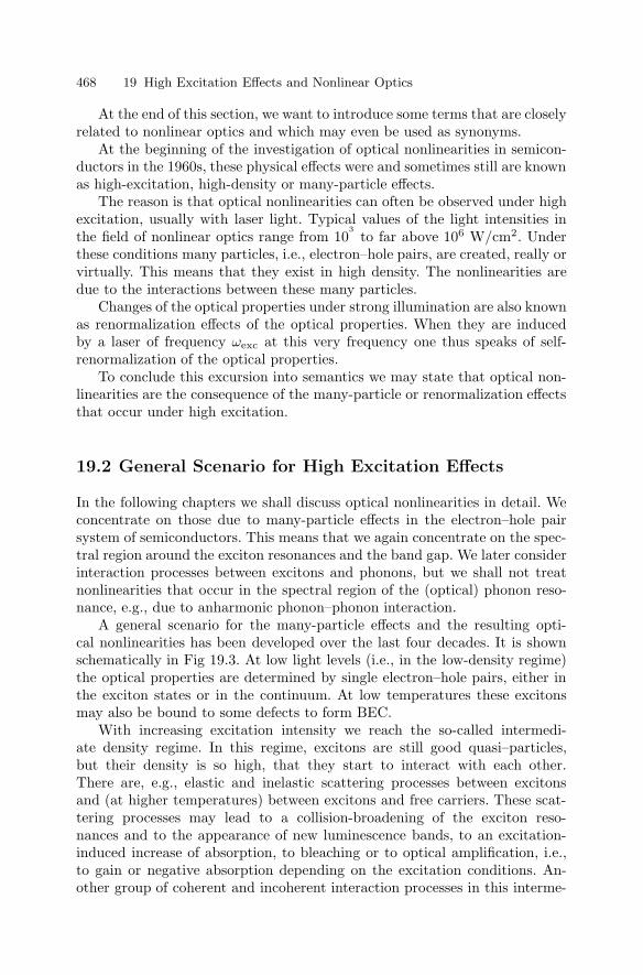
468 19 High Excitation Effects and Nonlinear Optics
At the end of this section, we want to introduce some terms that are closelyrelated to nonlinear optics and which may even be used as synonyms.
At the beginning of the investigation of optical nonlinearities in semicon-ductors in the 1960s, these physical effects were and sometimes still are knownas high-excitation, high-density or many-particle effects.
The reason is that optical nonlinearities can often be observed under highexcitation, usually with laser light. Typical values of the light intensities inthe field of nonlinear optics range from 10
3to far above 106 W/cm2. Under
these conditions many particles, i.e., electron–hole pairs, are created, really orvirtually. This means that they exist in high density. The nonlinearities aredue to the interactions between these many particles.
Changes of the optical properties under strong illumination are also knownas renormalization effects of the optical properties. When they are inducedby a laser of frequency ωexc at this very frequency one thus speaks of self-renormalization of the optical properties.
To conclude this excursion into semantics we may state that optical non-linearities are the consequence of the many-particle or renormalization effectsthat occur under high excitation.
19.2 General Scenario for High Excitation Effects
In the following chapters we shall discuss optical nonlinearities in detail. Weconcentrate on those due to many-particle effects in the electron–hole pairsystem of semiconductors. This means that we again concentrate on the spec-tral region around the exciton resonances and the band gap. We later considerinteraction processes between excitons and phonons, but we shall not treatnonlinearities that occur in the spectral region of the (optical) phonon reso-nance, e.g., due to anharmonic phonon–phonon interaction.
A general scenario for the many-particle effects and the resulting opti-cal nonlinearities has been developed over the last four decades. It is shownschematically in Fig 19.3. At low light levels (i.e., in the low-density regime)the optical properties are determined by single electron–hole pairs, either inthe exciton states or in the continuum. At low temperatures these excitonsmay also be bound to some defects to form BEC.
With increasing excitation intensity we reach the so-called intermedi-ate density regime. In this regime, excitons are still good quasi–particles,but their density is so high, that they start to interact with each other.There are, e.g., elastic and inelastic scattering processes between excitonsand (at higher temperatures) between excitons and free carriers. These scat-tering processes may lead to a collision-broadening of the exciton reso-nances and to the appearance of new luminescence bands, to an excitation-induced increase of absorption, to bleaching or to optical amplification, i.e.,to gain or negative absorption depending on the excitation conditions. An-other group of coherent and incoherent interaction processes in this interme-

19.2 General Scenario for High Excitation Effects 469
diate density regime involves transitions to the excitonic molecule or biex-citon. The biexciton, which was briefly mentioned in Sect. 9.4, is a newquasiparticle which consists of two electrons and two holes. If the excitoncan be seen in analogy to the hydrogen or rather the positronium atom,then the biexciton corresponds to the H2 or the positronium molecule.Similarly, there are so-called trions, which consist of two electrons andone hole ore vice versa. They are also known as X− and X+
2 , respec-tively, and correspond to H− or H+
2 . As we shall see in Sect. 20.3, tran-sitions involving biexcitons or trions give rise to a large variety of opticalnonlinearities.
If we pump the sample even harder, we leave the intermediate and ar-rive at the high density regime, where the excitons lose their identity asindividual quasiparticles and where a new collective phase is formed whichis known as the electron–hole plasma (EHP). In this regime, the density of
Fig. 19.3. The general scenario for many-particle effects in semiconductors

470 19 High Excitation Effects and Nonlinear Optics
electron–hole pairs np is at least in parts of the excited volume so high thattheir average distance is comparable to or smaller than their Bohr radius aB,i.e., we reach a “critical density” nc
p in an EHP, given to a first approxima-tion by
a3Bn
cp ≈ 1 . (19.20)
We shall meet some more elaborate formulas than (19.20) in Chap. 21.In this high-density regime, we can no longer say that a certain electron is
bound to a certain hole; instead, we have the new collective EHP phase. As weshall see in more detail in Chap. 21, the transition to an EHP is connected withvery strong changes of the electronic excitations and the optical properties ofsemiconductors.
The scenario outlined in Fig 19.3 has been observed in every group of semi-conductors investigated so far including structures of reduced dimensionality.However, the ranges of observability of the various groups of phenomena canbe very different. In the indirect gap material Ge it is possible in favorablecases to observe an EHP even under illumination with an incandescent lamp,due to the long lifetime of the carriers which can reach ms in the bulk of highquality samples. In contrast, for CuCl pump powers in the range of GW/cm2
have to be used to fulfill the condition of (19.20) and to produce an EHP. Suchhigh power densities can be applied only for a few ps, otherwise the samplewill be evaporated.
As a rule of thumb, one can say that plasma phenomena are most easilyobserved in indirect gap materials due to the long carrier lifetime or in directgap materials with large excitonic Bohr radius, so that (19.20) can also bereadily satisfied as in GaAs. The Cu halides, on the other hand, are modelsubstances for biexciton phenomena, due to the large exciton and biexcitonbinding energies. The II–VI compounds have an intermediate position allow-ing observation of all of the effects shown in Fig 19.3 (and some more). This isvery satisfying but poses the challenge of separating the various contributions,which partly overlap spectrally. Recent reviews which cover high excitationeffects are [81K1, 89S1, 90G1, 90H1, 91C1, 94P1, 99N1, 02S1, 04O1] and refer-ences therein.
In the following chapters we describe the various effects in some detail,always beginning with three-dimensional materials but also giving examples ofsystems of reduced dimensionality. We start in Chap. 20 with the intermediatedensity regime and continue in Chap. 21 with the electron–hole plasma.
It should be added that at low temperatures theory predicts betweenthe intermediate and high density regime the possibilities of excitonic Bose–Einstein condensation and superfluidity. We come back to this aspect inSect. 20.5.
A Bose–Einstein condensation (also generally abbreviated by BEC) is dif-ficult to depict in a figure like Fig. 19.3 since it is a condensation in k-space.We tried very tentatively to do it as shown in Fig. 19.3

19.3 Beyond the χ(n) Approximations 471
19.3 Beyond the χ(n) Approximations
An expansion of the susceptibility in a power series of the electric field likein (19.2) only makes sense if it converges fast. Though terms up to χ(7) arediscussed in the literature, e.g., in [95A1,00A1,01A1], one usually stops withχ(3) terms.
On the other hand, presently available pulsed lasers bring focus intensitiesup to 1020 Wcm−2. These intensities, the resulting generation rates, and therelated electrical field strengths clearly go far beyond the applicability of theapproaches used in Sects. 19.1 and 19.2.
Expected effects have been discussed in [51S1, 64B1, 66K1, 97C1, 98M1,01C1, 01Z1, 02M1, 02S2, 02S3, 03W1, 04W1] and the references given therein.We give here only a short and limited listing since most of these effects are nolonger specific for semiconductors and thus lead beyond the scope of this book.
– The Rabi frequency mentional already, discussed in more detail in Sect. 20.4and in Chap. 23 and 27, can become comparable to the light frequency,allowing the population to flip coherently from the ground to the excitedstate and back during a laser pulse with only a few cycles of light. Thisso-called (carrier-wave) Rabi flopping has been predicted in [37R1] andobserved, in semiconductors in [01M1,02S1].
– Higher harmonics can be generated up to the soft X-ray regime from atoms[66K1,93H1,01P1] or from a laser induced plasma on a solid surface [01C1,02S2].
– Since laser pulses with extreme intensity are often very short and partlycomprise only a few cycles of light, the nonlinear properties start to dependon the relative phase of the carrier wave of the light and the maximum ofthe pulse envelope. If this phase shifts in a controlled manner from pulse topulse, the resulting carrier envelope offset frequency can be measured andpossibly used as a frequency normal (see, e.g., [02M2,03C1,04W1]).
– Solids can be melted or evaporated [92B1,97G1,00H1,01C1].– A plasma can be produced at the surface or in the bulk of solids [97G1,02S2].– A fusion can be ignited [98M1,02M1].– The so-called ponderomotive energy of electrons can reach relativistic ener-
gies. The ponderomotive energy is defined as the energy a free electron canreached during acceleration in the light field of a laser pulse. If we assumethat the electron is free, initially at rest, and consider only the electric fieldover one half a period of light, neglecting the B field or relativistic effects,we can easily show that [96J1]
Epond =p2
2m=
2e2E20
mω20
(19.21a)
with
p =∫ π
0
pdt =∫ π
0
E0 sinω0tdt = 2eE0ω−10 (19.21b)

472 19 High Excitation Effects and Nonlinear Optics
Since the therm ev×B of the Lorenz-force depends via (19.21b) quadraticallyon the field amplitude it can give rise to photon-drag effects [03H1]. Epond
can easily exceed the width of the forbidden gap of a semiconductor or thework function of electrons by orders of magnitude, thus giving only limitedimportance to whether an electron is initially free or bound in an atom ora solid. Expected effects that are partly observed are, e.g., nuclear fusion orsecond harmonic generation from a single electron in vacuum. Effects that areexpected for the future are, e.g., nonlinear optics involving the Dirac sea witheffects like e−e+ pair production in vacuum with two counter propagating lightbeams (see, e.g., [98M1,00C1,02M1,03W1,04W1] and references therein).
Obviously, exciting phenomena are emerging in this field.
19.4 Problems
1. Try to make a rough guess of the electric field strength due to the posi-tively charged nucleus of Si at the distance of the outer electron shell. Atwhat light intensities would you expect to observe coherent optical non-linearities assuming that the electric field in the light beam is about 0.1of the electric field from the nucleus. How do the field strength and thelight intensity change if you consider excitons instead of atoms?
2. Calculate the light intensity necessary to create in a semiconductor withEg ≈ 1.5 eV a stationary density np of 1018 cm−3 electron–hole pairs, iftheir lifetime is 0.1 ns (direct gap semiconductor) or 1 µs (indirect gapsemiconductor).
3. Give a schematic drawing as in Fig. 19.2 for a three-photon absorptionprocess and for third-harmonic (3ω) generation. Give the formula for thethree-photon absorption coefficient β3 and for the third-harmonic gen-eration in perturbation theory. Can third-harmonic generation occur incentrosymmetric crystals?
4. Try to find some more processes which contribute to Ren2(ω).5. Calculate the critical densities nc
p for some semiconductors using the for-mula (19.20).
6. Letaparallel laserbeamwithalateralGaussianenvelopefallonasamplewithRen2 = 0. Explain qualitatively how self-focussing or defocussing works.
7. If the pulse of problem 6 also has a short temporally Gaussian envelope,one expects so-called self-phase modulation, which broadens the spectrumbeyond the Fourier limit (the so-called chirp mentioned in the text). Tryto figure out qualitatively how this effect works.
References to Chap. 19
[31G1] M. Goppert-Mayer, Annalen der Physik 9, 273 (1931)[37R1] I.I. Rabi, Phys. Rev. 51, 652 (1937)

References to Chap. 19 473
[51S1] J. Schwinger, Phys. Rev., 82, 664 (1951)[61K1] W. Kaiser and C.G.B. Garrett, Phys. Ref. Lett., 7, 229 (1961)[62B1] R. Braunstein, Phys. Rev. 125, 475 (1962)[62M1] P.D. Maker et al., Phys. Rev. Lett. 8, 21 (1962)[63F1] P.A. Franken and J.F. Ward, Rev. Mod. Phys. 35, 23 (1963)[64B1] L.S. Brown and T.W.B. Kibble, Phys. Rev. A 133, 705 (1964)[64B2] R. Braunstein and N. Ockman, Phys. Rev. 134, 499 (1964)[65B1] M. Bass, P.A. Franken, and J.F. Ward, Phys. Rev. A 138, 534 (1965)[65B2] N. Bloembergen, Nonlinear Optics, Benjamin, New York (1965)[66K1] T.W.B. Kibble, Phys. Rev. A 150, 1060 (1966)[67B1] I. Broser in Phys. and Chem. Of II–VI Compounds, M. Aven and J.S. Prener
(eds.), North Holland Pupl., Amsterdam p. 487 (1967)[71K1] C. Klingshirn, Z. Phys. 248, 433 (1971)[75A1] L. Allen and J.H. Eberly, Optical Resonance and Two Level Atoms, Wiley
Interscience, New York (1975)[81K1] C. Klingshirn and H. Haug, Phys. Rep. 70, 315 (1981)[84S1] Y.R. Shen, The Principles of Nonlinear Optics, Wiley, New York (1984)[86E1] H.J. Eichler, P. Gunter and D.W. Pohl, Laser Induced Dynamic Gratings,
Springer Ser. Opt. Sci. Vol. 50, Springer, Berlin, Heidelberg (1986)[89N1] Nonlinear Optics of Organics and Semiconductors, Kobayashi, T., ed.,
Springer Proc. in Physics 36 (1989)[89S1] S. Schmitt-Rink, D.A.B. Miller and D.S. Chemla, Adv. Phys. 38, 9 (1989)[90B1] P.N. Butcher and D. Cotter, The Elements of Nonlinear Optics, Cambridge
Studies in Modern Optics Vol. 9, Cambridge University Press, Cambridge(1990)
[90G1] E.O. Gobel and K. Ploog, Progr. Quantum Elektron. 14, 289 (1990)[90H1] H. Haug and S.W. Koch, Quantum Theory of the Optical and Electronic
Properties of Semiconductors, World Scientific, Singapore (1990)[91C1] R. Cingolani and K. Ploog, Adv. Phys. 40, 535 (1991)[91M1] D.L. Mills, Nonlinear Optics, Springer, Berlin, Heidelberg (1991)[92B1] U. Becker et al., J. Crystal Growth 125, 384 (1992)[93H1] S.E. Harris, J.J. Macklin, and T.W. Hansch, Opt. Commun. 100, 487 (1993)[94P1] K.-H. Pantke and J.M. Hvam, Intern. Journ. of Modern Physics B8, 73
(1994)[95A1] V.M. Axt et al., phys. stat. sol. (b) 188, 447 (1995)[95M1] S. Mukamel, Principles of Nonlinear Optical Spectroscopy, Oxford Univer-
sity Press, New York (1995)[96J1] A. Jauho, Phys. Rev. Lett. 76, 4576 (1996)[97C1] J. Cerne et al., Appl. Phys. Lett. 70, 3543 (1997)[97G1] E.N. Glezer and E. Mazur, Appl. Phys. Lett. 71, 882 (1997)[98M1] G.A. Mouron et al., Physics Today, January Issue p. 22 (1998)[99N1] Nonlinear Optics in Semiconductors I and II, E. Garmire and A. Kost (eds.),
Semicond. and Semimetals 58 and 59 (1999)[00A1] V.M. Axt et al., phys. stat. sol. (b) 221, 205 (2000)[00C1] A.H. Chin, Phys. Rev. Lett. 85, 3293 (2000)[00H1] T.-H. Her et al., Appl. Phys. 70, 383 (2000)[00N1] Nonlinear Optical Effects and Materials, Gunter, P., ed., Springer, Berlin
(2000)[01A1] V.M. Axt et al., Phys. Rev. B 63, 115303 (2001)

474 19 High Excitation Effects and Nonlinear Optics
[01C1] A. Cavalleri et al., Phys. Rev. B 63, 193306 (2001)[01P1] P.M. Paul et al., Science 292, 1689 (2001)[01M1] O.D. Mucke et al., Phys. Rev. Lett. 87, 057401 (2001)[01Z1] M. Zudov et al., Phys. Rev. B 64, 121204 (R) (2001)[02M1] G.A. Mouron and D. Umstadter, Scientific American, May Issue p 63 (2002)[02M2] O.D. Mucke et al., Opt. Lett. 27, 2127 (2002)[02S1] W. Schafer and M. Wegener, Semiconductor Optics and Transport Phenom-
ena, Springer, Berlin (2002)[02S2] K. Sokolowski-Tinten et al., Springer Series in Chemical Physics 71, p. 36,
102, 499 (2002)[02S3] M.Y. Su et al., Appl. Phys. Lett. 81, 1564 (2002)[03C1] S.T. Cundiff and J. Ye, Rev. Mod. Phys. 75, 325 (2003)[03H1] F. He, Phys. Rev. Lett. 90, 055002 and 91, 195001 (2003)[03W1] M. Wegener, Intern. School on Frontiers of Optical Spectroscopy, Erice, May
(2003), Kluwer, Dordrecht, in press[04O1] Optics of Semiconductors and their Nanostructures, H. Kalt and M. Het-
terich (eds.), Springer Series in Solid State Science 146, (2004)[04W1] M. Wegener, in Ref. [04O1], p. 171

20
The Intermediate Density Regime
In the following sections we present selected examples from the intermedi-ate density regime where excitons biexcitons and trions are still good quasi-particles.
20.1 Two-Photon Absorption by Excitons
We have mentioned already the two-photon absorption (TPA) to the excitonlevel in connection with k-space spectroscopy of polaritons (Sect. 13.1.4) andwith the magnetic properties of excitons (Sect. 16.1). The process is describedin the weak coupling limit by (19.9), i.e., a first photon virtually excites anintermediate state which is converted by a second photon to the exciton in thefinal state. In the strong coupling limit, one would say that two photon-likepolaritons merge to form one exciton-like polariton. The momentum conser-vation
k1 + k2 = kexc (20.1)
usually allows only the longitudinal exciton and the upper polariton branch(UPB) to be reached. The two-photon selection rules are different from thosefor one photon. Consequently it is sometimes possible by TPA to reach statesthat are forbidden in one-photon absorption and vice versa. Examples aregiven in Chap. 26 on group theory. Experimental result for the two-photonspectroscopy of excitons have already been given in Figs. 13.20, 13.23, 13.30and in Fig. 16.5. More details, including three-photon absorption, are foundin [81F1].
More recent data on two- and three-photon absorption spectroscopy e.g. ofZnTe or ZnO and on the influence of stress are found in [93F1,98W1]. Someexamples for two-photon spectroscopy of excitons in quantum-wells can befound in [01L1] of Chap. 1.
The two-photon absorption coefficient β of (19.8), (19.9) has been in-vestigated for various bulk semiconductors in the band-to-band transition

476 20 The Intermediate Density Regime
region in, e.g., [80K1]. More data for this quantity as well as for secondharmonic-, sum- and difference frequency generation in bulk or at surfacesor for the dc-effect can be found e.g. in [71K1, 84S1, 97C1, 01Z1, 02S3] andthe books [65B2,75A1,86E1,90B1,95M1,00N1] both of Chap. 19. Some morerecent data on second harmonic generation including quantum structures aregiven e.g. in [98W1, 01L1, 01W1]. The creation of squeezed light via an n2
process (see (19.3)) has been reported in [95F1]. We will come across furtherexamples of two-photon absorption and χ(3) and higher processes in Sects. 20.3and 23.2.
20.2 Elastic and Inelastic Scattering Processes
If we increase the density of really excited excitons, it can happen that two ex-citons meet during their lifetimes on their diffusive motion through the sampleand scatter via their mutual dipole-dipole interaction while a dipole-monopoleinteraction would describe the scattering of excitons with free carriers. Scat-tering of excitons with LO-phonons has already been introduced in Sect. 13.1.For an early description of such scattering processes see [69B1] and for a re-view [81K1]. All of these scattering processes will disturb the phase of the ex-citon (exciton-like polaritons). We will meet an example of this phenomenonin Chap. 23.
The scattering processes themselves can be categorized into elastic andinelastic. For elastic scattering the sums of kinetic energies before and afterthe collision are equal, in addition to momentum conservation. For an elasticscattering event between two excitons we obtain, e.g.,
ki,1 + ki,2 = kf,1 + kf,2 (20.2a)
2
2M(k2
i,1 + k2i,2
)=
2
2M(k2
f,1 + k2f,2
)(20.2b)
in analogy to the definition in classical mechanics. These processes show upmainly in the reduction of the phase relaxation time T2 i.e. in an increaseof the homogeneous broadening. In the inelastic processes on which we shallconcentrate now, an exciton is scattered into a higher excited state with prin-cipal quantum number nB,f ≥ 2, while another is scattered on the photon-likepart of the polariton dispersion and leaves the sample with high probabil-ity as a luminescence photon, when this photon-like particle hits the surfaceof the sample. This process is shown schematically in Fig. 20.1. The mo-mentum conservation law is given by (20.2a) with one of the kf being ≈ 0.If we assume that both excitons are initially in states nB,i = 1 and thatthe momentum of the photon-like polariton is zero, then energy conserva-tion reads
ωPnB,f= Eex(nB = 1,k = 0) − Eb
ex
(1 − 1
n2B,f
)− 2
Mki,1ki,2 . (20.3)

20.2 Elastic and Inelastic Scattering Processes 477
The resulting emission bands are usually called P -bands with an indexgiven by nB,f. The bands are broadened by averaging over the last term on theright of (19.3) and by the fine structure of the exciton states, e.g., the splittingof the nB = 2 exciton into states with S, P0 and P1 envelope functions.
The transition probability into the continuum (P∞) decay rather fast withincreasing excess energy. A summary of the calculations for the transitionprobabilities and further references are given in [69B1,81K1,94K1].
In the simplest approximation, one expects that the luminescence intensityof these scattering processes increases quadratically with the density of exci-tons. Indeed one finds a superlinear increase of these bands with increasingpump power with exponents ranging from 1.5 to 2.
In Fig. 20.2 we give an example for ZnO showing the P2 and P∞ bands.References to further experimental results are compiled in [75K1,81K1,85H1,94K1]. Fo r more recent data in semiconductors like ZnO or CuI see [97Z2,02T1]
At higher lattice (and exciton) temperatures a fraction of the exci-tons will be thermally ionized. In this situation a similar inelastic scat-tering process becomes possible, in which an nB = 1 exciton-like polari-ton is again scattered onto the photon-like branch of the dispersion curve,while a free carrier (electron or hole) is scattered under energy and mo-mentum conservation into a higher state in the respective band. A char-acteristic feature of the resulting rather broad and unstructured emissionband is that its maximum shifts with increasing temperature considerablyfaster to lower energies than the band gap does. Examples are given inFig. 20.3, for CdS and ZnO. While the basis for exciton-exciton scatter-ing is the dipole-dipole interaction, we have to consider dipole-monopole in-teraction for the scattering between excitons and free carriers. For exaplessee [76H1,78K1,78M1,81K1].
In the literature one can find many other inelastic scattering processes notconsidered here in detail involving both free and localized states, for example,biexciton-biexciton scattering, scattering between a bound-exciton complexand a free carrier, and scattering processes involving phonons. A review isgiven in [81K1].
Most of these inelastic scattering processes give rise to the appearance ofnew emission bands (which usually grow more than linearly with the genera-tion rate), to induced absorption and, eventually, to optical gain. The latterpoint will be addressed specifically in Chap. 22.
The inelastic scattering processes have been studied in great detail in thehexagonal and cubic II–VI semiconductors, but they have also been observedin III–V and I–VII compounds [69B1, 73H1, 74H1, 75G1, 75K1, 76H1, 78K1,78M1,81K1,86U1,90P1,91C1,94K1,97Z2,02T1].
A density-dependent scattering between exciton polartons and LA phononsleads to the concept of phonoritons, e.g., in Cu2O [99H1].
Inelastic scattering processes between excitons or between excitons andfree carriers have also been observed in quantum wells [01L1] and referencestherein.

478 20 The Intermediate Density Regime
Fig. 20.1. Schematic representation of the inelastic exciton-exciton scattering pro-cesses P2 and P∞
Presently we see a lot of activities to extend or to reinvent the conceptof inelastic scattering processes to cavity polaritons, introduced in (17.1).Examples for exciton-exciton or polariton-polariton scattering are found e.g.in [00B1, 00T1, 02B4, 02B5, 02H1, 02S5] and for electron-polariton scatteringin [03L1]. Energy conservation has to be valid again similarly to (20.2) whilek conservation is restricted to the two-dimensional k‖-space. As it is fre-quently the case in such a situation, partly also the nomenclature changes.The photon-like lower polariton branch, which shows more a parabolic dis-persion in microcavities (Fig. 17.2a) than a light cone, is named k-space trap,the fulfillment of k conservation involves a “magic” angle, and the polaritonsthemselves are introduced as “mysterious” particles, which are half light, halfmatter [02B4]. See also Fig. 13.2
20.3 Biexcitons and Trions
We start with the discussion of biexcitons and trions for bulk material inSect. 20.3.1 and proceed to structures of reduced dimensionality in Sect. 20.3.2

20.3 Biexcitons and Trions 479
Fig. 20.2. The P2 and P∞ bands in the luminescence spectra of ZnO. Accordingto [73H1,74H1]
Fig. 20.3. The temperature dependence of various emission band maxima in CdS(b) and ZnO (a). According to [75K1,81K1,94K1]
including in both cases also external fields, generally magnetic fields. Theconcept of excitons and trions has already been introduced in Sect. 9.4.
20.3.1 Bulk Semiconductors
The idea that biexcitons might exist as bound states of two excitons hasbeen put forward in [58L1,58M1]. Relatively recent reviews of this topic are,

480 20 The Intermediate Density Regime
e.g., [81K1,85H1,86U1,98I1]. Data for bulk semiconductors and for structuresof reduced dimensionality are compiled also in [99L1,02L1] and [01L1,04L1],respectively.
The biexciton or excitonic molecule is, as already mentioned, a quasi-particle consisting of two electrons and two holes, in analogy to the H2 or thepositronium molecule.
Its dispersion relation is given, in the simplest approximation, by
Ebiex(k) = 2Eex(nB = 1,k = 0) − Ebbiex +
2k2
4M, (20.4)
where one assumes that the envelope function in the ground state is symmetricunder the exchange of equal particles, while the combination of the electronsand of the holes is antisymmetric including spin.
General calculations have been made of the biexciton binding energy nor-malized by the exciton binding energy as a function of the ratio of electronand hole mass σ = me/mh (Fig. 20.4). The experimental data points for Ebiex
are normalized to the experimentally determined values of Ebex or to the calcu-
lated excitonic Rydberg energy. We have seen already in Sect. 9.2 that thesetwo quantities partly disagree. What is important from the theoretical pointof view is that the biexciton exists as a bound state for all values of σ andthat the curve Eb
biex/Ry∗ decreases monotonically in the range 0 ≤ σ ≤ 1.The data points scatter around the theoretical predictions with an accuracycomparable to that of the various calculations.
The semiconductor Cu2O (see Sect. 13.2.1.2) is possibly an exception.Calculations indicate that the biexciton binding energy vanishes, though theexciton binding energy is about 150meV [76B1]. This fact is cused by thelarge ortho-para exciton splitting.
In the following we concentrate on optical nonlinearities connected withthe creation and the decay of biexcitons. For further reading see [76N1,81K1,85H1,86U1,91C1,94K1,01K1].
The probability of creating two electron–hole pairs with one photon isvery low, but the probability for two-photon excitation is rather high andis sometimes said to have a “giant” oscillator strength, since the virtuallycreated intermediate state is almost resonant with the exciton if photons withωexc ≈ Ebiex/2 are used.
In connection with Fig. 20.5 we discuss this process as a two-polaritontransition. We give the real part of k and schematically the imaginary part.The latter is close to zero for low damping away from the exciton resonance(see Figs. 4.5 and 5.1). If we shine (laser-) light of an energy exc onto thesample, we populate this state on the lower polariton branch (LPB). A secondpolariton with an energy
ωabs = Ebiex − ωexc (20.5)
can accomplish the transition from there to the biexciton. This means thatwe get an absorption dip or a peak in Im k at ωabs with an oscillator-

20.3 Biexcitons and Trions 481
Fig. 20.4. Calculations of thebinding energy of the biexcitonin units of the excitonic Ryd-berg energy Ry∗. Experimen-tal data for various semicon-ductors, normalized to the ex-perimentally observed excitonbinding energy (open symbols)and to the calculated Ry∗ en-ergy (full symbols). Accordingto [81K1]. Theories accordingto [72A1,72A2,72B1,73H2]
strength which increases with the population at ωexc on the LPB, evidentlyan optically nonlinear effect. The peak in Im k is necessarily connected witha resonance-like structure in the real part of the dispersion relation. In the fol-lowing we give examples of both phenomena, but first we should mention thatthere is another way to create biexcitons. This starts from exciton-like polari-tons, which may even have an incoherent, e.g., thermal population. In thelatter case an exciton is converted into a biexciton by absorption of a photonof energy ω′
abs fulfilling energy and momentum conservation. Considering thedifferent curvatures, i.e., effective masses, of exciton and biexciton dispersion,this process yields an induced absorption at
ω′abs = Eex(nB = 1,k = 0) − Eb
biex −
2k2i
4M, (20.6)
where M is the translational exciton mass, 2M the biexciton mass and ki themomentum of the exciton-like polariton in the initial state, which equals themomentum of the biexciton in the final state if we neglect the wave vector

482 20 The Intermediate Density Regime
Fig. 20.5. The two-photon (or two-polariton) transition from the crystal groundstate to the biexciton state and the two-step process starting from the exciton state
of the photon-like polariton. This process is also known as a two-step processto distinguish it from the two-polariton (or two-photon) transition discussedfirst. See also Sect. 19.1.
Actually one difference lies in the fact that in the latter case one of thepolaritons is either on the photon- or on the exciton–like branch, respectively.A second difference is that the laser at ωexc generally produces a more-or-less coherent population on the LPB while the population on the exciton-likebranch produced, e.g., by some resonant or non-resonant pump laser, tendsto lose its coherence within a few ps (see Sect. 23.2).
In Fig. 20.6 we give an example of the various processes in a pump andprobe beam experiment for CuCl. One can see the scattered, spectrally narrowpump laser light ωexc and the absorption dips in the probe continuum, whichcorrespond to a bound-exciton complex labelled BEC, the TPA process of(20.5) which shifts oppositely to the energy of the laser, and the two-step orinduced absorption process of (20.6) which is fixed in energy and has a larger

20.3 Biexcitons and Trions 483
Fig. 20.6. Two-photon and two-step transitions to the biexciton observed in CuCl.According to [85H1]
width due to the incoherent distribution of the excitons on their dispersioncurve.
By varying the wave vectors of pump and probe beams relative to eachother, it is even possible to measure the dispersion relation of the biexcitonin a TPA experiment. An example is shown in Fig. 20.7 for CuBr. Due to thefour-fold degeneracy of the Γ 8 valence band, the biexciton ground state splitsinto three states with symmetries Γ 1, Γ 5 and Γ 3. The Γ 1 state shows thesimple dispersion of (20.4), while the higher states show some k-dependentsplitting.
The dispersion of the biexciton has been also measured in CuCl [84K1,85H1] or CdS [82L1]. In [98I1] it has been shown, that the polariton-polaritoninteraction in a biexciton may result in a modification of the dispersion rela-tion of the biexciton. For experimental data see, e.g., [01M1].
The decay of biexcitons into an exciton-like and a photon-like polariton isjust the reverse process of the two-step transition of (20.6).
Energy and momentum conservation show, that these luminescence bands,which are frequently called M -bands, have an inverted Boltzmann line shape.Consequently the binding energy of the molecule has to be deduced not fromthe emission maximum but from its high energy edge (see, e.g., [81K1]).
Furthermore it should be noted that the biexciton luminescence generallyoccurs in the same spectral range as the emission from bound exciton com-plexes like AX and DX, which are also made up of two positively and twonegatively charged particles. Side bands of these complexes originating, e.g.,from emission of acoustic phonons or inelastic scattering with free carriers

484 20 The Intermediate Density Regime
Fig. 20.7. The dispersion of the lowest biexciton states in CuBr. According to [85H1]
often look very similar to biexcitonic M bands and can be easily confused.For more details on this topic see [81K1].
Figure 20.8 shows biexciton luminescence spectra of CuCl under non-resonant and resonant high excitation. In the first case excitons are created,which form biexcitons with a thermal distribution. The temperature of theexciton and the biexciton gas can be higher than the lattice temperature TL
which describes the phonon system and, in the situation of Fig. 20.8, liesaround 25 K.
In the decay process a longitudinal exciton or a transverse exciton-likepolariton can appear in the final state together with the photon-like lumi-nescence. Consequently one observes in cubic materials the so-called ML andMT bands. Under resonant two-photon excitation of the biexciton, one createsa biexciton gas with a narrow, non-thermal distribution, the decay of whichgives rise to narrow emission structures NT and NL at the high energy sidesof the ML and MT bands, respectively. This spectral position corresponds tothe recombination of biexcitons with small wave vectors [76L1, 79H1, 85H1].Similar effects are also known for CuBr [85H1,86U1] or for CdS [79S1] or forβ-ZnP2 [01D1].
For (inconclusive) attempts to observe a Bose–Einstein condensation ofbiexcitons see [76N1,82P1] and Sect. 20.5.

20.3 Biexcitons and Trions 485
Fig. 20.8. Biexciton luminescence of CuCl under resonant and non-resonant exci-tation. According to [85H1]
As stated in Chap. 26, the angular momentum can be used (with con-siderable care) for arguments concerning selection rules, especially for cubicmaterials. This fact has been used for beautiful experiments with circularlypolarized light. Starting from the Γ1 ground state a Γ1 biexciton state canonly be reached by two quanta with opposite circular polarization as veri-fied in [78I1,82I1,82K3,84K1,86I1,86K1,96H1]. This approach was also usedlater in quantum wells wires and dots to prove the assignment of an observedtransition to biexcitons. See e.g. [96P1,99W1,03P1] and references therein.
The diamagnetic shift of the biexciton has been measured, e.g., in CdS[82K1]. It is larger than that of the exciton due to the larger radius of thebiexcitons.
In the II–VI compounds, the emission bands of biexcitons are less struc-tured due to the orientation-dependent mixed mode final states (see Sect. 13.1and [81K1,85H1]). Furthermore, in many II–VI compounds the biexciton emis-sion is spectrally almost degenerate with other recombination processes, espe-cially ones involving bound-exciton complexes like inelastic BEC-free-carrierscattering or the acoustic phonon side-band of EEC. Therefore a clear-cutproof of the existence and the properties of biexcitons is difficult to obtainin these materials from luminescence alone. Details of this topic are givenin [81K1]. Some recent work on biexcitons in epitaxial layers of wide gap semi-conductors such as ZnO, ZnS or GaN is found in [97Z1,00K1,00Y1,00Y2,03A1,03H2,04A1]. As earlier in bulk ZnO [83H1] biexcitons have been observed re-

486 20 The Intermediate Density Regime
Fig. 20.9. The two-photon Raman scattering via intermediate exciton and biexcitonstates in a backward scattering geometry (a) and for the lower polariton branch overa two-dimensional k space (b) [82K2]
cently with countain two holes from the A valence band, one hole from theA and one from the B valence band for ZnO and GaN and even two holesfrom the B valence band in ZnO [03A1,03H2,04A1]. Slight discrepancies existbetween the energies of the three levels in ZnO, especially concerning the BBbiexciton in [83H1,03H2,04A1]. The data in [83H1] have been consistently ob-served by different groups and in different samples, while it is known [83H1],that resonances in two-photon Ramon scattering, a technique from the groupof four-wave mixing experiments (see Chap. 25), may lead to erroneous results.
Excitonic molecules have also been observed in the indirect materials Geand Si in the intermediate density regime before the onset of plasma forma-tion [79G1, 79M1, 82T1, 84T1, 01R1]. Furthermore, biexcitons have not onlybeen found in I–VII, II–VI and group-IV materials, but also in other less com-mon semiconductors like HgI2 or AgBr [81K1, 85H1, 99L1, 02L1], so that theformation of biexcitons can be considered a rather general feature in the in-termediate density regime at low temperatures. At higher temperatures biex-citons are rapidly ionized and their resonances become so broad that they cangenerally no longer be detected.
Trions have been p redicted for bulk material, e.g., in [76S1, 97S1], butthere is not much of experimental evidence for their existence in contrast toquantum wells (see Sect. 20.3.2).
To conclude this subsection on biexcitons in bulk semiconductors we de-scribe in some detail a coherent process which is doubly resonant and whichbelongs into the group of χ(3) phenomena. We refer to the two-photon orhyper-Raman scattering and the associated (non-) degenerate four-wave mix-ing. The idea is described in the following in both the weak and the strongcoupling limits (see Fig. 20.9a,b and compare with Fig. 19.2).

20.3 Biexcitons and Trions 487
An incident photon, which is almost resonant with the exciton state, isconverted by a second photon into a virtually excited biexciton. This biexcitonhas to decay again after a time ∆t determined by the energy-time uncertaintyrelation. If it decays into two photons, which are identical to the incident ones,this process would describe an intensity induced change of the phase velocity,i.e., a contribution to Ren2 in (19.3). However, there are many other decayprocesses which fulfill energy and momentum conservation.
In a backward scattering process, the virtually excited biexciton at wavevector
(k
(1)i + k
(2)i
)can decay into a transverse or a longitudinal exciton at
kf and a Raman-like photon with ωRt,l according to
kR = k(1)i + k
(2)i − kf , (20.7a)
ωRt,l = ω(1)i + ω
(2)i − El,t , (20.7b)
Since the transverse and longitudinal eigenenergies do not vary much withk in this range, we get for ω
(1)i = ω
(2)i simply
ωRt,l = +2ωi − El,t , (20.7c)
where the factor 2 on the right explains the name two-photon Raman scat-tering.
In forward scattering and for all intermediate scattering geometries ((20.7))would be the same in the weak coupling limit. In the polariton picture thisstatement is only true if one particle in the final state is a longitudinal exci-ton. Indeed, the two-polariton state created by the two incident beams, whichis almost resonant with the biexciton, can decay either into a longitudinalexciton and a transverse polariton or into two polaritons. In the latter situ-ation both final state particles are on the transverse branches. One particleis exciton-like in the backward configuration, but moves down into the bottleneck if the scattering geometry is changed towards forward scattering. In thiscase both final state particles have a certain chance of leaving the sample asa photon. For ω(1)
i = ω(2)i they will be situated in scattering geometries close
to forward scattering slightly above and below ωi and they will be thereforecalled ω+
R and ω−R , respectively. The resulting relation between ωR and ωi
deviates significantly from the slope-two relation of (20.7c).In Fig. 20.9b we show a graphical solution. The kx-ky plane is the scatter-
ing plane which contains k(1)i = k
(2)i = ki and kf. The lower polariton branch
is plotted centered around k = 0 and again in negative energy direction, start-ing from 2ki, 2ω; according to (20.7a), (20.7b). The intersection line betweenboth energy surfaces or dispersion relations gives just the solutions of (20.7a-c). An avoided crossing has not been considered in Fig. 20.9b. It leads to theadditional modification shown in [98I1] and mentioned above in the contextof bipolaritons. We come to various (self-) renormalization effects below, butfirst discuss the solution obtained, if they are neglected.

488 20 The Intermediate Density Regime
Examples for forward and backward scattering are given in Fig. 20.10 forCuCl and various geometries. A self-consistent fit of the data with calculateddispersion curves for the exciton polaritons allows one to determine theirdispersion curve with high accuracy, as was mentioned in Sect. 13.4 on k-spacespectroscopy of excitonic polaritons. It should be stressed that the deviationsfrom the slope-two relation in Fig. 20.10c can be only understood in thepolariton or strong coupling picture.
The excitation-induced resonance of Fig. 20.5 shows up as an anomaly inthe otherwise smooth relation between ωi and ωR if one of the incomingor outgoing energies coincides with it. An example of this density dependentrenormalization of the polariton dispersion is shown in Fig. 20.11.
The fact that the splitting between ωexc and ωRT± does not convergeto zero for higher intensities in exact forward scattering indicates that thereare also self-renormalization effects of the dispersion at ωexc in the senseof an n2 effect in (19.3) [85H1]. For further examples of renormalizations ofthe polariton dispersion with increasing excitation see, e.g., [78I1,79M2,82I1,82K3,83H1,84K1,86K1,96H2] and the reviews [81K1,85H2,98I1]. These ref-erences also give examples and/or references for hyper- or two-photon Raman
Fig. 20.10. The dependence on ωexc of the two-photon Raman emission via anintermediate biexciton state in CuCl for various scattering geometries (a,c) and a setof spectra for forward scattering (b). According to [85H1]

20.3 Biexcitons and Trions 489
Fig. 20.11. The anomaly in the relation between ωexc and ωemission caused bythe TPA resonance explained with Fig. 20.5. The dashed and solid lines give thetheory without and with this resonance. According to [85H1]
scattering in semiconductors other than CuCl, like CuBr or various II–VIcompounds.
Until now we have been considering the “spontaneous” decay of the virtu-ally excited biexciton in the intermediate state. It is also possible to stimulatethis decay by directing a third beam onto the sample which coincides in di-rection and energy with one of the particles in the final state. The emissionof the other particle is then stimulated and we get a typical χ(3) process inthe sense of Fig. 19.2d. Alternatively we can describe this process as (non-)degenerate four-wave mixing (N)DFWM or as a diffraction of the third beamfrom a coherent laser-induced grating set up by the interference of the othertwo incident beams. Actually the close relation between two-photon Ramanscattering and (N)DFWM has been verified by various groups, e.g., for CuCl.Details are given, e.g., in [85H1, 86U1]. For a measurement of second ordernonlinear susceptibility in various II-VI compounds see [98W2].
20.3.2 Structures of Reduced Dimensionality
Trions, biexcitons and even higher complexes have been observed in many dif-ferent quantum wells, wires and dots. We give a small selection of results here

490 20 The Intermediate Density Regime
and refer the reader for further data to [98I1, 01L1, 04L1] and the referencesgiven therein.
In III–V quantum wells and superlattices like GaAs/Al1−yGayAs biex-citons have been predicted and observed experimentally. See, e.g., [83K1,91B1, 92B1, 92O1, 92P1, 92P2, 93P1, 94P1, 96B1, 97M1, 01E1]. Though thereis still some controversy concerning the calculation of their binding energy[83K1,96S1,98I1,99D1,02R1], there is general agreement that the binding en-ergy of the biexciton is around 1.8meV for a GaAs well with a width around10 nm. Actually it has been found that the ratio of the width dependent bind-ing energies of biexcitons and excitons is roughly constant [96B1, 96S1]. ForIn1−yGayAs wells see [99B1].
Ebbiex/E
bex ≈ 0.23 (20.8)
In Fig. 20.12 we show normalized emission spectra of an lz = 10 nmGaAs/Al1−yGayAs MQW sample at low temperature and for various pumppowers.
The peak labeled M on the low energy side of the exciton emission growsmore strongly than that of the exciton as shown in the insert. It is at-tributed to the radiative decay of a thermal population of biexcitons intophotons and excitons. The line shape fit gives Eb
biex = (1.75 ± 0.05) meV ingood agreement with other experimental findings, e.g., quantum beats (seeSect. 23.2 or [92O1,92P1]).
Fig. 20.12. The absorption and normalized emission spectra of an AlGaAs MQWsample, showing the biexciton luminescence band M , which grows superlinearly asshown in the insert. According to [92O1,93P1,94P1,96B1]

20.3 Biexcitons and Trions 491
Similarly as for excitons, one realized that also biexcitons tend to be lo-calized by, e.g., well width fluctuations. This effect may even enhance thebiexcitons binding energy [99L2, 03P1] opening a bridge to the investigationof biexcitons in quantum islands (see below).
Biexcitons have been investigated in external magnetic fields in GaAs andIn1−yGayAs wells [94B2,01B1] partly revealing an unexpected field indepen-dence of the biexciton binding energy.
Biexcitons have also been observed in quantum wells embedded in mi-cro cavities (see Sect. 17.1.2) resulting in an additional resonance due to theexciton to biexciton transition [00D1,03B3].
Trions have been observed in quantum wells by many groups. This factcontrasts the situation in bulk samples (see above) and has the followingorigin. Quantum wells (or wires) can contain a moderate density of electronsor of holes by slightly doping the barrier. Excitons created by optical pumpingthen have a rather high probability to bind another carrier resulting in X− =(e, e, h) or X+
2 = (e, h, h) trion complexes.Trions are usually observed in luminescence. Their binding energy is
slightly smaller than that of the biexciton. Examples can be found, e.g., in[95F2,96F1,96O1,99L4,00E1,03P1] and in the references given in [01L1,04L1].For charge transport by X− see, e.g., [01S1].
Until now we have mainly presented references for III–V, GaAs-basedquantum wells, a group of semiconductors in which biexcitons are hardlydetectable in bulk materials due to their small binding energy.
In contrast, biexcitons are already well known in bulk II–VI semiconduc-tors as shown in Sect. 20.3.1. Consequently they must also exist in II–VI quan-tum wells with an even confinement enhanced binding energy. In the followingwe give a small selection of references. More will be compiled in [03N2,04L1].
The binding energy of biexcitons reaches values up to 6 meV in ZnSe-based quantum wells as shown, e.g., in [02W1]. The ratio Eb
biex/Ebex varies
here systematically from 0.10 to 0.23 with decreasing lz in contrast to (20.8),but is at least in the same range.
For localized excitons and biexcitons values up to Ebbiex ≈ 8, 5 meV are
reported in [96P1, 97L1, 99G1, 99L2, 00W1] in agreement with findings forGaAs-based structures mentioned above.
Biexcitons containing one hh and one lh have been identified using theselection rules for circularly polarized light in [96P1, 99W1]. This finding isin close analogy as for biexcitons in bulk ZnO, which may contain two holesfrom the A valence band, one from the A and another from the B valenceband, or two B holes as discussed above [83H2].
Biexcitons in semi-magnetic semiconductors are treated in [01M1] and stim-ulated emission in [95K1]. Biexcitons in type II ZnSe/BeTe superlattices are ob-served in [01M1,04J2]. Eletrons and holes reside in the two different materials.
The existence and the properties of trions in II-VI quantum wells are alsowell established. They show up in luminescence, reflection and transmissionspectra [02A1,02G1].

492 20 The Intermediate Density Regime
Their binding energies tend to be larger for X− compared to X+2 . The
influence of a magnetic field on this quantity has been investigated in [02A1].The differences between electron singlet and triplet states of X− are elabo-rated in [02G1]. The trion reflection signal has been used to determine thecarrier density [02A2] and optical gain connected with the recombination oftrions is reported in [01P1].
For quantum wires, the situation is similar as for quantum wells. Theexistence of biexcitons and of trions is well established in nanostructured, T-shaped and V-groove wires. For biexcitons see, e.g., [98B1, 98V1, 99L3, 01L1,02W1,04L1]. It has been found in [98B2] that the binding energy of the biex-citon is 40% higher than in a corresponding quantum well.
For trions, data can be found in [04K1]. For recent reviews see [93B1,97W1,01L1,04L1].
Biexcitons in quantum dots in glasses have been observed both in lumi-nescence and in pump-and-probe beam spectroscopy. The biexciton groundstate is lower in energy than twice the energy of a single exciton in a dot[90H1]. Due to the three-dimensional confinement there is also a large num-ber of excited states of the biexciton or two electron–hole pair system ina dot [90U1,93B1,94K1,97W1].
In the following we show two examples. Figure 20.13a gives luminescencespectra of CuBr dots in a glass matrix for increasing excitation intensity.
The peak on the high energy side is due to the recombination of single ex-citons in the dots. The peak on the low energy side, which grows more rapidlywith increasing Iexc than the other one, is attributed to the recombinationof a biexciton, giving a photon and a single exciton in the dot. This inter-pretation is not only confirmed by the superlinear increase of the biexcitonluminescence band but also by the dependence of the emission maxima onthe (inverse squared) average dot radius R. The extrapolation to large dotradii converges to the energies of the free exciton and the lowest biexcitonluminescence band in bulk samples. The binding energy of the biexciton asa function of R agrees well with theory (Fig. 20.13c).
In Fig. 20.14 we show the inhomogeneously broadened absorption spectraof two (photo-darkened) glass samples containing CdSe quantum dots and thechange of the optical density for various pump photon energies ωexc.
In Fig. 20.14a,b we observe a bleaching or spectral hole burning at ωexc
in the inhomogeneously broadened absorption band, and at a second energyfor the dot size of Fig. 20.14a. These two features correspond to the saturationof the transitions form the two uppermost quantized hole states to the lowestconduction band state.
The two structures of induced absorption marked by arrows, correspondto transitions in dots containing one exciton to the ground and an excitedstate of the biexciton, respectively.
Quantum dots of various II–VI compounds have been also produced byprecipitation in organic solvents. For biexcitons in these materials see, e.g.,[97W1,02M1,02M2].
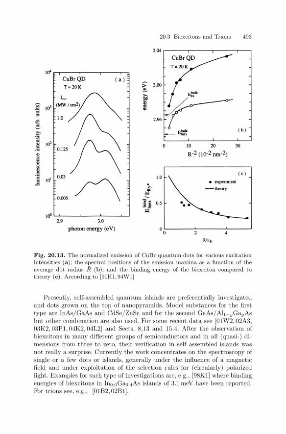
20.3 Biexcitons and Trions 493
Fig. 20.13. The normalized emission of CuBr quantum dots for various excitationintensities (a); the spectral positions of the emission maxima as a function of theaverage dot radius R (b); and the binding energy of the biexciton compared totheory (c). According to [90H1,94W1]
Presently, self-assembled quantum islands are preferentially investigatedand dots grown on the top of nanopyramids. Model substances for the firsttype are InAs/GaAs and CdSe/ZnSe and for the second GaAs/Al1−yGayAsbut other combination are also used. For some recent data see [01W2, 02A3,03K2, 03P1, 04K2, 04L2] and Sects. 8.13 and 15.4. After the observation ofbiexcitons in many different groups of semiconductors and in all (quasi-) di-mensions from three to zero, their verification in self assembled islands wasnot really a surprise. Currently the work concentrates on the spectroscopy ofsingle or a few dots or islands, generally under the influence of a magneticfield and under exploitation of the selection rules for (circularly) polarizedlight. Examples for such type of investigations are, e.g., [98K1] where bindingenergies of biexcitons in In0.6Ga0.4As islands of 3.1 meV have been reported.For trions see, e.g., [01B2,02B1].

494 20 The Intermediate Density Regime
Fig. 20.14. The absorption spectra of two photo-darkened glass samples containingdots of CdSe and the differential transmission spectra for various pump-photonenergies. According to [93G1]
Phonon-assisted biexciton generation or recombination is a topic treatedboth in III–VI [00F1,00F2,01Z1] and II–VI islands [99G1].
Multiexciton complexes in quantum islands also form a recent topic of re-search [98B1,00D2,00D3,00F2,01W2,01W3]. These complexes have a certainsimilarity to the multiexciton complexes bound to point defects like P in Si(see Sect. 14.1).
For singly or even higher charged excitons see, e.g., [00H1, 01B1, 01H1,01W2,01Z1,02S1,02S2] and for internal transitions in biexcitons [01P2].
In II–VI islands the binding energy of excitons is partly larger than that ofexcitons in the parent bulk material. Values above 20 meV have been reported,e.g., in [99W2,00W1,01H2].
Optical gain resulting from the recombination of excitons, biexcitons or ofeven higher complexes has been reported, e.g., in [92D1, 95W1, 95W2, 96G1,96W1,02M1,02M2,03H1]
To conclude, we state that biexcitons, trions and mutliexciton complexesare well established phenomena in semiconductors.
Correlated photons have been observed in the single InAs dot emissionfrom the optical transitions biexciton → exciton and subsequently exciton →ground state [01M2,02S1,02S2,03U1]. We shall briefly return to this topic inChap. 23.

20.4 Optical or ac Stark Effect 495
20.4 Optical or ac Stark Effect
A further example of optical nonlinearities in the intermediate density regimeis the optical, ac or dynamical Stark effect. The name implies that we aredealing with a shift of the exciton resonance caused by the electric field ofa light beam in the sample. For recent reviews see, e.g., [88O1, 89C1, 90Z1,93Z1,01B4] and references therein.
This phenomenon is well known in atomic spectroscopy [92C1] and is fre-quently described in the “dressed atom” picture, i.e., as an atom in the pre-sence of photons. A simple explanation, outlined in the following, is in termsof level repulsion, a phenomenon which we encountered already several timesand which generally occurs in quantum mechanics for two energetically closelying levels which interact with each other.
We assume that the energy of the incident photons is chosen slightly be-low the exciton resonance and use the weak coupling picture. Then a state|m,n = 0〉 containingm photons and n = 0 excitons is almost degenerate witha state |m− 1, n = 1〉. Since the two states are coupled via dipole interaction,an energetic repulsion of the two levels occurs.
The frequency of the photons ω is held constant from the outside by theincident laser. Consequently the exciton resonance shifts in a model whichincludes only the 1 s exciton resonance to slightly higher energies for ω −Eexc < 0 and possibly to lower energies for ω − Eexc > 0 by an amount δE.This quantity has been calculated by various authors [88O1,89C1,89S1,90Z1,93Z1,01B4]. We cite here the result from [89S1]:
δE =2 |ercvEp|2 |φ1s (re − rh = 0)|2
(E1s − ωp)NPSFS
, (20.9)
where ercv is the band-to-band transition matrix element or polarizability, Ep
the field amplitude of the incident laser at frequency ωp, |φ1s (re − rh = 0)|2describes the (Sommerfeld) enhancement of the transition probability of the 1sexciton, E1s − ωp the detuning, and NPSF
S the density of electron–hole pairsnecessary to block the exciton resonance by phase-space filling (Chap. 21).
The term ercvEpφ1s(re − rh) gives the so-called Rabi frequency (see alsoChap. 27) for the 1s exciton. This is basically a field-dependent beat frequencywith which the excitation oscillates coherently back and forth between theelectronic excitation and the photon state.
The Rabi frequency also gives the splitting if ω and the exciton energycoincide.
Actually there are more terms in the shift that include, apart from therenormalization of the 1s exciton resonance, the continuum transitions, phasespace filling, etc. with the consequence that the exciton resonance might shiftto blue even if ω is chosen above the exciton [96N2,00M2]. In the experimentsone is generally restricted to the situation ω < E1s to avoid real excitation,which would mask the optical Stark effect. Exceptions are the experiments

496 20 The Intermediate Density Regime
on ZnSe [96N2], which allowed also to tune the laser in the transparent win-dow above the exciton energy and gave clear evidence for dominating levelrepulsion according to (20.9) in this situation.
We show in Fig. 20.15 two different experiments and two calculations,namely in Fig. 20.15a subpicosecond pump-and-probe absorption spectra forzero delay for a MQW sample with 10 nm GaAs and Al1−yGayAs barriersfrom [86M1]. The pump beam was tuned significantly below the hh excitonresonance. A clear blue shift of the hh exciton and a less pronounced oneof the lh exciton are observed. The rather strong reduction of the oscillatorstrength might be due to some real excitation, e.g., via two photon absorption.Figure 20.15c and d show some calculations from [96H1] using Boltzmann andquantum kinetics for a single resonance. The fact that the latter shows betteragreement with experiments underlines the importance of this approach, towhich we come back in Sect. 23.2.
Fig. 20.15b finally shows, that very intense (generally several 10 MW/cm2)subpicosecond lasers are not necessary to observe the optical Stark effect.Nanosecond pulses properly chosen concerning intensity and detuning workalso. The fact that the differential transmission signal is almost symmetric andcoincides very well with the derivative of a Lorentzian fit to the absorptionspectrum indicate, that one observes a blue-shift without a change in oscillatorstrength under quasi-stationary conditions.
The quantity
σ =δE(E1hh − ωp)
IP, (20.10)
deduced from Fig. 20.15b is σexp = 8.5 × 10⁻⁸ (meV)2 cm2 W−1 and com-pares favorably with the theoretical value and ps experiments giving σtheory ≈5.8 × 10⁻⁸ (meV)2 cm2 W−1 [90K1].
A better description would again be in terms of polariton-polariton inter-action [92K1]. This picture describes not only the shift of the exciton reso-nance by an amount δE but also the appearance of optical gain positionedsymmetrically to the low energy side of the pump laser, i.e., at
ωg = ωP − (Eex + δ − ωp) (20.11)
Equation (20.11) follows from the simple picture that a state with two po-laritons at ωp decays into a Stark-shifted exciton-like polariton and a photon-like polariton at ωg [88S1].
The optical Stark effect has also been observed in bulk materials like Cu2O[85F1] and GaN [02C1] and in quantum wires [03F1].
To conclude, we may state that the optical or ac Stark-effect is also nowa-days well understood for excitons in semiconductors. Apart from the specificreviews [88O1, 89S1, 90Z1] mentioned above more details may also be foundin [96H1,96S1,01L1].
If we pump the samples even harder we leave the intermediate densityregime and enter the high density regime where the optical properties are

20.5 Excitonic Bose–Einstein Condensation 497
Fig. 20.15. Pump-and-probe beam spectra of a 10 nm GaAs/10 nm Al1−yGayAsMQW sample showing the optical Stark effect [86M1] (a) an absorption spectrumwithout excitation and the differential transmission using 10ns pulses showing thesame effect according to [90K1] (b). Calculations using Boltzmann (c) and quantumkinetics (d) [96H1]
determined by the electron–hole plasma. This concept was introduced inSect. 19.2. However, before treating this aspect we discuss briefly the Bose–Einstein condensation of excitons and biexcitons and introduce another groupof optical nonlinearities, the so-called photo-thermal nonlinearities which alsogenerally belong to the intermediate density regime.
20.5 Excitonic Bose–Einstein Condensation
Excitons are Bosons to a good approximation, but are made up of two fermionsi.e. they are composite Bosons. Actually, the creation and annihilation oper-

498 20 The Intermediate Density Regime
ators of excitons obey the commutation rules for Bosons, however, with anadditional correction term of the order 0
(npa
3B
)where aB is the excitonic
Bohr radius and np is the density of electron hole pairs.This fact already triggered predictions of excitonic Bose Einstein condensa-
tion (BEC)andexcitonic superfluidity (ESF) fortyyears ago [62B1,62M1,68K1].For older and more recent reviews of this topic see [77H1,95B2,00M1,03P2].
On the other hand, the fermionic constituents result in a transition to anelectron–hole plasma at the highest intensities (see Fig. 19.3 and Chap. 21).While the existence of the EHP is well established, excitonic BEC was, at thetime of writing this manuscript, still a controversially discussed topic [04I1],in contrast to the situation of (alkali-)atoms in a trap (see, e.g., [95B2,02K2]and the references given therein). Alkali atoms are also composite Bosons,but the ratio between the ionisation energy and the thermal energy kBTC (see(20.12)) is by many orders of magnitude larger than for excitons.
In the following we concentrate on attempts and possibilities to observeexcitonic BEC and ESF.
We start with some general considerations in Sect. 20.5.1, and then treatthe attempts to observe it in bulk (Sect. 20.5.2) and quasi-two-dimensionalsemiconductors (Sect. 20.5.3). The section will be completed with short com-ments about excitonic insulators and so-called “driven BEC”.
20.5.1 Basic Properties
BEC is a macroscopic population of one quantum mechanical state by Boseparticles (ideally, non- or weakly interacting) in thermal (quasi-)equilibrium[24B1,24E1]. It occurs if either the temperature T is lowered below a criticaltemperature Tc at constant particle density n, or if n is raised above nc atconstant T .
For non-interacting ideal Bosons, one finds the following relation betweennc and Tc [00M1]:
nc = 2.612g(mkBTc
2π2
)3/2
(20.12)
where m and g are the mass of the particles and the degeneracy of the state,respectively. The condensate can show superfluidity.
The fact that the mass of excitons is comparable to the free electron mass,while those of, e.g., alkali atoms are ten to 100 times the proton mass andthat excitons can easily be created by pulsed lasers in a density range upto 1017 cm−3, allows one to expect values of TC up to around 10 K, whilesuccessful experiments to observe atomic BEC in traps required T as low asa few 10 µK.
The weak interaction should be slightly repulsive, to avoid condensationof the particles in real space, since a BEC is a condensation in k-space.
The only example of a BEC of weakly interacting Bosons is the condensa-tion of alkali and H atoms in a trap treated, e.g., in the reviews [95B2,02K2].

20.5 Excitonic Bose–Einstein Condensation 499
There are further examples of BEC for Bosons with rather strong inter-action like the superfluidity of 4He and systems that involve the pairing ofFermions and the formation of a gap, like superconductors or superfluid 3He.
Excitons would evidently be another example for weakly interacting Bosons.Before we start to treat experimental attempts to observe excitonic BEC andthe objections against these interpretations, first we illustrate how (20.12) canbe understood.
We showed in Fig. 2.5 three occupation probabilities for particles with aneffective mass m, namely the Boltzmann statistics for distinguishable parti-cles and the Fermi–Dirac and Bose–Einstein statistics for indistinguishableparticles with half or integer spin, respectively. They are given by
fB (T,E, µ) =1
e(E−µ)/kBT, (20.13a)
fFD (T,E, µ) =1
e(E−µ)/kBT + 1(20.13b)
fBE (T,E, µ) =1
e(E−µ)/kBT − 1(20.13c)
where µ is the chemical potential or for Fermions the Fermi energy. Evidently,they coincide for (E − µ)/kBT > 2 and show characteristic differences below.
For particles with a well defined density n, µ is defined by (20.14)
n =
∞∫E0
D (E) · fB,FD,BE (T,E, µ) dE. (20.14)
For particles like photons in black body radiation or phonons in thermalequilibrium, the density of which is not conserved, one has µ ≡ 0. In Fig. 8.20we showed the square root density of states of particles with a finite andconstant (effective) mass m in three dimensions starting at energy E0
D (E) ≈√E − E0 . (20.15)
If one now performs the integration (20.14) for a low density, then µ,i.e., the origin of Fig. 2.5, is situated below E0. If the density increases, µshifts towards E0. Eventually µ coincides with E0. There is no singularityfor Boltzmann particles and Fermions. The density one reaches under thiscondition for Fermions is given by
neff = g
(mkBT
2π2
)(20.16)
and is known as effective density of states (see Sect. 8.9). For further increasingn, µ shifts into the band. For Fermions, the distribution is then said to bedegenerate since the Pauli principle reduces the occupation probability from1 to 1/2 at µ and limits it to 1.

500 20 The Intermediate Density Regime
For Bosons the situation is different. The singularity at E − µ = 0 doesnot allow µ to shift beyond E0. For µ = E0 the integrated population is finiteand corresponds to nc in (20.12).
For further increasing n > nc a macroscopic and coherent population ofthe lowest state develops and accommodates all particles beyond nc. This isthe Bose–Einstein condensation. The condensed phase may show superfluidity,i.e., loss- or frictionless motion.
Apart from a prefactor of the order of unity, the densities for the onsetof a degenerate population for Fermions and for the onset of BEC for Bosonsare equal.
20.5.2 Attempts to find BEC in Bulk Semiconductors
We now present various attempts to observe excitonic BEC in bulk semi-conductors and the objections against these interpretations brought forward.Since the topic of excitonic BEC and/or superfluidity appears almost regu-larly every few years in literature since its prediction in 1962 we cannot treatall examples. We briefly mention some older ones and then concentrate onrecent experiments for Cu2O.
The macroscopic population of one state should or could show up in a nar-row luminescence peak. Therefore, several attempts have concentrated onspectrally narrow emission lines. Unfortunately, not only a condensed exci-ton phase gives rise to narrow emission lines but other processes, too. Thenarrow emission bands from bound exciton complexes (which are, by the way,also abbreviated BEC) have been misinterpreted as excitonic BEC, e.g., inAgBr, CdS or CuCl [74C1,74J1,75A1,75N1,76W1,77H1,77W1].
The recombination of biexcitons into a photon and an exciton gives rise towell-known and well-understood emission bands in different semiconductorslike the Cu-halides, II–VI compounds or Si as described above in Sect. 20.3.Under resonant two-photon excitation of the biexciton narrow emission bandsappeared, which also have been interpreted as a BEC of biexcitons [76N1].It was shown, however, by two independent groups, that these narrow linesresult from a cold but uncondensed gas of biexcitons and/or from resonanttwo-photon or Hyper-Raman scattering [76L1,78D1,78H1,78O1,79K1,85H1].In the meantime cold biexcitons have been also identified in β-ZnP2 [01D1].However, it was possible to verify the Bosonic character of biexcitons in CuClin the sense that they are preferentially scattered into a state, that is stronglypopulated by an external laser pump source [82P1,83P1], but again no spon-taneous BEC could be reached.
For a short while the disappearance of excitonic features from the reflectionand transmission spectra of CdSe under high excitation was considered as anindication for an excitonic BEC [70A1], but as we will learn in Chap. 21, thisis actually an indication for a transition to an EHP.
In Ge the formation of an EHL at low temperatures could be suppressedby the application of stress and magnetic field. Nevertheless, it was also not

20.5 Excitonic Bose–Einstein Condensation 501
possible in this case to reach an excitonic BEC with increasing pump power,although a Bosonic line narrowing was observed at intermediate densities[83T1].
After this short overview of older work we now concentrate on Cu2O.This is a direct gap semiconductor with a large exciton binding energy of150 meV, but with parity forbidden band-to-band transition. See Sect. 13.2.1.2and references therein. The lowest exciton state (nB = 1) is split by exchangeinteraction by 12 meV in a lower para–exciton, which is optically forbiddento all orders. Only its Γ−
5 -LO phonon satellite is seen very weakly in theluminescence spectra. The ortho-exciton is only quadrupole allowed, never-theless resulting in a beautiful polariton dispersion leading continuously fromthe ortho-exciton branch over the bottleneck and the photon-like branch toE → 0 for k → 0 [81U1,91F1]. It is weakly seen both in absorption and emis-sion and strongly in two-photon absorption (see Fig. 13.30). Furthermore itsvarious LO phonon replica show up strongly in luminescence and absorption.The LO-phonon assisted absorption shows nicely the square root dependenceof the density of states. This absorption band is superimposed by the nBPexciton states, which are weakly dipole allowed due to the odd parity of theP -envelope function. In good samples the nBP series can be observed up tonB = 9 and beyond.
The LO-assisted luminescence bands, which reflects the distribution ofthe excitons in their bands, prove that the excitons reach thermal equilibriumwith the lattice down to temperatures well below 10 K, at least under lowexcitation. Examples for all of these statements can be found in Sect. 13.2.1.2and the references given therein.
Since the relaxation of ortho-excitons to para-excitons is rather slow at lowtemperatures [01J1] there was a hope that ortho-excitons might be pumped tobeyond the critical density nc of (20.12) at low crystal temperatures. A certainchange of the emission line shape from a simple Boltzmann-type to a narrowerBose-type has been found [83H1, 83M1, 83M2, 90S1, 00M1]. However, variousauthors agree, that the density approaches the nc(Tc) curve from low densities,but never reaches it [87F1,90S2,96K1,96N1,00M1,01K1]. For calculations ofthe relaxation dynamics see [98E1,00T2].
The next approach came from transport measurements of presumablypara-excitons [95B1, 96M1]. The experimental setup and the main findingsare the following. A brick-shaped Cu2O sample is exited on one side by in-tense ns pulses in the LO phonon continuum, producing a cloud of excitons.Their arrival at the opposite side is monitored by a current pulse produced bytheir field ionization in a Cu2O/Cu Schottky barrier contact. The resultingcurrent pulse is monitored on an oscilloscope. The signal starts after a delaytime given by the LA velocity of sound vLA. The following signal is temporallyrather broad, indicating a diffusive transport of the excitons over the samplelength of about 3.5 mm. However, the signal becomes steeper and gets shorterif the density is increased at low temperature or if the temperature is loweredat high excitation.

502 20 The Intermediate Density Regime
The interpretation given in [95B1, 96M1] is that the excitons undergoa BEC into a superfluid state, when the critical values of nc and Tc aremet, and the condensed cloud propagates with vLA through the sample tothe Schottky barrier.
A first small problem in this interpretation is that the signal area saturateswith increasing intensity while one would rather expect the opposite behaviorfor a BEC.
As is usual in the field of excitonic BEC, various alternative explanationshave been put forward and BEC and superfluidity have seriously been ques-tioned in various ways.
Due to the weak absorption in the 1s ortho-exciton state, excitons have tobe excited in the LO-phonon or ionization continuum, if one wants to reachhigh densities. Consequently, a large non thermal population of optical andthen of acoustic phonons is created by the relaxation of the excitons to the(para-) exciton ground state, and later on by their dominantly non-radiativerecombination [01J1]. The phonon cloud created near the surface propagatesinto the sample and it has been calculated by [96K2, 97T1, 02J1] that anexciton flux caused by the phonon wind and very similar to the experimentallyobserved signal can be expected at the detector, i.e., a (quasi-) ballistic motionof the excitons driven by the expanding nonthermal cloud of LA phonons. Thisinterpretation does not involve any superfluidity or BEC of the excitons andexplains easily why the signal onset delay at the detector coincides with thetime of flight of LA phonons.
Spatially and temporally resolved pump and probe beam spectroscopyof a thin Cu2O rod has been performed in [02J2] using the broadening andbleaching of the higher nBP excitons states caused by a high density of exci-tons [98J1, 00J1] as a measure of the density of excitons along the crystal asa function of distance from the excited surface and of time.
The results show exciton transport over distances of around 1 mm, but thewhole propagation process could be simulated within experimental error byclassical diffusive propagation for a temperature range from 2 to 30 K and theaverage propagation velocity of the exciton cloud was well below vLA.
Another criticism came from a detailed analysis of the intensity and dy-namics of the ortho-exciton luminescence in [99O1,99O2] and led the authorsto the conclusion, that the Bose–Einstein luminescence line shape is due toinhomogeneities of the exciton population and more importantly, that theAuger-recombination of the excitons and the heating of the exciton gas are sodramatic, that one cannot even come close to the conditions of an excitonicBEC.
This huge Auger cross-section has in turn been questioned since the Bohrradius is small and the excitons do not even carry an electric dipole moment.Instead, an efficient ortho → para conversion mechanism has been put for-ward in theoretical investigations [00K2] for high densities. Experimentally, ithas been found independently in [02D1,02J2] that the Auger cross-section isindeed small, however this topic has been introduced again in [04W1].

20.5 Excitonic Bose–Einstein Condensation 503
Fig. 20.16. pedestrian approach to a phase diagram [04K2]
Even more recently it has been shown [02K1] that the Schottky barrierexciton detector used in [95B1, 96M1] to monitor the arrival of the excitonsmight be driven under the highest excitation conditions by several ordersof magnitude into saturation, explaining both qualitatively the variation ofthe time dependence of the electrical signal with increasing excitation andthe saturation behaviour of its time integral. The discussion on this aspectwas still going on during the writing this manuscript [03K3,03M1,04K2]. Seealso [80A1] in this context.
First attempts failed to confine excitons at sufficiently high densitiesin Cu2O in a potential trap caused by externally applied inhomogeneousstress [86T1], but new experiments in this direction using two-photon pump-ing partly connected with stress-induced wells started recently [01S2, 02N1,02N2,03N1]. They present possibly the most promissing approch towards theexperimental verification of excitonic BEC in analogy to [02K2], but have notyet resulted in conclusive evidence for excitonic BEC.
The same statement is true for excitonic inter-subband spectroscopy (i.e.,the investigation of the excitonic Lyman series) for which theory predicts fea-tures characteristic of excitonic BEC [01J2,03J1,04J1]. See also the discussionwith Fig. 13.36b. The influence of the recently discovered anisotropy of theexciton masses in Cu2O [03D1] on the issue of excitonic BEC has only to beexplored.
Though it is not possible to cite all experimental work published duringthe last forty years, the selection shown here makes clear, that there is cur-rently no clear-cut and generally accepted proof for excitonic BEC. On theother hand, there is no generally accepted theoretical result explaining whyit should not occur [74J1]. So the search for proof will and does continue, in-cluding structures of reduced dimensionality. Before we go to such structuresin Sect. 20.5.3 we consider a simple phase diagram in Fig. 20.16.

504 20 The Intermediate Density Regime
A transition to an EHP (see for more details Chap. 21) occurs beyonda certain density nM or if the screening length lc becomes comparable to theexcitonic Bohr radius aB (see Chap. 22).
In the Debye–Huckel approximation, lc is given by
lDH =(εε0kBT
e2nP
)1/2
(20.17a)
resulting in
nDHM = (1.19)2
εε0kBT
e2a2B
= (1.19)2kBT
2a3BRy∗ . (20.17b)
This approach is only valid as long as the exciton and carrier gases canbe described by classical statistics. For very low temperatures it would givethe unphysical result that a vanishing density already results in a screening ofthe exciton. We therefore give nDH
M in Fig. 20.16 for higher temperatures only.At low temperatures, where the carrier gas is degenerate, the Thomas–Fermiscreening length is more appropriate. It gives a temperature-independent valueof nTF
M given roughly bynTF
M a3B ≈ 1 , (20.17c)
which is also given in Fig. 20.16. This means than an EHP exists to the rightand below these two curves.
Now we give the criterion for a BEC for ideal Bosons according to (20.12).We can anticipate, that excitons will no longer behave as ideal Bosons closeto the Mott transition to a Fermi gas.
In [71F1] it is claimed that excitons behave as weakly interacting Bosonsfor
nPa3B 1
8π≈ 0.04 . (20.17d)
The limit 0.04 is shown as a vertical line in Fig. 20.16, too.The shaded region where an excitonic BEC can be expected already be-
comes rather small.Now we add the phase diagram for EHL formation from Chap. 21 for
a finite binding Φ > 0 of the EHL and see that the possibility to observean excitonic BEC disappears completely. This is also stated in ( [00M1], p12) but is then set aside rather quickly. The author feels, that some moreconsideration should be given to this argument.
In Si, Ge and diamond the EHL has been clearly observed (see Sect. 21.3.2).Even if Φ was brought close to zero by external fields, no excitonic BEC oc-curred.
In all III–V and II–VI compounds the plasma forms a bound state. Thefact that no phase separation was observed is not due to the fact that theplasma is not bound, but that the carrier lifetime is too short for the phaseseparation to form. Possibly it is also too short for the BEC condensation totake place, which would explain the failure to observe it in this rather largegroup of materials.

20.5 Excitonic Bose–Einstein Condensation 505
In CuCl the creation of an EHP has been verified experimentally [85H2]and recently even the formation of an EHL [02N3], however our knowledgeof its properties is too limited to give a definite statement about Φ. In Cu2Ono report of an EHP is known to the author. Under conditions where it ispossible to bleach all nBP exciton states [00J1], the 1s excitons are possiblyfar away from being idealized, weakly interacting Bosons.
To conclude this section, it should be mentioned, that more complex phasediagrams are discussed in theory, which allow for an excitonic BEC pocket andare reviewed, e.g., in [00M1]. However there does not yet seem to be much ofan experimental verification of these diagrams.
20.5.3 Structures of Reduced Dimensionality
Before discussing recent results on coupled quantum wells, we want to havea short look into two-dimensional systems in general.
Shifting the step-like density of states function of the two-dimensional sys-tem of massive particles in Fig. 8.20 relative to the Bose–Einstein distributionfunction in Fig. 2.5 shows immediately that, strictly speaking, a BEC is notpossible in two dimensions. Either µ is below E0, and there is no BEC orµ coincides with E0 and a divergence of the particle density arises from theproduct of a finite density of states and the divergence in their occupationprobability.
Actually, the DOS is not step-like in the sense of a mathematical heavy sidefunction Θ(E−E0). One has a (often exponential) tail of localized states belowE0. These tail states behave, however, unlike Bosons. They can be empty andthey can be occupied by one exciton. If two excitons (i.e., a biexciton) areplaced in this state the energy of both shifts to the red. Higher occupancieslead, if possible, to a blue shift (see also Sect. 20.3.2).
On the other hand it would also be difficult to imagine what a BEC oflocalized excitons means when every particle sits in another place and ata different energy.
Though there is strictly no BEC in two dimensions for massive particles,a transition to a superfluid state is possible according to Kosterlitz and Touless[00M1] (KTS) for densities nc above or temperatures below Tc given by
Tc ≈(
2/2m)4πnc
ln ln (1/nca2)(20.18a)
resulting, to a good approximation, in
nc ≈ 0.32gmkBTc
2. (20.18b)
In the following we describe to which extent these ideas could be realizedin a system not completely different from the one proposed in [75L1].

506 20 The Intermediate Density Regime
Fig. 20.17. Schematic sketch of the band alignment of the samples used by[98B3, 01B3, 02B2, 02B3, 02S3, 02S4] (a) schematic drawings of the luminescencering structure observed by [02S3,02S4] (b) and by [98B3,01B3,02B2,02B3] (c) andthe behavior observed by both groups when two excitation spots are used withdecreasing distance (d)
There have been recent attempts by two groups (Butov et al. and Snoke etal.) to observe excitonic superfluidity in the frame of KTS using two coupledand quantum wells, tilted by an external electric field [94B1,98B3,01B3,02B2,02B3, 02S3, 02S4]. The appearance of narrow emission bands has also beendescribed in [02L2]. The basic idea of the samples is the same in both casesand is shown in Fig. 20.17a. In a n+in+ structure, two coupled wells witha narrow barrier are incorporated in the intrinsic layer. A voltage applied tothe n+ cladding layers tilts the band structure and spatially separates thelowest electron state from the highest hole state as shown in Fig. 20.17a.Butov et al. use n+GaAs and Al1−yGayAs barriers around and between thetwo GaAs wells in the intrinsic region while Snoke et al. use In1−yGayAs wells.
In both cases excitons are formed, which carry a permanent dipole momentdue to the spatial separation of electrons and holes under the action of anexternal field. This separation increases the exciton lifetime to values in the100 ns regime, but also reduces the exciton binding energy [03S1]. The parallel-oriented excitonic dipole moments create a repulsive interaction that preventsbiexciton formation.
20.5 Excitonic Bose–Einstein Condensation 507
At low temperatures, and under cw excitation, both authors observe rathersimilar phenomena. With increasing excitation in the barrier, luminescence isnot only observed from the excitation spot but also from a bright ring with nodetectable emission between Fig. 20.17b,c except for some localization centersin the case of [98B3,01B3,02B2,02B3]. The diameter of the ring increases withincreasing pump power reaching diameters in the mm regime. If the excitationspot is moved on the sample, the ring structure follows the excitation spot.
Abrupt temporal variations of the excitation intensity result in variationsof the luminescence in the ring structure indicating radial velocities on theorder of 1 × 10⁶ to 5 × 106 cm/s which is considerably larger than the LAvelocity of sound in GaAs [02S3,02S4,03S2].
Snoke at al. investigate the ring at temperatures of a few K but can followit up to T ≈ 90K. Butov et al. works preferentially at lower temperatures andobserves a fragmentation of the ring into bright spots, which are rather equallyspaced along the ring with some bright spots between the directly excitedarea and the ring resulting from localization sites in the MQW structure[98B3,01B3,02B2,02B3,02S3,02S4,03S2] (see Fig. 21.7c).
If two widely separated spots are excited, they are surrounded by indi-vidual rings. If the excitation spots are brought closer together, both groupsfind that the rings are deformed and merge into a single structure as shownin Fig. 21.17d.
Though the experimental findings are rather similar, the interpretationsof both groups are very different.
Butov et al. claim that the mutual repulsion of the excitons (which iseven enhanced by the depolarization field) results in a rapid, presumablyballistic expansion of the excitons with k‖ > klight so that they cannot radiatebecause k‖ is conserved at a plane interface. The velocities given by Snoke areconsistent with such arguments. After that expansion, the excitons undergoa BEC transition resulting in the ring and the bright dots along the ring areconsidered superfluid vortices.
In contrast Snoke claims that the excitons are in the KTS superfluid statein the dark range between the excitation spot and the ring. The bright ringresults from the transition of the excitons into their normal state due to di-lution and subsequent recombination. While being in the superfluid state,emission is forbidden for the excitons for some reason, e.g., because of theirlarge value of k‖. The argument of Snoke against the interpretation of Bu-tov is that a purely ballistic propagation of excitons in these structures overdistances up to one mm is extremely unlikely. If, on the other hand, scatter-ing is allowed, then excitons will also be created at smaller values of k‖ anda measurable luminescence should be observed between the exciton spot andthe ring.
The merging of the rings is more difficult to explain in the model of Butov,because the density should be higher in the overlapping region, while theobservation of the equally spaced bright spots is difficult to explain in Snoke’smodel.

508 20 The Intermediate Density Regime
At a recent workshop as part of the seventh “Nonlinear Optics and Exci-tation Kinetics in Semiconductors” meeting (NOEKS 7) [03N2], Snoke cameup with a completely different interpretation of the data [03S2]. He observed,that the ring only appears if the sample is excited in the barrier. If one excitesthe sample directly in the wells, no ring structure appears, even if the incidentintensity is increased to compensate for the reduced absorption.
Snoke’s present interpretation is, that the formation of the ring has nothingto do with a superfluid state at all. If excited in the well, carriers essentiallyrecombine at the excitation spot. When excited in the barrier, the holes arecaptured in their well, but electrons partly escape from the wells to the n+
layer or are not captured at all due to their smaller effective mass. This hasthe consequence that a two-dimensional “puddle” of holes forms in the wellaround the excitation spot. Apart from the directly excited area, hardly anyelectrons exist in this “puddle” and consequently no luminescence appears.The luminescence only occurs at its boarder when electrons reach it, coming,e.g., from the n+ layers. This model easily explains the merging of the ringsin Fig. 20.17d by a merging of the two hole “puddles”. However, this modelcannot explain the equally spaced bright dots on the ring. Butov still explainsthese bright dots superfluid vortices [03B1, 03B2]. Future investigation mustclarify the origin of the dots. See also the proceedings [04I1], where the ringhas been reported also by a third group [04R2] and where Snoke introducedthe possibility of a strain induced trap also for quantum wells [99N1,04S1].
As a short addendum it can be stated that similar rings have been observedby V. Lyssenko in GaAs single quantum wells and superlattices [03L1]. Theappearance and disappearance of theses rings can be influenced by varyingthe focus of the excitation beam.
Luminescence ring structures have also been observed in thin CdS plateletsunder pulsed excitation and at low temperatures [78L1] but have been inter-preted as light scattering under conditions of stimulated emission.
Evidently we are left in quasi two-dimensional systems with the samesituation as in bulk material. There is presently no clear, generally acceptedevidence for excitonic BEC nor for superfluidity.
There are possibly some unknown reasons why it does not occur, which isa challenge to the theoreticians, or, as L.V. Keldysh stated [03K1] “Possibly wehad it all the time without noticing it, because its influences on the optical prop-erties are completely unspectacular,” which is a challenge to experimentalists.
Furthermore, Snoke stated as a joke during NOEKS 7 [03N2] that notevery circular emission is connected with KTS or BEC, as the reader canconfirm by entering “Hoag’s Object” in a search engine on the Web.
20.5.4 Driven Excitonic Bose–Einstein Condensations
Since it is obviously difficult to find and to uniquely prove excitonic BECor (KTS) superfluidity in semiconductors, some authors invented the term“driven BEC”.

20.5 Excitonic Bose–Einstein Condensation 509
A general property of these suggestions, which are briefly reviewed, e.g.,in [02L3,02S3,02S4] is, that no process is occurring in thermal (quasi-) equi-librium distribution and thus no BEC.
Instead, one is either creating a coherent population by an external laserinto which or out of which particles are scattered, as already found for thebiexciton case in CuCl mentioned above, or it involves lasing on the (photon-like) part of the exciton-polariton dispersion.
It is also a common feature that very similar phenomena have been foundone or a few decades ago under different, less spectacular names and are nowbeing reinvented under the name “driven BEC”.
For example, all of the processes shown in Figs. 19.3 and 22.1 in theintermediate density regime can result in stimulated emission on the lowerpolariton branch as found theoretically and verified experimentally in bulkmaterials and in structures of reduced dimensionality including cavity polari-tons [81K1, 85H1, 94H1, 01E1] but at that time nobody had the idea to callsuch a phenomenon a BEC.
As already mentioned, the scattering of biexcitons into a state which ispopulated coherently by an external laser source was considered as proof ofthe Bosonic character of biexcitons, but not as a BEC [82P1, 83P1, 84W1](also see above).
Another phenomenon connected with biexcitons or more generally two-polariton states, which has been observed in several I–VII and II–VI com-pounds [81K1, 85H1], has been introduced as two-photon or hyper Ramanscattering. See Sects. 13.1.4 and 20.3.1. This process can occur spontaneously,but it can also show gain and stimulated emission in the sense of an opticalparametric amplifier. Actually, it is a process belonging to the group of χ(3)
or of higher order processes like four-wave mixing (FWM).The decay can also be stimulated by sending an external laser beam into
one of the outgoing channels resulting in an enhanced scattering into this andalso into the other channel. This would then be a typical example for non-degenerate four-wave mixing (NDFWM) or electronic coherent (anti-) StokesRaman scattering (CARS).
Apart form the fact that one has transfered the experiments from bulksamples to quasi two-dimensional systems and cavities they are extremelysimilar to the processes described in connection with Figs. 20.9 to 20.11.
20.5.5 Excitonic Insulators and Other Systems
To conclude this section on BEC we shortly mention another concept of exci-tonic BEC, namely the so-called excitonic insulators. There are two scenariosfor the occurrence of this phenomenon, that will be briefly outlined below.More details and many references can be found in [00M1].
One scenario occurs in narrow gap semiconductors with Eng , or semi-
metals (Eg = 0). If the binding energy of excitons is still finite, the sys-tem may lower its energy at sufficiently low temperatures by the spon-

510 20 The Intermediate Density Regime
taneous formation of excitons provided that the following inequalities arefulfilled
Ry∗ > Eng and Ry∗ kBT . (20.19)
Since a gas of excitons is insulating compared to the gas of free carriers,usually present in semimetals and narrow gap semiconductors, the transitionto the excitonic insulator should show up in a characteristic variation of theresistivity.
One candidate is (or was) the semimetal grey tin but no experimentalindication of spontaneous exciton formation nor of their condensation is knownto the author.
In [91B2,03W1] experiments have been reported for TmSe0.45Te0.55, wherethe resistivity varies by roughly three orders of magnitude when tuning thegap by external pressure.
Other systems, where a transition to an excitonic insulator can occur, arewide-gap semiconductors in which a degenerate EHP has been created. If theeffective masses of electrons and holes are equal (a situation generally notmet in real semiconductors) a gap in the sense of a BCS-theory could opensimultaneously in the degenerate conduction and valence band populationswith decreasing temperature resulting in a vanishing of the total conductivityof the condensates.
The BEC of magnons in TlCuCl3 has been reported in [00N1]. Forquantum-Hall exciton condensates in bilayers see [02B6,02B7,03S3,04K3]
20.5.6 Conclusion and Outlook
We shall see in the next chapter, that the existence and the properties ofthe electron–hole plasma in semiconductors are well established both exper-imentally and theoretically. Concerning excitonic BEC and superfluidity, thesituation is still unclear and controversially discussed in the literature even 40years after the first theoretical prediction and it is to some extent a questionof taste or of the personal experiences of the scientist if he stresses the “pros”or “cons.” Obviously, the author is presently more on the “contra” side. Inany case, there is much more theoretical work on the topic than hard experi-mental facts or, as Littlewood stated [03L2], the “smoking gun” argument isstill missing. Maybe it will come in the future, to finish with an optimisticstatement.
20.6 Photo-thermal Optical Nonlinearities
The first interaction of visible light with matter is usually via the electronicsystem, i.e., an incoming photon is absorbed creating an electron–hole pair.This pair recombines after a while and, since most recombination processesin semiconductors are nonradiative, energy is transferred to the lattice, i.e.,

20.6 Photo-thermal Optical Nonlinearities 511
to the phonon system. In simpler words, the lattice is heated. An increase ofthe lattice temperature in turn results in changes of the absorption spectrum,e.g., via the Urbach rule of (13.12) and of the real part of the refractive index(Chap. 6).
We show an example in Fig. 20.18. The transmission spectrum (a) of a CdSsample is measured at RT with a weak cw probe beam from an incandescentlamp. We see Fabry–Perot modes of the platelet type sample in the trans-parent region and the onset of the excitonic absorption. When we illuminatethe sample with the green (514.5 nm) line of a cw Ar+ laser with a powerof about 2 kW/cm2 we find the spectrum (b). The sample temperature in-creases in the laser spot by roughly 50 K and the consequences are seen in thespectrum. The absorption edge becomes less steep and shifts to the red. TheFabry–Perot modes also show a slight red shift revealing an increase of therefractive index.
At the position of the Ar +-laser line, which is indicated by an arrow, wefind a strong excitation-induced increase of absorption.
The photo-thermal optical nonlinearities are thus much less complex thansome of the electronic effects of preceding sections and they usually haverather long relaxation time constants, often in the ms range. If one wantsto investigate the electronic properties of semiconductors, thermal effects areoften unwanted and disturbing. But, as we shall see in Chap. 24, it is pre-cisely because of these properties that they can be used as model systemsfor the applicability of (electro-) optical nonlinearities in optical bistabil-ity or in (electro-) optic data handling. We come back to these aspects inChap. 23
Fig. 20.18. Transmission spec-tra of a CdS platelet at a sur-rounding temperature of 300 Kwithout (a) and with (b) excita-tion by the green line of an Ar+
laser. According to [92K2]

512 20 The Intermediate Density Regime
20.7 Problems
1. If a crystal has inversion symmetry, then the parity of the eigenstates iswell defined. Which states can you reach from the crystal ground state(even parity) in one-, two- and three-photon absorption processes? Com-pare your results later with the information given in Chap. 26.
2. Assume that the scattering cross section of excitons is determined simplyby their Bohr radius. Try to estimate the density at which an excitonhas a probability of 0.1 of hitting another exciton during its lifetime.Which other parameters of the exciton do you need to make this estimate?Compare with values of the Mott density in Chap. 21.
3. Calculate the spectra of the luminescence of the biexciton and of the in-duced absorption. From which feature can you deduce the binding energyof the biexciton?
4. What are the best conditions for observing the optical Stark effect? Checkif they have been met in some of the experiments described in the refer-ences.
5. Calculate the increase of the lattice temperature of a semiconductor underpulsed excitation: Iexc = 106 W/cm2; ωexc = 2 eV; pulse duration =10 ns; repetion rate = 10 s−1; α(ωexc) = 105 cm−1; diffusion length ofexcitons Td = 1 µm. Consider bath temperatures of 5 K and of 300K anduse Debye’s approximation for the specific heat with lD = 300K. Can youmake a modified guess if you know that the velocity of sound in solids isof the order of 3 × 10³ m/s?
6. Calculate the critical density for the onset of BEC in a typical semicon-ductor ( electron mass 0.1 m0, hole mass 0.6 m0 dielectric constant ε = 10)for T = 4.2 and 100 K. Campare with the densities for the transition toan electron–hole plasma given in Chap. 21.
References to Chap. 20
[24B1] S.N. Bose, Z. Physik 26,178 (1924)[24E1] A. Einstein, Sitzungsber. der konigl. Preuss. Akademie der Wissenschaft
(1924)[58L1] M.A. Lampert, Phys. Rev. Lett. 1, 450 (1958)[58M1] S.A. Moskalenko, Optics and Spectroscopy 5, 147 (1958)[62B1] J.M. Blatt, K.W. Boer and W. Brandt, Phys. Rev. 126, 1691 (1962)[62M1] S.A. Moskalenko, Fiz. Tverd. Tela (Sov. Phys. Solid State) 4, 276 (1962)[63H1] J.J. Hopfield and D.G. Thomas, Phys. Rev. B 132, 563 (1963)[68K1] L.V. Keldysh and A.N. Kozlov, Sov. Phys. JETP 27, 521 (1968)[69B1] C. Benoit a la Guillaume, J.M. Debever and F. Salvan, Phys. Rev. 177,
567 (1969)[70A1] I.Kh. Akopyan and B.S. Razbirin, JETP Lett. 12, 251 (1970)[71F1] A.L. Fetter and J.D. Wlecka, Quantum Theory of Many Particle Systems,
Mc Graw Hill, New York (1971)

References to Chap. 20 513
[72A1] O. Akimoto and E. Hanamura, J. Phys. Soc. Jpn. 33, 1537 (1972)[72A2] O. Akimoto and E. Hanamura, Solid State Commun. 10, 253 (1972)[72B1] W.F. Brinkmann, T.M. Rice and B. Bell, Phys. Rev. B 8, 1570 (1972)[73H1] J.M. Hvam, Solid State Commun. 12, 95 (1973)[73H2] W.T. Huang, phys. stat. sol. (b) 60, 309 (1973)[74C1] W. Czaja and C.F. Schwerdtfeger, Solid State Communication 15, 87
(1974)[74H1] J.M. Hvam, phys. stat. sol. (b) 63, 511 (1974)[74J1] W.D. Johnyston, Jr. and K.L. Shaklee, Solid State Commun. 15, 73 (1974)[75A1] T. Anzai, T. Goto and M. Ueta, J. Phys. Soc. Japan 38, 774 (1975)[75G1] E.O. Gobel, K.L. Shaklee and R. Epworth, Solid State Commun. 17, 1185
(1975)[75K1] C. Klingshirn, phys. stat. sol. (b) 71, 547 (1975)[75L1] Yu.E. Lozovik and V.I. Yudson, JETP Lett. 22, 274 (1975)[75N1] N. Nagasawa et al., J. Phys. Soc. Japan 38, 593 (1975)[76B1] F. Bassani, and M. Rovere, Solid State Commun. 19, 887 (1976)[76H1] B. Honerlage, C. Klingshirn and J.B. Grun, phys. stat. sol. (b) 78, 599
(1976)[76L1] R. Levy et al., phys. stat. sol. (b) 77, 381 (1976)[76N1] N. Nagasawa et al., Journ. of Luminesc. 12/13, 587 (1976)[76S1] B. Stebe and C. Comte, Solid State Commun. 19, 1237 (1976)[76W1] J. Weber, phys. stat. sol. b 78, 699 (1976)[77H1] E. Hanamura and H. Haug, Phys. Rep. 33 c, 209 (1977)[77W1] J. Weber and H. Stolz, Solid State Commun. 24, 707 (1977)[78D1] Vu Duy Phach et al., phys. stat. sol. b 86, 159 (1978)[78H1] B. Honerlage, Vu. Duy Phach and J.B. Grun, phys. stat. sol. b 88, 545
(1978)[78I1] T. Itoh, T. Suzuki and M. Ueta, J. Phys. Soc. Jpn., 44, 345 (1978)[78K1] S.W. Koch et al., phys. stat. sol. 89, 431 (1978)[78L1] V.G. Lyssenko and C. Klingshirn, unpublished (1978)[78M1] W. maier and C. Klingshirn, Sol. State Commun. 28, 13 (1978)[78O1] M. Ojima et al., J. Phys. Soc. Japan. 45, 884 (1978)[79G1] P.L. Gourley and J.P. Wolfe, Phys. Rev. B 20, 3319 (1979)[79H1] B. Honerlage et al., J. Lumin. 18/19, 683 (1979)[79K1] T. Kushida, Solid State Commun. 32, 209 (1979)[79M1] A.E. Mayer and E.C. Lightowlers, J. Phys. C12, L507 (1979)[79M2] V. May, K. Henneberger and F. Henneberger, phys. stat. sol. (b) 94, 611
(1979)[79S1] H. Schrey, V.G. Lyssenko and C. Klingshirn, Sol. State Commun. 31, 299
(1979)[80A1] V.F. Agekyan and A.A. Berezhnaya, Sov. Phys. Semicond. 14, 1002 (1980)
and references therein[80K1] G. Kobbe and C. Klingshirn, Z. Physik B37, 9 (1980)[81F1] D. Frohlich, Festkorperprobleme / Adv. Solid State Phys. XXI, 363 (1981)[81K1] C. Klingshirn and H. Haug, Phys. Rep. 70, 315 (1981)[81U1] Ch. Uihlein, D. Frohlich and R. Kenklies, Phys. Rev. B 23, 2731 (1981)[82I1] T. Itoh and T. Katohno, J. Phys. Soc. Jpn., 51, 707 (1982)[82K1] G. Kurtze, V.G. Lyssenko and C. Klingshirn, phys. stat. sol. (b) 110, K103
(1982)

514 20 The Intermediate Density Regime
[82K2] G. Kurtze, Ph.D. Thesis, Karlsruhe (1982)[82K3] M. Kuwata and N. Nagasawa, J. Phys. Soc. Jpn., 51, 2591 (1982)[82L1] V.G. Lyssenko et al., Sol. State Commun. 42, 401 (1982)[82P1] N. Peyghambarian, L.L. Chase and A. Mysyrowicz, Optics Commun. 41,
178 (1982)[82T1] V.B. Timofeev, in Excitons, ed. By E.I. Rashba, M.D. Sturge, North-
Holland, Amsterdam, Cahp. 9, p. 349 (1982)[83H1] H. Haug and H.H. Kranz, Z. Phys. B 53, 151 (1983)[83H2] J.M. Hvam et al., phys. stat. sol. (b) 118, 179 (1983)[83K1] D.A. Kleinmann, Phys. Rev. B 28, 871 (1983)[83M1] A. Mysyrowicz et al., Phys. Rev. B 27, 2562 (1983)[83M2] A. Mysyrowicz, Phys. Rev. B 27, 2325 (1983) and in ref. [81A1]a of chapt.1
p659[83P1] N. Peyghambarian, L.L. Chase and A. Mysyrowicz, Phys. Rev. B 27, 2325
(1983)[83T1] V.B. Timofeev, V.D. Kulakovskii and I.V. Kukushkin, Physica B + C
117/118, 327 (1983)[84K1] M. Kuwata, J. Phys. Soc. Japan. 53, 4456 (1984)[84T1] M.L.W. Thewalt and W.G. Mc Mullan, Phys. Rev. B 30, 6232 (1984)[84W1] J.P. Wolfe and A. Mysyrowicz, Sci. Am. 250 (3), 70 (1984)[85F1] D. Frohlich, A. Nothe and K. Reimann, Phys. Rev. Lett. 55, 1355 (1985)[85H1] B. Honerlage et al., Phys. Rep. 124, 161 (1985)[85H2] D. Hulin et al., J. Luminesc., 30, 290 (1985)[86I1] M. Inoue, Phys. Rev. B 33, 1317 (1986)[86K1] M. Kuwata, T. Itagaki and N. Nagasawa, Jpn. J. Appl. Phys., 25, 1382
(1986)[86M1] A. Mysyrowicz et al., Phys. Rev. Lett. 56, 2748 (1986)[86U1] M. Ueta et al., Excitonic Processes in Solids, Springer Ser. Solid-Stte Sci.
60, Springer, Berlin, Heidelberg (1986)[86T1] D.P. Trauernicht, J.P. Wolfe and A. Mysyrowicz, Phys. Rev. B 34, 2561
(1986)[87F1] D. Frohlich, K. Reimann and R. Wille, Europhys. Lett. 3, 853 (1987)[88O1] Optical Switching in Low Dimensional Solids, H. Haug, L. Banyai, eds.,
NATO ASI Ser. B 194, (1988)[88S1] W. Schafer, Festkorperprobleme / Advances in Solid State Physics 28, 63
(1988)[89C1] D.S. Chemla et al., J. Lumin. 44, 233 (1989)[89S1] S. Schmitt-Rink, D.S. Chemla and D.A.B. Miller, Adv. Phys. 38, 89 (1989)[90H1] Y.Z. Hu, M. Lindberg and S.W. Koch, Phys. Rev. B 42, 1713 (1990)[90K1] C. Klingshirn, Semicond. Sci. Technol. 5, 457and 1006 (1990)[90P1] N. Presser, phys. stat. sol. (b) 159, 443 (1990)[90U1] A. Uhrig et al.: Z. Phys. B 81, 385 (1990)[90S1] D.W. Snoke, J.P. Wolfe and A. Mysyrowicz, Phys. Rev. B 41, 11171 (1990)[90S2] D.W. Snoke and J.P. Wolfe, Phys. Rev. B 42, 7876 (1990)[90Z1] R. Zimmermann, Festkorperprobleme / Adv. Solid State Phys. 30, 295
(1990)[91B1] S. Bar-Ad and I. Bar Joseph, Phys. Rev. Lett. 66, 2591 (1991)[91B2] B. Bucher, P. Steiner and P. Wachter, Phys. Rev. Lett. 67, 2717 (1991)[91C1] R. Cingolani and K. Ploog, Adv. Phys. 40, 535 (1991)

References to Chap. 20 515
[91F1] D. Frohlich et al., Phys. Rev. Lett. 67, 2343 (1991)[92B1] S. Bar-Ad and I. Joseph, I., Phys. Rev. Lett. 68, 349 (1992)[92C1] C. Cohen-Tannoudji, J. Dupont-Roc and G. Grynberg, Atom-Photon
Interactions: Basic Processes and Applications, Interscience, New York(1992)
[92D1] V.S. Dneprovskii et al., Solid State Commun. 81, 227 (1992)[92K1] L.V. Keldysh, phys. stat. sol. (b) 173, 119 (1992)[92K2] C. Klingshirn, J. Grohs and M. Wegener, In Nonlinear Dynamics in Solids,
ed. by H. Thomas (Springer, Berlin, Heidelberg 1992), p. 88 and referencestherein
[92O1] D. Oberhauser et al., phys. stat. sol. (b) 173, 53 (1992)[92P1] R.T. Phillips et al., Phys. Rev. B 45, 4308 (1992)[92P2] R.T. Phillips et al., Phys. Rev. Lett. 68, 1880 (1992)[93B1] L. Banyai and S.W. Koch, Semiconductor Quantum Dots World Scientific
Series on Atomic, Molecular and Optical Physics, Vol. 2, World Scientific,Singapore, (1993)
[93F1] D. Frohlich et al., phys. stat. sol. (b) 177, 379 (1993)[93G1] S.V. Gaponenko et al., J. Opt. Soc. Am. B 10, 1947 (1993)[93P1] K.-H. Pantke et al., Phys. Rev. B 47, 2413 (1993)[93Z1] R. Zimmermann and D. Frohlich, p. 51 in Optics of Semiconductor
Nanosstructures, F. Henneberg, S. Schmitt-Rink and E.O. Gobel eds.,Akademieverlag, Berlin (1993)
[94B1] L.V. Butov et al., Phys. Rev. Lett. 73, 304 (1994)[94B2] S. Bar-Ad et al., Phys. Rev. B 50, 18375 (1994)[94H1] R. Houdre et al., Physical Review Letters 73, 2043 (1994)[94K1] C. Klingshirn, Adv. Materials for Optics and Electronics 3, 103 (1994) and
references given therein[94K2] V. Klimov, S. Hunsche and H. Kunze, Phys Rev. B 50, 8110 (1994)[94P1] K.-H. Pantke and J.M. Hvam, Intern. Journ. Of Modern Physics B 8, 73
(1994)[94W1] U. Woggon et al., J. Lumin. 59, 135 (1994)[95B1] E. Benson, E. Fortin and A. Mysyrowicz, phys. stat. sol. (b) 191, 345
(1995)[95B2] Bose–Einstein Condensation, D.W. Snoke and S. Stringari, eds., Cam-
bridge University Press, Cambridge, UK (1995)[95F1] A.M. Fox et al., Phys. Rev. Lett. 74, 1728 (1995)[95F2] G. Finkelstein et al., Phys. Rev. Lett. 74, 976 (1995)[95K1] F. Kreller et al., Phys. Rev. Lett. 75, 2420 (1995)[95W1] U. Woggon, phys. stat. sol. b 189, 285 (1995)[95W2] U. Woggon et al., Jpn. J. Appl. Phys. 34, 232 (1995) and phys. stat. sol.
b 188, 221 (1995)[96B1] D. Birkedahl et al., J.M.: Phys. Rev. Lett. 76, 672 (1996)[96F1] G. Finkelstein et al., Phys. Rev. B 53, R1709 and 12593 (1996)[96G1] H. Giessen et al., J. Opt. Soc. Am. 13, 1039 (1996), Chemical Physics 210,
71 (1996) and Optics Letters 21, 1043 (1996)[96H1] H. Haug and A.-P. Jauho, Quantum Kinetics in Transport and Optics
of Semiconductors, Springer Series in Solid State Sciences 123, Springer,Berlin (1996))
[96H2] M. Hasuo, H. Kawano and N. Nagasawa, J. Liminesc. 66/67, 396 (1996)

516 20 The Intermediate Density Regime
[96K1] G.M. Kavoulakis, G. Baym and J.P. Wolfe, Phys. Rev. B 53, 7227 and16625 (1996)
[96K2] G.A. Kopelevich et al., Sov. Phys. JETP 82, 1180 (1996)[96M1] A. Mysyrowicz, E. Benson and E. Fortin, Phys. Rev. Lett. 77, 896 (1996)[96N1] N. Naka, Crystal Growth and Charact. 33, 89 (1996)[96N2] U. Neukirch and K. Wundke, Solid State Commun. 99, 607 (1996)[96O1] J.L. Osborne et al., Phys. Rev. B 53, 13002 (1996)[96P1] J. Puls, H.-J. Wunsche and F. Henneberger, J. Chem. Phys., 210, 235
(1996)[96S1] J. Singh et al., Phys. Rev. B 45, 15909 (1996)[96S2] J. Shah, Ultrafast Spectroscopy of Semiconductor Nanostructrures,
Springer Series in Solid State Sciences 115, Springer Berlin (1996)[96W1] U. Woggon et al., Phys. Rev. B 54, 17681 (1996), J., Luminesc. 70, 269
(1996) and Festkorperprobleme / Adv. Solid State Phys. 35, 175 (1996)[97L1] W. Langbein et al., Phys. Rev. B 55, R7383 (1997)[97M1] V. Mizeikis et al., Phys. Rev. B 55, 5284 (1997)[97S1] B. Stebe et al., Phys. Rev. B 56, 12454 (1997)[97T1] S.G. Tikhodeev et al., Phys. Rev. Lett. 78, 3225 (1997)[97W1] U. Woggon, Springer Tracts in Modern Physics 136 (1997)[97Z1] R. Zimmermann et al., Phys. Rev. B 56, R12722 (1997)[97Z2] P. Zu et al., Solid State Commun. 103, 459 (1997)[98B1] T. Baars et al., Phys. Rev. B 58, R1750 (1998)[98B2] M. Bayer et al., Phys. Rev. B 58, 4740 (1998)[98B3] L.V. Butov and A.I. Filin, Phys. Rev. B 58, 1980 (1998)[98E1] C. Ell, A.L. Ivanov and H. Hang, Phys. Rev. B 57, 9663 (1998)[98I1] A.L. Ivanov, H. Haug, and L.V. Keldysh, Phys. Reports 296, 237 (1998)[98J1] A. Jolk and C. Klingshirn, phys. stat. sol. b 206, 841 (1998)[98K1] A. Kuther et al., Phys. Rev. B 58, R7508 (1998)[98V1] F. Vouilloz et al., Solid State Commun. 108, 945 (1998)[98W1] J. Wrzesinski and D. Frohlich, J. Cryst. Growth 184/185, 686 (1998)[98W2] H.P. Wagner et al., Phys. Rev. B 58, 10494 (1998)[99B1] P. Borri et al., Phys. Rev. B 60, 4505 (1999)[99D1] R. Denschlag and R. v.Baltz, phys. stat. sol. (b) 215, 287 (1999)[99G1] F. Gindele et al., Phys. Rev. B 60, 8773 and R2157 (1999)[99H1] L. Hanke et al., Phys. Rev. Lett. 83, 4365 (1999)[99L1] Landolt-Bornstein, New Series, Group III, Vol. 41 A2, Rossler, U. ed.,
Springer, Berlin (1999)[99L2] W. Langbein and J.M. Hvam, Phys. Rev. B 59, 15405 (1999)[99L3] W. Langbein, H. Gislason and J.M. Hvam, Phys. Rev. B 60, 16667 (1999)[99L4] W. Langbein, Appl. Phys. Lett. 75, 2150 (1999)[99N1] V. Negoita, D.W. Snoke and K. Eberl, Appl. Phys. Lett. 75, 2059 (1999)[99O1] K.E. O’Hara, J.R. Gullingsrud and J.P. Wolfe, Phys. Rev. B 60, 10872
(1999)[99O2] K.E. O’Hara, L.O. Suillebhain and J.P. Wolfe, Phys. Rev. B 60, 10565
(1999)[99W1] H.P. Wagner, Phys. Rev. B 59, 4584 (1999)[99W2] H.P. Wagner et al., Phys. Rev. B 60, 10640 (1999)[00B1] F. Boeuf et al., Phys. Rev. B 62, R2279 (2000)[00D1] G. Dasbach et al., phys. stat. sol. (b) 221, 319 (2000)

References to Chap. 20 517
[00D2] E. Dekel et al., Phys. Rev. B 61, 11009 (2000)[00D3] E. Dekel et al., Phys. Rev. B 62, 11038 (2000)[00E1] A. Esser, Phys. Rev. B 62, 8232 (2000)[00F1] F. Findeis et al., Phys. Rev. B 61, R10579 (2000)[00F2] F Findeis et al., Solid State Commun. 114, 227 (2000)[00H1] A. Hartmann, Phys. Rev. Lett. 84, 5648 (2000)[00J1] A. Jolk et al., phys. stat. sol. (b) 221, 295 (2000)[00K1] H.J. Ko et al., Appl. Phys. Lett. 77, 537 (2000)[00K2] G.M. Kavoulakis and A. Mysyrowicz, Phys. Rev. B 61, 16619 (2000)[00M1] S.A. Moskalenko and D.W. Snoke, Bose–Einstein Condensation of Excitons
and Biexcitons (and Coherent Nonlinear Optics with Excitons), CambridgeUniversity Press, Cambridge, UK (2000)
[00M2] T. Meier et al., Phys. Rev. B 62, 4218 (2000)[00N1] T. Nikuni et al., Phys. Rev. Lett. 84, 5868 (2000)[00T1] F. Tassone and Y. Yamamoto, phys. stat. sol. A 178, 119 (2000)[00T2] D.B. Tran Thoial and H. Hang, Sol State Commun. 115, 379 (2000)[00Y1] Y. Yamada et al., Phys. Rev. B 61, 8363 (2000)[00Y2] Y. Yamada et al., ICICE Transaction on Elektronics, Japan, E83-c, 605
(2000)[00W1] U. Woggon et al., Phys. Rev. B 61, 12632 (2000)[01B1] T. Baars et al., Phys. Rev. B 63, 153312 (2001)[01B2] M. Baier et al., Phys. Rev. B 64, 195326 (2001)[01B3] L.V. Butov et al., Phys. Rev. Lett. 86, 5608 (2001)[01B4] P. Brick et al., Phys. Rev. B, 64, 075323 (2001)[01D1] I. Dmitruk et al., Phys. Rev. B 64, 045207 (2001)[01E1] J. Erland et al., Phys. Rev Lett. 86, 5791 (2001)[01H1] K. Hinzer et al., Phys. Rev. B 63, 075314 (2001)[01H2] K. Hild et al., phys. stat. sol. (b) 224, 379 (2001)[01J1] M. Jorger et al., Phys. Rev. B 64, 113204 (2001)[01J2] K. Johnsen and G.M. Kavoulakis, Phys. Rev. Lett. 86, 858 (2001)[01K1] G.M. Kavoulakis, Phys. Rev. B 65, 035204 (2001)[01L1] Landolt- Bornstein, New Series, Group III, Vol. 34 C1, C. Klingshirn ed.,
Springer, Berlin (2001)[01M1] Ch. Mann et al., Phys. Rev. B 64, 235206 (2001)[01M2] E. Moreau et al., Phys. Rev. Lett. 87, 183601 (2001)[01M3] H. Mino et al., Physica B 298, 421 (2001)[01P1] J. Puls et al., phys. stat. sol. (b) 229, 637 (2001)[01P2] R. Perez, J. Physics, Cond. Matter 13, L539 (2001)[01R1] A.A. Rogachev, Progress in Quant. Electronics 25, 141 (2001)[01S1] D. Sanvitto et al., Science 294, 837 (2001)[01S2] Y. Sun, G.K. Wong and J.B. Ketterson, Phys. Rev. B 63, 125323 (2001)[01W1] G. Wang, G.K. Wong and J.B. Ketterson, Applied Optics 40, 5436 (2001)[01W2] C. Watatani et al., phys. stat. sol. (b) 224, 353 (2001)[01W3] A.J. Williamson, A. Franceschitti and A. Zunger, Europhys. Lett. 53, 59
(2001)[01Z1] A. Zrenner et al., Physica B 298, 239 (2001)[02A1] G.V. Astakhov et al., Phys. Rev. B 65, 165335 (2002)[02A2] G.V. Astakhov et al., Phys. Rev. B 65, 115310 (2002)[02A3] I.A. Akimov et al, Appl. Phys. Lett. 81, 4730 (2002)

518 20 The Intermediate Density Regime
[02B1] M. Bayer et al., Phys. Rev. B 65, 195315 (2002)[02B2] L.V. Butov et al., Nature 417, 47 (2002)[02B3] L.V. Butov, A.C. Gossard and D.S. Chemla, Nature 418, 751 (2002)[02B4] J.J. Baumberg, Physics World 15, 37 (2002) or in [04E1][02B5] J.J. Baumberg et al., Physica A 13, 358 (2002)[02B6] A.A. Burkov and A.H. MacDonald, Phys. Rev. B 66, 115320 (2002)[02B7] E. Bascoes, A.A. Burkov and A.H. MacDonald, Phys. Rev. Lett. 89, 086401
(2002)[02C1] C.K. Choi et al., Phys. Rev. B, 65, 155206 (2002)[02D1] S. Denev and D.W. Snoke, Phys. Rev. B 65, 085211 (2002)[02G1] J. Gutowski et al., phys. stat. sol. (b) 229, 653 (2002)[02H1] R. Huang et al., Phys. Rev. B 65, 165314 (2002)[02J1] A.D. Jackson and G.M. Kavoulakis, Europhys. Lett. 59, 807 (2002)[02J2] A. Jolk, M. Jorger and C. Klingshirn, Phys. Rev. B 65, 245209 (2002)[02K1] C. Klingshirn, T. Fleck and M. Jorger, phys. stat. sol. (b) 234, 23 (2002)[02K2] W. Ketterle, Intern. J. Mod. Phys. B 16, 4537 (2002) and Rev. Mod. Phys.
74, 1131 (2002)[02L1] Landolt-Bornstein, New Series, Group III, Vol. 41 A1B, Rossler, U., ed.,
Springer, Berlin (2002)[02L2] A.V. Larionov et al., JETP Lett. 75, 570 (2002)[02L3] P.B. Littlewood et al., phys. stat. sol. (b) 234, 36 (2002)[02M1] A.A. Mikhalovsky et al., Appl. Phys. Lett., 80, 2380 (2002)[02M2] A.V. Malko et al., Appl. Phys. Lett., 81, 1303 (2002)[02N1] N. Naka and N. Nagasawa, Phys. Rev. B 65, 075209 (2002)[02N2] N. Naka and N. Nagasawa, Phys. Rev. B 65, 245203 (2002)[02N3] M. Nagai and M. Kuwata-Gonokami, J. Luminesc. 100, 233 (2002)[02R1] C. Riva et al., phys. stat. sol. (b) 234, 50 (2002)[02S1] Ch. Santori et al., Phys. Rev. B 66, 045308 (2002)[02S2] Ch. Santori et al., Phys. Rev. B 65, 073310 (2002)[02S3] D. Snoke et al., Nature 418, 754 (2002)[02S4] D. Snoke, Science 298, 1368 (2002)[02S5] M.S. Skolnick et al., Mat. Science and Engineering C 19, 407 (2002)[02T1] I. Tanaka and M. Nakayama, Molecular Crystals & Liquid Crystals Science
& Technology B 29, 507 (2002)[02W1] H.P. Wagner et al., phys. stat. sol. (b) 231, 11 (2002)[03A1] S. Adachi et al., Phys. Rev. B 67, 205212 (2003) and phys. stat. sol. b
240, 348 (2003)[03B1] L.V. Butov, phys. stat. sol. b 238 (2003)[03B2] L.V. Butov, Solid State Commun., 127, 89 (2003)[03B3] P. Borri et al., Semicond. Science and Technol. 18, 351 (2003)[03D1] G. Dasbach et al., Phys. Rev. Lett. 91, 107401 (2003) and phys. stat. sol.
b 238, 541 (2003) and Phys. Rev. B (2004) in press[03F1] Qu. Fanyao and P.C. Morais, Phys. Lett. A 310, 460 (2003)[03H1] H. Htoon et al., Appl. Phys. Lett. 82, 4776 (2003)[03H2] K. Hazu, Phys. Rev. B 68, 033205 (2003)[03J1] M. Jorger et al., phys. stat. sol. b 238, 470 (2003)[03K1] L.V. Keldysh, private communication (2003)[03K2] K.V. Kavokin, phys. stat. sol. a 195, 592 (2003)[03K3] C. Klingshirn, T. Fleck and M. Jorger, phys. stat. sol. b 239, 261 (2003)

References to Chap. 20 519
[03K4] E. Kapon in Ref. [81A1]l of Chap. 1[03L1] V.G. Lyssenko, private communication (2003)[03L2] P.B. Littlewood, private communication (2003)[03L3] P.G. Lagoudakis et al., Phys. Rev. Lett. 90, 206401 (2003)[03M1] A. Mysyrowicz, P.J. Leblanc and E. Fortin, phys. stat. sol. b 239, 257
(2003)[03N1] N. Naka and N. Nagasawa, phys. stat. sol. b 238, 397 (2003) and in Refs.
[04I1,04E1][03N2] Nonlinear Optics and Excitation Kinetics (NOEKS 7), Karlsruhe: Proc.
published in phys. stat. sol. C, 0 issue 5 (2003)[03P1] B. Patton, W. Langbein and U. Woggon, Phys. Rev. B 68, 125316 (2003)[03P2] L. Pitaevskii and S. Stringari, Bose–Einstein Condensation, Clarendon
Press, Oxford (2003)[03S1] M.H. Szymanska and P.B. Littlewood, Phys. Rev. B 67, 193305 (2003)[03S2] D. Snoke, phys. stat. sol. b 238, 389 (2003)[03S3] S.H. Simon et al., Phys. Rev. Lett. 91, 646803 (2003)[03U1] S.M. Ulrich et al., Appl. Phys. Lett., 83, 1848 (2003)[03W1] P. Wachter, B. Bucher and J. Malar, Europhys. Lett. 62, 343 (2003)[04A1] S. Adachi, EXCON ’04, Cracow, to be published in J. Luminesc.[04E1] EXCON ’04, Cracow, Proc. to be published in J. Luminesc.[04I1] Intern. Conf. on Spontaneous Coherence in Excitonic Systems (ICSCES),
Pitsburgh, 2004 to be published in Solid. State Commun.[04J1] M. Jorger PhD Thesis, Karlsruhe (2004) and EXCON ’04, Cracow, to be
published in J. Luminesc.[04J2] Z. Ji et al., EXCON ’04, Cracow, to be published in J. Luminesc.[04K1] A. Klochikin et al., 27th ICPS, Flagstaff (2004) to be published[04K2] C. Klingshirn et al., in Ref. [04I1][04K3] M. Kellog et al., Phys. Rev. Lett 93, 036801 (2004)[04L1] Landolt-Bornstein, New Series, Group III, Vol. C2, C. Klingshirn, ed.,
Springer, Berlin (2004), in press[04L2] W. Langbein et al., Phys. Rev. B 69, 161301(R) (2004)[04R2] R. Rapaport et al., Phys. Rev. Lett. 92, 117405 (2004) and Ref. [04I1][04S1] D. Snoke et al., in Ref. [04I1][04W1] J. Wolf in Ref. [04I1]

21
The Electron–Hole Plasma
Having introduced the basic idea of the electron–hole plasma (EHP) inSect. 19.2, we now give details of some of its properties, e.g., the densityat which the transition from an exciton gas to an EHP occurs in Sect. 21.1,the renormalization of the band gap in the EHP and its thermodynamic prop-erties in Sect. 21.2. Then we present results for indirect and direct-gap semi-conductors showing some characteristic differences in these properties. Thenext section brings the results of the EHP in semiconductor structures of re-duced dimensionality followed by aspects of inter-subband transitions in bulksemiconductors and in structures of reduced dimensionality (Sect. 21.5).
For early ideas of the EHP see, e.g., [68K1, 74T1, 77H1, 77R1] and thereferences therein. The concept of the Mott-transition was introduced forhighly doped semiconductors and later adapted for highly excited ones [74M1].Strong input also came from the physics of metals including the jellium model.Some reviews for further reading beyond the selected topics addressed beloware, e.g., [81K1, 84H1, 84K1, 85B1, 85E1, 88Z1, 90C1, 90H1, 92K1, 94C1, 94K1,94K2,96K1,04O1].
21.1 The Mott Density
Equation (19.20) and (20.17) gave a very crude approximation of the densityof electron–hole pairs nc at which the transition from an excitonic system to anEHP can be expected. In this section we give some more refined considerations.
The transition to the EHP can be tackled in the following way. We considerone exciton in a sea of free carriers (electrons and holes) of density np. Thefree carriers screen the Coulomb potential of the exciton transforming it toa Yukawa-type potential. For the derivation of this and the following formulasee [84H1,84K1,88Z1,90H1] and references therein.
14πε0ε
e2
|re − rh| ⇒1
4πε0ε (nP)exp
−|re − rh|
l
· e2
|re − rh| (21.1)

522 21 The Electron–Hole Plasma
where some thought is necessary concerning the value of ε entering in thisequation. In the simplest approximation one could use the static dielectricconstant (static screening). A better approximation is obtained if both thedependence of ε on frequency and on np are taken into account and thus thecontributions of plasmons or of plasmon–phonon mixed states to ε (ω, nP),the so-called dynamic screening [81K1, 85B1, 88Z1]. If the screening lengthl falls below a certain value lc, the Yukawa potential no longer has a boundstate, at least in three-dimensional systems. The excitonic Bohr radius and lcare connected with each other by
aBl−1c = 1.19 ; l−1 =: ks . (21.2)
The inverse screening lenght l−1 is also called screening-“vector”.By considering an electron–hole gas described by classical Boltzmann
statistics, one can find the so-called Debye–Huckel screening length lDH [23D1]and the density nM at which the EHP starts to exist or, in other words, wherethe excitons cease to exist as individual quasi-particles, is given by
lDH =(ε0εkBT
e2nP
)1/2
, (21.3a)
nM = (1.19)2εε0kBT
e2a2B
= (1.19)2kBT
2a3BRy∗ , (21.3b)
since we have
aBRy∗ =
2εε0µe2
· e4µ
2 (εε0)2
2=
e2
2εε0, (21.3c)
where µ is the reduced mass of electron and hole.Though this is a reasonable approach at higher temperatures at which
a large fraction of excitons is thermally ionized, it gives the physically un-reasonable result that in the limit T ⇒ 0 lc is reached already for vanishingvalues of np, which can be orders of magnitude smaller than what is given by(19.20).
For the case of a degenerate electron–hole plasma, which is more likelyat low temperatures, (see, (8.41)), one obtains the Thomas–Fermi screeninglength lTF [27T1,28F1] and correspondingly a different value for nM
l−2TF =
e2
εε0
∑i=e,h
∂ni
∂EiF
, (21.4a)
where EiF stands for the quasi Fermi levels of electrons and holes, respec-
tively, and the terms ∂ni/∂EiF give the densities of states at the quasi Fermi
energies. In the effective mass approximation (21.4a) simplifies for isotropic,non-degenerate bands to:
l−1TF =
[3e2
εε02(me +mh)
(1
3π2
)2/3
n1/3P
]1/2

21.2 Band Gap Renormalization and Phase Diagram 523
and
nM = (1.19)6 a−6B
(εε0
2
3e21
me +mh
)3 (3π2
)2(21.4b)
The density nM given by (21.3),(21.4) is also known as the Mott density,because it describes the transition from an insulating gas of excitons at lowerdensities to the metal-like state of an EHP at higher densities [74M1].
A description of the screening on a more sophisticated theoretical levelinvolves the so-called random-phase approximation (RPA) or the simplifiedversion of the single plasmon pole (SPP) approximation. In the latter case thecontribution of the free carriers in the EHP to ε(ω) is described by a pole at theplasma frequency ωPL (Sect. 10.1) or more precisely by the plasmon–phononmixed state (Sects. 10.1 and 12.4). These topics are however beyond the scopeof this book and we refer the reader to [77H1, 77R1, 81K1, 84H1, 84K1, 88Z1]for earlier calculations, to [98M1,98M2,98P1,98S1] for more recent ones andreferences therein.
21.2 Band Gap Renormalization and Phase Diagram
In addition to the screening of the Coulomb interaction in the exciton, thereare further important renormalization effects of the electronic eigenstates inan EHP. They will be treated in this section and we shall show how theyresult in the formation of a liquid-like state of the plasma below some criticaltemperature Tc, at least under thermodynamic quasi-equilibrium conditions.
The width of the forbidden gap is a monotonically decreasing function ofthe electron–hole pair density nP in the plasma, due to exchange and correla-tion effects as shown in Fig. 21.1, where we give various energies as a functionof nP. This statement can be explained qualitatively in the following way.In the plasma we have Coulomb energies which attract carriers of oppositecharge and repel those of like charge. If electrons and holes were completelyrandomly distributed in the sample, then the Coulomb attraction and repul-sion energies would cancel exactly and the width of the forbidden gap wouldbe independent of nP.
In reality, the carriers are not randomly distributed. The Pauli principlewhich is a consequence of the exchange interaction of identical fermions forbidstwo electrons with parallel spin from sitting in the same unit cell. Since thissituation would occur for a random distribution, but does not for fermions, wecan conclude that the exchange energy increases the average distance betweenelectrons with parallel spin and consequently reduces their total repulsiveCoulomb energy. The reduction of a repulsive energy term means a loweringof the total energy of the electron system. The same arguments also hold forthe holes.
The correlation energy is spin independent and describes the fact that theelectron–hole pair system can lower its energy further, if the distribution of

524 21 The Electron–Hole Plasma
electrons and holes relative to each other is not random, but if in the vicinityof a hole an electron is found with higher probability than another hole andvice versa. This correlation really occurs. It is a “reminder” of the Coulombinteraction between electron and hole which is responsible for the formationof excitons at low densities. Usually the sum of these two terms is calledexchange and correlation energy.
There are some universal formula that describe the reduction of the bandgap ∆Eg normalized by the excitonic Rydberg energy as a function of thenormalized plasma density nP including the exchange (or Hartree–Fock) andthe correlation energy [82V1,88Z1,88Z2]. Usually one chooses a dimensionlessquantity called rs in which the volume occupied by a carrier pair in the plasmais compared with the volume of an exciton
rs =(
4πa3B
3nP
)−1/3
. (21.5)
One should note that rs decreases with increasing nP due to the negativeexponent. In an EHP in semiconductors values of rs generally lie between 1and 4.
In Fig. 21.2 we give approaches to the universal behavior of
∆Eg/Ry∗ = f(rs) (21.6)
Fig. 21.1. Schematic dependence of the width of the forbidden gap E′g, of the
exciton energies, and of the chemical potential of the electron–hole pair system µon the electron–hole pair density nP. Numerical data for CdS [88Z1]

21.2 Band Gap Renormalization and Phase Diagram 525
from the three references [82V1,88Z1,88Z2]. It can be stated that the band-gaprenormalization is almost temperature independent, and that the universalcurves describe the experimental situation very well in the more covalentlybound semiconductors like Si, Ge, GaAs, GaP etc. For clarity these are notshown in Fig. 21.2 since the experimental data for these substances coincideclosely with the theoretical curves. In contrast, further corrections have tobe considered for substances with increasing degree of ionic binding like theII–VI materials CdS or ZnSe. We come back to this aspect later.
In addition to E′g (nP) Fig. 21.1 shows the energy of the 1s exciton as
a function of nP. It has been found that the excitons roughly maintain theirabsolute energy with increasing nP until the binding energy vanishes at theMott density. Sometimes a small red- or blue-shift is observed with increasingnP, especially in narrow QW see, e.g., [00M1] and references therein. Thisfinding is due to the almost complete compensation of two effects. One is thedecrease of E′
g with increasing nP which should shift the exciton energy to thered. The other is the decrease of the exciton binding energy with increasingnP due to the screening of the Coulomb energy mentioned in Sect. 21.1 whichshifts the exciton closer to the gap, i.e., towards the blue.
This screening of the binding energy leads to an increase of the excitonicradius and thus to a decrease of the overlap of electron and hole wavefunctionand a decrease of oscillator-strength with increasing nP. Furthermore, thedamping of the exciton resonances increases with nP due to an increasingscattering rate which reduces the phase relaxation time T2. This effect isindicated schematically by the hatched area in Fig. 21.1. The Mott densityintroduced in Sect. 21.1 is, in the representation of Fig. 21.1, the density
Fig. 21.2. The universal relation between the band-gap renormalization ∆Eg mea-sured in units of the excitonic Rydberg energy Ry∗ and the normalized carrierdensity rs(nP) together with data for various II–VI compounds [82K1,88Z2,90K1]

526 21 The Electron–Hole Plasma
at which the curves Eex(nP) and E′g(nP) cross. This density decreases with
increasing quantum number nB. For experimental verifications of these factssee, e.g., [78L1,00J1]. Usually one concentrates on the lowest exciton, i.e., onnB = 1.
Until now we have discussed mainly the screening of the Coulomb in-teraction between electrons and holes as a reason for the disappearanceof the exciton as a bound electron–hole pair state. Actually there is an-other process which contributes, namely phase-space filling [88C1]. As hasbeen explained in connection with (8.10) and (9.4),(9.6), one needs electronand hole wavefunctions from a certain regime in k-space to build up theexciton wavefunction. If these states are occupied by electrons and holes,they are blocked and can no longer be used for the construction of theexciton. This phase-space filling is again a consequence of the fermioniccharacter of the constituents of the exciton. It is already present in three-dimensional semiconductors but plays a more important role in QW andin structures of even lower quasi-dimensionality, where the screening of theCoulomb interaction is reduced, since it is not so easy to screen the elec-tric field lines between electron and hole which propagate through the barri-ers.
The next quantity given in Fig. 21.1 is the chemical potential µ of theelectron–hole pair system. In a pumped system away from thermodynamicequilibrium the distribution of electrons and holes in their bands can no longerbe described by a single Fermi energy (or chemical potential) EF. Insteadindividual quasi Fermi energies Ee
F and EhF have to be introduced for electrons
and holes, respectively. The chemical potential of the electron–hole pair systemis just the energetic distance between Ee
F and EhF. If we measure them from
the extrema of the renormalized bands, we get
µ(nP, TP) = EeF(nP, TP) +Eh
F(nP, TP) +E′g(nP) , (21.7)
where we assume that the carriers have a thermal distribution in their re-spective bands and that the temperatures of electrons Te and of holes Th areequal. We call this temperature then the plasma temperature TP:
Te = Th = TP . (21.8)
Depending on the material and the excitation conditions, TP can be higherthan the lattice temperature TL [81K1, 04C1]. This means that a thermaldistribution of electrons and holes is established by mutual scattering (thisgenerally happens in an EHP on a ps time scale) but that this distribution isnot in equilibrium with the phonon system described by TL.
Without pumping, µ is zero. It increases with increasing density. At somedensity, µ will exceed E′
g(nP). In this case the quasi Fermi level of the electronsand possibly also of the holes are situated in the bands. This is the onset ofpopulation inversion between conduction and valence band. We speak in thissituation of a degenerate EHP and the use of Fermi statistics is mandatory.

21.2 Band Gap Renormalization and Phase Diagram 527
When neither EeF nor Eh
F are situated in the respective bands, Boltzmanstatistics are a good approximation.
In the degenerate case, the mean kinetic energy of the particles increasesrapidly with density. At zero temperature a simple relation holds in the effec-tive mass approximation
Ee,hkin =
35Ee,h
F . (21.9)
The steep increase of µ with increasing nP is due to this effect and at highdensities (21.9) overcomes the decrease of E′
g(nP). In the literature one oftenfinds the term “Burstein–Moss shift”. It means a blue shift of the absorp-tion edge for highly doped or excited semiconductors and it is explained bya generally degenerate population of, e.g., electrons in the conduction band,which blocks optical transitions close to the band extremum. The inspectionof Fig. 21.1 tells us that the situation is more complex because we have theinterplay of band gap renormalization, which shifts the onset of absorptionto the red, and state filling, which shifts it to the blue. The application ofa simple Burstein–Moss shift would only be justified for a situation where theband-gap renormalization is much smaller than the band filling.
The free energy F (nP, TP) of the EHP is connected with µ(nP, TP) by[74T1]
µ (nP, TP) =(∂nPF (nP, TP)
∂nP
)T,V
. (21.10a)
On the other hand, it is given by
F (nP, TP) = U(nP, TP) − TPS(nPTP) (21.10b)
with S being entropy and U being the internal energy of the EHP. The pressurep(nP, TP) of the plasma is given by
p (nP, TP) = n2P
(∂F (nP, TP)
∂nP
)N,T
(21.10c)
where N is the number of the electron hole pairs in the system.Below a certain critical temperature Tc the dependence of µ on nP is not
monotonic but may go through a maximum and a minimum as shown inFig. 21.1. In this situation quasi-equilibrium thermodynamics predict a first-order phase transition to an electron–hole liquid (EHL) [74T1, 81K1, 84H1,84K1,88Z1]. Thus, similar to the case of a real or van der Waals gas, below Tc
we expect a phase separation into a liquid-like EHL surrounded by a gas phaseof excitons and free carriers. Liquid-like means essentially that the densityof the plasma is constant for constant TP. An increase of the pump-power,i.e., of the average density then merely increases the ratio of the volumesfilled by the EHL and the gas. The phase diagram of this transition followsfrom a Maxwell-type construction and is shown in Fig. 21.3 for the simplestcase, where we have a coexistence region of gas and liquid below Tc while

528 21 The Electron–Hole Plasma
a distinction between gas and liquid is not physically meaningful above Tc.Modifications of this simple phase diagram may be introduced if one considersexcitons and biexcitons, possible regions where these quasi-particles mightundergo a Bose condensation, the influence of the finite lifetime, etc. Thesecomplications have already been partly discussed in Sect. 20.5 in connectionwith Fig. 20.16 and are therefore not repeated here.
There are some scaling rules for the phase diagram assuming parabolicbands, a temperature independent exchange and correlation energy (seeFig. 21.2) and a free energy varying quadratically with temperature
E0
kBTc= const (21.11a)
nc
n0= const (21.11b)
where E0 is the ground state energy of the EHP at T = 0 K with respect tothe gap at nP = 0, i.e.,
E0 (n0) = E′g (n0, T = 0) +
35EF (n0, TP = 0) − Eg (nP = 0, T = 0) (21.11c)
and where Tc and nc are data of the critical point.The binding energy Φ(n0, TP = 0) of the EHP is defined as the difference
Φ(n0, TP = 0) = Eex − µ(n0, TP = 0) . (21.11d)
The EHL has indeed been observed in some semiconductors in the form ofsmall liquid-like EHP droplets (EHD), especially if the lifetime of the carriersis long enough that the spatial separation into a liquid and a gas phase candevelop. This is often the case for indirect gap materials like C, Si, Ge, GaPor Al1−yGayAs (y > 0.45) [75R1, 77H1, 77H2, 77R1, 84H1, 84K1, 85B1, 85E1,92K1,96K1,02N3,02N4,02S1,03N1].
Fig. 21.3. The phase diagramfor an EHP under thermody-namic quasi-equilibrium con-ditions [88Z1]. Compare withFig. 20.16

21.3 Electron–Hole Plasmas in Bulk Semiconductors 529
In the direct gap materials with dipole allowed band-to-band transition thelifetime of the carriers is generally so short (τ ≈ 0.1 ns) that no liquid phasecan develop, though an EHP is created under sufficiently strong pumping. Ithas a positive binding energy Φ as for the indirect gap materials [78B1,79C1].We shall see examples of both cases (the formation of a liquid-like phase ornot) in the next sections. Recently EHL formation has even been claimed inCuCl under resonant excitation [00N1,02N1].
Before that we comment briefly on the description of the EHP used sofar. We considered an exciton in a sea of electrons and holes. This descrip-tion is adequate at higher temperatures, where a significient fraction of theexcitons is thermally ionized, or at densities around nM, or under band-to-band excitation, where primarily free carriers are created, which form exci-tons only after relaxation from the continuum to the bound states [04C1]. Ifwe excite excitons resonantly, we should consider the screening and phase-space filling of excitons by excitons and not by free carriers. Furthermore,the curve of µ(nP) should start for TP = 0 K and nP → 0 not from Eg
but from Eex. The corresponding calculations and experiments have beenmade and indicate that the above-outlined scenario of the EHP formationremains qualitatively valid except for a possible shift of nM to higher val-ues [81S1,82F1,82F2,84M1,98M1,98M2,98P1,98S1,00M2].
21.3 Electron–Hole Plasmas in Bulk Semiconductors
We preset now some selected results starting with indirect gap semiconduc-tors, which have usuallly sufficiently long carrier lifetimes to develop a phaseseparation to an electron–hole liquid below Tc.
21.3.1 Indirect Gap Materials
The first observation of an EHP was in Si. The “history” of its investiga-tion is outlined briefly in reviews [77H1, 77R1, 85E1]. In Fig. 21.4 we showa luminescence spectrum of Ge under high excitation. Due to the indirectbandstructure, the emission bands shown involve a momentum-conservingLA phonon. We see the recombination of free excitons and a broad bandwhich is the emission of the EHL. Due to the long carrier lifetime in puresamples, which is in the µs to ms regime, the phase separation can developand the carriers can cool down to equilibrium with the lattice so that verylow values of TP close to TL can be reached. As expected for the liquid phasethe shape of this emission does not change with increasing pump intensitybelow Tc but the ratio of free exciton to EHP emission changes accordingto the changing volume fractions that the two phases occupy. The density ofelectron–hole pairs can be estimated from the generation rate and the lifetime.The onset of plasma luminescence for a fixed TL then gives the low densityside of the coexistence region in the phase diagram. The high density side

530 21 The Electron–Hole Plasma
can be deduced more easily from an analysis of the lineshape of the plasmaluminescence.
Since a momentum-conserving phonon is involved, the emission at a certainenergy ω is given simply by an integral over all transitions separated byω + ΩLA, independent of the wave vectors of electron and hole, weightedby the density of states and the occupation probabilities of electrons and ofholes in their respective bands.
For spontaneous emission we get in the simplest approximation
Ilum (ω) =c1∫ ∞
0
∫ ∞
0
(Eekin)1/2 (Eh
kin
)1/2fefhδ [ω
− (E′
g + Eekin + Eh
kin + ΩLA
)]dEe
kin dEhkin , (21.12)
where we have assumed parabolic bands, i.e., Ee,hkin = 2k2
e,h/2me,h resultingin the square-root dependence of the density of states and the energy con-servation contained in the δ-function. The quasi Fermi functions are givenby
fe,h (ω) =
[1 + exp
(±E
e,hkin − Ee,h
F
kBT
)]−1
. (21.13)
Furthermore the transition probability is assumed in (21.12) to be energyindependent and to be contained in c1 together with other constant terms.
The term for stimulated emission or reabsorption looks similar, except thatthe product fefh in (21.12) is replaced by (1 − fe − fh). Stimulated emissionhowever is of no importance for most indirect gap materials since the transitionprobability is very small. This prevents the standard semiconductor Si frombeing used as a material for laser diodes.
Recently it has been shown, however, that stimulated emission from theEHP can be obtained in indirect Al1−xGaxAs and similar compounds forcompositions x close to the direct-indirect transition due to a strong coupling
Fig. 21.4. The luminescence ofGe in the presence of an EHP (LAphonon replica) [77M1]

21.3 Electron–Hole Plasmas in Bulk Semiconductors 531
of the direct and the indirect conduction band minima due to alloy scattering[88K1,90F1,92K1,92K2,92P1,94K1,96K1,98D1].
Some modifications can be introduced in (21.12), e.g., by final state damp-ing Γ0. We come back to these effects in connection with direct gap materialsin Sect. 21.3.2.
A detailed analysis of luminescence spectra like that of. Fig. 21.4 alongthe lines outlined above gives the values of TP, Ee,h
F and consequently thedensities nP and E′
g(nP). This allows one to determine the high density sideof the phase diagram of the EHL. The low density side can be deduced fromthe onset of EHL luminescence with increasing excitation, i.e., generation rate.Examples of such results are shown in Fig. 21.5 for Ge and Si. The criticaltemperatures Tc for the EHL in Si and Ge have been determined to be around23 and 6.5 K, respectively. In addition, the band-gap renormalization E′
g(nP)is found. It agrees nicely with the universal formula of Fig. 21.2.
The multi-valley structure of the conduction band reduces the kinetic en-ergy and helps to stabilize the plasma. By applying homogeneous uniaxialstress to the samples it is possible to lift the degeneracy of the multi-valleyconduction band structure. The results elucidated the influence of the bandpeculiarity on the kinetic energy and on µ(nP, TP) [81F1,82F1]. More complexphase diagrams are discussed, e.g., in [95S1].
As an example for a less common semiconductor and for an indirect gapcompound semiconductors we give a references for the EHP phase diagram inC and GaP [79M1, 02N4, 02S1, 03N1]. For the discussion of EHL in the widegap, direct semiconductor CuCL see [02N1].
The size and the number of carriers in the EHD has been determined byvarious techniques including disintegrating them in the internal field of a pn-
Fig. 21.5. The phase diagrams of the electron–hole liquid in Si and Ge. Accordingto [81F1] and [74T1], respectively. Note the linear and logarithmic scales on thex-axes of Figs. 21.3 and 21.5

532 21 The Electron–Hole Plasma
junction and measuring the current pulses connected with this event. Usuallyone finds about 103 carrier pairs per droplet in Si or Ge [77H1, 77R1, 83C1,85E1].
The EHD can be pinned by impurities such as those which produce themulti-exciton complexes (see Sect. 14.1) and which may act thus as nucle-ation centers for the EHD condensation [79M1]. In pure materials the EHPmay move through the sample in a diffusive way or be driven by a heatflow (phonon wind) if there is a spatial gradient in the phonon popula-tions [79W1,80G1]. In Fig. 21.6a and b we show an example. The phonons arecreated in the excitation spot by the nonradiative recombination of carriers.Since the phonons propagate (ballistically) into some preferential directionsdetermined by their dispersion, they push the droplets also into these di-rections. The expansion of the droplet cloud is therefore in-homogeneous asseen in Fig. 21.6 a where the luminescence from the EHD is recorded directlyand even better in b where contours of equal luminescence brightness aregiven.
We want to conclude the discussion of indirect bulk semiconductors witha beautiful experiment concerning the so-called γ-drops in Fig. 21.6c,d. The
Fig. 21.6. The expansion of a plasma droplet cloud under the influence of thephonon wind (a, b) and the flow of excitons and plasma droplets into a γ-drop.Front and side views of the sample (c, d) [77M2,80G1]

21.3 Electron–Hole Plasmas in Bulk Semiconductors 533
basic idea is the following. The width of the forbidden gap depends on strainas already mentioned above. If inhomogeneous stress is applied to a sample inan appropriate orientation, a situation can be created in which a minimum ofEg appears in the volume of a sample and not at its surface. If the sample isstrongly pumped at the surface (e.g., by a blue laser) then the excitons and thedroplets move under the influence of the gradient of Eg and accumulate in thepotential minimum, forming there a macroscopic drop called a γ-drop. Thediameter of such drops can be as large as one millimeter. In Fig. 21.6c,d thissituation is seen recorded again by imaging the luminescence of the electron–hole pair recombination.
21.3.2 Electron–Hole Plasmas in Direct-Gap Semiconductors
Many properties of the EHP in direct-gap materials are comparable to thosein indirect-gap semiconductors, for example, the renormalization of the gapand the transition from a degenerate to a non-degenerate EHP with increasingplasma temperature at constant density or with decreasing density at constanttemperature. Calculations in the limit of quasi-equilibrium thermodynamicspredict for direct gap materials, too, a first-order phase separation into anEHL. For CdS these calculations yield a value of Tc of 64 K [81K1,88Z1]
However, there are also characteristic differences between the EHP in di-rect and indirect gap materials. One is the appearance of strong stimulatedemission in a degenerate EHP in semiconductors with a direct, dipole-allowedband-to-band transition. Gain values of up to 104 cm−1, i.e., 1 µm−1 can beexpected. Another difference is the short carrier lifetime, which is in the (sub)-ns regime for a nondegenerate EHP and may be as short as 100 ps or belowin the degenerate case.
We now discuss the consequences of these two differences and other aspectsof the EHP in direct gap semiconductors. The EHP has been observed in manydirect gap III–V, II–VI and I–VII compounds [81K1,82F1,85H2,90K1,90K2,93D1,93P1,94I1,94K2,95G1,02N1,04C1,04K2,04P1]. We concentrate here onCdS and GaAs for bulk materials.
The gain in the degenerate EHP leads to stimulated emission which dis-torts the luminescence spectra so that their evaluation becomes very difficult.Only if extremely small volumes are excited with a few µm length in all threedimensions is it possible to observe sometimes the spontaneous emission ofthe EHP. In Fig. 21.7 we give an example where an excitation spot of a fewµm2 has been used and even there some laser modes start to show up. Westress that the spectral width of the emission increases with increasing pumpintensity, in contrast to the situation in Si or Ge below Tc.
In order to overcome the problem of stimulated emission, the gain spec-tra have been investigated directly. The experimental technique is pump-and-probe beam spectroscopy. One measures the transmission or reflection spectrawith a weak, spectrally broad probe beam, once without and once with a spec-trally narrow, intense pump beam on. The difference between the two spec-
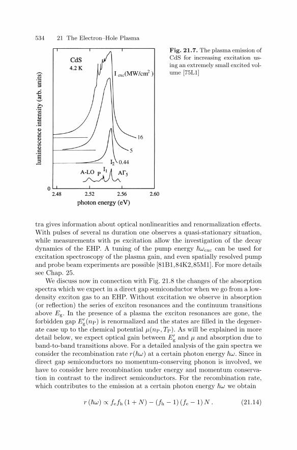
534 21 The Electron–Hole Plasma
Fig. 21.7. The plasma emission ofCdS for increasing excitation us-ing an extremely small excited vol-ume [75L1]
tra gives information about optical nonlinearities and renormalization effects.With pulses of several ns duration one observes a quasi-stationary situation,while measurements with ps excitation allow the investigation of the decaydynamics of the EHP. A tuning of the pump energy ωexc can be used forexcitation spectroscopy of the plasma gain, and even spatially resolved pumpand probe beam experiments are possible [81B1,84K2,85M1]. For more detailssee Chap. 25.
We discuss now in connection with Fig. 21.8 the changes of the absorptionspectra which we expect in a direct gap semiconductor when we go from a low-density exciton gas to an EHP. Without excitation we observe in absorption(or reflection) the series of exciton resonances and the continuum transitionsabove Eg. In the presence of a plasma the exciton resonances are gone, theforbidden gap E′
g(nP) is renormalized and the states are filled in the degener-ate case up to the chemical potential µ(nP, TP). As will be explained in moredetail below, we expect optical gain between E′
g and µ and absorption due toband-to-band transitions above. For a detailed analysis of the gain spectra weconsider the recombination rate r(ω) at a certain photon energy ω. Since indirect gap semiconductors no momentum-conserving phonon is involved, wehave to consider here recombination under energy and momentum conserva-tion in contrast to the indirect semiconductors. For the recombination rate,which contributes to the emission at a certain photon energy ω we obtain
r (ω) ∝ fefh (1 +N) − (fh − 1) (fe − 1)N . (21.14)

21.3 Electron–Hole Plasmas in Bulk Semiconductors 535
Fig. 21.8. Schematic drawing of the low temperature absorption spectra of a direct-gap semiconductor at low excitation and in the presence of an electron–hole plasma
The first term describes spontaneous and stimulated emission, where N is thedensity of photons in the (laser) mode with frequency ω under consideration.The second term describes the reabsorption.
Equation (21.14) can be rewritten as a term independent of N giving thespontaneous emission and a term linear in N giving the net rate of stimulatedemission and of reabsorption
r ∝ fefh −N (1 − fe − fh) (21.15a)
∝ rspont + rstim . (21.15b)
Net gain evidently results for fe + fh > 1 and this simply means
µ (nP, TP) > E′g (nP) (21.16)
as mentioned above.Using now the square-root dependence of the combined density of states
(Sects. 8.9 and 13.1) and also momentum conservation, we get for the spectraof spontaneous emission Ilum(ω) and of gain g(ω) for ω ≥ E′
g(nP)
Ilum (ω) = c2[ω − E′
g (nP)]1/2
fefh , (21.17a)
g (ω) = c2[ω − E′
g (nP)]1/2 (fe + fh − 1) , (21.17b)

536 21 The Electron–Hole Plasma
where ω is given by
ω = E′g (nP) +
2k2
e
2me+
2k2
h
2mh(21.18)
with ke = −kh, and c2 is a proportionality constant including once morethe transition matrix element, which is assumed to be k-independent. Theexpression (21.17) leads to a square-root increase of the gain spectra at thelow energy side and a transition to absorption at ω = µ see Fig. 21.8.
Some modifications of the simple shape of the spectra given in (21.17) arenecessary. One is the so-called Landsberg or final-state damping explainedon the right of Fig. 21.9. If an electron recombines with a hole there is anempty state in the Fermi sea of electrons in the conduction band and anoccupied state in the sea of holes in the valence band. Both states relax veryrapidly as indicated by the dashed arrows. This short lifetime enters as anenergy-dependent broadening which is also known as Landsberg damping.Consequently the gain spectrum has to be convoluted with a Lorentzian. Theparameter Γ in this Lorentzian depends on energy [81K1]. It has a minimumat the quasi Fermi energies and increases below and above roughly linearly
Fig. 21.9. Schematic explanation of the recombination and of the final state damp-ing in a plasma

21.3 Electron–Hole Plasmas in Bulk Semiconductors 537
with energy; see Fig. 21.10a. This final-state damping is the reason why thegain and luminescence spectra do not actually start at E′
g with a square-root dependence but with a smooth tail extending below E′
g as indicated inFig. 21.8. Further contributions to the broadening include the scattering withother quasiparticles such as carriers or plamsons. This phenomenon is alsoknown as “Fermi-sea shake up”. It has been stressed recently in [93S1] andreferences therein and is a “remainder” of or analogy to the inelastic scatteringprocesses discussed in the previous chapter.
The other correction is the so-called excitonic enhancement [81K1,88Z1]which is in metals also known as Fermi-edge singularity or Mahan ex-citon. See [88Z1, 89K1, 93C1] and references therein. It describes an en-hancement of the oscillator strength around µ as a multiplicative termρ(ω) to the gain, absorption or luminescence spectra Fig. 21.10b. Thephysical origin is the following. Around the quasi Fermi levels there areclose-lying occupied and empty states. Electrons and holes in the EHPcan therefore perform around µ under their mutual Coulomb attractionat least pieces of a Bohr-orbit-like motion. This correlation effect is remi-niscent of the exciton and enchances the oscillator strength. In Fig. 21.10we give as examples the k-dependence of the damping for the conductionand valence bands in GaAs and the excitonic enhancement ρ(ω). Morerecent discussions of the optical properties of an EHP can be found, e.g.,in [98M1, 98M2, 98P1, 98S1, 04C1, 04K2]. Especially it has been shown in[04C1, 04K2] that an exciton-like peak can appear in a (dilute) EHP at thespectral position of the exciton due to the e-h Coulomb correlation. See alsothe above information about the role of the excitonic enhancement in thetransmission spectrum.
Fig. 21.10. The damping in the conduction and valence bands of GaAs in thepresence of a plasma (a) and the excitonic enhancement (b). From [81K1]

538 21 The Electron–Hole Plasma
After these general considerations we want to see some examples. InFig. 21.11 we show transmission spectra of a CdS single crystal platelet witha thickness of a few µm without and with additional excitation in the band-to-band transition region.
The plane parallel surfaces of the sample give rise to Fabry–Perot modesin the transparent spectral regions. At low temperatures we see without exci-tation the absorption dip of the AΓ5 exciton (cf. Fig. 13.9), the transparentwindow above, and the onset of the BΓ5 exciton resonance. For higher latticetemperatures the absorption becomes less steep and shifts to the red accord-ing to the Urbach rule of (13.12) or Fig. 13.10. With pump, we see that theexciton resonance disappears at low temperatures. This fact is also confirmedin the reflection spectra not shown here [81B1, 85M1]. In addition we clearlysee optical amplification. In Fig. 21.11a the chemical potential µ coincidingwith the crossover from gain to absorption is situated around 2.54 eV and thereduced gap is at 2.49 eV compared to 2.58 eV in the unexcited sample. Forhigher temperatures, population inversion is no longer reached (see the curvefor TL = 300K) because of the temperature dependence of the effective den-sity of states (8.41) which gives the onset of degeneracy. Nevertheless it is stillpossible to bleach the tail of the absorption.
Fig. 21.11. Transmissionspectra of a CdS platelet-type sample without (- - -)and with (—–) additionalexcitation and for variouslattice temperatures [88S1]

21.3 Electron–Hole Plasmas in Bulk Semiconductors 539
In addition we see a blue-shift of the Fabry–Perot modes at all tempera-tures. This means that the refractive index decreases. This finding is easilyintelligible with the help of the Kramers–Kronig relations of Chap. 6, if weconsider that the exciton resonance disappears from the absorption spectrum.For more recent details of this phenomenon see, e.g., [82K1,83S1].
From raw data as in Fig. 21.11 it is possible to deduce the gain spectra.Examples are given in Fig. 21.12 for CdS for different values of Iexc and forGaAs. The fit including the above mentioned phenomena gives nP, TP, E′
g(nP)and µ(nP, TP). The agreement between calculated data for these quantitiesand experiment is shown in Fig. 21.12b. Figure 21.12c gives finally the gainspectrum of a 1 µm thick epitaxial GaAs layer. The energies of the excitonand of the gap without excitation are given and the data for E′
g and µ underexcitation. The density reached here is considerable higher than in bulk GaAsbecause of the confirment of the EHP to a 1 µm thick layer. We now list severaltypical features of the EHP observed in many direct gap semiconductors, butwithout giving figures or detailed references in every case. They may be foundin [78B1, 80B1, 81K1, 82D1, 84H1, 85B1, 88Z1, 89K4, 89K5, 90H1, 90K2, 94K2,
Fig. 21.12. Gain spectra of CdS at low temperatures for various pump intensities(a) the reduced gap E′
g(nP) and chemical potential µ(nP, TP) deduced from spectralike in (a), (b) and a gain spectrum for a thin GaAs epitaxial layer (c) [81B1,80B1,89K4]. Note the different directions of positive gain in (a) and (c)

540 21 The Electron–Hole Plasma
02N2, 02N3]. The width of the gain spectra increases under quasi-stationarynanosecond excitation with the generation rate as long as there is no pinningof the quasi Fermi levels by stimulated emission, and decreases in time afterpicosecond excitation. This means that the density is not constant, althoughTP is clearly below Tc e.g. for CdS. In Fig. 21.12 the values for the highestexcitation are nP = 3.1018 cm2; TP = 20 K (TL = 7 K, Tc = 64 K). Evidentlyno liquid phase is formed. The reason is the short lifetime of the carriers ofabout 100 to 200 ps in a degenerate EHP [81B1]. This time is not long enoughfor the formation of a spatial phase separation into liquid like droplets anda gas phase. There will be strong spatio–temporal density fluctuations and insome regions (e.g., in the vicinity of fast recombination centers in the volumeor at the surface) the density will stay lower than in others, possibly even belowthe Mott density. No clear evidence of a phase separation has been observed ina binary direct gap semiconductor up to now. A pinning of nP with increasingexcitation and spatial density inhomogeneities are often results of stimulatedemission and not of a phase separation. However, recently EHL formation hasbeen claimed in the direct gap semiconductor CuCl, based among others onthe dynamics of luminescence and IR-reflection spectra [02N1].
The plasma temperature TP usually lies above the lattice temperature TL.The difference is only a few ten K in the more ionic II–VI compounds withgood coupling of the carriers to the lattice. However, after pulsed excitationthe difference can reach several tens of K up to around a hundred K in a firsttransient cooling period. In the more covalent III–V compounds the differ-ences between TP and TL are generally higher. This temperature differencealso increases with the excess energy of the excitation, i.e., with ωexc −Eex.A rather cool electron–hole plasma can consequently be created under reso-nant excitation in the exciton region or even slightly below.
Since the absorption coefficient is rather high in direct gap semiconduc-tors (104 − 105 cm−1) the penetration depth of the pump light is 1 µm.Consequently a strongly inhomogeneous spatial density distribution is cre-ated in thicker bulk samples. The gradient of the chemical potential (orof the density) causes an expansion of the plasma. Typical values of thedrift or diffusion length lD of a degenerate EHP, e.g., in CdS or CdSe, arelD ≈ (10 ± 5)µm, while the values for the nondegenerate case are closer to1 µm [81B1,84K2,88S1,89R1]. Depending on the experimental conditions onetherefore often has to consider an inhomogeneous density distribution in theevaluation of luminescence or gain spectra. In quasi-stationary pump andprobe beam experiments it is therefore advisable to probe only in the spatialand temporal center of the pump pulse and to use thin ( 10 µm) samples.In narrow gap materials such as InSb values of lD up to 60 µm have beenreported due to the longer carrier lifetimes and the smaller effective massesin this group of materials [85H1].
In Fig. 21.2 we compare finally the calculated, normalized band-gap renor-malization as a function of rs [see (21.5)] with experimental data. As alreadymentioned, good agreement is found for the mainly covalently bound direct

21.3 Electron–Hole Plasmas in Bulk Semiconductors 541
and indirect gap semiconductors like Si, Ge, GaAs, GaP etc. For clarity we donot give data points for them here. In the case of several populated (in-) equiv-alent minima, the distribution of the carriers over the various minima has tobe considered explicitly [82F2,88K1,92K2,96K1]. Beautiful experiments alongthese lines exist for Al1−yGayAs in the transition region from a direct to anindirect band structure around y = 0.43 [88K1,92G1,92K2,98D1].
The data for various II–VI semiconductors are shown explictly in Fig. 21.2.They follow the trend of the theory, but with an average shift of about 0.5 Ry∗
to lower energies. This discrepancy has two main causes. The ionic part of thebinding in the II–VI stabilizes the plasma, e.g., via plasma-phonon mixedstates. This contribution is not contained in the general formula. Addition-ally the values of Ry∗ and of the experimentally determined exciton bindingenergies do not exactly coincide, as was mentioned in Sects. 9.2 and 20.3.1in connection with the biexciton. Similar arguments also hold for aB whichappears in rs.
In mixed crystals such as CdS1−xSex and Al1−yGayAs it has been foundthat the many-particle effects are strongly reduced as long as the electron–hole pairs occupy only the localized states. One finds essentially a bleach-ing of the absorption tail of the localized states with increasing density, butnot much of a band-gap renormalization [87M1]. If the extended states arepopulated, however, the properties of the band renormalization and bandfilling are very similar to those of the binary compounds CdS, CdSe andGaAs [85C1,87M1,89K1,96K1]. The population of the extended states occurse.g. under sufficiently strong pumping so that the total density of electron–hole pairs exceeds the density of localized states. Nloc. This situation can beachieved quite easily in Al1−yGayAs but not in CdS1−xSex where Nloc is be-tween 1018 and 1019 cm−3. In the latter case, however, the extended states
Fig. 21.13. The shift of the absorption edge in CdS, CdSe, and CdS1−xSex underhigh excitation as a function of temperature [89K1]

542 21 The Electron–Hole Plasma
are also populated to a considerable degree for TP TL > εloc/kB where εloc
is the tailing parameter introduced in (14.7). In Fig. 21.13 we show the shiftof the absorption edge under high excitation for CdS (see also Fig. 21.11),CdSe, and CdS1−xSex,. In CdS1−xSex one finds at low temperatures a blueshift, due to state filling without renormalization, but a higher temperaturesa behavior similar to that for the EHP in the binary compounds.
For the observation of plasmons or plasmon-phonon mixed states in uni-polar plasmas created by high doping levels see e.g. Fig. 12.1 and 12.4or [97G2], for bipolar plasmas Fig. 12.3 or for more recent work in Si, C,GaAs, GaN or CuCl [00N1, 02N2, 02N3, 02N4, 02S1]. As a short preview toChap. 23, we mention that the formation time of Coulomb screening andband-gap renormalisation has been found to be a few ten fs [01H1].
21.4 Electron–Hole Plasma in Structuresof Reduced Dimensionality
In this section, we look at the electron–hole plasma in systems of reduceddimensionality. For recent reviews of this topic see [90C1, 90H1, 94C1, 94K1,94K2,94K3,96K1,01L1,04C1,04K1,04O1] and references therein.
In Fig. 21.14a we show pump and probe spectra of an Al1−yGayAs/GaAsMQW sample, the GaAs substrate of which has been removed by a selec-tive etching technique. Without excitation we see the now familiar featuresof the nz = 1 and 2hh and lh exciton resonances. With increasing pumppower, again using quasi-stationary ns excitation, a scenario develops similarto that for the three-dimensional system: The exciton resonances disappear,and there is population inversion between the reduced gap and the chemi-cal potential. The weak modulation in the resulting gain spectra comes fromresidual Fabry–Perot modes of the structure. The slope of the transition fromgain to absorption gives the plasma temperature if the excitonic enhance-ment is also properly taken into account. The approximately constant gainvalue reflects the constant density of states for effective mass particles ina two-dimensional system (see Fig. 8.20). In agreement with the statementsabove, TP is higher than in the more ionic II–VI compounds. In Fig. 21.14bwe show the density dependence of E′
g and of µ and a calculation of E′g for
a strictly two-dimensional system using some effective parameters of the exci-tonic Rydberg energy to account for the finite well thickness lz. The band gaprenormalization shown in Fig. 21.14b has been confirmed for lower densities(0.5 to 2 × 1011 cm−2) in [01I1]
Looking closer, we find some differences that are characteristic of the two-dimensional system. The nz = 2hh resonance is still seen quite clearly atdensities where the nz = 1hh feature has already vanished. The screening ofthe Coulomb interaction by the free carriers would act on occupied and emptystates in the same way. Consequently we may conclude that phase-space filling,which depends on the occupation of the states, is more important in quasi-2d

21.4 Electron–Hole Plasma in Structures of Reduced Dimensionality 543
Fig. 21.14. Transmission spectra of an Al1−yGayAs/GaAs MQW sample for variouspump intensities (a) and the resulting dependence of the reduced gap E′
g (b) and ofthe chemical potential µ on the electron–hole pair density per unit area nP [89K4,91S1]
systems than in 3d ones. This interpretation is confirmed by the fact that thenz = 2hh resonance disappears only when the chemical potential comes closeto it, i.e., when the occupation of the higher subbands starts.
Qualitatively this finding can be understood as follows: The Coulomb in-teraction between electron and hole can be screened in a 3d system in all

544 21 The Electron–Hole Plasma
Fig. 21.15. Luminescence spectra of small mesas of InGaAs MQW samples [89K2]
directions of space, whereas the screening in a QW affects preferenentially thefield lines in the well. It is more difficult to screen the field lines which gothrough the barrier since here the probability of finding carriers is reduced tothe exponential tails of wave function shown in Figs. 8.22 and 23.
The other point concerns the fact that the renormalization of the highersubbands (nz 2) in a QW system is smaller than that of the fundamentalgap, as long as the higher subbands are not populated. One reason for thisfinding [88C1, 89K2, 89K3, 89K4, 91S1] is that electrons (and holes) in differ-ent subbands are no longer subject to the exchange interaction, which formsan important contribution to the renormalization of the gap, as outlined inSect. 21.2.
In Fig. 21.15 we give as a further example for the above phenomena lumi-nescence spectra of an In1−yGayAs MQW sample. In this case the plasmahas been confined laterally by the formation of mesa-structures of about10 µm × 10 µm, resulting in a very homogeneous excitation. The band renor-malization and the successive filling of states and of higher subbands withincreasing pump power are clearly visible even under cw excitation. The bandgap renormalization in short period type II GaAs/AlAs superlattices (seeSect. 15.2) has been investigated in [95L1,96K1]. Due to the redistribution ofthe carriers between the various band extrema, even a negative, differentialband gap renormalization occurs.
The influence of a unipolar plasma on the optical spectra of an In1−yGayAssingle quantum well has been presented in [87B1,88C1]. The two-dimensional

21.5 Inter-subband Transitions in Unipolar and Bipolar Plasmas 545
carrier density has been varied by the gate voltage in a MODFET. See also[04C1,04K2] for a discussion of the luminescence spectra of this material.
Obviously electron–hole plasmas also exist in Si/Si1−xGex quantum wells.In [92X1] a band gap renormalization of about 15 meV has been observed forwider wells, which tend to vanish for narrower wells.
Recent results on the EHP in quasi-one-dimensional quantum wires arecompiled in [90C1,94C1,96K1,01L1,04K1].
In quantum wires, the screening is even less important than in quasi two-dimensional systems. To a good approximation it can be neglected. Calcu-lations of the band gap renormalization (BGR) by exchange and correlationeffects can be found, e.g., in [96B1,97G1,99P1]. Experiments for, e.g., GaAs-or InAs-based quantum wires are found, e.g., in [95G1,95G2,99B1,99P1,01L1]and the references given therein.
In quantum dots, it is to some extent a question of semantics to distin-guish between (possibly charged) multiexciton complexes (see Sect. 20.3.2)and a plasma. We give here some references for type II Ge/Si dots [02Y1].References for GaAs- and InAs-based dots are found, e.g., in [95G2, 96B2,96S1,98H1,01L1].
In this section we have mentioned several times the appearance of opticalgain or of stimulated emission in an EHP. Actually this phenomenon doesnot only appear in an EHP but also in connection with other high-excitationprocesses. We give more information about these cases in the next chapter.
21.5 Inter-subband Transitions in Unipolarand Bipolar Plasmas
In Sect. 13.3 we gave examples for intra-excitonic transitions.When the excitons disappear in a unipolar or bipolar plasma, there is still
the possibility to observe transitions between various subbands both in bulksemiconductors and in structures of reduced dimensionality. These transitionsare known as inter-valence band or inter sub-band transitions.
21.5.1 Bulk Semiconductors
In Fig. 21.16 we show the valence band structure of a cubic group IV or binarysemiconductor including heavy and light holes and the spin orbit split-off (so)valence band.
The dashed line corresponds to a situation without interaction between thelh and the so bands and the solid lines include such an interaction resultingin an avoided crossing (also see Sect. 8.8). This interaction increases withdecreasing spin orbit splitting ∆so. The calculation in Fig. 21.6 has beenmade for InP [99D1] where ∆so ≈ 100 meV.
If holes are present, e.g., in the hh band created either by p-doping or byoptical interband excitation of electrons from the valence to the conduction

546 21 The Electron–Hole Plasma
Fig. 21.16. Valence band of a cubicsemiconductor with heavy hole (hh), lighthole (lh), spin orbit split-off band (so)and transitions of holes [99D1]
band, these holes can be excited to deeper bands by absorption of a photonas shown by the two arrows.
At elevated temperatures, these transitions usually lead to rather broadand unstructured absorption bands. Examples for InP are found, e.g., in[99K1]. Data for other materials including Si or Ge can be found in [02L1].
The electron and hole states can already be quantized for bulk materialsby applying a sufficiently strong magnetic field. If electrons and/or holes arecreated by doping, optical excitation or carrier injection the inter-Landaulevel transitions or cyclotron transitions can be observed in luminescence orabsorption. A few out of the many references in this field are, e.g., [76B1,83L1,92U1,02L1].
21.5.2 Structures of Reduced Dimensionality
In structures of reduced dimensionality the valence and conduction bands arealready split without external magnetic field into various subbands. For anearly example see [85W1].
The selection rules for inter-subband transitions in a simple conductionband are simple
∆nz = ±1; for E⊥ well . (21.19)
The selection rule between different subbands connects states of oppositeparity and the orientation of the electric field results from the orientationof the dipoles normal to the plane of the well as becomes obvious, e.g., byinspecting the wave functions of the first two quantized electron states inFig. 8.21.
We show various examples in Fig. 21.17. Figure 21.17a gives the absorp-tion of an n-type modulation doped, 6 nm wide GaAs multiple quantum well

21.5 Inter-subband Transitions in Unipolar and Bipolar Plasmas 547
Fig. 21.17. (a) The inter-subband absorption ofan n-modulation dopedGaAs/Al1−yGayAs MQWsample. (b) The inter-miniband absorption ofa homogenously n doped200 × (7.5 nm GaAs/2.5 nmAl1−yGayAs) superlattice[95T1, 93H1] and (c) of anoptically pumped 140 × (2 nmCdS/1.9 nm ZnSe) superlat-tice [00G1,02G1]

548 21 The Electron–Hole Plasma
sample. The absorption band for the nz = 1 → nz = 2 transitions is rathernarrow. If the two conduction subbands are parallel, the width comes from ho-mogeneous broadening and an additional inhomogeneous contribution causedby interface disorder.
The situation is quite different for superlattices. The miniband disper-sion results in a characteristic broadening of the inter-miniband absorptionas shown for the conductions bands of a III–V and a II–VI superlattice inFig. 21.17b, c.
Figure 21.17c is also an example for the verification of the selection rules forconduction subbands. The sample is undoped and optical excitation createsboth electrons and holes [00G1, 02G1]. In this reference data are also givenfor multiple quantum wells and many particle effects and their influence oninter-subband transitions are discussed.
Inter- and intra-subband transitions in GaAs/Al1−yGayAs and in GaN/Al1−yGayN multiple quantum wells are discussed in [98Z1,03C1] and data oninter-subband transitions in Si/Si1−xGex multiple quantum wells are foundin [94F1]. Inter-miniband transitions are reviewed in [95H1].
For quantum wires see, e.g., [00C1]. Further examples and references aregiven in [01L1].
21.6 Problems
1. Compare the values of the Mott density of CuCl, CdS, and InSb at 0 andat 300 K using the appropriate formulas and material parameters. Whatare the excitation intensities needed to reach the Mott density under quasi-stationary conditions if you excite with ωexc Eg and assume a diffusionlength of the carrier of 1, 10 or 50 µm and a lifetime of 0.1 ps?
2. Develop formulas to deduce the gain spectra from raw data as in Fig. 21.11assuming that the diffusion length of the plasma is greater than (less than)the thickness of the sample. If you get stuck, try to make reasonableassumptions.
3. How would the gain spectra (21.17) change qualitatively, if you assumea drift of the carriers with a velocity v = 1
2vF? Here, vF is the Fermivelocity.
4. Deduce the effective plasma temperature from some of the spectra ofFigs. 21.12, 21.14 and 21.15, neglecting excitonic enhancement and final-state damping.
References to Chap. 21
[23D1] P. Debye and E. Huckel, Phys. Z. 24, 185, 305 (1923)[27T1] L.H. Thomas, Proc. Camb. Phil. Soc. 23, 542 (1927)[28F1] E. Fermi, Z. Phys. 48, 73 (1928)

References to Chap. 21 549
[68K1] L.V. Keldyh, Proc. 9th Intern. Conf. Phys. Semiconductors, p. 1303,Moscow (1968)
[74M1] N.F. Mott, Metal-Insulator Transitions, Taylor, Francis, London (1974)[74T1] G.A. Thomas, T.M. Rice and J.C. Hensel, Phys. Rev. Lett. 33, 219 (1974)[75L1] V.G. Lyssenko et al., Sov. Phys. JETP 41, 163 (1975)[75R1] T.L. Reinecke and S.C. Ying, Phys. Rev. Lett. 35, 311 (1975)[76B1] G. Bauer et al., phys. stat. sol. (b) 75, 543 (1976)[77H1] T.C. Hensel, T.G. Phillips and G.A. Thomas, Solid State Phys. 32, 88
(1977)[77H2] E. Hanamura and H. Haug, Phys. Rep. 33C, 209 (1977)[77M1] R.W. Martin, Solid State Commun. 19, 373 (1976); ibid. 22, 523 (1977)[77M2] R.S. Markiewicz, J.P. Wolfe and C.D. Jeffries, Phys. Rev. B 15, 1988 (1977)[77R1] T.M. Rice, Solid State Phys. 32, 1 (1977)[78B1] G. Beni and T.M. Rice, Phys. Rev. B 18, 768 (1978)[78L1] V.G. Lysenko and V.I. Revenko, Sov. Phys. Sol. State 20, 1238 (1978)[79C1] M. Combescot, Solid State Commun. 30, 81 (1979)[79M1] H. Maaref et al., J. Lumin. 18/19, 547 (1979)[79W1] R.M. Westervelt, J.C. Culbertson and B.S. Black, Phys. Rev. Lett. 42, 269
(1979)[80B1] K. Bohnert, G. Schmieder and C. Klingshirn, phys. stat. sol. (b) 98, 175
(1980)[80G1] M. Greenstein and J.P. Wolfe, Solid State Commun. 33, 309 (1980)[81B1] K. Bohnert et al., Z. Phys. B 42, 1 (1981)[81F1] A. Forchel et al., Phys. Rev. Lett. 46, 678 (1981)[81K1] C. Klingshirn and H. Haug, Phys. Rep. 70, 315 (1981)[81S1] H. Stolz, R. Zimmermann and G. Ropke, phys. stat. sol. (b) 105, 585
(1981)[82D1] R. Dai et al., Z. Physik B 46, 189 (1982)[82F1] A. Forchel, Ph.D. Thesis, Stuttgart (1982)[82F2] G.W. Fehrenbach et al., Phys. Rev. Lett. 49, 1281 (1982)[82K1] A. Kreissl et al., phys. stat. sol. (b) 114, 537 (1982)[82V1] P. Vashista and R.K. Kalia, Phys. Rev. B 25, 6492 (1982)[83C1] M. Combescot and C. Benoit a la Guillaume, Solid State Commun. 46,
579 (1983)[83L1] G. Lindemann et al., Phys. Rev. B 28, 4693 (1983)[83S1] S. Schmitt-Rink et al., Physica B 117/118, 339 (1983)[84H1] H. Haug and S. Schmitt-Rink, Prog. Quantum Electron 9, 3 (1984)[84K1] S.W. Koch, Dynamics of First-Order Phase Transitions in Equilibrium
and Nonequilibrium Systems, Lecture Notes Phys. 207, Springer, Berlin,Heidelberg (1984)
[84K2] K. Kempf and C. Klingshirn, Solid State Commun. 49, 23 (1984)[84M1] G. Manzke, V. May and K. Henneberger, phys. stat. sol. (b) 125, 693
(1984)[85B1] D. Bimberg, in Landolt-Bornstein New Series, Group III, Vol. 17i, 297
(1985)[85C1] M. Capizzi et al., Helv. Phy. Acta 58, 272 (1985)[85E1] Electron–Hole Droplets in Semiconductors, C.D. Jeffries and L.V. Keldysh,
(eds.), Mod. Probl. Cond. Mat. Sci., Vol. 6, North-Holland, Amsterdam(1985)

550 21 The Electron–Hole Plasma
[85H1] D.J. Hagan et al., Opt. Lett. 10, 187 (1985)[85H2] D. Hulin et al., J. Luminesc. 30, 290 (1985)[85M1] F.A. Majumder et al., Phys. Rev. B 32, 2407 (1985)[85W1] L.C. West and S.J. Eglash, Appl. Phys. Lett. 46, 1156 (1985)[87B1] I. Bar-Joseph et al., Phys. Rev. Lett. 59, 1357 (1987)[87M1] F.A. Majumder et al., Z. Phys. B 66, 409 (1987)[88C1] D.S. Chemla et al., IEEE J. QE 24, 1664 (1988)[88K1] H. Kalt, A.L. Smirl and T.F. Bogges, phys. stat. sol. (b) 150, 895 (1988)[88S1] H.E. Swoboda et al., Z. Phys. B 70, 341 (1988) and Phys. Rev. B 39,
11019 (1989)[88Z1] R. Zimmermann, Many Particle Theory of Highly Excited Semiconductors,
Teubner Texte Phys., Teubner, Leipzig (1988)[88Z2] R. Zimmermann, phys. stat. sol. (b) 146, 371 (1988)[89K1] C. Klingshirn et al., NATO ASI Seri. B 194, 353 (1989)[89K2] V.D. Kulakovskii et al., Phys. Rev. B 40, 8087 (1989)[89K3] H. Kalt et al., Phys. Rev. B 40, 12017 (1989)[89K4] C. Klingshirn et al., NATO ASI Ser. B 200, 167 (1989)[89K5] C. Klingshirn et al., NATO ASI Ser. B 194, 353 (1989)[89R1] M. Rinker et al., Solid State Commun. 69, 887 (1989)[90C1] R. Cingolani and K. Ploog, Adv. Phys. 40, 535 (1990)[90F1] H. Fieseler, R. Schwabe and J. Staehli, phys. stat. sol. (b) 159, 411 (1990)[90H1] H. Haug and S.W. Koch, Quantum Theory of Optical and Electronic Prop-
erties of Semiconductors, World Scientific, Singapore (1990)[90K1] C. Klingshirn, Festkorperprobleme / Adv. Solid State Phys. 30, 335 (1990)[90K2] M. Kunz et al., J. Crystal Growth 101, 734 (1990)[91S1] K.-H. Schlaad et al., phys. stat. sol. (b) 159, 173 (1990) and Phys. Rev. B
43, 4268 (1991)[92G1] S. Gurtler et al., phys. stat. sol. (b) 173, 441 (1992)[92K1] H. Kalt, Festkorperprobleme / Adv. Solid State Phys. 32, 145 (1992)[92K2] H. Kalt and M. Rinker, Phys. Rev. B 45, 1139 (1992)[92P1] P.P. Paskov, Europhys. Lett. 20, 143 (1992)[92U1] K. Unterrainer et al., Semicond. Sci and Technol. 7, B 604 (1992)[92X1] X. Xiao et al., Appl. Phys. Lett. 60, 1720 (1992)[93C1] M. Combescot and Ch. Tanguy, in Proc. 21st Int. Conf. on Physics of Semi-
conductors, Beijing 1992, Ping Jiang, Hou-Zhi Zheng eds., World Scientific,Singapore, p. 141 (1993)
[93D1] F. Daminger et al., In Proc. 21st Int. Conf. on Physics of Semiconductors,Beijing 1992, Ping Jiang, Hou-Zhi Zheng eds., World Scientific, Singapore,p. 1293 (1993)
[93H1] M. Helm et al., Phys. Rev. B 48, 1601 (1993)[93P1] K. Ploog, R. Notzel and O. Brandt, In Proc. 21st Int. Conf. on Physics
of Semiconductors, Beijing 1992, Ping Jiang, Hou-Zhi Zheng eds., WorldScientific, Singapore, p. 1297 (1993)
[93S1] M.S. Skolnick et al., In Proc. 21st Int. Conf. on Physics of Semiconductors,Beijing 1992, Ping Jiang, Hou-Zhi Zheng eds., World Scientific, Singapore,p. 41 (1993)
[94C1] R. Cingolani, Physica Scripta T 49 B, 470 (1994)[94F1] T. Fromherz et al., Phys. Rev. B 50, 15073 (1994)[94I1] M. Illing et al., J. Crystal Growth 138, 638 (1994)

References to Chap. 21 551
[94K1] E. Kapon, Semiconductors and Semimetals 40, 259 (1994)[94K2] C. Klingshirn, NATO ASI Series B 339, 327 (1994)[94K3] H. Kalt, J. Lumin. 60/61, 262 (1994)[95G1] M. Grundmann et al., J. Nonlin. Opt. Phys. Mater. 4, 99 (1995)[95G2] H.F. Ghaemi et al., Superlattices and Microstructures 17, 15 (1995)[95H1] M. Helm, Semicond. Sci. and Technol. 10, 557 (1995)[95L1] W. Langbein et al., Phys. Rev. B 51, 1946 (1995)[95S1] L.M. Smith and J.P. Wolfe, Phys. Rev. B 51, 7521 (1995)[95T1] E. Towe et al., Superlattices and Microstructures 17, 129 (1995)[96B1] M. Bayer et al., Phys. Rev. B 55, 13180 (1996)[96B2] K. Bollweg et al., Phys. Rev. Lett. 76, 2774 (1996)[96K1] H. Kalt, Optical Properties of II–V Semiconductors: The Influence of
Multi-Valley Band Structures Springer Series in Solid State Sciences 120,Springer, Berlin (1996)
[96S1] R. Steffen et al., Surf. Sci 361, 805 (1996)[97G1] A. Grindt et al., phys. stat. sol. (b) 202, 725 (1997)[97G2] H. Goppert et al., J. Luminesc. 72–74, 430 (1997)[98D1] U. Dorr et al., J. Appl. Phys. 83, 2241 (1998)[98H1] R. Heitz et al., Phys. Rev. B 57, 9050 (1998)[98M1] G. Manzke et al., phys. stat. sol. (b) 206, 37 (1998)[98M2] G. Manzke et al., Phys. Rev. Lett. 80, 4943 (1998)[98P1] M.F. Pereira, Jr. and K. Henneberger, phys. stat. sol. (b) 206, 477 (1998)[98S1] R. Schepe et al., phys. stat. sol. (b) 206, 273 (1998)[98Z1] Q.-S. Zhu et al., Phys. Rev. B 57, 12388 (1998)[99B1] C.R. Bennet et al., Physica B 263-264, 546 (1999)[99D1] A. Dargys, Optics Commun. 170, 47 (1999)[99K1] S. Kakimoto and H. Watanabe, J. Appl. Phys. 85, 1822 (1999)[99P1] C. Piermarocchi et al., Sol. State Commun. 112, 433 (1999)[00C1] S. Calderon et al., Phys. Rev. B 62, 9935 (2000)[00G1] M. Goppert et al., J. Crystal Growth 214/215, 625 (2000) and Physica E
7, 89 (2000)[00J1] A. Jolk et al., phys. stat. sol. (b) 221, 295 (2000)[00M1] T. Meier et al., Phys. Rev. 62, 4218 (2000)[00M2] T. Meier and S.W. Koch, phys. stat. sol. (b) 221, 211 (2000)[00N1] M. Nagai and M. Kuwata-Gonokami, phys. stat. sol. b 221, 261 (2000)[01I1] H. Ichida et al., Proceedings of 2000 Internat. Conf on Excitonic Processes
in Condensed Matter (= EXCON 2000), Osaka, Japan, August 22–25,2000, K. Cho and A. Matsui eds., World Scientific, Singapore, New Jersey,London, Hong Kong, p. 225 (2001)
[01L1] Landolt-Bornstein New Series, Group III, Vol 34C1, C. Klingshirn, ed.,Springer, Berlin (2001)
[01H1] R. Huber et al., Nature 414, 286 (2001)[01N1] M. Nagai, R. Shimano and M. Kuwata-Gonokami, Phys. Rev. Lett. 86,
5795 (2001)[02G1] M. Goppert et al., Phys. Rev. B 65, 115334 (2002)[02I1] T.J. Inagaki and M. Aihara, Phys. Rev. B 65, 205204 (2002)[02L1] Landolt-Bornstein New Series, Group III, Vol. 41 A1 B, U. Rossler, ed.,
Springer, Berlin (2002)[02N1] M. Nagai and M. Kuwata-Gonokami, J. Luminesc. 100, 233 (2002)

552 21 The Electron–Hole Plasma
[02N2] M. Nagai, K. Ohkawa and M. Kuwata-Gonokami, Appl. Phys. Lett. 81,484 (2002)
[02N3] M. Nagai and M. Kuwata-Gonokami, J. Phys. Soc. Japan 71, 2276 (2002)[02N4] M. Nagai et al., phys. stat. sol. b 238, 509 (2002)[02S1] R. Shimano et al., Phys. Rev. Lett. 88, 057404 (2002)[02Y1] A.I. Yakimov et al., Physica E 13, 1026 (2002)[03C1] G. Chen et al., phys. stat. sol. b 240, 384 (2003)[03N1] M. Nagai, phys. stat. solidi B, 238, 509 (2003)[04C1] S. Chatterjee et al., Phys. Rev. Lett. 92, 067402 (2004)[04K1] E. Kapon in ref. [81A1]l in press[04K2] S.W. Koch and M. Kira in Ref. [04O1]p 1[04O1] Optics of Semiconductors and Their Nanostructures, H. Kalt and M. Het-
terich eds., Springer Series in Solid State Science 146 (2004)[04P1] H. Priller et al., phys. stat. sol. b 241, 587 (2004)

22
Stimulated Emission and Laser Processes
Stimulated emission from semiconductors is usually identified in experimentsby the occurrence of one or several of the following criteria: a strongly super-linear increase of the optical luminescence output Ilum as a function of thepump power Iexc above a certain threshold Ith
exc with slopes α in Ilum ∝ Iαexc of
three and more; a simultaneous spectral narrowing of the emission, often ac-companied by the appearance of laser modes imposed by some cavity lengthand a spatially directed emission above Ith
exc. The increase of the coherencelength of the emitted light is also characteristic for laser emission, but is lessused to identify laser emission from semiconductors, though semiconductorslaser with external, wavelength-selective cavities are developed with extremlynarrow spectral emission.
Many of the high excitation effects outlined in Chaps. 19 to 21 can leadto stimulated emission under suitable conditions; see, e.g., [73B1,75K1,81K1,81S1, 92E1, 93K1, 94C1, 95K1, 97N1, 99M1, 03I1, 03R1, 03R2] and referencestherein. In this chapter we treat those aspects of the high excitation phenom-ena of Chaps. 19 to 21 which are specific for stimulated emission.
Pumping can be accomplished by excitation with intense (laser-) light[81K1, 94C1], (Iexc 104 W/cm2 depending on the material and the pumpconditions), with electron beams [64B1, 73B1, 92B1, 92N1] (j 10 A/cm2,U 30 keV), by a flash-lamp [83B1] or by a forward biased pn junction[81S1, 92E1, 92N1, 04H1], provided that it is possible to grow the materialin the desired highly p- and n-doped versions. Optical pumping is usuallythe proper choice for scientific investigations of the gain processes, since itallows resonant excitation of some species, e.g., certain exciton or biexcitonlevels. Pumping by electron beams, on the other hand, is unselective and anenergy of about 3Eg is deposited for the creation of one electron–hole pair.Electron–beam pumping was widely used before high power lasers were avail-able [64B1,73B1] and more recently for the realization of color projection TVtubes with high brightness [92B1,92N1].
Pumping by a pn (hetero-) junction biased in the forward direction isobviously the best choice for most technical applications in laser diodes, which

554 22 Stimulated Emission and Laser Processes
are found, for example, in every CD player, laser scanner, laser printer or barcode reader [81S1,92E1].
Stimulated emission has, until now been almost exclusively limited todirect gap semiconductors. An exception, namely Al1−yGayAs close to thedirect-indirect crossover, was mentioned in Sect. 21.3 and in [96K1] and weshall come back to this later. Our considerations are restricted therefore todirect gap materials where not stated otherwise.
22.1 Excitonic Processes
The processes which lead to stimulated emission can either be of intrinsicnature, i.e., they involve only excitations of the perfect lattice, or of extrinsicnature, involving some impurity or defect states. We shall see in the followingexamples of both groups.
We use the language of the weak coupling limit for reasons of simplicity,but state, that we are actually dealing with polaritons. We start with intrinsicprocesses in the intermediate density regime, namely the recombination of anexciton with emission of one or more LO phonons, or with inelastic scatter-ing by another exciton or a free carrier, or finally the decay of a biexcitoninto a photon and an exciton. All these processes were already introducedin Chap. 20. In Fig. 22.1 we summarize these effects again actually drawingthem in the strong coupling or polariton picture.
In all four cases some initial state decays under emission of a photon andleaves behind in the crystal another excitation, for example an exciton inits ground state in the case of biexciton decay, an LO phonon in the caseof the phonon replica, or an exciton in an excited state nB 2 or a freecarrier at higher kinetic energy in the cases of inelastic exciton-exciton or-free carrier scattering, respectively. All these processes have the low thresholdfor population inversion typical for four-level laser systems as long as thisexcited final state in the sample is not (thermally) populated. If there are noexcitons thermally excited into nB = 2 state, or no thermally populated LOphonons, then population inversion is reached in the presence of two or evenone exciton, respectively. See also (22.2c). We consider now the rate equationsfor these processes, assuming that for a given photon energy ω there is justone (laser-) mode containing photons with a density Nph. The general rateequation which holds is [81K1]:
dNPh
dt= −2κNPh +
∑ 2πδ (∆E) |W |2Q , (22.1)
where −2κNPh contains all losses of the resonator, e.g., due to finite reflectionor diffraction. The second term on the right of (22.1) contains a sum over all(scattering) processes contributing to the emission at ω,δ(∆E) stands for theenergy conservation, Q is a population factor into which we can integrate thek-conservation, and |W |2 finally is the transition matrix element. As a first

22.1 Excitonic Processes 555
approach to the strong coupling limit one can also incorporate into |W |2 theprobabilities that the exciton polariton is exciton-like in the initial state andphoton-like in the final state. The next step would involve the use of thepolariton dispersion curves of Fig. 22.1 instead that of excitons and photons.See [81K1].
We consider here as an example the P2 line, i.e., the inelastic scatter-ing between two excitons in the nB = 1 state, from which one is scatteredunder energy and momentum conservation into a state with nB = 2, whilethe other one appears as a photon. In the strong coupling limit one wouldstate, that there occours an inelastic polariton-polariton scattering processbetween two exciton polaritons, from which one is scattered onto the pho-tonlike (lower) polariton branch and the other into an excited exciton-likepolariton state.
In this case we have
∆E = Eex (nB = 1,k1) +Eex (nB = 1,k2)−ω − Eex (nB = 2,k1 + k2) ,
(22.2a)
Fig. 22.1. Inelastic scattering processes in the intermediate density regime: exciton-LO phonon emission (c), inelastic exciton–exciton scattering (b), inelastic exciton–electron scattering (a) and biexciton decay (d) [81K1]

556 22 Stimulated Emission and Laser Processes
and the population factor Q reads
Q = Nex (k1, nB = 1) ×Nex (k2, nB = 1)× [1 +Nex (k1 + k2, nB = 2)] (1 +NPh)−NPhNex (k1 + k2, nB = 2) [1 +Nex (k1, nB = 1)]× [1 +Nex (k2, nB = 1)] ,
(22.2b)
where we consider photons and excitons as bosons.We can now decompose Q into two terms. One which is independent of
NPh and describes the spontaneous emission and another one which is linearin NPh and gives the net gain or absorption. For the latter, Qstim, we find
Qstim = NPh Nex (k1, nB = 1)Nex (k2, nB = 1)−Nex (k1k2, nB = 2)× [1 +Nex (k1, nB = 1) +Nex (k2, nB = 1)] .
(22.2c)
If we assume thermal equilibrium between the excitons in the variousstates, we see that inversion occurs, i.e., Qstim > 0 at low temperatures, evenif we have only two excitons which collide as mentioned already above.
The luminescence and gain increase roughly quadratically with the exci-ton density and thus superlinearly with the pump intensity at low tempera-ture until the gain overcomes the losses and stimulated emission sets in. Athigher temperatures the nB = 2 states will be also populated, reabsorptionoccurs and may even overcome the gain in some spectral regions, resulting inexcitation-induced absorption.
The biexciton decay and the exciton-free carrier scattering also have gainvalues which increase superlinearly with density, while the gain of the ex-n LOprocess grows essentially linearly with the generation rate until laser emissionsets in.
If Fig. 22.2 we show the calculated temperature dependences of the laserthreshold densities for three of the above-mentioned processes for a given con-stant value of κ. A variation of κ will shift the various quadratic processeswith respect to the linear one. The increase of the thresholds with increasingtemperature comes from the thermal population of the final states as indi-cated above. The high threshold at low temperatures of the process involvingfree carriers originates from the assumption of thermal equilibrium. In thiscase no free carriers (i.e., excitons in the continuum state) are present at lowtemperatures. The exciton-free carrier-scattering process can be influencedby doping. The fact that the calculated carrier densities are relatively highand may exceed the Mott density (Chap. 21) is due to the use of rather highlosses in the calculations. Lower loss values reduce the calculated thresholddensities.
On the other hand this finding shows that stimulated emission occurs fre-quently in the transition region between intermediate and high densities. The

22.1 Excitonic Processes 557
exciton binding energy decreases with increasing density, i.e., the excitons be-come “soft” and inelastic scattering processes between carriers may take placein an EHP or the emission of phonons or plasmons in the recombination pro-cess of an electron–hole pair. While scientists tried to separate these variousprocesses in the 1970s and 1980s it is now, at least from the theoretical side,the aim to present calculations that are valid continuously from low densitiesto the EHP as already mentioned in Chap. 21 where some references are alsogiven. A technical term to describe these effects is gain and loss in a “stronglyCoulomb correlated electron–hole plasma”. For some more experimental andtheoretical references see, apart from the references given in Chap. 21, e.g.[96G1,96H1,96K1,97P1,98M1,98P1].
For the purpose of didactics and clarity, we still separate these processeshere, but one should be aware of the continuous transition from the interme-diate to the high density regime, especially in direct-gap semiconductors.
In Fig. 22.2 we give experimental data for the excitation intensity atthreshold for CdS which show the trends predicted by theory and dicussedabove. The low value of the threshold around 80 K comes from a cooperativeeffect, since various processes are spectrally degenerate in CdS at this tem-perature; see Fig. 20.3. Similar data are known for other semiconductors likeZnO. See [81K1] and reference therein. For more recent data on GaN and ZnOsee Sect. 22.3.
Fig. 22.2. The calculated threshold density N ththeory for various gain processes in the
intermediate density regime of CdS as a function of temperature, and the experi-mentally observed excitation intensity at threshold Ith
exc as a function of the latticetemperature [81K1]

558 22 Stimulated Emission and Laser Processes
Fig. 22.3. The luminescence intensity ofthe first two LO phonon replicas of ZnO asa function of the generation rate G, showingthe laser threshold [75K1,80W1]
In Fig. 22.3 we show an example of the optical input-output curves, show-ing clearly the laser threshold. As an example, the exciton-LO process in ZnOhas been chosen [80W1].
Similar input–output curves are obtained for the light output as a functionof the forward current (density) in laser diodes. Often one defines a differentialor slope efficiency which is the (maximum) of the derivative of curves likeFig. 22.3. It must be mentioned that theses slope efficencies may raech unitbut they say nothing about the absolute internal or external luminescenceyield of the device.
Recent publications also stressing (bi-) excitonic gain processes in quantumstructures are, e.g., [95K1, 95K2, 97C1, 01L1, 01R1], which are even partlyclaimed to coexist with EHP phenomena.
Inelastic scattering processes between two excitons or free carriers aretreated in quantum structures, e.g., in [87F1,89F1,94C2,96R1,97F1].
We come back to the laser emission in structures of reduced dimensionalitybelow and in Sect. 22.3.
Another group of intrinsic laser processes, still in the intermediate densityregime, involves only interaction processes of virtually and coherently createdparticles. As an example we take the two-photon or hyper-Raman scattering

22.1 Excitonic Processes 559
already introduced in Sects. 20.3 and 13.1.4. There we presented a processwhere a biexciton is created virtually by two quanta and decays under energyand momentum conservation.
If we now send an additional third quantum ωs into the sample withmomentum and energy coinciding with those of a possible decay channel,this quantum can stimulate the decay of the virtually excited biexciton intoanother photon ωs, ks. A second photon ωf, kf must then necessarily besimultaneously emitted according to (20.7). See [85H1].
If the third quantum lies energetically below the two pump quanta, ωf isnecessarily located above, and the whole process is an example of electronicCARS (coherent anti-Stokes Raman scattering). This latter process also oc-curs with optical phonons. The sample in this case is again illuminated withsome pump photon and with quanta corresponding to the Stokes emission,resulting in stimulated emission of the anti-Stokes line.
Alternatively these processes can be named non-degenerate four-wave mix-ing (NDFWM) and can also be considered as diffraction from a moving laser-induced grating written by the interference of one pump and one stimulatingquantum, ωp and ωs, respectively, and read by one of the two incident beamsresulting in a Doppler-shifted diffracted signal. After the investigation of theabove mentioned inelatic scattering or coherent NDFWM processes with re-spect to their laser properties in bulk material and in quantum structures(see above or [01L1]), we see now that analogous phenomena are investigatedinvolving cavity polaritons, as outlined already in Sect. 20.2. The experimentsare beautiful and the introduction of a new language in connection with therediscovery continues. Stimulated emission due to polariton-polariton scatter-ing in a microcavity in analogy to Fig. 20.1 or 22.1b is named polariton laseror PLASER, and the low theshold well known for four level laser systems men-tioned above comes now partly under names like thesholdless lasing or lasingwithout inversion. See e.g. the Ref. [00B1, 00T1, 02B4, 02B5, 02S5, 03L1] ofChap. 20 or for more recent considerations of microcavity lasers [02K3,02Z1].The close connection between stimulated emission and Bose–Einstein conden-sation of cavity polaritons has already been mentioned in Sect. 20.5.4. Furtherreferences are e.g. [01O1,02L2].
We now give two examples of stimulated emission in disordered systems.The tail of localized states in CdS1−xSex. typically has a maximum tailingparameter E0(x) of about 5 meV and contains roughly 1018 states per cm3.So the lower portion of this tail can be easily filled by optical pumping at lowtemperatures where thermal excitation into the extended states with a muchhigher density of states is prevented. If the gain value, i.e., the inversion, ofthe filled states is sufficiently large, laser emission sets in.
We show schematically in Fig. 22.4 (left-hand side) the density of stateswith the mobility edge ME and the chemical potential, µ, which indicates theenergy up to which the states are filled at the highest excitation intensity.The right-hand side gives observed emission spectra showing the spikes oflaser modes slightly above threshold.

560 22 Stimulated Emission and Laser Processes
Another aspect of disordered systems has been exploited recently to ob-serve stimulated emission in indirect gap Al1−yGayAs and similar materi-als [90C1, 94C1, 94K1, 94W1, 96K1] as mentioned briefly in Chap. 21 andreferences therein. GaAs is a direct-gap material with Eg ≈ 1.4 eV at 4 Kand AlAs an indirect one with Eg ≈ 2.2 eV. There exist alloys of all com-positions y. For y < yc = 0.57, the minimum in the conduction band atthe X point in the first Brillouin zone becomes lower than that at Γ. Underhigh (optical) pumping most of the electrons therefore sit in the X min-imum. However, the alloy disorder couples the states and Γ and at X sothat the electron–hole pairs can recombine without participation of phonons.This fact enhances the transition rate so strongly that stimulated emissionhas been reached for y < 0.57 at a wavelength of 620 nm corresponding to2.2 eV, i.e., already in the orange part of the spectrum with gain values up to200 cm−1 [94W1].
The coupling between Γ andX states can also be presented in another way.The alloying destroys to some extent the translational invariance of the lattice.As a consequence the k-conservation, which is based on this translationalinvariance as shown in Sect. 3.1.3, is partly relaxed, allowing recombinationprocesses which violate a strict k-conservation rule.
We should like to mention that some recombination processes which in-volve impurity centers also lead to optical gain. In fact, one of the first theoret-ical considerations of stimulated emission from semiconductors started withthe recombination of bound-exciton complexes (BEC) like excitons bound to
Fig. 22.4. Left: The density of localized and extended states in CdS1−xSex
(schematic). Right: Observed emission spectra below and above threshold [87M1]

22.1 Excitonic Processes 561
neutral acceptors or donors in CdS [62T1], because of their small spectralwidth. However, direct stimulated emission from BEC is observed only veryrarely, but a slightly more complex mechanism gives optical gain. This is therecombination of a BEC under emission of a photon and an acoustic phonon,the so-called acoustic sideband. See Sect. 14.1 and [81K1]. This process alsobecomes possible because of the disturbed translational invariance. It is againa four-level process with low threshold as long as the acoustic phonon statesare not (thermally) populated.
The two-electron transition explained in connection with Fig. 14.5 alsoyields gain as shown in [75K1] for ZnO.
One expects some advantages for semiconductor lasers in structures ofreduced dimensionality. We come back to this aspect in Sect. 22.3. As a con-sequence of these expectations, gain processes have been widely investigatedin structures of reduced dimensionality. We already mentioned a few examplesabove. Often the parameters of the gain are provided, such as its spectral posi-tion, spectral width, maximum value, temperature dependence and the pumppower necessary to observe it, but no detailed information is given about therecombination process. We give in the following a further, rather limited selec-tion of references to gain measurements, allowing the reader to enter deeperinto the field. Apart from [92E1,94C1,99K1,01L1] we mention the following.
The gain in GaN-based structures or more generally group III-nitridesis investigated, e.g., in [97N1,98O1,99M1,03R1]. These structures resulted incommercially available light-emitting and laser diodes for the short wavelengthpart of the visible spectrum including the near-UV.
For the green spectral range, gain processes in Zn1−yCdySe-based struc-tures have been investigated [92N1,95K1,95U1,96G1,97C1,97P1,98M1,02G1]as well as ZnTe-based structures [94M1, 01C2, 01S3]. Laser diodes based onthis material combination are still awaiting their commercial application, be-cause the device lifetime is still limited to unacceptably low values by thecreation of dark line defects under operation.
For laser emission in the IR based on lead salts or Ga1−yInyN1−xAsx
see [01L1,03I1] and [02K4,04K1,04P2,04S1], respectively.Some examples for the investigation of gain and lasing in quantum wires of
III–V and II–VI materials can be found, e.g., in [90C1,94C1,94C2,94K1,99K1].A further reduction of the dimensionality leads to gain and lasing from
quantum dots including dots in insulators or self-assembled islands in semi-conductors [92N1,93F1,93M1,95G1,95W1,99E1,99I1,99K1,01B1,01E1,02E1,02S1,03C1], in [97W1] of Chap. 1 and [95W1,95W2,96G1,96W1] of Chap. 20.
Other materials for gain and laser emission in the blue and near-UV, whichhave become fashionable again, are ZnO [75K1, 81K1, 04P1] and ZnO-basedquantum structures including nanorods (see, e.g., [02K3,02Z1] or [97S1,01H1,02K4] of Chap. 15) allowing, similarly to GaN, partial lasing well above roomtemperature [98B1,00O1,04P1].
ZnO powders are also used to investigate lasing in “active random media”,a process that involves enhanced backscattering of light at the ZnO grains
562 22 Stimulated Emission and Laser Processes
[99C1,00S1,01C1,01M1,01S1,04H2,04Q1]. This process has been discussed inSects. 8.15, 9.6 and 14.4 in connection with localization of free carriers and/orexcitons.
22.2 Electron–Hole Plasmas
The laser process which has presently the highest importance with respect totechnical applications in laser diodes is the stimulated emission of a degenerateelectron–hole plasma as outlined in Sect. 21.4. Population inversion occurswhen the chemical potential µ of the electron–hole pair system is locatedabove the reduced gapE′
g. See Fig. 21.1 or (21.16). It should be mentioned thatsome of the inelastic scattering processes or recombination under emission ofa phonon or of a plasmon-phonon mixed state quasiparticle mentioned abovemay also occur in a plasma, contributing to the long-wavelength part of thegain spectra, or at densities below those fulfilling (21.16).
Population inversion can be achieved much more easily in indirect gapsemiconductors like Si or Ge due to the longer carrier lifetimes, but theindirect nature of the transition makes the gain values so small that im-practicably large volumes have to be pumped. However, far-infrared lasinghas been reported in p-Ge between the heavy and light hole valence bands,or in a magnetic field between hole Landau (or cyclotron) levels [91G1].Light emission and possibly gain from (partly doped) Si nanostructures arediscussed in [01D1, 01K2, 02L1, 03D1] and the references given therein. Onthe other hand, gain values of up to 104 cm−1 can be reached with directgap semiconductors, so that devices with a length of the active materialof about 100µm can be pumped in a forward-biased pn junction to givepower densities in the 105 W/cm2 range at the surface of the laser. Dif-ferential internal quantum efficiencies deduced from the slope of the lightpower output versus electrical current input in excess of 50% have been re-ported.
We come now to one of the reasons why structures of reduced dimension-ality are in principle favorable for the use as active materials in laser diodes.
In Fig. 22.5 we show calculated gain spectra resulting from an EHP foridealized In.53Ga.47As/InP quantum structures of various quasi-dimensions dfrom 3 down to 0 as indicated in the figure.
The density is kept constant and the confining linear lengths are always10 nm. It is obvious that the absolute gain values increase and that the widthsof the gain spectra decrease with decreasing d. This effect would allow smalleractive volumes and/or lower threshold currents for decreasing d.
We stress that these calculations are valid for idealized structures. Thecalculations include, e.g., only homogeneous broadening.
In reality, inhomogeneous broadening due to alloying and fluctuations ofthe width in the confinement direction(s) tend to increase the width and to

22.3 Basic Concepts of Laser Diodes and Present Research Trends 563
Fig. 22.5. Calculated gain spectraof idealized In1−yGaAs/InP quantumstructures for various quasi-dimensionsbut with constant electron–hole pairdensity nP = 3 × 1018 cm−3 [86A1,99K1]
decrease the height of the gain spectra with decreasing d. Furthermore theconfining potentials are sometimes rather moderate, e.g., for self-assembledislands so that carriers can escape at elevated temperatures. Consequently,commercially available laser diodes are based on double-heterostructures orquantum wells. The future will show if the various types of wires, e.g., etched,T-shaped or V-grooves (see Sects. 8.11 to 13) or even quantum dots or islandswill make it into application.
22.3 Basic Concepts of Laser Diodesand Present Research Trends
Though this is not a textbook on semiconductor technology or devices, weoutline in the first part of this section some developments and trends in thedesign of light emitting and laser diodes. A detailed discussion of this topicis, however, beyond the scope of this book and may be found, e.g., in [81S1,92E1, 94C1, 99K1] and references therein. In the second part we list some ofthe present research trends in the field of semiconductors lasers.
The simplest way to build a laser diode would be to strongly bias a pnjunction in the forward direction. In order to fulfill the condition µ > E′
g forsimple band-to-band recombination at least one (better both) of the n and pdoped layers had to be doped so highly, that the Fermi level is in the band,i.e., that the population is degenerate (see Fig. 22.6a).
This design has the disadvantage that neither the carriers nor the photonsare confined or guided in any direction. Consequently, the threshold currentdensity of such structures is extremely high so that such devices could onlybe operated in a pulsed mode and at reduced temperatures. This means that

564 22 Stimulated Emission and Laser Processes
they were essential to prove that the concept of laser diodes works, but theywere only of very limited practical use.
A major breakthrough was the invention of double-heterostructures em-bedded in the intrinsic region of a pin diode (Fig. 22.6b). An undopedGaAs layer is, e.g., grown between n- and p-doped Al1−yGayAs layers.The reduced band gap of this layer allows one to reduce the doping lev-els, as can be seen from a comparison between Figs. 22.6a and b. Fur-thermore the carriers are confined and the light quanta are already guidedin one dimension since the larger band gap material has a smaller refrac-tive index. Lateral guiding of the light can be achieved, e.g., by gain guid-ing (Fig. 22.6c) using a strip-like contact. Consequently, the current is in-jected along this line and photons experience maximum amplification alongthe direction of this line, which coincides trivially with the axis of the res-onator, which in turn consists generally in the cases shown in Fig. 22.6a-dof cleaved semiconductor surfaces. Photons emitted under an oblique anglewith respect to the resonator axis are lost for the laser, but are only ampli-fied over a shorter distance. A lateral wave guiding can be achieved, e.g.,by etching a ridge under the upper contact, possibly followed by a coat-ing or overgrowth with high-band-gap (i.e., low-index) material to reducesurface recombination. This design already allows cw room temperatureoperation.
Since the threshold current in the forward-biased pin laser diode depends,among other things, on the volume in which inversion has to be reached,a more advanced design has been realized in which the electrons and holes are
Fig. 22.6. Schematic drawings of a simple pn junction laser biased in the forwarddirection (a) of a double-heterostructure (b) of the effect of gain guiding (c) ofa GRINSCH structure (d) and of a VCSEL (e)

22.3 Basic Concepts of Laser Diodes and Present Research Trends 565
confined in one (or a few) quantum wells with a typical width of about 10 nm,while the light quanta are guided in a structure with a width comparableto their wavelength, i.e., about 1 µm [81S1, 92E1, 96K1]. These graded indexseparate confinement heterostructure (GRINSCH) structures are shown inFig. 22.6d. The funnel-shaped bandstructure of the optical waveguide helps tocollect the injected carriers in the quantum well. Minimum threshold currentsreached with these and similar structures are in the 1 mA range. A certaindrawback of these structures is the limited spatial overlap of light-field andelectron wavefunction.
Another currently very lively field of research concerns the developmentof surface-emitting laser diodes which can be arranged in one- and two-dimensional arrays and addressed individually. These arrays are very impor-tant ingredients for high brightness displays and in parallel electro–optic datahandling (Sect. 24.2).
Among the most promising concepts are so-called vertical cavity sur-face emitting lasers (VCSELs) shown in Fig. 22.6e. These are monolithicdevices, where two stacks of Bragg mirrors (BM) are grown epitaxially to-gether with the cavity, which contains one or a few quantum wells at thepositions of the antinodes of the cavity (also see Sect. 17.1). The cur-rent is injected, e.g., through n+ and p+ doped Bragg reflectors form-ing the cavity. Ideally two-dimensional arrays of VCSELs are fabricated,in which every single laser structure can be addressed individually to al-low, for high-brightness two-dimensional displays. The concept of VCESL’sis closely related to lasing involving cavity polaritons and their interactionprocesses. See Sect. 22.1 [04K1] or Refs. [00B1, 00T1, 02B4, 02B5, 02S5, 03L1]of Chap. 20.
Laser diodes have developed into various directions. Linear arrays are op-timized towards maximum output to pump, e.g., Nd-solid-state lasers. Oth-ers are optimized towards minimum threshold currents or towards maximummodulation band width for data transfer. A basically simple way to mod-ulate the output power is via current modulation. Another possibility hasbeen realized by sending short optical pulses from the laser [98H1] with suf-ficient excess energy to heat the carrier gas to temperatures that reduce µbelow E′
g. As a consequence, the laser switches off, although the electron-holepair density is increased. After cooling the carriers the laser starts operatingagain.
Concerning the emission wavelength there are the two windows in glassfiber communication at 1.55 µm and 1.3 µm that can be covered by Ga1−yIny
As1−xPx-based structures and more recently by Ga1−yInyNxAs1−x-basedones. Ga1−yAlyAs-based structures emit in the (nearinfra-) red.
For full color displays, diodes in the yellow and green (e.g., those basedon Cd1−yZnySe) and in the blue (based on Aly1Ga1−y1−y2Iny2N or onCdy1Mgy2Zn1−y1−y2O) are under investigation. References for these materi-als have been given above, but some can be added, e.g., [96R1,96R2] for ZnO(though this is definitely not the “first report on lasing in ZnO by optical

566 22 Stimulated Emission and Laser Processes
pumping” as can be seen from [75K1,81K1] and the references given therein)or [01C2, 01S3] for ZnTe-based materials and [00F1, 00T1] for Zn1−yCdySe-based structures or [02A1] for CdS-based ones.
Shorter emission wavelengths also allow one to increase the density of bitsper unit area nb, e.g., on CDs. There is a rough scaling law nb ∼ λ−2. Thismeans that a transition from the near-IR to the near-UV allows one to increasenb by a factor often.
Organic semiconductors or phosphors are also being investigated for thepurpose of (full color) displays. Presently these are mainly in the shape oflight emitting diodes or electroluminescent devices, i.e., devices that operatebelow the onset of stimulated emission [02T1,03M1,04H1]. In this sense, onealso investigates Si nanocrystals as they occur in porous Si (see, e.g., [01K2]and references therein).
Now we give a few references on some further present research trends insemiconductor lasers.
The incorporation of CdSe-based quantum islands as active materialsmight help to improve the lifetime of Cd1−yZnyS1−xSex-based II–VI lasers[01K1,02K1].
Inter-subband or inter-miniband transitions like the ones described inSect. 21.5 can be inverted to give laser emission. Examples for quantum struc-tures can be found, e.g., in [96W1,02K2]. We already mentioned an examplefor bulk p-Ge [91G1].
Quantum cascade lasers are unipolar devices that use, e.g., an electronseveral times for the emission of photons. See, e.g., [96F1, 02K2] and refer-ences therein. The basic idea is roughly the following. Electrons are injectedin a p+in+ structure, which contains a periodic array of superlattices andquantum wells in the intrinsic region. The electron reaches the nz = 2 statein the quantum well through the miniband states of the SL and performsa nz = 2 → nz = 1 transition under emission of a photon, e.g., in the mid-IR,and tunnels from the nz = 1 state into the miniband of the next SL, wherethe process repeats itself. For the incorporation of quantum cascade lasers inphotonic crystals see [03C1].
Another topic are lasers without inversion, treated, e.g., in [89H1, 96F1,01B2] and references therein.
Concerning the resonators, semiconductor laser resonators are made inthe simplest case by cleaved surfaces. They may also contain Bragg mir-rors like the cavities in Sect. 17.1 or the VCSEL structures mentionedabove or in [01E1, 02P1], or other distributed feedback (DFB) structures[81S1,92E1].
A recently investigated topic in this field is microdisc lasers emitting intoso-called whispering gallery modes (see, e.g., [94J1,00C1,00L1,03R1]).
For quantum kinetics, spatio-temporal dynamics and quantum fluctuationsin semiconductor lasers see, e.g., [96H1,03G1].
The last point we want to address is the temperature dependence of thelaser threshold. As seen, e.g., from Fig. 22.2 there may be various types of de-

References to Chap. 22 567
pendencies. For laser diodes one often finds for the forward current at thresh-old an empirical relation
Ith (T ) = I0 exp T/T0 . (22.3)
The art of device development and materials engineering is currently tomake I0 as small as possible, e.g., by reducing losses including the densitydependent Auger-recombination and to make T0 large so that the propertiesof the laser do not change much with varying operating temperature.
With this small excursion into more application-oriented topics in semi-conductor laser research and development we close this chapter.
22.4 Problems
1. How would you expect the curves of Fig. 22.2 a to shift with respectto each other if the total losses of the cavity increases or decreases bya factor
√10?
2. Why is lasing via a degenerate EHP at room temperature more likelyin standard III–V than in II–VI compounds? To answer this questioncalculate the effective density of states for electrons and holes in various2d and 3d materials. Why should you do so?
3. Calculate the gain spectra for a 3d degenerate EHP of a direct and anindirect-gap semiconductor with otherwise identical parameters. Do thesame for a quasi-2d direct gap material.
4. Why does lasing generally occur not at the maxima of the gain spectrabut rather on their low-energy sides?
References to Chap. 22
[62T1] D.G. Thomas and J.J. Hopfield, J. Appl. Phys. 33, 3243 (1962)[64B1] N.G. Basov and O.V. Bogdankevich, In Proc. 7th Int. Conf. Phys. Semi-
cond., Paris, 1964, Dunod, Paris, p. 225 (1964)[73B1] J. Bille, Festkorperprobleme/Adv. Solid State Phys. 13, 111 (1973)[75K1] C. Klingshirn, phys. stat. sol. (b) 71, 547 (1975)[80W1] W. Wunstel and C. Klingshirn, Opt. Commun. 32, 269 (1980)[81K1] C. Klingshirn and H. Haug, Phys. Rep. 70, 315 (1981)[81S1] S.M. Sze, Physics of Semiconductor Devices, 2nd e., Wiley, New York
(1981) and Semiconductor Devices, Physics and Technology ibid. (2002)[83B1] M.S. Brodin et al., Sov. Phys. Techn. Phys. 9, 1852 (1983)[85H1] B. Honerlage et al., Phys. Rep. 124, 161 (1985)[86A1] M. Asada, Y. Miyamoto and Y. Suematsu, IEEE J. QE 22, 1915 (1986)[87F1] Y.-P. Feng and H.M. Spector, J. Phys. Chem. Solids 48, 593 and 1191
(1987)[87M1] F.A. Majumder et al., Z. Phys. B 66, 409 (1987)

568 22 Stimulated Emission and Laser Processes
[89F1] Y.-P. Feng, Z. Huang and H.N. Spector, J. Phys. Chem. Solids 50, 117(1989)
[89H1] S.E. Harris, Phys. Rev. Lett. 62, 1033 (1989)[90C1] R. Cingolani and K. Ploog, Adv. Phys. 40, 535 (1990)[91G1] E. Gornik, K. Unterrainer and C. Kremser, Optical and Quantum Elec-
tronics 23, 267 (1991)[92B1] R.B. Bhargava, J. Cryst. Growth 117, 894 (1992)[92D1] V.S. Dneprovskii et al., phys. stat. sol. (b) 173, 405 (1992)[92E1] K.J. Ebeling, Integrierte Optoelektronic, 2nd edn., Springer, Berlin, Hei-
delberg (1992)[92N1] A.S. Nasibov et al., J. Cryst. Growth 117, 1040 (1992)[92N2] A.V. Nurmikko and R.L. Gunshor, phys. stat. sol. (b) 173, 291 (1992)[93F1] P. Faller et al., Opt. Mater. 2, 39 (1993)[93K1] C. Klingshirn, Adv. Mater. Opt. Electron. 2 (1993)[93M1] Y. Masumoto, T. Kawamura and K. Era, Appl. Phys. Lett. 62, 225 (1993)[94C1] W.W. Chow, S.W. Koch and M. Sargent III, Semicondcutor Laser Physics,
Springer, Heidelberg Berlin (1994)[94C2] R. Cingolani, Physica Scripta T 49 B, 470 (1994)[94I1] A. Imamoglu and R.J. Ram, Optics Letters, 19, 1744 (1994)[94J1] F. Jahnke and S.W. Koch, SPIE Proc. 2146, 354 (1994)[94K1] E. Kapon, Semicond. and Semimetals 40, 259 (1994)[94M1] F.A. Majumder et al., phys. stat. sol. b 186, 591 (1994)[94W1] A. Worner, H. Kalt and R. Westphaling, Proc. 22th ICPS, Vancouver, p.
301 (1994)[95G1] H. Giessen, N. Peyghambarian and U. Woggon, Optics and Photonics
News, 6, (dec. issue) 34 (1995)[95K1] H. Kalt, Materials Science Forum 182-184, 329 (1995)[95K2] F. Kreller et al., Phys. Rev. Lett. 75, 2420 (1995)[95W1] U. Woggon et al., Japanes J. of Appl. Physics 34, Supp. 232 (1995)[95U1] M. Umlauff et al., Phys. Rev. B 52, 5063 (1995)[96F1] J. Faist et al., Phys. Rev. Lett. 76, 411 (1996) and Appl. Phys. Lett. 68,
3680 (1996)[96G1] H. Grempel et al., phys. stat. sol. (b) 194, 199 (1996)[96H1] K. Henneberger and S.W. Koch, Phys. Rev. Lett. 76, 1820 (1996)[96K1] H. Kalt, Optical Properties of II–V Semiconductors: The Influence of
Multi-Valley Band Structures, Springer Series in Solid State Sciences 120,Springer, Berlin (1996)
[96R1] D. Robart et al., JOSA B 13, 1000 (1996)[96R2] D.C. Reynolds, D.C. Look and B. Jogai, Solid State Commun. 99, 873
(1996)[96W1] J. Wang et al., Superlattices and Microstructures 20, 245 (1996) and IEEE
Photonics Technol. Lett. 8, 1001 (1996)[97C1] L. Calcagnile et al., Mater. Sci. Eng. B 43, 71 (1997)[97F1] A.I. Filin et al., JETP Lett. 65, 656 (1997)[97N1] S. Nakamura and G. Fasol, The Blue Laser Diode, Springer, Berlin (1997)[97P1] M.F. Pereira and K. Henneberger, phys. stat. sol. (b) 202, 751 (1997)[98B1] D.M. Bagnall et al., Appl. Phys. Lett. 73, 1038 (1998)[98H1] S.G. Hense, M. Elsasser and M. Wegener, Festkorperprobleme/Advances
in Solid State Physics 37, 207 (1998)

References to Chap. 22 569
[98M1] P. Michler et al., J. Crystal Growth 184/185, 575 (1998) and phys. stat.sol. (b) 206, 399 (1998)
[98O1] Optical Properties of GaN and Related Materials, S.J. Pearton ed., Gordonand Break, Amsterdam (1998)
[98P1] Q.Y. Peng, phys. stat. sol. (b) 206, 419 (1998)[99C1] H. Cao et al., Phys. Rev. Lett. 82, 2278 (1999)[99E1] R. Engelhardt et al., J. Appl. Phys. 86, 5578 (1999)[99I1] S.V. Ivanov et al., Appl. Phys. Lett. 74, 498 (1999)[99K1] E. Kapon, in Semicondcutor Lasers, E. Kapon ed., p. 291, Academic Press,
Amsterdam (1999)[99M1] H. Morkoc, Nitride Semiconductors and Devices, Springer Series in Mate-
rials Science 32, Springer, Berlin (1999)[00C1] H. Cao et al., Appl. Phys. Lett. 76, 3519 (2000)[00E1] P.G. Eliseev et al., Appl. Phys. Lett 77, 262 (2000)[00F1] W. Faschinger and J. Nurnberger, Appl. Phys. Lett., 77, 187 (2000)[00L1] K.J. Luo et al., Appl. Phys. Lett. 77, 2304 (2000)[00O1] A. Ohtoma et al., Appl. Phys. Lett. 77, 2204 (2000)[00S1] Y. Sun et al., Appl. Phys. Lett. 77, 2322 (2000)[00T1] M.C. Tamargo et al., J. Crystal Growth 214/215, 1058 (2000)[01B1] P. Borri et al., Appl. Phys. Lett. 79, 2633 (2001)[01B2] A. Belyanin et al., Phys. Rev. A 64, 013814 (2001)[01C1] H. Cao et al., Phys. Rev. Lett. 86, 4524 (2001)[01C2] J.H. Chang et al., Appl. Phys. Lett. 78, 566 (2001)[01D1] L. Dal Negro et al., Opt. Materials 17, 41 (2001)[01E1] J. Erland et al., Phys. Rev. Lett. 86, 5791 (2001)[01H1] M.H. Huang et al., Science 292, 1897 (2001)[01K1] M. Klude et al., Electronics Lett. 37, 1119 (2001) and SPIE Proc. 4594,
260 (2001)[01K2] D. Kovalev et al., Opt. Materials 17, 35 (2001)[01L1] Landolt-Bornstein, New Series Group III, Vol. 34 C1 and 2, C. Klingshirn,
ed., Springer, Berlin (2001) and (2004)[01M1] A. Mitra and R.K. Thareja, J. Appl. Phys. 89, 2025 (2001)[01O1] A. Olaya-Castro et al., Phys. Rev. Lett. 87, 246403 (2001)[01R1] J. Rubio et al., Solid State Commun. 120, 423 (2001)[01S1] G. v. Soest et al., Phys. Rev. Lett. 86, 1522 (2001)[01S2] R.L. Sellin et al., Appl. Phys. Lett. 78, 1207 (2001)[01S3] M. Schmidt et al., Proc. 25th ICPS, N. Miura and T. Ando eds., Springer
Proc. in Physics 87, 1557 (2001)[02A1] T. Abe et al., phys. stat. sol. (b) 229, 1015 (2002)[02E1] H.-J. Eisler et al., Appl. Phys. Lett. 80, 4614 (2002)[02G1] J. Gutowski et al., phys. stat. sol. (b) 234, 70 (2002)[02K1] M. Klude et al., phys. stat. sol. (b) 229, 1029 (2002)[02K2] R. Kohler et al., Nature 417, 156 (2002)[02K3] A. Kakovin et al., phys. stat. sol. (a) 192, 212 (2002)[02K4] J. Kvietkova et al., Proc. ASDAM ’02 p 175, IEEE, Piscataway (2002)[02L1] K. Luterova, J. Appl. Phys. 91, 2896 (2002)[02L2] Yu.E. Lozovik et al., Phys. Rev. B 66, 075124 (2002) and JETP 98, 582
(2004)[02P1] Th. Passow, Adv. in Solid State Phys. 42, 13 (2002)

570 22 Stimulated Emission and Laser Processes
[02S1] K. Sebald et al., phys. stat. sol. (a) 190, 593 (2002)[02T1] N. Tessler et al., Science 295, 1506 (2002)[02Z1] M. Zamfirecu, Phys. Rev. B 65, 161205 (R) (2002)[03C1] R. Colombelli, Science 302, 1374 (2003)[03C2] S.A. Crooker et al., Appl. Phys. Lett. 82, 2793 (2003)[03D1] J. De la Torre et al., Physica E 17, 604 (2003)[03I1] A. Ishida and H. Fujiasu, Optoel. Properties of Semicond. and Superlattices
18, 533 (2003)[03G1] E. Gehring and O. Hess, Spatio-Temporal Dynamics and Quantum Fluc-
tuations in Semiconductor Lasers, Spriner Tracts in Modern Physics 189,Springer, Heidelberg, Berlin (2003)
[03H1] H. Htoon et al., Appl. Phys. Lett. 82, 4776 (2003)[03M1] C.D. Muller et al., Nature 421, 829 (2003)[03R1] Y.P. Rakovich et al., Semicond. Science and Technol. 18, 914 (2003)[03R2] W.P. Risk, T.R. Gosnell and A.V. Nurmikko, Compact Blue-Green Lasers,
Cambridge University Press, Cambridge (2002)[04H1] W.E. Howard, Scientific Am. 290 (2), 64 (2004)[04H2] G. Hackenbroich, Physik Journal 3, 25 (2004)[04K1] J. Kovac et al., Laser Physics 14, 521 (2004)[04P1] H. Priller et al., phys. stat. sol. (b) 241, 587 (2004)[04P2] S.H. Park, Appl. Phys. Lett. 85, 890 (2004)[04Q1] F. Quochi et al., Apll. Phys. Lett. 84, 4454 (2004)[04S1] S.A. Smith et al., Electronics Lett. 40, 935 (2004)

23
Time Resolved Spectroscopy
Until now we have considered the linear and nonlinear optical properties ofsemiconductors mainly under quasi-stationary conditions, i.e., the excitationor measuring pulse lengths were assumed to be longer than the lifetime of theexcited species.
The development of ps sub ps and finally of fs lasers pulses, with pulsedurations down to only two cycles of the electromagnetic field [03T1] duringthe last two decades has allowed the dynamics of the optical excitations insemiconductors to be measured directly in the time domain. Since the charac-teristic time constants can be as short as a few fs, this field of research is alsoknown as “ultrafast Spectroscopy”. The field developed very rapidly throughthe competitive work of many research groups worldwide who were investigat-ing intra- and inter-subband transitions in bulk semiconductors and quantumstructures. When the pulse duration reached the limit of only two cycles oflight (FWHM) and when all (quasi) dimensions had been explored from d = 3down to d = 0 and the spatial resolution has been stretched to the resolutionlimit, the field reached, though still very active, a certain degree of maturity.The development of the field can be nicely followed in the Proceedings of theSeries of International Conferences on the Physics of Semiconductors (ICPS)mentioned in the introduction, in Ultrafast Phenomena [93U1], in NonlinearOptics and Excitation Kinetics (NOEKS) [88N1] and in some monographs, re-views and data collections such as [96H1, 96S1, 01L1, 02L1, 02S1,03Q1,04O1]or some older ones like [77L1, 78S1, 84S1, 91D1]. The diversity of topics inthe various time regimes mentioned below is so large that it is completelyimpossible to cover all phenomena in all types of materials or structuresin a general textbook on semiconductor optics. We therefore present herea didactic, but also to some extent, arbitrary selection of topics and exam-ples.
We start with an introduction of the basic time constants and then pro-ceed from shorter to longer times, or in other words, from coherent pro-cesses over intra- and inter-subband relaxation to the lifetime of electron–holepairs.

572 23 Time Resolved Spectroscopy
23.1 The Basic Time Constants
We first introduce the basic time constants on a very elementary level andrefine these concepts later to some extend. We concentrate again on the prop-erties of electronic excitations in semiconductors and present the basic mech-anisms with the help of Fig. 23.1, again using the weak-coupling limit if notstated otherwise.
With a short laser pulse an electronic excitation is created, here excitonsin the continuum states.
The polarization, P , produced by the incident electromagnetic field of thispulse is initially in phase with this field, i.e. the two waves are coherent. Thefirst scattering processes which occur destroy this coherence. The characteris-tic time in which the fraction of the polarization that is still in phase with theexciting pulse decays to e−1 is called the phase-relaxation time T2 ore moreprecisely the decoherence time (see also Chap. 4 and Sect. 3.1.5). For the partof the polarization wave which is still coherent with the exciting pulse we canwrite, to a first approximation
P coh = P 0 exp (−t/T2) . (23.1)
Here we assume that the decay of the polarization is simply exponential andthat this decay starts immediately after the excitation due to coupling to some“bath”. For details see the so-called fluctuation-dissipation theorem treated,e.g., in refs. [81A1]k,l of Chap. 1. These are the so-called Markovian processes.
Fig. 23.1. A schematic drawing of the dispersion relation of excitons and of themain time constants
23.1 The Basic Time Constants 573
Deviations from this simple behavior then obviously form the non-Markovianprocesses. We shall see examples for both cases below [01B3,01W1,04O1].
The scattering processes which destroy the phase include:
(i) scattering with phonons. The interaction mechanisms are the Frohlichcoupling with the electric field of (preferentially longitudinal) opticalphonons, the deformation potential and the piezo-coupling to acousticand optical phonons. For the interaction processes with phonons seeSect. 8.6.
(ii) scattering with other electronic excitations, e.g., elastic and inelasticexciton-exciton or exciton-electron scattering,
(iii) scattering at impurities or other lattice defects. These processes also in-clude the interface roughness scattering in quantum wells and scatteringwith alloy fluctuations in mixed crystals,
(iv) recombination. If there are no other phase-destroying processes, the phasewill ultimately be lost in the recombination process, which can be de-scribed by a lifetime T1 of the excited species with density N(t). Weassume again a simple exponential decay in this case we have as an up-per limit
N = N0e−t/T1 ∝ P 2 ∝ [P 0 exp (−t/T2)]2 (23.2)
since the number-density N is proportional to the amplitude squared. From(23.2) follows the inequality
T2 2T1 . (23.3a)
The “<” sign is valid if there are phase disturbing processes other than recom-bination, the equality is valid if recombination is the only phase-destroyingprocess. We shall see in the future examples of both cases.
Sometimes one wants to investigate the “pure” dephasing T ∗2 , i.e., all pro-
cesses that destroy the phase other than recombination. In this case one canwrite
1T2
=1
2T1+
1T ∗
2
(23.3b)
where T ∗2 can exceed T1 by more than the factor 2 present in (23.3a).
The first process (i) obviously obtains increasing importance with in-creasing temperatures, and the second one (ii) with increasing optical ex-citation or doping. The third process (iii) is especially important for freeexcitons in ordered structures and for excitons in extended states in disor-dered structures, while it can be considerably reduced at low temperaturesfor spatially localized excitons occurring, e.g., as bound-exciton complexes(Sects. 8.14 and 14.1, 2) or as localized excitons in alloys or quantum struc-tures (Chap. 15).
To make this simple picture slightly more “true” in the sense of the state-ment at the beginning of this book, we state that there is a collection of timesdescribing the phase relaxation.

574 23 Time Resolved Spectroscopy
The first aspect we mention is homogenous versus inhomogeneous broad-ening.
If all oscillators have exactly the same frequency, as introduced, e.g., inChap. 4, the decay times of the polarization of the ensemble and of every indi-vidual oscillator are the same. The damping or the width Γ of the (Lorentzian)resonance are given by [77L1,91D1,96S1]
T2 =2
Γ. (23.4a)
In numbers this means that
Γ = 1 meV = T2 ≈ 1.3 ps . (23.4b)
On the contrary, for a periodic harmonic oscillation a period T of 1 ps corre-sponds to
ω = hν =h
T(23.4c)
resulting inT = 1 ps = ω ≈ 4 meV . (23.4d)
If we have, on the other hand, an inhomogeneously broadened system, whereevery oscillator has a slightly different eigenfrequency distributed over an in-terval ∆ωin around ω0, e.g., according to a Gaussian distribution, the decayof the polarization of the ensemble is shorter than the decoherence of everyindividual oscillator for the following reason.
At the beginning, all oscillators are excited in-phase by a short pulse. Dueto the slightly different eigenfrequencies a phase shift develops with time be-tween the various oscillators with the consequence that the polarizations of theindividual oscillators cancel. The dephasing of the macroscopic polarizationor the “free polarisation” decay Tpd is given roughly by
Tpd · ∆ωin ≈ 1 , (23.4e)
which also depends on details of the frequency distribution. The decoherencetime of the individual oscillator T2 can be considerably longer than Tpd.
The amplitude of the radiation emitted according to (2.26), e.g., from anensemble of oscillating dipoles, decays for inhomogeneous broadening with Tpd
due to dephasing of the ensemble. This effect is called free polarisation decayin analogy to the free induction (or magnetization) decay of spin systems,e.g., in electron paramagnetic resonance (EPR, ESR) or nuclear magneticresonance (NMR) experiments (see Chap. 27 for details and references).
Inhomogeneous broadening is important for localized or bound excitons,e.g., in alloys or quantum structures at low temperature, while homogeneousbroadening dominates for free exciton resonances in high-quality bulk samplesor at elevated temperatures when the homogenous broadening due to inelasticscattering with optic and acoustic phonons dominates over inhomogeneouscontributions.

23.1 The Basic Time Constants 575
We shall see below that it is possible to distinguish, e.g., in four-wave mix-ing experiments, between homogenous and inhomogeneous broadening and todeduce the decoherence time T2 of individual oscillators even in the presenceof inhomogeneous broadening.
The coherence in the time interval from the excitation pulse to the dephas-ing is also known under the keyword quantum coherence and manipulationscarried out during this time interval under coherent control.
The discussion has so far concentrated on the dynamics of the so-calledinterband polarization, which is valid, e.g., for excitons or band-to-band tran-sitions, i.e., for the optical properties in the vicinity of the fundamental gap.
For electrical transport properties, e.g., through nanowires or point con-tacts another quantity is relevant, the so-called intraband coherence. Thiscoherence is destroyed only by inelastic scattering processes. Elastic scat-tering of the charge carriers at defects does not destroy this type of coher-ence as becomes clear if we consider, e.g., the weak localization by enhancedbackscattering introduced in Sects. 8.15 or 9.6. This topic is beyond the scopeof this book, but we mention it here so that the reader is familiar with theterms.
A further aspect concerns the difference of the coherence of the interbandpolarisation of an (in)homogeneously broadened transition and the dephasingor decoherence of the spin of either the exciton as a whole or of an individualcarrier (i.e., electron or hole) in the exciton. Since spins interact only weaklywith phonons and electric polarisation, the coherence of the spin may bemaintained even if the coherence of the interband polarization is destroyed,e.g., by some scattering process. This is especially true if the spatial part of thewave function and the spin part are not strongly coupled, e.g., via spin-orbitinteraction. As we shall see below it is also possible to measure the dephasingof the spin independently of the dynamics of the spatial part of the wavefunction.
To conclude this short tour d’horizon on dephasing we mention a morephilosophical aspect. If we make the system under consideration larger andlarger (in the ultimate limit the whole universe) there is no more “bath” left bythe coupling to which dephasing is introduced. Instead, all degrees of freedomoscillate with their proper energy factors expiωt. At the end, this aspectmay lead to similar philosophical problems like the deterministic point of viewin classical physics, but this aspect leads even further beyond the scope of thisbook than intraband coherence above.
The above aspects are treated in great detail in [96S1,99A1,02S1] and thereferences given therein, in addition to some of the text books mentioned atthe beginning of this chapter.
Now we return to the discussion of the longer time constant.A next step during the lifetime of an electron–hole pair is the intraband
relaxation. This process is sometimes desbribed by a time constant T3. It isof special importance when the excess energy with which the pair has beencreated is considerably larger than kBT .

576 23 Time Resolved Spectroscopy
The usual intraband relaxation for excess energies above ωLO takes placeby emission of optical phonons. This process is rather fast with typical timeconstants in the (sub-) ps regime. The rest of the excess energy has to be dis-sipated by emission of acoustic phonons. This process is usually much slowerand takes progressively more time with decreasing energy- and increasing mo-mentum transfer towards the bottom of a parabolic dispersion.
After a few scattering processes among themselves and with the lattice,free electron–hole pairs (excitons) reach a thermal distribution which can bedescribed by a temperature Te and (usually) by Boltzmann statistics. (Thisstatement is not true at low temperatures for excitons in localized tail states[93K1,99K1]).
If the lifetime of the exciton is sufficiently long and the coupling to phononssufficiently strong, the excitons thermalize with the lattice. This means thatthe temperatures Te and TL describing the distribution of excitons and ofphonons in their respective bands become equal.
If the excitons are created with some excess energy Eexcess kBTL, ther-malization means a decrease of the average kinetic energy towards a value of3/2kBTL. If, in contrast, excitons are created resonantly at the bottom of thelowest band, thermalization means an increase of energy and a spreading ink-space, since the kinetic energy connected with the photon momentum kph
is usually much smaller than kBTL even for TL ≈ 4.2 K, i.e., at liquid He tem-perature. The quantity kB “times” 4.2 K is roughly 0.4 meV while 2k2
ph/2Mis in the 10 µeV range depending on the material parameters.
Finally the excitons recombine radiatively or non-radiatively with a timeconstant T1. T1 is generally in the ns regime for direct gap semiconductorsand reaches values in the µs or even ms range for indirect materials.
In most semiconductors, the recombination process is predominantly non-radiative. Only for some high quality quantum well or alloy samples has theluminescence yield η (i.e., the ratio of the number of emitted photons to ex-cited electron–hole pairs) been claimed to reach unity [98W5,03F1]. Otherwisetypical values of η are 10−3 η 10−1 for good direct gap bulk materialswith dipole-allowed band-to-band transition. For materials containing a lotof non-radiative centers (so-called luminescence killers like Fe or Cu ions insome compounds) or in indirect gap materials like Si and Ge or in directones with dipole-forbidden band-to-band transition like Cu2O, η can be evenconsiderably smaller.
This means that the decay time of the luminescence generally doesnot give, i.e., for all cases with η < 0.5, the radiative decay time incontrast to frequent claims of this sort found in the literature. The factthat good agreement between theories assuming η = 1 and experiment isnevertheless often found can possibly be reasoned as follows. The radia-tive and many of the nonradiative recombination channels depend on theelectron–hole overlap integral. Since this quantity is generally not very pre-cisely known in absolute units, it is frequently used as a fitting parame-ter, with the result that both radiative and nonradiative recombination pro-

23.1 The Basic Time Constants 577
cesses are taken into account implicitly but unintentionally in the theoreticaldescription.
Apart from the “mono-molecular” recombination processes which result inan exponential decay described by T1 in (23.2), there are other recombinationprocesses like inelastic scattering described in Sect. 20.2 or the nonradiativeAuger recombination. In the latter process one electron–hole pair (exciton) re-combines and transfers all of its energy to a third particle, e.g., a free electron,as additional kinetic energy. This process can limit the quantum efficiency inhigh density electron–hole pair systems, e.g., in laser diodes [75H1,79H1]. Stillother processes involve the subsequent capture of a carrier, e.g., an electron atsome deep center and the subsequent recombination with or capture of a holeat the same center. All these processes lead to a nonexponential decay thatcan in principle not be described by a single time constant T1 but involvesmore complex models of recombination kinetics, which generally tend to con-tain a lot of unknown cross-sections or reaction constants. Sometimes it is atleast possible to give an effective lifetime T eff
1 averaged over a certain densityor spectral interval. In the following, we shall see examples for the varioussituations.
Wegivehere a short summaryof variousdecay relations for apopulationN(t)
N = N0e−t/T1 (23.5a)
is the simple (and single-) exponential decay obtained for mono-moleculardecay processes.
Sometimes one observes a multi-exponential decay
N =∑
i
N0ie−t/T1 (23.5b)
which goes over to
N =∫ ∞
0
N(T1)T1
e−t/T1 dT1 (23.5c)
if the number of different T1i gets large.In some cases one observes a stretched exponential decay
N = N0e−(t/T1)
β
(23.5d)
especially for localized states.In some other cases power laws appear
N =∑
i
N0i(t/T1i)−α (23.5e)
with −α = −1 for a bimolecular decay process.In order to be also to make a reliable distiction between the various pos-
sibilities (23.5a to e), one should be able to follow the decay of N(t) overat least three orders of magnitude. For a smaller variation a reasoable fit ipossible with various models by an appropriate selection of the parameters.
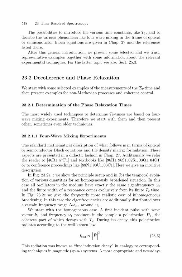
578 23 Time Resolved Spectroscopy
The possibilities to introduce the various time constants, like T2, and todecribe the various phenomena like four wave mixing in the frame of opticalor semiconductor Bloch equations are given in Chap. 27 and the referenceslisted there.
After this general introduction, we present some selected and we trust,representative examples together with some information about the relevantexperimental techniques. For the latter topic see also Sect. 25.3.
23.2 Decoherence and Phase Relaxation
We start with some selected examples of the measurements of the T2-time andthen present examples for non-Markovian processes and coherent control.
23.2.1 Determination of the Phase Relaxation Times
The most widely used techniques to determine T2-times are based on four-wave mixing experiments. Therefore we start with them and then presentother, sometimes even older techniques.
23.2.1.1 Four-Wave Mixing Experiments
The standard mathematical description of what follows is in terms of opticalor semiconductor Bloch equations and the density matrix formulation. Theseaspects are presented in a didactic fashion in Chap. 27. Additionally we referthe reader to [46B1, 57F1] and textbooks like [96H1, 96S1, 02S1, 03Q1, 04O1]or to conference proceedings like [88N1,93U1,03C1]. Here we give an intuitivedescription.
In Fig. 23.2a–c we show the principle setup and in (b) the temporal evolu-tion of various quantities for an homogeneously broadened situation. In thiscase all oscillators in the medium have exactly the same eigenfrequency ω0
and the finite width of a resonance comes exclusively from its finite T2 time.In Fig. 23.2c we give the frequently more realistic case of inhomogeneousbroadening. In this case the eigenfrequencies are additionally distributed overa certain frequency range ∆ωinh around ω0.
We start with the homogeneous case. A first incident pulse with wavevector k1 and frequency ω1 produces in the sample a polarization P 1, thecoherent part of which decays with T2. During its decay, this polarizationradiates according to the well-known law
Irad ∝∣∣∣P ∣∣∣2 . (23.6)
This radiation was known as “free induction decay” in analogy to correspond-ing techniques in magnetic (spin-) systems. A more appropriate and nowadays

23.2 Decoherence and Phase Relaxation 579
Fig. 23.2. The setup for a photon-echo experiment (a), and the time dependenceof the polarization for a homogeneously (b) and an inhomogeneously (c) broadenedtwo-level system
generally used name is “free polarization decay”. Usually radiation has onlya minor influence on the damping, i.e., T2 is usually limited by scattering pro-cesses rather than by the radiative lifetime. Exception will be mentioned later.
After a delay τ a second pulse k2 arrives which is coherent with the firstone and (usually) has the same frequency but a different direction. To achieve

580 23 Time Resolved Spectroscopy
this coherence the two pulses are generally produced from a single pulse usinga beam splitter and a variable optical delay for one of them.
The second pulse creates a polarization P 2, which interferes with the co-herent part left over from the first one. This interference produces a laser-induced grating (LIG) of the polarization which radiates its first orders inthe directions given by (23.7), assuming a thin grating, i.e., the Raman–Nathregime:
k(1)diff = 2k2 − k1; k
(−1)diff = k1 . (23.7)
The Raman–Nath regime is characterized to a first approximation by thefollowing inequality between the thickness of the sample d, the spacing of thegrating Λ and the wavelength of the incident beams λ:
d2 < λΛ . (23.8)
The negative first-order signal is difficult to detect since it coincides with thedirection of the transmitted part of the pulse 1. So we concentrate on theother, background-free direction.
Since, in the homogeneously broadened case, all oscillators have the sameeigenfrequency, the coherent parts of the polarizations all have the same phaseand the scattered signal Is starts to develop immediately when the secondpulse arrives. It reaches its maximum Isp when the second pulse is over, as-suming that the duration τp of both pulses is much shorter than T2, i.e.,
τp T2 . (23.9)
The diffracted signal in the case of homogeneous broadening depends onthe delay time τ in the following way
Ihom+1 ∝ |P (τ)|2 ∝ [exp (−τ/T2)]
2 ∝ exp (−2τ/T2) , (23.10a)
and the same relation holds for the time-integrated signal as shown below inFig. 23.3a.
For the inhomogeneously broadened case of Fig. 23.2b, the part of thepolarization amplitude of every oscillator which is still coherent with pulse 1again decays with T2. But since all oscillators have (slightly) different eigen-frequencies, they lose phase with one other in a time inversely proportional tothe inhomogeneous broadening (∆ωin)−1, resulting essentially in destructiveinterference of the radiation of all oscillators. The emission of the free po-larization decay is then also limited by this quantity as shown in Fig. 23.2b.When the second pulse arrives after τ , a rephasing starts in the sense of phaseconjugation or cum grano salis of a time reversal. See Chap. 27. After anothertime τ all oscillators are in phase again and radiate the so-called photon-echo(Figs. 23.2c and 23.3b). Its temporal width is limited by the free polariza-tion decay and thus by τp or by (∆ωin)−1, and the (time-integrated) signalintensity decays with τ according to

23.2 Decoherence and Phase Relaxation 581
Fig. 23.3. The temporal evolution of the diffracted order as a function of thedelay between the two pump pulses and the time after the second pump pulse fora homogeneously (a) and an inhomogeneously broadened system (b). The time-integrated diffracted signal is also given [89D1]
I inhoms(0) ∝ |P (t = 2τ)|2 ∝ [exp (−2τ/T2)]
2 ∝ exp (−4τ/T2) . (23.10b)
The appearance of an echo as shown in Figs. 23.2c and 23.3b is thus a clearindication of an inhomogeneous broadening.
The formula to calculate the diffracted orders and their time evolutiontend to get rather lengthy and can be treated only numerically when goingfrom the optical to the semiconductor Bloch equations ore when using realisticlaser pulses of finite duration and not just δ-pulses (see Chap. 27). Therefore

582 23 Time Resolved Spectroscopy
we refer the reader to the books mentioned at the beginning of this chapter,in addition to Chap. 27, for approximate formulae on the basis of two- andthree-level systems.
The appearance of a photon echo can be demonstrated in a didactic wayalso by Fig. 23.4 (see Chap. 27).
A bunch of runners representing the polarisation of the various oscillatorsstarts in a stadion at t = 0, i.e., at the arrival time of the first pulse. Sincethey all have different speeds (inhomogeneous broadening) their angular po-sitions spread with time. At the time of the second pulse arriving at t = τthey turn around instantaneously and run back with the same speed. Thisresults in a collective arrival at the starting point t = 2τ , (emission of theecho). The decay of the echo amplitude with τ can be visualized in this pic-ture if we assume that some runners stumble during their way and fall down(recombination). Even if they get up again after a while and continue to runthey will not arrive back at the starting point in time. The same holds forrunners who change their speed (these two processes would correspond to in-elastic scattering) or who arbitrarily change their direction without stoppingor changing |υ| (inelastic scattering).
A peculiarity of the description in the weak coupling limit in the frameworkof χ(3) and of the optical Bloch equations is the fact that no signal appears inthe direction 2k2 −ki for negative delay, i.e., if pulse 2 arrives before pulse 1.This fact is surprising since a negative delay corresponds to an interchange ofpulse 1 and 2 and the first diffracted orders of pulse 1 and 2 go in the directionof k2 and 2k1 −k2 and k1 and 2k2 −k1, respectively. If the polariton pictureor the semiconductor Bloch equations are used which include among othersthe Coulomb interaction between the carriers (see Chap. 27), a signal is alsoexpected for negative delays. First calculations show [91W1] that the temporalbuildup of the signal for negative delays has twice the slope of the decay forpositive τ .
Fig. 23.4. The illustration of the appearance of a photon echo with runners ina stadion

23.2 Decoherence and Phase Relaxation 583
We have mentioned already that most transitions in semiconductors areinhomogeneously broadened, at least at low temperatures and densities.Bound exciton complexes are inhomogeneously broadened since the sur-roundings of every impurity are slightly different due, e.g., to other impu-rities in the neighborhood. For the localized tail states in disordered sys-tems and for quantum structurs at low temperatures the inhomogeneousbroadening is obvious. For free excitons or exciton polaritons the questionof homogeneous or inhomogeneous broadening is less clear since a differ-ent eigenenergy belongs to every k-vector due to dispersion. The contin-uum states of the excitons or the band-to-band transitions in an electron–hole plasma again form, to a good approximation, an inhomogeneouslybroadened system with, however, very short T2 times. At higher densitiesor temperatures the T2 times get shorter and may become so short thatthey dominate the broadening, i.e., we get a transition to homogeneousbroadening.
We now present first experimental results for bulk samples, namely FWMresults obtained in the (nB = 1) AΓ5 free exciton resonance of CdSe at lowtemperature. Since even samples of a few µm thickness are opaque in thisregime, the diffracted signal in reflection was used (Fig. 23.5a). With increas-ing pump power, the signal increases, too, but the decay gets faster. This is dueto inelastic exciton-exciton scattering. Using these data and others obtainedin the exciton to biexciton transition (Fig. 23.5b), the curve of Fig. 23.5c is ob-tained which shows a linear increase of the dephasing rate T−1
2 with increasingexcitation. The extrapolation to zero density (and temperature) gives T2 val-ues around 50 ps. The slope of the curve in Fig. 23.5c allows one to determineadditionally the exciton-exciton scattering cross-section via
T−12 = T−1
02 + δNex (23.11a)
and one finds with [89D1]
σex−ex = δvth (23.11b)
σex−ex = 6.87πa2B, i.e., a value slightly larger than the geometrical one.
In [91W1, 98W1] a linear dependence of the dephasing rate on the densityhas been found both for bulk-like and quasi 2d ZnSe structures, with somedependence on the fact that if the exciton population is still coherent or not.It should be mentioned that for much higher densities corresponding to thosereached in an electron–hole plasma and short times one finds a decay timeTs of the FWM mixing signal on the electron–hole pair density neh givenby [88B1,91W1,01W2]
T−1s = T−1
0 + cn1/3eh (23.11c)
for all quasi-dimensions.The temperature dependence of the dephasing rate is given in all dimen-
sions by the sum over a low temperature value Γ0, a term linear in T due to

584 23 Time Resolved Spectroscopy
Fig. 23.5. The evolution of the time-integrated photon echo as a function of τ inthe nB = 1AΓ5 exciton resonance of CdSe for different pump powers in reflectiongeometry (a) in the exciton → biexciton transition, where a well-defined excitondensity is created by a prepulse in transmission geometry (b) and the dependenceof T−1
2 on the exciton density (c) [89D1]

23.2 Decoherence and Phase Relaxation 585
scattering with acoustic phonons and a Bose term proportional to the occu-pation probability of LO phonons [92O1,98W1,04H1], i.e.,
T−12 = Γ0 + βacT +
βLO
(exp (ωLO/kBT ) − 1). (23.11d)
The onset of the signal for negative delays is not covered by the simple theory,as mentioned above, but by the improvements given in [91W1,98W1].
Photon-echo experiments at low temperature in GaAs revealed T2 valuesaround 10 ps [89K1,92O1]. Diffusion measurements with laser-induced popu-lation gratings in CdS gave a diffusion constant D(5 K) ≈ 20 cm2s−1 and withthe Nernst–Townsend–Einstein relations,
D = µkBT
e, µ = e
T ′2
M, D =
kBT
MT ′
2 , (23.11e)
for classical effective mass particles, a time between scattering events T ′2 ≈
30 ps [88W1]. Here, µ is the mobility of excitons and T ′2 the time between two
scattering processes. Evidently this quantity is closely related to the phaserelaxation time. We shall describe a more detailed experiment concerning thispoint later in connection with MQW. Here, we can state that T2 times in therange a ps up to a few tens of ps are obviously typical for the lowest free excitonstates in high quality bulk (and MQW, see below) samples at low temperatureand density in agreement with data from reflection spectroscopy. The T1 valuesunder these conditions are in the 0.3–3 ns regime, i.e., we have T2 T1. T2
decreases with increasing density and with increasing temperature. In thelatter case T2 values in the range of 100 fs are reached at room temperature,so that the homogeneous dominates the inhomogeneous broadening.
The damping of polaritions has been deduced in CuCl by FWM in [83M1,91V1]. Polaritons and bipolaritons have been analyzed for CdS in [01M1]reaching the T2 = 2T1 limit of (23.3a) for the biexciton with times of a few ps.
Now we consider, still in 3d semiconductors, excitons which cannot movefreely through the sample. We start with an example of a bound-exciton com-plex (Sects. 9.5, 14.1), more precisely with an exciton bound to a neutralacceptor (A0X) in CdSe.
In Fig. 23.6a we show directly the time-resolved photon-echo for the lasertuned into the A0X resonance of CdSe at low temperatures. One sees clearlythe scattered intensities of the two pump pulses P1,2 and the photon-echoPs. A first inspection already shows that the T2 times of this BEC are muchlonger than for free excitons. Extrapolation of the data to T = 0 K (Fig. 23.6b)gives T2 ≈ 600 ps. Since the lifetime T1 of this BEC in this same sample hasbeen determined to be around 400 ps, we come here again close to the limitgiven by (23.3a). The comparison of this value, which corresponds roughly toa homogeneous width of 20 µeV, with the spectral width of the BEC lumi-nescence, which in good samples is between 0.1 and 1 meV, together with theobservation of a photon-echo, clearly shows the inhomogeneous broadening ofthe BEC resonances.

586 23 Time Resolved Spectroscopy
Fig. 23.6. Photon-echo observed in the resonance of a bound exciton complex inCdSe (a) and the dephasing rate as a function of temperature (b) [92P1,92P2,94P1]
The temperature dependence of T2 time is given in Fig. 23.6b. It can befitted by an activation law.
T−12 = T−1
02 + ν0 exp(−Ea/kBT ) (23.12)
with T02 ≈ 600 ps, ν0 = 3 × 10¹¹s−1 and an activation energy of Ea ≈5.6 meV. This value corresponds approximately to the binding energy of theexciton to the complex. Since T02 is slightly above the observed luminescencedecay time and thus of T1 [92P2], we can conclude that the main phase de-stroying processes for this complex at low temperature are the recombination

23.2 Decoherence and Phase Relaxation 587
and at higher temperatures the thermal ionization of the exciton from theneutral acceptor by absorption of a phonon.
In CdS a T2 value of 400 ps has recently been observed for the D+X com-plex with the quantum-beat technique to which we shall return later [91S1].
The difference in the T2 times of BEC compared to free excitons at lowtemperatures can be qualitatively understood in the following way. A freeexciton moves through the sample with a certain velocity and has a goodchance of hitting a defect like an impurity or a dislocation. The resultingscattering process destroys the phase coherence with the driving laser pulse.A resonantly created bound exciton sits on the defect, oscillates in phase withthe generating light field and cannot do much more at low temperatures untilit recombines, provided that the density of other centers is so low that thereis no interaction between them. The same type of arguments seems to holdfor localized excitons in some disordered systems (Sects. 9.6 and 14.4) such asCdS1−xSex to which we turn now. See, e.g., [92S1,92S2] and references therein.
In Fig. 23.7 we show the luminescence spectrum of a CdS0.65Se0.35 sampleat T = 2 K excited at the high energy edge of the zero phonon luminescenceband, i.e., in the transition region from extended to localized states. Oneobserves the zero phonon emission from the localized states around 2.21 eVand the CdSe and CdS LO phonon replica around 2.19 and 2.18 eV, respec-tively. The full dots give T2 values at the respective energies measured withthe photon-echo technique. The values range from T2 400 ps close to the“mobility edge” up to T2 ≈ 3 ns for deeper localized states. Again these valuesare comparable with the intraband relaxation times T3 and the interband re-combination times T1. Data for these latter quantities have been determinedfrom time- and spectrally resolved luminescence and range from some hun-
Fig. 23.7. The low temperature luminescence spectrum of a CdS1−xSex, sample andthe energy dependence of the T2 times deduced from photon-echo experiments [92S1]
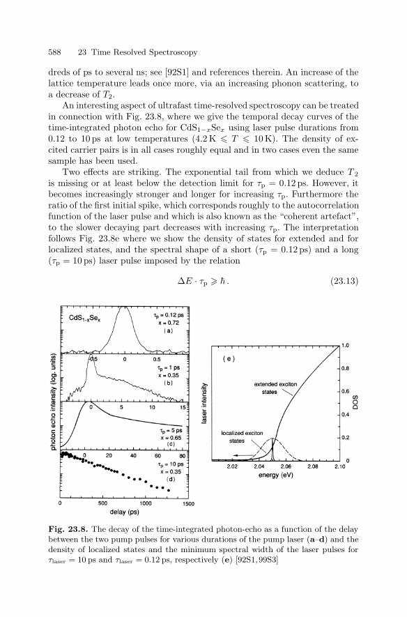
588 23 Time Resolved Spectroscopy
dreds of ps to several ns; see [92S1] and references therein. An increase of thelattice temperature leads once more, via an increasing phonon scattering, toa decrease of T2.
An interesting aspect of ultrafast time-resolved spectroscopy can be treatedin connection with Fig. 23.8, where we give the temporal decay curves of thetime-integrated photon echo for CdS1−xSex using laser pulse durations from0.12 to 10 ps at low temperatures (4.2 K T 10 K). The density of ex-cited carrier pairs is in all cases roughly equal and in two cases even the samesample has been used.
Two effects are striking. The exponential tail from which we deduce T 2
is missing or at least below the detection limit for τp = 0.12 ps. However, itbecomes increasingly stronger and longer for increasing τp. Furthermore theratio of the first initial spike, which corresponds roughly to the autocorrelationfunction of the laser pulse and which is also known as the “coherent artefact”,to the slower decaying part decreases with increasing τp. The interpretationfollows Fig. 23.8e where we show the density of states for extended and forlocalized states, and the spectral shape of a short (τp = 0.12 ps) and a long(τp = 10 ps) laser pulse imposed by the relation
∆E · τp . (23.13)
Fig. 23.8. The decay of the time-integrated photon-echo as a function of the delaybetween the two pump pulses for various durations of the pump laser (a–d) and thedensity of localized states and the minimum spectral width of the laser pulses forτlaser = 10 ps and τlaser = 0.12 ps, respectively (e) [92S1,99S3]

23.2 Decoherence and Phase Relaxation 589
A spectrally narrow, rather long pump pulse tuned to the spectral rangeof localized states allows one to measure the true T2 of these states. If thepulse length is reduced, the high energy tail of the laser extends into theregion of extended states. In alloy semiconductors even at low temperaturesthese states have a very short T2 time of the order of 0.1 ps due to alloydisorder scattering [91S1,92S2]. This value explains the short autocorrelationspike. Furthermore, the excitons in the extended states which are created bya short, spectrally broad pulse also scatter with the excitons in the localizedstates and thus reduce the T2 values of the latter. Consequently the T2 valuesobtained with rather long, spectrally narrow pulses with ∆E from (23.14)much smaller than the tailing parameter ε0
∆E ε0 (23.14)
will give the most reliable results. See also the discussion in connection withFig. 23.11.
The spectral proximity of states with different T2 times occurs not onlyfor disordered systems and necessitates some considerations concerning theselection of a laser for a planned experiment.
It must be mentioned here that short phase relaxation times have beenobserved in other disordered systems like Al1−yGayAs crystals, amorphous(α-) Si, and InGaAs MQW [91W1, 92S2]. The T2 values at low temperatureare only around or below a few ps. The difference is presently explained asfollows. If the disorder causes fluctuations essentially only in one band (inCdS1−xSex this is the valence band originating mainly from the 3p and 4porbitals of S2 and Se2, respectively) a stationary state with long T2 time canbe constructed from a localized carrier of one type (here a hole) binding a freecarrier of the other type by Coulomb attraction to form a localized exciton.If, on the other hand, fluctuations and localization occur in both bands, asis the case for the more covalently bound materials Al1−yGayAs and α-Si,it is not possible to get a stationary state with two localized carriers plusCoulomb interaction. Here alloy disorder scattering always appears as a phase-destroying process. More details about these topics are found in [92S2] andreferences therein. Furthermore, the short pulses used in these experimentsmay play a role in the sense of the discussion in connection with Fig. 23.8and with data for quantum wells cited below. Before we present results onstructures of reduced dimensionality we introduce another aspect of FWMexperiments namely (quantum) beats.
In this case a short laser pulse of sufficient spectral width simultane-ously excites coherently two spectrally narrow, well-separated resonances.This means the spectral width of the laser ∆E, the spectral separation ofthe two resonances ∆Er and the homogenous width of each of them ∆Eh
should obey the inequality
∆E ∆Er ∆Eh . (23.15)

590 23 Time Resolved Spectroscopy
Under these conditions a beating occurs, as known already from two cou-pled pendula in classical mechanics, with a beat frequency ωb
ωb = ∆Er . (23.16)
In our case a modulation of the intensity with ωb can be observed, e.g., ina FWM experiment or in the free polarization decay signal. In Fig. 23.9 wegive examples of the beating between the nz = 1 heavy- and light-hole exci-ton resonances (a, b) and the beating between the exciton resonance and theinduced transition exciton → biexciton (c, d). Since the beating is a coherentprocess, the decay of the envelope of the beat signal contains information onthe T2 of the resonance with the lower T2 value.
The beat frequency just fulfils (23.17). These quantum beats have re-cently been observed in many systems, such as excitons in the indirectgap semiconductor AgBr [91S1], between strain-split heavy and light holeexcitons in ZnSe layers [96W1], in bound exciton complexes in CdS andCdSe [91S1, 92P1, 93P1, 93P2, 94E1, 94P1, 96B1] and even between the lowerand upper polariton branches of the lowest dipole-forbidden nB = 1 ex-citon resonance in Cu2O, which has a longitudinal transverse splitting of
Fig. 23.9. Quantum beats and their Fourier transforms for the beating between theheavy- and light-hole exciton in an Al1−yGayAs/GaAs MQW (a, c) sample and forthe exciton → biexciton transition (b, d) [92O1,93P1]

23.2 Decoherence and Phase Relaxation 591
a few µeV only [91F1]. Other experiments concern the beating between var-ious polariton branches in CdSe [93P2, 94E1, 96B1] or in InGaAs MQW[91W1] or between the exciton and the biexciton state in AlGaAs MQW;see [92O1,93P1,93P2,94E1,96B1] and references therein.
Recently it has been possible to distinguish between a beating of twoelectronic transitions and a mere interference of the electromagnetic wavesradiated from two independent, slightly detuned oscillators [91B1,92G1,92K1,92P1,94P1].
For a “real” quantum beat, i.e., a beating between to spectrally close-lyingtransitions that have at least one state in common or, in other words, thatoccur in one quantum mechanical system, one expects maxima in a plot of theFWM intensity over a two-dimensional plane of real time t and delay time τfor
T = τ + nTB (23.17a)
where TB is the beat period. Meanwhile, the interference of the radiationemitted from two independent systems on the detector results in
t = 2τ + nB . (23.17b)
In Fig. 23.10 examples are given for both situations. In Fig. 23.10a one ob-serves upconverted and time resolved quantum beats between the light and
Fig. 23.10. Quantum beats between hh and lh exciton in a MQW sample (a)Polarization interference from the hh resonance of a sample containing quantumwells of two different thicknesses [92G1,92K1]

592 23 Time Resolved Spectroscopy
heavy hole over a two-dimensional t, τ plane. Figure 23.10b gives, in contrast,the polarization interference of the hh excitons of spatially separated QWswith lz = 9 nm and 8 nm. The main maxima follow the relations (23.18a) and(23.18b), respectively.
This picture is very clear, but not completely true, since the whole semi-conductor sample has one common ground state and since even spatially sep-arated oscillating dipoles have some, though possibly weak, radiative cou-pling. This coupling is, in a classical description, responsible for the Clausius–Massotti correction to the dielectric function (see Sect. 4.2).
Consequently, in calculated or measured data that show a pronouncedbehavior according to (23.17b), one usually observes weaker intensity modu-lations obeying (23.17a) and vice versa.
In the picture of strong exciton–photon coupling, a generalized descrip-tion of the quantum beats can be expected that includes both of the above-mentioned aspects as limiting cases.
In Fig. 23.11 we present a FWM experiment on a GaAs/Al1−yGayAs sam-ple containing wells of different thicknesses, as shown in the absorption spec-trum.
The laser pulse is so short that it covers spectrally several transitions. Forthe 8 nm QW only the hh is excited. One observes the rise and the slow signaldecay of predominantly localized excitons. As compiled, e.g., in [01L1] the T2
times range at low temperatures up to several tens of ps. For the 10 nm QWthe hh and the lh exciton are excited simultaneously, resulting in quantumbeat features and again a slow signal decay. For the 13 and 16 nm-wide wells,
Fig. 23.11. Time integrated FWM spectra as a function of time delay for a sam-ple containing quantum wells of various thicknesses as indicated in the absorptionspectrum [97E1,98H1]

23.2 Decoherence and Phase Relaxation 593
both the hh and the lh excitons are excited as well as the continuum stateswith even higher intensity. As shown in [97E1] this has the consequence thata FWM signal appears spectrally at the position of the exciton, but first witha rapid decay given by the inverse of the spectral width of the laser pulserather than by the T2 time of the exciton. Note that the spectral widths ofthe exciton absorption features are not compatible with the short decay timesvia (23.4). After this first decay, a much weaker, but slowly decaying signal isobserved that gives the actual T2 time. It is possible that this slow and weakpart of the signal was partly below the detection limit of the experimentsdescribed in connection with Fig. 23.8.
In [01W1] the FWM signal has been analyzed as a function of delay timebetween the pulses and the real time after the second pulse, revealing detailsof the FWM process, which go beyond both the simple explanations givenhere and the scope of this book.
Recently, beautiful experiments have been reported on FWM on a gradedsuperlattice, i.e., one where the well width varied systematically from wellto well. By spectral filtering of the laser, excitons in adjacent wells or next-nearest neighbors could be excited deliberately and the beating between theresonances in one well as well as the interactions between wells could beobserved in the spectrally resolved, time-integrated signal as a function ofthe delay time between the pulses [04L1].
Now we give a small selection of further results of FWM in various quan-tum structures: The dephasing in the quasi-two-dimensional exciton-biexcitonsystem of GaAs/Al0.3Ga0.7As single quantum wells has been treated in [00L1]and for In0.18GA0.82As SQW in [99B2]. The contributions of acoustic and op-tic phonons to the dephasing have been analyzed and separated in [99B1] forIn1−yGayAs/GaAs SQW.
The oscillations of wave packets in space and time in In1−yGayAs/GaAs1−xPx MQW samples are investigated in [99O1] and the influence ofstrong magnetic fields on excitons and biexcitons has been detailed in [94B1]and references therein.
For data on exciton and biexciton dephasing in various types of III–V andII–VI quantum wires see, e.g., [98W2,98W3,99L1] and references therein.
In self-assembled III–V quantum islands, very long dephasing times havebeen measured for excitons, biexcitons and multiexcitons for the reasons givenabove for localized states [01B1,01B2,02B1,02B3,04L2]. For localized excitonand biexciton states in II–VI structures, data are found in [97L1,99W1], whereit has been shown that an inhomogeneous broadening of the biexciton bindingenergy results in a fast decay of the FWM signal that is not related to themuch longer dephasing of the biexciton.
Excitons in single dots are probed in [98B1,01F1,01F2]. Data for the de-phasing in electrically pumped InAs/In1−yGayAs amplifiers are given in [00B2].
More data for III–V compounds can be found, e.g., in [01L1].It should be noted that the observation of higher diffracted orders than the
first one in FWM experiments are indications of χ(2n+1) processes with n > 1.
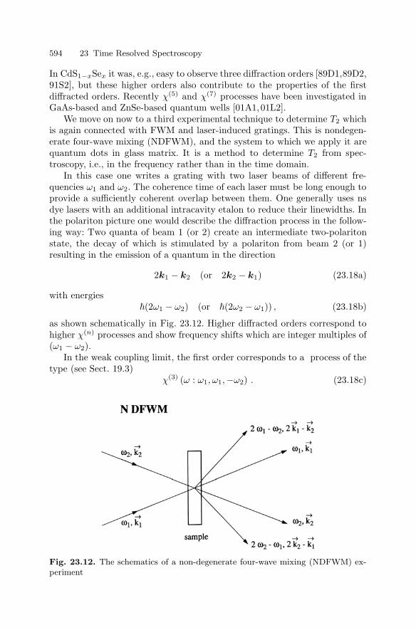
594 23 Time Resolved Spectroscopy
In CdS1−xSex it was, e.g., easy to observe three diffraction orders [89D1,89D2,91S2], but these higher orders also contribute to the properties of the firstdiffracted orders. Recently χ(5) and χ(7) processes have been investigated inGaAs-based and ZnSe-based quantum wells [01A1,01L2].
We move on now to a third experimental technique to determine T2 whichis again connected with FWM and laser-induced gratings. This is nondegen-erate four-wave mixing (NDFWM), and the system to which we apply it arequantum dots in glass matrix. It is a method to determine T2 from spec-troscopy, i.e., in the frequency rather than in the time domain.
In this case one writes a grating with two laser beams of different fre-quencies ω1 and ω2. The coherence time of each laser must be long enough toprovide a sufficiently coherent overlap between them. One generally uses nsdye lasers with an additional intracavity etalon to reduce their linewidths. Inthe polariton picture one would describe the diffraction process in the follow-ing way: Two quanta of beam 1 (or 2) create an intermediate two-polaritonstate, the decay of which is stimulated by a polariton from beam 2 (or 1)resulting in the emission of a quantum in the direction
2k1 − k2 (or 2k2 − k1) (23.18a)
with energies(2ω1 − ω2) (or (2ω2 − ω1)) , (23.18b)
as shown schematically in Fig. 23.12. Higher diffracted orders correspond tohigher χ(n) processes and show frequency shifts which are integer multiples of(ω1 − ω2).
In the weak coupling limit, the first order corresponds to a process of thetype (see Sect. 19.3)
χ(3) (ω : ω1, ω1,−ω2) . (23.18c)
Fig. 23.12. The schematics of a non-degenerate four-wave mixing (NDFWM) ex-periment

23.2 Decoherence and Phase Relaxation 595
In a classical wave picture we have the following description. The two incidentwaves interfere to form a moving interference pattern. It moves laterally witha speed vG given by
vG =ω1 − ω2
|k1 − k2| . (23.19)
The orders diffracted off this moving grating are Doppler shifted and a quan-titative analysis of these ideas leads to exactly the same results as given in(23.18).
If there is an optical nonlinearity due to the real or virtual excitationof some species with a lifetime T1 or T2, respectively, then the grating willbe washed out if it moves over one period Λ in a time shorter than T1,2.Consequently the efficiency drops, when
Λv−1G < T1 or T2 . (23.20)
A quantitative analysis leads to the following relation for the efficiency η±1 ofthe ± first diffracted order [78Y1].
η±1 ∝∣∣∣χ(3)
∣∣∣2 ∝ [(1 + Ω2T 2
1
) (1 + Ω2T 2
2
)]−1(23.21)
with Ω = ω1 − ω2. This means that there is a narrow central spike, whosedecay with increasing detuning Ω is determined by T1 and wider wings fromwhich one can deduce T2 in the case T1 T2.
In Fig. 23.13 we give as an example results for a semiconductor-doped glasswith CdS crystallites with an average radius of 7.5 nm. The narrow central
Fig. 23.13. The NDFWM signal as a function of the detuning in a silicate glassdoped with CdS nanocrystals for various pump powers Ip [94W1]

596 23 Time Resolved Spectroscopy
spike is limited rather by the spectral width of the lasers than by T1. The T1
time of a few hundred ps typical for such a system was measured independentlyby time-resolved luminescence and would give a width below 0.1 meV. Thewider wing can be fitted with (23.21) to give a T2 time of the resonantlyexcited electron–hole pairs in these quantum dots of about 100 fs, decreasingwith increasing pump power as shown in the inset. These values increase onlyslightly when going to lower temperatures. The reason why this value is soshort in comparison with bound exciton complexes is not completely clear atpresent. The stronger coupling to the optical phonons in QD compared to thebulk material may be of importance or the scattering at, or the relaxationof the carriers into, some interface states between the semiconductor and thesurrounding matrix.
Similar values of T2 have been obtained from spectral hole burning (see be-low) and also from time-resolved FWM experiments. It should be mentioned,however, that much longer dephasing times of several tens of ps have beenobserved by various techniques for quantum dots capped by or embedded inorganic matrices [97W1].
23.2.1.2 Other Techniques and Coherent Processes
In the following sections we briefly present some further techniques to deter-mine dephasing times and some other coherent phenomena including, e.g., thespin system, to give the reader an impression of the width and wealth of thefield and present research activities.
23.2.1.2.1 Propagation Effects
An inherent problem in time-resolved four-wave mixing experiments is thefact that the pulses have to have a certain time delay. In bulk material thepolarization propagates together with the electromagnetic part of the lightpulse as introduced in the polariton concept in Chap. 5. If the pulses are short,their shape in the samples is pancake-like. A 100 fs pulse may have, dependingon the parameters for group and phase velocities, a thickness of only a few µmwith some dispersion during propagation through the sample. With a delaybetween the pulses of several ps the spatio-temporal overlap of the two pulsesis an issue, which must be carefully checked and depends on the angle betweenthe beams k1 and k2 in the sample and on the lateral diameter of the pulses.This is a reason why little FWM data exists in the exciton resonances ofdirect-gap bulk semiconductors with dipole-allowed band-to-band transitions.Another reason is the strong absorption in the exciton resonance of manysemiconductors. A way out also used in Fig. 23.5a is to measure the reflectiongeometry since the reflection signals originate from the polarization close tothe surface.
In contrast, for quantum structures the polarization stays essentially con-fined in the quantum well, wire or dot for the usual close to normal inci-dence geometry, except for some polarization or radiation coupling between

23.2 Decoherence and Phase Relaxation 597
the wells. The spatial coincidence of the polarization created by subsequentpulses is therefore unproblematic.
An adequate method for bulk semiconductors would therefore be to in-vestigate the polariton propagation. This can and has been done. We alreadypresented corresponding data for various bulk materials for the case of prop-agation quantum beats and for time of flight experiments in Sects. 5.3 and13.1.4, respectively. We add here some references for a thin ZnSe layer [96N1]for the layered semiconductor InSe [97N1] and for photonic crystal waveguides [02N1]. We come back on propagation effects under the aspect of trans-port properties in Sect. 23.2.1.2.5 and 2.3.3.
23.2.1.2.2 Rayleigh Scattering and Speckle Analysis
An effect that has been considered for a long time as more disturbing thanuseful in semiconductor spectroscopy is Rayleigh scattering. This means co-herent and elastic scattering of light without a frequency shift in contrast toBrillouin or Raman scattering. Rayleigh scattering requires some deviationsfrom the strict periodicity of a perfect crystal lattice, which are generally al-ways present even in high quality samples due to, e.g., defects, strain fields orinterface roughness for quantum structures.
In pioneering work summarized in [94S1] it has been shown that the dy-namics of resonant Rayleigh scattering involved information on the dephasingof, e.g., bound exciton complexes, confirming the long T2-times mentionedabove. For examples of more recent work see [98B2,99S1,04M1,04M2,04Z1].
The light scattered resonantly and coherently from various regions of thesample can interfere constructively or destructively depending on the scat-tering direction. This effect leads for rather small illuminated areas to theappearance of bright and dark spots in the scattered light field, know asspeckle.
The dependence of the speckles on the direction and their temporal dynam-ics under pulsed excitation allow one to distinguish pure dephasing from life-time (see (23.3b)) [99L2,02K1,03M1] or to investigate polaronic effects [00P1]and the references therein.
23.2.1.2.3 Linear Spectroscopy
If one has no further information it is difficult to learn something about the de-phasing time T2 of a system from linear absorption, reflection or luminescencespectra.
If one does not know, e.g., if an absorption band is only homogeneously oradditionally inhomogeneously broadened, its spectral width gives only a lowerlimit for the decoherence time T2 or for the time of the free polarization decayTPD via (23.4) and (23.5).
However, the spectrally extremely narrow emission lines from individuallocalization sites of excitons in quantum wells observed at low temperaturesor the narrow emission features of bound exciton complexes, which we have

598 23 Time Resolved Spectroscopy
seen in some of the preceding chapters, indicate that the T2 times must be inthe range of several tens to hundreds of ps as is indeed found from photonechoes as shown above. The temperature dependence of the spectral half widthof the emission line of excitons in self-assembled In0.6Ga0.4As islands growsfrom values of 2 µeV (T2 > 0.7 ns) to almost 10meV at RT (T2 ≈ 0.13 ps)[02B2,02B3,04L2].
The reflection spectra of free exciton resonances of high-quality bulk sam-ples (see, e.g., Chap. 13) can be fitted at low temperatures usually by dampingparameters around or below 1 meV. Therefore T2 times measured by FWM inthe range of some ps (see above) did not come as a big surprise [04H1].
23.2.1.2.4 Spectral Hole Burning and Related Techniques
A further technique to determine the homogeneous width of a transition isspectral hole burning. This method is frequently used in the spectroscopy ofatoms in gases, solutions or solids but has only more recently been used insemiconductor optics [77L1,91D1,93W1,94M2,94W1]. We explain shortly thebasic idea before going to examples.
A homogeneously broadened absorption band has a Lorentzian line shapefor the simplest case of a two-level system (see Fig. 23.14a). Its width is givenby (23.4). Pumping at any energy ωP results in a decrease of the wholeabsorption feature if a certain fraction of the carriers is transferred from theground to the excited state.
For an inhomogeneously broadened system (see Fig. 23.14b) the absorptionband is composed of different transitions as shown schematically on the r.h.s.of this figure. If every single transition has a Lorentzian profile, and if theinhomogeneous distribution is Gaussian, the total line shape is a Voigt profileas long as both widths are comparable.
Pumping at ωP saturates the transition at this energy, but does notinfluence the others, resulting in a spectral hole. If the pump laser is spectrallynarrower than the homogeneous width of every individual absorption peak inthe inhomogeneous broadened distribution, the width of the spectral hole givesthe homogeneous width according to (23.4).
Care has to be taken that the laser is spectrally sufficiently narrow andsufficiently weak to avoid the spectral wings saturating adjacent transitions.This effect is known as power broadening and results in an overestimation atthe homogeneous width (for more details see, e.g., [94M2]).
Examples of spectral hole burning are experiments on CdS1−xSex quantumdots in glass matrices, revealing homogeneous widths on the order of 10 meV[93W1,93W2,97W1], corresponding to T2 times of about 100 fs, in agreementwith the NDFWM data of Fig. 23.13 or time resolved FWM [93S1,94M1]. Notethat the dots in organic matrices may show much longer T2 times [96E1,97W1]as mentioned already above.
Other examples are the spectral hole burning experiments in the gainregion of an inverted bulk semiconductor and of quantum dots [93M1, 96G1,98M1].

23.2 Decoherence and Phase Relaxation 599
Fig. 23.14. Schematic drawing of the absorption of a homogeneously (a) and aninhomogeneously (b) broadened absorption band centered around ω0 and the mod-ification induced by optical pumping at ωP (solid and dashed lines, respectively)
A similar technique has been used in [02W1] for ZnSe quantum wells,where it has been explicitly shown that the homogeneous width of the excitonincreases with increasing excitation intensity and that the data deduced fromthe fit of a density-dependent Voigt profile and from FWM coincide.
For spectral hole burning and bleaching dynamics in the semiconductorSr2CuO3, which is related to high Tc superconductors see [00O1].
23.2.1.2.5 Transport Measurements
In transport measurements, another time constant appears in the frame ofa relaxation approach, namely the momentum relaxation time T ′
2, i.e., thetime of free flight between random collisions. We give an example of hownonlinear optics can contribute to the determination of transport properties.

600 23 Time Resolved Spectroscopy
In Fig. 23.15 we compare the results for phase-destroying processes mea-sured with two different techniques. The crosses are data for the scatteringrate, i.e., for T−1
2 , obtained from photon-echo experiments. They start withvalues around 30 ps at 2 K and T2 decreases with increasing temperature es-sentially due to scattering with (acoustic) phonons in the temperature intervalof Fig. 23.15. The open circles are obtained from diffusion measurements. Theidea of this experiment is the following: two coherent pulses falling simultane-ously on the sample interfere and produce a spatially modulated populationgrating (laser-induced grating, LIG). If this population produces any opticalnonlinearity, light will be diffracted from this grating. The grating efficiencydecays for times longer than T2 due to recombination and due to diffusion.The first process does not depend on the grating period Λ of the LIG, but thesecond one does. By variation of Λ the two contributions can be separated.If two short pulses (τp T1) are used, the diffracted signal intensity, whichis measured by a third delayed pulse, decays with a characteristic time τsgiven by
1τs
=2T1
+8π2D
Λ2, (23.22)
which allows the determination of D and via (23.11d) of T ′2. The values given
by open circles in Fig. 23.15 have been obtained in this way.As a short aside, we mention here the following alternate method: For
quasistationary conditions (i.e., τp > T1), one can state as a rule of thumbthat the grating efficiency (i.e., the intensity of the diffracted order) decayswith varying Λ to one half for Λ1/2 (see e.g. [88W1])
Λ1/2 = lD2π , (23.23)
Fig. 23.15. The inverse T2 times deduced by photon echo experiments and theinverse momentum relaxation times T ′
2 or scattering rates deduced from diffusionexperiments for Al1−yGay , As MQW samples. From [93O1]

23.2 Decoherence and Phase Relaxation 601
where lD is the diffusion length of the relevant particles, i.e., excitons. Thisquantity is connected with the diffusion constant D via
lD ≈ (DT1)1/2 (23.24)
and (23.11d).We return now to the ps experiments.As can be seen in Fig. 23.15, the values of T2 and T ′
2 coincide approximatelyfor T around 5 K. For higher temperatures T ′
2 becomes significantly shorterthan T2.
The reason is that at least one additional scattering process contributesto T2, which is relevant for transport properties and which is absent or muchsmaller in photon-echo experiments. One of these processes is the interfaceroughness scattering in the quantum wells. The scattering rate increases withthe (thermal) velocity vth of the excitons, i.e., with T 1/2. In photon-echoexperiments the excitons are created optically and have only extremely smallin-plane velocities. The excitons acquire thermal equilibrium with the latticeand considerably higher velocities after one (or a few) scattering processeswith phonons, but then they no longer contribute to the coherent photon-echosignal. Thermalization with the lattice means in this case evidently an increaseof energy and momentum of the optically created excitons, as discussed inSect. 22.1. The solid curves in Fig. 23.15 have been calculated without andwith inclusion of interface roughness scattering, respectively. For more detailssee [92O1,93O1].
For more recent quasiballistic transport measurements of excitons inZnSe quantum wells and the dynamic properties deduced from them see,e.g., [02Z1,04Z2].
23.2.1.2.6 Bloch Oscillations and Terahertz Spectroscopy
In Sect. 16.2.2 we mentioned the Wannier Stark Ladder appearing in superlat-tices under the influence of an electric field. We treat this topic here, togetherwith the Bloch oscillations and add some further aspects of THz spectroscopybecause it involves many aspects of ultrafast spectroscopy.
The basic idea is rather old and goes back to the 1930s [28B1,34Z1,65S1].We shall first introduce the concept of Bloch oscillations, explain why theyhave been observed only recently, and then present various approaches tounderstand the phenomenon and give experimental data. The presentationhere is essentially based on various recent review articles [92F1, 92L1, 94L1,94R1, 94V1, 02L1]. Then we outline some analogies and differences betweenthe concept of Bloch oscillations in the presence of an electric field and thecyclotron resonance in the presence of a magnetic field. For the latter topicsee also Sect. 16.1. We finish this subsection with some references of THzspectroscopy.
The basic concept of Bloch oscillations is based on the motion of a wavepacket centered around k in a periodic lattice under the influence of an exter-

602 23 Time Resolved Spectroscopy
nal force F , e.g., an electric field E, neglecting for the moment all scatteringprocesses; see [28B1] or Sect. 8.5
k = F = eE . (23.25)
Under the above conditions the electron will perform a periodic orbit ink-space in the direction of E as shown schematically in Fig. 23.16.
The carrier starts, e.g., at point A at rest, and is accelerated by the externalfield moving thus towards B. At B the sign of the effective mass changesand the carrier is decelerated by the field but still increasing its momentumand energy according to (23.25) and reaching the right-hand edge of the firstBrillouin zone at point C with zero group velocity. Instead of consideringwave vectors beyond the first Brillouin zone, we can assume that the electronis transferred by a reciprocal lattice vector G from π/a to −π/a, i.e., topoint D; see Sects. 7.2 and 8.1. From D, the wave packet is accelerated until itreaches point E and decelerated from E to A reaching point A again with zerogroup velocity. The duration of one orbit in k-space TB and the frequency ωB
are given by [92F1]
ωB = 2π/TB = ae |E|−1 . (23.26)
This periodic motion in k-space is necessarily connected with a periodic mo-tion in real space in the direction of E with an amplitude lB [92F1,02L1]:
lB = B/2e |E| , (23.27)
where B is the width of the band. The periodic motions in real and inmomentum space are known as Bloch oscillations or as “Zener Pendeln”[28B1,34Z1,65S1].
This phenomenon has been used to explain (partly erroneously) the I–Vcharacterisitcs of Zener diodes in the blocking direction. It was assumed thatthe electrons in the valence band under the influence of the blocking voltage
Fig. 23.16. Schematic presentationof the Bloch oscillation or “Zener Pen-deln” of a charge carrier in an electricfield in the absence of scattering

23.2 Decoherence and Phase Relaxation 603
over the pn junction execute such a periodic orbit, and tunnel with a certainprobability to the conduction band whenever they hit the top of the valenceband.
Actually, the carriers in bulk semiconductors have no chance to completesuch an orbit in a partly occupied band (in a completely filled band, thereis no net motion at all due to Pauli’s principle), since the T2 times are tooshort. Even at low temperatures the T2 values at the bottom of the band areonly a few tens of ps and they tend towards ten fs deeper in the band; seeSect. 23.2.1. In order to fulfill the condition
ωB · T2 1 (23.28)
which would be necessary to be able to observe Bloch oscillations, one wouldneed with (23.26) dc electric fields in excess of 107 V/m which would result inrapid destruction of the sample.
The way out of this dilemma follows from an inspection of (23.26). Fora given T2 an increase of the spatial period of the system results in a decreaseof the electric field strength E necessary to fulfill (23.28). Since the lattice con-stant a of all simple semiconductors is comparable to the atomic diametersand thus of the order of 0.5 nm only the use of man-made artificial superlat-tices can help. With periods d around 10 nm we can expect a reduction ofthe field strength by more than an order of magnitude. In connection withFig. 23.17, we recall and extend what we have learned about superlattices inSect. 8.10.
The solid line in Fig. 23.17 gives the lower edge of the conduction bandof the two materials forming the superlattice. The width of the barriers is sonarrow that the electron wavefunctions of adjacent wells overlap. This over-lap integral results in a finite band width (Sects. 5.4 and 8.1). The width ofthese minibands is directly proportional to the overlap integral and can thusbe varied in this Kronig–Penney-like system by the thickness of the barriers.Typical widths of the minibands are of the order of a few meV, in contrastto about 10 eV for the width of the bands in bulk material. Note that thedispersion E(k) and the motion of the carriers in the plane normal to thegrowth direction is still almost bulk-like. The formation of minibands in the
Fig. 23.17. The conduction-bandedge of a superlattice and the re-sulting miniband for kx = ky = 0indicated schematically by thehatched area

604 23 Time Resolved Spectroscopy
valence band is generally much less pronounced, due to the greater effec-tive masses of the holes, which reduces the tunneling into the barriers andconsequently the overlap integral. The appearance of the minibands in theconduction bands also modifies the density of states in the effective-mass ap-proximation from the step-like function of a two-dimensional system to theone given in Fig. 8.26e.
Since superlattices usually have some ten to one hundred periods, thenumber of different k-states in the growth direction in the interval from −π/dto +π/d is also some ten to one hundred, in contrast to values above 107 fora bulk crystal with a length of about one centimeter.
If such a superlattice is incorporated into a pn junction biased in theblocking direction, electric fields can be applied in the growth direction whichare sufficient to cause optically excited carriers to perform Bloch oscillationswith frequencies ωB which fulfil (23.28).
The experimental observation of these oscillations can be accomplishedby time-resolved four-wave mixing in the way discussed with Figs. 23.2 or23.9. There is an overall temporal decay of the diffracted signal intensityas a function of the delay between the two pump pulses, which is governedessentially by the dephasing time T2, but this decaying signal is modulatedwith the frequency ωB. A rather early example for such an experiment is givenin Fig. 23.18.
The frequency of the modulation varies in this type of experiments linearlywith the applied field according to (23.26) giving support to the underlyingconcepts.
In a more elaborate model, detailed in [92F1,94L1], the occurrence of theoscillations can be understood along the following lines. A pump pulse ofduration of about 100 fs has a (Fourier-limited) spectral width comparableto, or larger than, the width of the minibands. It thus excites coherently allthe several ten to one hundred band-to-band transitions in the miniband.
Fig. 23.18. The temporal evolution of the FWM signal in a GaAs/Al1−yGayAssuperlattice with a period of 11 nm under the influence of an electric field of0.3 × 107 V/m [92F1]

23.2 Decoherence and Phase Relaxation 605
Since each of these transitions has a different frequency, the polarizationsconnected with the transitions run out of phase with respect to each other.It can be shown, however, that the influence of an external field is such thatthe polarization of all these transitions rephase again after integer multiplesof TB. Consequently the signal peaks for delay times of the two pump beamswhich are integer multiples of TB.
This picture has another consequence: If there is a macroscopic polariza-tion in the medium, which oscillates with frequency ωB, this frequency mustbe radiated. Indeed it was recently possible to observe the THz emission atfrequency ωB direclty [94R1,94V1] by the use of a micro-dipole antenna whichis gated in a sampling technique by a part of the 100 fs pump pulse. The ex-perimental setup is shown in Fig. 23.19. In Fig. 23.20 the signal of the antennais shown as a function of the delay time of the gate pulse.
The temperature of the GaAs/Al1−yGayAs superlattice with a period of11.4 nm was 10 K resulting in a reasonably long T2 time. Beautiful oscillationswith frequency ωB can be seen. With increasing temperature, the decay of theenvelope gets faster due to a decrease of T2. More details of this experimentare given in [94R1,94V1].
Before we proceed to have a look at Bloch oscillations from anotherpoint of view we make the following statement. Until now we presentedthe Bloch oscillations in the picture of free carriers. This is the originalapproach and it is easily intelligible from the didactic point of view. Actu-
Fig. 23.19. An experimental setup to observe the Bloch oscillation directly.Schematic overview of the experiment (a) and of the emission of the THz pulseat ωB (b) [94R1]
606 23 Time Resolved Spectroscopy
Fig. 23.20. Electric field at theantenna as a function of the delayof the gate pulse [94R1]
ally we should remember, however, that by optical pumping, electron–holepairs or excitons are created. At a first glance it seems difficult to under-stand the concept of Bloch oscillations for the neutral quasi-particle exci-ton. However, it can be shown theoretically and experimentally [97L2, 00L3,03D2, 03H1] that the frequency ωB survives when the exciton wave functionis constructed from a superposition of electron and hole wave packets. Thisstatement is a good example for the motto given at the beginning of thisbook.
More recent aspects of Bloch oscillations include, e.g., the direct obser-vation of the spatial motion of the carriers according to (23.27) [97L2, 98S1,02L1], the coupling to phonons or plasmons [91D1, 01L2], the appearance ofa dc current [00L2,00L3] or Zener breakdown [01R1].
Now we come back to the formation of the minibands. They appear, asalready stated, from the overlap of the wavefunctions in the various quantumwells which would have all the same energy without this overlap in the someway as the bands appear from atomic orbitals in the bulk (Fig. 8.1).
If we apply a constant electric field along the structure of Fig. 23.17 thewhole structure is tilted (Fig. 23.21), and the eigenstates of the carriers in thevarious wells no longer have the same eigenenergy.
As a consequence, a miniband is no longer formed and the wavefunctions,which are extended and of the Bloch-type without electric field, become lo-calized in the growth direction extending only over a few periods of the su-perlattice. They have discrete energy levels.
En = E0 + ne |E| d, with n = 0,±1,±2, . . . (23.29)
This picture is especially appropriate for electric fields, which produce a po-tential drop over one superlattice period e|E|d which is comparable to orlarger than the width of the miniband without field.
The formation of the localized states is also known as Stark localizationand the equally spaced ladder of eigenenergies of (23.29) is known as theWannier–Stark ladder. In this picture, the temporal modulation of the FWMsignal in Fig. 23.18 can be understood as quantum beats between adjacentband-to-band transitions with ∆n = ±1. The (coherent) emission of quanta

23.2 Decoherence and Phase Relaxation 607
Fig. 23.21. The conduction bandstructure (similar to Fig. 23.16) and the valencebandstructure of a type-I superlattice, however now under the influence of a constantelectric field in the growth direction. A wave function in the valence band is shownand several in the conduction band and three different transitions with energies E0
and E0 ± e|E|d [94L1,94R1,02L1]
ωB in Fig. 23.20 is then just a result of transitions between adjacent rungsof the ladder.
In addition, the transitions indicated in Fig. 23.21 suggest that the struc-tures should also be visible in simple linear absorption spectroscopy andindeed they are. An example is given in Fig. 23.22. Photocurrent excita-tion spectra are shown instead of absorption because the substrate of theGaAs/Al1−yGayAs superlattice which is incorporated in a pin junction isopaque; see Chap. 25.
The parameter in Fig. 23.22 is the bias voltage over the diode which isclosely related to the electric field strength over the depletion region. A rathercomplex fan of optical transitions evolves with increasing blocking voltage.The following transitions can be identified: the quantized heavy hole to elec-tron transition for n = 0,±1,−2 denoted by 1hh, 0hh,−1hh and −2hh, twotransitions involving the second quantized hh level denoted by 0hh2 and−1hh2 and one transition starting from the first quantized light hole level.The fan of the various transitions again follows at least for higher fields, thelinear relations of (23.26) (with a being replaced by the superlattice period d)and (23.29).
The Bloch oscillation and the Wannier–Stark ladder which we have dis-cussed now from various points of view evidently allow one to perform beau-

608 23 Time Resolved Spectroscopy
Fig. 23.22. The photocurrent ex-citation spectrum of a superlatticeincorporated in a pin junction forvarious bias voltages [94L1]
tiful experiments and they may also offer prospects for application, especiallyconcerning the creation of THz radiation. More information on these topics isfound in [92F1,92L1,94L1,94R1,94V1,01L1,02L1] and references therein.
The THz pulses created by this and other techniques (see Chap. 25) startto allow ultrafast time resolved spectroscopy in the energy range of a fewmeV, which earlier was only accessible by Fourier spectroscopy, which is aninherently slow technique. Just to give one example we mention the THzemission of an oscillating wave packet in asymmetric coupled double quantumwells [92R1,96B2,00H1].
For the observation of Bloch oscillations in ultra cold atoms, its analogyto the Josephson Effect and other aspects of “nonlinear optics” with atoms,see [99J1,99M2,00E2,00R2].
Now we address a rather well-known magnetic-field-induced effect, whichhas a lot of similarities but also some differences to the above-discussedelectric-field-induced effects, namely the cyclotron resonance. See alsoSect. 16.1.Under the influence of a magnetic field B a particle with a velocity v per-forms a periodic orbit in the plane perpendicular to B. For particles with anisotropic effective mass this orbit is simply a circle (again assuming negligi-ble scattering) and the frequency around this circle is independent of v (weassume |v| c) and given by the cylotron resonance ωc
ωc = 2π/Tc = e |B| /meff . (23.30)
The circular motion in real space is necessarily connected with a periodicorbit in k-space. In contrast to the Bloch oscillations, however, these orbitsoccur at constant energy since the force ev×B is always normal to the orbit.

23.2 Decoherence and Phase Relaxation 609
If scattering processes are included, the condition for the observability of thecyclotron orbit is, in analogy with (23.28),
ωcT2 1 . (23.31)
In analogy to the THz emission of the Bloch oscillation, the cyclotronresonance can be observed in absorption or emission at frequency ωc dependingon the relative phase of the electromagnetic radiation and the particle in thecyclotron orbit.
In the regime of the excitonic continuum or of the band-to-band transition,the combination of electron and hole cyclotron energies can be seen, as shownin Fig. 16.6, which corresponds in this comparison to Fig. 23.22.
The analog of the Wannier–Stark ladder are here the Landau levels. Themotion of the carrier is quantized in the plane normal to B resulting ina harmonic-oscillator-like ladder
E = E0 + (n+ 1/2)ωc + 2k2
‖B/2meff n = 0, 1, 2, . . . . (23.32)
The quasi one-dimensional free motion parallel to B results, in the effectivemass approximation, in a DOS for every level of the ladder which varies withthe inverse square-root of the kinetic energy, as found in Sect. 2.6 and shownin Fig. 23.23.
Quantum beats induced by a magnetic field are described in [91B2,92B1,94B1], though the explanation is in most cases not quite as simple as outlinedhere in connection with the Landau levels.
Further aspects of intersubband transitions in a magnetic field and relatedtopics are treated in [82H1, 86H1, 87M1, 89H1, 90M1] and references therein,which leads us back to Chap. 16.
Fig. 23.23. The dispersion of the subbands resulting from the Landau levels andthe corresponding density of states

610 23 Time Resolved Spectroscopy
23.2.1.2.7 Spin Dynamics
We mentioned in Sect. 23.1 that the decay time of the spin polarization maybe different from the interband decoherence time. Therefore we present hereexamples of the measurement of the decay of the electron spin and then somereferences to work on spin dynamics.
The basic idea of the experiment is outlined in Fig. 23.24a. A 25 nm-wideGaAs quantum well is kept at low temperatures in a magnetic field of 2Tnormal to the directions of luminescence excitation and detection.
The excitation is either in the continuum states, in the nz = 1lh or inthe hh exciton resonances. The circularly polarized excitation preferentiallyproduces spin-polarized electron–hole pairs. While the hole spin is assumedto randomize rapidly due to spin–orbit coupling, the electron spin has a longdephasing time of several hundred ps, comparable to the luminescence decaytime and produces, by its Larmor precession (r.h.s. of Fig. 23.24a), a modula-
Fig. 23.24. The basic idea to measure the spin dephasing time by observing the Lar-mor precession for circularly polarized excitation and detection (a) and the temporalevolution of the hh-luminescence intensity for various excitation energies (b) [96O1]

23.2 Decoherence and Phase Relaxation 611
tion of the luminescence intensity in the circularly polarized detection channel(Fig. 23.24b). The long value of the spin decoherence time, exceeding evidently(Fig. 23.24b) several hundred ps, contrasts with the interband decoherencetime, which hardly exceeds the range of a few tens of ps at low temperaturein the lowest exciton resonance and decreases rapidly with increasing excessenergy and temperature.
Evidently, the electron spin does not even lose its coherence in an inter-subband transition. Therefore it can be concluded that the electron spin (butnot the hole spin) is strongly decoupled from the spatial part of the electronwave function.
This effect, which is known as the Hanle effect, has been observed evenmore pronouncedly in the (stimulated) emission from a semiconductor micro-cavity laser [97O1]. An extension of electron and hole spin dynamics in GaAsquantum wells towards quantum computing is suggested in [01H2,01H3].
The long spin dephasing times have also been observed in self-assembledInAs quantum islands [01P1,02C1].
The density-dependent spin dynamics in ZnSe quantum wells and dotshave been investigated, e.g., in [00K1,01O1,02T1].
In semi-magnetic semiconductors the interaction of the spin of the carrierswith the Mn2+ spins seems to possibly shorten the interband decoherencetime [96C1], while the spin relaxation times of the free induction decay timesseem to be long [97C1].
23.2.1.2.8 Phonon Dynamics
To conclude this survey of coherence times, we give an example of the phonondynamics in Fig. 23.25. Similarly to exciton resonances in reflection spec-troscopy (see Sect. 23.2.1.2) it is possible to determine the damping parameterof optically active phonons from a fit of their reststrahlbande (see Chap. 11).Recently it became possible to determine this quantity in the time domainby, e.g., impulsive Raman scattering [85Y1,92Z1].
The data shown in Fig. 23.25 have been obtained from phonon generationvia ultra fast screening of surface space charge fields [90C1,92K2].
Many semiconductors have a strong electric field close to the surface result-ing in band bending. If this field is screened in a time that is short compared tothe oscillation period of optical phonons by creating a high density of electron–hole pairs with a sufficiently short pulse (< 50 fs) see (23.4d), (23.4e), thentwo things happen. The reflectivity of the surface changes over a time untilthe surface field recovers (which can be rather long) and a coherent pulse ofLO phonons is excited.
As long as this pulse stays coherent, it modulates the reflectivity witha frequency ωLO, e.g., via an electro-optic effect [92K2]. Both effects areseen in Fig. 23.25 for a GaAs:Cr surface.
The oscillation period of 8.84THz corresponds to the LO phonon energyof GaAs of about 36 meV and the decay of the periodic part of the signal

612 23 Time Resolved Spectroscopy
Fig. 23.25. Time resolvedreflection changes of a GaAs:Crsample after excitation of2 × 1018 cm−3 of carrier pairswith a 50 fs pulse [92K2]
corresponds to a dephasing time of the order of 1 ps in agreement with datafrom reflection spectroscopy. For very high excitation densities it was alsopossible to excite the TO phonon mode resulting in beating [92K2]. For morerecent data see, e.g., [01D1,01Y1].
With this example we finish the short overview of possibilities to experi-mentally determine various dephasing times.
Before we come to the generally longer relaxation and recombination timeswe give some examples of experiments in the regime of quantum coherence.
23.2.2 Quantum Coherence, Coherent Controland Non-Markovian Decay
In the following we treat some aspects of quantum kinetics. In the first partwe give an intuitive and didactic example of the distinction between Marko-vian and non-Markovian damping. Then we proceed with an example of non-Markovian damping and coherent control. In the third subsection we explainthe concept of Rabi oscillations. Contributions to these topics can be founde.g. in [01W1,02S1,03Q1,04O1].
23.2.2.1 Markovian versus Non-Markovian Damping
We closely follow an idea presented by M. Wegener in [01W1].We introduced in Chap. 4 the model of Lorentz-oscillators to understand,
on a basic level, the spectra of complex dielectric functions and the complexindex of refraction and reflection.
For convenience we repeat (4.6) here for the case of vanishing driving force
x(t) + γx(t) + ω20(t) = 0 . (23.33)

23.2 Decoherence and Phase Relaxation 613
A mechanical realization would be a pendulum that is for small amplitudes,to a very good approximation, a harmonic oscillator and the damping couldbe realized by attaching a sphere to the pendulum, which is submersed ina water tank as shown in Fig. 23.26. The friction proportional to the velocityforce Ff would then be given by Stokes’s law
Ff = 6πηrx (t) (23.34)
where r and η are the radius of the sphere and the viscosity of the water,respectively.
The damping is evidently instantaneous in time and does not depend onthe past. This approach is used, e.g., in the Boltzmann equation or in Fermi’sgolden rule.
The second order differential equation says that x ≡ 0 for all times t ≥ t0if we realized at t = t0 for an infinitely short time x = 0 and x = 0, i.e.,
x (t0) = 0; x (t0) = 0 ⇒ x (t) ≡ 0 for t > t0 . (23.35)
If we stop the oscillating pendulum for a very short time at its equilibriumposition, then the result will be different. The bath itself flows with the movingpendulum and keeps flowing for a while when we stop it, since the energytransferred to the water is not immediately or instantaneously dissipated intoa huge (ideally infinite) number of degrees of freedom of the bath.
If we release the pendulum after the above-mentioned very short time, itwill be pushed by the still moving water and continue to perform a dampedharmonic oscillation, although with a much smaller amplitude than before.This phenomenon is not described by (23.33), (23.35) but requires a memorykernel of the form
x (t) +
t∫−∞
γ (t− t′)x (t′) dt′ + ω0x (t) = 0 . (23.36)
Fig. 23.26. A mechanical model to re-alize the difference between Markovianand non-Markovian damping. Accord-ing to [01W1]

614 23 Time Resolved Spectroscopy
The “history” is taken into account by the integral over the function γ(t− t′).The equation is non-local in time (see Chap. 5, where we introduced non-locality in space).
In contrast to the solutions of (23.33) the amplitude of x(t) does not decayimmediately exponentially with time.
A simple approach to the memory function γ(t− t′) would be an exponen-tial
γ (t− t) ∼ exp− (t − t′)
TM
(23.37)
where TM is obviously the memory time.Setting TM to zero or replacing it by a δ function δ (t− t′) would bring
(23.36) back to (23.33).The limit TM = 0 corresponds to a Markovian and a memory function
extending over a finite time to non-Markovian relaxation.In the following we give experimental data from [01W1,02S1] as an example
of the damping of the interband polarization of GaAs bulk layers by emissionof LO phonons.
23.2.2.2 Damping by LO Phonon Emission and Other Processes
Various experimental and theoretical examples of quantum kinetics and ofcoherent control can be found, e.g., in [96H1, 96S1, 01L1, 02S1, 03Q1] andthe references given therein. We concentrate here first on an example of LOemission from the inter-subband transition in thin, bulk-like GaAs epilay-ers [95B1,98W3,98W4].
In Fig. 23.27a,b we show schematically the experimental setups for theexperiments described below and in Fig. 23.27c the band-to-band excitationand the LO phonon emission process.
Figure 23.27a gives the standard setup for a two-beam four-wave mixingexperiment (also see Chap. 26). In Fig. 23.27b there are two coherent pulses onone beam line. The delay time τ11′ between them can be tuned with extremelyhigh precision with a technique based on the Pancharatnam phase [97W2].
Finally, Fig. 23.27c shows the band-to-band excitation at ωP under k-conservation. Under the assumption that the electron emits the LO phononalone, the transition energy of the final Ef state is given by
ωP − Ef = ωmod = ΩLO
(1 +
me
mh
)(23.38)
independent of k.There are several reasons why the inclusion of excitonic effects can be
neglected in a first approximation for GaAs. The experiments described belowhave been performed at 77 K. So for bulk GaAs the inequality Ebind
ex ≤ kBTholds and the exciton resonance is already significantly damped. In additionthe short Fourier limited pulses with a duration of about 15 fs have a spectral

23.2 Decoherence and Phase Relaxation 615
Fig. 23.27. Schematic experimental setups for a two-beam four-wave mixing ex-periment (a), a coherent control experiment (b), and the band-to-band excitation(c) [98W3,98W4,01W1]
width of almost 100 meV (see (23.4)), thus covering the energy difference givenby (23.38) and exceeding the exciton binding energy by a factor of 20. Thismeans that excitons and continuum states are excited simultaneously or, inother words, on such a short timescale that the electron–hole pair does notyet “know” if it is bound to an exciton due to the time-energy uncertaintyrelation.
In Fig. 23.28 we show experimental and theoretical results [95B1, 98W3,98W4,01W1].
Figure 23.28a gives results of two-beam four-wave mixing for variouselectron–hole pair densities from 1.2 × 1016 cm−3 to 6.3 × 1016 cm−3. ACis the autocorrelation trace of the 15fs laser. The insert shows the laserspectrum and the spectrum of the four-wave mixing signal for τ1,2 = 0,which is centered on the exciton energy as already discussed in connec-tion with Fig. 23.11. The experimental solid traces show the overall decayof the coherent interband polarization, but additionally a modulation witha frequency ωm given by (23.38) in agreement with theory (dots). In thesimplest approximation, the beating can be understood as a coherent su-perposition of a state at ωP, which has not yet emitted a LO phononand a state at Ef which has. The decay of the oscillation results froma damping of the LO-phonon, i.e., a decay to lower energy lattice vibra-

616 23 Time Resolved Spectroscopy
Fig. 23.28. Spectrally and temporally integrated two-beam four-wave mixing exper-iments on GaAs (a), experiments for coherent control (b), and theoretical modeling(c) [95B1,98W3,98W4,01W1]
tions corresponding to an increasing number of degrees of freedom of theheat bath. Only after these processes have occurred, the absorption pro-cess is irreversibly completed. This is the reason why we stressed the im-

23.2 Decoherence and Phase Relaxation 617
portance of phase relaxation or a scattering process in the absorption processin Sect. 3.2.
Once the LO phonon has decayed in (many) other degrees of freedom,decoherence of the inter-band polarization is completed.
The modulation of the oscillatory signal in Fig. 23.28 a decays faster thanin Fig. 23.25, among others, because of the lower sample temperature in thelatter case, reducing inelastic phonon-phonon scattering.
Similar data have been also obtained for GaAs quantum wells [98W4]and for ZnSe epitaxial layers [99S2], in the latter case with the impor-tant difference that the modulation occurs directly with the LO phononfrequency of ZnSe and not with the mass corrected term of (23.28). Thisfinding proves that in ZnSe the electron–hole pair or exciton emits the LO-phonon as a whole and not a single carrier as can also be expected fromthe higher exciton binding energy and the stronger polar coupling to LOphonons.
The emitted, but still coherent phonon obviously corresponds to the flow-ing water in the tank of Fig. 23.26.
As long as the absorption process or the dephasing are not completed, itshould be possible to influence its decay by a third coherent pulse. This is theidea of coherent control in the regime of quantum coherence.
In Fig. 23.28b and c we show measured and calculated spectrally andtemporally integrated four-wave mixing signals as a function of the time delayτ12 but now with the delay τ11′ as a parameter (see Fig. 23.27b). Dependingon the type of interference of the polarizations created by pulses 1 and 1′
(constructive or destructive) the height, the decay time and the degree ofmodulation of the signal vary, with a periodicity given by the light frequency[01W1]. The experimental data can be reproduced to a good approximationby theory.
Some further examples of quantum coherence and coherent control can befound for the interaction with phonons in [00W1] with plasmons in [98M2,00H2, 00H3, 00V1] or for Coulomb quantum kinetics in the regime of band-to-band transitions [99H1] and references therein, for exciton polaritons andbiexcitons in quantum wells [95H1,97B1,03V1] or single quantum dots [98B3,98B4] or for inter-subband transition [00S1].
A rather early example was the manipulation of the THz emission of twocoupled and asymmetric quantum wells by the delay between two coherentincident pulses [93P3].
After this excursion to coherent control we turn to the last, but not least,effect in the quantum coherent regime, namely to Rabi oscillations.
23.2.2.3 Rabi Oscillations
The idea of coherent oscillations of the population of a two-level system wasintroduced by Rabi for atomic systems [37R1,39R1]. For a detailed descriptionof two-level systems see, e.g., [75A1]. The basic idea is outlined in Fig. 23.29.
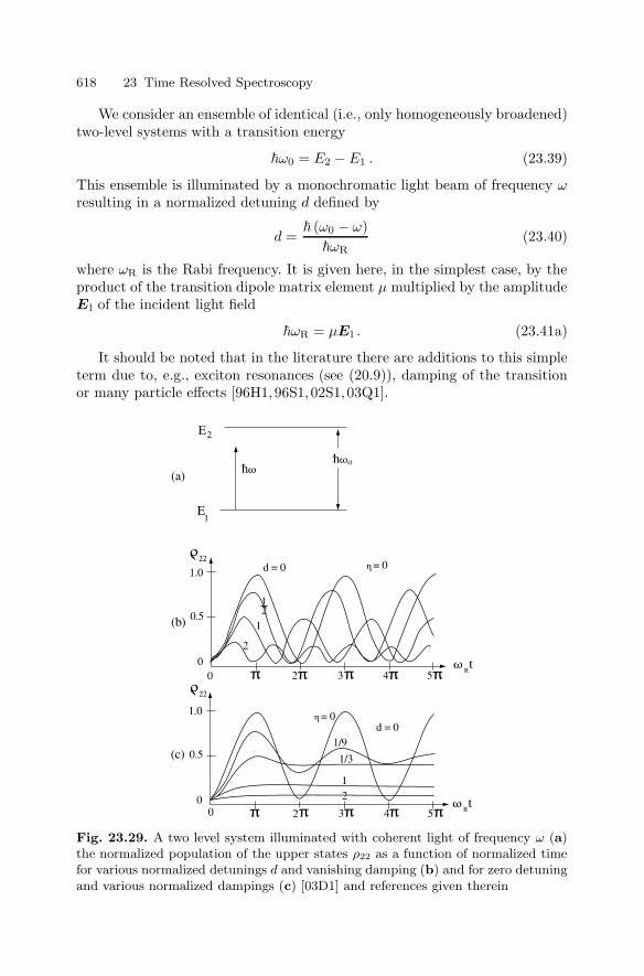
618 23 Time Resolved Spectroscopy
We consider an ensemble of identical (i.e., only homogeneously broadened)two-level systems with a transition energy
ω0 = E2 − E1 . (23.39)
This ensemble is illuminated by a monochromatic light beam of frequency ωresulting in a normalized detuning d defined by
d = (ω0 − ω)
ωR(23.40)
where ωR is the Rabi frequency. It is given here, in the simplest case, by theproduct of the transition dipole matrix element µ multiplied by the amplitudeEl of the incident light field
ωR = µEl . (23.41a)
It should be noted that in the literature there are additions to this simpleterm due to, e.g., exciton resonances (see (20.9)), damping of the transitionor many particle effects [96H1,96S1,02S1,03Q1].
Fig. 23.29. A two level system illuminated with coherent light of frequency ω (a)the normalized population of the upper states ρ22 as a function of normalized timefor various normalized detunings d and vanishing damping (b) and for zero detuningand various normalized dampings (c) [03D1] and references given therein

23.2 Decoherence and Phase Relaxation 619
If the dephasing time is infinitely long, i.e., η = γ = 0 in Fig. 23.29, thedriving field pumps all systems coherently from the ground state to the excitedstate and back again and so on. The characteristic frequency for this process,the so-called Rabi oscillation, is just the Rabi frequency of (23.40). If thedetuning d is zero the population of the two-level system can be completelycoherently driven between the ground and excited state. For finite detuning,the maximum value of ρ22, i.e., the population of the upper state, decreasesas shown in Fig. 23.29b.
If the population is flipped once or a few times from the ground state toan excited state by a short pulse, one speaks of Rabi flopping rather than ofRabi oscillations.
Zero damping is, of course, an idealization. For finite (normalized) dampingthe oscillations disappear with time and one reaches a steady state populationunder cw excitation, which can be described by simple recombination kineticsusing, e.g., Einstein’s coefficients. In this case the maximum value of ρ22 is0.5 after the Rabi oscillations die out (see Fig. 23.29c).
The sample is transparent under these conditions, which is why populationinversion and lasing are usually not possible in a pure two-level system.
While the dephasing times can be rather long in atomic systems and Rabioscillations and the optical Stark effect (see Sect. 20.4) have been known fora long time [75A1], Rabi flopping could only be observed in semiconductorsafter the invention of intense fs lasers.
In early experimental examples in In0.08Ga0.92As multiple quantum wellsand CdSe epilayers indications of Rabi flopping have been deduced from theshape of the transmitted pulse [94C1,95C1,97F1,98G1,01N1] with a durationof about 100 fs and a peak intensity in the GW cm−2 range. We show herean example of a 20-period In0.1Ga0.9Ga/GaAs multiple quantum well samplefrom [99S3] in Fig. 23.30. In Fig. 23.30a the transmission spectrum exhibitsthe nz = 1hh and light hole transitions. Figure 23.30b gives the spectra andpolarization of the 770 fs pump pulse tuned to the hh transition and the 150 fsprobe pulse, centered on the lh resonance.
The almost periodic oscillations of the transmission in Fig. 23.30c are at-tributed to Rabi oscillations. This interpretation is based on agreement withcalculations including nonlinear Coulomb renormalization of the transitions(Fig. 23.30d) and the fact that the oscillation frequency increases with thesquare root of the energy flux of the pulse, i.e., linearly with the field ampli-tude.
Rabi oscillations in quantum dots have been reported, e.g., in [01S1,02B2,02B3,02K2] and for µ-cavities in [01D2].
Usually one has the situation
ωR ωc ≈ Eg (23.42a)
where ωR is the Rabi frequency and ωc the carrier frequency of the laser pulse.According to (23.40), if the laser intensity is sufficiently high, however, one
may reach a situation

620 23 Time Resolved Spectroscopy
Fig. 23.30. (a) The transmission spectrum of the In0.1Ga0.9As/GaAs MQW sam-ple. (b) The spectral shapes and polarizations of pump and probe pulses with therelevant transitions in a band-to-band model in the inset. (c) The differential trans-mission signal as a function of pump-probe delay. (d) Calculations neglecting (dottedline) and including (solid line) Coulomb renormalization [99S3]
ωR ≈ ωc ≈ Eg (23.42b)
known as carrier wave Rabi flopping.This new phenomena, which appears under this unusual situation, belongs
to the regime of extreme nonlinear optics (see Sect. 19.3) and can only be ob-served for lasers with a duration of a few light cycles to avoid sample damageor (excitation-induced) dephasing. The Rabi doublets of the fundamental andthe third harmonic may overlap around the second harmonic, producing sig-nals that depend on the absolute optical phase between the carrier wave andthe envelope, i.e., whether the maximum of the envelope coincides with a max-imum of the carrier wave or with a zero transition. Examples for this regimeare found in [01M2,03S1].
23.3 Intra-Subband and Inter-Subband Relaxation
After this overview of coherent processes we review incoherent intraband andinter-subband relaxation and finish this subsection with some transport prop-erties. For the latter topic see also Sect. 23.2.1.2.5

23.3 Intra-Subband and Inter-Subband Relaxation 621
23.3.1 Formation Times of Various Collective Excitations
The first processes we consider concern the formation times of some quasipar-ticles or collective states. These times are partly as short as the decoherencetimes and involve concepts of quantum kinetics. A recent review connectingthe regimes of 23.2 and the one here in is [01C1].
The first example is the formation time of excitons. They can be either di-rectly resonantly excited by a spectrally sufficiently narrow laser (i.e., smallerthan ∆LT) as stationary eigenstates, or can from after band-to-band excitationi.e. excitation in their ionization continuum with some delay.
In GaAs the exciton binding energy is small(Eb
x ≈ 4.5 meV)
compared tothe LO phonon energy (ωLO ≈ 36 meV), and the polar coupling to phononsis weak.
Consequently the formation time of excitons is rather slow in the range of100 ps for electron–hole pair excitation in the continuum [98K2, 02H1, 03K1,03K2, 04C1, 04K2, 04O1] in contrast to resonant excitation [03K2]. The pres-ence of excitons has been deduced for GaAs bulk samples or In1−yGayAsquantum wells from the 1s → 2p transition at about 6.3 meV in time-resolvedpump and THz probe spectroscopy [03K1]. In these experiments it was alsopossible to show the thermal ionization of excitons at a lattice temperatureof 60 K to occur on a time scale around 10 ps.
The rather slow formation time of excitons in bulk GaAs and in GaAs- orInAs-based wells has even provoked the extreme question of whether excitonsexist at all. For a recent review see, e.g., [03K2] or [04C1] and referencestherein. This question has a philosophical aspect, namely “what does theexistence of a quasiparticle in a solid mean”, which we do not attempt toanswer here. The more down-to-earth aspect is if excitons exist in a similarway as other quasi-particles like phonons, plasmons and magnons. Here, wethink the answer is rather clear and yes.
All the experiments showing the free motion of excitons (see below inSect. 23.4), the direct measurements of their (polariton) dispersion curves orof their thermal distribution on this dispersion as detailed in Chaps. 9, 13and 15 or the formation of biexcitons (20.3) make it difficult to discard theconcept of excitons as quasiparticles.
Furthermore (time-resolved) photo-luminescence excitation spectra of ex-citons show in more ionic bound semiconductors with higher binding energycomparable to the LO phonon energy like in CdTe or ZnSe, that excitons areformed rapidly, even in the ionization continuum. We already addressed thispoint in Sect. 23.2.2 and will see a further example below.
The dynamics of LO phonon emission from heavy holes occurring evenfor a kinetic energy below ωLO has been investigated as a function of theFrohlich coupling parameter α in GaAs and CdTe both experimentally andtheoretically using quantum kinetics (see [01B4] and references therein). Theseresults essentially confirm the more didactically formulated statements aboveand also give, for the example of the hh in CdTe, some information on the
622 23 Time Resolved Spectroscopy
formation times of the polaron of several 10 fs. For the polaron concept seeSect 8.6.
The formation time of the magnetic polaron introduced in Sect. 10.2 hasbeen investigated by various groups (see e.g. [87Z1,95D1,96H2] and referencestherein). The formation time depends on the Mn concentration, on temper-ature, on the presence of an external magnetic field and, for quantum wells,also on the well width. Typical formation times range from several tens of psto a few ns. Thus the formation time of magnetic polarons is substantiallylonger than that of (phonon) polarons mentioned above.
The last example for formation times is the build-up of Coulomb screeningin an electron–hole plasma. As explained in Chap. 21 a random spatial distri-bution of electrons and holes does not result in band gap renormalization.
Recently it was possible to observe in beautiful experiments with timeresolved band-to-band pump and THz probe beam spectroscopy the build-upof Coulomb screening and plasmon scattering on a timescale of a few 10 fs. Fordetails on the experiment and theory see, e.g., [98B3,98B4,01C1,01H1,01H2,01H3]. These buildup times are roughly equal to the inverse of the plasmafrequency ωPL, a fact that is not totally surprising.
23.3.2 Intraband and Inter-subband Relaxation
We now leave the regime of ultrashort times and of quantum kinetics and turnto “usual” intraband and inter-subband relaxation, starting with bulk mate-rials, proceeding to alloys and then to structures of reduced dimensionality.
We start with rather old measurements on the exciton polariton in CdS[75W1]. Figure 23.31 shows the polariton dispersion of the nB = 1AΓ5 ex-citon, the luminescence spectra for two polarizations, and the lifetime mea-sured from the luminescence decay at various energies after band-to-bandexcitation. The excitons relax in about 1 ps by LO-phonon emission onto thelower polariton brand (LPB). There they can relax further, e.g., by emissionof acoustic phonons. This process becomes slower and slower with decreas-ing slope of the dispersion, since less and less energy transfer is allowed perunit of momentum transfer. For this reason the excitons accumulate in theindicated area, which is known as the “bottle neck”. See also Sect. 13.1.3. Asa loss mechanism, polaritons can be transmitted from the UPB and the LPBthrough the surface, but only if the parallel component of their wave vectork satisfies
k‖ 2πλvac
(23.43)
with a probability depending on the reflection coefficient and on the squaredamplitude of the photon-like part of the wavefunction. Additionally the ex-citons can be trapped at defects and recombine there (non-) radiatively orbe thermally reexcited into extended states. They can be scattered onto thephoton-like branch of the dispersion curve under emission of one or more

23.3 Intra-Subband and Inter-Subband Relaxation 623
LO phonons (Sect. 13.1.3). A further relaxation to the regime below thebottle-neck by emission of acoustic phonons becomes rather improbable dueto the rapidly decreasing density of final states; see Sect. 2.6 and Fermi’sgolden rule.
A similar scenario exists also for the cavity polaritons introduced inSets. 17.1, 20.2 and 22.1.
The accumulation of the exciton-like polaritons in the bottle-neck duringthe relaxation in the band directly explains the increase of their radiativedecay times in Fig. 23.31c at these energies.
The relaxation of localized excitons through the localized tail states showsup in the time dependence of the emission line shape and its maximum po-sition after pulsed excitation. Some examples have already been given inSect. 14.4 and another will be given in Sect. 23.4. The thermally activatedrelaxation from metastable states to deeper ones at intermediate tempera-tures (e.g., 10 K to 50 K) and the thermal excitation to higher, generally ex-tended states at even higher temperatures caused by the higher density ofthese states result in the well-known non-monotonous shift of the emissionmaximum with temperature. Examples for various II–VI or III–V materi-als and theoretical modeling are given for bulk materials and quantum filmsin [87S1,87S2,92S1,92S2,92S4,92S5,99K1,00K2,01T1,02K4,02R1,03R1,04K1]and the references given therein.
Fig. 23.31. The dispersion of the nB = 1AΓ5 exciton polariton in CdS in thebottle-neck region (a); the luminescence spectra for the dipole allowed orientationE ⊥ c and the forbidden one E ‖ c (b); and the decay time of the luminescence asa function of photon energy (c) [75W1] compare also with Figs. 13.4, 11, 14, 15 and 29

624 23 Time Resolved Spectroscopy
In Fig. 23.32 we give another example of intraband relaxation, this time ofa AlGaAs MQW sample. The differential transmission between unexcited andexcited sample is measured with 50 fs increments when the sample is excitedaround t = 0 with a pump pulse of 80 fs duration. There is some bleaching dueto partial blocking of the band-to-band transitions by the bunch of electron–hole pairs excited in the continuum (dotted areas). The temporal evolution ofthe intraband relaxation can be seen nicely. There is a decrease of excitonic ab-sorption in the region of the nz = 2hh transition around 1.57 eV. This changeis rather small and constant on the time scales shown here ( T1) and is dueto direct screening of the Coulomb interaction in the exciton by the carriers.This screening is largely independent of the energy and distribution of the freecarriers in the bands. A similar behavior is found for the nz = 1hh and lh res-onances around 1.46 eV in the three lowest traces. When the excited electronsrelax down into the exciton states, the transmission increases drastically. Thisfinding is attributed to phase-space filling and exchange interactions which be-come effective for these exciton resonances only after the excited species startto populate the respective states. Figure 23.32 thus demonstrates qualitatively
Fig. 23.32. Intraband relaxation of electron–hole pairs in the Al1−yGayAs/GaAsMQW measured by time-resolved pump and probe experiments [88C1]

23.3 Intra-Subband and Inter-Subband Relaxation 625
that direct screening of the Coulomb interaction is less efficient in quasi two-(and one-)dimensional systems than exchange interaction and phase-space fill-ing. This difference to three-dimensional materials has already been pointedout Sect. 21.2 and 4 in connection with electron–hole plasmas.
As a further example of quantum wells we provide data in Fig. 23.33 fora ZnSe/ZnS1−xSex superlattice from [98U1].
The l.h.s. of Fig. 23.33a shows schematically the luminescence spectrum.There is a zero-phonon line (ZPL) resulting from the emission of excitons lo-calized in tail states and of a free exciton with small k vector (23.43). TheLO phonon sideband monitors in a similar fashion as for bulk samples inFigs. 13.12 and 13.13 the whole distribution of excitons since radiative re-combination through emission of a LO phonon is possible from every k stateas indicated on the r.h.s. of Fig. 23.33a, while Fig. 23.33b shows a time-integrated photoluminescence spectrum showing free and localized lh, hh andbound-exciton (BE) luminescence and their LO phonon replicas. The photolu-minescence excitation spectrum taken at the position of the hh exciton showsthe lh exciton resonance and peaks at integer multiples of LO phonon energiesabove the hh. Up to four such LO phonon resonances are visible. The absenceof a mass renormalization factor (23.38) shows, that the electron–hole pairs
Fig. 23.33. (a) Schematics of the luminescence spectrum and of the exciton relax-ation process in ZnSe/ZnS1−xSex superlattices (b) A time-integrated luminescencespectrum c, d Time-resolved spectra for two different excess energies [98U1]

626 23 Time Resolved Spectroscopy
emit the LO phonons together, i.e., that they form a rapidly bound state thatrelaxes on the exciton dispersion curve as shown schematically on the r.h.s. ofFig. 23.32a. This interpretation is confirmed by time-resolved measurementsof the LO phonon replica after ps-pulsed excitation in Fig. 23.32c,d wherethe excitation energy is 1.5 and 1.2 LO phonon energies above the hh band.Within the temporal resolution luminescence appears 2 LO phonons belowthe excitation. Then a slower relaxation of the excitons by emission of acous-tic phonons (see r.h.s. of Fig. 23.32a) leads to a population of hh excitons ona time scale of 100 ps followed by a lifetime-limited decay of this line of about0.5 ns. Calculations in [98U1] not shown here agree with the experimentaldata and further corroborate this model.
Further relaxation processes include, e.g., the capture of carriers into quan-tum wells, wires or dots. For some references see, e.g., [96S2,98R1,98U2,99F1,00L4,00R1,01R1,01L1] and references therein. For the inter-subband or inter-level relaxation in the quantum structures see, e.g., [99F1,99H1,99H2,99M1,00L4, 01L1, 01M3, 02B2, 02B3, 02B4, 02D1, 02K2, 02K3, 04O1] and referencestherein.
We give here an example for the inter subband relaxation of hh excitons ina GaAs/Al1−yGayAs MQW sample, which is excited into the third subbandas shown schematically in the inset of Fig. 23.34.
Fig. 23.34. Time-resolved differential transmission (bleaching) signal of the firstthree hh exciton resonances [94H1]

23.3 Intra-Subband and Inter-Subband Relaxation 627
The bleaching of the resonantly excited nz = 3hh exciton decays on a subps timescale by relaxation to deeper levels. Simultaneously, the bleaching ofthe nz = 2hh and nz = 1hh builds up. The subsequent decay of the nz = 2hhresonance bleaching is already much slower, while the nz = 1hh ground statestill shows a slight increase due to feeding from higher states over the timeinterval shown in Fig. 23.34 of 3 ps. The lifetime of this state is in the rangeof 100 ps as shown below.
Further topics in the field of relaxation concern, e.g., the relaxation bytunneling processes see [96S1, 96T1, 01L1] and references therein, or the re-laxation in an electron–hole plasma [93M1,96S1,97M1,97M2,98M1] and ref-erences therein.
Recent reviews on relaxation processes is also found in [97M2, 04O1] andin other contributions to this book.
23.3.3 Transport Properties
Transport properties are intimately related to relaxation and collision pro-cesses, e.g., in the relaxation time approximation of the electrical conductivityresulting in
σ =ne2τ
mand µ =
υD
|E| =τe
m(23.44a)
where n is the carrier density, m is the effective mass of the carriers, τ isthe time between collisions, υD is the drift velocity, and µ is the mobility,resulting in the expression (23.44b) for the diffusion constant according to theNernst–Townsend–Einstein Relation
D = kBTτ/m = kBTµ/e . (23.44b)
A more elaborate theoretical concept is given in terms of the Boltzmannequations, treated in many textbooks of solid state or semiconductor physics.
Electrical transport and conductivity as well as heat conductivity are obvi-ously not topics of this book. However we give below some examples of excitonor electron–hole pair transport in semiconductors. See also 23.2.1.2.5 above.
Actually we have already given several examples of such transport mea-surements, e.g., for excitons in Cu2O in Sect. 20.5.2 of the electron–holeplasma in Sect. 21.3.1 or above with references [92O2, 02Z1, 03Z1] includingtransition from coherent or balistic transport to diffusive one [04D1,04Z2].
Furthermore the coherent polariton transport has been discussed, e.g., inconnection with propagation quantum beats in Sect. 5.2. In the following wegive some more examples.
An early example is exciton diffusion in CdS [59B1]. The transport ofexcitons via the decay of laser-induced population grating (also see above)has been investigated for CdS in [88W1,88W2] revealing a temperature- anddensity-dependent diffusion length on the order of 1 µm.

628 23 Time Resolved Spectroscopy
The influence of the polariton dispersion on the exciton transport hasbeen investigated by the same technique as for ZnSe/ZnS1−xSex quantumwells in [98N1] showing the influence of the polariton group velocity on thetransport length.
In contrast, the diffusion length of excitons tends to zero for zero tem-perature due to localization effects in alloys like CdS1−xSex as found in[92S1, 92S2, 92S4]. For the influence of disorder in quantum wells on trans-port see [00Z1] and references therein.
The expansion of an electron–hole plasma in direct gap semiconductorslike CdS or CdSe has been investigated by spatially resolved pump-and-probebeam spectroscopy resulting in diffusion lengths in the 4 to 10 µm regime[84K1,85M1].
23.4 Interband Recombination
Now we discuss some measurements of the interband recombination time T1.For the definition of this quantity see the discussion with (23.5) or Chap. 27.
To measure this quantity it is best in principle to observe effects to whichall excited species contribute by roughly the same amount. One could follow,e.g., the further temporal evolution of the bleaching of the exciton resonancesin Figs. 23.32 and 23.34 and one would find that the differential transmissionsignal disappears with a time constant of about 0.5 ns.
Very often one relies, however, simply on the temporal evolution of theluminescence, e.g., of excitons or biexcitons, as a monitor of the population ofthe respective species, although it is well known that the luminescence yield ηfor most semiconductors is considerably smaller than 1. For high quality directgap samples one finds, as already mentioned several times,
10−1 η 10−3 ; (23.45a)
only for localized excitons in some selected samples of bulk alloys or quan-tum structures or for some laser diodes have values of η close to 1 beenreported. For indirect gap materials or direct ones with dipole forbiddenband-to-band transitions or for direct ones containing “luminescence killers”like Fe or Cu ions η can even be much smaller than in (23.45) (see, e.g.,[97W3,98W5,01J1,03F1,03T1] and the references given therein for examples).This means that with luminescence decay measurements only, one monitorsthe fate of a minority of the exited species and assumes quietly that theyrepresent the majority.
Furthermore, radiative decay involves the conservation of the component ofk parallel to the surface (see below) so that large k excitons hardly contributeto the zero phonon line. Finally the luminescence decay is often not simplyexponential after pulsed excitations (see (23.5)), so a definition of a lifetimeis, strictly speaking, not possible. Only something like an effective decay timeover a certain time – or intensity interval – can be given.

23.4 Interband Recombination 629
Looking closely, the problem of radiative decay turns out to be rathercomplex. An exciton polariton in a perfect three-dimensional crystal cannotdecay radiatively, since it is already the quantum of the mixed state of excitonand photon.
It can move (diffusively or ballistically) through the sample and be trans-mitted through or reflected at the surface of the crystal when it hits it witha certain probability. In the first case it appears as luminescence on the otherside. Transmission through the surface is only possible if the parallel com-ponent of k, which is conserved at the surface (see Sect. 3.1.3), is smallerthan
k‖ ≤ kvac = 2πω/c . (23.45b)
(see, e.g., Fig. 13.11). For |k| k‖ given by (23.45b) the transmission proba-bility decreases rapidly. One can either argue that the polariton is essentiallyexciton-like or that the refractive index of these states is very large result-ing with (3.19) in a high reflectivity or substantial ranges of total internalreflection.
What can happen in a perfect crystal is that the exciton polariton is scat-tered by emission of n LO phonons on the photon-like branch of the disper-sion curve, where it travels with a high group velocity essentially ballisticallythrough the sample and has a good chance of being transmitted through thesurface when it hits it, appearing as luminescence as shown in Fig. 13.12.
If there are defects in the sample (or at its surface), the exciton polaritoncan be trapped at these defects and recombine there either nonradiativelyresulting in (23.45a) or emit a photon-like polariton, which appears with highprobability as a luminescence photon. The same holds for capture in localizedtail states in bulk alloys or quantum structures. Similar arguments are validfor cavity polaritons.
In quantum wells and wires k‖ is the only component of k, this meansthat free exciton (-polaritons) with large k cannot radiate at all. Those withsmall k produce photons outside the quantum structure very quickly (in about10 ps) and particles with higher k have then to relax down to small k values.
This process and the restriction of the emission of free excitons to the lightcone defined by (23.45b) results in a law for the luminescence decay time TL
as a function of the lattice temperature Tlattice ([91A1,91F2,92O1,92O2,94A1,98L1,00Z2,04P2] and references given therein)
TL α Td/2lattice (23.45c)
where d is the quasidimensionality of the system. We give a detailed deriva-tion for d = 2 below. The linear increase of the luminescence decay time withtemperature for d = 2, i.e., for quantum wells, is frequently used as an ar-gument for dominant radiative decay. This is a clear over-interpretation ofthe data since similar samples show different slopes in the relation (23.45c)as shown below in Fig. 23.35 and samples with ηlum 1 can also show suchbehavior [91O1, 92O1, 92O2, 92S5, 03F1]. If one assumes that the capture of

630 23 Time Resolved Spectroscopy
excitons or exciton-like polaritons into nonradiative and radiative centers, in-cluding localization sites, decrease rapidly with increasing k it becomes clearthat a similar law to (42.343 b) also holds for these cases, no longer restrict-ing (23.45c) to dominant radiative recombination. However, the decrease ofthe luminescence yield observed for many high-temperature samples (e.g., forGaAs QW is usually above 100 K) implies that excitons or electron–hole pairswith high thermal kinetic energy find an increasing number of nonradiativedecay channels.
The situation is slightly different for quasi-zero-dimensional quantum dots,islands and other localization sites since there is no more k-conservation.
In spite of all these implications it is experimentally quite easy to mea-sure the temporal decay of a luminescence signal, and therefore many dataon T1 of electronic excitations of semiconductors are obtained by this tech-nique. If one remains aware of the above implications it may be a usefultechnique.
We start with a few typical exciton lifetimes in bulk semiconductors.The exciton lifetimes are at low temperature and density in bulk semi-
conductors with direct, dipole-allowed band-to-band transitions typically inthe range of a few hundred ps to a few ns (see Fig. 23.31) and for dipole-forbidden materials from several tens of ns to 5 ms (see Sect. 20.5). ForCu2O the values for the lifetime reported for the forbitten para excitonrange from around 10 ns to beyond 10 ms. See the ref. given in Sects. 13.2.1.2and 20.5.2.
Fig. 23.35. The decay time of theluminescence in various Al1−yGay
As/GaAs MQW samples as a func-tion of the lattice temperature[92O1]

23.4 Interband Recombination 631
In indirect gap materials values from a few tens of ns to ms are ade-quate. Increasing temperatures and increasing densities tend to decrease thelifetimes, e.g., due to increasing average k-vectors and inelastic scatteringprocesses like Auger recombination [75H1, 79H1], respectively. Stimulatedemission also reduces the effective lifetime down to the 100 fs range [85M1].
The localized excitons in alloy semiconductors show that at low tempera-ture there is a strong dependence of the luminescence decay time on the photonenergy (see e.g. [89G1,91U1,98K1,99K1,04K1] and references therein). How-ever this decay is governed by a complex interplay of temperature dependentrelaxation between various localized states (see Sects. 23.4, 9.6 and 14.4) andradiative as well as nonradiative recombination. Typical lifetimes are againin the range of a few ns but may reach 100ns for deeply localized states andespecially for distant pairs [92S4,98K1,99K1,04K1].
The same holds true for localized excitons in quantum structures, es-pecially in II–VI quantum wells and superlattices. Examples are found in[93K2, 01S2, 04O1]. In type II structures the electron–hole overlap dependsstrongly on the well widths and therefore also on the lifetime. An example forCdS/ZnSe structures is found in [01S2,03S2,04P1].
In piezo-superlattices like CdSe/CdS the band bending and consequentlythe electron–hole overlap integral depend not only on the layer widths butalso depend strongly on the carrier density via a screening of the piezo fieldsresulting in an extremely nonlinear recombination dynamics and in a temporalshift of the emission photon energy over several hundreds of meV after pulsedexcitation [94L2,95L1].
Now we look in more detail into GaAs/Al1−yGayAs multiple quantum wellsamples with less pronounced localization effects.
In the following example (Figs. 23.35 and 23.36) we consider a MQW sam-ple of high quality with narrow absorption and emission lines and virtuallyno Stokes shift between emission and absorption. In emission under cw ex-citation and at a low temperature this sample shows the nz = 1hh excitonand weakly, on its high energy side, the nz = 1lh exciton. A shoulder onthe low energy side is presumably due to a bound exciton complex or to anexcitonic molecule or trion (Sect. 20.3) and a band around 1.53 eV due toa free-to-bound transition (Sect. 14.2). The latter structure saturates rapidlywith increasing pump power. In Fig. 23.36a,b we see the decay of the nz = 1hhluminescence after resonant and non-resonant ps excitation for various pumppowers. The most striking feature is that a simple exponential decay is almostnever observed.
For low, resonant excitation (curve 1) one observes a rapid decay of theluminescence, which can be attributed to a rapid capture of excitons into somedeep, presumably non radiative centers. For increasing excitation this processsaturates and for t > 250 ps one gets in curve 2 a simple exponential decaywith T1 ≈ 200 ps. This order of magnitude seems to be representative for theradiative and nonradiative decay of excitons in good MQW samples at lowtemperatures (T 10 K). For even higher pump power (curve 3) this value is

632 23 Time Resolved Spectroscopy
Fig. 23.36. The decay curves of the 1hh exciton luminescence for various excitationfluences for resonant (a) and non-resonant (b) excitation of the nz = 1hh excitonin an AlGaAs MQW sample, and some calculated decay curves (c) [92O1]
reached only at later times and a hump develops in the decay curves, which iseven more pronounced in the case of non-resonant excitation with some excessenergy (curves 4 to 6).
This feature can be interpreted as a thermalization (or T3) process. In-creasing Iexc or ωexc leads to the creation of a hot gas of excitons witha certain average kinetic energy and with finite k‖ vectors. In contrast to thethree-dimensional case, k‖ is the total momentum k of the excitons in quasitwo-dimensional systems, as mentioned above. Due to the conservation of k‖in the radiative recombination process only excitons with k‖ around zero (orexcitons in the small tail of localized states caused by well-width fluctuations)can participate in radiative recombination without emission of LO phonons,a process which is usually much weaker in standard III–V materials compared,e.g., to II–VI semiconductors. The humps or plateaux in curves 7 and 8 reflect

23.4 Interband Recombination 633
the cooling or the formation process of the exciton gas from states with largertowards states with smaller k = k‖.
A modeling of the decay along the lines above gives the curves 1′, 2′, 5′,and 6′, in Fig. 23.14c, which correspond to the unprimed experimental ones.The good agreement gives some support to these ideas.
A related experimental finding concerns the fact that in quantum wellsone often observes a linear increase of the luminescence decay time T1 timewith lattice temperature for TL 10 K up to around 100 K. Examples aregiven in Fig. 23.35 or in [91A1,91F2,91G1,92O1].
T1 =T ′
1kBTL
Em(10 K TL 100 K) . (23.46)
where T ′1/Em is for the moment only a characteristic parameter of the ma-
terial. We will present a simple model from [92O1] which accounts for thiseffect. For details and partly similar, partly complementary approaches see[91A1,91F2,91G1,92O1,96P1,98L1,00Z2].
The relation to the effect discussed above comes from the considerationthat the exciton temperature Tex has the lattice temperature TL as a lowerlimit and is close to this limit for low excitation intensities and small excessenergies. In the following we thus assume Tex ≈ TL. It is also reasonable toassume that only excitons with small (kinetic) energy 0 E Em participatein the recombination process. This condition is fulfilled for radiative decay forfree excitons with [see also (23.45b)]∣∣k‖
∣∣ 2πλv
≈ 8 × 104 cm−1 (23.47)
where k‖ is the in-plane wave vector and λv the luminescence wavelength invacuum, due to the conservation of the parallel component of k.
The numerical values refer to Al1−yGayAs/GaAs(M)QW and k‖ = 0 andk‖ = 2π/λv correspond to normal and grazing emission, respectively.
The contribution to Em resulting from (23.47) is
E0m =
2k2
‖2M
=22πMλ2
v
≈ 10 µeV . (23.48)
The value of E0m can be increased by damping and by inhomogeneous broad-
ening. This means that we can include a tail of localized states, providedthat its tailing parameter E0 fulfills the condition E0 kBTL, i.e., the local-ized excitons are in equilibrium with the free ones. From the absorption andluminescence linewidth of good samples (Fig. 15.3a) we can conclude that
E0 < Em ≈ 0.5–1 meV (23.49)
so that the above conditions are fulfilled for TL 10 K.

634 23 Time Resolved Spectroscopy
For kBTL < Em the excitons decay with an average lifetime around 200 ps(Fig. 23.36b). For T > 10 K we give the following treatment.
The two-dimensional density of states in effective mass approximationD(E) is given according to Sect. 2.6 by
D(E) =
D0 for E 00 for E < 0
(23.50a)
with
D0 = g · 12π
2M2
≈ 1012 (cm2meV)−1 (23.50b)
possibly including a small exponential tail as mentioned above.The number of excitons per unit interval of energy N(E) is then given by
N(E) = D0 exp[−(E − µ)/kBT ] E 0 , (23.51)
where µ is the chemical potential of excitons and where Boltzmann statisticsand the weak coupling approach are used.
The total density N0 at a time t follows from integration over (23.51):
N0(t) = kBTD0 exp[µ(t)/kBT ] (23.52a)
This means that the chemical potential µ can be expressed in terms of N0
and Tµ = kBT ln
N0
D0kBT, (23.52b)
or
N(E) = D0 exp(− E
kBT+ ln
N0
D0kBT
). (23.53)
For the Boltzmann approximation to be valid we must have µ < 0 or
N0 < D0kBT ≈ 1012 cm2 for T = 10 K . (23.54)
This condition is very well fulfilled for low excitation.For a “monoatomic” recombination process one generally uses the ansatz
−dN0
dt=
1T ′
1
N0 . (23.55)
This ansatz has to be modified because of momentum conservation, since onlya fraction γ of the excitons can participate in the recombination, namely thosewhich are sitting in the interval Em around the bottom of the band:
γ =N(E = 0)Em
N0. (23.56)

23.4 Interband Recombination 635
Equation (23.55) has then to be rewritten as
−dN0
dt=
1T ′
1
γN0 =1T ′
1
N(E = 0)Em
N0N0 , (23.57)
which means we have an effective lifetime T1
T1 = T ′1N(E = 0)Em/N0 . (23.58)
With (23.49) and (23.52), (23.53) we finally obtain
T1 = T ′1
kBT
Em≈ 200 ps
kBT
1 meVfor T > 10 K , (23.59)
in agreement with the experimental finding.The linear increase of T1 with temperature is sometimes used to argue
that the recombination of excitons in quantum wells is essentially radia-tive [91F1], as mentioned above. This assumption may hold in some se-lected samples in which the spectral width of the free exciton emission isgoverned by E0
m in (23.48). See [03T1]. For other samples, the above ap-proach seems to be more realistic, especially if one recalls that MQW sam-ples with comparable parameters can show different slopes in the relationT1 = f(TL) (Fig. 23.35) and that some II–VI superlattices with ratherlow luminescence yields also show a linear relation as mentioned alreadyabove.
We refer the reader for more details and examples to e.g. [88N1,91S1,92P1,92S1,92S2,93U1,96S1,01L1,03P1,04O1] and references therein.
To conclude this section we give some more references to the recombinationdynamics of excitons, trions or biexcitons as a function of sample parametersand excitation [96L1,98L1,98Z1,00E1,00Y1,00Z1,00Z2,02G1] for various II–VI and III–V quantum wells.
For Si1−xGey/Si multiple quantum wells lifetimes on the order of 0.1 µshave been found [95Z1].
For V grooves see, e.g., [98B5,99O2] and references therein,for ZnO nano-rods [04P2] and for quantum dots or islands see [97W1, 99B3, 00B1, 00D1,00F1, 02S2, 03C2, 03H2]. For the dynamics of eletron–hole plasma see e.g.[00N1,02N2,02N3].
Exciting and beautiful new results emerged recently as shown here orcan be expected in the field of ultrafast spectroscopy of semiconductors inthe near future partly in connection with (extreme) nonlinear optics. Theywill comprise e.g. the first elementary interaction processes of the electro-magnetic radiation field with the electronic system, where memory effects ornon-Markovian behaviour occur, or the coherently driven polarization fieldin the sense of Rabi flopping or the consistent description of the phenom-ena in the strong coupling limit, i.e. in the polariton picture. An impor-tant step into this direction is the transition from the optical Bloch equa-tions to the semiconductor Bloch equations, though this approach involves an

636 23 Time Resolved Spectroscopy
extremely high computational effort see Chap. 27. First results into thesedirections will be found e.g. in the recent and future issues of [88N1] orin [04O1].
23.5 Problems
1. If you prefer the mathematical description of physics to the intuitive pic-ture given here, then go through the concept of the optical Bloch equa-tions, e.g., with the help of [75A1, 78S1, 84S1] or Chap. 27, and find outwhat the Rabi frequency, a π/2- and a π-pulse are, and what the relationto a spin system is (spin echo). By the way, the photon echo also works ifpulses other than π/2 and π are used, but the description is more difficult.
2. Find some data for the electrical conductivity of standard semiconductors.Use the equations given in this chapter to deduce the momentum relax-ation of free carriers in electrical transport at various temperatures andcompare with the data for excitons. Are the above-mentioned formulasalso adequate to analyse the electrical conductivity of a metal?
3. Many of the above effects of ultrashort time-resolved spectroscopy likeRabi oscillations, photon echoes, etc., have been previously found inatomic systems. Find some examples. Why have they been detected solate for semiconductors?
4. There are several ways to create THz pulses. Find some of them in theliterature.
References to Chap. 23
[28B1] F. Bloch, Z. Phys. 52, 555 (1928)[34Z1] C. Zener, Proc. Royal. Soc. London A 145, 523 (1934)[37R1] I.I. Rabi, Phys. Rev. 51, 652 (1937)[39R1] I.I. Rabi et al., Phys. Rev. 55, 526 (1939)[46B1] F. Bloch, Phys. Rev. 70, 460 (1946)[57F1] R.P. Feynmann, F.L. Vornon and R.W. Hellwarth, J. Appl. Phys. 28, 49
(1957)[59B1] I. Broser and R. Broser-Warminsky, J. Phys. Chem. Solids 8, 177 (1959)[65S1] E. Spenke, Elektronische Halbleiter 2nd edn., Springer, Berlin, Heidelberg
(1965)[75A1] L. Allen and J.H. Eberly, Optical Resonance and Two-Level Atoms, Wiley,
New York (1975)[75H1] A. Haug, Festkorperprobleme XII, 411 (1975)[75W1] P. Wiesner and U. Heim, Phys. Rev. B 11, 3071 (1975)[77L1] V.S. Letokhov and V.P. Chebotayev, Nonlinear Laser Spectroscopy,
Springer Ser. Opt. Sci. 4, Springer, Berlin, Heidelberg (1977)[78S1] R.L. Shoemaker, in Coherence and Laser Spectroscopy, Plenum, New York,
p. 197 (1978)

References to Chap. 23 637
[78Y1] T. Yajima and H. Souma, Phys. Rev. A 17, 309, 324 (1978)[79H1] A. Haug, J. Lumin. 20, 173 (1979) and references therein[82H1] R. Hopfel et al., Surf. Sci. 113, 118 (1982)[83M1] Y. Masumoto, S. Shionoya and T. Takagahara, Phys. Rev. Lett. 51, 923
(1983)[84K1] K. Kempf and C. Klingshirn, Solid State Commun. 49, 23 (1984)[84S1] Y.R. Shen, The Principles of Nonlinear Optics, Wiley, New York (1984)[85M1] F.A. Majumder et al., Phys. Rev. B 32, 2407 (1985)[85Y1] Y.X. Yan, E.B. Gamble and K.A. Nelson, J. Chem. Phys. 83, 5391 (1985)[86H1] D. Heitmann, Surf. Sci. 170, 332 (1986)[87M1] U. Merkt, Festkorperprobleme / Adv. Solid State Phys. 27, 109 (1987)[87S1] S. Shevel et al., J. Luminesc. 37, 45 (1987)[87S2] H.E. Swoboda et al., J. Luminesc. 38, 79 (1987)[87Z1] J.J. Zayhowski et al., Phys. Rev. B 35, 6950 (1987)[88B1] P.C. Becker et al., Phys. Rev. Lett. 61, 1647 (1988)[88C1] D.S. Chemla, S. Schmitt-Rink and D.A.B. Miller, in Optical Nonlinearities
and Instabilities in Semiconductors, ed. By H. Haug, Academic, New York,p. 83 (1988)
[88N1] Series of the International Conference “Nonlinear Optics and ExcitationKinetics in Semiconductors”, published in:NOEKS I: phys. stat. sol. (b) 146, 311–391; 147, 699–756 (1988)NOEKS II: phys. stat. sol. (b) 159, 1–484 (1990)NOEKS III: phys. stat. sol. (b) 173, 1–478 (1992)NOEKS IV: phys. stat. sol. (b) 188, 9–587 (1995)NOEKS V: phys. stat. sol. (b) 206 (1997)NOEKS VI: phys. stat. sol. (b) 221 (2000)NOEKS VII: phys. stat. sol. (c) 0 (5) (2003)NOEKS VIII: in preparation
[88W1] Ch. Weber et al., Z. Phys. B 72, 379 (1988)[88W2] Ch. Weber et al., Appl. Phys. B 45, 113 (1988)[89D1] C. Dornfeld and J.M. Hvam, IEEE J. QE-25, 904 (1989)[89D2] C. Dornfeld, PhD Thesis, Kaiserslautern (1989)[89G1] C. Gourdon and P. Lavallard, phys. stat. sol. (b) 153, 641 (1989)[89H1] M. Helm et al., Phys. Rev. Lett. 63, 74 (1989)[89K1] J. Kuhl et al., Festkorperprobleme / Adv. Solid State Phys. 29, 157 (1989)[90C1] G.C. Cho, W. Kutt and H. Kurz, Phys. Rev. Lett. 65, 764 (1990)[90M1] U. Merkt, Festkorperprobleme / Adv. Solid State Phys. 30, 77 (1990)[91A1] L.C. Andreani, Solid State Commun. 77, 641 (1991)[91B1] J.-Y. Bigot et al., Phys. Rev. Lett. 66, 1138 (1991)[91B2] S. Bar Ad and I. Bar-Joseph, Phys. Rev. Lett. 66, 2491 (1991)[91D1] W. Demtroder, Laserspektroskopie, 2nd edn., Springer, Berlin, Heidelberg
(1991)[91F1] D. Frohlich et al., Phys. Rev. Lett. 67, 2343 (1991)[91F2] J. Feldmann et al., Phys. Rev. Lett. 67, 2355 (1991)[91G1] M. Gurioli et al., Phys. Rev. B 44,3115 (1991)[91O1] D. Oberhauser et al., Superlat. Microstruct. 9, 107 (1991)[91S1] H. Stolz, Festkorperprobleme / Adv. Solid State Phys. 32, 219 (1991)[91S2] H. Schwab, PhD Thesis, Kaiserslautern (1991)[91U1] M. Urban, H. Schwab and C. Klingshirn, phys. stat. sol. (b) 166, 423 (1991)

638 23 Time Resolved Spectroscopy
[91V1] F. Vallee, F. Bogani and C. Flytzanis, Phys. Rev. Lett. 66, 1509 (1991)[91W1] M. Wegener et al., Phys. Rev. A 44, 2124 (1991)[92B1] S. Bar Ad et al., Phys. Rev. Lett. 68, 349 (1992)[92F1] J. Feldmann, Festkorperprobleme / Adv. Solid State Phys. 32, 81 (1992)[92G1] E.O. Gobel et al., phys. stat. sol. (b) 173, 21 (1992)[92K1] M. Koch et al., Phys. Rev. Lett. 69, 3631 (1992)[92K2] W. Kutt, Festkorperprobleme / Adv. Solid State Phys. 32, 113 (1992)[92L1] K. Leo, Festkorperprobleme / Adv. Solid State Phys. 32, 97 (1992)[92O1] D. Oberhauser et al., phys. stat. sol. (b) 173, 53 (1992)[92O2] D. Oberhauser et al., J. Lumin. 53, 409 (1992)[92P1] K.-H. Pantke et al., phys. stat. sol. (b) 173, 69 (1992)[92P2] K.-H. Pantke, Proc. 21th ICPS, Ping Jiang and Hou-Zhi Zheng eds. World
Scientific, Singapore, p. 129 (1992)[92R1] H.G. Roskos et al., Phys. Rev. Lett. 68, 2216 (1992)[92S1] H. Schwab et al., phys. stat. sol. (b) 172, 479 (1992)[92S2] U. Siegner et al., Phys. Rev. B 46, 4564 (1992)[92S3] H. Schwab and C. Klingshirn, Phys. Rev. B 45, 6938 (1992)[92S4] H. Schwab et al., Phys. Rev. B 46, 7528 (1992)[92S5] W. Sack et al., J. Luminesc. 53, 409 (1992)[92Z1] H.J. Zeiger et al., Phys. Rev. B 45, 768 (1992)[93K1] H. Kalt et al., Physica B 191, 90 (1993)[93K2] M. Koch et al., Phys. Rev. B 47, 1532 (1993)[93M1] K. Messner et al., Phys. Rev. B 48, R15472 (1993)[93O1] D. Oberhauser et al., Phys. Rev. B 47, 6827 (1993)[93P1] K.-H. Pantke et al., Phys. Rev. B 47, 2413 (1993)[93P2] K.-H. Pantke et al., Phys. Rev. Lett. 70, 327 (1993)[93P3] P.C.M. Planken et al., Phys. Rev. B 48, 4903 (1993)[93S1] R.W. Schoenlein et al., Phys. Rev. Lett. 70, 1014 (1993)[93U1] Ultrafast Phenomena VIII, eds.: J.-L. Martin, A. Migus, G.A. Mourou and
A.H. Zewail, Springer Ser. Chem. Phys. 55, Springer, Berlin, Heidelberg(1993) and previous Vols. 4, 14, 23, 38, 46, 48, 53 of this series and Ul-trashort Processes in Condensed Matter W.E. Bron ed., NATO ASI SeriesB 314, (1993)
[93W1] U. Woggon et al., Phys. Rev. B 47, 3684 (1993)[93W2] S. Weiss et al., Appl. Phys. Lett. 63, 2567 (1993)[94A1] H. Akyiama et al., Phys. Rev. Lett. 72, 924 (1994)[94B1] S. Bar Ad et al., Phys. Rev. Lett. 72, 776 (1994)[94C1] S.T. Cundiff et al., Phys. Rev. Lett. 73, 1178 (1994)[94E1] J. Erland et al., J. Crysal Growth 138, 800 (1994)[94H1] S. Hunsche et al., Phys. Rev. B 50, 5791 (1994)[94L1] P. Leisching et al., Phys. Rev. B 50, 14389 (1994)[94L2] W. Langbein et al., Appl. Phys. Lett. 65, 2465 (1994)[94M1] D.M. Mittlemen et al., Phys. Rev. B 49, 14435 (1994)[94M2] R.M. Macfarlane in refs. [81A1] of Chap. 1 g p 151 and h p 471[94P1] K.-H. Pantke and J.M. Hvam, J. Mod. Phy. B 8, 73 (1994)[94R1] H.G. Roskos, Festkorperprobleme / Adv. Solid State Phys. 34, 297 (1994)[94S1] H. Stolz, Time Resolved Light Scattering from Excitons, Springer, Berlin
(1994)[94V1] K. Victor, H.G. Roskos and Ch. Waschke, J. Opt. Soc. Am. B (1994) 11,
2470 (1994)

References to Chap. 23 639
[94W1] U. Woggon et al., J. Crystal Growth 138, 976 and 988 (1994)[95B1] L. Banyai et al., Phys. Rev. Lett. 75, 2188 (1995)[95C1] S.T. Cundiff et al., phys. stat. sol. (b) 188, 307 (1995)[95D1] T. Dietl et al., Phys. Rev. Lett. 74, 474 (1995)[95H1] A.P. Heberle, J.J. Baumberg and K. Kohler, Phys. Rev. Lett. 75, 2598
(1995)[95L1] W. Langbein, M. Hetterich and C. Klingshirn, Phys. Rev. B 51, 9922 (1995)[95Z1] A. Zrenner et al., Phys. Rev. B 52, 16608 (1995).[96B1] D. Birkedal et al., Phys. Rev. Lett. 76, 672 (1996)[96B2] A. Bonvalet et al., Phys. Rev. Lett. 84, 4392 (1996)[96C1] S.T. Cundiff et al., JOSA B 13, S. 1263 (1996)[96E1] S.A. Empedokles, D.J. Norris and M.G. Bawendi, Phys. Rev. Lett. 77, 3873
(1996)[96G1] H. Giessen et al., JOSA B 13, 1039 (1996)[96H1] H. Haug and A.-P. Jauho, Quantum Kinetics in Transport and Optics of
Semiconductors, Springer Series in Solid State Sciences 123, Springer Berlin(1996)
[96H2] R. Hellmann et al., J. Crystal Growth 159, 976 (1996)[96L1] W. Langbein, H. Kalt and J.M. Hvam, Phys. Rev. B 54, 14589 (1996)[96N1] U. Neukirch et al., phys. stat. sol. (b) 196, 473 (1996)[96O1] M. Oestreich, S. Hallstein and M. Ruhle, IEEE J. Selected Topics Quantum
Electron. 2, 747 (1996) and Phys. Rev. B 53, 7911 (1996)[96P1] C. Piermarochi et al., Phys. Rev. B 53, 15834 (1996)[96S1] J. Shah, Ultrafast Spectroscopy of Semiconductors and Semiconductor
Nanostructures, Springer Series in Solid State Sciences 115, Springer, Berlin(1996)
[96S2] H. Schneider et al., Superlattices and Microstruct. 19, 347 (1996)[96T1] S. Ten et al., Phys. Rev. B 53, 12637 (1996)[96W1] K. Wundke et al., Phys. Rev. B 53, 10973 (1996)[97B1] J.J. Baumberg et al., phys. stat. sol. (b) 204, 9 (1997)[97C1] S.A. Croober et al., Phys. Rev. B 56, 7574 (1997)[97E1] K. El-Sayed et al., Phys. Rev. B 55, 2456 (1997)[97F1] C. Furst et al., phys. stat. sol. (b) 204, 20 (1997)[97L1] W. Langbein et al., Phys. Rev. B 55, R7383 (1997)[97L2] V.G. Lyssenko et al., Phys. Rev. Lett. 79, 301 (1997)[97M1] G. Manzke, U. Moldzio and K. Henneberger, phys. stat. sol. (b) 202, 961
(1997)[97M2] E. Mazur, in Spectroscopy and Dynamics of Collective Excitations in Solids,
NATO ASI series B 356, 417 (1997)[97N1] S. Nusse et al., Phys. Rev. B 55, 4620 (1997)[97O1] M. Oestreich et al., Festkorperprobleme / Adv. Solid State Phys. 37, 245
(1997)[97W1] U. Woggon, Optical Properties of Semiconductor Quantum Dots, Springer
Tracts in Mod. Physics 136 (1997)[97W2] M.U. Wehner, M.H. Ulm and M. Wegener, Opt. Lett. 22, 1455 (1997)[97W3] R. Westphaling et al., J. Luminesc. 72-74, 980 (1997)[98B1] N.H. Bonadeo et al., Phys. Rev. Lett. 81, 2759 (1998)[98B2] D. Birkedal, J. Shah, Phys. Rev. Lett. 81, 2372 (1998)[98B3] N.H. Bonadeo et al., Science 282, 147 (1998)

640 23 Time Resolved Spectroscopy
[98B4] L. Banyai et al., Phys. Rev. Lett. 81, 882 (1998)[98B5] J. Bellessa et al., Phys. Rev. B 58, 9933 (1998)[98G1] H. Giessen et al., Phys. Rev. Lett. 81, 4620 (1998)[98H1] J.M. Hvam, NATO ASI Series B 372, 357 (1998)[98K1] A.A. Klochikhin et al., Physics of Solid State 40, 821 (1998)[98K2] M. Kira, F. Jahnke and S.W. Koch, Phys. Rev. Lett. 81, 3263 (1998)[98L1] P. Lefebvre et al., Phys. Rev. B 57, R9447 (1998)[98M1] P. Michler et al., phys. stat. sol. (b) 206, 399 (1988)[98M2] U. Moldzio, G. Manzke and K. Henneberger, phys. stat. sol. (b) 206, 265
(1998)[98N1] U. Neukirch et al., Phys. Rev. B 57, 9208 (1998)[98R1] A. Richter et al., Appl. Phys. Lett. 73, 2176 (1998)[98S1] M. Sudzius et al., Phys. Rev. B 57, R12693 (1998)[98U1] M. Umlauff et al., Phys. Rev. B 57, 1390 (1998)[98U2] A.V. Uskov et al., Appl. Phys. Lett. 72, 58 (1998)[98W1] H.P. Wagner et al., Phys. Rev. B 57, 1791 (1998)[98W2] H.P. Wagner et al., Phys. Rev. B 57, 1797 (1998)[98W3] M.W. Wehner et al., Phys. Rev. Lett. 80, 1992 (1998)[98W4] M.U. Wehner, D.S. Chemla and M. Wegener, Phys. Rev. B 58, 3590 (1998)[98W5] R. Westphaling et al., J. Appl. Phys. 84, 6871 (1998) and J. Crystal Growth
184/185, 1072 (1998)[98Z1] S. Zimmermann et al., Appl. Phys. Lett. 73, 154 (1998)[99A1] D.D. Awschalom and J.M. Kikkawa, Physics Today 52, 33 (1999)[99B1] P. Borri et al., Phys. Rev. B 59, 2215 (1999)[99B2] P. Borri et al., Phys. Rev. B 60, 4505 (1999)[99B3] G. Bacher et al., Phys. Rev. Lett. 83, 4417 (1999)[99F1] R. Ferreira and G. Bastard, Appl. Phys. Lett. 74, 2818 (1999)[99H1] W.A. Hugel et al., Phys. Rev. Lett. 83, 3313 (1999)[99H2] P. Hawker, J. Kent and M. Henini, Appl. Phys. Lett. 75, 3832 (1999)[99J1] S. Jorda, Phys. Blatter 55, issue 2, p 12 (1999)[99K1] A.A. Klochikhin et al., Phys. Rev. B 59, 12947 (1999)[99L1] W. Langbein, H. Gislason and J.M. Hvam, Phys. Rev. B 60, 16667 (1999)[99L2] W. Langbein, J.M. Hvam and R. Zimmermann, Phys. Rev. Lett. 82, 1040
(1999)[99M1] D. Morris, N. Perret and S. Fafard, Appl. Phys. Lett. 75, 3593 (1999)[99M2] J.H. Muller, Phys. Blatter 55, issue 5, p 14 (1999)[99O1] R. Otremba et al., Sol. State Commun. 109, 317 (1999)[99O2] D.Y. Oberli et al., Phys. Rev. B 59, 2910 (1999)[99S1] A.V. Shchegrov, D. Birkedal and J. Shah, Phys. Rev. Lett. 83, 1391 (1999)[99S2] D. Steinbach et al., Phys. Rev. B 60, 12079 (1999)[99S3] A. Schulzgen et al., Phys. Rev. Lett. 82, 2346 (1999)[99W1] H.P. Wagner et al., Phys. Rev. B 60, 10640 (1999)[00B1] D. Birkedahl et al., Appl. Phys. Lett. 77, 2201 (2000)[00B2] P. Borri et al., Appl. Phys. Lett. 76, 1380 (2000)[00D1] E. Dekel et al., Phys. Rev. B 62, 11038 (2000)[00E1] A. Esser et al., Phys. Rev. B 62, 8232 (2000)[00E2] T. Esslinger, I. Bloch and T. Hansch, Phys. Blatter 56, issue 2, p 47 (2000)[00F1] A. Fiore et al., Appl. Phys. Lett. 76, 3430 (2000)[00H1] P.G. Huggard et al., Phys. Rev. Lett. 84, 1023 (2000)

References to Chap. 23 641
[00H2] W.A. Hugel, M.F. Heinrich and M. Wegener, Phys. Rev. B 62, 2686 (2000)[00H3] W.A. Hugel, M.F. Heinrich and M. Wegener, phys. stat. sol. (b) 221, 473
(2000)[00K1] H. Kalt et al., phys. stat. sol. (b) 221, 477 (2000)[00K2] A. Klochikhin et al., JETP Lett. 72, 320 (2000)[00L1] W. Langbein and J.M. Hvam, Phys. Rev. B 61, 1692 (2000)[00L2] F. Loser et al., Phys. Rev. B 61, R13373 (2000)[00L3] F. Loser et al., Phys. Rev. Lett. 85, 4763 (2000)[00L4] S. Lan et al., Phys. Rev. B 61, 16847 (2000)[00N1] N. Nagai and M. Kuwata-Gonokami, phys. stat. sol. b 221, 261 (2000)[00O1] T. Ogasawara et al., Phys. Rev. Lett. 85, 2204 (2000)[00P1] J.P. Prineas et al., Phys. Rev. Lett. 85, 3041 (2000)[00R1] S. Raymond et al., Phys. Rev. B 61, R16331 (2000)[00R2] M. Rauner, Phys. Blatter 56, issue 2, p 10 (2000)[00S1] G.B. Serapiglia et al., Phys. Rev. Lett. 84, 1019 (2000)[00V1] Q.T. Vu et al., Phys. Rev. Lett. 85, 3508 (2000)[00W1] U. Woggon et al., Phys. Rev. B 61, 1935 (2000)[00Y1] S. Yamaguchi et al., Phys. Rev. B 61, 10303 (2000)[00Z1] K.C. Zeng et al., Appl. Phys. Lett. 76, 864, 1728 and 3040 (2000)[00Z2] B.P. Zhang et al., J. Appl. Phys. 88, 4916 (2000)[01A1] V.M. Axt et al., Phys. Rev. B 63, 115303 (2001)[01B1] D. Birkedal, K. Leosson and J.M. Hvam, Phys. Rev. Lett. 87, 227401 (2001)[01B2] P. Borri et al., Phys. Rev. Lett. 87, 157401 (2001)[01B3] R. v. Baltz, in Advances in Energy Transfer Processes, B. Di Bartolo and
X. Chen eds. World Scientific, p. 73, Singapore (2001)[01B4] M. Betz et al., Phys. Rev. Lett. 86, 4684 (2001)[01C1] D.S. Chemla and J. Shah, Nature 411, 549 (2001)[01D1] Th. Dekorsky, Phys. Blatter 57, issue 7, 8, p. 67 (2001)[01D2] B. Devaud et al., Comptes Rendus de l’Academie des Sciences, Series IV,
France, Vol. 2, 1439 (2001)[01F1] T. Flissikowski et al., Phys. Rev. Lett. 86, 3172 (2001)[01F2] T. Flissikowski et al., Phys. Rev. B 68, 161309 (R) (2001)[01H1] D. Hagele et al., Sol. State Commun. 120, 73 (2001)[01H2] R. Huber et al., Nature 414, 286 (2001)[01H3] H. Haug, Nature 414, 261 (2001)[01J1] M. Jorger et al., Phys. Rev. B 64, 113204 (2001)[01L1] Landolt-Bornstein, New Series, Group III, Vol. 34C1 and the forth coming
subvolumes C2 and C3, C. Klingshirn, ed., Springer, Berlin (2001)[01L2] W. Langbein et al., JOSA B 18, 1318 (2001)[01M1] Ch. Mann et al., Phys. Rev. B 64, 235206 (2001)[01M2] O.D. Mucke et al., Phys. Rev. Lett. 87, 057401 (2001)[01M3] T. Muller et al., Appl. Phys. Lett. 79, 2755 (2001)[01N1] N.C. Nielsen et al., Phys. Rev. B 64, 245202 (2001)[01O1] M. Oestreich et al., Festkorperprobleme / Adv. Solid State Phys. 41, 173
(2001)[01P1] M. Paillard et al., Phys. Rev. Lett. 86, 1634 (2001)[01R1] B. Rosam et al., Phys. Rev. Lett. 86, 1307 (2001)[01S1] T.H. Stievater, Phys. Rev. Lett. 87, 133603 (2001)[01S2] M. Schmidt et al., phys. stat. sol. (b) 229, 643 (2001)

642 23 Time Resolved Spectroscopy
[01T1] S.A. Tarasenko et al., Semicon. Science and Technol. 16, 486 (2001)[01W1] M. Wegener, in Advances in Energy Transfer Processes, B. Di Bartolo and
X. Chen, eds. World Scientific, p. 215, Singapore (2001)[01W2] M. Wegener, Adv. In Solid State Physics 41, 89 (2001)[01Y1] K.J. Yee et al., Phys. Rev. Lett. 86, 1630 (2001)[02B1] P. Borri et al., Phys. Rev. Lett. 87, 187401 (2002)[02B2] M. Bayer and A. Forchel, Phys. Rev. B 65, 041308 (2002)[02B3] P. Borri et al., Phys. Rev. B 66, 081306(R) (2002)[02B4] M. Betz et al., phys. stat. sol. (b) 233, 401 and ibid. 231, 181 (2002)[02C1] S. Cortez et al., Phys. Rev. Lett. 89, 207401 (2002)[02D1] B. Dal Don et al., phys. stat. sol. (b) 229, 463 (2002)[02G1] J. Gutowski et al., phys. stat. sol. (b) 229, 653 (2002)[02H1] G.R. Hayes and B. Ohkawa, phys. stat. sol. a 190, 637 (2002)[02L1] V.G. Lyssenko, in ref. [81A1]k of Chap. 1 p 323[02K1] G. Kocherscheidt et al., Phys. Rev. B 66, 161314 (2002)[02K2] H. Kamada et al., phys. stat. sol. (a) 190, 485 (2002)[02K3] T. Kuroda et al., Phys. Rev. B 66, 121302 (2002)[02K4] E. Kurtz et al., Thin Solid Films 412 89 (2002)[02N1] M.C. Netti et al., Appl. Phys. Lett. 81, 3927 (2002)[02N2] M. Nagai and M. Kuwata-Gonokami, Appl. Phys. Lett. 81, 484 (2002)[02N3] M. Nagai and M. Kuwata-Gonokami, J. Phys. Soc. Japan 71, 2276 (2002)[02R1] A. Reznitsky et al., phys. stat. sol. (c) 0, issue 1, 280 (2002)[02S1] W. Schafer and M. Wegener, Semiconductor Optics and Transport Phenom-
ena, Springer, Berlin (2002)[02S2] Ch. Santori et al., Phys. Rev. B 65, 073310 (2002)[02T1] E. Tsitsishvili, R. v. Baltz and H. Kalt, Phys. Rev. B 66, 161405 (2002)[02W1] S. Wachter et al., Phys. Rev. B 65, 205314 (2002) and Physica B 314, 309
(2002)[02Z1] H. Zhao, S. Moehl and H. Kalt, Appl. Phys. Lett. 80, 1391; 81, 2794 (2002)
and Phys. Rev. Lett. 89, 097401 (2002)[03C1] Coherence and Quantum Optics VIII, N.P. Bigelow, J.H. Eberly,
C.R. Stroud Jr., and I.A. Wamsley eds. Kluwer, Dordrecht (2003) and thepreceeding volumes of this series
[03C2] S.A. Crooker et al., Appl. Phys. Lett. 82, 2793 (2003)[03D1] D. Di Bartolo, in ref. [81A1]l of Chap. 1[03D2] M.M. Dignam and M. Hawton, Phys. Rev. B 67, 35291 (2003)[03F1] T. Fleck, M. Schmidt and C. Klingshirn, phys. stat. sol. (a) 198, 248 (2003)[03H1] M. Hawton and M.M. Dignam, Phys. Rev. Lett. 91, 267402 (2003)[03H2] H. Htoon et al., Appl. Phys. Lett. 82, 4776 (2003)[03K1] R.A. Kaindl et al., phys. stat. sol. (b) 238, 451 (2003)[03K2] S.W. Koch et al., phy. stat. sol. (b) 238, 404 and 443 (2003)[03M1] G. Mannarini et al., phys. stat. sol. (b) 238, 494 (2003)[03P1] B. Patton, W. Langbein and U. Woggon, Phys. Rev. B 68, 125316 (2003)[03Q1] Quantum Coherence, Correlation and Decoherence in Semiconductor
Nanostructures, T. Takagahara, ed., Academic Press, Amsterdam (2003)[03R1] A. Reznitsky et al., phys. stat. sol. (c) 0, issue 5, 1544 (2003)[03S1] T. Serenyi, C. Benedek and M.G. Benedict, Fortschr. Phys. 51, 226 (2003)[03S2] M. Schmidt et al., Proc. 26th ICPS in Institute of Physics Conf. Series 171,
82 (2003)

References to Chap. 23 643
[03T1] T. Tritschler et al., SPIE Proc. 4992, 33 (2003) and phys. stat. sol. (b) 238,561 (2003)
[03V1] T. Voss et al., Optics Commun. 218, 415 (2003)[03Z1] H. Zhao et al., Phys. Rev. B 67, 353300 (2003)[04C1] S. Chatterjee et al., Phys. Rev. Lett. 92, 067402 (2004)[04D1] B. DalDon et al., phys. stat. sol. c 1 (3), 462 (2004)[04H1] K. Hazu et al., J. Appl. Phys. 96, 1270 (2004)[04K1] A. Klochikhin et al., Phys. Rev. B 69, 085304 (2004)[04K2] M. Kira, W. Hoyer and S.W. Koch, Solid State Commun. 129, 733 (2004)[04L1] V. Lysenko et al., in Ref. [81A1]l of Chap. 1, in press[04L2] W. Langbein, P. Borri and U. Woggon, Phys. Rev. B 70, 033301 (2004)[04M1] G. Mannarini et al., Phys. Rev. B 69, 085326 (2004)[04M2] G. Mannarini, W. Langbein and R. Zimmermann, phys. stat. sol. c 1 (3),
489 (2004)[04O1] Optics of Semiconductors and Their Nanostructures, H. Kalt and M. Het-
terich (eds.), Springer Series in Solid State Science 146, (2004)[04P1] H. Priller et al., phys. stat. sol. (c) 1, issue 4, 747 (2004)[04P2] H. Priller et al., Proc. EXCON ’04, Cracow, J. Luminesc., in press (2004)[04P3] P. Plochocka et al., Phys. Rev. Lett. 92, 177402 (2004)[04T1] E. Tsitsishvili, R.v. Balz and H. Kalt, phys. stat. sol. c 1 (3), 564 (2004)[04Z1] R. Zimmermann and E. Runge, Phys. Rev. B 69, 155307 (2004)[04Z2] H. Zhao and H. Kalt, Phys. Rev. B 69, 233305 (2004)
24
Optical Bistability, Optical Computing,Spintronics and Quantum Computing
In this chapter we present some of the properties of optical bistability,an effect that is not limited to semiconductors, and some of the conceptsof digital optical computing. This concept is based on optical nonlineari-ties and bi- or multistability. We also explain why digital optical comput-ing did not make its way into broad commercial use. Then we proceedto spintronics and quantum computing. The latter concept especially re-lies, to a limited extent only, on semiconductor optics. We introduce theseideas here because the author feels that beautiful physics has been ac-complished in all three fields, though he also sees strong analogies to thedevelopment and the fate of the concept of digital optical computing forthe combinations of semiconductor optics with spintronics and quantumcomputing.
24.1 Optical Bistability
Optical bistability in semiconductors, but also in other materials like Na vaporor liquid crystals, was a hot topic of research in the 1980s and the beginningof the 1990s. Although there are presently still about 500 papers per yearon optical bistability and 400 on optical computing, the interest in opticalbistability in semiconductors has faded, especially when it became clear thatthe hope for a digital optical computer based on optically bistable elementsis unrealistic.
We nevertheless address this topic here in some breadth because beautifulphysics came out of this research and because something can also be learnedfrom it for the topics of spintronics and quantum computing, which we presenttowards the end of this chapter.
The development of optical bistability and optical computing is nicelydocumented in the proceedings of a series of conferences and summer schoolsthat we mention here [80O1,84O1,84O2,85G1,86O1,87F1,88O1,88O2,88O3,88P1,89O1,92N1,93O1,98D1], where also the history of this field is described.

646 24 Bistability, Optical and Quantum Computing
24.1.1 Basic Concepts and Mechanisms
An optically bistable element shows a static hysteresis loop in the relationbetween incident and transmitted (or reflected) light intensities. In Fig. 24.1we show two possible input-output characteristics. In the case Fig. 24.1a thedevice switches with increasing incident power at I ↑ from a state of low, intoa state of high transmission and stays there for further increasing incidentintensity Iin, but also for decreasing intensity. Only at Iin = I ↓< I ↑ does thesystem switch back to the state of low transmission.
In Fig. 24.1b the device switches with increasing incident intensity at I ↓,from a high transmission a lower one and back at I ↑< I ↓. This means that thehysteresis loops in Fig. 24.1a and b are rotated anticlockwise and clockwise,respectively.
In both cases one has two stable output states between I ↑ and I ↓ andwhich one of them is realized depends on the history, i.e., on whether onecomes from higher or lower intensities. This is the essence of optical bistability.
The dashed lines in Fig. 24.1 show a third, unstable branch. If the sys-tem is prepared by some means on this branch it can in principle stay thereforever. However, the slightest deviation from this unstable branch (e.g., dueto fluctuations) causes the system to move into a state on the upper or lowerstable branch, as indicated by the dotted arrows. The dotted line thus sepa-rates the “basins of attraction” of upper and lower branches and is thereforealso called “separatrix”.
Only two ingredients are necessary to create optical bistability, namelya sufficiently strong (electro-)optical nonlinearity, e.g., of the types we haveseen in Chaps. 19–22 or Sect. 16.2, and a suitable feedback.
It is not necessary that the optically nonlinear material is a semiconductor,it can equally be a gas like sodium vapor, but in line with the title of thisbook we concentrate here exclusively on semiconductors.
Fig. 24.1. Input–output characteristics of optically bistable elements (a) anticlock-wise; (b) clockwise

24.1 Optical Bistability 647
A hysteresis loop which is rotated anticlockwise as in Fig. 24.1a can beobtained in transmission with a dispersive nonlinearity and the feedback froma Fabry–Perot resonator. In reflection one then observes a hysteresis which isrotated clockwise as in Fig. 24.1b. The hysteresis of Fig. 24.1a in transmissioncan be also obtained with bleaching of absorption and again a Fabry–Perot,while a hysteresis like Fig. 24.1b is obtained in transmission with excitation-induced absorption. In this case the feedback is “built-in”, as we shall seelater.
To further clarify the terminology we can say that dispersive nonlinearitymeans a change of the real part of the refractive index with increasing lightintensity I i.e. ∆n(I) ≷ 0, bleaching means an excitation-induced decreaseof the absorption coefficient or of the imaginary part of n i.e., ∆α(I) < 0or ∆κ < 0, and induced absorption means finally an increase of α or κ withincreasing excitation, i.e., ∆α(I) > 0 or ∆κ(I) > 0.
There are also some other mechanisms which can lead to optical bista-bility, but those mentioned above are the most important ones and we shallconcentrate on these in the following examples.
24.1.2 Dispersive Optical Bistability
For dispersive optical bistability one starts with an incident wavelength cor-responding to a transmission minimum of the Fabry–Perot (FP) resonator(Sect. 3.1.6). In this situation one has destructive interference of the partialwaves reflected from the partly transmitting mirrors at the front and back ofthe FP. Consequently most of the incident intensity Iin is reflected and theintracavity intensity Iintra as well as the transmitted intensity Iout are muchsmaller then Iin. Now we increase Iin. Then Iintra increases, too. If Iinlra be-comes so large that it changes the refractive index n of the medium in thecavity, the positive feedback sets in: a change on n causes a change of thephase shift per round trip δ. As a consequence, the interference of the partialwaves becomes more constructive whatever the sign of ∆n, since we startedwith maximum destructive interference. Thus, Iintra increases, which changesδ even more, and so on. If this positive feedback is sufficiently strong, at a cer-tain incident intensity I ↑, it can cause an abrupt transition to a state of hightransmission close to a transmission maximum of the FP. Then we have a highIintra which can even exceed Iin. We can then lower Iin below I ↑ and still keepthe system in the highly transmitting state. Only at some value I ↓ of Iin withI ↓< I ↑ does the system return to the low transmission state.
To complement these intuitive arguments we now describe the processmathematically following the sets of equations given in several of the abovereferences. We have two equations for the transmission of the Fabry–Perotresonator which have to be solved simultaneously. One is the (Airy-) functionfrom Sect. 3.1.6, repeated here for convenience:
TFP = (1−R)2[exp(αL/2)−R exp(−αL/2)]2 +4R sin2 δ−1 =Iout
Iin(24.1a)

648 24 Bistability, Optical and Quantum Computing
TFP ≈ (1 −R)2
(1 −R)2 + 4R sin2 δfor αL 1 , (24.1b)
where R is the reflectivity of one mirror.Equation (24.1b) holds for weak absorption, and we assume for the moment
that α is small and does not change much with Iintra so that (24.1b) can beused.
The refractive index and thus the phase shift δ is assumed to depend onIintra in the simplest case in a linear way (see Sects. 19.1 and 19.2):
δ = δ0 + ∆δ(Iintra) = nωLc−1(1 + n2Iintra) (24.2a)
or ∆δ ∝ Iintra . (24.2b)
The second equation for the transmission reads
TFP = Iintra
(1 − R
1 + R
)1Iin
(24.3)
Equations (24.1) and (24.2) give the transmission as a function of Iintra,and (24.3) gives a straight line with a slope inversely proportional to Iin.
In Fig. 24.2a we show both curves. The solutions are the intersectionsand are shown in Fig. 24.2b. If we start with small Iin we have an almostvertical line from (24.3) and only one solution. With increasing Iin two newsolutions appear, but the system still remains in the low transmission state.At Iin = I ↑ this lower solution disappears (point A) and the FP jumps to thenew solution (point B). The spike in Fig. 24.2b is a transient feature whichcan be observed if the transition from A to B is so slow that the system canbe followed through the transmission maximum. For further increasing Iin weremain on the upper branch. For decreasing Iin this remains true down to I ↓where this solution disappears (point C) and the system has to return to thelower state at point D.
The intermediate solution appearing in Fig. 24.2a, e.g., at point E andindicated in Figs. 24.1a and 24.2b by dotted lines, can be shown to be unstablein the sense mentioned above.
Since for low absorption the intensity reflected from a FP is just the com-plement of the transmitted intensity, i.e.,
IrI0
= 1 − ItIin
, (24.4)
one can observe a hysteresis which is rotated clockwise in reflection.In Fig. 24.3a,b we show this situation for an idealized, lossless FP and
Fig. 24.3c, gives an example. The nonlinear medium is a semiconductor-dopedglass, coated on both plane parallel surfaces by dielectric mirrors to form theFP. The optical nonlinearity is a photo-thermal one (Sect. 20.6), namely theincrease of the refractive index with increasing temperature caused by thesmall absorbed fraction of the intracavity intensity.

24.1 Optical Bistability 649
Figure 24.4 shows another example of dispersive optical bistability. In thiscase the dispersive nonlinearity of CdS observed under high excitation is ex-ploited (Fig. 21.11). The surfaces of the platelet type sample are coated withdielectric mirrors with R ≈ 0.6. In this case pulses of a duration of only 15 nsare used. The switching processes, which occur on a (sub)ns time scale, areclearly seen in Fig. 24.4a,b. The resulting hysteresis loop is given in Fig. 24.4c.
Fig. 24.2. The graphicalsolution of ((24.1b), (24.2),(24.3)) (a) and the resultinginput–output characteristic(b)

650 24 Bistability, Optical and Quantum Computing
Fig. 24.3. The bistable hysteresis loops resulting from a dispersive optical nonlin-earity in a Fabry–Perot resonator in transmission and reflection; idealized (a, b)and experimentally observed (c, d) [92G1]
Many other examples are found e.g. in [80O1, 84O1, 86O1, 88B2, 88O1, 04B1]and the references given therein.
24.1.3 Optical Bistability Due to Bleaching
A hysteresis loop similar to those of Figs. 24.1a, 24.2b, and 24.4c can becreated by bleaching of absorption.
We start with a FP resonator with an absorbing medium and use a wave-length for which a transmission maximum would occur if the medium in theresonator were transparent.
This means
sin2 δ = 0 but TFP ≈ (1 − R)2 exp(−αL) 1 . (24.5)

24.1 Optical Bistability 651
Fig. 24.4. The dispersive optical bistability of a CdS platelet with dielectric coatingsobserved in the temporal evolution of the incident and transmitted pulses (a) andin the trans-mision (b). Part (c) shows the resulting hysteresis loop [86W1]
The absorption of the medium with αL 1 destroys the action of the FP.If the medium starts to bleach with increasing Iin, however, the constructiveinterference in the FP comes into play and increases Iintra even further, causingan even stronger bleaching, and so on.
Iinlra can again become larger than I0 and TFP reaches unity.The construction of the bistable loop is similar to that described in
Sect. 24.1.2 above with the main difference that the nonlinearity now oc-

652 24 Bistability, Optical and Quantum Computing
curs in the α(Iintra) instead of the δ(Iintra). In Fig. 24.5 we give an experi-mental example. The nonlinearity is the bleaching of the absorption edge inCdS at room temperature due to the formation of an electron–hole plasma(Fig. 21.11c). Dielectric mirrors have been evaporated directly onto the planeparallel surfaces of the platelet type crystal.
Since bleaching is often connected with dispersive changes due to Kramers–Kronig relations, hysteresis loops like that in Fig. 24.5 are often the result ofa cooperative effect of bleaching and dispersive nonlinearities.
Fig. 24.5. Bistable hysteresis loop caused by bleaching of absorption [86W1]
24.1.4 Induced Absorptive Bistability
We first explain the process of induced absorptive optical bistability in words.The idea is the following: A sample is used whose absorption increases asa function of the density N of some excited species. These may be electron–hole pairs as in Fig. 21.11a around 2.541 eV or simply an increase of thephonon population, i.e., of the lattice temperature TL as shown in Fig. 20.18.One starts at low excitation at a wavelength where the sample is almosttransparent. To give a number, let us assume that 10% of the incident lightis absorbed. If we increase Iin, then the absorbed power increases, too, and iseventually sufficient to raise the density of the excited species N , which causes

24.1 Optical Bistability 653
the sample to absorb more. This gives a built-in positive feedback, because anincrease of the absorption in turn increasesN . If the effect is sufficiently strongthe sample can switch at I ↓. in Fig. 24.1b to a state of low transmission andhigh absorption. We assume now that 80% of the incident light is absorbed.Because of this high value, we can lower Iin to values below I ↓ and stillkeep the sample on the low transmission branch down to I ↑ (< I ↓) wherethe sample switches back again. In our example the two intensities wouldobviously be connected by
I ↓ · 0.1 = I ↑ · 0.8 . (24.6)
Note the interchange of I ↓ and I ↑ between Figs. 24.1a and b and betweenFigs. 24.2b and 24.6b.
The most important difference between the induced absorptive bistabilityand those relying on bleaching or on dispersive nonlinearities is the fact thatno external FP resonator is necessary to produce the positive feedback sinceit is “built–in”.
To calculate the hysteresis we again have to solve two simultaneous equa-tions, as shown in Fig. 24.6a. One is the transmission as a function of N :
T = exp−α(ω,N)L =ItI0
(24.7)
represented in Fig. 24.6 by the heavy line.The other equation states that the increase of N , i.e.,
∆N = N −N0 (24.8)
Fig. 24.6. The graphical solution of (24.7)–(24.9) (a) and the resulting input–output characteristic (b). In this case N is the lattice temperature and the data referapproximately to a CdS platelet with d < 10 µm, E ⊥ c and ω ≈ 2.4 eV [92K1]

654 24 Bistability, Optical and Quantum Computing
is a function of the absorbed fraction of the incident light. In the simplest casea linear relation can again be assumed
∆N = AIin , (24.9a)
withA = 1 − T = 1 − exp[−α(ω,N)L] (24.9b)
orT = 1 − ∆N
Iin. (24.9c)
So we once more have a straight line with a negative slope inversely propor-tional to Iin.
The procedure is now similar to that shown in Fig. 24.2a. For low Iin westart in Fig. 24.6a with one solution. With increasing Iin two new ones appear.At I ↓ (point A) the initial solution disappears and the system has to jumponto the low transmission branch to point B. There it remains for furtherincreasing Iin and also for Iin below I ↓, down to I ↑ (point C) where thesolution on the low transmission branch disappears and the system jumps topoint D. Again, the intermediate dotted branch is unstable.
It should be noted that the width of the hysteresis, or indeed the factif there is optical bistability at all and not just a strongly nonlinear, butmonostable input–output characteristic, depends critically on the initial valueof the absorption at N0 and on the steepness of the T (N) curve [84M1]. Weshall see later in Sect. 24.1.6 an example where this phenomenon will beused.
In Fig. 24.7 we show two experimental results, again for CdS, based in (a)on the increase of absorption on the low energy flank of the lowest free excitonwith increasing exciton density, which is shown schematically in Figs 20.18and 21.11. In Fig. 24.7b the increase of the absorption due to photothermalnonlinearities is exploited, (see Fig. 20.18). For early examples of inducedoptical bistability see e.g. [83B1,84H1,84M1,86H1] and references therein.
In Fig. 20.18 we have also seen that photothermal nonlinearities can leadto an increase of both n and of κ. In Fig. 24.8 this fact is used to demonstratea “butterfly” hysteresis of a CdS sample with dielectric reflecting coatings.The sample is first in a transmission minimum of the FP. With increasing I0it switches to the highly transmitting state at I1 ↑ due to dispersive opticalbistability. A further increase of I0 results at I1 ↓ in an induced-absorptiveswitch down, which simultaneously switches off the FP. If we now decreaseI0 we have at I2 ↑ the switch back of the induced-absorptive bistability andthe system is again on the upper branch of the dispersive bistability fromwhich it switches down at I2 ↓. For more details of this phenomenon see[87W1,88K1,90G1,92G1,92G2].
There are several further topics connected with (photothermal induced-absorptive) optical bistability which we mention here only briefly, referringthe reader for more details to the literature.

24.1 Optical Bistability 655
Fig. 24.7. The induced absorptive optical bistability demonstrated with a photo-electronic (a) and a photothermal nonlinearity (b) [87K1] and [87W1], respectively
Lateral structure formation occurs, e.g., when a spatially wide holdingbeam with an intensity in the bistable regime is switched in a smaller spot.The resulting “switching waves” have been treated in [90G1, 92G1]. The useof photothermal optical bistability as a temperature sensor is investigated

656 24 Bistability, Optical and Quantum Computing
Fig. 24.8. “Butterfly” type hysteresis loops in CdS [87W1]
in [91G1,92G1] and the relation between the dynamic width of the hysteresisloop and the duration of the incident pulse is analyzed in [91G1] and referencestherein.
24.1.5 Electro-Optic Bistability
As a further example of optical bistability, we present an electro-optic devicethat relies on the quantum-confined Stark effect (QCSE) introduced in theSect. 16.2. The mechanism is the excitation-induced increase of absorption[88C1,89M1].
The basic concept is outlined in Fig. 24.9a. A constant voltage U0 is ap-plied in the blocking direction to a MQW pin structure through a resistor R.If the semiconductor is not or only weakly illuminated, it has an internalresistivity Ri R so that most of the voltage drops over the diode. Con-sequently, the exciton resonances are red-shifted due to the QCSE as shownin Fig. 16.15 or in Fig. 24.9b. The photon energy ω of the incident light ischosen so that it corresponds to the spectral position of the free hh nz = 1exciton without electric field. This means that the absorption is weaker withan electric field over the MQW than without. This effect is now exploited.One starts at low light input Iin with an applied voltage and relatively hightransmission (Fig. 24.9b,c). With increasing Iin free carriers are created in theMQW, i.e., in the intrinsic region of the pin diode, through thermal ioniza-tion of the excitons produced by the absorbed fraction of Iin. These carriersgive rise to a photocurrent through the system. With increasing Iin, and thusincreasing photocurrent, a greater voltage drops over R and the electric fieldin the MQW decreases. This reduces the QCSE and the exciton resonance

24.1 Optical Bistability 657
Fig. 24.9. The basic concept of a self-electro-optic effect device (SEED) (a), theQCSE in an AlGaAs MQW pin diode (b), its input–output characteristics (c) [89M1]
shifts towards ω, i.e., the absorption at this photon energy increases andconsequently the photocurrent, too. This is the positive feedback which re-sults in optical bistability if it is sufficiently strong. An example is given inFig. 24.9c.
These devices have been called self-electro-optic effect devices (SEED) andwere considered to be the most promising candidates for application in opticaldata handling (see below). The devices used in this field usually have a morecomplex structure integrating the diode with field effect transistors to enhancethe width and height of the hysteresis loop and to lower the necessary opticalinput power. See e.g. [89M1,89O1].
Finally it should be mentioned that photo–thermal SEEDs have been de-veloped on the basis of Si, CdS, and other semiconductors [87F2,88B1,88E1,88W1,90K1,93L1,93Z1,93Z2,95G1,95K1]. One again uses the induced absorp-tive optical bistability shown in Fig. 24.6b and evaporates some transparent(ohmic) contacts onto the sample. An applied voltage helps, via the photocur-rent, to increase the sample temperature. This means that the battery deliversa part of the energy necessary to switch the sample. The incident light inten-sity can be correspondingly reduced. Furthermore, the device can be driventhrough a bistable loop by varying the incident light intensity at constantapplied voltage and vice versa.

658 24 Bistability, Optical and Quantum Computing
Other systems that show strong optical nonlinearities and therefore havebeen used or proposed for (electro-) optically bistable elements are nipi struc-tures, sometimes with an incorporated multiple-quantum-well structure (see,e.g., Sects. 8.10 and 15.2 and [86D1]) and piezo superlattices [93C1,94L1].
24.1.6 Nonlinear Dynamics
A field that in recent years has developed partly in parallel to, and partlyindependent of optics is that of nonlinear dynamics and synergetics. In thisfield one considers, e.g., phase transitions in driven systems, the formationof temporal and/or spatial patterns in dissipative systems under a constantinflow of energy, and other cooperative effects.
Such investigations are of rather general nature and, in addition to physicalsystems, may also involve biological and sociological systems. References tothis fascinating field are [83H1,84K1,88S1,92N1,98D1].
Examples in which the concepts of nonlinear dynamics are applied to solidshave been collected in a recent school [92N1]. We concentrate here on someselected examples in which the nonlinear optical properties of semiconductorsand especially optical bistability play an essential role.
First, we repeat schematically in Fig. 24.10a the well known phase diagramof a real or van der Waals gas in the p–V plane with the coexistence regionbelow Tc and Maxwell’s construction showing the familiar aspects of a firstorder phase transition below Tc.
A first example of a pumped system was already discussed in Chap. 21.The transition from an exciton gas to an electron–hole plasma below Tc isalso a first-order phase transition in a driven system with a coexistence region(Fig. 24.10b) similar to that of a van der Waals gas (Fig. 24.10a).
Another example is the optical bistability. The hysteresis is again a typicalindication of a first-order phase transition in a driven system; it is shown inFigs. 24.10c and d. The bistable or “coexistence region” depends on somecontrol parameter such as the initial temperature of the sample in the case ofFigs. 24.2b or 24.6b. We compare it in Fig. 24.10 with the usual p–V phasediagram of a “real” or van der Waals gas. The usual isothermic way throughthe coexistence region follows the Maxwell construction and is shown by a thinhorizontal line. In principle, however, one could go, on the curve given by thevan der Waals equation along the solid lines to the points A and B, resultingin a hysteresis loop similar to Figs. 24.10c and d. These states correspondto a supersaturated vapor or superheated liquid. They can occur if care hasbeen taken to remove all nucleation centers. The dotted line, however, is reallyunstable; if the system could be prepared on this branch by some trick, theslightest fluctuation would cause it to develop into a stable state.
In the case of optical bistability, which is an open, dissipative, drivensystem one often has transitions from the extrema and not the “mean-field”solution of the van der Waals gas given by Maxwell’s construction and imposedby the law of energy conservation. However, the mean-field solution pertains

24.1 Optical Bistability 659
Fig. 24.10. The phase diagram of a van der Waals gas (a) the co-existence region ofan EHP (b) and the input–output characteristics of optically bistable devices (c, d)
if a sufficient amount of “noise” is added to the optical input beam. For moredetails of these aspects, see [84K1].
A characteristic of transitions from the extrema (and also of second-orderphase transitions) is the so-called critical slowing down. This term denotesthe following: If we prepare the system in a state, e.g., on the upper branch inFig. 24.10d, and increase the incident intensity at t = 0 to a value above I ↓ byan amount δ, it takes some time tswitch until the system switches to the lowerbranch. For small values of δ( I ↓) one obtains a logarithmic singularity oftswitch with δ, i.e.,
tswitch ∝ − ln δ/I ↓ for δ/I ↓ 1 . (24.10)
In Fig. 24.11 we show as an example for the critical slowing the case of inducedabsorptive photothermal optical bistability of Fig. 24.6b. The experimentaldata points coincide nicely with the logarithmic singularity. The singularitycan be understood in this case at least qualitatively in the following way. Aslong as the system is on the upper branch, all power which is deposited (i.e.,absorbed) from the input beam can be dissipated while the system stays onthe upper branch. If we now proceed stepwise to an input power I ↓ + δ, only

660 24 Bistability, Optical and Quantum Computing
Fig. 24.11. The critical slowing down for the induced absorptive optical bistabilityof Fig. 24.6b [87W1]
the small fraction δ will be used to drive the system to the new stable stateon the lower branch. Since a finite amount of energy is needed to go fromone state to the other, i.e., to go to a higher temperature, the transition timetswitch increases with decreasing δ. The quantitative analysis then gives thelogarithmic singularity of (24.10).
Other features of this driven or non-equilibrium phase transition includethe dynamical blowing-up of the hysteresis loop, the measurement of the un-stable branch, and the temporal expansion of the switching front in the caseof inhomogeneous excitation. We do not want to go into details here but referthe reader to [86H1, 87F1, 87W1, 88C1, 88K1, 88W1,89M1, 90G1, 90K1, 91G1,92G1,92G2,93Z1,95G1,95K1] and references therein.
Instead we now introduce a setup used to study another group of effectsthat are characteristic of nonlinear dynamics, namely self-oscillations. Thesetup is a ring resonator containing an induced absorptive element, which canbe bistable or monostable. This system is thus complementary to the Ikedaresonator [80I1,82I1,86M1], which contains a dispersive nonlinear element ina ring resonator.
The basic idea [86L1,87G1,87W1,87W2] is shown in Fig. 24.12a. We havea ring resonator whose roundtrip time τR is long compared to the switchingtime of the nonlinear device. The incident intensity I0 is chosen such thatthe part transmitted through the first beam splitter TI0 is below the switchback intensity I ↑ of the bistable device and the sample is assumed to be inthe highly transmitting state at the beginning. This means that the inten-sity falling on the sample I(t) is almost completely transmitted. (We neglect

24.1 Optical Bistability 661
Fig. 24.12. The ring resonator with a bistable element (a); the input–output charac-teristics of this element (b); the realisation of (a) by a electro-optic hybrid resonator(c); and the resulting self-oscillations (d) [87W1]
the reflectivity of the sample itself for the moment for reasons of simplicity.)A small fraction of the transmitted intensity It, is coupled through the nextmirror and detected to see what is going on in the resonator. After one roundtrip, the incident and the transmitted intensity fall on the sample, and we as-sume, again for simplicity, that we have to add intensities, i.e., that τR is muchlarger than the coherence length of the laser. The above sequence repeats itselfseveral times, each with a step-like increase of the intensities falling on the

662 24 Bistability, Optical and Quantum Computing
sample and being transmitted through it, I and It, respectively. After severalround trips I eventually exceeds I ↓ and the crystal switches to the absorbingstate. This means, that almost no more light is transmitted. Consequentlyonly TI0 falls on the sample after another round trip time and the crystalswitches again into the transmitting state and the above described sequencebegins a new, i.e., for constant incident intensity we observe self-oscillation(a temporal structure) with a period which is an integer multiple of τR.
For photothermal optical nonlinearities the condition τR τ would ne-cessitate ring resonators with a delay time of at least 100 ms, equivalent toapproximately one trip around the globe. Such devices tend to get unwieldyand therefore the electro-optic hybrid system of Fig. 24.12c has been set up.The incident light passes through an electro-optic modulator (EOM), oper-ated in the linear regime. A constant offset U0 on the high-voltage amplifier(HVA), which drives the EOM models the constant incident intensity I0T ofFig. 24.12c. The optical nonlinearity is really the photothermal nonlinearityof a CdS platelet type sample using the green line (514.5 nm) of an Ar+ laser.The transmitted intensity It, is detected by a photodiode, monitored by anoscilloscope and sent through an electronic delay line τR. Then the signal re-turns via the high voltage amplifier on the EOM, which opens according tothe applied signal. The choice of the amplification in the delay time allowsone to monitor the total reflectivity of the set of four mirrors/beamsplittersin Fig. 24.12a. In this ring resonator, as assumed above, we lose the phaseinformation of the light, and we neglect lateral structures which may appeardue to partial switching of the sample.
The system is described by the following set of equations [87W1]:
ddt
∆TL = A (∆TL) I(t)1c′L
, (24.11a)
A (∆TL) = 1 − exp[−α(∆TL)] , (24.11b)
I(t) = I0T +R2It(t− τR)
= I0T +R2I(t− τR) exp−α [∆TL(t− τR)] , (24.11c)
where ∆TL is the increase of the lattice temperature of the sample in theilluminated spot above the surrounding temperature T0L at time t
∆TL(t) = TL(t) − T0L (24.11d)
A,c′ and L are the absorption, the heat capacity, and the sample thickness,respectively; α is the temperature-dependent absorption coefficient; R2 thetotal reflectivity of the loop, and I0T the constant intensity which drives thewhole system.
Equation (24.11a) is the rate equation containing the thermal relaxationtime τ0 and, in the generation term, the absorbed fraction A of the intensity

24.1 Optical Bistability 663
I(t) falling on the sample. A is given in (24.11b) while (24.11c) is the delay(or iteration) equation of the system. The experimental results shown belowfor a system such as that of Fig. 24.12c can be obtained qualitatively and inmost cases quantitatively by solving the set of equations (24.11) using realisticmaterial parameters for α(TL), τ0, c′ and L.
In Fig. 24.13 we show three examples of the many different scenarios whichcan be realized with the above resonator. In Fig. 24.13a the CdS plateletis used in the polarization E ‖ c. It shows for sample thicknesses below10 µm, T0L < 300 K and the green line of the Ar+ laser, photothermallyinduced absorptive bistability. In a certain range of incident intensities self-oscillations occur as described in Fig. 24.12. Depending on R2 or on I0Tvarious oscillation modes can be observed, which lock into multiples of τRfor τR τ0. A mode with a total period nτR and m different maxima perperiod is designated an n/m mode. With this definition we see in the row (a)of Fig. 24.13 for different incident intensities a 3/1 and a 2/1 mode. Forintermediate incident intensity we get a 5/2 mode. This new mode can bepredicted from those of the preceding generation by independently addingthe numerators and denominators of the mode. This is exactly the way toconstruct a Farey tree and indeed it can be shown using (24.11) that themodes follow this Farey tree pattern and that the stability ranges of I0T for thevarious modes form a devil’s staircase [87W1,87W2,92G1]. Indeed, this ringresonator with a bistable element seems to be another rather universal systembesides the circle map for the investigation of Farey trees [88S1]. Farey treesalso occur under periodic modulation of the input intensity I0T . With otherforms of hysteresis loop both ascending and descending steps can be realizedand a short perturbation of the incident intensity reveals mode coexistence[87W1,90G1,92G1,92G2,93Z1].
If the polarization of the light with respect to the crystallographic c axisis rotated by 90 [row (b) of Fig. 24.13], the input–output characteristic is nolonger bistable but monostable, due to the dichroism of CdS and the higherinitial absorption for E ⊥ c compared to E ‖ c. Under favorable conditionsit is then possible to observe another scenario. For a certain value of I0T weagain observe a periodic oscillation locking into a multiple of τR (here 2τR). Fordecreasing TI0 we find period doubling to 4τR showing two different maxima.
Finally, for further decreasing TI0, we reach a non periodic behavior, i.e.,a deterministic chaotic oscillation. This sequence of period doublings is theso-called Feigenbaum scenario, which represents one of the routes leading fromperiodic to deterministic chaotic behavior. The “strange attractor” on whichthe system moves in the case of the nonperiodic oscillations was found tohave a fractal dimensionality of about 2.6 [87W1]. The important point hereis the parabolic maximum of the iteration procedure, i.e., of the input–outputcharacteristic, which is common to the generic system for the Feigenbaumscenario, namely the logistic equation given by
xn+1 = axn(1 − xn) . (24.12)
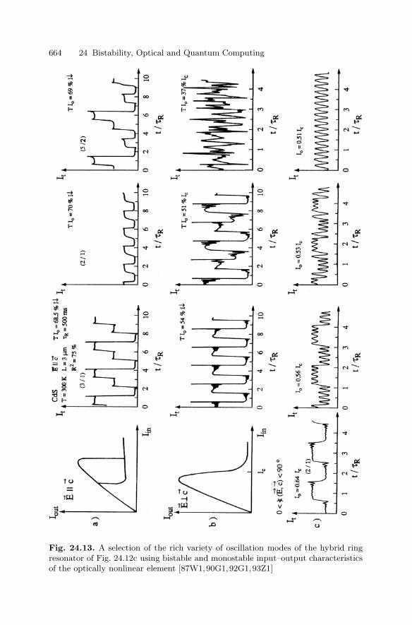
664 24 Bistability, Optical and Quantum Computing
Fig. 24.13. A selection of the rich variety of oscillation modes of the hybrid ringresonator of Fig. 24.12c using bistable and monostable input–output characteristicsof the optically nonlinear element [87W1,90G1,92G1,93Z1]

24.2 Device Ideas, Digital Optical Computing and Why It Failed 665
The fast relaxation oscillations which can be seen on the plateaux can pre-vent the transition to chaotic behavior. Such a situation is shown in part (c)of Fig. 24.13. Here, the angle between E and c was chosen to yield a mono-stable input–output characteristic with a very steep descending branch. Westart again with a regular oscillation, which is locked into a multiple of τR.With changing input parameters, the amplitude of the fast relaxation oscilla-tion increases until more and more of the spikes result in a modulation overthe whole intensity regime. Finally we are left with a regular oscillation, theperiod of which is determined approximately by the period of the relaxationoscillation τ0 and not by τR, however in such a way that an integer multi-ple of τ0 equals τR and with every peak having a shape similar to the initialoscillation governed by τR.
The first two scenarios shown in Figs. 24.13a,b can be deduced from(24.11) even in the adiabatic limit, i.e., τ0/τR ⇒ 0 whereas the full dynam-ics are necessary to describe and understand the observations of part (c) ofFig. 24.13.
Some examples of spatio-temporal structure formation in optical bistabil-ity in semiconductors are found in [88O2,92N1] and references therein. Theyrepresent a further aspect of nonlinear dynamics which can be investigatedwith optically bistable systems, but we do not want to go into details here.We, nonetheless, hope that the reader has acquired the feeling that nonlinearsemiconductor optics can contribute significantly to the fascinating field ofnonlinear dynamics and synergetics.
24.2 Device Ideas, Digital Optical Computing and WhyIt Failed
As mentioned in the introduction, semiconductors have a very wide field ofapplications especially in electronics and opto-electronics. It is not the aimof this book to cover this field, but we refer the reader to [81S1, 92E1] andreferences therein.
What we want to do here is to outline an aspect of application of (electro-)optical bistability in (electro-) optic data processing, also known as (digital)“optical computing” [84O2,85G1,87F1,89O1,93O1,98D1].
An optically bistable device with an input-output characteristic such asthose shown in Fig. 24.1 can be considered as a binary memory if, in thebistable region, we identify the states of low and high transmission with thelogic states “zero” and “one”, respectively.
By a suitable choice of the nonlinearity and the excitation conditions,the width of the bistable loop can be made rather narrow. In this case thedevices can be used as “AND”, “OR” and “NOT” gates (or inverters) as shownschematically in Fig. 24.14. These three functions, together with a memory,are the basic ingredients needed to construct a computer. When this factbecame clear in the early nineteen-seventies, there was a very enthusiastic

666 24 Bistability, Optical and Quantum Computing
Fig. 24.14. The use of nonlinear optical devices as logic gates
period, where scientists hoped that it would be relatively easy to build anall-optical computer based on the above devices [85G1, 87F1, 89O1, 93O1].Indeed, such an optical computer would in principle have one big advantageover electronic computers and this is massive parallel data handling. Whatone wants to do basically in a computer is the following (Fig. 24.15): Onehas a certain input signal which is processed in a logic unit. The processingdepends on the information stored in a large number of memories and resultsin an output signal.
In electronic computers one faces the following problem: If there are Nmemory cells, the processing unit has to be connected with 2N wires if one
Fig. 24.15. Parallel (a) and serial (b) data handling

24.2 Device Ideas, Digital Optical Computing and Why It Failed 667
wants to simultaneously know the contents in all memories for the logic de-cision, since in one wire only one signal can propagate at one (cycle-)time(Fig. 24.15a). If N becomes large (N 106) this concept breaks down be-cause it is impossible to have 2 × 10⁶ pins on one chip. The ingenious way outof this problem was serial data processing. Here one has only two connectionsbetween the logic unit and the memory and one uses an address and requeststhe information in the memories serially, i.e., one after the other (Fig. 24.15b).Unfortunately this takes time and, together with the propagation time in theconnections, it is the limiting factor for presently available “calculation speed”in electronic computers. This problem is also known as the “von Neumann”bottleneck.
In optics, on the other hand, one simple lens can be used to handle manydata-streams in parallel, since photons in vacuum usually do not interact. Soone could imagine a two-dimensional array with let us say N = 103 × 103
data points (Fig. 24.16). All these data points can be focussed simulta-neously by one lens or by a holographic grating (not shown here) ontoa logic plane which simultaneously reads data from a memory and performssome logic.
One (or several) further planes can be used to interchange the pixels, e.g.,with the help of permanent or reconfigurable holographic gratings, to obtaina “perfect shuffle” function. The output obtained in this way can be processedfurther or fed back as input to go several times through a loop.
Fig. 24.16. Schematic sequence of two-dimensional optical logic arrays

668 24 Bistability, Optical and Quantum Computing
Another approach to optical data handling involves data transport through(glass) fiber optics. In this case, data have to be brought into an optical formanyhow and one can try to do progressively more operations in the opticalregime. Here the demand for parallelism is reduced, but the switching speedhas to be high.
At the end of the nineteen-seventies, expectations, especially in digi-tal all-optical computing, were strongly damped for two reasons. Amplifi-cation of optical signals with high frequency is very difficult. But this isa crucial requirement for fan-out, i.e., the output of one device must beable to drive several others in the next logic plane. The first way foundto solve this problem uses “threshold devices” which, with a constant op-tical holding beam, are kept just below the switching point and can thenbe switched with a small input signal. However, it was found that the sta-bility of such a “threshold logic” is not sufficient for practical applications.The other disappointment was that optical switches were found to be infe-rior to electronic switches concerning speed and power consumption. Opticalswitches which need low input powers are usually slow (µs to ms) like thephotothermal ones. The fast ones, exploiting for example the formation ofan electron–hole plasma can have switching times in the ps to ns regimebut need powers that are too high for dc operation and sometimes also lowtemperatures.
Apart from the unsolved fan out problem there was another shortcoming.There was no consistent concept of hard- and software or of devices andcomputer architecture for (digital) optical computing. Obviously it did notmake sense to copy the architecture of serial electronic computers and merelyuse optical pulses instead of electric ones. A genuine new architecture wasmissing that makes use of the massive parallelism offered by optical basedrealistic devices.
At the end there was a “demonstrator”, which could optically add 2 + 2but used one or several Ar+ lasers with an electrical power consumption ofseveral kW and some PCs to control the whole system, which filled a com-plete lab.
Although there is presently still some ongoing research into using semicon-ductors for optical memory and switches (e.g., [99Z1]) and though beautifuland excellent physics has been made with optically nonlinear or bistable sam-ples or “devices”, the author does not expect (digital) optical computing tobecome a widely used technology in the next few decades.
What emerges, however, and what might spread into common use areelectro-optic devices. With the increasing use of optical fiber communicationsystems, electronic data must be transformed into optical signals and backand we may eventually see an increasing amount of optical data handling atthe interconnects.
Another field of optical data handling in a wider sense is making goodprogress in the form of luminescent semiconductor displays, laser scannersand related devices.

24.4 Quantum Computing 669
24.3 Spintronics
As already demonstrated in Sect. 16.1 magnetic fields and the spin of carri-ers, including diluted magnetic semiconductors (DMS), are exciting topics ofresearch. Some further examples, which are chosen rather arbitrarily, are thecontrol of ferromagnetism in materials like In1−yMnyAs or Ga1−yMnyAs bythe carrier concentration in field effect transistor like structures [00A1,00O1],injection and transport properties of electron spin through a sample oracross hetero interfaces in semiconductors [96C1, 98H1, 99F1, 99K1, 00J1,00O1, 01G1, 01O1], the generation of spin currents without electric chargetransport [00B1, 03H1, 03S1], and spin coherence and relaxation phenom-ena [97A1,97K1,97T1,98K1,99A1,99O1,99O2,00K1,01O1,01S1,03T1].
Based on such results, the idea of spintronics was born, i.e., analogous toelectronics but using the spin of the carriers (generally electrons) in additionto or instead of their electric charge. See, e.g., [02S1, 02S2, 04S1] for reviewsor [95N1,98P1,99P1,00B1,01H1,01S1] for a few individual results.
In a wider sense there is a real success of spintronics in the application ofread heads for magnetic disks, based on the giant magnet resistance (GMR)that occurs if a nonmagnetic metal layer, e.g., Cu is sandwiched betweenferromagnetic layers (see, e.g., [03A1,04S2] and references therein).
On the other hand the author feels that it will be very unlikely that spinprecision transistors [03R1] or other electronic devices based on DMS will beable to compete with the highly developed Si technology. The devices are muchmore complicated, the relevant effects are often observed in semiconductorsonly at low temperatures (e.g., ferromagnetism in Ga1−yMnyAs or ZnO:Co),the spin coherence times are usually short, rarely exceeding a few ns, exceptfor a few exceptions [97K1, 02C1] and the spin injection from metallic ferro-magnets into semiconductors is very difficult and requires tunnel barriers sincethe density of states (or the impedance) in the metal and the semiconductorare too different. Furthermore, and this is an analogy to the failure of digitaloptical computing mentioned above, there is no consistent concept for the useof spins instead of the electric charge, which would show advantages over theestablished Si-technology. The author feels that he is not the only scientistsharing this skepticism [03D1].
24.4 Quantum Computing
In a conventional electronic computer there are two states presenting thelogic “0” and “1”. Their realization is by electric current or voltage “off” and“on”, respectively. Recently a new idea emerged, namely to use a coherentsuperposition of two quantum mechanical states, a so-called quantum- or q-bit
a|0〉 + b|1〉 (24.13)

670 24 Bistability, Optical and Quantum Computing
and to carry out manipulations or logic operations in a time shorter than thedecoherence time (see Sect. 23.2) of states |0〉 and |1〉.
For an overview see, e.g., [02N1, 02S1]. The realization of the two states|0〉 and |1〉 is considered via Josephson junctions [99M1], via single atoms ina cavity or atoms in a coherent state in a trap [95B1, 95D1, 95T1, 01C1] orvia electron or nuclear spins or excitons in semiconductors and semiconductorstructures of reduced dimensionality like quantum dots [98K2, 98L1, 01B2,01H1,01S2,02S3,03P1,03Q1] and this is why we address this topic here briefly.
The situation seems to be very similar to the one of optical computingfrom two decades ago or of spintronics.
There is a huge amount of novel, beautiful and exciting basic researchbeing performed in this field. However, the realization of the promised orat least envisaged applications, here via quantum computing, seems ratherunlikely to the author.
There is again no consistent approach for hard- and software or computerarchitecture. Many of the possible systems for the realization of q-bits re-quire low temperatures and they are intrinsically very sensitive to all types ofdecoherence processes.
To the best of the author’s knowledge, the only case where an advantageof quantum computing over conventional computing has been shown theo-retically is the factorization of large numbers. It is unlikely that industry iswilling to invest too much money in this niche.
The other field of applications of quantum computing including thepresently very fashionable field of entangled states is quantum cryptography.Though this might be a huge market, practical realizations are a long wayaway, if they come at all.
Another approach to the continuing miniaturization of electronic devicesis to use molecular structures including carbon nanotubes [00J2], but this fieldleads beyond the scope of this book.
24.5 Problems
1. Find a simple relation for the “sufficiently strong” excitation induced in-crease of the absorption (Sect. 24.1.4) needed to produce optical bistabil-ity.
2. Is it possible for longitudinal structures to appear in the switching pro-cess of induced absorptive optical bistability in thick samples, under theassumption that the excited species responsible for the increase of absorp-tion have negligible diffusion length?
3. Can induced absorptive optical bistability occur if the increase of theabsorption depends not on the density of some excited species, but directlyand instantaneously on the amplitude or intensity of the light field? Isyour answer also true for dispersive and bleaching optical bistability ina Fabry–Perot resonator?

References to Chap. 24 671
4. Give the conditions on the finesse of the Fabry–Perot and the bleachingrequired to get optical bistability from the combination of both.
5. Iterate the logistic equation (24.12) to get the Feigenbaum scenario.6. Find some additional information about the “circle map” and the Farey
tree, e.g. in [88S1].7. Find out what an “entangled state” is. Compare it to the description of two
or more identical Fermions by Slater’s determinate, which was developedin the 1930s soon after the introduction of quantum mechanics.
References to Chap. 24
[80I1] K. Ikeda, H. Daido and O. Akimoto, Phys. Rev. Lett. 45, 709 (1980)[80O1] Optical Bistability, Ch.M. Bowden, M. Ciftan, H.R. Robl, eds., Plenum,
New York (1980)[81S1] S.M. Sze, Physics of Semiconductor Devices, 2nd, eds., Wiley, New York
(1981) and Semiconductor Devices, Physics and Technology 2nd ed. (2002)[82I1] K. Ikeda, H. Daido and O. Akimoto, Phys. Rev. Lett. 48, 617 (1982)[83H1] H. Haken, Synergetics, an Introduction, Springer Ser. Syn., Vol. 1 and
subsequent volumes, Springer, Berlin, Heidelberg (1983)[83B1] K. Bohnert, H. Kalt and C. Klingshirn, Appl. Phys. Lett. 43, 1088 (1983)[84H1] F. Henneberger and H. Rossmann, phys. stat. sol. (b) 121, 685 (1984)[84K1] S.W. Koch, Dynamics of First-Order Phase Transitions in Equilibrium
and Nonequilibrium Systems, Lecture Notes Phys. 207, Springer, Berlin,Heidelberg (1984)
[84M1] D.A.B. Miller, J. Opt. Soc. Am. B1, 857 (1984)[84O1] Optical Bistability II, P.Ch.M. Bowden, H.M. Gibbs, S.L. McCall, eds.,
Plenum, New York (1984)[84O2] Optical Bistability, Dynamical Nonlinearity and Photonic Logic, B.S.,
Wherrett and S.D. Smith, eds., The Royal Society, Cambridge UniversityPress, Cambridge (1984)
[85G1] H.M. Gibbs, Optical Bistability, Controlling Light with Light, Academic,New York (1985)
[86D1] G.H. Doehler, IEEE J. QE-22, 1682 (1986)[86H1] F. Henneberger, phys. stat. sol. 137, 371 (1986)[86L1] M. Lindberg, S.W. Koch and H. Haug, J. Opt. Soc. Am. B 3, 751 (1986)[86M1] J.V. Moloney, Phys. Rev. A 33, 4061 (1986)[86O1] Optical Bistability III, P. Mandel, N. Peyghambarian, S.D. Smith, eds.,
Springer Proc. Phys. Vol. 8, Springer, Berlin, Heidelberg (1986)[86W1] M. Wegener et al., Semicond. Sci. Technol. 1, 366 (1986)[87F1] From Optical Bistability Towards Optical Computing, P. Mandel,
S.D. Smith, B. Wherett, eds., North-Holland, Amsterdam (1987)[87F2] F. Forsmann, D. Jager and W. Niessen, Opt. Commun. 62, 193 (1987)[87G1] I. Galbraith and H. Haug, J. Opt. Soc. Am. B 4, 1116 (1987)[87K1] C. Klingshirn, in [87F1][87W1] M. Wegener and C. Klingshirn, Phys. Rev. A 35, 1740, 4247 (1987)[87W2] M. Wegener, C. Klingshirn and G. Muller-Vogt, Z. Phys. B 68, 519 (1987)[88B1] S.V. Bogdanov and V.G. Lyssenko, Sov. Tech. Phys. Lett. 14, 270 (1988)

672 24 Bistability, Optical and Quantum Computing
[88B2] T. Brand, H.J. Eichler and B. Smandek, SPIE Proc. 1017, 200 (1988)[88C1] D.S. Chemla, D.A.B. Miller and S. Schmitt-Rink, in [88O3] p 83[88E1] H.J. Eichler et al., SPIE Proc. 1017, 90 (1988)[88K1] S.W. Koch, in [88O3] p 273[88O1] Optical Bistability IV, W. Firth, N. Peyghambarian, A. Tallet, eds., J.
Phys., Paris 49, C2 suupl. au no. 6 (1988)[88O2] Optical Switching in Low-Dimensional Solids, H. Haug, L. Banyai, eds.,
NATO ASI Ser. B 194 (1988)[88O3] Optical Nonlinearities and Instabilities in Semiconductors, H. Haug, ed.,
Academic, New York (1988)[88P1] Photonic Switching, T.K. Gustafson and P.W. Smith, eds., Springer Series
in Electronics and Photonics 25, Springer, Berlin (1988)[88S1] H.G. Schuster, Deterministic Chaos, 2nd eds., Physik Verlag, Weinheim
(1988)[88W1] A. Witt et al., IEEE J. QE-24, 2500 (1988)[89M1] D.A.B. Miller, in [89O1] pp 55 and 71[89O1] Optical Computing, B.S. Wherett and F.A.P. Tooley, eds., The Scottish
Universities Summer School in Physics 34, Edinburgh University Press,Edinburgh (1989)
[90G1] J. Grohs et al., Opt. Commun. 78, 77 (1990)[90K1] V. Kazukauskas et al., Z. Phys. B 79, 149 (1990)[91G1] J. Grohs, H. Issler and C. Klingshirn, Opt. Commun. 86, 183 (1991)[92E1] K.J. Ebeling, Integrierte Optoelektronik, 2nd eds., Springer, Berlin, Hei-
delberg (1992)[92G1] J. Grohs et al., Int’l J. Bifurcation Chaos 2, 861 (1992)[92G2] J. Grohs et al., SPIE Proc. 1807, 192 (1992)[92K1] C. Klingshirn, J. Grohs and M. Wegener, in [92N1][92N1] Nonlinear Dynamics in Solids, H. Thomas, ed., Springer, Berlin (1992)[93C1] J. Cibert et al., Phys. Scr. T 49, B487 (1993)[93L1] N. Linder et al., Appl. Phys. Lett. 62, 1916 (1993)[93O1] Optical Information Technology, S.D. Smith and R.F. Neale, eds., Esprit
Basic Research Series, Springer, Berlin (1993)[93Z1] U. Zimmermann et al., in [93O1][93Z2] U. Zimmermann et al., Semicond. Science and Tech. 8, 1399 (1993)[94L1] W. Langbein et al., J. Crystal Growth 138, 191 (1994)[95B1] A. Barenco et al., Phys. Rev. Lett. 74, 4083 (1995)[95D1] D.P. Di Vincenco, Science 270, 255 (1995)[95G1] J. Grohs et al., Z. Phys. B 98, 133 (1995)[95K1] V. Kazukauskas et al., Optics Comm. 122, 83 (1995) and phys. stat. sol.
(b) 187, 241 (1995)[95N1] Y. Nishikawa et al., Appl. Phys. Lett. 66, 839 (1995)[95T1] Q.A. Turchette et al., Phys. Rev. Lett. 75, 4710 (1995)[96C1] S.A. Croober et al., Phys. Rev. Lett. 77, 2814 (1996)[97A1] T. Amand, Phys. Rev. Lett. 78, 1355 (1997)[97K1] J.M. Kikkawa et al., Science 277, 1284 (1997)[97T1] A. Tackeuchi, O. Wada and Y. Nishikawa, Appl. Phys. Lett. 70, 1131
(1997)[98D1] C. Denz, Optical Neuronal Networks, Vieweg, Braunschweig (1998)[98H1] D. Hagele et al., Appl. Phys. Lett. 73, 1580 (1998)
References to Chap. 24 673
[98K1] J.M. Kikkawa and D.D. Awschalom, Phys. Rev. Lett. 80, 4313 (1998)[98K2] B.E. Kane, Nature 393, p. 133, May (1998)[98L1] D. Loss and D.P. Di Vincenco, Phys. Rev. A 57, 120 (1998)[98P1] G.A. Prinz, Science 282, 1660 (1998)[99A1] D.D. Awschalon and J.M. Kikkawa, Physics Today, p 33, June (1999)[99F1] R. Fiederling et al., Nature 402, 787 (1999)[99K1] J.M. Kikawa and D.D. Awschalom, Nature 397, 139 (1999)[99M1] Y. Makhlin, G. Schon and A. Shnirman, Nature 398, 305 (1999)[99O1] M. Oestreich et al., Appl. Phys. Lett. 74, 1251 (1999)[99O2] Y. Ohno et al., Phys. Rev. Lett. 83, 4196 (1999) and Nature, 402, 791
(1999)[99P1] S.S.P. Parkin et al., J. Appl. Phys. 85, 5828 (1999)[99Z1] S. Zimmermann et al., Science 283, 1292 (1999)[00A1] H. Akinaga et al., Appl. Phys. Lett. 76, 97 (2000)[00B1] R.D.R. Bhat and J.E. Sipe, Phys. Rev. Lett. 85, 5432 (2000)[00J1] B.T. Jonker et al., Phys. Rev. B 62, 8180 (2000)[00J2] C. Joachim, J.K. Gimzewski and A. Aviram, Nature 408, 541 (2000)[00K1] H. Kalt et al., J. Crystal Growth 214/215, 630 (2003) and phys. stat. sol.
b 221, 477 (2000)[00O1] H. Ohno et al., Nature 408, 944 (2000)[01B1] B. Beschoten et al., Phys. Rev. B 63, 121202 (2001)[01B2] M. Bayer et al., Science 219, 451 (2001)[01C1] B.E. Cole et al., Nature 410, 60, (2001)[01G1] M. Ghali et al., Solid State Commun. 119, 371 (2001)[01H1] D. Hagele et al., Solid State Commun. 120, 73 (2001)[01O1] M. Oestreich et al., Festkorperpbrobleme / Adv. Solid State Physics 41,
173 (2001)[01S1] J.S. Sandhu et al., Phys. Rev. Lett. 86, 2150 (2001)[01S2] G. Salis et al., Nature 414, 619, (2001)[02C1] S. Cortez et al., Phys. Rev. Lett. 89, 207401 (2002)[02N1] M.A. Nielsen, Scientific American, p 49, Nov. (2002)[02S1] Semiconductor Spintronics and Quantum Computing, D.D. Awschalom,
D. Loss and N. Samarath, eds., Springer, Berlin (2002)[02S2] Semiconductor Spintronics, H. Ohno, ed., special issue, Semicod. Science
and Technol. 17, 275 pp (2002)[02S3] R.M. Stevensen et al., Phys Rev. B 66, 081302 (R) (2002)[03A1] M. Albrecht, J.-U. Thiele and A. Moser, Phys. Journal, p 25, Okt. (2003)[03D1] M.I. Dyakonov, Optika i Spektroskopiya 95, 279 (2003) and Proc. Future
Trends in Microelectronics, Workshop, Corsica, (2003), in press[03H1] J. Hubner et al., Phys. Rev. Lett. 90, 216601 (2003) and phys. stat. solidi
(a) 195, 3 (2003)[03P1] E. Pazy et al., phys. stat. sol. (b) 238, 411 (2003)[03Q1] Quantum Computing and Quantum Bits in Mesoscopic Systems,
A. Leggett, B. Ruggiero and P. Silvestrini eds., Kluwer, Dordrecht (2003)[03R1] E.I. Rashba and Al.L. Efros, Appl. Phys. Lett. 83, 5295 (2003)[03S1] M.J. Stevens et al., Phys. Rev. Lett. 90, 136603 (2003)[03T1] E. Tsitsishivili, R.V. Baltz and H. Kalt, Phys Rev. B 67, 205330 (2003)[04B1] A. Baas et al., Phys. Rev. A69, 023809 (2004)[04S1] Spin Electronics, D.D. Awschalom et al., eds., Kluwer, Dordrecht (2004)[04S2] S.A. Solin, Sci. American, p 45, July (2004)

25
Experimental Methods
Warning: Many of the experimental techniques and set-ups generally used insemiconductor optics, some of which being described below, can involve somerisks. For example lasers beams may damage the eyes, high voltages used inmany lasers are hazardous, gases and liquids used as laser materials may bepoisonous etc. Before you build any set-up or start any experiment read therelevant safety instructions and regulations and stick to them!
This chapter is based both on the contribution of the author to [89L1, 01L1]and on the preceding edition of this book. Further references may be found,e.g., in [82L1,86L1,89S2,92E1,93O1,93H2] or in [86L1,89L1,90K1,91D1,92E1,92S1,96O1,96Y1,97E1,98D1,01H1,02S1,03T1] of Chap. 1.
The purpose of this chapter is to review experimental techniques, whichhave been or can be used for the optical spectroscopy of semiconductors.
In agreement with the concept of this book outlined in the introduction,it is not the purpose of this chapter to present all possibilities of opticalspectroscopy, which have ever been used. This would fill a whole volume byits own. Instead we concentrate on typical, widely used techniques.
It is also not the purpose to cite the first, the most recent or the “best”application of a certain technique of spectroscopy, but rather one or a fewtypical examples, which are by no means exhaustive. In this sense the selectionof examples is and must be to some extend arbitrary.
We divide the topic in five main sections namely
25.1 Linear optical spectroscopy25.2 Nonlinear optical spectroscopy25.3 Time-resolved spectroscopy25.4 Spatially resolved spectroscopy25.5 Spectroscopy under the influence of external fields
and give not only information on the equipment, which has to be used andthe experimental techniques but also some information, which properties ormaterial parameters can be obtained with the respective technique.

676 25 Experimental Methods
An important aspect is that many of the techniques can be applied forvarious fields or in various combinations. We want to illustrate this statementwith a simple example.
The observation of the photoluminescence (PL) spectrum of a sample un-der low non-resonant, cw excitation is a method belonging generally to thefield of linear optical spectroscopy. If the photon energy of the exciting lightbeam is tuned, one has the method of photoluminescence excitation spec-troscopy (PLE), which may give some information on the absorption spectrumor on excited states of the luminescing complex (see below). If the excitationpower is increased, one may reach the intermediate or even the high-densityregimes where e.g. biexcitons and trions or even an electron–hole plasma arecreated, see Chaps. 19 to 21. Since these phenomena are usually connectedwith strong optical nonlinearities, the PLE has been shifted or applied tononlinear spectroscopy. If, on the other hand, the luminescence is excitedwith a short pulse, it is possible to monitor the luminescence rise and decaytimes leading us to Sect. 25.3 and to Chap. 23. If the short exciting pulsesare strong enough, and tunable, the technique of PLE, which originates fromlinear spectroscopy, ends up in a combination of nonlinear and time resolvedspectroscopy. Even spatial resolution techniques or external fields can be com-bined with PLE.
It is obvious that we cannot list all these combinations and/or modifica-tions, but restrict here to the basic concepts and leave it to the fantasy andthe experimental skill of the reader to use or even to invent new cases of suchcross-linked techniques.
At the end of this introduction to Chap. 25 we want to give again some re-ferences to further articles or books in which techniques of optical spectroscopyhave been presented already. Optics in general is outlined e.g. in [98L1,99H1]and various aspects on experimental techniques used for semiconductors canbe found e.g. in [81K2, 82L1, 85H1, 86L1, 89S2, 89L1, 91D1, 92E1, 93O1, 96Y1,97K1,98K1,98K3,01A1].
25.1 Linear Optical Spectroscopy
The most widely performed experiments in linear spectroscopy are transmis-sion-, reflection- and luminescence spectroscopy. Other techniques include, e.g.,photoluminescence excitation spectroscopy, ellipsometry, modulation spectros-copy, measurements of the luminescence yield or Raman spectroscopy.
Linear spectroscopy means in general that the intensities of all incidentlight-beams are so low that the optical properties of the sample under in-vestigation are not changed by the illumination or in other words that theelectric and magnetic susceptibilities do not depend on the field strength ofthe incident light beams (see Chaps. 2 and 19).
The range or upper limit of the incident energy flux densities of the light(often called light intensity) for the regime of linear spectroscopy cannot be

25.1 Linear Optical Spectroscopy 677
given in general, since they depend strongly on the sample under investigation,on the lifetime of the excited species and on the experimental conditions likethe spectral position of the incident light beams relative to the fundamentalabsorption edge of the sample, on the sample temperature, on the duration ofthe excitation pulse etc. There is, however, a rather simple test if one is in theregime of linear optics: One measures the spectra of reflection or transmissionfor a given incident intensity and then again for an intensity which is one orat least half an order of magnitude different. If the spectra do not change, oneis in the linear regime. The same holds, if the emission spectra grow with theexcitation intensity but do not change their spectral shape, or in other words,if normalized spectra coincide [81K2].
25.1.1 Equipment for Linear Spectroscopy
The standard set-up for linear optical spectroscopy consists of a light source,the sample under investigation, frequently placed in a cryostat, a monochro-mator or spectrometer to disperse the light, a detection unit and a PC tohandle and evaluate the data. The light sources for reflection, transmissionand luminescence spectroscopy can be incandescent lamps for the visible in-cluding the near IR and UV, glow-bars for the IR, low or high pressure gasdischarge lamps, and cw or pulsed lasers. Without trying to be complete wemention gas lasers like Ar+, He-Ne for the visible, CO and CO2 lasers for theIR, Ar+, He-Cd, N2 and excimer lasers for the UV, solid state lasers like theNd-based ones for the near IR including their harmonics in the green and nearUV, or tunable titanium sapphire lasers for the red and near IR, dye lasers,which can cover the whole spectral range from the near IR over the visible tothe near UV depending on the dye and the pump source. Free electron laserswork in the IR while synchrotron radiation covers the spectral region fromthe IR over the visible to the soft X ray regime.
Standard diode lasers are based on Ga1−yAlyAs, (Al1−yGay)1−xInxP orIn1−yGayAs quantum structures and cover the range from the red to the nearIR (see Chap. 4) while lead salt diodes emit deeper in the IR (see Chap. 7).GaN-based laser diodes for the blue or near UV are now also commerciallyavailable [97N1].
Some more information on these various light sources and references todetailed literature can be found e.g. in [98K1]. Luminescence is generally ex-cited optically, especially in fundamental research, but excitation with elec-tron beams [73B1], by injection of carriers in pn junctions (see e.g. theSect. 22.3 on laser diodes) or by impact ionization in electroluminescent de-vices [89S1,96M1] are also common.
Very recently the use of short THz pulses has been introduced for spec-troscopy in this range i.e. in the range up to a few meV photon energy. Seee.g. [94S1,97N2,98C1,98K7,00H1,00L1,04C1] and references therein.
The samples under investigation are frequently kept in a cryostat. Theheads of closed cycle refrigerators reach, dependent on the heat inflow, e.g.

678 25 Experimental Methods
through windows, temperatures down to 5 or 10 K; cold fingers of He-cryostats,on which the samples are attached in a vacuum chamber, have also lower tem-peratures around 5 K. If the sample is immersed in liquid He under normalpressure one finds 4.2 K but has the problem that the He is boiling. Pump-ing of the He below the λ-point avoids boiling in the volume and results intemperatures ≤ 2 K.
Though semiconductor devices are generally operated at room tempe-rature or above, it is very useful in fundamental research to start spectros-copic experiments at low temperature, since the spectral width of absorption-,reflection- and luminescence peaks is frequently much smaller at low tem-peratures and facilitates interpretation. Following the spectral features withincreasing temperature allows then to observe thermal broadening or the(dis-)appearance of spectral features with temperature.
For the spectral dispersion of the reflected, transmitted or emitted lightgrating monochromators or spectrometers are almost exclusively used in thevisible, near UV and near IR. The theoretical resolution limit ∆λ of a gratingis given at a wavelength λ by
λ
∆λ= Nm (25.1)
where N is the number of coherently illuminated grooves of the grating andmis the diffraction order. In practice the resolution is rather limited by the widthof entrance and exit slits, by aberrations in the optical system of the spectro-meter/monochromator or by the spatial resolution of the detector array. Dueto these facts the resolution depends on the focal length of the spectrometerand on the number of grooves of the grating per mm.
In the visible a resolution of ∆λ ≤ 0.1 nm is usually reached with a fo-cal spectrometer length around 0.5 m and a grating with 1200 to 2400 linesper mm.
A grating blazed at a wavelength λB can be generally used for the spec-tral range
23λB ≤ λ ≤ 1.5λB (25.2)
in first order and for a corresponding interval around λB/2 in second order.Care has to be taken that the various orders of spectrally broad features mayoverlap, i.e. the direction, into which the first order is diffracted at wavelengthλ, coincides with the second order at λ/2. This may cause spurious signalsin the spectra. A prevention is to use filters which cut short wavelengths andwhich are available from the near IR over the visible to the near UV.
Though the efficiency of gratings varies rather smoothly with λ over therange given in (25.2) for unpolarized light, it must be kept in mind thatthe efficiency curves are different for light with the electric vector polar-ized parallel and perpendicular to the grooves of the grating, respectively[82H1,98L1,99H1]. In polarization sensitive experiments it is therefore eithernecessary to correct the spectra with the spectral efficiency curves for both

25.1 Linear Optical Spectroscopy 679
polarizations or to have always the some state of polarization at the entranceslit of the spectrometer e.g. by inserting suitable delay plates or other deviceslike polarization scramblers.
Prism spectrometers/monochromators have the advantages to produceonly one spectrum and to have often high optical through put. This makesthem a good tool for the preselection of a wavelength interval or a individualline of a lamp. Due to their nonlinear dispersion, they are no longer much inuse in spectroscopy itself.
Interference filters may also serve for a preselection of light.Fabry–Perot resonators with high finesse can be used in contrast as ex-
tremely high resolution devices which can easily exceed λ/∆λ = 106 but whichhave usually only a very small free spectral range [88H1,98L1,99H1].
Fourier spectrometers are ideal for the range from the far IR to the redpart of the spectrum [72B1,99H1].
We conclude this subsection with a few words on the detector side of theset up. Photographic plates and films are generally out dated due to theirnonlinear characteristics and the long processing time between exposure andthe availability of the data.
Vacuum- and semiconductor photodiodes have typical sensitivities of 0.1 Aper Watt of incident light power. Especially vacuum photodiodes can be veryfast with rise- and decay-times in the 0.1 ns regime. Avalanche diodes, pho-tomultipliers or channeltrons are much more sensitive due to the built-inmultiplication of optically created carriers. Photomultipliers can reach sin-gle photon sensitivity. However they are generally used behind the exit slitof monochromators. This means that a spectrum can be recorded only se-quentially e.g. by turning the grating. This procedure, often connected withlock-in techniques [83M1] to improve the sensitivity or the signal to noiseratio, makes the recording of a wider spectrum generally a rather time con-suming procedure.
If a one- or two-dimensional diode array or a vidicon tube (eventually com-bined with an image intensifier e.g. a channel plate) are used at the exit ofa spectrometer, one has a significant multiplex advantage, i.e. one records si-multaneously the spectrum over a certain interval, which is determined by thedispersion of the spectrometer and the geometrical dimension of the sensitivearea of the detector array. The sensitivity can reach a few photons especiallyfor cooled detector arrays.
A similar multiplex advantage holds also for a Fourier spectrometer. Thedifference is that the spectral resolution is preset with a diode array andthe signal to noise ratio increases with integration time, while the signallevel is essentially given in a Fourier spectrometer but the spectral resolu-tion increases with increasing shift of the mirror in the Michelson interfero-meter.
The useful spectral range of the detectors is generally limited on the lowphoton energy side by the work function for photo-cathodes and the bandgap (or the ionisation energy of a defect) for semiconductor-based detectors.

680 25 Experimental Methods
On the high photon energy side, the limitation comes often from the windowmaterial (glass, silica, sapphire, etc) (see e.g. also [98K1]).
25.1.2 Techniques and Results
In the following we give some examples of techniques of linear spectroscopyand the information, which can be deduced from them. Many further exampleshave been given already in Chaps. 11 to 17.
Luminescence spectra give usually information on the deepest radia-tive states of a system including their optical phonon replica or acousticphonon wings. At low temperatures these are often defect states or local-ized states resulting from some disorder like spatial fluctuations of the wellwidth or of the composition of alloys. At higher temperatures extendedstates become also accessible in luminescence. It should be noted that thequantum efficiency i.e. the average number of luminescence photons cre-ated per excited electron–hole pair is in most samples considerably belowunity [98W1, 03F1]. Luminescence spectra give therefore generally only in-formation on the fate of a minority of excited species as discussed alreadyin Sect. 23.4. Furthermore it should be noted that the thermal distributionfunction (generally a Boltzmann term) can, if reached during the lifetimeof the excited species, enhance at low temperatures the luminescence of lowlying but forbidden transitions (e.g. triplet or so-called dark excitons) com-pared to energetically slightly higher allowed transitions (see e.g. Sect. 13.2or Chap. 14).
The spectra of the transmitted and reflected light allow to deduce in var-ious degrees of sophistication [82L1] the spectra of absorption andreflection.
The absorption- and reflection structures give information of optically al-lowed transitions from the occupied ground state in the unexcited sample toexcited states [92D1]. The area under the absorption peak is a measure forthe oscillator strength of the transition and the width for the inhomogeneousor homogeneous broadening whatever is larger. These transitions can be thevarious exciton series and their continuum states close to the band gap (forexamples see Chaps. 13 to 15), intersubband transitions e.g. in doped quan-tum structures (see e.g. Sects. 13.3 and 21.5), phonon transitions (e.g. [98G1]or Chap. 11) or plasmons (see e.g. [97G1] or Chap. 12). The quantitativeevaluation of reflection spectra needs generally more complex model theories.Examples are found for excitons in [88U1] or in Sects. 13.1 and 15.1, or forplasmons in [97G1] and in Chap. 12.
Usually only transitions with rather high oscillator strength show up inreflection. An experimental trick to enhance the signal is to observe not undernormal incidence, which is the geometry most easily to evaluate, but close toBrewster’s angle of the barrier or substrate material with light polarized inthe plane of incidence. For an example see Sect. 15.1.
Fabry–Perot modes, which appear often in quantum structures due toparallel surfaces or interfaces of substrate, buffer layers etc., can be partly

25.1 Linear Optical Spectroscopy 681
avoided by anti-reflection coatings [81C1,99H1], otherwise they may producespurious structures [95W1].
A way to deduce extremely weak absorption features using a generalizedPlanck’s law together with Kirchhoff’s law has been elaborated in [95D1,95W3]. Also see in this context [57K1,59M1,04C1].
Ellipsometry allows in principle to deduce the spectra of the real and imag-inary parts of the dielectric function or of the complex index of refraction.While the method is basically simple and described essentially by Fresnel’sformulae for a single surface against vacuum, it becomes increasingly complexif (partly unknown) absorbate layers and multi-layers structures are investi-gated [77A1,98K1,04K1,04S1].
A classical method to enhance weak signals is modulation spectroscopy[69C1, 73S1, 94P1, 97H2, 98D1, 98D2]. The basic idea is, to modulate the
spectra slightly by a weak, temporally periodic external perturbation likean electric field, (electro-modulation), a heating of the sample (thermo-modulation), a variation of the detection wavelength (wavelength-modulation)etc. and to detect the reflected or transmitted light with a lock-in ampli-fier at the frequency of the modulation. In the simplest case, this resultsin the observation of the derivative of the spectrum and allows to observeweak structures on a broad background or dark current. Observation attwice the modulation frequency gives the second derivative. The increasingavailability of digital data handling reduces the use of analog modulationtechniques.
A widely used technique is the excitation spectroscopy of photolumines-cence (PLE) or of the photo current in pin-diode structures (PCE). The ideais to monitor e.g. the intensity of a certain luminescence feature (e.g. theexciton luminescence of a multiple quantum well) or the photocurrent andto tune the spectrally narrow excitation source ideally keeping the incidentphotonflux density constant. These PLE or PCE spectra show often peaksat positions of stronger absorption simply because more electron–hole pairsare created at these energies. For examples see Sects. 13.1, 14.1 and 15.1or [81B1,81B2,87B1]. It is remarkable that exciton features show up in PCEspectra at temperatures much too low for thermal ionisation of these excitons.Field ionisation in some Schottky (surface-) barriers possibly plays a role (see,e.g., [80A1,82S1,83S1,02K1,03K1] and references therein).
In this sense PLE or PCE spectra are related to the absorption spectrum.The technique is very useful in cases where the absorption spectrum is notdirectly accessible, e.g. because the substrate on which the quantum structurehas been grown is opaque at the spectral region of interest (e.g. in AlGaAsstructures grown on GaAs) and cannot be removed by selective chemical etch-ing, or because the optical density is too low to be detected (e.g. for a singlequantum well or for forbidden transitions).
However it should be noted that the PLE and PCE spectra are related tobut not identical with the absorption spectrum [87B1]. Processes which enterare the reflection spectrum in the range in which the exciting photon energy

682 25 Experimental Methods
is tuned, the absorption length of the exciting light, the diffusion length ofthe excited species, the relaxation into the observed luminescent channel in-cluding the branching ratio for relaxation into other states, and finally theefficiency and the escape depth of the luminescence. Similar arguments holdfor PCE. In [97K1, 98U1] it has been shown e.g. that the PLE spectra de-pend strongly on the selected spectral position of the exciton luminescence ofZnSe-based quantum wells. This dependence has been even used to study theintra(sub)band relaxation processes.
Measurements of the absolute luminescence efficiency can be performed invarious ways:
A calculation from the signal intensity of the recorded luminescence spec-trum for a given excitation power involves a quantitative knowledge of thespectral through-put or the efficiency of all optical components like detector,monochromator / spectrometer, lenses, mirrors, beamsplitters, etc. and of thegeometry like the solid angle of acceptance of the spectrometer, the size ofthe image of the excitation spot on the entrance slit of the spectrometer andthe spatial radiation characteristics of the sample. It is obvious that there aremany possibilities to obtain erroneous results.
The comparison of a measured luminescence spectrum of the sample un-der investigation with a standard, which has luminescence efficiency close tounity (usually a laser dye or some luminescence centers in a solid matrix) ne-cessitates identical geometries for both experiments including the excitationdepth and the spatial radiation characteristics. These conditions are usuallyhard to fulfill.
Placing the sample under investigation in an integrating or Ulbricht sphere,fitted into a cryostat, eliminates the radiation characteristics of the sample andallows to obtain even absolute luminescence efficiencies per spectral intervalwith rather simple calibration techniques. Examples are found in [90L2,93V1,97W1,98W1,03F1].
In an alternative method, the heat is measured, which is deposited in thesample under investigation. If the absorbed energy is known, it is easy to cal-culate the luminescence efficiency. Examples for this calorimetric absorptionspectroscopy (CAS) are found in [88J1, 91B1, 94F1]. However there are twodraw-backs: one is usually limited to very low temperatures, to have suffi-ciently sensitive bolometers and the other is that the luminescence may beemitted in a spectral range which is not detected e.g. via deep centers resultingin an over estimation of the luminescence yield of the monitored luminescencechannels.
For other thermal methods see e.g. [81J1,82I1].Another general caveat is that often differential efficiencies are given in
literature (partly without explicitely mentioning it), e.g. the slope in the re-lation between emitted number of photons versus excited electron–hole pairs.If this relation is strictly linear through the origin, the absolute efficiencyand the differential efficiency are the same. If the relation is nonlinear, e.g.above the threshold of stimulated emission of a laser diode, the differential

25.1 Linear Optical Spectroscopy 683
efficiency may be close to unity while the absolute efficiency is still muchsmaller.
While transition energies from the near IR through the visible to the UVare usually determined directly by luminescence, absorption and reflectionspectroscopy, one uses often inelastic light scattering techniques for the spec-troscopy of transition energies in the range below a few hundred meV. Thesetechniques are known as Raman scattering for creation or annihilation of op-tical phonons (see [76R1, 96Y1, 98K1, 01L1] or Chap. 11) including confinedones or backfolded acoustic phonons [99D1], electronic excitations like inter-subband transitions (e.g. [92J1]), spin flips (see e.g. Sect. 16.1), or plasmons(Chap. 12). The energies of such excitations and consequently the energyshifts resulting from such excitations in Raman scattering are usually situ-ated in the range from one or a few meV up to a few hundred meV. Brillouin(-Mandelstamm) scattering means the scattering under emission or absorptionof acoustic phonons close to the origin of their dispersion relation. It is morerestricted to bulk materials Sect. 13.1.4 and the frequency shift is usually inthe (sub-) meV range.
Raman scattering requires a stable and spectrally very narrow (∆ω <0.1meV) laser irradiation. The background of this laser beam caused e.g. byamplified spontaneous emission (ASE) should be as low as possible. Possiblyit makes sense to send the laser over a grating and through a distant (≈ 1 m)pinhole or diaphragm. Frequently used lasers are the various lines of Ar+
lasers or tunable dye lasers pumped by Ar+ lasers. Especially in the secondcase, the ASE problem has to be considered.
One observes the scattered light frequently in a back scattering geometryor under a right angle. The scattering geometry is often described by theso-called Porto-notation
ki [(ei, es)] ks (25.3)
where the k and e give the directions of wavevectors and polarizations (Efields) and the indices stand for ingoing and scattered light. In the spectraldispersion of the inelastically scattered light, stray light from the incidentbeam has to be suppressed as far as possible to observe the weak Raman- (orBrillouin-) signals. Therefore double – or even triple spectrometers are used,followed by a sensitive (single photon) detection. For examples see [76R1,94D1,95V1,96Y1,98K1,99D1].
The characteristic energies which can be deduced are e.g. those of Ramanactive phonons, electronic intersubband transitions, plasmons or plasmon-phonon mixed states.
Alternatively, these low laying excitations can be observed in the IR byFourier spectroscopy if they are IR active. The selection rules are partlycomplimentary for both techniques. If the sample has a center of inversion,phonons are either Raman active or IR active. Without center of inversionthey may be both [76R1,96Y1].

684 25 Experimental Methods
Since the geometrical and optical thicknesses of many quantum struc-tures are often very small, and since some transitions are allowed only foran electric field polarized perpendicular to the well, like intersubband tran-sitions between neighbouring conduction subbands, one often uses sampleswith a “wave-guide” geometry as shown in Fig. 25.1, which allows multiplepass and an appropriate orientation of the electric field vector. For examplessee [90O1,00G1].
Coupling to surface or quasi two-dimensional excitations with largerwavevectors than offered by the light can be obtained by producing a grat-ing on top of the sample with a period Λ. The wavevectors of excited statesaccessible in the sample ksample are then given by
ksample = k‖ + n2πΛ−1, n = 0,±1,±2, ... (25.4)
where k‖ is the parallel component of the wavevector of the incident lightbeam. For an example in combination with Raman scattering see [88Z1].
For excitation energies around and below a few meV, which tend to behardly accessible by Fourier spectroscopy one can use THz spectroscopy withsources described e.g. in [94S1,97N2,98C1,98K1,00H1,00L1,04C1,04K1], orin Fig. 23.12.
The scattering of light without frequency shift is known as Rayleigh scat-tering. The observation of Rayleigh scattered light gives e.g. information on(static) disorder in the sample but also on phase coherence times, etc. Ex-amples are found in [94S2]. The spatial structure of the Rayleigh scatteredlight is known as “speckle”. One started recently to extract the informationcontained therein for quantum wells [99L2]. For recent discussions of Rayleighscattering see contributions to Sect. 23.2.1.2.2.
The influence of the barrier thickness between quantum wells in MQWsamples compared to the wavelength λ has a significant influence on the opticalproperties. The limiting cases of λ/4 or λ/2, so-called Bragg-structures, arepresented e.g. in [96M2].
Fig. 25.1. The “waveguide” geometry to allow for multiple pass of the probe lightthrough the quantum structure with a significant component of the electric fieldvector normal to this quantum well structure

25.2 Nonlinear Optical Spectroscopy 685
25.2 Nonlinear Optical Spectroscopy
The term “nonlinear optics” includes all phenomena in which the optical prop-erties of a sample are modified by (usually optical) excitation in a reversibleway. Reversible means in this context that the sample returns to its previousoptical properties with a certain relaxation- or decay time, once the excitationsource has been switched off.
These modifications include an excitation-induced increase or decrease ofabsorption in some spectral regions, the latter effect being also known asbleaching, the appearance of optical amplification or gain, excitation-inducedchanges of the real part of the refractive index (so-called dispersive opticalnonlinearities) or changes of the spectral shape of luminescence spectra withincreasing excitation, like an excitation-induced broadening of emission bands,the disappearance or saturation of low excitation features and the appearanceof new ones.
We have intoduced the main ideas already in Chap. 19. A good overviewof the recent development of the field is found e.g. in Ref. [88N1, 04O1] ofChap. 23
The description of the phenomena in the frame of semiconductors or op-tical Bloch equations is given in Chap. 27 and the references there.
25.2.1 Equipment for Nonlinear Optics
The excitation source for the observation of optical nonlinearities is usuallya sufficiently strong laser (cw or pulsed). There is again no rule from whichintensity on optical nonlinearities can be expected for the same reasons thatdid not allow to give a general value when the regime of linear optics ofSect. 25.1 is left.
To some extend, the more or less powerful pump lasers necessary for theobservation of optical nonlinearities can be replaced by (cw or pulsed) electronbeams or by a forward biased p(i)n junction. In all cases a high density ofelectron–hole pairs can be created, which modify the optical properties of thesemiconductor.
Optical excitation or pumping has the big advantage that lasers existfor a wide range from the IR, visible and near UV (see (25.1)). They canbe continuously working (cw) or be pulsed down to a few fs pulse dura-tion [93K1,98F1,98I1,01A1,03C1,03S1,03S2,03T1,03T2,05F1]. Many of themare tunable over a certain spectral range (e.g. dye-, colour center-, diode-, tita-nium sapphire- or CO2 lasers) which allows to excite resonantly some species.
In p(i)n junctions the electrons and holes are usually injected close to theband extrema of the doped regions.
The excitation by electron-beams (typically 10 to 100 keV electrons withcurrent densities up to some 10 A/cm2) is completely unselective. Usually anenergy of about 3Eg is deposited to create one electron–hole pair. This meansthat a lot of heat is introduced into the samples.

686 25 Experimental Methods
The repetition rate νR of pulsed excitation sources should be smaller thanthe inverse of the lifetime of the excited species T1 i.e.
νR · T1 1 (25.5)
to avoid accumulation effects.If quasi stationary conditions shall be reached, the pulse duration TP
should fulfill
TP ≥ T1 (25.6)
and the opposite, if dynamical processes shall be studied (see Chap. 23).Under quasi stationary conditions, the density of excited species nP can beapproximated by
nP = G · T1 (25.7)
where G is the generation rate i.e. the number of created species per unitvolume (or area) and time. T1 is the “effective” lifetime. The term “effective”has been introduced, since a lifetime is defined strictly only for an exponentialdecay i.e.
dnP
dt= −nP
1T1
or nP(t) = nP0 exp(−t/T1) (25.8)
but in certain density intervals it is often useful or convenient to operate withan effective lifetime even for the case of a non-exponential decay. See (23.5).
Before we present several techniques of nonlinear spectroscopy we want togive some information on possible general problems.
We defined the regime of nonlinear optics as the one of reversible changes.The investigation of irreversible changes and damages is a research field ofits own. For examples see e.g. [97M1, 99C1]. Macroscopic damages can beoften identified by observing the sample before and after (but never during!)illumination through a microscope. Surface and volume damages can be oftencaused by melting and/or evaporation of the sample by the energy depositedby the excitation source.
If the sample has to be viewed in situ during the experiment it is moreconvenient and much more safer to view it through a microscope with a smallTV camera and to observe the image on a CRT screen. If the camera isdamaged by an intense laser pulse it can be replaced for a few hundred US
or less, your eye cannot.Another simple test is to measure the linear optical properties e.g. the
luminescence spectrum before the experiment of nonlinear optics and after it.If the spectra coincide, the sample was most likely not damaged. If they aredifferent, permanent changes or damages have been introduced.
A frequent problem is heating of the sample by the excitation source, whileone is looking for effects caused by high carrier densities. A simple change of
25.2 Nonlinear Optical Spectroscopy 687
the lattice temperature may cause significant changes of the optical properties(see e.g. [82L1]). A test for such phenomena is to reduce the repetition rateof the pump source, or the duration of the excitation pulse (if possible) andto check if the phenomena remain the same. One can also try to measure thedecay time of the phenomena and to check if it coincides with the expectedor known lifetime of the excited species or rather with the thermal relaxationtime constant τth, which is given for a homogeneous, isotropic medium insimplest approximation by
τth = d2/κ (25.9)
[95G1] where d is the diameter of the excitation spot and κ the conductivityfor temperature.
One can also try to calculate the upper limit of the rise in lattice tem-perature using the energy deposited per unit of volume and the temperaturedependent specific heat. Diffusion of the excited species, heat conductivity orradiative recombination reduce the rise of the lattice temperature and maybe introduced in refined models.
Sometimes the experimental findings allow directly to exclude thermaleffects as the main origin of optical nonlinearities. An example is an observedblue-shift of an emission band with increasing excitation in a semiconductorthe gap of which shrinks with temperature.
A further point which we want to address here are inhomogeneities ofthe density of excited species, frequently electron–hole pairs or excitons. Suchinhomogeneities can occur, if the thickness of the sample under investigationis larger than the absorption length of the exciting radiation or the diffusionlength of the excited species.
This is usually not a problem for samples containing one or a few quantumwells, which are excited in the well but can become a topic to be consideredfor excitation of thicker multiple quantum well stacks, or for excitation inthicker cap or bufferlayers and subsequent capture of the excited carriers intothe wells, or for thick samples containing e.g. quantum dots.
Fast surface recombination can even complicate the issue.Lateral inhomogeneities over the excited area can result from hot spots or
other inhomogeneities of the beam profile of the exciting laser, from micro-scopic or macroscopic defects of the sample, which act as fast recombinationcenters like dislocations or precipitates, or from local fluctuations of the po-tential relief, which funnel the carriers or excitons to the local minima.
A point which deserves some consideration is the variation of the intensityof the incident laser beams.
The simplest and cheapest way is to insert neutral density filters, which areeither homogeneously doped glasses or thin metal films (Pt or Ir) deposited onglass or silica. The wavelength range over which they have (almost) constantextinction can be seen in the data sheets of the manufacturers like Schott orCorning. If the filters are placed normal to the beam, they can possibly pro-vide an unwanted feedback into the lasers. Therefore they should be inserted

688 25 Experimental Methods
slightly off normal. This produces however a slight lateral displacement of thebeam, which can be of importance in spatially resolved experiments. Evenworse is the kink in the optical beam resulting from an (un-)intentional slightwedge shape of the filters.
A variation of the laser beam intensity by variation of its pump power isusually discouraged, since it results often in a variation of the beam profile ordiameter.
A further possibility to attenuate a laser beam is to use rotatable polariz-ers. Polaroid foils are easily damaged by high power (pulsed) lasers. The sameholds for polarizers which are glued together with Canda balm. Polarizers withan air-gap are the choice for high power laser beams, with lateral openingsfor the reflected beams. These reflected beams must be carefully blocked toavoid eye-damage, which can arise from a (collimated) laser beam but evenfrom scattered laser light.
Since a rotation of the polarizer prism may also displace the beam, a com-bination of fixed polarizers and suitably oriented Pockels- or Kerr-cells isrecommended but more expensive. The intensity can be then tuned by theapplied voltage without mechanically moving parts.
A special technique to vary the intensity of an incident laser beam isthe so-called z-scan technique [93S2, 95K1]. In this case the laser beamis focussed by a lens and the sample is moved through the focal pointby varying the relative distance between lens and sample. The method issimple and cheap. However, it has the disadvantage that the light inten-sity in the vicinity of the focal point is often calculated in the diffractionlimit assuming aberration free focussing lenses and an ideal laser beamwith plane wave-fronts and a laterally Gaussian profile. Deviations fromthese conditions occur frequently and modify the intensity profile in thevicinity of the focal point. Furthermore, the beam diameter changes nec-essarily in these experiments, resulting in a variable influence of carrierdiffusion.
25.2.2 Experimental Techniques and Results
The experimental methods can be roughly subdivided in one-beam methods,pump-and-probe beam spectroscopy and four-wave mixing or laser-inducedgratings. The second and the third one use two (or more) beams. The differ-ence is essentially that the two beams need not (or even must not) be coherentfor pump-probe spectroscopy, while they must be coherent for four-wave mix-ing and laser-induced gratings. See Chaps. 19 to 24 for results in addition tothe references given below.
25.2.2.1 One Beam Methods
Experimentally most simple are one beam methods. One sends one, usuallyspectrally narrow cw or pulsed laser beam on the sample and is able to observee.g. the following phenomena:

25.2 Nonlinear Optical Spectroscopy 689
second, third and higher harmonic generation. (See Chap. 19.) In thinsamples with thickness d k−1 where k is the normal component ofthe wavevector of the incident light, the second harmonic signal growthsoften quadratically with increasing sample thickness. In thicker samplesone obtains high signal amplitudes only under so-called phase- or indexmatching conditions. This means that the wavevector of the second har-monic is twice that of the fundamental wave (k conservation) or that therefractive indices n at ω and 2ω are equal. Since n tends to increase with ωthis condition can be usually fulfilled only in some material with suitablebirefringence for a selected orientation [65B1,84S1,91M1,95K1].
the rectification of light. This effect, which is also known as dc-effect,closely related to second harmonic generation (it is just the differencefrequency instead of the sum frequency) and to the linear electro-opticeffect [71K1].
two-photon absorption [31G1]. In this effect two photons of an incidentbeam are absorbed simultaneously to create an excited state. If one- andtwo-photon absorption, described by the absorption (or extinction) co-efficient α and by β, respectively, are simultaneously present, then theattenuation of a beam propagating over an infinitesimal distance dx in thesample is given by [71K1,75K1]:
−dI(x) =[αI(x) + βI2(x)
]dx (25.10)
integration over x form zero to the sample thickness d leads to
I(d) =[
1I0
eαd − (1 − eαd)β
α
]−1
(25.11)
where reflection at the surfaces is not yet included. two step absorption, which proceeds not via a virtually excited intermedi-
ate state, but via a really excited or populated state created by the same oranother beam. It may show a similar dependence as (25.10), (25.11) [73B2].For luminescence assisted two-photon absorption spectroscopy (LATS)see [79S1]
bleaching of absorption. This effect results in a superlinear increase of thetransmitted intensity. Note that optical amplification cannot be reachedin a one-beam experiment.
dispersive nonlinearities. This term includes all changes of the real part ofthe refractive index by the light field i.e. an increase or a decrease of n(I)caused by the light intensity I e.g. according to
n(ω, I) = n0(ω) + n2(ω)I (25.12)
Depending on the sign of n2 this may result in self-focusing (n2 > 0) orself defocussing (n2 < 0) of a beam and in “blooming” of the farfield ona screen.

690 25 Experimental Methods
two-photon- or hyper-Raman scattering [85H1]. optical bi- or multistability. For details see e.g. Chap. 24 or [86W1] and
references therein. Excitation-induced variations of the luminescence spectra. The electronic
eigenstates close to the fundamental absorption edge are strongly modifiedwith increasing excitation density in the electronic system going e.g. fromexcitons at low densities to an electron–hole plasma at the highest densities(see e.g. Chap. 19 to 21 for these effects).
If a spectrally broad laser beam is used, which covers absorbing and trans-parent parts of the transmission spectrum of the sample one can excite itstrongly with one spectral part of the incident beam and simultaneously mon-itor changes in the transmission- or reflection-spectra [88S1]. This techniqueleads directly to pump-and-probe measurements.
25.2.2.2 Pump-and-Probe Beam Spectroscopy
As the name says, one uses in pump-and-probe beam spectroscopy two beams.The pump beam is usually a spectrally narrow, intense, pulsed or cw-laserbeam (possibly replaced by an electron beam or by carrier injection in a for-ward biased p-n junction) to excite the (electronic system of the) sample. Thispump beam can be tuned to a specific transition or resonance like an exciton.The second beam is usually spectrally broad, tuned to the spectral intervalof interest and is used to monitor the changes in transmission or reflectioninduced by the pump beam. The probe beam has to be so weak that it doesnot itself introduce any optical nonlinearities.
If the change in transmission is small one speaks also about differentialtransmission spectroscopy (DTS), especially if the signal is the difference ofthe transmission spectrum without and with excitation. A related techniqueis differential photoluminescence excitation spectroscopy (DPLE) [92B1].
There are many geometries for pump-and-probe beam spectroscopy. Anexample is given in Fig. 25.2a.
Both beams can impinge collinearly on the sample. This makes the achieve-ment of spatial coincidence rather simple. If the sample is not completelyopaque for the pump, it is better to have the pump beam incident under a fi-nite angle (Fig. 25.2a) or even from the reverse side of the sample to separatethe transmitted pump light from the probe beam.
The spatial coincidence of pump-and-probe beam on the sample can bechecked by placing a pinhole at the place of the sample or by observing theexcitation spot with a small TV camera, possibly through a microscope (butnever with the eye!). The temporal coincidence of pulsed pump and probebeams can be verified by placing a fast photodiode at the position of thecrystal for pulses longer than the response-time of the detector and displayunit, usually an oscilloscope. For very short pulses, correlation techniques haveto be used and fine delay stages for the two beams.

25.2 Nonlinear Optical Spectroscopy 691
If no spatial or temporal resolution is required, it is recommended tomake the diameter of the probe beam and its duration (in case of pulsedlasers) narrower and shorter than those of the pump beam, to monitor thechanges only during the pump pulse maximum in a region of homogeneousexcitation.
The intensity (power per unit area) or the fluence (energy per unit area) ofthe pump pulse can be varied as mentioned above up to the damage threshold.The intensity of the probe beam has - as already mentioned - to be kept so lowthat it does not itself induce any optical nonlinearities. This can be checkedby varying the probe-beam intensity. A factor 10 difference to the pump beamis minimum. Possibly one has to subtract from the transmitted or reflectedprobe beam the luminescence caused by the pump beam and of course thedark current of the detector. If optical amplification of the probe beam shallbe investigated, care has to be taken, not to saturate the gain by too intenseprobe beams [93M1,98K2].
There are some variants of pump-and-probe beam spectroscopy, which usethe light emitted from the excited area of the sample as probe beam. Oneis luminescence assisted, two-photon spectroscopy (LATS) [79S1], the otherthe so-called stripe-length method [81K2,98K2]. See Fig.2.2b. The excitationspot is focussed to a narrow stripe of length l and width w with w l. Theemission spectrum Ilum(ω, l) is detected which propagates along this stripe.In case of optical amplification or gain g(ω) in the excited stripe, the emittedintensity does not vary linearly with l but according to
Ilum(l, ω)Ilum(l + ∆l, ω)
=exp g(ω)l − 1
exp g(ω)(l + ∆l) − 1(25.13a)
if the length l of the excited stripe is varied from l to l + ∆l [98K2].
Fig. 25.2. An example for the arrangement of pump-and-probe beam spectroscopy(a), and for the stripe-length method (b)

692 25 Experimental Methods
An especially simple situation arises if l is varied between l and 2l [78H1,98K2]
g(ω) =1l
lnIlum(2l, ω)− 1Ilum(l, ω) − 1
(25.13b)
Similar formula hold for absorption. In the case of gain, care has again tobe taken that the gain is not saturated by the amplified spontaneous emission.A rough limit is reached for
g(ω) · l ≥ 1 (25.14)
Since gain values can exceed 103 cm−1 this implies l < 100 µm andw ≤ 10 µm. For processes with even higher gain values pump-and-probe spec-troscopy in transmission is recommended. A recent detailed investigation ofthe stripe-length method can be found in [95B2,95U1,98K2].
Phenomena, which can be observed with pump-and-probe spectroscopy aree.g. two-photon or two-step transitions e.g. to biexciton levels [85H1, 97W2],a broadening of the exciton resonances due to collisions with optically ex-cited species (like free carriers or other excitons, the so-called excitation-induced dephasing), a bleaching of the exciton resonances in the transitionto an electron–hole plasma, the band gap renormalization ocurring in thisprocess, the gain connected with a degenerate electron–hole plasma, and in-tersubband transitions in the IR induced by optical pumping across the gap(see e.g. [98S1,00G1] or examples in Chaps. 20 to 23).
25.2.2.3 Four-Wave Mixing and Laser-Induced Gratings
The basic idea of all four-wave mixing (FWM) and laser-induced grating (LIG)experiments is to have two coherent laserbeams interfere on the sample un-der investigation. See e.g. [84S1,85H1,86E1,91M1] and references therein. InFig. 25.3 the wavefronts are shown and the angle θ between the two beamswith wavevectors k1,2 and (angular) frequencies ω1,2 is defined.
The interference leads to a laterally periodic modulation of field amplitudeand intensity. The period Λ of this grating and its vector in reciprocal spaceG are given by
G = k1 − k2 (25.15a)
G =2πΛ
(25.15b)
Λ = λ(2 sin θ/2)−1 (25.15c)
One can consider in the calculation of Λ and G wavevectors, wavelengthλ and angle θ of the incident beams in vacuum or of the beams in the sample.The result will be the same.
If the incident light fields produce any optical nonlinearity either via theinterference of the coherent polarizations, which they create in the medium, or

25.2 Nonlinear Optical Spectroscopy 693
Fig. 25.3. The interference of two laser beams on a sample
via incoherent population, which they excite, one obtains a phase-, amplitude-or mixed grating, which diffracts light.
The names four-wave mixing (FWM) and laser-induced grating (LIG) areoften used synonymously. If one wants to differentiate them, one can use FWMfor the coherent polarization gratings and LIG for incoherent population grat-ings.
One can now apply various criteria to distinguish different regimes.A grating is considered as thick or thin if its thickness d is above or below
a critical value dc, respectively. The quantity dc is given in simplest approxi-mation by
dc = Λ2/λ (25.16)
where λ is the wavelength of the light diffracted from a grating with periodΛ. Refined formulae can be found in [80M1,86E1].
The diffraction properties of thick gratings (the so-called Bragg-regime)differ from those of thin gratings (Raman-Nath-regime) as will be shown belowfor some examples.
The wavevectors of the diffracted orders kD,n are in principle given by
kD,n = ki ± nG, n = 0, 1, 2, . . . (25.17)
where ki is one of the incident beams. The multitude of the values of n is muchmore restricted for thick than for thin gratings. See below and Fig. 25.4. Forquantum structures one will be generally in the regime of thin gratings excepte.g. for thick samples filled with semiconductor nanocrystals (e.g. semicon-ductor doped glasses).

694 25 Experimental Methods
Another criterion is to distinguish between gratings which are createdby two beams of equal frequency. This is the so-called degenerate four-wavemixing (DFWM), defined by
DFWM : |k1| = |k2| ;ω1 = ω2 (25.18)
In this case the interference pattern is spatially stationary and the elasti-cally diffracted light shows no frequency shift. The grating is washed out, ifthe diffusion length of the excited species lD is comparable with Λ i.e. with(25.15b)
lDG ≥ 1 (25.19)
and the diffracted intensity decays for smaller Λ. For an example see [88W1].Non-degenerate four-wave mixing (NDFWM) occurs for generally small
differences ∆ωω1 − ω2 = ∆ω ωi; i = 1, 2 (25.20)
of the frequencies of the two incident laser beams, resulting in small differencesof the |ki|; i = 1, 2
|k1| − |k2| ∆k = |k1 − k2| |ki| ; i = 1, 2 (25.21)
The grating or interference pattern moves in this case laterally with a speedυgr given by
υgr =∆ω∆k
(25.22)
The diffracted orders are Doppler–shifted by integer multiples of ∆ω. Inaddition sum and difference frequency generation can occur.
Note that the grating structure is washed out, if the grating moves overone period in a time short compared to the characteristic decay time Tc ofthe species responsible for the grating [78Y1,78Y2] i.e. if
Tc∆ω ≥ 1 (25.23)
For examples see e.g. [88R1,92S2,97W2], and the references therein.A further criterion is how the gratings are read out. See Fig. 25.4The simplest possibility is to have the two beams, which form the grat-
ing diffracted off it themselves. This so-called self-diffraction method givesdiffracted orders in transmission or reflection according to Fig. 25.4a. A thingrating produces several orders if the spatial modulation of the optical proper-ties is non-sinosoidal. The transmission direction +0t contains the transmittedpart of the incident beam “k1” and the +1 diffracted order of beam k2. Thetransmission direction +1t gives the first diffracted order of beam k1 andthe second of k2 and so on. Similar statements hold for the reflected orders.Sometimes orders up to six or higher can be observed [86E1]. In most casesthe diffracted amplitude decreases rapidly with increasing order. In this casee.g. “−1t” gives essentially the minus first diffracted order of beam k2.

25.2 Nonlinear Optical Spectroscopy 695
Fig. 25.4. A selection of geometries for four-wave mixing and laser-induced gratingarrangements
An exact fulfillment of (25.24), (25.25) resulting from (25.17), (25.18) isnot possible in self-diffraction e.g. in DFWM
kdiff = k1 + G = k1 − (k1 − k2) = 2k2 − k1 (25.24)
and|kdiff| = |k1| = |k2| (25.25)
As shown in Fig. 25.4b there remains a small misfit of k called ∆, which ispossible for a thin grating since the place at which diffraction occurs is limitedby the grating or sample thickness d and consequently the normal componentof k is defined only according to
d∆ ≈ 1 (25.26)
Multiplied with , (25.26) is just the uncertainty relation. On the otherhand (25.26) is equivalent to (25.16). Note that self-diffraction is also possiblefor NDFWM.
For thick gratings the acceptable value of ∆ tends to zero and conse-quently there is only diffraction of beam k1 into to direction “−0” i.e. in thedirection of k2 and vice versa. Since transmitted and diffracted beams aredifficult to separate or to distinguish, one chooses often a different geometryfor thick gratings shown in Fig. 25.4c. The beams k1 and k2 interfere to forma grating from which beam k3 is diffracted as signal beam kS counterpropa-gating to k2. The beams ks and k2 can be now easily separated by a beamsplitter. Note that the role of the three beams k1, k2 and k3 can be inter-changed. In all cases the signal beam propagates in direction ks = −k2. Thegrating constants are however different e.g. for the interference of k1 and k3
or of k2 and k3, respectively. Consequently the gratings may be differently

696 25 Experimental Methods
influenced by diffusion. See (25.19). Sometimes one calls two of the three in-cident beams pump beams and the third one test beam. If the thick sampleis absorbing, care has to taken to have sufficient spatial overlap between thebeams.
With the arrangement of Fig. 25.4c the term “four-wave mixing” becomesclear. Three beams interfere to produce a forth one. In self-diffraction one ofthe incident beams is used twice as pump and as test beam.
A slightly more elaborate technique also for thin gratings is to write thegrating by beams 1 and 2 and to probe it with a third independent beam3 as shown in Fig. 25.4d. There can be a lot of diffracted orders: not onlyof k3 diffracted off the grating produced by k1 and k2, but as in Fig. 25.4call other combinations of self- and non-self-diffraction may occur. A possibil-ity, to separate the various orders is to have the three beams k1, k2 and k3
not coplanar. An especially simple arrangement is to send the beams fromthree corners of a square onto the interference spot of the sample. The beamwhich results from an interaction of all three incident beams is then radi-ated into the direction of the remaining fourth corner in transmission. SeeFig. 25.4e.
A further criterion is to distinguish the state of polarization of the inci-dent (and diffracted) beams. If the beams k1 and k2 are equally polarized,e.g. both linear and parallel (i.e. collinear), then their interference leads toa real spatial modulation of the field amplitude and intensity in the inter-ference pattern. If they are e.g. linearly but orthogonally polarized, thenthe light intensity will be spatially constant over the spot, but the stateof polarization will vary periodically from linear over elliptic to circularand back.
A different approach to the whole group of phenomena is to stress notthe interference of waves and the diffraction off the interference pattern,but the interaction between light quanta, generally polaritons as discussedin Chap. 19.
It is obvious that FWM and LIG offer a huge variety of experiments, whichmultiplies if time resolution (Sect. 25.3) is added. Therefore we can give onlya very small selection of the information, which can be deduced from theseexperiments. The simple observation of any diffracted order proofs that theremust be some optical nonlinearity. These nonlinearities can be due to real andvirtual (or incoherent and coherent) excitations in the electronic system of thesemiconductor, excitation-induced (or collision-) broadening of exciton reso-nances, two-photon transitions, or the transition to an electron–hole plasma.A tuning of ω1,2 allows to detect resonances, i.e. frequencies for which certainnonlinearities are especially strong. Non-self-diffraction (Fig. 25.4d) allowsto probe e.g. dispersive nonlinearities in the transparent part of the samplecaused by a population grating created by the beams k1 and k2 situated inthe absorbing region.
Similarly to the pump-and-probe beam technique, thermal gratings mustbe considered, which may result from the deposited energy [91T1].

25.3 Time-Resolved Spectroscopy 697
The intensity of the diffracted signal varies in lowest approximation lin-early with the intensity of all three incident beams i.e.
Is ∼ I1I2I3 (25.27)
The proportionality constants contains terms squared which describe thevariation of refractive index or absorption coefficient with light intensity, pop-ulation density, etc. in the wave picture, the (dipole-) transition matrix el-ements and resonance denominators in the quantum picture. Generally oneobserves a trend towards saturation for high intensities.
A variation of Λ via θ (25.15) allows to determine the diffusion length ofthe excited species. See [88W1,92O1,92S2] as examples.
Non-degenerate four-wave mixing allows to determine even with longpulses extremely short dephasing times of the order of a few tens of fs [97W2].
25.3 Time-Resolved Spectroscopy
Time-resolved spectroscopy is one of the most powerful tools to investigatethe dynamical processes of excited species in semiconductors. Almost step-like progress of the field was often connected with the development of newlasers with shorter pulses and easier handling, the most recent example be-ing the titanium sapphire laser (also Al2O3:Ti or Ti-Sa) [93K1, 97G2, 98F1,98I1,01A1,03C1,03S1,03S2,03T1,03T2,05F1]. The main dynamical processeswhich can be studied by time-resolved spectroscopy are presented in detail inChap. 23.
A good overview of the development of this field is presented again inRef. [88N1,04O1] of Chap. 23.
25.3.1 Equipment for Time-Resolved Spectroscopy
To obtain time resolution one needs a pulsed or temporally modulated exci-tation source and possibly a time-resolving detection system.
We start with the excitation sources. One possibility is to chop or modulatea cw beam. Pulse durations, which can be easily reached with Pockels-cellsor acousto-optic modulators go down to the sub µs regime and reach even toa few ns.
The other possibility is to use light sources, which already emit pulses.Flashlamps are available for the ms and µs regimes.
Q-switched neodymium and chromium lasers emit pulses of typically a fewns duration. The same holds for N2 and excimer lasers and dye lasers pumpedby them.
Shorter pulses from 100 ps down to about 10 fs are produced by mode-locking ( [98I1] and references therein). Mode-locking means a suitable, phase-stable superposition of various modes of a laser, which results in short bursts

698 25 Experimental Methods
of light. The repetition rate νR of mode-locked lasers is given by the inverseof the round-trip time of the pulses in the cavity TR, and the duration ofthe pulses TP is limited by the spectral width ∆ω of the optical amplificationspectrum of the active- or gain medium of the laser.
TRνR = 1 (25.28a)
TP∆ω ≈ 1 (25.28b)
Mode-locked Ar+ lasers reach e.g. pulse durations in the 100ps regime.Mode-locking can occur spontaneously like for TiSa lasers or it can be inducedactively e.g. by electro-optic or acousto-optic modulators with are tuned tothe round-trip time TR, or passively by saturable absorbers.
If shorter pulses are required than produced by a mode-locked Ar+ or Ndlaser, it is possible to pump with the mode-locked Ar+ (or with the funda-mental or second harmonic of a mode-locked Nd(YAG-) laser) synchronouslya dye or colour-center laser. Synchronously means in this context that theround-trip times of both lasers are equal. The dye or colour-center lasers canemit shorter pulses in the sub-ps to the 100 fs regime due to their wider gainspectra [87T1,88K1,92S1].
The next step of sophistication were colliding pulse mode-locked (CPM)lasers pumped usually by a cw Ar+ laser [83F1, 87H1]. Here two counter-propagating pulses are circulating in the same cavity which contains the gainmedium (usually a dye jet) and the saturable absorber at places chosen foroptimal performance.
Many of these ps to fs lasers became more and more out-dated by the in-vention of the titanium sapphire laser. The Al2O3:Ti crystal is either pumpedby a cw Ar+ laser or the second harmonic of high power semiconductor laserdiode arrays. The TiSa laser starts mode-locking by itself via the Kerr-lensmode-locking effect. Typical pulse durations are 100 fs and the correspondingFourier-limited width is about 20 meV. The laser is tunable from the near IRto the red.
The pulses can be amplified e.g. in regenerative amplifiers and shaped e.g.with pulse stretchers and compressors, the later ones reaching pulse durationsbelow 10 fs.
A detailed description of these techniques is beyond the scope of this bookand we refer the reader e.g. to [98F1, 98I1, 01A1, 03S1, 03T1, 03T2,05F1] andreferences therein.
Tunable fs emission can be also obtained from optical parametric oscilla-tors (OPO) or -amplifiers (OPA) [97H1].
Presently pulses with a minimum duration of a few fs can be reached inthe IR, the red and the blue [87T1,88K1,92S1,98S2,02M1,02S1]. These pulsesare necessarily spectrally very broad and react very sensitively on a passagethrough lenses, windows or other optical elements.
An actual line of development aims at small (shoe-box size) fs-lasers basedon semiconductor laser diodes and glass fibers [98I1].

25.3 Time-Resolved Spectroscopy 699
Almost deliberate pulse-shaping becomes possible by the development ofdiffraction structures combined with suitable apertures [98C1].
The ultimate limit of pulse durations has been discussed in [90K1].Short THz pulses can be created from Bloch oscillations (see Sect. 23.2)
but also from switching processes of strip lines, difference frequency generationetc. [94S1,97N2,98C1,00H1,00L1,04K1].
The next aspect is to measure the duration of the laser pulses. Thesetechniques are partly identical to those which are used to investigate e.g. thedecay time of the luminescence. So we treat them here partly together.
Time constants from cw down to a few ns can be easily monitored byphotomultipliers, semiconductor- or -vacuum photodiodes and a (storage) os-cilloscope. Faster, but repetitive processes down to the sub ns regime can stillbe recorded by sampling oscilloscopes and related techniques.
The range from µs down to a few ps is most conveniently covered bya streak camera. The way in which such a streak camera works, is shownschematically in Fig. 25.5.
The light beam, which shall be temporally dispersed falls on a photo-cathode. The photo-electrons are accelerated and imaged on a luminescencescreen. On their way they are deflected in a capacitor by a voltage varyinglinearly with time (see upper part). Consequently one obtains a time resolvedsignal on the screen. The time resolution depends for fixed acceleration voltageand geometry of the set-up on the speed, with which the deflection voltagesvaries and on the height of the entrance slit. Both parameters can be changed.Usually light amplifier stages are incorporated in the tube of the streak camera.
There are single shot cameras which sweep with a certain time delay afterthe arrival of a trigger pulse and synchroscan cameras which are synchronized
Fig. 25.5. Schematic diagram of theoperation of a streak camera

700 25 Experimental Methods
to the repetition rate of a mode-locked laser. These repetition rates are oftenin the 80MHz range. Normal to the paper of Fig. 25.5 one can have a photonenergy axis, e.g. if the streak camera is placed behind a spectrometer. On thescreen one obtains then a three-dimensional plot namely signal intensity asa function of time and photon energy. This allows e.g. to monitor the temporaland spectral evolution of the luminescence or of a reflected or transmittedprobe pulse. For an example see [98U1].
The regime from a few (tens) of ps down to the shortest optical pulses ofa few fs has to be covered by correlation techniques. For the characterizationof the laser pulse itself one uses autocorrelation techniques. There are manydifferent ways of these autocorrelation techniques (see e.g. [93K1,97G2,01A1,03S1,05F1] and references therein). We show here schematically one examplein Fig. 25.6a.
The pulse, which has to be investigated, is split into two parts, which canbe delayed with respect to each other by a variable delay stage. Then they arefocussed together on a nonlinear crystal which produces the second harmonic.Every beam is frequency doubled by itself, but in the so-called background-free direction one obtains a signal which is proportional to:
S(τ) =∣∣∣∣∫ E1(t)E2(t+ τ)dt
∣∣∣∣2 (25.29)
where τ is the relative delay time between the pulses.
Fig. 25.6. Schematic set-up foran autocorrelation measurement(a) and for time resolved lu-minescence spectroscopy usinga Kerr-cell shutter (b) or up-conversion (c)

25.3 Time-Resolved Spectroscopy 701
Evidently S(τ) goes to zero, if the pulses do no longer overlap. A problemwith many of these techniques is that they do not give the complete infor-mation of the pulse and require some additional information e.g. whether thepulse is Fourier limited or not.
Complete information is available with techniques known as FROG (fre-quency resolved optical gating) See e.g. [93T1,97G2,98J2,98L3] and referencestherein. The basic idea is to measure via an optical gate the spectrum of thelaser pulse at various times. The gate is operated by a part of the laserpulseitself. These so-called FROG traces contain the complete information on theelectric field E(t) of the laser pulse and allow to detect also a so-called chirpi.e. a shift of ω of the pulse with time.
Correlation techniques can also be used to determine the temporal de-velopment of e.g. the luminescence light or a transmitted probe pulse. Onecan send the pulse through a sequence of two crossed polarizers with a Kerr-cell in between. This arrangement transmits light only during the intervalover which a short, suitably polarized gate pulse induces birefringence in theKerr medium (Fig. 25.6b). Alternatively the luminescence at frequency ω canbe mixed with a short probe pulse of frequency ωP and the sum frequencysignal is detected as a function of the relative delay between luminescenceand probe pulse (Fig. 25.6c). Examples for these techniques are found e.g.in [96S1, 99L3] and the references given therein. It should be noted that ev-ery spectral resolution of the pulses e.g. in a grating monochromator resultsin a lengthening of the pulse. Therefore it is necessary to perform the time-resolution before the pulse is spectrally dispersed. For details of this aspectsee e.g. and [97G2].
The time delay can be controlled with extremely high precision by usingthe Pancharatnam phase [97W3].
25.3.2 Experimental Techniques and Results
We proceed in this subsection from longer to shorter times i.e. from the lifetime(T1) over intraband relaxation (T3) to dephasing times (T2) and coherenteffects.
Before we give some examples for time-resolved spectroscopy, we shouldstress again significant differences between bulk or 3d materials and systemsof reduced dimensionality like single and multiple quantum wells. See alsoChap. 23. In bulk material, the wavevector k is a three-dimensional quantity.If an exciton, or more precisely a polariton hits the surface of the sample, onlythe component of k parallel to the surface is conserved, due to the reducedtranslational invariance of a surface. Consequently an exciton or polaritionthat hits the surface can contribute with a certain transmission probabil-ity to the emission e.g. to luminescence as long as its parallel componentk‖ of k is
k‖ ≤ ω
c; |k| ≥ k‖ (25.30a)

702 25 Experimental Methods
whatever the amount of k is. For ideal quantum wells or wires, the parallelcomponent of k is in contrast to bulk already the total k, i.e.
k‖ = |k| (25.30b)
For localized states, which tend to appear at the bottom of the bandsdue to fluctuations of the composition or of the width of wells or wires or forquantum dots and ∼islands, k conservation is, however, relaxed.
This has consequences on the luminescence and its dynamics as discussede.g. in [92O1] or in Sects. 13.1, 15.1 and 23.4
25.3.2.1 Lifetime Measurements
Luminescence decay measurements are often used to determine the lifetimeof some excited species like excitons. For examples see [95M1, 96S1] and theremarks to this topic in Sect. 23.5. The statement given already several timesthat the luminescence monitors only the fate of a minority of excitons orelectron–hole pairs is also valid here. However, luminescence decay measure-ments are easy to perform and therefore often used as means to learn some-thing about T1.
The luminescence decay includes radiative and nonradiative processes,characterized in the simpliest case by their respecitve time constants Tr andTnr. The luminescence decay time Tlum is then given by
1T1
=1
Tlum=
1Tr
+1Tnr
(25.31)
as long as no complications occur as the relaxation from high energy statesto the luminescing ones.
In most cases it will be therefore not correct to identify the luminescencedecay time with the radiative lifetime and this quantity (25.31) with the de-phasing time.
In ideal, quasi two- or one-dimensional structures without k-relaxing lo-calization effects, the guided and antiguided or radiative polariton modes haveto be considered. See Sects. 9.3, 13.1 or 15.1. However, at low temperatureand excitation density the luminescence comes generally from more or lessdeeply localized states. This is no longer true at higher excitation levels e.g.in an electron–hole plasma, where all localized states are filled and where theluminescence and gain spectra reflect the density of states of free particles.For an example see e.g. Sect. 21.4.
More reliable methods, which involve all excited species, would be time-resolved pump- and probe beam experiments, which exploit an optical non-linearity to which all excited species contribute like an excitation-inducedcollision broadening of a (exciton) resonance or the band-gap renormaliza-tion. However, even then the time dependent distribution can influence thenonlinearity.

25.3 Time-Resolved Spectroscopy 703
An additional complication may arise through the stimulated emission,which reduces the effective lifetime of the carriers. In [97M2,99H2] it has beennicely shown, how this stimulated emission can be manipulated by an addi-tional pulse with some excess energy, which creates on one hand side additionalcarriers, but transiently heats the carrier gas to temperatures, which turn thecarrier gas from an degenerate, inverted population into a non-degenerate onethus switching off the stimulated emission.
The decay of the diffracted intensity of a laser-induced diffraction grating(LIG) (see Sect. 25.2) depends both on the lifetime T1 and on the diffusion-length lD or ∼constant D of the excited species. The decay time constant ofthe signal intensity after pulsed excitation of the LIG τs is given in simplestapproximation by [78S1]
1τs
=2T1
+8πDΛ2
(25.32)
where Λ is the lateral period of the LIG. A plot τ−1s = f(Λ−2) gives by its
slope D and its abcissa T1. For an example see e.g. [92O1].A way to determine an effective lifetime T1 without time resolution is to
use the equationN = G · T1 (25.33)
where N is the number (or density) of excited species, and G the generationrate (per unit volume or unit area). This method can be applied if N canbe determined in absolute numbers e.g. by a certain optical nonlinearity likea certain amount of excitation-induced broadening or bleaching of an excitonresonance, which can be directly related to the density of present carriers. Foran example see e.g. [98J1,02J1]
25.3.2.2 Intraband and Intersubband Relaxation
The intra- and intersubband-relaxation can be followed most convenientlyby time-resolved luminescence spectroscopy. Examples can be found e.g. in[98G1,98K2,98K4,98S1].Another possibility is time-resolved pump-and-probespectroscopy.
The relaxation of a population e.g. through a tail of localized and radiativestates can be seen in the leading edge of the luminescence dynamics. Oftenone finds a delayed onset of luminescence at lower photon energies or a redshift of the emission maximum with time [93H2,93K2,98U1,99K2]. A detailedinvestigation of the intraband relaxation via LO and acoustic phonon scat-tering has been deduced from time-resolved luminescence spectroscopy e.g. inZnSe or CdTe-based quantum wells [98U1].
The evolution of the emission from the resonantly excited states over a non-thermal, then thermal but hot distribution (i.e. T > Tlattice) and eventuallyto a thermal one in equilibrium with the lattice (T = Tlattice), if the lifetimeis sufficiently long, is known also as hot luminescence. Since free states withlarge (|k| > ω/c) cannot contribute to the luminescence in quasi two- or

704 25 Experimental Methods
one-dimensional structures (see above) it is sometimes good to monitor theradiative recombination to a strongly localized state e.g. a hole bound to anacceptor, which relaxes k conservation [94H1, 94H2, 94H3, 95L1, 99S1] or tolook for LO phonon replica (see Fig. 23.33). The warning that luminescencespectroscopy monitors often only the fate of a minority of the excited species(electron–hole pairs, excitons etc.) holds also here.
Experimentally more difficult is to monitor the temporal evolution ofa cloud of carriers created with some excess energy in time-resolved pump-and-probe spectroscopy or differential transmission spectroscopy. An exampleis found in [92F1]. Here all excited species contribute to phase-space fillingand screening of the Coulomb interaction, however with a weight dependingon their distribution function.
25.3.2.3 Coherent Processes
We come now to some examples of coherent processes. The dephasing timeT2 of the interband polarization and the lifetime T1 are connected by theinequality
T2 ≤ 2T1 (25.34)
In most cases one has T2 T1, but the upper limit for T2 is given by2T1, if there are no other phase-destroying processes than recombination. Thefactor 2 comes from the fact that T2 describes the decay of an amplitude andT1 of a population.
One should note that there are other, partly independent dephasing timeslike the one of the intraband polarization or of the spin. See e.g. [92B2,96B2,96B3,96B4] or Sect. 23.2.
Especially the dephasing time of spin can be much longer than the de-phasing of the real space part of the wavefunction. This is the case e.g. forelectrons with negligible spin orbit coupling (e.g. for l = 0; j = s = 1
2 ) but notfor almost degenerate hole states (j = 3
2 ,12 , l = 1, s = 1
2 ). See e.g. [96O1,96O2].The most widely used technique to determine T2 and related phenomena
are FWM experiments. See Sect. 23.2 or [89D1]Before we give examples, we stress here also some differences between bulk
samples and quantum structures.A short pulse propagates in bulk material as a polariton wave packet
[83M2, 85H1, 85T1, 93P1, 94B1, 95L2, 95V1, 00D1, 00D2, 01A1] i.e. the polar-ization and the electric field amplitude propagate together. Consequentlythe overlap of two short pulses “1” and “2” in a four-wave mixing experi-ment, which have a certain relative time delay t12 and which are supposedto form the grating is an issue, which has thoroughly to be considered forbulk samples [83M2, 85T1, 00D1, 00D2]. For a single or a few quantum wellsthe same holds for pulse propagation in the plane of the well. The situationbecomes however different for the generally used geometry that both pulseshit the sample under almost normal incidence. The (macroscopic) polariza-tion created in a quantum well can decay by radiating an electromagnetic

25.3 Time-Resolved Spectroscopy 705
field, by destructive interference between different oscillators in an inhomo-geneously broadened ensemble, by dephasing processes like scattering withphonons, but it stays confined in the well. Therefore there is no problemfor the polarization created by a second, delayed pulse in the well to over-lap with (the left over of) the polarization of the first pulse. This fact oradvantage compared to bulk material is one of the reasons that a domi-nant part of coherent spectroscopy is performed in quantum structures orthin films.
It should be noted that the situation must develop again to bulk-like,anisotropic behaviour for stacks of quantum wells or superlattices with a totalthickness exceeding the wavelength of the light and an internal spacing smallcompared to this quantity. See e.g. [98K3] but also [96H2, 96H3] for largerspacing.
Another important aspect in time-resolved FWM experiments is to dis-tinguish between the time delay between the incident pulses t12, which doesnot involve a time resolved detection and the “real time” observation of thediffracted signal appearing at or after the arrival of the second pulse. Forexamples see [92G1,96W1] and Sect. 23.2.1.
Now we present some selected experimental techniques. The dephasingtime T2 of the interband polarization can be measured in the time or in thefrequency domain.
Linear measurement in the frequency domain include investigations of thespectral width of an absorption peak, which is inversely proportional to T2, ora fit of the reflection feature. However, in both cases one has to know by otherarguments that the spectral feature under investigation is homogeneously butnot inhomogeneously broadened. This is often the case for exciton resonancesat elevated temperatures (e.g. room temperature) but usually not for quantumstructures at very low temperatures, e.g. liquid He temperature.
Spectral hole burning and nondegenerate four-wave mixing (NDFWM)are nonlinear techniques in the frequency domain which allow to measureT2 values down to a few tens of fs, which became accessible in the timedomain only very recently. As a first example we cite the dephasing mea-surements by spectral hole burning in the gain region of an inverted semi-conductor [93M1]. Another example are CdS and CdSe quantum dots inglass matrices. Spectral hole burning [93W1, 97W2], non-degenerate four-wave mixing [97W2] as well as time resolved four-wave mixing [93S1, 94M1]revealed independently and consistently temperature and excitation den-sity dependent dephasing times of a few tens of fs. It should be notedthat similar dots in organic matrices can have considerably longer dephas-ing times, as deduced from spectral widths ≤ 0.1 meV observed in singledot spectroscopy [96E1]. Spectral hole burning allows with sufficient spec-tral resolution on the other hand also to deduce extremely long dephasingtimes [92M1].
Some further examples for NDFWM with ns and fs pulses can be foundin [92S2,98K5].
706 25 Experimental Methods
Four-wave mixing spectroscopy in the two-beam, self-diffraction configu-ration and using two short incident pulses (see Fig. 25.8a) is the usual way todetermine the dephasing time T2 of a resonance in a quantum well or ∼wireor ∼dot sample in the time domain. See Sect. 23.2.
As an extension of these measurements it is possible to send a prepulseon the sample, which arrives at a time t13 before pulse one. This allows toinvestigate the excitation-induced dephasing, i.e. the decrease of T2 inducedby a well defined incoherent population density if
T1 > t13 > T2 (25.35)
and by a polarization for
T2 > t13 (25.36)
In the latter case also diffracted orders can be observed, which result fromthe interference of beams 3 and 1 or 2. For examples see e.g. [98K4].
Recent topics include the investigation of exciton (or carrier) phonon andexciton-exciton scattering, and its reversibility in the regime of quantum co-herence also known as coherent control (see Sect. 23.2 or [95B3, 99W2]), theinvestigation of the dynamics of Rayleigh scattering and the speckle associ-ated with it [94D1, 94S2, 96S1, 99L2], or the investigation of the decay of theexcitonic polarization [94B1].
Another group of experiments in the coherent regime is the investigationof beat phenomena. See again Sect. 23.2 or [96H2,96H3,96M2].
The quantum beat spectroscopy allows to detect a (roughly constant) en-ergy splitting e.g. between exciton and biexciton transition, even if the in-homogeneous broadening of the exciton resonance is comparable to or evenlarger than this splitting. For examples see e.g. [96A1,99E1].
In superlattices it is possible to observe in the presence of an elec-tric field applied perpendicular to the layers so-called Bloch oscillations seeSect. 23.2.1.2.6.
The dephasing of spin states can be investigated by the Hanle effect ina magnetic field [96O1,96O2].
Examples of time resolved spectroscopy in the THz regime are publishede.g. in [97N2,00H1,00L1,04C1,04K2].
25.4 Spatially Resolved Spectroscopy
Spatially resolved spectroscopy is generally used to investigate the diffusionlength of excited species (carriers, excitons) both in bulk material and instructures of reduced dimensionality as well as ballistic and tunnelling trans-port. For the latter group of samples spatially resolved spectroscopy is alsofrequently employed to separate one or a few localized states in an inhomo-geneously broadened resonance.

25.4 Spatially Resolved Spectroscopy 707
25.4.1 Equipment for Spatially Resolved Spectroscopy
The main equipment are various types of microscopes, pinholes or other aper-tures. Conventional microscopes are limited in their resolution roughly by thewavelength of the light. Confocal microscopes reach a resolution dmin whichis a factor 1/
√2 smaller [90W1,98L1,99H1]
Conventional : dmin = 0.61λ/NA (25.37a)
Confocal : dmin = 0.61λ/(NA · √2) (25.37b)
where λ is the used wavelength and NA the numerical aperture. For goodmicroscope objectives NA can reach values around one.
In both cases, it is easier to use microscope objectives with long workingdistance at least for low temperature measurements. This allows to keep thesample inside a cryostat and the optics outside, which facilitates handlingand alignment considerably. Note that the microscope objectives have to becorrected for the cryostat window, if the resolution limit shall be reached.However, better NA can be reached with objectives in the cryostat. For theuse of solid state immersion lenses see [99V1,99V2,03D1,03M1].
The set-up for a confocal microscope is shown schematically in Fig. 25.7.The improvement of the resolution according to (25.37b) results from the
fact that the excitation beam is focused on a small volume, and that theemission (luminescence, scattered light, etc.) is re-collected from this excita-tion spot by the same optics. Excited species, which diffuse out of the fo-cal “point” contribute hardly to the detected signal. Example can be foundin [98D1,98D2,99L1,02Z1,03D1,03M1,03Z1].
Cathodoluminescence in a scanning electron microscope (SEM) can be alsoused for spatially resolved luminescence measurements. If no spatial resolution
Fig. 25.7. Schematic set-up for a con-focal microscope

708 25 Experimental Methods
is introduced in the detection system of the luminescence, the resolution islimited by the diameter of the exciting electron beam or the diffusion lengthof the excited species, whatever is larger. For an example see [91H1].
While far-field optics does not allow to reach a resolution below the diffrac-tion limit given by (25.37), it is possible in near-field optics.
One can either produce, e.g. by lithographic techniques, pinholes in opaque(metal) layers on the sample, with diameters below the limit given in (25.37).Due to the close contact, an incident excitation beam leaks through the pinholeas long as the thickness of the layer is smaller than its diameter. In turn,luminescence light can leak out of such a pinhole. Problems may arise frompolarization-dependent field enhancement effects at the metal edges of thepinhole and from strain induced by the metal layer. For examples see [00H2].
More versatile but also more expensive are so-called near field scanning op-tical microscopes (NSOM) also called frequently (especially in Europe) scan-ning near field optical microscope (SNOM) [01K1].
The basic idea is the following (see Fig. 25.8)A fiber tip is produced by pulling or etching [99A1] a monomode glass
fiber. See [95P1] and references therein. The aperture of this fiber can beconsiderably below λ in the range down to or even below 100nm. If a lightbeam is sent down the fiber it produces an evanescent light field at the tip,which can couple to the sample, if it is brought very closely (distance λ) tothe sample surface. Alternatively it can collect luminescence from the samplefrom an area which couples to the evanescent light field. For the approach ofthe tip to the sample surface and for the scanning over the surface, techniquesare used, which are borrowed from scanning force microscopy. For an uncoatedtip, the evanescent field originates not only from the end of the tip but partly
Fig. 25.8. Schematic drawing of thefiber tip of a SNOM and of the evanes-cent light field
25.4 Spatially Resolved Spectroscopy 709
also from its flanks [98F2,98K6]. The aperture can be more tightly defined bya reflecting metal coating (Al) of the flanks [95P1].
The prize one has to pay for circumventing the diffraction limit of resolu-tion is a low optical through-put of the fiber tip (or of the pinhole). It dependson the width of the aperture and on the presence of a metal coating and canbe as low as 10−4 for a single passage.
Therefore one often excites the sample globally by conventional opticsand collects the light locally with the SNOM or vice versa. Local excitationand collection through the SNOM would give the best spatial resolution butinvolves the limited through-put twice i.e. squared.
Note that the reconstruction of spatial structures from SNOM scanningpatterns is a nontrivial task [98F2,99A1].
Present trends in the use of SNOMS aim towards single molecule [96B1,96H1, 01K3], single quantum dot resolution [96E1], single localization sitespectroscopy [98V1, 00F1] including homogeneity tests [97L1], (ultra-)hightime resolution [93W1,95B1,95W2,99L1], low temperature applications [97B1,00F1], polarization resolved imaging [96L1,99A1,99B1] or transport measure-ments [97R1, 99R1]. Nearfield photo-current spectroscopy has been reportedin [97L2]. A light-induced thermal expansion of the SNOM tip has been foundin [96L2].
For a review, also see e.g. [01K2]. In summary, it can be stated thata SNOM with an uncoated tip gives a spatial resolution around 0.2 to 0.3 µm,i.e. not much better than a confocal microscope with a solid-state immersionlens. The first has a larger scanning field on the sample surface, but is muchmore expensive than the latter.
A SNOM with a metal-coated tip reaches a spatial resolution below 0.1 µmbut the throughout through the metal coated tip is very small, as alreadymentioned.
There are further methods to investigate diffusion and transport e.g. vialaser-induced gratings (see Sect. 25.2 and 25.3) which do not need a specialequipment.
For other approaches to overcome the for field diffraction limit see [03H1].
25.4.2 Experimental Techniques and Results
In the following, we give some examples of experiments, in which spatial res-olution is crucial.
The diffusion length lD of some excited species can be determined byvarious techniques.
A rather simple method is to excite the sample in a narrow spot withdiameter < lD and to observe the luminescence resulting from the recom-bination spatially resolved. This method has the big disadvantage that theluminescence light is scattered in the sample and at its surface or interfacesby any inhomogeneity. Therefore one can in most cases argue, whether a lu-minescence photon, which is detected at a place outside the excitation spot,

710 25 Experimental Methods
Fig. 25.9. An ar-rangement, which al-lows to detect transportof electron–hole pairsthrough a superlattice
originates from the recombination of an electron–hole pair, which diffused tothis place and recombined there radiatively, or it recombined radiatively inthe excited area and the luminescence photon has been scattered out of thesample at the place of its detection. For a recent example see [01N1]. Note thatin both cases the luminescence signal will decrease with decreasing distancefrom the excitation spot.
If the density of excited species is so high that they result in some opticalnonlinearities, other and more reliable techniques can be used like spatiallyresolved pump-and-probe experiments or diffraction from laser-induced pop-ulation gratings (LIG). In the case of LIG measurements the grating con-stant has to be varied (see Sect. 25.2.2.3). The diffusion length can be de-duced under quasi-stationary and pulsed excitation. For examples see e.g.[84K1,85M1,92O1,98J1,02J1].
The diffusion or tunneling of excited species into the depth of the samplecan be monitored e.g. for a superlattice or for coupled quantum wells byexciting at the surface of the sample, e.g. in a cap layer and detecting theluminescence from a wider quantum well with smaller quantization energy inthe depth of the sample, which can be reached by diffusion, ballistic transportor tunneling as shown schematically in Fig. 25.9.
Examples of the investigation of ballistic and diffusive transport with thehelp of a pinhole in a metal coating of the sample are found e.g. in [00H2].
Some further techniques, which have been introduced in the last years forthe investigation of quantum structures are described in the following.
Brightness maps can be obtained by scanning e.g. a quantum well samplewith an electron microscope or a focussed laser beam on the excitation side,or by a classical, or a confocal microscope or a near-field microscope (SNOM)on the detection side. Usually one obtains an irregular pattern of brighter andless bright spots or areas. For examples see e.g. [89C1,90L1,93B1,98V1,00F1].Sometimes, the luminescence spectra are red shifted at the brighter spotscompared to the less bright ones. Current interpretations include either thediffusion of excited carriers to and the relaxation into deeper localized states,resulting e.g. from local variations of the well width, or the diffusion to fast,nonradiative recombination centers. These centers can be point or line defectslike dislocations [00D3].

25.5 Spectroscopy Under the Influence of External Fields 711
Alternatively, information on the homogeneity of a transition can be ob-tained from reflection mapping [97L1].
The resolution of an inhomogeneously broadened luminescence band intoa limited number (≤ 100) of individual localization sites can be achieved alsoby various types of microscopy or by preparing small and well separated mesastructures. Examples for both techniques are found in [99K1,99W1,00D3] orin [98P1], respectively.
See in this context the discussion about the continuous transition fromdisorder-induced localization sites via so-called self-organized or ∼assembledquantum islands or dots to nanocrystals in Sect. 8.13 or 15.4
Single dots or defects can also be observed by conventional microscopy, ifthey are sufficiently diluted [96E1,99L4,99L5].
The diffusion of excitons from GaAs wells into GaAs wires has been mon-itored by near-field spectroscopy in [97R2] and the transport in the wellin [98L2].
To conclude this point on spatially resolved spectroscopy an aspect shouldbe mentioned which is presently hardly exploited, though it is well knownthat a lateral confinement of the resolution ∆x results in an uncertainly ∆kx
according to
∆x · ∆kx ≥ 1 (25.38a)
In SNOM experiments ∆x can be brought considerably below the wave-length of the light λ i.e.
∆x < λ = 2πc/ω (25.38b)
Consequently ∆kx reaches values
∆kx > 2π/λ = ω/c (25.38c)
This allows to couple to states which are not accessible in conventionalspectroscopy like surface polaritons [97K1] or guided polariton modes in idealquantum wells or wires
Furthermore, relative transition intensities can be manipulated via (25.38c)e.g. for quadrupole transitions, the transition matrix element of which varieslinearly with k.
25.5 Spectroscopy Under the Influenceof External Fields
The external fields which we discuss are mechanical stress/strain, electric andmagnetic fields.
For experimental results see Chap. 16 and the references given thereinand below.

712 25 Experimental Methods
25.5.1 Equipment for Spectroscopy Under the Influenceof External Fields
For the spectroscopy itself one needs a set-up for linear or nonlinear spec-troscopy and / or for temporally or spatially resolved spectroscopy as outlinedin Sects. 25.1 to 25.4. In addition and this is what we discuss below, one needssome means to create and/or to apply the external fields.
Hydrostatic pressure up to some GPa can be applied in diamond anvilcells. See e.g. [94L1, 94L2] where also references for the construction of suchcells are given. The samples are kept together with a small piece of ruby forcalibration purposes in a liquid or, at low temperatures in liquid/solid He,which has enough plasticity to reach almost hydrostatic pressure conditions.The access to the sample is usually through the diamonds. The pressurizedvolume is usually tiny for two reasons: big diamonds tend to be expensiveand high pressures are difficult to be realized over large areas with experi-mentally reasonably accessible forces. Typical sample dimensions are in the100 × 100 (µm)2 range.
Two-dimensional compressive or tensile strain results generally also insome lattice distortion in the third dimension in the sense of uniaxial strainand can be created in different ways, e.g. through
pseudomorphic growth of thin layers on a substrate with different latticeconstant. This growth-mode is possible only over a thickness below a crit-ical thickness lc. Above lc lattice relaxation sets in by the formation ofdislocations or by the formation of hillocks or dots (see Sect. 8.13). Thelatter tend to alloying and/or segregation during overgrowth.
mismatch of the thermal expansion coefficients. Even if a material growson a lattice matched substrate or is grown in a thickness exceeding lc,so that it adopts its own lattice constant, strain may occur during thecooling from the growth temperature (usually a few hundreds of C) tothe measurement temperature e.g. room- or liquid He temperature.
In some cases the quantum well sample has been glued on a new substrateand the original one has been removed. This procedure allows within somelimits to choose the difference of the thermal expansion coefficients deliber-ately [89S3].
Inhomogeneous stress with a maximum in the volume of the sample can becreated by applying the pressure via a round plunger (see e.g. [77M1,03N1]).
Magnetic fields can be applied either parallel to the propagation directionof k i.e. of the incident light beam (Faraday configuration) or perpendicular toit (Voigt configuration). Since one has often k also normal to the plain of thequantum wells, the Faraday configuration leads to a complete quantizationof the electron states in all three dimensions for sufficiently strong fields inquantum wells.
Design questions, which have to be answered for the design of a magnet andwhich enter in the costs, concern e.g. the diameter of the bore, the homogeneity

25.5 Spectroscopy Under the Influence of External Fields 713
of the field, the volume over which it is homogeneous, and the arrangementof the windows.
For magnetic fields up to approximately 14 T one uses generally supercon-duction coils. Fields up to 25 T can be reached with resistive coils, e.g. of theBitter type and 35 T with hybrid magnets which consist of an outer super-conducting coil and an inner resistive one. Such set-ups are available e.g. atthe high magnetic field laboratory in Grenoble.
Even higher fields up to 100 T can be produced only in a pulsed way bydischarging a capacitor bench through the coil. Such facilities exist e.g. atthe university of Tokyo or at the Humboldt Universitat zu Berlin [81K1].For recent references see e.g. the Conferenc Proceedings of the InternationalConferences on High Magnetic Fields in the Physics of Semiconductors [97H3].
Explosive flux compression is also possible, but less frequently used insemiconductor optics, because every shot is connected with the loss of thesample.
Electric fields are most conveniently applied by growing the quantum struc-ture in the intrinsic region of a pin diode, which is then operated in the block-ing direction.
Since some semiconductor materials cannot be made n- and p-type, or onlywith considerable effort, like many of the II–VI compounds, one can also applyelectric fields via metal contacts on high resistivity semiconductur structures.See e.g. [89W1].
Finally it should be mentioned that high electric fields can result instrained superlattices or mutliple quantum well structures from the piezo-effect. The piezoeffect appears if a sample is deformed which has at leastpartly ionic binding and no center of inversion. The electric fields in quantumwell structures tend to be higher for materials with the hexagonal wurtzitetype structure than for the cubic zincblende type structure. It tends also tobe higher for the more ionic bound II–VI compounds compared to the III–Vmaterials. In hexagonal CdSe/CdS and Ga1−yInyN/GaN superlattices piezo-fields up to 107...8 V/m have been detected [95L3].
25.5.2 Experimental Techniques and Results
Measurements under hydrostatic, bi- or uniaxial stress allow to investigateshifts and splittings of energy levels like the conduction or valence band,or – in other words – to determine the corresponding deformation po-tentials. For the definition of this quantity see e.g. [82L1] and referencestherein. A splitting of otherwise (not accidentally) degenerate levels can oc-cur only if the symmetry of the system is lowered i.e. not through hydro-static pressure. A frequently observed example is the splitting of the Γ8 va-lence band of zincblende-type compounds under biaxial stress. See Sect. 16.3or [01L1]
Another frequently investigated effect is the shift (and splitting) of phononstates with strain, resulting in deformation potentials for phonons.

714 25 Experimental Methods
The dominant part of work is devoted to spectroscopy under the influenceof external magnetic fields.
The phenomena and material parameters which can be observed or deter-mined are manifold, and we list a selection of the most prominent ones below.Since there are ample examples and references in Sect. 16.1 we give only veryfew others here:
the diamagnetic shift, i.e. a shift quadratic in the magnetic field to higherenergies, allows to determine the extension of the wavefunction of thespecies under investigation,e.g. an exciton, in the plane normal to themagnetic field. In the usual Faraday configuration this is the exciton Bohrradius in the quantum well. For very high magnetic fields this quantitystarts to decrease with increasing field strength with consequences e.g. onscattering processes or localization.
The Zeeman-splitting allows to determine the g-factors of various excitedspecies like excitons. Since it is an off-diagonal element in a matrix repre-sentation it mixes also the states and introduces some additional oscillatorstrength to otherwise forbidden states. Note that a finite zero-field splittingcan quench the Zeeman splitting for small fields.
A further aspect is the avoided crossing of a B-field-induced fan of levels.This fan is especially obvious for Landau levels into which the higher excitonstates and the continuum states develop, if the product of cyclotron frequencyωc and the dephasing time T2 fulfill
ωcT2 > 1 (25.39)
The observation of the Landau levels e.g. in the interband spectroscopy, orof the cyclotron resonance i.e. the transition between adjacent Landau levelsin one band, allows to determine the effective masses, in simplest case via
ωc =eB
meff(25.40)
The selection rules are for simple parabolic bands complementary i.e. in-terband transitions are allowed between Landau levels with equal quantizationnumber for electrons and holes
nLLVB = nLLCB (25.41a)
while within one series the relations
∆nLLVB = ±1 or ∆nLLCB = ±1 (25.41b)
hold.The cyclotron absorption can be observed depending on the material pa-
rameters and the magnetic field in EPR (electron paramagnetic resonance)
25.5 Spectroscopy Under the Influence of External Fields 715
like experiments, in Fourier IR-spectroscopy, in electronic Raman scatteringor in THz spectroscopy. For examples see [94S1].
The g-factor of carriers or of excitons can be also determined from spin-flip Raman scattering or from spin quantum beats or the Hanle effect. Theg-factors of defects and doping centres are generally deduced in EPR.
Semimagnetic semiconductors (also known as diluted magnetic semicon-ductors), i.e. structures containing e.g. manganese or iron ions, can have ex-tremely high g-factors [94G1] and it is even possible to tune the band structureby a magnetic field [96Y2]. Furthermore such structures allow to investigatemagnetic polarons, i.e. carriers with a spin polarization cloud. See e.g. [96Y2]Sects. 10.2 or 16.1.2.
Further important experiments, which concern the integer and fractionalquantum Hall-effect and its interpretation, are not subject of this subvolumebut can be found in the Landolt–Bornstein subvolume on transport in quan-tum structures [01L2].
The optical spectroscopy of semiconductor quantum structures under elec-tric fields is mainly centered around the following phenomena. See Sect. 16.2
the quantum-confined Stark effect (QCSE). This effect includes shifts andtransfer of oscillator strength of various exciton levels caused by an electricfield perpendicular to the wells (or wires). While the Stark effect of excitonsis frequently obscured in bulk material by field- or impact ionisation, itcan be nicely observed in quantum structures as long as the field is appliednormal to the confining potential.
the observation of Bloch oscillations in the minibands of superlattices andof the Wannier–Stark ladder connected with it.
tunneling, ballistic or diffusive transport through quantum structures.Though this is predominantly a topic treated in [01L2], there are alsoseveral examples that transport can be detected optically.
electroluminescence. This term is not very precisely determined. In a closersense it means excitation of some luminescent center by impact excitationor ionization through free carriers accelerated in an applied electric field.This effect is less frequently studied in quantum structures. For an examplesee [97A1]. In a wider sense, electroluminescence includes all types of lightemission caused by the application of a voltage and includes then alsoluminescence- and laser diodes, which form the main part of applicationsof semiconductor quantum structures in optics. For nano-optoelectronicssee e.g. [92E1,02N1]
piezo-superlattices or multiple quantum well have a build-in electric field,resulting from strained layers. This field tilts the bands and shifts thetransition energies to the red similarly as in nipi-structures or the exci-ton ground state in the quantum confined Stark effect. The main tasksare here to determine the field strength, and the band-alignment withoutfield. Under high excitation, the piezo-field can be screened by the spatialseparation of carriers. For examples see [95L3].

716 25 Experimental Methods
In some selected cases one applies simultaneously two or three of the externalfields discussed here. Examples are given in [01L1].
25.6 Problems
1. What is the blaze wavelength of a grating? How does it work? Why arethe efficiencies for + and − first order different even for normal incidence?
2. Which type of lens (plane-convex, bi-convex) would you choose to focusa parallel beam? And which to yield a 1:1 imaging?
3. Is it best to place a crystal polarizer (like a Glan-Thompson) in a parallel,a convergent, or a divergent beam or in the focus?
4. Discuss the advantages and disadvantages of a spectrometer employinga grating or a prism as dispersive element.
5. Inform yourself about the advantages of modulation spectroscopy.6. What happens if you place an optical component with some coatings or
some adhesive layers at the focal point of a high-power laser?7. What do you see when you look into a phase-conjugating mirror? Solve
this problem by thinking, do not do it!8. Have a good idea, which you like yourself, for an experiment on semi-
conductor optics. Convince some funding agency that your idea has greatprospects, both in basic and applied research even if you are yourselfrather sceptic about the second aspect, and that it belongs to the best10% in this universe and this century, and so acquire some 300 kilo unitsof Euro, US or another comparable currency to buy your equipment, payoverheads, hire coworkers etc. Set up your own experiments. If and whenit works, please send me some comments or addenda for this or any otherchapter based on your own experiences with Murphy’s Laws [86M1].
References to Chap. 25
[31G1] M. Goppert-Mayer, Ann. Phys. 9, 273 (1931)[57K1] R. Kubo, J. Phys. Soc. Japan, 12, 570 (1957)[59M1] P.C. Martin and J. Schwinger, Phys. Rev., 115, 1342 (1959)[65B1] N. Bloembergen, Nonlinear Optics, Benjamin, New York (1965)[69C1] M. Cardona, Modulation Spectroscopy, Academic Press, New York (1969)[71K1] C. Klingshirn, Z. Phys. 248, 433 (1971)[72B1] R.J. Bell, Introductory Fourier-Transform Spectroscopy, Academic Press,
New York (1972)[73B1] J. Bille, Festkorperprobleme / Advances in Solid State Physics 13, 111
(1973)[73B2] E. Beckmann, I. Broser, R. Broser, in Luminescence of Crystals, Molecules
and Solutions, F. Williams (ed.), Plenum Press, New York 155 (1973)[73S1] B.O. Seraphin, Modulation Spectroscopy, North-Holland, Amsterdam
(1973)
References to Chap. 25 717
[75K1] C. Klingshirn, phys. stat. sol. (b) 71, 547 (1975)[76R1] W. Richter, Resonant Raman Scattering in Semiconductors, Springer
Tracts Mod. Phys., Springer, Heidelberg (1976)[77A1] R.M.A. Azzam, N.M. Bashara, Ellipsometry and Polarized Light, North-
Holland, Amsterdam (1977)[77M1] R.S. Markiewicz, J.P. Wolfe and C.D. Jeffries, Phys. Rev. B 15, 1988 (1977)[78H1] J.M. Hvam, J. Appl. Phys. 49, 3124 (1978)[78S1] J.R. Salcedom et al.: Phys. Rev. Lett. 41, 131 (1978)[78Y1] T. Yajima and H. Souma, Phys. Rev. A 17, 309 (1978)[78Y2] T. Yajima, H. Souma and Y. Ishida, Phys. Rev. A 17, 324 (1978)[79S1] H. Schrey, V. Lyssenko, and C. Klingshirn, Sol. State Commun. 32, 897
(1979)[80A1] V.F. Agekyan and A.A. Berezhnaya, Sov. Phys. Semicond., 14, 1002 (1980)[80M1] M.G. Moharam, T.K. Gaylord and R. Magnusson, Opt. Commun. 32, 19
(1980)[81B1] K. Bohnert et al.: Z. Phys. B 42, 1 (1981)[81B2] G. Blattner et al., phys. stat. sol. (b) 107, 105 (1981)[81C1] W.F. Croydon, and E.H.C. Parker, Dielectric Films on Gallium Arsenide,
Gordon and Breach, New York (1981)[81J1] W.B. Jackson et al.: Appl. Opt. 20, 1333 (1981)[81K1] G. Kido et al.: J. Phys. E: Sci. Instrum. 14, 349 (1981)[81K2] C. Klingshirn and H. Haug, Phys. Rep. 70, 315 (1981)[82H1] M.C. Hutley, Diffraction Gratings, Academic Press, London (1982)[82I1] M. Itoh and I. Ogura, J. Appl. Phys. 53, 5140 (1982)[82L1] Landolt-Bornstein, New Series, Group III, Vol. 17a, O. Madelung, ed.
Springer, Berlin (1982), or 41a (2001)[82S1] D.G. Seiler et al., Phys. Rev. B 25, 7666 (1982)[83F1] R. Fork et al.: IEEE J. Quantum Electron. 19, 500 (1983)[83M1] M.L. Meade, Lock-in Amplifiers: Principles and Applications, IEE electri-
cal measurement series, Peregrinus, London (1983)[83M2] Y. Masumoto, S. Shionoya and T. Takagahra, Phys. Rev. Lett. 51, 923
(1983)[83S1] D.G. Seiler et al.: Phys. Rev. B 27, 2355 (1983)[84K1] K. Kempf and C. Klingshirn, Sol. State Commun. 49, 23 (1984)[84S1] Y.R. Shen, The Principles of Nonlinear Optics, Wiley, New York (1984)[85H1] B. Honerlage et al.: Phys. Rep. 124, 161 (1985)[85M1] F.A. Majumder et al.: Phys. Rev. B 32, 2407 (1985)[85T1] T. Takagahra Phys. Rev. B 31, 8171 (1985)[86E1] H.J. Eichler, P. Gunter and D.W. Pohl, Laser-Induced Dynamic Gratings,
Springer Ser. Opt. Sci. 50, Springer, Berlin (1986)[86L1] Laser Spectroscopy of Solids, W.M. Yen and P.M. Selzer, eds., Top. Appl.
Phys., Vol. 49, Springer, Berlin (1986)[86M1] Murphy‘s Laws, Books I to III, A. Bloch ed., Price/Stern/Sloan, Los An-
geles (1986)[86W1] M. Wegener et al., Semicond. Science and Technol. 1, 366 (1986)[87B1] I. Bar-Joseph et al, Appl. Phys. Lett. 50, 1010 (1987)[87H1] C. Hirlimann, Rev. Phys. Appl. 22, 1673 (1987)[87T1] W.J. Tomlinson and W.H. Knox, JOSA B 4, 1404 (1987)[88H1] G. Hernandez, Fabry-Perot Interferometers, Cambridge Studies in Mod.
Optics 3, Cambridge (1988)

718 25 Experimental Methods
[88J1] A. Juhl and D. Bimberg, J. Appl. Phys. 64, 303 (1988)[88K1] W.H. Knox, IEEE J. Quantum Electron. 24, 388 (1988)[88R1] R. Renner et al., J. Cryst. Growth 86, 581 (1988)[88S1] H.E. Swoboda et al., Z. Phys. 70, 341 (1988)[88U1] I.N. Uraltsev et al., phys. stat. sol. (b) 150, 673 (1988)[88W1] Ch. Weber et al., Z. Phys. B 72, 379 (1988)[88Z1] J.E. Zucker,A. Pinczuk and D.S. Chemla, Phys. Rev. B 38, 4287 (1988)[89C1] J. Christen and D. Bimberg, Rev. Phys. Appl. Colloq. C6, Supplement au
no 6, C6–85 (1989)[89D1] C. Dornfeld and J.M. Hvam, IEEE J. Quantum Electron. 25, 904 (1989)[89L1] Laser Spectroscopy of Solids II, W.M. Yen ed., Top. Appl. Phys., Vol. 65,
Springer, Berlin (1989)[89S1] S. Shionoya et al., eds., Springer Proc. Phys. 38 (1989)[89S2] Spectroscopy of Semiconductors, G. Fasol, A. Fasolino and P. Lugli, eds.,
NATO ASI Ser. B 206, Plenum Press, New York (1989)[89S3] M. Schiekamp et al., Phys. Rev. D 40, 3077 (1989)[89W1] Ch. Weber et al., Appl. Phys. Lett. 54, 2432 (1989)[90K1] W.H. Knox et al., Optics and Photonics News, April Issue p. 44 (1990)[90L1] G. Livescu et al.: J. Electron. Mater. 19, 937.[90L2] J.D. Lambkin et al., Appl. Phys. Lett. 57, 1986 (1990)[90O1] M. Olszakier et al., J. Lumin. 45, 186 (1990)[90W1] T. Wilson, ed., Confocal Microscopy, Academic Press, New York (1990)[91B1] D. Bimberg, T. Wolf, and J. Bohrer, NATO ASI Ser. B 249, 529, Plenum
Press, New York (1991)[91D1] W. Demtroder, Laserspektroskopie, Springer, Berlin (1991)[91H1] M.A. Hermann, D. Bimberg and J. Christen, J. Appl. Phys. 70, R1 (1991)[91M1] D.L. Mills, Nonlinear Optics, Springer, Berlin (1991)[91T1] M.L. Thoma, Ch. Weber and C., Klingshirn, Appl. Phys. A 52, 255 (1991)[92B1] G. Bongionvanni, A. Mura and J.L. Staehli, phys. stat. sol. (b) 173, 355
(1992)[92B2] O. Brandt et al., Phys. Rev. B 45, 3803 (1992)[92D1] B. Di Bartolo, ed., Optical Properties of Excited States in Solids, NATO
ASI Ser. B 301, Plenum Press, New York (1992)[92E1] K.J. Ebeling, Integrierte Optoelektronik, 2nd ed., an English version is
available, Springer, Berlin (1992)[92F1] B.D. Fluegel et al., Sol. State Commun. 83, 17 (1992)[92G1] E.O. Gobel et al., phys. stat. sol. (b) 173, 21 (1992)[92J1] D.S. Jiang et al., Superlattices Microstruct. 12, 273 (1992)[92M1] R.M. Macfarlane, NATO ASI Ser. B 301, 399, Plenum Press, New York
(1992)[92O1] D. Oberhauser et al., phys. stat. sol. (b) 173, 53 (1992)[92S1] G. Sucha, S.R. Bolton and D.S. Chemla, IEEE J. Quantum Electron. 28,
2163 (1992)[92S2] H. Schwab et al., phys. stat. sol. (b) 172, 479 (1992)[93B1] D. Bimberg and J. Christen, Inst. Phys. Conf. Ser. No 134, 629 (1993)[93H1] H. Haug and S.W. Koch, Quantum Theory of the Optical and Electronic
Properties of Semiconductors, 2nd ed., World Scientific, Singapore (1993)[93H2] C.I. Harris et al., J. Phys. IV 3 C5, 171 (1993)[93K1] W. Kaiser ed., Ultrashort Laserpulses, 2nd.ed., Top. Appl. Phys. 60,
Springer, Berlin (1993)

References to Chap. 25 719
[93K2] H. Kalt et al.. Physica B 191, 90 (1993)[93M1] K. Meissner et al., Phys. Rev. B 48, 15472 (1993)[93O1] Optics of Semiconductor Nanostructures, F. Henneberger, S. Schmitt-Rink
and E.O. Gobel, eds., Akademie Verlag, Berlin (1993)[93P1] S. Permogorov et al., Solid State Commun. 88, 705 (1993)[93S1] W. Schoenlein et al., Phys. Rev. Lett. 70, 1014 (1993)[93S2] R. De Salvo et al., Opt. Lett. 18, 193 (1993)[93T1] R. Trebino and D.J. Kane, J. Opt. Soc. Am. A 10, 1101 (1993)[93V1] M. Vening, D.J. Dunstan and K.P. Homewood, Phys. Rev. B 48, 2412
(1993)[93W1] S. Weiss et al., Appl. Phys. Lett. 63, 2567 (1993)[94B1] J.-Y. Bigot et al., in Coherent Optical Interactions in Semiconductors,
R.T. Phillips,ed., Plenum Press, New York, p. 245 (1994)[94D1] E. Dunschede et al., Philos. Mag. B 70, 443 (1994)[94F1] F. Fuchs et al., Supperlattices Microstruct. 16, 35 (1994)[94G1] J.A. Gaj et al., Phys. Rev. B 50, 5512 (1994)[94H1] W. Hackenberg et al., Semicond. Sci. Technol. 9, 1042 (1994)[94H2] W. Hackenberg and H.P. Hughes, Semicond. Sci. Technol. 9, 686 (1994)[94H3] W. Hackenberg et al., Phys. Rev. B 50, 10598 (1994)[94L1] Z.-X. Liu et al., Solid State Electron. 37, 885 (1994)[94L2] G.-H. Li et al., Phys. Rev. B 50, 1575 (1994)[94M1] D.M. Mittlemen et al., Phys. Rev. B 49, 14435 (1994)[94P1] F.H. Pollok, Modulation Spectroscopy of Semiconductors and Semicon-
ductor Microstructures; Handbook of Semiconductors, Elsevier, Amsterdm(1994)
[94S1] D. Some and A.V. Nurmikko, Appl. Phys. Lett. 65, 3377 (1994)[94S2] H. Stolz, Time-resolved Light-Scattering from Excitons, Springer Tracts
Mod. Phys., Vol. 130, Springer, Berlin (1994)[95B1] D. Botkin et al., Rev. Sci. Instrum. 66, 4130 (1995)[95B2] G. Bongiovanni, J. Butty and J-L. Staehli, Opt. Eng. 34, 1941 (1995)[95B3] L. Banyai et al., Phys. Rev. Lett. 75, 2188 (1995)[95D1] E. Daub and P. Wurfel, Phys. Rev. Lett. 74, 1020 (1995)[95G1] Gerthsen, Physik, 18th ed., Springer, Berlin (1995), presently available
22nd ed. (2003)[95K1] T.D. Krauss et al., Optics Lett. 20, 1110 (1995)[95L1] D.J. Lovering and H.P. Hughes, 22nd Int. Conf. Phys. Semicond., Vancou-
ver, Lockwood, D.J. (ed.), World Scientific, Singapore, Vol. 1, 209 (1995)[95L2] V. Langer, H. Stolz and W. von der Osten, Phys. Rev. B 51, 2103 (1995)[95L3] W. Langbein, H. Hetterich and C. Klingshirn, Phys. Rev. B 51, 9922 (1995)[95M1] G. Mohs et al., Appl. Phys. Lett. 67, 1515 (1995)[95P1] D.W. Pohl, Springer Ser. Surf. Sci., 2nd ed., 28, 232 (1995)[95U1] M. Umlauff et al., Phys. Rev. B 52, 5063 (1995)[95V1] H. Vogelsang et al., 22nd Int. Conf. Phys. Semicond. Vancouver, Lockwood,
D.J. (ed.), World Scientific, Singapore, Vol. 2, 1260 (1995)[95W1] Th. Weber et al., Semicond. Sci. Technol. 10, 1113 (1995)[95W2] S. Weiss et al., phys. stat. sol. (b) 188, 343 (1995)[95W3] P. Wurfel,S. Finkbeiner and E, Daub, Appl. Phys. A 60, 67 (1995)[96A1] T.F. Albrecht et al., Phys. Rev. B 54, 4436 (1996)[96B1] D. Botkin et al., Appl. Phys. Lett. 69, 1321 (1996)

720 25 Experimental Methods
[96B2] K. Bott et al., J. Opt. Soc. Am. B 13, 1026 (1996)[96B3] J.J. Baumberg et al., J. Opt. Soc. Am. B 13, 1246 (1996)[96B4] D. Birkedal et al., Phys. Rev. B 54, R14250 (1996)[96E1] S.A. Empedocles, D.J. Norris and M.G. Bawandi, Phys. Rev. Lett. 77,
3873 (1996)[96H1] T. Ha, et al., Proc. Natl. Acad. Sci. USA, Biophysics 93, 6264 (1996)[96H2] M. Hubner et al., Phys. Rev. Lett. 76, 4199 (1996)[96H3] M. Hubner M. et al., 23rd Int. Conf. Phys. Semicond., Berlin; Scheffler and
R. Zimmermann eds., World Scientific, Singapore, 1, 769 (1996)[96L1] Ch. Lienau et al., Appl. Phys. Lett. 69, 2471 (1996)[96L2] Ch. Lienau et al., Appl. Phys. Lett. 69, 325 (1996)[96M1] R.H. Mauch and H.-E. Gumlich eds., Inorganic and Organic Electrolumi-
nescence, Wiss.- und Technik-Verlag, Berlin (1996)[96M2] Merle d’Aubigne et al., Phys. Rev. B 54, 14003 (1996)[96O1] M. Oestreich, S. Hallstein and W.W. Ruhle, IEEE J. Selected Topics Quan-
tum Electron. 2, 747 (1996)[96O2] M. Oestreich et al., Phys. Rev. B 53, 7911 (1996)[96S1] J. Shah, Ultrafast Spectroscopy of Semiconductors and Semiconductor
Nanostructures, Springer Ser. Solid-State Sci. 115, Springer, Berlin (1996)[96W1] M.U. Wehner, D. Steinbach and M. Wegener, Phys. Rev. B 54, R5211
(1996)[96Y1] P.Y. Yu and M. Cardona, Fundamentals of Semiconductors, Springer,
Berlin (1996)[96Y2] D.R. Yakovlev and K.V. Kavokin, Comments Condens. Matter Phys. 18,
51 (1996)[97A1] M.V. Artemyev, V. Sperling and U. Woggon, J. Appl. Phys. 81, 6975
(1997)[97B1] G. Behme et al., Rev. Sci. Instrum. 68, 3458 (1997)[97G1] M. Goppert et al., J. Lumin. 72–74, 430 (1997)[97G2] E.N. Glezer, NATO ASI Ser. B 356, 375, Plenum Press, New York (1997)[97H1] J. Hebeling et al., Optics Commun. 141, 229 (1997)[97H2] J.S. Hwang et al., J. Appl. Phys. 82, 3888 (1997)[97H3] High Magnetic Fields in the Physics of Semiconductors I and II,
G. Landwehr and W. Ossau eds., World Scientific, Singapore (1997)[97K1] C. Klingshirn, phys. stat. sol. (b) 202, 857 (1997)[97L1] W. Langbein et al., phys. stat. sol. (a) 164, 541 (1997)[97L2] Ch. Lienau, A. Richter and J.W. Tomm, Appl. Phys. A 64, 341 (1997)[97M1] E. Mazur, NATO ASI Ser. B 356, 4174, Plenum Press, New York (1997)[97M2] O.D. Mucke et al., phys. stat. sol. (b) 204, 556 (1997)[97N1] S. Nakamura and G. Fasol, G., The Blue Laser Diode, Springer, Berlin
(1997)[97N2] M. Nuss and J. Bowers eds., OSA Trends in Optics and Photonics 13, X,
302 (1997)[97R1] A. Richter et al., phys. stat. sol. (b) 204, 247 (1997)[97R2] A. Richter et al., Surf. Interf. Anal. 25, 583 (1997)[97W1] R. Westphaling et al., J. Lumin. 72-74, 980 (1997)[97W2] U. Woggon, Optical Properties of Semiconductor Quantum Dots, Springer
Tracts Mod. Phys., Vol. 136, Springer, Berlin (1997)[97W3] M.U. Wehner, M.H. Ulm and M. Wegener, M., Opt. Lett. 22, 1455 (1997)

References to Chap. 25 721
[97Z1] R. Zimmermann, NATO ASI Ser. B 356, 123, Plenum Press, New York(1997)
[98B1] R. v. Baltz, NATO ASI Ser. B 372, 323, Plenum Press, New York (1998)[98C1] T.F. Crimmins, R.M. Koehl and K.A. Nelson, NATO ASI Ser. B 372, 407,
Plenum Press, New York (1998)[98D1] E. Dekel et al., Physica E 2, 777 (1998)[98D2] E. Dekel et al., Phys. Rev. Lett. 80, 4991 (1998)[98F1] A.I. Ferguson, NATO ASI Ser. B 372, 233, Plenum Press, New York (1998)[98F2] G. v. Freymann, Th. Schimmel and M. Wegener, Appl. Phys. Lett. 73,
1170 (1998)[98G1] L.E. Golub et al., phys. stat. sol. (b) 205, 203 (1998)[98I1] E.P. Ippen, NATO ASI Ser. B 372, 213, Plenum Press, New York (1998)[98J1] A. Jolk and C. Klingshirn, phys. stat. sol. (b) 206, 841 (1998)[98J2] M. Jutte, W. von der Osten and H. Stolz, Opt. Commun. 157, 173 (1998)[98K1] H. Kuzmany, Solid State Spectroscopy, Springer, Berlin (1998) and more
recent editions[98K2] H. Kalt et al., J. Cryst. Growth 184/185, 627 (1998)[98K3] C. Klingshirn, NATO ASI Ser. B 372, 143, Plenum Press, New York (1998)[98K4] H. Kalt et al., Acta Phys. Polon. A 94, 139 (1998)[98K5] D.S. Kim et al., Phys. Rev. Lett. 80, 4803 (1998)[98K6] A. Knorr et al., phys. stat. sol. (b) 206, 139 (1998)[98K7] R.A. Kaindl et al., Optics Lett. 23, 861 (1998)[98L1] S.G. Lipson, H. Lipson and D.S. Tannhauser, Optical Physics, Cambridge
University Press, Cambridge (1998)[98L2] Ch. Lienau et al., Phys. Rev. B 58, 2045 (1998)[98L3] S. Linden, H. Giessen and J. Kuhl, phys. stat. sol. (b) 206, 119 (1998)[98P1] W. Petri et al., J. Crystl. Growth 184/185, 320 (1998)[98S1] I. Shtrickman et al., Physica E 2, 65 (1998)[98S2] D. Steinbach, W. Hugel and M. Wegener, JOSA B 15, 1231 (1998)[98U1] M. Umlauff et al., Phys. Rev. B 57, 1390 (1998)[98V1] A. Vertikov et al., Appl. Phys. Lett. 72, 2645 (1998)[98W1] R. Westphaling et al., J. Appl. Phys. 84, 6871 (1998)[99A1] Ch. Adelmann et al., Appl. Phys. Lett. 74, 179 (1999)[99B1] S.I. Bozhevolnyi, X. Mufei and J.M. Hvam, J. Opt. Soc. Am. A 16, 2649
(1999)[99C1] A. Cavalleri et al., J. Appl. Phys. 85, 3301 (1999)[99D1] A. Dinger et al., phys. stat. sol. (b) 215, 413 (1999)[99E1] A. Euteneuer et al., Phys. Rev. Lett. 83, 2073 (1999)[99H1] E. Hecht, Optik, Oldenbourg, Munchen (1999)[99H2] S.G. Hense and M. Wegener, Appl. Phys. Lett. 74, 920 (1999)[99K1] J.C. Kim et al., Appl. Phys. Lett. 75, 214 (1999)[99K2] A. Klochkhin et al., Phys. Rev. B 59, 12947 (1999)[99L1] Ch. Lienau et al., Physica B 272, 96 (1999)[99L2] W. Langbein, J.M. Hvam and R. Zimmermann, Phys. Rev. Lett. 82, 1040
(1999)[99L3] S. Linden, J. Kuhl and H. Giessen, Opt. Lett. 24, 569 (1999)[99L4] D. Luerssen et al., Appl. Phys. Lett. 75, 3944 (1999)[99L5] D. Luerssen et al., Phys. Rev. B 59, 15862 (1999)[99R1] A. Richter et al., J. Microsc. 194, 393 (1999)

722 25 Experimental Methods
[99S1] V.F. Sapega et al., phys. stat. sol. (b) 215, 379 (1999)[99V1] M. Vollmer et al., Appl. Phys. Lett. 74, 1791 (1999)[99V2] M. Vollmer et al., J. Microsc. 194, 523 (1999)[99W1] Q. Wu et al., Phys. Rev. Lett. 83, 2562 (1999)[99W2] M. Wegener et al., Festkorperprobleme / Advances in Solid State Physcis
38, 297 (1999)[00D1] A. Dinger et al., J. Cryst. Growth 214/215, 847 (2000)[00D2] A. Dinger et al., phys. stat. sol. (b) 221, 485 (2000)[00D3] A. Dinger et al., J. Cryst. Growth 214/215, 676 (2000)[00F1] G. v. Freymann et al., Appl. Phys. Lett. 76, 203 (2000)[00G1] M. Goppert et al., J. Cryst. Growth 214/215, 625 (2000)[00H1] R. Huber et al., Appl. Phys. Lett. 76, 3191 (2000)[00H2] J. Hetzler et al., phys. stat. sol. (b) 221, 425 (2000)[00K1] C. Klingshirn, Physik in unserer Zeit 31, 144 (2000)[00L1] I.H. Libon et al., Appl. Phys. Lett. 76, 2821 (2000)[01A1] Advances in Energy Transfer Processes, B. Di Bartolo ed., World Scientific,
Hongkong (2001)[01K1] S. Kawata, M. Ohtsu and M. Irie, Nano Optics, Springer Series in Optical
Sciences 84, Springer, Berlin (2001)[01K2] T.A. Klar, E. Engel and S.W. Hell, Phys. Rev. E 64, 066613 (2001)[01K3] C. Klingshirn, in ref.[01A1] p165[01L1] Landolt-Bornstein, New Series, Group III, Vol. 34 C1 and 2, C. Klingshirn
(ed.), Springer, Berlin (2001) and (2004)[01L2] Landolt-Bornstein, New Series, Group III, Vol. 34 B1 and 2, B. Kramer
(ed.), Springer, Berlin (2001) and in preparation[01N1] Y. Nakamura et al., Phys. Rev. B 64, 075203 (2001)[02J1] A. Jolk, M. Jorger and C. Klingshirn, Phys. Rev. B 65, 245209 (2002)[02K1] C. Klingshirn, T. Fleck and M. Jorger, phys. stat. sol. (b) 234, 23 (2002)[02M1] O. Mucke et al., Optics Lett. 27, 2127 (2002) and Phys. Rev. Lett. 89,
127401 (2002)[02N1] Nano-Optoelectronics, M. Grundmann ed., Springer, Berlin, (2002)[02S1] W. Seitz et al., Opt. Soc. America, TOPS 72, 66 and 326 (2002)[02Z1] H. Zhao et al., Appl. Phys. Lett. 80, 1391 (2002)[03C1] A. Christ et al., Phys. Rev. Lett. 91, 183901 (2003) and ibib. 81, 2794
(2002)[03D1] B. Dal Don et al., phys. stat. sol. c 0 (4), 1237 (2003)[03F1] T. Fleck, M. Schmidt and C. Klingshirn, phys. stat. sol. (a) 198, 248 (2003)[03H1] S.W. Hell, Nature Biotechnology 21, 1347 (2003)[03K1] C. Klingshirn, T. Fleck and M. Jorger, phys. stat. sol. (b) 239, 261 (2003)[03M1] S. Moehl et al., J. Appl. Phys. 93, 6265 (2003)[03N1] N. Naka and N. Nagasawa, phys. stat. sol. (b) 238, 397 (2003)[03S1] Spectroscopy of Systems with Spatially Confined Structures, B. Di Bartolo
(ed.), NATO Science Series II, 90, Kluwer, Dordrecht, (2003)[03S2] E. Sorokin et al., Appl. Phys. B, 77, 245 (2003)[03T1] J. Teipel et al., Appl. Phys. B, 77, 245 (2003) and CLEO, Baltimore,
CMO3 (2003)[03T2] T. Tritschler et al., SPIE Proc. 4992, 33 (2003) and phys. stat. sol. (b)
238, 561 (2003)[03Z1] H. Zhao et al., Phys. Rev. B 67, 035306 (2003) and phys. stat. sol. b 238,
529 (2003)

References to Chap. 25 723
[04C1] S. Chatterjee et al., Phys. Rev. Lett. 92, 067402 (2004)[04K1] J. Kvietkova et al., Thin Solid Films 455/456, 228 (2004) and Phys. Rev.
B70, 045316 (2004)[04K2] M. Kuwata-Gonokami et al., J. Phys. Soc. Japan 73, 1065 (2004)[04S1] M. Schubert, Infrared Ellipsometry on Semiconductor Layer Structures:
Phonons, Plasmons and Polaritons, Springer Tracts in Modern Physics, inpress (2004)
[05F1] Frontiers of Optical Spectroscopy, B. Di Bartolo ed., Kluwer, Dordrecht,in press (2005)

26
Group Theory in Semiconductor Optics
By K. Hummer and C. Klingshirn
In this chapter, we shall give an outline of group theory, its connection toquantum mechanics, and its applications in semiconductor optics. We shallpresent only the most important aspects and rules and generally give no proofsof the various relations.
The information compiled here has been taken from different books ongroup theory and on crystallography, which are listed at the end this Chapter,namely [60H1,64K1,64T1,67S1,74B1,88L1,90I1,92I1,94H1,96Y1,01L1]. Verygood collections of tables found in the books by Koster et al. and by W. Ludwiget al. [63K1,88L1], from which most of the Tables 26.6 – 26.15 are taken.
26.1 Introductory Remarks
Noether’s theorem of Sect. 3.1.3, which we have already used several times inthis book, states that a conservation law follows from every invariance of theHamiltonian. The classic examples are the following.
IfH is invariant under an infinitesmally shift in time, then the total energyof the system described by this Hamiltonian is conserved.
If H does not depend on a particular spatial coordinate xi, i.e., if it isinvariant under an infinitesimal translation along xi, then the componentof the momentum pi in the direction xi is conserved.
If H has spherical symmetry (as for a single atom, for example) it isinvariant with respect to an infinitesimal rotation dφ around any axis,and a conservation law for the angular momentum follows for L2 and forone component of L, e.g., Lz.
In a crystal the first condition remains valid in the absence of explicitly time-dependent (perturbative) terms, i.e., energy is still conserved.
The second condition is no longer valid, but is replaced by invariancewith respect to translations by integer multiples of the ai (Sect. 7.2). Wehave already presented this subject and its consequences in some detail, e.g.,

726 26 Group Theory in Semiconductor Optics
in Sect. 3.1.3 and Sects. 7.1–5, 8.1, but we shall return to it briefly in thischapter, too.
The third condition concerning infinitesimal rotations likewise no longerapplies to crystals. Instead we have, depending on the crystal structure, onlyinvariance with respect to rotations around 2-, 3-, 4-, and 6-fold symmetryaxes. This means that strictly speaking L is not a good quantum numberin crystals, but later, in connection with compatibility relations, we shall seethat arguments based on L2 and/or Lz can still sometimes be used, if withconsiderable care. In the following sections we give a short introduction togroup theory (Sect. 26.2) and to representations and characters (Sect. 26.3).Then we present the crucial part, namely the connection between the Hamil-tonian and group theory, in Sect. 26.4. Finally we give applications both ofgeneral nature and others which are more or less specific to semiconductorsSects. 26.5, 26.6. The aim of this chapter is not to give the reader a deepinsight into group theory and its implications but rather a feeling and under-standing of what the γi mean that are met in bandstructures as in Sect. 8.6,and to enable him or her to calculate simple selection rules.
26.2 Some Aspects of Abstract Group Theoryfor Crystals
A group G is a set of elements Xi and a connection or composition be-tween the elements which is often called “multiplication” with the followingproperties:
Closure: if Xi and Xj are elements of G (Xi, Xj ∈ G) then the “product”is element of G.
XiXj = Xk ∈ G . (26.1)
Associative law:Xi (XjXk) = (XiXj)Xk . (26.2)
There is a neutral element or identity operation or ∼mapping E in G with
EXi = XiE = Xi . for Xi ∈ G . (26.3)
There is an inverse element X−1i for each Xi ∈ G with
X−1i Xi = XiX
−1i = E . (26.4)
The number g of different elements in a group gives the order of the group.There are finite and infinite groups. If the commutative law holds, i.e., if
XiXj = XjXi for all XiXj ∈ G (26.5)
the group is said to be Abelian.

26.2 Some Aspects of Abstract Group Theory for Crystals 727
26.2.1 Some Abstract Definitions
A group is called cyclic if it can be generated by one of its elements G =X,XX = X2, XXX = X3, . . .. If one of these elements is the unit element,Xk = E, then G is finite and cyclic of order k.
A subset H of a group G is called a subgroup of G if H obeys the groupaxioms. The whole group G and E are called trivial or improper subgroups;the others are called proper subgroups and one writes H < G.
A set of elements from which the complete group can be obtained bycomposition, is called a set of generators of G.
A cyclic group obviously has exactly one such generator.
26.2.2 Classification of the Group Elements
A distribution of the elements into subsets such that each element belongsto exactly one subset, i.e., two different subsets have no element in common,is called a classification. There are two important methods to classify theelements of a group: (1) coset decomposition and (2) partition into conjugacyclasses.
1. A group can be decomposed into left or right cosets relative to a subgroup,say H = Y , by multiplying each Xi ∈ G with the elements of H fromleft XiY or right Y Xi, respectively. Exactly one of these cosets is agroup, namely the subgroup H .
2. An element Xj is called conjugate to Xi, if an element Xk ∈ G exists forwhich the following holds:
X−1k XiXk = Xj .
IfXj is conjugated toXi thenXi is also conjugated toXj with the elementX−1
k ∈ G, which must exist. The subset of the elements of G, which areconjugate to Xi, Xk running through G, is the conjugacy class of Xi. Thenumber of elements in a conjugacy class is called its length l, which maybe different for different conjugacy classes, but is always a factor of g.Elements of the same conjugacy class have the same order with respectto their cyclic group.
An element for whichX−1
k XiXk = Xi (26.6)
holds for all Xk ∈ G is called self-conjugate in G. Therefore, in Abelian groupseach Xi ∈ G forms a conjugacy class by itself of length l = 1.
Conjugacy is also defined for subgroups. Of special interest are self-conjugate subgroups, also called normal or invariant subgroups for whichholds:X−1
k Y Xk = Y for all Xk ∈ G where Y = H is a proper subgroupof G : H < G. Then, Y Xk = XkY , i.e. for a normal subgroup the rightand left coset decomposition coincide.

728 26 Group Theory in Semiconductor Optics
The cosets of G relative to a normal subgroup H are elements of a group,called the factor group F , sometimes denoted as F = G/H . The unit elementof F is the normal subgroup H .
26.2.3 Isomorphism and Homomorphism of Groups
Isomorphism is a special case of the more general concept of homomorphism.An isomorphism is a one-to-one correspondence between the elements ofgroups, which is preserved during multiplication. Two groups G and G′ withelements Xi and X ′
i are isomorphic if (after suitable ordering of their ele-ments) there is a reversible mapping of G onto G′: Xi ↔ X ′
i, and for eachpair Xi, Xj ∈ G the product of the images X ′
i X′j ∈ G′ is equal to the image
of the product: X ′iX
′j = (XiXj)′.
The isomorphism yields a classification of all possible groups into isomor-phism classes, which is sometimes called an abstract group. The abstractgroup displays the common group theoretical features of isomorphic groupsindependent of the realization of their elements.
In contrast, a homomorphism maps G onto a possibly smaller group G′
and is then an irreversible, many-to-one correspondence between G and G′,which is preserved during multiplication; more formally: X ′
iX′j = (XiXj)′.
26.2.4 Some Examples of Groups
1. the positive and negative integers including zero 0,±1,±2 with normaladdition as connection. They form an infinite Abelian group.
2. the positive rational numbers p/q with p = 0, 1, 2, 3, . . . and q = 1, 2, 3, . . .with normal multiplication as connection. They again form an infiniteAbelian group.
3. Symmetry operations of any physical object, e.g., atoms, molecules orcrystalline solids, by definition map object onto itself. Symmetry opera-tions are geometric mappings that leave all distances invariant, so-calledisometries or rigid motions. They form a group, called the symmetry groupof the object. In any symmetry group the unit element is the identity map-ping that leaves every point fixed.
4. In the following example we shall use a model in order to explain the de-finitions of abstract group theory given above. The symmetry operationsthat map an equilateral triangle onto itself form a group (Fig. 26.1). Thesymmetry operations are: E, the unit element, which simply leaves thetriangle unchanged; J and K are rotations of +120 and 240 = −120,respectively, around the axis through the center of the triangle and nor-mal to it; L, M , and N are rotations of 180 around the axis a, b andc. In the latter case the upper and lower faces of the triangle must beindistinguishable. Alternatively, there can be mirror planes normal to thetriangle that contain the a-, b- or c-axis. The symmetry elements at whichthe rotations are carried out are called either a 3-fold or 2-fold axis as the
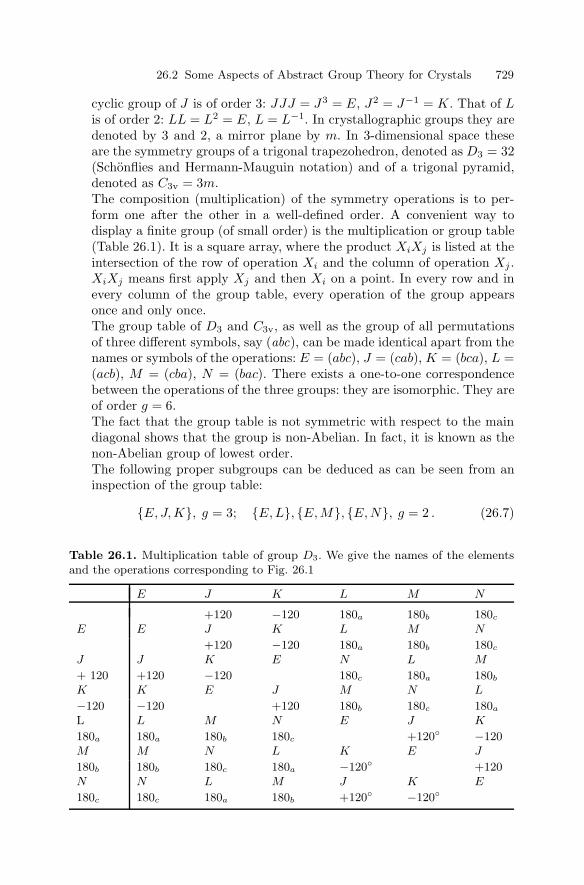
26.2 Some Aspects of Abstract Group Theory for Crystals 729
cyclic group of J is of order 3: JJJ = J3 = E, J2 = J−1 = K. That of Lis of order 2: LL = L2 = E, L = L−1. In crystallographic groups they aredenoted by 3 and 2, a mirror plane by m. In 3-dimensional space theseare the symmetry groups of a trigonal trapezohedron, denoted as D3 = 32(Schonflies and Hermann-Mauguin notation) and of a trigonal pyramid,denoted as C3v = 3m.The composition (multiplication) of the symmetry operations is to per-form one after the other in a well-defined order. A convenient way todisplay a finite group (of small order) is the multiplication or group table(Table 26.1). It is a square array, where the product XiXj is listed at theintersection of the row of operation Xi and the column of operation Xj .XiXj means first apply Xj and then Xi on a point. In every row and inevery column of the group table, every operation of the group appearsonce and only once.The group table of D3 and C3v, as well as the group of all permutationsof three different symbols, say (abc), can be made identical apart from thenames or symbols of the operations: E = (abc), J = (cab), K = (bca), L =(acb), M = (cba), N = (bac). There exists a one-to-one correspondencebetween the operations of the three groups: they are isomorphic. They areof order g = 6.The fact that the group table is not symmetric with respect to the maindiagonal shows that the group is non-Abelian. In fact, it is known as thenon-Abelian group of lowest order.The following proper subgroups can be deduced as can be seen from aninspection of the group table:
E, J,K, g = 3; E,L, E,M, E,N, g = 2 . (26.7)
Table 26.1. Multiplication table of group D3. We give the names of the elementsand the operations corresponding to Fig. 26.1
E J K L M N
E E+120J
−120K
180a
L180b
M180c
N
J J+120K
−120E
180a
N180b
L180c
M
+ 120K
+120K
−120E J
180c
M180a
N180b
L
−120L
−120L M
+120N
180b
E180c
J180a
K
180a
M180a
M180b
N180c
L K+120
E−120J
180b
N180b
N180c
L180a
M−120
J K+120E
180c 180c 180a 180b +120 −120

730 26 Group Theory in Semiconductor Optics
The coset decomposition relative to the subgroup E, J,K gives one morecoset L,M,N, i.e. left and right cosets are identical, and E, J,K isa normal or invariant subgroup. The coset decomposition relative to thesubgroup E,L gives two additional left cosets J,N, K,M and twomore right cosets J,M, K,N as can be seen from an inspection ofthe group table.In the abstract group mentioned above there are three conjugacy classes,or in short simply Ci classes, as can be verified using the group table:
C1 = E, l = 1; C2 = J,K, l = 2; C3 = L,M,N, l = 3 . (26.8a)
For example, the operations J and K belong to the same class since
N−1JN = NM = K and with N−1 = N . (26.8b)
Geometrically, conjugacy means the search for symmetrically equivalentsymmetry elements. They must be of the same type, or from the point ofview of group theory, their cyclic groups must be of the same order. Infact, the two 3-fold axes J andK are symmetrically equivalent through thethree 2-fold axes or mirror planes L,M,N and vice versa. The 2-fold axesor mirror planes are symmetrically equivalent through the 3-fold axes.
5. The set of all symmetry operations (isometries) of an idealized infi-nite crystal structure forms a crystallographic space group. In three-dimensional space we distinguish 230 types of crystallographic spacegroups of order g = ∞. The most characteristic feature of a crystal isthat its structure can be embedded into a lattice. The existence of a lat-tice, i.e. the presence of three-dimensional periodicity, gives rise to diffrac-tion effects, as first shown by Laue, Friedrich and Knipping. In terms ofgroup theory this corresponds to the existence of a discrete translationsubgroup T of every space group G. The symmetry operations of T aretranslations by lattice vectors Rn. Choosing a suitable basis of latticevectors, a so-called primitive basis, each lattice vector is represented by alinear combination of the basis vectors with integer coefficients (see alsoSect. 7.2):
Rn =∑
i
niai . (26.9)
Isometries are special affine mappings described by a system of equations
x = Dx + R = (D, R)x . (26.10)
The pair (D, R) consists of the (3×3)-matrix D, the rotational part, andthe (3×1)-column R, the translational part. For isometries, i.e., distance,preserving mappings, the condition detD = ±1 must be obeyed.The lattice of translation vectors of a crystal imposes restrictions on theisometries occurring in space groups. The rotational matrix D has to obey

26.2 Some Aspects of Abstract Group Theory for Crystals 731
Dk = E, with the order k = 2, 3, 4, 6. That means a crystal only allowsrotations by multiples of 180, 120, 90, and 60.Therefore, in crystallographic space groups the following symmetry oper-ations occur. Their symbols are given in the Hermann-Mauguin notation.a) Identity (E, 0). Symbol 1: E is the unit matrix.b) Translations by lattice vectors (E,Rn).c) Rotations and screw rotations detD = +1
i. Rotations. Symbols k = 2, 3, 4, 6 according to their order k; foreach one exists a line of (invariant) fixed points, the rotation axis.
ii. Screw rotations. Symbols kn with n < k : (D,R)k = (E,Rn)must hold where Rn is a lattice translation; (D,R) can be de-composed into a rotation around an axis (screw axis) and a trans-lation by the screw vector parallel to this axis R‖ = n
k R0, whereR0 is the shortest lattice vector along the screw axis.
d) Inversion D = −E. Symbol 1: exactly one point is fixed, the centerof inversion or center of symmetry.
e) Rotoinversions detD = −1. Symbols k, k = 2: it may be decomposedinto a rotation followed by an inversion.
f) Reflection and glide reflection detD = −1, D2 = E:i. Reflection (D,R)2 = (E,0). Symbol m: the fixed points form
a plane at which reflection of space is performed, the so-calledmirror plane. It is a special rotoinversion 2 = m where the axisstands normal to the mirror plane.
ii. Glide reflection (D,R)2 = (E,Rn). Symbols a, b, c, n, d: may bedecomposed into a reflection through a plane (glide plane) and atranslation by the glide vector parallel to this plane.
As already mentioned above, the subset of isometries (E,Rn), i.e.,translations by lattice vectors, forms a subgroup T of the space groupG. It is normal or invariant since the left and right coset decompositioncoincide. The symmetry operations in each coset relative to T have therotational part D in common since the product of any space group op-eration (D,R) and any lattice translations (E,Rn) does not change therotational part D. The factor group F = G/T where the cosets are theelements of F , is isomorphic to the point group P of the space group G.This point group P of the crystal can thus be obtained directly from thecoset decomposition relative to T by considering only the rotational partsgiven by (3 × 3)-matrices.To know the point group P or the crystal class of the space group G of thecrystal structure is important with regard to, e.g., the symmetry of theform of the crystal, the symmetry of the lattice and thus of the reciprocallattice and the symmetry of a diffraction pattern.There is one further important aspect of this coset decomposition, namelythe denotation of space groups by means of the Hermann-Mauguin sym-bols used in crystallography. The first character is the letter of the type of

732 26 Group Theory in Semiconductor Optics
the Bravais lattice of the structure given by the translation subgroup T .P means primitive; A,B and C mean one face is centered; I means bodycentered; F means all faces are centered; R means special centering typein trigonal crystal classes. Then follows a finite set of symbols (maximumthree) of generators that when combined with T permits the generationof all space group operations.
The following are some examples of space groups for important types ofsemiconductor structures.
1. Wurtzite structure. Prototype: ZnO; other examples CdS, CdSe, GaN.
G : P63mc; P : 6mm = C6v (Schonflies notation) .
The point group symbol in the Hermann-Mauguin notation is simply de-rived by replacing the screw axes by their rotation axes and the glideplanes by their mirror planes.6mm belongs to the hexagonal crystal system. It is of order g = 12 withthe following symmetry operations. Rotation axis 6 contains the opera-tions 6+ = rotation by 60, 6− = rotation by −60, 3+ = rotation by 120,3− = rotation by −120, and 2 = rotation by 180. There are two triplesof mirror planes. In each triple the symmetrically equivalent mirror planesenclose an angle of 60. However, the mirror planes of different triples arerotated by 30 against each other. Thus, they are not symmetrically equiv-alent (there is no symmetry operation rotation by 30) and they belong todifferent conjugacy classes, which is why the Hermann-Mauguin symbol6mm has two sets of non-equivalent mirror planes indicated. Therefore, inthe single group there are six (conjugacy) classes denoted in the Schonfliesnotation as (Table 26.6): E, 2C6, 2C3, C2, 3σd, 3σv.
2. Zincblende structure. Prototype: ZnS, other examples III–V-compoundslike GaAs, InP, or I–VII compounds like the Cu-halides or AgBr.
G : F 43m; P : 43m = Td .
43m belongs to the cubic crystal system. It is of the order g = 24. It is non-centrosymmetric. The classes of the single group contain (Table 26.10),apart from the identity class, the operations 3+ and 3− of four diagonal3-fold axes (8C3) of a cube, 2-fold operations rotation by 180 of threeaxes 2 = 42(3C2), the operations 41 = 4+ and 43 = 4−(6S4) of the three4 rotoinversion axes along the axes of a cube and 2-fold operations at sixdiagonal mirror planes (6σd)
3. Diamond structure Prototype: C, other examples Ge, Si, Cu2O, NaCl
G : Fd3m; P : m3m = Oh
m3m is centro-symmetric and belongs to the cubic crystal system. It is oforder g = 48. It can be considered as the direct product of 43m = Td and

26.3 Theory of Representations and of Characters 733
the point group 1 = Ci. Therefore, we also have the classes (Table 26.14)Ci, 6C4 (since 4 × 1 = 4), 8C3i (since 3 × 1 = 3 = C3i) and 3σh (since2 × 1 = m).
The outer or direct product of two groups G = Xi and G′ = X ′i is
again a group G′′ which consists of all ordered pairs Xi, X ′j. The definition of
the connection of the elements of G′′ is
(Xi, X′j)(Xk, X
′l) = (XiXk, X
′jX
′l) , (26.11)
and the order of G′′ is g · g′.
26.3 Theory of Representations and of Characters
Any set of elements which fulfils the multiplication table of a group is calleda representation of this group. The operations in Fig. 26.1 can be consideredas a representation of D3.
In a stricter sense, to which we shall stick from now on, we consider arepresentation to be a set of (n×n) matrices (n = 1, 2, 3, . . .) which fulfils themultiplication table with normal matrix multiplication as the connection.
The name of a certain representation is given by a label α used as an index.With Γ α we denote a set of g matrices that fulfil the multiplication table
of group G. Γ α(Xi) is the matrix that represents the element Xi of G andΓ α(Xi)jk is the element of this matrix in row j and column k.
The normal matrix multiplication then results in
Fig. 26.1. The symmetry operations which map an equilateral triangle into itself

734 26 Group Theory in Semiconductor Optics
Fig. 26.2. The reduction of a reducible representation into irreducible ones
Γ (Xi, Xj)kl =∑
h
Γ α(Xi)k,hΓ α(Xj)h,l . (26.12)
We introduce nα to denote the dimension of the (nα × nα) matrices of acertain representation α; nα is the same for all matrices of one representationΓ α.
There is an infinite number of representations for one group. If Γ α is arepresentation and X is a non-singular matrix of the same dimension nα thenX−1Γ αX is again a representation.
In the following we shall destill from this infinite number of representationssome with special properties (the so-called irreducible representations) andpresent some of their characteristic properties.
Table 26.2 gives four examples of representations of D3, two one-dimen-sional ones, a two- and a three-dimensional one. A representation Γ α is calledreducible if a non-singular matrix Y can be found such that all matricesY −1Γ α(Xi)Y acquire the same block form. This means there are squaresub-matrices and otherwise zeros; see Fig. 26.2. From the properties of ma-trix multiplication it follows immediately that only submatrices at identicalpositions are connected with each other in multiplication. This means thatthe submatrices of all Xi which are located in the same position, alone forma representation.
A representation Γ α which can be brought into such a block form of sub-matrices is called reducible. A representation Γ α, for which no matrix Y canbe found to bring all Γ α(Xi) into the same block form is called irreducible.The representations Γ 1 − Γ 3 in Table 26.2 are irreducible; Γ 4 is evidentlyreducible. It is already expressed in the desired block form.
We concentrate in the following on irreducible representations.Two irreducible representations Γ α, and Γ β are called equivalent, if there
exists a non singular matrix S with
S−1Γ α(Xi)S = Γ β(X i) for all Xi ∈ G (26.13)
With this definition of equivalence we arrive at a very important state-ment: There exist exactly as many non equivalent ( = different) irreduciblerepresentations of a group as the group has classes Ci.
For D3 we found three classes (see above). Consequently D3 has threenonequivalent irreducible representations. These are the Γ 1,Γ 2 and Γ 3 in
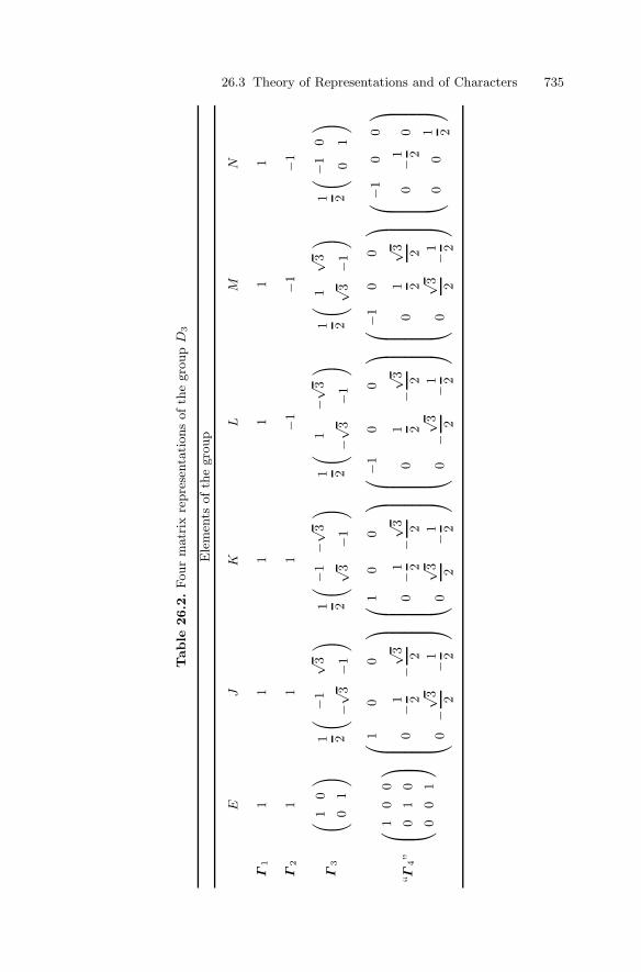
26.3 Theory of Representations and of Characters 735
Table
26.2
.Four
matr
ixre
pre
senta
tions
ofth
egro
up
D3
Ele
men
tsofth
egro
up
EJ
KL
MN
Γ1
11
11
11
Γ2
11
1−1
−1−1
Γ3
( 10
01
)1 2
( −1√ 3
−√ 3−1
)1 2
( −1−√ 3
√ 3−1
)1 2
(1
−√ 3
−√ 3−1
)1 2
( 1√ 3
√ 3−1
)1 2
( −10
01
)
“Γ
4”
⎛ ⎜ ⎝10
0
01
0
00
1
⎞ ⎟ ⎠⎛ ⎜ ⎜ ⎜ ⎜ ⎜ ⎝10
0
0−
1 2−√ 3 2
0−√ 3 2
−1 2
⎞ ⎟ ⎟ ⎟ ⎟ ⎟ ⎠⎛ ⎜ ⎜ ⎜ ⎜ ⎜ ⎝10
0
0−
1 2−√ 3 2
0
√ 3 2−
1 2
⎞ ⎟ ⎟ ⎟ ⎟ ⎟ ⎠⎛ ⎜ ⎜ ⎜ ⎜ ⎜ ⎝−10
0
01 2
−√ 3 2
0−√ 3 2
−1 2
⎞ ⎟ ⎟ ⎟ ⎟ ⎟ ⎠⎛ ⎜ ⎜ ⎜ ⎜ ⎜ ⎝−10
0
01 2
√ 3 2
0
√ 3 2−
1 2
⎞ ⎟ ⎟ ⎟ ⎟ ⎟ ⎠⎛ ⎜ ⎜ ⎜ ⎜ ⎝−10
0
0−
1 20
00
1 2
⎞ ⎟ ⎟ ⎟ ⎟ ⎠

736 26 Group Theory in Semiconductor Optics
Table 26.2. The irreducible representation in which all elements are repre-sented by 1 is called the trivial representation and is always called Γ 1. Therepresentations of the identity element are always unit matrices with 1 on themain diagonal and zeros otherwise. For irreducible representations Γ α andΓ β there exists an orthogonality relation∑
Xi
Γ α(Xi)kpΓ β(X−1i )ql =
g
nαδαβδklδpq (26.14)
with δkl and δpq being the Kroneckers symbol and
δαβ =
⎧⎨⎩0 if Γ α and Γ β are not equivalent1 if Γ α and Γ β are identical= 0 but undefined if Γ α and Γ β are equivalent
A characteristic quantity which is identical for all equivalent irreduciblerepresentations is the trace of the matrices
χα(Xi) = TrΓ α(Xi) =∑
j
Γ α(Xi)jj . (26.15)
These traces are called characters. Two equivalent representations havethe same characters since
TrΓ α(Xi) = TrS−1Γ α(Xi)S . (26.16)
We can thus write down the characters of all nonequivalent irreduciblerepresentations in a table. Since the characters of conjugate elements are thesame, as seen from a comparison of (26.6) and (26.16), it is sufficient to givethe characters for the different classes. This results in a square scheme ofnumbers. Table 26.3 gives as a first example the character table for the groupD3. It is identical, by the way, to that of the group C3v mentioned above.
As already mentioned, Γ 1, in the first line is always the trivial representa-tion, while the first column gives the dimensionality nα of the representationΓ α.
The nomenclature χα(Ci) means the character of the irreducible represen-tation a for the class Ci.
Introducing the number hi of elements of the class Ci, with a total num-ber r of classes and of irreducible representations in the group, we find thefollowing relations for the irreducible representations
r∑i=1
hiχα(Ci)χ∗β(Ci) = gδαβ , (26.17a)
r∑α=1
hiχα(Ci)χ∗α(Cj) = gδij . (26.17b)

26.3 Theory of Representations and of Characters 737
Two representations Γ α and Γ β are equivalent if χα(Xi) = χβ(Xi) for allXi. If a representation Γ is given, it contains the irreducible representationΓ α pα times in the sense of a decomposition into block form:
Γ =∑α
pαΓ α with pα =∑Xi
χ(Xi)χ∗α(Xi) . (26.18)
This means that it is not necessary in practice to try out all possiblenon singular matrices since one can immediately deduce from (26.18) thedecomposition of a given representation into irreducible ones. The reduciblerepresentation “Γ 4” in Table 26.2 can consequently be decomposed into
Γ 4 = Γ 2 ⊕ Γ 3 . (26.19)
This process also explains the use of the symbol ⊕.The direct product Γ α ⊗ Γ β of two representations Γ α and Γ β with di-
mensions nα and nβ , respectively, is a new representation of dimension nα ·nβ .The new set of matrices is obtained in the following way
Γ α(Xi)⊗Γ β(Xi) =
⎛⎜⎝ Γ α(Xi)11Γ β(Xi) . . . Γ α(Xi)1nαΓ β(Xi)...
Γ α(Xi)nα1Γ β(Xi) . . . Γ α(Xi)nαnαΓ β(Xi)
⎞⎟⎠ (26.20)
The direct product of two representations is again a representation of thegroup. The direct product of two irreducible representations can be reducibleor irreducible.
For the characters of the direct product one finds
χ (Γ α ⊗ Γ β) = χα · χβ . (26.21)
The decomposition of the products of the irreducible representations of agroup is usually given in tables:
Γ α ⊗ Γ β =∑
γ
gαβγΓ γ (26.22)
with
Table 26.3. The character table of the group D3
Irre
duci
ble
repre
senta
tions
Classes of elements
D3 E 2C3 3C2
Γ 1 1 1 1
Γ 2 1 1 −1
Γ 3 2 −1 0

738 26 Group Theory in Semiconductor Optics
Table 26.4. Multiplication table for the irreducible representations of the groupD3
D3 Γ 1 Γ 2 Γ 3
Γ 1 Γ 1 Γ 2 Γ 3
Γ 2 Γ 2 Γ 1 Γ 3
Γ 3 Γ 3 Γ 3 Γ 1 + Γ 2 + Γ 3
gαβγ =1g
∑Xi
χα(Xi)χβ(Xi)χ∗γ(Xi) . (26.23)
We give the direct products of the irreducible representations of D3 inTable 26.4.
The criterion for a given representation to be irreducible is
Γ α irred ⇔∑Xi
|χα(Xi)|2 = g . (26.24)
A representation of a group is also a representation of each of its subgroups.An irreducible representation of a group can be a reducible or irreduciblerepresentation of the subgroup. Which possibility applies can either be checkedwith formula given above or it can be found in the tables. In Table 26.5 wegive these so-called compatibility relations of the irreducible representationsof D3 with the irreducible representations of its two proper subgroups C2 andC3.
26.4 Hamilton Operator and Group Theory
In this section we derive the connections between the eigenfunctions and eigen-states of the stationary or time-independent Hamilton operator H and theirreducible representations of a group.
We do not yet specify a particular type of group, but notice that an opera-tor P (Xi) which transforms the system into itself commutes with the Hamiltonoperator
P (Xi)H = HP (Xi) , (26.25)
where Xi is a symmetry operation of the group. It is known that wheneveran operator P commutes with H , there exists a set of functions which aresimultaneously eigenfunctions of H and of P . These eigenfunctions are calledbasis functions. They are given in the tables of Sect. 25.6. We also come backto them in Sect. 25.5.
The group which transforms the system into itself is also known as thegroup of H .
We consider now an eigenvalue Eα of H with eigenfunction(s) ψαj ;j = 1, . . . ,m. If the eigenvalue Eα is not degenerate one has m = 1. Fora degenerate eigenvalue m > 1.

26.4 Hamilton Operator and Group Theory 739
Table 26.5. Compatibility table of the irreducible representations of the group D3
with the irreducible representations of its proper subgroups C2 and C3
D3 Γ1 Γ2 Γ3
C3 Γ1 Γ1 Γ2 + Γ3
C2 Γ1 Γ2 Γ1 + Γ2
WithHψαj = Eαψαj (26.26)
we also have
P (Xi)Hψαj = HP (Xi)ψαj = P (Xi)Eαψαj = EαP (Xi))ψαj , (26.27)
since Eα is just a real number.This means that together with ψαj also P (Xi)ψαj is an eigenfunction with
eigenvalue Eα. Since the ψαj already include all possible eigenfunctions witheigenvalue Eα, the P (Xi)ψαj can only be linear combinations of the ψαj .
This means
P (Xi)ψαk =m∑
j=1
Γ α(Xi)jkψαj . (26.28)
If we perform this procedure for one symmetry operation Xi and for allψαk we get a matrix of coefficients Γ α(Xi)jk. For a nondegenerate eigenvaluethis is just a (complex) number of unit magnitude.
If we then perform the procedure for all symmetry operations Xi of thegroup of the Hamiltonian we get a set of matrices Γ α(Xi). Now comes thecrucial point: this set of matrices forms a representation of the group of H ,and generally an irreducible representation.
If this is the case we can identify the eigenvalue Eα which belongs to theeigenstates ψαj with the label of the irreducible representation Γ α, i.e., wesay that the eigenvalue Eα has symmetry Γ α or the eigenstates ψαj of Eα
transform according to Γ α.Since most physical systems have an infinite number of eigenstates but
finite groups have only a finite number of non-equivalent irreducible represen-tations, the name of one irreducible representation will occur many times asshown schematically in Fig. 26.3.
If the representation of the group produced by the eigenfunctions of oneeigenenergyEα is reducible, we speak of an accidental degeneracy. An exampleis shown in Fig. 26.3. This means there are actually two different eigenenergieswith their sets of eigenfunctions which just happen to be equal for the specificparameters of H, but which could in principle be different.
The important point now is that group theory allows us to make manyimportant predictions, for example, about selection rules or splitting of statesunder external perturbations, without even knowing the Γ α(Xi)ij nor theeigenvalues or eigenfunctions. There is one drawback, however, group theory

740 26 Group Theory in Semiconductor Optics
Fig. 26.3. The schematic relation of the eigenener-gies Eα, and the corresponding irreducible represen-tation Γ α
tells us only whether a certain matrix element is zero or not; it does not sayanything about its magnitude if it is non zero. To get quantitative informationwe must either use physical arguments to deduce how small or large an effectcan be, once group theory has told us that it exists, or we just have to calculatethe matrix elements. But here group theory helps us again, by telling us whichones are zero.
Until now we have dealt only with real space. For electronic eigenstates weshould also consider spin. Spin does not have a representation in real space.Since we do not want to indulge in a lot of mathematics, we simply note thatthere exists a group D1/2 which describes the behavior of particles with spin1/2 under point operations (a translation does not affect spin).
To describe electronic wave functions with spin
ψαj = ψαj · s , (26.29)
we have to consider the “double group” which is formally just the directproduct of D1/2 and the corresponding point group D1/2 ⊗ (point group).This double group is again a group, possessing conjugate elements, classes,irreducible representations, and a character table. We shall finally end up withmore classes and more Γα compared to the simple point group without spin.In the tables given at the end of this chapter for the three most importantpoint groups of semiconductors one can see from the basis functions whichones are the additional Γα and classes. For vibrations (phonons) of moleculesand of solids spin is not important. Therefore often only the simple and notthe double groups are given in corresponding books.

26.5 Applications to Semiconductors Optics 741
26.5 Applications to Semiconductors Optics
The two groups that describe crystalline solids are, as already mentioned, thetranslation group and the space group. The translation group is an infiniteAbelian group of all translations Rn as introduced in Sects. 7.2 or 8.1 (alsosee below).
Additionally, the space group contains all other symmetry operations thatmap the crystal onto itself like inversion, rotation axes, screw rotation axes,mirror (or reflection) planes or glide reflection planes.
Symmorphic space groups can be decomposed into a semi-direct productof the translation group and a point group that contains symmetry operationsthat keep at least one point fixed, e.g., inversion, rotation axes or reflectionplanes.
The generators of symmorphic groups do not contain screw rotation axesor reflection glide planes. Nonsymmorphic groups contain such symmetry ope-rations in their generators and cannot be decomposed in the above way. Detailsabout this topic can be found, e.g., in [94H1].
The translation group is obviously Abelian, i.e.,
T (R1)T (R2) = T (R1 + R2) = T (R2 + R1) = T (R2)T (R1) , (26.30)
where R1 and R2 are two translations of the lattice and T is the translationoperator. Consequently every Ri, is self-conjugate and forms a class by itselfand all irreducible representations are one-dimensional. A detailed inspectionof their properties leads to
T (Ri)u(r, k) = eikRiu(r,k) (26.31)
since the prefactor must be linear in Ri and of the magnitude one. This shortargument shows that the Bloch theorem of Sect. 8.1 also follows from group-theoretical considerations.
Since we have already treated this theorem and its consequences in somedetail in Chaps. 7 and 8, we need not further pursue it here, but concentratenow on point groups.
We note (again without proof) that according to what we have said above,we can restrict ourselves trivially for symmorphic space groups to the pointgroup.
For nonsymmorphic space groups the following statements are correct forthe point group we obtain if we replace screw rotation axes by simple rotationaxes and glide reflection planes by simple reflection planes [94H1]. In thissense the point group of the wurtzite crystal structure, which contains a screwrotation axis, is C6v or 6mm.
The proper consideration of screw rotation axes or glide reflection planesintroduces, e.g., phase factors in X-ray scattering but does not change thestatements about matrix elements or selection rules given below.

742 26 Group Theory in Semiconductor Optics
The point group of a crystal defined in this sense contains all symmetryoperations that transform the crystal into itself and keep at least one pointfixed. This group also describes the symmetries of the eigenstates for k = 0,i.e., at the Γ point in reciprocal space that is the center of the first Brillouinzone.
Since this is also the region of k-space that is important for the opticalproperties of most direct gap semiconductors, we stick in the following to k = 0(this is the reason why we use Γ to label the irreducible representations) anddiscuss only later what happens when we go to k = 0. For the moment wenote that a statement which is exact for k = 0 will be almost correct in theclose vicinity of the Γ -point.
We now leave the group D3, which we used above for illustration purposes,and return to the three point groups that are most important for the semi-conductors, namely Td, Oh, and C6v and which we have introduced alreadyabove.
In Sect. 25.6 we give the character tables and the basis functions of thesethree point groups. The remainder of the 32 point groups can be found ine.g. [63K1, 88L1]. Additionally we give the multiplication tables for the ir-reducible representations, their compatibility tables with the full rotationgroup, which is valid for spherical problems like atoms (see below), andwith the proper subgroups. There we indicate examples of external per-turbations which reduce the symmetry of the point group to that of itssubgroups.
The classes with a bar come from the formation of the double group whenwe include spin and the same is true for the irreducible representations whichcontain noninteger J and Jz values in their basis functions φ(J, Jz). Basisfunctions are examples of functions that possess the symmetry properties ofthe irreducible representation. Basis functions Sx, Sy and Sz transform likex, y and z, however, without a change of sign under inversion and R means aspherically symmetric function like x2 +y2 +z2. A superscript + or − appearswhere inversion Ci is an element of the group and where, consequently, parityis a good quantum number. Obviously + or − mean even and odd parity underinversion, respectively.
The information contained in these tables is sufficient to answer many ofthe questions addressed below.
We present the first important rule. If we have to calculate a transitionmatrix element Mif (see also Sect. 3.2)
Γ fΓ sΓ i
Mif ∝〈f |Hs| i〉 =∫ψ∗
fHsψi dτ , (26.32)
where we start from an initial state |i〉 of symmetry Γ i, and want to reach afinal state 〈f | of symmetry Γ f with a perturbation operator Hs that trans-
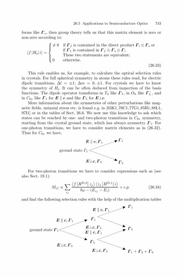
26.5 Applications to Semiconductors Optics 743
forms like Γ s, then group theory tells us that this matrix element is zero ornon-zero according to:
〈f |Hs| i〉 =
⎧⎪⎪⎨⎪⎪⎩= 0 if Γ f is contained in the direct product Γ i ⊗ Γ s or
if Γ 1 is contained in Γ f ⊗ Γ s ⊗ Γ i
These two statements are equivalent;0 otherwise.
(26.33)
This rule enables us, for example, to calculate the optical selection rulesin crystals. For full spherical symmetry in atoms these rules read, for electricdipole transitions, ∆l = ±1; ∆m = 0, ±1. For crystals we have to knowthe symmetry of Hs. It can be often deduced from inspection of the basisfunctions. The dipole operator transforms in Td like Γ 5, in Oh like Γ−
5 , andin C6v like Γ 1 for E ‖ c and like Γ 5 for E⊥c.
More information about the symmetries of other perturbations like mag-netic fields, uniaxial stress etc. is found e.g. in [63K1,76C1,77G1,85H1,88L1,97I1] or in the tables of Sect. 26.6. We now use this knowledge to ask whichstates can be reached by one- and two-photon transitions in C6v symmetry,starting from the crystal ground state, which has always symmetry Γ 1. Forone-photon transitions, we have to consider matrix elements as in (26.32).Thus for C6v we have,
For two-photon transitions we have to consider expressions such as (seealso Sect. 19.1):
Mif ∝∑zj
⟨f∣∣HD,2
∣∣ zj
⟩ ⟨zj
∣∣HD,1∣∣ i⟩
ω − (Ezj − Ei)+ c.p. (26.34)
and find the following selection rules with the help of the multiplication tables

744 26 Group Theory in Semiconductor Optics
This means that in two-photon absorption we can reach states with sym-metries Γ 1, Γ 2, Γ 5 and Γ 6 depending on the polarization.
Another field in which the vanishing or otherwise of a matrix element is ofimportance is perturbation theory. We assume that we have an unperturbedstationary Hamiltonian H with non-degenerate eigenstate E0
n, ψ0n. We now
apply a small stationary perturbation Hs to get a total Hamiltonian
H = H0 +Hs. (26.35a)
The perturbed eigenenergy En, and wavefunction ψn are then given by
En = E0n +
⟨ψ0
n |Hs|ψ0n
⟩, (26.35b)
and
ψn = ψ0n +
∑k =0
⟨ψ0
k |Hs|ψ0n
⟩ψ0
k
E0n − E0
k
. (26.35c)
Equation (26.33) tells us now which perturbations can change the eigenen-ergy and mix the states and which cannot. As stated earlier, group theory doesnot tell us how large this effect will be.
In the case of a degenerate level E0n with ψ0
n,i, perturbation theory leadsto a secular equation given by the determinant
det∣∣⟨ψ0
n,i |Hs|ψ0n,j
⟩− Eδij∣∣ = 0 , (26.36)
and again (26.33) can predict which matrix elements vanish. The problem ofdegenerate states has been developed even further with a technique known as“invariant expansion”. A discussion of this technique is beyond the scope ofthis book but the reader may find an elaborate presentation in [76C1, 77G1,85H1].
Partly equivalent information is obtained if we consider that the pertur-bation reduces the symmetry of the problem, so that the perturbed problemcorresponds to a subgroup of the unperturbed one. If the irreducible repre-sentation of E0
n is still irreducible in the subgroup, En, may shift but doesnot split. If it decays into more than one irreducible representation in thesubgroup, E0
n can split into a corresponding number of different levels underthe influence of Hs. If some of the new eigenvalues still coincide we have anaccidental degeneracy.
To illustrate this fact, inspection of the compatibility relations C6v showsthat an electrostatic field E⊥c (Γ 5) will result in a splitting of a Γ 5 level intotwo states of symmetries Γ 1 and Γ 2 of the group Cs.
Another case in which group theory is helpful concerns product wave func-tions. If, for example, we know that the spatial part of the hole wave functionφh(rn) in Td transforms like Γ 5 (this results from an atomic p-state as willbe shown below) and we want to add spin σ we get
ψ = φΓ 5n (rh) · s . (26.37)

26.5 Applications to Semiconductors Optics 745
In order to discover the symmetry of the total wave function we just formthe direct product of the symmetry of the spatial part (here Γ 5) and of theirreducible representation of spin 1/2. For Td this reads
Γ total = Γ 5,space ⊗ Γ 1/2 = Γ 5 ⊗ Γ 6 = Γ 7 ⊕ Γ 8 . (26.38)
This means that the spin results in a splitting into two states of symmetriesΓ 7 and Γ 8. From physical arguments we know that this is the spin-orbitsplitting.
A very important example of product wave functions in semiconductorsare exciton wave functions. As shown in Sect. 9.1, they are a product of theelectron and hole wavefunctions and of the envelope function.
The possible symmetries of an exciton therefore result from the directproduct of the symmetries of the electron, hole and envelope functions, i.e.,
Γ exciton = Γ el ⊗ Γ h ⊗ Γ env . (26.39)
For the ground state (main quantum number nB = 1) Γ env is always Γ 1. Soin Td, for example, we find excitons formed with the hole in the Γ 7 or Γ 8
valance band and the electron in the Γ 6 conduction band
Γ 6 ⊗ Γ 8 ⊗ Γ 1 = Γ 3 ⊕ Γ 4 ⊕ Γ 5 (26.40a)
Γ 6 ⊗ Γ 7 ⊗ Γ 1 = Γ 2 ⊕ Γ 5 (26.40b)
The Γ 5 is the spin singlet state, which can be reached from the groundstate by an electric-dipole transition; the Γ 3, Γ 4 and Γ 2 states are dipoleforbidden. Actually they are the triplet states with parallel electron and holespins.
The number of possible exciton states increases rapidly for nB > 1.Still another important case is the reduction of symmetry in a quantum
well compared to the parent bulk materials.In Table 26.6 we give the irreducible representations, the compatibility
relations and the selection rules when going from a bulk zincblende structureto a QW grown on a (001) surface. For this, but also for other orientations,see, e.g., [96I1, 97I1, 00S1, 02M1]. A single ideal interface between two differ-ent materials both having the point group Td reduces the symmetry to C2v.See [96I1, 97I1] and references therein. A quantum well, i.e., two close-lyinginterfaces, results in symmetry D2d if the two materials have a common anionor cation, e.g., AB/AC. This situation is treated in Table 26.6. In the case ofa well/barrier combination without a common anion or cation AB/CD, thetotal symmetry may be D2d or C2v depending on the termination of the inter-faces. For C2v symmetry, the orthogonal directions [110] and [110] in the planeof the quantum well are no longer equivalent. This may result in polarizationanisotropies of the optical properties or in different band offsets at both in-terfaces and in internal electric fields if, e.g., the dipole layers on both sides

746 26 Group Theory in Semiconductor Optics
Table 26.6. Group theoretical relations and selection rules for zincblende-type bulkmaterial and quantum wells grown on (100) oriented substrates [93J1]
Point group(example)
Td
(GaAs, bulk)D2d
GaAs QW on(001) orientedsubstrate
Comments
Irreducible representationof lowest conduction band
Γ 6 Γ 6
Irreducible representationof highest valence band(does not apply to CuCl ora few other exceptions)
Γ 8 Γ 6
Γ 7
Heavy holeslight holes
Excitons with S, i.e., Γ 1
envelope functionΓ LB
6 ⊗ Γ VB8 ⊗
Γ env1 = Γ 3 + Γ 4
+Γ 5
Γ LB6 ⊗ Γ VB
6 ⊗Γ env
1 = Γ 1 + Γ 2
+Γ 5
Γ LB6 ⊗ Γ VB
7 ⊗Γ env
1 = Γ 3 + Γ 4
+Γ 5
Heavy-holeexcitons
Light-holeexcitons
Dipole-allowed transitions Γ 5 Γ 5 for E⊥zΓ 4 for E ‖ z
z is the growthdirection, i.e., thenormal to theQW plane
are different. For more details see, e.g., [97I1,00S1,02M1,03T1] and referencestherein.
Going one step further, we come to the more complicated entities suchas bound-exciton complexes or biexcitons. The procedure is basically asabove, i.e.,
Γ biex = (Γ el ⊗ Γ el)± ⊗ (Γ h ⊗ Γ h)±Γ∓∓env . (26.41)
However, one now has to consider that these systems contain partly in-distinguishable fermions. Therefore the total wave-function must change signunder the exchange of two identical particles. This means that if the combi-nation of the two electrons (Γ el ⊗ Γ el)− changes sign under exchange, thenthe envelope function must have even parity under this operation and viceversa. The same holds for the holes. The parity of the combinations can beseen from the coupling coefficients in tables like [63K1]. We do not go intodetails here but mention that the ground state of the biexciton always hasan envelope of Γ 1 symmetry. The possible combinations for the excitons of(26.40a), (26.40b) are in the ground state Γ 1 and Γ 1⊕Γ 3⊕Γ 5 [77G1,85H1],respectively. In C6v the biexciton containing two holes from the same valenceband always has only symmetry Γ 1 in the ground state, but with a hole fromthe Γ 9 and another from a Γ 7 valence band it is possible to construct inaddition Γ 5 and Γ 6 biexciton levels [77G1,85H1].

26.5 Applications to Semiconductors Optics 747
The bands in semiconductors often still contain some information aboutthe parent atomic orbitals, especially in the lattice periodic part uk(r) of theBloch function. The atomic orbitals result from a spherically symmetric prob-lem. Therefore it is reasonable to say a few words about this group and itscompatibility relations with the point groups of semiconductors. In the fullspherical rotation group, the system can be rotated around any axis by anyangle and is transformed in to itself. It can be shown that all rotations by thesame angle φ but around arbitrary axes are in the same class. The full rotationgroup can therefore be considered as a continuous group (Fig. 26.4) with rota-tion angle 0 ≤ φ < 2π. Consequently there must be a correspondingly infinitenumber of irreducible representations Γ l. Figure 26.4 gives the character ofthe representation. For the identity element E we get the dimensionality ofΓ l which is obviously 2l+ 1. The basis functions are the spherical harmonicsY m
l (φ, θ).The compatibility relations between the full rotation group for even and
odd parity, called D±Lz
and D±Jz
and the three point groups Td, Oh and C6v
are given in Sect. 26.6. These tables may be used as follows: In a tight-bindingapproximation we would assume that the uppermost valence band of CdS isformed from the filled 3p levels of S2−, while the lowest conduction band comesfrom the empty 5s levels of Cd2+. From the compatibility tables we learn thatthis results in the following band symmetries for C6v, at the Γ -point:
CB : 5s levels ⇒ D1/2 ⇒ Γ 7 ;
VB : 3p levels ⇒D3/2 ⇒ Γ 7 + Γ 9
D1/2 ⇒ Γ 7 .(26.42)
For Td symmetry one finds similarly
CB : Γ 6, VB : Γ 7 + Γ 8 . (26.43)
This implies a twofold splitting in the valence band of Td symmetry, whichcomes from the spin-orbit interaction as already mentioned, and a threefoldsplitting in C6v again arising from spin-orbit splitting and, in addition, fromthe hexagonal crystal field.
Note, that for covalent sp3 binding the top of the valence band and thebottom of the conduction band also have p- and s-character, thus leading tothe same results as for ionic binding.
Group theory cannot tell us the magnitude of the splittings nor the or-dering of the bands. It is found, however, that for Td symmetry the Γ 8 stateusually forms the upper valence band and the Γ 7 comes below (except in CuClwhich has the reverse ordering) and in C6v one usually has an uppermost va-lence band of symmetry Γ 9 and two Γ 7 levels below (except for ZnO, wherethe two upper bands are also most probably interchanged). See Sect. 8.8, 13.1,16.1
It is clear that angular momentum is no longer a good quantum numberin solids. The good quantities are the Γ i. With great care, however, one can

748 26 Group Theory in Semiconductor Optics
Fig. 26.4. The character table of the spherical rotation group
sometimes still use arguments based on angular momentum. In the wurtzitestructure the c axis is the quantization axis and Jz is to some extent usablefor discussions. The p-orbitals forming the valence band have l = 1 and m =0,±1. The m = 0 states have symmetry Γ 1 (or Γ 2) the m = ±1 states havesymmetry Γ 5. With the z-component of the spin of ±1/2 we can then produceJz = ±/2 and Jz = ±3/2 states corresponding to Γ 7 and Γ 9 respectively.For values of Jz larger than 3/2, however, the rather shaky approach abovebreaks down completely. See also the basis functions in the tables for Oh andTd.
To conclude this last chapter we consider two more topics namely finitek-values and time-reversal symmetry.
What happens if we leave the Γ point and go to k = 0? First we apply allsymmetry operations of the point group to the system as shown schematicallyin Fig. 26.5a for a two-dimensional square lattice. We end up with a number ofk-vectors, which are known as the “star of k”. If k is in a “general” positionwe get as many k-vectors in the star as the group has elements. On theother hand, all these symmetry operations transform the system into itself.Consequently the properties must be the same for all elements of the star ofk. We illustrate this statement in Fig. 26.5b for the dispersion E(k). We givecontours of constant energy and see clearly that the star of k allows a fourfoldband warping as indeed occurs for Td and Oh symmetries, simply becausecubic symmetry is lower than spherical symmetry.
If k is not in a “general” direction but coincides with one of the symmetrylines or planes of the system, then several of the elements of the star of k co-incide as shown in Fig. 26.5c. The symmetry operations that transform k into

26.5 Applications to Semiconductors Optics 749
itself are known as the “group of k”. This group of k is a subgroup of the fullpoint group. The irreducible representations at the Γ -point are consequentlyalso representations of the subgroup. If we start at the Γ -point with a certainlevel which transforms like Γ α and move along some symmetry direction, thelevel Γ α may or may not split, depending on whether Γ α becomes a reduciblerepresentation or remains an irreducible one in the (sub) group of k.
A typical example is the splitting of the fourfold degenerate Γ 8 state in Td
symmetry for k = 0 into two twofold degenerate states known as heavy andlight-hole bands (Figs. 8.16 and 26.6), where the states (J, Jz) = (3/2,±3/2)correspond to the heavy hole valence band and (3/2,±1/2) corresponds tothe light holes (see e.g. [74B1,03T1]). The Γ 6 and Γ 7 states do not show suchbehavior.
Fig. 26.5. The star of k, (a) the quali-tative shape of surfaces of constant en-ergy E(k) (b); and a k-vector of highersymmetry (c)
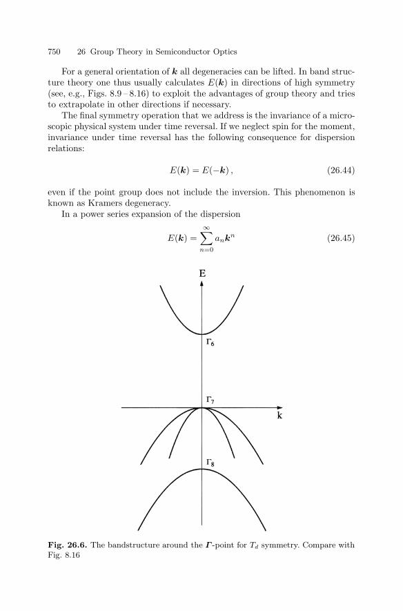
750 26 Group Theory in Semiconductor Optics
For a general orientation of k all degeneracies can be lifted. In band struc-ture theory one thus usually calculates E(k) in directions of high symmetry(see, e.g., Figs. 8.9 – 8.16) to exploit the advantages of group theory and triesto extrapolate in other directions if necessary.
The final symmetry operation that we address is the invariance of a micro-scopic physical system under time reversal. If we neglect spin for the moment,invariance under time reversal has the following consequence for dispersionrelations:
E(k) = E(−k) , (26.44)
even if the point group does not include the inversion. This phenomenon isknown as Kramers degeneracy.
In a power series expansion of the dispersion
E(k) =∞∑
n=0
ankn (26.45)
Fig. 26.6. The bandstructure around the Γ -point for Td symmetry. Compare withFig. 8.16

26.6 Some Selected Group Tables 751
Fig. 26.7. Schematic drawing of the Kramers degeneracy without spin (a) and withspin (b) as occurs e.g., for Γ7 bands in C6v symmetry for k⊥c
this permits only even values for n (Fig. 26.7a). If we now include the spin,(26.46) changes to
E(k, ↑) = E(−k, ↓) . (26.46)
This means that time reversal flips the spin. This condition can be alsofulfilled with odd powers in the expansion (26.46) and, in particular, allowsterms linear in k (Fig. 26.7b).
Detailed group-theoretical investigations show that k-linear terms are pos-sible for Γ8 states in Td symmetry or for Γ7 states k⊥c in C6v symmetry, butnot for k ‖ c and not for Γ 9 levels.
Indeed such k-linear terms are known; for example, for the B-exciton inCdS which contains a hole from the Γ7 valence band or for the A excitons inZnO. See Sect. 13.1.
26.6 Some Selected Group Tables
In this section, we give some tables for the three most important groups ofsemiconductors. We start in Tables 26.7 – 26.10 with the character tables ofthe point group C6v. In the first column we give the names of the irreduciblerepresentations in various notations, in the last one typical basis functions.From them it becomes clear, which representation belongs to the simple andwhich one to the double group, including spin namely here Γ 1 to Γ 6 and Γ 7
to Γ 9, respectively. The next tables give the multiplication tables of the irre-ducible representations and the combatibility relation with the subgroups andwith the full rotation group. Tables 26.10 – 26.13 give the same informationfor Td. For Oh we give only two tables for characters and the compatibilityrelation.

752 26 Group Theory in Semiconductor Optics
Table 26.7. Character table and basis functions of the point group C6v (or 6mm).Below E2 or Γ6 are the additional irreducible representations of the double groupwhich includes spin
C6v E E C2 2C3 2C3 2C6 2C6 3σd 3σv Basic functions
A1 Γ 1 1 1 1 1 1 1 1 1 1 a R or z
A2 Γ 2 1 1 1 1 1 1 1 −1 −1 a Sz
B1 Γ 3 1 1 −1 1 1 −1 −1 1 −1 a x3 − 3xy2
B2 Γ 4 1 1 −1 1 1 −1 −1 −1 1 a x3 − 3xy2
E1 Γ 5 2 2 −2 −1 −1 1 1 0 0 a (Sx − iSy)
−(Sx + iSy)E2 Γ 6 2 2 2 −1 −1 −1 −1 0 0 a Γ 3 ⊗ Γ 5
Γ 7 2 −2 0 1 −1√
3 −√3 0 0 c φ(1/2,−1/2),
φ(1/2, 1/2)
Γ 8 2 −2 0 1 −1 −√3
√3 0 0 c Γ 7 ⊗ Γ 3
Γ 9 2 −2 0 −2 2 0 0 0 0 c φ(3/2,−3/2),
φ(3/2, 3/2)
Table 26.8. Multiplication table for the irreducible representations of the groupC6v
Γ1 Γ2 Γ3 Γ4 Γ5 Γ6 Γ7 Γ8 Γ9
Γ1 Γ2 Γ3 Γ4 Γ5 Γ6 Γ7 Γ8 Γ9 Γ1
Γ1 Γ4 Γ3 Γ5 Γ6 Γ7 Γ8 Γ9 Γ2
Γ1 Γ2 Γ6 Γ5 Γ8 Γ7 Γ9 Γ3
Γ1 Γ6 Γ5 Γ8 Γ7 Γ9 Γ4
Γ1 + Γ2 + Γ6 Γ3 + Γ4 + Γ5 Γ7 + Γ9 Γ8 + Γ9 Γ7 + Γ8 Γ5
Γ1 + Γ2 + Γ6 Γ8 + Γ9 Γ7 + Γ9 Γ7 + Γ8 Γ6
Γ1 + Γ2 + Γ5 Γ3 + Γ4 + Γ6 Γ3 + Γ4 Γ7
Γ1 + Γ2 + Γ5 Γ5 + Γ6 Γ8Γ1 + Γ2
Γ3 + Γ4Γ9
Table 26.9. Compatibility table of the irreducible representations of the group C6v
with the irreducible representations of its proper subgroups
C6v : E(z) Γ 1 Γ 2 Γ 3 Γ 4 Γ 5 Γ 6 Γ 7 Γ 8 Γ 9
C6 : H(z) Γ 1 Γ 1 Γ 4 Γ 4 Γ 5 + Γ 6 Γ 2 + Γ 3 Γ 7 + Γ 8 Γ 9 + Γ 10 Γ 11 + Γ 12
C3v Γ 1 Γ 2 Γ 1 Γ 2 Γ 3 Γ 3 Γ 4 Γ 4 Γ 5 + Γ 6
C2v Γ 1 Γ 3 Γ 2 Γ 4 Γ 2 + Γ 4 Γ 1 + Γ 3 Γ 5 Γ 5 Γ 5
Cs : E(x) : H(y) Γ 1 Γ 2 Γ 1 Γ 2 Γ 1 + Γ 2 Γ 1 + Γ 2 Γ 3 + Γ 4 Γ 3 + Γ 4 Γ 3 + Γ 4
Cs : H(x) : E(y) Γ 1 Γ 2 Γ 2 Γ 1 Γ 1 + Γ 2 Γ 1 + Γ 2 Γ 3 + Γ 4 Γ 3 + Γ 4 Γ 3 + Γ 4

26.6 Some Selected Group Tables 753
Table 26.10. Compatibility table of the irreducible representations of the full ro-tation group of angular momentum Lz ≤ 6 and Jz ≤ 13
2with the irreducible repre-
sentations of the group C6v
D+0 Γ 1 D−
0 Γ 2
D+1 Γ 2 + Γ 5 D−
1 Γ 1 + Γ 5
D+2 Γ 1 + Γ 5 + Γ 6 D−
2 Γ 2 + Γ 5 + Γ 6
D+3 Γ 2 + Γ 3 + Γ 4 + Γ 5 + Γ 6 D−
3 Γ 1 + Γ 3 + Γ 4 + Γ 5 + Γ 6
D+4 Γ 1 + Γ 3 + Γ 4 + Γ 5 + 2Γ 6 D−
4 Γ 2 + Γ 3 + Γ 4 + Γ 5 + 2Γ 6
D+5 Γ 2 + Γ 3 + Γ 4 + 2Γ 5 + 2Γ 6 D−
5 Γ 1 + Γ 3 + Γ 4 + 2Γ 5 + 2Γ 6
D+6 2Γ 1 + Γ 2 + Γ 3 + Γ 4 + 2Γ 5 + 2Γ 6 D−
6 Γ 1 + 2Γ 2 + Γ 3 + Γ 4 + 2Γ 5 + 2Γ 6
D+1/2 Γ 7 D−
1/2 Γ 7
D+3/2 Γ 7 + Γ 9 D−
3/2 Γ 7 + Γ 9
D+5/2 Γ 7 + Γ 8 + Γ 9 D−
5/2 Γ 7 + Γ 8 + Γ 9
D+7/2 Γ 7 + 2Γ 8 + 2Γ 9 D−
7/2 Γ 7 + 2Γ 8 + 2Γ 9
D+9/2 Γ 7 + 2Γ 8 + Γ 9 D−
9/2 Γ 7 + 2Γ 8 + 2Γ 9
D+11/2 2Γ 7 + 2Γ 8 + 2Γ 9 D−
11/2 2Γ 7 + 2Γ 8 + 2Γ 9
D+13/2 3Γ 7 + 2Γ 8 + 2Γ 9 D−
13/2 3Γ 7 + 2Γ 8 + 2Γ 9
Table 26.11. Character table and basis functions for the irreducible representationsof the point group Td (or 43m)
Td E E 8C3 8C3 3C2 6S4 6S4 6σd Time reversal Basis functions
A1 Γ 1 1 1 1 1 1 1 1 1 a R or xyz
A2 Γ 2 1 1 1 1 1 −1 −1 −1 a SxSySz
E Γ 3 2 2 −1 −1 2 0 0 0 a (2z2 − x2 − y2)√3(s2 − y2)
F1 Γ 4 3 3 0 0 −1 1 1 −1 a Sx, Sy, Sz
F2 Γ 5 3 3 0 0 −1 −1 −1 1 a x, y, z
E1 Γ 6 2 −2 1 −1 0√
2 −√2 0 c φ(1/2,−1/2)
φ(1/2, 1/2)
E2 Γ 7 2 −2 1 −1 0 −√2
√2 0 c Γ 6 × Γ 2
E3 Γ 8 4 −4 −1 1 0 0 0 0 c φ(3/2,−3/2)
φ(3/2,−3/2)
φ(3/2, 1/2)
φ(3/2, 3/2)

754 26 Group Theory in Semiconductor Optics
Table
26.1
2.
Multip
lica
tion
table
ofth
eirre
duci
ble
repre
senta
tions
ofth
egro
up
Td
Γ1
Γ2
Γ3
Γ4
Γ5
Γ6
Γ7
Γ8
Γ1
Γ2
Γ3
Γ4
Γ5
Γ6
Γ7
Γ8
Γ1
Γ1
Γ3
Γ5
Γ4
Γ7
Γ6
Γ8
Γ2
Γ1
+Γ
2+
Γ3
Γ4
+Γ
5Γ
4+
Γ5
Γ8
Γ8
Γ6
+Γ
7+
Γ8
Γ3
Γ1
+Γ
3+
Γ4+
Γ5
Γ2
+Γ
3+
Γ4
+Γ
5Γ
6+
Γ8
Γ7
+Γ
8Γ
6+
Γ7
+2Γ
8Γ
4
Γ1
+Γ
3+
Γ4
+Γ
5Γ
7+
Γ8
Γ6
+Γ
8Γ
6+
Γ7
+2Γ
8Γ
5
Γ1+
Γ4
Γ2
+Γ
5Γ
3+
Γ4
+Γ
5Γ
6
Γ1
+Γ
4Γ
3+
Γ4
+Γ
5Γ
7
Γ1
+Γ
2+
Γ3
Γ8
2Γ
4+
2Γ
5
Table
26.1
3.
Com
patibility
table
ofth
eirre
duci
ble
repre
senta
tions
of
Td
with
the
irre
duci
ble
repre
senta
tions
ofits
pro
per
subgro
ups
Td
Γ1
Γ2
Γ3
Γ4
Γ5
Γ6
Γ7
Γ8
TΓ
1Γ
1Γ
2+
Γ3
Γ4
Γ4
Γ5
Γ5
Γ6
+Γ
7
D2d
Γ1
Γ3
Γ1+
Γ3
Γ2
+Γ
5Γ
4+
Γ5
Γ6
Γ7
Γ6
+Γ
7
C3v
:E
(w)
Γ1
Γ2
Γ3
Γ2
+Γ
3Γ
1+
Γ3
Γ4
Γ4
Γ4
+Γ
5+
Γ6
S1
:H
(z)
Γ1
Γ2
Γ1+
Γ2
Γ1
+Γ
3+
Γ4
Γ2
+Γ
3+
Γ4
Γ5+
Γ6
Γ7
+Γ
8Γ
5+
Γ6
+Γ
7+
Γ5
C3
:H
(w)
Γ1
Γ1
Γ2+
Γ3
Γ1
+Γ
2+
Γ3
Γ1
+Γ
2+
Γ3
Γ4+
Γ5
Γ4
+Γ
5Γ
4+
Γ5
+2Γ
6
C2v
:E
(z)
Γ1
Γ3
Γ1+
Γ3
Γ2
+Γ
3+
Γ4
Γ1
+Γ
2+
Γ4
Γ5
Γ5
2Γ
5
Cs
:E
(v):H
(v)
Γ1
Γ2
Γ1+
Γ2
Γ1
+2Γ
22Γ
1+
Γ2
Γ3+
Γ4
Γ3
+Γ
42Γ
3+
2Γ
4

Table 26.14. Compatibility table of the irreducible representations of the full ro-tation group for Lz ≤ 6 and Jz ≤ 13
2with the representations of the point group Td
D+0 Γ 1 D−
0 Γ 2
D+1 Γ 4 D−
1 Γ 5
D+2 Γ 3 + Γ 5 D−
2 Γ 3 + Γ 4
D+3 Γ 2 + Γ 4 + Γ 5 D−
3 Γ 1 + Γ 4 + Γ 5
D+4 Γ 1 + Γ 3 + Γ 4 + Γ 5 D−
4 Γ 2 + Γ 3 + Γ 4 + Γ 5
D+5 Γ 3 + 2Γ 4 + Γ 5 D−
5 Γ 3 + Γ 4 + 2Γ 5
D+6 Γ 1 + Γ 2 + Γ 3 + Γ 4 + 2Γ 5 D−
6 Γ 1 + Γ 2 + Γ 3 + 2Γ 4 + Γ 5
D+1/2 Γ 6 D−
1/2 Γ 7
D+3/2 Γ 8 D−
3/2 Γ 8
D+5/2 Γ 7 + Γ 8 D−
5/2 Γ 6 + Γ 8
D+7/2 Γ 6 + Γ 7 + Γ 8 D−
7/2 Γ 6 + Γ 7 + Γ 8
D+9/2 Γ 6 + 2Γ 8 D−
9/2 Γ 7 + 2Γ 8
D+11/2 Γ 6 + Γ 7 + 2Γ 8 D−
11/2 Γ 6 + Γ 7 + 2Γ 8
D+13/2 Γ 6 + 2Γ 7 + 2Γ 8 D−
13/2 2Γ 6 + Γ 7 + 2Γ 8

756 26 Group Theory in Semiconductor Optics
Table
26.1
5.
Chara
cter
table
and
basis
funct
ions
ofth
epoin
tgro
up
Oh
(or
m3m
)w
hic
hco
nta
ins
the
inver
sion
and
conse
quen
tly
has
parity
as
agood
quantu
mnum
ber
Oh
EE
8C
38C
33C
2
3C
26C
46C
46C
2′
6C
2′
II
8S
68S
63σ
h
3σ
h6S
46S
46σ
d
6σ
dT
ime
rever
sal
Basis
funct
ions
A1g
Γ1
Γ+ 1
11
11
11
11
11
11
11
11
aR
A2g
Γ2
Γ+ 2
11
11
−1−1
−11
11
11
1−1
−1−1
a(x
2−
y2)(
y2−
z2)(
z2−
x2)
Eg
Γ12
Γ+ 3
22
−1−1
20
00
22
−1−1
20
00
a(2
z2−
x2−
y2),
√ 3(x
2−
y2)
F1g
Γ′ 15
Γ+ 4
33
00
−11
1−1
33
00
−11
1−1
aS
x,S
y,S
z
F2g
Γ′ 25
Γ+ 5
33
00
−1−1
−11
33
00
−1−1
−11
ayx,xz,xy
A1u
Γ′ 1
Γ− 1
11
11
11
11
−1−1
−1−1
−1−1
−1−1
aΓ
− 2×
Γ+ 2
A2u
Γ′ 2
Γ− 2
11
11
1−1
−1−1
−1−1
−1−1
−11
11
axyz
Eu
Γ′ 12
Γ− 3
22
−1−1
20
00
−2−2
11
−20
00
aΓ
+ 3×
Γ− 2
F1u
Γ15
Γ− 4
33
00
−11
1−1
−3−3
00
1−1
−11
aΓ
+ 5×
Γ− 1
F2u
Γ25
Γ− 5
33
00
−1−1
−11
−3−3
00
11
1−1
aΓ
+ 5×
Γ− 1
Γ+ 6
2−2
1−1
0√ 2
−√ 20
2−2
1−1
0√ 2
−√ 20
aφ(1
/2,−
1/2),
φ(1
/2,1
/2)
Γ+ 7
2−2
1−1
0−√ 2
√ 20
2−2
1−1
0−√ 2
√ 20
aΓ
+ 6×
Γ+ 2
Γ+ 8
4−4
−11
00
00
4−4
−11
00
00
aφ(3
/2,−
3/2),
φ(3
/2,3
/2)
φ(3
/2,1
/2),
φ(3
/2,3
/2)
Γ− 6
2−2
1−1
0√ 2
−√ 20
−22−1
10
−√ 2√ 2
0c
Γ+ 6×
Γ− 1
Γ− 7
2−2
1−1
0−√ 2
√ 20
−22−1
10
√ 2−√ 2
0c
Γ+ 6×
Γ− 2
Γ− 8
4−4
−11
00
00
−44
1−1
00
00
cΓ
+ 8×
Γ− 1

26.6 Some Selected Group Tables 757Table
26.1
6.
The
com
patibility
table
of
the
irre
duci
ble
repre
senta
tions
of
the
gro
up
Oh
and
the
irre
duci
ble
repre
senta
tions
of
its
pro
per
subgro
ups
Oh
Γ+ 1
Γ+ 2
Γ+ 3
Γ+ 4
Γ+ 5
Γ− 1
Γ− 2
Γ− 3
Γ− 4
OΓ
1Γ
2Γ
3Γ
4Γ
5Γ
1Γ
2Γ
3Γ
4
Td
Γ1
Γ2
Γ3
Γ4
Γ5
Γ2
Γ1
Γ3
Γ5
Th
Γ+ 1
Γ+ 1
Γ+ 2
+Γ
+ 3Γ
+ 4Γ
+ 4Γ
− 1Γ
− 1Γ
− 2+
Γ− 3
Γ− 4
D4h
Γ+ 1
Γ+ 3
Γ+ 1
+Γ
+ 3Γ
+ 2Γ
+ 5Γ
+ 4+
Γ+ 5
Γ− 1
Γ− 3
Γ− 1
+Γ
− 3Γ
− 2+
Γ− 5
D3d
Γ+ 1
Γ+ 2
Γ+ 3
Γ+ 2
Γ+ 3
Γ− 1
+Γ
− 3Γ
− 1Γ
− 2Γ
− 3Γ
− 2+
Γ− 3
C4h
:H
(z)
Γ+ 1
Γ+ 2
Γ+ 1
+Γ
+ 2Γ
+ 1+
Γ+ 3
+Γ
+ 4Γ
+ 2+
Γ+ 3
+Γ
+ 4Γ
− 1Γ
− 2Γ
− 1+
Γ− 2
Γ− 1
+Γ
− 3+
Γ− 4
C2h
:H
(v)
Γ+ 1
Γ+ 2
Γ+ 1
+Γ
+ 22Γ
+ 2+
Γ+ 1
2Γ
+ 1+
Γ+ 2
Γ− 1
Γ− 2
Γ− 1
+Γ
− 22Γ
− 2+
Γ− 1
C31
:H
(w)
Γ+ 1
Γ+ 1
Γ+ 2
+Γ
+ 3Γ
+ 1+
Γ+ 2
+Γ
+ 3Γ
+ 1+
Γ+ 2
+Γ
+ 3Γ
− 1Γ
− 1Γ
− 2+
Γ− 3
Γ− 1
+Γ
− 2+
Γ− 3
C4v
:E
(z)
Γ1
Γ3
Γ1
+Γ
32Γ
2+
Γ5
2Γ
4+
Γ5
Γ2
Γ4
Γ2
+Γ
4Γ
1+
Γ5
C2v
:E
(v)
Γ1
Γ2
Γ1
+Γ
22Γ
2+
Γ3
+Γ
42Γ
1+
Γ3
+Γ
4Γ
3Γ
4Γ
3+
Γ4
Γ1+
Γ2+
Γ4
C3v
:E
(w)
Γ1
Γ2
Γ3
2Γ
2+
Γ3
2Γ
1+
Γ3
Γ2
Γ1
Γ3
Γ1+
Γ3
Oh
Γ− 5
Γ+ 6
Γ+ 7
Γ+ 8
Γ− 6
Γ− 7
Γ− 8
OΓ
5Γ
6Γ
7Γ
8Γ
6Γ
7Γ
8
Td
Γ4
Γ6
Γ7
Γ8
Γ7
Γ6
Γ8
Th
Γ− 4
Γ+ 5
Γ+ 5
Γ+ 6
+Γ
+ 7Γ
− 5Γ
− 5Γ
− 6+
Γ− 7
D4h
Γ− 4
+Γ
− 5Γ
+ 6Γ
+ 7Γ
+ 6+
Γ+ 7
Γ− 6
Γ− 7
Γ− 6
+Γ
− 7
D3d
Γ− 1
+Γ
− 3Γ
+ 4Γ
− 4Γ
+ 6+
Γ− 5
+Γ
− 6Γ
− 4Γ
− 4Γ
− 4+
Γ− 5
+Γ
− 6
C4h
:H
(z)
Γ− 2
+Γ
− 3+
Γ− 4
Γ+ 5
+Γ
+ 6Γ
+ 7+
Γ+ 8
Γ+ 5
+Γ
+ 6+
Γ+ 7
+Γ
+ 8Γ
− 5+
Γ− 6
Γ− 8
+Γ
− 7Γ
− 5+
Γ− 6
+Γ
− 8+
Γ− 7
C2h
:H
(v)
2Γ
− 1+
Γ− 2
Γ+ 3
+Γ
+ 4Γ
+ 3+
Γ+ 4
2Γ
+ 3+
2Γ
+ 4Γ
− 3+
Γ− 4
Γ− 3
+Γ
− 42Γ
− 3+
2Γ
− 4
C3l:H
(w)
Γ− 1
+Γ
− 2+
Γ− 3
Γ− 4
+Γ
− 5Γ
− 4+
Γ− 5
Γ+ 4
+Γ
+ 5+
2Γ
+ 6Γ
− 4+
Γ− 5
Γ− 4
+Γ
− 52Γ
+ 4+
Γ+ 5
+2Γ
+ 6
C4v
:E
(z)
Γ3
+Γ
5Γ
6Γ
7Γ
6+
Γ7
Γ6
Γ7
Γ6+
Γ7
C2v
:E
(v)
Γ1
+Γ
2+
Γ3
Γ5
Γ5
2Γ
5Γ
5Γ
52Γ
5
C3v
:E
(w)
Γ2
+Γ
3Γ
4Γ
4Γ
+ 4+
Γ+ 5
+2Γ
+ 6Γ
4Γ
+ 4Γ
4+
Γ5
+Γ
6

758 26 Group Theory in Semiconductor Optics
26.7 Problems
1. Calculate the symmetries of the states which can be reached by one- andtwo-photon transitions in point groups Oh and Td.
2. Calculate the possible symmetries of the excitons with principal quantumnumber nB = 1, 2 and 3 in the point groups Oh, Td and C6v.
3. Calculate the symmetries of the ground state (Γ 1 envelope) of D0X, A0Xand D+X centers in Oh, Td, and C6v, assuming that the radius of thesecomplexes is so large that the carriers feel the full symmetry of the latticeand not only the nearest neighbors.
4. SnO2 is a direct gap semiconductor with the band extrema at the Γ -point.It crystallizes in the point groupD4h. Which symmetries do you expect forthe highest valence and the lowest conduction band. The lowest band-to-band transition is dipole forbidden. Why? Do you except dipole-allowedexciton transitions? Do you think that they will have a big oscillatorstrength?
5. Rock salt, diamond and Cu2O all have point group Oh (i.e., a face-centered-cubic lattice), but different crystal structures. Inspect the crystalstructures. Find the primitive unit cell and the nonprimitive cubic one.Parity is a good quantum number. The highest valence band is formedin Cu2O from the 3d levels of Cu+ and the lowest conduction bands re-sult from the Cu+ 4s and 4p levels. Which symmetries do you expect atthe Γ -point and which exciton states with S envelope? Are they dipoleallowed or forbidden?
References to Chap. 26
[60H1] V. Heine, Group Theory in Quantum Mechanics, Pergamon, Oxford (1960)[63K1] G.F. Koster, et al., eds., Properties of the Thirty-Two Point Groups, MIT,
Cambridge (1963)[64K1] R.S. Knox and A. Gold, Symmetry in the Solid State, Benjamin, New York
(1964)[64T1] W.A. Tinkham, Group Theory in Quantum Mechanics, McGraw-Hill, New
York (1964)[67S1] H.W. Streitwolf, Gruppentheorie in der Festkorperphysik, Akad. Verl.
Leipzig (1967)[74B1] G.L. Bir and G.E. Pikus, Symmetry and Strain-Induced Effects in Semi-
conductors, Wiley, New York (1974)[76C1] K. Cho, Phys. Rev. B 14, 4463 (1976)[77G1] O. Goede, phys. stat. sol. (b) 81, 235 (1977)[85H1] B. Honerlage, et al., Phys. Rep. 124, 161 (1985)[88L1] W. Ludwig and C. Falter, Symmetries in Physics, Springer Ser. Solid-State
Sci. Vol. 64, Springer, Berlin, Heidelberg (1988)[90I1] T. Inui, Y. Tanabe and Y. Onadera, Group Theory and its Applications in
Physics, Springer Series on Solid State Sciences 78, Springer, Berlin (1990)

References to Chap. 26 759
[92I1] International Tables for Crystallography Vol. A Space Groups 3rd ed., T.Hahn, Kluver, Dordrecht (1992)
[93J1] S. Jorda, U. Rossler and D. Broido, Phys. Rev. B 48, 1669 (1993)[94H1] Th. Hahn and H. Wondratschek, Symmetry of Crystals, Lecture Notes to
the Summer School in Gjuletchitsa, Bulgaria, Heron Press Ltd., Sophia,Bulgaria (1994)
[96I1] E.L. Ivchenko, Yu.A. Kaminski and U. Rossler, Phys. Rev. B 54, R2315(1996)
[96Y1] P.Y. Yu and M. Cardona, Fundamental of Semiconductor, Springer, Berlin,Heidelberg (1996)
[97I1] E.L. Ivchenko and G.E. Pikus, Superlattices and other Heterostructures,2nd ed. Springer, Berlin (1997)
[00S1] M. Schmidt, et al., Appl. Phys. Lett. 77, 85 (2000)[01L1] Landolt-Bornstein, New Series, Group III, Vol. 41a1 Part 2, U. Rossler,
ed., Springer, Berlin, Heidelberg (2001)[02M1] A.A. Maksimov, et al., phys. stat. sol. 229, 35 (2002)[03T1] E. Tsitisishvili, NATO Science Series II, Vol. 90, p 357, Kluver, Dordrecht
(2003)

27
Semiconductor Bloch Equations
By R. v. Baltz
The electrodynamic description of matter requires constitutive equations thatrelate the induced charge ρ and current density j of the semiconductor (or,equivalently, the polarization P , with j = P and ρ = −divP ) to the electro-magnetic fields E,B. Generic models in this respect are the Lorentz-oscillatorand the Drude free-carrier model of linear optics that have already been exten-sively used in Chaps. 4, 5, and 11–13. The description of nonlinear propertiesof matter, on the other hand, mostly uses a power series expansion of thepolarization in terms of the electrical field (see Chap. 19). Such an expan-sion, however, is inappropriate under resonant or near-resonant conditions.In some cases new solutions may even arise “spontaneously” above a criticallight field and can lead to second harmonic generation although a power ex-pansion (including even-order terms with respect to the light field) does notexist. Therefore, a realistic description of semiconductor optics requires theproper dependence on the light field, the inclusion of the valence conductionband continuum states, exciton effects, as well as band-filling dynamics. Thesephenomena are consistently described by the Semiconductor Bloch-Equations(SBEs), which have become the standard model for semiconductor optics. 1
In this approach the semiconductor is treated quantum mechanically leads toa set of coupled nonlinear differential equations for the polarization and theelectron/hole distribution functions (supplemented by higher order correlationfunctions, which will be omitted here). The polarization acts as a source termin the (classical) Maxwell equations as discussed in Chap. 2. In this sense,the SBEs are a semiclassical theory. It successfully covers linear as well asnonlinear phenomena such as pump-probe, four-wave-mixing, or photon echoexperiments (see Chaps. 20– 25).
1 The main idea of the SBEs originates from Bloch’s seminal work on the theoryof (nuclear) spin resonance [46B1] and Haken’s theory of the laser [70H1]. Forsemiconductors, the band-edge equations were first studied by Stahl [84S1] andsubsequently developed, by Haug and his coworker and colleagues [94H1] andothers, into a powerful tool for semiconductor theory.

762 27 Semiconductor Bloch Equations
1ε
ε2
ωh
E
vb
cbstatesexciton
groundstate
1s
b) c)a)
Fig. 27.1. Route for a qualitative derivation of the the semiconductor Bloch equa-tions. (a) Two-level system (resonant and nonresonant excitation) (b) Noninter-acting valence and conduction bands viewed as a collection of TLSs with differenttransition energies (c) Two interacting bands including some bound exciton states
The SBEs are of considerable complexity in derivation and application,therefore, we shall give only a “pedestrian version” of their derivation andsome selected applications. Details can be found in Haug and Koch’s text-book [94H1]. For a recent comprehensive presentation of the SBEs see, e.g.,Schafer and Wegener’s book [02S1]. We approach the problem in three stepsas sketched in Fig. 27.1
1. First we study the dynamics of atoms near resonance in the two-levelapproximation and derive the optical Bloch equations. In this formulation,damping processes can also be included on a phenomenological level.
2. Second, we generalize this result for a two-band model of a direct semi-conductor omitting the Coulomb interaction between electrons and holes.In this description the semiconductor is sketched as a collection of nonin-teracting two-level systems (TLSs).
3. Finally, we add the Coulomb interaction between the electrons and holes,which includes exciton and screening effects. This will lead us to the SBEsin their simplest form, including excitons or the transition to an electronhole plasma.
27.1 Dynamics of a Two-Level System2
Near the resonance of an atomic transition, ω ≈ ω0 = (ε2−ε1)/, we may onlyretain the pair of nearly resonant stationary states |1〉 and |2〉 with energiesε1 and ε2, (ε2 > ε1), between which the transition occurs (see Fig. 27.1a). Inthis two-level approximation, the wave function
| ψ(t)〉 = c1(t)|1〉 + c2(t)|2〉 (27.1)
2 The dynamics of a TLS is very well presented in many texts, in particular Allenand Eberly’s classic book on optical resonance and two-level atoms [87A1] orthe textbooks The Feynman Lectures, Vol. III, in connection with the Ammoniamaser [64F1] and Licht und Materie by Haken [70H1]. Note the differentenumeration of states.

27.1 Dynamics of a Two-Level System 763
is described by coefficients c1, c2, which may be arranged as a column vectorc, the time-dependence of which is governed by the Schrodinger equation
i∂
∂t
(c1c2
)= H
(c1c2
). (27.2)
In addition, we assume that the optical transition between |1〉 and |2〉 isdipole-allowed and the light is polarized parallel to the z-axis. As a result, theHamiltonian reads
H = H0 − dEz(t), H0 =(ε1 00 ε2
), d =
(0 d∗
d 0
). (27.3)
H0 and d denote the Hamiltonian of the isolated atom and the electric dipoleoperator with d = 〈2| − ez|1〉, respectively (see also Sect. 3.2.2).
From c1(t), c2(t) the induced dipole moment d(t) and the population in-version I(t) of the TLS are determined by
d(t) = c†d∗c = 2 Re [d∗ P(t)] , (27.4)I(t) = |c2(t)|2 − |c1(t)|2, and (27.5)P(t) = c∗1(t)c2(t), (27.6)
where P(t) is the (dimensionless) complex dipole moment.3 ε1, ε2 and d areconsidered as parameters of this model. There are at least three ways to tacklethe problem. These will be discussed in the next sections.
27.1.1 Wave-Function Description
We start with a pure state described by (27.1) and factor off the time depen-dence of the state vector without an external field (interaction picture),
cj(t) = aj(t)e−ıεjt/, j = 1, 2, (27.7)
where aj(t) obey the differential equations
a1(t) = id∗
Ez(t) e−iω0ta2(t), (27.8)
a2(t) = id
Ez(t) e+iω0ta1(t). (27.9)
Equations (27.8,27.9) are linear and first order. Nevertheless, no analyticalsolution is achievable. However, for a monochromatic field with frequency ωnear resonance, ω ≈ ω0, the product of Ez(t) = E0 cos(ωt) and e±iω0t, re-spectively, contain a term that is almost constant and another that oscillates
3 Haug and Koch [94H1] use a reverse notation concerning P and P .

764 27 Semiconductor Bloch Equations
rapidly. The first term drives the system coherently whereas the fast oscil-lating term almost averages to zero, which will be neglected in the following.For reasons that will become obvious later, this approximation is called therotating wave approximation (RWA). Within the RWA, (27.8,27.9) become
a1(t) = iω∗
R
2e+iδta2(t), (27.10)
a2(t) = iωR
2e−iδta1(t), (27.11)
which (besides ω and ω0) contain two characteristic frequencies
ωR = dE0/, the Rabi frequency (real, for simplicity) and δ = ω − ω0, which is called the “detuning” frequency.
By insertion, (27.10,27.11) lead to an equation of motion for a harmonicoscillator with “imaginary damping”
a1(t) − iδa1(t) + (ωR
2)2a1(t) = 0 , (27.12)
which can be solved by the standard exponential ansatz. For example, atresonance, δ = 0, and initial conditions a1(0) = 1, a2(0) = 0, we have
a1(t) = cos(ωR
2t), a2(t) = i sin(
ωR
2t). (27.13)
Hence, the probability of finding the TLS in the excited state, |c2(t)|2 =|a2(t)|2, oscillates with the Rabi frequency ωR. The same holds true for thepopulation inversion, (see Fig. 27.2). At time t1 = π/ωR the atom is in theexcited state and at 2π/ωR it is back in the ground state. This is called Rabiflopping. For detuned fields, the solution of (27.12) displays incomplete Rabiflopping where the period becomes shorter and the amplitude is smaller thanwhen on resonance. See also Sect. 23.2.2.3.
A numerical example may be found, e.g., in Boyd [92B1]. For atomicsodium the parameters for the 3s−3p transition are: d = 2.5aBe, λ0 = 589nm
0.5 1 1.5 2
−1
−0.5
0.5
1
R πt/2
I(t)
ω0.5 1 1.5 2
−1
−0.5
0.5
1
πt/2ωR
d(t)
Fig. 27.2. Rabi oscillations of the inversion (left) and induced dipole moment(right). Resonant excitation (solid line), detuned excitation at ω = 0.5ω0 (dashedline), ωR = 0.05ω0

27.1 Dynamics of a Two-Level System 765
(aB is the Bohr radius). For an intensity of 127 W cm−2 (which can beeasily realized by focusing a low power laser beam) the Rabi frequencyωR/2π ≈ 1 GHz becomes larger than the natural line width and oscillationswill appear. For further examples see, e.g., Di Bartolo’s article [05B1].
27.1.2 Polarization and Inversion as State Variables
Instead of c1, c2 one can likewise use the inversion I(t) and the complexpolarization P(t) themselves as state variables which – remarkably – obeya closed set of first order differential equations. Using (27.5,27.6) togetherwith (27.8,27.9) we obtain (even without RWA)[
ddt
+ iω0
]P(t) = −iωR(t) I(t) + Prel, (27.14)
dI(t)dt
= −4 Im[ωR(t)P∗(t)
]+ Irel, (27.15)
ωR(t) =d
Ez(t). (27.16)
ωR(t) is the instantaneous Rabi frequency. (In the following, d as well as ωR(t),can be assumed to be real).
The advantage of this description with respect to (27.8,27.9) is the pos-sibility to include damping (i.e., incoherent interactions with a “bath”) ina phenomenological way just by adding relaxation terms, which is not possi-ble to do for (27.8,27.9)4:
Prel = − PT2, Irel = −I(t) − Ieq
T1. (27.17)
T1 and T2 determine the population (or energy) and phase relaxation of theTLS and they are also called longitudinal and transverse relaxation times.(The notation will become clear at the end of the next section). As I is thesquare of an amplitude, we may expect T2 = 2T1. However, there are alwaysphase disturbing processes that do not contribute to energy relaxation so thatin general T2 ≤ 2T1. In semiconductors, one finds frequently that T2 2T1.Ieq is the equilibrium value of the inversion in the absence of the driving field,e.g., at zero temperature Ieq = −1. See also Sect. 23.1.
Without damping, there is a conserved quantity,
4 |P(t)|2 + I2(t) = const , (27.18)
which may be used to eliminate the inversion from (27.14). Its origin becomesobvious from a remarkable analogy between any TLS and a spin-1/2 systemin a magnetic field as discussed in the following subsection.4 A microscopic treatment of relaxation processes requires a density matrix ap-
proach or equivalent formulations. I(t) contains the diagonal elements of thedensity operator, ρjj(= |cj |2), whereas P(t) probes the off-diagonal elementρ12(= c∗1 c2).

766 27 Semiconductor Bloch Equations
27.1.3 Pseudo-Spin Formulation
The Hamiltonian of a single spin-1/2 in a magnetic field B reads
H = −gµB
SB = −µBBσ, (27.19)
where S =
2 σ is the spin vector operator in terms of Pauli matrices σx,σy, σz, g = 2 is the g-factor of the electron, and µB is the Bohr magneton,respectively [50H1].
When comparing (27.3) with (27.19) we conclude that any TLS is dynam-ically equivalent to a spin-1/2 system (zero energy such that ε2 = −ε1). Thelevel-splitting between the ground state and the excited state of the atom cor-responds to a constant magnetic field in z-direction, whereas the light field isequivalent to an oscillatory magnetic field in the x-direction. The expectationvalue of the (pseudo-) spin operator is closely related to the complex dipolemoment and the inversion:
S1 = < σx >= c∗1c2 + c1c∗2 = 2 Re P(t), (27.20)
S2 = < σy >= −ic∗1c2 + ic1c∗2 = 2 Im P(t), (27.21)
S3 = < σz >=| c1 |2 − | c2 |2 = −I(t). (27.22)
The vector S = (S1, S2, S3) obeys the Bloch equation
dS(t)dt
= Ω × S(t) + Srel, Ω = (−2ωR(t), 0,−ω0) , (27.23)
which describes a rotation of S around a vector Ω at each instant of time.These equations are identical with the classical equations of motion of a sphe-rical top in an external field (yet with fixed magnitude of the angular mo-mentum) (see Fig. 27.3). The relaxation term Ωsc is of similar structure as(27.17).
In RWA, the rotation vector Ω = (−2ωR cosωt, 0,−ω0), is replaced by
ΩRWA = (−ωR cosωt, ωR sinωt,−ω0) (27.24)
so that the notation eventually becomes obvious. The linearly polarized elec-tromagnetic wave is decomposed into two counter-rotating circular (pseudo-magnetic) waves and only the resonant component is retained, which rotateswith the same chirality as the spin vector.
In the absence of relaxation, the length of the Bloch vector is conserved,|S| = 1 [which is equivalent to (27.18)] and its motion can be nicely visualized(see Fig. 27.3). We consider two limiting cases.
For E(t) = 0, S rotates on a cone around the z-axis, which is called theLarmor precession
SL(t) =(s0 sinω0t, s0 cosω0t, 1 − s20
), 0 ≤ |s0| ≤ 1. (27.25)

27.1 Dynamics of a Two-Level System 767
Fig. 27.3. Larmor precession of the Bloch vector in a constant magnetic field B ‖ z(left) and Rabi flopping due to an additional superimposed ac field along the 1-direction (right) (without relaxation)
If the system is excited at a resonance from initial state S(0) = (0, 0, 1)the angle of the Larmor cone increases with time and the Bloch vectorperforms a spiral motion on the unit sphere from the north to the southpole and vice versa (Rabi flopping). In RWA, we have
SR(t) = (sinωRt sinω0t, sinωRt cosω0t, cosωRt) . (27.26)
For Rabi frequencies comparable with or even larger than the atomic tran-sition frequency, the regime of extreme nonlinear optics is reached. Obviously,the two-level approximation is no longer well justified in this regime but, ne-vertheless, it seems to describe the physics fairly well. For an overview of theamazing complexity and beauty of the nonlinear optical response see Sect. 19.3and the paper by Tritschler et al. [03T1].
27.1.4 Linear Response of a Two Level System
We are looking for a solution of (27.14,27.15) in a linear approximation withrespect to the light field and zero temperature. In this case I(t) = −1 in(27.14) so the problem of finding a solution reduces to[
ddt
+ (ıω0 + γ)]P(t) = −i d
Ez(t), (27.27)
where γ = 1/T2. For P(−∞) = 0 the solution reads
P(t) = −i d
∫ t
−∞e−(ıω0+γ)(t−t′)Ez(t′)dt′. (27.28)

768 27 Semiconductor Bloch Equations
In particular, for a monochromatic field the dipole moment (27.4) becomes
d(t) =Re α(ω)E0 e−ıωt, (27.29)
α(ω) =|d|2
[1
ω0 − (ω + ıγ)+
1ω0 + (ω + ıγ)
]. (27.30)
α(ω) is the polarizability of the TLS. Remarkably, this result is almost iden-tical with the polarizability of a classical harmonic oscillator (e.g., a par-ticle with mass m and charge e bound to a spring with D = mω2
0, seeChap. 4).
αcl(ω) =e2
m
ω20 − ω2 − 2ıγω
(27.31)
In contrast to (27.30), the resonance frequency of a classical oscillator shiftswith increasing damping to lower values
√ω2
0 − γ22 .
27.2 Optical Bloch Equations
As sketched in Fig. 27.4 the generalization of the optical Bloch equationsto the case of a two-band semiconductor is straightforward. Neglecting themomentum of the absorbed photon, the optical transitions are vertical ink-space. Under homogeneous conditions and neglect of scattering processes(between different k-states in the same band) a two-band semiconductor isjust an assembly of uncoupled TLSs and resembles the case of a inhomo-
Fig. 27.4. Two noninteracting bands viewed as a collection of TLSs with differenttransition energies

27.2 Optical Bloch Equations 769
geneously broadened line problem in atomic physics. The equations of mo-tion are:
i∂P(k, t)∂t
=[Ec(k) − Ev(k)
]P(k, t)
+ dcv(k)E(t)[nc(k, t) − nv(k, t)
]+ iPrel, (27.32)
∂nc(k, t)∂t
= − 2 Im[dcv(k)E(t)P∗(k, t)
]+ nrel
c , (27.33)
∂nv(k, t)∂t
= + 2 Im[dcv(k)E(t)P∗(k, t)
]+ nrel
v . (27.34)
These are the optical Bloch equations. nc and nv are the mean occupa-tion numbers (per spin) of the conduction and valence band Bloch states. Inaddition, particle conservation requires nc + nv = 1. In a phenomenologicaldescription, relaxation may be included analogously to (27.17). For a quali-tative treatment and allowed (dipole) transitions, the k-dependence of theinterband dipole matrix element dcv(k) ∝ 〈c, k |p| v,k 〉 may often be ne-glected near the band edge. The k-dependence is only relevant for forbiddentransitions or if the variation of the polarization over the whole Brillouin-zoneis needed. Note that these equations are uncoupled with respect to the wavenumber k.
From P(k, t) the electronic polarization of the semiconductor can be ob-tained from
P (t) =2V
Re∑k,s
d∗cv(k)P(k, t), (27.35)
where V denotes volume of the sample, which eventually drops out whenperforming the sum over wavenumbers in terms of the integral
1V
∑k,s
. . . = 21
(2π)d
∫. . .ddk, (27.36)
where d = 1, 2, 3 specifies the space-dimension and the factor 2 arises fromspin summation.
27.2.1 Optical Susceptibility: Interband Transitions
Next, we discuss the linear response result for the optical susceptibilityof an undoped semiconductor at low temperatures and neglecting crystalanisotropy. Here, nc and nv can be replaced by the (equilibrium) Fermi func-tions fc(k) ≈ 0, fv(k) ≈ 1 for the electrons in the conduction and valencebands. As k is merely a parameter in this approximation, the required solu-tion of (27.32) can be found by the ansatz
P(k, t) = Q(k, t) exp[− i
(Ec(k) − Ev(k)) t
](27.37)

770 27 Semiconductor Bloch Equations
with a simple integration of Q(k, t). Eventually, we read off the electrical sus-ceptibility χ(ω) from the Fourier components of P (t) and E(t) (see Prob. 3):
P (ω) =ε0χ(ω)E(ω), (27.38)
χ(ω) =1V ε0
∑k,s
|dcv(k)|2
fv(k) − fc(k)Ec(k) − Ev(k) − (ω + iη)
+
+fv(k) − fc(k)
Ec(k) − Ev(k) + (ω + iη)
, η → +0. (27.39)
For parabolic bands and k-independent dipole matrix elements dcv (along thefield direction) the absorptive part of the susceptibility is proportional to thejoint density of states of the valence and conduction bands. In the d = 1, 2, 3dimensions, the (joint) density of states, and hence the absorption, rises asIm χ(ω) ∝ [ω − Eg]
(d−2)/2 (see also Sect. 7.7 and 8.9).
27.3 Semiconductor Bloch Equations
We are close to the summit of our tour towards SBEs. Two features have notyet been taken into account:
There is a change in Coulomb and exchange energy of the interactingmany-electron (ground) state when exciting an electron to the conductionband and leaving a hole behind. The main part of this interaction turnsout to be an attractive Coulomb potential, which adds to the externalelectrical field (also see Chap. 9).
With increasing band filling there is a renormalization of the electron/holeband energy by the electron/hole Coulomb interaction (also see Chap. 21).
i∂P(k, t)∂t
=[Eg + Ee(k) +Eh(k)
]P(k, t)
+[ne(k, t) + nh(k, t) − 1
]ΩR(k, t) + iPrel, (27.40)
∂nc(k, t)∂t
= −2 ImΩRP∗(k, t)
+ nrel
c , (27.41)
∂nh(k, t)∂t
= −2 ImΩRP∗(k, t)
+ nrel
h (27.42)
For convenience, the change in population of the valence band is formu-lated within the hole picture (as indicated by the index h):
nv(k, t) = 1 − nh(k, t), Ev(k, t) = −Eg − Eh(k, t). (27.43)
The factor ne(k, t) + nh(k, t) − 1 is again the population inversion at k. Itsinfluence on the optical absorption is often denoted as phase space filling or

27.3 Semiconductor Bloch Equations 771
Pauli-blocking. The term −2Im ΩRP∗(k, t) in (27.41, 27.42) describes thegeneration of electron hole pairs by the absorption of light.
Ee(k, t) and Eh(k, t) are the electron/hole (Hartree-Fock) energies includ-ing the interaction with other electrons/holes. For parabolic bands these are:
Ej(k, t) =2k2
2mj− 1V
∑q ( =k)
V (k − q) nj(q, t), j = e, h. (27.44)
Note, mh > 0.ΩR(k, t) denotes the generalized Rabi frequency (function)
ΩR(k, t) = dcv(k)E(t) +1V
∑q ( =k)
V (k − q) P(q, t), (27.45)
where V (q) is the Fourier transform of the (repulsive) Coulomb potentialscreened by a background dielectric constant εb
V (q) =e2
ε0εb q2, V (r) =
e2
4πε0εb r. (27.46)
Going beyond the time-dependent Hartree-Fock approximation is not easyand requires higher-order correlation functions. Physically, this leads to a fur-ther renormalization of interactions and energies, which are described by four,six, or more particle (e.g., biexcitons) amplitudes, and a microscopic formula-tion of the relaxation terms (dephasing of the polarization, collisions of elec-trons and holes) [88Z1,94H1,96H1]. An important mechanism in this respectis the dynamical screening of the (e–e, h–h, e–h) Coulomb interactions by theexcited carriers in terms of a (Lindhard-) dielectric function ε (q, ω). Suchcontributions are of increasing importance for high excitation and ultrashortpulses. Moreover, in addition to the purely electronic interactions there areother scattering mechanisms, such as carrier-phonon scattering or scatteringof the carriers by impurities and interface roughness in spatially confined sys-tems. For very short times, memory effects of the scattering processes comeinto play so that the scattering integrals in the Boltzmann equation for ne, nh
become non-Markovian.Further refinements of the theory may also include some details of the re-
alistic semiconductor band-structure (e.g., more than two bands, heavy hole-light hole splitting, band-warping, etc.) or spatial dispersion. This, however,requires a huge numerical effort. At this level one is generally left with anapproximate numerical treatment and the problem is considered to be under-stood (or solved) if these results agree well with the experimental findings.
27.3.1 Optical Susceptibility: Excitons
To demonstrate the simplicity as well as the potential of SBEs (e.g., as com-pared with Elliott’s evaluation of the Kubo formula [57E1]) we discuss the

772 27 Semiconductor Bloch Equations
linear optical susceptibility of the interacting electron-hole system includingexciton states. At low excitation and zero temperature we have nv = nh ≈ 0so that (27.40-27.42) reduce to:
i∂P(k, t)∂t
=[Eg +
2k2
2µr
]P(k, t)− 1
V
∑q( =k)
V (k−q)P(q, t)−dcvE(t). (27.47)
µr denotes the reduced electron hole mass. As opposed to the optical Blochequations, (27.32-27.34), k is no longer just a parameter; different ks arecoupled by V (k − q). However, this interaction term is a convolution typeand, by Fourier-transformation, it reveals as the (inhomogeneous) Schrodingerequation of the hydrogen atom
i∂P(r, t)∂t
=[Eg − 2
2µr∆]P(r, t) − V (r)P(r, t) − dcv E(t) δ(r). (27.48)
Equation (27.48) is also known as the Wannier-Equation.P(r, t) plays the partof the exciton (envelope) wave function. The k-dependence of the interbandmatrix element dcv(k) has been neglected.
For E = 0 the stationary states are well known from standard texts onquantum mechanics
Pα(r, t) = e−i Eα
t Ψα(r), Eα = −Ry∗
n2, Ry∗ = Ry
µr/m0
ε2b. (27.49)
Ry = 13.6 . . . eV is the hydrogenic Rydberg energy.5 Quantum numbersα = (n, l,m) have their usual meaning and, formally, n labels the discrete, aswell as the continuum, states. In a semiconductor, these (bound) hydrogenicstates are called excitons, which have been extensively discussed in previouschapters, (in particular see Chaps. 9, 13 and the references cited therein).
For E(t) = 0 (parallel to the z-direction) we seek the solution of P(r, t)in terms of the complete set of the stationary states as given by (27.49),
P(r, t) =∑α
Qα(t)Pα(r, t), (27.50)
where Qα(t) can be found by the simple integration
Qα(t) = idcv
Ψ∗
α(r = 0)∫ t
−∞Ez(t′) ei Eα
t′eηt′ dt′, η → 0+. (27.51)
exp(ηt) has been added to switch on the light at t = −∞ adiabatically. Obvi-ously, the (spatially constant) light-field creates only those exciton states thathave a nonvanishing wave function at the origin; these are the s-states.6
5 If the excitonic Rydberg Ry∗ is smaller than the LO-phonon energy, εb is givenby the static dielectric constant εs and otherwise by ε∞ (see also Sect. 9.2).
6 This result originates from our approximation that dcv(k) = const. If the dipoleelement vanishes linearly with k at the band edge, the coupling is solely to p-states. A prominent example is Cu2O (see Sect. 13.2.1.2 and Prob. 4.)

27.3 Semiconductor Bloch Equations 773
Inserting (27.50) in (27.36) and using the completeness relation of the sta-tionary states (27.49), we finally obtain the electrical susceptibility (isotropicapproximation, dcv along E)
χ(ω) = 2|dcv|2ε0
∑α
|Ψα(r = 0)|2
1Eg + Eα − (ω + iη)
+
+1
Eg + Eα + (ω + iη)
. (27.52)
In a bulk semiconductor the absorptive part consists of a series of delta-functions at the bound exciton s-states with rapidly decreasing oscillatorstrength ∝ n−3 and a continuum part [94H1]
Im χ(ω) ∝∞∑
n=1
4πn3δ(∆ +
1n2
) + θ(∆)π exp
(π√∆
)sinh( π√
∆). (27.53)
∆ = (ω − Eg)/Ry∗ denotes the normalized photon energy. Close to theionization continuum, ∆ → 0, the absorption increases stepwise in strikingdistinction to the square root law for noninteracting bands (cf. (27.39)). Thus,the attractive Coulomb interaction not only creates bound states below thegap but leads to a pronounced enhancement of the absorption above the gap(the so-called Sommerfeld-enhancement). Equation (27.53) was first derivedby Elliott [57E1] but in a much more elaborate way. The corresponding realpart can be calculated from the Kramers–Kronig relations (see Chap. 6).
0-1 0 20 60
g( ω - E ) / Ry*h
2
4
6
8
C
χ (ω
)
A
B
Fig. 27.5. Electrical susceptibility of a direct semiconductor near the gap energy.Im χ (A) and Re χ (B) of the interacting electron hole system, (27.53). Im χ (B)of the noninteracting system, (27.39). Note the different frequency scale above andbelow the gap. An appropriate broadening was included phenomenologically [87S1]

774 27 Semiconductor Bloch Equations
The optical absorption spectrum bulk GaAs is displayed in Fig. 27.5, whichgives a lively impression of the importance of the Coulomb interaction andexciton states near the band gap. In the very best samples, exciton lines upto n = 3 can be resolved in this material (see Chap. 13).
27.4 Some Selected Coherent Processes
An important class of optical experiments involves two or three short pulsesimpinging from different directions and at different times on the sample (seeFig. 27.6 and Sects. 23.2.1.1 and 25.2.2.3). From the analysis of such studies onthe dynamics and coherence properties, such as T1, the T2 times are obtained.In terms of nonlinear optics, the processes in question are of third order withrespect to the light
Pj = χ(3)jklmEkElEm. (27.54)
The products are in fact convolutions with respect to time, and j, k, l,mdenote Cartesian components of the (total) electrical light field. One of thesepulses, shown in Fig. 27.6, may have a twofold effect. The following sectionsdiscuss some typical examples.
k1
k2
k3
k1
k2 k2
k1
2k −k2 1
a) b) c)
Fig. 27.6. (a) Sketch of some third-order nonlinear processes. (b) Pump-probe (c)Four-wave mixing experiment
27.4.1 Pump-Probe Experiments
In a pump-probe experiment the first pulse (pump) pre-excites the system.After a delay time τ the linear optical (absorption, reflection) response witha second pulse (probe) is measured. As a reference, we give the result for theoptical Bloch equations, where a δ(t) shaped pulse #1 induces the followingchange in the optical absorption
δα(ω; τ, I1) = α(ω; τ, I1) − α0(ω) ∝ −I1 eτ/T1 α0(ω) . (27.55)

27.4 Coherent Processes 775
Hence, pump-probe experiments reflect the influence of the excited car-riers and their relaxation on the optical properties. α0(ω) is the absorptioncoefficient of the system in equilibrium. In Fig. 27.6b the electrical field ofpulse #1 enters twice because I1 ∝ E2
1 .
27.4.2 Four-Wave Mixing Experiments
In a wave mixing experiment the nonlinear response is studied in a so-calledbackground free direction, which is different from those of the incident pulsesand their transmission or reflection, which, of course, is experimentally fa-vorable (see also Chap. 25). The first pulse excites a coherent polarizationwhose radiation field interferes with the second pulse forming an interferencepattern with wave vector k1 − k2. This pattern, in turn, modulates the (lin-ear) optical properties of the system and, thus, diffracts off the second pulsein direction 2k2 − k1 (other directions are less efficient). This phenomenonis called (degenerate) four-wave mixing (FWM) as four waves are involved:#1, #2 (counted twice!) and the wave emitted in the direction 2k2 − k1 (seeFig. 27.6c).
For a general overview of nonlinear coherent processes in semiconductors,see Haug and Koch [94H1], Shah [96S1], or Schafer and Wegener [02S1]. A re-view on the coherent spectroscopy of semiconductor microcavities has beengiven by Lyssenko et al. [05L1]. Experimental results for typical semiconductorsystems are discussed in Chap. 23.
27.4.3 Photon Echo
The analogy of a TLS with the spin-1/2 problem offers an unexpected in-sight into an interesting phenomenon called photon echo. Here, we examinethe rather marvelous notion that not all macroscopic decay processes are ir-reversible.7 In a photon echo experiment, many TLS are usually involved andbecause of different local environments these have individually slightly dif-ferent transition frequencies (inhomogeneous line broadening, spectral widthparameterized by 1/T ∗
2 ). Hence, the macroscopic (magnetization or polariza-tion) signal contains many contributions with slightly different frequenciesthat add up almost to zero in a rather short time (≈ T ∗
2 ), yet the individualsystems are still oscillating with a fixed phase relation with respect to the ex-citing pulse and the energy stored in the moments being out of phase can berecovered in a coherent fashion. Instead of waiting for the extremely unlikelyPoincare recurrence of the initial state, a second pulse after time T is used,which – loosely speaking – causes a time reversal operation followed by anecho of the initial pulse after total time 2T .7 This technique was developed by Hahn [50H1] for nuclear spin systems and it plays
an important role in measuring the T2-time. For a survey and thorough discussionwe refer readers to Chap. 9 of Allen and Eberly [87A1] and to Chap. 23 of thisbook for experimental results.

776 27 Semiconductor Bloch Equations
To uncover the echo phenomenon it is convenient to describe the dynamicsof the Bloch vector in a frame rotating with the frequency of the light (notthe atomic transition frequency!) around the 3-axis:
R1(t) = S1(t) cosωt− S2(t) sinωt, (27.56)R2(t) = S1(t) sinωt+ S2(t) cosωt, (27.57)R3(t) = S3(t). (27.58)
(In complex notation the 1, 2 components can be summarized byR = R1+iR2,S = S1 + iS2, with R = Seiωt.) In this frame the equations of motion read
R1(t) = −δR2(t) − R1(t)T2
, (27.59)
R2(t) = +δR1(t) + ωRR3(t) − R2(t)T2
, (27.60)
R3(t) = −ωRR2(t) − R3(t) −Req3
T1. (27.61)
These linear differential equations have constant coefficients so that the so-lution can be found by an exponential ansatz. In particular, for ωR = 0 theBloch vector performs a (damped) Larmor-precession around the 3-axis:
R1(t) = [R1(0) cos δt−R2(0) sin δt] e−t
T2 , (27.62)
R2(t) = [R1(0) sin δt+R2(0) cos δt] e−t
T2 , (27.63)
R3(t) = Req3 + [R3(0) −Req
3 ] e−t
T1 . (27.64)
At resonance, δ = 0, but by neglecting damping a light pulse causes a Rabirotation of the Bloch vector around the 1-axis
R1(t) = +R1(0), (27.65)R2(t) = +R2(0) cosωRt+R3(0) sinωRt, (27.66)R3(t) = −R2(0) sinωRt+R3(0) cosωRt. (27.67)
In the discussion of a photon echo experiment four periods have to bedistinguished (see Fig. (27.7)). To simplify matters, we shall assume that thepulse duration is short with respect to T1, T2, T
∗2 and intense, ωRT
∗2 1, so
that the influence of damping and detuning can be safely neglected duringthe pulses.
1. All TLSs start from the same initial state R(0) = (0, 0, 1). Then the ensem-ble of atoms is polarized by an initial light pulse (duration τ1), which, ac-cording to (27.65–27.67), leads to a common Bloch vector R(1) = (u, v, w).For a so-called π/2-pulse, i.e., φ1 = ωRτ1 = π/2, the polarization (mag-netization) is “tipped” to the 2-direction: R(1) = (0, 1, 0) (see Fig. 27.7a).
2. After the first light pulse, the individual Bloch vectors R(2) precess ac-cording to (27.62–27.64). Because of their slightly different frequencies theindividual dipole moments get out of phase (relative to each other) and

27.4 Coherent Processes 777
δ0
δ+
−δ0δ
+δ
δ−
π2
0 2ΤΤ
2
3
2
1
3
c)a) d)1
b)
π
1
3
2
.
1
2
3
echoFPD
Fig. 27.7. Principle of a photon echo experiment. Upper part: Standard pulse se-quence (dashed blocks, exaggerated duration) and resulting polarization (solid lines).Lower part : Dynamics of the Bloch vector in the rotating frame. (a) Alignment ofthe individual Bloch vectors along the 2-direction by a π/2-rotation around the 1-axis. (b) Precession of the individual Bloch vectors in the 1-2 plane as determinedby their various detunings leading to free polarization decay (FPD). (c) π-rotationaround the 1-axis transforms R2 → −R2 but leaves R1 unchanged. (d) Reproduc-tion of the initial state at time T after the π-pulse (For simplicity only three Blochvectors are displayed with detunings δ+ > 0, δ0 = 0, δ− < 0)
add to zero in a time T ∗2 , which is much shorter than T2. This dephasing
phenomenon is called free polarization decay (FPD) and is depicted in Fig.27.7b. (Since we are in a rotating frame only the phase deviations relativeto exp(iωt) appear in this figure.)
3. After time T a second light pulse is applied (duration τ2, phase φ2 =ωRτ2), which, according to (27.65, 27.66), tips the polarization to R(3).
4. After the second pulse the Bloch vectors R(4) again rotate freely aroundthe 3-axis. As a result, we obtain for the 2-component
R(4)2 (t) =
u [cos δT sin δt+ cosφ2 sin δT cos δt] (27.68)
−v [sin δT sin δt− cosφ2 cos δT cos δt]e−
t+TT2 (27.69)
+ sinφ2 cos δt[1 + (w − 1) e−T/T1
]e−T/T2 , (27.70)
where the time t counts from the end of the second pulse. For φ2 = πthe terms in the [..] brackets combine to cos δ(T − t) and sin δ(T − t) andall individual Bloch vectors are again in phase at time 2T after the firstpulse and add up to a macroscopic polarization. This causes the emissionof a light pulse, the photon echo.
The resurrected free polarization signal has the magic quality of somethingcoming from nothing. However, this resurrection is only possible for timescomparable with the T2 time. For larger times, the intensity of the photon

778 27 Semiconductor Bloch Equations
Fig. 27.8. Experimental spin echo for protons in water (ω/2π = 95MHz, durationof π-pulse: 1.4µs, T2 ≈ 75µs, T ∗
2 ≈ 1µs, T1 ≈ 10s, room temperature) [03F1] (left)and photon echo in a II-VI semiconductor compound [92S1](right)
echo decays as the square of exp(−2T/T2), i.e., exp(−4T/T2). T2 is also calledthe decoherence or dephasing time.
It is interesting that the existence of the echo is not attributed to the π-character of the second pulse as it is frequently imputed. When decomposingthe products of trigonometric functions cos δT cos δt, etc., in terms of sum anddifferences, we realize that there is a contribution to the polarization of theform:
R(4)2 = −1 − cosφ2
2
u sin [δ(T − t)] + v cos [δ(T − t)]
e− t+T
T2 + . . . (27.71)
Thus, a second pulse of any duration will induce an echo. However, its intensityis largest for φ2 = π (and φ1 = π/2). (Terms omitted in (27.71) indicatenonecho terms).
Although spin and photon echo phenomena have the same theoreticalroots, there are profound experimental differences.
In semiconductors, photon echoes are generated with light pulses thatcorrespond to phase shifts much smaller than π. Φ = π would lead toa complete band inversion, which in turn would lead to a collapse of thesemiconductor band structure. This regime is hardly accessible and wouldgenerate additional fast dephasing processes.
Spin echoes are generated with rf or microwave fields with wavelengthsmuch larger than the dimensions of the specimen. The situation is op-posite for photon echoes in semiconductors where standard experimental

27.5 Problems 779
techniques, e.g., four-wave mixing, uses pulses traveling in different direc-tions so that the echo signal can be spatially separated from the excitingpulses (details are discussed in Chaps. 23 and 25).
A popular analogy of the spin echo phenomenon and a group of runners ina stadium as discussed in Chap. 9 of Allen and Eberly’s book [87A1] and inSect. 23.2 of this book. (However, it should be kept in mind that π-rotationaround the 1-axis at time T causes a reconfiguration of the pulse, analogouslyto optical phase conjugation, rather than a reversal of time of the individualBloch vectors.)
Experimentally, photon echo measurements are often used as a tool to de-termine the optical dephasing rate T−1
2 . In semiconductor systems, however,the (dynamically screened) interactions of the electron hole pairs may lead tosignificant deviations from the atomic case and the analysis of experimentalresults requires a detailed numerical study of the SBEs, which was first un-dertaken by Lindberg et al. [92L1]. For an overview and details see Haug andKoch [94H1] and Schafer and Wegener [02S1]. An easily readable review ofspin echo and photon echo in semiconductors, as well as an overview on relatedecho phenomena, was recently published by Meier and Thomas [03M1].
A preliminary version of this chapter was published in the proceedings ofan Erice Summer School [98B1].
27.5 Problems
1. Solve (27.12) for arbitrary detuning and calculate the wave function coef-ficients cj(t) (or aj(t)), inversion I(t), and complex polarization P(t). Usethe initial conditions c1(0) = 1 and c2(0) = 0.
2. At resonance there are stationary states of the coupled TLS electrical field,(27.12), with time-independent probabilities |cj(t)|2=const. Find these“dynamic Stark-states.”
3. Use the ansatz proposed by (27.37) to solve (27.32) for a monochromaticfield and derive the interband susceptibility χ(ω) given by (27.39). Hint: Inthe absence of damping, the light field must be switched on adiabaticallyat t = −∞, E(t) = E0 exp(ηt) cos(ωt), η → +0. Otherwise the responsecontains spurious contributions from the physically irrelevant initial state.
4. If the transitions near the band-edge are forbidden (in first order) thedipole matrix element behaves as dcv(k) ∝ k. Show that the optical ab-sorption is now linked to exciton p-states.Hints: For r→ 0 hydrogenic wave functions behave as Ψn,l,m(r, θ, φ) ∝ rl.Under Fourier transformation: grad → ık.
5. Find the general solution of the Bloch equations for the photon echo prob-lem (27.59–27.61). Express the integration constants in terms of the Blochvector at t = 0, R(0).Hint: The solution can be obtained by an exponential ansatz with R(t) =ρ exp(λt), where ρ is a time-independent 3-component vector.
780 27 Semiconductor Bloch Equations
6. Consider a photon echo with pulses of equal duration, i.e. Φ = Φ1 = Φ2.Show that the echo signal has a maximum for Φ = 2π/3 and even a bitstronger than that for the π/2-π sequence.
References to Chap. 27
[46B1] F. Bloch, Phys. Rev. 70, 460 and 474 (1946).[50H1] E. L. Hahn, Phys. Rev. 80, 580 (1950).
See also: Nonlinear Spectroscopy of Solids, Advances and Applications, B.Di Bartolo ed., Nato ASI Series B, Vol. 339, page 75 (Plenum, New Yorkand London 1994).
[57E1] R. J. Elliott, Phys. Rev. 108, 1384 (1957). See also: Polarons and Excitons,edited by C. G. Kuper and G. D. Whitfield (Oliver and Boyd, Edinburghand London 1963).
[64F1] R. P. Feynman, R. B. Leighton, M. Sands, The Feynman Lectures onPhysics, Vol. III (Addison-Wesley, Reading, Massachusetts, Palo Alto, Lon-don 1964).
[70H1] H. Haken, Handbuch der Physik, S. Flugge ed., Vol. XXV/2c, Light andMatter 1c (Springer, Berlin, Heidelberg, New York 1970).
[79H1] H. Haken, Licht und Materie, Vol. 2 (Bibliographisches Institut, Mannheim,Wien, Zurich 1979).
[84S1] A. Stahl, Solid State Commun. 49, 91 (1984).[87A1] L. Allen, J. H. Eberly, Optical Resonance and Two-Level Atoms (Dover,
New York 1987).[87S1] A. Stahl, I. Balslev, Electrodynamics of the Semiconductor Band Edge,
Springer Tracts in Modern Physics, Vol.110 (Springer, Berlin 1987).[88Z1] R. Zimmermann, Many Particle Theory of Highly Excited Semiconductors,
(Teubner, Leipzig 1988).[92B1] R. W. Boyd, Nonlinear Optics (Academic Press, Boston 1992).[92L1] M. Lindberg, R. Binder, S. W. Koch, Phys. Rev. A 45, 1865 (1992).[92S1] U. Siegner, D. Weber, E. O. Gobel, D. Bennhardt, V. Heukeroth, R. Saleh,
S. D. Baranovskii, P. Thomas, H. Schwab, C. Klingshirn, J. M. Hvam,V. G. Lyssenko, Phys. Rev. B 46, 4564 (1992).
[94H1] H. Haug, S. W. Koch, Quantum Theory of the Optical and Electronic Pro-cesses of Semiconductors (World Scientific, Singapore, New Jersey, London,Hong Kong 1994).
[96H1] H. Haug, A-P. Jauho, Quantum Kinetics in Transport and Optics of Semi-conductors (Springer, Berlin, Heidelberg 1996).
[96S1] J. Shah, Ultrafast Spectroscopy of Semiconductor and Semiconductor Nanos-tructures, Springer Series in Solid State Sciences, 115, (1996).
[98B1] R. v. Baltz, in: Ultrafast Dynamics of Quantum Systems: Physical Processesand Spectroscopic Techniques, B. Di Bartolo ed., Nato ASI series B, Vol. 372(Plenum, New York and London 1998).
[02S1] W. Schafer, M. Wegener, Semiconductor Optics and Transport Phenomena,Advanced Texts in Physics (Springer, Berlin 2002).
[03F1] F. Fujara, Ch. Kohler, private communication. Institut furFestkorperphysik, Technische Universitat Darmstadt.

References to Chap. 27 781
[03M1] T. Meier, P. Thomas, Echoes in Festkorpern, Physik Journal, Marz issue, p53, Wiley-VCH (2003).
[03T1] T. Tritschler, O. D. Mucke, M. Wegener, Phys. Rev. A 68, 33404 (2003).[05B1] B. Di Bartolo, in: Investigating Extreme Physical Conditions with Advanced
Optical Techniques, B. Di Bartolo ed., Nato ASI series II (Kluwer, Dor-drecht, Boston, London, to be published).
[05L1] V. Lyssenko, D. Meinhold, B. Rosam, K. Leo, D. Birkedal, J. Erland, M. vander Poel, J. Hvam, Coherent Spectroscopy of Semiconductor Microcavities,in Ref. [05B1].

782 27 Semiconductor Bloch Equations
The final problem
Find all errors in this book both in physics and in printing, collect all aspectswhich can be improved and all important phenomena which have been omittedand solve all problems. Send a corresponding listing to the author and helphim by doing so to improve the next editions of this book – if there are any.Many thank inadvance for your help.
Actually, the author himself is working hard on parts of this problem, trying to
reduce the number of mistakes and misprints from one edition to the next, but
possibly introducing some new ones at the same time. A dear colleague, Prof. Dr.
B. Di Bartolo at Boston College often states, “In science a case is never closed.”
The author generally agrees with this statement and especially as it applies to this
“final problem”.

Subject Index
Γ -point 135, 165χ(3) phenomena 486δ-doping 223γ-drop 533π/2-pulse 776Γ point 742
abc 112, 299Abelian 726absorption 20, 48, 680
excitation-induced 647induced 339strong 44weak 44
absorption coefficient 20absorption constant 20absorption index 20absorption process 617absorption spectra 304acceptor 220
neutral 345acceptors
ionized 345acoustic wing 348acousto-optic modulators 697active random media 561ALE 209alloy disorder 560alloy semiconductor 228amalgamation type 152amorphous semiconductor 228amplification
optical 468
amplified spontaneous emission 683,692
amplifiersregenerative 698
AND 665
Anderson model 225angular momentum 747anharmonicity 138, 147anti-bunching 392
anti-Stokes Raman scattering 463coherent 509
antiferromagnetic ordering 412aperture
numerical 707approximation
adiabatic 130, 147Born–Oppenheimer 130
one-electron 161tight binding 184
APW 162artificial atoms 217, 220
ASE 683associative law 726atom
artificial 219
interstitital 153substitutional 153
atomic layer eptiaxy 209atomic orbitals 747
ATR 321Auger recombination 631autocorrelation techniques 700avoided crossing 545, 714

784 Subject Index
background dielectric constant 82background-free 580backscattering
enhanced 233band
allowed 165band alignment 214band gap renormalization 542
negative, differential 544band structure
electronic 164band structure calculation 163band warping 748band-gap renormalization 525, 540band-structure 771band-warping 191basins of attraction 646basis 131basis functions 738, 740, 742BCS-theory 510beam
extraordinary 55ordinary 55
beat frequency 590beating 590biexciton 255, 469, 500, 506, 554, 556,
635biexciton binding energy 480binding
sp2 hybrid 169ionic 170, 177, 273
birefringence 54, 112, 317, 417bistability
induced absorptive 663Bitter magnet 713blackbody radiation 151blazed 678bleaching 652bleaching of absorption 647, 689blinking 391Bloch equation 578, 685, 766Bloch equations 578Bloch function 747Bloch oscillations 706, 715Bloch theorem 180Bloch vector 776Bloch waves 163Bloch’s theorem 164blooming 689
body centered 732
Bogoliubov-transformation 93
Bohr radiusexcitonic 243
bolometers 682
Boltzmann equation 613, 627Boltzmann statistics 247
Bose–Einstein condensation 559
Bose-statistics 24boson 24
Bosons 497
bosons 247bottle neck 487, 622
bottle-neck 298
bound exciton complex 370bound exciton complexes 411
bound-exciton complex 585
bound-exciton complexes 560, 573multiple 351
poly-centric 353
boundary condition 27, 39, 41, 111boundary conditions
additional 112, 299
Bragg mirrors 438Bragg-regime 693
Bragg-structures 684
branchacoustic 141
optic 141
Brewster’s angle 46brightness maps 710
Brillouin (-Mandelstamm) scattering683
Brillouin scattering 65
resonant 315Brillouin zone 140, 742
first 134, 164
mini 156, 206second 134
broadening
homogeneous 370, 680homogenous 84, 574
inhomogeneous 84, 320, 680
inhomogenous 574bulk material
artificial 219
Burstein–Moss shift 527butterfly hysteresis 654
Subject Index 785
c g s system 13calorimetric absorption spectroscopy
682capping 389, 393capture of carriers 626carrier wave Rabi flopping 620CARS 463, 559CAS 682cathodoluminescence 707Cauchy’s theorem 125causality 124cavity 433cavity polaritons 436, 559centers
deep 224, 355central-cell correction 222chaotic behavior 663character table 736characters 726, 736charge density 12charged excitons 494chemical potential 526, 540, 634chirp 466, 701circle map 663classification 727cleaved-edge overgrowth 216closure 726cluster
percolating 233coalescence 387coatings
anti-reflection 681coexistence region 529, 658coherent artefact 588coherent control 575, 578, 614, 617collision-broadening 417, 468compensation
self- 221composition fluctuations 219compressors 698computer
all-optical 666conduction band 163, 166conductivity 267
minimum 228confinement
intermediate 253lateral 383medium 253
strong 253weak 253
conjugacy class 727conservation laws 42, 103continuous group 747corner-cube 219correlation techniques 700corrugated superlattices 216Coulomb blockade 219Coulomb gauge 66Coulomb interaction 221, 524, 762Coulomb screening 622coupled quantum wells 205covalent
binding 168CPM 698critical point 199, 207, 326crystal field 192, 747crystal structure 131CT 323current density 761cyclotron energy 412cyclotron resonance 601, 714cylotron resonance 608
damages 686damping 762, 765
final state 531final-state 536Landsberg 536
dangling bonds 231dark excitons 680dc effect 461dc-effect 689de Broglie wavelength 200dead layer 299Debye 150decay
bimolecular 577mono-molecular 577multi-exponential 577nonexponential 577simple exponential 577stretched exponential 577
decoherence time 572, 670, 778deep centers 346defect-electron 173defects 220
dark line 561

786 Subject Index
deformation potential 213, 422, 713deformation-potential 179degeneracy
accidental 739degenerate 198density fluctuations 540density matrix formulation 578density of states 499
combined 200, 326effective 198joint 200, 770
dephasingexcitation-induced 706
dephasing time 438, 701, 704, 778detector 679detector arrays 679devil’s staircase 663DFB 566diamagnetic shift 406, 414, 714diamond anvil cells 712diamond structure 732dichroism 54, 317dielectric constant 19dielectric function 18, 79, 274
Lindhard 771difference-frequency generation 461differential photoluminescence excita-
tion spectroscopy 690differential transmission 624differential transmission spectroscopy
690diffracted signal
intensity 697diffusion 600
spectral 391diffusion constant 627diffusion length 703, 709diluted magnetic semiconductors 669dimensionality 196
effective 251diode array 679dipole approximation 69dipole matrix element 769dipole moment
induced 763permanent 506
dipole operator 763dipole-transition 69dislocation 152, 212
disorderdiagonal 225off-diagonal 225
disordered systems 559dispersion 108
polariton 374spatial 111, 112
dispersion relation 24, 139, 314dispersive nonlinearities 689distant pairs 631distributed feedback 566DMS 412, 669donor 220
ionized 345neutral 345
donor–acceptor pairs 222doping 221doping superlattices 208Doppler broadened 338Doppler–shifted 694double group 740, 742double-heterostructures 564DPLE 690dressed atom 495driven system 658droplets 528Drude free-carrier 761Drude–Lorentz model 266DTS 690Dulong and Petit 150dynamical screening 771
edge filters 386effective mass 323, 714
force 177momentum 177
effective mass approximation 222effective-mass approximation 175efficiencies
differential 682EHL 529EHP 469, 500, 504eigen-states 738eigenfunctions 738Einstein 150Einstein’s coefficients 619EL2 346electric displacement 12electric field strength 12

Subject Index 787
electric fields 713electrical current density 12electro-modulation 681electro-optic effect 689
linear 461electroluminescence 715electron system
quasi two-dimensional 200electron turn style 219electron–hole plasma 313, 469, 628electron-beams 685electrons 173
nearly free 182ellipsometry 676, 681emission
anti-Stokes 333spontaneous 70, 535stimulated 70, 530, 533, 535, 703Stokes 333
empty lattice 183energy band 163energy flux density 16, 47, 676energy-flux density 57entangled states 670envelope 245envelope function 300EPR 714, 715escape depth 308etalon 52, 435evanescent field 708Ewald’s construction 134Ewald–Bloch theorem 164, 219EXAFS 330exchange and correlation effects 523exchange interaction 392exchange splitting 392excitation
virtual 65excitation spectroscopy 681exciton 92, 772
charge transfer 323heavy hole 366light hole 366saddle point 376
exciton binding energy 248exciton condensates
quantum-Hall 510exciton localization 257exciton polariton 373
exciton statesextended 257
exciton-exciton scattering 554, 583exciton-free carrier scattering 556exciton-like 298exciton-LO phonon coupling 309exciton-phonon complex 393exciton-polarons 393excitonic enhancement 537excitonic molecule 255, 469, 480excitonic Rydberg energy 248excitons
core 329formation of 313localized 257saddle-point 329
extended Huckel method 163extinction 20, 48extreme nonlinear optics 767
Fabry–Perot mode 304, 314, 511, 539,680
Fabry–Perot resonator 433, 647, 679face centered 732Fano resonance 333Faraday configuration 712, 714Faraday effect 61Faraday rotation 413Farey tree 663feedback 647
positive 647, 653, 657Feigenbaum scenario 663Fermat 41Fermi energy 177, 197, 526Fermi integral 198Fermi’s golden rule 67, 613Fermi–Dirac statistics 197Fermi-edge singularity 537Fermi-sea shake up 537fermions 746ferromagnetic 413field ionization 417filters
neutral density 687flashlamps 697fluctuation 229flux compression
explosive 713four-level laser systems 554
788 Subject Index
four-wave mixing 317, 463, 486, 509,604, 688, 692, 775
degenerate 694non-degenerate 509, 594, 694
Fourier series 134Fourier spectrometers 679Fourier spectroscopy 683Fourier transform 101, 116Fourier transformation 124Fourier-spectroscopy 715Frohlich coupling 178Frohlich interaction 179fractal dimensionality 663Frank-Van der Merwe mode 213Franz–Keldysh effect 416Franz–Keldysh oscillations 418free induction decay 578free polarisation decay 574free polarization decay 579, 590, 777free spectral range 52free-to-bound transition 355Frenkel excitons 323frequency
angular 14Rabi 619
frequency resolved optical gating 701Fresnel formulae 44FROG 701fs lasers 571full color displays 565fulleren 169fullerene 395function 245FWM 463, 692, 704, 775
g-factor 715g-factors 407, 413, 714gain 468, 494gain guiding 564gain spectra 533gap
direct 167indirect 167
gapsforbidden 165
Gaussian 598giant magnet resistance 669glide plane 131glide reflection 731
glide reflection planes 741GMR 669grain boundaries 153graphit 169grating
amplitude 693phase 693thermal 696thick 693thin 693
GRINSCH 565group
Abelian 131point 131space 132translational 131
group of k 749group of H 738, 739group theory 726group velocity 15, 21, 181, 245, 309
Hamilton operator 23Hanle effect 611, 706, 715harmonic generation 689harmonic oscillator 764
classical 768Hartree-Fock 771He-cryostats 678heating 686heavy hole 186, 191, 749Helmholtz–Ketteler formula 76, 79HEMT 223, 368high density regime 469high-excitation 468hole 173
heavy 204light 204
hole bandsheavy 749light 749
HOMO 168, 187, 323homoepitaxy 211hot luminescence 703hot-wall (beam) epitaxy 210HRS 317, 463Huang–Rhys factor 312Huang-Rhys factor 224, 389, 393HWBE 210HWE 210

Subject Index 789
hybrid magnets 713hybrid system
electro-optic 662hydrogen atom 221hydrostatic pressure 712hyper Raman scattering 509hyper-Raman scattering 463, 486, 559,
690hysteresis 394hysteresis loop 646
identity 731Ikeda 660immersion lenses
solid state 707impact excitation 715impact ionization 417increase of absorption
excitation-induced 511index matching 689index of refraction 19
complex 82, 274indicatrix 60indirect
k space 380real space 380
induced charge 761inhomogeneous line broadening 775inhomogeneously broadened line 769insulator 166
inorganic 325integrating sphere 682intensity 16inter subband relaxation 626interaction
electromagnetic 129gravitational 129strong 129weak 129
interband polarization 575interband spectroscopy 714interface disorder 548interface modes 157interfaces fluctuations 214interference filters 679intermediate density regime 468intermittency 391, 397interstitial 220intersubband transitions 683
intra excitonic transition 313intraband coherence 575intraband relaxation 575, 624, 701invariant expansion 744inversion 131, 731, 741, 742, 765islands
self-assembled 563isoelectronic traps 220, 346
k-linear term 300k-linear terms 751k · p theory 162, 189Kerr effect 417Kerr rotation 413Kerr-cell 701Kerr-lens mode-locking 698Kirchhoff’s law 681Kosterlitz and Touless 505Kramers degeneracy 750Kramers–Heisenberg formula 76Kramers–Kronig relation 102, 274Kramers–Kronig relations 417, 539,
652Kronig–Penney potential 224, 441
Landau levels 405, 411, 414, 562, 609,714
Landau-level fan 414Larmor precession 610, 766Larmor-precession 776laser 48
colliding pulse mode-locked 698four level 70q-switched 697three level 70titanium sapphire 698
laser diodes 562, 715laser-induced grating 600, 688, 692,
709lasers without inversion 566LATS 691lattice 131
empty 183reciprocal 132, 143
lattice defect 152lattice distortion 178LCAO 163, 164, 184, 186level repulsion 189, 372, 495lifetime 533, 573, 701, 702, 704

790 Subject Index
radiative 702Lifshitz model 225LIG 600, 692, 703, 710light cone 370light hole 186, 191light holes 749light scattering
inelastic 683light source 677linear combination of atomic orbitals
163linear optics 18lineshape
Voigt 84LO phonon replica 311LO-phonon replicas 309localization 228localization site 371, 630localized excitons 573, 587, 628localized states 541, 559, 606, 702lock-in techniques 679logistic equation 663longitudinal branch 97Lorentz oscillator 76, 99, 266, 612, 761Lorentzian 598loss function 274luminescence 306, 701luminescence decay 702luminescence efficiency
absolute 682luminescence spectra 680, 690luminescence yield 323, 337, 394, 628,
676absolute 335
LUMO 168, 187, 323Luttinger parameters 191Lyman series 338
M -bands 483Mosbauer transition 101magnetic dichroism 61magnetic field strength 12magnetic fields 712, 743magnetic flux density 12magnetic induction 12magnetic polarons 715magnetization cloud 269magnetization density 12magneto-optic 405
magneto-polaritons 410magnon 269, 510
acoustic 269optic 269
Mahan exciton 537Maker fringes 463many-particle effects 468markers 393Markovian processes 573mass
effective 175reduced 243translational 243
materialsantiferromagnetic 269ferrimagnetic 269
matrix elements 740Maupertius 41Maxwell equations 761Maxwell’s construction 658Maxwell’s equations 11, 112, 439MBE 209, 210mean-field solution 658MEE 209memory
binary 665memory effects 771memory kernel 613mesa structures 711metal 166, 177, 228metal-organic chemical vapour
deposition 209metal-organic vapour phase epitaxy
209Michelson interferometer 679microcavities 393microdisc lasers 566microscopes 707
confocal 707Mie-scattering 49migration enhanced epitaxy 209mini band 206, 253, 375, 395, 548,
566, 603mirror plane 131, 728, 741mixed mode polariton 303mixed-mode polariton 97mixed-mode states 331mobility edge 234, 257, 356, 559MOCVD 209, 210

Subject Index 791
MOD–FET 368mode
evanescent 111propagating 111
Mode-locking 698MODFET 223modulation doped 546modulation doping 223modulation spectroscopy 681modulators
acousto-optic 698electro-optic 698
moduluselasticity 136shear 137
molecular beam epitaxy 209molecular orbital
highest occupied 168lowest unoccupied 168
momentum 24quasi 173
momentum conservation 42, 462momentum density 16, 58momentum operator 69monochromator 677monochromators 678Mott density 523, 525, 556Mott transition 228, 504MOVPE 209MQW 205multi-exciton complexes 532multi-phonon resonance 274multiexciton complexes 494multiple quantum well 205multiplication 726multiplication table 729multistability 690Murphy’s Laws 716
N ± 1 particle problem 172n-type 221Na vapor 99nano crystal 217nanocrystals 386nanolithography 388nanorods 216, 385NDFWM 559, 594, 694, 705near field scanning optical microscopes
708
Nernst–Townsend–Einstein Relation627
neutron scatteringinelastic 111
NFE 162, 164nipi structure 208nipi structures 208, 382nipi-structures 715Noether’s
theorem 42Noether’s theorem 725non-crossing rule 95, 180, 268non-degenerate 198non-Markovian 771non-Markovian processes 578nonlinear dynamics 658, 665nonlinearity
dispersive 647photo-thermal 648
normalization in a box 27NOT 665NSOM 708nucleation 387
occupation probabilities 499one-photon transitions 743opal 218, 444
inverted 444natural 445
operatorannihilation 146creation 146number 146
optical activity 61optical bistability 511
induced absorptive 652optical Bloch equations 762optical computing 665optical gain 70optical nonlinearities
photo-thermal 511optical parametric amplifier 509optical tunnel effect 41OPW 162OR 665orbital
sp3 hybrid 168atomic 162, 184
organic ligands 389

792 Subject Index
organic semiconductors 566ortho exciton 332oscillation
deterministic chaotic 663Rabi 619
oscillatorharmonic 145
oscillator strength 78, 245, 323giant 352
overlap integral 186oxidation
anodic 395
p(i)n junctions 685P -bands 477p-type 221pairing 499Pancharatnam phase 614para-exciton 332parallel data handling 666parity 332, 742parity forbidden 249particle-wave dualism 23Pauli-blocking 771PCE 681percolation 233percolation theory 257period doubling 663periodic table 220persistent mode 152persistent-mode type 359perturbation theory 66, 744phase diagram 503, 528phase matching 462phase relaxation 573, 765phase separation 504, 529phase space filling 770phase transition 658
first order 394, 658phase velocity 15, 20phase-relaxation 572phase-space filling 495, 526, 542, 624phonon 92, 111, 146, 321
backfolded acoustic 156backfolded optic 156confined optical 157localized 153longitudinal optical 178optical 273
Raman active 683surface acoustic 116TO 96
phonon absorption 335phonon emission 335phonon replicas 359phonoritons 313, 477photodiodes 679photoelectric effect 22photomultipliers 679photon echo 775, 777photon-echo 580, 585, 600photon-like 298photonic band gap materials 433photonic crystals 220, 393, 566photons 23
correlated 494photovoltage excitation spectroscopy
420piezo coupling 179piezo-superlattices 631, 715piezoeffect 378, 713pinholes 707, 708Planck’s law 151
generalized 681PLASER 559plasma oscillations 264plasmon 92, 263
surface 116plasmon scattering 622plasmon-phonon mixed states 542, 683PLE 681Pockels effect 417Pockels-cells 697Poincare recurrence 775point defect 152, 220point group 731polarition 376polariton 323, 622
surface 118polariton branch
lower 95upper 95
polariton equation 19, 94, 314polariton operator 297polariton picture 296, 487polariton-polariton scattering 555, 559polaritonic crystal 442polaritons

Subject Index 793
surface 21polarization 250, 696, 765polarization density 12polarizers 688polaron 177, 622
large 178magnetic 180, 269, 414, 622small 178
populationmacroscopic 500
population grating 600population inversion 526, 542, 763porous silicon 395Porto-notation 683positronium atom 255positronium molecule 255positrons 173potential
Born-Mayer 138harmonic 138Lennard-Jones 138
potential trap 503power broadening 598Poynting vector 16, 55precipitate 153precipitation
chemical 218precursors 210primitive 732primitive basis 730prism 317prism spectrometers 679processes
nonradiative 702radiative 702
propagation quantum beats 319pseudomorphic growth 712puddle of holes 508pulse stretchers 698pump-and-probe 710pump-and-probe beam spectroscopy
688pump-probe experiment 774pumping 553pyramids 219
QCSE 656, 715quantization regimes 386quantum beat 591, 609, 706
quantum boxes 217quantum cascade lasers 566quantum coherence 575, 617quantum computing 670quantum confinement 395quantum cryptography 670quantum dot 158, 217, 253, 371, 416,
561, 630self-organized 218
quantum efficiency 389, 562quantum entanglement 392quantum Hall-effect 715quantum islands 254, 386, 396, 416,
593quantum kinetics 496, 614quantum number 747
principal 244quantum structures 558quantum well 351, 436, 629, 745
double 375quantum wire polaritons 385quantum wire superlattices 216quantum wires 215, 383, 416, 561, 593quantum-bit 669quasi Fermi energies 526quasi-Fermi levels 199quasi-momentum 26, 135, 146, 173quasi-particle 146, 173
Rabi flopping 71, 619, 764Rabi frequency 471, 495, 618, 764, 771Rabi rotation 776radiative decay 629Raman scattering 65, 683, 715
impulsive 611two-photon 317
Raman spectroscopy 676Raman-Nath-regime 693random-phase approximation 523rate equation 554Rayleigh scattering 684reabsorption 535, 556recombination centers 220, 224rectification of light 689reduced gap 542reflection 40, 680, 731
internal 308total internal 46, 309
reflection mapping 711

794 Subject Index
reflection spectra 302excitonic 373
reflection spectrum 273refraction 40refractive index 20refrigerators
closed cycle 677relaxation 769
intersubband 703intra 703longitudinal 765transverse 765
relaxation oscillations 665renormalization 523renormalization effects 468representation 726, 733, 739representations
irreducible 734resolution limit 678resonance
excitation-induced 488two close-lying 88, 98
resonator 433, 443response functions
linear 18Reststrahlbande 86, 95reststrahlbande 299, 611retardation 124risks 675rotating wave approximation 764rotation 131, 728, 731rotation axes 741rotoinversions 731roundtrip time 660RPA 523RWA 764Rydberg 221Rydberg energy
effective 244
safety instructions 675satellites
LO-phonon 310saturable absorbers 698scanning electron microscope 707scanning force microscopy 708scanning near field optical microscope
708scattering 771
elastic 476inelastic 476, 554
Schrodinger equation 129, 439, 763screening 544
Debye–Huckel 522dynamic 522Thomas–Fermi 522
screening length 522screw axe 131screw rotation axes 741screw rotations 731second harmonic 461second harmonic generation 476SEED 657selection rules 368, 726, 739self defocussing 689self-diffraction 694self-electro-optic effect devices 657self-focusing 689self-focussing 466self-oscillations 660self-phase modulation 466self-renormalization 468, 488self-trapping 323Selmaier oscillator 76SEM 707semiclassical treatment of radiation 66semiconductor 166
amorphous 230, 357crystalline 131diluted magnetic 412direct 167direct gap 191indirect 167, 191narrow gap 167, 509organic 321semimagnetic 412two-band 768wide gap 167
Semiconductor Bloch-Equations 761semimetals 509separatrix 646shift
chemical 222SI system 13single plasmon pole approximation
523single quantum wells 204singlet 245, 323

Subject Index 795
singlet-triplet splittings 323singularity
logarithmic 659SL 206SMSC 412SNOM 708Sommerfeld factor 251Sommerfeld-enhancement 773sp3 binding 747space
real 133reciprocal 133
space group 730, 741nonsymmorphic 741symmorphic 741
spatial dispersion 118, 124, 300, 314,317, 771
specific heat 151speckle 684spectral hole 598spectral hole burning 705spectrometer 677, 678spectroscopy
k-space 314luminescence 676modulation 676photoluminescence excitation 676reflection 676single dot 391transmission 676
spherical rotation group 747spin 575, 740, 744spin glass 413spin polarization 610spin quantum beats 715spin system
ferromagnetic 269spin–orbit coupling 192, 610spin-flip Raman scattering 715spin-flips 331spin-orbit splitting 745spintronics 669splitting of states 739SPP 523SQW 204stacking faults 153stacks
vertical 397star of k 748
Stark effect 416optical 619quantum confined 392quantum-confined 420, 656, 715
Stark localization 606Stark-superlattices 378states
excited 349localized 214, 623quantized 203
Stokes shift 368Stokes’s law 613stop-band 85, 95, 111strain 305, 533
biaxial 425strained layer 212strange attractor 663Stranski-Krastanov 218Stranski-Krastanov growth mode 213streak camera 699stress 503, 531
inhomogeneous 712stressors 219stripe-length method 691strong coupling 296strong-field limit 405structure formation
spatio-temporal 665subband 196, 204, 544
quasi-one-dimensional 215subband transitions 366subgroup 727sublevels
excitonic 339subsets 727substitutional 220sum frequency 701sum-frequency generation 461superconduction coils 713superfluid state 507superfluidity 498, 499superlattice 155, 206, 253, 548, 603
doping 382free standing 213piezo 658short period 380strain symmetrized 426strained 426strained layer 156, 212, 377, 425

796 Subject Index
superpositioncoherent 669
surface charge density 263surface layer
exciton-free 299surface plasmon 267surface recombination 687susceptibility 18
dielectric 460electrical 773nonlinear 489optical 772
switching waves 655symmetry
cubic 53, 191spherical 53, 191translational 104
symmetry operations 728synchroscan cameras 699synergetics 658, 665
T-shaped quantum wires 385tail states 368
localized 356tailing parameter 230, 358, 589Tauc-regime 358temperature
critical 498temperature sensor 655the chemical potential µ 534thermal expansion 712thermalization 632thermo-modulation 681thickness
critical 212three-photon absorption 319, 475threshold
laser 556threshold logic 668THz emission 605THz radiation 608THz spectroscopy 715Ti-Sa 697, 698tight-binding approximation 163time
dephasing 702time constants
basic 572time of flight 317, 374
time reversal 580, 750, 775titanium sapphire laser 697total internal reflection
attenuated 321total reflection
attenuated 41frustrated 41
TPA 317TPRS 317transition matrix element 742transitions
band-to-band 327dipole-allowed 331dipole-forbidden 331inter-miniband 566inter-subband 566internal 224
translation 730, 731infinitesimal 134
translation group 741translation vector 131
elementary 131transport 715
balistic 627traps
isoelectronic 224trions 486, 491, 635triplet 245, 300, 323, 680triplet fluorescence 323two particle excitation 265two polariton state 318two step absorption 689two-electron transitions 349two-level systems 618two-particle transition 241two-photon absorption 464, 475, 689two-photon excitation 312, 480two-photon spectroscopy 317
luminescence assisted 691two-photon transitions 743two-step process 482type I 207type II 253, 376type II misaligned 207type II staggered 207type III 207type–I structures 365
Ulbricht-sphere 682

Subject Index 797
uncertainty relation 116, 695uniaxial 97uniaxial stress 743unit cell 133, 134Urbach–Martienssen rule 306
V grooves 216V-groove wire 384vacancies 153, 221valence band 163, 166valenceband plasmons 268valley
multi 192single 192
van der Waals gas 658van Hoove singularities 376van Hove singularities 199VCSELs 565vector potential 66, 68velocity
energy transport 96group 96, 137, 317phase 96, 137signal 96
vibrons 321vidicon 679virtual crystal approach 151void 153Voigt 598Voigt configuration 712Vollmer-Weber growth mode 213von Neumann bottleneck 667
Wannier–Stark ladder 421, 606, 609,715
Wannier-Equation 772wave
backscattered 181evanescent 41, 321longitudinal 16, 21, 137transverse 16
wave equation 14harmonic 137
wave functionsproduct 744
wave guide 443wave packets 593wave vector 14, 25wavelength-modulation 681weak coupling 296weak field limit 405well-width fluctuation 228, 230wetting layer 218whispering gallery modes 566width
homogeneous 389Wigner–Seitz approach 186Wigner–Seitz cell 135wurtzite structure 732
X-ray 471XANES 330
Yablonovite 444Yukawa-type potential 521
z-scan 688Zeeman splitting 406, 413, 414Zeeman-splitting 714Zener breakdown 606Zener Pendeln 602zeolithe 218zero-point energy 23zincblende structure 732