Motorola Semiconductor Application Note - bitsavers.org
88
© Motorola, Inc., 1992, 2000 AN461 Order this document by AN461/D Motorola Semiconductor Application Note AN461 An Introduction to the HC16 for HC11 Users By Ross Mitchell MCU Applications Group Motorola Ltd., East Kilbride, Scotland Introduction — Basic Design Philosophy of the M68HC16 The M68HC16 (HC16) is a highly modular device family based on the CPU16 16-bit core. The CPU16 core is a true 16-bit design, with an architecture that will be very familiar to M68HC11 (HC11) users. The resemblances to the HC11 core design are a deliberate move to provide an upgrade path for those 8-bit 68HC11 designs that require the increased power of a 16-bit CPU. Many features of the HC16 and the CPU16 core will be new to HC11 users, and it is these changed and new features that this document aims at explaining. The HC16 provides a software upgrade path for HC11 users while giving full hardware compatibility with the asynchronous address and data bus found on the 32-bit microprocessors. The basic HC11 CPU is easily recognizable in Figure 4, with a number of additional registers enhancing the flexibility of the core. The addition of the multiply-accumulate (MAC) block (Figure 7) provides the user with greatly improved digital signal processing (DSP) capabilities. Many architectural changes have been made to improve the performance of the CPU. The hardware interface has, however, been radically changed. This is now compatible with the asynchronous address/data bus interface found
-
Upload
khangminh22 -
Category
Documents
-
view
5 -
download
0
Transcript of Motorola Semiconductor Application Note - bitsavers.org

Order this documentby AN461/D
Motorola Semiconductor Application Note
AN461
An Introduction to the HC16 for HC11 UsersBy Ross Mitchell
MCU Applications GroupMotorola Ltd., East Kilbride, Scotland
Introduction — Basic Design Philosophy of the M68HC16
The M68HC16 (HC16) is a highly modular device family based on theCPU16 16-bit core. The CPU16 core is a true 16-bit design, with anarchitecture that will be very familiar to M68HC11 (HC11) users. Theresemblances to the HC11 core design are a deliberate move to providean upgrade path for those 8-bit 68HC11 designs that require theincreased power of a 16-bit CPU. Many features of the HC16 and theCPU16 core will be new to HC11 users, and it is these changed and newfeatures that this document aims at explaining.
The HC16 provides a software upgrade path for HC11 users while givingfull hardware compatibility with the asynchronous address and data busfound on the 32-bit microprocessors.
The basic HC11 CPU is easily recognizable in Figure 4 , with a numberof additional registers enhancing the flexibility of the core. The additionof the multiply-accumulate (MAC) block (Figure 7 ) provides the userwith greatly improved digital signal processing (DSP) capabilities. Manyarchitectural changes have been made to improve the performance ofthe CPU.
The hardware interface has, however, been radically changed. This isnow compatible with the asynchronous address/data bus interface found
© Motorola, Inc., 1992, 2000 AN461

Application Note
on the 68000, 68020, and 68300 Families of devices. To greatly reducethe external logic, a module called the system integration module (SIM)has been designed and provides the signals required to control theexternal bus.
The HC16 is built with the 0.8-micron double metal HCMOS (high-density metal-oxide semiconductor) process.
The following discusses the various differences likely to be encounteredby a user of the M68HC16 who is experienced in using the HC11. Itcovers the CPU architecture, software compatibility, and hardware of theHC16 device. A detailed table of contents follows. Since there are anumber of technical references available, it will be assumed the readerhas these to hand.
Table of Contents
Introduction — Basic Design Philosophy of the M68HC16. . . . . .1
The Concept of the Intermodule Bus (IMB) . . . . . . . . . . . . . . . . .7
Explanation of the Basic IMB Concept . . . . . . . . . . . . . . . . . .7
Basic Starting Position . . . . . . . . . . . . . . . . . . . . . . . . . . . . . .9
Modularity. . . . . . . . . . . . . . . . . . . . . . . . . . . . . . . . . . . . . . . .9
Choosing a Module List for IMB Designs . . . . . . . . . . . . . . .11
On-Chip Peripherals . . . . . . . . . . . . . . . . . . . . . . . . . . . . . . . . . .11
CPU16 . . . . . . . . . . . . . . . . . . . . . . . . . . . . . . . . . . . . . . . . .12
System Integration Module (SIM). . . . . . . . . . . . . . . . . . . . .12
General-Purpose Timer Module (GPT) . . . . . . . . . . . . . . . .13
Standby RAM (SRAM) . . . . . . . . . . . . . . . . . . . . . . . . . . . . .14
Serial Communications Interface (SCI) . . . . . . . . . . . . . . . .15
Serial Peripheral Interface (SPI). . . . . . . . . . . . . . . . . . . . . .16
Analog-to-Digital Converter (ADC) . . . . . . . . . . . . . . . . . . . .18
Ports . . . . . . . . . . . . . . . . . . . . . . . . . . . . . . . . . . . . . . . . . . .18
AN461
2 MOTOROLA

Application NoteTable of Contents
Basic CPU16 Core Architecture Differences . . . . . . . . . . . . . . .19
A Look at the Non-DSP Parts of the Core for the CPU16 . .19CCR Register . . . . . . . . . . . . . . . . . . . . . . . . . . . . . . . . . .22K Registers. . . . . . . . . . . . . . . . . . . . . . . . . . . . . . . . . . . .24Program and Data Space. . . . . . . . . . . . . . . . . . . . . . . . .25
Examination of the DSP Part of the CPU16 Core . . . . . . . .28HC16 n-Tap FIR Filter . . . . . . . . . . . . . . . . . . . . . . . . . . .29Use of SM, EV, and MV Bits of the CCR . . . . . . . . . . . . .31
Source Code Compatibility . . . . . . . . . . . . . . . . . . . . . . . . . . . . .31
Basic Approach to Source Code Compatibility. . . . . . . . . . .31
Changes in Detail . . . . . . . . . . . . . . . . . . . . . . . . . . . . . . . . .32Addressing Modes . . . . . . . . . . . . . . . . . . . . . . . . . . . . . .32Timing Changes. . . . . . . . . . . . . . . . . . . . . . . . . . . . . . . .34
Assembly Code Differences Between HC11 and HC16. . . .34
Enhancements in CPU16 Source Code . . . . . . . . . . . . . . . .3620-Bit Addressing. . . . . . . . . . . . . . . . . . . . . . . . . . . . . . .36Moving Data without Affecting the Accumulators. . . . . . .36MAC and RMAC. . . . . . . . . . . . . . . . . . . . . . . . . . . . . . . .38Stack Operations . . . . . . . . . . . . . . . . . . . . . . . . . . . . . . .40Difference between RTI and RTS . . . . . . . . . . . . . . . . . .4216-Bit Signed Branch . . . . . . . . . . . . . . . . . . . . . . . . . . . .43Pipelining . . . . . . . . . . . . . . . . . . . . . . . . . . . . . . . . . . . . .4316- and 32-Bit Arithmetic . . . . . . . . . . . . . . . . . . . . . . . . .44
Comparison of HC11 and HC16 Code and Benchmarks . . .47
Check List of Changes to HC11 Code . . . . . . . . . . . . . . . . .47
Initialization of HC16 Device . . . . . . . . . . . . . . . . . . . . . . . . . . . .48
PLL Control . . . . . . . . . . . . . . . . . . . . . . . . . . . . . . . . . . . . .48
SRAM Initialization Procedure . . . . . . . . . . . . . . . . . . . . . . .49
Stack Initialization. . . . . . . . . . . . . . . . . . . . . . . . . . . . . . . . .50
K Register Initialization. . . . . . . . . . . . . . . . . . . . . . . . . . . . .50
Mode Selection During Reset. . . . . . . . . . . . . . . . . . . . . . . .52
Reset Operation . . . . . . . . . . . . . . . . . . . . . . . . . . . . . . . . . .52Vectors, Stack Operations . . . . . . . . . . . . . . . . . . . . . . . .54Exception Routine Address . . . . . . . . . . . . . . . . . . . . . . .54User-Defined Vectors. . . . . . . . . . . . . . . . . . . . . . . . . . . .55New Vectors for HC11 Users . . . . . . . . . . . . . . . . . . . . . .55Reset Status Register . . . . . . . . . . . . . . . . . . . . . . . . . . .56
AN461
MOTOROLA 3

Application Note
Exception Handling (Interrupts) . . . . . . . . . . . . . . . . . . . . . . . . .59
Interrupt Request Handling . . . . . . . . . . . . . . . . . . . . . . . . .59
Module Design Influence on the Conversionfrom HC11 to HC16 Code . . . . . . . . . . . . . . . . . . . . . .59
Setting Up an Internal Exception . . . . . . . . . . . . . . . . . . . . .59HC11 Timer Initialization . . . . . . . . . . . . . . . . . . . . . . . . .60HC16 Code for GPT Interrupt Initialization. . . . . . . . . . . .61Initializing the QSPI . . . . . . . . . . . . . . . . . . . . . . . . . . . . .63
Setting Up an External Exception. . . . . . . . . . . . . . . . . . . . .63
Periodic Interrupt vs. Real-Time Interrupt . . . . . . . . . . . . . .65
Different Exception Levels . . . . . . . . . . . . . . . . . . . . . . . . . .66Arbitration. . . . . . . . . . . . . . . . . . . . . . . . . . . . . . . . . . . . .67Same Exception Level . . . . . . . . . . . . . . . . . . . . . . . . . . .68Multiple Exception Events . . . . . . . . . . . . . . . . . . . . . . . .68Prioritization Schemes . . . . . . . . . . . . . . . . . . . . . . . . . . .70
Exception Routine Entry Latency . . . . . . . . . . . . . . . . . . . . .70
External Hardware Interfacing . . . . . . . . . . . . . . . . . . . . . . . . . .73
Asynchronous vs. Synchronous Bus . . . . . . . . . . . . . . . . . .73Wait States. . . . . . . . . . . . . . . . . . . . . . . . . . . . . . . . . . . .74Fast Termination (Synchronous Timing) . . . . . . . . . . . . .75
Using Chip Selects . . . . . . . . . . . . . . . . . . . . . . . . . . . . . . . .758-Bit and 16-Bit Read/Write Access to
8-Bit Wide Memory Devices . . . . . . . . . . . . . . . . . .75Hardware for 8-Bit and 16-Bit Addressing Using a
Single-Chip Select . . . . . . . . . . . . . . . . . . . . . . . . . .77VDDE vs. VDDI vs. VDDA . . . . . . . . . . . . . . . . . . . . . . . . . . . .78
Minimum Required Connections for the SIM . . . . . . . . . . . .79
Debugging Tools. . . . . . . . . . . . . . . . . . . . . . . . . . . . . . . . . . . . .83
Background Mode . . . . . . . . . . . . . . . . . . . . . . . . . . . . . . . .83
Evaluation Board . . . . . . . . . . . . . . . . . . . . . . . . . . . . . . . . .83
Appendix A . . . . . . . . . . . . . . . . . . . . . . . . . . . . . . . . . . . . . . . . .84
Appendix B . . . . . . . . . . . . . . . . . . . . . . . . . . . . . . . . . . . . . . . . .85
Appendix C . . . . . . . . . . . . . . . . . . . . . . . . . . . . . . . . . . . . . . . . .86
AN461
4 MOTOROLA

Application NoteFigures, Tables, and Examples
Figures, Tables, and Examples
Figure Title Page
1 68HC16Z1, 68HC16Y1, and 68332 Block Diagrams . . . . . . . .82 68HC11E9 and 68HC11K4 Block Diagrams . . . . . . . . . . . . . .83 QSPI RAM Model . . . . . . . . . . . . . . . . . . . . . . . . . . . . . . . . . .174 HC11 Register Set . . . . . . . . . . . . . . . . . . . . . . . . . . . . . . . . .195 Basic HC16 Register Set Minus the MAC Registers . . . . . . .216 HC11 and CPU16 Condition Code Registers. . . . . . . . . . . . .247 MAC Registers . . . . . . . . . . . . . . . . . . . . . . . . . . . . . . . . . . . .288 MAC Instruction Flow . . . . . . . . . . . . . . . . . . . . . . . . . . . . . . .299 MAC Instruction Operation . . . . . . . . . . . . . . . . . . . . . . . . . . .3910 Schematic Diagram of the PLL. . . . . . . . . . . . . . . . . . . . . . . .4811 Multiple Interrupts . . . . . . . . . . . . . . . . . . . . . . . . . . . . . . . . . .6912 8- and 16-Bit Address Read and Write Access
with CSBOOT. . . . . . . . . . . . . . . . . . . . . . . . . . . . . . . . . .7813 Shows the Suggested Decoupling as Close to the
HC16 Pins as Possible for These Pairs of Power Pins . .7914 HC11 with External Memory. . . . . . . . . . . . . . . . . . . . . . . . . .8115 HC16 with External Memory. . . . . . . . . . . . . . . . . . . . . . . . . .8216 MC68HC11E9 Device . . . . . . . . . . . . . . . . . . . . . . . . . . . . . .8417 MC68HC16Z1 Device. . . . . . . . . . . . . . . . . . . . . . . . . . . . . . .8518 Simplified HC16 Timing Diagram . . . . . . . . . . . . . . . . . . . . . .86
Table Title Page
1 Initial Modules Available for the IMB Family. . . . . . . . . . . . . .102 Example Baud Rates Possible with a System Clock
of 16.78 MHz . . . . . . . . . . . . . . . . . . . . . . . . . . . . . . . . . .153 Accumulator D and E Instructions Compared . . . . . . . . . . . .234 HC11 Instructions Modified for CPU16 Implementation . . . . .355 Move Instruction . . . . . . . . . . . . . . . . . . . . . . . . . . . . . . . . . . .366 DSP Register Initialization . . . . . . . . . . . . . . . . . . . . . . . . . . .387 DSP Support Instructions . . . . . . . . . . . . . . . . . . . . . . . . . . . .408 HC11 Stack Control Instructions . . . . . . . . . . . . . . . . . . . . . .419 CPU16 Stack Control Instructions . . . . . . . . . . . . . . . . . . . . .4210 Registers that Must/Should be Written after Reset . . . . . . . .5111 List of 1-Time Write Bits/Registers . . . . . . . . . . . . . . . . . . . . .5212 SIM Configuration Out of Reset . . . . . . . . . . . . . . . . . . . . . . .5313 Vector Table Definition for the HC16 . . . . . . . . . . . . . . . . . . .5714 Generating an Autovector and Initializing the Watchdog . . . .6415 Periodic Interval Timer Setup and Exception Handler . . . . . .66
AN461
MOTOROLA 5

Application Note
Example Title Page
1 HC16 Code with Data Accesses the Same64-Kbyte Segment . . . . . . . . . . . . . . . . . . . . . . . . . . . . . .26
2 HC16 Code Data Accesses Across Adjacent64-Kbyte Segments . . . . . . . . . . . . . . . . . . . . . . . . . . . . .27
3 HC11 Code to Average 64 10-Bit A/D Values . . . . . . . . . . . .304 N-Tap FIR Filter for the HC16 . . . . . . . . . . . . . . . . . . . . . . . .305 HC16 Moving Data from an ADC Result Register
to a RAM Table . . . . . . . . . . . . . . . . . . . . . . . . . . . . . . . .376 HC11 Code to Calculate 16-Bit Times 8 Bits
Divided by 16 Bits . . . . . . . . . . . . . . . . . . . . . . . . . . . . . .457 HC16 Code to Perform 16-Bit Times 8-Bit
Divided by 16 Bits . . . . . . . . . . . . . . . . . . . . . . . . . . . . . .458 HC11 (8-Bit x 8-Bit x 8-Bit) / 9-Bit. . . . . . . . . . . . . . . . . . . . . .469 HC16 (8-Bit x 8-Bit x 8-Bit) / 9-Bit. . . . . . . . . . . . . . . . . . . . . .4610 MC68HC16Z1 Initialization Routine . . . . . . . . . . . . . . . . . . . .5111 HC11 Initialization Code . . . . . . . . . . . . . . . . . . . . . . . . . . . . .5112 Definition of HC11 Vector Table . . . . . . . . . . . . . . . . . . . . . . .5613 Actual HC16 Vector Table . . . . . . . . . . . . . . . . . . . . . . . . . . .5814 HC11 Code for Timer Initialization . . . . . . . . . . . . . . . . . . . . .6015 HC16 GPT Initialization for Interrupts on OC2 . . . . . . . . . . . .6216 Initialization of the QSPI . . . . . . . . . . . . . . . . . . . . . . . . . . . . .6317 HC11 Timer Output Compare 2 Interrupt Routine . . . . . . . . .7118 HC16 Timer Output Compare 2 Exception Handler . . . . . . . .7219 Initialization Code for 8- and 16-Bit Addressing of
External Memories . . . . . . . . . . . . . . . . . . . . . . . . . . . . . .76
AN461
6 MOTOROLA

Application NoteThe Concept of the Intermodule Bus (IMB)
The Concept of the Intermodule Bus (IMB)
Explanationof the Basic IMBConcept
The HC11 device is made up of a number of functionally differentmodules which are connected together to form a fully operationalmicrocontroller. These modules range from CPU (central processor unit)and ROM (read-only memory) to very complex timers andcommunications interfaces. The HC16 employs the same techniques,but goes one step further by standardizing the shape and interface of themodules to one another. Each module must be designed so that there isthe absolute minimum of change in connection to the rest of the design,and this means that the intermodule connections and the external pinconnections are standardized.
This is achieved by the intermodule bus (IMB) which is a standard businterface for all internal modules of the HC16 and 68300 Families ofmicrocontrollers. It consists of 16 data lines, 24 address lines, andnumerous control lines that are available to all modules in the device.
In general terms, the IMB has a similar function to an address and databus on any computer system. This bus is very like the 68020asynchronous bus and so uses handshaking between the sending andreceiving modules to allow a data transfer to occur. Thus, a very largenumber of modules can be accommodated simply with little design effortfor each variant of the HC16 or 68300.
The system integration module (SIM) is simply the logic required to runthe asynchronous address and data bus and takes care of both internaland external bus activity with little differentiation between them. It alsoprovides control of interrupt events and includes a number ofsystemwide functions such as system monitors and clock generation.
One thing that you will notice is that the IMB concept results in a “backbone” for the device, with a visible track stretching across the middle ofthe device. See Figure 1 showing the block diagrams of the HC16devices 68HC16Z1 and 68HC16Y1 for an example of the back boneeffect. Compare these to the design of the 68HC11E9 and 68HC11K4devices in Figure 2 and note the irregular shapes of the HC11 devices.
AN461
MOTOROLA 7

Application Note
Figure 1. 68HC16Z1, 68HC16Y1, and 68332 Block Diagrams
Figure 2. 68HC11E9 and 68HC11K4 Block Diagrams
68HC16Z1 68HC16Y1 68332
GPT
QSM
IMB
SIMCS
SIMCPU16
S
RAM
ADC
ADC
GPT
MCCI
TPURAM TPU
IMB
ROM CPU16 SC
I
M
CS
SCIM
S
I
M
CS
SIM
QSM
TPURAM TPU
IMB
CPU32
68HC11K468HC11E9
TIMER
CPU
512 RAM
12-K ROM
A/D OSC
SPI
SCI
MMUA/D
640 EEROM
512 EEROM
768 RAM
CPU WDGOSC
SCI
SPITIMER PWM
24-K
RO
M
WDG
AN461
8 MOTOROLA

Application NoteThe Concept of the Intermodule Bus (IMB)
Basic StartingPosition
A couple of modules always exist on an intermodule bus (IMB) device.The IMB itself is, of course, absolutely required. A CPU is a good idea,and then one must choose a system integration module to suit theapplication. After that, there is a free hand in choosing of the modules.
Modularity The HC11 and HC05 customer will be well acquainted with the CSIC(customer-specified integrated circuit) approach. This is simply wherethe customer specifies a custom integrated circuit, and it will often havea completely new module that must be designed to support thecustomer’s particular needs. Where a design does not involve a newmodule to be designed, the complete design and layout process cantake as little as three months. Most of this time is spent integrating thecustomer-specified modules and incorporating them into a rectangularpiece of silicon, where each module is often an irregular shape.
The intermodule bus (IMB) allows even faster integration by specifyinga standard shape and interconnectivity for all modules. The IMB liesalong the center of the device and each module has a fixed height suchthat only the width of the silicon will vary according to the number andwidth of each module. Figure 1 illustrates two devices in the HC16Family and compares them with the 68332, the first CPU32-based IMBdevice.
It is a relatively simple matter to assemble the appropriate modules togive the best utilization of the silicon, and then all that remains is toconnect the external pads of the device to the modules. As aconsequence, a 3- to 6-month design period can turn out vastly morecomplex devices than the HC11 and HC05 in a comparable time frame.
The modularity of each module normally requires that there be nocustomization of the module so that it has precisely the samefunctionality as that module on another device. This is not a restrictionas the modules themselves are therefore designed to provide themaximum flexibility for the user. As new requirements of the MCUs aredemanded, the library of modules increases. Currently, 12 are availableand many more are in design. See Table 1 for a brief list of the firstmodules to become available.
AN461
MOTOROLA 9

Application Note
A clear result of this modular approach is that the initialization of eachmodule is very important and certainly more complex than would be thecase for an HC11 device. In the majority of cases, the registers are pre-initialized to a value that would be either safe or expected in normaloperation.
The HC11 offers an approach called the fixed chassis customer-specified integrated circuit (FCCSIC), where the basic device chassisand pinout are restricted to a few combinations and there is an area ofsilicon known as white space which is available for any random logicdesign. There is no such equivalent as yet for the IMB Family, but oftenthe flexibility of the modules will account for much of the logic required inthese cases.
Table 1. Initial Modules Available for the IMB Family
CPU16 16-bit CPU, based on HC11 core
CPU32 32-bit CPU, based on 68020 core
SIM System integration module (chip selects, clock, system protection)
SCIM Single-chip SIM (Address/data bus can become port lines.)
SRAM Static RAM with low-voltage standby operation
TPURAM TPU emulation SRAM
TPU Timer processor unit, 16-channel timer with RISC-type core
EEROM 16-k and 48-k FLASH EEROM modules
ROM 48-Kbyte ROM module
QSM SCI and queued SPI module
MCCI 2 SCIs and a single SPI
ADC 8/10-bit, 8-channel A to D converter
AN461
10 MOTOROLA

Application NoteOn-Chip Peripherals
Choosinga Module Listfor IMB Designs
Making a choice of modules is a complex task. In essence, it comesdown to choosing the functionality required of the application andbuilding up the device out of the available blocks. Since the functionalityof each module is very specific, the application can often be brokendown to match these functions. The choice is then between two or threemodules and becomes much more obvious.
Each module has its own reference manual and so it is easy to collect allthe relevant data on each module function for analysis of a system’sdesign of an application.
As the Family of HC16 devices grows, it is increasingly likely that theuser will find a device close to the ideal requirements of the application.This makes the task of defining a new variant of the HC16 much simpler,since the combination of critical modules can be assessed easily.
On-Chip Peripherals
The HC16 consists of a number of different modules, each with its ownspecialist function which will combine to give the functionality of apowerful microcontroller. The CPU and the external bus interface areobvious elements of such a device and are known as CPU16 and thesystem integration module (SIM), in this case. These are connected tothe IMB just as any other module would and so it is important to considerthe functions of the core and the SIM as separate from one another, withcommunication via the intermodule bus (IMB).
Much of this document is directed at giving the reader a basicunderstanding of the features of the CPU16 and SIM modules sincethese are the basic blocks of any version of the HC16. Many othermodules exist today, with many more in design. The following, therefore,will concentrate on the peripherals found on the MC68HC16Z1, sincethis device most closely resembles the very popular MC68HC11E9device.
AN461
MOTOROLA 11

Application Note
CPU16 The core is a module like all other modules. It is a true 16-bit CPU withsome novel features. It has a pseudo-linear address capability of1 Mbyte for the user program, while the data space is built up from16 banks or segments of 64 Kbytes. The CPU16 also boasts a digitalsignal processor (DSP) functionality with a full MAC capability, allowing16-bit x 16-bit multiply and addition into a 36-bit wide accumulator in asingle 720-ns instruction.
The programmer’s model can be seen in Figure 4 , Figure 5 , andFigure 6 .
System IntegrationModule (SIM)
The system integration module is one of the most complex modulesavailable and interfaces between the internal device modules and theexternal peripheral devices on the system. It has 12 chip selects,24 address lines, 16 data lines, seven interrupt pins, numerous buscontrol lines, digital I/O (input/output) ports, a periodic interval timer,arbitration logic, system monitors, and the system clock generation via aPLL (phase-locked loop).
The chip selects are a large piece of the SIM and are basically12 comparators that can check the 24 bits of the address bus and someof the bus control signals such as address strobe, read/write, andaddress space type. This then allows a handshake signal called DSACKto be signalled to the external bus interface section of the SIM, and thisin turn completes the bus cycle. The comparator is also used forgeneration of AVEC, a signal to indicate the presence of an autovector(interrupt event).
The bus monitor is disabled after reset, but when enabled it will flag(BERR) a long delay in the bus cycle completion, possibly due to a writeor read from non-existent memory.
The PLL allows a 32.78-kHz crystal to be connected to the externaloscillator pins and then multiply up the frequency by the use of aprescaler in the feedback circuit of the PLL from the VCO to the phasedetector. It is this multiplied clock that becomes the system clock. Theprescaler is a 6-bit modulus prescaler with separate divide-by-2 anddivide-by-4 selections and so can generate a system clock ranging from131 kHz up to 16.78 MHz from a 32.78-kHz input clock. This allows the
AN461
12 MOTOROLA

Application NoteOn-Chip Peripherals
user to arrange the exact frequency for timers, periodic timer, SCI, etc.,to suit the application. See Figure 10 for a block diagram of the PLL.
A significant portion of this document aims to explain the operation of theSIM. The basic blocks of the SIM and its external pins can be seen inAppendix B .
The following is a very brief overview of the HC11-like peripherals foundon the HC16 device. These peripherals offer many improved featuresover the HC11 equivalent, and so the user must refer to the appropriatereference manuals to take full advantage of the increased functionality.
General-PurposeTimer Module(GPT)
The general-purpose timer (GPT) module is based mainly on theHC11F1 or HC11E9 timer. It has three input captures, four outputcompares, an input capture or output compare channel, a pulseaccumulator input, and two 8-bit PWM (pulse-width modulation) outputsand a PWM clock input. The PWM is similar to the 68HC05B6’s PWM.
The differences are:
1. Maximum of 4 MHz (240 ns) timer clock (2-MHz HC11 has amaximum of 500-kHz (2 µs) timer clock)
2. The pulse accumulator input is a separate pin from the OC1channel.
3. The PWMs are additional. These are more sophisticated than theHC05B6 PWMs, since they have a prescaler in addition to thefast/slow mode. They do not, however, have the modulus countersof the HC11G5 device.
The two 8-bit PWMs can run from a maximum of 32.78 kHz downto just 4 Hz. These cannot, however, be concatenated as is thecase with the HC11G5.
The PWM clock can come from an external pin called PCLK.
4. All the input capture and output compare pins have alternatefunctions of digital I/O capability, and the PWM pins may be usedas discrete output pins.
AN461
MOTOROLA 13

Application Note
Standby RAM(SRAM)
The SRAM can be mapped anywhere in the 1-Mbyte addressableprogram or data space. To move the SRAM, the STOP (RAMenable/disable) bit must be set, meaning that the RAM is disabled, andthe RLCK (RAM base address lock) bit must not have been written to a1 state. (This is a write-once register bit.) A write to the RAM baseaddress registers RAMBAR ($FFB04) and ($FFB06) will allow the userto place the RAM base address anywhere in memory.
A good place to put the SRAM is at address $F0000, since this can beaccessed by the same instructions that access the module registers asthey, too, are situated in bank 15.
The SRAM can be either program or program and data space. Thisallows the user to decide whether code can be run out of RAM or if it isto be used for data storage.
If using the RAM only for program space, the initialization is important.Since there is no way to write data from the CPU registers to programspace, it is necessary to initialize the RAM as program and data spacefirst and then copy the user code into RAM. The RASP (RAM arrayspace) bit is then set and the RAM will only execute code from RAM untilthe RASP bit is cleared once more.
An application for running code from RAM would possibly be where theuser has slow or maybe 8-bit wide external memory in the system andwishes to use the internal 16-bit wide fast termination RAM for executionof a critical piece of code that requires short cycle times. Remember thatin program space-only mode there is no possibility of storing data inRAM from the CPU registers.
NOTE: The SRAM is disabled in standby mode which operates whenever theVSTBY pin is approximately 0.5 volts higher than the VDDI supply. Toavoid this situation, the VSTBY pin may be grounded and the SRAM willalways be powered from VDDI.
AN461
14 MOTOROLA

Application NoteOn-Chip Peripherals
SerialCommunicationsInterface (SCI)
The SCI and the queued SPI share the QSM module and so theregisters will all be found together.
The SCI operates in almost exactly the same way as the SCI of theHC11K4. This means that it has a modulus register to generate the baudrate for the receive and transmit and so can have a very wide range ofbaud rates to allow for the variable system clock frequency possible fromthe PLL.
The HC11E9 has a much simpler SCI baud rate generator that has fixeddivide ratios that sometimes cause problems for users wishing to run thedevice at 3-MHz bus speed and still require 9600 baud, for example.With the modulus baud rate divider, a simple equation is used togenerate the appropriate baud rate. It is:
Baud rate = system clock / (32 * BR)
where BR is the divide ratio selected in the baud rate register ($FFC08).
Clearly, the PLL can be used to bring these small errors to a minimum.
Table 2. Example Baud Rates Possible with a System Clockof 16.78 MHz
NominalBaud Rate
ActualBaud Rate
PercentError
Baud RateRegister Value
500,000 524,288 +4.9 1
38,400 37,449 –2.5 14
19,200 19,418 +1.1 27
9600 9533 –0.7 55
4800 4810 +0.2 109
2400 2405 +0.2 218
1200 1200 0 437
300 300 0 1748
110 110 0 4766
AN461
MOTOROLA 15

Application Note
The other features of the SCI that have changed are relatively minor.The SCI has an option for wired OR mode for the TXD output, and it willautomatically generate the parity bit and check the parity on receivingdata. Also, there is a bit in the status register called RAF that is set whenthe SCI receiver is busy, indicating that another message is beingreceived.
Serial PeripheralInterface (SPI)
The basic SPI from the HC11 is recognizable after a good long look atthe QSPI. There are a great many additional features in this modulewhich have been grafted onto the HC11 type of SPI. It should be arelatively easy job to convert the HC11 over to the QSPI function, but itis more likely that the user will wish to take advantage of the improvedfunctionality of this module in particular to reduce unnecessary CPUintervention in the SPI transfers.
The SPI is a queued SPI and so has a 16-word transmit and 16-wordreceive storage RAM within the module. The actual function of the SPIremains unchanged, but each of the 16 words of transmit/receive RAMare controlled by an 8-bit command register that autonomously controlsthe SPI operation without direct control from the CPU.
The queue can send or receive a number of words or bytes and canmanipulate the external slave select lines continuously or in a burst andthen await further intervention from the CPU.
The obvious applications are for control of an SPI LCD display orexternal A/D converter, to name just two external peripherals. Here thereis a need to send or receive several bytes/words of data regularly andthe QSPI can handle this with little or no CPU control once started. In thecase of the A/D, the data could be read from the receive queue by aninterrupt service routine and the SPI would just continue to collect thedata automatically.
The queue control byte associated with each of the 16 sets of receiveand transmit registers is made up from two 4-bit fields. The first fieldcontrols the protocol and the second field determines which of theexternal SPI devices is being accessed.
AN461
16 MOTOROLA

Application NoteOn-Chip Peripherals
Thus, it is possible to determine the number of bytes transferred,whether there is a delay after a transfer, the delay from slave select totransmission start, and whether to disable the slave devices betweendata transfers on each SPI transfer. Also, the four slave select lines canbe changed on each of the 16 transfers.
In addition to the number of bytes, the QSPI can transmit/receive anynumber of bits from eight up to 16, thus making communication with a10-bit external A/D much simpler.
The SPI baud rate definition is very similar to that for the SCI baud rate.Again, there is a modulus prescaler, set by the 8-bit BAUD field of theSPCR0 (QSPI control register 0) register at $FFC18. The equation is setas follows:
Baud rate = system clock / (2 * baud)
where baud has values ranging from 2 up to 256.
At reset, the baud register is preset to 4, giving a baud rate of 2.1 MHzwith a 16.78-MHz system clock. The maximum baud rate is 4.19 MHzand the minimum baud rate is 33 kHz (with the 16.78-MHz systemclock).
Figure 3. QSPI RAM Model
15 0 15 0
$FFD00 $FFD20 $FFD40 0
F$FFD3E $FFD4F$FFD1E
07
RECEIVE DATA TRANSMIT DATA COMMAND CONTROL
AN461
MOTOROLA 17

Application Note
Analog-to-DigitalConverter (ADC)
The ADC is basically the same as the MC68HC11E9 in its functionality,but it does have a number of significant improvements.
For example, the module can operate as an 8-bit or 10-bit converter(taking 1 µs longer to convert a 10-bit result). The results of all eightchannels can be read from their individual data registers in threedifferent data representations: right justified unsigned, left justifiedunsigned, and left justified signed. This means that there are a total of24 16-bit wide registers for the eight channels of 10-bit A/D. The dataformatting is intended to make the application of DSP functions muchsimpler by providing the results in signed form. The left justified unsignedvalue gives easy access to the most significant 8-bit result, while theright justified unsigned value gives easy handling of the 10-bit result.
Conversion times are 8 µs for eight bits and 9 µs for 10 bits.
The other ADC features — such as continuous sampling, singleconversion and stop, and grouping of four or eight channels — are muchthe same as for the HC11G5.
Ports Each module on the HC16 has its own digital port lines as an alternatefunction to the primary module function. The GPT has a parallel digitalI/O port which operates in precisely the same way as port A on theHC11.
Since the modules are designed to be completely separate, the port linecontrol registers are scattered across the register/address map. In somecases, the individual control of port pins may be in completely differentregisters. An example of this is the timer processor unit (TPU), where thedigital I/O pin control comes from the control for each timer channel.
AN461
18 MOTOROLA

Application NoteBasic CPU16 Core Architecture Differences
Basic CPU16 Core Architecture Differences
A Lookat the Non-DSPParts of the Corefor the CPU16
A close inspection of the CPU16 register set in Figure 5 reveals veryclose similarity to the corresponding registers of the HC11 in Figure 4 .There are several additional registers, with accumulator E, index registerIZ largely being duplicates of the accumulator D and index register IY,respectively. The K register is completely new, the result of extendingthe address range of the CPU. The condition code register has changedquite a bit to support the enhancements to the CPU.
Figure 4. HC11 Register Set
Accumulators D and E differ slightly from one another. Accumulator E isonly a 16-bit accumulator (unlike accumulator D, which also can beconsidered as two 8-bit accumulators). As can be seen in Table 3 , mostof the instructions apply equally to accumulators D and E. All the logical,comparative, and data movement instructions are identical for bothaccumulators; however, there are some differences with the arithmeticinstructions. Just as with the HC11, there is a decrement and incrementon the 8-bit registers A and B, but since there is no 16-bit decrement onthe HC11, there is no such instruction on the CPU16. Accumulator E,therefore, has no associated decrement/increment instruction.Additionally, the ABA instruction is complemented by the ADEinstruction on the CPU16; however, there is no instruction to add E to D.
NOTE: The decimal adjust only operates on accumulator A. In a similar way,reading from/writing to the CCR is possible only from accumulators A orD for an 8-bit or 16-bit operation, respectively.
ACCUMULATOR D
INDEX REGISTER X
PROGRAM COUNTER
FLAGS
STACK POINTER
INDEX REGISTER Y
CONDITION CODE REGISTER
015 ACCUMULATOR A ACCUMULATOR B
AN461
MOTOROLA 19
Application Note
The implications of this is to continue to concentrate on accumulator Das the primary 16-bit accumulator and use accumulator E for the resultsof the calculations. All accumulator D and accumulator E instructionstake the same number of clock cycles to execute. This is furtheremphasized by the addition of two new types of instruction for theCPU16. These are the 16-bit offset on an indexed instruction and theaccumulator E offset on an indexed instruction.
There is only a 16-bit signed offset available for the accumulator Einstructions whereas accumulator D has the possibility of an unsigned8-bit offset or a signed 16-bit offset on the index register. The 8-bit offsetis directly compatible with the HC11 and is normally a 2-byte opcode,making it a very efficient and normally 2-cycle (120 ns) instruction.
The accumulator E offset on an index register is a significantimprovement over the HC11. This will allow an offset calculation of asigned 16-bit value to be used to directly access a memory location. Thisallows the index register to remain pointing at the top of the data fieldrather than save the pointer address and then restore later as requiredby the HC11. Example 1 and Example 2 show how this instructionmight be used.
AN461
20 MOTOROLA

Application NoteBasic CPU16 Core Architecture Differences
Figure 5. Basic HC16 Register Set Minus the MAC Registers
Table 3 also shows that there are 32-bit instructions. These are primarilyintended for use with 32-bit registers found on some modules for the IMBbus. In particular, the TPU can be configured to have 32-bit registerswhich must be written in one memory access cycle. See Example 5 foran example of this instruction in a program example. As is shown laterin this section, there are also special uses for accumulator E when usingthe multiply accumulate functions in the CPU16.
ACCUMULATOR A ACCUMULATOR B
01519 16
19 16
(EK)
(XK)
(YK)
(ZK)
(PJK)
(SK)
FLAGSPC EXTENSION
PK
STACK EXTENSION
SK
IZ EXTENSION
ZK
EXT. ADDR.EXTENSION
EK
IX EXTENSION
XK
IY EXTENSION
YK
PROGRAM COUNTER
STACK POINTER
INDEX REGISTER IZ
INDEX REGISTER IY
INDEX REGISTER IX
ACCUMULATOR E
ACCUMULATOR D
DIIRECT PAGE/INDEX REGISTER
CONDITION CODEREGISTER
K REGISTER
SK REGISTER
AN461
MOTOROLA 21

Application Note
CCR Register At first sight, there is little difference between the CCR (condition coderegister) of the HC11 and that of the HC16. Most of the bits from theHC11 are included in the CPU16 CCR, but there are a number ofchanges (see Figure 6 ). Bits C, V, Z, N, H, and S operate the same wayfor both devices. The I and X bits in the HC11 CCR are replaced by threebits: I0, I1, and I2. This is as a result of a major change in the approachto interrupt handling on the HC16. Rather than have a single non-maskable interrupt and a prioritized maskable interrupt, the HC16 hasseven levels of interrupt or exception mask, the highest level (7) of whichis non-maskable. The section on Exception Handling (Interrupts)covers this in detail.
NOTE: After reset, the interrupt mask is at level 7.
CPU16 bits SM, EV, and MV relate to the MAC instruction and arecovered later in this section. The PK field is the 4-bit extension to the PCregister to allow 20-bit addressing by the CPU16 program counter.When the CCR and PC are stacked during an interrupt, there is no needfor a special additional stack operation for the PK register. During abranch to subroutine, the HC11 would normally stack just the PC, buthere we need the additional four bits of the PK register and so both theCCR and PC registers are also stacked for a branch-to-subroutineoperation on CPU16. An RTS instruction discards the stacked CCRcontent on returning to the calling routine.
AN461
22 MOTOROLA

Application NoteBasic CPU16 Core Architecture Differences
Table 3. Accumulator D and E Instructions Compared
InstructionAccumulator
A 8-Bit
AccumulatorB
8-Bit
AccumulatorD
16-Bit
AccumulatorE
16-Bit
Accumulator E:Accumulator D
32-Bit
ARITHMETICadd with carryaddadd B to Aadd D to Esubtract with carrysubtractsubtract B from Asubtract D from Edecrementincrementdecimal adjustclear
ADCAADDAABAADE
SBCASUBASBASDE
DECAINCADAA
CLRA
ADCBADDB
SBCBSUBB
DECBINCB
CLRB
ADCDADDD
SBCDSUBD
CLRD
ADCEADDE
SBCESUBE
CLRE
LOGICALcomplementandnegateORexclusive ORarithmetic shift Larithmetic shift Rlogical shift Rrotate leftrotate right
COMAANDANEGAORAAEORAASLAASRALSRAROLARORA
COMBANDBNEGBORABEORBASLBASRBLSRBROLBRORB
COMDANDDNEGDORD
EORDASLDASRDLSRDROLDRORD
COMEANDENEGEORE
EOREASLEASRELSREROLERORE
COMPARATIVEcomparetest
CMPATSTA
CMPBTSTB
CPDTSTD
CPETSTE
DATA MOVEMENTloadstoretransferexchangestackunstack
LDAASTAATBA
XGABPSHAPULA
LDABSTABTAB
XGABPSHBPULB
LDDSTDTED
XGDEPSHM DPULM D
LDESTETDE
XGDEPSHM EPULM E
LDEDSTED
PSHM D,EPULM D,E
CCR OPERATIONStransfer A to CCRtransfer CCR to Atransfer D to CCRtransfer CCR to D
TAPTPA
TDPTPD
INDEX REGISTERCONTROLadd to index Xadd to index Yadd to index Z
ADXADYADZ
AEXAEYAEZ
AN461
MOTOROLA 23

Application Note
Figure 6. HC11 and CPU16 Condition Code Registers
K Registers The HC11 has a limit of 64 Kbytes unsegmented addressable memorywhich is clearly a limitation of the 16-bit wide program counter and otherCPU registers. The CPU16 core has been designed to provide a linear,unsegmented memory map of 1 Mbyte for the user program.
A 1-Mbyte address space requires 20 bits in the address bus and,therefore, the program counter, index registers, stack pointer, andaccumulators must be able to address 20 bits of address bus. This isdone by adding 4-bit registers to the normally 16-bit wide registers in theCPU. These additional 4-bit registers are collectively known as theK registers.
There are six in total:
• Three for the X, Y, and Z index registers called XK, YK, and, ofcourse, ZK.
• The program counter 4-bit extension is PK.
• The stack pointer 4-bit extension is, obviously, called SK.
• The sixth 4-bit extension is a little different, EK, but it is not justassociated with the accumulator E. The EK register is the 4-bitextension for any direct read or write from/to memory from any ofthe accumulators A, B, D, or E.
15
7 S X H I N Z V C
0PK
HC11
CPU16DSP SUPPORT
S MV H EV N Z V C I2 I1 I0 SM
X BIT EQUATES TO I2:I0 = 7I BIT EQUATES TO I2:I0 = 1,2,3,4,5,6
0
AN461
24 MOTOROLA

Application NoteBasic CPU16 Core Architecture Differences
Figure 5 shows the K registers both in their symbolic location and in theirapparent physical location. As can be seen, the index K registers and theEK register are grouped together in a single 16-bit wide register called,unsurprisingly enough, K. PK is added to the lowest nibble of the CCR.This makes a great deal of sense when it comes to stacking the CPUregisters for interrupt and subroutines. Clearly, SK should not be alteredafter a stacking operation and so need not be accessible in a 16-bit wideregister for stacking purposes.
The K registers are the most obvious core differences to an HC11 user,but they are normally set up at the start of a program and after that, rarelyaltered. This is a good idea, not least because a new value for the 4-bitK registers must first be loaded in the accumulator B and thentransferred to nK (nK is XK or YK or ZK or EK or SK) by the commandTBnK and read from nK by the command TnKB. A primary reason for notchanging the K registers is that they normally point to data either withinthe program or generated by the program or HC16 peripheral modules.Often, the K registers may take advantage of the CPU distinguishingbetween data and program space.
Program and DataSpace
NOTE: There is a difference between data and program address space for theCPU16. The CPU determines that any access of data that requires theuse of the program counter (and, of course, the PK register) must be anaddress space known as program space. Data space is any memoryaccess via the accumulators (such as a read or write operation withaccumulator E). A third type of space is CPU space and this will beexplained later in the section concerning hardware interfacing andexternal interrupts.
Program space is a linear 1-Mbyte addressable space and the CPU16automatically handles all the manipulation of the additional 4-bit PKregister. Thus, there is no way to manipulate the PC or PK registersother than with stack operations.
AN461
MOTOROLA 25

Application Note
Data space is 16 segments of 64 Kbytes of address space. The EK, XK,YK, ZK, and SK extension registers all point to data space. The CPU willnot automatically change the K register contents when a series of datainstructions crosses a 64-Kbyte boundary (unlike the PK register forprogram space). The user must, therefore, ensure that the tables of dataare within a 64-Kbyte segment or take care of the boundary conditionsas the access to the data fields cross the 64-Kbyte boundary.
The following examples illustrate the small modifications required toensure data accesses will operate between adjacent segments. It onlytakes five additional lines of code and 10 bytes to make Example 1 workover a bank boundary. The resultant code can be found in Example 2 .Both examples perform the same task, but Example 2 has norestrictions on where the input table lies.
Another interesting point is the use of the std, e,y instruction. Had theoutput table in RAM gone across a bank boundary, this code would stillwork because accumulator E is added to YK:IY and the value of YK willbe temporarily incremented if the sum of accE and IY exceeds $FFFF.YK itself is never changed by such an instance.
Example 1. HC16 Code with Data Accessesthe Same 64-Kbyte Segment
*************** MOVE the data within a bank boundary ************** 64-Kbyte ROM extends from $0000 to $0FFFF* Move 256 words of table from ROM to internal RAM in bank 15*RAM_TABLE equ $0040 ; output table at $F0040 (RAM in bank 15)TABLE equ $F000 ; input table starts at $0F000 (bank 0)TABLE_END equ $F200 ; input table ends at $0F200 (bank 0)TABLE_LENGTH equ $200 ; table is 512 bytes in length
ldab #$0 ; point to bank 0 for ROM tabletbxkldab #$F ; point to bank 15 for RAMtbyklde #$0000ldy #RAM_TABLE ; destination in SRAMldx #TABLE ; source in ROM
moveloopldd 0,x ; get the data from ROMstd e,y ; write it to RAMaix #2 ; increment source pointer by a wordadde #2 ; increment destination pointer by a wordcpe #TABLE_LENGTH ; check if past end of tableblt moveloop ; if not then continue to move data
AN461
26 MOTOROLA

Application NoteBasic CPU16 Core Architecture Differences
Example 2. HC16 Code Data Accesses Across Adjacent 64-Kbyte Segments*************** MOVE the data within a bank boundary ************** 128-Kbyte ROM extends from $0000 to $1FFFF* Move 256 words of table from ROM to internal RAM in bank 15*RAM_TABLE equ $0040 ; output table at $F0040 (RAM in bank 15)TABLE equ $FF80 ; input table starts at $0FF80 (bank 0)TABLE_END equ $0180 ; input table ends at $10180 (bank 0)TABLE_LENGTH equ $200 ; table is 512 bytes in length
ldab #0tbxk ; point to bank 0 (ROM) for input tableldab #$Ftbyk ; point to bank 15 (RAM) for output tablelde #$0000ldy #RAM_TABLE ; destination in SRAMldx #TABLE ; source in ROM
moveloopldd 0,x ; get the data from ROMstd e,y ; write it to RAMaix #2 ; increment source pointer by a word
check_bankcpx #$0000 ; check if data runs over a bank boundarybne same_bank ; if IX not $0000 then still in same bank
new_banktxkb ; if IX=$0000 then get the current bankaddb #1 ; increment it by 1tbsk ; update the bank pointer
same_bankadde #2 ; increment destination pointer by a wordcpe #TABLE_LENGTH ; check if past end of tableblt moveloop ; if not then continue to move data
AN461
MOTOROLA 27

Application Note
Examinationof the DSP Partof the CPU16 Core
A totally new function of the core is the multiply-accumulate capability.As can be seen from Figure 7 , there are a number of new registers thatare intended to be used to multiply two 16-bit numbers pointed to byindex registers X and Y and the result added to the contents of a 36-bitregister called M by a single instruction MAC (multiply-accumulate). Thisinstruction can post increment/decrement up to 15 both the X and Yindex registers to allow a series of MAC n m commands to multiply andaccumulate the results of a series of values very quickly. This function isfor digital filtering and it can complete a MAC in 720 ns (12 clock cycles).
The H and I registers are used as pointers to the indexed data and theXMASK and YMASK bytes control the actual addressing of the data.These masks, when not set to 0, will effectively give an upper limit on theaddress range of the H and I registers. This gives a wrap around effectto the data, but remember to start the table of input data and coefficientdata at a multiple of the X and Y mask value. The table size is a powerof 2 of the XMASK maximum bit set plus 1. A value of XMASK equal to$1 will allow a table of 2 values, while XMASK equal to $3 will allow fourvalues and XMASK equal to $7 will allow a table of eight values.
DSP algorithms can be found in many HC11 applications and theCPU16 core will perform the same function very much faster.
Figure 7. MAC Registers
15
35
SIGNLATCH
15
15
15
0
0
16
0
0
MAC MULTIPLIER INPUT REGISTER H
MAC MULTIPLIER INPUT REGISTER I
MAC ACCUMULATOR M BITS 35–16
MAC ACCUMULATOR M BITS 15–0
XMASK YMASK
AN461
28 MOTOROLA

Application NoteBasic CPU16 Core Architecture Differences
Figure 8. MAC Instruction Flow
HC16 n-Tap FIRFilter
It is often found that the HC11 device was required to perform someaveraging of data to reduce noise in the A/D reading, for example.Normally, this would simply be a buffer with the last n readings from theA/D channel and this would be updated regularly, while a separateroutine would add up all the results and divide the answer by the numberof readings averaged. In effect, this is making the HC11 perform a low-pass digital filter function.
The HC16 device has the MAC and RMAC instructions to allow it toperform more than just an averaging function on the incoming data. Toshow the actual operation of the DSP part of the core, the followingshows a simple FIR filter performing the averaging routine through theuse of what is called a finite response filter (FIR).
The 64 results to be averaged, it would be necessary for the HC11 todivide the sum of the values by 64. If the average is more than a 10-bitresult, then the HC11 would have problems storing the sum of the resultsbecause this would exceed 16 bits. A solution to this is to divide eachresult by 64 or a multiple of 2 at least to prevent overflow, but this wouldreduce the accuracy of the result. The only alternative is to performarithmetic on greater than 16 bits which is time consuming for the HC11.
COEFFICIENTSA/D READINGS
IYIX
15 0 15 0H I
ACCUMULATOR M
35 0
x
+
AN461
MOTOROLA 29

Application Note
The FIR routine in Example 4 is more general and allows fairly complexfiltering functions where the coefficients are not constant as in theaveraging routine described earlier. This routine also shows theinitialization of the MAC registers and masks for modulus addressing ofthe coefficients and input data.
There are a number of commands especially for this DSP function.
Example 3. HC11 Code to Average 64 10-Bit A/D Values cycles
ldd #0 3 clear the accumulatorldy #63 4 set up for 64 values to be averaged
loop addd result,x 6 add the next valueinx 3 move pointer to next result in RAMinx 3dey 4 decrement the result counterbne loop 3 check if all 64 values added to acc D
loop = 19 * 64 = 1216lsrd 2lsrd 2lsrd 2lsrd 2 divide total by 64 (6 left shifts)lsrd 2lsrd 2std average 4 save average
Example 4. N-Tap FIR Filter for the HC16* ENTRY: E = INPUT DATA (Q15 fraction)NTAP EQU 65 ; NUMBER OF TAPS
ORG DATASTATE RMB NTAP ; STATES (2 WORDS)
ORG COEFF_TABLECOEFF RMB NTAP ; COEFFICIENTS (4 WORDS)
ORG USER_ROM** INITIALIZE*START1LDX #STATE ; initialize input data pointer
LDY #COEFF ; initialize coefficient pointerLDD #$3F3F ; X,Y masks set for 2**6 (64)TDMSK ; Load X & Y masksLDHI ; (IX) -> HR(m); (IY) -> IR(m)CLRMLDE #NTAP-1 ; loop count
** calculation*LOOP RMAC 2 2 ; accM + [HR(m-1) x IR(m-1)] -> accM
; IX+2 -. IX; IY+2 -> IY; (IX) -> HR(m); (IY) -> IR(m); accE-1 -> accE
MAC 0 2 ; perform the 65th MAC and slip the input; data pointer
TMR ; transfer rounded result to accE from accM
AN461
30 MOTOROLA

Application NoteSource Code Compatibility
Use of SM, EV,and MV Bitsof the CCR
EV saturation of the M accumulator shows that there has been anoverflow into bit 31. The value of M is now greater than 0.99997 or lessthan –0.99997.
MV extension of the M accumulator shows that there has been anoverflow into bit 35 and that the result in accumulator M is incorrect andchanged from a positive number to a negative number. This bit is writtento an invisible register called the signlatch which will retain the sign of theoverflow.
SM (saturation mode) is a bit that can be written in the CCR. When theMV bit or EV bit is set, the result in accM (31:16) will be either the mostpositive ($7FFF) or most negative ($8000) number, depending upon thesign of the overflow. This simulates analogue saturation.
Source Code Compatibility
Basic Approachto Source CodeCompatibility
The HC16 is considered to be source code compatible with the HC11.This means that the user can take HC11 code and pass it through anHC16 assembler and it will function just as before (ignoring the obvioushardware differences). With a few exceptions, which will be explained inthis section, this is indeed the case.
The CPU16 core is fully 16-bit and has the additional feature of 20-bitaddressing built into the core design. This accounts for many of thechanges, but these new features do not normally affect the way thatHC11 source code would operate. Interrupts, stack operations, andcommunication with on-chip peripherals are the main areas of change,and these are very simple to make.
AN461
MOTOROLA 31

Application Note
Changes in Detail In fact, a great deal of effort has gone into maintaining HC11 sourcecode compatibility. For example, there is now an exception vector for adivide by 0; however, this does not function with the HC11 commandIDIV or FDIV. It will function only with the new CPU16 divide instruction,EDIV and EDIVS. Similarly, there is a direct page (page zero)addressing mode to enable the user to use code efficient 8-bit offsetoperations anywhere in memory.
At a quick glance, HC16 assembly code looks very much like HC11code. The most obvious difference is in the initialization sequence at thestart of the user program. Here, the K registers are set up and theperipheral modules configured for the specific requirements of theapplication. Since the HC11 can only address 64 Kbytes (except, ofcourse, the HC11K4), the K registers most likely will be set to 0 or F.
K reg = 0 will point to the lowest 64-Kbyte address space where the resetvectors are situated and where the user program most likely will start.The registers for the peripherals, however, are located at the very top ofthe 1-Mbyte memory address. Therefore, they can be accessed eitherby forcing the read/write at the top 64-Kbyte segment or by a negativeoffset on the address.
Addressing Modes The CPU16 core makes full use of signed arithmetic and so it isimportant to remember that an unsigned operation on the HC11 couldbecome a signed operation with the HC16. The 16-bit indirect offset isan unsigned value on the HC11, but becomes a signed 16-bit value onthe HC16. The following example should help illustrate this.
Taking a register TOC2 (timer output compare 2 in the GPT module) withaddress $FF916 as an example, we can read this with the followinginstructions:
1. LDD $F916,X where XK = $0, X = $0000 signed offset
2. LDD – $06EA,X where XK= $0, X = $0000 signed offset
3. LDD $F916 where EK = $F unsigned direct address
4. LDD $16,X where XK = $F, X = $F900 unsigned offset
AN461
32 MOTOROLA

Application NoteSource Code Compatibility
In number 1, $F916 is a negative number and since a 16-bit offset isalways signed, the XK register must be 0. Indeed, Number 2 is exactlythe same instruction, but this time the negative number is shown moreclearly by the negative sign. In number 3, the address mode haschanged from indirect 16-bit signed offset on an index register to a directaddress mode. In this case, the address is considered a positive,unsigned number, and so the EK register must be set to $F to force theread from segment 15 ($F). For completeness, number 4 shows theHC11 approach to this by using the unsigned 8-bit offset on an indexregister address. In this last example, the XK and X register form a20-bit address and so the XK register must point to segment 15 ($F) atthe top of the address space.
For simplicity, the programmer would normally utilize number 3 toaccess the HC16 registers since this leaves the X index register for otheractivities within the program.
Making full use of the 16-bit offset addressing mode on the HC16 leadsto other small changes in the user’s software. Taking the previousexample, we can look at it from the point of view of the HC11 user.
Normally, the HC11 TOC2 register would reside at address $1018, andso the HC11 program would have:
a. LDD $18,X where X = $1000
b. LDD $1018
Experienced users of the HC11 usually would opt for example (a) (or theequivalent using the Y register) because when using equates for theperipheral register address (for example LDD TOC2, whereTOC2 = $1018), it is important to remember that the bit manipulation(BRSET, BRCLR) instructions can use only 8-bit offsets. To avoidmultiple definitions of the same register, most HC11 programmers keepthe register address at a byte value and so can equally have LDDTOC2,X and BRSET #1, TOC2,X,LABEL (with TOC2 EQU $18) to readthe register. With the HC16, the EK register allows a 16-bit (2-byte)address to be used for the equate and so frees up the index register.
NOTE: Bit manipulation now operates on both 8- and 16-bit addresses. Hence,for the HC16, with TOC2 EQU $F916, the following would work perfectly.
LDD TOC2 (EK = $F)
BRSET #1,TOC2,LABEL (EK = $F)
AN461
MOTOROLA 33
Application Note
Timing Changes Program delay or timing loops are obviously affected by the change tothe cycle times for instructions. There is no relation between the HC11instruction timing and the CPU16 timing. Remember also that the HC16can run at clock speeds of up to 16.78 MHz (bus speed of up to 8.39MHz).
On the HC11, there are advantages in using the X index register ratherthan the Y index register. This is because the instructions using index Yrequire an additional opcode and so take one byte more memory andone more bus cycle to execute. The CPU16 does not have such adifference between the index registers which have the same number ofopcodes and timing.
Assembly CodeDifferencesBetween HC11and HC16
A number of HC11 instructions are changed slightly to allow them tofunction with the new core design. The list in Table 4 is not a long one,and often the user can create a macro routine to instruct the assemblerto change the HC11 code into CPU16 code.
The new instructions ANDP, AIX, AIY, AIS, PSHM, PULM, and ORPeach replace several HC11 instructions. In particular, AIX #2 will oftenreplace either two sequential INX instructions (similarly, AIX #-2replaces two sequential DEX instructions) and so will make the CPU16code smaller and look better.
The remaining changes are to accommodate the different stackoperation of the CPU16 (discussed later in Exception Handling(Interrupts) ) and the 20-bit addressing capability of the core.
AN461
34 MOTOROLA

Application NoteSource Code Compatibility
Table 4. HC11 Instructions Modified for CPU16 Implementation
HC11 Instruction Change in CPU16
BSR Generates a different stack frame
CLC, CLI, CLV Replaced by ANDP instruction
DES,DEX,DEY Replaced by AIS, AIX, and AIY instructions
INS, INX, INY Replaced by AIS, AIX, and AIY instructions
JMPIndirect 8-bit offset replaced by 20-bit offset
and extended addressing (20-bit address) modes
JSR As JMP instruction and generates different stack frame
PSHX, PSHY Replaced by PSHM
PULX, PULY Replaced by PULM
RTI Only unstacks the PC and CCR registers
RTS Only unstacks the PC and PK registers
SEC, SEI, SEV Replaced by ORP instruction
TAP, TPA CCR bits and interrupt masking differ from HC11
TSX, TSY Adds 2 to SK:SP before transfer to XK:IX or YK:IY
TXS, TYS Subtracts 2 from XK:IX / YK:IY before transfer to SK:SP
TXY, TYX Transfers full 20 bits, including K registers
WAI Generates a different stack frame
AN461
MOTOROLA 35

Application Note
Enhancementsin CPU16 SourceCode
20-Bit Addressing The 16-bit signed branch (or long branch) limits the programmer tomoving plus $7FFF and minus $8000 bytes from the current PC position.The HC11 JMP and JSP instructions have an operand of 16 bits and soallow a jump anywhere within the 68-Kbyte address range of a 16-bitoperand. The JMP and JSR instructions have been changed on theCPU16 to take a 20-bit address. These instructions also allow a jump toan indexed IX, IY, or IZ address with a 20-bit signed offset. Thus, it isnow possible to calculate the destination address of a jump with theHC16 where it would have required building and executing theinstruction in RAM for the HC11. This instruction is not affected by theEK register which remains unchanged.
Moving Datawithout Affectingthe Accumulators
Two new instructions have been added to CPU16 to move data from aspecific memory location to another memory or range of memorylocations. These are the MOVB and MOVW instructions which ratherunsurprisingly are move byte and move word, respectively.
The instructions are in the form shown in Table 5 , with, of course, thesame instructions for word moves.
Table 5. Move Instruction
MOVB offset,X(n) EXTMove byte from indexed address with post increment
signed 8-bit offset to extended 16-bit address.
MOVB EXT offset,X(n)Move byte from extended 16-bit address to indexed
address with post increment signed 8-bit offset.
MOVB EXT EXTMove byte from extended 16-bit address to extended
16-bit address.
AN461
36 MOTOROLA

Application NoteSource Code Compatibility
This instruction is not completely orthogonal and does not include amove from indexed address to indexed address.
These instructions are particularly useful when capturing data from aperipheral module such as the SCI or ADC and placing the results in abuffer for future use. An interrupt routine could move the data with theminimum disturbance to the CPU registers and hence reduce theinterrupt execution time. Such an example is shown here, where aninterrupt routine triggered by the periodic interrupt timer (PIT) copies andA/D value to a circular buffer for an FIR filter.
Note also the use of the 32-bit load and store instructions LDED andSTED.
Example 5. HC16 Moving Data from an ADC Result Registerto a RAM Table
************************MOVEW A/D data into RAM ***************************** Interrupt routine running from PIT* 128 word table for FIR filter*addreslt1 equ $F732start_tableequ $0100end_table equ $0200
org RAMRAMpoint rmb 4 ; 32-bit result
org PIT_exceptionmoveAD1 pshm D,E,X,K ; save altered CPU registers
ldab #$Ftbek ; point to ADClded RAMpoint ; get 32bit value containing 20bit pointertbxk ; put bits 19:16 into XKxgex ; move bits 15:0 into IXmovw adres1tl, x(2); get the data from ADC result registercpx #end_table ; check if IX pointing past end of RAM tablebmi OK ; if not then continueldx #start_table ; if yes, rest pointer to start of table
OK xgex ; get new value of IX into accEsted RAMpoint ; store new value in RAM againpulm D,E,X,K ; restore altered CPU registersrti
AN461
MOTOROLA 37

Application Note
MAC and RMAC The multiply-accumulate (MAC) instruction and the repeat MAC (RMAC)offer a substantial improvement in CPU performance over the HC11. Ashas been explained in the previous section about the core design, theMAC function has a number of dedicated registers in the CPU. Theseregisters require the support of a number of new instructions, some ofwhich can be seen in the example of code describing an FIR filteralgorithm.
The new instructions are described here and provide the programmerwith all the necessary tools to perform DSP algorithms.
First, the DSP section of the CPU must be initialized.
The MAC and RMAC instruction multiples the HR and IR registerstogether and then adds the 32-bit result to the lower 32 bits of the Mregister.
The MAC and RMAC instructions are of the form:
Table 6. DSP Register Initialization
LDHILoads the contents of the addresses pointed to by IX and IY
into registers HR and IR, respectively
TDMSK Loads the modulo addressing mask for the IX and IY registers.
CLRM Zeros the M register and clears the appropriate flags in the CCR
TEMTransfers the contents of acc E into bits 31:16 of the M register
and clears the other bits in the M register
TEDM Loads the M register with a 32-bit value in accE:accD
MAC offsetX offsetY (HR x IR) + M; IX and IY post incremented by offsets
RMAC offsetX offsetY(HR x IR) + M; IX and IY post incremented by offsetsAccumulator E decremented and then the calculation
is repeated until acc E is 0
AN461
38 MOTOROLA

Application NoteSource Code Compatibility
The flow of the MAC instruction is shown in Figure 9 .
NOTE: All the CPU registers are modified by the MAC, with the exception ofaccumulator E which is used by the RMAC instruction to count thenumber of MAC instructions performed.
Figure 9. MAC Instruction Operation
The RMAC instruction is interruptable and takes 18 cycles for the firstcalculation followed by 12 cycles per iteration thereafter.
NOTE: The IX and IY modulo masks must be cleared to allow more than256 indexed values to be multiplied by the RMAC instruction.
IY IX
I REGISTER H REGISTER IZ
++
Y OFFSET X OFFSET
+
AccD AccE AccM
+
MAC:AccE:AccD<--(H-Reg)x(I-Reg)AccM <--(AccM)+(AccE:AccD)IX <--(IX)+X-offset, qualified by X maskIY <--(IY)+Y-offset, qualified by Y maskIZ <--(H-Reg)H-Reg <--(IX)I-Reg <--(IY)
MAC FLOWCHART
RMAC:AccM <--(H-Reg)x(I-Reg)+AccMIX <--(IX)+X-offset, qualified by X maskIY <--(IY)+Y-offset, qualified by Y maskH-Reg <-- (IX)I-Reg <-- (IY)E <--E - 1Until E<0
AN461
MOTOROLA 39

Application Note
The four additional bits of the M accumulator allow a certain amount ofoverflow without the loss of data. The data in the M accumulator can beaccessed by the commands listed in Table 7 .
Stack Operations The differences between the cores mean that the stack operations willbe quite different. The HC11 has a number of instructions for stackmanipulation, but the stack is always made up of 8-bit values. TheCPU16 stack consists of 16-bit values and has many more registers tosave on the stack.
A fundamental difference is that only the CCR and PC are saved duringan exception process. It is left to the programmer to decide which of theremaining CPU registers must be saved on the stack. To make lifesimpler, there are two new instructions to perform this task:
Table 7. DSP Support Instructions
TMER Transfer a convergent-rounded 16-bit value of M(31:0) into accE
TEMT Transfer a truncated 16-bit value of accumulator M(31:16) into accE
TMXEDTransfer all 36 bits of accumulator M into IX(3:0):accE:accD with
IX(15:4) sign extended with the value of bit 3 of IX
Support instructions also available:
FMULSPerform a signed fractional multiply of accE by accD and then shifts
the result left one place and clear the accD(0) bit
ACED Adds accE:accD to accumulator M(31:0)
ACE Adds accE to accumulator M(31:16)
ASLMShifts the entire 36 bits of accumulator M left one place
(multiply M by 2)
ASRMShifts the entire 36 bits of accumulator M right one place
(divide M by 2)
PSHMAC Save the contents of the HR, IR, M, and modulo masks on the stack
PULMACRestore the contents of the HR, IR, M, and modulo masks
from the stack
LBEV Long branch if the EV bit is set (M(31) set)
LBMV Long branch if the MV bit is set (M(35) set)
PSHM D,E,X,Y,Z,KSaves any combination of listed registers to the stack
in a fixed order
PSHMAC Stacks all the MAC registers (M, HR, IR, X, Y masks)
AN461
40 MOTOROLA

Application NoteSource Code Compatibility
PSHA and PSHB are retained from the HC11 source code to maintaincompatibility, but PSHX and PSHY become PSHM X and PSHM Y,respectively, or can be performed with one line of code, PSHM X,Y, tosave time.
The push multiple (PSHM) instruction adds the appropriate number ofwords to the stack and decrements the stack pointer appropriately.
It always makes sense to use as few CPU registers as possible whenwriting exception (interrupt) handlers for the HC16 as each additionalstacked register takes two clock cycles to save it onto the stack andusing the MAC registers (any of them requires 14 clock cycles for thestack operation). Remember also that they must all be pulled from thestack afterward, when the routine is complete and ready to return frominterrupt.
The stack pointer is 20 bits on the CPU16 and can be placed anywherein memory using the SK register. The SK and SP registers are either setup by including their address in the reset vector table (see Initializationof HC16 Device ) or by the use of the TBSK and LDS instructions in thesame way as the HC11.
NOTE: Initialize the stack pointer at an even address (see Example 10 ).
Table 8. HC11 Stack Control Instructions
BSR Relative branch to subroutine (stack 2 bytes – PC reg)
DES Decrement stack pointer by 1 byte
INS Increment stack pointer by 1 byte
JSR Direct jump to subroutine (stack 2 bytes – PC reg)
LDS Load stack pointer with memory or immediate value
PSHA, PSHB Push 8-bit A or B accumulators
PSHX, PSHY Push 16-bit X or Y registers
PULA, PULB Pull 8-bit A or B accumulators
PULX, PULY Pull 16-bit X or Y registers
RTI Return from interrupt (unstack 9 bytes)
RTS Return from subroutine (unstack 2 bytes – PC register)
STS Store stack pointer value in memory
SWI Software interrupt (stack all 9 CPU registers)
TSX, TSY Transfer stack pointer to X or Y register
TXS, TYS Transfer X or Y register to stack pointer
Interrupt event Stack 9 bytes (all CPU registers)
AN461
MOTOROLA 41

Application Note
Differencebetween RTIand RTS
At first sight, the RTI and RTS instructions look very similar, but there isa subtle difference between them. They both pull the CCR and SPregisters off the stack and both take 12 clock cycles to execute, but theRTI stores the entire CCR register contents while the RTS only restoresthe PK field of the CCR register.
Another small change is the fact that the RTI must return to theinstruction following the one just completed prior to taking the exception.Since the pipeline fetches the code six cycles ahead, the RTIdecrements the program counter by six and thus points to the correctplace in memory after the exception.
Table 9. CPU16 Stack Control Instructions
BSR Branch to subroutine (stack 4 bytes – PC, CCR)
CPSCompare stack pointer with memory or immediate
value
AIS Add signed 16-bit value to stack pointer
JSR Jump to subroutine (stack 4 bytes – PC, CCR)
LDSLoad stack pointer with memory or immediate
value
PSHA, PSHB Push 8-bit A or B accumulators
PSHM D, E, X, Y, Z, K, CCR Push any combination of 16-bit registers in the list
PULA, PULB Pull 8-bit A or B accumulators
PULM D, E, X, Y, Z, K, CCR Pull any combination of 16-bit registers in the list
RTI Return from interrupt (unstack 4 bytes – PC, CCR)
RTSReturn from subroutine (unstack 4 bytes – PC,
CCR)
STS Store stack pointer value in memory
SWI Software interrupt (stack 4 bytes – PC, CCR)
TBSK Transfer accB(3:0) to SK register
TSKBTransfer SK register to accB and sign extend
accB(7:4)
TSX, TSY, TSZ Transfer stack pointer to X, Y, or Z register
TXS, TYS, TZS Transfer X, Y, or Z register to stack pointer
Interrupt event Stack 4 bytes (PC and CCR registers)
AN461
42 MOTOROLA

Application NoteSource Code Compatibility
The RTS assumes that the jump or branch instruction was a 2-wordinstruction (except for a BSR label) and so just subtracts 2 from the PCafter restoring the stacked PC and CCR. The BSR instruction adds 2 tothe PC since it is a single word opcode, and so it simulates the JMP andLBSR opcode instructions of 2-word length.
By comparison, the HC11 takes 12 bus cycles for an RTI and five buscycles for an RTS instruction, and the RTI pulls all the CPU registers offthe stack.
16-Bit SignedBranch
To overcome the limitations of the HC11 branch instruction being limitedto a signed 8-bit value, the CPU16 has a new set of instructions calledlong branches. These have a 16-bit signed offset and so allow a32-Kbyte jump anywhere in program space, even across 64-Kbyteboundaries.
The instructions are simply the same as the 8-bit signed offset with theaddition of the letter L before the instruction (for example, BRA REL8becomes LBRA REL16). Since the 16-bit offset requires more data in theoperand, the opcode becomes two bytes and the operand two bytes witha typical execution time of four to six cycles compared with the 8-bitrelative branch which takes two or six cycles and has single-byte opcodeand operand.
Pipelining You will notice that there were two possible execution times for theconditional branch instructions. This is a function of the CPU16architecture which involves pipelining the data read from memory andpreprocessing the information before it is actually executed.
The pipeline is a 3-stage operation which first reads the 2-byte (word)value and then evaluates the opcodes. At this stage, the operands areevaluated and the instruction is executed. Finally, the opcodes aremoved through to the third stage after execution is complete.
The improvements in CPU performance are approximately two-fold overthe more conventional approach of the HC11 and hence the HC16 isroughly twice as fast as the HC11 for a given bus speed.
The pipeline is especially noticeable with two types of instructions.
AN461
MOTOROLA 43

Application Note
The inherent instructions take two clock cycles (or one bus cycle inHC11 terms) to execute. Even the NOP instruction on the HC11 takestwo bus cycles to execute.
The more important change, especially for the HC11 user, is that aconditional branch can take differing execution times depending uponwhether the pipeline needs purging after the instruction is completed.
Let us take the BNE instruction. This takes three cycles for the HC11,irrespective of whether the condition is true or false. The CPU16 pipelineis set to read the next instruction as if the result is false and so it will readthe next address after the BNE instruction while the BNE instruction isbeing evaluated and executed. If the result is false, then the CPU hasalready fetched and evaluated the next instruction and can immediatelyexecute it, thus saving possibly four clock cycles. If, however, the BNEinstruction result is true and the branch taken, then the CPU16 must lookfor the new address indicated by the relative offset in the operand andfetch this instruction instead. It will, therefore, need to disregard the firststages of the pipeline and start again. Hence, it takes six cycles this timeto complete the BNE instruction.
The long branch is similar, but here the opcode plus operand now fill twoof the three stages, and so only one stage of the pipeline must bedisregarded if the branch is taken. Thus, the LBNE takes four cycles ifnot taken and six cycles if taken.
NOTE: When converting code from HC11, take special note of the critical timingloops as it may be faster to invert the logic of the test to take advantageof the pipeline and speed up the execution.
16- and 32-BitArithmetic
The following four examples show two pieces of code for the HC11 andthen for the HC16 device. First, it will be striking how much shorter theHC16 code is compared to the HC11 code. Clearly, speed of executionis another important difference.
The first example comes from a linear interpolation table routine wherea limited number of data points were used to form a complex table.
NOTE: The HC16 code uses signed multiply and divide to allow the table tohave positive and negative slopes.
AN461
44 MOTOROLA
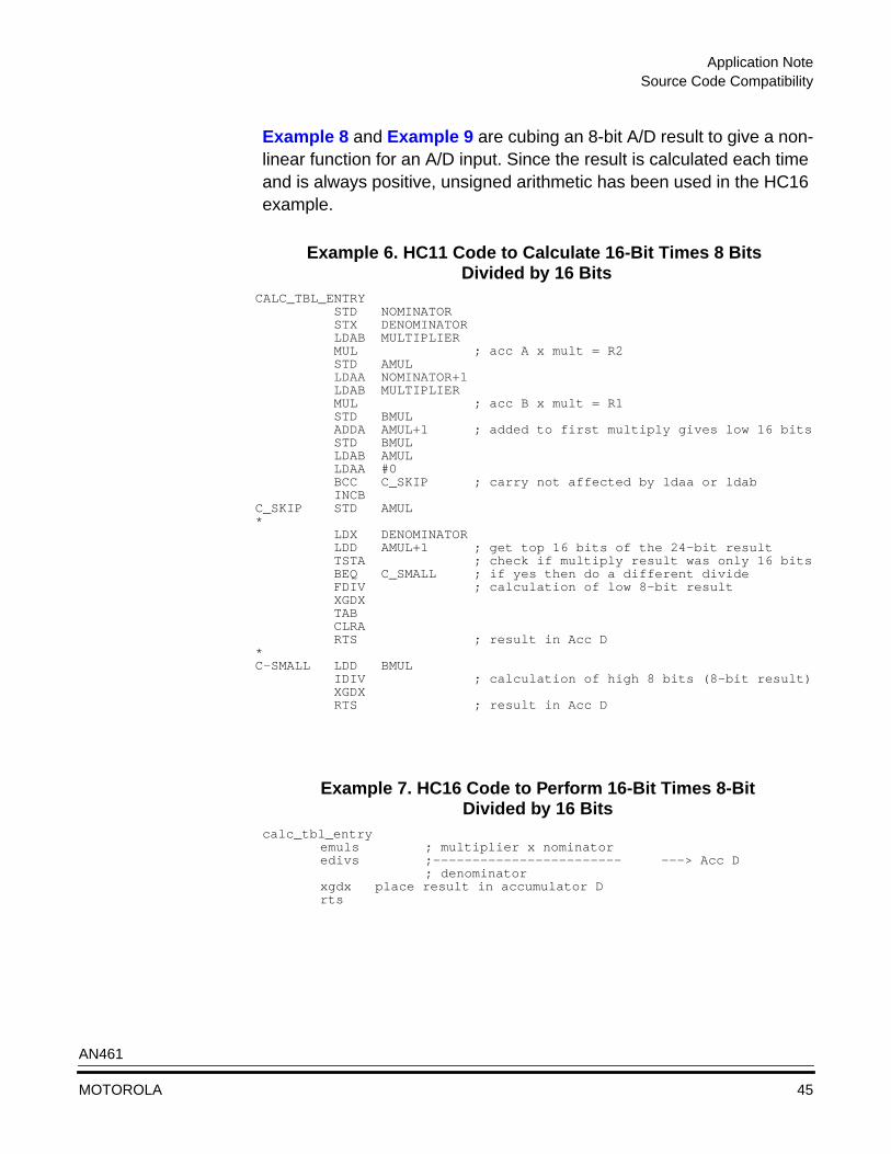
Application NoteSource Code Compatibility
Example 8 and Example 9 are cubing an 8-bit A/D result to give a non-linear function for an A/D input. Since the result is calculated each timeand is always positive, unsigned arithmetic has been used in the HC16example.
Example 6. HC11 Code to Calculate 16-Bit Times 8 Bits Divided by 16 Bits
CALC_TBL_ENTRYSTD NOMINATORSTX DENOMINATORLDAB MULTIPLIERMUL ; acc A x mult = R2STD AMULLDAA NOMINATOR+1LDAB MULTIPLIERMUL ; acc B x mult = R1STD BMULADDA AMUL+1 ; added to first multiply gives low 16 bitsSTD BMULLDAB AMULLDAA #0BCC C_SKIP ; carry not affected by ldaa or ldabINCB
C_SKIP STD AMUL*
LDX DENOMINATORLDD AMUL+1 ; get top 16 bits of the 24-bit resultTSTA ; check if multiply result was only 16 bitsBEQ C_SMALL ; if yes then do a different divideFDIV ; calculation of low 8-bit resultXGDXTABCLRARTS ; result in Acc D
*C-SMALL LDD BMUL
IDIV ; calculation of high 8 bits (8-bit result)XGDXRTS ; result in Acc D
Example 7. HC16 Code to Perform 16-Bit Times 8-BitDivided by 16 Bits
calc_tbl_entry emuls ; multiplier x nominator edivs ;------------------------ ---> Acc D
; denominator xgdx place result in accumulator D rts
AN461
MOTOROLA 45

Application Note
Example 8. HC11 (8-Bit x 8-Bit x 8-Bit) / 9-Bit********************************************************************* CALCULATE THE NUMBER OF PULSES FOR A, D, S, R* Acc A contains the A/D value for calculation* Acc D contains result** f(x) = (ad_measured + 15) cubed / 400* or* f(x) = ( (AD_RESULT) x (AD_RESULT) x (AD_RESULT) ) / 400********************************************************************CALC_PULSES ; save A/D value temporarily
STAA TEMP_ADTABMUL ; A/D squaredCLR CALC_SHIFT
READ_5 CMPA #0BEQ READ_6 ; check if greater than 8-bit valueINC CALC_SHIFT ; if yes then continueLSRD ; keep track of divisionsBRA READ_5 ; divide by 2
READ_6 LDAA TEMP_AD ; go back and check for 8-bit resultMUL ; restore original A/D resultLDX #400 ; and obtain cubed valueIDIV ; offset for normalized valuesXGDX ; divide by offset for best values
READ_7 TST CALC_SHIFT ; place 16-bit result in acc DBEQ READ_8 ; check if had previously div by 2DEC CALC_SHIFT ; if not then finishLSLD ; keep track of multipliesBRA READ_7 ; go back and check if all mults done
READ_8 RTS ; result in Acc D
Example 9. HC16 (8-Bit x 8-Bit x 8-Bit) / 9-Bit******************************************************************** calculate the number of pulses for a, d, s, r** acc B contains the A/D value for calculation* acc D contains result** f(x) = (ad_measured + 15) cubed / 400* or* f(x) = ( (ad_result) x (ad_result) x (ad_result) ) / 400**********************************************************************
**calc_pulses
clra ; ad_resulttde ; placed in accE (making sure upper byte=0)tba ;mul ; multiply accA and accBemul ; Multiply accD and accE (=24 bits E:D)ldx #400 ;ediv ; divide E:D by 400 scale factorxgdx ; place result in accDrts
AN461
46 MOTOROLA

Application NoteSource Code Compatibility
Comparisonof HC11 and HC16Code andBenchmarks
A rough estimate of the increased performance of the HC16 over theHC11 is that at 16.78-MHz clock the HC16 is nine times faster at 8-bitoperations than a 2-MHz HC11. Taking a theoretical 8-MHz bus speedHC11 and comparing it with the 16-MHz clock speed HC16 (8-MHz fasttermination bus speed), the performance differential is stillapproximately a factor of 2. This is largely due to the improved opcodeefficiency and pipeline of the CPU16 architecture.
For 16-bit and 32-bit calculations, the HC16 is even faster than theHC11.
Check Listof Changesto HC11 Code
• Set the K registers up correctly.
• Ensure the CPU registers are stack in interrupt routines.
• Remember to add exception routines for the additional vectors.
• Initialize the SIM and peripherals MCR register at the start of theprogram.
• Change the register equate addresses if using similar peripheralfunctions.
• Check actual timing of software delay loops.
• Make use of the interrupt and arbitration priorities correctly.
• Remember that the HC16 averages nine times the speed of the2-MHz bus HC11.
• Alter any code that manipulates the CCR. (The bits are movedabout.)
• Check for misaligned stack addressing using PSHA, PSHB, etc.
• Indirect 16-bit offset address operations are now signed values.
AN461
MOTOROLA 47

Application Note
Initialization of HC16 Device
PLL Control A significant change from the HC11 is the control of the clock frequency.The HC16 SIM module has a phase-locked loop (PLL) and a “limpmode” 8-bit oscillator built into the clock circuitry.
In normal operation, the SIM would have a 32-kHz crystal connected tothe EXTAL and XTAL pins. This frequency is then multiplied and phaselocked by the PLL to provide an internal clock frequency of up to 33 MHzin theory.
In practice, the maximum speed is currently restricted to 16.78 MHz.
Figure 10. Schematic Diagram of the PLL
SYSTEM CLOCK CONTROL
FEEDBACK DIVIDER
CRYSTALOSCILLATOR PHASE COMPARATOR LOW-PASS FILTER VCO
SYSTEMCLOCK
CLKOUT
VDDSYN
XFC
0.1 µF
VDDSYNXFC PIN 0.01 µF10 MXTALEXTAL
330 k20 pF 20 pF
0.1 µF
Notes:1. Must be low-leakage capacitor.2. EXTAL can be driven with an external oscillator.
(NOTE 1)
AN461
48 MOTOROLA

Application NoteInitialization of HC16 Device
After reset, the PLL is preset at 8-MHz clock frequency from a 32-kHzcrystal and so normally will be changed in the initialization section of theHC16 code.
NOTE: There is a 20-ms lock time for the PLL and altering the W-bit will,therefore, take this amount of time before the frequency has stabilized.Changing the X bit has an instantaneous effect since it is outside the PLLfeedback loop. As a consequence, it is necessary to check if a changeto the X bit will take the oscillator over 16.78 MHz before the effect of achange to the W bit takes effect.
An example is changing the oscillator from 8 MHz to 16.78 MHz wherethe W bit = 1 and X bit = 0 (SYNCR(15:8) = $8F). Writing $9F to theupper byte of SYNCR looks the same as writing $7F to SYNCR(15:8),but the latter would cause the oscillator to attempt to run at 33 MHz fora short time as the PLL changes frequency and would certainly causethe system a fatal error. The correct procedure is to write $3F toSYNCR(15:8) and then after the SLOCK bit is set to a 1 state (10 to20 ms later) write $9F to SYNCR(15:8).
A pin called MODCLK controls whether the PLL is enabled. Holding theMODCLK pin at a logic low during reset will disable to PLL and thesystem designer can then use an external high-frequency clock driverconnected to the EXTAL pin.
NOTE: It is not possible to connect a 16-MHz crystal to the EXTAL and XTALpins directly.
SRAM InitializationProcedure
The internal SRAM is disabled at reset. This is because the RAM is fullyrelocatable and the default start address is at the same location as thereset vectors. The SRAM base address registers should, therefore, bewritten and then the module configuration register written to enable theSRAM.
NOTE: The SRAM base address registers cannot be modified unless bit 15(STOP control) is set to a 1 (SRAM disabled) and bit 11(RLCK: RAM base address lock) is cleared. The RLCK bit is a 1-timewritable register after reset.
AN461
MOTOROLA 49
Application Note
When using the HC16Z1 evaluation board, it is often the case that amemory display window will be pointing to the RAM after it has beeninitialized. Typing the reset command will cause the HC16 device to bereset and the SRAM to be disabled again. The window will now showgarbage data unless it is pointing to a chip-selected address. In addition,any further EVB16 commands will try to update the memory displaywindow and could cause a string of DSACK errors as the EVB16software reads non-existent memory.
Stack Initialization Since the SRAM can be placed anywhere in the 1-Mbyte address space,it is obvious that the stack pointers will very likely be required to have thesame flexibility. The 20-bit stack pointer is set up by the reset vectors,and so it seems a good idea to move the SRAM to this location as soonas possible after reset.
Remember that the stack will decrement by two bytes and so the stackpointer is always set to an even address. As an example, assume thatthe SRAM is positioned at $14000 and since the MC68HC16Z1 hastwo Kbytes of SRAM, the top address is byte addressable RAM is$143FF. The stack would be initialized with the value SK = $1 andSP = $43FE.
When debugging code with the HC16Z1 evaluation board, the user mayfind debug of code simpler by adding initialization of the stack pointer tothe initialization code, even though it is loaded after issuing the RESETcommand on the EVB. Such an example is shown in Example 10 .
K RegisterInitialization
The 4-bit K registers are normally set up in the initialization routine of theHC16 along with any index register initialization just as one would do inHC11 code. Since the only way to access the K registers is viaaccumulator B, it is a simple matter to set up accB and copy the valueinto the appropriate K register.
The following code illustrates MC68HC16Z1 initialization of the SRAM,stack pointer, CSBOOT, GPT module and the K registers. Bycomparison, the HC11 routine is quite tiny.
AN461
50 MOTOROLA

Application NoteInitialization of HC16 Device
Example 10. MC68HC16Z1 Initialization Routinereset ldab #1
tbzktbsklds $ramstart+$03feldab #$0ftbekldab #rambase ; init rambase (=1)stab $fb05 ; rambah(low)ldd #ramstart ; (=4000)std $fb06 ; lower 16 bits = $4000clr $fb00 ; rammcr = $8000ldd #$78b0std csorbt ; set up csboot with 1 wait stateldab #$7f ; 16.777 mhzstab $fa04 ; syncrclr $fa21 ; sypcrldab #0 ; =0 for movedata subroutinetbxkldab #1tbykldz #0000ldd #$000f ; iarb=$fstd gptmcrldd #$9650 ; overflow=highest priority, irq level 6, vect=5xstd gpticrandp #$ff1f ; set cpu interrupt priority to 0 (lowest)
Example 11. HC11 Initialization CodeRESET LDS #$FF
CLI ; CLEAR INTERRUPT INHIBIT
Table 10. Registers that Must/Should be Written after Reset
SIMMCR SIM module configuration register
QSMMCR QSM module configuration register
ADCMCR ADC module configuration register
GPTMCR GPT module configuration register
SRAMMCR SRAM module configuration register
SYNCR PLL control register
CSPAR0 Action of chip select pins
CSPAR1 Action of chip select pins
CSPDR Chip-select port pins status – port C
PORTF Port F output pin status
DDRF Mode of operation of port F
PFPAR Bus control pin status – port F
AN461
MOTOROLA 51

Application Note
Mode SelectionDuring Reset
The SIM can be configured in several different ways out of reset. Thisallows for the basic functions of asynchronous data/address bus,data/program space selection and chip selects. To bring the HC16 outof reset in a particular mode of operation, simply pull the appropriatedata bus pin to logic 0 during reset. The best way to force the data pin isto connect the data bus to the outputs of a 74HC244 device and enableto outputs with the reset signal. Alternatively, a 2-kΩ resister can beused to condition the data bus pins with a small effect on the switchingcharacteristics of the data bus. The table of possible mode options isshown in Table 12 .
Reset Operation Reset of the HC16 is much like the HC11. An address is fetched from aknown area in the memory map and used to determine the start of theuser’s program.
The HC11 vector table contains the reset vector and interrupt vectorsstarting at $FFFE,$FFFF (16-bit address) and moving down the memorymap two bytes at a time with increasing priority. See Example 12 for anexample of the HC11 vector table.
Table 11. List of 1-Time Write Bits/Registers
SIMMCR (MM bit) SIM module address
SRAMMCR (RAMBAR bit) SRAM base address
SYPCR (entire register) System protection control register
AN461
52 MOTOROLA

Application NoteInitialization of HC16 Device
The HC16 has a similar approach with the exception that the table startsat $00000 and moves up the memory two bytes at a time. Prioritizationof the interrupts is described in Exception Handling (Interrupts) anddiffers significantly from the HC11. The HC16 reset vector actuallyconsists of four 16-bit values. These are the K register values for the ZK,SK, and PK registers, the 16-bit reset vector, the 16-bit stack pointeraddress, and lastly the 16-bit IZ register value. In effect, this is the 20-bitaddress of the reset vector and stack pointer plus a direct page addressof 20 bits.
The reset vector can, therefore, jump anywhere in the 1-Mbyte addressrange of the program space, but all other vectors are just 16 bits and socan only jump directly to the first 64-Kbyte address segment of programspace. From there, a JMP 20-bit address instruction will go anywhere inprogram space memory.
Table 12. SIM Configuration Out of Reset
Mode SelectPin
Default FunctionPin Left High
Alternate FunctionPin Pulled Low
DB0 CSBOOT 16-bit CSBOOT 8-bit
DB1CS0 16-bitCS1 16-bitCS2 16-bit
BRBG
BGACK
DB2CS3 16-bitCS4 16-bitCS5 16-bit
FC0FC1FC2
DB3DB4DB5DB6DB7
CS6 16-bitCS7–CS6 16-bitCS8–CS6 16-bitCS9–CS6 16-bit
CS10–CS6 16-bit
A19A20–A19A21–A19A22–A19A23–A19
DB8Bus control
DSACK0, DSACK1,AVEC, DS, AS, SIZE
PORTE
DB9 IRQ7–IRQ1 MODCK PORTF
DB11 Slave mode disabled Slave mode enabled
MODCK VCO = system clock EXTAL = system clock
BKPT Background mode disabled Background mode enabled
AN461
MOTOROLA 53

Application Note
The reason for including the IZ register is for compatibility with the HC11direct page instructions. These offer code efficient 8-bit operations andnow have the added feature of being anywhere in memory, rather thanjust between addresses $0000 and $00FF in the HC11.
Vectors, StackOperations
The first 512 bytes of address bank 0 (from $00000 to $001FF) arereserved for the vector or exception table. The first eight bytes arespecial, since these contain the reset vector data. This is followed by anumber of special vectors required to maintain system operation. Theseare directly related to the SIM and CPU operation. After this is space for200 user-defined vectors to be stored, each a 2-byte (16-bit) addresspointing to address bank 0 ($00200 to $0FFFF).
There are many differences from the HC11 vector table. The mostobvious is that the vector table starts at the beginning of the memorymap and increments up through the map compared with the HC11vector table starting at $FFFE,F and decrementing the address twobytes at a time for each vector. The HC11 has fixed vectors always16 bits in length, but the HC16 has vectors set up for most peripheralmodules by the user and the reset vector has substantially moreinformation in eight bytes. There are also a number of new vectors notfamiliar to the HC11 user. These are explained later.
Exception RoutineAddress
There are many more interrupt sources possible in an HC16 system. Toallow maximum flexibility and maintain compatibility with the 68000exception handling and external bus protocol, the internal peripherals donot have fixed predetermined exception vectors like the HC11.
Each peripheral may have the exception vector number initialized afterreset, and it is up to the user to maintain these correctly. In addition, thescheme allows any external device to be initialized with its own vectornumber so there are no restrictions on the mix of peripheral devices.
AN461
54 MOTOROLA

Application NoteInitialization of HC16 Device
User-DefinedVectors
The user vector number is initialized for each module or interrupt source.Some modules or submodules may have just a single vector, such asthe PIT, while others, such as the GPT, have 12 vectors associated withthe module. The vector number is an 8-bit value that, when multiplied by2, becomes the vector address of the first exception vector for thatmodule or peripheral.
An example of the HC16 vector table is shown in Example 13 . Thisshows that for the GPT the vector number is set to $38 (decimal 56).
This can be compared with the definition of the HC11 and HC16 vectortables that follow. Note the different start addresses and direction downthe vector table.
New Vectorsfor HC11 Users
The divide-by-zero interrupt is caused by a failure of the extended divideinstructions from the CPU16. The bus error exception is explained inExternal Hardware Interfacing , covering hardware design andbasically occurs as a result of a read of non-existent memory. Thebreakpoint vector is associated with background mode. This leaves aspurious interrupt where the SIM cannot determine the source of theinterrupt, the uninitialized interrupt, which is the default value for aninterrupt on 68000 peripheral devices and, finally, the autovectors. Thelatter are most likely treated as XIRQ and IRQ pins by HC11 users.These are directly linked to the IRQ1 to IRQ7 pins of the SIM and providethe user with general-purpose interrupt vectors for non-68000 peripheraldevices.
Remember that the order of the vectors is not linked to the priority of theinterrupt and so, for example, the IRQ1 vector comes before the IRQ2vector. There is, of course, a hierarchy of priorities for the exceptionprocessing, and this can be found in the SIM reference manual.
AN461
MOTOROLA 55

Application Note
Reset StatusRegister
After a reset, this register can be checked to determine the source of thereset for the HC16 device. This register is at $FFA06.
Sources of reset are:
• External reset
• Power-up reset
• Software watchdog reset
• Halt monitor reset
• Loss of clock reset
• System reset; from CPU32 and not available from CPU16
Example 12. Definition of HC11 Vector TableORG $FFD6
VECTORSFDB SCI_interrupt ; SCIFDB SPI_interrupt ; SPIFDB PAC_interrupt ; PULSE ACC INPUTFDB PAC_overflow ; PULSE ACC OVERFLOWFDB OVERFLOW ; TIMER OVERFLOW 1FDB IC4_INT ; INPUT CAPTURE 4 / OUTPUT COMPARE 5FDB OC4_INT ; OUTPUT COMPARE 4FDB OC3_INT ; OUTPUT COMPARE 3FDB OC2_INT ; OUTPUT COMPARE 2FDB OC1_INT ; OUTPUT COMPARE 1FDB IC3_INT ; INPUT CAPTURE 3FDB IC2_INT ; INPUT CAPTURE 2FDB IC1_INT ; INPUT CAPTURE 1FDB RTI ; REAL TIME INTERRUPTFDB IRQ ; IRQFDB XIRQ ; XIRQFDB swi_interrupt ; SWIFDB illegal ; ILLEGAL OPCODEFDB cop_interrupt ; COPFDB RESET ; CLOCK MONITORFDB RESET ; RESET
AN461
56 MOTOROLA

Application NoteInitialization of HC16 Device
Table 13. Vector Table Definition for the HC16
VectorNumber
VectorAddress
SPACE(prog/data) Exception
0 0000 P Reset — Initialize ZK, SK, PK
1 0002 P Reset — Initial PC (start of user prog)
2 0004 P Reset — Initialize SP
3 0006 P Reset — Initialize IZ (direct page)
4 0008 D Breakpoint (BKPT)
5 000A D Bus error (BERR)
6 000C D Software interrupt (SWI)
7 000E D Illegal instruction
8 0010 D Divide by zero
9-14 0012–001C D Unassigned
15 001E D Uninitialized interrupt
16 0020 D Unassigned
17 0022 D Level 1 interrupt vector (autovector)
18 0024 D Level 2 interrupt vector (autovector)
19 0026 D Level 3 interrupt vector (autovector)
20 0028 D Level 4 interrupt vector (autovector)
21 002A D Level 5 interrupt vector (autovector)
22 002C D Level 6 interrupt vector (autovector)
23 002E D Level 7 interrupt vector (autovector)
24 0030 D Spurious interrupt
25–55 0032–006E D Unassigned
56–255 0070–01FE D User-defined interrupt vectors
AN461
MOTOROLA 57

Application Note
Example 13. Actual HC16 Vector Tableorg $0
k equ $0110 ; not used, zk=$1, sk=$1, pk=$0sp equ ramstart+$03fe ; stack pointer starts at address $43feiz equ $0000 ; index pointer set for registers
org vectorsfdb k ; initial zk, sk, pkfdb reset ; initial program counter valuefbd sp ; initial stack pointer valuefdb iz ; initial direct page select (iz)fdb bkpt_int ; breakpoint addressfdb bus_err ; bus error addressfdb swi_int ; swi interrupt addressfdb illegal ; illegal instruction addressfdb div_by_0 ; divide by zero
dumy1 rmb 6 ;dumy2 rmb 6 ;
fdb un-initialised ; uninitialised interruptfdb reset ; reservedfdb int_1 ; level 1 interrupt autovectorfdb int_2 ; level 2 interrupt autovectorfdb int_3 ; level 3 interrupt autovectorfdb int_4 ; level 4 interrupt autovectorfdb int_5 ; level 5 interrupt autovectorfdb int_6 ; level 6 interrupt autovectorfdb int_7 ; level 7 interrupt autovectorfdb spurious ; spurious interrupt
end_main_vect equ *org $70fdb itic1 ; highest priority within GPT module
; - any of below can be selectedfdb itic1fdb itic2fdb itic3fdb itoc1fdb oc2_intfdb itoc3fdb itoc4fdb iti4o5fdb ioverflowfdb ipulse_ovrfdb ipactl ; lowest priority within GPT module
AN461
58 MOTOROLA

Application NoteException Handling (Interrupts)
Exception Handling (Interrupts)
Interrupt RequestHandling
Interrupts are called exceptions in the HC16 world. This conforms to thenomenclature of the 68000 processor and more accurately explains thenature of the sudden change in the activities of the CPU. Interrupts will,therefore, be referred to as exceptions from now on.
Module DesignInfluenceon the Conversionfrom HC11to HC16 Code
Many of the HC16 modules are clearly based on the functionality of anHC11 module. A prime example of this is the general-purpose timer(GPT) timer module. The main difference lies in the IMB interface andthis required some specific initialization of the interrupt vectors,arbitration, etc. After this, there is often a modulus prescaler where theHC11 had a choice of just divide-by-two options before and this isnecessary to accommodate the variable system clock frequencypossible with the PLL. In addition to this, the module may also operateat higher maximum speeds, greater functionality, and generally be moreflexible in its operation. All the peripheral modules have 16-bit wideregisters and in general a much greater flexibility of operation than anequivalent HC11 module.
As an example, we will look at the GPT for the HC16 as we set up themodule for interrupt handled events. This module is based upon thetimer used on the HC11E9 and the HC11F1, but has a number ofimportant differences.
Setting Upan InternalException
Both internal and external exceptions are basically handled the sameway.
An exception starts when an interrupt source pulls an IMB or externalIRQ line low (active state). The SIM responds with an interrupt cycle(CPU space) and waits for acknowledgment from the interrupt source.Any interrupt must generate an interrupt acknowledge (IACK) cycle. Thislets the SIM know that the interrupt source is still available and it will thentake control of the bus.
AN461
MOTOROLA 59
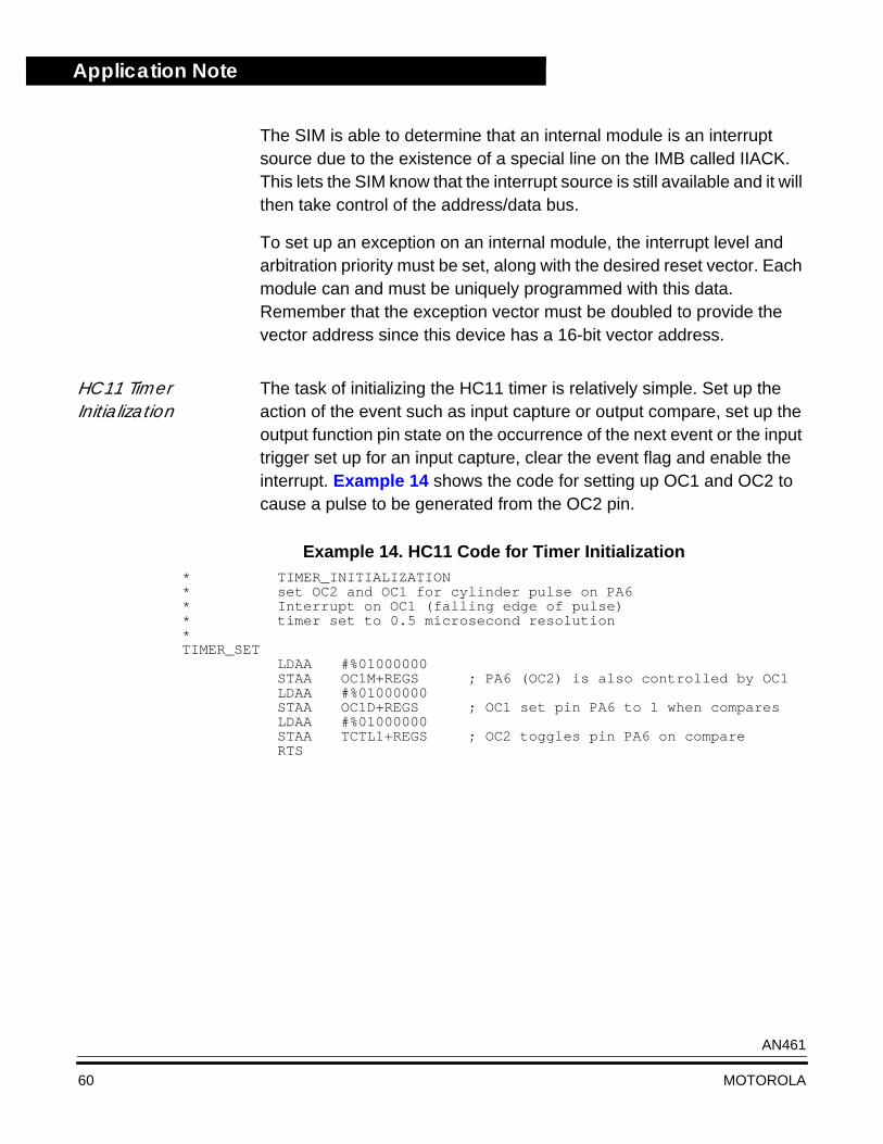
Application Note
The SIM is able to determine that an internal module is an interruptsource due to the existence of a special line on the IMB called IIACK.This lets the SIM know that the interrupt source is still available and it willthen take control of the address/data bus.
To set up an exception on an internal module, the interrupt level andarbitration priority must be set, along with the desired reset vector. Eachmodule can and must be uniquely programmed with this data.Remember that the exception vector must be doubled to provide thevector address since this device has a 16-bit vector address.
HC11 TimerInitialization
The task of initializing the HC11 timer is relatively simple. Set up theaction of the event such as input capture or output compare, set up theoutput function pin state on the occurrence of the next event or the inputtrigger set up for an input capture, clear the event flag and enable theinterrupt. Example 14 shows the code for setting up OC1 and OC2 tocause a pulse to be generated from the OC2 pin.
Example 14. HC11 Code for Timer Initialization* TIMER_INITIALIZATION* set OC2 and OC1 for cylinder pulse on PA6* Interrupt on OC1 (falling edge of pulse)* timer set to 0.5 microsecond resolution*TIMER_SET
LDAA #%01000000STAA OC1M+REGS ; PA6 (OC2) is also controlled by OC1LDAA #%01000000STAA OC1D+REGS ; OC1 set pin PA6 to 1 when comparesLDAA #%01000000STAA TCTL1+REGS ; OC2 toggles pin PA6 on compareRTS
AN461
60 MOTOROLA

Application NoteException Handling (Interrupts)
HC16 Codefor GPT InterruptInitialization
The HC16 has several different timers, but the GPT design is basicallytaken from the MC68HC11E9 timer. As a consequence, there is verylittle difference in the main part of the setup procedure. There are someadditional lines of code to set up the GPT module exception vector baseaddress, interrupt level, arbitration, and timer prescaler.
In the code in Example 15 , we can see the GPT being initialized forinterrupts from output compare 2.
NOTE: 1. The vector number (5) is part of the GPTICR register and sets upthe vector number to be from $50 onward. This means the vectortable starts at $A0.
2. The GPTICR also contains the interrupt level (level 6 is used inthis example) and the highest priority vector adjustment just as ispossible with the HC11.
3. The arbitration priority is set to the maximum of $F. This is notrequired, but the timer is usually the highest priority event. Butremember that the IRQ level is much more important than thearbitration level for prioritization of interrupts.
4. Some registers only have half of the 16 bits written in this example.This is because the reset condition of the vectors is used.
5. The output OC2 must be specifically made an output of the OC2function. The default would be an input general-purpose port line.
6. Just as with the HC11, the OC1 function can drive the OC2 pin.
7. The interrupt capability is enabled finally and the timer is fullyinitialized. Remember to set the prescaler selection for the timer.
AN461
MOTOROLA 61

Application Note
AN461
Example 15. HC16 GPT Initialization for Interrupts on OC2**GPT registers*gptmcr equ $f900gptmtr equ $f902gpticr equ $f904gptport equ $f906oc1 equ $f908 :toc1 equ $f914toc2 equ $f916 :tct1 equ $f91etmsk equ $f920*
org $A0fdb ioverflowfdb itic1fdb itic2fdb itic3fdb itoc1fdb oc2_intfdb itoc3fdb itoc4fdb iti4o5fdb ioverflowfdb ipulse_ovrfdb ipact1
*********************************************************************** Timer_initialization** set oc2 and oc1 for cylinder pulse on oc2data* interrupt on oc1 (falling edge of pulse)* timer set to 0.5 microsecond resolution**********************************************************************
timer_setldab #$ftbek
ldd #$000f ; iarb=$fstd gptmcr
ldd #$000f ; overflow=highest prioritystd gptmcr ; irq level 6,vect=5x
ldaa #%00010000 ; oc2data (oc2) is also controlled by oc1ldab #%00010000 ; oc1 set pin oc2data to 1 when comparesstd oc1
ldaa #%00000001 ; oc2 toggles pin oc2data on comparestaa tct1
ldd #$1010 ; enable OC2 outputstd gptport
ldaa #%00010000 ; oc2 output compare interrupt enableldab #$00000001 ; set timer prescaler to divide by 8staa tmskrts
62 MOTOROLA

Application NoteException Handling (Interrupts)
Initializing the QSPI The QSPI was briefly described previously. The QSM reference manualhas a very good explanation of its use and good examples ofinitialization code. The code in Example 16 initializes the QSPI. The fourconfiguration registers are set up at the start of the user program andthen normally only require changes in a few bits during the rest of theuser software.
The steps are relatively simple:
1. Assign the pin functions in the QPAR register.
2. Configure the clock, SPI as master/slave, data size.
3. Set beginning and end of the queue, enable/disable wrap mode(continuous transmit) and enable interrupts.
4. Set up the command and transmit data in the appropriate queues.
5. Select any delay options as required and enable the QSPI.
The QSPI RAM model can be seen in Figure 9 .
Setting Upan ExternalException
The HC11 user is most likely to use the IRQx pins of the SIM to emulatethe functions of the IRQ and XIRQ pins of the HC11. The HC16 requiresthat an autovector (AVEC) cycle be returned to the SIM to complete theinterrupt acknowledge of an IRQ request. The simplest and cheapestway to do this is to use the built-in chip select control logic to generatean AVEC signal and so complete the interrupt acknowledge (IACK) cycleof the SIM. The later section on external memory control explains thechip select logic in more detail. There will be no need to use the chipselect as an output since it will be purely for the generation of an internalsignal for the SIM, but it does mean that particular chip select will bereserved for this purpose and cannot also be used as a chip-selectfunction for external memory, etc.
Example 16. Initialization of the QSPIQSPI_INIT
LDD #$1B7ESTD QPAR ; PCS1 active, enable SPI pins, make MISO inputLDD #$8008STD SPCR0 ; SPI master, inactive=0, leading edge, 1.05MHzLDD #$2069STD SPCR1 ; PCS to SCK delay=1.9 µs, transfer delay=200 µsLDD #$8F00STD SPCR2 ; SPI finished interrupt enable, end queue=$FLDD #$0200STD SPCR3 ; HALTA and MODE FAULT interrupt enabled
AN461
MOTOROLA 63

Application Note
In this instance, the chip select is a comparator checking for the CPUspace identifier on the upper four bits of the address bus (A(23:20) whichwill be $F. It also checks for the appropriate interrupt level that it isresponding to by placing this data on address A(3:1). All the otheraddress bits are set to logic 1. Hence, an autovector for level 2 will resultin $FFFF3 appearing on the address bus, and for autovector level 7(IRQ7) the address bus will issue $FFFFF.
An example follows that illustrates the implementation of the chip-selectlogic to generate an AVEC signal.
This example also illustrates the initialization of the software watchdog.This operates in exactly the same way as the HC11. On starting thewatchdog, it cannot be disabled until a reset occurs. A register called thereset status register ($FFA06) contains a number of flags that show thelast cause for reset in the HC16. One of these bits is a flag to indicatethe existence of a watchdog reset.
Table 14. Generating an Autovector and Initializing the WatchdogLDAB #$C0 ; enable the watchdog (COP)STAB SYPCR ; and set timeout period to 8 seconds
LDD #$FFF8 ; initialize Chip Sel Base Reg for AutovectorSTD CSBAR3 ; on an IACK cycle: A24-A11=$FFF8, blK_sz = 2KLDD #$7801 ; initialize Chip Sel Option Reg for Autovector:STD CSOR3 ; asynchronous, any Interrupt Priority Level
LDAB #$FF ; set port F pins to be IRQ pinsSTAB PFPAR ; this is redundant: it happens at reset
AUTOV: ; when IRQ6 is low, this autovector routine startsJSR SEND_STRINGRTI ; return to the main loop
AN461
64 MOTOROLA

Application NoteException Handling (Interrupts)
Periodic Interruptvs. Real-TimeInterrupt
The HC11 real-time interrupt (RTI) allows the user to generate “ticks” orregularly spaced events with four possible periods: 4.1 ms, 8.2 ms,16.4 ms, and 32.8 ms with a 2-MHz HC11 device.
The HC16 has a much improved version of this called the periodicinterval timer (PIT). As we have seen with other modules, the variablesystem clock frequency of the HC16 means that a modulus counterprescaler has replaced the four options of the HC11 to give a total of 255options for timer periods, plus an additional divide by 512. This results inperiods ranging from 122 microseconds up to 15.9 seconds.
The PIT clock source is the 32.78-kHz oscillator frequency (EXTAL) andnot the system clock.
The PIT can be set to have an interrupt level from 1 to 7, and it isimportant to set up the vector number (multiplied by 2 to give the vectoraddress).
NOTE: No flag is set and hence there is no clearing mechanism other than theexecution of the PIT exception handler after the interrupt occurs.
The next example shows some example code of initialization of the PITand also includes the vector and exception handler.
AN461
MOTOROLA 65

Application Note
DifferentException Levels
The CPU16 has seven discrete exception levels, compared with theHC11’s two levels. Level 1 is the lowest exception mask level andlevel 7 is the equivalent of the non-maskable interrupt (NMI) of the HC11(masked by its X bit in the CCR). Looking once again at the conditioncode registers in Figure 6 , it can be seen that there are bits I0, I1, andI2 on the CPU16 which replace the X and I bits of the HC11.
On the HC11, only the maskable interrupt (masked by the I bit) isavailable to the on-chip peripherals, whereas all seven levels arepossible for on-chip peripherals on the HC16.
External interrupt pins IRQ1, IRQ2 up to IRQ7 can each generate anexception request if the feature is enabled.
Table 15. Periodic Interval Timer Setup and Exception Handler; PIT demo code.picr equ $fa22pitr equ $fa24
; PIT INTERRUPT VECTORorg $70fdb pitint ; PIT interrupt vector
; PIT INITIALIZATION VECTORorg ROMCODEldd #$0110 ; period = 1 secondstd pitrldd #$0238 ; PIT vector $38, IRQ level 2std picrandp #$FF0F ; set cpu interrupt mask = 0bra *
; PIT INTERRUPT ROUTINE; assume EK=$Fpitint
pshm d,xldx #string
send_stringldaa 0,xbeq doneldab $fc0c ; scsrandb #1 ; wait for TDRE=1beq send_chstaa $fc0f ; scdraix #1bra send_string
done pulm d,xrti
string fcb ’The Z1 writes this using the PIT’ ,$0a, $0d, $00
AN461
66 MOTOROLA

Application NoteException Handling (Interrupts)
In this case, IRQ7 is the direct equivalent to the XIRQ pin of the HC11,and any of the others can be used as the HC11 IRQ pin.
One fundamental difference is the fact that all internal and externalexception requests are handled in exactly the same way by a singlesection of the system integration module (SIM).
Level 0 exception is effectively disabling the interrupt source.
Arbitration The exception scheme is taken directly from the 68000 and latermicroprocessors where there could be very many different interruptsources. Seven separate levels of exception mask is a great help, but ina complex system there is a need for an even greater control ofexception priorities. For this reason, the concept of arbitration wasdeveloped and is implemented on the HC16 in the SIM to be precise.There are four arbitration bits available to the programmer that will allow15 discrete levels of exception priority for each exception level. It isimportant that every exception source is given a non-zero arbitrationpriority so that only one exception source must have a unique arbitrationpriority for a given exception level or even the arbitration logic will beunable to differentiate between two sources of the same exception level.
Remember that even the external exception source must also haveunique arbitration priorities. IARB = 1 is the lowest practical value ofarbitration.
There is little chance of running out of exception levels and priorities asthere are a total of 115 active levels.
An arbitration level of 0 means that the internal arbitration is switched offand so it will not be possible to have the CPU16 service an interrupt fromsuch a source. This is because IARB = 0 disables the internal interruptacknowledge (IIACK) signal and so the CPU cannot see the source ofthe interrupt and defaults to the spurious interrupt vector.
AN461
MOTOROLA 67

Application Note
Same ExceptionLevel
Several exceptions set at a single exception level are commonplace inHC11 applications and are equally possible on the HC16. Just as onewould expect, an exception request of a given level locks out all otherexceptions of that same level and lower. Similarly, as for the HC11, theexception vector is decided after the stacking operation of the CCR andPC registers is completed.
NOTE: Here the CPU16 will stack fewer registers and consequently fetches theexception vectors very much faster than the HC11. The reducedexception latency is generally a great advantage when converting codefrom the HC11.
Multiple ExceptionEvents
When several exceptions occur simultaneously, the highest level ofexception and arbitration will normally win. Also, a subsequent higherlevel of exception can interrupt a lower level exception routine.
For example, assuming a level 3 exception is in progress when a level 4exception occurs. The level 4 exception is not masked out and will causethe system to stack the PC and CCR and then start executing thelevel 4 exception routine. The exception mask is now set to 4 and so asubsequent level 4 exception of any arbitration level cannot exceptionuntil the exception mask has dropped below level 4 once more. This willhappen as the RTI of the first level 4 routine restores the CCR. At thispoint, the pending level 4 exception immediately takes control and thelevel 3 exception must wait a while longer before resuming its task.There is a short (2 µs to 4 µs) delay from the interrupt event occurringand the CPU fetching the vectors. During this time, other interrupts mayoccur of the same or higher interrupt level. It is during this period that thearbitration takes place.
See examples in Figure 11 where three types of events can occur.
AN461
68 MOTOROLA

Application NoteException Handling (Interrupts)
Figure 11. Multiple Interrupts
MAIN ROUTINE MAIN ROUTINE
SAME INTERRUPT LEVEL 2 EXCEPTIONS OF THE SAME INTERRUPT LEVEL,EVENT B AT LEAST 2 µs AFTER EVENT A
INTERRUPT A(IVL = 4,
IARB = $7)
INTERRUPT B
(IVL = 4,
IARB = $9)
EXCEPTION AHANDLER
EXCEPTION BHANDLER
DELAY BEFORE EXCEPTION IS PROCESSED
ARBITRATION HAS NO EFFECT SINCE B OCCURS AFTER EVENT A VECTORS ARE FETCHED.
MAIN ROUTINE MAIN ROUTINE
ARBITRATION AT WORK 2 EXCEPTIONS OF THE SAME INTERRUPT LEVEL,EVENT B 0.5 µs AFTER EVENT A
EXCEPTION BHANDLER
EXCEPTION AHANDLERINTERRUPT A
(IVL = 4,
IARB = $7)DELAY BEFORE EXCEPTION IS PROCESSED
ARBITRATION TAKES EFFECT SINCE VECTORS HAVE NOT YET BEEN FETCHED.
INTERRUPT B
(IVL = 4,
IARB = $9)
HIGHER INTERRUPT LEVEL OCCURS DURING EXCEPTION PROCESS
MAIN ROUTINE MAIN ROUTINE
EXCEPTION AHANDLER
EXCEPTION AHANDLER
INTERRUPT A(IVL = 4,
IARB = $7)
INTERRUPT B
(IVL = 5,
IARB = $1)
EXCEPTION A IS INTERRUPTED AND EXCEPTION BHANDLER RUNS. WHEN B IS COMPLETE, A WILLRESUME AND COMPLETE ITS TASK AND RETURN TOTHE MAIN ROUTINE.
EXCEPTION BHANDLER
AN461
MOTOROLA 69

Application Note
PrioritizationSchemes
Prioritizing exceptions is normally self evident from the systemspecification, but when converting from HC11 code it is worth carefulconsideration where it is required on the HC16. The HC16 is much fasterthan the HC11 and most HC11 interrupt routines will not account for thepossibility of being interrupted themselves, so leaving all routines at thesame level of interrupt will normally work perfectly.
The flexibility of the exception scheme may seem rather daunting, butthere are just a few key points to remember:
1. Simultaneous exceptions of the same interrupt level are arbitratedon the basis of the IARB0–IARB3 bits in each of the modulecontrol registers and so these must be unique.
2. An exception of the same level as the current exception maskcannot be executed until the mask level reduces below thatpending exception level except for level 7 exceptions.
3. A higher level exception will interrupt a lower exception levelroutine which must then wait until the exception mask hasreturned to its level before continuing.
4. Level 7 exception is highest interrupt level and is a non-maskableexception that can be interrupted by another level 7 exception.
5. An arbitration level of 0 will cause a spurious interrupt if anyinterrupt occurs from that module.
Exception RoutineEntry Latency
An HC11 interrupt takes the same amount of time as the SWI instructionto get into the interrupt routine (14 cycles) but the CPU16 exception mustalso clear the pipeline in addition to the operations common with the SWIcommand and so the SWI command takes 16 cycles while the exceptiontakes 20 cycles (4 to reload 2 stages of the 3 stage pipeline).
If exception latencies are the reason for moving to the HC16, thenremember that the first line of the exception routine is guaranteed toexecute and could be a PSHM instruction. Making the first instruction aNOP will reduce the time from a maximum of 18 cycles down to just2 cycles in addition to the 20 cycles entry latency and 38 cycles for theworst case instruction (EDIVS).
Included later are two exception routines that perform the same task,one for the MC68HC11E9 and the other for the MC68HC16A1. Thesimilarity of the two routines is the most striking feature and emphasizesthe ease of code conversion. The differences are easily seen and willinvariably follow the same approach for any code conversion of anexception routine from HC11 to HC16.
AN461
70 MOTOROLA

Application NoteException Handling (Interrupts)
The first difference is to remember to save the registers that are to beused in the exception routine, but not necessarily those that are used forglobal variables. As we can see, the accumulator D, IX, and K registersare all changed within the routine, but the IZ register is used as a globalregister and contains the base address of SRAM and so is not saved onthe stack. At the end of the routine, the registers are pulled back off thestack with the same syntax as pushed onto the stack. The assemblerorders the registers to ensure that the unstacking order is reversed.
The XK register is different in the exception routine and so must beinitialized. This requires the use of accumulator B to make use of theTBXK instruction.
In terms of execution speed, the HC16 manages to perform the entireexception routine in 5.76 µs where the HC11 takes 35.5 µs. Also, theworst case latency reduces to 2.3 µs from the HC11’s 20.5 µs.
Example 17. HC11 Timer Output Compare 2 Interrupt Routine| <--A---><---B----><--C---> || +----------+ || | | |
--- --------+ +--------| ---------------- A + B + C = 331 cycles A = 331 cycles – 258 ---> minimum low state (73 cycles) B = PWM duty (256 – 2 cycles) PWM frequency is 6.7 kHz (timer clock is same as bus clock)
Subroutine below takes 32 cycles (including interrupt latency)until the output compare 1 is re-armed, plus an IDIV or FDIVinstruction may start executing with max 41 cycles left before done.Thus min period for this must be 331 cycles since the risingedge of the pwm must occur after the OC1 is re-armed.
Routine takes 71 bus cycles to complete (35.5 µs at 2 MHz)with a worst case entry latency of 41 bus cycles (20.5 µs at 2 MHz)
; 14 interrupt latencyOC2_INT LDX TEMP_X ; 4
LDD TOC1+REGS ; 5ADDD #PERIOD ; 4 256 (max PWM) + 2 + (max time) before
; switch to other table is completeSTD TOC1+REGS ; 5 write OC1
* The OC1 reg has been updated so this is the point at which the routine* must get to before OC1 has to go high. Worst case is when OC2 has* maximum delay (max duty cycle).
ADDD 2,X ; 6 get new compare for OC2 (added to OC1)ADDD #2 ; 4 prevent OC’s occurring simultaneouslySTD TOC2+REGS ; 5 write OC2LDAA #%01000000 ; 2STAA TFLG1+REGS ; 4 clear OC2 flag
* Note that OC2 only occurs soon after OC1 when there is plenty of time* for the interrupt routine to execute (over 300 cycles) and so the* OC2 flag may be cleared after updating the OC2 register.
INX ; 3INX ; 3 increment X index by 2STX TEMP_X ; 4INC TABLE_POINTER ; 6 increment A/D output counterRTI ; 12
AN461
MOTOROLA 71

Application Note
Example 18. HC16 Timer Output Compare 2 Exception Handler|<--a---><---b----><--c---> || +----------+ || | | |
---|-------+ +--------|---------------- a + b + c = 310 timer counts a = 310 cycles – 258 ---> minimum low state (52 timer counts) b = pwm duty (256 – 2 timer counts) PWM frequency is 15 kHz (timer clock is system clock divided by 4)
The minimum pulse width is 2 timer clocks.The PWM is 8 bits (256 timer clocks)The subroutine below takes 52 cycles (including interrupt latency)until the output compare 1 is re-armed, plus an edivs instruction maystart executing with max 38 cycles left before done. Thus the minimumperiod for this must be 90 cycles (23 timer counts) since the risingedge of the pwm must occur after the oc1 is re-armed.
Entry conditions :ZK:IZ points to SRAMlocation temp_x,Z is temporary save of IX register
Routine takes 96 clock cycles (5.76 µs at 16.66MHzwith a worst case entry latency of 38 clock cycles (2.28 µs at 16.66MHz
; 20 interrupt latencyoc2_int pshm d,x,k ; 10 save accD,IX and K on stack
ldab #1 ; 2 set up accB=1 ready for TBXK
tbxk; 2 and point IX to data space; segment 1
ldx temp_x,z ; 4ldd toc1 ; 5addd #period ; 4 256(max pwm) + 2 + (max time)
; before switch to other table is completestd toc1 ; 5 write oc1
* the oc1 reg has been updated so this is the point at which the routine* must get to before oc1 has to go high. worst case is when oc2 has* maximum delay (max duty cycle).
addd 2,x ; 6 get new compare for oc2(added to oc1)addd #2 ; 4 prevent oc’s occurring simultaneouslystd toc2 ; 5 write oc2bclrw tflg,oc2f ; 4 clear oc2 flag
* note that oc2 only occurs soon after oc1 when there is plenty of time* for the exception routine to execute and so the* oc2 flag may be cleared after updating the oc2 register
aix #2 ; 3 increment x index by 2stx temp_x,z ; 4inc table_pointer,z ; 6 increment D/A output counterpulm d,x,krti ; 12
AN461
72 MOTOROLA

Application NoteExternal Hardware Interfacing
External Hardware Interfacing
Asynchronous vs.Synchronous Bus
The HC11 address and data bus is called a synchronous bus since allthe timing is derived from the address strobe (AS) and E clock. The68020 devices have an asynchronous bus where the MPU has a numberof additional pins that act as handshakes for the bus communication. Ineffect, this allows a fast or slow external device to communicate with theMPU, and the MPU must wait for a handshake from the peripheraldevice before continuing with the portion of the bus cycle.
The HC16 uses the techniques from the 68020 devices but has theaddition of chip-select circuitry to allow the user to control the entire buscycle from the HC16. In the case of conversion from HC11 to HC16, it isalmost certain that the user will make extensive use of the chip-selectlogic to reduce external hardware and access external peripheraldevices.
The SIM reference manual describes the bus in great detail, but for avery basic look at the bus, we will look at using two external 6226(128-Kbyte) SRAM devices will the HC16.
The chip-select logic lets the user program a specific set of conditionsfor the chip selects to function. This includes qualification withaddress/data strobes, address bus A(23:11), type of address space,etc., and the chip select has a base address and block size over whichit will function.
To overcome the asynchronous bus, the chip-select logic generates theDSACK signals that would normally come from an external peripheralcircuit. These can be programmed in terms of wait states. This refers tothe number of bus cycles that the HC16 must wait before it can completethe bus cycle to read or write to the peripheral device. One wait state isthe equivalent of 60 ns at a 16.66-MHz clock.
If the DSACK signal is not received within the time set up by the busmonitor (64 cycles default value), then the bus error (BERR) signal isasserted. This indicates the possibility of non-existent memory at thisaddress. A second consecutive bus error indicates that the CPU iscompletely lost and so the SIM will force a reset.
NOTE: The bus monitor is disabled after reset.
AN461
MOTOROLA 73

Application Note
The CSBOOT line is the only chip select to be active after reset. Itsdefault settings are address strobe, upper and lower data busread/writes, asynchronous mode, and 13 wait states. This allows for theslowest external memory and so will normally be altered immediatelyafter reset to speed up the communication with the memory to thedesired rate (normally, the fastest the memory can operate at). A chipselect with zero wait states equates to a chip select access time of 85 ns(with a 16.78-MHz clock).
If there is only a single external memory, then the chip-select pins maynot be required to be connected to the memory device. This wouldassume that the user had no other external bus devices and so noproblems with bus contention. This would give an address access timeof 114 ns at zero wait states, but remember that the chip-select logicmust be configured for this memory or there will be no generation ofDSACK when accessing external memory and the memory will not beaddressable. The chip select logic is, therefore, essential to theoperation of external memory even if the memory has the chip-enablepin permanently connected to ground.
Wait States A wait state is a function of the asynchronous bus of the SIM. Normally,a 68000 system would have a mixture of different memory types withvarying address access times. To accommodate this, the address/databus sends out the address and then waits for handshaking signalsbefore reading the data bus. To make this system operate as simply aspossible, the chip-select logic in the SIM allows for a number of buscycles to remain unchanged while the external memory fetches the datathat it will output on the bus. By adding a clock cycle to the fastest normalbus cycle as a built-in delay is known as a wait state. At 16.66 MHz, thistranslates to 60 ns per wait state.
AN461
74 MOTOROLA

Application NoteExternal Hardware Interfacing
Fast Termination(SynchronousTiming)
Fast termination is a special case of address/data bus timing that is mostcommonly used with the internal peripheral modules and takes just twoclock cycles to complete, compared with a zero wait state memoryaccess of three clock cycles. In effect, this is the equivalent to the HC11type of address/data bus cycle as it is synchronous with the CPU internalclock.
NOTE: All the cycle times for instructions are shown in terms of fast termination.An external memory must have an access time of 35 ns to be able tooperate fast termination mode with a 16.78 MHz HC16. This compareswith the 4-MHz HC11F1 (non-multiplexed) memory address access timeof 100 ns.
Using Chip Selects The chip selects take care of all the address and bus control comparelogic required to drive external memory devices. A single-chip select canbe eight or 16 bits wide and general chip-select signals and a range ofaddresses with a resolution of two Kbytes anywhere in the addressrange of the HC16 device.
Further options are upper/lower data bus, read, and/or write, wait states,type of address space, qualification on a read cycle with address strobeor data strobe and asynchronous or synchronous control.
The additional control of interrupt priority level (IPL) and AVEC are justfor an alternative function of the chip-select logic to generate AVEC foran external IRQ as described in the previous section on exceptionprocessing.
8-Bit and 16-BitRead/WriteAccess to 8-BitWide MemoryDevices
In the following example, three chip selects are connected to two 32-kby 8 bits wide RAM devices (MCM60L256AP10) with 100 ns accesstime. CS2 is connected to the output enable pins of both devices, whileCS0 and SC1 are connected to the write enable pins of the evenaddressed and odd addressed memory devices, respectively. This is thearrangement to be found for controlling the two optional RAMs (U1 andU3) on the HC16Z1 EVB.
AN461
MOTOROLA 75

Application Note
We will put the memory at address range $80000 up to $8FFFF (64-krange). There are two 8-bit wide memories, and these attach in parallelto the 16-bit wide data bus. Address A0 effectively determines whichdevice is written to, but A0 is not connected to the device because wewill set up the chip-select logic to perform this task for us. Figure 15shows the actual device connections to the chip-select logic and HC16bus. This all means that the base address for both memories is $80000.
NOTE: Although the memories are 32 Kbytes, the block size is 64 Kbytes withthe two memories attached to different halves of the data bus.
Since CS0 is connected to the RAM on the upper eight bits of the databus, it is the even addresses, and CS1 controls writes to the RAM on thelower eight bits and becomes the odd addresses.
The memory devices in use are 100-ns access time, and since we areusing the chip selects to enable the device, we must take the accesstimes from the chip-select falling edge rather than the address bus validtime which is earlier. See Appendix C for a simplified timing diagram.This gives an access time required for zero wait states of 85 ns. This isclearly less time that the 100-ns device can manage, and so we mustuse one wait state timing which gives an extra 60-ns access time of145 ns.
Example 19. Initialization Code for 8- and 16-Bit Addressing of External MemoriesCSOR0 EQU $FF4CCSBAR0 EQU $FF4ECSOR1 EQU $FF50CSBAR1 EQU $FF52CSOR2 EQU $FF54CSBAR2 EQU $FF56CSPAR0 EQU $FA44
LDAB #$0FTBEK ; select bank 15 for direct writesLDD #$0803STD CSBAR0 ; set U1 RAM base addr to $80000: bank 3, 64kSTD CSBAR1 ; set U3 RAM base addr to $8000: bank 3, 64kLDD #$50B0STD CSOR0 ; set Chip Select 0, upper byte, write onlyLDD #$30B0STD CSOR1 ; set Chip Select 1, lower byte, write onlyLDD #$0803STD CSBAR2 ; set Chip Select 2 to fire at base addr $80000LDD #$78B0STD CSOR2 ; set Chip Selects 2, both bytes, read and writeLDD #$3FFFSTD CSPAR0 ; set Chip Selects 0,1,2, to 16-bit ports
AN461
76 MOTOROLA

Application NoteExternal Hardware Interfacing
Hardware for 8-Bitand 16-BitAddressing Using aSingle-Chip Select
It is normal practice to use the CSBOOT line to select two separatememory devices (often EPROMs) since this is the only chip select activefollowing reset. In some cases, however, it may be desired to write both8-bit and 16-bit values to a RAM which is selected using CSBOOT. Anexample of this is the HC16Z1 evaluation board where the mainemulation memory is selected by CSBOOT. The HC16 can read an 8-bitvalue correctly with a single chip select connected to both memoriesbecause the CPU16 will only read the relevant data. Writing a byte is adifferent matter and in the same setup as earlier, an 8-bit write wouldcause a write to both memories with the same data in each byte. Thus,a write of $55 would appear to be a write of $5555.
To cure this, the chip select must be gated with signals that indicate abyte write and the address to be written. The chip select is set up for16 bits, and rather than go directly to the output enable pins of bothmemory devices, is gated by the SIZ0 and A0 lines. The SIZ0 line is alogic 1 during a byte read or write operation and the address A0 line isused to determine which of the two memory devices is to be written to.SIZ1 indicates an even address read or write and so is not required inthe equation that follows because the function of the extra logic is toprevent writes to the wrong memory device. This approach makes theexternal logic much simpler.
Thus a simple logic equation results in two chip-select lines with slightlydelayed timing compared with the original chip select. The chip selectdelay is a maximum of 30 ns with the circuit described in Figure 12 .Thus, an 85-ns access time RAM would require an extra wait state to beadded to the chip-select access time (zero wait states in 85 ns at16.6 MHz).
Taking the chip select to be CSBOOT, we have the following equationsfor the high and low memory chip enable pins.
The logic equations are:
CSLOW = SIZ0 . A0 + CSBOOT
CSHIGH = SIZ0 ./A0 + CSBOOT
This can be done either by a PAL, such as a 16L8, or with two 74HC00devices.
AN461
MOTOROLA 77

Application Note
Figure 12. 8- and 16-Bit Address Read and Write Accesswith CSBOOT
VDDE vs. VDDIvs. VDDA
A device with so many different modules on board can be a real problemfor the designers. Some modules generate a great deal of noise on theVDD and VSS supplies because they are switching loads very quickly (forexample, address and data bus and I/O ports), while other modulesrequire as noise free a supply as possible (for instance, ADC and PLL).
To overcome some of these problems, the HC16 has four separatepower supplies.
VDDI and VSSI are the internal power supply pins. This powers up theCPU, SIM internal logic and the internal logic of other modules. Powerconsumption is relatively consistent, with few sudden changes inimpedance.
VDDE and VSSE are the power supply for the external pin logic. Thissupply can have large swings in current consumption as I/O pins switchon and off.
VDDA and VSSA are the supply for the analog-to-digital converter (ADC).Since the ADC module has a 10-bit accuracy, it is important to have aslittle noise on these power supply pins as possible. A 10-bit accuracymeans a resolution of just 3-mV peak to peak with a 3-volt referencevoltage differential.
NC
NC11
11
+5 V
12
13
12
13
1d
2d2c
2d 6
8
CSlow
CShigh3
9
10
81c
1a
1b
2a
6
3
5
4
2
CSBOOT
1
2
4
5
1
A0
SIZ0
10
9
BYTE AND WORD ADDRESSING USING CSBOOT
AN461
78 MOTOROLA

Application NoteExternal Hardware Interfacing
VDDSYN is a special power supply just for the PLL circuit. Just as with theADC, the PLL internal voltages are very susceptible to noise and theinternal analog section of the circuit is affected by changes in voltage ofas little as 5 mV. The effect of noise on VDDSYN is to alter the VCOfrequency by a small amount.
VSTBY for the SRAM standby power should be treated as for the VDDIsupply. It may also be grounded to avoid the SRAM being disabled by alowering of the VDDI supply below the VSTBY voltage.
Figure 13. Shows the Suggested Decoupling as Close to the HC16 Pins as Possiblefor These Pairs of Power Pins
MinimumRequiredConnectionsfor the SIM
The SIM is rather more complex than the address/data bus section of theHC11 and may take a while to learn, but many of the features havedefaults that enable the user to place the device into an application withthe minimum of fuss and with few external connections.
Figure 15 shows the HC16 in the same application as the HC11 inFigure 14 .
NOTE: Unused input pins should be tied to VSS or VDD via 10-kΩ resistors. Notethe changes to the address and data bus interface and the connectionsto the SIM module in particular.
0.1 µF CAPACITOR0.01 µF CAPACITOR
VDDE
VSSEHC16 DEVICE
VCC
VSSPLACE CAPACITORS AS NEARTO HC16 PINS AS POSSIBLE
AN461
MOTOROLA 79

Application Note
Points to note about the HC16 application include:
1. The HC16 data bus has internal pullup resistors internally in theSIM.
2. There are several power supply pin pairs, all of which must beconnected to power and each pair should be suppressed with a0.01 µF and 0.1 µF capacitor to reduce system noise. Takeparticular care over noise suppression on VDDSYN.
3. Mode selection after reset is set by the 74HC244 device.
4. The memories need doubling up to make full use of the speed ofthe HC16. A single 8-bit wide data bus can be used but reducesthe performance of the system significantly.
5. Four chip selects are used. The EPROM is byte and word readaccess, and the RAM is byte and word read and write access.
6. The EPROM uses A15 to select the device on the lower 32-k partof a 64-k block, the CSBOOT line selects the bank (in this casebank0).
7. Many pins can be input or output depending upon the mode afterreset, so pullup resistors have been shown in these cases. Manycould be removed for specific modes of operation.
AN461
80 MOTOROLA

Application NoteExternal Hardware Interfacing
Fig
ure
14. H
C11
with
Ext
erna
l Mem
ory
V DD
XT
ALEX
TAL
MC
68H
C11
E9
A0 /
D0
A1 /
D1
A2 /
D2
A3 /
D3
A4 /
D4
A5 /
D5
A6 /
D6
A7 /
D7
MO
DA
MO
DB
/VST
BY
PD5
/SS
PD4
/ SC
KPD
3 / M
OSI
PD2
/ MIS
OPD
1 / T
D0
PD0
/ RD
I
PA0
/ IC
3PA
1 / I
C2
PA2
/ IC
1PA
3 / I
C4
/ OC
5PA
4 / O
C4
PA5
/ OC
3PA
6 / O
C2
PA7
/ PAI
/ O
C1
IRQ
XIR
Q
RES
ET
V SS
AS ER
/ W A8 A9 A10
A11
A12
A13
A14
A15
AN0
AN1
AN2
AN3
AN4
AN5
AN6
AN7
V RH
V RL
10kΩ
47kΩ
47kΩ
10kΩ
10kΩ
47kΩ
47kΩ
10kΩ
10 n
FR
ESET
V DD
8 M
Hz
22 p
F22
pF
V SS
OEW
VCC
A14
A13
A12
A11
A10
A9 A7 A6 A5 A4 A3 A2 A1 A0
G
D0
D1
D2
D3
D4
D5
D6
D7
A15
ER
/W
V DD
LEO
E
74HC373
V DD
A0 A1 A2 A3 A4 A5 A6 A7
D0
D1
D2
D3
D4
D5
D6
D7
V DD
VCC
PGM
VPP
OE
CE
27C
128
16 K
BYTE
S
A15
A14
V SS
A13
A12
A11
A10 A9 A8 A7 A6 A5 A4 A3 A2 A1 A0
V DD
8 X
22kΩ
1kΩ
1µF
MC
M60
L256
32 K
BYTE
S
MC
68H
C11
E9 IN
EXP
AND
ED M
OD
E
A8
10 M
Ω
V DD
AN461
MOTOROLA 81
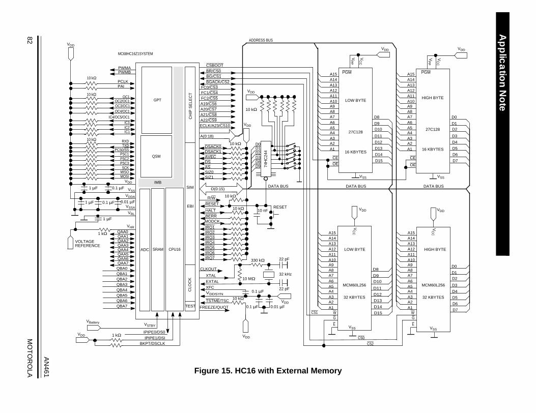
Ap
plic
atio
n No
te
82M
OT
OR
OLA
VDDVDD VDD
VC
C
VP
P
VDD
VC
C
VSS
VSS
MCM60L256
32 KBYTES
HIGH BYTE
D0
D1D2
D3
D4
D5
D6
D7
A15A14A13A12A11A10A9A8A7A6A5A4A3A2A1
CE
OE
D0
D1D2
D3
D4
D5
D6
D7
A15A14A13A12A11A10A9A8A7A6A5A4A3A2A1
HIGH BYTE
27C128
16 KBYTES
PGM
DATA BUS
ADDRESS BUS
E
WG
AN
461 Figure 15. HC16 with External Memory
GPT
QSM
CPU16SRAM
10 kΩ
10 kΩ
10 kΩ
RXDTXD
PCS0/SSPSC1PSC2PSC3
SCKMISOMOSI
OC1OC2/OC1
OC4/OC1
IC4/OC5/OC1IC3IC2IC1
OC3/OC1
1 µF
1 kΩ
0.1 µF1 µF 0.01 µF
1 µF 0.1 µF
VRL
VHR
VDD
VDDA
PWMAPWMB
PCLKPAI
QBA0QBA1QBA2QBA3QBA4QBA5QBA6QBA7
QAA0QAA1QAA2QAA3QAA4QAA5QAA6QAA7
VSTBY
IPIPE0/DS0
IPIPE1/DSIVDD
VBattery
BKPT/DSCLK
1 kΩ
TEST
CLO
CK
SIM
EBI
CH
IP S
ELE
CT
IMB
CSBOOTBR/CS0BG/CS1BGACK/CS2
FC0/CS3FC1/CS4FC2/CS5A19/CS6A20/CS7A21/CS8A22/CS9ECLK/A23/CS10
A(0:18)
DSACK0DSACK1AVECDSASSIZ0SIZ1
DD(0:15)
IRQ1IRQ2IRQ3IRQ4IRQ5IRQ6IRQ7
MODCKBERR
R/W
RESET
HALT
CLKOUT
FREEZE/QUOT
TSTME/TSC
VDDSYN
XFCEXTAL
XTAL
10 kΩ
0.01 µF0.1 µFVDD
VDD
10 MΩ
330 kΩ
32 kHz
22 pF
22 pF
VC
C
VP
P
VDD
VC
C
VDD
10 kΩ
74H
C24
4
VDD
D0D1D2D3D8D9
10 nFRESET
DATA BUS DATA BUS
10 kΩ
CEOE
VSS
VSS
LOW BYTE
MCM60L256
32 KBYTES
D8
D9D10
D11
D12
D13
D14
D15
A15A14A13A12A11A10A9A8A7A6A5A4A3A2A1
D8
D9D10
D11
D12
D13
D14
D15
A15A14A13A12A11A10A9A8A7A6A5A4A3A2A1
LOW BYTE
27C128
16 KBYTES
PGM
E
WG
CS1
CS0
CS2
10 kΩ
10 kΩ
ADC
VSS
VSSA
MC68HC16Z1SYSTEM
0.1 µF
VOLTAGEREFERENCE

Application NoteDebugging Tools
Debugging Tools
Background Mode Those experienced in using PCBUG11 for the HC11 device will findbackground mode on the HC16 very familiar. This mode is intended justfor debug purposes and would not normally be used in a finishedapplication, although the application could leave access to the mode forlater problem solving.
Background debug mode uses three dedicated pins that are the onlydirect connection to the CPU16. The communication with the CPU16 issimilar to the SPI synchronous serial communication, with a clock pin(DSCLK) and transmit and receive pins (DSO and DSI, respectively).
In general, the user will be unaware of the background mode operation,but it is used in most of the emulation systems and is the basis of theEVB for the MC68HC16. There is a small number of commands whichare built up by the software running on a PC to make up the normalemulator commands. Thus, a dump of a block of 256 bytes of memorywill be translated into 256 reads of memory contents at specifiedaddresses which are sequential. The programmer can enter thebackground debug mode with the CPU16 instruction BGND.
An ample explanation of the background mode can be found in theM68HC16 Family CPU Reference Manual, Motorola document ordernumber CPU16RM/AD.
Evaluation Board The EVB16 software on the IBM PC provides a sophisticated debug toolwith very little external hardware. The EVB16Z1 emulator for theHC16Z1 device has sockets for 128 Kbytes of RAM, the HC16Z1 device,of course, and a background mode connector to the PC via the parallelport of the PC. There is little requirement for much else as thebackground debug mode and the PC software provide a high degree ofdebug capability, including 256 instructions trace buffer and assemblysource level debug to name just two features. HP logic analyzer clipscan be used to perform real-time analysis of code running on the EVBvia the special groups of pins for these clips.
There is ample information available from Motorola concerning the EVBand other related products.
AN461
MOTOROLA 83

Application Note
Appendix A
Figure 16. MC68HC11E9 Device
EXPANDED
ADDRESS/DATE BUS
HANDSHAKE I/O
PORT B
DATA DIRECTION C
PORT C
SINGLECHIP
R/W
ASST
RB
STR
A
AD0
PC0
PC7
AD7
A8PB
0
PB7
A15
POWER
V SS
V DD
MODESELECT
MODA(LIR)
MODB(VSTBY)
OSCILLATOR
E
EXTAL
XTAL
INTERRUPTS
RESET
XIRQIRQ
M6811 CPU
A/D
VRL
VRH
POR
T E
PE0
PE7SCI TxD
RxD
SPI
SSSCK
MOSIMISO
DAT
A D
IREC
TIO
N D
POR
T D
PD0
PD5
RAM — 512 BYTES
EEPROM —512 BYTES
ROM — 12 KBYTES
POR
T A
PA7
PA0PERIODIC INTERRUPTCOP WATCHDOG
TIMER
PULSE ACCUM.
PAIOC2OC3OC4
IC4/OC5
IC1IC2IC3
OC
1
AN461
84 MOTOROLA

Application NoteAppendix B
Appendix B
Figure 17. MC68HC16Z1 Device
CO
NTR
OL
POR
T GP
OC1OC2/OC1OC3/OC1OC4/OC1IC4/OC5/OC1IC3IC2IC1
PWMAPWMBPCLKPAI
OC1
OC2/OC1
OC4/OC1
IC4/OC5/OC1IC3
IC2
IC1
GPT
CO
NTR
OL
POR
T GP
QSM
CPU16
SRAMADCC
ON
TRO
L
POR
T GP
CO
NTR
OL
CHIPSELECT
SIM
EBI
CLOCK
TEST
RXD
VDD
VSS
TXDPCS0/SSPSC1PCS2PSC3SCKMISOMOSI
TXDPCS0PSC1PCS2PCS3SCKMISOMOSISS
VDD
VHR
VRL
VSTBY
IPIPE0/DS0
IPIPE1/DSI
BKPT/DSCLK
ADA0ADA1ADA2ADA3ADA4ADA5ADA6ADA7
ADA0ADA1ADA2ADA3ADA4ADA5ADA6ADA7
DSCLKDSODSIIPIPE1IPIPE0BKPT
CO
NTR
OL
POR
T E
CO
NTR
OL
POR
T F
IRQ(1:7)
MODCK
MODCKIRQ1IRQ2IRQ3IRQ4IRQ5IRQ6IRQ7
CO
NTR
OL
TSCTSTMEQUOT
FREEZE
TSTME/TSCFREEZE/QUOT
EXTALXFC
VDDSYN
XTALCLKOUT
RESETHALTBERR
R/W
D(0:15)
DSACK0DSACK1AVECPE3DSASSIZ0SIZ1
DSAS
SIZ0SIZ1
DSACK0DSACK1
AVEC
A(0:18)
CSBOOT
CO
NTR
OL
POR
T C
CS0-CS10
BRBGBGACK
FC0FC1FC2
BR/CS0BG/CS1
BGACK/CS2FC0/CS3FC1/CS4FC2/CS5A19/CS6A20/CS7A21/CS8A22/CS9
ECLK/A23/CS10
IMB
VSS
A(19:23)
AN461
MOTOROLA 85

Application Note
Appendix C
Figure 18. Simplified HC16 Timing Diagram
S0 S1 S2 S3 S4 S5 S0
6 1
ADDRESS ADDRESS VALID
AS
WRITEREAD
27
DATA READ
CS
DATA
DATA
26
25
WAIT STATES INSERTED BETWEEN S3 AND S4
TIMING PARAMETERS1 – CLOCK PERIOD2 – HALF CLOCK PERIOD6 – CLOCK HIGH TO ADDRESS VALID9 – CLOCK LOW TO AS, DS, CS ASSERTED9A – AS TO DS OR CS ASSERTED (READ)25 – DS, CS NEGATED TO DATA OUT INVALID (DATA HOLD)26 – DATA OUT TO DS, CS ASSERTED (WRITE)27 – DATA IN TO CLOCK LOW (DATA SETUP)29 – DS, CS NEGATED TO DATA IN INVALID (DATA IN HOLD)
MIN 60 nsMIN 28 nsMAX 29 nsMAX 25 nsMAX 15 nsMIN 15 nsMIN 15 nsMIN 5 nsMIN 0 ns
AT 16.66 MHZCHIP SELECT = 1 + 1 – 9 – 27 = 60 ns + 60 ns – 25 ns – 5 ns = 85 ns =ADDRESS ACCESS = 1 + 1 + 2 – 6 – 27 = 60 ns +60 ns +28 ns – 29 ns – 5 ns = 114 ns
9A9
2
29
DATA WRITE
9
AN461
86 MOTOROLA

Application NoteAppendix C
AN461
MOTOROLA 87

N
ON
-D
IS
CL
OS
UR
E
AG
RE
EM
EN
T
RE
QU
IR
ED
Application Note
Motorola reserves the right to make changes without further notice to any products herein. Motorola makes no warranty, representation or guarantee regarding the suitability of itsproducts for any particular purpose, nor does Motorola assume any liability arising out of the application or use of any product or circuit, and specifically disclaims any and all liability,including without limitation consequential or incidental damages. "Typical" parameters which may be provided in Motorola data sheets and/or specifications can and do vary in differentapplications and actual performance may vary over time. All operating parameters, including "Typicals" must be validated for each customer application by customer's technical experts.Motorola does not convey any license under its patent rights nor the rights of others. Motorola products are not designed, intended, or authorized for use as components in systemsintended for surgical implant into the body, or other applications intended to support or sustain life, or for any other application in which the failure of the Motorola product could create asituation where personal injury or death may occur. Should Buyer purchase or use Motorola products for any such unintended or unauthorized application, Buyer shall indemnify and holdMotorola and its officers, employees, subsidiaries, affiliates, and distributors harmless against all claims, costs, damages, and expenses, and reasonable attorney fees arising out of,directly or indirectly, any claim of personal injury or death associated with such unintended or unauthorized use, even if such claim alleges that Motorola was negligent regarding thedesign or manufacture of the part. Motorola and are registered trademarks of Motorola, Inc. Motorola, Inc. is an Equal Opportunity/Affirmative Action Employer.
How to reach us:USA/EUROPE/Locations Not Listed: Motorola Literature Distribution, P.O. Box 5405, Denver, Colorado 80217, 1-303-675-2140
or 1-800-441-2447. Customer Focus Center, 1-800-521-6274JAPAN: Motorola Japan Ltd.; SPS, Technical Information Center, 3-20-1, Minami-Azabu, Minato-ku, Tokyo, 106-8573 Japan.
81-3-3440-8573ASIA/PACIFIC: Motorola Semiconductors H.K. Ltd.; Silicon Harbour Centre, 2 Dai King Street, Tai Po Industrial Estate,
Tai Po, N.T., Hong Kong. 852-26668334Mfax™, Motorola Fax Back System: [email protected]; http://sps.motorola.com/mfax/;
TOUCHTONE, 1-602-244-6609; US and Canada ONLY, 1-800-774-1848HOME PAGE: http://motorola.com/sps/
AN461/D
© Motorola, Inc., 1992, 2000
Mfax is a trademark of Motorola, Inc.