
SIEMENS - bitsavers.org
224
!!! SIEMENS m l: m z Ut Edition 1978/79
-
Upload
khangminh22 -
Category
Documents
-
view
1 -
download
0
Transcript of SIEMENS - bitsavers.org

!!! SIEMENS m l: m z Ut
Edition 1978/79

SIEMENS
Design Examples of Semiconductor Circuits
Edition 1978n9
SIEMENS AKTIENGESELLSCHAFT


Published by Siemens Aktiengesellschaft. Bereich Bauelemente, Produkt-lnformation, Balanstrasse 73, D-8000 Mi.inchen 80
The circuit designs and descriptions contained in this book are suggestions intended to demonstrate the wide variety of possible applications for electronic components.
Applications of the same category are grouped together.
For the circuits, descriptions and tables contained in this book no responsibility is assumed relative to patents or other rights of third parties.
Technical questions and requests for price and delivery information should be directed to your nearest Siemens Sales Office listed in the back of this book.
Delivery is subject to availability and rights to technical changes are reserved.
Please consult the publisher concerning reprints, copies and reproductions of the contents of this book including extracts.
3

Siemens Components Service (SCS}
A central components depot has been opened to assure prompt delivery.
Orders for ex-stock delivery should be sent to:
Siemens Aktiengesellschaft Bauteile Service Grundlacher Strasse 260 851 O Furth-Bislohe Postbox 146
Tel. Germany (911) 7798-1 between 8 am and 4.30 pm Central European Time. After 4.30 pm CET an automatic telephone answering service is operating. Telex: 623818 (several lines)
Technical inquiries, general queries, complaints and questions concerning payment terms will be handled by your nearest responsible Siemens sales office, addresses of which can be found on the latter 3 pages of this book.
Orders must contain the following information:
1. Quantity (piece, pair or set) 2. Type number or ordering code 3. Depot number }
P . Please refer to SCS order catalogue 4. nee 5. Your address and delivery address 6. Desired form of shipment
If the stated type number does not correspond to the depot number, delivery will be made based on the depot number.
Applicable embargo regulations must be observed when ordering.
In all other respects the Siemens General Conditions of Sales and the "General Conditions of Supply and Delivery for Products and Services of the German Electrical Industry" apply.
4

Contents
1. RF Circuits 1 .1 Combination Tuner with VHF-MOS- Mixer Offering Excellent Large
Signal Characteristics . . . . . . . . . . . . . . . 8 1.2 UHF Tuner with Preamplifier Using a MOS Transistor . . . 14 1.3 Broadband VHF Amplifier Using 2 x BFR 96 with Bandpass Filters
for Band I and Band Ill . . . . . . . 17 1.4 1.5 1.6
1.7
FM Tuner Using Two MOSFETS BF 961 . Car Superhet Using an IC Maximum AM Receiver Circuits Using New Types BB 413 and BB 312 and IC TOA 1046 IF LC-Filter for TCA 440 and TOA 1046 .
of Capacitance Diodes
1.8 Transposer with BF 960/961 Transposing 432 to 434 MHz into 28
19 22
35 40
to 30 MHz . . . . . . . . . . . . . . . . . . . . . . . 42 1.9 RF Circuit for Small SSB-Receiver for 80 m-Band Using TCA 440
and S 042 P . . . . . . . . . . . . . . . . . . . 44
2. AF Circuits 2. 1 AF Amplifier for 5.5 Watt Output Power Using TOA 1037 D 46 2.2 AF Amplifier for Output Power of 10 Watt Using TOA 2870 48 2.3 AF Amplifier for Output Power of 1 5 Watt Using TOA 3000 49 2.4 Tone Control Using TOA 4290 . . . . . . . . . . . . 51 2.5 Hearing-Aid Preamplifier Using TAB 1031 K. . . . . . . 53 2.6 Push-Pull Output Amplifier for Hearing-Aids Using TAB 1041 57
3. TV Circuits 3.1 Digital Tuning System SDA 100 . . . . . . . . . 60 3.2 Video-IF Amplifier with AFT Using Surface Wave Filter 65 3.3 RGB-Circuit Using TOA 2530 . . . . 68 3.4 FM Receiver with TBA 120 U and TOA 1037 D for TV-Sets 71 3.5 Pulse Generator with LSI MOS-IC S 178 Used for Video Systems 74
4. Optoelectronic Circuits and Remote Control Systems 4. 1 4.2 4.3
4.4
4.5
4.6
4.7 4.8 4.9 4.10
Preamplifier for IR- Remote Control System . . . . . . . IR Transmitter Using Two SAB 3210 in Multiplex Operation Remote Control Receiver IC SAB 3209 Operating with 4-fold Analog Memory SAB 101 3 . . . . . . . . . . . . . . . . . System IR 60 Utilized for Remote Control of Radio Sets, Tape and Cassette Recorders . . . . . . . . . . . . . . . . . . . Remote Control of Various Hi-Fi Devices via a Common Data Bus with Optoelectronic Couplers and Application of the IR 60-System IR Remote Control System Using SAB 3209 and SAB 3210 Operating at a Carrier Frequency of 455 kHz . . . . . . Driving a 16x31-LED-Matrix by Three UAA 170 Level Meter with Logarithmic Scale Using UAA 180 Light Barrier Indicating the Direction of Interruption Power Supply Using Photovoltaic Cell BPY 64 for Low Consump
77 80
82
83
89
96 100 103 105
tion- Devices . . . . . . . . . . . . . . . . . . . . . . 1 08
5

5. Control, Regulating and Switching-Amplifier Circuits 5.1 Reducing the Hysteresis of Window Discriminator TCA 965 111 5.2 Circuit for Reducing the Hysteresis of TCA 105 . . . . . 113 5.3 Integrated Circuits TCA 105 or TCA 205A Utilized as Switches for
Two-tine-Connection . . . . . . . . . . . 114 5.4 Triac Matching Circuit for the LSL-Family FZ 100 . . . . . . . 116 5.5 Magnetic Barrier Using the Hall-IC SAS 251 . . . . . . . . . 120 5.6 Electronic Temperature Sensor Using a Simple 4 bit-AID-Converter 123 5.7 Replacement of an Unijunction Transistor Used in Time Circuits. . 128 5.8 Control of Rotation Direction of Small Motors with an AC Power
Supply . . . . . . . . . 130 5.9 Control of Rotation-Direction of Small Motors with a DC Power
Supply . . . . . . . . . 133
6. Electronic Circuits for Electric Power Engineering 6.1 Electronic Dimmer with Touch Keys . . . . . . . . . . . . 134 6.2 Phase Angle Control Using IC S 566 for Small Supply Voltages 139 6.3 Excess Temperature Protection Circuit for Dimmer IC S 566 142 6.4 Low- Loss DC-Control Circuit Using S 566 . . . . . . . . . 144 6.5 Triac Triggering Circuit with TCA 780 . . . . . . . . . . . 147 6.6 Contactless Control for Solenoid Valves with 3000 W Using a Triac 1 50 6.7 Control Circuit for Direct-Triggering a Thyristor with IC TCA 780 . 152 6.8 Phase Angle Control Circuit for Thyristors with TCA 780 and Transis-
torized Trigger- Pulse-Amplifier . . . . . . . . . . . . . . . 154 6.9 Thyristor Phase Angle Control Circuit with TCA 780 and Potential
Separation by Using a Trigger Pulse Transformer. . . . . . . . 155 6.10 Control Set for Half-Controlled Three-Phase Current Bridge . . . 157 6.11 Periodical Control of a Pulse Train with Continuous Adjustment
Range between 1 and 99% . . . . . . . . . . . . . . . . 161 6.1 2 Overload Protection for a PTC Resistor Used in a Motor Protection
Circuit . . . . . . . . . . . . . . . . . . . . . . . . 165 6.13 SI KAFIT, a PTC Resistor for Smooth Quick-Start of Fluorescent
Lamps . . . . . . . . . . . . . . . . . . . . . . . . 166 6.14 Quick-Start Device for Fluorescent Lamps Using PTC Resistor and
Series Diode . . . . . . . . . . . . . . . . . . . . . . 169
7. Power Supply Circuits 7.1 Power Supply Using Precision Voltage Regulator IC TDB 0723A 171 7.2 Short-Circuit Proof Charging Device for 6A and 12 V Offering
Preserving Charging and Automatical Cut-Off . . . . . . 173 7.3 Control Circuit with Transformer for Push-Pull Switch Mode Power
Supply . . . . . . . . . . . . . . . . . . . . . . 176 7.4 Control Circuit for Push-Pull Switch Mode Power Supply with
2xBD647. . . . . . . . . ..... 179 7.5 Control Circuit for Push-Pull Switch Mode Power Supplies with
two Driver Transformers . . . . . . . . . . . . . . . . . 181 7 .6 1 kW /20 kHz-Generator with 0 utput Voltages of 500 V and 40 V
at 25 A . . . . . . . . . . . . . . . . . . . . . . . . 184
6

8. Digital Circuits 8.1 Reaction-Time Test Device . . . . . . . 187 8.2 Control Circuit for Touch Keys with S 056 H 190
9. Microcomputer Systems 9.1 Two-Position Temperature Control with the Microcomputer System
Kit SIKIT-DK/8080 . . . . . . . . . . . . . . . . . . . 192 9.2 Multiplex Operation of Key Boards and LED-Displays with the Micro-
processor SAB 8080A . . . . . . . . . . . . . . . . . . 201 9.3 16- Digit-Display for the Microcomputer System SAB 8080A Using
the Alphanumeric LED-Display HA 4041 . . . . 214
Addresses of Siemens Sales Offices and Representatives . 219
7

1. RF Circuits
1.1 Combination Tuner with VHF-MOS-Mixer Offering Excellent Large Signal Characteristics
The UHF- and VHF-circuits of the combination tuner shown in fig. 1.1 exactly correspond to those already described in "Design Examples of Semiconductor Circuits Edition 1977 /78". To improve the large signal characteristics of the VHF-Tuner the MOS-tetrode BF 961 is used. Thus the crossmodulation factor is increased by a factor of two.
PIN-diode attenuator
For the PIN-diode attenuator a common circuit is chosen and the diodes are mounted on the board to achieve a sufficient control range without any screening between input and output. The control characteristics are determined by resistors R1 , R 2 , R 3 and R5 and the downwards control starts at 7 V. It reaches its maximum at 1.5 V.
UHF-prestage
The high-pass filter at the front end of the UHF-circuit consists of components C9 , C14 and L6 . It suppresses frequencies of stations which do not belong to the UHF-range. Good broad-band matching and neutralization are obtained by base capacitor C19 and series coil L33 . The latter also improves the noise figure in the upper frequency range. The choosen operating point (8 mA at 8 V) guarantees a distortion minimum of the prestage transistor. The choke L 1 3 , the capacitor C21 ,
the internal transistor capacitance and the circuit capacitance react as a broad-band parallel-resonant-circuit the resonant frequency of which is just below the UHFrange.
By the high L/C-ratio of this resonant circuit a very high matching impedance of the transistor is guaranteed within the lower frequency range. Thus a high gain of this stage is obtained and the gain loss occurring usually at ;\/4-tuned circuits is compensated. By this measure the gain is nearly constant in the total UHF-range. The resistance of the different resonant circuits has to be high to achieve a good selectivity at a fixed quality factor and initial capacitance of the capacitance diode. Therefore a series capacitor with a low capacitance is used assuming the effective parallel capacitance of the resonant circuit is very low. This measure means that even in the UHF-range discrete coils are used. The low quality factor of these coils is well compensated by the high resistance of the resonant circuits. As the capacitance diodes and the coils of the resonant circuits are vertically mounted, the connections to the resonant circuits are not made on the pc-board. By this measure and by the low capacitance of the coupling capacitor C21 the parallel capacitances are additionally reduced.
The coupling of the band-pass filter is obtained by the stray field of the coils. Besides that an additional coupling is realized in the lower frequency range by the coil L15.
8

Self-oscillating mixer stage
The oscillator circuit is also operated with high impedances and in conjunction with a very weak reverse feedback via C34 and R22 a coni;tant oscillating behaviour is achieved in the total frequency range. In the lower frequency range the oscillation is supported by the low-pass choke L25, which shows an effect similar to the coil L, 3 of the prestage. By the resistor R 22 a too strong resonance increase of the feedback circuit is avoided.
The resistance of R32 attenuates the resonant circuit consisting of L25 and adjacent capacitors. The mixing stage is coupled to the second RF band-pass filter via capacitor C29 . On the primary side of the band-pass filter a load decrease is obtained by the frequency-dependent voltage divider consisting of the capacitance diode D 5 and the series capacitor C27 . It is then easier to realize constant gain and selectivity.
The transistor AF 279S operates at 10.2 V and 1 .8 mA to achieve a low temperature drift of the oscillator-frequency.
The series resonant circuit consisting of L, 8 and C32 keeps the resistance of the emitter circuit low and thus an optimum of the conversion transconductance is obtained. The IF signal is coupled to the first gate of the VHF mixer via the loaded band-pass filter, the switching diode D 1 5 and the capacitor C50 . In the UHF-range the tetrode BF 961 operates as an IF amplifier. In the VHF-range the switching diode is negatively biased by the resistors R40 and R41 , to reduce the harmful! influence of the capacitors at gate 1.
VHF prestage
The front end low-pass filter consisting of L3 and C10 decouples the VHF- and the UHF-prestage. L 4 and C8 act as an IF band-stop filter. Additional band-pass filters with excellent selection characteristics eliminate stations from other frequency bands. The dynamic of the prestage is improved by resistor R 1 2 connected to the emitter of the prestage transistor. The noise factor of the prestage is then increased by 1 dB. Undesired oscillations are suppressed by means of the capacitor C26 and the ferrite bead L17 . The prestage transistor operates at 8 V and 8 mA.
The tuned RF band-pass filter is dimensioned in that a slightly flattened curve is realized. As the band-pass filter is only marginally influenced by the high input impedance of the mixing stage the primary side is attenuated by the resistor R 16 .
An additional attenuation is obtained by the current-limiting resistors R20 and R 27 during operation of band I. By this measure the gain of the stages infront of the mixer is kept relatively low to obtain good crossmodulation characteristics.
The coupling of the band-pass filter is realized in band Ill by utilizing the stray field of L19 and L22 or of L 21 in band I.
9

VHF mixing stage
The VHF mixing stage includes an additive mixing circuit using the MOS tetrode BF 961. Contrary to common mixers with bipolar transistors the following advantages are provided:
excellent crossmodulation characteristics,
simple coupling to the band-pass filter by using the capacitor C43 with a low capacitance,
a low noise figure of 6 dB, therefore only a low gain of the prestage is required, thus the dynamic range of the tuner is increased,
because of the high input impedance a very good selectivity of the RF band-pass filter is obtainable and the influence of adjacent stations is eliminated,
improved interference suppression by reducing the generation of harmonics,
unwanted modulations are not transferred to the oscillator circuit as the mixer impedance depends only marginally on the driving signal.
VHF oscillator
The oscillator circuit operates with the PN P-Si-transistor BF 606. Because of its epitaxial construction the BF 606 is well favoured for driving MOS-mixers. The circuit is dimensioned in that an oscillator voltage greater than 500 mV is applied at gate 1 of the MOS-tetrode in band I and Ill. In band I the capacitor C55 additionally supports the reverse feedback and C65 connected in series to C45 assures an optimum of static and dynamic tracking.
The transistor of the oscillator circuit operates at 4.6 V and 1.9 mA.
10

Technical data
Band I Band Ill UHF
Frequency range (f) 51-65 178-227 470-860 MHz Supply voltage (Vs) 12 12 12 v Supply current Us) 25 40 23.5 mA Tuning voltage (VR) 2.5-23 5-24 1.2-24 v Power gain (G) 23-25 23-26 26-29 dB RF bandwidth (BRF) 8.5-9.5 9.5-11.5 12-16 MHz IF bandwidth (B 1F) 5 5 5 Noise factor (NF) <7.5 <7.5 <8 dB Image frequency attenuation Interference voltage for 1 %
16 16 10 mV crossmodulation in channel (N)
N±1 50 30 20 mV N±2 85 55 mV N±3 120 110 mV
Oscillator frequency drift for < ±150 < ±200 < ±500 KHz
L'.1Tamb=15 K
Components for circuit 1.1 Ordering code scs
stock number
2 Transistors AF379 062701-F72 7018 Transistor AF279S 062701-F87 70589 Transistor BF961 062702-F518 71218
1 Transistor BF606 062702- F492 71 217 3 Pin-diodes BA379 062702-A485 7013 3 Capacitance diodes BB205B 060201-B61-E1 71504 3 Capacitance diodes BB205G 060201 - B62- E3 71505 6 Switching diodes BA243 062702-A521 71082 3 Bead-type capacitors 1 pF±0.1 pF N750
Bead-type capacitor 1.8 pF±0.25 pF N470 B38185-J5010-C800 Bead-type capacitor 2.2 pF ±0.5 pF N750 B38186-J5020-D200 Bead-type capacitor 3.3 pF ±0.25 pF N750 B38186-J5030-C300
2 Tube-type capacitors 1 pF±0.1 pF N1500
Trapezium capacitor 1.5 nF±~g% B37296-B5152-Z2
Trapezium capacitor 50
820 pF± 20% B37292-B5821-S2
Trapezium capacitor 50
470 pF± 20% B37291-B5471-S2
2 Trapezium capacitors 150 pF±10% B37290-B5151-K2 2 Trapezium capacitors 12 pF ±0.5 pF N470 B38285-J5120-J2
11

Ordering code scs stock number
Trapezium capacitor 16 pF±0.5 pF 1 Trapezium capacitor 20 pF±5% 838286-J5200-J2 1 Disc-type capacitor 3.3 pF±0.5 pF 838112-A5030-D1 2 Disc-type capacitors 4.7 pF±0.5 pF 838112-A5040-D701 3 Disc-type capacitors 5.6 pF ± 0.5 pF 838112-A5050-D601 2 Disc-type capacitors 6.8 pF±0.5 pF 838112-A5060-D801 1 Disc-type capacitor 10 pF±5% 838116-J51 OO-J1 17878 1 Disc-type capacitor 15pF±5% 838116-J5150-J1 1789 1 Disc-type capacitor 18 pF±5% 838116-J5180-J1 1777 2 Disc-type capacitors 22 pF±5%N750 838116-J5220-J1 1778 5 Disc-type capacitors 47 pF±5%N750 838116-J5470-J1 2 Disc-type capacitors 56 pF±5% 838116-J5560-J1 1 Disc-type capacitor 100 pF±10% 837215-85101 -K1 3 Disc-type capacitors 150 pF±10% 837215-85151 -K1
Disc-type capacitor 220 pF±10% 837205-A5221 - K1
9 Disc-type capacitors 1 nF±;g% 837235-J5102-S1 1726
Feed-through capacitor 33 pF±10% 837810-A3330-K2
9 Feed-through capacitors 1 nF±;g% 837810-A3102-S2
12

w
"Tl cp" ..... .....
aer.
tn 3,3 k
+12vo r-c ®2
1 2 3 4
3,9 k R2 R3
BI
150p Cs
\5 k
tn +UHF~ CD JC15
C10 -lH 10p
YrJf +12 V
C;c, 2x BB2~0B' ~
lp .l. ~ HD5 1,Bp '·- •• , C ,:t: hL14 L15
11 C29 L1s
TP1 tp 22
R11
68p
ln@ Ic;+12V
IL34 l C54
~· . . . 33p ~1--;'--oI IF
tn C52 ®
.. yr- R
~'" J " ""E
3,9k R13 ~RI Rg 56p 14
~ C2s 470p C24 lnl H C30
© +VHF BA 243
R10 ! !3,9k

1.2 UHF Tuner with Preamplifier Using an MOS Transistor
Most of the UHF-tuners use aperiodic input circuits. The input transistor operates with a high-pass filter connected infront of it to reduce the influence of unwanted stations. If, however, an interfering station is located in the UHF-range, the undesired signals are processed by the first transistor, the crossmodulation characteristics of which are responsible for the maximum of the admissible interfering voltage. The crossmodulation characteristics can be improved by using a MOS-tetrode and a selective circuit at the front end (see fig. 1.2). The aerial is coupled to gate 1 via the coil L 1 and thus a better edge steepness of the input filter curve is obtained. To keep the bandwidth constant over the total frequency range the MOS transistor BF 960 is coupled to the front end circuit via capacitance diode D2 . The BF 960 offers high conductance as well as low input and output impedances. The stability is much better than that obtained with bipolar transistors. The control characteristic is determined by resistors R1 to R 4 . If the tetrode is not controlled the voltage at gate 1 should be 0.5 V higher than the source level.
The band-pass between the prestage and the self-oscillating mixer is dimensioned in that good selectivity is attained. The mixing circuit is similar to that shown in fig. 1.1.
Technical data
Supply voltage Tuning voltage Power gain Noise figure
14
Vs = 12 V VD = 1 V to 25 V G >20 dB NF <7 dB

.I= <..:;-
Fig. 1.2.
15

Components for circuit of 1.2 Ordering code scs
stock number
1 Transistor BF960 062702- F0499 71443 1 Transistor AF279S 062701-F87 70589 5 Capacitance diodes BB505B 062702-B113 71511
Bead-type capacitor 2.2 pF ±0.25 pF B38186-J5020-C20 Bead-type capacitor 1.5 pF±0.1 pF B38185-J501 O-B5
1 Bead-type capacitor 2 pF±0.25 pF B38186-J5020-CO 2 Bead-type capacitors 1 pF±0.1 pF N750
Disc-type capacitor 10 nF±;g% 037449-D6103-S1 17332
2 Trapezium capacitors 12 pF±0.5 pF N470 B38285-J5120-J2 2 Trapezium capacitors 16 pF±0.5 pF 1 Trapezium capacitor 150 pF±10% B37290-B5151-K2
2 Trapezium capacitors 50
470 pF± 20% B37291-B5471-S
Disc-type capacitor 15pF±5% B38116-J5150-J1 1789 Disc-type capacitor 33 pF±5% B38117 -J 5330-J 1 1757 Disc-type capacitor 100 pF±10% B37215-B5101 -S1 1721
4 Feed-through capacitors 1 nF±;g% B3781O-A3102-S2
16

1.3. Broadband VHF Amplifier Using 2xBFR 96 with Band-Pass-Filters for Band I and Band Ill
Fig. 1.3 shows the circuit of an aerial amplifier for the TV bands I and Ill. The band-pass filters at the front end function as a diplexer and reduce signals of undesired stations. The transistor BFR 96 offers extremely linear transmission characteristics as well as a high cutoff frequency (fT=5 GHz).
The gain of every stage is about 8 dB. It is deterrnined by an inverse current feedback of the emitter and by an inverse voltage feedback from collector to base. The output stage operates at a collector current of 60 mA to obtain a high output voltage whereas the prestage operates at 40 mA. These two operating points have been chosen for compensating the distortions generated in the prestage and in the output circuit. Two 39 0-resistors are connected in parallel to keep the emitter inductance low.
Technical data
Supply voltage Vs =24 v Supply current Is approx. 110 mA Input impedance R, =75 0 Output impedance Ro =75 0 Power gain G =15 dB Noise figure N =7.3dB Input reflection factor I rl =0.2 to0.3 Output reflection factor lrl =0.1 Output voltage Va =350 mV (DIN 45004 IMA=66 dB)
470 270 Vs= 24 V
1 n 1 n
H H I I
17: Z µH La: Z µH 3,9p 3,9p 6,8 k
I I
750);-j~f;J-j 6,8 k
1 n I 4 15 I39p5 270 l--------;C 7 5 12
18 p
75r 39 39 39
Fig. 1.3.
17

Components for circuit 1.3
Ordering-code scs stock number
2 Transistors BFR 96 062702-F516 71322 2 Disc-type capacitors 3.9 pF B38112-A5030-D901 2 Disc-type capacitors 18 pF B38116-J5180-J1 1777 1 Disc-type capacitor 39 pF B38062-A6390-G9 1 Disc-type capacitor 120 pF B38066-J6121-G9 7 Disc-type capacitors 1 nF B37235-J5102-S1 1726 2 Cylindrical cores for
UHF-chokes (2 µH) U17, 1.5mmx10coarsely B61110-A2050-X17 wound with 25 turns of Cu L, 0 0.25 mm
18

1.4 FM Tuner Using two MOSFETs BF961
Fig. 1.4 shows the circuit of a FM tuner using two MOS tetrodes in the prestage as well as in the output stage. The circuit is characterized by good input sensitivity and extremely good large-signal behaviour. The front end circuit is optimally coupled to gate 1 with reference to the noise figure. The prestage is controllable by a transistor in that VR is connected to ground level. The source potential is determined by resistors R7 and R 8 connected to V5 to avoid a negative control voltage. Besides that the potential of gate 1 has to be positive. This is achieved by the voltage devider consisting of R 2 and R4 . If VR has no connection to ground the prestage operates at gain maximum.
The RF band-pass filter is very weakly coupled to the drain via a 1 pF-capacitor. It offers practically a no-load quality factor as the coupling to the mixing stage is also very weak.
The mixer operates multiplicatively and an operating point has been chosen in that a very good crossmodulation characteristic is obtained.
The oscillator using the transistor BF255 operates in a common-collector circuit, guaranteeing few harmonics. If frequency indicator or synthesizer are to be driven the oscillator signal can be picked up at point Vose• whereby the internal impedance is very low.
Technical data
Supply voltage Supply current Tuning voltage Power gain Noise figure RF bandwidth Input reflection factor Control voltage Control range Drift of osci Ila tor Frequency with respect to temperature
vs Is Vo G NF B r VR LIG
=12 v ~30mA
=4.5 to 28 V >20 dB <5 dB <1 MHz <0.35 9 to 0.5 v >50 dB
3 kHz/K
19

N "Tl 0 cfi'
..... ~
BB 204
56 k Ri
VR
150 k
1 k
Rs
BF 961 Ti
1,2 k Re
1p
r.:i:.101 I :ll I i-3:: I 10p
56kL j '?1[7 Rg jl3 14
T1
BB 204
55k Ris
100 k
R11 4.7k
Rie
2.Zp i:14
68 k R10
47 n
IC15
I22n I47n 111 -
I 1 ! ! 1 22 1 I 1 1 TC11 TC1e Vo '---------+---_ __._l __.1~-------;c::J l + 470 ::;:= ~Vs
Ri1 22n
TC4 55k Rio
1.:t10, I :ll I
~f-3:: ...E.P _J
47:11 I R12
15p
IC13
~11
~Vose C19
BF 255 T3
820 Ri4

Components for circuit 1.4 Ordering code
2 Transistors BF961 062702- F518 1 Transistor BF255 Q62702-F202 4 Capacitance diodes BB204 green Q60201-B58-X5
Disc-type capacitor 82pF±2% B38066-J6820-G6 dito 3 pF±0.25 pF B38115-J5030-C301 dito 5.6 pF±0.25 pF B38112-A5050-C601 dito 4.7 pF±0.25 pF B38112-A5040-C701 dito 15 pF±5% B38116-J5150-J1 di to 2.2 pF ±0.25 pF B38115-J5020-C201
Disc-type capacitor 1 pF±0.25 pF B38060-A601 O-C9 Styroflex capacitor 150 pF±2,5% B31310-A1151-H
2 Disc-type capacitors 47 nF±;~% B37 449-A64 73-S2
2 Disc-type capacitors 22 nF±;~% B37 449- D6223-S1
4 Disc-type capacitors 1 nF±;~% B37235-J5102-S1
3 Ceramic disc-type 10 pF capacitors, variable 5 mm distance Choke core B69310-A0001-X101 Ferrite bead B62110-A3011-25
4 Screw cores B63310-B3021-X017
Coil data
L, 2 x 1 turn 0.5 mm 0 Cul L2 5 turns 0.8 mm 0 CuAg tap at 3'd turn L3 5 turns 0.8 mm 0 CuAg L4 5 turns 0.8 mm 0 CuAg tap at 2.5 turns L5 8.5 turns 0.8 mm 0 CuAg Le 12 turns 0.2 mm 0 Cul L7 2 turns 0.2 mm 0 Cul
L1 to L5 on coil formers 4.3 mm 0 L 1 to L4 on screw cores B63310-B3021-X017 L 5 with screw core 3.5 x 0.5 x 1 0 (brass) Le and L7 on Vogt coil formers D41-2520 Choke 6.8 µH choke core Ferrite bead
B69310-A0001-X101 B6211 O-A3011-25
scs stock number 71218 8748 70732 17254
1789
111 2
17233
17333
1726
21

1.5 Car-Superhet Using an IC Maximum
Fig. 1.5.1 shows the circuit of a car superheterodyne receiver. It operates with a maximum quantity of integrated circuits and a minimum of mechanical parts and switches.
FM tuner
Fig. 1.5.2 shows the circuit of the FM tuner using the MOS FET BF961. It offers extremely low noise figure and good interference suppression. With an optimal relation between the bandwidth of the front end circuit, the prestage gain of approx. 6 dB and the mixing gain of the 5042 P a total noise figure of 4 to 5 dB is realized.
As the symmetrical mixer is characterized by a very low noise figure the S 042 P can be very weakly coupled to the RF band-pass filter (bandwidth approx. 1 MHz). Thus a high interference immunity is achieved. The internal transistors of the 5042 P operate with an impressed current and therefore the feed back influence of the RF input to the oscillator circuit is strongly reduced and aerial voltages of up to 3 V can be operated without causing any essential detuning of the oscillator (less than 10 kHz).
An impedance transmitter using the transistor BF 241 with a gain of approx. 1.4 dB is connected to the IF circuit as shown in fig. 1.5.3. The in- and outputs of the following ceramic filter are matched with 330 Q-resistors to obtain good filter characteristics and optimum phase linearity. The filter offers a 300 kHz-selectivity of more than 20 dB and the spurious responses are sufficiently suppressed by the IF circuit connected to the mixer output.
The FM signal is demodulated by the symmetrical coincidence demodulator of the TOA 1047, incorporating an 8-stage limiting amplifier. Its external phase shifting circuit consists of one or two sections according to the required distortion factor.
The incorporated adjustable squelch is effective over an input signal range of more than 40 dB. It assures an easy operation as well as the possibility to switch off the AF signal depending on the detuning. This muting occurs from ilf= ±80 kHz.
The AFT push-pull current output of the TOA 1047 influences via the PNP-transistor BC258 B and the z-diode ZTK27 the potential at the potentiometer (Preomat) with reference to the AFT-current. The voltage divider is dimensioned in that a voltage shift of ±1 V occurs at the detuning maximum and thus an AFT-range of ± 250 kHz is realized.
A LED indicates as to whether a station with a sufficiently high input signal is received. It is turned off by the TCA 105 if a voltage of more than 400 mV is applied to the input of the TCA 105. This positive switching-off voltage is supplied from the TOA 1047 and reduced by a voltage divider.
22

N w
"T1 ~-
..... !J1 .....
y Aerial
~
H FM-Tuner Hlmpedance BF 961, SO 42 p converter
v,
'---l AM-Tuner i--+--8 F 961. TOA 10461--J_____
R
IDQ_ut "cassette"
Mono input
Vs FM
FM IF amplifier TOA 1047, TCA 105 MPX
~-~M~PX-1
Roadside information broadcast decoder SV 280, SV 281 I
s 551 . s 5 5 2 Stereodecoder
TCA 4500 A R iR L
R I IL
ws
Fade-in for warning sound
[ f I I I R t FM t l tMonoi lAM P CAS .I. l
Station indication UAA 170+16 LED
1--
Switch for different AF sources
Selector and programming of the required stations SAS 560 S . SAS 570 S
iiiiiiii CAS CBExt AMH FMH AMI AM2 FMI FM2 Switches for ranges and functions
Tone and .---I volume 1--
control
AFam-~ plifier
TOA 2870
Tone and AF am-1 volume 1----
1
plifier I rt' TOA 2870~
...J...
WS = Warning sound I= Traffic information
• 14,4 v - l .. • 32 v
--=------"""'--Tuning voltage generation

N "Tl -!>- cfi"
.... c.n ~
BB 204
IF 60 Q
I L - ~ I 11 l I Ca~ v,
~., I - '.e I : H '""o I '· 56 k
56k 47nI I' 100
r I I I
: ...LI
liJ BB 204

IF preamplifier IF-FM-IC TOA 1047, station indicator IC TCA 105
v,,o-----+-------, Field strength V14o------+-----t---.-----,;;;;;-:-:-t--<>--Cs:J-ti==r-+-1
1 n
IFo---1
330n from V0 0>-------l111---~
v,o-------'-'"-'----'-"'-'--_.-t--c:::::H AFO>------,c-t~llll--=o.,--------~
5µ ·16V 27 k
Fig. 1.5.3.
10 k
Coil setTOKO KAMS-K 1363 GH
The threshold for the LED is adjustable by a de voltage which is supplied from the TOA 1047 and which depends on the input level of the FM signal. This de voltage may also be utilized as positive switching voltage for stereo operation. The LED should be turned on, when the signal-to-noise ratio of the input signal is 26 dB.
AM tuner
The circuit of the AM tuner shown in fig. 1.5.4 uses the ICTDA1046. The electronic tuning of the front end circuit and of the oscillator circuit is achieved by the capacitance diode BB 413. Because of the amplitude-controlled oscillator the TOA 1046 is especially favoured for applications with capacitance diodes operating in a tuning voltage range of up to 30 V.
It has to be considered that relatively high input signals (some volts) are often applied to the aerial of a car radio when the car passes stations at a minimum distance. Therefore an aperiodically-operating control circuit attenuates high input signals to a maximum value of 800 mVpp· Up to this voltage the capacitance diode can be operated without generating undesired distortions of the AF signal. The MOS FET BF 961 is used as control transistor. In opposite to c;:ommon circuits the control voltage is applied to gate 1 and the AM signal to gate 2. The tuner offers distortion factors of less than 1 % at input voltages of approx. 1 Vrms· The
25

N "Tl
°' cp' ... c.n ;.
10 k
I FP , \
~: 5.6\J l. 1oonI 32 mH , 0.1 iL["
t BA 127 I 4,7kl k 150 k 10 µH ~: BC 238
I
1 µ
I16V
0,1 µ
390
zz k
10 p
AM tuning voltage
1,5 to 27 V
~ZZµ
T16V
+Vs
~ZZµ T16V
6 ~NF
Tln
~,-r-r1-r1 :~:
SFZ 45h-1----1-_J

signal level at the capacitance diode of the oscillator c1rcu1t 1s kept constant to a value of approx. 800 mV PP by means of the internally controlled oscillator.
The control voltage for the aperiodically-operating control circuit is supplied to transistor BC 238 via the 1 0 pF-capacitor. The transistor operates as rectifier. The filtered signal is applied to gate 1 and thus the FET is controlled. The tuned circuit is tapped off to reduce influences of the front end circuit to the FET-output and its connected loads. As the FET and the capacitance diode operate with different polarities of the supply voltage a galvanically-decoupled input circuit has to be used.
Decoder for roadside information broadcast
As it is very important that car drivers are promptly informed of traffic situation a decoder for roadside information broadcast is installed in the described car radio. It operates with the Siemens I Cs S 0280, S 0281, S 551 and S 552. By that the station identification (SI), the announcement identification (Al) as well as the region identification (RI) can be utilized (see fig. 1.5.5).
By the station identification all stations transmitting a roadside information are detected. The announcement identification is broadcasted additionally during the period of the special announcement for the traffic and can be utilized for switching purposes, e.g. interrupting the cassette playback or increasing volume if it had been turned down for some reasons. The region identification identifies the station broadcasting in a certain region. In this case the IC S 552 decodes an auxiliary frequency, which is modulated upon the station frequency. The IC S 0280 incorporates a circuit which regenerates from the M PX-signal the 57 kHz-signal and its modulation products. As the master generator of the system oscillates with a frequency of 455 kHz interferences in the AM-frequency range are possible. Therefore the oscillator circuit is turned off via a diode and a voltage divider when an AM-signal is received. In the ICS0280 the electronic switch for the MPX-signal is closed, if a switching signal is supplied from the IC S 551 after the identification of a VFR station or if the programming allows all stations to pass. From the regenerated 57 kHz-signal the identification for region as well as for announcement is filtered by two active filters and supplied to the I Cs S 551 and S 552 for further processing.
The IC S 0281 contains additionally three electronic switches which interrupt the cassette programme if a traffic announcement is made. The traffic information is passed on to the AF-stage. The JCS 552 is suited for selecting the station of a defined district.
The stereo decoder
For stereo the PLL-stereo-decoding IC TCA4500A operating without coils is utilized as demonstrated in fig. 1.5.6.
27

N 00
"Tl c.e·
~ ~
Warning sound delay time Start pulse 1,5µ
M PX. Signal o-------j~ V;= 1.5 Vpp
BA 127
~J~~t~~eg~~t~rj ~sellection ~ lt:l5 5 tors Iearching V
~ ....... ....1.......J.--l-L.L...L....,-l*m "1 1H F~ ("~ I L 16 9 l j 19 I I ~ 10
56 k
"T "1
I I stereoH~· 1 : MPX 1.5µ ~100µ
.J..
3 x 1.5 µ
I I • I . -1~.
s 0208
1
-lI455kHz
T150p
s 551 Jz.2 k
J 11 11 1 ~-I I I j I I I :r~:c;~;r;~" ~':
1 stations
~]ft'l Vs
~A k
AA 118 H 10 µ
~12k 22µ
I-' k
fo~ kerer r~
Announcement Region Vs identification RI Region identification
1 16 t----------~ 100k ITT
10 Vs A 23.75 Hz
S 0281 B 28.27 Hz
"' 100 k t:g C 3 4.93 Hz
r
I I 1111 s=t 3x 1.5 µ
-I~
L~:· 'l ~ tmm "::;;;;\;, - 9,, mo k cassette decoder
-c::::l--<
*022µ *022µ
0 47 µ II 1r-
Announcement identification AI
125 Hz
~· 470 I
Warning
L_
V> 0 39.58 Hz
E 45.67 Hz
F 55.98 Hz
Vs o---ls 9 H ...J....

AF stage
The AF circuit is shown in fig. 1.5.7. It comprises the electronic switches for the different signals, the tone control and the output amplifiers. The AF signals from the tuner or other sources, e.g. cassette playback (stereo) and CB-receiver (mono), are supplied via diodes to the base of a common-emitter circuit. The switching signal is utilized as base voltage for the transistors. RC-circuits with relatively long time constants guarantee that the switching is achieved with a smooth cross fade. As switching diode the type BA 243 is used. Generally this diode is applied in VHF tuners to obtain a good cross-talk attenuation.
If an announcement identifier is transmitted the traffic message can be faded in by the roadside information broadcast decoder. This happens even if the volume control is turned down. In this case the message is audible with standard or with preset volume.
For the output circuit two TDA2870 are used. This amplifier IC is especially suited for applications in car radios. It operates in a push-pull mode and has an output power maximum of 12 W. By its internal protection circuit the TOA 2870 is well protected against short-circuits and thermal overloads. The load maximum is 2 0.
Operating instructions
The different functions of the device are selected by the switching amplifier !Cs -SAS 560 S and SAS 570 S. They are driven by push buttons as touch sensors do not work reliably when the operator wears gloves or when the air humidity is high. These !Cs store the push button signals and supply the tuning voltage to the tuner (see fig. 1.5.8). The lamp power-output Uaut=approx. 50 mA) drives not only the indication LEDs but is also responsible for different switching operations,
F ~ti zzo p I
Vs
10 n
- 2µ1: 15iil~'
Fig. 1.5.6.
16
~ OZZµ
TCA 4500 A
8.2 k Tin
to warning-sound generator 5551
Vl
"' zzo k. ~ 0
- Vl Ou...
s:: UC ~e
"'"' Vl:::: o·-
1-7" Iµ
29

w 0
"T1 cp' ... 91 :--1
CB Ext.
FM~
Cassett~I
Inputs
8 x BA 243
CB Ext. IAM /CAS FM Switching voltages
J f BC 239 [ r ~ J: 014.4V ~2200µ
I16V
22
Input of announcement information signals from the decoder
~100n
1.7 0 I"" Rl=411
17µ
&100n
,, 0 I"" AF output stage

A!>l-Tuner
Tuning voltage to AM-Tuner, to FM-Tuner Qz
1.1 k IM
from AFC, from_T_D_A_1_0_47_. _______ "'i.. ___ ~
Fig. 1.5.8.
01 016 BA 117
15.8
·IZV .JOV
e.g. turn-off of the roadside information broadcast decoder, selecting the different AF-signal sources, switching on one of the two tuners for the desired frequency range (D 1 to D 11 ). To assure that a traffic information is reproduced, even if the cassette programme is running, i.e. the push button "cassette" is pressed, the FM tuner and the traffic broadcast decoding system are turned on. In this case a station, broadcasting a traffic message, can be manually selected.
The diodes D 1 5 , D16 , D, 7 and D18 as well as the four 680 0-resistors belong to the AFC circuit of the FM tuner. A current, which is controlled by the TDA 1047 is applied via the transistor BC 258 B to these resistors. The value of the current depends on the difference between the oscillator frequency and the station carrier frequency. With reference to this difference this current increases or decreases and different voltage drops across the 680 0-resistors are generated. Thus the tuning voltage is influenced.
Frequency indication
The IC UAA 170 drives LEDs which indicate the received stations (see fig. 1.5.9). The tuning voltage is matched to the circuit by means of a FET.
In the described concept the tuners operate with two different tuning voltages (FM =4.5 to 27 V and AM =1.5 V to 27 V). Therefore a switching of the reference
31

33 k
Fig. 1.5.9.
5,5 k
Tuning voltage FM 4.5. .. 27V AM 1.5 .. Z7V
"' 19k -i
16
16 x / LO 461 /
100 k
30 V from the tuning voltage generator
Vs
A
UAA 170
B B
voltages for the UAA 170 is necessary. This is realized by the two voltage dividers and the two transistors type BC238B.
Components for the car superhet
IC TOA 1046 IC TOA 1047 IC S042P IC SAS560S IC SAS570S IC S0280 IC S0281
1 IC s 551 1 IC S552 2 Transistors BC239C 1 Transistor BC258B 4 Transistors BC414C 1 Transistor BF241
32
Ordering code
Q67000-A1092 067000-A 1091 Q67000-A0335 067000-S30 067000-531 Q67000-A1264 Q67000-A1265 067000-Z109 Q67000-Z110 062700-C282 Q62702-C188 062702-C376-V2 062702-F303
scs stock number 71092 71093 7252 70346 70347
8832 8602 7032 8484

Ordering code scs stock number
Transistor BF256 B Transistor BF451 Q62702-F313 7039
1 Capacitance diode BB413 Q62702-B86 71302 4 Capacitance diodes BB 204 green Q62702-B57-X5 70732
36 Diodes BA 127 D Q60201-X127-D9 70044 8 Switching diodes BA243 Q62702-A521 71082 1 Z-diode ZTK27 3 Sibatit ®-capacitors 10 n/63 V B37448-A6103-S2 17224 4 Si batit ®-capacitors 22 n/63 V B37448-A6223-S2 17225 3 Sibatit ®-capacitors 47 n/63 V B37448-A6473-S2 17227 1 Sibatit ®-capacitor 100 n/63 V B37449-A6104-S2 17235 1 Styroflex ®-capacitor 330 pF/25 V B3131 O-A3331-H 1367 2 Styroflex ®-capacitors 33 pF/63 V B3131 O-A5330-F 2477 2 Styroflex ®-capacitors 12 pF/63 V B3131 O-A5120-F 2 Styroflex ®-capacitors 560 pF/25 V B3131 O-A3561-H 1371 6 Styroflex ®-capacitors 3300 pF B3131 O-A3332-H 1383 2 Styroflex ®-capacitors 680 pF B3131 O-A3681 -H 1373 1 Styroflex ®-capacitor 150 pF B31310-A3151-H 1363 2 Styroflex ®-capacitors 1000 pF B31310-A3102-H 1377 1 Styroflex ®-capacitor 2200 pF B3131 O-A3222-H 1381 5 M KT capacitors 10n/63V B32509-A0130-M 3 M KT capacitors 15 n/63 V B32509-A0153-M 1 M KH capacitor 22 n/63 V B32509-A0223-M 29945 1 M KH capacitor 33 n/63 V B32509-A0333-M 29946 3 M KH capacitors 47 n/63 V B32509-A0473-M 29947
15 M KH capacitors 100 n/63 V B32509-A0104- M 29949 10 M KH capacitors 220 n/63 V B32509-A0224-M 29951
1 M KH capacitor 330 n/63 V B32509-A0334- M 29952 1 M KH capacitor 470 n/63 V B32509-A04 7 4- M 29953 2 M KH capacitors 680 n/100 V B32510-D1684-K 29959 1 M KH capacitor 1 µ/100 v B2510-D1105-K
MKH capacitor 150 n/63 V B32509-A01 54- M 1 Electrolytic capacitor 2200/16 v B41 01 2- E4228- T 7865 2 Electrolytic capacitors 1000/16V B41012-B4108-T 7864
11 Electrolytic capacitors 100 µ/16 v B41286-B4107-T 5 Tantalum capacitors 1 µ/40 v B45181-B4105-M 7943
10 Tantalum capacitors 1.5 µ/25 v B45181 - B31 55- M 7944 8 Tantalum capacitors 2.2 µ/20 v B45181-A3225-M 1 Tantalum capacitor 4.7 µ/40 v B45181-B4475-M 7947 1 Tantalum capacitor 10 µ/25 v B45181 - B3106- M 7939 4 Tantalum capacitors 10 µ/40 v B45181-B4106-M 7949 3 Tantalum capacitors 22 µ/16 v B45181-A2226-M 7933 1 Tantalum capacitor 47 µ/16 v B45181-A2476-M 7934 2 Tantalum capacitors 47 µ/40 v B45181 - B4476- M 7953
Ceramic capacitor 3 pF B38112-A5030-C3 Disc-type capacitor 3.3 pF B38062-A6030-C306 17240
33

1 Disc-type capacitor 10 pF B38062-J61 OO-G6 17246 1 Disc-type capacitor 27 pF B38062-J6270-G6 17249 2 Disc-type capacitors 100 pF B38066-J6101 -G6 17255 1 Disc-type capacitor 120 pF B37370-A1121-S 2 Disc-type capacitors 220 pF B38066-J6221-G6 17257 1 Disc-type capacitor 330 pF B37370-A1331-S 1 Disc-type capacitor 1000 nF B37062-A61 02- K6 17262 2 Disc-type capacitors 2200 nF B37066-A6222- K6 17263 1 Disc-type capacitor 4700 nF B37062-A6472-K6 17264 1 AM ceramic filter SFZ455 B Fa. Stettner 1 FM ceramic filter SFE 10.7 MS Fa. Stettner 2 Coils KANS K1363GH Fa. Componex 1 Coilspule YXNS 30931 X Fa. Componex 2 Coils D41-2519
Fa. Vogt-coil set Coil D41-2520
Fa. Vogt-coil set 4 Ferrite beads 62110-A5028-X022 1 Ferrite bead B6211O-Mll3.5x1.2 x 5.2 2 Coils 22 mH TOKO 1ORA146LY223J
Fa. Componex Pot-core B65517-AOOOO-R030 2814
1 Pot-core B65531-L0160-A028 2817 2 Chokes B82114-R-A2 28326
34

1.6 AM Receiver Circuits Using New Types of AM Capacitance Diodes BB 413 and BB 312 and IC TOA 1 046
Circuits of AM receivers very often operate with switching diodes for selecting the frequency range. In this case very high parallel capacitances influence the resonant circuits of the medium and long wave ranges. Therefore the MW range has to be split into two sections. To avoid this disadvantage two new types of capacilance diodes have been developed by the Siemens AG, the BB 4·13 and the BB 312. Both offer a higher capacitance and thus, even under the forementioned conditions, the total MW range can be covered.
Circuits using the AM receiver IC with demodulator, type TOA 1046, have already been described in "Design Examples of Semiconductor Circuits, Edition 1977 /78 ··. This IC includes a controlled RF prestage, a multiplicatively-operating push-pull mixer with separate oscillator, a controlled IF amplifier with integrated two-path demodulator, an active low-pass filter and an AF preamplifier. For improving the selectivity, i.e. the crossmodulation characteristics, the TOA 1046 can also be utilized to realize receivers with 3 tuned circuits as they are mainly used in car radios.
The capacitance diode BB 312 is a double-diode with a capacitance of 2 x 485 pF at VR=1 V and approx. 21 pF at VR=30 V.
The BB 413 is a triple-diode similar to the BB 113 with a capacitance of 360 pF at 1 V and approx. 15 pF at 30 V. It is mounted in the same type of case as the BB113. By means of the BB413 receivers with three tuned circuits can be realized with a common prestage gain of 10 to 15 dB. For devices operating with two circuits, two systems of the capacitance diode are connected in parallel and utilized in the front end circuit. The circuit of the receiver is shown in fig. 1.6.1. The front end is dimensioned in that the optimal matching source-impedance is 60 Q. The circuit offers a low-pass filter characteristic and therefore the sensitivity is nearly constant over the frequency range. Because of its controlled oscillator the TOA 1046 is especially favoured for receivers with capacitance diodes. By that the amplitude of the oscillator voltage is kept to a constant value of approx. 700 mV00 . The voltage across the capacitance diode is 500 mV 0 P at 975 kHz and approx. 700 mV0 P at 2075 kHz. The corresponding frequencies of the received signal are 520 kHz and 1640 kHz. Usually the non-linearity of the capacitance diode characteristic Cc =f ( V R) causes tracking errors. But with the relatively low voltages mentioned above the influence is kept to a minimum. The resistance of R is dimensioned in that on one hand it does not excessively damp the oscillator circuit but on the other hand the voltage dropping across it due to the reverse current does not noticeably influence the oscillator frequency. A value between 47 and 68 kQ meets these requirements.
35

VR
BB 413
2.2n 60 V;--d,__.---r 47
16Bk
330 n
lc;I~ 5.6k
BB 413 213 pF
'"~" VR
.. 27 v
Fig. 1.6.1.
BB 413/312
22
(:( Li
to oscillator diode
Fig. 1.6.2.
T Field strength( Y, indicator )<.i
10
TOA 1046
AM IS
~ ) Ferrite bead 2211
6 ... 22 pF Ci1
= -4' = 10
<( = ,_
5.6 k
VR
+ 14 v
r _f1q_ I c::::J c::::J I
L-7-f-! __ J >--0----.--0 AF output
BB413/312 Ferrite aerial (see fig. 1.6.4) I I I I I I I I I I
Li 10
to oscillator diode
Fig. 1.6 3.
Fig. 1.6.2 shows the receiver circuit with inductive coupling to the transmitter (R;=60 0).
Fig. 1.6.3 demonstrates the front end circuit using a ferrite aerial the construction of which can be understood from fig. 1.6.4.
36

----------- 140 - --- ---
Oscillator circuit
Hot end
Fig. 1.6.4.
Table 1 indicates the coil data for all receiver circuits.
Technical data
Frequency Tuning voltage IF bandwidth Supply voltage AF output voltage (at a signal-to-noise ratio of 26 dB) Signal-to-noise ratio maximum
f =520 to 1640 kHz Vo =1.5 to 27 V 8 1F =4 kHz at 6 dB, 7 kHz at 10 dB v. = 9 V (8 to 18 V)
V0 =280 mV at RL =10 kO 51dB
Technical data of the receivers with capacitive coupling in accordance to fig. 1. 6.1
a) with 88413:
Frequency 600 kHz Input voltage in µV at a signal-to-noise ratio of
S/N = 6 dB 1.7 S/N=10dB 3.0 S/N=20dB 11.0 S/N=26 dB 21.0 S/N =40 dB 120.0
Tuning voltage 1.5 to 27 V
900 kHz
1.8 3.2
11.0 22.0
140.0
1500 kHz
2.8 4.5
16.0 32.0
180.0
Front-end circuit bandwidth 9 to 40 kHz (f; n = 520 to 1640 kHz)
b) with BB 312:
Frequency 600 kHz Input voltage in µV at a signal-to-noise ratio of
S/N= 6 dB 2.0 S/N=10dB 3.25 S/N=20 dB 11.5 S/N =26 dB 23.0 S/N =40 dB 150.0
Tuning voltage 1.5 to 27 V
900 kHz
2.0 3.5
13.0 27.0
140.0
1500 kHz
3.8 6.5
21.0 42.0
270.0
Front-end circuit bandwidth 8 to 40 kHz (f;n=520 to 1640 kHz)
37

Technical data of the receivers with inductive coupling {source impedance 60 Q)
a) with BB 413:
Frequency 600 kHz 900 kHz 1500 kHz Input voltage in µVat a signal-to-noise ratio of
S/N = 6 dB 3.0 1.8 1.4 S/N=10 dB 4.8 3.0 2.2 S/N=20 dB 15.0 10.0 7.4 S/N =26 dB 30.0 20.0 15.0 S/N =40 dB 180.0 110.0 85.0
Tuning voltage 1.5to27V Front-end circuit bandwidth 8 to 32 kHz (f,n = 520 to 1 640 kHz)
b) with BB312:
Frequency 600 kHz 900 kHz 1500 kHz Input voltage in µVat a signal-to-noise ratio of
S/N= 6 dB 4.5 2.4 2.2 S/N=10dB 7.2 4.0 3.4 S/N =20 dB 22.0 13.0 12.0 S/N =26 dB 48.0 27.0 23.0 S/N =40 dB 280.0 170.0 130.0
Tuning voltage 1.5to27V Front-end circuit bandwidth 8.5 to 40 kHz (f;n=520 to 1640 kHz)
Technical data of the receivers with ferrite aerial
a) with BB 413:
Frequency 600 kHz Input voltage in mV at a signal-to-noise ratio of
S/N = 10 dB 0.16 S/N =20 dB 0.520 S/N=26 dB 1.0 S/N =40 dB 6.4
Tuning voltage 1.5 to 27 V
900 kHz
0.19 0.57 1.2 7.0
1500 kHz
0.1 0.525 0.650 3.75
Front-end circuit bandwidth 13 to 35 kHz (f;n = 520 to 1640 kHz)
b) with BB 312:
Frequency 600 kHz Input voltage in mV at a signal-to-noise ratio of
S/N=10 dB 0.12 S/N =20 dB 0.38 S/N =26 dB 0.8 S/N =40 dB 4.2
Tuning voltage 1.5 to 27 V
900 kHz
0.10 0.44 0.9 5.0
1500 kHz
0.10 0.38 0.8 4.8
Front-end circuit bandwidth 8 to 40 kHz (f, 0 =520 to 1640 kHz)
38

Table 1
TOA 1046 Front-end Oscillator Coupling coil Coupling coil coil coil (primary (secondary
winding) winding)
with ferrite aerial BB312 49 turns 90 turns 10 turns BB413 49 turns 90 turns 10 turns
with source impedance of 60 0 BB 312 115 turns 90 turns 15 turns BB413 90 turns 90 turns 15 turns
with inductive coupling of 60 0 BB312 115turns 90 turns 2 turns 15 turns BB413 90 turns 90 turns 2 turns 15turns
Ferrite aerial: cross-wise wound coil 09234-117-06 on ferrite aerial rod B61610-J1017-X025
Components for circuit 1.6 Ordering code scs
stock number
IC TOA 1046 067000-A 1092 71092 Capacitance diode BB413 062702-B86 71302 Ceramic capacitor 47 pF B37370-A 1470-S Ceramic capacitor 120 pF B37370-A1121-S Styroflex -capacitor 213 pF combination of 180 pF B31110-A1181-H and 33 pF B31110-A1330-H Ceramic capacitor 330 pF B37370-A1331-S Styroflex-capacitor 1.5 nF B31063-A5152-H MKH-layer capacitor 2.2 nF B32560-A3222- K M KH-layer capacitor 6.8 nF B32560-A3682- K
4 MKH-layer capacitors 0.1 µF B32560-01104-J 27548 1 MKH-layer capacitor 0.33 µF B32560-01334-J 27552 2 Electrolytic capacitors 22 µF/40 V B41286-A7226-T 7833 1 Ferrite bead N22 B62110-A3007-X022
39

1.7 IF LC-Filter for TCA440 and TDA1046
In some applications the use of ceramic filters for IF selection is accompanied by problems, e.g. the employment of these filters in aeroplane models where high vibrations occur. Therefore it is advantageous to use a compact LC-filter as shown in fig. 1.7.1. The IF-selection is totally accomplished by it. The input circuit is dimensioned meeting all requirements of the TCA440 with respect to the supply voltage. The bandwidth is easily and reproducibly adjustable by means of the cou piing capacitors.
The insertion loss of 11 dB corresponds to the values of a ceramic filter. The measured selections at different coupling capacitors are documented in table 1.7 and shown in fig. 1.7.2.
Table 1.7
CK Insertion Bandwidth loss
3 dB 6 dB 10 dB
5.6 pF 11 dB 4.1 KHz 6.0 KHz 7.0 KHz 6.8 pF 8.5 dB 5.2 KHz 7.2 KHz 8.6 KHz 8.2 pF 8.0 dB 6.0 KHz 8.2 KHz 10.0 KHz
10.0 pF 7.0 dB 7.0 KHz 9.4 KHz 11 .2 KHz
Coil data
L 1 : 85 turns } 6 x 0.04 ESSCu L2: 1 5 turns L3: 100 turns 6 x 0.04 ESSCu L4: 88 turns } 6 x 0.04 ESSCu L5: 1 2 turns
wound on Vogt coil former 071-2498.1
Note: ESSCu =enamelled silk screened copper wire
r:-· ,~j I 1n1 ! I
I I I I I 12 I L_ ..J
VsO--+--~
TD1µ TD1
Fig. 1. 7.1. TCA 440 pin 15
40
50 dB
13.6 KHz 15.7 KHz 17.3 KHz 19.6 KHz
Pin 12
Curve
1 2 3 4

10
dB
20
30
40
50
60
Fig. 1.7.2. -20
Components for circuit 1. 7
3 Polypropylene capacitors 1 M KH-layer capacitor
-10
3 Vogt coil formers 071-2498.1 (coil data according to table)
0.= 455 kHz
1nF/160V 0.1 µF/100 V
• 20 kHz
Ordering code SCS
833063-A 11 02- H 832560- D 11 04-J
stock number 27828 27548
41

1.8 Transposer with BF960/961 Transposing 432 to 434 MHz into 28 to 30 MHz
Fig. 1.8 shows a circuit which transposes a section of the 70 cm-band into the 10 m-band. It uses the MOS tetrodes BF960 and BF961 recently developed by the Siemens AG. The circuit consists of the prestage with the BF 960 and the mixer. The operating point of the BF 960 is adjusted by potentiometer P,. No additional negative bias is necessary as a positive voltage is supplied via the 1.2 k0/270 0-divider to the source terminal of the MOS tetrode. The following RF band-pass filter is constructed according to principles of line techniques. The multiplicatively operating mixing circuit uses the VHF MOS-FET BF961. The output resonant circuit consisting of L3 and C, 2 is tuned to 29 MHz. The IF is coupled out via L4 . The oscillator signal with a frequency of 404 MHz and an amplitude between 0.9 and 1.5 V,ms at 60 0 can be generated by multiplying a crystalfrequency or by frequency synthesis. It is applied to gate 2 of the BF961.
The coupling of the oscillator signal is not critical as gate 2 operates with a 68 0-resistor and a series 1 nF-capacitor connected to ground. Thus a low impedance for the IF signal and a good mixing gain are realized.
432 to 434 MHz Input 60 o Aerial
Fig. 1.8.
42
50kl'l P, lin ·11 V
Contr.12 .. 2V
I
Oscillator 404~ • 11 v
I I I I I __________ i _______________________ ~

Technical data
Power gain Noise figure Front end circuit bandwidth RF bandwidth Image frequency rejection Input reflexion coefficient Dynamic range Crossmodulation characteristics
B,_3 dB)
8(-3 dB)
Vintert. *) in the range between 430 and 440 MHz in the range at 20 dB downward control from ±50 MHz
27 dB 3 to 3.5 dB 30 MHz 16 MHz 40 dB [r[ =0.3 L1Gp=45 dB
3 mV 100 mV 100 mV
') V;ntecf is the R.M.S.-value at 60 Q of the interference voltage of an undesired station frequency which is 100% modulated by a sine signal and which generates an amplitude modulation of 1 % upon the actual carrier.
Coil data
8 turns, 3 mm 0, 0.5 mm ECu 11 turns, 3 mm 0, 0.5 mm ECu 25 turns, ECu 0.3 mm 0 } on coil former
4 turns, ECu 0.3 mm 0 Sp 3.5/18.5-core U17 distance L3 /L4
L4 wound on top of L3
Note: ECu =enamelled copper wire
Components for circuit 1.8
MOS-Transistor MOS-Transistor
1 Disc-type capacitor 1 Disc-type capacitor 3 Ceramic trimmers (tube-type)
Disc-type capacitor Trapezium capacitor Disc-type capacitor Disc-type capacitor
7 Disc-type capacitors 2 Feed-through capacitors 2 Ferrite beads 1 Screw core
BF960 BF961 2.7 pF 8.2 pF 10 pF 12 pF 180 pF 180 pF 220 pF 1 nF 1 nF
Ordering code
062702- F499 062702- F518 B38112-A5020-D701 B38112-A5080-D201
B38116-J5120-J5 B37290- B5181 - M002 B38066-J6181-G1 B37205-A5221-M1 B37235-J5102-S1 B37810-A31 02-S2 B6211 O-A3011 -25 B63310-B3021-X017
scs stock number 71743 71218
1788
1726
43

1.9 RF Circuit of a Small SSB Receiver for the 80 m-Band Using TCA440 and S042P
Fig. 1.9 shows a very simple circuit of a receiver which is suited for rece1v1ng single-sideband (SS B )-transmissions. The AM receiver- IC TCA 440 comprises a RF prestage with AGC, a balanced mixer, an oscillator and an IF amplifier with AGC.
The RF band-pass filter of the prestage selects the required frequency range of 3.5 to 3.8 MHz. It assures a sufficient image frequency rejection at a used IF of 455 kHZ. The prestage circuit cannot be tuned. Only the oscillator circuit is tunable by a variable capacitor. Therefore the amount of required components is reduced to a minimum.
The oscillator operates below the receiving frequency.
For the SSB-operation the bandwidth of the ceramic filter should not exceed 3 kHz. The gain of the IF circuit is automatically controlled and the control of the RF prestage is obtained by a potentiometer. It is possible to drive an indicator for the relative field-strength of the input signal via pin 10 of the TCA440. For this application a moving-coil instrument is recommended.
Usually double-sideband (DSB )-transmissions are demodulated by the diode AA 118.
t Is
220p 5to60pF _1, Fig. 1.9.
44
Jon 8.2k =
SSB AF

At SSB-operations the IF-signal is supplied via L10 to the pins 7 and 8 of the S 042 P, which offers the function of a product-demodulator with heterodyning oscillator.
As the lower sideband is not usually transmitted a switching of the heterodyning oscillator is not provided for.
If the described circuit is completed with an AF amplifier a portable receiver is realized.
With a sample device an input sensitivity of less than 1 µV at a signal-to-noise ratio of 10 dB across 60 0 has been measured.
Coil data
Turns Wire diameter Coil former Screw core
3 12 x 0.4 ESSCu } Sp 3.5/18.5 K1 33 12 x 0.4 ESSCu 33 12x0.4 ESSCu } Sp 3.5/18.5 K1 15 1 2 x 0.4 ESSCu
40 0.15 ECu } Vogt filter set 15 0.15 ECu D41-2519 or cube core
70 12x0.04 ESSCu l D41-2519 complete
12 1 2 x 0.04 ESSCu f 70 1 2 x 0.04 ESSCu } D41-2519 complete
5 12 x 0.04 ESSCu
70 0.1 ECu D41-2519 complete
Notes: ECu =enamelled copper wire; ESSCu =enamelled silk screened copper wire
List of components
IC TCA440 IC S042P Diode AA 118
1 Disc-type capacitor 22 pF 2 Disc-type capacitors 220 pF 1 Styroflex-capacitor 220 pF 2 Styroflex-capacitors 1.5 nF 3 M KH layer capacitors 3.3 nF 1 M KH layer capacitor 6.8 nF 5 Si batit®-ca pacito rs 100 nF
Electrolytic capacitor 10 µF Electrolytic capacitor 470 µF
Ordering code
Q67000-A669 Q67000-A335 0601 01 -X118 B38116-J5220-J1 B37205-A5221 - M 1 B3131 O-A3221 - H B3131 O-A31 52-H B32560-D6332-J B32560- D6682-J B37449-A6104-S2 B41286-A8106- T B41286-A4477-T
scs stock number
7469 7252 8010 1778
1365 1379 27622 27624 17235 7836 7889
45

2. AF Circuits
2.1 AF Amplifier for 5.5 Watt Output Power Using TOA 1 037 D
Circuits of AF amplifiers using TOA 1037 have already been described in section 2.1 of "Design Examples of Semiconductor Circuits, Edition 1977 /78 ". The TOA 1037 is encapsulated in a single-in-line package, whereas the TOA 1037 D has a dual-in-line case with eighteen pins. Therefore AF amplifiers can be realized very economically. Pins 1 0 to 18 perform the thermal contact of the IC to the chassis. An internal electronic circuit reacts like a fuse and protects the TOA 1037 D against thermal overload.
Fig. 2.1 shows a circuit as generally used in TV sound-amplifiers. The gain is controlled by the resistor connected via an electrolytic capacitor to pin 6, whereas the 1.5 nF- and 3.3 nF-capacitors are responsible for the deemphasis. If the described AF amplifier is used for other applications the capacitances have to be varied. The output power stage is controlled by an internal bootstrap circuit via the 470 µFcapacitor. Thus a higher efficiency is realized.
The de current flows through the loudspeaker coil.
Fig. 2.1.
46
Vin o---11---+--.. 0.22 µ
100 k
AF-ground
TOA 1037 D
----t--n-+----+---+~~ 1.5 n 0.1 µ
~--+-...------0+ Vs 17 to 24 V
r~-+--

Technical data
Supply voltage Vs 17 17 18 18 19 19 20 20 24 v 0 utput voltage Vo 6.3 6.6 6.6 7 7 7.4 7.3 7.8 8.5V 0 utput power Po 5 2.7 5.4 3 6.1 3.5 6.7 3.8 4.6W (f=1 KHz, K=10%) Load RL 8 16 8 16 8 16 8 16 16 0 Ambient temperature Tamb 55 55 55 55 55 55 55 55 55 oc
Components for circuit 2.1 Ordering code scs
stock number
IC TOA 1037 D 067000-A 1 229 Ceramic capacitor 1.5 nF 837981 -J5152- K 17311 Ceramic capacitor 3.3 nF 837981-J5332-K 17313 Ceramic capacitor 100 nF 837988-J 51 04- M 17326 M KT capacitor 220 nF 832509-A0224- M 29951 Electrolytic capacitor 100µF/25V 841286-85107-T 7891 Electrolytic capacitor 470 µF/25 V 841012-A5477-T 7911 Resistor 1 0/0.3 w 854311-Z5010-G001 28572 Resistor 110 0/0.3 w 854311-Z5111-G001 28570 Resistor 100 k0/0.3 w 854311-Z5104-G001 28598
47

2. 2 AF Amplifier for an Output Power of 1 0 Watt Using TDA2870
The TDA2870 is an IC which was especially designed for applications in car radios. Its output power stage is controlled by an internal circuit in that the IC is protected against thermal overload and short-circuits. The total output power is 1 0 Watt at a load of 2 0.
The gain is adjustable by the two resistors of 1.2 kQ and 10 n. If an application with a minimum of components is required the former resistor can be eliminated. In this case the other resistor has to be increased to a value of 82 n.
The circuit shown in fig. 2.2 operates in a supply voltage range between 5 and 18 Volts, whereas the output power stage is controlled by an internal bootstrap circuit in order to increase the efficiency. For realizing this feature a 100 µF-capacitor is connected from pin 5 to 7 of the TDA 2870.
Components for circuit 2.2 Ordering code
1 IC TDA2870 2 Ceramic capacitors 100 nF B37988-J5104-M 1 Ceramic capacitor 680 pF B37986-J5681 -J 1 M KT capacitor 1000 nF B32561-D1105-J 1 Electrolytic capacitor 22 µF/25 V B41315-A7226-V 2 Electrolytic capacitors 100µF/25V B41286-A5107-T
Electrolytic capacitor 2200 µF/16 V B41 01 O-E4229- T Resistor 1 Q/0.3 w B54311-Z5010-G001 Resistor 10 Q/0.3 w B54311-Z5100-G001 Resistor 1.2 kQ/0.3 w B54311-Z5122-G001
~------.----v+Vs
14.4 v
1 µ
Vino-f o---<o---r------0--11
Fig. 2.2.
48
]!so 1.Zk
R, = 2to 4 n
scs stock number
17326 17289 27574
7891 7850 25572 79860 28510

2.3 AF Amplifier for an Output Power of 15 Watt Using TOA 3000
Fig. 2.3 shows a circuit for an AF amplifier for an output power of 15 Watt using the IC TDA 3000. By an internal electronic fuse the IC is protected against thermal overloads and short-circuits. Treble and bass are controlled by 10 dB referred to the value at about 1 kHz. This feature is achieved by a specially dimensioned reverse feedback circuit. The transistor BC 238 operates as an electronic switch by which the tone control can be turned off. If no switching voltage is applied to the base of the transistor the control circuit is ineffective. As the TDA 3000 supplies high output currents a second loudspeaker can be used.
For supply voltages equal or higher than 20 V an internal bootstrap circuit increases the efficiency. In this case an electrolytic capacitor has to be connected from pin 5 to 7 as already described for circuit 2.2.
+Vs (24 V)
Switching voltage
Electronic tone switch
Fig. 2.3.
+) 470 µF
Second loudspeaker
RL ill C/µF
2 2200 4 1000 B 470 16 220
49

Technical data
Supply voltage Vs 20 20 20 24 v Output power (f= 1 Hz, K = 10%) Po ~ 9 13.5 15 w Load RL 8 4 2 4 n
Components for circuit 2.3 Ordering code scs
stock number
1 IC TDA3000 067000-A 1332 1 Transistor BC238 Q62702-C698 70091 1 Ceramic capacitor 3.3 nF B37981-J5332-K 17313 4 Ceramic capacitors 100 nF B37S87-J5104-K 17322 1 Ceramic capacitor 470 nF B37985-J5474-M 17328 1 Electrolytic capacitor 4.7 µF/25 V B41315-A8475-V 1 Electrolytic capacitor 22 µF/25 V B41315-A7226-V
Electrolytic capacitor 100 µF/25 V B41286-B5107-T 7891 Electrolytic capacitor 470 µF/25 V B41Q12-A5477-T 7911
or 220 µF/25 V B41286-B5227-T 7892 1000 µF/25 V B41 Q12-C5108-T 7912 2200 µF/25 V B41012-85228-T 7913
Resistor 1 Q/0.3 w B54311-Z5010-G001 28572 Resistor 47 Q/0.3 w B54313-Z5470-G001 28390 Resistor 150 Q/0.3 w B54311-Z5151-G001 28545
1 Resistor 820 Q/0.3 w B54411-Z5821-G001 28560 1 Resistor 1 kQ/0.3 w B54311-Z5102-G001 28509 1 Resistor 1.5 k0/0.3 w B54311-Z5152-G001 28512 3 Resistors 10 kQ/0.3 w B54311-Z5103-G001 28532
50

2.4 Tone Control Using TDA4290
The IC TDA4290 is favoured for tone, treble and bass control. A selection between a linear and a physiological characteristic is possible, whereby the control is achieved by means of a de voltage.
Treble emphasis and deemphasis depend on the de voltage supplied to pin 14 and a linear characteristic is achieved at V14 =0.5 x V2 . The capacitance at pin 13 determines the start of the emphasis.
Pre- and deemphasis of the bass are realized by the voltage at pin 8 and by the capacitor connected from pin 10 to 11, whereas a linear characteristic is achieved at V8 =0.5 x V2 .
The volume is adjustable by the voltage at pin 5 and under the condition of V5 =0.5x V2 the output level at pins 3 and 6 is nearly the same as the input level at pin 9. The voltage at these two outputs is decreased by 80 dB, if the voltage is zero at pin 5 and if there is no connection to pin 4.
CD
Fig. 2.4.
Vin Input
mk I. I I ,Jiiop >1µ ~ 6.8 n + 10µ 100n I __ J
14 13 12
-1? T B
TOA 4290
,{?" V1 ,j? V2
e-----<1 +Vs 100 µT (10.5to 18 V)
r I
-------- -1
I / 1 3.3n 020
Circuit for L ____ _ physiological volume control
I I I
lk I _ ___ _J
Output Va
51

For realizing the volume control a reference voltage V2 is applied to pin 4. The deemphasis obtained at pin 3 differs from that at pin 6. If the voltage V5 is 1 Volt, e.g., a decrease of 30 dB occurs at pin 3 and of 60 dB at pin 6. If, however, a frequency-dependent circuit is connected to pin 3 and 6 as shown in fig. 2.4, the output signal depends on the frequency as well as on the adjusted volume, i.e. the levels at pin 3 and 6. As the voltage at pin 3 is equal to that at pin 6 under the condition of maximum volume, the frequency-dependent circuit has no influence to the voltage V 0 . If the deemphasis increases the output voltage at pin 6 decreases faster than at pin 3. Therefore the circuit connected to pin 6 reacts as a frequency-dependent shunt for the signal path from pin 3 to the output.
Components for circuit 2.4 Ordering code scs
stock number
1 IC TDA4290 067000-A1359 1 Ceramic capacitor 330 pF B37979-J5331-J 17285 1 Ceramic capacitor 3.3 nF B37981-J5332-K 17313 1 Ceramic capacitor 6.8 nF B37981-J5682-K 17315 2 Ceramic capacitors 100 nF B37987-J5104-K 17322 1 M KT capacitor >1 µF e.g. B32234-A 11 55- K 2683 1 Electrolytic capacitor 10 µF/63 V B4131 5-A51 06-T 1 Electrolytic capacitor 100 µF/25 V B41286-A5107-T 7891 1 Resistor 820 0/0.3 w B54311-Z5821-G001 28560 1 Resistor 1 k0/0.3 w B54311-Z5102-G001 28509 1 Resistor 10 k0/0.3 w B54311-Z5103-G001 28532 1 Resistor 22 k0/0.3 w B54311-Z5223-G001 28540 3 Potentiometers 10 kO/lin.
52

2.5 Hearing-Aid Preamplifier Using TAB 1031 K
Fig. 2.5.1 to 2.5.4 show circuits for hearing-aid preamplifiers without automatical gain control. The circuit of fig. 2.5.1 is favoured by a minimum of components required. For guaranteeing a stable operation the impedance of the driving voltage source has to be less than 3 kO. The gain depends on the load R13 and amounts 55 to 80 dB at resistances of 150 to 3.3 kO. The coupling capacitor at the input should have a low leakage current.
For increasing the dynamic characteristics and the gain a resistor can be connected from pin 14 to ground. Thus the emitter resistance of the output stage is decreased (100 0). This measure is recommended especially for load currents of R13 <300 0.
If the impedance of the voltage source is high an additional filtering is advantageous. This is achieved by the combination of the internal resistance of 100 0 between pin 8 and 11 and the capacitor C11 connected to pin 11 (pis. refer to fig. 2.5.3).
In the circuit of fig. 2.5.4 an additional capacitor is connected from pin 5 to ground as the driving voltage source has a high impedance. The capacitor C 5 improves the characteristics at low frequencies. With reference to the circuit of fig. 2.5.1 an improved noise factor is realized but the dynamic becomes worse.
If an external gain adjustment is required, a 100 kO-potentiometer has to be connected from pin 1 to pin 14 as demonstrated in fig. 2.5.5. Besides that a 2.2 nFcapacitor is connected from pin 12 to 13 to achieve a better frequency compensation and to influence the high frequency cutoff.
Fig. 2.5.6 shows a circuit with earphone. Because of the inductive part of the phase impedance, the compensating capacitor Cf is connected from pin 12 to pin 11 or to ground.
Vs= 1to10 V Vs= 1to10 V
-----<f------1------< 'Va -----<f------1------< 'Va
14 13 12 11 ID 14 13 12 11 ID
TAB 1031 K TAB 1031 K
l-____ T~· 1µF
VmO
TIDOnF
Fig. 2.5.1. Fig. 2.5.2.
53

Vs= 1 to10V
Va ,ImµF ~h + c,,
14 13 12 11 10 9 14 13 12 11 10 9
TAB 1031 K TAB 1031 K 6 4 5
TlµF TlOOnF 1-------, 150nFJ?s V;,o
I R;e I I I I iv;, [% I I L_ ___ J
Fig. 2.5.3. Fig. 2.5.4.
Vs Vs
Va Va!
c, 14 10 9 8 14 13 12 11 10 9
Rg 100k TAB 1031 K TAB 1031 K 4 5
Vino TlµF TlOOnF
V;,O TlµF
Fig. 2.5.5. Fig. 2.5.6.
Fig. 2.5.7 shows a circuit with earphone as well as with microphone. The de operating point is adjustable by the potentiometer P10 and the gain is set by the resistor R9 •
A circuit using TOA 1031 K with automatic gain control is demonstrated in fig. 2.5.8 to 2.5.10. The difference being that pin 6 is not connected to ground but to an RC-circuit consisting of a 1 MO-resistor R6 and a 2.2 µF-capacitor C6 • The latter component should have a low leakage current.
54
Va

Vsn---...----.---~
Pio !Ok
22nF
14 13 12 11 10 9 10 9
Hg 100k TAB 1031 K TAB 1031 K
4 5
,_r==---ilµF H;<3~ iv'" Fig. 2.5.7. Fig. 2.5.8.
V5u------.------.o----~ Vs<>------+-------->--~
lOOQ 22nF
100
12 11 10
TAB 1031 K TAB 1031 K
Fig. 2.5.9. Fig. 2.5.10.
The earphone of the circuit shown in fig. 2.5.9 has a low impedance. The source impedance of the microphone should not exceed 3 kO.
In the amplifier circuit· of fig. 2.5.10 the impedance of the earphone as well as of the driving voltage source is high. The operating point is adjustable by the potentiometer P10 to keep the de current low.
Components for circuits 2.5.1 and 2.5.2
Hearing-aid preamplifier Ceramic capacitor (flat type) Tantalum electrolytic capacitor
TAB 1031 K 0.1 µF 1 µF/40 V
Ordering code SCS stock number
067000-A 1314 B37449-A6104-S2 B45178-E6105-M
55

Components for circuit 2.5.3 Ordering code scs stock number
As for circuit 2.5.1 and 1 Tantalum electrolytic capacitor 10 µF 845178-A5106- M 29806
Components for circuit 2.5.4
Hearing-aid preamplifier TA81031K Q67000-A1314 M KH layer capacitor 0.15 µF 832560-01154-J 27549 Tantalum electrolytic capacitor 1 µF/40 V 845178-E6105-M 29818
Components for circuit 2.5.5
As for circuit 2.5.1 and 1 Polypropylene capacitor 2.2 nF 833063-A1222-H 27833
Components for circuits 2.5.6 and 2.5.7
As for circuit 2.5.1 and 1 M KH layer capacitor 22 nF 832560- 03223-J 27564
Components for circuit 2.5.8
As for circuit 2.5.5 and 1 Tantalum electrolytic capacitor 2.2 µF 845178-A4225- M 29797
Components for circuit 2.5.9
As for circuit 2.5.7 and 1 Tantalum electrolytic capacitor 2.2 µF 845178-A4225-M 29797
Components for circuit 2.5.10
Hearing-aid preamplifier TA81031K Q67000-A1314 M KH layer capacitor 22 nF 832560- 03223-J 27564 M KH layer capacitor 0.15 µF 832560-01154-J 27549 Tantalum electrolytic capacitor 1 µF/40 V 845178-A6105-M 29818 Tantalum electrolytic capacitor 2.2 µF 845178-A4225- M 29797 Tantalum electrolytic capacitor 10 µF 845178-A5106- M 29806
56

2.6 Push-pull Output Amplifier for Hearing-Aids Using TAB 1041
The TAB1041 is available in a miniature package (TAB 1041W) and as micropack. The latter package is especially favoured for application in film circuits.
Fig. 2.6.1 shows an amplifier circuit for operation of hearing-aids with a minimum of external components. The two symmetrical coils of the earphone are represented by the resistors R 1 and R 4 . The centre tap of the coil is connected to Vs. If a gain adjustment is required, an additional resistor R6 has to be connected from ground to pin 6 as shown in fig. 2.6.2. Besides that a reverse feedback from pin 3 to 6, consisting of the series resistor R 3 and the 68 nF-capacitor is recommended.
Vs= 1.3V Vs= 1.3 V
/Rl R TlOµF R/ L~ Ri R4 ~ R, 4
TAB 1041 R3
TAB 1041 58nF
Fig. 2.6.1. Fig. 2.6.2.
Vs= 1.3V
TAB 1041
. Tn IlµF 1nF
Vm Fig. 2.6.3.
57

A NTC resistor compensates the temperature dependence on the operating point. In fig. 2.6.3 a shunt of 180 kO is connected in parallel to the NTC resistor. The series resistor adjusts the de current.
Components for circuit 2.6.1 Ordering code scs stock number
Push-pull output amplifier TA81041K 067000-A 1315 or TA81041W 067000-A 1 31 5W
M KH layer capacitor 1 nF 832560-06102-J 27618 Tantalum electrolytic capacitor 1 µF/40 V 845178-E6105-M 2324 Tantalum electrolytic capacitor 10 µF/25 V 845178-A3106- M 2316
Components for circuit 2.6.2
As for circuit 2.6.1 and 1 M KH layer capacitor 68 nF 832560- D 1683-J 27547
Components for circuit 2.6.3
As for circuit 2.6.2 and 1 NTC resistor K22/250 k 063022- K254- M 8423
58

Vs= 1.3V
39
lOµFI. R 100 l 100
14 ...... --l-+---+---\------+-~
13
~ Vin~ 3 TAB 12
4 1031 K 11 1---_ _. 15k
10 2 TAB 7
3 10 41 6 ......,_-{3=30J--t
81-------.
Fig. 2.6.4. 68 nF
Fig. 2.6.4 demonstrates the combination of the hearing-aid preamplifier TAB 1031 K and the push-pull output amplifier TAB 1041. The circuit operates with a mono cell battery.
Components for circuit 2.6.4 Ordering code scs stock number
Hearing-aid preamplifier TAB 1031 K 067000-A 1314 Hearing-aid push-pull-amplifier TAB 1041 K 067000-A 1315 MKH layer capacitor 1 nF B32560-06102-J 27618 M KH layer capacitor 22 nF B32560-03223-J 27564 M KH layer capacitor 68 nF B32560- 01683-J 27547 Ceramic capacitor (flat type) 0.1 µF B37449-A6104-S2 17235
1 Tantalum electrolytic capacitor 1 µF/40 V B45178-E6105-M 29818 2 Tantalum electrolytic capacitors 2.2 µF/20 V B45178-A4225- M 29797 1 Tantalum electrolytic capacitor 10 µF/25 V B45178-A5106-M 29806
59

3. TV Circuits
3.1 Digital Tuning System SDA 100
Fig. 3.1.1 shows a block diagram of the digital tuning system SDA100, developed by Siemens AG. It essentially comprises three groups of functions:
frequency processing controlling and displaying station storing.
The required frequencies are produced by a frequency synthesis generator accordingly to the phase-locked-loop principle (PLL). This generator consists of a voltagecontrolled oscillator (the actual tuner oscillator), a frequency divider type S 0436 with a constant ratio of 1: 64, a programmable divider ICS0437, a phase detector and an integrator using the IC TB B 1331 A. The reference frequency for the phase detector is produced by a 4 MHz-crystal-oscillator with 2048: 1 -divider.
The fast-operating ECL-divider S 0436 covers a frequency range between 60 and 1 GHz. For a reliable operation a sine-wave signal with an r.m.s.-value of ~200 mV in the forementioned frequency range should be applied to its input. This divider is suitably mounted also in the tuner case. A broadband amplifier offering a voltage gain of approx. 20 dB is connected between the divider and the oscillator to avoid influences of the oscillator frequency. The push-pull outputs of the S0436 offer a good immunity to noise and interferences from the output signal being 1 Vpp·
The PLL-IC S0437 includes a 13 bit-programmable synchroneous divider. Its input frequency maximum is 15 MHz.
The dividing factor is serially set to a 13 bit-shift-register. Its clock frequency is generated by a crystal divider and is available for the IC SM 564 at the collector output. The repetition period of the clock CL is 16 µs and the pulse duration is 4 µs. Shifting is processed at the low-high transition of the shifting cycle. The S0437 also supplies a synchroneous pulse SYC with a repetition time of 512 µs and a pulse duration of 8 µs.
The push-pull output at pin 4 operates as a current source at "too high" input frequencies and as current drain at "too low". If the input frequency is correct the output has a high impedance.
For tuning voltages of V 0 ~12.5 V an integrating network has to be connected directly to the output. If higher voltages are required, e.g. for TV-tuners, an external operational amplifier is necessary.
In the described circuit the op amp. TBB 1331 is used. It operates as integrator and boosts the tuning voltage to V 0 =0.5 to 30 V.
The MOS IC SM 564 is located between the programmable divider and the station memory, which stores the channel number and the corresponding tuning information.
60

"TI
cfi' !Al .... ....
,-··· - ---
rl I
I 50436 I
Tuner Pre-divider LJ Tuner Oscill. 1 64 vco I-------
Ol
SOA 100
EZJChannel no , ,
,
I
Indicator control circuit SAB 3211
Channel information
Channel fine tuning (manual)
Tens I Units +
Control
Channel and fine tuning 1·
I I I Stop Start PC Searching
50437
Programmable divider - Comparator 2 to 8191
l Integrator TBB 1331 A
Control panel Remote control SAB 3209/10
.• Station · 1 memory r
I Storage
Divider 2048
Programme indication .-------,
Indicator control circuit SAB 3211
Reference oscillator
-
(-~, r-: /--~,' /--]' , ___ , , ___ ,
-:i.. c::::::J 4 MHz
_::r
It is electrically programmable and converts the tuning information to a frequency information which determines the dividing factor of the PLL-divider and which is serially transfered to the PLL-circuit. The total channel numbers are stored in the station memory, i.e., each address of the memory corresponds to a TV station.
When the push button of the TV channel-selector is operated the control circuit receives a programme change instruction from the remote control receiver. By this instruction a tuning information is serially transfered from the station memory to the PLL-circuit and the TV set is tuned with the accuracy of a crystal to the frequency of the required station.
Fig. 3.1.2 shows the wiring for the different ICs of the SDA 100. The initial programming of a TV station, the frequency of which has not yet been stored, is realized by the control push buttons "channel units" and "channel tens". By each push button operation the relevant channel number is increased by one, i.e. the channel information is converted in a frequency and passed on to the PLL-circuit. Then it is audible on the TV-screen that the next channel has been selected.
Besides that the SM 564 offers a "search-tuning". When this function is started by pressing the push button "search-tuning start", the frequency information is transfered from the ROM to the PLL-circuit by means of the control circuit. This process is stopped automatically when a frequency of a station is received. Then the control circuit receives an input signal which completes the searching.
By using the push buttons "fine tuning plus" and "fine tuning minus" frequency deviations can be compensated with an accuracy of +3.875 MHz and -4 MHz in steps of 125 kHz. The frequency tuning automatically is in operation every 250 ms, when the push button is pressed. It stops when one of the range limits is reached (automatical overflow limitation).
In this case the channel indication lamp blinks as long as the push button is pressed. For every frequency information, being stored in the memory, the corresponding tuning information as well as fine tuning information can also be placed into the tuning memory.
The SM 564 comprises a mask programmable ROM with the capability of storing a frequency information for 100 TV channels. For every frequency information the corresponding instructions for band. selection (VHF-band I, Ill and UHF) are also stored in the ROM and processed by the control circuit.
Between the SM 564 and the tuning memory the data are transfered as a pulse train, incorporating the shift clock <p, the data and an enable signal PCM. The data word contains the information of the channel number and of the fine tuning. The former is BCD-coded (4 bits for each figure) whereas the latter exists as a dual figure of 6 bit. The information for the channel number indication is available at the outputs 6 to 9 as a BCD-coded word of 4 bit. The outputs 10 and 11 are responsible for the assignment of units and tens. The frequency of these multiplex signals is approx. 60 Hz.
62

O'l w
'Tl cp' !"' ... ~
----------~+1sv-l r----1 --EL j J \}3xBC30B ) I I I I I I I I I I I I I I I I I I I I I I I I ~I
I I I I I
I I I I I
!control ·15v~ll 1 I~=~~~ ) ~nddisplay ______ _21_JLk93.l_~H•u. -:'.:..J:. ~-TITI ~
~~~~~~e~ ~~oo~ cncnl+uuc..u~ ,
to the control panel

Components for circuit 3.1.2 Ordering code scs stock number
High frequency divider S0436 067000-A 1339 1 PLL-IC S0437 067000-A 1347 1 Operational amplifier TB81331A 067000-A 1 348 1 Control circuit SM564 0671OO-Z123 2 Transistors 8C238 062702-C698 70091 3 Transistors 8C308 062702-C704 70097 1 Ceramic capacitor 22 pF 837979-J5220-J 17273 1 Polypropylene capacitor 150 pF 833063-86151-H 27871 3 Disc type ceramic capacitors 1 nF 837062-A6102-K6 17262 1 . Disc type capacitor 3.3 nF 837232-J5332-S1 1718 1 M KH layer capacitor 47 nF 832560-D3473-J 27566 2 Ceramic capacitors 0.1 µF 837449-A6104-S2 17235 1 M KH layer capacitor 0.33 µF 832560-D1334-S2 27552 2 Tantalum electrolytic capacitors 1 µF/40 V 845178-A6105-M 29818 1 Electrolytic capacitor 100 µF 841316-A5107-V 2344
64

3.2 Video-IF Amplifier with AFT Using a Surface Wave Filter
The circuit shown in fig. 3.2 is characterized by the following sections
preamplifier with BF 199 surface wave filter OFW361-G video-IF amplifier using TBA1440G or TBA1441 AFT-circuit with TDA4260
Because of the low input impedance of the preamplifier the coupling to the tuner is not critical. Its gain of approx. 28 dB compensates the loss of the surface wave filter.
If the tuner is directly coupled to the front end, a high attenuation for its output circuit is necessary. But an operation with a second resonant circuit (as drawn with intermittent lines) connected to the output is also possible. In this case a two-circuit filter with nearly critical coupling is realized.
The collector current of the BF 199 is 14 mA. The transistor operates in a range of low crossmodulation to achieve good crossmodulation characteristics. Besides that a revers current feedback is realized by the 22 0-resistor connected to the emitter. A reverse voltage feedback is effective between collector and base, and therefore the input impedance is low. For VCR play back the prestages can be turned off by the diode BA 127. In this case a voltage of 12 V has to be applied to the diode, which switches off the BF 199 by increasing its emitter-voltage.
The BF 199 is connected to the TBA 1440 G via a surface wave filter made of lithium niobad. Its standardized transmission characteristic, the phase response and the traps are determined by the construction of the different sections.
The video- IF IC TBA 1440 G (or TBA 1441) contains a controllable video-IF amplifier with high gain, a controlled demodulator and two video output stages supplying positive and negative signals, keyed control as well as delayed tuner-control. The demodulator circuit connected to pins 8 and 9 is tuned to a frequency of 38.9 MHz. It is responsible for the image carrier regeneration and supplies the voltage for the integrated demodulator. This resonant circuit is dimensioned in that video interferences are effectively suppressed. Therefore a 12 pF-capacitor is connected in series to the demodulator circuit (Hartley oscillator). At pin 12 a negative video signal of approx. 4 V00 is available. The positive video signal at pin 11 is supplied to the transistor BC 238. At its emitter a voltage of 1 V00 across 75 0 is available. This standardized signal is utilized for operations of VCR-devices. A 5.5 MHz-stopband filter is connected to the base of the BC 238. It suppresses the sound carrier by 20 dB. The synchroneous signal, i.e. the level of the video signal, is adjusted by the 1 0 kO-potentiometer connected to pins 10 and 11. The tuner control-start is determined by the resistance of the 5 kO-potentiometer at pin 6. Pin 5 supplies enough current that PIN-diode circuits can be operated without using additional transistors.
For video-recorder play back the video-IF amplifier has to be switched off. This is achieved by turning-off the transistor BF1 99 and by downward-controlling the
65

~ ~ ~ N
4.7 k : ~ 1.2 µH
2µH Fl ln approx. 10 p 1 __JH- \ I'--t~~h---.. I ~_____, l I
l 15p~ l/l2k *3-pprox. I I
l I I I ..I..
120 VswR<h from VCR (recording: O V play back: + 12 V)
Vs (+ 13 v)
I
9µH i l
33 k
Vvideo (neg.)
l~vv;u ":5.~lM:z 1 k : ~ 9 µH Vdown
Vvideo 820 k
2.2 k (pos)
1M
I 150 k
8 7 6
TOA 4260 ~I l150k
ri VHF UHF 1 mA 0.25mA

TBA 1440 to a gain minimum by an impressed IF control-voltage of approx. 3 V. Because of the internal control amplifier the tuner is also downward-controlled.
The IC TDA4260 is utilized for the AFT-circuit. It comprises a limiting amplifier with a coincidence demodulator and an AFT-amplifier with a controllable currentsource output. A resonant circuit is connected to pins 7 and 8. It is tuned to a frequency of 38.9 MHz and in conjunction with the TDA4260 it operates as a frequency discriminator. As a function of the frequency deviation at the input a negative or positive current is available at pin 5. This correcting signal is superimposed to the tuning voltage via a resistor network. The current variation can be advantageously programmed. Thus a matching optimum of the conductance is possible over a wide range. The described circuit operates with a programming current of 1 mA in the VHF-range and with approx. 0.25 mA in the UHF-range. The offset-current of the TOA 4260 is compensated by the influence of the 500 kOpotentiometer. It is set that without RF signal the same de voltage is available at the AFT-output independently of the programming current.
The TDA4260 is weakly coupled to the demodulator circuit. Thus a relatively small and symmetrical capture range is realized and a faultless change from one channel to the other is guaranteed even if the AFT is switched on.
Components for circuit 3.2 Ordering code scs stock number
IC TBA 1440G 067000-A 1022 71042 IC TDA4260 067000-A 1300 71330
1 Surface wave filter OFW361 B39936-A1 1 Transistor BF199 062702- F355 7072 1 Transistor BC238C 062702-C280 8830 2 Diodes BA127 060201-X127 8019 3 Ceramic disc type capacitors 10 pF/63 V B38062-J61 OO-G6 17246 1 Disc type ceramic capacitor 100 pF/63 V B38066-J6101-G6 17255 1 Disc type ceramic capacitor 120 pF/63 V B38062-J6121-G 1 Disc type ceramic capacitor 680 pF /63 V B37062-A6681 - K6 17261 2 Disc type ceramic capacitors 1 nF/63 V B37062-A61 02- K6 17262 1 Disc type ceramic capacitor 2.2 nF/63 V B37062-A6222-K6 17263 2 Sibatit® capacitors 10 nF/63 V B37449-D6103-S1 17332 6 Sibatit® capacitors 100 nF/63 V B37449-A6104-S2 17235 1 Electrolytic capacitor 4.7 µF/16 V B41313-A4475-V 1933
Electrolytic capacitor 22 µF/40 V B41316-A7226-V 2343
Filter coils LD 10 N, LD 10 NA, LD 11 N =type 10 K of Toko Elektronik, Diisseldorf (required circuit capacitors are included to the filter kit)
67

3.3 RGB-Circuit Using TOA 2530
The RGB-matrix preamplifier TOA2530 is an improved version of the TBA530. It offers the following features
internal clamping so-called electronical potentiometer for gain adjustment excellent transmission characteristics capacitively coupled colour difference-signal inputs.
Fig. 3.3 shows the combination of the TOA2530 and two complementary output stages. The colour difference-signals are applied to the inputs of the TOA 2530 via the 33 nF-coupling-capacitors. The Y-signal has a de-level of 1.5 V and is supplied to pin 1. After the RGB-matrixing and the clamping the colour signals are available at pins 10, 12 and 14 of the TOA 2530 to drive the output stages, using the transistors BF469 and BF470. Because of the excellent thermal characteristic of the SOT-32-package a high reliability of the output stages is achieved. The emitters of the BF469 are biased via a z-diode to a level of 7.5 V, because the outputs of the TOA 2530 offer a de level of 8.2 V. The bases of the N PNtransistors are directly controlled whereas the bases of the PN P-transistors are driven via a 4.7 nF-capacitor. The 470 0-emitter-resistors have the effect of a reverse de feedback. The operating point, i.e. the de current for the BF470, is determined by the voltage divider connected to the base. This de current is necessary to avoid distortions.
Because of the high-pass filter characteristic of the base circuits only a very small video signal is applied to the transistor bases at low video frequencies. In this case the transistor operates as a constant-current source and by its de current a positive potential is applied to the picture tube.
The signals of the output stages are supplied to the corresponding picture tube cathodes via 1.8 kO-resistors. Besides that the output signal is reduced by the voltage divider consisting of the 68 kO- and 1 kO-resistors. It is supplied to the feedback inputs at pins 11, 13 and 15 of the TOA 2530. This feedback signal can be superimposed by a de current for adjusting the black level with a value of approx. 50 V.
The output signal is clamped by a pos1t1ve line-fly-back pulse, which is supplied via a voltage divider to pin 8 of the TOA 2530. At this test point the pulse amplitude should be approx. 10 V. For adjusting the gain a de voltage between 0 and 12 V is applied to pins 3, 5 and 8. The gain can be varied approx. 6 dB by means of the potentiometer.
68

v
+zoo v I Z.7kll ~
B'""~'' 50~Bs ~ I BLUE ZZOkr ...J...4.7n 470 55k
1Zk lk 1.Bk -8 ~ . 69k = . t?'
~ A ''.°'" 330k '"i I ---, L_______ I
I
I 2.7 k I
I I I I
~ Black level
B 8 9 GREEN ., 0 ~55 k I c - ' m ,, /! ', • -G 1 33 n 5 TOA
8-Y?-----i 5 2530
I 33• 4 33 p •
G-Y?-----i 3 I BZX 83
I "" ' - BF 469 C7 V5 n?-----J , Lc-c
y 2.7 k I
I s.2k lk lk lk
: _ Black level
I 47 + 1 I L 11 RED ---47 r1i '+I u I 155 k V ~ ""'I I - · " ·17 BZY97°*1 T·100µ n._ ~· ·-R
C12 J: '· •
I 33 PI OJ • value depends on the layout of the pc board
(!)

Components for circuit 3.3 Ordering code scs stock number
1 IC TDA2530 Q67000-A1295 3 Transistors BF469 Q62702-F497 71074 3 Transistors BF470 Q62702-F498 71075 3 Diodes BAY61 Q62702-A389 8579 1 z-diode BZX83C7V5 Q62702-Z1074-F82 7314 1 z-diode BZY97C12 Q68000-A955- F82 70152 3 Ceramic capacitors 33 pF B38066-J6330-G1 3 M KH layer capacitors 4.7 nF/250 V B32560-A3472- K 3 M KH layer capacitors 33 nF/250 V B32560-A3333-J 1 M KH layer capacitor 0.1 µF/250 V B32560-A31 04-J 3 Electrolytic capacitors 4.7 µF/63 V B41016-A8475-V 1 Electrolytic capacitor 100µF/16V B41316-A4107-V 2341 1 Resistor 47 n 0.25 w B51260-Z4470-J1 36674 3 Resistors 470 n 0.25 w B51260-Z4471-J1 36683
12 Resistors 1 kO 0.25 W B51260-Z4102-J1 36688 4 Resistors 1.2 kO 0.25 W B51260-Z4122-J1 36689 3 Resistors 1.8 kO 0.25 W B51260-Z4182-J1 36691 6 Resistors 2.7 kO 0.25 W B51260-Z4272-J1 36693 1 Resistor 82 kO 0.25 W B51260-Z4823-J1 37281 1 Resistor 10 kO 0.25 W B51260-Z4103-J1 37270 3 Resistors 56 kO 0.25 W B51260-Z4563-J1 37279 3 Resistors 220 kO 0.25 W B51260-Z4224-J1 37283 1 Resistor 330 kO 0.5 W B51261-Z4334-J1 37951 3 Resistors 1.8 kO 0.5 W 651261 -Z4182-J1 37675 3 Resistors 68 kO 2 W B51266-A2683-G 28812 3 Potentiometers 470 n B58655-Z0471-M401 79928
(vertically mounted)
70

3.4 FM-Receiver with TBA120U and TOA 1 037 D for TV Sets
Complete FM receivers for processing the sound frequency in TV sets are economically developed by using the TBA 120 U and TOA 1037 0. As these I Cs operate with a wide supply-voltage range of 4 to 28 V they can generally be utilized for many applications. The circuit shown in fig. 3.4 comprises an electronic volume control for manual and remote operation, an adjustment for a standard value of the volume as well as an AF-switch for selecting an operation either with tape recorder or with video signals.
The sound-IF of 5.5 MHz is supplied via a RC-circuit to the ceramic filter SFE 5.5 MA and then applied to pin 14 of the TBA 120 U. The internal limiting amplifier eliminates the residual AM of the FM signal being supplied to the coincidence demodulator. The coincidence circuit consisting of coil £ 2 and capacitor C9 is connected to pins 7 and 9 of the IC. The coupling capacitors for realizing the phase shift are integrated to the TBA 1 20 U. The capacitor Ca is connected between pins 8 and 11. Together with the internal impedance of the output stage and the tone control circuit a deemphasis is realized. The volume control is achieved by applying a variable de-voltage between 0 and + 12 V. Manual as well as remote control is possible. The AF signal being processed by the electronic volume control is available at pin 8 of TBA 120 U. It is supplied via a 1 kn-resistor and the coupling capacitor C,, to pin 8 of the TOA 1037 0. A deemphasis is realized by the capacitor C, 0 in conjunction with the tone control potentiometer of 2.5 kn.
AF-signal switch
For sound reproduction a switching voltage of +12 V is supplied from the VCRrecorder to the sound frequency processor. Therefore transistor T, is switched off.
A positive voltage is applied to the emitter of T, via resistor R4 . It is higher than the base voltage at pin 12. Therefore the AF signal is supplied via the capacitor C, and the two resistors R 2 and R 3 to the base of transistor T2 . This AF signal is amplified and available at the collector of T2 . It is applied via the capacitor C6 to pin 3 of the IC. When the operation of reproduction is selected the switching voltage is also applied via the diode D, and the resistor Ra to pin 13 of the TBA 120 U. Therefore the limiting amplifier for the sound-IF signal is switched off.
When an operation of recording is selected no switching voltage is supplied from the VCR recorder. The uncontrolled AF signal is available at pin 12 and is applied via the transistor T,, resistor R3 and capacitor C, to the output.
The circuit of the AF amplifier is described in chapter 2.1. If greater output powers are required the circuits of fig. 2.2 and fig. 2.3 can be used.
71

-..i "'Tl N cp"
w ;i:.
,---------1 - -I - -I BZX 97 CIS , I I " I
lbOp SFE ].~MA D -k, + 100µ I 150 I I 5.5 MHz I Rg I l 15 ,,.... re l - I 100n C:::J I ~ I I 11 --c }--_J I
Switching C1 470J----'-: : ...... 470 C17 I voltage L ' 2 I
AF BA127d o, - _, 2~ I -~k ~
220 k
22 n C4
22n
Cs
14 13 12 11 10 9 8
TBA 120 U
1234567
IS 1
~20p liEZ Cg /~I
I I I I I I
I
1 k Rs
330 Ry
I -----r-:-m f" 1
~;n
r·""' L__ _ - - IF ground Volume
0.22 µ
c,,
220 n c,o
I
10 11 12 13 14 15 16 17 18 I
I I TOA 1037 0
987654321
100 µ I+
C14
lOOk R14
r R16 =15012) at Vs :5 17 V ~Diode D15
l not used
470 µ C19
I I I
I
I
I
I
AF ground Vs
17Vor28V

Components for circuif 3.4 Ordering code scs stock number
IC TBA 120 U 067000-A920 70351 (Siemens)
IC TDA 1037 D 067000-A1229 71041 (Siemens)
Transistor BC238A 062702-C278 8828 Transistor BC308A 062702-C285 8797 Diode BA 127 D 060201-X127-09 70044 Ceramic or 1.5nF25V B37981 -J5152- K 17311 M KM capacitor Ceramic or 10nF25V B37981-J5103-K 17316 M KM capacitor
3 Ceramic or 22 nF 25 V B37987-J5223- K 17318 M KM capacitors
2 Ceramic or 100 nF 25 V B37987-J5104-K 17322 M KM capacitors Ceramic or 220 nF 25 V B37988-J5224-M 17327 M KM capacitor Styroflex or 100 pF 25 V B38066-J6101-G6 17255 Ceramic capacitor Styroflex or 820 pF 25 V B37986-J5821 -J 17290 Ceramic capacitor
1 Electrolytic capacitor 22 µF 16 V B41316-A7226-V 2343 3 Electr. cap. (vertical) 100µF25V B41316-A5107-V 2344
Electr. cap. (vertical) 470 µF 10 V B41316-A3477-V 2339 Electr. cap. (vertical) 470 µF 25 V B41316-A5477-V 7918 Resistor 1 0 0.4 w B54311-Z5010-G001 28572 Resistor 100 0 0.4 w B54311-Z5101-G001 28569 Resistor 110 0 0.4 w B54311-Z5111-G001 28570 Resistor 150 0 0.4 w B54311-Z5151-G001 28545 Resistor 330 0 0.4 w B54311-Z5331-G001 28552 Resistor 820 0 0.4 w B54311-Z5821-G001 28560 Resistor 3.3 kO 0.4 W B54311-Z5332-G001 28520 Resistor 6.8 kO 0.4 W B54311-Z5682-G001 28528 Resistor 100 kO 0.4 W B54311-Z5104-G001 28598 Ceramic filter SFE 5.5 MA Firma Murata Coil filter E2 Firma Toko
73

3. 5 Pulse Generator with LSI MOS-IC S 178 Used for Video Systems
The core of the circuit shown in fig. 3.5 is the LSI MOS-IC S178. This generator supplies all the pulses required for video operation. It operates with reference to a crystal-controlled clock frequency fT. As the S 178 processes also one half of the clock cycle a symmetrical signal with a pulse duty factor of 2: 1 is required. Th·e used integrated crystal-oscillator 0052 supplies such a signal.
The video pulse generator S 178 comprises two counters. The first one (named horizontal counter) divides the clock frequency to a value of twice the line frequency, whereas the second one (named vertical counter) operates as an 11 -bit-asynchronedus-counter. It can externally be set to a defined line number by a 10-bit-dual-code. Pins 11 to 2 are the programming inputs for the figures from 2° to 210. The two last bits, 29 and 210, are commonly applied to pin 2. The set line number is compared with the content of the vertical counter. If both are indicating the same value the counter is reset and started again by the next 2H-pulse-edge. Th'e set line number is refered to the picture frequency. However, since the counter is driven by a signal with twice the line frequency, vertical pulses are generated for every field.
The position of the horizontal and vertical pulses is determined by an external 3-bit-code. Pins 25 to 23 are the programming inputs NA to Ne.
Line Field Required 3-bit-code 10-bit-code number frequency clock
frequency
(Hz) (MHz) NA Na Ne 210 29 2s 27 2s 2s 24 23 22 21 20
525 60 1.00800 L L L L H L L L L L H H L H 625 50 1.00000 L L H L H L L H H H L L L H 735 60 1.41120 L H L L H L H H L H H H H H 875 50 1.40000 L H H L H H L H H L H L H H
1023 60 1.96416 H L L L H H H H H H H H H H
By means of the 3-bit-coding and the line-code various pulse diagrams can be set. In this case, different clock frequencies are also obtained. The following table demonstrates that five pulse diagrams are possible.
Theoretically every other line number can be set, but as the bits 29 and 210 are commonly applied to pin 2 a range of 512 to 1535 lines is only possible. If an even line number is set the pulse diagram has no intermediate line.
The circuit shown in fig. 3.5 operates with a pulse diagram of 625 lines/50 Hz.
74

--.J 01
.,, ce· !" !J'1
--1 ov ---5V
---10v
S ( H l.,1 I
Hext
VRext 11
S (V lext I I I I 1
B (H) 1111
Kt
f1 ,1MHz 8 7 6 5 IC 2
0.0 52 I I4.7µ 1 2 3 4 4'1n Ti6 v
!
-SV -5V
I lnl -10 v
H'lll +------t-J I ~/16V
H NA Me Mc Kt s H H, Sl~I T 2H V00 47~
23 22 21 20 19 18 17 16 15
s 178 re 1
2 3 4 5 6 7 8 g 10 11 12 13 14 zO VR
ext ~VI ext
VR
l. 1 - - --10 v
470 470
I ii .,., v v 8 8 4.7
VR
14 13 12 11 10 g 8 VR
F LH 211 I IC 3
1 2 3 4 5 6 7
Is I' jH !" !t P,;\,;J, - 5 v
2H•VR,l__l l,Jtl -y I I I _g__ ZH. VR II
1
I I 150 p II
4 'uw 1 1 2H
I I
'"V
470611 15~.p 4.7
- 5 v

All important pulses are generated either as pulse composition (synchroneous pulse composition S, blanking pulse composition B) or as separate pulses (V, H, 2H, 2H +VA). They are available at transistor output stages driven by the TTL- IC FLH 211. Besides that the horizontal blanking pulses B (H) and the clamping pulses Kt are generated. The fan out for the output stage of these two pulses is one TTL-input each.
The pulse generator can be externally synchronized. In this case external pulses s (H)ext and s (V)ext or Hext and VAext are supplied to the S178. Hext and VA ext are used if a synchronization with the 2H +VA-signal is necessary, e.g., for mixing of various video signals.
A synchroneous-pulse composition S[S(H) +S(V)] or a 2H +VA-signal is available at the output and can be selected by a switch. The (2H +VA)- pulses and the (2H + V A)-signal are mixed in the output stage.
Components for circuit 3.5 Ordering code scs stock number
1 LSI-MOS Video pulse generator S 178 0671 OO-Z84 71054 1 Hexinverter FLH 211 067000-H153 8757 1 Integrated crystal oscillator 0052 6 Transistors BSY63 060218-Y63 8321 3 Styroflex® capacitors 150 pF B31310-A3151-H 1363 3 Styroflex® capacitors 1.5 nF B31310-A3152-H 1379 2 Ceramic capacitors 47 nF B37443-B0473-S3 17052 1 Ceramic capacitor 100 nF B37443-B0104-S3 17054 3 Electrolytic capacitors 4.7 µF/16 V B41313-A4475-V 1933
Electrolytic capacitor 470 µF/6.3 V B41286-A2477-T 2336
76

4. Optoelectronic Circuits and Remote Control Systems
4.1 Preamplifier for IR Remote Control Systems
Infrared remote control receivers with MOS-ICs usually require a digital input signal with TTL-levels. Therefore a preamplifier has to be connected between the photodiode and the MOS-circuit. Such a preamplifier has already been described in "Design Examples of Semiconductor Circuits, Edition 77 /78, Chapter 4.2 ". In the following a circuit, using the IC TDA4050 is commented. The TDA4050 was espe cially developed for applications of IR remote control systems. It comprises a controlled prestage, an amplifier and a threshold amplifier. This IC offers excellent large-signal characteristics, an output with short-circuit protection and a simple driver circuit for active band-pass filters. Although solutions without coils are cheaper, an LC-network is connected to the input of the circuit shown in fig. 4.1.1 to obtain a higher selectivity. The photodiode SFH 205 is connected directly to the resonant circuit. It is reversely operated and biased with 11 to 14 Volt. The signal from the resonant circuit is supplied to the input of the IC via transistor BC414C. Thus the signal-to-noise ratio is improved. An active filter is connected to pins 4 and 5. It is part of the reverse feedback circuit of the operational amplifier. The output signal is available at pin 3, offering a protection against short-circuits to ground (R; = 1 0 kQ). At L-level the output has a low impedance.
Fig. 4.1.2 shows a circuit without coils. The large-signal characteristics and noise immunity are improved by a network consisting of resistors and diodes.
Both circuits should advantageously be mounted in a double-screened case.
' -, 100mH: !
Shieldin~ J
Fig. 4.1.1.
+V8 =12to15V
.:i; 10 µ
------------<>Output
11to14V 1k
x"'- SFH 205 BAW ?6
ca. 240 P 580 k I ,-c=i--+-"-1
10 n
15 v 2.5 v
TOA 4050 ~ l,~ I
1.5 n 180 k BC 414 C m
~---e---~ 3.3! 13µ
(to decoder)
3.9k
H 3.3 n
3.9 k
77

+Vs = 12 to 15 V
lµJ; ~------------<>Output
1.5 k
H· 22 µ
82 k
27k
Fig. 4.1.2.
3 5
TOA 4050
25V 1V 2.7V
~ 1.~-i 1.5 n
(to decoder)
Without any influence of extraneous light a distance of 25 to 30 m between transmitter and receiver can be easily realized, whereas the distance is much higher if the circuit with LC-network is used.
The described preamplifier circuit is also applicable for IR remote control systems used in TV sets. In this case only a range of 15 to 18 m is covered because of the wire-netting protection and the stray influences of the TV defection coils.
Components for circuit 4.1.1 Ordering code scs stock number
Infrared preamplifier TDA4050 067000-A 1 373 71792 Transistor BC414C 062702-C376-V2 7032 Photodiode SFH 205 062702-P102 Diode BAW76 062702-A397 8646 Polypropylen capacitor ca. 240 pF combination of 220 pF 833063-86221-H 27873 and 22 pF 833063-86220-F 27859
2 M KH layer capacitors 1.5 nF 832560-06152-J 27619 1 M KH layer capacitor 3.3 nF 832560-06332-J 27622 1 M KH layer capacitor 4.7 nF 632560-06472-J 27623 1 M KH layer capacitor 10 nF 832560- 06103-J 27625 2 Tantalum electrolytic capacitors 3.3 µF/16 V 845178-A3335-M 29792 1 Electrolytic capacitor 10 µF/63 V 841286-A8106-T 7836 1 Electrolytic capacitor 22 µF/40 V 841286-A7226-T 7833 1 Coil 100 mH Fa. Tako
78

Components for circuit 4.1.2 Ordering code scs stock number
Infrared preamplifier TDA4050 067000-A 1373 71792 Transistor 8C414C Q62702-C376-V2 7032 Photodiode SFH 205 Q62702-P102
1 Diode 8AW76 Q62702-A397 8646 2 M KH layer capacitors 1.5 nF 832560- 06152-J 27619 1 M KH layer capacitor 2.2 nF 832560-06222-J 27621 1 M KH layer capacitor 3.3 nF 832560-06332-J 27622 2 MKH layer capacitors 6.8 nF 832560- 06682-J 27624 1 Tantalum electrolytic capacitor 1 µF/40 V 845178-A6105-M 29818 2 Tantalum electrolytic capacitor~ 3.3µF/16V 845178-A3335- M 29792 1 Electrolytic capacitor 22 µF/40 V 841286-A7226-T 7833
79

4.2 IR Transmitter Using Two SAB 3210 in Multiplex Operation
The use of two multiplex-operating SAB 3210 offers many additional applications for the remote control system IR 60. By transmitter I as well as by transmitter II one of the 60 instructions can be transmitted. The first instruction may be utilized to transmit a coded address in order to select a defined device and the second one may include the actual information. Another application is thinkable in that with TV games the transmitter I is used by one party and transmitter II by another. Besides that it is possible to start the transmitter I with the 0-bit and transmitter II with the 1 -bit.
The two transmitter !Cs are commonly controlled by one oscillator and connected together at pin 17. During the no-operation state the transmitters are turned off. When an instruction is set via the matrix keys both transmitters are switched on. But a transmitting signal is produced only by the SAB 3210, the matrix of which released an instruction. If both matrixes are operated the instructions are successively processed. The transmitters are switched on via the transistor BC 238, which receives its turn-on signal via the line ETA I or ETA II. When both transmitters are connected via 15 kn-resistors to the base of the BC 238, they have the same priority. If only the transmitter II is connected to the transistor, it operates as a slave of transmitter I, since the oscillator of transmitter I leads by half of the clock cycle.
Zx LO 271
15 k IRA I 8 Z1
Trans- 21
.Ji 15 k mitter I 13 Matrix I Matrix II
Z4
Z5
Z6
Z7
Z8
ETAlli,,7~___,=)-<r---t-----C' Ta Ra 7 ETA I Z4
Startbit 0
Party 2 or System-Functionscode
(Instruction sequence:
Voo 5 ClckO 18
Signal transmitter II, signal transmitter I) System precode
Fig. 4.2.1.
80
15 k
5 Voo Z5 11 k 18 Clck 0
Z6 Start bit 1
Z7
H Clck1 Vss ZS 17
580p 1
9V 'f Party 1 or System-Precode
r with Re/Te both transmitters have same priority
(games) with R/1 transmitter I has priority

Sd
Sd II -------------- -~~--''------------~ A e c a E r Party 1 or system precode
IRA 1 Pretrigger "Startbit O. . IRA II -puls Party 2 or system precode n n 1 A.B. c. a. u I
Function code Pr-r'::'.startbit 1 .__ ______ _ pulse
Fig. 4.2.2.
The sequential processing of the signals from transmitter I and 11 is accomplished by resetting the internal timing circuit by means of short pulses being applied to the column inputs Sa+ Sb and having H-levels. The scan line Sd of transmitter I is connected via the diodes D 1 and D 2 to the column inputs Sa and Sb of transmitter II. By the mentioned resetting the coded information of transmitter II is delayed by 20 ms with reference to the one of transmitter I (see fig. 4.2.2).
Transmitters I and II may operate with the same or with different start bits. In this case one or two receiver !Cs SAB 3209 or one SAB 3271 have to be used.
Components for circuit 4.2 Ordering code scs stock number
2 !Cs SAB3210 Q67100-Y396 71790 2 Transistors BC238B Q62702-C279 8829
Transistor BC328 Q62702-C312 70100
2 Diodes BA 127 D Q60201-X127-D9 70044 2 LEDs LD271 Q62703-Q148 71058 1 LED LD30C Q62705-P22-F39 7368
Styroflex® capacitor 680 pF 83131 O-A3681 - H 1373 Styroflex® capacitor 820 pF 83131 O-A3821-H 1375 Coil 20 mH Fa. Tako
1 Resistor o.68 n 1 Resistor 100 n o.5 w 851261-Z4101-J1 37659 5 Resistors 15 kn o.5 w 851261-Z4153-J1 37691 2 Resistors 22 kQ 851261-Z4223-J1 37694 8 Resistors 33 kQ B51261-Z4333-J1 37697
81

4.3 Remote Control Receiver-IC SAB 3209 Operating with 4-fold Analog Memory SAB 1013
The analog functions of the remote control system IR 60 can be extended by using the SAB 1013. In this case the instructions 8 to 15 are utilized for the SAB 1013. The instructions 40 to 47 are responsible for coding the SAB 3209.
The circuit shown in fig. 4.3 operates with a power supply of 10 V. The ports for data and enable signals are connected together via 1 kO-resistors. The clock is available at pin 2 of the SAB 3209. It is applied to the z-diode BZX83 C9 via a resistor. The z-diode limits the amplitude to 9 Vpp· For the muting during programme selection a signal is supplied via a 1 kO-resistor from pin 8 of SAB 3209 to pin 6 of SAB 1 013.
1 kll OLEN 16
11 DATA
18 1 k ll
SAB SAB 1013 13
Clock 2 3209 62.5 kHz
JUl 9 Vpp
SILT BZX 83 3 8 24
C9V1 T68Dp
Vs= 10 V 1 k
I I
Vs= 10 V To1µ I
Fig. 4.3. Programme change
Components for circuit 4.3 Ordering code scs stock number
4-fold analog memory IC SAB1013 I R60 receiver IC SAB 3209 Q67100-Y395 71789 Z-diode BZX83 C9V1 Q62702-Z1076-F82 7316 Styroflex capacitor 680 pF B31310-A3681-H 1373 Styroflex capacitor 820 pF B3131 O-A3821 -H 1375 MKH layer capacitor 0.1 µF B32560-D1104-J 27548 Coil 20 mH Fa. Tako
82

4.4 System IR 60 Utilized for Remote Control of Radio Sets, Tape and Cassette Recorders
In this chapter the principle of IR remote control for Hi-Fi-devices is explained. The following functions are remotely controlled:
Tuner:
Amplifier:
Tape recorder:
6 stations mono/stereo-selector
AF-signal-source selector, tuner, tape recorder, volume, treble, bass, quicktone, normal position of volume, treble and bass
on, off, start, stop, break, recording.
~~9V ~ 11!~ LO 57 t 1
~-.---+--,.,-c --c<c ..,_,_J ~ BC 636 580p* *680p 47
22 k * i' 2 x LO 271 ~20 mH G@_BC 238
..filS kHz ~leO k::J-l----_.__-1 1 18 17 &
18 16 ~---'--17 17 15
l 6 14
l a 3 b 4 c 5 d
l 5 13 SAB 3210 14 '""12~------~
13<"11 _______ _
Z2 plO~-----~ 11 ,_,9~-----~
----~---~-----~--~--~--
11 --t-';-+-+1-t-1~--t-~--+-+11' ~-+-+\-!--~~ ~te----+--+-~ ';-+-~ ~l--l-~+-+-+-+1-+-';--+J_.___,t 12-+-+--+-t-+--+-----+-+--+-t-t---+------+--+-t-+--+--+-t-t---+--t---~
15-+--+--<>-+--+-+---+---+--~--+-+--+-+---+-~1--1--+-+----~ lfi,~--~------+----+-----~ ........ _._-+-+-+-+--+-----~ 17~--------..~----=~--------+-+-+--+------~
zs~------~---~~~--------->-+---+------~ PRl PRJ PRS
PRl PR4 PR6
Fig. 4.4.1.
l• l- H• H-id -
NU 1 TU TBE « SIP PAU MIS OFF TBW TBA » STA REC
83

v.~o-~~...-~~~~~~-..-~-.c~-c~
\2 k 580p* *580p
~ ~-,------D-D AK
l m UltJ_ BC 238
~
BC 238
..,.. lr 18 17 8~ i ovo~~-+--+~~--1~~--'6,_.:-.i...--...i..----.---Z•8~ 15
7 z 7 15 22 k
~4-[x 3=9:::i-k ~---2'-la SAB 3210 3 b 4 c 5 d
z 5 14 zs~1~3~~~~~~~~~~~ Z4~1~2~~~~~~~~~~ 23~1~1~~~~~~~~~
2 2 10 Zl ~9"--~~~~~~~~ ..._ ____________ __.
Zl ~~~1-------1~~+-~-+-~~+--1--~+=-'1--~-+--+---+---+--~-+--'
z2~~~1----t~~+-~-+-~~+--+--~._._~-+--+--+-+-~~~~
ZS~~~~~~~~~--+-~~--!~~~~~+-+-+-+-~~~~~~
Z5 ~~~~~~~~~-+-~~~+---~~~~+--+-+-+-~~~~~----' Z7 ~~~~~~~~~--t-~~--1~~~~~~~._._~~~~~~~
Fig. 4.4.2.
For tape recorder operation it is presumed that the motor is electronically controlled. The following circuit is only one example representing a manifold of other applications. It is absolutely possible to control more devices than used in the described circuit. In this case the remote control instructions have to be extended.
Fig. 4.4.1 shows the circuit of the transmitter, mounted in a very small box. The basic operation of the transmitter has already been described in "Design Examples of Semiconductor Circuits, Edition 1 977 /1978", chapter 4.8. The touch keys for the various instructions are connected to the matrix input of the transmitter- IC SAB 3210. If the corresponding row "Z" is connected to one of the columns "a to d" a serial-coded information is available at pin 8. The two light emitting diodes, type LD 271, convert the pulse current of transistors T1 and T2 to modulated infrared light. The diode LD 57 limits the current and is utilized for operation indication. T3 operates as switching-on transistor, which turns on the SAB 3209 only
84

if one of the touch keys is pressed. During the stand-by operation this transistor is turned off and the supply current of the IC is only a few µA.
If use of only manual controls is desired, a second SAB 3210 is utilized as shown in fig. 4.4.2. Its output AK is directly connected to the series input of the receiver IC (see fig. 4.4.3). For manual control the connection between preamplifier and SAB 3210 is interrupted by a signal being applied to input X. If this turn-off is not made the noise of the preamplifier would interfere the received signal. In opposite to the remote control the programmes are selected in the stepping mode by PR+ or PR-. At the same time the device is connected to the mains by PR+.
The circuit already described in chapter 4.1 can be used for the preamplifier.
The SAB 3209 receives its information either from the preamplifier or via the line AK from the transmitter IC for manual control (see fig. 4.4.3).
The SAB 3209 contains three memories for the analog functions L (volume), H (treble control), T (bass control). Each of these functions is supplied as pulse-widthmodulated signal and by an integrating network a de voltage is generated. At the outputs for the programme control PRGA to PRGD the binary-coded instructions are available. They are decoded by the 1 of 16-decoder. If the information at the programme control outputs changes a strobe pulse for the auxiliar memories of the decoder is available at pin 8. The instruction for selecting mono or stereooperation is supplied directly from the SAB 3209.
Preamplifier, receiver IC and the second transmitter IC for manual control are connected to the power supply 1. During stand-by, i.e. when the remote control is turned off, the idle-current relay R1 is pulled up. Therefore the power supply to the other circuits is interrupted. The relay drops out when the keys PR1 to PR6 are touched or when PR+ is applied. In this case the other circuits are turned on via the break contact of R 1 .
Fig. 4.4.4 shows the interconnection of the various devices. When the power supply is connected to the mains the flip-flops FF1 to FF3 are set to a privileged state by means of capacitors. If this state is not forced it may occur that the AF-signal source switch is in the position of tape play back whilst a radio station is selected. Six stations can be chosen by the lines PR1 to PR6, whereas the rest of the lines correspond to the other functions of the circuit. For stereo operation two TDA4290 (so-called electronic potentiometer) are required. The tape recorder can be switched on or off via the control lines TB E and TBA.
85

00 ,, m ip·
.i=. ;i:~
AK~~~~~~~~~
i-·-· IR transmitterl·. Preamplifi~ signal · AV
-------- UK ·+· ov
15
~Op I HI . -22 mH
11 I 131 141 101 9
L T H M/S
SAB 3209
!.§_
18
17 UK--__._~t-~~~~~~==~===--~ <>-I
•12V OV
Power supply 1 12 V/100 mA
- 220 v
21 22
TSE TBW STP PAU PR 1 2 3 4 TU TBA « STA REC •12V OV - ZZOV
t 10 41 181 171 201 191 141 131 151 15
2 3 4 5 7 B 9 10 11 12 13 14 15
Decoder 1 of 16 active "Low" e.g. MC 14515
24 12
• 12 v 0 v
Power supply 2 12 V/1 A
- 220 v
-zzov .....--;-===~~:::::::::::::::~~::::::::::::::::::::~::::::::::::::::::::::::::::=-~~--~~-1-~~~~~~~~~~-NS

'Tl rp' .i:. ~ ,,..
r·-·-, ~·12V . . - 220 V 1 µF 5 5 . 1
I Indicator I Tuner lj 191· ~' I module I . NFA 7. 12, i 2x UAA 170 · Tuning Ref. volt. M 1 µFllO)L- . ~ . mD,~nf voltage +30 v St~;eo~ 3 ~
Scale potentiometer
Switching
r·-·1 i!_n'.e~a.c~
Vo amplifier module. V"' !·1-·-·-· ., I I
• lU' AF-signalsource selector
•lrq I I I I
4.7n
00
"
J-i I I L.
PR 1
\l\1\1\1\1\ . _j
Connections to receiving module
H1--I _._! ---
M/S Tape playback
--
H
Tuner
-220 v
-, r~, 221< 11 I 11 I '1 I I I I I I I I I I I I I I I
_JL_j
01
4.7n
H r: la
~~! T OV ·12V -220V TBA TSE
NFA
Taperecorder
__ 1r·12V R1 lk j Interface
~4.7n
r·~ j FF3
<< >> STA REC STP PAU

Components for circuit 4.4.1 Ordering code SBS stock number
1 IR remote control transmitter SAB 3210 067100-Y396 71790 2 Transistors BC238 062702-C314 70102 1 Transistor BC636 068000-A3365 70893 2 LEDs LD271 062703-0148 71058 1 LED LD 57 /II 062703-01 OO-S3 70635 4 Diodes BA 127 D 060201-X127-D9 70044 2 Styroflex® capacitors 680 pF B31 31 O-A3681 - H 1373 1 Electrolytic capacitor 2200 µF 841 012-E4228-T 7865 1 Coil 20 mH Fa. Toko
Components for circuit 4.4.2
1 IR remote control transmitter SA83210 067100-Y396 71790 2 Transistors BC238 062702-C314 70102 4 Diodes BA 127 D 060201 -X1 27-D9 70044 2 Styroflex® capacitors 680 pF 83131 O-A3681 -H 1373 1 Coil 22 mH Fa. Toko
Components for circuit 4.4.3
IR remote control transmitter SAB3209 067100-Y395 71789 Decoder 1 of 1 6 e.g. MC 14515 -
(Fa. Motorola) Transistor BC238 062702-C314 70102
1 Diode 8AW76 062702-A397 8646 2 Styroflex® capacitors 680 pF B31310-A3681 -H 1373
Coil 22 mH Fa. Toko
Components for circuit 4.4.4 Ordering code scs stock number
IC TDA4290 067000-A1359 IC SAS580 067000-S28
or 590 067000-S29 1 IC HEF4011 2 Transistors BC238 062702-C314 70102
Transistor 8C416 062702-C378 70106 1 LED LD 57 /II 062703-01 OO-S3 70635 3 M KH layer capacitors 4.7 nF B32560-D6472-J 27623 3 M KH layer capacitors 1 µF B32561-D1105-J 27574
88

4.5 Remote Control of Various Hi-Fi-Devices via a Common Data Bus with Optoelectronic Couplers and Application of the IR 60-System
Nowadays the application of an IR remote control system for a TV set is self-evident. But it can also be efficiently utilized for Hi-Fi-devices. Therefore a circuit based on the Siemens remote control system IR 60 and using the I Cs SAB 321 0, SAB 3209/4209 and SAB 3271 is described in the following. It is obvious that the influence of single instructions on various devices has to be considered when the instructions for each device are assigned. Each device, e.g., tuner, amplifier, recordplayer and tapedeck has to be controlled separately.
The preamplifier for the infrared signals (see chapter 4.1) is advantageously placed in an optimal position to obtain a good reception. The remote control signal supplied from this preamplifier is applied to every Hi-Fi-device via a loop-through connection. To avoid hum influences each device is coupled to the preamplifier by optoelectronic couplers as shown in fig. 4.5.1.
Fig. 4.5.1.
IR-Preamplifier
TOA 4050
+ 15 v
[
Opto coupler for amplifier
Opto coupler for tuner
Opto coupler for record player
89

•IS V
TU
General-o~-tt--+-t-t-M-a-tri-x m-anual control
Fig. 4.5.2.
A >---+---<>---+-< B l----+---1-~ c >---+--+~ 0 PC
DEF
AFsignalsource selector
Fig. 4.5.2 shows the decoding circuit of the amplifier using SAB 4209 and memories for four analog functions. The circuit for selecting the AF-signal source is characterized by a logic operation circuit and by a slave memory. For the decoding 4 of the 16 possible instructions have been utilized. Their D-bit is characterized by H-level. At three combinations one of the outputs A, B or C supplies a signal with H-level, whereas at the fourth combination the outputs A to C offer a signal with L-level. This bit-combination is shifted into the D-flip-flop by the PC-signal which happens as positive pulse at every change.
The clock for this shifting is generated by adding the D- and PC-signal. By the D-bit the operation for AF-signal-source switching and for station selecting is unambiguously separated. The amplifier is switched on by the AF-signal-source switching as well as by the station selecting. As privileged status the amplifier is connected to the tuner, the programme 1 is selected for the tuner and the stereo operation is chosen when the on-instruction occurs. Besides that the tuner is switched on when another AF-signal source is selected.
For the manual control of the Hi-Fi-devices an additional transmitter IC SAB 3210 is used.
Fig. 4.5.3 shows the receiver decoder SAB 3209 of the tuner. As already described for the AF-signal-source selection the instructions 17 to 23 influence the station selection of the tuner. Instruction 16 activates the manual tuning. Tuner and amplifier are automatically turned on when the station touch-keys of the remote control are operated during stand-by. Since the D-bit of the 8 station touch-keys has
90

1--1
1--1
General off
Oil ~ H
On ~ l
SB RSV Tuner
Off Olf Oil
On I Off Off
On On On
not possible - Oil On Off as RSV2 reset is combined with SB
Fig. 4.5.3.
Fig. 4.5.4.
+Vs
SAB 3209 OLEN DATA
Decoder 1 of 10
Device control
c~--------t HE F 4028 r6--c=i--+-t +--+--+--+----+
Mono/Stereo
ABCDEF
SAB 3271
OLER Data +Vs
OLES
+Vs
Instruction 33
4.7 k
Aux Tuner
SAS 5800 SAS 5900
Programme Diode matrix or indicator SAB 3211 with Display
Down [ Lift c L 33
an L-level, the 1 of 10 decoder decodes only the instructions for station 1 to 7 for manual tuning, for auxiliary and for tuner.
If the AF-signal-source selector of the amplifier is set to the positron "tuner" by the remote control, the same instruction is decoded again by the tuner and interpreted as tuner-turn-on instruction. The auxiliary flip flop 1 of the SAB 3209 is an alternating one. It is utilized for selecting mono or stereo operation, whereas "stereo" is the privileged position, which occurs when the power supply is turned on during the "stand-by" and when the instruction "normal" is set.
91

OLES
OLER Data
SAB 3271
HEF 4556
<< >> > Stop
Fig. 4.5.5.
E F
SAB 6810
l Instruction 35
Instruction 34
U1
The auxiliary flip flop 2 is also alternate. It turns the tuner on or off. The turn-on occurs only when the SB flip flop is set by a station selection or by an AF-signalsource selecting. The privileged position is "low" and corresponds to "tuner-off".
Four instructions are assigned to the record player (see fig. 4.5.4). These are received and processed from the IC SAB 3271. The instructions "down" and "lift" are stored by the SAS 6810, whereby the opposite position can be achieved by instruction 33.
The receiver decoder SAB 3271 also processes the five control instructions for the cassette recorder as shown in fig. 4.5.5. Wind, rewind and playback are oppositely released. The brake-instruction has the function of an alternate flip flop. By the stop instruction all recorder functions are set to stand-by and the turn-off occurs. Wind, rewind and playback have switching-on functions at the same time.
If a system extension is required an instruction-set to two additional devices is possible as shown in fig. 4.5.6.
92

OLES
OLER Data
SAB 3271
Ea Ei
A, B, Ao Bo
HEF 4556
Fig. 4.5.6.
The above mentioned solutions are typical applications for a remote control of Hi-Fi-devices. The table 4.5.7 indicates the features of the used !Cs SAB3209, SAB 321 0, SAB 4209 and SAB 3271. They supplement each other without showing a great redundance. The operating comfort is extremely high since some instructions are used for some functions to influence several devices.
93

Table 4.5.7. Important features of the IR60-receiver ICs
SAB 3209 SAB4209 SAB 3271
4-bit-programme memory 3 Analog functions
4-bit-programme memory 4 Analog functions
2 Auxiliary flip flops Ouicktone set, volume
and reset Repeat PC-pulse Static OLEN Analog functions
instructions 40 to 45 2 Pin LC oscillator
1 Touch key selector Ouicktone, A- FF,
volume and reset Single PC-pulse 31 kHz clock burst Analog functions
instructions 8 to 1 5 2 Pin LC oscillator
Components for circuit 4. 5.1
IR preamplifier TOA4050 Transistor BC238 Photodiode SFH 205
Components for circuit 4.5.2
IR remote control transmitter IC SAB 3210 IR remote control receiver IC SAB 3209 Optoelectronic coupler 4N37X Transistor BC238 Transistor BC308 Styroflex capacitor 680 pF Coil 30 mH
94
1 Pin LC oscillator 6 bit-parallel outputs Start-bit switch Single OLEN Repeat OLEN (clock
burst 31 kHz) RS-FF-output Altern. flip flop output
Selectable pulse, flip flop or time-analog outputs
Ordering code scs stock number
067000-A 1373 062702-C698 70091 062702-P102
067100-Y396 Q67100-Y395 068000-A4897-F72 71488 Q62702-C698 70091 Q62702-C704 70097 83131 O-A3681 - H 1373 Fa. Toko

Components for circuit 4.5.3 Ordering code scs stock number
1 IR remote control receiver IC SAB3209 Q67100-Y395 1 Decoder 1 of 1 0 HEF4028 1 Switching amplifier SAS5800 Q67000-S62 1 Switching amplifier SAS5900 Q67000-S63 1 Optoelectronic coupler 4N37X Q6SOOO-A4897-F72 71488 2 Transistors BC308 Q62702-C704 70097 2 Diodes BA 127 D 060201-Y127-D9 70044 2 Styroflex capacitors 680 pF B31310-A3681-H 1373
Coil 22 mH Fa. Toko
I
ComponentS for circuit of 4.5.4
IR receiver IC with parallel outputs SAB3271 Q67100-y461
1 Switch-IC SAS6810 Q67000-S61 1 Optoelectronic coupler 4N37X Q68000-A4897-F72 71488 2 Styroflex capacitors 680 pF B3131 O-A3681 - H 1373 1 M KH layer capacitbr 0.1 µF B32560-D1104-J 27548 1 Coil 22 mH Fa. Toko
Components for circuit 4.5.5
JR remote control receiver IC with parallel outputs SAB3271 Q671 OO-Y461
1 IC HEF4556 1 Switching amplifier SAS5800 Q67000-S62 1 Switching IC SAS6810 Q67000-S61 1 Optoelectronic coupler 4N37X Q68000-A4897-F72 71488 1 Transistor BC308 Q62702-C704 70097 4 Diodes BA 127 D Q60201-X127-D9 70044 1 Styroflex capacitor 680 pF B3131 O-A3681-H 1373
M KH layer capacitor 0.1 µF B32560-D1104-J 27548 Coil 22 mH Fa. Toko
Components for circuit 4.5.6
IR remote control receiver IC with parallel outputs SAB3271 Q67100-Y461 IC HEF4556 Optoelectronic coupler 4N37X Q68000-A4897-F72 71488 Styroflex capacitor 680 pF B3131 O-A3681 - H 1373 M KH layer capacitor 0.1 µF B32560-D1104-J 27548 Coil 22 mH Fa. Toko
95

4.6 IR Remote Control System Using SAB 3209 and SAB 3210 and Operating at a Carrier Frequency of 455 kHz
The described IR remote control system operates at a carrier frequency of 455 kHz, which had been chosen as there are cheap electronic components available for this frequency range. Besides that the electro-magnetic influences are insignificant and therefore only simple screening measures are necessary.
Transmitter (Fig. 4.6.1)
The carrier frequency of 455 kHz is generated by a Meissner oscillator, whereby a ceramic filter is used to obtain a very constant frequency of the feedback circuit.
The carrier frequency signal is combined with the 7-bit-biphase code of the transmitter ICSAB3210 by the gate ICHEF4011. It is supplied to the output stage of the transmitter IC (see fig. 4.6.2). The carrier frequency of 30 kHz is suppressed by an RC-network operating as a low-pass filter.
The output stage of the transmitter operates with an impressed current and the diode peak-current of approx. 1 APP is kept constant in a power supply range of 7 to 9 V. The radiant intensity maximum of the two emitting diodes LO 271 is 150 mW/sr.
Technical Data
Receiver (Fig. 4.6.3)
9V 17 mA
le =150 mW/sr
The receiver essentially corresponds to the circuit already described as preamplifier for the remote control system IR 60 in "Design Examples of Semiconductor Circuits, Edition 77 /78, page 46 ". The RF input circuit of the TCA440 has a very low impedance. Therefore it is coupled to the receiving diode BP 104 via a commonly used TOKO-filter. A TOKO coil is also utilized for the output circuit.
Technical Data Vs =15 V Is =12 mA Distance =0 to 15 m
A criterion for the sensitivity of remote control system IR 60 is the distance between transmitter and receiver, at which all instructions without any faults are received. With the described system a distance of 15 m was realized, whereas at a carrier frequency of 30 kHz about 23 meters are possible.
96

(0
.....
,, cp' f>o ?> .....
• 9 v
55 p
Ht\H L---=d-iss o
Murata
Output "IRA" (SAB 3210)
47
!1000 µF
BC 328/40

@ 6:~ f,455 kHz
@ -
____- 30 kHz-Carrier
0
© 8V~m ~wm~ 0 ~~/ __ ___-455 kHz-Carrier
Fig. 4.6.2.
Components for circuit 4.6.1 Ordering code scs stock number
1 IC HEF4011 2 Transistors 8C238 8 062702-C279 8829 1 Transistor 8C328/40 062702-C312-V2 8806 2 Diodes (infra red) LD 271 062703-0148 71058 1 Diode (red) LD30C 062705- P22-F39 7368 1 M KH capacitor 47nF 832234- 834 73- M 1681
Ceramic capacitor 0.1 µF 837449-A6104-S3 17042 Electrolytic capacitor 1 µF/40V 841313-A7105-V 1915 Electrolytic capacitor 4.7 µF 841313-A2106-V Electrolytic capacitor 1000 µF/10V 841 01 O-A31 08-T 7846 Ceramic filter SFD455 8 Murata IF filter 455k47 Toko
Components for circuit 4.6.3
Receiver IC TCA440 067000-A669-S2 7469 1 Transistor 8C2388 062702-C279 8829 1 Photodiode 8P104 062702-P84 71262 2 Diodes 8AY61 062702-A389 8579 1 Styroflex capacitor 330 pF 83131 O-A3331 -H 1367 1 Styroflex capacitor 820 PF 831310-A3821 - H 1375 1 M KH layer capacitor 22 nF 832560- 83223-J 2 Ceramic capacitors 100 nF 837449-A6104-S3 17042
Ceramic capacitor 22 nF 837 449-A6223-S3 17335 Electrolytic capacitor 22 µF 16 V 845181-A2226-M 7933 Transformer YMCS 1500 W Fa. Toko Coil 160 µH Fa. Toko
98

c.o c.o
"TI ip·
~ !'> !Al

4. 7 Driving a 16 x 31-LED-Matrix by Three UAA 170
Only one in-line-array of LEDs can usually be driven by the IC UAA 170, whereby every light point of the array corresponds to a defined voltage.
With three I Cs UAA 170, however, a two-dimensional 16 x 31 - LED-matrix can be operated. One IC controls the horizontal lines (voltage Vx) and the two others the columns (voltage Vy). Every of the 496 light dots of the matrix are determined by a defined value of Vx and Vy.
There exists a manifold of applications for such a LED-matrix, e.g., two-dimensional position indication step-and-repeat manufacturing processes phase compensation by means of Lissajous figures, whereby the achievable accuracy is 1 degree with a 5 x 5-matrix dynamic control.
The principle of operation is explained at a reduced matrix of 5 x 5 LEDs (see fig. 4.7.1 ).
The columns are driven by one UAA 170 and via optoelectronic couplers, type CNY17, i.e. the IC controls the infrared light emitting diodes of the coupler. The collectors of the optoelectronic coupler-transistors are connected to the power supply + V 5 , the emitters drive directly the columns of the matrix. The transistor is turned on when infrared light is emitted by the corresponding diode. The horizontal lines can also be operated by optoelectronic couplers. In this case their emitters have to be connected to ground via a resistor. The optoelectronic couplers, however, are replaced by the cheaper circuit A, consisting of a diode, a transistor and two resistors.
Fig. 4.7.2 shows a circuit for driving a 16x31-LED-matrix.
Special measures have been taken for achieving exactly the same increase of switch-on voltage for the horizontal line diodes as well as for the vertical ones. Thus an equal light change-over (smooth to abrupt) from one LED to another is realized in horizontal as well as in vertical direction of the matrix.
100

---116
~--114
12k
12
47k
13
11 10
Vv
1to5V1
~ m O--t--------------------jll
1 to5V1 13
Fig. 4.7.1.
Components for circuit 4.7.2
3 Control ICs for LED-arrays UAA 170 31 Optoelectronic couplers CNY1711
496 GaP LEDs or a corresponding LD471 number of LED-arrays
16 Transistors BC238 1 Transistor BC308
17 Diodes BAY61 1 Resistor 100 Ohm
16 Resistors 150 Ohm 16 Resistors 220 Ohm
1 Resistor 470 Ohm 3 Resistors 1 kOhm
Resistor 39 kOhm Resistor 56 kOhm
12
47 k 12k
4
170
Ordering code
067000-A940
14
062703-N1 -S2 062703-0102
062702-C698 062702-C704 062702-A389 B51261-Z4101-J1 B51261-Z4151-J1 B51261-Z4221-J1 B51261-Z4471-J1 851261-Z4102-J1 B51261-Z4393-J1 B51261-Z4563-J1
MATRIX of 5 :t 5 LEDs
Opto coupler CNY 17 II
Sx
scs stock number
70353 70838 70131
70091 70097 8579 37695 37661 37663 37667 37672 37698 37941
101

..... 0 N
'T1 cE" ---1 ""' :...i +~10
~ ~11 0.1to1
81-'
ll 6
~"= ....... ~ ....;
16
71---'
61----' 7
B MATRIX of
16 x 31 LEDs
+\fs<>-~-<H--++-<H--++--e-+--+i-----+--.+----+-..+------+--o+---.-t--o+---+-1~H---+-l-<H--++-<H--++--e+-...+---.+--++---.+--o+---..t--H---+-I~
+Vs 9 8 10 7 6 4 5 3 2 , , UAA 170 , ' B ' 6 < ; , ,, I••''•· 'I 0.1102.sv 12 13 14
16 UAA 170 11 12 13 14 15 10 1
I Iv"' Qk b I +Vs
i----25 z.z k 255 2 2 k 4.7k¢

4.8 Level Meter with Logarithmic Scale Using UAA 180
Fig. 4.8 shows a circuit of a level meter with an LED-array for indication. The input signal is applied via a pre-resistor to the operational amplifier TBA221. The logarithmic characteristic is realized by 3 resistors and 3 z-diodes being part of the reverse feedback circuit. Contrary to the common circuits already described in "Design Examples for Semiconductor Circuits, Edition 76/77, Section 4.10.1" this one operates with only one power supply. A network consisting of the two diodes BAY 61 and the transistor BC 308 sets a bias of approx. 2 V to the noninverting input of the operational amplifier. This voltage is also the reference for the UAA 180 and for the 27 k/1 kO-divider connected to the output of the operational amplifier. This reference voltage is slightly increased by a 18 0-resistor to decrease the threshold for the first light spot. The upper level of the reference voltage is generated by the 9.1 k/1 kO-divider and the voltage of 5.6 V being stabilized by the z-diode BZX83 C5V6.
With the described circuit a good conformity to a logarithmic characteristic is achieved and the indicated level increases by 5 dB from one light spot to another.
Components for circuit 4.8 Ordering code scs stock number
IC UAA 180 067000-A 11 04 70757 Operational amplifier TBA221 067000-A134 8783
1 Transistor BC308 062702-C704 70097 2 LED-arrays LD466 062703-084 70129 2 Z-diodes BZX83C5V6 062702-Z1071-F82 7312
Z-diode BZX83 C5V1 062702-Z1070-F82 7311 1 Z-diode BZX83 C4 V7 062702-Z1069-F82 7310 2 Diodes BAY61 062702-A389 8579
103

Fig. 4.8.
104
BZX 83 BZX 83 C5V6 C4V7
56k BZX 83 C5 V1 +Vs (+15 V)
V;n 0-------1C:1 k::::i---~--1 Oto-10V
+Vs (• 15 Vl 820 BZX 83
C5 V6
9.1 k
BC 308 lk
2x BAY 61 18
18
17
15
15 UAA
14 180
13
12
11
10
27 k
1 k
2x LO 466

4.9 Light Barrier Indicating the Direction of Interruption
It is generally important to know not only that a light barrier has been passed but also from which direction the passing occurred. These requirements can be met by using the window discriminator TCA 965 with RS memory function (refer to "Design Examples of Semiconductor Circuits, Edition 77 /78, Section 5.4 "). Two receiver diodes are necessary to indicate the passing direction (see fig. 4.9.1).
The LED CQY77 operates as transmitter diode. It is supplied with short current pulses of approx. 1A peak value and a repetition period of 30 ms. These pulses are generated by the programmable unijunction transistor BRY 56. The emitted light pulses are received by the diodes BP 104. They are connected to two transistors operating as emitter followers. The transistors are connected to a differential amplifier via a 15 nF-capacitor each. The output signal of the TCA971 is supplied to pin 8 of the window discriminator.
No signal is available from the differential amplifier if both receiver diodes are covered and when both receive light. If the diode A is not met by the light beam the voltage Va at pin 8 is greater than that at pin 7. If the diode B is not met by the light beam Va is lower than Vs (see fig. 4.9.2).
If the light barrier is passed from A to B an L-level is available at pin 14 (curve I). But if it is passed from B to A, pin 14 shows an H-level (curve II).
The sensitivity of the circuit is adjustable by potentiometer P 2 . Potentiometer P1
sets the de level of the output symmetrically to Vs and V7 . The five transistors are combined in the transistor-array TCA971.
Thus a very good temperature behaviour of the differential amplifier is obtained. The reference voltage V10 at pin 10 of the TCA 965 is also utilized by the constantcurrent source of the TCA 971.
Components for circuit 4. 9.1 Ordering code scs stock number
1 Window discriminator TCA965 067000-A982 70754 1 Transistor-Array TCA971 067000-T11 70755 1 Unij unctiontra nsistor BRY56 068000-A803- F1 2 Photodiodes BP104/blue 062702-B58-X6 70731 1 LED COY77/I 062703-01 21-S1 70844 2 Diodes BAY61 062702-A389 8579 2 MKH layer capacitors 15 nF B32560-D6153-J 27626 1 M KH layer capacitor 0.22 µF B32560-D1224-J 27551
105

"T1 o s· CJ) •
~ to :....
4.7 k
+Vs
100 k
® BP 104
BRY 56 CO.Y 77 ~-+-~~ /
Vs = 12 V
J_ • ov
< " '1 "... 022µ I ~
11 BP~4 --I f;p;ox. 1 m.
330 k
TCA 971 +Vs
+Vs +Vs
8.2 k
Output 330 k 47 k 1k

II~,~, ~-#-___.~~~~~~~'~~I--~~
II
Curve I for passing direction @-®
Curve II for passing direction ®--@ Fig. 4.9.2.
107

4.1 0 Power Supply Using the Photovoltaic Cell B PY 64 for Low-Consumption-Devices
In the following a circuit using the photovoltaic cell B PY 64 and a blocking oscillator is described. It is utilized for supplying energy to small electronic devices of low power consumption, e.g., transmitter of infrared remote control systems. Generally a buffer accumulator is connected in parallel to this circuit and thus an operation without any batteries or other power supplies is realized.
On sunny days transmitted energy of approx. 1 mWh can be generated by a Silicondiode area of 2 cm 2 (corresp. to 6 x BPY64) even in standard-size living rooms. But on cloudy or winterdays a maximum value of only 0.2 mWh can be expected.
Assuming a current of 1 0 mA for the short operation period of a IR remote control transmitter a power of 60 mW at a battery voltage of 6 V is necessary. As the sum of all operations for remote control of a TV set does not exceed one minute per day, an electric energy of 1 mWh per day is required.
Under ideal conditions (i.e. power matching R; =R0 , meeting exactly the colour temperature for the sensitivity maximum) the photovoltaic cell B PY 64 supplies approx. 60 µW at 1000 Ix and at a colour temperature of 2856 K. In practice, however, an average power generation between 15 and 1 6 µW can be obtained at diffused daylight and cloudy sky (E = 1000 Ix).
Six photovoltaic cells, type BPY64, connected in series as shown in fig. 4.10.1 guarantee a safe starting of the blocking oscillator even at a low illuminance of 100 Ix (daylight). The oscillator operates at 10 kHz. Its frequency strongly depends on the illuminance and the load. The basic current is adjusted by resistor R,. A value of 82 kO can be considered as a good compromise especially at a low illuminance. The resistance of R, should be lower for higher illuminance values.
The circuit offers an efficiency of approx. 60 to 65%.
I
:6x : BPY 64 I I I I
Fig. 4.10.1.
108
BAY 61 T Sx
I NiCd DK 20 ..L

Fig. 4.10.2.
Fig. 4.10.3.
80
70
60
50
40
30
20
10
10 9 8 7 6 5 4 3 2 1
+ IL [µA I
500
• I I I hi
IL ~ f [EI
Incandescent lighting
~ E [Lux I
____ ______._
1000 1500 2000
E [Lux] ___ __.,..
0 ~~~~~~~~~~~~~~~~~~~ 500 1000 1500 2000
Five Ni Cd-cells (20 DK, Varta, ordering number 3910020001) can be suitably utilized as buffer accumulators. They supply an open-circuit voltage of approx. 6.2 V at a 100% charge. The capacity is 20 mAh.
Fig. 4.10.2 shows the accumulator current as a function of illuminance at an opencircuit voltage of 5.8 V and at a charge without load. The two curves show the dependence on incandescent lighting (60 W-bulb, matt, with white reflector) and on daylight (diffuse, near the window).
Fig. 4.10.3 shows the time necessary per day as a function of the illuminance. As reference an energy of 1000 µWh is assumed. This is required by the accumulator if the remote control transmitter is operated 60 times per day for a period of 1 s.
Coil data
n 1 : 15 turns 0.07 enamelled copper wire n 2 : 340 turns 0.07 enamelled copper wire
109

Components for circuit 4.10.1
1 Transistor 6 Si photovoltaic cells
Si switching diode Alu electrolytic capacitor Alu electrolytic capacitor Alu electrolytic capacitor Pot core Coil former Assembly Resistor
5 NiCd cells
110
BC238 B BPY64 BAY61 1 µF 40 V 10 µF 25 V 100 µF 10 V 09x5 mm, N30
82 kOhm, 0.25 W 20 DK, Fa. Varta
Ordering code
Q62702-C279 Q60215-Y64 Q62702-A389 B41313-A7105-V B41313-A5106-V B41283-B3107-T B65517-AOOOO-R030 B65522-AOOOO-R001 B65518-A2001-XOOO B51260-Z4823-J1 3 910020001
scs stock number
8829 71497 8579 1915 1935 7806 2814 3004
37281

5. Control, Regulating and Switching Amplifier Circuits
5.1 Reducing the Hysteresis of Window Discriminator TCA 965
In some cases the reduction of the internal hysteresis of TCA 965 is desired. This can only be realized by circuits in which pin 9 is not connected to ground. (Setting of the window is achieved by adjusting the window middle voltage and the window width voltage V9 ).
Fig. 5.1.1 shows a hysteresis reduction circuit which is only applicable for voltages V9 > 200 mV. For lower values of V9 the circuit of fig. 5.1.2 has to be utilized. It can also be used for higher voltages but with reference to the circuit 5.1.1 one additional resistor is required.
The hysteresis reduction is obtained by resistor RH connected in parallel to R2
(see fig. 5.1.1). The transistor at output 13 operates as a switch.
If the voltage V9 has nearly the same value as the collector-emitter reverse voltage V cm of the switching transistor (output 13), the parallel connecting of RH to R 2 results in that no evident hysteresis reduction is obtained. This disadvantage is avoided in that a higher voltage (approx. 1 to 2 V) is applied to RH (see fig. 5.1.2). Thus the influence of Vern is essentially lower. In accordance to resistors R 2 and R 1 the resistance of RH has to be high.
+Vs
Vref
10 11 TO.lµF
13 R,
)..
TCA RH
965 Vg
Vm
R1
Fig. 5.1.1.
111

.---------o+Vs
Fig. 5.1.2.
Components for circuits 5.1.1 and 5.1. 2
Window discriminator M KH layer capacitor
112
TCA965 0.1 µF
R" 1
approx 1Vto2 V
Ordering code
Q67000-A982 B32560-D1104-J
SCS stock number
70754 27548

5.2 Circuit for Reducing the Hysteresis of TCA 105
For some applications it is necessary to operate the threshold switch TCA 105 with a smaller hysteresis than the internal one. This can be realized by an external resistor RH connected from the inverted output (pin 5) to the input (pin 2). The resistance of RH depends on the fact that an additional load resistor is connected from pin 5 (output) to + V5 or not.
In the latter case the feedback resistor RH is connected to ground by the output transistor if an input voltage, being higher than the threshold, is applied. Therefore the input current is reduced to compensate the internal hysteresis (see fig. 5.2). If the input signal is below the threshold the output is non-conductive, i.e. the input is not loaded. This compensation operates independently of the supply voltage. The resistance of RH is in the range of some 100 kO and depends on the hysteresis.
The operations are completely different if a load is connected to the inverted output. In this case the resistor RH is connected via the load RL to the power supply, when the output transistor is turned off. There is no additional input current.
The resistance for RH has to be in the range of some MOhms. It depends on the power supply voltage.
In both cases the resistance of the feedback resistor RH has to be dimensioned in that no overcompensation occurs. The input load change should not be too high during the switching. Otherwise an oscillation with a low frequency will be generated at the outputs.
Components for circuit 5.2
1 Threshold switch TCA 105
TCA 105
Fig. 5.2.
Ordering code
Q67000-A572
+Vs
SCS stock number
7249
113

5.3 Integrated Circuits TCA 105 or TCA 205A Utilized as Switches for Two-Line-Connection
It is often necessary to replace a mechanical switch with an electronic one. However, this electronic device should operate without any third line for the power supply.
This requirement can be satisfied by using the threshold switches TCA 105 or TCA 205A as shown in fig. 5.3.1 and 5.3.2. The wide range of the power supply voltage from V5 =4.5V (TCA105) or V5 =4.75V (TCA205A) to 30V is utilized to keep the on- and off-state of the IC. If the output of the threshold switch is conductive the IC is supplied with a sufficiently high voltage by means of the voltage divider consisting of the load (resistance of the relay windings) and the resistor Ra (see fig. 5.3.2). If the output is non-conductive a current of approx. 3 mA flows through the load (refer to fig. 5.3.1 ).
V= V5 '5 30V
D
2.2 nF C TCA 105 or
TCA 205A 1u =a
Fig. 5.3.1.
v = 4.5 v c (475 Vl
Fig. 5.3.2.
114
I I I I I I
"lt, L.µ
I I I I I I I
BA 1270
Vr 2: 5.5 V I 575 Vl

As the supply voltage for the IC changes very rapidly during the switching the internal voltage regulation circuit is not able to react, i.e. a strong oscillation will be generated at the output of the IC. Therefore the 2.2 n F-capacitor is connected in parallel to the IC to reduce the voltage increase.
If the load is inductive (e.g. a relay) either a protection diode has to be connected in parallel to the relay or a z-diode in parallel to the IC.
For the conductive state of the output the following conditions are assumed:
1. Power supply voltage V5 :£30 V
2. Divider voltage VR= (Vs+ Vo): VT=(V5 -VL)~5.5 V (5.75 V)
3. Load current VL
/L =--~50mA R -L 4. Voltage divider
Ra VT-VOL VOL =f(/L), see Fig. 5.3.2
RL VL
Components for circuits 5.3.1 and 5.3.2
Threshold switch
Diode Ceramic capacitor Resistor in accordance to the a.m. equation
TCA105 or TCA205A
BA 127D 2.2 nF
Ordering code
Q67000-A527 Q67000-A1034 Q60201-X127-D9 B37238-J5222-S
SCS stock number
7249 70741 70044 1728
115

5.4 Triac-Matching-Circuit for the LSL-Family FZ 100
The following chapter describes five of the mostly used circuits for driving power switches, e.g. triacs, with components of the LSL-family FZ 100. For industrial control applications very often an isolation of the control circuit from the power switching circuitry is required. The optoelectronic coupler as shown in fig. 5.4.1 and consisting of the LED LD 52 and the photoresistor FW 9802 is favoured for this application. When no light is applied the photoresistor has a high resistance ( <800 kO), i.e. no current flows to the gate of the triac and therefore the triac is turned off. If the output of gate FZH 101 A shows H-level a current flows via transistor BCY 58 to the LD 52. Because of the illumination the resistance of the FW 9802 decreases to approx. 2.4 kO. The triac is then triggered.
Fig. 5.4.2 shows a circuit for direct matching without any isolation. In this case the positive pole of the power supply is connected with the neutral line. A negative
Fig. 5.4.1.
Fig. 5.4.2.
116
• 12 v
-12V
- 12 v
LO 52
33 k
470
BCV 58 YII
I I I I I
_J
FW 9802
R
RL
~ ,. 200W
220 v-A1
TXC03 C60
Ai
R
220 v-TXC 03 C60

• 12 v R
33 k
BC 308 A 220 V-
TXC 02 C60 10 k 150
l.
~BC 23BA
- 12 v 0
33 k
Fig. 5.4.3.
• 12 v R
33 k RL
~ "'600 w BCY 78]]] 220 V-
TCX 02 C60 47 k
- 12 v (}--------------~
Fig. 5.4.4.
voltage is applied to the gate and the triac is triggered, if the output of the logic IC has H-level. However, it has to be assured that the logic circuit refers to a level of -12 V with regard to the neutral line. If this is not feasible a power supply with plus and minus 12 V-lines has to be used.
As shown in fig. 5.4.3 the triac is triggered. The transistor BC 308 is switched on via the base voltage divider and drives the following transistor BC 238. Its collector supplies a negative trigger signal via the 150 0-resistor to the gate and th us the triac is turned on.
117

• 1ZV < ;----------------<>-----~ ~---<<R
BCV 78 filII
10 k 150
l 33 k
-1ZV 0-------------------~
Fig. 5.4.5.
BCY 5Bfilll
220 v-TXC 01 C60
In the circuit of fig. 5.4.4 the triac is triggered when the .FZH 1 01 A has H-level at its output. In this case the upper transistor BCY78 is non-conductive and the lower transistor BCY78 is driven via a diode and a 4.7 kO-resistor. The emitter of the lower transistor supplies a trigger signal, which is negative with reference to the neutral line, to the gate of the triac.
Fig. 5.4.5 shows another circuit in which the triac is triggered when the FZH 101 A has H-level at its output. Besides that the triac TXC01 C60 is used. Contrary to the types of the before mentioned circuits this one supplies a current of 6 A.
Components for circuit 5. 4.1 Ordering code SCS stock
number
Triac TXC03C60 C66048-A1502-A12 NANO gate FZH101A 067000- H 1 242 70786 Transistor BCY58Vll 060203-Y58-G 8290 LED LD 52/11 062703-0159 71332 Photo resistor FW9802 062705- P1 9- F65
Components for circuit 5.4.2
Triac TXC03C60 C66048-A1502-A12 NANO gate FZH 101 A 067000-H1242 70786 Transistor BCY 58 VII 060203-Y58-G 8290
Components for circuit 5.4.3
Triac TXC02C60 C66048-A1501-A23 NANO gate FZH101A 067000-H 1242 70786 Transistor BC238A 062702-C278 8828 Transistor BC308A 062702-C285 8797
118

Components for circuit 5.4.4 Ordering code SCS stock
number
1 Triac TXC02C60 C66048-A1501-A23 1 NANO gate FZH 101A 067000-H1242 70786 2 Transistors BCY78Vlll 060203-Y78-H 8613 1 Diode BAY61 062702-A389 8579
Components for circuit 5.4.5
Triac TXC01C60 C66048-A1500-A23 1 NANO gate FZH 101A 067000-H1242 70786 2 Transistors BCY58Vll 060203- Y58-G 8290 1 Transistor BCY58Vlll 060203- Y58- H 8291 1 Transistor BCY78Vlll 060203-Y78-H 8613 1 Z-diode BZX83C4C7 062702-Z1069-F82 7310
11 9

5.5 Magnetic Barrier Using the Hall-IC SAS 251
Contactless electronic switches are becoming more and more popular due to their many advantages: bounce-free, no-functional disturbance due to impurities or aggressive atmosphere, high switching speed, practically unlimited operational life. New simplified switching possibilities for magnetically-operated contactless switches are given when using the IC SAS251. It is encapsulated in a 4 pin-plastic package and includes the Hall-generator and the necessary processing circuit, i.e. amplifier, Schmitt-trigger and two in-phase output amplifiers for switching 30 mA (see fig. 5.5.1).
The described magnetic barrier can be used as end-switch or position-switch, as pulse generator or with a correspondingly shaped soft iron part (e.g. toothwheel) as an electronic tachometer. The large temperature range of the SAS 251 also allows the device to be applied in the automotive industry, for instance for transistor ignition systems.
Layout and function
The mechanical layout of the magnetic barrier is illustrated in fig. 5.5.2. It comprises the IC SAS 251, the cube-shaped permanent magnet VACOMAX® (Vakuumschmelze GmbH, Hanau), two soft iron pole shoes (FL) and an amagnetic fixation (HA) which may also be replaced by a compound.
,-----~-~-~-~-~-~-~-~-~-~l
I . . ~- I I .
Vs (4.5Vto27V)i
I
I
*) Vo= f(B)
! I Oso--r-1 , . L--~-~-~-~-~-~-~-~-~-~-~
Fig. 5.5.1 f--1---t-- --+---111---+--1v-+--v----l
I Voltage stabilization 11 Hall generator Ill Amplifier IV Threshold switch V Output stages with open collector, in-phase le Constant supply current Vstab Internally stabilized supply voltage, derived from Vs
120

FL
Fig. 5.5.2. HA
Fig. 5.5.3a.
Fig. 5.5.3b.
The function is based on the principle of the magnetic short-circuit. Fig. 5.5.3a shows the barrier without the iron lug in the slot The magnetic flux lines close via the upper area of the soft iron part and the Hall generator in the SAS 251 which receives a reasonable amount of induction to exceed the turn-on induction BE. In this case the output transistors of the SAS 251 are conductive.
As soon as the iron lug is in the slot (fig. 5.5.3b) the magnetic flux lines are short-circuited via the iron lug. The induction in the Hall generator then decreases below the turn-off induction BA and the SAS 251 output transistors are switched off. Fig. 5.5.4 shows the magnetic flux density B and the signal V 0 of one IC-output transistor as a function of the path s in the soft iron sheet in the slot of the barrier. The new VACOMAX®-magnetic-material delivers at smallest dimensions high inductances as they are needed for the application.
1 21

Fig. 5.5.4.
Va
t
Steepness Turn-on induction Turn-off induction Magnetic hysteresis
s = J....!l.. j s
Path within the iron sheet
-s
The two outputs 0 1 and 0 2 of SAS 251 have open collectors and can switch currents up to 30 mA. Thus LEDs, relays and power Darlington transistors can be directly driven.
Components for circuit 5.5.2
1 Hall IC SAS251
122
Ordering code
Q67000-S47
SCS stock number
71355

5.6 Electronic Temperature Sensor Using a Simple 4 bit-AID-Converter
In fig. 5.6.1 the circuit of an electronic temperature sensor is illustrated. Temperatures between +3° and +33 °C are indicated as coded word with a length of 4 bit. This A/D converter principally may also be extended to word lengths of more than 4 bit.
Function
The NTC resistor R1 is part of an analog bridge circuit (R1 to R4). The bridge voltage is compared by a window discriminator consisting of operational amplifiers OP1 and OP2. The window discriminator distinguishes the signals inside or outside the window, i.e. whether the measurement signal is too high, too low or correct. In case the signal is too high or too low, the window discriminator will release
+BV
R2 4.7k +5V
IC1
.IU1.
©-
R1 R4 -!J VH 1.5k FLJ211
M831/3.3kQ ...L
'---*-~~~~--c~~~~~~~~_.-+-~~~~~-oc
'---+~~~~~~-L....J-~~~~~~~~_._~~~~~-oD
Fig. 5.6.1
I Analog test bridge using the NTC resistor R1 II Binary step divider with a ratio of 1 : 2: 4: 8 Ill Window discriminator (OP1 and OP2) IV Binary counter (forward-backward counter)
If a simple forward counter is used the circuit simplifies as shown in fig. 5.6.2.
123
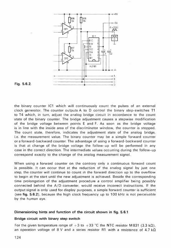
------+H+-------<>A ---------+<>+--------<>B
Fig. 5.6.2. -----_.-+---------oC ______ __._ _____ ---oD
the binary counter IC1 which will continuously count the pulses of an external clock generator. The counter outputs A to D control the binary step-switches T1 to T4 which, in turn, adjust the analog bridge circuit in accordance to the count state of the binary counter. The bridge adjustment causes a stepwise modification of the bridge voltage between points E and F. As soon as the bridge voltage is in line with the inside area of the discriminator window, the counter is stopped. The count state, therefore, indicates the adjustment state of the analog bridge, i.e. the measurement value. The binary counter may be a simple forward counter or a forward-backward counter. The advantage of using a forward-backward counter is that at change of the bridge voltage the follow-up will be performed in any case in the correct direction. The intermediate values occurring during the follow-up correspond exactly to the change of the analog measurement signal.
When using a forward counter on the contrary only a continuous forward count is possible. It can occur that at the reduction of the analog signal by just one step, the counter will continue to count in the forward direction up to the overflow to begin at the start until the new adjustment is achieved. Beside the corresponding time prolongation of the adjustment procedure a control amplifier being possibly connected behind the AID-converter, would receive incorrect instructions. If the output signal is only used for display purposes, a simple forward counter is sufficient (see fig. 5.6.2), because the high clock frequency up to 100 kHz is not perceivable by the human eye.
Dimensioning hints and function of the circuit shown in fig. 5.6.1
Bridge circuit with binary step switch
For the given temperature range of +3 to +33 °C the NTC resistor M 831 (3.3 kO), an operation voltage of 8 V and a series resistor R1 with a resistance of 4. 7 kO
124
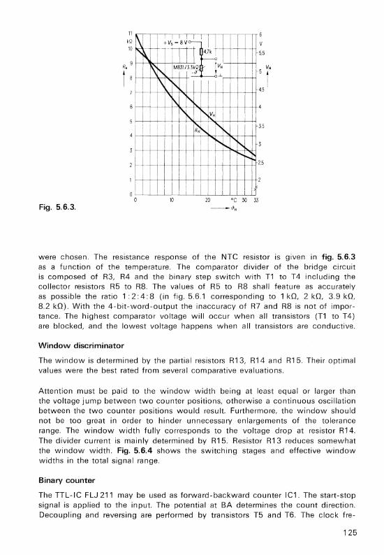
Fig. 5.6.3.
11
kQ
10
10 20 °C 30 33 ~-gH
were chosen. The resistance response of the NTC resistor is given in fig. 5.6.3 as a function of the temperature. The comparator divider of the bridge circuit is composed of R3, R4 and the binary step switch with T1 to T4 including the collector resistors R5 to RS. The values of R5 to RS shall feature as accurately as possible the ratio 1 · 2: 4: S (in fig. 5.6.1 corresponding to 1 kO, 2 kO, 3.9 kO, S.2 kO). With the 4-bit-word-output the inaccuracy of R7 and RS is not of importance. The highest comparator voltage will occur when all transistors (T1 to T4) are blocked, and the lowest voltage happens when all transistors are conductive.
Window discriminator
The window is determined by the partial resistors R13, R14 and R1 5. Their optimal values were the best rated from several comparative evaluations.
Attention must be paid to the window width being at least equal or larger than the voltage jump between two counter positions, otherwise a continuous oscillation between the two counter positions would result. Furthermore, the window should not be too great in order to hinder unnecessary enlargements of the tolerance range. The window width fully corresponds to the voltage drop at resistor R14. The divider current is mainly determined by R1 5. Resistor R13 reduces somewhat the window width. Fig. 5.6.4 shows the switching stages and effective window widths in the total signal range.
Binary counter
The TTL-IC FLJ 211 may be used as forward-backward counter IC1. The start-stop signal is applied to the input. The potential at BA determines the count direction. Decoupling and reversing are performed by transistors T5 and T6. The clock fre-
125

Fig. 5.6.4.
55
6.3°c 501s4°c
gs•c 9.5°C
~ ~
4.0
14.2°c
~ ~
11s4•c 20.i•c
3.5
3.0
2.5
'*' 0 ~ ~ ~ ~ ~ ~
0 ~ ~ ~ ~ I I
00 ~ ~ I I ~ ~
""' ~ I ~ I ~ I
203oq 211°c ~.
~
I
I
~
1u-1.,1 ~ ~ 24.9°c
~ I
I ~
I ~
I ~
2s.1°c ~ ~ 21s0 c
I I
~ ~
~ I
I ~
~. 28J.7"<:°C ~30°c
r04oe; 31s0 c
I I I
~ I I
I ~ ~
I ~ I
31~'--'330C
' I I
I I
I I
- I
quency is applied externally. The test circuit showed a permissible maximum clock frequency of 100 kHz. The clock frequency in any case has to be smaller than the response delay from counter output to recognition of the signal at the window discriminator output. If necessary, the clock frequency may be reduced to several pulses per second. This is, for instance, useful if filter capacitors have to be added to suppress interferences on the sensitive sensor line.
A/D converter with simple forward counter
As already mentioned, the AID-converter may also be designed with a simple forward counter (fig. 5.6.2). For this purpose, the circuit is somewhat reduced. T5 and T6 may be eliminated. The counter may be, as in our example, the IC FLJ 181.
126

Components for circuit 5.6 Ordering code SCS stock
number 2 Aluminium electrolytic
capacitors 47 µF 25 V 841283-85476-T 7876 Binary 4 bit-forward-backward FLJ 211 Q67000-J145 8901 counter or 4 bit-binary counter FLJ 181 Q67000-J34 8763
2 Operational amplifiers with Darlington input TCA315A Q67000-A561 7293
6 NPN silicon transistors BCY581X 060203-Y-J 8292 NTC resistor M 831 /10%/ 063483-
3.3 kQ/2.1 1) M 1003-K43 3950
1 ) NTC resistor moulded in an aluminium case. suitable for sensoring temperatures of air as well as of liquids. Length of the PVC connection cable is 2100 mm.
127

5. 7 Replacement of an Unijunction Transistor Used in Timing Circuits
Unijunction transistors are very often used as clock generators in photo-flash warning devices. In the circuit illustrated in fig. 5.7 the unijunction transistor is replaced by two inexpensive transistors T1 and T2 . The frequency of the oscillation varies only in the admissible range because RC-components with small tolerances have been used. Therefore adjustment is not necessary.
The threshold Vth is determined by resistors R1 and R2 which have a resistance tolerance of ± 2%.
The clock frequency is (134 ± 9.3) min- 1 , if components are used with tolerances as indicated in fig. 5.7. The switching time is:
l's ts=RxCxln l{-(Vz+0.6 V)
If the EB-voltage of 0.6 V for the transistor BC 308 is neglected the clock frequency is voltage-independent. For the voltage Vz and thus for the power supply voltage Vs high values have to be chosen to reduce the influence of the EB-voltage. However, the admissible reverse voltage of the EB-diode has to be considered.
The following table shows the dependence of frequency on the power supply voltage Vs. The temperature coefficient is +0.3 min- 1 /K. It is linear between -10° and +50 °C.
V5=+14 V
12 k t5 'lo
Vs 8.16V
R 4.7 M • ± 2 °/o R, 4.7 k
:!: 2°/o
BC 308 Vz5.87V
12 k
0,068 µ c ± 5 °/o Output
470ll
Ri 4711
Fig. 5.7. * Carbon resistor
128

Table
Supply voltage Vs -20% -10% Nominal +10% +20% value
Frequency (min- 1 ) 129 132 134 136 141
Components for circuit 5. 7 Ordering code SCS stock
number
Transistor BC238 Q62702-C698 70091 Transistor BC308 Q62702-C704 70097 M KH layer capacitor 68 nF 832560-01683-J 27547
129

5.8 Control of Rotating-Direction for Small Motors with an AC Power Supply
The circuit of fig. 5.8.1 operates with bridge-connected rectifiers consisting of two Darlington-transistor pairs. One pair is directly controlled by potentiometer P1, the other is phase-reversely driven by an operational amplifier. The circuit operates as follows. A signal is supplied from the tap of potentiometer P1 to the inverting input of the op.amp. The non-inverting input is connected to the power supply lines via the voltage divider consisting of R, and R 2 . All four Darlington transistors are switched off when the tap of P, is in its centre position. In every other position two transistors, being in diagonal position, are always conductive. The current flows either through transistor T,, the motor and transistor T4 or through transistor T2 , the motor and transistor T3 . The power dissipation of the Darlington transistors reaches its maximum at half of the motor voltage. As there are two pairs of transistors it is advantageous to use two separate heat sinks, one for the npn-types and one for the pnp-transistors. No additional measures for protecting the transistors against inductive voltage peaks from the motor are necessary since the Darlington transistors B D 675/676 already incorporate an inversely-poled diode. If the motor is short-circuited a current of approx. 4A flows through the transformer. As the Klixon reacts within 10 seconds no additional protection measures are required.
120 V- I
Fig. 5.8.1.
130
10k R1 10k
4x lN 4001
L---·-·------
K1. K2: Heat sinks each:;:; 45 cm2 (11 K/W)
330
10 k 2x
\ -~-~-~~~- h1 330
1.5 k
330
BO

220 v
K1-K2 Heat sinks 2'120 cm2 (Darlington isolated)
Fig. 5.8.2.
The circuit of fig. 5.8.2 operates with two power supply voltages. For reversing the direction of rotation one of the bridge arms consisting of transistors BO 675 and B D 676 is utilized. The controlling is directly realized by potentiometer P1 .
As the possible power dissipation maximum at half of the motor voltage is only applied to one transistor a greater area of heat sink is necessary. The transformer has to be dimensioned in that the short-circuit current does not exceed a value of 4A. Thus an overloading of the transistor between the period of short-circuit and Klixon reaction is avoided. The case temperature of each transistor has to be less than 50 ·c.
Fig. 5.8.3 shows a circuit which operates only with one half-wave. Contrary to the two circuits described before a small current flows through the transistors when the tap of P1 is in its dentre position. The current of the positive half-wave flows via the upper transistor, the negative one via the lower transistor. The reaction of both half-wave currents compensates and the motor does not rotate. The value of the half-wave current depends on the resistance of P, and on the current gain of the transistors. Therefore a compromise between a reasonably low current of the centre tap position and a sufficiently high current for the control range, i.e. for the angle of rotation at asymmetrical positions, has to be found. The resistance of P, is 33 n when the potentiometer is in one of its final positions. This resistance
determines essentially the current maximum of the transistors.
131

JI 33
Fig. 5.8.3.
Components for circuit 5.8.1 Ordering code scs
stock number
1 Operational amplifier TAA 761A 067000-A522 7236 2 PN P darlington transistors 8D676 062702-D239 70559 2 N PN darlington transistors 8D675 062702-D238 70558 4 Diodes 1N4001 C6604 7-Z1 306-A21 48001 1 M KH layer capacitor 1.5 nF/400 V 832560- D6152-J 27619 1 Potentiometer 2.5 k0/0.1 w 7 Resistors 1 x 330 0/0.5 w 851261-Z4331-J1 37665
2 x 330 0/0.1 w 851260-Z4331-J1 36681 4 x 10 k0/0.1 w 851260-Z4103-J1 37270
2 Heat sinks 2 x45 cm 2
£,11 K/W
Components for circuit 5.8.2
1 PN P darlington transistor 8D676 062702-D239 70559 1 N PN darlington transistor 8D675 062702-D238 70558 4 Diodes 1 N4001 C6604 7-Z1306-A21 48001 1 Potentiometer 2.5 k0/0.1 w 2 Resistors 330 0/0.1 w 851260-Z4331 -J1 36681 1 Heat sink 120 cm 2
£,6 K/W
Components for circuit 5.8.3
1 Transistor 8D135 062702-D106 70121 1 Transistor 8D136 062702-D107 70122 2 Diodes 1N4001 C6604 7-Z1 306-A21 48001 1 Resistor 33 o
Potentiometer 2.5 k0/0.1 w 132

5.9 Control of Rotation Direction of Small Motors with a DC Power Supply
Contrary to the before-mentioned circuits, the motor current of the circuit shown in fig. 5.9 flows through potentiometer P1 • In the centre position of the potentiometer no current is flowing through the motor, but only a power supply current through the two arms of P 1 , the two diodes and the two transistors. An automatical current limitation is realized by the resistance of the potentiometer. When the slider of P; is turned to the left the motor current flows through diode D, and transistor T2 •
In this case the transistor T1 is weakly conductive.
When the slider is turned to the right the motor current flows through diode D 2 and transistor T1 • A diode BA 127 D is connected to the base of each transistor to reduce the leakage current when one of the transistors is switched off.
Fig. 5.9.
Components for circuit 5.9
2 Transistors 2 Diodes 2 Diodes 2 Resistors 1 Potentiometer
BD135 1N4001 BA 127D 33 0/0.1 w 50 0/5 w
50
P, <>---+---+-~
Ordering code
Q62702-D106 C66047-Z1306-A21 Q60201-X127-D9
SCS stock number
70121 48001 70044
133

6. Electronic Circuits for Electric Power Engineering
6.1 Electronic Dimmer with Touch Keys
The new MOS IC S 566 B makes it possible to control all functions by a single touch key (sensor). This solution offers together with modern comfort and design a further advantage in that any number of, even physically separated, parallel controls or an electronic remote control, can be operated.
Principle of the MOS dimmer
The operation principle of a touch key (sensor) is based on the finite resistance between human body and earth. Thus the input potential of an electronic circuit may be varied and switching and control operations released. As the commands "0 N ", "0 FF" and "phase-angle-control" is controlled by a single sensor the duration of the touch remains as the only discrimination criteria. The application of this input information, its storage and the correctly phased gate triggering of the triac is achieved by the integrated MOS IC S 566 B. By means of a PLL circuit the internal clocks are generated and synchronized to frequency and phase with the mains. The almost digital operation mode provides exact and stable adjustment of the desired phase angle. The triac is triggered at each half-wave by an approximately 30 µs-pulse at pin 8.
Description of the circuit
Fig. 6.1.1 shows a dimmer circuit for incandescent lamps, which can replace the ordinary mechanical switch usually connected in series with the lamp. The switching function is realized by triac Tc· In the reversed state the mains voltage is applied to the triac terminals, in the conductive state only a residual voltage is present. However, the electronic control circuit requires a de voltage of 15 V for operation. The IC, therefore, was designed for an adjustable phase angle of approx. 30° (minimum). The voltage delivered by this angle causes capacitor C3 to be charged to the operating voltage of the IC via rectifier 02. A capacitance of an electrolytic capacitor is sufficient with regard to the very low power consumption of the circuit. R1 and C2 serve as current limiters for the z-diode 01. Capacitor C1 and choke Ch give the specified RF interference suppression.
The synchronization with the mains frequency is achieved by the ac voltage applied to the triac, and supplied via R2 to pin 4. The inherent interference signals are filtered by C6. C4 and C5 are part of the internal control circuit of the IC. A touch of the sensor surface influences the potential of the voltage divider at the control input (pin 5). The necessary touch protection is provided by resistors R8 and R9. The sensitivity of the sensor is adjustable by R7. Further touch keys are not easily connected in parallel to this input because, on long lines, the highresistance input is too sensitive to external interference. A second inverting input is provided for this purpose. It can be terminated with low impedance. The control is achieved by short-circuiting by means of a mechanical push button or a sensordriven transistor as shown in fig. 6.1.1.
134

R
Fig. 6.1.1. Circuit of the electronic sensor dimmer using the new MOS IC type S 566 8. Attention has to be paid in that the correct connections are made, i.e. R to the hot lead, and L to the lamp.
Parallel controls or simple switches are connected to terminal N.
Mpo---<>------------R
f--- I --+---][-+---]I -----1
Fig. 6.1.2. Arrangement of parallel-connected control devices
Resistive load (lamp) 11 Triac control using S 566 8 in accordance to fig. 6.1 .1 Ill Parallel-connected control devices or keys of any number (see fig. 6.1.1, right)
135

s - 1 I I S I I I ; I: I I .... ---
1 I I ' I ; I I ; I I I • I • I I ;
t(/!118500:~1 I: ·.• ii I I '., lVL=0(~180") ' I ' : Vlm;n I
goo . • f ------; VL
~ ~-a+-~~~~~~~~~~-.-----.~.-~~~~~~~~~
1 2 3 4 5 6 7 8 9 s 10 ----1
Fig. 6.1.3. Influencing the phase angle by touching the sensor
Fig. 6.1.2 illustrates the easy connection for parallel control devices. If no controls are required R5 and R6 may be eliminated. Input 6 has then to be directly connected to Voo (pin 7).
For reliable operation of the sensor it is absolutely necessary that the IC is correctly connected to the mains, i.e. terminal R to the "hot" lead and L via the lamp to the neutral wire Mp. But with a mechanical contact at pin 6 the connection to the proper terminals is no longer important, i.e. mobile power consumers, for instance, floor lamps can be operated.
The triac is triggered in the 3rd and the 4th quadrant via a driver transistor ( T,) which allows also the use of triacs with higher gate currents. The maximum power of the connected load is limited by the maximum ratings of the triac. The RFI suppression has also to be selected accordingly. For incandescent lamp control the switch-on transient pulses which may reach 5 to 10 times the rated lamp current due to the low cold resistance, have to be considered.
Control behaviour
Fig. 6.1.3 shows the control behaviour. With a short touch of the sensor, i.e. less than 0.4 s but more than 60 ms (immunity period for interference suppression) the phase angle is aligned to a preliminarily fixed value for turn-on. Another short touch releases the turn-off. If the touch lasts more than 0.4 s the phase angle <fJ will sweep the whole control range within a period of 7 s, i.e. the output voltage is controlled from the minimum to the maximum and return as long as the finger remains on the key.
A new touch causes the control direction to reverse, e.g. first touch: <fJ gets larger, i.e. the lamp becomes darker; second touch: <fJ becomes smaller, i.e. the lamp becomes brighter, and so on. At turn-off, a short touch allows the previously set value to remain stored in the IC memory. At the next turn-on the phase angle <fJ adopts this last value. Hence the lamp burns at the previously set brightness or dimming begins at this initial value.
136

Fig. 6.1.4.
Vss
Sync cr---c=i---+---0---1
r· I I I I I
I
rl==J--o T riac
s 566
Voo0------------+------~
The phase angle can be adjusted between 30 to 150° of each half-wave. The smallest angle (30°) is necessary to provide the supply voltage, the largest angle (150°) still allows a significant margin between the lowest output voltage (i.e. the least brightness) and the off-position in that a clear identification of the dimmer switching state is obtained.
The control is achieved without the hysteresis which is common in conventional circuits.
Fig. 6.1.4 shows a circuit which continuously changes the phase angle. Therefore the voltage across a load is periodically controlled up- and downwards. These kinds of control are favoured for applications of illuminated advertisements, warning devices or electric sirens. In this case the sensor input (pin 5) has to be connected to V00 (dashed line) or the auxiliary input (pin 6) directly to V55 .
Components for circuit 6.1 Ordering code scs stock number
Electronic dimmer IC S566B Q67100-Z120 71429 N PN silicon transistor BC238 Q62702-C698 70091 PN P silicon transistor BC308 Q62702-C704 70097 (for parallel sensors) Triac for loads of up to max. 200 W: Triac TXC03A60 C66048-A1 502-A2 48058 for load of up to max. 400 W: Triac TXC02A60 C66048-A1 501-A6 48053 (mounted on a cooling block 10 K/W)
137

Ordering code scs stock number
RFI suppression choke 2.5 A nominal current 882603-V-811 35033 (ring core) 1 )
1 Z-Diode, 8ZX97 /C15 0.5 W Q62702-Z1239-F82 7353 1 Silicon switching diode 8AY61 Q62702-A389 8579 2 M KH layer capacitors 47 nF/250 Vdc 832560-83473-J 27566 1 Ceramic disc type 470 pF/400 Vdc 837205-A5471 -S1 1724
capacitors RFI suppression 0.15 µF/250 Vac 881111-8-827 35008 capacitor RFI suppression 0.2 µF/250 Vac 881111-8-828 35009 capacitor (X) 2 )
Aluminium electrolytic 47 µF/25 Vdc 841286-A-5476-T 7890 capacitor
1 Carbon resistor 1 k/1 W, ±5% 851264-Z4102-J1 39171 1 Carbon resistor 120 0/0.33 w ± 5% 851261-Z4121 -J1 37660 1 Carbon resistor 1 0 k0/0.33 w ± 5% 851 261-Z4103-J 1 37689 2 Carbon resistors 470 k0/0.33 W±5% 851261-Z4474-J1 37952 1 Carbon resistor 1.5 M0/0.33 W±5% 851261-Z4155-J1 37938 6 Carbon resistors 4.7 M0/0.33 W±5% 851261 -Z4475-J1 37939
1 ) For a lamp load of up to 200 W a 1.6 A-choke is sufficient ordering code B82603-V-B1 O (not available from SCS-Furth).
2 ) In the described circuit this capacitor is used as a current limiter and not for RFI suppression.
138

6.2 Phase Angle Control Using IC S 566 for Small Supply Voltages
The operation principle of the electronic dimmer IC S 566 has already been described in chapter 6.1. The following demonstrates an application of this IC for supply voltages between 12 and 16 V as they are used for, e.g., toy railway-trains. As shown in fig. 6.2.1 the de voltage supplying the S 566 is produced by rectification during a half-wave. Contrary to the operation with 220 V only a small voltage drops across the limiting resistor R 1 . For direct synchron1zat1on the secondary voltage of transformer is not sufficient. Because of the slow voltage increase the threshold is only readed at defined phase angles. Therefore the control would have a wide dead zone. But by the transistor T1 a steeper slope is produced. It can be adjusted to the required phase angle by matching the resistance of the divider resistor R3 .
As this application operates with very low load currents a triac offering low holding currents has to be used. A further advantage is obtained in that a lamp with 1 to 2 W is connected in parallel to the output.
At transformers with a low output power the stray inductance corresponds to a high series resistance when the triac is turned on by a fast current increase. Therefore a short voltage breakdown will occur. It is applied to the synchronous input of the IC and causes interferences. This disadvantage can be avoided by increasing the capacitance of C4 to approx. 0.1 µF. For the short-circuit protection a bimetal switch, type Klixon, is utilized. But the triac has to be rated for the maximum short-circuit current which will flow until the bimetal switch interrupts the power supply line.
The storage of the preset value is a certain disadvantage of the S 566 for this application. If the load, in this case the train, is switched off by a short touch of the sensor, no possibility exists for re-start with a reduced speed, as the driving
Kl1xon ~.,_ . ..-~~~~~-~~~~~--...~--..--...--...----..~~-Ill 1
Fig. 6.2.1.
I I I I I I I I I I I I I I I
*Ci. :10 1100n I I I I I I I I
: lk I
BZX 83 c 15 . [
47 µ 1
BAY 61
100k R, C5 =!:; [1
:10n
' ' I I I I
IOOk I I
RI
10 k
[J 47n 47n 1.5M R6
z I zzo
5 566 B 8
470k R,
Sensor
I R,
I
Tc
'•I j r,
l'" ~"""''" 139

Ri 14
100k Rz R4
1/2 s© 1/ 2
® TDB 0556 Gate-
C1 TDB 0556 ®
control I I
_______ _J
100k R3 10nF [3
-15 v
Fig. 6.2.2.
voltage jumps again to the previously adjusted value. The memory can be erased by turning off the supply voltage. Fig. 6.2.2 shows an circuit which interrupts momentarily the voltage supply line when the dimmer circuit is switched off. Thus the above mentioned disadvantage is avoided. The first timing circuit operates as a monostable multivibrator, which is always reset again by the trigger pulses of the triac. If these trigger pulses are not applied the charging procedure continues without any interruption and the output is switched. The second monostable multivibrator is triggered by output signals from the first multivibrator, which interrupts the voltage supply line of the S 566 for a short time.
Components for circuit 6. 2.1 Ordering code scs
stock number
1 IC S5668 067100-Z1 20 71429 1 Triac TXD10 K40 P C66048-A 1 504-A4 2 N PN-Transistors 8C238 Q62702-C698 70091 1 Z-Diode 8ZX83/C15 Q62702-Z1081-F82 7321 1 Diode 8AY61 062702-A389 8579 2 M KH layer capacitors 10 nF 832560-83103-1 27562 2 M KH layer capacitors 47 nF 832560-83473-1 27566 1 Electrolytic capacitor 47 µF 841286-A5476-T 7890 1 Resistor 220 0/0.3 w 851261-24221 -J1 37663 1 Resistor 1 k0/0.3 w 851261-Z4102-J1 37672 2 Resistors 10 k0/0.3 w 851261-24103-J1 37689
Resistor 220 k0/0.3 w 851261-Z4224-J1 37948 Resistor 470 k0/0.3 w 851261-Z4474-J1 37952 Resistor 1.5 M0/0.3 W B51261-Z4155-J1 37938
140

Components for circuit 6.2.2 Ordering code scs
stock number
1 IC TDB0556A 067000-A 1 046 70320 1 PN P-Transistor BC308 Q62702-C704 70097 2 MKH layer capacitors 10 nF 832560- B3103-1 27562 1 M KH layer capacitor 47 nF B32560-B3473-I 27566 2 Resistors 100 kO B51261-Z4104-J1 37944 ...,
Resistors 330 kO B51261-Z4334-J1 37951 "-
141

6.3 Excess Temperature Protection Circuit for Dimmer IC S 566
Fig. 6.3 shows a circuit with a PTC resistor whic;h protects the dimmer IC S 566 against excess temperatures during operation. As the resistance of the PTC resistor increases when the temperature rises, the trigger current is decreased in that the triac is finally switched off. When the temperature drops again the current increases and the circuit starts automatically to operate. The advantage of switching off the triac only and not the total circuit is in that the function of the dimmer IC is not influenced, i.e. the same illumination is set with reference to the previously adjusted value.
Another possibility for excess temperature protection is given by replacing the resistor R4 by a PTC resistor, type P 350- B 11. This P 350 increases its resistance at 80 'C. In the temperature range below 80 'C, the resistance reaches a minimum of 200 n. Therefore triacs with a trigger current of ~50 mA can be used only.
If triacs with higher trigger currents are used the circuit "b" is recommended. It interrupts the base control of transistor T1 . The PTC resistor P 330-B 11 is well favoured for this application. The resistor RA is connected in parallel to the baseemitter-junction and thus a safe turn-off is assured when the PTC resistor becomes high-resistive. The resistance of RA depends on the gain of T1 and on the triggercurrent group of the triac. It is dimensioned in that the excess temperature protection circuit becomes effective at temperatures of approx. 80 'C.
Fig. 6.3.
142
220 V-
c,
i ~ ~ -1 Excesstemperature 1 • {7 ~K I protection cicuit L ___ _j 0
I I b-..-----J Excesstemperature protection circuit
CD
s 566

Since the trigger currents are slightly unsymmetrical in the 3rd and 4th quadrant a triac is triggered often at one half wave, i.e. the lamp is operated at half of its illumination.
But with the second half-wave, which is later applied, the triac and thus the lamp are completely turned off.
Components for circuit 6.3
1 PTC resistor P330-B 11 or P350-B 11
Ordering code
Q63100-P330-B11 Q63100-P350-B11
scs stock number
143

6.4 Low-Loss DC-Control Circuit Using S 566
Fig. 6.4 shows a low-loss circuit which controls a de voltage by using the IC S 566. It operates in accordance to the principle of a keyed control. The effective output voltage is controlled by the duty cycle with which the load is turned on or off and not by a voltage drop across a series resistor as usually practised.
A square-wave generator produces an ac voltage which is required for the synchronization. The frequency is 50 Hz. The output pulses supplied by the S 566 are phase-shifted by the required angle with reference to the basic oscillation. A bistable multivibrator is triggered by the output pulse of the S 566 and reset by the following slope of the control signal. Thus a signal with a constant frequency (100 Hz) and a controllable duty cycle is available at the output.
The square-wave generator and the bistable multivibrator are realized by the dual timer IC TDB0556. One of the timers is utilized as an astable the other as a monostable multivibrator The resistance of R, has to be chosen essentially lower than that for R2 to get a duty cycle of approximately 2: 1 for the square-wave voltage. An accurate adjustment is not necessary, as the PLL-circuit of the S 566 synchronizes automatically within a defined capture range. The output of the monostable multivibrator is set to H-level by the trigger pulses of the S0556 applied to its trigger input. The slopes of the square-wave signal are differentiated by the circuit consisting of C5 , R7 and R8 • These pulses alternatively reset the output to L-level via the threshold or the reset input.
The timer offers a push-pull output which supplies a maximum current of 200 mA. If higher currents are required a power amplifier has to be used.
If an unkeyed de voltage with an amplitude being controlled by the sensor circuit is required it can be realized by a series transistor and an RC-circuit connected to its base as shown on the right side of fig. 6.4.
144

.p. 01
.,, cp' O'I
~
• 15V
c, '22n
0.15 µ
14 __ _
112 TDB 0556
IC2
*[5 ilO n
C7~ R4 ® 6.8ni 15M 100krR6 ~R7 I 100 k
Cs ©
~ 4 I @
10 s 566
IC1
470kl !Rs ~r,
BC 238
Sensor 10Dkl iR8
-- ---------,
112
I I I I I@
TDB 0556 ~ IC2 I :
I I
: I ----+----"
10n=Cs
Type in accordance to the required output current
T2
Rg
-1 " JRL 100 l
T 4 i I

Components for circuit 6.4 Ordering code scs
stock number
IC S566A/5668 Q671OO-Z120 71429 IC TD80556A Q67000-A 1046 70320 N PN Transistor 8C238 Q62702-C698 70091 N PN Transistor type is deter-
mined by load 1 M KH layer capacitor 6.8 nF 832560-83682-K 27561 3 M KH layer capacitors 10 nF 832560-83103-1 27562 1 M KH layer capacitor 22 nF 832560-83223-1 27564 2 M KH layer capacitors 47 nF 832560-83473-1 . 27566 1 M KH layer capacitor 0.15 µF 832231-A1154- K 16981 1 Electrolytic capacitor 100µF/16V 841316-A4107-V 2341 1 Resistor 1 kQ/0.3 w 851261-24102-J1 37672 1 Resistor 1.8 kQ/0.3 w 851261-Z4182-J1 37675 5 Resistors 100 kQ/0.3 w 851261-24104-J1 37944 1 Resistor 470 kQ/0.3 w 851261-Z4474-J1 37952 1 Resistor 15 MQ/0.3 W 851261-Z4156-J1
146

6.5 Triac Triggering Circuit with TCA 780
The thyristor triggering IC TCA 780 supplies output currents with a maximum of +50 mA at both half-waves. Fig. 6.5.1 shows a circuit for control of a triac by a positive trigger current. It is suitable for types:
TXD10 H60, TXD10H60M, TXD10H60P.
In general standard triac types are not specified for such a control in the second quadrant (positive current, negative voltage at A 2 ).
The above-mentioned triacs are also available for peak voltages of 700 V. In this case the type identification is TX D 10 H70.
Fig. 6.5.2 shows a circuit for control of a triac with a negative trigger current. The 0.22 µF-capacitor is charged via the 10 kO-resistor and has a polarity as shown in the figure. In this case the transistor BC 238 is non-conductive. It is controlled by the trigger pulses via the two diodes, type BAY 61. Thus the emittercollector-junction becomes conductive and one plate of the capacitor is connected to ground potential. A negative trigger current is generated.
Fig. 6.5.3 shows another circuit which allows higher trigger currents of approx. 100 mA. In this case the transistor operates as an emitter follower and the trigger current is limited by resistor R,. This circuit is applicable for selected types of standard triacs with a trigger current of + 100 mA in all quadrants.
• 15 v
BAY 61 14
TCA 780 15
BAY 61
1) Special triac. specified also for the 2nd quadrant
Fig. 6.5.1.
AZ 1) TXD 10 H60
H60 M H 60 P
147

V-u-----1---------
h~ 220 µA
·15Vo----T-1----------
16
14
TCA 780 15
100 G Al
22 k 1 k
* 8 32 560-81224-J
Fig. 6.5.2.
v_u-----r--------
R°"'~ ZOO µA
•15VO----i-+--------
16 BC 238
14 TCA 780
15
Fig. 6.5.3.
148

Components for circuit 6. 5.1 Ordering code scs
stock number
1 Thyristor trigger IC TCA 780 Q67000-A 1087 71428 1 Triac TXD10 H60 C66048-A 1 504-A8 2 Diodes BAY61 Q62702-A389 8579
Components for circuit 6.5.2
Thyristor trigger IC TCA 780 Q67000-A1087 71428 1 Triac type depends
on the required load
1 Transistor BC238 Q62702-C698 70091 2 Diodes BAY61 Q62702-A389 8579
M KH layer capacitor 0.22 µF 832560- B 1224-J
Components for circuit 6.5.3 Ordering code scs
stock number
Thyristor trigger IC TCA 780 Q67000-A 1 087 71428 Triac type depends
on the required load
1 Transistor BC238 Q62702-C698 70091 2 Diodes BAY61 Q62702-A389 8579
149

BZY
6.6 Contactless Control for Solenoid Valves with 3000 W Using a Triac
Solenoids require the total power only during the pull-up. For types with 300 to 3000 W the hold power is much lower. Therefore a remarkable power saving is possible by choosing the correct construction and the optimal power supply.
Fig. 6.6 shows a circuit in which the total de power is supplied to the solenoid valve only during the pull-up time of 5 s. Thereafter a lower hold power is applied by means of a phase-angle control circuit. This power is sufficient to hold the solenoid.
When the circuit is connected to the mains the LED LD 52 is non-reversely poled and emits light. Thus the photoresistor FW 9802, being connected to the triac gate, is illuminated. It resistance is decreased to approx. 2.5 kO. The supplied gate current is sufficient to trigger the triac Tc and to operate the solenoid winding via the rectifier-bridge GI.
After 5 s the RC-circuit turns on the transistor T, and therefore the transistor T2 is non-conductive. No current flows through the LED (20 mA). The photoresistor is not illuminated and becomes high resistive (800 kO), i.e. no gate current and thus no full-wave-load current flow.
The triac has a second trigger circuit, which operates as a phase angle control circuit. The trigger voltages is adjusted by potentiometer P. When the voltage across the capacitor C3 has reached the necessary trigger voltage level for the diac, the triac receives a short trigger pulse.
0.68 µF 1250 V-
LO 52r- -1
SSi 836 40 ~ : FW 9802 I
-·-·-·J
E 29- B 250/ ZZS-10
550
Ch
Selenoid valve 1200W
---~ or3000W
97G12 18 k
'2 ZD 1
58 k
Cs • 2.2 k 33 k
C1 100 µF 100 µF 16 V- 10 V- 0.1 µF
53 V-
27
C3
0.22 µF 63 V-
De
A 9903
Tc
0,22 µF 250 V-
~-------+-------+-----+----+------------------0 Grou1
Fig. 6.6.
150

The load is connected to the mains during the remaining time of the positive half-wave. Assuming the triac is triggered at an angle of a= 125°, then the de voltage at the solenoid valve is Vd(Avi=75 Vdc. The hold-voltage for the solenoid can be adjusted by potentiometer P between 60 Vdc and 90 Vdc.
Components for circuit 6.6
Triac
Diac Rectifier bridge
2 Transistors Z-diode Z-diode Diode Diode LED Capacitor Capacitor Capacitor Capacitor
Capacitor Electrolytic cap. Electrolytic cap. Photo resistor Choke
TXD10 H70 M (Tc) 1 )
TX D98A60 (Tc) 2 )
A9903 E29- 8250/225-10 8CY58-Vll 8ZY97C12 8ZX83C4V7 SSi 8 3640 8AY61 LD 52/11 0.10 µF/63 V~ 0.22 µF/63 V~ 0.22 µF/250 V~ 0.22 µF/250 V~
0.47 µF/250 V~
0.68 µF/250 V~ 100 µF/10 V-100 µF/16 VFW9802
1 ) For solenoid valve controls of 1200 W /198 V de 2 ) For solenoid valve controls of 3000 W /198 V de
Ordering code
C66048-A 1504-A20 C66048-Z1651-A4 C66048-Z1304-A1 C66067-A 1740-A2 Q60203-Y58-G 062702-Z1237-F82 Q62702-Z1069-F82 C66047-A1062-A4 Q62702-A389 062703-0159 832560-81104-J 832560-81224-J 832655-A6224- M 881121-C-856 or 881121-C-875 (C4) 1 )
881121-C-858 or 881121-C-877 (C4) 2 )
832655-A6684-M 841283-83107-T 841283-84107-T 062705-P19-F65 882603-V-812 1 )
882603-V-814 2 )
scs stock number
4790 4680 8290 7351 7310 48403 8579 71332
7806 7810
151

6. 7 Control Circuit for Direct Triggering a Thyristor with TCA780
Fig. 6.7 shows a phase angle control circuit using the IC TCA 780 for direct triggering of thyristors, e.g. type BSt C 0540. However, small thyristors with silicon dices in the size of B, C and D (fourth letter in the ordering code, e.g. BStC ... ) may also be used.
The phase angle is adjustable between 0 and 180° el, the power at the load between 0 and 400 W.
The IC supply voltage (pin 16) is directly generated from the mains via a series resistor R1, rectified by the diode D1 and stabilized to 15 V by the z-diode D4.
The synchronization input (pin 5) is connected to phase R via a 1.2 MO-seriesresistor and to ground via two antiparallelly connected diodes (D2, D3). The two diodes limit the voltage for the synchronization input to about ±0.6 V.
The frequency of the ramp generator is determined by the zero voltage detector, i.e. at each zero-crossing of the mains voltage the saw tooth wave is generated again. The steepness of the voltage rise is adjusted by the ramp capacitor
Th1 BSt C0540
" "C...:._ D 5 f. }""
L'::. SSi B 3610 J '.'~1 10k
~------!----__._~
47mA
[14.?k
_..._ __ 330~ 47n* ~ Rg
R
t ( 2ZO C12 C10 ~00k1 o--..-c,.;.;..;..,R=1:r-+:S"-S*i _B 3.-6-40-.---+-----. 56 k r] [l 22 k
1Dki3w m <L J'
C1
1000µF + (l· 16V_ ~~~ J 15k
D4,~ BZY97/C15
220V~ ] 1.2M
16 15 14 13 12 11 10 9
D TCA 780
1 2 3 4 5 6
" 02 VI L.AD3
7 8
s
2xBAY6~ Mp"<>---1------..... -+--------------------' (ground)
Fig. 6.7.
152

(C10=47 nF) and the ramp resistor (R9~100 kO). In the present circuit the saw tooth amplitude is 7 V.
The control voltage V11 is adjustable from 0 to 8 V by potentiometer P1. This allows to set a current flow angle from 0 to 180' at the load. As in the described half-wave control circuit the thyristor is only conductive in one direction, output A2 (pin 1 5) is only connected with the thyristor gate. A positive trigger pulse is applied to the gate every 20 ms during the positive half-wave. The output A 1 (pin 14) which supplies a positive trigger pulse during the negative half-wave, remains unconnectecL The output pulse duration is determined by the capacitance of the capacitor C12 as demonstrated in table 6.7. In the circuit of fig. 6.7 the thyristor is triggered by a pulse with a ,duration of 200 µs and a gate current of 47 mA.
Turn-on and -off with inhibit signal
Positive trigger pulses will only be generated during the pos1t1ve half wave of mains voltage if the potential at the inhibit input (pin 6) is higher than + 3.5 V. A resistance of 15 kO is therefore connected to +-terminal (pin 16) of the power supply. When the voltage at the inhibit input decreases below + 2 V no output pulses are supplied. Short-circuiting pin 6 to ground, for instance by a switch S or a logic circuit, disconnects the load independently from any other signal state at the TCA 780.
Table 6.7
Capacitor C1 2 (Extension of pulse duration) Trigger pulse duration
Components for circuit 6. 7
1 Thyristor 1 Thyristor control IC 2 Diodes 1 Diode 1 Diode 1 Z-Diode 1 Styroflex capacitor 1 M KH layer capacitor 1 Electrolytic capacitor
0 100 pF 220 pF 330 pF 680 pF 1000 pF
30 µs 80 µs 1 30 µs 200 µs 370 µs 550 µs
Ordering code scs stock number
8StC0540 C66048-A 1400-A5 48249 TCA 780 067000-A 1087 71428 8AY61 Q62702-A389 8579 SSi83610 C66047-A 1062-A2 48401 SSi 83640 C66047-A1062-A4 48403 8ZY97 /C15 Q62702-Z1239-F82 7353 330 pF/25 V- 831310-A3331 -H 1367 47 nF/250 V- 832560-D3473-J 27566 1 000 µFI 1 6 V - 841010-84108-T 7849
153

6.8 Phase Angle Control Circuit for Thyristors with TCA 780 and Transistorized Trigger-Pulse-Amplifier
Fig. 6.8 shows a circuit as it is used for the half-wave control with thyristors for high currents (maximum rms-current of BStF 2553 is 30 A). A separate power supply (15 V) with transformer and rectifier is required. The de load can be controlled by potentiometer P1. As the TCA 780 is delivering only output currents of up ro 50 mA but thyristors of the type BStF 25 need a triggerr current of 1 A to provide a fast and low-loss turn-on, an amplifier stage with the N PN silicon transistor BSX45 has to be connected between the IC and the thyristor.
Components for circuit 6.8
Thyristor Thyristor control IC
1 Transistor 2 Diodes 1 Styroflex capacitor 2 M KH layer capacitors
MKH layer capacitor TSE capacitor
+ 15V
15k R
220V~ 1,2M
BStF 2553 TCA 780 BSX45-16 BAY61 330 pF/25 V-10 nF/400 V-47 nF/250 V-0.22 µF/250 V-
4.?k
10nF
56k
C12 330pF
P1
10k
16 15 14 13 12 11
TCA 780
3 4 5 6 7 8
02 s 03
2xBAY61
Ordering code scs stock number
C66048-A2458-A2 067000-A 1087 71428 Q60218-X45-V16 8628 Q62702-A389 8579 B3131 O-A3331 - H 1367 B32560- 06103-J 27625 B32560-D3473-J 27566 B25839-A6224- M
12 RL
R9 i 45mA VdOAV
220 Th BSt F2553
10nF
0,22µ
220V"'
Mpo-..... ~1---+-~~+-~~~~+--+~~~~-1..._ ..... ~~ ...... --e-__. (ground)
Fig. 6.8.
154
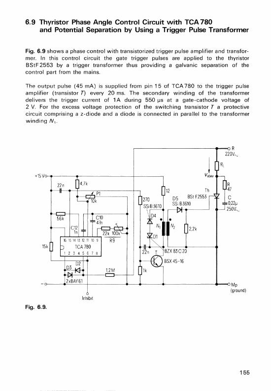
6.9 Thyristor Phase Angle Control Circuit with TCA 780 and Potential Separation by Using a Trigger Pulse Transformer
Fig. 6.9 shows a phase control with transistorized trigger pulse amplifier and transformer. In this control circuit the gate trigger pulses are applied to the thyristor BStF 2553 by a trigger transformer thus providing a galvanic separation of the control part from the mains.
The output pulse ( 45 mA) is supplied from pin 1 5 of TCA 780 to the trigger pulse amplifier (transistor T) every 20 ms. The secondary winding of the transformer delivers the trigger current of 1 A during 550 µs at a gate-cathode voltage of 2 V. For the excess voltage protection of the switching transistor T a protective circuit comprising a z-diode and a diode is connected in parallel to the transformer winding N 1 .
~----------~..,_~R
+15 Vo-.>---------------+---~
22 n
270
16 15 14 13 12 11 10 9
15k TCA 780 12345678
12 DS BSt F2553 SSi 83610
BZX 83C 20
BSX 45-16
2.2k
220V~-
2xBAY 61 o----<1~~--+--------<1~--.---e-------~---oMp
(ground)
Inhibit
Fig. 6.9.
155

Components for circuit 6.9 Ordering code scs
stock number
1 Thyristor 8St F2553 C66048-A2458-A2 1 Thyristor control IC TCA780 Q67000-A1087 71428 1 Transistor 8SX45-16 Q60218-X45-V16 8628 2 Diodes 8AY61 Q62702-A389 8579 2 Diodes SSi 8 3610 C66047-A1062-A2 48401 1 Z-Diode 8ZX83C20 Q62702-Z1084-F82 7324 1 M KH layer capacitor 1000 pF/250 V- 832560-83102-K 2 M KH layer capacitors 22 nF/250 V- 832561- D3223-J 27577
M KH layer capacitor 47 nF/250 V- 832560-D3473-J 27566 TSE capacitor 0.22 µF/250 V~ 825839-A6224- M Trigger pulse produced by ZK8418/079-02-PF 28204 transformer IT VAC
156

6.10 Control Set for Half-Controlled Three-Phase Current Bridge
Fig. 6.10.1 shows a half-controlled three-phase current bridge with thyristors connected to the positive terminal of the output voltage (common cathode) and three diodes connected to the minus. In each arm of the bridge an uncontrolled rectifier and a thyristor are connected in series.
Each phase ( R, S, T) requires a control device ZB 1 T for one thyristor which periodically generates control pulses being synchronized to the mains frequency. These control pulses trigger the thyristors at the time given by the control device. The trigger time can be shifted synchronously for all three phases by means of potentiometer P1.
The phase angle a is measured in electrical degrees (a full cycle=360 °el). It relates to the natural trigger time of the thyristor, i.e. counts from the point at which in a rectifier circuit, consisting of diodes, the following valve processes the current, which is the crosspoint of the positive half-wave voltages (fig. 6.10.2). The highest possible de voltage at the converter output is achieved by a control pulse at this point, so when rectifying we refer to "total rectifier control" and define the relevant control angle as a=O 0 el.
~10kTJil P1 H 16
r+--t"< 560
Vs I I 20 to 40 V _ ~~.._.~,._____,-+-+--01
p= ~ Tr
15 T :r+-+-z s n ~
220k )
~
380 V~ R S T
01 to 03: SSi E 2060
~ C6 ~ C4 nc2
\V 380 v~\l7 380 v""\l 380 v~
300 300 300
03 * 50n 02 I *T 50n Dl ~ 50n
F- R6 UR4 ~r- R2
...__._~'J4W ~ 4W t-- 4W
V,=500 V 0-15_· -+--+-+-~'-----+-----+----.]dAr 38 A RL
~max~ 19kW
I ~
R S T 380 V~
Fig. 6.10.1.
ZB 1T 15"
220k
t~s ~ ~
~ C5 t-----, C3 ..----, Cl Th3 *Olµ Th21 =i:=Olµ Th1 *Olµ
L.l---l---<>--4 'u'l 380 v?f;?\l 380 v~ 380 v~ G RS G-; R3 G-1 RI _,,_ ~\oo HK 100 H~ 100 HK t-- 6W ~~6W ~6W 15
10µ R
.~"~~_z_s_n_~<,~~------~-----~ 15 v Th1 to Th3: BSt F 2590
WoRM/VRRM=1350 V; IrnMSlll-47 A)
157

0 n -r 2:c
JI u
t
Fig. 6.10.2. 0 n -r 2n
Fig. 6.10.2 shows the voltage response at a resistive load and an operation without interval (I) and with interval (II). The trigger pulses have a duration of 550 µs. They can be extended by increasing the capacitance of C1 2 and have to be rated such as to allow the thyristor to have a sufficiently high hold-current at the end of every pulse to remain conductive.
v,, v, ,---- 11 8 5 +15V"--~-----1------'------'-----~
22n
15k
2xBAY 61
12
270
15. Th G
I I
2.2k I I
.__.,.._.______,""" ..._ __ ,._______,, Th-C BZX 83 C 20 15"
BSX 45 -16
ZB1T L_____ 6 --~--------------
Fig. 6.10.3.
158
Inhibit

V11 v, ,----- 11 8 12
22n
~--+----0Th2-C
22n
?xBAY61 ZB2T
L _____ 6 ____________ _ Inhibit
Fig. 6.1 0.4.
Fig. 6.10.3 and 6.10.4 show the control circuit ZB 1T (for triggering one thyristor) and ZB2T (for triggering two transistors, operating in anti-parallel connection). With these two control circuits any other version of converters or control devices in the one- or three-phase mode can be realized.
The complete control set comprising three ZB 1 T devices requires a supply voltage of 15 V at a consumption of 1 5 mA per device (the power requirement of the connected trigger pulse amplifier is not included). The outputs of the control devices can be loaded up to 1 A at a supply voltage of 15 V. The pulse duration is about 0.55 ms. The positive supply voltage for the IC is applied to pin 16 and pin 1 is grounded.
The synchronization inputs (pin 5) of the control device ZB 1 T are connected to phases R, S and T via a series resistance of 220 kO at each phase.
The saw tooth wave amplitude of the described circuit is 2.4 V.
159

The control voltage V11 can be varied between 0 V and 3.1 V by potentiometer P 1 .
V11 is deviated from the reference voltages V8 which are in parallel connected for the three-phase mode. When the positively rising saw tooth voltage reaches the value of the control voltage applied to pin 11, a trigger pulse is available at pin 15' or 1 5" (see fig. 6.10.3). This pulse can be linearily shifted by V11 thus adjusting the current flow angle at the load.
The three control circuits are synchronized by the three-phase star voltage and allow a pulse shift over 180 °el theoretically.
In the three-phase bridge circuit the natural trigger time (total rectifier control) occurs 30 °el after zero crossing, leaving 150 °el for the maximum phase control range.
An adjustment has to be achieved at the stop of potentiometer P 1 for the trigger angle a=O 0 el to avoid that the first pulse is not generated before the natural trigger time is reached.
Components for circuit 6.1 0.1
3 Stud type thyristors 8 St F 2590 3 Stud type diodes SSi E2060 3 Capacitors 0.05 µF/380 V~ 3 Capacitors 0.1 µF/380 V~ 3 Resistors 100 0/6 w 3 Resistors 300 0/4 w
Components for circuit 6.10.3
1 Thyristor control IC TCA 780 1 Transistor 8SX45-16 2 Diodes 8AY61 2 Diodes SSi 8 3610 1 Z diode 8ZX83C20 1 MKH layer capacitor 1nF/250V-2 M KH layer capacitors 22 nF/250 V-1 M KH layer capacitor 0.1 µF/100 V-1 Trigger pulse produced by
transformer IT VAC
Components for circuit 6.10.4
1 Thyristor control JC TCA 780 2 Transistors 8SX45-16 2 Diodes 8AY61 4 Diodes SSi 8 3610 2 Z-diodes 8ZX83C20 1 M KH layer capacitor 1nF/250V-4 M KH layer capacitors 22 nF/250 V-1 M KH layer capacitor 0.1 nF/100 V-2 Trigger pulse trans- produced by
formers IT1, IT2 VAC
160
Ordering code
C66048-A2458-A6 C66047-A1024-A4 837819-S7503-S1 825839-A6104-M
067000-A 1 087 Q60218-X45-V16 Q62702-A389 C66047-A 1062-A2 Q61702-Z1084-F82 832560-83201-K 832561 -83223-J 823560- 81104-J ZK8418/079-02-PF
067000-A1087 Q60218-X45-V1 6 Q62702-A389 C66047-A 1062-A2 Q62702-Z1084-F82 832560-83102-K 832561-83223-J 832560-81104-J ZK8418/079-02-PF
SCS stock number 49054 4917
71428 8628 8579 48401 7324
28204
71428 8628 8579 48401 7324
28204

6.11 Periodical Control of a Pulse Train with Continuous Adjustment Range between 1 and 99%
If a triac is to be utilized for controlling an ac load there are two possibilities: either the phase angle control which is common in the converter technology or the full wave control during which the load is switched with a certain rhythm during the zero-voltage crossing.
The phase control is only accepted where for technical reasons a pulse train control is not allowed as is the case with the brightness control of illumination fittings or the rpm control of motors.
In all other applications - for instance heaters, ovens, stove plates, electrical blankets, washing machine heatings, irons, hair driers, and soldering irons - the ac load control has to be accomplished by the periodic pulse train control with a switching device operating at no voltage. The described circuit allows the load to be continuously controlled between 1 and 99%.
Periodic wave packet control
Fig. 6.11.1 shows the circuit. The control of the load is realized by varying the duty cycle t, /T (switch-on time t 1 referred to the switching period T) by potentiometer P. The switching time is approximately 5 s and may be varied by changing the capacitance of capacitor C1, i.e. adapting the thermal time constant to the load.
The circuit consists essentially of the adjustable timer TD B 05558, the no-voltage switching device T1 in the diagonal branch of the diode bridge D1 to D4, and the operational amplifier TAA861 which supplies the trigger current for the triac.
Power supply
For the power supply of IC and op amp a one-way rectifier circuit composed of line diode D5 and series resistor R9 is provided. The de voltage is stabilized by the z-diode D6 to 9.1 V.
Timer function of TDB 05558 and influence on the op amp
Due to the input 2 (trigger) of the timer IC being connected to the input 6 (trigger threshold) the circuit triggers itself like an astable multivibrator. C1 is loaded via R1 and the potentiometer partial resistor P1 by applying the supply voltage. The capacitor voltage V c 1 exponentially rises with the time constant:
r=(R1 +P1 ) xC1
The IC output (pin 3) has ground potential as long as the voltage at C1 is below 2/3 x V5 . Output 3 of the IC applies ground potential to the resistor R5 of the resistor bridge R2 to R6.
A comparison shows the non-inverting input of OP (pin 3) which is more pos1t1ve than the inverting input (pin 4). Therefore, the output (pin 7) of the op amp
161
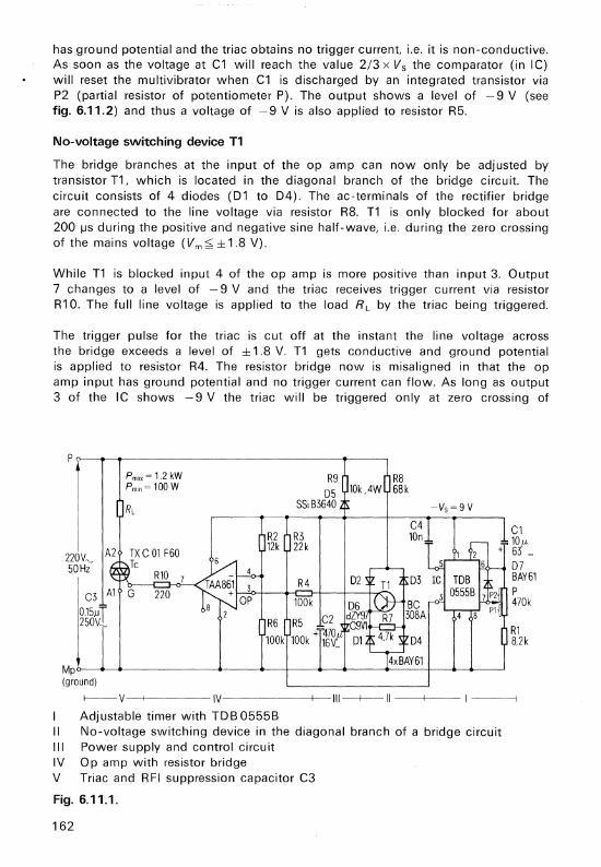
has ground potential and the triac obtains no trigger current. i.e. it is non-conductive. As soon as the voltage at C1 will reach the value 2/3 x V5 the comparator (in IC) will reset the multivibrator when C1 is discharged by an integrated transistor via P2 (partial resistor of potentiometer P). The output shows a level of -9 V (see fig. 6.11.2) and thus a voltage of -9 V is also applied to resistor R5.
No-voltage switching device T1
The bridge branches at the input of the op amp can now only be adjusted by transistor T1, which is located in the diagonal branch of the bridge circuit. The circuit consists of 4 diodes (01 to 04). The ac-terminals of the rectifier bridge are connected to the line voltage via resistor R8. T1 is only blocked for about 200 µs during the positive and negative sine half-wave, i.e. during the zero crossing of the mains voltage (V m ~ ± 1.8 V).
While T1 is blocked input 4 of the op amp is more positive than input 3. Output 7 changes to a level of -9 V and the triac receives trigger current via resistor R10. The full line voltage is applied to the load RL by the triac being triggered.
The trigger pulse for the triac is cut off at the instant the line voltage across the bridge exceeds a level of ± 1.8 V. T1 gets conductive and ground potential is applied to resistor R4. The resistor bridge now is misaligned in that the op amp input has ground potential and no trigger current can flow. As long as output 3 of the IC shows -9 V the triac will be triggered only at zero crossing of
p
Pmax=1.2kW R9 RB Pm;n=100W
05 10k.4W 68k
RL SSiB3640 -Vs=9V
C4 C1 R2 10n 105
A2 TXC01 F60 12k + 6 -
220V"' 50Hz Tc 07
R10 7 03 BAY61
C3 A1 G 220 p 470k
0.15µJ 250V~
R1 04 8,2k
Mpo-_.___. ______ .,.___~,.__-+ _ __. _ _._ __ ...__--+--+_._ _ __. (ground)
1----V IV Ill---+- II ---+--
I Adjustable timer with TD B 05558 II No-voltage switching device in the diagonal branch of a bridge circuit Ill Power supply and control circuit IV Op amp with resistor bridge V Triac and RFI suppression capacitor C3
Fig. 6. 11.1.
162

the ac line voltage. The described circuit controls the triac in the third and fourth quadrant. As soon as the voltage at C1 drops to a value of 1 /3 x Vs the multivibrator flops by the negative edge of the positive pulse at pin 2. The discharge of C1 is stopped and output 3 of the IC has again ground potential, i.e. the triac separates the load from the line.
% Vs +Vc1
1 1/3 Vs
0
0 Vout(IC1,3)
1
-9V-+-------! + 312 V--1---~~~
VRL (220 V)
1
- 312V-+----+'~~
Fig. 6.11.2. -T
Duty cycle
b
c
-t
a at capacitor C1 (zero point referred to -V5 =9 V)
b at output pin 3 of the integrated timer TD B 05558 (zero point referred to ground)
c at the resistive load R L· The 50 Hzpulse-train has the switch-on time t 1 , the pulse repetition period T is about 5 s in the case of fig. 6.11.1. The duty cycle may be adjusted by potentiometer P
The duty cycle is determined by resistor R1 as well as P1 and P2. It is normally limited to 50%. By connecting diode 07 in parallel to the partial resistor of potentiometer P2 duty cycles of less than 50% can also be obtained.
163

Components for circuit 6.11 Ordering code scs
stock number
Timing IC TDB0555B 067000-A 1 044 70139 Operational amplifier TAA861 Q67000-A89 8694 Triac TXC01 F60 C66048-A1500-A38 Silicon transistor BC308A Q62702-C285 8797 Silicon Z diode 1 W, BZY97 C9V1 Q68600-A952- F82 70149 plastic package (D0-41) Diode (VRRM=600 V) SSi B 3640 C66047-A 1062-A4 48403
5 Si-switching diodes BAY61 062702-A389 8579 M KH layer capacitor 10 nF±5%, 250 Vdc B32560-B3103-J 27562 RFI suppression 0.15 µF, 250 Vac B81121-C-F13 1802 capacitor (X) Aluminium electrolytic 10 µF, (+50 -10%) B41 286-A81 06- T 7836 capacitor 63 Vdc Aluminium electrolytic 470 µF, (+50 -10%) B41286-A4477-T 7889 capacitor 16 Vdc Potentiometer linear 470 kO B58621-Z474-M 26182 Carbon layer resistor 220 0/0.25 W, ± 5% B51261-Z4221-J1 37663 Carbon layer resistor 4.7 kO, 0.25 W, ±5% B51261-Z4472-J 37683 Carbon layer resistor 8.2 kO, 0.25 W, ±5% B51261 -Z4822-J 37688 Carbon layer resistor 12 kO, 0.25 W, ±5% B51261-Z4123-J 37690 Carbon layer resistor 22 kO, 0.25 W, ± 5% B51261 -Z4223-J 37694
1 Carbon layer resistor 68 kO, 0.25 W, ± 5% B51261 -Z4683-J 37942 3 Carbon layer resistors 1 00 kO, 0.25 W, ± 5% B51261-Z4104-J 37944
Wire resistor 10 kO, 4 W, ±5% B25295-A2103-J 26272
164

6.1 2 Overload Protection for a PTC Resistor Used in a Motor Protection Circuit
PTC resistors are generally utilized to protect motors against inadmissible excess temperature caused by overloads. As the resistance of this PTC resistor is to be only dependent on the temperature of the motor the operating voltage can be low (V~2 to 3 V). Practically there is no self-heating.
In practice, however, it may occur that the motor protection- PTC resistor is directly connected to the mains, e.g. during repair or during initial installation. In this case the resistor is destroyed.
To protect such a PTC resistor against mains voltages a fuse should be used, whereby a so-called" microfuse" which is very often utilized in transistor protection circuits offers a great benefit. It can be connected directly to the mains (220 V or 110 V).
If, however, voltages lower than 100 V are required for application to the PTC resistor the protection circuit has to be extended as shown in fig. 6.12. When an excess voltage (Vz) occurs the PTC resistor is short-circuited by the transistor and thus the microfuse reacts.
The resistance of R1 has to be dimensioned for high power peaks and not for a high constant-power, as the microfuse turns off after a short period of time. The turn-off time depends on the hight of the excess voltage and the resistance of the PTC resistor (temperature). In the described circuit a turn-off time of t0tt~2 s is guaranteed for a rated current being twice as normal. As a transistor is used for short-circuiting the PTC resistor, the mains ac voltage has to be rectified by the diode 1N4004.
BC 337
Fig. 6.12.
Components for circuit 6.12
Transistor Z diode Diode Fuse
BC337 BZX97 C30 1N4004 5 mA microfuse
fl-fuse 1 N 4004
Ordering code
Q62702-C313 Q62702-Z1246-F82 C66047-Z1306-A24
SCS stock number
70101 7360 48004
165

6.13 SIKAFIT, a PTC Resistor for a Smooth Quick-Start of Fluorescent Lamps
Almost every fluorescent lamp used in Western Europe is turned on by special glow starters. This results - as probably known - in a non-satisfying starting behaviour. During a time duration of seconds several fruitless trigger attempts occur before reaching the operational state. This also unfavourably influences the life of the lamps.
If an especially dimensioned PTC resistor is connected in parallel to the ballast, starting can be essentially improved (see fig. 6.13.1). The start is then fast, lamp preserving, and usually also without triggering. For the most common lamp types adequate PTC resistors, called SIKAFIT, are now available.
A typical characteristic of a PTC resistor is shown in fig. 6.13.2. If a voltage V is applied to such a component an initial current i0 =VI R 0 is flowing. The PTC resistor is heated up within a certain time ("switching time" t8 ) to its characteristic
Fig. 6.13.1.
3
0 Rb
Ro ~-;'"~~~~~~'
I
~11---1----------+-: --+--
Fig. 6.13.2.
166
9 0 Ambient temperature 9b Reference temperature (beginning of
the steep resistance increase at heating)
9e Final temperature R0 Initial temperature Rb (~2xR0 ) Reference resistance Re Final resistance at 9e (depends on
the thermal dissipation conditions)

reference temperature 9b. Its resistance increases rapidly in that the current drops to a very small value. The final resistance Re which will be adopted depends on the heat dissipation conditions. It is, in this case, rising at least to the power of two decades of the initial resistance R 0 . The power to maintain the highly resistive balance is about 1 W.
For the required application the PTC resistor has to be dimensioned relating to the initial resistance in that the resulting current flowing through the helice will have the desired value.
The relevant nominal resistances are in table 6.13.3. The initial current flowing through the PTC resistor at nominal conditions is also shown. This is necessary in calculating the switching time. During this switching time the lamp is highly heated. Furthermore, the choke is shunted in such a way that no triggering, caused by a high voltage pulse, can occur. With the auxiliary device, lamps with small and medium power usually fire after the first opening of the glow starter contact just by the mains voltage amplitude as a result of favourable conditions. The initially somewhat increased operating current then causes the PTC resistor to heat further until it finally reaches the highly-resistive state and practically gets ineffective.
Such lamps which need an increased triggering voltage even with a good preheating (e.g. 65 W lamp) allow a triggering only if the PTC resistor has reached a high resistance. Thus triggering attempts within the switching time of the PTC resistor remain ineffective, i.e. harmful cold starts are avoided. At the end of the relatively short switching time the lamp is well preheated and, under normal conditions, will fire immediately at the next starting trial.
Table 6.13.3
Lamp type 20W 40W 65 w
Ba last cap. ind. cap. ind. cap. ind.
Ra n 330 330 280 330 180 220 jo A 0.56 0.56 0.67 0.57 1.05 0.86
Investigations have shown that a switching time of 1 s is sufficient to obtain the best possible preheating. Lamps with low power have an optimal value of about 0.5 s.
The most favorable reference temperature the PTC resistor has to have depends on the application conditions. If the ambient temperature varies in a wide range (i.e. for illumination in the open air or in work-shops) the reference temperature should not be less than 100 °C. For living rooms, however, materials having lower temperatures may be considered and may even have certain advantages (simpler assembly, lower power dissipation during operation).
Naturally, the PTC resistor after turning-off the lamp needs some time to be cooled down to the ambient temperature and thus to become fully effective at the next turn-on. As the cooling is rapid in the beginning and the switching time increases
167

correspondingly, the cooling effect which is seldomly realized is of secondary importance. But it is very essential that no disadvantages are caused by this cooling effect with reference to the normal triggering process.
In view to subsequent mounting of the quick-start auxiliary device into any lamp type a suitable plastic package has been developed for the PTC resistor. The case is electrically and thermally isolated and has self clamping terminals. The dimensions are illustrated in table 6.13.4. Corresponding types for other fluorescent lamps will be advised on request.
Table 6.13.4 Short characteristics of SI KAFIT
Type40W 1 ) Type 65 W
Cold resistance R25 300 to 400 200 to 260 Q
Maximum case temperature during 9case 70 70 "C operation (on top of case) (at 9amb= +25 "C)
Thermal cooling constant Tth ~100 ~100 s Turn-on time at rated conditions ls ~1 ~1 s
Ordering code
1 063100- 063100-P9390-D140 P9390-D165
SCS stock number I 72262 72263 I 1 ) Can be used also for 20 W-lamps, however, the matching is not optimal.
168

6.14 Quick-Start Device for Fluorescent Lamps Using PTC Resistor and Series Diode
In chapter 6.13 a quick-starting method for fluorescent lamps has been described. A further decrease of the turn-on time can be realized by optimizing the pre-heating. In this case which is called "rapid start" a diode is connected in series to the PTC resistor. If an inductive balance is used a higher effective preheating current other than in the case of a direct short-circuit is achieved by de magnetization of the choke. Fig. 6.14.1 shows a rapid-start circuit for a tandem lamp of 2 x 20 W. For the triggering two starters connected also in series have to be used. As these starters operate independently from each other, i.e. they do not react exactly at the same time, the trigger characteristics of tandem lamps are usually disadvantageous. But the rapid-start device enables a triggering at the same time at least during the preheating period. Thus an advantageous operation of both lamps is realized.
Fig. 6.14.1.
Fig. 6.14.2.
40-W-choke -20W
20 w
-- ·--r---o _., :-- - - - -: St 151
I I I' I I
I I I I I I
- _J
L _____ _
169

Fig. 6.14.2 shows a rapid-start circuit with a capacitive ballast. Besides the already mentioned series diode another PTC resistor is connected in parallel to the phaseshifting capacitor.
List of components for circuits 6.14.1 and 6.14.2
Ordering code
1 Diode 1 N4004 C66047-Z1306-A24
SCS stock number
48004
For suitable types of PTC resistors please contact Components Sales Department of the Siemens AG, Balanstr. 73, D-8000 Munich 80.
170

7. Power Supply Circuits
7.1 Power Supply Using Precision Voltage Regulator IC TDB0723A
Fig. 7.1 shows a circuit of a power supply which may be considered as an alternation to the circuit already described in "Design Examples of Semiconductor Circuits, Edition 1977 /78, Page 135 ".
The advantage of the following circuit is in that the collectors of the four transistors, type 2 N 3055, can be mounted directly on iron sheet of the chassis. Therefore the thermal resistance between transistor case and heat sink device is low. The output voltage is adjustable by potentiometer P (2.5 kO). The resistor R 0 determines the threshold of the short-circuit current limitation Umax~0.7 V/R0 ). The TDB0723A incorporates also an excess temperature protection circuit. Four transistors, type 2 N 3055, have been connected in parallel because of the high output current required.
Components for circuit 7.1 Ordering code SCS stock
number
1 Voltage regulator IC TDB0723A 067000-A 1069 70322 4 Transistors 2 N 3055 062702-U58-F14 71214 1 Transistor BD 135 062702-0106 70121 1 Bridge rectifier SSi4E11 /12 B 30/25-8 C66117-A5002-A201 48024 1 Styroflex capacitor 470 pF 83111 O-A1471-K 1578
Electrolytic capacitor 22 µF/40 V 841286-A7226-T 7833 Electrolytic capacitor 4.7 mF/40 V 841070-87478-T Electrolytic capacitor 10 mF/40 V 841070- K7109-T
171

3 = c: ci
Fig. 7.1.
172
~ +
<i = (") = "' ,..._
> 0
~ c:>~-> -~_;;;;;....;;,;.. .... -I I
-> ~ s
·~ ~E
~:-
LO LO
= (")
= "' x -.j-
~
-~J---
kl d kl =
I
LO
"" -- n = (")
=
x N

7.2 Short-Circuit Proof Charging Device for 6 A at 12 V Offering Preserving Charging and Automatical Cut-Off
The charging process has three phases as shown in fig. 7.2.1. During phase A-B, for instance, a charge current of only 2A is flowing in the event of a totally discharged accu. Thus the charging device is protected against overload. In the second phase C-D the charging is achieved with maximum constant current. During the third phase E F, above the gas voltage, a strongly reduced current is used for charging. A higher volwge causes the current to drop down to (;Ut-off.
Description of the circuit
The circuit is shown in fig. 7.2.2. The power control comprises two epibase transistors, type BD 646 (T2, T3). In spite of the current control and the parallel connection of the two power transistors T2 and T3, no series resistor is included in the basic current-circuit. This provides small total power dissipation. As the current control must not be extremely accurate when using chargers the current-impression can be realized by the base current. If two transistors are coupled, no current distribution by resistors connected in series to the emitters is necessary. If the transistors do not have the same current-gain characteristics, different currents would arise and thus different power dissipations in the transistors. When the maximum power dissipations of two uncoupled transistors are known and the difference taken into account by inserting an adequate heat-sink, even different transistors may be connected in parallel without resistors for the current distribution.
The result is that the base current to a great extent determines the load current. The base current, however, depends on the symmetrical resistors R5 and R6, on
;1 P2-61-
Iaccu sL-t
3 -
A 2P--+-~-r---t-~-t-~~--+-----j-t---+-----1
P1-+=~~ . oLj _ _J___
0 2 4 6
Fig. 7.2.1.
-~~-L--~---=-f _J 141 16 v 18
~Vaccu
10 12
P3
A-B Reduced charge current at discharged accu between 0 and 10 V.
C-D Charging with full constant current at accu voltages between 10 and 14.4 V. The current is adjusted by P2. The transition from B to C depends on the temperature.
D-E Abrupt decrease of the charging current at a threshold voltage of 14.4 V to a lower value being adjusted by P1. The threshold voltage is adjustable by P3.
E-F Further decrease of the charging current at increasing accu voltages down to the cutt-off Fat 16.5 V.
173

418V, SA max.
10000µ 40V-
R1 12k
R2 10k
D1 BZX97 CSVB
R3 82k
Heat sink 2x2.5 K/W
r---------------, I I
I I I I
RS : 2,2k J
.__ _ _,__ I
R~X97
I I
C 5VS Rg
R7 B,2k
RB 8,2k
4,7k
P3
R10 3,9k
"T" I I I
I v".,=14.4to1S.5V I I I I I
...L
TrD v, 220 v L-<i>-------+---------<t-----<>----'
Fig. 7.2.2.
the PTC resistor KL, on the parallel connected potentiometers P1 and P2 (at conductive T1) as well as on the output voltage of the operational amplifier.
The PTC resistor KL is responsible for thermal protection, It is mounted on the common heat sink of the power transistors T2 and T3 with a good heat-conduction. If this heat sink reaches a temperature of + 100 °C, for instance by overload, overvoltage or insufficient air-conditioning, the PTC resistor gets a high resistance. The base current and thus the charge current are reduced in that the power dissipation and with it the heating decrease to a permissible value.
Adjustment of the charge currents
Besides the three adjustment possibilities for the charge currents, which all interfere, the adjustment is conveniently simple. First, the switching threshold of 14.4 V is adjusted by potentiometer P3. Then with P1 the value for the residual current above the flip point (point E, fig. 7.2.1) has to be set. Finally, the charge current rating has to be adjusted by means of P2 below the flip point (phase C-D). The initial current (phase A-B) depends on the adjustment of the residual charge current and is 30 to 100% higher than the residual charge current adjusted by P1, following the transistor characteristics. The rated load current (/Nd and the residual charge current (/RL) have to be adjusted with reference to the Ah-capacity of the accu. Relevant approximative values are
Ah-capacity /NL';:;; 5 h
and / ~Ah-capacity RL~ 20h
174

Components for circuit 7.2.2 Ordering code scs
stock number
Operational amplifier TAA 761A Q67000-A522 7236 (plastic package, 6 pins)
1 Silicon N PN transistor 8C237 Q62702-C697 70090 2 Silicon PN P power 80646 Q62702-D232 71359
Darlington transistors Small rectifier set E29-830/ C66067-A1740-A5 4677 (moulded) 25-10 Silicon switching diode 8AY61 Q62702-A389 8579 2 diode 82X97 /C5V6 Q62702-21229-F82 7343
0.5 w 2 diode 82X97 /C6V8 Q62702-21231-F82 7345
0.5W PTC resistor NAT95°C Q63100-P366-D201 72015
R25 = 70 0 Vmax=20 V
Aluminium electrolytic 10000 µF 841111-K7109-T 2739 capacitor 40 Vdc Styroflex capacitor 220 pF 831063-A5221 -H 2389
63 Vdc 2 Carbon layer resistors 2.2 kO 0.3 W 851261-24222-J1 37677
±5% Carbon layer resistor 3.9 kO 0.3 W 851261-24392-J1 37681
±5% Carbon layer resistor 4.7 kO 0.3 W 851261-24472-J1 37683
±5% 2 Carbon layer resistors 8.2 kO 0.3 W 851261-24822-J1 37688
±5% Carbon layer resistor 10k00.3W 851261-24103-J1 37689
±5% Carbon layer resistor 12 kO 0.3 W 851261-24123-J1 37690
±5% Carbon layer resistor 82 kO 0.3 W 851261-24823-J1 37943
±5% Carbon layer resistor 1 MO 0.3 W 851261-24105-J1 37957
+5% Potentiometer 22 kO 0.1 W 858042-20223-M320 26689 Potentiometer 4.7 kO 0.1 W 858042-20472-M320 26687 Potentiometer 2.2 kO 0.1 W 858042-20222-M320 26686 Mains transformer M 102/35, Dyn. sheet IV /0.35 without air gap
N1 725 turns, 0.65 varnished copper wire N2 50 turns, 2.0 varnished copper wire (or 4 x 0.95 varnished copper wire)
175

7.3 Control Circuit with Transformer for Push-Pull Switch Mode Power Supply
Push-pull switch mode power supplies (SM PS) for higher voltages require a keycontrolled operation with blanking intervals to avoid high commutating currents flowing through the switching transistors. These currents are generated since the transistors have finite charging times between 2 and 3 µs. Generally it is very difficult to transmit blanking intervals by using only one transformer because of the undesired overshoots at pulse edges. Therefore two transistors are recommended for circuits with higher output powers and higher supply voltages.
The circuit shown in fig. 7.3.1 demonstrates a solution with only one driving transformer. It transmits the corresponding staircase voltage. The supply voltage for the driving circuit can be derived from the SM PS directly or from any other source.
The generator voltage at the input is in a range between 30 and 50 V pp· If necessary the phase of the output signal can be adjusted by potentiometer R1 . The pulse symmetry is set by R 2 , whereas R 3 and R 4 adjust the blanking intervals. The blanking pulses are differentiated by the 3.3 nF-capacitor and the control transistor T10 . They are applied to the driving transistors via T3 to T7 .
The bases of transistors Ts and T9 are based by a divider to a level being half of the supply voltage. Thus an unobjectionable transmission of the blanking intervals is guaranteed. The positive blanking pulses control transistor Ts whereas transistor T9
is driven by the negative ones. Every inductively - generated, fly-back voltage at the two emitters is automatically attenuated by one of the corresponding transistors. Both signal paths have been crossed to achieve equal propagation times.
Diode 0 1 connected to the base of T1 is responsible for time symmetry.
A reversed current-flow via the base of each transistor T3 and T5 is avoided by diodes D 2 and D 3 .
During the uncontrolled state the transistors T6 and T7 are non-conductive. Therefore half of the supply voltage Vs is applied to the base of each transistor Ts and T9 .
It is very important that the driving transformer has a very low stray inductance.
The primary windings 1-2 and 3-4 have to be split into two sections because the secondary windings 5-6 and 7-8 have to be inserted between them (refer to fig. 7.3.2).
176

---- ------···- - ------
47k
Time symmetry lOk
30 Vee ,1
Vk
rv 5 k R1 10 k O,lµF
[~·1-=-~~ --- rOnf ~~~7
Fig. 7.3.1.
E E 25
Fig. 7.3.2.
1 - 2 3 - 4 5 - 6 7-8

Components for circuit 7.3.1 Ordering code SCS stock
number
5 Transistors BC237 B 062702-C277 8827 2 Transistors BC307 B 062702-C324 8879 1 Transistor BC337 062702-C313-V1 8834 1 Transistor BD 137-10 062702-0108-V2 8811 1 Transistor 80138-10 062702-0109-V2 8822 5 Diodes BA 127 D 060201-Y127-09 70044
Z diode BZX97 C24 062702-Z1244-F82 7358 1 Styroflex capacitor 22 pF 831110-A 1 220- F 1562 2 M KT capacitors 3.3 nF B32535-C6332-K
M KT capacitor 22 nF B32535-C3223-K M KT capacitor 0.1 µF B32535-C1104-K Electrolytic capacitor 4.7 µF B41286-A9475-T Siferrit core EF25(Tr1) B66207-AOOOO-R027 Coil former for EF25(Tr1) B66207-A1003-R001
178

7.4 Control Circuit for Push-Pull Switch Mode Power Supply with 2 x BO 647
The circuit shown in fig. 7.4 is favoured for driving switch mode power supplies (SM PS). It operates without any control circuit. The operating voltage for the control circuit is 30 V and can be supplied from the SMPS itself or from any other source. The supply voltage for the drivers (5 V) or the resistances of the driver collector resistors can be varied with reference to the base currents of the output transistors. !f higher output currents are required a cirt;uit with driving transformers is recommended. The generator source voltage or the reverse feedback voltage at the input should range between 30 and 50 VPP' The phase of the output voltage can be adjusted by resistor R1. A coarse symmetry of the signal is obtained by diode 01 connected to the base of transistor T1, whereas a fine adjustment is achieved by potentiometer R2. A square wave voltage is available at the base as well as at the collector of T1. It is differentiated by the 3.3 nF-capacitor with reference to the control current of transistor T5 (BC307 B). This current is set to a determined rated value by the reference diode 06 and the potentiometer R5. In this case the output voltage is indirectly controlled. If the control should be influenced by the output signal an optoelectronic coupler or a transformer has to be used.
After the phase reversal at transistor T2 the square wave voltage is differentiated again by a 3.3 nF-capacitor. Both signal paths are separated by means of the two fast-reacting diodes 04 and 05 being components of the control circuit.
47k
Time symmetry IOk
30 to 50 Vpp, 10 kHz R2
rv 5k 10 k
0,1 µf
Phase
Rl mr BA 127
Fig. 7.4.
Uk
Blanking ~ intervall ~k
P3 /
BC 237 8 3,lnf ~--~-----I~ -- -+~~~
100 k 2Zpf
BC 307 B
-----,---0 .Jo v ----.--+----.----<J·S V
IOk
Control range 1-4-~l<"+----OW 2,5 k R5
..LzznF T5 T 06
1./Zk
.L
179

The blanking intervals are adjusted by potentiometers R3 and R4. The differentiated pulses are amplified by the Darlington transistors T3 and T4 and applied in push-pull to base 1 and 2 of the output-stage transistors, whereby the two 100 µF - electrolytic - capacitors transmit the control and turn-off currents.
Components for circuit 7.4
2 Transistors 1 Transistor 2 Transistors 5 Diodes 1 Z diode 1 Styroflex capacitor 2 M KT capacitors 1 M KT capacitor 1 M KT capacitor 1 M KT capacitor 2 Electrolytic capacitors 1 Electrolytic capacitor
180
BC237 B BC307 B BD647 BA127 BZX83C24 22 pF 3.3 nF 4.7 nF 22 nF 0.1 µF 100 µF 220 µF
Ordering code
062702-C277 Q62702-C324 062702-D233 060201 -X1 27 062702-Z1086-F82 B31110-A 1220-J B32535-C6332-K B32535-C6472-K B32535-C3223-K B32535-C1104-K B41283-B5107-T B41010-E9227-T
SCS stock number
8827 8879 71357 8019 7326 1562
7877 7859

7.5 Control Circuit for Push-Pull Switch Mode Power Supplies with 2 Driver Transformers
Push-pull circuits for switch mode power supplies (SM PS) with higher voltages require a key-controlled operation with blanking intervals to avoid high commutating currents flowing through the switching transistors. These currents are generated as the transistors have finite charging times (2 to 3 µs). Generally it is very difficult to transmit blanking intervals by using one transformer because undesired overshoots at pulse edges ilre generated.
In the circuit shown in fig. 7.5 two driving transformers are used. They transmit the signals with a phase shift i.e. the blanking intervals are also transmitted. The operating voltage for the control circuit can be supplied from the SM PS itself or from any other source.
The driving voltage at the input is between 30 and 50 VPP" If necessary the phase of the output signal can be influenced by potentiometer R1 . The potentiometer R 2 adjusts the symmetry of the signal and the blanking intervals are set by potentiometers R 3 and R4 . The blanking pulses are differentiated by the 3.3 nF-capacitor and the control transistor T9 . They are supplied to transistors T3 and T4 . A negative current for the base of T3 and T4 is avoided by two diodes, D3 and D 4 .
The two fast-reacting diodes D 5 and D 6 and the two 3.3 kO-resistors decouple the two signal paths and suppress common-mode interferences.
The control current is set to a defined value by reference diode D 7 and potentiometer R 5 .
No additional RCD-components are required for suppressing overshoots for an unobjectionable signal transmission. The positive blanking pulses (pulse duration) control the transistor T5 and the negative ones (pulse space) the transistor T6 .
Every inductively generated flyback voltage at the two emitters is automatically attenuated by one of the corresponding transistors. If there is no control the transistors T5 and T6 are non-conductive. The output transistors can be arranged as shown
in fig. 7.6.1.
181

,,
?, Z.1k10.5W r~JB '" OJ cp'
~- -! N
3,3k/1W 137
:....i
2 3
: ~0utput
!-11
~"' '" t T5 5 I R1 Pulse space 1
stage 1 10 k I 1 LI 6 4
I
IBC Phase 1 : 2372, ..
v lI~ I BC 237B -l... I o) k ~z.~ gs 10k -I I 0,1µF-,-l\J 1:1 ' d::4.7 n *'n• U
100µF
10 k BO~ +_, + 0+35 to 50 V
T1 I 3.3 nF T7 --· to output stage 2
Bc 231Bit11 r UH IL/"U~ I 1 r;\ E>I xQ 4
I 2.7 k
Tr1
R, T [ [3.3k _____ P_ul_se_ space 2
3,3 nF R5 5,Bk
10 nF
Tg

Components for circuit 7.5 Ordering code SCS stock
number
4 Transistors BC237B 062702-C277 8827 Transistor BC327 062702-C311 70099
2 Transistors BO 137 /16 062702-0108-V3 2 Transistors BD138/16_ 062702-0109-V3 6 Diodes BA 127 D 060201-X127-09 70044
Capacitor 2.2 nF B32535-C6222-K 2 Capacitors 3.3 nF B32535-C6332-K 2 Capacitors 4.7 nF B32535-C6472-K 1 Capacitor 0.1 µF B32535-C1104- K1 2 Capacitors 1 µF B32535-C1105-K 1 Electrolytic capacitor 100 µF B41010-B9107-T 7858 2 Transformer cores EF 25 (Tr1) B66207-A0400-L026 2 Coil formers for E F 25 B66208-A1003-R001 33605
183

7.6 1 kW /20 kHz-Generator with Output voltages of 500 V and 40 Vat 25 A
Fig. 7.6.1 shows the circuit for a 1 kW-generator. Its principle of operation is as follows. At the base of T1 positive pulses are generated by a feedback via windings n4 and n5 or by any other corresponding signal source. The transistors T, and T3 are turned on. The maximum minus-voltage is applied via the 1 µFcapacitor to transformer Tr1. If the transistor T1 is turned off the transistor T2
is conductive and the maximum positive-voltage is supplied to Tr1. Thus a square wave voltage with a low source impedance is generated. It controls the power transistor T4 and turns it on and off. The recovery currents are such high in that the transistor T4 can be switched fast enough. Directly after the conductive period of T4 the voltage at the collector-emitter-junction is kept in that the turn-off current can be decreased sufficiently and in that the collector voltage is not increasing inadmissibly.
The start of the oscillation is achieved by applying the operating voltage to the prestage transistors when the circuit is connected to the mains. The operating voltage is derived either from the rectified mains voltage in conjunction with a RCZ-circuit or from any other separate power supply. In some concepts it may be advantageous to apply a starting de-current via the base divider to the transistors T4 and T, to guarantee the oscillation-generation for all stages. At self-oscillating circuits the oscillation is interrupted immediately when a short-circuit happens or is increased towards higher frequencies if the transformer has a greater stray inductance. The blanking intervals are determined by the time circuit consisting of C1 and R1 .
Fig. 7.6.1.
184
I - - - - - - - - - -~ - - - -- - -- - - - - - 1 50.0 V I 220 k 2Z k 1 1 f,F I ,- - --c=J- _J__ i~ - -
ru Tr 3
10 -~h--40V
i0'; I g I
n2 I I I I
-'----__.____.__ __ __. I

The pulse duration can be adjusted by resistor R, if a control voltage is applied. For variable blanking intervals the resistance of R1 or the ±24 V-supply-voltage has to be changed.
The explained principle of operation also applies correspondingly to the other amplifier of the push-pull circuit. For the transformer Tr3 a Siferrit core N 27 with a seize PM 87 0 x 70 mm and an air gap of approx. 1 mm (inside} has been used.
Components for circuit 7.6
2 2 2 2 2 2 2 2 2 1 1
Transistors Transistors Transistors Transistors Diodes Diodes Capacitors Capacitors Capacitors Capacitor Electrolytic capacitor
n;
I Tr 1 I I
!E I I
Ordering code
BU208 Q68000-A494-F193 BC237 B 062702-C277 80137-10 Q62702-D108-V2 80138-10 Q62702-D109-V2 BA 1270 Q60201-X127-09 1N4001 C66047-Z1306-A21 10 nF/>100 V 832510-03103-K 22 nF/100 V 1 µF/>100 V 1 µF/630 V 100 µF
B32650-J0223- K 832511-01105-K B32334-A8683-M B41283-A8107-T
!-----------
I!-----------
l1----------~ 1
Winding schematic for transformer Tr1
Core EF 25/N 27
Coil former
B 66 207 - AOOOO - R027
B 66 208 -A1003 - R001
1-2 150 turns 0.25 0 enamelled copper wire
3-4 30 turns 0.4 0 enamelled copper wire
5-6 150 turns 0.25 0 enamelled copper wire
Fig. 7.6.2.
SCS stock number
71326 8827 8811 8822 70044 48001 28923
7880
185

Fig. 7.6.3.
186
Winding schematic for transformer Tr 3
Potcore: 87 mm 0 x 70 mm, L = 1 mm (inside)
B 65713 - AOOOO - R027
Coil former: B 65714-A1001-T 001
1-2 22 turns stranded wire 120 x 0.1 0 double enamelled copper wire 3-4 22 turns stranded wire 120 x0.1 0 double enamelled copper wire 5-6 22 turns stranded wire 120 x 0.1 0 double enamelled copper wire 7-8 22 turns stranded wire 120x0.1 0 double enamelled copper wire 9-10 5 turns stranded wire 10x(120x0.10 double enamelled copper wire)

8. Digital Circuits
8.1 Reaction-Time Test Device
With the device the circuit of which is described in fig. 8.1 it is possible to test ones typical reaction time under different physical conditions. Because of its power supply with batteries a mobile operation is feasible. The clock generator (f = 100 Hz) consists of two I Cs, type FLK 101, and the adjacent components. The two monostable multivibrators automatically trigger each other.
The output signal of the clock generator (pin 1) drives the frequency divider, consisting of three I Cs FLJ 181, as well as the decade counter comprising the three ICs, type FLL 171.
A random time between 0.5 and 20 s is generated by the frequency divider. When the start push button is pressed only the dividers of IC 3 are reset via inverter R. As the clock is still running the content of the two other divider-ICs is undefined and it depends on accident when the pulse being available at pin 12 of inverter S is displayed at the beginning of the test time.
When the start push button is operated the RS-flipflop consisting of NAN D-gates _is set. The pulse of its output II is supplied via a 1 nF-capacitor to another RS-flipflop incorporating the NANO-gates C and D. The decade counter is reset to "000" and the first two digits are blanked in that only a "0" is displayed.
When the random time has passed the second flipflop is reset via inverter S. On the display the other two "0" are visible. If the switch S 2 is in its upper position "acoustical" a 1 00 Hz-signal is supplied via the inverters L M, N to the base of transistor BC338, which drives a loudspeaker. Now the decade timecounter consisting of the three ICs, type FLL 171 runs. In the first instance the count is not displayed.
The operator of the test-reaction time device should then immediately press the stop push button to reset the first flipflop and to stop via inverter E the time counter. Then the accumulated count is displayed or the tone is turned off.
If the stop push button is not operated within the maximum displayable time of 9.99 s an automatic stop is realized by the decade counter and the inverters G, H, J and K. In this case "9.99" is displayed.
The device can also be utilized as a stop watch. In this case the counter runs immediately after the start push button has been pressed. The count is always displayed and the automatic stop at 9.99 s is ineffective. The operation may also be used for calibrating the test time. In this case a longer clock time is compared with those of a normal watch and the 5 kO-potentiometer is adjusted correspondingly.
187

10 121 111 12 11
FLK 101 CD 14 FLJ 181G) 14 FLJ 181 (D 14 FLJ 181 CD
M10
r----1"'-0.5 A --clo, r o -I- 4,5V t10µF/5V -D- 115 FLH 271 =[)-114 FLH 101
E
[8a BC 338

Components for circuit 8.1 Ordering code scs
stock number
2 NAN D-gates FLH 101 (7400) 067000-H1 8658 2 Inverters FLH 271 (7405) Q67000-H154 8774 2 Monoflip-flops FLK101 (74121) 067000-K13 8910 3 4 bit binary counters FLJ 181 (7493A) Q67000-J34 8763 3 Decimal counters FLL 171 (74143) 067000-L58 70723 1 Transistor BC338 Q62702-C314 70102 3 7-Segment-LED- HA1101r 030-X313 71283
Displays 2 M KH layer capacitors 1 nF/400 V 832560- D6102-J 1 M KH layer capacitor 10 nF/400 V 832560-D6103-J 2 M KH layer capacitors 1 µF /100 V B32561-D1105-J 1 Electrolytic capacitor 10 µF/6 V B41313-A2106-V 1931 1 Resistor 330 0 B54311-Z5331-G1 28552
Resistor 1 kO B54311-Z5102-G1 28509 Resistor 4.7 kO B54311-Z5472-G1 28524 Resistor 6.8 kO B54311-Z5682-G1 28528 Potentiometer 5 kO lin.
1 Mini loud-speaker 8 0/0.2 W; ~600 3 2 pole reversing switches 2 Push buttons Make contact
(1 x red, 1 x green) 3 Batteries 1.5V(Baby;
Alkali-Mangan)
189

8.2 Control Circuit for Touch-Keys with S056H
Fig. 8.2 shows a circuit of a control device with touch keys for two channels. The monolithic IC S 056 H offers 4 output drivers, but in the described application only two of them are utilized. When the touch key "on 1" is operated the first stage is set and the output at pin 15 has the level of the power supply voltage. Thus the relay 1 pulls up. When the touch key "off 1" is operated the second stage which is not utilized in this application is set ... A switching pulse is available at the corresponding output and resets stage 1. Thus the transistor BC 338 is turned off and the relay drops.
The touch key pair "on 2/off 2" operates correspondingly. In this case the load is a relay. It is directly connected to the output pin 11 which supplies a maximum driving current of 55 mA. Diode BA 133 F protects the circuit against wrong polarity.
Fig. 8.2.
190
On 1 Off1 On 2
6 6 6
16
S 056H
Off 2
6
Reed Relay
BA 127 d
.___.__ ___ _._ _____ ...------1 TDB 7808
I~ bA bR bM
BA 133 F
10to 14V

Components for circuit 8.2 Ordering code SCS stock
number
Switching amplifier S056 H 067000-S36 Positive voltage regulator TDB 7808 067000-A 1053 70327
1 Transistor BC338 062702-C314 70102 2 Diodes BA 127 D 060201-X127-D9 70044 1 Diode BA 133 F 062702-A505 4 M KH layer capacitors 10 nF B32560-D6103-J 1 Resistor 1 kO 0.3 W B51261-Z4102-Jl 37672 2 Resistors 15 kO 0.3 W B51261-Z4153-J1 37691 4 Resistors 1MO0.1W 4 Resistors 6.8 MO 0.1 W
1 91

9. Microcomputer Systems
9.1 Two-Position Temperature Control with the Microcomputer System Kit SIKIT-DK/8080
The two-pos1t1on temperature control is frequently used in control systems. It is particularly suited for temperature control in household appliances, heating, cooling equipment and for automotive industry.
An application example of a two-position temperature control is the use with the microcomputer system kit SI KIT-D Kl8080. The AID-conversion of the actual temperature value is mainly achieved by the microcomputer in a cost effective way, and may be used also for the AID-conversion of other physical quantities by means of suitable sensors. This principle is also adaptable for the microcomputer systems 8085 and 8048. The assembler programme described in detail eases the use of control as a subprogramme.
Fig. 9.1.1 shows the control characteristic with different on- and off-values which are typical for this kind of control. In this example, the temperature rating is Trated = 60 "C and the hysteresis amounts ± 2 "C.
0 20
Fig. 9.1.1. --------.. Tactual
40 60 °C 80 58 °c~_J l___ 62 °C min. Trated max
The total circuit diagram (fig. 9.1.2) includes the microcomputer system kit SIKITD K18080 and the timer TD B 0555 B. The NTC resistor M 822 is utilized as temperature sensor.
Analog-Digital Conversion
The NTC resistor changes its resistance RH in dependence on the temperature following the e-function:
8(1_ _ _!__) RH =RN xe r TN
whereas
RN=nominal temperature B =material constant T =absolute temperature in K TN= nominal temperature in K
192

Heating On ALARM
RH R1 LO 57C 18 k 1" 1"
RT
180
8 Output
TDS 3 0555 s Trigger
2 5
C5 Cr
330n 10n 2X sex 58
Fig. 9.1.2.
t'l-J=~~--~-Monoflop-triggering -- t im--~ --l-----1' .... ~-~ .... r~-~e .... rs-io_n
Monoflop-output, tM min i-1-1 Strobe I ]
1lli~-~ltl Monoflop-output, tM max
Fig. 9.1.3. -r
LD 52
180
+5 v
SIKIT-DK/8080
21 C4lnput PORT C of
10k SAS 8255
o~~~~~-~~~~~~
0 w ~ w 00 ~100 -r
Fig. 9.1.4.
This analog value cannot be directly applied to the microcomputer. The thermistor resistance has to be converted in a proportional time period. This can be achieved by the cheap timer- IC TD B 0555 B. Then, in turn, the time is converted in a binary number by the microcomputer.
The timer acts as monostable multivibrator (fig. 9.1.2) whose output pulse duration tMF is determined by the RTCrcircuit:
t M F = 1 . 1 x RT x c T·
193

The pulse duration is dependent on the supply voltage, i.e. the + 5 V voltage applied to the microcomputer system kit may be used also for the timer. The trigger and output levels of the TD B 0555 B are TTL-compatible and can be directly supplied to the programmable interface IC, SAB 8255.
Function
Fig. 9.1.3 shows the time-response of the A/D conversion. The microcomputer supplies a pulse with a duration of about 7 µs to the trigger input 2 of the timer via pin C 0 of the programmable interface IC, SAB 8255. The monoflop is started, output 3 changes to positive potential. Now, a count loop is established in the microcomputer, whose run time tcvcre = 21 µs. The time is determined by the crystal of the microcomputer and the programme. It serves as a very accurate reference.
As soon as the loop is completed, output 3 is read and as long as level is "high" a 1 is added in the register pair B, C of SAB 8080 A. At "low" the counter is stopped; the register content corresponds to the actual temperature value.
Accuracy of A/D conversion
Fig. 9.1.3 illustrates the principle error of the procedure with a maximum of +1 bit. It may be seen that the accuracy increases proportionally to the number of count cycles. In the example of fig. 9.1 .1 a cycle number of 190 is obtained at a rated temperature T rated min= 58 'C. Hence the maximum resolution error is approximately +0.5%.
Temperature characteristic-maximum values for line cut-off, short-circuits and rated values
Fig. 9.1.4 shows the relative temperature response of the total resistor RT and the monoflop time tM F·
The lowest temperature determines the limit value for a line interruption between sensor RH and IC. In the given example Tm; 0 =0 'C. On account of the exponential function of the NTC resistance it would result, with respect to the rated temperature of Trated=60 'C, a count time which is 19 times longer and which would block the microcomputer for a long time. Consequently, resistor R 1 was connected in parallel and this limits the strobing time to 1.7xtrated· R1 , however, reduces the rise of the characteristic and should not have a too low resistance.
The maximum short-circuit value is determined by the highest occurring temperature. In our example T max= + 1 00 'C. The series resistor R 2 protects the timer against overload.
The number of loop runs of the A/D converter can be calculated as
1.1 xRTxCT n=-----
194

Our example leads to the following values:
a) Normal operation:
T,ated max=+ 62 "C RT=10.30 kQ, n,ated max=178 Trated min= +58 "C RT=11.01 k, n,ated min=190
b) Line cut-off:
TLco<O °C 18.21 k0<RT<19 kO, 315<n<328.
c) Line short-circuit:
TLsc>100 °C 1 k0<RT<4.89 kO, 17<n<85.
Total control error
With the circuit as shown in fig. 9.1.5 the tolerances of components as RH, R1, R2 and CT, the SIKIT quartz frequency and the timer switching point can be adjusted in that only the TC of the mentioned components and the quantization error of the A/D converter will have influence.
At the rated temperature of + 60 "C the monoflop characteristic as shown in fig. 9.1.4 has a rising edge of 63 µs/°C which corresponds to 3 count cycles of the A/D converter. Thus the quantization causes an error of 0.33 °C.
Flow chart
The subroutine "TEMP" for the temperature control (fig. 9.1.6) begins with the triggering of the monoflop via output C 0 of the programmable interface IC. Then

Fig. 9.1.6.
196
Monoflop-Start
Monoflop strobe
Subroutine
Gp Output gate c ~0
(actual value generation)
Strobe line interrupt
Strobe line shortcircuit
Comparison of rated and actual values
( RET )

a count loop is provided which is necessary for the A/D conversion of the actual temperature value described above. It follows the checking of line interrupt and short-circuiting with the limit values of G RU and GR K. Disturbances produce in both cases alarm and disconnect the heating. If the actual value is between the limits of GRU and GRK a possibly preset alarm command is reset by ALAUS. The comparison of the actual and rated value follows. For that purpose the microprocessor compares the rated value data allocated in the RAM with the actual one. To realize the required two-position temperature characteristic, SOMIN and SOMAX are stored alternatively in one section of the RAM. When the temperature is higher than the rated value (actual value <rated value) the heating is cut-off and with SOMIN the minimum rated value is stored in the RAM. If the temperature gets too low, the heating turns on and the maximum rating is allocated in the RAM with SOMAX.
The storage of the minimum and maximum ratings offers the advantage in that the rated values can be varied by other subroutines. Besides that these ratings can also be stored in one of the MP-registers. But this register has not to be changed by any other subroutine.
After the device is turned on an undefined rated value is stored in the RAM during the first programme run. This will result in an undefined state for the heating. Only after the second run, which happens normally after a few seconds, the heating is switched on in a defined way.
Assembler programme (subroutine)
The EQU-pseudo-instructions determine the control word for the selected 1/0 interface devices, for the limits of the line interruption, for the limits of the short-circuit and for the rated value. The subroutine "TEMP" needs a ROM-capacity of 79 x 8 bit.
Label Op. Operand Time Comment Code µs
CWR EQU 0F7H Address of control word register of SAB 8255 PORTC EQU 0F6H Select a SAB 8255 and its port C NGRU EQU 3AH } Limit value of line interrupt HGRU EQU 01 H NGRK EQU 54H } Limit value of line shortcircuit HGRK EQU 00 SOMIN EQU 0BDH Rated value T min
SO MAX EQU 0B1H Rated value T max
MERK EQU 1 ***H Address for special location in the RAM TEMP: MVI A, 8AH 3.5 Determine operation mode "0" of the SAB 8255
(control word No. 6) OUT CWR 8.5 LXI B, 0 13.5 Set registers B, C to 0
STAMF: MVI A, 0 3.5 Set output Ca of SAB 8255 to 0 and OUT CWR 8.5 start monoflop MVI A, 01 12 Set output Ca to 1 and OUT CWR 17 reset monoflop trigger
197

Label Op. Operand Time Comment Code µs
ABFMF: IN PORTC 5 Strobe mo noflop output
ANI 10H 8.5
JZ LTGU 13.5 l c'""' mask for input C4
INX B 16 loop
increment register B, C JPM ABFMF 21 Jump
LTGU: XRA A 2 Line interrupt, carry to 0 MVI A, NGRU 5.5 Load accu with least significant byte of GRU SBB c 7.5 NG RU-NIST with carry MVI A, HGRU 11 Load accu with most significant byte of G RU SBB B 13 HGRU-HIST with carry JNC LTGK 18 At carry=0-+jump to line shortcircuit
ALEIN: MVI A, 05H 3.5 Output C2 to 1 OUT CWR 8.5 JMP HZGA 13.5 Jump to heat OFF
LTGK: XRA A 2 Line shortcircuit, carry to 0 MVI A, NGRK 5.5 Load accu with least significant byte of GRK SBB c 7.5 NGRK-NIST with carry MVI A, HGRK 11 SBB B 13 HGRK-HIST with carry JNC ALEIN 18 At carry=1-+jump to alarm ON
ALAUS: MVI A, 04H 3.5 0 utput C2 to 0 OUT CWR 8.5
SIV: XRA A 2 Comparison of rated and actual value, carry to 0 LOA MERK 8.5 Load accu with content of special RAM location =rated
value SBB c 10.5 SOLL-NIST with carry MVI A, 0 14 Load accu with 0 SBB B 16 0-HIST with carry JNC HZGA 21 At carry=0-+jump to heating OFF
HZG~: MVI A, 03H 3.5 Output C1 to 1-+ heating ON OUT CWR 8.5 MVI D, SOMAX 12 Maximum rated value into accu STA MERK 18.5 into special RAM location RET 23.5
HZGA: MVI A, 02H 3.5 Output C1 to 0-+heating OFF OUT CWR 8.5 MVI A, SOMIN 12 minimum rated value into accu STA MERK 18.5 into special RAM location RET 23.5
198

Auxiliary programme
If the subroutine "TEMP" shall be tested in the SIKIT without a main programme the auxiliary routine is needed.
Label Op. Operand Time Comments Code µs
ORG 1 *** H YY start address STACK: EQU 1 *** H ZZ RAM address for stack pointer
LXI SP, STACK Load stack pointer with ZZ address HPROG: CALL TEMP Call subroutine TEMP
ZVERZ: MVI A, 0FH Time delay, load accu with 16D ZSCHL: DCR A 2.5 Decrement accu
JNZ ZSCHL 7.5 Result=f0-+jump time loop JMP HP ROG Result=0-+jump main program
Here the "CALL" instruction is followed by a time delay on account of a time loop into which the subroutine "TEMP" will jump on the "RETURN" instruction. This time delay of 16 x 7.5 µs is required for the complete discharge of capacitor CT in the monoflop before the next start. In case of a line interrupt the monoflop would start again after 85 µs.
If there is a main programme a subroutine is called after time intervals of more than 200 µs, so that a time loop is not required.
Real time consideration
The run of the routines is entered into the programme list. The total duration is
at line interrupt: 6.97 ms with n=328, at line short-circuit: 0.46 ms with n = 17 and at normal operation: 4.12 ms with n=190 (at !rated max).
At normal operation the programme time depends on the number of count cycles n of the A/D conversion. At Tactual= !rated =60 °C, which is the steady state of the controller, the time period for the programme is:
(184 x 21 µs) + 120 µs =3984 µs.
When a lower resolution of the A/D converter is selected the programme time is reduced respectively.
Note! If the programme development and test is achieved with the RAM of the SIKIT, SAB8111 A-4-D with an access time of <450 ns have to be used. This is the same when employing ROMs or EPROMs. In case memories with a longer access times are used, a wait cycle has to be added. The microcomputer adopts the waiting state after receiving the instruction address. In this case the A/D conversion has to be accordingly dimensioned.
199

Auxiliary routine
~ I CALL TEMP I
~ A=,0F H
Fig. 9.1.7. JMP HPROG
Components for circuit 9.1.2 Ordering code SCS stock
number
System Kit SI KIT-D K/8080 067201-C5 1 Timer IC TDB 0555 B 067000-A1044 70319 2 Transistors BCX58/Vlll 062702-C619 71173 1 LED LD52C 062703-0160 71333
LED LD57C 062703-0100-S4 70859 NTC resistor M 822 100 k 063082-M2104-k 72126 M KH layer capacitor 10 nF 832560- 061 03-J M KH layer capacitor 0.33 µF 832560- D 1334-J
200

9.2 Multiplex Operation of Key Boards and LED-Displays with the Microprocessor SAB 8080A
For the realization of equipment controls by means of microcomputer systems there exists often the problem that the provided input/output lines do not suffice. This concerns in particular single-chip microcomputers with 24 to 32 1/0 lines.
One possibility to reduce the necessary number of 1/0 lines consists in operating the keys and displays in multiplex. The keys and displays are arranged in a matrix with lines and columns. The time-multiplex means that the different lines of the matrix are activated periodically, one after the other. The switching frequency is chosen so high in that the impression for the human eye is that of a static display. If we want to get the same visual brightness as in the static operation also in the multiplex operation, higher LED currents are necessary.
At microcomputer controlled devices the multiplex function is realized by software together with a periodic interrupt, i.e. the programme is interrupted by influence of external hardware.
The principle is explained by circuit of fig. 9.2.1. The difference between circuit 9.2.2 will be explained later on.
The total circuit comprises: Microcomputer system kit SIKIT-DK/8080 Interrupt oscillator TD B 0555 Key matrix LED matrix
fig. 9.2.3
The function of the key and LED matrices is determined by the user specified software of the microcomputer system (stored in the SIKIT either in a RAM or in an EPROM). Keyboard and LED display are composed of two matrices with four lines and eight columns each. The lines of two matrices are identical. They can be activated via Darlington transistors (BC 876).
Function of the LED matrix
The lines are turned on sequentially via Darlington transistors with a frequency of 200 Hz. Each line gets positive potential for 5 ms (5 V minus VCE-leakage voltage of the BC876). After 20 ms each line was activated at least one time (see pulse diagram of fig. 9.2.4). The columns of the LED matrix are switched by NPN transistors (BC237). A LED is placed in every cross point of line and column. It only luminates if the respective line and column are activated. The current flows from the supply voltage +5 V via the Darlington transistor BC876, the LED, the 68 0-limiter and the transistor BC 237 to ground. If a line is activated, a bit combination corresponding to the LED state of the relevant line, is applied simultaneously to the base of the column transistors. The drive of the next line switches also the information at the columns in that the actual column information is applied to each line (LED state of the corresponding line). Due to the high switching speed (5 ms per line) one gets the impression of a static image (static display).
201

N ::!! 0 co N .
!D !'J .....
Key board
LED-displays
4X100k
+5V
,---------------~--~----------------------~-~-~-~-~----------~--, 1 80 81 82 83 84 85 86 87 Ao A1 A2 A3 A4 A5 A6 A7 C0C1C2C3 1
I SIKIT OK/8080-SAB 8255 (I/0-periph. interface) I L ___________________________________________________________________ J

Key board LED display matrix
FLH 281 BCD-DecimalDecoder
A B C
8X1M
+5V
+sv
I ,- __ j___ -~--- _l_ ---, I C4 C5 C6 C7 C0 C, C2 C3 A0 A1 A2 I
I SIKIT DK/8080-SAB 8255 (I/0-periph. interface) I L--------------------------------------------~
Fig. 9.2.2.
As the single LEDs are switched with a pulse duty cycle of 1 : 3 a correspondingly higher pulse current is necessary to obtain the same visual impression of brightness as with a static display.
Function of the key matrix
As LED and key lines are identical a new key line is activated every 5 ms (via Darlington transistors BC876). The columns of the key matrix are directly connected with port B of the programmable 1/0-interface SAB 8255. Port B is defined by the programme as an input in that the information at the columns can be read by the microprocessor (Lor H signal). Lines and columns are connected by a key in the respective cross point. If a line is activated and a key of this line is pushed, the corresponding column will have H signal. A current flows from +5 V terminal via Darlington transistor BC876, the key, the 470 0-resistor towards ground.
203

Fig. 9.2.3.
+12V
+5V
-12V
A
1/0-Ports /~Port A { (SAB 8255) IAddr.
:0 F4 H I o I
Microcomputer System Kit SIKIT-DK/8080
INT REO (Pin H)
4 8 68k
I I I : Port C 1Addr. 10 F6 H I I I
: { 8, I I Port B ------0
:Addr. 10 F5 H I Bo
Oscillator for 7 TDB 0555 2
6 5
3 9k interrup.t frequency · generation.
(200 Hz)
During the activation time of a line the information is read by the microprocessor at the columns of the key matrix and stores them. Each line has an own memory place. Each of the 32 keys is read at least once within 20 ms to ensure that a key action is gathered in any case, even if it is caused by a very short manual touch.
The same functions of circuit 9.2.2 differ from circuit 9.2.1 by the following items:
Line-column distribution: eight lines (identical for display and keyboard) and four columns each. The line switching is not caused by the microprocessor directly with the help of the line Darlington transistors but by the BCD-decimal decoder FLH 281. Every BCD combination at inputs A, B, C of decoder FLH 281 (numbers 0 to 7) exactly corresponds to an activated output (L signal) of 0 to 7 at the FLH 281 and thus to one activated line (out of eight lines). The advantage of circuit 9.2.2 consists of a very small number of necessary 1/0 lines (11 ). This is achieved by the line-column distribution as well as by the use of the BCD-decimal decoder FLH 281.
204

Interruptfrequency (200 Hz)
co
C1
C2
I
1~5ms--,~'-----------,
H
H
L H
L ~-------- H
I I L
,,:: b-i'--~~-: :~-=c-_ ~:: ::i ) L -t
I
( T=50µs (<100µs) -i -1 1~ I
I ~I -----------------~' Interrupt~ LJ frequency , 1
I MUX : I I 1 I I ""100µs I
Prag ram me ~T-i m_e_f_o_r -m-ai_n_p-ro-g-ra_m_m_e_H_P_R_O_G_"'"_4_,9_m_s __ -,'777= run
Fig. 9.2.4.
Return (RETUR) 49.5 to 63 µs Key strobe (ABFR) and storage 16.5 µs LED-control (CAKT) 26.5 µs
~-------~Sms--------~
Timing for different programme parts
The higher pulse duty cycle of the LED current in the order of 1 : 7 (8 lines!) has to be considered as an inconvenience. To obtain the same brightness as in circuit 9.2.1 higher pulse currents are necessary. Circuit 9.2.2 can be extended by doubling the column number to 64 keys and 64 LEDs. There is no need to change the software.
Application possibilities of electronic switches for the keyboard
The function (see fig. 9.2.5) is very similar to that of the keyboards of the circuits 1 and 2. The keys are replaced by N PN transistors BC 237 accommodated in the cross points of lines and columns.
205

If a line is activated and a transistor of this same line is switched on, the relevant column reaches H-signal which can be read by the microprocessor. The current flows from + 5 V terminal via the line Darlington transistors, the switching transistor and the 470 0-resistor to ground.
The transistors in the key matrix can be switched by corresponding signals, generated, e.g., by electronic sensors.
One example is the temperature monitoring with the help of an NTC resistor. The arrangement illustrates a two-position regulator with hysteresis.
When the rated temperature, which is fixed by a voltage divider, is reached, C3
will feature H-signal as soon as the corresponding line is activated. If the microprocessor has read this information, it will for instance cut off the heating. If the temperature lies below the rated value, C3 has an L-signal (heating turned on).
Software
As the functional mode (time multiplex) requires a time pattern (continuous line switching frequency=200 Hz, T =5 ms) a periodical subroutine call is needed. Each call controls one line. The subroutine controls the correct timing of lines and columns.
A periodic subroutine call is enabled by applying a periodic interrupt request (see also pulse level diagram, fig. 9.2.4) by means of the interrupt oscillator (timer TD B 0555, fig. 9.2.3). The timer output is connected to the interrupt-request-pin of the SIKIT. Each time the output of the interrupt oscillator changes from H to L the main programme is interrupted and the subroutine is activated for the control of keys and displays. An automatic return to the main programme follows.
4X470
LED-displays r---1
+sv ~ c0
Port B
Fig. 9.2.5.
206
c, c,
RH +{j
- -- Rated valu1
Actual valu

Principally, a subroutine can also be enabled by a CALL instruction. In this case a software counter has to follow the routine, which executes a call every 5 ms.
As the 200 Hz-clock-frequency is continuously needed, the microprocessor otherwise could not fulfill its tasks.
If the microprocessor includes an internal timer (e.g. SAB 8048) the external interrupt oscillator can be eliminated. An internal clock increments the time register (8 bit). An overflow of the timer register releases a so-called timer interrupt which, in turn, calls a subroutine, for instance keyboard and display subroutine. A preadjustment of the time register allows realization of different times. Here it is important that the counting in the timer register is independent of the currently running programme.
In view of an application of the programme as universal as possible for the different tasks of a key- and display matrix, no special functions were introduced into the programme.
The storage of a line key state and the strobe of the keys are executed separately. The storage is done by the subroutine, the strobe is realized by the main programme. It corresponds, for instance, one key line to eight different programmes of which one programme can be selected and started by pushing a key. The state of one of the pushed programme keys is stored accordingly in the subroutine. The main programme evaluates then the identity of the key and starts the corresponding programme. If the strobe was made by the subroutine, the latter had to be adapted to the application {loss of flexibility). The strobe routines within the programme require only a short time and a few ROM capacity.
The subroutine is divided into clearly defined functional blocks, so that an adaption to different tasks is easy. Consequently, the software of circuit 9.2.1 distinguishes from circuit 9.2.2 only by some constant values.
The programme can also be used, for instance, for a multi 7-segment display in multiplex mode. The lines correspond to the different digits of the display. The 7-segment code of the correspondingly displayed figure is applied to the columns.
The following tested programme has several functions:
A LED is affected to each key for the acknowledgement (to state that the key action was recognized by the microprocessor). The corresponding LED luminates if the key is activated. Every key push is stored and can be read by the main programme. If a LED shall luminate without a key being pushed, the main programme just has to write the bit assigned to the desired LED into the corresponding register. The LED is turned off in the same way, i.e. by erasing the corresponding bit in the register.
207

HPROG
Any programme function
l!!!e.!!!!P!.e_!!aEI~ _ Control word to 8255
L~~~u~t~ki:_ Start address K~~!~_!!'J_T~IJ) Start value Line follower (~!t~l_ ___ _ RET
Fig. 9.2.6.
Flow chart
Main programme
Call SMUX 0 once before 1st interrupt
Startroutine
Return routine
Shift flag bits and register of HPROG to stack Decrement line counter l.i (Zc 1)
Interrupt routine Multiplex control
CAKT: Turn off LED
ABFR:
(~O_i:!~~---Activate n~~l~E!J~..':!9_ Turn on LED in new line
Read keys of an activated line (Port B) and store into RAM
RETUR: Increment key memory address (TSP) by 1
Request value for activation of n~~i~eJ~2.:~L reload flag bits a~!.e~~i::_ __ _ Enable new i~.!:!:l!PU@ __ _ RET
The flow chart shown in fig. 9.2.6 comprises the logic structure of the subroutine as well as the relations to the main programme. It does not concern a certain microcomputer system. Beside some special 8080 designations (8255, register E) given with regard to the assembler programme, the chart can generally be used. The main programme is labled HPROG. Before the fl!Ultiplex routine MUX for control of key and display matrices is first started by an interrupt, a unique call with the start routine SM UX0 has to be executed.
208
SMUXO carries out the following:
Interrupt is enabled. The inputs and outputs of 8255 are defined by the control word. Line counter Z4 is set to the initial value 4. The key storage address is set to the initial value TSPO. This is the RAM address which stores the key and LED state of the first line. The initial value for the activation of the first line is set (ZEIFO).
As soon as HPROG is interrupted by the first interrupt request, the jump to the multiplex control M UX follows. Now the interrupt status of the flag bit and the registers of HPROG are stored in the stack. The line counter Z4 is decremented.
The following inquiry requests as to whether Z4 has 0. This will by the case as soon as all lines of the matrix have been activated, i.e. at least after four MUX calls. If Z 4 =0, the reset routine MUXO is called. This event reestablishes the conditions as they are necessary for the activation of the first line. If the result of the Z4 request is unequal to zero, the programme executes the routine CAKT (activation of a line at port C).
CAKT controls the line commutation as well as affects the correct column information. As the microprocessor cannot execute at a time the line switching and the switching of the column information (lines and columns are connected to different 1/0 ports), the following procedure is necessary to avoid errors:
1. Turn off all LEDs of the previously activated line. 2. Line switch-over. 3. Set the column information corresponding to the newly activated line (from
key memory TSP in the RAM). See also port A in the pulse diagram of fig. 9.2.4.
This method prevents that the wrong column information is shortly put on the activated line. Now, in the request routine ABFR the keys of the activated line are read and stored in the RAM under the key memory address TSP. The return routine RETU R prepares along with the return to the main programme, the activation of the next line:
increment the key memory address, for the activation of the next line shift bit pattern into E, enable a new interrupt. If one interrupt is accepted, automatically any other interrupt is disabled.
Before the return is achieved, the stored values from the stack have to be reloaded. Every new interrupt causes the same procedure as described. Thus, the two matrices (keys and display) are automatically controlled in the multiplex mode by the periodic subroutine call with interrupt.
Assembler programme (see listing)
Circuit 9.2.1 for SIKIT-DK/8080
The programme is written in the 8080-Assembler language. For the use of hardwares other than SIKIT the programme constants (stack, RAM range, 1/0 addresses) and the interrupt transfer routine have to be changed.
209

The symbolic addresses (MUX, MUX0, and so on) are in accordance with the descriptions in the flow-chart. To make the subroutine MUX run on the SIKIT, the given main programme HPROG can be used. The latter executes the unique call of the start routine SMUX0 and establishes a loop without apparent function. In the real user programme, HPROG executes the corresponding control functions.
Interrupt transfer routine
When an interrupt is executed with the SIKIT-DK/8080 the command RST 7 causes the programme to jump to address 38 H. This address lies in the ROM range of the SI KIT monitor programme and is inaccessible to the user. This is why a jump instruction (JMP) to the RAM address 13 FDH is marked under the address 38 H. In this RAM address the user can now write his special jump instruction for the interrupt routine, for instance JM P M UX.
If no SIKIT is used as hardware, the interrupt treatment has to be adapted accordingly.
Changes of the Assembler Programme for circuit 9.2.2
New programme constants: MODE EQU 88H ZEILE EQU 08H ZEIF0 EQU 0H Affect lines and columns anew to the 1/0-ports by the routines CAKT and ABFR. Within the RETUR routine, RLC is replaced by INR E.
Proposition for reading routines within the HPROG (see listing)
ABFR1 finds the pushed key out of a row of eight keys and executes the jump to the corresponding programme.
Inquiry criterion is the carry bit.
ABFR2 monitors a switch (also an electronic one). Here, the corresponding bit is masked.
Time requirement for MUX
Requirements on the interrupt signal (fig. 9.2.4)
The interrupt oscillator releases an interrupt every 5 ms. The multiplex routine MUX requires about 100 µs. That means at the disposal of the main programme H PROG there are 4.9 ms between the two calls (98% referred to 5 ms).
The L-phase of the interrupt signal has to be shorter than the execution time of MUX ( <100 µs). If this is not the case, HPROG would be interrupted twice within 5 ms. If the interrupt call is still present after the return of the first reading (L-phase > 100 µs), a new interrupt would immediately be released.
The interrupt frequency can be increased if the structural timing of the main programme permits same.
210

Main programme and Multiplex routine
Label Op. Code Operand Comment
ORG 1000 H PROGRAM CONSTANTS:
TSP0 EQU 1310 H START ADDRESS OF KEY MEMORY COUNT EQU 1309 H COUNT REGISTER PORTA EQU 0F4 H 1/0 PORT 8255 ADDRESSES PORTB EQU 0F5 H PORTC EQU 0F6 H CWR EQU 0F7 H CONTROL WORD REGISTER 8255 MODE EQU 82 H CONTROL WORD 8255 ZEILE EQU 04 H LINE NUMBER ZEIF0 EQU 0EE H START VALUE LINE FOLLOWER STAC EQU 1390 H STACK POINTER
START ROUTINE SMUX0 AND RETURN ROUTINE MUX0 HPROG CALLS SMUX0 BY CALL SMUX0 MUX CALLS MUX0 BY CZ MUX0
SMUX0 El ENABLE INTERRUPT MVI A, MODE 8255 INITIALIZE OUT CWR LXI H, COUNT LOAD REGISTER AND RAM
MUX0 MVI M, ZEILE WITH START VALUES LXI B, TSP0 MVI E, ZEIF0 RET
MULTIPLEX ROUTINE MUX CALL MULTIPLEX ROUTINE MUX BY PERIODIC INTERRUPT (RST 7)
MUX PUSH PSW STATUS WORD AND ACCU IN THE STACK PUSH H H, L INTO STACK LXI H, COUNT COUNT ADDRESS TO H, L OCR M DECREMENT COUNTER CONTENTS CZ MUX0 JUMP TO MUX0 FOR Z=0
ACTIVATION OF THE DIFFERENT LINES (PORTC) CAKT XRA A ACCU=0
OUT PORTA TURN OFF LED MOV A, E ACTIVATE OUT PORTC CORRESPONDING LINE LDAX B ACTUAL DATA (STATE OF LED) OUT PORTA TO PORT A
KEY STORAGE ABFR IN PORTB PORT B INTO ACCU
MOV D,A MASK ACTUAL DATA LDAX B OF PORT B WITH STORED DATA ORA D STAX B STORAGE
211

Label Op. Code Operand Comment
RETURN INTO MAIN PROGRAM RETUR INX B INCREMENT CONTENTS OF B, C,
MOV A, E REQUEST LINE FOLLOWER VALUE FOR RLC ACTIVATION OF MOV E, A NEXT LINE POP H POP STACK INTO H, L POP PSW SHIFT ACCU AND STATE WORD El ENABLE INTERRUPT RET
MAIN PROGRAM HPROG HERE ONLY AUXILIARY PROGRAM TO ENABLE RUN AND TEST OF MUX WITH SIKIT
HPROG LXI SP, STAG LOAD STACK POINTER NOP CALL SMUX0 SINGLE CALL OF START ROUTINE
SCHL NOP SIMULATE A PROGRAM LOOP JMP SCHL AS MAIN PROGRAM END
ORG 13FDH INTERRUPT TRANSFER ROUTINE JMP MUX END
Subroutines
Label Op. Code Operand Comment
SUBROUTINES ABFR1 AND ABFR2 SUBROUTINE ABFR1 WITHIN HPROG FINDS A PUSHED KEY OUT OF 8 IN ONE LINE WITH JUMP TO THE CORRESPONDING PROGRAM
ABFR1 XRA A ERASE CARRY BIT LDA TSP LOAD ACCU WITH CONTENTS OF TSP RRC ROTATE ACCU CONTENTS RIGHT
WITH BRANCH CARRY JC ADR0 IF CARRY=1, JUMP TO ADR0 RRC JC ADR1 RRC JC ADR2 RRC JC ADR3 RRC JC ADR4 RRC JC ADR5 RRC JC ADR6 RRC JC ADR7 JMP HPROG CONTINUE IN MAIN PROGRAM
212

ABFR2 LOA ANI JNZ JMP
TSP XXH ADRX HPR02
Components for circuit 9.2.1
1 MC system kit 8 Transistors 4 Transistors
32 LEDs
Components for circuit 9.2.2
MC system kit 1 BCD-Decimal-Decoder 4 Transistors 8 Transistors
32 LEDs
Components for circuit 9.2.3
Timer IC 2 M KH layer capacitors
Components for circuit 9.2.5
1 Operational amplifier 8 Transistors 2 Transistors 4 LEDs
REQUEST ROUTINE ABFR2 WITHIN HPROG EXECUTES MONITORING OF A SWITCH LOAD ACCU WITH CONTENTS OF TSP MASK SWITCH SWITCH CLOSED, JUMP TO ADRX SWITCH OPEN, CONTINUE IN HPROG
Ordering code
SIKIT-DK/8080 067201-C5 BC237 062701 - C697 BC 876 062702-D908 LD57C 062703-01 OO-S4
SI KIT-D K/8080 067201-C5 FLH 281 067000-L3 BC237 062702-C697 BC876 062702- D908 LD57C 062703-01 OO-S4
TDB 0555 B 067000-A 1044 10 nF B32535-D6103-J
TAA861A 067000-A278 BC237 062702-C697 BC308 062702-C704 LD57C 062703-0100-S4
scs stock number
70090 71720 70859
8761 70090 71720 70859
70319
7239 70090 70097 70859
213

9.3 16-Digit-Display for the Microcomputer System SAB 8080A Using the Alphanumeric LED-Display HA 4041
The LED-display-IC, type HA4041, incorporates a memory and a decoder. It is favoured for applications in microcomputer systems. The HA 4041 contains 4 displays, therefore 4 !Cs are required for displaying 16 digits.
The circuit shown in fig. 9.3.1 is especially suited for the Mikroset 8080, but it can also be applied to other microcomputer systems offering D MA-facilities.
Function
An additional circuit supplies a HOLD-instruction every 6 ms and after acknowledgement by HLDA an ASCII-data-word is loaded into the internal memory of the HA 4041. In this case the microprocessor programme has to be interrupted for 6 µs. After 16 HOLD-instructions the information for all 16 digits has been written into the display memory of the HA4041 and is displayed. The total loading requires 16 x 6 ms=96 ms and during this period the microprocessor does not operate for a time period of 96 µs. No additional software is required for reading and displaying. The ASCII-data-words, however, have to be defined and stored at corresponding places of the memory.
Circuit description
An oscillator consisting of 2 inverters supplies a signal with a frequency of approx. 150 Hz. Periodical HOLD-pulses with a duration of 8 µs are generated by a differentiation-circuit comprising 3.3 nF-capacitor and 1 kO-resistor. The pulse repetition period is 6 ms. The microprocessor SAB 8080 supplies a H LOA-signal approx. 2 µs after receiving the leading edge of the HO LO-pulse. By adding this signal with the HOLD-signal a pulse with a duration of 6 µs is generated, the trailing edge of which coincides with the one of the HOLD-pulse. During the HLDA-pulse the address of the memory-place, which has just been read, is supplied to the address-bus of the MC-system via two latches SAB 8212. The 12 most significant address-bits are determined by preselector switches, the 4 least significant ones are supplied by a 16 bit-counter, which is incremented by one at each H LOA-pulse. Since there are to be data on the data-bus after receiving the display writing pulse W, this pulse is generated from the MEMR-pulse by a double-differentiation and by means of two Schmitt-triggers. Fig. 9.3.3 shows the timing of the described pulses.
Display
Buffers are connected between the data bus and the HA 4041 as shown in fig. 9.3.2. The IC FLL 101 operates as 1 of 4-decoder for selecting one of the 4 display-ICs.
214

a 17 a 18 a 19 a 20 a 21 a 22 a 23 I a 24 I I
I I I I I
a 25 I a 25 I a 27 I a 28 I a 29 I a 30 I I a 31 I a 32 I
I I I I I I I I I I
c 30 I I I I I I I I I I
A 15
A 14 A 13
- A 12
Fig. 9.3.1.
Osc.
// Preselector switches I Address range
/
See fig. 9.3.2
Displaywritepulse
21 5

N "Tl o; ~·
CD
n n o t
'---13 g [El,
l______jfi FLL s ITT 7 101 15 m 4 15 ITT
12 4x22k
·5 v 100k --c::J--0• 5 v

Fig. 9.3.3.
Fig. 9.3.4.
HLDA
HLOA 0
T
w
:---s µs ---..:
I.__' __ i ~- 6µs~ I :1 -----!, I"-: ----
: --: :- - 0,5 µs
I I - 2 µS --., ~ ' ------;u :
I -2 µS : I ---..! i.-- I
----'--~l_J~'--:-----1
1 k
Mill i--2-4 ~-t--+------ To the
SA 8 AA 118 ~~~~f'ti~cs 8 228 bus connector
Modification of the Mikroset 8080
As shown in fig. 9.3.4 a diode AA 118 and a pull-up resistor are connected between the IC SAB8228 and the memories avoiding that the MEMR-line of the Mikroset 8080 is influenced by two different sources.
Expansion possibilities
The described principle of operation is applicable to an infinite number of digits. The address counter, however, has to be adapted to the requirement and the strobe frequency probably has to be increased to avoid too long cycle-times. Besides that it is possible to drive display-lines for letters. If the total text is stored at successive memory places, single text lines can be displayed with a chosen rhythm by means of the microcomputer system. In this case the most significant address bits have to be incremented by one at corresponding times. Moving-news-panel is also possible, if the address range is periodically shifted within the memory of the microcomputer system.
217

Components for circuit 9. 3.1 Ordering code scs
stock number
2 8-Bit-1/0-ports SAB 8212-P Q67020-P3-F88 70964 1 NANO-gate FLH 101 Q67000-H1 8658 1 Schmitt-Trigger- Hex-Inverter 7414 Q67000-L109 1 4-Bit-binary counter FLJ 181 Q67000-J34 8763 1 Diode AA 118 Q60101-X118 8010 2 M KH layer capacitors 1 nF 832560- 06102-J 27618 1 M KH layer capacitor 3.3 nF 832560-06332-J 27622 1 M KH layer capacitor 0.1 µF 832560-01104-J 27548 1 Tantalum electr. capacitor 3.3 µF B45178-A5335- M 29803
Components for circuit 9.3.2
4 LED-displays red HA4041 r Q68000-A4825 71784 2 C-MOS-drivers HEF4010
BCD-decimal-Decoder FLL 101 Q67000-L1 8776
Components for circuit 9.3.4
Diode AA 118 Q60101-X118 8010
218

Offices Federal Republic of Germany and Berlin (West)
Siemens AG Salzufer 6-8 Postfach 11 05 60 1000 Berlin 11 "O" (030) 39 39-1, llil 1 83 766
Siemens AG Contrescarpe 72 Postfach 10 78 27 2800 Bremen 1 "O" (0421) 3 64-1, llil 2 45 451
Siemens AG Lahnweg 10 Postfach 1115 4000 DiisseldoFf 1 "O" (0211) 30 30-1, IB 8 581 301
Siemens AG GutleutstraBe 31 Postfach 41 83 6000 Frankfurt 1 "O" (0611) 2 62-1, llil 414131
Europe
Austria $.iemens Aktiengesellschaft Osterreich Apostelgasse 12 Postfach 326 A-1031 Wien "O" (0222) 72 93-0, IB 11 866
Belgium Siemens S.A. chaussee de Charleroi 116 B-1060 Bruxelles "O" (02) 5 37 3100, IB 21347
Bulgaria RUEN, Technisches 8eratungsbiiro der Siemens Aktiengesellschaft uliza Nikolai Gogol 5, agal Boulevard Lenin BG-1504 Sofia "O" 45 70 82, IB 22 763
Czechoslovakia EFEKTIM Technisches Biiro Siemens AG Anglicka ulice 22 P.O.B. 1087 CS-12000 Praha 2 "O" 25 8417, 1B 122 389
Denmark Siemens A/S Borupvang 3 DK-2750 Ballerup "O" (02) 65 65 65, llil 35 313
Finland Siemens Osakeyhtio Mikonkatu 8 Fach 8 SF-00101 Helsinki 10 "O" (90) 16 26-1, IB 12 465
Siemens AG Lindenplatz 2 Postfach 10 56 09 2000 Hamburg 1 "O" (040) 2 82-1, IB 2 162 721
Siemens AG Am Maschpark 1 Postfach 53 29 3000 Hannover 1 "O" (0511) 1 99-1, llil 9 22 333
Siemens AG Richard-Strauss-StraBe 76 Postfach 20 21 09 8000 Miinchen 2 "O" (089) 92 21-1, 1B 5 29 421
Siemens AG Von-der-Tann-StraBe 30 Postfach 48 44 8500 Niirnberg 1 "O" (0911) 6 54-1, IB 6 22 251
France Siemens Societe Anonyme 39-47, boulevard Ornano B.P. 109 F-93203 Saint-Denis CEDEX 1 "O" (16-1) 8 20 61 20, IB 620 853
Great Britain Siemens Limited Siemens House Windmill Road Sunbury-on-Thames Middlesex TW 16 7HS "O" (09327) 85 691, IB 89 51 091
Greece Siemens Hellas E.A.E. Voulis 7 P.0.B. 601 Athen 125 "O" (021) 32 93-1, IB 216 291
Hungary lntercooperation AG, Siemens Kooperationsbiiro B6sz6rmenyi ut 9-11 P.0.B. 15 25 H-1126 Budapest "O" (01) 15 49 70, llil 224133
Iceland Smith & Norland H/F N6atun 4 P.O.B. 519 Reykjavik "O" 2 83 22, llil 2055
Ireland Siemens Limited 8, Raglan Road Dublin 4 "O" (01) 6847 27, llil 5 341
Siemens AG Martin-Luther-StraBe 25 Postfach 3 5 9 6600 Saarbriicken 3 "O" (0681) 30 08-1, IB 4 421 431
Siemens AG Geschwister-Scholl-StraBe 24 Postfach 1 20 7000 Stuttgart 1 "O" (0711) 20 76'-1, IB 7 23 941
Siemens AG N 7, 18 (Siemenshaus) Postfach 20 24 6800 Mannheim 1 "O" (0621) 2 96-1, 1B 4 62 261
Italy Siemens Elettra S.p.A. Via Fabio Filzi, 25/A Casella Postale 41 83 1-20124 Milano "O" (02) 62 48, IB 36 261
Luxemburg Siemens Societe Anonyme 17, rue Glesener B.P. 17 01 Luxembourg "O" 4 97 11-1, IB 3430
Netherlands Siemens Nederland N.V. Wilhelmina van Pruisenweg 26 Postbus 1 6068 Den Haag 2500 "O" (070) 78 27 82, llil 31 373
Norway Siemens A/S 0stre Aker vei 90 Postboks 10, Veitvet N-Oslo 5 "O" (02) 15 30 90, llil 18 477
Poland PHZ Transactor S.A. ul. Stawki 2 P.O.B. 276 PL-00-950 Warszawa "O" 39 89 10, IB 81 32 288
Portugal Siemens S.A.R.L. Avenida Almirante Reis, 65 Apartado 13 80 Lisboa 1 "O" (019) 53 88 05, IB 12 563
219

R1,1mania Siemens birou de_ consultatii tehnice Strada Edgar-Quine! 1 R-7 Bucure11ti 1 "O' 1518 25, [El 11473
Spain Siemens S.A. Sede Central Orense, 2 Apartado 155 Madrid 20 "O' (91) 4 55 25 00, [El 27 769
Sweden Siemens Aktiebolag Avd. elektronikkomponenter Norra Stationsgatan 69 Stockholm (Fack, S-104 35 Stockholm) "O' (08) 2417 00, [El 116 72
Switzerland Siemens-Al bis AG Freilagerstrall.e 28 Postfach CH-8047 Zurich "O' (01) 2 47 3111, [El 52131
Turkey Elektrik Tesiat ve Muhendislik A.~. Meclisi Mebusan Caddesi, 55/35 Findikli P.K. 64, Tophane Istanbul "O' 45 20 90, [El 22 290
U.S.S.R. Vertretung der Siemens AG Kurssowoj Pereulok, Dom 1 /1, Kwartira 4, Wchod Sojmonowskij Projezd Postf. 77, lnternationales Postamt SU.Moskau G 34 "O' 2 02 7711. [El 7413
Yugoslavia Generalexport Masarikova 5/XV Postanski fah 223 YU-11001 Beograd "O' (011) 68 48 66, [El 11 287
Africa Algeria Siemens Algeria S.A.R.L. 3, Vi11duc du Due des Cars B.P. 224, Alger-Gare Alger "O' 639547/51, [El 52817
Eqypt Siemens Resident Engineers 6, Salah El Din Street, Zamalek P.O.B. 775 Cairo "O' 81 72 28, [El 321
Ethiopia Siemens Ethiopia Ltd. Ras Bitwoded Makonen Building P.O.B. 5505 Addis Ababa "O' 1515 99, [El 21 052
220
Libya Assem Azzabi 17, 1st September Street, Tariq Building P.O.B. 2583 Tripoli "O' 415 34, [El 20 029
Morocco SETEL S.A. km 1, Route de Rabat Casablanca-Ain Seblla "O' 3510 25, [El 21914
Nigeria Siemens Nigeria Limited Industrial Estate 3 f, Block A P.O.B. 304 Lagos {Oshodi) "O' 419 20, [El 21 357
South African Republic Siemens Limited Siemens House, Corner Wolmarans and Biccard Streets, Braamfontein P.O.B. 45 83 Johannesburg 2000 "O' (011) 7 15 9111, [El 58-7721
Sudan National Electrical & Commercial Company Murad Sons Building, Barlaman Street P.0.B. 12 02 Khartoum "O' 8 0818, [El 642
Tunisia Sitelec S.A .. Societe d'lmportation et de Travaux d'Electricite 26, Avenue Farhat Hached Tunis "O' 24 28 60, [El 12 326
Zaire Siemens Zaire S.P.R.L. 1222, Avenue Tombalbaye B.P. 98 97 Kinshasa 1 "O' 2 26 08, [El 21 377
America Argentina Siemens Sociedad Anonima Avenida Pte. Julio A. Roca 51 6 Casilla Correo Central 12 32 RA-1067 Buenos Aires "O' 30 0411,lQ 121 812
Bolivia Sociedad Comercial e Industrial Hansa Limitada Calle Mercado esquina Yanacocha Cajon Postal 14 02 La Paz "O' 5 44 25, [El 5261
Brazil ICOTRON S.A., lndustria de Componentes Electronicos Avenida Mutinga, 3716 Caixa Postal 1375 BR-05110 Sao Paulo 1 "O' (011) 2 61 02 11 [El 11-23633, 11-23641
Canada Siemens Electric Limited Montreal Office 7300 Trans-Canada Highway P.0.B. 7300 Pointe Claire, Quebec H9R 4R6 "O' (514) 6 95 73 00, [El 05-822 778
Chile Gildemeister S.A.C., Area Siemens Amunategui 178 Casilla 99-D Santiago de Chile "O' 8 25 23, lQ TRA SGO 392, TDE 40 588
Colombia Siemens S.A. Carrera 65, No. 11-83 Apartado Aereo 8 01 50 Bogota 6 "O' 6104 77, [El 44 750
Ecuador Siemens S.A. Avenida America y Hernandez Giron s/n .. Sector 28 Casilla 35 80 Quito "O' 24 53 63, [El 22 190
Mexico Siemens S.A. Poniente 116, No. 590 Apartado Postal 1 50 64 Mexico 15, D.F. "O' 5 67 07 22, [El 1 772 700
Uruguay Conatel S.A. Ejido 1690 Casilla de Correo 13 71 Montevideo "O' 9173 31, [El 934
U.S.A. Siemens Corporation 1 86 Wood Avenue South lselin, New Jersey 08 830 "O' (201) 494-1000 lQ WU 844491
TWX WU 710 998 0588
Venezuela Siemens S.A. Avenida Principal, Urbanizaci6n Los Ruices Apartado 36 16 . Caracas 101 "O' (02) 34 85 31, [El 25131
Asia Afghanistan Afghan Electrical Engineering and Equipment Limited Alaudin, Karle 3 P.O.B. 7 Kabul 1 "O' 40446, [El 35
Bangla Desh Siemens Bangladesh Ltd. 74, Dilkusha Commercial Area P.0.B. 33 Dacca 2 "O' 24 43 81, [El 824

Hong Kong Jebsen & Co .• Ltd. Prince's Building, 23rd floor p_o_B_ 97 Hong Kong "O' 5 22 5111, llil 73 221
India Siemens India Ltd. 134A, Dr. Annie Besant Road, Worli P.O.B. 65 97 Bombay 400018 "O' 37 99 06, llil 112 373
Indonesia PT Siemens Indonesia Kebon Sirih 4 P.0.B. 24 69 Jakarta "O' 5 10 51, llil 46 222
Iran Siemens Sherkate S. (K.) Khiabane Takhte Djamshid 32, Siemenshaus Teheran 15 "O' (021) 614-1, llil 212 351
Iraq Samhiry Bros. Co. (W.LL) Abu Nawas Street p_o_B_ 300 Baghdad "O' 9 00 21, llil 2255
Japan Nippon Siemens K.K. Furukawa Sogo Building, 6-1, Marunouchi 2-chome, Chiyoda-ku Central P.O.B. 1619 Tokyo 100-91 "O' 00 813284-01 73, llil 27 441
Korea (Republic) Siemens Electrical Engineering Co., Ltd. Daehan Building, 8th floor, 75, Susomun-dong, Chung-ku C.P.0.B. 30 01 Seoul "O' 7 77 75 58, llil 23 229
Kuwait Abdul Aziz M.T. Alghanim Co. & Partners Abdullah Fahad Al-Mishan Building Al-Sour Street P.O.B. 32 04 Kuwait. Arabia "O' 42 33 36, llil 21 31
Lebanon Ets. FA Kettaneh SA (Kettaneh Freres) Rue du Port, lmmeuble Fattal P.B. 1102 42 Beyrouth "O' 22 11 80, llil 20 614
Malaysia Guthrie Engineering (Malaysia) Sdn. Bhd., Electrical & Communications Division 1 7, Jalan Semangat P.O.B. 30 Petaling Jaya "O' 77 33 44, llil 37 573
Pakistan Siemens Pakistan Engineering Co. Ltd. llaco House, Abdullah Haroon Road P_O_B_ 71 58 Karachi 3 "O' 51 60 61, llil 2820
Philippinen Engineering Equipment, Inc. Machinery Division, Siemens Department E. Rodriguez Avenue Murphy, Quezon City Philippines P.O.Box 7160 Airmail Exchange Office Manila International Airport Philippines 3120 "O' 773011, llil RCA 722 2382, EEC 3695 Telegramme: Engcomach Manila
Saudi Arabia E. A. Juffali & Bros. Head Office King Abdul-Aziz-Street P.0.B. 1049 Jeddah "O' 2 22 22, llil 40 130
Singapore Siemens Components PTe_ Ltd. Promotion Office 19B - 45B, Jalan Tenteram Singapore 12 "O' 55 08 11, llil 21 000
Syria Syrian Import Export & Distribution Co., SAS. SIEDCO Port Sa-id Street P.0.B. 363 Damas "0' 1 34 31, !El 11 267
Taiwan Delta Engineering Ltd. 42, Hsu Chang Street, 8th floor P.O.B. 5 84 97 Taipei "0' 3 114 7 31, llil 21 826
Thailand B. Grimm & Co., R.O.P. 1643/4, Petchburi Road (Extension) P_Q_B_ 66 Bangkok10 "0' 2524081,!E!2614
Yemen (Arab. Republic) Tihama Tractors & Engineering Co. Ltd. P.O.B. 49 Sana a "0' 24 62, llil 217
Australasia
Australia Siemens Industries Limited Melbourne Office 544 Church Street Richmond, Vic_ 3121 "O' (03) 4 29 7111, llil 30 425
10.78
221


SIEMENS