
TeleVided - bitsavers.org
153
.-- .. ,-
-
Upload
khangminh22 -
Category
Documents
-
view
3 -
download
0
Transcript of TeleVided - bitsavers.org

.-- .. , -
TeleVided TS 160S/TS 160SH
Technical Reference
TeleVideo Systems, Inc., • 1170 Morse Avenue· P.O. Box 3568· Sunnyvale, CA 94088· (408) 745-7760

TS 1605/16058 Technical Reference
Te1eVideo®Te1e-PC and Te1e-XT Models TS 1605 and TS 16058 Technical Reference Manual
Copyright
TeleVideo Part Number 123181-01 Rev. A 15 June 1984
This document contains reference information to be used in specifying, operating, and maintaining the TS 1605 and TS l605H Personal Computer systems. The contents of this document are copyrighted by TeleVideo Systems, Inc. 1984, and must not be photocopied, duplicated, or reproduced without the express written permission of TeleVideo Systems, Inc.
Disclaimer
TeleVideo Systems, Inc. reserves the right to make improvements to products without incurring any obligations to incorporate such improvements in products previously sold. Specifications and information contained in this manual are subject to change without notice.
Material describing applications of components supplied by independent vendors such as Intel, Synertek, and Western Digital have been based in large part upon handbooks, technical manuals, and similar information distributed by such vendors. For a complete description of those parts and the ways in which they may be used, reference should be had to vendors' texts, which will be more complete.
TeleVideo is a registered trademark of TeleVideo Systems, Inc.
TeleVideo Systems, Inc., 1170 Morse Avenue, P.O. Box 3568, Sunnyvale, CA 94088
TeleVideo Systems, Inc.

TS 1605/16058 Technical Reference
COMPUTER SYSTEMS DIVISION BOYER'S LIMITED WARRANTY
TeleVideo Systems, Inc. ("TeleVideo") warrants to Buyer that its products, except software, will be free from defects in materials and workmanship for 90 calendar days after date of sale. TeleVideo's obligations under this warranty will be limited to repairing or replacing, at TeleVideo's option, the part or parts of the products which prove defective in material or workmanship, provided that Buyer gives TeleVideo prompt notice of any defect and satisfactory proof thereof.
If service is required under this warranty, Customer must return the product to an Authorized TeleVideo Dealer or the original Dealer from which the unit was purchased. With respect to any product or part thereof not manufactured by TeleVideo, only the warranty, if any, given by the manufacturer thereof will apply.
EXCLUSIONS
All statements, technical information, and recommendations in this document and in any manuals or related documents are believed to be reliable, but the accuracy or completeness thereof is not guaranteed.
This limited warranty does not cover losses or damage which occurs in shipment to or from Buyer, or is due to (1) improper installation or maintenance, misuse, neglect, or any cause other than ordinary commercial or industrial application or (.2) adjustment, repair, or modifications by other than TeleVideo authorized personnel or (3) improper environment, excessive or inadequate heating or air conditioning, and electrical power failures, surges, or other irregularities or (4) any statements made about TeleVideo's products by salesmen, dealers, distributors, or agents unless confirmed in writing by a TeleVideo off icer.
The foregoing TeleVideo limited warranty is in lieu of all other warranties, whether oral, written, express, implied, or statutory. Implied warranties or merchantability and fitness for a particular purpose will not apply. TeleVideo's warranty obligations and buyer's remedies hereunder are solely and exculsively as stated herein. TeleVideo makes no warranty whatsoever concerning any software products, which are sold ·as is· and ·with all faults.·
TeleVideo's liability, whether based on contract, tort, warranty, strict liability, or any other theory, shall not exceed the price of the individual unit whose defect or damage is the basis of the claim. In no event shall TeleVideo be liable for any loss of profits, loss of use of facilities or equipment, or other indirect, incidental, or consequential damages.
TeleVideo Systems, Inc.

TS 1605/1605H Technical Reference
TABLE OF CONTENTS
1.
2.
3.
INTRODUCTION . . . . · · • · FUNCTIONAL DESCRIPTION · · · · •
System Board . . . . · · · · Video Monitor Interface · · · · Winchester Disk Controller Board
CIRCUIT DESCRIPTION · · · · · · CPU Controller Section • Main Memory • • • • Interrupt System • • • • • • • • DMA • • • • •• • • • •
• •
· · • ·
· · · .
Serial I/O • •• • • • • • • • . Parallel Printer Port • • • Keyboard Interface • • • • • • • • • Speaker Drive System •••••••• Input/Output Channel • ••• Floppy Disk Controller • • • Winchester Controller Interface Winchester Disk Controller Board •
· • · · · • · · • · · · · · · · · · · • · · · ·
· . .
System/Controller Interface ••• Operations With Buffer RAM • • • • • • • • • Writing Disk Data •••• •• Reading Disk Data
Video Section •••
• .
· •
· . · .
Video Memory • • • • • • • • • • CRT Controller and Character Generator •
Video Module • • . . . . .
1.1
2.1
2.3 2.6 2.6
3.1
3.3 3.7
3.10 3.12 3.15 3.18 3.20 3.22 3.25 3.25 3.27 3.28 3.29 3.29 3.31 3.34 3.35 3.36 3.37 3.40
4. HARDWARE PROGRAMMING. • • • • • • • • • • • • • • • 4.1
System Interrupts ••••••••••• Programmable Interval Timer Programming Memory • • • • • • • • • • • • • • • • • • • • • • Programmable Peripheral Interface Device • Speaker Interface ••• • • • • • • • • • Keyboa rd. • • • • • • •• •••••••••• Video Section • • • • • • • • • • ••
Controller Programming • • •••••• • • • Mode-Select Register • • • • • • • • • • Color-Select Register • • • • • • • Status Register •••• ••• •• • Alphanumeric Mode ••• • ••••••••• Graphics Mode • • • • • • • • • • •
Floppy Disk Controller • • • • • •• ••• Command Status Register 0 • • • • • • • • • Command Status Register 1 ••••••••• Command Status Register 2 ••• ••••
4.1 4.1 4.5 4.5 4.6 4·.7 4.8
4.10 4.10 4.11 4.12 4.13 4.14 4.16 4.25 4.25 4.26
Te1eVideo Systems, Inc. Page v

TS 1605/16058 Technical Reference
5.
Command Status Register 3 •••• • • • • • Serial Port • • • • • • • ••••••••••
Line-Control Register • • • • • • • • • Programmable Baud Rate Generator • • • • • • Line-Status Register • • • • • • • • • • Interrupt-Identification Register • • • Interrupt-Enable Register ••••••••••• Modem-Control Register • •• •••• • • Modem-Status Register ••••••••••• Receiver Data Register • •• •••• • • Transmitter Holding Register • • • •
Parallel Port ••••••• • • • • . • • • • liD Channel • • • • • • • •• •••••• Winchester Disk Controller Board . • •
Task File Register Functions • • • •
ROM BIOS AND SYSTEM USAGE
ROM BIOS • • • • • • • . • . • • . • • • • • • Video liD - Interrupt %10 • • • Character Handling Routines • •• .•• Graphics Interface Routines •••••••••• Equipment Check - Interrupt %11 •••••• Memory - Interrupt %12 • • • • •• • • • Diskette liD - Interrupt %13 • • • • • • . . Fixed Disk liD - Interrupt %13 •• ••• RS-232C Communications - Interrupt %14 • Keyboard - Interrupt %16 . . • • •• Printer - Interrupt %17 • •• . •••••• Bootstrap - Interrupt %19 • • • Time of Day - Interrupt %lA • • • • • • Keyboard Break Address - Interrupt %lB • Timer Tick - Interrupt %lC • • •• •• • Video Parameters - Interrupt %lD • • • • Diskette Parameters - Interrupt %lE • • • • Graphics Character Extensions - Interrupt %IF •• Interrupt %40 •...••..••.•. Fixed Disk Parameters - Interrupt %41 ••• BIOS Memory Usage • • •• •••
Keyboard Encoding and Usage . • • Extended Codes • • • • • • . • •• ••• Shift States • • • • • • . . • • • • Special Key Combinations • •••••••
APPENDICES
A. References · · · · · · · · · · · · · · · · B. liD Port Addresses · · · · · · · · · · · · C. Power-On Self Test . . . . . . . . • . . . D. ASCII Character Code Chart · · · .. · · · · E. Glossary of Acronyms · · · · · · · F. Connector Pin Assignments · · · · · · G. Disk Drive Specifications. · · · · · · · • H. Jumpers . · · · · · · · · · · · · · · · · · · I. Schematics · · · · · · · · · · · · · ·
4.27 4.28 4.28 4.30 4.31 4.32 4.33 4.34 4.35 4.36 4.36 4.37 4.39 4.41 4.41
5.1
5.1 5.2 5.3 5.3 5.4 5.4 5.4 5.5 5.7 5.8 5.9 5.9 5.9
5.10 5.10 5.10 5.10 5.10 5.10 5.10 5.11 5.11 5.14 5.14 5.15
A.l B.2 C.4 D.5 E.6 F.7
G.12 H.13 1.14
Te1eVideo Systems, Inc. Page vi

TS 1605/16058 Technical Reference
LIST OF FIGURES
2-1 3-1 3-2 3-3 3-4 3-5 3-6 3-7 3-8 3-9 3-10 3-11 3-12 3-13 3-14 3-15 3-16 3-17 4-1 4-2 4-3 5-1 D-l
TS 1605 System Board • • • • • • • • • • • • • • • Block Diagram of the Main Board • • • •• Control Section •••••••• ••••••• RAM Main Memory • • • • • • • • • • • • • • • • • Interrupt System • • • • • • • • • • • • • • • • • DMA Control • • • • • • • • • • • • • • • . • • • DMA Memory Address Generation ••• • • • Asynchronous Communications • • • • • • • I/O Interface Diagram • • • • • • • • • • Parallel Printer Logic • • • • • • • • • • • • • • Keyboard Circuit • • • • • • • • • • • • • • • Speaker Drive System ••••••••••••••• Floppy Disk Controller • • • • • • • • • • Winchester Disk Controller Board Block Diagram Writing Disk Data •••••••••••••• Reading Disk Data ••••••••• • • • • • CRT Controller and Video Memory Block Diagram. Video Monitor •••••••••••••• System Memory Map •• • • • • • • • • • • • • Software-Selectable Palettes • • • • • • • Graphic Memory Addresses • •• • BIOS Memory Map • • • • • • • • • • • • • ASCII Character Code Chart • • • • • • • • • •
LIST OF TABLES
2-1 I/O Port Addresses · · · · · · 3-1 CPU Devices · · · · · · · · · · · · · 3-2 Main Memory Components · · · · · · · · 3-3 I/O Component · · · · · · · · · · 3-4 Major Parallel I/O Components · · · · · · 3-5 Keyboard Interface Components · · · · · · · · 3-6 Floppy Disk Controller Components · · · · · · 3-7 Winchester Controller Interface Components · · · · 3-8 System/Controller Interface Components · · · · 3-9 Write from Buffer RAM • · · · · · · · 3-10 Read from Buffer RAM · · · · · · · · · · · 3-11 Writing from Buffer RAM · · · · · · · · · 3-12 Disk Data . · · · · · · · · · · · 3-13 Video Memory Components · · · · · · · · · 3-14 CRT Controller and Character Generator Components. 4-1 Hardware Interrupt Listing · · · · · · · · · · 4-2 Timer Command Format · · · · · · · 4-3 Timer Modes · · · · · · · · · · · · · 4-4 8255A-5 I/O Bit Map · · · · · · · · · · · 4-5 Keyboard Scan Codes · · · · · 4-6 CRT Controller Registers · • · · · · · · · 4-7 Mode-Select Register • • • • · · · 4-8 Mode-Select Register Summary · · · 4-9 Color-Select Register. · · · · 4-10 Status Register · · · · · · · · · · · · · · · 4-11 Character Attribute Byte · · · · · · · 4-12 Color Codes · · · · · · · · · · ·
2.2 3.2 3.4 3.8
3.11 3.13 3.14 3.16 3.17 3.19 3.21 3.24 3.26 3.28 3.32 3.34 3.38 3.42
4.5 4.9
4.15 5.11 D.5
2.5 3.5 3.9
3.18 3.20 3.22 3.27 3.28 3.29 3.30 3.30 3.32 3.35 3.37 3.39
4.1 4.2 4.3 4.6 4.7
4.10 4.11 4.11 4.12 4.13 4.13 4.14
TeleVideo Systems, Inc. Page vii

TS 1605/1605B Technical Reference .
4-13 4-14 4-15 4-16 4-17 4-18 4-19 4-20 4-21 4-22 4-23 4-24 4-25 4-26 4-27 4-28 4-29 4-30 4-31 4-32 4-33 4-34 4-35 4-36 4-37 5-1 5-2 5-3 5-4 5-5 B-1 E-l F-l F-2 F-3 F-4 F-5 F-6 F-7
F-8 F-9 F-IO F-ll
Medium-Resolution Byte Usage • • • • • • • Medium-Resolution Color Selection Logic ••• Digital-Output Register. • •••••••• FDC Status Register •••• ••••.•• FDC Command Summary • • •• • .• • • • • • FDC Command Symbols •••• • • • • • UART I/O Register Addresses • • • • • Line-Control Register ••••••• Divisor Latches ••••••• Divisor Baud Rates • • • • • • • • • • • • • • Line-Status Register • • • • • • • • • • • Interrupt-Identification Register Interrupt Control Functions ••••••••• Interrupt-Enable Register ••• • • • Modem-Control Register • . • • • • • • • • • • Modem-Status Register ••••••••••••• Receiver Data Register • • • • • •• ••• Transmitter Holding Register • • • • • • • • • Data Output Port • • • • • • • • • ~ • Output Control Port ••••••••••••• Control Signal Input Port • • • . • • • • I/O Channel Signals ••••••••••••• TS 1605 Registers ••••• • • • • • Error Register Bit Assignments • ••••• Command Register Format •.•• . • • • • ••• Interrupt Vectors ••• • • • • • Character Codes •••• • • • • • Numeric Keypad Keys . • • • •• . •• Keyboard Extended Codes • • • • • • • Special Key Combinations • • • • • • • lID Port Addresses •••••••••••• Glossary of Acronyms • • • • •• • Connector PI (Serial I/O) •••••• Connector P2 (Parallel I/O) ••••••• Connector P3 (I/O) Channel) • • • Connector PS (Power Supply) ••••••••• Connector P7 (Floppy Disk Controller) •••• Connector P9 (Programmable Interval Timer) Connector P8 (Winchester Hard Disk Controller Interface) • • • • • • • • • • • • • • • • • • Connector PII (Keyboard Interface) • • • • •• Connector VPl (Composite Color Monitor Port) • Connector VP2 (RGB Color Monitor Port) • • • • • • Connector VP3 (Standard TeleVideo Video Monitor) •
4.15 4.15 4.16 4.17 4.17 4.23 4.28 4.29 4.30 4.30 4.31 4.32 4.33 4.33 4.34 4.35 4.36 4.37 4.37 4.38 4.38 4.39 4.41 4.42 4.44 5.1
5.12 5.13 5.14 5.15
B.2 E.6 F.7 F.7 F.8 F.9 F.9
F.lO
F.IO F.IO F.ll F.ll F.ll
Te1eVideo Systems, Inc. Page viii

TS 1605/16058 Technical Reference Introduction
1. INTRODUCTION
The TeleVideo TS 1605 and TS 16058 computer systems are based on the Intel 8088 microprocessor, using the same circuit board in different configurations. The 8088 microprocessor is an 8-bit external, l6-bit internal device with a 20-bit address bus.
The TS 1605 is an integrated stand-alone system with two slim line floppy disk drives. The vertically-mounted floppy disk drives are 48 TPI drives with a formatted storage of 360 kilobytes per drive.
The system board contains an RS-232 serial I/O port, configured for asynchronous communication. An IBM-compatible parallel I/O port is configured for a parallel printer or other general communications device. Keyboard I/O is handled by a programmable peripheral interface device. An IBM-type I/O channel can interface with any I/O devices not on the system board.
The TS l605H is similar to the TS 1605, except that it features a 3 1/2-inch 10 megabyte Winchester hard disk drive and a single floppy disk drive. The controller for the Winchester drive is contained on a separate board.
Standard main memory for the TS 1605 is 128 kilobytes, expandable to 256 kilobytes with an expansion board or added memory chips. Standard main memory for the TS l605H is 256 kilobytes. An 8-kilobyte system ROM device is used for system power-on self-test, disk drive bootstrap loader, and input/output drivers.
The color/graphics monitor interface, capable of operating in black and white or color, is designed around the Synertek 6845R CRT controller. Graphics memory uses 16 kilobytes of static RAM. Resolution is 640 pixels horizontal by 200 pixels vertical for the monochrome graphics display and 320 pixels by 200 pixels for the color graphics display. The alphanumeric display is 25 lines by 80 columns of characters, featuring hidden attributes for the monochrome display, and eight background colors and sixteen foreground colors for the color display.
The TS 1605 and TS 16058 use an IBM-style keyboard and standard TeleVideo video driver circuits.
See Appendix A for a list of suggested technical references that include more information about the TS 1605 and the TS l605H.
TeleVideo Systems, Inc. Page 1.1

TS 1605/1605B Technical Reference Description
2. FUNCTIONAL DESCRIPTION
The TS 1605 and TS l605H are single-board systems (see Figure 2-1). The TS l605H has interface circuitry for a Winchester hard disk controller board.
Te1eVideo Systems, Inc. Page 2.1

TS 1605/16059 Technical Reference Description
Figure 2-1 TS 1605 System Board
Serial Port RS232C ---.....,
Serial Communications
Light Pen
Connector
Speaker
Gate Array
Power --I~'II
RGB
Connector
Connector
Timer
Character Generator
,....---------- Parallel Printer Connector
,....-----------Interrupt Controller
,....------- DMA
r-------- 1/0 Bus Connector
Video Gate Array
Hard Disk Interface
8087 ~~--coprocessor
~-:--- 8088 Microprocessor
Floppy Disk
Controller
CRT Controller
Keyboard Connector
Multiplexer Socket
Te1eVideo Systems, Inc. Page 2.2

TS 1605/16058 Technical Reference Description
SYSTEM BOARD
The system board contains circuits for control and video processing functions. An Intel 8088 8-bit HMOS microprocessor device performs logical and computational functions of the running software, handles graphics processing, and updates video memory.
Arithmetic and comparison operations can be handled with the addition of an optional Intel 8087 Numeric Data Processor. The CPU and numeric data processor operate at a frequency of 4.77 MHz, which is divided down from a 14.31818-MHz crystal through an Intel 8284A Clock Generator.
An Intel 8237A-5 DMA controller device allows external devices to transfer information directly to or from system memory. The DMA provides four channels of 16-bit address,space. Twenty bits of address space can be obtained by programming a hardware latch for the highest four bits of address. One DMA channel is used to refresh dynamic memory. The three remaining DMA channels are used for data transfers of the floppy disk, hard disk, and I/O channel.
All necessary signals for dynamic memory reads and writes are generated by the TeleVideo Memory Control Gate Array. The memory control gate array works together with an Intel 8288 Bus Controller to control timing when the DMA uses the buses.
An Intel 8259A Interrupt Controller provides eight prioritized levels of interrupt for the system.
Main memory is configured in 64K x 1 dynamic RAM chips with a minimum data access time of 150-200 nanoseconds. Standard main memory capacity is 128 Kbytes of dynamic RAM for the TS 1605 and 256 Kbytes for the TS 1605H. Main memory can be expanded in three ways:
*
*
*
Up to 256 Kbytes on th,e TS 1605 by adding 64K x 1 RAM chips into the existing sockets on the system board.
Up to 512 Kbytes by replacing the 64K x 1 RAM chips with 256K x 1 RAM ch ips (64K chips cannot be mixed with 256K chips). This requires installing a multiplexer 74LS158 chip into the existing socket on the system board (see the Multiplexer Socket in Figure 2-1).
Up to 640 Kbytes by connecting an expansion board via a 64-pin ribbon cable to the expansion slot on the system board (see the I/O Bus Connector in Figure 2-1). Before connecting the expans ion boa rd, all 64K x 1 RAM chips must be installed on the system board.
Te1eVideo Systems, Inc. Page 2.3
TS 1605/1605B Technical Reference Description
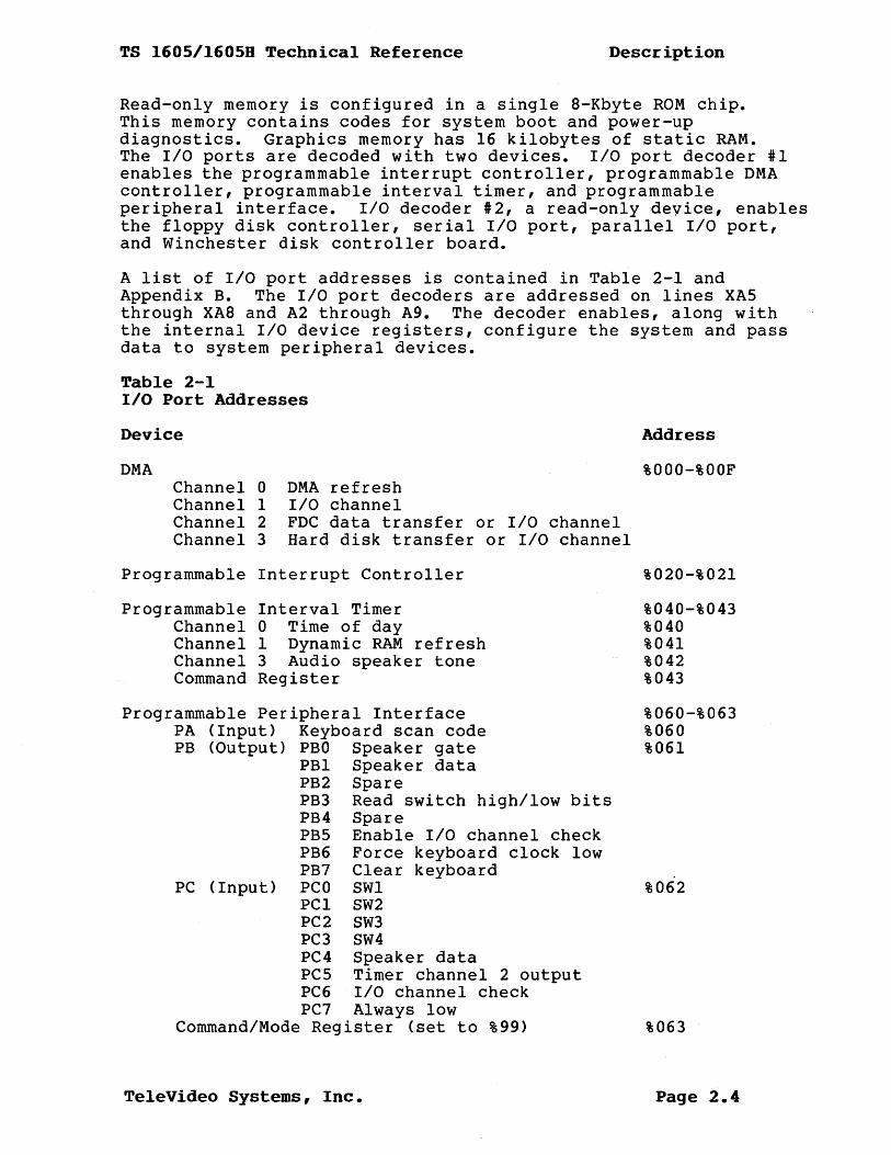
Read-only memory is configured in a single 8-Kbyte ROM chip. This memory contains codes for system boot and power-up diagnostics. Graphics memory has 16 kilobytes of static RAM. The liD ports are decoded with two devices. liD port decoder #1 enables the programmable interrupt controller, programmable DMA controller, programmable interval timer, and programmable peripheral interface. liD decoder #2, a read-only device, enables the floppy disk controller, serial liD port, parallel liD port, and Winchester disk controller board.
A list of liD port addresses is contained in Table 2-1 and Appendix B. The liD port decoders are addressed on lines XAS through XA8 and A2 through A9. The decoder enables, along with the internal I/O device registers, configure the system and pass data to system peripheral devices.
Table 2-1 I/O Port Addresses
Device
DMA Channel 0 Channel 1 Channel 2 Channel 3
DMA refresh liD channel FDC data transfer or liD channel Hard disk transfer or liD channel
Programmable Interrupt Controller
Programmable Interval Timer Channel 0 Time of day Channel 1 Dynamic RAM refresh Channel 3 Audio speaker tone Command Register
Programmable Peripheral Interface PA (Input) Keyboard scan code PB (Output) PBO Speaker gate
PBl Speaker data PB2 Spare PB3 Read switch highllow bits PB4 Spare PBS Enable liD channel check PB6 Force keyboard clock low PB7 Clear keyboard
PC (Input) PCO SWI PCl SW2 PC2 SW3 PC3 SW4 PC4 Speaker data PCS Timer channel 2 output PC6 liD channel check PC7 Always low
CommandlMode Register (set to %99)
Te1eVideo Systems, Inc.
Address
%OOO-%OOF
%020-%021
%040-%043 %040 %041 %042 %043
%060-%063 %060 %061
%062
%063
Page 2.4

TS 1605/16058 Technical Reference Description
DMA Page Register %OSO-%OS3
NMI Mask Register %OAO To enable NMI, write data %SO into address %OAO To disable NMI, write data %00 into address %OAO
Serial Port (Primary) Tx Buffer/Rx Buffer/ Divisor Latch Interrupt Enable/Divisor Latch MSB Interrupt Identification Register Line Control Register Modern Control Register Line Status Register Modern Status Register
Floppy Disk Control Port Select drive A Select drive B Reset 8272A FDC Disable interrupt/DMA operation Enable interrupt/DMA operation Turn on both motors
Floppy Disk Controller FDC Main Status Register FDC Data Register
Parallel Data Port (Read/write)
Parallel Control Port (Read/write) STROBE (-) AUTO FD XT INIT (-) SLCT IN (-) INTERRUPT ENABLE
Parallel Status Port (Read only) ERROR (-) SLCT PE ACK (-) BUSY (-)
Winchester Disk Control Register To enable interrupt: To disable interrupt: To enable DMA operation: To disable DMA operation:
TeleVideo Systems, Inc.
LSB %3FS-%3FF %3FS %3F9 %3FA %3FB %3FC %3FD %3FE
%3F2 DO = 0 DO = 1 D2 = 0 D3 = 0 D3 = 1 D4 = 1 or D5 = 1
%3F4-%3F5 %3F4 %3F5
%3BC
%3BE DO Dl D2 D3 D4
%3BD D3 D4 D5 D6 D7
%OEO D6 = 1 D6 = 0 D7 = 1 D7 = 0
Page 2.5

TS 1605/l605H Technical Reference Description
Winchester Disk Read Data Error flag Sector count Sector number Cylinder low Cylinder high SDH
Controller Board Task File Register Write Data Write precomp cylinder Sector count Sector number Cylinder low Cylinder high SDH
Status register Command register
%330-337 %330 %331 %332 %333 %334 %335 %336 %337
The serial I/O port is contained in a WD8250 serial I/O device as a general purpose, asynchronous RS-232 port. This device can be programmed for data rates of from 50 baud to 9600 baud. Currentloop operation is also supported in the serial port.
A general-purpose parallel I/O port provides a parallel printer interface. Interrupts are enabled or disabled by program control.
The I/O channel is used to interface to any I/O devices not on the system board. The I/O channel provides data and address lines, control signals, interrupt lines, and DMA control lines. Devices are addressed using I/O mapped address space. The I/O channel provides power to expansion slot Jl.
An Intel 8272A Floppy Disk Controller device and FDC9229B Data Separator support double-sided, double-density format for the system floppy disk drives.
An eight-section DIP switch pack can be read by program control through an Intel 8255 Programmable Peripheral Interface device. The DIP switch provides all system information to firmware and software. Settings for this switch pack are given in the system User's Manual.
Scan codes from the keyboard, which are in serial data format, are converted into parallel data format and read by the programmable peripheral interface. The peripheral interface also controls the audio speaker tone and enable/disable I/O channel er ror check.
VIDEO MONITOR INTERFACE
The video monitor interface is configured around the Synertek 6845R CRT Controller. The interface is capable of operating in either monochrome or color.
WINCHESTER DISK CONTROLLER BOARD
A Western Digital WDIOIO-05 Controller on a WDIOOO-05 3 1/2-inch Winchester Disk Controller board is used to interface with the 5 1/4-inch Winchester hard disk drive.
TeleVideo Systems, Inc. Page 2.6
TS 1605/16058 Technical Reference Circuits
3. CIRCUIT DESCRIPTION
This section contains circuit descriptions of the major functional blocks of the TS 1605 and TS 1605H system board, as well as a description of the WD1000-05 Winchester Disk Controller Board.
The system board contains the CPU, main memory, I/O ports, controllers, and video display circuits for the system.
Figure 3-1 is a block diagram of the main board for the system.
TeleVideo Systems, Inc. Page 3.1

~ Il't'Il ~ tD ........ en .... O~ tD nc: .... <I ;w.., G\ .... tD 0 Q, 0 U1 tD ... ·W "-0 S» I ....
~ .... G\ en .., 0 '< S» U1 til IS = rt tD, 0 ~ IS H\ tD til n .. rt t:r
t:r CS ..... tD .... CS n n =- S» • S» .... ....
CS ~ Il' H\ 0 tD DJ .., .., tD c" CS n
tD
a ~
n .... .., n
~ c: S» .... ~ rt tD til
eN • N

TS 1605/16058 Technical Reference Circuits
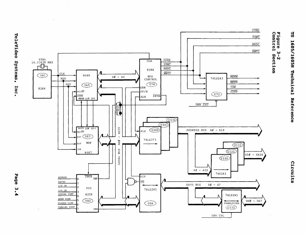
CPU CONTROLLER SECTION
The controL section block diagram illustrates the processing of the control, data, and address buses. The 8284 time (U63) sends three signals to the 8088 and 8087 processors. The clock signal is a 4.77 MHz signal with a 33% duty cycle. The RESET .signal halts CPU operation. The RDY signal inserts wait states between times T3 and T4 of the system bus cycle.
There are four signals that tie the 8088 to the 8087 coprocessor. QSO and QSI are input to the 8087 so it can monitor the status of the 8a88's internal queue. The RQ/GTI signal of the 8088 is connected to the RQ/GTO pin of the 8087. This signal allows the co-processor (8087) to take over the local bus to perform its functions. The TEST signal to the 8088 is examined by a WAIT instruction. If the TEST input is LOW, execution continues. Otherwise, the processor waits in an "idle" state.
Signals SO-S2 leave the 8088 with status information used and decoded by the 8288 bus controller. When decoded by the bus controller, these signals become the control bus signals lORD, IOWC, MRDC, and MWTC. However, during a DMA cycle, bidirectional transceiver U44 is the path for control bus signals which come from the DMA controller.
The 8288 bus controller also issues control signals DEN, DT/R, and ALE. The DEN signal enables bidirectional transceiver U45 which enables data onto the system data bus at T3 of the bus cycle. ~he DT/R signal controls the direction of the data flow through bidirectional transceiver U45. When active HIGH, the ALE signal latches address lines AO-A19 into latches U29, U30, and U3l. These address lines are then buffered by U2l, U22, and U23.
The 8259 interrupt controller accepts one of eight designated interrupts and issues an interrupt request (-INT) to the 8088. The 8288 bus controller checks the SO-S2 status lines from the 8088 and issues the interrupt acknowledge signal (-INTA) to the interrupt controller.
TeleVideo Systems, Inc. Page 3.3
XTAL 1 4.31818 MHZ
r1Qb C§)
8284
-
tog PI ~ tD
W • ~
IOWC
MRDC
MWTC I I
CLK
I - 8288 CLK --< -
8088 S~ - S2 ROY r\
'------\ BUS CONTROL ~ 74LS243
MEMW --- .... RST .... @D .4
r-tf @D
----,DEN
MEMR .... ..... -lOW -......
r+ RG/GT r\ -ifWTR
~ Tt:"ST Qs0 QSl
! ~
-
_DT/R
,...- ALE
-
lORD ---- G2D 'OMA cye 1
- 0'\ BUSY QS0 QS 1 rl Cl ~ RG/GT .:t:
RST@D ~ l--'- I L--.
t... '& i\_.4 Cl __ RDY NDP .:t: I"""'" '11"11' If' .~
r {Ul3§) -) r 1:u10 DI L-----:---=-=-=-------
~ ADDRESS BUS A~ - A19 __ ..... ALE ~ ~ II'
'--"---\- 7 4 L S 3 73
@Y (I) -- CLK ::J
-8087_ trl
H .:t: U 0
- XA~ r @) XA~ -
@V r-~
H
~ DIR
I"'" INTA RFRESH
0 INT
CE .. • l\r KEYBD
1 I/O CH 2 PIC 74LS245 I/O CH -3
-\ SERIAL P~ 4 8259
)I _lA HARD DISK GiD /
J ~ 5
~ FLOPPY DISK _ 6 'ill'" J - If' PARLLEL PORT
7 DEN
-f\ t--
• 1---' A~ - A19 J 74S241 - r
~ DATA BUS D~ - 07
" C( -\ 74LS245 AI
DDt> / DD~ ... -.... 1\ -J TRANSCEIVER
CQ~ ~ .. ..
, - - ] CPU CYC
n~ I-i 0 .... til CJ ~ rt C ... ... ... G\ 0 tD C ... VI
W "'-till ... tDN G\ n C rt VI .... = 0
t-I :s tD n tT CJ .... n PI ... ~ t-h tD ... tD CJ n tD
n .... ... n C .... rt m

TS 1605/1605B Technical Reference Circuits
The major components of the CPU Controller section are:
U55 U41 U63 U29,U30,U31 U45,U14 U21,U22,U23 U39 U28 U40 U27
Intel 80B8 CPU System Microprocessor Intel 8087 Numeric Data Processor Intel 8284A Clock Generator Address Latches, #1,#2,#3 Transceivers, #1,#2 Address Buffers, #1,#2,#3 Intel 8259A Programmable Interrupt Controller Intel 8237A-5 Programmable DMA Controller Intel 2764 System ROM Intel 8254 Programmable Interval Timer
Table 3-1 lists the devices or lines on the CPU and their description.
Table 3-1 CPO Devices
Device or Line
8088 CPU
-RD
RDY
-RQ/GTO,-RQ/GTI
-LOCK
QSl,QSO
Source/Description
Operated in the maximum mode, the CPU handles central processing functions, graphics display-related processing, and all writes to video memory. CPU timing conforms to the standards shown in the Intel Component Data Catalog.
CPU. Read signal indicates that the CPU is performing a memory or 1/0 read cycle.
CPU. Ready acknowledges that when not busy, addressed memory or 1/0 device will complete a data transfer. -S2,Sl,SO CPU. Status signal is active during clock high of T4, Tl, and T2 and is returned to the passive state (1,1,1) during T3 or during Tw when ROY is high. Status signals are used by bus controller to generate all memory and 1/0 access control signals.
RequestlGrant signals are used by other local bus masters to force the CPU to release the local bus at the end of the CPU's current bus cycle.
CPU. This signal indicates that other system bus masters are not to gain control of system bus while LOCK is active (low).
CPU. Queue status signal allows external tracking of the internal CPU instruction queue.
Te1eVideo Systems, Inc. Page 3.5

TS 1605/16058 Technical Reference Circuits
Numeric Data Processor
Clock Generator
Address Latch II
Address Latch 12
Address Latch 13
Data Transceiver
Data Transceiver
Address Buffer
Address Buffer
Address Buffer
Programmable Interrupt Controller
Programmable DMA Controller
System ROM
Programmable Interval Timer
Provides instructions and data types for high-performance numeric applications. Serves as a co-processor to the CPU.
Generates the system clock for the CPU. Using a l4.3l8l8-MHz crystal, the clock generator divides down a 4.77-MHz frequency source for the CPU and numer ic da ta processor.
Address latch II converts CPU lines ADO through AD7 to address lines AO through A7.
Address latch '2 converts CPU lines AA8 through AA15 to address lines A8 through A15.
Address latch '3 converts CPU lines AS16 through AS19 to address lines A16 through A19.
Converts CPU lines ADO through AD7 to data 'I lines DO through 07.
Converts data lines DO through 07 to data '2 lines 000 through 007.
Buffers address lines AO through A7, which II become XAO through XA7.
Buffers address lines A8 through A15, which '2 become XA8 through XA15.
Buffers address lines A16 through A19, which #3 become XA16 through XAI9.
Handles vectored interrupts for the CPU, accepting interrupt requests from peripherals and determining priority.
Allows peripheral devices todirectly transfer information from or to system memory.
Addressed on lines XAO through XA7, XA8 through XA13, and data lines 000 through 007, system ROM allows CPU to operate without generating wait states to the system.
A three-channel,counter-timerdevice. Channel 0 is used for time-of-day implementation, and channel 1 times out dynamic memory refresh. Channel 2 supports tone generation for the speaker.
TeleVideo Systems, Inc. Page 3.6

TS 1605/16058 Technical Reference Circuits
MAIN MEMORY
The addresses on the TS 160S/160SH RAM are multiplex. The RAM address MUX signal selects either the Row address (RAS> or the column address (CAS> lines. For 64K x 1, U60 is not used. The total address is 16 bit - the upper 8 bits are used for column, and the lower are used for row. READ comes from memory to the cpu. WRITE comes from the cpu to memory. Refer to Figure 3-3 for a block diagram of the RAM main memory.
TeleVideo Systems, Inc. Page 3.7

t-i tD .... tD < .... Q, tD o til ~ m rt tD II m 'III
.... ::s n •
MEMR
RAM SEL
AIIo
D0 - 07
"" CAS"i RAS1" RAM ADDR MUX -
XAI6 - XA3
XA8 - XAll
XA4 - XA7
XA12 - XA15
XA16 - XA17
CASl RASl CAS2 RAS2 CAS3 RS3 WE
G OIR
74LS245
~"" ~ ~ !\ U96 -...
I ~ S
" ~ Ul18
.~
" J 74LS158 ...
I -\ S
~ ~ U107
~ AI6- A8 ~
" .. ~
74LS158 .. 1 S
~ ul19 , ~ .. 7 4LS 158
"
DATA BUS 016 - 07
~ 64KX8 AI6 - A8
, or
..4 (256kz8) V'-.. 016 07 !\ CAS 16 "!II
:: RASI6 --<: WE
~
AI6 - A8 , 64KX8 ... or
... (256kz8) 016 y.. 07 !\
'" CAS1 ..... - RAS1
4~ WE
~
Ar6 - A7 , 64KX8 ... ...
016 ;a 07\
:: CAS2 .. I'I~
4.......-.<l WE
~ 64KX8 AI6 - A7
~ ... 016
AI V
!: CAS3 071\
-" RAS3 ~
4~ WE
) ...
t\ , 016 - 07 ~ ...
-\ 0r6 - 07 J ..
~
016 - 07 , ..4 .,
1\ 016 - 07
..4 ... -
=~ c:: :..., DltD .... ::sW :.~ tD
~ .., ~
t-i til
.... 0\ 0 VI
'" .... 0\ 0 VI = ... tD n ~ ::s .... n DI .... ~ tD I-h tD .., tD ::s n tD
n .... .., n c:: .... rt m

TS 1605/1605B Technical Reference Circuits
The major components of main memory are:
U50 U51 U128,U93,Ul19, U86,U110,U77, U101,U69 U127,U92,Ul18, U85,U109,U76, U100,U68 U126,U91,Ul17, U84,U108,U75, U99,U67 U125,U90,Ul16, U83,U107,U74, U98,U66
Te1eVideo Memory Control Gate Array Intel 8288 Bus Controller Bank 0 Dynamic RAM
Bank 1 Dynamic RAM
Bank 2 Dynamic RAM
Bank 3 Dynamic RAM
Table 3-2 lists the components of the main memory and their description.
Table 3-2 Main Memory Components
Device or Line
Memory Control Gate Array
A16-A19
SO,Sl -RASO, -RAS1 -RAS2, -RAS3
-CASO,-CAS1, -CAS2,-CAS3
-RAM SEL
Bus Controller
Source/Description
Generates all necessary signals for reads and writes to dynamic memory.
CPU address latch #3. Address lines to memory control gate array. Provide address for memory data bus exchanges.
CPu. Status lines to memory control gate array. Memory control gate array. Row select -RAS2,-RAS3 signals to main memory. -RASO selects row address for bank 0, -RAS1 for bank 1, -RAS2 for bank 2, and -RAS3 for bank 3.
Memory control gate array. Column select signals to main memory. -CASO selects column address for bank 0, -CAS1 for bank 1, -CAS2 for bank 2, and -CAS3 for bank 3.
Memory control gate array. Control signal selects one of four banks of main memory.
Decodes status lines and provides the system with all bus control signals. Together with memory control gate array, provides command and control timing generation and bipolar bus drive capability.
TeleVideo Systems, Inc. Page 3.9

TS 1605/16058 Technical Reference Circuits
-MEMR
-MEMW
INTERRUPT SYSTEM
Bus controller. Control signal into memory control gate array to generate memory reads to main memory.
Bus controller. Control signal into memory control gate array to generate memory writes to main memory.
The system can generate one of eight designated interrupts to the 8259 interrupt controller. The INT controller then issues an interrupt signal to the CPU. Status lines -SO, -Sl, and -S2 go from the CPU to the 8288 bus controller. The signal tells the 8259 to run an interrupt. The 8288 issues an INTA (two signal pulses) to the 8259. The first pulse freezes the interrupt priority in the 8259. The second pulse causes the 8259 to put an a-bit word on the data bus to the CPU. This is a partial address of the interrupt vector in the lower lK of system RAM.
The CPU issues a lO-bit address that accesses one of a possible 256 locations in memory. Each of these 256 memory locations consists of 32 bits of memory. These 32 bits are segmented to establish the current address of the interrupt subroutine.
See Figure 3-4 for a diagram of the interrupt system.
Te1eVideo Systems, Inc. Page 3.10

ttl PI \Q tD
W • .... ....
MEMORY CONTROL GATE ARRAY
NMIEN 19
050
8087 NP IRQ
I/O CHANNEL CK
CH0 TIMER COUNTER KYBD
I/O CH
I/O CH
SERIAL PORT
HARD DISK
FLOPPY DISK
PARALLEL PORT
8088
t--------tNMI CPU
..---....... ~INTR
055
8259 HIGHEST LEVEL a INTERRUPT
CONTROLLER
2 INTR
AVAILABLE ON THE BUS
5
039
SUMMARY OF INTERRUPT LEVELS
NMI I/O CHANNEL CHECK, NUMERIC PROCESSOR
IRQ 0 SYSTEM TIMER OUTPUT 8254 CHANNEL 0
IRQ KEYBOARD SCAN CODE INTERRUPT
IRQ 2 I/O CH
IRQ I/O CH
IRQ 4 RS-232-C SERIAL PORT
IRQ HARD DISK INTERRUPT
IRQ 6 DISKETTE DRIVE STATUS
IRQ PARALLEL PORT
.... toa:I ::I ~. rt'\Q tDC ...... ... tD C ttjW rtl ... tn '< rn rt tD S
~ tn
.... 0\ 0 Ut "-.... 0\ 0 Ut = ~ tD n cr ::I ~.
n PI .... ~ H'I tD ... tD ::I n tD
n ~. ... n c .... rt rn

TS 1605/16058 Technical Reference
DNA
There are four OMA channels, 0, 1, 2, and 3.
o = refresh 1 = optional I/O channel 2 = floppy disk controller 3 = optional I/O channel
Circuits
The OMA cycle is ini tia ted by a OMA request from one of the four above channels. For example, if the FOC requests a OMA request, it sends an FOC ORQ signal to the memory control gate array. The gate array issues a signal to the OMA controller. See Figures 3-5 and 3-6 for diagrams of the OMA.
TeleVideo Systems, Inc. Page 3.12

t-3 tD .... tD < .... c" tD o en '< en rt tD lEI en .. .... ::s n •
(. \ V ~
CPU CYC
I/O CH
FDC
woc 8237CS
DMA CYC
XAg
XAI
DMA PG. REG CS
74S245
• • ~
U132
DIR
DDH -
DDg -
AfJ - A19
DD.0' - DD7
+5 U26
FF REFRESH TIME OUT
CK CLR
DACK .d 't DREQ Z DACK 1 I
DD~ DACK 2 8237-5 DACK 3
~ V'- \ DREQ 1 Air - A7 DREQ 2 \l- i
DREQ 3 HRQ ., : CS Ul28 ADSTB
I
~ G
DD{\ J
74L5373 A8 - A15 ., U131
GR
I OE WA
RA WB
RB
~ 74LS670
V U129 A16 - A19
j'GW
~ QU
ml
74LS245
Vt 1\ • • Af,r - A7
~ V U130
. DMA CYC J 0\ r-f ..x: I
~ ..x:
1\ ./
r "
~ ~
~....,
~~. c n..,
OtD ::s
J rtw .., I OU1 .... .,
DACK .11
DACK 1
DACK 2
DACK 3
HRQ
t-3 en .... G\ 0 U1 "-.... G\ 0 U1 = t-3 tD n tr ::s .... n III .... !:a tD H\ tD .., tD ::s n tD
n .... ... n c .... rt en

TS 1605/16058 Technical Reference
Figure 3-6 DMA Memory Address Generation
~ rz:J ~ ~ 0 ~ 8 Z 0 u II( :E: t:l
Ltl I .....
('t')
N ex)
028
Circuits
OJ .c -
AO - A15~ -....
Ltl r-t 11('
DMA MEMORY ADDRESS
4 BIT DMA PAGE REGISTER \OJ r-t II(
DACK2 - SELECT ~
DACK3 - A16
A19~ ~
A16 -
A19 ... 0\ r-t
015 II(
SELECT 015
TeleVideo Systems, Inc. Page 3.14

TS 1605/1605B Technical Reference Circuits
SERIAL I/O
The serial communications port interfaces with an RS-232 asynchronous communications-type device at 50 - 9600 baud rate, such as a serial printer or modem. There is a transmit and receive line, and handshaking protocol. Figure 3-7 shows a diagram of the asynchronous communications of the TS 1605/1605H.
TeleVideo Systems, Inc. Page 3.15

.... ::s o •
ADDRESS BUS ADDRESS DECODE
CHIP SELECT
DATA BUS ~ ----~V
OSCILLATOR 1.8432 MHZ
EIA RECEIVERS
A
-'"
8250 ASYNCHRONOUS COMMUNICATIONS ELEMENT
CURRENT LOOP
A
25-PIN D-SHELL CONNECTOR
IRQ4
.. EIA DRIVERS
~:! to<\Q ::s r:: o.., trCD .., ow ::s I 0"-001 r:: en n
I ::s .... 0 At rt-.... 0 ::s en
t-3 en t-G\ 0 U1
'" t-G\ 0 U1 tel
t-3 to 0 tr ::s .... 0 At t-
~ CD t-h CD .., CD ::s 0 CD
n .... .., o r:: .... rt en

TS 1605/16058 Technical Reference Circuits
The major serial I/O component is:
Ull WDS250 or INSS250BSerial I/O Controller
A block diagram of the serial I/O port is shown in Figure 3-S.
Figure 3-8 I/O Interface Diagram
XA0-XAI PB(1-PB7 SPEAKER DATA
000-007 PROGRAMMABLE
1/0 CHCK PERIPHERAL
m. T"Q"W0 INTERFACE
8255 CS SHIFT KEYBOARD
~
REGISTER
\8 SWITCH PC0-t-- N
PC3 0 <t: PACK 0 :><
I
~ I
(So. lSI 0 <t: 0 :><
lOR, lOW ~ INTR
XA~, XAI PROGRAMMABLE 1
DD(.J-DD7 INTERVAL RFSH TIMER 2
8254 CS SPK
D0-07 TO EXTERNAL DEVICES
Art-A7 1/0 CHANNEL A8-A15 A16-A19 FLOPPY DISK
MOTOR ON DRIVE CONTROL LATCH
~\l XA~, XAI STATUS AND CONTROL lOR, lOW
FLOPPY DISK WRITE DATA OUT DB0-DB7 CONTROLLER
FDC CS READ DATA DATA IN SEPARATOR
DBrt-DB7 CONTROL AND STATUS
XA0, XAI WD0-WD7 DATA 1/0 HARD DISK lOR, lOW INTERFACE W,ll,0-WA2
CONTROLLER ADDR WOC C5
XA0, XA2
lOR, lOW ASYNCHRONOUS RS-232C COOMUNICATIONS
8250 CS SERIAL 1/0
DB~-DB7
XA~-XAI
lOR, IOIv .. • PARALLEL PRINTER PARALLEL
DB0-DB7 1/0 PORT CONTROL AND PAR C5 STATUS
Te1eVideo Systems, Inc. Page 3.17

TS 1605/1605B Technical Reference Circuits
Table 3-3 lists the major component of the serial I/O and its description.
Table 3-3 I/O Component
Device or Line
Serial I/O Controller
Source/Description
An RS-232Cdevice thatis usedfor asynchronous communications only, but is capable of supporting current loop operation. Enabled by CPU lines XAO through XA2 and DBO through DB7 and control signals -lOR, -lOW, and -8250 CS. This device can be programmed from 50 baud to 9600 baud.
PARALLEL PRINTER PORT
The parallel port is a general purpose I/O port configured on the TS 1605/l605H to interface to a parallel printer. Interrupts can be enabled or disabled under program control. Since a 25-pin, 0-type connector is used in this system, a special cable is required for interface to a standard Centronics-type printer. See Figure 3-9 for a diagram of the parallel printer port.
U8 is a bidirectional receiver with the direction controlled by the parallel chip select or an I/O read.
Write data in U6 is read back through UIO. Then write control and write information goes into INIT, SLST N, AUTO FD XT, STROBE. Read control is enabled to read those control signals. Once read, the system and hardware are functioning properly. Then status is read from the printer for error, busy, ACK, PE, or select. Then write data is sent to the printer. STROBE then goes to low. This initiates read status to read busy and ACK signals from the printer. When okay, reads information into the CPU via the data bus. Then a write data into U6, then strobe data with write control signal into parallel printer. Then another read status cycle. This process continues until all of the data is transferred.
NOTE! Read control is performed for the data latch only when the system is first booted up.
Te1eVideo Systems, Inc. Page 3.18

~ 1\ 74LS245 r .. ..
D~ - D7 J DB~ - DB7 U13 .. .. ~
DIR
PAR RD ..... U89 AAAAA
74LS155 C""""" '" '" '" "'-+5U
XA~ 13 7 READ DATA A lYO
XAI 3 lYl 6 READ CONTROL
1 B U20 2
IG .2...READ STATUS
)U97 lY2
PAiiCS 9 WRITE
T 14 2G 2YO DATA
I 15 11
WRITE lOW 2C 2Y2 CONTROL
U29
3BD -P2-25
ERROR tL 1 DB3
OEA
P2-11> BUSY
ACK DB~ - DB7 P2-10 ...... U12 -
P2-12) PE
~ SLCT P2-13~ 74LS240
SLCT IN
INIT .... /'
-{;»---... AUTO FDXT STROBE
OED 19 3BE
r~
~ 74LS374
.. ~ ".~ ..
U6
3BC fCK
74LS244
~ .. ~ ..
l-t:O 0 U18
11G I
"& 3BC - t:O 0
3BE
lCK
i'...... DB~ 74LS374 V ~_ DBI V
DB2
\ ..
1>"" DB3 ~ ... DB4
DB4 U!l
~,
~ P2- 2 DATA~ - DATA7 ) :
- P2- 9 ..
All I \
....
2G
STROBE -AUTO FD XT -INIT -
SLCT IN --IRQ ENABLE
IRQ7
P2-1
P2-14
P2-16
P2-17
togt;2 PI .... "''-0 PIC 1-1 ... I-ItD tD I-IW
I tog\G ... .... ::s rt tD ... ~ 0 '-0 .... n
t-3 til
1-1 G\ 0 U1
"" 1-1 G\ 0 U1 = t-i tD n cr ::s "",. n PI .... ~ tD t-h tD ... tD ::s n tD
n .... ... n C .... rt en

TS 1605/16058 Technical Reference Circuits
The major parallel
U6 UIO U12 U9 U20
The major parallel
Table 3-4 Major Parallel I/O
Device or Line
Data Latch
Data Buffer
Status Buffer
Control Latch
KEYBOARD INTERFACE
IIO components are:
Data Latch Data Buffer Status Buffer Control Latch Multiplexer
IIO components are in Table 3-4.
Components
Source/Description
Used as a temporary storage buffer for data transmitted to the parallel printer on output lines DATAO through DATA7. Data is written into the data latch by the CPU when signals -PAR CS and -lOW are activated. Data lines DBO through DB7 carry data transfers to this latch.
Buffers output lines DATAO through DATA7 into data lines DBO through DB7.
Buffers status signals, -ERROR, SLCT, PE, -ACK, and BUSY that go from the parallel printer to the CPU. These signals are read by the CPU when -lOR and -PAR CS are activated.
Control signals -STROBE, -AUTO FEED, -INIT, and -SLCT IN are transmitted to the parallel printer when the CPU enables lines -lOW and -PAR CS.
The TeleVideo and IBM keyboards are not plug-compatible. A TeleVideo keyboard must be used with the TeleVideo system. Under normal keyboard conditions, the output register of 8255, PB bits 6 and 7, control the keyboard-enabling circuit - bit 6 is high, bit 7 is low. In this condition, the keyboard circuit can receive data from the keyboard. Whenever the key is pressed, the data goes from the keyboard to input A of the Ul16 input register (see Figure 3-10). At the same time, the keyboard clock sends information through inverter U19 and through AND gate U25 and then to the clock of the shift register. This clocks the 8-bit code representing the number of the key that was pressed. The start bit is the MSB (QH). When the information is stored in the shift register, QH is fed back to the data input of D flip-flop U127. When the clock goes in, it generates interrupt IRQ1. This sends the microprocessor into the interrupt service routine which processes the key.
TeleVideo Systems, Inc. Page 3.20

TS 1605/1605B Technical Reference Circuits
When the interrupt is generated at the Q output with a logic high, the Q is a logic 0 which is sent back to the keyboard data input via U7 and that prevents the keyboard from sending more data. It also inhibits U25 to prevent the keyboard clock from shifting more data into the shift register.
Figure 3-10 Keyboard Circuit
8255-5 ~ 0
r-1
l"-
ll:: 2 1&1 r-Eo< til ~ 3 (.!) 1&1 r-Il::
Eo< 4 0 Po r-Eo< 0 0 5
t--
SBIFT REGISTFtR
CLK KEY DATA
BLD KBD CLK LOW
I ,-- OA KEYBOARD 6 r-OB 036 t-- KBD ENABLE A
7 1&1 CLR
~ "--- §"
Dlf - D7 U125 u.
~ ~\Sl .. U
0 til
r-
~ 1 I"-
~ Il:: 2 1&1
1 Eo< r- OA - OB til ~ 3 (.!) 1&1 r-Il:: CLR Eo< 4 0 t-- PA~ COB) iIROl Po z 5 D 0 ~
t-- 74LS74 6
lCrrl> U127
t-- CK 0" 7 ~
KBD CLK
TeleVideo Systems, Inc. Page 3.21

TS 1605/1605B Technical Reference Circuits
The major components of the keyboard interface are:
U37
U38
Intel 8255A-5 Programmable Peripheral Interface (PPI)
Serial Shift Register
The major components of the keyboard interface and their description are listed in Table 3-5.
Table 3-5 Keyboard Interface Components
Device or Line
Programmable Peripheral Device
PAO-PA7, PBO-PB7, PCO-PC7
AO-AI
Serial Shift Register
Source/Description
Programmedby system software, this device reads the eight-position DIP switch and interfaces to keyboard receiving and transmitting scan code. Controls audio speaker tone and enable/disable I/O channel error check. Enabled by address lines XAO through XAI, data lines DDO through DD7, and control signals -lOR, -lOW, and -8255 CS.
PPI. Ports A, B, andC. Each port is composedof eightbits, configured by system software. Accepts commands from read/write control logic, receives control words from the internal data bus, and issues the proper commands to the associated ports.
Cpu. Port select input signals, in conjunction with -RD and -WR signals, control the selection of one of three ports or the control word registers.
Permits complete control over incomingdata lines PAO through PA7. Data at serial inputs may be changed while clock is high or low, but only information meeting set-up requirements is entered. Clocking occurs in low-to-high transition of clock input.
SPEAKER DRIVE SYSTEM
You can control the frequency of the speaker output by programming the different frequencies coming from timer 8254 (see Figure 3-11). The speaker frequency is controlled by the frequency divider in the 8254 timer 2. The frequency can be controlled by programming so you can change it through software. Bit 0 of the output register PB of the 8255 is used to control the speaker gate so you can turn the timer on and off. The timer clock is ANDed with the 8255 output register PB bit 1. The output of U26 provides the information to speaker drive Q25.
TeleVideo Systems, Inc. Page 3.22

TS 1605/1605B Technical Reference Circuits
The speaker driver is controlled by 8255. 0 enables the speaker interface. Channel 2 timer clock is used to supply the oscillating frequency to control the speaker.
When you want to turn on a speaker, use 8255 PB 1.
PBI = I = turn on speaker PBI = 0 = turn off speaker
TeleVideo Systems, Inc. Page 3.23

8255
PPI
U37
PB
0
1
2
6
7
8254 CLK
SPEAKER GATE
SPEAKER DATA
TYPE 8 INTERRUPT TO 8088
U27
8254 TIMER
TIMER CLOCK
GATE 2
01
SPKR DRIVE
(PBa)
(PBI)
en~ "0 .... tD~ AlC ~..,
tDtD .., W
c;,1 .., .... ........ <I tD
en ~ en rT tD IS
t-3 en .... G\ C) U1
"" .... G\ C) U1
= t-3 tD n ::r ::I .... n AI .... ~ tD t-h tD .., tD ::I n tD
n .... .., n C .... rT rn

TS 1605/1605H Technical Reference Circuits
INPUT/OUTPUT CHANNEL
The input/output channel, located on the system board, provides interface to I/O devices external to the system board. This channel consists of a connector with data and address buses, control signals, interrupt lines, DMA control lines, and power and ground lines. The I/O channel pin configuration is listed in Appendix F. A block diagram of the input/output channel is shown in Figure 3-8.
FLOPPY DISK CONTROLLER
The floppy disk control circuitry is based around the 8272A (U96) floppy disk controller chip. The 9229B FDe does all write precompensation functions. The 8272A keeps track of where the floppy heads are currently located and stores more internal memory than previous floppy disk controllers. Also, data being read from the disk is intercepted by a 9229B (U81) Data Separator. The Data and Clock pulses that compose MFM data on the diskette are separated and synchronized with the 8272A internal clock to ensure accurate data exchanges. The 8272A FDe is programmed to operate in the burst transfer mode at system initialization by the EPROM.
The other important support Ies are the bidirectional buffer (U13) and the floppy disk latch (U42). They control the selection of the disk drive and the turning on of the floppy motor. These are taken as control words from the system data bus.
The basic functions of the floppy disk controller circuitry are 1) writing data to the diskette, 2) reading data form the diskette 3) determining where to write on the diskette, and 4) turning the drive off and on and selecting drive A or B. 1, 2, and 3 are all controlled by the 8271A FDe.
TeleVideo Systems, Inc. Page 3.25

~ tD ... tD < .... C. tD o fn '< en rt tD IS en ... H ::s n •
: \Q tD
W • ~ G\
r"
I 16 MBZ H ~
TIMING osc. 2 .
WRITE 03 PRECOMP.
DATA SEPARATION
~ DATA BOS ~ BOFFER f----.,...
__ ...;0..;,8_ ....... rY. DB7
A ,,~
~ .---
READ DATA
WRITE DATA
I
I 1
I I 1 __ -
J j
f'PT SENSOR
WRITE G~~~~ SIDE SELECT <....
Ir=> READ/ WRITE
AMPLIFIER
HEAD READ
FILE PROTECT SENSOR (WRITE PROTECT)
HEAD WRITE
I iC-.FILE PROTECT SENSOR
INDI-CA,\R ~ FILE PROTECT SENSOR LED
r-------;::P~S-9-,R-W--... ~ PS1,RDD CLK,MFM WCB,WD
WRITE GATE J WRITE DATA, ~ ERASE GATE
INDICATOR
I / ~~INDF.X SENSOR LED n It>~'~' r-::::X SENSOR
L _____ .I FRONT PANEL LED II ,/ ",:,XS:. 0-...':, or SPINDLE MOTOR
- INDEX
::::: TRACK nil ... ~ WRITE PROTECT
'" ~ DBB - DB7 0,...--....... '1 HEAD SELECT
al
~ ~
DIRECTION
DRIVE SELECT If r STEP
~ f:; al
FDC 8272 v MOTOR ON
v
07 I L .. ~ LT~IL-----., l..., I -" eo" "'~ ,=~" ~
------~,~ ~~ • 024 I- 034
,m,,,,, ~'"'''' _ "" r ~~~"-<..<Et--
FLOPPY DISK DRIVE
1
I I 1
I
POWER SENSE READ DATA
MFD CONTROL
5V OV
I~-""'" 1
I I I 1
I I
MOTOR ON
PHASE CONTROL TRACK «« SENSOR HEAD LOAD SOLENOID INDEX SENSOR INDEX SENSOR LED F' .F. PIlOTE:T SENSOR .ED
(DRIVE SELECT)
'----'==-.;..:~::.::.::..:-----+-+----I 1 \0 ~l~-=-~~::, ~;, {){!~'>6:~r
MAGNETIC BEAD
BEAD LOAD SOLENOID
TRACK Oil SENSOR
STEPPING MOTOR I
FLOPPY DISK CONTROLLER CIRCUIT
n .... ... n c .... rt en

TS l605/l605H Technical Reference Circuits
The major components of the floppy disk controller are:
U96 U42 U8l
Intel 8272A Floppy Disk Controller Device Floppy Disk Drive Control Latch FDC9229B Data Separator
The floppy disk controller components and their description are listed in Table 3-6.
Table 3-6 Floppy Disk Controller Components
Device or Line
Floppy Disk Controller
-COMP READ DATA
-COMP WR DATA
Floppy Disk Drive Control Latch
Data Separator
Source/Description
Provides parallel-to-serial conversionof data from the system to the floppy disk, and serial-to-parallel conversion from the floppy disk to the system, as well as all drive control functions, such as head step, head direction, write protect, and track 0 detection. The controller can be programmed to handle seek track, read sector, write sector, read address, read track, and write track operations. The DBO-DB7 Data Transceiver carries data and programming signals between the FDC and CPU.
FDD. Carries composite read data to floppy disk drives.
FDC. Carries composite write data to floppy disk dr i ves.
Controls floppy disk drive number selection, motor on/off, enable/disable interrupt, enable/disable DMA operation, and FDC reset.
Performs write precompensation and data separation.
WINCHESTER CONTROLLER INTERFACE
The major components of the Winchester controller interface are:
U8 U18
Data/Address Transceiver Control Signals Buffer
A block diagram of the Winchester controller interface is shown in Figure 3-8.
TeleVideo Systems, Inc. Page 3.27

TS l605/l605H Technical Reference Circuits
The Winchester controller interface components and their description are listed in Table 3-7.
Table 3-7 Winchester Controller Interface Components
Device or Line Source/Description
Data/Address Transceiver and Control Signals Buffer
The transceiver and buffer pass data, address, and control signals to an external Winchester disk controller board.
WOO-WD7 Data/Address Transceiver. Buffered data lines to the Winchester controller board. WAO-WA2 Control signals buffer. Buffered address lines to the Winchester controller board.
-WCS,-WWE, Control signals buffer. Buffered control signals to the Winchester controller board. -WRE,WMR,
-WOC RD
WINCHESTER DISK CONTROLLER BOARD
The Winchester disk controller board provides all control and data handling functions needed to interface the system with a 3 1/2-inch Winc.b .. e.ster disk dr i vee Figure 3-13 shows a block diagram of the Winchester disk controller board.
Figure 3-13 Winchester Disk Controller Board Block Diagram
r--~-C-RD------------------ ~~i~ES~~~~~~S iff
DRIVE READ DATA
SWITCH DATA WDP"WD7
~~~~RFAeE I--~DE:g;.~N _____ r-1 ~~~~~~R~~~ BRDY -'it t----+--------- ~~~~~OL BUFFER RAM....-----;;BC~R -----1 .k eONTROLLERf+;;;:;:;-,"~==:::;---lwINeHESTER ·WRITE
D~-DZ
...... --I~;~~ROLLERt--_---+i ~~~~OMP/
'" "
SEPARATOR
t--_><-+-___ --.-,f--+-_DR_QI_NTR_Q __ INTERRUPT
L,--.,........,..... REQUEST
we
!~~~~~S >--___ -A;.;.;;..~--=A2--+------J g~i~~L>-----::;CS::..!...' =RE.!.-;. W::.::..E _~ ___ --J
DRIVE >-__ =DRI=VE~ST=AT=US:....::.LI=NE::::....S _____ ----1
STATUS
Re
DRIVE WRITE DATA
TeleVideo Systems, Inc. Page 3.28

TS l605/l605B Technical Reference Circuits
The major components of the Winchester disk controller board are:
U24
U23 U16 U25 U26 US Ull,U18 U13 U27
) U3 U17
.,. U4
WDllOO-2l Host Interface, Head and Drive Select, and Buffer Ram Controller WDl010-05 Winchester Disk Controller WDllOO-10 Write Precompensation and Data Separator Type 6116 Buffer RAM Board Busy Tristate Buffer Error Amplifier Pump Logic Voltage Controlled Oscillator (VCO) Host Interface Bus Transceiver Differential Line Receiver Precompensation Logic Differential Line Transmitter
System/Controller Interface
The system programs the Winchester disk controller board by accessing the WD1010-05 controller device task file registers.
The system/controller interface lines are shown in Figure 3-2.
Table 3-8 lists the system/controller interface components and their description.
Table 3-8 System/Controller Interface Components
Active Line
AO to A2
-WE or -RE
DO to D7
Source/Description
System. Task file register address.
System. -WE to activate task file write, or -RE to activate task file read.
System. Data or command.
Operations With Buffer RAM
The Winchester disk controller board uses 1 kilobyte of a 2 kilobyte-by-8-bit buffer RAM to interact with the system during disk read and write operations. When writing to disk, the system writes the data to the buffer RAM by sector. After a sector of data is loaded into the buffer RAM, the WDI010-05 reads the data from the buffer RAM to the disk. The lines used in the operations with buffer RAM are shown in Figure 3-2.
TeleVideo Systems, Inc. Page 3.29

TS 1605/16058 Technical Reference Circuits
Table 3-9 Write From Buffer RAM
Active Line
DO to D7
-BCR
DRQ
-BCS
-WE
-BRDY
-BCS
-RE
-BCS
INTRQ
Source/Description
System. Sets up Task File Register and Write Sector command in WDIOIO-05 task file and writes data to buffer RAM.
WDIOIO-05. Strobed to zero counter in WDIIOO-21.
WDIOIO-05. Active to indicate that the buffer RAM is empty.
WDIOIO-05. Set high to enable host control of buffer RAM. Transceiver direction is ready for write.
System. Loads buffer and increments counter with -CS.
WDIlOO-21. Active to indicate buffer full.
WDIOIO-05. Active to disconnect host control of buffer RAM. Board busy tristate buffer on line WD7 is activated by -BCS to prevent system access during next operation.
WDIOIO-05. Reads buffer RAM to transfer data to disk (See Writing Disk Data).
WDIOlO-05. by system. inactive.
WDIOIO-05.
Set high to allow next operation Board busy tristate buffer
Signals end of command to system.
Reads of buffer RAM occur after a sector of data has been loaded to the RAM from the disk. For a read f rom buffer RAM, see Table 3-10.
Table 3-10 Read From Buffer RAM
Active Line
DO to D7
Source/Description
System. Sets up Task File Registers and places Read Sector command in WDIOIO-05 task file.
Te1eVideo Systems, Inc. Page 3.30

TS 1605/16058 Technical Reference Circuits
-BCS
-BCR
-WE
BRDY
-BCR
-BCS
DRQ
-RE
-BRDY
-INTRQ
Writing Disk Data
WDlOlO-OS. Active to disconnect host control of buffer RAM. Board busy tristate buffer on line WD7 is activa ted by -BCS to prevent system access during next operation.
WDIOIO-OS. Strobed to zero counter in WDIIOO-21.
WDIOIO-OS. Loads buffer from disk <See Reading Disk Data), and increments counter with -CS.
-
WDIIOO-21. Active to indicate buffer full.
WDIOlO-Od. Strobed to zero counter in WDIIOO-21.
WDIOlO-OS. Set high to enable system control of buffer RAM. Board busy tristate buffer inactive.
WDIOIO-OS. Active to initiate transfer to system.
System. Reads buffer RAM and increments counter with -CS.
WDIIOO-21. Active to indicate buffer empty.
WDIOIO-OS. Set high to stop operation.
The write sector command requires that the Winchester controller locate the place on the disk that is to receive the data, control the write operation to buffer RAM by the system, then read the data from the buffer RAM, condition the data into MFM format, and write the data to disk.
Under MFM, clock bits are recorded only when two successive data bits are missing in the serial data stream. Using MFM reduces the total number of bits required to record a given amount of information on the disk. Because this effectively doubles the amount of disk capacity, it is termed ndouble density."
Encoding MFM follows three rules: 1) if the current data cell contains a data bit, then no clock is generated, 2) if the previous data cell contained a data bit, then no clock is generated; 3) if the previous data cell and the present data cell are vacant, then a clock is generated in the current clock cell. Data and clock cells are defined by the state of the write clock line, WC. If WC is low, it is a data cell; if WC is high, it is a clock cell. Both clock and data cells are 100 nanoseconds long in STS06-compatible drives.
TeleVideo Systems, Inc. Page 3.31

TS 1605/16050 Technical Reference Circuits
The active lines for writing disk data are diagrammed in Figure 3-14.
Figure 3-14 Writing Disk Data
BUFFER A RAM CONTROL .... WD1l00-11 ~~AM XTAL
RAM ...
00'-D7 • • TO/FROM~ SYSTEM
DRIVE 1 DRIVE STATUS I r
I~
Table 3-11
OSC CONTROL ~
2XDR WO
WG
WD1010-00 RWC EARLY LATE
WC
EARLY NORMAL
LATE
PRECOMP .. LOGIC
WD1l00-10
OIFF LINE XMTR
I---
'1
.. DRIVE DATA OUT
Writing from Buffer RAM
Active Line
DO to D7
-BCR
BRDY
-BCS
-STEP,-DIRET
Source/Description
System. Contains write sector command. When the WDIOIO-05 receives this command, it checks its cylinder registers against the current cylinder position.
WDIOIO-05. Strobed to begin write to buffer RAM by system.
WDIIOO-21. Buffer RAM full.
WDIOIO-05. Active to disconnect host control of buffer RAM. Board busy tristate buffer on line WD7 is activated by -BCS to prevent system access during next operation.
WDIOIO-05. Moves head to locate cylinder.
Te1eVideo Systems, Inc. Page 3.32

TS 1605/16058 Technical Reference Circuits
SEEK COMPLETE
WG
WC
-RWC
-WD
-EARLY, -LATE
EARLY, NORMAL, LATE
Data
-BCS
Drive. Informs WDlOlO-05 that the head settling time for the current step is expired. If current step is not the required cylinder position, the head is moved again. After seek to desired cylinder, controller checks for desired sector address by reading data from dr ive.
WDlOlO-05. Write gate signal to WDllOO-lO.
WDllOO-lO. Carries 5 MHz write clock, derived from 2XDR clock signal, to WDlOlO-05.
WDIOlO-05. Reduced write current signal; turns on precompensation circuits for write to/disk.
WDlOlO-05. Write data as read from buffer RAM and serialized by WDlOlO-05.
WDlOlO-05. Precompensation signals to WDllOO-10.
Precompensation is used to counteract the effects of dynamic bit shift when writing the inside recorded tracks of the disk. Dynamic bit shift results when a bit on the disk influences the position of an adjacent bit. The leading edges of the bits are moved closer together, or further apart, depending upon the polarity of each bit. Because the positions of the bits shift as they are written to the disk, the data is harder to recover without error. Write precompensation is applied to counteract the effects of dynamic bit shift.
Precompensation predicts the direction a bit will be shifted, then writes the bit out of position in the opposite direction to the shift. The prediction is done in the WDlOlO-05 by checking the next two data bits, the last bit written, and the present bit.
WDllOO-lO. Precompensationsignals to precompensation logic. Data is shifted +/-12 nanoseconds from normal position through a delay line.
Differential Line Driver. Carries MFM formatted, precompensated, RS-422 write data to dr i ve head.
Set high to allow next operation by system. Board busy tristate buffer inactive.
TeleVideo Systems, Inc. Page 3.33

TS 1605/16058 Technical Reference Circuits
Reading Disk Data
For disk reads, the Winchester disk controller board locates the sector to be read, identifies the start of the data field, reads the data in from the disk, separates the data and clock signals, w r i t est he d a tat 0 b u f fer RAM, and con t r 0 1 s the s y s t e m rea d 0 f the data out of buffer RAM.
The active lines for reading disk data are diagrammed in Figure 3-15 and are listed with a description in Table 3-12.
Figure 3-15 Reading Disk Data
BUFFER .A CONTR ...
SYS ..
DRIVE DATA IN
RAM
.1
-
""
D0-D7
DIFF RCVR
.,;>
-2, ,
Cl 0:: Cl
-
WD 11~0-11
Te1eVideo Systems, Inc.
1 } DRIVE , ---=t4 CONTROL
DRUN
.A BUFF RAM .. RG CONTROL .? WD
- 10HI-00 Cl
DATAl 0:: WD u 1100-10 - CLOCK
SEPR ~
CRD
RD
RC
Page 3.34

TS 1605/16058 Technical Reference Circuits
Table 3-12 Disk Data
Active Line
DO to D7
-BCS
-STEP,-DIRET
-SEEK COMPLETE
VIDEO SECTION
Source/Description
System. Contains read sector command. When the WDlOlO-05 receives this command, it checks its cylinder registers against the current cylinder position.
WDlOlO-05. Active to disconnect host control of buffer RAM. Board busy tristate buffer on line WD7 is activated by -BCS to prevent system access during next operation.
WDlOlO-05. Moves head to locate cylinder.
Drive. Informs WDlOlO-05 that head settling time for ts enter C below and each item
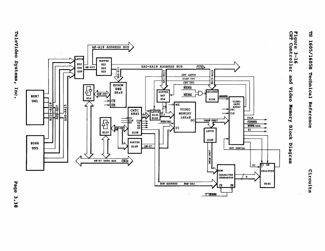
The major integrated circuits in the video display section include the following:
CRTC U90 Video gate array U150 Character generator ROM U15l Shift register U143 16K of video display RAM
The CRTC has several outputs which affect video display operation. Both the vertical and horizontal sync pulses originate at the output of the CRTC. During power up, the CRTC's internal registers are initialized with the proper vertical and horizontal operating frequencies. The vertical sync operates at 60 Hz and the horizontal frequency rate is approximately 16 KHz. Cursor movement is controlled by the cursor output of the CRTC. The CRTC has four output signals RAO-RA3, the scan line count signals, which increment upon completion of each horizontal scan line.
During a display cycle, the CRTC addresses video memory. Latches Ul12 and Ul13 are enabled by the DISP CYCLE signal and the addresses are passed to the latch outputs by the CRT LATCH clock. Each character that is displayed occupies two bytes of video memory. One byte represents the character to be displayed while the following memory location stores the attribute of the character. The function of the EVEN/ODD signal is to alternately select either the address of the character or its associated attribute.
Te1eVideo Systems, Inc. Page 3.35

TS 1605/1605H Technical Reference Circuits
The information stored in video memory is passed to both the video gate array and character latch U59. The outputs of the character latch, access the appropriate memory location in the character generator ROM, U151. The TS 1605 employs an 8 x 9 character matrix. Therefore, the scan line count signals to the ROM, reset with the completion of the ninth scan line. Parallel data from the ROM is loaded into the parallel to ser ial shift register, U143, at the character clock rate of 1.7895 MHz. Data is shifted out of the register by the Dot clock, which is an output of the video gate array. The data is shifted out of U58 serially, at the Dot clock rate of 14.31 MHz. The output of U143 is sent to one of the input lines of the video gate array for processing.
There are many outputs to the video gate array, many of which are not shown in the block diagram. Outputs EG (green voltage), EB (blue voltage), ER (red voltage), and EI (half-intensity video are mixed in a transistor circuit prior to becoming the raw video signal sent to the video module board. Signals 12 (video and color), 13 (horizontal and vertical blanking), and 14 (sync) are mixed in a transistor and sent to a phono jack at the back panel of the TS 1605, as the composite video signal.
During a CPU cycle, video information can either be written into video memory or read from video memory by the CPU. Dur ing a CPU cycle it is the CPU that addresses video memory. The signal, CPU CYCLE, enables buffers UllO and Ulll. The CRTC and CPU cannot address video memory simultaneously.
Video Memory
The CPU performs all writes to video memory, and reads data from video memory to perform graphics formatting. All graphics control firmware is in system ROM and is acted on by the CPU. The CRT controller reads data from video memory to perform screen updates.
The major components of video memory are:
U62,U70,U78, Type 6167 Static RAM devices U87,U94,Ul02, Ulll,U120 U47,U54 CPU Address Buffer
A block diagram of video memory is shown in Figure 3-3.
The video memory components and their description are listed in Table 3-13.
Te1eVideo Systems, Inc. Page 3.36

TS l605/l605B Technical Reference Circuits
Table 3-13 Video Memory Components
Device or Line
GDO-GD7
Source/Description
cpu. Buffered data lines DO through D7, carry write data to video memory.
-cpu CYC CPU. Toggles alpha graphics for the CPU.
XAO-XA7,XA8-XA13 CPU. Buffered address lines to video memory.
DMDO-DMD7 Video memory. Carry read data from video memory.
CRT Controller and Character Generator
The CRT controller retrieves data from the video memory for screen updates. Alphanumeric data from the video memory is passed through a character generator and shifted into a serial bit stream for the video display circuits. Graphics data is sent directly to the shift register. The major components of the CRT controller and character generator are:
U138 U137 U12l,U122 U15l U97 U150 U143 Q2,Q3
Synertek SY6845R CRT Controller CRT Data Transceiver CRT Latch Character Generator ROM Display Buffer TeleVideo Video Gate Array Video Shift Register Video Drivers
A block diagram of the CRT controller and character generator is shown in Figure 3-16.
TeleVideo Systems, Inc. Page 3.37
8087 U41
8088
U55
-A~-A19 ADDRESS BUl:> .,.
r-----~ ..... ':::a LATCH BUFFER
--- 0\ r-i -rJl < I - \Q
r-i - rJl <
~
~
~
::: 03l - - 021
r---""-~-...J~'~ .: "'-A15 ..... -:-~~-.. lJJ XAO-XA19 ADDRESS BUS ~ M.-----------~~~~~ M M
;:i CRT LATCH ~ ,....-----f I .----;;.;;.D.;.;;.IS.....:P=Cy...;..C::...-----I I t-----------, - a ~ t--------......
.... an
1 r-i
~:f &'1
~ co
~< <
CPU CYC " ~ EPROM ~ U40 L(1 K2; 8Kx8
014 ~ II'"
----- CE ~OE
V'J MEMR 'v' BUFFER ~ '"' ~ECODER __ _
47 MEMW ~ :54 0136 ~ .... --...
VIDEO ... __ ... CRTC i:i.~ WE VIDEO - os;;::. 6845 ~3 0121 13 MEMORY ---+ eLK
- ~ CS 0122 II'" 16Kx 8 t--____ ~ ___ ...."......---'.J'...
~ - CLK CUR r----.- iViii7ODo DO~ __ D_MD .... '-DMD7 _ ~ - RS VS r----.- r- Q .,. ~ ~~~ ~DI
0137 ~ II"" 0138 I r'Y"' ..... ---_ LATCH
--
CCLK
IV!lf/ODD
EI
0149 r DOT SERIAL-
.t. ~
~ BUFFER -0129 D'-D7 -
V V D,.-D7 DATA BUS ~
r-
fi " I
! !
_~ROM .,.. CHARACTER t--+--.~
GENERATOR ..... -+.....;_ ..... ~ ROW ADDRESS RAB-RA3 -"'.
-------------~~I~ ~ ~ CGiift y
n~ t-3 ~ .... til toi\Q
C .... n,., '" OtD 0 ~ UI rtw "" ,., I .... 0 .... '" .... '" 0 .... U1 tD = ,., PI
t-3 tD
~ n Q, ::r
~ <: .... .... n Q, PI tD .... 0
tI: ~ tD
tD H\ S tD 0 ,., ,., tD '< ~
n = tD .... 0 n ~
~ .... PI \Q ,., PI S
n .... ,., n c .... rt rn

TS 1605/16058 Technical Reference Circuits
Table 3-14 lists the CRT controller and character generator components and their description.
Table 3-14 CRT Controller and Character Generator Components
Device or Line
CRT Controller
-DISP CYCLE
GDO-GD7
CRT VS,CRT HS
CRT CUR
RAO-RA3
CRT Latch
Character Generator ROM
Display Buffer
Video Gate Array
Source/Description
Performs screen updates and generates control signals for video display. Internal registers define and control the raster-scan CRT display.
CRT controller. Toggles alpha graphics for the CRT.
CPU. Buffered data lines DO through D7, carry write data to the CRT controller.
CRT controller. Vertical and horizontal synchronization signals for video monitor.
CRT controller. Indicates the position of the graphics cursor.
CRT controller. These lines form the address to the character generator.
Latches address lines MAO through MAl2 of video memory to refresh the screen.
A read-only memory containing two different character fonts. Character size for the high resolution mode is 8 dots x 9 dots. A jumper option, E13, provides a single-dot font or double-dot font in a character size of 8 dots x 9 dots.
Defines display characters, with each character having a corresponding character attribute. Takes the alpha video bit stream and the character bytes and generates attributes of the screen. The most significant bit of the character determines whether the character is shown blinking or not.
Performs all the logic and timing functions of the graphics section. Takes in CPU lines GDO through GD7 and XAO through XA2, CPU signals -MEMR, -MEMW, and -GMEMSEL, and lines DMDO through DMD7 from video memory. Handles screen attributes for the video monitor.
TeleVideo Systems, Inc. Page 3.39

TS 1605/1605B Technical Reference Circuits
Video Shift Register
Video Drivers
VIDEO MODULE
Creates the dot serial bit stream from the character generator that is then sent to the video gate array on the DOT SERIAL line. Takes in alpha data and creates a serial bit stream for the video drivers.
Boost the video signal on the VIDEO line for application to the video monitor. Supports RGB, composite, and monochrome.
The Video Monitor is made up of two sections: the vertical amplifier and the horizontal amplifier. These amplifiers provide the voltages necessary to drive the CRT yoke, which deflects the electron beam across the CRT.
The electron beam which is generated by the CRT electron gun is swept across and down the screen to create scan lines. The movement of the beam is driven by vertical and horizontal sweep rates. These sweep rates are determined by the display circuitry on the logic board. The horizontal sweep is approximately 16 KHz and the vertical sweep is 60 Hz for domestic and 50 Hz for international applications.
The horizontal sync pulses corning into the Video Monitor are inverted by transistor Q305 and then trigger IC30l. In the precision timing mode of operation, the pulse width of IC301 is precisely controlled by R304, R306, and C312. The output of IC301 is then coupled by Q303 and Q30l to drive transformer T301. The output of T301 is amplified by drive transistor Q302. This transistor drives both the horizontal yoke windings and the stepup transformer that produces the anode high voltage and the grid voltage for the CRT grid in the neck of the CRT. A new width coil is used for better raster width control.
The vertical sync pulses corne into the Video Monitor and are converted to a sawtooth wave form. The sawtooth pulse goes from a negative leading edge to a positive falling edge and goes through transistor Q202 where it is inverted to its usable form. The pulse now goes from a positive 2 volt leading edge to a negative 2.5 volt falling edge. The timing is critical because within one sawtooth pulse there are 250 horizontal pulses. This is the total number of horizontal scan lines on the CRT. The sawtooth pulse has to be proportional to all of the previous pulses or the timing will be wrong for the vertical sweep and the horizontal sweep.
TeleVideo Systems, Inc. Page 3.40

TS 1605/16058 Technical Reference Circuits
When the vertical sweep is negative, Q20l conducts and Q202 discharges. During the positive time that C202 is charging, the electron beam is scanning. The vertical sweep scans from top to the bottom. When the scan reaches the bottom of the page, a (blank) occurs, the video beam is turned off, and it is retraced back to the top of the screen, where C202 is now discharging.
After the retrace, the beam is once again turned on and begins its scan routine. Adjusting SFRI (vertical height) and SFR2 (vertical linearity) changes the rate of charge of C202 thus changing the slope of the sawtooth pulse.
TeleVideo Systems, Inc. Page 3.41

t-3 tD ~ tD <I .... Q, tD 0
en '< tn rt" tD EI tn '" ~ ::s n
"'01 1.111
V-LINEARITY - -
L .'Nr.X].~ITY lXll (Oil _~I~'!,
¥'4:"~-;'-
-l.a. 1.4UM
"5C5 llot/l
JI"'l
J~ ,p,
0501 PLR817
I
I
1. ____________________ ...
1111($, 1JU55 OTM(lIIIlll SlftlFlEl I. lilt IISISIOI VIII.IIS II 0lIl1-1." ~I."." 2. N.t CN'A{IHJII V.IIS II FMIM .. 10 "10. J. IIIlISS fJIH(IIWISl SUnD. IIOMIII5 .IA&ES IJF UNCI.
ME SO YIlI.IS. _. IHIS SOtlll"'( ilIUM COII(IIS USI( 01 1II'IIES(IT."t(
(HASSIS fl..,. IH(II"". SIft (_liS 01 "'''111. S("''''II( DlfF(II(IIQS .!lIUI .(I~ OIMSIS .. 1M( S("''''''( DIAGMI!.
<I ttl ........ Q,~ tDC 0,.,
:II tD
OW ::s I .... ~ rt"--.I 0 ,.,
~ ~ G\ 0 U'I "-~ G\ 0 U'I
= t-3 tD n tr ::s .... n QJ ~
~ tD H\ tD ,., tD ::s n tD
n .... ,., n c .... rt tn

TS 1605/1605H Technical Reference Hardware Programming
4. HARDWARE PROGRAMMING
This section provides the experienced programmer with the coding tables, command codes, and registers needed to interface with the system hardware.
SYSTEM INTERRUPTS
The programmable interrupt controller provides eight prioritized levels of interrupts with level 0 having the highest priority. The interrupt levels are shown in Table 4-1.
Table 4-1 Hardware Interrupt Listing
Interrupt Level Input
o IRQO 1 IRQl 2 IRQ2 3 IRQ3 4 IRQ4 5 IRQ5 6 IRQ6 7 IRQ7
Type Code
%08 %09 %OA %OB %OC %00 %OE %OF
Device
Timer channel 0 Keyboard lID channel lID channel Serial port or lID channel Hard disk or lID channel Floppy disk or lID channel Parallel port or lID channel
An interrupt source can be disabled by setting the respective bit of the interrupt controller interrupt mask register (%21) to 1.
The other active interrupt controller register is the interruptcommand register at %020. Upon completion of an interrupt service routine, an end of interrupt (EOI) command must be sent to the interrupt control register. The EOI command is represented by the value %20.
PROGRAMMABLE INTERVAL TIMER PROGRAMMING
Each channel of the programmable interval timer contains a 16-bit latch register and a 16-bit counter register. The three access ports (%40-%42) are the least significant bits of the channel latch registers. Each channel also has two input signals (clock and gate) and one output signal (out). The clock inputs of all three channels are tied to a 1.1931S-MHz signal and the gate inputs of channels 0 and 1 are tied to a positive high signal (always enabled). The gate for channel 2 is controlled by bit 0 of the programmable peripheral interface device, (PPI) port B at %061.
Te1eVideo Systems, Inc. Page 4.1

TS 1605/1605H Technical Reference Hardware Programming
To place a count value in the count register, the value must be programmed into the latch register and transferred to the count register. The count value is then decremented by one each time a clock pulse is received. When the count register reaches zero, a signal is output on the out line.
The programmable interval timer is programmed by writing a command to the command register (%043) and then reading or writing the appropriate latch register. If both bytes of a latch register need to be accessed, two read or write instructions are needed. The command format is outlinea in Table 4-2. The six possible timer modes are described in Table 4-3.
Table 4-2 Timer Command Format
Bits 7 6 5 4 3 2 1 0
I I I I I I I 0 = Decremented in I I I binary format I I I I = Decremented in I I I format I I I 0 0 0 = Mode 0 0 0 I = Mode I 0 I 0 = Mode 2 0 I 1 = Mode 3 I 0 0 = Mode 4 1 0 1 = Mode 5
0 = Latch present counter value
o o 1
0 1 = Read/write 1 0 = Read/write 1 I = Read/write
o = Program channel 0 1 = Program channel 1 1 = Program channel 2
Te1eVideo Systems, Inc.
MSB only LSB only LSB, then MSB
Page 4.2
BCD

TS 1605/1605H Technical Reference Hardware Programming
Table 4-3 Timer Modes
Mode
o
1
2
Description
When the latch register is loaded the following occurs:
1. The value is transferred from the latch register to the count register
2. The out signal goes low 3. The counter begins to decrement (if the gate is
high) 4. When the count reaches zero, the out signal goes
high and remains high 5. The count register continues to decrement below
zero
When the latch register is loaded the following occurs:
1. The value is transferred from the latch register to the count register
2. The out signal goes low 3. The counter begins to decrement when the gate goes
high 4. When the count reaches zero, the out signal goes
high and remains high
If the gate is dropped low before the count reaches zero, the counting will stop. If the gate is again brought high, the count value is reloaded into the count register (from the latch register) and counting will begin again.
When
1.
2. 3. 4.
5.
the latch register is loaded the following occurs:
The value is transferred from the latch register to the count register The out signal goes high The counter begins to decrement When the counter reaches one, the out signal goes low for one clock period The counter register is reloaded from the latch register and the operation repeats
This mode produces a low pulse on the out line for one clock cycle out of every N clock cycles, where N is the value loaded in the latch register.
TeleVideo Systems, Inc. Page 4.3

TS 1605/1605H Technical Reference Hardware Programming
3
4
5
When the latch register is loaded the following occurs:
1. The value is transferred from the latch register to the count register
2. The out signal goes high 3. The counter begins to decrement 4. When the count reaches half of the original count
value, the out signal goes low 5. When the count reaches zero, the count value is
reloaded into the count register and the operation is repeated
This mode can be used to create a square wave on the out line with the frequency of the clock input signal divided by the value programmed into the latch register.
When the latch register is loaded the following occurs:
1. The value is transferred from the latch register to the count register
2. The out signal goes high 3. The counter begins to decrement (if the gate is
high) 4. When the count reaches zero, the out signal goes
low for one clock cycle and then returns high
When the latch register is loaded the following occurs:
1. The value is transferred from the latch register to the count register
2. The out signal goes high 3. The counter begins to decrement when the gate goes
high 4. When the count reaches zero, the out signal goes
low for one clock cycle and then returns high
If the gate is dropped low before the count reaches zero, the counting stops. If the gate is again brought high, the count value is reloaded into the count register (from the latch register) and counting begins again.
When power is applied to the system, the BIOS initializes channel o to operate in mode 3 with a count value of %0000. This results in 65536 counts before zero is reached again. The output is a square wave with a frequency of 18.2 Hz. When the 0 level interrupt is enabled, this output is used by the BIOS for the time-of-day clock.
Timer channell is programmed by the BIOS to operate in mode 2. A count value of 18 is used to send DMA refresh pulses every 15 microseconds.
Te1eVideo Systems, Inc. Page 4.4
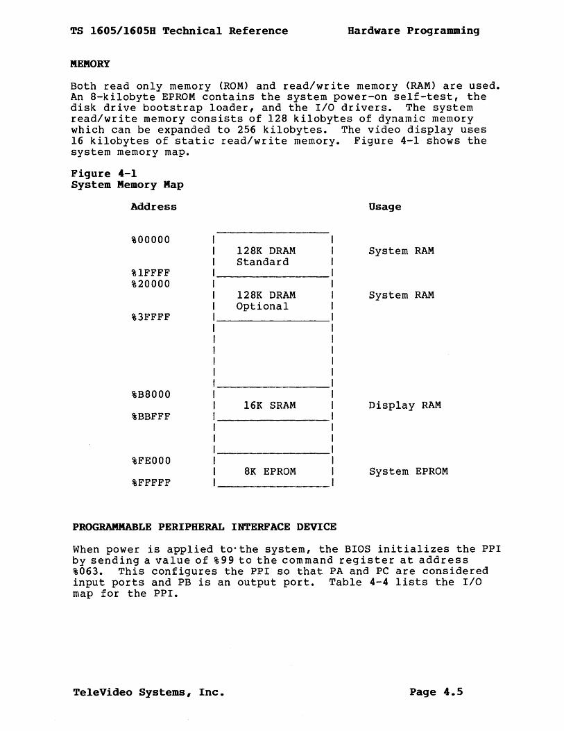
TS 1605/1605H Technical Reference Hardware Programming
MEMORY
Both read only memory (ROM) and read/write memory (RAM) are used. An 8-kilobyte EPROM contains the system power-on self-test, the disk drive bootstrap loader, and the I/O drivers. The system read/write memory consists of 128 kilobytes of dynamic memory which can be expanded to 256 kilobytes. The video display uses 16 kilobytes of static read/write memory. Figure 4-1 shows the system memory map.
Figure 4-1 System Memory Map
Address
%00000
%lFFFF %20000
%3FFFF
%B8000
%BBFFF
%FEOOO
%FFFFF
l28K DRAM Standard
l28K DRAM Optional
16K SRAM
8K EPROM
PROGRAMMABLE PERIPHERAL INTERFACE DEVICE
Usage
System RAM
System RAM
Display RAM
System EPROM
When power is applied to· the system, the BIOS initializes the PPI by sending a value of %99 to the command register at address %063. This configures the PPI so that PA and PC are considered input ports and PB is an output port. Table 4-4 lists the I/O map for the PPI.
Te1eVideo Systems, Inc. Page 4.5

TS 1605/1605H Technical Reference Hardware Programming
Table 4-4 8255A-5 I/O Bit Map
Addr
%0060
%0061
%0062
I/O Port
I
o
I
PA 0 1 2 3 4 5 6 7
PB 0 1 2 3 4 5 6 7
PC 0 1 2 3 4 5 6 7
Function
+Keyboard Scan Code 0 1 2 3 4 5 6 7
+Timer 2 Gate (Speaker) +Speaker Data Spare
(PA = Port A)
o - Read Switches 5-8/1 - Read Switches 1-4 Spare -Enable I/O Channel Check -Hold Keyboard Clock Low -(Enable Keyboard) or +(Clear Keyboard)
Operation 8087 Installed RAM Size RAM size Speaker Data
*SW-I SW-2 or SW-3 SW-4
+Timer Channel 2 Output +1/0 Channel Check Spare (low)
Display Mode SW-5 Display Mode SW-6 5 1/4 Drive SW-7 5 1/4 Drive SW-8
%0063 Command/Mode Register
Mode Register = %99
* Refer to the system User's Manual for switch settings
NOTE! A plus (+) indicates a bit value of 1 performs the specified function
A minus (-) indicates a bit value of 0 performs the specified function
SPEAKER INTERFACE
The system contains a small speaker, which can be driven from one or both of the following sources:
1. Alternating the value of bit 2 of port B of the PPI.
2. Programming channel 2 of the programmable interval timer.
TeleVideo Systems, Inc. Page 4.6

TS 1605/1605H Technical Reference Hardware Programming
KEYBOARD
The keyboard is controlled by an Intel 8048 microprocessor. The 8048 performs keyboard scanning, buffering of up to 16-key scan codes, bidirectional communications with the system board, and executes the handshake protocol required by each scan-code transfer.
The keyboard sends scan codes back to the system board as shown in Table 4-5. All keys are typematic and generate a make and break scan code. Break codes are formed by adding %80 to the make code.
Table 4-5 Keyboard Scan Codes
Code Code Key Decimal Hex Key Decimal Hex
Function Keys
F1 59 %3B F6 64 %40 F2 60 %3C F7 65 %41 F3 61 %3D F8 66 %42 F4 62 %3E F9 67 %43 F5 63 %3F FlO 68 %44
Alphanumeric Keys
1 2 %2 A 30 %lE 2 3 %3 S 31 %IF 3 4 %4 D 32 %20 4 5 %5 F 33 %21 5 6 %6 G 34 %22 6 7 %7 H 35 %23 7 8 %8 J 36 %24 8 9 %9 K 37 %25 9 10 %OA L 38 %26 0 11 %OB . 39 %27 ,
12 %OC I 40 %28 = 13 %OD 41 %29 Q 16 %10 \ 43 %2B W 17 %11 Z 44 %2C E 18 %12 X 45 %2D R 19 %13 C 46 %2E T 20 %14 V 47 %2F y 21 %15 B 48 %30 U 22 %16 N 49 %31 I 23 %17 M 50 %32 0 24 %18 , 51 %33 p 25 %19 . 52 %34 [ 26 %lA / 53 %35 ] 27 %lB PrtSc 55 %37
SPACE BAR 57 %39
Te1eVideo Systems, Inc. Page 4.7

TS 1605/1605H Technical Reference Hardware Programming
Numeric Keypad
7 71 %47 + 78 %4E 8 72 %48 1 79 %4F 9 73 %49 2 80 %50
74 %4A 3 81 %51 4 75 %4B 0 (Ins) 82 %52 5 76 %4C . (Del) 83 %53 6 77 %4D
Control Characters
Esc 1 %1 Shift (R) 54 %36 Backspace 14 %OE Alt 56 %38 Tab 15 %OF Caps Lock 58 %3A Enter 28 %lC Num Lock 69 %45 Ctrl 29 %lD Scroll Lock 70 %46 Shift (L) 42 %2A
VIDEO SECTION
The video section operates in an alphanumeric mode and a bitmapped graphics mode.
The alphanumeric mode provides two resolutions. The lowresolution mode is a 40-column by 25-row display using an 8-dots w ide by 9-dots high character box and 7 dots x 7 dots with one descender character font. The high-resolution mode is an 80-column by 25-row display with an 8-dots wide by 9-dots high character box and 7 dots x 7 dots with one descender character font. The alphanumeric modes support 256 different character codes (see Appendix D). An 8-kilobyte ROM character generator contains the two different fonts and a jumper option gives a single-dot font or double-dot font in a character size of 8 dots x 9 dots in any alphanumeric mode.
The black-and-white mode provides reverse video, blinking, and highlighting character attributes. The color mode has 16 foreground and eight background colors for each character. Blinking on a per-character basis is also available.
There are 16 kilobytes of static memory used for the display buffer. In the alphanumeric modes, eight screen displays can be stored in the 40 x 25 mode and four screen displays can be stored in the 80 x 25 mode. The start of each display page begins at an even 2- or 4-kilobyte offset and is accessed by changing the offset in the start-address registers.
Two resolutions are provided in the bit-mapped graphics mode; a medium resolution color graphics mode of 320 X 200 pixels and a high resolution black-and-white mode of 640 X 200 pixels.
Te1eVideo Systems, Inc. Page 4.8

TS l605/l605H Technical Reference Hardware Programming
Each pixel can have one of four colors in the medium-resolution mode. The background color can be one of sixteen colors, with one of two software-selectable palettes providing the three remaining colors. One palette contains red, green, and brown and the other palette contains cyan, magenta, and white, as shown in Figure 4-2. Since both graphics modes require 16 kilobytes of the buffer to define the screen display, the high resolution is available only in black-and-white.
Figure 4-2 Software-Selectable Palettes
WHITE
TeleVideo Systems, Inc. Page 4.9

TS l605/l605H Technical Reference Hardware Programming
Controller Programming
There are nineteen internal registers in the CRT controller that define and control a raster-scan CRT display. The 5-bit, writeonly Index register is used as a pointer to the other eighteen registers. This register is loaded from the CPU by executing an OUT instruction to IIO address %304.
Anyone of the 18 controller registers can be loaded by loading the Index register at %304 with the necessary pointer (0-17 decimal) and then loading the Data register with th~ desired value using an OUT instruction to %3D5. Table 4-6 lists the values that are loaded into the CRT controller registers for controlling the various operational modes.
Table 4-6 CRT Controller Registers
Reg. No.
RO Rl R2 R3 R4 R5 R6 R7 R8 R9 RIO Rll R12 R13 R14 R15 R16 R17
NOTE!
Register
Horizontal Total Horizontal Displayed Horizontal Sync Position Horizontal Sync Width Vertical Total Vertical Total Adjust Vertical Displayed Vertical Sync Position Mode Control Max. Scan Line Address Cursor Start Cursor End Start Address MSB Start Address LSB Cursor Address MSB Cursor Address LSB Light Pen Address MSB Light Pen Address LSB
1/0
WO WO Wo Wo Wo Wo Wo WO Wo WO Wo Wo Wo wo R/w R/w RO RO
40x25 Alpha Hex
%38 %28 %20 %OA %lC %01 %19 %lA %02 %08 %08 %08 %O(Pg 0) %O(Pg 0)
80x25 Alpha Hex
%71 %50 %59 %OA %lC %01 %19 %19 %02 %08 %08 %08 %O(Pg %O(Pg
MA8 - MA13 MAO - MA7
Graphics Mode Hex
%38 %28 %2D %OA %7F %06 %64 %70 %02 %01
%0 %0
0) %0 0) %0
Addresses in start-address and cursor-address registers are offsets into graphics memory. The CRT controller views these values as offsets into the character positions, ignoring attribute bytes; therefore, the offsets are 1/2 the offset value as viewed by the CPU.
Mode-Select Register
The 6-bit, write-only mode-select register is located at %3D8 and is used to select the video mode. Table 4-7 lists the bit assignments for the mode-select register and Table 4-8 summarizes this reg ister.
TeleVideo Systems, Inc. Page 4.10
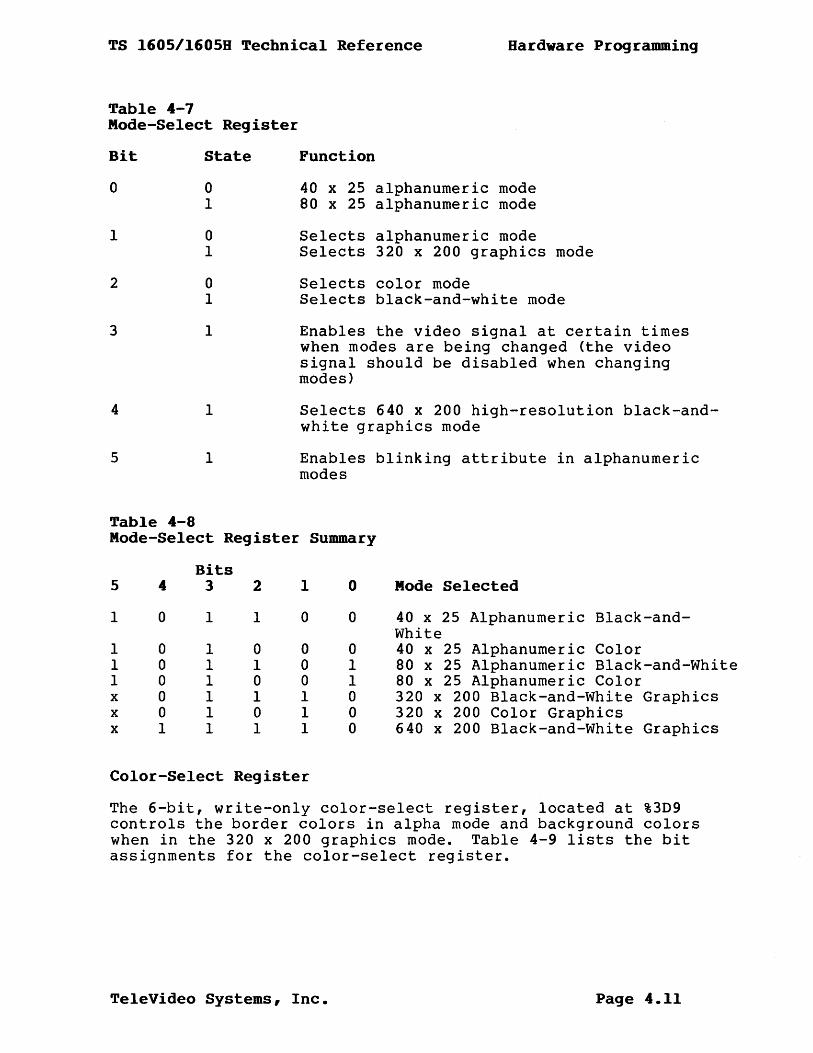
TS 1605/1605H Technical Reference Hardware Programming
Table 4-7 Mode-Select Register
Bit State
0 0 1
1 0 1
2 0 1
3 1
4 1
5 1
Table 4-8
Function
40 x 25 alphanumeric mode 80 x 25 alphanumeric mode
Selects alphanumeric mode Selects 320 x 200 graphics mode
Selects color mode Selects black-and-white mode
Enables the video signal at certain times when modes are being changed (the video signal should be disabled when changing modes>
Selects 640 x 200 high-resolution black-andwhite graphics mode
Enables blinking attribute in alphanumeric modes
Mode-Select Register Summary
Bits 5 4 3 2 1 0 Mode Selected
1 0 1 1 0 0 40 x 25 Alphanumeric Black-and-White
1 0 1 0 0 0 40 x 25 Alphanumeric Color 1 0 1 1 0 1 80 x 25 Alphanumeric Black-and-White 1 0 1 0 0 1 80 x 25 Alphanumeric Color x 0 1 1 1 0 320 x 200 Black-and-White Graphics x 0 1 0 1 0 320 x 200 Color Graphics x 1 1 1 1 0 640 x 200 Black-and-White Graphics
Color-Select Register
The 6-bit, write-only color-select register, located at %3D9 controls the border colors in alpha mode and background colors when in the 320 x 200 graphics mode. Table 4-9 lists the bit assignments for the color-select register.
TeleVideo Systems, Inc. Page 4.11

TS 1605/16058 Technical Reference
Table 4-9 Color-Select Register
Bit Function 40x25 Alpha
0 Set Blue Border
1 Set Green Border
2 Set Red Border
3 Set Intensity Border
Color
Color
Color
Color
4 Set Background Background Intensity
5 Palette Select
6 Not used
7 Not used
8ardware Programming
MODE 320x200 640x200 Graphic Graphic
Background Foreground
Background Foreground
Background Foreground
Background Foreground
Intensified Set
0 - red, green, brown 1 - cyan, magenta, white
When bit 5 is set to 0, colors are determined as follows:
Cl CO Set Selected 0 0 Background, as determined by bits 0-3 0 1 Green 1 0 Red 1 1 Brown
When bit 5 is set to 1, colors are determined as follows:
Cl o o 1 1
CO o 1 o 1
Status Register
Set Selected Background, as determined by bits 0-3 Cyan Magenta White
The 4-bit, read-only status register is located at %3DA. Table 4-10 lists the status register bit assignments.
TeleVideo Systems, Inc. Page 4.12

TS 1605/1605H Technical Reference Hardware Programming
Table 4-10 Status Register
Bit Function
o Display Enable
1 Light Pen
2 Light Pen
3 Vertical Sync
4-7 Not used
Alphanumeric Mode
Description
A 1 indicates a display cycle is active.
A 1 indicates that a positive going edge of the signal Tr igger Set from the light pen has set the light pen's trigger. This trigger is reset upon power-on and may be cleared by performing an IIO OUT command to address %3DB. No specific data setting is required, the action is address-activated.
Indicates the status of the light pen switch. A 0 indicates that the switch is on.
When active, indicates that the raster is in a vertical retrace mode.
The alphanumeric mode supports 256 character codes (refer to Appendix D). Each display character is defined by two bytes in the display buffer memory. An even-numbered byte contains the character code and the following odd-numbered byte contains the corresponding character attribute. Table 4-11 lists the bit assignments for the character attribute byte.
Table 4-11 Character Attribute Byte
Attribute Byte 7 6
Function Blk R
Normal BL 0 Reverse Video BL 1 Blank (Black) BL 0 Blank (White) BL 1
NOTE! R = Red G = Green B = Blue
5 G
0 1 0 1
TeleVideo Systems, Inc.
4 B
0 1 0 1
3 2 1 0 Background Foreground I R G B Color Color
In 1 1 1 Black White In 0 0 0 White Black In 0 0 0 Black Black In 1 1 1 White White
BL = 1: Blinking, 0: steady I = Intensity (foreground) In = 1: Intensity set, 0: normal
Page 4.13

TS 1605/16058 Technical Reference 8ardware Programming
Bits 0-3 indicate the foreground color and bits 4-6 indicate the background color. The standard display will produce white characters on a black background with all other foreground/background code combinations. A color monitor will produce the foreground or background colors listed in Table 4-12. The background intensity is set in bit 4 of the color-select register.
Table 4-12 Color Codes
R G B I Color
0 0 0 0 Black 0 0 1 0 Blue 0 1 0 0 Green 0 1 1 0 Cyan 1 0 0 0 Red 1 0 1 0 Magenta 1 1 0 0 Brown 1 1 1 0 White 0 0 0 1 Gray 0 0 1 1 Light Blue 0 1 0 1 Light Green 0 1 I 1 Light Cyan 1 0 0 I Light Red I 0 1 1 Light Magenta 1 1 0 1 Yellow I 1 I I White (High Intensity)
NOTE! Not all RGB monitors recognize the intensity bit.
Graphics Mode
There are two graphics modes: a 320 x 200 pixels mediumresolution color graphics mode and a 640 x 200 pixels highresolution black-and-white mode. Both modes use memory-mapped graphics and require 16 kilobytes to define the screen.
The graphic information for the screen display is stored in two 8-kilobyte banks as shown in Figure 4-3.
TeleVideo Systems, Inc. Page 4.14
TS 1605/1605H Technical Reference
Figure 4-3 Graphic Memory Addresses
Address
%B8000
%B9EFO
%BAOOO
%BBF3F
%BBFFF
Function
Even Scans (0 - 198)
8 kilobytes
Not Used
Odd Scans (1 - 199)
8 kilobytes
Not Used
Hardware Programming
In the medium-resolution mode, each byte contains information for four pixels as shown in Table 4-13.
Table 4-13 Medium-Resolution Byte Osage
7 6 5 4 3 2 1 0 Cl CO Cl CO Cl CO Cl CO
First Second Third Fourth display display display display pixel pixel pixel pixel
Each pixel may have one of four colors, while the background color may be one of 16 colors. One of two software-selectable palettes provides the remaining three colors, and are selected by bit 5 of the color-select register. Table 4-14 shows the color selection logic.
Table 4-14 Medium-Resolution Color Selection Logic
Cl
o o 1 1
CO
o 1 o 1
Color
1 of 16 preselected background colors If palette 1 Green If palette 2 Cyan
Red Magenta Brown White
TeleVideo Systems, Inc. Page 4.15

TS 1605/16058 Technical Reference 8ardware Programming
In the high-resolution black-and-white mode, each bit of a display byte contains the state of one display pixel. Bit 7 corresponds to the first display pixel and bit 0 corresponds to the eighth display pixel.
FLOPPY DISK CONTROLLER
The floppy disk controller (FDC) uses a write only, digitaloutput register at %3F2 to control drive motors, drive selection, and feature enable. Table 4-15 lists the digital-output register bit assignments.
Table 4-15 Digital-output Register
Bits 7 6 5 4 3 2 1 0 I I I I I I I I
I I I I I I 0 0 = Drive A selected I I I I I I 0 1 = Drive B selected I I I I I I
I I I I I 0 = FDC held reset I I I I I 1 = FDC enabled I I I I I
I I I I 0 = Interrupt and DMA request disabled
I I I 1 = Interrupt and DMA request I I I
I I 0 = Drive A motor off I I 1 = Drive A motor on I I
I 0 = Drive B motor off I 1 = Drive B motor on I
Not used
I/O driver
I/O drive enabled
The FDC has two registers accessible to the CPU: a status register at %3F4 and a data register at %3F5. The status register contains status information on the FDC, as shown in Table 4-16 and may be accessed at any time. The data register stores data, commands, and parameters and provides floppy disk drive (FDD) status information. Data bytes are read from or written to the data register in order to program or obtain results after a command.
TeleVideo Systems, Inc. Page 4.16

TS 1605/1605H Technical Reference Hardware Programming
Table 4-16 FDC Status Register (%3F4)
Bit 7 6 5 4 3 2 1 0 I I I I I I I I I I I I I 1 = FDD A is in the seek mode I I I I I I I I I I I 1 = FDD B is in the seek mode I I I I I I I I not used I I I I I 1 = FDC is busy - a read or w rite command I I progress I 1 = FDC is in the non-DMA mode I a = Data transfer from CPU to FDC data register 1 = Data transfer from FDC data register to CPU
1 = Data register is ready to send or receive data
is in
The FDC is capable of performing 15 different commands. Commands are initiated by a multi-byte transfer from the CPU. The result after execution of a command may include a multi-byte transfer back to the CPU. Table 4-17 is a summary of the FDC commands. Table 4-18 defines the symbols used in the command table.
Table 4-17 FDC Command Summary
Data Bus Command Phase R!W D7 D6 DS D4 D3 D2 D1 DO
READ DATA
Command W MT MF SK a a 1 1 a W x x x x x HD USI usa w C W H W R W N W EDT W GPL W DTL
Te1eVideo Systems, Inc.
Remarks
Command Codes
Sector ID information prior to command execution
Page 4.17

TS 1605/16058 Technical Reference 8ardware Programming
Execution Data transfer between FDD and system. Status
Result R STO information R STI after command R ST2 execution. R C Sector ID R H information R R after command R N execution.
READ DELETED DATA
Command W MT MF SK 0 1 1 0 0 Command Codes W x x x x x HD USI usa w C Sector ID W H information W R prior to W N command W EDT execution W GPL W DTL
Execution Data transfer between FDDand system. Status
Result R STO information R STI after command R ST2 execution. R C Sector ID R H information R R after command R N execution.
WRITE DATA
Command W MT MF 0 0 0 I 0 I Command Codes W x x x x x HD USI USO W C Sector ID W H information W R prior to W N command W EDT execution W GPL W DTL
Te1eVideo Systems, Inc. Page 4.18

TS 1605/1605H Technical Reference Hardware Programming
Execution Data transfer between FDD and system. Status information
Result R STa after command R STI execution. R ST2 Sector ID R C information R H after command R R execution. R N
WRITE DELETED DATA
Command W MT MF a a I a a I Command Codes W x x x x x HD USI usa w C Sector ID W H information W R prior to W N command W EDT execution W GPL W DTL
Execution Data transfer between FDD and system. Status
Result R STa ID information R STI after command R ST2 execution. R C Sector ID R H information R R after command R N execution.
READ A TRACK
Command W a MF SK a a a I a Command Codes W x x x x x HD USI usa w C Sector ID W H information W R prior to W N command W EDT execution W GPL W DTL
TeleVideo Systems, Inc. Page 4.19

TS 1605/1605H Technical Reference
Execution
Result
Execution
Result
Command
Execution
Result
R R R R R R R
R R R R R R R
W W w W W W
R R R R R R R
a MF x x
Te1eVideo Systems, Inc.
a x
STa STI ST2
C H R N
STa STI ST2
C H R N
FORMAT A TRACK
a 1 1 a x x HD USI
N SC GPL
D
STa STI ST2
C H R N
Hardware Programming
a usa
Data transfer between FDD and system. FDC reads all cylinders from index hole to EDT. Status information after command execution. Sector ID information after command execution.
First correct ID information cylinder is stored in data register. Status information after command execution. Sector ID information during execution.
Command Codes
Bytes/Sector Sector/Track Gap 3 filler byte. FDC formats an entire cylinder. Status information after command execution. In this case, ID information has no meaning.
Page 4.20

TS 1605/1605H Technical Reference Hardware Programming
SCAN EQUAL
Command W MT MF SK I a a a I Command Codes W x x x x x HD USI usa w C Sector ID W H information W R prior to W N command W EOT execution W GPL W DTL
Execution Data compared between FDD and system. Status
Result R STa information R STI after command R ST2 execution. R C Sector 10 R H information R R after command R N execution.
SCAN LOW OR EQUAL
Command W MT MF SK I I a a I Command Codes W x x x x x HD USI usa w C Sector 10 W H information W R prior to W N command W EOT execution W GPL W DTL
Execution Data compared between FDD and system. Status
Result R STa information R STI after command R ST2 execution. R C Sector ID R H information R R after command R N execution.
Te1eVideo Systems, Inc. Page 4.21

TS 1605/1605H Technical Reference Hardware Programming
SCAN HIGH OR EQUAL
Command W MT MF SK 1 1 1 0 1 Command Codes W x x x x x HD USI uso W C Sector 1D W H information W R prior to W N command W EDT execution W GPL W DTL
Execution Data compared between FDD and system. Status information
Result R STO after command R STI execution. R ST2 Sector 1D R C information R H after command R R execution. R N
RECALIBRATION
Command W 0 0 0 0 0 1 1 1 Command Codes W x x x x x 0 USI USO
Execution Head retracts to track O.
SENSE INTERRUPT STATUS
Command W 0 0 0 0 1 a a a Command Codes Result R STa Status
R PCN FDC information at end of seek operation
SPECIFY
Command W a a 0 a 0 a 1 1 Command Codes W ---SRT--------I-------HUT---W I------HLT--------------I ND
SENSE DRIVE STATUS
Command W a 0 0 a 0 1 a 0 Command Codes W x x x x x HD USI usa
Result R ST3 Status PDD information
TeleVideo Systems, Inc. Page 4.22

TS 1605/1605H Technical Reference Hardware Programming
Command
Execution
Command
Result
Table 4-18
W W W
W
R
o x
o x
FDC Command Symbols
Symbol
C
D
D7-DO
DTL
EDT
GPL
H
HD
Name
Cylinder Number
Data
Data Bus
Data Length
End of Track
Gap Length
Head Address
Head
o x
SEEK
o 1 x x
NCN
1 1 1 Command Codes HD USI USO
Head positioned over proper cylinder on diskette.
INVALID
Invalid Codes Invalid command codes (NoOp-FDC goes into standby state). STO = %80. STO
Description
The current/selected cylinder (track) number.
The data pattern that is written into a sector.
8-bit data bus, where D7 stands for the most significant bit and DO the least significant bit.
When N is defined as 00, DTL stands for data length that users read from or write to the sector.
The final sector number on a cylinder.
The length of gap 3 (spacing between sectors excluding VCO sync field).
The head number 0 or 1, as specified in the ID field.
A selected head number 0 or 1. (H=HD in all command words.)
HLT Head Load Time The head load time in the FDD (4 to 512
TeleVideo Systems, Inc.
milliseconds in 4-millisecond increments) •
Page 4.23

TS 1605/1605H Technical Reference Hardware Programming
HUT
MF
MT
N
NCN
ND
PCN
R
R/W
SC
SK
SRT
STO STl ST2 ST3
Head Unload Time
The head unload time after a read or write operation has occurred (0 to 480 milliseconds in 32-millisecond increments) •
FM or MFM Mode If MF is low, FM mode is selected. If it is high, MFM mode is selected only if MFM is implemented.
Multi-Track
Number
New Cylinder
Non-DMA Mode
Present Cylinder
Record
Read/Write
Sector
Skip
Step Rate Time
Status 0 Status 1 Status 2 Status 3
If MT is high, a multi-track operation is to be performed. (A cylinder under both HDO and HDI will be read or written.)
The number of data bytes written in a sector.
A new cylinder number to define the desired position of the head after the seek operation.
Operation in the non-DMA mode.
Cylinder number at the completion of sense-interrupt-status command that indicates the position of the head at present time.
The sector number to be read or written.
Either a read or write operation.
Indicates the number of sectors per cylinder.
Skip deleted-data address mark.
FDD stepping rate 2 to 32 microseconds (in 2-microsecond increments).
Oneofthe four command status registers that store the status information after a command has been executed. This information is available during the result phase after command execution. These registers should not be confused with the main status register. These registers may only be read after a command has been executed and contain information relevant to that particular command.
TeleVideo Systems, Inc. Page 4.24

TS l605/1605H Technical Reference Hardware Programming
STP Scan Test If STP=l during a scan operation, the data in contiguous sectors is compared byte-by-byte with data sent from the CPU. If STP=2, then alternate sectors are read and compared.
Command Status Register 0
Bit Name Description
usa Unit Select Aselecteddrive number encodedthe same as USI as bits a and 1 of the digital-output
register.
00 Unit Select 0 Used to indicate a drive unit number at 01 Unit Select 1 interrupt.
02 Head Address Used to indicate the state of the head at interrupt.
03 Not Ready This bi t is set when the FOO is in the notready state and a read or write command is issued.
04 Equipment This bit is set if a fault is received from
05
06
07
Check the FOO, or if the track a signal fails to occur after 77 step pulses (recalibrate command) •
Seek End
Interrupt
Code 07 06 a a
a 1
1 a
1 1
This bi t is set when the FOC completes the seek command.
Normal termination of command. Command was completed and properly executed.
Abnormal termination of command. Execution of the command was started, but was not successfully completed.
Invalid command issue. The command that was issued was never started.
Abnormal termination because, during execution, the ready signal from the FOO changed states.
Command Status Register 1
Bit Name Description
TeleVideo Systems, Inc. Page 4.25

TS 1605/16058 Technical Reference 8ardware Programming
DO Missing Address
Dl Not Writeable
D2 No Data
D3 Not used
D4 Over Run
D5 Data Error
D6 Not used
D7 End of Cylinder
This bit is set if the FDC cannot Mark detect the ID address mark. Note, the missing address mark in the data field of status register 2 is also set.
This bit is set if the FDC detects a write- protect signal from the FDD during execution of a write data, cylinder command.
This bit is set if 1) the FDC cannot find the sector specified in the ID register during execution of a read data, write deleted data, or scan command, 2) the FDC cannot read the ID field without an error during execution of the read ID command, or 3) starting sector cannot be found during executiQn of the read a cylinder command.
Al ways set = 0
This bit is set if the FDC is not serviced by the main system during data transfers within a certain time interval.
This bit is set if the FDC detects a cyclic redundancy check <CRC) error in either the ID field or the data field.
Al ways set = 0
This bit is set when the FDC tr ies to access a sector beyond the final sector of a cylinder.
Command Status Register 2
Bit Name
DO Missing Address Mark in Data Field
Dl Bad Cylinder
Te1eVideo Systems, Inc.
Description
Thisbit is set if the FDC cannot find a data address mark or deleted data address in Data Field when data is read from the medium.
This bi t is set when contents of C on the medium are different from that stored in ID register, when contents of Care %FF.
Page 4.26

TS 1605/1605H Technical Reference Hardware Programming
02
03
04
05
06
07
Scan Not Satisfied
Scan Equal Hit
Wrong Cylinder
Data Error in Data Field
Control Mark
Not used
Command Status Register
Bit Name
DO Unit Select 0
01 Unit Select 1
02 Head Address
03 Two Side
04 Track 0
05 Ready
06 Write Protect
07 Fault
Te1eVideo Systems, Inc.
This bit is set if FDC cannot find a sector on the cylinder that meets the condition during execution of scan command.
This bit is set if equal condition is satisfied during execution of scan command.
This bit is set when the contents of C on the medium are different from that stored in the ID register.
3
This bit is set if the FDC detects a CRC error in the data.
This bit is set if the FDC encounters a sector containing a deleted data address mark during execution of read data or scan command.
Always = 0
Description
The status of the unit-select-O signal from the FDD.
The status of the unit-select-l signal from the FOD.
The status of the side-select signal from the FDD.
The status of the two-side signal from the FOD.
The status of the track 0 signal from the FDD.
The status of the ready signal from the FDD.
The status of the write-protected signal from the FOD.
The status of the fault signal from the FDD.
Page 4.27

TS 1605/1605H Technical Reference Hardware Programming
SERIAL PORT
The WD8250 UART can be programmed to operate from 50 to 9600 baud. Five, six, seven, or eight bit characters with 1, 1-1/2, or 2 stop bits are supported. A fully prioritized interrupt system controls transmit, receive, error, line status, and data set interrupts. Appendix F lists the pin connector assignments for the serial port.
Different modes of operation are selected by initializing the appropriate UART registers. The divisor latch access bit CDLAB), bit 7 of the line-control register, is used to select certain registers. Table 4-19 lists the UART 1/0 register addresses.
Table 4-19 UART I/O Register Addresses
Address I/O Register Selected DLAB State P S
%3F8 %2F8 0 Transmitting Holding 0 (Write) %3F8 %2F8 I Receiver Data Register 0 (Read) %3F8 %2F8 0 Baud-rate Divisor LSB 1 %3F9 %2F9 0 Baud-rate Divisor MSB 1 %3F9 %2F9 0 Interrupt Enable 0 %3FA %2FA I Interrupt Identification %3FB %2FB 0 Line Control %3FC %2FC 0 Modem Control %3FD %3FD I Line Status %3FE %3FE I Modem Status
P = Primary, S = Secondary
The serial port primary adapter uses interrupt line IRQ4. To allow the port to send interrupts to the system, bit 3 of the modem control register must be set high. With bit 3 high, any interrupts allowed by the interrupt enable register will cause an interrupt. A secondary adapter may be utilized with the addition of an optional board.
Line-Control Register
The format of the asynchronous data communication is specified through the line-control register (the contents of this register may be retrieved for inspection). Table 4-20 lists the bit assignment of the line-control register.
TeleVideo Systems, Inc. Page 4.28

TS 1605/1605H Technical Reference Hardware Programming
Table 4-20 Line-Control Register
Bit
o 1 2 3 4 5 6 7
Bits 0 & 1
Bit 2
Bit 3
Bit 4
Bit 5
Bit 6
Assignment
Character length select bit 0 Character length select bit 1 Number of stop bits Parity enable Even parity select Stick parity Set break Divisor Latch Access Bit
These bi ts set the number of bi ts in each transmi tted transmitted or received serial character. They are encoded as follows:
Bit 1 Bit 0 Character Length
0 0 5 Bits 0 1 6 Bits 1 0 7 Bits 1 1 8 Bits
This bit specifies the number of stop bits as follows:
Bit 2 Character Length Stop Bits
0 5 - 8 1 1 5 1-1/2 1 6 - 8 2
Parity enable bit. 0 = No parity bit 1 = Parity bit generated
This bit has the following effect:
Bit 4
o 1
Bit 3
1 1
I of Data bits and parity bit
Odd number Even number
This bit has the following effect:
Bit 5
1 1
Bit 4
o 1
Bit 3
1 1
= =
Parity bit state
1 o
Set break control bit. When set to 1, the serial output (SOUT) is forced low and remains there regardless of other transmitter activity.
TeleVideo Systems, Inc. Page 4.29

TS l605/l605H Technical Reference Hardware Programming
. Bit 7 Divisor Latch Access Bit. This bit must be set to 1 to
access the divisor latches of the baud rate generator during a read or write operation. This bit must be set to 0 to access the receiver data register, the transmitting holding register, or the interrupt enable register.
Programmable Baud Rate Generator
The UART contains a programmable baud rate generator that is capable of taking the clock input and dividing it by any divisor from 1 to 65,535. The output frequency of the baud rate generator is 16 times the baud rate.
divisor # = input frequency / (baud rate x ~6)
Two 8-bit latches store the divisor in a 16-bit format. These divisor latches must be loaded during initialization in order to ensure the desired operation of the baud rate generator. The address bits for the divisor latches are shown in Table 4-21. The divisor baud rates are listed in Table 4-22.
Table 4-21 Divisor Latches
(DLAB=l) %3F9 %3F8
Address Bit 7 6 5 4 3 2 1 0 7 6 5 4 3 2 1 0
Divisor Bit 15 14 13 12 11 10 9 8 7 6 5 4 3 2 1 0
Table 4-22 Divisor Baud Rates
Desired Baud Rate Divisor Hex Decimal
50 %09 00 2304 75 %06 00 1536
110 %04 17 1047 134.5 %03 59 857 150 %03 00 768 300 %01 80 384 600 %00 CO 192
1200 %00 60 96 1800 %00 40 64 2000 %00 3A 58 2400 %00 30 48 3600 %00 20 32 4800 %00 18 24 7200 %00 10 16 9600 %00 OC 12
TeleVideo Systems, Inc. Page 4.30

TS 1605/1605H Technical Reference Hardware Programming
Line-Status Register
The line-status register provides status information on data transfer. Table 4-23 lists the line-status register bit assignments.
Table 4-23 Line-Status Register (%3FD or %2FD)
Bit
0 1 2 3 4 5 6 7
Bit 0
Bit 1
Bit 2
Bit 3
Bit 4
NOTE!
Assignment
Data Ready Overrun error Parity error Framing error Break interrupt Transmitting holding register empty Transmitting shift register empty Set = 0
Data Ready indicator. This bit is set to 1 whenever a complete incoming character has been received and transferred into the receiver buffer register. This bit is reset to 0 either by the CPU reading the data in the receiver buffer register or by writing a logical 0 into it from the CPU.
Overrun error indicator. This bit indicates that data in the r e c e i ve r b u f fer reg is t e r was not read by the CPU before the next character was transferred into the receiver buffer register. This bit is reset whenever the CPU reads the contents of the line status register.
Parity error indicator. This bit indicates that the received data character does not have the correct even or odd parity, as selected by the even parity-select bit. This bit is set to 1 upon detection of a parity er ror and reset to 0 whenever the CPU reads the contents of the line status register.
Framing error indicator. This bit indicates that the received character did not have a valid stop bit. This bit is set to 1 whenever the stop bit following the last data bit or parity bit is detected as a zero bit.
Break Interrupt indicator. This bit is set to 1 whenever the received data input is held in the 0 state for longer than a full word transmission time.
Bits 1-4 are the error conditions that produce a receiver line status interrupt whenever any of the corresponding conditions are detected.
Te1eVideo Systems, Inc. Page 4.31

TS l605/l605B Technical Reference Bardware Programming
Bit 5
Bit 6
Bit 7
Holding register empty indicator. This bit indicates tha t the UART is ready to accept a new character for transmission. In addition, this bit causes the UART to issue an interrupt to the processor when the transmit holding register empty interrupt enable is set high. Bi t 5 is set to 1 when a character is transfer red from the transmitter holding register into the transmitter shift register. The bit is reset to 0 when the CPU loads the transmitter holding register.
Transmitter shift register empty. This bit is set to 1 whenever the transmitter shift register is idle. It is reset to 0 upon a data transfer from the transmitter holding register to the transmitter shift register. Bit 6 is a read-only bit.
This bit is set permanently to O.
Interrupt-Identification Register
The interrupt-identification register is used to indicate that a prioritized interrupt is pending and the type of interrupt. Table 4-24 shows the interrupt-identification register bit assignments and Table 4-25 describes the interrupt control functions.
Table 4-24 Interrupt-Identification Register (%3FA or %2FA)
Bit
o 1 2 3-7
Assignment
o if interrupt pending Interrupt ID bit 0 Interrupt ID bit 1 Set = 0
Bit 0 Indicates whether an interrupt is pending. When set to 1, no interrupt is pending and polling (if used) is continued.
Bit 1 & 2 These two bits identify the highest priority interrupt pending as indicated in Table 4-25.
TeleVideo Systems, Inc. Page 4.32

TS 1605/16058 Technical Reference Hardware Programming
Table 4-25 Interrupt Control Functions
Interrupt ID Interrupt Set and Reset Functions
Register Bits Priority Interrupt Interrupt Interrupt 2 1 0 Level Type Source Reset Action
0 0 1 None None
1 1 0 First Received Overrun error Read the character or line-status error Parity error register <break or condition) Framing error
or Break interrupt
1 0 0 Second Received Receiver Read the data data receiver available available data reg.
0 1 0 Third Transmitter Transmitter Output a ready holding character
reg. empty to the transmitter holding register
0 0 0 Fourth Modem Clear to send Read the status or modem changed Data set ready status
or register Ring indicator or Received line
Interrupt-Enable Register
The interrupt-enable register is used to enable the four types of interrupts used in the UART. Table 4-26 lists the bit assignments for the interrupt enable register.
Table 4-26 Interrupt-Enable Register (%3F9 or %2F9 DLAB=O)
Bit Assignment
o 1 = Enable Data Available Interrupt 1 1 = Enable Transmitter Holding Register Empty Interrupt 2 1 = Enable Receive Line Status Interrupt 3 1 = Enable Modem Status Interrupt 4-7 Set = 0
TeleVideo Systems, Inc. Page 4.33

TS l605/l605H Technical Reference Hardware Programming
Modem-Control Register
The modem-control register controls the interface with the modem or data set. Table 4-27 lists the bit assignments for the modem control register.
Table 4-27 Modem-Control Register (%3FC or %2FC)
Bit
o 1 2 3 4 5-7
Bit 0
Bit 1
Bit 2
Bit 3
Bit 4
Assignment
Data Terminal Ready (DTR) Request to Send (RTS) Out 1 Out 2 Loop Set = 0
When this bit is set to 1, the UART -DTR output is forced low (log ic 0).
When this bit is set to 1, the UART-RTS output is forced low (log ic 0).
When this bit is set to 1, the UART -OUT 1 output is forced low (logic 0). This bit must be set to 1 for the UART to send interrupts to the system bus.
When this bit is set to 1, the UART -OUT 2 output is forced low (log ic 0).
This bit provides a loopback feature for diagnostic testing. When set to 1, the following occurs:
1. The transmitter serial output is set low 2. The receiver serial input is disconnected 3. The output of the transmitter shift register is
looped back into the receiver shift register input 4. The four modem control inputs are disconnected 5. The four modem control outputs are internally
connected to the four modem control inputs
In the diagnostic mode, data that is transmitted is immediately received. This feature allows the CPU to verify the transmit-and receive-data paths of the UART.
I~ the diagnostic mode, the receiver and transmitter interrupts are fully operational. The modem-control interrupts are also operational but the interrupt's sources are now the lower four bits of the modemcontrol register instead of the four modem-control inputs. The interrupts are still controlled by the interrupt-enable register.
TeleVideo Systems, Inc. Page 4.34

TS 1605/1605H Technical Reference Hardware Programming
Bits 5-7 These bits are permanently set to O.
Modem-Status Register
The modem-status register provides the current state of the control lines from the modem to the processor. In addition to the current-state information, four bits provide change information. Table 4-28 lists the bit assignments for the modem status register.
Table 4-28 Modem-Status Register (%3PE or %2FE)
Bit
o 1 2 3 4 5 6 7
Bit 0
Bit 1
Bit 2
Bit 3
NOTE!
Bit 4
Assignment
Delta Clear to Send Delta Data Set Ready Trailing Edge Ring Indicator Delta Receive Line Signal Detect Clear to Send Data Set Ready Ring Indicator Receive Line Signal Detect
Delta Clear to Send bit. This bit indicates that the UART -CTS input to the device has changed state since the last time it was read by the CPU.
Delta Data Set Ready bit. This bit indicates that the UART -DSR input to the device has changed since the last time it was read by the CPU.
Trailing Edge Ring Indicator bit. This bit indicates that the UART -RI input to the device has changed from an on (logical 1) to an off (logical 0) state.
Delta Receive Line Signal Detect bit. This bit indicates that UART -RLSD input has changed state.
Whenever bit 0, 1, 2, or 3 is set to 1, a modem status interrupt is generated.
Clear to Send bit. This bit is the complement of the UART Clear to Send (-CTS) input. If bit 4 (LOOP) of the modem control register is 1, this is equivalent to the Request to Send bit in the modem control register.
TeleVideo Systems, Inc. Page 4.35

TS l605/l605H Technical Reference Hardware Programming
Bit 5
Bit 6
Bit 7
Data Set Ready bit. This bit is the complement of the UART Da ta Set Ready (-DSR) inpu t. If bit 4 (LOOP) of the modem control register is 1, this bit is equivalent to the Data Terminal Ready bit in the modem control register.
Ring Indicator bit. This bit is the complement of the UART Ring Indicator input. If bit 4 (LOOP) of the modem control register is 1, this bit is equivalent to the OUT 1 bit of the modem control register.
Receive Line Signal Detect bit. This bit is the complement of the UART Received Line Signal Detect input. If bit 4 of the modem control register is 1, this bit is equivalent to the OUT 2 bit of the modem control register.
Receiver Data Register
The receiver data register contains the received character as listed in Table 4-29.
Table 4-29 Receiver Data Register (%3F8 or %2F8 DLAB=O Read Only)
Bit Assignment
o 1 2 3 4 5 6 7
Data bit 0 (least significant bit - first bit received) Data bit 1 Data bit 2 Data bit 3 Data bit 4 Data bit 5 Data bit 6 Data bit 7
Transmitter Holding Register
The transmitter holding register contains the character to be serially transmitted as listed in Table 4-30.
TeleVideo Systems, Inc. Page 4.36

TS 1605/1605B Technical Reference
Table 4-30 Transmitter Bolding Register (%3F8 or '2F8 DLAB=O Write Only)
Bit Assignment
Bardware Programming
o Data bit 0 (least significant bit - first bit transmitted)
1 2 3 4 5 6 7
Data bit 1 Data bit 2 Data bit 3 Data bit 4 Data bit 5 Data bit 6 Data bit 7
PARALLEL PORT
The parallel port uses three ports for data transfer and control. Tables 4-31, 4-32, and 4-33 list the three 1/0 ports, their addresses, and bit assignments.
Table 4-31 Data Output Port ('3BC)
Bit Signal Pin t
0 Data 0 2 1 Data 1 3 2 Data 2 4 3 Data 3 5 4 Data 4 6 5 Data 5 7 6 Data 6 8 7 Data 7 9
TeleVideo Systems, Inc. Page 4.37

TS 1605/1605H Technical Reference Hardware Programming
Table 4-32 Output Control Port (%3BE)
Pin 17 Bit 7 6 5 4 3
I I I not used
16 14 1 2 1 0 I I I I I 0 = Normal setting I I 1 = Pulse bit to 1 to output data to I I printer I I I 0 = No auto line feed (normal setting> I 1 = Auto line feed after carriage return I 0 = Pulse bit must be set low for at -least
50 microseconds to initialize printer 1 = Normal operation
1 = To allow printer to read output
o = Printer interrupt disabled 1 = IRQ7 interrupt enabled on printer Acknowledge
signal pulse
Table 4-33 Control Signal Input Port (%3BD)
Pin 11 10 12 13 15 Bit 7 6 5 4 3 2 1 0
I I I I I I I I I not used I I I I I 0 = Printer error I I 1 = Printer normal I I I 0 = Printer not on line I 1 = Printer on line I o = Printer has paper 1 = Printer out of paper
o = Acknowledge pulse 1 = Normal input
o = Printer busy, do not send data 1 = Printer not busy, send data
Te1eVideo Systems, Inc. Page 4.38

TS 1605/16058 Technical Reference Hardware Programming
Once the printer is initialized, data can be output using the following steps:
1. Send a data character to the data output port (%3BC).
2. Check the printer status by reading the control-signal input port (%3BD). Note, bit 7 must be set to 1 before data can be strobed into the printer.
3. When the printer is ready, pulse bit 1 of the output-control port to 1 and then reset it to D. Note, bit 3 must be set to 1 for the printer to read the data character.
4. When the printer has processed the data character, it sends back an acknowledge signal by pulsing bi t 6 of the controlsignal input port low. The procedure is then repeated for the next data character.
I/O CHANNEL
The IIO channel provides data bus lines, address bus lines, interrupt lines, DMA control lines, and power and ground lines. These lines and signals are described in Table 4-34.
Table 4-34 I/O Channel Signals
Signal Name
Address Bits
1/0 Description
o Lines AD through A19 address system memory and IIO devices, allowing access of up to 1 megabyte of memory. AD is the leastsignificant bit and A19 is the mostsignificant bit. Active high, these lines are addressed by the CPU or DMA.
Address Enable 0 The Address Enable line disables the CPU and other devices from the IIO channel for DMA transfers. The DMA controls address and data lines and readlwrite command lines when this line is active high.
Address Latch 0 Enable
Data 0 Acknowledge
Provided by the bus controller, Address Latch Enable latches valid CPU addresses. When used with Address Enable, it indicates a valid address to the liD channel. CPU addresses are latched wit~ falling edge of Address Latch Enable.
Active low, these lines acknowledge DMA requests and refresh system dynamic memory.
TeleVideo Systems, Inc. Page 4.39

TS 1605/1605H Technical Reference Hardware Programming
Data Bits
Data Request
Interrupt Request
I/O Channel Check
liD Channel Ready
liD Read
liD Reset
liD Write
Memory Read
liD Lines DO through D7 provide data bus bits for the CPU, memory, and liD devices. Active high, DO is the least significant bit and D7 is the most significant bit.
I The peripheral devices use these asynchronous channel requests to gain DMA service. Request I is prioritized as the highest and request 3 as the lowest. A request is initiated by making a request line active high and holding it high until the corresponding data acknowledge line goes active.
I Whenan liD device needs attention, Interrupt Request lines signal the CPU. Request 2 is prioritized as the highest and request 7 as the lowest. An interrupt request is initiated by raising the interrupt request line from low to high and holding it high until it is acknowledged by the CPU.
I
I
o
o
o
o
The liD Channel line provides the CPU with parity information on liD channel devices. A parity error is indicated by an active low signal.
liD cycles are lengthened by an liD device pulling the liD channel line low, which allows slower devices to be easily attached to the liD channel. When a slow device uses this line, it immediately drives it low as it detects a valid address and a read or write command. This line is held no longer than 10 clock cycles.
InputlOutput Read command line instructs an liD device to drive its data onto the data bus. This active low line may be driven by the CPU or DMA.
liD Reset signal initilizes or resets system logic upon power-up or a low line voltage outage. This active high signal is synchronized to the falling edge of clock.
InputlOutput Write command signal instructs an liD device to read data on the data bus. It may be dr i ven by the CPU or the DMA and is active low.
Memory Read command signal instructs memory to drive its data onto the data bus. This act i ve low line may ·be dr i ven by the CPU or the DMA.
TeleVideo Systems, Inc. Page 4.40

TS 1605/1605H Technical Reference Hardware Programming
Memory Write a Memory Write command signal instructs the memory to store the data on the data bus. This active low line may be driven by the CPU or the DMA.
Oscillator a The oscillator is a high speed clock with a 70-nanosecond period (14.31818 MHz) and a duty cycle of 50%.
System Clock a The system clock is a divide-by-three of the oscillator with a 210-nanosecond period and a duty cycle of 33%.
Terminal Count a Active high, this line provides a pulse when the terminal count for a DMA channel is reached.
WINCHESTER DISK CONTROLLER BOARD
The Winchester disk controller board contains a WD1010-05 Winchester disk controller device to perform executive control over disk operations. To command the board, the system addresses a set of task file registers in the WD1010-05 with the I/O port address of each of the individual registers. Table 4-35 is a list of the individual registers, along with their I/O port addresses for the TS l605H:
Table 4-35 TS 1605 Registers
Address
%0020 %0021 %0022 %0023 %0024 %0025 %0026 %0027
Read
System Access Error Flags Sector Count Sector Number Cylinder Low Cylinder High Sector/Drive/Head Status Register
Write
System Access Write Precomp Cylinder Sector Count Sector Number Cylinder Low Cylinder High Sector/Drive/Head Command Register
A detailed description of the WDlOlO-05 device is given in the referenced Western Digital documentation.
Task File Register Functions
For a typical operation, the task file registers are written to or read for status, and a command is given to the command register. The WD1010-05 then tri-states the address bus and executes the command. At the end of the operation, the task file is again opened to the system.
TeleVideo Systems, Inc. Page 4.41

TS 1605/1605H Technical Reference Hardware Programming
Error Register. Contains error flags for bad block detect, CRC data field, ID not found, aborted command, TKOOOO error, and data address mark error. During read operations, the error register is read after the data is read out of buffer RAM, that is, after the byte count goes to zero~ The error register bit assignments are listed in Table 4-36.
Table 4-36 Error Register Bit Assignments
Bit Description
o This bit is set during a read sector command if the address mark is not found after the proper sector ID is read.
1 This bit is set only by the restore command. It indicates that the head is not positioned over track 000 after 1024 stepping pulses.
2 This bit is set if a command was issued while the status register shows a drive fault (bit 5), or command disable (bit 6) condition. This bit is also set if an undefined command is issued.
4 This bit is set when the desired cylinder, head, sector, or size parameter cannot be found after 8 revolutions of the disk. This bit is also set if a cyclic redundancy check error has occurred.
6 This bit is set if a data field CRC error has occurred or the data mark address has not been found.
7 This bit is set if an ID field has been encountered that contains a bad block mark (used for bad sector mapping).
write Precomp. Defines the starting cylinder number at which reduced write current (RWC) begins. This value is in the range 0 to 255, and is internally multiplied by four to obtain the actual cylinder.
Sector Count. Contains the number of sectors that are to be transferred to buffer RAM. Because this is a decrementing function, all zeros are written for a 256-sector transfer and a 1 is written for a one-sector transfer.
Sector Number. range 0 to 255. transfer.
Contains the starting sector of a transfer in the This register is incremented with every
Cylinder Number Low. Least significant eight bits of the starting cylinder number in the range 0 through 1023.
Cylinder Number High. Carries the most significant bits of the starting cylinder number as bits 0(8) and 1(9). The other bits of this register are unused.
TeleVideo Systems, Inc. Page 4.42

TS 1605/16058 Technical Reference Bardware Programming
Sector/Drive/Bead Register. Contains the sector size, drive number, and head number parameters for the operation:
Bit 7 6 5 4 3 2 1 0 I I I I I I I 0 0 0 = Select head 0 I I 0 0 1 = Select head 1 I I 0 0 1 = Select head 1 I I 0 0 1 = Select head 1 I I 1 1 1 = Select head 7 I I 0 0 = Select drive 1 0 1 = Select drive 2 1 0 = Select drive 3 1 1 = Select drive 4
0 0 = Sector size 256 0 1 = Sector size 512 1 0 = Sector size 1024 1 1 = Sector size 128 = Extension bit
Bit 7 is an extension bit that extends the data field by seven bytes when ECC codes are used. When set to 1, CRC is not appended to the end of the data field; the data field becomes sector size + 7 bytes long.
The SOH byte written into the IO field is different than the SOH register contents. The recorded SOH byte does not have the drive number written and contains a bad block in bit 7.
Status Register. Contains status bits for device busy, device ready, write fault (same as WF line), seek complete (same as SC line), data request (same as BORQ line), command in progress, and error register flags set.
Bit Description
o This bit is set whenever any bits in the error register are set. This bit is reset when a new command is written into the command register.
1 When this bit is set, a command is being executed and a new command should not be loaded.
3 This bi t is set when the sector buffer should be loaded or read (depending on the command). It is reset upon completion of the operation.
4 This bit is set during a seek, and reset when the head settling time has expired.
5 This bit indicates a fault condition at the drive when set. An interrupt is generated when this bit is set.
Te1eVideo Systems, Inc. Page 4.43

TS 1605/1605H Technical Reference Hardware Programming
6 This bit must be set for commands to execute.
7 This bit is set whenever the disk is being accessed. Commands should not be loaded into the command register when this bit is set. This bit is reset at the end of all commands except the read sector command. This bit is reset after the sector buffer is filled on the read sector command.
Command Register. This write-only register is used to load the desired command. A command begins to execute immediately upon loading. This register should not be loaded while bits I or 7 are set in the status register.
The command set consists of six commands, as shown in Table 4-37. Prior to loading a command, the task file registers must be set with the proper parameters. Except for the command register, the task file registers can be loaded in any order.
RESTORE - Restore heads. The restore command is usually used on a power-up condition. The head is stepped back to track 000. If after 1024 stepping pulses, the head is not over track 000, bit 1 of the error flag is set. The stepping rate used is determined by the head settling time. The rate entered into the rate field of the restore command is stored in an internal register and used in future commands with implied seeks (the default stepping rate is 7.5 ms.)
SEEK - For seek operations between multiple drives. Since all commands feature an implied seek, the seek command is primarily used for overlap seek operations on multiple drives. The rate field step rate is used and then stored in an internal register for future use. The direction and number of step pulses needed
Table 4-37 Command Register Format
Command 7 6 5 4 3 2 1 0
Restore 0 0 0 1 R3 R2 Rl RO Seek 0 1 1 1 R3 R2 Rl RO Read sector 0 0 1 0 I M 0 0 Write sector 0 0 1 1 0 M 0 0 Scan ID 0 1 0 0 0 0 0 0 Write format 0 1 0 1 0 0 0 0
TeleVideo Systems, Inc. Page 4.44

TS 1605/1605H Technical Reference Hardware Programming
Notes: 1.
2.
3.
4. I
RO through R3 is the rate field:
R3 R2 R1 RO
0 0 0 0 = approx. 35 microseconds 0 0 0 1 = 0.5 milliseconds 0 0 I 0 = 1.0 milliseconds 0 0 I 1 = 1.5 milliseconds 0 I 0 0 2.0 milliseconds 0 1 0 1 = 2.5 milliseconds 0 1 1 0 = 3.0 milliseconds 0 1 1 1 = 3.5 milliseconds 1 0 0 0 = 4.0 milliseconds 1 0 0 1 = 4.5 milliseconds 1 0 1 0 = 5.0 milliseconds 1 0 1 1 = 5.5 milliseconds 1 1 0 0 = 6.0 milliseconds 1 1 0 1 = 6.5 milliseconds 1 1 1 0 = 7.0 milliseconds 1 1 1 1 = 7.5 milliseconds
M is the multiple sector flag: 0 = transfer 1 sector 1 = transfer multiple sectors
When limited RAM buffer size does not allow multiple sector operations, M must be set to O.
is the interrupt enable:
o = set interrupt when bit 3 of the status register is set (sector buffer is ready to be loaded or read)
I = set interrupt upon completion of command
The value is calculated by comparing the contents of the cylinder high/low registers to the cylinder position number stored internally. After all steps have been issued, the command is terminated.
READ SECTOR - Transfers one or more sectors to disk. The following programming sequence should be used with the read sector command:
a. Check the status of the Busy bit (bit 7) of the status register until a reset condition is found.
b. Write to the task file registers with the transfer parameters:
Precomp reg = Desired precomp start track/4 Sector count = 1 Sector number = Sector number to read Cylinder high/low = Desired cylinder number SDH = Desired sector size, drive number, and head number
Te1eVideo Systems, Inc. Page 4.45

TS 1605/1605H Technical Reference Hardware Programming
c. Send the read sector command to the command register
d. Delay 1 or 2 NOP instructions
e. Check the status of the Busy bit (bit 7) of the status register until a reset condition is found.
f. Read the data buffer (total number of bytes is equal to the sector size).
g. Read the status register and check the error bit (bit 0).
h. If the error bit is set, read the error register for error information.
WRITE SECTOR - Writes one or more sectors to disk. The following programming sequence should be used with the write command:
a. Check the status of the Busy bit (bit 7) of the status register until a reset condition is found.
b. write to the task file registers with the transfer parameters:
Precomp reg = Desired precomp start track/4 Sector count = 1 Sector number = Sector number to write Cylinder high/low = Desired cylinder number SDH = Desired sector size, drive number, and head number
c. Send the write command to the command register.
d. Write a sector of data to data buffer.
e. Delay 1 or 2 NOP instructions.
f. Check the status of the Busy bit Register (bit 7) of the status register until a reset condition is found.
g. Re-read the status register and check the error bit (bit 0).
h. If the error bit is set, read the error register for error information.
SCAN ID - Updates the head, sector size, sector number, and cylinder registers. The internal cylinder position is also updated. This operation is used for multiple drives for an implied seek.
WRITE FORMAT - Used to format a single track using the task file and sector buffer. The sector buffer is used for additional parameter information instead of sector data. The following programming sequence should be used with the write format command:
TeleVideo Systems, Inc. Page 4.46

TS 1605/1605H Technical Reference Hardware Programming
a. Check the status of the Busy bit (bit 7) of the status register until a reset condition is found.
b. Write to the task file registers with the transfer parameters:
Precomp reg = Desired precomp start track/4 Sector count = Number of sectors to be formatted. Sector number = Number of bytes minus three to be used for Gap 1 and Gap 3. Gap 3 is determined as follows:
Gap 3 = 2 * M * S + K + E
where: M = motor speed variation (.03 for +-3%) S = sector length in bytes K = 25 for an interleave factor of 1
o for any other interleave factor E = 7 if the sector is to be extended
Cylinder high/low = Desired cylinder number SDH = Desired sector size, drive number, and head number (set extension = 0)
c. Send the write format command to the command register.
d. Fill the interleave table in the sector buffer. Each sector to be formatted requires a two-byte sequence. The first byte indicates whether a bad block mark is to be recorded in the sector's ID field. A 80H indicates a bad block mark for that sector, a OOH is normal. The second byte indicates the logical sector number to be recorded. Using this scheme, sectors may be recorded in any interleave factor desired. The remaining memory in the sector buffer may be filled with any value (but must be filled with one sector size worth of data) •
e. Delay 1 or 2 NOP instructions.
f. Check the status of the Busy bit (bit 7) of the status register until a reset condition is found.
g. Re-read the status register and check the error bit (bit 0).
h. If the error bit is set, read the error register for error information.
Te1eVideo Systems, Inc. Page 4.47

TS 1605/1605B Technical Reference ROil BIOS
5. ROM BIOS AND SYSTEM USAGE
This chapter explains how the assembly language programmer can use the basic input/output system (BIOS) to perform block (diskette and disk) or character-level operations.
ROil BIOS
Located in system ROM, BIOS provides device level control for the major I/O devices. BIOS routines are accessed through CPU interrupts. Table 5-1 is a listing of the interrupt vectors.
Table 5-1 Interrupt Vectors
Interrupt Number
%0 %1 %2 %3 %4 %5 %6 %7
%8 %9 %A %B %C %0 %E %F
%10 %11 %12 %13 %14 %15 %16 %17 %18 %19 %lA %lB %lC
8088 Interrupt Vectors
Interrupt Controller Interrupt Vectors
BIOS Entry Points
User Supplied
Name
Divide by zero Single step Nonmaskable Breakpoint Overflow Print screen Not used Not used
Time of day Keyboard Not used Not used Communications Disk Diskette Printer
Video Equipment Check Memory Diskette/Disk Communications Reserved Keyboard Printer Reserved Bootstrap Time of day Keyboard break Timer tick
TeleVideo Systems, Inc.
Initialized by
DOS DOS BIOS DOS DOS BIOS
BIOS BIOS
BIOS BIOS BIOS BIOS
BIOS BIOS BIOS BIOS BIOS BIOS BIOS BIOS BIOS BIOS BIOS DOS BIOS
Page 5.1

TS 1605/1605B Technical Reference ROM BIOS
%10 %lE %IF
BIOS Parameters
Video initialization Diskette parameters
BIOS BIOS BIOS Video graphics characters
An in ter rupt routine is called by us ing the INT opcode with the interrupt number as the operand. All parameters passed to and from the BIOS routines are transferred through the CPU registers. The BIOS routines normally save all registers except for AH/AL and the flags. Other registers are modified on return only if they are returning a value to the caller. If a BIOS function has several possible operations, the AH register is used at input to indicate the desired operation.
The following sections describe the BIOS entry point interrupt routines.
Video 110 - Interrupt %10
This routine interfaces with the CRT, providing the following functions:
AH = 0
AH .- 1
AH = 2
AH = 3
H = 4
AL = 0 40x25 Black-and-white AL = 1 40x25 Color AL = 2 80x25 Black-and-white AL = 3 80x25 Color AL = 4 320x200 Color AL = 5 320x200 Black-and-white AL = 6 640x200 Black-and-white
Set cursor type CH = Start line for cursor in bits 0-4 (0-8 valid)
(Erratic blinking or no cursor results when bi ts 5 or 6 are set.)
CL = End line of cursor in bits 0-4 (0-8 valid)
Set cursor position DH,DL = Row, column: 0,0 is upper left corner BH = Display page number (0 for graphics modes)
Read cursor position BH = Display page number (0 for graphics modes) On exit, DH,DL = Row, column of current cursor
CH,CL = Currently set cursor mode
Read light pen position On exit, AH = a Light pen switch not down/not
triggered AH = 1 Valid light pen value in registers
DH,DL = Character light pen position row, column
CH = Raster line, a - 199 BX = Pixel column, a - 319 or 619
TeleVideo Systems, Inc. Page 5.2

TS 1605/1605H Technical Reference ROM BIOS
AH = 5
AH = 6
AH = 7
Select active display page for alphanumeric modes AL = New page value: 0-7 for modes 0 and 1, 0-3 for
modes 2 and 3
Scroll up active page AL = Number of input lines blanked at window bottom
AL = 0: entire window is blanked CH,CL = Row, column of upper left scroll corner DH,DL = Row, column of lower right scroll corner BH = Blank line attribute
Scroll down active page AL = Number of input lines blanked at window top
AL = 0: entire window is blanked CH,CL = Row, column of upper left scroll corner DH,DL = Row, column of lower right scroll corner BH = Blank line attribute
Character Handling Routines
AH = 8
AH = 9
AH = 10
Read attribute/character at current cursor position BH = Display page for alphanumeric modes On exit, AL = Character read
AH = Character attribute
write attribute/character at current cursor position BH = Display page for alphanumeric modes CX = Count of characters to write AL = Character to write BL = Character attribute
Write character only at current cursor position BH = Display page for alphanumeric modes CX = Count of characters to write AL = Character to write
Graphics Interface Routines
AH = 11 Set color palette BH = Palette color ID being set, 0-127 BL = Color value used with color ID
Color ID = 0 selects background color, 0-15 Color ID = 1 selects palette:
o = Green: 1 I Red: 2 I Blue: 3 1 = Cyan: 1 I Magenta: 2 I White: 3
Value 0-31 indicates the border color used for palette color 0 in 40x25 or 80x25 alphanumeric modes.
TeleVideo Systems, Inc. Page 5.3

TS 1605/1605B Technical Reference ROM BIOS
AH = 12
AH = 13
Write dot DX = Row number CX = Column number AL = Color value (If bit 7 of AL = 1, the color value
is exclusive OR'd with the current contents of the dot
Read dot DX = Row number CX = Column number AL = Returns dot read
Equipment Check - Interrupt %11
This routine determines, when possible, the optional devices to be attached to the system.
Input
Output
No registers
AX is set, indicating attached IIO
Bits 15,14 = Number of attached printers Bit 13 is not used Bit 12 is not used Bits 11,10,9 = Number of RS-232C ports Bit 8 is not used Bits 7,6 = Number of diskette drives
0,0 = 1 0,1 = 2
Bits 5,4 = Initial video mode 0,1 = 40 x 25 BW 1,0 = 80 x 25 BW
Bits 3,2 = RAM size Always 1,1
Bit 1 is not used Bit ° = IPL from diskette, indicating diskette drives
are in the system.>
Memory - Interrupt %12
Memory quantity in the system is determined by this routine, as represented on the rear panel of the computer by switch SW.
Input No registers
Output AX = Number of contiguous 1 kilobyte memory blocks
Diskette I/O - Interrupt %13
This routine accesses the 5 1/4-inch diskette drives.
Input AH = 0 AH = 1
Reset diskette system Read the system status into AL
TeleVideo Systems, Inc. Page 5.4

TS 1605/1605B Technical Reference ROM. BIOS
Output
Registers for Read/Write/Verify/Format
DL = Drive number (0-1 allowed, value checked) DH = Head number (0-1 allowed, not value checked) CH = Track number (0-39, not value checked) CL = Sectornumber (1-8, not value checked,not used
for format) AL = Number of sectors (Max = 8, not value checked, not
used for format) ES:BX = Buffer address (not required for verify)
AH = 2
AH = 3
AH = 4
AH = 5
Read the desired sectors into memory
write the desired sectors from memory
Verify the desired sectors
Format the desired track The buffer pointer, ES:BX, points to the collection of desired address fields for the track during the format operation. There are 4 bytes in each field (C,H,R,N). C = track number, H = head number, R = sector number, and N = number of bytes per sector (00=128, 01=256, 02= 512, 03=1024). An entry is required for every sector on the track to find the requested sector during read/write access.
AH = Operation status 80 = Attachment failed to respond 40 = Seek operation failed 20 = Controller has failed 10 = Bad CRC on diskette read 09 = Attempt to DMA across 64 kilobyte boundary 08 = DMA overrun on operation 04 = Requested sector not found 03 = Write attempted on write-protected disk 02 = Address mark not found 01 = Bad command passed to diskette I/O
CY = 0 Successful operation (AH = 0 on return) CY = 1 Failed operation CAH has error reason)
For Read/Write/Verify DS,BX,DX,CH,CL preserved AL = Number of sectors actually read (may not be
correct if time out error occurs)
Fixed Disk I/O - Interrupt %13
This routine accesses the 5 1/4-inch fixed disk through the Winchester disk controller board (TS 1605H).
Te1eVideo Systems, Inc. Page 5.5

TS 1605/16058 Technical Reference ROM BIOS
Input
Output
AH = Hex = %00 = %01
= %02 = %03 = %04 = %05 = %06
= %07
= %08 = %09
= %OA = %OB
= %OC = %OD = tOE = %OF
= %10 = %11 = %12 = %13 = %14
value Reset disk (DL = %80, %81)/diskette Read status of the last disk operation into AL DL < %80 - Diskette
DL > %80 - Disk Read the desired sectors into memory Write the desired sectors from memory Verify the desired sectors Format the desired track Format the desired track and set bad sector flags Format the drive starting at the desired track Return the current drive parameters Initialize drive pair characteristics Interrupt %41 points to data block Read long Write long Note: Read and wr i te long encompass 512 + 4 bytes ECC Seek Alternate disk reset Read sector buffer Write sector buffer (recommended practice before formatting) Test drive ready Recalibrate Controller RAM diagnostic Drive diagnostic Controller internal diagnostic
Registers used for fixed disk operations
DL = Drive number (%80-%87 for disk, value checked) DH = Head number (0-7 allowed, not value checked) CH = Cylinder number (0-1023, not value checked) CL = Sector number (1-17 decimal, not value checked)
NOTE! High 2 bits of cylinder number are placed in the high 2 bits of the CL register (10 bits total)
AL = number of sectors (maximum possible range 1-%80, for read/write long %01-%79)
ES:BX = Buffer address for reads and writes (not required for verify)
AH = Status of current operation %OFF = Sense operation failed %OBB = Undefined error occurred
%80 = Attachment failed to respond %40 = Seek operation failed %20 = Controller has failed
TeleVideo Systems, Inc. Page 5.6

TS 1605/1605B Technical Reference ROil BIOS
%11 = ECC corrected data error %10 = Bad ECC on disk read %OB = Bad track flag detected %09 = Attempt to DMA across 64 kilobyte boundary %07 = Drive parameter activity failed %05 = Reset failed %04 = Requested sector not found %02 = Address mark not found %01 = Bad command passed to disk I/O
CY = 0 Successful operation (AH = 0 on return) = 1 Failed operation (AH has error reason)
DL = Number of consecutive acknowledging drives attached
DH = Maximum usable value for head number
CH = Maximum usable value for cylinder number
CL = Maximum usable value for sector number and cylinder number high bits
RS-232C Communications - Interrupt %14
This routine provides byte stream I/O to the RS-232C serial port.
AH = 0
AH = 1
Initialize the port AL = Initialization parameters
7 6 5 4 3 2 1 0 I baud rate I I parity I Istopbitl Ichar length I
000 = 110 xO = none 0=1 10 = 7 bits 001 = 150 01 = odd 1=2 11 = 8 bits 010 = 300 11 = even 011 = 600 100 = 1200 101 = 2400 110 = 4800 III = 9600
Send the character in AL (AL register is preserved) •
On exit, if the routine was unable to transmit the data byte over the line, bit 7 of AH is set. When this bit is not set, the remainder of AH is set as in a status request, reflecting the current line status.
TeleVideo Systems, Inc. Page 5.7

TS 1605/16058 Technical Reference ROM BIOS
AH = 2
AH = 3
Receive an AL character from the line before returning to caller.
On exit, AH has the current status of the line set by the status routine, but the only bits remaining on are the error bits (7,4,3,2,1). These bits are not predictable if AH has bit 7 on (time out). AH is nonzero only when there is an error.
Return the port status in AX
AH contains the line status Bit 7 = Time out Bit 6 = Transmitter shift register empty Bit 5 = Transmitter holding register empty Bit 4 = Break detect Bit 3 = Framing error Bit 2 = Parity error Bit I = Overrun error Bit 0 = Data Ready
AL contains the modem status Bit 7 = Received line signal detect Bit 6 = Ring indicator Bit 5 = Data Set Ready Bit 4 = Clear to Send Bit 3 = Delta receive line signal detect Bit 2 = Trailing edge ring detector Bit 1 = Delta Data Set Ready Bit 0 = Delta Clear to Send
DX = Parameter indicating which RS-232C (0 and 1 allowed)
Output AX modified according to parameters of call
Keyboard - Interrupt %16
This routine provides support for the keyboard.
Input AH = 0
AH = 1
Read the next ASCII character in the buffer and return the result in AL (scan code in AH). If the buffer is empty, the routine waits for a key to be pressed.
Set the Z flag to indicate if an ASCII character is available to be read ZF = 0 Code is available ZF = 1 No code available If ZF = 0, the next character in the buffer to be read is in AX, and the entry remains in the buffer
Te1eVideo Systems, Inc. Page 5.8

TS 1605/16058 Technical Reference ROM BIOS
AH = 2 Return current shift status in AL register. Bit 7 - I = Insert mode is on
6 - I = Caps lock state is on 5 - I = Num lock state is on 4 - I = Scroll lock state is on 3 - I = Alternate shift key depressed 2 - I = Control shift key depressed I - I = Left shift key depressed 0 - I = Right shift key depressed
Output Only AX and flags changed
Printer - Interrupt %17
This routine provides communication with the printer.
Input
Output
AH = 0
AH = I
AH = 2
Print the character in AL
On exit, AH = I if character could not be printed (time out). Other bits set as on normal status call
Initialize the printer port
On exit, AH = printer status
Read the printer status into AH 7 - I = Not busy 6 - 1 = Acknowledge 5 - 1 = Out of paper 4 - 1 = Selected 3 - 1 = IIO error 2 - not used 1 - not used o - Time out
DX = Printer to be used (0,1,2)
AH is modified
Bootstrap - Interrupt %19
This routine reads track 0, sector 1 into the boot location (segment 0, offset 7COO), where control is transferred.
Time of Day - Interrupt %lA
This routine allows the clock to be set or read.
Input AH = 0 Read the current clock setting Returns, CX = High portion of count
DX = Low portion of count AL = 0 If timer has not passed 24
hours since last read <> 0 if on another day
Te1eVideo Systems, Inc. Page 5.9

TS 1605/16058 Technical Reference
AH = 1 Set the current clock CX = High portion of count DX = Low portion of count
ROM BIOS
Note: Counts occur at approx. l8.2/sec
Keyboard Break Address - Interrupt lIB
This vector points to the code called when the Ctrl and Break keys are pressed (keyboard interrupt) and is initialized by power-on routines to point to an IRET instruction. This prevents anything from occurring when the Ctrl and Break keys are pressed. If a different value is set, control should be returned using an IRET instruction.
Timer Tick - Interrupt I1C
This vector points to the code called on every system-clock tick (timer interrupt) and is initialized by power-on routines to point to an IRET instruction. If a different value is set, control should be returned using an IRET instruction.
Video Parameters - Interrupt %ID
This vector points to those parameters necessary for CRT controller initialization, and is initialized by power-on routines to point to parameters in the ROM video routines.
Diskette Parameters - Interrupt %IE
Power-on routines initialize the vector to point to the parameters contained in the ROM diskette routine.
Graphics Character Extensions - Interrupt %IF
The ASCII code point character is developed in the graphics mode by the read/write character interface, using a set of dot patterns. ROM contains the first 128 code points, while the second 128 code points are accessed by pointing the vector to a table of up to 1 kilobyte. Each code point is then represented by eight bytes of graphic information. Power-on routines initialize this vector to 000:0.
Interrupt %40
This vector is used to revector the diskette pointer for the hard disk on the TS l60SH.
Fixed Disk Parameters - Interrupt %41
This vector points to the parameters necessary for the fixed disk drive, and is initalized by power-on routines to point to the parameters in the ROM disk routine.
Te1eVideo Systems, Inc. Page 5.10

TS 1605/16058 Technical Reference ROM BIOS
BIOS Memory Usage
Beginning at absolute addresses %400 to %4FF, the BIOS routines use 256 bytes of memory. Figure 5-1 shows an overall BIOS memory map.
Figure 5-1 BIOS Memory Map
Starting Address
%00000
%00080
%00400
%00500
%C8000
%FOOOO
%FEOOO
KEYBOARD ENCODING AND OSAGE
Function
BIOS Interrupt Vectors
Available Interrupt Vectors
BIOS Data Area
User Read/Write
Memory
Disk Adapter
BIOS Program
Area
Keyboard scan codes are translated into an extended ASCII code by BIOS keyboard routines. Included in the extended ASCII code are one-byte character codes with values from 0-255, extended codes for certain extended keyboard functions, and functions handled within the keyboard routine or through interrupts.
The keyboard routine suppresses the typematic action of the Ctrl, Shift, Alt, Num Lock, Scroll Lock, Caps Lock, and Ins keys. Table 5-2 lists the character codes that are passed through the BIOS routine to the system or program. For key numbers, refer to Table 5-2. For a complete listing of character codes, refer to Appendix D.
TeleVideo Systems, Inc. Page 5.11

TS 1605/16058 Technical Reference ROM BIOS
Table 5-2 Character Codes
Key I Base Shift Alt Ctr1
1 Esc Esc See note Esc 2 1 Table 5-4 See note 3 2 @ Table 5-4 Nul 4 3 # Table 5-4 See note 5 4 $ Table 5-4 See note 6 5 % Table 5-4 See note 7 6
,.. Table 5-4 RS(030)
8 7 & Table 5-4 See note 9 8 * Table 5-4 See note
10 9 ( Table 5-4 See note 11 0 ) Table 5-4 See note 12 Table 5-4 US(031} 13 = + Table 5-4 See note 14 Backspace Backspace See note Del
( 008) (008) ( 127) 15 Tab Backtab See note See note
( 009) (Note 1) 16 q Q Table 5-4 DCl(017) 17 w W Table 5-4 ETB(023) 18 e E Table 5-4 ENQ(005) 19 r R Table 5-4 DC2(018) 20 t T Table 5-4 DC4(020) 21 Y Y Table 5-4 EM(025) 22 u U Table 5-4 NAK(021) 23 i I Table 5-4 HT(009) 24 0 a Table 5-4 SI (015) 25 P P Table 5-4 DLE(016) 26 [ { See note Esc(027) 27 ] } See note GS(029) 28 CR CR See note LF (010) 29 Ctrl See note See note See note See note 30 a A Table 5-4 SaH(OOl) 31 s S Table 5-4 DC3(019) 32 d D Table 5-4 EaT (004) 33 f F Table 5-4 ACK(006) 34 9 G Table 5-4 BEL(007) 35 h H Table 5-4 BS(008) 36 j J Table 5-4 LF(OlO) 37 k K Table 5-4 VT(Oll) 38 1 L Table 5-4 FF (012) 39 See note See note 40 n See note See note 41 See note See note 42 Shift See note See note See note See note 43 \ I See note FS(028) 44 z Z Table 5-4 SUB(026) 45 x X Table 5-4 CAN (024) 46 c C Table 5-4 ETX(003) 47 v V Table 5-4 SYN(022) 48 b B Table 5-4 STX(002)
Te1eVideo Systems, Inc. Page 5.12

TS 1605/16058 Technical Reference ROM BIOS
49 n N Table 5-4 SO (014) 50 m M Table 5-4 CR(013) 51 , < See note See note 52 • > See note See note 53 / ? See note See note 54 Shift See note See note See note See note 55 * Table B-5 See note Table 5-4 56 Alt See note See note See note See note 57 Space Space Space Space 58 See not,e See note See note See note 59 Table 5-4 Table 5-4 Table 5-4 Table 5-4 60 Table 5-4 Table 5-4 Table 5-4 Table 5-4 61 Table 5-4 Table 5-4 Table 5-4 Table 5-4 62 Table 5-4 Table 5-4 Table 5-4 Table 5-4 63 Table 5-4 Table 5-4 Table 5-4 Table 5-4 64 Table 5-4 Table 5-4 Table 5-4 Table 5-4 65 Table 5-4 Table 5-4 Table 5-4 Table 5-4 66 Table 5-4 Table 5-4 Table 5-4 Table 5-4 67 Table 5-4 Table 5-4 Table 5-4 Table 5-4 68 Table 5-4 Table 5-4 Table 5-4 Table 5-4 69 See note See note See note Pause 70 See note See note See note Break
The keys in the numer ic keypad only have meaning in the states listed in Table 5-3. The shift key reverses the current Num Lock state.
Table 5-3 Numeric Keypad Keys
Key I Base Lock Num Alt Ctrl
71 See Table 5-4 7 See note Clear screen 72 See Table 5-4 8 See note See note 73 See Table 5-4 9 See note Top of Text and Home 74 See note See note 75 See Table 5-4 4 See note Table 5-4 76 See note 5 See note See note 77 See Table 5-4 6 See note Table 5-4 78 + + See note See note 79 See Table 5-4 1 See note Table 5-4 80 See Table 5-4 2 See note See note 81 See Table 5-4 3 See note Table 5-4 82 Ins 0 See note See note 83 Tables 5-4, 5-5. Table 5-5 Table 5-5
NOTE! The combination is suppressed in the keyboard routine.
Te1eVideo Systems, Inc. Page 5.13

TS 1605/16058 Technical Reference ROM BIOS
Extended Codes
An extended code is used for certain functions that cannot be represented in the standard ASCII code. If a nul (000) is returned in the AL register, the system or program should check the AH register for a second code, normally the scan code of the primary key that was pressed. Table 5-4 lists the second code and its function.
Table 5-4 Keyboard Extended Codes
Second Code Function
3 15 16 - 25 30 - 38 44 - 50 59 - 68 71 72 73 75 77 79 80 81 82 83 \ 84 - 93 94 - 103 104 - 113 114 115 116 117 118 119 120 - 131 132
Nul character Backspace Al t Q, W, E, R, T, Y, U, I, 0, P Al t A, S, D, F, G, H, J, K, L Alt Z, X, C, V, B, N, M F1 - FlO Home Cursor up Page up and Home cursor Cursor left Cursor right End Cursor down Page down and home cursor Insert Delete F1l - F20 (Upper-case F1 to FlO) F21 - F30 (Ctr1 Fl to FlO) F31 - F40 (Alt F1 to FlO) Ctr1 PrtSc Ctr1 Cursor left (Back one word) Ctrl Cursor right (Advance one word) Ctrl End (Erase to end of line) Ctr1 Pgdn (Erase to end of screen) Ctr1 Home (Clear screen and home) Al t 1, 2, 3, 4 , 5, 6, 7, 8, 9, 0, -, = Ctrl PgUp (Top 25 lines and Home cursor)
Shift States
The keyboard routine handles most of the shift states so they appear transparent to the system or applications program. The following keys initiate the shifted states:
Shift The shift keys temporarily shift keys 2-13, 15-27, 30-41, 43-53, 55, and 59-68 to upper-case, or base-case if in the Caps Lock state. The shift keys also temporarily reverse the state of the numeric keypad keys 71,73,75,77, and 79 through 83.
Te1eVideo Systems, Inc. Page 5.14

TS 1605/16058 Technical Reference ROil BIOS
Ctrl
Alt
The Ctrl key temporarily shifts keys 3, 7, 12, 14, 16-28,30-38,43-50,55,59-71,73,75,77,79, and 81 to the Ctrl state.
The Alt key temporarily shifts keys 2-13, 16-25, 30-38, 44-50, and 59-68 to the Alt state.
The Alt key is also used to enter character codes from o to 255 into the system. Hold down the Alt key and enter the decimal value of the desired character using the number keys on the numeric keypad. If more than three digits are entered, a modulo-256 is created. The system interprets these three digits as a character code and transmits them through the keyboard routine to the system or applications program.
Caps Lock The Caps Lock key shifts keys 16-25, 30-38, and 44-50 to upper-case. The Caps Lock key works as a toggle between the base-and upper-case state.
In cases where combinations of the Alt, Ctrl, and shift keys are pressed, the Alt key has first priority, followed by the Ctrl key, and then the shift keys.
Special Key Combinations
Table 5-5 lists special key combinations that perform system functions.
Table 5-5 Special Key Combinations
Function
Reset
18 19 20 21
Pause
e r t y
Key Combination Description
Ctrl/Alt/Del When these three keys are pressed simultaneously, a system reset is initiated.
w W Table 5-4 E Table 5-4 ENQ(005) R Table 5-4 DC2(018) T Table 5-4 DC4(020)
calling interrupt %lB.
Ctrl/Num Lock This key combination causes the keyboard interrupt routine to loop, waiting for any key except the Num Lock key to be pressed. This provides a method of temporarily suspending and then resuming operation. The resume key code is discarded.
TeleVideo Systems, Inc. Page 5.15

TS 1605/16058 Technical Reference
Print Screen Shift/PrtSc
TeleVideo Systems, Inc.
ROM BIOS
This key combination results in the keyboard routine calling interrupt %5 (Print Screen). This routine works in both the alpha and graphics modes and prints unrecognizable characters as blanks.
Page 5.16

TS 1605/1605B Technical Reference Appendix
APPENDIX A REFERENCES
The following publications contain information on the TS 1605 and TS 1605H microcomputer systems:
* *
* * *
* *
* * *
*
TS 1605 Computer System User's Manual, TeleVideo
Tele-XT Computer System User's Manual, TeleVideo
TS 1605 TeleDOS User's Manual, TeleVideo
TS 1605 Field Replaceable Units Manual, TeleVideo
Intel Component Data Catalog, Intel
Intel Microprocessor and Peripherals Handbook, Intel
Synertek SY6845R CRT Controller Data Sheet, Synertek
How to Get Started with MS-DOS, Dilithium Press
The 8086/8088 Primer, Hayden Book Company
The 8086 Book, Osborne/McGraw-Hill
Western Digital Components Handbook, Western Digital Corporation
Te1eVideo Systems, Inc. Page A.1

TS 1605/16058 Technical Reference Appendix
APPENDIX B 1/0 PORT ADDRESSES
Table B-1 1/0 Port Addresses (Repeated here from Table 2-1 for easy access)
Device
DMA Channel 0 Channel 1 Channel 2 Channel 3
DMA refresh liD channel FDC data transfer or liD channel Hard disk transfer or liD channel
Programmable Interrupt Controller
Programmable Interval Timer Channel 0 Time of day Channel 1 Dynamic RAM refresh Channel 3 Audio speaker tone Command Register
Programmable Peripheral Interface PA (Input) Keyboard scan code PB (Output) PBO Speaker gate
PBI Speaker data PB2 Spare PB3 Read switch highllow bits PB4 Spare PBS Enable liD channel check PB6 Force keyboard clock low PB7 Clear keyboard
PC (Input) PCO SWI PCl SW2 PC2 SW3 PC3 Sv14 PC4 Speaker data PCS Timer channel 2 output PC6 liD channel check PC7 Always low
CommandlMode Register (set to %99)
DMA Page Register
NMI Mask Register To enable NMl, write data %80 into address %OAO To disable NMl, write data %00 into address %OAO
Te1eVideo Systems, Inc.
Address
%OOO-%OOF
%020-%021
%040-%043 %040 %041 %042 %043
%060-%063 %060 %061
%062
%063
%080-%083
%OAO
Page B.2

TS 1605/16058 Technical Reference
Serial Port (Primary) Tx Buffer/Rx Buffer/ Divisor Latch Interrupt Enable/Divisor Latch MSB Interrupt Identification Register Line Control Register Modem Control Register Line Status Register Modern Status Register
Floppy Disk Control Port Select drive A Select drive B Reset S272A FDC Disable interrupt/DMA operation Enable interrupt/DMA operation Turn on both motors
Floppy Disk Controller FDC Main Status Register FDC Oata Register
Parallel Data Port (Read/write)
Parallel Control Port (Read/write) STROBE (-) AUTO FD XT INIT (-) SLCT IN (-) INTERRUPT ENABLE
Parallel Status Port (Read only) ERROR (-) SLCT PE ACK (-) BUSY (-)
Winchester Disk Control Register To enable interrupt: To disable interrupt: To enable DMA operation: To disable DMA operation:
LSB
Winchester Disk Read Data Error flag Sector count Sector number Cylinder low Cylinder high SDH
Controller Board Task File Write Data
Status register
Write precomp cylinder Sector count Sector number Cylinder low Cylinder high SDH Command register
Te1eVideo Systems, Inc.
Appendix
%3FS-%3FF %3FS %3F9 %3FA %3FB %3FC %3FD %3F?E
%3F2 DO = 0 DO = 1 D2 = 0 D3 = 0 D3 = 1 D4 or D5 =
%3F4-%3F5 %3F4 %3F5
%3BC
%3BE DO Dl D2 D3 D4
%3BD D3 D4 D5 D6 D7
%OEO D6 = 1 D6 = 0 D7 = 1 D7 = 0
Register %330-%337 %330 %331 %332 %333 %334 %335 %336 %337
Page B.3
1

TS 1605/16058 Technical Reference
APPENDIX C POWER-oN SELF TEST
Appendix
The TS 1605/1605H has a power-on self test that checks the system unit, keyboard, video display, and disk drives. The self test resides in the system's operating ROM and runs automatically when power is applied to the system.
When the test finds a malfuntion, it indicates the source by displaying one of these error messages on the screen:
101 201 301 601 1701
System Board (DMA, Interval Timer) RAM (excluding first 16 kilobytes of memory) Keyboard Diskette Drive Hard Disk Drive (on TS 1605H only)
If the "301" error message appears on the screen, check the keyboard plug. Ensure the keyboard is plugged in properly and repeat the self test by turning the system off and then on again. If the error message reappears, or if other error messages appear, call your authorized dealer.
Because malfunctions in static RAM, the CRT controller, and the video display cannot be displayed on the screen, the system indicates these errors with one long beep and two short beeps from the system's speakers. Should this occur, call your authorized dealer.
When it completes the self tests, the system sounds one short beep. It then attempts to boot the operating system from dr ive A (TS 1605) or the hard disk (TS 1605H). If it loads the operating system successfully, a blinking cursor appears on the screen indicating the system is ready for operation. If it fails to load the operating system, an error message appears on the screen.
If the system completes the self test and boots the operating system properly but does not operate, run the special diagnostics (available from your authorized dealer) or return the system to your dealer.
Te1eVideo Systems, Inc. Page C.4

TS 1605/1605H Technical Reference Appendix
APPENDIX D ASCII CHARACTER CODE CHART
Figure D-1 ASCII Character Code Chart
7 .. 00 00 01
011
10 10 110 11 6 .. 5 .. 0 1 0 0 1 1
Bits
I~ 4 3 2 1 0 1 2 3 4 5 6 7
0 0 0 0 0 NUL OLE SP 0 @ P P
0 0 0 1 1 SOH DCl ! 1 A Q a q
0 0 1 0 2 STX DC2 2 B R b r
0 0 1 1 3 ETX DC3 # 3 C S c S
0 1 0 0 4 EOT DC4 $ 4 0 T d t
0 1 0 1 5 ENQ NAK % 5 E U e u
0 1 1 0 6 ACK SYNI & 6 F V f v
0 1 1 1 7 BEL ETB 7 G W 9 W
1 0 0 0 8 BS. CAN ( 8 H X h x
1 0 0 1 9 SKIPHT EM ) 9 I Y i Y
1 0 1 0 10(a) LF SUB * : J Z j z
1 0 1 1 11(b) VTl ESC + ; K [ k { 1 1 0 0 12(c) FF ' FS ..:- L \ I I
I
1 1 0 1 13(d) CR GS = M ] m } 1 1 1 0 14(e) SO HOME RS ? N /\ n -1 1 1 1 15(f) SI NEWLINE
I ? 0 - 0 DEL RUB US
ASCII Code Table Abbreviations For Control Characters
NUL null FF form feed CAN cancel
SOH start of heading CR carriage return EM end of medium
STX start of text SO shift out SUB substitute
ETX end of text SI shift in ESC escape
EaT end of transmission DLE data link escape FS file separator
ENQ enquiry DC1 device control 1 GS group separator
ACK acknowledge DC2 device control 2 RS record separator
BEL bell DC3 device control 3 US unit separator
BS backspace DC4 device control 4 SP space
HT horizontal tabulation NAK negative acknowledge DEL delete
LF linefeed SYN synchronous idle
VT vertical tabulation ETB end of transmission block
Te1eVideo Systems, Inc. Page D.S

TS 1605/16058 Technical Reference Appendix
APPENDIX E GLOSSARY OF ACRONYMS
Table £-1 Glossary of Acronyms
Abbreviation Description
BIOS Basic Input/Output System
CRC Cyclic Redundancy Check
CRT Cathode Ray Tube
CTS Clear To Send
DIP Dual-In-Line Package
DLAB Divisor Latch Access Bit
DMA Direct-Memory Access
DSR Data Set Ready
DTR Data Terminal Ready
ECC Error Checking And Correction
EPROM Erasable Programmable Read-Only Memory
FDC
FDD
LSB
MFM
MSB
PPI
Floppy Disk Controller
Floppy Disk Drive
Least Significant Bit (Byte)
Modified Frequency Modulation
Most Significant Bit (or Byte)
Programmable Peripheral Interface
Te1eVideo Systems, Inc. Page E.6

TS 1605/16058 Technical Reference Appendix
APPENDIX P CONNECTOR PIN ASSIGNMENTS
Table P-l Connector PI (Serial I/O)
Pin Number
1 2 3 4 5 6 7 8 9 11 18 20 22 25
Table P-2
Signal Designator
GND TXD RXD RTS CTS DSR GND RLSD TXD CL RET TXD CL RXD CL DTR RI RXD CL RET
Signal Description
Signal Ground Transmitted Data Received Data Request to Send Clear to Send Data Set Ready Signal Ground Received Line Signal. Detector Transmit Current Loop Data Return Transmit Current Loop Data Receive Current Loop Data Data Terminal Ready Ring Indicator Received Current Loop Data Return
Connector P2 (Parallel I/O)
Pin Signal Signal Number Designator Description
1 -STROBE Strobe 2 DATA 0 Data 0 3 DATA 1 Data 1 4 DATA 2 Data 2 5 DATA 3 Data 3 6 DATA 4 Data 4 7 DATA 5 Data 5 8 DATA 6 Data 6 9 DATA 7 Data 7 10 -ACK Acknowledge 11 BUSY Busy
((2) PE Paper Empty _ ... _v
),,3,) SLCT Select
<it -AUTO FD Auto Feed ERROR Error
16 -INIT Initialize Printer 17 -SLCT IN Select Input
Pins 18 through 25 are signal ground.
TeleVideo Systems, Inc. Page F.7

TS 1605/16058 Technical Reference Appendix
Table F-3 Connector P3 (I/O Channel)
Pin Signal Signal Number Designator Description
1 GND GROUND 2 I/O CH CK I/O Channel Check 3 I/O RESET I/O Reset 4 D7 Data Line 7 5 +5V +5 Volts 6 D6 Data Line 6 7 IRQ2 Interrupt Request 2 8 D5 Data Line 5 9 -5V -5 Volts 10 D4 Data Line 4 11 DERQ2 Data Request 2 12 D3 Data Line 3 13 -12V -12 Volts 14 D2 Data Line 2 15 +5V +5 Volts 16 Dl Data Line 1 17 +12V +12 Volts 18 DO Data Line 0 19 GND Ground 20 I/O CH RDY I/O Channel Ready 21 -MEMW I/O Memory Write I/O 22 AEN Address Enable 23 -MEMR I/O Memory Read 1/0 24 A19 Address Line 19 25 -lOW I/O Write 26 A18 Address Line 18 27 -lOR I/O I/O Read 1/0 28 A17 Address Line 17 29 -DACK3 Data Acknowledge 3 30 A16 Address Line 16 31 DERQ3 Data Request 3 32 A15 Address Line 15 33 -DACKI Data Acknowledge 1 34 A14 Address Line 14 35 DERQl Data Request 1 36 A13 Address Line 13 37 -DACKO Data Acknowledge 0 38 A12 Address Line 12 39 CLK Clock 40 All Address Line 11 41 IRQ7 Interrupt Request 7 42 AI0 Address Line 10 43 IRQ6 Interrupt Request 6 44 A9 Address Line 9 45 IRQ5 Interrupt Request 5 46 A8 Address Line 8 47 IRQ4 Interrupt Request 4 48 A7 Address Line 7
TeleVideo Systems, Inc. Page F.8

TS l605/l605B Technical Reference Appendix
49 IRQ3 Interrupt Request 3 50 A6 Address Line 6 51 -DACK2 Data Acknowledge 2 52 AS Address Line 5 53 TC Terminal Count 54 A4 Address Line 4 55 ALE Address Latch Enable 56 A3 Address Line 3 57 +5V +5 Volts 58 A2 Address Line 2 59 OSC Oscillator 60 Al Address Line 1 61 GND Ground 62 AO Address Line 0 63 GND Ground 64 +5V +5 Volts
Table F-4 Connector PS (Power Supply)
Pin Signal Signal Number Designator Description
1 -12V -12 Volts 2 Not Used Not Used 3 GND Ground 4 +5V +5 Volts 5 +12V +12 Volts
Table F-5 Connector P7 (Floppy Disk Controller)
Pin Signal Signal Number Designator Description
6 -DR SEL 4 Select Drive 4 8 -INDEX Index 10 -DR SEL 1 Select Drive 1 12 -DR SEL 2 Select Drive 2 14 -DR SEL 3 Select Drive 3 18 -DIR SEL Direction Select 20 -STEP Step 22 -COMP WE DATA Composite Write Data 24 -WRITE EN Write Enable 26 -TRACK 0 Track 0 28 -WR PROTECTED Write/Read Protected 30 -COMP READ DATA Composite Read Data 32 SIDE SEL Side Select
All odd pins are ground.
TeleVideo Systems, Inc. Page F.g

TS l605/l605B Technical Reference Appendix
Table F-6 Connector P9 (Programmable Interval Timer)
Pin Number
1 2
Table F-7
Signal Designator
SPEAKER OUT SPEAKER RET
Signal Description
Speaker Out Speaker Return
Connector P8 (Winchester Bard Disk Controller Interface)
Pin Signal Signal Number Designator Description
1 WDO Data Line 0 3 WDI Data Line 1 5 WD2 Data Line 2 7 WD3 Data Line 3 9 WD4 Data Line 4 11 WD5 Data Line 5 13 WD6 Data Line 6 15 WD7 Data Line 7 17 WAO Address Line 0 19 WAI Address Line 1 21 WA2 Address Line 2 23 -WCS Controller Board Select 25 -WWE Controller write Enable 27 -WRE Controller Read Enable 29 -WMR Controller Reset 35 WINTRQ Controller Interrupt Line
All even pins are ground.
Table F-8 Connector Pll (Keyboard Interface)
Pin Signal Signal Number Designator Description
1 GND Ground 2 +12V +12 Volts 3 GND Ground 4 KEY DATA Key Data 5 KEY CLOCK Key Clock 6 -KEY RESET Key Reset
TeleVideo Systems, Inc. Page F.lO

TS l605/l605B Technical Reference
Table F-9 Connector VPl (Composite Color Monitor Port)
Pin Number
I 2
Table F-lO
Signal Designator
GND
Signal Description
Peak-to-Peak Amplitude Chassis Ground
Connector VP2 (RGB Color Monitor Port)
Pin Signal Signal Number Designator Description
I GND Ground 2 GND Ground 3 R Red 4 G Green 5 B Blue 6 I Intensity 7 Reserved· Reserved
Appendix
8 RGB HS Red, Green, Blue Horizontal Sync 9 RGB VS Red, Green, Blue Vertical Sync
Table F-Il Connector VP3 (Standard TeleVideo Video Monitor)
Pin Signal Signal Number Designator Description
I HYS Horizontal Sync 2 Not Used Not Used 3 GND Ground 4 VIDEO Video 5 VSYN Vertical Sync
TeleVideo Systems, Inc. Page F.ll

TS 1605/1605B Technical Reference Appendix
APPENDIX G DISK D~ SPECIFICATIONS
DISKETTE DRIVE
TYPE
DISKETTES
STORAGE CAPACITY
TRANSFER RATE
ACCESS TIME
BARD DISK DRIVE
TYPE
DISKS
HEADS
STORAGE CAPACITY
TRANSFER RATE
SEEK TIMES
Slim-line 5 l/4-inch TEAC floppy disk drives
48 TPI double-sided, double-density 5 1/4-inch floppy diskettes
500 Kbytes·per drive unformatted 368.6 Kbytes per drive formatted 737.2 Kbytes total (formatted)
250 Kbits/second
84 milliseconds average 120 milliseconds maximum
Rodine R0252 3 1/2 inch winchester disk drive
2
4
12.75 Mbytes unformatted 10.0 Mbytes formatted 8192 bytes per track 256 bytes per sector 32 sectors per track 306 cylinders
5 Mbits per second
(in milliseconds, includirig settlIng):
18 track to track 85 average 180 maximum 8.3 average latency
Te1eVideo Systems, Inc. Page G.12

TS 1605/16058 Technical Reference Appendix
APPENDIX 8 JUMPERS
This section describes jumpers on the system board.
COMMUNICATIONS PORT CONFIGURATION
E7, E8, E9
The default setting for E7, E8, and E9 configures the asynchronous communications port for RS-232.
When you change them all, you reconfigure the asynchronous communications port to a Current Loop.
All three must be changed as a set for each configuration.
DYNAMIC RAM CONFIGURATION
EIO, Ell, The default setting for EIO, Ell, and El2 configures El2 the board for 64K dynamic RAM.
When you change them all, you reconfigure the board for 256K dynamic RAM.
All three must changed as a set for each configuration.
VIDEO CONFIGURATION
El3 Default setting configures th~ board for double-dot character display.
Remove the jumper for single-dot character display.
El4 Default setting maps the monochrome display memory address BOOOO - B7FFF to be the same as the color graphics memory address B8000 - BFFFF. For those applications that require monochrome only, leave the jumper at default.
When you change the jumper, you disable the monochrome display memory address map BOOOO - B7FFF, thus leaving only the color graphics memory address map enabled. For those applications that can be dynamically configured to run with color graphics, remove the jumper.
El5 When the jumper is connected, the board is configured for an internal video controller.
When the jumper is removed, the board is configured for an external video controller.
TeleVideo Systems, Inc. Page B.13

TS 1605/1605H Technical Reference
APPENDIX I SCHEMATICS
Appendix
This section contains board assembly schematics and logic diagrams. Parts for TeleVideo systems are available from TeleVideo distributors.
Te1eVideo Systems, Inc. Page 1.14

r-__ ~8 ______ ~ _____ --~7~·_~~~_·_--~ ______ ~'~-_-__ --_·_-_·L-__ -_~~_~5~·_·~~_-_-_-L-_··===~24_-·_·-_~_-___ -L---· ___ -_·_~_-~3_-~=-----'~·L,_-_~=~_~2=,~~-.o-o~~~=:=~~~:-.--Ir-~=-T-~.~l
e PROD Rel... P£R E.CO 12" t' '" +
1
NOTES: UNLESS OTHERWISE SPECIFIED
I. ALL RESISTORS ARE VALUED IN OHMS
AND ARE 1/4WATT,±5% •
2. ALL CAPACITORS ARE VALUED f N.uf
AND A·RE 16VDC,±20 % •
5. T14E. FOLLOWI~<S I.C.'S ARE. SPARE.S, Ul2.~J 1'50,131
1'32,159,140,I""',14a. 124, liS .
G THE. FOLLQWIt-JG COMPONE.NT5 ARE. NOT USE.O;
CI!S/lfolle,ZO,22,2.8-~, R 12, RIJ"
@] THE. FOLLOWINel COMFONE.NTS ARE..CUSTOMER
OPTION U41,lDO
.,.
OPTIOI-J
-00
-01
-02 ---
A
C PROO R.L PER Er.O I~a I
DESCRIPiIOt-J
F"OR SYSTEM ItoOS (BASIC8YSTEM) FOR SYSTEM lfoQl3H ADD Ie P"RT NQ.1250llD-oO TO DE.SIGt-JATIO~S: U~iQ,~7,7~,7SJ 8'3,84 CJO,'lI, qe,q~ ,107, 108,1IG,,1I7, 125,I2fo
F"OR SYSTEM liQOO DELE:TE. Ie PM 12.34'53-00 USI DELETE le.P/N 123431-00 Ll'lG,
0:
c
B
IVI
~I CD -,J , :X' )(1

, "'U~ SH1I 5"T5
5HTI A $HTI $HTII 5HTII
SHT ,,,, , SHTlt,12 .5"T .,11 SHTI~II
5MT5 SHT 3
SHT5~
8
-,
l.U
81
I 7
T
:C,5Y 1:Y AP7 V 4.7K t:1
OIIvec 5 ~1I1J vee AD.
'7 NY Aor ~ INT INT. A02
~ cue A03 g: CASW RESET "04 ; READY ADe De CAS1
ar AO& gf CAn A07 I R" un MN/III A. Wi 112590\ WII A9
10,11
r.: -=. Un A" 1=: um ~
A'2 A'~ m Sl'/£II Q~ 10'4 QS' un A'5 ~7 a ... ..... A" A' wn A,B
~14 If= 1 x,
16 X2
8~:iA CLK ~ 1m I E6W .. £SIT" !Ii' '..... . .... v READY .,15<-__ -t++ 4.7k Loi ray. • AQl8T1 \ICC :gf'
.t1~? 7
'~'p'~7 m; F~ EFt
- .mil
ffi'
I
~ I U ADa I -;;; Q5. 1003
OP'c '--'X ~ :~ T~";;;'''''~ .f+lH-'----23.........,~ 2~
4.7' 4+----""iCLk ~g: .... ---...2J~'1RESIT :g:f '-___ ...ll""'iREADT ~gl~
~ UoO' AD.'
, a'B? AD,5 ap? r.<1 A,e 4.71( ~ :~i
I ~7 10,9
~ ~ r-~ .. ~ lfus.._ r+. L:_:"_O _____ IN_T..J
~.. r I I 1.fus ••
GNO
g r-------'
, I ,5 I
----1=- 51[1 SHIlT.
~
A
rlH ..... -' .. 5V
J
usn 8254 SHT!
4 I 3 2 I 1
i r-:
I
cl
I I
! 8 1
I--('");
~ u, ~I .,." )c,
"': I--

-._--- ---- r -. -- _ .. _------ --r I - --
I --_._._-
-~--- ~------ - ----r I 2 , 1 _1\ a 7 • 5 4 3 - - - 1_ ... 1---I='- 511 SMIIT I
I I I I
'f'j"V ! 2'
5HU nr.; " ~ \ICC
} ".'''.''
SHTI D'. • e D: U45
".U245
-GND • RP3, ""5V
~ 19 r 4.7,12 :
" G vee 5N'4,&.8,I"II,t4 IMT4.'AI~1z.,14'15.
~, 5 "T6."l' 12,14.15 U23 SHT6,1,1 &
745244 mtl:~r~~5 $"T'-6 .... S,l5
I GND SHT&'6."13.16 SHTI AL£
l,lJzlv ~ I 'HT5~
.~{ , lil STavee '2 IHTI ..... '
0 11 'HT.,II IHToU,1I
U3' 'HT.,s,1I C: 74L5373 s:~~~: ::~3.i:
i GNO
,~. Jt 19 4.7K ~v - I G vee
5NT"5 ..... IS.'5
~=~N:ffJ3 .. ~
W U22 SHT~,15 745241 LIm:::::
I:~la, • 6010
""L -hlll~V 9 , [lll"ST8 vee
S"T4t~1I : HT4,5,1f 0 11 SNT.,It·
U3' 5NT"'''. SHT4 .. 11 74L5373 SHT .... ' Ii SHT .... '
~ SHT .,11
GNO ~~,lOOK_ ... R.3
~fi ~ .+SV Z "7' I v .. T2_ ~I IN 14 G vee HT6,1I
~I ~h. 'ltT6.B $HT4,13
2Z - U2' IHT .... ' 145241 $HTI ~. SHU CPu CLK $HT 4,11,14
f---.
tt 5HTII SHT!.
Ii GNO
~,,'t~ v -~ ~. IllRllnl'il'ill SO,,",.
J I D'5~ r<5rST8VCC ,..~
5HT2 A 0 11
IIII ,,'" ; U29
I J5"T"'~" ,
= 14L5'13- I:: AI = GHO t= r-- - "RIIMdeo~1Dc. i -& --d! ~ •. +=-=' -. e PCB SCHEMATIC
1& - .. - :--.-" - TS -160,~/I"i!l5H OAF! eo "'"'" 1_' ~ ..... :-- ID1 .... ~ ~ 123$8N.~JC -~- -.~ 1M -'!t!l.
8 I 7 1 • I 5 1 4 I 3 2 I 1
-
-
-
a --,--------TI-------5--- ---~----------- --I r----I
---.--~
4 3 ~ -.... .."......
5HT, REFRESH TINE OUT --1=- SH SHHTI
1
$HT2 5 NT 2 SHT 2 SHT 2. SHT 5 SHT 5 StH5 SNT I: SHTII
5HT',11 5"TII,12
'Imf _ __ .,&vee HLOA ~ a-OY _EN fZ-
I AtSE'T
,g:~~ DREQ9f' ... ·---------4------, DREG]
5HT l eLK
T ,_ ~ .. 'Zce. ~L-...Jl:r: uu::~ .. ~!L--r U34 74L532 ~1'4LS32 74LS32
.5Y
I 2' I~ ":" SHT&~
.. ,·{jI:I!~~~~!I~1I:~4:;;4:1'1'~~~~~~~~~~~~~~~~~~~~~~~~~~JIII' ~ N ,
0 •• 4.71<
uta aZ3?"'! I~·~~
GIlD
V26 74LS74
WeK IIIL<-£~
H~f~~----~~----------~~--------------------------------~~
··~+tS: 4.'tc +5V
mJS 36 U191"'1 '----t-------------------J £.. 'T.Ls., DACk.~Z~5~-----------4~-----------------~~JL DACICIr=·------------------------------~~~ D~K2f'~4-----~-----------------------~---------JU~JL OACIC3f'~5-----ti-----------------------------------JU~~
-¥' :5V
!lj=JJ===~====J~====Jb~~ln~O"~DI ve'ilI~tr:II .. ~~~ g~ ~I'= ~~g YO n UI5:hLS67.
5HT5 oUI PG REd C5 12 _ I I
»l " I , e vcc , o ~ g UI6 g 0 Q 0 G , 0 Q
~ 74LS~73
74LSlll2
I~U •• 13
{
' PROM "OOR IS I 74 LS'2
~HT! ::.~-~.t:::::::::::::::~'~7,~4r.L~~~7 . 'IZ U ..
~ I 1 I 1 I I 3 , '1
D
-I
--------
I I - -- T 5 4 7 I 8 ----r----I --- -,
2 1 3 ._-- ......... -
.sv --T=- Sl£ ,MIFF I
~{ vc'6 I
I~~~~~~~~~~~~~~~~~~~~~~~~~~:t ol,IlLI,. __ ,--,,-] ~ :~ D2~ A4 03~
:: 04~ .7 G2t-=L-t ill un r-~~r''-+''5V
D:
~-----------------------, - : ,1121821 ~ .·s 4.7 Ie
'----1-1---4~ L __ ,L~1~~' ______ ...JI'nn!~~ SHTIII ' I• .IU4' _
' .- ~ l ___ ~~~---------::FDC~C5 SNT8 ~~H Lf 01 02 O~:;. 0 I +5V 74LS.8 L ___ -+....l _________ -;;;mrn;;~ SH~" 1'-' jIEll!L--------=====:;:=;:--=~~U1t IN U43 ~ SHTI2
il!IIIIII~~~;IIIIII_OELI~'YiL_'~NE_fl: ~:'fi.lnL-I-1~f=,~7=:~:::~:~~·~==;·'~~~&:~=======i===================~~'~"~'D~DA~~:}~TI ~ I ~ U&e/.
~. ~"r~~4-t----t:::::::::::~~::~M~L~~!!IIJ"~': __ ~'~~IL-~ __________________ ~~~ SHT1
121 U&e./ c: ~H AO".'S2 t.. 2,. 74LSH Inn SH17
J U581:
'" AAS31o
• ~ T4LS'1I C'XD SMTe ~6 ... 34 .,7 .... --_ ... -.J"f U51i!.&
~================f~tJO~:·T.b-Bli!J",,[bf:? .. rt '.. CAS·rl21:r....I~===:::::::::2,.~L:! . .!!.!......_---Aj~ US1 'b-L-.----.jf.----------------........ 'l:XnCZL SHU
I ~ ~~i~;S2'r~r~:~~1~~~~~~~~~~~~~~~~U~5=1~~~=7~~~L~'LS~.~.i~~~~;~:~~~~M-~=II:'--~---------------~~~~~LI~7 J . "a&ht ' J US11.'b-
SL---I---------------" ......... ~ c·"~~~iiiiiiiii~lj~iiiiiii~~~~7i4L~.~-f~~~~~~~~~~~~~~~II SHT 4 I
IIllf'1n SH T 2 I HLO' SHT 2 .
~ ~~t; Focd'rct~~~ ~ ;~~:. ~p..'-.-------,."llI''i1 ,4 ~ 8MT2:3,. B i 1-~.jl7'3V.4S'" In1 lO~ ~ JII'..... I ~U1> UN. SHT 1~13 ~u.i"!- N"'£N~ U 452., ~"""'5 CPU c'rc SHT2 n
- • .J' ~ '-_ ...... GT.NO;r~ 4;, 745241 fil'I;~ ,"T4 ~~_I 4;4 LsII, g' UIt. ll5§";:s. a .. n ~ APO 5V L _____ .J-j~---..:=-----_I-_;;::=:_---, ~c:s: SHYI U ,
c- 10.--.. 14L5". ARIrES 8MTI ~ 'I 4.7K .. , 5---. -----;-;t, '" ~ j Wt2]::Q[li _______________ .!I,~ ue.ll. ~ ua. '-b'!'4..J,..--...... '~u::-:-al;}"i----.....;I""3lu_.~'l.... 2 b!L ____ --.J~3:!!El:n:l ~ . """" till ......!d., 7.LS .... T ~ __ .......!~=--."\. " SMT4 ~
SHT 8 74Lst14 • .-LS L_l--r __ ~_7!.:..~L~S!!tl.~ _____ _=::t--..., l---t:::::l::t::t:t:::~=1::::::~1:3~.]U::!;5U.'f~L--------.lII!1. IIftjl I i SHT 2 ... I..!RtJ'!tIL·T5L __________________ "t __ ~JLu_.2~)L==t ~ •• SHT 2
SRT e J! D 'NT OW 74LS'; vdo GI.II~§§~~~~~~~~L-J I ~-------:i" ~ I J ~-----~I Y2
,..--, ~c U59~: r-----·~G2 •• ~ I'--
{~~~~~~,.----"-i56::0 ~~ ~3 : 7 ...
S .. TII ~
~9HTI!
74L5138 J
1
_- -
~ ---8 I 7 I 8 I 5 1 4 I 3 2

-
-
-----....---------.~-~~-----~---___r_---
4 3 a
SitTS -= SitTS .....
SHT2 PrIiIl
+~ 11"
7 •
uea SHTS ~~~I _______________________ ~ .. ~»~,~.------------------~~ SitTS _~~A~, ______________________ ~"~IW~e~6.--------------------+_+
33
8 I 7 I
5
I , • I
2
--=- SEE SHEET I
D
Ci

.---,---- --- -----,r---------- ---
I a
SHT & iiiSJ SHT 5 em
SHT I iffii1I' $H T 5 AAiiSEL
7 -------------,--------------.-------------------,------------------,-------------------r----------------~ I 5 I 4 I 3 2 I 1 ~ ,
I
I
I I
us vee
fl Ae AI AZ 11.3 UI2.' ::'4I~a: A' AT
A' nn
~
.... 'v 4 m vee
N AI AZ 11.3 ulCiI :; IfMA-ZO
A' A1
It,ft,DT ftll
~-~
I I
--1=- SEE SHEET I
1
I I --I
~sv
4 , vee I
I I I
AO AI AZ A3 U9' A"'4~ A5 A' !! btOD. nn
• } 5HT6
- .. '.$V vee
- e'·SV 'm e<
I ......-U!aE-O ON '''~ H V" SYS'-C.M
-:!::;"Z "
et+5V
vee
W A. AI OZ A3 ~;,,~ A' ~ 01 DO.. ~ Z 14
et+5Y
4 m V<C
~i AI OZ .3 UIWl' :;~t) Ai A1
I~n' nn
-:!l,"~
vee
1!..IZ 14 --:-
I I I I I I I I
W 'S\' 4m 481 I ,.e •• ~ :: I
- &,+sv vc<
8T+5Y
AI .1 AI AI I AZ A2 A' A2 11.3 ~ I :: .. ,~~.3._ A3 UT4 11.3 IJI,I,
~ _20 !l ,~"~ ~ _20 I :i'll""""" I ., AT A' A7
D
c:
I
~
I
Bi ~ ~ "'. CD ,-I' x ,. -
I ~_m DD t.:.D1 DO tot III DO ~D1 DO_ I -!!'- Z 14 -:!!!! 1< 14 ~IZ 14 -=~IZ 14
~e-. ~_-=!-~I~ SHT 6
} SHT5 _ A! ______ _ .:; ::- ,,'MIMdeo lIjowIIomI, IDe.
•• :..........- - A C PCB SCHEMATIC
11
_- -. :-- TS 160!Y~HCMP.60 ------ _.: --- I'D'\'........... i23~8j·",iI. l'r
=--== --. --- 1M or 8 I 7 I I 5 I 4 I 3 2 I

f -._--- - ~
--~-l- ----- --_. I I
---"- ---~ -r---- 3 r- -=; I 7 • 5 4 2 1 , .... -- - - -- !
~ --1':-. SEE SHEET I
1 J. " 127 10
A •• VPP ~ vee AI SPE .. ER RET P9-2 A2 A3
0: AO u441 AS 1+12• SHT3 Ai 2764
A7 O' .12Y ) PII-2 A8 2712. A9 .D"~'Op~
A .... All ~ QI
-=- ,,>v ::i -= 2N2222'"
.. ,,{ 01 GNO ) -! - 01 10 PII-3 02 ~+5V 03 i 00
1..-- Nil r': n 0' TIMER ouT ,-Q6 un'- S'EAKER out P9-' I 07
5HT'!I PRii'A!I5Jr 2. a 7",-se.
WEMA 22i5( ZRO 8HT2 i SHT2 GNO i ,g,' A£FRFSH Tt ... OUT 5 .. T. C! - I
~+5Y +t I 00. ~ vee Out • .It..- 01 vee m' J~ ... I 01
0U7 I 13 01 ~. 02 02 P8Z r- 4.7' ","'Y
4.7k EN %/0 CH CK 00 ..!.L.- 03 P83 IMT5
W. 00 our 2 04 8~-' PSO 0' ~
~ ,.,
~. 06 06 pe, 2 Z 14 1"'. - 07 0' ,.7
r+-HY "AI 9 AI P" I 8 vee
~ AI AI PAl 8~74UL~'4 I SHT5 i l!1l PAZ RP, I
O. ..7. 81-1T2 ~ PA3 QE e. 2 ... DATA SHT2 PA4 00 CUi!. "'-4 +5V t .'4_1~ 'AT[.
RESET PA' oc -I I~ .:c. PA6 08 Im'p,
0.7' ....Ii GATE I PA7 QA 6NO A , ~TEZ PCI _ ~v
£1 CLit. ----U PCZ U7 U19 ~~
-PC3 ~ eLK I
1;,~ ".&- ~'V 1254 ellt ": 8 SHT5 eLK 2
GNO PCO RPO PC5 70L5e4 .. 1M -~. PC6 +,. KEy CLOCII. PC7
, '''-I (') GNO m ~ ill\' -=-
'" ~ L---Z 0 _ ,,>v U
m!"n 0 - lJOOI SHTI Y
5HT&
C:!HV CD
SHT2
~. J ! .,., SHTS SPk GATE ~~ ot5
,PO ~I +,V 74.7.
- ~ RP': f!+ 5V r1 m'p, PII-' ~
~ 4.', lie 74\.$08
I -<T
L~~ 11.4 .! •• ~y , UII '
_ 50Y GHO )_ PII_' • 19 2A - 1 .....,-
18 4A 2. 17 ~
IA oov-17 I. U33 c.~. §~. ~
118 28 4Y II 4.
-=- ~ s '! ..l,l"0 N.~1frfT SW
'.:! r-' . 114 SHT S
r-' 13 ~ ,",-5157 Ai --,-<: 12 - "1I!II."Meo sv-..1De. """-x ------- - .:. -1 " .. 6 :-----' - A TEC ~CB SCHEMATIC
I SHU mlT ~ .. - -. : - TS-16165/1~CtJiP.!:!D ==..--- ...... I.
--------- -.. : - ~ IDI-'-'~ 12:538H~ ~C I ==== - .----....' • MI
8 I 7 I 8 I !II I 4 , 3 , I 1

..,.!o
-----,------------------,-------------------------------_ .. - -- -- --~----
1 -n~ ------ -------------:-.--~--.-----:-----
3 2 a 7
111-
• II. Ulo2'-"
/"
~ ,4LS21
~!4lS32 c&
~UI-;r $HTI "A2
SHT I lCii III)
tv
A vee
8 ' A B A UIS B ~74LS2~ A 8 A B
I~'R_~~ I' ~j
,14LS3I
I 5 4
/ NOT US"-C ON 11.00 SVSTE.M
,_1_-. I r~v I
I t.=f gif :~I
.sv I ••• 4.7K
I;jUIII'i..ll
74t.~8 .!4t.S3Z UI.--;-' 1 .JUI;I·3
SHT I iiEs£i' SHT. ~
-=:::±i gU U.~' ~~~------+_--t_----------~~~--------------t_--~ L~::::~~g:: USI&1-11
I DB? HOL!a-1 J>oI.--a-------'-"I1IlI
SHT 2 roR!AI 741.S3Z
--=-
..
~l:! ~ IL UI •• -II ~ ~~~ __ ~-I~= I I
.ES"~'~~------------------------------+_------~ P7-5 ~ P7-7 P7-9 ~ P'7-11 P7-13 +!IV
• U?l,.
I.~·::··II
-SEE SHEET I
u'~~" p: ",I ,,-1!1r.'Rn.
'1-11
~t 1!II::nT1. P1-I.
I U~. IilIT1!InIIt. P1-15 .4LS •• _
= .7-..
P1-6 SIDE SEL .7-31
IiIIlft"TII. ~ P7-1& P7-11 ~ P7-19
P7-at ~ P7-23
+5V
I ~ fR1' vee
R .. t L2K
uos 8272'\ un 7.LS." , I.
U'l •• LS2.; I!T1nrI:.
HoSEL~' I WE !, 1
~Trol.~IM2-~I--------------------------T_~H;~~~------------------~~~ 'A/STP 1.J13~7l-1 _______ .L&f-....,
.7-24
...... P7-25 r--P7-27 P1-19 ~ P1-31 P7-:53 -
-=-C'.btIAe'RCAb bl.'f').
~
I ;OCSE~E"elkl'f:t==t==+==IADW PI mgtlf-' :~~
1'&?n. If ,. WDIN WR DATA
2' .2 !~Am ~r - MLT eLie CLI'
~ z~~~ " -, • e~D~~~ wek ~ V 5 ue60 MlNie- Cl kJ!! FO~"~ll"
•••
P'J-I* P1'- • fii5li
-# .£g ~~~----~+_r------------~D.~uee::J° L--------·--t_-----------i;---~1J'f7 lOX
~.'L-- r--- h P'-28 iummn..J~----~u'll!!:'.tl" -I ~. >- ~)dL---~~~~~~---------i+-~~Wo/TS
P1-2& ftiAcKi 7!1& I. 1
$H'. Tr.
)1IOLSo!I..-.-----+-......2l...JIfuu-,I •• =-•• ":Y)L.-tT_-..;....I""fS3,LTIr ...
-U~------------------------------~-£rUU-,I:1I1I44~~J'~~ 1 ~~ I, TC
1 ""74L... L
8
SHT. I5ll!n SHTS Foe DRQDL,(
7
U71 S •
·SV
I 5
aND
JII
"~'I 'SIU"~ 74L~'
IIW/SEU "'1.L..9'..-_....., ____ -""'L..:../.
I INT II I
I 1
DAQI,. l I
.-J
4
$V I. vee
ul!f "MHZ Dse
II t un 14LS24'
!I'mI P7-2.
II .11 un us • .;
P7"'22
~UsSI usa 4LSI25
""'" SHTZ
~-U3I • L5125 •••• o+!Iv
OOA.". 5"'. .. II< ~ U41./"...1
I '-74S8
5M,S
FOC ORa SHU
U7~, R'<O lliMHlc SHT5
"'LS,. ~I
D
C.
81
"1 N, (.I, (.I,
CD ,.,. >< ' ><

r-__ ~ ______ ~ ______ ~ ____ ~ ______ ~ ______ ~ ____ ~~ ____ ~ ______ ~======:======~3~======:=~===~r-2-~-~-_-_-_-_-_~~I====~=1=;~~-_.,, __ ~:~ ~.... ........ _...... 1 ';1 --1=- SEE SHEET t
1
L l1e1! TID til .I.T~ " ... ,
_'~; .... riel! TXD e~.t-t,
TlID.
L U ..
ci 15'" ~ 1 t~
lea r-+PH nflf l50v
I - -= j
- J ~ chi .w
~
~II M~t'4 I---
-1
~~ ~
,.,... != f'-
14~u.. I- U~_~ t:::-
I~II .• us.
1M ~ -
BI -(')1
~ c..,
~l ,.."
~t -
II
'HT s 0"-' ~ .. ,.
'HT 0
,,-t! '.1-7 ,s-•• '3-41 "-45 , ...... ,j-4t P3-35
1'3-11
'3-31 P3- Z.
5HTI4 ) IIp CH "P!
SMT SMT
iiTjljiJ!! ~ mf17l! mrm rnn DTeT1 1rXfi"l pm I/o "UIT eLK
2 ose 5 ~I!I
Ie S"O SHT z ALI
'~~R
1 ~:
H
, ... .1 .u A4
, .. ,&&
.07 .. .. .,' .. , , .,. .. ,.
+&V +av ,A'. , .. RPI, "s. .,& ,_. ". " ,.
'61 " ".
011 ,0 ,Da
DO ,U , .. ,DC ,ft,
p >4. ,& ,. ,a 10
-
---------
• • 62 .-58 56 54 52 ., 4e 06 44 42 411 ~
56 .. .. ., --
.. 0 .. ' ....
.. as u
UGI lOG. ...... - SHT I a.· IRO' .... (
HTO .u •• DUGaJ.
IAl CH Cit SH n -a' ) PO
) ,.-., ) ) ) ) ) ) ) ) ) )
) )
-1.1 -II -u -31 -53
-&I
-I' -, -59
--II -u
)ps- u
-'8 1. L 1 =~: In ·In 122 ~S_&,} __ ~ _________________________ ~ __ ~_~ __ ~ _______________________________ ~6~H~D~
7 • 0: ,
-- .:. SEE SHEET I
D
81
n'
N. (..I, (..I
CD' -.>' x: x

- ~ .--~. -.~--.- -[-----7-----'- - -_.- ------1--- I ---_.
-,----1-:::_-~ a I 5 4 3 2
~. - - - -- ... -,,-55 w ..... ~ --1=· SEE SMIET I
"-S? WDRQ
U)5 ... r" ~R2: usa", ..
SHU ~ "'O!I
-.! 10 .-'=~ D
t-
* U24 ~ "·6 It- !--- ......
• 74U115
t :=::: =:::r ::=: :::::: .- "·1' .- .....
_'~ -= ::=: ::::~ SHT4 . iiAci[l.
_1'8.i!6 -.
~" ::=: =::&
I ::=: ::::54 "NT! ii5CCS
- .. ·56 i 12.~./ ::=: ::::~ ..... , ! A
..... 5
..... 5 SHU' .,.('&45
.... , .... , cl
_II PI-I!
~ 1'8·15
I I
SHTI ... ~ u - \ICC '.,7
5HT' .. ·19 .~~!. SHT I PI·Z.
5HT I mw!,..., ..... 23 """5
, SHT Z PI-!? SHT Z P8-39
r ~
L--
! I~ 8i -==:::iJ u'II':-' iii5i'IIi\ SHT' I---
~ ~I
P5-5 I2V (.Ii
P5-1 "V 00 P5-4 t- ---- SV -,.I-
x. ,
INl;:. ... cn i:7 ... ca. Xi - .. •• t--5C>.! + OCN ,",V 0.01
P5-. 6MD
P5-'~HC -!- ! I
i
\ A! - "'MI!I4deo~1nc. : ~ --& -
JI .. :---- - AMEC. J..n&e! PCB SCHEM~TIC: I :-- .. ~ :- - , TS-I6f~I~H CMP.I!O
------- .-. : 11i1~-' ~ 12~387·M ~ C· I ::::"= -.-- C!'. '.~ .. _ J
8 I 7 I II I II I .. 1 • " I

- ~ -~
I -~-- ~ --
I I I I ----~-
I , ---1 8 7 • 5 4 3 2 1 - - - -- -- I --1=- SEE SHElf I
An 1 1
8~ +5V
~!C~ U5 22
A" EA ..... ~ 1&0 AU ) QS D
9';:::'. AS' 5 I \bI 2NZZZZA
EG 130 AI' vIDEO
IJ~'. YP3--4
All .. E8 we> m
I ~,' ;Ji "0 EX ~ VP3-3
SHTI4 ~?~? ':' I U .... ' I ., •. ~
-~
I lIt07 UI06 1-'
" -nLSSl .Iul.. U" IZ UI4t ~~S.I 1~'
-=- 7.~ ,., :1> IS un ., 1t12 5.'. 1 :u "
?LSZ44 "Z4,.3.311{ 1 ~+5V i Y& • 5 .. 13K . Q2 .
I MIZZI d "13 .. 2.2.
• ." .I~ I~Y"t c:
* ? ,. 51 ~ I ~UISi'A
II I
OQ-07 - 74LS8e GOe-GOT I SNTl 0 Oil' , SHT 14",
YP4 -I
i YP4-3 UI!? SMTI
ZOA :uo 1111. 7«"52_'
I .JUI3;'U1 FV~-I J tMTI lOW X/O VP2-Z
- --'7.LS"
<I. I -
~ EN 1
19 IOA7W ... 74Lsee 74LS!2 SHTM ,
5MT3 ,IUIM SMT 15
SHTI "8 c " y? .7. 4. LP' SHT I.
"5 - ~UI.-;-6 SMTl IlZ. I P SHT I'
I SHTI iza SMT 14 SHTl C ;;;:srz
I. I
SMT3 • ,.o- 5_ J 5MT3 • Ull' IIUI~ ~ ,.LSllI
~ J~ - xu 74LS32
74LS., -=- .. LSft 3-SHTl • U'''.J '
, .... E. SHTI. S SHT l XA~" • il _7 _7 ..... 2
~I"TI. 1\01
SMTl '2" Y7 (.II SMT"
'];I£141f
:iuls.p.t' GZa ~j ...... Ulla "'1..22
SHn. 74LSI.)8 • A VPZ-3 "l'" IMT3
XAI7 --'4I.S .. C un "" .22 ~I- l54tpf
~ - SMT .3 , • 74LS244 I. G YP2-4
+( A I, loe 121 ~zz ~t- 15. pF • ku.zt(,- VI'2-S
• 1,6 "'.2Z ISf pF I i II t!!!tt-
YPZ-5 I 15. pF ,
¥ un ':' SHTI4 Rii1ii I[:>,! A6B MS » VPZ-B , SHTI4 RGB TS , ...... _II 741.5;. A,O yS
YPZ-t ~ U .. 7.~s'4 VP3-5 Al
SHTI4 VSy- - .~9f*me,""" YP4-5 ~+5V ±~2 ~ -. - I
YP4-, >--- + 12Y I~"" .o~ _ AZTEC~
PCB SCHEMATIC I v .....
* sov - - .. ~ TS-I6.~I~H eMF! eD. I-Ir
~ .. :.-..-' DI r ~ 123381-)1.1. ~ C
I -. -- '"=' -~- - 0---.---- ... UT ..
It I 7 I ., , 8 I .. I 3 2 I 1

I 7 I
+ ,y
SHT D«<T .~~.
I"
"3. SMT
~ veL;
UI5Q _LP2 ~v'C£OG/"
vee
5" TI3 ~ ,-
S"T~-IHTI'
SNTIS ,~--vce
SHY.!!
rr §l SNT.] ...............
II .iIi ii'EiiAiTcj'"
I+! .-~ r;t)U'M,
SHT
11 ;;u.s $HT3
... ---;r U'3;:" '74Lse&
",v+i:CLATCH
~~ 7¥lit-
0"0"-0"07 +! HT r-;--;
m D ... A l!
.DU
SHT ,! au
5 "'T'~ . ~I>T"~
7
5 4 s
eLOCK EN
-~~ I
DOT sr.,A
VI .. ~ J 174L~~\' ~ I:;
I~~ M I: j U'4~~ rz--,-
I~ ~ ~~~11 .51!
t~
~rt - -:-
~w " ~ r Z
~I .L
--------~ ~
II ..
2 ,--_ .... .."
--=- UI SMUT I
~ SMTI5
e. ~m(! D:
-sHt;!!'
v< -,
>SHTI
I~ T~
5HT ':J
~
rOT &T'" >SHTI
mlOOO
' ...
- .~
iiniV Tl3
A&.
81
0'
~ vP3~
--&
2
I _____ --iAI
I

a I 7 a 5 I 4 SHTI.~wr~ __________________________________________________________________________ ------,
5HT3~·,·.'-~13~ .............................. ~~~ j,. JalJ.I'
SMT 14 CPifCVC
SHf I. IiiiiP"i:Ym SHTl4 CRT LATCH
r.;;;, , Goe
I Gn,
va:.
•
,\ICC
U'I'I "'LSZ~~
GNC
.xu
+5Y D7 t_ • lIZ ~t;,WE 01
UIZ 6167
D3
I
~ D6
201 6' lIZ '(iWE Dt
oz ":' D5
lOt)" I" ~CiWE Ot
- ---I-='· sa SHUT I
DI +~v )D4 to ,I.. lIZ
4,WE 01
... "":;-J I I
D,
1--' ,
I cl
SHT 13 l,;n
•• 07
n 01
•• 0' ... O. I
i GO' '" D3
I~GDIL-Z ________ ~++_~3IDI
IGO 32 DI
I GO. .. O.
SMT 1.1iEm 2 IIr!n 5" T 14 J..!:p ... t ""--------------+_-""4lPI!: N
SMT 13 asT""TI SHT 14 SloJL
'MTI'~ SHT 13
.s cs 24 R5
23 .2 .. ,..;;
U13. 654~E
... es GNO DO
l;H DIID I
DIIO I
vs i.o CIITd
HS 3' COT HS
"~ ~M CUR .. co,...".
~~ ~
~M ~
.AI ~3~7--+_--~--------------------_+----------------------------------------------------------------------____________ ~.UU-."
I-
SIfTI4
SNT " eelK 21 elK G"D ••• ~3aL.--+----J __ ------------------_+----------------------------------------------------------------__________________ ~o~ •• _~
'~ SHT 14 GRAPH
5 MT 14 EVEN/ODO
E~~~A _ =-- ::- "1Wddeo~Jnc.
1
_' _. - .. :--~, TS-1605/IG,Ql~HCMP •. BO
_ _.' ------ _. i IDl-~ t 123~-XXrC' - .-- ___ I
I
II I 7 I I I •
..------1 ------.:-- ..:~ -. C H PCB SCHE .... ATIC J'
I S 2 I 1 -

8 7
SHT2 r = ~ l
D[;l.U
':;::"[4
+i: .Olil Z Vee 18 DOl
A0 B WOI J 81,17 01
Al wD2 4
A2 U27 B2 16 02
wO) 5 OJ
pz- t
P2-J P2~S
PZ-?
P2~9
P2- II P2-IJ ;;2- 15
:wD4 6 A,J 74LS B3 .5
84 '4 D4 A4 245
WDS 7 AS 85 13 OS
W06 8 A6 8 12 06
~~~ 07
12 II
U26 _ I 74LSJ68
" .~ I · '" "",, l~ 74LS I 74500
• 22 5 U21 6 9 8 9 8
74504 U21 74500' J 74503
r-=- 2.7450'4
;02-23
U28 8 26 1 ) ~I! I ""-+5V
:ot 6 4~K
74 LSJ4 ~'M LSJ68
P2-27
WI: U28 S 4 f'-I.@ 5 74lS14 l-;9 "'LSJ68
P2 - 2S
U28 U22 12 '0 I 2 .) pz - 17 74LSl4 745.04
" 13 U28 ,2
" UZZ 'O
74lS14 745.04
P2- 21 E A2 "
U28tO J 22. 7r1LSt4 74S
8 7
6 5
I
2 )
4
olil ZS
01 26 02 V 0) 28 04 29 05 "" D6 31
fz~V 24 ~ 9 11'01 Vee At! ",8 )9
10' 1/Q2 7 AI 38 AI 11 !.IOO A2 6 A2 S7
13' 1/04 A:l 5 _ A) 36
14 1/05 4 A4 )5 A4
15 11()6(2KXSA5 ) AS :J4
16 1/07 ~SV ~ t-17 1/03 U25
2KX8 ~r--v!Z-~ 5fRA~ /J6 Q.. B
A7~Cl& A~ V AB~~19 A9 ~ Q LS29J R22 .<
Al0·9A .. ~ IX ar ~GNJ IJ 7 12
21 18 12 -
g~V = Till 1<20 R20A . _ 'IOJ(. 2.71't 19
C41 ~ ISOpf~
6l: 500V - JJ
~ .1 18
8 5
4
kf = tllIl2
= Va:. 40"
i5RD4 oe HD0 9 J UIS 4
01 HO I 8 VU05
02 HD2 7
03 6 ORL
04 DRH 5
K8 OS 13 12
06 74lS04
~84 BeLR Afif 74LS.0'4
AI A2
A) +SV
A' AS
R21 2..7K
RDTRlH ~ +SV
U24 I
WDIIOO-21 RP) IK
2
•• ""'" CRD IJ IS
DIOl>I AW 2'
[RlJf TTIIM AW'
23
Aw2 22 .2 AAii:S ern
~ f1Il '" WI: at!: " ill'
5NO
l-20
"
3 . Dlil
01
D2 ))
04 SHT 2
OS D6 07
HD SELECT,0
~6 HO SELECT I S~06 N(;Z2 HO SELECT2
I 740'6
~80R SELECT I
"3B 5 6 ~ ~SEL£CT2
7438 12
t I DR SELECT J I) UI
74J8 . J DR SELECT4
2 u. 7438
CRD
BRDY
DRUN AI'J
AI
A2
ern mI at!:
II[
wr
~
PJ-14
PJ-tB
PJ- 4
PJ-26
PJ-ZB
PJ-JO
PJ-J.2
5HT J
$HT 2
.... r .... 0:':"'""
2
PROTUTYPE REL PROTOTYPE REL
3 PROTOTYPE REL 4 PROi'OTY'PE RCl.-
A PROD REL PER ECO 0900 '0
-, INcaRP PER 1001
D Il'lCQRP PE.R E.CO 1025 01 RECORD CHANGE 1215
E. If.JCORP PER E.eO 134\
NOTE: UNLESS OTHEP.IHSE SPECIFIED 1. ALL R~SISTDRS ARE VALUED It! OllJ'IS
AllO ARE 1/4 wrn. ! 5%
: .\11.'
A"" 'I,.. S ,;j?J
, , -5
'"
2. r,lL CAF'.AClTOr.S .ARl VALUED II-i UFo AND ARE. 50 VDC +_ lOL ___ _
5] F\2OA IS USED WITHOUT P.20. R20 IS USED ONLY WHEN R.20A IS NOT USED By ENGRG CHANGE ORDER.
L>-
V
'" D s· ... ·
c
;;; B
I\) CD OIl
f'1 % 0
'" '" <D 9. CD CD (0) 6 0

8
o SHT I
SHTJ
SHT.
C
SHTJ ( PJ- 20
PJ-lQ
PJ· 8
PJ-12
B PJ-22
P2 -39
PA - 17
P4 - 18
P5 - 17 PS - 18 PS - II
PS -1.2
PS - 5
PS -6
A
P6 -17
P6 -18
8
1
00 01
D2 OJ D4 DS
D6 07
RO I~~ + 5V IK J
BROY DRUN
'" AI
.2 9Vl Rll ~
Jrr .~
cs
~
RC RPI
~~7 u2 ,Ni':£j( 9 8
C
~JY ~LSI4
~~-
IJ U2 12 TRACI<g000
~4~ 74LSl4
U2 4 ~ J
~2L~ 74l~14
~rTE FAULT I U2",~
~sY 74{S14
l1ViOV. " ~i 10
= ~ -J:IlS14
220 ~_,J
5
~
U2 -r
6 "~, u'S. IO
74LS14
Rc o I 0
I [fiIYo<h
I~r
1
8
Isv
t4Q 19
00 v=
I DI 17
D2 16 OJ IS D4 we 24
14 DS IJ D6 12 07 R-..;:
JJ
J7 RO JS
BROY STEP 27
34 DRUN 9
'0 10 AI D\"
26
" .2 2 EII:R S flI! NC.~ I lII:S U2J
WQlf1lI0-~5 6 II!: RG '" 7 WE 21 a; "" cs
EARLY 2J
2S I>( J9 G\1'E: 22
RC
~ INDEX
" TRACK0!tUiJ J6 J2 sc 8DRQ
JO WF J 26 DROY '"TRO
V"
20~
+SV j
I ""'2 4.7"
6
, 5V
I. Vee
I t- J
• "" 7 uJ S
10 + 9 26lS 32- "
14 + IJ I
GNO E E
SLli2
8
5 4 3 2 "
-- ='. SEE SHT I
} SHT J P2 -2 P2-4 0
PJ - 6 P2-6 P2- e P3- I
"'"
r RI>(
12
" WG IJ U9
»J8 PZ-I(6 PJ- J
P3 - 2 P2-12 PJ- 5 P2-14 PJ - 7 P2-16 PJ - 9
PJ-24 P2-18 PJ-II
P2-20 P3- IJ P2-22 PJ- 15
9 10 u9
S i!iK
,,'" <4 _
S I U9 ,6 SID> »J8
P3 -34 P2-24 PJ- 17
P2-26 PJ- 19 P2-28 PJ-21
':-'-1 DIRET J
~-~ 2 u9 ~ 74:J8
P2-Jf/1 PJ- 2J P2-J2 P]-Zs
+'j;," Sv RPJ
I IIPI2 I I 4.7K
P2 -:)4 PJ-27 P2 -29 P2- J6 pJ-29
j." P2- J8 PJ-JI P2-~ p,J-JJ C
P4- 2 PS - 3
RI9 IK IK iNAi1' 470 2
S' R6
we
EARLY
LATE
+5V P4- • PS - 4
P4 - 6 PS - 9 P4- 8
P2 - 37 P4- llif Ps- 10 UI5. 4.7{:
I RPl2
uS 4.7K
5 6 9 DRQ
74LS04 7406 P4- 12
P2 - J5 P4- IS PS-15
P4- '6 PS -16 I U8 2 IJ 15 12 4 INTRQ
74lSQ4 7406 P4-19 PS -19 P4 -20 PS-20
.... I\)
P6 - 2 I\)
PO -. B CD
~ P6 - 6
P6 -8 (Tf
P6-IO N P6-12 N 113 PG -15 <D
OJ 0 P6 -16 CD -P6 -19 6 Co)
P6-20 0
ORO I
DRD2
ORO ,
ORD4
5 4

0
c
B
A
8
,---------I + SV
~NO PLANE A
Ria 27K
--, 1
I
I
7
68p" 1 U20 R2S
8 5 4
(2". !:~D ~4 SOOV 1 0 7'1574 -,~6<--+__-_'\i,.vei._-4 I~ I '---~
RI7 27.
bJ. .~2~4~ 4 UI2 lSI/ = II O,~8"------_.
74SrU! RI4 CL
II( 1.3
I I 1 - 1 L_ _ .::_ -.J
1------ ---- --- ----I J GNO PLANE 6
9
__ ..., 111/914 00iN 10 UI2 e
: 1 74sJlil
1 :- - .::.: ;- - - -'-rSip.- - -- -- - -- : fi2 J~
3
~ r 12: 0 PR Q R4
VII I. ~ 74514 8
II a Cl
10
F R5
~ JJO
20PQ Q S
-~ Cl ,
'Sv 14 S~'0 : :)~UH C8 1 r;Kr T-5-T---,v"""'-----,
;...2.~~ ~ : : ;r~-------+~---~·,l--r L-.f-'-: __ +-__ 2"-1 2XtII O:;:I-r.~: __ ------.:..;I vllJ ~ 7 S I I R2J Rfl 16 IS "J;.- I II DL.2J71 4
~ IN914 CR6 I I ". nK 4,7. lot< 7 1 ~~ (60NS1[.!L
~iZ TP~6l0!1 1N914~CR~4+:...1 ~1 ..... _ _iJvJv0-_ _1r_<~+-_+-..;2Oj· Fel UIO YJ-!--------+-,h roClK ~ ~
U16
2
--=011 SEE SHT I
T tsv I.
,----!-Vee +
0
~ + 6 U4
f-----2 Z6LS.JI 10
T
~ II
" (~ +" \---E _ f2 4
, 2 L!L_ 1 I GJ3 . CERT S 2SOv 1
.-- r--- I 1 C7 CI7 0 .... , ~ 8 I WDII00-10 r---------j
EAAE.~!~5-JE~MUY-----~~--_+4_~~9~1~~~ I I ,- R7 JJOpI'.. T, ,~
RO
~~. .. 14~: ~i I, i, J~.'~ - ~r~i :;<; L--ll z74SI~k~,. ~~ :
I JW'2 \1 fsOOv ~ liOO\I <-". filS 16 G;;O I
1 ~ I. I 1 9: I II I L ___________ . ________ ..J L ___ ...: ________________ -.I
." ( RG
IME. aID CAT!':
LATEN 1 LATE
+5v ~ I
~K ~l : L------4-+. ~~IJ~I I 1211
": j e 41 SI ..
RWC 1110
SHT I CRD
PI- S H2v
,pI ~4
+lc20
PI -J
PI - I ~N.C.
8
+Sv SEP.
7 8 5
+sv
-RIJ 47!1l
ONO
4
P4 - 13
P4 - 14
PS - 1:3 pS - 14 PS - 7
PS - 8 PS - I
PS - 2
P6 -14
P6 -13
SHT 2
) SHT 2
o
c
B
m
N N
;§5 CD 6 o