service manual - bitsavers.org
324
585-45 SERVICE MANUAL Z-49 Video Display Terminal NOTE: This is a PRELIMINARY manual. This publica- tion has not been through our normal testing phase; therefore, it may contain technical inaccuracies. You will receive a final version of the manual after our nor- mal evaluation cycle is completed. 860-38 aNI'. data systems HEATH .---. .... , ':
-
Upload
khangminh22 -
Category
Documents
-
view
0 -
download
0
Transcript of service manual - bitsavers.org

585-45
SERVICE MANUAL
Z-49 Video Display
Terminal
NOTE: This is a PRELIMINARY manual. This publication has not been through our normal testing phase; therefore, it may contain technical inaccuracies. You will receive a final version of the manual after our normal evaluation cycle is completed.
860-38
aNI'. data ~ systems
HEATH
,~. .---. ~ .... , ':

The purpose of this page is to make sure that all service bulletins are entered in this manual. When a service bulletin is received, annotate the manual and list the information in the record below.
Record of Service Bulletins
SERVICE DATE CHANGED PURPOSE OF SERVICE BULLETIN OF PAGE(S) BULLETIN NUMBER ISSUE
LIMITED RIGHTS LEGEND Contractor is Zenith Data Systems Corporation of St. Joseph, Michigan 49085. The entire document is subject to Limited Rights data provisions.
CQpyright ©1984 Zenith Data Systems Corporation, all rights reserved. Printed in the United States of America
Zenith Data Systems Corporation St. Joseph, Michigan 49085
INITIALS

Record of Service Bulletins Figures Tables Abbreviations
Contents
Ii viii
ix xi
Specifications . . . . . . . . . . . . . . . . . . . . . . . . . . . . . . . . . . . . . . . . . . . . . . . .. xiii Video Display ............................................... xiii
Cursor ...................... ' ............................. xiv Communications ........................................... xiv Editing and Erasing Functions. . . . . . . . . . . . . . . . . . . . . . . . . . . . . . .. xv Printer Functions . . . . . . . . . . . . . . . . . . . . . . . . . . . . . . . . . . . . . . . . . .. xv Environment . . . . . . . . . . . . . . . . . . . . . . . . . . . . . . . . . . . . . . . . . . . . . .. xv Power .................................................... xv Dimensions ............................................... xvi
Keyboard ................................................... xvi Environment ............................................... xvii Dimensions ............................................... xvii
Introduction . . . . . . . . . . . . . . . . . . . . . . . . . . . . . . . . . . . . . . . . . . . . . . . . . . . xix The SMZ-49 Manual .......................................... xx List of Tools ................................................ xxi Test Equipment .............................................. xxi List of Supplies .............................................. xxii
Chapter 1 Installation Introduction .................................................... 1.1 Video Display . . . . . . . . . . . . . . . . . . . . . . . . . . . . . . . . . . . . . . . . . . . . . . . . . . 1.2 Keyboard ..................................................... 1.2
Keyboard Indicators .......................................... 1.4 Keyboard Tilt Adjustment . . . . . . . . . . . . . . . . . . . . . . . . . . . . . . . . . . . . . . 1.5
Voltage Selection . . . . . . . . . . . . . . . . . . . . . . . . . . . . . . . . . . . . . . . . . . . . . . . 1.6 Connections ............................ . . . . . . . . . . . . . . . . . . . . . . . 1.8 Interfacing . . . . . . . . . . . . . . . . . . . . . . . . . . . . . . . . . . . . . . . . . . . . . . . . . . . . . 1.8 DTE Device ................................................... 1.9 Self-Check Tests .............................................. 1.11 POWER ON Indicator . . . . . . . . . . . . . . . . . . . . . . . . . . . . . . . . . . . . . . . . . . 1.11
Chapter 2 Operation Introduction .................................................... 2.1 Alphabetic Keys ................................................ 2.1 Nonalphabetic Keys ............................................. 2.2 Control Format Keys ............................................ 2.3 Keypad Keys .................................................. 2.4 Special Purpose Keys ........................................... 2.5 Entering the Setup Mode ........................................ 2.8

Page iv
Contents
Main Menu Selection ........................................... 2.8 ON/OFF Line ....................... , ........................ 2.9 Primary Port Parameters ...................................... 2.9
Baud Rate ................................................ 2.9 Duplex Mode ............................................. 2.10 Handshaking ............................................. 2.10 RTS/CTS Busy ........................................... 2.11 DTR/DSR Busy ........................................... 2.12 Stop Bits ................................................ 2.12 Parity ................................................... 2.13
Aux Port Parameters ........................................ 2.13 Baud Rate ............................................... 2.13 Auto Print ............................................... 2.14 Blind Print ............................................... 2.15 Handshaking ............................................. 2.15 End With Form Feed ...................................... 2.16 DTR/DSR Busy ........................................... 2.16 Stop Bits ................................................ 2.17 Parity ................................................... 2.17 Extent ................................................... 2.17
Display Parameters .......................................... 2.18 Wrap ................................................... 2.18 Auto LF on CR ........................................... 2.18 Auto CR on LF ........................................... 2.19 Screen Saver ............................................ 2.19 Status Line .............................................. 2.19 Columns ................................................. 2.19 Scroll ................................................... 2.20 Hold Screen , ............................................ 2.20
Cursor Parameters .......................................... 2.21 Cursor .................................................. 2.21 Blink ................... , ................................ 2.21 Shape .................................................. 2.21
Keyboard Parameters ........................................ 2.22 Key Click ................................................ 2.22 Keypad Shift ............................................. 2.22 Keypad Alt ............................................... 2.23 Auto Repeat ....•........................................ 2.23 Margin Bell .............................................. 2.23 New Line ................................................ 2.24
Set Tabs .................................................. 2.24 Monitor Mode .............................................. 2.25

Page V
Contents
Mode ANSI/Zenith ........................................... 2.25 Misc ...................................................... 2.26
Char Font ............................................... 2.26 Line Frequency ........................................... 2.26 Change Answer Back Message ............................. 2.27 One Pass Self Test ....................................... 2.27 Continuous Self Test ...................................... 2.28
Restore .................................................... 2.28 Save .................................................... : . 2.28 Programmable Keys ......................................... 2.29
Function Type ............................................ 2.29 Change User Function ..................................... 2.30
Chapter 3 Theory of Operation Introduction .................................................... 3.1 Theory of Operation ............................................ 3.1
Chapter 4 Detailed Circuit Description Introduction .................................................... 4.1 Keyboard Assembly ............................................. 4.1 Terminal Logic Board (TLB) ...................................... 4.4 Video Circuit Board ............................................ 4.10
Vertical Circuits ............................................. 4.10 Video Amplifier ............................................. 4.11 Horizontal Circuits ........................................... 4.11 Horizontal Scan and Power Supplies ........................... 4.12
Power Supply ................................................. 4.14
Chapter 5 Disassembly Introduction .................................................... 5.1 Cabinet Top ................................................... 5.2 Terminal Logic Board ........................................... 5.3 Video Circuit Board ............................................. 5.4 Power Supply .................................................. 5.5 Cathode Ray Tube ............................................. 5.6
Chapter 6 Service Instructions Introduction .................................................... 6.1 Safety Servicing Guidelines ...................................... 6.1
Warnings ................................................... 6.1 Cautions .................................................... 6.3
Cleaning Procedures ............................................ 6.4

Page vi
Contents /
Adjustments ........................•.......................... 6.4 Horizontal Phase Control ...................................... 6.5 Brightness Control ............................................ 6.5 Vertical Size Control .......................................... 6.5 Horizontal Width Control ....................................... 6.5 Focus Control ............................................... 6.5 Yoke Adjustments ............................................ 6.7
Inspection ..................................................... 6.8 Testing and Troubleshooting ..................................... 6.8
General Troubleshooting ....................................... 6.8 Power Supply Troubleshooting ................................. 6.10 Terminal Logic Board Troubleshooting .......................... 6.12
Terminal Logic Board Waveforms ............................ 6.13 Video Driver Board Troubleshooting .... . . . . . . . . . . . . . . . . . . . . . . . . 6.18
Video Driver Board Waveforms . . . . . . . . . . . . . . . . . . . . . . . . . . . . . . 6.19 Transistor Voltage Measurements ............................ 6.22 Picture tube Voltage Measurements ......................... 6.22
Keyboard Troubleshooting ....................................... 6.23
Chapter 7 Reassembly Cathode Ray Tube Installation .................................... 7.1 Power Supply Installation ........................................ 7.4 Video Circuit Board Installation ................................... 7.6 terminal Logic Board Installation .................................. 7.7 Cabinet Top Installation ......................................... 7.8
Chapter 8 Parts List Introduction .................................................... 8.1 Video Display Unit .............................................. 8.2 Terminal Logic Board ........................................... 8.3 CRT MonitorNideo Driver ........................................ 8.8 Keyboard Unit ................................................ 8.12 Keyboard Assembly ............................................ 8.13 Semiconductor Identification ..................................... 8.15 PAL Equation ................................................. 8.27
Chapter 9 Data Sheets Introduction .................................................... 9.1
Appendix A Foreign Keyboards United Kingdom ............... '. . . . . . . . . . . . . . . . . . . . . . . . . . . . . . .. A.1 Danish/Norwegian ............................................. A.2 French ...................................................... A.3 German ...................................................... A.4

, ,
Page vii
Contents
Italian ....................................................... A.5 Spanish. . . . . . . . . . . . . . . . . . . . . . . . . . . . . . . . . . . . . . . . . . . . . . . . . . . . .. A.6 Swedish ..................................................... A.7
Appendix B Programming Information Zenith ........................ , .............................. B.1
Summary of Zenith Escape Sequences .......... . . . . . . . . . . . . . .. B.2 Cursor Functions. . . . . . . . . . . . . . . . . . . . . . . . . . . . . . . . . . . . . . . . . . .. B.3 Editing and Erasing ......................................... B.4 Configuration ............................................... B.5 Modes of Operation ......................................... B.6 Additional Functions ......................................... B.7 Print Functions ............................................. B.8
ANSi ....................................................... B.10 Summary of ANSI Escape Sequences . . . . . . . . . . . . . . . . . . . . . . . .. B.11 Cursor Functions . . . . . . . . . . . . . . . . . . . . . . . . . . . . . . . . . . . . . . . . . .. B.12 Screen Functions .......................................... B.13 Editing and Erasing ........................................ B.14 Configuration .............................................. B.15 Modes of Operation ........................................ B.17 Additional Functions ........................................ B.19 Print Functions ............................................ B.20
Software Handshake . . . . . . . . . . . . . . . . . . . . . . . . . . . . . . . . . . . . . . . . .. B.23 Fill Character Requirements . . . . . . . . . . . . . . . . . . . . . . . . . . . . . . . . . . .. B.24
Schematics Z-49 Terminal Logic Board Schematic Z-49 Video Circuit Board Schematic Z-49 Keyboard Schematic
Fold-Ins

Page viii
Contents
Figures
1.1 Rear Panel View .......................................... 1.3 1.2 LED Indicators ............................................ 1.4 1.3 Tilt Adjustment ............................................. 1.5 1 .4 Voltage Adjustment ........................................ 1.7 2.1 Alphabetic Keys ........................................... 2.1 2.2 Nonalphabetic Keys ........................................ 2.2 2.3 Control Format Keys ....................................... 2.3 2.4 Keypad Keys ............................................. 2.4 2.5 Special Purpose Keys ...................................... 2.5 3.1 Block Diagram ............................................ 3.3 4.1 Z-49 Memory Map ......................................... 4.6 5.1 Cabinet Disassembly ....................................... 5.2 5.2 Disassembly .............................................. 5.9 6.1 AC Leakage Test .......................................... 6.2 6.2 Service Adjustments ........................................ 6.6 6.3 Yoke Adjustment .......................................... 6.7 6.4 Power Supply Testing ..................................... 6.11 6.5 Video Interconnect ........................................ 6.13 6.6 60Hz Refresh, 80 Characters Per Line ....................... 6.14 6.7 50Hz Refresh, 80 Characters Per Line ....................... 6.15 6.8 60Hz Refresh, 132 Characters Per Line ...................... 6.16 6.9 50Hz Refresh, 132 Characters Per Line ...................... 6.17 6.10 Vertical Circuit Waveforms .................................. 6.19 6.11 Low Voltage Horizontal Circuit Waveforms .................... 6.20 6.12 High Voltage Horizontal Circuit Waveforms .................... 6.21 6.13 Picture Tube Socket Pinout ................................. 6.23 6.14 Terminal Logic Board to Keyboard Pinout (P103) .............. 6.23 7.1 Reassembly ............................................... 7.9 7.2 Cabinet Reassembly ....................................... 7.3 8.1 Z-49 Video Display Terminal Exploded View .................. 8.29 8.2 Terminal Logic Board Component View ....................... 8.31 8.3 Video Circuit Board Component View ........................ 8.33
. 8.4 Keyboard Exploded View ................................... 8.33 8.5 Keyboard Component View ................................. 8.35 B.1 United Kingdom Keyboard. . . . . . . . . . . . . . . . . . . . . . . . . . . . . . . . .. A.1 B.2 Danish/Norwegian Keyboard ................................ A.2 B.3 French Keyboard ......................................... A3 B.4 German Keyboard ........................................ A4 B.5 Italian Keyboard .......................................... A5 B.6 Spanish Keyboard ........................................ A6 B.7 Swedish Keyboard . . . . . . . . . . . . . . . . . . . . . . . . . . . . . . . . . . . . . . .. A.7

Page ix
Contents
Tables
1.1 Primary Serial Connector (DTE) ............................... 1.9 1.2 Aux Connector (Printer Port) . . . . . . . . . . . . . . . . . . . . . . . . . . . . . . . . . 1.10 1.3 Self-Check Tests .......................................... 1.11 4.1 DTE Signal Names ......................................... 4.5 6.1 General Troubleshooting ..................................... 6.9 6.2 Terminal Logic Board Troubleshooting ......................... 6.12 6.3 Video Driver Board Troubleshooting ........................... 6.18 6.4 Transistor Voltage Measurements ............................. 6.22 6.5 Picture Tube Voltage Measurements .......................... 6.22 B.1 Fill Character Requirements ................................ B.25


L
ACIA ANSI AT ASCII AVDC AUX CMAC CRTC CTS CPU CR CRT DIN DOS DSR DTE DTR DUART EEROM ESC ESD F-F GO G1 IC LED LF PAL PIA PVTC RAM RMS ROM RTS RXD SCS TLB TXD VDC XOFF XON
Abbreviations
Asynchronous Communication Interface Adapter American National Standards Institute Attribute American Standard Code for Information Interchange Advanced Video Display Controller Auxiliary Color/Monochrome Attributes Controller Cathode Ray Tube Controller Clear to Send Central Processing Unit Carriage Return Cathode Ray Tube German Industry Norm Disk Operating System Data Set Ready Data Terminal Equipment Data Terminal Ready Dual Asynchronous ReceiveriTransmitter Electrically Erasable Read Only Memory Escape Electrostatic Sensitive Device Flip-Flop User selected primary character set User selected alternate character set Integrated Circuit Light-Emitting Diode Line Feed Programmable Array Logic Peripheral Interface Adapter Programmable Video Timing Controller Random Access Memory Root Mean Squared Read Only Memory Ready to Send Receive Data Select Character Set Terminal Logic Board Transmit Data Voltage Direct Current Transmit Off Transmit On


f
l.
Video Display
CRT:
Display Format:
Display Size:
Character Type:
Character Size: (approximate)
Character Set:
Special Display Features:
Video Attributes:
Specifications
14"(35.5cm) diagonal, enhanced contrast, nonglare video screen. Z-49 screen: Chromogoldl!M> screen (amber). Z-49G screen: P31 green phosphor.
25 rows of 80 characters or 25 rows of 132 characters.
6.75"(171 mm) high x 9.25"(235mm) wide.
1 0 x 12 character cell for 80-column display. 8 x 12 character cell for 132-column display .
. 255"(6mm) high x .12"(3mm) wide for 80-column display. .255"(6mm) high x .07"(1.8mm) wide for 132-column display.
Normal: 128 characters; 95 printing ASCII, upper and lower case, numerics and punctuation, 33 Zenith graphic characters.
Alternate: 128 characters; 32 graphic representation of non-printing ASCII 7 foreign character sets, 32 special Greek characters, and 32 graphic characters (VT -100).
Double-high double-wide characters per line, Double-wide characters, smooth scroll, and screen saver.
Normal or reverse character, normal or underlined character, variable intensity character and background, normal or blinking display.
~ Chromogold is a trademark of Zenith Data Systems

Page xiv
Specifications
Refresh Rate:
Status Line:
Cursor
Type:
Attributes:
Addressing:
Communications
Type:
Baud Rates:
Mode:
Code:
Format:
Word Length:
Stop Bits:
Data Transmission Control:
Parity:
500r60 Hz.
25th line user programmable or indicates the terminal's status of: ON or OFF Line, Insert Mode, CAPS Locked, Printer Enabled.
Underline or reverse (solid) video block.
On, Off, or blinking.
Direct or relative.
EIARS-232C
50, 75, 110, 134.5, 150, 200, 300, 600, 1050, 1200, 1800, 2000, 2400, 4800, 7200, 9600, and 19200 baud. Different receive and transmit baud rates on the primary port, the same receive and transmit baud rates on the aux port.
Half or full duplex on the primary port, full duplex on the aux port.
ASCII conforming to ANSI X3.4-1977.
Serial asynchronous.
7 data bits, 1 parity bit.
10r2.
Hardware and software (Auto XON and XOFF).
Even, odd, mark, space, or none.

'--
Page XV
Specifications
Editing and Erasing Functions
Editing:
Erasing:
Printer Functions
Blind Mode:
Auto Print:
Print Cursor Line:
Print Screen:
Environment
Operation:
Storage:
Power
Voltage Range:
Frequency:
Insert or delete character. Insert or delete line.
Erase page, erase line, erase to end of line, erase to beginning of line, erase to beginning of page, and erase to end of page.
Turns print controller on and off (echo from DTE port).
Prints a display line after the cursor is moved off the line, using a form feed, line feed, vertical tab, or wraparound.
Prints displayed line with cursor.
Prints the full screen or defined scrolling region.
Temperature: 32 to 105 degrees Fahrenheit (0 to 40 degrees Celsius).
Humidity: 10-90% (relative) noncondensing.
Temperature: - 40 to 150 degrees Fahrenheit ( - 40 to 66 degrees Celsius).
Humidity: 0-95% (relative) noncondensing.
105-127 VAC or 210-254 VAC.
SOor60 Hz.

Page xvi
Specifications
Fuse:
Consumption:
Dimensions
Monitor:
Weight:
Keyboard
Unit:
Layout:
Indicators:
Video Display: 3 Ampere, slow-blow for 120 VAC operation; 1.5 Ampere, slow-blow for 240 VAC operation.
Power Supply: 2 Ampere, 250 VAC.
73 Watts.
13.625" high x 15.5" wide x 14.25" deep (34.6 cm x 39.4 cm x 36.2 cm).
Monitor 22.8 pounds (10.37 kg).
92-key, detached, low-profile, sculptured keys keyboard unit conforming to European DIN ergonomic standards with a 6-foot(182 cm) coiled cord.
Split: 74-key QWERTY layout with 5 programmable special function keys, 8 indicators (LEOs), and an 18-key keypad with 14 numeric and 4 special programmable function keys.
Visual: POWER ON, KEYBOARD LOCKED, OFF LINE, CAPS LOCK, L 1, L2, L3, and L4.
Audible: Power on; beep. Print finished; beep. Margin bell; beep. Each key entry; click. Brightness high and low limits; beep. Save function; beep. Restore function; beep.
./

Cursor Controls:
Environment
Operation:
Storage:
Dimensions
Keyboard:
Weight:
(
Page xvii
Specifications
Up, down, left, right, backspace, tab, back tab, home, carriage return (CR), line feed (LF) and brightness.
Temperature: 32 to 105 degrees Fahrenheit (0 to 40 degrees Celsius).
Humidity: 10-90% (relative) noncondensing.
Temperature: - 40 to 150 degrees Fahrenheit ( - 40 to 66 degrees Celsius).
Humidity: 0-95% (relative) noncondensing.
1.35" high x 18.25" wide x 8" deep (3.33 cm x 46.33 cm x 18.4 cm).
Keyboard 3.8 pounds (1.73 kg).


Introduction
The Zenith Data Systems Z-49 Terminal represents a truly state-of-the-art design capable of satisfying both business and personal needs. The many features include:
• Built-in power-up self check.
• Terminal emulation modes for both Zenith and ANSI (VT-100®/VT-102 compatible).
• Printing capabilities.
• Programmable character attributes and scrolling regions.
• Advanced keyboard features: automatic key repeat, status indicators, user defined function keys, and full cursor control keys.
• A height adjustable, detached, low-profile keyboard with sculptured keys and a six-foot coiled cable.
• All features are accessible through the keyboard, and a nonvolatile memory stores the settings.
• A professional 14-inch, non-glare screen with 24 rows of either 80 or 132 characters and a terminal 25th status line.
• Special attributes including double-high double-wide characters, double-wide characters, bold intensity, reverse video, blinking, underline capabilities and keyboard display brightness control.
• Character support for the following languages:
DANISH
FRENCH
GERMAN
® VT -100 is a registered trademark of Digital Equipment Corporation

Page XX
Introduction
ITALIAN
NORWEGIAN
SPANISH
SWEDISH
UNITED KINGDOM
USA
SPECIAL GREEK CHARACTERS
The built-in flexibility and ease of operation make the terminal one of the most versatile units available today. The terminal can serve as a remote unit of a powerful and expandable business automation package.
The SMZ-49 Manual
This manual is divided into the following sections:
Installation - Describes the hardware and provides information for configuration, interfacing, and power on.
Operation - Describes the keys, functions, and modes of the terminal.
Theory of Operation - Briefly describes the hardware theory of operation of the terminal.
Circuit Description - Provides detailed description of hardware circuitry.
Disassembly - Provides disassembly sequence and instructions to board level.
Service Procedures - Provides information on cleaning, inspection, testing, and troubleshooting to board level.

Page xxi
Introduction
Assembly - Provides reassembly instructions.
Parts List - Provides exploded views with part numbers, board component views, reference designator index to part numbers and semiconductor identification.
Data Sheets - Provides data for multifunctional integrated circuits.
Schematics - Provides a reference for circuit descriptions, testing, and troubleshooting.
Appendix A - Provides foreign keyboard information.
Appendix B - Provides escape sequence information.
List of Tools
1/4" nut driver 4" straight slot screwdriver 4" #1 Phillips screwdriver 4" #2 Phillips screwdriver 6" diagonal cutters
Test Equipment
The following is a list of recommended test equipment for this unit. Equivalent test equipment may be substituted.
• Oscilloscope - DC to 1 00 MHz, dual trace, triggered sweep. Tektronics Model 465B.
• Logic Probe - DC to 20 MHz. Capable of detecting 10 ns single pulses, and indicating logic one, logic zeroes, and high impedance states. Heath ModeIIT-7410.
• Digital Voltmeter - High impedance input, zero to 1000 volts, zero to one megohm. Heath Model SM-2215.

Page xxii
Introduction
• Variable Power Supply - Zero to 120 VAC AMS, 3 amperes. Heath ModeIIM-S210.
• Low Capacitance Oscilloscope Probe - Input capacitance adjustable from 1S pf to SO pf, 4 ns rise time. Heath Model PKW-10S.
• Video Monitor - AGB color and monochrome composite wide band monitor. Zenith Model ZVM-13S.
• High Voltage Probe - Zero to 40 kV. Heath ModellMS21 O.
List of Supplies
DESCRIPTION
Heat sink compound Cable ties Fuse 3AG slow blow
PART NUMBER
205-00303 HE 354-5 HE 421-6

r
Introduction
Chapter 1
Installation
The Zenith Data Systems terminal has two main components: a video display and a detached keyboard. The two are connected to each other with a 6-foot coiled cord. In addition to this documenation and the above components, a Programmer's Quick Reference Guide and an RS-232C cable are included.
NOTE: If you use a printer, you must use a null modem cable, part number HE 134-1454. Verify that the printer is configurable with the null modem cable.
Refer to Figure 1.1 for a description of the plugs (connectors) on the video display and keyboard.

Page 1.2
Installation
Video Display
Refer to Figure 1.1.
The following is a rear view description of the video display. Be sure the video display power ON/OFF switch is in the OFF position and the line cord is unplugged from the AC power source. Turn the video display until the back is visible.
Power ON/OFF Switch - Turns the terminal ON or OFF.
WARNING: Be sure power is OFF when replacing the fuse.
FUSE - Provides circuit protection due to component failure and line voltage surges.
CAUTION: Replace only with a properly rated fuse.
Line Cord Connector - Connects power to the terminal.
Connector (AUX) - Connector for printer.
DTE Connector (MAIN) - Connector for computer or modem.
Keyboard Connector - Connector for keyboard cable.
Keyboard
Refer to Figure 1.1.
The following is a description of the keyboard unit.
Keyboard cable - Connects the keyboard to the video display.
Keyboard - The keyboard consists of 92 keys, a connector, eight visual indicators (LEDs), and is available in eight different languages.

Page 1.3
Installation
KEYBOARD
~~~~~~;~~~~§l~CONNECTOR
COILED CORD
~\ __ • ___ SW_IT_~H-__________ -------,:2~
r--l~
.......... ~::--.-.
Figure 1.1. Rear Panel View

Page 1.4
Installation
Keyboard Indicators
Refer to Figure 1.2.
POWER ON - lights when power is on and the keyboard is properly connected.
CAPS LOCK - Lights when the CAPS LOCK function is on.
OFF LINE - Lights when the terminal is off line with the host computer.
KEYBRD LOCK - Lights when the keyboard unit is locked or the terminal is printing. The keyboard must be enabled to operate.
L 1 through L4 - Lights when instructed, by a user program.
POWORf ... '
GREEN y RED
~L4 )
Figure 1.2. LED Indicators
/"'- -',

r
Page 1.5
Installation
Keyboard Tilt Adjustment
Refer to Figure 1.3.
You can raise the tilt of the keyboard by pressing the two tabs located in back of the unit.
PUSH IN
TO OPEN
Figure 1.3. Tilt Adjustment

Page 1.6
Installation
Voltage Selection
Before connecting the terminal, make sure it is rated for the voltage available in your area. The terminal is wired for 120 VAC. To change the voltage rating to 240 VAC, refer to Figure 1.4 and perform the following six steps:
WARNING: This power supply contains lethal DC voltages. The line cord must be unplugged before proceeding with the following steps.
1. Place the terminal on a selected work surface so that the back is accessible.
2. Remove the two screws at point A and two screws at point B; then remove the back cover.
3. Remove two 6-32 x .375 screws (C) and the cover from the power supply.
4. Figure 1.4 (inset) depicts the jumper used to select either 115 VAC or 230 VAC operating voltage. Pull the jumper straight up and connect the jumper to the pins corresponding to the correct operating voltage.
5. Replace the power supply cover and the two screws that were removed in step 3.
6. Replace the back panel and the four screws that were removed in step 2.

r
A
---~::::::::==~---._--II---'::-=-i ~---- I
r, I l----4r-_____ J, L.J
Figure 1.4. Voltage Adjustment
A
Page 1.7
Installation
KEYBOARD CONNECTOR

Page 1.8
Installation
Connections
To install and connect the terminal, refer to Figure 1.4 and complete the following procedure:
• Place the video display on a solid work surface and turn it until the back is facing you.
• Locate the coiled keyboard cable. Connect it to the keyboard connector on the back of the video display.
CAUTION: The coiled cable assembly resembles a conventional telephone cord. DO NOT attempt to connect the end to a telephone plug or keyboard damage could result.
• Connect the line cord to the line cord connector.
Interfacing
The terminal is designed to be used as an input/output (1/0) device for a computer system. The terminal may be connected directly or through telephone lines (via a modem) to any computer. The following discussion covers some of the considerations for proper installation with a computer.
CAUTION: A shielded cable must be used. A shielded cable is required for the terminal by FCC regulations.

Page 1.9
Installation
DTE Device
Refer to Figure 1.4.
On the back panel of the terminal, there are two standard connectors, marked AUX and DTE (MAIN). The DTE (MAIN) connects to the host computer or modem and AUX to the printer.
Table 1.1 provides information on the DTE connector, and Table 1.2 provides information on the AUX connector.
NOTE: The computer or modem used with the terminal must meet RS-232C standards or improper operation may result.
Table 1.1. Primary Serial Connector (DTE)
PIN SIGNAL INPUTIOUTPUT SIGNAL # NAME 1/0 FUNCTION
1 GND Protective Ground 2 TXD 0 Transmitted Data 3 RXD I Received Data 4 RTS 0 Request to Send 5 CTS I Clear to Send 6 DSR I Data Set Ready 7 GND Signal Ground 8 CD I Carrier Detect 11 SS 0 Reserved 12 SI I Reserved 20 DTR 0 Data Terminal Ready 22 RI I Reseved

Page 1.10
Installation
Table 1.2. Aux Connector (Printer Port)
PIN SIGNAL INPUTIOUTPUT SIGNAL # NAME 1/0 FUNCTION
1 GND Protective Ground 2 TXD 0 Transmitted Data 3 RXD I Received Data 6 DSR I Data Set Ready 7 GND Signal Ground 20 DTR 0 Data Terminal Ready
When connecting the terminal directly to a computer, connect the RS-232C cable into the DTE connector and the other end into the computer's DCE connector (refer to the computer hardware manual for the proper connector).
When connecting the terminal to a modem, connect the RS-232C cable into the DTE connector and the other end into the modem's (DCE) connector (refer to the modem hardware manual for the proper connector).
When you connect the terminal to a printer, you must use a null modem cable (HE 134-1454). Plug the printer cable into the AUX connector. The baud rate setting in AUX port parameters applies to both transmit and receive. Configure the terminal to the desired printer baud rate.
Make sure the power switch is OFF, then plug the power source into an AC outlet (wall plug).
Rotate the video display, so that the screen is faCing you.
Press the power switch to ON.

(
(
Page 1.11
Installation
Self-Check Tests
As soon as you turn on the terminal, a series of internal self-check tests are performed to verify proper operation. If no faults are found, a beep will sound. If a problem is detected, an error message may be printed on the video display. Table 1.3 lists the tests performed and the corresponding error messages. Refer to Chapter 6, "Service Instructions," for further information and instructions.
Table 1.3. Self-Check Tests
TEST
ROM RAM CRT Controller Keyboard Nonvolatile RAM CPU Interrupt Communications Port
ERROR MESSAGE
ROM Checksum RAM Fault CRTCError Keyboard NVRAM Checksum CPUFIRQ ERROR DUARTError
POWER ON Indicator
When you turn the terminal ON, the POWER ON indicator (LED) should light. If the POWER ON indicator is not lit, either the keyboard is not connected to the terminal correctly or the terminal is not connected to an acceptable power source.
After 10 to 30 seconds a cursor should appear in the upper left corner of the screen. The 25th line also may display one or more messages: CAPS Lock, OFF Line, or ON Line.


Introduction
Chapter 2
Operation
The Z-49 Terminal uses the latest in solid-state technology for setting up and maintaining vital communication functions. You can enter these functions quickly and easily through the keyboard. This section covers the keyboard keys and setting up the features and functions of the terminal.
Alphabetic Keys
Refer to Figure 2.1.
The terminal's keyboard has the standard 26 letters of the alphabet arranged the same as a normal typewriter (QWERTY). The F and J keys are recessed to help determine the home row position. These keys will function in either upper or lower case. Press the SHIFT key or CAPS LOCK key to use upper case.
The CAPS LOCK key will light a keyboard indicator (CAPS LOCK) when enabled. If the status indicator line on the video display is on, a CAPS LOCK message will be displayed. The CAPS LOCK key affects only the alphabetic keys.
B [2 8 B PF1 PF2 Pf' PF' . .. , "
rm: rG:' "r--oc-' B, 9
~G1 :G1 '(--j CJ 6...l"
mIGI liT r-' DL
3 " ENT<R
( o [ D >---
Figure 2.1. Alphabetic Keys

Page 2.2
Operation
Nonalphabetic Keys
Refer to Figure 2.2.
Nonalphabetic keys include the numbers 0 through 9, punctuation marks, and special characters. The lower marking on each key is generated when the SHIFT keys are not held down. The upper marking will be generated when either SHIFT key is held down. The CAPS LOCK key will not shift these keys.
Figure 2.2. Nonalphabetic Keys
G B PF'
, .. ITl [s1
J~l W ll1[Q ( 0 f
......
B 1:J PF3 PF.
# ~ ,
'Ioe B, 9
'r----; "r-1 ~
, J.-.!
ill 1--'
:3 "
D ENTER
'--

Page 2.3
Operation
Control Format Keys
Refer to Figure 2.3.
NOTE: The following discussions describe the most common function for each key. However, software may direct any key to cause some other function to take place. Any key that has a special function is usually described in the documentation for that program.
Space Bar - Functions the same as a typewriter. A blank character can be entered by pressing the space bar.
BACK SPACE - Functions the same as a typewriter. Pressing the BACK SPACE key moves the cursor one space to the left.
TAB - Positions the cursor to the next tab column as set by software or in the Setup mode. If you press either SHIFT key and the TAB key simultaneously, the cursor will move to the previous tab column.
RETURN - Returns the cursor to the first character on the left side of the display, not necessarily advancing to the next line.
EJ B B I:1 PFI PF2 PF3 PF4
- , -, ~ . "
(I) til '~ ... .8, '" 7 , 9
~g 'G1 'r----i [] 6 ~ , ,
tD' [Gl uT r--' IL DL
1 3" /. '" ( "0
ENTER
a ) . " ,
Figure 2.3. Control Format Keys

Page 2.4
Operation
Keypad Keys
Refer to Figure 2.4 for the following discussion of the keypad.
Calculator Style Keypad - The group of keys, located to the right of the main keyboard, is organized somewhat like a calculator and includes: numbers 0 through 9; a period for the entry of decimal points; a comma for data entry; a dash for the entry of negative numbers; and an ENTER key for signaling the computer that the entry has been completed.
The 5 key has a raised dimple to indicate the "home" position of the calculator keypad.
Four Keys: 1, 3, 7, and 9 are used for special insertion and deletion applications using the shifted mode. Key 1 (IL) is used to insert a line. Key 3 (DL) is used to delete a line. Key 7 (IC) is used to insert a character, and key 9 (DC) is used to delete a character.
Figure 2.4. Keypad Keys

(
(
Page 2.5
Operation
Special Purpose Keys
Refer to Figure 2.5 for the following discussion of keyboard functions.
The following keys are used for special purposes and are nonrepeating. Instructions that tell you how to use them will appear with the software programs.
PF1 through PF4 and F5 through F9 - Special function keys used for special purposes by software, or may be user-defined.
RESET - This key is used with the right-hand SHIFT key to "hardware reset" the terminal.
ERASE - This key erases the screen from the cursor to the bottom of the screen. The ERASE key and either SHIFT key are used to erase the entire screen.
HELP - Used by software programs to provide special "prompts" or "helps."
Figure 2.5. Special Purpose Keys

Page 2.6
Operation
HOME, t (up arrow), ~ (down arrow), ~ (left arrow), -+ (right arrow) and LINE FEED are cursor control keys. These keys are used by some programs to control cursor movement and screen presentation.
BREAK - This key generates a 233.3 millisecond signal to interrupt (modem) communications. The BREAK key and either SHIFT key generate a 3.5 second signal for modem disconnect.
DELETE - Deletes one character to the left, or sometimes in software duplicates the BACK SPACE.
NO SCROLL-
Hold Screen enabled: • Pressing the NO SCROLL key displays the next line of data. • Pressing the NO SCROLL and either SHIFT key displays
the next full page (24 lines). Hold Screen disabled.
• Hardware and none-handshaking options disabled. • Pressing the NO SCROLL key generates XON or XOFF
commands.
NOTE: The following keys are used in a combination with other keys to perform a function.
ESC - The ESC (ESCAPE) key generates a control code for escape sequences.
EXAMPLE: ESCrA
In the above example, press and release the ESC key, press and release the lower case r key, and press and release the capital A key.
CTRL - Pressing the CTRL (CONTROL) key and another key at the same time performs a special function. Refer to Appendix B for more information.
Pressing the CTRL and ENTER will enter and exit auto print. Exiting or entering the Setup mode will terminate current printing.

(
(
Page 2.7
Operation
The CTRL and BREAK keys pressed at the same time generate a programmed answer-back message.
SHIFT - Pressing the SHIFT and ENTER keys will transmit the entire contents of the screen to the printer. Entering the Setup mode will terminate printing.
SET UP - Used to enter or exit the Setup mode. When printing, entering the Setup mode will terminate printing.
The terminal's functions are programmed in the Setup mode. To enter the Setup mode, press the SET UP key. The terminal will display the Main menu and be "off line".
NOTE: The terminal cannot communicate with the host computer until you exit the Main menu. The SET UP key sends an XOFF when entered and an XON when exited.
NOTE: Many of the setup procedures can be programmed by using software escape sequences. For more information about escape sequences, see Appendix B.
Brightness is controlled by pressing the SET UP key and then pressing either the up arrow ( i) key to increase contrast or the down arrow ( t ) key to decrease contrast. A beep will sound whenever the high and low limits of brightness are reached.
The Main menu is shown in reverse, bold, and normal video on the bottom four lines of the screen (lines 22 through 25).
The selections displayed are: ON or OFF line, Primary port, Aux port, Display, Cursor, Keyboard, Set tabs, Monitor ON or OFF, Mode ANSI or ZENITH, Misc, Restore, Save, and Programmable keys.
Each function selected will display its status (current value). You may temporarily change or store the current value as explained in this section.
The cursor keys and auto repeat will be inoperative when you are in the Main menu, except for selected keys at selected times.

Page 2.8
Operation
Entering the Setup Mode
To enter the Main menu, press the SET UP key. The bottom four lines will indicate a display similar to this Main menu.
A ON line D Display G Set tabs B Primary port E CUrsor H Monitor ON C Aux port F Keyboard I Mode ANSI
MAIN MENU (Press SETUP to exit)
Main Menu Selection
J Mise PFI PF4 F7 R Restore PF2 F5 F8 S Save PF3 F6 F9 Programmable keys
To select a function or feature, press the corresponding key.
Each function or feature is associated with an alphabetical key. You can temporarily change the current value of the function by pressing the alphabetical key as many times as necessary until you obtain the desired configuration, and then exiting the Main menu, or a new submenu (feature) can be displayed by pressing the appropriate alphabetical key. To exit the Main menu, press the SET UP key.
To store a new current value, press the CTRL key and the S (SAVE) key while in the Main menu. The screen will display the message SAVING and a beep will sound. When SAVING disappears, a beep sounds, the screen will display the Main menu, and the new current value will be stored.To exit the Main menu, press the SET UP key.
NOTE: Entering and exiting the Setup mode will cancel the current print option without a termination character. When printing is resumed, the printer will start printing from the previous postion unless a termination character is sent.
.~ .. j

Page 2.9
Operation
ON/OFF Line
The terminal is an input/output device for a computer whenever it is on-line.
When the terminal is off-line, it is controlled only through the keyboard, and no information can be received from or transmitted to the host computer.
When the OFF Line mode is selected, OFF LINE will be displayed on the terminal status line of the screen and the OFF LINE indicator will be lit. When the terminal is ON Line, the OFF LINE indicator will not be lit and the status line will display ON LINE.
You can change ON/OFF Line from the Main menu by pressing the A key. The ON/OFF Line selection will be effective upon exiting the Main menu.
Primary Port Parameters
To change the Primary port parameters in the Main menu, press the B key. The bottom four lines will indicate a display similar to:
A Rev baud 9600 D Handshake SOFTWARE G stop bits 1 B Xmt baud 9600 E RTS/CTS busy LOW H Parity EVEN C Duplex FULL F DTR/DSR busy LOW
PRIMARY PORT PARAMETERS (Press SET UP to return to main menu)
Baud Rate
The terminal can use a variety of baud rates to communicate with the host computer. These rates are: 50, 75, 110, 134.5, 150, 200, 300, 600, 1050, 1200, 1800,2000, 2400,4800, 7200, 9600, and 19200 baud. The display shows a current value of 9600 baud.
The primary port can receive and transmit data at different baud rates.
• The receive baud rate can be changed by pressing the A key.

Page 2.10
Operation
• The transmit baud rate can be changed by pressing the B key.
• Pressing the up arrow ( t ) key increases both the receive and transmit baud rates.
• Pressing the down arrow ( t ) key decreases both baud rates.
Press the desired key(s) as many times as necessary until the desired baud rate(s) is displayed. The new baud rate will become effective when you exit the Main menu.
Duplex Mode
The terminal can communicate with the host computer in either the FULL or HALF Duplex mode.
.• FULL duplex is simultaneous communication between the terminal and the host which displays the data returned from the computer.
• HALF duplex is one-way communication between the terminal and the computer, but not at the same time. The terminal will display the data from the keyboard.
You can change the Duplex mode between FULL and HALF Duplex by pressing the C key. The new Duplex mode will become effective when exiting the Main menu.
Handshaking
The terminal uses four methods of handshaking: Software, Hardware, Both, or None.
In the Software handshake mode, the terminal will automatically generate the XON or XOFF codes.

(
Page 2.11
Operation
Hardware handshaking is performed through the use of four control lines via the DTE (MAIN) connector. The four lines are: CTS (Clear to Send), RTS (Request to Send), DSR (Data Set Ready), and DTR (Data Terminal Ready).
Both handshaking is a combination of hardware and software handshaking.
The None option disables handshaking between the terminal and host computer.
You can change the Handshaking mode by pressing the D key until the desired mode is displayed. The new Handshaking will become effective when exiting the Main menu.
RTS/CTS Busy
The RTS/CTS function uses two methods of communication.
• Hardware handshaking must be enabled.
• RTS (Request to Send) is a signal from the terminal to the host computer.
• CTS (Clear to Send) is a signal from the host computer to the terminal (ignored).
The two signals are RTS/CTS busy LOW, and RTS/CTS busy HIGH. Normal RS-232 operation is RTS/CTS busy LOW.
If you change the above functions, the terminal can respond to either busy LOW or busy HIGH signals.
You can change this function by pressing the E key until the desired method of communication is displayed. RTS/CTS busy will become effective when exiting the Main menu.

Page 2.12
Operation
DTR/DSR Busy
The DTR/DSR function uses two methods of communication.
• Hardware handshaking must be enabled.
• DTR (Data Terminal Ready) is a signal from the terminal to the host computer.
• DSR (Data Set Ready) is a signal from the host computer to the terminal (ignored).
The two signals are DTR/DSR busy LOW, and DTR/DSR busy HIGH. Normal operation per RS-232 is DTR/DSR busy LOW.
If you change the above functions, the terminal can respond to either busy LOW or busy HIGH signals.
You can change this function by pressing the F key until the desired method of communication is displayed. The new DTR/DSR busy will become effective when exiting the Main menu.
Stop Bits
The terminal operating in the Zenith or ANSI modes uses one stop bit at all baud rates. When operating at 110 baud, some systems require two stop bits.
You can change stop bits by pressing the G key until the desired Stop bit option is displayed. The new Stop bits will become effective when exiting the Main menu.
/
/

(-
Page 2.13
Operation
Parity
The available parity options are: ODD, EVEN, MARK, SPACE, and NONE. MARK and SPACE are used in modem communications. The data word with and without parity is outlined as below.
• Seven bits with parity; parity being EVEN, ODD, MARK, or SPACE. The eighth bit will be set according to the parity selected.
• Seven bits with no parity; the eighth bit will be forced to zero (no parity checking will be performed).
You can change the parity option by pressing the H key until the desired option is displayed. Parity will become effective when exiting the Main menu.
NOTE: The terminal has parity sensing capabilities. If the data received is the wrong polarity, the VT-100 graphic character for 61 HEX is displayed.
Aux Port Parameters
To change the Aux port parameters, in the Main menu press the C key. The bottom four lines will indicate a display similar to:
A R/T baud 9600 D Handshake SOFTWARE G stop bits 1 B Auto Print OFF E End with Form Feed OFF H Parity EVEN C Blind Print OFF F DTR/DSR Busy LOW I Extent ENTIRE SCREEN
AUX PORT PARAMETERS (Press SETUP to return to main menu)
Baud Rate
The terminal can use a variety of baud rates to communicate with the printer. These rates are: 50, 75, 110, 134.5, 150, 200, 300, 600, 1050, 1200, 1800, 2000, 2400, 4800, 7200, 9600, and 19200 baud. The display shows a current value of 9600 baud.

Page 2.14
Operation
The receive and transmit baud rates can only be increased or decreased at the same time.
• You can increase the receive and transmit baud rates by pressing the A key or up arrow ( t ).
• You can decrease the receive and transmit baud rates by pressing the down arrow ( ~ ).
Press the desired key(s) as many times as necessary until the desired baud rate is displayed.
The new baud rates will become effective when exiting the Main menu.
Auto Print
Auto print prints a display line after the cursor moves to the next line via a line termination character (LF, CR, or VT).
• Prints during WRAP with a line termination character of CR or LF.
• Double-high/double-wide lines are converted to single-wide lines when printed.
• Double-wide characters are converted to single-wide characters followed by a space when printed.
• Exiting the Setup mode will terminate printing of the current line only.
• After Restore, the Auto print status remains until any type of reset is initiated.
• The terminal will automatically generate the proper GO character set to the printer.
The Auto print mode can be turned on or off by pressing the B key.

Page 2.15
Operation
Blind Print
Blind print enables the print controller. The terminal transmits received characters to the printer without displaying them.
• The terminal does not insert or delete spaces, provide line delimiters, or select character sets.
• Blind print has a higher priority than Auto print.
• During this operation, a print page can be initiated from the keyboard by pressing the SHIFT and ENTER keys simultaneously.
- A beep will sound after the print page is printed.
- Exiting the Setup mode will terminate printing.
- The terminal will automatically change the character set and then reset the character set to the original value, if the print page is initiated.
• After Restore, the Blind print status remains until any type of reset is initiated.
The Blind print mode can be turned ON or OFF by pressing the C key.
Handshaking
The two methods of handshaking are Software or Both.
In the Software handshake mode, the terminal will look for the XON or XOFF codes from the printer.
• The XOFF code tells the terminal that data transmission to the printer should cease.
• The XON code tells the terminal that data transmission to the printer can be resumed.

Page 2.16
Operation
Both handshaking is a combination of hardware and software handshaking.
NOTE: Software handshaking always is on.
Hardware handshaking is performed through the use of two control lines via the AUX connector.
The two lines are: DSR (Data Set Ready) and DTR (Data Terminal Ready).
You can change the Handshaking mode by pressing the D key until the desired mode is displayed. The new Handshaking mode will become effective when you exit the Main menu.
End With Form Feed
Screen print always ends with a line feed; also, it can end with a form feed. This option can be set to ON by pressing the E key.
DTR/DSR Busy
The DTRlDSR function uses two methods of communication.
• Both handshaking must be enabled.
• DTR (Data Terminal Ready) is a signal from the terminal to the printer.
• DSR (Data Set Ready) is a signal from the printer to the terminal.
The two signals are DTRlDSR busy LOW and DTR/DSR busy HIGH. Normal operation per RS-232 is DTRlDSR busy LOW.
You can change this feature by pressing the F key until the desired method of communication is displayed.
'/

Page 2.17
Operation
Stop Bits
The terminal operating in the Zenith or ANSI modes uses one Stop bit at all baud rates. When operating at 110 baud some systems require two stop bits.
You can change Stop bits by pressing the G key until the desired Stop bit option is displayed. The new Stop bits will become effective when you exit the Main menu.
Parity
The available parity options are: ODD, EVEN, MARK, SPACE, and NONE. MARK and SPACE are used in modem communications. The data word with and without parity is outlined as below.
• Seven bits with parity; parity being EVEN, ODD, MARK, or SPACE. The eighth bit will be set according to the parity selected.
• Seven bits with no parity; the eighth bit will be forced to zero (no parity checking will be performed).
You can change the parity option by pressing the H key until the desired option is displayed. Parity will become effective when you exit the Main menu.
Extent
Extent is an option between printing the entire screen or the defined scrolling region.
The desired option can be selected by pressing the I key.

Page 2.18
Operation
Display Parameters
To change Display parameters, in the Main menu press the 0 key. The bottom four lines will indicate a display similar to:
A Wrap OFF B Auto LF on CR OFF C Auto CR on LF OFF
DISPLAY PARAMETERS
Wrap
D Screen saver OFF G Scroll JUMP E Status Line ON H Hold Screen OFF F Columns 80
(Press SETUP to return to main menu)
The Wrap (wraparound) is a feature that allows you to continue to enter data after reaching the end of a line, without a 1055, by generating a CR orLF.
• Depending on the terminal's configuration, a line may be 80 or 132 characters.
• When Wrap is on, the next character you enter after you reach the end of a line, will start the next line.
• If the line is at the bottom of the screen, the screen will be scrolled (moved) up one line.
• When Wrap is off, the character at the end of the line will be overprinted.
You can turn the Wrap function on or off by pressing the A key. The Wrap function will become effective when exiting the Main menu.
Auto LFon CR
When Auto (Automatic) LF (Line Feed) on CR (Carriage Return) is ON, a line feed is generated whenever a carriage return is received.
You can turn the Auto LF on CR ON or OFF by pressing the B key. Auto LF on CR will become effective when exiting the Main menu.

(
(
Page 2.19
Operation
AutoCRon LF
When Auto (Automatic) CR (Carriage Return) on LF (line Feed) is ON, a carriage return is generated whenever a line feed is received.
You can turn the Auto CR on LF ON or OFF by pressing the C key. Auto CR on LF will become effective when exiting the Main menu.
Screen Saver
The screen will be automatically "blanked out" if no key is pressed or no data is received by the terminal for 15 consecutive minutes. This function increases the life of the screen.
The screen can be restored by pressing any key, or reception of data from the host computer, or auxiliary port via the serial channels.
You can turn the Screen saver function ON or OFF by pressing the 0 key. The selection will become effective immediately.
Status Line
The terminal Status line (25th) on the CRT displays the following information after you exit from the Main menu: CAPS LOCK if the CAPS LOCK is enabled, OFF LINE if the terminal is in the Off-line mode or ON LINE if the terminal is On-line, Printer if the printer line is enabled, and INSERT MODE if the terminal is in the Insert mode.
You can turn the Status line ON or OFF by pressing the E key. The terminal Status line is not displayed until exiting the Main menu.
Columns
This function allows you to select between 80- or 132-character Columns (characters per line).

Page 2.20
Operation
You can select the desired number of Columns by pressing the F key. The selection will become effective immediately.
NOTE: When you change the number of Columns, the display is cleared and the data previously displayed is lost.
Scroll
The terminal is capable of scrolling the screen up in two modes, JUMP and SMOOTH Scroll.
• JUMP Scroll moves one character line up at a time.
• SMOOTH Scroll improves readability from rapidly received data by scrolling part of a character line up, instead of a whole line.
You can select the Scroll function desired by pressing the G key. The Scroll selection will become effective when exiting the Main menu.
NOTE: Screen flicker may occur when you select SMOOTH Scroll.
Hold Screen
The Hold Screen function operates in the Zenith mode only.
• When you enable the Hold Screen function, pressing the NO SCROLL key displays a new line of received information.
• You can display an entire new page of received information by pressing the NO SCROLL key and either SHIFT key at the same time.
• When the Hold Screen function is OFF, the NO SCROLL key gener-ates a software handshake. Refer to Appendix B for more information.
You can turn the Hold Screen function ON or OFF by pressing the H key. The new Hold Screen selection will become effective when exiting the Main menu.
, '
"---.~/
/

(
[
Page 2.21
Operation
Cursor Parameters
To change the Cursor parameters, in the Main menu press the E key. The cursor will be disabled while in the Main menu. The bottom four lines will indicate a display similar to:
A Cursor ON B Blink ON C Shape UNDERLINE
CURSOR PARAMETERS
Cursor
(Press SETUP to return to main menu)
You can turn the Cursor ON or OFF by pressing the A key. The cursor selection will become effective when exiting the Main menu.
Blink
When the Blink function i~ OFF, the cursor is a steady solid character line or block. When the Blin;tunction is ON, the cursor blinks.
You can turn the Blink function ON or OFF by pressing the B key. The Blink selection will become effective when exiting the Main menu.
Shape
The Shape function selects either an UNDERLINE or BLOCK cursor.
You can select the desired shape by pressing the C key. The Shape selection will become effective when exiting the Main menu.

Page 2.22
Operation
Keyboard Parameters
To change the Keyboard parameters, in the Main menu press the F key. The bottom four lines will indicate a display similar to:
A Key Click ON B Keypad shift OFF C Keypad alt OFF
KEYBOARD PARAMETERS
Key Click
D Auto repeat ON E Margin Bell OFF F New Line OFF (Press SETUP to return to main menu)
Key Click is an audible click indicating that a key entry has been made. Keys that modify other keys, such as SHIFT and CTRL, will not sound the click when pressed individually.
You can turn the Key Click function ON or OFF by pressing the A key. The Key Click selection will become effective immediately.
Keypad Shift
When the Keypad shift is OFF, the numeric characters on the keypad are transmitted by pressing the desired key. The shifted characters are transmitted by pressing the SHIFT and desired key.
When Keypad shift is ON, characters normally shifted are transmitted by pressing the desired key. The numeric characters are transmitted by pressing the SHIFT and the desired numeric key.
You can turn the Keypad shift ON or OFF by pressing the B key. The Keypad shift selection will become effective when you exit the Main menu.

(
Page 2.23
Operation
Keypad Alt
When Keypad alt is ON, the keypad transmits alternate function codes to identify keypad keys from keyboard keys.
You can turn Keypad alt ON or OFF by pressing the C key. The Keypad alt will become effective when exiting the Main menu.
Auto Repeat
When the Auto repeat function is ON, pressing and holding any key except the SHIFT, CAPS LOCK, SET UP, RESET, BREAK, RETURN, ENTER, HELP, ESC, TAB, NO SCROLL, and CTRL for more than one-half second will cause the key to be repeated.
• The longer the key is held down, the faster the repeat rate, until the maximum repeat rate is reached.
• The key will continue to repeat until released.
You can turn the Auto repeat function ON or OFF by pressing the D key. The Auto repeat selection will become effective immediately.
Margin Bell
The Margin Bell provides an audible right margin warning beep. The beep sounds eight columns before the end of either a 80- or 132-column line.
You can turn the Margin Bell ON or OFF by pressing the E key. The Margin bell selection will become effective when exiting the Main menu.

Page 2.24
Operation
New Line
The New Line feature generates a CR or CR and LF.
• A CR and LF is generated by pressing the RETURN or ENTER key when the New Line feature is ON.
• A CR is generated by pressing the RETURN or ENTER key when the New Line feature is OFF.
The selected mode of operation will become effective when exiting the Main menu.
Set Tabs
To enter the Set tabs mode, in the Main menu press the G key. The four bottom lines will indicate a display (either 80 characters or 132 characters) similar to:
T T T T T T TT T T T 12345678901234567890123456789012345678901234567890123456789012345678901234567890 SET TABS ( Press SETUP to return to main menu )
• Capital T's represent tab locations.
• You can set or clear the tabs by moving the cursor block left or right with the appropriate arrow keys to the desired location.
• Use the up arrow ( i ) to set the tab.
• Use the down arrow ( i ) to clear the tab.
• Press the upper or lower case c to clear all tabs.

Page 2.25
Operation
• Press the upper or lower case t to clear all tabs and automatically set the tabs every eight columns.
• When the TAB key is pressed, the cursor will move to the next tab location.
• When the RETURN key is pressed, the cursor will be moved to the next margin.
The tab selections will become effective when exiting the Main menu.
Monitor Mode
The Monitor mode displays the control character codes, as graphic characters in reverse video.
• Normal configuration is OFF.
• When you use the Monitor mode, the Wrap feature should be enabled to verify data transmitted to the terminal.
• The terminal will not respond to any control or escape codes while in this mode.
You can turn the Monitor function ON or OFF by pressing the H key. The Monitor selection will become effective when exiting the Main menu.
Mode ANSI/Zenith
The terminal emulates two modes of operation: ANSI X3.64-1979 (similar to the VT100) and Zenith. Each of the two modes respond differently to received codes.
You can change the mode of operation in the Main menu by pressing the I key. The selected Mode of operation will become effective when exiting the Main menu.

f Page 2.26(
Operation
Mise
To change the Misc parameters, in the Main menu press the J key. The bottom four lines will indicate a display similar to:
A Char Font USA D Self test, one pass B Line Freq 60 Hz E Self test, continuous C Change answer back, message = <current answer back message> ~ (Press SETUP to return to main menu)
Char Font
The terminal has available eight character font options. The options are: USA, Danish, French, German, Italian, Norwegian, Spanish, Swedish, and UK (United Kingdom).
You can change the Char Font feature by pressing the A key until the desired option is displayed. The active Char Font set (GO or G1) will become effective when exiting the Main menu.
Line Frequency
The Line Frequency selects between 50 Hz or 60 Hz. If you live in an area where the line frequency is 50 Hz, be sure to change this function.
You can change the Line Frequency by pressing the B key. The new Line Frequency will become effective immediately.

Page 2.27
Operation
Change Answer Back Message
The maximum number of characters allowed is 40. You can change the answer back message by pressing the C key. The bottom four lines will indicate a display similar to:
Presently, Message= New message =
MIse (Press SETUP to Finish/left arrow to delete)
Type the desired message. The answer back message will be displayed as it is typed. The left arrow key (~) will delete the last character typed and display the graphics dot character.
Press the SET UP key when finished; then press the SET UP key again to return to the Main menu. The Change answer back message will become effective immediately.
One Pass Self Test
The Self test, one pass is a test performed on the video RAM, EEROM, ROM, keyboard and display character set.
• The terminal will display random blocks of reverse video while performing this test.
• If a failure is detected, a message is displayed.
You can select one pass self test by pressing the 0 key. One pass self test will become effective immediately. Press the SET UP key to return to Main menu.

Page 2.28
Operation
Continuous Self Test
Self test, continuous tests the video RAM, EEROM, ROM, and displayed character set continuously.
• The terminal will display random blocks of reverse video while performing this test.
• If a failure is detected, a message is displayed.
You can select continuous self test by pressing the E key. Continuous self test will become effective immediately. Press the right SHIFT and RESET keys to discontinue the test.
Restore
The Restore function changes all temporary functions to the functions stored in nonvolatile memory without resetting the terminal.
EXAMPLE: The current value of receive baud rate is 9600 and you have temporarily changed it to 4800. You can change to the current value by pressing the SET UP key and then simultaneously press the CTRL key and the R key. A beep will sound and Restore will become effective immediately. The receive baud rate is now 9600.
Save
The Save function stores a selected value of a function. The selected value stored then becomes the new current value.
To use the Save function, enter the Main menu, then press the CTRL key and the S key simultaneously.
• A beep will sound.

f
Page 2.29
Operation
• A message SAVING will appear on the display for a short time.
• The information you desire to save will be effective when the message SAVING disappears, a beep sounds, and the Main menu is displayed.
Programmable Keys
To change the Programmable keys, in the Main menu press the desired function key. The bottom four lines will indicate a display similar to:
A Function type STANDARD
A Function type USER B Change user function
or
key= <current key function>
PROGRAMMABLE KEYS (Press SETUP to return to main menu)
Function Type
The terminal provides for two Function types, STANDARD and USER.
• When you select the STANDARD Function, the menu will not display a message of the selected key. The STANDARD Function is either the ANSI or Zenith mode of operation.
• When you select the USER Function, the menu will display the user programmed mnemonic or graphic symbols for control characters of the selected key.
You can change Function type by pressing the A key. The selected Function type will become effective when exiting the Main menu.

Page 2.30
Operation
Change User Function
Change user function changes the user current key function. A maximum of 40 characters can be used.
To change the user function, press the B key. The bottom four lines will indicate a display similar to:
Presently key = (CUrrent key function) New key =
PROGRAMMABLE KEYS (Press SETUP to finish/left arrow key to delete)
Type in the desired command. The left arrow will delete the last character typed and print the dot graphics character. Press the SET UP key when finished, then press the SET UP key to return to Main menu. Change user function will become effective immediately.

( ,
Introduction
Chapter 3
Theory of Operation
This section provides a brief explanation on the theory of operation. If a more detailed theory of operation is desired, refer to "Detailed Circuit Description," Chapter 4 of this manual.
Refer to the block diagram, Figure 3.1 , while reading the following.
Theory of Operation
The keyboard communicates serially with the terminal via an Asynchronous Communication Interface Adapter (ACIA).
The Central Processing Unit (CPU) clock is divided down from the video clock to provide the necessary timing for the ACIA, Peripheral Interface Adapter (PIA), and the CPU.
The CPU controls all the terminal functions. The CPU's program is stored in Read Only Memory (ROM), Random Access Memory (RAM), and Electrically Erasable Read Only Memory (EEROM). EEROM can be altered by the keyboard to change the status (default value) of a function or mode of operation. The address decoder provides enable signals for all memories and peripheral devices.
The terminal communicates serially with the host computer and printer by use of a Dual Asynchronous ReceiveriTransmitter (DUART). A 3.68 MHz crystal provides a frequency source for baud rate generation.
The terminal uses a Peripheral Interface Adapter (PIA). PIA 1 is used for internal control signals such as contrast.
A buffer is used to interface between the main data bus and video bus. This allows simultaneous operation of the CPU and video sections.

Page 3.2
Theory of Operation
The video controller provides the addresses and signal conditioning necessary to access video memory.
The video RAM provides two pages of SO-character or 1 .24 pages of 132-character wide text and attributes.
The character generator ROM combines the character codes from the video RAM and scan line settings from the video controller to generate the character to be displayed.
The video clock consists of 19.76 MHz and 24.S MHz oscillators. The 19.76 MHz oscillator provides a dot clock for the SO-character video display, and is divided down to provide a baud rate frequency reference for the ACIA. The 24.S MHz oscillator provides a dot clock for the 132-character video display and is divided down to provide the CPU clock.
The video attribute controller modifies the attributes (characteristics) of text and graphics according to instructions received from the video RAM. The attributes are used to modify normal display characteristics such as: double-wide, blink, underline, background intensity, and foreground intensity.
The video level control generates an analog signal using digital information received from the video attribute controller. This circuit controls contrast.
The video deflection circuit receives the analog and synchronization signals from the video level controller and generates the necessary waveforms for CRT deflection and brightness.
The power supply converts the AC line voltage to the DC voltage levels necessary for terminal operation.
/'

EEROM 2Kx8
ADDRESS DECODER
ROM 24Kx8
CHIP SELECT SIGNALS
V
RAM 2Kx8
VIDEO CONTROLLER
I ,.------1 ~ 1----.
CHARACTER GENERATOR
ROM 8Kx8
24.8 19.76
VIDEO CLOCK
o
VIDEO ATTRIBUTES CONTROLLER
VIDEO RAM
4Kx16
VIDEO LEVEL
CONTROL
VIDEO DEFLECTION
CIRCUITS
Figure 3.1. Block Diagram
Page 3.3
Theory of Operation
D.C.
3.68 MHz
o
VOL TAGE
CRT
IE'--~DTE
Ir--_AUX
A.C. POWER SUPPLY VOLTAGE


Chapter 4
Detailed Circuit Description
Introduction
This section provides a detailed circuit description of the keyboard assembly, terminal logic board, video circuit board, and power supply. Refer to the appropiate schematic diagram while you read the circuit descriptions.
Keyboard Assembly
Refer to the keyboard schematic as you read the following circuit description.
The keyboard is a strobe scanning keyboard, controlled by microprocesser U201 (refer to the data sheets on the 6805U2 in Chapter 9 for more information). U201 performs keyboard matrix scanning, setting and resetting of lEOs, actuation of the beeper, and serial communication with the terminal logic board.
All keys except SHIFT (l), SHIFT (R), RESET and ConTRol are configured in a general matrix consisting of 12 scan lines and 8 sense lines. A keyswitch and diode are arranged at each crossover point. The diodes prevent the generation of phantom keys due to multiple closures.
Port bits PAO (Is b) through PA3 (msb) of U201 control the scan lines. The port bits drive U203 (1 of 16 decoder) with the selected scan line being driven low. After setting a scan line, the sense lines are checked for a key closure.
Resistors R6 through R13 are used for pullups of the sense lines. The active-low sense lines are buffered by U202 to provide static immunity to the microprocesser which is an NMOS device. The sense lines are read by port bits POO through P07.
The SHIFT (L), SHIFT (R), RESET, and ConTRol keys are direct drive, active-low keys with pullup resistors R14, R15, R25, and R26. These keys all have special functions and may be used with other keys to send unique keycodes.

Page 4.2
Detailed Circuit Description
The SHIFT (l) and SHIFT (A) keys are OAed together and buffered by U207-11 into port bit PA6 of the microprocessor.
The SHIFT (A) and AESET keys are ANDed together by U206. the output of U206-3 is buffered by the network U206-11; A16 and C7 provide a minimum reset pulse width into AESET* resetting the microprocessor. The output of U206-3 is also buffered by U205-2, generating AES* to hardware reset the terminal. Capacitor C12 increases signal rise time.
The AESET key is also buffered by U207-3 into port bit PA4 of the microprocessor.
The ConTAol key is buffered by U207-6 into port bit PA5.
The PI filter of C18, l6, and C19 provides the required filtering of the + 5 VDC for the microprocessor U201.
U206-8 buffers the data stream input signal TXD (serial data sent to the keyboard) into port bit PA7. U206-3 buffers TXD and port bit PC into INT* for use as a start bit interrupt. A1 is the TXD line pullup resistor and C13 increases the signal rise time.
Port bit PC5 outputs the serial data generated by the keyboard (AXD) through buffer U205-4 to the terminal logic board. Capacitor C15 increases the rise time of the signal.
Port bit PC6 outputs the clear to send signal (CTS*), indicating that the keyboard is ready to receive another serial character, through buffer U205-6 to the terminal logic board. Capacitor C14 increases the signal rise time.
JP1 provides jumper selectability of either masked AOM or EPAOM versions of U201. Production keyboards are jumpered for EPROMs.
JP2, JP3, and JP4 are read by port bits PCO, PC1, and PC2. These jumpers provide configuration information to U201 in order to select communication options.
/--"-...,

(
Page 4.3
Detailed Circuit Description
A 3.S79 MHz crystal is connected between XTAL and EXTAL for the internal control and timing references of U201.
Port bit PBO drives piezoelectric beeper BUZ, with U20S-10 providing the current path. Diode 01 is used as a current shunt and R30 is the bias resistor.
Port bits PB1 through PB7 drive the LED indicators 1 through 7. Current drivers for the LEOs are U20S-12 and U204. Resistors R17 through R23 are bias resistors. LED 8 (POWER ON) is driven from the S-volt line with R24 as a bias resistor. LEOs 1 through 7 are turned on by U201 in response to commands from the terminal logic board. LED 8 is turned on by the application of power to the keyboard.
TIM is not used and is tied high through RS to + S VDC.
Power of approximately 8.S VDC is applied to the keyboard through pin 1. A PI filter consisting of C16, LS, and C17 filters the input voltage and is used with diode 02 to provide 7.S VDC to BUZ and the input to voltage regulator U208. U208 regulates the output to + S VDC, with C2 used as a filter capacitor. The keyboard grounds are pins 7 and 8.

Page 4.4
Detailed Circuit Description
Terminal Logic Board (TLB)
Refer to the terminal logic board (TLB) schematic as you read the following paragraphs.
The keyboard control and data signals are interfaced between the keyboard and UART (U140) by connector P105. The hardware reset signal (KRES*) is pulled up by R110 and filtered by L 115 and C198 before being inputted to the hardware reset flip-flop (U152). The output data line (KTXO) to the keyboard is buffered by U150 pin 6 and filtered by L 112 and C194. The input data line (KRXO) is pulled up by R128, filtered by L 113 and C195, and buffered by U150 pin 8. The clear to send signal (KCTS) is pulled up by R127, filtered by l114 and C196, and buffered by U150 pin 11. The keyboard voltage of 8.5 VOC is reduced, regulated and filtered from 12 VOC by C185, U156, R129, R126, and C191.
UART (U140) transmits data to, and receives data from, the microprocessor (U119) via the data bus. Clock signals TXC and RXC generated from U147 control the baud rate of the UART. The reset (RS), interrupt (IRQ), and RIW* signals are generated directly from the microprocessor. The E signal is the peripheral clock generated by U151. The chip select signal KUART* is generated by PAL U109 (refer to the PAL equation located in Chapter 8).
Power supply voltages are supplied to the terminal logic board via connector P104. The voltages supplied are 12 VOC 1 amp, 12 VOC 2 amp, 5 VOC, and -12 VOC. The 5 VOC input is filtered by pi filter C187, L 111, C188, and C186. Capacitor C186 is a filter for the -12 VOC. The TLB supplies the voltages to the keyboard and video circuit board.
The OTE signals (refer to Table 4.1) are interfaced between the output connectors and a OUART (U122) by connector P101. These input and output signals are buffered by U153, U123, U126, U141, and U128. Resistors R108 and R107 are pull up resistors. Pi filter C136, L106, and C137 provide the necessary filtering for U122. The chip enable signal OUART* is generated by PAL U109 (refer to the PAL equation located in Chapter 8). Input and output of data is via data lines 00-07. Address lines AO-A3 select the address register to be read or programmed by the microproces-

(
Page 4.5
Detailed Circuit Description
sor. The RD* signal is generated directly by the microprocessor, while the WR* signal is generated by U132. The DUART is reset by U135. Crystal Y100 is a 3.686 MHz series resonant crystal which provides a baud rate frequency reference for the host (primary) and auxiliary (printer) serial ports.
Table 4.1. DTE Signal Names
SIGNAL NAME
TXD RXD RTS CTS DSR CD SS SI DTR RI
INPUT/OUTPUT SIGNAL FUNCTION I/O
o Transmitted Data I Received Data o Request to Send I Clear to Send I Data Set Ready I Carrier Detect o Speed Select I Speed Indicator o Data Terminal Ready I Ring Indicator
The microprocessor (U119) is an 8-bit 68B09E. This microprocessor controls the data/address bus, bus status, bus timing/control, and power/clock. For a more detailed description, refer to Chapter 9. Figure 4.1 depicts the memory map of the microprocessor.
Page 4.6
Detailed Circuit Description
FFFF
COOO BFFF
8000 7FFF
4800 4000 3FFF
1000
0800
0000
STANDARD ROM SOCKET
OPTIONAL ROM SOCKET
110 DECODE
NON-VOLA TILE RAM
OPTIONAL RAM
STANDARD RAM
7FEO DATA LATCH
7FCO ATTRIBUTE LATCH
7FAO PVTC
7F80 KEYBOARD UART
7F60 DUAL UART
7F40 PARALLEL PORT A
7F20 PARALLEL PORT B
Figure 4.1. Z-49 Memory Map
U109 is a PAL that generates chip enable and select signals when addressed by the microprocessor (U119) and enabled by ADDVAL* generated by U 151 . Refer to the PAL equation in Chapter 8.
The power-up diagnostic routines are contained in the ROMs U104 and U105. The ROMs are selected by address lines A14 and A15, and ADDVAL* true during a read cycle by decoder U127.

(
Page 4.7
Detailed Circuit Description
Crystal Y102 is a 24.8064 MHz oscillator. The output is buffered by U134 and when selected by CLKSEL not true, provides the dot clock reference for 132-character generation via U139. The frequency is divided by four by U136 and inputted to U151. The processor clock (PE) and associated clocks and timing signals are generated by U151 in combination with U135, U150, U149, and U146. The other clock and timing signals generated are: Quadurature (Q) clock, Peripheral (E) clock, an address valid signal (ADDVAL*), an EEPROM access timing phase signal (EEW*), and a gating signal for the RAM write strobe (PQ*).
Crystal Y101 is a 19.7676 MHz oscillator with the output buffered by U134. The output of U134 when CLKSEL is true provides the dot clock reference for 80-character generation via U139. U147 divides the frequency by 64 to provide the baud rate for the UART (U140).
The menus for the terminal are located in EEPROM (U103). The chip select signal E2* is generated by PAL U109 (refer to the PAL equation located in Chapter 8). The RIW* signal and EEW* timing signal are ANDed by U132, allowing the changing of the default values when W* is true. The RIW* is inverted by U135 to provide the output enable for a read cycle.
The RAMs (U111 and U112) are selected by the chip select signals RAM 1 or RAM 2, generated by PAL U109 (refer to the PAL equation located in Chapter 8). The PQ clock and the RIW* signal are AN Oed by U132, determining whether the selected RAM is written to or read from. Switch SW 101 (refer to schematic for switch settings) provides the capability to change the 2KB x 8 RAMs to 8KB x 8 RAMs.
NOTE: 8KB x 8 RAMs require a different PAL (U1 09).
The PIA (U100) generates the board control signals which determine brightness (BRI), keyboard reset (KRES*), dot geometry (DOTS), dot clock source (CLKSEL), and screen luminance reset (VID BLANK). The PIA is selected by the chip select signal PORT A, generated by PAL U109 (refer to the PAL equation located in Chapter 8), and clocked by E clock. The output is determined by the RIW* signal. When U100 is interrupted or reset, all outputs go high.

Page 4.8
Detailed Circuit Description
The programmable video timing controller (U120) generates video display addresses, timing controls, and video driver board input vertical synchronization (V SYNC) and horizontal synchronization (H SYNC) signals. U120 is selected by the chip enable signal PVTC* generated by PAL U109 (refer to the PAL equation located in Chapter 8) and addressed by bits AO through A3. U124 latches the line attributes double wide (OW) and line graphics (LG) when clocked by BLANK* generated by U120 and inverted by U135. U118 and U126 are the video RAM address latches enabled by CCLK via U145.
The CCLK and CTRL1 signals are NAN Oed together by U149 clocking U148 which generates the write signal (W*) to the video RAM and initiates the write sequence. The next CCLK cycle generates the PEW* signal which enables data latches U142 and U130, and is inverted by U135 to clock U133 providing an ENOW* signal. ENOW* and PEW* are ANOed together by U145 to provide a reset for the write cycle. The OE* signal generated from U145 provides a time delay of one-half of the character clock during the read cycle to prevent buffer clash between RAM banks. CCLK and LROB* are ANOed by U145 to provide a read latch clock (RLC*) for latches U143 and U129.
Latches U143, U142, U130, and U129 allow the microprocessor and video controller to operate independently. The outputs of U131 determine which latch will be enabled or clocked. U129 and U143 read the data to the microprocessor; U130 and U142 write the data from the microprocessor onto the video data bus.
The video RAM (U 107, U 108, U 116, and U 117) contains character code and attribute information. Video address VA13 in conjunction with inverter U135 determine which bank of RAM is selected. Switch SW100 (refer to schematic for switch settings) provides the capability to increase RAM size from 2KB x 8 to 8KB x 8. The character and attribute data are passed through pipeline latches U125 and U106. The character code data is routed to the character generator ROM (U110) and the attribute data is routed to the video attribute controller (U115).
The terminal reset is generated by flip-flop U152. U152 pin 12 generates a 100 J.LS low pulse from the keyboard reset signal KRES*. U152 pin 4 generates a 30 ms hardware reset low pulse. Both signals are NORed by U137, outputting RESET* and inverted by U135, outputting RESET.

(
f
Page 4.9
Detailed Circuit Description
Data from U120 is inputted to U121 to generate the line count for the character generator ROM (U110). U121 is selected by LACE* from U100 and clocked by BLANK from U120. The character data is passed through the pipeline latch U134 to the video attributes controller U115. U134 is enabled via U132 when LG (line graphics) is not true and SSBEN* generated by U133 is true.
The video attributes controller (U115) modifies the display characteristics of the ROM characters received according to the attributes received from the video RAM. These attributes are: • ATO - Low order foreground intensity. • A T1 - High order foreground intensity. • AT2 - Low order background intensity. • AT3 - High order background intensity. • AT4- Underline. • AT5-BHnk. • AT6 - Double wide character. • AT7 - Highest order address bit.
U138 is a pipeline latch which passes information to U139. U139 provides the necessary synchronization for blank, cursor, blink and underline attributes. U149, U144, and U137 gate the double wide attribute to the video attribute controller. U144 and U137 provide for the implementation of dot stretching.
The video data from U115 (output 1 and output 2) is passed through a digital to analog network consisting of U144, U155, and R120 through R123, developing character and intensity levels to the base of 0101. The output of 0101 (an emitter follower) is combined with the digital to analog contrast network consisting of U154 and R114 through R119 at the base of 0102. The video output of 0102 is filtered and sent with the other required signals to the video board via P1 02.

Page 4.10
Detailed Circuit Description
Video Circuit Board
Refer to the video circuit board schematic as you read the following paragraphs.
The video circuit board converts TTL signals, coming from the terminal logic board, to the voltages necessary to drive the CRT. This circuit board contains the vertical circuits, horizontal circuits, video amplifier, and high voltage power supply.
Vertical Circuits
Capacitor C301 couples the vertical sync signal (from the TLB) to synchronize vertical oscillator transistors Q301 and Q302. Capacitor C303 shapes the 60 Hz output at the emitter of Q301 to help produce a linear sweep.
The shaped 60 Hz oscillator signal is applied to differential amplifier Q303, where the base is the inverting input and the emitter the noninverting input. Feedback from the collector is provided by R319 to the emitter, providing good linearity.
The output of Q303 drives Q304 (vertical driver), which in turn drives the complementary vertical amplifier Q306 and Q307. This stage develops the sweep current through the deflection yoke TX202A. Diodes CR302 and CR303 prevent crossover distortion. RC network R312, R313, R314, R316, R317, C307, C308, and C309 set the gain and frequency of the vertical amplifier.
Q308 generates a fast vertical retrace of 850 jJ.s maximum when measured from the leading edge of the vertical sync pulse.

:(
(
Page 4.11
Detailed Circuit Description
Video Amplifier
Transistors 0401 and 0402 are connected in cascode to form the video amplifier. This circuit has high gain, low noise, and low input and output capacitance.
The positive video signal from the TLB is applied to the base of 0402. Transistors 0401 and 0402 conduct, driving the CRT cathode more negative. Resistor R412 determines the overall stage gain, while C403 and R413 determine the frequency response.
Horizontal Ci reu its
CapaCitor C101 couples the positive horizontal sync pulse from the TLB to the base of 0101. Resistor R102 and capacitor C102 are an input impedance network. CR101 is a blocking diode allowing only the positive signal through. Transistor 0104 is normally conducting, biasing 0101 off. The horizontal sync pulse turns 0101 on, cutting off 0104 at a pOint on the slope of the pulse determined by the phase shift network R103, R104, and C103.
When 0104 cuts off, 0101 is cut off, turning 0104 on. This action produces an amplified sync pulse across capacitor C106 and blocking diode CR103 to the horizontal oscillator consisting of 0106 and 0107. The horizontal oscillator outputs an 1B.6 KHz horizontal frequency to preamp 010B. Diodes CR113 and CR114, resistors R113, R114, R116, and R117 are discharge diodes and resistors. The output of 010B drives the horizontal driver 0102. Resistor R127 and capacitor C114 form a wave shaping network. Transformer TX1 01 couples the signal from the horizontal driver to the horizontal output transistor 0103. Resistor R12B prevents transformer ringing.

Page 4.12
Detailed Circuit Description
Horizontal Scan and Power Supplies
Transistor Q103 is used as an electronic switch which is on for approximately 60 to 70 percent of the horizontal scan period. Capacitor CX117 acts as a pseudo B + for the horizontal deflection yoke TX202B. When Q103 is on, current flows out of CX117, through TX202B, LX102, LX1 01 , and Q103 to ground. This action produces the right side of the scan. LX102 is a magnetically biased saturable reactor which provides left to right linearity. LX101 sets the horizontal scan width. The value of CX117 determines the parabolic waveform on the pseudo B + which controls center to edge linearity. The network RX129, CR112, R131, and C118 provide suppression of spurious ringing which would cause black vertical lines at the left side of the raster.
When Q103 turns off, the resonant circuit of CX116 and LX1 01, LX102, and TX202B rings for one-half of a sine wave for a period of time equal to the LC time constant of the resonant circuit CX116 and LX101. This is the retrace pulse which moves the scanning beam from left to right side of the CRT and also provides a high amplitude pulse for use in developing the auxiliary power supplies. TX102 steps up the pulse to develop 12KV of high voltage. TX102 also inverts and steps down the pulse. The inverted pulse is rectified by CR111 to provide the video B +, clamped by C119 and CR107 to provide a negative voltage supply for the CRT, and rectified by CR1 06 to provide grid 2 bias for the CRT.
At the end of the retrace the sine wave goes negative, biasing the damper diode CR104 on. Current flowing through the yoke circuit into the damper diode provides the left side of the raster scan. The above cycle is then repeated.
The 12 volts for the horizontal scan is fed through diode CR109 into a tap on TX102 where transformer action increases the voltage to 20.5 for the pseudo B + necessary for the horizontal deflection. Resistor R501 improves the high voltage regulation by lowering the supply's source impedance.
/

(
Page 4.13
Detailed Circuit Description
The voltage parabola on CX117 is coupled through C134, and amplified and inverted by 0109. The output of 0109 is coupled through C136 to the focus grid of the CRT to provide dynamic focus across the screen. The dynamic focus circuit provides a sharper focus at the edges of the screen.
The positive pulse from 0103 saturates the flyback transformer TX102 and charges CX117 through width coil LX1 01, linearity coil LX102, and horizontal deflection yoke TX202B. When 0103 turns off, the magnetic field of TX102 collapses, generating the acceleration voltage to the CRT through an internal rectifier diode. Diode CR1 06 rectifies the focus voltage, charging C129 to a static level. Diode CR107 is the charge path for C126, which develops the brightness voltage; CR107 also provides the conduction path for 0109. C119 couples the positive pulse from 0103, causing CR107 to conduct cutting of 0109. CR104 and CX116 form a damper network to eliminate the ringing effect of flyback transformer TX1 02.
The width coil LX101 and linearity coil LX102 modify the sawtooth waveform generated by TX1 02 to provide a linear horizontal picture. Resistors RX129, R131, diode CR112 and capacitor C118 form an arc suppression network. Diode CR109 and capacitor C123 rectify and filter the 20.5 VDC from the primary of TX102. Diode CR111, C122, and R132 rectify and filter the 60 VDC from the secondary of TX102. 0109 is a dynamic focus correction circuit. This circuit provides a sharper focus on the outer edges of the horizontal scan. A higher voltage is applied to the focus grid synchronized by the output pulse coupled across C119 and the charging and discharging of CX117. R501 is a bleeder resistor used to discharge the high voltage to ground when the display is switched off.

Page 4.14
Detailed Circuit Description
Power Supply
WARNING: The power supply contains lethal DC voltages. The line cord must be unplugged before removal or installation.
Due to the proprietary nature of the power supply, only a functional description is provided. No schematic or parts list is contained in this manual.
The power supply is an off line, voltage fed, half-wave bridge, switch mode power supply capable of 115 VAC or 230 VAC operation. The input voltage selection is internally jumper selectable.
The input voltage is filtered and converted to regulated and quasi-regulated output voltages. The regulated output voltages are + 5 VDC, + 12VDC, and + 15VDC. The quasi-regulated voltages are + 12 VDC and -12 VDC. This power supply contains overcurrent and overvoltage protection circuitry. Refer to Chapter 6, "Service Instructions," for the required load and pin number locations.

Introduction
ChapterS
Disassembly
The following information is provided to assist you in the removal of the back cover, cabinet top, power supply, terminal logic circuit board (TLB), video drive board, and cathode ray tube (CRT) for servicing.
WARNING: Be sure the line cord is disconnected from the terminal before continuing.
Figure 5.2 has the major units labeled which are referenced in the disassembly procedures. All components are numbered and may be identified in the "Parts List," Chapter 8.

Page 5.2
Disassembly
Cabinet Top
Refer to Figure 5.1 as you perform the following steps.
CAUTION: Be sure all interconnecting cables are disconnected from the back of the video display.
1. Position the video display as shown. Remove the two 6-32 x .875" screws from the top side of the rear panel.
2. Remove the two 4-40 x .375" screws from the bottom of the rear panel.
3. Carefully lower and lift the rear panel off the rear of the video display.
4. Lift the cabinet top up and off the video display.
Figure 5.1. Cabinet Disassembly

(
Page 5.3
Disassembly
Terminal Logic Board (110)
To remove the terminal logic board for servicing, refer to Figure 5.2, the foldout at the end of this chapter, while performing the following steps.
CAUTION: Be sure all interconnecting cables are disconnected from the back of the video display.
1. Remove the back cover (265) as previously described.
2. Remove the cabinet cover (260) as previously described.
3. Cut the cable tie (280) securing the video circuit board ferrite bead to the top RFI shield (255).
NOTE: Note the location of the tie wrap on the top RFI shield.
4. Remove two screws (103), two screws (105) securing the top RFI shield (255) and the RFI shield.
5. Remove two 8-BT x .625" self tapping screws (15) securing the lower left RFI guard (25) to the cabinet front (5).
6. Remove two 6-32 x .375" screws (40) securing the side panel (100) to the chassis (170).
7. Carefully remove the side panel (100) with the terminal logic board and unplug plugs P101 (125), P102 (150), and P105 (75).
8. Remove the six 6-32 x .375" screws (40) securing the terminal logic board to the side panel (100).

Page 5.4
Disassembly
Video Circuit Board (120)
To remove the video circuit board for servicing, refer to Figure 5.2 while performing the following steps.
CAUTION: Be sure all interconnecting cables are disconnected from the back of the video display.
1. Remove the back cover (265) as previously described.
2. Remove the cabinet cover (260) as previously described.
3. Cut the cable tie (280) securing the video circuit board ferrite bead to the top RFI shield (255).
NOTE: Note the location of the tie wrap on the top RFI shield.
4. Remove two screws (103), two screws (105) and the top RFI shield (255).
WARNING: High Voltage.
5. Refer to the inset drawing #1 on Figure 5.2 and discharge the CRT as shown.
6. Refer to the inset drawing #2 on Figure 5.2 and disconnect the anode lead from the CRT.
7. Carefully unplug the CRT socket from the neck of the CRT. Then disconnect the black ground wire from the CRT ground clip (85) at the upper right-hand corner.
8. Unplug the red/blue two-wire cable from VERT YOKE and the yellow/black two wire cable from HORIZ YOKE on the video drive board (120).
9. Loosen the two 6-32 x .375" screws (40) securing the lower right RFI guard (25) to the right side panel (115).
'----

(
Page 5.5
Disassembly
10. Remove two 6-32 x .375" screws (40) securing the side panel (115) to the chassis (170).
11. Carefully remove the side panel (115) with the video drive board and unplug the ten-pin plug (125).
12. Remove the four screws (132) securing the video display board to the side panel (115).
Power Supply (135)
WARNING: This power supply contains lethal DC voltages. The line cord must be disconnected before you remove the power supply.
To remove the power supply for servicing, refer to Figure 5.2 while performing the following steps.
CAUTION: Be sure all interconnecting cables are disconnected from the back of the video display.
1. Remove the back cover (265) as previously described.
2. Remove the cabinet cover (260) as previously described.
3. Remove the terminal logic board (110) as previously described.
4. Remove the video circuit board (120) as previously described.
5. Remove the two 6-32 x .375" screws (40) securing the power supply cover (140) and solder lug (165) to the power supply.
6. Carefully remove the power supply cover (140), and unplug connectors P1 and P2 (150).

Page 5.6
Disassembly
7. Remove the four 6-32 x .375" screws (40) securing the power supply chassis (155) to the main chassis (170).
8. Carefully remove the power supply chassis (155) from the terminal.
9. Remove the two 6-32 x .375" screws (105) on the power supply chassis (155) bottom and the power supply.
Cathode Ray Tube (60)
To remove the CRT for servicing, refer to Figure 5.2 while performing the following steps.
CAUTION: Be sure all interconnecting cables are disconnected from the back of the video display.
1. Remove the back cover (265) as previously described.
2. Remove the cabinet cover (260) as previously described.
3. Remove power supply (135) as previously described.
4. Remove the terminal logic board (110) as previously described.
WARNING: High Voltage.
5. Refer to the inset drawing #1 on Figure 5.2 and discharge the CRT as shown.
6. Refer to the inset drawing #2 on Figure 5.2 and disconnect the anode lead from the CRT.
7. Remove the video display board (120) as previously described.

8.
9.
10.
Page 5.7
Disassembly
Carefully place the cabinet front face (5) down on a smooth flat surface.
Remove one 8-32 x .375 screw (75), two #8 flat metal washers (80), and the CRT ground clip (85) from the upper right CRT bracket (55).
Remove three 8-32 x .375 screws (75), three insulated outside washers (65), and three insulated inside washers (70).
NOTE: Note the difference between the inside and outside insulated washers.
11. Carefully remove the CRT~


255
115
270
BACK COVER
35
75
Figure 5.2. Disassembly


(
(
Introduction
Chapter 6
Service Instructions
This chapter provides servicing and troubleshooting information. Included are safety servicing guidelines, cleaning, adjustments, inspection, testing and troubleshooting. To aid in troubleshooting, Appendix B (escape sequences) is included in this manual.
Safety Servicing Guidelines
Warnings
The terminal contains an on-line DC switching mode power supply. This power supply contains lethal voltages. The line cord must be disconnected before servicing is attempted.
Do not work on any exposed chassis if you are not familiar with Zenith serviCing procedures and precautions, or personal injury may result.
Do not attempt to modify any circuit, or injury to the user may result.
Always connect the terminal to an isolation transformer, or shock and/or injury may result.
Discharge the high voltage anode lead of the picture tube using a jumper lead connected between the chassis and a screwdriver, or personal shock and/or injury may result.
Be sure that a terminal with excessive high voltage is not operated longer than necessary, or x-radiation may result.
NOTE: Excessive high voltage produces x-rays from the picture tube.
Carefully handle and install the picture tube, or implosion injury may result.

Page 6.2
Service Instructions
To prevent electrical shock after reassembly, perform an AC leakage test on all exposed metal parts of the cabinet and screws. DO NOT use an isolation transformer during this test.
Refer to Figure 6.1 while reading the following.
• Use an AC voltmeter that has sensitivity of 5000 ohms per volt or greater.
• Connect a 1500-ohm, 10-watt resistor in parallel with a 0.15 J.LF 150 VAC capacitor.
• Connect the parallel network to a known good earth ground and the exposed metal parts, one at a time.
• Measure the AC voltage across the parallel combination, then reverse the AC plug and repeat the measurements.
• Any voltage reading exceeding 0.75 volts RMS (0.5 milliamps) constitutes a potential shock hazard and must be corrected immediately.
A.C. VOLTMETER
ICPI 22-4384
.15uF A.C. TYPE
PLACE THIS PROBE TO GOOD EARTH GROUND 63-10401-76 ON EACH EXPOSED
SUCH AS WATER PIPE. L....-_"""""'-_.....I METALLIC PART.
CONDUIT. ETC. 15000. 10 WATT
Figure 6.1. AC Leakage Test

.1··· ,
:(
Page 6.3
Service Instructions
Cautions
Integrated circuits (ICs) are electrostatic sensitive devices (ESO). These devices can be damaged by static electricity. When removing an IC from its protective foam packing, do not lay the IC down or let go of it until after the IC is installed. When bending the leads, use a wrist grounding strap or hold the IC in one hand and touch your other hand to the work surface to equalize static electricity.
Be sure that all components are positioned in such a manner as to avoid the possibility of component shorts, or equipment damage may result.
Inspect soldering for cold solder joints, frayed leads, damaged insulation, solder splashes and sharp solder pOints, or faulty equipment operation may result.
Never release a repair unless all protective devices and other hardware have been installed, or faulty equipment operation may result.
Remove all loose foreign material, or equipment damage may result.
Follow original layout, lead length, lead dress and lead tension, or faulty equipment operation may result.
No lead or component should touch a resistor whose rating exceeds one (1) watt, or equipment damage may result.
Replace all components with exact Zenith replacement types, or equipment damage and/or faulty operation may result.

Page 6.4
Service Instructions
Cleaning Procedures
Use the following suggestions to keep the terminal equipment clean.
WARNING: Be sure power is OFF.
• Clean the cabinet and keyboard with a clean lint-free cloth slightly dampened with a nondetergent cleaning solution.
• DO NOT use spray liquids or a soaking wet cloth.
• Dry the cabinet, keyboard, and screen with a clean lint-free cloth.
• Clean the screen of the terminal with a commercial nonabrasive window cleaner.
• Be sure the terminal is thoroughly dry before applying power.
Adjustments
Before you begin troubleshooting, make sure all adjustments are correct. Much time and effort has been spent on troubleshooting procedures when a mere adjustment is all that is needed to rectify the problem.
r:; ~'
11 ~ .. ;

Page 6.5
Service Instructions
Refer to Figure 6.2 while reading the following.
Horizontal Phase Control (PHASE)
Adjust the horizontal phase control (R103) to bring the video information into the center of the screen.
Brightness Control (BRITE)
Adjust the brightness control (R139) to cut off the screen.
Vertical Size Control (VERT)
Adjust vertical size control (R312) as required to provide normal picture height (6 inches).
Horizontal Width Control (WIDTH)
Adjust horizontal width control (LX1 01) as required to provide normal picture width (8.5 inches).
Focus Control (FOCUS)
Adjust the focus control (R148) until the video has maximum clarity of detail.

Page 6.6
Service Instructions
R139 BRITE
\ L 101 ~~ WIDTH
)tv '~R~3 R312 R148 PHASE VERT FOCUS
~
~Ullllllll ~~---
Figure 6.2. Service Adjustments

Page 6.7
Service Instructions
Yoke Adjustments
Refer to Figure 6.2 while reading the following.
• Remove any foam magnets that may be present on the yoke.
• Loosen the clamp screw and rotate the deflection yoke until the display edges are vertical and horizontal, then tighten the clamp screw.
• Adjust the centering rings to the position that best centers the display.
• Select the least straight of the four displayed edges and install a foam magnet on the yoke post that is nearest the greatest bow. Rotate the magnet slowly until the display is as straight as possible.
• Repeat the foam magnet procedure as necessary around the yoke until a uniform rectangular shape is displayed.
NOTE: If only a small foam magnet effect is desired, reduce the size of the foam magnets by cutting them with a pair of diagonal cutters.
CLAMP SCREW
MAGNET
~;;/j 'YlJ~'~
Figure 6.3. Yoke Adjustment

Page 6.8
Service Instructions
Inspection
The following inspections will assist you in determining possible failures.
• Unplug the line cord and check for broken insulation, burn marks, and loose plug prongs.
• Test the wall outlet for the appropriate voltage.
• Check the terminal fuse (refer to Figure 1.1).
• Check connectors for proper electrical connections.
• Check all boards for broken, burnt, or arced-over components.
• Check all boards for heat darkened areas.
Testing and Troubleshooting
The testing and troubleshooting contained in this chapter consists of general troubleshooting, power supply, terminal logic board, video driver board, and keyboard.
General Troubleshooting
Refer to Table 6.1 for general troubleshooting.

Table 6.1. General Troubleshooting
PROBLEM
Nothing happens at turn on, and POWER ON indicator in the keyboard is not lit.
POWER ON indicator is not lit, but cursor is on screen. Screen displays Keyboard error
POWER ON indicator is lit. No video.
Insufficient brightness.
Terminal inadvertently resets to power on.
Display does not respond to the keyboard.
Strange or wrong characters appear on the screen.
POSSIBLE CAUSE
1. 2. 3. 4. 5. 6.
Line cord is not plugged in. Power not on at wall plug. Power switch is not ON. Fuse is missing or blown. Keyboard is not connected. Power supply.
Keyboard cable not plugged into terminal.
1. Contrast turned down or Screen saver option on. 2. Terminal logic board. 3. Video driver board. 4. TLB to video driver cable not connected.
1. Contrast turned down. 2. Video driver board. 3. TLB video output circuit.
Loose line cord or keyboard cable wire broken.
1. On line (under host computer control). 2. Keyboard locked. 3. Keyboard cable not connected.
1. Wrong terminal mode. 2. Wrong communications mode (baud rate, parity, du
plex). 3. Wrong character font. 4. Terminal in Monitor mode.
REMEDY
Plug in line cord. Use different receptacle. Press power switch to ON. Replace fuse (page 1.3). Connect keyboard (page 1.3). Replace power supply (page 5.5).
Plug in keyboard cable.
Refer to page 2.7 and page 2.19. Replace TLB. Replace video driver board. Connect TLB to video driver.
Refer to page 2.7. Replace video driver board. Replace TLB.
Replace keyboard cable.
Refer to page 2.9. Refer to pages 2.22 and 2.23. Connect keyboard cable.
Refer to page 2.25. Refer to page 2.9.
Refer to page 2.26. Refer to page 2.25.

Table 6.1 (continued). General Troubleshooting
PROBLEM POSSIBLE CAUSE REMEDY
NOTE: In order to communicate effectively with a host computer directly or via a modem, the baud rate, parity, and duplex characteristics must agree. Zenith software utilizes full duplex and does not check parity.
Screen display wavers. Terminal in the wrong line frequency option.
Error message received during diagnostic test. l"erminallogic board.
Double-spaced lines. AUTO LF on CR or AUTO CR on LF configured incorrectly.
No responses to ESC sequences. 1. Terminal mode incorrect. 2. Terminal in monitor operation.
Power Supply Troubleshooting
WARNING: This power supply contains lethal voltages. The line cord must be unplugged before proceeding with the following steps.
NOTE: This power supply is not serviceable.
To test the power supply, refer to Figure 6.4 while reading the following.
WARNING: DO NOT touch the load resistors after power is applied. The resistors will become hot and may cause burns.
• Connect a 120 n dummy load resistor rated at 2 watts between pin 1 and pin 5 of the power supply connector.
• Connect a 6 n dummy load resistor rated at 5 watts or above between pin 2 and pin 3 of the power supply connector.
Refer to page 2.26.
Replace TLB.
Refer to pages 2.18 and 2.19.
Refer to page 2.25. Refer to page 2.25.

(
20
30
40
50
70
80
90
100
P104
Page 6.11
Service Instructions
• Connect a 6 n dummy load resistor rated at 25 watts between pin 2 and pin 4 of the power supply connector.
• Connect a 120 n dummy load resistor rated at 2 watts between pin 7 and pin 10 of the power supply connector.
• Connect a 6 n dummy load resistor rated at 5 watts or above between pin 8 and pin 9 of the power supply connector.
• Apply power and check the voltages at their respective pins.
GND
GND
+5V
+12V 2a
-12V
IKEY I
+12V 1a
+5V
GND
GND
(BLACK)
(OR G)
(WHT)
(BLUE)
(RED)
POWER SUPPLY DUMMY LOAD CONNECTOR PINOUT
1 GND
2 R 1:6fi@5T010
3 +5V
WATTS ONOJ] R 3 =6n@25 WATTS
4 +12V
5 -12V~------------------~
6 + 12V
7 +12V~----------------~
(BLACK) 8 +5V]R2 =6fi@ 5TO 1 0 WATTS
9 GND
10 GND~------------------~
Figure 6.4. Power Supply Testing
R 4=120n@ 2 WATTS
R 5 :; 1 2 on@ 2 W A T T S

Page 6.12
Service Instructions
Terminal Logic Board Troubleshooting
Refer to Table 6.2 for terminal logic board troubleshooting when error messages appear.
Table 6.2. Terminal Logic Board Troubleshooting
ERROR MESSAGE
ROM Checksum
RAM Fault (Power up test)
(One pass or continous test)
CRTCError
Keyboard
NVRAM Checksum
CPUFIRQ Error
DUARTError
POSSIBLE CAUSE
U104,U105,U127,U136, U151
U109, U111, U112, U132, U135, SW101
U107, U108, U116, U117, U118, U120, U121, U124, U125,U126,U129,U130, U131, U133, U135, U142, U143,U145,U148,U149, SW101
U109,U115,U120,U132, U134, U139, U146, Y102, Y103
U109,U134,U140,U146, U147,U150,U151,Y103
U103,U109,U132,U135
U109, U115, U119, U120, U132,U134,U139,U146, Y102,Y103
U109,U122,U123,U128, U132,U141,U153,Y100

(
Page 6.13
Service Instructions
Terminal Logic Board Waveforms
The following waveforms were taken with the terminal off line and the screen filled with E's. The menu setups are supplied with the waveforms. Refer to Figure 6.5 for the video interconnect pinout. Refer to Figures 6.6 through 6.9 for waveforms.
10 GND (BLACK)
20 VERT SYNC (BLUE)
3D VIDEO IN (WHITE)
40 + 12 2 a(AMPS) (ORG)
50 HORIZ SYNC (YELLOW)
60
70
sO 9. IKEY
100 GND (BLACK)
P102
Figure 6.5. Video Interconnect

Page 6.14
Service Instructions
•
II- ~
!--
HORIZONTAL RETRACE VIDEO
VERTICAL SCALE 2 VOLTS /DIV HORIZONTAL SCALE 2011 SEC/DIV
VERTICAL SCALE 2 VOL TS/DIV HORIZONTAL SCALE 10011 SEC/DIV
REFERENCE REFERENCE
, , J
\i~
VERTICAL RETRACE
VERTICAL SCALE 2 VOL TS/DIV HORIZONTAL 5m SEC/DIV
'- REFERENCE
Figure 6.6. 60Hz Refresh, 80 Characters Per Line

Page 6.15
(- Service Instructions
i ,
" " r " . _. --t-- '1!Il
If! • I r .. ... L,·· , .~ '''\;;;; 10,; .- ,'. -• HORIZONTAL RETRACE VIDEO
VERTICAL SCALE 2 VOL TS/DIV HORIZONTAL SCALE 201J SEC/DIV
VERTICAL SCALE 2 VOL TS/DIV HORIZONTAL SCALE 100U SEC/DIV
L-.. REFERENCE '-- REFERENCE
" •
VERTICAL RETRACE
VERTICAL SCALE 2 VOL TS/DIV HORIZONTAL SCALE 5m SEC/DIV
L-.. REFERENCE
Figure 6.7. 50 Hz Refresh, 80 Characters Per Line

Page 6.16
Service Instructions
I -t-- t---- ---
--I-- - +--i- 1--- -
, , + --+------ .. ' .. ~~~. ... -!It
HORIZONTAL RETRACE VIDEO
VERTICAL SCALE 2 VOL TS/DIV VERTICAL SCALE 2 VOL TS/DIV HORIZONTAL SCALE 20u SEC/DIV HORIZONTAL SCALE 10011 SEC/DIV
L- REFERENCE '- REFERENCE
I ~ j ~ •
VERTICAL RETRACE
VERTICAL SCALE 2 VOL TSfDIV HORIZONTAL SCALE 5m SEC/DIV
REFERENCE
Figure 6.8. 60 Hz Refresh, 132 Characters Per Line

Page 6.17
( Service Instructions
! !1 +-' I t -- ---t-----t--
--,. --+----1 -" + I ! , p' , , H ... f-.+.;-
f-- - -- +-, f- - --- ,,---I-------
II :. Il I. i-. i-
I--' -t -- - --
,-
! I
HORIZONTAL RETRACE VIDEO
VERTICAL SCALE 2 VOL TS/DIV VERTICAL SCALE 2 VOL TS/DIV
HORIZONTAL SCALE 2011 SEC/DIV HORIZONTAL SCALE 100l.! SEC/DIV
'-- REFERENCE '- REFERENCE
l I
---I
VERTICAL RETRACE
VERTICAL SCALE 2 VOL TS/DIV HORIZONTAL SCALE 5m SEC/DIV
~ REFERENCE
Figure 6.9. 50 Hz Refresh, 132 Characters Per Line
(
.: :,

Page 6.18
Service Instructions
Video Driver Board Troubleshooting
Refer to Tables 6.3, 6.4, 6.5, and waveforms Figures 6.10 through 6.12 for video driver board troubleshooting.
Table 6.3. Video Driver Board Troubleshooting
PROBLEM
No Raster
Raster, No Video
No Vertical Deflectiori
Vertical Off Frequency
No Vertical Sync
Horizontal Off Frequency
No Horizontal Sync
Horizontal Phasing
Poor Horizontal Linearity or Foldover
Narrow Picture
Edge of Screen Out of Focus
POSSIBLE CAUSE
Power supply, VX101, TX102. Check high voltage at the anode of the CRT. Check cathode to grid bias, 0102, 0103, CR104, TX202A, TX202B, R128, 0301, 0302.
Terminal logic board, 0401, 0402, VX101, CR401, CR111, CRT socket
R139, 0301, 0302,0306,0307
Terminal logic board, 0301, 0302, C303
Terminal logic board, C302, CRX301, C301, R301
Terminal logic board, 0106, 0107, 0108
Terminal logic board, 0101, R101, C101, R102, CR101
0101,0104,C103,R104,R105,R107,R103
TX102, LX101, LX102, CR104, TX202B, 0106, 0107,0108,0103,0102
0106, 0107, 0108, 0103, CR104, LX101, CR111
0109, R155, R156, R153, R154, C137, C136, C134

(
~
Page 6.19
Service Instructions
Video Driver Board Waveforms
The following waveforms are taken with the oscilloscope triggered at the beginning of the vertical sync pulse for vertical measurements, and the beginning of the horizontal sync pulse for horizontal measurements.
_ .. - I- -- --
I , t-1-- -- 1-. 01
EMITTER 0301 BASE 0301
2 VOL TS/DIV 2 VOL TS/DIV 2m SEC/DIV 2m SEC/DIV
REFERENCE - REFERENCE
~ ~
... ~
-• RED LEAD ON YOKE
10 VOL TS/DIV 2m SEC/DIV
L.- REFERENCE
Figure 6.10. Vertical Circuit Waveforms

Page 6.20
Service Instructions
I..- .... - .... I r r ,
COLLECTOR Q 1 04 COLLECTOR Q 1 07
2V /DIV 2V/DIV 10u SEC/DIV 10U SEC/DIV
~ REFERENCE '- REFERENCE
-~ • ,1 , ..
...
COLLECTOR Q 1 02
5V /DIV 10u SEC/DIV
'-- N E REFERE C
Figure 6.11. Low Voltage Horizontal Circuit Waveforms
r51\'v'7; lfLJ
-
, /'

(
1..-
"'T -.
BASE 0103
5V IOIV 10u SEC/OIV
Page 6.21
Service Instructions
I I
+ -t--- ---~ iii -+-
I i
I COLLECTOR 0103
50 VIOl V 10u SEC/OIV
REFERENCE L.. REFERENCE
~ "-~ I ~ J \ I I~ I , r , , ~ ~ 1~ j , ~ ~ ~-
COLLECTOR 0109
20V/OIV 10u SEC/OIV
- REFERENCE
Figure 6.12. High Voltage Horizontal Circuit Waveforms
/
',rl

Page 6.22
Service Instructions
Transistor Voltage Measurements
Refer to Table 6.4 for dynamic transistor voltage measurements.
Table 6.4. Transistor Voltage Measurements (Reference Video Driver Board Ground)
TRANSISTOR
0101 0102 0103 0104 0106 0107 0301 0302 0303 0304 0306 0307 0308 0401 Q402
EMITTER
OVDC OVDC OVDC OVDC OVDC OVDC 7.26VDC 8.78VDC 7.72VDC OVDC 9.44VDC
10.24 VDC 6.0VDC
.03VDC 6.5VDC
BASE
0.7VDC 0.8VDC 0.7VDC 0.7VDC 0.7VDC 0.7VDC 7.0VDC 8.62VDC 7.3VDC 0.31 VDC 9.0VDC
10.64VDC 6.84VDC OVDC 7.2VDC
COLLECTOR
3.0VDC 9.0VDC
15.0VDC 3.0VDC 3.0VDC 3.0VDC 8.35VDC 6.99VDC 0.32VDC 9.0VDC OVDC OVDC
17.15VDC 6.5VDC
50.0VDC
Picture Tube Voltage Measurements
Refer to Table 6.5 for dynamic picture tube voltage measurements, and Figure 6.13 for picture tube socket pinout.
Table 6.5. Picture Tube Voltage Measurements (Reference Video Driver Board Ground)
PIN
1 2 3 4 5 6 7 ANODE
VOLTAGE
-50T012VDC 50VDC 12VDC OVDC -50T012VDC 500VDC - 50 TO 400 VDC 12.5 KV (use high voltage probe)

(
Page 6.23
Service Instructions
Figure 6.13. Picture Tube Socket Pinout
Keyboard Troubleshooting
If you suspect a problem with the keyboard, substitute a known good keyboard. If the problem remains, refer to Figure 6.13 and check the 8.5 VDC from the terminal logic board.
6 .+8.5
5 KRES.
4 .KTXO
3 KRXO.
2 .KCTS
1 KGNO.
Figure 6.14. Terminal Logic Board to Keyboard Pinout (P103)


(
\
',"
(
Chapter 7
Reassembly
Cathode Ray Tube Installation (60)
To install the CRT, refer to Figure 7.1, the foldout at the end of this chapter.
1. Carefully place the cabinet front (5) face down on a smooth flat surface.
2. Carefully place and align the CRT (60) into the front mounting brackets (55, 10).
3. Install two #8 flat metal washers (80), the CRT ground clip (85), and one 8-32 x .375" screw (75) into the upper right CRT bracket (55).
4. Install three insulated inside washers (70), three insulated outside washers (65), and three 8-32 x .375" screws (75) into the remaining three locations.
5. Secure the power supply (140) to the power supply chassis (155) by installing two 6-32 x .375" screws (105) into the bottom of the power supply chassis.
6. Carefully install the power supply chassis (155) and secure to the main chassis (170) using four 6-32 x .375" screws (40).
7. Connect plugs P1 and P2 (150).
8. Install power supply cover (140) and solder lug (165) using two 6-32 x .375" screws (40).
9. Secure the video circuit board (120) to the right side panel (115) using four 6-32 x .375" screws (40).
10. Connect the 10-pin plug (125) to the video circuit board (120).
11. Secure the right side panel (115) to the chassis (170) using two 6-32 x .375" screws (40), and tighten the two 6-32 x .375" screws (40) securing the lower right RFI guard (25).

Page 7.2
Reassembly
12. Connect the yoke cables (90) (red/blue) to VERT YOKE and (yellow/ black) to HORIZ YOKE on the video circuit board (120).
13. Connect the anode lead (Inset #2) to the CRT.
14. Carefully plug the CRT socket into the CRT.
15. Connect the black ground wire to the CRT ground clip (85).
16. Secure the terminal logic board (110) to the left side panel (100) using six 6-32 x .375" screws (40).
17. Connect plugs P101 (125), P102 (150), and P105 (175).
18. Secure the left side panel (100) to the chassis (170) using two 6-32 x .375" screws (40).
19. Secure the lower left RFI guard (25) to the front cabinet (5) using two 8-8T x .625" screws (15).
20. Secure the lower left RFI guard (25) to the left side cover using two #6 washers (45) and two 6-32 x 250" nuts (50).
21. Install top RFI shield (255) using two screws (103) and two screws (105).
22. Install a cable tie (280) to the video circuit board ferrite bead and route it (at the position previously noted) through the top of the RFI shield (255). Secure it in position using another cable tie. Cut off the excess ends of the cable ties.
23. Refer to Figure 7.2 and replace the cabinet top cover and rear panel using two 6-32 x .875" screws in the top and two 4-40 x .375" screws in the bottom of the rear panel.
----~
_~-/-I

Page 7.3
Reassembly
--~- -~~----= ---~--- .-~~ I-===----~-=r--. ~ ~~
Figure 7.2. C abinet Reassembly
(

Page 7.4
Reassembly
Power Supply Installation (135)
1. Secure the power supply to the power supply chassis by installing two 6-32 x .375" screws (105) into the bottom of the power supply chassis (155).
2. Carefully install the power supply chassis (155) and secure to the main chassis (170) using four 6-32 x .375" screws (40).
3. Connect plugs P1 and P2 (150).
4. Install power supply cover (140) and solder lug (165) using two 6-32 x .375" screws (40).
5. Secure the video circuit board (120) to the right side panel (115) using four 6-32 x .375" screws (40).
6. Connect the 1 O-pin plug (125) to the video circuit board (120).
7. Secure the right side panel (115) to the chassis (170) using two 6-32 x .375" screws (40), and tighten the two 6-32 x .375" screws (40) securing the lower right RFI guard (25).
8. Connect the yoke (90) cables (red/blue) to VERT YOKE and (yellow/ black) to HORIZ YOKE on the video circuit board (120).
9. Connect the anode lead (Inset #2) to the CRT (60).
10. Carefully plug the CRT socket into the CRT (60).

Page 7.5
( Reassembly
11. Connect the black ground wire to the CRT ground clip (85).
12. Secure the terminal logic board (110) to the left side panel (100) using six 6-32 x .375" screws (40).
13. Connect plugs P1 01 (125), P102 (150), and P105 (175).
14. Secure the left side panel (100) to the chassis (170) using two 6-32 x .375" screws (40).
15. Secure the lower left RFI guard (25) to the front cabinet (5) using two 8-BT x .625" screws (15).
16. Secure the lower left RFI guard (25) to the left side cover (100) using two #6 washers (45) and two 6-32 x 250" nuts (50).
17. Install top RFI shield (255) using two screws (103) and two screws (105).
18. Install a cable tie (280) to the video circuit board ferrite bead and route it (at the position previously noted) through the top of the RFI shield (255). Secure it in position using another cable tie. Remove cable tie excesses.
19. Refer to Figure 7.2 and replace the cabinet top cover and rear panel using two 6-32 x .875" screws in the top and two 4-40 x .375" screws in the bottom of the rear panel.

Page 7.6
Reassembly
Video Circuit Board Installation (120)
1. Secure the video circuit board to the right side panel (115) using four screws (132).
2. Connect the 1 O-pin plug (125) to the video circuit board.
3. Secure the right side panel (115) to the chassis (170) using two 6-32 x .375" screws (40). and tighten the two 6-32 x .375" screws (40) securing the lower right RFI guard.
4. Connect the yoke (90) cables (red/blue) to VERT YOKE and (yellow/ black) to HORIZ YOKE on the video circuit board.
5. Connect the anode lead (Inset #2) to the CRT (60).
6. Carefully plug the CRT socket into the CRT (60).
7. Connect the black ground wire to the CRT ground clip (85).
8. Install top RFI (255) shield using two screws (103) and two screws (105).
9. Install a cable tie (280) to the video circuit board ferrite bead and route it (at the position previously noted) through the top of the RFI shield (255). Secure it in position using another cable tie. Cut off the excess ends of the cable ties.
10. Refer to Figure 7.2 and replace the cabinet top cover and rear panel using two 6-32 x .875" screws in the top and two 4-40 x .375" screws in the bottom of the rear panel.

(
(
Page 7.7
Reassembly
Terminal Logic Board Installation (110)
1. Secure the terminal logic board to the left side panel (100) using six 6-32 x .375" screws (40).
2. Connect plugs P1 01 (125), P102 (150), and P105 (175).
3. Secure the left side panel (100) to the chassis (170) using two 6-32 x .375" screws (40).
4. Secure the lower left RFI guard (25) to the front cabinet (5) using two 8-BT x .625" screws.
5. Secure the lower left RFI guard (25) to the left side cover (100) using two #6 washers (45) and two 6-32 x 250" nuts (50).
6. Install top RFI shield (255) using two screws (103) and two screws (105).
7. Install a cable tie (280) to the video circuit board ferrite bead and route it (at the position previously noted) through the top of the RFI shield. Secure it in position using another cable tie. Cut off the excess ends of the cable ties.
8. Refer to Figure 7.2 and replace the cabinet top cover and rear panel using two 6-32 x .875" screws in the top and two 4-40 x .375" screws in the bottom of the rear panel.

Page 7.8
Reassembly
Cabinet Top Installation
Refer to Figure 7.2 and replace the cabinet top cover and rear panel using two 6-32 x .875" screws in the top and two 4-40 x .375" screws in the bottom of the rear panel.

255
115
75
~ 103
&0 ,75
Figure 7.1. Reassembly
~\~~ ~~
~~\\\~
BACK COVER
35
IN SET fA'J Ihl ~
270


Introduction
Chapter 8
Parts List
This chapter provides an exploded view of the video display unit and keyboard. Component views of the terminal logic board, video circuit board, and keyboard circuit board are included to help you identify parts for replacement. Semiconductor identification also is included. No parts list or views are included for the power supply due to proprietary information.
fOr)) n ,", I ' !; tf u

Page 8.2
Parts List
Video Display Unit
Refer to Figure 8.1, the exploded view of the video display unit, at the end of this chapter.
CAUTION: This unit contains ESD.
ITEM PART ITEM PART NUMBER NUMBER DESCRIPTION NUMBER NUMBER DESCRIPTION
5 HE 92-836-1 Cabinet, front panel 150 HE 134-1400 Cable assembly 10 HE 204-2712 Bracket, top left 155 HE 203-2185 Panel, power supply mounting 15 HE 250-1138 Screw, 8-BT x .625" 160 HE 208-50 Clip 20 HE 204-2711 Bracket, CRT bottom 165 HE 259-29 Solder lug 25 HE 204-2753 Bracket, RFI guard 170 HE 200-1449-3 Chassis, main
30 HE 204-2714 Bracket, ground strap 175 HE 134-1453 Cable assembly 35 HE 250-1307 Screw, 6-AB x .250" 180 HE 475-36 RFcore 40 HE 250-1264 Screw, 6-32 x .375" 185 HE 255-757 Spacer, hex " ,--45 HE 254-1 Washer, #6 190 HE 254-9 Washer,#4 50 HE 252-3 Nut, 6-32 x .250" 195 HE 252-15 Nut, 4-40 x .187"
55 HE 204-2713 Bracket, top right 200 HE 259-1 Solder lug 60 HE 234-612 Picture tube, amber 205 HE 250-1412 Screw, 4-40 x .375"
HE 234-205 Picture tube, green 210 HE 434-354 Line cord connector 65 HE 253-748 Washer, shoulder, insulated 215 HE 423-11 Fuse holder 70 HE 253-747 Washer, flat, insulated 218 HE 421-6 Fuse, 3AG slow blow 75 HE 250-1314 Screw, 8-32 x .375"
220 HE 61-43 Rocker switch, DPDT 80 HE 253-45 Washer, #8 225 HE 75-840 Insulator 85 080-02377 CRT ground spring 230 Deleted 90 A-08337 Yoke 235 HE 92-766 Cabinet, bottom 95 149-00464-01 Magnet 240 HE 266-1205 Wire tilt foot 100 HE 203-2209 Panel, left side
245 HE 261-28 Foot 103 HE 250-83 Screw, 10-BT x .375" 250 HE 134-1403 Cable assembly 105 HE 250-1232 Screw, 8-BT x .375" 255 HE 206-1480 Shield, top RFI 110 HE 181-4501 Terminal logic board 260 HE 92-765 Cabinet, top 115 HE 203-2208 Panel, right Side 265 HE 203-2182-3 Panel, rear 120 A10856 Video driver board assembly
270 HE 250-1240 Screw,6-32 x .875" 125 HE 475-35 RFcore 275 HE 89-60 Line cord 130 HE 207-5 Cable clamp 280 HE 354-5 Cable tie 135 HE 234-429 Power supply HE 354-7 140 HE 203-2193 Panel, guard 285 HE 391-648 ZDS logo nameplate 145 HE 75-741 Insulator, fish paper
132 HE 250-1331 Screw /"'"
_/

(
CIRCUIT REFERENCE PART DESIGNATOR NUMBER
Capacitors
Cl00 Cl0l Cl02 Cl03 Cl04 Cl05
Cl06 Cl07 Cl08 Cl09 Cll0
Clll Cl12 Cl13 Cl14 Cl15
Cl16 Cl17 Cl18 Cl19 C120
C121 C122 C123 C124 C125
HE 25-195 HE 25-195 HE 21-769 HE 21-769 HE 25-942 Not used
Not used Not used Not used Not used HE 25-942
HE 21-769 HE 25-195 Not used Not used Not used
Not used Not used Not used Not used Not used
Not used HE 21-762 HE 25-195 Not used Not used
Page 8.3
Parts List
Terminal Logic Board
Refer to Figure 8.2, the component view of the terminal logic board, at the end of this chapter.
CAUTION: This board contains ESO;
NOTE: Refer to semiconductor identification or the data sheets in Chapter 9 for a description of semiconductor devices.
DESCRIPTION
2.2 JLF tantalum 2.2 JLF tantalum .01 JLF ceramic .01 JLF ceramic 220 ILF electrolytic
220 JLF electrolytic
.01 JLF ceramic 2.2 JLF tantalum
.1 JLF ceramic 2.2 JLF tantalum
CIRCUIT REFERENCE PART DESIGNATOR NUMBER
C126 C127 C128 C129 C130
C131 C132 C133 Cl34 C135
C136 C137 Cl38 C139 Cl40
C141 C142 C143 Cl44 C145
C146 C147 C148 C149 C150
Not used Not used Not used HE 21-769 HE 25-195
HE 25-195 HE 21-769 Not used Not used HE 21-718
HE 25-195 HE2t-769 Not used Not used HE 25-942
Not used Not used Not used Not used Not used
Not used Not used Not used Not used Not used
DESCRIPTION
.01 JLF ceramic 2.2 JLF tantalum
2.2 ILF tantalum .01 JLF ceramic
20 pF ceramic
2.2 ILF tantalum .01 ILF ceramic
220 JLF electrolytic

Page 8.4
Parts List
CIRCUIT CIRCUIT REFERENCE PART REFERENCE PART DESIGNATOR NUMBER DESCRIPTION DESIGNATOR NUMBER DESCRIPTION
Capacitors (continued)
C151 Not used C191 HE 25-195 2.2 .... F tantalum C152 Not used C192 HE 21-769 .01 .... F ceramic C153 Not used C193 Not used C154 Not used C194 HE 21-769 .01 .... F ceramic C155 Not used C195 Not used
C156 Not used C196 HE 21-769 .01 .... F ceramic C157 Not used C197 Not used C158 Not used C198 HE 21-769 .01 .... F ceramic C159 Not used C199 Not used C160 Not used C200 Not used
C161 Not used C201 HE 25-841 4.7 .... F tantalum C162 Not used C163 Not used Diodes C164 Not used C165 Not used 0100 Not used
0101 Not used C166 Not used 0102 Not used C167 HE 25-195 2.2 .... F tantalum 0103 Not used C168 HE 21-769 .01 .... F ceramic 0104 Not used C169 HE 21-43 .001 .... F ceramic 0105 Not used C170 HE 21-43 .001 .... F ceramic
0106 Not used C171 HE 25-195 2.2 .... F tantalum 0107 Not used C172 Not used 0108 HE 56-56 1N4149 C173 Not used 0109 HE 56-56 1N4149 C174 HE21-172 100 pF ceramic C175 Not used Inductors
C176 HE 21-762 .1 .... F ceramic L100 HE 475-33 Ferrite bead C177 Not used L101 HE 475-33 Ferrite bead C178 HE 25-195 2.2 .... F tantalum L102 HE 475-33 Ferrite bead C179 HE 21-762 .1 .... F ceramic L103 HE 475-33 Ferrite bead C180 Not used L104 HE 475-33 Ferrite bead
L105 HE 475-33 Ferrite bead C181 HE 25-195 2.2 .... F tantalum C182 HE 21-769 .01 .... F ceramic L106 HE 475-33 Ferrite bead C183 HE 25-195 2.2 .... F tantalum L107 HE 475-33 Ferrite bead C184 HE 25-195 2.2 .... F tantalum L108 HE 40-2120 25 .... Hfixed C185 Not used L109 HE 475-33 Ferrite bead
L110 HE 475-33 Ferrite bead C186 HE 21-799 1 .... Fceramic C187 HE 21-799 1 .... Fceramic C188 HE 25-942 220 .... F electrolytic C189 HE 25-927 22 .... F electrolytic "
C190 HE 25-917 10 .... F electrolytic "- /

Page 8.5
Parts List
CIRCUIT CIRCUIT REFERENCE PART REFERENCE PART DESIGNATOR NUMBER DESCRIPTION DESIGNATOR NUMBER DESCRIPTION
Inductors (continued)
L111 HE 235-229 35 .... H RF choke R116 HE 6-6040-12 6040 L112 HE 475-10 Ferrite bead R117 HE 6-3749-12 37.40 L113 HE 235-229 35 .... H RF choke R118 HE6-1241-12 12400 L114 HE 235-229 35 .... H RF choke R119 HE 6-1300-12 1300 L115 HE 235-229 35 .... H RF choke R120 HE6-1211-12 12100
L116 HE 235-229 35 .... H RF choke R121 HE 6-2211-12 22100 R122 HE 6-4530-12 4530
Connectors R123 HE 6-7150-12 7150 R124 HE 6-101-12 1000
P100 Not used R125 HE 6-303-12 30k{} P101 HE 432-1328 26-pin P102 HE 432-1327 10-pin Molex R126 HE 6-562-12 5.6kO P103 Not used R127 HE 6-471-12 4700 P104 HE 432-1327 10-pin Molex R128 HE 6-471-12 4700 P105 HE 434-362 Phone jack R129 HE 6-102-12 1 kO
R130 HE 6-220-12 220 Transistors
RP100 HE 9-133 4.7 kO resistor pack 0100 Not used RP101 Not used 0101 HE 417-875 2N3904 RP102 HE 9-133 4.7 kO resistor pack 0102 HE 417-875 2N3904 RP103 HE 9-133 4.7 kO resistor pack
RP104 HE 9-133 4.7 kO resistor pack Resistors
Switches R100 HE 6-3169 31.60 R101 HE 6-103-12 10kO SW100 HE 60-644 SlideSPST R102 HE 6-103-12 10kO SW101 HE 60-644 SlideSPST R103 HE 6-103-12 10k{} SW102 Not used R104 HE 6-681-12 6800 R105 HE 6-103-12 10k{} Integrated Circuits
R106 HE 6-103-12 10kO U100 HE 443-1104 PIA R107 HE 6-472-12 4.7kO HE 434-253 4O-pin socket R108 HE 6-472-12 4.7kO U101 HE 443-863 F-F octal D tri-state R109 HE 6-153-12 15kO HE 434-131 20-pin socket R110 HE 6-471-12 4700 U102 Not used
HE 434-131 20-pin socket R111 HE 6-104-12 1ook{} U103 HE 444-193 Nonvolatile RAM R112 HE 6-471-12 4700 HE 434-312 28-pin socket R113 HE 6-471-12 4700 U104 HE 444-251-1 Program ROM R114 HE 6-6040-12 6040 HE 434-312 28-pin socket R115 HE 6-2870-12 2870 U105 HE 444-212-1 Program ROM
HE 434-312 28-pin socket
i(-

Page 8.6
Parts List
CIRCUIT CIRCUIT REFERENCE PART REFERENCE PART DESIGNATOR NUMBER DESCRIPTION DESIGNATOR NUMBER DESCRIPTION
Integrated Circuits (continued)
U106 HE 443-863 F-F octal D tri-state U126 HE 443-1070 Transparent latch HE 434-131 20-pin socket HE 434-311 2o-pin socket
U107 HE 443-1027 RAM2K x 8 U127 HE443-8n Decoder HE 434-312 28-pin socket HE 434-299 16-pin socket
U108 HE 443-1027 RAM2K x 8 U128 HE 443-794 Driver RS-232 HE 434-312 28-pin socket HE 434-298 14-pin socket
U109 HE 444-213 Memory select U129 HE 443-863 F-F octal D tri-state HE 434-368 24-pin socket HE 434-131 20-pin socket
U110 HE 444-210-1 Character ROM U130 HE 443-863 F-F octal D tri-state HE 434-312 28-pin socket HE 434-131 20-pin socket
U111 HE 443-1027 RAM2K x 8 U131 HE 443-1072 Quad 2-input OR gate HE 434-312 28-pin socket HE 434-298 14-pin socket
U112 HE 443-1027 RAM2K x 8 U132 HE 443-1072 Quad 2-input OR gate HE 434-312 28-pin socket HE 434-298 14-pin socket
,/ U113 Not used U133 HE 443-1051 F-FduaiD U114 Not used HE 434-298 14-pin socket ~ U115 HE 443-1135 Attribute controller U134 HE 443-1073 Quad 2-input AND gate
HE 432-253 4O-pin socket HE 434-298 14-pin socket U135 HE 443-755 Hex inverter
U116 HE 443-1027 RAM2K x 8 HE 434-298 14-pin socket HE 434-312 28-pin socket
U117 HE 443-1027 RAM2K x 8 U136 HE 443-1051 F-FduaiD HE 434-312 28-pin socket HE 434-298 14-pin socket
U118 HE 443-1070 Transparent latch U137 HE 443-1073 Quad 2-input AND gate HE 434-311 20-pin socket HE 434-298 14-pin socket
U119 HE 443-1069 Microprocessor U138 HE 443-863 F-F octal D tri-state HE 434-253 40-pin socket HE 434-131 20-pin socket
U120 HE 443-1134 Video display controller U139 HE 443-863 F-F octal D tri-state HE 434-253 4O-pin socket HE 434-131 20-pin socket
U140 HE 443-1129 ACIA U121 HE 443-1103 Quadmux HE 434-307 24-pin socket
HE 434-299 16-pin socket U122 HE 443-1136 DUART U141 HE 443-794 Driver RS-232
HE 434-253 4O-pin socket HE 434-298 14-pin socket U123 HE 443-795 RS-232 receiver U142 HE 443-863 F-F octal D tri-state
HE 434-298 14-pin socket HE 434-131 20-pin socket U124 HE 443-863 F-F octal D tri-state U143 HE 443-863 F-F octal D tri-state
HE 434-131 20-pin socket HE 434-131 20-pin socket U125 HE 443-863 F-F octal D tri-state U144 HE 443-1137 Inverter
HE 434-131 20-pin socket HE 434-298 14-pin socket U145 HE 443-1072 Quad 2-input OR gate
HE 434-298 14-pin socket
/.-."
"'-.- "

Page 8.7
( Parts List
CIRCUIT CIRCUIT REFERENCE PART REFERENCE PART DESIGNATOR NUMBER DESCRIPTION DESIGNATOR NUMBER DESCRIPTION
Integrated Circuits (continued)
U146 HE 443·728 Quad 2·input NAND gate U156 HE 442·708 Voltage regulator HE 434·298 14·pin socket HE 250·357 Screw
U147 HE 443·973 Binary counter HE 215·699 Heat sink HE 434·298 14·pin socket HE 75·204 Insulator
U148 HE 443·1051 F·Fdual D HE 254·1 Lockwasher HE 434·298 14·pin socket HE 252·3 Nut
U149 HE 443·779 Quad 2·input NOR gate ·U157 HE 443·1167 RS·422 Line driver
HE 434-298 14·pin socket HE 434·299 16·pin socket
U150 HE 443·891 Quad 2·input XOR HE 434·298 14-pin socket Crystals
U151 HE 443·1031 F·Foctal D Y100 HE 404·659 3.6864 MHz crystal
HE 434·311 20·pin socket Y101 HE 150·139 19.7676 MHz oscillator circuit
U152 HE 443·1008 Dual monostable Y102 HE 150·140 24.8064 MHz oscillator circuit
HE 434·299 16·pin socket U153 HE 443·795 RS·232 receiver
HE 434·298 14-pin socket ·NOTE: Installed in SW102 position.
U154 HE 443·1020 Hex buffer HE 434·298 14-pin socket
U155 HE443·1128 2·input NAND open collector HE 434·298 14-pin socket
(

Page 8.8
Parts List
CRT MonitorNideo Driver
Refer to Figure 8.3, the component view of the video circuit board, at the end of this chapter.
NOTE: Refer to semiconductor identification or the data sheets in Chapter 9 for a description of semiconductor devices.
CIRCUIT CIRCUIT REFERENCE PART REFERENCE PART DESIGNATOR NUMBER DESCRIPTION DESIGNATOR NUMBER DESCRIPTION
Capacitors
Cl0l 022'()7742..()4 330 pF ceramic C131 Not Used Cl02 022'()77 43-30 56 pF ceramic C132 Not Used Cl03 022'()7773 .001 jLF polyester Cl33 Not Used Cl04 022'()77 43-30 56 pF ceramic Cl34 022'()7371 1 jLF electroylic Cl05 022'()7773 .001 jLF polyester C135 Not Used \.,
Cl06 022'()7742-O7 560 pF ceramic C136 022'()3512 .01 jLF disc Cl07 022'()7615-08 .022 jLF disc C137 022'()7742-12 1500 pF ceramic Cl08 022.()7859-07 35 jLF electrolytic C301 022'()7742-12 1500 pF ceramic Cl09 022'()7773 .001 jLF polyester C302 022'()7742 150 pF ceramic Cll0 Not Used C303 022-07773-24 .1 jLF polyester
Cl11 Not Used C304 022-O7859'()7 33 jLF electrolytiC Cl12 Not Used C305 Not Used Cl13 022'()7860-08 47 jLF electrolytic C306 022'()7614-24 .01 jLF disc Cl14 022'()7615-O8 .022 jLF disc C307 022'()7860-05 10 jLF electrolytic C115 Not Used C308 022'()7862-01 1 jLF electrolytic
Cl16 Not Used C309 022'()7862-01 1 jLF electrolytic C117 Not Used C310 Not Used Cl18 022.()7615-08 .022 jLF disc C311 022'()7860-08 47 jLF electrolyic Cl19 022'()7440 .0047 pF ceramic disc C3l2 022-07860-08 47 jLF electrolyic C120 Not Used C313 022'()7860-05 10 jLF electrolytic
C121 022-00781 1000 pF ceramic disc C3l4 022'()7615-08 .022 jLF disc C122 022'()7864-06 22 jLF electrolytic C315 Not Used C123 022-07860-10 220 jLF electrolyic C316 022'()7859-12 470 jLf electrolytic C124 022'()7860-10 220 jLF electrolyic C3l7 022'()7860-10 220 jLf electrolytiC C125 Not Used C401 022'()7864-06 22 jLf electrolytiC
C126 022'()7371 1 jLF electroylic C402 022'()7860-05 10 jLf electrolytic C127 022'()777 4-12 .01 jLF polyester C403 022'()77 43-26 39 pf ceramic C128 022-00781 1000 pF ceramic disc C404 Not Used C129 022'()O781 1000 pF ceramic disc ( ''', C130 Not Used CXl16 022'()7798-02 .015 jLF polypropylene
CXl17 022'()7892-04 6.8 jLF electrolytic •• • F

Page 8.9
:( Parts List
CIRCUIT CIRCUIT REFERENCE PART REFERENCE PART DESIGNATOR NUMBER DESCRIPTION DESIGNATOR NUMBER DESCRIPTION
Diodes Transistors
CR101 103-00142-01 0101 121-00975 CR102 Not Used 0102 121-01040 CR103 103-00142-01 0103 121-01070 CR104 103-00339-04 126-02096 Heat sink CR105 Not Used 0104 121-00975
0105 Not Used CR106 103-00323-04 CR107 103-00295-03 0106 121-00975 CR108 63-07893 Resistor 390 kG 0107 121-00975 CR109 103-00339-02 0108 121-01093 CR110 Not Used 0109 121-01058
0301 121-00975 CR111 103-00323-03 CR112 103-00252-01 0302 121-00699 CR113 103-00142-01 0303 121-00699 CR114 103-00142-01 0304 121-01040
<: CR115 Not Used 0305 Not Used 0306 121-01036
CR201 Not Used CR202 Not Used 0307 121-01035 CR301 Not Used 0308 121-01040 CR302 103-00142-01 0309 Not Used CR303 103-00142-01 0401 121-01088
126-01910 Heat sink CR304 103-00142-01 0402 121-01090 CR305 Not Used CR306 Not Used Resistors CR307 Not Used CR308 Not Used R101 063-10236 15kG
R102 063-10235-66 560G CR309 Not Used R103 063-10651-02 2.5 kG phase control CR310 Not Used R104 063-10236-04 22kn CR401 103-00254-01 R105 063-10236-16 68 kG CR402 103-00295-03 CR403 Not Used R106 063-10235-72 1 kG
R107 063-10236-26 180 kG CR404 Not Used R108 063-10235-96 10kG CRX301 103-00279-23 14Vzener R109 063-10236-04 22kn
R110 063-10235-72 1 kG Inductors
R111 063-10235-96 10kn L101 Not Used R112 063-10235-72 1 kG L102 Not Used R113 063-10938-76 47 kG L103 Not Used R114 063-10234-23 130 kG L104 020-03907-05 2.7 .... Hcoil R115 Not Used
(~ LX101 020-03943-04 Tunable coil
LX102 020-03906 Unearity coil

Page 8.10
Parts List
CIRCUIT CIRCUIT REFERENCE PART REFERENCE PART DESIGNATOR NUMBER DESCRIPTION DESIGNATOR NUMBER DESCRIPTION
Resistors (continued)
R116 063-10234-35 430k.o R156 063-10236-28 220kfl R117 063-10938-71 43kn R201 063-07968-40 3.3.0 R118 063-10183-48 100.0 R202 063-on63 330.0 R119 063-10235-72 1 k.o R203 063-on99 2.2k.o R120 063-10235-74 1.2k.o R204 063-07627 10kn
R121 063-10236-02 18kn R205 063-07855 47kn R122 Not Used R301 063-10235-90 5.6kn R123 Not Used R302 063-10236-04 22k.o R124 Not Used R303 063-10236-27 200kfl R125 Not Used R304 063-10183-40 470
R126 Not Used R305 Not Used R127 063-10183-54 180.0 R306 063-10236 15kO R128 063-10235-46 82.0 R307 063-10235-92 6.8kn R129 Not Used R308 063-10236-06 27k.o R130 Not Used R309 063-10236-52 2.21'.4.0
R131 063-10235-68 680.0 R310 Not Used R132 063-10236-04 22kn R311 063-10236-48 1.5M.o R133 Not Used R312 063-10651-13 250 kfl vel1ical control R134 Not Used R313 063-10183-48 100.0 R135 063-10420-24 1.0 R314 063-10235-98 12kn
R136 Not Used R315 Not Used R137 063-07799 2.2kn R316 063-10236-06 27kfl
103-00323-02 Diode R317 063-10235-80 2.2k.o R138 063-10184-18 82kn R318 063-10183-48 100.0 R139 063-10651-12 100 kn brite control R319 063-10236-12 47k.o R140 Not Used
R320 Not Used R141 Not Used R321 063-10235-80 2.2kn R142 Not Used R322 063-10235-80 2.2kn R143 Not Used R323 Not Used R144 063-10184-18 82kfl R324 063-10243-56 220.0 R145 Not Used
R325 Not Used R146 Not Used R326 063-10235-45 75.0 R147 063-10184-36 470kn R327 063-10235-84 3.3kn R148 063-10651-14 2 1'.4.0 focus control R328 063-10235-62 390.0 R149 063-10184-32 330kfl R329 063-10235-68 6eon R150 Not Used
R330 Not Used R151 Not Used R331 063-10235-10 2.7.0 R152 Not Used R332 Not Used R153 063-10235-80 2.2k.o R333 Not Used ,/- -, R154 063-10235-78 1.8k.o R334 Not Used R155 063-10236-20 100kn "'--_..--'/

Page 8.11
f Parts List
CIRCUIT CIRCUIT REFERENCE PART REFERENCE PART DESIGNATOR NUMBER DESCRIPTION DESIGNATOR NUMBER DESCRIPTION
Resistors (continued)
R335 Not Used RX122 063-10243-61 3600 R336 Not Used RX123 063-10836-44 680 R337 063-10183-48 1000 RX124 Not Used R338 Not Used RX134 Not Used R401 Not Used RX323 063-10559-24 100
R402 063-10428-86 3900 RX332 Not Used R403 063-10235-72 1 kO RX333 063-10832-40 470 R404 063-10235-72 1 kn RX416 063-10559-32 220 R405 Not Used R406 063-10183-40 470 Transformers
R407 Not Used TX101 095-03136 Horizontal driver R408 Not Used TX102 095-03575-02 Sweep transformer R409 063-10183-40 470 019-00642 Anode Clip and cap R410 Not Used TX201 Not Used R411 Not Used TX202 095-03397-02 Deflection yoke
R412 063-10183-34 270 Vacuum Tube R413 063-10183-38 390 R414 063-10236 15kO VX101 HE 234-533 CRT,amber R415 Not Used HE 234-205 CRT,green R501 063-10824 165 MO bleeder
(

Page 8.12
Parts List
Keyboard Unit
Refer to Figure 8.4, the exploded view of the keyboard unit, at the end of this chapter.
ITEM PART NUMBER NUMBER
5 HE 92-804 10 HE 134-1345 15 HE 73-142 20 HE 950-31 25 HE 250-365
30 HE 205-1923-1 35 HE 266-1220 40 HE 258-759 45 HE 73-192 50 HE 75-109
DESCRIPTION
Cabinet Cable assembly Foam Wired keyboard assembly Screw 6-AB x .250"
Plate Support legs Leg return spring Foam Fish paper
ITEM NUMBER
55 60 65
PART NUMBER
HE 250-1434 HE 75-138 HE 485-54
DESCRIPTION
6-BT x .375" Foot Plug
"'- ... /

f
CIRCUIT REFERENCE PART DESIGNATOR NUMBER
Buzzer
BUZ 391R
Capacitors
C1 Not Avail. C2 Not Avail. C3 Not Avail. C4 Not Avail. C5 Not Avail.
C6 Not Avail. C7 Not Avail. C8 Not Avail. C9 Not Avail. C10 Not Avail.
C11 Not Avail. C12 Not Avail. C13 Not Avail. C14 Not Avail. C15 Not Avail.
C16 Not Avail. C17 Not Avail. C18 Not Avail. C19 Not Avail.
Diodes
01 Not Avail. 02 Not Avail.
('
Page 8.13
Parts List
Keyboard Assembly
Refer to Figure 8.5, the component view of the keyboard, at the end of this chapter. The wired and assembled keyboard part number is HE-181-4957.
NOTE: Refer to semiconductor identification or the data sheets in Chapter 9 for a description of semiconductor devices.
CIRCUIT REFERENCE PART
DESCRIPTION DESIGNATOR NUMBER DESCRIPTION
Inductors
Piezoelectric buzzer L1 Not Used L2 Not Used L3 Not Used L4 Not Used
2.2J.1.F L5 Not Avail. 33,...H 1,...F L6 Not Avail. 33,...h .01 J.l.F .01 J.l.F LEOs .01 J.l.F
L1 Not Avail. Red .01 J.l.F L2 Not Avail. Red 10,...F L3 Not Avail. Red 22pF L4 Not Avail. Red .01,...F LS- Not Avail. Red .01,...F
L6 Not Avail. Red .01,...F L7 Not Avail. Red .01,...F L8 Not Avail. Green .01,...F .01,...F Resistors .01,...F
R1 Not Avail. 4.7kO 22,...F R2 Not Avail. 4.7kO .1 ,...F R3 Not Avail. 4.7kO 2.2,...f R4 Not Avail. 4.7kO .01,...F R5 Not Avail. 4.7kO
R6 Not Avail. 4.7kO R7 Not Avail. 4.7kO
Not Avail. R8 Not Avail. 4.7kO Not Avail. R9 Not Avail. 4.7kO
R10 Not Avail. 4.7kO

Page 8.14
Parts List
CIRCUIT CIRCUIT REFERENCE PART REFERENCE PART DESIGNATOR NUMBER DESCRIPTION DESIGNATOR NUMBER DESCRIPTION
Resistors (continued)
R11 Not Avail. 4.7kO R31 Not Avail. 4.7kO R12 Not Avail. 4.7kO R32 Not Avail. 4.7kO R13 Not Avail. 4.7kO R33 Not Avail. 4.7kO R14 Not Avail. 4.7kO R34 Not Avail. 4.7kO R15 Not Avail. 4.7kO
Integrated Circuits R16 Not Avail. 1k0 R17 Not Avail. 1500 U201 HE 444-211 Keyboard encoder R18 Not Avail. 1500 HE 434-253 Socket R19 Not Avail. 1500 U202 HE 443-791 Tri-state octal buffer R20 Not Avail. 1500 U203 Not Avail. 4to 16 decoder (74HC154)
U204 HE 443-72 Hex buffer R21 Not Avail. 1500 HE 434-298 Socket R22 Not Avail. 1500 U205 HE 443-72 Hex buffer R23 Not Avail. 1500 HE 434-298 Socket R24 Not Avail. 1800 /
R25 Not Avail. 4.7kO U206 HE 443-1072 Quad 2-input positive OR gate '" U207 HE 443-1073 Quad 2-input positive AND gate R26 Not Avail. 4.7kO U208 Not Avail. + 5 VDC regulator (7805) R27 Not Avail. 4.7kO R28 Not Avail. 4.7kO Crystal R29 Not Avail. 4.7kO R30 Not Avail. 680 Y1 Not Avail. 3.579545 MHz
Wired Keyboard
HE 163-21

r-
PART REPLACEMENT NUMBER NUMBER
103-142-01 None
103-252-01 None
103-254-01 None
103-279-23 None
103-295-03 None
103-323-03 None
:(
Page 8.15
Parts List
Semiconductor Identification
Semiconductor identification provides assistance with a cross-reference between part numbers and semiconductor part numbers. The part numbers are listed in numerical and then alphanumerical order with replacement part numbers (if available), description and reference designator, and lead configuration in adjacent columns.
DESCRIPTION LEAD CONFIGURATION
Diode, Video board CR101,CR103, CR113, CR114, CR302, CR303, CR304
Diode, Video board CR112
IMPORTANT: IKE lANDED END OF DIODES CAN
Diode, IE MAiKED IN A NUMBER OF WAYS.
~ Video board CR401
\. ~ ... Diode, BAlDED EID (CATHODE)
Video board CRX301
Diode, Video board CR107, CR402
Diode, Video board CR111

Page 8.16
Parts List
PART REPLACEMENT NUMBER NUMBER DESCRIPTION LEAD CONFIGURATION
103-323-04 None Diode, Video board CR106
IMPORTANT: THI lANDED END Of DIODES CAN IE MIRIED IN A NUMIER Of WAYS.
103-339-02 None Diode, ~ Video board CR109 ,
"" J
UNDIOIN' (CATHODE)
103-339-04 None Diode, Video board CR104
121-1035 None Transistor, EMITTER-€...t~BASE Video board 0307 COLLECTOR
121-1036 None Transistor, EMJTTERJq~BASE Video board 0306 COLLECTOR
121-1040 None Transistor, COLLECTOR-o/EMITTER Video board
0102,0304, BASE 0308
121-1058 None Transistor, ~COLLECTOR Video board o EMITTER
0109 BASE
121-1070 None Transistor, COLLECTOR-o/EMITTER Video board
0103 BASE
121-1088 None Transistor, Video board ~COLLECTOR o EMITTER 0401 BASE /-',
"-~/

PART REPLACEMENT NUMBER NUMBER
121-1090 None
121-1093 None
121-699 None
121-95 None
63-789 None
7805 None
HE 150-139 None
DESCRIPTION
Transistor, Video board 0402
Transistor, Video board 0108
Transistor, Video board 0302,0303
Transistor, Video board 0101,0104, 0106,0107, 0301
Resistor, Video board CR108
+ 5 VDC regulator, Keyboard U208
19.7676 MHz oscillator circuit, TLB Y101
Page 8.17
Parts List
LEAD CONFIGURATION
COLLECTORVEMITTER
BASE
~
~~ I~OMO~ 1NeW OUT

Page 8.18
Parts List
REPLACEMENT PART NUMBER NUMBER DESCRIPTION
HE 150-140 None
HE 404-659 None
HE 417-875 2N3904
HE 442-708 LM317
24.8064 MHz oscillator circuit, TLB Y102
3.6864 MHz crystal, TLB Y100
Transistor, TLB 0101,0102
Voltage regulator, TLB U156
LEAD CONFIGURATION
/
''''----
B e E c

REPLACEMENT PART NUMBER NUMBER DESCRIPTION
HE 443-1008 74LS221
HE 443-1020 7407
HE 443-1027 6116-P4
HE 443-1031 74ALS574
Dual monostable, TLB U152
Hex buffer, TLB U154
RAM 2K x 8, TLB U107, U108, U111, U112, U116, U117
F-Foctal D, TLB U151
u u
>
..... «
u u
>
u u u > 2:
LEAD CONFIGURATION
~ g '2
Vee 6A 6Y 5A 5Y 4A
00 ..... 00 0- I~ 11:: '" t; g g « « «
'" "' ... '" N :;;: <> ~ « <C <C <C <C <C g
g 2' ;;( fJ Ii{ g g
Page 8.19
Parts List
GND
'" '" ... g g g
N '" C
g 2: g <.;)
:'5 0 00 u

Page 8.20
Parts List
PART REPLACEMENT NUMBER NUMBER
HE 443-1051 74ALS74
HE 443-1070 74ALS573
HE443-1072 74LS32
HE 443-1073 74LS08
DESCRIPTION
F-Fdual D, TLB U133, U136, U148
Transparent latch octal D, lLB U118, U126
Quad 2-input OR gate, Keyboard U206 TLB U131, U132, U145
Quad 2-input AND gate, Keyboard U205 TLB U134,U137
LEAD CONFIGURATION
2 CLR 20 2CK 2PR
ICLR lD ICK IPR 10 10 GNO
Vce 10 20 3Q 50 6Q 70 8Q ENA 8LE C
OC 10 20 3D 40 50 60 70 80 GNO
84 Y4 83 A3 Y3
Al 81 Yl 82 GNO

(
REPLACEMENT PART NUMBER NUMBER DESCRIPTION
HE 443-11 03 74L8298
HE 443-1128 74803
HE 443-1137 74F04
HE 443-72 7417
Quad multiplexer, TLB U121
2-input NAND open collector, TLB U155
Inverter, TLB U144
Hex buffer, Keyboard U204, U205
Page 8.21
Parts List
LEAD CONFIGURATION
Vee 46 4A 4Y 36 3A
16 I Y 2A 2Y GND
IY 2A 2Y 3A 3Y GND
6A SA SY 4A
IA IY 2A 2Y 3A GND

Page 8.22
Parts List
REPLACEMENT PART NUMBER NUMBER DESCRIPTION·
HE 443-728 74LSOO
HE 443-755 74LS04
HE 443-779 74LS02
HE 443-791 74LS244
Quad 2-input NAND gate, TLB U146
Hex inverter, TLB U135
Quad 2-input NOR gate, TLB U149
Tri-state octal buffer, Keyboard U202
LEAD CONFIGURATION
Vee 2G IY2 2A3 IY3 2AI
/
IA I 2Y4 IA2 IA3 lA4 2YI GND
Vee
IAI 2Y4 IA2 2Y3 IA3 IA4 2YI GND

f
(
REPLACEMENT PART NUMBER NUMBER DESCRIPTION
HE 443-794 75188
HE 443-795 75189
HE 443-863 74LS374
HE443-8n 74LS138
RS-232 driver, TLB U128, U141
RS-232 receiver, TLB U123,U153
F-F octal D tri-state, TLB U101, U106, U124, U125, U129, U130, U138, U139, U142,U143
Decoder, TLB U127
Page 8.23
Parts List
LEAD CONFIGURATION
Vee 8D 7D
3D 4D GND
DATA OUTPUTS 1 ,
Vee YO YI Y2 Y3 Y4 Y5 Y6
I 2 3 4 5 6
~B ~ G2A G2B GI Y7 -.--~ OUTPUT
GND
SElECT ENABLE

Page 8.24
Parts List
REPLACEMENT PART NUMBER NUMBER DESCRIPTION
HE 443-891 74LS86
HE 443-973 74LS393
HE 443-1167 MC3487
HE 444-193 2816
Quad 2-input XOR, TLB U150
Binary counter, TLB U147
RS-422 Line Driver
Non-volatile RAM, TLB U103
LEAD CONFIGURATION
OUTPUTS
lOC 200
]A I lOA lOB 100 GNO CLEAR ___ -.,. ___ _
OUTPUTS
Vec INPUT C

{ ..
REPLACEMENT PART NUMBER NUMBER DESCRIPTION
HE 444-210 None
HE 444-211 None
HE444-212 None
Character ROM, TLB U110
Keyboard encoder, Keyboard U201
Program ROM, TLB U105
§ Z
Page 8.25
Parts List
LEAD CONFIGURATION
'G ~I~ ~
ie ~ ~ co D- o..
:;, ~
A9 All

Page 8.26
Parts List
REPLACEMENT PART NUMBER NUMBER DESCRIPTION
HE 444-213 None
HE 444-251 None
HE 56-56 1N4149
PAL memory select, TLB U109
Program ROM,
TLB U104
Diode, TLB 0108,0109
LEAD CONFIGURATION
Ii I~ Ii
~

Page 8.27
Parts List
PAL Equation
PAL equations are Boolean expressions where I equals a negated signal, * equals an AND function, and + equals an OR function.
PAL 12L10 HE 444-213 U1 09 Terminal Logic Board
IDATA=ADDVAL*/A15*A14*A13*A12*A11 *A10*A9*A8*A7*A6*A5
IA ITR = ADDVAL */A 15*A 14*A 13*A 12*A 11 *A 1 0*A9*A8*A7*A6*/A5
IPVTC = ADDVAL */A 15*A 14*A 13*A 12*A 11 *A 1 0*A9*A8*A7*/A6*A5
IKUART =ADDVAL*/A15*A14*A13*A12*A11 *A10*A9*A8*A7*/A6*/A5
IDART =ADDVAL*/A15*A14*A13*A12*A11 *A10*A9*A8*/A7*A6*A5
IPORT A=ADDVAL*/A15*A14*A13*A12*A11 *A10*A9*A8*/A7*A6*/A5
IPORT B=ADDVAL*/A15*A14*A13*A12*A11 *A10*A9*A8*/A7*/A6*A5
IEE=ADDVAL*/A15*A14*/A13*/A12*/A11
JRAM 1 =ADDVAL*IA15*/A14*/A13
IRAM 2=ADDVAL*/A15*/A14*A13


255
105
og~~
(.. ..... ',t c.t:~i~,t- ~.,.,
CABINET FRONT
115
76
Figure 8.1.
~ 103
Z-49 Video Di splay Terminal E xploded View
~\~~ ~~
~~\\\\\
BACK COVER
36
INSET?!:,) Ihl ~J
270


!:n ~t,nn_ - RtOt n '" '" Ul0S el U102 Y n (+'\ -c::::J- N 5' U 118 ~
· ~'" ': ~ -~ ~n~~r---l_ u'" ~0 ~::~:tQ+ I P NCD+L-::: --____ I ~CDNO+ VlO' I Y ~ ~ I ~ -m2D-- "'=---U-l1S----- ~ Ull0
U~ ~ot:J~oo :;;~~_I ~¢f If h ~ U120 Ul04
b ~~ i ~¢: UI5' I P;~U'''-----,I ~~~ u'" I§I ~+~: u'" I f UII' If u'o, I ! §~+M$d¢~i u'" I :¢~ u'" 1 I,,,., ,,~IA~"OO I§¢ ~ ... _____ "" L... ______ o~ ~ +~ ~~IilQ~ ~- ""~r_-'=-~-U=14=O=====: £6~J. ? CI3SC) "----" U122 I -:lRt061- U113
(~}~"Cj"'d"' ~~o~o:~ j, I~~ Q~ ~ o~ Q~ ¢~ o~ ~ ~':::--____ :;--r- I:-________ ~ ~----------'~,
~ t ~ n ~'~L, 't' U'4' 1 ~ ~l,,- ~u'" 1 D~ 1 '.'0' I"of UII4 I" [] """"';;;'---, y~ Yi -:-0 ~~ y~t--J~~~C r-+!_-____ :_10_2-~_,2+! :C~ ~ ~o.-" 0 ,I , * *"* -. * * * * .. t _4 ___ .....
W I I °CD ~ T 1 0 -~ I 00000000 en + 11 00000000
Pl0S P 0 5 0 5 5 0 0 5 0 F" 8 2 T "I L "B d C tV" a: • I .... C7I (II ~ (II '" - 0 Igure "" ermlna ogle oar omponen lew


-n cS' c Ci Q)
~
i o I» ... Q. m >< "0 0' Q. CD Q.
< I'
~
-n cS' c Ci Q)
~
< is: 3 Q c; c ;::;: ID o I» a. (') o 3 "0 o ~ CD ~ -< I'
R128 Q_ ~-- m 0 01 ::: n 0\ 0
~R501\ o J cae; U ...!!.l!...- RX124 / t l~ g ~ ~ - 0.--- I~ oj. -g .Hm u; :! ~ C114, '" , a: III / R127\ 01 00 ~~ ~ + \RI26/
/ :; 0 Oe;Q102 ~ .. RI20-
/ R125 -0 ,RI21\ \ ~ o 0 0 e; /RI19'--. ~ 0 mOl 0 ... CR114 + - II
~ ~/ 1 -\, J "Ill g II 0 I \R117 \.~J ~ ~
~ ~ ~ \RI16/ a: 'f W37 ... t \ ) / .... \RI14/ 0 0 II
mQl~ \R113/ ~ CD ?? ~ 000 ~ 0 :Ii r ::
Ql06 Cl05/ f CDN i ~ / o ~ +. wu T CR103 II II 0 , __
OP ~ ~:: ~ ... ~ :II ~ 0
-Rl11_, '" r ~ II ~:: /RI33\ ;;;
m 0 [[bJ ,.1,/"",,- /""\ ~ ~ 0 0 0 ,RHO" \0 f 18 RI54\ ~ ~ f;I:~~ ~:~::~ ITJ~ ~ f ~ +8+ ~ CD-' r~ 0;;; / R1OS, ,Rl04" - • _... II ~ + '" CR102 fI II> ~ \;;: ~ + + ~ om 0 -- m N _
0001 Cl03 , / :::i / ,RIse,
::00 Rl00 Rl06 ~ ,RI43\ I J \C136 \ /
I \ ... 0 R155 4 CR101 / "'1 II ;;; I R151~ ...!!.!.-..... -~ "TO / II \RI44/ _.. .. ( ~:II llO - III ... ~ \Rl0l/ § / I ~ t I \.RI42/ 0:" ~ '0 ... 0'" / ~ I ~:!l ~ / R403 \ '" II II
~lIl ~ ~ R201\ i ONO~ U; '0\ \ ~ 1 / / ,
C; 01 I I / I II + 0 0 \ R40/ /-,2 Ii ~ 10,,,,,/ H § II (0) •• n fO I~ ... I~ \ \ \ \ N W34 CD II tll ~ t! 0 I /R409\ /R414\ Q401 I _ ~ - 0 'l' L401 ......... + ~~ llZ ~ mOmQlo is ......... I~ ~ [~J ~0+ \, \ ~ lD~ ~ \. w: r
R334\ \.
5 ~ !J ~;;:~ / + ___ 2 m g
I;;";;""! ... I;;;;;;;;;;! .. '»\»»))\2' 0
I !:l I I I \R336 [ill< CV ,R324':Ii 0 / 4 / om !J m 0 ~w__ \ \ WS 'R317 ",:II ~ II1II CR304
II II --- CD m.... ,R326 \ o r R307
\ ~ ~ ~ !J +..JillL Q307 ® I I"'M\ • c1 / / £!l+. 0 .. 1_' Q+(]) ',. \ Sl m fl 0 / C306, f;;\ _ r R328, " + ~ ><
/ \ \ , o~ ,V loB C E / R329, \!J.J I ~ II • i!l ~ !J ~ \, \, \..!.Io \ 00: ':318/ ~ Q306 q II1II :: R321 I
" 7/ I • J ~-" I ~o '~.I \ '"~ '".. " + '" '" '" fl '" ",0 II - 0
o / fill!! :::i+ ~ 'C301/ ~ ..... ..
__ ..... ~~,,\\",\':y"\-'\-'\-t'i~.'\-t\1~W /~ )' )))))))))J)JJJJ).J.JJ.J.
/' ,)J) •
I / I II
I I / I
I I I I
I I I I
I I I I
I I I I
I I I I
" I I I I I
I I J,.., ~ ~ !f-0
~~1 ;:i . -' .~
j:E3 ~3 .::1 .J
C1l o
I I I I I I
~
(11
(11
\ I C1l , °
"-EEl ~.\<{~"'IJ ~ ~i---:"_I""@
-"\,lUI (11
(11


Figure 8.5. Keyboard Component View


Introduction
Chapter 9
Data Sheets
This chapter provides the necessary technical information to understand the PIA, ACIA, QUART, microprocessor, 4-line to 16-line decoder/multiplexer, attributes controller, and video display controller. The following pages are reprinted with the permission of Motorola Inc., Signetics Corporation and Texas Instruments Inc.

Page 9.2
Data Sheets
1283
TYPES SN54154, SN54L154, SN74154 4-LINE TO 16-LINE DECODERS/DEMULTIPLEXERS
• '154 is Ideal for High-Performance Memory Decoding
• 'L 154 is Designed for Power-Critical Applications
• Decodes 4 Binary-Coded Inputs into One of 16 Mutually Exclusive Outputs
• Performs the Demultiplexing Function by Distributing Data From One Input Line to Any One of 16 Outputs
• Input Clamping Diodes Simplify System Design
• High Fan-Out, Low-Impedance, Totem-Pole Outputs
• Fully Compatible with Most TTL and MSI Circuits
TYPE
'154
'L154
TYPICAL AVERAGE PROPAGATION DELAY
3 LEVELS OF LOGIC STROBE
23 ns
46 no
19 ns
36 ns
TYPICAL POWER DISSIPATION
170mW 85mW
description
Each of these monolithic, 4-line-to-16-line decoders utilizes TIL circuitry to decode four binary-coded inputs into one of sixteen mutually exclusive outputs when both the strobe inputs, (;1 and (;2, are low. The demultiplexing function is performed by using the 4 input lines to address the output line, passing data from one of the strobe inputs with the other strobe input low. When either strobe input is high, all outputs are high. These demultiplexers are ideally suited for implementing high-performance memory decoders. For ultra-high speed systems, SN54S1381SN74S138 and SN54S1391SN74S139 are recommended.
These circuits are fully compatible for use 'with most other TIL circuits. All inputs are buffered and input clamping diodes are provided to minimize transmissionline effects and thereby simplify system design.
The SN54154 and SN54L 154 are characterized for operation over the full military temperature range of -55'e to 125'e. The SN74154 is characterized for operation from o'e to 70'e.
DECEMBER 1972-AEVISED DECEMBER 1983
SN54154 ... J OR W PACKAGE
SN54L 154 ..• J PACKAGE
SN74154 ... J OR N PACKAGE
(TOPVIEWI
0 Vee A
2 B 3 e 4 D 5 G2 6 131 7 15 8 14 9 13
10 12 GND 11
logic symbol
Pin numbers shown on logic symbols &f8 for J and N packages only.
TEXAS ." INSTRUMENTS
POST OFFICE BOX 225012. DALLAS. TEXAS 75265

(
(
TYPES SN54154, SN54L154, SN74154 4-LlNE TO 16-LlNE DECODERS/DEMULTIPLEXERS
INPUTS ~~
Gl G2 0 C B A 0 1
L L L L L L L H
L L L L L H H L
L L L L H L H H
L L L L H H H H
L L L H L L H H
L L L H L H H H
L L L H H L H H
L L L H H H H H
L L H L L L H H
L L H L L H H H
L L H L H L H H
L L H L H H H H
L L H H L L H H
L L H H L H H H
L L H H H L H H
L L H H H H H H
L H X X X X H H
H L X X X X H H
H H X X X X H H
H '" high level, L '" low level, X '" irrelevant
schematics of inputs and outputs
EQUIVALENT OF EACH INPUT
vee=x-'"'"' Lf '154: A = 6 kf2 NOM
'L 164: R "" 8 kil NOM
FUNCTION TABLE
OUTPUTS
2 3 4 5 6 7
H H H H H H
H H H H H H
L H H H H H
H L H H H H
H H L H H H
H H H L H H
H H H H L H
H H H H H L
H H H H H H
H H H H H H
H H H H H H
H H H H H H
H H H H H H
H H H H H H
H H H H H H
H H H H H H
H H H H H H
H H H H H H
H H H H H H
TEXAS ." INSTRUMENTS
8 9 10 11 12 13
H H H H H H
H Ii H H H H
H H H H H H
H H H H H H
H H H H H H
H H H H H H
H H H H H H
H H H H H H
L H H H H H
H L H H H H
H H L H H H
H H H L H H
H H H H L H
H H H H H L
H H H H H H
H H H H H H
H H H H H H
H H H H H H
H H H H H H
TYPICAL OF ALL OUTPUTS Vee
OUTPUT
'154: R = 130 n NOM
'L 154: A'" 260 n. NOM
POST OFFICE BOX 225012 • DALLAS TEXAS 75265
Page 9.3
Data Sheets
14 15
H H
H H
H H
H H
H H
H H
H H
H H
H H
H H
H H
H H
H H
H H
L H
H ·L
H H
H H
H H
1283

Page 9.4
Data Sheets
logic diagram
G1 G2
A
INPUTS B
C
0
1283
A
(18) G
119)
123) " -"A v IVA
122) ... _ .... B
V l Y B
121) c
C
120) .... J'..D V l-V 0
A
B C
C
B
rvPES SN54154, SN54L154, SN74154 4-LlNE TO 16-LlNE DECODERSIDEMULTIPLEXERS
............ 11) 0
0 ............ A 12) 1
B ~2 - 14)
3
c L.b ~4 ............ 16)
5
17) 6
- IS) 7
- 19) 8
OUTPUTS
0
~9
~10 0 ............. 113)
11
............. 114) 12
- 115) 13
............ 116) 14
G ............. 1171 A 15 B C 0
TEXAS • INSTRUMENTS
POST OFFICE BOX 225012 • DA.LLAS. TEXAS 75265

(
(
TYPES SN54154, SN74154 4-LlNE TO 16-LINE DECODERS/DEMULTIPLEXERS
absolute maximum ratings over operating free-air temperature range (unless otherwise noted)
Supply voltage, VCC Isee Note 1) Input voltage. . . . . . . .. ..... . Operating free·air temperature range: SN54154 Circuits
SN74154 Circuits Storage temperature range
NOTE 1: Voltage values are with respect to network ground terminal.
recommended operating conditions
Supply voltage, Vee High-level output current, IOH
Low-level output current, IOL
Operating free-air temperature, T A
SN54154
MIN NOM MAX
4.5 5 5.5
-800
16
-55 125
MIN
4.75
0
7V 5.5 V
_55°C to 125°C O°C to 70°C
_65°C to 150°C
SN74154 UNIT
NOM MAX
5 5.25 V
-800 ~A
16 mA
70 "e
electrical characteristics over recommended operating free-air temperature range (unless otherwise noted)
TEST eONDITIONSt SN54154 SN74154
PARAMETER TVPt
UNIT MIN TYP MAX MIN MAX
VIH High-level input voltage 2 2 V
VIL Low-level input voltage 0.8 0.8 V
VIK I nput clamp voltage Vee - MIN, 11--12mA -1.5 -1.5 V
VOH High-level output voltage Vee - MIN, VIH - 2 V,
VIL = 0.8 V, 10H = -800~A 2.4 3.4 2.4 3.4 V
VOL Low-level output voltage Vee - MIN, VIH-2V,
VIL = 0.8 V, 10L = 16mA 0.2 0.4 0.2 0.4 V
II Input current at maximum input voltage Vee= MAX, VI = 5.5 V 1 1 mA
IIH High-level input current Vee- MAX, VI=2.4V 40 40 "A
IlL Low-level input current Vee- MAX, VI- 0.4 V -1.6 -1.6 mA
lOS Short-circuit output current9 Vee- MAX -20 -55 -18 -57 mA
ICC Supply current Vee = MAX, See Note 2 34 49 34 56 mA
tFor conditions shown as MIN or MAX, use the appropriate value specified under recommended operating conditions for the applicable type. ~AII typical values are at Vee = 5 V, T A = 2S"C. §Not more than one output should be shorted at a time. NOTE 2: ICC is measured with all inputs grounded and all outputs open.
switching characteristics, Vee = 5 V. T A = 25° e PARAMETER
Propagation delay time, low-to-high-level output,
tpLH from A. B, e, or D inputs through 3 levels of logic
TEST CONDiTIONS
Propagation delay time. high-to-Iow-Ievel output,
tpHL from A. B, C, or D inputs through 3 levels of logic CL = 15 pF, I------=P=-r-op-.-ga-'-t"'"io'-n-d.,-e.,-I.-Y-t-:-im.:..e-,.,-Io-W-.-to-""'ho'i-:gh-.:-lev-e-:"l-o-utp-uO't.-------l See Note 3
tpLH from either strobe input
Propagation delay time, high-to-Iow-Ievel output,
tpH L from either strobe input
NOTE 3: Load cif"Cuit and voltage waveforms are shown on page
TEXAS ." INSTRUMENTS
POST OFFICE BOX 225012 • DALLAS, TEXAS 75265
MIN TYP MAX UNIT
24 36
22 33
20 30
18 27
Page 9.5
Data Sheets
1283

Page 9.6
Data Sheets
1283
TYPE SN54L 154 4-LlNE TO 16-LlNE DECODER/DEMULTIPLEXER
absolute maximum ratings over operating free-air temperature range (unless otherwise noted) Supply voltage, VCC· (see Note 1) . . . . . . . . . . . . . . . . . . . . . . . . . . . . . . . . . . . . . . . . . . . . . . . . . . . . . . . . . . . . . 7 V Input voltage . . . . . . . . . . . . . . . . . . . . . . . . . . . . . . . . . . . . . . . . . . . . . . . . . . . . . . . . . . . . . . . . . . . . . . . . . . . .. 5.5 V Operating free .. ir temperature range .................................................. - 55°C to 125°C Storage temperature range .......................................................... - SSoC to 150°C
NOTE 1: VOltage values .re with respect to network ground terminal.
recommended operating conditions
SN54L154
MIN NOM MAX UNIT
VCC Supply voltage 4.5 5 5.5 V
V,H High-level input voltage 2 V
V,L Low-level input voltage o.a V
IOH High-level output current 0.4 mA
'OL Low-level output current a mA
TA Operating free-air temperature 55 125 °c
electrical characteristics over recommended operating free-air temperature range (unless otherwise noted)
PARAMETER TEST CONOITIONSt SN54L154
MIN TYP* V,K Vcc' MIN. 11--12mA
VOH VCC"MIN, V,H = 2 V, V,L -o.a V, IOH = O.4mA 2.4 3.4
VOL VCC=MIN, V'H-2V, V,L = o.a V, IOL =a mA 0.2
I, VCC· MAX, V, = 5.5 V
'IH VCC= MAX, V,- 2.4 V
'lL VCC· MAX, V,=O.4V
IOS§ VCC=MAX 9
ICC VCC=MAX, See Note 2 17
t For conditions shown as MIN or MAX, use the appropriate value specified under recommended operating conditions. t All typical values are at Vee == 5 V, T A = 2SoC. § Not mora than one output should be shorted at a time. NOTE 2: ICC is measured with all outputs open and all inputs grounded.
switching characteristics, Vee = 5 V. TA = 25°e (see note 3)
FROM TO PARAMETER
UNPUT) (OUTPUT) TEST CONDITIONS MIN TVP
tPLH 48 A,a,C,D 44 tPHL
CL "IS pF Any RL"aoon, 40 tPLH
Strobe tpHL 36
NOTE 3: For load circuits and voltage waveforms, sea page __ .
TEXAS ." INSTRUMENTS
POST OFFiCe BOX 225012 • DALLAS, TEXAS 75265
MAX
1.5
0.4
1
20
o.a
29
25
MAX
72
66
60
54
UNIT
V
V
V
mA
"A mA
mA
mA
UNIT
ns
ns
ns
ns

(
Page 9.7
Data Sheets
MICROPROCESSOR DIVISION JANUARY 1983
COLOR/MONOCHROME ATTRIBtlTES.._CONTROLLER (CMAC) SCB2675
'21",.11,+," DESCRIPTION The Signetics SCB2675 Color/Monochrome Attributes Controller (CMAC) Is a bipolar LSI device designed for CRT terminals and display systems that employ raster scan techniques. It contains a programmable dot clock divider to generate a character clock, a high speed shift register to serialize input dot data into a video stream, latches and logic to apply visual attributes to the resulting display, and logic to display a cursor on the display.
The CMAC provides control of visual attributes on a character by character basis for two operating modes: monochrome and color. The monochrome mode provides . reverse video, blank, highlight and two general purpose user definable attributes. In this mode, the display characters can be specified to appear on either a light or dark screen background. Retrace video suppression can be automatically or externally controlled. The color mode provides eight COlors for foreground (character) video and eight colors for background video together with a luminance output for external color set selection or to simultaneously drive a monochrome monitor. Additionally, both modes provide double width, underline, blink, dot stretching and dot width attributes. In monochrome mode, the SCB2675 emulates the attribute characteristics of Digital Equipment Corporation's VT100 terminal.
The horizontal dot frequency is the basic timing input to the CMAC. This clock is divided internally to provide a character clock output for system synchronization. Up to ten bits of dot data are parallel loaded into the video 'shift register on each character boundary. The two TTL video data outputs In monochrome mode are encoded to provide four video intensities (black, gray, white and highlight). The video data in color mode is encoded to provide eight foreground colors and shifted out on three TTL outputs, together with the luminance output.
FEATURES o 25 and 18MHz video dot rate varelone· o Four video Intansltle. encoded on two
TTL outpute (monochrome mode) o Eight foreground and background
color. encoded on threa TTL outputs (color mode)
o Intarnally latched character attributes: - Reveree video - Blank - Blink - Underline - Highlight - Two general purpose - Eight foreground color. - Eight background colore - Dot width control - Doubla width character.
o vr100 compatlbla attributes o Raver.e video cursor with optional
whlta cursor In color moda o Up 10 10 dots per character • Light or dark background In
monochrome mode - Automatic retrace blanking
o Programmable dot stretching o Compatlbla with SCN2874 AVDC and
SCN2870 DCGO o TTL compatible o 4O-pln dual In-line package
APPLICATIONS • CRT tarmlnals • Word proca.slng .ystems o Small buslne •• computer.
·For taster versions consult factory.
ORDERING CODE
PACKAGES DOTS PER CHARACTER
Ceramic DIP 7,8,9,10
Plastic DIP
Ceramic DIP 6,8,9,10
Plastic DIP
Signetics
PIN CONFIGURATION
DOTS
BLINK
BLANK
UL
ADOUBLE
RESET
ABLINK AQREENFI
BKGND AGREENBI
ARVID AUL
GND
TOP VIEW
DO
D. o. II<
C1
CO
CcTK
DelK
DOTM
MIC
BLUElTTLV2
AEDlTTlV1
GREEN/GP1
LUM/GP2
AAEDFIAHILT
ADOTM
ABlUEFI ASLANK
ABLUEB/AGP2
AREDBIAGPl
Vec = 5V:!: 5%, O·C to + 70·C
25M Hz 18MHz
SCB2675BC5140 SCB2675BC8140 SCB2675BC5N40 SCB2675BC8N40
SCB2675CC5140 SCB2675CC8140 SCB2675CC5N40 SCB2675CC8N40
2-97

Page 9.8
Data Sheets
MICROPROCESSOR DIVISION JANUARY 1983
COLOR/MONOCHROME ATTRIBUTES CONTROLLER (CMAC) SCB2675
'ata""n,'_iij PIN DESIGNATION
MNEMONIC PIN NO.
Vee 40
Vee 1
GND 20
OCLK 32
~ 33
REO/TILV1 28
BLUE/TILV2 29
GREEN/GP1 27
LUM/GP2 26
UL 13
BLINK 11
BLANK 12
RBLANK
AGREENF/BKGNO 17
ABLUEF/ABLANK 23
AREOF/AHILT 25
CURSOR 8
CMOOE 9
AUL 19
2-98
TYPE
I
I
I
I
0
0
0
0
0
Power Supply: + 5VOC
BI •• Supply: See figure 5
Ground: OV reference
NAME AND FUNCTION
Dol Clock: 001 frequency input. Video output shift rate.
Character Clock: An output which is a submultiple of OCLK. The period ranges from 7 to 10 OCLK periods per cycle and Is determined by the state of the CO-C1 Inputs.
Red/TIL Video 1: In color mode, this output provides the red gun serial video. In monochrome mode, it should be used with the blue/TIL video 2 output to decode four video Intensities.
Blue/TIL Video 2: In color mode, this output provides the blue gun serial video. In monochrome mode, it should be used with the red/TTL video 1 output to decode four video intensities.
Green/General Purpo.e1: In color mode, this output provides the green gun serial video. In monochrome mode, it Is a general purpose TIL output which Is asserted if the AREOB/AGP1 input Is asserted when the corresponding character dot data Is loaded Into the video shift register.
Luminance/General Purpoee 2: In color mode, this output Is the logical-OR of the RGB foreground video. II Is low during a blanking Interval and during the foreground portion of Ihe cursor display. In monochrome mode, it is a general purpose TIL oulput which is asserled If the ABLUEB/AGP2 Input Is asserted when the corresponding character dot data Is loaded Into the video shift register.
Underline Timing: Indicates the scan line(s) for the underline attribute. Latched on the falling edge of BLANK.
Blink Timing: This input is sampled on the falling edge of BLANK to provide the blink rate for the blink attribute. Should be a submultiple of the frame rate.
Sc_n Blank: When high, this inpul forces the video outputs to the specified background color in color mode and to the level specified by the BKGNO Input (either black or gray) in monochrome mode.
Retrace Blank: This Input is used to force the video outputs to a low during retrace periods. If pulled high, It will automatically suppress video during the retrace periods when BLANK Is high. The user may also pulse this Input while BLANK is high to selectively suppress raster video.
Green Foreground/Background Int.nslty: In color mode, this Input activates the GREENi GP1 output during the foreground (character video) portion ·of the associated character block. In monochrome mode, this input specifies gray or black screen background.
Blue Foreground/Blank Attribute: In color mode, this Input activates the BLUEITILV2 output during the foreground (character video) portion of the associated character block. In monochrome mode, this input generates a blank space for the associated character. The blank space intenSity Is controlled by the AGREENF/BKGNO input, the reverse video attribute and cursor Input.
Red Foreground/Highlight Attribute: In color mode, this Input activates the REO/TILV1 output during the foreground (character video) portion of the associated character block. In monochrome mode, this input highlights the associated character (including underline).
Cursor Timing: This Input provides the timing for the cursor video. In color mode, with CURSOR and CMOOE high, the RGB outputs are driven high (white cursor). If CMOOE Islow, or In monochrome mode, this input reverses the intensities of the video and attributes. Cursor pOSition, shape, and blink rate are controlled by this input.
Cursor Mode: Used in color mode only. When CURSOR and CMOOE are high, the RGB outputs are driven high (white cursor). When CURSOR Is high and CMOOE is low, the RGB outputs are logically Inverted (reverse video cursor).
Underline Attribute: Specifies a line to be displayed in the character block. The specific line(s) are specified by the UL input. All other attributes apply to the underline video.
Signetics

Page 9.9
Data Sheets
MICROPROCESSOR DIVISION JANUARY 1983
COLOR/MONOCHROME ATTRIBUTES CONTROLLER (CMAC) SCB2675
PIN DESIGNATION (Continued) MNEMONIC PIN NO. TYPE NAME AND FUNCTION
ABLINK 16 I Blink Attribute: In color mode, this active high input will drive the foreground RGB com· binatlon to the background RGB combination. In monochrome mode, the associated char· acter or background Is driven to the intensity determined by BKGND, reverse video attribute and the cursor input.
ADOUBLE 14 I Double Width Attrlbut.: This acllve high Input causes the associated character video to be shifted out of the serial shift register at one half the dot frequency (DCLK). The CCLK output Is not affected.
AREDB/AGPI 21 I A.d Background/G.n.ral Purpose Attrlbut. 1: In color mode, this input activates the REDmlVl output during the background porllon of the associated character block. In monochrome mode, it activates the GREEN/GPI output for the associated character block.
ABLUEB/AGP2 22 I Blue Background/G.n.ral Purpose Attribute 2: In color mode, this input activates the BlUE/TTlV2 output during the background portion of the associated character block. In monochrome mode, it activates the LUM/GP2 output for the associated character block.
AGREENB/ARVID 18 I Gr •• n Background/A ...... Vld.o Attribute: In color mode, this input activates the GREEN/GPI output during the background portion of the associated character block. In monochrome mode, It causes the associated character block video intensities to be reversed.
00-08 36-39, I Dot Data Input: These are parallel inputs corresponding to the character/graphic symbol 2-6 dot data for a given scan line. These inputs are strobed into the video shift register on the
trailing (fallingl edge of each character clock (CClK).
CO-Cl 34-35 I Charact.r Clock Control: The states of these two static inputs determine the internal divide factor for the CClK output rate.
RESET 15 I A.I.t: This active high input Initializes the internal logic and resets the attribute latches.
M/C 30 I Monochrome/Cofor Mode: This Input selects whether the CMAC operates in monochrome or color mode. A low selects color mode and a high selects monochrome mode.
ADOTM 24 I Dot Modul.tlon Attrlbut.: When DOTM and this Input are high, the active dot width of the associated character video is one DClK. When DOTM is high and this Input is low, the active dot width of the associated character video Is two DCLKs.
DOTM 31 I Dot Width Modulation: When this input is high, two DClKs are used for each dot shifted through the shift register. When this input is low, one DClK is used.
DOTS 10 I Dot Stretching: Sampled at the failing edge of BLANK. When this input is high, one extra dot is appended to individual dots or groups of dots of the input parallel data and then transferred through the shift register. When this input is low, normal transfer of input parallel data results.
( Signefics 2·99

Page 9.10
Data Sheets
MICROPROCESSOR DIVISION JANUARY 1983
" COLOR/MONOCHROME ATTRIBUTES CONTROLLER (CMAC) SCB2675
'm"""iI."~i BLOCK DIAGRAM
DCLK -----------,
c,--r---....,
DO-DO
UL
\+---------- ADOUBLO
L."---;D;;O;:;T-"'~--------- DOlM I++----l MODULATION \+---------- DOTS
LOGIC ADOTM
~~---------------_.Cc:cX L.~----~~---------RBUNK
BLINK CURSOR CMODE
ABLINK
AUL MIC
ABLUEF/ABLANK
MONOCHROME AND COLOR ATTRIBUTE
ANa CURSOR
lOGIC
REDITTLV1 BLUEITTLV2 GHEEN/GP1
r--v1L_ ..... _...Jt---~ ____ J- LUM/GP2
\+-____ ~---~---------8LANK AREDFIAHll T
ABLUEB/AGP2 AGREENB/ARVID
AREDBJAGP1
FUNCTIONAL DESCRIPTION The CMAC consists of seven major seclions (see block diagram). The high speed dot clock input is applied to a programmable divider to provide a character clock output for system liming. Parallel dot data is loaded into the video shift register on character boundaries and shifted into the video logic block at the dot rate specified by the dot modulation seclion. The appropriate attribute control Inputs are selected by the mode select logic, latched internally on character boundaries, and combined with the serial dot data to provide monochrome or color video outputs.
The BLANK input defines the active screen area. In color mode, the video outputs are forced to the specified background color when this signal is asserted; in monochrome mode the video outputs are forced to the states defined by the BKGND input, i_e., black if dark background is selected and gray if light background Is selected_ A separate RBLANK input allows the user to select the amount of border around the active area when operating in color mode or in monochrome mode with light background. This Input can be tied high, in which case the area outside the active area will be dark, or it may be pulsed during BLANK periods to externally control the border widths.
2-100
I.-------------------OOSOT
In color mode, eight colors for the character (foreground) and eight colors for the background (area other than character) can be selected by the attribute inputs. In monochrome mode, the intensities of
4- Vee ~V88
.-.- GND
foreground and background are a function of the attribute and BKGND inputs, i.e., characters may be black, gray, white, or highlight (very white) while background may be black, gray, or white (see Tacle 1).
Table 1 MONOCHROME MODE ATTRIBUTE CHARACTERISTICS
REV' AHILT ABLINK' FOREGROUND BACKGROUND VIDEO VIDEO
0 0 0 W B 0 0 1 WIG B 0 1 0 H B 0 1 1 H/W B 1 0 0 B G 1 0 1 B/W G/B 1 1 0 B W 1 1 1 B/H W/B
NOTES 1. REV;: (BKGND) XOR (ARVID):
BKGNO ARVID REV o 0 0 o
2. For blinking, the video outputs are shown as OJ1, where 0 and 1 are the blink timing input states. 3. Foreground Includes underline when underlining is specified by AUL;: 1, 4. When ABLANK;: " foreground component becomes same as background component. 5. Codes for video outputs are as follows:
CODE TTLV2 TILVl BEAM INTENSITY 8 0 0 Black G 0 Gray W White H Highlight
Signetics

(
Page 9.11
Data Sheets
MICROPROCESSOR DIVISION JANUARY 1983
COLOR/MONOCHROME ATTRIBUTES CONTROLLER (CMAC) SCB2675
'II",;n, .. I', Character Clock Counter The character clock counter divides the DCLK input to generate the character clock (CCLK). The divide factor is speci· fied by the clock control Inputs (Cl-CO) as follows:
SCB2675B
Cl CO DOTS! CCLK CHAR. DUTYCYCLE*
0 0 10 515 0 1 7 413 1 0 8 414 1 1 9 514
High/lOW
SCB2875C
C1 CO DOTS! CCLK CHAR. DUTYCYCLE*
0 0 10 515 0 1 6 313 1 0 8 414 1 1 9 514
-High/low
The number of dot clocks/character is nor· mally the number of dots/character as listed above. However, when dot width control is specified, the OCLK input is divided by two before it is applied to the character clock counter resulting in the number of dot clocks/character being double those listed above, although the number of displayed dotslcharacter reo mains the same. See Dot MOdulation sec· tion 'of this data sheet.
Video Shift Register On each character boundary, the parallel input dot data (00-08) is loaded into the video shift register. The data is shifted out least significant bit first (DO) at the DCLK rate. If 10 dots/character are specified (Cl-CO; 00), the tenth dot will be the same as 08. The serial dot data from the video shift register Is routed to the video logiC where it Is combined with the cursor and attribute control bits to produce the video data outputs.
Mode Select. Attribute and Cursor Control The mode select logic multiplexes the monochrome and color attribute inputs and outputs as specified by the M/C input. The monochrome mode provides blank, reverse video, highlight and two general purpose attributes. The latter may be used, with external logiC, to combine
other attributes (e.g., overseare) into the video stream. The color mode provides RGB foreground and background color attributes. Both modes provide double width characters, blink, underline, dot width control and dot stretching.
The cursor and attribute inputs are pipe· lined internally to allow for system pipe· line propagations. The cursor input signal is delayed internally by two CCLKs (one for RAM and one for the character genera· tor), while the attribute inputs are delayed for one CCLK to account for the delay of the character data through the character generator latches. The attribute timing inputs (BLINK, UL and DOTS) are clocked into the 2675 at the beginning of each scan line time by the falling edge of BLANK. Thus, these inputs must be in their proper state at the falling edge of BLANK preceding the scan line where they are required to be active. The BLANK signal Itself Is also delayed internally to provide for the "AM and character generator delays (see 'figures 6 and 7). Internal delays cause the video outputs to be delayed relative to CCLK as Illustrated In figure 8.
Video Logic Each character block consists of the three components shown In figure 1. Symbol video is generated from the dot data inputs 00-08. Underline video is enabled by the AUL attribute and is generated during the scan lines for which the UL input Is active. Underline and symbol video are always the same Intensity or color, and other attributes (e.g., ABLINK) apply to them equally. The combination of under· line and symbol video Is also referred to as foreground video. Background video is the area of the character block corresponding to the absence of foreground video. The assertion of the non·display attribute (ABLANK) causes the entire character block to be displayed as background.
In monochrome mode, the serial dot data and plpellned cursor and attributes are combined to generate four video intensities (black, gray, white and highlight) which are encoded on the TILV1 and TILV2 outputs as follows:
TILV2 TILV1 VIDEO INTENSITY 0 0 Black 0 1 Gray 1 0 White 1 1 Highlight
Table 1 describes the relationship be· tween attributes and video intensity of the
Signetics
foreground and background components of the character block in monochrome mode.
In color mode, the colors of the foreground and background components are specified by the corresponding attribute inputs; AREDF, AGREENF and ABLUEF dictate the color of the foreground compo· nent while AREDB, AGREENB and ABLUEB do the same for the background component. In this mode, the serial dot data and plpelined cursor and attributes are combined to generate four video outputs. The RED, GREEN and BLUE outputs separately contain the corresponding foreground and background components. The LUM output is the logical-OR of the foreground colors and can be used to drive a separate monochrome monitor or to select a different set of colors for the foreground.
VIDEO
Figure 1. Character Block Dellnltlon
2·101

Page 9.12
Data Sheets
MICROPROCESSOR DIVISION JANUARY 1983
COLOR/MONOCHROME ATTRIBUTES CONTROLLER (CMAC) 5CB2675
'm"rllI,,-', Dot Modulation Logic The dot modulation logic controls the video shift register to supply dot stretch· Ing and dot width control.
Dot stretching Is controlled by the DOTS input which is sampled each scan line at the trailing (falling) edge of BLANK. If DOTS Is asserted at that time, all charac· ters on the following scan line will have dot stretching applied. Dot stretching causes an extra dot to be added to in· dividual dots or groups of dots as shown in ligures 2 and 3. Dot stretching can be used to:
1. Compensate for low video bandwidth monitors (since the minimum active displayed segment with dot stretching is two OClKs).
2. Assure crisp black characters when operating In white background mode.
3. Provide thick characters as a means of distinguishing areas of the display.
Dot width is controlled by the DOTM and ADOTM inputs. OOTM is tied either high,
DOT CLOCK
which enables the feature on the entire display, or low, which disables the feature. With AOOTM high, the dot width of characters can be selectively controlled by assertion of the ADOTM attribute input. When operating in this mode, the dot clock input Is divided by two before being applied to other circuits In the CMAC. This affects the ~ output.
When dot width control Is enabled as above, two DClKs are used for each video dot period. Asserting AOOTM for a partlc· ular character Will cause each active video dot of the displayed character to be turned on for one DClK and off for the other OClK, while if ADOTM Is negated for that character, the active video dot for that character will be turned on (black back· ground) or off (white background) for both OClK times (see figures 2 and 4). Only the character video component of the charac· ter block Is modulated. Underline video and background are not affected by on· time modulation. Width control can be used to:
DOT STRETCHING
1. Make horizontal lines and vertical lines appear the same brightness on the display.
2. Provide two different brightness levels for characters without requiring a moni· tor with analog brightness inputs.
However, note that the effects produced by this feature are highly dependent on the video amplifier characteristics of the monitor used.
Double Width Logic The double width logic controls the rate at which dots are shifted through the video shift register. When the ADOUBlE input is asserted, the associated character video will be shifted at one half the DClK rate, and the dot information for the next character will be loaded into the shift register two CClKs later. The CClK out· put is not affected. If a double width character is specified at the last location of a character row, the second half of the double width character (one CCLK) will ex· tend into the horizontal front porch.
STRETCHED~
2·102
NORMAL
STRETCHED
DOT CLOCK
WIDTH ADOTM=O
WIDTH ADOTM=1
WIDTH ADOTM=O
WIDTH ADOTM=1
----
DISPLAYED ON MONITOR -~OT WIDTH CONTROL
DISPLAYED ON MONITOR ----- ---Figure 2. Dol Modulation Timing
Signetics

(
MICROPROCESSOR DIVISION
COLOR/MONOCHROME ATTRIBUTES CONTROLLER (CMAC)
Imiled"'.'"
CHARACTER AS STORED IN CHARACTER GENERATOR
ACTUAL CHARACTER DISPLAYED WITH DOT STRETCHING EMPLOYED
Figure 3. Dot Stretching
NORMAL CHARACTER DISPLAY WITHOUT WIDTH CONTROL
ACTUAL CHARACTER DISPLAY WITH WIDTH CONTROL
Figure 4. Dot Width Control
ABSOLUTE MAXIMUM RATINGS1
PARAMETER RATING UNIT
Operating ambient temperature2 o to + 70 ·C Storage temperature -65to +150 ·C All voltages with respect to ground' - 0.5 to + 6.0 V
DC ELECTRICAL CHARACTERISTICS TA=O·C to +70·C, Vcc= 5V± 5%, VBB = figure 5'·5,.
LIMITS PARAMETER TEST CONDITIONS
Min Typ
V,L Input low voltage V,H Input high voltage 2.0 VOL Output low voltage IOL= 4rnA VOH Output high voltage 10H = - 400"A 2.4
I,L Input low current VIN = O.4V DCLK All other inputs
I'H Input high current VIN = 2.4V DCLK All other inputs
Icc Vee supply current Y,N = OV, Vee = max IBB Vee supply current Figure 5
Signetics
Page 9.13
Data Sheets
JANUARY 1983
SCB2675
UNIT Max
0.8 V V
0.4 V V
-800 "A -400 "A
40 "A 20 "A
80 rnA 120 rnA
2·103

Page 9.14
Data Sheets
MICROPROCESSOR DIVISION JANUARY 1983
COLOR/MONOCHROME ATTRIBUTES CONTROLLER (CMAC) SCB2675
.m .. "n'ij''i AC ELECTRICAL CHARACTERISTICS TA=O'C 10 + 70'C Vcc =5V.,5% Vee= figure 54,',6
TENTATIVE LIMITS
PARAMETER TEST CONDITIONS 26MHz VERSION 18MHzVERSION UNIT
Min Max Min Max
Dol clock timing' fD Frequency 25 18 MHz IDH High time 15 22 ns IDL Low time 15 22 ns
Selup limes· Ise BLANK 10 CCLK 40 50 ns ISA Attribules 10 ~ 40 50 ns ISD 00-09 10 CCLK 60 70 ns ISK CURSOR 10 CCiJ( 40 50 ns Isc CO, C1 10 DCLK 20 20 ns ISA RBLANK 10 DCLK 20 20 ns ISM BLINK, UL, DOTS 10 BLANK 20 20 ns
Hold times8
IHB BLANK from CCLK 20 20 ns IHA Attrlbules from CCLK 20 20 ns IHD 00-08 from CCLK 30 30 ns IHK CURSOR from CCiJ( 20 20 ns IHC CO, C1 from DCLK 20 20 ns IHA RBLANK from DCLK 20 20 ns IHM BLINK, UL, DOTS from BLANK 20 20 ns
Delay limes' CL=50pF loe CCLK from DCLK 55 70 ns IDV Other oulputs from DCLK 30 60 35 70 ns
NOTES 1. Stresses above those listed under Absolute MaKimum Ratings may cause permanent damage to the device. This Is a stress rating only and lunctlonal operation of the device at
these or at any conditions other than those described in the AC and DC Electrical Characteristics section of this specification is nol implied. 2. For operating at elevated temperatures, the device must be derated baaed on +150"C maximum junction temperature. 3. This product Includes circuitry specifically designed for the protection of Its Internal devtces from damaging effects of excessive static charge. Nonetheless, it is suggested
that conventional precautions be taken to avoid applying voltages greater than the rated maxima. 4. Parameters are valid over operating temperature range unless otherwise specified. 5. All voltage measurements are referenced to ground. For teating, allinpul signals swing between O.4V and 2.4V with a transition time of 3ns maximum. All time measurements
are referenced at Input voltages of O.BV and 2.0V and at output vollages ot O.BV and 2.0V as approprtate. 6. Typical values are at + 25·C, typical supply voltages and typical processing paramelers. 7. See figure 8. 8. See figures 6, 7, 9, and 10.
Vee
Vee ~ 31.10 1%,1/2W
Ve. ~ ~O"/1F
Figure 5. Recommended V •• Tes' Circuit
2·104 Signetics

(
(.
MICROPROCESSOR DIVISION
COLOR/MONOCHROME ATTRIBUTES CONTROLLER (CMAC)
':m1""IIeE"i
ATTRIBUTES' -----~
------~
VIDE03
NOTES: 1. Attributes include: ABUNK, ABLANK, ARVID, AUl, AHILT, ADOUBLE, ADOTM, two general purpose, and foreground/background colors. 2 One ecrK delay tor dol data (obtained from delay through character generator). 3. See figure 8 for detail tIming of video outputs. 4. Non-actIVe scan lime. VIDEO reverts to polarity selected by the BKGNO input in monochrome mode
Figura 8. CMAC Plpallna Timing
r·~r C'"'SOR--_--J ~ ...... __ _
VIDEO I .,. CHARACTER ~ WITH CUASOA
Figura 7. Cursor Plpellna Timing
Signetics
Page 9.15
Data Sheets
JANUARY 1983
SCB2675
2·105

Page 9.16
Data Sheets
MICROPROCESSOR DIVISION
COLOR/MONOCHROME ATTRIBUTES CONTROLLER (CMAC)
'm""n,I_'"
Del"
_I \-.DC mK, ~-----------------------------
OTHER OUTPUTS
Figure 8. Output Pipeline Timing
MONOCHROME MODE
JANUARY 1983
SCB2675
DCLK J.LJLJl 'SAj f- r'HA~ ,...--___ ..!-I -~ll~+-I __
""QND""\~ ______ J IV I" I d~'SR 'HR~
VIDEO----Q-RA-Y--~, I .~ ,M, ~~2 __ "_lA_C_" ___ -.J/ Figure 9. BKGND and RBLANK Timing During Inacllve Scan Time (Blank = 1)
DCl"
CO, C1
~~ ________________ ~~---------------------J~---------NOTE 1. The high and low times of CCLK may be controlled independently.
Figure 10. Clock Divider Timing
2-106 Signetics

(
MICROPROCESSOR DIVISION
COLOR/MONOCHROME ATTRIBUTES CONTROLLER (CMAC)
'F" .. ""·"i
287. CHARACTER GENERATOR : }MONITOR
LUM
Figure 11. System Block Diagram 01 SCB2675In Color Mode
2&70 CHARACTER GENERATOR
287S CMAC
t-.L.----"7----"\.1 ATTRIBUTE INPUTS
TTLV1! MONITOR TTLV2
! GENERAL PURPOSE OUTPUTS
Figure 12. System Block Diagram 01 SCB2675 In Monochrome Mode
Signetics
Page 9.17
Data Sheets
JANUARY 1983
SCB2675
2·107

Page 9.18
Data Sheets
MICROPROCESSOR DIVISION
ADVANCED VIDEO DISPLAY CONTROLLER (AVDC)
'E",ij"'·"i DESCRIPTION The Signetics SCN2674 Advanced Video Display Controller (AVDC) is a programmable device designed for use in CRT terminals and display systems that employ raster scan techniques. The AVDC generates the vertical and horizontal timing signals necessary for the display of interlaced or non-interlaced data on a CRT monitor. It provides consecutive addressing to a user specified display buffer memory domain and controls the CPUdisplay buffer interface for various buffer configuration modes. A variety of operating modes, display formats, and timing profiles can be Implemented by programming the control registers in the AVDC.
A minimum CRT terminal system configuration consists of an AVDC, an SCN2671 Keyboard and Communication Controller (PKCC), an SCN2670 Display Character and Graphics Generator (DCGG), an SCB2675 Color/Monochrome Attributes Controller (CMAC), a single chip micro-computer such as the 8048, a display buffer RAM, and a small amount of TIL for miscellaneous address decoding, interface, and control. Typically, the package count for a minimum system is between 15 and 20 devices; system complexity can be enhanced by upgrading the microprocessor and expanding via the system address and data busses.
ORDERING CODE
FEATURES • 4M Hz characler rate • 1 to 256 characters per row • 1 to 16 raster lines per character row • 1 to 128 character rows per Irame • Bit mapped graphics mode • Programmable horizontal and vertical
sync generators - RS170 compatible sync
• Interlaced or non-Intertaced operation • Up to 64K RAM addressing lor
multiple page operation • Readable, writable and Incrementable
cursor - Programmable cursor size and blink
• AC line lock • Automatic wraparound of RAM • Automatic split screen • Automatic bidirectional soft scrolling
- Programmable scan line increment • Row table addressing mode • Double height tops and bottoms • Double width control output • Selectable buller interlace modes • Dynamic RAM relresh • Completely TTL compatible • Single + 5 volt power supply • Power on reset circuit
APPLICATIONS • CRT terminals • Word processing systems • Small business computers • Home computers
PACKAGES Vcc=5V :1:5%. TA=O·t070·C
4MHz I 2_7MHz
Ceramic DIP SCN2674BC4140 I SCN2674BC3140 Plastic DIP SCN2674BC4N40 SCN2674BC3N40
signetics
JANUARY 1983
SCN2674
PIN CONFIGURATION
AD'
CURSOR 1
D2
BLANK 17
~S:y~~ 18
HSYNe
TOPYIEW
23 gtl~':t11' 22 DADD12JODD
21 DAD0131LL
2·69
/

Page 9.19
Data Sheets
MICROPROCESSOR DIVISION JANUARY 1983
ADVANCED VIDEO DISPLAY CONTROLLER (AVDC) SCN2674
'jAii"""·'fA BLOCK DIAGRAM
~ INTERFACE CONTROL CTRL1
1Ili INITIALIZATION, ~
DISPLAY . READI POINTER MEMORY CTRL2
WI! WRITE AND ;-v' HANDSHAKE lOGIC
CONTROL DISPLAY CTRl3 LOGIC REGISTERS r+
~ COMMAND DeCODE
lOGIC DISPLAY
00·2 I
r SCROLL AND 1
/ ADDRESS DOUBLE HEIGHT DECODER LOGIC
DADOO·13 I. 13 v INTERRUPT
-~ ,.-- LOGIC STATUS ---,/
114 REGISTER
I 1 ADDRESS riMING
I I
1 MULTIPLEXERS
iNTII
! ! r
CURSOR AND 1 SCREEN START
REGISTERS
00-1 I DATA ... , CURSOR
< 7 BUS
I I / 8 DRIVERS CURSOR AND
COMPARE lOGIC
Vee -GNO -ACLL
HSYNC = CLOCK f--~ TIMING CHAIN
BUFFER AND VSYNC/CSYNC DECODE LOGIC
BLANK
TIMING
2·70 Signetics

Page 9.20
Data Sheets
MICROPROCESSOR DIVISION JANUARV 1983
ADVANCED VIDEO DISPLAY CONTROLLER (AVDC) SCN2674
'am""""·"i PIN DESIGNATION
PIN MNEMONIC NO. TYPE NAME AND FUNCTION
AO-A2 37-39 I Add,e.. Lines: Used to select AVDC Internal registers for read/write operations and for commands.
DO-D7 8-15 I/O 8-BIt Bidirectional Three·State Data Bus: Bit 0 is the LSB and bit 7 is the MSB. All data; com· mand, and status transfers between the CPU and the AVDC take place over this bus. The direc· tion of the transfer is controlled by the A"15andW"Ffinputs when the ~input is low. When the ~ input is high, the data bus is in the three·state condition.
RD 1 I Read Strobe: Active low inpu\. A low on this pin while CE is low causes the contents of the register selected by AO-A2 to be placed on the data bus. The read cycle begins on the leading (falling) edge of RD.
WR 3 I Write Strobe: Active low input. A low on this pin while CE is also low causes the contents of the data bus to be transferred to the register selected by AO-A2. The transfer occurs on the trailing (rising) edge of WR.
GE 2 I Chip Enable: Active low inpu\. When low, data transfers between the CPU and the AVDC are enabled on 00-07 as controlled by the WR, RD, and AO-A2 inputs. When CE Is high, effectively, the AVDC is isolated from the data bus and DO-D7 are placed in the three·state condition.
CClK 16 I Character Clock: Timing signal derived from the video dot clock which is used to synchronize the AVDC's timing lunctions.
HSVNC 19 0 Horizontal Sync: Active high output which provides video horizontal sync pulses. The timing parameters are programmable.
VSVNC/CSVNC 18 0 Vertical SynciComposlte Sync: A control bit selects either vertical or composite sync pulses on this active high outpu\. When CSVNC is selected, equalization pulses are included. The timing parameters are programmable.
BLANK 17 0 Blank: This active high output defines the horizontal and vertical borders of the display. Display control signals which are output on DADDO and DADD3 thru DADD13 are valid on the trailing edge of BLANK.
CURSOR 7 0 Cursor Gate: This output becomes active for a specified number of scan lines when the address contained in the cursor register matches the address output on DADDO through DADD13 for dis· playable character addresses. The first and last lines of the cursor and a blink option are pro· grammable. When the row table addressing mode Is enabled, this output is active for a portion of the blanking interval prior to the first scan line of a character row, while the AVDC is fetching the starting address for that row.
iNTR 35 0 Interrupt Request: Open drain output which supplies an active low interrupt request from any of five maskable sources. This pin is inactive after a power on reset or a master reset command.
ACLl 36 I AC Line lock: If this input Is low after the programmed vertical front porch Interval, the vertical front porch will be lengthened by Increments of horizontal scan line times until this input goes high.
CTRll 4 I/O Handshake Control 1: In independent mode, provides an active low write data buffer (WDB) out· put which strobes data from the interface latch Into the display memory. In transparent and shared modes, this is an active low processor bus request (j5'B~) input which indicates that the CPU desires to access the display memory.
CTRL2 5 0 Handshake Conlrol2: I n independent mode, provides an active low read data buffer (ROB) output which strobes data from the display memory Into the Interface latch. In transparent and shared modes, this is an active low bus external enable (BEXn output which indicates that the AVDC has relinquished control of the display memory (DADDO-DADDI3 are in the three·state condi· tion) in response to a CPU bus request. BEXT also goes low in response ~display off and float DADO' command. In row buffer mode, it Is an active low bus request (BREQ) output which halts the CPU during a line DMA.
CTRL3 6 0 Handshake Conlrol 3: In independent mode, provides the active low buffer chip enable (BeE) signal to the display memory. In transparent and shared modes, provides an active low bus acknowledge (BACK) output which serves as a ready Signal to the CPU in response to a pro-cessor bus request. In row buffer mode, this is an active high memory bus control (MBC) output which configures the system for the DMA transfer of one row of character codes from system memory to the row display buffer.
Signetics 2·71

f
(
Page 9.21
Data Sheets
MICROPROCESSOR DIVISION JANUARY 1983
ADVANCED VIDEO DISPLAY CONTROLLER (AVDC) SCN2674
'",II"II,I·'IA
PIN MNEMONIC NO. TYPE NAME AND FUNCTION
DADDO-DADDI3 34-21 0 Display Address: Used by theAVDC to address up to 16K of display memory directly, or to 64K of memory by de·multiplexing DADD14 and DADDI5. These outputs are floated at various times depending on the buffer mode. Various control signals are multiplexed on DADDO through DADD13 and are valid at the trailing edge of BLANK. These control signals are:
DADDOILG Lfne Graphics: Output which denotes bit mapped graphics mode.
DADDliDADD14 Display Address 14: Multiplexed address bit used to extend addressing to 64K.
DADD21DADD15 Display Addre •• 15: Multiplexed address bit used to extend addressing to 64K.
DADD3ILR Last Row: Output which indicates the last active character row of each field.
DADD4-DADD7ILAO-LA3 Line Address: Provides the number of the current scan line count for each character row.
DADDBIFL First Line: Asserted during the blanking interval just prior to the first scan line of each character row.
DADD91DW Double Width: Output which denotes a double width character row. ! DADD10lUL I Underline: Asserted during the blanking interval just prior to the scan line which matches the programmed underline position (line 0 thru 15).
DADDlllBLINK Blink Frequency: Provides an output divided down from the vertical sync rate.
DADD1210DD Odd Field: Active high signal which Is asserted before each scan line of the odd field when in· terlace is specified. Replaces DADD4ILAO as the least significant line address for interlaced sync and video applications.
DADDI31LL Last Line: Asserted during the blanking interval just prior to the last scan line of each character row.
Vcc 40 I Power Supply: + 5 volts power Input.
GND 20 I Ground: Signal and power ground input.
FUNCTIONAL DESCRIPTION permit communications with the micro· processor via the data bus buffer. The functions performed by the CPU read and write operations are shown in table 1.
Operation Control As shown in the block diagram, the AVDC contains the following major blocks:
Data bus buffer Interface Logic Operation Control Timing Display Control Buffer Control
Data Bus Buller The data bus buffer provides the interface between the external and Internal data busses. It is controlled by the operation control block to allow read and write operations to take place between the can· trolling CPU and the AVDC.
Interface Logic The interface logic contains address decoding and read and write circuits to
2·72
The operation control section decodes configuration and operation commands from the CPU and generates appropriate
Table 1 AVDC ADDRESSING A2 Al AO READ (111)=0) WRITE (Wii'=0)
0 0 0 Interrupt register Initialization registers 1
0 0 1 Status register Command register 0 1 0 Screen start 1 lower register Screen start 1 lower register 0 1 1 Screen start 1 upperregister Screen start 1 upper register 1 0 0 Cursor address lower register Cursor address lower register 1 0 1 Cursor address upper register Cursor address upper register 1 1 0 Screen start 2 lower register Screen start 2 lower register 1 1 1 Screen start 2 upper register Screen start 2 upper register
1There are 15 initialization registers which are accessed sequentially via a Single address. The AVOC maintains an internal pointer to these registers which IS incremented after each write at this address until the last register (lR141 is accessed. The pointer then continues to pOint to IA14 for additional accesses. Upon a power·on or a master reset command, the internal painter is reset to point 10 the lirst register (lAO) of the Initialization register group. The internal painter can also be preset to any register of the group via the 'toad IA address pointer' command
Signetics

Page 9.22
Data Sheets
MICROPROCESSOR DIVISION
ADVANCED VIDEO DISPLAY CONTROLLER (AVDC)
'am",,",I-"t signals to other internal sections to control the overall device operation. It contains the timing and display registers which configure the display format and operating mode, the interrupt logic, and the status register which provides opera· tional feedback to the CPU.
Timing The timing section contains the counters and decoding logic necessary to generate the monitor timing outputs and to control the display format. These timing paramo eters are selected by programming of the initialization registers.
Display Control The display control section generates linear addressing for up to 16K bytes of display memory. Internal comparators limit the portion of the memory which is displayed to programmed values. Addi· tional functions performed in this section include cursor positioning and address comparisons required for generation of timing signals, double height tops and bottoms, smooth scrolling, and the split screen interrupts.
Buffer Control The buffer control section generates three signals which control the transfer of data between the CPU and the display buffer memory. Four system configurations requiring four different 'handshaking' schemes are supported. These are described below.
SYSTEM CONFIGURATIONS Figure 1 illustrates the block diagram of a typical display terminal using the Signetics SCN2670, SCN2671, SCN2674, and SCB2675 CRT terminal devices. In this system, the CPU examines inputs from the data communications line and the keyboard and places the data to be displayed in the display buffer memory. This buffer is typically a RAM which holds the data for a single or multiple screenload (page) or for a single character row.
The AVDC supports four common system configurations of display buffer memory, designated the independent, transparent, shared, and row buffer modes. The first three modes utilize a single or multiple page RAM and differ primarily in the means used to transfer display data be· tween the RAM and the CPU. The row buf· fer mode makes use of a single row buffer (which can be a shift register or a small RAMI that is updated in real time to can· tain the appropriate display data.
The user programs bits 0 and 1 of IRO to select the mode best suited for the sys· tem environment. The CNTRl1-3 outputs perform different functions for each mode and are named accordingly in the descrip· tion of each mode.
Independent Mode The CPU to RAM interface configuration for this mode is illustrated in figure 2. Transfer of data between the CPU and display memory is accomplished via a bidirectional latched port and is con· trolled by read data buffer (RDB), write data buffer (WOB), and buffer chip enable (BCE). This mode provides a non· contention type of operation that does not require address multiplexers. The CPU does not address the memory directlythe read or write operation is performed at the address contained in the cursor ad· dress register or the painter address register as specified by the CPU. The AVDC enacts the data transfers during blanking intervals in order to prevent visual disturbances of the displayed data.
The CPU manages the data transfers by supplying' commands to the AVDC. The commands used are: 1. Read/write at painter address. 2. Read/write at cursor address (with
optional increment of address). 3. Write from cursor address to pOinter
address.
The operational sequence for a write operation is: 1. CPU checks ROFlG status bit to
assure that any delayed commands have been completed.
2. CPU loads data to be written to display memory into the interface latch.
3. CPU writes address into cursor or pointer registers.
4. CPU issues 'write at cursor withl without increment' or 'write at pointer' command.
5. AVDC generates control signals and outputs specified address to perform requested operation. Data is copied from the interface latch into the memory.
6. AVDC sets RDFlG status to indicate that the write is completed.
Similarly, a read operation proceeds as follows: 1. Steps 1 and 3 as above. 2. CPU issues 'read at cursor withl
without increment' or 'read at pOinter' command.
3. AVDC generates control signals and outputs specified address to perform requested operation. Data is copied
Signefics
JANUARY 1983
SCN2674
from memory to the interface latch and AVDC sets RDFlG status to indicate that the read is completed.
4. CPU checks RDFlG status to see if operation is completed.
5. CPU reads data from interface latch.
loading the same data into a block of display memory is accomplished via the 'write from cursor to pOinter' command: 1. CPU checks RDFlG status bit to
assure that any delayed commands have been completed.
2. CPU loads data to be written to display memory into the interface latCh.
3. CPU writes beginning address of memory block into cursor address register and ending address of block into pointer address register.
4. CPU issues 'write from cursor to pOinter' command.
5. AVDC generates control signals and outputs block addresses to copy data from the interface latch into the specified block oLmemory.
6. AVDC sets RDFlG status to indicate that the block write is completed.
Similar sequences can be implemented on an interrupt driven basis using the READY interrupt output to advise the CPU that a previously asserted delayed command has been completed.
Two timing sequences are possible for the 'read/write at cursor/pointer' commands. If the command is given during the active display window (defined as first scan line of the first character row to the last scan line of the last character row), the operation takes place during the next horizontal blanking interval, as illustrated in figure 3. If the command is given during the vertical blanking interval, or while the display has been commanded blanked, the operation takes place immediately. In the latter case, the execution time for the command is approximately five character clocks (see figure 4).
Timing for the 'write from cursor to pointer' operation is shown in figure 5. The memory is filled at a rate of one loca· tion per two character times. The command will execute only during blanking in· tervals and may require many horizontal or vertical blanking intervals to complete. Additional delayed commands can be asserted immediately after this command has completed.
Immediate commands can be asserted at any time regardless of the state of the ready status/interrupt.
2·73

~ ~ [JU1J [j==3 c:=::::::J
§ t .. ::J
~ ~ ~ ~
CS2) @ ~J ~
~,
N .:.. ....
~ m: o (II
2674
DOUBLE HEIGHT LOGIC
SOFT SCROLL lOGIC
>-"',
ATTRIBUTES AND
COLOR lOGIC
2675
VIDEO TIMING' AnRIBUTES
I" .. DATA COMMUNICATIONS LINE
Figure 1. CRT Terminal Block Diagram
I
~ MONITOR
> o ~ z o m o < 6 m o o en ."
~ o o Z -I ;lID
o rrm ;lID
> < o g
en 0 z ~ 0-..... ~
s: o e5
~ ~ Q < tn o Z
~ '"
............
10 a
'"0 tu ~ en CD
~ U) CD N ~ w en

Page 9.24
Data Sheets
MICROPROCESSOR DIVISION JANUARY 1983
ADVANCED VIDEO DISPLAY CONTROLLER (AVDC) SCN2674
"VDe REFRESH "AM
DADO DISPLAY ADDRESS AD"
CTAL3 BCE
CE CTAL1
WOB Wli OATA110
CTRL2 f-- Hoi
TO DISPLAY DATA BUS ) VIDEO
LOGIC
L-.J; 74LS364 I OE CP 74LS384
iiii ViR FROM CPU FROM CPU
SYSTEM DATA 8US
Figure 2. Indendent Buller Mode Configuration
~ l ~
;U I ~
... ~ \ l HORllONTAL BLANKING
INTERVAL
IlL
~~ ~).. DO LAST CURSOR OR
X X X ~~og;:~~~~:,: X ~~~;EH:SA I I . Y ADORESS Y POINTER ADDRESS X
--------------~l. ---- ~I--------~------------------~I I '''",'''OO",SS£5_
I I I ...
"""
NOTES ,. Write waveforms shown In dotted hnes. 2. II command execution occurs just pnor to the firsl scan line of a character row and row table addressing mode.s enabled, execution of the command IS delayed
by two character clocks from the timing illustrated.
Figure 3. Re.dlWrlte at CurlorlPolntBr Command Timing (Command Received During Active Display Window)
Signetics 2·75
. "'.

f
Page 9.25
Data Sheets
MICROPROCESSOR DIVISION JANUARY 1983
ADVANCED VIDEO DISPLAY CONTROLLER (AVDC) SCN2674
'F,n,,·,'-'tJ
~~----------~~~2----------~~----------
""" ----------------------------~nl~-----------------
Figure 4. ReadlWrile at Cursor/Pointer Command Timing (Command Received While Display is Blanked)
Shared and Transparent Buller Modes In these modes, the display buffer RAM is a part of the CPU memory domain and is addressed directly by the CPU. Both modes use the same hardware configuration with the CPU accessing the display buffer via three·state drivers (see figure 6). The processor bus request (PBREO) can· trol signal informs the AVDC that the CPU is requesting access to the display buffer. In response to this request, the AVDC raises bus acknowledge (BACK) until its bus external (BEXT) output has freed the display address and data busses for CPU access. BACK, which can be used as a 'hold' input to the CPU, is then lowered to indicate that the CPU can access the buffer.
In transparent mode, the AVDC delays the granting of the buffer to the CPU until a vertical or horizontal blanking interval, thereby causing minimum disturbance of the display. In shared mode, the AVDC will blank the display and grant immediate ac· cess to the CPU. Timing for these modes is illustrated in figures 7, 8, and 9.
Row Buffer Mode Figures 10 and II show the timing and a typical hardware implementation for the
2·76
row buffer mode. During the first scan line (line 0) of each character row, the AVDC halts the CPU and DMA's the next row of character data from the system memory to the row buffer memory. The AVDC then releases the CPU and displays the row buffer data for the programmed number of scan lines. The control signal BREQ in:-orms the CPU that character addresses and the MBC signal will start at the next falling edge of BLANK. The CPU must release the address and data busses before this time to prevent bus conten· tion. After the row of character data is transferred to the CPU, BREQ returns high to grant memory control back to the CPU.
Row Table Addressing Mode In this mode, each character row in the screen image memory has a unique start· ing address. This provides greater flexibility with respect to screen operations, such as editing, than the sequential addressing mode. The row table, figure 12, is a list of starting addresses for each character row and may reside anywhere in the AVDC's addressable memory space. Each entry in the table consists of two bytes: the first byte contains the 8 LSBs of the row starting address and the second byte contains, in its 6 least significant bits, the 6 MS8s of the row starting address. The
Signetics
function of the two MSBs of the second byte is selected by programming IRO[7J. They may be used either as row attribute bits to control double width and double height for that character row, or as an additional two address bits to extend the usable display memory to 64K,
The first address of the row table is desig· nated in screen start register two (SSR2). If row table addressing is enabled via IR2[7J, and the display is on, the ADVC fetches the next row's starting address from the table during the blanking IOterval prior to the first scan line of each char· acter row, while simultaneously incrementing the contents of SSR2 by two so as to point to the next table entry. The fetching of the row starting address from the row table is indicated by the assertion of the CURSOR output during BLANK. The ad· dress read from the table by the AVDC is loaded into screen start register 1 (SSRI) for use internally. Since the contents of SSR2 changes as the table entries are fetched, it must be re·initialized to point to the first table entry during each vertical retrace interval.
Row table addressing is intended primari· Iy for use in conjunction with the row buf· fer mode of operation and requires no additional circuitry in that case. It may

~ ~ [iUiJ [J===1 c:::::::J
~ c:::::::J
~ SJ S ~
CS2) (c::::»
~ ~
I \
$-::J
m: 0 CI)
N .:.. .....
\
eeL~'
BLANK r-- --- \ HFP.ODD '---------
HSYNC ----------------~I \~ ____________ __ DADO
WDB
BeE
ROB
BLANK r----nn - _u____ ~
____ ~--.J HF'.EVEN '---------------
HSYNC ~--.....J,- ,~ __________________________ _ DADDX:
BLANK I \,, ___ _ HSYNC [ COMMAND \
-_. COMPLETION
DADD~~ir'---'l~~Jt.~~~~~~~~~~r'-~~~~J"-~r'---"~-J~-~r'----'l~-J~ __ ~~~~~~Jt. NOTE If command execution occurs just prior to the first scan line of a character row and row table addressing mode is enabled, execution of the command is delayed by two character clocks from the liming Illustrated.
Figure 5. Write from Cursor to Pointer Command Timing
I ~ . » z 0 m 0 < 6 m 0 c en "'a r-
~ 0 0 Z ~ ,g 0 r-r-m ,g
» < 0 n
en o ); z z N j; 0- ~ .... ~ ,.. ~
'"
( \.
0 e S» (J) =r CD CD .-+
.CJ)
'\ \
/
"1J ~ (1)
CD . N en

(
Page 9.27
Data Sheets
MICROPROCESSOR DIVISION
ADVANCED VIDEO DISPLAY CONTROLLER (AVDC)
'"",,lId-"i
CPU IPiiiEQ
BAcK IEXT
2874 AVDC
REFRESH RAM
~ ____ ~DI~SP~L~A~Y~A~DD~R~E~§~ ____ -,~ADR
~===:::::ICe I- Wii DATA 110
SYSTEM DATA BUS
Figure 6. AVDC Shared Dr Transparent Buffer Modes
JANUARY 1983
SCN2674
I'Im! -"\,1) r-- r.;;-------------~~----------------. ~~------+-----+---------~~ .... ______ I
~ ~ ~{4~1 ______ ~il~--------------------------------------------------~t2 : r--____ .lr-----------~~-----------------
~ L.:.{3;;..4.;.1 _____ ~.~ ---... (2J
- n·-----------~~-----\ ----~l.) HORIZONTALILANKINGINTt:fIVAL \ \ __________ _
am
NOTES , PBREO must be .sserted pnor to the rlSI"g edge of BLANK In order lor sequence to
begin during that blanking penod
2 II P8FiE'Q IS negated attar the n.~1 to las' CClK 01 the horizontal blanking Inlerval, the ned scan line will also be blanked
3. Accesses during vertical blank or "display off" are granted only at the beginning of the horizontal front porch.
4. If row lable addressing is enabled, CPU access is delayed by Iwo character clocks prior to the first scan line of each character row.
Figure 7. Transparent Buller Mode Timing
2·78 Signetics

Page 9.28
Data Sheets
MICROPROCESSOR DIVISION JANUARY 1983
ADVANCED VIDEO DISPLAY CONTROLLER (AVDC) SCN2674
'am" .. ""-I,
\ ,--- I<;j----------i~--------------\---f--+--I-~~--- _____ J
UOK I ___ ---J
\ r---- r--------~~-------------\-------i~-------J
NOTE , It ~ is negaled .t'er Iha naxllo 'aat CCI:K 01 the horizontal blanking 11".rv,r, Ihe
next scan Ilne Will al80 be blanked
1'1
\ ---- ----~?- - ---' .... ------ ---
Figure 8. Sharad Buffer Mode Timing
,.,
DADO ~ -REFRESHADDAESSES- ~
ADDRESSES
a) During Vertical Blank or alter 'display off' command In shared mode only. See Figure 7 lor Iransparenlllming.
'"
/I ~
----------------~~----------------. UOK ---------/n/---------am ---------/1~/---------
II Bl .... NK
DADO -{ SYSTEM PRocnSOR HAS :10NTIHUOUS eus CONTROL }-
b) Aller 'display off and 3-slal.' command
Figura 9. Shared and Transparenl Mode Timing
Signetics

(
Page 9.29
Data Sheets
MICROPROCESSOR DIVISION JANUARY 1983
ADVANCED VIDEO DISPLAY CONTROLLER (AVDC) SCN2674
Imil .. "".""
iREQ TO CPU
2814 AVDC
2X2111
ROW LSI I REFRESH
~--'D"'IS"P~L'AY"A"D'"D~R~ES"S~~-~ RAM
Figure 10. Row Buller Mode Configuration
CCLKJlfV\JlJl.J\JVU-V-V-V-
I.----l-.. I I I aLANK-{ I '~I (LINEa ON LV) II lr--
I
:-----
~ \ 1 ~I II i
Mac I~ II \ ...... __ _
NOTE If row lable addressing is enabled, BREQ will be asserted at the middle of the last scan line of the pnor row, and MBC wIll be asserted at the begmnmg of BLANK.
also be used with the other modes, but circuitry must be added to route the data from the display memory to the data bus Inputs of the AVDC. Additionally, when not operating in row buffer mode, care must be taken to assure that the CPU does not attempt to access the AVDC while it is reading the row table. One way of prevent· ing this is to latch the last line output which is multiplexed on DADD13 and to test this latch prior to reading or writing the AVDC. The AVDC should only be accessed jf the latch is low, indicating that the last line of the row is not active.
Figure 13 illustrates a typical hardware implementation for use in conjunction with independent and transparent modes, and figure 14 shows the timing for row table operation.
2·80
Figure 11. Row Buffer Mode Timing
OPERATION After power is applied, the AVDC will be in an inactive state. Two consecutive 'master reset' commands are necessary to release this circuitry and ready the AVDC tor operation. Two register groups exist within the AVDC: the initialization regis· ters and the display control registers. The initialization registers select the system configuration, monitor timing, cursor shape, display memory domain, pOinter address, scrolling region, double height and width condition, and screen format. These are loaded first and normally reo quire no modification except for certain special visual effects. The display control registers specity the memory address of the base character (upper left corner of screen), the cursor position, and the split screen addresses associated with the
Signefics
scrolling area or an alternate memory. These may require modification during operation.
After initial loading ot the two register groups, the AVDC is ready to control the monitor screen. Prior to executing the AVDC commands which turn on the display and cursor, the user should load the display memory with the first data to be displayed. During operation, the AVDC will sequentially address the display memory within the limits programmed in· to its registers. The memory outputs char· acter codes to the system character and graphics generation logiC, where they are converted to the serial video stream necessary to display the data on the CRT. The user effects changes to the display by modifying the contents of the display memory, the AVDC display control and

Page 9.30
Data Sheets
MICROPROCESSOR DIVISION
ADVANCED VIDEO DISPLAY CONTROLLER (AVDC)
.mll""".'ij
ROW TABLE j IN MEMORY
THIRD DATA ROW
FIRST DATA ROW
SECOND DATA ROW
j
j
2nd CHAR
o o o
LAST CHAR
1st CHAR
2nd CHAR
0 0 0
LAST CHAR
1st CHAR
2nd CHAR
0 0 0
lAST CHAR
r-
Figure 12. Row Table Address Formal
command registers, and the initialization registers. if required. Interrupts and status conditions generated by the AVDC supply the 'handshakmg' information necessary for the CPU to effect real lime display changes in the proper time frame if required.
INITIALIZATION REGISTERS There are 15 initialization registers (IRO-IRI4) which are accessed sequen· tially via a single address. The AVDC main· tains an internal pointer to these registers which is incremented after each write at this address until the last register (IRI4) is accessed. The pointer then continues to point to IR14 for further accesses. Upon a power-on or a master reset command, the internal pointer is reset to point to the first register (lRO) of the initialization register group. The internal pOinter can also be preset to any register of the group via the 'load IR address pointer" command. These registers are write only and are used to specify parameters such as the system configuration, display format, cursor shape, and monitor timing. Register for· mats are shown in figure 15.
IROI7) - Double Heightl Width Enable When this bit is set, the value in IR14[7:6) is used to control the double height and width conditions of each character row. Assertion of this bit also allows IR14[7:6) to be programmed in two ways:
1. By the CPU writing to IR14 directly.
2. When the contents of screen start regisler 1 (SSR1) upper are changed, either by the CPU writing to this regis· ter or by the automatic loading of SSRI when operating in row table mode, the two MSBs of SSRI upper are copied in· to IRI4[7:6). Thus, the MSBs of each row table entry can be used to control double height and double width attri· butes on a row by row basis.
IR14[5:4) are not active when this bit is set. When this bit is reset, the double height and width attributes operate as described in IR(14).
IRO[6:3) - Scan Lines per Character Row Both interlaced and non·interlaced scan· ning are supported by the AVDC. For inter· laced mode, two different formats can be implemented, depending on the intercon· nection between the AVDC and the char· acter generator (see IRI17]). This field defines the number of scan lines used to compose a character row for each tech· nique. As scanning occurs, the scan line count is output on the LAO-LA3 and ODD pins.
IRO(2) - VSYNC/CSYNC Enable This bit selects either vertical sync pulses or composite sync pulses on the VSYNCICSYNC output (pin 18). The com· posite sync waveform conforms to EIA RSHO standards, with the vertical interval composed of six equalizing pulses, six vertical sync pulses. and six more equaliz· ing pulses.
IRO[1:0) - Buffer Mode Select Four buffer memory modes may be selec· tively enabled to accommodate Ihe desired system configuration. See System Configurations.
IR1(7) - Interlace Enable Specifies interlaced or non interlaced timing operation. Two modes of interlaced operation are available, depending on whether LO-L3 or ODD. LO-L2 are used as the line address for the character generator. The resulting displays are shown in figure 16.
For 'interlaced sync' operation, the same information is displayed in both odd and
Signetics
JANUARY 1983
SCN2674
even fields, resulting in enhanced read· ability. The AVDC outputs successive line numbers in ascending order on the LAO-LA3 lines, one per scan line for each field.
The 'interlaced sync and video' format doubles the character density on the screen. The AVDC outputs successive line numbers in ascending order on the odd and LAO-LA2 lines, one per scan line for each field.
IR1[6:0) - Equalizing Constant This field indirectly defines the horizontal front porch and is used internally to generate the equalizing pulses for the RSHO compatible CSYNC. The value for this field is the total number of character clocks (CCLKs) during a horizontal line period divided by two, minus two times the number of character clocks in the horizontal sync pulse:
HAcr + HFP + HSYNC + HBP EC = 2 - 2(H SYNcl
The definition of the individual parameters is illustrated in figure 17. The minimum value of HFP is two character clocks.
Note thaI when using the 2675 CMAC, it will delay the blank pulse three CCLKs relative to the HSYNC pulse.
IR2(7) - Row Table Mode Enable Assertion/negation of this bit causes the AVDC to beginlterminate operating in row table mode starting at the next character row. See Row Table Addressing Mode sec· tion. By using the split interrupt capability of the AVDC, this mode can be enabled and disabled on a particular character row. This allows a combination of row table and sequential addressing to be utilized to provide maximum flexibility in generating the display.
IR2[6:3) - Horizontal Sync Pulse Width This field specifies the width of the HSYNC pulse in CCLK periods.
IR2[2:0) - Horizontal Back Porch This field defines the number of CCLKs between the trailing edge of HSYNC and the trailing edge of BLANK.
IR3[7:5) - Vertical Front Porch Specifies the number of scan line periods between the rising edges of BLANK and VSYNC during the vertical retrace interval. The vertical front porch will be extended in increments of scan lines if the ACLL input is low at the end of the programmed value.
2·81 I i

(
Page 9.31
Data Sheets
MICROPROCESSOR DIVISION JANUARY 1983
ADVANCED VIDEO DISPLAY CONTROLLER (AVDC) SCN2674
':m1",,\I.i·'N
SELECT DECODE
RAM
~.-__________ ~~~~~~ _____________ v1AOO
DATA 110
OE~--------------------~
74LS244f'.. ______________ ---'O""S"-'PL""A"-Y"O"-AT"'A'-'B"'U:!.S _______________ -./
Figure 13. Row Table Mode Configuration (non-Row Buller Modes)
IR3[4:0) - Vertical Back Porch This field determines the number of scan line periods between the falling edges of the VSYNC and BLANK outputs.
IR4[7) - Character Blink Rate Specifies the frequency for the character blink attribute timing. The blink rate can be specified as 1/64 or 1/128 of the vertical field rate. The timing signal has a duty cy· cle of 50% and is multiplexed onto the DADD11/BLINK output at the falling edge of each BLANK.
IR4{6:0) - Character Rows Per Screen This field defines the number of character rows to be displayed. This value multiplied by the scan lines per character row, plus the vertical front porch, the vertical back porch values, and the vertical sync pulse width is the vertical scan period in scan lines.
2·82
IR5[7:0) - Active Characters Per Row This field determines the number of char· acters to be displayed on each row of the CRT screen. The sum of this value, the horizontal front porch, the horizontal sync width, and the horizontal back porch is the horizontal scan period in CCLKs.
IR6[7:4). IR6[3:0) - First and Last Scan Line 01 Cursor These two fields specify the height and position of the cursor on the character block. The 'first' line is the topmost line when scanning from the top to the bottom of the screen.
IR7[7:6) - Vertical Sync Pulse Width This field specifies the width of the VSYNC pulse in scan line periods.
IR7[5) - Cursor Blink Enable This bit controls whether or not the cursor output pin will be blinked at the selected
Signetics
rate (IR7[4]). The blink duty cycle for the cursor is 50%.
IR7(4) - Cursor Blink Rate The cursor blink rate can be specified at 1/32 or 1/64 of the vertical scan frequency. Blink is effective only if blink is enabled by IR7[5].
IR7[3:0) - Underline Position This field defines which scan line of the character row will be used for the under· line attribute by the 2675 CMAC. The timing signal is multiplexed onto the DADD10/UL output during the falling edge of BLANK.
IR9[3:0). IR8[7:0) - Display Buller First Address IR9[7:4) - Display Buller Last Address These two fields define the area within the buffer memory where the display data will reside. When the data at the 'display buffer last address' is displayed, the AVDC

Page 9.32
Data Sheets
MICROPROCESSOR DIVISION JANUARY 1983
ADVANCED VIDEO DISPLAY CONTROLLER (AVDC) SCN2674
'aA'lr,ji,ieiQ
ROW BUFFER MODE
CCLK 1IlIlIU1JUUUUl I I
BlANK----, .. __ ;;LA.;.;;S.;.T.;;;LI;.;N.;;.EO.;;.F;..R;;.;O;.;W'-_ .... 1 1'-t1_.;.F;;.;IR.;;.ST;..;L;;;IN.;.;;E;.;;O;.;.F..;,R;;;.OW.;.;..._-, L HSVNCn n i IL.
r-~-EC-+-2-H-S-W~~~CL~K-'--1~----~ ~--+I---------~ BREO I I r----
SSR2 I MBC ______________ ~
SSA2+1 I REFRESH I
DADO
----L-L------------+~~~-------------r--~--' LAST LINE ADDRESSES FIRST LINE ADDRESSES
1------------1 POSSIBLE CURSORS
r----------CURSOR ____ ....I._-":;,;PO:,:S::S::'B:::LE:;,;C::;U::R::S::,OR::;S:.....--f
DADO FIRST LINE ADDRESSES 3·5TA1E
8REQ ___ t-...... Ir II NO FETCH BUS
r-------+-I REQUEST TRANSPARENT BUFFER MODE
INDEPENDENT BUFFER MODE
BACK
DADO
BUS REQUEST DURING
FETCH CYCLE
(CURSOR OR POINTER ADDRESSES FOR DELAYED COMMANDS)
FIRST liNE ADDRESSES
IL.J 1
BCE~ ________________ _
.l :0 MULTIPLEXED CONTROL SIGNALS EC '" EQUALIZING CONSTANT HSW '" HORIZONTAL. SYNC WIDTH
Figure 14, Row Table Mode Timing
Signetics 2·83
\.

(
Page 9.33
Data Sheets
MICROPROCESSOR DIVISION JANUARY 1983
ADVANCED VIDEO DISPLAY CONTROLLER (AVDC) SCN2674
':mIii""eieiN
DOUBLE HT/WD
0001'" 2LINfS 0001.=" UNES
.1T2 BIT!. 81TO
$'fffC BUFFER MODE ...!!!!£!.... SELECT
O .. OFF 0010=3UNES 0010=6 LINES 00 '" INDEPENDENT 01'" TRANSPARENT 1=0101
"'0'" 1SLINES
"" '" UlllNE$
'----'---
1110=30 LINES
"" = UNDEfiNED
=;;;;.;"..,---""rr=-II • BITS .. BIT.. .. BIT3 .. BIn .. BlTl • BITO
INTULACE -- ~LIiiiiG'"'Cc5iiST;;;rr- -- j ~ OOOOOOD~lCCLK
0000001 = 2 Cell( CALCULATED FROM
: Ee = 0 ~H"CT+HFp+HSYNC+H8Pl - 2{HSYNC) 1111110=127CCLK 1111111 .. 121CCLK
'----'----_._-,--,--,--,--,
om OOW O",OFF , .. ON
• BITS. 8114 • HOIIIIZOHTAl SYNC WIDTH
0001 = .. Cell( 000 NOT ALLOWED 001:3CCLK
110'" 23CCLK 111 = 21CCLK
-.:..:..:;.: ';:'1 '----'--- -- -- ---'---
IITT .. liTe .. BITS lIT ... 11113 .. BIn .. BIT I .. BlTO
V=T~:L~~~=CH I OO::;:~~KL~ : 001 = aSCANl/NES 00001 = BSCAHLINIES
"0: aeSC"HL_~ 11110: U SCAN LINES III = 32SCANLIHES I"~"~ '" 66 SCAN LINES
'--' '--'--'--'
,,~=~!!....'. BITS. 8114 .. Bl13 .. 81"2 .. BIT!. 81TO
fCKARACTER --AcTiViCHiAACTiiiFiOWs PiiiSCAii:N--J BLlMI' 00000oo '" I ROW
~ 0000001 '" 2 AOWS
0 .. ,/64 VSYNC '=1/128 1111110 = 121 ROWS
VSYNC 1111111'" 12'ROWS L-_--'-_, __ , __ ' __ ' __ ' __ ,
["" '~'~"O''''''~::O'~''::':'O;~'~'J''''
00000010 - :) CHARACTERS 00000011 '" 4 CHARACTERS
~5 •
",',110: 255 CHARACTERS 11111111 = 256CHAAACTEAS
'--'--'--'--'--'--'
["" ',~s~::,,~c:~o 'I"" "" ''-':;',~",;"c~;:o:J''''
0000 = SCAN LIME 0 0000 '" SCAN LINE 0
0001'" SCAN LINE I 0001 '" SCAN UNE I
IRe: : IIIO",SCANLlNEI4 1110", SCAN LINE 14
111'=SCANLINEIS 111I=SCAN LINE IS
'--'--' '--'--'
81TS BIT4
CURSOR
.-!.!:!!!!L.~
10=5 SCAN lN
0000 - SCAN LINE 0 0001 = SCAN-LINE'
"'0 - SCAN LINE ,. 1111 = SCAN LINE IS
, ..:::"..; ,o~~:o. 'J"" ~' __ L-_...L_-"-__ ' __ ' __ '
BlT7 • BIT6 • BIT5 • BIT4 • BITl • ItlT2 • 81Tl • alTO
[
-- ~BUF'FERFiASTAOiiiiiiSLsa:s- --J HOOD = 0
HOOf = I
• NOTE MH'S loR!! IN IR8 • 11t9(30J
I1FFE =4.094 . HFFF '" 4.095 . . . . . . . -- -- -- ---- --
1-..:..-;:,,;u:;:..:.···1 ::;.;.;;..".:::.0'= 1 0000 '" 1.023 0001" 2.()otT
' '"'': SEE"" Ino= 15.359 1111 = 16.383
'--'--' '--'--'
lBIT1 ~.-!!!L.' ~:::lA:P~::~ER'AO~';;SS'lO;':~ '~',8ITO
SEE IR11
IRIO
• • • • • . • I ____________ ----l
81n • 81T6 • SIT5 • 8114 • BIT3 • BIT2 .. Bin" 8.tO
I LZ OOWN LZ UP ---""O"iSPLA~ ~ iJP"PE"R =::]
1'<"' .<0" "-<. I"ON 1 =ON HOOOt "',
IR" •
I """ :'6l" . .----.----.---.~
81T7 • BIT6 • BITS 81T4' BIT3 • BIT2 • BI1\ • BITO
SCROLL ---- --S-PLI~ER-'-----~
START 0000000= ROW I ] ~ 0000001'" ROW 2
IR12 1 =ON
'--_-.l. __ . __ . __ ":=~~. __ . BI17 • 81T6 • BIT5 • SIT4 ° Sill • BIT2 • SITI ° 81TO --- --- --- --- ---------
SCROll I _______ """..:'::.".::":.:'G:::"::.':.:'O:..:''--_____ _
O=E:~F II
I =ON
0000000" ROW 1 0000001 ",ROW 2
1111111",ROW 126
L--L_'_'_'_'_'_'--.J
BI11 • BIT6 • BIT5 o---,,':.:."=-4 -r--":c.":..:'_. &IT2 • Sifl • 81TO
~~!-----oOuSLE2 I LINESTO~~ \ 00", NORMAL i 00" NORMAL 0000" j I ~~: ~~':~~ ~~:SH i ~~: ~~~~~ ~~pT:1 0001 = 2
II ~ DB wo & eaTS 11 = DB we & BaTS: 1110,,15
_____ --, __ ,. __ . __ .---.-J
Figure 15. Initialization Register Formats
2·84 Signetics

Page 9.34
Data Sheets
MICROPROCESSOR DIVISION JANUARY 1983
ADVANCED VIDEO DISPLAY CONTROLLER (AVDC) SCN2674
'am""illi_'"
r-------,--l=O~: =ll -1..2-
-L3
I SCAN LINESI
ROW
liNE ADDRESS TO CHAR GEN
1 -e-e-o-e-e--
2 -e-------3 -e-------
4 -e-e-e-----, -e-------• -e--------7 -e-e-e-e-e--
1 -e-e-e-e-e--
2 -e-------3 -e-------
4 -e-e-e-----, -e------• -e-------7 --e-e-e-e-e--
NDNINTERLACED IRO .. 1000; TDTALLINESlROW .. 9
18 $CAN lINESI
ROW
g m
LINE ADDRESS TO CHAR OEN
7 ---------
0--------1 -e-e-e-e-e--
1 -0-0-0-0-0--
2-e~~ 2-0 3 -e
3-0
4-e~e 4-0 0 a , -e ,-0 • -e
• -0 7 -o-e-e-e-e--
7 -0-0-0-0-0--
o 1 -e-e-e-e-e--
1 -0-0-0-0-0--
2 -e~~~l:l:l:l:~ 2-0
3 -e 3 -0
4 -e e e 4-0 0 0 , -e
, -0 • -e
• -0 7 --e-e-e-e-e--
7 -0-0-0-0-0--
INTERLACED SYNC IRO .. 1000; TOTAL LlNESJROW= 16
Figure 16. Interlaced Display Modes
Signetics
LINE ADDRESS TO CHAR GEN
10SCAN{: lINESI 4
ROW
• •
1-00000----
-e~~~~~~~ 3~0
-eee ,-0 -e------7-00000----
1-00000----
2 -e~~~~~~~ 3-0 4 -eee
'-0 • -e-------
7-00000----
1-00000----
2 -e~~~~~~~ 3-0 · -eee ,-0 • -e 7-00000----
1-00000----
2 -e~~~~~~~ 3-0 4 -eee
'-0 • -e INTERLACED SYNC AND VIDEO IROz01DO; TOTAL I..INESJROW = 10
2·85

'.(
(
Page 9.35
Data Sheets
MICROPROCESSOR DIVISION JANUARY 1983
ADVANCED VIDEO DISPLAY CONTROLLER (AVDC) SCN2674
'IAn"iirl."" ~ _________ CH~~~OW __________ ~
~----~ ~----,
H.LAN'~ L---1 r- FRONT PORCH (IAll BACK PORCH (IR2) --{ I--
HSYNC ~,--___________ ----,nL. __ __ t-- HSYNC(IR2) CHAR ROW$JSCHEEN (lH4)
~ANLINESPERROW(IRO) I I~------~ r-----~L
YBLANK ---..J
--l f-- FRONT PORCH t1R3) BACK PORCH (IR31 --l r-VSYNC ~L-_____________ ---,nL. ___ _
---j r- VSYNCIIA7)
lINESJROW I
lAO I I I I I HSVNC HaACK WIDTH PORCH
I I
IA' I I I I CHAR ROWSJSCREEN
I
IRO I I I I
will wraparound and obtain the data to be displayed at the next screen position from the 'display buffer first address'. If 'last address' is the end of a character row and a new screen start address has been loaded into the screen start register, or jf 'Jast address' is the last character position of the screen, the next data is obtained from the address contained in the screen start register.
Note that there is no restriction in display· ing data from other areas of the addressable memory. Normally, the area between these two bounds is used for data which can be overwritten (e.g., as a result of scrolling). while data that is not to be over· written would be contained outside these bounds and accessed by means of the automatic split screen or split screen interrupt feature of the AVDC.
IR10[7:0) - Display Pointer Address Lower
IR11[5:0) - Display Pointer Address Upper These two fields define a buffer memory address for AVDC controlled accesses in
2·86
EQUALIZING CONSTANT
IA1 I I VFRONT VBACK PORCH PORCH
IA3 I I CHARACTERS PER ROW
lAS I I I Figure 17. Horizontal and Vertical Timing
response to 'read/write at pointer' commands. They also define the last buffer memory address to be written for the 'write from cursor to pointer' command.
IR11(7) - Scan Line Zero During Scroll Down This field specifies normal scan line count of all scan line zero counts for the new character row that occurs at the top of the scrolling area during soft scroll down operation. If the character generator provides blanks during scan line zero, this will cause the new row to be automatically blanked on the display. This feature can be used, if necessary, to blank the new row until the CPU places 'blank data' into the display buffer.
IR11(6) - Scan Line Zero During Scroll Up This field specifies normal scan line count of all scan line zero counts for the new character row that occurs at the bottom of the scrolling area during soft scroll up operation. See above.
Signetics
VSYNC WIDTH ,.--'---,
IA7 I I I I I
IR12Jn - Scroll Start This bit is asserted when soft scroll is to take place. The scrolling area begins at the row specified in split register 1 (IR12[6:0J). If set, the first row to scroll scan line count will be reduced by the value In the lines to scroll register (IR14[3:0]). The scan line count of this row will start at the programmed offset value. When this bit is asserted, scroll end IR13[7] must be set before split 2.
IR12[6:0) - Split Register 1 Split register 1 can be used to provide special screen effects such as soft (scan line by scan line) scrolling, double heightl width rows, or to change the normal addressing sequence of the display memory. The contents of this field is compared, in real time, to the current row number. Upon a match, the AVDC sets the split screen 1 status bit, and issues an interrupt request if so programmed. The status changel interrupt request is made at the beginning of scan line zero of the split screen character row. If enabled by the SPl1 bit of screen start register 2, an automatic split screen to the address specified in screen

Page 9.36
Data Sheets
MICROPROCESSOR DIVISION
ADVANCED VIDEO DISPLAY CONTROLLER (AVDC)
'F""n"_.,, start register 2 will be made for the desig· nated character row. During a scroll opera· tion, this field defines the first character row of the scrolling area.
IR1317) - Scroll End This field specifies that the row pro· grammed in split register 2 (IR13[6:0]) is to be the last scrolling row of the scrolling area. Note that this bit must be asserted for a valid row only when the scroll start bit IR12[7] is also asserted.
IR1316:0) - Split Register 2 This field Is similar to the split register 1 field except for the following: 1. Split screen 2 status bit is set. 2. During a scroll operation, this field
defines the last character row of the scrolling area. This row will be followed by a partial row. The LTSR (IR14) value replaces the normal scan lines/row value for the partial row, thus keeping the total scan lines/screen the same.
3. If enabled by the SPL2 bit of screen start register 2, an automatic split to the address contained In screen start register 2 will occur in one of two ways: a) If not scrolling an automatic split will occur for the next character row. b) If scrolling, the automatic split will occur after the partial row being scrolled onto or off the screen.
4. ThE! specified double width and height conditions (IR14) are also asserted in two possible ways: a) Automatic split will assert the programmed condition for the current row. b) During soft scroll operation the programmed conditions are asserted for the partial row scroll· ing onto or off the screen.
IR1417:6) - Double 1 This field specifies the conditions (double width/height or normal) of the row desig. nated in split register 1 (IR12[6:0]). When double height tops or bottoms has been specified, the AVDC will automatically toggle between tops and bottoms until another split 1 or 2 occurs which changes the double height/width condition. If a double height tops row is specified, the scan line count will start at zero and incre· ment the sc"n line count every other scan line. If a double height bottom row is specifiE!d, the AVDC will start at one half the normal scan line total. If double width is specified, the AVDC will assert the DADD9/DW output at the falling edge of blank. This condition will also remain ac· tive until the next split t or 2. When I RO[7]= 1, the values written into bits 7 and 6 of screen start 1 upper will also be written into IR14[7:6] and the automatic
toggling between tops and bottoms is disabled.
IR1415:4) - Double 2 This field specifies the conditions (double width/height or normal) of the row desig· nated In split register 2 (IR13[6:0). Not used when IRO[7] = 1.
IR1413:0) - Lines to Scroll This field defines the scan line increment to be used during a soft scroll operation. This value will only be used when scroll start (IR12[7]) and scroll end (IR13[7]) are enabled.
Timing Considerations Normally, the contents of the initialization registers are not changed during normal operation. However, this may be necessary to implement special display features such as multiple cursors and horizontal scrolling. Table 2 describes timing details for these registers which should be can· sidered when implementing these features.
DISPLAY CONTROL REGISTERS There are seven registers in this group, each with an individual address. Their for· mats are Illustrated in figure 15. The com· mand register is used to invoke one of 19 possible AVDC commands as described in the COMMANDS section of this data sheet. The remaining registers in the group store address values which specify the cursor location, the location of the first character to be displayed on the screen, and any split screen address loca· tions. The user initializes these registers after powering on the system and changes thE!ir values to control the data which is displayed.
Screen Start Registers 1 and 2 The screen start 1 registers contain the address of the first character of the first row (upper left corner of the active display). At the beginning of the first scan line of the first row, this address is trans· ferred to the row start register (RSR) and into the memory address counter (MAC). The counter is then advanced sequentially at the character clock rate for the number of times programmed into the active char· acters per row register (IRS), thus reaching the address of the last character of the row plus one. At the beginning of each subsequent scan line of the first row, the MAC is reloaded from the RSR and the above sequence is repeated. At the end of the last scan line of the first row, the can· tents of the MAC is loaded into the RSR to serve as the starting memory address for
Signetics
JANUARY 1983
SCN2674
the second character row. This process is repeated for the programmed number of rows per screen. Thus, the data in the display memory is displayed sequentially starting from the address contained in the screen start register. After the ensuing vertical retrace interval, the entire process repeats again.
During vertical blanking, the address counter operation is modified by stopping the automatic load of the contents of the RSR into the counter, thereby allowing the address outputs to free· run. This allows dynamic memory refresh to occur during the vertical retrace interval. The refresh addressing starts at the last address displayed on the screen and increments by one for each character clock during the retrace interval. If the display buffer last address is encountered, refreshing con~ tinues from the display buffer first address.
The sequential operation described above will be modified upon the occurrence of anyone of three events. First, if during the incrementing of the memory address counter the 'display buffer last address' (tR9[7:4]) is reached, the MAC will be loaded from the 'display buffer first address' register (IR9[3:0] and IR8[7:0]) at the next character clock. Sequential oper· ation will then resume starting from this address. This wraparound operation allows portions of the display buffer to be used for purposes other than storage of displayable data and is completely auto· matic without any CPU intervention (see figure 19a).
The sequential row to row addressing can also be modified via split register 1 (IR12) and split register 2 (IR13), under CPU con· trol, or by enabling the row table address· ing mode. If bit 6 of screen start register 2 upper (SPL 1) is set, the screen start regis· ter 2 contents will be loaded automatically into the RSR at the beginning of the first scan line of the row deSignated by split register 1 (IR12[6:0]). If bit 7 of screen start 2 upper (SPL2) is set, the screen start reg· ister 2 contents is automatically loaded into the RSR at the end of the last scan line of the row deSignated by split register 2 (IR13[6:0]). SPL 1 and SPL2 are write only bits and will read as zero when reading screen start register 2.
If the contents of screen start register 1 (upper, lower, or both) are changed during any character row (e.g., row 'n'), the start· ing address of the next character row (row 'n + 1') will be the new value of the screen start register and addressing will continue
2·87

,f \
(
Page 9.37
Data Sheets
MICROPROCESSOR DIVISION JANUARY 1983
ADVANCED VIDEO DISPLAY CONTROLLER (AVDC) SCN2614
'm""""·"i Table 2 TIMING CONSIDERATIONS sequentially from there. This allows fea·
tures such as split screen operation, par· tial scroll, or status line display to be implemented. The split screen interrupt feature of the AVDC is useful in control· ling the CPU initiated operations. Note that in order to obtain the correct screen display, screen start register 1 must be reloaded with the original (origin of dis· play) value prior to the end of the vertical retrace. See figure 19b.
PARAMETER
First line of cursor Last line of cursor Underline line
Double height character rows Double width character rows Rows to scroll
Cursor blink Cursor blink rate Character blink rate
Split register 1 Split register 2
Character rows per screen
Vertical front porch
Vertical back porch
Screen start register 1 Row table mode enable
11T7 BIT6 BITS
TIMING CONSIDERATIONS
These parameters must be established at a minimum of two character times prior to their occurrence
Set/reset prior to the row specified in split 1 or 2 registers
New values become effective within one field after values are changed
Change anytime prior to line zero of desired row
Change only during vertical blanking period
Change prior to first line of VFP
Change prior to fourth line after VSYNC
Change prior to the horizontal blanking interval of the last line of character row before row where new value is to be used
When row table addressing mode is en· abled, the first address of the row table is deSignated in SSR2. The AVDC fetches the next row's starting address from the table during the blanking interval prior to the first scan line of each character row and loads it into SSR1 for use as the start· ing address of the next row. Since the con· tents of SSR2 changes as the table entries are fetched, it must be re·initialized to point to the first table entry during each vertical retrace interval.
The values in the two MSBs of SSR1 upper are multiplexed onto the DADD1IDADD14 and DADD2/DADD15 outputs during the
8117 BiTe BITS BIT4 BIT3 BI12 BIT1 BITO
COMMAND CODe
SEE COMMANDS SECTION FOR COMMAND CODES
COMMAND REGISTERS (WAITE ONLy)
BIT3 BIT:! BITT BITO 8117 BIT6 BITS 81T4 BIT3 8112 BITO
UPPER REGISTER LOWEll REGISTER ILSBj
2·88
DADD" I DADD" I Msa's
NOTES: 1. Bits 7 and 6 01 upper register are not used in the cursor address register. 2. Bits 7 and 6 of upper register are always zero when read by the CPU.
H'OOOO'_D H'OOO1'=1
THRU H'3FFE'=16,3I2 H'3FFF'=111,3t3
NOTE: MSI'. ARE IN UPPER REGISTER [S:OI
3. When lRO[7} = " the values written into bits 7 and 6 of screen start 1 upper will also be written into IA1417:6J to control the double WIdth and double height attributes of the display as foUows:
I ~ o None o 1 Double width only 1 0 Double width and double height tops 1 1 Double width and double height bottoms
SCREEN START 1 REGISTERS (READ AND WRITE) CURSOR ADDRESS REGISTERS (READ AND WRITE)
BIT1 BITII BITS BIT4 BITS BIT2 BIT1 8ITO BIT1 SITS BITS 81T3 BIT2 BIT1 BITO
UPPER REGISTER LOWER REGISTER (LSBI
SPlO '1 SPLI J O_OFF O=OFF ,,,,ON 1 .. 0N MSS',
NOTE: Bit 7 and bit 6 are always zero when read by CPU.
H'OOOO' ",0 H'OOOI' .. ,
THRU H'3FFE'.'I1,382 H'3FFF'.'6,383
SCREEN START 2 REGISTERS (READ AND WRITEI
Figure 18. Display Control Register Formats
Signefics
NOTE: MSS's ARE IN UPPER REOISTER is:OI

Page 9.38
Data Sheets
MICROPROCESSOR DIVISION JANUARY 1983
ADVANCED VIDEO DISPLAY CONTROLLER (AVDC) SCN2674
':m1 i1"ii".iN falling edge of BLANK. If IRO[7j = 0, these two bits act as memory page select bits which may be used to extend the display memory addressing range of the AVDC up to 64K. In that case, these two bits act as a two-bit counter which is incremented each time that 'wraparound' occurs (see above). Note that the counter is incremented at the falling edge of BLANK and that for proper display operation the wraparound address should be programmed to occur at the last character position of a row. Also, the first address accessed in the new page will be the address contained in the display buffer first address register (IR9[3:0j and IR8[7:0]).
CurSor Address Registers The contents of these registers define the buffer memory address of the cursor. The cursor output will be asserted when the memory address counter matches the value of the cursor address registers for the scan lines specified in IRS. The cursor address registers can be read or written by the CPU or incremented via the 'Increment cursor address' command. In independent buffer mode, these registers define a buffer memory address for AVDC controlled access in response to 'readfwrite at cursor with/without increment' commands, or the first address to be used in executing the 'write from cursor to pointer' command.
INTERRUPT/STATUS REGISTERS The interrupt and status registers provide information to the CPU to allow it to interact with the AVDC to effect desired changes that implement various display operations. The interrupt register provides information on five possible interrupting conditions, as shown in figure 20. These conditions can be selectively enabled or disabled (masked) from causing interrupts by certain AVDC commands. An interrupt condition which is enabled (mask bit equal to one) will cause the iN'fA output to be asserted and will cause the corresponding bit in the interrupt register to be set upon the occurrence of the interrupting condition. An interrupt condition which is disabled (mask bit equal to zero) has no effect on either the iN'fA output or the interrupt register.
The status register provides six bits of status information: the five possible interrupting conditions plus the RDFLG bit. For this register, however, the contents are not affected by the state of the mask bits.
Descriptions of each interruptlstatus reg· ister bit follow. Unless otherwise indicated, a bit, once set, will remain set until
1------.., - DISPLAY BUFFER START
BOTTOM OF SCREEN" 1---------1
16. '-_____ --'
MEMORY
MONITOR DISPLAY
(a, DISPLAY MEMORY WRAPAROUND
1---------1- DISPLAY BUFFER START
1--------1 ... BOTTOM OF SCREEN
p..-'--''--'--'--''--'--'--''--'I'" DISPLAY BUFFER END
MONITOR DISPLAY
16. '-_____ --'
MEMORY
(b) DISPLA.Y MEMORY SPLIT SCREEN WITH WRAPAROUND
Figure 19. Display Addressing Operation
reset by the CPU by issuing a 'reset interrupt/status bits' command. The bits are also reset by a 'master reset' command and upon power-up.
SR(5) - RDFLG This bit is present in the status register only. A zero indicates that the AVDC is currently executing the previously issued delayed command. A one indicates that the AVDC is ready to accept a new delayed command.
I/SR(4) - VBLANK Indicates the beginning of a vertical blanking interval. Set to one at the beginning of the first scan line of the vertical front porch.
Signetics
I/SR(3) - Line Zero Set to one at the beginning ot the first scan line (line 0) of each active character row.
I/SR(2) - Split Screen 1 This bit is set when a match occurs between the current character row number and the value contained in split register " IR12[6:0j. The equality condition is only checked at the beginning of line zero of each character row.
I/SR(1) - Ready The delayed commands affect the display and may require the AVDC to wait for a
2·89

(
MICROPROCESSOR DIVISION
ADVANCED VIDEO DISPLAY CONTROLLER (AVDC)
'M""II.I.I, ••
~;. __ ~.'~l'~r-~.~IT~'-, __ ~~-, __ ~~~~~'-, ___ B~IT~' __ .-~B~ITI~-r~.~ll~'--,
I ~~~~~I~ NOT USED
O=NO ALWAYS iEAO AS 0 1°== R8E~S:y O=NO 1 ",YES
O=NO 1 ",YES
r .. BUSY 1=REAOY
O .. NO 1=YES
~' ______ ~ ____ ' __ -L ______ -L ______ L-____ ~ ______ -L ____ ~
.. STATUS REGISTER ONLY. ALWAYS 0 WHEN READING INTERRUPT REGISTER.
Figure 20. Interrupt and Status Register Format
blanking interval before enacting the com· mand. This bit is set to one when execution of a delayed command has been com· pleted. No other delayed command should be invoked until the prior delayed command is completed.
I/SRIO) - Split Screen 2 This bit is set when a match occurs between the current character row number and the value contained in split register 2 (IR1316:0]) when you are not scrolling. It is set for the value contained in (split screen register 2) + 1 when scrolling.
COMMANDS The AVDC commands are divided into two classes: the instantaneous commands which are executed immediately after they are invoked, and the delayed commands which may need to wait for a blanking interval prior to their execution. Command formats are shown in table 3. The commands are asserted by performing a write operation to the command register with the appropriate bit pattern as the data byte.
Instantaneous Commands The instantaneous commands are executed immediately after the trailing edge of the WR pulse during which the command is issued. These commands do not affect the state of the RDFlG or READY interrupt/status bits and can be invoked at any time.
Master Reset This command initializes the AVDC and can be invoked at any time to return the AVDC to its initial state. Upon power-up, two successive master reset commands must be applied to release the AVDC's internal power on circuits. In transparent and shared buffer modes, the CNTRl1 input must be high when the command is issued. The command causes the following:
1. VSYNC and HSYNC are driven low for the duration of the command and BLANK goes high. After command completion, HSYNC and VSYNC will begin operation and BLANK will remain high until a 'display on' command is received.
2·90
2. The interrupt and status bits and masks are set to zero, except for the RDFlG flag which is set to a one.
3. The row buffer mode, cursor-off, display-off, and line graphics disable states are set.
4. The initialization register painter is set to address IRO.
5. IR217) is reset.
Load IR Address This command is used to preset the initial· ization register pOinter with the value 'V' defined by 03-00. Allowable values are 0 to 14.
Enable Graphics After invoking this command, the AVDC will increment the MAC to the next consecutive memory address for each scan line even if more than one scan line per row is programmed. This mode can be used for bit·mapped graphics where each location in the display buffer within the defined area contains the bit pattern to be displayed. This command is row buffered and should be asserted during the character row prior to the row where this feature is required. This allows the user to enter and exit graphics mode on character row boundaries.
To perform split screen operations while in graphics mode use SSR2 only.
DADDOllG is asserted during the trailing edge of BLANK for each scan line while this mode is active.
Disable Graphics Normal addressing resumes at the next row boundary.
Display Off Asserts the BLANK output. The DADDO through DADD13 display address bus outputs can be optionally placed in the threestate condition by setting bit 2 to a '1' when invoking the command.
Display On Restores normal blanking operation either at the beginning of the next field (bit 2 = 1) or at the beginning of the next scan line (bit 2=0). Also returns the DADDO-DADD13 drivers to their active state.
Signetics
Page 9.39
Data Sheets
JANUARY 1983
SCN2674
Cursor Off Disables cursor operation. Cursor output is placed in the low state.
Cursor On Enables normal cursor operation.
Reset Interrupt/Status Bits This command resets the deSignated bits in the interrupt and status registers. The bit pOSitions correspond to the bit posi· tions in the registers:
Bit 0 - Split 2 Bit 1 - Ready Bit 2 - Split 1 Bit 3 - Line zero Bit 4 - Vertical blank
Disable Interrupts Sets the interrupt mask to zeros for the deSignated conditions, thus disabling these conditions from being set in the interrupt register and asserting the INTR output. Bit position correspondence is as above.
Enable Interrupts This command writes the associated interrupt mask bits to a one. This enables the corresponding conditions to be set in the interrupt register and asserts the INTR output. Bit position correspondence is as above.
Delayed Commands This group of commands is utilized for the independent buffer mode of operation, al· though the 'increment cursor' command can also be used in other modes. With the exception 01 the 'write from cursor to pOinter' and 'increment cursor' com· mands, all the commands of this type will be executed immediately or will be delayed depending on when the command is invoked. If invoked during the active screen time, the command is executed at the next horizontal blanking interval. If invoked during a vertical retrace interval or a 'display off' state, the command is executed immediately.
The 'increment cursor' command is executed immediately after it is issued and requires approximately three CClK periods for completion. The 'write from cursor to pOinter' command executes during blanking intervals. The AVDC will execute as many writes as possible during each blanking interval. If the command is not completed during the current blanking interval, the command will be held in suspension during the next active portion of the screen and continues during the next blanking interval until the command is completed.

Page 9.40
Data Sheets
MICROPROCESSOR D.IVISlON JANUARY 1983
ADVANCED VIDEO DISPLAY CONTROLLER (AVDC) SCN2674
'iIl",AilE" In ali cases, the AVDC will assert the Table 3 AVDC COMMAND FORMATS REAOY/RDFlG status to signify completion 01 the delayed command. No other delayed command Should be given until the previous delayed command has completed_ Therefore, the READY interrupt or RDFLG status flag should be used for handshaking control between the AVOC and CPU when using the delayed commands.
Read/Write at Pointer Transfers data between the display buffer and the bus interface latch using the address contained in the pOinter registers.
Reael/Write at Cursor Transfers data between the display buffer and the bus interface latch using the address contained in the cursor registers.
Increment Cursor AddS one (modulo 16K) to the cursor address registers.
Read/Write at Cursor and Increment Transfers data between the display buffer and the bus interface latch using the address contained in the cursor registers and then adds one (modulo 16K) to the cursor address registers.
Write from Cursor to Pointer Writes the data contained in Ihe bus interface latch into the block of display memory designated by the cursor address and pOinter address registers, inclusive. After
07 OS OS 04 03 02
fnstantaneous Commands:
0 0 0 0 0 0 0 0 0 1 V V
0 0 1 d d d 0 0 , d d d 0 0 1 d 1 N 0 0 1 d 1 N
0 0 1 1 d d 0 0 1 1 d d 0 1 0 N N N
1 0 0 N N N
0 1 1 N N N
V l S B Z P
1
Oetayed Commands:
1 0 1 0 0 1 1 0 1 0 0 0 1 0 1 0 1 0 1 0 1 0 1 1 1 0 , 0 1 0 1 0 1 0 1 1
1 0 1 0 1 0
1 0 1 1 1 0
1 0 1 1 1 1
01 DO COMMAND
0 0 Master reset V V Load IR pOinter with value V
(V=O to 14) 1 0' Disable graphics , ,2 Enable graphics d 0' Display off. Float DADO bus if N = 1 d l' Display on: Next field (N = 1) or scan
line (N=O) d 0' Cursor off d l' Cursor on N N Reset interrupt/status: Bit reset
where N= 1 N N Disable interrupt: Disable where
N=1 N N Enable interrupt: Enables interrupts
where N= 1
R S Interrupt Bit
0 P Y 2
Assignments
Hex
0 0 A4 Read at pointer address 1 0 A2 Write at pOinter address 0 1 A9 Increment cursor address 0 0 AC Read at cursor address 1 0 AA Write at cursor address 0 1 AD Read at cursor address and
increment address 1 1 AB Write at cursor address and
increment address 1 1 BB Write from cursor address to pointer
address 0 1 BD Read from cursor address to pointer
address completion of the command, the pOinter NOTES: 2 Any combination of these three commands IS valid
address will be unchanged, but the cursor ,. Any combmation of these three commands is valid. 3 d= don't care
register contents will be equal to the
pOinter address. ABSOLUTE MAXIMUM RATINGS1
PARAMETER RATING UNfT
Operating ambient temperature' o to + 70 ·C Storage temperature -65 to + 150 ·C All voltages with respect to ground3 -0.5 to +6.0 V
DC ELECTRICAL CHARACTERISTICS TA - o·c to + 70·C Vcc - 5 OV + 5% 4.5.6 - - -LIMITS
PARAMETER TEST CONDITIONS UNIT Min Typ Max
V" Input low voltage 0.8 V V,H Input high voltage 2.0 V
VOL Output low voltage IOL=2.4mA 0.4 V VOH Output hig~tage
(except INTR output) 10H= - 200"A 2.4 V
I'L Input leakage current V,N=O to Vcc -10 10 "A ILL Data bus 3-state
leakage Ourrent Vo=OtoVcc -10 10 "A 100 TNTR open drain output
leakage current Vo=OtoVcc 10 "A Icc Power supply current 160 mA
Signetics 2·91
/

f
(
Page 9.41
Data Sheets
MICROPROCESSOR DIVISION JANUARY 1983
ADVANCED VIDEO DISPLAY CONTROLLER (AVDC) SCN2674
'amii"ii,i·'N AC ELECTRICAL CHARACTERISTICS T.=O'C to + 70'C Vcc=5 OV ± 5%,,5,6,7,6
TENTATIVE LIMITS
PARAMETER TEST CONDITIONS 2.7MHz 4,OMHz UNIT
Bus Timing (Fig. 21)9 tAS AO·A2 setup time to iiiiR, RD low tAH AO·A2 hold time from iiiiR, R5 high tcs CE setup time to WR, RD low tCH CE hold time from iiiiR, RD high tAW WR, RD pu Ise width too Data valid after RD low tOF Data bus floating after RD high tos Data setup time to WR high tOH Data hold time from WR high tcc High time from CE to IT
Consecutive commands Other accesses
CClK Timing (Fig 22, 23, 24) tccp CClK period tecH CClK high time teel CClK low time
Output delay from CClJ( edge tCCDt DADDO'13, MBC tCCD2 BLANK, HSYNC, VSYNC/CSYNC,
CURSOR, BEXT, BREQ, BACK, BCE, WDB, RDB'o
Other Timings (Fig 23)
tRDL READY/RDFLG low from WR high9
tSAK BACK high from PBREQ low texT BEXT high from PBREQ high tlRL INTR low from CCLK low tlRH INTR high from WR, RD high9 tAC ACLL from HSYNC
Row Table Input Timing (Fig. 24) tOSAl Data setup time to CCLK low tOHAT Data hold time from CCLK low
NOTES 1. Stresses above those listed under Absolute MaXimum Ratings may cause perma
nent damage to the deVice ThiS IS a slress rating only and functional operation of the deVice at these or at ally other condition above those In the operation section of thiS speclircatlOn IS nol Implied
2 For operatmg al elevated temperatures. the deVIce must be derated based on + 150'C maxImum JunctIon temperature
3 ThiS produCllnctudes CIrCUItry specIfically deSIgned for the protection of its Inler· nal deVIces from damaging effects of excessIve stallc charge. Nonetheless. It IS !'iuggesled that conventional precautions be laken to a'lOld applying any 'Iollages larger than the rated maXima.
4 Parameters are 'Ialld over specified temperature range
Min Max Min Max
30 30 ns 0 a ns 0 0 ns a a ns
250 200 ns 200 200 ns 100 100 ns
150 150 ns 10 5 ns
tccp tccp ns 300 300 ns
370 10,000 250 10,000 ns 125 100 ns 125 100 ns
40 175 40 150 ns
40 225 40 200 ns
tccp tccp +30 +30 ns 225 200 ns 225 200 ns 225 200 ns 600 600 ns
3xtccp 3xtccp ns
100 60 ns 60 60 ns
5 All VOltage measurements are referenced to ground (GNO) 6 TYPical values are al + 2S-C. tYPical supply vollages. and typical processing
parameters 7 For testing, all ~npul signals swing between OAV and 2.4V with a tranSition time of
20ns maximum. All lime measurements are referenced at Input voltages 01 O.SV and 2.0V and output voltages of 0 8V and 2.0V as appropriate.
8. Test condition for outputs' CL = 150pF. 9. TIming (S Illustrated and speCIfied referenced to"WA and AD Inputs. DeVIce may
aJso be operated With CE as the ·stroblng· Input In thiS case. all timing speclfica· lions apply referenced 10 falling and riSing edges of CE
10. BCE. WDB, and ROB delays track each other within 10nsec. Also, these output delays will lend to follow direction (minimax) of DADOO'13 delays
2·92 Signetics

Page 9.42
Data Sheets
MICROPROCESSOR DIVISION JANUARY 1983
ADVANCED VIDEO DISPLAY CONTROLLER (AVDC) SCN2674
'aA" .. ",I.I"
FLOAT
I-- tDS I j-IDH
(W":rr"~ ________ ..... f VALID I ~ ... _____ _
CE,iiii,\Yii1 V 4 _------JA-Icc~ NOTE 1. Any two mUflItbe high lor tee-
Figure 21, Bus Timing
OUTPUTS (NOTE 1)
_.Q!!!P.!!I! WDe, ADI, ICE
-------'
________________ -J
NOTES 1. OAOoo-OA0013, BLANK, HSYNC, CSYNCNSYNC, CURSOR, SEXT, B'REQ,
iCE, MBC, BACK. 2. BCE CHANGES STATE ON BOTH ~EOGES-(see Figures 3 and 4)
Figure 22. CCO< Timing
Signetics 2·93

(
MICROPROCESSOR DIVISION
ADVANCED VIDEO DISPLAY CONTROLLER (AVDC)
'tm1""JJ"·'tA
2·94
BLANK
HSVNC
V8LANK STATUS 81T
BLANK
DADDO· DADD13
LINE ZERO AND SPLIT SCREEN STATUS BITS
VERTICAL BLANKING INTERVAL
1s1 HSYNC OF VBLANK
HSVNC~ ~~l------------~-----
B~NK' __________ -JII~ .. --~-~~~~~ ________________ ~ __________ __ NORMA~ I,VFP = n SCAN l.INE~ I VSVNC I
(ACLL = 1)' __________ -;-__ .. I'l-l ______ ...... -l
·---------L~~------------------~I -------ACLL_ I U .
DELAYED I VSyNC· __________ i;::~==::;;;:-;:;;;;;:;;:;;;;;===::::;~· I_ U VFP=n+3SCANLINES _I
Figure 23. Other Timings
Signetics
Page 9.43
Data Sheets
JANUARY 1983
SCN2674

Page 9.44
Data Sheets
MICROPROCESSOR DIVISION
ADVANCED VIDEO DISPLAY CONTROLLER (AVDC)
'PI""II,'.I" WRFORA DEl.AYED
COMMAND
READY OR RDFLG
STATUS 81TS
PiiiEQ ~'----~1~1 --JIBAK r--~ ________ ~/~-------------T1I ~~--I-BX-T--------__
~J
Figure 23. Other Timings (Continued)
I I I I
8~ I I I I
ICCD,--j l- I I
Mac I I I
ICCD2--t l- I CURSOR I I '---I
tCCD'~ l- I I
DADO X SSR2 ADDRESS X SSR2 ADDRESS + 1 X x:= --jIDS.,!-IDH.' -i-!tDS.,!-IDH.,--j
DO·D7
Figure 24. Row Table Fetch I/O Timing
Signetics
n , ! LJ
JANUARY 1983
SCN2674
2·95

Page 9.45
Data Sheets
MICROPROCESSOR DIVISION JANUARY 1983
ADVANCED VIDEO DISPLAY CONTROLLER (AVDC) SCN2674
'i'fji" EVEN FIELD
LAST DISPLAYED ~ -+ +- FIRST DISPLAYED SCAN SCAN OF VERTICAL FRONT PORCH VERTICAL SYNC PULSE VERTICAL BACK PORCH ---l OF EVEN FIELD
PREVIOUS FIELD I / HORIZONTAL \ SYNC
CSVNC~ ~SES
~I __________ I~~I n BLANKUI--------------- VERTICAL BLANKINGINTERYAL ---L.J L-
ODD FIELD ~ FIRST DISPLAYED LAST DISPLAYED + SCAN OF
SCAN OF I-- VEATtCAL FRONT PORCH-1/2 H VERTICAL SYNC PULSE t-VERTICAL BACK PORCH-t/2 H 000 FIELD evEN FIELD I 112H---1 I--- /
CSYNC~ JL:JLJL 1/2 HORllONTAL SYNC ---ll- ~ H PERIOD
~I II---, BLANK SU--I-------------VERTICAL BLANKING INTERVAL ~
HORIZONTAL BLANKINQ INTERVAL NOTES 1. In non·interlaced operation the ellen field is repeated continuously. 2. In Interlaced operation the even field alternates with the odd field.
FIgure 25. CompoBllB Sync TImIng
( 2·96 Signetics

Page 9.46
Data Sheets
MICROPROCESSOR DIVISION IN>lUAIl'/ 1983
DUAL ASYNCHRONOUS RECEIVER/TRANSMITTER (DUARn SCN2681 SERlES
'aA""ihi·'N DESCRIPTION The Signetics SCN2681 Dual Universal Asynchronous ReceiverlTransmltter (DUARn Is a single chip MOS-LSI communications device that provides two Independent full-duplex asynchronous receiver/transmitter channels in a single package_ It Inlerlaces directly with microprocessors and may be used in a polled or Interrupt driven system.
The operating mode and data format of each channel can be programmed independenlly. Additionally, each receiver and transmitter can select Its operating speed as one of eighteen fixed baud rates, a 16x clock derived from a programmable counter/timer, or an external IX or ISx clock. The baud rate generator and counterltimer can operate directly from a crystal or from external clock Inputs. The ability to independently program the operating speed of the receiver and transmitter make the DUART particularly attractive for dual-speed channel applications such as clustered terminal systems_
Each receiver is quadruply buffered to minimize the potential of receiver overrun or to reduce interrupt overhead In interrupl driven systems. In addition, a flow control capability is provided to disable a remote DUART transmilter when the buffer of the receiving device is full.
Also provided on the SCN2681 are a multipurpose 7-bit input port and a multipurpose B-bit output port. These can be used as general purpose I/O ports or can be assigned specific functions (SUCh as clock inputs or statusilnterrupt outputs) under program control.
The SCN2681 is available in three package versions to satisfy various system requirements: 4O-pin and 2B-pin, both O.S" wide DIPs, and a compact 24-pin, 0_4' wide, DIP_
ORDERING CODE
FEATURES
• Dual lull-duplex a.ynchronoul .-iYad tranamlter
• QudNple buflerlN! ~ data NIl" .... • Programmable dala formal
-5 10 8 dala bll. plu. parity -Ocld, evan, no parlly or f,,",", parity -1,1_5 or 2 .top bil. pcogrammableln
1/16 bit Increment.
• P'ogrammable baud .... for each reeelver and Iranlmller Mlectabl. from: -1. flalN! .. ta" 50 to 38_4K baud -One u .. , daflnlN! .. te dariYINI from
programmable tlmarfcounler -Exlernallx or 16. clock
• h"ty, framing, and overrun error d.tec· tlon
• F al ••• tart bit detection • Line bna.k delection and generation • Programmable chennel mode
-Normal (lull duplex) -Automatic echo - Local loopback - Remole Ioopback
• Mult~funclion programmable 16-blt counterltlmer
• Mull~functlon 7-bll Input port -Can .erva a. clock or control Inpull -Chenga of .tat. detection on tour
Inpull
• Multi-function "" outpul port -Individual bit .. Ure .. 1 capability -Outpul. een be programmed to be
alatusllnterrupt .Ignall
• Verlltl1. Inlerrupl 'Yltam -Slngla inlerrupt output with eight
meakable Interrupting condition. -Output port can be configurINI to pro
vide. total 01 up 10 alx ..... ral. wireOR'able Interrupt oulpull
• Maximum dall tran.fer: 1X - 1 MBJaac:, laX - 125KBJaac
• Aulomatlc waka-up mocIa for muilldrop applk:atl""l
• Start-end break interruptl.tatu. • Detecl. b ... k which original" In lhe
mlddl. 01 a cllaracter
• On-chlp cry"al _ililtor
• TTL compallble • Single + 5V power IUppIy
PACKAGES Vccz5V :2:5%, T._0·Ct07O"C
CeramIc DIP Plastic DIP
1..00 mtlw .. e DIP
2eoo mil _Ide DIP
1·68
2C Pin' I 28 Pin" I 40 Pin"
Not available II; SCN2681 AC1128; I!SCN268tAClI40 SCN2681AC1N24 SCN2681AC1N28 SCN2681AC1N40
PIN CONFIGURATION
0P7
D.
DO
D7
GND
IIXDI
TOPvtEWS
Vee .. !PI
IN
PO
"" Vee CEh
X,ICLK
04
DO
INTRN
/

MICROPROCESSOR DIVISION
DUAL ASYNCHRONOUS RECEIVER/TRANSMITTER (OUARn
BLOCK DIAGRAM
ODN
WON
CEN
AO-A3
RESET
IHTMN
X1lCLK
'2
( • !
AI
)I
'I
.
.
.
IUS BUFFER Ie I.:
OPERATION CONTROL
I ADDRESS I DECOOE f---
I RtW CONTROL I
INTERRUPT CONTROL 1-
t18 IS'
J
~ TIMING z
0
" l BAUD RATE J GENERATOR
I CLOCK I SHEeTORS
I--
I COUNTERI I TIMER
I nALOSC I rcs;;:;:-: CS'.
AC.
: CTU'
~
'""'-
CHANNEL A
r--TRANSMIT
HOLDING REG
TRANSMIT SHin REGISTER
- I--RECEIVE
HOLDING REG 13,
RECEIVE
~ SHIFT REG
BE C'A
•••
~ .1 )I CHANNELl
(AS ABOVE)
t--r- I
INPUT PORT
,,1- CHANGE OF Z STATE
~ DETECTORS (4)
t--t- tiE AC'
~ OUTPUT PORT "--
FUNCTION SELECT LOGIC
V- ~ DP.
Sig)etics
l I I
Page 9.47
Data Sheets
JANUARY 1983
SCN2681 SERIES
7
•
.
.
TaDA
TxDB
'b.OB
IPO-IP6
OPO-OP7
'Vee
eND
1-89
Page 9.48
Data Sheets
MICROPROCESSOR DIVISION JANUARY 1983
DUAL ASYNCHRONOUS RECEIVER/TRANSMITTER (DUART) SCN2681 SERIES
PIN DESIGNATION
APPLICABLE MNEMONIC TYPE NAME AND FUNCTION
40 28 24
00-07 X X X 110 Oltl Bus: Bidirectional :;'state data bus used to transfer commands, data and status between the oUART and the CPU. DO is the least significant bit.
CEN X X X I Chip ENlbJe: Active low input signal. When low, data transfers between the CPU and the OUART are enabled on 00-07 as controlled by the WRN, RON and Ao-A3 inputs. When high, places the 00-07 Jines in the :;'state condition.
WRN X X X I Write Strobe: When low and CEN is also low, the contents of the data bus Is loaded into the addressed register. The transler occurs on the rising edge of the signal.
RON X X X I Rud Strobe: When low and CEN is also low, causas the contents of the addressed register to be presented on the data bus. The read cycle begins on the falling edge of RON.
Ao-A3 X X X I Addr ••• Input.: Select the OUART internal registers and ports for readiwrite operations.
RESET X X X I R .. et: A high level clears internal registers (SRA, SRB, IMR, ISR, OPR, OPCR), puts OPO-OP7 in the high state, stops the counter/timer, and puts channels A and B in the inactive state, with the TxoA and TxOB outputs in the mark (high) state.
INTRN X X X 0 Interrupt Reque.t: Active low, open drain, output which signals the CPU that one or more of the eight maskable interrupting conditions are true.
X1/CLK X X X I Crystal 1: Crystal or external clock input. A crystal or clock of the specified limits must be supplied at all times. When a crystal is used, a capaCitor must be connected from this pin to ground (see figure 5).
\
X2 X X 0 ,Crystll 2: Connection for other side of the crystal. Should be connected to ground If a crystal is not used. When a crystal is used, a capaCitor must be connected from this pin to ground (see figure 5).
RxOA X X X I Chlnn.1 A Racelv.r Serial Oltl Input The least significant bii'is received first. 'Mark' is high, 'space' is low.
RxoB X X X I Chlnnel B Racelver Serial Oltl Input The least significant bit io received first. 'Mark' is high, 'space' is low.
TxoA ·X X X 0 Chlnnel A Trlnsmltter SerIal Data Output The leaot significant bit is transmitted first. This output is held in the 'mark' condition when the transmitter is disabled, idle, or when operat· ing in local loopback mode. 'Mark' is high, 'space' Is low.
TxoB X X X 0 Chlnnel B Trlnamlltar Serial Dati Output The least significant bit is transmitted first. This output is held in the 'mark' condition when the transmitter is disabled, idle, or when operat· ing in local loopback mode. 'Mark' is high, 'space' is low.
OPO X X 0 Output 0: General purpose output, or channel A nsquest to send (RTSAN, active low). Can be deactivated on receive or transmit.
OP1 X X 0 Output 1: General purpose output, or channel B request to send (RTSBN, active low). Can be deactivated on receive or transmit.
OP2 X 0 Output 2: General purpose output, or channel A transmitter IX or 16X clock output, or chan-nel A receiver IX clock output.
OP3 X 0 Output 3: General purpose output, or open drain, Ictive low counter/timer output, or channel B transmitter 1X clock output, or channel 8 receiver IX clock output.
OP4 X 0 Output.: General purpose output, or channel A open drain, active low, RxROY AlFFULLA out· put.
OPS X 0 Output S: General purpose output, or channel 8 open drain, active low, RxRDYBIFFULLB out· put.
OP6 X 0 Output .: General purpose output, or chan net A open drain, active low, TxROYA output.
OP7 X 0 Output 7: General purpose output, or Channel 8 open drain, active low, TxROYB output.
IPO X I Input 0: General purpose input, or channel A clear to send active low input (CTSAN).
IP1 X I Input 1: General purpose input, or channel 8 clear to send active low Input (CTSBN).
1P2 X X I Input 2: General purpose input, or counterltimer external clock Input.
IP3 X I Input 3: Generll purpose input, or channel A transmitter exte"",1 clock Input (TxCA~ When the external clock Is used by the transmiller, the !rlftsmilled date Is clocked on the falling edge of the clock.
1070

f
(
Page 9.49
Data Sheets
MICIIOPROCESSOR DIVISION JANUARY 1983
DUAL ASYNCHRONOUS RECEIVER/TRANSMITIER (DUARl) SCN2681 SERIES
PIN DESIGNATION (Continued)
APPLICABLE MNEMONIC TYPE NAIIE AND FUNCTION
40 2& 2~
IP4 X I Input 4: General purpose input, or channel A receiver external clock input (RxCA). When the external Clock is used by the receiver. the received data is sampled on the rising edge or the clock.
IP5 X I Input 5: General purpose input, or channel B transmitter extemal clock input (TxCB). When the external clock is used by the transmitter, the transmitted data is clocked on the falhng edge of the clock.
IPS X I Input 6: General purpose Input or channel B receive, external clock input (RxCB). When the external clock is used by the receiver, the received data is sampled on the rising edge of the clock.
Vee X X X I Power Supply: + 5V supply input
GND X X X I Ground
BLOCK DIAGRAM The 2681 DUART consists of the following eight major sections: data bus buffer, operation control, interrupt control, timing= communications channels A and e, in· put port and output port. Reter to the block diagram.
Data Bus Buffer The data bus buller provides the interface between the external and internal data busses. It is controlled by the operation control block to allow read and write operations to take place between the controlling CPU and the DUART.
Operation Control The operation control logic receives operation commands from the CPU and generates appropriate signals to internal sections to control device operation. It contains address decoding and read and write circuits to permit communications with the microprocessor via the data bus buller.
IntellUpt Control A single active low interrupt output (INTRN) Is proyided which is activated upon the occurence of any of eight internal events. ASSOCiated with the interrupt system are the interrupt mask register (IMR) and the interrupt status register (lsRI. The IMR may be programmed to "'ect only certain conditions to cause INTRN to be asserted. The IsR can be reed by the CPU to determine all currently active interrupting conditions.
Outputs OP3-0P7 can be programmed to provide discrete interrupt outputs for the transmitters. receivers. and counterltimer.
Timing Circuits The timing block consists of a crystal OSCillator, a baud rate generator, a programmable 16--bit counterhimer, and four clock selectors. The crystal OSCillator operates directly from a 3.6864MHz crystal connected across the Xl/CLK and X2 inputs. If an external clock of the appropriate frequency is available, it may be con· nected to Xl/ClK. The clock serves as the basic timing reference for the baud rate generator (BRG), the counterltimer, and other internal circuits. A clock signal within the limits specified in the specifica· tions section of this data sheet must alwa\'s be supplied to the DUART.
The baud rate generator operates from the OSCillator or externaf clock input and is capable 01 generating 18 commonly used data communications baud rates ranQing from 50 to 38.4K baud. The clock outputs from the BRG are 8t lSX the actual baud rale. The counterltimer can be used as a limer to produce a 16X clock for any other baud rate by counting down the cryslal clock or an external clock. The lour clock selectors allow the independent selection, for each receiver and transmitter. of any of these bauc! rate$ or an external timing signal.
The counterltimer (CIT) can be programmed to use one of several timing sources as Its input. The output of the CIT is avai~ able to the clock selectors and can also be programmed to be output at 01>3. In the counter mode, the contents of the CIT can be read by the CPU and it can be stopped and started under program control. In the timer mode, the CIT acts as a programmable divider.
5igletics
Communications Channels A and B Each communications channel of the 2681 comprises a full duplex asynchronous re-ceiverltransmitler (UARl). The operating frequency for each receiver and .ransmit· ter can be selected independently from the baud rate generator, the counter timer. or from an external input.
The transmitter accepts parallel data from the CPU, converts it to a serial bit stream, inserts the appropriate start, stop. and op· tional parity bits and outputs a composite serial stream of data on the TxO output pin. The recei"er accepts serial da!a on the RxD pin. converts thiS seriai input to paraHel format, checks for sla!1 til!. stop bit, parity bit (if any). or break condition and sends an assembled character to the CPU.
Input Port The inputs to this unlatched 7-bit port can be read by the CPU by performing a read operation at address 0,6' A high input results in a logic 1 while a low input results in a logic O. D7 will always be read as a logiC ,. The pins of this par;:an also serve as auxiliary inputs 10 cenaln portions of the DUART logic.
Four ch-noe-of-state detectors are provided which are associated with inputs IPl, 1P2, tP1, and IPO. A high-to-low or Iowto-high trllnsition of these inputs lasting longer than 25-5005 will set the co ... aponding bit In the input port will change registe,_ T1Ie bits are cleared when the .. gistar ia rwad by the CPU_ Any change of etate can also be programmed to generete an Interrupt to the CPU.
1·71

Page 9.50
Data Sheets
MICROPROCESSOR DIVISION JANUARY 1983
DUAL ASYNCHRONOUS RECEIVER/TRANSMITIER (DUART) SCN2681 SERIES
Output Port The 8-bit multi-purpose output pon can be used as a general purpose output pon, in which case the outputs are the complements of the output pon register (OPA)_ OPAln]= 1 results in Op(n] = low and viceversa. Bits of the OPA can be individually set and reset. A bit is set by performing a write ope!ation at address E,& with the ae· companying data specilying the bits to be set (1 = set, 0 = no change). Likewise, a bit is reset by a write at address F16 with the accompanying data specilying the bits to be reset (1 = reset, 0 = no change)_
Outputs can be also individually assigned specific lunctions by appropriate programming 01 the channel A mode registers (MAlA, MA2A), the channel B mode registers (MA1S, MA2B), and the output pon configuration register (OPCA).
OPERATION
Transmitter The 2681 is conditioned to transmit data when the transmitter is enabled through the command register. The 2681 indicates to the CPU that it is ready to accept a character by setting the TxADY bit in the status register. This condition can be pro-grammed to generate an interrupt request at OPe or OP7 and INTAN. When a character is loaded into the transmit holding register (THA), the above conditions are negated. Data is transferred Irom the holding register to the transmit shift register when it is idle or has completed transmission of the previous character. The TxADY condit ions are then assened again which means one full character time of buffering is provided. Characters eannot be loaded into the THA while the transmitter is disabled.
The transmitter convens the parallel data Irom the CPU to a serial bit stream on the TxO output pin. It automatically sends a stan bit followed by the programmed number of data bits, an optional parity bit, and the programmed number of stop bits. The least significant bit is sent first. Following the transmission of the stop bits, il a new character is not available in the THR, the TxO output remains high and the TxEMT bit in the status register (SR) will be set to 1. Transmission resumes and the TxEMT bit is cleared when the CPU loads a new character into the THA. II the transmitter is disabled, 1\ continues operating until the character currently being transmitted is completely sent out. The transmitter can be forced to send a continuous
1·72
low condition by issuing a send break command.
The transmitter can be reset through a aoltware command. If it is reset, operation ceases immediately and the transmiller must be enabled through the command register before resuming operation. I! CTS operation is enabled, the CTSN input must be low in order for the character to be transmitted. il it goes high in the middle 01 a transmission, the character in the shift register is transmitted and TxOA then remains In the marking state until CTSN goes low. The transmitter can also control the deactivation 01 the RTSN output. " programmed, the RTSN output will be reset one bit time after the character In the transmit shilt register and transmit holding register (If any) are completely transmitted, II the transmitter has been dis· abled.
Receiver The 2681 is conditioned to receive data when enabled through the command register_ The receiver looks for a high to low (mark to space) transition of the stan bit on the RxO input pin. If a tranSition Is detected, the state 01 the RxO pin is sampled each 16X clock lor 7-1/2 clocks (16X clock mode) or at the next rising edge of the bit time clock (IX clock mode). IfAxO is sampled high, the start bit is invalid and the search for a valid stan bit begins again. IfAxO is still low, a valid start bit is assumed and the receiver conlinues to sample the input at one bit time intervals at the theoretical center 01 the bit, until the proper number 01 data bits and the parity bit (if any) have been assembled, and one stop bit has been detected. The least sigilieant bit is received first. The data is then translerred to the receive holding register (AHA) and the RxAOY bit in the SA Is set to a 1. This condition can be programmed to generate an interrupt at OP4 or OPS and INTAN. If the character length is less than eight bits, the most significant unused bits in the AHA are set to zero.
After the stop bit is detected, the receiver will immediately look lor the next stan bit. However, If a non-zero character was recaived without a stop bit (framing arror) and AxO remains low lor one hall of the bit period alter the stop bit was sampled, then the receiver operates as if a new stan bit transition had been detected at that point (one-hall bit lime alter the stop bit was sampled)_
The perity error, lramlng error, overrun error and received break state (If any) are
Sigletics
strobed into the SA at the received Character boundary, before the AxAOY status bit Is set. If a break condition Is detected (RxO is low for the entire character including the slop bill, a character consisting 01 all zeros will be loaded into the RHA and the received break bit in the SR is set to 1. The AxO Input must return to a high condition for alleast one-half bit time before a search lor the next stan bit begins.
The RHR consists of a first-in·lirst-out (FIFO) stack with a capacity 01 three characters. Dala is loaded from the receive shift register into the topmost empty position 01 the FIFO. The RxADY bit In the status register is set whenever one or more characters are available to be read, and a FFULL status bit is set if all three stack positions are Iilled with data. Either 01 these bits can be selected to cause an interrupt. A read 01 the AHA outputs the data at the top of the FIFO_ After the read cycle, the data FIFO and its associated status bits (see below) are 'popped' thus emptying a FIFO position lor new data.
In addition to the data word, three status bits (parity error, framing error, and received break) are also appended to each data character in the FIFO (overrun is not). Status can be provided in two ways, as programmed by the error mode control bit in the mode register. In the 'character' mode, status is provided on a characlerby-character basis: the status applies only to the character at the top 01 the FIFO. In the 'block' mode, the status provided in the SA lor these three bits is the logical OA of the status lor all characters coming to the top of the FIFO since the last 'reset error' command was issued. In either mode reading the SA does not affect the FIFO. The FIFO is 'popped' only when the RHA is read. Therelore the status register should be read prior to reading the FIFO.
lithe FIFO is full when a new character is received, that character is held in the receive shift register until a FIFO position is available. I! an additional character is received while this state exits, the contents 01 the FIFO are not _flected: the character previously in the shift register is lost and the overrun error status bit (SAI4D will be set upon receipt of the stan bit 01 the new (overruning) character_
The receiver can control the deactivation of ATS. II programmed to operate In this mode, the RTSN OUtput will be negated when a valid stan bit was received and the FIFO is lUll. When a FIFO position becomes available, Ihe RTSN output will be re-assened automaticaHy. This feature ean be uaecl to prevent an overrun, In the
~_/

(-
Page 9.51
Data Sheets
MICROPROCESSOR DIVISION JANUARY 1983
DUAL ASYNCHRONOUS RECEIVER/TRANSMITTER (DUARij SCN2681 SERIES
receiver, by connecting the RTSN output ate normally whether or not the receiver is to Ihe CTSN input of Ihe transmitting enabled.
MR1A - Channel A Mode Register 1
device.
If Ihe receiYer is disabled, the FIFO char· acters can be read. Howeyer, no additional characters can be received until the receiver is enabled again. If the receiver is reset, the FIFO and all of the receiyer slalus, .and the corresponding output ports and interrupt are reset. No addi· tional characters can be received until the receiver is enabled again.
Multidrop Mode The DUART is equipped with a wake up mode used for multic-op applications. This mode Is selected by programming bits MRIA[4:3] or MRIB[4:3] to '11' for channelS A and B respectively. In Ihis mode of operation, a 'masler' slalion transmilS an address character followed by data characters for Ihe addressed 'slave' station. The slave stations, with receivers that .are normally disabled, ex· amine the received data stream and 'wakeup' the CPU (by setting RxRDY) only upon receipl of an address character. The CPU compares the received address to its slalion address and enables the receiver if it wishes to receive the subsequent data characters. Upon receipt of another address character, the CPU may disable the receiver to initiate the process again.
A Iransmitted character consists of a start bit, the programmed number of dala bits, an address/data (AID) bit, and Ihe pro· grammed number of stop bits. The polarity of the transmitted AID bit is selected by the CPU by programming bit MRIA[2V MR1B[2J. MRIA[2VMR1B[2]= 0 transmits a zero in the AID bit position, which iden· tifies Ihe corresponding dala bits as data. while MR1A[2VMR1B[2] = I transmits a one in the AID bit position. which idenlifies the corresponding data bits as an ad· dress. The CPU should program the mode register prior 10 loading Ihe corresponding data bits inlo Ihe THR.
In this mode, Ihe receiver continuously looks at the received data stream, whelher it is enabled or disabled. If disabled, it sels Ihe RxRDY slat us bil and loads Ihe characler into the RHR FIFO if the receiyed AID bil is a one (address lag), bul discards the received character if the received AID bit is a zero (data tag). If enabled. all received characters are trans· ferred 10 Ihe CPU via the RHR. In either case, Ihe data bits are loaded into the data FIFO while the AID bit is loaded into the atatus FIFO posilion normally used for parity error (SRA[5] or SRB[5Jl. Framing error, overrun error. and break detect oper-
PROGRAMMING The operation of the DUART is programmed by writing control words into the appropriate registers. Operational feedback Is provided Yia stalus registers which can be read by the CPU. The addressing of the registers is described in table 1.
The contents of certain control registers are initialized to zero on RESET. Care should be exercised If the contents of a register are changed during operation, since certain changes may cause operational problems. For example, changing the number of bils per character while the transmitter is active may cause the transmission of an incorrect character. In general, the contents of the MR, the CSR, and the OPCR should only be changed while the receiYer(s) and transmitter(s) are nol enabled, and certain changes to the ACR should only be made while the CIT Is stopped.
Mode registers 1 and 2 of each channel are accessed via independent auxiliary point· ers. The pointer is set to MR1x by RESET or by issuinQ a 'reset pointer' command yia the corresponding command regisler. Any read or writ. of the mode register while the pointer is at MR1x switches the pOinter to MR2x. The pointer then remains at M R2x, so thaI subsequent accesses are always to MR2x unless the pOinter is reset to MRI x as described aboye.
Mode, command, clock select, and status registers are duplicated for each channel to provide total independent operation and control. Refer 10 table 2 for register bit descriptions.
MRIA is accessed when the channel A MR pointer points to MR1. The pointer is set io MRI by RESET orby a 'set poinler' com· mand applied via CRA. After reading or wriling MR1A, the pointer will pOint to MR2A.
MR1A[7J - ClIIonnel A Receiver Requesl· t ... Send Conlrol - This bit controls the deactivalion of the RTSAN output (OPO) by the receiver. This output Is normally asserted by selling OPR[O] and negated by resetting OPR[O]. MR1A[7] = 1 causes RTSAN to be negated upon receipt of a valid start bit if the channel A FIFO is full. Howeyer, OPR[O] is not reset and RTSAN will be assened again when an empty FIFO position is ayailable. This feature can be used for flow control to prevent overrun in the receiver by using the RTSAN output signal to conlrol the CTSN input of the transmitting device.
MR1A[61 - ClIIonnel A Recel.er Interrupt Selecl - This bit selects either the chan· nel A receiYer ready slatus (RXRDY) or the channel A FIFO full status (FFULL) 10 be used for CPU interrupts. It also causes the selected bit 10 be oulput on OP4 if it is programmed as an interrupt output via the OPeR.
MR1A[5] - ClIIonnel A Error Mode Select - This bil selects the operalinQ mode of the three FIFOed status bits (FE, PE, receiyed break) for channel A. In the ·charac· ter" mode, status is provided on a charac· ter-by-character basis: the status applies only to the character at the top of Ihe FIFO. In the 'block' mode, the status provided in the SR for these bits is the ac-
Table 1 2681 REGISTER ADDRESSING
A3 A2 A1 AD READ (RDN-O) WRITE (WRN = 0)
0 0 0 0 Mode Register A (MRIA, MR2A) Mode Register A (MRIA, MR2A) 0 0 0 1 Slatus Register A (SRA) Clock Select Reg. A (CSRA) 0 0 1 0 • Reserved· Command Register A (CRA) 0 0 1 1 RX Holding Regisler A (RHRA) TX Holding Register A (THRA) 0 1 0 0 Input Port Change Reg. (I PeR) Aux. ContrOl Register (ACR) 0 1 0 I Interrupt Slat us Reg. (ISR) Interrupt Mask Reg. (IMR) 0 1 I 0 CounterlTimer Upper (CTU) CIT Upper Register (CTUR) 0 1 1 1 CounterlTimer Lower (CTL) CIT Lower Register (CTLR) 1 0 0 0 Mode Regisler B (MRIB, MR2B) Mode Register B (MRIB, MR2B) 1 0 0 1 Status Regisler B (SRB) Clock Select Reg. B (CSRB) 1 0 1 0 • Reserved· Command Register B (CRB) 1 0 1 1 RX Holding Register B (RHRB) TX Hofding Regisler B (THRB) 1 I 0 0 • Reserved· ·Reserved· 1 I 0 1 Inpul Port Output Port Conf. Reg. (OPeR) 1 , 1 0 Start Counter Command Set Outpul Port Bits Command 1 1 I 1 Stop Counler Command Resel Oulput Port Bits Command
1-73

Page 9.52
Data Sheets
MICIlOPROCESSOR DIVISION JANU~y ~98.3
DUAL ASYNCHRONOUS RECEIVER/TRANSMITTER (DUARn SCN2681 SERlES
'm""Od-lii
MR1A MRll
MR2A MR2B
CSRA CSRB
CRA eRB
SRA SRB
OPCR
ACR
IPCR
1·74
Table 2 REGISTER BIT FORMATS BIT7 BIT6 BITS BIT4 BIT3 BIT2 BlTl BITO
RX RTS RXINT ERROR PARITY MODE
PARITY BITS PER CHAR. CONTROL SELECT MODE TYPE
0= no 0= RXRDY 0= Char 00 = wilh parity 0= even 00=5 lzyes 1= FFULL 1 = block 01 = force parily l=odd 01=6
10= no parity 10=7 11 = mull i-drop mode 11=8
BIT7 BITS BITS BIT4 BIT3 BIT2 BIT1 BITO
CHANNEL MODE T. RTS CTS STOP BIT LENGTH" CONTROL ENABLE Tx
00= Normal O=no O=no 0=0.563 4= 0.813 8= 1.563 C= 1.813 01 = AulO echo 1z:yes 1=yes 1 =0.625 5= 0.875 9= 1.625 0= 1.875 10 = Local loop 2= 0.688 6=0.938 A= 1.688 E= 1.938 11 = Remole loop 3= 0.750 7= 1.000 B= 1.750 F=2.ooo
Me! 0.$ tc) value. ahown tor O~ 7 If channel IS programmed tor 5 tutSichar.
BIT7 BIT6 IITS BIT4 BIT3 BIT2 BIT1 BITO
RECEIVER CLOCK SELECT TRANSMITTER CLOCK SELECT
See lexl See lexl
BIT7 BITS BITS BIT4
MISCELLANEOUS COMMANDS
See lexl
11T7 BITS BITS BIT4 BIT3 BIT2 BITI BITO
RECEIVED FRAMING PARITY OVERRUN TxEMT TIRDY FFULL AlRDY
BREAK ERROR ERROR ERROR
O=no O=no O=no O=no O=no O=no O=no O=no to, yes 1 = ves ,;:: yes '''yes 1=yes 1=yes l=yes 1= yes
°Tne •• ttSllIS btl' a'e "ppenOMJ 10 Ihe carr •• ponellng ClI'. C,..,.."I., ,n the ,..; .... FIFO. A fuel ot tM stiluS regilt.' pro",oes the .. bltl (7:5) from '''' lop 01 n~e FIFO looetne, Wllh CU'I 4:0. The .. 1)111 are cltl.,.d by a " ... 1 enor Il.I.luS· command. In cf\ara,CI.r mooe th.y.re dilColrded wl'\tn lh1 corr.spondlng daY! e!'wl,.c;I., I' read from the FIFO.
BIT7 BIT6 BITS BIT4 BIT3 IIT2 BITI BITO
OP7 OP6 OPS OP4 OP3 OP2
0= OPR[7] 0=OPR[61 0= OPRI5j 0= OPR[.j 00=OPRI3j 00=OPR121 1 = TxRDYB I=T.RDYA 1. R.RDYI ,= R.RDYI 01 = CIT OUTPUT 01 = T.CA (16X)
FFULLB FFULLA 10= TxCB (1X) 10= TxCA (IX) 11 = RxCB (IX) 11 = RxCA (IX)
BIT7 BITI BITS BIT4 BIT3 IIT2 IITI BITO
BRG SET COUNTERlTIMER DELTA DELTA DELTA DELTA SELECT MODE AND SOURCE IP31NT IP21NT IPllNT IPO INT
0= sell See lable. 0=011 0=011 0=011 0=011 '.5812 1=on 1=on 1=on l=on
11T7 Bin BITS 11T4 BIT3 BIT2 lIT' BITO
DELTA DELTA DELTA DELTA IP3 IP2 IP1 IPO IP3 IP2 IPI IPO
O.no O.no Oano O=no 0 .. low 0= low O.low 0= low l.yea 1_y •• 1=y.s layes 1. high ,= high 1a high l.high
Sig1etics

{
Page 9.53
Data Sheets
MICROPROCESSOR DIViSION JANUARY 1983
DUAL ASYNCHRONOUS RECEIVERITRANSMITTER (OUARn SCN2681 SERIES
Table 2 REGISTER BIT FORMATS (Continued) BIT7 BIT6
tSR
tNPUT DELTA
PORT BREAK B
CHANGE
0= no 0= no , =yes , = yes
BtT7 BIT6
IN. PORT DELTA CHANGE BREAK B
IMR tNT INT
0=011 O=off l=on 1=on
CTUR
CTlR
cumulation (logical OR) of Ihe slalus for all charaClers coming 10 Ihe top of Ihe FIFO since Ihe last 'reset error' command for channel A was issued.
MR1A14:3] - Channal A Partly Moda SalKt - II 'with parily' or 'force parity' is selected, a parily bit is added to the trans· milled character and Ihe receiver per· forms a parity check on incoming dala. MR1AI4:3J= 11 selecls channel A looper· ale in the sp6cial multidrop mode described In Ihe Operalion seclion.
MA' Al2] - Channel A Partly Type Selecl - This bit seleCIS the parily type (odd or even) If Ihe 'with parity' mode is program· med by MR1AI4:3J, and Ihe polarity of the forced parily bit II Ihe 'force parity' mode is programmed. It has no ellecl illhe 'no parily' mode is programmed. In Ihe special multidrop mode It selecls Ihe polarity of Ihe AID bit.
III R, AI' :0] - Channel A Bill per Charact.r Select - This field selecls the number of dala blls per characler 10 be Iransmilled and received. The characler lenglh does nol includelhe slart, parity, and Slop bits.
BITS BIT4 BIT3
RxRDYI COUNTER FFUllB TxRDYB READY
0= no O=no O=no , =yes l=yes l=yes
BITS BIT4 BIT3
RxRDYI TxRDYB
COUNTER FFUllB
tNT READY tNT tNT
0= off 0= off 0=011 1= on l=on 1= on
MR2A - Channel A Mode Register 2 MR2A is accessed when the channel A MR poinler pOints to M R2, which occurs after any access 10 MR1A. Accesses 10 MR2A do not change the poinler.
MR2A[7:6] - Chennal A Moda $elKI -Each channel of Ihe DUART can operate in one of four modes. MR2A[7:6J = 00 is the normal mode, with the Iransmitter and receiver operating independently. MR2A[7:6] = 01 places the channel in Ihe automatic echo mOde, which automatically rel,ans· milS Ihe received dala. The following con· qitions are Irue while in automalic echo mode:
,. Received data is ,eclocked and relrans· milled on Ihe TxDA oulput.
2. The receive clock is used for Ihe Irans· mitter.
3. The receiver must be enabled, bul Ihe Iransmltter need nol be enabled.
4. The channel A TxRDY and TxEMT status bits are inactive.
5. The received parity is checked, but Is not regeneraled for transmission, i.e., transmitted parity bit is as received.
Sigletics
BIT2 BIT' BITO
DELTA RxRDYI BREAK A FFUlLA
TxRDYA
O=no O=no 0= no l=yes '=yes '=yes
BIT2 Bill BITO
DELTA RxRDYI TxRDYA
BREAK A FFULLA tNT tNT INT
0= off 0=011 0=011 1=on l=on 1 = on
6. Character framing is checked, but the slop bits are relransmitted as received.
7. A received break is echoed as received unlillhe next valid start bil IS deleCled.
8. CPU to receiver communication continues normally, bullhe CPU 10 transmit· ler link is disabled.
Two diagnostic modes can also be config. ured. MA2A[7:6J = 10 selects local loop· back mode. In Ihis mode:
,. The Iransmiller OUlput is inlernally connected to the receiver input.
2. The Iransmit clock is used lor Ihe re-ceiver.
3. The TxOA oulpul is held high.
4. The RxDA inpul is ignored.
5. The Iransmitter musl be enabled, but Ihe receiver need not be enabled.
6. CPU 10 transmitter and receiver com· munications continue normally.
The second diagnostic mode is Ihe remole loopback mode, selecled by MR2A{7:6J = 11. In Ihis mode:
1. Received dala is relocked and retrans· milled on Ihe TxDA oulpuL
2. The receive clock Is used tor Ihe Irans· mltter.
1-75

Page 9.54
Data Sheets
MICROPROCESSOR DIVISION JANIlAAV 1983
DUAL ASYNCHRONOUS RECEIVER/TRANSMITTER (DUARn SCN2681 SERIES
'WilIfU,t.!" 3. Received data is not sent to the local
CPU, and the error status conditions are inactive.
4. The received parity is not checked and is not regenerated for transmission, i.e., transmitted parity bit is as received.
S. The receiver must be enabled. 6. Character framing is not checked, and
the stop bits are retransmitted as received.
7. A received break is echoed as received until the next valid start bit is detected.
... user must exercise care when switch· ing into and out of the various modes. The selected mode will be activated immedi· ately upon mode selection, even if this oc· curs in the middle of a received or transmitted character. likewise, if a mode is deselected, the device will switch out of the mode immediately. An exception to this is switching out of autoecho or remote loopback modes: if the de-selection occurs just after the receiver has sampled the stop bit (indicated in autoecho by asser· tion of RxROy), and the transmitter is enabled, the transmitter will remain in autoecho mode until the entire stop bit has been retransmitted.
MR2A[SJ - Chlnnel A Trlnlmltter R. quest· to-Send Control - This bit controls the deactivation of the RTSAN output (OPO) by the transmitter. This output is normally asserted by setting OPA[Oj and negated by resetting OPR[Oj. MR2A[5j= 1 causes OPR[Oj to be reset automatically one bit time after th~ characters in Ihe channel A transmit shift register and in the THR, if any, are completely transmit· ted, including the programmed number of stop bits, if the transmitter is nol enabled. This feature can be used to aulomatically terminate the transmission of a message as follows:
I. Program auto-resel mode: MR2A[5j='.
2. Enable transmitter.
3. Assert RTSAN: OPR[Oj= I.
4. Send message.
S. Disable transmitter after Ihe last char· acter is loaded into the channel A THR.
6. The lasl character will be transmitted and OPR[Oj will be reset one bit time after the last stop bit, causing RTSAN to be negaled.
MR2A[41 - Channel A Clelr·lo-Send Control - If this bit is 0, CTSAN has no eltect on the transmitter. If this bit is aI, Ihe transmitter checks Ihe Itate of CTSAN
1·76
(I PO) each time it is ready to send a charac· ter. If IPO is asserted (low), the character is transmitted. If it Is negated (high), the TxOA output remains in the marking state and the transmission Is delayed until CTSAN goes low. Changes in CTSAN while a character is being Iransmitted do not affect the transmission 01 thaI charac· ter.
MR2A[3:0) - Chlnnel A Stop Bit Length Select - This field programs Ihe length of the stop bit appended 10 the Iransmitted character. Stop bit lengths 01911610 1 and 1·9116 to 2 bits, In increments of 1116 bit, can be programmed for characler lengths of 6,7, and 8 bits. For a characler length of 5 lJits, 1·1116 to 2 Slop bits can be programmed in increments of 1116 bit. The receiver only checks for a 'mark' condition at the center of the firsl stop bit position (one bit time after the lasl data bit, or alter the parity bit if parity is enabled) in all cases.
If an external IX clock Is used for the transmitter, MR2A[3j = 0 selects one stop bit and MR2A[3j .. 1 selecls two stop bits 10 be Iransmitted.
MR1 B - Channel B Mode Register 1 M RIB is accessed when the channel B MR pointer points to MRI. The painter is set to MRI by RESET or by a 'set pOinler' com· mand applied via CRB. Alter reading or writing MRtB, the poinler will point 10 MR2B.
The bit definitions for this regisler are identical to the bit definitions for MR1A, except Ihal all control actions apply 10 the Channel B receiver and transmiller and the corresponding inpuls and outputs.
MR2B - Channel B Mode Register 2
MR2B is accessed when the channel B MR pointer points 10 MR2, which occurs alter any access to MAl B. Accesses to MR2B do not change the pointer.
The bit definitions lor Ihis register are Identical to Ihe bit definitions for MR2A, except that all control actions apply to the channel B recei.er and transmitter and the corresponding inputs and outpuls.
CSRA - Channel A Clock Select Register CSRA(7:4J - Chlnnel A A-w-r Clod< SeMet - This field selects the baud rate clock for the channel A receiver as fo~ lows:
Sigletics
Baud Rite CLOCK .. 3.6864101 Hz
CSRA(7:4] ACRl71=O ACRl71'"
0 0 0 0 50 75 0 0 0 1 110 110 0 0 1 0 134.5 134.5 0 0 1 1 200 150 0 1 0 0 300 300 0 1 0 1 600 600 0 1 0 1,200 1,200 0 1 1 1 1,050 2,000
0 0 0 2,400 2,400 0 0 1 4,800 4,800 0 1 0 7,200 1,800 0 1 1 9,600 9,600 1 0 0 38.4K 19.2K
0 I Timer Timer 0 IP4-16X IP4-16X 1 IP4-1X IP4-1X
The receiver clock is always a 16X clock except for CSRA[7:4J = 111 1.
CSRA(3:Oj - Channel A Trln.mllter Clock Select - This field selects the baud rate clock for the channel A Iransmitter. The field definition is as per CSRA[7:4J except as follows:
Baud Rite CSRA(3:O) ACRl71" 0 ACR{1) .. 1
1 I 1 0 1 1 1 1
IP3-16X IP3-1X
IP3-16X IP3-1X
The transmitter clock is always a lex clock except for CSRA[3:0j = I Ill.
CSRB - Channel B Clock Select Register
CSRBI7:4] - Chlnnel B Receiver Clock Select - This field selects the baud rale clock for Ihe channel B receiver. The field definition Is as per CSRA[7:4j except as follows:
Blud Rate CSRB(7:4] ACRl71 = 0 ACR(7)" 1
I I I 0 1 1 1 1
1P6-16X 1P6-1X
1P6-1eX 1P6-1X
The recei.er clock is always a lex clock excepl lor CSRB{7:4j = ", 1.
CSRB[3:01- Channel B Tranamltter Clock Select - This field selects tile baud rale clock lor the channel B transmitter. The field definilion Is as per CSRA(7:4j except as follOWS:
aaud Rale CSRB{3:O) ACRl71-0 ACRl71= 1
I 1 I 0 1 1 I 1
IPS-lex IPS-IX
IPS-t6X IPS-IX
The trlnamltter clock is always a lex clock excepl for CSRB{3:01= 1111. ,/

:(
(
Page 9.55
Data Sheets
MICROPROCESSOR DIVISION JANUARY 1963
DUAL ASYNCHRONOUS RECEIVER/TRANSMITTER (DUARij . SCN2681 SERIES
'mih.J"i.iki
CRA - Channel A Command Register CRA Is a register used to supply com· mands to channel A. Multiple commands can be specified in a single write to CRA as long as the commands are non·conflict· lng, e.g., the 'enable transmitter' and 'reset transmitter' commands cannot be specified in a single command word.
CRA[8:4i - CNnna' A Miscallaneou. Command. - The encoded value of this field may be used to specify a single command as follows:
CRA/8:41 COMMAND
o 0 0 No command. o 0 1 Reset MR pOinter. Causes the
channel A MR pointer to point to MR1,
o 1 0 Reset receiver. Resets the chan· nel A receiver as If a hardware reset had been applied. The receiver. is disabled and the FIFO is flushed.
o 1 1 Reset transmitter. Resets the channel A transmitter as If a hardware reaet had been applied.
, 0 0 Reset error status. Clears the channel A Received Break, Par· ity Error, Framing Error, and Overrun Error bits in the status register (SRA[7:4D. Used in char· acter mode tc clear OE status (although RB, PE, and FE bits will also be cleared) and in block mode to clear all error status after a block of data has been received.
1 0 1 Reset channel A break change interrupt. Causas the channel A break detect change bit In the In· terrupt status regisler (ISR[2D to be cleared to zero.
1 1 0 Stan break. Forces the TXoA output low (specing). If the transmitter Is empty the stan of the break condition will be delayed up to two bit limes. If the Iransmitter is active the break begins when~ransmission of the character is completed. If a char· acter is in the THR, the stan of the break will be delayed until Ihat character, or any others loaded subsequently are transmitted. The transmitter must be enabled for this command to be accepted.
1 1 1 Stop Break. The TXoA line will go high (marking) within two bit
limes. TXOA will remain high for one bit time before the next character, If any, is transmitted.
CRA/3j - Dluble Channel A Transmitter - This command terminates transmitter operation and resets the TxRoY and TxEMT status bits. However, if a character Is being transmitted or If a character I. in the THR when the transmitter is disabled, the transmission of the character(s) is completed before assuming the inactive state.
CRA/2l - E""bla CNnnel A Transmltt.r - Enables operation of the channel A transmitter. The TxRoY status bit will be assened.
CRA(1) - olubl. CNnn.1 A Receiver -This command terminates operation of the receiver immediately - a character being received will be lost. The command has no effect on the rece!ver status bits or any other control registers. If the special multidrop mode is programmed, the receiver operales even if il is disabled. See Operation section.
CRA/O) - Enabl. Channal A Recalv.r -Enables operalion of the channel A receiver. If not in the speCial wakeup mode. Ihis also 'orces the receiver into the search for stan·bit state.
CRB - Channel B Command Register CRB is a register used to supply com· mands to channel B. Multiple commands can be specified in a single write to CRB as long as the commands are non·conflict· ing, e.g., the 'enable transmitter' and 'reset transmitter' commands cannot be specified in a single command word.
The bit definitions for this register are Identicalto the bit de'inilions for CRA, ex· cept that all control aclions apply to the channel B receiver and transmitter and the corresponding inputs and outputs.
SRA - Channel A Status Register SRA/1I - CNnnel A R_I.eeI Brut -This bit indicates that an all zero character of the programmed length has been received without a stop bit. Only a single FIFO position is occupied when a break is received: funher entries to the FIFO are in· hlbited until the RxoA line relurns 10 the marking state for at least one-half a bit lime (two successive edges of the Internal or external 1 x clock).
When this bit is set. the channel A 'cllange In break' bit in Ihe ISR (ISRI2D is set. ISRI2] is also set when tile end of the break con· dltion, as defined above, is detected.
The break detect circuitry can detect breaks that originate in the middle of a received character. However, If a break begins in the middle of a character, it must persist until at least the end 01 tne next character time in order for it to be detected.
SRA(6)- Channel A Framing Error - This bit, when set, indicates that a stop bit was not detected when the corresponding data character in the FIFO was received. The stop bit clleck is made in the middle of the first stop bit position.
SRA/5) - CNnn.1 A Parity Error - This bit is set wilen tile 'with parity' or 'force parity' mode is programmed and the corresponding character in the FIFO was received with incorrect parity.
In the special multidrop mode the parity error bit stores the received AJo bit.
SRA(4) - CNnnel A Overrun Error - This bit, when set, indicates that one or more characters in tile received data stream have been lost. It is set upon receipt of a new character when the FIFO is full and a character is already in the receive shift register waiting for an empty FIFO posi· tion. When this occurs, the character in the receive shift register (and its break detect, parity error and framing error status, if any) is lost.
This bit is cleared by a 'reset error status' command.
SRA/3j - CNnn.f A Transmitter Empty (TxEMTA) - This bit will be set when the channel A transmitter underruns, i.e., both the transmit holding register [THR) and the transmit shift register are empty. It is set after transmission of the last stop bit of a character if no cllaracter is in the THR awaiting transmission. It is reset when the THR is loaded by the CPU or when the Iransmitter is disabled.
SRA/21 - CN"nel A Transmitter Ready (TxRDYA) - This bit, when set, indicates Ihat the THR is empty and ready to be loaded with a character. This bit is cleared when the THR is loaded by the CPU and is set when the character is transferred to the transmit shift register. TxRoY is reset when the transmiller is disabled and is set when the transmitter is first enabled. viz., characters loaded into Ihe THR while the transmiller is disabled will not be trans· milled.
1·71

Page 9.56
Data Sheets
MICROPROCESSOR DIVISION J/'HJNrt 1983
DUAL ASYNCHRONOUS RECEIVER/TRANSMITTER (DUARij SCN2681 SERIES
'W'''d',J·'ra SRAll) - Channel A FIFO Full (FFULLA) - This bit is set when a character is trans· lerred Irom the receive shift register to the receive FIFO and the transfer causes the FIFO to become full, i.e .• all three FIFO positions are occupied. It is reset when the CPU reads the RHR. If a character is waiting in the receive shift register because the FIFO IS full, FFULL will not be reset when the CPU reads the RHR.
SRAlO) - Channel A ReceiYer Re.dy (RxRDYA) - This bit indicates that a char· acter has been received and is waiting in the FIFO to be read by the CPU. It is set when the character is transferred from the receive shift register to the FIFO and reset when the CPU reads the RHR, if after this read there are no more characters still in the FIFO.
SRB - Channel B Status Register The bit definitions for this register are identical to the bit definitions for SRA, ex· cept that all status applies to the channel B receiver and transmitter and .. he corresponding Inputs and outputs.
OPCR - Output Port Configur. ation Register OPCFIfT) - OP7 Oulpul SeI..:I - This bit programs the OP7 output to provide one of the following:
- The complement of OPRI7} - The channel B transmitter interrupt
output, which is the complement of T.RDYB. When in this mode OP7 acts as an .open collector output. Note that this output is not masked by the con· tents of the IMR.
OPCR(6) - OP6 Oulput Select - This bit programs the 0P6 output to provide one of the lollowng:
- The complement 01 OPRIS)
- The channel A transmitter interrupt output, which is the complement 01 TxRDYA. When in this mode 0P6 acts as an open collector output. Note that this outpuLls not masked by the con· tents 01 the IMR.
OPCR(S) - OP5 Output Select - This bit programs the OPS oulput to provide one 01 the following:
- The complement 01 OPRIS}
- The· channel B receiver interrupt out· put, which is the complement of ISRlS}. When in this mode OPS acts as an open collector output. Note that this output is not masked by the contents of the IMR.
1·78
OPCR(4) - OP4 Oulput Select - 'This bit programs the OP4 output to provide one 01 the following:
- The complement of OPRI4} - The channel A receiver interrupt out·
put, which is the complement of ISR(I). When in this mode OP4 acts as an open collector outpu!. Note that this output is not masked by the contents of the IMR.
OPCR(3:2) - OP3 Output Select - This field programs the OP3 output to provide one of the following:
- The complement 01 OPR(3}
- The counterltlmer output, in which case OP3 acts as an open collector out· put. In the timer mode, this output is a square wave at the programmed frequency. In the counter mode, the out· put remains high until terminal count is reached, at whiCh time It goes low. The output retums to the high state when the counter is stopped by a stop counter command. Note that this out· put is not masked by the contents of the IMR.
- The 'X clock for the channel B transmltter, which is the clock that shifts the transmitted data. If data is not being transmitted, a free running lX clock is output.
- The lX clock for the channel B receiver, which is the clock that samples the received data. If data is not being received, a free running lX clock is oul· put.
QPCR[l:O) - OP2 Output Select - This field programs the OP2 output to provide one of the following:
- The complement 01 OPR[2}
- The '6X clock for the channel A trans· mltter. This Is Ihe clock selected by CSRA(3:0}, and will be • lX clock il CSRAl3:0}= 1111.
- The lX clock for the Channel A trans· mitter, which is Ihe clock that shifts the transmitted datL If data is not being transmitted, a 'ree running tX clock is output.
- The IX clock lor the channel A receiver, which is the clock that samples the received dalL II data Is not being received, a Iree running IX clock Is out· put.
ACR - Auxiliary Control Register
ACFIfT)- BlUd Rat. G .... rator S.t Selecl - This bit selects one of two sets 01 baud rates 10 be generated by the BRG:
Set I: SO, 110, 134.5, 200, 300, 600, '.OSK, 1.2K, 2.4K, 4.BK, 7.2K, B.SK, and 38.4K baud.
Set 2: 75, 110, 134.5, lSO, 300, 600, 1.2K, UK, 2.0K, 2.41(, 4.BK, B.6K, and 19.2K baud.
The selected set of }BttS Is available for use by the channel A and B receiYers and transmitters as described in CSRA and CSRB. Baud rate generator characteristics are given in table 3.
Tab)e 3 BAUD RATE GENERATOR CHARACTERISTICS CRYSTAL OR CLOCK = 3.6864MHz
NOMINAL RATE (BAUD) ACTUAL llX CLOCK (KHz) ERROR (PERCENT)
SO O.B 0 75 1.2 0 110 1.759 -0.069
134.5 2.153 0.059 lSO 2.4 0 200 3.2 0 300 •. B 0 600 9.6 0
'OSO lS.756 -0.260 1200 19.2 0 1600 28.B 0 2000 32.056 0.175 2400 38.4 0 4800 7S.6 0 7200 115.2 0 9600 '53.S 0 19.2K 307.2 0 38.4K 614.4 0
NOTE: Duty c'fCWt 01 'IX ~1OCtI1. 5O'"JIi. ~ 1 "'-.
Sigletics

(
Page 9.57
Data Sheets
MICROPROCESSOR DIVISION JANUARY 1983
DUAL ASYNCHRONOUS RECEIVER/TRANSMITTER (DUARn SCN2681 SERIES
ACR(6:4)-CounterfTImer Mode and Clock Table 4 ACR 16:4) FIELD DEFINITION Source Select - This field selects the operating mode of the counter/timer and Its clock source as shown in table 4,
ACR[3:O) - IP3, IP2, IP1, IPO Chllnge 01 Stat. Int.mapt Enabl. - This field selects which bits of the Input Port Change regis· ter (IPCA) cause the input change bit in the interrupt status register (ISA[7)) to be set. If a bit is in the 'on' state, the setting of the corresponding bit in the IPCA wlli also resuit in the setting of ISA[7), which results in the generation of an interrupt output If IMA[7) = I, If a bit is in the 'oil' state, the setting 01 that bit in the IPeA has no ellect on iSA[7),
IPCR - Input Port Change Register IPCR[7:4) - IP3, 1P2, 1P1, IPO Chllnv. of Stata - These bits are set when a change of state, as defined in the input Port sec· tion of this data sheet, occurs at the respective input pins, They are cleared when the IPCA is read by the CPU. A read of the IPeA also ciears iSA£7i. the input change bit in the Interrupt status register.
The setting 01 these bits can be program· med to generate an interrupt to the CPU.
IPCRl3:01- 1P3,IP2,IP1,IP0 Cumnt Stale - These bits 'provide the current slate of the respective inputs. The information is unlatched and reflects the state of the in· put pins at the time the IPCA is read.
ISR - Interrupt Status Register This register provides the status of all potential interrupt sources. The contents of this register are masked by the interrupt mask register (1M A), If a bit in the ISA is a '1' and the corresponding bit In the IMA is also a '1', Ihe INTAN output will be as· serted. If the corresponding bil in the IMA is a zero, the state of the bit in the ISA has no effect on the INTAN output, Note that the IMA does not mask the reading of the ISA - Ihe true status will be provided regardless of the contents of the IMA, The contents of this register are initialized to 00" when the QUAAT is reset.
tSR(7) - Input Port Chllnge Stalul - This bit is a '1' when a change of state has occurred at the IPO, IPI, IP2, or IP3 inputs and that event has been selected to cause an Interrupt by the programming of ACA[3:0). The bit is cleared when the CPU reads the IPCA.
ACRI6:4) MODE CLOCK SOURCE
000 Counler External (I P2)
00 I Counter TXCA - IX clock of channel A transmitter
o 1 0 Counler TXCB - IX clock 01 channel B transmiller o t 1 Counter Crystal or external clock (XI/CLK) divided by 16 , 00 Timer External (1P2)
, 0' Timer External (tP2) divided by 16 , 1 0 Timer Crystal or external clock (X,/eLK) 1 , , Timer Crystal or external clock (X,/eLK) divided by '6
IS A(6) - Chllnnel B Chllnge in Break -This bit, when set, Indicales Ihat Ihe chan· nel B receiver has detected the beginning or Ihe end 01 a received break, It is reset when the CPU issues a channel B 'reset break change interrupt' command.
ISRISI - Chllnnal a A_I •• r R .. dy or FIFO Full - The function of this bit is programmed by MAtB[SI. II programmed as receiver ready, it indicates that B character has been received in channel B and is waiting in the FIFO to be read by the CPU. it is set when the character is transferred Irom the receive shilt register to the FIFO and reset when the CPU reads the AHA. II alter this read Ihere are more characters still in the FIFO the bil will be set again alter the FIFO is 'popped'. If programmed as FIFO full, it is set when a character is translerred from the receive holding regis· ter to the receive FIFO and the transfer causes the channel B FIFO to become full, i.e., all three FIFO positions are occupied. It is reset when the CPU reads the RHR. II a character Is waiting in lhe receive shift register because the FIFO is lull, the bit will be set again when the waiting charac· ter is loaded into the FIFO.
ISR(4) - Channal a TrensmUlar Ready -This bit is a duplicate of TxADYB (SRB{2D·
ISR(3) - Counler R .. dy - In the counler mode, this bit is set when the counter reaches lerminal count and is reset when the counter Is stopped by a slop counter command.
In the timer mode, this bit Is sel once each cycle of the generated square wave (every other time that the counlerllimer reaches zero count). The bit is reset by a stop counter command. The command, how· ever, does not stop the counlerltimer.
Sigletics
ISA[2) - Cllannal A Chllng. In a ... k -This bit, when set, indicates that the chan· net A receiver has detected the beginning or the end of a received break. It is reset when the CPU issues a channel A 'reset break change interrupt' command.
ISRlI) - Chllnnal A Recel •• r Raady or FIFO Full- The function of this bit is pro· grammed by MA1A[6}. II programmed as receiver ready,lt indicates that a character has been received in channel A and is waiting in the FIFO to be read by the CPU, It is set when the character is transferred from the receive shift register to the FIFO and reset when the CPU reads the AHR. If after this read there are more characters still In the FIFO the bit will be set again after the FIFO is 'popped', II programmed as FIFO lull, it is set when a character is translerred f,om the receive holding regis· te' to the receive FIFO and the Iransfer causes the channel A FIFO to become full, i.e., all three FIFO pOSitions are occupied. It is reset when the CPU reads the AHA. If a character is waiting in the receive shift register because the FIFO is full, the bit will be set again when the waiting charac· ler is loaded into the FIFO.
ISRIOI - Chllnne' A Transmitter R .. dy -This bit is a duplicate of TxADYA (SAA[2D·
IMR - Interrupt Mask Register The programming of this reg.ster selects which bits in the ISA cause an interrupt output. If a bit in the ISA is a '" and the corresponding bit in the IMA is also a"', the INTAN output will be assertect. If the corresponding bit in thelMA is a zero, the lIate 01 the bit in the ISA has no effect on the INTAN output. Note that Ihe IMA does not mask the programmable interrupt oul· puts OP3-0P7 or the reading of the ISA.
1·79

Page 9.58
Data Sheets
MICROPROCESSOR DIViSION JANUARV 1983
DUAL ASYNCHRONOUS RECEIVER/TRANSMITTER (DUARij SCN2681 SERIES
'ilG""ii"·'tl CTUR and CTLR - CounterfTimer Registers
The CTUR and CTlR hold the eight MSBs and elghl lSBs respectively of the value to be Uled by the counler/tlmer In .'ther the counter or timer modes of operation. The minimum value which may be loaded Into the CTURlCTlR reglslers Is 0002,6' Note thai the .... egister. are wrlt ... only and can· nol be read by Ihe CPU.
In Ihe timer (programmable divider) mode, the CIT generates a square wave with a period of twice the value (in clock period.) of the CTUR and CTlA. If the value in CTUR or CTlR is changed, the currenl hall·period will nol be affected, bul subs ... quenl hall periods will be. In this mode the CIT runs continuously. Receipl of a slart counter command (read wilh A3-AO = 1110) causes Ihe counter ·10 terminale Ihe
ABSOLUTE MAXIMUM RATINGS'
PARAMETER
OperalinQ ambienl lemperature2
Storage lemperalure All vol1ages with respecI 10 ground3
NOTES:
current timing cycle and to begin a new cycle using Ihe vaiues in CTUR and CTlR.
The counler ready status bil (ISRI3D is .et once each cycle of Ihe square wave. The bil is resel by a slop counter command (read wllh A3-AO= 1111). The command, however, does not slop Ihe CIT. The gen· eraled square wave is OUlpul on OP3 if il is programmed 10 be the CIT oulput.
In Ihe counler mode, the CIT counts down the number of pulses loaded inlo CTUR and CTlR by the CPU. Counting begins upon receipl of a slart counler command. Upon reaching lerminal counl (OOOO,e), the counter ready inlerrupl bll (ISRI3D Is set. The counter continues counting past the terminal counl unlll stopped by the CPU. If OP3 is programmed 10 be Ihe OUlpul of Ihe CIT, Ihe oulput remains high until terminal counl is reached, al which time il goes low. The OUlpul relurns 10 the high Slale
RATING UNIT
010 + 70 'C -6510 + ISO 'C -0.510 +6.0 V
t. Stress .. aDo"'. thou 1I'led "noer AD$Oh,lIe Maaimum ~I ings may caun permanent oamage to IhI ae"iet. This ia a.I1.IS ,.Img only and funCllonai opelillion 01lh8 d''4I,CI!.t these or a' any ottt.r condltion.bOve thOse indlU'e(I In the operation HC110n 01 ''''IS speClhe..1I0r: is not Implied
2. For oper,I,ne; .1 eleyated letnpera'uf". 'h' deVice must ~ oer.'ed &la .. d on ... 1f1O·C maximum junction tempe'"''''
3. ThiS proauct ,neIYCes. CirCUitrY spec'hca"y GeSlQnecI tor th_ proteC\lon at ,I. int.ma' deviCes from CIamIglng _,. tecll o! .:.ce" • .,8 SI.lIC eN,;1! '-'onllnelesa, It is .",ggeIIeC u ... t conyenllona' ~utton' be taken 10 avoid APplymg any voltages .. rger .han 'ht ratea ft':&alm&.
DC ELECTRICAL CHARACTERISTICS T .. =O·Clo +70·C. Vee=5.0V :1:5%0.5.0
PARAMETER TEST CONDITIONS
and ISRI31 Is cleared when the counler is slopped by a SlOp counler command. The CPU may change the values of CTUR and CTlR al any time, bUllhe new counl becornes effective only on the nexl slart counler command. If new values haye nol been loaded, the preyious counl values are preserved and used lor Ihe nexI counl cycle.
In the counler mode, the currenl value 01 the upper and lower 8 blls ollhe counler (CTU, CTl) may be read by Ihe CPU. 11 is recommended Ihal the counler be SlOpped when reading 10 prevenl polential problems which may occur II a carry from Ih. lower 8-blls 10 the upper 8-bils occurs bel· ween the times Ihal bolh halves 01 Ihe counter are read. However, note that a subsequenl slart counler command will cause the counter to begin a new count cycle using Ihe values in CTUR and CTlR.
LIMITS UNIT
Min TJP Max
V'L Inpullow yollage 0.8 V
V,H Inpul high yollage (exCepl Xl/ClK) 2.0 V
V,H Input high yollage (Xl/CL.K) 4.0 V
VOL OulPUI low yoltage IOL",2.4mA 0.4 V
VOH Oulpul high yollage (excepl o.c. OUlputS) 10H = - .aD,.A 2.4 V
I,L Inpul leakage currenl V,N=OtO Vee -10 10 ,.A
ILL Oala bus 3-5lale leakage current VOzO to Vcr. -10 10 ,.A
Icc Open COl/eClor outpul leakage currenl Vo=O 10 Vee -10 10 ,.A
lee Power supply currenl ISO rnA
NOTES: 4. Par.,...,.I'1 .... .,altel ower ,pKl'..a ,.rno.ral1,,, .. rtlngI.
5. All 'lOll_OIl meu"' ... .".n" .... ,.,. .. nceG to oro",nclIGNO), FOII.llina •• 11 Input .10 ...... wing .......... 0 AV" Z.4V wtth ....... ion '''"01 20M IftUlft'lum. All 'aIM m ... ..". IMn" ate r.t.,enced al ,,,,p,,,1 YOII .. of C.IV and 2.OY MCf OI.Ilp",t '10'''' 01 O.IV WIG Z.OV ............ .
6. TyptCoal.,.,"H.re ••• a-c, l,ptC.alauoo&, 'tot, ... ...., typiC.a.1 proceuing s-amele,...
Sigletics
(
.,,- .. /

(
Page 9.59
Data Sheets
MICROPROCESSOR DIVISION JANUARY 1983
OUAl ASYNCHRONOUS RECEIVER/TRANSMITTER (OUARij SCN2681 SERIES
'm"",u!·'t' AC ELECTRICAL CHARACTERISTICS TA= O·C 10 + 70·C, Vee" !I.ov z 5%4.U.7
PARAMETER Min
TENTATIVE LIMITS
Typ M ... UNIT
Resel Timing (ligure 1) I AES RESET pulse widlh 1.0 ,.s Bus Timing (figure 2t1 lAS AO-"3 selup lime 10 RON, WRN lOW 10 ns IAH · "0-"3 hold lime from RON, WRN high 0 ns Ics CEN selup time 10 RON, WRN low 0 ns ICH CEN hold time from RON, WRN high 0 ns lAW WRN, RON pulse wldlh 225 ns 10D Dala valid alter RON low 175 ns to, Dala bus Itoaling alter RON high 100 ns los Oala selup time bel ore WRN high 100 ns IDH Dala hold lime alter WRN high 20 ns I.WD High lime belween READs and/or WRITEs9'0 200 ns
Port Timing (ligure 3t1 Ips Port input setup time before RON low 0 ns IpH Port inpul hold time alter RON high 0 ns IPO Por! output yalid alter WRN high 400 ns
Interrupt Timing (figure 4)
t'A INTRN (or OP3-0P7 when used as interrupts) high from: Read RHR (RXRDY/FFULl interrupt) 300 ns Write THR (TXROY interrupl) 300 ns Reset command (della break interrupt) 300 ns Stop err command (counter interrupl) 300 ns Read IPCR (Inpul por! change inlerrupl) 300 ns Write IMR (clear of inlerrupt mask bil) 300 ns
Clock Timing (figure 5)
IClK Xl/ClK high Dr low lime 100 ns
fCI.K X1/ClK frequency 2.0 3.6864 4.0 MHz
ICTC CTClK (IP2) high or low time 100 ns fCTC CTCLK (IP2/ Irequency 0 4.0 MHz tAX RxC high or low time 220 ns fAX RxC Irequency (16X) a 2.0 MHz
(IX) a 1.0 MHz tT> TxC high or low lime 22D ns fTX TxC frequency (16X) a 2.0 MHz
(1X) a 1.0 MHz
Transmitter Timing (figure 6)
ITXD TxO oulput delay from TxC low 350 ns
ITCS TIC output skew from TxO output data a 150 ns
ReceiYer Timing (figure 7) 1_ RxD data setu~ time to RXC high 240 ns
lAX" RxO data hold time from RXC high 200 ns
NOTES-.c. Paramel.,. a,. .,alia 0"' sPlClhed ternPtf'8lurt 'ange 5. All vOlI. m .... 'uf.ments a,. ,.t.renclCl to ground IG"'O). For 1.,IInG. aUlnpu! IIDlYil ,.Nlg bll ... " O'V Ind 2 4V with "tlM.IIOr. tlma of 20ns m&almum. All 1Ime m ... ure·
menu .... r,f.renced al Inpuf WOllages Of O.IV .ftCI 2.0V anCl 01,111',,1 VOI:.1 01 C.lv a'MI 21N .. ,,",'opr"le. e. Typeal valun ..... t ... 2S ·C. trp,c.' IUppir Yol~gel .• nel Iyp.ca' procell,nG pararna,e,.. 7. T.,I condlhon lor 0,,11''''' CL. 1501''' .•• C'PI interrupl Outpull Te'l conClIIIOI'I 10' inM'ftUpl OUtpull: CL. 5OpF. AL. 2.1K Ohm 10 Vee· I. Timing it Iltulna'eClanCI rafarancaClIO tne WAfr\ ana RDN ,npull The oavlce may allo be OC*flllltd w,I" CEH .. the 'Itroblng' ,nput.ln 1f"1 caM. at: liming apeclliCaltOnlaDPl,
,.lerar.caCllo the lalhng Inc III.ng eoges at CEN . • "CEN II uMd II ,F'_ ·"roblng ,np",l. 1t"1 p.,,.mtle' defin" Iha ml:umum hlVl'I 'rma bel.,," one CEN and the nt.1.
10 ConHCU1ive W'III' opel'hons 101M .. me co"''''and reU'I'er "qul'I' a' "asl ,n'H MIga. 0'1,.. X1 CIOC'" be, __ n .'1 ....
Sig)etics 1-81

Page 9.60
Data Sheets
MICROPROCESSOR DIViSiON JANUARY 1983
DUAL ASYNCHRONOUS RECEIVER/TRANSMITTER (DUARn SCN2681 SERIES
.m!!"jj,j·'ii
1-82
RESET /I ~_ ---J~,.,,~~
OON
DO-D7 (READ)
WAN
DO-07 {WAITEI
Figure 1. R •••• Timing
F~OAT
---~
Figure 2. BUI Tlmino
Sigletics

Page 9.61
( Data Sheets
MICROPROCESSOR DIVISION JANUARY 1983
DUAL ASYNCHRONOUS RECEIVERITRANSMITTER (DUARn SCN2681 SERIES
':m1U"JJ,j·'d
ODN\ Ii -II.'~ 1 I~IN==X
WRN\ A L'··1
OPO·OP7 01.0 OAT" X NEW DATA
Figure 3. Port Timing
~ .. \ WRN ! ~IIR"""'~
1
IN TAN r OR OP3·0P1
Figure 4. Interrupt Timing
I C1: 1"'IpF ... (STRAY < ill" C2: .... SpF + esTRAY < Ipf) •• .. CLOCK
-+; te .. ....... TO OTHE" --e.: leTc ,-... r- , ....... CHIPS -, I., --- IT, '--
X11CLK CTC,-" O.C X,
T.e
-l te .. -- C'I 0 -! ICTC .... +:
.... -! la, -- T 1 , ---. IT, r--
X2 ~ ...
figure 5. Clock TIming CIllYST AL IEIIIIEI IIIESlS1 ANCE SHOULD .IE LESS T1tAN ,. OHIIS.
( Sigletics 1-83

Page 9.62
Data Sheets
MICROPROCESSOR DIVISION JNoruARV 1983
DUAL ASYNCHRONOUS RECEIVER/TRANSMITTER (DUARij SCN2681 SERIES
Figure 6. T ... nsmll
R.C (IX INPUT, \'----
Figure 7. Receive
T.D ---, D1 ; ! D' I ~ "'E" ~L..~"....JI u::!!OJ lIl"~~"!'~:~.Jr-------"!'--"----~-/+1 ---~\ ....;...., f"
T:::;,.s-l..Jl. ____ ~/( ~b _--I-....Jn n~.,....-_
NOTES
'\ J \ /
W'N trL/ \ lfLf',,4-( -----,LtL.r' U lrr'l"--D1 02 \ D2 lTAFIT 1M STOP D5 WILl. '"
\ ."UK DUK T...':.os!.~:"ID CTSfiII' ~"' __ ....J '+ . ,
J I
"~~IA r;! .... __ _ .o'L .... -,.-, -------------------1 'OP_.,
, TIM'NG SMOWN 'OA "lUI.,. t. 2 nil NG SHOW" FOil M!IUIS,_ to
Figure •. T ... n .... ItIe'Tlmlng
/

:(
Page 9.63
Data Sheets
MICROPROCESSOR DIVISION JANUARY 1983
DUAL ASYNCHRONOUS RECEIVER/TRANSMITTER (DUARij SCN2681 SERIES
'W""j),j·iij
R.D
RECEIYER ENABLED
"dIDY (5"01 ______ ..J
FFUL (5"'1 __________ -+ _________ __'
II»:RDY(-------, FFUll coPSI'
"ON
DS WILL . STA~ D.,!!." ,~~~~TUS DATA IE LO~; \ 02 1 '03 D4 r,
OYEA"UN ~ ~ tiUSET IV COMMAND (SR41 _____________________ ...,. __ .....;:=..J J
~:~ ~L _________________ __'
( OPR(O •• '
NOTES
r ,. TIMING SHOWN FOR MR1{71.'. 2. SHOWN FOR OPCR(~J.' AND MR(6).0.
Figure 9. Recel •• r Timing
.MASTER STATION .IT, ,-_.""T,.:....,_-I, , "T' LEn'--.l-c:.D0:-i..:~ol L ...... -------< ::= ToO
WAN
M",,'-31=" "DDtt MR'G!)aQ 00 "R1(21_'
PERIPMERAL STATION lIT , lIT •
A.D~ RECEIVER
~'
'1.rl.r MA1C2J=' ADDU
~. ~. ~.
00 iol L· ... -------""':-=-J F§OmL-L.._ ... !..J°1 l: EN.OLEO ______________ -' L
RIRDY (5"0' ___________ ....
RDHMAN ~ .. ",,4- 31-"
~~---------~ ~i
,\001' Sl~S...e..ATA DO
Figure 10, Wake Up Mode
Sig)etics
.~ ST~US..£. ... TA
ADDU
HIS

Page 9.64
Data Sheets
--that can't wait===~ttt~:::==== ftlW~rROm THI IIGnITIO. mo. mlOROPROCIIIOR DIVI.lon
SCN2681/SCN68681
AC PARAMETER UPDATE
CHARACTERIZATION OF THE SCN2681 AND SCN68681 DEVICES JNDICATES THAT MODIFICATIONS ARE REQUIRED TO THE AC ELECTRICAL CHARACTERISTICS FOR THESE DEVICES.
ATTACHED IS A SUMMARY OF THE PARAMETERS CHANGED AS WELL AS THE REVISED AC ELECTRICAL CHARACTERISTICS AS THEY WILL APPEAR IN THE NEXT PRINTING OF THESE DATA SHEETS AND IN THE 1983 DATA MANUAL.
PLEASE CONVEY THESE CHANGES TO YOUR CUSTOMERS. ALL FUTURE SHIPMENTS OF THESE DEVICES WILL BE GUARANTEED TO THESE SPECS ONLY.
ALSO ATTACHED IS AN APPLICATION BRIEF PERTAINING TO THE CRYSTAL OPERATION FOR THE SCN2681/SCN68681.
SHEET'OF&
\.
4-'5-83 "- /

(
Page 9.65
Data Sheets
MICROPROCESSOR DA TA SHEET/MANUAL
CHANGE NOTICE 1-----------------------------------------------1 DEVICE I JEFERENCE . DOCUMENT PAGE
I S00681 I Data Sheet 14
I (7/82) I I and 1983 I
Data Manual 1-81
I Parameter
, t»D (aax)
I t»H (m1n) I tp» (_x)
CHANGE
150
10
300
175
20
400
, tTXO (_x) 300 350
I I I tTCS (_x) 125 150
I I \ tRXS (m1n) 200 240 1-----------------------------------------------------------------I SCN68681 \ I parameter ~ ~ I
Data Sheet 15 I (4/82) t»D (_x) 150 175
I and 1983 I I I Data Manual 4-168 t»F (_x) 90 100
II II \\ tDH (1I1n) 0 12205
I t»CR (_x) 50 I I I t»CW (_x) 30 125 I
I I 1 t»AH (_x) 80 100
I I I t»AT <_x) 100 , "
II 1\ 1\1 ::: ~:::~ feTC <_x)
I '\ tTCS (m1n/typ/max)
tus (m1n)
30
200
-75/0175
200
------------------------------
125
90
100
4.0
-1-/150
240
SHEET 2 OF 5 4-15-83

Page 9.66
Data Sheets
DUAL ASYNCHRONOUS RECEIVER/TRANSMITTER (DUARn SCN2681 SERIES
AC ELECTRICAL CHARACTERISTICS TA- O·C to • ?D·C. vcc. 5.0V .5 ........ ·•
'''''''IoIETIJI TENT"nVE LlIoIITI
lIill T" fleHl Tim!"D (figure II
"-s RESET lOuiN .illlII 1.0 aus TiIIIillg (figure 2f' ... AO-"3 .11 up time to R!)N. WRN low 10
"'" AO-A3 IIold time from RON. WRN IIigll 0 tea CEN lit up time 10 RON. WRN 10. 0 Ie.. CEN hold time from RON, WRN IIIg11 0 taw WRN, RON pulse width 225 IDO Dati valid ehlt RON low 11>0' Oall bUI floallng .ft.r RON IIlg11 till Dall IItup tima belorl WRN lIigh 100 10M Dall 1I0ld time .fter WRN high 20 IIIWO High lime between READs .ndlo' WRITE,I'D 200
'ort TiminD (Iigure 3f' t.s Port inpul selup lime belor. RON low 0 .... Port input hold tim. after RON IIlgh 0 IPI) Port oulpul vllid a'tl' WRN IIigh
Interrupt Timing (Iigure 41 I", INTRN (0' OP3-0P7 ,.,hen used as interrupts) high from:
Ru~ RHR (RXRPY/FFULL Interrupt) Write THR (fXRPY interrupt) Fleset command (delta break Interrupt) 6top CIT comma"d (counter Int.rrupt) FlUd IPCR (input port change interrupt) W,ite IMR (clea' 01 inlerrupt mask bit)
Clock T,ming (f,gure 5) tCLK Xl/CLK high or low time 100 fC;.K Xl/CLK freQuency 2.0 3.1864 teTC CTCLK (IP2) h'gh 0' 10 .. tim. 100 feTC CTCLK (IP2/ freQ..ency 0 I"" FI.C IIigh or 10 .. tim. 220 f"" R.C frequency (laX) 0
IIX) C).
In TIC IIigh 0' low lime 120 fn TIC frequency (I6X) 0
(IX) 0
Tranlmiller Timing (figure 6) lno TID output aelay Irom TIC low I,es TIC outPul.kew from TID output aatl 0
Recei.e' T,ming (!tgure 7)
I"", RID alII "Iu~ time 10 FlXC IIigh 240 I",," RxO dall hold lime from RXC high 200
Sigletics
....
175 100
'DO
300 300 300 300 300 300
'.0
'.0
2.0 1.0
2.0 1.0
350 'SO
UNIT
,.. flS fl,
lIS 1\1 1\1 liS fli fl. lIS liS
fl.
fl' fl'
". "I "I nl III nl
nl 101Hz nl
101Hz
"' MH: MHz III
101Hz MHZ
n. "I
n. n.
SHEET30F5 4-15-83
'''1

(
DUAL ASYNCHRONOUS RECEIVER/TRANSMITTER (DUARn
MiI,,1I"-"1 AC ELECT"ICAL CHARACTERISTICS T._ D"C 10 • yo'e Vet- 5'OV ........ ..,
PAIUMmil TENTATIYl LtMlTS
.. In T" IIIIHt TImI .. (111"" 'I .... IIUETN p"IM wldtll ,.0
."1 TIlllIfto (lill"'" 2.1. c, ... A'·A. NII/II lime 10 CSN low '0 c... A,·", IIoId time from CSN low 0
"- IlWN NI"p lime 10 CSN lOw 0
:::. IIWN hOldllp lime 10 CSN fIitII 0 CSN 1111111 piliM whlth tID
'-' CSN or IACKN 1111111 floon MACKN .... III • De .. ".IICI flom CSN or IACKN lOw .... Del. "". flOlll"lI from eSN Of IACltN IIIgII e. De .. Nlup time to CLK "1111 tOO .... Del. hOld 1_ f,om CSN IIiOII • loa&. DTACKN lOw from rues 118" ftllCl • toea DT ACK N lOw (rNd ercll) floon eLie 11111" lot .. DTACKN low (writ. erell, from CLK hill" 10& .. MACKN lIill" from CSN or IACltN 11111" Io&T CTACKN 1111111 ImpeCl.nc. frO'll CSN or IACKN 110011 tesc" CIN 0' IACKN Itlull time to clock 1111111 10
Port Tlmi"l1 (f'III111 5)
"" Port mpul 1"lIp lime 10 ItDN low 0 ..... Port IfIplll hOld lime from "ON lliOlI 0 t.o Port olllplll •• lies flom W ... N IIillll
"'te"uPI It'H' Timinlll'ill"r, II "'- tNT"'N. or 0"3-0"7 wilen U .. d II "'terrIlPII.IIII111 from:
Aud ItH'" rfl .... PYIFFULL "'te""pl) W"I. THR (TaRDY "'I'""P\l ", •• 1 com ...... c: 11Ie1l. to, ... 1",."uPI) SlOP Crt com .... nd Icounte. III'lrruplI ,,-.e IPCIII (i"pIII pori c'l&nllllllll""pl) W'it' IMP lelea' 01 Inl,""pl IIIIlk to,lI
elOC" T,",in; (fillllre 7, lci.. • 'ICLK lIill" or lOw lime .DO fc.._ 1l,ICLIt f'lqlllnc, 1.0 I .... fete C'TCLK lIiOIl or lOw lime tOO fete C'T eLK '"Qlllne, 0
"'. IIxe lIillll Of 10" lime 220 f .. AXC frequency ,'IX, 0
C1XI 0 IT. TXC lIiO" Of lOw lime 220 ft. TXC freQuener (,IXI 0
('XI 0
T,.nlmilll' T,mln; Ihllil'. II ITID TXO OUlpU1 d.I., f,om TXC lOw
"ca TXe Olllpill Ikl. f,om TXO OulPIII dala
flee.i .. , TIIIII"11 If'III1'' Ii
"- AXD 118" MI liP llInt 10 "XC lIill" ... ...... IUD data IIOld lime from ItxC "'1111 100
.. 170
Page 9.67
Data Sheets
SCN6S6Si
.... UNIT
• . .a
"a III III ". II. III
'75 lIa 'DO II. ft.
lIa III
'2$ '" 12$ "1 'DO III '2$ III
III
"1 "1
COO "a
100 fl. 100 "1 100 'I' 100 III 100 II. 100 nl
n • c.o MH2
II. c.o MHZ
." 2-D "''12 1.0 MHZ
II. 2.0 Mt1: 1.0 "*'12
150 "I '50 II,
na n.
IHEET40F6 4-16-83

Page 9.68
Data Sheets
CRYSTAL FOR SCN2681/SCN68681
CHARACTERIZATION OF INITIAL PRODUCTION RUNS OF THESE CHIPS HAS INDICATED THAT THE CAPACITOR VALUES RECOMMENDED FOR THE CRYSTAL OSCILLATOR IN THE CURRENT DATA SHEET MAY NOT WORK FOR ALL DEVICES. THE NEXT REVISION OF THE DATA SHEET WILL SHOW THE FOLLOWING RECOMMENDED CIRCUIT:
Cl: 10 • tlpF • (STRAY <IpPl C: 0·",. (STIlAY<IpFl
_-~~I'
.1'1
ICNaal' IC ..... '
...... ,., Cfit'flT AL. aa'''UtlUrI'ANCI ,"OIJLD II LUI ..... H • .,_,
NOTE THAT THE BOARD LAYOUT MAY AFFECT THE CAPACITOR VALUES. IT IS RECOM· MENDED THAT THE CRYSTAL AND CAPACITOR(S) 8E AS CLOSE AS POSSIBLE TO THE PINS OF THE DEVICE TO MINIMIZE STRAY CAPACITANCE.
THE RECOMMENDED CRYSTAL IS A STANDARD TYPE HC1. AVAILABLE FROM MANY MANUFACTURERS SUCH AS Q-MATIC. McCOY. M-TRON AND CRYSTEK.
~o/l d U
SHEET50F5 4-15-83

(
Reading of DUART Reserved Registers
In using the 2681/68681 the user should be careful to avoid reading any of the "reserved" registers - addresses ' 02'. ' OA' or ' OC'. This will cause the device to enter a diagnostic mode in which the external device behavior appears to be erratic. Two common situations in which this can occur are the following:
Case I ------The user software after any register write operation automatically
performs a register read to verify the data written.
ease II In a memory mapped I/O configuration, the user may attempt to perform a dump of a memory block. This can result in an inadvertent reading of the reserved registers.
\",' .- .. :', ,~: "
Page 9.69
Data Sheets

Page 9.70
Data Sheets
® MOTOROLA
SEMICONDUCTORS 3501 ED BLUESTEIN BLVD, AUSTIN. TEXAS 78721
B-BIT MICROPROCESSING UNIT
The MC6809E is a revolutionary high performance 8-bit microprocessor which supports modern programming techniques such as position independence, reentrancy. and modular programming.
This third-generation addition to the M6800 Family has major architectural improvements which include additional registers, instructions, and addressing modes.
The basic instructions of any computer are greatly enhanced by the presence of powerful addressing modes. The MC6809E has the most complete set of addressing modes available on any 8-bit microprocessor today.
The MC6809E has hardware and software features which make it an ideal processor for higher level language execution or standard controller applications. External clock inputs are provided to allow synchronization with peripherals, systems, or other MPUs. MC6800 COMPATIBLE • Hardware - Interfaces with All M6800 Peripherals • Software - Upward Source Code Compatible Instruction Set and
Addressing Modes ARCHITECTURAL FEATURES • Two 16-Bit Index Registers • Two 16-Bit Indexable Stack Pointers • Two 8-Bit Accumulators can be Concatenated to Form One 16"8it
Accumu lator • Direct Page Register Allows Direct Addressing Throughout Memory HARDWARE FEATURES • External Clock Inputs, E and G, Allow Synchronization • TSC Input Controls Internal Bus Buffers • LlC Indicates Dpcode Fetch • AVMA Allows Efficient Use of Common Resources in a Multiprocessor
System • BUSY is a Status Line for Multiprocessing • Fast Interrupt Request Input Stacks Only Condition Code Register and
Program Counter • Interrupt Acknowledge Output Allows Vectoring By Devices • Sync Acknowledge Output Allows for Synchronization to External Event • Single Bus-Cycle RESET • Single 5-Volt Supply Operation • NMI Inhibited After RESET Until After First Load of Stack Pointer • Early Address Valid Allows Use With Slower Memories • Early Write Data for Dynamic Memories SOFTWARE FEATURES • 10 Addressing Modes
• M6800 Upward Compatible Addressing Modes • Direct Addressing Anywhere in Memory Map • Long Relative Branches • Program Counter Relative • True Indirect Addressing • Expanded Indexed Addressing
0-,5-,8--, or 16-Bit Constant Offsets 8- or 16-Bit Accumulator Offsets Auto-Increment/Decrement by 1 or 2
• Improved Stack Manipulation • 1464 Instruction with Unique Addressing Modes • 8 x 8 Unsigned Multiply • 16-B it Arithmetic • Transfer/Exchange All Registers • Push! Pull Any Registers or Any Set of Registers • Load Effective Address
MC6809E
HMOS (HIGH-DENSITY N-CHANNEL, SILICON·GATEI
8-BIT MICROPROCESSING
UNIT
L SUFFIX CERAMIC PACKAGE
CASE 715
~ PSUFFIX
~~:IIII~ PLAS~~~:~~,KAGE
~ SSUFFIX , ,.,': CERQIP PACKAGE
CASE 734
PIN ASSIGNMENT
HAC1' 39 TSC
38 Lie 37 R'rnET
38 AVMA
35 0
34
33 BUSY
Al 32 R/W
Dl
D2
D4
D5
AS 16 D6
A9 17 D7
Ala 18 A15
All 19 A14
A12 20 A13
©MOTOROLA INC., 1984 DS9846-R2

(
(
MAXIMUM RATINGS Rating Symbol Value Unit
Supply Voltage VCC 0.3 to + 7.0 V
I nput Voltage Yin 0.3 to + 70 V
Operating Temperature Range TL toTH MC6809E, MC68A09E, MC68B09E TA o to +70 °C
MC6809EC, MC68A09EC, MC68B09EC -40 to +85
Storage Temperature Range Tstg -55 to +150 °C
THERMAL CHARACTERISTICS Characteristic Symbol Value Unit
Thermal Aesistance Ceramic 50 Cerdip qJA 60 °C/W Plastic 100
POWER CONSIDERATIONS
The average chip~junction temperature, T J, in °C can be obtained from:
TJ=TA+IPD·9JAI Where:
TA-Ambient Temperature, °C
9JA-Package Thermal Resistance, Junction-to-Amblent. 'CIW
PO- PINT + PPORT PINT.,ICC x VCC, Watts - Chip Internal Power
PPORT"' Port Power Dissipation, Watts - User Determined
This device contains cIrcuitry to protect the inputs against damage due to hIgh static voltages or electric fields; however. it IS advised that normal precautions be taken to avoid application of any voltage higher than maximum rated voltages to this high impedance circuit
Reliability of operatIon IS enhanced if unused inputs are tied to an appropriate logiC voltage levelle.g., either VSS or Veel.
III
For most applications PPORT"" PINT and can be neglected. PPORT may become significant if the device is configured to drive Darlington bases or sink LED loads.
An approximate relationship between Po and T J lif PPORT is neglected I is:
PO= K+ IT J+ 273'CI 121
Solving equations 1 and 2 for K gives:
K= PO.ITA + 273'CI +9JA.P0 2 131
Where K is a constant pertaining to the particular part. K can be determined lrom equation 3 by measuring Po lat equilibriuml for a known T A. Using this value 01 K the values 01 PD and T J can be obtained by solving equations 111 and 121 Iteratively lor any value of TA.
DC ELECTRICAL CHARACTERISTICS IVCC=5 0 V ±5%, vSS=O Vdc, TA = TL to TH unless otherwise noted I
Characteristic Symbol Min Typ Max Unit
Input High Voltage Lo~~cs~f VIH VSS + 2.0 VCC VIHR VSS + 4.0 - VCC V
E VIHC VCC-0.75 - VCC+ 0.3
Input Low Voltage Logic, RESET VIL VSS-03 - VSS +0.8 V E VILC VSS-03 - Vss +0.4 V a VILa Vss -0.3 - Vss +0.6 V
Input Leakage Current Logic, a, RESET lin
2.5 ~A
IVin = a to 5.25 V, VCC = maxi E - - 100
dc Output High Voltage "Load = - 205 "A, Vee = mini DO-D7
VOH VSS + 2.4 - - V
IILoad = -145 ~A, VCC = mini AO-AI5, R/Vii VSS + 2.4 - -"Load = -100 ~A, VCC = mini 8A, 8S, LlC, AVMA, BUSY VSS + 2.4 - -
dc Output Low Voltage VOL - - VSS + 0.5 V
"Load = 2.0 mA, VCC = mini Internal Power Dissipation! Measured at T A - DOC in Steady State Operation) PINT 1.0 W
Capacitance Cin IVin = 0, TA = 25°C, 1= 1.0 MHzl DO-D7, Logic Inputs, 0, RESET - 10 15
pF E - 30 60
AO-A15, R/Vii, BA, BS, Cout - 10 15 pF
LlC, AVMA, BUSY Frequency of Operation MC6809E 0.1 1.0
IE and a Inputsl MC68A09E I 0.1 - 1.5 MHz
MC68B09E 0.1 - 2.0
Hi-Z (Off State) Input Current DO-Dl ITSI
- 2.0 10 ~A
IVin = 0.4 to 2.4 V, VCC = maxi AO-AI5, R/Vii - - 100
"'Capacitances are penodlcally tested rather than 100% tested.
'-------@ MOTOROLA Semiconductor Products Inc.
Page 9.71
Data Sheets

Page 9.72
Data Sheets
BUS TIMING CHARACTERISTICS ISee Notes 1 2 3 and 41
ldent. Symbol
MC6809E MC68A09E MC68B09E Unit Number Characteristics Min Max Min Max Min Max
1 Cycle TIme teye 1.0 10 0.007 10 0.5 10 .s
2 Pulse Width, E Low PWEl 450 9500 295 9500 210 9500 ns
3 Pulse WIdth, E HIgh PWEH 450 9500 280 9500 220 9500 ns
4 Clock Rise and Fall TIme Ir,lf - 25 - 25 - 20 ns
5 Pulse W,dth, Q HIgh PWOH 450 9500 280 9500 220 9500 ns
7 Delay Time, E 10 0 Rise tEOl 200 130 100 ns
7A Delay Time, Q High to E Rise tE02 200 - 130 - 100 - ns
7B Delay Time, E High to Q Fal! tE03 200 - 130 - 100 ns
7e Delay Time, Q High to E Fall tE04 200 - 130 - 100 - ns
9 Address Hold T 1mB tAH 20 - 20 - 20 - ns
11 Address Delay Time from E Low (SA. BS. RiWI tAD 200 . 140 110 ns
17 Read Data Setup Time tDSR 80 .. 60 40 ns
18 Read Data Hold Time 'DHR 10 - 10 - '0 - ns
20 Data Delay Time from O· 'DDO 200 140 110 ns
21 Write Data Hold Time 'DHW 30 - 30 - 30 - ns
29 Usable Access Time 'ACC 695 - 440 330 ns
30 Control Delay Time 'CD 300 -- 250 200 ns
Interrupts, HALT, RESET, and TSC Setup Time tpcs 200 -- 140 .. 110 - ns (Figures 6,7,8,9, 12, and 131
TSC Drive to Valid Logic Level (Figure 13~ 'TSV 210 150 120 ns
TSC Release MOS Buffers to High Impedance (Figure 13) 'TSR - 200 - 140 - 110 ns
TSC Hi-Z Delay Time IFiigure 13) tTSD - 120 - 85 80 r,s
Processor Control Rise and Fall Time (Figure 7) tper. 100 - 100 100 n5 'PCt
FIGURE 1 - READ/WRITE DATA TO MEMORY OR PERIPHERALS TIMING DIAGRAM
}-------------~,r---------------------------~\~IHC
o
R/W, Address,---ht7\7C~[AAJ~.....:..t------------------=------t1rtrd~ BA, BS
Read Dota_ -===~===1r----i-t--------:::::----------1 Non-Muxed " __________ ~:r-----I--'t ~-----(29}
Wnte Data ====)-----1---=--.... t================~=t=~ BUSY, lIC, ---------+,...,...,..,..,.. ...... rT"....,.~,."..,I--------------------
AVMA
NOTES: ~ NotValld
1. Voltage levels shown are VLsOA V, VH:=!::2.4 V, unless otherwise specified 2. Measurement points shown are 0.8 V and 2.0 V, unless otherwise specified.
3. Hold time! ® ) for BA and BS,is not specified. 4. Usable access time is computed by: 1-4-11 max-17.
'------@ MOTOROLA Semiconductor Products Inc. 3
',,-. ./

(
MC6809E
FIGURE 2 - EXPANDED BLOCK DIAGRAM
* Internal Three-State Control
FIGURE 3 - BUS TIMING TEST LOAD
5.0V
MM06150 or Equiv.
Test POint ~o--.... -+o!-""
e MM07000 or EQuiv.
C=30 pF for BA, BS, Lie, AVMA, BUSY 130 pF for 00-07 90 pF for Ao-A 15, Riw
R = 1'.7 kll for 00-07 16.5 kll for Ao-A 15, Aiw 24 kll for BA, BS, LlC, AVMA, BUSY
Instruction Register
_Vee
_VSS
FlAG
iRli L--,:=d.~. LlC
AVMA RiVii TSC
HALT BA
BS BUSY
PROGRAMMING MODEL
As shown in Figure 4, the MC6809E adds three registers to the set available in the MC6800. The added registers include a direct page register, the user stack pointer, and a second index register.
ACCUMULATORS lA, B, 0)
The A and B registers are general purpose accumulators which are used for arithmetic calculations and manipulation of data.
Certain instructions concatenate the A and B registers to form a single 16-bit accumulator. This is referred to as the D register, and is formed with the A register as the most significant byte.
DIRECT PAGE REGISTER lOP) The direct page register of the MC6809E serves to enhance
the direct addressing mode. The content of this register appears at the higher address outputs lAB-A 151 during direct addressing instruction execution. This allows the direct mode to be used at any place in memory, under program control. To ensure M6800 compatibility, all bits of this register are cleared during processor reset.
'------® MOTOROLA Semiconductor Products Inc. 4
Page 9.73
Data Sheets

Page 9.74
Data Sheets
MC6809E
FIGUIIE 4 - PROGRAMMING MOOEL OF THE MICROPROCESSING UNIT
15 o x - Index RegIster
Y - Index Register
U - User Stack Pointer
S - Hardware Stack Pomter
PC
A I B
v D
7 o I DP '--________ --', Direct Page RegIster
7 0
I ElF I H I I I N I z I V I C I CC - Condition Code Register
INDEX REGISTERS (X, VI
The index registers are used in indexed mode of addressing. The 16-bit address in this register takes part in the calculation of effective addresses. This address may be used to point to data directly or may be modified by an optional constant or register offset. During some indexed modes, the contents of the index register are incremented and decremented to point to the next item of tabular type data. All four pointer registers IX, Y, U, SI may be used as index registers.
STACK POINTER (U, 51 The hardware stack pointer I SI is used automatically by
the processor during subroutine calls and interrupts. The user stack pointer lUI is controlled exclusively by the programmer. This allows arguments to be passed to and from subroutines with ease. The U register is frequently used as a stack marker. Both stack pointers have the same indexed mode addressing capabilities as the X and Y registers, but also support Push and Pull instructions. This allows the MC6809E to be used efficiently as a stack processor, greatly enhancing its ability to support higher level languages and modular programming.
NOTE
The stack pOinters of the MC6809E point to the top of the stack in contrast to the MC6800 stack pointer, which pointed to the next free location on stack.
PROGRAM COUNTER
The program counter IS used by the processor to point to the address of the next instruction to be executed by the processor. Relative addressing is provided allowing the program counter to be used like an index register in some situations.
CONDITION CODE REGISTER
The condition code register defines the state of the processor at any given time. See Figure 4.
FIGURE 5 - CONDITION CODE REGISTER FORMAT
BITO (el
EIFIHlllNlzlvlcl
I I L= g~;~tlow ~Zero
'----- Negative -----IRG Mask
Half Carry '--------- FIRG Mask.
'---------- Entire Flag
CONDITION CODE REGISTER DESCRIPTION
Bit 0 is the carry flag and is usually 1he carry from the binary ALU. C is also used to represent a "borrow" from subtract like instructions ICMP, NEG, SUB, SBCI and is the complement of the carry from the binary ALU.
BIT 1 (VI Bit 1 is the overflow flag and is set to a one by an operation
which causes a signed twos complement arithmetic overflow. This overflow is detected in an operation in which the carry from the MSB in the ALU does not match the carry from the MSB-1.
BIT2 (ZI
Bit 2 is the zero flag and is set to a one if the result of the previous operation was identically zero.
® MOTOROLA Semiconductor Products Inc.
5

:f
:(
Page 9.75
Data Sheets
MC6809E
BIT3IN)
Bit 3 is the negative flag, which contains exactly the value of the MSB of the result of the preceding operation. Thus, a negative twos complement result will leave N set to a one.
BIT 4111 Bit 4 is the IRO mask bit. The processor will not recognize
interrupts from the IRO line if this bit is set to a one. NMI FIRO, IRO, RESET, and SWI all set I to a one. SWI2 and SWI3 do not affect I.
BIT5IH) Bit 5 is the half-carry bit. and is used to indicate a carry
from bit 3 in the ALU as a result of an S-bit addition only lADe or ADD). ThiS bit is used by the DAA instruction to perform a BCD decimal add adjust operation. The state of this flag is undefined in all subtract-like instructions.
BIT6IF)
Bit 6 is the FIRO mask bit. The processor will not recognize interrupts from the FIRO line if this bit is a one. NMI. FIRO, SWI, and RESET all set F to a one. Tml, SWI2, and SWI3 do not affect F.
BIT7IE)
Bit 7 is the entire flag, and when set to a one indicates that the complete machine state lall the registers) was stacked, as opposed to the subset state IPe and eci. The E bit of the stacked ec is used on a return from interrupt IRTII to determine the extent of the. unstacking. Therefore, the current E left in the condition code register represents past action.
PIN DESCRIPTIONS
POWER <VSS, Vce) Two pins are used to supply power to the part VSS is
ground ora volts, while Vee is +5.0 V ±5%.
ADDRESS BUS (Ao-A 15)
Sixteen pins are used to output address information from the M PU onto the address bus. When the processor does not require the bus for a data transfer, it will output address FFFF16, R/W ~ 1, and BS ~ 0; this is a "dummy access" or VMA cycle. All address bus drivers are made highimpedance when output bus available I BA) is high or when TSe is asserted. Each pin will drive one Schottky TTL load or four LSTTL loads and 90 pF.
DATA BUS (Da-D7)
These eight pins provide communication with the system bidirectional data bus. Each pin will drive one Schottky TTL load or four LSTTL loads and 130 pF.
READ/WRITE (R/W) This Signal indicates the direction of data transfer on the
data bus. A low indicates that the MPU is writing data onto the data bus. R/W is made high impedance when SA is high or when TSC is asserted.
RESET
A low level on this Schmitt-trigger input for greater than one bus cycle will reset the MPU, as shown in Figure 6. The
reset vectors are fetched from locations FFFE16 and FFFF16 ITable 1) when interrupt acknowledge is true, IBA.BS~ 1). During initial power on, the reset line should be held low until
·the clock input Signals are fully operational. Because the MC6B09E RESET pin has a Schmitt-trigger in
put with a threshold voltage higher than that of standard peripherals, a Simple RIC network may be used to reset the entire system. This higher threshold voltage ensures that all peripherals are out of the reset state before the processor.
HALT
A low level on this input pin will cause the MPU to stop running at the end of the present instruction and remain halted indefinitely without loss of data. When halted, the BA output is driven high indicating the buses are high impedance. BS is also high which indicates the processor is in the halt state. While halted, the MPU will not respond to external real-time requests IFIRO, IRO) although NMI or RESET will be latched for later response. During the halt state, ° and E should continue to run normally. A halted state IBA.BS ~ 11 can be achieved by pulling HALT low while RESET is still low. See Figure 7.
BUS AVAILABLE, BUS STATUS (BA, BS)
The bus available output is an indication of an internal control signal which makes the MOS buses of the MPU high impedance. When BA goes low, a dead cycle will elapse before the MPU acquires the bus. BA will not be asserted when TSC is active, thus allowing dead cycle consistency.
The bus status output signal, when decoded with BA, represents the M PU state I valid with leading edge of 0).
MPU State MPU State Definition
BA BS
0 0 Normal (Running)
0 1 Interrupt or Reset Acknowledge
1 0 Sync Acknowledge
1 1 Halt Acknowledge
Interrupt Acknowledge is indicated during both cycles of a hardware vector fetch IRESET, NMI, FIRO, IRO, SWI, SWI2, SWI3). This signal, plus decoding of the lower four address lines, can provide the user with an indication of which interrupt level is being serviced and allow vectoring by device. See Table 1.
TABLE 1 - MEMORY MAP FOR INTERRUPT VECTORS
Memory Map For Interrupt Vector Vector Locations
MS LS Description
FFFE FFFF RESET
FFFC FFFD NMI
FFFA FFFB SWI
FFF8 FFF9 IRO
FFF6 FFF7 FIRO
FFF4 FFF5 SWI2
FFF2 FFF3 SWI3
FFFO FFFl Reserved
® MOTOROLA Semiconductor Products Inc.
6

c:eJ @ ~
[fU1] I ~
~ c::::::J
~ c::::::J ~ ~ ~
~ ..... en
~ ~ (;'
0 ::s ~ ~
Ct ."
CS2) l (<=:)) ~ fit
~ S'
~ f)
FIGURE 6 - RESET TIMING
Address ... po......... L_"'_'" .......................... ,.. ........................ _....... ... ............... , ......... po... ... ........ po ...... po__ "'po ___ ... ____ ... ____ ~
Daffi~~~~ __ JL __ ~ __ -A __ ~~=-~ __ ~==~ __ -A __ ~~ __ ~ __ ~~~~ __ J'-__ JL __ ~ __ ~ __ ~~=-A-~~==~ ___ New PCH New PCl "i7!;1A
R!W~ ~ BA S\\\\\\\\ ... BS \\\\\\\\\\ \, / \
AVMA ~ '---l = '---1"-;===== BUSV'i,\\\ ,,~ ,,'--___ _
LlC'i,\\\ I'~
NOTE: Timing measurements are referenced to and from a low voltage of 0.8 volts and a high voltage of 2.0 volts. unless otherwise noted.
o e S» (J') ::::T CD ~ CJ)
"tI
~ CI)
CO ~ 0)

~:
, )
@
o~>:]
I
~ ~ ~
00 en ~ c;-O ~
~ n 0' .. ~ n r;r S-f)
FIGURE 7 - HALT AND SINGLE INSTRUCTION EXECUTION TIMING FOR SYSTEM DEBUG
2nd to Last Last Cycle Cycle of of Current Dead
Halted
Q
Fetch Execute
Riw __ J'L ___ J'L __ J
BA I.... \ / BS I.... \ /
Data ---v----\, Bus~
Instruction Opcode
AVMA ~ 1\ / ,'---__ _
LlC I"" '-----l
NOTE: Timing measurements are referenced to and from a low voltage of 0.8 volts and a high voltage of 2.0 volts, unless otherwise noted.
......
o et Q)
en :::r CD CD -en
""0 ~ CD
<0 ~ .....

Page 9.78
Data Sheets
MC6809E
Sync Acknowledge is indicated' while the M PU is waiting for external synchronization on an interrupt line.
Halt Acknowledge is indicated when the MC6809E is in a halt condition.
NON MASKABLE INTERRUPT (NMI)'
A negative transition on this input requests that a nonmaskable interrupt sequence be generated. A non-mask able interrupt cannot be inhibited by the program and also has a higher priority than FIRQ, IRQ, or software interrupts. During recognition of an NMI, the entire machine state is saved on the hardware stack. After reset, an NMI will not be recognized until the first program load of the hardware stack pointer IS). The pulse width of NMI, low must be at least one E cycle. If the NMI input does not meet the minimum set up with respect to Q, the interrupt will not be recognized until the next cycle. See Figure 8.
FAST-INTERRUPT REQUEST (FIRQ)'
A low level on this input pin will initiate a fast interrupt sequence, provided its mask bit IF) in the CC is clear. This sequence has priority over the standard interrupt requestllRQ) and is fast in the sense that it stacks only the contents of the condition code register and the program counter. The interrupt service routine should clear the source of the interrupt before doing an RTI. See Figure 9.
INTERRUPT REQUEST IIRQ)'
A low level input on this pin will initiate an interrupt request sequence provided the mask bit (I) in the CC is clear. Since IRQ stacks the entire machine state, it provides a slower response to interrupts than FIRQ. IRa also has a lower priority than FIRO. Again, the interrupt service routine should clear the source of the interrupt before doing an RTI. See Figure 8.
CLOCK INPUTS E, a E and a are the clock signals required by the MC6809E. a
must lead E; that is, a transition on a must be followed by a similar transition on E after a minimum delay, Addresses will be valid from the MPU, tAD after the falling edge of E, and data will be latched from the bus by the falling edge of E. While the a input is fully TTL compatible, the E input directly drives internal MOS circuitry and, thus, requires a high level above normal TTL levels. This approach minimizes clock skew inherent with an internal buffer. Refer to BUS TIMING CHARACTERISTICS for E and a and to Figure 10 which shows a simple clock generator for the MC6809E.
BUSY
BUSY will be high for the read and modify cycles of a read-modify-write instruction and during the access of the first byte of a double-byte operation le.g., LOX, STD, ADDDI. BUSY is also high during the first byte of any indirect or other vector fetch le.g., jump extended, SWI indirect. etc.).
In a multiprocessor system, BUSY indicates the need to
defer the rearbitration of the next bus cycle to insure the integrity of the above operations. This difference provides the indivisible memory access required for a "test-and-set" primitive, using anyone of several read-modify-write instructions.
BUSY does not become active during PSH or PUL operations. A typical read-modify-write instruction IASLI is shown in Figure 11. Timing information is given in Figure 12. BUSY is valid tCD after the rising edge of Q.
AVMA
AVMA is the advanced VMA Signal and indicates that the MPU will use the bus in the following bus cycle. The predictive nature of the AVMA Signal allows efficient shared-bus multiprocessor systems. AVMA is low when the MPU is in either a HALT or SYNC state. AVMA is valid tCD after the rising edge of O.
LlC
LlC lIast instruction cycle) is high during the last cycle of every instruction, and its transition from high to low will indicate that the first byte of an opcode will be latched at the end of the present bus cycle. LlC will be high when the MPU is halted at the end of an instruction li.e., not in CWAI or RESETI, in sync state, or while stacking during interrupts. LlC is valid tCD after the rising edge of O.
TSC
TSC Ithree-state cant roll will cause MOS address, data, and RIW buffers to assume a high-impedance state. The control Signals IBA, BS, BUSY, AVMA, and LlC) will not go to the high-impedance state. TSC IS intended to allow a single bus to be shared with other bus masters I processors or DMA controllersl.
While E is low, TSC controls the address buffers and RIW directly. The data bus buffers during a write operation are in a high-impedance state until Q rises at which time, if TSC is true, they will remain in a high-impedance state. If TSC is held beyond the rising edge of E, then it will be internally latched, keeping the bus drivers in a high-impedance state for the remainder of the bus cycle. See Figure 13.
MPU OPERATION
During normal operation, the MPU fetches an instruction from memory and then executes the requested function. This sequence begins after RESET and is repeated indefinitely unless altered by a special instruction or hardware occurrence. Software instructions that alter normal M PU operation are: SWI, SWI2, SWI3, CWAI, RTI, and SYNC. An interrupt or HALT input can also alter the normal execution of instructions. Figure 14 is the flowchart for the MC6809E.
* ~I, FrnC), and iRll requests are sampled on the falling edge of Q. One cycle is required for synchronization before these Interrupts are recog-
fMS~n~hmn~~~~~~~~~(f~:i~n~~tc~~S~~\~~do~~~~ ccOu~fe~:i~~t~~~~~;,u;~~~t ~:~r~~~i~~ ~~~~SSnTz;:'NH~~e~~A~7~;~?Cnh~d~~~e~~~ onlSETmain low for one cycle. No interrupts are recognized or latched between the falling edge of m and the riSing edge of BS indicating RE acknowledge. See R'E"Sn' sequence in the MPU flowchart in Figure 14.
'------® MOTOROLA Semiconductor Products Inc. g
/

~:
~ @ §J
[fUiJ
5 ~ c=::::J
~ § c=::::J
~ ~ ~
~ <5 fC ! §J n
t ~ ~ 6' ..
CS2) i (e::,) ~ fit c:eJ -~ ~
Last cycle of Current Instruction
FIGURE 9 - ilIQ AND iii!.flINTERRUPT TIMING
InstructIon Fetch
I • Interrupt Stacking and Vector Fetch Sequence -I
I m-2 I m-l I m I m+ 1 I m+21 m+31 m+41 m+51 m+61 m+ 71 m+SI m+9Im+ 101m+ lllm+ 12lm+ 131m+ 141m+ 151m+ 161m+ 17lm+ lsi n I n+ 1 I
E"
Q
lRQor NMI
I'EfC Fill FFFF INMII INMII
~m r~~
Data • ___ • __ • New VMA
PCl
R/W~
New PC
New PC+l
BA~~ ______________________________________________ ~====~ ______ ___ BS~
AVMA _A-..--1'I._.J
BUSY~ 1\ ~
LlC I
-E clock shown for reference only.
NOTE: Timing measurements are referenced to and from a low voltage of O.B volts and a high voltage of 2.0 volts, unless otherwise noted.
........
o a 0> CJ) ::T CD ~ en
." ~ CD
CD
~

~ @ §J
[FU1] ~ [J===l
c::=::J
~ § c::=::J ~ ~ ~
~ ~ fI) CD 3
§J r;" g
~ ~ n 6' ...
CS2) i @ a c:el 5"
~ f)
/- \.
E*
Q
Address Bus
FIGURE 9 - FIRQ INTERRUPT TIMING
Last Cycle of Current Instruction
I Instruction Interrupt Stacking and Vector Fetch Sequence Fetch I 0( .1_ )01. •
I m-2 1 m-l m I m+l I m+2 1 m+3 1 m+4 1 m+5 1 m+6 I m+7 1 m+8 I m+9 n+l n+
mo~ rpcs
PC PC FFFF SP-l SP-2 $FFFF $FFF6 $FFF7 $FFFF New PC New PC+ 1
Data
pel PCH CCR New PCH New PCl
R/W~ \ /
BA~~ __________________________________________ _
BS~ I ,'--_____ _ AVMA
BUSY~ ~~=-______________ ~r-\ c== Lie ,----------\'-___ _
* E clock shown for reference only. NOTE: Timing measurements are referenced to and from a low voltage of 0.8 volts and a high voltage of 2.0 voltS, unless otherwise noted.
( ~
o a 0)
(f) :::T CD ~ en
\ I
"'0 ~ (I)
CD C» o

(
FIGURE 10 - CLOCK GENERATOR
r, ------------------, , I I , ,MADY , , I
I I I I I
Optional MRDY f'fCUtt ,
I I
----'
+5V
4 MHz
Q
MRDY------------~~~~~--~~---
~------------------~
r--+----------{~Q to System and Processor
I'-'-..... -------,.,--E>E to System
1500
NOTE: If optional circuit is not included the CLR and PRE inputs of U2 and U3 must be tied high.
FIGURE 11 - READ-MODlFY-WRITE INSTRUCTION EXAMPLE IASL EXTENDED INDIRECT)
Memory Location
PC-$0200
$0201
$0202
$0203
$0204
L--
Memory Contents
$fiB
$9F
$63
$00
-$~~ $6301~
Contents Description
ASL Indexed Opcode
Extended Indirect Postbyte
Indirect Address Hi-Byte
Indirect Address La-Byte
Next Main Instruction
Effective Address Hi-Byte
Effective Address Lo-Byte
Target Data
L..-____ ® MOTOROLA Semiconductor Products Inc.
12
Page 9.81
Data Sheets

~ @ §3
[fU1J ~ [j==J
r:::=:J
~ ~ r:::=:J ~ ~ ~
~ w C/)
~ ~ (j'
0 :3 ~ Q. c: (')
0' ... (52) I §)
(')
&t ~ :;-~ ~
o
Last Cycle of Current Instr.
FIGURE 12 - BUSY TIMING
I m-1 m I m+ 1 I m+ 2 I m+3 I m+4 I m+5 I m+6 I m+ 7 m+8 I m+9 I m+ 10 I
Addr~s ____ A-______ JL~~~~~~~-A~~~~L-~~~L-~~ __ A-~~~fL~~ __ J~~~~~'~~~_J\~~~~.L-~~~L-~~~A-__
Data ~'---:-c----1L--c:-=-~'--==--I\-------.JL-==--:JL--= ___ " ______ _
BUSY~ r--I / \'-___ _ LIC~ ~
AVMA-----1
FIGURE 13 - TSC TIMING
, \ 1 1 F_tpcs_
"".I L I ~ TSC
__ --L-/~77Yj L"" ""~ r-: ",,:'.1 ~l'---r-~-tT_sv-== -----~ < I }--- <'--__
R/W, Address J ~ !--tDDW --1 ~l-tT~SV_ -----) ~ ('----MPU Data ~ ~
"-See Note 1
NOTES 1 Data will be asserted by the MPU only during the interval while RfW IS low and (E or Q) is high A composite bus cycle is shown to give most cases of
timing 2. Timing measurements are referenced to and from a low voltage of 0.8 volts and a high voltage of 2.0 volts, unless otherwise noted
o ea. S» (J) ;r (1)
~ CJ)
"'0 ~ CD
CO
= I\)

~.
L-0 (!) '--~ ~O
s.....-...r",
uulJ
~ r;::==:J LJ L I ~.~
! ~ ::=:-C=_-:J t:;;.---:J C.:::':J
.: f 2~ :I
§~ c;-O
r-~ ~ n S' ...
C;-2) l (~ ~ L, OJ
~ I~~ -~
//
FIGURE 14 - FLOWCHART FOR MCIlIQIE INSTRUCTIONS
!!i"lrn.f
NOTES: 1. Asserting RESET will result in entering the reset sequence from any point in the flowchart.
2. BUSY is high during first voctor fetch cyc,e.
Bus State
Running
Interrupt or Reset Acknowledge
Sync Acknowledge
Halt Acknowledge
SA I BS
o
~.
o a Q)
(J) ~ CD se-C/)
"'0 ~ CD
CD Co w

Page 9.84
Data Sheets
MC6829E
ADDRESSING MODES
Tile basic :instructions of .any compute< are ·9,,,ally enIhlancetil bv !he """"",06 of powerful addressing ,modes. The MC6BOOE !>as ilie most OOIIJ11pieleset of addressing mollies ""aiijal!ile 0ITll ""Y microcomputer today. Fo, "><ample, the McmJ!lE !>as ll9 oosic iorslrucoons; 00w"""', it recognizes 14&1 dlff"""" ",m,,!ioos of ioolTuctioos aoo addressill!l modes. Too addr""'ng mOOes SUIIP<>rl modem p,IDgrammjng teclnniques. Tile 101111""",i<>9 addressing modes are.·.ai:lable 0," tt\e MC1l8OOE:
In:he,en! Uncillaes Aeeum·ul"torl
immed"'l<l
Exlended Exleooool "d,ireel
Doreet
>Regis!er
incle><ed Zero-Ollset Conslant O!lset Accumu:lator Offsel Auto J!I1Icrrement/Dearement 'Indexed ,Indirect
Relative Shorl/Long Relati", Branching Program Counter Re1.atlive Addresstng
INHERENT HNCLUDES ACCUMULATORI 'In this eddressing mode, the OJ)code of Ihe instruction
contains a:l~ the address "informat·ion necessary. Examples of inhere"' addressing are: ABX, DAA, SWI, ASIRA, and CLRB.
IMMEDIATE ADDRESSING '10 'immediate addressing, the eflective address of the data
is tihe 'IOC81:ioTl ,immediately fol1.owi.ng t.he opoooe ii.e .. Ihe data to be used lilrl the ,instruction immediatelv to~'lowj'l'\g the opcode oj .he '"stwctionl. The MC6809E uses both 8- and 16-llit immediate values depending on the size 01 .'9,ume"! speoified bv lhe opcode. Examples of instructions with immediate .addressing are:
LOA #$20 LOX l$ffiOO W'f ICAT
NOTE
I signifies :immediale addressing; $ signifies hexadecimal va,loo to tile MC6809 assembler.
EXTENDED ADDRESSING In extended addressing, tile CDntents 01 the two bytes
immediately following !he opcollie fully specify the l6-bit e"ec~i""address used bv the instructio". No!e th.t the addr,ass genera1ed by all extended i"struc~on defines an a~ute address and is O10t position independeot. hamp:les 01 extended address'ing ,mel-ude:
LOA CAT
SlX MOUSE LOD $2a:xJ
EXTENDED INDIRECT As a spedal case of indexed addressing idiscussed
oolowi, I)"" 'lew! 01 indirection may be added II) extended addressing. In extended .indirect, the two bvles folloWIng the postby!e 01 an indexed instruction conta,in the address of the datta.
LDA ICAfl
LOX [$fHE) STU .[DOG)
DIRECT ADDRESSING Dkect address1ing ~s slim'jlfa:r to extended addre5Smlg except
",.t only one byle 01 address j",lows the opcode. This byte specifies the lower "'ght bits oj tihe address to be used. The 'Upper "'gilt hilS of the address are supplied by Ihe direct page reg'ister. S4nce on'lv one byte of address ~s required in direct addressmg, this mode requ'lres less memory and execules faster than extended addressing. Of course, on'ly 256 'locations (one pagel can be accessed without redefflinmg the contents of the DP register. Sine" the DP register is set 10 $00 00 reset. direct addresSing on the MC6009Eis upward compatible with direct addressing on the M6800. bdreclion ,is mot a1'Jowed in direct addresSing, Some €xamploes of ,direct addressUng are:
LDA whe,e DP= $00
LOB where OP= $10 LDD <CAT
NOTE < 'is an assembler d4,rective which forces direct address:ing.
REGISTER ADDRESSING Some opcodes are fol.lowed by a byte thaI defines a
register ,or set of registers to be used by the instruction. ThiS is ca~'led a postbvte. Some examples of register ,addressing are:
TFR X, Y Transfers X ,into Y
EXG A, B bDhaages A with B PS1-IS A, B, X, Y Push Y, X, B and A onto S
stack
PULU X, Y,O Pull D, X, and Y from U stack
INDEXED ADDRESSING ~n aU :indexed address,ng, one 01 the painter registers {X,
\(, U, S, and sometimes PCI '5 used in a calculation of the ef'ect;ve address of the operand to be used by the instruction. Five basic types of index;f1IQ are ,a'l1ai,\able and are discussed b~ow. The pos'tbyte of an indexed instf·uctioll specdies the ba,"c type and variat'ion of the addressmg mode, as well as tile pointer register to be used. figure 15 lists the legal formats lor the postbyle. Table 2 gives the assemble, form and the number of cycles and bytes added to the besic values for 'indexed address~ng for each variation,
1....-____ ® MOTOROLA Semiconductor Products Inc.
15

(
Page 9.85
Data Sheets
MC6809E
AGURE 15 - INDEXED ADDRESSING POSTBYTE REGISTER BIT ASSIGNMENTS
_-BvIIo _ IiIr Bit
7 8 5 4
0 R R d
1 R R 0 1 R R i
1 R R 0 1 R R i
1 R R i
1 R R ; 1 R R i
1 R R i
1 R R i
1 R R i
1 x x i
1 x x i
1 R R i - -T x = Don't care d - Offset Bit . 0= Not Indirect 1=11= Indirect
3 2
d d 0 0 0 0 0 0 0 0 0 1
0 1
0 1
1 0
1 0 1 0 1 1 1 1
1 1
I
1 0
d d
0 0 0 1
1 0 1 1 (} 0 (} 1 1 0
0 0 0 1
1 1 0 0
0 1
1 1
1---.u
Mode
EA = ,R + 5 Bit Offset
,R+
,R+ +
,-R
,--R
EA - ,R +0 Offset
EA = ,R + ACCB Offset
EA = ,R + ACCA Offset
EA - ,R +8 Bit Offset
EA = ,R + 16 Bit Offset
EA - ,R +0 Offset
EA = ,PC +8 Bit Offset
EA = ,PC + 16 Bit 0fIget
EA = {,Addressl
Addressing Mode Field
Indirect Field ISign Bit when b7 = Ol
Register Field: RR 00 = X 01 = Y 10 = U 11 = S
ZERO-OFFSET INDEXED - In this mode, the selec!ed pOinter register contains the effective address 01 the data to be used by the inslruction. This is the lastest indexing mode.
Examples are: LDD 0, X LOA ,S
CONSTANT OFFSET INDEXED - In this mode, twos complement offset and the contents 01 one 01 the pointer registers are added to form the effective address 01 the operand. The pointer register's initial content is "nchanged by the addition.
Three sizes of ollset are available: 5-bit ( - 16 to + 15~ 8-bit f -128 to + 127J
IS-bit f -32768 to +327671
The twos complement 5.bit offset is included in the postbyte and, therefore, is most efficient in use of bytes and cycles. The twos complement 8-bit offsel is contained in a single byte following the pestbyte. The twos complement IS-bit offset is in the two bytes following the postbyte. In most cases the programmer need not be concerned with the size of this offset since the assembler will select the optimal size automatically.
Examples of constant-offset indexing are: LDA 23,X LDX -2,S LDY 3OO,X LOU CAT,Y
TABLE 2 - INDEXED ADDRESSING MODE
Type Forms
ConSlant Offset From R No Offset 128 Complement Offsets) 50Bit Offset
8-Bit Offset
lEi-Bit Offset
Accumulator Offset From R A Register Offset (28 Complement Offsets) B Register Offset
D Register Offset
Auto Incrementl Decrement R Increment By 1
Increment By 2
Decrement By 1
Decrement By 2
Constant Offset From PC 8-BitOffset (2s Complement Offsets) 16-Bit Offset
Ex18nded Indirect 16-8it Address
R - X, y, U or S RR: • - Don't care (]()=X
O1-Y 10=U 11=5
Non Indirect
Aaembler Poetbyte Form Opcode
R lRRooloo
n, R ORRnnnnn n, R lRROlooo
n, R lRROloo1
A,R lRRoollO
B,R lRRool0l D,R lRR010ll
,R+ lRROOOOO
,R+ + lRROOOOl
,-R lRRoool0
,- -R lRRoool1
n,PCR lx.o11oo
n, PCR lxx01101
- -
Indirect
+ + -- Postbyta - I Form Opcode
0 0 R lRR10loo
1 0 defaults to 8-bit
1 1 [n, Rl lRRllooo
4 2 {n, Rl lRR11oo1
1 0 [A, Rl lRR10110
1 0 [B, Rl lRR10101
4 0 {D, Rl lRRll0ll
2 0 not allowed
3 0 £.R+ +l 1 lRRlooo1
2 0 not allowed 3 0 [,- -Rl lRRlooll
1 1 [n, PCRl lxxl1100
5 2 [n, PCRl lxxl1101
- - [nl 10011111
!..and ~I indicate the number of additional cycles and bytes respectively for the particular indexing variation.
~----@ MOTOROLA Semiconductor Products Inc. 16
+ +
- I 310
4 1
7 2
4 0
4 0
7 0
6 0
6 0
4 1
8 2
5 2

Page 9.86
Data Sheets
MC6809E I
ACCUMULATOR-OFFSET INDEXI!D - This mode is similar to constant offset indexed except that the twos complement value in one of the accumulators (A, B, or D) and the contents of one of the pointer registers are added to form the effective address of the operand. The contents of both the accumulator and the pointer register are unchanged by the addition. The postbyte specifies which accumulator to use as an offset and no additional bytes are required. The advantage of an accumulator offset is that the value of the offset can be calculated by a program at run-time.
Some examples are: LDA B, Y LDX D,Y LEAX B, X
AUTO INCREMENT/DECREMENT INDEXED - In the auto increment addressing mode, the pointer register contains the address of the operand. Then, after the pointer register is used, it is incremented by one or two. This addressing mode is useful in stepping through tables, moving data, or creating software stacks. In auto decrement, the pointer register is decremented prior to use as the address of the data. The use of auto decrement is similar to that of auto increment, but the tables, etc., are scanned from the high to low addresses. The size of the increment! decrement can be either one or two to allow for tables of either 8- or 16-bit data to be accessed and is selectable by the programmer. The pre-decrement, post-increment nature of these modes allows them to be used to create additional software stacks that behave identically to the U and S stacks.
Some examples of the auto increment/ decrement addressing modes are:
LOA ,X+ STD ,Y+ + LDB ,-V LDX ,--S
Care should be taken in performing operations on 16-bit pointer registers IX, y, U, S) where the same register is used to calculate the effective address.
Consider the following instruction: STX O,X + + (X initialized to 01
The desired result is to store a zero in locations $0000 and $O()()l, then increment X to point to $0002. In reality, the following occurs: O-temp calculate the EA; temp is a holding register
X + 2 - X perform auto increment X-(temp) do store operation
INDEXED INDIRECT All of the indexing modes, with the exception of auto in
crement! decrement by one or a ± 5-bit offset, may have an additional level of indirection specified. In indirect addressing, the effective aqdress is contained at the location specified by the contents of the index register plus any offset. In the example below, the A accumulator is loaded indirectly using an effective address calculated from the index register and an offset.
Before Execution A= XX (don't care) X=$FOOO
$0100 LOA [$lO,XJ
$FOlO $F1 $F011 $50
$Fl50 $AA
After Execution
EA is now $FOlO
$Fl50 is now the new EA
A = $AA lactual data loaded) X= $Fooo
All modes of indexed indirect are included except those which are meaningless le.g., auto increment/decrement by 1 indirectl. Some examples of indexed indirect are:
LDA LXJ LDD [10,SJ LDA [B,YJ
LDD LX+ +J
RELATIVE ADDRESSING The byte(s) following the branch opcode is lare) treated as
a signed offset which may be added to the program counter. If the branch condition is true, then the calculated address I PC + signed offset) is loaded into the program counter. Program execution continues at the new location as indicated by the PC; short lone byte offset) and long Itwo bytes offset) relative addressing modes are available. All of memory can be reached in long relative addressing as an effective address interpreted modulo 216. Some examples of relative addressing are:
CAT DOG
RAT RABBIT
BEG BGT LBEQ LBGT
Nap Nap
CAT DOG RAT RABBIT
PROGRAM COUNTER RELATIVE
Ishord Ishort) (long) Iiong)
The PC can be used as the pointer register with 8- or 16-bit Signed offsets. As in relative addressing, the offset is added to the current PC to create the effective address. The effective address is then used as the address of the operand or data. Program counter relative addressing is used for writing pOSition independent programs. Tables related to a particular routine will maintain the same relationship after the routine is moved, if referenoed relative to the program counter. Examples are:
LOA CAT, PCR LEAX TABLE, PCR
Since program counter relative is a type of indexing, an additional level of indirection is available.
LOA [CAT, PCRJ
LOU [DOG, PCRJ
L...-____ ® MOTOROLA Semiconductor Products Inc. 17
(

Page 9.87
Data Sheets
MC6809E
INSTRUCTION SET The instruction set of the MC6809E is similar to that of the
MC6800 and is upward compatible at the source code level. The number of opcodes has been reduced from 72 to 59, but because of the expanded architecture and additional addressing modes, ihe number of available opcodes Iwith different addressing modesl has risen from 197 to 1464.
Some of the new instructions are described in detail below.
PSHUIPSHS The push instructions have the capability of pushing onto
either the hardware stack lSI or user stack lUI any single register or set of registers with a single instruction.
PULU/PULS The pull instructions have the same capability of the push
instruction, in reverse order. The byte immediately following the push or pull opcode determines which register or registers are to be pushed or pulled. The actual pushl pull sequence is fixed; each bit defines a unique register to push or pull, as shown below.
Pushl Pull Postbyte
II I I I I L I CCR A 8 DPR
ll,l~ X y
S/U PC
TFR/EXG
Stacking Order Pull Order
I CC A B
DP X Hi X Lo V Hi V La
U/S Hi U/S Lo PC Hi PC Lo
I Push Order
Increasing Memory
I
Within the MC6809E, any register may be transferred to or exchanged with another of like size; i. e., S-bit to S-bit or 16-bit to 16-bit. Bits 4-7 of postbyte define the source register, while bits 0-3 represent the destination register. These are denoted as follows:
Transfer/Exchange Postbyte
I Isou:rc. I I D~sti7atio:n I Register Field
()()()()= D 1A:8) 1000= A ooot =X t001=8 0010= V tOtO= CCR ooll=U 1011 = DPR 0100= S 010t = PC
NOTE All other combinations are undefined and INVALID.
LEAX/LEAY/LEAU/LEAS The LEA (load effective addressl works by calculating the
effective address used in an indexed instrl.lction and stores that address value, rather than the data at that address, in a pointer register. This makes all the features of the internal addreSSing hardware available to the programmer. Some of the implications of this instruction are illustrated in Table 3.
The LEA instruction also allows the user to access data and tables in a position independent manner. For example:
MSG1
LEA X MSG1, PCR LBSR PDATA (Print message routine) . . FCC 'MESSAGE'
This sample program prints: 'MESSAGE'. By writing MSG1, PCR, the assembler computes the distance between the present address and M SG 1. This result is placed as a constant into the LEAX instruction which will be indexed from the PC value at the time of execution. No matter where the code is located when it is executed, the computed offset from the PC will put the absolute address of MSG1 into the X pointer register. This code is totally position independent.
The LEA instructions are very powerful and use an internal holding register Itempl. Care must be exercised when using the LEA instructions with the auto increment and auto decrement addressing modes due to the sequence of internal operations. The LEA internal sequence is outlined as follows: LEAa ,b+ (any of the 16-bit pointer registers X, y,
U, or S may be substituted for a and b.1
1. b-temp 2. b+1- b
3. temp-a
LEAa ,- b
1. b-l-temp 2. b-1-b 3. temp-a
(calculate the EAI (modify b, postincrementl !load a)
(calculate EA with predecrement) (modify b, predecrementl (load al
TABLE 3 - LEA EXAMPLES Instruction Opera~on Comment
LEAX 10,X X + 10 -X Adds 5-8;t Constant to to X LEAX 500, X X+5OO-X Adds 1&-8it Constant 500 to X LEAY A, Y V + A -V Adds 8-Bit A Accumulator to Y
LEA V D, Y Y + D -V Adds 16-Bit 0 Accumulator to Y LEAU -10, U U - 10 -U Substracts 10 from U
LEAS -10, S S - to -S Used to Reserve Area on Stack
LEAS 10, S S + 10 -S Used to 'Clean Up' Stack
LEAX 5, S S+5 -x Transfers As Well As Adds
'----@ MOTOROLA Semiconductor Products Inc. 18

Page 9.88
Data Sheets
Auto increment-by-two and auto decrement-by-two instructions work similarly. Note that'LEAX ,X+ does not change X; however LEAX, - X does decrement X. LEAX 1 ,X should be used to increment X by one.
MUL Multiplies the unsigned binary numbers in the A and B ac
cumulator and places the unsigned result into the 16-bit D accumulator. This unsigned mUltiply also allows multipleprecision multiplications.
LONG AND SHORT RELATIVE BRANCHES
The MC6809E has the capability of program counter relative branching throughout the entire memory map. In this mode, if the branch is to be taken, the 8- or 16-bit signed offset is added to the value of the program counter to be used as the effective address. This allows the program to branch anywhere in the 64K memory map. Position independent code can be easily generated through the use of relative branching. Both short 18 bitl and long 116 bit! branches are available.
SYNC
After encountering a sync instruction, the MPU enters a sync state, stops processing instructions, and waits for an interrupt. If the pending interrupt is non-maskable INMII or maskable IFIRQ, IRQI with its mask bit IF or II clear, the processor will clear the sync state and perform the normal inter~ rupt stacking and service routine. Since FIRQ and IRQ are not edge-triggered, a low level with a minimum duration of three bus cycles is required to assure that the interrupt will be taken. If the pending interrupt is maskable IFIRQ, IRQI with its mask bit I F or I) set, the processor will clear the sync state and continue processing by executing the next in-line instruction. Figure 16 depicts sync timing.
SOFnNAREINTERRUPTS
A software interrupt is an instruction which will cause an interrupt and its associated vector fetch. These software interrupts are useful in operating system calls, software debugging, trace operations, memory mapping, and software development systems. Three levels of SWI are available on this MC6809E and are pri.oritized in the following order: SWI, SWI2, SWI3.
16-BIT OPERATION
The MC6809E has the capability of processing 16-bit data. These instructions include loads, stores, compares, adds, subtracts, transfers, exchanges, pushes, and pulls.
CYCLE-BY-CYCLE OPERATION
The address bus cycle-by-cycle performance chart I Figure 161 illustrates the memory-access sequence corresponding to each possible instruction and addreSSing mode in the MC6809E. Each instruction begins with an opcode fetch. While that opcode is being internally decoded, the next program byte is always fetched. IMost instructions will use the next byte, so this technique considerably speeds throughput.1 Next, the operation of each opcode will follow the flowchart. VMA is an indication of FFFF16 on the address bus, R/W= 1 and BS=O. The following examples illustrate the use of the chart.
Example 1: LBSR IBranch Takenl Before Execution S P = FOOO
$8000 LBSR CAT
$AOOO CAT
CYCLE-BY -CYCLE FLOW
Cycle # Address Oata R/W Description
1 8000 17 1 Opcode Fetch
2 8001 20 1 Offset High Byte 3 8002 00 1 Offset Low Byte 4 FFFF · 1 VMA Cycle 5 FFFF · 1 VMA Cycle 6 AOOO · 1 Computed Branch Address
7 FFFF · 1 VMA Cycle a EFFF 80 0 Stack HIgh Order Byte of
Return Address
9 EFFE 03 0 Stack Low Order Byte of Return Address
Example 2: DEC I Extendedl
$8000 $AOOO
Cycle # 1 2 3 4 5 6 7
DEC FCB
Address
8000 8001 8002 FFFF AOOO FFFF FFFF
$AOOO $80
CYCLE-BY-CYCLE FLOW
Data RIW Description
7A 1 Opcode Fetch AO 1 Operand Address. High Byte 00 1 Operand Address. Low Byte · 1 IJliilA Cycle 80 1 Read the Data · 1 VMA Cycle 7F 0 S tore the Decremented Data
* The data bus has the data at that particular address.
INSTRUCTION SET TABLES
The instructions of the MC6809E have been broken down into five different categories. They are as follows:
8-bit operation ITable 41 16-bit operation ITable 51 Index register/stack pointer instructions ITable 6) Relative branches Iiong or short! ITable 7)
Miscellaneous instructions ITable 8)
Hexadecimal values for the instructions are given in Table 9.
PROGRAMMING AID
Figure 18 contains a compilation of data that will assist you in programming the MC6809E.
'------- rjJ;:. MOTOROLA Semiconductor Products Inc. '0 19

~
~ @ ~ [fU1] 5 [j==l c:=:::J ~ § c:=:::J ~ ~ ~
~ ~ ~
~ ~ 0
~ ~ CI' , f 0 .,
CS2) ~ 0
§) ~ (')
fit
~ 3"
~ ~
FIGURE 16 - SYNC TIMING
Last Cvcle Sync of Previous Opcode Last Cycle I Instruction Fetch Execute Sync Acknowledge· of Sync
• )0 I. )0 I. )01. • Iinstruction , )0 • )01
Q
Address PC+'
Data --A __ ..J\.. __ ~ __ J'-_~
~ ~"----~--------~ RM~ r
~--------~, \L ______________ __ BA==:1 / ~ . ~~ , /
AVMA~ \ ~
Lie ~ ~tiltPcf ~ See NOle1
IRQ. , ~JI ____ ~Se:e~N~0:,e::2 ____________________________________ _ NMI VIL 1'-FIRG !'oo:-tpcs
NOTES: 1. If the associated mask bIt IS set when the Interrupt is requested, lie will go low and this cycle wilt be an instructIon fetch from address location PC + 1. However, If the Interrupt is accepted (NMI or an unmasked Fi"RQ or mol LIe will remain high and interrupt processing will start with this cycle as m on Figures 8 and 9 (Interrupt Timing).
2. If mask bits are clear, IRQ andFiT«:l must be held low for three cycles to guarantee that Interrupt will be taken, although only one cycle is necessary to bring the processor out of SYNC
3. Timing measurements are referenced to and from a low voltage of 0 8 volts and a hIgh voltage of 2 0 volts, unless otherWIse noted
/ ......
CJ a D> CJ) ;;T CD CD -en
'1J ~ CD
co CD co

Page 9.90
Data Sheets
MC6809E
FIGURE 17 - CYCLE·BY·CYCLE PERFORMANCE (Sheet 1 of51
Opeode: IOorll?
No Opcode. 2nd Bvle
Re~tl .... eAddresslng Mode
Bce, BCS, BEQ, SGE. SGT. BHI.
No
LBce. Lacs, LBEO, lBGE, LaGT, lBHI. lBHS, LBlE. lBLO. LBlS. LBlT. r-=...L.,--, ~:~~, ~~~~.l~:~R.I-"~N",If~"":,;;.=,,,ll~::,;,-I
:~~: :~~: :~~: :~~, BLT',:8:;,;M:;,;I'_O",,,L .. _,_-,
lsve, LBVS
NOTES
1 Each slate S;:hO;::W,,-' ,,-__ , Data Bus ellset High
Address Bus NNNN "I" 1121
2 Address NNNN ,s loca110n 01 ope ode
3 If opcode IS a two byte opcOOe subseQuent addresses are In parentheSIs (- I
4 Two-byteopcodes are highlighted
Take Branch~
No
Yo,
BSR, ave, 8VS NNNN+ 1
No Don'teare
Sub Des!. Addr
Don'teare
'------® MOTOROLA Semiconductor Products Inc.
21

(
MC6809E
PCLow
ASLA'B ASAAIB CLRA,B COMArB CAA DECAlS INCAIB lSlAIB lSAAIB NEGAIB NOP AOLA/S AORAtB SEX TSTAI8
FIGURE 17 - CYCLE-BY-CYCLE PERFORMANCE ISheet 2 of 5)
Don'ICare
Don'lCare
L..-____ ® MOTOR01.A Semiconductor Products Inc.
22
(rl'lrnl ~\V7 l.liJ~)uj U
Page 9.91
Data Sheets

Page 9.92
Data Sheets
MC6809E
fiGURE 17 - CYCLE·BY·CYLE PERFORMANCE (Sheet 3 of 5)
'------® MOTOROLA Semiconductor Products Inc. 23

(
I
MC6809E
FIGURE 17 - CYCLE-BY-CYCLE PERFORMANCEISheet4of5J
ConSlani Offset from II NoOlfMt 8-B.tOifSilI
ACl;umulator Offset from R A RegI5lerO!!set BAegoste,Otlset o Aegt51e<Olfsel
AUIO IncremenvDecrement R Inereme!1lbv2 Decrement by 2
Consl~nlonset1'om f'C ~--
16-bltOll5et
Inde~ Heglste, Inde~fleglslef < mlselBv!e IndH RegMer + ou,>!!! HIgh BVII' OIt""1 t.ow Bvle
lndl1. Reg,sle' • A Heg.Mer Inde. ReglSle' • B Regl~l'" in(le. R~'9'~lI!r + D Reg'~I"f
f'rOQ,am(.ourt1p,.OtfwIBYle
Progl"m CO""!,,, • Oils", H''lh B,I" Olt"", Low BVh>
'------® MOTOROLA Semiconductor Products Inc. 24
Page 9.93
Data Sheets

Page 9.94
Data Sheets
MC6809E
EftectlwAddress
ANDCC, JMP ORce IAII Except
(Immediate Immediate) Only)
• FIGURE 17 - CYCLE-BY-CYCLE PERFORMANCE (Sheet5of51
Const~nt Offsellrom R NoOUse! ,·8,10115111 8-81\ Otls!!1 16B'101lsel
Accumulato,OIt,ell1omA A ReglSlefOlisel B Aeg.sterOft;ll1 o Aegr'iter Oltsel
AutolncrementlDecremenl A Incremenlbv 1 Increment b~ 2 Decrement bv 1 Oecrementbv2
Constant OffS!lllrom PC SB,IOliset 16-8110tfsel
LOO. -LOU, lOX, - STD,
STU, STX. "JAII heep! Immedliltel
Theond!!x reg.sle, s,nc,emel1!ed lol!ow1119Iheonde~edacc~5
A5L. ASR. elf!. COM. DEC. INC. LSL.LSR, NEG. ROL, ADA tAli Except Immediate)
1ST IAllhcept
Effective Address lEAl
indellReg,ster Index Aeglsler Indexfiog,ster+POSlBVle Indel! Register ... Post Bvte High PO~I BVle Low
Inde" Register ... A Aeglster ,,,de>. Reg.ster + B Aeg'~\er Index Register ... D Register
:~:: ~:~::::~: IndexReg,s18r-l Indel!AegISler-2
Program Counle, ... OHSBI BVle P,ogl"am COUl11er ... 01tset H'gh Byle 01tset Low BYle
Olfec! Page RegtSle, AddressLow
Address High Addr!!sslow
'------® MOTOROLA Semiconductor Products Inc. 25
/ r
j

(
(
TABLE 4 - 8-BIT ACCUMULATOR AND MEMORY INSTRUCTIONS
Mnemonic!o) Operation
ADCA,ADCB Add memory to accumulator with carry
ADOA,ADOB Add memory to accumulator
ANOA,ANOB And memory with accumulator
ASL,ASLA,ASLB Arithmetic shift of accumulator or memory left
ASR, ASRA,ASRB Arithmetic shift of accumulator or memory T.!.9..ht
BIT A, BITB Bit test memory with accumulator
CLR, CLRA, CLRB Clear accumulator or memory location
CMPA,CMPB Compare memory from accumulator
COM, COMA, COMB Complement accumulator or memory location
OAA Decimal adjust A accumulator
DEC, OECA, OECB Decrement accumulator or memory location
EORA, EORB Exclusive or memory with accumulator
EXG Rt, R2 Exchange Rt with R2 IRt, R2 = A, B, CC, OPI
INC, INCA, INCB Increment accumulator or memory location
LDA,LOB Load accumulator from memory
LSL, LSLA, LSLB Logical shift left accumulator or memory location
LSR, LSRA, LSRB Logical shift right accumulator or memory location
MUL Unsigned multiply IA x B - DI
NEG,NEGA,NEGB Negate accumulator or memory
ORA, ORB Or memory with accumulator
ROL,ROLA, ROLB Rotate accumulator or memory left
ROA,AORA,RORB Rotate accumulator or memory right
SBCA, SBCB Subtract memory from accumulator with borrow
STA, STB Store accumulator to memory
SUBA, SUBB Subtract memory from accumulator
TST, TSTA, TSTB Test accumulator or memory location
TFR Rt, R2 Transfer Rt to R2 IRt, R2 - A, B, CC, OPI
NOTE: A, B, CC or OP may be pushed to (pulled from) either stack With PSHS, PSHU IPULS, PULUI instructions. .
TABLE 5 - tS-BIT ACCUMULATOR AND MEMORY INSTRUCTIONS Mnemonic{s) Operation
ADOO Add memory to 0 accumulator
CMPD Compare memory from 0 accumulator
EXG 0, R Exchan\ie 0 with X, Y, S, U or PC
LOD Load 0 accumulator from memory
SEX Sign Extend B accumulator into A accumulator
STD Store 0 accumulator to memory
SUBO Subtract memory from D accumulator
TFR 0, R Transfer 0 to X, Y. S, U or PC TFR R, 0 Transfer X, Y. 5, U or PC to 0
NOTE: D may be pushed Ipulledl to either stack with PSHS, PSHU IPULS, PULUI instructions.
TABLE 6 - INDEX REGISTER/STACK POINTER INSTRUCTIDNS
Instruction Description
CMP5,CMPU Compare memory from stack pOinter
CMPX, CMPY Compare memory from index register
EXG Rt, R2 Exchange D, X, Y, S, U or PC with 0, X, y, S, U or PC
LEAS, LEAU Load effective address into stack pOinter
LEAX, LEAY Load effective address Into index register
LOS, LOU Load stack pointer from memory
LOX, LOY Load Index register from memory
.-
PSHS Push A, B, CC, OP, D, X, Y, U, or PC onto hardware stack
PSHU Push A, B, CC, DP, D, X. Y. S, or PC onto user stack
PULS Pull A, B, CC, DP, D. X, Y, U or PC from hardware stack
PULU Pull A, B, CC, OP, 0, X, Y, S or PC from hardware stack
5T5, STU Store stack pointer to memory
STX, STY Store Index register to memory
TFR Rt, R2 Transfer 0, X, Y, S, U or PC to D, X, Y, 5, U or PC
ABX Add B accumulator to X (unsigned)
~----® MOTOROLA Semiconductor Products Inc.
26
Page 9.95
Data Sheets

Page 9.96
Data Sheets
MC6809E ,
TABLE 7 - BRANCH INSTRUCTIONS
Instruction I Description
SIMPLE BRANCHES
BEQ, LBEQ Branch ,1 equal
BNE, LBNE Branch If not equal
BMI, lBMI Branch If minus
BPl, lBPL Branch If plus
BCS, lBCS Branch If carry set
BCC, lBCC Branch If carry clear
BVS, lBVS Branch If overflow set
BVC, lBVC Branch If overflow clear
SIGNED BRANCHES
BGT, LBGT Branch It greater (signed)
BVS, LBVS Branch It invalid 2'5 complement result
BGE, LBGE Branch It greater than or equal ~slgned)
BEQ, LBEQ Branch If equal
BNE, lBNE Branch If not equal
BlE, lBlE Branch If les5 than or equal (signed)
BVC, lBVC Branch If valid 2'5 complement result
BlT, lBlT Branch If less than (signed)
UNSIGNED BRANCHES
BHI, lBHI Branch if higher (unsigned)
BCC, lBCC Branch If higher or same (unsigned)
BHS,lBHS Branch If higher or same (unsigned)
BEQ, lBEQ Branch If equal
BNE, lBNE Branch If not equal
BlS, lBlS Branch If lower Of same (unslgnedl
BCS, lBCS Branch If lower (unsigned)
BlQ, LBlQ Branch If lower (unsigned)
OTHER BRANCHES
BSR, LBSR Branch to subroutine
BRA, LBRA Branch always
BRN, lBRN B ranch never
TABLE 8 - MISCELLANEOUS INSTRUCTIONS
Instruction Description
ANDCC AND condition code register
CWAI AND condition code register, then wait for Interrupt
NQP No operation
ORCC OR condition code register
JMP Jump
JSR Jump to subroutine
RTI Return from mterrupt
RTS Return from subroutine
SWI, SWI2, SWI3 Software Interrupt (absolute indirect)
SYNC SynchrOnize With interrupt line
'-------® MOTOROLA Semiconductor Products Inc.
27

Page 9.97
Data Sheets
MC6809E
TABLE 9 - HEXADECIMAL VALUES OF MACHINE CODES
OP Mnem Mode - , OP Mnem Mode - , OP Mnem Mode - , 00 NEG Oir ct 6 2 30 LEAX Indied 4+ 2+ 60 NEG Indexed 6+ 2+ 01 · 31 LEAY 4+ 2+ 61 · 02 · 32 LEAS 4+ 2+ 62 · 03 COM 6 2 33 LEAU Indexed 4+ 2+ 63 COM 6+ 2+ 04 LSR 6 2 34 PSHS lmmed 5+ 2 '64 LSR 6+ 2+ 05 · 35 PULS lmmed 5+ 2 65 · 06 ROR 6 2 36 PSHU lmmed 5+ 2 66 ROR 6+ 2+ 07 ASR 6 2 37 PULU lmmed 5+ 2 67 ASR 6+ 2+ 06 ASL, LSL 6 2 36 · - 68 ASL, LSL 6+ 2+ 09 ROL 6 2 39 RTS Inherent 5 I 69 ROL 6+ 2+ OA DEC 6 2 3A ABX ! 3 I 6A DEC 6+ 2+ OB · 3B RTI 6/15 I 6B · DC INC 6 2 3C CWAI ,,20 2 6C INC 6+ 2+ CD TST 6 2 3D MUL Inherent II I 60 TST 6+ 2+
OE JMP 3 2 3E · - 6E JMP 3+ 2+ OF CLR Direct 6 2 3F SWI Inherent 19 I 6F CLR Indexed 6+ 2+
10 Page 2 - - - 40 NEGA Inherent 2 I 70 NEG Extended 7 3 II Page 3 - - - 41 · 71 · 12 NOP Inherent 2 I 42 · 72 · 13 SYNC Inherent ,,4 I 43 COMA 2 I 73 COM 7 3 14 · 44 LSRA 2 I 74 LSR 7 3 15 · 45 · 75 · 16 LBRA Relative 5 3 46 RORA 2 I 76 ROR 7 3 17 LBSR Relative 9 3 47 ASRA 2 I 77 ASR 7 3 18 · 46 ASLA, LSLA 2 I 78 ASL, LSL 7 3 19 DAA Inherent 2 I 49 ROLA 2 I 79 ROL 7 3 lA ORCC Immed 3 2 4A DECA 2 I 7A DEC 7 3 18 · - 4B · 78 · lC ANDCC Immed 3 2 4C INCA 2 I 7C INC 7 3 10 SEX Inherent 2 I 40 TSTA 2 I 70 TST 7 3 IE EXG Immed 8 2 4E · 7E JMP 4 3 IF TFR Immed 6 2 4F CLRA Inherent 2 I 7F CLR Extended 7 3
20 BRA Relative 3 2 50 NEGB Inherent 2 I 60 SUBA Immed 2 2 21 BRN 3 2 51 · 81 CMPA 2 2 22 BHI 3 2 52 · 82 SBCA 2 2 23 BLS 3 2 53 COMB 2 I 53 SUBD 4 3 24 BHS, BCC 3 2 54 LSRB 2 I 64 ANDA 2 2 25 BLD, BCS 3 2 55 · 55 BITA 2 2 26 BNE 3 2 66 RORB 2 I 55 LOA 2 2 27 BEQ 3 2 57 ASRB 2 I B7 · 26 BVC 3 2 58 ASLB, LSLB 2 I 68 EORA 2 2 29 BVS 3 2 59 ROLB 2 I 89 ADCA 2 2 2A BPL 3 2 5A DECB 2 I 8A ORA 2 2 2B BMI 3 2 5B · 8B ADDA 2 2 2C BGE 3 2 5C INCB 2 I BC CMPX lmmed 4 3 20 BLT 3 2 50 TSTB 2 I BD BSR Relative 7 2 2E BGT 3 2 5E · BE LOX lmmed 3 3 2F BLE Retative 3 2 5F CLRB Inherent 2 I 8F · LEGEND:
- Number of MPU cycles (less possible push pull or indexed-mode cvcles) , Number of program bytes • Denotes unused opcode
( MOTOROLA Semiconductor Products Inc.
28

Page 9.98
Data Sheets
MC6809E
TABL&9 - HEXADECIMAL VALUES OF MACHINE CODES (CONTINUEDI
OP Mnem Mode - , OP Mnem Mode - , OP IMnem Mode I- I 90 SUBA Direct 4 2 CO SUBB Immed 2 2 91 CMPA 4 2 Cl CMPB
I 2 2 Page 2 and 3 Machine 92 SBCA 4 2 C2 SBCB 2 2 Cod .. 93 SUBD 6 2 C3 ADDD 4 3 94 ANDA 4 2 C4 ANDB 2 2 1021 LBRN Relative 5 4 95 BITA 4 2 C5 BITB Immed 2 2 1022 LBHI 5161 4 96 LOA 4 2 C6 LDB Immed 2 2 1023 LBLS 5161 4 97 STA 4 2 C7 ·
I 1024 LBHS, LBCC 5161 4
9B EORA 4 2 CB EORB 2 2 1025 LBCS, LBLO 5161 4 99 ADCA 4 2 C9 ADCB 2 2 1026 LBNE 5161 4 9A ORA 4 2 CA ORB 2 2 1027 LBEQ 5(61 4 9B ADDA 4 2 CB ADDB 2 2 1028 LBVC 5161 4 9C CMPX 6 2 CC LDD 3 3 1029 LBVS 5161 4 9D JSR 7 2 CD · l02A LBPL 5161 4 9E LOX 5 2 CE LDU Immed 3 3 1028 LBMI 5161 4 9F STX Direct 5 2 CF · 102C LBGE 5(61 4
Direct 4 2 102D LBLT 5161 4 AO SUBA Indexed 4+ 2+ DO SUBB
102E LBGT 5(61 4 Al CMPA 4+ 2+ Dl CMPB 4 2
Relative 5(61 4 2 102F LBLE A2 SBCA 4+ 2+ D2 SBCB 4
20 2 6 2 103F SWI2 Inherent A3 SUBD 6+ 2+ D3 ADDD
1083 CMPD Immed 5 4 A4 ANDA 4+ 2+ D4 ANDB 4 2
I 5 4 D5 BITB 4 2 lOBC CMPY A5 BITA 4+ 2+ lOBE LDY Immed 4 4 A6 LDA 4+ 2+ D6 LDB 4 2
Direct 7 3 4 2 1093 CMPD A7 STA 4+ 2+ D7 STB
.~ 7 3 2 l09C CMPY AB EORA 4+ 2+ D8 EORB 4
l09E LDY 6 3 A9 ADCA 4+ 2+ D9 ADCB 4 2
6 3 l09F STY Direct AA ORA 4+ 2+ DA ORB 4 2
Indexed 7+ 3+ 4 2 IOA3 CMPD ADDA 4+ 2+ DB ADDB
~ 7+ 3+ AB
5 2 IOAC CMPY CMPX 6+ 2+ DC LDD
6+ 3+ AC
5 2 10AE LOY AD JSR 7+ 2+ DD STD
lOAF STY Indexed 6+ 3+ DE LDU 5 2 AE LDX 5+ 2+ 5 2 10B3 CMPD Extended 8 4
AF STX Indexed 5+ 2+ DF STU Direct IOBC CMPY : ~ 4
EO SUBB Indexed 4+ 2+ lOBE LDY 4 BO SUBA Extended 5 3 El CMPB 4+ 2+ IOBF STY Extended 7 4 Bl CMPA 5 3 E2 SBCB 4+ 2+ IOCE LDS Immed 4 4 B2 SBCA 5 3 E3 ADDD 6+ 2+ lODE LDS Direct 6 3 B3 SUBD 7 3 E4 ANDB 4+ 2+ IODF STS Direct 6 3 B4 ANDA 5 3 E5 BITB 4+ 2+ lOEE LOS Indexed 6+ 3+ B5 BITA 5 3 E6 LDB 4+ 2+ 10EF STS Indexed 6+ 3+ B6 LOA 5 3 E7 STB 4+ 2+ 10FE LDS Extended 7 4 B7 STA 5 3 E8 EORB 4+ 2+ 10FF STS Extended 7 4 88 EORA 5 3 E9 ADCB 4+ 2+ 113F SWI3 Inherent 20 2 B9 ADCA 5 3 EA ORB 4+ 2+ 1183 CMPU Immed 5 4 BA ORA 5 3 EB ADDB 4+ 2+ llBC CMPS Immed 5 4 BB ADDA 5 3 EC LDD 5+ 2+ 1193 CMPU Direct 7 3 BC CMPX 7 3 ED STD 5+ 2+ 119C CMPS Direct 7 3 BD JSR 8 3. EE LDU 5+ 2+ llA3 CMPU Indexed 7+ 3+ BE LDX 6 3 EF STU Indexed 5+ 2+ llAC CMPS Indexed 7+ 3+ BF STX Extended 6 3 llB3 CMPU Extended 8 4 FO SUBB Extended 5 3
llBC CMPS Extended 8 4 Fl CMPB 5 3 F2 SBCB 5 3 F3 ADDD 7 3 F4 ANDB 5 3 F5 BITB 5 3 F6 LDB 5 3 F7 STB 5 3
All unused opcodes are both undefined FB EORB 5 3 NOTE: F9 ADCB 5 3 and illegal FA ORB 5 3 FB ADDB Extended 5 3 FC LDD Extende d 6 3 FD STD : 6 3 FE LDU 6 3 FF STU Extende d 6 3
MOTOROLA Semiconductor Products Inc.
29

MC6809E
FIGURE 18 - PROGRAMMING AID
Addressing Modes
Immediate Direct Indexed Extended Inherent 5 J 2 1 0 I"8truction Forms Op - I Op - I Op - I Op - I Op - I DescriPtion H N Z V C
ABX 3A 3 1 B+ X-X (UnsIgned) · · · · · ADC ADCA B9 2 2 99 4 2 A9 4+ 2+ B9 5 3 A+M+C-A 1 1 1 1 1 ADCB C9 2 2 D9 4 2 E9 4+ 2+ F9 5 3 B+M ... C-8 1 1 1 1 1
ADD ADDA 88 2 2 9B 4 2 AB 4+ 2+ BB 5 3 A+M-A 1 1 1 1 1 ADDB CB 2 2 DB 4 2 EB 4+ 2+ FB 5 3 B+M~B 1 1 1 1 1 ADDD C3 4 3 D3 6 2 E3 6+ 2+ F3 7 3 D+M.M-+l-D · 1 1 1 1
AND ANDA 84 2 2 94 4 2 A4 4. 2+ B4 5 3 A A M-A · 1 1 0 · ANDB C4 2 2 D4 4 2 E4 4+ 2+ F4 5 3 BA M-B · 1 1 0 · ANDCC lC 3 2 CC A IMM-CC 7
ASL ASLA 4B 2 1 ~1[J.-1lliTT1l ~O 8 1 1 1 1 ASLB 68 2 1 8 1 1 1 1 ASL 08 6 2 68 6+ 2+ 78 7 3 M C b7 bO B 1 1 1 1
ASR ASRA 47 2 1 A~- 8 1 1 · 1 ASRB 57 2 1 8 1 1 · 1 ASR 07 B 2 67 6+ 2+ 77 7 3
~IIIIIIIIHJ 8 1 1 · 1 7 fiO C
BIT BITA 85 2 2 95 4 2 A5 4+ 2. B5 5 3 811 Test A (M A Al · 1 1 0 · BITB C5 2 2 D5 4 2 Eo 4+ 2+ F5 5 3 Bit Test B (M A Bt · 1 1 0 · CLR CLRA 4F 2 1 O-A · 0 1 0 0 CLRB 5F 2 1 O-B · 0 1 0 0 CLR OF 6 2 6F 6+ 2+ 7F 7 3 O-M · 0 1 0 0
CMP CMPA 81 2 2 91 4 2 Al 4+ 2+ Bl 5 3 Compare M from A 8 I 1 1 1 CMPB Cl 2 2 Dl 4 2 El 4+ 2+ F1 5 3 Compare M from B B 1 1 1 1 CMPD 10 5 4 10 7 3 10 7+ 3+ 10 B 4 Compare M M + 1 from 0 · 1 1 1 I
83 93 A3 B3 CMPS 11 5 4 11 7 3 11 7+ 3+ 11 B 4 Compare M M + 1 from S · I I I I
BC 9C AC BC CMPU 11 5 4 11 7 3 11 7+ 3+ 11 8 4 Compare M M'+ 1 from U · I I I I
B3 93 A3 B3 CMPX 8C 4 3 9C 6 2 AC 6+ 2+ BC 7 3 Compare M M + 1 from X · I I I I CMPY 10 5 4 10 7 3 10 7+ 3+ 10 B 4 Compare M M + 1 from Y · I I I I
Be 9C AC BC
COM COMA 43 2 1 A-A · I I 0 1 COMB 53 2 1 B-B · I I 0 1 CDM 03 6 2 63 6+ 2+ 73 7 3 M-M · I I 0 1
CWAI 3C i<:!21 2 CC A IMM - CC Walt tur Interrupt 7
DAA 19 2 1 DeCimal AdlU.st A · I I 0 I
DEC DECA 4A 2 1 A I-A · I I I · DECB 5A 2 1 8-1-8 · I I I · DEC OA 6 2 6A 6+ 2+ '7A 7 3 M-l-M · I I I · EOR EORA 88 2 2 98 4 2 A8 4+ 2+ BB 5 3 A ..... M A · I I 0 · EOR8 C8 2 2 08 4 2 E6 4+ 2+ F8 5 3 B .... M-B · : I 0 · EXG Rl, R2 IE 8 2 nl-R22 · · · · · INC INCA 4C 2 1 A+ l-A · I I I · INCB 5C 2 1 B+ 1-8 · I I I · JNC OC 6 2 6C 6+ 2+ 7C 7 3 M+l-M · I I I · JMP OE 3 2 6E 3+ 2+ 7E 4 3 EA3_ PC · · · · · JSR 9D 7 2 AD 7+ 2+ BD 8 3 Jump to Subroutine · · · · · LD LDA 86 2 2 96 4 2 AS 4+ 2+ B6 5 3 M-A · I I 0 · LDB C6 2 2 08 4 2 E6 4+ 2+ F6 5 3 M-B · I I 0 · LDD CC 3 3 DC 5 2 EC 5+ 2+ FC 6 3 M:M+ 1-D · I I 0 · LDS 10 4 4 10 6 3 10 6+ 3+ 10 7 4 M:M+ 1-5 · I I 0 · CE DE EE FE
LDU CE 3 3 DE 5 2 EE 5+ 2+ FE 6 3 M M+l-U · I I 0 · LDX 8E 3 3 9E 5 2 AE 5+ 2+ BE 6 3 M:M+l-X · I I 0 · LDY 10 4 4 10 6 3 10 6+ 3+ 10 7 4 M:M+l-Y · I I 0 · 8E 9E AE BE
LEA LEAS 32 4+ 2+ EA3_S · · · · · LEAU 33 4+ 2+ EA3_ U · · · · · LEAX 30 4+ 2+ EA3_X · · I · · lEAY 31 4+ 2+ EA3_y · · I · · LEGEND: M Complement of M Test and set If true, cleared othelWlse OP Operation Code (Hexadecimal)
Number of MPU Cycles
Number of Program Bytes + ArithmetIc Plus
Arithmetic Minus Multiply
H
N
Z
V C
Transfer Into Half-carry (from bit 31
Negative (sign bit)
Zero result Overflow, 2's complement Carry from ALU
Not Affected
CC Condition Code Register Concatenation
V Logical or
A Logical and ¥ Logical Exclusive or
'-------@ MOTOROLA Semiconductor Products Inc. 30
Page 9.99
Data Sheets

Page 9.100
Data Sheets
MC6809E '
FIGURE 18 - PROGRAMMING AID (CONTINUED)
Addressing Modes Immediate Direct Indexed1 Extended Inherent 5 3 2 1 0
Instruction Forms up - up - , Up - , Op - , Op - , Description H N Z V C
LSL LSLA 48 2 1 ~I[H liTllll f-O · I I I I LSLB 58 2 1 .. I I I I LSL 08 6 2 68 6+ 2+ 78 7 3 c b7 be · I I I I
l.SR LSRA 44 2 1 ~I 0 -JIll IIII Hl · 0 I · I LSRB 54 2 1 · 0 I · I LSR 04 6 2 64 6+ 2+ 74 7 3 b7 be C · 0 I · I
MUL 3D 11 1 A x B- 0 (Unslgnedl · · I · 9
NEG NEGA 40 2 1 A+ l-A 8 I I I I NEGB 50 2 1 B+ 1-8 8 I I I I NEG 00 6 2 60 6+ 2+ 70 7 3 M+l-M 8 I I I I
NOP 12 2 1 No Operation · · · · · OR ORA 8A 2 2 9A 4 2 AA 4+ 2+ BA 5 3 A V M-A · I I 0 · ORB CA 2 2 DA 4 2 EA 4+ 2+ FA 5 3 B V M-8 · I I 0 · ORCe lA 3 2 ee V IMM-CC 7
PSH PSHS 34 5+ 4 2 Push Registers on S Slack. · · · · · PSHU 36 5+ 4 2 Push Registers on U Stack · · · · · PUL PULS 35 5+ 2 Pull Registers trom S Slack · · · · · PULU 37 5+ 4 2 Pu!i Registers ilom U Stack · · · · · ROL ROLA 49 2 1
~ILtHiTTTmP · I I I I ROLB ~'9 2 1 · I I I I ROL 08 6 2 69 6+ 2+ 7~ 7 3 M c b7 bO I I I I
ROR RORA 46 2 1 ~ I c:o:rrTttttTP · I I · I RORB 56 2 1 · I I I ROR D6 6 2 66 6+ 2+ 76 7 3 M C b7 bO · I I · I
RTI 3B 6115 1 Return From Interrupt 7
RTS 39 5 1 Return from SubroutIne · · · · · SBC SBCA 82 2 2 92 4 2 A2 4+ 2+ B2 5 3 A M C-A 8 I I I I SBCB C2 2 2 D2 4 2 E2 4+ 2+ F2 5 3 B-M-C-B 8 I I I I
SEX lD 2 1 Sign Extend B Into A · I I 0 · ST STA 97 4 2 A7 4+ 2+ B7 5 3 A-M · I I 0 · STB D7 4 2 E7 4+ 2+ F7 5 3 B-M · I I 0 STD DD 5 2 ED 5+ 2+ Fa 6 3 O-M M+ 1 · I I 0 · STS 10 6 3 10 6+ 3+ 10 7 4 S-M M + 1 · I I 0 · DF EF FF STU DF 5 2 EF 5+ 2+ FF 6 3 U-M.M+ , · I I 0 · STX 9F 5 2 AF 5+ 2+ BF 6 3 X-MM+l · I I 0 · STY 10 6 3 10 10 7 4 Y-M"M+l · I I 0 · 9F AF 6+ 3+ BF
SUB SUBA BO 2 2 SO 4 2 AO 4+ 2+ BO 5 3 A-M-A B I I I I SUBB CO 2 2 DO 4 2 EO 4+ 2+ FO 5 3 B-M-B 8 I I I I SUBD 83 4 3 93 6 2 A3 6+ 2+ B3 7 3 0- M:M+ 1-0 · I I I I
SWI SWI 3F 19 1 Software Interrupt 1 · · · · · SWI~ 10 20 2 Software Interrupt 2 · · · · · 3F SWI:P 11 20 1 Software Interrupt 3 · · · · · 3F
SYNC 13 ;04 1 Synchronize to Interrupt · · · · · TFR Rl, R2 IF 6 2 Rl-R2" · · · · · TST TSTA 4D 2 1 Test A · I I 0 · TSTB 5D 2 1 Test B · I I 0 · TST OD 6 2 6D 6+ 2+ 7D 7 3 Test M · I I 0 · NOTES:
1. This column gives a base cycle and byte count. To obtain total count, add the values obtained from the INDEXED ADDRESSING MODE table, Table 2.
2. Rl and R2 may be any pair of 8 bit or any pair of 16 bit registers. The 8 bit registers are: A, B, CC, DP The 16 bit registers are: X, y, U, S, D, PC
3. EA is the effective address. 4. The PSH and PUL instructions require 5 cycles plus 1 cycle for each byte pushed or pulled. 5. 5(6) means: 5 cycles if branch not taken, 6 cycles if taken (Branch instructions). 6. SWI sets I and F bits. SWI2 and SWI3 do nol affect I and F.
7. Conditions Codes set as a direct result of the instruction. 8. Vaue of half-carry flag is undefined. 9. Special Case - Carry set if b7 is SET.
'-------® MOTOROLA Semiconductor Products Inc. 31

,
MC6809E
FIGURE 18 - PROGRAMMING AIO (CONTINUEDI
Branch Instructions
AdcI .... ng Addresaing Mode Modo
R 5 3 1 1 lnotruc:tioo Forms OP -. , 08lCription H N V Instruction Forms OP -5 , Description H N Z V
BCC BCC 24 3 Branch C=O BlS BlS 23 3 2 Branch Lower laCe 10 5(6/ long Branch or Same
2' C=O LBLS 10 5(6) • Long Branch Lower
BCS BCS 25 3 2 Branch C= 1 23 or Same
lBCS 10 5(6) • Long Branch BlT Bll 2D 3 2 Branch < Zero 25 C'" 1 l8LT 10 5(6) • Long Branch < Zero
BEQ BEQ 27 3 Branch Z=:.' 2D
LBEQ 10 SIB} Long Branch BMI BMI 2B 3 2 Branch Minus 27 Z·' LBMI 10 5(6) • long Branch Minus
BGE BGE 2C 3 8ranchOi!:Zero 2B
LBGE 10 5(6) long Branch O!:" Zero BNE BNE 26 3 2 Branch Z-O
2C LBNE 10 5161 • Long Branch
BGT BGT 2E 3 2 Branch> Zero 26 Z=O lBGT 10 5161 • Long Sranch>lero BPl BPl 2A 3 2 Branch Plus
2E LBPl 10 5(6) 4 Long Branch Plus
BHI BHI 22 3 Branch Higher 2A
LBHI 10 5(61 Long Branch Higher BRA BRA 20 Branch Always 22 LBRA 16 Long Branch Always
BHS BHS 2. 3 2 Branch Highet BRN BAN 21 Branch Never or Same LBRN 10 Long Branch Never
lBHS 10 516J • Long Branch Higher 21 2. or Same BSA BSA SD Branch to Subroutine
BlE BlE 2F 3 2 Branch:sZero LBSR 17 Long Branch to lBlE 10 5(6) • long Branch:$ Zero Subroutine
2F BVC BVC 2B 3 Sranch v-o BlO BlO 25 3 Branch lower LBVe 10 5161 Long Branch
lBLO 10 5(61 long Branch lower 2B V=O 25 BVS BVS 29 3 Branch V 1
lBVS 10 5!SJ long Branch 2S V=1
SIMPLE BRANCHES OP SIMPLE CONDITIONAL BRANCHES (Notes 1-41
BRA 20 Toot True OP False OP lBRA 16 N=l BMI 2B BPl 2A BRN 21 3 Z=1 BEQ 27 BNE 26 LBRN 1021 5 V=l BVS 29 BVC 28 BSR 80 7 C=l BCS 25 BCC 24 lBSR 17 9
SIGNEO CONDITIONAL BRANCHES INotaa 1-41 UNSIGNED CONDITIONAL BRANCHES (Notes 1-41 Toot True OP Flise OP Toot True OP False OP r>m BGT 2E BlE 2F r>m BHI 22 BlS 23 r~m BGE 2C BlT 20 r~m BHS 24 BlO 25 r=m BEQ 27 BNE 26 r=m BEQ 27 BNE 26 rsm BlE 2F BGT 2E rsm BlS 23 BHI 22 r<m BlT 20 BGE 2C r<m BlO 25 BHS 24
NOTES: 1. All conditional branches have both short and long variations.
2. All short branches are 2 bytes and require 3 cycles.
3. An conditional long branches are formed by prefixing the short branch opcode with $10 and using a l6-bit destination offset.
4. AU conditional long branches require 4 bytes and 6 cycles if the branch ;s taken or 5 cycles if the branch is not taken.
5. 516) means: 5 cycles if branch not taken. 6 cycles if taken.
'------® MOTOROLA Semiconductor Products Inc.
32
Page 9.101
Data Sheets

Page 9.102
Data Sheets
MC6809E
INDEXED ADDRESSING MODES
Nondirect Indirect
Assembler Post-Byte + + Assembler Post- Byte + + Type Forms Form Opcode - # Form Opcode - # Constant Offset From R No Offset , R lRR00100 o 0
I d=iault~~: ~O~~ 3 0 5-Bit Offset n, R ORRnnnnn 1 0 8-Bit Offset n, R lRR01000 1 1 In, RI lRR11000 4 1 16-Bit Offset n, R lRA01001 4 2 In, RI lRR11001 7 2
Accumulator Offset From R A - Register Offset A, A lAAOOll0 1 0 lA, Al lRR10110 4 0 B - Register Offset B, R lRA0010l 1 0 IB, Al lRA10101 4 0 0- Register Offset D, R lRR010l1 4 0 ID, RI lRR11011 7 a
Auto Increment/Decrement R Increment By 1 ,R+ lAROOOOO 2 a not allowed Increment By 2 , R + + lRROOOOl 3 0 L R + + ill RR10001 6 0 Decrement By 1 , -R lRROOO10 2 0 not allowed Decrement By 2 , --R lRROOO11 3 0 L --RI 1 RR10011 6 0
Constant Offset From PC 8-Bit Offset n, PCR lXX01100 1 1 In, PCRI lXXlll00 4 1
16-Bit Offset n, PCR lXXOll01 5 2 In, PCRI lXXlll0l 8 2
Extended Indirect 16-8it Address - - - - In! 10011111 5 2
R=X, Y, U, or S RR: OO=X 10= U X:= Don't Care 01=Y 11 = S
INDEXED ADDRESSING POSTBYTE REGISTER BIT ASSIGNMENTS 6809 PROGRAMMING MODEL
Indexed I X - Index Register
} Post-Byte Register Bit Addressing 7 6 5 4 3 2 1 0 Mode I Y - Index Register I 0 R A x x x x x EA , R + 5 Bit Offset
1 A R 0 0 0 0 0 ,R + I Pointer Register
1 R A I 0 0 0 1 , R + + U - User Stack I
1 R A 0 0 0 1 0 ,- A I S - Hardware Stack I 1 R A I 0 0 1 1 , -- A
1 A R I 0 1 0 0 EA-,R+OOffset I PC I Program Counter 1 R R I 0 1 0 1 EA - , R + ACCB Ollset
1 R R I 0 1 1 0 EA - , R + ACCA Offset I A I B I Accumulators 1 R R I 1 0 0 a EA - , R + B-Bit Offset
1 R R I 1 a a 1 EA - , R + 16-Bit Offset ~ 1 R R I 1 a 1 1 EA-,R+DOffset D
1 x x I 1 1 a a EA - , PC + 8-Bit Offset
I I 1 x x I 1 1 0 1 EA - , PC + 16-Bit Offset DP DIrect Page Register
1 R R 1 1 1 1 1 EA - L Address! E j F j HjljNlzlvlc
CC- Condition Code
I I I I
r-M~~"'_"'" I c Carry-Borrow
Overflow
Indirect Field Zero
Negative {Sign bit when b7 = 01 IRQ Interrupt Mask
Register Field: R R Half Carry
00 = X Fast Interrupt Mask 01 = Y Entire State on Stack 10 = U
X = Don't Care 11 = S
MOTOROLA Semiconductor Products Inc.
33

(
MC6809E
Pushl Pull Post Byte 6809 Stacking Order
I I I I I I I I I L.::=~CR
B II '------DPR
'------x '-------Y
'--------- S/U
'-----------Pc Transfer/Exchange Post Byte
I ~ouice I I De~tin~tion: I
Pull Order
I CC A B
OP X Hi X La Y Hi Y La
U/S Hi
U/S La PC Hi PC La
t
6809 Vectors FFFE Restart FFFC NMI FFFA SWI FFFS lAO FFF6 FIRO FFF4 SW12 FFF2 SW13 FFFO Reserved
Register Field 0000 = D IA-B)
000l=X OO10=Y OO11=U 01OO=S
0101 = PC 1000= A lool=B 1010=CCR 1011=DPR
Push Order
I Increasing Memory
ORDERING INFORMATION
Pacl<age Temperature Type Frequency Ranga Order Number
Ceramic 1.0 MHz Qoe to 70De MC6809EL L Suffix 1.0 MHz -40DC to 85°C MC6809ECL
1.5 MHz ODC to 70De MC68A09EL 1.5 MHz -40°C to 85°C MC68A09ECL 2.0 MHz COC to 70 0 e MC68B09EL 2.0 MHz -40°C to 85°C MC68B09ECL
Plastic 1.0 MHz O°C to 70°C MC6809EP P Suffix 1.0 MHz -40°C to 85°C MC6809ECP
1.5 MHz oDe to 700e MC68A09EP 1.5 MHz - 4O°C to 85°C MC68A09ECP 2.0 MHz oDe to 700e MC68B09EP 2.0 MHz - 40°C to 85°C MC68B09ECP
Cerdip 1.0 MHz oDe to 700e MC6809ES S Suffix 1.0 MHz -40DC to 85°C MC6809ECS
1.5 MHz O°C to 70°C MC68A09ES 1.5 MHz -40DC to 85°C MC68A09ECS 2.0 MHz oDe to 700e MC68B09ES 2.0 MHz - 40°C to 85°C MC68B09ECS
'------® MOTOROLA Semiconductor Products Inc.
34
Page 9.103
Data Sheets

Page 9.104
Data Sheets
MC6809E
PACKAGE DIMENSIONS
t:::::::::::::::::::]
~iN;C~ --1Hf--- -lGi- ...; 1-- F ~i- 0 SIAIINGK __ M
PLA~I
NOTES: 1. POSITIONAL TOLERANCE OF LEADS 101.
SHALL BE WITHIN 0.25 mm (0.010) AT MAXIMUM MATERIAL CONOITION. IN RElATION TO SEATING PLANE AND EACH OTHER.
2. DIMENSION L TO CENTER OF LEADS WHEN FORMED PARALLEL.
3. DIMENSION B DOES NOT INCLUDE MOLD FlASH.
NOTES: 1. DIMENSIDNmlS DATUM. 2. POSITIONAL TOLERANCE FOR LEADS:
I~ 10.2510.0101 ®I T 1 A®I
3. IT] IS SEATING PLANE. 4. DIMENSION "l" TO CENTER Of LEADS
WHEN FORMED PARALLEl. 5. DIMENSIONING AND TOLERANCING
PER ANSI Y14.5, 1973.
NOTES, 1. DlMENSION-A-IS DATUM. 2. POSITIONAL TOLERANCE
FOR LEADS:
I ... 'fO.2510.0101@' T IA@I
3. m IS SEATING PLANE. 4. DIMENSION L TO CENTER
OF LEADS WHEN FORMED PARALLEL.
5. DIMENSION A AND B INCLUDES MENISCUS.
MILLIMETERS INCHES DIM MIN MAX MIN MAX A 51.1i9 52.45 2.035 2.065
• 13.72 14.22 0.540 0.560 C 3.94 5.0' 0.155 0.200 0 0.36 0.56 0.014 0.021 F 1.02 1.52 0.040 0.060 G 2.54 'SC 0.100 'SC H 1.65 2.16 0.065 0.085 J 0.20 0.38 0.008 0015 K 1.92 3.43 0.115 0.135 L 15.248SC 0.6008SC M N
0' 15° 0° 0.51 1.02 0.020
P SUFFIX PLASTIC PACKAGE
CASE 711-03
15° 0.040
MILLIMETERS INCHES DIM MIN MAX MIN MAX A 50.29 51.31 1.980 2.020 8 14.63 15.49 0.576 0.610 C 2.79 422 0.110 0.17 0 0.38 0.53 0.015 0.021 F 0.76 1.52 0.030 0.060 G 2.54 .SC 0.1008SC J 0.20 0.33 0.008 0.013 K 2.54 4.57 0.100 0.180 L 14.99 15.65 0.590 0.616 M - 100 10 N 1.02 1.52 0.040 0.060
L SUFFIX CERAMIC PACKAGE
CASE 715-05
MILLIMETERS DIM MIN MAX A 51.31 53.24 B 12.70 15.49 C 4.06 5.84 D 0.38 0.56 F 1.27 1.65 G 2.548 C J 0.20 0.30 K 3.18 4.06 l 15.24 BSe M 50 150 N 0.51 1.27
S SUFFIX CERDIP PACKAGE
CASE 734-03
'------® MOTOROLA Semiconductor Products Inc.
35
/

Page 9.105
Data Sheets
MC6809E
Motorola reserves the fight to make changes to any products herein to improve reliability, function or design. Motorola does not assumeanyliabilityansing out of the application or use of any product or Circuit described herein; neither does it convey any license under its patent rights nor the rights of others.
® MOTOROLA Semiconductor Products Inc. 3501 ED BLUESTEIN BLVD., AUSTIN, TEXAS 78721 • A SUBSIDIARY OF MOTOROLA INC.

Page 9.106
Data Sheets
@ MOTOROLA
SEMICONDUCTORS 3501 ED BLUESTEIN BLVD. AUSTIN. TEXAS 78721
ASYNCHRONOUS COMMUNICATIONS INTERFACE ADAPTER (ACIA)
The MC6850 Asynchronous Communications Interface Adapter provides the data formatting and control to interface serial asynchronous data communications information to bus organized systems such as the MC6800 Microprocessing Unit.
The bus interface of the MC6850 includes select, enable, read!write, interrupt and bus interface logic to allow data transfer over an 8-bit bidirectional data bus. The parallel data of the bus system is serially transmitted and received by the asynchronous data interface, with proper formatting and error checking. The functional configuration of the ACIA is programmed via the data bus during system initialization. A programmable Control Register provides variable word lengths, clock division ratios, transmit control, receive control, and interrupt control. For peripheral or modem operation, three control lines are provided. These lines allow the ACIA to interface directly with the MC6860L 0-600 bps digital modem.
• 8- and 9-Bit Transmission • Optional Even and Odd Parity • Parity, Overrun and Framing Error Checking • Programmable Control Register • Optional + 1, + 16, and + 64 Clock Modes
• Up to 1.0 Mbps Transmission • False Start Bit Deletion • Peripheral! Modem Control Functions
• Double Buffered • One- or Two-Stop Bit Operation
MC6860 ASYNCHRONOUS COMMUNICATIONS INTERFACE AOAPTER BLOCK DIAGRAM
Data.Bus
Address Control
and Interrupt Peripherall ,.---;0. Modem
Control
Transmit Data
Receive Data
MC68S0
MOS (N-CHANNEL, SILICON-GATEI
ASYNCHRONOUS COMMUNICATIONS INTERFACE
ADAPTER
~ .",. ~.-~~"'" "I'
\
S SUFFIX CEADIP PACKAGE
CASE 623
P SUFFIX PLASTIC PACKAGE
CASE 709
L SU:'FIX CERAMIC PACKAGE
CASE 716
PIN ASSIGNMENT
VSS m Ax Data DCD
Rx ClK 22 DO
21 01
m 20 02
Tx Data 19 03
iRQ 18 D4
CSO 17 05
CS2 16 D6
CSI 15 07
RS 14
VCC 13 R/W
© MOTOROLA INC, 1984 DS-9493-R3

(
(
MC6850
MAXIMUM RATINGS
Characteristics Symbol Value Unit
Supply Voltage VCC -0.3 to + 7.0 V Input Voltage Vin -0.3to +7.0 V Operating Temperature Range Tl to TH
MC6850, MC68A50, MC68B50 TA 0 to 70 °c MC6850C, MC68A50C -40 to +85
Storage Temperature Range T sto 55 to +150 °C
THERMAL CHARACTERISTICS
Characteristic Symbol Value Unit
Thermal Resistance Plastic
8JA 120
°C/W Ceramic 60 Cerdip 65
POWER CONSIDERATIONS
The average chip-junction temperature, T J, in °c can be obtained from:
T J = T A + IPoo8JAI Where:
TA-Ambient Temperature, °c
This devIce contains circuitry to protect the inputs against damage due to high statiC voltages or electric fields; however, it is advised that normal precautions be taken to avoid application of any voltage higher than maximum rated voltages to this highimpedance circuit. Reliability of operation is enhanced if unused inputs are tied to an appropriate logic voltage levelle.g., Bither VSS or VCCI.
(II
8JA- Package Thermal Aesistance, Junction-to-Ambient, °CIW
Po E PINT + PPOAT PINT-ICC x VCC, Watts - Chip Internal Power
PPOAT-Port Power Oissipation, Watts - User Oetermined
For most applications PPORT~PINT and can be neglected. PPORT may become significant if the device is configured to drive Oarlington bases or sink LEO loads.
An approximate relation.ship between Po and T J Of PPORT is neglected I is:
PO= K+ IT J + 273°CI (21 Solving equations 1 and 2 for K gives:
K= POo(T A + 273°CI +8JAoP0 2 (31
Where K is a constant pertaining to the particular part. K can be determined from equation 3 by measuring Po (at equilibriuml for a known T A. Using this value of K the values of Po and T J can be obtained by solving equations (1 I and 121 iteratively for any value of TA.
DC ELECTRICAL CHARACTERISTICS IVce= 5 0 Vdc ±5%, Vss=O TA= Tl to TH unless otherwise noted I
Characteristic Symbol Min Typ Max Unit
Input High Voltage VIH VSS+2.0 - Vec V
Input Low Voltage Vil VSS 0.3 - VSS+O.S V
Input Leakage Current R/W, CSO, CS1, C~ Enable lin - 1.0 2.5 pA
{Yin = 0 to 5.25 VI RS,RxD,RxC,CTS,DCD Hi-Z (Off State) Input CUrrent Do-D7
ITSI 2.0 10 pA IVin = 0.4 to 2.4 VI
-
Output High Voltage IiLoad = - 206 pA, Ena.ble Pulse Width < 25 ""I Do-D7 VOH VSS+2.4 - - V IiLoad= -100pA, Enable Pulse Width<25psl Tx Data, RTS VSS+ 2.4 - -
Output Low Voltege Iiload-1.6 mA, Enable Pulse Width<25 ""I VOL - - VSS +0.4 V
Output Leakage Current 10ff Statel IVOH - 2.4 VI lAO IlOH 1.0 10 pA Internal Power Dissipation (Measured at T A - aOC) PINT - 300 525" mW Internal Input Capacitance
IVin = 0, T A = 25°C, f = 1.0 MHzl DO-D7 Cin - 10 12.5 pF E, Tx ClK, Ax ClK, A/W, RS, Rx Data, CSO, CS1, CS2, ro, DCD - 7.0 7.5
Output Capacitance RTS, Tx Data Cout
10 pF IVin=O, TA=25°C, f= 1.0 MHzl TIm - - 5.0
.. For temperatures less than T A = ooe, PINT maximum will increase.
'------® MOTOROLA Semiconductor Products Inc.
Page 9.107
Data Sheets

Page 9.108
Data Sheets
MC6850
SERIAL DATA TIMING CHARACTERISTICS
Charact\ft'istic Symbol MC6850 MC68A50 MC68B50 Unit
Min Max Min Max Min Max
Data Clock Pulse Width. Low ..... 16, -+- 64 Modes PWCL
600 - 450 - 280 -ISee Figur. II -+- 1 Mode 900 - 650 - 600 - ns
Data Clock Pulse Width, High -+- 16, -+- 64 Modes PWCH
600 - 450 - 280 -ns
(Se. Figure 21 -+- 1 Mode 900 - 650 - 600 -Data Clock Frequency ... 16, -+- 64 Modes
IC - 0.8 - 1.0 - 1.5 MHz
-+- 1 Mode - 600 - 750 - 1000 kHz
Data CIOcK-to-Oata Delay for Transmitter (See Figure 3) tTDD - 600 - 540 - 480 ns
Receive Data Setup T:me (See Figure 41 -+- 1 Mode tAOS 250 100 30 ns
Receive Data Hold Time (See Figure 5) -+- 1 Mode tADH 250 - 100 - 30 ns
Interrupt Request Release Time (See Figure 61 tlA - 1.2 - 0.9 - 0.7 ~s
Aequest-to-Send Delay Time I See Figure 6) tRTS - 580 - 480 - 400 ns
Input Rise and Fall Times (or 10% of the pulse width if smaller) tr,tf - 1.0 - 0.5 - 0.25 ~s
FIGURE I - CLOCK PULSE WIDTH, LOW-STATE FIGUAE 2 - CLOCK PULSE WIDTH, HIGH-STATE
_PWCl_
I TXCI'~
TXCI'\ 0' '
0' Ax CIk f.-- ' Ax elk PWCH-1
FIGURE 3 - TRANSMIT DATA OUTPUT DELAY FIGURE 4 - RECEIVE DATA SETUP TIME
(+1 Model
hO"~ "'""~ tTOD r-- P'""' Tx Data '+ Ax Clock 'L
FIGURE 5 - RECEIVE DATA HOLD TIME FIGURE 6 - REQUEST-TO-SEND DELAY AND (+ 1 Model INTERRUPT-REQUEST RELEASE TIMES
AX~ Enable
- r--tATS - R-"" X -ATS Ax Data
~tIA!--IAQ
Note: Timing measurements are referenced to and from a low voltage of 0.8 volts and a high voltage of 2.0 volts, unless otherwise noted.
MOTOROLA Semiconductor Products Inc. 3

(
MC6850
BUS TIMING CHARACTERISTICS I See Notes 1 and 2 and Figure 71
ldent. Characteristic Symbol
MC68IiO MC68A50 MC68B50 Unit
Number Min Ma. Min Ma. Min Max
1 Cycle Time teye 1.0 10 0.67 10 0.5 10 ,s
2 Pulse Width, E Low PWEL 430 9500 280 9500 210 9500 ns
3 Pulse Width. E High PWEH 450 9500 280 9500 220 9500 ns
4 Clock Rise and Fall Time tr.tf - 25 - 25 - 20 ns
9 Address Hold Time tAH 10 - 10 - 10 - ns
13 Address Setup Time Before E tAS 80 - 60 - 40 - ns
14 Chip Select Setup Time Before E tcs 80 - 60 - 40 - ns
15 Chip Select Hold Time tCH 10 - 10 - 10 - ns
18 Read Data Hold Time tDHR 20 50' 20 50' 20 50' ns
21 Write Data Hold Time tDHW 10 - 10 - 10 - ns
30 Output Data Delay Time tDDR - 290 - 180 - 150 ns
31 Input Data Setup Time tDSW 165 - 80 - 60 - ns
-The data bus output buffers are no longer sourcing or sinking current by tDHRmax (High Impedance!.
FIGURE 7 - BUS TIMING CHARACTERISTICS
A/Vi. Address ---'-tt=7'V'1~~~V"\T----''7':x::;t=---tt----------------rr=li;7'i;ifj INon.Muxedl __ ~~~-L~~~~ ___ ~~~F-__ ~ _____________________ +-~~~
Read Data -::=!=~-:~-----...!~~~~~..!:!.:~~~--':::"---~E==t==::==Utj~ Non-Muxed _
Write Data -::=~=} _______ ~M~p~u~w~ri~te:.E.Da~t~a.!:Nl;:o~n-~M~u~x=ed~ ________ --1~~~====:!=) Muxed _
1. Voltage levels shown are VL~O.4 V. VH~2.4 V. unless othelWfse specified. 2. Measurement points shown are 0.8 V and 2.0 V, unless otherwise specified.
FIGURE 8 - BUS TIMING TEST LOADS Load A
(00·07. RTS, Tx Data)
C A
5.0 V
AL =2.5 kO
MM07000 or EqlJlV
Load B IIRQ Only) ! 5.0 V
_ f 3 kO
T,,,po,n'l
I 100 OF
c = '30 pF tor DO 07 R = 11.7 kn for 00-07 = 30 pF lor RTS iHHl T" Daw ... 24 kf! for ATS and Tx Data
'------@ MOTOROLA Semiconductor Products Inc, 4
Page 9.109
Data Sheets
Page 9.110
Data Sheets
FIGURE 9 - EXPANDED BLOCK DIAGRAM
Transmit Clock 4 -----------------+1 Enable 14
Read/Write 13 Chip Select a 8
ChIp Select 1 10
Chip Select 2 9 Register Select 11
0022
0121
0220
0319
0418
0517
0616
0715
Data Bu,
Buffers
Vcc=Pin12 Vss=Pinl
6 Transmit Data
b=~~~~~~;r---- 24 Clear·to-Send
7 I nterrupt Request
L _____ .---'=====:..-__ 23 Data Carrier Detect
5 Request-ta-Send
2 Receive Data
Receive Clock 3 ----------------~
DEVICE OPERATION
At the bus interface, thB ACIA appears as two addressable memory locations. Internally, there are four registers: two read-only and two write-only registers. The read-only registers are Status and Receive Data; the write-only registers are Control and Transmit Data. The serial interface consists of serial input and output lines with independent clocks, and three peripheral/ modem control lines.
POWER ON/MASTER RESET The master reset ICRO, CR1! should be set during system
initialization to insure the reset condition and prepare for programming the ACIA functional configuration when the communications channel is required. During the first master reset, the IRQ and RTS 0.!:!!l!..uts are held at level 1. On all other master resets, the RTS output can be programmed high or low with the IRQ output held high. Control bits CR5 and CR6 should also be programmed to define the state of fITS whenever master reset is utilized. The ACIA also contains internal power-on reset logic to detect the power line turn-on transition and hold the chip in a reset state to prevent erroneous output transitions prior to initialization. This circuitry depends on clean power turn-on transitions. The
power-on rBset is released by means of the bus-programmed master reset which must be applied prior to operating the ACIA. After master resetting the ACIA, the programmable Control Register can be set for a number of options such as variable clock divider ratios, variable word length, one or two stop bits, parity leven, odd, or none!, etc.
TRANSMIT A typical transmitting sequence consists of reading the
ACIA Status Register either as a result of an interrupt or in the ACIA's turn in a polling sequence. A character may be written into the Transmit Data Register if the status read operation has indicated that the Transmit Data Register is empty. This character is transferred to a Shift Register where it is serialized and transmitted from the Transmit Data output preceded by a start bit and followed by one or two stop bits. Internal parity lodd or even! can be optionally added to the character and will occur between the last data bit and the first stop bit. After the first character is written in the Data Register, the Status Register can be read again to check for a Transmit Data Register Empty condition and current peripheral status. If the register is empty, another character can be loaded for transmission even though the first character is in the process of being transmitted (because of
'--------® ItIIOTOROLA Semiconductor Products Inc. 5
\,,- ,/

(
I MC6850
double buffering). The second character will be automatically transferred into the Shift Register when the first character transmission is completed. This sequence continues until all the characters have been transmitted.
RECEIVE
Data is received from a peripheral by means of the Receive Data input. A divide-by-one clock ratio is provided for an externally synchronized clock Ito its data) while the divideby-16 and 64 ratios are provided for internal synchronization. Bit synchronization in the divide-by-16 and 64 modes is initiated by the detection of a or 32 low samples on the receive line in the divide-by-16 and 64 modes respectively. False start bit deletion capability insures that a full half bit of a start bit has been received before the internal clock is synchronized to the bit time. As a character is being received, parity lodd or even) will be checked and the error indication will be available in the Status Register along with framing error, overrun error, and Receive Data Register full. In a typical receiving sequence, the Status Register is read to determine if a character has been received from a peripheral. If the Receiver Data Register is full, the character is placed on the a-bit ACIA bus when a Read Data command is received from the MPU. When parity has been selected for a 7-bit word 17 bits plus parity), the receiver strips the parity bit 107 = Ol so that data alone is transferred to the M PU. This feature reduces MPU programming. The Status Register can continue to be read to determine when another character is available in the Receive Data Register. The receiver is also double buffered so that a character can be read from the data register as another character is being received in the shift register. The above sequence continues until all characters have been received.
INPUT/OUTPUT FUNCTIONS
ACIA INTERFACE SIGNALS FOR MPU
The ACIA interfaces to the M6800 M PU with an B-bit bidirectional data bus, three chip select lines, a register select line, an interrupt request hne, read/write line, and enable line. These signals permit the MPU to have complete control over the ACIA.
ACIA Bidirectional Data (00-07) - The bidirectional data lines IDO-D7) allow for data transfer between the ACIA and the MPU. The data bus output drivers are three-state devices that remain in the high-impedance loff) state except when the MPU performs an ACIA read operation.
ACIA Enable (E) - The Enable signal, E, is a highimpedance TTL-compatible input that enables the bus input/output data buffers and clocks data to and from the ACIA. This signal will normally be a derivative of the MC6800 ",2 Clock or MC6809 E clock.
Read/Write (R/W) - The Read/Write line is a highimpedance input that is TTL compatible and is used to control the direction of data flow through the ACIA's input/output data bus interface. When Read/Write is high 1M PU Read cycle), ACIA output drivers are turned on and a selected register is read. When it is low, the ACIA output drivers are
turned off and the MPU writes into a selected register. Therefore, the Read/Write signal is used to select read-only or write-only registers within the ACIA.
Chip Select (CSO, CS1. CS2) - These three highimpedance TTL-compatible input hnes are used to address the ACIA. The ACIA is selected when csa and CS 1 are high and CS2 is low. Transfers of data to and from the ACIA are then performed under the control of the Enable Signal, Read/Write, and Register Select.
Register Select (RS) - The Register Select line is a highimpedance input that is TTL compatible. A high level is used to select the Transmit/Receive Data Registers and a low level the Cantrall Status Registers. The Read/Write Signal line is used in conjunction with Register Select to select the read-only or write-only register in each register pair.
Interrupt Request (IRQ) - Interrupt Request is a TTLcompatible, open-drain (no internal pullup), active low output that is used to interrupt the MPU. The IRO output remains low as long as the cause of the interrupt is present and the appropriate interrupt enable within the ACIA is set. The IRO status bit, when high, indicates the iRO output is in the active state.
Interrupts result from conditions in both the transmitter and receiver sections of the ACI-A. The transmitter section causes an interrupt when the Transmitter Interrupt Enabled condition is selected (CR50CR6), and the Transmit Data Register Empty (TDRE) status bit is high. The TDRE status bit indicates the current status of the Transmitter Data Register except when inhibited by Clear-to-Send (CTS) being high or the ACIA being maintained in the Reset condition. The interrupt is cleared by writing data into the Transmit Data Register. The interrupt is masked by disabling the Transmitter Interrupt via CR5 or CR6 or by the loss of CTS which inhibits the TDRE status bit. The Receiver section causes an interrupt when the Receiver Interrupt Enable is set and the Receive Data Register Full (RDRFI status bit is high, an Overrun has occurred, or Data Carrier Detect 15CiS) has gone high. An interrupt resulting from the RDRF status bit can be cleared by reading data or resetting the ACIA. Interrupts caused by Overrun or loss of DCD are cleared by reading the status register after the error condition has occurred and then reading the Receive Data Register or resetting the ACIA. The receiver interrupt is masked by resetting the Receiver Interrupt Enable.
CLOCK INPUTS
Separate high-impedance TTL-compatible inputs are provided for clocking of transmitted and received data. Clock frequencies of 1, 16, or 64 times the data rate may be selected.
Transmit Clock (Tx ClK) - The Transmit Clock input is used for the clocking of transmitted data. The transmitter initiates data on the negative transition of the clock.
Receive Clock (Rx ClK) - The Receive Clock input is used for synchronization of received data. lin the + 1 mode, the clock and data must be synchronized externally.l The receiver samples the data on the positive transition of the clock.
'-------® MOTOROLA Semiconductor Products Inc. 6
Page 9.111
Data Sheets

Page 9.112
Data Sheets
MC6850
SERIAL INPUT/OUTPUT LINES
Receive Data (Rx Datal - The Receive Data line is a highimpedance TTL-compatible input through which data is received in a serial format. Synchronization with a clock for detection of data is accomplished internally when clock rates of 16 or 64 times the bit rate are used.
Transmit Data (Tx Data) - The Transmit Data output line transfers serial data to a modem or other peripheral.
PERIPHERAL/MODEM CONTROL
The ACIA includes several functions that permit limited control of a peripheral or modem. The functions included are Clear-to-Send, Request-to-Send and Data Carrier Detect.
Clear-ta-Send (CTS) _ This high-impedance TTlcompatible input provides automatic control of the transmitting end of a communications link via the modem Clear-toSend active low output by inhibiting the Transmit Data Register Empty ITDRE) status bit.
Request-ta-Send (RTS) - The Request-to-Send output enables the M PU to control a peripheral or modem via the data bus. The RTS output corresponds to the state of the Control Register bits CR5 and CR6. When CR6=O or both CR5 and CR6= 1, the RTS output is low It he active statel. This output can also be used for Data Terminal Ready IOTR!.
Data Carrier Detect (DCD) - This high-impedance TTlcompatible input provides automatic control, such as in the receiving end of a communications link by means of a modem Data Carrier Detect output. The DCD input inhibits and initializes the receiver section of the ACIA when high. A low-to-high transition of the Data Carrier Detect initiates an interrupt to the MPU to indicate the occurrence of a loss of carrier when the Receive Interrupt Enable bit is set. The Rx ClK must be running for proper DCD operation.
ACIA REGISTERS
The expanded block diagram for the ACIA indicates the internal registers on the chip that are used for the status, control, receiving, and transmitting of data. The content of each of the registers is summarized in Table 1.
TRANSMIT DATA REGISTER (TOR)
Data is written in the Transmit Data Register during the negative transition of the enable IE) when the ACIA has been addressed with RS high and R/W low. Writing data into the register causes the Transmit Data Register Empty bit in the Status Register to go low. Data can then be transmitted. If the transmitter is idling and no character is being transmitted, then the transfer will take place within l-bit time of the trailing edge of the Write command. If a character is being transmitted, the new data character will commence as soon as the previous character is complete. The transfer of data causes the Transmit Data Register Empty ITDRE) bit to indicate empty.
RECEIVE DATA REGISTER (RDR)
Data is automatically transferred to the empty Receive Data Register IRDR) from the receiver deserializer la shift register) upon receiving a complete character. This event causes the Receive Data Register Full bit IRDRF) in the status buffer to go high Ifuili. Data may then be read through the bus by addressing the ACIA and selecting the Receive Data Register with RS and RiW higll when the ACIA is enabled. The non-destructive read cycle causes the RDRF bit to be cleared to empty although the data is retained in the RDR. The status is maintained by RDRF as to whether or not the data is current. When the Receive Data Register is full. the automatic transfer of data from the Receiver Shift Register to the Data Register is inhibited and the RDR contents remain valid with its current status stored in the Status Register.
TABLE 1 - DEFINITION OF ACIA REGISTER CONTENTS
Data RS. R!W RS. R/W
Bu, Transmit Receive Line Data Data
Number Register Register
(Write Only) (Read Only)
Data Bit 0' D.-ta e,t 0
Data Bit 1 Data e,t 1
Data Bit 2 Data Bit 2
Data Bit 3 Data Bit 3
Data Bit 4 Data Bit 4
Data elt 5 Data B11 5
Data Bit G Data 81t G
Data Bit 7'" Data e,t 7"
• Leading bit'" LSB = e,t 0 •• Data bit Will be lero in 7 bit plus parity modes .
••• Data bit IS ·'don't care" in 7 bit plus panty modes
Buffer Address
RS. RlW RS. R!W
Control Status Register Register
(Write Only) (Read Only)
Counter D,v,de Receive Data Register
Select 1 ~CAOI FIJIlIRORF)
Counter DiVide TransmiT Data Register
Select 2 ICR1) Empty (TORE)
Word Select 1 Data Carrier Detect
(CR2) lOCO)
Word Select 2 Clear to Send
(CR3) ICTS)
Word Select 3 Framing Error
(CR4i (FE)
Transmit Control 1 Receiver OVerrlJIl
(CASI IOVRN)
Transmit Control 2 Par;ly Error (PEl
(CAG)
Aecelve Interrllpt I nterrupl Request
Enable (CR71 (i'R'Q1
'-------® MOTOROLA Semiconductor Products Inc. 7

(
Page 9.113
Data Sheets
CONTROL AEGISTER
The ACIA Control Aeglster consists of eight bits of writeonly buffer that are selected when AS and R/W are low. This register controls the function of the receiver, transmitter, Interrupt enables, and the Request-to-Send peripheral/modem control output.
Counter Divide Select Bits (CAO and CAt) - The Counter Divide Select Sits (CRG and CA 11 determine the divide ratios utilized in both the transmitter and receiver sections of the ACIA. Additionally, these bits are used to provide a master reset for the ACIA which clears the Status Register (except for external conditions on CTS and DCDI and initializes both the receiver and transmitter. Master reset does not affect other Control Register bits. Note that after power-on or a power fail/restart, these bits must be set high to reset the ACIA. After resetting, the clock divide ratio may be selected These counter select bits provide for the follOWing clock divide ratios:
CRt CRO Function
a a + 1 a 1 + 16 1 a +64 1 1 Master Reset
Word Select Bits (CA2, CR3, and CA4) - The Word Select bits are used to select word length, parity, and the number of stop bits. The encoding format is as follows:
CR4 CR3 CR2 Function
a a a 7 8ilS+ Even Parity + 2 Stop Bits a a 1 7 Bits+Odd Parity+2 Stop Bits a 1 a 7 Bits+ Even Panty + 1 Stop B,t a t 1 7 Bits+ Odd Parlty+ 1 Stop Bit 1 a a 8 Bits + 2 Stop Bits t a 1 8 Bits+ 1 Stop Bit 1 1 a 88115+ Even panty + 1 Stop Bit 1 t 1 8 Bits + Odd Parity + 1 Stop Bit
Word length, Parity Select, and Stop Sit changes are not buffered and therefore become effective immediately.
Transmitter Control Bits (CA5 and CA6) - Two Transmitter Control bits provide for the control of the interrupt from the Transmit Data Register Empty condition, the Request-toSend (RTS) output, and the transmission of a Break level (space). The following encoding format is used:
CR6 CR5 Function
a a RTS~low, Transmitting Interrupt Disabled a 1 RTS = low, Transmitting Interrupt Enablad. 1 a RTS = high. Transmitting Interrupt Disabled. t 1 RTS = low. Transmits a Break level on the
Transmit Data Output. Transmitting Inter-rupt Disabled.
Receive Interrupt Enable Bit (CR7) - The following interrupts will be enabled by a high level in bit position 7 of the Control Aeglster (CA7I: Receive Data Aegister Full, Overrun, or a low-to-high transition on the Data Carrier Detect IDCD) signal line.
STATUS REGISTER
Information on the status of the ACIA is available to the MPU by reading the ACIA Status Register. ThiS read-only register is selected when RS IS low and R/W IS high. Information stored In thiS register Indicates the status of the Transmit Data Register. the Receive Data Register and error logic, and the peripheral/modem status inputs of the ACIA
Receive Data Register Full (ADRF), Bit 0 - Receive Data Register Full indicates that received data has been transferred to the Receive Data Register. RDRF is cleared after an M PU read of the Receive Data Register or by a master reset. The cleared or empty state indicates that the contents of the Receive Data Register are not current. Data Carner Detect being high also causes RDRF to Indicate empty.
Transmit Data Register Empty (TORE), Bit t - The Transmit Data Register Empty bit being set high indicates that the Transmit Data Register contents have been transferred and that new data may be entered. The low state indicates that the register is full and that transmission of a new character has not begun since the last write data command.
Data Carrier Detect (DCD), Bit 2 - The Data Carner Detect bit Will be high when the DCD input from a modem has gone high to indicate that a carrier is not present. ThiS bit gOing high causes an Interrupt Request to be generated when the Receive Interrupt Enable is set. It remains high after the OeD input is returned low untIl cleared by first reading the Status Register and then the Data Register or until a master reset occurs. If the OCD Input remains high after read status and read data or master reset has occurred. the interrupt is cleared.. the OCD status bit remains high and will follow the DCD input.
Clear-to-Send (CTS), Bit 3 - The Clear-to-Send bit indicates the state of the Clear-to-Send input from a modem. A low CTS Indicates that there is a Clear-to-Send from the modem. In the high state, the Transmit Data Register Empty bit is inhibited and the Clear-to-Send status bit Will be high Master reset does not affect the Clear-to-Send status bit.
Framing Error (FE), Bit 4 - Framing error indicates that the received character is improperly framed by a start and a stop bit and is detected by the absence of the first stop bit. This error Indicates a synchronization error. faulty transmission. or a break condition. The framing error flag IS set or reset during the receive data transfer time. Therefore, this error indicator is present throughout the tIme that the associated character is available.
Receiver Overrun (OVRN). Bit 5 - Overrun IS an error flag that indicates that one or more characters in the data stream were lost. That IS. a character or a number of characters were received but not read from the Receive Data Register IRDRI prior to subsequent characters being received. The overrun condition begins at the midpoint of the last bit of the second character received in succession without a read of the RDR having occurred. The Overrun does not occur in the Status Register until the valid character prior to Overrun has
'-------® MOTOROLA Semiconductor Products Inc. a
" , .',

Page 9.114
Data Sheets
MC6850
been read. The RDRF bit remains set until the Overrun is reset. Character synchronization is maintained during the Overrun condition. The Overrun indication is reset after the reading of data from the Receive Data Register or by a Master Reset.
Parity Error (PE), Bit 6 - The parity error flag indicates that the number of highs (ones) in the character does not agree with the preselected odd or even parity. Odd parity is defined to be when the total number of ones is odd. The parity error indication will be present as long as the data
character is in the RDR. If no parity is selected, then both the transmitter parity generator output and the receiver partiy check results are inhibited.
Interrupt Request URQ), Bit 7 - The IRQ bit indicates the state of the iRa output. Any interrupt condition with its applicable enable will be indicated in this status bit. Anytime the iRLi output is low the IRQ bit will be high to indicate the interrupt or service request status. iRQ is cleared by a read operation to the Receive Data Register or a write operation to the Transmit Data Register.
ORDERING INFORMATION
Package Type Frequencv (MHzl Temperature Order Number
Ceramic 1.0 ooe to 70 0 e MC6850L L Suffix 1.0 -40'C to 85'C MC6850CL
1.5 O'C to 70'C MC68A50L 1.5 - 40'C to 85'C MC68A50CL 2.0 QOC to 70 0e MC68850C
Cerdip 1.0 ooe to 70 0 e MC6850S S Suffix 1.0 - 40°C to 85°C MC6850CS
1.5 ooe to 70 0e MC68A50S 1.5 -40'C to 85'C MC68A50CS 2.0 ooe to 70 0 e MC68850S
Plasti,c 1.0 O°C to 70 0 e MC6850P P Suffix 1.0 _40°C to 85°C MC6850CP
1.5 OOC to 70 0 e MC68A50P 1.5 _40°C to 85°C MC68A50CP 2.0 QOC to 70 0 e MC68850P
'------® MOTOROLA Semiconductor Products Inc. 9 \'-. .. /

, MC6850
PACKAGE DIMENSIONS
NOTES 1 DIM 'L"TO CENTER OF
LEADS WHEN FORMED PARAllEL.
2. LEADS WITHIN 0 13 mm (ODDS) RADIUSQFTRUE POSITION AT SEATING PLANE AT MAXIMUM MATERIAL CONDITION (WHEN FOAMED PARALLEl)
A
-:- F
H- --,-0 G·- -
MILLIMETERS INCHES DIM MIN MAX MIN MAX A 27.64 3099 1088 1.220 B 14.73 15.34 0.580 0.604 C 167 431 0105 0110 0 038 0.53 O.!l1S 0.021 F 0.76 140 0.030 5 G 2~BSC 0100 H O}6 1.78 0.030 0.070 J 0.20 0.30 OODS .1 K 1.54 4.57 0.100 0,180
h\- 14.9 15.49 0.590 0.610 M 10 10' N 101 151 (1.040 0060
~t ~
CASE 709-02 {PLASTIC}
&ffffff1PiiWN :N ; r-~~4 -H- -G- F--
CASE 716-06 (CERAMIC}
i--L-----j
t~~ ".t
--, ..... J M -,...-
NOTE 1. LEADS TRUE POSITIONED WITHIN
O.2Smm W.010) alA (AT SEATING PLANE) AT MAXIMUM MATERIAL CONDITION.
2 DIM "L" TO C~NTER OF LEADS WHEN FORMED PARALLEL
K J --
~OTf~
1 POSITIONAL T01~RANCf O~ LEADSIDI
SHAll8E WIIHIN 0 25mnll00101 AT MAXIMUM MATlRIAl CONDITION IN
RE:LATION TO SEAliNG PLANe AND
EACH OTHER 2 OIM~NSION l TO CENTHl OF LEADS
WHfNFORME!JPARAlLH
3 DIMENSION 8 DOES NOT INC1UD~ MOLD
rtASH
Motorola reser\les the Tight to make changes to any products herein to Improve relIability, functIon or deSIgn Motorola does not assume any liabliltyarlsln9 out of the applicatIon or use of any product or circUIt described hereIn; neIther does 11 convey any license under 'IS patent rights nor the rights of others
® MOTOROLA Semiconductor Products Inc. 3501 ED BLUESTEIN BLVD. AUSTIN. TEXAS 78721 • A SUBSIDIARY OF MOTOROLA INC
Page 9.115
Data Sheets

Page 9.116
Data Sheets
@ MOTOROLA
SEMICONDUCTORS 3501 ED BLUESTEIN BLVD. AUSTIN. TEXAS 78721
PERIPHERAL INTERFACE ADAPTER (PIA)
The MC6821 Peripheral Interface Adapter provides the universal means of interfacing peripheral equipment to the M6800 family of microprocessors. This device is capable of interfacing the MPU to peripherals through two 8-bit bidirectional peripheral data buses and four control lines. No external logic is required for interfacing to most peripheral devices.
The functional configuration Of the PIA is programmed by the MPU during system initialization. Each of the peripheral data lines can be programmed to act as an input or output, and each of the four control/interrupt lines may be programmed for one of several control modes. This allows a high degree of flexibility in the overall operation of the interface.
• 8-Bit Bidirectional Data Bus for Communication with the MPU
• Two Bidirectional 8-Bit Buses for Interface to Peripherals • Two Programmable Control Registers
• Two Programmable Data Direction Registers • Four Individually-Controlled Interrupt Input Lines; Two
Usable as Peripheral Control Outputs
• Handshake Control Logic for Input and Output Peripheral Operation
• High-Impedance Three-State and Direct Transistor Drive Peripheral Lines
• Program Controlled Interrupt and Interrupt Disable Capability • CMOS Drive Capability on Side A Peripheral Lines • Two TTL Drive Capability on All A and B Side Buffers
• TTL-Compatible • Static Operation
ORDERING INFORMATION
Frequency Package Type (MHz) Temperature Order Number Ceramic 1.0 QOC to 70 0 e MC6821L
L Suffix 1.0 - 40°C to 85°C MC6821CL 1.5 O°C to 70 0 e MC68A21L 1.5 -40°C to B5°C MC68A21CL 2.0 DoC to 70 0e MC68B21L
Cerdip 1.0 O°C to 70°C MC6821S S Suffix 1.0 -40°C to 85°C MC6821CS
1.5 Doe to JOoe MC68A21S 1.5 -40°C to 85°C MC68A21CS 2.0 QOG to 70 0 e MC68B21S
Plastic 1.0 O°C to JOoe MC6821P P Suffix 1.0 -40°C to 85°C MC6821CP
1.5 O°C to 70°C MC68A21P 1.5 - 40°C to 85°C MC68A21CP 2.0 O°C to 70°C MC68B21P
MC6821
MOS (N-CHANNEL, SILICON-GATE,
DEPLETION LOAD)
PERIPHERAL INTERFACE ADAPTER
.. *' L SUFFIX t. fr n I CERAMIC PACKAGE [~lnl CASE 715
~SSUFFIX , ' CEADIP PACKAGE
CASE 734
~":>". , " ,.... P SUFFIX
'. ' ' ' • • PLASTIC PACKAGE CASE 711
PIN ASSIGNMENT
VSS CAl
PAO 39 CA2
PAl 38 iROA 37 IROB
PA3 36 RSO
PA4 RSI
PA5 RESET
PA6 DO
PA7 Dl
PBO 10 D2
PBl 11 D3
PB2 12 D4
PB3 13 D5
PB4 14 D6
PB5 15 D7
PB6 16 E
PB7 17 CS1
CB1 18 CS2
CB2 19 CSO
VCC 20 R/iN
©MOTOROLA INC., 1983 DS9435-R3
( \ , .. /

MC6821
MAXIMUM RATINGS
Characteristics Symbol Value Unit Supply Voltage VCC -0.3 to + 7.0 V Input Voltage V,n -0.3 to +7.0 V Operating Temperature Range TL to TH
MC6821 , MC68A21, MC68B21 TA 0 to 70 'C MC6821C, MC68A21C -40 to +85
Storage Temperature Range Tstg -55 to +150 'c
THERMAL CHARACTERISTICS
Characteristic Symbol Value Unit Thermal Resistance
Ceramic 9JA
50 'C/W Plastic 100
Cerdip 50
POWER CONSIDERATIONS
The average chip-junction temperature, T J, in °c can be obtained from:
T J = T A + IPDoOJAI Where:
T A _ Ambient Temperature, °c
OJA-Package Thermal Resistance, Junction-to-Ambient, °C/W
PD- PINT + PPORT PINT-ICC x VCC, Watts - Chip Internal Power
PPORT-Port Power Dissipation, Watts - User Determined
This device contains circuitry to protect the inputs against damage due to high static voltages or electric fields; however, it is advised that normal precautions be taken to avoid applications of any voltage higher than maximum rated voltages to this highimpedance circuit. For proper operation it is recommended that Vin and Vout be constrained to the range GND:s (Vm or
Voutl"VCC· Unused inputs must always be tied to an
appropriate logic voltage level le.g., either GND or VCCI.
111
For most applications PPORT'" PINT and can be neglected. PPORT may become significant if the device is configured to drive Darlington bases 6r sink LED loads.
An approximate relationship between PD and T J lif PPORT is neglected I is:
PD=K+ITJ+273°CI 121
Solving equations 1 and 2 for K gives:
K = PDolTA + 273°CI +OJA·PD2 131
Where K is a constant pertaining to the particular part. K can be determined from equation 3 by measuring PD lat equilibriuml for a known T A. Using this value of K the values of PD and T J can be obtained by solving equations III and 121 ileratively for any value of TA.
DC ELECTRICAL CHARACTERISTICS IVCC=5.0 Vdc ±5%, VSS=O, TA=TL to TH unless otherwise noted!.
I Characteristic I Symbol I Min I Typ
BUS CONTROL INPUTS IR/W, Enable, RESET, RSO, RS1, CSO, CS1, CS21
Input High Voltage VIH VssITO -
Input low Voltage VIL VSS-0.3 -
Input Leakage Current IVin = 0 to 5.25 VI lin - 1.0
Capacitance IVin-O, TA-25'C, 1-1.0 MHzl Cin - -INTERRUPT OUTPUTS (lRaA, IRQBI
Output Low Voltage IILoad-1.B mAl Hi~Z Output leakage Current
Capacitance IVin=O, TA=25°C, 1= 1.0 MHzl DATA BUS IDO-D7)
Input High Voltage VIH VSS+2.0 -Input Low Voltage VIL VSS -0.3 -Hi-Z Input Leakage Current IVin - 0.4 to 2.4 VI liZ - 2.0
Output High Voltage (lLoad- -205~AI VOH VSS+2.4 -
Output Low Voltage II Load = 1.6 mAl VOL - -
Capacitance IVin=O, TA=25°C, 1= 1.0 MHzl Cin - -
'------® MOTOROLA Semiconductor Products Inc. 2
Max Unit
VCC V VSS+O.B V
2.5 ~A
7.5 pF
VCC V
VSS+O.B V
10 ~A
- V
VSS +0.4 V
12.5 pF
'.\ ,f
Page 9.117
Data Sheets

Page 9.118
Data Sheets
DC ELECTRICAL CHARACTERISTICS IContinuedl
I Cha .. cteria1ic I Symbol Min TyP Max Unit
PERIPHERAL BUS (PM-PA7 PBC-PB7 CAl CA2 CBl CB21
Input Leakage Current R/W, RESET, RSO, RS1, CSO, CS1, CS2, CAl, 1m - 1.0 2.5 ~A
IVin = 0 to 5.25 VI CS1, Enable
Hi~Z Input Leakage Current (Vin-O.4 to 2.4 VI PSO-PS7, CS2 liZ 2.0 10 ~A
Input High Current IVIH -2.4 VI PAQ-PA7, CA2 IIH 200 400 ~A
Darlington Drive Current (Vo -1.5 V) PSO-PS7, CB2 10H 1.0 10 mA
Input Low Current IVIL -0.4 VI PAO-PA7, CA2 IlL 1.3 2.4 mA
Output High Voltage
(ILoad= -2oo~A) PAC-PA7, PBO-PS7, CA2, CS2 VOH VSS+2.4 - - V
"Load= -1O~A) PAO-PA7, CA2 VCC-l.0 - -Output Low Voltage ilLoad - 3.2 rnA) VOL VSS+U.4 v
Capacitance (Vin-D, TA-25°C, f-1.0 MHz) Gin 10 pF
POWER REQUIREMENTS
Internat Power Dissipation (Measured at TL:::: DOC)
BUS TIMING CHARACTERISTICS ISee Notes 1 and 2)
!dent, Charactariotic Symbol
MC8821 MClI8A21 MC6BB21 Unh
Number Min Max Min Max I Min IMax
1 Cycle Time tcyc 1.0 10 0.67 10 0.5 10 ~s
2 Pulse Width, E Low PWEL <00 - 2BO 210 ns
3 Pulse Width, E High PWEH 450 - 2BO - 220 - ns
4 Clock Aise and Fall Time tr,tf 25 25 20 ns
9 Address Hold Time tAH 10 - 10 - 10 - ns
13 Address Setup Time Before E 'AS 80 - 60 40 ns
14 Chip Select Setup Time Before E tcs 80 - 60 - 40 - ns
15 Chip Select Hold Time 'CH 10 - 10 - 10 - ns
lB Aead Data Hold Time tDHA 20 SO' 20 SO' 20 SO' ns
21 Write Data Hold Time tDHW 10 - 10 - 10 - ns
30 Output Data Delay Time tDDA - 290 - 180 - lSO ns
31 Input Data Setup Time tDSW 165 80 60 ns
-The data bus output buffers are no longer sourcing or sinking cl,Jrrent by tOHRmax tHigh Impedance).
FIGURE 1 - BUS TIMING
R/IN, Address -.....!+,j:-,'""T:r., ..... ,..,..-r----.,.,..-r.;~--H----------------+l_::t=><"~ INon-Muxoo) __ -r~~-L~~~~ ___ ~~~F-__ H-------------------------+~~~
Write Data --...:..-~ MPU Write Data Non-Muxed
Non-Muxed --------~----------------------------------~::::~-----~=_~--f
Notes: 1. Voltage levels shown are VL:SO.4 y, VH il!: 2.4 V, unless otherwise specified. 2. Measurement points shown are 0.8 V and 2.0 V. unless otherwise specified.
'------® MOTOROLA Semiconductor Products Inc. 3

Page 9.119
:( Data Sheets
MC6821
PERIPHERAL TIMING CHARACTERISTICS IVCC=5.0 v ±5%, Vss =0 V, TA = TL 10 TH unless olherwise specified I
Characteristic Symbol MC6821 MC68A21 MC68B21
Unit Reference
Min Max Min Max Min Max Fig, No,
Data Setup Time IpDS 200 - 135 - 100 - ns 6
Data Hold Time IPDH 0 - 0 - 0 - ns 6
Deray Time, Enable NegatIve TransitIon to CA2 Negative Transition ICA2 - 1.0 - 0.670 - 0.500 .s 3,7,8
Delay Time. Enable Negative Transition to CA2 Positive Transition TRS1 - 1.0 - 0.670 - 0.500 .s 3,7
Rise and Fall Times for CA 1 and CA2 Input Signals tr.tf - 1.0 - 1.0 - 1.0 .s 8 Delay Time from CAl Active Transition to CA2 Positive Transition IRS2 - 2.0 - 1.35 1.0 .s 3,8
Delay Time, Enable Negative Transition to Data Valid IpDW - 1.0 - 0.670 - 0.5 .s 3,9,10
Delay Time, Enable Negative Transition to CMOS Data Valid tCMOS - 2.0 - 1.35 - 1.0 .s 4,9
PAO-PA7, CA2
Delay Time, Enable Positive Transition to CB2 Negative Transition IC82 - 1.0 - 0.670 - 0.5 .s 3, 11, 12
Delay Time. Data Valid to CB2 NegatIve Transition IDC 20 20 20 ns 3,10
Delay Time. Enable Positive Transition to Ca2 Positive Transition IRSI - 1.0 - 0.670 - 0.5 .s 3,11
Conlrol OUlput Pulse Widlh, CA2/C82 PWCT 50U - 375 - 250 - ns 3, 11
Rise and Fall Time for CB 1 and CB2 Input Signals Ir,lf - 1.0 - 1.0 - 1.0 • 12
Delay Time, CB1 Active Transition to CB2 Positive Transition tAS2 - 2.0 - 1.35 - 1.0 .s 3, 12
Interrupt Release Time, i'RTIA and i"RTIB IIR - 1.60 - 1.10 - 0.85 .s 5,14
Interrupt Response Time IRS3 - 1.0 - 1.0 - 1.0 .s 5,13
Interrupt Input Pulse Time PWI 500 - 500 - 500 - ns 13
RESET low Time- IRL 1.0 - 0.66 - 0.5 - .s 15
-The RESET line must be high a minimum of 1.0 #l-s before addressing the PIA.
FIGURE 2 - BUS TIMING TEST LOADS FIGURE 3 - TTL EaUIVALENT TEST LOAD
IDO-D71 5.0V (PAC-PA7, PBO-PB7, CA2, CB21
RL=2.4 kO 5.0V
Test Point MMD6150 AL = 1.25 kO or EQuiv. -', Test Point MM06150
C F R v, or Equiv.
130 pF 11.7 kO MMD7000 or EQuiv. C A
~ MM07000
'=" "" , or Equiv. ~
'=" "" C=3OpF, R=12k
FIGURE 4 - CMOS EaUIVALENT FIGURE 5 - NMOS EaUIVALENT TEST LOAD TEST LOAD
(PAo-PA7, CA2) IIRQ Only)
5.0 V
Ta"poin'l d'''' 130PF
Test Point
100 pF I ( MOTOROLA Semiconductor Products Inc.
4

Page 9.120
Data Sheets
MC6821
FIGURE 6 - PERIPHERAL DATA SETUf' AND HOLD TIMES (Road Modo)
PAO-PA7~ ~ paO-PB7 ._
tPDR t::.i=--=1 j---tPDH
Enable _____ ....IT L
FIGURE 8 - CA2 DELAY TIME (Road Modo; CRA-5~I, CRA-3~CRA-4~0)
/ Enable~
FIGURE 10 - PERIPHERAL DATA AND CB2 DELAY TIMES (Write Modo; CRB-5~CRB-3~I, CRB-4~O)
Enable~ /
~DW PBO.PB7 _____ .Jt:__ tDC--i
CB"" ~ ·CB2 goes low &5 a result of the
posi1:i\le transition of Enable.
FIGURE 12 - CB2 DELAY TIME (Write Modo; CRB-5~I, CRB-3~CRB-4=01
:::.~~ CB2 ~
• Assumes part was deselected during any previous E pulse.
FIGURE 7 - CA2 DELAY TIME (Road Modo; CRA-5~CRA3~I, CRA-4~O)
• Assumes part was deselected during
the previous E purse.
FIGURE 9 - PERIPHERAL CMOS DATA DELAY TIMES (Write Mode; CRA-5~CRA-3~I, CRA-4~0)
Enahle
PAD-PA7, CA2
FIGURE I I - CB2 DELAY TIME (Wr~. Mode; CRB-5~ CRB-3~ I, CRB-4~O)
I
CB2-------~-~PWCT~· ·Assumes part was deselected during the previous E pulse
FIGURE 13 - INTERRUPT PULSE WIDTH AND iRa RESPONSE
"Assumes Interrupt Enable Bits are set .
Note: Timing measurements are referenced to and from a low voltage of 0.8 volts and a high voltage of 2.0 volts, unless otherwise noted,
'-------® MOTOROLA Semiconductor Products Inc. 5
\"

:{
MC6821
FIGURE 14 - IRQ RELEASE TIME FIGURE 15 - RESET LOW TIME
Enable_----1 _____ tl_R _-:---..J
IRO ~I -The RESET line must be a YIH for a minimum of 1.0 p.5 before addressing the PIA.
Note: Timing measurements are referenced to and from a low voltage of 0.8 volts and a high voltage of 2.0 volts, unless otherwise noted
iRQ'A" 3.
DO 33
Dl 32
D2 31
D3 30
D4 29
D5 28
D6 27
D7 26
Vee ~ Pin 20
VSS Pm 1
CSO 22
CSI 24
m 23
ASO 36
ASI 35
Riw 21
Enable 25
Rilli' 34
FIGURE 16 - EXPANDED BLOCK DIAGRAM
Data 8us Buffers (OBB)
Bus Input
Register (SIRI
tAOB 37 ~------------------____________________ -{ __ ~~~~ __ ~
'------® MOTOROLA Semiconductor Products Inc. 6
40 CAl
39 CA2
2 PAO
3 PAl
4 PA2
5 PA3
6 PA4
7 PA5
a PAS
9 PA7
10 PeD
11 pal
12 PB2
13 pa3
14 PS4
15 PBS
16 PBG
17 Pa7
18 cal
19 CB2
Page 9.121
Data Sheets

Page 9.122
Data Sheets
MC6821
PIA INTERFACE SIGNALS FOR MPU
The PIA interfaces to the M6800 bus with an 8-bit bidirectional data bus, three chip select lines, two register select lines, two interrupt request lines, a read/write line, an enable line and a reset line. To ensure proper operation with the MC6800, MC6802, or MC6808 microprocessors, VMA should be used as an active part of the address decoding.
Bidirectional Data (00-07) - The bidirectional data lines 1D0-D7I allow the transfer of data between the MPU and the PIA. The data bus output drivers are three-state devices that remain in the high-impedance loffl state except when the MPU performs a PIA read operation. The read/write line is in the read Ihighl state when the PIA is selected for a read operation.
Enable (E) - The enable pulse, E, is the only timing signal that is supplied to the PIA. Timing of all other signals is referenced to the leading and trailing edges of the E pulse.
Read/Write IR/W) - This signal is generated by the MPU to control the direction of data transfers on the data bus. A low state on the PIA read/write line enables the input buffers and data is transferred from the MPU to the PIA on the E signal if the device has been selected. A high on the read/write line sets up the PIA for a transfer of data to the bus. The PIA output buffers are enabled when the proper address and the enable pulse E are present.
RESET - The active low RESE'f line is used to reset all register bits in the PIA to a logical zero (low). This line can be used as a power-on reset and as a master reset during system operation.
Chip Selects ICSO, CS1, and CS2) - These three input Signals are used to select the PIA. CSO and CS 1 must be high and CS2 must be low for selection of the device. Data transfers are then performed under the control of the enable and read/write Signals. The chip select lines must be stable
for the duration of the E pulse. The device is deselected when any of the chip selects are in the inactive state.
Register Selects (RSO and RS1) - The two register select lines are used to select the various registers inside the PIA. These two lines are used in conjunction with internal Control Registers to select a particular register that is to be written or read.
The register and chip select lines should be stable for the duration of the E pulse while in the read or write cycle.
Interrupt Request IIRQA and IROBI - The active low Interrupt Request lines IIROA and IROB) act to interrupt the M PU either directly or through interrupt priority circuitry. These lines are "open drain" Ina load device on the chipl. This permits all interrupt request lines to be tied together in a wire-OR configuration.
Each Interrupt Request line has two internal interrupt flag bits that can cause the Interrupt Request line to go low. Each flag bit is associated with a particular peripheral interrupt line. Also, four interrupt enable bits are provided in the PIA which may be used to inhibit a particular interrupt from a peripheral device.
Servicing an interrupt by the MPU may be accomplished by a software routine that, on a prioritized basis, sequentially reads and tests the two control registers in each PIA for interrupt flag bits that are set.
The interrupt flags are cleared Izeroedl as a result of an M PU Read Peripheral Data Operation of the corresponding data register. After being cleared, the interrupt flag bit cannot be enabled to be set until the PIA is deselected during an E pulse. The E pulse is used to condition the interrupt control lines ICA1, CA2, CB1, CB2l. When these lines are used as interrupt inputs, at least one E pulse must occur from the inactive edge to the active edge of the interrupt input signal to condition the edge sense network. If the interrupt flag has been enabled and the edge sense circuit has been properly conditioned, the interrupt flag will be set on the next active transition of the interrupt input pin.
PIA PERIPHERAL INTERFACE LINES
The PIA provides two 8-bit bidirectional data buses and four interrupt/control lines for interfacing to peripheral devices.
Section A Peripheral Data (PAO-PA7) - Each of the peripheral data lines can be programmed to act as an input or output. This is accomplished by setting a "1" in the corresponding Data Direction Register bit for those lines which are to be outputs. A "0" in a bit of the Data Direction Register causes the corresponding peripheral data line to act as an input. During an MPU Read Peripheral Data Operation, the data on peripheral lines programmed to act as inputs appears directly on the corresponding MPU Data Bus lines. In the input mode, the internal pullup resistor on these lines represents a maximum of 1.5 standard TTL loads.
The data in Output Register A will appear on the data lines that are programmed to be outputs. A logical" 1" written into the register will cause a "high" on the corresponding data
line while a "0" results in a "low." Data in Output Register A may be read by an MPU "Read Peripheral Data A" operation when the corresponding lines are programmed as outputs. This data will be read properly if the voltage on the peripheral data lines is greater than 2.0 volts for a logiC "1" output and less than 0.8 volt for a logic "0" output. Loading the output lines such that the voltage on these lines does not reach full voltage causes the data transferred into the MPU on a Read operation to differ from that contained in the respective bit of Output Register A.
Section B Peripheral Oat. IPBO-PB7) - The peripheral data lines in the B Saction of the PIA can be programmed to act as either inputs or outputs in a similar manner to PAOPA7. They have three-state capabiity, allowing them to enter a high-impedance state when the peripheral data line is used as an input. In addition, data on the peripheral data lines
L---___ @ MOTOROLA Semiconductor Products Inc. 7

(
(
Page 9.123
Data Sheets
MC6821
PBO-PB7 will be read properly from those lines programmed as outputs even if the voltages are below 2.0 volts for a "high" or above 0.8 V for a "low". As outputs, these lines are compatible with standard TTL and may also be used as a source of at least 1 milliampere at 1.5 volts to directly drive the base of a transistor switch.
Interrupt Input (CA1 and CBlI - Peripheral input lines CA 1 and CB 1 are input only lines that set the interrupt flags of the control registers. The active transition for these signals is also programmed by the two control registers.
Peripheral Control (CA2) - The peripheral control line CA2 can be programmed to act as an interrupt input or as a
peripheral control output. As an output, this line is compatible with standard TTL; as an input the internal pullup resistor on this line represents 1.5 standard TTL loads. The function of this signal line is programmed with Control Register A.
Peripheral Control (CB2) - Peripheral Control line CB2 may also be programmed to act as an interrupt input or peripheral control output. As an input, this line has high input impedance and is compatible with standard TTL. As an output it is compatible with standard TTL and may also be used as a source of up to 1 milliampere at 1.5 volts to directly drive the base of a transistor switch. This line is programmed by Control Register B ..
INTERNAL CONTROLS
INITIALIZATION
A RESET has the effect of zeroing all PIA registers. This will set PAO-PA7, PBO-PB7, CA2 and CB2 as inputs, and all interrupts disabled. The PIA must be configured during the restart program which follows the reset.
There are six locations within the PIA accessible to the M PU data bus: two Peripheral Registers, two Data Direction Registers, and two Control Registers. Selection of these locations is controlled by the RSO and RSl inputs together with bit 2 in the Control Register, as shown in Table 1.
Details of possible configurations of the Data Direction and Control Register are as follows:
TABLE 1 - INTERNAL ADDRESSING
RS! ASO
0 0
0 a
0
X ""' Don't Care
Control Register 81t
CRA·2 CAB·2
X
a X
X X
X
X a X
Location Selected
Penpheral Register A
Data Direction Register A
Control Register A
Peripheral Register 8
Data Direction Register B
Control Register B
PORT A-B HARDWARE CHARACTERISTICS
As shown in Figure 17, the MC6821 has a pair of 110 ports whose characteristics differ greatly. The A side is designed to drive CMOS logic to normal 30% to 70% levels, and incorporates an internal pullup device that remains connected even in the input mode. Because of this, the A side requires more drive current in the input mode than Port B. In contrast, the B side uses a normal three-state NMOS buffer which cannot pullup to CMOS levels without external resistors. The B side can drive extra loads such as Darlingtons without problem. When the PIA comes out of reset. the A port represents inputs with pullup resistors, whereas the B side (input mode alsol will float high or low, depending upon the load connected to it.
Notice the differences between a Port A and Port Bread operation when in the output mode. When reading Port A, the actual pin is read, whereas the B side read comes from an output latch, ahead of the actual pin.
CONTROL REGISTERS (CRA and CRB)
The two Control Registers (CRA and CRBI allow the MPU to control the operation of the four peripheral control lines CAl, CA2, CB1, and CB2. In addition they allow the MPU to enable the interrupt lines and monitor the status of the interrupt flags. Bits a through 5 of the two registers may be written or read by the M PU when the proper chip select and register select signals are applied. Bits 6 and 7 of the two registers are read only and are modified by external interrupts occurring on control lines CA 1, CA2, CB1, or CB2. The format of the control words is shown in Figure 18.
DATA DIRECTION ACCESS CONTROL BIT (CRA-2 and CRB-2)
Bit 2, in each Control Register (CRA and CRBI. determines selection of either a Peripheral Output Register or the corresponding Data Direction E Register when the proper register select signals are applied to RSO and RS1. A "1" in bit 2 allows access of the Peripheral Interface Register, while a "0" causes the Data Direction Register to be addressed.
Interrupt Flags (CRA-6, CRA-7, CRB-6, and CRB-7) -The four interrupt flag bits are set by active transitions of signals on the four Interrupt and Peripheral Control lines when those lines are programmed to be inputs. These bits cannot be set directly from the M PU Data Bus and are reset indirectly by a Read Peripheral Data Operation on the appropriate section.
Control of CA2 and CB2 Peripheral Control Lines (eRA-3, CRA-4, CRA-5, CRB-3, CRB-4, and CRB-5) - Bits 3, 4, and 5 of the two control registers are used to control the CA2 and CB2 Peripheral Control lines. These bits determine if the control lines will be an interrupt input or an output control signal. If bit CRA-5 (CRB-51 is low, CA2 ICB21 is an interrupt input line similar to CAl ICB1I. When CRA-5 ICRB-5) is high, CA2 ICB21 becomes an output signal that may be used to control peripheral data transfers. When in the output mode, CA2 and CB2 have slightly different loading characteristics.
'------® MOTOROLA Semiconductor Products Inc. B

Page 9.124
Data Sheets
MC6821
Control of CAl and CBl Interrupt Input lines (CRA-O, CRB-O, CRA-l, and CRB-l1 - The two lowest-order bits of the control registers are used to control the interrupt input lines CAl and CB1. Bits CRA-O and CRB-O are used to
enable the M PU interrupt signals iiiOA and ifiOi3, respectively. Bits CRA-1 and CRB-1 determine the active transition of the interrupt input signals CA1 and CB1.
Port A
Data --"_-.J Direction
11....output Pinl 10-lnput Pin I
FIGURE 17 - PORT A AND PORT B EaUIVALENT CIRCUITS
Vee Port 8
Read of B Data When in Output
Mode
Read A Data in Input or
Output Mode
Internal PIA Bus
ORDERING INFORMATION
MC68A21CP
Mota. rela I ntegra.,oo '"'"" =r Tf 1 M6800 Family -Blank5~ 1.0 MHz A~ 1.5 MHz B~2.0 MHz DeVIce DeSIgnation In M6800 FamIly Temperature Range Blank=Oo- + 70 0 e C~ -40'- +85'C Package ---------------' P = PlastIC S= Cerdip L= CerBr.lic
BETTER PROGRAM
Better program processing is available on all types listed. Add suffix letters to part number.
Levell add "5" Level 2 add "0" Level 3 add "OS"
Levell "S"=10TempCycles - 1-25to 150°C); Hi Temp testing at TA max.
Level 2 "0" = 168 Hour Burn-in at 125°C Level 3 "OS" = Comblnatloll of Levelland 2.
Vcc
Read of B Data when
in Input Mode
'------® MOTOROLA Semiconductor Products Inc. 9

Page 9.125
Data Sheets
Detannine Active CAlICB1) Transition for Setting FIGURE 18 - CONTROL WORD FORMAT
Interrupt Flag IROAIBI1 - Ibit 7) bl ~O: IRQA(B11 set by high-ta-Iow transition on CA 1
ICBll bl ~1. IROAIS)1 set by low-to"hlgh transItion on CAl CAl ICB1) Intarrupt Raquest Enable/Disable
ICBll. bO~O: Disables IRGAIBI MPU (CB1) active transition.'
Interrupt by CAl
bO~ 1: Enable IRGAIBI MPU Interrupt by CAl ICBlI active transition
IROAIB) 1 Interrupt Flag Ibit 71 1. IRQAIS) will occur on next (MPU generated) positive Goes high on active tranSition of CA 1 (CB 1): Automa- transition of bO If CAl (CB1) active transition OC-tically cleared by MPU Read of Output Register AlB). curred while interrupt was disabled. May also be cleared by hardware Reset.
~ -L-~ I b7 I b6 I b5 I b4 b3 b2 I bl I bO I
Control Register llRGAIBll IIRGAIBI2 I CA21CB21 DDR
l
CA1ICBli I Flag Flag Control Access Control
IROAIBI2 Interrupt Flag Ibit 81 I
When CA2 (C821 is an input, IRQA(8) goes high on ac- Determines Whether Data Direction Register Or Output tive transition CA2 (Ca21; Automatically cleared by Register is Addressed MPU Read of Output Register A(BJ. May also be b2~O: Data Direction Register selected. cleared by hardware Reset. b2~ 1: Output Register selected. CA2 ICB2) Established as Dutput Ib5~ 1): IRGAIB) 2=0, not affected by CA2 (CB21 transitions.
I I CA2 ICB2) Established.as Output by b5~ 1 CA2ICB2) Established as Input by b5~O
(Note that operation of CA2 and CB2 output
ll§. M b3 functions are not identical) ll§ b4 b3 F---+ CA2
0 L CA2ICB2) Interrupt Request Enabla/Disable 1 0 b3~O: Raad Strobe w~h CAl Restore CA2 goes Iowan first high-to-low b3~O: Disables IRGAiB) MPU Interrupt by
E transition following an MPU read CA2 (CB2) active transition."
of Output Register A; returned high b3~1: Enables IRGAIBI MPU Interrupt by by next active CA1 transition, as CA2 (CB2J active tranSition. specified by bit 1. ·lROA(B) will occur on next (MPU generat-
b3~ 1: Road Strobe w~h E Restore ted) positive transition of b3 if CA2 (CB21 CA2 goes Iowan first high-ta-Iow active transition occurred while interrupt E transition following an MPU read was disabled. of Output Register A; returned high ~Oetermin8S Active CA2 (CB2) Transition for by next high-to-Iow E transition dur- Setting Intarrupt Flag IRQAIB)2 - IBit b61 ing a deselect.
b4~O: IROA(BI2 set by hlgh-ta-low transi-~CB2 tion on CA2 ICB21.
b3~O: Write Strobe with CBl Restore b4~ 1: IRGAIBl2 set by lOW-la-high transi-CB2 goes Iowan first low-to-high tion on CA2 ICB21. E transition following an MPU write into Output Register B; returned high by the next active CB1 transi-tion as specified by bit 1. CRB-b7 must first be cleared bV a read of data.
b3~1: Write Strobe w~h E Restore CB2 goes low on first low-to-high E transition following an MPU write into Output Register B; returned
b5 b4 b3 high by the next low· to-high E 1ran· --L sItton follOWIng an E pulse whIch occurred whIle the part was de· selected
1 1 Sat/R_ CA2ICB2)
CA2 ICB21 goes low as MPU writes b3 = 0 into Control Register.
CA2 ICB2) goes high as MPU writes b3 = 1 into Control Register.
MOTOROLA Semiconductor Products Inc. 10

Page 9.126
Data Sheets
,
MC6821
PACKAGE DIMENSIONS
[= "D .. ]] I-F _. __ ... A --- .. J 1 rLJ liT I I I III II III III 1'11: J ·C F==l J :JLilll 11111 I I I I Ilj·I~:J I ~
H '- D SEATING PLANEG'J L K +J M-I \..-
MILLIMETERS INCHES DIM MIN MAX MIN MAX A 51.31 1980 2.020 8 lU4 15.34 O.!j8! 0.604 t 3.05 4.(16 0.1211 0.160 D 0.015 0.021 f 0.76 1.400.0300.55 G 2.5485C 9.100 esc
0.76 1.180.0300.(110 0.20 0.33 OJlO8 0.013 2.54 4.190.100 0.165
14.99 15.490.5900.610 100 100
1.02 1.520.0400.1160
~::::::::::::::::::J~ I' ~'l='=1 J~-<~~mmm
S[AHNG I'lAN[
[:::::::: :::::::: :::0 ~~ . ~--_1=1 :.1" C J ::-1Lo K.../ M
MILLIME TEAS DIM MIN MAX A 51.3153.24 8 12.101549 C 406 5.84 o 0.38 0.56 F 121 1.65 G U4 SC J 0.20 0.3(1 IC 3.18 4.D6 L 15.2485C M 50 150 I'll 051 1.21
L SUFFIX CERAMIC PACKAGE
CASE 7'f>{)4
NOTES 1. LEAOS, TRUE POSITIONED WITHIN n25 mm
IQ.OIO) DIll. (AT SEATING PLANE), AT MAX MArl CONOITION
2. DIMENSION "L" TO CENTER OF LEADS WHEN FORMED PARAllEl.
P SUFFIX PLASTIC PACKAGE
CASE 711.()3
NOTES , POSITIONAL TOLERANCE OF LEAOS ([II.
SHALL BE WITHIN D.n mm (0.0101 AT MAXIMUM MATERIAL tONomON, IN RELATION TO SEATING PLANE AND EACH OTHER
2. DIMENSION l TO CENTER OF LEADS WHEN FORMEO PARALLEL
3 DIMENSION 8 DOES NOT INCLUDE MOLD flASH
S SUFFIX CERDIP PACKAGE
CASE 734-03
NOTES I DIMENSION-A·ISDATUM 2 POSITIONAL TOLERANCE
FOAtEAOS
I .. I t!l25100 10IGITIA'"B]
1 WISSEATINGPLANE 4 DIMENSION t TO CENTER
OfLEAOSWIHNfOAMHl PARAllEL
5 DIMENSIONAANOB INCLuoeSMENISCUS
'-------® MOTOROLA Semiconductor Products Inc. _____ -l
11

(
MC6821
Motorola reserves the right to make changes to any products herein to improve reliability, function or design. Motorola does not assumeanyliabilityarrsing out of the application or use of any product or circuit described herein; neither does it convey any license under its patent rights nor the rights of others.
® MOTOROLA Semiconductor Products Inc. 3501 ED BLUESTEIN BLVD .. AUSTIN, TEXAS 78721 • A SUBSIDIARY OF MOTOROLA INC.
Page 9.127
Data Sheets


(
r
Appendix A
Foreign Keyboards
United Kingdom
'8 B B '8. PFl .., PFa PF<
, .. . .- ~ ~,
til ill ~G1 W DC
.. 7 , 9
L~1 Ji! rm rJ tD' [Gl liJ
~, Il
1 ,3" /. <:-
( [0 ENTER
0 ","--
Figure A.1. United Kingdom (UK) Keyboard
NOTE: Shaded keys denote differences from USA Keyboard.
Ii :;,

Page A.2
Foreign Keyboards
Danish/Norwegian
EJ B 8 E0 PF1 PF3 PF4
, ~ " ' ~ "
til l!J ~C=I rn DC
" 7 , 9
J:;1 'Gj /", " Ie] t1
ITl' :w:: W' ~, IL
1 ,3" ~
1 [0 ENTER
0 .-
Figure A.2. Danish/Norwegian Keyboard
NOTE: Shaded keys denote differences from USA Keyboard.

Page A.3
f Foreign Keyboards
French
EJ 8 B I:J '" '" "" p,.
, ~ " .. 1- ,,'
Tn '" , 1[;1 .~ ~G1
T~l lit r~~ [1 ITr ~r 1]1' l--'
DL
3 /. <- " ENTER
1 0 fD "L--"" '" "
Figure A.3. French Keyboard
NOTE: Shaded keys denote differences from USA Keyboard.

Page A.4
Foreign Keyboards
German
B 8 B PFI 'F2 'F3 , .. . .. OJ W 'Ioc
;" 7 ...: 9
I~J li! r-----; 6....l , ,
TIJ rw: ITl " 1 <-, 'l[j ( 0 ) .
" '
Figure A.4. German Keyboard
NOTE: Shaded keys denote differences from USA Keyboard.
I:J "4 ~ -'
B, 0 i===,
ENTER
f--
( " I \
'-..-, /

Page A.5
Foreign Keyboards
Italian
B, e B B .. , .F3 ""4 . ,
en T;J ''Dc B, 9
:G1 :G1 't-----i
0 ~
nJ w uJ l--'
,
to ENTER
( 0 I----
Figure A.S. Italian Keyboard
NOTE: Shaded keys denote differences from USA Keyboard.

Page A.6
Foreign Keyboards
Spanish
B B B PF1 pf, pf, , , #
Ii] ltD NI J~1 W ' , ~ !Ir 121 IT1 IL
1
( "0 0 ) . " ,
Figure A.6. Spanish Keyboard
NOTE: Shaded keys denote differences from USA Keyboard.
13. "'. . ,
~G, [Q r---'
ENTER
-
\ / " '

Page A.7
( Foreign Keyboards
Swedish
t~J B B E0. PFI PF2 PF3 PF4
, ~ . " ' ~ ~,
1i1 111 .8, m DC
-> 7 , 9
I~ G1 8 8 " , "
DJ Q: ul' r--IL DL
1 3" '" " ,
"[0 ENTER
( 0 ) . .... ' " >---
Figure A.7. Swedish Keyboard
NOTE: Shaded keys denote differences from USA Keyboard.

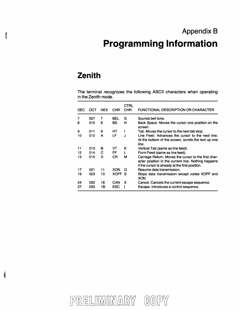
Zenith
Appendix 8
Programming Information
The terminal recognizes the following ASCII characters when operating in the Zenith mode.
CTRL DEC OCT HEX CHR CHR FUNCTIONAL DESCRIPTION OR CHARACTER
7 007 7 BEL G Sounds bell tone. 8 010 8 BS H Back Space. Moves the cursor one position on the
screen. 9 011 9 HT I Tab. Moves the cursor to the next tab stop. 10 012 A LF J Line Feed. Advances the cursor to the next line.
At the bottom of the screen, scrolls the text up one line.
11 013 B VT K Vertical Tab (same as line feed). 12 014 C FF L Form Feed (same as line feed). 13 015 D CR M Carriage Return. Moves the cursor to the first char-
acter poSition in the current line. Nothing happens if the cursor is already at the first position.
17 021 11 XON Q Resume data transmission. 19 023 13 XOFF S Stops data transmission except codes XOFF and
XON. 24 030 18 CAN X Cancel. Cancels the current escape sequence. 27 033 1B ESC [ Escape. Introduces a control sequence.

Page B.2
Programming Information
Summary of Zenith Escape Sequences
A space has been included between the escape key (ESC) and the actual code for clarity. Do not include this space. The term "defined scrolling region" appears in the following listings and means lines 1-24 unless altered by the use of escape code sequences. An explanation for the codes is provided where necessary. The escape sequences are listed by function.
NOTES:
1. "Default" is the parameter assumed when no parameter, or a value of zero, is specified.
2. Pn - Numeric Parameter. Any decimal number that is substituted for Pn.
3. Bn - Alphanumeric Parameter. Any alphanumeric character selected from a list and used to select a subfunction.
j
(

Page B.3
Programming Information
Cursor Functions ESCAPE SEQUENCE MNEMONIC DEFINITION
ESCH ESC A ESCB ESCC ESCD ESC I
ESCn
ESCj ESCk ESCy
ESC -
ESC.O ESC.3 ESC.8
ZCUH ZCCU ZCUD ZCUF ZCUB ZRL
ZCPR
ZSCP ZRCP ZDCA
Cursor home. The cursor to the first column, first line. Cursor up. Cursor down. Cursor forward (right). Cursor backward (left). Reverse index. Moves the cursor to the same horizontal position on the preceding line. If the cursor is on the top line, the cursor will scroll down one line. Cursor position report. The terminal indicates the cursor position in the form ESC Y line# column# (ASCII character). Refer to direct cursor addressing for more information. Save cursor position. Return cursor to previously saved position. Direct cursor addressing. Moves the cursor to a position on the screen by entering the escape code, the ASCII character representing the line number, and the ASCII character representing the the column number. The first line and column number are both 32. Lines are numbered 1-25 top to bottom. Columns are numbered 1-80 (1-132) left to right. Add the line and column numbers to 31. Convert the numbers to the equivalent ASCII characters and enter in the following order:
ESC Y line# (ASCII character) column# (ASCII character).
ZCBT
ZCTCP ZCAT ZSTCP
The cursor will not move if the entered line number is too high. The cursor will move to the end of the line if the entered column number is too high. The 25th line must be enabled to move the cursor to the 25th line. Cursor backward tabulation-Moves cursor backwards to last tab set. Clear tab at cursor position. Clear all tab positions. Set tabs at current cursor position.

Page B.4
Programming Information
Editing and Erasing ESCAPE SEQUENCE MNEMONIC DEFINITION
ESCE ZCD ESCb ZDB ESCJ ZEOP ESC 11 ZEl ESC 0 ZEBl ESCK ZEOl ESCl Zil
ESCM ZDl
ESCN ZDCH
ESC@ ZEIM
ESC 0 ZERM
1 Denotes lower case L.
Clear display. Erase to beginning of display. Erase to end of display. Erase line. Erase to beginning of line. Erase to end of line. Insert line. Inserts a new blank line by the line the cursor is on and all other lines, down one line. Delete line. Deletes the line the cursor is on and moves all other lines up one line. Delete character. Deletes a character at the cursor position and shifts the text on the line, one character to the left. Enter character insert mode. Inserts characters or words into displayed text. As each new character is inserted the cursor is shifted to the right and the character at the end of the line is lost. Exit insert character mode.

Page 8.5
Programming Information
Configuration ESCAPE SEOUENCE MNEMONIC DEFINITION
ESCz ESCrBn
ESCxPn
ESCyPn
ZRAM 2MBR
ZSM
ZRM
Reset to power up configuration. Modify baud rate.
Bn= @=75 A=110 B=150 C=300 D=600 E=1200 F=1800 G=2000 H=2400 I=NotUsed J=4800 K=7200 L=9600 M=19200 N=50 0=134.5 P=200 0=1050 R=NotUsed
Set mode(s). Pn = 1 = Enable 25th line
2 = Disable key click 3 = Enter hold screen mode 4 = Block cursor 5 = Cursor off 6 = Keypad shifted 7 = Enter alternate keypad mode 8 = Auto LF on CR 9=Auto CR on LF
Reset mode(s). Pn = 1 = Disable 25th Line
2 = Enable key click 3 = Exit hold screen mode 4 = Underscore cursor 5=Cursoron 6 = Keypad unshifted 7 = Exit alternate keypad mode 8 = No Auto LF on CR 9 = No Auto CR on LF

Page 8.6
Programming Information
Configuration (continued) ESCAPE SEQUENCE MNEMONIC DEFINITION
ESC < ESC 1
ZEAM ZDWO
Enter ANSI mode. Double wide characters on. The cursor movement will follow as in the normal character operation. The double wide character can be turned on or off anywhere on the line. Thus a line can be mixed with both double wide and normal wide characters. If a double wide character is returned to normal, a space will be displayed following that character.
NOTE: If double high/double wide characters had been selected while in the ANSI mode and double wide characters are selected on the same line, the cursor will blank out.
ESC 2 ZDWF Double wide characters off.
Modes of Operation ESCAPE SEQUENCE MNEMONIC DEFINITION
ESC [
ESC[ ESCp
ZEHS
ZXHS ZERU
ESCq ZXRU ESC s <atr> ZSA
Enter hold screen mode. Press the NO SCROLL key and a new line of information will be printed on the bottom line. Press the SHIFT and NO SCROLL keys and a new page of text will be displayed. Exit hold screen mode. Enter reverse video mode. Displays dark characters on a light background. Exit reverse video mode. Set attribute. The video attributes are:
Alternate character font < 132 character set> . Underline <undr>. Half intensity <half>. Blinking <blink>. Reverse video <rev>.
The video attributes are set as follows: ESCs<alt><undr><half> <blink><rev>
Where <attributes> is the ASCII character formed when the ASCII value for 0 (30 hex, 48 decimal) is added to the binary value obtained from each bit position listed above.
EXAMPLE: Underline and reverse video are desired. Binary = 01001 Decimal= 17 17+48=65 ASCII character for 65 = A
Escape sequence would be ESCsA

(
Page B.7
Programming Information
Modes of Operation (continued) ESCAPE SEQUENCE MNEMONIC DEFINITION
ESC- ZHLP Help key. ESCF ZEGM Enter Z-29 graphics mode. ESCG ZXGM Exit Z-29 graphics mode. ESCt ZEKS Entered keypad shifted mode. Inverts the normal and shifted
functions of the keypad. ESCu ZXKS Exit keypad shifted mode. ESC = ZAKM Enter alternate keypad mode. Transmits the special escape
codes used by software instead of normal characters.
KEY ESCAPE CODE 0 ESC?p 1 ESC?q 2 ESC?r 3 ESC?s 4 ESC?t 5 ESC?u 6 ESC?v 7 ESC?w 8 ESC?x 9 ESC?y
ESC?m ESC?n ESC?I
ENTER ESC?M ESC> ZEKS Exit alternate keypad mode.
Additional Functions ESCAPE SEQUENCE MNEMONIC DEFINITION
ESC} ESC { ESC v ESCw ESCZ
ESCiO
ZDK ZEK ZEWA ZXWA ZID
ZRTT
r<eyboard disabled. Keyboard enabled. Wrap around at end of line. Discard at end of line. Identify as VT52. Terminal responds to the interrogation with ESCIZ indicating performance as a DEC VT52. Request terminal type. Terminal responds to the request with an ESCiBO.

Page B.8
Programming Information
Print Functions
ESCAPE SEQUENCE MNEMONIC DEFINITION
ESC A DAP
ESC- DAPO
ESCW DPC
ESC X DPCO
ESC V DPCl
ESC] DPS
AUTO PRINT ON. Tums on auto print. A display line will be printed after moving the cursor off the line by using IF, CR, or vertical tab (also transmitted to the printer. The line also prints during an autowrap. Auto wrap lines end with a retum. When double high/double wide lines are sent to the printer, they are converted to single wide lines. If double wide characters are sent to the printer, each character is followed by a space.
AUTO PRINT OFF. Tum media copy off.
PRunER CONTROllER ON. Tums on printer controller (blind print). The printer transmits received characters to printer without displaying them. The terminal does not insert or delete spaces, provide line delimiters, or select the correct character set.
PRINTER CONTROllER OFF.
PRINT CURSOR LINE. Prints line at cursor location. Keyboard locked indicator will be enabled. When double high/ double wide lines are sent to the printer, they are converted to single wide lines. If double wide characters are sent to the printer, each character is followed by a space. A beep is sounded at the end of the printed line.
PRINT SCREEN. Prints the full screen. Keyboard locked indicator will be enabled. When double high/double wide lines are sent to the printer, they are converted to single wide lines. If double wide characters are sent to the printer, each character is followed by a space. A beep sounds at the end of print screen.

Page B.9
Programming Information
NOTE: The terminal transmits the following escape codes to perform a user-defined function. There is no response by the terminal.
TRANSMITTED NOTE: CODE MNEMONIC KEY Z-29 ke:t:s
ESCP ZF1 Function key (PF1) (F6) Blue ESCQ ZF2 Function key (PF2) (F7) Red ESCR ZF3 Function key (PF3) (Fa) Gray ESCS ZF4 Function key (PF4) (F1) ESCT ZFS Function key (FS) (F2) ESCU ZF6 Function key (F6) (F3) ESC V ZF7 Function key (F7) (F4) ESCW ZF8 Function key (F8) (FS) ESCX ZF9 Function key (F9) (F9)

Page 8.10
Programming Information ( \",
ANSI
The terminal recognizes the following ASCII characters when operating in the ANSI mode.
CTRL DEC OCT HEX CHR CHR FUNCTIONAL DESCRIPTION OR CHARACTER
0 000 0 NUL@orSP Used as fill character. 5 005 5 ENQ E Transmits answerback message. 7 007 7 BEL G Sounds bell tone. 8 010 8 BS H Back Space. Moves the cursor one position to the
left except at left end of screen. 9 011 9 HT I Tab. Moves the cursor to the next tab stop. 10 012 A LF J Line Feed. Advances the cursor to the next line.
At the bottom of the screen, scrolls the text up one line.
11 013 B VT K Same as Line Feed. 12 014 C FF L Same as Line Feed. 13 015 D CR M Carriage Return. Moves the cursor to the first char-
acter pOSition in the current line. Nothing happens if the cursor is already at the first position.
14 016 E SO N Selects the user-defined G1 character set by the select character set (SCS) sequence.
15 017 SI 0 Selects the user-defined GO character set by the SCS sequence.
17 021 11 XON Q Resume data transmission. 19 023 13 XOFF S Stops data transmission except codes XOFF and
XON. 24 030 18 CAN X Cancel. Cancels the current escape sequence. 26 032 1A SUB Z Same as Cancel. 27 033 1B ESC [ Escape. Introduces a control sequence. 127 1n 7F DEL Fill character.

:f"
Page 8.11
Programming Information
Summary of ANSI Escape Sequences
A space has been included between the escape key (ESC) and the actual code for clarity. Do not include this space. The term "defined scrolling region" appears in the following listings and means lines 1-24 unless altered by the use of escape code sequences. An explanation for the codes is provided where necessary. The escape sequences are listed by function.
NOTES: 1. "Default" is the parameter assumed when no parameter, or a value
of zero is specified. 2. Pn - Numeric Parameter. Any decimal number that is substituted
forPn. 3. Ps - Selective Parameter. Any decimal number selected from a list
and used to select a subfunction. Several subfunctions can be selected at once by putting one number after another and separating each number by a semicolon. A maximum of eight parameters may be selected.
4. Bn - Alphanumeric Parameter. Any alphanumeric character selected from a list and used to select a subfunction.
5. Sequences noted with a subscript "0" emulate the DEC model VT-100* terminal.
* DEC and VT100 are registered trademarks of Digital Equipment Co.
~rg) ,; ,n'~ u .JU

Page 8.12
Programming Information
Cursor Functions ESCAPE SEQUENCE MNEMONIC DEFINITION
ESC[H CUP ESC [O;OH or ESC [O;Of ESC [Pn;PnH HVP
Cursor home. Moves cursor to the first line first column.
Direct cursor addressing. Moves the cursor to a position on the screen by entering the escape code, the ASCII character representing the line number, and the ASCII character representing the the column number. The first line and column number are both 32. Lines are numbered 1-25 top to bottom. Columns are numbered 1-80 (1-132) left to right. Add the line and column numbers to 31. Convert the numbers to the equivalent ASCII characters and enter in the following order:
ESC[ ASCII line character; ASCII column character H or
ESC[PnA
ESC [PnB
ESC [PnC
ESC [PnD
ESCD
ESCM
ESC[ ASCII line character; ASCII column character f
CUU
CUD
CUF
CUB
IND
RI
Direct cursor addressing and the 25th line must be enabled to move the cursor to the 25th line. If the line number or column number is too high, the cursor will not move.
Cursor up. Moves the cursor up a number of lines determined by the value of Pn. A one or a zero moves the cursor up one line. The cursor stops at the top line of the scrolling region. The default value is zero. Cursor down. Moves the cursor down a number of lines determined by the value of Pn. A zero or one moves the cursor down one line. The cursor will stop at the bottom line of the defined scrolling region. The default value is zero. Cursor forward (right). Moves the cursor right the number of characters determined by the value of Pn. A zero or one moves the cursor one position. The cursor stops at the rightmost character position. The default value is zero. Cursor backward (left). Moves the cursor left the number of characters determined by the value of Pn. A zero or one moves the cursor one position. The cursor stops at the leftmost position. The default value is zero. Index. Moves the cursor down in the same manner as line feed. Reverse index. Moves the cursor to the same horizontal position on the preceding line. If the cursor is on the top line of the defined scrolling region, the lines will move down, but the cursor will not move.

Page 8.13
Programming Information
Cursor Functions (continued) ESCAPE SEQUENCE MNEMONIC DEFINITION
ESCE ESC[6n
ESC[s ESC[u ESC7 ESC 8
ESCH
ESC [PnZ
ESC [Psg
NLR CPR
PSCP PRCP SVD RSD
CHT
CBT
CCT
Cursor next line return. Cursor position report. The terminal indicates the cursor position in the form ESC[PI; PcR where I=line and c=column. The positions are expressed in decimal. Refer to direct cursor addressing for more information. Save cursor position. Return cursor to previously saved position. Save cursor position, attributes, and character set. Return cursor to previously saved position, attributes, and character set. Cursor horizontal tab set. Sets horizontal tabs at cursor position. Cursor backward tabulation. Moves cursor backwards to previous tab set where Pn indicates the number of tabs back from cursor position. Clear horizontal cursor tab stops.
Ps = 0 = Clear horizontal tab at cursor. 3 = Clear all horizontal tab stops.
The default value is the value saved in nonvolatile memory.
Screen Functions ESCAPE SEQUENCE MNEMONIC DEFINITION
ESC #3 DHT ESC #4 DHB ESC #5 SWL ESC #6 DWL ESC #8 ALN ESC [?3h NCH
ESC [?311 NCL
ESC [Pnv SAR
1 Denotes a lower case L.
Double height line (character top half). Double height line (character bottom half). Single width line. Double width line. Fill screen. Fills screen with E's for alignment. 132 characters per line. Selects 132 characters per line. When selected all screen data will be lost. 80 characters per line. Selects 80 characters per line. When selected all screen data will be lost. Set blinking attributes.
Pn = 0 = 1/64 of 50 or 60 Hz (field rates). 1 = 1/128 of 50 or 60 Hz (field rates).
The default value is zero.

Page 8.14
Programming Information
Editing and Erasing ESCAPE SEQUENCE MNEMONIC DEFINITION
ESC[PnJ ED
ESC [PnK El
ESC [Pnl Il
ESC[PnM Dl
ESC[Pn@ IC
ESC [PnP DCH
ESC[4h IRM
ESC [41' IRM
, Denotes lower case l.
Erase display. Pn = 0 = Erase from cursor to end of page.
1 = Erase from cursor to beginning of display. 2 = Clear display.
The default value is zero. Erase in line.
Pn= 0 = Erase from cursor to end of line. 1 = Erase from cursor to start of line. 2 = Erase line.
The default value is zero. Insert line. Inserts one or more blank lines depending on the value of Pn. The cursor is moved to the beginning of the new blank line. Delete line. Deletes one or more lines of characters depending on the value of Pn. The lines below the deleted area move up the number of deleted lines and the cursor is moved to the beginning of the next line. Insert character. Inserts the number of characters depending on the value of Pn. Remaining characters move to the right. Delete character. Deletes characters at the cursor position depending on the value of Pn. Remaining characters move to the left. Insert/Replacement mode on. Inserts characters or words into displayed text. As each new character is inserted the cursor and characters to the right are shifted to the right and the character at the end of the line is lost.
Insert/Replacement mode off.

Page 8.15
Programming Information
Configuration ESCAPE SEQUENCE MNEMONIC DEFINITION
ESCc PRAM Reset to power up configuration. or
ESC[z ESC [Pnw PMBR Modify baud rate.
Pn= 0=75 1 =110 2=150 3=300 4=600 5=1200 6=1800 7=2000 8=2400 9=NotUsed 10=4800 11 =7200 12=9600 13=19200 14=50 15= 134.5 16=200 17=1050
ESC [>Pnh SM Set mode(s). Pn = 1 = Enable 25th line
2 = Disable key click 3 = Enter hold screen mode 4 = Block cursor 5 = Cursor off 6 = Keypad shifted 7 = Enter alternate keypad mode 8=Auto LF on CR 9=AutoCRon LF
ESC [>PnI1 RM Reset mode(s). Pn = 1 = Disable 25th line
2 = Enable key click 3 = Exit hold screen mode 4= Underscore cursor 5= Cursor on 6 = Keypad unshifted 7 = Exit alternate keypad mode 8= No Auto LF on CR
c( 9=NoAutoCRon LF
ESC [?21 1 PEZM Enter Zenith mode.
1 Denotes lower case l.
[POO~~u~u~illOOW (fD1illr0W ll::k u

Page B.16
Programming Information
ESCAPE SEQUENCE MNEMONIC DEFINITION
ESC [20h LNM ESC [2011 LNM ESC [Pt;Pbr SR
ESC[?4h SSC ESC [?411 JSC ESC(Pn SCS
ESC)Pn SCS
1 Denotes lower case L.
Enter new line mode. Exit new line mode. Define scrolling region. The scrolling region is equal to the values of Pt and Pb expressed in decimal numbers.
Pt= Top of scrolling region. Pb = Bottom of scrolling region.
Minimum size is two lines (top must be less than bottom).The cursor is placed in the HOME position. Smooth scroll enable. Jump scroll enable. Set character set GO. Character set GO is set on terminal power up. To select GO when in character set G1 type CTRL character for SI, and then the ESC sequence.
Pn = A = United States (USACII) B = United Kingdom set C = Danish/Norwegian D=German E=Spanish F=Swedish G=ltalian H=French 0= VT -100 line graphics 1 = Undefined 2 = Z-29 block graphics 3 = Greek alphabet
Set character set G1. To select character set G1, type the CTRL character for SO and then the ESC sequence.
Pn = A = United States (USACII) B = United Kingdom set C = Danish/Norwegian D=German E=Spanish F=Swedish G=ltalian H=French 0= VT -100 line graphics 1 = Undefined 2 = Z-29 block graphics 3 = Greek alphabet

(
Page 8.17
Programming Information
ESCAPE SEQUENCE MNEMONIC DEFINITION
ESC[c or
ESC[Oc ESC[Sn
RDA
DSR
Report device attributes. VT100 responds ESC[?1 ;2c.
Device status report. Response: ESC[On = No malfunction. ESC[3n = Malfunction - Retry.
Modes of Operation ESCAPE SEQUENCE MNEMONIC DEFINITION
ESC [>3h SM
ESC [>311 RM
ESC [Pnm SGR
ESC [?6h DOMR
ESC [?611 DOMA
ESC[- SS3
1 Denotes lower case L.
Enter hold screen mode. Press the NO SCROLL key and a new line of information will be printed on the bottom line. Press the SHIFT and NO SCROLL keys and a new page of text will be displayed. Exit hold screen mode. Pressing the CTRL and S keys generates a XOFF, preSSing the S and NO SCROLL key generates a XON. Pressing the CTRL and Q keys generates aXON, pressing the NO SCROLL key generates a XOFF. Enter/Exit select graphic rendition mode.
Pn = 0 = Exit all attributes. 1 = Bold Intensity. 2 = Enter 1/2 intensity. 4 = Enter underline. S = Enter blinking. 7 = Enter reverse video. 10= Enter graphics mode. 11 = Exit graphics mode.
The default value is zero. Origin mode relative. Positions the cursor at the upper left hand character position within the margin. line numbers are relative to current margin settings. Origin mode absolute. Positions the cursor outside the margin settings through the use of CUP or HVP controls. Line numbers are independent of margin settings. Help key

Page 8.18
Programming Information
ESCAPE SEQUENCE MNEMONIC DEFINITION
ESC[>6h
ESC [>611
ESC = or
ESC[>7h
ESC [>711
ESC [?1h
ESC [?111
ESC>
ESC [Pnq
SM
SM SM
RM OCKA
OCKC
OKNM
OLL
1 Denotes lower case L.
Entered keypad shifted mode. Inverts the normal and shifted functions of the keypad. Exit keypad shifted mode. Enter alternate keypad mode. Transmits the special escape codes used by software instead of normal characters.
KEY o
1 2 3 4 5 6 7 8 9
, ENTER
Exit alternate keypad mode.
ESCAPECOOE ESCOp ESCOq ESCOr ESCOs ESCOt ESCOu ESCOv ESCOw ESCOx ESCOy ESCOm ESCOn ESCOI ESCOM
Cursor key mode set. This mode is only used in the application keypad mode. The four cursor keys send application functions. Cursor key mode reset. This mode is only used in the cursor keypad mode. The four cursor keys send ANSI cursor control commands. Keypad numeric mode. Sends ASCII codes corresponding to the engraved key characters. Load LEOs. Loads the four programmable LEOs.
Pn = 0 = Clear all LEOs. 1 =LightL1 2=LightL2 3= Light L3 4=LightL4

Page B.19
Programming Information
Additional Functions ESCAPE SEQUENCE MNEMONIC DEFINITION
ESC [?8h ESC [?81' ESC[2h ESC [21' ESC [?7h
DRMO DRMF SM RM SM
ESC [?71' RM ESC [<sol>c DREQ
, Denotes lower case L.
Auto repeat mode on. Keyboard keys auto repeat. Auto repeat mode off. KeybOard disabled. Keyboard enable. Enables the keyboard output. Wrap around at end of line. A wrap around is performed when the first character of the next line is entered. Discard at end of line. Request terminal parameters. The terminal reports the parameters as:
ESC [<sol>;<par>;<nbits>;<xspeed>; <rspeed> ;<clkmul> ;<flags>x
sol = 0 = Send unsolicited reports. 1 = Send reports upon request. 2 = Message is a report. 3 = Message is a report on request.
par= 1 = No parity. 2 = Space parity. 3 = Mark parity. 4=Odd parity. 5 = Even parity.
nbits = 1 = 8 bits per character. 2 = 7 bits per character.
xspeedl = 0 = 50 baud. rspeed 8 = 75 baud.
16= 110 baud. 24 = 134.5 baud. 32 = 150 baud. 40 = 200 baud. 48 = 300 baud. 56 = 600 baud. 64= 1200 baud. 72 = 1800 baud. 80 = 2000 baud. 88 = 2400 baud. 96 = 3600 baud. 104 = 4800 baud. 112 = 9600 baud. 120 = 19200 baud. 128 = 1050 baud. 136 = 7200 baud.
clkmul = 16 bit rate multiplier. flags=O

Page 8.20
Programming Information
Additional Functions (continued) ESCAPE SEQUENCE MNEMONIC DEFINITION
ESC [2;Psy DTST
Print Functions ESCAPE
Confidence test. Ps = DECIMAL TEST
o No test. 1 Power up. 2 Reserved. 4 Reserved. 16 Video RAM. 32 Display character set. 64 Keyboard. 128 Reserved.
To run the test continously add 8 to the number. EXAMPLE: To run the Video RAM test continously add 16 + 8, then enter ESC[2;24y.
SEQUENCE MNEMONIC DEFINITION
ESC [?5i
ESC [?4i
ESC[5i
ESC[4i
DAP
DAPO
DPC
DPCO
Auto print on. Turns on auto print. A display line will be printed after moving the cursor off the line by using LF, CR, or vertical tab (also transmitted to the printer). The line also prints during an autowrap. Auto wrap lines end with a return. When double high/double wide lines are sent to the printer, they are converted to single wide lines. If double wide char-" acters are sent to the printer, each character is followed by a space.
Auto print off. Turn media copy off.
Printer controller on. Enables Blind Print (printer controller). The printer transmits received characters to printer without displaying them. The terminal does not insert or delete spaces, provide line delimiters, or select the correct character set.
Printer controller off. Disables Blind Print.

Page 8.21
Programming Information
Print Functions (continued) ESCAPE SEQUENCE MNEMONIC DEFINITION
ESC [?1i DPCl
ESC[i DPS or
ESC[Oi
ESC [?19h DPXF
ESC [?191' DPXR
ESC [?18h DPTC
ESC [?181' DPT
ESC [?15n DPSR
Print cursor line. Prints line at cursor location. KEYBOARD lOCKED is enabled. Cursor position does not change. Command ends when the line is printed. When double high/double wide lines are sent to the printer, they are converted to single wide lines. If double wide characters are sent to the printer, each character is followed by a space. A beep sounds at the end of the line.
Print screen. Prints the full screen or selected scrolling region as determined by Printer Extent ESC [?19h or ESC [?19i. KEYBOARD lOCKED is enabled. When double high/double wide lines are sent to the printer, they are converted to single wide lines. If double wide characters are sent to the printer, each character is followed by a space. Print screen ends when the screen is printed and a beep will sound. Printer extent mode. Prints full screen when print screen selected. When double high/double wide lines are sent to the printer, they are converted to single wide lines. If double wide characters are sent to the printer, each character is followed by a space.
Printer extent mode. Prints scrolling region when print screen selected. When double high/double wide lines are sent to the printer, they are converted to single wide lines. If double wide characters are sent to the printer, each character is followed by a space.
Print termination character. Prints termination character form feed (hex, E).
Disable print termination character.
Request printer status report. A cable must be connected between the terminal and printer, or an erronous report will be recieved.
Response: ESC[?13n = Printer was off from power up ESC[?11 n = Printer was on but is now off Esc[?10n = Printer ready
, Denotes lower case L.

Page 8.22
Programming Information
NOTE: The terminal transmits the following escape codes to perform a user-defined function. There is no response by the terminal.
TRANSMITIED CODE MNEMONIC KEY Z-29KEYS
ESCOP SS3 Function key (PF1 ) (FS) Blue ESCOQ SS3 Function key (PF2) (F7) Red ESC OR SS3 Function key (PF3) (F8) Gray ESC OS SS3 Function key (PF4) (F1) ESCOT SS3 Function key (F5) (F2) ESCOU SS3 Function key (FS) (F3) ESCOV SS3 Function key (F7) (F4) ESC OW SS3 Function key (F8) (F5) ESC OX SS3 Function key (F9) (F9)
(
.",.

Page 8.23
Programming Information
Software Handshake
The terminal operates up to 19,200 baud. Incoming characters are stored in a 128-character buffer and processed on a first in/first out (FIFO) basis. When the buffer contents reach 96 characters, the terminal transmits 13H (XOFF or DC3). The host computer will stop transmitting to the terminal, upon receipt of this signal. The terminal will continue to deplete the buffer.
When 32 characters are left in the buffer, the terminal transmits 11 H (XON or DC1) signaling the host to resume transmission. If the host fails to respond to a XOFF from the terminal in a timely manner, the buffer will continue to fill. When the 128 character capacity is exceeded, a buffer overflow will occur. To determine when the buffer will overflow, use the following formula:
[buffer length-XOFF point-worst case(receive speedltransmit speed)) x [bits per character + parity bits + stop bit + start bit]
Time to respond to XOFF = ---,;;,..........:....----~.....:.....--......:....------=---receive speed
Example:
The terminal is transmitting and receiving at 9600 baud, 8 bits per character, no parity, buffer length = 128, and XOFF point = 96. The terminal has just sent an XOFF which the host must respond to within ??? milliseconds.
[128-96-3(9600/9600)] x [8 + 0 + 2] Time to XOFF = 9600 = 30.208 millisecs.
When the buffer overflows, the terminal discards the most recent character in the buffer and places the current character into the buffer.
Software that does not support receipt of the XOFF/XON Signals can still use the terminal, provided the software never sends the ESC code to the terminal, the baud rate is limited to 4800 or less, and smooth scroll is not used.
Alternately, if XOFFIXON can not be used, a fill character such as NUL (OOH) can be used following certain character strings which are sent to the terminal. Table 1 provides a list of fill character requirements.

Page 8.24
Programming Information
Fill Character Requirements
Fill characters are required to keep the terminal synchronized with the host computer when the XOFF/XON codes are not used. Table 5.1 shows the terminal fill character requirements for every terminal receive speed. No entry in a column indicates that fill characters are not required. All entries indicate the worst case. In some situations, the terminal can actually operate with less fill characters.
NUL characters take time for the computer to process, if a time delay is available from the host computer and inserted in place of a Nul character the time between characters at baud rates will be reduced.
Another way to transmit XOFF/XON is by using CTRL and S keys for XOFF and CTRL and Q keys for XON.The terminal coordinates the two sources so that the desired effect occurs. For example, if the buffer filling condition has sent a XOFF and the operator presses the CTRL and S keys, a second XOFF is not sent. When the buffer is empty an XON will not be sent until the operator presses the CTRL and Q keys.
In the Setup mode, XOFF is transmitted as soon as SETUP is entered and an XON is transmitted on exiting SETUP>
When hardware handshaking is used, the buffer filling condition does not transmit a XOFF, CTRL and S keys, and CTRL and Q keys are transmitted as typed.

Page B.25
r Programming Information
Table B.1. Fill Character Requirements
RECEIVE FUNCTION NUMBER BAUD RATE 2 3 4 5 6 7
19200 2 90 243 243 4 384 60 9600 1 45 122 122 2 192 30 7200 34 92 92 2 144 22 4800 15 61 61 1 96 15 2400 11 30 30 48 7 2000 9 25 25 40 6 1800 9 23 23 36 6 1200 6 15 15 24 4 1050 5 14 14 21 4 600 3 8 8 12 2 300 1 4 4 6 1 200 1 3 3 4 1 150 1 2 2 3 134.5 1 2 2 3 110 1 1 2 75 1 1 2 50 1 1 1
Explanation of Function Number:
1. All characters except those listed below.
2. Erase in Display.
3. Columns.
4. Alignment.
5. Erase in Line.
6. (Smooth Scroll) Line Feed, Reverse Index, Index, Next Line.
7. (Jump Scroll) Line Feed, Reverse Index, Index, Next Line.