
DL11 asynchronous line interface manual - bitsavers.org
84
DL11 asynchronous line interface manual EK-DLII-TM-003 digital equipment corporation • maynard, massachusetts
-
Upload
khangminh22 -
Category
Documents
-
view
1 -
download
0
Transcript of DL11 asynchronous line interface manual - bitsavers.org

DL11 asynchronous line interface manual
EK-DLII-TM-003
digital equipment corporation • maynard, massachusetts

Ist Edition, September 1972 2nd Printing, May 1973 3rd Printing (Rev), June 1974 4th Printing, January 1975 5th Printing (Rev), September 1975
Copyright © 1972, 1973, 1974, 1975 by Digital Equipment Corporation
The material in. this manual is for· informational purposes and is subject to change without notice.
Digital Equipment Corporation assumes no responsibility for any errors which may appear in this manual.
Printed in U.S.A.
The following are trademarks of Digital Equipment
Corporation, Maynard, Massachusetts:
DEC
FLIP CHIP DIGITAL
UNIBUS
PDP
FOCAL COMPUTER LAB

CONTENTS
Page
CHAPTER 1 INTRODUCTION
1.1
1.2
1.3
1.4
Introduction .......................................... 1-1 Scope ............................................... 1-1
Maintenance ... . . . . . . . . . . . . . . . . . . . . . . . . . . . . . . . . . . . . . . .. 1-3 Engineering Drawings . . . . . . . . . . . . . . . . . . . . . . . . . . . . . . . . . . . .. 1-3
CHAPTER 2 GENERAL DESCRIPTION
2.1 Introduction .......................................... 2-1
2.2 Available Options ..................................... " . 2-1 2.3 Data Format .......................................... 2-4 2.4 Functional Description . . .. '. . . . . . . . . . . . . . . . . . . . . . . . . . . . . . . . 2-6 2.4.1 DL 11 Dataset Interface ................................... 2-6 2.4.2 DLll Teletype Control ................................... 2-8 2.4.3 DL11 EIA Terminal Control ................................ 2-9 2.5 Physical Description .................................... 2-10 2.6 Specifications ......................................... 2-11
CHAPTER 3 INSTALLATION AND CONFIGURATION
3.1 Introduction .......................................... 3-1
3.2 Configuration .................... ~ . . . . . . . . . . . . . . . . . . . . . 3-1
3.3 Installation ........................................... 3-1 3.3.1 Power Connections ...................................... 3-3
3.3.2 Address and Priority Assignments .... . . . . . . . . . . . . . . . . . . . . . . . . . 3-3
3.3.3 Installation Testing ...................................... 3-3
3.4 Cabling ............................................... 3-3
CHAPTER 4 PROGRAMMING INFORMATION
4.1 Scope ............................................... 4-1 4.2 Device Registers ......................... ~ .............. 4-1 4.3 Interrupts ............................................ 4-7 4.4 Timing Considerations .................................... 4-8 4.4.1 Receiver ............................................. 4-8 4.4.2 Transmitter ........................................... 4-8 4.4.3 Break Generation Logic ................................... 4-8 4.5 Program Notes ................................. ' ... '.' . . . 4-8 4.6 Program Example ................... ' .................... 4-9
iii
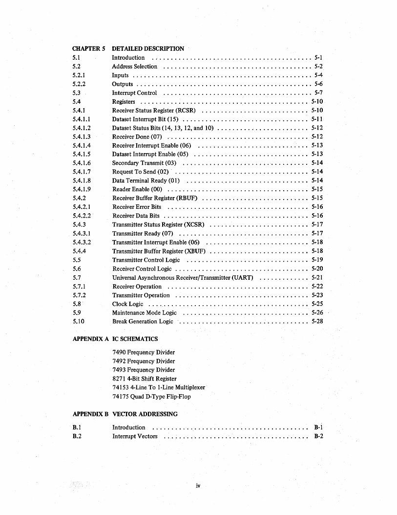
CHAPTER S DETAILED DESCRIPTION
5.1 Introduction .;........................................ 5-1
5.2 Address Selection .....................•......•........•• 5-2
5.2.1
5.2.2
5.3
5.4
5.4.1
5.4.1.1
5.4.1.2
5.4.1.3
5.4.1.4
5.4.1.5
5.4.1.6
5.4.1.7
5.4.1.8
5.4.1.9
504.2
5.4.2.1
5.4.2.2
5.4.3
5.4.3.1
5.4.3.2
5.4.4
5.5
5.6
5.7
5.7.1
5.7.2
5.8
5.9
5.10
Inputs .................•..... 0 •••••• 0 ••• 0 0 •• 0 •••••••• 5-4
Outputs . . . . . . . 0 • • 0 0 • • • • • • • 0 •• 0 0 • 0 • 0 • • • • • • • • • 0 • • • • • • • • 5-6
Interrupt Control 0 0 • 0 ••••• 0 •••••• 0 ••••• 0 •••••• 0 0 •••••••• 5-7
Registers ..... 0 ; • 0 • • • • • 0 • • • 0 • • • • 0 • • • • • 0 • • • • • • 0 0 • • • • •• 5-10
Receiver Status Register (RCSR) ................. 0 •••••••••• 5-10
Dataset Interrupt Bit (15) 0" 0 •••••••••••••••••••••••••• 0 •• 5-11
Dataset Status Bits (14, 13, 12, and 10) ...........•.... 0 • • • • • •• 5-12
Receiver Done (07) ... 0 •• 0 0 0 •••••••••• 0 0 • • • • • • • • • • • • • • • •• 5-12
Receiver Interrupt Enable (06) .. 0 •• 0 ••••••••••••• 0 ••• 0 ••• o. 5-13
Dataset Interrupt Enable (05) ... 0 0 • 0 • 0 • • • • • • • • • • • • • • 0 0 • • • o. 5-13
Secondary Transmit (03) .. 0 ••••• 0 '0 •• 0 ••• 0 •• 0 ••• 0 •••••• o. 5-14
Request To Send (02) .......... 0 •• 0 0 • 0 •••••••••••••••••• 5-14
Data Terminal Ready (01) ... 0 0 ••••••••••••• 0 • • • • • • • • • • • •• 5 .. 14
Reader Enable (00) ............... ·0 •••••••• 0 ••• 0 • 0 •• 0 0 •• 5-15
Receiver Buffer Register (RBUF) .. .. 0 0 • • • • 0 • • • • • • • • • • • • 0 • • •• 5-15
Receiver Error Bits . 0 • 0 • • • • • 0 • • 0 • 0 • • • • • • • • 0 • • • • • • • • • • • •• 5-16
Receiver Data Bits ........... 0 • 0 • • • • 0 • • • • • • • 0·. • 0 •• 0 • • ••• 5-16
Transmitter Status Register (XCSR) ...... 0 •• 0 0 0 • • • • • • • • • • • • •• 5-17
Transmitter Ready (07) .......... 0 • 0 • 0 •••• 0 ••••••• 0 • • • • •• 5-17
Transmitter Interrupt Enable (06) . 0 •••••••• 0 ••••• 0 • 0 •••••••• 5~18
Transmitter Buffer Register (XBUF) ..... 0 • • • • 0 • 0 •• 0 • • • • • • • • •• 5-18
Transmitter Control Logic .... 0 • 0 • 0 0 • • 0 0 • • • 0 • • • • • • • • • • • • •• 5-19
Receiver Control Logic ....... 0 0 •••••••••••••••• 0 • 0 ••• 0 ••• 5-20
Universal Asynchronous Receiver/Transmitter (UART) ............• 5-21
Receiver Operation . 0 • 0 0 ••••••••••••• 0 ••• 0 •••• 0 '0 • • • • • •• 5-22
Transmitter Operation .... 0 0 ••••••••••••• 0 • 0 ••••••• 0 •• 0 •• 5-23
Clock Logic ... 0.' • 0 0 • • 0 • • • • • • • • • • • • • • • • • • • • • • • • • • • • • •• 5-25
Maintenance Mode Logic ......... 0 • • • • • • • • • • • • • • • • • • • • • •• 5-26
Break Generation Logic
APPENDIX A IC SCHEMATICS
7490 Frequency Divider
7492 Frequency Divider
7493 Frequency Divider
8271 4-Bit Shift Register
74153 4-Line To I-Line Multiplexer
74175 Quad D-Type Flip-Flop
APPENDIX B VECTOR ADDRESSING
B.I
B.2
Introduction ......................•................. • B-1
Interrupt Vectors .. 0 • • •.• • • • • • • • • • • • • • • • • • • • • • • • • • • • • •. •• B-2
iv

Figure No.
2-1
2-2
2-3
2-4
3-1
3-2
3-3
4-1 4-2 4-3 4-4 5-1
5-2
5-3
5-4
5-5
5-6
5-7
5-8
5-9
B-1
Table No.
1-1 1-2
2-1 2-2
2-3 2-4
3-1 3-2
3-3 3-4 3-5
3-6
ILLUSTRATIONS
Title Page
DLII Data Formats ...................................... 2-4
DLII-E Block Diagram ................................... 2-6
DLII-A Block Diagram ................................... 2-8
Crystal and Switch Location ............................... 2-10 l
DLl1 (M7800 module) Mounted in DDII-A ..................... 3-2
Jumper Locations on the M7800 Module ..... .
DLII Cable Connections ............. .
Receiver Status Register (RCSR) - Bit Assignments
Receiver Buffer Register (RBUF) - Bit Assignments
Transmitter Status Register (XCSR) - Bit Assignments
3-4 3-5
4-2
4-4
4-6
Transmitter Buffer Register (XBUF) - Bit Assignments .............. 4-6
Address Selection Logic - Simplified Diagram .................... 5-5
Interface Select Address Format ............................. 5-5
Interrupt Control Logic - Simplified Diagram ................... ~ 5-8
RBUF and XBUF Gating Logic - Simplified Diagram (one bit position) . .. 5-17
DART Receiver - Block Diagram ............................ 5-23
DART Transmitter - Block Diagram ......................... 5-24
Frequency Divider Logic - Simplified Diagram ................... 5-26
Operating Modes ....................................... 5-27
Maintenance Logic - Simplified Diagram ... . . . . . . . . . . . . . . . . . . .. 5-28
Address Map ......................................... B-4
TABLES
Title Page
Applicable PDP-II Documents .............................. 1-2
Applicable Device Documents ............................... 1-3
DLll Options ......................................... 2-2
Baud Rates with Standard Crystals ............................ 2-3
Data Format Jumpers .................................... 2-5
DLll Operating Specifications ............................. 2-11
Option Configurations .................................... 3-2
Pin Connections ........................................ 3-6
Input/Output Signals ..................................... 3-7
7008360 Connections .................•.................. 3-7
7008519 Connections .................................... 3-8
BC05C Connections . . . . . . . . . . . . . . . . . . . . . . . . . . . . . . . . . . . . . . 3-8
v

4-1
5~I
5-2
5-3
5-4 5~5
5-6 5-7
Standard DLII Register Assignments .......................... 4-1
DL 11 Functional Units ................................... 5-1
DL 11 Address Assignments ...............................•. 5-3
Register Selection ~ignals .................................. 5-6
DLII Vectors and Priority Levels ..........................••. 5-7
Device Register Functions . . . . . . . . . . . . . . . . . . . . . . . . . . . . . . . .. 5-11
Transmitter Control and Input Logic ......................... 5-19
Receiver Status and Control Logic ........................... 5-21
vi

CHAPTER 1
INTRODUCTION
1.1 INTRODUCTION
The DL 11 Asynchronous Line Interface is a character-buffered communications interface designed to assemble
or disassemble the serial information required by a communications device for parallel transfer to, or from, the
PDP-II Unibus. The interface consists of a single integrated circuit quad module containing two independent
units (receiver and transmitter) capable of simultaneous 2-way c0n:tmunication.
The DLII interface provides the logic and buffer register necessary for program-controlled transfer of data between a PDP-II system requiring parallel data and an external device requiring serial data. The interface also
includes status and control bits that may be controlled by the program, the interface, or the external device for
command, monitoring, and interrupt functions.
Five available DLll options (DLll-A through DLll-E) provide the flexibility needed to handle a variety of
terminals. For example, the user can use a DLII-A as a Teletype@ Control or a DLII-E for complete dataset
control of communications datasets such as the Bell Model 103 or 202. Depending on the option used, the user
has a choice of line speeds (baud rates), character size, stop-code length, parity selection, line control functions,
and status indications.
Although each option uses an M7800 module, certain discrete component variations exist for each specific
option so that the interface performs the intended function. Therefore, although generally similar, each option
uses a slightly different M7800 variation which is not interchangeable with other options. These variations are
installed at the factory only. For example, an M7800 used as a DLll-A could be used as another DLII-A but
noUn place of a DLII-B, C, D, or E.
A description of the individual options is given in Chapter 2 of this manual.
1.2 SCOPE
This manual provides the user with the theory of operation al).d logic diagrams necessary to understand and
maintain the DLll Asynchronous Line Interface. The level of discussion assumes that the reader is familiar with
basic digital computer theory.
® Teletype is a registered trademark of Teletype Corporation.
1-1
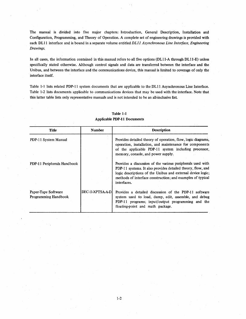
The manual is divided into five major chapters: Introduction, General Description, Installation and Configuration, Programming, and Theory of Operation. A complete set of engineering drawings is provided with each DLll interface and is bound in a separate volume entitled DLll Asynchronous Line Interface, Engineering Drawings.
In all cases, the infonnation contained in this manual refers to all five options (DLII-A through DLII-E) unless specifically stated otherwise. Although control signals and data are transferred between the interface and the Unibus, and between the interface and the communications device, this manual is limited to coverage of only the interface itself.
Table 1-1 lists related PDP-II system documents that are applicable to the DL 11 Asynchronous Line Interface. Table 1-2 lists documents applicable to communications devices that may be used with the interface. Note that this latter table lists only representative manuals and is not intended to be an all-inclusive list.
Title
PDP-II System Manual
PDP-II Peripherals. Handbook
Paper-Tape Software Programming Handbook
Table 1-1 Applicable PDP-II Documents
Number Description
Provides detailed theory of operatiori, flow, logic diagrams, operation, installation, and maintenance for components of the applicable PDP-II system including processor, memory, console, and power supply:
Provides a discussion of the various peripherals used with PDP-II systems. It also provides detailed theory, flow, and logic descriptions of the Unibus and external device logic; methods of interface construction; and examples of typical interfaces.
DEC-U-XPTSA-A-D Provides a detailed discussion of the PDP-ll software system used to load, dump, edit, assemble, and debug PDP-II programs; input/output programming and the floating-point and math package.
1-2

Table 1-2
Applicable Device Documents
Title Number Description
Automatic Send-Receive Bulletin 273B Sets, Manual (two volumes)
Teletype Corp.
Model 33 Page Bulletin 1184B Printer Set, Parts Teletype Corp.
Describes operation and maintenance of the Model 33 ASR Teletype unit used as an input/output device.
Contains an illustrated parts breakdown to serve as a guide for disassembly, reassembly, and parts ordering for the Model 33 ASR Teletype unit.
NOTE Comparable manuals exist for other available Teletypes such as the Model 28, Model 35, and Model 37.
VTOS Alphanumeric Display Terminal
VTOS Alphanumeric Display Terminal, Maintenance Manuals,
VT06 Maintenance Manual
Bell System Data Communications Data Sets 103 E/G/H
Bell System Data Communications Data Sets 202 C/D
1.3 MAINTENANCE
EK-VT05-HR-002 Describes purpose and operation of the VT05 Display used as an input/output device.
EK-VT05-MM-005 Provides detailed theory of operation and maintenance procedures for the VT05 Display.
Datapoint Corp. Provides detailed theory of operation and maintenance data for the VT06 Data Display Terminal.
Provides dataset interface specifications; includes dataset description and options including interface signals and timing.
Provides dataset interface specifications; includes dataset description and options including interface signals and timing.
The basic maintenance philosophy of the DLII Asynchronous Line Interface is to present the user with the information necessary / to understand normal system operation. The user can utilize this information when analyzing trouble symptoms to determine necessary corrective action. A Modem Test Connector (Engineering Drawing D-CS-H3 I 5-0-1 ) can be used in troubleshooting the DLII.
1.4 ENGINEERING DRAWINGS
A complete set of engineering drawings and circuit schematics is provided in a companion volume to this manual
entitled DLll Asynchronous Line Interface, Engineering Drawings. The following paragraphs describe the signal nomenclature conventions used on the drawing set.
1-3

Signal names in the DLll print set are in the following basic form:
SOURCE SIGNAL NAME POLARITY
SOURCE indicates the drawing number of the print set where the signal originates. The drawing number of a
print is located in the lower right-hand comer of the print title block (DL-l, DL-2, DL-3, etc.).
SIGNAL NAME is the name proper of the signal. The names used on the print set are also used in this manual
for correlation between the two.
POLARITY is either H or L to indicate the voltage level of the signal: H means +3V; L means ground.
As an example, the signal:
DL-4 RCVR DONE H
originates on sheet 4 of the M7800 module drawing and is read, "when RCVR DONE is true, this signal is at
+3V."
Unibus signal lines do not carry a SOURCE indicator. These signal names represent a bidirectional wire-ORed
bus; as a result, multiple sources for a particular bus signal exist. Each Unibus signal name is prefixed with the
word BUS.
Interface signals fed to, or received from, the Berg connector on the M7800 module are preceded by the pin
number in parentheses:
(DD) EIA DATA TERMINAL READY
1-4

2.1 INTRODUCTION
CHAPTER 2
GENERAL DESCRIPTION
The DLII Asynchronous Line Interface is a character-buffered communications interface designed to translate serial bit stream data to parallel character data. The interface contains two independent units (receiver and
transmitter) capable of simultaneous 2-way communication.
The five available DLII options (DLII-A through DLII-E) provide the flexibility needed to handle a variety of
terminals. For example, the user can select an option for interfacing a Teletype or display keyboard, for handling
EIA data, or for handling dataset devices. In addition, depending on the option used, the user has a choice of line
speeds, character size, stop-code length, and parity.
This chapter is divided into five major portions: available options, data format, functional description, physical
description, and specifications.
2.2 AVAILABLE OPTIONS
There are five available DLII options: DLII-A through DLII-E. The major differences among these options are
the data code, baud rates, and certain control and monitoring bits in the status registers. Although there are five
options, they may be divided into the following functional groups:
a. Teletype Control
b. EIA Terminal Control
c. Data Set Control
DLII-A DLII-C
DLII-B DLII-D
DLII-E
The DLII-A and DLll-C both use a 20-mA currentloop for receive, transmit, and reader run operations necessary for Teletype or display terminal control.
The DL ll-C is simply a more flexible version of the DLII-A and includes data code and baud rate selection.
The DLll-B and DLII-D both contain EIA drivers and receivers ·for compatability with the logic levels required for EIA terminals such as the VT06 display.
The DL Il-D is simply a more flexible version of the DLII-B and includes data code and baud rate selection.
The DL ll-E provides complete data set control for communications modems such as Bell Model 103 or 202.
2-1

A brief description of each of these options is included in Table 2-1 and a listing of available standard baud rates
is given in Table 2-2. Note that these baud rates are based on the standard crystals supplied by DEC; however,
the user may order special crystals, if desired. The physical differences of each option (cables, connectors, etc.)
are described in Paragraph 2.5.
Option Data Code Typical Use
DLll-A Restricted(1 ) Model 33 or 35 Teletype
Model VT05 Display Terminal
DL11-B Restricted(1) Model VT05 orVT06 Display Terminal
DLll-C Full Model 28 Selection(2) Teletype
DLll-D Full Model 37 Selection(2) Teletype
(null modem required)
Table 2-1
DLll Options
Baud Rates Notes
110 a. No dataset bits 150 a. No BREAK or 300 ERROR bits 600 c. No 1200/110 split
1200 2400
Same as a. No dataset bits DLIl-A b. No BREAK or
ERROR bits c. No 1200/110
split d. DATA TERM-
INAL RDY and REQTOSEND bits strapped on permanently
e. Null modem usually re-quired for local EIA terminal
Crystal a. No dataset bits and switch b. BREAK and select- ERROR bits able(3) enabled
Crystal a. No dataset bits and switch b. BREAK and select- ERROR bits able(3) enabled
c. DATA TERM-INAL RDY and REQTOSEND bits strapped on permanently
2-2
Description
Uses 20-mA current loop operation for receive, transmit, and reader run.
Has EIA drivers and receivers for compatability with EIA terminals.
Basically identical to D L ll-A except has full code and baud rate selection. Also includes both BREAK and ERROR bits.
Basically identical to DLll-B except has full code and baud rate selection. Also includes both BREAK and ERROR bits.
(continued on next page)

Option Data Code Typical Use
Table 2-1 (Cont)
DLll Options
Baud Rates Notes Description
DLII-E Full Model 103 Crystal a. Full dataset Provides complete dataset Selection(2) or 202 and switch control control.
modems select- Dataset lines monitored by able(3) this interface are: RING,
RECEIVE DATA, CARRIER DETECT, CLEAR TO SEND, and SECONDARY RECEIVE DATA.
Dataset lines controlled by
the program are: TRANS-
MITTED DATA, REQUEST
TO SEND, SECONDARY
TRANSMITTED DATA, and
DATA TERMINAL READY.
NOTES: 1. Restricted data code = 8 data bits, no partiy, 1 or 2 stop bits. 2. Full selection data code = 5,6,7, or 8 data bits; parity off, even, or odd; and 1, 1.5, or 2 stop bits. 3. Baud rates that may be selected by the crystal and switch are listed in Table 2-2.
Table 2-2
Baud Rates with Standard Crystals
Switch Crystal #1 Crystal #2 Crystal #3
Position (844.8 kHz) (1.03296 MHz) (1.152 MHz)
1 36.7 44.8 50 2 55 67.3 75 3 110 134.5 150 4 220 269 300 5 440 538 600 6 880 1076 1200 7 1320 1614 1800 8 1760 2152 2400 9* - - -
10* - - -
*These switch positions are for external clock inputs and do not tap off the crystal oscillator.
NOTE: The baud rates in italics are the most commonly used.
2-3
Crystal #4
(4.608 MHz)
200 300 600
1200 2400 4800 7200 9600 '-
-

2.3 DATA FORMAT
There are two basic data formats used with the DLII interface options. The first format (Figure 2-I,a) is
referred to as "restricted" because the only variable is the number of STOP bits. A character in this format
consists of a START bit, eight DATA bits, and one or two STOP bits. This code is used only with the DLII-A
and DLII-B options.
The second format (Figure 2-1 ,b) is referred to as "full selection" because there is a number of variables. This
format consists of a START bit, five to eight DATA bits, a PARITY bit or no PARITY bit, and one, one and
one-half, or two STOP bits.
IDLE STATE OF 1 OR 2 RETURN TO IDLE
~INE I· 8 DATA BITS + BITS~ ~STATE OF LINE
1 ;o-i-o~ ~~~i-o~i~:~-o~i~~~-o; ] STOP :STOP [j ~~ART BIT OF o ______ ~:e:J. __ ..1 __ ..1 __ ..1 __ .L __ .J. __ ..l..~~ 1 I 2 NEW CHARACTER
START -II-ONE BIT TIME=ONE/BAtJD RATE BIT
o. RESTRICTED DATA CHARACTER FORMAT-DL1i-A.B
IDLE STATE OF ODD,EVEN RETURN TO IDLE
~NE I.. 5 TO 8 DATA BITS '1 /OR UNUSED ~ STATE OF LINE
1 - - 'T--T--T--T--T--"--T--T-t!.·-~-../'--OR 00 I 01 I 02 I 03 I 04 I 05 I 06 I 07 I P STOP I START BIT OF LSB BIT - NEW CHARACTER 0---- -- -L __ .L __ J.. __ J.. __ .L __ J.. __ -L __ ..l.. __
START,---- JUSTIFIED TO LSB BIT POSITIONS WHEN 1- 1-: : : BIT'- 5,6, OR 7 B ITS USED ~ , i i
'---1.5- , r- " 1--2 ---i
b.FULL SELECTION DATA CHARACTER FORMAT-DL11-C,D,E
Figure 2-1 DLll Data Formats
11-1336
When less than eight DATA bits are selected in the second format, the hardware justifies the bits into the least
significant bit positions for characters received by the interface. When transmitting characters, the program
provides the justification into the least significant bits. The PARITY bit may be either on or off; when on, it can
be selected for checking either odd or even parity during receive and for providing an extra PARITY bit during
transmit.
All variable items within any data format are selected by jumpers on the DLll module. None of the variables
can be controlled by the program. Split lugs are provided on the module for installation of appropriate jumpers.
These jumpers are listed in Table 2-3 and described more fully in Chapter 5.
Note that a jumper indicates a low (0) and no jumper indicates a high (1). The jumper locations are shown on
DL11 drawing DL-4.
2-4

Name
No Parity
Even Parity
STOP Bit
Number of Data Bits
Table 2-3
Data Format Jumpers
Jumper UART
NP
EPS
2SB
NBI NB2
Pin No.
35
39
36
38 37
Function
Enables or disables the parity bit in the data character.
When enabled, the value of the parity bit is dependent on
the type of parity (odd or even) selected by the even
parity select (EPS) jumper.
When disabled, the STOP bits immediately follow the last DATA bit during transmission. During reception, the receiver does not check for parity.
jumper - parity enabled no jumper - parity disabled
Determines whether odd or even parity is to be used. The receiver checks the incoming character for appropriate parity; the transmitter inserts the appropriate parity value.
jumper - odd parity no jumper - even parity
Used in conjunction with three other jumpers (J9, JIO, and J 11) to select the desired number of STOP bits.
1 STOP bit - jumper in 2SB jumper in JIO no jumpers in J9, J 11
2 STOP bits - no jumper in 2SB no jumpers in J9, J 11 jumper in J 1 0
1.5 STOP bits - jumper in 2SB jumper in J9 or J 11 no jumper in J 1 0
These two jumpers are used together to provide a code that selects the desired number of DATA bits in the character.
Note that in the following code, a 0 indicates a jumper, a 1 indicates no jumper:
NB2 NBI No. of DATA Bits 0 0 5 0 1 6 1 0 7 1 1 8
2-5

2.4 FUNCTIONAL DESCRIPTION
The DLII is a character-buffered communications interface that performs two basic operations: receiving and
transmitting asynchronous data. When receiving data, the interface converts an asynchronous serial character
from an external device into the parallel character required for transfer to the Unibus. This parallel character can
then be gated through the bus to memory, a processor register, or some other device. When transmitting data, a
parallel character from the bus is converted to a serial line for transmission to the external device. Because the
two data transfer units (receiver and transmitter) are independent, they are capable of simultaneous.2-way
communication. The receiver and transmitter each operate through two related registers: a control and status
register for command and monitoring functions, and a data buffer register for storing data prior to transfer to
the bus or the external device.
Although there are actually five DLII options, the pri,mefunctional differences can be shown by presenting
three typical cases: a DL 11 used for dataset devices, a DL 11 used as a Teletype control, and a DL 11 used with
EIA level converters. Each of these three cases is covered separately in Paragraphs 2.4.1 through 2.4.3,
respectively.
2.4.1 DLll Dataset Interface
Only the DLII-E (Figure 2-2) option can be used to interface to datasets. The DLll uses call and acknowledge
signals from the computer and the dataset, translates these signals to set up a handshaking sequence, and thus
establish a data communication channel.
0<15:00>
BBSY SSYN SACK BR-BG INTR
U N I B U A<17:00> S C<I:0>
MSYN SSYN
0<15:00>
PARALLEL DATA
XMIT RCVR STATUS STATUS
RCVR OR XMIT SELECTION
ERROR BITS
I I I
MAINT: MODEl
.--+-__ --1f-=Bc...:.RE=A..:.;.K-=--_-, LOOP:
PARALLEL DATA
Figure 2-2 DLll-E Block Diagram
2-6
I I I
EIA LEVEL CONV
r--I
DATASET
I L __ _
11-1337

A typical method of establishing a data communication channel is as follows: the dataset at the computer is
called by another remote dataset and a RING signal is transmitted to the DLII interface. This RING signal
initiates an interrupt provided the DATASET INT ENB bit in the DLII register is set. The program then determines if the interrupt was caused by RING and, through a service routine, issues a DATA TERMINAL
READY and a REQ TO SEND signal. These signals cause the dataset to answer the call and send a carrier signal
or tone to the caller. The caller acknowledges the carrier signal with its own carrier signal which, when detected
by the dataset, causes another interrupt (CARRIER) sequence to be initiated. Upon recognizing the CARRIER
interrupt, the program can then either receive or transmit data. The only two prerequisites for the handshaking
sequence are that the program use appropriate service routines and that the DATASET INT ENB bit in the DLII
status register is set prior to setting up the data channel.
Once the data channel is set up, the DLII-E receiver accepts incoming serial data from the dataset lines for
parallel conversion and transfer to the Unibus. The transmitter converts parallel data from the bus and shifts the
resultant serial data onto the dataset lines.
The receiver offers serial-to-parallel conversion of 5, 6, 7, or 8 level codes. This serial character code is described in Paragraph 2.3. Once the character has been received, a parity error flag, if selected, is available to the
programmer for testing. An interrupt request (RCVR DONE flag) is initiated in the middle of the first STOP bit
of the character being received. This indicates that the character is stored in the receiver holding register. If the program does not transfer the character from the holding register before the middle of the first STOP bit of the next character, a data overflow error (OR ERR) bit is set in the receiver buffer register. This buffer also provides
other error indications such as framing error (FR ERR) which indicates that the character had no valid STOP bit,
and partiy error (P ERR) which indicates that the received parity did not agree with the expected parity. It
should be noted that both the receiver and transmitter character length and format are controlled by jumpers on
the module and are always identical.
The transmitter performs parallel-to-serial conversion of 5,6, 7, or 8 level codes. Data from the Unibus is loaded
in parallel into the holding register. When the transmitter shift register is empty, the contents of the holding
register is shifted into the transmitter shift register and the XMIT RDY flag comes up. A second character from
the bus can then be loaded into the holding register. However, because the shift register is still working on
previous data, the shifting operation of the second character is delayed until the previous character has been
completely transmitted. Once the last bit of a character is transferred to the dataset (because of double-buffering, this is actually the last bit of the first character in a 2-character pair), the interface initiates an
interrupt request (XMIT RDY) to indicate that the buffer is empty and can now be loaded with another
character for transfer to the dataset. The transmitter status register contains a BREAK bit that can be set to
transmit a continuous space to the dataset. A maintenance (MAINT) bit is also available for connecting the serial output of the transmitter to the input of the receiver and to force the receiver clock speed to be the same as the
transmitter speed.
The rest of the control portion of the DLII-E is available through the receiver status register, and provides the necessary command and monitoring functions for use with Bell 103 and 202 type datasets. This register
monitors such functions as: CLEAR TO SEND, which indicates the operating condition of the dataset; CAR
DET, which indicates that the carrier is being received; RCVR ACT, which indicates that the receiver is accepting
a character; and RCVR DONE, which indicates that a full character is stored in the receiver buffer.
2-7

Dataset interrupt requests are initiated at the transition of RING, CAR DET, CLR TO SEND, or SEC REC
signals. The SEC REC (secondary or supervisory received data) and the,SEC XMIT (secondary or supervisory
transmitted data) bits provide receive and transmit capabilities for the reverse channel of a remote station. The
DTR bit functions as a control lead for the dataset communication channel and permits the channel to be either
connected or disconnected.
The DLll-E option contains EIA level converters for changing the bipolar inputs to TTL logic levels and the
TIL logic level outputs to the bipolar signals required by the dataset. The EIA converters provide failsafe
operation of the control leads because they appear off if the dataset loses power.
2.4.2 DLll Teletype Control
Both the DLII-A and DLII-C options can be used to interface Teletype units. The prime difference between the
two is that the DLll-C can operate with a variable character format and is available in several different baud
rates. The DLII-A option (Figure 2-3) is normally used to interface Model 33 and 35 Teletypes; the DLII-C option could be used to interface Model 28 Teletypes.
U N I B
0<11:00>
BBSY SSYN SACK BR-BG INTR
U A<17:00> S C<1:0>
MSYN SSYN
0<07:00>
PARALLEL DATA
RDR ENB
RCVR OR XMIT SELECTION
Figure 2-3 DLIl-A Block Diagram
20mA INTERFACE CIRCUITS
r--I
TELETYPE UNIT
L __ _
11-1338
Serial information read or written by the Teletype unit is assembled or disassembled by the DL 11 interface for
parallel transfer to, or from, the Unibus. When the processor addresses the bus, the DL 11 'interface decodes the
address to determine if the Teletype is the selected external device and, if selected, whether it is to perform an
input (read) or output (punch) operation.
2-8

If, for example, the Teletype has been selected to accept information for printout, parallel data from the Unibus
is loaded into the DL II transmitter (punch) buffer. At this point, the XMIT RDY flag drops because the
transmitter (punch) logic has been activated (the flag comes back after a fraction of a bit time if the transmitter
is not presently active). The interface generates a START bit, shifts the data from the buffer into the Teletype
one bit at a time, again sets the XMIT RDY flag (as soon as the holding register of the double-buffering is empty,
even though the shift register is active), and then times out the required number of STOP bits.
Thus, if the DL I I-A option is being used, the 8-bit parallel bus data is converted to the II-bit serial input
required by the Teletype. If the DLII-C option is used, the format and character length may be different, but
the parallel-to-serial conversion is accomplished in the same manner. Note that whenever a series of characters is
to be loaded into the Teletype, the XMIT ROY flag is set prior to generation of the STOP bits and the shifting out of the character in the holding register, thus allowing another character to be loaded from the bus as soon as
the transmitter holding buffer is empty. The XMIT RDY flag is used to initiate an interrupt sequence to inform
the processor that the interface is ready to transfer another character to the Teletype for printing.
When receiving data from the Teletype unit, the operation is essentially the reverse. The START bit of the
Teletype serial data activates the interface receiver logic, and data is loaded one bit at a time into the reader
buffer register. When loading of the buffer is complete, the buffer contents is transferred to the holding register
and the interface sets the RCVR DONE flag, indicating to the program that a character has been assembled and is ready for transfer to the bus. The RCVR DONE flag, if RCVR INT ENB is also set, initiates an interrupt
sequence, thereby causing a vectored interrupt.
The DLII-A and DLII-C options both have a reader enable (RDR ENB) bit that can beset to advance the
paper-tape reader in the Teletype. When set, this bit clears the RCVR DONE flag. As soon as the Teletype sends
another character, the START bit clears the RDR ENB bit, thus allowing just one character to be read.
The DLII-A and DLII-C options also have a receiver active (RCVR ACT) bit which indicates that the DLll
interface is receiving data from the Teletype. This bit is set at the center of the START bit, which is the
beginning of the input serial data, and is cleared by the leading edge of the RCVR DONE bit. The DLII-C also
has a BREAK bit which can be set by the program to transmit a continuous space to the Teletype.
The DLII-A and DLII-C options, as well as all other DLII options, can be operated in a maintenance mode
which is selected by the program by setting the MAINT bit in the transmitter status register~ When in this mode,
special logic is used to perform a closed loop test of interface logic circuits. A character from the bus is loaded in parallel into the transmitter (punch) buffer register. The serial output of this register,besides entering the
Teletype, enters the receiver (reader) buffer register where it is converted back into parallel data and transferred to the bus. If the DLII is functioning properly, the character in the reader buffer (RBUF) is identical to the character loaded into the transmitter buffer (XBUF).
2.4.3 DLl1 EIA Terminal Control
Both the DLII-B and DLII-D options provide the control logic required for interfacing EIA terminals such as
the VT06 Display or the Model 37 Teletype. Thy prime difference between these two options is that the DLII-D
can operate with a variable format and is available in several baud rates.
2-9

Functionally, the DLll-B and DLll-D operate in an identical manner to the DLll-A and DLll-C, respectively
(Paragraph 2.4.2). However, both the DLll-B and DLll-D options have additional logic consisting ofEIA level
converters for changing bipolar inputs to TTL logic levels and for changing the TTL logic level outputs to the
bipolar signals required by EIA terminals.
2.5 PHYSICAL DESCRIPTION
The DLII interface is packaged on a single M7800 Quad Intergrated Circuit Module that can easily be plugged
into either a small peripheral controller slot in the processor or into one of the four slots in aDD ll-A Peripheral
Mounting Panel. When the DD Il-A is used, up to four DL 11 interfaces can be mounted in a single system unit.
Power is applied to the logic through the power harness already provided in the BA 11 Mounting Box. The
required current is approximately 1.8A at +5V and 150 rnA at -15V. If one of the EIA options is used (DL ll-B,
D, or E), then 50 rnA of current, at a level between +9V and + l5V, is also required.
The M7800 module has a Berg connector for all user input/output signals. The specific signals fed to this
connector depend on the particular option used. The signals transferred between the M7800 and the external
device are dependent on the specific cable used with the selected option. Mounting, cabling, and connector
information is given in Chapter 3.
The specific baud rate used with the DLII interface is selected by a switch which taps off the frequency divider
output of a crystal oscillator.
RC VR 0 0 XMIT
~CRYSTAL
M7800 11-1339
Figure 2-4 Crystal and Switch Location
2-10

One of four available crystals (1.03296 MHz, 844.8 kHz, 1.152 MHz, or 4.608 MHz) is mounted on the M7800
module as shown on Figure 2-4. The user may use a different crystal if desired, but the DLll operating speed is
limited from 40 baud to 10K baud.
Figure 2-4 also shows the position of the two switches used to select the baud rate. Both switches are identical:
one is used for the receiver portion of the interface; the other is used for the transmitter. Each switch is a
10-position rotary switch. Positions 9 and 10 are used to select an external clock. Positions 1 through 8 are used
to select the baud rate from the crystal. The standard available baud rates selected by each switch position are
listed in Table 2-2. A detailed description of the frequency division is given in Chapter 5 of this manual.
2.6 SPECIFICATIONS
Operating and physical specifications for the DL 11 Asynchronous Line Interface are given in Table 2-4. Unless
otherwise specified in the table, the specifications refer to' all five DLII options.
Specification
Registers
Register Addresses
Interrupt Vector Address
Priority Level
Table 2-4
DLII Operating Specifications
Options
All
DLll-A or DLII-B
DLII-C, D, orE
DLII-A or DLII-B
All
DLII-A, B, C, D,orE
Description
Receiver Status Register Receiver Buffer Register Transmitter Status Register Transmitter Buffer Register
(RCSR) (RBUF) (XCSR) (XBUF)
RCSR 777560 } RBUF 777562 XCSR 777564 when used as console
XBUF 777566
RCSR 776XXO} RBUF 776XX2 XX = 50 through 67 for up to XCSR 776XX4 16 interfaces XBUF 776XX6 .
RCSR 77XXXO} RBUF 77XXX2 XXX = 561 through 617 for up XCSR 77XXX4 to 31 interfaces XBUP 77XXX6
060 = Receiver } 064 = Transmitter when used as console
Floating Vectors (Appendix B)
BR4 (may be changed by jumper plug)
(continued on next page)
2-11

Specification
Interrupt Types
Commands
Status Indications
Options
DLII-A, B, C,orD
DLll-E
DLll-A, B
DLll-C, D
DLll-E
DLII-A, B
DLII-C, D
DLII-E
Table 2-4 (Cont)
DLII Operating Specifications
Description
Transmitter Ready (XMIT RDY) Receiver Done (RCVR DONE)
Transmitter Ready (XMIT RDY) Receiver Done (RCVR DONE) Dataset Interrupt (DATASET INT) which is caused by one of the following:
CARDET RCV ACT SEC REC RING
(carrier detect) (receiver active) ( secondary receiver) (ringing signal)
Receiver Interrupt Enable (RCVR INT ENB) Transmitter Interrupt Enable (XMIT INT ENB) Reader Enable.(RDR ENB) Maintenance Mode (MAl NT)
All of the above commands plus BREAK.
All of the above commands plus the following commands:
Dataset Interrupt Enable (DATASET INT ENB) Secondary Transmit (SEC XMIT) Request to Send (REQ TO SEND) Data Terminal Ready (DTR)
Receiver Active (RCVR ACT) Transmitter Ready (XMIT RDY) Receiver Done (RCVR DONE)
Same as DL I I-A plus the following:
Error (ERROR) Overrun (OR ERR) Framing Error (PR ERR) Parity Error (P ERR)
Same as DLII-C plus the following:
Clear to Send (CLR TO SEND) Carrier Detect (CAR DET) Secondary Receive (SEC REC) Ring (RING)
(continued on next page)
2-12

Specification
Data Input and Output
Data Format
Data Rates
Clock Rates
Bit Transfer Order
Parity
Size
Options
DLII-A, C
DLII-B,D
DLI1-E
DLII-A, B
DLI1-C, D orE
DLI1-A, B
DLI1-C, D, orE
DLII-A, B
DLII-C, D, orE
All
DLll-C, D, orE
All
Table 2-4 (Cont)
DLll Operating Specifications
Description
Serial data, 20-mA active current loop.
Serial data, conforms to EIA and CCITT specifications.
Serial data, EIA and CCITT specifications, compatible with Bell 103 and 202 datasets.
1 START bit, 8-bit DATA character, 1 or 2 STOP bits.
1 START bit; 5, 6, 7, or 8 bit DATA character; PARITY bit (odd, even, or unused); 1, 1.5, or 2 STOP bits.
Baud rate restricted to 110, 150, 300, 600, 1200, and 2400. No 1200/110 split.
Baud rate dependent on crystal used and switch position (Table 2-2).
Crystal oscillator at one of two standard frequencies; 844.8 kHz or 1.152 MHz.
External clock can be connected to two switch positions· (9 and 10).
Crystal oscillator at one of four standard frequencies: 1.03296 MHz, 844.8 kHz, 1.152 MHz, or 4.608 MHz.
External clock can be connected to two switch positions (9 and 10).
Special crystal frequencies can be ordered from DEC.
Low-order bit (LSB) first.
Computed on incoming data or inserted on outgoing data dependent on type of parity (odd or even) used.
Parity may be odd, even, or unused.
Consists of a single quad module (M7800) that occupies ~ of aDD 1 I-A or one of two controller slots in a KA 11, KC 11, or other PDP-II processor system unit.
(continued on next page)
2-13

Specification
Cables
Power Required
Options
DLll-A, C
DLII-B, D, orE
DLll-A, C
DLII-B, D, orE
Table 2-4 (Cont)
DLII Operating Specifications
Description
One 7008360 cable (2-ft length) with Berg connector for mating to M7800 and female Mate-N-Lok for mating to device.
One BC05C-25 (25-ft length) cable with Berg connector for mating to M7800 and male Cinch connector for rna ting to device.
I.8A at +5V 150 rnA at -I5V
1.8A at +5V 150 rnA at -I5V 50 rnA at level between +9V and + I5V
2-14

3.1 INTRODUCTION
CHAPTER 3
INSTALLATION AND CONFIGURATION
This chapter describes the physical components which constitute each of the five DLII Asynchronous Line
Interface options, and methods of mounting and connecting the DL 11 to other devices. The chapter is divided
into three major parts: configuration, installation, and cabling.
3.2 CONFIGURATION
Each DLII option basically consists of an M7800 quad module, either a standard crystal (one of four available
from DEC) or a special crystal (also available from DEC), and associated cabling. The specific components of
each of the five options are listed in Table 3-1.
Although general operation of the M7800 is similar for each option, specific functions of this module differ from
option to option. This is due partially to the jumpers which may be added to or removed from the logic to
enable or disable certain signals, partially due to the specific cable used with the module which mayor may not
connect all lines between the module and the external device, and partially due to the addition or deletion of
certain discrete components on the module so that the M7800 can perform the logic functions required for a
particular option. In effect, there are five different versions of the M7800.
The crystals covered in Table 3-1 are the standard crystals available from DEC. The customer may substitute a
special crystal, if desired. However, the resultant baud rate must remain within the range of 40 baud to 10K
baud. Derivation of baud rates from the crystal oscillator frequency divider logic is described in Chapter 5.
3.3 INSTALLATION
The DL 11 interface can be mounted in either a small peripheral controller slot in the PDP-II processor or in one
of the four slots in a DD 1 I-A Peripheral Mounting Panel as shown in Figure 3-1. Note that the DL 11 can be
mounted in anyone of the four slots and up to four DLII interfaces can be mounted in a single system unit.
A DL 11 interface can also be mounted in one of the four slots of a BB 11 system unit, provided that slot has
been wired as a DDII-A or equivalent. Once the M7800 module has been installed, the appropriate cable must
be connected as described in Paragraph 3.4.
3-1

Option Module Cables
DLII-A M7800 7008360 (2-1/4 ft)
DLI1-B M7800 BC05C-25 (25 ft)
DL11-C M7800 7008360 (2-1/4 ft)
DL11-D M7800 BC05C-25 (25 ft)
DLll-E M7800 BC05C-25 (25 ft)
Table 3-1
Option Configurations
Crystal Notes
#1 or #3 Cable mates to Model 33 or Model only 35 Teletype.
#1 or #3 only
#1, #2, #3, or #4
#1, #2, #3, Model 37 Teletype, VT05, or VT06 or #4 null modem required.
#1, #2, #3, Cable mates to Bell 103 or 202 or #4 modem.
NOTES: 1. Crystal frequencies are: #1 = 844.8 kHz
#2 = 1.03296 MHz
#3 = 1.152 MHz
#4 = 4.608 MHz
2. Although each option uses an M7800 module, the signals supplied on the specific module
depend on the option used.
4
3
A B
UNIBUS (SEE NOTE 2)
POWER
c
2 RESERVED
NOTES: 1. Can be mounted in slot 1,2,3 or 4 2. Can be M920, BCII-A,or M930 3. Can be M920 or BCI1-A
o E F
11- 1340
Figure 3-1 DLll (M7800 module) Mounted in DDI1-A
3-2

3.3.1 Power Connections
Power connections to the DLII interface are provided by the associated PDP-II system via the power supply in
the BAll mounting box. When power is applied to the PDP-II system, the DLII receives power also; These
power connections are described in detail in the:PDP-ll Peripherals Handbook.
When using the DLII-B, D, or E option, a positive voltage is required between 9 and IsV to operate the EIA
drivers. For PDP-II/IS and PDP-I 1/20 systems with an H720 Power Supply, a G8000 module must be installed
to provide this voltage. This module uses a filter network to convert the full-wave rectified +8V /rms signal to a
positive dc voltage. Installation of the G8000 module is perfonned as follows:
I. Install the G8000 module into slot A02 of the DD II-A. 2. Connect a wire between A03V2 and A02V2. 3. Connect a wire between A02N2 and CXXUI where XX is the slot location of the M7800 module.
3.3.2 Address and Priority Assignments
The DLI1 interface is addressed through the address selection logic and its interrupt vector determined by the
interrupt control logic. Each specific DLII interface has a unique address and vector, both determined by
jumpers on the M7800 module. Figure 3-2 shows the locations of the jumpers on the M7800 module. The
addressing scheme is described in Paragraph 5.2 and the vector address (interrupt control) scheme is covered in
Paragraph 5.3. The priority level is determined by the priority plug on the module and is nonna11y a BR4Ievel
for options DLII-A through DLII-D (refer to Engineering Drawing C-IA-s408776-0-0). However, this priority
level may be changed, if desired, by changing the priority plug.
3.3.3 Installation Testing
Installat~ontesting is perfonned by running the appropriate diagnostic program after the DLII interface has
been completely installed. This program is contained on the diagnostic tape supplied with the interface.
Instructions for running the diagnostic are included with the program tape.
Depending on the option used, the following diagnostic programs are supplied:
a. DLII-A option b. DLII-B option c. DLII-C option d. DLII-D option e. DLII-E option
3.4 CABLING
KLII Teletype Tests VTOs Tests Off-Line Test Off-Line Test Off-Line Test On-Line Test
MAINDEC-II-DZKLA MAINDEC-II-DZVTB MAINDEC-II-DZDLA MAINDEC-II-DZDLA MAINDEC-II-DZDLA MAINDEC-II-DZDLB
Figure 3-3 illustrates the method of connecting cables between the various DLll options and associated external
devices.
Table 3-2 lists the signal names and associated pins on the Berg connector mounted on the M7800 module. This
table also lists the associated signals supplied on the 7008360 and BCOsC cables.
3-3

C31 = IN FOR 110,150 BAUD ONLY
(NO PARITY) NP= OUT
(2 STOP BITS)2SB =OUT
EPS= INSIGNI F ICANT
(8DATA BITS)NBI=OUT
(8 DATA BITS) NB2=OUT
SEE NOTE 2C ~~ CRYSTAL
J4=INSIGNIFICANT
J5 =OUT
J8=OUT
J9=OUT JIO= IN Jl1 = OUT
DL11-A C29=IN FOR 110,150 BAUD ONLY
+C22 -14---
~ NOTES:
14 C4 14 uu vv
I C2~01 C49 14 C6 14
I~I~ ~I~ 1. For further information on the DLll-A configuration or the installation of DLll-B. DL11-C. DL11-D or DL11·E refer to A-SP-DL11-O-Z
E23
+-02
-==~~ --Ib --R4 _C53
~
RS4 15 C814--
~I~ R7
14 C7 14
~I~ R6
+ C23 + C24
(DL11 installation procedure) in the DLII
2. SPEED GROUP 1 2 3 CRYSTAL FREQ (HZ) 844.8K 1.03296M 1.l52M
14 SI. S2 POS. BAUD RATE
~ 1 36.7 44.8
C50
14
~ yI6YYYYYYY
~ Y Y YYYYYY
2 55 67.3 3 110 134.5 4 220 269
-R53 5 440 538 16 14
~~ 14
~ 14
~ 6 880 1076 7 1320 1614
14
~ 14
R56 C48 14 --c54 sg I~
8 1760 2152
_-----t __ ~====dE;;}QR51 ~ ~~
~ 14 R20 ~~ ~ -- Position 1 is most counter-clockwise position.
R30 14 C R22 14 14
--L.. __ ..J r--~ ~ R29 14 Frr:::::-1 "'ii1T~ ADDRESS (JUMPER IN FOR 0, OUT FOR 1)
C21
J5 R35 14
16 RB"" r:-:-:--lC12 £ll. 16 CII 14
~IC33~1~ -R34-~ I .!!ll... E41 rE'4Ol R32 ~
14 • RI
rE'55'"l R17. == ~ t J9 14 .JiE
E62 .o!IL. R40
~461f'l1 ~IC35
14 14
~~ ~a
I~ CI514
~I~
- C47 14
~I~ 14 CI314 + C27 ~ I ~ NI _---+-- Nt( I N EXCEPT FOR 11/20 a 11115 SYSTEMS
_R4_2 R39 ~! WITHOUT KHl1 OPTION)
14 CI4 14 ...:tL ~ I ~ ~ >---+- VECTOR ADDRESS (JUMPER IN FOR " OUT FOR 0)
2!-R37
14 C2014 C 14 cia 14 --CI7 14
~1~'t~I~I~
11-2454
Figure 3-2 Jumper Locations on the M7800 Module
50 75 150 300 600 1200 1800 2400
4 4.608M
200 300 600 1200 2400 4800 7200 9600

Table 3-3 provides a quick reference of M7800 input/output signals for TTL, EIA, and 20-mA current loop
devices.
Table 3-4 lists connector pin numbers and signals for the 7008360 cable.
Table 3-5 lists connector pin numbers and signals for the 7008519 cable connector which is used in conjunction
with the 7008360 cable.
Table 3-6 lists connector pin numbers for the BC05C cable connectors.
DL11 M7800
MODULE
DL11 M7800
MODULE
DL11 M7800
MODULE
(l]~_7_0_0_8_3_60 ________ ~~ ~ ____ 7_00_8_5_19 ________ ~~ F
M F MATE-N-LOCK MATE-N-LOCK
a.DL11 CONNECTED TO DISPLAY
~~_7_0_0_8_36_0 __________ ~ M F MATE-N-LOCK
b.DL11 CONNECTED TO TELETYPE
~ ___ B_C_O_5_C __________________________________ ~~ F
M F CINCH
c.DL11 CONNECTED TO DATA SET
Figure 3-3 DLII Cable Connections
3-5
DISPLAY
TELETYPE
DATA SET
11-1341

Berg
Pin
A B C D E F H J K L M N P R S T U V W X y
Z AA BB CC DD EE FF HH 11 KK LL MM NN PP RR SS IT UU VV
M7800 Module
Ground Ground Force Busy (EIA)
Serial Input (TTL) Serial Output (EIA) 20 rnA Interlock Serial Input (EIA) Serial Input + (20 rnA)
EIA Interlock
Seria] Input - (20 rnA) Clear to Send (EIA)
Request to Send (EIA)
Ring (EIA)
Serial Output + (20 rnA) Carrier (EIA) Clock Input (TTL)
Table 3-2
Pin Connections
BC05C Modem Cable
Ground Ground Force Busy Sec. Clear to Send Interlock In -Transmitted Data
Received Data
External Clock Interlock Out Serial Clock Xmit Sec. Request to Send Serial Clock Rcvr
Clear to Send
Request to Send -Power Ring + Power Data Set Ready
Carrier
Data Tenninal Rdy (EIA) Data Tenninal Ready Reader Run - (20 rnA) Secondary Xmit (EIA) 202 Sec. Xmit Berg Clock Enb Secondary Rec (EIA) 202 Sec. Rcvr Serial Output - (20 rnA)
EIA Sec. Xmit Signal Quality EIA Sec. Rcvr
Reader Run + (20 rnA) Signal Rate
Serial Output (TTL) +5V Ground Ground Ground Ground
3-6
7008360 Cable
Ground
Interlock In :J Interlock Out
Received Data +
Received Data -
Transmitted Data +
Reader Run-
Transmitted Data -
Reader Run +
Ground Ground

Type
TTL Signals
20-mA Current Loop Signals
EIA Signals
Twisted Pair Color
Black/Red Black Red
Black/White Black White
Black/Green Black Green
Table 3-3
Input/Output Signals
Signals
INPUT: Serial Data Clock Clock Enable
OUTPUT: Serial Data
INPUT: + Serial Data - Serial Data
OUTPUT: + Serial Data - Serial Data
+ Reader Run}(RDR ENB) - Reader Run
INPUT: Serial Data Clear to Send Ring Carrier Secondary Receive
OUTPUT: Serial Data Force Busy Request to Send Data Terminal Ready Secondary Transmit
Table 3-4
7008360 Connections
Mate-N-Lok Berg Connector PI Connector P2
(To Device) (To DLII)
2 KK 3 S 4 EE 5 AA 6 PP 7 K
black[~
NOTES: 1. Connector on ASR Teletype uses all pins (2-7).
Pin No.
E CC HH SS
K S
AA KK PP EE
J T X BB JJ
F C V DD FF
Signal
- Transmitted Data - Received Data - Reader Run + Transmitted Data + Reader Run + Received Data Interlock In Interlock Out
2. Connector on KSR Teletype does not use pins 4 or 6 (Reader Run - and +).
3-7

7008360
Mate-N-Lok
Connector PI
2 3 4 5 6 7
Color
Blue/White
White/Blue Orange/White White/Orange Green/White White/Green Brown/White
White/Brown Slate/White White/Slate Blue/Red Red/Blue Orange/Red Slate/Red Slate/Green Red/Brown Slate Red/Slate Blue/Black Black/Blue Orange/Black Black/Orange Green/Black Brown/Red Red/Orange
Mate-N-Lok
Table 3-5
7008519 Connections
Mate-N-Lok
Connector P2 Color Connector PI Signal
(To 7008360)
2 3
5
7
Cinch
(To Device)
Black Red
White
Green
Table 3-6
BC05C Connections
Berg
2 3
5
7
Connector PI Connector P2 (To Device) (To DLII)
1 A VV
2 F 3 J 4 ~black V 5 T 6 Z 7 B
UU 8 BB 9 Y 10 W 11 FF 12 11 13 D 14 LL 15 N 16 NN 17 R 18 U 19 P 20 DD 21 MM 22 X 23 RR 24 L 25 C
red~[~
3-8
- Transmitted Data - Received Data
+ Transmitted Data
+ Received Data
Signal
Ground Ground Transmitted Data Received Data Request to Send Clear to Send Data Set Ready Ground Ground Carrier + Power -Power 202 Secondary Transmit 202 Secondary Receive Secondary Clear to Send EIA Secondary Transmit Serial Clock Transmit EIA Secondary Receive Serial Clock Receive Unassigned Secondary Request to Send Data Terminal Ready Signal Quality Ring Signal Rate External Clock Force Busy
Interlock In Interlock Out

CHAPTER 4 J
PROGRAMMING INFORMATION
4.1 SCOPE
This chapter presents general programming information for software control of the DLII Asynchronous Line
Interface. Although a few typical program examples are included, it is beyond the scope of this manual to
provide detailed programs. For more detailed information on programming in general, refer to the Paper-Tape
Software Programming Handbook, DEC-II-XPTSA-A-D.
This chapter of the manual is divided into five major portions: device registers, interrupts, timing considerations,
programming notes, programming examples.
4.2 DEVICE REGISTERS
All software control of the DLII Asynchronous Line Interface is performed by means of four device registers.
These registers have been assigned bus addresses and can be read or loaded (with the exceptions noted) using any
PDP-II instruction referring to their addresses. Address assignments can be changed by altering jumpers on the
address selection logic to correspond to any address within the range of 774000 to 777777. However, register
addresses for the various DLII options normally fall within the range of 775610 to 776177 or 776500 to
776677. An explanation of the addressing scheme for the various options is covered in Chapter 5 of this manual.
For the remainder of this discussion, it is assumed that a DLll-A option is being used as a Teletype (console)
control. The description is valid for all options; only the specific device register address changes.
The four device registers and associated DLII-A addresses are listed in Table 4-1.
Table 4-1
Standard DLll Register Assignments
Register Mnemonic Address*
Receiver Status Register RCSR 777560 Receiver Buffer Register RBUF 777562 Transmitter Status Register XCSR 777564 Transmitter Buffer Register XBUF 777566
* These addresses are only for the DLII-A or DLII-B option when used as 1:1 Teletype (console) control. For other address assignments for these registers, refer to Table 5-2.
4-1

Figures 4-1 through 4-4 show the bit assignments for the four device registers. Note that the number of bits
within a specific r~gister may vary, dependent on the particular option being used. However, when a specific bit
is used in all options, it always retains the same bit position in the register.
The unused and load-only bits are always read as Os. Loading unused or read-only bits has no effect on the bit
position. The mnemonic INIT refers to the initialization signal issued by the processor. Initialization is caused by
one of the following: issuing a programmed RESET instruction; depressing the START switch on the processor
console; or the occurrence of a power-up or power-down condition of the processor power supply.
In the following descriptions, "transmitter" refers to those registers and bits involved in accepting a parallel
character from the Unibus for serial transmission to the external device; "receiver" refers to those registers and
bits involved with receiving serial information from the external device for parallel transfer to the Unibus.
Bit
15
14
a.DL11-E OPTION
NOTE: RDR ENB (bit O)used only with DL11-A and DL11-C
b.DL11-A THROUGH DL11-D OPTIONS 11-1342
Figure 4-1 Receiver Status Register (RCSR) - Bit Assignments
Name
DATASETINT (Dataset Interrupt)
RING
Option
DLll-E only
DLII-E only
Meaning and Operation
This bit initiates an interrupt sequence provided the DATASET INT ENB bit (OS) is also set.
This bit is set whenever CARDET, CLR TO SEND, or SEC REC changes state; i.e., on a 0 to 1 or 1 to 0 transition of anyone of these bits. It is also set when RING changes from 0 to 1.
Cleared by INIT or by reading the RCSR. Because reading the register clears the bit, it is, in effect, a "read-once" bit.
When set, indicates that a RINGING signal is being received from the dataset. Note that the RINGING signal is not a level but an EIA control signal with the cycle time as shown below:
J 2 SEC I ... __ 4_S_E_C_.....I
Read-only bit.
4-2
2 SEC ..... __ 4_S_E_C_ ...... 1 2SEC L

Bit
13
12
11
10
9-8
07
06
05
04
Name
CLR TO SEND (Clear to Send)
CARDET (Carrier Detect)
RCVR ACT (Receiver Active)
SEC REC (Secondary Receive or Supervisory Received Data)
Unused
RCVRDONE (Receiver Done)
RCVRINTENB (Receiver Interrupt Enable)
DATASETINT ENB (Dataset Interrupt Enable)
Unused
Option
DLll-E only
DLII-E only
All
DLII-E only
All
All
All
DLII-E only
All
Meaning and Operation
The state of this bit is dependent on the state of the CLEAR TO SEND signal from the dataset. When set, this bit indicates an ON condition; when clear, it indicates an OFF condition.
Read-only bit.
This bit is set when the data carrier is received. When clear, it indicates either the end of the current transmission activity or an error condition.
Read-only bit.
When set, this bit indicates that the DLII interface receiver is active. The bit is set at the center of the START bit which is the beginning of the input serial data from the device and is cleared by the leading edge of RCVR DONE.
Read-only bit; cleared by INIT or by RCVR DONE (bit 07).
This bit provides a receive capability for the reverse channel of a remote station. A space (+6V) is read as a 1. (A transmit capability is provided by bit 03.)
Read-only bit; cleared by INIT.
Not applicable.
This bit is set when an entire character has been received and is ready for transfer to the Unibus. When set, initiates an interrupt sequence provided RCVR INT ENB (bit 06) is also set.
Cleared whenever the receiver buffer (RBUF) is addressed or whenever RDR ENB (bit 00) is set. Also cleared by INIT.
Read-only bit.
When set, allows an interrupt sequence to start when RCVR DONE (bit 07) sets.
Read/write bit; cleared by INIT.
When set, allows an interrupt sequence to start when DATASET INT (bit 15) sets.
Read/write bit; cleared by INIT.
Not applicable.
4-3

Bit
03
02
01
00
Name
SEC XMIT (Secondary Transmit or Supervisory Transmitted Data)
REQTO SEND (Request to Send)
DTR (Data Terminal Ready)
RDR ENB (Reader Enable)
15 14 13
15 14 13
12
12
Option
DLll-E only
DLll-E only
DLll-E only
Meaning and Operation
This bit provides a transmit capability for a reverse channel of a remote station. When set, transmits a space (+6V). (A receive capability is provided by bit 10.)
Read/write bit; cleared by INIT.
A control lead to the dataset which is required for transmission. A jumper ties this bit to REQ TO SEND or FORCE BUSY in the dataset.
Read/write bit; cleared by INIT.
A control lead for the dataset communication channel. When set, permits connection to the channel. When clear, disconnects the interface from the channel.
Read/write bit; must be cleared by the program, is not cleared by INIT.
NOTE The state of this bit is not defined after power-up.
All
11
11
10 9 8
NOT USED
When set, this bit advances the paper-tape reader in ASR Teletype units and clears the RCVR DONE bit (bit 07).
This bit is cleared at the middle of a START bit which is the beginning of the serial input from an external device. Also cleared by INIT.
Only the DLll-A and DLll-C options connect to the 20-mA current loop.
Write-only bit.
7 6 5 4 3 2 0
RECEIVED DATA BITS
a.DL11-C,D,E OPTIONS
10 9 8 7 6 5 4 3 2 0
NOT USED RECEIVED DATA BITS
b.DL11-A,B OPTIONS 11-1343
Figure 4-2 Receiver Buffer Register (RBUF) - Bit Assignments
4-4

Bit Name
15 ERROR (Error)
Option
DLll-C,D,E only
Meaning and Operation
Used to indicate that an error condition is present. This bit is the logical OR of OR ERR, FR ERR, and P ERR (bits 14, 13, and 12, respectively). Whenever one of these bits is set, it causes ERROR to set. This bit is not connected to the interrupt logic.
Read-only bit; cleared by removing the error-producing condition.
NOTE Error indications remain present until the next character is received, at which time the error bits are updated. INIT does not necessarily clear the error bits.
14
13
12
OR ERR (Overrun Error)
FRERR (Framing Error)
PERR (Parity Error)
11-08 Unused
07 -00 RECEIVED DATA BITS
DLII-C,D,E only
DLII-C,D,E only
DLll-C,D,E only
All
All
When set, indicates that reading of the previously received character was not completed (RCVR DONE not cleared) prior to receiving a new character.
Read-only bit. Cleared in the same manner as ERROR (bit 15).
When set, indicates that the character that was read had no valid STOP bit.
Read-only bit. Cleared in the same manner as ERROR (bit 15).
When set, indicates that the parity received does not agree with the expected parity. This bit is always 0 if no parity is selected.
Read-only bit. Cleared in the same manner as ERROR (bit 15).
Not applicable.
Holds the character just read. If less than eight bits are selected, then the buffer is right-justified into the least significant bit positions. In this case, the higher unused bit or bits read as as.
Read-only bits; not cleared by INIT.
4-5
-.'
15 14 13 12 11 10 9 8 5 4 3
NOT USED NOT USED
o.DL11-C,~E OPTIONS
15 14 13 12 11 10 9 8 7 6 5 4 3
NOT USED NOT USED
b.DL11-A,B OPTIONS I 11-1344
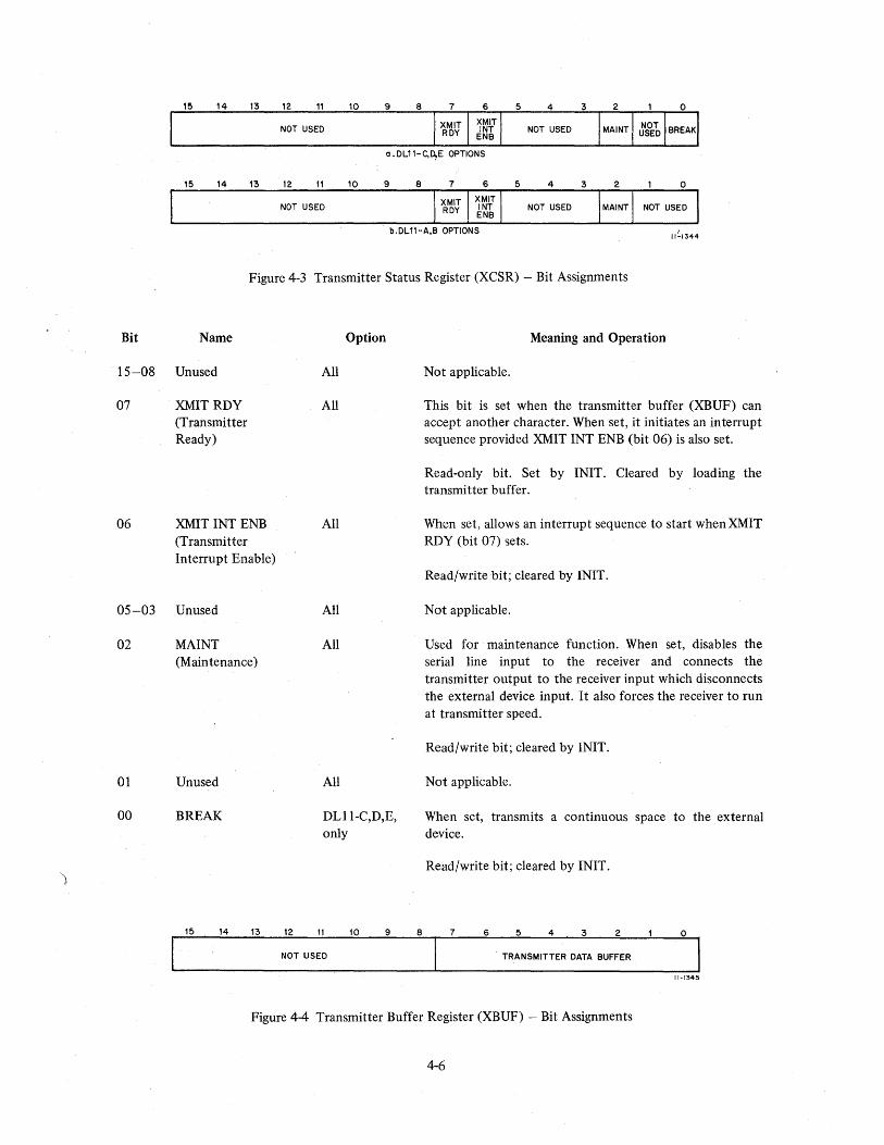
Figure 4-3 Transmitter Status Register (XCSR) - Bit Assignments
Bit Name
15 -08 Unused
07 XMIT RDY (Transmitter Ready)
06 XMIT INT ENB (Transmitter Interrupt Enable)
05-03 Unused
02 MAINT (Maintenance)
01 Unused
00 BREAK
15 14 13
Option
All
All
All
All
All
All
DLII-C,D,E, only
12 11 10 9
NOT USED
8
Meaning and Operation
Not applicable.
This bit is set when the transmitter buffer (XBUF) can accept another character. When set, it initiates an interrupt sequence provided XMIT INT ENB (bit 06) is also set.
Read-only bit. Set by INIT. Cleared by loading the transmitter buffer.
When set, allows an interrupt sequence to start when XMIT RDY (bit 07) sets.
Read/write bit; cleared by INIT.
Not applicable.
Used for maintenance function. When set, disables the serial line input to the receiver and connects the transmitter output to the receiver input which disconnects the external device input. It also forces the receiver to run at transmitter speed.
Read/write bit; cleared by INIT.
Not applicable.
When set, transmits a continuous space to the external device.
Read/write bit; cleared by INIT.
7 6 5 4 3 2
TRANSMITTER DATA BUFFER
11-1345
Figure 4-4 Transmitter Buffer Register (XBUF) - Bit Assignments
4-6

Bit Name
15-08 Unused
07 -00 TRANSMITTER DATA BUFFER
4.3 INTERRUPTS
All
All
Option Meaning and Operation
Not applicable.
Holds the character to be transferred to the external device. If less than eight bits are used, the character must be loaded so that it is right-justified into the least significant bits.
Write-only bits.
The DL 11 Interface uses BR interrupts to gain control of the bus to perform a vectored interrupt, thereby
causing a branch to a handling routine. The DLII has two interrupt channels: one for the receiver section and
one for the transmitter section. These two channels operate independently; however, if simultaneous interrupt requests occur, the receiver has priority. In addition, the DLll-E (dataset option) receiver section handles
multiple source interrupts.
A transmitter interrupt can occur only if the interrupt enable bit (XMIT INT ENB) in the transmitter status
register is set. With XMIT INT ENB set, setting the transmitter ready (XMIT RDY) bit initiates an interrupt
request. When XMIT RDY is set, it indicates that the transmitter buffer is empty and ready to accept another
character from the bus for transfer to the external device.
A receiver data interrupt can occur only if the interrupt enable (RCVR INT ENB) bit in th~ receiver status
register is set. With RCVR INT ENB set, setting the receiver done (RCVR DONE) bit initiates an interrupt
request. When RCVR DONE is set, it indicates that an entire character has been received and is ready for transfer
to the bus. The additional interrupt request sources for the DL ll-E option are discussed in the following paragraphs.
The receiver portion of the DLII-E dataset option handles multiple source interrupts. One of the receiver
interrupt circuits is activated by RCVR INT ENB and RCVR DONE. The additional interrupt circuit can cause
an interrupt only if the dataset interrupt enable bit (bit 05, DATASET INT ENB) in the receiver status register is
set. With DATASET INT ENB set, setting the DATASET INT bit initiates an interrupt request. The DATASET
INT bit can be set by one of four other bits: CAR DET, CLR TO SEND, SEC REC, or RING.
When servicing an interrupt for one condition, if a second interrupt condition develops, a unique second
interrupt, as well as all subsequent interrupts, may not occur. To prevent this, either all possible interrupt
conditions should be checked after servicing one condition or both interrupt enable bits (bits 05 and 06) should
be cleared upon entry to the service routine for vector XXO and then set again at the end of service.
The interrupt priority level is 4 for all options, with the receiver having a slightly higher priority than the
transmitter in all cases. Note that the priority level can be changed with a priority plug.
Floating vector addresses are used for all options and are assigned according to the method described in
Paragraph 5.3. If the DLIl-A or B option is used as a console, then the vector address is 060. The vector address
can be changed by jumpers in the interrupt control logic.
4-7

Any DEC programs or other software referring to the standard BR level or vector addresses must also be changed
if the priority plug or vector address is changed.
4.4 TIMING CONSIDERATIONS
When programming the DL 11 Asynchronous Line Interface, it is important to consider timing of certain
functions in order to use the system in the most efficient manner. Timing considerations for the receiver, transmitter, and break generation logic are discussed in the following paragraphs.
4.4.1 Receiver
The RCVR DONE flag (bit 07 in the RCSR) sets when the Universal Asynchronous Receiver/Transmitter
(UART) has assembled a full character. This occurs at the middle of the first STOP bit. Because the UART is
double buffered, data remains valid until the next character is received and assembled. This permits one full
character time for servicing the RCVR DONE flag.
4.4.2 Transmitter
The transmitter section of the UART is also double buffered. The XMIT RDY flag (bit 07 in the XCSR) is set
after initialization. When the buffer (XBUF) is loaded with the first character from the bus, the flag clears but
then sets again within a fraction of a bit time. A second character can then be loaded, which clears the flag again.
The flag then remains cleared for nearly one full character time.
4.4.3 Break Generation Logic
When the BREAK bit (bit 00 in the XCSR of DLll-C, D, and E options) is set, it causes transmission of a continuous space. Because the XMIT RDY flag continues to function normally, the duration of a break can be
timed by the pseudo-transmission of a number of characters. However, because the transmitter section of the UART is double buffered, a null character (all Os) should precede transmission of the break to ensure that the previous character clears the line. In a similar manner, the final pseudo-transmitted character in the break should
be null.
4.5 PROGRAM NOTES
The following notes pertain to programming the DLII interface and contain information that may be useful to
the programmer. More detailed programming information is given in the Pf!per Tape Software Programming
Handbook, DEC-II-XPTSA-A-D and in the individual program listings.
a. Character Format - The character formats for the different DLII options are given below. Note that when less than eight DATA bits are used, the character must be right-justified to the least significant bit. The character format pertains to both the receiver and the transmitter.
1. DLll-A and B Options - A character consists of a START bit, eight DATA bits, and I or 2 STOP bits.
2. DLll-C, D, and E Options - A character consists of a START bit, five to eight DATA bits, I, 1.5, or 2 STOP bits and the option of PARITY (odd or even) or no parity.
4-8

b. Maintenance Mode - The maintenance mode is selected by setting the MAINT bit (bit 02) in the XCSR. In this mode, the interface disables the normal input to the receiver and replaces it with the output of the transmitter. The programmer can then load various bits into the transmitter and read them back from the receiver to verify proper operation of the DL 11 logic circuits.
4.6 PROGRAM EXAMPLE
The following is an example of a typical program that can be used as an echo program for a Type 103 dataset.
When a remote terminal dials in, this program answers the call and provides a character-by-character echo.
Characters are also copied onto the console device.
4-9

"'et('l 2 r.ra ,:1200 00eJ2CJ!ra 000167 001616 START; JMP REGIN iJUMP '0 BEGlNNING 0' PROGRAM
,SYMBOL DEF"l N IT IONS
(1I491V'0~ RING: 7-4 t'l0 0!0 ,BtT 14 OF' ReSR, RING
r.'!200t"121 ers: C112t?'01;'J0 la IT 1~ OF' ReSR, CLEAR HI 5E ~fO ?l2l02~11J ROONE: ~0P12~" i8 tT 0' OF' RCSR, RECEIVER ~ONE "'1Zl~0('1~ t'lTR: 0000"'2 .-8tT 01 or RCSR, DATA 'ERM!NAL. RE.OY t'!f2j(i'l2!J" XRDY: V-"rlI2C'1" ,Bn 01 Of' XCSR, TRANSMlfTER READY
9'QJ2f2lr'1Zl ,=20t'10 \,,;020('110 t756U RCSRI 175610 iCSR Of!' PECEIVER 0020('12 1756'-2 RBur, 175612 ,BUf or RECEIVER 002·0~4 175614 XCSRI j 75614 ,C~R or TRANSM IT tER eJ~201l!6 175616 XBUrl j.75616 IBUf OF' TRANSM! TTER 002iH0 1775"4 CXCSR; 177564 IC~R or CONSOI.,E TR ANSM! HER 002~a 2 177566 CX8UF"1 177566 iaUf or CONSOI.,E fR ANSM lT1E~ 00201.4 ?lra17J11J00 BUF'FER I '" iH~I.,~S C~ARAr,TER RECEIVE~ Ql02016 !"1Zl('l,,00 DELAY' ('11 ,I;OI.."S DELAY COUNT. ~lt;H ORorR ~0?rc?0 ?l0tH'?!0 ?' iHOL~S DELAY COUNT. l.OW OReER
JBEGINNING or ECHO PROGRAM
f" 00?[b22 0051017 177752 BEGIN; CLR tJIIRCSR ,STA~T av !NITtA~12ING A~L SITS TO i!ERO ..-0
1211212026 '1'32717 ('14"000 177744 I.,OOP1; BI" #RING,fiIIRCSR "C~E~K fOR INCOMING CALL 01212034 0.017 7 4 SEQ L,OOP1 J BRA~ICIol If PIoiONE IS ~OT IIIINGtNt; ~02fcl36· 'l!52717 PI 121 t1J0C'l 2 177734 8IS __ OTR,GDRCSR J'PIolO~!E IS RlNGING, SO ANSWER WtTlol OTR 1211212044 'l!12767 !'Jl2leJ0C"5 171744 MOV #5,OfLAY "S~T U" COUNT POR OELAV
2!02"~2 'l!32717 Zl20"~" 17772121 ~OOP21 BIT #CTS,ElRC5R iCJ.lEC:K fOR C~EAR TO SEND 12102060 012110~1 BNf. l.OOP3 "BRA~'CJ.l If O~ 2102062 162767 ~12I12f"'l!1 t 77730 SUB Ii, DELA'f+2 l·cHEeK DELAY QJ0?070 QlI2I5667 177 722 s~c DEI..AY JDF:CI!IEto.1ENT A TWO.,WORO !NTEr,EP 1211212,,'4 01211152 REO BEGIN "B~ A"JC~ IF' WE IoIAVE WAITE!"! TOO bONG 01212016 2'12I(lJ765 BR L,OOP2 J BRA ~I C 101 AND CONTINUE TO WAtT fOR CTS
12f02U!1Z 9.1327 77 "'2010"'0 177672 L.OOP3; Bll' #CTS,(jIRCSR J IS eHANNEb 5Tl~~ ESTABL!S~Er?
"02106 (?I0114~ REO 8EGIN ,-E3 R A \IC~ IF" eT.S N~'f P~ESENT
"'02110 ~32717 Ql0Qf2t?10 171662 BIT #¢ROONE.(jIQCSR ICJ,:fEr'K fOR RECEIVEn eHAR4C'ER 1IJ02116 0017"70 REO L,OOfl3 18RA~JC,", !F' NO C:HARACTER ~EeE!Vro 012l2V0 ~17767 177656 1.77666 MOV ,RBUF',Bur,p.R ,RPM') ~ECEIVED C~ARAt::T[R INTI') RurFER
0021?6 "'32717 !1!0~2"'121 177650 1.00P41 BIT URDY. CiXCSR '-CHEC'K F'OR lRANSM 1 HER Rf.AOY 00~134 (1'01714 AEC'J 1.0 0P4 ,·BRA\ICIol !F' NOT READY 002136 01,('717 1716'52 177642 ~ov BUF'F'ER, @XBUF' ;TRA~ISMI'f ~H4RACTER TO RrM~'1'f TERMtNAL
el12I21~4 "'3'2777 ~e!elUJ0 177636 I.OOP5; BlT *XROY,~C)(CSR iC~ECK FOR CONSOLE T~ANSMITttR REA6V 002152 01211774 8E~ 1..00P5 "BRANC~ If NOT R£AOY ~02154 "'16717 177b~4 177630 ~OV BurfER, 'CX~UF' iTR A~!SM IT CHARACTER TO C~NSOLE 002162 r.:"12Ie!746 SR L.OOP3 "BRA~ICj.l AND WAfT FOR NEX' r.HARACTER

CHAPTER 5
DETAILED DESCRIPTION
5.1 INTRODUCTION
This chapter provides a detailed description of the DLll Asynchronous Line Interface. The discussions in this
chapter are supported by a complete set of engineering drawings contained in a companion volume entitled
DL11 Asynchronous Line Inter/ace, Engineering Drawings.
The complete DLll interface may be divided into 11 functional areas; each of these areas is covered separately
in subsequent paragraphs. Table 5-1 lists each functional unit, the option number to which it applies, and th~
general purpose of the unit. A description of the prime differences among options (baud rates, code, operation,
etc.) is presented in Chapter 2.
Functional Unit Options
Selection Logic A-E
Interrupt Logic A-E
Register Logic A-E
Table 5-1
DLll Functional Units
Purpose
Determines if the DLII interface has been selected for use and what type of operation (transmit or receive) has been selected. Permits selection of one of four internal registers and determines if the register is to perform an input or output function.
Permits the interface to gain bus control and perform a program interrupt. Either the receiver or transmitter can issue an interrupt request. The DL ll-E option can issue a dataset interrupt in addition to the two other interrupts. Priority level of bus request (BR) line can be changed by the user.
F our internal registers, addressable by the program, provide data transfer, command and control, and status monitoring functions for the interface. Although all options have the same registers, the number of bits used may differ from option to option. However, bit positions of specific bits do not change. ,
(continued on next page)
5-1

Functional Unit
Transmitter Control Logic
Receiver Control Logic
Universal Asynchronous Receiver /Transmi tter (UART)
Clock Logic
Maintenance Mode Logic
Break Generation Logic
EIA Logic
Dataset Logic
5.2 ADDRESS SELECTION
Options
A-:-E
A-E
A-E
A-E
C,D,E
B,D,E
E only
Tabie 5-1 (Cont) DL11 Functional Units
Purpose
Provides necessary input control signals for the UART when it is used to convert parallel data from the bus to serial data required by the external device. Typical signals include: data strobe, clock frequency, and parity select.
Provides necessary input control signals for the UART when it is used to convert serial data to the parallel data required for transmission to the bus. Typical signals include: data enable, status word, and clock frequency.
Performs the necessary serial-to-parallel or parallel-to-serial conversion on the data and supplies control and error detecting bits.
Determines the clock frequency and, therefore, the baud rates for the transmitter and receiver sections of the UART. Eight baud rates are derived from a single crystal. One of four standard crystals is offered with the options.
Performs a closed loop test of the DLII control logic by tying the serial output of the transmitter into the receiver input and forces the receiver clock to be the same frequency as the transmitter clock.
Permits the transmission of a continuous space or "break." The duration of the break can be timed by. the pseudo-transmission of a specific number of characters.
Provides necessary level converters for use with EIA levels.
Provides full EIA dataset control. Monitors such dataset lines as RECEIVE DATA, SEC RECEIVE DATA, CARRIER DETECT, RING, and CLEAR TO SEND. Permits program to control TRANSMITTED DATA, DATA TERMINAL READY, REQUEST TO SEND, and SEC XMIT DATA.
The address selection logic (Drawing DL-5) decodes the incoming address information from the bus and provides
the signals that determine which register has been selected and whether it is to perform an input or output
function. Jumpers on the logic can be altered so that the module responds to any address within the range of
774000 to 777777. However, standard address assignments for the various DLII options normally fall within
the ranges of 775610 to 776177 or 776500 to 776677.
5-2

The standard address assignments for all DL11 options are listed in Table 5-2. Note that these addresses provide
for 16 additional units when using the DLI1-A or B, and 31 additional units when using the DLI1-C, D, or E.
For the purpose of clarity, the following discussion assumes that a DL11-A is being used as a Teletype (console)
control.
When the DLII-A or DLI L .. B is to be used as a Teletype (console) control, jumpers are arranged so that the
module responds only to standard device register addresses 777560, 777562, 777564, and 777566 Uumpers in
bit positions 3 and 7). Although these addresses have been selected by DEC as the standard assignments for the
Table 5-2
D L 11 Address Assignments
Option Unit Address Remarks
DL11-A or B Console 777560 777562 777564 777566
Unit #1 776XXO XX= 50 for Unit #1 776XX2 51 for Unit #2 776XX4 52 for Unit #3 776XX6
67 for Unit #16
Unit #16 776XXO 776XX2 776XX4 776XX6
DL11-C, D, or E Unit #1 77XXXO XXX = 561 for Unit #1 77XXX2 562 for Unit #2 77XXX4 563 for Unit #3 77XXX6
Unit #31 77XXXO 617 for Unit #31 77XXX2 77XXX4 77XXX6
5-3

DLII when used as a Teletype control, the user may change the jumpers to any address desired. However, any
MAINDEC program or other software that references these DLII standard assignments must also be modified
accordingly if other than the standard assignments are used.
The first five octal digits of the address (77756) indicate that the DLII has been selected as the device to be
used. The final octal digit, consisting of address lines A02, AOI, and AOO, determines which register has been
selected and whether a word or byte operation is to be performed. The two mode control lines, COO and CO I, determine whether the selected register is to perform an input or output operation (provided the selected register
is a read/write register).
The address decoding is performed by a series of logic gates that provide the inputs to a 4-line to 10-line decoder
circuit (7442 IC chip). Basically, the state of the four input lines provides a signal on one of the 10 output lines
(only 7 of the 10 output Hnes are used in the DLIl). A detailed schematic, truth table, and packaging diagram
are provided in Appendix A.
Three of the input lines (lC pins 15, 14, and 13) are true or false dependent on the state of input lines BUS AO 1,
BUS A02, and BUS CI, respectively. Lines BUS AOI and BUS A02 are used for selecting one of four registers
and line BUS CI controls direction of data transfers, i.e., gate data to the bus (DATI, DATIP) or gate data from
the bus (DATa, DATOB). The fourth input line (pin 12) is an address enable signal that must always be true in
order for the decoder to operate. This address enable signal is derived from a series of gates that are true when
MSYN is present and when the address line conditions indicate that one of the four valid addresses is present on
the bus, and when the Unibus cycle is not a DATOB to the odd byte (i.e., AOO=I, Cl=l, and CO=l).
Table 5-3 lists the input conditions required to select an appropriate output signal. Note that only one of these
output signals can be present at any given time.
5.2.1 Inputs
A simplified block diagram of the address selection logic is shown in Figure 5-1. Note that IN and OUT are
always used with respect to the master (controlling) device. Thus, when the DLll interface is used, an OUT
transfer is a transfer of data out of the master (the processor) and into the interface. Similarly, an IN transfer is
the operation of the interface furnishing data to the processor.
The address selection logic input signals consist of 18 address lines, A (17:00); 2 bus control lines, C (I :0); and
a master synchronization (MSYN) line. The address selection logic decodes the incoming address as described
below. This address format is shown in Figure 5-2. Note that all input gates are standard bus receivers.
a. Lines AO I and A02 are decoded to select one of the four addressable device registers.
b. Line CI is decoded to select either aninput (DATI) or output (DATa) function. When line CI is false, an input (read) operation is selected; when it is true, an output (write or load) operation is selected.
c. Decoding of lines A 00:03) is determined by jumpers. When a given line contains a jumper, the address logic searches for a 0 on that line; if there is no jumper, the logic searches for a 1.
NOTE Connection of jumpers on the M7800 module is identical to the method used on other devices which employ an M105 Address Selector Module.
5-4

d. Address lines A (I 7: I 1) must be all I s. This specifies an address within the top 8K byte address bounds for device registers.
e. Line AOO is used for byte control in such a manner that no control signals are generated when a byte operation is performed on the high-order byte of any register.
AEBI DATA STROBE L
ADDRESS SELECTION I LOGIC EEl BUS .... EJI
" CONTROL BUS MSYN L BUS SSYN L
BUS A17 L
BUS A03 L
BUS AOO L
BUS CO L
BUS AOI L
BUS A02 L
. BUS Cl L
17
ED1,..
EE2:
ED2: EK1 :
EK2;:
~ -:-C EL1 ,..
EPI :
ER1 :
EN2 ;:
EP2 :
EUI ;:
EV1 ,..
EU2,..
EV2 :: -EH2 ...
EJ2 ::
EHI ::
EFI ;:
EF2 :: -
16
I 1_
2
3_
4o-UNUSED
5"" ....
ADRS ENB IC7442 6_
:! Al0:! INPUT 12 7 .... GATES DECODER :! A9 :! 8o-UNUSED
~ AS ~ 9 v _ A7..., 10 ~}UNUSEO ..0 A6 C 11
~A5 ~
-C A4 C f--
I A __ 3
\ 15 14 13
JUMPER FOR A 0, NO
I JUMPER FOR A I, SEE NOTE BELOW
EL2 r---
NOTE: Jumper configuration shown indicates standard address assignment when used as teletype console control (0L11-A,B Options)
Figure 5-1 Address Selection Logic - Simplified Diagram
15 14 13 12 11 10 9 8 7 6 5 4
SELECTED BY JUMPERS
3
RCSR TO BUS} RBUF TO BUS IN (READ)
XCSR TO BUS
BUS TO RCSRl BUS TO RBUF
BUS TO XCSR OUT (WRITE)
BUS TO XBUF
REG SEL H
11-1347
2 o
I I I T ~I MUST BE ALL Is I
DECODED FOR 1 OF 4 REGISTERS ------------__________ ----1 •
BYTE CONTROL -11-1346
Figure 5-2 Interface Select Address Format
5-5

5.2.2 Outputs
The address selection logic output signals that are used permit selection of four 16-bit registers and determine
whether information is to be gated into or out of the master device. All of these output signals are listed in Table
5-3.
The first three output signals listed in the table are used for reading (gating data into the master) three of the
registers (RCSR, RBUF, and XCSR). There is no signal generated for the fourth register (XBUF) because it is a
write-only register.
Three of the remaining four signals are used for writing (gating data from the master) into three of the registers
(RCSR, XCSR, and XBUFj. Although the fourth register (RBUF) is a read-only register which cannot be loaded,
a signal is still produced. However, this signal is not used as a true loading signal but, rather, is used to produce
SEL 2 L which is necessary for compatability with the KLII.
The address selection logic also produces three other outputs: BUS SSYN L, DATA STROBE L, and SEL 2 L.
The BUS SSYN L signal is derived from MSYN and the address line inputs and is the acknowledgement signal
that is returned to the master device approximately 400 ns after MSYN becomes true.
Decoder Pins
Pinl5 Pinl4 Pinl3
(AOl) (A02) (Cl)
0 0 0 I 0 0 0 I 0 1 I 0 0 0 1 1 0 1 0 1 1 1 1 1
Table 5-3
Register Selection Signals
Output Function Selected
Pin
I Receiver status to bus 2 Receiver buffer to bus 3 Transmitter status to bus 4 Not used 5 Bus to receiver status 6 Bus to receiver buffer 7 Bus to transmitter status 9 Bus to transmitter buffer
Reg .. Bus Cycle
RCSR DATI or DATIP RBUF DATI or DATIP XCSR DATI or DATIP
- -RCSR DATa or DATOB* RBUF DATa or DATOB* XCSR DATa orDATOB* XBUF DATa orDATOB*
*DATOB to low byte only (ADO = 0)
NOTES: 1. There is no selection signal for transmitter buffer to bus because the transmitter buffer (XBUF) is a write-only register.
2. The bus to receiver buffer signal is used to produce a SEL 2 signal for KLlI Teletype control compatability. This signal,is not used to load the buffer because the RBUF is a read-only buffer.
3. Input pin 12 is not shown since it must be true in all cases (address enable level).
4. Only seven of the possible ten outputs are used in the DLlI. Output pins 4, 10, and 11 are unused.
5-6

When the transmitter buffer (XBUF) is addressed for loading, the address selection logic produces the BUS TO
XBUF output signal. This signal triggers a monostable multivibrator that generates the DATA STROBE L pulse.
This pulse strobes data from the bus lines into the UART and is of sufficient duration to allow data to be
strobed into the UART. The DATA STROBE L pulse also inhibits the assertion of BUS SSYN L which ensures
that the D lines remain stable during strobing. Operation of the UART is described in Paragraph 5.7.
The purpose of SEL 2 L is to reset the Teletype DONE flag. When the receiver buffer (RBUF) has been
addressed for reading or writing, a signal triggers a monostable multivibrator that generates SEL 2 L. The SEL 2
L signal becomes RESET DAT A AVAILABLE L which is applied to the UART. The function of this signal is to
reset the DAT A AVAILABLE line which indicates that an entire character has been received (DONE flag
function).
5.3 INTERRUPT CONTROL
The interrupt control logic (Drawing DL-6) permits the' DLII interface to gain control of the bus (become bus
master) and perform an interrupt operation. Jumpers on the logic can be altered so that the logic has a normal
vector address within the range of 000 to 776. However, the specific vector used with a particular DLII is
dependent on the DLII option and its use within a system.
The standard vector address assignments for all DL 11 options are listed in Table 5-4. Note that most of the
vectors are "floating" and therefore, are assigned according to the addressing scheme given in Appendix B. For
the purpose of clarity, the following discussion assumes that a DLl1-A is being used as a Teletype (console)
control.
Table 5-4
DLll Vectors and Priority Levels
DLII Option Vector Address Priority Level
DLII-A or B 060 BR4 (when used as a console) 064
DLll-A orB Floating* BR4 (additional units)
DLI1-C, D, or E Floating* BR4
* A floating vector address means that the initial vector is assigned according to a scheme that considers other PDP-II devices in a particular system. This addressing scheme is given in Appendix B.
The interrupt control logic consists of a dual-input request and grant acknowledge circuit for establishing bus
control. One input (referred to as the A input) is connected to the receiver section and provides a vector address
of 060. The other input (referred to as the B input) is connected to the transmitter section and provides a vector
address of 064. The two circuits operate independently; however, if simultaneous interrupt requests occur, the
receiver section has priority over the transmitter section.
NOTE The final octal digit of the vector address is not affected by the jumpers; therefore, regardless of the vector address selected by the jumpers, the final octal digit is always 0 for the receiver and 4 for the transmitter.
5-7

Figure 5-3 is a simplified diagram of the interrupt control logic. It is important to note that the DLII-E option
has the capability of handling multiple source interrupts in the receiver (A input) portion of the logic. In
addition, the dataset interrupt (DATASET INT) signal can be set by anyone of several conditions such as RING,
CARRIER, etc. In order to cover all interrupt logic, the remainder of this discussion assumes that a DL II-E
option is being used.
DL-4 RCVR INT ENB (1) H
DL-4 RCVR DONE H
RCVR INT
DL-4 DATASET INT (1) H
_____ ~1l:: ~t;!J BUSBG IN H;....;FB;:.,;.1 ________________ +_-----t BUS ~YN LF~C~l _______________ ----+-----;3
O-Va D----1rr-FK.:.;..l BUS DOa L
o V7 FH1. BUS 007 L
o V6 FF2 BUS 006 L
U-_O'"'FF....;..l BUS 005 L
D----1rr-FN=2 BUS 004 L D----1D-"FL;.;...l BUS 003 L
MASTER CONTROL
FE2 BUS 002 L
BUS NPRL;....;FJ~l ________________________ +_-----~~~ Nl0
DL-4 XMIT INT ENB (1) H-=_,...-------I
DL-4 XMIT READY H------i XMIT INT
NOTES: 1. Jumpers shown for use as Teletype control, 2. Jumper. J6 can be removed to disable dataset interrupt request logic. 3. Dataset interrupt available only on DL11-E option.
11-1348
Figure 5-3 Interrupt Control Logic - Simplified Diagram
As shown in Figure 5-3, a receiver (or A input) interrupt request can be generated by the receiver (DLII-A, B, C,
or D options) or can be generated by either the receiver or the dataset (DLII-E option). In either case, a RCVR
INT signal is generated and sent to the master controllogic which initiates the interrupt sequence. Jumper J6 on
the DLII~E option can be removed if the user desires to disable the dataset interrupt logic.
The receiver interrupt logic is shown on drawing DL-4. When the receiver is issuing an interrupt request, two
input signals must be high: RCVR INT ENB (I) and RCVR DONE. When a I is loaded into bit 06 of the receiver
status register (RCSR), it sets the RCVR INT ENB flip-flop to produce RCVR INT ENB (1). This signal is
applied to one leg of a 2-input AND gate as an enabling level. The second input to the gate is RCVR DONE
which comes from the R DONE output line of the UART. When true, this line indicates that an entire character
has been received, transferred to a holding register, and is ready for transfer to the bus. With the RCVR INT
ENB (I) and RCVR DONE signals both true, the AND gate is qualified and RCVR INT is produced to initiate
the interrupt sequence. A detailed explanation of UART operation is given in Paragraph 5.7.
When the dataset is issuing an interrupt (DLII-E option only), two different input signals must be high:
DATASET INT ENB (1) and DATASET INT (1). When a I is loaded into bit 05 of the receiver status register
(RCSR), it sets the DATASET INT ENB flip-flop to produce DATASET INT ENB (1). This signal is applied to
one leg of a 2-input AND gate as an enabling level. The second input to the gate is DATASET INT (1). The logic
that generates this signal is shown on Drawing DL-7 and described in Paragraph 5.4.1.~. Basically, the signal is
5-8
generated by a flip-flop that is direct set when anyone of the following dataset signals is asserted: RING,
CARRIER, CLR TO SEND, or SEC REC DATA. When this flip-flop sets, DATASET INT (l)is produced, the
AND gate is qualified, and RCVR INT is generated as before to initiate an interrupt sequence.
The receiver (or A input) section of the interrupt control logic is used to gain control of the bus. When RCVR
INT H is asserted, a bus request is made on the BR level corresponding to the level of the priority plug in the
logic. The standard level for all DLII options is BR4. This level may be changed on the priority plug, if desired.
When the priority arbitration logic in the processor recognizes the request and issues a bus grant signal, the
interrupt control circuit acknowledges with a SACK signal. When the DLII interface has fulfilled all
requirements to become bus master (BBSY false, SSYN false, and BG false), the interrupt control logic asserts BBSY.
The transmitter (or B input) section of the interrupt controllogic operates in a similar manner to that of the
receiver section (or A input). In this case, the two input signals that must be high are: XMIT INT ENB (1) and
XMIT READY. When a 1 is loaded into bit 06 of the transmitter status register (XCSR), it sets the XMIT INT
ENB flip-flop to produce XMIT INT ENB (I). This signal is applied to one leg of a 2-input AND gate as an
enabling level. The second input to the gate is XMIT READY which comes from the XRDY (transmitter ready)
output line of the UART. When true, this line indicates that another character may be loaded into the UART
holding register. With the XMIT INT ENB (1) and XMIT READY signals both true, the AND gate is qualified
and XMIT INT is produced to initiate an interrupt sequence. A detailed explanation of UART operation is given
in Paragraph 5.7.
The transmitter control interrupt logic functions in an identical manner to the receiver control interrupt log;ic
except that it generates a different vector address. Although both the receiver and the transmitter are at the same
BR level (for example, both at BR4), the receiver has a slightly higher priority.
Once the DL 11 interface has gained control by means of a BR request, an interrupt is generated. The interrupt
vector address iss~lected by jumpers on the logic as shown in Figure 5-3. Because the vector is a 2-word (4-byte)
block, it is not necessary to assert the states of bits 00 and 01.
The six selectable Uumpered) lines determine the two most significant octal digits of the vector address. The
least significant octal digit is controlled by bit 02 so that all vector addresses end in either 0 or 4. The input to
bit 02 is tied to the V2 flip-flop logic. Whenever an interrupt occurs in the receiver section, bus line D02 is not
asserted, and the interrupt causes a vector at location 060 (or XXO where XX refers to the digits selected by the
jumpers). When an interrupt occurs in the transmitter control, bus line D02 is asserted, and the interrupt causes a
vector at location 064 (or XX4). Note that the first two digits canbe changed by the jumpers but the last digit is
~always either 0 or 4.
The BG IN signal is allowed to pass through the logic to BUS BG OUT when the interface is not issuing a
request. To request bus use, the AND condition of interrupt enable and interrupt must be satisfied (i.e., RCVR
INT ENB and RCVR DONE, or DATASET INT ,ENB and DATASET INT, or XMIT INT ENB and XMIT
READY). Both levels must remain true until the interrupt service routine clears one of them. Once bus control
has been attained, it is released when the processor has strobed in the interrupt vector. After releasing bus
control, the logic inhibits further bus requests even if the interrupt and interrupt enable levels remain asserted. In
order to make another bus request, one of the two levels must be dropped and then reasserted to cause the logic
to reassert the request line. This prevents multiple interrupts when the control logic is used to generate
interrupts.
5-9

In the case of the DLII-E option, the receiver section handles a multiple source interrupt (RCVR DONE and
DATASET INT). In addition, DATASET INT can be caused by one of many conditions (RING, CARRIER;
etc.). If the program is servicing an interrupt for one condition and a second interrupt condition develops, it is
possible that this second, and subsequent, interrupt may not occur. In order to prevent this, all possible interrupt
conditions should be checked after servicing a specific condition. An alternative solution is to clear both
interrupt enable bits (05 and 06) upon entry' to the service routine for vector XXO and reset the bits at the end of the service routine.
Note that the interrupt control logic used in the DLII interface is not capable of issuing NPR requests.
In order to improve NPR latency, the NPR line is sampled and prevents an interrupt request until all NPRs have
been honored. The sampling of the NPR line is controlled by a jumper (Nl) on the DLII interface module.
5.4 REGISTERS
CAUTION Only certain PDP-II processors can work with the special circuit described above. The jumper (Nl) on the module, when cut, prevents this special circuit from working. This circuit does not work on PDP-llj20 and PDP-lljlS systems unless the KHII has been included.
All software control of the DLll Asynchronous Line Interface is performed by four device registers. These
registers are assigned Unibus addresses and can be read or loaded with any PDP-II instruction that refers to their address (with certain exceptions such as load-only, read-only, or unused bits). Table 5-5 lists these registers and
the function of each. Subsequent paragraphs discuss each of the registers from a hardware standpoint. A
discussion of the registers from a programming standpoint is presented in Chapter 4.
NOTE Although the basic function of each register is identical for all DLII options, certain bit positions and functions may not be used from option to option. Therefore, the following paragraphs cover all possible bit positions and indicate which options they pertain to.
5.4.1 Receiver Status Register (RCSR)
The receiver status register (RCSR) is used to monitor the status of receiver logic operation when the DL 11
accepts a character and is used to initiate interrupt sequences.
The receiver status J;egisters in the DLII-A and C options include a reader enable (RDR ENB) bit that is used to
advance the paper-tape reader in an ASR Teletype Unit.
The receiver status register in the DL lI-E option includes nine additional bits for use with datasets.
Each of the bits (for all options) is discussed separately in the following paragraphs, beginning with the most
significant bit. Any bit that is not applicable to all DLII options is so specified.
5-10

Register
Receiver Status Register
Receiver Buffer Register
Transmitter Status Register
Transmitter Buffer Register
Table 5-5
Device Register Functions
Mnemonic
. RCSR
RBUP
XCSR
XBUF
Function
Provides detailed information on the status of the DLII receiver logic. Status information includes such flags as receiver active (RCVR ACT) and receiver done (RCVR DONE). Also includes the interrupt enable bit that can be used to initiate interrupt sequences when RCVR DONE sets.
The DLll-E status register contains additional status and interrupt enable bits for use with datasets. Status bits include such information as carrier detection, ring, secondary transmitter, and clear to send.
Holds the character received from the external device prior to transfer to the Unibus. The format of the character is dependent on the specific DL 11 option used.
The receiver buffer in the DLI1-C, D, and E options also includes four error bits that are set if a corresponding error condition arises during reading of a character from the device.
Provides the interrupt enable bit and the transmitter ready (XMIT RDY) flag so that transmitter logic. can be monitored and an interrupt sequence initiated, if desired.
Provides the maintenance bit which can be set under program control to use the maintenance mode of operation.
The DLl1-C, D, and E options also include a BREAK bit for continuous generation of a space.
Holds the character to be transferred to the external device. Format of this data is dependent on the specific DLII option used.
5.4.1.1 Dataset Interrupt Bit (15) - The dataset interrupt (DATASET INT) bit, available only on the DLll-E
option, indicates that a dataset signal has made a transition. An interrupt sequence is initiated provided the
DATASET INT ENB bit (bit 05) is also set. The DATASET INT bit is controlled by a flip-flop that is set
whenever RING, CARRIER, CLEAR TO SEND, or SEC REC DATA signals from the dataset change states.
The DATASET INT flip-flop (Drawing DL-7) is direct set by the output of one of four series of gates; each series
of gates is tied to one of four signals fro~he dataset. The first series of gates is qualifeid by a RING signal from
the dataset. Note that the initial gate has a differentiating circuit connected in such a way that the gate is
qualified only when the RING signal changes from 0 to 1. The remaining three series of gates function similarly
5-11

except that a delay circuit is connected in such a way that the input gate is qualified on either a 0 to 1 or 1 to 0
transition of the input signal. The three dataset signals to these three series of gates are: CARRIER, CLEAR TO
SEND, and SEC REC DATA.
When the DATASET INT flip-flop is set, it produces a DATASET INT H signal which is applied to the interrupt
control logic (Paragraph 5.3). The signal is also applied to a bus driver for BUS DIS L (Drawing DL-2) so that
the status of the bit can be read by the program.
The DATASET INT flip-flop is cleared whenever the receiver status register is read because of the RCSR TO
BUS signal at the clock input. Because the flip-flop is cleared when it is read, bit 15 is, in effect, a read-once bit.
The flip-flop may also be cleared by an initialize (BINIT) signal.
5.4.1.2 Dataset Status Bits (14, 13, 12, and 10) - These four bits are available only on the DLII-E option and
indicate the status of the dataset. All four bits (RING, CLEAR TO SEND, CARRIER, and SEC REC DATA)
operate in a similar manner and when set, set the DATASET INT bit as described in Paragraph 5.4.1.1.
The RING bit indicates that a ringing signal is being received from the dataset. The RING signal from the dataset
qualifies a series of gates (Drawing DL-7) whenever it changes from 0 to 1. The output of the gates direct sets the
DATASET INT flip-flop and is also applied to a bus driver for BUS D14 L (Drawing DL-2) so that the status of
the bit can be monitored by the program.
The remaining three dataset signals operate similarly except that the related gates are qualified when the signal
from the dataset changes from 0 to 1 or from 1 to O. Qualifying the gates sets the DATASET INT flip-flop and
applies the appropriate signal to a related bus driver for reading by the program.
The CLR TO SEND bit (bit 13) is activated by the CLEAR TO SEND signal from the dataset. When the related
gates are qualified, the bit is set to indicate an ON condition; when not qualified, the bit is clear to indicate an
OFF condition.
The CAR DET bit (bit 12) is activated by the CARRIER signal from the dataset and the related gates are
qualified (bit set) when the data carrier is received. When the gates are not qualified (bit clear), it indicates that
the dataset has either completed the current transmission or that an error condition exists in the dataset.
The SEC REC bit (bit 10) is activated by the SEC REC DATA signal from the dataset to provide a receive
capability for the reverse channel of a remote station. When the related gates are qualified (bit set), it indicates a
space (+6V).
5.4.1.3 Receiver Done (07) - The receiver done (RCVR DONE) flag, which is available on all options, indicates
that a full character has been received. This bit, when set, clears the receiver active (RCVR ACT) flag and
initiates an interrupt sequence provided the associated interrupt enable bit (RCVR INT ENB bit 06) is also set.
Once an entire character has been received and is stored in the UART holding register, the UART issues a
received data available (R DONE) signal (Drawing DL-4) which is inverted and fed to the direct clear input of the
RCVR ACT flip-flop to clear it, thereby indicating that the receiver is no longer in use and is capable of receiving
a new character.
5-12

The output of the inverter passes through another inverter to become RCVR DONE H. This signal is ANDed
with RCVRINT ENB (1) H, which is true if bit 06 is set, to produce the RCVRINT H signal that initiates an
interrupt sequence as described in Paragraph 5.3. The RCVR DONE H signal is also ANDed with RCSR TO BUS
H (Drawing DL-2) so that the status of the RCVR DONE bit can be read by the program from bus data line BUS
D07.
The RCVR DONE flag can be cleared by INIT or by the occurrence of RESET DATA A V AILABLE L. This
signal occurs under one of two conditions. Whenever the reader buffer (RBUF) is addressed, indicating that a
new character is to be loaded into the receiver, SEL 2 L is true and passes through an OR gate to produce
RESET DATA AVAILABLE L. This signal is applied to the CLR R DONE line of theUART, causing the R
DONE line to reset, thereby resetting RCVR DONE.
If the reader enable (RDR ENB) flip-flop is set, indicating that the tape reader in a Teletype unit is being
advanced, then the 0 side is low and passes through the same OR gate as before to reset RCVR DONE.
5.4.1.4 Receiver Interrupt Enable (06) - The receiver interrupt enable bit (RCVR INT ENB) permits an
interrupt sequence to be initiated, when the RCVR DONE bit sets, to indicate that a character has been received
and is ready for transfer to the Unibus. This bit is set by using the BUS TO RCSR H signal as a load pulse to load
a 1 from bus line BD06 H into the RCVR INT ENB flip-flop (Drawing DL-4). Note that this flip-flop is shown
on the drawing as a 74175 IC chip. This chip is basically four D-type flip-flops with common clock and clear
inputs. A schematic of this IC is shown in Appendix A.
The output of the flip-flop, RCVR INT ENB (1) H, is applied to one leg of a 2-input AND gate. The other input
to this AND gate is the RCVR DONE H signal which is produced when the receiver has stored a full character of
data. When both inputs to the AND gate are true, the RCVR INT H signal is produced and is applied to the
interrupt control logic (Paragraph 5.3) to initiate the interrupt sequence.
The RCVR INT ENB (1) H signal is also ANDed with RCSR TO BUS H so that the program can read the status
of this bit position from bus data line BUS D06.
The RCVR INT ENB flip-flop is cleared by BINIT L.
5.4.1.5 Dataset Interrupt Enable (05) - The dataset interrupt enable bit (DATASET INT ENB), which is only
available on the DLII-E option, permits an interrupt sequence to be initiated when the DATASET INT bit sets
to indicate that the dataset is interrupting the program. This bit is set by using the BUS TO RCSR H signal as a
load pulse to load a 1 from bus line BUS DOS H into the DATASET INT flip-flop (Drawing DL-4). This flip-flop
is part of a 74175 IC chip. The chip contains four D-type flip-flops with common clock and clear inputs. A
schematic of this IC is shown in Appendix A.
The DATASET INT ENB (1) H output of the flip-flop is applied to one leg of a 2-input AND gate. The other
input to this gate is the DATASET INT H signal which is produced when the dataset attempts to interrupt the
program. When both inputs to the gate are true, the RCVR INT H signal is produced and is applied to the
interrUpt control logic (Paragraph 5.3) to initiate the interrupt request. Generation of DATASET INT is described in Paragraph 5.4.1.1.
The DATASET INT ENB (1) H signal is also ANDed with RCSR TO BUS H (Drawing DL-2) so that the program
can read the status of this bit position from bus data line BUS DOS.
5-13

The DATASET INT ENB flip-flop is cleared by BIN IT L.
5.4.1.6 Secondary Transmit (03) - The secondary transmit (SEC XMIT) bit, which is also referred to as
supervisory transmitted data, provides a transmit capability for a reverse channel of a remote station and is
available only on theDLII-E option.
The SEC XMIT bit is set by. using the BUS TO RCSR H signal as a load pulse to load a 1 from bus line BD03 H
into the SEC XMIT flip-flop (Drawing DL-4). Note that this flip-flop is part of a 74175 IC chip which contains
four D-:type flip-flops with common clock and clear inputs. A schematic of this IC is shown in Appendix A.
The SEC XMIT (1) output of the flip-flop is applied to an EIA driver (Drawing DL-7) which provides the +6V
level required by the dataset. This 6V level is connected to pin FF of the Berg connector (EIA SEC TRANSMIT
DATA).
The SEC XMIT (1) output of the flip-flop is also ANDed with RCSR TO BUS H (Drawing DL-2) so that the
program can read the status of this bit position from bus data line BUS D03.
The SEC XMIT flip-flop is cleared by BINIT L.
5.4.1.7 Request To Send (02) - The request to send (REQ TO SEND) bit is a control bit for the dataset and is
required for transmission. This bit is only available on the DLII-E option.
The REQ TO SEND bit is set by using the BUS TO RCSR H signal as a load pulse to load a 1 from bus line BD02
H into the REQ TO SEND flip-flop (Drawing DL-4). Note that this flip-flop is part of a 74175 IC chip which
contains four D-type flip-flops with common clock and clear inputs. A schematic of this IC is shown in
Appendix A.
The REQ TO SEND (1) output of the flip-flop is applied to an EIA driver (Drawing DL-7) which provides the
+6V and -6V levels required by the dataset. The 6V output of the EIA driver is connected either to' pin V of the
Berg connector (EIA REQ TO SEND) or to pin C (EIA FORCE BUSY) depending on whether jumper J 1 or J2 is
installed in the module. Normally, jumper J1 is connected to provide an EIA REQ TO SEND level. However, on
certain modems, an EIA FORCE BUSY signal is sometimes required. In this case, jumper J2 is installed. Note
that either J 1 or J2 is present, but never both.
The REQ TO SEND (1) output of the flip-flop is also ANDed with RCSR TO BUS H (Drawing DL-2) so that the
program can read the status of this bit position from bus data line BUS D02.
The REQ TO SEND flip-flop is cleared by BINIT L.
5.4.1.8 Data Terminal Ready (01) - The data terminal ready (DTR) bit is a control bit for the dataset and
permits the interface to be connected to (bit set) or disconnected from (bit clear) the dataset communication
channel. This bit is only available on the DL ll-E option.
The DTR bit is set or cleared by using the BUS TO RCSR H signal as a load pulse to load either a 1 or 0 from
bus line BUS DOl into the DTR flip-flop (Drawing DL-4). If a 0 is loaded, the flip-flop is cleared, and the
interface is disconnected from the dataset communication channel.
5-14

If a I is loaded into the flip-flop, the flip-flop is set and produces DATA TERMINAL READY (I) which is
applied to an EIA driver (Drawing DL-7) that provides the +6V level required by the dataset. This level (EIA
DATA TERMINAL READY) is fed through Berg connector pin DD to the dataset, thereby establishing a data
communication channel between the dataset and the DL II interface.
The DATA TERMINAL READY (1) output of the flip-flop is also ANDed with RCSR TO BUS H (Drawing
DL-2) so that the program can read the status of this bit position from bus data line BUS DO I.
NOTE The BINIT L signal has no effect on the DTR flip-flop. This flip-flop can only be cleared by the program by loading a 0 into bit position 01. Therefore, the DTR flip-flop is not cleared when the START key is depressed, a RESET instruction is issued, or a power-up condition occurs.
5.4.1.9 Reader Enable (00) - The reader enable (RDR ENB) bit, when set, advances the paper-tape reader in
ASR Teletype units and is available on all options; however, only the DLII-A and DLII-C options connect to
the 20 rnA output circuit. The BDOO H signal, which is derived from receiving BUS DOO L, is applied to the data
input of the RDR ENB flip-flop (Drawing DL-4); the clock input receives the loading signal, BUS TO RCSR H.
When the flip-flop is set, the RDR ENB (I) H output is applied to pin PP of the Berg connector (Drawing DL-3)
for application to the Teletype unit. The 0 side of the flip-flop, which is now low, is gated through an OR gate
(Drawing DL-4) to produce RESET DATA AVAILABLE L which resets the RCVR DONE flag as described in
Paragraph 5.4.1.3.
The RDR ENB bit is a write-only bit; it cannot be read by the program.
Whenever the Teletype starts sending data to the interface, the RDR ENB bit is cleared so that the Teletype
reader does not advance another frame while it is transmitting information to the DL II.
The serial input data (SI H) from the Teletype is fed to a 4-bit shift register (IC 8271) as shown on Drawing
DL-4. The four output lines of this shift register (which is referred to as the "START bit detector") are
connected to a series of gates that are qualified when the START bit enters the register. Actually, the lines are
not qualified until the middle of the START bit enters the register. This ensures sufficient time to guarantee a
valid START bit. When qualified, the gates produce RESET RDR ENB L which direct clears the RDR ENB
flip-flop.
The RESET RDR ENB L signal is also applied through an inverter to the RCVR ACT flip-flop, thereby setting it
to indicate that the interface is now receiving data and the receiver logic circuits are in use.
The RDR ENB flip-flop can also be cleared by BINIT L.
5.4.2 Receiver Buffer Register (RBUF)
The receiver buffer (RBUF) is an 8-bit read-only register in the UART. Serial information is converted to parallel
data by the UART and then gated to the Unibus. The RBUF consists of gating logic rather than a flip-flop
register; therefore, the data output lines from the UART must be held until read onto the bus. Because the
UART is double-buffered, data on these output lines is valid until the next character is received and assembled.
The RBUF register is read by a DATI sequence and the data is transmitted to the Unibus for transfer to the
processor, memory, or some other PDP-II device.
5-15

The low-order byte portion of the register is identical for all DLII options and is only used for holding data. If,
however, a variable data format is used, the buffer is justified into the least significant bit positions. This
justification is performed by the UART. The data loaded into the buffer is coded so that binary Os correspond to
spaces and binary 1 s correspond to marks (or holes).
The four most significant bits in the high-order byte portion of the register are used for error indications on the
DLII-C, D, and E options only.
The four error bits and the data portion of the receiver buffer register are covered separately in the following
paragraphs.
5.4.2.1 Receiver Error Bits - The high-order byte of the receiver buffer register (RBUF) contains four error bits
that set to indicate improper receiver operation. These bits are available only on the DLII-C, D, and E options.
Three of the four error bits are generated by the UART as follows:
a. OR ERROR (overrun error, bit 14) - Indicates that R DONE was not reset (previously received character was not read) prior to receiving a new character. When this condition exists, the UART generates an OR ERR H signal.
b. FR ERR (framing error, bit 13) - Indicates that a framing error is present because the character read had no valid STOP bit. When this condition exists, the UART generates an FR ERR H signal.
c. P ERR (parity error, bit 12) - Indicates that the parity received does not agree with the expected parity. If parity has been selected and this condition exists, the UART generates a P ERR H signal.
Bit 1 S, which is the error (ERROR) bit, is the inclusive-OR of the OR ERR, FR ERR, and P ERR bits. Whenever
one of these errors occurs, the appropriate signal from the UART (OR ERR H, FR ERR H, or P ERR H) passes
through an inverter and qualifies an OR gate (Drawing DL-2). The output of the OR gate is ERROR H. Each of
the four error signals (ERROR H, OR ERR H, FR ERR H, and P ERR H) qualifies one leg of an associated
2-input AND gate. The other leg is qualified by RBUF TO BUS L which is true when the receiver buffer is
addressed for reading. The output of each AND gate is tied to an associated bus data line (BUS DIS, BUS D14,
BUS D 13, and BUS D 12) so that the status of each error bit can be monitored by the program.
It should be noted that none of the error bits is tied to the interrupt logic. Therefore, occurrence ora receiver
error does not cause the program to be interrupted for a branch to a handling routine. However, these flags are
updated each time a character is received, at which point an interrupt may occur by means of R DONE.
The initialize signal (BINIT) may have an effect on these bit positions depending on the UART used. A bit is
cleared by clearing the error-producing condition. When the next character is received by the UART, the error
bits are updated and the new status is available when the receiver buffer register is read.
5.4.2.2 Receiver Data Bits - The receiver buffer register is not a flip-flop register but consists simply of gates
that strobe data from the output lines of the UART to the Unibus. The UART receives the incoming serial data
from the external device, converts it to parallel data, and places it on eight parallel output lines. Each of these
lines (RDO through RD7) is fed to one leg of an AND gate as shown on Drawing DL-2. When the receiver buffer
is addressed for reading (RBUF TO BUS H is true), the levels on these lines are gated through to bus data lines
BUS DOO through BUS D07.
S-16

Figure 5-4 is a simplified diagram of both receiver and transmitter gating logic showing a single bit position.
When the receiver gating is used, the output of the UART is gated through to the Unibus. When the transmitter
is used, data from the Unibus is gated through to the transmitter inputs of the UART.
The receiver buffer can only be read by the program, it is loaded by the UART. Note that the initialize signal
(BINIT) has no effect on this register.
~----'-----------------------------~-----BUS004L
RBUF TO BUS H
B004 H OB4 R04 R04 H
UART
//-1349
Figure 5-4 RBUF and XBUF Gating Logic - Simplified Diagram (one bit position)
5.4.3 Transmitter Status Register (XCSR)
The transmitter status register (XCSR) consists of control and status monitoring bits for the transmitter portion
of the DLII interface.
All DLll options contain two bits associated with transmitter operation: a transmitter ready flag to indicate
that the transmitter buffer can be loaded, and an interrupt enable to allow the transmitter to initiate an interrupt
sequence. Both of these bits are described in subsequent paragraphs.
A maintenance (MAINT) bit is also included in all options so that a closed loop test of DL 11 interface operation
can be performed. The maintenance function is covered in detail in Paragraph 5.9.
A BREAK bit (bit 00) is available only on the DL11-C, D, and E options and permits transmission of a
continuous space to the external device. This logic is described in Paragraph 5.10.
5.4.3.1 Transmitter Ready (07) - The transmitter ready (XMIT RDY) flag, which is available on all DLII
options, indicates that the transmitter buffer (XBUF) is ready to accept another character from the Unibus for
transfer to the external device. This bit, when set, initiates an interrupt seq~ence, provided the associated interrupt enable bit (XMIT INT ENB bit 06) is also set.
This bit is controlled by the XRDY output of the UART which indicates that the transmitter buffer is empty. It
is set by the initialize signal (BINIT) to indicate that the data bits' holding register within the UART may be
loaded with another character. It is also set whenever the holding register is empty. Once loading of the
transmitter buffer begins, this bit is cleared. The XRDY output of the UART is gated to produce the XMIT
READY H flag.
5-17

As shown on Drawing DL-4, the XMIT READY H signal is ANDed with XMIT INT ENB (1) H, which is true if
bit 06 is set, to produce the XMIT INT H signal that initiates an interrupt sequence as described in Paragraph
5.3. The interrupt sequence allows the program to branch to a handling routine for loading a character for
transmission to the external device.
The XMIT READY H signal is also ANDed with XeSR TO BUS H (Drawing DL-2) so that the status of the
XMIT READY flag can be read by the program from bus data line BUS D07.
5.4.3.2 Transmitter Interrupt Enable (06) - The transmitter interrupt enable bit (XMIT INT ENB) permits an
interrupt sequence to be initiated when the XMIT RDY bit sets to indicate that the transmitter buffer can accept
another character from the Unibus. This bit is set by using the BUS TO XeSR H signal as a load pulse to load a 1
from bus line BD06 H into the XMIT INT ENB flip-flop (Drawing DL-4). Note that this flip-flop is shown on the
drawing as part of a 74175 Ie chip. This chip is basically four D-type flip-flops with common clock and clear
inputs. A schematic of this Ie is shown in Appendix A.
The output of the flip-flop, XMIT INT ENB 0) H, is applied to one leg of a 2-input AND gate. The other input
to this AND gate is the XMIT READY H signal which is produced when the transmitter buffer is clear and
capable of receiving a character from the bus. When both inputs to the gate are true, the XMIT INT H signal is
produced and is applied to the interrupt control logic (Paragraph 5.3) to initiate the interrupt sequence.
As shown on Drawing DL-2, the XMIT INT ENB (1) H signal is also ANDed with XeSR TO BUS H so that the
program can read the status of this bit position from bus data line BUS D06.
The XMIT INT ENB flip-flop is cleared by BINIT L.
5.4.4 Transmitter Buffer Register (XBUF)
The transmitter buffer (XBUF) is an 8-bit write-only register that receives the parallel character from the Unibus
and loads it into the UART for serial conversion and transmission.
Although this buffer is identical for all DLII options, some options may function with a variable code format of
less than eight data bits. In these cases, the data character must be justified into the least significant bit positions
by the program. Bit positions within the UART itself are enabled or disabled according to the format code
employed by a specific option. Thus, for example, if a 5-bit code format is used, bit positions 5, 6, and 7 are
disabled in the format. If the program does not justify the character and it is loaded into the most significant bit
positions, data loaded into bits 5, 6, and 7 would be lost.
When the interface is initialized, the XMIT RDY flag is set to indicate that the XBUF can be loaded. When the
buffer is loaded with the first character, the flag clears and then sets again within a fraction of a bit time. A
second character can then be loaded because the UART transmitter section is double-buffered. When the second
character is loaded, the flag clears again but this time remains clear for nearly a full character time.
The transmitter buffer (Drawing DL-2) is not a flip-flop register but consists simply of a series of gates that
strobe data from the Unibus lines to the input lines of the UART. Transfer of data is accomplished by a DATO
or DATOB bus cycle.
5-18

The character to be transmitted to the deviCe is loaded onto bus data lines BUS D07 through BUS DOO and gated
to the UART input lines as BD07 through BDOO. Once on the input lines, the data is strobed into the UART by
the DATA STROBE L signal which is derived from the BUS TO XBUF signal that occurs when the transmitter
buffer is addressed for loading.
Figure 5-4 is a simplified diagram of both receiver and transmitter gating logic showing a single bit position.
Loading of the transmitter buffer is such that a logic 1 causes a mark (or hole) to be transmitted and a logic 0
causes a space.
The UART also generates two signals associated with transmitter buffer operation. An XRDY (indicating
transmitter buffer is empty) signal is generated when the UART can be loaded with another character. This
signal is the XMIT RDY flag described in Paragraph 5.4.3.1. The second signal is EOe (end of character) which
goes high after a full character has been transmitted to the device. It is used to generate the number of STOP bits
required by a specific option and is described more fully in Paragraph 5.8.
S.S TRANSMITTER CONTROL LOGIC
The transmitter control logic provides the necessary input, control, and output logic for the UART when it is
used to convert parallel data from the Unibus to the serial data required for output; This logic may" be divided into three functional areas: control and input, format selection, and data output.
The control and input logic for the transmitter portion of the UART consists of both input and output control
signals, a clock frequency, and an input data character. These signals are listed in Table 5-6 along with a reference to the paragraph containing a detailed description of the logic.
Table S-6
Transmitter Control and Input Logic
Signal Signal Name Paragraph Description
Mnemonic Number
XRDY Transmitter 5.4.3.'1 The XMIT RDY flag that indicates the buffer is empty and Ready (indi- may be loaded with another character from the Unibus. cates buffer empty)
LDXD Load Trans- 5.4.4 The signal that strobes data from the buffer into the mitter Data UART when the XBUF is addressed for loading.
EOC End of 5.8 Signals that a character has been transmitted. Character
XCLK Transmitter 5.8 Provides the required transmitter clock rate. This rate is 16 Clock Pulse times the selected baud rate.
XDO - XD7 Data Buffer 5.4.4 Represents the character (five to eight data bits) loaded from the Unibus into the UART.
5-19

The format selection logic basically consists of jumpers that are arranged to select the number of data bits, STOP
bits, and type of parity. Format selection is covered in Table 2-3 which also lists applicable DLII options for
each of the format selection functions.
The output logic of the transmitter is described in the following paragraphs.
Once the UART has converted the parallel character from the Unibus (UART operation is described in Paragraph 5.7), it shifts the character out, one bit at a time, onto the serial output (SO) line. The first bit shifted out is the
START bit, followed by the DATA bits (LSB first), then the PARITY bit (if selected), and finally, the STOP
bits. The output of the line passes through a flip-flop to become SERIAL OUT H. This flip-flop is used to
compensate for the different number of STOP bits that can be selected.
When the DLII-A or C option is used, the SERIAL OUT H data line is connected to a circuit that converts the
line to the bipolar levels required by the 20 rnA current loop (Drawing DL-3). The resultant positive serial data is
applied to pin AA of the Berg connector and the negative serial data is applied to pin KK.
The SERIAL OUT H data also passes through an inverter and is applied as a TTL level directly to pin SS of the Berg connector.
When t~e DLII-B, D, or E option is used, SERIAL OUT H passes through an EIA level converter (Drawing DL-7) to pin F of the Berg connector.
Regardless of the option used, the SERIAL OUT H is also applied to the MAINT multiplexer circuit for use
during the maintenance mode as described in Paragraph 5.9.
5.6 RECEIVER CONTROL LOGIC
The receiver control logic provides the necessary input, output, and control logic for the UART when it is used to convert serial data to the parallel data required by the Unibus. This logic may be divided into three functional
areas: status and control, format selection, and data input.
The status and control portion of the logic consists of both input control and output status signals, a clock frequency, and an output data character. These signals are listed in Table 5-7 along with a reference to the
paragraph contairting a detailed description of the logic.
The format selection logic is basically the same as used for the transmitter control and is described in Table 2-3.
The input logic of the transmitter is described in the following paragraphs.
Regardless of the device used, the serial input from the device is loaded into the DL 11 one bit at a time
beginning with the START bit, then the DATA bits (LSB first), the PARITY bit (if used), and the STOP bits.
When the DLII-A or C option is used, the bipolar levels of the serial data are applied to pins K (+) and S (-) of
the M7800 Berg connector. The bipolar level is converted to a TTL level (Drawihg DL-3) and fed to pin H which
is connected to pin E when these options are used. The serial data is gated through an OR gate to a 2-line to
I-line multiplexer. When the interface is not in the maintenance mode, the multiplexer has no effect and the
serial data (SI H FS 1) is applied to the input (SI) of the UART as shown on Drawing DL-4. The SI H input is
also fed to a shift register that has its output decoded to reset the RDR ENB flip-flop.
5-20

Table 5-7
Receiver Status and Control Logic
Signal Signal Name Paragraph Description Mnemonic Number
RDONE Reader Done 5.4.1.3 The R DONE flag that indicates a full character has been received from the device and is ready for transfer to the Unibus.
PERR Parity Error 5.4.2.1 A status signal indicating that the received character has a parity error. Can be read by the program.
FRERR Framing Error 5.4.2.1 A status signal indicating that the received character has no valid STOP code. Can be read by the program.
OR ERR Overrun Error 5.4.2.1 A status signal indicating that the character was not read prior to receiving another character from the device. Can be read by the program.
RCLK Receiver Clock 5.8 Provides the required receiver clock rate. This rate is 16 Pulse times the selected baud rate.
RD7 - RDO Receiver Data 5.4.2 Represent the character (five to eight data bits) transferred Buffer from the UART to the Unibus after serial-to-parallel
conversion.
When the DL11-C, D, or E option is used, the serial input, referred to as EIA RECEIVE DATA (Drawing DL-7),
enters pin J and passes through an EIA level converter to pin M of the Berg connector. Because of the cabling,
pin M is connected to pin E (TTL input) and'the data follows the same path as before.
5.7 UNIVERSAL ASYNCHRONOUS RECEIVER/TRANSMITTER (UART)
The Universal Asynchronous Receiver/Transmitter (DART) is an LSI subsystem which accepts binary characters
from either a terminal device or a computer and receives or transmits this character with appended control and
error detecting bits. In order to make this subsystem universal, the baud rate, bits per word, parity mode, and
number of stop bits are selected by extemallogic circuits.
The UART is a full duplex receiver/transmitter. The receiver section accepts asynchronous serial binary
characters and converts them to a parallel format for transmission to the Unibus. The transmitter section accepts
parallel binary characters from the bus and converts them to a serial asynchronous output with start and stop
bits added.
All UART characters contain a START bit, five to eight DATA bits, one, one and a half, or two STOP bits, and a
PARITY bit which may be odd, even, or turned off. The STOP bits are opposite in polarity to the START bit.
This is the maximum format that can be used. Although the UART itself produces these bits, certain DL11
options do not use all of them. Therefore, the format of an input or output serial word may vary from option to
option as shown in Figure 2-1.
5-21

Both the receiver and transmitter are double bufTered. The UART internally synchronizes the START bit with the clock input to ensure a full 16-element (clock periods) START bit independent of the time of data loading.
Transmitter distortion (assuming perfect clock input) is less than 3 percent on any bit up to 10 kilobaud. The receiver strobes the input bit within ±8 percent of the theoretical center of the bit. The receiver also rejects any
START bit that lasts less than one-half of a bit time.
The UART input and output lines are shown on Drawing DL-4. A description of the receiver is given in Paragraph 5.7.1 and a description of the transmitter is given in Paragraph 5.7.2. Note that in the following
discussions, the mnemonic and pin number of UART input and output lines are given in parentheses.
5.7.1 Receiver Operation
A block diagram of the UART receiver is shown in Figure 5-5. When the receiver is in the idle state, it samples
the serial input line (SERIAL IN, pin 20) at the selected clock edges (R eLK, pin 17) after the first
mark-to-space transition of the serial input line. If the first sample is a mark (high), the receiver returns to the
idle state and is ready to detect another mark-to-space transition. If, however, the first sample is a space (low),
then the receiver enters the data entry state.
If the receiver control logic has not been conditioned to the no parity state (a low on pin 35), then the receiver
checks the parity of the data bits plus the parity bit following the data bits and compares it with the parity sense on the parity select line (pin 39). If the parity sense of the received character differs from the parity of the
UART control logic, then the receive parity error line (P ERR, pin 13) goes high and causes the P ERR bit in the
RBUF register to set.
If the receiver control logic has been-conditioned to the no parity state (a high on pin 35), then the receiver
takes no action with respect to parity and maintains the parity error line (P ERR, pin 13) in the false (low) state. When the control logic senses a parity error, it generates a P ERR signal. The DATA AVAILABLE signal updates
the parity error indicator. Note that the P ERR output is always produced by the UART but is coupled to the
RBUF only on DLII-C, D, and E options.
The receiver samples the first STOP bit which occurs either after the PARITY bit, or after the data bits if no
parity is selected. If a valid (high) STOP bit exists, no further action is taken. If, however, the STOP bit is false (low), indicating an invalid STOP code, then the UART control logic provides a framing error indication (a high
on FR ERR, pin \14). The status of the framing error bit can also be read from the RBUF on DLII-C, D, and E
options.
Because the serial input from the external device is shifted into the UART a bit at a time (SI, pin 20), occurrence
of a STOP code indicates that the entire data character has been received and shifted into· the receiver shift , register. After the STOP bit has been sampled, the receiver control logic parallel transfers the contents of the
shift register into the receiver data holding register and then sets the data available (R DONE) flag.
The data available signal also functions as the clock input to the FRAME ERR, PARITY, and OVERRUN
flip-flops in the UART status register. At this point, the DA flip-flop is set, the OVERRUN flip-flop is clear but
has a high on the data input because of the output from the DA flip-flop, and the PARITY and FRAME ERR
flip-flops are set or cleared depending on the signal (true or false) strobed in from the control logic.
5-22

An OVERRUN condition indicates that another data character is being sent to the UART before the previous
character has been transferred to the DL II receiver buffer register. If the DA flip-flop is set, indicating a
character is stored in the holding register, and the UART control logic attempts to set the DA flip-flop again
(indicating a new character has been shifted into the shift register), the DA signal from the control logic provides a clock input to the OVERRUN flip-flop. This flip-flop then sets because the data input is high (DA flip-flop was
already set by the previous DA signal).
During normal operation (no OVERRUN condition), the character in the receiver data holding register is strobed
onto the Unibus by an RBUF TO BUS H signal (Drawing DL-5) which produces SEL 2 L. This signal is applied to the UART reset data available line (pin 18) to clear the flip-flop.
Whenever the serial input ,line goes from a mark (high) to a space (low) and remains at the low level, the receiver
shifts in one character, which is all spaces, then sets the FR ERR indicator and waits until the input line goes high (marking) before shifting in another character.
DATA ENABLE (ROE)
SERIAL DATA
INPUT
CLOCK INPUT
DATA BITS AND GATES
BDOO '----.------"""'T'-----r-----r-' XMIT
BUF LSB ~ __
RDO IUART ~~~~~~~~~~ ISTATUS
RESET REGISTER
EVEN NO PARITY PARITY SELECT
DATA R AVA I ABLE
NB2 NB1 NUMBER OF
BITS/CHARACTER
SHOWN AS SINGLE BUFFERING
Figure 5-5 UART Receiver - Block Diagram
EMPTY --, I I I
....J
11-1350
5.7.2 Transmitter Operation
A block diagram of the UART transmitter is shown in Figure 5-6. When the UART transmitter is in the idle
state, the serial output line (pin 25) is a mark (high). When it is desired to transmit data, a parallel character is
placed on bus data lines BUS DOO through D07 and strobed into the UART transmitter data buffer (lines
connected to pins 26 - 33) by means of the data strobe signal (pin 23). The time between the low-to-high
transition of data strobe and the corresponding mark-to-space transition of the serial output line is within one
clock cycle (1/16 of a bit time) if the transmitter has been idle. The data strobe signal is a derivative of BUS TO
XBUF (Drawing DL-5) which is used to load a character from the Unibus into the transmitter buffer register
(XBUF).
5-23

When the data has been loaded into the UART data buffer, it is next transferred to the transmitter shift register under control of signals from an encoder which selects the fonnat detennined by the control logic. This permits selection of parity or no parity (pin 35), the type of parity (pin 39), the number of STOP bits (pin 36), and the number of data bits per character (pins 37 and 38). Note, however, that not all of these functions are supported as options on all DL II variations. The· specific functions available for each option are covered in Chapter 2.
The transmitter logic converts the parallel character from the Unibus into a serial output that is in a format selected by the control logic.
The clock input to the timing generator (pin 40) is derived from the DLll clock circuits (Paragraph 5.8). The
other input to the timing generator is the end-of-character (pin 24) signal from the output logic. This line goes high each time a full character (including STOP bits) is transmitted. If this line goes low, it prevents the timing
generator from loading another character into the shift register. The line is nonnally high when data is not being
transmitted and goes low at the start of transmission of the next character.
Whenever the transmitter data buffer is loaded while the previous character is being shifted through to the output line, the START bit of the new character immediately follows the last STOP bit of the previous character.
NO. STOP BITS
EVEN PAR. SEL.
B005
DATA B004 BITS B003
BD02
B001
BOOO
DATA STROBE
CONTROL LOGIC
DATA BUFFER
XMTR SHIFT
REGISTER
LOAD SHIFT
OUTPUT LOGIC
25 SERIAL OUTPUT
END OF CHARACTER (EOC)
t--___ +-_-t-T;.;.;R:;..;;AN~S"'"'M;.:..;IT~T.=.:ER_=__::;.BU=.;F...:..F=ER:..:.....::E.:.:.:M:...PT:...:Y __ __42;;;.;2.~~~~~MITTER (XROY)
11-1351
Figure 5-6 UART Transmitter - Block Diagram

The end-of-character signal is applied to a decade counter (Drawing DL-4) which the DLll employs to generate
the various STOP codes. This is necessary because the UART generates only 1 or 2 STOP bits but the DLII
generates 1, 1.5, or 2 STOP bits. Depending on the DLII option used and the selection of jumpers J9, 110, and
J 11, the outputs of the decade counter and the XMIT CLK signal are combined to provide the appropriate input
to the transmitter clock input at pin 40 of the UART. Note that the end-of-character signal cannot be read by
the program.
When the data strobe (pin 23) signal loads the UART data buffer, the DL 11 transmitter buffer (XBUF) is
unloaded. Therefore, the data strobe signal sets the TBMT (transmitter buffer empty) flip-flop to provide a signal
that becomes XRDY (transmitter ready). This XRDY signal can be read by the program and indicates that a new
character can be loaded in the DL 11 transmitter buffer.
5.8 CLOCK LOGIC
The DL 11 clock logic (Drawing DL-3) provides the clock frequency and, therefore, the baud rates for both the
receiver and transmitter sections of the DLII interface. The basic frequencies are derived from a single crystal
oscillator. Although only one crystal is used, four different crystal types are available from DEC so that the basic
frequency range can be selected by simply plugging the appropriate crystal into the M7800 module.
The output of the crystal (YI) is applied to four frequency divider circuits. A rotary switch taps off various
divider outputs to provide selection of one of eight derived frequencies. Two additional switch positions permit
application of external clock pulses. There are two rotary switches on the module: one for the receiver, one for
the transmitter. Therefore, the receiver can operate at a different baud rate than the transmitter but both must
be within the operating range of the selected crystal.
The specific frequencies selected by the four crystals, the frequencies that can be used with various DLII
options, and the location of the crystal and rotary switches on the module are covered in Chapter 2. The
following paragraphs describe the clock logic. Clock circuits used during the maintenance mode are described. in
Paragraph 5.9.
The output frequency of crystal YI (Drawing DL-3) is applied to four IC chips that function as frequency
dividers to provide the eight different frequencies fed to the rotary switches.
Figure 5-7 is a simplified diagram of the frequency divider circuits. The divisor of the circuit is dependent on
which IC output line is tapped. For example, four output lines from the 7493 IC provide divide-by-2,
divide-by-4, divide-by-8, and divide-by-I6 functions. The diagram shows the various divisors, the output
frequency, the rotary switch pin to which each frequency is tied, and the baud rate. Note that the clock
frequency is 16 times the baud rate. In the example shown in the figure, a I.I52-MHz crystal is used. Any of the
other crystals, such as the 4.608-MHz crystal, can also be used. If a different crystal is employed, the resultant
output frequencies (and baud rates) are different, but the divider circuits function in an identical manner.
Note that switch positions 9 and 10 (or 0) are not shown on the figure. Position 9 is used to select an external
clock pulse from the Berg connector. In this case, the external clock is applied to pin CC of the Berg connector
and serves as a common clock pulse for both the receiver and transmitter.
Switch position lOis also used for an external clock. However, in this case, the clock pulse is brought in on the
back panel wiring and a different pulse can be used for the receiver and for the transmitter. The external
transmitter clock is applied to pin DR 1 ; the external receiver. clock is applied to pin DS 1.
5-25
The frequency selected by the transmitter switch is the XMIT CLK H signal which is used for generation of the
transmitter clock input (pin 40) of the UART (Drawing DL-4).
The frequency selected by the receiver switch is the RCVR CLK H pulse which is applied to the MAINT
multiplexer (Drawing DL-3). The output of this RCLK H is applied directly to the receiver clock input (pin 17)
of the UART. Operation of the UART receiver is described in Paragraph ~.7.1.
On DLII-A and DLII-C options, the RCVR CLK H (RCLK H) also sets a divide-by-2 flip-flop which provides
the clock input for the START bit detector (8271 chip) that produces RESET RDR ENB L. This circuit is
described in Paragraph 5.4.1.9.
SWITCH FREQ POSITION (IN Hz) BAUD
8 38400 2400
6 19200 1200
5 96000 600
7 28800 1800
rIC74161' I 2 141 4
4800 300
I 13 1 3
I 2400 150
I 800 50
I I .... __ .... 14 12 I 2
72
I 1200 75
1 L ___ .J
11-1352
Figure 5-7 Frequency Divider Logic - Simplified Di.agram
5.9 MAINTENANCE MODE LOGIC
The maintenance mode is used to check operation of the DLII control logic and is available on all DLll
options. Figure 5-8 is a simplified diagram of both the normal and maintenance modes. During normal operation,
data from the bus is converted by the transmitter and sent to the external device, or data from the external
device is converted by the receiver and sent to the bus.
5-26

During the maintenance mode, a character is loaded into the transmitter buffer (XBUF) from the Unibus. This
parallel character is then converted to a serial output by the UART transmitter section. However, in addition to
entering the external device, the serial data is also fed back into the receiver, which converts it back to parallel data and places it on the bus. If the character received by the bus is identical to the character sent out on the
bus, then both the transmitter and the receiver are functioning properly.
Before the maintenance loop can be used, the transmitter must be selected for use and the transmitter buffer
(XBUF) loaded with a character. The program selects the maintenance mode by setting bit 02 (MAl NT bit) in
the transmitter status register (XCSR). This sets the MAINT flip-flop in the transmitter logic (Drawing DL-4).
The MAINT (1) H output of the flip-flop is used as an enabling level for a 4-line to I-line multiplexer (lC 74153
on Drawing DL-3). A simplified version of this multiplexer is shown in Figure 5-9. Normally, the gates shown
enabled by the MAINT (1) H signal in the figure are inhibited and the serial output from the transmitter, as well
as the clock signals, are fed to the logic used during the normal operating mode. However, when MAINT (I) H is
present, the gates are qualified and perform two basic functions.
The first function is to gate the serial output of the transmitter (SERIAL OUT H) to the serial input line (SI H)
of the receiver. The second function is to force the RCVR CLK pulse to be the same as the XMIT CLK,
regardless of the switch position of the RCVR CLK. When MAINT (I) H is present, the gate receiving RCVR
CLK H is inhibited and the XMIT CLK H pulse is gated through to the RCLK H line of the receiver. Although
not shown in the figure, the XMIT CLK H is also applied to the clock line of the transmitter.
Because the receiver logic is activated by a START bit (regardless of where the START bit comes from), the
receiver is activated as soon as it receives the first input from the transmitter. After the receiver assembles the data, the program can compare the received character with the transmitted character to determine if the DLII interface is functioning properly.
<IIi ~
J TRANSMITTER I
U t I I
t N I PARALLEL SERIAL EXTERNAL B DATA DATA DEVICE U
+ + S
I RECEIVER L I I
'IIi ., a.NORMAL OPERATIN G MODE
'" ~
J TRANSMITTER I U t
I I t N
I PARALLEL SERIAL EXTERNAL B DATA DATA DEVICE U
~ + S
I L I
RECEIVER I 0-------
'IIi ~ b.MAINTENANCE MODE
11-1353
Figure 5-8 Operating Modes
5-27

r------------ TO EXTERNAL DEVICE
SERIAL OUTPUT H FROM TRANSMITTER -------'----1
XMIT ClK H ----t----+---t
RCVR ClK H ----f----+__~
MAINT (1) H -----'---I
11-1354
Figure 5-9 Maintenance Logic - Simplified Diagram
S.10 BREAK GENERATION LOGIC
The break generation logic permits the DLII interface to transmit a continuous space to the external device. This capability is only available on the DLII-C, D, and E options.
When it is desired to transmit a break, the BREAK bit (bit 00) in the transmitter status register (XCSR) must be
set. This is accomplished by using the BUS TO XCSR H signal as a load pulse to load a 1 (BDOO H) into the
BREAK flip-flop (Drawing DL-4). Note that this flip-flop is shown on the drawing as part of a 74175 IC chip.
This chip is basically four D-type flip-flops with common clock and clear inputs. A schematic of this IC is shown
in Appendix A.
The BREAK (0) H output of the flip-flop, which is low when the flip-flop is set, is applied to the direct clear
input of the SERIAL OUT flip-flop. Because this output is a level, it holds the SERIAL OUT flip-flop clear and
prevents the UART transmitter output from being sent to the device. In effect, a continual low (space) level is
presented on the SERIAL OUT line.
The duration of the break can be timed by the program because the transmitter and XMIT RDY flag continue to
function normally; only the transmitter output line is inhibited. For example, the program can continue loading
characters into the transmitter and counting the numb~r of characters by monitoring the XMIT RDY flag. At a
predetermined count, the program can clear the BREAK bit and resume normal operation.
Whenever the BREAK bit is used, a null character (all Os) should be transmitted before the BREAK bit is set and
immediately after it is cleared. This is necessary because the UART transmitter is double-buffered and it is
important to ensure that the previous character has cleared the line.
5-28

APPENDIX A
IC SCHEMATICS
The DL 11 Asynchronous Line Interface employs six types of integrated circuit (lC) chips in its design. A
detailed schematic of each type, including a packaging diagram with pin number designations, and a truth table,
is given in this appendix.
The following IC schematics are included in this Appendix:
7490 Frequency Divider
7492 Frequency Divider
7493 Frequency Divider
8271 4-bit Shift Register
74153 4-line to I-line Multiplexer
74175 Quad D-Type Flip-Flop
A-I

7490 FREQUENCY DIVIDER
INPUT A NC
DUAL-IN-L1NE PACKAGE (TOP VIEW)
A o GND B C
8E-0314
A-2

A NC
GND A OUTPUT
Vee
A INPUTO----.------+-+---~~~--~~--~
{
(1) RESET 0
INPUTS (2)
NOTES: 1 . Component values shown are nominal. 2. Resistor values are in ohms.
A B GND C o
BC INPUT C OUTPUT o OUTPUT B OUTPUT
11-1359

7493 FREQUENCY DIVIDER
TOGGLE OUTPUT INPUT PULSE Yl Y2 Y3 Y4
0 0 0 0 0
1 1 0 0 0
2 0 1 0 0
3 1 1 0 0
4 0 0 1 0
5 1 0 1 0
6 0 1 1 0
7 1 1 ; 0
8 0 0 0 1
9 1 0 0 1
10 0 1 0 1
II 1 1 0 1
12 0 0 1 1
13 1 0 1 1
14 0 1 1 1
15 1 1 1 1
*TRUTH TABLE
*Applies When 7493 Is Used As 4-Bit Ripple-Through Counter.
RESET ZERO
Yl
A-4
14 13
2
Y2 Y3
DIAGRAM
12 11 10
345 PIN LOCATOR
(TOP VIEW OF IC)
Y4
9 8
6 7
8E-0142

A PACKAGE 7654321
GND
8 9 10 11 12 13 14
B PACKAGE
1:::::::.:1 9 10 11 12 13 14 15 16
AO Os So
8271 4-BIT SHIFT REGISTER
J PACKAGE
14
2 13
3 12
4 11
5
6
7
DC
10
9
8
11-0475
Co 00 00
RO----------------------------~--4_------+_----~--~----_+------~_;------_r----_.
A-S
74153 4-LINE TO I-LINE MULTIPLEXER
CONTROL { F INPUTS
DATA INPUTS
2A
2B
2C
20
2G STROBE ------------~
CONTROL INPUT STROBE OUTPUT
E F G y
LOW LOW LOW A
HIGH LOW LOW B
LOW HIGH LOW C
HIGH HIGH LOW 0
DON'T CARE HIGH LOW
TRUTH TABLE (EACH HALF)
LOGIC DIAGRAM
16 15
2
A-6
14 13 12 11
345 6
PIN LOCATOR (TOP VIEW OF IC)
OUTPUTS
2Y
10 9
7 8
8E- 0138

(5)
(12)
(13)
CLOCK
CLEAR
Pin(16)=VCC. Pin (8)"GND
TRUTH TABLE
INPUT OUTPUTS tn In+ 1
0 Q Q
H H L L L H
tn = Bit time before clock pulse.
tn1"1 = Bit time ofter clock pulse •
...----OCLK QA CLEAR
DC QC
ClK QC CLEAR
DO QO
(10)
(15)
A-7
74175 QUAD D-TYPEFLIP-FLOP
11-1113

B.t INTRODUCTION
APPENDIX B
VECTOR ADDRESSING
Because the DL11 Asynchronous Line Interface is basically a communications device, interrupt vectors must be
assigned according to the floating vector convention used for all communications devices. These vector addresses
are assigned in order from 300 to 777 according to a specific method that ranks the type of devices in a
particular PDP-II System.
The first vector address (300) is assigned to the first DC 11 Serial Asynchronous Line Interface in the system, the
next DC 11 (if used) is then assigned vector address 310, etc. The vector addresses are assigned consecutively to
each unit of the second ranked device type (KLII or DLl1-A or DLl1-B), then to the third ranked device
(DP11), and so on in accordance with the following list:
1. DC 11 Asynchronous Line Interface
2. KLll Teletype Control (or DL11-A or DL11-B)
3. DPII Synchronous Serial Modem Interface
4. DM11 Asynchronous Serial Line Multiplexer
5. DNll Automatic Calling Unit
6. DM ll-BB Modem Control
7. DR11-A Device Registers
8. DR11-C General Device Interface
9. DTll Bus Switch
10. DLI1-C Asynchronous Line Interface
11. DL II-D Asynchronous Line Interface
12. DLI1-E Asynchronous Line Interface
If any of these devices are not included in a system, the vector address assignments move up to fill the vacancies.
If a device is added to an existing system, its vector address must be inserted in the normal position and all other
addresses must be moved accordingly. If this procedure is not followed, DEC software cannot test the system.
Note that the floating vectors range from addresses 300 to 777 but addresses 500 through 534 are reserved for
special bus testers. In addition, address 1000 is used for the DSll Synchronous Serial Line Multiplexer.
B-1

An address map is shown in Figure B-1 and a list of the vector addresses is given in Paragraph B.2. It should be
noted that the system Teletype (KL 11) is not part of the floating vector scheme and is assigned vector addresses
060 and 064. Therefore, if a DL 11 is used as a control for the system Teletype console, it should be assigned
addresses 060 and 064. All other DL II s would follow the floating vector conventions.
B.2 INTERRUPT VECTORS
RESERVED ERROR TRAP
000 004 010 014 020 024 030 034 040 044 050 054 060 064 070 074 100 104 110 114 120 124 130 134 140 144 150
RESERVED INSTRUCTION TRAP DEBUGGING TRAP lOT TRAP POWER FAIL TRAP EMTTRAP "TRAP" TRAP
SYSTEM SOFTWARE }
SYSTEM SOFTWARE .. COMMUNICATION WORDS SYSTEM SOFTWARE SYSTEM SOFTWARE TELETYPE IN TELETYPE OUT PCll HIGH-SPEED READER PC 11 HIGH-SPEED PUNCH KW ll-L LINE CLOCK KW II-P PROGRAMMABLE CLOCK
154 160 164
DRI1-A (Request A) DRII-A (Request B) XY 11 XY PLOTTER DRll-B ADOI AFCll AAII-A,B,C,E SCOPE AAII LIGHT PEN
170 USER RESERVED 174 USER RESERVED 200 LPll LINE PRINTER CONTROL 204 RFll DISK CONTROL 210 RCll DISK CONTROL 214 TCII DECTAPE CONTROL 220 RK 11 DISK CONTROL 224 TMll MAGTAPE CONTROL 230 CRll CARD READER CONTROL 234 UDCll 240 11/45 PIRQ 244 FPU ERROR 250
B-2
(continued on next page)

254 RP11 DISK PACK CONTROL 260 264 270 USER RESERVED 274 USER RESERVED 300 +- FLOATING VECTORS START AT THIS ADDRESS 304 310 314 320 324 330 334 340 344 350 354 360 364 370 374 400 404 410 414 420 424 430 434 440 444 450 454 460 464 470 474 500 504 510 514 520 524 530 534 540 544 550 554 560 564 570 574
NOTE
Floating vectors start at address 300 and are assigned in the following order:
all DC 11s, then all KLlls,* then all DP 11 s, then all DM Its, then all DN11s, then all DM 11-BBs, then all DR11s, then all DT 11 s, then all DLII-Cs, then all DL 11-Ds, then all DLll-Es
*or DLII-As or DLII-Bs
SPECIAL BUS TESTERS
600 through 774 +- FLOATING VECTORS END HERE 1000 +- DSll
B-3

"-./
./
000077 "-000100
,
000000 000170 .....
000 377 000 177 000200
"-...-017 777 020 000
037 777 040 000 .......
"-057 777 /'
060 000
t::C 077 777 ~ 100 000
117 777 000374
120 000 00 377
4K MEMORY 137 777 140 000
4K MEMORY 157 777 760 000
4K DEVICE REGISTER
ADDRESSES 777 777
TRAP VECTORS
SYSTEM SOFTWARE COMMUNICATION WORDS
TTY AND PAPER TAPE INTERRUPT VECTORS
INTERRUPT VECTORS
INTERRUPT VECTORS
INTERRUPT VECTORS
UNASSIGNED
RESERVED FOR USER DEVICES
RESERVED FOR DEC DEVICES
RESERVED FOR
DEC DEVICES
~
\ ~ /
v1
a 4 ERROR 10 RESERVED 14 TRACE 20 lOT 24 PWR FAIL 30EMT 34 TRAP
60 TELETYPE KEYBOARD 64 TELETYPE PRINTER 70 PAPER TAPE READER 74 PAPE R TAPE PUNCH
RESERVED FOR CUSTOMER DEVICES (000 170 000174) (000 270 000 274)
NOT PROTECTED AGAINST
777 550 PRS > PAPER TAPE READER 777 552 PRB
STACK OVERFLOW /
TELETYPE AND PAPER
777 554 PPS > PAPER TAPE PUNCH 777556 PPB
777 560 TKS > TELETYPE KEYBOARD 777562 TKB 777564 TPS 777 566 TPB > TELETYPE PRINTER TAPE DEVICE ADDRESSES
,.-----j 777 570 a 777 571 ARE SWITCH REGISTER
~~-~-~~~~~~j -RO-R7
TEMP-SOURCE-ETC
PRO LOC
CESSOR GENERAL STORAGE-THESE 16 ATIONS ARE EACH 1 FULL WORD
R6 IS STACK POINTER R7 I S PROGRAM COUNTER
f----t 777 776 a 777 777 ARE STATUS REGISTER
11-0191
Figure B-1 Address Map

I IJ.J Z
I~ s ~
Iz o
I~ IB
DLll ASYNCHRONOUS LINE INTERFACE EK-DLII-TM-003
Reader's Comments
Your comments and suggestions will help us in our continuous effort to improve the quality and usefulness of
our publications.
What is your general reaction to this manual? In your judgment is it complete, accurate, well organized, well
written, etc.? Is it easy to use?
What features are most useful? --------------------------------------------------------------------------------------
What faults do you find with the manual?
Does this manual satisfy the need you think it was intended to satisfy?
Does it satisfy your needs? _________ _ Why? ___________________________ __
Would you please indicate any factual errors you have found.
Please describe your position.
Name __________________ Organization
Street ____________________________ Department
City __ ~ ________________ _ State ___________ _ Zip or Country

Fold Here - - - - - - - - - - -
- - - - -- -- -- -- Do Not Tear - Fold Here and Staple - - - - - -- -- --
BUSINESS REPLY MAIL NO POSTAGE STAMP NECESSARY IF MAILED IN THE UNITED STATES
Postage will be Ilaid by:
Digital E(IUipmcnt Corporation Technical Documentation Department 146 M~,in Stn't.'( Maynard. Mas~,chusetts 01754
FIRST CLASS PERMIT NO. 33
MAYNARD, MASS.

DIGITAL EQUIPMENTCORPORATION MAYNARD, MASSACHUSETTS 01754