MSP430 Family - bitsavers.org
271
INSTRUMENTS MSP430 Family 1994 1994 ==-=---===========
-
Upload
khangminh22 -
Category
Documents
-
view
1 -
download
0
Transcript of MSP430 Family - bitsavers.org

~TEXAS INSTRUMENTS
MSP430 Family
1994 1994 ==-=---===========

IMPORTANT NOTICE
Texas Instruments (TI) reserves the right to make changes to its products or to discontinue any semiconductor product or service without notice, and advises its customers to obtain the latest version of relevant information to verify, before placing orders, that the information being relied on is current.
TI warrants performance of its semiconductor products and related software to the specifications applicable at the time of sale in accordance with TI's standard warranty. Testing and other quality control techniques are utilized to the extent TI deems necessary to support this warranty. Specific testing of all parameters of each device is not necessarily performed, except those mandated by government requirements.
Certain applications using semiconductor products may involve potential risks of death, personal injury, or severe property or environmental damage ("Critical Applications").
TI SEMICONDUCTOR PRODUCTS ARE NOT DESIGNED, INTENDED, AUTHORIZED, OR WARRANTED TO BE SUITABLE FOR USE IN LIFE-SUPPORT APPLICATIONS, DEVICES OR SYSTEMS OR OTHER CRITICAL APPLICATIONS.
Inclusion of TI products in such applications is understood to be fully at the risk of the customer. Use of TI products in such applications requires the written approval of an appropriate TI officer. Questions concerning potential risk applications should be directed to TI through a local SC sales office.
In order to minimize risks associated with the customer's applications, adequate design and operating safeguards should be provided by the customer to minimize inherent or procedural hazards.
TI assumes no liability for applications assistance, customer product design, software performance, or infringement of patents or services described herein. Nor does TI warrant or represent that any license, either express or implied, is granted under any patent right, copyright, mask work right, or other intellectual property right of TI covering or relating to any combination, machine, or process in which such semiconductor products or services might be or are used.
Copyright © 1994, Texas Instruments Incorporated

MSP430 Family
MSP430 Family Software Users Guide

MSP430 Family
Topics
Introduction 1-1
2 Instruction Set 2-3
3 General Initialization 3-3
4 Integer Calculation 4-3
5 General Purpose Subroutines 5-3
6 I/O-Module Programming Examples 6-3
7 Timer Examples 7-3
8 LCD Display 8-3
9 The Analogue-to-Digital Converter 9-3
10 Hints and Recommendations 10-3
A Appendixes A-3

MSP430 Family


MSP430 Family Introduction
1 Introduction
This section discusses the features of the MSP430 family of controllers with special capabilities for analog processing control. All family members are software compatible, allowing easy migration within the MSP430 family by maintaining a software base, design expertise and development tools.
The concept of a CPU designed for various applications with a 16-bit structure is presented. It uses a "von-Neumann Architecture" and hence has RAM, ROM and all peripherals in one address space.
1-1

Introduction MSP430 Family
1-2

MSP430 Family
2
2.1
2.2
2.3
2.4
2.5
2.6 2.6.1 2.6.2 2.6.3 2.6.4 2.6.5 2.6.6 2.6.7
Note
2.1
2.2
2.3
2.4
2.5
2.6
2.7
2.8
2.9
2.10
2.11
2.12
2.13
2.14
2.15
2.16
2.17
Instruction set
Instruction Set Overview
Instruction Formats
Topics
Instruction set description - alphabetical order
Macro instructions emulated with several instructions
Stack pointer addressing
Branch operation Indirect Branch, CALL Indirect indexed Branch, CALL Indirect symbolic Branch, CALL Indirect absolute Branch, CALL Indirect indirect Branch, CALL Indirect, indirect Branch, CALL with autoincrement Direct Branch, direct Call
Notes
Title
Marked instructions are emulated instructions
Marked instructions
Operations using Status Register SR for destination
Conditional and unconditional Jumps
Emulation of the following instructions
Disable Interrupt
Enable Interrupt
Other instructions can be used to emulate no operation
The system Stack Pointer 1
The system Stack Pointer 2
The system Stack Pointer 3
The system Stack Pointer 4
RLA substitution
RLA.B substitution
RLC substitution
RLC.B substitution
Borrow is treated as a .NOT. carry 1
Instruction set
2-3
2-4
2-6
2-11
2-91
2-92
2-94 2-94 2-96 2-98
2-100 2-102 2-104 2-106
Page
2-5
2-5
2-6
2-8
2-9
2-43
2-44
2-61
2-62
2-63
2-64
2-65
2-68
2-69
2-70
2-71
2-76
2-1

Instruction set
2.18 Borrow is treated as a .NOT. carry 2
2.19 Borrow is treated as a .NOT. carry 3
2.20 Borrow is treated as a .NOT. carry 4
2.21 Borrow is treated as a .NOT. carry 5
2.22 Borrow is treated as a .NOT. carry 6
2-2
MSP430 Family
2-77
2-81
2-82
2-83
2-84

MSP430 Family Instruction set
2 Instruction set
The MSP430 Core CPU architecture evolved from the idea of using a reduced instruction set and highly transparent instruction formats. There are instructions that are implemented into hardware and instructions that use the present hardware construction and emulate instructions with high efficiency. The emulated instructions use core instructions with the additional built-in constant generators CG1 and CG2. Both the core instructions (hardware implemented instructions) and the emulated instructions are described in this part. The mnemonics of the emulated instructions are used with the examples.
The words in programme memory used by an instruction vary from 1 to 3 words depending on the combination of addressing modes. Each instruction uses a minimum of one word (two bytes) in the programme memory. The indexed, symbolic, absolute and immediate modes need in one additional word in the programme memory. These four modes are available for the source operand. The indexed, symbolic and absolute mode can be used for the destination operand. The instruction combination for source and destination consumes one to three words of code memory.
2.1 Instruction Set Overview
Status Bits
V N Z C ADC[.w];ADC.B dst dst + C -> dst ADD[.w];ADD.B src,dst src + dst -> dst ADDC[.w];ADDC.B src,dst src + dst + C -> dst AND[.w];AND.B src,dst src .and. dst -> dst 0 BIC[.w];BIC.B src,dst .not.src .and. dst -> dst BIS[.w];BIS.B src,dst src .or. dst -> dst BIT[.w];BIT.B src,dst src .and. dst 0 BA dst Branch to ....... CALL dst PC+2 -> stack, dst -> PC CLA[. W];CLA.B dst Clear destination CLAC Clear carry bit 0 CLAN Clear negative bit 0 CLAZ Clear zero bit 0 CMP[.w];CMP.B src,dst dst - src DADC[.W];DADC.B dst dst + C -> dst (deCimal) DADD[.w];DADD.B src,dst src + dst + C -> dst (decimal) DEC[.w];DEC.B dst dst - 1 -> dst DECD[.w];DECD.B dst dst - 2 -> dst DINT Disable interrupt EINT Enable interrupt INC[.w];INC.B dst Increment destination,
dst +1 -> dst
2-3

Instruction set
INCD[.w];INCD.B
INV[.w];INV.B JC/JHS JEQ/JZ JGE JL JMP IN
JNC/JLO JNE/JNZ
dst
dst Label Label Label Label Label Label
Label Label
Double-Increment destination, dst+2->dst Invert destination Jump to Label if Carry-bit is set Jump to Label if Zero-bit is set Jump to Label if (N .XOR. V) = 0 -Jump to Label if (N .XOR. V) = 1 -Jump to Label unconditionally Jump to Label if Negative-bit is set Jump to Label if Carry-bit is reset -Jump to Label if Zero-bit is reset -
MSP430 Family
Note: Marked instructions are emulated instructions
All marked instructions (*) are emulated instructions. The emulated instructions use core instructions combined with the architecture and implementation of the CPU for higher code efficiency and faster execution.
2-4
MOV[.w];MOV.B src,dst NOP POP[.w];POP.B dst PUSH[.w];PUSH.B src RETI
RET
RLA[.w];RLA.B RLC[.W];RLC.B RRA[.w];RRA.B RRC[.w];RRC.B SBC[.w];SBC.B SETC SETN SETZ SUB[.w];SUB.B SUBC[.w];SUBC.B SWPB SXT TST[.w];TST.B XOR[.w];XOR.B
dst dst dst dst dst
src,dst src,dst dst dst dst src,dst
src -> dst No operation Item from stack, SP+2 --7 SP SP - 2 --7 SP, src --7 @SP Return from interrupt TOS --7 SR, SP + 2 --7 SP TOS --7 PC, SP + 2 --7 SZP Return from subroutine TOS --7 PC, SP + 2 --7 SP Rotate left arithmetically Rotate left through carry MSB --7 MSB --7 .•.. LSB --7 C C --7 MSB --7 .......•• LSB --7 C Subtract carry from destination Set carry bit Set negative bit Set zero bit dst + .not.src + 1 --7 dst dst + .not.src + C --7 dst swap bytes Bit? --7 Bit8 ........ Bit15 Test destination src .xor. dst --7 dst
Status Bits
V N Z C
o *
o * o *

MSP430 Family Instruction set
Note: Marked instructions
All marked instructions (*) are emulated instructions. The emulated instructions use core instructions combined with the architecture and implementation of the CPU for higher code efficiency and faster execution.
2.2 Instruction Formats
Double operand instructions (core instructions)
The instruction format using double operands consists of four main fields, in total a 16bit code:
• operational code field, 4bit • source field, 6bit • byte operation identifier, 1 bit • destination field, 5bit
lOP-Code] [source register + As] [BW] [des!. register + Ad]
The source field is composed of two addressing bits and the 4bit register number (0 .... 15); the destination field is composed of one addressing bit and the 4bit register number (0 .... 15). The byte identifier BIW indicates whether the instruction is executed as a byte (BIW=1) or as a word instruction (BIW=O)
15 12 11 8 7 6 5 4 3 o
OP - Code source register I Ad I BIW I As I des!. register I operational code field
2-5

Instruction set MSP430 Family
ADD[.w[;ADD.B ADDC[.w];ADDC.B AND[.w];AND.B BIC[.w];BIC.B BIS[.W];BIS.B BIT[.w];BIT.B CMP[.w];CMP.B DADD[.w];DADD.B MOV[.w];MOV.B SUB[.w];SUB.B SUBC[.w];SUBC.B XOR[.w];XOR.B
src,dst src,dst src,dst src,dst src,dst src,dst src,dst src,dst src,dst src,dst src,dst src,dst
src + dst -> dst src + dst + C -> dst src .and. dst -> dst .not.src .and. dst -> dst src .or. dst -> dst src .and. dst dst - src src + dst + C -> dst (dec) src -> dst dst + .not.src + 1 -> dst dst + .not.src + C -> dst src .xor. dst -> dst
Status Bits
V N Z C
o
o
Note: Operations using Status Register SR for destination
All operations using Status Register SR for destination overwrite the content of SR with the result of that operation: the status bits are not affected as described in that operation.
Example: ADD #3,SR ; Operation: (SR) + 3 --> SR
Single operand instructions (core instructions)
The instruction format using a single operand consists of two main fields, in total 16bit: • operational code field, 9bit with 4MSB equal '1 h' • byte operation identifier, 1 bit [BW] • destination field, 6bit [destination register + Ad]
The destination field is composed of two addressing bits and the 4bit register number (0 .... 15). The bit position of the destination field is located in the same position as the two operand instructions. The byte identifier BIW indicates whether the instruction is executed as a byte (BIW=1) or as a word instruction (BIW=O)
15 12 11 10 9 7 6 5 4 3 o o o o x x x x Ad I destination register
operational code field destination field
2-6

MSP430 Family Instruction set
Status Bits
V N Z C
RRA[.w);RRA.B dst MSB ~ MSB ~ ... LSB ~ C o RRC[.w);RRC.B dst C ~ MSB ~ ........ LSB ~C PUSH[.w);PUSH.B dst SP· 2 ~ SP, src ~ @SP SWPB dst swap bytes CALL dst PC+2 ~ @SP, dst ~ PC RETI TOS ~ SR, SP + 2 ~ SP
TOS ~ PC, SP + 2 ~ SP SXT dst Bit7 .> BitS ........ Bit15 o
Conditional and unconditional Jumps (core instructions)
The instruction format for (un·)conditional jumps consists of two main fields, in total 16bit
• operational code (OP·Code) field, 6bit • jump offset field, 1 Obit
The operational code field is composed of OP·Code (3bits) and 3 bits according to the following conditions.
15
o 13 12 10 9
o x X XXXX XXX X XX X
OP·Code IJump·on .Code Sign I
operational code field
Offset
Jump offset field
o
The conditional jumps allow jumps to addresses in the range ·511 to +512 words relative to the current address. The assembler computes the signed offsets and inserts them into the opcode.
2-7

Instruction set MSP430 Family
JC/JHS Label Jump to Label if Carry-bit is set
JEQ/JZ Label Jump to Label if Zero-bit is set
JGE Label Jump to Label if (N .XOR. V) = 0
JL Label Jump to Label if (N .XOR. V) = 1
JMP Label Jump to Label unconditionally
IN Label Jump to Label if Negative-bit is set
JNC/JLO Label Jump to Label if Carry-bit is reset
JNElJNZ Label Jump to Label if Zero-bit is reset
Note: Conditional and unconditional Jumps
The conditional and unconditional Jumps do not effect the status bits.
A Jump which has been taken alters the PC with the offset: PCnew=PCold + 2 + 2*offset. A Jump which has not been taken continues the programme with the ascending instruction.
Emulation of instructions without ROM penalty
The following instructions can be emulated with the reduced instruction set without additional ROM words. The assembler accepts the mnemonic of the emulated instruction and inserts the opcode of the suitable core instruction.
Note: Emulation of the following instructions
The emulation of the following instructions is possible using the contents of R2 and R3: The register R2(CG1) contains the immediate values 2 and 4; the register R3(CG2) contains -1 or OFFFFh, 0, +1 and +2 depending on the addressing bits As. The assembler sets the addressing bits according to the used immediate value.
2-8

MSP430 Family Instruction set
Short form of emulated instructions
Mnemonic Description Statusbits Emulation
V N Z C Arithmetical instructions ADC[.w] dst Add carry to destination AD DC #O,dst ADC.B dst Add carry to destination ADDC.B #O,dst DADC[.w] dst Add carry decimal to destination * DADD #O,dst DADC.B dst Add carry decimal to destination * DADD.B #O,dst DEC[.w] dst Decrement destination SUB #1,dst DEC.B dst Decrement destination SUB.B #1,dst DECD[.w] dst Double-Decrement destination SUB #2,dst DECD.B dst Double-Decrement destination SUB.B #2,dst INC[.w] dst Increment destination ADD #1,dst INC.B dst Increment destination ADD.B #1,dst INCD[.w] dst Increment destination ADD #2,dst INCD.B dst Increment destination ADD.B #2,dst SBC[.w] dst Subtract carry from destination SUBC #O,dst SBC.B dst Subtract carry from destination SUBC.B #O,dst
Logical instructions I NV[.w] dst Invert destination XOR #OFFFFh,dst INV.B dst Invert destination XOR.B #OFFFFh,dst RLA[.w] dst Rotate left arithmetically ADD dst,dst RLA.B dst Rotate left arithmetically ADD.B dst,dst RLC[.w] dst Rotate left through carry AD DC dst,dst RLC.B dst Rotate left through carry ADDC.B dst,dst
Data instructions (common use) CLR[.w] Clear destination MOV #O,dst CLR.B Clear destination MOV.B #O,dst CLRC Clear carry bit ° BIC #1,SR CLRN Clear negative bit ° BIC #4,SR CLRZ Clear zero bit ° BIC #2,SR POP dst Item from stack MOV @SP+,dst SETC Set carry bit BIS #1,SR SETN Set negative bit BIS #4,SR SETZ Set zero bit BIS #2,SR TST[.w] dst Test destination ° CMP #O,dst TST.B dst Test destination ° CMP.B #O,dst
Programme flow instructions BR dst Branch to ....... MOV dst,PC DINT Disable interrupt BIC #8,SR EINT Enable interrupt BIS #8,SR NOP No operation MOV #Oh,#Oh RET Return from subroutine MOV @SP+,PC
2-9

Instruction set MSP430 Family
2.3 Instruction set description - alphabetical order
This section catalogues and describes all core and emulated instructions. Some examples are given for explanation and as application hints. The suffix .W or no suffix in the instruction memonic will result in a word operation. The suffix .B at the instruction memonic will result in a byte operation.
* ADC[.W] Add carry to destination
Syntax ADC dst or ADC.W dst
Operation dst + C -> dst
Emulation ADDC #O,dst
Description The carry C is added to the destination operand. The previous contents of the destination are lost.
Status Bits N: Set if result is negative, reset if positive Z: Set if result is zero, reset otherwise C: Set if dst was incremented from OFFFFh to 0000, reset otherwise V: Set if an arithmetic overflow occurs, otherwise reset
Mode Bits OscOff, CPUOff and GIE are not affected
Example
2-10
The 16-bit counter pointed to pointed to by R12. ADD @R13,0(R12) ADC 2(R12)
by R13 is added to a 32-bit counter
; Add LSDs ; Add carry to MSD

MSP430 Family Instruction set
* ADC.B Add carry to destination
Syntax ADC.B dst
Operation dst + C -> dst
Emulation ADDC.B #O,dst
Description The carry C is added to the destination operand. The previous contents of the destination are lost.
Status Bits N: Set if result is negative, reset if positive Z: Set if result is zero, reset otherwise C: Set if dst was incremented from OFFh to 00, reset otherwise V: Set if an arithmetic overflow occurs, otherwise reset
Mode Bits OscOff, CPUOff and GIE are not affected
Example The 8-bit counter pointed to by R 13 is added to a 16-bit counter pointed to by R12. ADD.B @R13,0(R12) ; Add LSDs ADC.B 1 (R12) ; Add carry to MSD
2-11

Instruction set MSP430 Family
ADD[.W] Add source to destination
Syntax ADD src,dst or ADD.W src,dst
Operation src + dst -> dst
Description The source operand is added to the destination operand. The source operand is not affected, the previous contents of the destination are lost.
Status Bits N: Set if result is negative, reset if positive Z: Set if result is zero, reset otherwise C: Set if there is a carry from the result, cleared if not. V: Set if an arithmetic overflow occurs, otherwise reset
Mode Bits OscOff, CPUOff and GIE are not affected
Example RS is increased by 10. The 'Jump' to TONI is performed on a carry
2·12
ADD JC
#10,RS TONI ; Carry occurred
; No carry

MSP430 Family Instruction set
ADD.B Add source to destination
Syntax ADD.B src,dst
Operation src + dst .> dst
Description The source operand is added to the destination operand. The source operand is not affected, the previous contents of the destination are lost.
Status Bits N: Set if result is negative, reset if positive Z: Set if result is zero, reset otherwise C: Set if there is a carry from the result, cleared if not. V: Set if an arithmetic overflow occurs, otherwise reset
Mode Bits OscOtt, CPUOtt and GIE are not affected
Example RS is increased by 10. The 'Jump' to TONI is performed on a carry
ADD.B JC
#10,RS TONI
; Add 10 to Lowbyte of RS ; Carry occurred, if (RS) <= 246 [OAh+OF6h) ; No carry
2-13

Instruction set MSP430 Family
ADDC[.W] Add source and carry to destination.
Syntax ADDC src,dst or ADDC.w src,dst
Operation src + dst + C -> dst
Description The source operand and the carry C are added to the destination operand. The source operand is not affected, the previous contents of the destination are lost.
Status Bits N: Set if result is negative, reset if positive Z: Set if result is zero, reset otherwise C: Set if there is a carry from the MSB of the result, reset if not V: Set if an arithmetic overflow occurs, otherwise reset
Mode Bits OscOff, CPUOff and GIE are not affected
Example The 32-bit counter pointed to by R13 is added to a 32-bit counter eleven words (20/2 + 2/2) above pOinter in R13.
2-14
ADD AD DC
@R13+,20(R13) @R13+,20(R13)
; ADD LSDs with no carryin ; ADD MSDs with carry ; resulting from the LSDs

MSP430 Family Instruction set
ADDC.B source and carry to destination.
Syntax ADDC.B src,dst
Operation src + dst + C -> dst
Description The source operand and the carry C are added to the destination operand. The source operand is not affected, the previous contents of the destination are lost.
Status Bits N: Set if result is negative, reset if positive Z: Set if result is zero, reset otherwise C: Set if there is a carry from the MSB of the result, reset if not V: Set if an arithmetic overflow occurs, otherwise reset
Mode Bits OscOff, CPUOff and GIE are not affected
Example The 24-bit counter pointed to by R13 is added to a 24-bit counter eleven words above pointer in R13.
ADD.B ADDC.B ADDC.B
@R13+,10(R13) @R13+,10(R13) @R13+,10(R13)
; ADD LSDs with no carryin ; ADD medium Bits with carry ; ADD MSDs with carry
; resulting from the LSDs
2-15
Instruction set MSP430 Family
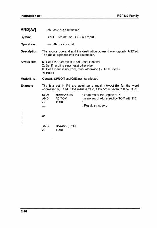
AND[.W] source AND destination
Syntax AND src,dst or AND.W src,dst
Operation src .AND. dst -> dst
Description The source operand and the destination operand are logically AND'ed. The result is placed into the destination.
Status Bits N: Set if MSB of result is set, reset if not set Z: Set if result is zero, reset otherwise C: Set if result is not zero, reset otherwise (= .NOT. Zero) V: Reset
Mode Bits OscOff, CPUOff and GIE are not affected
Example The bits set in R5 are used as a mask (#OAA55h) for the word addressed by TOM. If the result is zero, a branch is taken to label TONI
2-16
MOV AND JZ
or
#OAA55h,R5 R5,TOM TONI
AND #OAA55h,TOM JZ TONI
; Load mask into register R5 ; mask word addressed by TOM with R5 , ; Result is not zero

MSP430 Family Instruction set
AND.B source AND destination
Syntax AND.S src,dst
Operation src .AND. dst -> dst
Description The source operand and the destination operand are logically AND'ed. The result is placed into the destination.
Status Bits N: Set if MSB of result is set, reset if not set Z: Set if result is zero, reset otherwise C: Set if result is not zero, reset otherwise ( = .NOT. Zero) V: Reset
Mode Bits OscOff, CPUOff and GIE are not affected
Example The bits of mask #OA5h are logically AND'ed with the Lowbyte TOM. If the result is zero, a branch is taken to label TONI
AND.S #OA5h,TOM ; mask Lowbyte TOM with R5 JZ TONI
; Result is not zero
2-17

Instruction set MSP430 Family
BIC[.W] Clear bits in destination
Syntax BICsrc,dst or BIC.w src,dst
Operation .NOT.src .AND. dst -> dst
Description The inverted source operand and the destination operand are logically AND'ed. The result is placed into the destination. The source operand is not affected.
Status Bits N: Not affected Z: Not affected C: Not affected V: Not affected
Mode Bits OscOff, CPUOff and GIE are not affected
Example The 6 MSBs of the RAM word LEO are cleared.
BIC#OFCOOh,LEO ; Clear 6 MSBs in MEM(LEO)
2-18

MSP430 Family Instruction set
BIC.B Clear bits in destination
Syntax BIC.B src,dst
Operation .NOT.src .AND. dst -> dst
Description The inverted source operand and the destination operand are logically AND'ed. The result is placed into the destination. The source operand is not affected.
Status Bits N: Not affected Z: Not affected C: Not affected V: Not affected
Mode Bits OscOtt, CPUOff and GIE are not affected
Example
Example
The 5 MSBs of the RAM byte LEO are cleared.
BIC.B #OF8h,LEO ; Clear 5 MSBs in Ram location LEO
The Portpins PO and P1 are cleared.
POOUT .equ PO .equ P1 .equ
011h 01h 02h
;Definition of the Portaddress
BIC.B #PO+P1,&POOUT ;Set PO and P1 to low
2-19

Instruction set MSP430 Family
BIS[.W] Set bits in destination
Syntax SIS src,dst or SIS.w src,dst
Operation src .OR. dst -> dst
Description The source operand and the destination operand are logically OR'ed. The result is placed into the destination. The source operand is not affected.
Status Bits N: Not affected Z: Not affected C: Not affected V: Not affected
Mode Bits OscOff, CPUOff and GIE are not affected
Example The 6 LSS's of the RAM word TOM are set.
Example
2-20
SIS #003Fh,TOM ; set the 6 LSS's in RAM location TOM
Start an AID-conversion
ASOC .equ ACTL .equ
1 114h
SIS #ASOC,&ACTL
;Start of Conversion bit ;ADC-Control Register
;Start AID-conversion

MSP430 Family Instruction set
BIS.B Set bits in destination
Syntax BIS.B src,dst
Operation src .OR. dst -> dst
Description The source operand and the destination operand are logically OR'ed. The result is placed into the destination. The source operand is not affected.
Status Bits N: Not affected Z: Not affected C: Not affected V: Not affected
Mode Bits OscOff, CPUOff and GIE are not affected
Example The 3 MSBs of the RAM byte TOM are set.
BIS.B #OEOh,TOM; set the 3 MSBs in RAM location TOM
Example The Portpins PO and P1 are set to high
POOUT .equ 011 h PO .equ 01h P1 .equ 02h
BIS.B #PO+P1,&POOUT
2-21

Instruction set MSP430 Family
BIT[.W] Test bits in destination
Syntax BIT src,dst or BIT.W src,dst
Operation src .AND. dst
Description The source operand and the destination operand are logically AND'ed. The result affects only the Status Bits. The source and destination operands are not affected.
Status Bits N: Set if MSB of result is set, reset if not set Z: Set if result is zero, reset otherwise C: Set if result is not zero, reset otherwise (.NOT. Zero) V: Reset
Mode Bits OscOff, CPUOff and GIE are not affected
Example If bit 9 of R8 is set, a branch is taken to label TOM.
Example
2-22
BIT JNZ
#0200h,R8 TOM
; bit 9 of R8 set? ; Yes, branch to TOM ; No, proceed
Determine which AID-Channel is configured by the MUX
ACTL
BIT jnz
.equ 114h
#4,&ACTL END
;ADC Control Register
;Is Channel 0 selected? ;Yes, branch to END

MSP430 Family Instruction set
SIT.S Test bits in destination
Syntax BITB src,dst
Operation src .AND. dst
Description The source operand and the destination operand are logically AND'ed. The result affects only the Status Bits: the source and destination operands are not affected.
Status Bits N: Set if MSB of result is set, reset if not set Z: Set if result is zero, reset otherwise C: Set if result is not zero, reset otherwise (.NOT. Zero) V: Reset
Mode Bits OscOff, CPUOff and GIE are not affected
Example If bit 3 of R8 is set, a branch is taken to label TOM. BITB #8,R8 JC TOM
Example ; The receive bit RCV of a serial communication is tested. Since while using the BIT
; instruction to test a single bit the carry is equal to the state of the tested bit, the carry is ; used by the subsequent instruction: the read info is shifted into the register RECBUF.
; Serial communication with LSB is shifted first:
BITB RRC
#RCV,RCCTL RECBUF
; Serial communication with MSB is shifted first:
; xxxx xxxx xxxx xxxx ; Bit info into carry ; Carry -> MSB of RECBUF ; cxxx xxxx ; repeat previous two instructions ; 8 times ; cccc CCCC ./\ /\
; MSB LSB
BITB #RCV,RCCTL ; Bit info into carry RLC.B RECBUF ; Carry -> LSB of RECBUF
; xxxx xxxc ; repeat previous two instructions ; 8 times ; cccc cccc ; I LSB ; MSB
2-23

Instruction set MSP430 Family
* BR, BRANCH Branch to .......... destination
Syntax BR dst
Operation dst -> PC
Emulation MOV dst,PC
Description An unconditional branch is taken to an address anywhere in the 64 K address space. All source addressing modes may be used. The branch instruction is a word instruction.
Status Bits Status bits are not affected
Examples Examples for all addressing modes are given
BR #EXEC
BR EXEC
BR &EXEC
BR R5
BR @R5
BR @R5+
2-24
; Branch to label EXEC or direct branch (e.g #OA4h) ; Core instruction MOV @PC+,PC
; Branch to the address contained in EXEC ; Core instruction MOV X(PC),PC ; Indirect address
; Branch to the address contained in absolute ; address ; EXEC ; Core instruction MOV X(O),PC ; Indirect address
; Branch to the address contained in R5 ; Core instruction MOV R5,PC ; Indirect R5
; Branch to the address contained in the word R5 ; points ; to. Core instruction MOV @R5,PC ; Indirect, indirect R5
; Branch to the address contained in the word R5 ; points to and increments pOinter in R5 afterwards. ; The next time - SIW flow uses R5 pointer - it can ; alter the programme execution due to access to ; next address in a table, pointed by R5 ; Core instruction MOV @R5,PC ; Indirect, indirect R5 with autoincrement

MSP430 Family
BR X(R5)
Instruction set
; Branch to the address contained in the address ; pointed to by R5 + X (e.g table with address start; ing at X). X can be an address or a label ; Core instruction MOV X(R5),PC ; Indirect indirect R5 + X
2-25

Instruction set
CALL
Syntax
Operation
Subroutine
CALL dst
dst SP-2 PC tmp
-> tmp -> SP -> @SP -> PC
dst is evaluated and stored
updated PC to TOS saved dst to PC
MSP430 Family
Description A subroutine call is made to an address anywhere in the 64-K-address space. All addressing modes may be used. The return address (the address of the following instruction) is stored on the stack. The call instruction is a word instruction.
Status Bits Status bits are not affected
Example Examples for all addressing modes are given
2·26
CALL #EXEC ; Call on label EXEC or immediate address (e.g ; #OA4h) ; SP-2 ~ SP, PC+2 ~ @SP, @PC+ ~ PC
CALL EXEC ; Call on the address contained in EXEC ; SP-2 ~ SP, PC+2 ~ @SP, X(PC) ~ PC ; Indirect address
CALL &EXEC ; Call on the address contained in absolute address ; EXEC ; SP-2 ~ SP, PC+2 ~ @SP, X(PC) ~ PC ; Indirect address
CALL RS ; Call on the address contained in RS ; SP-2 ~ SP, PC+2 ~ @SP, RS ~ PC ; Indirect RS
CALL @RS ; Call on the address contained in the word RS ; points ;to ; SP-2 ~ SP, PC+2 ~ @SP, @RS ~ PC ; Indirect, indirect RS
CALL @RS+ ; Call on the address contained in the word RS points ; to and increments pointer in RS. The next time -; SIW flow uses RS pointer - it can alter the ; programme execution due to access to next address ; in a table, pointed; to by RS ; SP-2 ~ SP, PC+2 ~ @SP, @RS ~ PC ; Indirect, indirect RS with autoincrement
CALL X(RS) ; Call on the address contained in the address pointed ; to by RS + X (e.g table with address starting at X) ; X can be an address or a label ; SP-2 ~ SP, PC+2 ~ @SP, X(RS) ~ PC ; Indirect indirect RS + X

MSP430 Family Instruction set
* CLR[.W] Clear destination
Syntax
Operation
Emulation
CLR
0-> dst
MOV
dst or CLR.w dst
#O,dst
Description The destination operand is cleared.
Status Bits Status bits are not affected
Example RAM word TONI is cleared
CLR TONI ; 0 -> TONI
Example Register R5 is cleared
CLR R5
2-27

Instruction set
* CLR.B
Syntax
Operation
Emulation
Clear destination
CLR.B dst
0-> dst
MOV.B #O,dst
Description The destination operand is cleared.
Status Bits Status bits are not affected
Example RAM byte TONI is cleared
CLR.B TONI ; 0 -> TONI
2-28
MSP430 Family

MSP430 Family Instruction set
* CLRC Clear carry bit
Syntax CLRC
Operation 0 -> C
Emulation BIC#1,SR
Description The Carry Bit C is cleared. The clear carry instruction is a word instruction.
Status Bits N: Not affected Z: Not affected C: Cleared V: Not affected
Mode Bits OscOff, CPUOff and GIE are not affected
Example The 16bit decimal counter pointed to by R13 is added to a 32bit counter pointed to by R12.
CLRC DADD @R13,O(R12)
DADC 2(R12)
; C=O: Defines start ; add 16bit counter to Lowword of 32bit ; counter ; add carry to Highword of 32bit counter
2-29

Instruction set
*CLRN
Syntax CLRN
Operation
Clear Negative bit
O~N or (.NOT.src .AND. dst -> dst)
Emulation BIC#4,SR
MSP430 Family
Description The constant 04h is inverted (OFFFBh) and the destination operand are logically AND'ed. The result is placed into the destination. The clear negative bit instruction is a word instruction.
Status Bits N: Reset to 0 Z: Not affected C: Not affected V: Not affected
Mode Bits OscOff, CPUOff and GIE are not affected
Example The Negative bit in the status register is cleared. This avoids the special treatment of the called subroutine with negative numbers.
CLRN CALL SUBR
SUBR IN SUBRET ; If input is negative: do nothing and return
SUBRET RET
2-30

MSP430 Family Instruction set
* CLRZ Clear Zero bit
Syntax CLRZ
Operation 0 ~ Z or (.NOT.src .AND. dst -> dst)
Emulation BIC#2,SR
Description The constant 02h is inverted (OFFFDh) and the destination operand are logically AND'ed. The result is placed into the destination. The clear zero bit instruction is a word instruction.
Status Bits N: Not affected Z: Reset to 0 C: Not affected V: Not affected
Mode Bits OscOff, CPUOff and GIE are not affected
Example The Zero bit in the status register is cleared.
CLRZ
2-31

Instruction set
CMP[.W]
Syntax
Operation
compare source and destination
CMP src,dst or CMP.w src,dst
dst + .NOT.src + 1 or (dst - src)
MSP430 Family
Description The source operand is subtracted from the destination operand. This is made by adding of the 1 's complement of the source operand plus 1. The two operands are not affected, the result is not stored, only the status bits are affected.
Status Bits N: Set if result is negative, reset if positive (src >= dst) Z: Set if result is zero, reset otherwise (src = dst) C: Set if there is a carry from the MSB of the result, reset if not V: Set if an arithmetic overflow occurs, otherwise reset
Mode Bits OscOff, CPUOff and GIE are not affected
Example RS and R6 are compared. If they are equal, the programme continues at the label EQUAL
Example
2-32
CMP JEQ
RS,R6 EQUAL
; RS = R6? ; YES, JUMP
Two RAM blocks are compared. If they not equal, the programme branches to the label ERROR
MOV L$1 CMP
JNZ DEC JNZ
#NUM,RS &BLOCK1,&BLOCK2 ERROR RS L$1
;number of words to be compared ;Are Words equal? ;No, branch to ERROR ;Are all words compared? ;No, another compare

MSP430 Family Instruction set
CMP.B compare source and destination
Syntax
Operation
CMP.8 src,dst
dst + .NOT.src + 1 or (dst - src)
Description The source operand is subtracted from the destination operand. This is made by adding of the 1 's complement of the source operand plus 1. The two operands are not affected, the result is not stored, only the status bits are affected.
Status Bits N: Set if result is negative, reset if positive (src >= dst) Z: Set if result is zero, reset otherwise (src = dst) C: Set if there is a carry from the MSB of the result, reset if not V: Set if an arithmetic overflow occurs, otherwise reset
Mode Bits OscOff, CPUOff and GIE are not affected
Example The RAM bytes addressed by EDE and TONI are compared. If they are equal, the programme continues at the label EQUAL
Example
CMP.B JEQ
EDE,TONI ; MEM(EDE) = MEM(TONI) ? EQUAL ; YES, JUMP
Check two Keys, which are connected to the Portpin PO and P1. If key1 is pressed, the programme branches to the label MENU1, if key2 is pressed, the programme branches to MENU2 .
POIN . EQU 010h KEY1 .EQU 01h KEY2 .EQU 02h
CMP.B #KEY1,&POIN JEQ MENU1 CMP.B #KEY2,&POIN JEQ MENU2
2-33
Instruction set MSP430 Family
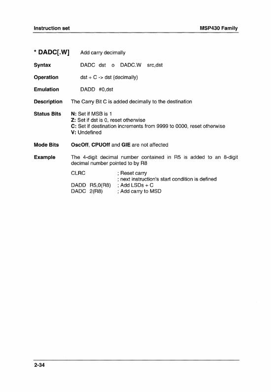
* DADC[.W] Add carry decimally
Syntax DADC dst 0 DADC.w src,dst
Operation dst + C -> dst (decimally)
Emulation DADD #O,dst
Description The Carry Bit C is added decimally to the destination
Status Bits N: Set if MSB is 1
Mode Bits
Example
2-34
Z: Set if dst is 0, reset otherwise C: Set if destination increments from 9999 to 0000, reset otherwise V: Undefined
OscOff, CPUOff and GIE are not affected
The 4-digit decimal number contained in R5 is added to an 8-digit decimal number pointed to by R8
CLRC
DADD R5,0(R8) DADC 2(R8)
; Reset carry ; next instruction's start condition is defined ; Add LSDs + C ; Add carry to MSD

MSP430 Family Instruction set
* DADC.B Add carry decimally
Syntax DADC.B dst
Operation dst + C -> dst (decimally)
Emulation DADD.B #O,dst
Description The Carry Bit C is added decimally to the destination
Status Bits N: Set if MSB is 1
Mode Bits
Z: Set if dst is 0, reset otherwise C: Set if destination increments from 99 to 00, reset otherwise V: Undefined
OscOff, CPUOff and GIE are not affected
Example The 2-digit decimal number contained in R5 is added to an 4-digit decimal number pOinted to by R8
CLRC
DADD.B R5,0(R8) DADC 1(R8)
; Reset carry ; next instruction's start condition is ; defined ; Add LSDs+ C ; Add carry to MSDs
2-35

Instruction set MSP430 Family
DADD[.W] source and carry added decimally to destination
Syntax DADD src,dst or DADD.W src,dst
Operation src + dst + C -> dst (decimally)
Description The source operand and the destination operand are treated as four binary coded decimals (BCD) with positive signs. The source operand and the carry C are added decimally to the destination operand. The source operand is not affected, the previous contents of the destination are lost. The result is not defined for non-BCD numbers.
Status Bits N: Set if the MSB is 1, reset otherwise Z: Set if result is zero, reset otherwise C: Set if the result is greater than 9999. V: Undefined OscOff, CPUOff and GIE are not affected
Example The 8-digit-BCD-number contained in RS and R6 is added decimally to a 8-digit-BCD-number contained in R3 and R4 (R6 and R4 contain the MSDs).
2-36
CLRC DADD DADD JC
RS,R3 R6,R4 OVERFLOW
; CLEAR CARRY ; add LSDs ; add MSDs with carry ; If carry occurs go to error handling routine

MSP430 Family Instruction set
DADD.B source and carry added decimally to destination
Syntax DADD.B src,dst
Operation src + dst + C -> dst (decimally)
Description The source operand and the destination operand are treated as two binary coded decimals (BCD) with positive signs. The source operand and the carry C are added decimally to the destination operand. The source operand is not affected, the previous contents of the destination are lost. The result is not defined for non-BCD numbers.
Status Bits N: Set if the MSB is 1, reset otherwise Z: Set if result is zero, reset otherwise C: Set if the result is greater than 99. V: Undefined OscOtt, CPUOtt and GIE are not affected
Example The 2-digit decimal counter in RAM byte CNT is incremented by one.
CLRC DADD.B
or
SETC DADD.B
#1,CNT
#O,CNT
; clear Carry ; increment decimal counter
; =DADC.B CNT
2-37
Instruction set MSP430 Family
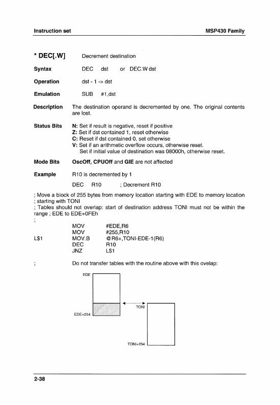
* DEC[.W] Decrement destination
Syntax DEC dst or DEC.Wdst
Operation dst - 1 -> dst
Emulation SUB #1,dst
Description The destination operand is decremented by one. The original contents are lost.
Status Bits N: Set if result is negative, reset if positive Z: Set if dst contained 1, reset otherwise C: Reset if dst contained 0, set otherwise V: Set if an arithmetic overflow occurs, otherwise reset.
Set if initial value of destination was 08000h, otherwise reset.
Mode Bits OscOff, CPUOff and GIE are not affected
Example R10 is decremented by 1
DEC R10 ; Decrement R10
; Move a block of 255 bytes from memory location starting with EDE to memory location ; starting with TONI ; Tables should not overlap: start of destination address TONI must not be within the range; EDE to EDE+OFEh
L$1
2-38
MOV MOV MOV.B DEC JNZ
#EDE,R6 #255,R10 @R6+,TONI-EDE-1(R6) R10 L$1
Do not transfer tables with the routine above with this ovelap:
EDE ,----.,
EDE+254
+--_.,-----, TONI
TONI+254'--__ --'

MSP430 Family Instruction set
* DEC.B Decrement destination
Syntax DEC.B dst
Operation dst·1 .> dst
Emulation SUB.B #1,dst
Description The destination operand is decremented by one. The original contents are lost.
Status Bits N: Set if result is negative, reset if positive Z: Set if dst contained 1, reset otherwise C: Reset if dst contained 0, set otherwise V: Set if an arithmetic overflow occurs, otherwise reset.
Set if initial value of destination was OaOh, otherwise reset.
Mode Bits OscOff, CPUOff and GIE are not affected
Example Memory byte at address LEO is decremented by 1
DEC.B LEO ; Decrement MEM(LEO)
; Move a block of 255 bytes from memory location starting with EDE to memory location ; starting with TONI ; Tables should not overlap: start of destination address TONI must not be within the range; EDE to EDE+OFEh
L$1
MOV MOV.B MOV.B DEC.B JNZ
#EDE,RS #255,LEO @RS+,TONI-EDE-1(RS) LEO L$1
2-39

Instruction set MSP430 Family
* DECD[.W] Double-Decrement destination
Syntax DECO dst or DECDW dst
Operation dst - 1 -> dst
Emulation SUB #2,dst
Description The destination operand is decremented by two. The original contents are lost.
Status Bits N: Set if result is negative, reset if positive Z: Set if dst contained 2, reset otherwise
Mode Bits
Example
C: Reset if dst contained 0 or 1, set otherwise V: Set if an arithmetic overflow occurs, otherwise reset.
Set if initial value of destination was 08001 or 08000h, otherwise reset.
OscOff, CPUOff and GIE are not affected
R 10 is decremented by 2
DECO R10 ; Decrement R10 by two
; Move a block of 255 words from memory location starting with EDE to memory location ; starting with TONI ; Tables should not overlap: start of destination address TONI must not be within the range; EDE to EDE+OFEh
L$1
2-40
MOV MOV MOV DECO JNZ
#EDE,R6 #510,R10 @R6+,TONI-EDE-2(R6) R10 L$1

MSP430 Family Instruction set
* DECD.B Double-Decrement destination
Syntax DECD.B dst
Operation dst - 2 -> dst
Emulation SUB.B #2,dst
Description The destination operand is decremented by two. The original contents are lost.
Status Bits N: Set if result is negative, reset if positive Z: Set if dst contained 2, reset otherwise C: Reset if dst contained 0 or 1, set otherwise V: Set if an arithmetic overflow occurs, otherwise reset.
Set if initial value of destination was 081 or 080h, otherwise reset.
Mode Bits OscOtt, CPUOtt and GIE are not affected
Example Memory at location LEO is decremented by 2
DECD.B LEO ; Decrement MEM(LEO)
Decrement status byte STATUS by 2
DECD.B STATUS
2-41

Instruction set MSP430 Family
* DINT Disable (general) interrupts
Syntax
Operation
DINT
O~GIE or (OFFF7h .AND. SR ~ SR .NOT.src .AND. dst -> dst)
Emulation BIC #8,SR
Description All interrupts are disabled. The constant #08h is inverted and logically AND'ed with the status register SA. The result is placed into the SA.
Status Bits N: Not affected Z: Not affected C: Not affected V: Not affected
Mode Bits GIE is reset. OscOff and CPUOff are not affected
Example The general interrupt enable bit GIE in the status register is cleared to allow a non disrupted move of a 32bit counter. This ensures that the counter is not modified during the move by any interrupt.
DINT
MOV MOV EINT
COUNTHI,R5 COUNTLO,R6
Note: Disable Interrupt
; All interrupt events using the GIE bit are
; disabled ; Copy counter
; All interrupt events using the GIE bit are ; enabled
The instruction following the disable interrupt instruction DINT is executed when the interrupt request becomes active during execution of DINT. If any code sequence needs to be protected from being interrupted the DINT instruction should be executed at least one instruction before this sequence.
2-42

MSP430 Family Instruction set
* EINT Enable (general) interrupts
Syntax EINT
Operation 1 ~ GIE or (0008h .OR. SR -> SR / .NOT.src .OR. dst -> dst)
Emulation BIS #8,SR
Description All interrupts are enabled. The constant #08h and the status register SR are logically OR'ed. The result is placed into the SR.
Status Bits N: Not affected Z: Not affected C: Not affected V: Not affected
Mode Bits GIE is set. OscOff and CPUOff are not affected
Example The general interrupt enable bit GIE in the status register is set.
; Interrupt routine of port PO.2 to PO.? ; The interrupt level is the lowest in the system ; POIN is the address of the register where all port bits are read. POIFG is the address of ; the register where all interrupt events are latched.
MaskOK
PUSH.B BIC.B EINT
BIT JEQ
BIC
INCD
RETI
&POIN @SP,&POIFG ; Reset only accepted flags
#Mask,@SP
; Preset port 0 interrupt flags stored on stack ; other interrupts are allowed
MaskOK ; Flags are present identically to mask: Jump
#Mask,@SP
SP ; Housekeeping: Inverse to PUSH instruction ; at the start of interrupt subroutine. Corrects ; the stack pointer.
Note: Enable Interrupt
The instruction following the enable interrupt instruction EINT is executed anyway even on a pending interrupt service request
2-43

Instruction set MSP430 Family
* INC[.W] Increment destination
Syntax INC dst or INC.W dst
Operation dst + 1 -> dst
Emulation ADD #1,dst
Description The destination operand is incremented by one. The original contents are lost.
Status Bits N: Set if result is negative, reset if positive Z: Set if dst contained OFFFFh, reset otherwise C: Set if dst contained OFFFFh, reset otherwise V: Set if dst contained 07FFFh, reset otherwise
Mode Bits OscOff, CPUOff and GIE are not affected
Example The item on the top of a software stack (not the system stack) for byte data is removed.
SSP .EQU R4
2-44
INC SSP ; Remove TOSS (top of SW stack) by increment ; Do not use INC.B since SSP is a word register
MSP430 Family Instruction set
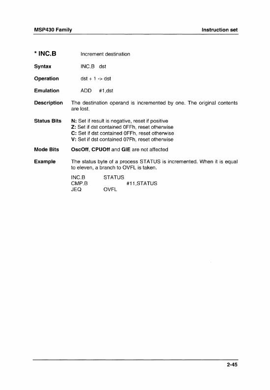
* INC.B Increment destination
Syntax INC.B dst
Operation dst + 1 -> dst
Emulation ADD #1,dst
Description The destination operand is incremented by one. The original contents are lost.
Status Bits N: Set if result is negative, reset if positive Z: Set if dst contained OFFh, reset otherwise C: Set if dst contained OFFh, reset otherwise V: Set if dst contained 07Fh, reset otherwise
Mode Bits OscOff, CPUOff and GIE are not affected
Example The status byte of a process STATUS is incremented. When it is equal to eleven, a branch to OVFL is taken.
INC.B CMP.B JEQ
STATUS
OVFL #11 ,STATUS
2-45

Instruction set MSP430 Family
* INCD[.W] Double-Increment destination
Syntax INCD dst or INCD.w dst
Operation dst + 2 -> dst
EmulationADD #2,dst
Description The destination operand is incremented by two. The original contents are lost.
Status Bits N: Set if result is negative, reset if positive Z: Set if dst contained OFFFEh, reset otherwise C: Set if dst contained OFFFEh or OFFFFh, reset otherwise V: Set if dst contained 07FFEh or 07FFFh, reset otherwise
Mode Bits OscOff, CPUOff and GIE are not affected
Example The item on the top of the stack is removed without the use of a register.
SUB
2-46
PUSH RS ;RS is the result of a calculation, which is stored in the ; Stack
INCD SP ;Remove TOS by double-increment from stack Do not use INCD.B, SP is a word aligned register
RET
MSP430 Family Instruction set
* INCD.B Double-Increment destination
Syntax INCD.B dst
Operation dst + 2 -> dst
Emulation ADD.B #2,dst
Description The destination operand is incremented by two. The original contents are lost.
Status Bits N: Set if result is negative, reset if positive Z: Set if dst contained OFEh, reset otherwise C: Set if dst contained OFEh or OFFh, reset otherwise V: Set if dst contained 07Eh or 07Fh, reset otherwise
Mode Bits OscOff, CPUOff and GIE are not affected
Example The byte on the top of the stack is incremented by two.
INCD.B O(SP) ; Byte on TOS is increment by two
2-47

Instruction set MSP430 Family
* INV[.W] Invert destination
Syntax INVdst
Operation .NOT.dst -> dst
Emulation XOR #OFFFFh,dst
Description The destination operand is inverted. The original contents are lost.
Status Bits N: Set if result is negative, reset if positive Z: Set if dst contained OFFFFh, reset otherwise C: Set if result is not zero, reset otherwise ( = .NOT. Zero) V: Set if initial destination operand was negative, otherwise reset OscOff, CPUOff and GIE are not affected
Example Content of R5 is negated (two's complement).
2-48
MOV INV INC
#OOAeh,R5 R5 R5
; Invert R5, ; R5 is now negated,
R5 = OOOAEh R5 = OFF51h R5 = OFF52h

MSP430 Family Instruction set
* INV.B Invert destination
Syntax INV.B dst
Operation .NOT.dst -> dst
Emulation XOR #OFFh,dst
Description The destination operand is inverted. The original contents are lost.
Status Bits N: Set if result is negative, reset if positive Z: Set if dst contained OFFh, reset otherwise C: Set if result is not zero, reset otherwise ( = .NOT. Zero) V: Set if initial destination operand is negative, otherwise reset
Mode Bits OscOff, CPUOff and GIE are not affected
Example Content of memory byte LEO is negated.
MOV.B INV.B INC.B
#OAEh,LEO LEO ; Invert LEO, LEO ; MEM(LEO) is now negated,
MEM(LEO) = OAEh MEM(LEO) = 051 h MEM(LEO) = 052h
2-49

Instruction set
JC JHS
Syntax
Jump if carry set
Jump if higher or same
JC JHS
label label
MSP430 Family
Operation if C = 1: PC + 2'offset -> PC if C = 0: execute following instruction
Description The Carry Bit C of the Status Register is tested. If it is set, the 10-bit signed offset contained in the LSB's of the instruction is added to the Programme Counter. If C is reset, the next instruction following the jump is executed. JC Gump if carry/higher or same) is used for the comparison of unsigned numbers (0 to 65536).
Status Bits Status bits are not affected
Example The signal of input POIN.1 is used to define or control the programme flow.
Example
2-50
BIT #10h,&POIN; State of signal-> Carry JC PROGA ; If carry=1 then execute programme routine A
; Carry=O, execute programme here
R5 is compared to 15. If the content is higher or same branch to LABEL.
CMP JHS
#15,R5 LABEL ; Jump is taken if R5 ;:: 15
; Continue here if R5 < 15

MSP430 Family Instruction set
JEQ, JZ Jump if equal, Jump if zero
Syntax JEQ label, JZ label
Operation if Z = 1: PC + 2*offset -> PC if Z = 0: execute following instruction
Description The Zero Bit Z of the Status Register is tested. If it is set, the 10-bit signed offset contained in the LSB's of the instruction is added to the Programme Counter. If Z is not set, the next instruction following the jump is executed.
Status Bits Status bits are not affected
Example Jump to address TONI if R7 contains zero.
Example
Example
TST JZ
R7 TONI
; Test R7 ; if zero: JUMP
Jump to address LEO if RS is equal to the table contents.
CMP RS,Table(RS); Compare content of RS with content of ; MEM(Table address + content of RS)
JEQ LEO ; Jump if both data are equal ; No, data are not equal, continue here
Branch to LABEL if RS is o.
TST RS JZ LABEL
2-51

Instruction set MSP430 Family
JGE Jump if greater or equal
Syntax JGE label
Operation if (N .XOR. V) = 0 then jump to label: PC + 2*offset -> PC if (N .XOR. V) = 1 then execute following instruction
Description The negative bit N and the overflow bit V of the Status Register are tested. If both N and V are set or reset, the 10-bit signed offset contained in the LS8's of the instruction is added to the Programme Counter. If only one is set, the next instruction following the jump is executed. This allows comparison of signed integers.
Status Bits Status bits are not affected
Example When the content of R6 is greater or equal the memory pointed to by R7 the programme continues at label EDE.
2-52
CMP JGE
@R7,R6 EDE
; R6 ~ (R7)?, compare on signed numbers ; Yes, R6 ~ (R7) ; No, proceed
MSP430 Family Instruction set
JL Jump if less
Syntax JL label
Operation if (N .xOR. V) = 1 then jump to label: PC + 2*offset -> PC if (N .xOR. V) = 0 then execute following instruction
Description The negative bit N and the overflow bit V of the Status Register are tested. If only one is set, the 10-bit signed offset contained in the LSB's of the instruction is added to the Programme Counter. If both N and V are set or reset, the next instruction following the jump is executed. This allows comparison of signed integers.
Status Bits Status bits are not affected
Example When the content of R6 is less than the memory pointed to by R7 the programme continues at label EDE.
CMP JL
@R7,R6 EDE
; R6 < (R7)?, compare on signed numbers ; Yes, R6 < (R7) ; No, proceed
2-53

Instruction set MSP430 Family
JMP Jump unconditionally
Syntax JMP label
Operation PC + 2*offset -> PC
Description The 10-bit signed offset contained in the LSB's of the instruction is added to the Programme Counter.
Status Bits Status bits are not affected
Hint This 1 word instruction replaces the BRANCH instruction in the range of -511 to +512 words relative to the current programme counter.
2-54

MSP430 Family Instruction set
IN Jump if negative
Syntax JN label
Operation if N = 1: PC + 2*offset -> PC if N = 0: execute following instruction
Description The negative bit N of the Status Register is tested. If it is set, the 10-bit signed offset contained in the LSB's of the instruction is added to the Programme Counter. If N is reset, the next instruction following the jump is executed.
Status Bits Status bits are not affected
Example The result of a computation in RS is to be subtracted from COUNT. If the result is negative, COUNT is to be cleared and the programme continues execution in another path.
L$1
SUB JN
RS,COUNT L$1
CLR COUNT
; COUNT - RS -> COUNT ; If negative continue with COUNT =Oat PC=L$1 ; Continue with COUNT2':O
2-55

Instruction set
JNC JLO
Syntax
Jump if carry not set
Jump if lower
JNC label JNC label
MSP430 Family
Operation if C = 0: PC + 2'offset -> PC if C = 1: execute following instruction
Description The Carry Bit C of the Status Register is tested. If it is reset, the 10-bit signed offset contained in the LSB's of the instruction is added to the Programme Counter. If C is set, the next instruction following the jump is executed. JNC (jump if no carry/lower) is used for the comparison of unsigned numbers (0 to 65536).
Status Bits status bits are not affected
Example The result in R6 is added in BUFFER. If an overflow occurs an error handling routine at address ERROR is going to be used.
ERROR
CONT
Example
2-56
ADD JNC
R6,BUFFER CONT
; BUFFER + R6 -> BUFFER ; No carry, jump to CO NT ; Error handler start
; Continue with normal programme flow
Branch to STL2 if byte STATUS contains 1 or o. CMP.B JLO
#2,STATUS STL2 ; STATUS <2
; STATUS?: 2, continue here

MSP430 Family Instruction set
JNE, JNZ Jump if not equal, Jump if not zero
Syntax JNE label, JNZ label
Operation if Z = 0: PC + 2*offset -> PC if Z = 1: execute following instruction
Description The Zero Bit Z of the Status Register is tested. If it is reset, the 10-bit signed offset contained in the LSB's of the instruction is added to the Programme Counter. If Z is set, the next instruction following the jump is executed.
Status Bits Status bits are not affected
Example Jump to address TONI if R7 and R8 have different contents
CMP R7,R8 JNE TONI
; COMPARE R7 WITH R8 ; if different: Jump ; if equal, continue
2-57

Instruction set MSP430 Family
MOV[.W] Move source to destination
Syntax MOV src,dst or MOV.w src,dst
Operation src -> dst
Description The source operand is moved to the destination. The source operand is not affected, the previous contents of the destination are lost.
Status Bits Status bits are not affected
Mode Bits OscOff, CPUOff and GIE are not affected
Example The contents of table EDE (word data) are copied to table TOM. The length of the tables should be 020h locations.
Loop
2-58
MOV MOV MOV DEC JNZ
#EDE,R10 #020h,R9 @R10+,TOM-EDE-2(R10) R9 Loop
; Prepare pointer ; Prepare counter ; Use pointer in R10 for both tables ; Decrement counter ; Counter "# 0, continue copying ; Copying completed

MSP430 Family Instruction set
MOV.B Move source to destination
Syntax MOV.B src,dst
Operation src -> dst
Description The source operand is moved to the destination. The source operand is not affected, the previous contents of the destination are lost.
Status Bits Status bits are not affected
Mode Bits OscOff, CPUOff and GIE are not affected
Example The contents of table EDE (byte data) are copied to table TOM. The length of the tables should be 020h locations.
Loop
MOV MOV
DEC JNZ
#EDE,R10 #020h,R9 MOV.B @R10+,TOM-EDE-1 (R1 0)
R9 Loop
; Prepare pointer ; Prepare counter ; Use pointer in R10 for ; both tables ; Decrement counter ; Counter", 0, continue ; copying ; Copying completed
2-59

Instruction set MSP430 Family
*NOP No operation
Syntax NOP
Operation None
Emulation MOV #0,#0
Description No operation is performed. The instruction may be used for the elimination of instructions during the software check or for defined waiting times.
Status Bits Status bits are not affected
The NOP instruction is mainly used for two purposes: • hold one, two or three memory words • adjust software timing
Note: Other instructions can be used to emulate no operation
Other instructions can be used to emulate no-operation instruction using different numbers of cycles and different numbers of code words.
Examples: MOV 0(R4),0(R4) MOV @R4,0(R4) BIC #0,EDE(R4) JMP $+2 BIC #0,R5
2-60
; 6 cycles, 3 words ; 5 cycles, 2 words ; 4 cycles, 2 words ; 2 cycles, 1 word ; 1 cycles, 1 word.

MSP430 Family Instruction set
* POP[.W] Pop word from stack to destination
Syntax
Operation
Emulation
POP dst
@SP -> dst SP + 2 -> SP
MOV @SP+,dst or MOV.w @SP+,dst
Description The stack location pointed to by the Stack Pointer (TOS) is moved to the destination. The Stack Pointer is incremented by two afterwards.
Status Bits Status bits are not affected
Example The contents of R7 and the Status Register are restored from the stack.
POP R7 ; Restore R7 POP SR ; Restore status register
Note: The system Stack Pointer SP, Note 1
The system Stack Pointer SP is always incremented by two, independent of the byte suffix. This is mandatory since the system Stack Pointer is used not only by POP instructions; it is also used by the RETI instruction.
2-61

Instruction set MSP430 Family
* POP.B Pop byte from stack to destination
Syntax POP.B dst
Operation @SP -> dst SP + 2 -> SP
Emulation MOV.B @SP+,dst
Description The stack location pointed to by the Stack Pointer (TOS) is moved to the destination. The Stack Pointer is incremented by two afterwards.
Status Bits Status bits are not affected
Example The content of RAM byte LEO is restored from the stack.
Example
Example
POP.B LEO ; The Low byte of the stack is moved to LEO.
The content of R7 is restored from the stack.
POP.B R7 ; The Low byte of the stack is moved to R7, ; the High byte of R7 is OOh
The contents of the memory pointed to by R7 and the Status Register are restored from the stack.
POP.B O(R7)
POP SR
; The Low byte of the stack is moved to the ; the byte which is pointed to by R7 : Ex1: R7 = 203h
Mem(R7) = Low Byte of system stack , : Ex2: R7 = 20Ah
Mem(R7) = Low Byte of system stack
Note: The system Stack Pointer, Note 2
The system Stack Pointer SP is always incremented by two, independent of the byte suffix. This is mandatory since the system Stack Pointer is used not only by POP instructions; it is also used by the RETI instruction.
2-62

MSP430 Family Instruction set
PUSH[.W] Push word onto stack
Syntax
Operation
PUSH src or PUSH.w src
SP-2 ~ SP src~ @SP
Description The Stack Pointer is decremented by two, then the source operand is moved to the RAM word addressed by the Stack Pointer (TOS).
Status Bits N: Not affected Z: Not affected C: Not affected V: Not affected
Mode Bits OscOff, CPUOff and GIE are not affected
Example The contents of the Status Register and R8 are saved on the stack.
PUSH SR PUSH R8
; save status register ; save R8
Note: The system Stack Pointer, Note 3
The system Stack Pointer SP is always decremented by two, independent of the byte suffix. This is mandatory since the system Stack Pointer is used not only by PUSH instruction; it is also used by the interrupt routine service.
2-63

Instructi()n set
PUSH.B
Syntax
Operation
Push byte onto stack
PUSH.B src
SP - 2 ~ SP src ~ @SP
MSP430 Family
Description The Stack Pointer is decremented by two, then the source operand is moved to the RAM byte addressed by the Stack Pointer (TOS).
Status Bits N: Not affected Z: Not affected C: Not affected V: Not affected
Mode Bits OscOff, CPUOff and GIE are not affected
Example The content of the peripheral TCDAT is saved on the stack.
PUSH.B &TCDAT ; save data from 8bit peripheral module, ; address TCDAT, onto stack
Note: The system Stack Pointer, Note 4
The system Stack Pointer SP is always decremented by two, independent of the byte suffix. This is mandatory since the system Stack Pointer is used not only by PUSH instruction; it is also used by the interrupt routine service.
2-64

MSP430 Family Instruction set
* RET Return from subroutine
Syntax RET
Operation @SP~ PC SP+2 ~SP
Emulation MOV @SP+,PC
Description The return address pushed onto the stack by a CALL instruction is moved to the Programme Counter. The programme continues at the code address following the subroutine call.
Status Bits Status bits are not affected
2-65

Instruction set
RETI
Syntax
Operation
Return from Interrupt
RETI
TOS SP+2 TOS
~SR
~SP
~PC
SP+2 ~SP
MSP430 Family
Description 1. The status register is restored to the value at the beginning of the interrupt service routine. This is performed by replacing present the contents of SR with the contents of TOS memory. The stack pointer SP is incremented by two.
2. The programme counter is restored to the value at the beginning of interrupt service. This is the consecutive step after the interrupted programme flow. Restore is performed by replacing present contents of PC with the contents of TOS memory. The stack pointer SP is incremented.
Status Bits N: restored from system stack Z: restored from system stack C: restored from system stack V: restored from system stack
Mode Bits OscOff, CPUOff and GIE are restored from system stack
Example Main programme is interrupted
--PC-S ......... --PC-4 --PC-2
i ~ Interrupt request --PC ~ Interrupt accepted -- 1------ ----PC+2 PC+2 is stored PC=PCi . . . . . . . . . -- onto stack --- ----PC+4 PCi+2 -- --PC+S PCi+4 -- --PC+8 --
IV
PCi+n-4
PCi+n-2
PCi+n "- RETI --
2-66

MSP430 Family Instruction set
* RLA[.W] Rotate left arithmetically
Syntax RLA dst ·or RLA.W dst
Operation C <- MSB <- MSB-1 .... LSB+1 <- LSB <- 0
Emulation ADD dst,dst
Description The destination operand is shifted left one position. The MSB is shifted into the carry C, the LSB is filled with O. The RLA instruction acts as a signed multiplication with 2. An overflow occurs if dst ~ 04000h and dst < OCOOOh before operation is performed: the result has changed sign.
15 o
~--------------~~ Status Bits
Mode Bits
Example
N: Set if result is negative, reset if positive Z: Set if result is zero, reset otherwise C: Loaded from the MSB V: Set if an arithmetic overflow occurs-
the initial value is 04000h :'> dst < OCOOOh; otherwise it is reset
OscOff, CPUOff and GIE are not affected
R7 is multiplied by 4.
RLA R7 RLA R7
; Shift left R7 (x 2) - emulated by ADD R7,R7 ; Shift left R7 (x 4) - emulated by ADD R7,R7
Note: RLA substitution
The Assembler does not recognize the instruction
RLA @R5+.
It must be substituted by
ADD @R5+,-2(R5).
o
2-67
Instruction set MSP430 Family
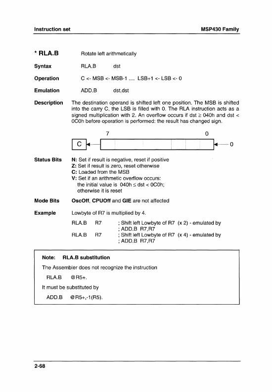
* RLA.B Rotate left arithmetically
Syntax RLA.B dst
Operation C <- MSB <- MSB-1 .... LSB+1 <- LSB <- 0
Emulation ADD.B dst,dst
Description The destination operand is shifted left one position. The MSB is shifted into the carry C, the LSB is filled with o. The RLA instruction acts as a signed multiplication with 2. An overflow occurs if dst ~ 040h and dst < OCOh before operation is performed: the result has changed sign.
Status Bits
Mode Bits
Example
7
N: Set if result is negative, reset if positive Z: Set if result is zero, reset otherwise C: Loaded from the MSB V: Set if an arithmetic overflow occurs:
the initial value is 040h::; dst < OCOh; otherwise it is reset
OscOff, CPUOff and GIE are not affected
Lowbyte of R7 is multiplied by 4.
o
RLA.B R7 ; Shift left Lowbyte of R7 (x 2) - emulated by ; ADD.B R7,R7
RLA.B R7
Note: RLA.B substitution
; Shift left Lowbyte of R7 (x 4) - emulated by ; ADD.B R7,R7
The Assembler does not recognize the instruction
RLA.B @R5+.
It must be substituted by
ADD.B @R5+,-1(R5).
2-68

MSP430 Family Instruction set
* RLC[.W] Rotate left through carry
Syntax RLC dst or RLC.w dst
Operation C <- MSB <- MSB-1 .... LSB+1 <- LSB <- C
Emulation ADDC dst,dst
Description The destination operand is shifted left one position. The carry C is shifted into the LSB, the MSB is shifted into the carry C.
15 o .@r .. ~L...-_____ ------,f..n
Status Bits
Mode Bits
Example
Example
N: Set if result is negative, reset if positive Z: Set if result is zero, reset otherwise C: Loaded from the MSB V: Set if arithmetic overflow occurs otherwise reset
Set if 03FFFh < dstinitial < OCOOOh, otherwise reset
OscOff, CPUOff and GIE are not affected
R5 is shifted left one position.
RLC R5 ; (R5 x 2) + C -> R5
The information of input POIN.1 is to be shifted into LSB of R5.
BIT.B RLC
#2,&POIN R5
; Information -> Carry ; Carry=POin.1 -> LSB of R5
Note: RLC substitution
The Assembler does not recognize the instruction
RLC @R5+.
It must be substituted by
AD DC @R5+,-2(R5).
2-69

Instruction set MSP430 Family
* RLC.B Rotate left through carry
Syntax RLC.B dst
Operation C <- MSB <- MSB-1 .... LSB+1 <- LSB <- C
Emulation ADDC.B dst,dst
Description The destination operand is shifted left one position. The carry C is shifted into the LSB, the MSB is shifted into the carry C.
Status Bits
Mode Bits
Example
7
N: Set if result is negative, reset if positive Z: Set if result is zero, reset otherwise C: Loaded from the MSB V: Set if arithmetic overflow occurs otherwise reset
Set if 03Fh < dstinitial < OCOh otherwise reset
OscOff, CPUOff and GIE are not affected
Content of MEM(LEO) is shifted left one position.
o
RLC.B LEO ; Mem(LEO) x 2 + C -> Mem(LEO)
Example The information of input POIN.1 is to be shifted into LSB of RS.
BIT.B #2,&POIN RLC.B RS
Note: RLC.B emulated
; Information -> Carry ; Carry=POin.1 -> LSB of RS ; High byte of RS is reset
The Assembler does not recognize the instruction
RLC.B @RS+.
It must be substituted by
ADDC.B @RS+,-1(RS).
2-70

MSP430 Family Instruction set
RRA[.W] Rotate right arithmetically
Syntax RRA dst or RRA.W dst
Operation MSB -> MSB, MSB -> MSB-1, MSB-1 -> MSB-2 .... LSB+1 -> LSB, LSB -> C
Description The destination operand is shifted right one position. The MSB is shifted into the MSB, the MSB is shifted into the MSB-1, the LSB+ 1 is shifted into the LSB.
15 a -~ .. ~L.-._-_. - __ . __ .. ___ ---'~ I
Status Bits N: Set if result is negative, reset if positive Z: Set if result is zero, reset otherwise C: Loaded from the LSB V: Reset
Mode Bits OscOff, CPUOff and GIE are not affected
Example RS is shifted right one position. The MSB remains with the old value. It operates equal to an arithmetic division by 2.
;OR
RRA RS ; RS/2 -> RS
The value in RS is multiplied by 0.7S (O.S + 0.2S)
PUSH RRA ADD RRA
RRA PUSH RRA ADD
RS RS @SP+,RS RS
RS RS @SP @SP+,RS
; hold RS temporarily using stack ; RS x O.S -> RS ; RS x O.S + RS = 1.S x RS -> RS ; (1.S x RS) x O.S = 0.7S x RS -> RS
; RS x O.S -> RS ; RS x O.S -> TOS ; TOS x O.S = O.S x RS x O.S = 0.2S x RS -> TOS ; RS x O.S + RS x 0.2S = 0.7S x RS -> RS
2-71

Instruction set MSP430 Family
RRA.B Rotate right arithmetically
Syntax RRA.B dst
Operation MSB -> MSB, MSB -> MSB-1, MSB-1 -> MSB-2 .... LSB+ 1 -> LSB, LSB -> C
Description The destination operand is shifted right one position. The MSB is shifted into the MSB, the MSB is shifted into the MSB-1, the LSB+ 1 is shifted into the LSB.
7 o
• 1-
Status Bits N: Set if result is negative, reset if positive Z: Set if result is zero, reset otherwise C: Loaded from the LSB V: Reset
Mode Bits OscOff, CPUOff and GIE are not affected
Example The Lowbyte of R5 is shifted right one position. The MSB remains with the old value. It operates equal to an arithmetic division by 2.
;OR
2-72
RRA.B R5 ; R5/2 -> R5: Operation is on Low byte only ; High byte of R5 is reset
The value in R5 - Low byte only! - is multiplied by 0.75 (0.5 + 0.25)
PUSH.B RRA.B ADD.B RRA.B
RRA.B PUSH.B RRA.B ADD.B
R5 R5 @SP+,R5 R5
R5 R5 @SP @SP+,R5
; hold Low byte of R5 temporarily using stack ; R5 x 0.5 -> R5 ; R5 x 0.5 + R5 = 1.5 x R5 -> R5 ; (1.5 x R5) x 0.5 = 0.75 x R5 -> R5
; R5 x 0.5 -> R5 ; R5 x 0.5 -> TOS ; TOS x 0.5 = 0.5 x R5 x 0.5 = 0.25x R5 -> TOS ; R5 x 0.5 + R5 x 0.25 = 0.75 x R5 -> R5

MSP430 Family Instruction set
RRC[.W] Rotate right through carry
Syntax RRC dst or RRC.W dst
Operation C -> MSB -> MSB-1 .... LSB+1 -> LSB -> C
Description The destination operand is shifted right one position. The carry C is shifted into the MSB, the LSB is shifted into the carry C.
Status Bits
Mode Bits
Example
15 o
~ ~~--------' N: Set if result is negative, reset if positive Z: Set if result is zero, reset otherwise C: Loaded from the LSB V: Set if initial destination is positive and initial Carry is set, otherwise
reset
OscOff, CPUOff and GIE are not affected
R5 is shifted right one position. The MSB is loaded with 1.
SETC RRC R5
; PREPARE CARRY FOR MSB ; R5/2 + 8000h -> R5
2-73

Instruction set MSP430 Family
RRC.B Rotate right through carry
Syntax RRC dst
Operation C -> MSB -> MSB-1 .... LSB+ 1 -> LSB -> C
Description The destination operand is shifted right one position. The carry C is shifted into the MSB, the LSB is shifted into the carry C.
Status Bits
Example
2-74
7
N: Set if result is negative, reset if positive Z: Set if result is zero, reset otherwise C: Loaded from the LSB
o
V: Set if initial destination is positive and initial Carry is set, otherwise reset
OscOff, CPUOff and GIE are not affected
RS is shifted right one position. The MSB is loaded with 1.
SETC RRC.B RS
; PREPARE CARRY FOR MSB ; RS/2 + BOh -> RS; Low byte of RS is used

MSP430 Family Instruction set
* SBC[.W] Subtract borrow') from destination
Syntax SBC dst or SBC.w dst
Operation dst + OFFFFh + C -> dst
Emulation SUBC #O,dst
Description The carry C is added to the destination operand minus one. The previous contents of the destination are lost.
Status Bits N: Set if result is negative, reset if positive Z: Set if result is zero, reset otherwise C: Reset if dst was decremented from 0000 to OFFFFh, set otherwise V: Set if initially C=O and dst=08000h
Mode Bits OscOff, CPUOff and GIE are not affected
Example The 16-bit counter pointed to by R13 is subtracted from a 32-bit counter pointed to by R12.
SUB @R13,0(R12); Subtract LSDs SBC 2(R12) ; Subtract carry from MSD
Note: Borrow is treated as a .NOT. carry 1
The borrow is treated as a .NOT. carry: Borrow Yes No
Carry bit o 1
2-75

Instruction set MSP430 Family
* SBC.B Subtract borrow *) from destination
Syntax SBC.B dst
Operation dst + OFFh + C -> dst
Emulation SUBC.B #O,dst
Description The carry C is added to the destination operand minus one
the borrow is subtracted from the destination operand.
Status Bits
Mode Bits
Example
The previous contents of the destination are lost.
N: Set if result is negative, reset if positive Z: Set if result is zero, reset otherwise C: Reset if dst was decremented from 0000 to OFFFFh, set otherwise V: Set if initially C=O and dst=080h
OscOff, CPUOff and GIE are not affected
The 8bit counter pointed to by R13 is subtracted from a 16bit counter pointed to by R12.
SUB.B @R13,0(R12) ; Subtract LSDs SBC.B 1(R12) ; Subtract carry from MSD
Note: Borrow is treated as a .NOT. carry 2
The borrow is treated as a .NOT. carry: Borrow
2-76
Yes No
Carry bit o 1

MSP430 Family Instruction set
* SETC Set carry bit
Syntax SETC
Operation 1 -> C
Emulation BIS #1,SR
Description The Carry Bit C is set, an often necessary operation.
Status Bits N: Not affected Z: Not affected C: Set
Mode Bits
Example
DSUB
V: Not affected
OscOtt, CPUOtt and GIE are not affected
Emulation of the decimal subtraction: Subtract R5 from R6 decimally Assume that R5=3987 and R6=4137
ADD #6666h,R5
INV R5
SETC DADD R5,R6
; Move content R5 from 0-9 to 6-0Fh ; R5 = 03987 + 6666 = 09FEDh ; Invert this(result back to 0-9) ; R5 = .NOT. R5 = 06012h ; Prepare carry = 1 ; Emulate subtraction by adding of: ; (10000 - R5 - 1) ; R6 = R6 + R5 + 1 ; R6 = 4137 + 06012 + 1 = 10150 = 0150
2-77

Instruction set
*SETN Set Negative bit
Syntax SETN
Operation 1 -> N
Emulation BIS #4,SR
Description The Negative bit N is set.
Status Bits N: Set Z: Not affected C: Not affected V: Not affected
Mode Bits OscOff, CPUOff and GIE are not affected
2-78
MSP430 Family

MSP430 Family Instruction set
* SETZ Set Zero bit
Syntax SETZ
Operation 1 -> Z
Emulation SIS #2,SR
Description The Zero bit Z is set.
Status Bits N: Not affected Z: Set C: Not affected V: Not affected
Mode Bits OscOff, CPUOff and GIE are not affected
2-79

Instruction set
SU8[.W]
Syntax
Operation
subtract source from destination
SUB src,dst or SUB.w
dst + .NOT.src + 1 -> dst or [(dst - src -> dst)]
MSP430 Family
src,dst
Description The source operand is subtracted from the destination operand. This is made by adding of the 1 's complement of the source operand and the constant 1. The source operand is not affected, the previous contents of the destination are lost.
Status Bits N: Set if result is negative, reset if positive Z: Set if result is zero, reset otherwise C: Set if there is a carry from the MSB of the result, reset if not
Set to 1 if no borrow, reset if borrow. V: Set if an arithmetic overflow occurs, otherwise reset
Mode Bits OscOff, CPUOff and GIE are not affected
Example See example at the SBC instruction
Note: Borrow is treated as a .NOT. carry 3
The borrow is treated as a .NOT. carry: Borrow
2-80
Yes No
Carry bit o 1

MSP430 Family Instruction set
SUB.B subtract source from destination
Syntax
Operation
SUB.B src,dst
dst + .NOT.src + 1 -> dst or (dst - src -> dst)
Description The source operand is subtracted from the destination operand. This is made by adding of the 1 's complement of the source operand and the constant 1. The source operand is not affected, the previous contents of the destination are lost.
Status Bits N: Set if result is negative, reset if positive Z: Set if result is zero, reset otherwise C: Set if there is a carry from the MSB of the result, reset if not
Set to 1 if no borrow, reset if borrow. V: Set if an arithmetic overflow occurs, otherwise reset
Mode Bits OscOff, CPUOff and GIE are not affected
Example See example at the SBC.B instruction
Note: Borrow is treated as a .NOT. carry 4
The borrow is treated as a .NOT. carry: Borrow Yes No
Carry bit o 1
2-81
Instruction set MSP430 Family
SUBC[.W]SBB[.W] subtract source and borrow/.NOT. carry from destination
Syntax
Operation
SUBC SBB
src,dst src,dst
or SUBC.w or SBB.W
dst + .NOT.src + C -> dst or (dst - src - 1 + C -> dst)
src,dst src,dst
or
Description The source operand is subtracted from the destination operand. This is made by adding of the 1 's complement of the source operand and the carry C. The source operand is not affected, the previous contents of the destination are lost.
Status Bits N: Set if result is negative, reset if positive Z: Set if result is zero, reset otherwise C: Set if there is a carry from the MSB of the result, reset if not
Set to 1 if no borrow, reset if borrow. V: Set if an arithmetic overflow occurs, otherwise reset
Mode Bits OscOff, CPUOff and GIE are not affected
Example Two floating point mantissas (24bits) are subtracted. LSB's are in R13 resp. R10, MSB's are in R12 resp. R9.
SUB.W R13,R10 ; 16bit part, LSB's SUBC.B R12,R9 ; 8bit part, MSB's
Note: Borrow is treated as a .NOT. carry 5
The borrow is treated as a .NOT. carry: Borrow
2-82
Yes No
Carry bit o 1

MSP430 Family Instruction set
SUBC.B,SBB.B subtract source and borrow/.NOT. carry from destination
Syntax
Operation
SUBC.B src,dst or SBB.B src,dst
dst + .NOT.src + C -> dst or (dst - src - 1 + C -> dst)
Description The source operand is subtracted from the destination operand. This is made by adding of the 1's complement of the source operand and the carry C. The source operand is not affected, the previous contents of the destination are lost.
Status Bits N: Set if result is negative, reset if positive Z: Set if result is zero, reset otherwise C: Set if there is a carry from the MSB of the result, reset if not
Set to 1 if no borrow, reset if borrow. V: Set if an arithmetic overflow occurs, otherwise reset
Mode Bits OscOff, CPUOff and GIE are not affected
Example The 16-bit counter pointed to by R13 is subtracted from a 16-bit counter in R10 and R11 (MSD).
SUB.B @R13+,R10; Subtract LSDs without carry SUBC.B @R13,R11 ; Subtract MSDs with carry
; resulting fron the LSDs
Note: Borrow is treated as a .NOT. carry 6
The borrow is treated as a .NOT. carry: Borrow Yes No
Carry bit o 1
2-83

Instruction set MSP430 Family
SWPB Swap bytes
Syntax SWPB dst
Operation bits 15 to 8 <-> bits 7 to 0
Description The high and the low bytes of the destination operand are exchanged.
Status Bits N: Not affected Z: Not affected C: Not affected V: Not affected
Mode Bits OscOff, CPUOff and GIE are not affected
Example
Example
2-84
15 8 7
MOV #040BFh,R7 SWPB R7
o
; 0100000010111111 -> R7 ; 1011111101000000 in R7
The value in R5 is multiplied by 256. The result is stored in R5,R4
SWPB R5 MOV R5,R4 BIC #OFFOOh,R5 BIC #00FFh,R4
;Copy the swapped value to R4 ;Correct the result ;Correct the result
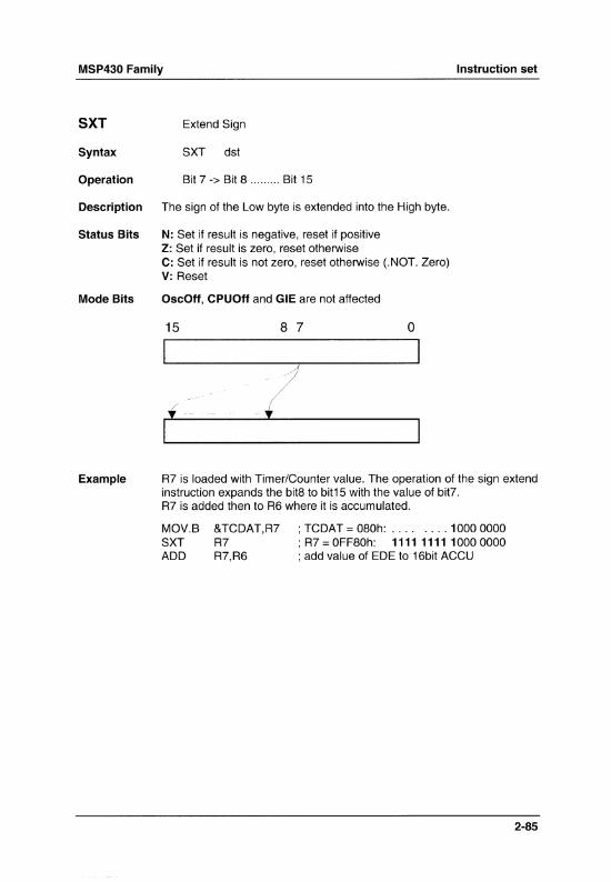
MSP430 Family Instruction set
SXT Extend Sign
Syntax SXT dst
Operation Bit 7 -> Bit B ......... Bit 15
Description The sign of the Low byte is extended into the High byte.
Status Bits N: Set if result is negative, reset if positive Z: Set if result is zero, reset otherwise C: Set if result is not zero, reset otherwise (.NOT. Zero) V: Reset
Mode Bits OscOff, CPUOff and GIE are not affected
15 8 7 o
Example R7 is loaded with Timer/Counter value. The operation of the sign extend instruction expands the bitB to bit15 with the value of bit7. R7 is added then to R6 where it is accumulated.
MOV.B SXT ADD
&TCDAT,R7 R7 R7,R6
; TCDAT = OBOh: . . .. . ... 10000000 ; R7 = OFFBOh: 1111111110000000 ; add value of EDE to 16bit ACCU
2-85

Instruction set MSP430 Family
* TST[.W] Test destination
Syntax TST dst or TSTW dst
Operation dst + OFFFFh + 1
Emulation CMP #O,dst
Description The destination operand is compared to zero. The status bits are set according to the result. The destination is not affected.
Status Bits N: Set if destination is negative, reset if positive
Mode Bits
Example
R7POS
R7NEG
R7ZERO
2-86
Z: Set if destination contains zero, reset otherwise C: Set V: Reset.
OscOff, CPUOff and GIE are not affected
R7 is tested. If it is negative continue at R7NEG; if it is positive but not zero continue at R7POS.
TST R7 IN R7NEG JZ R7ZERO
; Test R7 ; R7 is negative ; R7 is zero ; R7 is positive but not zero
; R7 is negative
; R7 is zero

MSP430 Family Instruction set
* TST.B Test destination
Syntax TST.8 dst
Operation dst + OFFh + 1
Emulation CMP.B #O,dst
Description The destination operand is compared to zero (R15). The status bits are set according to the result. The destination is not affected.
Status Bits N: Set if destination is negative, reset if positive
Mode Bits
Example
R7POS
R7NEG
R7ZERO
Z: Set if destination contains zero, reset otherwise C: Set V: Reset.
OscOff, CPUOff and GIE are not affected
Lowbyte of R7 is tested. If it is negative continue at R7NEG; if it is positive but not zero continue at R7POS.
TST.B R7 IN R7NEG JZ R7ZERO
; Test Low byte of R7 ; Low byte of R7 is negative ; Low byte of R7 is zero ; Low byte of R7 is positive but not zero
; Lowbyte of R7 is negative
; Lowbyte of R7 is zero
2-87

Instruction set MSP430 Family
XOR[.W] Exclusive OR of source with destination
Syntax XOR src,dst or XOR.w src,dst
Operation src .XOR. dst -> dst
Description The source operand and the destination operand are OR'ed exclusively. The result is placed into the destination. The source operand is not affected.
Status Bits N: Set if MSB of result is set, reset if not set Z: Set if result is zero, reset otherwise C: Set if result is not zero, reset otherwise ( = .NOT. Zero) V: Set if both operands are negative
Mode Bits OscOff, CPUOff and GIE are not affected
Example The bits set in R6 toggle the bits in the RAM word TONI.
XOR R6,TONI; Toggle bits of word TONI on the bits set in R6
2-88

MSP430 Family Instruction set
XOR.B Exclusive OR of source with destination
Syntax XOR.B src,dst
Operation src .XOR. dst -> dst
Description The source operand and the destination operand are OR'ed exclusively. The result is placed into the destination. The source operand is not affected.
Status Bits N: Set if MSB of result is set, reset if not set Z: Set if result is zero, reset otherwise C: Set if result is not zero, reset otherwise ( = .NOT. Zero) V: Set if both operands are negative
Mode Bits OscOff, CPUOff and GIE are not affected
Example The bits set in R6 toggle the bits in the RAM byte TONI.
R6,
Example
XOR.B R6,TONI ; Toggle bits in word TONI on bits set in Low byte of
Reset bits in Lowbyte of R7 to 0 that are different to bits in RAM byte EDE.
XOR.B INV.B
EDE,R7 R7
; Set different bit to '1 s' ; Invert Lowbyte, Highbyte is Oh
2-89

Instruction set MSP430 Family
2.4 Macro instructions emulated with several instructions
The following table shows the instructions which need more words if emulated by the reduced instruction set. This is not of big concern due to the rare use of them. The immediate values -1, 0, +1, 2, 4 and 8 are provided by the Constant Generator Registers R2/CG1 and R3/CG2.
Emulated instruction Instruction flow Comment
ABS dst TST dst ; Absolute value of destination IN L$O ; Destination is negative
L$1 ; Destination is positive
L$O INV dst ; Convert negative destination INC dst ; to positive JMP L$1
DSUB src,dst ADD #6666h,src ; Decimal subtraction INV src ; Source is destroyed! SETC DADD src,dst ; DST - SRC (dec)
NEG dst INV dst ; Negation of destination INC dst
RL dst ADD dst,dst ; Rotate left circularly ADDC #O,dst
RR dst CLRC ; Rotate right circularly RRC dst JNC L$1 BIS #8000h,dst
L$1
2-90

MSP430 Family Instruction set
2.5 Stack pointer addressing
The placement of the Stack Pointer inside the register space allows a lot of features not possible with the normal allocation outside the register space.
MOV Rn,SP ; Load SP with the contents of Rn
MOV @Rn,SP ; Load SP with the contents of the word pointed to by ; Rn
MOV @Rn+,SP ; Same as above with autoincrement of Rn
MOV X(Rn),SP ; Load SP with the contents of a table pointed to by Rn. ; X defines the offset relative to the table start
MOV #n,SP ; Load SP with a constant n (e.g. for initialization)
MOV ADDR,SP ; Load SP with the contents of word AD DR
MOV &ADDR,SP ; Load SP with the contents of absolute address ADDR
MOV SP,Rn ; Copy SP to Rn (e.g. for later restoring)
MOV @SP,Rn ; Move top of stack (TOS) to Rn
MOV @SP+,Rn ; Pop stack item to Rn
MOV X(SP),Rn ; Move a stack item relative to the SP to Rn
MOV Rn,O(SP) ; Replace TOS by contents of Rn
MOV Rn,X(SP) ; Replace item on the stack. X defines the offset relative ; to the SP (TOS)
INCD SP ; Remove TOS item
The Stack Pointer allows the transfer of arguments in several ways. The following example shows a CALL with arguments and the handling inside of the subroutine:
CALL . BYTE .wORD .wORD .wORD
#SUBROUT MODE,CODE ERRADD ARG1 ARG2
; Control bytes ; Error address, if ERROR occurs ; ARGUMENT #1 ; ARGUMENT #2 ; Continue here after RETURN
2·91

Instruction set MSP430 Family
SUBROUT ; prepare registers MOV @SP,Rn ; TOS points to control bytes ADD #8,O(SP) ; Ajust return address MOV @Rn+,Rm ; Control bytes -> Rm MOV @Rn+,Rx ; Error address -> Rx MOV @Rn+,Ry ; ARGUMENT #1 -> Ry MOV @Rn+,Rz ; ARGUMENT #2 -> Rz
RETN ; Normal RETURN ERROR MOV Rx,PC ; Error occured: return address to PC
The same subroutine can be called in different ways. The arguments following the call are read by the subroutine and the information is handled appropriately.
2-92

MSP430 Family Instruction set
2.6 Branch operation
All seven addressing modes can be applied to the Branch instruction. The Branch instruction is emulated by the core instruction MOV source,PC.
Branch and call instructions operate within one segment; both do not manipulate the code segment information.
2.6.1 Indirect Branch, CALL
Indirect Branch
BR RS
MOV RS,PC ; Core instruction
Before: After: Address Register Address Register space space
OFF16h Oxxxxh PC OFF16h Oxxxxh PC OFF14h 04S00h PC RS OFF14h 04S00h RS OFF12h Oxxxxh OFF12h Oxxxxh
OFA34h Oxxxxh OFA34h Oxxxxh OFA32h Oxxxxh OFA32h Oxxxxh PC OFA30h Oxxxxh OFA30h Oxxxxh
2-93
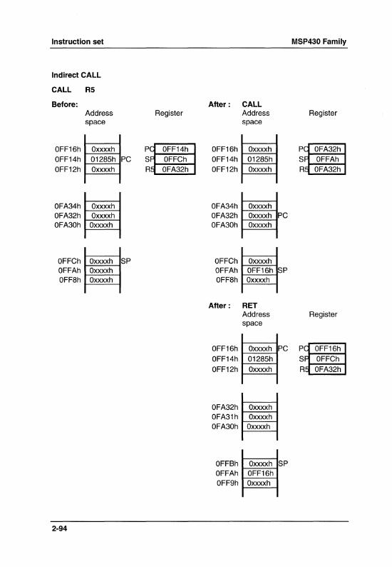
Instruction set
Indirect CALL
CALL RS
Before: Address space
OFF16h Oxxxxh OFF14h 01285h OFF12h Oxxxxh
OFA34h Oxxxxh OFA32h Oxxxxh OFA30h Oxxxxh
OFFCh Oxxxxh OFFAh Oxxxxh OFF8h Oxxxxh
2-94
PC
SP
C F IE
P S R
Register
OFF14h OFFCh OFA32h
After: CALL Address space
OFF16h Oxxxxh OFF14h 01285h OFF12h Oxxxxh
OFA34h Oxxxxh OFA32h Oxxxxh PC OFA30h Oxxxxh
OFFCh Oxxxxh OFFAh OFF16h OFF8h Oxxxxh
After: RET Address space
OFF16h Oxxxxh OFF14h 01285h OFF12h Oxxxxh
OFA32h Oxxxxh OFA31h Oxxxxh OFA30h Oxxxxh
SP
PC
OFFBh Oxxxxh SP OFFAh OFF16h OFF9h Oxxxxh
MSP430 Family
C ~F
IE
P S R
C ,F I~
P S R
Register
OFA32h OFFAh OFA32h
Register
OFF16h OFFCh OFA32h

MSP430 Family Instruction set
2.6.2 Indirect indexed Branch, CALL
Indirect indexed Branch
BR 2(R5)
MOV 2(R5),PC ;Core instruction
Before: After: Address Register Address Register space space
OFF16h 0OOO2h PC OFF16h Oxxxxh PC OFF14h 04510h PC OFF14h 04510h R5 OFF12h Oxxxxh OFF12h Oxxxxh
0OOO2h OFA36h Oxxxxh +OFA32h OF08Ch Oxxxxh OFA34h OF08Ah OFA34h OF08Ah Oxxxxh PC OFA32h Oxxxxh OF088h Oxxxxh
2-95

Instruction set
Indirect indexed CALL
CALL 2(RS)
Before: Address Register space
OFF18h Oxxxxh OFF16h 0OOO2h PC OFF14h OFF14h 01295h PC SP OFFCh OFF12h Oxxxxh R5 OFA32h
0OOO2h OFA36h Oxxxxh +OFA32h OFA34h OF088h OFA34h OFA32h Oxxxxh
OFFCh Oxxxxh SP OFFAh Oxxxxh OFF8h Oxxxxh
2-96
After: CALL Address space
OFF18h Oxxxxh OFF16h 0OOO2h OFF14h 01295h OFF12h Oxxxxh
OF08Ah Oxxxxh OF088h Oxxxxh OF086h Oxxxxh
OFFCh Oxxxxh OFFAh OFF18h OFF8h Oxxxxh
After: RET Address space
OFF18h Oxxxxh OFF16h 0OOO2h OFF14h 01295h OFF12h Oxxxxh
OF08Ah Oxxxxh OF088h Oxxxxh OF086h Oxxxxh
PC
SP
PC
OFFCh Oxxxxh SP OFFAh OFF18h OFF8h Oxxxxh
MSP430 Family
Register
PC OF088h SP OFFAh R5 OFA32h
.Register
PC OFF18h SP OFFCh R5 OFA32h

MSP430 Family Instruction set
2.6.3 Indirect symbolic Branch, CALL
Indirect symbolic Branch
BR EDE
MOV EDE,PC ; Core instruction
Before: After: Address Register Address Register space space
OFF16h OFB1Eh PCI OFF14h OFF16h OFB1Eh Pcl OF378h I OFF14h 04010h PC OFF14h 04010h OFF12h Oxxxxh OFF12h Oxxxxh
OFB1Eh OFA36h Oxxxxh +OFF16h OF37Ah Oxxxxh
OFA34h OF378h EDE OFA34h OF378h Oxxxxh PC OFA32h Oxxxxh OF376h Oxxxxh
2-97
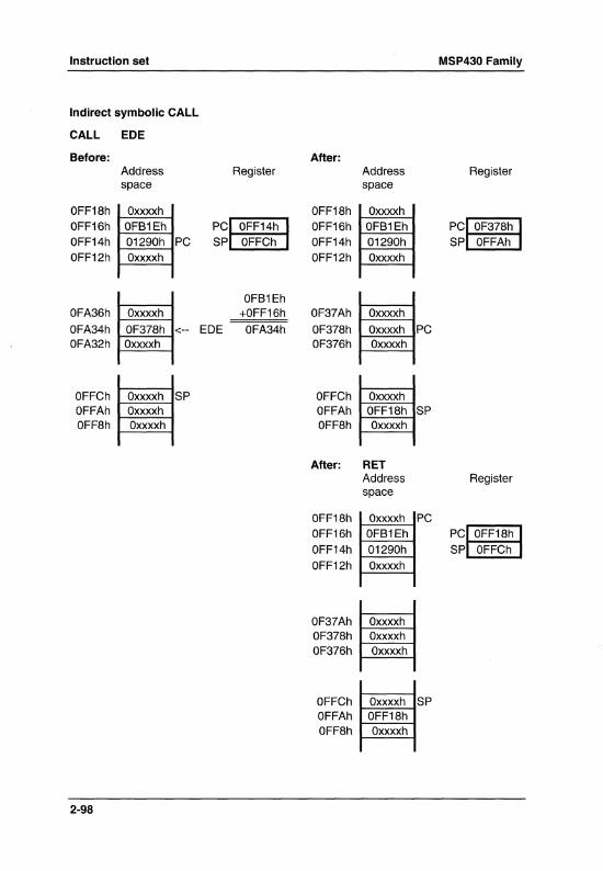
Instruction set MSP430 Family
Indirect symbolic CALL
CALL EDE
Before: After: Address Register Address Register space space
OFF18h Oxxxxh OFF18h Oxxxxh OFF16h OFB1Eh PC OFF16h OFB1Eh PC OFF14h 01290h PC SP OFF14h 01290h SP OFF12h Oxxxxh OFF12h Oxxxxh
OFB1Eh OFA36h Oxxxxh +OFF16h OF37Ah Oxxxxh OFA34h OF378h <-- EDE OFA34h OF378h Oxxxxh PC OFA32h Oxxxxh OF376h Oxxxxh
OFFCh Oxxxxh SP OFFCh Oxxxxh OFFAh Oxxxxh OFFAh OFF18h SP OFF8h Oxxxxh OFF8h Oxxxxh
After: RET Address Register space
OFF18h Oxxxxh PC OFF16h OFB1Eh PC OFF14h 01290h SP OFF12h Oxxxxh
OF37Ah Oxxxxh OF378h Oxxxxh OF376h Oxxxxh
OFFCh Oxxxxh SP OFFAh OFF18h OFF8h Oxxxxh
2-98

MSP430 Family Instruction set
2.6.4 Indirect absolute Branch, CALL
The absolute branch and call instruction in the segmented memory model will result in a branch or call to code segment O.
Indirect absolute Branch
BR &EDE
MOV &EDE,PC ; Core instruction
Before: After: Address Register Address Register space space
OFF16h OF378h PC I OFF14h OFF16h OF378h PC I 01234h I OFF14h 04210h PC OFF14h 04210h OFF12h Oxxxxh OFF12h Oxxxxh
OF378h OF37Ah Oxxxxh +OOOOOh 01236h Oxxxxh OF378h 01234h OF378h 01234h Oxxxxh PC EDE OF376h Oxxxxh 01232h Oxxxxh
2-99

Instruction set MSP430 Family
Indirect absolute CALL
CALL &EDE
Before: After: Address Register Address Register space space
OFF18h Oxxxxh OFF18h Oxxxxh OFF16h OF378h PC OFF16h OF378h PC OFF14h 01292h PC SP OFF14h 01292h SP OFF12h Oxxxxh OFF12h Oxxxxh
OF378h OF37Ah Oxxxxh +OOOOOh 01236h Oxxxxh OF378h 01234h OF378h 01234h Oxxxxh PC EDE OF376h Oxxxxh 01232h Oxxxxh
OFFCh Oxxxxh SP OFFCh Oxxxxh OFFAh Oxxxxh OFFAh OFF18h SP OFF8h Oxxxxh OFF8h Oxxxxh
After: RET Address Register space
OFF18h Oxxxxh PC OFF16h OF378h PC OFF14h 01292h SP OFF12h Oxxxxh
OF37Ah Oxxxxh OF378h 01234h OF376h Oxxxxh
OFFCh Oxxxxh SP OFFAh OFF18h OFF8h Oxxxxh
2-100

MSP430 Family
2.6.5 Indirect indirect Branch, CALL
Indirect indirect Branch
BR @R9
MOV @R9,PC ; Core instruction
Before: Address Register space
OFF16h Oxxxxh PC OFF14h 04920h PC R9 OFF12h Oxxxxh
OFA34h Oxxxxh OFA32h OF124h OFA30h Oxxxxh
After: Address space
OFF16h Oxxxxh OFF14h 04920h OFF12h Oxxxxh
OF126h Oxxxxh OF124h Oxxxxh PC OF122h Oxxxxh
Instruction set
Register
PC~~~ R91..,;,,;...;....;.;;;~
2-101
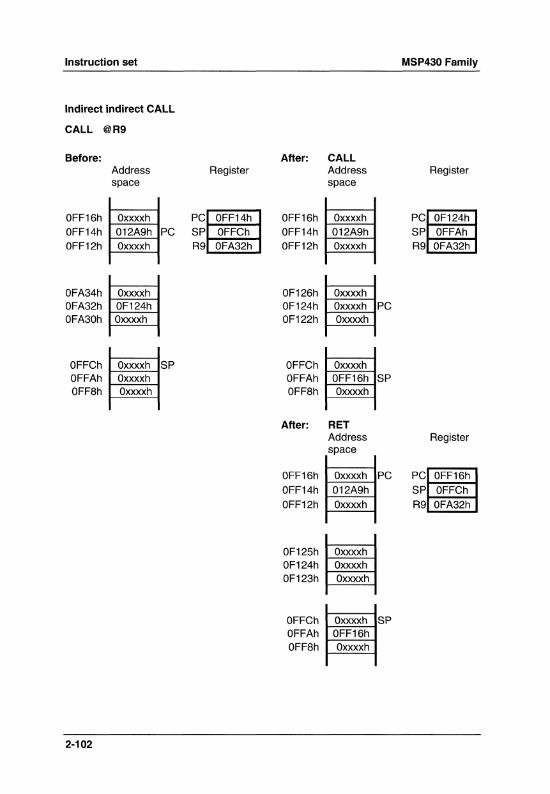
Instruction set MSP430 Family
Indirect indirect CALL
CALL @R9
Before: After: CALL Address Register Address Register space space
OFF16h Oxxxxh PC OFF14h OFF16h Oxxxxh PC OF124h OFF14h 012A9h PC SP OFFCh OFF14h 012A9h SP OFFAh OFF12h Oxxxxh R9 OFA32h OFF12h Oxxxxh R9 OFA32h
OFA34h Oxxxxh OF126h Oxxxxh OFA32h OF124h OF124h Oxxxxh PC OFA30h Oxxxxh OF122h Oxxxxh
OFFCh Oxxxxh SP OFFCh Oxxxxh OFFAh Oxxxxh OFFAh OFF16h SP OFF8h Oxxxxh OFF8h Oxxxxh
After: RET Address Register space
OFF16h Oxxxxh PC PC OFF16h OFF14h 012A9h SP OFFCh OFF12h Oxxxxh R9 OFA32h
OF125h Oxxxxh OF124h Oxxxxh OF123h Oxxxxh
OFFCh Oxxxxh SP OFFAh OFF16h OFF8h Oxxxxh
2-102

MSP430 Family
2.6.6 Indirect indirect Branch, CALL with autoincrement
Indirect indirect Branch with autoincrement
BR @R5+
MOV
Before:
@R5+,PC
Address space
; Core instruction
Register
OFF16h Oxxxxh PC OFF14h 04530h PC R5 ~~~-t OFF12h Oxxxxh
OFA36h Oxxxxh OFA32h OF124h OFA30h Oxxxxh
After: Address space
OFF16h Oxxxxh OFF14h 04530h OFF12h Oxxxxh
OF126h Oxxxxh OF124h Oxxxxh PC OF122h Oxxxxh
Instruction set
Register
PC R5~~~
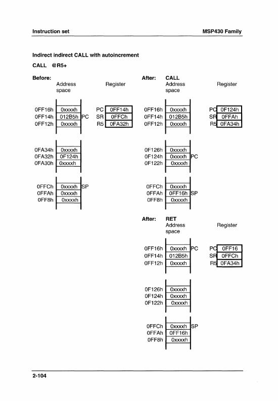
Instruction set
Indirect indirect CALL with autoincrement
CALL @R5+
Before: Address Register space
OFF16h Oxxxxh PC OFF14h OFF14h 01285h PC SR OFFCh OFF12h Oxxxxh R5 OFA32h
OFA34h Oxxxxh OFA32h OF124h OFA30h Oxxxxh
OFFCh Oxxxxh SP OFFAh Oxxxxh OFF8h Oxxxxh
2-104
After: CALL Address space
OFF16h Oxxxxh OFF14h 01285h OFF12h Oxxxxh
OF126h Oxxxxh OF124h Oxxxxh PC OF122h Oxxxxh
OFFCh Oxxxxh OFF16h S OFFAh P
OFF8h Oxxxxh
After: RET Address space
OFF16h Oxxxxh PC OFF14h 01285h OFF12h Oxxxxh
OF126h Oxxxxh OF124h Oxxxxh OF122h Oxxxxh
OFFCh Oxxxxh SP OFFAh OFF16h OFF8h Oxxxxh
MSP430 Family
(
R Ie
P S R
C F Ie
P S R
Register
OF124h OFFAh OFA34h
Register
OFF16 OFFCh OFA34h

MSP430 Family Instruction set
2.6.7 Direct Branch, direct CALL
Branch immediate #N, Branch Label
BR #OF146h OR BR #Label
MOV @PC+,PC ; Core instruction
Before: After: Address Register Address Register space space
OFF16h OF146h pcl OFF14h OFF16h OF146h pcl OF146h I OFF14h 04030h PC OFF14h 04030h OFF12h Oxxxxh OFF12h Oxxxxh
OF148h Oxxxxh OF148h Oxxxxh OF146h Oxxxxh <-- Lab OF146h Oxxxxh PC
el OF144h Oxxxxh OF144h Oxxxxh
2-105

Instruction set MSP430 Family
Direct CALL
CALL #OF146h OR CALL #Label
Before: After: CALL Address Register Address Register space space
OFF18h Oxxxxh OFF18h Oxxxxh OFF16h OF146h PC OFF16h OF146h PC OFF14h 012BOh PC OFF14h 012BOh SP OFF12h Oxxxxh OFF12h Oxxxxh
OF148h Oxxxxh OF148h Oxxxxh OF146h Oxxxxh <-- Label OF146h Oxxxxh PC OF144h Oxxxxh OF144h Oxxxxh
OFFCh Oxxxxh SP OFFCh Oxxxxh OFFAh Oxxxxh OFFAh OFF18h SP OFF8h Oxxxxh OFF8h Oxxxxh
After: RET Address Register space
OFF18h Oxxxxh PC OFF16h OF146h PC OFF14h 012BOh SR OFF12h Oxxxxh
OF148h Oxxxxh OF146h Oxxxxh OF144h Oxxxxh
OFFCh Oxxxxh SP OFFAh OFF18h OFF8h Oxxxxh
2-106

MSP430 Family
3 General Initialization
3.1 System Clock Generator
3.2 RAM Clearing Rmoutine
3.3 RAM Self-Test
3.4 ROM Checksum
3.5 Battery Check
3.6 Interrupt Management
Figure Title
3.1 Battery Check
Topics
Figures
General Initialization
3-3
3-3
3-4
3-4
3-5
3-6
3-9
Page
3-6
3-1

General Initialization MSP430 Family
3-2

MSP430 Family General Initialization
3 General Initialization
The most important thing to initialize the processor is the reset vector, which is located at address FFFEh and must point to the starting address of the programme code. The initialization of the stack in the RAM area is important as well. This is done by simple MOV instructions as shown in the following example. To operate with the proper system frequency the system clock generator must be initialized.
3.1 System Clock Generator
The first thing to do after the power up reset is to initialize the system clock generator. The following waiting loop is used to get the initialized system frequency. Then the stack is defined at the RAM address 300h and can range down to 200h (depending on the MSP430 type). Therefore, the first word which is pushed on the stack will be located at 2FEh. If the RAM is used for storing variables the space for the stack will be smaller.
STACK SCFQCTL SCFIl
START
.EQU
.EQU
.EQU
.SECT
MOV.B MOV.B MOV CALL
.SECT
. WORD
300H 052H 051H
"INIT",OF100H
#lFH,&SCFQCTL #80H, &SCFIl #STACK,SP #RAMCLR
;STARTADDRESS OF THE RAM VERSION ;SPECIAL STARTUP FOR FLL ;LOAD FLL TO RUN WITH 32KHZ*20H ;LOAD FLL TO RUN WITH lMHZ ;INITIALIZE STACK ;USED FOR WAITING, TOO
"RES_VECT",OFFFEH START ; POR, EXT. RESET, WATCHDOG
3-3

General Initialization MSP430 Family
3.2 RAM Clearing Routine
This subroutine sets all of the RAM to zero and is called after the initialization of the system clock generator. The size of the RAM depends on the type of the MSP430. For the following example the RAM starts at address 200h and the size is assumed to be 100h.
; DEFINITIONS FOR THE RAM BLOCK (DEPENDS ON MSP430 TYPE) RAMSTRT .EQU 0200H ; START OF RAM RAMEND .EQU 02FFH ; LAST RAM ADDRESS
; SUBROUTINE FOR THE CLEARING OF THE RAM BLOCK RAMCLR CLR R4 PREPARE INDEX REGISTER RCL CLR
INCD CMP JLO RET
RAMSTRT(R4) ; 1ST RAM ADDRESS R4 ; NEXT ADDRESS #RAMEND-RAMSTRT+1,R4 ; RAM CLEARED? RCL ; NO, ONCE MORE
3.3 RAM Self-Test
This routine performs a simple alternating 0/1 test on the RAM. The RAM is tested by writing a AAh,55h pattern to the entire RAM and checking the RAM for this patten. The inverted pattern is then written to RAM and rechecked. Finally, the entire RAM is cleared. If an error is found, the negative bit is set.
RAMSTRT .EQU RAMEND .EQU
0200H 02FFH
START OF RAM ; LAST RAM ADDRESS
;SUBROUTINE TO CHECK ENTIRE RAM ;USE REGISTER: R4,R5 RAMCHECK
MOV FILLS CLR FILLR MOV
INCD CMP JLO CLR
COMPAR CMP JNE
#55AAH,R4 ;FIRST TESTPATTERN R5 ;POINTER TO RAM R4,RAMSTRT(R5);FILL RAM WITH R4 R5 ;NEW RAM POINTER #RAMEND-RAMSTRT+1,R5 ;IS RAM FILLED? FILLR R5 ;NEW RAM POINTER R4,RAMSTRT(R5);COMPARE RAM WITH R4 ERROR ;EXIT IF VALUES DON'T MATCH
DECD R5 ; NEXT RAM WORD
?
3·4
CMP #RAMEND-RAMSTRT+1,R5 ;ALL OF RAM TESTED
JLO SWPB
COMPAR R4
TST R4 IN JZ CLR
FILLS EXIT R4
;NEW TESTPATTERN
;=AA55H, NEW TEST ;=OOOOH, FINISCHED ;TESTPATTERN = 0000

MSP430 Family General Initialization
JMP FILLS ERROR SETN EXIT RET
3.4 ROM Checksum
This routine checks the integrity of the ROM by performing a checksum on the entire ROM. All ROM words from ROMSTRT+2 to ROMEND are added together in a 16-bit word. This sum is checked against the value at the beginning of the ROM ( ROMSTRT ). If these values do not match, then an error has occurred and the negative bit is set.
STACK .SET 02EOH ;START OF SYSTEM STACK
ROMSTRT . SECT . WORD
START MOV
"PROG",OFOOOH CHECKSUM #STACK,SP
;PUT CORRECT CHECKSUM INTO ROM ;INITIALIZE SYSTEM STACK ; POINTER ;OTHER INITIALIZATION PROGRAM ; HERE
;SUBROUTINE TO CHECK THE INTEGRITY OF THE ROM ;USE REGISTER: R4,R5 ;OUTPUT: ROM OK. N=O
ROM CHECK FAILED: N=l
ROMCHECK CLR R5
#ROMEND,R4 MOV SUB ADD DECD
#ROMSTRT,R4 ;R4 CONTAINS THE LENGTH OF ROM ROML ROMSTRT(R4),R5 ;MAKE CHECKSUM
R4 JNZ ROML CMP JEQ SETN
ROMEXIT RET
R5, &ROMSTRT ROMEXIT
;IF MATCH, N-BIT IS CLEARED
;INTERRUPT VECTOR ADDRESSES:
ROMEND .SECT . WORD
"RSTVECT",OFFFEH; PUC/RESET ADDRESS START
3-5

General Initialization MSP430 Family
3.5 Battery Check
Due to the ratiometric measurement principle of the ADC, the measured digital value is an indication of the supply voltage of the MSP430. The measured value is inversly proportional to the supply voltage Vcc. To get the reference for later battery tests a measurement is made with Vcc = Vccmin. The result is stored in the RAM. If the battery should be tested, another measurement has to be made, and the result compared to the stored value measured with Vcc=Vccmin determines the status of the battery. If the measured value exceeds the stored one, then Vcc<Vccmin and a Battery low indication can be given by software.
o 32kHz
.-____________ --i SVcc
R=82k MSP430
~----------~A3
LMx85-1.2 Uref=1.2V
'---------f AGND Vss Vcc
OV +3V
Figure 3.0: Battery Check
If no reference measurement has to be done, the value for the comparison can be determined by calculation.
According to the data sheet of the LMx85-1.2 the typical reference voltage is 1.235 Volt with a maximal deviation of ±O.012 Volt. Using the Auto-Mode of the ND-Converter, the digital value is
3-6
N = INT VIN . 2141
SVcc

MSP430 Family General Initialization
The reference voltage can be calculated as follows:
SV cc=SV ccmin=2.8 Volt
VIN = 1.235 ± 0,012 Volt
NREF = INTI(1.235±0,012 Volt).2 14 = 7226±70 2.8 Volt
To ensure that the voltage of the battery is above SVccmin, the reference value should be set to:
NREF=7156
Every measured value above 7156 indicates that the battery voltage is lower than the calculated value, and a battery low signal should be sent.
The software for making a reference measurement and a resulting comparison with a new measured value is shown below.
ASOC .SET 1 ;BIT POSITION FOR CONVERSION START
;IN BTCTL ADAUTO .SET BOOH ;BIT POSITION TO SELECT AUTO MODE ADNOI .SET 100H ;BIT POSITION TO SELECT NO CURRENT
; SOURCE ADA3 .SET OCH ;BIT POSITION TO SELECT INPUT TO
;A3 ADVREF .SET 2H ;SVCC=VCC
;FIRST THE VCCMIN VALUE HAS TO BE MEASURED ;AND IS STORED IN THE RAM VARIABLE BATREF
CALL #MEAS_A3 ;MEASURE VCCMIN MOV R10,&BATREF ;AND STORE VALUE IN RAM
;MAIN PROGRAM:
;NOW THE BATTERY SHOULD BE CKECKED. IF THE BATTERY IS LOW, THE ;PROGRAM JUMPS TO THE LABEL BATLOW
CALL #MEAS_A3 ;MEASURE INPUT A3 CMP &BATREF,R10 ;IS VBATT <= VMIN ? JLO BAT OK
;BATTERY IS LOW! BATLOW BATOK ;BATTERY IS OK, NORMAL OPERATION
3-7

General Initialization MSP430 Family
3-8

MSP430 Family General Initialization
;***************************************************************
;SUBROUTINE TO MEASURE CHANNEL A3 WITH THE POLLING METHOD FOR ONE ;TIME. THE RESULT WILL BE CONTAINED IN R10 ;OUTPUT: ADC VALUE OF A3 IN R10 ;***************************************************************
MEAS_A3 BIC.B MOV
MEAS 1 BIT.B -(IE2 )
JZ BIC.I3 MOV BIS.B RET
#ADIE,&IE2 ;DISABLE ADC INTERRUPT #ADVREF+ADA3+ADNOI+ADAUTO+ASOC,&ACTL
;SVCC=VCC
#ADIFG,&IFG2
MEAS 1 #ADIFG,&IFG2 &ADAT,R10 #ADIE,&IE2
;INPUT=A3 ;NO CURRENT SOURCE ;RANGE=AUTO ;WAIT FOR EOC-SHOULD BE IFG2
;CLEAR EOC FLAG
;ENABLE ADC INTERRUPT
3.6 Interrupt Management
Using Interrupts is a very good method for achieving fast response with several events: for example, a transition at the 110 port initiating a communication (Start Bit). Another reason for using interrupts instead of the polling method is that the time during the occurrence of interrupts can be used for further calculations: e.g. during an NDconversion, a multiplication can be performed. By entering an interrupt service routine, the GIE bit will be set and therefore no other interrupt request can be handled. After leaving the interrupt service routine by executing the RETI instruction, the status word including the GIE-bit will be restored and every occurring interrupt request can now be handled. If an interrupt request should be handled while executing another interrupt service routine, the GIE-bit has to be set explicitly by software in the dedicated interrupt service routine. The handling of the interrupts is easy, as shown in the following example.
START .SECT "PROG",OFOOOH CLR.B &IEl ; CLEAR ALL INTERRUPT ENABLE
; FLAGS CLR.B &IE2 CLR.B &IFG ; CLEAR ALL INTERRUPT FLAG
; REGISTER CLR.B &IFG2 BIS.B #PO _0 IE+ .. , &IEl ; ENABLE USED INTERRUPTS BIS.B #ADIE+BTIE+ .. ,&IE2 EINT ; ENABLE INTERRUPTS
3-9

General Initialization MSP430 Family
;INTERRUPT SERVICE ROUTINES PO OISR EINT ;SET GIE-BIT TO ALLOW INTERRUPT NESTING
RETI ADCISR
RETI BTISR
RETI ;INERRUPT VECTORS
.SECT
. WORD
. WORD
. WORD
. WORD
. WORD
. WORD
. WORD
. WORD
. WORD
. WORD
. WORD
. WORD
. WORD
. WORD
. WORD
. WORD
3-10
" INT_ VECT" , OFFEOH PO 27ISR ;PORTO, BIT 2 TO BIT 7 BTISR ;BASIC TIMER START ;NO SOURCE START ;NO SOURCE START ;NO SOURCE ADCISR ;EOC FORM ADC START ;NO SOURCE START ;NO SOURCE START ;NO SOURCE START ;NO SOURCE WDTISR ; WATCHDOG/TIMER, TIMER MODE START ;NO SOURCE UARTISR ;ADDRESS OF UART HANDLER PO OISR ;PORTO BIT 0 START iNMI, OSCILLATOR FAULT START ;POWER UP RESET, WATCHDOG

MSP430 Family General Initialization
3-11


MSP430 Family
Topics
4 Integer Calculation Subroutines
4.1 Unsigned Multiplication 16 x 16 bits
4.2 Signed Multiplication 16 x 16 bits
4.3 Unsigned Multiplication 8 x 8 bits
4.4 Signed Multiplication 8 x 8 bits
4.5 Unsigned Division 32/16 bits
4.6 Shift Routines
4.7 Rules for the Integer Subroutines
Figures
Figure Title
4.1 16 x 16 Bit Multiplication: Register Use 4.2 8 x 8 Bit Multiplication: Register Use 4.3 Unsigned Division: Register Use
Integer Calculation
4-3
4-4
4-5
4-6
4-7
4-8
4-9
4-10
Page
4-4 4-6 4-8
4-1

Integer Calculation MSP430 Family
4-2

MSP430 Family Integer Calculation
4 Integer Calculation Subroutines
Integer routines have important advantages compared to all other calculation subroutines:
1. Speed: The highest speed is possible, especially if no loops are used.
2. ROM space: The minimum of ROM space is needed for these subroutines.
3. Adaptability: With the following definitions it is very easy to adapt the subroutines to the actual needs. The necessary calculation registers can be located in the RAM or in registers.
The following definitions are valid for all of the following Integer Subroutines
; INTEGER SUBROUTINES
IRBT .EQU R9 IROPl .EQU R4 IROP2L .EQU R5 IROP2M .EQU R6 IRACL .EQU R7 IRACM .EQU R8
DEFINITIONS
BIT TEST REGISTER MPY FIRST OPERAND SECOND OPERAND LOW WORD SECOND OPERAND HIGH WORD RESULT LOW WORD RESULT HIGH WORD
4.1 Unsigned Multiplication 16 x 16 bits
The following subroutine performs an unsigned 16 x 16-bit multiplication (label MPYU) or "Multiplication and Accumulation" (label MACU). The multiplication subroutine clears the result registers IRACL and IRACM before the start; the MACU subroutine adds the result of the multiplication to the contents of the result registers.
The multiplication loop starting at label MACU is the same one as the one used for the signed multiplication. This allows the usage of this subroutine for signed and unsigned multiplication, if both are needed. The used registers are shown below:
15 o Bit Test Register
Multiplicand
R6 IROP2M R5 IROP2L I Multiplier
R7 IRACL I Accumulated Result L-__________ ~ ____________ ~
R8 IRACM
Figure 4.1: 16 x 16 Bit Multiplication: Register Use
4-3

Integer Calculation MSP430 Family
; EXECUTION TIMES FOR REGISTERS USED (CYCLES @ lMHZ) : ; TASK MACU MPYU EXAMPLE "-------------------------------------------------------------,
MINIMUM 132 134 OOOOOH X OOOOOH OOOOOOOOOH MEDIUM 148 150 OA5A5H X 05A5AH 03A763E02H MAXIMUM 164 166 OFFFFH X OFFFFH OFFFEOO01H
UNSIGNED MULTIPLY SUBROUTINE: IROPl X IROP2L -> IRACM/IRACL USED REGISTERS IROP1, IROP2L, IROP2M, IRACL, IRACM, IRBT
MPYU CLR IRACL 0 -> LSBS RESULT CLR IRACM 0 -> MSBS RESULT
UNSIGNED MULTIPLY AND ACCUMULATE SUBROUTINE: (IROPl X IROP2L) + IRACMIIRACL -> IRACMIIRACL
MACU CLR IROP2M MSBS MULTIPLIER MOV #l,IRBT BIT TEST REGISTER
L$002 BIT IRBT,IROPl TEST ACTUAL BIT JZ L$Ol IF 0: DO NOTHING ADD IROP2L,IRACL IF 1: ADD MULTIPLIER TO RESULT ADDC IROP2M,IRACM
L$Ol RLA IROP2L MULTIPLIER X 2 RLC IROP2M
RLA IRBT NEXT BIT TO TEST JNC L$002 IF BIT IN CARRY: FINISHED RET
4.2 Signed Multiplication 16 x 16 bits
The following subroutine performs a signed 16 x 16-bit multiplication (label MPYS) or "Multiplication and Accumulation" (label MACS). The multiplication subroutine clears the result registers IRACL and IRACM before the start, and the MACS subroutine adds the result of the multiplication to the contents of the result registers. The register use is the same as with the unsigned multiplication; Figure 4.1 is therefore also valid.
EXECUTION TIMES FOR REGISTERS USED (CYCLES @ lMHZ):
TASK MACS MPYS EXAMPLE 0 ______ ----------------------------------------------- _______ _ ,
MINIMUM MEDIUM MAXIMUM
138 155 172
140 157 174
OOOOOH X OOOOOH OA5A5H X 05A5AH OFFFFH X OFFFFH
OOOOOOOOOH OE01C3E02H 000000001H
SIGNED MULTIPLY SUBROUTINE: IROPl X IROP2L -> IRACMIIRACL
4-4

MSP430 Family Integer Calculation
; USED REGISTERS IROP1, IROP2L, IROP2M, IRACL, IRACM, IRBT
MPYS CLR CLR
IRACL IRACM
o -> LSBS RESULT o -> MSBS RESULT
;SIGNED MULTIPLY AND ACCUMULATE SUBROUTINE: ; (IROPl X IROP2L) + IRACM I IRACL -> IRACM I IRACL
MACS TST IROPl MULTIPLICAND NEGATIVE ? JGE L$OOl SUB IROP2L,IRACM YES, CORRECT RESULT REGISTER
L$OOl TST IROP2L MULTIPLIER NEGATIVE ? JGE MACU SUB IROP1,IRACM YES, CORRECT RESULT REGISTER
; THE REMAINING PART IS EQUAL TO THE UNSIGNED MULTIPLICATION
MACU CLR IROP2M MSBS MULTIPLIER MOV #l,IRBT BIT TEST REGISTER
L$OO2 BIT IRBT,IROPl TEST ACTUAL BIT JZ L$Ol IF 0: DO NOTHING ADD IROP2L,IRACL IF 1: ADD MULTIPLIER TO RESULT ADDC IROP2M,IRACM
L$Ol RLA IROP2L MULTIPLIER X 2 RLC IROP2M
RLA IRBT NEXT BIT TO TEST JNC L$OO2 IF BIT IN CARRY: FINISHED RET
4.3 Unsigned Multiplication 8 x 8 bits
The following subroutine performs an unsigned 8 x 8-bit multiplication (label MPYU8) or "Multiplication and Accumulation" (label MACU8). The multiplication subroutine clears the result register IRACL before the start, the MACU subroutine adds the result of the multiplication to the contents of the result register. The upper bytes of IROP1 and IROP2L must be zero when the subroutine is called. The register use is shown below:
4-5

Integer Calculation
15 0
00 R9 Bit Test Register IRBT
I 00 R4 Multiplicand IROP1
00 R5 I Multiplier IROP2L
R7 I Accumulated Result IRACL
Figure 4.2: 8 x 8 Bit Multiplication: Register Use
EXECUTION TIMES FOR REGISTERS USED (CYCLES @ 1MHZ):
TASK
MINIMUM MEDIUM MAXIMUM
MACU8 MPYU8 EXAMPLE
58 62 66
59 63 67
OOOH X OOOH OA5H X 05AH OFFH X OFFH
OOOOOH 03A02H OFEOIH
MSP430 Family
UNSIGNED BYTE MULTIPLY SUBROUTINE: IROP1 X IROP2L -> IRACL
USED REGISTERS IROP1, IROP2L, IRACL, IRBT
MPYU8 CLR IRACL ; 0 -> RESULT
UNSIGNED BYTE MULTIPLY AND ACCUMULATE SUBROUTINE: (IROP1 X IROP2L) +IRACL -> IRACL
MACU8 MOV #1,IRBT BIT TEST REGISTER L$002 BIT IRBT,IROP1 TEST ACTUAL BIT
JZ L$Ol IF 0: DO NOTHING ADD IROP2L,IRACL IF 1: ADD MULTIPLIER TO RESULT
L$Ol RLA IROP2L MULTIPLIER X 2 RLA.B IRBT NEXT BIT TO TEST JNC L$002 IF BIT IN CARRY: FINISHED RET
4-6

MSP430 Family Integer Calculation
4.4 Signed Multiplication 8 x 8 bits
The following subroutine performs a signed 8 x 8-bit multiplication (label MPYS8) or "Multiplication and Accumulation" (label MACS8). The multiplication subroutine clears the result register IRACL before the start, and the MACS8 subroutine adds the result of the multiplication to the contents of the result register. The register usage is the same as with the unsigned 8 x 8 multiplication; Figure 4.2 is therefore also valid.
The part starting with label MACU8 is the same as used with the unsigned multiplication.
EXECUTION TIMES FOR REGISTER USED (CYCLES @ 1MHZ):
TASK MACS8 MPYS8 EXAMPLE "-------------------------------------------------------------,
MINIMUM MEDIUM MAXIMUM
64 75 86
65 76 87
OOOH X OOOH OA5H X 05AH OFFH X OFFH
OOOOOH OE002H OOOOlH
SIGNED BYTE MULTIPLY SUBROUTINE: IROP1 X IROP2L -> IRACL
USED REGISTERS IROP1, IROP2L, IRACL, IRBT
MPYS8 CLR IRACL ; 0 -> RESULT
SIGNED BYTE MULTIPLY AND ACCUMULATE SUBROUTINE: (IROP1 X IROP2L) +IRACL -> IRACL
MACS8 TST.B IROP1 MULTIPLICAND NEGATIVE JGE L$lOl NO SWPB IROP2L YES, CORRECT RESULT SUB IROP2L, IRACL SWPB IROP2L RESTORE MULTIPLTCATOR
L$lOl TST.B IROP2L MULTIPLICATOR NEGATIVE JGE MAcu8 SWPB IROP1 YES, CORRECT RESULT SUB IROP1,IRACL SWPB IROP1
; THE REMAINING PART IS THE UNSIGNED MULTIPLICATION
MACU8 MOV #1,IRBT BIT TEST REGISTER L$002 BIT IRBT,IROP1 TEST ACTUAL BIT
JZ L$Ol IF 0: DO NOTHING
?
?
ADD IROP2L,IRACL IF 1: ADD MULTIPLIER TO RESULT L$Ol RLA IROP2L MULTIPLIER X 2
RLA.B IRBT NEXT BIT TO TEST JNC L$002 IF BIT IN CARRY: FINISHED RET
4-7

Integer Calculation MSP430 Family
4.5 Unsigned Division 32/16 bits
The subroutine performs an unsigned 32-bit by 16-bit division. If the result does not fit into 16-bit, then the carry is set after return. If a valid result is obtained, then the carry is reset after return. The register usage is shown in the next figure:
15 0
R6 IROP2M Divisor
R5 IROP2L R4 IROP1 Dividend
Remainder R7 IRACL Result
Figure 4.3:Unsigned Division: Register use
DIVISION SUBROUTINE 32-BIT BY 16-BIT IROP2L/IROP1 : IROP2M -> IRACL REMAINDER IN IROP2L RETURN: CARRY 0: OK CARRY = 1: QUOTIENT> 16 BITS
DIVIDE CLR IRACL #17,IRACM IROP2M,IROP2L DIV2
CLEAR RESULT MOV
DIV1 CMP INITIALIZE CYCLE COUNTER DIVIDEND > DIVISOR ?
DIV2
DIV3 DIV4
4-8
JLO NO SUB IROP2M,IROP2L ;YES, DIVIDEND = DIVIDEND -
RLC JC DEC JZ RLA RLC JNC
IRACL DIV4 IRACM DIV3 IROP1 IROP2L DIV1
;DIVISOR ;C = 0, IF DIVIDEND < DIVISOR ;IF CARRY, END ;OPERATION AT THE END? ;YES, ;DOUBBLE DIVIDEND
;NO CARRY BY DOUBBLING THE ;DIVIDEND ?
SUB IROP2M,IROP2L; IF CARRY, DIVIDEND = DIVIDEND-; DIVISOR
SETC ;CARRY = 1 IF DIVIDEND> DIVISOR JMP DIV2 CLRC RET
;CLEAR CARRY

MSP430 Family Integer Calculation
4.6 Shift Routines
The results of the above subroutines (MPV, DIV) accumulated in IRACM/IRACL have to be adapted to different numbers of bits after the decimal point, or because they are getting too large to fit into 32 bits. The following subroutines can do these jobs. If other numbers of shifting are necessary they may be constructed as shown for the 6-bit shifts. No tests are made for overflow!
SIGNED SHIFT RIGHT SUBROUTINE FOR IRACM/IRACL DEFINITIONS SEE ABOVE
SHFTRS6 CALL #SHFTRS3 SHIFT 6 BITS RIGHT SHFTRS3 RRA IRACM SHIFT MSBS, BITO -> CARRY
RRC IRACL SHIFT LSBS, CARRY -> BIT15 SHFTRS2 RRA IRACM
RRC IRACL SHFTRSl RRA IRACM
RRC IRACL RET
UNSIGNED SHIFT RIGHT SUBROUTINE FOR IRACM/IRACL
SHFTRU6 CALL #SHFTRU3 SHIFT 6 BITS RIGHT SHFTRU3 CLRC CLEAR CARRY
RRC IRACM SHIFT MSBS, BITO -> CARRY, 0 -> BIT15
RRC IRACL SHIFT LSBS, CARRY -> BIT15 SHFTRU2 CLRC
RRC IRACM RRC IRACL
SHFTRUl CLRC RRC IRACM RRC IRACL RET
SIGNED/UNSIGNED SHIFT LEFT SUBROUTINE FOR IRACM/IRACL
SHFTL6 CALL #SHFTL3 SHIFT 6 BITS LEFT SHFTL3 RLA IRACL SHIFT LSBS, BITO -> CARRY
RLC IRACM SHIFT MSBS, CARRY -> BIT15 SHFTL2 RLA IRACL
RLC IRACM SHFTLl RLA IRACL
RLC IRACM RET
4-9

Integer Calculation MSP430 Family
4.7 Rules for the Integer Subroutines
Despite the fact that the subroutines shown above can only handle integer numbers, it is possible to use numbers with fractional parts. It is only necessary to define for each number where the "virtual" decimal pOint is located. Relatively simple rules define where the decimal point is located for the result.
For calculations with the integer subroutines it is almost impossible to remember where the virtual decimal point is located. It is therefore a good programming practice to indicate, in the comment part of the software listing, where the decimal point is currently located. The indication can have the following form:
N.M
with: N Worst case bit count of integer part (allows additional assessments) M Number of bits after the virtual decimal point
The rules for determining the location of the decimal point are easy:
1. Addition and subtraction: Positions after the decimal point have to be equal. The position is the same for the result.
2. Multiplication: Positions after the decimal point may be different. The two positions are added for the result.
3. Division: Positions after the decimal point may be different. The two positions are subtracted for the result. (Dividend - divisor)
EXAMPLES:
First Operand Operation Second Operand Result
NNN.MMM + NNNN.MMM NNNN.MMM NNN.M x NN.MMM NNNNN.MMMM NNN.MM NN.MM NNN.MM
NNNN.MMMM NN.MMM NN.M NNN.M + NNNN.M NNNN.M NNN.MM x NN.MMM NNNNN . MMMMM NNN.M NN.M NNN.M
NNNN.MMMMM NN.M NN.MMMM
If two numbers have to be divided and the result should have n digits after the decimal pOint, the dividend has to be loaded with the number appropriately shifted to the left, and zeroes filled into the lower bits. The same procedure may be used if a smaller number is to be divided by a larger one.
4-10
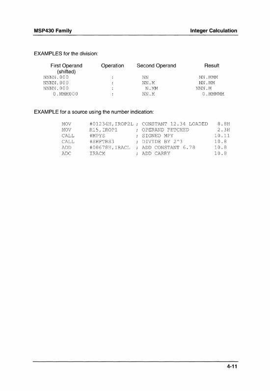
MSP430 Family
EXAMPLES for the division:
First Operand (shifted)
NNNN.OOO NNNN.OOO NNNN.OOO
O.MMMOOO
Operation Second Operand
NN NN.M
N.MM NN.M
Integer Calculation
Result
NN.MMM NN.MM
NNN.M o .MMMMM
EXAMPLE for a source using the number indication:
MOV #01234H, IROP2L CONSTANT 12.34 LOADED 8.8H MOV R15,IROP1 OPERAND FETCHED 2.3H CALL #MPYS SIGNED MPY 10.11 CALL #SHFTRS3 DIVIDE BY 2 A 3 10.8 ADD #00678H,IRACL ADD CONSTANT 6.78 10.8 ADC IRACM ADD CARRY 10.8
4-11

Integer Calculation MSP430 Family
4-12

MSP430 Family
TOPICS
5 General Purpose Subroutines
5.1 Saving Power Consumption
5.2 Calculated Branch
5.3 Binary to BCD
5.4 BCD to Binary
5.5 Bubble Sort
5.6 Table Search
5.7 Parity
5.8 Realtime Clock with 8 bit Timer
5.9 Realtime Clock with Basic Timer
5.10 Optional Calendar
5.11 Square Root
5.12 Trigonometric Calculation
Figures
Figure Title
5.1 Format of the Calendar
5.2
5.3
Straight Line Approximation
Sine Wave Approximation
General Purpose Subroutines
5-3
5-3
5-4
5-6
5-7
5-8
5-9
5-10
5-12
5-14
5-15
5-17
5-19
Page
5-15
5-19
5-21
5-1

General Purpose Subroutines MSP430 Family
5-2

MSP430 Family General Purpose Subroutines
5 General Purpose Subroutines
5.1 Saving Power Consumption
The following software routine generates a square-wave at the port pin PO.O. The low to high ratio is 1 :1. The time for the high and the low period is determined by the 8bit Timer Preload Register, which is set to fOh. This means that every 512 MCLK cycles (= 16 ACLK cycles) an interrupt occurs. In the time between these interrupts the processor is switched to Low Power Mode LPM3, to save power consumption. A wake up is initiated by the 8bit Timer. In the corresponding interrupt service routine the level of the port pin is determined.
i***************************************************** ******* ;EVERY 512 MCLK CYCLES A TC8-INTERRUPT OCCURS AND WAKES UP ;THE MSP430 FROM LOW POWER MODE 3 i***************************************************** *******
LOOP
MOV.B CLR.B
CLR.B BIS.B MOV.B
EINT MOV.B
CLR.B
MOV.B
BIS JMP
#PO_lIFG, &IE1 ;ENABLE TC8 INTERRUPT &IE2 ;AND DISABLE ALL OTHER
; INTERRUPTS &POIE ; DISABLE I/O INTERRUPT #po_O,&PODIR ;SET PORTPIN PO TO OUTPUT #PO_O,&POOUT ;SET PORTPIN PO TO LOW
;SET GIE BIT IN SR #OFOH,&TCPLD ;LOAD PRELOAD REGISTER
; (0100H-16) &TCDAT ;LOAD COUNTER WITH PRELOAD
; REGISTER #SSELO+ISCTL+ENCNT,&TCCTL
;SET TC8 TO ACLK CLOCK SOURCE, ;INTERRUPT FROM COUNTER AND ;ENABLE COUNTER
#SCGO+SCG1+CPUOFF,SR ;ENTER LP-MODE 3 LOOP ;NEVER ENDING LOOP
;INTERRUPT SERVICE ROUTINE FOR INTERRUPT CAUSED BY TC8: PO lINT XOR.B #PO_O,&POOUT ;TOGGLE OUTPUT
RETI ;RETURN FROM INTERRUPT
; INTERRUPT VECTOR ADDRESSES: . SECT "PO_1 VECT" ,OFFF8H ;ADDRESS FOR TC8 INTERRUPT . WORD .SECT . WORD
PO lINT "RSTVECT",OFFFEH START
;PUC/RESET ADDRESS
5-3
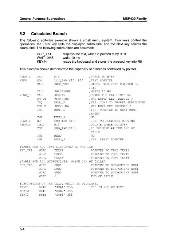
General Purpose Subroutines MSP430 Family
5.2 Calculated Branch
The following software example shows a small menu system. Two keys control the operations: the Enter key calls the displayed subroutine, and the Next key selects the subroutine. The following subroutines are assumed:
DSP_TXT WAIT10MS KEVIN
displays the text, which is pointed to by R10 waits 10 ms reads the keyboard and stores the pressed key into R6
This example should demonstrate the capability of branches controlled by pOinter.
CLR MOV CALL
CALL CALL CMP.B JEQ CMP.B JEQ
JMP BR INCD TST
JNZ JMP
R15 TXT_TAB (R15) ,Ria #DSP_TXT
#WAIT10MS #KEYIN #KEYE,R6 MENU_E #KEYN,R6 MENU_N
MENU_3 SUB_TAB (R15) R15 SUB_TAB (R15)
;TABLE POINTER ;TEXT POINTER ;DISPL. THE TEXT POINTED BY ;Rl0 ;WAITS 10 MS ;READS THE KEYS INTO R6 ;WAS ENTER KEY PRESSED ?
;YES, JUMP TO PROPER SUBROUTINE ;WAS NEXT KEY PRESSED ?
;YES, POINTER TO NEXT MENU ; ENTRY ;NO ;JUMP TO SELECTED ROUTINE ;UPDATE TABLE POINTER ;IS POINTER AT THE END OF ; TABLE ;NO ;YES, RESET POINTER
;TABLE FOR ALL TEXT DISPLAYED ON THE LCD TXT_TAB . WORD TEXTl ; POINTER TO TEXT TEXTl
. WORD
. WORD TEXT2 TEXT3
; POINTER TO TEXT TEXT2 ;POINTER TO TEXT TEXT3
;TABLE FOR ALL SUBROUTINES, WHICH CAN BE CALLED SUB_TAB . WORD SUBl ; POINTER TO SUBROUTINE SUBl
. WORD
. WORD
. WORD
SUB2 SUB3 a
;POINTER TO SUBROUTINE SUBl ; POINTER TO SUBROUTINE SUBl ;END OF TABLE
;DEFINITION OF THE TEXT, WHICH IS DISPLAYED TEXTl . BYTE "SUB1" ,255 ;255 IS END OF TEXT TEXT2 . BYTE "SUB2" ,255 TEXT3 . BYTE "SUB3" ,255
5·4

MSP430 Family General Purpose Subroutines
; SUBROUTINES WHICH ARE CALLED BY THE MENU SUBl
JMP MENU SUB2
JMP MENU SUB3
JMP MENU
The above program example use word-tables to branch to the appropriate location. To reduce program space, the word tables can be substituted by byte-tables. The following example use byte-tables to branch to the apropriate program location.
MEASINIT MOV.B #O,ADCST STATUS 0 IS THE INITIALIZATION VALUE
;SUBROU1'INE TO DEMONSTRATE THE BRANCHES IN REGARD OF BYTE-TABLES
ADCINT PUSH R6 WORKING REGISTER MOV.B ADCST,R6 ADC STATUS BYTE MOV.B ADCIT(R6) ,R6 REL. ADDRESS OF CURRENT
HANDLER ADD R6,PC BRANCH TO HANDLER
ADCIT . BYTE ADCSTO-ADCIT STATUSO: ADC INACTIVE . RYTF ADCST1-ADCIT 1: INIT 1ST CHARGE . BYTE ADCST2-ADCIT 2: CHARGE, INIT 1ST MEASUREMENT .BYTE ADCST3-ADCIT 3 : 1ST MEAS., INIT 2ND CHARGE
ADCSTO JMP L$402
ADCST1 JMP L$402
ADCST2 JMP L$402
ADCST3 JMP L$402
5-5
General Purpose Subroutines
L$402 INC.B
POP RET
ADCST
R6
5.3 Binary to BCD
MSP430 Family
ADCST + 1
RESTORE R6
The conversion of binary to BCD and vice versa is normally a time-consuming task. For example, five divisions by ten are necessary to convert a 16-bit binary number to BCD. The DADO instruction reduces this to a loop with five instructions.
THE BINARY NUMBER IN R4 IS CONVERTED TO AS-DIGIT BCD NUMBER CONTAINED IN R5 AND R6
BINDEC MOV #16,R7 LOOP COUNTER CLR R6 0 -> RESULT MSD CLR R5 o -> RESULT LSD
L$I RLA R4 DADD R5,R5 RESULT X2 LSD DADD R6,R6 MSD DEC R7 THROUGH? JNZ L$I RET YES, RESULT IN R51R6
The above subroutine may be enlarged to any length of the binary part simply by adding registers for the storage of the BCD number.
5.4 BCD to Binary
This subroutine converts a packed 16 bit BCD word to a 16 bit binary word by multiplying the digit with its valency. To reduce code length, the horner scheme is used as follows:
R4
;THE PACKED BCD NUMBER IN R4 IS CONVERTED INTO A BINARY NUMBER ;CONTAINED IN R5 ; INPUT: R4 = BCD NUMBER ; OUTPUT: R5 = BINARY NUMBER ;EXECUTION TIME: 79 CYCLES
5-6

MSP430 Family General Purpose Subroutines
BCDBIN MOV CLR CLR
SHFT4 RLA RLC RLA RLC RLA RLC RLA RLC ADD CLR DEC JZ
MPY10 RLA MOV RLA RLA ADD JMP
END RET
5.5 Bubble Sort
#4,R8 R5 R6 R4 R6 R4 R6 R4 R6 R4 R6 R6,R5 R6 R8 END R5 R5,R7 R5 R5 R7,R5 SHFT4
;LOOP COUNTER ( 4 DIGITS)
;SHIFT LEFT DIGIT INTO R6 ;THROUGH CARRY
;THROUGH ?
;YES ;NO, MULTIPLICATION WITH 10
;NEXT DIGIT ;RESULT IS IN R5
The following routine is sorting a word-array in falling sequence by using the Bubble Sort Algorithm, which is the most efficient algorithm if the array is less than 20 elements. If up to 100 elements are contained in the array, the execution time of this algorithm is acceptable with regard to the code-length. The number of loops which are necessary to check the entire word array is as follows:
n·(n-1) N=--
2 N = number of loops n = number of elements to be sorted
The absolute execution time depends on the number of changes to be done.
Example: Number of words to be sorted: 20 Number of cycles, if words are sorted: 7412 Number of cycles, if words are sorted inversely: 9122
The software to implement the Bubble Sort algorithm is as follows.
VARSTRT . SECT TABST . WORD TABEND . WORD
"VAR",0200H 10,20,30,4,5,6,7 8
;TABLE OF WORDS TO BE SORTED ;END OF TABLE ; INITIALISATION, ASO.
5-7

General Purpose Subroutines MSP430 Family
;SUBROUTINE TO SORT A LIST OF WORDS ;THE LIST TO SORT BEGINS AT ADDRESS TABST AND ENDS WITH ADDRESS ;TABEND. ;USE REGISTER: RS,R6,R7
BUBBLE L$20 L$30
L$12
MOV MOV MOV CMP JHS MOV MOV CMP JNE DEC JNE RET
#TABEND-TABST,R6 #TABST,RS @RS+,R7 @RS,R7 L$12 @RS,-2(R5) R7,O(R5) #TABEND,R5 L$30 R6 L$20
5.6 Table Search
;LENGTH OF LIST ;START OF LIST ;FETCH 1ST ITEM ;COMPARE TWO ITEMS ;RIGHT ORDER ;WRONG ORDER: ;EXCHANGE ITEMS ;ALL THROUGH? ;NO ;N-TIMES MADE ? ;NO
Table searches are efficiently performed by using the indexed mode (X(Rn)) to address the tables. In the following example, a table of 31 bytes is searched for a match with a 5-byte string. The used index mode has the capability to search a 65535-byte string in an 65535-byte table, if needed. If the search-string is found, the address of the first character will be TABST(R6).
EOS .EQU OFFH ;END OF STRING
VARSTRT . SECT "VAR",0200H TABST . BYTE "MUEHLHOFERANTONTEXASINSTRUMENTS" TABEND . BYTE EOS
ROMSTRT . SECT "PROG",OFOOOH ;INITIALIZATION AND OTHER SOFTWARE
SEARCH STRLEN MOV #OFFFFH,R4 ;DETERMINES THE LENGTH OF A STRING STR_1 INC R4 ;RESULT WILL BE CONTAINED IN R4
CMP.B #EOS,STRING(R4) JNE STR_l ;R4 IS LENGHT OF STRING
DEC R4 ;POINTER TO END OF STRING MOV #TABEND-TABST,R6 ;LENGHT OF TABLE
L1 MOV R4,R7 ;RESET POINTER L2 DEC R6 ;NEXT CHARACTER TO COMPARE
JNC NOFIND ;THE SEARCH STRING WAS NOT FOUND CMP.B STRING (R7) ,TABST(R6)
5-8

MSP430 Family General Purpose Subroutines
JNE DEC JC
MATCH
Ll R7 L2
;COMPARE NEXT ;ONE CHARACTER WAS FOUND ;IS NEXT CHARACTER THE SAME
;TABSTRT(R6) IS THE BEGINNING
NOFIND ;OF THE FOUND STRING IN THE TABLE ;THE TEXT WAS NOT FOUND
STRING . BYTE "TEXAS",EOS ;STRING TO FIND
5.7 Parity
This routine provides a quick way of determining the parity of the number of 1 's in a byte. By exclusive OR'ing all the bits of the byte together, a single bit will be derived which is the even parity of the word. When exclusive OR'ing, an even number of 1 's will combine to form a 0, leaving either an odd 1 or 0 bit. This routine keeps splitting the byte in half, and exclusive OR'ing the two halves. The algorithm is shown below:
STEP 1 7654 3210 R4
XOR 7654 R5 ---------
XXXX ABCD R4 STEP 2
AB CD R4 XOR AB R5 ---------
XXXX XX AB R4 STEP3
A B R4 XOR A R5
XXXX XX X P (RESULT) R4-> CARRY
i***************************************************** **********
;SUBROUTINE TO FIND EVEN PARITY IN R4 ;CARRY ~ 0 ~ EVEN NUMBER OF is ;CARRY ~ 1 ~ ODD NUMBER OF is ;R4 IS CLEARED AFTERWARDS ;USE REGISTER : R5 ;EXECUTION TIME: 17 CYCLES INCLUDING RET ;CODE LENGTH : 30 BYTES i***************************************************** **********
5-9

General Purpose Subroutines
PARITY MOV R4,R5 RRA R5
RRA R5 RRA R5 RRA R5 XOR R5,R4
MOV R4,R5 RRA R5 RRA R5 XOR R5,R4 MOV R4,R5 RRA R5 XOR R5,R4 RRA R4 RET
MSP430 Family
;DUBLICATE TARGET BYTE ;LINE UP THE MS NIBBLE WITH ;THE LS NIBBLE
;EXCLUSIVE OR THE NIBBLES TO GET A ;NIBBLE ANSWER ;DUBLICATE THE NIBBLE ANSWER ;LINE UP BITS 0, 1 OF THE ANSWER ;2, 3 OF THE ANSWER ;GET A NEW 2-BIT ANSWER ;DUBLICATE THIS 2-BIT ANSWER ;LINE UP BIT ° WITH BIT 1 ;GET FINAL EVEN PARITY ANSWER ;ROTATE ANSWER INTO THE CARRY BIT
The next possibility to find the parity of a byte is less program memory consuming, but needs more execution time. All bits of the byte whose parity has to be determined are shifted into the carry and added to as a sum. If the lowest significant bit is zero, the number of 1 's is even; if it is one, the number of 1 's is odd. This bit is shifted into the carry to identify the parity.
i***************************************************** **********
;SUBROUTINE TO FIND EVEN PARITY IN R4 ;CARRY = ° = EVEN NUMBER OF 1S ;CARRY = 1 = ODD NUMBER OF 1S ;R4 IS CLEARED AFTERWARDS ;USE REGISTER: R5,R6 ;EXECUTION TIME : 46 CYCLES INCLUDING RET ;CODE LENGTH : 16 BYTES i***************************************************** **********
PARITY2 MOV #8,R5 CLR R6
L1 RRA R4 ADC R6 DEC R5 JNZ L1 RRA R6 RET
5-10

MSP430 Family General Purpose Subroutines
5.8 Realtime Clock with 8 bit Timer
To programme a realtime clock, in this example the 8bit Timer is used to get the appropriate timing. The AClK frequency ( 32.768 kHz) is divided by 256 by the 8 bit Timer, and an interrupt is generated. This interrupt occurs every 1/128 second. The corresponding interrupt handler has to accumulate these interrupts to be able to calculate the time of it. The current time is stored in the 16 bit registers RTClSW and RTCMSW as follows:
RTCMSW I 2 :J 5 5 hours minutes
RTClSW 55 12l seconds 1/128sec
These registers are defined as R4 and R5, but they can also be located in the RAM. The routine to display the time is assumed to exist and is named DSP _ClK.
This routine can be extended to a complete calendar. For this purpose, the days can be accumulated to weeks, and further to months and years.
The accuracy of the calendar and the clock depends only on the accuracy of the crystal frequency.
i***************************************************** ******** 8BIT TIMER/COUNTER AS REALTIME CLOCK
;*************************************************************
RTCLSW RTCMSW CALEN
.EQU
.EQU
.EQU °
CLR CLR MOV.B CLR.B
CLR.B CLR.B
MOV.B
R4 R5
; ° ;LO WORD OF REALTIME CLOCK ;HI WORD OF REALTIME CLOCK
NO CALENDAR IS IMPLEMENTED
RTCLSW RTCMSW #PO_lIFG, &IE1 &IE2
&TCPLD &TCDAT
;1 ~ CALENDAR IS IMPLEMENTED ; INITIALIZATION:
;CLEAR REALTIME CLOCK
;ENABLE TC8 INTERRUPT ;AND DISABLE ALL OTHER ; INTERRUPTS ;CLEAR PRELOAD REGISTER ;LOAD COUNTER WITH PRELOAD ; REGISTER
#SSEL1+ISCTL+ENCNT,&TCCTL ;SET TC8 TO ACLK CLOCK ; SOURCE, ;INTERRUPT FROM COUNTER AND
5-11

General Purpose Subroutines MSP430 Family
; ENABLE COUNTER EINT ;SET GIE BIT IN SR
;INTERRUPT SERVICE ROUTINE FOR INTERRUPT CAUSED BY TC8: TC8 INT
INC BIT JZ CLRC DADD CMP JLO CLRC DADD DADC CMP.B JNE CLRC DADD CMP JNE CLR .IF CALL
.ENDIF TC8 1 CALL TC8_END RETI
RTCLSW #80H,RTCLSB TC8_END
#20H,RTCLSW #6000H,RTCLSW TC8_1
#4000H,RTCLSW RTCMSW #0060H,RTCMSW TC8_1
#40H,RTCMSW #2400H,RTCMSW TC8 1 RTCMSW CALEN #CALDAR
;INTERRUPT VECTOR ADDRESSES:
;INC 1/128 SEC COUNTER ;1 SEC OVER? ;NO ;YES ;ADJUST LSW WITHOUT CARRY ;60 SEC OVER? ;NO, DISPLAY NEW TIME ;YES ;ADJUST MSW WITHOUT ;AND ADJUST MSW ;1 HOUR OVER ? ;NO ;YES ; ADJUST MSW WITHOUT ;1 DAY OVER? ;NO ;YES, ADJUST MSW
CARRY
CARRY
;ONLY IF THE CALENDAR ; FUNCTION ;IS IMPLEMENTED
;DISPLAY THE TIME
. SECT
. WORD
. SECT
. WORD
"PO_1VECT",OFFF8H ;ADDRESS FOR TC8 INTERRUPT TC8_INT "RSTVECT",OFFFEH START
; PUC/RESET ADDRESS
5.9 Realtime Clock with Basic Timer
The appropriate timing for a Realtime Clock can also be generated by the Basic Timer. The initialization routine has to be substituted by the following routine:
; INITIALIZATION: CALEN .EQU o
CLR RTCLW CLR RTCMSW
; 0 ; 1
NO CALENDAR IS IMPLEMENTED CALENDAR IS IMPLEMENTED
;CLEAR REALTIME CLOCK
;LCD-TIMING CONFIGURATION STANDS HERE
5-12

MSP430 Family General Purpose Subroutines
BIS.B
BIS.B CLR.B
EINT
#IP2+DIV,&BTCTL;TIMER INTERRUPT OCCURS EVERY ;SEC.
#BTIE,&IE2 &IEl
;ENABLE BASIC TIMER INTERRUPT ;AND DISABLE ALL OTHER ; INTERRUPTS ;SET GIE BIT IN SR
Because of the possibility of configuring the Basic Timer in such a way that the interrupt occurs only every second (not every 1/128 sec as above), the counter for the 1/128 seconds is unnecessary and will be set to zero. For that reason the interrupt service routine becomes shorter as follows:
;INTERRUPT SERVICE ROUTINE FOR INTERRUPT CAUSED BY BT: BT_INT
CLRC DADD CMP JLO CLRC DADD
#lOOH,RTCLSW #6000H,RTCLSW BT_1
#4000H,RTCLSW DADC RTCMSW CMP.B #0060H,RTCMSW JNE BT_l CLRC DADD CMP JNE CLR .IF CALL
.ENDIF CALL
#40H,RTCMSW #2400H,RTCMSW BT_l RTCMSW CALEN #CALDAR
#DSP_CLK
;ADJUST LSW WITHOUT CARRY ;60 SEC OVER? ;NO, DISPLAY NEW TIME ;YES ;ADJUST MSW WITHOUT CARRY ;AND ADJUST MSW ; 1 HOUR OVER ? ;NO ;YES ;ADJUST MSW WITHOUT CARRY ;1 DAY OVER? ;NO ;YES, ADJUST MSW
;ONLY IF THE CALENDAR ; FUNCTION ;IS IMPLEMENTED
;DISPLAY THE TIME
; INTERRUPT VECTOR ADDRESSES: . SECT "PO_1 VECT" , OFFE2H; ADDRESS FOR BT INTERRUPT . WORD . SECT . WORD
BT_INT "RSTVECT",OFFFEH ;PUC/RESET ADDRESS START
5-13

General Purpose Subroutines MSP430 Family
5.10 Optional Calendar
This code enhances the previous realtime clock to a calendar, which will keep track of days, months, and years including leap years. To implement these functions, it is necessary to set the assembler variable CALEN =1. The result will be in the following registers in the BCD Format:
MONDAY 12 3D months days
YEAR
years
Figure 5.1: Format of the Calendar
i***************************************************** ***********
; SUBROUTINE: CALDAR ;THIS ROUTINE IS CALLED EVERY DAY AND CALCULATES THE DATE INCLUDING ;LEAP YEARS. ; INPUT: IS CALLED EVERY DAY ;OUTPUT: WORD MODAY : MSB = MONTHS, LSB DAYS
WORD YEAR : YEARS ;USED REGISTER: TEMP .EQU RB ;****************************************************************
TEMP .EQU RB ; TEMPORARY REGISTER LEAPO .EQU OFFECH ; MASKS LEAPl .EQU 12H LEAP2 .EQU OH
DAYTAB . BYTE 31H,2BH,31H,30H,31H,30H ;MAX DAYS EACH MONTH . BYTE 31H,31H,30H,31H,30H,31H ;IN BCD FORMAT
CALDAR MOV MODAY, TEMP ;ONLY MONTHS TO TEMP SWPB TEMP BIC #OFFOOH,TEMP ;CLEAR DAYS OF TEMP CMP.B #lO,TEMP ;ADJUST BCD -> BIN JLO CALDAR_l SUB.B #6,TEMP
CALDAR_l CMP.B DAYTAB-l(TEMP),MODAY ;IS ONE MONTH OVER ? JLO CALDAR_6 ;NO CMP #022BH,MODAY ; WAS IT 2B.FEB. ?
5-14

MSP430 Family General Purpose Subroutines
JNE CALDAR_5
CALCULATION OF THE LEAP YEAR MOV YEAR,TEMP BIC #LEAPO , TEMP CMP #LEAP1,TEMP JEQ CALEAP CMP #LEAP2,TEMP JEQ CALEAP JMP CALDAR_5
CALEAP INC MODAY RET
; NORMAL OPERATION WITHOUT LEAP YEAR CALDAR_5
CLRC DADD #OlOOH,MODAY BIC #OOFFH,MODAY
CALDAR_6 CLRC DADD #l,MODAY CMP #13 OOH, MODAY JLO CALDAR_7 MOV #OlOlH,MODAY CLRC DADD #l,YEAR
CALDAR_7 RET
5.11 Square Root
;NO, NORMAL OPERATION
;NO LEAP YEAR, NORMAL OPERATION ;TODAY IS 29.FEB
;YES, ONE MORE MONTH ; DAYS TO ZERO
;ONE DAY IS OVER ;IS ONE YEAR OVER ? ;NO ;YES, ADJUST MONTHS AND DAYS
;ONE MORE YEAR
The square root is often needed in computations. The following subroutine uses the NEWTONIAN approximation for this calculation. The number of iterations depends on the length of the operand. The general formula is:
m.fA = X
Xn+l = ~(m-1).xn+_A_) m Xnm- 1
With the substitution of m=2 it follows:
.fA =X
Xn+l=..!..(Xn+~) 2 Xn
XO=%
5-15

General Purpose Subroutines MSP430 Family
To calculate NXn a division is necessary, which is done in the subroutine XDIV. The result of this division has the same integer format as the divisor Xn. This makes an easy operation possible.
AH AL XNH XNL
.EQU
.EQU
.EQU
.EQU
R8 R9 RiO Rll
;HIGH WORD OF A ;LOW WORD OF A ;HIGH WORD OF RESULT ;LOW WORD OF RESULT
;THE RANGE FOR THE OPERAND EXTENDS FROM OOOO.0002H TO 7FFF.FFFFH ; INPUT: OPERAND IN AH.AL ;OUTPUT: RESULT IN XNH.XNL ; EXAMPLE: SQR(2)=1.6A09H
SQR(7FFF.FFFFH) B5.04F3H SQR(OOOO.0002H) O.016AH
SQR ;SET XO TO A!2 FOR THE FIRST MOV AH,XNH MOV RRA RRC CALL ADD ADDC RRA RRC CMP JNE CMP JNE RET
AL,XNL XNH XNL #XDIV R13,XNL R12,XNH XNH XNL XNH,R12 SQR_l XNL,R13 SQR_l
; APPROXIMATION ;XO=A!2
;R12XR13=A!XN ;XN+i=XN+A!XN
;XN+i=1!2(XN+A!XN)
;IS HIGH WORD OF XN+l = XN ;NO, ANOTHER APPROXIMATION ;YES, IS LOW WORD OF XN+i = XN ;NO, ANOTHER APPROXIMATION ;YES, RESULT IS XNH.XNL
i***************************************************** ******** ;EXTENDED UNSIGNED DIVISION ;R81R9 ! RiOIRil = R121R13, REST IS R141R15 ;THIS DIVISION ROUTINE IS WRITTEN EXCLUSIVELY FOR THE SQUARE ;ROOT ROUTINE TO OPTIMIZE THE EXECUTION TIME FOR THE DIVISION ;OF A!XN. i***************************************************** ********
XDIV PUSH R8 ;SAVE OPERANDS ONTO THE STACK PUSH R9 PUSH RiO PUSH Rll MOV #48,R7 ;ONLY 48 LOOPS ARE NECESSARY CLR R15 ; CLEAR REST CLR R14 CLR R12 ; CLEAR RESULT CLR R13
5-16

MSP430 Family General Purpose Subroutines
L$361 RLA R9 ;SHIFT ONE BIT OF R81R9 TO ;R141R15
RLC R8 RLC R15 RLC R14 CMP RIO,R14 ;1S SUBTRACTION NECESSARY? JLO L$364 ;NO JNE L$363 ;YES CMP Rll,R15 ;Rll=R15 JLO L$364 ;NO
L$363 SUB Rll, R15 ;YES, SUBTFACT SUBC FIO,R14
L$364 RLC R13 ;SHIFT FESULT TO R121 R13 RLC F12 DEC R7 ;AFE 48 LOOPS OVEF ?
JNZ L$361 ;NO POP Rll ;YES, FESTOFE OPEFANDS POP RIO POP R9 POP F8 RET
5.12 Trigonometric Calculation
As a matter of principle there are three methods of calculating trigonometric functions:
1. Power series e.g. Series of Taylor
2. Straight line approximation Fetch the gradient and offset of a straight line equation from a table e.g. sin(x) = mx . x = tx ;mx and tx are stored in a table.
3. Fetching the calculated values from a table.
The first method is the most time-consuming method, since there is no hardware multiplier implemented in the processor. The advantage of this method is the optional accuracy. The higher the accuracy the higher is the ordinal number of the power series. The multiplication can be reduced by using the horner scheme.
As opposed to the first method, the following two methods determine the value indirectly from tables. For this purpose the trigonometric curves are divided into sections and therefore the accuracy of the result is limited. The straight line approximation needs one table to determine the gradient and one table to determine the offset of a straight line.
5-17
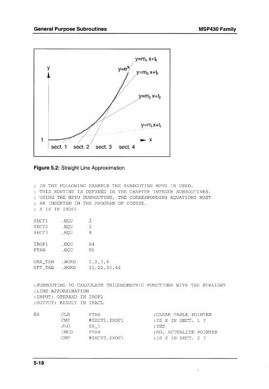
General Purpose Subroutines MSP430 Family
Y=~x+~
Y Y=111a X+a
1 Y=~X+~
Y=~X+~
_x sect. 1 sect. 2 sect. 3 sect. 4
Figure 5.2: Straight Line Approximation
IN THE FOLLOWING EXAMPLE THE SUBROUTINE MPYU IS USED. THIS ROUTINE IS DEFINED IN THE CHAPTER INTEGER SUBROUTINES. USING THE MPYU SUBROUTINE, THE CORRESPONDING EQUATIONS MUST BE INSERTED IN X IS IN IROP1
SECTl .EQU SECT2 .EQU SECT3 .EQU
IROPl .EQU PTAB .EQU
GRA_TAB . WORD OFF_TAB . WORD
THE PROGRAM OF COURSE.
2 5 8
R4 R5
1,2,3,4 11,22,33,44
;SUBROUTINE TO CALCULATE TRIGONOMETRIC FUNCTIONS WITH THE STRAIGHT ;LINE APPORXIMATION ; INPUT: OPERAND IN IROP1 ; OUTPUT: RESULT IN IRACL
EX CLR PTAB CMP #SECT1,IROP1 JLO EX_1 INCD PTAB CMP #SECT2,IROP1
5-18
;CLEAR TABLE POINTER ;IS X IN SECT. 1 ? ;YES ;NO, ACTUALIZE POINTER ;IS X IN SECT. 2 ?

MSP430 Family General Purpose Subroutines
JLO EX_l ;YES INCD PTAB ;NO, ACTUALIZE POINTER CMP #SECT3,IROPl ;IS x IN SECT. 3 ? JLO EX_l ;YES INCD PTAB ;NO, x IS IN SECT. 4
EX_l MOV GRA_TAB(PTAB) ,IROP2L ; FETCH GRADIENT CALL #MPYU ;IRACL=M*X ADD OFF_TAB (PTAB) ,IRACL ;IRACL=M*X+T RET
The straight line approximation method is advantageous, if the trigonometric curve can be divided into a few sections. If many sections are needed, the search for the right section will take a lot of time and code space. A solution is to calculate the pointer by the x-value immediately.
For example: Range of x-values: 0.0 ... 10.0 Sections needed at least: 8
To get the right pointer from the x-value only, the input value is used. This means that if the trigonometric curve is divided into 10 sections, the input value is already the pointer to the tables.
The third method to calculate a trigonometric function is to get the value directly from a table. This is suitable if only a few operands are possible. For example the operands of a sine wave can only be one of 46 possible values of one period.
y
~~~~~--------~----------------~~~x
Figure 5.3: Sine Wave Approximation
5-19

General Purpose Subroutines MSP430 Family
Only the values of the quarter of the sinus wave are stored in the table. All values can be determined as follows:
O<x<n/2 n/2<x<1t 1t<x<21t
y=y(x) y = y(INV(x)+1t) Y = -y(x-1t)
The accuracy of the values that are stored in the table is 8 bit and can be increased to 16 bit. The table length can be up to 65536 bytes or words. In this example 12 values are stored (including 0) for one quarter of the sine wave.
HALFW .EQU
QUARTW .EQU
24
12
;NUMflRR OF VALUES FOR THE HALF ; WAVE ;NUMBER OF VALUES FOF THE ; QUARTER
;************************************************************ SIN(R4)=R5
;IN THE SIN_TAB ONLY THE NUMBERS AFTER THE POINT ARE PERFORMED. ;THE OPERAND HAS TO BE LOADED INTO R4 BEFORE CALLING SIN AND ;MUST BE A NUMBER BETWEEN 0 AND 45. THE RESULT WILL BE IN R5 ;************************************************************
SIN
. BY'rE
. BYTE PUSH CMP JLO SUB CMP
JLO INV ADD MOV.B
O,22H,45H,65H,85H,OA1H,OBBH,OD1H,OE3H,OF1H OFAH,OFFH R4 #HALFW,R4 SIN_1 #HALFW-1,R4 #QUARTW,R4
SIN_2 R4
;IS x IN THE NEGATIVE HALF WAVE? ;NO ;YES, CORRECT x ;IS x IN THE 2TH HALF OF THE ;HALF WAVE ;NO
#HALFW,R4 ;YES, ADJUST x SIN_TAB (R4) ,R5 ;GET RESULT FROM TABLE
POP R4 CMP JLO INV INC
SIN_END RET
5-20
#HALFW,R4 SIN_END R5 R5
;IS x IN THE NEGATIVE HALF WAVE? ;NO RESULT IS OK ;YES, RESULT HAS TO BE NEGATED

MSP430 Family
Topics
6 6.1
6.2
6.3
6.4
6.5
6.6
1/0 Module Programming Examples
Initialization
Keyboard-Matrix of 4 x 4 Keys
Keyboard-Matrix of 3 x 4 Keys
Noise Generator
External EEPROM for Setup Values
12C BUS Connection
Figure Title
6.1 4x4 Keyboard Matrix
6.2 3x4 Keyboard Matrix
6.3
6.4
6.5
Noise Generator
External EEPROM Connection
12C-Bus Connections
Figure Title
Figures
Notes
6.1 Next example does not contain the necessary delay times
6.2 Next example does not contain the necessary delay times
Tables
Figure Title
6.1 Configuration of the MUX Modes
6.2 Configuration of the MUX Modes
1/0 Module
6-3 6-3
6-4
6-6
6-8
6-9
6-11
Page
6-4
6-6
6-8
6-9
6-11
Page
6-10
6-11
Page
6-4
6-6
6-1

110 Module MSP430 Family
6-2
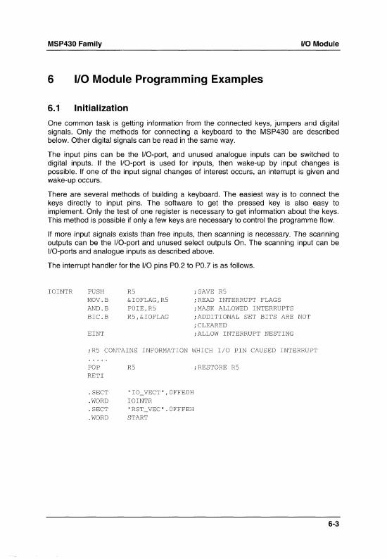
MSP430 Family I/O Module
6 I/O Module Programming Examples
6.1 Initialization
One common task is getting information from the connected keys, jumpers and digital signals. Only the methods for connecting a keyboard to the MSP430 are described below. Other digital signals can be read in the same way.
The input pins can be the I/O-port, and unused analogue inputs can be switched to digital inputs. If the I/O-port is used for inputs, then wake-up by input changes is possible. If one of the input signal changes of interest occurs, an interrupt is given and wake-up occurs.
There are several methods of building a keyboard. The easiest way is to connect the keys directly to input pins. The software to get the pressed key is also easy to implement. Only the test of one register is necessary to get information about the keys. This method is possible if only a few keys are necessary to control the programme flow.
If more input signals exists than free inputs, then scanning is necessary. The scanning outputs can be the I/O-port and unused select outputs On. The scanning input can be I/O-ports and analogue inputs as described above.
The interrupt handler for the 1/0 pins PO.2 to PO.? is as follows.
IOINTR PUSH RS ;SAVE RS MOV.B &IOFLAG,RS ;READ INTERRUPT FLAGS AND.B POIE,RS ;MASK ALLOWED INTERRUPTS BIC.B RS,&IOFLAG ;ADDITIONAL SET BITS ARE NOT
; CLEARED EINT ;ALLOW INTERRUPT NESTING
;RS CONTAINS INFORMATION WHICH I/O PIN CAUSED INTERRUPT
POP RS ;RESTORE RS RETI
.SECT "IO_VECT",OFFEOH
. WORD IOINTR
. SECT "RST_VEC".OFFFEH
. WORD START
6-3

I/O Module MSP430 Family
6.2 Keyboard-Matrix of 4 x 4 Keys
This is the most commonly used method of connecting a keyboard to a microprocessor, because of the minimal hardware requirement. Only the diodes are necessary to protect the outputs PO.O to PO.3 if more than one key is pressed.
o 32kHz
LCD
COM 112jY55lB I SEL
MSP430
PO.O PO.l
PO.2 PO.3
PO.4 *A *8 *C *D
PO.5 *E *F *G *H
PO.6 *1 *J 'K *L
po.? *M *N '0 *P
*=F Figure 6.1: 4x4 Keyboard matrix
To check the keyboard, one output line ( PO.O to PO.3 ) has to be high. If a key in this line is pressed, the corresponding input line will be high too. To scan all keys, the outputs have to be high, one after the other, and the input lines can then be read in.
The following table shows the key-code which is on the 1/0 port, if the correspondig key was pressed.
6-4

MSP430 Family 1/0 Module
Key inp autp Hex
A 0001 1000 18
B 0001 0100 14
C 0001 0010 12
D 0001 0001 11
E 0010 1000 28
F 0010 0100 24
G 0010 0010 22
H 0010 0001 24
I 0100 1000 48
J 0100 0100 44
K 0100 0010 42
L 0100 0001 41
M 1000 1000 88
N 1000 0100 84
0 1000 0010 82
p 1000 0001 81
Table 6.1: Configuration of the MUX Modes
The Routine to scan the 4x4 keyboard now follows. The pressed key will be stored in KEYOUT. If more than one key was pressed, the result is the binary OR of the keycodes shown in the table above. If no key was pressed, KEYOUT becomes zero.
KEYMASK . EQU KEYOUT .EQU
R4 R6
; MASK FOR THE OU~'PUT
;RESULT OF THE SCAN
MOV.B #OFH, &PODIR ;INITIALIZATION OF THE I/O PORT
;SUBROUTINE TO GET THE SCANCODE FROM THE KEYBOARD WITH THE ;4X4 MATRIX ;OUTPUT: SCANCODE AS SHOWN IN TABLE 6.1 IN KEYOUT ;USE REGISTER: R7
KEYSCAN MOV #4,R7 MOV #1, KEYMASK MOV.B TST.B JZ
KEYMASK,&POOUT &POIN SCAN_2
;LOOP COUNTER
;SCAN ONE LINE ;ANY KEY PRESSED ;NO
6-5

I/O Module MSP430 Family
BIS.B KEYMASK,KEYOUT ;YES, SET CORRESPONDING BITS BIS.B &POIN,KEYOUT
SCAN_2 RLA.B KEYMASK ; NEXT SCANNING LINE DEC R7 ;ALL LINES TESTED ? JNZ SCAN_l ;NO, NEXT LINE RET
6.3 Keyboard-Matrix of 3 x 4 Keys
The next scheme describes a keyboard matrix which needs only 4 1/0 pins to handle 12 keys. This is possible because of the capability of switching the direction of the 110 pins independently.
32kHz
r1Dfl" LCD
COM =>[123Y56lB I SEL
Key Outp Inp Hex
A 0001 1000 18 MSP430
B 0001 0100 14
C 0001 0010 12 po.o
A l! C 0 0010 1000 28 PO.1
D E F E 0010 0100 24 PO.2
G H I F 0010 0001 21 PO.3
J K L G 0100 1000 48
'7 '7 H 0100 0010 42
'---- I 0100 0001 41
J 1000 0100 84
'=F K 1000 0010 82
L 1000 0001 81
Figure 6.2: 3 x 4 Keyboard Matrix Table 6.2: Configuration of the MUX Modes
6-6

MSP430 Family I/O Module
KEYMASK . EQU KEYOUT .EQU
R4 R6
;MASK FOR THE OUTPUT ;RESULT OF THE SCAN
;SUBROUTINE TO GET THE SCANCODE AS SHOWN IN TABLE 6.2 ; OUTPUT: KEYOUT = SCANCODE ;USE REGISTER: R7,R8,R9
KEYSCAN MOV MOV BIC.B BIC.B
SCAN_l BI S . B BIS.B MOV.B BIC.B TST.B
JZ MOV.B
RLA.B
#4,R7 #l,KEYMASK #OFH,&POOUT #OFH,&PODIR
KEYMASK,&POOUT KEYMASK,&PODIR &POIN,R8 KEYMASK+OFOH,R8 RS
R9
RLA.B R9 RLA.B R9 RLA.B R9 BIS.B BIS.B BIC.B BIC.B RLA.B DEC JNZ RET
R9,KEYOUT R8,KEYOUT KEYMASK,&POOUT KEYMASK,&PODIR KEYMASK R7 SCAN_l
6.4 Noise Generator
;LOOP COUNTER ;FIRST SCANNING LINE ; INITIALISATION VALUE ;SET ONLY KEYBOARD LINES TO ; INPUT ;SCAN ONE LINE ;SET THE OUTPUT LINE ;WHOLE INPUT REGISTER TO R8 ;RS CONTAINS THE PRESSED KEY ;WAS ANY KEY IN THIS LINE ;PRESSED ?
;NO, TEST ANOTHER LINE ;YES, SET THE CORRESPONDING ;BITS ;SHIFT THE OUTPUT MASK 4 BITS ; LEFT
;SET THE MASKED OUTPUT BITS ;SET THE MASKED INPUT BITS ;CLEAR OUTPUT REGISTER ;CLEAR DIRECTION REGISTER ;NEW SCANNING LINE ;ALL LINES TESTED ;NO, NEXT LINE ;YES, RETURN
The Noise Generator is constructed with a 32bit shift register having feedback which is generated by a logical XNOR of bit 1 and bit 14 of the 16bit register NREG+ 1. Therefore, the shift register receives about 2 billion different conditions before the values are repeated.
The output can be a loudspeaker with amplifier and low-pass filter. If a random number is necessary, the value of the register NREG or NREG+ 1 has simply to be used.
6-7

VO Module
Noise
NREG+1 16 bit
Bit 14
XNOR
MSP430 Family
NREG+O 16 bit
Figure 6.3: Noise Generator
LS .EQU 1 ;OUTPUT PIN FOR THE LOUDSPEAKER NREGO .EQU R4 NREG1 .EQU R5
BIS.B #LS,&PODIR ;PREPARE I/O PIN FOR OUTPUT NOISE CLR NREGO ;STARTING VALUE FOR THE 32 BIT
; SHIFT CLR NREG1 ;REGISTER, CAN BE EVERY OTHER
; NUMBER
NLOOP1 BIC.B #LS,&POOUT ;SET OUTPUT TO LOW NLOOP2 MOV NREG1,R6 ;DUPLICATE NREG1
RRC R6 ;SHIFT BIT 14 TO BIT 1 RRC R6 RRC R6 RRC R6 XOR NREG1,R6 ;XOR BIT 14 AND BIT 1 BIT #4000H,R6 ;AND MOVE RESULT TO CARRY XOR #1,SR ;INVERT CARRY
;NOW CARRY IS BIT 14 XNOR BIT 1 RLC NREGO ;SHIFT 32BIT REGISTER FOR ONE TIME RLC NREG1 JNC NLOOP1 ;AND OUTPUT CARRY TO LS BIS.B #LS,&POOUT JMP NLOOP2
One loop needs 17 cycles, so the sampling rate of the generated signal on the output is about 59 kHz and therefore the signal repeats after about 9 hours. This should be acceptable for a noise.
6-8

MSP430 Family I/O Module
6.5 External EEPROM for Setup Values
To save important values in a nonvolatile storage, a serial EEPROM can be connected to the 1/0 port of the MSP430. This memory keeps its values even if the supply voltage is disconnected. In this way it is possible to store setup values which are necessary to initialize the system after the Powerup Reset.
The EEPROM is connected to the MSP430 by dedicated inputs and outputs. Three (two) control lines are necessary for proper operation:
- Data line SDA: an I/O-port is needed for this bi-directional line. Data can be read from and written to the EEPROM
- Clock line SCL: an output line is sufficient for the clock line. This clock line may be used for other peripheral devices too, if it is ensured that no data is present on the data line during use.
- Supply line: if the current consumption of the EEPROM when not in use is too high, then switching of the EEPROM's Vcc is necessary. Three possible solutions are shown: 1. The EEPROM is connected to SVcc. This is a very simple way to have the
EEPROM switched off when not in use 2. The EEPROM is switched on and off by an external PNP transistor. 3. The EEPROM is connected permanently to +5V , if its power consumption does
not playa role.
SVee +5V +5V
PO.z,Oy
MSP430
Clock PO.y,Ox
Vee SCL ~-.;:.:.:.;::.:..t--l
X24LCxx Data Ax SDA 1+-_-==-4-~ PO.x
Vss Vss Vee
OV
OV +5V
Figure 6.4: External EEPROM Connection
An additional way to connect an EEPROM to the MSP430 is shown in the chapter describing the 12C-8us.
6-9

1/0 Module MSP430 Family
Note: Next example does not contain the necessary delay times
The next example does not contain the necessary delay times between the setting and resetting of the clock and data bits. These delay times can be seen in the specifications of the EEPROM device. With a processor frequency of 1 MHz each one of the next instructions needs 5f.ls.
EXAMPLE: The EEPROM with the dedicated I/O-lines is controlled with normal 1/0-instructions. The SCL line is driven by 017; the SDA line is driven by PO.6:
POOUT .EQU 011H PORTO OUTPUT REGISTER PODIR .EQU 012H PORTO DIRECTION REGISTER SCL .EQU OFOH 017 CONTROLS SCL, 039H LCD
ADDRESS SDA .EQU 040H PO.6 CONTROLS SDA LCDM .EQU 030H LCD CONTROL BYTE
INITIALIZE I2C BUS PORTS: INPUT DIRECTION: BUS LINE GETS HIGH OUTPUT BUFFER LOW: PREPARATION FOR LOW SIGNALS
BIC.B #SDA,&PODIR SDA TO INPUT DIRECTION BIS.B #SCL,&LCDM+9 SET CLOCK HI BIC.B #SDA,&POOUT SDA LOW
START CONDITION: SCL AND SDA ARE HIGH, SDA IS SET LOW, AFTERWARDS SCL GOES LO
BIS.B #SDA,&PODIR SET SDA LO (SDA GETS OUTPUT) BIC.B #SCL,&LCDM+9 SET CLOCK LO
DATA TRANSFER: OUTPUT OF A "1 " BIC.B #SDA, &PODIR SET SDA HI BIS.B #SCL,&LCDM+9 SET CLOCK HI BIC.B #SCL,&LCDM+9 SET CLOCK LO
DATA TRANSFER: OUTPUT OF A 110 " BIS.B #SDA,&PODIR SET SDA LO BIS.B #SCL,&LCDM+9 SET CLOCK HI BIC.B #SCL,&LCDM+9 SET CLOCK LO
STOP CONDITION: SDA IS LOW, SCL IS HI, SDA IS SET HI BIC.B #SDA,&PODIR SET SDA HI BIS.B #SCL,&LCDM+9 SET SCL HI
The examples shown above for the different conditions can be implemented into a subroutine which outputs the content of a register. This shortens the necessary ROM code significantly. Instead of line Ox for the SCL line, another I/O-port PO.x may be used. See section 12C Bus Connection for more details of such a subroutine.
6·10

MSP430 Family VO Module
6.6 12C BUS Connection
If more than one device is to be connected to the 12C-Bus, then two I/O-ports are needed for the control of the 12C-peripherals. The reason for this is the need to switch SOA and SCl to the high impedance state.
The figure below shows the connection of three 12C-peripherals to the MSP430: - An EEPROM PCF8581 with 128x8-bit data - An EEPROM X24lCxx with 2048x8-bit data - An 8-bit OAC/AOC
+5V
Rp ORP
PO.a
PO.b t t MSP430
SCL SDA SCL SDA SCL SDA A2 - A2 - Ax
PCF8581 A1 - X24LCxx A1 r- PCF8591 AINx AO - AO - AOUT
Vee Vss Vdd Vss Vdd Vss Vdd Vss
I I I I I I I I +5V OV +5V OV +5V OV +5V OV
Figure 6.5: 12C-Bus Connections
Note: Next example does not contain the necessary delay times
SCL
SDA
~ ~ ~
The next example does not contain the necessary delay times between the setting and resetting of the clock and data bits. These delay times can be seen in the specifications of the peripheral device.
6-11

I/O Module MSP430 Family
The complete 12C-Handler for one byte of data follows. The data pin SDA needs an 1/0-pin (PortO); the clock pin SCL may be an I/O-pin or an output pin.
Bit 15 8 7 0
I Slave Address I RIW I Data I
SCLDAT .EQU OllH POOUT SCLEN .EQU 012H PODIR SDA .EQU 040H PO.6 CONTROLS SDA SCL .EQU 080H PO.7 CONTROLS SCL SDADAT .EQU OllH PO OUTPUT DIRECTION
REGISTER SDAEN .EQU 012H PO DIRECTION REGISTER
INITIALIZATION FOR THE I2C BUS PORTS: INPUT DIRECTION: BUS LINES GET HIGH BY PULL-UPS OUTPUT BUFFERS LOW: PREPARATION FOR LOW ACTIVE SIGNALS INITIALIZATION FOR SDA AND SCL FROM PORTO
BIC.B #SCL+SDA,&SDAEN
BIC.B #SCL+SDA,&SDADAT
INITIALIZATION FOR SDA AT PORTO, SCL
BIC.B #SDA,&SDAEN BIC.B #SDA,&SDADAT BIC.B #SCL,&SCLEN BIC.B #SCL,&SDADAT
SCL AND SDA TO INPUT DIRECTION SCL AND SDA OUTPUT BUFFER LOW
AT TP.X (EVEOPT)
SDA TO INPUT DIRECTION SDA OUTPUT BUFFER LOW SCL TO INPUT DIRECTION SCL OUTPUT BUFFER LOW
i***************************************************** *************
I2C-HANDLER: OUTPUTS OR READS 8-BIT DATA
WRITE: R/@W = O. R6 CONTAINS SLAVE ADDRESS AND 8-BIT DATA RETURN: C = 0: TRANSFER OK (R6 UNCHANGED)
; CALL
;READ:
6-12
MOV.B BIS CALL JC
R/@W
C = 1: ERROR (R6 UNCHANGED) DATA,R6 (2*ADDR)*0100H,R6 #I2CHND ERROR
8-BIT DATA TO R6 ADDRESS AND FUNCTION CALL HANDLER C = 1: ERROR OCCURED
1. R6 CONTAINS SLAVE ADDRESS, LOW BYTE UNDEFINED

MSP430 Family I/O Module
; CALL RETURN: R6 CONTAINS 8-BIT DATA IN LOW BYTE, HI BYTE 0
MOV CALL
(2*ADDR+1)*0100H,R6 #I2CHND
ADDRESS AND FUNCTION CALL HANDLER 8-BIT INFO IN R6 LO
;******************************************************************
I2CHND . PUSH R5 ; SAVE REGISTERS
I2C START CONDITION: SCL AND SDA ARE HIGH, SDA GOES LOW THEN SCL GOES LOW
BIS.B BIS.B
#SDA,&SDAEN #SCL,&SCLEN
SET SDA LO SET SCL LINE LO
SENDING OF THE ADDRESS BITS (7) AND R/@W-BIT
MOV #8000H,R5 BIT MASK MSB I2CCL BIT R5,R6 BIT -> CARRY
CALL #I2CSND SEND CARRY CLRC RRC R5 NEXT ADDRESS BIT CMP #080H,R5 R/@W SENT? JNE I2CCL NO, CONTINUE
ADDRESS AND R/@W SENT: RECEIVE OF ATHEN CKNOWLEDGE BIT, DECISION IF READ OR WRITE
CALL #I2ACKN JC 12CERR NO ACKNOWLEDGE, BIT #100H,R6 READ OR WRITE? JNZ I2CRI
; WRITE: CONTINUE WITH 8-BIT DATA IN LOW BYTE OF R6
ERROR
I2CWL BIT CALL CLRC RRC
R5,R6 #I2CSND
; WRITE: CONTINUE WITH DATA
R5
JNC I2CWL CALL #I2CACKN
; CARRY INFORMATION: 0: OK, 1: ERROR
I2CEND I2CERR
.EQU BIC.B BIC.B RET
$ #SCL,&SCLEN #SDA,&SDAEN
IF TESTBIT IN CARRY: FINISHED
ACKNOWLEDGE BIT -> CARRY
STOP CONDITION SET SDA HI CARRY INFO UNDESTROYED
READ: READ 8 DATA BITS TO R6 LOW BYTE. R5 = 080H
6-13

I/O Module
I2CRI CALL RLC.B RRA JNC
CALL JMP
#I2CRD R6 R5 I2CRI
#I2CO I2CEND
SUBROUTINES FOR I2C-HANDLER
MSP430 Family
READ BIT -> CARRY CARRY TO LSB R6 BIT MASK USED FOR COUNT BIT MASK IN CARRY: FINISHED ACKNOWLEDGE BIT = 0 CARRY = 0
SENDROUTINE: INFO IN CARRY IS SENT OUT. ACKNOWLEDGE BIT SUBROUTINE IS USED FOR CLOCK OUTPUT
I2CSND JNC I2CO INFO IN CARRY BIC.B #SDA,&SDAEN INFO 1 JMP I2CACKN
I2CO BIS.B #SDA,&SDAEN INFO 0
; READING OF ACKNOWLEDGE (OR DATA) BIT TO CARRY
I2CACKN .EQU $ I2CRD BIC.B #SCL,&SCLEN SET CLOCK HI
BIT.B #SDA,&SDAIN READ DATA TO CARRY BIS.B #SCL,&SCLEN CLOCK LO RET
6-14

MSP430 Family
7
7,1
7,1 7,1,1 7,1,2
7,2 7.2,1 7,2,2 7,2,3
7,2
7,3 7,3,1 7,3,2
Timer Examples
Watchdog
8 bit Timer Measuring the Pulse Width
Topics
Output Pulse Responding to Input Signal
Basic Timer Generating Interrupts Sequently PWM-Modulation Software UART
8 bit PWM Timer
Universal Timer / Port Module Initialization Measuring the Revolutions of a Toothed-Wheel
Figures
Figure Title
7,1 Measuring the Pulse Width
7,2 Output a 1 ms Signal
7,3
7.4
7,5
PWM Modulation
PWM Modulation
Measuring the Revolutions of a Toothed Wheel
Timer Examples
7-3
7-3
7-4 7-4 7-5 7-6 7-6 7-7
7-10
7-18
7-20 7-21 7-23
Page
7-4
7-5 7-7
7-18
7-23
7-1

Timer Examples MSP430 Family
7-2

MSP430 Family Timer Examples
7 Timer Examples
7.1 Watchdog
The Watchdog timer can be used as Watchdog, or as a normal timer. It is even possible to switch between these functions. The following example shows the correct method. The watchdog mode is first selected and a time interval of 0.5 ms is performed. The Watchdog Timer then works as a normal timer with an time interval of 250 ms. The corresponding interrupt service routine can be programmed as usual.
WDTCTL .EQU 0120H ;ADDRESS OF WATCHDOG TIMER WDTPW .EQU 05AOOH ; PASSWORD T250MS .EQU 5 ;INTERVAL IS SET TO 250 MS T05MS .EQU 2 ;INTERVAL IS SET TO 0.5 MS CNTCL .EQU 8 ;BITPOSITION TO RESET WDTCNT TNSEL .EQU OlOH ;BITPOSITION TO SELECT TIMER MODE IEl .EQU 0 ;ADDRESS OF IEl
;FOLLOWING INSTRUCTION SELECTS THE WATCHDOG MODE AND A TIME ;INTERVAL OF 0,5MS IS PERFORMED.
MOV MOV
#WDTPW+CNTCL,&WDTCTL #WDTPW+T05MS,&WDTCTL
;RESET WDT COUNTER ;WATCHDOG MODE AND ;0.5 MS TIME INTERVAL
;TO CHANGE TO TIMER MODE AND A TIMER INTERVAL OF 250 MS, THE ;FOLLOWING INSTRUCTION SEQUENCE CAN BE USED:
MOV #WDTPW+CNTCL,&WDTCTL ;CLEAR WDT COUNTER MOV #WDTPW+T250MS+TMSEL,&WDTCTL ;SELECT 250 MS AND
BIS.B #l,&IEl EINT
;TIMER MODE ;ENABLE WDT INTERRUPT ;ALLOW INTERRUPT
;IN THE TIMER MODE A INTERRUPT SERVICE ROUTINE IS NECESSARY TO ;HANDLE THE INTERRUPT CAUSED BY THE WATCHDOG TIMER WDTISR ;INTERRUPT SERVICE
;ROUTINE FOR THE WDT RETI
.SECT
. WORD "WDTVECT",OFFF4H WDTISR
;IN THE TIMER MODE
;INTERRUPT VECTOR OF ;WDT IN TIMER MODE
7-3

Timer Examples MSP430 Family
7.2 8 bit Timer
7.2.1 Measuring the Pulse Width
The following example shows the performance of the 8bit Timer I Counter to measure the pulse width of a signal on port pin PO.1. In the 8bit Counter Control Register there is an option to select the source of the clock input to the signal on pin PO.1 AND MCLK. Therefore, if the signal at pin PO.1 is high, the MCLK pulses are counted. The maximum length of the pulse can be up to 4096 seconds. The result of the following pulse will be 13.
I( tpulse
PO.1
MCLK = 1 MHZ .... I (~ __ 1_3_c .... y_cl_es __ ~> I
Figure 7.1: Measuring the Pulse Width
i***************************************************** **********
;THIS ROUTINE MEASURES THE TIME DURING A PULSE AT THE I/O PIN ;PO.l IS HIGH. THE RESULT IN 1/(2 A 20) SEC IS TO BE STORED IN ;R5IR6. i***************************************************** **********
;CONFIGURE 8BIT TIMER TO COUNT THE MCLK'S DURING THE SIGNAL ;AT THE I/O PIN PO.l IS HIGH.
LOOP
TC8ISR
7-4
MOV.B CLR.B CLR.B BIC.B BIS.B EINT
BIT.B JNZ BIS.B JMP
ADD ADC RETI
#ENCNT+ISCTL+SSELO+SSELl,&TCCTL &TCPLD &TCDAT #PO_l, &PODIR #8,&IEl
#PO_l,&POIN LOOP &TCDAT,R5 LOOP
#100H,R6 R5
;CLEAR COUNTER ;PO.l IS INPUT ;ALLOW COUNTER INTERRUPT
;IS SIGNAL HIGH? ;YES ;RESULT IS R51R6

MSP430 Family Timer Examples
;INTERRUPT VECTOR ADDRESSES: .SECT . WORD .SECT . WORD
"TC8VECT" , OFFF8H TC8ISR " RSTVECT " , OFFFEH START
;PUC/RESET ADDRESS
7.2.2 Output Pulse Responding to Input Signal
Output a 1 ms pulse on every positive edge of an input signal.
po.o
PO.3
Figure 7.2: Output a 1 ms Signal
In this example, a rising edge on the PO.2 input pin causes a 1 ms pulse to be outputted on the PO.3 pin. To give a simple application, this could be used in a 50 Hz lamp dimmer or motor speed controller, where the input is the 50 Hz signal and the output connects to the output driver.
; INITIALIZATION OF THE COUNTER: MOV.B #-32,&TCPLD CLR.B &TCDAT
;LOAD PRELOAD REGISTER ;LOAD COUNTER WITH PRELOAD
MOV.B #SSELO+ISCTL,&TCCTL
BIS.B
; INITIALIZATION OF THE I/O PORT BIS.B #po _3,&PODIR BIS.B #PO _OIE,&IEl BIC.B #PO_O,&POIES EINT
LOOP JMP LOOP
POINT BIS.B #ENCNT,&TCCTL BIS.B #PO_3,&POOUT RETI
;SET TC8 TO ACLK CLOCK SOURCE, ;INTERRUPT FROM COUNTER AND ;ENABLE COUNTER ;ENABLE TC8 INTERRUPT
;PO_3 TO OUTPUT ;ENABLE po_o INTERRUPT ;SET INTERRUPT EDGE TO LO/HI ;SET GIE BIT IN SR ;ENDLESS LOOP
;ENABLE COUNTER ;START OF 1 MS PULSE
7-5

Timer Examples MSP430 Family
TC8INT BIC.B BIC.B RETI
#ENCNT,&TCCTL #PO_3,&POOUT
;DISABLE COUNTER ;END OF 1 MS PULSE
; INTERRUPT VECTOR ADDRESSES: .SECT "PO_IVECT",OFFF8H ; ADDRESS FOR TC8 INTERRUPT . WORD TC8INT . SECT "PO _OVECT",OFFFAH ; ADDRESS FOR PO 0 INTERRUPT -. WORD POINT .SECT "RSTVECT",OFFFEH ;PUC/RESET ADDRESS . WORD START
7.3 Basic Timer
7.3.1 Generating Interrupts Sequentially
The Basic timer is well suited for generating interrupts periodically. The following software routine generates a one second interrupt sequence. In the corresponding interrupt service routine, the LCD can be updated or a new measurement cycle can be initiated, for example.
; INITIALISATION
START BIC.B
BIS.B BIS.B
EINT
#OE7H,&BTCTL
#IP2+DIV,&BTCTL #BTIE,&IE2
;INTERRUPT SERVICE ROUTINES
CALL CALL
RETI
#LCD_UPD #NEW_MEAS
; INTERRUPT VECTOR ADDRESS
7-6
. SECT
. WORD
. SECT
. WORD
"BTVECT",OFFE2H BT_ISR "RSTVECT",OFFFEH START
;CLEAR CONFIGURATION BITS FOR ;BT ;NOW THE BT IS CONFIGURED ;ALLOW INTERRUPT CAUSED BY BT
;ALLOW ALL INTERRUPTS ; PROGRAM
;UPDATE LCD ;INITIATE A NEW MEASUREMENT
;ADDRESS FOR BASIC TIMER INT .
;PUC/RESET ADDRESS

MSP430 Family
7.3.2 PWM Modulation
Output a 1 kHz signal with a varying duty cycle
PWMPIN
1< t2 >1 ~t2~
n 1< t1 >1<
t1 = periodic time (=1 ms)
t2= duty cycle
Figure 7.3: PWM Modulation
t1
Timer Examples
I( t2 >1
U >I( t1 >1
The Basic Timer controls the period of the signal (t1) and is not changed in this routine, while the 8 bit Timer / Counter controls the varying duty cycle (t2). The Basic Timer Service Routine will be entered each time the interrupt request flag BTIFG is set. The main programme is required to load any new values for the PWM duty cycle into the working Register, which is loaded into the Pre-load Register by the interrupt routine.
The discrepancy between the value in the PWM register and the corresponding duty cycle is caused by the interrupt service rotine, which takes about 34 cycles, if the value in the PWM regiser is lower than 100h. If it is higher than 100h, the 8 bit Timer service routine is called more times, and therefore it takes additional cycles (14 cycles per additional interrupt request).
The periodic time can be increased by choosing another time devision factor for the Basic Timer. Therefore the difference between the value in the PWM register and the duty cycle must not be considered.
7-7

Timer Examples MSP430 Family
;********************************************************
;PWM Tl = 939 CYCLES = 1117 HZ ( MCLK = 220 HZ )
CAUSED BY BASIC TIMER WITH DEVIDING FACTOR 32 T2,MIN = 40 CYCLES (PWM=6) T2,MAX = 908 CYCLES (PWM=830)
;*********************************************************
RAMSTART . SECT PWM . WORD PWMLOAD . WORD
"RAM",0200H o o
START .SECT "PROG", OFOOOH
;WORKING REGISTER ;MAX=990, MIN=10
;INITIALIZATION OF THE BASIC TIMER FOR THE 1 MS INTERRUPT INTERVAL BIC.B #OE7H,&BTCTL ;CLEAR CONFIGURATION BITS FOR
;BT BIS.B BIS.B BIS.B
;INITIALZATION OF CLR.B
BIS.B
BIS.B
#IP2,&BTCTL #BTIE,&IE2 #BTME,&ME2
THE 8 BIT TIMER / &TCCTL
#SSEL1+ISCTL
#PO_lIE, &IEl
;INITIALIZATION OF THE I/O PORT BIS.B BIC.B
EINT
#PWMPIN,&PODIR #PWMPIN,&POOUT
;INTERRUPT INTERVAL IS 1 MS ;ENABLE BT INTERRUPT ;ENABLE BT MODULE
COUNTER ; CLEAR CONFIGURATION OF 8 BIT ; TIMER ; CARRY IS INTERRUPT SOURCE ; CLOCK INPUT IS MCLK ;ENABLE 8 BIT TIMER INTERRUPT
;SET DEDICATED PIN TO OUTPUT ;PWM OUTPUT = LOW
;ENABLE SELECTED INTERRUPTS ;MAIN PROGRAM CHANGES THE DURY CYCLE BY CHANGING THE VALUE IN ;THE RAM WORD PWM
MAIN MOV #l,&PWM CALL #WAIT MOV #lOO,&PWM CALL #WAIT MOV #lOOOH,&PWM CALL #WAIT JMP MAIN
7-8

MSP430 Family Timer Examples
WAIT WAITL$
MOV DEC JNZ RET
#500,R4 #R4 WAITL$
;BASIC TIMER INTERRUPT SERVICE ROUTINE BTISR MOV.B
INV.B CLR.B
BIS.B BIS.B RETI
&PWM,&TCPLD
&TCPLD &TCDAT
#PWMPIN,&POOUT #ENCNT,&TCCTL
;LOAD PWM VALUE INTO PRELOAD ;REG ;8 BIT TIMER = UPCOUNTER ! ;LOAD PRELOAD REGISTER INTO ; COUNTER ;OUTPUT PIN = HIGH ;ENABLE 8 BIT TIMER
;8 BIT TIMER / COUNTER INTERRUPT SERVICE ROUTINE TC8ISR CLR.B &TCPLD ;CLEAR PRE-LOAD REGISTER
BIC.B
CLR.B
SUB JNC BIC.B BIC.B
TC8_END RET I
&TCDAT
#lOOH,&PWM TC8_END #PWMPIN,&POOUT #ENCNT,&TCCTL
; NECESSARY , IF PRE-LOAD VALUE ;IS FFH ;AND LOAD NEW VALUE INTO ; COUNTER ;ACTUALIZE WORKING REGISTER ;T2 OVER ? ;YES, SET OUTPUT TO LOW ;DISABLE 8 BIT TIMER
;INTERRUPT VECTOR ADDRESSES: . SECT . WORD . SECT . WORD . SECT . WORD
"BTVECT",OFFE2H ;ADDRESS FOR BT INTERRUPT BTISR "PO_1VECT",OFFF8H ;ADDRESS FOR TC8 INTERRUPT TC8ISR "RSTVECT",OFFFEH ;PUC/RESET ADDRESS START
7.3.3 Software UART
The following software routines for implementing a Software UART use the 8 bit Timer/ Counter for generating the appropriate timing, and support half duplex protocols. The baudrate is up to 2400 bps with the ACLK of 32768 Hz. The transmit and receive routines are written as interrupt service routines, to get high performance. The communication parameters (Stop bit, Data bits, Parity) can be defined at the setting part at the beginning of the programme.
7-9
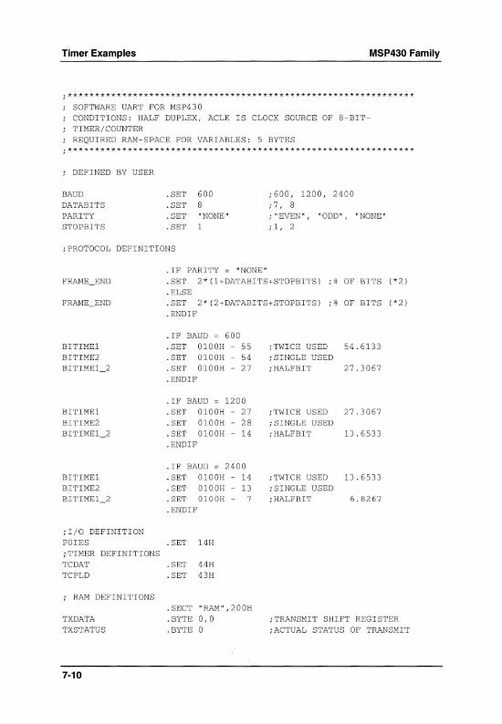
Timer Examples MSP430 Family
;****************************************************************
SOFTWARE UART FOR MSP430 CONDITIONS: HALF DUPLEX, ACLK IS CLOCK SOURCE OF 8-BITTIMER/COUNTER REQUIRED RAM-SPACE FOR VARIABLES: 5 BYTES
;****************************************************************
; DEFINED BY USER
BAUD DATABITS PARITY STOPBITS
.SET
.SET
.SET
.SET
600 8 "NONE" 1
;600,1200,2400 ; 7 I 8 ; "EVEN", "ODD", "NONE" ; 1, 2
; PROTOCOL DEFINITIONS
.IF PARITY = "NONE" FRAME_END .SET 2* (l+DATABITS+STOPBITS) ;# OF BITS (*2)
.ELSE FRAME_END .SET 2* (2+DATABITS+STOPBITS) ;# OF BITS (*2 )
.ENDIF
.IF BAUD = 600 BITIME1 .SET 0100H - 55 ;TWICE USED 54.6133 BITIME2 .SET 0100H - 54 ;SINGLE USED BITIME1 2 .SET - 0100H - 27 ;HALFBIT 27.3067
.ENDIF
. IF BAUD = 1200 BITIME1 .SET 0100H - 27 ;TWICE USED 27.3067 BITIME2 .SET 0100H - 28 ;SINGLE USED BITIME1 2 .SET 0100H - 14 ;HALFBIT 13.6533
.ENDIF
.IF BAUD = 2400 BITIME1 .SET 0100H - 14 ;TWICE USED 13.6533 BITIME2 .SET 0100H - 13 ;SINGLE USED BITIME1 - 2 .SET 0100H - 7 ;HALFBIT 6.8267
.ENDIF
;1/0 DEFINITION POlES .SET 14H ; TIMER DEFINITIONS TCDAT .SET 44H TCPLD .SET 43H
; RAM DEFINITIONS . SECT "RAM",200H
TXDATA . BYTE 0,0 ;TRANSMIT SHIFT REGISTER TXSTATUS . BYTE 0 ;ACTUAL STATUS OF TRANSMIT
7-10

MSP430 Family
TXFLAGS . BYTE RXBUF . BYTE
RXDATA .SET RXSTATUS .SET
RXFLAGS .SET
REC BIT .SET PAR_BIT .SET ERR_BIT .SET
; CONTROL DEFINITIONS POlES 1 .SET POIFG 1 .SET
TCCTL .S~'l'
RXD .SET TXD .SET RXACT .SET ENCNT .SET TXE .SET
ISCTL .SET lEI .SET
POlE .SET
IFG1 .SET TEMP .SET
TXDATA TXSTATUS
TXFLAGS
01H 02H 04H
02H OSH
042H
1 2 4
010H
020H OH
OSH
02H R4
Timer Examples
; SEQUENCE ;FLAGS DURING TRANSMITTING ;RECEIVE BUFFER FOR COMPLETED ;CHARS
;RECEIVE SHIFT REGISTER ;ACTUAL STATUS OF RECEIVE ; SEQUENCE ;FLAGS DURING RECEIVING
;FLAG INDICATES 'CHAR RECEIVED' ;PARITY BIT ;RECEIVE ERROR
;EDGE SELECT FOR PO.1 INTRPT ;INT. FLAG FOR PO.1
; 'j' lM~R/ COUNTER CONTROL ; REGISTER ;RECEIVE DATA BIT IN TCCTL ;TRANSMIT DATA BIT IN TCCTL ;EDGE DETECT LOGIC BIT ;COUNTER ENABLE BIT IN TCCTL ;1: TX BUF ACTIVE, 0: TX BUF ;3-STATE ;INTERRUPT SOURCE BIT ;INT ENABLE 1 REGISTER ;ADDRESS (SFR) ;BIT IN INT ENABLE 1 REGISTER ; (SFR) ;INTERRUPT FLAG REGISTER 1
; SUBROUTINE : INn'IALIZE UART CONTROL REGISTERS ; (CALLED ONCE AFTER RESET)
INIT RXTX MOV.B #072H,&TCCTL
BIS.B #POIES_1,&POIES
BIC.B #POIFG_1,&IFG1
CLR.B RXFLAGS CLR.B RXSTATUS RET
;ACLK IS SOURCE FOR 8-BIT; TIMER/COUNT ;SELECT NEGATIVE EDGE FOR ;PO.l ;INTRPT ;AND RXACT_FF, RESET INT. ;FLAG
CLEAR RX/TX REGISTERS ; CLEAR RX STATUS REGISTER
7-11

Timer Examples
; SUBROUTINE : PREPARE TRANSMIT CYCLE
CLR.B MOV.B
MOV.B
MOV.B
MOV.B
BIS.B JMP
TXSTATUS #072H,&TCCTL
#OFOH, TCPLD
#O,&TCDAT
#BITIME1,TCPLD
#ENCNT,&TCCTL PREP_RXTX
; SUBROUTINE : PREPARE RECEIVE CYCLE
PREP_RX CLR.B RXSTATUS MOV.B #072H,&TCCTL
MOV.B #BITIMEl _2,&TCPLD
MOV.B #0, &TCDA'!'
MOV.B #BITIME1,&TCPLD
BIS.B #RXACT,&TCCTL
MSP430 Family
;INITIALIZE TRANSMIT STATUS ;TXD = 1, TXE = 1
;LOAD TIME UNTIL START BIT ; STARTS ;DUMMY WRITE TO LOAD ; COUNTER/TIMER ;LOAD PRELOAD REG. WITH ;BITTIME 1
;SET TRANSMIT START CONDITION ;FALL INTO COMMON PART
; INITIALIZE RECEIVE STATUS ;SSELl = 0, SSELO = ISCTL = 1
;SET PRELOAD REGISTER WITH ;'1'1-2 ;DUMMY WRITE TO LOAD COUNTER/ ; TIMER ; LOAD PRELOAD REG. WITH ;BITTIME 1
; ACTIVATE NEG. EDGE DETECT OF ;PO.l(RX)
PREP RXTX ;COMMON PART ALSO FOR ;PREP_TX
7-12
.IF PARITY = "EVEN" BIC.B #PAR_BIT,RXFLAGS .ELSE BIS.B .ENDIF BIS.B
RET
#PAR_BIT,RXFLAGS
;PRESET PAR_BIT o
;PRESET PAR_BIT 1
;ENABLE PO.l / 8BIT COUNTER ;INTRPT ;ACCORDING TO STATE OF ISCTL

MSP430 Family Timer Examples
;****************************************************************
; INTERRUPT HANDLER OF SOFTWARE UART ;****************************************************************
BIT JNZ
# RXACT , TCCTL RXINTRPT
;RX/TX INTRPT HANDLER? ;RECEIVE MODE IS ACTIVE ->
; JUMP
TRANSMIT INTERRUPT HANDLER : DATA IS IN TXDATA ; INPUT : DATA TO TRANSMIT IN TXDATA ; OUTPUT: IF TRANSMIT IS COMPLETED, TXSTATUS WILL BE #FRAME_END
TXINTRPT
TXTAB
PUSH MOV.B BR . WORD . WORD . WORD . WORD . WORD . WORD . WORD . WORD
R5 TXSTATUS,R5 TXTAB (R5) TXSTATO TXSTAT2 TXSTATl TXSTATl TXSTAT2 TXSTATl TXSTATl TXSTAT2
.IF DATABITS = 8
. WORD TXSTATl
.ENDIF
.IF PARITY != "NONE"
. WORD TXPAR
.ENDIF
.IF STOPBITS = 2
. WORD
.ENDIF
. WORD
. WORD
TXSTOP
TXSTOP TXRET
TXSTATO MOV. B JMP
TXSTAT2 MOV. B
#BITIME1,&TCPLD TX_LO #BITIME2,&TCPLD
TXSTATl MOV. B TX_BIT RRA
JNC XOR.B BIS.B JMP BIC.B
#BITIME1,&TCPLD &TXDATA TX_LO #PAR_BIT,TXFLAGS #TXD,&TCCTL TXRET #TXD,&TCCTL
;RXACT = 0 --> TRANSMIT ;USE TXSTATUS FOR ;TRANSMIT PROCESS TABLE ;STARTBIT ;BIT 0, LSB BITIME2 ;BIT 1 BITIMEl ;BIT 2 ;BIT 3 ;BIT 4 ;BIT 5 ;BIT 6
;BIT 7
BITIMEl BITIME2 BITIMEl BITIMEl BITIME2
BITIMEl
;PARITY BIT BITIMEl
;STOPBIT BITIMEl
;STOPBIT BITIMEl ;FRAME TRANSMITTED
;LOAD BITTIME OF NEXT BIT ;STARTBIT, OUT=LO ;LOAD BITTIME OF NEXT BIT
;LSB -> CARRY
; 1
; 0
TOGGLE PARITY OUT=HI
OUT=LO
7-13

Timer Examples
TXRET INCD.B &TXSTATUS POP R5 RETI
; PARITY BIT CHECK: PAR_BIT + PARITY TXPAR MOV.B #BITIME1,&TCPLD
BIT.B #PAR_BIT,TXFLAGS JNZ TX_HI JMP TX_LO
; OUTPUT OF STOP BIT(S) TXSTOP MOV.B #BITIME1,&TCPLD
JMP TX_HI
RECEIVE INTERRUPT HANDLER ; OUTPUT: RECEIVED DATA IN RXDATA
MSP430 Family
;TXSTATUS + 2
;TRANSMISSION OF ONE BIT ; COMPLETED
BIT MUST BE EVEN
;CHECK PARITY BIT VALUE ;PARITY BIT SHOULD BE MARK ;PARITY BIT SHOULD BE SPACE
;SEND STOP BIT 1 OR 2
; RECEIVE FINISHED: #REC_BIT IS SET IN STATUS BYTE RXFLAGS 0 _______________________________________________________________ _ ,
RXINTRPT PUSH R5 ;RECEIVER INTERRUPT ROUTINE MOV.B &RXSTATUS,R5 ;R5 IS USED TEMPORARY AS
; POINTER OF BR RCTAB(R5) ;RECEIVE PROCESS TABLE
RCTAB . WORD RCSTATO ; START BIT . WORD RCSTATl ;BIT 0 . WORD RCSTATl ;BIT 1 . WORD RCSTAT2 ;BIT 2 . WORD RCSTATl ;BIT 3 . WORD RCSTATl ;BIT 4 . WORD RCSTAT2 ;BIT 5 . WORD RCSTATl ;BIT 6 .IF DATABITS = 8 . WORD RCSTATl ;BIT 7 .ENDIF .IF PARITY 1= "NONE" . WORD RCSTAT2 ;PARITY BIT BIT 1 .ENDIF .IF STOPBITS = 2 . WORD RCSTOPl ; STOP BIT BIT 2 .ENDIF . WORD RCSTOP2 ; STOP BIT BIT 2
7-14

MSP430 Family
RCSTATO BIT. B JC
MOV.B
#RXD,&TCCTL RCERROR
#BITIME2,&TCPLD
JMP RCRETO RCSTAT2 MOV. B #BITIME2,&TCPLD
JMP RCBIT RCSTAT1 MOV. B
RCBIT BIT.B JNC
#BITIME1,&TCPLD
#RXD,&TCCTL RCRET
&RXDATA
Timer Examples
;CHECK START BIT ; ERROR: START BIT IS MARK NOT ; SPACE ;START BIT FINE, LOAD PRE;LOAD REG.
;LOAD PRELOAD REG. WITH BIT ;TIME 2
;LOAD PRELOAD REG. WITH BIT ;TIME 1 ;RXD BIT->CARRY BIT ;RXD BIT=CARRY BIT=O ? YES, ; JUMP ;RXD BIT -> MSB, NEGATIVE BIT RRC
XOR.B JMP RRC
#PAR_BIT,RXFLAGS; RXD BIT = 1, TOGGLE PAR_BIT RCRETO
RCRET
RCRETO RCCMPL
INCD.B POP RET I
&RXDATA
&RXSTATUS R5
;RXD=O, RXD BIT -> MSB, ;NEGATIVE BIT
; PARITY BIT WAS RECEIVED JUST LIKE ALL OTHER BITS
RCSTOP1 MOV. B
RCSTOP2
BIT.B JZ JMP
#BITIME1,&TCPLD
#RXD,&TCCTL RCERROR RCRETO
.IF PARITY != "NONE" BIT.B #PAR_BIT,RXFLAGS
JNZ RCERROR .ENDIF BIT.B #RXD,&TCCTL JZ RCERROR POP R5
;LOAD PRELOAD REG. WITH BIT ;TIME 1 ;CHECK STOP BIT FOR MARK ;STOP BIT IS MARK -> OK
;CHECK PARITY BIT. BIT MUST ;BE ZERO ;PARITY BIT FALSE.
;CHECK STOP BIT FOR MARK ;STOP BIT IS MARK -> OK
PREPARE CHARACTER RECEIVED AND STORE IT
.IF PARITY != "NONE" RLA .ENDIF
RXDATA
.IF DATABITS = 7 CLRC RRC RXDATA .ENDIF MOV.B &RXDATA+1,&RXBUF
;SHIFT PARITY OUT
;CLEAR CARRY ;SHIFT 0 INTO BIT 7
;STORE RECEIVED CHARACTER
7-15

Timer Examples MSP430 Family
BIS.B CALL RETI
#REC_BIT,RXFLAGS #PREP_RX
; ERROR HANDLING: A NEW START IS TRIED RCERROR BI S. B #ERR_BIT, RXFLAGS
CALL #PREP_RX JMP RCCMPL
INTERRUPT VECTOR ADDRESS
;SET 'RECEIVED' BIT ;PREPARE NEXT FRAME
1
. SECT "PO_l VECT" ,OFFF8H ; ADDRESS FOR TC8 INTERRUPT
. WORD
. SECT
. WORD
INT_PO_l "RST_VECT",OFFFEH ;PUC / RESET ADDRESS START
The following subroutines shows the capability of the software UART described above. First, the timer must be initialized by calling the subroutine INIT _RXTX.
The direction of the communication has to be selected by calling the subroutines PREP _PX respectively PREP _ TX. This subroutine call is performed in the following example.
RX_CHAR initiates the timer to receive one byte, that will be stored in the RAMbyte RXBUF after the complete receive cycle. If an error occurs during the serial communication, the error bit in the RXFLAGS byte will be set.
; SUBROUTINE : RECEIVE 1 CHARACTER INTO RXBUF ; OUTPUT : RECEIVED CHARACTER IN RXBUF
RX_CHAR BIC.B #ERR_BIT,RXFLAGS ;CLEAR ERROR BIT FROM PREVIOUS CALL
BIT.B #REC_BIT, RXFLAGS ;TEST 'RECEIVED' FLAG JZ RX_CHAR ; ° : WAIT FOR CHAR. BIC.B #REC_BIT,RXFLAGS ; 1 : CLEAR FLAG AND EXIT RET ;RXBUF HOLDS DATA
The next example called TX_SPACE transmits one space character, that is located in the RAM byte TXDATA. Every other character can be transmitted, of course. Saving code space, this routine uses the part TX-END, that is used by the subroutined TX_TABLE, too. The routine TX_TABLE transmits a whole string, which is pointed to by TEMP. The end of the string is indicated by the value 00.
7-16
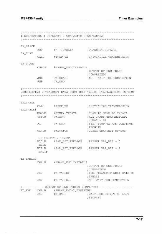
MSP430 Family Timer Examples
; SUBROUTINE : TRANSMIT 1 CHARACTER FROM TXDATA
TX SPACE -MOV #' , ,TXDATA ;TRANSMIT <SPACE>
TX_CHAR CALL #PREP_TX ;INITIALIZE TRANSMISSION
TX_CHARl CMP.B #FRAME_END,TXSTATUS
; OUTPUT OF ONE FRAME ; COMPLETED?
JNE TX_CHARl ;NO : WAIT FOR COMPLETION JMP TX_END
;SUBROUTINE : TRANSMIT DATA FROM TEXT TABLE, STARTADDRESS IN TEMP
TX_TABLE CALL #PREP_TX ;INITIALIZE TRANSMISSION
TX_TABLEl MOV.B @TEMP+,TXDATA ;CHAR TO SEND TO TXDATA TST.B TXDATA ;ALL CHARS TRANSMITTED?
; (CHAR = 0) JZ TX_END ;YES, STOP TX AND CONTINUE
; PROGRAM CLR.B TXSTATUS ;CLEAR TRANSMIT STATUS
.IF PARITY = "EVEN" BIC.B #PAR_BIT,TXFLAGS ; PRESET PAR_BIT 0 .ELSE BIS.B #PAR_BIT,TXFLAGS ; PRESET PAR_BIT 1 .ENDIF
TX_TABLE2 CMP.B #FRAME_END,TXSTATUS
; OUTPUT OF ONE FRAME ; COMPLETED?
JEQ TX_TABLEl ;YES, TRANSMIT NEXT DATA OF ; TABLE !
JMP TX_TABLE2 ;NO, WAIT FOR COMPLETION
----------- OUTPUT OF ONE STRING COMPLETED --------------------CMP.B JNE
#FRAME_END+2, TXSTATUS ;WAIT FOR OUTPUT OF LAST ;STOPBIT
7-17

Timer Examples
BIC.B
MSP430 Family
;INTERPT DISABLED FOR PO.1/TC ;IN SFR
BIC.B #ENCNT,&TCCTL ;STOP COUNTER TO SAVE POWER ;CONS.
RET
; EXAMPLE FOR TRANSMITTING THE STRING . BYTE "TONI",O
TEST MOV STRING,TEMP CALL #TX_TABLE
7.3 8 bit PWM Timer
TEXT
;TRANSMISSION OF TABLE IS ; COMPLETED
"TONI" ; a IS THE INDICATION OF THE ; END OF ;THE STRING
This module is integrated in the EVE_OPT-Version of the MSP430 family, and generates a rectangular output pulse with a duty factor of 0% to 100 %. The period of the PWM signal can be selected from 242 ~s up to 992,2 ms, as shown in the table below. The resolution of the duty factor is 1/254 .
Figure 7.4: PWM Modulation
7-18
t1 = periodic time (=1 ms) t2 = duty cycle

MSP430 Family Timer Examples
Clock Source Period Time t1 SSEL2
MCLK X20 ·254 = 242 ILs 0
MCL'X ~20 ·254 = 969ILs 0
MCL'X6 1%20 ·254 = 3,88 ms 0
ACLK X15· 254 = 7,75 ms 0
ACL'X ~15·254 = 31,01 ms 1
ACL% ,%15 ·254 = 62,01 ms 1
ACL'X6 1%15 ·254 = 124,02 ms 1
ACL'X28 12,% .254 = 9922 ms 1 215 '
t2 = t1. PWMDT 254
; PWMDT E [O,FEh]
SSEL1 SSELO
0 0
0 1
1 0
1 1
0 0
0 1
1 0
1 1
The following software example shows the capability of this peripheral module. After configuration of the PWM registers, no software control is necessary to generate the output pulses, unless the duty cycle or the PWM period have to be modified. These modifications will affect the output after the end of the actual PWM period.
INITIALIZATION CLR.B
MOV.B
&PWMCTL
#7FH,&PWMCTL
; CHANGE DUTY CYCLE T2 MOV.B #3FH,&PWMDT
; CHANGE PWM PERIOD Tl
;Tl=242 US ;PWM OUTPUT IS DISABLED ;POSITIVE LOGIC ;DUTY CYCLE = 50 %
;DUTY CYCLE 25 %
BIC.B #SSELO+SSEL1+SSEL2, &PWMCTL
BIS.B ;CLEAR ALL CLOCK SOURCES
#SSELO+SSELl,&PWMCTL ;NEW CLOCK SOURCE IS ACLK, ;Tl=7,75MS
7-19

Timer Examples MSP430 Family
; STOP PWM SIGNAL AT LOW STATE LOOP BIT.B #CMPM,&PWMCTL ; WAIT FOR PWM OUTPUT LOW
JZ LOOP BIC.B #OEH,&PWMCTL ;STOP PWM SIGNAL CLR.B &PWMCNT ;RESET COUNTER
BIS.B #OEH,&PWMCTL ;CONTINUE WITH PWM
7.4 Universal Timer I Port Module
The Universal Timer / Port Module is implemented in the EVE-Opt version of the MSP430 family and contains up to six independent outputs (TP.O .. TP.5), two 8 bit counters which are cascadeable for 16 bit mode, and a comparator for AID-conversion of the slope-converter type. The use of this module as an AID-Converter is described in the section The Analog to Digital Converters.
If no AID-conversion is needed, this module can be configured as an Universal Timer / Counter with interrupt capability.
The following example shows the use of this module in the timer mode. The Register Equate table for the software examples is shown below.
;UNIVERSAL TIMER PORT REGISTER DEFINITIONS TPCTL .EQU 4BH TPCNTl .EQU 4CH TPCNT2 .EQU 4DH TPD .EQU 4EH TPE .EQU 4FH
;TPCTL BIT DEFINITIONS EN1FG .EQU lH RC1FG .EQU 2H RC2FG .EQU 4H ENl .EQU BH ENA .EQU lOH ENB .EQU 20H TPSSELO .EQU 40H TPSSELl .EQU BOH
;TPD BIT DEFINITIONS CPON .EQU 40H TP16B . EQU BOH
;TPE BIT DEFINITIONS TPSSEL2 .EQU 40H TPSSEL3 .EQU BOH
7-20

MSP430 Family Timer Examples
lEI .EQU OOH IE2 .EQU 01H IFGl .EQU 02H IFG2 .EQU 03H
TPIE .EQU 4H
7.4.1 Initialization
The initalization for using the two 8 bit counters in 16 bit mode is shown in the following example. Every other configuration can be achieved easily by modifying the appropriate bits in the configuration registers described in the MSP430 Architecture Guide.
;INITIALIZATION OF THE TIMER / PORT REGISTERS MOV.B
CLR.B CLR.B
MOV.B
#TPSSELO,&TPCTL
&TPCNTI &TPCNT2
#TPI6B,&TPD
;CLEAR ENI FLAG ;CLEAR RCI AND RC2 FLAG ;ENl=O : DISABLES COUNTER ;CLOCK SOURCE IS ACLK
; CLEAR COUNTER 1 ; CLEAR COUNTER 2
;16 BIT COUNTER MODE ; TPCNTI = LOW BYTE ; TPCNT2 = HIGH BYTE ; RESETS OUTPUTS TP.O TO TP.5
CLR.B &TPE ;TO.O TO TP.5 ARE SET TO 3-STATE ;CLOCK SOURCE = CLKI = ACLK
MOV.B #OAAH,&TPCNTI ;LOAD LOW BYTE WITH APPROPRIATE ; VALUE
MOV.B #OBBH,&TPCNT2 ;LOAD HIGH BYTE WITH APPROPRIATE ; VALUE
BIS.B GIE
#TPIE,&IE2 ;ENABLE TIMER/PORT INTERRUPT ;ENABLE ALL SELECTED INTERRUPTS
i***************************************************** ***********
; TIMER / PORT COUNTER INTERRUPT SERVICE ROUTINE ;FOLLOWING INTERRUPT SERVICE ROUTINE CAN BE USED FOR EVERY MODE ;OF ;THIS MODULE. IN THE 8 BIT MODE THREE DIFFERENT SOURCES CAN CAUSE ;INTERRUPTS CAN OCCUR
- NEGATIVE EDGE OF ENI - OVERFLOW FROM TPCNTI - OVERFLOW FROM TPCNT2
RCI SIGNAL RC2 SIGNAL
7-21

Timer Examples MSP430 Family
;IN THE 16 BIT MODE OF THE COUNTER TWO DIFFERENT SOURCES CAN ; CAUSE ; INTERRUPTS:
- NEGATIVE EDGE OF EN1 - OVERFLOW FROM TPCNT2
i***************************************************** ***********
TPA8 ISR
EN1 ISR
BIT.B
JNZ BIT.B
JNZ BIT.B JNZ
BIC.B
RETI
BIC.B
RETI
BIC.B
RETI
BIC.B
RETI
#EN1FG,&TPCTL
EN1_ISR #RC1FG,&TPCTL
TPA8_ISR #TP16B,&TPD TP16 ISR
#RC2FG,&TPCTL
;16 BIT MODE #RC2FG,&TPCTL
;NEG.EDGE ON EN1 CAUSES INTERRUPT
;YES, EXECUTE CORRESPONDING ISR ;RIPPLE CARRY OF COUNTER1 CAUSES ;INT ? ;YES, EXECUTE CORRESPONDIG ISR ;IS 16 BIT MODE SELECTED? ;YES, EXECUTE 16 BIT ISR
;8BIT MODE, ISR FOR COUNTER 2
;8 BIT MODE, COUNTER 1 #RC1FG,&TPCTL
;EN1 ISR #EN1FG,&TPCTL
;INTERRUPT VECTOR ADDRESSES FOR THE UNIVERSAL COUNTER
7-22
. SECT
. WORD "TPVECT",OFFEAH ;UNIVERSAL COUNTER TP_ISR

MSP430 Family Timer Examples
7.4.2 Measuring the Revolutions of a Toothed Wheel
The Figure below shows the set-up for determining the number of revolutions and the angular resolution of the number of the tooths of the wheel. If the toothed wheel has 72 teeth, the resolution is in steps of 5 degrees.
LED
LDR
< MSP430
CIN tl Figure 7.5: Measuring the Revolutions of a Toothed-Wheel
When the light from the LED impinges on the LOR, the pulse which occurs increments the 8 bit counter by 1. If one revolution of the disk is performed, the counter TPCNT1 will generate an overflow, and an interrupt occurs. The corresponding ISR increments the revolution register; the actual angle is contained in the PTCNT1 register.
7-23

Timer Examples
NUT REV
.EQU
.EQU 72 RIO
MSP430 Family
;NUMBER OF TOOTHS ;CONTAININ~ THE NUMBER OF ; REVOLUTIONS
;INITIALIZATION OF THE UNIVERSAL COUNTER
CLR.B &TPCTL
MOV.B #O-NUT,&TPCNTI
CLR.B &TPD
CLR.B &IFGI
CLR.B &IFG2
BIS.B #TPIE,&IE2
BIS.B #ENA,&TPCTL
;ENI=O ;CLKI = CIN ;INTERRUPT FLAGS = 0
;GENERATE OVERFLOW, IF ONE ;REVOLUTION IS OVER ;IS OVER
;SET OUTPUTS TP.O TO TP.5 TO ; LOW ;8 BIT COUTER MODE ;COMPARATOR IS SWITCHED OFF
;CLEAR INTERRUPT REQUEST ;FLAG 1 ;CLEAR INTERRUPT REQUEST ;FLAG 2 ;ENABLE UNIVERSAL COUNTER ; INTERRUPT ;START COUNTER
;INTERRUPT SERVICE ROUTINE
BIC.B INC MOV.B
APPROPRIATE
RETI
#RCIFG,&TPCTL REV #O-NUT,&TPCNTI
;CLEAR INTERRUPT REQUEST FLAG ;ONE MORE REVOLUTION ;RELOAD COUNTER WITH
; VALUE
;INTERRUPT VECTOR ADDRESSES FOR THE UNIVERSAL COUNTER
7-24
. SECT
. WORD "TPVECT",OFFEAH;UNIVERSAL COUNTER TP_ISR

MSP430 Family
8 8.1
8.2
8.3
8.4 8.4.1 8.4.2 8.4.3
8.5
LCD Display
Initialization
Definition of the Characters
Display Text
Adaption to other MUX Modes Adaption to 3MUX Mode Adaption to 2MUX Mode Adaption to Static Mode
Topics
Use of Unused Select Lines for Digital Outputs
Figures
Figure Title
8.1 Allocation of the Segments, 4 MUX Mode
8.2
8.3
8.4
8.5
Allocation of the LCD Digits in the Memory
Allocation of the Segments, 3 MUX Mode
Allocation of the Segments, 2 MUX Mode
Allocation of the Segments, Static Mode
Notes
Figure Title
8.1 Restrictions using select lines as outputs
Tables
Figure Title
8.1 Allocation of the LCD Digits in 4MUX Mode
8.2
8.3
8.4
8.5
8.6
Configuration of the MUX Modes
Allocation of the LCD Digits in 3MUX Mode
Allocation of the LCD Digits in 2MUX Mode
Allocation of the LCD Digits in Static Mode
Dependence of the Select Lines to LCDP
LCD Display
8-3
8-3
8-4
8-6
8-9 8-10 8-12 8-14
8-16
Page
8-4
8-6
8-10
8-12
8-14
Page
8-16
Page
8-4
8-9
8-10
8-12
8-14
8-16
8-1

LCD Display MSP430 Family
8-2

MSP430 Family LCD Display
8 LCD Display
In many applications the result of an operation must be visually displayed. For this purpose, the integrated LCD Driver can be used. In the 4 MUX mode, up to 8 userdefined characters can be displayed at once.
8.1 Initialization
First, the right display mode has to be selected. In the following example the 4MUX mode is selected, because this mode allows displaying up to 8 digits with only 20 lines ( 4xCOM + 16xSelect ). The correct timing for the selected mode is generated by the basic timer, which has to be initialized accordingly. The number of digits on the LCD used can be defined by LCD_DIG.
i***************************************************** ****** ;BASIC-TIMER DEFINITIONS ;***********************************************************
BTCTL .SET 040H ;BASIC TIMER CONTROL REGISTER
i***************************************************** ****** ;LCD DRIVER DEFINITIONS FOR ALL MUX MODES i***************************************************** ****** LCDO LCDM LCD_DIG
.SET
.SET
.SET
00030H 0031H 8
;ADDRESS OF LCD CONTROL ;START OF LCD DIGIT MEMORY ;LCD WITH 8 DIGITS
i***************************************************** ****** ;PREPARE LCD AND BASIC TIMER FOR 4 MUX MODE ;***********************************************************
MOV.B
MOV.B
BIS.B BIC.B
#-lH,&LCDO
#077H,&BTCTL
#80H,&ME2 #040H,&BTCTL
;SELECTED FUNCT. ANALOG ;GENERATOR ON ;LOW IMPEDANCE OF AG ; 4MUX ACTIVE ;ALL OUTPUTS ARE SEG
;SELECTED FUNCTION BASIC TIMER: ; ACLK ;RESET ;HIGHEST DIVISION FACTOR ;LCD FRAME FREQUENCY @4MUX: 64HZ ;ENABLE BASIC TIMER MODULE ;BASIC TIMER RESET DISABLED
8-3

LCD Display MSP430 Family
8.2 Definition of the Characters
To define the characters, the allocation of the segments is assumed to be as shown in Figure 8.1. In the first table of the following software routine, the 8 segments ( a to h ) are defined. In the LCDTAB the characters which can be built with the segments are arranged with the ASCII code. Therefore, it is possible to get the segment code in a simple manner.
n mm!l COM3
[]® - COM2
c=J COMl
c=J COMO
SEGn SEGn+l
Figure 8.1: Allocation of the Segments, 4 MUX Mode
The allocation of the segments depens on the model of the used LC Display. Figure 8.1 shows only a possible allocation. if a different display is used, the proper segment allocation has to be defined by the tables shown in the MSP430 Family Architecture Guide. For the 4MUX Mode LCD's the table of the segment allocation is as follows.
bit position 3Fh
32h 31h
7
----
COM3
6 5 4
f e d COM2 COM1 COMO
select n+1
3 2 o --- y h ~ - c b a
COM3 COM2 COM1 COMO select n
Table 8.1: Allocation of the LCD Digits in 4MUX Mode
For example the a-segment can be selected by COM3 and odd select (select n+ 1), the appropriate equation is:
A .EQU BaH ;= 1000 0000 B ; BIT 7 MEANS COM3 AND SELECT N+1
8-4

MSP430 Family LCD Display
If this pattern is written in the RAM Memory, the a-segment will shine. Writing OFFh into the LCD RAM byte, all segments will shine. If the segments are defined correctly by the 8 equations, all of the described subroutines will work.
A .EQU BOH ; DEFINITION OF THE 7 SEGMENTS B .EQU 40H ;BY THE USER. C .EQU 20H ;DEPENDS ON THE USED LC DISPLAY D .EQU 01H ;THIS EXAMPLE IS IN RELATION TO E .EQU 02H ;THE LCD CONFIGURATION SHOWN IN F .EQU OBH ;FIGURE B.l G .EQU 04H H .EQU 10H
;THE FOLLOWING ASCII TABLE CAN BE USED FOR ALL MUX MODES LCDTAB . BYTE A+B+C+D+E+F ; "0"
. BYTE B+C ;" 1"
. BYTE A+B+G+E+D ; "2"
. BYTE A+B+G+C+D ; "3"
. BYTE F+G+B+C ; "4"
. BYTE A+F+G+C+D ;" 5"
. BYTE A+F+E+D+C+G ; "6"
. BYTE A+B+C ;"7"
. BYTE A+B+C+D+E+F+G ;"B"
. BYTE A+B+C+D+G+F ; "9"
. BYTE 0 i":"
. BYTE 0 i";"
. BYTE 0 ; 11<"
. BYTE G .11_11 , -
. BYTE 0 ; ">11
. BYTE 0 ill? II
.BYTE 0 ; "@"
.BYTE E+F+A+B+C+G ;"A"
.BYTE F+E+D+C+G ; "B"
. BYTE G+E+D ; "C"
. BYTE G+E+D+C+B ; "D"
. BYTE A+F+E+D+G ; "E"
. BYTE A+F+E+G ; "F"
. BYTE A+F+E+D+C+G ; "G"
. BYTE F+E+B+C+G ; "H"
. BYTE B+C ; "I"
. BYTE B+C+D ; "J"
. BYTE 0 ; "K"
. BYTE F+E+D ; "L"
. BYTE E+F+A+B+C ;"M"
. BYTE 0 ; "N"
. BYTE E+D+C+G ; "0"
. BYTE F+E+A+B+G ; "P"
. BYTE 0 ; "Q"
. BYTE E+G ; "R"
. BYTE A+F+G+C+D ; "S"
8-5

LCD Display MSP430 Family
. BYTE F+E+D+G i "Tn
. BYTE F+E+D+C+B ;"U"
. BYTE 0 ;"V"
. BYTE 0 ;"W"
. BYTE 0 i "X"
. BYTE F+G+B+C+D ; "yn
. BYTE 0 ;"Z" T - LCD . BYTE "LCDTEST",255 ;TESTSTRING WITH END OF
; TEXT = 255
8.3 Display Text
The following subroutines describe how easy it is to handle the display driver. The text which is to be displayed is simply moved into the LCD RAM. The allocation of the LCD RAM is shown in Figure 8.2.
38h 37h 36h 35h 34h 33h 32h 31h 30h
Digit Position: 765 4 3 2 1 0
digit 8
~ digit 7
digit 6
digit 5
digit 4
digit 3
digit 2
digit 1
LCDO
Figure 8.2: Allocation of the LCD Digits in the Memory
8-6

MSP430 Family LCD Display
i***************************************************** ***** ;LCD DISPLAY CHARACTER USING 4 MUX MODE ;THE LSDIGIT OF REGISTER R12(OOOM) IS DISPLAYED ON ;DIGIT R13(O .. LCD_DIG) i***************************************************** *****
DSP_CHR SUB CMP JLO MOV
DSP_MUX4 MOV.B RET
#030H,R12 #42, R12 DSP_MUX4 #11, R12
;R12 IS ASCII FORMAT ;ABOVE TABLE ;NO ;YES PRINT SPACE
LCDTAB(R12),LCDM(R13)
i***************************************************** ******* ; DSP_TXT, CAN BE USED FOR ALL MUX MODES ;SHOWS THE TEXT, WHICH IS POINTED TO BY R10 ON THE BEGINING OF ;THE DISPLAY ; EXAMPLE
MOV CALL
#T_LCD,R10 #DSP_TXT
i***************************************************** *******
DSP_TXT PUSH R13 MOV #LCD_DIG-l,R13 ;R13 IS MAX LCD POSITION
DSP_L$l MOV.B @R1O+,R12 ;CHAR TO REGISTER CMP.B #OFFH,R12 ; END OF TEXT JZ DSP_L$2 CALL #DSP_CHR ; ONE CHARACTER TO THE LCD DEC R13 ; NEW POSITION OF THE POINTER JHS DSP_L$l ;NEXT CHARACTER
DSP_L$2 POP R13 RET
i***************************************************** *********
;CLRSCR : WRITE BLANKS TO THE LCD BY CLEARING THE LCD MEMORY i***************************************************** *********
CLRSCR PUSH MOV
CLR.B DEC
R5 #LCD_DIG,R10
LCDM(R10) R10
;NUMER OF LCD DIGITS TO R10
;CLEAR ONE DIGIT ;NEXT LCD POSITION
8-7

LCD Display
JNZ POP RET
;ALL DIGITS CLEARED ;YES
MSP430 Family
i***************************************************** ******** ;BINTOLCD : PUT THE INTEGER IN R10 ON THE LCD BY USING DSP_CHR ;R13 MUST CONTAIN THE POSITION ON THE LCD(4 .. 7) i***************************************************** ********
BINTOLCD
BINL$l
BINL$2
PUSH PUSH PUSH MOV SUB
MOV BIC CMP JLO ADD
ADD CALL INC RRA RRA RRA RRA DEC JNZ POP POP
R12 R10 R4 #4,R4 #3, R13
R10,R12 #OFFFOH,R12 #10,R12 BINL$2 #7,R12
#30H,R12 #DSP_CHR R13 R10 R10 R10 R10 R4 BINL$l R4 R10
POP R12 RET
;SAVE USED REGISTERS
;COUNTER OF DIGITS ;FIRST MEMORY POSITION
;STORE VALUE ;ONLY LAST DIGIT ;VALUE ABOVE 10 (A) ;NO ;YES, SELECT A .. F
;ADJUST TO ASCII CODE ;ONE CHARACTER TO LCD ;NEW POSITION ON LCD ;NEXT DIGIT INTO LAST POSITION ;OF REGISTER
;ALL DIGITS DISPLAYED? ;NO ;YES, RESTORE USED REGISTERS
8.4 Adaption to other MUX Modes
The routines described above can also be used for Displays using other Modes (3 MUX, 2 MUX or static). For these purposes the initialization of the LCD Mode Register has to be modified as follows:
8-8

MSP430 Family LCD Display
MUX Mode Mode Register
LCDM4 LCDM3 LCDM2
MUX4 1 1 1
MUX3 1 0 1
MUX2 0 1 1
Static 0 0 1
Table 8.2:Configuration of the MUX Modes
Additionally, the equations for the segments have to be adjusted. Furthermore, the software routines for displaying one character on the dedicated LCD position (DSP _CHR) have to be substituted.
The DSP _CHR routine for the 3 MUX Mode is the most complicated, because the determination of the LCD position in the LCD memory needs a lot of code.
8.4.1 Adaption to 3MUX Mode
The DSP _CHR routine for the 3 MUX Mode is the most complicated, because the determination of the LCD position in the LCD memory needs a lot of code. The eight segments of the digits are located in 1 Y, display memory bytes. In the 3MUX Mode an additional segment Y can be selected.
Example for a layout of a 3MUX driven LCD digit:
selectn
selectn+l selectn+2
_ COM2
c=J COMI
1""",0\1 COMO
Figure 8.3: Allocation of the Segments, 3 MUX Mode
8-9

LCD Display MSP430 Family
Using a LCD with the segment allocation as shown above, the corresponding RAM memory should be as follows:
bit position 3Fh
32h 31h
7 ----
6 5
f e COM2 COM1
select n+1 (odd)
4 3 ---
d -COMO
Table 8.3: Allocation of the LCD Digits in 3MUX Mode
2 o
y h Q
c b a COM2 COM1 COMO select n (even)
The following equations shows the allocation between segments and memory location.
a .equ 001h b .equ 002h c .equ 004h d .equ 010h e .equ 020h f .equ 040h g .equ 100h h .equ 200h y .equ 400h
;**********************************************************
;LCD DISPLAY CHARACTER USING 3 MUX MODE ;THE LSDIGIT OF REGISTER R12(OOOM) IS DISPLAYED ON ;DIGIT R13(O .. LCD_DIG) i***************************************************** *****
;FIRST THE POSITON OF THE DIGIT ;THE LCD MEMORY MUST BE LOCATED
BIT.B #8,R13 ;IS LCD POSITION 6 OR 7 ? JZ NEXTl ;NO ADD #3, R13 ;YES, ADJUST MEMORY POSITION JMP DSP_STRT ;WRITE CHARACTER INTO MEMORY
NEXTl BIT.B #4, R13 ;IS LCD POSITION 4 OR 5 ? JZ NEXT2 ;NO ADD #2, R13 ;YES, ADJUST MEMORY POSITON JMP DSP_STRT ;WRITE CHARACTER INTO MEMORY
NEXT2 BIT.B #2, R13 ;IS LCD POSITION 2 OR 3 ? JZ DSP_STRT ;NO, LCD POSITION IS o OR 1 INC R13 ;YES, ADJUST MEMORY POSITION
8-10
IN

MSP430 Family LCD Display
SUB CMP JLO MOV
MOV.B BIT.B JNZ MOV.B SWPB BIC.B BIS.B RET RLA RLA RLA RLA BIC.B BIS.B SWPB MOV.B RET
#030H,R12 #42,R12 DSP_MUX3 #11, R12
LCDTAB(R12) ,R4 #1, R13 DIG_1 R4, LCDM (R13) R4
;R12 IS ASCII ;ABOVE TABLE ;NO ;YES PRINT SPACE
; POSITION ODD OR EVEN
#07H,LCDM+1(R13) R4,LCDM+1(R13)
R4 R4 R4 R4 #07H,LCDM(R13) #R4,LCDM(R13) R4 R4,LCDM+1(R13)
8.4.2 Adaption to 2MUX Mode
?
The DSP _CHR routines for the 2 Mux and the static Mode are simpler to implement than the 3 MUX Mode, because of the easy to determine coherence between the LCD position and the corresponding memory position.
The eight segments of one digit are located in 2 bytes of the display memory.
Example of a possible layout of the segjments of a 2 MUX driven LCD
~~.
,r{l ~?
selectn+2 selectn+1 selectn+3
Figure 8.4: Allocation of the Segments, 2 MUX Mode
COMl
COMO
8-11

LCD Display
The corresponding RAM memory should be as follows:
bit position 3Fh
32h 31h
7
----
6 5 --- h - d
COM1 select n+1 (odd)
4 3 --
g -c -
COMO
Table 8.4: Allocation of the LCD Digits in 2MUX Mode
a .equ 001h b .equ 002h c .equ 010h d .equ 020h e .equ 004h f .equ 008h g .equ 040h h .equ 080h
MSP430 Family
2 o --- f e - b a
COM1 COMO select n (even)
i***************************************************** ***** ;LCD DISPLAY CHARACTER USING 2 MUX MODE ;THE LSDIGIT OF REGISTER R12(OOOM) IS DISPLAYED ON ;DIGIT R13(O .. LCD_DIG) ;**********************************************************
DSP_CHR SUB #030H,R12 ;R12 IS ASCII CMP #42,R12 ;ABOVE TABLE JLO DSP_MUX2 ;NO MOV #11, R12 ;YES PRINT SPACE
DSP_MUX2 RRA R13 MOV.B LCDTAB(R12),R4 MOV.B R4,LCDM(R13) RRA R4 RRA R4 MOV.B R4,LCDM+l(R13) RET
8-12

MSP430 Family
8.4.3 Adaption to Static Mode
The eight segments of one digit are located in four display memory bytes.
Example for a layout of a static driven LCD digit:
selectn
"~'~'-Q ! 9-"", . ., ~selectn+6
selectn+4 ----D a-- selectn+2 ¥ ®-",,-, selectn+3
Figure 8.5: Allocation of the Segments, Static Mode
The corresponding display-RAM is shown below:
bit position 3Fh
33h 32h 31h
7 -----
6 5 - -- -- -- -- -
COM2 COM1 select n+1 (odd)
4
h f d b
COMO
3 -----
Table 8.5: Allocation of the LCD Digits in Static Mode
2 - -- -- -- -- -
COM2 COM1 select n (even)
LCD Display
o
g e c a
COMO
If the static driven LCD is connected as shown above, following equation are valid:
a .equ 001h b .equ 010h c .equ 002h d .equ 020h e .equ 004h f .equ 040h g .equ 008h h .equ 080h
8-13

LCD Display MSP430 Family
;**********************************************************
;LCD DISPLAY CHARACTER USING STATIC MODE ;THE LSDIGIT OF REGISTER R12(OOOM) IS DISPLAYED ON ;DIGIT R13(O .. LCD_DIG) i**********************************************************
DSP_CHR SUB #030H,R12 ;R12 IS ASCII CMP #42, R12 ;ABOVE TABLE JLO DSP_MUX1 ;NO MOV #11, R12 ;YES PRINT SPACE
DSP_MUXI RRA R13 RRA R13 MOV.B LCDTAB(R12) ,R4 MOV.B R4,LCDM(R13) RRA R4 MOV.B R4,LCDM+l(R13) RRA R4 MOV.B R4,LCDM+2(R13) RRA R4 MOV.B R4,LCDM+3(R13) RET
8-14

MSP430 Family LCD Display
8.5 Use of Unused Select Lines for Digital Outputs
The LCD Driver of the MSP43Cl allows the use of additional digital outputs if select lines are not used. Up to 28 digital outputs are possible in the hardware design, but not all of them will be implemented for a given chip. The addressing scheme for the digital outputs 02 to 029 is as follows:
Address 7 6 5 4 3 2 1 0 Digit Nr. LCDP
03Fh 029 028 Digit 15 6toO
03Eh 027 026 Digit 14 6to 0
03Dh 025 024 Digit 13 5 to 0
03Ch 023 022 Digit 12 5toO
03Sh 021 020 Digit 11 4to 0
03Ah 019 018 Digit 10 4 to 0
039h 017 016 Digit 9 3toO
038h 015 014 Digit 8 3 to 0
037h 013 012 Digit 7 2 to 0
036h 011 010 Digit 6 2toO
035h 009 008 Digit 5 1 to 0
034h 007 006 Digit 4 1 to 0
033h 005 004 Digit 3 0
032h 003 002 Digit 2 0
031h h g f e d c b a Digit 1
Table 8.6: Dependence of the Select Lines on LCDP
The above table shows the dependence of the select/output lines on the 3-bit value LCDP. Only if LCDP = 7 are all lines switched to the LCD Mode (select lines).
8-15
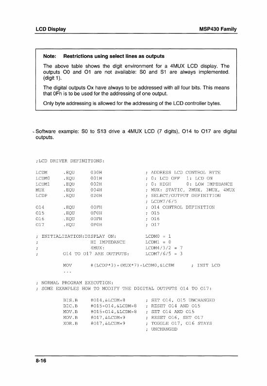
LCD Display MSP430 Family
Note: Restrictions using select lines as outputs
The above table shows the digit environment for a 4MUX LCD display. The outputs 00 and 01 are not available: SO and S1 are always implemented. (digit 1).
The digital outputs Ox have always to be addressed with all four bits. This means that OFh is to be used for the addressing of one output.
Only byte addressing is allowed for the addressing of the LCD controller bytes .
• Software example: SO to S13 drive a 4MUX LCD (7 digits). 014 to 017 are digital outputs.
;LCD DRIVER DEFINITIONS:
LCDM .EQU 030H LCDMO .EQU 00lH LCDMl .EQU 002H MUX .EQU 004H LCDP .EQU 020H
014 .EQU OOFH 015 .EQU OFOH 016 .EQU OOFH 017 .EQU OFOH
INITIALIZATION:DISPLAY ON: HI IMPEDANCE 4MUX:
014 TO 017 ARE OUTPUTS:
ADDRESS LCD CONTROL BYTE 0: LCD OFF 1: LCD ON 0: HIGH 0: LOW IMPEDANCE MUX: STATIC, 2MUX, 3MUX, 4MUX SELECT/OUTPUT DEFINITION LCDM7/6/5 014 CONTROL DEFINITION 015 016 017
LCDMO = 1 LCDMl = 0 LCDM4/3/2 LCDM7/6/5
7 3
MOV #(LCDP*3)+(MUX*7)+LCDMO,&LCDM INIT LCD
NORMAL PROGRAM EXECUTION: SOME EXAMPLES HOW TO MODIFY THE DIGITAL OUTPUTS 014 TO 017:
BIS.B #014,&LCDM+8 SET 014, 015 UNCHANGED BIC.B #015+014,&LCDM+8 RESET 014 AND 015 MOV.B #015+014,&LCDM+8 SET 014 AND 015 MOV.B #017,&LCDM+9 RESET 016, SET 017 XOR.B #017,&LCDM+9 TOGGLE 017, 016 STAYS
UNCHANGED
8-16

MSP430 Family The Analogue-to-Digital Converters
Topics
9 The Analogue-to-Digital Converters
9.1 The 14-bit Analogue-to-Digital Converter 9.1.1 The Current Source 9.1.2 The 14-bit Analogue-to-Digital Converter used in 14-bit-Mode 9.1.2.1 ADC with Signed Signals 9.1.2.2 Four-Wire Circuitry for Sensors 9.1.2.3 Referencing with Reference Resistors 9.1.2.4 Interrupt Handling using the 14-bit-Mode
9.1.3 The 14-bit Analogue-to-Digital Converter used in 12-bit-Mode 9.1.3.1 ADC with Signed Signals 9.1.3.2 Interrupt Handling using the 12-bit-Mode
9.2 The Universal Timer/Port Module used as ADC 9.2.1 Interrupt Handling
Figures
Figure Title
9.1 Possible Sensor Connections to the MSP430
9.2 Complete ADC Range
9.3 Virtual Ground IC for Level Shifting
9.4 Splitted Power Supply for Level Shifting
9.5 Current Source for Level Shifting
9.6 4-Wire Circuitry with Voltage Supply
9.7 4-Wire Circuitry with Current Supply
9.8 Referencing with Precision Resistors
9.9 The four Single ADC Ranges
9.10 Single ADC Range
9.11 Possible Sensor Connections to the MSP430
9.12 Timing for the Universal Timer
9.13 Schematic of Example
Notes
Figure Title
9.1 ADC Definitions are Valid for all ADC Examples
9.2 ADC Ranges
9-3
9-3 9-5 9-6 9-7
9-11 9-13 9-15
9-16 9-18 9-19
9-20 9-23
Page
9-4
9-6
9-7
9-9
9-10
9-11
9-12
9-13
9-16
9-16
9-17
9-20
9-20
Page
9-7
9-16
9-1

The Analogue-to-Oigital Converters MSP430Family
9-2
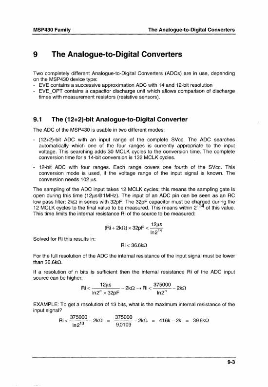
MSP430 Family The Analogue-to-Digital Converters
9 The Analogue-to-Digital Converters
Two completely different Analogue-to-Digital Converters (ADCs) are in use, depending on the MSP430 device type: - EVE contains a successive approximation ADC with 14 and 12-bit resolution - EVE_OPT contains a capacitor discharge unit which allows comparison of discharge
times with measurement resistors (resistive sensors).
9.1 The (12+2)-bit Analogue-to-Digital Converter
The ADC of the MSP430 is usable in two different modes:
- (12+2)-bit ADC with an input range of the complete SVcc. The ADC searches automatically which one of the four ranges is currently appropriate to the input voltage. This searching adds 30 MCLK cycles to the conversion time. The complete conversion time for a 14-bit conversion is 132 MCLK cycles.
- 12-bit ADC with four ranges. Each range covers one fourth of the SVcc. This conversion mode is used, if the voltage range of the input signal is known. The conversion needs 1 02 fls.
The sampling of the ADC input takes 12 MCLK cycles; this means the sampling gate is open during this time (12flS@1MHz). The input of an ADC pin can be seen as an RC low pass filter: 2kn in series with 32pF. The 32pF capacitor must be charged during the 12 MCLK cycles to the final value to be measured. This means within 2-14 of this value. This time limits the internal resistance Ri of the source to be measured:
Solved for Ri this results in:
(Ri + 2kn) x 32pF < 12~ In2
Ri< 36.6kQ
For the full resolution of the ADC the internal resistance of the input signal must be lower than 36.6kn.
" a resolution of n bits is sufficient then the internal resistance Ri of the ADC input source can be higher:
Ri < 12flS _ 2kn -t Ri < 375000 - 2kn In2n x 32pF In2n
EXAMPLE: To get a resolution of 13 bits, what is the maximum internal resistance of the input signal?
Ri < 375000 _ 2kn In213
375000 _ 2kn = 41.6k - 2k = 39.6kQ 9.0109
9-3

The Analogue-to-Digital Converters MSP430Family
The internal resistance of the input signal must be lower than 39.6kQ.
The next figure shows different methods of connecting analogue signals to the MSP430:
1. Current supply for resistive sensors 2. Voltage supply for resistive sensors 3. Direct connection of input signals 4. 4-Wire circuitry with current supply S. 4-Wire circuitry with voltage supply
yin
R1
R2
(Rsens1 at AO) (Rsens2 at A 1 ) (Vin at A2) (Rsens3 at A3 to AS (Rsens4 at A6 to A7
svcc svcc A3
Ri A6
A2 A4
A1 AO A5
A7 MSP430
--~--------~~--------~~-----tAGND AGNDr-----~------------~--------
Vss Vee
OV +5V
Figure 9.1: Possible Sensor Connections to the MSP430
9.1.1 The Current Source
A stable, programmable Current Source is available at the analogue inputs AO to A3. With a programming resistor Rext between pins SVcc and Ri it is possible to get defined currents out of the programmed analogue input An: the current is directly related to the voltage SVcc. The analogue input to be measured and the analogue input for the Current Source are independent of each other. This means that the Current Source may be programmed to A3 and the measurement taken from A4 as shown in the example above.
When using the Current Source it is not possible to use the full range of the ADC: only the range defined with "Load Compliance" in the Electrical Description is usable (O.SSVcc in Revision 0.44, which means only ranges A and 8).
9-4

MSP430 Family The Analogue-to-Digital Converters
The current ICS defined by the external resistor Rext is:
Ics = 0.25 x SVcc Rext
The input voltage at the analogue input with the current ICS is then:
Vin = RSENs x les = RSENs x 0.25 x SVcc Rext
9.1.2 The (12+2)-bit Analogue-to-Digital Converter used in 14-bit Mode
The 14-bit mode is used if the range of the input voltage exceeds one ADC range. The input signal range is from analogue ground (Vss) to SVcc (Vcc).
ADCValue
03FFFh
03000h
02000h
01000h
OOOOOh
o 0.25 SVdd 0.5 SVdd 0.75 SVdd SVdd
Figure 9.2: Complete ADC Range
The nominal ADC formulas for the 14-bit conversion are:
N= VAx X214 ~ VAx = NxVref Vref 214
with: N 14-bit result of the ADC conversion VAx Input voltage at the selected analogue input Ax Vref Voltage at pin SVcc (external reference or internal Vcc)
If the current source is used, the above equation changes to:
N= 0.25 x Vref x Rx X214
Rext Vref
Input Voltage
9-5

The Analogue-to-Digital Converters MSP430Family
This gives for the resistor Rx:
R _ NxRext x - 12
2
with: Rext Resistor between SVcc pin and Ri pin (defines current Ics) Rx Resistor to be measured (connected to Ax and AGND)
9.1.2.1 ADC with Signed Signals
The ADC of the MSP430 measures unsigned signals from Vss to Vcc. If signed measurements are necessary. then a virtual zero-point has to be provided. Signals above this zero-point are treated as positive signals; signals below it are treated as negative ones.
Three possibilities for a virtual zero-point are shown: - Virtual Ground IC - Split power supply - Use of the current source
Virtual Ground IC
With the "Phase Splitter" TLE2426 a common reference is created which lies exactly in the middle of the voltage SVcc. All signed input voltages are connected to this virtual ground with their reference potential (OV). The virtual ground voltage (at AO) is measured at regular time intervals and the measured ADC value is stored and subtracted from the measured signal (at A 1). This gives a signed result for the input A 1.
+5V SVee
A1
+2.5V AO
MSP430
OV AGND
Vss Vee
OV +5V
Figure 9.3: Virtual Ground IC for Level Shifting
9-6

MSP430 Family The Analogue-to-Digital Converters
Note: ADC Definitions are Valid for all ADC Examples
The ADC definitions given in the next example are valid for all ADC examples which follow. They are in accordance with the "MSP430 Family User's Guide Preliminary Specification".
EXAMPLE: The virtual ground voltage at AO is measured and stored in RAM cell VIRTGR. The value of VIRTGR is subtracted from the ADC value measured at input A1. This gives the signed value for the A 1 input.
; HARDWARE DEFINITIONS FOR THE ANALOGUE-TO-DIGITAL CONVERTER
AIN
AEN
ACTL CS VREF AO A1
.EQU
.EQU
.EQU
.EQU
.EQU
.EQU
.EQU A2 .EQU CSAO .EQU CSA1 .EQU CSOFF .EQU CSON .EQU RNGA .EQU RNGB .EQU RNGC .EQU RNGD .EQU RNGAUTO . EQU PD .EQU
ADAT .EQU IFG2 .EQU ADIFG .EQU
IE2 .EQU ADIE .EQU
VIRTGR .EQU
OllOH
01l2H
01l4H 01H 02H OOH 04H OSH OOH 40H 100H OOOH OOH 200H 400H 600H SOOH 1000H
OllSH 03H 04H
01H 02H
R4
INPUT REGISTER (FOR DIGITAL INPUTS) 0: ANALOGUE INPUT INPUT ADC CONTROL REGISTER CONVERSION START
1: DIGITAL
0: EXT. REFERENCE 1: SVCC ON INPUT AO INPUT A1 INPUT A2 CURRENT SOURCE TO AO CURRENT SOURCE TO A1 CURRENT SOURCE OFF CURRENT SOURCE ON RANGE SELECT A (0 ... 0.25SVCC) RANGE SELECT B (0.25 .. 0.50SVCC) RANGE SELECT C (0.5 ... 0.75SVCC) RANGE SELECT D (0.75 .. SVCC) 1: RANGE SELECTED AUTOMATICALLY 1: ADC POWERED DOWN
ADC DATA REGISTER (12 OR 14-BIT) INTERRUPT FLAG REGISTER 2 ADC "EOC" BIT (IFG2.2)
INTERRUPT ENABLE REGISTER 2 ADC INTERRUPT ENABLE BIT
VIRTUAL GROUND ADC VALUE
MEASURE VIRTUAL GROUND INPUT AO AND STORE VALUE FOR REFERENCE MOV #RNGAUTO+CSOFF+AO+VREF+CS,&ACTL
9-7

The Analogue-to-Digital Converters
L$101 BIT.B JZ MOV
#ADIFG,&IFG2 L$101 &ADAT,VIRTGR
CONVERSION COMPLETED? IF Z=l: NO STORE AO 14-BIT VALUE
MEASURE INPUT Ai (0 ... 03FFFH) AND COMPUTE SIGNED VALUE (02000H ... 01FFFH).
L$102 MOV BIT.B JZ
#RNGAUTO+CSOFF+Al+VREF+CS,&ACTL #ADIFG,&IFG2 CONVERSION COMPLETED? L$102 IF Z=l: NO
READ ADC VALUE FOR Ai
MSP430Family
MOV SUB
&ADAT,R5 VIRTGR,R5 R5 CONTAINS SIGNED ADC VALUE
Split Power Supply
With two power supplies, for example +2.SV and -2.SV, a potential in the middle of the ADC range of the MSP430 can be created. All signed input voltages are connected to this voltage with their reference potential (OV). The mid range voltage (at AO) is measured at regular time intervals and the measured ADC value is stored and subtracted from the measured signal (at A 1). This gives a signed result for the input A 1.
+2.5V SVee
OV
<?-2V+2V A1
AO
MSP430
-2.5V AGND
Vss Vee
I I -2.5V +2.5V
Figure 9.4: Split Power Supply for Level Shifting
The same software can be used as shown with the Virtual Ground IC.
9-8

MSP430 Family The Analogue-to-Digital Converters
Use of the Current Source
With the current source a voltage which is partially or completely below the AGND potential can be shifted to the middle of the usable ADC range of the MSP430. This is accomplished by a resistor Rh whose voltage drop shifts the input voltage accordingly. This method is useful especially if differential measurements are necessary, because the ADC value of the signal's midpoint is not available as easily as with the methods shown previously.
The example below shows an input signal V1 reaching from -1V to +1V. To shift the signal's midpoint (OV) to the midpoint of the usable ADC range (SVcc/4) a current ICS is used. The necessary current ICS to shift the input signal is:
Ics= SVcc/4 Rh
Rh SVcc/4
Ics
Rh includes the internal resistance of the voltage source Vi.
The current Ics of the current source is defined by:
Ics = 0.25 x SVcc Rext
Therefore, the necessary shift resistor Rh is
Rh= SVcc/4xRext ~ Rh=Rext 0.25xSVcc
The voltage VA 1 at the analogue input A 1 is:
VA1 = V1+Rhx 0.25xSVcc Rext
Therefore, the unknown voltage V1 is:
V1 = VA1-Rhx 0.25 x SVcc Rext
N SVcc( 14
2
RhxO.25) Rext
9-9

The Analogue-to-Digital Converters
-----------1~~SV~
Rex!
Ri V1 +(Iade x Rh)
r-~-~----------'A1 lade
-1V ... +1V
MSP430
--~--------------1AGND
Vss v~
OV +5V
Figure 9.5: Current Source for Level Shifting
9.1.2.2 Four-Wire Circuitry for Sensors
MSP430Family
A proven method for eliminating the error coming from the voltage drop on the connection lines to the sensor is the use of 4-wire circuitry. Instead of 2 lines, 4 lines are used: 2 for the measurement current, and 2 for the sensor voltages. These 2 sensor lines do not carry current (the input current of the analogue inputs is only some nanoamps), and this means that no voltage drop falsifies the measured values. The formula for voltage supply is:
R1+R2 Rsens = -14--
~-1 ~N
--------~------__1SV~
R1
~------_I A 1
MSP430
'-------_I AO
---------+--------;AGND Vss v~
OV +5V
Figure 9.6: 4-Wire Circuitry with Voltage Supply
9-10

MSP430 Family The Analogue-to-Digital Converters
EXAMPLE: The sensor Rsens at AO and A1 is measured, and the ADC value of it is computed by the difference of the two results measured at A1 and AO. The result is stored in R5.
MEASURE UPPER VALUE OF RSENS AT INPUT A1 AND STORE VALUE
L$103 MOV BIT.B JZ
MOV
#RNGAUTO+CSOFF+A1+VREF+CS,&ACTL #ADIFG,&IFG2 CONVERSION COMPLETED? L$103 IF Z=l: NO
&ADAT,R5 STORE A1 VALUE
MEASURE INPUT AO AND COMPUTE ADC VALUE OF RSENS
L$104 MOV BIT.B JZ
#RNGAUTO+CSOFF+AO+VREF+CS,&ACTL #ADIFG,&IFG2 CONVERSION COMPLETED? L$104 IF Z=l: NO
SUB &ADAT,R5 R5 CONTAINS RSENS ADC VALUE
The next figure shows the more common 4-wire circuitry with Current Supply:
R _ ANxRext sens - 212
--------~~-------;AGND
Vss Vee
OV +5V
Figure 9.7: 4-Wire Circuitry with Current Supply
9-11
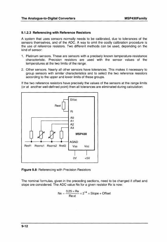
The Analogue-to-Digital Converters MSP430Family
9.1.2.3 Referencing with Reference Resistors
A system that uses sensors normally needs to be calibrated, due to tolerances of the sensors themselves, and of the ADC. A way to omit the costly calibration procedure is the use of reference resistors. Two different methods can be used, depending on the kind of sensor:
1. Platinum sensors. These are sensors with a precisely known temperature-resistance characteristic. Precision resistors are used with the sensor values of the temperatures at the two limits of the range.
2. Other sensors. Nearly all other sensors have tolerances. This makes it necessary to group sensors with similar characteristics and to select the two reference resistors according to the upper and lower limits of these groups.
If the two reference resistors have precisely the values of the sensors at the range limits (or at another well-defined point) then all tolerances are eliminated during calculation:
SVee
Rex!
Ri
r--------~ AO r-------I A1
.------1 A2 A3
MSP430
-~-~-~--~--~AGND
Rref1 Rsens1 Rsens2 Rref2 Vss Vee
OV +5V
Figure 9.8: Referencing with Precision Resistors
The nominal formulas, given in the preceding sections, need to be changed if offset and slope are considered. The ADC value Nx for a given resistor Rx is now:
O.25xRx 14 Nx = x 2 x Slope + Offset
Rext
9-12

MSP430 Family The Analogue-to-Digital Converters
With two known resistors Rref1 and Rref2 it is possible to compute slope and offset and to get the values of unknown resistors exactly. The result of the solved equations gives:
with: Nx Nref1 Nref2 Rref1 Rref2
Nx-Nref2 Rx = x (Rref2 - Rref1) + Rref2
Nref2 - Nref1
ADC conversion result for Rx ADC conversion result for Rref1 ADC conversion result for Rref2 Resistance of Rref1 Resistanceof Rref2
As shown, only known or measurable values are needed for the computation of Rx from Nx. The slope and offset of the ADC disappear completely.
9.1.2.4 Interrupt Handling using the 14-bit-Mode
The examples shown above all use polling techniques for checking the completion of conversion. This takes up computing power which can be used otherwise if interrupt techniques are used.
EXAMPLE: Analogue input AO (without Current Source) and A1 (with Current Source) are measured alternately. The measured 14-bit results are stored in address MEASO for AO and MEAS1 for A 1. The background software uses these measured values and sets them to OFFFFh after use. The time interval between two measurements is defined by the a-bit timer: every timer interrupt starts a new conversion for the prepared analogue input.
HARDWARE DEFINITIONS SEE 1ST ADC EXAMPLE ANALOGUE INPUT AO A1 CURRENT SOURCE OFF ON RESULT TO MEASO MEAS1 RANGE SELECTION AUTO AUTO REFERENCE SVCC SVCC
INITIALIZATION PART FOR THE ADC:
#RNGAUTO+CSOFF+AO+VREF,&ACTL #ADIE,&IE2 ENABLE ADC INTERRUPT
MOV MOV.B MOV #OFFH-3,&AEN ONLY AO AND A1 ANALOGUE INPUTS
INITIALIZE OTHER MODULES
ADC INTERRUPT HANDLER: AO AND A1 ARE MEASURED ALTERNATIVELY THE NEXT MEASUREMENT IS PREPARED BUT NOT STARTED.
AD_I NT BIT #A1,&ACTL A1 RESULT IN ADAT? JNZ ADI YES MOV &ADAT,MEASO AO VALUE IS ACTUAL MOV #RNGAUTO+CSON+A1+VREF,&ACTL ; A1 NEXT MEAS. RETI
9-13

The Analogue-to-Digital Converters MSP430Family
ADI MOV MOV RET I
&ADAT, MEASl ; Al VALUE #RNGAUTO+CSOFF+AO+VREF,&ACTL AO NEXT MEAS.
8-BIT TIMER INTERRUPT HANDLER: THE ADC CONVERSION IS STARTED FOR THE PREPARED ADC INPUT
T8BINT BIS #CS,&ACTL START CONVERSION FOR THE ADC
RETI
.SECT "INT_VECO",OFFEAH INTERRUPT VECTORS
. WORD AD_I NT ADC INTERRUPT VECTOR;
.SECT "INT_VEC1",OFFF8H
. WORD T8BINT 8-BIT TIMER INTERRUPT VECTOR
9.1.3 The (12+2)-bit Analogue-to-Digital Converter used in 12-bit Mode
This mode is used if it is known in which range the input voltage is. If, for example. a temperature sensor is used whose signal range always fits into one range (for example range C). then the 12-bit mode is the correct selection. The measurement time with MCLK = 1 MHz is only 102 !-Is. compared to 132 !-Is if the auto ranging mode is used. The following Figure shows the four ranges compared to SVcc.
ADCValue
Overflow OFFFh
OCOOh
0800h
0400h
OOOOOh~~------~------~~------~~-------r Input~
SVcc Voltage Vax o 0.25 SVcc 0.5 SVcc 0.75 SVcc
Figure 9.9: The four Single ADC Ranges
9-14

MSP430 Family The Analogue-to-Digital Converters
Note: ADC Ranges
The ADC results OOOOH and OFFFh mean underflow and overflow: the voltage at the measured analogue input is below or above the limits of the addressed range respectively.
The next figure shows how one of the ranges can be seen:
ADCValue
OFFFh
0800h
Range N-1 Range N+1
OOOOh
o (N-1)xO.25 SVcc NxO.25 SVcc
Figure 9.10: Single ADC Range
SVcc
Input __
Voltage
The possible ways to connect sensors to the MSP430 are the same as shown for the (12+2)-bit ADC:
----_------.---1 SVee SVee 1------_-
Ri ~~--_!_-----~A2
+-------f A1
A3
A6 I--_!_---,. A4
AO ~~ 1-_-+ __ ./ MSP430
-+---~---~--~AGND AGNDI--~---+---v__ Vee
OV +5V
Figure 9.11: Possible Sensor Connections to the MSP430
9-15

The Analogue-to-Digital Converters MSP430Family
The nominal ADC formulas for the 12-bit conversion are:
N
with: N VAx Vref n
VAx-nxO.25xVref 214 V V f ( N 025) x ~ Ax = re 14"+nx. Vref 2
12-bit result of the ADC conversion Input voltage at the selected analogue input Ax Voltage at pin SVcc (external reference or internal Vcc) Range constant (n = 0,1,2,3 for ranges A,B,C,D)
The ADC formula for a resistor Rx (Rsens2 in the above figure) which is connected to Vref via a resistor Rv is:
~ x Vref - n x 0.25 x Vref N Rv+Rx x214 ~ Rx
Vref
If a current source is used (as for Rsens1 in the above figure), the above equation changes to:
N
0.25 x Vref x Rx _ n x 0.25 x Vref Rext X214
Vref (~_n)x212
Rext
This gives for the unknown resistor Rx:
with: Rext Rx
RX=(2~2 +n)xRext
Resistor between SVcc pin and Ri pin (defines current Ics) Resistor to be measured (connected to Ax and AGND)
9.1.3.1 ADC with Signed Signals
Only the Current Source method is applicable if signed signals have to be measured: - Normal phase splitter circuits are not able to shift the virtual ground into the middle of
range A (0.125 SVcc) or B (0.375 SVcc), as is necessary here. - The split power supply method would need two different voltages to get the zero point
into the middle of range A (0.625v/4.375V) or range B (1.875V/3.125V)
For signed signals it is necessary to shift the input signal V1 to the middle of the range A or B. If range B (0.375 SVcc) is used the necessary shift resistor Rh is
Rh = 0.375 x SVcc xRext ~ Rh = 1.5 x Rext 0.25 x SVcc
9-16

MSP430 Family The Analogue-to-Digital Converters
The unknown voltage V1 referred to its zero point in the middle of range n is:
V1 = VAx - Rh x Ics
With the above equations for Vax this leads to:
V1 = 0.25 x SVcc -+n---( N Rh ) 212 Rext
9.1.3.2 Interrupt Handling using the 12-bit-Mode
The software is the same as for the 14-bit conversion. The only difference is the omission of the RNGAUTO bit during the initialization of ACTL. Instead, the desired range is to be included into the initialization part of each measurement.
EXAMPLE: Analogue input AO (without Current Source, always range C, external reference at pin SVcc) and A 1 (with Current Source, always range A) have to be measured alternately. The measured 12-bit results have to be stored in address MEASO for AO and MEAS1 for A1. The background software uses these measured values and sets them to OFFFFh after use. The time interval between two measurements is defined by the 8-bit timer: every timer interrupt starts a new conversion for the prepared analogue input.
HARDWARE DEFINITIONS SEE 1ST ADC EXAMPLE ANALOGUE INPUT AD A1 CURRENT SOURCE RESULT TO RANGE REFERENCE
OFF ON MEASD MEAS1 C A EXTERNAL SVCC
INITIALIZATION PART FOR THE ADC:
MOV MOV.B MOV
#RNGC+CSOFF+AD,&ACTL #ADIE,&IE2 ENABLE ADC INTERRUPT #DFFH-3,&AEN ONLY AD AND A1 ANALOGUE
INPUTS INITIALIZE OTHER MODULES
ADC INTERRUPT HANDLER: AD AND A1 ARE MEASURED ALTERNATIVELY THE NEXT MEASUREMENT IS PREPARED BUT NOT STARTED
BIT JNZ
#A1,&ACTL ADI
A1 MEASURED YES
MOV &ADAT,MEASD AD VALUE IS ACTUAL MOV #RNGA+CSA1+A1+VREF,&ACTL ; A1 NEXT MEAS. RETI
9-17

The Analogue-to-Digital Converters MSP430Family
ADI MOV MOV RETI
&ADAT,MEASI Al VALUE #RNGC+CSOFF+AD,&ACTL; AD NEXT MEASUREMENT
8-BIT TIMER INTERRUPT HANDLER: THE ADC CONVERSION IS STARTED FOR THE ADDRESSED ADC INPUT
T8BINT BIS #CS,&ACTL START CONVERSION
RETI
. SECT "INT_VECT",OFFEAH INTERRUPT VECTORS
. WORD AD_INT ADC INTERRUPT VECTOR;
. SECT "INT_VECT",OFFF8H
. WORD T8BINT 8-BIT TIMER INTERRUPT VECTOR
9.2 The Universal Timer/Port Module used as ADC
This ADC module is contained in MSP430 versions that do not have the (12+2)-bit ADC. The function is completely different from the (12+2)-bit ADC: the discharge times tdc for different resistors are measured and compared.
Vth +---+----..,...:::::----f---+-------""''''""--
o
Figure 9.12: Timing for the Universal Timer
9-18
~
Time

MSP430 Family
with Vth tdc1 tdc2 tc
The Analogue-to-Digital Converters
Threshold voltage of the comparator Discharge time with the reference resistor Discharge time with the sensor Charge time for the capacitor
EXAMPLE: Use of the Universal Timer Port as an ADC without interrupt
MSP430
Enable Control TPIN.5 TPD.5 TPE.5 TPD.4 TPE.4 TPD.3 TPE.3 TPD.2 TPE.2 TPD.l TPE.l TPD.O TPE.O
Figure 9.13: Schematic of Example
; DEFINITION PART FOR THE UT/PM ADC
TPCTL .EQU 04BH TIMER PORT CONTROL REGISTER TPSSELO .EQU 040H TPSSEL.O ENB .EQU 020H CONTROLS ENI OF TPCNTI ENA .EQU 010H AS ENB ENI .EQU 008H ENABLE INPUT FOR TPCNTI RC2FG .EQU 004H RIPPLE CARRY TPCNT2 ENIFG .EQU 001H ENI FLAG BIT
TPCNTI .EQU 04CH LO 8-BIT COUNTER/TIMER TPCNT2 .EQU 04DH HI 8-BIT COUNTER/TIMER
TPD .EQU 04EH DATA REGISTER B16 .EQU 080H 0: SEPARATE TIMERS 1: 16-BIT
TIMER CPON .EQU 040H 0: COMP OFF 1 : COMP ON TPDMAX .EQU 008H BIT POSITION OUTPUT TPD.MAX
9-19

The Analogue-to-Digital Converters MSP430Family
TPE
MSTACK NN
.EQU
.EQU
.EQU
04FH
0240H OllH
DATA ENABLE REGISTER
RESULT STACK 1ST WORD TPCNT2 VALUE FOR CHARGING OF C
MEASUREMENT SUBROUTINE WITHOUT INTERRUPT. TPD.4 AND TPD.5 ARE NOT USED AND THEREFORE OVERWRITTEN INITIALIZATION: STACK INDEX <- 0, START WITH TPD.3 16-BIT TIMER, MCLK, CIN ENABLES COUNTING
MEASURE PUSH.B#TPDMAX ; START WITH SENSOR R3 TPD.MAX ; INDEX FOR RESULT STACK CLR
MEASLOP MOV. B R5 # (TPSSELO*3)+ENB+ENA,&TPCTL ; RESET FLAGS
CAPACITOR C IS CHARGED UP FOR> 5 TAU. N-1 OUTPUTS ARE USED
OUTPUTS
MLPO
MOV.B
MOV.B MOV.B
BIT.B JZ
MOV.B CLR.B
#B16+CPON+TPDMAX-1,&TPD ; SELECT CHARGE
#TPDMAX-1,&TPE; ENABLE CHARGE OUTPUTS #NN,&TPCNT2 LOAD NEG. CHARGE TIME
#RC2FG,&TPCTL MLPO
@SP,&TPE &TPCNT2
CHARGE TIME ELAPSED? NO CONTINUE WAITING
ENABLE ONLY ACTUAL SENSOR CLEAR HI BYTE TIMER
SWITCH ALL INTERRUPTS OFF, TO ALLOW NON-INTERRUPTED START OF TIMER AND CAPACITY DISCHARGE
; WAIT
MLP1
DINT CLR.B BIC.B
EINT UNTIL EOC
BIT.B JNZ BIT.B JZ
&TPCNT1 @SP,&TPD
(EN1 = 1) OR OVERFLOW
#RC2FG,&TPCTL MERR #EN1,&TPCTL MLP1
ALLOW NEXT 2 INSTRUCTIONS CLEAR LO BYTE TIMER SWITCH ACTUAL SENSOR TO LO COMMON START TOOK PLACE
ERROR (RC2FG = 1)
OVERFLOW (BROKEN SENSOR)? YES, GO TO ERROR HANDLING CIN < UCOMP? NO, WAIT
EN1 = 0: END OF CONVERSION: STORE 2 X 8 BIT RESULT ON MSTACK ADDRESS NEXT SENSOR, IF NO ONE ADDRESSED: END REACHED
L$301
9-20
MOV.B MOV.B INCD RRA.B
& TPCNT1,MSTACK (R5) &TPCNT2,MSTACK+1(R5) R5 @SP
STORE RESULT ON STACK HI BYTE
ADDRESS NEXT WORD NEXT OUTPUT TPD.X

MSP430 Family
JNC INCD
RET
MEASLOP SP
The Analogue-to-Digital Converters
IF C=1: FINISHED HOUSEKEEPING: TPDMAX OFF STACK
ERROR HANDLING: ONLY OVERFLOW POSSIBLE (BROKEN SENSOR ?) OFFFFH IS WRITTEN FOR RESULT AND SUBROUTINE CONTINUED
MERR MOV JMP
#OFFFFH,MSTACK(R5) L$301
9.2.1 Interrupt Handling
; OVERFLOW
EXAMPLE: Use of the Universal Timer Port as an ADC with interrupt. This has the same function as the example without interrupt.
; DEFINITION PART FOR THE UT/PM ADC
TPCTL .EQU TPSSELO . EQU ENB .EQU ENA .EQU EN1 .EQU RC2FG .EQU EN1FG .EQU
TPCNT1 .EQU TPCNT2 .EQU
TPD B16
CPON
TPE
MSTACK
ADCST NN
IFG2 TPIFG
IE2 ADIE
.EQU
.EQU
.EQU
.EQU
.EQU
.EQU
.EQU
.EQU
.EQU
.EQU
.EQU
04BH 040H 020H 010H 008H 004H 001H
04CH 04DH
04EH 080H
040H
04FH
0240H
MSTACK+8 OllH
003H 008H
001H 004H
TIMER PORT CONTROL REGISTER TPSSEL.O CONTROLS EN1 OF TPCNT1 AS ENB ENABLE INPUT FOR TPCNT1 RIPPLE CARRY TPCNT2 EN1 FLAG BIT
LO 8-BIT COUNTER/TIMER HI 8-BIT COUNTER/TIMER
DATA REGISTER 0: SEPARATE TIMERS 1: 16-BIT TIMER 0: COMP OFF 1: COMP ON
DATA ENABLE REGISTER
RESULT STACK 1ST WORD (8 BYTES)
TPCNT2 VALUE FOR CHARGING OF C
INTERRUPT FLAG REGISTER 2 ADC INTERRUPT FLAG
INTERRUPT ENABLE REGISTER 2 ADC INTERRUPT ENABLE BIT
9-21
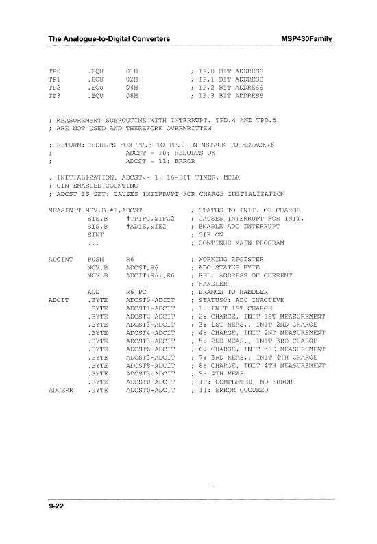
The Analogue-to-Digital Converters
TPO TP1 TP2 TP3
.EQU
.EQU
.EQU
.EQU
01H 02H 04H OSH
TP.O BIT ADDRESS TP.1 BIT ADDRESS TP.2 BIT ADDRESS TP.3 BIT ADDRESS
MSP430Family
MEASUREMENT SUBROUTINE WITH INTERRUPT. TPD.4 AND TPD.5 ARE NOT USED AND THEREFORE OVERWRITTEN
RETURN: RESULTS FOR TP.3 TO TP.O IN MSTACK TO MSTACK+6 ADCST 10: RESULTS OK ADCST ~ 11: ERROR
INITIALIZATION: ADCST<- 1, 16-BIT TIMER, MCLK CIN ENABLES COUNTING ADCST IS SET: CAUSES INTERRUPT FOR CHARGE INITIALIZATION
MEASINIT MOV.B #l,ADCST
ADCINT
ADCIT
ADCERR
9-22
BIS.B #TPIFG,&IFG2 BIS.B EINT
PUSH MOV.B MOV.B
ADD . BYTE . BYTE . BYTE . BYTE . BYTE . BYTE . BYTE . BYTE . BYTE . BYTE . BYTE . BYTE
#ADIE,&IE2
R6 ADCST,R6 ADCIT(R6),R6
R6,PC ADCSTO-ADCIT ADCST1-ADCIT ADCST2-ADCIT ADCST3-ADCIT ADCST4-ADCIT ADCST3-ADCIT ADCST6-ADCIT ADCST3-ADCIT ADCSTS-ADCIT ADCST3-ADCIT ADCSTO-ADCIT ADCSTO-ADCIT
STATUS TO INIT. OF CHARGE CAUSES INTERRUPT FOR INIT. ENABLE ADC INTERRUPT GIE ON CONTINUE MAIN PROGRAM
WORKING REGISTER ADC STATUS BYTE REL. ADDRESS OF CURRENT HANDLER BRANCH TO HANDLER STATUSO: ADC INACTIVE 1: INIT 1ST CHARGE 2: CHARGE, INIT 1ST MEASUREMENT 3: 1ST MEAS., INIT 2ND CHARGE 4: CHARGE, INIT 2ND MEASUREMENT 5: 2ND MEAS., INIT 3RD CHARGE 6: CHARGE, INIT 3RD MEASUREMENT 7: 3RD MEAS., INIT 4TH CHARGE 8: CHARGE, INIT 4TH MEASUREMENT 9: 4TH MEAS . 10: COMPLETED, NO ERROR 11: ERROR OCCURED

MSP430 Family The Analogue-to-Digital Converters
MEASUREMENT COMPLETED? EN1FG RC2FG
1: YES, OK
ADCST3
L$401
MOV.B RLA BIT.B JNZ MOV.B
JMP
MOV.B MOV.B
1: OVERFLOW BY BROKEN SENSOR
ADCST,R6 STATUS X 2 R6 #EN1FG,&TPCTL
FOR RESULT ADDRESSING EN1 OR RC2FG?
L$401 #ADCERR-ADCIT-1,ADCST
ADCCMPL
& TPCNT1,MSTACK-6 (R6) &TPCNT2,MSTACK-5(R6)
ERROR CODE-1 TO STATUS SWITCH OFF ADC
STORE RESULT ON STACK HI BYTE
IF LAST MEASUREMENT (ADCST = 9): SWITCH OFF ADC
CMP.B #9,ADCST JNE ADCST1 ADCST # 9: INIT NEXT
MEAS.
ADCCMPL CLR &TPE OUTPUTS DISABLED CLR &TPD ADC OFF, OUTPUTS LO JMP L$402 ADCST =10 AFTER
RETURN
; CAPACITOR C CHARGE-UP FOR> 5 TAU. TP.2 TO TP.O ARE USED
ADCST1 MOV.B #(TPSSELO*3)+ENB+ENA,&TPCTL RESET FLAGS
MOV.B #B16+CPON+TPO+TP1+TP2,&TPD SELECT OUTPUTS MOV.B #TPO+TP1+TP2,&TPE ENABLE CHARGE OUTPUTS MOV.B #NN,&TPCNT2 LOAD NEG. CHARGE TIME JMP L$402
; CHARGE IS MADE, INIT MEASUREMENT
ADCST8 MOV.B #TPO,&TPE ENABLE TP.O BIC.B #TPO,&TPD SET TP.O LOW JMP L$403
ADCST6 MOV.B #TP1,&TPE ENABLE TP.1 BIC.B #TP1,&TPD SET TP.1 LOW JMP L$403
ADCST4 MOV.B #TP2,&TPE ENABLE TP.2 BIC.B #TP2,&TPD SET TP.2 LOW JMP L$403
9-23

The Analogue-to-Digital Converters MSP430Family
ADCST2 MOV.B #TP3,&TPE ENABLE TP.3 BIC.B #TP3,&TPD SET TP.3 LOW
L$403 CLR.B &TPCNT2 CLEAR HI BYTE TIMER CLR.B &TPCNTl CLEAR LO BYTE TIMER
L$402 INC.B ADCST ADCST + 1
ADCSTO BIC.B #TPIFG,&IFG2 RESET ADC FLAG POP R6 RESTORE R6 RETI
. SECT " INT _ VECT" , 0 FFEAH ; INTERRUPT VECTORS
. WORD ADCINT ; ADC INTERRUPT VECTOR;
9-24

MSP430 Family
Topics
10 Hints and Recommendations 10.1 Hints for Programmers
10.2 Design Checklist
10.3 Most often Occuring Software Errors
Notes Note Title 10.1 Handling the Stack
Hints and Recommendations
10-3 10-3
10-7
10-8
Page 10-4
10-1

Hints and Recommendations MSP430 Family
10-2

MSP430 Family Hints and Recommendations
10 Hints and Recommendations
10.1 Hints for Programmers
During the software development of the first MSP430 projects, a great deal of experience was acquired. The following hints and recommendations are intended for all programmers and system designers having more experience with 4- and 8-bit microcomputers than with 16-bit systems. Also mentioned are differences which the MSP430 family has when compared with other 16-bit architectures (e.g. the function of the carry bit as an inverted zero bit with some instructions).
Bits to be used frequently should be located always in bit positions 0, 1, 2, 3, 7, 15. The first four bits can be set, reset and tested with constants coming from the Constant Generator (1, 2, 4, 8) and the last two ones can be tested easily with the conditional jump instructions IN and JGE:
TST.B JGE
TST IN
RSTAT BIT7LO
MSTAT BIT15HI
TEST BIT7 (OV <- 0) JUMP IF MSB OF BYTE IS 0
TEST BIT15 (OV <- 0) JUMP IF MSB OF WORD IS 1
Use BCD arithmetic if simple up/down counters are used that are to be displayed. This saves time and ROM space due to unnecessary binary-BCD conversion.
EXAMPLE: Counter1 (4 BCD digits) is incremented, Counter2 (8 BCD digits) is decremented by one:
CLRC DADD ADDS CARRY BIT TOO! DADD #OOOl,COUNTERl INCREMENT COUNTERl
DECIMALLY CLRC DADD #9999,COUNTER2 DECREMENT 8 DIGIT COUNTER2 DADD #9999,COUNTER2+2 ; DECIMALLY
- The Conditional Assembly feature of the MSP430 assembler allows obtaining more than one version out of one source. This reduces the effort to maintain software drastically: only one version needs to be updated if changes are necessary. See section "Conditional Assembly".
- Use bytes wherever appropriate. The MSP430 allows using every instruction with bytes. (exceptions are only SWPB, SXT and CALL)
- Use status bytes or words, not flags, for remembering states. This allows the extremely fast branching in one instruction to the appropriate handler. Otherwise a time (and ROM) consuming skip chain is necessary.
10-3

Hints and Recommendations MSP430 Family
- Computing software. Use integer routines if speed is essential; use FPP if complex computing is necessary.
- Bit Test Instructions: With the bit handling instructions (BIS, BIT and BIC) more than one bit can be handled simultaneously: up to 16 bits can be handled inside one instruction. The BIS instruction is equivalent to the logical OR and can be used this way The BIC instruction is equivalent to the logical AND with the inverted source and can be used this way.
- Use of Addressing Modes: Use the Symbolic Mode for random accesses Use the Absolute Mode for fixed addresses like peripherals Use the Indexed Mode for random accesses in tables Use the Register Mode for time critical processing and as the normal mode Use assigned registers for extremely critical purposes: if a register contains always the same information, then it is not necessary to save it and to load it afterwards. The same is true for the restoring of the register when the task is done.
- Stack Operations: All items on the stack can be accessed directly with the Indexed Mode: this allows completely new applications compared with architectures that have only simple hardware stacks. The stack size is limited only by the available RAM, not by hardware register limitations.
Note: Handling the Stack
The above mentioned possibilities make careful "house keeping" necessary: every programme part which uses the stack has to ensure that only relevant information remains on the stack, and that all irrelevant data is removed. If this rule is not used consequently, the stack will overflow or underflow. If complex stack handling is used it is advisable to draw the stack with its items and the stack pointer as shown with the examples "Argument Transfer with Subroutine Calls" in the appendix.
- The Programme Counter PC can be accessed like every other register with all instructions and all addressing modes. Be very careful when using this feature! Do not use byte instructions when accessing the PC, due to the clearing of the upper byte when used.
- The Status Register SR can be accessed in register Mode only. Every status bit can be set or reset alone or together with other ones. This feature may be used for status transfer in subroutines.
10-4

MSP430 Family Hints and Recommendations
- If highest possible speed is necessary for multiplications then two possibilities exist. Straight through programming: the effort used for the looping can be saved if the shifts and adds are programmed straight through. The routine ends at the known MSB of the multiplicand (here at bit 13 due to an ADC result [14 bits] that is multiplied):
EXECUTION TIMES FOR REGISTER USE (CYCLES @ 1MHZ, 16 BITS):
TASK
MINIMUM 80 MEDIUM MAXIMUM 132
MACUF EXAMPLE
OOOOOH X OOOOOH = OOOOOOOOOH 96 OA5A5H X 05A5AH = 03A763E02H
OFFFFH X OFFFFH = OFFFE0001H
FAST MULTIPLICATION ROUTINE: PART USED BY SIGNED AND UNSIGNED MULTIPLICATION
MACUF CLR
RRA JNC ADD
ADDC L$Ol RLA
RLC
RRA JNC ADD
ADDC L$02 RLA
RLC
RRA JNC ADD
ADDC L$014 RET
R6
R4 L$Ol R5, R7
R6,R8 R5 R6
R4 L$02 R5,R7
R6,R8 R5 R6
R4 L$014 R5,R7
R6,R8
MSBS MULTIPLIER
LSB TO CARRY IF ZERO: DO NOTHING IF ONE: ADD MULTIPLIER TO RESULT
MULTIPLIER X 2
LSB TO CARRY IF ZERO: DO NOTHING IF ONE: ADD MULTIPLIER TO RESULT
MULTIPLIER X 2
SAME WAY FOR BITS 2 TO 12
LSB TO CARRY IF ZERO: DO NOTHING IF ONE: ADD MULTIPLIER TO RESULT
10-5

Hints and Recommendation~ MSP430 Family
- The following instructions have a special feature that is valuable during serial to parallel conversion: the carry acts as an inverted zero bit. This means that if the result of an operation is zero, then the carry is reset and vice versa. The instructions involved are:
XOR, SXT, INV, BIT, AND.
Without this feature a typical sequence for the conversion of an I/O-port bit to a parallel word would look like as follows:
RLA R5 FREE BIT 0 FOR NEXT INFO BIT #l,&IOIN PO.O HIGH ? JZ L$111 INC R5 YES, SET BIT 0
L$111 INFO IN BIT 0
With this feature the above sequence is shortened to two instructions:
BIT RLA
#l,&IOIN R5
PO.O HIGH? .NOT.ZERO -> CARRY SHIFT BIT INTO R5
The carry bit can be used if increments by one are used:
EXAMPLE: If the RAM word COUNT is greater than or equal to the value 1000 then a word COUNTER is to be incremented by one
CMP ADC
#1000,COUNT COUNTER
COUNT >= 1000 IF YES, CARRY = 1
- The carry bit can be added immediately. No conditional jumps are necessary for counters longer than 16 bits:
ADD ADC ADC
R5,COUNT COUNT+2 COUNT+4
LOW PART OF COUNT MEDIUM PART HIGH PART OF 48-BIT COUNTER
- "Fall Through" Usage: ROM space is saved if a subroutine call that is located immediately before a RET instruction is changed: The called subroutine is located after the instruction before the CALL and the programme falls through it. This saves.6 bytes of ROM: the CALL itself and the RET instruction. The 12C handler uses thiS mode.
NORMAL WAY: SUBR2 IS CALLED, AFTERWARDS RETURNED SUBR1
10-6
MOV CALL RET
R5,R6 #SUBR2 CALL SUBROUTINE

MSP430 Family Hints and Recommendations
; "FALL THROUGH" SOLUTION: SUBR2 IS LOCATED AFTER SUBR1
SUBRI MOV R5,R6 ;GO TO SUBR2
SUBR2 ;START OF SUBROUTINE SUBR2 RET
10.2 Design Checklist
Several steps are necessary to complete a system consisting of an MSP430 and its peripherals with the necessary performance. Typical and recommended development steps are shown below. All of the tasks mentioned should be done carefully in order to prevent trouble later on.
1. Definition of the tasks to be performed by the MSP430 and its peripherals. 2. Worst case timing considerations for all of the tasks (interrupt timing, calculation
times, 110 etc.). 3. Drawing of a complete hardware schematic. Decision which hardware options are
used (Supply voltage, pull-downs at the liD-ports ?) 4. Worst case design for all of the external components. 5. Organization of the RAM and if present of the EEPROM. 6. Flowcharting of the complete programme. 7. Coding of the software with an editor 8. Assembling of the programme with the ASM430 Assembler 9. Removing of the logical errors found by the ASM430 Assembler 10. Testing of the software with the SIM430 Simulator and EMU430 Emulator 11. Repetition of the steps 7 to 10 until the software is error free
10.3 Most frequently Occurring Software Errors
During software development the same errors are made by nearly all assembler programmers. The following list contains the errors most often heard of and experienced.
- A lack of "housekeeping" during stack operations: if items are removed from or placed onto the stack during subroutines or interrupt handlers, it is mandatory to keep track of these operations. Any wrong positioning of the stack pointer will lead to a programme crash due to wrong data which is written into the Programme Counter.
- Use of the wrong jump instructions: the conditional jump instructions JLO and JL, and JHS and JGE, respectively, give different results if used for numbers above 07FFFh. It is therefore necessary always to distinguish between signed and unsigned comparisons.
10-7

Hints and Recommendations MSP430 Family
- Wrong completion instructions: dDespite their virtual similarity, subroutines and interrupt handlers need completely different actions when completed. Subroutines end with the RET instruction: only the address of the next instruction (the one following the subroutine call) is popped from the stack. Interrupt handlers end with the RETI instruction: two items are popped from the stack, first the Status Register is restored and afterwards the address (the address of the next instruction after the interrupted one) is popped from the stack to the Programme Counter. If RETI and RET are used wrongly, then a wrong item is written into the PC anyway. This means that the software will continue at random addresses and will therefore hang-up.
- Addition and subtraction of numbers with differently located decimal points: if numbers with virtual decimal points are used the addition or subtraction of numbers with different fractional bits leads to errors. It is necessary to shift one of the operands in a way to achieve equal fractional parts. See "Rules for the Integer Subroutines".
- Byte instructions applied to registers always clear the upper byte of the register. It is necessary therefore to use word instructions if operations in registers can exceed the byte range.
- Use of byte instructions with the Programme Counter as destination register: if the PC is the destination register, byte instructions do not make sense. The clearing of the PC's high byte is certainly wrong in any case. Instead a register should be used before the modification of the PC with the byte information.
- Use of falsely addressed branches and subroutine calls. The destination of branches and calls is used indirectly; this means the content of the destination is used as the address. These errors occur most often with the symbolic mode and the absolute mode:
CALL CALL
MAIN #MAIN
;SUBROUTINE'S ADDRESS IS STORED IN MAIN ;SUBROUTINE STARTS AT ADDRESS MAIN
The real behaviour is seen easily when looking at the branch instruction. It is an emulated instruction, using the MOV instruction:
BR MAIN ; EMULATED INSTRUCTION BR MOV MAIN, PC ; EMULATION BY MOV INSTRUCTION
The addressing for the CALL instruction is exactly the same as for the BR instruction.
- If counters or timers longer than 16 bits are modified by the foreground (interrupt routines) and used by the background, it is necessary to disable the timer interrupt (most simple with the GIE bit in SR) during the reading of these words. If this is not done, the foreground can modify these words between the reading of two words. This would mean that one word contains the old value and the other one the modified one.
10-8

MSP430 Family Hints and Recommendations
EXAMPLE: The timer interrupt handler increments a 32-bit timer. The background software uses this timer for calculations. The disabling of the interrupts avoids a timer interrupt that occurs between the reading of TIMLO and TIMHI falsifying the read information. This is the case if TIMLO overflows from OFFFFh to OOOOh during the interrupt routine: TIMLO was read with the old information OFFFFh and TIMHI contains the new information x+ 1.
BT_HAN INC TIMLO ;INCR. LO WORD ADC TIMHI ;INCR. HI WORD RETI
BACKGROUND PART COPIES TIMXX FOR CALCULATIONS
DINT ;GIE <- a NOP ;DINT NEEDS 2 CYCLES MOV TIMLO,R4 ;COPY LSDS MOV TIMHI,RS ;COPY MSDS EINT ; ENABLE INTERRUPT AGAIN
- When using sophisticated stack processing it is often overlooked that the PUSH instruction decrements the stack pOinter first and moves the item afterwards.
EXAMPLE: The return address stored at TOS is to be moved one word down to free space for an argument.
PUSH @SP
PUSH 2 (SP)
;WRONG! 1ST FREE WORD (TOS-2) IS ; COPIED ;ON ITSELF
; CORRECT, OLD TOS IS PUSHED
10-9

Hints and Recommendations MSP430 Family
10-10

MSP430 Family
Topics
Appendixes
A1 CPU Registers and Features AU The Program Counter RO
A1.2 Stack Processing A1.2.1 Usage of the System Stack Pointer R1 A1.2.2 Usage of the System Stack Pointer R1 A1.3 Byte and Word Handling
A1.4 Constant Generator
A1.S Addressing
A1.6 Program Flow Control A1.6.1 Computed Branches and Calls A1.6.2 Nesting of Subroutines A1.6.3 Jumps
A2 Special Coding Techniques A2.1 Conditional Assembly A2.2 Position Independent Code A2.2.1 Referencing of Code Inside of PIC A2.2.2 Referencing of Code Outside of PIC (Absolute)
A2.3 Reentrant Code
A2.4 Recursive Code
A2.S Flag Replacement by Status Usage
A2.6 Argument Transfer with Subroutine Calls A2.6.1 Arguments on the Stack A2.6.2 Arguments following the Subroutine Call A2.6.3 Arguments in Registers
A2.7 Interrupt Vectors in RAM
A3 References
Figures
Figure Title
A 1 Word/Byte Configuration
A2
A3
Arguments on the Stack
Arguments on the Stack
Appendixes
A-3
A-3 A-3
A-3 A-3 A-4 A-S
A-6
A-7
A-9 A-9 A-9 A-9
A-11 A-11 A-12 A-13 A-14
A-1S
A-16
A-17
A-19 A-19 A-22 A-22
A-23
A-24
Page
A-S
A-20
A-20
A-1

Appendixes
Tables
Table Title
A1
A2
A3
Constants of the Constant Generator
Addressing Modes
Possible Jumps
Notes
MSP430 Family
Page
A-6
A-7
A-9
Note Title Page
A 1 Use no Odd Address, if the Program Counter is Involved A-3
A2 Use no Odd Address, if the Stack Pointer is Involved A-4
A3 Byte Addressing and RO to R15 A-5
A4 Conditional jumps for Signed and Unsigned Data A-10
A5 Only Unsigned Jumps are Adequate for Computed Addresses A-10
A6 Only Data at of above the Top Of Stack is Protected Against Overwriting A-21
A-2

MSP430 Family Appendixes
Appendixes
A 1 CPU Registers and Features
All of the MSP430 CPU-registers can be used with all instructions.
A 1.1 The Programme Counter RO
One of the main differences to other microcomputer architectures relates to the Programme Counter (PC) that may be used as a normal register with the MSP430. This means that all of the instructions and addressing modes may be used with the Programme Counter too. For example, a branch is made by simply moving an address into the PC:
MOV MOV
MOV
#LABEL,PC &LABEL,PC
@R14,PC
;JUMP TO ADDRESS LABEL ;JUMP TO ADDRESS CONTAINED ; IN ADDRESS LABEL ;JUMP INDIRECT INDIRECT R14
Note: Use no Odd Address, if the Programme Counter is involved
The Programme Counter always points to even addresses: this means the LSB is always zero. The software has to ensure that no odd addresses are used if the Programme Counter is involved. Odd PC addresses will end up with nonpredictable results.
A 1.2 Stack Processing
A 1.2.1 Usage of the Stack Pointer R1
The system stack pointer (SP) is a normal register like the other ones. This means it can use the same addressing modes. This gives good access to all items on the stack, not only to the one on the top of the stack.
The system stack pointer SP is used for the storage of the following items: • Interrupt return addresses and Status Register contents • Subroutine return addresses • Intermediate results • Variables for subroutines, floating point package etc.
When using the system stack, one should bear in mind that the microcomputer hardware uses the stack painter for interrupts and subroutine calls too. To ensure the error free
A·3

Appendixes MSP430 Family
running of the programme it is necessary to do exact "housekeeping" for the system stack.
Note: Use no Odd Address, if the Stack Pointer is involved
The Stack Pointer always points to even addresses: this means the LSB is always zero. The software has to ensure that no odd addresses are used if the Stack Pointer is involved. Odd SP addresses will end up with non-predictable results.
If bytes are pushed on the system stack, only the lower byte is used; the upper byte is not modified.
PUSH PUSH.B
#05H #05H
A 1.2.2 Software Stacks
0005H -> TOS XX05H -> TOS
Every register from R4 to R15 may be used as a software stack pointer. This allows independent stacks for jobs that have a need for this. Every part of the RAM may be used for these software stacks.
EXAMPLE: R4 is to be used as a software stack pointer.
MOV #SW_STACK,R4 ;INIT. SW STACK POINTER
DECD R4 ;DECREMENT STACK POINTER MOV ITEM,O(R4) ;STORE ITEM ON STACK
; PROCEED MOV @R4+,ITEM2 ;POP ITEM FROM STACK
Software stacks may be organized as byte stacks. This is not possible for the system stack which always uses 16-bit words. The example shows R4 used as a byte stack pointer:
MOV #SW_STACK,R4 ;INIT. SW STACK POINTER
DEC R4 ;DECREMENT STACK POINTER MOV.B ITEM,O(R4) ;STORE ITEM ON STACK
; PROCEED MOV.B @R4+,ITEM2 ;POP ITEM FROM STACK
A 1.3 Byte and Word Handling
Every word is addressable by three addresses as shown in Figure A 1 : • The word address: an even address N • The lower byte address: an even address N
A-4

MSP430 Family Appendixes
• The upper byte address: an odd address N+ 1
If byte addressing is used, only the addressed byte is affected: no carry or overflow can affect the other byte.
Note: Byte Addressing and RO to R15
Registers RO to R15 do not have an address: they are treated in a special way. Byte addressing always uses the lower byte of the register; the upper byte is set to zero.
The wayan instruction treats data is defined with its extension: • The extension .B means byte handling • The extension .W (or none) means word handling
Examples: The first two lines are equivalent. The 16-bit values, read in absolute address 050h, are added to the value in R5.
ADD ADD.W
&050H,R5 &050H,R5
; ADD 16~BIT VALUE TO R5 ; ADD 16~BIT VALUE TO R5
The 8-bit value, read in the lower byte of absolute address 050h, is added to the value contained in the lower byte of R5. The upper byte of R5 is set to zero. If the addressed byte 050h contains 078h, then R5 will contain 00078h afterwards, regardless of its former contents.
ADD.B &050H,R5 ; ADD 8~BIT VALUE TO R5
Bit 15 8 7 0
~I-----u-p-p-e-r-B-yt-e------~I-------L-ow-e-r-B-yt-e------'I
Odd Address N+ 1 Even Address N
Word Address N
Word/Byte Configuration
Figure A1: Word/Byte Configuration
A-5
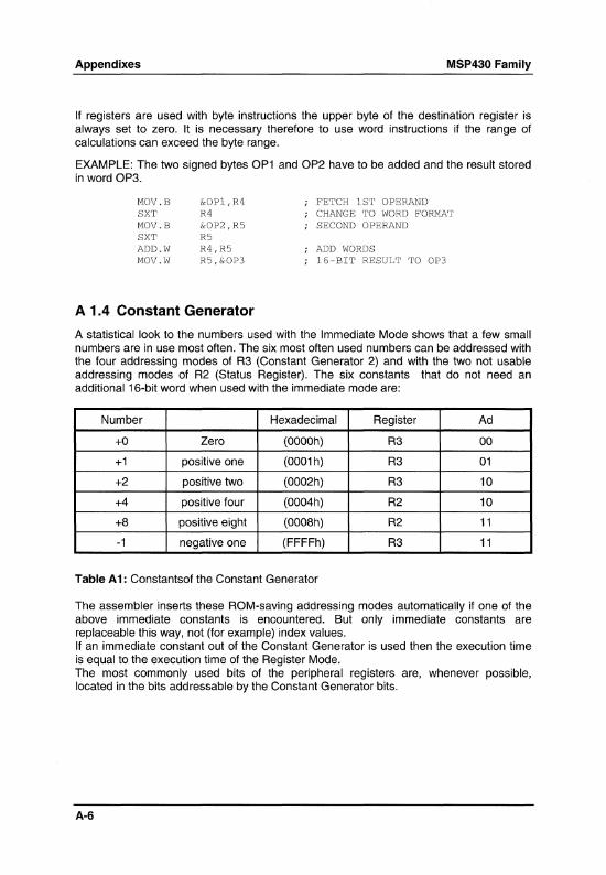
Appendixes MSP430 Family
If registers are used with byte instructions the upper byte of the destination register is always set to zero. It is necessary therefore to use word instructions if the range of calculations can exceed the byte range.
EXAMPLE: The two signed bytes OP1 and OP2 have to be added and the result stored in word OP3.
MOV.B &OP1,R4 SXT R4 MOV.B &OP2,R5 SXT R5 ADD.W R4,R5 MOV.W R5,&OP3
A 1.4 Constant Generator
FETCH 1ST OPERAND CHANGE TO WORD FORMAT SECOND OPERAND
ADD WORDS 16-BIT RESULT TO OP3
A statistical look to the numbers used with the Immediate Mode shows that a few small numbers are in use most often. The six most often used numbers can be addressed with the four addressing modes of R3 (Constant Generator 2) and with the two not usable addressing modes of R2 (Status Register). The six constants that do not need an additional 16-bit word when used with the immediate mode are:
Number Hexadecimal Register Ad
+0 Zero (OOOOh) R3 00
+1 positive one (0001 h) R3 01
+2 positive two (0002h) R3 10
+4 positive four (0004h) R2 10
+8 positive eight (0008h) R2 11
-1 negative one (FFFFh) R3 11
Table A 1: Constantsof the Constant Generator
The assembler inserts these ROM-saving addressing modes automatically if one of the above immediate constants is encountered. But only immediate constants are replaceable this way, not (for example) index values. If an immediate constant out of the Constant Generator is used then the execution time is equal to the execution time of the Register Mode. The most commonly used bits of the peripheral registers are, whenever possible, located in the bits addressable by the Constant Generator bits.
A-6

MSP430 Family Appendixes
A 1.5 Addressing
The MSP430 allows seven addressing modes for the source operand, and four or five addressing modes for the destination. The addressing modes used are:
Address Bits Source Modes Destination Modes Example
00 Register Register R5
01 Indexed Indexed TAB(R5)
01 Symbolic Symbolic TABLE
01 Absolute Absolute &BTCTL
10 Indirect --- @R5
11 Ind. autoinkr. --- @R5+
11 Immediate ---- #TABLE
Table A2: Addressing Modes
The three missing addressing modes for the destination operand are not of much concern for the programming: Immediate Mode: Not necessary for the destination; immediate operands can always be placed into the source. Only in a very few cases will it be necessary to have two immediate operands in one instruction
Indirect Mode: if necessary the Indexed Mode with an index of zero is usable. For example:
ADD CMP
#16,O(R6) RS,O(SP)
@R6 + 16 -> @R6 RS EQUAL TO TOS?
The second example above can be written in the following way saving 2 bytes of ROM:
CMP @SP,RS ; RS EQUAL TO TOS? (RS-TOS)
Indirect Auto increment Mode: with table computing a method is usable that saves ROM-space, and also the number of registers used:
Example: The content of TAB1 is to be written into TAB2. TAB1 ends at the word preceding TAB1END.
LOOP MOV MOV.B CMP JNE
#TAB1,RS @RS+,TAB2-TAB1-l(RS) #TAB1END,RS LOOP
INITIALIZE POINTER MOVE TAB1 -> TAB2 END OF TAB1 REACHED? NO, PROCEED YES, FINISHED
A-7

Appendixes MSP430 Family
The above example uses only one register instead of two and saves three words due to the smaller initialization part. The normally written, longer loop is shown below
MOV #TAB1,RS ;INITIALIZE POINTERS MOV #TAB2,R6
LOOP MOV.B @RS+,O(R6) ;MOVE TABl -> TAB2 INC R6 CMP #TAB1END,RS ;END OF TABl REACHED? JNE LOOP ;NO, PROCEED
;YES, FINISHED
In other cases it may be possible to exchange source and destination operands to have the auto increment feature available for a pointer.
Each of the seven addressing modes has its own features and advantages:
Register Mode: Fastest mode, least ROM requirements
Indexed Mode: Random access to tables
Symbolic Mode: Access to random addresses without overhead by loading of pointers
Absolute Mode: Access to absolute addresses independent of current programme address
Indirect Mode: Table addressing via register, code saving access to often referenced addresses
Indirect Autoincrement Mode: Table addressing with code saving automatic stepping, for transfer routines
Immediate Mode: Loading of pointers, 16-bit-constants within the instruction.
With the usage of the Symbolic Mode, an interrupt routine can be as short as possible. An interrupt routine is shown which has to increment a RAM word COUNTER, and to do a comparison if a status byte STATUS has reached the value 5. If this is the case, the status byte is cleared; otherwise, the interrupt routine terminates:
INTRPT INC COUNTER ;INCREMENT COUNTER CMP.B #S,STATUS ; STATUS S? JNE INTRET CLR.B STATUS ;STATUS = S: CLEAR IT
INTRET RETI
No loading of pointers or saving and restoring of registers is necessary. What needs to be done is performed immediately without any overhead.
A-8

MSP430 Family
A 1.6 Programme Flow Control
A 1.6.1 Computed Branches and Calls
Appendixes
The Branch instruction is an emulated instruction which moves the destination address into the Programme Counter:
MOV DST,PC ; EMULATION FOR BR DST
The possibility to access the Programme Counter in the same way as all other registers gives interesting possibilities: 1. The destination address can be taken from tables 2. The destination address may be computed 3. The destination address may be a constant
A 1.6.2 Nesting of Subroutines
Thanks to the stack orientation of the MSP430, one of the main problems of other architectures does not playa role at all: subroutine nesting can proceed as long as RAM is available. There is no need to keep track of the subroutine calls as long as all subroutines terminate with a "Return from Subroutine" instruction. If subroutines are left without the RET instruction, then some housekeeping is necessary: popping of the return address or addresses from the stack.
A 1.6.3 Jumps
Jumps allow the conditional or unconditional leaving of the linear programme flow. The Jumps cannot reach every address of the address map, but they have the advantage of needing only one word and only two oscillator cycles. The 10-bit offset field allows Jumps of 512 words maximum in the forward direction, and 511 words maximum backwards. This is four times the normal reach of a Jump: only in few cases is the two word branch necessary.
Eight Jumps are possible with the MSP430. Four of them have two mnemonics, to allow better readability:
A-9

Appendixes MSP430 Family
Mnemonic Condition Purpose
JMP label Unconditional Jump Programme control transfer
JEQ label Jump if Z = 1 After comparisons
JZ label Jump if Z = 1 Test for zero contents
JNE label Jump if Z = 0 After comparisons
JNZ label Jump if Z = 0 Test for non zero contents
JHS label Jump if C = 1 After unsigned comparisons
JC label Jump if C = 1 Test for set Carry
JLO label Jump if C = 0 After unsigned comparisons
JNC label Jump if C = 0 Test for reset Carry
JGE label Jump if N .XOR. V = 0
JL label Jump if N .xOR. V = 1
IN label Jump if N = 1 Test for sign of a result
Table A3: Possible Jumps
Note: Conditional Jumps for Signed and UnSigned Data
It is important to use the appropriate conditional Jump for signed and unsigned data. For positive data (0 to 07FFFh and 0 to 07Fh) both signed and unsigned conditional jumps behave similiarly. This changes completely when used with negative data (08000h to OFFFFh and 080h to OFFh): the signed conditional jumps treat negative data as smaller numbers than the positive ones; the unsigned conditional jumps treat them as larger numbers than the positive ones.
No "Jump if Positive" is provided, only a "Jump if Negative". But after several instructions it is possible to use the "Jump if Greater Than or Equal" for this purpose. It must only be ensured that the instruction preceding the JGE resets the overflow bit V. The following instructions ensure this:
AND SRC,DST V <- 0 BIT SRC,DST V <- 0 RRA DST V <- 0 SXT DST V <- 0 TST DST V <- 0
If this feature is used it should be noted in the comment for later software modifications. For example:
A-10
MOV TST JGE
ITEM,R7 R7 ITEMPOS
FETCH ITEM V <- 0, ITEM POSITIVE? v=o: JUMP IF >= 0

MSP430 Family Appendixes
Note: Only Unsigned Jumps are Adequate for Computed Addresses
If addresses are computed only the unsigned jumps are adequate: addresses are always unsigned, positive numbers.
A 2 Special Coding Techniques
A 2.1 Conditional Assembly
The Syntax for conditional assembly is described in detail in the MSP430 Family Assembler Tools User's Guide. Another example for conditional assembly is shown in the section Software UART.
Conditional assembly provides the possibility of compiling different lines of source into the object file, depending on the value of an expression that is defined in the source of the programme. This makes it easy to alter the behaviour of the code by modifying one single line in the source.
The following example shows how to use conditional assembly. The example will allow easy debugging of a programme that processes input from the ADC, by pretending that the input of the ADC is always 07FFh. The following is the routine used for reading the input of the ADC. It returns the value read from ADC input AO in R8.
DEBUG .SET 1 ;1= DEBUGGING MODE; 0= NORMAL MODE ACTL .SET 01l4H ADAT .SET 01l8H IFG2 .SET 3 ADIFG .SET 4
GET_ADC_VALUE:
. IF DEBUG=l MOV #07FFH,R8 .ELSE BIC #60,&ACTL INPUT CHANNEL IS AO BIC.B #ADIFG,&IFG2 BIS #l,&ACTL START CONVERSION
WAIT BIT.B #ADIFG, &IFG2 JZ WAIT WAIT UNTIL CONVERSION READY MOV &ADAT,R8 .ENDIF RET
With a little further refining of the code, better results may be achieved. The following piece of code shows more built-in ways to debug the code. The second 'debug code', where debug=2, returns 0700h and 0800h alternately.
A-11

Appendixes
DEBUG .SET 0= ACTL .SET ADAT .SET IFG2 .SET ADIFG .SET
; GET_ADC_VALUE:
VAR OSC
WAIT
. SECT
. WORD
.IF MOV .ELSEIF MOV SUB MOV .ELSE BIC BIC BIS BIT JZ MOV .ENDIF RET
1
01l4H 01l8H 3 4
"VAR"'0200H 0700H
DEBUG=l #07FFH,R8
DEBUG=2 #OFOOH,R8 OSC,R8 R8,OSC
#60H,&ACTL #ADIFG,&IFG2 #l,&ACTL #ADIFG,&IFG2 WAIT &ADAT,R8
A 2.2 Position Independent Code
MSP430 Family
1= DEBUG MODE 1; 2= DEB. MODE 2; NORMAL MODE
RETURNING CONSTANT VALUE
RETURNING ALTERNATING VALUE
INPUT CHANNEL IS AO
START CONVERSION
WAIT UNTIL CONVERSION READY
The architecture of the MSP430 allows the easy implementation of "Position Independent Code" (PIC). This is a code which may run anywhere in the address space of a computer, without any relocation being necessary. PIC is possible with the MSP430 mainly due to the allocation of the PC inside the register bank. Great use is made of the availability of the PC. Links to other PIC-blocks are possible only by references to absolute addresses (pointers).
EXAMPLE: Code is transferred to the RAM from an outside storage (EPROM, ROM, EEPROM) and executed there with full speed. This code needs to be PIC.
A 2.2.1 Referencing of Code Inside of PIC
The referenced code or data is located in the same block of PIC as that in which the programme resides.
Jumps Jumps are anyway position independent: their address information is an offset to the destination address.
A-12

MSP430 Family Appendixes
Branches
ADD . WORD
Subroutine Calls
@PC,PC DESTINATION-$
;BRANCH TO LABEL DESTINATION
Calling a subroutine starting at the label SUBR:
SC MOV ADD CALL
Operations on Data
PC,RN #SUBR-$,RN RN'
;ADDRESS SC+2 -> AUX. REG ;ADD OFFSET (SUBR - (SC+2)) ;SC+2+SUBR-(SC+2)) = SUBR
The symbolic addressing mode is position independent: an offset to the PC is used. No special addressing is necessary
MOV CMP
Jump Tables
DATA,RN DATA1,DATA2
;DATA IS ADDRESSED ; SYMBOLICALLY
The status contained in Rstatus decides where the SW continues. Rstatus contains a multiple of 2 (0, 2, 4 ... 2n). Range: +512 words, -511 words
ADD RSTATUS,PC ;RSTATUS = (2X STATUS) JMP STATUS 0 ;CODE FOR STATUS 0 JMP STATUSl ; CODE FOR STATUS 2
JMP STATUSN ; CODE FOR STATUS 2N
Branch Tables The status contained in Rstatus decides where the SW continues. Rstatus contains a multiple of 2 (0, 2, 4 ... 2n). Range: complete 64K
TABLE ADD . WORD . WORD
. WORD
TABLE (RSTATUS) ,PC STATUSQ-TABLE STATUS1-TABLE
STATUSN-TABLE
;RSTATUS = STATUS ;OFFSET FOR STATUS ;OFFSET FOR STATUS
;OFFSET FOR STATUS
A 2.2.2 Referencing of Code Outside of PIC (Absolute)
Q
2
2N
The referenced code or data is located outside the block of PIC. These addresses can be absolute addresses only, e.g. for linking to other blocks and peripheral addresses.
Branches Branching to the absolute address DESTINATION:
BR #DESTINATION ;#DESTINATION -> PC
A-13
Appendixes
Subroutine Calls Calling a subroutine starting at the absolute address SUBR:
CALL #SUBR
Operations on Data Absolute mode (indexed mode with Reg = 0)
CMP ADD PUSH
Branch Tables
&DATAl,&DATA2 &DATAl,RN &DATA2
;#SUBR -> PC
;DATAI + 0 = DATAl
;DATA2 -> STACK
MSP430 Family
The status contained in Rstatus decides where the SW continues. Rstatus steps in increments of 2. Table is located in absolute address space:
MOV TABLE (RSTATUS) ,PC ; RSTATUS STATUS
.SECT XXX ;TABLE IN ABSOLUTE ADDRESS ; SPACE
TABLE . WORD STATUS 0 ; CODE FOR STATUS 0 . WORD STATUS 1 ; CODE FOR STATUS 2
. WORD STATUSN ; CODE FOR STATUS 2N
Table is located in PIC address space, but addresses are absolute:
MOV RSTATUS,RHELP ;RSTATUS CONTAINS STATUS ADD PC,RHELP ;STATUS + L$l -> RHELP
L$l ADD #TABLE-L$l,RHELP ;STATUS+L$l+TABLE-L$l MOV @RHELP,PC ;COMPUTED ADDRESS TO PC
TABLE . WORD STATUS 0 ; CODE FOR STATUS 0 . WORD STATUSI ; CODE FOR STATUS 2
. WORD STATUSN ; CODE FOR STATUS 2N
The above shown programme examples may be implemented as MACRO's if needed. This would simplify usage and improve transparency.
A 2.3 Reentrant Code
If the same subroutine is used by the background programme and interrupt routines, then two copies of this subroutine are necessary with normal computer architectures. The stack gives a method of programming that allows many tasks to use a single copy of the same routine. This ability of sharing a subroutine between several tasks is called "Reentrancy" .
A-14

MSP430 Family Appendixes
Reentrancy allows the calling of a subroutine despite the fact that the current task in use has not yet finished the subroutine.
The main difference between a reentrant subroutine and a normal one is that the reentrant routine contains only "pure code": that is, no part of the routine is modified during usage. The linkage between the routine itself and the calling software part is possible only via the stack i.e. all arguments during calling, and all results after completion, have to be placed on the stack and retrieved from there. The following conditions must be met for "Reentrant Code": • No usage of dedicated RAM, only stack usage • If registers are used, they need to be saved on the stack and restored from there.
EXAMPLE: A conversion subroutine "Binary to BCD" needs to be called from the background and the interrupt part. The subroutine reads the input number from TOS and places the 5-digit result also on TOS (two words): the subroutines save all used registers on the stack and restore them from there, or they compute directly on the stack.
PUSH CALL MOV MOV
R7 #BINBCD @SP+,LSD @SP+,MSD
A 2.4 Recursive Code
R7 CONTAINS THE BINARY VALUE TO BE CONVERTED TO BCD BCD-LSDS FROM STACK BCD-MSD FROM STACK
Recursive subroutines are subroutines that call themselves. This is not possible with normal architectures: stack processing is necessary for this frequently used feature. A simple example of recursive code is a lineprinter handler that calls itself for inserting a "Form Feed" after a certain number of printed lines. This self-calling allows the use of all of the existing checks and features of the handler without the need to write them once more.
The following conditions must be met for "Recursive Code": • No usage of dedicated RAM; only stack usage • A termination item must exist to avoid infinite nesting (e.g. the lines per page must be
greater than 1 with the above line printer example) • If registers are used they need to be saved and restored on the stack
EXAMPLE: The line printer handler inserts a Form Feed after 70 printed lines
LPHAND PUSH R4 SAVE R4
CMP #70 , LINES 70 LINES PRINTED? JL L$500 NO, PROCEED CALL #LPHAND . BYTE CR,FF YES, OUTPUT CARRIAGE RETURN
AND FORM FEED L$500
A-15

Appendixes MSP430 Family
A 2.5 Flag Replacement by Status Usage
Flags have several disadvantages if used for programme control: • Missing transparency (flags may depend on other flags) • Possibility of nonexistent flag combinations, if not handled very carefully • Slow speed: the flags can only be tested serially
The MSP430 allows the use of a status (contained in a RAM byte or register) which defines the current programme part to be used. This status is very descriptive and prohibits "nonexistent" combinations. A second advantage is the high speed of the decision: one instruction only is needed to get to the start of the appropriate handler. See Branch Tables.
The programme parts that are used currently define the new status dependent on the actual conditions: normally the status is only incremented, but it may also change more randomly.
EXAMPLE: The status contained in register Rstatus decides where the software continues. Rstatus contains a multiple of 2 (0, 2, 4 ... 2n)
; RANGE: COMPLETE 64K
MOV TABLE . WORD
. WORD
. WORD
STATUS a INC JMP
TABLE(RSTATUS),PC ;RSTATUS = STATUS STATUSO ADDRESS HANDLER FOR STATUS
= a
STATUSI ADDRESS HANDLER FOR STATUS = 2
STATUSN ADDRESS HANDLER FOR STATUS = 2N
START HANDLER STATUS a RSTATUS NEXT STATUS IS 1 HEND COMMON END
The above solution has the disadvantage to use words even if the distances to the different programme parts are small. The next example shows the use of bytes for the branch table. The SXT instruction allows backward references (handler starts on lower addresses than TABLE4).
BRANCH TABLES WITH BYTES: STATUS IN R5 (0, 1, 2, .. N) USABLE RANGE: TABLE4-128 TO TABLE4+126
PUSH.B TABLE4 (R5) STATUSX-TABLE4 -> STACK SXT @SP FORWARD/BACKWARD REFERENCES ADD @SP+,PC TABLE4+STATUSX-TABLE4 -> PC
TABLE4 . BYTE STATUSO-TABLE4 DIFFERENCE TO START OF HANDLER . BYTE STATUS1-TABLE4
A-16

MSP430 Family Appendixes
. BYTE STATUSN-TABLE4 ; OFFSET FOR STATUS = N If only forward references are possible (normal case) the addressing range can be doubled. The following example shows this:
STEPPING IS FORWARD ONLY (WITH DOUBLED FORWARD RANGE) STATUS IS CONTAINED IN R5 (0, 1, .. N) USABLE RANGE: TABLE5 TO TABLE5+254
PUSH.B TABLE5 (R5) ;STATUSX-TABLE -> STACK CLR.B 1 (SP) ; HI BYTE <- 0 ADD @SP+,PC ;TABLE+STATUSX-TABLE -> PC
TABLE5 . BYTE STATUSO-TABLE5 ;DIFFERENCE TO START OF HANDLER . BYTE STATUS1-TABLE5
. BYTE STATUSN-TABLE5 ;OFFSET FOR STATUS = N
The above example can be made shorter and faster if a register can be used:
STEPPING IS FORWARD ONLY (WITH DOUBLED FORWARD RANGE) STATUS IS CONTAINED IN R5 (0, 1, 2 .. N) USABLE RANGE: TABLE5 TO TABLE5+254
MOV.B TABLE5(R5),R6 ;STATUSX-TABLE5 -> R6 ADD R6,PC ;TABLE5+STATUSX-TABLE5 -> PC
TABLE5 . BYTE STATUSO-TABLE5 ;DIFFERENCE TO START OF HANDLER . BYTE STATUS1-TABLE5
. BYTE STATUSN-TABLE5 ;OFFSET FOR STATUS N
The addressable range can be doubled once more with the following code; the status (0, 1, 2, .. n) is doubled before its use.
THE ADDRESSABLE RANGE MAY BE DOUBLED WITH THE FOLLOWING CODE: THE "FORWARD ONLY" VERSION WITH AN AVAILABLE REGISTER (R6) IS SHOWN: STATUS 0, 1, 2 ... N USABLE RANGE: TABLE6 TO TABLE6+510
MOV.B TABLE6(R5) ,R6 ; (STATUSX-TABLE6)/2 RLA R6 ;STATUSX-TABLE6 ADD R6,PC ;TABLE6+STATUSX-TABLE6 -> PC
TABLE6 . BYTE (STATUSO-TABLE6)/2 . BYTE (STATUS1-TABLE6)/2
. BYTE (STATUSN-TABLE6)/2 ;OFFSET FOR STATUS N
A-17

Appendixes MSP430 Family
A 2.6 Argument Transfer with Subroutine Calls
Subroutines often have arguments to work with. Several methods exist for the passing of these arguments to the subroutine: - On the stack
In the words (bytes) after the subroutine call - In registers - Address is contained in the word after the subroutine call
The information passed may itself consist of numbers, addresses, counter contents, upper and lower limits etc. It depends only on the application.
A 2.6.1 Arguments on the Stack
The arguments are pushed on the stack and read afterwards by the called subroutine. The subroutine is responsible for the necessary housekeeping (here, the transfer of the return address to the top of the stack).
Advantages: • Usable generally; no registers have to be freed for argument passing • Variable arguments are possible
Disadvantages: • Overhead due to necessary housekeeping • Not easy to understand
EXAMPLE: The subroutine SUBR gets its information from two arguments pushed onto the stack before the calling. No information is given back; normal return from subroutine is used.
PUSH ARGUMENT 0 1ST ARGUMENT FOR SUBROUTINE PUSH ARGUMENT 1 2ND ARGUMENT CALL #SUBR SUBROUTINE CALL
SUBR MOV 4 (SP) ,RX COPY ARGUMENTO TO RX MOV 2 (SP) ,RY COPY ARGUMENT1 TO RY MOV @SP,4(SP) RETURN ADDRESS TO CORRECT LOC. ADD #4,SP PREPARE SP FOR NORMAL RETURN
PROCESSING OF DATA RET NORMAL RETURN
A-18

MSP430 Family Appendixes
SP -
After the Call After the Return
ArgumentO
Argument1
Return Address
TOS before CALL S P ---iI 1-----------1
Address N+4
Address N+2
Address N
Figure A2: Arguments on the Stack
EXAMPLE: The subroutine SUBR gets its information from two arguments pushed onto the stack before the calling. Three result words are returned on the stack: it is the responsibility of the calling programme to pop the results from the stack.
PUSH ARGUMENT 0 1ST ARGUMENT FOR SUBROUTINE PUSH ARGUMENT 1 2ND ARGUMENT CALL #SUBR SUBROUTINE CALL POP R15 RESULT2 -> R15 POP R14 RESULT1 -> R14 POP R13 RESULTO -> R13
SUBR MOV 4(SP) ,RX COpy ARGUMENTO TO RX MOV 2(SP) ,RY COPY ARGUMENT 1 TO RY
PROCESSING CONTINUES PUSH 2 (SP) SAVE RETURN ADDRESS MOV RESULTO, 6 (SP) 1ST RESULT ON STACK MOV RESULT1,4(SP) 2ND RESULT ON STACK MOV RESULT2,2(SP) 3RD RESULT ON STACK RET
After the subroutine call and the RET, the stack looks as follows:
After the Call After the Return
TOS before CALL
ArgumentO Address N+4 ResullD
Argument1 Address N+2 Result1
SP - Return Address Address N SP - Result2
Figure A3: Arguments on the Stack
A-19
Appendixes MSP430 Family
Note: Only Data at or above the Top Of Stack is Protected Against Overwriting
If the stack is involved during data transfers it is very important to have in mind that only data at or above the top of stack (TOS, the word the SP points to) is protected against overwriting by enabled interrupts. This does not allow moving the SP above the last item on the stack; indexed addressing is needed instead.
A 2.6.2 Arguments following the Subroutine Call
The arguments follow the subroutine call and are read by the called subroutine. The subroutine is responsible for the necessary housekeeping; here, the adaptation of the return address on the stack to the 1 st word after the arguments.
Advantages: • Very clear and good readable interface
Disadvantages: • Overhead due to necessary housekeeping • Only fixed arguments possible
EXAMPLE: The subroutine SUBR gets its information from two arguments following the subroutine call. Information can be given back on the stack or in registers.
CALL #SUBR SUBROUTINE CALL . WORD START . BYTE 24,0
SUBR MOV @SP,R5 MOV @R5+,R6 MOV @R5+,R7 MOV R5,0(SP)
RET
A 2.6.3 Arguments in Registers
START OF TABLE LENGTH OF TABLE, FLAGS
COPY ADDRESS 1ST ARGUMENT TO R5 MOVE 1ST ARGUMENT TO R6 MOVE ARGUMENT BYTES TO R7 ADJUST RETURN ADDRESS ON STACK PROCESSING OF DATA NORMAL RETURN
The arguments are moved into defined registers and used afterwards by the subroutine.
Advantages: • Simple interface and easy to understand • Very fast • Variable arguments are possible
Disadvantages: • Registers have to be freed
EXAMPLE: The subroutine SUBR gets its information inside two registers which are loaded before the calling. Information can be given back or not, with the same registers.
A-20

MSP430 Family Appendixes
SUBR
MOV MOV CALL
RET
ARGO, R.5 ARG1,R6 #SUBR
A 2.7 Interrupt Vectors in RAM
1ST ARGUMENT FOR SUBROUTINE 2ND ARGUMENT SUBROUTINE CALL
PROCESSING OF DATA NORMAL RETURN
If the destination address of an interrupt changes with the programme run it is valuable to have the possibility to modify the pointer. The vector itself (which resides in ROM) is not changeable but a second pointer residing in RAM may be used for this purpose:
EXAMPLE: The interrupt handler for the Basic Timer starts at location BTHAN1 after initialization and at BTHAN2 when a certain condition is met (for example calibration is made).
BASIC TIMER INTERRUPT GOES TO ADDRESS BTVEC. THE INSTRUCTION "MOV @PC,PC" WRITES THE ADDRESS IN BTVEC+2 INTO THE PC: PROGRAM CONTINUES AT THAT ADDRESS
BTVEC .SECT . WORD .WORD
"VAR",0200H o o
RAM START OPCODE "MOV @PC,PC" ACTUAL HANDLER START ADDR.
; THE SOFTWARE VECTOR BTVEC IS INITIALIZED:
INIT MOV MOV
#04020H,BTVEC #B1'HAN1, BTVEC+2
OPCODE "MOV @PC,PC START WITH HANDLER BTHAN1 INITIALIZATION CONTINUES
THE CONDITION IS MET: THE BASIC 'rIMER INTERRUPT IS HANDLED AT ADDRESS BTHAN2 STARTING NOW
MOV #BTHAN2,BTVEC+2 CONT. WITH ANOTHER HANDLER
THE INTERRUPT VECTOR FOR THE BASIC TIMER CONTAINS THE RAM ADDRESS OF THE SOFTWARE VECTOR BTVEC:
.ORG
. WORD OFFE2H BTVEC
VECTOR ADDRESS BASIC TIMER FETCH ACTUAL VECTOR THERE
A-21

Appendixes MSP430 Family
A 3 References
MSP430 Family Architecture Guide and Module Library 1994
MSP430 Family Assembly Language Tools User's Guide 1994
MSP430 Family Metering User's Guide 1994
The Art of Electronics, Cambridge University Press 1989
A-22

Notes

TI SC Sales TI Technology Offices in Europe Centres
Belgium Hungary France Texas Instruments S.A.IN.v. TI Representation: Texas Instruments Brussels Budapest Velizy Villacoublay Tel.: (02) 7 26 75 80 Tel.: (1) 1 76 37 33 Tel.: Standard: Fax: (02) 7 26 72 76 Fax: (1) 2 02 62 56 (1) 30 70 10 01
Technical Service: Finland Italy (1) 30 70 11 33 Texas Instruments OY Texas Instruments S.p.A. Espoo Agrate Brianza (Mi) Holland Tel.: (0) 43 54 20 33 Tel.: (0 39) 6 84 21 Texas Instruments B.V. Fax: (0) 46 73 23 Fax: (0 39) 6 84 29 12 Amstelveen
Tel.: (020) 5 45 06 00 France, Republic of Ireland Fax: (0 20) 6 40 38 46 Middle-East & Africa Texas Instruments Ltd. Texas Instruments Dublin Italy Velizy Villacoublay Tel.: (01) 4 75 52 33 Texas Instruments S.p.A. Tel.: (1) 30 70 10 01 Fax: (01) 4 78 14 63 Agrate Brianza (Mi) Fax: (1) 30 70 10 54 Tel.: (039) 6 84 21
Spain Fax: (0 39) 6 84 29 12 Germany Texas Instruments S.A. Texas Instruments GmbH Madrid Sweden Freising Tel.: (1) 3 72 80 51 Texas Instruments Tel.: (0 81 61) 80-0 Fax: (1) 3 72 82 66 International Trade Corporation Fax: (0 81 61) 80 45 16 Kista
Sweden Tel.: (08) 7 52 58 00 Hannover Texas Instruments Fax: (08) 7 51 97 15 Tel.: (05 11) 90 49 60 International Trade Corporation Fax: (05 11) 6 49 03 31 Kista
Tel.: (08) 7 52 58 00 Ostfildern Fax: (08) 7 51 97 15 Tel.: (07 11) 3 40 30 European SC Fax: (07 11) 3 40 32 57 United Kingdom Information Centre
Texas Instruments Ltd. Holland Northampton Telephone: Texas Instruments B.V. Tel.: (0 16 04) 66 30 00 Dutch (33) 1 30 70 11 66 Amstelveen Fax: (0 16 04) 66 30 01 English (33) 1 30 70 11 65 Tel.: (0 20) 6 40 04 16 French (33) 1 30 70 11 64 Fax: (0 20) 5 45 06 60 German (33) 1 30 70 11 68
(0 20) 6 40 38 46 Italian (33) 1 30 70 11 67
Fax: (33) 1 30 70 10 32
~TEXAS INSTRUMENTS
Printed in Gennany Chlorine free paper - to protect our environment by Sellier Druck, Angerstr. 54, 85354, Freising

'1!1 TEXAS INSTRUMENTS
SLAUE11