1982_StandardMicrosystems.pdf - bitsavers.org
399
-
Upload
khangminh22 -
Category
Documents
-
view
2 -
download
0
Transcript of 1982_StandardMicrosystems.pdf - bitsavers.org


TABLE OF
CONTENTS
INDEX PART NUMBER
FUNCTIONAL
CROSS REFERENCE
GENERAL INFORMATION
INTRODUCTION
CUSTOM CAPABILITIES
QUALITY ASSURANCE & QUALITY CONTROL
PAGE I 3 _
4-7
8-10
11_131
14-17
18-24
DATA COMMUNICATION PRODUCTS ..... 25.1641 BAUD RATE GENERATOR ..... 165.1941
CRT DISPLAY ..... 195.2921
MICROPROCESSOR PERIPHERAL ..... 293.3541
PRINTER ..... 355.3681 KEYBOARD ENCODER ..... 369.3821
MiCROCOMPUTER ..... 383.390 I ORDERING INFORMATION ..... 391.3951


PART NUMBER INDEX I PART NUMBER PAGE PART NUMBER PAGE CCC 3500 339 COM 8502 141 CG 4103 357 CRT 5027 197 COM 1553A 27 CRT 5037 197 COM 1671 43 CRT 5047 205 COM 1863 59 CRT 5057 197 COM 2017 67 CRT 7004 255 COM 2017H 67 CRT 8002 235 COM 2449 75 CRT 8002H 247 COM 2502 67 CRT 8021 273 COM 2502H 67 CRT 9006 261 COM 2601 91 CRT 9007 207 COM 2651 99 CRT 9021 281 COM 2661 111 CRT 9212 267 COM 5016 167 CRT 96364 227 COM 5016T 167 FOC 1761 295
COM 5025 123 FOC 1763 295
COM 5026 169 FOC 1765 295
COM 5026T 169 FOC 1767 295
COM 5036 171 FOC 1791 311
COM 5036T 171 FOC 1792 311
COM 5046 173 FOC 1793 311
COM 5046T 173 FOC 1794 311
COM 8004 135 FOC 1795 311
COM 8017 141 FOC 1797 311 COM 8046 179 FOC 3400 339 COM 8116 181 FOC 9216/8 327 COM 8116T 181 KR 2376 371 COM 8126 183 KR 3600 375 COM 8126T 183 MPU 3870 383 COM 8136 185 ROM 4732 347 COM 8136T 185 ROM 36000 351 COM 8146 187 SR 5015 361 COM 8146T 187 SR 5017 365 COM 8251A 149 SR 5018 365
3

FUNCTIONAL INDEX
~ Data Communication Products Part Max Power
Number Name Description Baud Rate Supplies Package Page COM 1553A MIL-STD- MIL-STD-1553 (Manchester) Interface 1 MB +5 40 DIP 27-42 1553A UART Controller COM 1671 ASTRO Asynchronous/Synchronous
Transmitter/Receiver, Full Duplex, 5-8 1 MB +5,-5,+12 40 DIP 43-58 data bit, IX or 32X clock
COM 1863 UART Universal Asynchronous Receiver/ Transmitter, Full Duplex, 5-8 data bit, 6205 KB +5 40 DIP 59-66 I, 1 1/2, 2 stop bit, enhanced distortion margin
COM 2017 UART Universal Asynchronous Receiver Transmitter, Full Duplex, 5-8 data bit, 25KB +5,-12 40 DIP 67-74 I, 1 1/2, 2 stop bit
COM 20l7H UART Universal Asynchronous Receiver/ Transmitter, Full Duplex, 5-8 data bit, 40KB +5,-12 40 DIP 67-74 I, 11/2,2 stop bit
COM 2449 RB449-USART RS 449 Compatible Universal Synchronous/~chronous 1 MB +5 40 DIP 75-90 Receiver/Transmitter
COM 2502 UART Universal ~chronous Receiver/ Transmitter, Full Duplex, 5-8 data bit, 25KB +5,-12 40 DIP 67-74 1,2 stop bit
COM 2502H UART Universal ~chronous Receiver/ Transmitter, Full Duplex, 5-8 data bit, 40KB +5,-12 40 DIP 67-74 1,2 stop bit
COM 2601 USRT Universal Synchronous Receiver/ Transmitter, STR, BSC, Bi-sync 250KB +5,-12 40 DIP 91-98 compatible
COM 2651 USART/PCI Universal Synchronous/Asynchronous Receiver/Transmitter, Full Duplex, 5-8 1 MB +5 28 DIP 99-110 data bits; I, 11/2,2 stop bit, IX, 16X, 64X clock
COM 2661 USART/EPCI Universal Synchronous/Asynchronous Receiver/Transmitter, Full Duplex, 5-8 1 MB +5 28 DIP 111-122 data bits; I, 1112,2 stop bit, IX, 16X, 64X clock
COM 5025 Multi-Protocol SDLC, HDLC, ADCCP, Bi-sync, DDCMP USYNRT compatible, automatic bit stuffing/ 105MB +5, +12 40 DIP 123-134 stripping, frame detection/generation,
CRC generation/checking, sync detection COM 8004 32 Bit CRC Companion device to COM 5025
Generator/ for 32 bit CRC 200MB +5 20 DIP 135-140 Checker
COM 8017 UART Universal Asynchronous Receiver/ Transmitter, Full Duplex, 5-8 data bit, 40KB +5 40 DIP 141-148 1,11/2,2 stop bit
COM 8018 UART Universal Asynchronous Receiver/ Transmitter, Full Duplex, 5-8 data bit, 6205KB +5 40 DIP 59-66 I, 1l/2, 2 stop bit, enhanced distortion margin
COM 8251A USART Universal Synchronous/Asynchronous Receiver/Transmitter, Full Duplex, 5-8 64 KB (sync) data bit, I, 11/2,2 stop bit 906 KB (async) +5 28 DIP 149-164
COM 8502 UART Universal Asynchronous Receiver/ Transmitter, Full Duplex, 5-8 data bit, 40KB +5 40 DIP 141-148 1,2 stop bit
4

~ Baud Rate Generator All Baud Rate Generators are programmable dividers capable of providing 16 output frequencies" for UARTs or USARTs from either an on-Chip crystal oscillator or an external frequency input. "T" versions utilize an external frequency input only. Dual Baud Rate Generators provide two out-
put frequencies simultaneously for full duplex communications. Baud Rate Generators providing all standard baud rates from various popular crystal frequencies are available. In addition the baud rate generator mBJ" be custom mask programmed for other divisors.
"except as noted
Power Part Number Description Features Supplies Package
COM 5016 Dual Baud Rate Generator On-chip oscillator or external +5,+12 18 DIP frequency input
COM 5016T(3) Dual Baud Rate Generator External frequency input +5,+12 18 DIP
COM 5026 Single Baud Rate Generator On-chip oscillator or external +5,+12 14 DIP frequency input
COM 5026T(3) Single Baud Rate Generator External frequency input +5,+12 14 DIP
COM 5036 Dual Baud Rate Generator COM 5016 with additional +5,+12 18 DIP output of input frequency --;- 4
COM 5036T (3) Dual Baud Rate Generator COM: 5016T with additional +5,+12 18 DIP output of input frequency --;- 4
COM 5046 Single Baud Rate Generator COM 5026 with additional +5,+12 14 DIP output of input frequency --;- 4
COM 5046T (3) Single Baud Rate Generator COM 5026T with additional +5,+12 14 DIP output of input frequency --;- 4
COM 8046 Single Baud Rate Generator 32 baud rates; IX, 16X, 32X clock outputs; single +5 volt +5 16 DIP supply
COM 8046T (3) Single Baud Rate Generator COM 8046 with external +5 16 DIP frequency input only
COM 8116 Dual Baud Rate Generator Single +5 volt version of +5 18 DIP COM 5016
COM 8116T (3) Dual Baud Rate Generator Single +5 volt version of +5 18 DIP COM 5016T
COM 8126 Single Baud Rate Generator Single +5 volt version of +5 14 DIP COM 5026
COM 8126T (3) Single Baud Rate Generator Single +5 volt version of +5 14 DIP COM 5026T
COM 8136 Dual Baud Rate Generator Single +5 volt version of +5 18 DIP_ COM 5036
COM 8136T (3) Dual Baud Rate Generator Single +5 volt version of +5 18 DIP COM 5036T
COM 8146 Single Baud Rate Generator Single +5 volt version of +5 14 DIP COM 5046
COM 8146T (3) Single Baud Rate Generator Single +5 volt version of +5 14 DIP COM 5046T
,~ Keyboard Encoder Standard Fonts Power
Part Number No. of Keys Modes Features SUffix Description SUpplies Package KR-2376 XX(3) 88 3 2 Key Rollover -ST ASCII +5,-12 40 DIP KR-3600 XX (3) 90 4 2 Key or -ST ASCII +5, -12 40 DIP
N Key Rollover -STD ASCII -PRO Binary Sequential
(3)M~ be custom mask programmed
5
I Page
167-168
167-168
169-170
169-170
171-172
171-172
173-174
173-174
179-180
179-180
181-182
181-182
183-184
183-184
185-186
185-186
187-188
187-188
Page 371-374
375-382

';_1 Printer CHARACTERGENER~OR
Part Number Description Max Access Time Power Supplies CG 4103(3) 5x7x64 1.2 Ilsec +5, -12 or ±12
SHIFT REGISTER Max Power
Part Number Description Feature Clock Freq. Supply Package Page SR 5015-XX(3) Quad Static Shift Register Load, ReCirculate, ~
Mask Programmable Length Shift Controls, :
SR 5015-80 Quad 80 Bit Static i
SR 5015-81 Quad 81 Bit Static 1 MHz +5 16 DIP 361-364
SR 5015-133 Quad 133 Bit Static Shift Left/Shift
SR 5017 Quad 81 Bit Right, Recirculate 1 MHz +5 16 DIP 365-368 SR 5018 Quad 133 Bit Controls, Asynch-
ronous clear
Microprocessor Peripheral _ROM Part Number Description Access Time Power Supply Package Page
ROM 4732(3) 32K ROM; 32,768 bits 450 nsec +5 24 DIP 347-350 organized 4096x8 ROM 36000(1)(3) 64K ROM; 65,536 bits 250 nsec +5 24 DIP 351-364 organized 8192x8
""IM"a FLOPPY DISK Part Sectorl Data Side Select Power
Number Description Format Density Bus Output Supplies Package Page
FDCl761 Floppy Disk Controller/ Soft Double Inverted No +5, + 12 40 DIP 295-310 Formatter (mini-floppy only)
FDC1763 Floppy Disk Controller/ Soft Double True No +5, + 12 40 DIP 295-310 Formatter (mini-floppy only)
FDC1765 Floppy Disk Controller/ Soft Double Inverted Yes +5, + 12 40 DIP 295-310 Formatter (mini-floppy only)
FDCl767 Floppy Disk Controllerl Soft Double True Yes +5, + 12 40 DIP 295-310 Formatter (mini-floppy only)
FDC1791 Floppy Disk Controller/ Soft Double Inverted No +5, + 12 40 DIP 311-326 Formatter
FDC1792 Floppy Disk Controller/ Soft Single Inverted No +5, + 12 40 DIP 311-326 Formatter
FDCl793 Floppy Disk Controller/ Soft Double True No +5, + 12 40 DIP 311-326 Formatter
FDC1794 Floppy Disk Controller/ Soft Single True No +5, + 12 40 DIP 311-326 Formatter
FDC1795 Floppy Disk Controller/ Soft Double Inverted Yes +5, + 12 40 DIP 311-326 Formatter
FDC1797 Floppy Disk Controller/ Soft Double True Yes +5, + 12 40 DIP 311-326 Formatter
FDC3400 Floppy Disk Data Handler Hard N/A True NA +5, -12 40 DIP 331-338
FDC9216/B Floppy Disk Data Separator Soft/Hard Double NA NA +5 8 DIP 327-330
tCIt,Hiidlw CASSETTE/CARTRIDGE Max Power
Part Number Description Data Rate Features Supply Package Page CCC 3500 Cassette/Cartridge Data Handler 250K bps Sync byte detection, +5,-12 40 DIP 339-346
Read While Write
(l )For future release (3)May be custom mask programmed 6

Part liumber Description
provides all of the t1m1ng and control for interlaced and non-interlaced CRT d1spl8J7
I~ CR! Display TIMING CONTROLLERS
Features
fixed format
Display Format
80 column 24 row
CRT 9007 CRT video processor and controller
sequential or row-table driven memory
programmable 4 MHz +6
CRT 96364A/B complete CRT processor
on-chip cursor and write control
64 column 1.6 MHz +6 16 row
VDAC™ DISPLAY CONTROLLERS Max Power
Part Number Description Display Attribute~ Clock Supply
CRT 8002H (1.2.3) PrOvides complete 7 x 11 dot matrix, reverse video 26 MHz display and attri- wide graphics, blank butes control for thin graphics, blink
CRT 8002A (2.3) alphanumeric and on-chip cursor underline 20 MHz graphics display. strike-thru Consists of 7 x 11 x 128 +6
CRT 8002B (2.3) character generator, video shift register, 16 MHz latches, graphics and attributes circuits.
CRT 8002C (2.3) 10 MHz
CHARACTER GENERATORS Max
Part liumber Description Frequency Power Supply CRT 7004A (3.4) 20 MHz CRT 7004B (3.4)
7 x 11 x 128 character generator, 16MHz +6 latches, video shift regiSter
CRT 7004C (3.4) 10 MHz
ROW BUFFER Max
Part Number Description Row Length Power Supply
CRT 9006-83 8 bit wide serial cascadable single row buffer 83 characters +6
CRT 9006-136 memory for CRT or printer 136 characters
CRT 9212 8 bit wide serial cascadable double row buffer 135 characters +5 memory for CRT or printer
V7DEO~TRIB~ESCO~ROLLERS
Max Power Part Number Description Display Attributes Clock Supply
CRT 8021 Provides attributes AlphanumeriC, wide Reverse video, 20 MHz +5 and graphics control graphics, thin graphiCS, blank, blink, for CRT video on-chip cursor underline, displays strike-thru
CRT9021B Provides attributes AlphanumeriC, wide Reverse video, 28.5 MHz +6 and graphics control graphics, thin graphiCS, blank, blink, for CRT video on-chip cursor, double underline, displays height, double width intenSity
(1) For future release (3) M8J7 be custom mask programmed
40 DIP
28 DIP
Package
28 DIP
Package
24 DIP
Package
24 DIP
28 DIP
Package
28 DIP
28 DIP
(2) Also available as CRT 8002A,B,C - 001 Katakana CRT 8002A,B,C - 003 6X7 dot matrix
(4) Also available as CRT 7004A,B,C - 003 6X7 dot matrix
7
207-226
227-234
Page
247-264
236-244
236-244
236-244
Page
266-260
Page
261-266
267-272
Page
273-280
281-292

SMCCROSS
Description SMC AMI Fairchild
General Harris Intel Intersil Part # Instrument
UART (1112 8B)** COM 2017 81883 - AY 5-1013A - - -
UART (1, 28B)** COM 2502 - - AY 5-1013 - - -
UART (n-Channel)** COM 8017 86850* - AY 3-1015 HM6402 - IM6402
UART (n-Channel)** COM 8502 - - AY 3-1015 HM6403* 8251* IM6403*
UART (n-Channel)* COM 1863 81602 - - - - -
U8RT COM 2601 82350* - - - - -
A8TRO COM 1671 - - - - - -
PCI COM 2651 - - - - - -
EPCI COM 2661 - - - - - -
USART COM 8251A - - - - 8251A -
Multi-Protocol, COM 5025
F3846* - - - -USYNRT - F6856*
Dual Baud Rate Gen. COM 5016/36 - - - - -COM 8116/36
-
8ingle Baud Rate Gen. COM 5026/46 F4702* HD4702*
-COM 8126/46
- - HD6405* -
88 Key KB Encoder KR 2376 - - AY 5-2376 - - -
90 Key KB Encoder KR3600 - - AY 5-3600 - - -
CRT Controller CRT 5037 - - - - 8275* -
Character Generator CRT 7004 88564* - - - - -
Character Generator CRT8002 - - - - - -
Character Generator CG4100 88499 - RO 5-22408* - - -
8hift Register 8R5015 82182/3/5 - - - - -
ROM ROM 4732 868332 - RO 3-9332 - 2332* -
ROM ROM 36000 84264* - RO 3-9364 - - -
* Functional Equivalent **Most UART's are interchangeable; consult the factory for detailed information on interchangeability.
8

REFERENCE GUIDE I :ommodore Solid Texas Western
(MOS Mostek Motorola National NEe Signetics State Synertec Instruments Digital "echnology) Scientific
- - - MM5303* f../PD369* - - - TMS6011 TR1602
- - - - - 2536 - - - TR1402
- - MC6850* - - - SCR1854 - - -
- - - - - - - - - TR1983*
- - - - - - - - - TR1863
- - - - - - - - - -
- - - INS1671 - - - - - UC1671
- - - INS2651 - 2651 - - - -
- - - - - 2661 - SY2661 - -
- - - INS8251 f../PD8251A. - - - - -
- - - - f../PD379* 2652 SND5025 - - SD1933*
- - - - - - - - - BR1941 L
- - MC14411 * MM5307* - - - - - -
- - - - - - - - - -
MCS1009* - - MM5740* f../PD364* - - - TMS5001 -
- MK3807 MC6845* DP8350* - - SND5027 6545* TMS9927 -SND5037
-MCM66700* DM8678* - 2609* - - - --MC6570*
- - - - - - SND8002 - - -
MCS1004* MK2002 MC1132* M5240* - - - TMS4103 -
MCS2027* -
MK1007* 5054* 2532* - TMS3113* -- - - -TMS3114*
2332 - MCM8332 - JIPD2332 2632 - SY2332 TMS4732 -
2364* MK36000 MCM68A364* MM52864* JIPD2364* 2664* - SY2364* TMS4764* -
For Floppy Disk Controllers-See Next Page
9

FLOPPY DISK CONTROLLERS
Description SMC Fairchild Fujitsu Mostek Synertec Western Part # Digital
Floppy Disk Controller FDC 1791-02 - MB8876 - SY1791-02 FD 1791-02
Floppy Disk Controller FDC 1792-02 - - - - FD 1792-02
Floppy Disk Controller FDC 1793-02 - M8877 - SY1793-02 FD 1793-02
Floppy Disk Controller FDC 1794-02 - - - - FD 1794-02
Floppy Disk Controller FDC 1795-02 - - - - FD 1795-02
Floppy Disk Controller FDC 1797-02 - - - - FD 1797-02
Floppy Disk Controller FDC 1761-02 - - - - FD 1761-02
Floppy Disk Controller FDC 1763-02 - - - - FD 1763-02
Floppy Disk Controller FDC 1765-02 - - - - FD 1765-02
Floppy Disk Controller FDC 1767-02 - - - - FD 1767-02
Floppy Disk Data Separator FDC 9216 - - - - FD 1691*
Microcomputer MPU 3870 F3870-2 - MK3870/20 - -
*Functional Equivalent
10

Innovation in microelectronic technology is the key to growth at Standard Microsystems. Since its inception, Standard Microsystems has been a leader in creating new tech- I nology for metal oxide semiconductor large scale integrated (MOS/LSI) circuits.
For example, while the first MOS/LSI processes were p-channel, it was recognized -very early that an n-channel process would greatly improve switching speeds and circuit density. However, the fundamental problem of parasitic currents needed to be solved. The research and development staff at Standard Microsystems recognized this problem and directed its energy toward the development of its now-famous COPLAMOS® technology. COPLAMOS® defines a self-aligned, field-doped, locally oxidized structure which produces high-speed, high-density n-channel IC's.
In addition, on-chip generation of substrate bias, also pioneered by Standard Microsystems, when added to the COPLAMOS® technology, results in the ability to design dense, high-speed, low-power n-channel MOS integrated circuits through the use of one external power supply voltage.
Again recognizing a need and utilizing its staff of qualified process experts, Standard Microsystems developed the CLASP® process. The need was for fast turnaround, easily programmable semi-custom LSI technology. The development was CLASP®, a process that utilizes ion implantation to define either an active or passive device which allows for the presence of a logical 1 or 0 in the matrix of a memory or logic array. This step is accomplished after all wafer manufacturing steps are performed including metalization and final passiviation layer formation. Thus, the wafer can be tested and stored until customer needs dictate the application, a huge saving in turnaround time and inventory costs.
These innovations in both process and circuit technology have received widespread industry recognition; In fact, many of the world's most prominent semiconductor companies have been granted patent and patent/technology licenses covering various aspects of these technologies. The companies include Texas Instruments, IBM, General Motors, ITT, Western Electric, Mostek, Hitachi and Fujitsu.
Over the past few years, scientists and engineers at Standard Microsystems have been developing a technology to significantly reduce the sheet resistivity of polycrystalline silicon and thereby dramatically decrease internal time constants in MOS devices. Their work has culminated in the successful completion of a program to replace polycrystalline silicon in n-channel MOS devices with an alternate material, titanium disilicide. This has enabled Standard Microsystems to become the first semiconductor manufacturer to market and sell MOSNLSI circuits which employ a metal silicide to replace the conventional doped polycrystalline silicon layer.
11

Our engineering staff follows the principle that "necessity is the mother of invention. " This philosophy led Standard Microsystems Corporation to COPLAMOS®, CLASP®, and Titanium Oisilicide gate technology, as well as other innovative developments. It also brings companies to us to solve tough problems that other suppliers can't.
But it's a philosophy that involves more than just developing the next generation of MOS/LSI devices.
Such exploration, for example, helped Standard Microsystems recognize the need for communication controllers to handle the latest data communication protocols. As a result, Standard Microsystems was the first to introduce a one-chip LSI controller for HDLC protocols-the COM 5025.
The COM 5025 is so versatile it can actually provide the receiver/transmitter functions for all the standard bit and byte oriented synchronous protocols, including SOLC, HDLC, ADCep, bi-sync and ODCMP.
In another area, CRT display systems have traditionally required a great deal of support circuitry for the complex timing, refresh and control functions.
This need led the engineers at Standard Microsystems to develop the CRT 5027 Video Timer and Controller eVTAC®) that provides all these functions on a single chip. This left the display, graphics and attributes control spread over another 20 or 30 SSI, MSI and LSI devices. Standard Microsystems combined all these functions in the CRT 8002 Video Display Attributes Controller eVDAC n' ). The COPLAMOS® pro ccess was used to achieve a 20 MHz video shift register, and CLASP® was used for fast turnaround of character font changes through its last stage programmability.
So from 60 to 80 integrated circuits, Standard Microsystems reduced display and timing to 2 devices, drastically reducing the cost and size of today's CRT terminals.
Another major achievement was the development of the "next generation" Video Processor And Controller (VPAC™), the CRT 9007. This chip replaces up to 80 SSI and MSI TTL devices as well as providing a hardware solution to many of the software problems of CRT Video Controller design.
Achievements like these help keep Standard Microsystems custom and standard products in the forefront of technology with increased speeds and densities, and a lower cost per function.
12

Improvements in processing and manufacturing keep pace with advances in semiconductors. With the phenomenal growth of the electronics industry, innovation is, of course, highly desirable. But if the products are to perform as designed, they also have to be reliable.
That's why at Standard Microsystems we take every means to insure the utmost quality and dependability. Consequently, "state-of-the-art" applies not only to our products, but to the way we manufacture them.
In wafer fabrication, the latest equipment and techniques are-employed. In addition to conventional processing equipment, we use ion implantation technology extensively. We also use plasma reactors for much of our etching and stripping operations to maintain tight tolerances on process parameters.
To make plastic packaging immune to moisture, we use a process that deposits a protective (passivating) layer of silicon nitride on the device surface.
Standard Microsystems processes include high and low voltage p-channel metal gate, n-channel silicon gate (COPLAMOS®), high-speed n-channel silicon gate with depletion mode devices, CLASP® and titanium disilicide gate. In general, these processes have been engineered so that they are also compatible with most industry standard processes.
One obvious advantage our total capability gives customers, is that they can bring us their project at any stage in the development process. For instance, they may already have gone through system definition. Or they may have gone all the way to prototype masks, and only want production runs.
It makes no difference to Standard Microsystems. We can enter the process at any level.
Our full service capability lets us make full use of the technologies we develop. We can produce any quantity of semiconductors customers may require. And we can offer them one of the fastest turnaround times in the industry.
13
I

Standard Microsystems' Custom Capability.
Custom MOS. A Small Revolution with a Large Impact Remarkable advances in semiconductor technology, combined with the availability of quality, low-cost electronics, continue to open new markets for products incorporating microelectronic components.
Today, metal-oxide semiconductor/large scale integrated (MaS/LSI) circuits are integral components in computers and computer peripherals, automobiles, televisions, electrical appliances, electronic toys and games, bank terminals, telephones and a host of other significant applications.
With further applications for large scale integrated and very large scale integrated (VLSI) circuits being discovered every day, one thing is certain. They will have a profound effect on our lifestyle.
Custom Commitment Standard Microsystems is organized into two separate Product Lines; Custom Products and Standard Products. Custom Products has its own management, marketing, and engineering team that is fully dedicated to developing and producing custom products.
Custom MaS/LSI is a major portion of our business. Fully one-third of all our revenue is a direct result of our custom MaS/LSI projects.
Over the years, Standard Microsystems has developed custom circuits for a wide variety of applications: Computers and computer peripherals, telecommunications and data communications, garage door openers and burglar alarms, electronic toys and games, musical instruments and more. Both over-the-air and cable T.V. systems have made use of our custom circuits. One company's line of word . processing equipment makes almost exclusive use of our custom LSI.
As a company committed to serve the custom marketplace, Standard Microsystems has developed the resources and established procedures for MOS/LSI circuit development that enables the company to respond rapidly to growing customer needs.
14
System Design-The Alternatives The electronic system designer can select from several alternatives in the implementation of the system. The optimum selection for any system will depend upon the relative significance of the following factors-
• Costs-developmental, production and maintenance;
• Performance-speed, power dissipation; • Form factor-system size and weight; • Uniqueness-proprietary features; • Development time-product introduction; • Reliability-mean time between failures
(MTBF). No single alternative is best for all cases
each represents a combination of advantages and disadvantages to be evaluated for the system under consideration. The major alternatives available are listed below.
Standard Circuits The use of "off the shelf" small scale (SSI) , medium scale (MSI) , or large scale (LSI) integrated circuits is appropriate whenever development costs and time must be kept to a minimum, and system performance requirements can be met by interconnecting numbers of such standard components. Standard Microsystems is a recognized industry leader in standard LSI components for the data communi-.cations and computer peripheral markets.
Microprocessors These programmable LSI standard circuits can be the elements of choice for certain classes of systems where there is a good fit between the microprocessor capability and the system performance requirements. The system parts count is reduced at the expense of a longer (software) development time.
Gate Arrays A gate array is a semi-custom circuit containing a pattern of elements which can be selectively interconnected to form the desired logic. The interconnections are typically accomplished by a customized metal pattern.
For low to medium volume production, these "hardware programmable" circuits can reduce parts count and offer some degree of uniqueness, at modest development cost and time.

The Custom Option FOR HIGH VOLUME PRODUCTION, WHERE THE DEVELOPMENT INVESTMENT CAN BE MADE, THE CLEAR CHOICE IS THE FULLYCRAFTED CUSTOM CIRCUIT. A custom circuit implementation will provide-
Lowest Overall Cost The overall cost savings realized with custom LSI can be substantial, especially wh'en highvolume production is encountered.
Savings are effected in several ways. Because custom designed circuits contain only necessary components, the cost of unused circuitry on. st~ndo:rd .microprocessors or integrated cirCUltS.IS ellmmated. Costs for troubleshooting, repair and warranty claims are reduced. In addition, custom MOS can be more economical over SSI and MSI when purchase, inventory and assembly costs are considered. Also, when a ~ystem contains a large amount of SSI and MSI, Its custom counterpart can significantly reduce power consumption.
Lowest Parts Count There are many applications where a singlepackage custom LSI circuit can out-perform a microprocessor and its ROM and RAM circuits ~hile reducing costs. A custom LSI unit can rapIdly exec~te repe.titive functions using high speed logiC. A microprocessor needs time-consuming algorithms to do the same thing.
Highest Reliability Higher reliability is achieved, especially when replacing circuits that contain significant amounts of SSI and MSI. Fewer parts and solder points reduce the failure rate and raise the reliability. This means low MTTR (mean time to repair), which translates into lower maintenance costs and higher customer satisfaction.
Minimum Size, Weight, Power Dissipation The size and complexity of printed circuit boards are greatly reduced when using a custom circuit. The custom circuit results in a most compact package, specifically designed to perform only the necessary tasks utilizing minimum power and space.
Unique Proprietary Features Proprietary design is another major benefit. It protects your design from would-be copiers be~ause it make.s testing and support difficult. ThiS, coupled with the complexity of custom semiconductor fabrication, makes duplicating your custom circuit far less probable.
15
The Full Design Custom Program Typically in a custom program where Standard Microsystems performs all of the operationsfrom design through to finished product-the following sequence applies:
Evaluation The customer's system characteristics are carefully evaluated from the information provided to determine the feasibility of the custom approach, considering such factors as system partitioning, functional performance operation~l environment, operating speed,' power reqUIrements, process selection, packag-ing and testing.
If the conclusion is positive, Standard Microsystems will quickly provide a Quotation to the potential customer, which will include-
• a firm development schedule • the non-recurring engineering charge (NRE) • a production price schedule
System Definition Once the design is authorized, a thorough specification review takes place between Standard Microsystems' engineers and the customer's engineers. In this critical phase, Standard Microsystems' years of successful design experience are applied as an extension of the customer's design resource in a close working relationship.
Circuit Design Required functions are converted to detailed MOS logic. The logic is verified via advanced logic simulation routines, utilizing our in-house computers (VAX, Eclipse, PDP-I!), and/or breadboard emulators. Circuit simulation is done using SPICE, MOSAID, and Standard Microsystems written software.
Artwork Generation At Standard Microsystems, device layout is a blend of custom "hand-crafting" and sophisticated CAD, using our Calma GDS I and GDS II color graphics systems, to achieve the optimum composite drawing in terms of size and schedule. Check plots are obtained on our Xynetics and Versatec plotters, and advanced design rule checks (DRC) and electrical rule checks (ERC) provide comprehensive artwork verification.
Mask Fabrication Production tooling is obtained from qualified mask vendors to Standard Microsystems' exact-
I

ing, above-industry standards. Colored overlays of each mask layer are typically used as a final check point.
Wafer Fabrication Standard Microsystems offers a variety of processes, including a mature p-channel metal gate process, and a range of n-channel silicon gate processes. We will determine the appropriate process to satisfy each customer's cost! performance requirements.
All wafer processing is done in our facilities, utilizing state-of-the-art equipment. Standard
Microsystems has made substantial investments in direct-step-on-wafer equipment, and advanced ion-implantation, sputtering, deposition and plasma etch equipment.
Assembly Standard Microsystems can provide a wide variety of industry-standard packages, including ceramic, plastic and CERDIP dual-in-line types, flat-packs and chip carriers. The latest in automated equipment, such as our automatic wire bonders, insure high quality and high volume throughput.
SMC PROCESS CHARACTERISTICS TYPICAL MAX.
MASK SUPPLY FREQ. PROCESS LEVELS VOLTAGES (MHz) FEATURES/COMMENTS 3000 5 +5, -12 1 to 3 p-channel metal gate. Enhancement
mode, most mature process, low performance.
5000 5 +5, + 12 3 to 7 n-channel si-gate. Enhancement -3 (or pump) mode, most mature n-channel
process, moderate performance. Substrate bias required.
6000 6 +5, +12, 3 to 7 Same as 5000 process with buried -3 (or pump) contacts.
7000 7 +5 6 to 15 n-channel si-gate. Enhancement! depletion mode, buried contacts, moderate to high performance. No substrate bias required.
8000 6 +5 6 to 15 Same as 7000 process without buried contacts.
9000 7 +5 9 to 25 Very high performance n-channel si-+ 12 (optional) -3 (or pump)
Customer Owned Tooling An area of continuing interest to Standard Microsystems is that of Customer Owned Tooling (COT) or Customer Supplied Tooling (CST). In contrast to a full custom design program where Standard Microsystems is responsible for the MaS design, a COT/CST program is one in which the design function will be completed by the customer or an outside design house.
Many customers find it desirable to develop an in-house LSI design capability, for their internal circuit requirements. Standard Microsysterns can provide valuable assistance in achieving this goal.
16
gate. Enhancement/depletion mode. Substrate bias required.
The customer then provides Standard Microsystems with either a completed composite drawing, a data base tape (in suitable format), or an actual processing mask set. Whatever the entry level, Standard Microsystems is prepared to carry the program through to completion.
If the design is in the formative stages, the requirements will be studied and the most suitable set of design rules will be provided.
If the design is already completed, Standard Microsystems will examine the design rules used and recommend which of our processes is most compatible. If small variations to our "standard" processing are required, they can usually be accommodated at little or no expense.

Standard Microsystems has developed com-prehensive test sites that are incorporated into our masks for the purpose of parametric and quality assurance measurements. Automated
Device equipment collects and stores measurements
I from these test sites. If a customer purchases Specification
wafers from us, these measurements are pro-vided with the wafers. If a customer chooses to have masks fabricated himself, our test site can be provided for incorporation into the masks. C
Standard Microsystems is also prepared to U work with customers in establishing a suitable S test interface which will enable us to provide T the wafer probe and final test operations. 0 Of course, packaging and burn-in are M also available. E
Whichever approach is taken, Standard R Microsystems wants to partcipate in a C E partnership that makes best use of our respec- I N tive areas of expertise. We'll work together to R T bring the project to completion; on time and C R on budget. U y
I
Customer Interface T P 0
Standard Microsystems is a "full capability" D I E N company. We have the resources-an experi- V T enced staff and state-of-the-art equipment-to E S
design, process, package and test our Custom L MOS circuits. 0
Our customers are becoming increasingly P aware of the benefits of custom circuits in their M product lines. They know their products and E markets best. Some have developed the techni- N
cal expertise to perform or participate in the T
early design phases of a custom program. For C this reason, Standard Microsystems offers a var- y iety of customer interface possibilities to serve C the broadest possible market. L
E
Communications: The Key to D
Custom Development Finished E Wafers L
On every Custom program, we establish com- I V
munications with our customers that last E throughout the development and production R phases. y
Our engineers work in an environment that P stimulates creativity while encouraging adher-
ence to pragmatic objectives. The status of each 0 program is closely monitored. Strict scheduling, I
Final N thorough program management and frequent Product T customer contact have become the hallmark of S a Standard Microsystems Custom program. Numerous testimonials from satisfied cus-tomers give evidence of our ability to perform-to specification and on time.
17

STANDARD MICROSYSTEMS CORPORATION
Quality Assurance and Quality Control
Volume manufacturing of quality products requires a rigorous commitment on behalf of STANDARD MICROSYSTEMS and all of its employees. Each phase of the operation from design to shipping must adhere stringently to documented procedures which have produced a product of proven reliability.
The design of a reliable product is assured by adherence to tested and proven design rules. Any change in design rules must be evaluated using a design-rule test vehicle. Each new product is evaluated first by prototype wafer runs and thorough preliminary production and device characterization.
Manufacturing flow is monitored by Quality Control to insure that parameters meet specifications on incoming
1.0 Scope The measures taken by SMC to produce reliable integrated circuits and the assembly/screening options available to the customer are given in this section.
2.0 Approach Factors relating to quality and reliability are discussed in the following order: package options, screening, process control, test and characterization, quality conformance/reliability testing, and failure analysis.
3.0 Applicable Documentation SMC internal specifications define every phase of production and must be approved by the designated representatives of Engineering, Manufacturing, Processing, Quality Control and Quality Assurance departments.
3.1 Design Rules (DR-XXXX) 3.1.1 Geometric design rules define layout considerations, alignment structures, critical-dimension targets, and input-protection networks.
3.1.2 Electrical design rules define performance criteria, measurement methods, device parameters, and process parameters.
3.2 Purchase Specifications (PS-XX) . All critical material is purchased to SMC specifications
from qualified vendors.
3.3 Process Specifications (WX-XX, AX-XX) 3.3.1 The procedures used for wafer processing and assembly of microcircuits are fully documented.
3.4 Quality Control Procedures (QC-XX) QC procedures define the sampling techniques, accept/ reject criteria and test methods used in quality audits.
18
material, within the line and at outgoing inspection. Clean room standards, calibration and work methods are also monitored. Quality Circles operate within the manufacturing organization to reduce the cost of quality and improve the product.
The Quality Assurance Department is the customer representative with the primary responsibility of evaluating product to current industry standards and related responsibilities of evaluating developmental processes, product and the standards themselves.
The following is a more detailed description of the types of screening performed and how SMC is organized to produce quality products.
3.5 Quality Assurance Procedures (QA-XX) QA procedures define methods for product/process qualification, reliability testing and failure analysis.
4.0 Military Standards and Specifications MIL-C-45662 Calibration System
MIL-M-38510
MIL-M-55565 MIL-Q-9858 MIL-STD-105
MIL -STD-883
MIL -STD-976
MIL-STD-1331
Requirements General Specification for Microcircuits Packaging of Microcircuits Quality System Requirement Sampling Procedures and Tables for Inspection by Attributes Test Methods and Procedures for Microelectronics Certification Requirements for JAN Microcircuits Microelectronics Terms and Definitions
5.0 Package Options, Features 5.1 Ceramic (no suffix) 50JJ. inches gold plating on external leads and die cavity, gold eutectic die attach.
5.2 Tin-Plated Ceramic (Suffix "TC") Over 200JJ. inches tin plating on external leads, gold on die cavity, gold eutectic die attach .
5.3 Cerdip (Suffix "CD") Meets MIL-STD-883 internal moisture content requirements of Method 5005. Substrate connections are made through jumper chips, gold eutectic die attach.
5.4 Plastic (Suffix "P") The plastic used is a B-type epoxy or an approved advanced type having better resistance to a humid environment. Gold eutectic die attach and gold bond wires

are used. Lead material is MIL-M-3851 0 para 3.5.6 type B (42 Alloy) with a solder lead finish.
6.0 Screening Options 6.1 High-Reliability Screening The routing is as defined in MIL-STD-883 Method 5004 for Class B product. Periodic Quality Conformance data (para. 10.2) is taken on generically similar parts. A sample flow chart for ceramic product is given on page 6.
6.1.1 Internal Visual
Both Die and Preseal Visual inspections are to the criteria of Method 2010, Condition B of MIL-STD-883. An AQL audit is performed on each lot by Quality Control.
6.1.2 Stabilization Bake All parts are placed in 150°C storage for 24 hours per Method 1008, Condition C of MIL-STD-883.
6.1.3 Temperature Cycling All parts are subjected to 10 cycles of - 65°C to + 150°C per Method 1010, Condition C of MIL-STD-883.
6.1.4 Constant Acceleration All parts are subjected to a 30,000 g force in the Y1 orientation per Method 2001, Condition E.
6.1.5 Seal Hermeticity testing is performed to conditions A and C of MIL-STD-883 Method 1014.
6.1.6 Pre burn-in Electrical Test Ordinarily this is the same as final electrical test.
6.1.7 Burn-in
Condition A and Condition D of MIL-STD-883, Method 1015 are available. The stress is applied for 168 hours at 125°C or at other temperatures according to the timetemperature regression.
6.1.8 Final Electrical Test Verifies functional and parametric performance to the device specifications.
6.1.9 Final Visual Inspection All parts are inspected to Method 2009 of MIL-STD-883.
6.2 Standard Screening Standard Screening is designed for the industrial-commercial customer and is available in all package types. For hermetic packages, temperature cycling, centrifuge and hermeticity are specified as well as die, preseal, and final visual inspection.
6.2.1 Standard Die and Preseal Visual Inspections (AC-04, AC-08)
These inspections were developed from Method 2010 of MIL-STD-883.The inspection criteria are specific to SMC's pMOS and nMOS COPLAMOS® technologies.
6.2.2 Temperature Cycling (AC-15, AD-13)
Temperature cycling is performed to" the MIL-STD-883, equivalent of Method 1010, Condition C, - 65°C/ + 150°C, ten cycles.
6.2.3 Constant Acceleration (centrifuge) (AC-16, AD-14)
Constant Acceleration is performed to the MIL-STD-883, equivalent of Method 2001, Condition E, 30,000 g in the Y1 orientation.
6.2.4 Hermeticity (AC-11, AD~15) Includes fine and gross leak testing to SMC equivalent of MIL-STD-883 Method 1014 Conditions A and C.
19
6.2.5 Final Electrical Test Verifies functional and parametric performance to the device specifications.
6.3 Custom Screening Certain applications require special screening which can be arranged upon request.
7.0 Electrical Test 7.1 Probe and Final Test SMC test programs are de~~loped by ~he Test Eng!nee ring Department and venfled by device characterization. An approval procedure is required for the transfer of a new test program or a revised test program from engineering to production.
7.2 Characterization/correlation Characterization of parts and correlation of test results with customer incoming testing performed on SMC test equipment, including Megatest and SentryTM test systems.
7.3 Product Engineering SMC product engineers charact~rize parts to i.mproye processing target parameters and test correlation with customers.
8.0 Purchased Material All manufacturing materials are purchased from qualified vendors to SMC procurement specification.
9.0 Quality Control The Quality Control Department reports at the ~~me I~vel as the manufacturing, test and process engineering departments. QC is responsible for incoming inspection in-process audits, out-going inspection, document control, processing returned material and certification of compliance to specification.
9.1 . Incoming Inspection Inspectors verify critical parameters on all material used in manufacturing. The department maintains an approved vendor list and interfaces directly with vendor QC departments.
9.2 In-process Audits QC performs an on-going monitoring of wafer processing, test and assembly functions.
9.3 Outgoing Inspection QC inspectors verify proper documentation and perfo~m an external mechanical/visual inspection on each lot prior to shipment.
9.4 Document Control All procedures for desi!;Jn, wafer processing,. as~embly, quality control and quality assurance are maintained by document control.
9.5 Returned Material Processing Returned material, whether for device performance or clerical reasons, is processed through visual and electrical testing.
9.6 Certificates of Compliance Certificates of Compliance are available for specified screening and/or for products ordered under a customer part number/specification.
10.0 Quality Assurance The Quality Assurance Department is the customer's
I

representative and is independent of the product line and manufacturing organizations. Quality Assurance is responsible for reliability assessment of new and existing processes, material analysis, failure analysis, and development of evaluation methods.
10.1 Process Qualification All new processes and process revisions must equal or exceed the reliability of existing processes on applicable sections of the SMC Quality Conformance Test.
10.2 Quality Conformance Test Samples of finished product are tested periodically to the criteria of QA-01 (see table 2). This test sequence provides historical data which is also used for qualification of new products and processes. The various subgroups contain tests referenced in Method 5005 of MIL-STO-883 as well as tests designed around industry requirements not yet incorporated in military standards.
10.3 Analysis 10.3.1 The analytical facilities include a scanning electron microscope (SEM), an infrared microscope, optical microscopes, an X-ray unit and electronic test instruments.
10.3.2 Scanning electron microscopy is used in the periodic evaluation of workmanship in wafer processing and assembly, to support engineering efforts at process development and improvement, and in failure analysis.
10.3.3 Failure Analysis is performed upon request by sales, marketing or manufacturing organizations and is also performed on reliability test failures. The failure analysis procedures support the development of new product, process improvements, and the evaluation of screening methods.
10.3.4 Material analysis is performed on layers of the integrated circuit and on packaging to support the engineering development. This characterization is performed on in-house facilities. Independent outside analytical laboratories are used to supplement SMC facilities if and when required.
11.0 Lot Traceability SMC maintains full lot traceability on all product types in all packaging options (including plastic). The information available includes:
11.1 Wafer Processing Records Sign-Off and date on all operations, critical measurements and inspection records.
TABLE 1
WAFER LOT ACCEPTANCE
TEST LIMIT
wafer minimum thickness 0.010 in. exceeds MIL-M-38510 thickness minimum of .006 in. metallization 17,500 A ± 2,500 A thickness stability A VFB .:;: 0.5 volts
device Vth enhancement, depletion as applicable parameters K' enhancement, depletion as applicable
ps polysilicon ps mesa (n+) dielectric strength (BVox)
n + diode breakdown (BVn + ) SEM Mil-Std 883 Method 2018 Glassivation 3,000 A minimum Silicon Nitride
5,000 A minimum Silicon Dioxide
DATE CODE INTERPRETATION
82 41 M
the last two digits of the number of year -.:r T the calendar week of the year
wafer lot identification suffix _____ --1
20
PIN 1 INDICATION
SAMPLING PLAN LTPD = 10 (Incoming)
one wafer per metallization run
test piece each tube change, each week, and each wafer lot
each wafer
each week on each process one test piece per deposition run
DEVICE TYPE
DATE CODE
TOP MARKING
ASSEMBLY LOCATION (IF OTHER THAN U.S.A.)
BOTTOM MARKING
BI

11.2 Wafer Lot Acceptance (Mapping) (see table 1) Device parameters are recorded using a precision parametric interface to a Digital Equipment Corporation PDP 11/23 computer. The data base at wafer map includes probe, final test and wafer processing records (run sheets).
11.3 Wafer Probe and Final Test Data These are correlated with mapping results to develop optimized process targets and yield improvement.
11.4 Assembly Records Inspection results and screening throughput is recorded with date and sign-off for each lot.
TABLE 2-QA-01 QUALITY CONFORMANCE TEST GROUP B TESTS
MilStd Quantity/ SMCTest 883 accept no. or
Test Method Method Condition LTPD Frequency Subgroup 1
Physical dimensions QC-22 2016 2 devices every package (no failures) lot
Subgroup 2 Resistance to solvents QC-21 2015 Marking Permanence 4 devices every
(no failures) shipment Subgroup 3
Solderability 2003 Soldering temperature of 15 periodic 260 ± 10°C conformance
Subgroup 4 Internal visual and 2014 Failure criteria from design 1 device periodic mechanical and construction (no failures) conformance
requirements of applicable procurement document
Subgroup 5 Bond strength QC-12 2011 15 periodic (1) Thermocompression (1) Test condition C or D conformance (2)Ultrasonic or wedge (2) Test condition C or D Die sheer strength QC-13 2019
Subgroup 6 Internal water-vapor 1018 5,000 ppm maximum water 3 devices periodic content content at 100°C (no failures) or conformance
5 devices (1 failure)
Subgroup 7 Seal AC-11 1014 As applicable 5 periodic (a) Fine conformance (b) Gross
Subgroup 8 Electrical parameters Group A, subgroup 1 15 new device Electrostatic discharge 3015 Test condition A or B types sensitivity Electrical parameters Group A, subgroup 1
GROUP C TESTS-DIE RELATED
MilStd Quantity/ SMCTest 883 accept no. or Package
Test Method Method Condition LTPD Type Subgroup 1
Steady state life test QA-02 1005 Test condition to be 5 all specified (1,000 hours at 125°C)
End-point electrical Final test As specified in the parameters applicable device
specification Subgroup 2
Temperature cycling AC-15 1010 Test condition C 15 all Constant acceleration AC-16 2001 Test condition E min. hermetic
Y, orientation only Seal AC-09 1014 As applicable (a) Fine (b) Gross Visual examination QC-22 End-point electrical Final test As specified in the parameters applicable device
specification
21
I

GROUP D-PACKAGE RELATED
MilStd Quantity/ SMCTest 883 accept no. or Package
Test Method Method Condition LTPD Type Subgroup 1
Physical dimensions QC-22 2016 15 all Subgroup 2
Lead integrity QC-19 2004 Test condition 82 (lead 15 all fatigue
Seal AC-11 1014 As applicable all (a) Fine hermetic (b) Gross Lid torque 2024 As applicable cerdip only
Subgroup 3 Thermal shock 1011 Test condition 8, 15 cycles 15 all Temperature cycling AC-15 1010 Test condition C, 100 hermetic
I cycles Moisture resistance QA-03 1004 Seal AC-11 1014 As applicable (a) Fine (b) Gross Visual examination Per visual criteria of
Method 1004 and 1010 End-point electrical As specified in the parameters applicable device
specification Subgroup 4
Mechanical shock 2002 Test condition 8 minimum 15 all Vibration, variable 2007 Test condition A minimum hermetic frequency Constant acceleration AC-16 2001 Test condition E minimum,
Y1 orientation Seal AC-11 1014 As applicable (a) Fine (b) Gross Visual examination End-point electrical As specified in the parameters applicable device
specification Subgroup 5
Salt atmosphere 1009 Test condition A minimum 15 all Seal AC-11 1014 As applicable hermetic (a) Fine (b) Gross Visual examination Per visual criteria of
Method 1009 Subgroup 6
Internal water-vapor 1018 5,000 ppm maximum water 3 devices all content content at 100°C (no failures) hermetic
or 5 devices (1 failure)
Subgroup 7 Adhesion of lead finish 2025 15 all
Subgroup 8 Humid Environment QA·04 1000 hours 85°C/85% 15 plastic
Relative Humidity End-point electrical Final test parameters
Subgroup 9 Autoclave (Pressure QA-05 24 hours at 2 atm 121°C 15 plastic Cooker) End-point electrical Final test parameters
22

CERAMIC
WAFER LOT ACCEPTANCE
WAFER PROBE
AC-01 SAW
AC-02 BREAK
AC-03 DIE PLATE
AC-04 STD DIE VISUAL
QC-09 DICE INSPECTION AUDIT
AC-05 DIE ATTACH
AC-06-AL WIRE BOND AC-07-AU WIRE BOND
AC-08 PRE-SEAL VISUAL INSP
QC-09 PRE-SEAL AUDIT
AC-09 SEAL
AC-10 MARK
AC-15 TEMP CYCLE -65/+ 150°C 10 CY
AC-16 CONST ACCEL Y1-30,OOO G
AC-11 HERMETICITY
AC-12 TRIM
FINAL TEST
PACK
QC-22 OUTGOING AUDIT
SHIP
*This High Reliability flow chart applies to ceramic product. Similar flow charts exist for cerdip and TC packaging. All ACXX, acxx procedures are under SMC Document Control. All Method XXXX procedures are MIL-STD-883 Test Methods.
23
HI REL AVAILABLE ON ALL HERMETIC PACKAGES·
WAFER LOT ACCEPTANCE
WAFER PROBE
AC-01 SAW
AC-02 BREAK
AC-03 DIE PLATE
DIE VISUAL METHOD 2010 CONDo B
QC DIE VISUAL AUDIT METHOD 2010 CONDo B
AC-05 DIE ATTACH
METHOD 2019 DIE SHEAR STRENGTH
AC-06-AL WIRE BOND AC-07-AU WIRE BOND
METHOD 2011 BOND STRENGTH
PRE-SEAL VISUAL METHOD 2010 CONDo B
PRE-SEAL VISUAL AUDIT METHOD 2010 CONDo B
AC-09 SEAL
AC-10 MARK
METHOD 1008 STABILIZATION BAKE
METHOD 1010 CONDo C TEMP CYCLE
METHOD 2001 CONDo E CONSTANT ACCELERATON
METHOD 1014 SEAL (HERMETICITY)
AC-12 TRIM
PRE-BURN-IN TEST
METHOD 1015 BURN-IN
FINAL TEST
PACK
METHOD 2009 EXTERNAL VISUAL
QC-22 OUTGOING AUDIT
SHIP
I
PLASTIC (NOTE 1)
WAFER LOT ACCEPTANCE
WAFER PROBE
SAW/BREAK
DIE PLATE
SECOND OPTICAL DIE VISUAL
DIE VISUAL AUDIT
DIE ATTACH
DIE PUSH TEST
WIRE BOND
THIRD OPTICAL PRE-SEAL VISUAL
PRE-SEAL AUDIT
MOLD
BACK-SIDE MARK
TRIM/FORM
SOLDER DIP
MARK
OPEN/SHORT TEST
EXTERNAL VISUAL
MECHANICAUVISUAL MARKING PERMANENCE
FINAL ELECTRICAL TEST
PACK
QC 22 OUTGOING QC AUDIT
SHIP
Note 1-Plastic assembly is sub-contracted. Assembly operations are controlled by SMC approved sub-contractor specifications.
24
CERDIP
WAFER LOT ACCEPTANCE
WAFER PROBE
AD-01 SAW
AD-02 BREAK
AD-03 DIE PLATE
AD-04 STANDARD DIE VISUAL
QC-09 DICE INSPECTION AUDIT
AD-05 DIE ATTACH
AD-06 DIE SHEAR AUDIT
AD-O? WIRE BOND
AD-08 WIRE PULL AUDIT
AD-09 PRE-SEAL VISUAL INSPECTION
QC-08 PRE-SEAL AUDIT
AD-10 PRE-BAKE
AD-11 SEAL
AD-12 MARK
PS-10 TIN PLATE
PS-10 VISUAL INSPECTION
QC-15 SOLDERABILITY AUDIT
AD-13 TEMP CYCLE
AD-14 CONST ACCELERATION
AD-15 HERMETICITY
AD-16 TRIM
FINAL ELECTRICAL TEST
PACK
QC-22 OUTGOING QC AUDIT
QUALITY ASSURANCE AUDIT
SHIP

"",&dIN; Data Communication Products Part Max Po~er
Number Name ion Baud Rate - ... Page COM 1553A MIL-STD- MIL-STD-1553 (Manchester) Interface 1 MB +5 40 DIP 27-42 III 1553A UART Controller COM 1671 ASTRO Asynchronous/Synchronous
I Transmitter/Receiver, Full Duplex, 5-8 1 MB +5,-5,+12 40 DIP 43-58 data bit, IX or 32X clock
COM 1863 UART Universal Asynchronous Receiver/ Transmitter, Full Duplex, 5-8 data bit, 62.5KB +5 40 DIP 59-66 1, 1 1/2,2 stop bit, enhanced distortion margin
COM 2017 UART Universal Asynchronous Receiver Transmitter, Full Duplex, 6-8 data bit, 25KB +6, -12 40 DIP 67-74 1, 1 1/2,2 stop bit
COM 2017H UART Universal Asynchronous Receiver/ Transmitter, Full Duplex, 5-8 data bit, 40KB +5,-12 40 DIP 67-74 1, 1 V2, 2 stop bit
COM 2449 RS449-USART BS 449 Compatible Universal Synchronous/Asynchronous 1 MB +5 40 DIP 75-90 Receiver/Transmitter
COM 2502 UART Universal Asynchronous Receiver/ Transmitter, Full Duplex, 5-8 data bit, 25KB +6,-12 40 DIP 67-74 1,2 stop bit
COM 2502H UART Universal Asynchronous Receiver/ Transmitter, Full Duplex, 5-8 data bit, 40KB +5,-12 40 DIP 67-74 1 2 stop bit ,
COM 2601 USRT Universal Synchronous Receiver/ TranSmitter, STR, BSC, Bi-sync 250KB +5,-12 40 DIP 91-98 compatible
COM 2651 USART/PCI Universal Synchronous/Asynchronous Receiver/Transmitter, Full Duplex, 5-8 1 MB +5 28 DIP 99-110 data bits; 1, 1 V2, 2 stop bit, IX, 16X, 64X clock
COM 2661 USART/EPCI Universal Synchronous/Asynchronous Receiver/Transmitter, Full Duplex, 5-8 1 MB +5 28 DIP 111-122 data bits; 1, P/2, 2 stop bit, IX, 16X, 64X clock
COM 6025 Multi-Protocol SDLC, HDLC, ADCCP, Bi-sync, DDCMP USYNRT compatible, automatic bit stuffing/ 1.5 MB +5,+12 40 DIP 123-134 stripping, frame detection} generation,
CRC sync detection COM 8004 32 Bit CRC Companion device to COM 5025
Generator/ for 32 bit CRC 2.0MB +5 20 DIP 135-140 Checker
COM 8017 UART Universal Asynchronous Receiver/ Transmitter, Full Duplex, 6-8 data bit, 40KB +5 40 DIP 141-148 1 1 1/2, 2 stop bit
COM 8018 UART Universal Asynchronous Receiver/ Transmitter, Full Duplex, 5-8 data bit, 62.5KB +5 40 DIP 59·66 1, 1 V2, 2 stop bit, enhanced distortion margin
COM 8251A USART Universal Synchronous/Asynchronous Receiver/Transmitter, Full Duplex, 5-8 64 KB flsynC) data bit, 1, 1 1;",2 stop bit 9.6 KB :a.sync) +5 28 DIP 149-164
COM 8602 UART Universal Asynchronous Receiver/ Transmitter, Full Duplex, 5-8 data bit, 40KB +6, 40 DIP 141·148 1 2 stop bit
25

26

COM 1553A JLPC FAMILY
MIL-STD-1553A "SMART®"
FEATURES D Support of MIL-STD-1553A D Operates as a: Remote Terminal Responding
Bus Controller Initiating D Performs Parallel to Serial Conversion when
Transmitting D Performs Serial to Parallel Conversion when
Receiving D Compatible with HD-15531 Manchester Encoder/
Decoder D All Inputs and Outputs are TTL Compatible D Single +5 Volt Supply D COPLAMOS® N Channel MaS Technology D Available in PC Board Form from Grumman
Aerospace Corporation
PIN CONFIGURATION
"0" MSG FlG 1 40GNO
"O"WRO FlG 2 39 BOCST
IVWF 3 38Vcc
OTA AVl 4 37 A01
RCV INT 5 36 A02
TX INT 6 35 A03
CMO SYN 7 34 A04
OTA SYN 8 33 A05
RCV NRZ 9 32 ROE
SWE 10 3107
paR 11 30 D6
iA 12 2905
RCVClK13 2804
VW 14 2703
SEND DATA 15 2602
OTA RQST 16 2501
MSG COMPlT 17 2400
TX ENA 18 23 TOE
TX ClK 19 22 TX MODE
XMIT NRZ20 21 Be
PACKAGE: 40-pin D.I.P.
GENERAL DESCRIPTION
The COM 1553A SMART® (Synchronous Mode Avionics Receiver/Transmitter) is a special purpose COPLAMOS N-Channel MaS/LSI device designed to provide the interface between a parallel 8-bit bus and a MIL-STD-1553A serial bit stream.
The COM 1553A is a double buffered serial/parallel and parallel/serial converter providing all of the "hand shaking" required between a Manchester decoder/ encoder and a microprocessor as well as the protocol handling for both a MIL-STD-1553 bus controller and remote terminal.
The COM 1553A performs the following functions in response to a 16 bit Command Word. It provides address detection for the first five bits of the serial data input. If all 1 's appear in the address field, a broadcast signal is generated. The sixth bit is decoded as mode: transmit or receive. The next five bits are decoded for zero message flag and special flags in the subaddress/mode field. The last five bits (word-count field) are decoded determining the number of words to be received or transmitted.
When receiving data sync the COM 1553A performs a serial to parallel conversion, buffers the 16 bit message
word, and formats it into two parallel (8 bit) bytes for presentation to the I/O bus under processor or hard wired logic control.
In the transmit mode the COM 1553A takes two parallel 8 bit data words from the I/O bus and serially transmits the resultant 16 bit word to the Manchester encoder. This is done under the control of Send Data. To facilitate data transfer the COM 1553A provides all necessary buffering and storage for transmitted and received data. It also provides all necessary hand shaking, control flags and interrupts to a processor or hard wired logic terminal. See block diagram 1.
The COM 1553A can be set up as either a remote terminal or a bus controller interface. The COM 1553A is compatible with Harris' HD-15531 CMOS Manchester Encoder-Decoder chip and interfaces directly with it. A 3 device kit conSisting of: SMC's COM 1553A, Harris' HD-15531 and Circuit Technology's CT1231 forms a complete system interface for the message structure of MIL-STD-1553A. See block diagram 2. Note: All terminology utilized in this data sheet is consistent with MIL-STD-1553.
27
I

TERMINAL {AD1 ADDRESS
AD5
0 a: (')
0", "''''It-SLi~....J 23 = = LL en P P 0
~ 0.. 0
~ ~(') U S....J (') >LL (f)Z ~-
~N ....Ja: uz » uu a: a:
BLOCK DIAGRAM 1
....J « Z
....-...... -1-.- D0 f- :::J
CMD SYNC DATA SYNC
VALIDWORD--TX ENABLE SEND DATA
DATA REO CONTROL
LOGIC I/O SELECT : ~en
}
9(f)
DATA AVAIL
RCVINTERRUPT
TX INTERRUPT
INTERRUPT ACK
POR
t w a: o w o ....J ~1(f)O >< :::J a: f- en f-
Z o U
t > L{) +
o Z (')
RECEIVE HARRIS
COMMAND SYNc·-1 DATA~ 00'-07
a: w I(f) w I U Z <! :2!
HD 15531 DATA SYNC
r--- OAT 1 ENCODER/ RCV NRZ
r----.. DECODER RCV CLK r- CT >- 1231 ~ VW
~~-----~----I--------->- ~ XMITNRZ
'-- OAT 0 TX CLK
,--I~ TX ENABLE •
SEND DATA
TRANSMIT ----------------------
BLOCK DIAGRAM 2
I I I
··0·· MESSAGE FLG
i FLAGs{
··0·· WORD FLG INVALID WORD FLG
MESSAGE COMPLETE
~ SMC BROADCAST DATA REQUEST i COM15531 DATA AVAIL RCV INTERRUPT
I HAND TX INTERRUPT
I SHAKES READ DATA ENBL
~ TAKE DATA ENBL STATUS WD ENBL INTERRUPT ACK
CONTROL {
TX MODE BUS CONTROLLER
tt L 5 POR AD1-AD5
TERMINAL ADDRESS
28
I a: « I -I-:
-lD7 ~(§ fen ex:>
XMIT NRZ
~ -V
PROCESS OR CE INTERFA

DESCRIPTION OF PIN FUNCTIONS
PIN NO. NAME SYMBOL FUNCTION
1 "0" MESSAGE FLAG 0MF The ZERO MESSAGE FLAG output is set when the 7th through 11 th bits of the NRZ serial input data in a command envelope (see figure 1) are zero. 0MF is an open drain output.
2 "0" WORD FLAG 0WF TheZERO WORD FLAG output isset whenthe12ththrough 16th bits of the NRZ serial input data in a command envelope (see figure 1) are zero. 0WF is an open drain output.
3 INVALID WORD IVWF The INVALID WORD FLAG output is set when the word just FLAG received has an invalid parity bit or invalid format. IVWF is an open
drain output. I 4 DATA AVAILABLE DTA AVL DATA AVAILABLE is set when a word received is ready to be read.
When the COM 1553A is the bus controller, DTA AVL occurs on command, status or data words. When the COM 1553A is a remote terminal, DTA AVL is set only on data words. DTA AVL is an open drain output.
5 RECEIVE INTERRUPT RCVINT RECEIVE INTERRUPT is set to zero when the 6th bit follo~ command sync iS2..zeroand thefirst5 bits matchAD1-AD5. RCV INT is reset to one by IA or POR, or if the line is not active for 32 receive clocks.
6 TRANSMIT INTERRUPT TXINT TRANSMIT INTERRUPT is set to zero when the 6th bit following a command sync~a one,andthefirst5bitsmatchAD1-AD5. TXINT is reset to one by IA or POR.
7 COMMAND SYNC CMD SYN COMMAND SYNC is an input from the Manchester decoder and must be high for 16 receive clocks enveloping the receive NRZ data of a command word.
8 DATA SYNC DTA SYN DATA SYNC is an input from the Manchester decoder and must be high for 16 receive clocks enveloping the receive NRZ data of a data word.
9 RECEIVER NRZ RCV NRZ Receiver serial input from Manchester decoder. Data must be stable during the rising edge of the receive clock.
10 STATUS WORD SWE SWE is the output enable for the following open drain outputs: ENABLE 0MF
0WF IVWF DTA AVL DTA RQ MSG CPLT
11 POWER ON RESET paR POWER ON RESET. Active low for reset.
12 INTERRUPT ACKNOWLEDGE TA" TA resets TX INT, REC INT, 0MF, 0WF and BRD CST. iA may occur between the trailing edges of receive clocks 6 and 10, or between the leading edge of receive clock 12 and the falling edge of receive clock 15, or after the falling edge of clock 17.
13 RECEIVE CLOCK RCV CLK The RECEIVE CLOCK is synchronous with the Receiver NRZ input during the command sync or data sync envelopes.
14 VALID WORD VW This input is driven by the VALID WORD output of the Manchester Decoder. VW should occur immediately after the rise of the first RCV CLK following the fall DATA SYNC or COMMAND SYNC.
29

DESCRIPTION OF PIN FUNCTIONS
PIN NO. NAME SYMBOL FUNCTION
15 SEND DATA SD SEND DATA is a "handshake" signal received from the Manchester encoder indicating that the encoder is ready for the COM 1553A to transmit data. SD will bracket 16 transmit data clocks. The contents of the transmitter buffer will be transferred into the transmit register when SD is low.
16 DATA REQUEST DTA RQST DATA REQUEST is an open drain output which is set high when the transmitter holding register is ready to accept more data.
17 MESSAGE COMPLETE MSG CMPLT In the receive mode the MESSAGE COMPLETE output is set low when the appropriate number of data words have been received. In the transmit mode, MSG CMPLT indicates that the appropriate number of command, status or data words have been transmitted. When the COM 1553A is a bus controller, MSG CMPLT will be asserted low when 33 command status or data words have been transmitted. MSG CMPLT is an open drain output.
18 TRANSMIT ENABLE TXENA A TRANSMIT ENABLE signal will be sent to the Manchester Encoder to initiate transmission of a word. TXENA is generated under the following conditions: 1) COM 1553A isa bus controller: A TXMODE pulse will setTXENA. A second TXMODE pulse will reset TXENA. 2) COM 1553A is a remote terminal. A Transmit Command from the Controller will cause a TRANSMIT INTERRUPT (see pin 6). When this is acknowledged by a TXMODE pulse from the system, TXENA will be set. TXENA will then be reset by either
A) Send Data Command associated with the last data word. B) a second TXMODE pulse.
3) COM 1553A is a remote terminal. The falling edge of a DATA SYNC associated with the last data word of a message while in the receive mode. TXENAwill be reset during the next SEND DATA envelope.
19 TRANSMIT CLOCK TXCLK Transmitter shift clock.
20 TRANSMIT NRZ XMIT NRZ Serial data output to the Manchester Encoder.
21 BUS CONTROLLER BC BC determines whether the COM 1553A is acting as bus controller (BC = 0) or as a remote terminal (BC = 1).
22 TRANSMIT MODE TXMODE TXMODE is a system input controlling transmission. See TXENA (pin 18).
23 TAKE DATA ENABLE TDE TDE is an input from the system initiating transmission. Two TDE pulses are required for each 16 bit data word, one for each 8 data bits placed on D0-D7.
24-31 DATA BUS D0-D7 Bidirectional 8 bit Data Bus to the system. D0 is the LSB. D0-D7 present open drain outputs.
32 READ DATA ENABLE RDE R DE is an input from the system instructing the COM 1553A to place the received data onto D0-D7. Two RDE pulses are required per 16 bit data word, one for each 8 bits.
33-37 ADDRESS AD5-AD1 AD1-AD5 provide addressing to the COM 1553A. Each input has a pull-up resister allowing simple switching to ground to selecHhe-user address.
38 POWER SUPPLY VCC +5 Volt supply.
39 BROADCAST BDCST BDCST is set low when a "broadcast" command word (th~address bits all set to "one") is being received. BDCST is reset by IA.
40 GROUND GND Ground
30
OPERATION ... RECEIVE MODE
The COM 1553A is considered in the receive mode when TXENA = O. The most significant bit of both command and data words is received first.
Message reception is initiated when CMD SYN goes high. The next 16 receive clocks are used to shift serial data into RCV NRZ.
The first 5 bits of a command word designate a remote terminal address. These 5 bits are compared with AD1-5. Should the address bits compare, the sixth bit is examined. If it is a zero, a RECEIVE INTERRUPT is generated. If it is a one, a TRANSMIT INTERRUPT is generated. Bit fields 7-11 and 12-16 are examined for all zeros. All zeros in bit field 7-11 denotes a "ZERO MESSAGE" and all zeros in bit field 12-16 denotes a "ZERO WORD." Receipt of a data word is indicated when DTA SYN goes high.
When DTA SYN or CMD SYN goes low, the contents of the 16 bit receive register are loaded into the receive buffer. The buffer is organized into two groups of 8 bits each. The most significant 8 bits (byte 1) will be enabled onto the 8 bit data bus on receipt of the first ROE pulse (RDE1). The second byte will be enabled on receipt of the second ROE pulse (RDE2).
A DATA AVAILABLE is generated for data words only. However, data will be available on 00-07 for both command and data words.
If 32 clocks are received after the rising edge of CMD SYN or DTA SYN an "Idle Line Reset" condition exists. This implies that a new CMD SYN or DTA SYN has not yet been received within 16 clocks of the fall of the previous sync signal. The "Idle Line Reset"will reset the following signals:
REC INT "0" MSG FLG fXTNf "0" WRD FLG BRD CST
When the commanded number of data words have been received, a MESSAGE COMPLETE signal is generated.
As the transmitter and receiver registers operate independently, the COM 1553A will receive its own transmission. The following signals are inhibited during transmission:
BC =0
RECINT XMT INT BRD CST 0WF 0MF JAM MESSAGE ERROR*
BC = 1
OAT AVL IVWF RECINT XMTINT 0MG fbNF BRD CST JAM MESSAGE ERROR*
*JAM MESSAGE ERROR is an internal signal. See OPERATION ... TRANSMIT MODE.
OPERATION ... TRANSMIT MODE
The COM 1553A is considered in the transmit mode when TXENA = 1. This is caused by a TXMODE pulse (see description of pin functions, pin 18). The TXMODE pulse in turn is a system response to a transmit command from the receiver.
When the Manchester Encoder receives TXENA = 1, it will respond with SEND DATA = 1. The COM 1553A will then send the system a DATA REQUEST.
Data is loaded into the transmitter data buffer from the 8 bit data bus by pulsing TOE. The 8 most significant bits are loaded in by the first TOE pulse (TDE1), the 8 least significant bits by the second TOE pulse (TDE2).
When SEND DATA (pin 15) is low, the transmitter shift register inputs will follow either the transmit buffer output, JAM ADDRESS or JAM MESSAGE ERROR signals. When SEND DATA is high, theshift register parallel inputs are disabled and the shift register contents are shifted out in NRZ form using the 16 negative edges in the send data envelope.
To facilitate transmission of the status word from a remote terminal, the COM 1553A will "jam" the first (most significant) 6 bits of the status word into the transmit register when BC is high. These bits will automatically be sent at the first SEND DATA pulse. In general for MIL-STD-1553A the remaining 10 bits will normally be all zeros and will automatically be sent out as such. If it is desired to send additional status information (for MIL-STD-1553B), aTDE1 pulse will load
31
the least significant 2 bits of the first 8 bit byte, and a TDE2 will load all 8 bits of the second byte. Note that these TOE pulses must be sent (and data presented) before the first SO = 1 response from the Manchester Encoder. A JAM ADDRESS occurs when 1) a transmit command is addressed to the COM 1553A 2) A TXMODE pulse is received and 3) a valid word signal is received. Upon a JAM ADDRESS the COM 1553Awiliload its address into the first 5 bits of the transmit register. Alternatively, a JAM ADDRESS will also occur at the fall of the last data sync after valid receive command has been detected. The JAM ADDRESS function will be inhibited if a "0" word and "0" message condition exists in the command word. The JAM ADDRESS will be reset by the leading edge of SEND DATA.
The JAM MESSAGE ERROR function occurs when, in the receive mode, a data word is not followed by a VALID WORD.signal. JAM MESSAGE ERROR consists of loading a one in the sixth bit location of the transmit shift register (the message error location).
JAM MESSAGE ERROR is inhibited when the transmit command word contains "0" Message and "0" Word fields.
When the commanded number of data words has been transmitted a MESSAGE COMPLETE signal will be generated.
I

GENERAL OPERATION NOTES
1. BUS CONTROLLER. When BC = 0, signifying that the COM 1553A is the bus controller the following is true: A. DTA AVL is generated on the rising edge of the 17th receive clock following a Command Sync or Data Sync. This
allows the bus controller to receive command, status or data words regardless of their address. B. TXENA is contingent only on TXMODE. A bus controller can therefore transmit whenever it desires. C. The jam functions are inhibited.
2. INVALID WORD FLAG. When BC = 0, IVWF will be set if the Valid Word input (from the Manchester decorder) does not go high following receipt of all words. This includes words received from the same device's transmitter. (This provides a validity test of the controller transmission). When BC = 1, IVWF will be set if Valid Word does not go high following receipt of all command and address words addressed to the terminal. IVWF will be set for the following conditions:
Message type Word Terminal is IVWF generated Transit Group Transmit command receiving yes
Status word transmitting no Data word transmitting no
Receive Group Receive command receiving yes Data word receiving yes Status word transmitting no
Receive/Transm it Receive command receiving yes Group (this Transmit command receiving no terminal addressed Status word receiving no to receive) Data word receiving yes
Status word transmitting no
Receive/Transmit Receive command receiving no group (this terminal Transmit command receiving yes add ressed to Status word transmitting no transmit) Data word transmitting no
Status word receiving no
3. POWER ON RESET. During power-up, paR is a low to high exponential with a minimum low time, after the supply is within specified limits, of 10 microseconds. paR may also occur asynchronously anytime after power has stabilized.
paR initializes the following outputs:
0MG 0WF BRD CST XMTINT
RECINT MSG CMPLT IVW ROE
The following circuit may be used to implement paR.
TO OTHER SYSTEMS
10K
2mfd
I
4. WORD COUNT: Word count is decoded as follows:
01 02 03 04 05
o 0 0 0 1 o 0 0 1 0
1 1 1 1 1 o 0 0 0 0
IN914 or equiv
Word Count
1 2
31 32
32
TDE DTA AVL TXENA DTA RQ

TRANSMIT TIMING FIGURE 1
~18 --1-19-f-20-.1
TXCLK
TXENA ~ --...--------li ~~ --------, ____________ ---11-01 ~f__--16 transmit clocks---.-I·I L.. _____ _ SEND DATA
XMIT NRZ MSB
MAXIMUM GUARANTEED RATINGS* Operating Temperature Range ....................................................... -SsoC to +12SoC Storage Temperature Range ......................................................... -Sso C to +1S0° C Lead Temperature (soldering, 10 sec.) ......................................................... +32So C Positive Voltage on any Pin, with respect to ground .............................................. +8.0V Negative Voltage on any Pin, with respect to ground .............................................. -0.3V
*Stresses above those listed may cause permanent damage to the device. This is a stress rating only and functional operation of the device at these or at any other condition above those indicated in the operational sections of this specification is not implied.
NOTE: When powering this device from laboratory or system power supplies, it is important that the Absolute Maximum Ratings not be exceeded or device failure can result. Some power supplies exhibit voltage spikes or "glitches" on their outputs when the AC power is switched on and off. In addition, voltage transients on the AC power line may appear on the DC output. If this possibility exists it is suggested that a clamp circuit be used.
ELECTRICAL CHARACTERISTICS (TA = -SsoC to 12SoC, Vee = +S ±S%, unless otherwise noted)
PARAMETER MIN TYP MAX UNIT COMMENTS
DC CHARACTERISTICS Input Voltage Levels
Low Level, VIL 0.8 V High Level, VIH 3.0 V
Output Voltage Levels Low Level VOL 0.4 V IOL = -1.6 mA, except open drain High Level VOH 3.0 4.0 V IOH = 100 /lA, except open drain Low Level VOL 0.4 V IOL = -1.6 mA, open drain output
Output Leakage, ILO 10 /lA Input Current, AD1-ADS 60 /lA VIN = OV Output Capacitance S 10 pf Input Capacitance 10 2S pf Power Dissipation SOO mW
33
I

PARAMETER SYMBOL MIN TYP MAX UNIT COMMENTS
AC CHARACTERISTICS Clock Frequency fT, fR 980 1000 1020 KHz Clock Duty Cycle 45 50 55 % Rise and fall tiFes, fA, TDE
TX MODE, WE, ROE tr, tt 20 ns rise and fall times, all
other inputs tr, tf 50 ns receiver cloCk-NRZ tRN 65 ns figure3B receiver clock-sync delay tSR 85 ns figure3B receiver clock-VW delay tRY 100 ns figure3B VW reset delay tvs 500 ns figure3C transmit clock-TX ENA delay hx 25 ns figure4A TX ENA pulse width txw 60 ns figure4A transmit clock-send data set-up hs 40 ns figure4B transmit clock-send data hold time tST 140 ns figure4C transmit clock fall to NRZ hN 0 ns figure4B transmit clock rise to NRZ tNT 95 ns figure4B TX MODE pulse width tMW 150 ns figure5A TX MODE to TX ENA delay tMX 750 ns figure5B VALID word to TX ENA delay tvx 750 ns figure5B Data sync to TX ENA delay tox 750 ns figure5C TX ENA reset delay tsx 750 ns figure5C DATA SET-up time tOl 100 ns figure6A TDE pulse width t02 150 ns figure6A Data Hold time t03 100 ns figure6A Cycle time t04 450 16000 ns figure6A DTA ROST Delay t05 450 ns figure6A Output Enable time t06 100 ns figure6B RDE Pulse width t07 150 ns figure6B receive cycle time t08 450 17000 ns figure6B Flag delay time t09 450 ns figure6B Output disable time tOlD 100 ns figure6B SEND DATA delay tOll 2.5 3.5 J1s figure6C TDE off delay t012 1.5 J1s figure6C TDE1 delay t013 500 ns figure6C SYN to RDE t014 500 ns figure 6D RDE toSYN t015 2.5 J1s figure6D Status word Enable tSE 100 ns figure8A Status word Disable tSD 100 ns figure8A Flag delay time tCF 1 J1s figure8B VW delay time tcv 90 ns figure8B IVWF delay time tel 450 ns figure8B DTA AVL delay time tco 500 ns figure8B DTA ROST delay time tSR 450 ns figure8C BRD CST delay time tRB 2 J1S figure8C BRD CST pulse width tBW 1 J1s figure8D flag reset delay tlB 750 ns figure 8D, 8E I nterrupt delay tRI 1.5 J1S figure8D IA pulse width tlA 150 ns figure8D Interrupt pulse width tlW 1 J1s figure8D Flag reset time tFR 450 ns figure 8F DTA AVL reset delay tRO 750 ns figure 8F IVWF reset delay tRY 750 ns figure 8F MSG CMPLT turn-on delay tMR 1.5 J1s figure 9A, 9B MSG CMPLT turn-on delay tMF 1.5 J1s figure 9A. 9C
34
RECEIVE TIMING FIGURE 2
RCV ClK
~ ~ CMD SYNC
~ ~
I DATA SYNC
I :: RNRZ MSB lSB
VW I II
RECEIVER INPUT TIMING FIGURE 3 TRANSMITTER TIMING FIGURE 4
3A 4A
~ RCV CLK TXCLK ~ r
COMMANDI DATA SYNC
TXENA
I., 'I, CLOCK CYCLE
38 48
RNRZ f TXCLK
RCV CLK
- I.,
\ - 1.,- SEND DATA
CMD/DATA SYNC ~
_1 .. _
XNRZ VW
3C 4C
CMD/DATA SYNC b 'W =]'---+--_. _
Ivs
TXCLK ~
SEND DATA
35

TRANSMIT ENABLE (TX ENA) TIMING FIGURE 5
tMW+LJ+= I
SA
\ 1-\ ----.U
TX ENA ----------tM-X~-r!--~~
RCV BIT TIMES
*CMD SYNC
VALID WORD
TX ENA
LAST DATA SEND
5B*
-.,j f.-1115 min ----- I r-TX MODE, NEGATIVE TRANSITION WILL OCCUR IN CROSS-HATCHED AREA.
I I
-l ~xxxxxxxx)J \.- 1115 min
- ____________ -J---',yF 0.6115 typ
I -II-tvx
11-\--
~ I I I I
I I
L
*+~~SBII~ ~1 ~~,p E~~~~ ~JJ~~ ~i~~~~~, aoIBt~~~~f~~DT~~J~~ciW~~~:ND THE LAST SEND DATA (MESSAGE COMPLETE FUNCTION).
BC=1
DATA SYNC
RCV BIT TIMES
TX ENA
SEND DATA
~
I 1 I 2
5C**
) )
~ ~ ~
I ~ ~ I 15 ~.::..........L....:..::..16-+1~\ }= I
I I I
-----------------tD-X~-+!~~~ I
-----------I~ rJ **THIS IS THE LAST DATA WORD BRING RECEIVED. THIS TERMINAL PREVIOUSLY
HAD RECEIVED A REC CMD WORD WITH OUR ADDRESS AND A REC/XMIT BIT = 0 DURING THIS MESSAGE SEQUENCE. TX ENABLE IS SET BY MSG CMPLT FUNCTION AND RESET BY RECEIPT OF SEND DATA.
36

DATA 8US TIMING FIGURE 6
6A
00-07 - BITS 0-7 BITS 8-15
TOE
OTA RQST
f.--loo 1,,____oo 1--1,,_ 1'---
...-to. 1,,- _1,,_
I~ 1+---10.______.. I 68
00-07- BITS 0-7 BITS 8-15
., RiSE
OTA AVL 1'--
IVW
f.-loo- f.--Io .. -- 1--1,,- 1--10 .. __ ,'--
i----I" I" I" I"
DATA 8US TIMING FIGURE 6 IA RESETS FIGURE 7
6C
-1=. 11121314 I 5 161718191101111121131141151161171181191201 TXENA
REC CLK
.1 II I II I II III
CMOSYN~ II I II I II III
SENO OATA II I II I II III
II I II I II III I II I II III
ORO CST
~ II I II III
I II I II III
fOE ~STATE TOE1 STATE !~ II III
I I II III
~IO" 10"~ "0" MSG FLG I I II III
I I I I II III I I I I if:itj I I I I
"0" WRD FLG I I I I 'I II NOTE: SEND DATA RISING EDGE INITIALIZES TOE TO TDE1 STATE I I I I
Ilr I I I I INVWFLG I I I I
I I I I " I I I I ik$J DTA AVL
I I I I I I I I
60 IDATA SYNC = 1) I I I I I I i'X"iNT OR REC INT M-.- I I I I
I I I I
iA I I I
~ ~ ~ 7 10 12 15 17
CMO SYN
~~~ RISES FALLS RISES FALLS FALLS
or OTA SYN
]A OCCURRING DURING ZONE A RESETS: BRD CST. TX INT. REC INT.
ROE ]A OCCURRING DURING ZONE B RESETS: BRD CST. TX INT. REC INT. "0" MSG FLG.
]A OCCURRING DURING ZONE C RESETS: BRD CST. TX INT. REC INT. "0" MSG FLG. l".- r.J "O"WRD FLG.
37

8A
88
80
8E
8F
STATUS FLAGS FIGURE 8
1--10---4--11---4--12 ......J--13 ---4--14 ......J--15 --+l-16--+l-17 ---4--18 ---l
REC ClK
o MSG FlG
0WRD FlG
VW
IVWF
DTA AVl
Notes: 1. SWE = 0
SEND DATA
DTARQ
REC ClK
TXINT, REC INT
2. IVWF and DTA AVl reset by RDE2 or REC ClK 14 of the next word
I-- 4 -----l- 5 -I-- 6 -I-- 7 --+- 8 -t---- 9
"0"WRDFlG, ~
'"" ': _______ --,t=_t .. _~ __ .-. _______ _
DTAAVl 3 IVWF
RDE ----"\. '--L. '------
RCV ClK
DTA AVl
IVWF
"RDE2
If ROE is not used to reset IVWF and ROE, then they are reset by ReV elK 14 as shown below
f---13---l----14 -+f.-15 ---l----16-----...j
to.
38

9A
9B
9C
MESSAGE COMPLETE FIGURE 9
BUS CONTROLLER MODE
BC I Y 1-\ ------------1\ 1-\ -------
~~ 1'-------i( I MSG CMPLT
SEND DATA
~l }I--\ -, -
----1 1----:-\ ~-----\' ~'--I'-----1-1 1M, j I- I.,
'WORD COUNTER IS PRESET TO 33
"MSG CMPLT SET I., MAX AFTER RISE OF 33RD SEND DATA PULSE
REMOTE TERMINAL, RECEIVE COMMAND RECEIVED
y! II OC
CMD SYNC I I II
RCV CLK 16 ui I t
I~ DTA SYNC I I I
II f-jIM' .1
I I MSG CMPLT
'WORD COUNTER PRESET TO COUNT IN COMMAND WORD
"MSG CMPLT GENERATED BY LAST DATA SYNC OF THE MESSAGE GROUP
REMOTE TERMINAL, TRANSMIT COMMAND RECEIVED
.----------1\ \-\ ---------8C~
CMD SYNC
RCV CLK
SEND DATA
MSG CMPLT
~~I---LJl
---II~ IIU~,,_-
1M,
'WORD COUNTER PRESET TO TRANSMIT COMMAND WORD FIELD PLUS 1. THIS ALLOWS FOR THE STATUS WORD.
"MSG CMP[f GENERATED BY THE LAST SEND DATA OF THE TRANSMIT MESSAGE GROUP.
39
I

TYPICAL SYSTEM OPERATION
TO MPU
1~----____ ~_1~0EXAMINE >_~_O ______ ~.I 6th BIT
L-__ .-~ L-__ ~~
FROM MPU
r:;;-; Y
'SEE FIGURE 7 FOR ALLOWABLE TIMES TO SEND TA (J
40

I TO MPU
j;;7 ~
41

OPEN DRAIN OUTPUT FIGURE 10
INTERNAL LOGIC
RDE
DtJ-D7 INPUT/OUTPUT FIGURE 11
INTERNAL LOGIC
Vee
J2
OTHER OUTPUTS FIGURE 12
Vee
INTERNAL LOGIC -1--.... --1
Circuit diagrams utilizing SMC products are included as a means of illustrating typical semiconductor applications; consequently complete information sufficient for construction purposes is not necessarily given. The information has been carefully checked and is believed to be entirely reliable. However, no responsibility is assumed for inaccuracies. Furthermore, such information does not convey to the purchaser of the semiconductor devices described any license under the patent rights of SMC or others. SMC reserves the right to make changes at any time in order to improve design and supply the best product possible.
42

STANDARD MICROSYSTEMS CORPORATION jz
t COM1671 JLPC FAMILY
Asynchronous/Synchronous Transmitter-Receiver
ASTRO FEATURES o SYNCHRONOUS AND
ASYNCHRONOUS Full Duplex Operations
o SYNCHRONOUS MODE Selectable 5-8 Bit Characters Two Successive SYN Characters Sets
Synchronization Programmable SYN and DLE Character
Stripping Programmable SYN and DLE-SYN Fill
o ASYNCHRONOUS MODE Selectable 5-8 Bit Characters Line Break Detection and Generation 1-, 1 V2-, or 2-Stop Bit Selection Start Bit Verification Automatic Serial Echo Mode
o BAUD RATE-DC TO 1 M BAUD o 8 SELECTABLE CLOCK RATES
Accepts 1 X Clock and Up To 4 Different 32X Baud Rate Clock Inputs
Up to 47% Distortion Allowance With 32X Clock
o SYSTEM COMPATIBILITY Double Buffering of Data 8-Bit Bi-Directional Bus For Data, Status,
and Control Words All Inputs and Outputs TTL Compatible Up To 32 ASTROS Can Be Addressed
On Bus On-Line Diagnostic Capability
o ERROR DETECTION Parity, Overrun and Framing
PIN CONFIGURATION
Vee 1 IACKI
cs
OAL7 ('O'm) CD
107 (RTFffi) CE
MISC
Voo RE CA (1m;) BA (TSO) CB (eTS)
DB (n~_~c) Db (lXRC)
R4 R3
R2
Rl CF (Ci'iRi"i)
eX: (Dmn BJ;3 (HSI)
103 104 105 MR 106
o COPLAMOS® n-Channel Silicon Gate Technology
o Pin for Pin replacement for Western Digital UC1671 and National INS 1671
o Baud Rate Clocks Generated by COM5036@ 1X and COM5016-6 @32X
APPLICATIONS
Synchronous Communications Asynchronous Communications Serial/Parallel Communications
General Description
The COM1671 (ASTRO) is a MOS/LSI device which performs the functions of interfacing a serial data communication channel to a parallel digital system. The device is capable of full duplex communications (receiving and transmitting) with synchronous or asynchronous systems. The ASTRO is designed to operate on a multiplexed bus with other bus-oriented devices. Its operation is programmed by a processor or controller via the bus and all parallel data transfers with these machines are accomplished over the bus lines.
The ASTRO contains several "handshaking" signals to insure easy interfacing with modems or other peripheral devices such as display terminals. In addition, a programmable diagnostic mode allows the selection of an internal looping feature which allows the device to be internally connected for processor testing.
The COM1671 provides the system communication designer with a software responsive device capable of handling complex communication formats in a variety of system applications.
43
I

DAL BUS CONTROL
~I
COMMUNICATION CHANNEL CONTROL
Organization
CLOCK CONTROL
Data Access Lines - The DAL bus is an 8-bit bi-directional port over which all address, data, control, and status transfers occur. In addition to transferring data and control words the DAL bus also transfers information related to addressing of the device, reading and writing requests, and interrupting information.
Receiver Buffer - This 8-bit parallel register presents assembled received characters to the DAL bus when requested through a Read operation.
Receiver Register - This 8-bit shift register inputs the received data at a clock rate determined by Control Register 2. The incoming data is assembled to the selected character length and then transferred to the Receiver Buffer with logic zeroes filling out any unused high-order bit positions.
Syn Register - This 8-bit register is loaded from the DAL bus by a Write operation and holds the synchronization code used for receiver character synchronization. It serves as a fill character when no new data is available in the Transmitter Buffer during transmission. This register cannot be read onto the DAL bus. It must be loaded with logic zeroes in all unused high-order bits.
Comparator - The 8-bit comparator is used in the Synchronous mode to compare the assembled contents of the Receiver Register and the SYN register or the DLE register. A match between the registers sets up stripping of the received character, when programmed, by preventing the data from being loaded into the Receiver Buffer. A bit in the Status Register is set when stripping is effected. The comparator output also enables character synchronization of the Receiver on two successive matches with the SYN register.
OLE Register - This 8-bitregister is loaded from the DAL bus by a Write operation and holds the DLE character used in the Transparent mode of operation in which an idle transmit period is filled with the combination DLE-SYN pair of characters rather than a single SYN character. In addition the ASTRO may be programmed to force a single DLE character prior to any data character transmission while in the transmitter transparent mode.
Status Register - This 8-bit register holds information on communication errors, interface data register status, match character conditions, and communication equipment status. This register may be read onto the DAL bus by a Read operation.
Control Registers - There are two 8-bit Control Registers which hold device programming signals such as mode selection, clock selection, interface signal control, and data format. Each of the Control Registers can be loaded from the DAL bus by a Write operation or read onto the DAL bus by a Read operation. The registers are cleared by a Master Reset.
Transmitter Buffer - This 8-bit parallel register holds data transferred from the DAL bus by a Write operation. This data is transferred to the Transmitter Register when the transmitter section is enabled and the Transmitter Register is ready to send new data.
Transmitter Register - This 8-bit shift register is loaded from the Transmitter Buffer, SYN register, or DLE register. The purpose of this register is to serialize data and present it to the serial data output.
44

Astro Operation
Asynchronous Mode
Framing of asynchronous characters is provided by a Start bit (logic 0) at the beginning of a character and a Stop bit(s) (logic 1) at the end of a character. Reception of a character is initiated on recognition of the first Start bit by a positive transition of the receiver clock, after a preceding Stop bit(s). The Start and Stop bits are stripped off while assembling the serial input into a parallel character.
The character assembly is completed by the reception of the Stop bit(s) after reception of the last character bit (including the parity bit, if selected). If the Stop bit(s) is a logic 1, the character is determined to have correct framing and the ASTRO is prepared to receive the next character. If the Stop bit(s) is a logic 0, the Framing Error Status flag is set and the Receiver assumes this bit to be the Start bit of the next character. Character assembly continues from this point if the input is still a logic 0 when sampled at the theoretical center of the assumed Start bit. As long as the Receiver input is spacing, all zero characters are assembled and error flags and data received interrupts are generated so that line breaks can be determined. After a character of all zeroes is assembled along with a zero in the Stop bit(s) location, the first sampled logic one is determined as a Stop bit and this resets the Receiver circuit to a Ready state for assembly of the next character.
In the Asynchronous mode the character transmission occurs when information contained in the Transmitter Buffer is transferred to the Transmitter Register. Transmission is initiated by the insertion of a Start bit, followed by the serial output of the character (including the parity bit, if selected), then the insertion of a 1,1.5, or 2 bit length Stop condition. If the Transmitter Buffer is full, the next character transmission starts after the transmission of the Stop bit(s) of the present character in the Transmitter Register. Otherwise, the Mark (logic 1) condition is continually transmitted until the Transmitter Buffer is loaded.
Synchronous Mode
Framing of characters is carried out by a special Synchronization Character Code (SYN) transmitted at the beginning of a block of characters. The Receiver, when enabled, searches for two contiguous characters matching the bit pattern contained in the SYN register. During the time the Receiver is searching, data is not transferred to the Receiver Buffer, status bits are not updated, and the Receiver interrupt is not activated. After the detection of the first SYN character, the Receiver assembles subsequent bits into characters whose length is determined by the contents of Control Register 2. If, after the first SYN character detection, a second SYN character is present, the Receiver enters the Synchronization mode until the Receiver Enable Bit is turned off. If a second successive SYN character is not found, the Receiver reverts back to the Search mode.
In the Synchronous mode a continuous stream of characters are transmitted once the Transmitter is enabled. If the Transmitter Buffer is not loaded at the time the Transmitter Register has completed transmission of a character, this idle time will be filled by a transmission of the character contained in the SYN register in the Non-transparent mode, or the characters contained in the OLE and SYN registers respectively while in the Transparent mode of operation.
45
I

Astro Operation Receiver
The Receiver Data input is clocked into the Receiver Register by a 1X Receiver Clock from a modem Data Set, or by a local32X bit rate clock selected from one of four externally supplied clock.inputs. When using the 1X clock, the Receiver Data is spmpled on the positive transition of the clock in both the Asynchronous and Synchronous modes. When using a 32X clock in the Asynchronous mode, the Receiver Sampling Clock is phased to the Mark-To-Space transition of the Received Data Start bit and defines, through clock counts, the center of each received Data bit with + 0%, -3% at the positive transition 16 clock periods later.
In the Synchronous mode the Sampling Clock is phased to all Mark-To-Space transitions of the Received Data inputs when using a 32X clock. Each transition of the data causes an incremental correction of the Sampling Check by 1 /32nd of a bit period. The Sampling clock can be immediately phased to every Mark-To-Space Data transition by setting Bit 4 of Control Register 1 to a logic one, while the Receiver is disabled.
When the complete character has been shifted into the Receiver Register it is transferred to the Receiver Buffer; the unused, higher order bits are filled with logic zero's. At this time the Receiver Status bits (Framing Error/Sync Detect, Parity Error/OLE Detect, Overrun Error, and Data Received) are updated in the Status Register and the Data Received interrupt is activated. Parity Error is set, if encountered while the Receiver parity check is enabled in the Control Registers. Overrun Error is set if the Data Received status bit is not cleared through a Read operation by an external device when a new character is transferred to the Receiver Buffer.This error flag indicates that a character has been lost; new data is lost while the old data and its status flags are saved.
The characters assembled in the Receiver Register that match the content of the SYN or the OLE register are not loaded into the Receiver Butfer,:and the DR interrupt is not generated, if Bit 3 of Control Register 2 (CR23) or Bit 4 of Control Register 1 (CR14) are set respectively, and SYN Detect and OLE Detect are set with the next non SYN or non OLE character. When both CR23 and CR14 are set (Transparent mode), the DLE-SYN combination is stripped. The SYN comparison occurs only with the character received after the OLE character. If two successive OLE characters are received only the first OLE character is stripped. No parity check is made while in this mode.
Transmitter
Information is transferred to the Transmitter Buffer by a Write operation. Information can be loaded into this register at any time, even when the Transmitter is not enabled. Transmission of data occurs only when the Request to Send bit is set to a logic 1 in Control Register 1 and the Clear To Send input is logic O. Information is normally transferred from the Transmitter Buffer to the Transmitter Register when the latter has completed transmission of a character. However, information in the OLE register may be transferred prior to the information contained in the Transmitter Buffer if the Force OLE signal condition is enabled (Bits 5 and 6 of Control Register 1 set to a logic 1). The control bit CR15 must be set prior to loading of a new character in the Transmitter Buffer to insure forcing the OLE character prior to transmission of the data character. The Transmitter Register output passes through a flip-flop which delays the output by one clock period. When using the 1X clock generated by the Modem Data Set, the output data changes state on the negative clock transition and the delay is one bit period. When using a local32X clock the the transmitter section selects one of the four selected rate inputs and divides the clock down to the baud rate. This clock is phased to the Transmitter Buffer Empty Flag such that transmission of characters occurs within two clock times of the loading of the Transmitter Buffer, when the Transmitter Register is empty.
When the Transmitter is enabled, a Transmitter interrupt is generated each time the Transmitter Buffer is empty. If the Transmitter Buffer is empty, when the Transmitter Register is ready for a new character, the Transmitter enters an idle state. During this idle time a logic 1 will be presented to the Transmitted Data output in the Asynchronous mode or the contents of the SYN register will be presented in the Synchronous Non-transparent mode (CR16 = 0). In the Synchronous Transmit Transparent mode (CR16 = 1), the idle state will be filled by DLE-SYN character transmission in that order. When entering the Transparent mode OLE must precede the contents of the Transmitter Buffer. This is accomplished by setting of Bit 5 of Control Register 1.
If the transmitter section is disabled by a reset of the Request to Send, any partially transmitted character is completed before the transmitter section of the ASTRO is disabled. As soon as the Clear To Send goes high the transmitted data output will go high.
When the Transmitter parity is enabled, the selected Odd or Even parity bit is inserted into the last data bit of the character in place of the last bit of the Transmitter Register. This limits transfer of character information to a maximum of seven bits plus parity or eight bits without parity. Parity cannot be enabled in the Synchronous Transparency mode.
46

Input/Output Operations All Data, Control, and Status words are transferred over the Data Access Lines (DAL 0-7). Additional input
lines provide controls for addressing a particular ASTRO, and regulating all input and output operations. Other lines provide interrupt capability to indicate to a Controller that an input operation is requested by the ASTRO. All input/output terminology below is referenced to the Controller so that a Read or input takes data from the ASTRO and places it on the DAL bus, while a Write or Output places data from the DAL bus into the ASTRO.
A Read or Write operation is initiated by the placement of an eight-bit address on the DAL bus by the Controller. When the Chip Select signal goes to a logic 0 state, the ASTRO compares Bits 7-3 of the DAL bus with its hard-wired 10 code (Pins 17, 22, 24, 25, and 26) and becomes selected on a Match condition. The ASTRO then sets its RPL Y line low to acknowledge its readiness to transfer data. Bit 0 must be a logic 0 in Read or Write operation. A setup time must exist between CS and the RE or WE signals to allow chip selection prior to read/write operations.
Read Bits 2-0 of the address are used to select ASTRO registers to read from as follows:
Bits 2-0 Selected Register 000 Control Register 1 010 Control Register 2 100 Status Register 110 Receiver Buffer
When the Read Enable (RE) line is set to a logic 0 condition by the Controller the ASTRO gates the contents of the addressed register onto the DAL bus. The Read operation terminates, and the device becomes unselected, when both the Chip Select and Read Enable return to a logic 1 condition. Reading of the Receiver Buffer clears the Data Received Status bit. The data is removed from the DAL bus when the liE signal returns to the logic high state.
Write Bits 2-0 of the address are used to select ASTRO registers to be written into as follows:
Bits 2-0 Selected Register 000 Control Register 1 010 Control Register 2 100 SYN and OLE Register 110 Transmitter Buffer
When the Write Enable (WE) line is set to a logic 0 condition by the Controller the ASTRO gates the data from the DAL bus into the addressed register. If data is written into the Transmitter Buffer, the TBMT Status bit is cleared to a logic zero.
The 100 address loads both the SYN and OLE re·gisters. After writing into the SYN register the device is conditioned to write into the OLE if followed by another Write pulse with the 100 address. Any intervening Read or Write operation with other addresses or other ASTROs resets this condition such that the next 100 will address the SYN register.
Interrupts The following conditions generate interrupts:
Data Received (DR) Indicates transfer of a new character to the Receiver Bufferwhile the Receiver is enabled.
Transmitter Buffer Empty (TBMT) Indicates that the Transmitter Buffer is empty while the Transmitter is enabled. The first interrupt occurs when the Transmitter becomes enabled if there is an empty Transmitter Buffer, or after the character is transferred to the Transmitter Register making the Transmitter Buffer empty.
Carrier On Indicates""Cc-a-rr-rle-r-'O"'e-;tC-e-c-C-to-r input goes low and the Data Terminal Ready (DTR) bit (CR10) is high.
Carrier Off Indicates C""'-ar-r"-ie-r"""'D-e-:-te-c"""to-r input goes high and the Data Terminal Ready (DTR) bit (CR10) is high.
Data Set Ready On Indicates the Data Set Ready input goes low and the Data Terminal Ready (OTR) bit (CR1 0) is high.
Data Set Ready Off Indicates the Data Set Ready input goes high and the Oata Terminal Ready (OTR) bit (CR10) is high.
Ring On Indicates the Ring Indicator input goes low and the Data Terminal Ready (OTR) bit (CR1 0) is low.
Each time an interrupt condition exists the INTR output from the ASTRO is made a logic low. The following interrupt procedure is then carried out even if the interrupt condition is removed.
The Controller acknowledges the Interrupt request by setting the Chip Select (CS) and the Interrupt Acknowledge Input (IACKI) to the ASTRO to a low state. On this transition all non-interrupting devices receiving the IACKI signal set their Interrupt Acknowledge Output (IACKO) low, enabling lower priority daisy-chained devices to respond to the interrupt request. The highest priority device that is interrupting will then set its RPL Y line low. This device will place its 10 code on Bit Positions 7-3 of the OAL bus when a low RE signal is received. The data is removed from the DAL bus when the Read Enable (RE) signal returns to the logic one state. To reset the Interrupt condition (lNTR) Chip Select (CS) and IACKI must be received by the ASTRO.
47
I

Description of Pin Functions
Pin No. Symbol Pin Name 110 Function
1 VSB POWER SUPPLY PS - 5 Volts 21 Vee POWER SUPPLY PS + 5 Volts 40 Voo POWER SUPPLY PS + 12 Volts 20 Vss GROUND GND Ground
23 MR MASTER RESET The Control and Status Registers and other controls are cleared when this input is low.
8- DALO- DATA ACCESS LINES I/O Eig ht-bit bi-di rectional bus used for transfer of data, 15 DAL7 control status, and address information.
17 107 SELECT CODE Five input pins which when hard-wired assign the 22 106 device a unique identification code used to select 24 105 the device when addressing and used as an 25 104 identification when responding to interrupts. 26 103
3 CS CHIP SELECT The low logic transition of CS identifies a valid address on the DAL bus during Read and Write operations.
39 RE READ ENABLE This input, when low, gates the contents of the addressed register from a selected ASTRO onto the DAL bus.
4 WE WRITE ENABLE This input, when low, gates the contents of the DAL bus into the addressed register of a selected ASTRO.
7 INTR INTERRUPT 0 This open drain output, to facilitate WIRE-ORing, goes low when any interrupt conditions occur.
2 IACKI INTERRUPT When the Controller (determining the interrupting ACKNOWLEDGE IN ASTRO) makes this input low, the ASTRO places
its ID code on the DAL bus and sets reply low if it is interrupting, otherwise it makes IACKO a low.
5 IACKO INTERRUPT 0 This output goes low in response to a low IACKI if ACKNOWLEDGE OUT the ASTRO is not the interrupting device.
6 RPLY REPLY 0 This open drain output, to facilitate WIRE-ORing, goes low when the ASTRO is responding to being selected by an address on the DAL bus or in affirming that it is the interrupting source.
48

Description of Pin Functions
Pin No. Symbol Pin Name 1/0 Function
30 R1 CLOCK RATES These four inputs accept four different local32X 31 R2 data rate Transmit and Receive clocks. The input on 32 R3 R4 may be divided down into a 32X clock from a 33 R4 32X, 64X, 128X, or 256X clock input. The clock used
in the ASTRa is selected by bits 0-2 of Control Register 2.
I 37 BA TRANSMITTED DATA a This output is the transmitted serial data from the ASTRa. This output is held in a Marking condition when the transmitter section is not enabled.
27 BB RECEIVED DATA This input receives serial data into the ASTRa.
38 CA REQUEST TO SEND a This output is enabled by bit 1 of Control Register 1 and remains in a low state during transmitted data from the ASTRa.
36 CB CLEAR TO SEND This input, when low, enables the transmitter section of the ASTRa.
28 CC DATA SET READY This input generates an interrupt when going ON or OFF while the Data Terminal Ready signal is ON. It appears as bit 6 in the Status Register.
16 CD DATA TERMINAL a This output is generated by bit 0 in Control Register READY 1 and indicates Controller readiness.
18 CE RING INDICATOR This input from the Data Set generates an interrupt when made low with Data Terminal Ready in the OFF condition.
29 CF CARRIER DETECTOR I This input from the Data Set generates an interrupt when going ON or OFF if Data Terminal Ready is ON. It appears as bit 5 in the Status Register.
35 DB TRANSMITTER This input is the Transmitter 1 X Data Rate Clock. T-IMING Its use is selected by bits 0-2 of Control Register 2.
The transmitted data changes on the negative transition of this signal.
34 DD RECEIVER TIMING This input is the Receiver 1 X Data Rate Clock. Its use is selected by bits 0-2 of Control Register 2. The Received Data is sampled by the ASTRa on the positive transition of this signal.
19 MISC MISCELLANEOUS 0 This output is controlled by bits 4 and 5 of Control Register 1 and is used as an extra programmable signal.
49

Device Programming
The two 8-bit Control Registers of the ASTRa determine the operative conditions of the ASTRa chip.
Control Register 1
BIT 7 6 5 4 3 2 1 0
SYNC/ASYNC ~ ASYNC (TRANS. ENABLED) ~ ASYNC SYNC/ASYNC SYNC/ASYNC SYNC/ASYNC
o -LOOP 0- NONBREAK 0- lV. or 2 STOP BIT o - NON ECHO MODE 0- NO PARITY ENABLED 0- RECEIVER 0- SETS !ITS 0- SETS iifi'i MODE MODE SELECTION 1 - AUTO ECHO MODE 1 - PAR ITY CHECK DISABLED OUT=l OUT=l
1 - NORMAL 1 - BREAK MODE 1 - SINGLE STOP BIT ENABLED ON 1 - RECEIVER 1 - SETS !ITS 1 - SETS DTR MODE TX SELECTION SYNC (CR12 = 1) RECEIVER AND ENABLED OUT=O OUT=O
PARITY GENERATION ~ ASYNC (TRANS. DISABLED) 0- OLE STRIPPING ENABLED ON
NOT ENABLED TRANSM ITTER o - TRANSM ITTER O-~OUT=l 1 - OLE STRIPPING
NON TRANS· 1 - Mi'SC OUT = 0 ENABLED SYNC PARENT MODE
1 - TRANSMITTER SYNC (CR16 = 0) SYNC (CR12 = 0) 0- RECEIVER PARITY TRANSPARENT CHECK IS DISABLED MODE 0- NO PARITY 0- ~OUT=l 1 - RECEIVER PARITY
GENERATED 1 -1lfSC OUT=O CHECK IS ENABLED 1 - TRANSMIT PARITY
ENABLED
SYNC (CR16 = 1)
o - NO FORCE OLE 1 - FORCE OLE
BitO Controls the Data Terminal Ready output on Pin 16 to control the CD circuit of the Data Set. A logic 1 enables the Carrier and Data Set Ready interrupts. A logic 0 enables only the telephone line Ring interrupt. The DTR output is inverted from the state of CR1 O.
Bit 1
Controls the Request to Send output on Pin 38 to control the CA circuit of the Data Set. The RTS output is inverted from the state of CR11. A logic 1 combined with a low logic Clear to Send input enables the Transmitter and allows TBMT interrupts to be generated. A logic 0 disables the Transmitter and turns off the external Request to Send signal. Any character in the Transmitter Register will be completely transmitted before the Transmitter is turned off. The Request to Send output may be used for other functions such as Make Busy on 103 Data Sets.
Bit 2
A logic 1 enables the ASTRa to receive data into the Receiver Buffer, update Receiver Status Bits 1, 2, 3, and 4, and to generate Data Received interrupts. A logic 0 disables the Receiver and clears the Receiver Status bits.
Bit 3 Asynchronous Mode
A logic 1 enables check of parity on received characters and generation of parity for transmitted characters.
Synchronous Mode
A logic 1 bit enables check of parity on received characters only. Note: Transmitter parity enable is controlled by CR15.
50

Bit 4 Asynchronous Mode
A logic 1 enables the Automatic Echo mode when the receiver section is enabled. In this mode the clocked regenerated data is presented to the Transmitter Data output in place of normal transmission through the Transmitter Register. This serial method of echoing does not present any abnormal restrictions on the transmit speed of the terminal. Only the first character of a Break condition of all zeroes (null character) is echoed when a Line Break condition is detected. For all subsequent null characters, with logic zero Stop bits, a steady Marking condition is transmitted until normal character reception resumes. Echoing does not start until a character has been received and the Transmitter is idle. The Transmitter does not have to be enabled during the Echo mode.
Synchronous Mode A logic 1, with the Receiver enabled does not allow assembled Receiver data matching the DLE register contents to be transferred to the Receiver Buffer; also, parity checking is disabled. When the Receiver is not enabled this bit controls the Miscellaneous output on Pin 19, which may be used for New Sync on a 201 Data Set. When operating with a 32X clock and a disabled Receiver, a logic 1 on this bit also causes the Receiver timing to synchronize on Mark-To-Space transitions.
BitS Asynchronous Mode
A logic 1, with the Transmitter enabled, causes a single Stop bit to be transmitted. A logic 0 causes transmission of 2 stop bits for character lengths of 6, 7, or 8 bits and one-and-a-half Stop bits for a character length of 5 bits. With the Transmitter disabled this bit controls the Miscellaneous output on Pin 19, which may be used for Make Busy on 103 Data Sets, Secondary Transmit on 202 Data Sets, or dialing on CBS Data Couplers.
Synchronous Mode A logic 1 combined with a logic 0 on Bit 6 of Control Register 1 enables Transmit parity; if CR15:0 or CR16=1 no parity is generated. When set to a logic 1 with Bit 6 also a logic 1, the contents of the DLE register are transmitted prior to the next character loaded in the Transmitter Buffer as part of the Transmitter Transparent mode.
Bit 6 Asynchronous Mode
A logic 1 holds the Transmitted Data output in a Spacing (Logic 0) condition, starting at the end of any current transmitted character, when the Transmitter is enabled. Normal Transmitter timing continues so that this Break condition can be timed out after the loading of new characters into the Transmitter Buffer.
Synchronous Mode A logic 1 conditions the Transmitter to a transparent transmission which implies that idle transmitter time will be filled by DLE-SYN character transmission and a DLE character can be forced ahead of any character in the Transmitter Buffer (Bit 5 above). When forcing DLE transmission, Bit 5 should be set to a logic 1 prior to loading the Transmitter Buffer, otherwise the character in the latter register may be transferred to the Transmitter Register prior to sending the DLE character.
Bit7 A logic 0 configures the ASTRa into an Internal Data and Control Loop mode and disables the Ring interrupt. In this diagnostic mode the following loops are connected internally:
a. The Transmit Data is connected to the Receive Data with the BA pin held in a Mark condition and the input to the BB pin disregarded.
b. With a 1 X clock selected, the Transmitter Clock also becomes the Receive Clock.
c. The Data Terminal Ready (DTR) Control bit is connected to the Data Set Ready (DSR) input, with the Data Terminal Ready (DSR) output pin held in an OFF condition (logic high), and the DSR input pin is disregarded.
d. The Request to Send Control bit is connected to the Clear To Send (CTS) and Carrier Detector (CF) inputs, with the Request To Send (RTS) output pin held in an OFF condition (logic high), and the CTS and Carrier Detector input pins are disregarded.
e. The Miscellaneous pin is held in an OFF (logic high) condition.
A logic 1 on Bit 7 enables the Ring interrupt and returns the ASTRa to the normal full duplex configu ration.
51
I

Control Register 2
Control Register 2, unlike Control Register 1, cannot be changed at any time. This register should be changed only while both the receiver and transmitter sections of the ASTRO are in the idle state.
BIT 7 6 5 4 3 2 1 a
SYNC/ ASYNC MODE SELECT SYNC/ ASYNC ASYNC SYNC/ ASYNC
CHARACTER LENGTH SELECT a - ASYNCHRONOUS a - EVEN PARITY a - RECEIVER CLK = CLOCK SELECT SELECT RATE 1
000 :.... 1 x CLOCK 00=8 BITS MODE 1 - ODD PARITY 1 - RECEIVER CLOCK 01 =7 BITS 1 - SYNCHRONOUS SELECT DETERM I NED BY 001 - RATE 1 CLOCK 10=6BITS MODE BITS 2-0 010 - RATE 2 CLOCK 11=5BITS all - RATE 3 CLOCK
SYNC (CR16 = 0) 100 - RATE 4 CLOCK 101 - RATE 4 CLOCK -;- 2
0- NO SYN STRIP 110 - RATE 4 CLOCK -;- 4 1 - SYN STRIP 111 - RATE 4 CLOCK ~ 8
SYNC (CR16=1)
o - NO DLE-SYN STR I P 1 - DLE-SYN STR I P
Bits 0-2 These bits select the Tranmit and Receive clocks.
Bits Clock Source
210 Tx I Rx 000 1X Clock (Pin 35) . I 1 X Clock (Pin 34) o 0 1 Rate 1 32X clock (Pin 30) 010 Rate 2 32X clock (Pin 31) * o 1 1 Rate 3 32X clock (Pin 32) * 1 0 0 Rate 4 32X clock (Pin 33) * .
1 0 1 Rate 4 32X clock (Pin 33) (72) *t
1 1 0 Rate 4 32X clock (Pin 33) (7 4) * t 1 1 1 Rate 4 32X clock (Pin 33) (7 8) *t
NOTES: • Rx clock is modified by bit 3 in the asynchronous mode.
tRate 4 is internally dividable so that the required 32X clock may be derived from an applied 64X. 128X. or 256X clock which may be available.
Bits 3 Asynchronous Mode
A logic 0 selects the Rate 1 32X clock input (Pin 30) as the Receiver clock rate and a logic 1 selects the same clock rate for the Receiver as selected by Bits 2-0 for the Transmitter. This bit must be a logic 1 for the 1 X clock selection by Bits 2-0.
Synchronous Mode
A logic 1 causes all DLE-SYN combination characters in the Transparent mode when OLE strip (CR14) is a logic 1, or all SYN characters in the Non-transparent mode to be stripped out and no Data Received interrupt to be generated. The SYN Detect status bit is set with reception of the next assembled character as is transferred to the Receiver Buffer.
Bit 4 A logic 1 selects odd parity and a logic 0 selects even parity, when parity is enabled by CR13 and/or CR15.
Bit 5 A logic 1 selects the Synchronous Character mode. A logic 0 selects the Asynchronous Character mode.
Bits 6-7 These bits select the full character length (including parity, if selected) as shown above. When parity is enabled it must be considered as a bit when making character length selection (5 bits plus parity = 6 bits).
52

Status Register
The data contained in the Status Register define Receiver and Transmitter data conditions and status of the Data Set.
7 6 5 4 3 2 1 0 • Data • Data • Carrier • Framing • OLE • Overrun • Data • Transmitter
Set Set Detector Error Detect Error Received Buffer Change Ready • Syn • Parity (DR) Empty
(DSR) Detect Error (TBMT)
Bit 0 A logic 1 indicates that the Transmitter Buffer may be loaded with new data. It is set to a logic 1 when the contents of the Transmitter Buffer is transferred to the Transmitter Register. It is cleared when the Transmitter Buffer is loaded from the DAL bus, or when the Transmitter is disabled.
Bit 1 A logic 1 indicates that an entire character has been received and transferred into the Receiver Buffer. It is cleared when the Receiver Buffer is read onto the DAL bus, or the Receiver is disabled.
Bit 2 A logic 1 indicates an Overrun error which occurs if the previous character in the Receiver Buffer has not been read and Data Received is not reset, at the time a new character is to be transferred to the Receiver Buffer. This bit is cleared when no Overrun condition is detected (the next character transfer time) or when the Receiver is disabled.
Bit 3 When the OLE Strip is enabled (CR14) the Receiver parity check is disabled and this bit is set to a logic 1 if the previous character to the presently assembled character matched the contents of the OLE register; otherwise it is cleared. The OLE DET remains for one character time and is reset on the next character transfer or on a Status Register Read. If OLE Strip is not enabled this bit is set to a logic 1 when the Receiver is enabled, Receiver parity (CR13) is also enabled, and the last received character has a Parity error. A logic 0 on this bit indicates correct parity. This bit is cleared in both modes when the Receiver is disabled.
Bit 4 Asynchronous Mode
A logic 1 indicates that the received data did not have a valid stop bit, while the Receiver was enabled, which indicates a Framing error. This bit is set to a logic 0 if the stop bit (logic 1) was detected.
Synchronous Mode A logic 1 indicates that the contents of the Receiver Register matches the contents of the SYN Register. The condition of this bit remains for a full character assembly time. If SYN strip (CR23) is enabled this status bit is updated with the character received after the SYN character.
In both modes the bit is cleared when the Receiver is disabled.
Bit 5 This bit is the logic complement of the Carrier Detector input on Pin 29.
Bit 6 This bit is the logic complement of the Data Set Ready input on Pin 28. With 202-type Data Sets it can be used for Secondary Receive.
Bit7 This bit is set to a logic 1 whenever there is a change in state of the Data Set Ready or Carrier Detector inputs while Data Terminal Ready (CR1 0) is a logic 1 or the Ring Indicator is turned ON, with DTR a logic O. This bit is cleared when the Status Register is read onto the DAL bus.
53

en E: o
:::: ~ a-m c. o
54

Flow Chart Receiver Operations
I
55

READ
TeSRLF--
• TARL--J--------..r
WRITE
WE
TWE •
RPLY r TeSRLF---
---TARL
INTERRUPT
DAL
Tesl TiAO--
CS
~-----Tpl---+---~
56

MAXIMUM GUARANTEED RATINGS· Operating Temperature Range ................................................. OOC to + 70°C Storage Temperature Range ............................................... -55°C to + 150°C Lead Temperature (soldering, 10 sec.) " .............................................. +325°C Positive Voltage on any Pin, with respect to ground ...................................... +18.0V Negative Voltage on any Pin, with respect to ground ....................................... -0.3V • Stresses above those listed may cause permanent damage to the device. This is a stress rating only and functional operation of the device at these or at any other condition above those indicated in the operational sections of this specification is not implied.
ELECTRICAL CHARACTERISTICS (TA=O°C to 70°C, Vcc= +5V ±5%, VDD = +12V ±5%, VBB=-5V ±5%, Vss= OV, unless otherwise noted)
I Parameter Min Typ. Max. Unit Comments
D.C. Characteristics INPUT VOLTAGE LEVELS
Low Level, V1L 0.8 V High Level, V1H 2.4 V OUTPUT VOLTAGE LEVELS Low Level, VOL 0.4 V IOL =1.6ma High Level, VOH 2.4 IOH= 100p.a
INPUT LEAKAGE Data Bus 5.0 10.0 p'a 0~VIN~5v
All others 5.0 10.0 p'a V1N = +12v POWER SUPPLY CURRENT
Icc 80.0 rna IDD 10.0 rna IBB 1.0 rna
A.C. Characteristics TA=25°C CLOCK-RCP, TCP
frequency 1.0 MHz DAL Bus
TAs Address Set-Up Time 0 ns TAH Address Hold Time 150 ns TARL Address to RPL Y Delay 400 ns Tcs CS Width 250 ns TcsRLF CS to Reply OFF Relay 0 250 ns RL =2.7 Kn
Read TARE Address and RE Spacing 250 ns TRECSH RE and CS Overlap 20 ns TRECS RE to CS Spacing 250 ns TRED RE to Data Out Delay 180 ns CL =20 pf
Write TAwE Address~ WE Spacing 250 ns TWEcsH WE and CS Overlap 20 ns TWE WE Width 200 1000 ns TDs Data Set-Up Time 150 ns TDH Data Hold Time 100 ns TwEcs WE to CS Spacing 250 ns
Interrupt Tcsi CS to IACKI Delay 0 ns
TCSRE CS to RE Delay 250 ns TCSREH CS and RE Overlap 20 ns TRECS RE to CS Spacing 250 ns Tp, IACKI Pulse Width 200 ns TIAD lACK I to V~ID Code Delay 250 ns See Note 1.
TRED RE OFF to DAL Open Delay 180 ns TIARL lACK I to RPL Y Delay 250 ns See Note 1. T CSRlF CS to RPL Y OFF Delay 0 250 ns RL =2.7 Kn Til IACKI to IACKO Delay 200 ns TREI RE OFF to IACKO OFF Delay 250 ns
Note 1: If RE goes low after IACKI goes low, the delay will be from the falling edge of RE.
57

c ,2 -ta .. :::J C) ;: c o o c 'm .c o • >., en 'm c ,5 E Q) -en >., tn o a: Itn <C Q)
:e. -"5 :E
~ ~ UJ OZ 011 ~
~ft-; en
-v
a:
sns lifO
..J ..JUJ <t:z -zo a:<t: 1I ~(5
(/) ~ UJ ::> 00 [])
<t: o II ~
~ 0
~L (/) a:
.. snSllfO
r
(/) ::> [])
..J 0 a: f-Z 0 U
f-a. ::> a:
z a: UJ
Qa: f-f-UJ ~ <t:..J u..J -0 Za: ::>f-~z ~o >-oU ..J U Q.
UJ a:
IN 300::> O~ I~ IIIII ·t
~Z
to 11 ~O
~a: Of-u(/)
<t:
• t • I~ • •
10300:) 011 I~
" " It ~o I'- II ~o ~a: otn U<t:
I~
I~
I~
~ .~
I~
I~
I~
I~
Ii ~
c;>q ~I ~ Z3: ~I II O.
Circuit diagrams utilizing SMC products are included as a means of illustrating typical semiconductor applications; consequently complete information sufficient for construction purposes is not necessarily given. The information has been carefully checked and is believed to be entirely reliable. However, no responsibility is assumed for inaccuracies. Furthermore, such information does not convey to the purchaserof the semiconductor devices described any license under the patent rights of SMC or others. SMC reserves the right to make changes at any time in order to improve design and supply the best product possible.
58

STANDARD MICROSYSTEMS CORPORATION
COM 1863 COM 8018
j1PC FAMILY
Universal Asynchronous Receiver/Transmitter UART
FEATURES
o Compatible with TR1863 timing
o High accuracy 32X clock mode: 48.4375% Receiver Distortion Immunity and improved RDA/ROR operation (COM 8018 only)
o High Speed Operation-62.5K baud, 200ns strobes
o Single +5V Power Supply
o Direct TTL Compatibility-no interfacing circuits required
o Input pull-up options: COM 8018 has low current pull-up resistors; COM 1863 has no pull up resistors
o Full or Half Duplex Operation-can receive and transmit simultaneously at different baud rates
o Fully Double Buffered-eliminates need for precise external timing
o I mproved Start Bit Verification -decreases error rate
046.875% Receiver Distortion Immunity
o Fully Programmable-data word length; parity mode; number of stop bits: one, one and one-half, or two
o Master Reset-Resets all status outputs and Receiver Buffer Register
o Three State Outputs-bus structure oriented
o Low Power-minimum power requirements
o Input Protected-eliminates handling problems
o Ceramic or Plastic DIP Package-easy board insertion o Baud Rates available from SMC's COM 8046, COM 8116,
COM 8126, COM 8136, COM 8146 baud rate generators
GENERAL DESCRIPTION The Universal Asynchronous Receiver/Transmitter is an MaS/LSI monol ithic circuit that performs all the receiving and transmitting functions associated with asynchronous data communications. This circuit is fabricated using SMC's patented COPLAMOS® technology and employs depletion mode loads, allowing operation from a single +5V supply. The duplex mode, baud rate, data word length, parity mode, and number of stop bits are independently programmable through the use of external controls. There may be 5,6, 7, or 8 data bits, odd/even or no parity, and 1 or 2 stop bits or 1.5 stop bits when utilizing a 5-bit code. These programmable features provide the user with the ability to interface with all asynchronous peripherals.
*If pin 2 is taken to a logic 1 the COM 8018 will operate in a high accuracy mode. If pin 2 is connected to -12V, GND, a valid logic zero, or left unconnected, the high accuracy feature is disabled, and the UART will operate in a 16X clock mode. Pin 2 is not connected on the COM 1863.
59
23 TDS
TCP
cs
NPB NSB
NDB2 NDB1
POE
ROE
PIN CONFIGURATION
VOO
'HIACC Gnd ROE RD8 RD7 RD6 RD5 RD4 RD3 RD2 RD1 RPE RFE
ROR SWE RCP
RDA RSI [
'7 1 40 2 39 3 38 4 37 5 36 6 35 7 34 8 33 9 32 100 31 11 30 12 29 13 28 14 27 15 26 16 25 17 24 18 23 19 22 20 21 b
TCP POE NDB1 NDB2 NSB NPB CS TD8 TD7 TD6 TD5 TD4 TD3 TD2 TD1 TSO TEOC
TI5S TBMT MR
PACKAGE: 40-Pin D.I.P.
FUNCTIONAL BLOCK DIAGRAM TD1 TD2 TD3 TD4 TD5 TD6 TD7 TD8
TSO
TEOC
SWE
TBMT RPE RFE ROR RDA
ROAR
MR
VOD 1-----+--;; ..... HI ACC'
Gnd
RD8 RD7 RD6 RD5 RD4
I

DESCRIPTION OF OPERATION- TRANSMITTER'
At start-up the power is turned on, a clock whose frequency is 16 or 32 times the desired baud rate is applied, and master reset is pulsed. Under these conditions TBMT, TEOC, and TSO are all at a high level (the line is marking). When TBMT and TEOC are high, the control bits may be set. After this has been done the data bits may be set. Normally, the control bits are strobed into the transmitter prior to the data bits. However, as long as minimum pulse width specifications are not violated, TDS and CS may occur simultaneously. Once the data strobe (TDS) has been pulsed,the TBMT signal goes low, indicating that the data bits buffer register is full and unavailable to receive new data. If the transmitter shift register is transmitting previously loaded data the TBMT signal remains low. If the transmitter shift register is empty, or when it is through transmitting the previous character, the data in the buffer register is loaded immediately into the transmitter shift register and data transmission
commences. TEOC goes low, TSO goes low (the start bit), and TBMT goes high indicating that the data in the data bits buffer register has been loaded into the transmitter shift register and that the data bits buffer register is available to be loaded with new data. If new data is loaded into the data bits buffer register atthistime, TBMT goes low and remains inthisstate until the present transmission is completed. One full character time is available for loading the next character with no loss in speed of transmission. This is an advantage of double buffering. Data transmission proceeds in an orderly manner: start bit, data bits, parity bit (if selected), and the stop bit(s). When the last stop bit has been on the line for one bit time TEOC goes high. If TBMT is low, transmission begins immediately. If TBMT is high the transmitter is completely at rest and, if desired, new control bits may be loaded prior to the next data transmission.
TRANSMITTER BLOCK DIAGRAM
CONTROL STROBE
16X or 32X CLOCK
HIACC
i+--t---- DATA STROBE
TRANSMITTER BUFFER EMPTY
SERIAL OUTPUT
ENDOF CHARACTER
DESCRIPTION OF OPERATION - RECEIVER
At start-up the power is turned on, a clock whose frequency is 16 or 32 times the desired baud rate is applied and master reset is pulsed. The data available (RDA) signal is now low. There is one set of control bits for both the receiver and transmitter.
Data reception begins when the serial input line transitions for mark (high) to space (low). If the RSI line remains spacing for 15/32 to 17/32 bit times (in the 16X mode, HIACC = 0) or 31/64 to
60
33/64 bit times (in the 32X mode, HIACC = 1), a genuine start bit is verified. Should the line return to a marking condition prior to a 1/2 bit time, the start bit verification process begins again. A mark to space transition must occur in order to initiate start bit verification. Once a start bit has been verified, data reception proceeds in an orderly manner: start bit verified and received, data bits received, parity" bit received (if selected) and the stop bit(s) received.

If the received parity bit is incorrect, the parity error flip-flop of the status word buffer register is set high, indicating a parity error. However, if the no parity mode is selected, the parity error flipflop is unconditionally held low, inhibiting a parity error indication. If a stop bit is not received, the framing error flip-flop is set high, indicating a framing error.
receiver assumes that the previously received character has not been retid out and the over-run flip-flop is set high. The only way the receiver is aware that data has been read out is by having the data available reset low.
Subsequently the RDA output goes high indicating that all outputs are available to be examined. The receiver shift register is now available to begin receiving the next character. Due to the double buffered receiver, a full character time is available to remove the received character.
On the negative RCP edge preceding the stop-bit center sample, internal logic looks at the data available (RDA) signal. If, at this instant, the RDA signal is high,or the ROAR signal is low, the
CONTROL BITS FROM
HOLDING
RECEIVER BLOCK DIAGRAM
FRAMING ERROR
REGISTER -------------,r----t-------,
SERIAL INPUT
16X or 32X CLOCK
HIACC----..L...------------'
DESCRIPTION OF PIN FUNCTIONS
PIN NO. SYMBOL NAME FUNCTION
1 VDD Power Supply +5 volt Supply
2 HIACC High Accuracy Enables 32X clock and improved RDA/ROR operation. Mode See NOTE on high accuracy mode.
3 GND Ground Ground
--4 ROE Received Data A low-level input enables the outputs (RD8-RD1) of the
Enable receiver buffer register.
--5-12 RD8-RD1 Receiver Data These are the eight 3-state data outputs enabled by ROE.
Outputs Unused data output lines,as selected by NDB1 and NDB2, have a low-level output, and received characters are right justified, i.e. the LSB always appears on the RD1 output.
--13 RPE Receiver Parity This 3-state output (enabled by SWE) is at a high-level if
Error the received character parity bit does not agree with the selected parity.
--14 RFE Receiver Framing This 3-state output (enabled by SWE) is at a high-level if
Error the received character has no valid stop bit.
61
I

DESCRIPTION OF PIN FUNCTIONS
PIN NO. SYMBOL NAME FUNCTION
15 ROR Receiver Over This 3-state output (enabled by SWE) is at a high-level if Run the previously received character is not read (RDA output
reset not completed) before the present character is transferred into the receiver buffer register.
16 SWE Status Word A low-level input enables the outputs (RPE, RFE, ROR, Enable RDA, and TBMT) of the status word buffer register ...
17 RCP Receiver Clock This input is a clock whose frequency is 16 times (16X) or 32 times (32X) the desired receiver baud rate.
18 ROAR Receiver Data A low-level input resets the RDA output to a low-level. Available Reset ROAR must have gone low and come high again before
ROR is sampled to avoid overrun indication.
--19 RDA Receiver Data This 3-state output (enabled by SWE) is at a high-level
Available when an entire character has been received and transferred into the receiver buffer register.
20 RSI Receiver Serial This input accepts the serial bit input stream. A high-level Input (mark) to low-level (space) transition is required to initiate
data reception.
21 MR Master Reset This input should be pulsed to a high-level after power turn-on. This sets TSO, TEOC, and TBMT to a high-level and resets RDA, RPE, RFE, ROR and RD1-RD8 to a low-level.
--22 TBMT Transmitter This 3-state output (enabled by SWE) is at a high-level
Buffer Empty when the transmitter buffer register may be loaded with new data.
--23 TDS Transmitter A low-level input strobe enters the data bits into the
Data Strobe transmitter buffer register.
24 TEOC Transmitter End This output appears as a high-level during the last half
of Character clock cycle of the last stop bit. It remains at this level until the start of transmission of the next character or for one-half of a TCP period in the case of continuous transmission.
25 TSO Transmitter This output serially provides the entire transmitted Serial Output character. TSO remains at a high-level when no data is
being transmitted.
-26-33 TD1-TD8 Transmitter There are 8 data input lines (strobed by TDS) available.
Data Inputs Unused data input lines, as selected by NDB1 and NDB2, may be in either logic state. The LSB should always be placed on TD1.
34 CS Control Strobe A high-level input enters the control bits (NDB1, NDB2, NSB, POE and NPB) into the control bits holding register. This line may be strobed or hard wired to a high-level.
35 NPB No Parity Bit A high-level input eliminates the parity bit from being transmitted: the stop bit(s) immediately follow the last data bit. I n addition, the receiver requires the stop bit(s) to follow immediately after the last data bit. Also, the RPE output is forced to a low-level. See pin 39, POE.
62

PIN NO.
36
37-38
39
40
TDS
DESCRIPTION OF PIN FUNCTION
SYMBOL NAME
NSB Numberof Stop Bits
NDB2, Number of Data NDB1 Bits/Character
POE Odd/Even Parity Select
TCP Transmitter Clock
TRANSMITTER TIMING-8 BIT, PARITY, 2 STOP BITS
RECEIVER TIMING-8 BIT, PARITY, 2 STOP BITS
FUNCTION
This input selects the number of stop bits. A low-level input selects 1 stop bit; a high-level input selects 2 stop bits. Selection of two stop bits when programming a 5 data bit word generates 1.5 stop bits.
These 2 inputs are internally decoded to select either 5,6,7, or 8 data bits/character as per the following truth table: NDB2 NDB1 data bits/character
L L 5 L H 6 H L 7 H H 8
The logic level on this input, in conjunction with the NPB input, determines the parity mode for both the receiver and transmitter, as per the following truth table: NPB POE MODE
L L odd parity L H even parity H X no parity
X = don't care This input is a clock whose frequency is 16 times (16X) or 32 times (32X) the desired transmitter baud rate.
TRANSMITTER START-UP
T~'.?9 ______________________ .1
TBMT 1111 I II TSO
START BIT DETECT AND VERIFY 8 .. 16X
o 1 2 16 17 -32X
~~A2I .... ·ID~T~~~R~~ STOP1 STOP 21 START
RC~---~
RSI III I I II CENTER BIT SAMPLE
RCP
5 13
6 14
RECEIVER TIMING DETAIL
7 15
8 16
9 17
l ..... ___ 'Vl ___ ce_nt-Jer, sample
minimum continuous low required for start-bit verification
10 18
-16X -32X
t stop bit center sample
(HIA~~A =~) ---------------------------I (HIA~t = 1) ----------------------, r------------
RD1-RD8. X ROR
RPE. RFE X 63
I

MAXIMUM GUARANTEED RATINGS· Operating Temperature Range ..................................................... 0° C to + 70° C Storage Temperature Range .................................................... -55° C to +150° C Lead Temperature (soldering, 10 sec.) ..................................................... +325° C Positive Voltage on any Pin, with respect to ground ........................................... +8.0V Negative Voltage on any Pin (except Pin 2), with respect to ground .......................... -0.3V Negative Voltage on Pin 2, with respect to ground ......................................... -13.2V
Stresses above those listed may cause permanent damage to the device. This is a stress rating only and functional operation of the device at these or at any other condition above those indicated in the operational sections of this specification is not implied. NOTE: When powering this device from laboratory or system powersupplies, it is important that the Absolute Maximum Ratings not be exceeded or device failure can result. Some power supplies exhibit voltage spikes or "glitches" on their outputs when the AC power is switched on and off. I n addition, voltage transients on the AC power line may appear on the DC output. If this possibility exists it is suggested that at clamp circuit be used.
ELECTRICAL CHARACTERISTICS (TA = 0° C to 70° C, VDD = +5V ±5%, unless otherwise noted)
Parameter Min. Typ. Max. Unit Comments
D.C. CHARACTERISTICS INPUT VOLTAGE LEVELS
Low-level, VIL 0.8 V High-level, VIH 2.0 V
OUTPUT VOLTAGE LEVELS Low-level, VOL 0.4 V 10L = 1.6mA High-level, VOH 2.4 V IOH = -100JlA
INPUT CURRENT Low-level, ilL 300 JlA VIN = GND, COM 8018 only
INPUT LEAKAGE ±10 JlA COM 1863 only OUTPUT CURRENT
SWE = RDE = VIH, 0 :::; VOUT :::; +5V Leakage,lLo ±10 JlA Short ci"rcuit, los·· 40 rnA VOUT =OV
INPUT CAPACITANCE All inputs, CIN 5 10 pf
OUTPUT CAPACITANCE All outputs, COUT 10 20 pf SWE = RDE = VIH
POWER SUPPLY CURRENT Icc 25 rnA All outputs = VOH, All inputs = VDD
A.C. CHARACTERISTICS TA = +25°C, See Timing Diagrams CLOCK FREQUENCY DC 1.0 MHz RCP, TCP PULSE WIDTH
Clock 0.45 Jls RCP, TCP Master reset 500 ns MR Control strobe 200 ns CS Transmitter data strobe 200 ns TDS Receiver data available reset 200 ns RDAR
INPUT SET-UP TIME Data bits 0 ns TD1-TD8 Control bits 0 ns NPB, NSB, NDB2, NDB1, POE
INPUT HOLD TIME Data bits 0 ns TD1-TD8 Control bits 0 ns NPB, NSB, NDB2, NDB1, POE
ENABLE TO OUTPUT DELAY Load = 20pf +1 TTL input Receive data enable 250 ns RDE: TpD1, TpDo Status word enable 250 ns SWE: TpD1, TpDo
OUTPUT DISABLE DELAY 250 ns RDE,SWE
""Not more than one output should be shorted at a time.
NOTES: 1. If the transmitter is inactive (TEOC and TBMT are at a high-level) the start bit will appear on the TSO line within 1112 clock period (TCP) after the trailing edge ofTDS.
2. The start bit (mark to space transition) will always be detected within one RCP clock period, guaranteeing a maximum start bit slippage of ±1/32 or ±1/64 of a bit time.
3. The 3-state output has 3 states: 1) low impedance to VDD~low impedance to GND 3) high impedance OFF ~ 10M ohms The "OFF" state is controlled by the SWE and ROE inputs.
64

DATA/CONTROL TIMING DIAGRAM
DATA INPUTS t, = t f = 20 ns TSET·UP ~O THOLD ~O
VIH
VIL
T"'=x VIH
VIL
~T'W.==4 E
CS ~II:_ FTPW'~,_
;~~ __ 1t--___________________ ~ ____ ~ CONTROL INPUTS
"Input information (Data/Control) need only be valid during the last Tpw, min time of the input strobes (TOS, CS).
OUTPUT TIMING DIAGRAM
OUTPUTS (RD1-RD8, RDA,
RPE, ROR, RFE, TBMT)
NOTE: Waveform drawings not to scale for clarity.
ADDITIONAL TIMING INFORMATION
TCP~
~
--§[.:soons
TEOC
VOL
TCP
TSO -----------.
TCP
V,l
VOH
TBMT __________ .J
VOH
VOL
65
NOTES ON COM 8018 AND COM 1863 HIGH-ACCURACY AND IMPROVED
RDA/ROR MODE
The HIACC mode is enabled by applying a logic "one" to pin 2. If this pin is left unconnected, or connected to GND, -12V, or a logic "zero," the HIACC mode is disabled. The HIACC input has an internal pull-down resistor.
When the HIACC mode is selected, the TX and RX halves both operate on 32X instead of 16X clocks. Also, RDA is notched during the one half receiver clock cycle preceding the stop bit center sample when RD1-RD8 and ROR are changing.
Whether or not the HIACC mode is selected, RDA must be low and ROAR must have returned high to avoid setting ROR. If ROAR is held low past the stop-bit center sample, RDA will go high after RDAR returns high.
The maximum current HIACC will supply if connected to -13.2V is 3.SmA.
RCP
RDA
IMPROVED RDA/ROR OPERATION TIMING DIAGRAMS
"'\.RD1-RD8, and ROR determined
\ ~ bit center sample
U
ROR ---------+t-R-~~A-R--a-t-Ia-st-p-O-s-sl-b-Ie-m-o-m-e-n-t and not get ROR
RCP
RDA
ROR
RCP
RDA
ROR
~D1-RD8, and ROR determined
\ Stop-bit cenler sample
LJ
-------'
~-__ ----II
~--_----II
----_---J Protection against missing the ROR flag
I

FLOW CHART-TRANSMITTER FLOW CHART-RECEIVER
SET/RESET RFE SET /R ESET RPE
Circuit diagrams utilizing SMC products are included as a means of illustrating typical semiconductor applications; consequently complete information sufficient for construction purposes is not necessarily given. The information has been carefully checked and is believed to be entirely reliable. However, no responsibility is assumed for inaccuracies. Furthermore, such information does not convey to the purchaser of the semiconductor devices described any license under the patent rights of SMC or others. SMC reserves the right to make changes at any time in order to improve design and supply the best product possible.
66

STANDARD MICROSYSTEMS CORPORATION COM2502
COM2017 COM2502/H COM2017/H
Universal Asynchronous Receiver ITransmitter UART
FEATURES
o Direct TTL Compatibility- no interfacing circuits required
o Full or Half Duplex Operation-can receive and transmit simultaneously at different baud rates
o Fully Double Buffered-eliminates need for precise external timing
o Start Bit Verification - decreases error rate
o Fully Programmable-data word length, parity mode, number of stop bits; one, one and one-half, or two
o High Speed Operation-40K baud, 200ns strobes
o Master Reset - Resets all status outputs
o Tri-State Outputs- bus structure oriented
o Low Power- minimum power requirements
o Input Protected-eliminates handling problems
o Ceramic or Plastic Dip Package-easy board insertion
GENERAL DESCRIPTION
The Universal Asynchronous Receiver/Transmitter is an MaS/LSI monolothic circuit that performs all the receiving and transmitting functions associated with asynchronous data communications. This circuit is fabricated using SMC's P-channellow voltage oxidenitride technology. The duplex mode, baud rate, data word length, parity mode, and number of stop bits are independently programmable through the use of external controls. There may be 5, 6, 7 orB data bits, odd/even or no parity, and 1, or 2 stop bits or 1.5 stop bits when utilizing a 5-bit code from the COM 2017 or COM 2017/H.
TDS 23
The UART can operate in either the full or half duplex ADE
mode. These programmable features provide the user with the ability to interface with all asynchronous peripherals.
67
Pin Configuration
Vee '-.J
40 P TCP voo 39 ~ POE Gnd 3 38 B NDBl m5£ 37 NDB2 AD8 5 36 NSB AD7 6 35 NPB I AD6 34 CS AD5 33 TD8 R04 9 32 T07 A03 100 31 T06 A02 11 30 T05 ROl 12 29 T04 RPE 13 28 T03 AFE 14 27 T02
ROA 15 26 TOl SWE 16 25 TSO RCP 17 24 TEOC
ROAR 18 23 ~ ADA 19 22 TBMT RSI 20 21 MA
PACKAGE: 40-Pin D.I.P.
Functional Block Diagram
TSO
TEOC
SWE
TBMT APE RFE AOA ADA
RD'AR
21 MA
Vee Voo Gnd

DESCRIPTION OF OPERATION - TRANSMITTER
At start-up the power is turned on, a clock whose frequency is 16 times the desired baud rate is applied and master reset is pulsed. Under these conditions TBMT, TEOe, and TSO are all at a high level (the line is marking). When TBMT and TEOe are high, the control bits may be set. After this has been done the data bits may be set. Normally, the control bits are strobed into the transmitter prior to the data bits. However, as long as minimum pulse width specifications are not violated, TDS and es may occur simultaneously. Once the date strobe (TDS) has been pulsed the TBMT signal goes low, indicating that the data bits buffer register is full and unavailable to receive new data. If the transmitter shift register is transmitting previously loaded data the TBMT signal remains low. If the transmitter shift register is empty, or when it is through transmitting the previous character, the data in the buffer register is loaded immediately into the transmitter shift register and data transmission
commences. TSO goes low (the start bit), TEOe goes low, the TBMT goes high indicating that the data in the data bits buffer register has been loaded into the transmitter shift register and that the data bits buffer register is available to be loaded with new data. If new data is loaded into the data bits buffer register at this ti me, TBMT goes low and remai ns in th is state until the present transmission is completed. One full character time is available for loading the next character with no loss in speed of transmission. This is an advantage of double buffering. Data transmission proceeds in an orderly manner: start bit, data bits, parity bit (if selected), and the stop bit(s). When the last stop bit has been on the line for one bit time TEOe goes high. If TBMT is low, transmission begins immediately. If TBMT is high the transmitter is completely at rest and, if desired, new control bits may be loaded prior to the next data transmission.
TRANSMITTER BLOCK DIAGRAM
CONTROL STROBE
16x T CLOCK
ODD/EVEN PARITY SELECT
~--1--- DATA STROBE
TRANSMITTER BUFFER EMPTY
SERIAL OUTPUT
END OF CHARACTER
DESCRIPTION OF OPERATION - RECEIVER
At start-up the power is turned on, a clock whose frequency is 16 times the desired baud rate is applied and master reset is pulsed. Thedataavailable(RDA) signal is now low. There is one set of control bits for both the receiver and transmitter. Data reception begins when the serial input line transitions from mark (high) to space (low). If the RSIline remains spacing fora1/2 bittime,agenuine start bit is verified. Should the line return to a mark-
68
ing condition priortoa 1/2 bittime, the start bit verification process begins again. A mark to space transition must occur in order to initiate start bit verification. Once a start bit has been verified, data reception proceeds in an orderly manner: start bit verified and received, data bits received, parity bit received (if selected) and the stop bit(s) received. If the transmitted parity bit does not agree with the received parity bit, the parity error flip-flop of the

status word buffer register is set high, indicating a parity error. However, if the no parity mode is selected, the parity error flip-flop is unconditionally held low, inhibiting a parity error indication. If a stop bit is not received, due to an improperly framed character, the framing error flip-flop is set high, indicating a framing error.
not been read out and the over-run flip-flop is set high. The only way the receiver is aware that data has been read out is by having the data available reset low. At this time the RDA output goes high indicating that all outputs are available to be examined. The receiver shift register is now available to begin receiving the next character. Due to the double buffered receiver, a full character time is available to remove the received character.
Once a full character has been received internal logic looks at the data available (RDA) signal. If, at this instant, the RDA signal is high the receiver assumes that the previously received character has
CONTROL BITS FROM
HOLDING
RECEIVER BLOCK DIAGRAM
FRAMING ERROR
TRANSMITTER BUFFER EMPTY
REGISTER - __________ .--_____ ---,
SERIAL INPUT
16 x R CLOCK
PIN NO.
2
3
4
5-12
13
14
SYMBOL
Vee
Voo
GND
ROE
RD8-RD1
RPE
RFE
DESCRIPTION OF PIN FUNCTIONS
NAME FUNCTION
Power Supply +5 volt Supply
Power Supply -12 volt Supply
Ground Ground
Received Data A low-level input enables the outputs (RD8-RD1) of the Enable receiver buffer register.
Receiver Data These are the 8 tri-state data outputs enabled by ROE. Outputs Unused data output lines, as selected by NDB1 and NDB2,
have a low-level output, and received characters are right justified, i.e. the LSB always appears on the RD1 output.
Receiver Parity This tri-state output (enabled by SWE) is at a high-level if Error the received character parity bit does not agree with the
selected parity.
Receiver Framing This tri-state output (enabled by SWE) is at a high-level if Error the received character has no valid stop bit.
69
I

DESCRIPTION OF PIN FUNCTIONS
PIN NO. SYMBOL NAME FUNCTION
15 ROR Receiver Over This tri-state output (enabled by SWE) is at a high-level if Run the previously received character is not read (RDA output
not reset) before the present character is transferred into the receiver buffer register.
16 SWE Status Word A low-level input enables the outputs (RPE, RFE, ROR, Enable RDA, and TBMT) of the status word buffer register.
17 RCP Receiver Clock This input is a clock whose frequency is 16 times (16X) the desired receiver baud rate.
18 ROAR Receiver Data A low-level input resets the RDA output to a low-level. Available Reset
19 RDA Receiver Data This tri-state output (enabled by SWE) is at a high-level Available when an entire character has been received and transferred
into the receiver buffer register.
20 RSI Receiver Serial This input accepts the serial bit input stream. A high-level Input (mark) to low-level (space) transition is required to initiate
data reception.
21 MR Master Reset This input should be pulsed to a high-level after power turn-on. This sets TSO, TEOC, and TBMT to a high-level and resets RDA, RPE, RFE and ROR to a low-level.
22 TBMT Transmitter This tri-state output (enabled by SWE) is at a high-level Buffer Empty when the transmitter buffer register may be loaded with
new data.
23 TDS Transmitter A low-level input strobe enters the data bits into the Data Strobe transmitter buffer register.
24 TEOC Transmitter End This output appears as a high-level each time a full character of Character is transmitted. It remains at this level until the start of
transmission of the next character or for one...;half of a TCP period in the case of continuous transmission.
25 TSO Transmitter This output serially provides the entire transmitted Serial Output character. TSO remains at a high-level when no data is
being transmitted.
26-33 TD1,.TD8 Transmitter There are 8 data input lines (strobed by TPS) available. Data Inputs Unused data input lines, as selected by NDB1 and NDB2,
may be in either logic state. The LSB should always be placed on TD1.
34 CS Control Strobe A high-level input enters the control bits (NDB1, NDB2, NSB, POE and NPB) into the control bits holding register. This line may be strobed or hard wired to a high-level.
35 NPB No Parity Bit A high-level input eliminates the parity bit from being transmitted; the stop bit(s) immediately follow the last data bit. In addition, the receiver requires the stop bit(s) to follow immediately after the last data bit. Also, the RPE output is forced to a low-level. See pin 39, POE.
70

PIN NO. SYMBOL
36 NSB
37-38 NDB2, NDB1
39 POE
40 TCP
DESCRIPTION OF PIN FUNCTION
NAME FUNCTION
Numberof This input selects the number of stop bits. A low-level input Stop Bits selects 1 stop bit; a high-level input selects 2 stop bits.
Selection of 2 stop bits when programming a 5 data bit word generates 1.5 stop bits from the COM 2017 or COM 2017/H.
Number of Data These 2 inputs are internally decoded to select either 5,6,7, Bits/Character or 8 data bits/character as per the following truth table:
NDB2 NDB1 data bits/character L L 5 L H 6 H L 7 H H 8
Odd/Even Parity The logic level on this input, in conjunction with the NPB Select input, determines the parity mode for both the receiver and
transmitter, as per the following truth table: NPB POE MODE
L L odd parity L H even parity H X no parity
X = don't care
Transmitter This input is a clock whose frequency is 16 times (16X) the Clock desired transmitter baud rate.
TRANSMITTER TIMING-8 BIT, PARITY, 2 STOP BITS
I TBMT ~------------~~ TSO ~~~il ..... ID~~~~~~JsToPl STOP21 START
---+l Bi t I+-TEOC ~~ _____ t_im_e ______________________ ~~ __ __
TCP
TDS
TRANSMITTER START-UP
~ I 1/16 I ~ Bit f
time
S
M----, TSO L-----
Upon data transmission initiation, or when not transmitting at 100% line utilization, the start bit will be placed on the TSO line at the high to low transition of the TCP clock following the trailing edge of TDS.
RSI
CENTER BIT SAMPLE
RDA·
RDA··
RECEIVER TIMING-8 BIT, PARITY, 2 STOP BITS
~A2.;.1"."ID~T~8}~R~~ STOP 1 STOP 21sTART
~ ~ 1/16 Bit time ------------------- -11 ·The RDA line was previously not reset (ROR = high-level).
··The RDA line was previously reset (ROR = lOW-level).
START BIT DETECT/VERIFY
RCP ~ RSI -c:::y
If the RSlline remains spacing for a 1/2 bit time, a genuine start bit is verified. Should the line return to a marking condition prior to a 1/2 bit time, the start bit verification process begins again.
71
I

MAXIMUM GUARANTEED RATINGS· Operating Temperature Range ...................................................... 0° C to +70° C Storage Temperature Range ..............•...................................•• -55° C to +150° C Lead Temperature (soldering, 10 sec.) ..................................................... +325°C Positive Voltage on any Pin, Vcc ...........•................................................ +0.3V Negative Voltage on any Pin, Vcc ...........................................•................ -25V
*Stresses above those listed may cause permanent damage to the device. This is a stress rating only and functional operation of the device at these or at any other condition abovethose indicated in the operational sections of this specification is not implied.
ELECTRICAL CHARACTERISTICS (TA = 0° C to 70° C, Vee = +5V ±5%, Voo = -12V ±5%, unless otherwise noted)
Parameter Min. Typ. Max. Unit Conditions
D.C. CHARACTERISTICS INPUT VOLTAGE LEVELS
Low-level, VIL Voo 0.8 V High-level, VIH Vee-1.5 Vee V
OUTPUT VOLTAGE LEVELS Low-level, VOL 0.2 0.4 V 10L= 1.6mA High-level, VOH 2.4 4.0 V 10H = 100pA
INPUT CURRENT Low-level, IlL 1.6 mA see note4
OUTPUT CURRENT Leakage,ILo -1 pA SWE = ROE = VIH, 0 :::; VOUT:::; +5V Short circuit, los** 10 mA VOUT=OV
INPUT CAPACITANCE All inputs, CIN 5 10 pf VIN = Vee, f = 1 MHz
OUTPUT CAPACITANCE All outputs, COUT 10 20 pf SWE = ROE =VIH, f= 1MHz
POWER SUPPLY CURRENT lee 28 rnA All outputs = VOH, All inputs = Vee 100 28 mA
A.C. CHARACTERISTICS TA = +25°C CLOCK FREQUENCY
(COM2502, COM20i7) DC 400 KHz RCP, TCP (COM2502H, COM2017H) DC 640 KHz RCP, TCP
PULSE WIDTH Clock 1 ps RCP, TCP Master reset 500 ns MR Control strobe 200 ns CS Transmitter data strobe 200 ns TDS Reeeiver data available reset 200 ns ROAR
INPUT SET-UP TIME Data bits 2:0 ns TD1-TD8 Control bits 2:0 ns NPB, NSB, NDB2, NDB1, POE
INPUT HOLD TIME Data bits 2:0 ns TD1-TD8 Control bits 2:0 ns NPB, NSB, NDB2, NDB1, POE
STROBE TO OUTPUT DELAY Load = 20pf +1 TTL input Receive data enable 350 ns ROE: Tpo1, Tpoo Status word enable 350 ns SWE: Tpo1, TPDO
OUTPUT DISABLE DELAY 350 ns RDE,SWE
**Not more than one output should be shorted at a time.
NOTES: 1. If the transmitter is inactive (TEOCand TBMTareata high-level) the start bit will appearon the TSO line within one clock period (TCP) after the trailing edge of TDS.
2. The start bit (mark to space transition) will always be detected within one clock period of RCp, guaranteeing a maximum start bit slippage of 1/16th of a bit time.
3. The tri-state output has 3 states: 1) 10wimpedancetoVee 2-M0E'impedancetOGND 10M ohms. The "OFF" state is controlled by the SWE and D inputs.
3) high impedance OFF=
4. Under steady state conditions no current flows for TTL or MOS interfacing. (COM 2502 or COM 2502/H)
72

DATA/CONTROL TIMING DIAGRAM
DATA INPUTS tr=tf = 20 ns TSET-UP~O THOLD ~O
CS
CONTROL INPUTS
*Input information (Data/Control) need only be valid during the last Tpw, min time of the input strobes (TDS, CS).
OUTPUT TIMING DIAGRAM
OUTPUTS (RD1-RD8, RDA,
RPE, ROR, RFE, TBMT)
TPD1, TPDO
NOTE: Waveform drawings not to scale for clarity.
RDAR
200ns
VIL ----------
RDA 300ns
73
TDS
TMBT
VOH VOL
Outputs Disabled
VIH
VOL
I

FLOW CHART-TRANSMITTER FLOW CHART-RECEIVER
Circuit diagrams utilizing SMC products are included as a means of illustrating typical semiconductor applications; consequently complete information sufficient for construction purposes is not necessarily given. The information has been carefully checked and is believed to be entirely reliable. However, no responsibility is assumed for inaccuracies. Furthermore, such information does not convey to the purchaser of the semiconductor devices described any license under the patent rights of SMC or others. SMC reserves the right to make changes at any time in order to improve design and supply the best product possible.
74

STANDARD MICROSYSTEMS CORPORATION __ _ COM 2449-1
COM 2449-2 COM 2449-3
j.1PC FAMILY
RS-449 Programmable Communications
Interface FEATURES o RS-449 compatible inputs and outputs o Maskable Interrupts for RS-449 inputs o Synchronous and Asynchronous Full Duplex or
Half Duplex Operations ORe-programmable ROM on-chip baud
rate generator o Synchronous Mode Capabilities
-Selectable 5 to a-Bit Characters -Selectable 1 or 2 SYNC Characters -Internal or External Character Synchronization - Transparent or Non-Transparent Mode - Transparent mode DLE stuffing (Tx)
and detection (Rx) -Automatic SYNC or DLE-SYNC Insertion -SYNC, DLE and DLE-SYNC stripping -Odd, Even, or No Parity - Local or remote maintenance loop back mode
o Asynchronous Mode Capabilities -Selectable 5 to a-Bit Characters plus parity -3 Selectable Clock Rates (1X, 16X, 64X the
Baud Rate) - Line Break Detection and Generation -1, 11/2, or 2-Stop Bit Detection and Generation - False Start Bit Detection - Odd, Even, or No Parity - Parity, Overrun, and framing error detect - Local or remote maintenance loop back mode -Automatic serial echo mode (echoplex)
o Baud Rates -DC to 1.0M Baud (Synchronous) -DC to 1.0M Baud (1X, Asynchronous)
PIN CONFIGURATION
DO D1
RxD GND
D2
[ 1 '--"
S SF/SR ss R[
40 Pi 39 P
D3 D4 D5 D6 D7 Ie
TM sa A2
TxC/XSYNC CE A1 59 S
AO I
2 3 38 ~ 4 37 P 5 36 P 6 35 P 7 34
8 33 9 32 100 31 11 30 12 29 13 28 14 27
15 26 16 25
17 24
18 23 19 22
20 21
IT NS RR Vee RxC/BRKDET ffi AS DM RESET BRCLK TxD TxEMT/DSCHG CS TxRDY RxRDY RIW
PACKAGE: 40-Pin D.LP.
-DC to 62.5K Baud (16X, Asynchronous) -DC to 15.625K Baud (64X, Asynchronous)
o Double Buffering of Data o RxC and TxC pins are short circuit protected o Internal or External Baud Rate Clock 03 baud rate sets (2449-1, -2, -3) 016 internal rates for each version o Single +5 volt Power Supply o TTL Compatible o No System Clock Required
GENERAL DESCRIPTION
The COM 2449 is an MaS/LSI device fabricated using SMC's patented COPLAMOS~ technology. It is equivalent to the COM 2661 with the additional features required to create the interface to an RS-449 compatible modem. Six new outputs are added to implement the RS-449 signals sent to the Data Communications Equipment (DCE) and five new signals are added to receive the RS-449 status signals from the DCE. A second status register and an output register have been added to allow a processor full control of the additional I/O pins. The COM 2449 contains a baud rate generator which can be programmed to either accept an external clock or to generate internal transmit or receive clocks. Sixteen different baud rates can be selected under program control when operating in the internal clock mode. Each ver.sion of the COM 2449 (-1, -2, -3) has a different set of baud rates. Custom baud rates can be ROM reprogrammed to accommodate different baud rates
75
and different starting frequencies. The COM 2449 is a Universal Synchronous/ Asynchronous Receiver/Transmitter (USART) designed for microcomputer system dat~ communications. The USART is used as a peripheral and is programmed by the processor to communicate in commonly used asynchronous and synchronous serial data transmission t~chniqu~s including IBM Bi-Sync. The USART receives serial data streams and converts them into parallel data characters for the processor. While receiving serial data, the USART will also accept data characters from the processor in parall~1 format, conver~ th~m to serial format and transmit. The USART will signal the processor when it has complet.ely receiyed or transmitted a character and requires service. Complete USART status including data format errors and control signals is available to the processor at any time.
I

DATA BUS
00-07
RESET
A0
A1
A2
R/W
CE
iC,W,TM Sl.SS <: m, is, SFI
[[RI, SS
BRCLK
OM
FiR
CS
As"
rn TxEMTI DSCHG
SR
..
..
> ~
~
..
..
..
:> ~
..
..
~
..
..
DATA BUS BUFFER
t OPERATION CONTROL
MODE REGISTER 1
MODE REGISTER 2
COMMAND REGISTER
STATUS REGISTER 1
STATUS REGISTER 2
OUTPUT REGISTER
ROM RE-PROGRAMMABLE
BAUD RATE GENERATOR
AND CLOCK CONTROL
MODEM CONTROL
~ ~ SYN/DLE CONTROL
V SYN 1 REGISTER
SYN 2 REGISTER
OLE REGISTER
~ - TRANSMITTER
- ~
> TRANSMIT DATA HOLDING REGISTER
TRANSMIT TxD SHIFT REGISTER
r--
1---- I--- ! t r- RECEIVER -
RECEIVE DATA HOLDING REGISTER
RECEIVE .. vt= SHIFT REGISTER
~
RxD
.. Vee
'II GND
COM 2449 ORGANIZATION
The COM 2449 is organized into 6 major sections. Communication between each section is achieved via an internal data and control bus. The data bus buffer allows a processor access to all internal registers on the COM 2449. The COM 2449 is a COM 2661 with 5 new inputs (readable by the processor from STATUS REGISTER 2) and 6 new outputs (written by the processor via the OUTPUT REGISTER). Each of the 5 new inputs can cause an interrupt condition on the COM 2449. The ability to enable these conditions for interrupt handling is provided. Table 1 outlines the differences between the COM 2661 and the COM 2449. It should be noted that the COM 2449 can be viewed as a general purpose communications interface device with general purpose 1/0 pins to allow setting output controls and interrogation of input status. This additional I/O capability, although added to allow RS-449 compatibility, can ease the interface to any communications discipline. Operation Control This functional block stores configuration and operation commands from the processor and generates appropriate signals to various internal sections to control the overall device operation. It contains read and write circuits to permit communications with a processor via the data bus and contains Mode Registers 1 and. 2, the Command Register, the two Status Registers, and. the Output Register. Details of register addressing and protocol are presented in the COM 2449 programming section of this specification.
76
Timing The COM 2449 contains a Baud Rate Generator (BRG) which is programmable to accept external transmit or receive clocks or to divide an external clock to perform data communications. The unit can generate 16 commonly used baud rates, anyone of which can be selected for full duplex operation. Tables 2a, b, and c illustrate all available baud rates.
. Receiver The Receiver accepts serial data on the RxD pin, converts this serial input to parallel format, checks for bits or characters that are unique to the communication technique and stores the "assembled" character in the receive data holding register until read by the processor. Transmitter The Transmitter accepts parallel data from the processor, converts it to a serial bit stream, inserts the appropriate characters or bits (based on the communication technique) and outputs a composite serial stream of data on the TxD output pin. . Modem Control The modem control provides three output signals and accepts three input signals used for "handshaking" and status indication between the COM 2449 and a modem. Five signals to and from the modem control are given names that are in accordance with the RS-449specification. The signals, however, have an identical function to the corresponding COM 2661 RS-232 compatible signals and this correspondence is shown in Table 1.

SVN/DLE Control Interface Signals This section contains control circuitry and three 8-bit registers storing the SYN1, SYN2, and OLE characters provided by the processor. These registers are used in the synchronous mode of operation to provide the characters required for synchronization, idle fill and data transparency.
The COM 2449 interface signals can be grouped into two types: the processor-related signals (shown in Table 3) which interface the COM 2449 to the processor, and the device-related signals (shown in Table 4). which are used to interface to the communications equipment.
PIN NO. NAME
1,2,5,6, Data 7,8,9,10
14,17,20 Address
16 Chip Enable
21 Read/Write
22 Receiver Ready
23 Transmitter Ready
25 Transmitter empty/data set change
28 Reset
33 Supply Voltage
4 Ground
PIN NO. NAME
3 Receive Data
11 Incoming Call
12 Test Mode
13 Signal Quality
DESCRIPTION OF PIN FUNCTIONS TABLE 3-PROCESSOR RELATED SIGNALS
SYMBOL FUNCTION
D7-DO Bidirectional; 8 bit, three state data bus used to transfer commands, data and status between the COM 2449 and a processor. DO is the least significant bit; D7 is the most significant bit.
A2,A1, AO Input; Address lines used to select COM 2449 registers.
CE Input; when this signal is low, the operation specified by the R/W, A2, A1 and AO will be performed. When this input is high, D7 -0 are in the high impedance state.
RlW Input; Processor read/write direction control. This signal defines the direction of the data bus D7-o when the COM 2449 is selected. D7-0 drives out (read) when this signal is low and accepts data input when this signal is high. The input only has meaning when the CE input is active.
RxRDY Output; This Signal is the complement of Status Register 1, bit 1 (SR11). When low, it indicates that the Receive Data Holding Register (RHR) has a character ready forinput to the processor. It goes high when the RHR is read by the processor, and also when the receiver is disabled. It is an open drain output which can be used as an interrupt to the processor.
TxRDY Output; This signal is the complement of Status Register 1, bit 0 (SR10). When low, it indicates that the Transmit Data Holding Register (THR) is ready to accept a data character from the processor. It goes high when the data character is loaded. This output is valid only when the transmitter is enabled. It is an open drain output which can be used as an interrupt to the processor.
TxEMT/ Output; This signal is the complement of Status Register 1, bit 2 (SR12). When low, it DSCHG indicates that the transmitter has completed serialization of the last character loaded
by the processor, or that a.f..hC:!!lge of state ofJbe DM or RR inputs has occurred. This signal also goes low if the SI, SB, SQ, TM or IC experience a change of state if the corresponding input is enable for interrupt. Interrupt enable bits are located in the 3 most significant bits of Status Register 2 (SR2). This output goes high when Status Register 1 is read by the processor, if the TxEMT condition does not exist. Otherwise, the THR must be loaded by the processor for this line to go high. It is an open drain output which can be used as an interrupt to the processor.
RESET Input; A high on this input performs a master reset on the COM 2449. This signal asynchronously terminates any device activity and clears the Mode, Command and Status registers. The device assumes the idle state and remains there until initialized with the appropriate control words.
Vee +5 volt supply.
GND Ground.
TABLE 4-DEVICE RELATED SIGNALS
SYMBOL FUNCTION
RxD Input: Serial data to the receiver. "Mark" is high, "space" is low.
IC Input: This general purpose signal can be used for "incoming call" status from the DCE. Its complement appears in Status Register 2 bit 0 (SR20). When this input is enabled for interrupt via Status Register 2 bit 5 (SR25), a change in its state will cause a low output on TxEMT/DSCHG.
TM Input: This general purpose signal can be used for "test mode" status from the DCE. Its complement appears in Status Register 2 bit 1 (SR21). When this input is enabled for interrupt via Stat~{b~6ister 2, bit 6 (SR26) a change in its state will cause a low output on TxEMT/D .
SQ Input: This general purpose signal can be used for "signal quality" status from the DeE. Its complement appears in Status Register 2 bit 2 (SR22). When this input is enabled for interrupt vfa Status Register 2 bit 7 (SR27) a change in its state will cause a low out-put on TxEM /oSCHG.
77
I

TABLE 4-DEVICE RELATED SIGNALS (Cont'd)
PIN NO. NAME SYMBOL '·FUNCTION
15 Transmitter TxCI Input or Output: If the external transmitter clock is programmed, this input controls Clock/External XSYNC the rate at which the character is transmitted. Its frequency is 1 X, 16X, or 64X the Sync baud rate as programmed by mode Register 1. The transmitted data changes on the
falling edge of the clock. If the internal transmitter clock is programmed, this pin can be a 1X/16X clock output or an external jam synchronization input.
18 Standby SB Input: This general purpose signal can be used for "standby indicator" status from I
Indicator the DCE. Its complement appears in Status Register 2 bit 3 (SR23). When this input is enabled for interrupt via Status Register 2 bit 7 (SR27), a change in its state will cause a low output on TxEMT/DSCHG.
19 Signalling Rate Sf Input: This general purpose Signal can be used for "signalling rate indicator" status Indicator from the DCE. Its complement appears in Status Register 2 bit 4 (SR24). When this
input is enabled for interrupt via Status Register 2 bit 7 (SR27), a change in its state will cause a low output on TxEMT/DSCHG. .
24 Clear to Send CS Input: This signal must be low in order forthe transmitter to function. If it goes high during transmission, the character in the Transmit Shift Register will be transmitted before terminatiol"l.
26 Transmit Data TxD Output: Serial data from the transmitter. "Mark" is high, "Space" is low. This signal is held in the "Mark" condition when the transmitter is disabled.
27 Baud Rate Clock BRCLK Input: Clock input to the internal baud rate generator (See Tables2a, b, and c); not required if the external receiver and transmitter clocks are used. .
29 Data Mode OM Input: This general purpose signal can be used for Data Mode, Data Set ReadyorRing Indicator condition. Its complement appears as Status Register 1 bit 7 (SR17). OM causes a low output on TxEMT/DSCHG when its state changes if CR2 or CRO=1.
30 Request to Send RS Output: This general purpose signal is the complement of the Command Register bit 5 (CRS). It is normally used to indicate Request to Send. If the Transmit Shift Register is not empty when CRS is reset (1 to 0), then RS will go high on TxC time after the last serial bit is transmitted.
31 Terminal Ready TR Output: This general purpose signal is the complement of the Command Register bit1 (CR1 ).It is normally used to indicate Terminal Ready. .
32 Receive Clock! RxCI Input or Output: If the external receiver clock is programmed, this input controls the Break Detect BKDET rate at which the character is to be received. Its frequency is 1 X, 16X, or 64X the Baud
rate as programmed by Mode Register 1. Data are sampled on the riSing edge of the clock. If internal receiver clock is programmed, this pin can be a 1 X/16X clock or a break detect output.
34 Receiver Ready RR Input: This signal must be low in order for the receiver to function. The complement appears in Status Register 1 bit 6 (SR16), RR causes a low output on TxEMT/DSCHG when its state changes if CR2 or CRO=1. If RR goes high while receiving, the Rxe is internally inhibited.
35 New Signal NS Output: This signal is used to tell the DCE that a new line signal at the DTE has occurred. This output will go to its low active state when the Output Register, bit 0 (ORO) is set to a logiC 1. This output will go to its..blgh inactive state when the Output Register bit 0 (ORO) is set to a logic 0 and the RR input goes high.
36 Local Loopback LL Output: This general purpose signal can be used to inform the DCE of a "local loopback" test condition. It is the complement of Output Register bit 1 (OR1) which has direct cOr;Jtrol over the state of this output.
37 Remote RL Output: This general purpose signal can be used to inform the DCE of a "remote Loopback loopback" test condition. It is the complement of Output Register bit 2 (OR2)
which has direct control over the state of this output.
38 Select Standby SS Output: This general purpose signal can be used to select the normal or standby communication facilities of the DCE. It is the complement of Output Register bit 3 (OR3) which has direct control over the state of this output.
39 Select SF/SR Output: This general purpose signal can be used as a combined "Select Frequency" Frequencyl and "Signal Rate Select". It is the complement of Output Register bit 4 (OR4) Signal Rate which has direct control over the state of this output. Select
40 Terminal in IS Output: This general purpose signal can be used to inform the DCE of a Service "Terminal in Service" condition. It is the complement of Output Register bit 5
(ORS) which has direct control over the state of this output.
78

Table 1 COM 2449 vs. COM 2661 I/O SIGNAL NAME
NEW INPUTS NEW OUTPUTS EQUIVALENTS
Symbol Name Symbol Name COM 2449 COM 2661
IC incoming call NS new signal OM OSR
sa signal quality IS terminal in service RR OCO
TM test mode SF/SR select frequency/ CS CTS signal rate select
SI signaling rate IT local loop back TR OTR indicator
S6 standby select RL remote loopback RS RTS
SS standby select
Table 2b BAUD RATE GENERATOR CHARACTERISTICS 2449-2 (BRCLK =4.9152MHz)
ACTUAL BAUD FREQUENCY PERCENT
MR23·20 RATE 16XCLOCK ERROR DIVISOR
0000 45.5 0.7279kHz 0.005 6752 0001 50 0.8 - 6144 0010 75 1.2 - 4096 0011 110 1.7598 -0.01 2793 0100 134.5 2.152 - 2284 0101 150 2.4 - 2048 0110 300 4.8 - 1024 0111 600 9.6 - 512 1000 1200 19.2 - 256 1001 1800 28.7438 -0.19 171 1010 2000 31.9168 -0.26 154 1011 2400 38.4 - 128 1100 4800 76.8 - 64 1101 9600 153.6 - 32 1110 19200 307.2 - 16 1111 38400 614.4 - 8
Table 2a BAUD RATE GENERATOR CHARACTERISTICS 2449-1 (BRCLK=4.9152MHz)
ACTUAL BAUD FREQUENCY PERCENT
MR23·20 RATE 16X CLOCK ERROR
0000 50 0.8kHz -0001 75 1.2 -0010 110 1.7598 -0.01 0011 134.5 2.152 -0100 150 2.4 -0101 200 3.2 -0110 300 4.8 -0111 600 9.6 -1000 1050 16.8329 0.196 1001 1200 19.2 -1010 1800 28.7438 -0.19 1011 2000 31.9168 -0.26 1100 2400 38.4 -1101 4800 76.8 -1110 9600 153.6 -1111 19200 307.2 -
Table 2c BAUD RATE CHARACTERISTICS 2449-3 (BRCLK=5.0688MHz)
ACTUAL BAUD FREQUENCY PERCENT
MR23·20 RATE 16XCLOCK ERROR
0000 50 0.8kHz -0001 75 1.2 -0010 110 1.76 -0011 134.5 2.1523 0.016 0100 150 2.4 -0101 300 4.8 -0110 600 9.6 -0111 1200 19.2 -1000 1800 28.8 -1001 2000 32.081 0.253 1010 2400 38.4 -1011 3600 57.6 -1100 4800 76.8 -1101 7200 115.2 -1110 9600 153.6 -1111 19200 316.8 3.125
NOTE:
DIVISOR
6144 4096 2793 2284 2048 1536 1024 512 292 256 171 154 128 64 32 16
DIVISOR
6336 4224 2880 2355 2112 1056 528 264 176 158 132 88 66 44 33 16
16X clock is used in asynchronous mode. In synchronous mode. clock multiplier is lX and BRG can be used only for TxC.
COM 2449 OPERATION
The functional operation of the COM 2449 is programmed by a set of control words supplied by the processor. These control words specify items such as synchronous or asynchronous mode, baud rate, number of bits per character, etc. The programming procedure is described in the COM 2449 Programming section of this data sheet. After programming, the COM 2449 is ready to perform the desired communications functions. The receiver performs serial to parallel conversion of data received from a modem or equivalent device. The transmitter converts parallel data received from the processor to a serial bit stream. These actions are accomplished within the framework specified by the control words.
79
Receiver The COM 2449 is conditioned to receive data when the RR input is low and the RxEN bit in the command register is true. In the asynchronous mode, the receiver looks for a high to low (mark to space) transition of the start bit on the RxD input line. If a transition is detected, the state of the RxD line is sampled again after a delayof one-half of a bit time. If RxD is now high, the search for a valid start bit is begun again. If RxD is still low, a valid start bit is assumed and the receiver continues to sample the input line at one bit time intervals until the proper number of data bits, the parity bit, and one stop bit have been assembled. The data is then transferred to the
I

N
N
COM 2449 INITIALIZATION FLOW CHART
INITIAL RESET
NOTE Mode Register 1 must be written before 2 can be written. Mode Register 2 need not be programmed if external clocks are used. "
N
80
NOTE SYN1 Register must be written before SYN2 can be written, and SYN2 before OLE can be written.
N
Figure 1

Receive Data Holding Register: the RxRDY bit in the status register is set. and the ~ output is asserted. If the character length is less than 8 bits. the high order unused bits in the Holding Register are set to zero. The Parity Error. Framing Error. and Overrun Error status bits are strobed into the status register on the positive going edge of Rxe corresponding to the received character boundary. If the stop bit is present. the receiver will immediately begin its search for the next start bit. If the stop bit is absent (framing error). the receiver will interpret a space as a start bit if it persists into the next bit time interval. If a break condition is detected (RxD is low for the entire character as well as the stop bit). only one character consisting of all zeros (with the Framing error status bit set) will be transferred to the Holding Register. The RxD input must return to a high condition before a search for the next start bit begins. Pin 25 can be programmed to be a break detect output by appropriate setting of MR27-MR24. If so. a detected break will cause that pin to go high. When RxD returns to mark for one RxC time. pin 25 will go low. Refer to the break detection timing diagram. When the COM 2449 is initialized into the synchronous mode. the receiver first enters the hunt mode on a D to 1 transition of RxEN (CR2). In this mode. as data is shifted into the Receiver Shift Register a bit at a time. the contents of the register are compared to the contents of the SYN1 register. If the two are not equal. the next bit is shifted in and the comparison is repeated. When the two registers match. the hunt mode is terminated and character assembly begins. If the single SYN operation is programmed. the SYN DETECT status bit is set. If double SYN operation is programmed. the first character assembled after SYN1 must be SYN2 in order for the SYN DETECT bit to be set. Otherwise. the COM 2449 returns to the hunt mode. (Note that the sequence SYN1-SYN1-SYN2 will not achieve synchronization). When synchronization has been achieved. the COM 2449 continues to assemble characters and transfers them to the Holding Register. The RxRDY status bit is set and the RxRDY output is asserted each time a character is assembled and transferred to the Holding Register. The Overrun error (OE) and Parity error (PE) status bits are set as appropriate. Further receipt of the proper SYN sequence sets the SYN DETECT status bit. If the SYN stripping mode is commanded. SYN characters are not transferred to the Holding Register. Note that the SYN characters used to establish initial synchronization are not transferred to the Holding Register in any case. External jam synchronization can be achieved via pin 9 by appropriate setting of MR27-MR24. When pin 9 is an XSYNC input. the internal SYN1. SYN1-SYN2. and DLESYN1 detection is disabled. Each positive going signal on XSYNC will cause the receiver to establish synchronization on the rising edge of the next RxC pulse. Character assembly will start with the RxD input at this edge. XSYNC may be lowered on the next rising edge of RxC. This external synchronization will cause the SYN DETECT status bit to be set until the status register is read. Refer to XSYNC timing diagram:
Transmitter The COM 2449 is conditioned to transmit data when the CS input is low and the TxEN command register bit is set. The COM 2449 indicates to the processor that it can accept a character for transmission by setting the TxRDY status bit and asserting the TxRDY output. When the processor writes a character into the Transmit Data Holding Register. the TxRDY status bit is reset and the TxRDY output is returned to a high (false) state. Data is transferred from the Holding Register to the Transmit
81
Shift Register when it is idle or has completed transmission of the previous character. The TxRDY conditions are then asserted again. Thus. one full character time of buffering is provided. In the asynchronous mode. the transmitter automatically sends a start bit followed by the programmed number of data bits. the least significant bit being sentfirst.ltthen appends an optional odd or even parity bit and the programmed number of stop bits. If. following transmission of the data bits. a new character is not available in the Transmit Holding Register. the TxD o~put remains in the marking (high) condition and the xEMT IDSCHG output and its corresponding status bit are asserted. Transmission resumes when the processor loads a new character into the Holding Register. The transmitter can be forced to output a continuous low (BREAK) condition by setting the Send Break command bit high. In the synchronous mode. when the COM 2449 is initially conditioned to transmit. the TxD output remains high and the TxRDY condition is asserted until the first characterto be transmitted (usually a SYN character) is loaded by the processor. Subsequent to this. a continuous stream of characters is transmitted. No extra bits (other than parity. if commanded) are generated by the COM 2449 unless the processor fails to send a new character to the COM 2449 by the time the transmitter has completed sending the previous character. Since synchronous communication does not allow gaps between characters. the COM 2449 asserts TxEMT and automatically "fills" the gap by transmitting SYN1s. SYN1-SYN2 doublets. or DLE-SYN1 doublets. depending on the state of MR16 and MR17. Normal transmission of the message resumes when a new character is available in the Transmit Data Holding Register. If the SEND OLE bit in the command register is true. the OLE character is automatically transmitted prior to transmission of the message character in the transmit holding register.
COM 2449 PROGRAMMING Prior to initiating data communications. the COM 2449 operational mode must be programmed by performing write operations to the mode and command registers. In addition. if synchronous operation is programmed. the appropriate SYN/DLE registers must be loaded. The COM 2449 can be reconfigured at any time during program execution. A flow chart of the initialization process appears in Figure 1. The internal registers of the COM 2~9 are accessed by applying specific signals to the GE. R/W. A2. A1 and AD inputs. The conditions necessary to address each register are shown in Table 5.
TABLE 5-COM 2449 REGISTER ADDRESSING
CE A2 A1 AD R/W FUNCTION
1 X X X X Tri-state data bus 0 0 0 0 0 Read receive holding register 0 0 0 0 1 Write transmit holding register 0 0 0 1 0 Read status register 1 0 0 0 1 1 Write SYN1/SYN2/DLE registers 0 0 1 0 0 Read mode registers 1 and 2 0 0 1 0 1 Write mode registers 1 and 2 0 0 1 1 0 Read command register 0 0 1 1 1 Write command register 0 1 0 0 0 Read output register 0 1 0 0 1 Write output register 0 1 0 1 0 Read status register 2
Write status register 2
NOTE See AC Characteristics section for timing requirements.
I

The SYN1, SYN2, and OLE registers are accessed by performing write o.Qerations with the conditions A2=O, A1 =0, AO=1, and R/W=1. The first operation loads the SYN1 register. The next loads the SYN2 register, and the third loads the OLE register .. Reading or loading the mode registers is done in a similar manner. The first write (or read) operation addresses Mode Register 1, and a subsequent operation addresses Mode Register 2. If more than the required number of accesses are made, the internal sequencer recycles to point at the first register. The pointers are reset to SYN1 Register and
Mode Register 1 by a RESET input or by performing a "Read Command Register" operation, but are unaffected by any other read or write operation. The COM 2449 register formats are summarized in Tables 6,7,8,9,10 and 11. Mode Registers 1 and 2 define the general operational characteristics of the COM 2449, while the Command Register controls the operation within this basic framework. The COM 2661 indicates its status in the two Status Registers. The status registers are cleared when a RESET input is applied.
MODE REGISTER 1 (MR1) Table 6 illustrates Mode Register 1. Bits MR11 and MR10 select the communication format and Baud rate multiplier. 00 specifies synchronous mode and 1X multiplier. 1X, 16X, and 64X multipliers are programmable for asynchronous format. However, the multiplier in asynchronous format applies only if the external clock input option is selected by MR24 or MR25. MR13 and MR12 select a character length of 5,6,7, or 8 bits. The character length does not include the parity bit, if programmed, and does not include the start and stop bits in asynchronous mode. MR14 controls parity generation. If enabled, a parity bit is added to the transmitted character and the receiver performs a parity check on incoming data. MR15 selects odd or even parity when parity is enabled by MR14. In asynchronous mode, MR17 and MR16 select character
framing of 1, 1.5, or 2 stop bits (if 1X baud rate is programmed, 1.5, stop bits defaults to 1 stop bits on transmit). In synchronous mode, MR17 controls the number of SYN characters used to establish synchronization and for character fill when the transmitter is idle. SYN1 alone is used if MR17= 1, and SYN1-SYN2 is used when MR17=0. If the transparent mode is specified by MR16, OLE-SYN1 is used for character fill and SYN Detect, but the normal synchronization sequence is used. When transmitting, a OLE character in the transmit holding register will cause a second OLE character to be transmitted. This OLE stuffing eliminates the software OLE compare and stuff on each transparent mode data character. If the send OLE command (CR3) is active when a OLE is loaded into THR, only one additional OLE will be transmitted. Also OLE stripping and DLE Detect (with MR14=0) are enabled.
TABLE 6-MODE REGISTER 1 (MR1)
MR17 MR16 MR15 MR14 MR13 MR12 MRll MR10
SynclAlync Partty Type Partty Control Character Length Mode and Baud Rate Factor
ASYNCH: STOP BIT LENGTH OO=INVALIO 0=000 O=OISABLEO 00=5 BITS OO=SYNCHRONOUS 1X RATE 01 =1 STOP BIT 1 =EVEN 1=ENABLEO 01=6 BITS 01=ASYNCHRONOUS 1X RATE 10=1'" STOP BITS 10=7 BITS 10=ASYNCHRONOUS 16X RATE 11 =2 STOP BITS 11 =8 BITS 11 =ASYNCHRONOUS 64X RATE
SYNCH:NUMBER SYNCH: TRANS-OF SYN CHAR PARENCY CONTROL
O=OOUBLE SYN O=NORMAL 1 =SINGLE SYN 1 =TRANSPARENT
NOTE Baud rate factor In asynchronous applies only if external clock Is selected. Factor Is 1SX if Internal clock Is selected. Mode must be selected (MR11, MR10) In any case.
MODE REGISTER 2 (MR2) Table 7 illustrates mode register 2 (MR23, MR22, MR21 and MR20 control the frequency of the internal baud rate generator (BRG). Sixteen rates are selectable for each COM 2449 version (-1, -2, -3). Version 1 and 2 specifya 4.9152 MHz TTL input at BRCLK (pin 20); version 3 specifies a 5.0688 MHz input which is identical to the
COM 2651 and COM 2661-3. MR23-20 are don't cares if external clocks are selected (MR25-24=0). The individual rates are given in table 2a, band c. MR24-MR27 select the receive and transmit clock sou rce (either the BRG or an external input) and the function at pins 9 and 25. Refer to table 7.
TABLE 7-MODE REGISTER 2 (MR2)
MR-27-MR24 MR23-MR20
TxC RxC Pin 9 Pin 25 TxC RxC Pin 9 Pin 25 Mode Baud Rate Selection
0000 E E TxC RxC 1000 E E XSYNC' RxC/TxC sync 0001 E I TxC 1X 1001 E I TxC BKDET async 0010 I E 1X RxC 1010 I E XSYNC' RxC sync 0011 I I 1X 1X 1011 I I 1X BKDET async See baud rates in table 2 0100 E E TxC RxC 1100 E E XSYNC' RxC/TxC sync 0101 E I TxC 16X 1101 E I TxC BKDET async 0110 I E 16X RxC 1110 I E XSYNC' RxC sync 0111 I I 16X 16X 1111 I I 16X BKDET async
NOTES E=External clock I = Internal clock (BRG) 1X and 16X are clock outputs
1. When pin 9 Is programmed as XSYNC Input, SYN1, SYN1-SYN2, and DLE-SYN1 detection is disabled,
82

COMMAND REGISTER (CR) Table 8 illustrates the Command Register. Bits CRO (TxEN) and CR2 (RxEN) enabl~ or disable the transmitter and receiver respectively. A 0 to 1 transition of CR2 forces start bit search ~nc mode) or hunt mode (sync mode) on the second RxC rising edge. Disabling the receiver causes RxRDY to go high (inactive). If the transmitter is disabled, it will complete the transmission of the character in the Transmit Shift Register (if any) prior to terminating operation. The TxD output will then remain in the marking state (high while the TxRDY and TxEMT will go high (inactive). If the receiver is disabled, itwill terminate operation immediately. Any character being assembled will be---'J!lglected. Bits CR1 (TR) and CR5 (RS) control the TR and RS outputs. Data at the outputs are the logical complement of the register data. In asynchronous mode, setting CR3 will force and hold the TxD output low (spacing condition) at the end of the. current transmitted character. Normal operation resumes when CR3 is cleared. The TxD line will go high for at least one bit time before beginning transmission of the next character in the Transmit Data Holding Register. In synchronous mode, setting CR3 causes the transmission of the DLE register contents prior to sending the character in the Transmit Data Holding Register. Since this is a one time command, CR3 does not have to be reset by software. CR3 should be set when entering and exiting transparent mode and for all DLE- non-DLE character sequences. Setting CR4 causes the error flags in the Status Register 1 (SR13, SR14, and SR15) to be cleared. This is a one time command. There is no internal latch for this bit. When CR5 (RS) is set, the RS pin is forced low and the transmit serial logic is enabled. A 1 to 0 transition of CR5 will cause RS to go high (inactive) one TxC time after the last serial bit has been transmitted (if the transmit shift register was not empty). The COM 2449 can operate in one of four sub-modes within each major mode (synchronous or asynchronous). The operational sub-mode is determined by CR7 and CR6. CR7-CR6=OO is the normal mode, with the transmitter and receiver operating independently in accordance with the Mode and Status Register instructions. In asynchronous mode, CR7-CR6=01 places the COM 2449 in the Automatic Echo mode. Clocked, regenerated received data are automatically directed to the TxO line' while normal receiver operation continues. The receiver must be enabled (CR2=1), but the transmitter need not be enabled. Processor to receiver communications continue normally, but the processor to transmitter link is disabled. Only the first character of a break condition is echoed. The TxD output will go high until the next valid start is detected. The following conditions are true while in Automatic Echo mode: 1. Data assembled by the receiver are automatically
CR7 I CR6 CR5 CR4
Operating Mode Requeslto
Reset Error Send
OO=NORMAL OPERATION O=FORCERS O=NORMAL 01=ASYNCH: AUTOMATIC OUTPUT HIGH l=RESET
ECHO MODE ONE CLOCK ERROR FLAG SYNCH: SYN AND/OR TIME AFTER IN STATUS DLE STRIPPING MODE TxSR SERIAL- (FE.OE.
IZATION 10=LOCAL LOOP BACK l=FORCE AS PE/DLE DETECT)
REMOTE LOOP BACK OUTPUT LOW
placed in the Transmit Holding Register and retransmitted by the transmitter on the TxD output.
2. The transmitter is clocked by the receive clock. 3. TxRDY outpLJt=1. . 4. The TxEMT IDSCHG pin will reflect only the data set
change condition. 5. The TxEN command (CRO) is ignored. In synchronous mode, CR7-CR6=01 places the COM 2449 in the Automatic SYN/DLE Stripping mode. The exact action taken depends on the setting of bits MR17 and MR16: 1. In the non-transparent, single SYN mode (MR17-
MR16=10), characters in the data stream matching I SYN1 are not transferred to the Receive Data Holding Register (RHR). -
2. In the non-transparent, double SYN mode (MR17-MR16=OO), characters in the data stream matching SYN1, or SYN2 if immediately preceded by SYN1, are not transferred to the RHA.
3. In transparent mode (MR16=1), characters in the data stream matching OLE, or SYN1 if immediately preceded by DLE, are not transferred to the RHA. However, only the first DLE of a DLE-DLE pair is stripped.
Note that Automatic Stripping mode does not affect the setting of the DLE Detect and SYN Detect status bits (SR13 and SR15). Two diagnostic sub-modes can also be configured. In Local Loop Back mode (CR7-CR6=10), the following loops are connected internally: 1. The transmitter output is connected to the receiver
lDPut. _ _ _ 2. TR is connected to RR and RS is connected to CS. 3. The receiver is clocked by the transmit clock. 1
4. The TIt RS anfL TxD outputs are held high. 5~ The CS, RR, DM and RxD inputs are ignored.
Additional requirements to operate in the Local Loop Back mode are that CRO (TxEN), CR1 (TR), and CR5 (RS) must be set to 1. CR2 (RxEN) is ignored by the COM 2449. The second diagnostic mode is the Remote Loop Back mode (CR7-CR6=11). In this mode: 1. Data assembled by the receiver is automatically
placed in the Transmit Holding Register and retransmitted by the transmitter on the TxD output.
2. The transmitter is clocked by the receive clock. 3. No data are sent to the local processor, but the error
status conditions (PE, OE, FE) are set. 4. The RxRDY, TxRDY, and TxEMT IDSCHG outputs are
held high. 5. CR1 (TxEN) is ignored. 6. All other signals operate normally.
CR3 CR2 CRl CRO
Sync/Async Receive Terminal Transmit
Control (RxEN) Ready Control (TxEN)
ASYNCH: FORCE BREAK
O=NORMAL O=DISABLE O=FORCETR O=DISABLE
l=FORCE l=ENABLE OUTPUT HIGH l=ENABLE
BREAK l=FORCE TR OUTPUT LOW
SYNCH: SEND OLE
O=NORMAL l=SENO OLE
TABLE 8-COMMAND REGISTER (CR)
83

STATUS REGISTER 1 (SR1) The data contained in the Status Register 1 (as shown in Table 9) indicate receiver and transmitter conditions and modem/data set status. ' SR10 is the Transmitter Ready (TxRDY) status bit. It, and its corresponding output, are valid only when the transmitter is enabled. If equal to 0, it indicates that the Transmit Data Holding Register has been loaded by the processor and the data has not been transferred to the Transmit Shift Register. If set equal to 1, it indicates that the Holding Register is ready to accept data from the processo~. This bit is initially set when the Transmitter is enabled by CRO, unless a character has previously been loaded into the Holding Register. It is not set when the Automatic Echo or Remote LooR Back modes are programmed. When this bit is set, the TxRDY output pin is low. In the Automatic Echo and Remote Loop Back modes, the output is held high.
SR11, the Receiver Ready (RxRDY) status bit, indicates the condition of the Receive Data Holding Register. If set,it indicates that a character has been loaded into the Holding Register from the Receive Shift Register and is ready to be read by the processor. If equal to zero, there is no new character in the Holding Register. This bit is cleared when the processor reads the Receive Data Holding Register or when the receiver is disabled by CR2. When set, the RxRDY output is low.
The TxEMT/DSCHG b~SR1~when set, indicates a change of ,state of the DM or:.B.,B inRuts (when CR2 or CRO= 1), the Sf, SB, SQ, TM or TC inputs (when SR25, SR26, or -SR27=1) or that the Transmit Shift Register has completed transmission of a character and no new character has been loaded into the Transmit Data Holding Register. Note that in synchronous mode this bit will be set even though the appropriate "fill" character is transmitted. TxEMT will not go active until at least one character has been transmitted. It is cleared by loading the Transmit Data Holding Register. The DSCHG condition is enabled when TxEN=1 or RxEN=1.
SR17 SR16 SR15 SR14
Data Mode Receiver Ready FE/SYN Detect Overrun
O=DM INPUT O=RRINPUT ASYNCH: O=NORMAL IS HIGH IS HIGH
O=NORMAL 1=OVERRUN
1=DM INPUT 1=RR INPUT ERROR IS LOW IS LOW
1=FRAMING ERROR
SYNCH:
O=NORMAL 1=SYN CHAR
DETECTED
It is cleared when status register 1 is read by the processor. If status register 1 is read twice and SR12=1 while SR16 and SR17 remain unchanged. then a TxEMT condition exists. When SR12 is set, the TxEMT/DSCHG output is low.
SR13, when set, indicates a received parity error when parity is enabled by MR14. In synchronous transparent mode (MR16=1), with parity disabled, it indicates that a character matching the DLE Register has been received, and the present character is neither SYN1 nor DLE. This bit is cleared when the next character following the above sequence is loaded into the Receive Data Holding Register, when the receiver is disabled, or by a reset error command, CR4 .. The Overrun Error status bit, SR14, indicates that the previous character loaded into the Receive Holding Register was not read by the processor at the timea new received character was transferred into it. This bit is cleared when the receiver is disabled and by the Reset Error command, CR4. In asynchronous mode, bit SR15 signifies that the received character was not framed by a stop bit, i.e., only the first stop bit is checked. If the RHR contains all O's when SR15=1, a break condition is present. In synchronous non-transparent mode (MR16=0), it indicates receipt of the SYN1 character in single SYN mode or the SYN1-SYN2 pair in double SYN mode. In synchronous transparent mode (MR16=1), this bit is set upon detection of the initial synchronizing characters (SYN1 or SYN1-SYN2) and, after synchronization has been achieved, when a DLE-SYN1 pair is received. The bit is reset when the receiver is disabled, when the Reset Error command is given in asynchronous mode, or when Status Register 1 is read by the processor in the synchronous mode. SR16 and SR17 reflect the conditions of the RR and DM inputs respectively. A low input sets the corresponding status bit and a high input clears it.
SR13 SR12 SR11 SR10
PE/DLE Detect TxEMT/DSCHG RxRDY TxRDY
ASYNCH: O=NORMAL O=RECEIVE O=TRANSMIT
O=NORMAL 1=CHANGE HOLDING REG HOLDING IN DSR OR EMPTY REG BUSY
1=PARITY DCD, OR 1=RECEIVE 1=TRANSMIT
ERROR TRANSMIT HOLDING REG HOLDING
SYNCH: SHIFT REGIS- HAS DATA REG EMPTY
O=NORMAL TER IS
1=PARITY EMPTY
ERROR OR
OLE CHAR RECEIVED
TABLE 9-STATUS REGISTER 1 (SR1)
84

STATUS REGISTER 2 (SR2) The Data contained in the 5 least signiflQant bittlSR20 to SR24) reflect the conditions of the IC, TM, SO, S8 and SI inputs respectively. A low input sets the corresponding status bit high and a high input clears the corresponding status bit low. These 5 bits or read only. The three most significant bits (SR25 to SR27) allow interrupts to be enabled on the 5 inputs reflected in SR20 to SR24. Setting SR25 enables an interrupt to occur when the fC
SR27 SR26 SR25 SR24 Inlerrupt Interrupl Interrupt Signal Rate Enable 1 Enable 2 Enable 3 Indication
1 =INTERRUPT 1 =INTERRUPT 1 = INTERRUPT O=SlINPUT ON SQ. SI. S6 ON TM STATE ON IC STATE IS HIGH STATE CHANGE CHANGE 1=SlINPUT CHANGE IS LOW
input signal experiences a change of state. Setting SR26 enables an interrupt to occur when the TM input signal experiences a change of sta~Setting SR27 enables an interrupt to occur when the SO, SI, or S8 input signals experience a change of state. All interrupts enabled in these 3 bits will be reflected in the DSCHGITxEMT output signal and its corresponding status bit (SR12). These 3 bits can be read as well as written according to Table' 5. Table 10 illustrates bit assignments of Status Register 2.
SR23 SR22 SR21 SR20 Standby Signal Telt Incoming Indicator Quality Mode Call
-O=SQINPUT O=TM INPUT o=iC INPUT 0=S6 INPUT
IS HIGH IS HIGH IS HIGH IS HIGH 1=58 INPUT l=SQINPUT 1=TM INPUT 1=IC INPUT
IS LOW IS LOW IS LOW IS LOW
TABLE 10-STATUS REGISTER 2 (SR2)
OUTPUT REGISTER (OR) This 6 bit read write register (OR5-0RO) controls the 6 new output signals added to the...QOM2449.---.9R5-1 directly control the state of the IS, SF/SR, SS, RL, and LL respectively.
OR7 ORG OR5 OR4
Select Terminal Frequency/ In service Signal rate
select
ORO when set to a logic 1 will cause the NS output to become low. When ORO is set to a logic 0 the NS output will not change until the RR input goes high. Table 11 illustrates bit positions of the Output Register.
OR3 OR2 ORl ORO
Select Remote Local New Standby Loopback Loopback Signal
DON'T DON'T o=iS OUTPUT O=SFiSR OUTPUT Q=SSOUTPUT Q=AL OUTPUT O=ITOUTPUT O=NS OUTPUT GOES CARE CARE GOES HIGH HIGH HIGH GOES HIGH GOES HIGH HIGH ONLY WHEN
1 =iSOUTPUT 1 =SFiSR OUTPUT l=SSOUTPUT 1 =AL OUTPUT 1=AL OUTPUT RR INPUT GOES HIGH GOES LOW LOW LOW GOES LOW GOES LOW 1 =NS OUTPUT GOES
LOW
TABLE 11-0UTPUT REGISTER (OR)
85
I

ex> 0>
w C o ~ en ::J o Z o II: J: U Z > en
TIC (IX)
TID
TIEN
DATA 1
111213,4,5,1,2,3,4,5,1,2,3,4,5,1,2,3,4,511,2,3,415,
DATA 1 DATA 2 DATA 3 SYN 1 DATA 4
DATA 2 DATA 3 DATA 4
TID _O_AI""""'I" C AI""""'I" CAl' ""'i'1 8
C"-O~AI"" I DATA 1 I DATA 2 I DATA 3 1 I DATA 4 \
w
~ I TxEN -..-J en ::J o Z ~ '\ TxRDY J: U Z > en ___ _ < TxEMT
CE FOR WRITE OFTHR
DATA 1 DATA 2 DATA 3 DATA 4
~
~ z G)
c l> G) ::D l> 3: CJ)
'0 o :::J -c: -

OJ -....I
w C C ::E (/)
=> c z C II: :I: (J
Z > (/)
w C c ::E (/)
=> C Z o II: :I: (J
Z > (/)
'"
RxC
RxD
I RxEN
I SYNDET STATUS BIT
RxRDY
CE FOR READ
D
READ STATUS
READ STATUS
READ RHR
(DATA 1)
READ RHR
(DATA 2)
READ RHR
(DATA 3)
I I I ~
READ RHR
(DATA 3)
~ A ~ 1 :2 I 3 I 4 51 B I C A 11 I 2 , 3 , 4 I 51 B , C I - I D ,- A 11 I 2 , 3 , 4 I 5 I B I ~ A ~ 1 I 2 , 3 I
RxD I DATA 1 I DATA 2 I DATA 3 : I DATA 4 I I I I I I
I I
RxEN
RxRDY
OVERRUN STATUS BIT \ '<
CE FOR READ
NOTES
A Start bit B Stopbit 1 C Stopbit 2 o TxD marking condition
READ RHR
(DATA 1)
READ RHR
(DATA 3)
-t 3: z G)
c > G) :D » 3: en
-o o ~ -c: -

TIMING DIAGRAMS (Cont'd)
RESET CLOCK
RESET-1=,.,,~_-
TxC (INPUT)
TxD
TiC (OUTPUT)
AoA,
00-07 (WRITE)
00-07
TRANSMIT
1 BIT TIME .- (1. 16. OR 64 CLOCK PERIODS) ~
READ AND WRITE
(READ) .;..;~.;...;.;..o~t-r,"....;.;;.
88
BRCLK. TiC. ~
_1/1RIT ----..
RECEIVE
EXTERNAL SYNCHRONIZATION WITH XSYNC
1X RxC J1SLn..SU""1.. t., -.I j.- I t.,= XSYNC SETUP TIME=300ns
XSYNC ~ I 1!-____ t_"_=_XS_Y_N_C HOLD TIME= ONE RxC
~ tH I+-RxD
RxC+16 or 64
NOTE
~----------~vr-------CHARACTER ASSEMBLY
BREAK DETECTION TIMING
Rx CHARACTER=5 BITS, NO PARITY
MISSING STOP BIT DETECTED, SET FE BIT. O-RHR, ACTIVATE!@mY. SET BKDET PIN.
'II the stop bit Is present, the start bit search will commence Immediately.
RxD INPUT-RxSR UNTIL A MARK TO SPACE TRANSITION OCCURS.

MAXIMUM GUARANTEED RATINGS· Operating Temperature Range .................................................................... O°C to + 70°C Storage Temperature Range ................................................................. - 55°C to + 150°C Lead Temperature (soldering, 10 sec.) .................................................................. + 325°C Positive Voltage on any Pin, with respect to ground ............................................ . . . . . . . . . .. + 18.0V Negative Voltage on any Pin, with respect to ground ........................................................ - 0.3V
·Stresses above those listed may cause permanent damage to the device. This is a stress rating only and functional operation of the device at these or at any other condition above those indicated in the operational sections of this specification is not implied.
NOTE: When powering this device from laboratory or system power supplies, it is important that the Absolute Maximum Ratings not be exceeded or device failure can result. Some power supplies exhibit voltage spikes or "glitches" on their outputs when the AC power is switched on and off. In addition, volta~e transients on the AC power line may appear on the DC output. For example, the bench power supply pro~ rammed to deliver +12 volts may have large voltage transients when the AC power is switched on and off. If this possibility exists it is suggested that a clamp circuit be used.
DC ELECTRICAL CHARACTERISTICS TA=O°C to +70°C, Vcc=S.OV±S%
PARAMETER MIN TYP MAX Input voltage
V,L Low 0.8 V,H High 2.0
Output voltage VOL Low 0.4 VOH High 2.4
I,L Input leakage current 10 Output leakage current
ILH Data bus high 10 ILL Data bus low 10
Icc Power supply current 150 Capacitance
C,N Input 20 COUT Output 20 C,iO Input/Output 20
AC ELECTRICAL CHARACTERISTICS TA=O°C to +70°C, Vcc=S.OV±S%
PARAMETER MIN TYP Pulse width
tRES Aeset 1000 tCE Chip enable 250
Setup and hold time tAS Address setup 10 tAH Address hold 10 tcs B/W control setup 10 tCH A/W control hold 10 tos Data setup for write 150 tOH Data hold for write 0 tRxS Ax data setup 300 tRXH Ax data hold 350
too Data delay time for read tOF Data bus floating time
for read tCEO CE to CE delay 600
Input clock frequency feRG Baud rate generator 1.0 4.9152
(2449-1, -2) feRG Baud rate generator 1.0 5.0688
~449~ fIVT' TxC or AxC dc
Clock width teRH Baud rate high 75
(2449-1, -2) teRH Baud rate high 70
(2449-3) teRL Baud rate low 75
(2449-1, -2) teRL Baud rate low 70
_(24~ tIVTHl TxC or AxC high 480 tIVTL TxC or RxC low 480
trxo TxD delayJrQrn falling edge of TxC
ircs Skew between TxD changin9...illJd falling edge of TxC output 0
NOTE: 1. fA;T and tAITL shown all modes except Local Loopback. For Local Loopback mode
f A;T=O.7MHz and tA;TL=700ns min.
89
MAX
200
100
4.9202
5.0738
1.0
650
UNIT TEST CONDITIONS
V
V IOL=2.2mA IOH=-400pA
pA V,N=O to 5.5V
pA Vo=4.0V pA Vo=0.45V rnA
pF fc=1MHz pF Unmeasured pins tied pF to ground
UNIT TEST CONDITIONS
ns ns
ns ns ns ns ns ns ns ns ns CL=150pF
ns CL=150pF ns
MHz
MHz
MHz
f eRG=4.915MHz; measured at V,H
feRG=5.0688MHz; measured at V,H
feRG=4.915MHz; measured at V,L
feRG=5.0688MHz; measured at V,L
ns ns
ns CL=150pF
ns CL=150pF
I

COM 2449
TYPICAL APPLICATIONS
ASYNCHRONOUS INTERFACE TO CRT TERMINAL
SYNCHRONOUS INTERFACE TO TERMINAL OR
PERIPHERAL DEVICE
ADDRESS BUS
CONTROL BUS
DATA BUS
r------, R.D~ EIATOTTL I'· zgJ)r---o-CONVERT T.D ~ __ +-I (OPT} L ______ J
T.D ...... --.....
COM 2449 RiC~----1 TiC~----I
SYNCHRONOUS TERMINAL
OR PERIPHERAL DEVICE
BRCLK ... __ --1 5.0618 MHz OSCILLATOR CRT
TERMINAL
ASYNCHRONOUS INTERFACE TO TELEPHONE LINES
SYNCHRONOUS INTERFACE TO TELEPHONE LINES
PHONE LINE
INTER· FACE
TELEPHONE LINE
SYNC MODEM
PHONE LINE
INTER· FACE
t TELEPHONE
LINE
Circuit diagrams utilizing SMC products are included as a means of illustrating typical semiconductor applications. consequently complete information sufficient for construction purposes is not necessarily given. The information has been carefully checked and is believed to be entirely reliable. However. no responsibility is assumed for inaccuracies. Furthermore. such information does not convey to the purchaserofthe semiconductor devices described any license under the patent rights of SMC or others. SMC reserves the right to make changes at any time in order to improve design and supply the best product possible.
90

STANDARD MICROSYSTEMS CORPOR~iriIOiN'F __ = COM2601
Universal Synchronous Receiver/Transmitter USRT
FEATURES
o STR, BSC- Bi-sync and interleaved bi-sync modes of operation
o Fully Programmable-data word length, parity mode, receiver sync character, transmitter sync character
o Full or Half Duplex Operation-can receive and transmit simultaneously at different baud rates
o Fully Double Buffered-eliminates need for precise external timing
o Directly TTL Compatible- no interface components required
o Tri-State Data Outputs- bus structure oriented
o IBM Compatible-internally generated SCR and SCT signals
o High Speed Operation-250K baud, 200ns strobes
o Low Power-300mW
o Input Protected-eliminates handling problems
o Dip Package-easy board insertion
APPLICATIONS
OBi-Sync Communications
o Cassette I/O
o Floppy Disk I/O
GENERAL DESCRIPTION
The Universal Synchronous Receiver/Transmitter is an MOS/LSI monolithic circuit that performs all the receiving and transmitting functions associated with synchronous (STR, SSC, Bi-sync, and interleaved bi-sync) data communications. This circuit is fabricated using SMC's P-channel low voltage oxide-nitride technology, allowing all inputs and outputs to be directly TTL compatible. The duplex mode, baud rate, data word length, parity mode, receiver sync character, and transmitter sync character are independently programmable through the use of external controls. The USR/T is fully double buffered and internally generates the sync character received and sync character transmitted signals. These programmable features provide the user with the abilityto interface with all synchronous peripherals.
91
PIN CONFIGURATION
'-" Vee 40 POE
TBMT 39 CS TSO 38 NDB1 Gnd 37 NPB SCT 36 NDB2 Voo 35 RD1 DB1 34 RD2 DB2 33 RD3 DB3
190D~~ RD4
DB4 RD5 DB5 11 30 RD6 DB6 12 29 RD7 DB7 13 28 RD8 DB8 14 27 ROR
RR 15 26 RDA RPE 16 25 RDE SCR 17 24 RDAR TSS 18 23 RCP TCP 19 22 RSI TDS 20 21 RSS
PACKAGE: 40-Pin D.I.P.
FUNCTIONAL BLOCK DIAGRAM DB8 DB7 DB6 DBS DB4 DB3 DB2 DB1
20 TDS~---fI 1I-+-+--,-,18
'-i TSS
CS
NDB1 NDB2
POE NPB
RR RCP SCR RPE ROR ADA
ADAR
1----++---=3'-<1 TSO
ASI F----+--~.:.::::~~::..:.:~
Vee Voo Gnd
I

DESCRIPTION OF PIN FUNCTIONS
PIN NO. SYMBOL NAME FUNCTION
Vcc Power Supply +5 volt Supply
2 TBMT Transmitter This output is at a high-level when the transmitter data Buffer Empty buffer register may be loaded with new data.
3 TSO Transmitter This output serially provides the entire transmitted Serial Output character. This character is extracted from the transmitter
data buffer register provided that a TDS pulse occurs during the presently transmitted character. If TDS is not pulsed, the next transmitted character will be extracted from the transmitter sync register.
4 GND Ground Ground
5 SCT Sync Character This output is set high when the character loaded into the Transmitted transmitter shift register is extracted from the transmitter
sync register, indicating that the TDS was not pulsed during the previously transmitted character. This output is reset low when the character to be transmitted is extracted from the transmitter data buffer register. This can only occur if TDS is pulsed.
6 Voo Power Supply -12 volt Supply
7-14 DB1-DB8 Data Bus Inputs This 8 bit bus inputs information into the receiver sync register under control of the RSS strobe, into thetransmitter sync register under control of the TSS strobe, and into the transmitter data buffer register under control of theTDS strobe. The strobes operate independently of each other. Unused bus inputs may be in either logic state. The LSB should always be placed on DB1.
15 RR Receiver Reset This input should be pulsed to a high-level after power turn-on. This resets the RDA, SCR, ROR, and RPE outputs to a low-level. The transition of the RR input from a high-level to a low-level sets the receiver into the search mode (bit phase). In the search mode the serially received data bit stream is examined on a bit by bit basis until async character is found. A sync character is found, by definition, when the contents of the receiver sync register and the receiver shift register are identical. When this occurs the SCR output is set high. This character is then loaded into the receiver buffer register and the receiver is set into the character mode. In this mode each character received is loaded into the receiver buffer register.
16 RPE Receiver This output is a high-level if the received character parity Parity Error bit does not agree with the selected parity.
92

DESCRIPTION OF PIN FUNCTIONS
PIN NO. SYMBOL NAME FUNCTION
17 SCR Sync Character This output is set high each time the character loaded into Received the receiver buffer register is identical to the character in
the receiver sync register. This output is reset low the next time the receiver buffer register is loaded with a character which is not a sync character.
I 18 TSS Transmitter Sync A high-level input strobe loads the character on the OB1-Strobe DB8 lines into the transmitter sync register.
19 TCP Transmitter Clock The positive going edge of this clock shifts data out of tlie transmitter shift register, at a baud rate equal to the TCP clock frequency.
20 TDS Transmitter Data A high-level input strobe loads the character on the DB1-Buffer Strobe DB8 lines into the transmitter data buffer register.
21 RSS Receiver Sync A high-level input strobe loads the character on the DB1-Strobe DB81ines into the receiver sync register.
22 RSI Receiver Serial I nput This input accepts the serial bit input stream.
23 RCP Receiver Clock The negative-going edge of this clock shifts data into the receiver shift register, at a baud rate equal to the RCP clock frequency.
24 ROAR Receiver Data A high-level input resets the RDA output to a low-level. Available Reset
25 ROE Received Data A high-level input enables the outputs (R08-RD1) of the Enable receiver buffer register
26 RDA Receiver Data This output is at a high-level when an entire character has Available been received and transferred into the receiver buffer
register.
27 ROR Receiver Over- This output is at a high-level if the previously received Run character is not read (RDA not reset) before the present
character is transferred into the receiver buffer register.
28-35 RD8-RD1 Receiver Data These are the 8 tri-state data outputs enabled by ROE. Output Unused data output lines, as selected by NDB1 and NDB2,
have a low level output, and received characters are right justified, i.e. the LSB always appears on the RD1 output.
36,38 NDB2, Number of Data These 2 inputs are internally decoded to select either 5,6,7, NOB1 Bits or 8 data bits/character as per the following truth table:
NDB2 NDB1 data bits/character L L 5 L H 6 H L 7 H H 8
93

PIN NO. SYMBOL
37 NPB
39 CS
40 POE
TCP
OUTPUT
RCP
OUTPUT
DESCRIPTION OF PIN FUNCTIONS
NAME
No Parity Bit
Control Strobe
Odd/Even Parity Select
FUNCTION
A high-level input eliminates the parity bit from being transmitted. In addition, it is necessary that the received character contain no parity bit. Also, the RPE output is forced to a low-level. See pin 40, POE.
A high-level input enters the control bits (NDB1, NDB2, POE, and NPB) into the control bits register. This line may be strobed or hard wired to a high-level.
The logic level on this input, in conjunction with the NPB input, determines the parity mode for both the reciever and transmitter, as per the following table:
NPB L L H
POE L H X
MODE odd parity even parity no parity X = don't care
ADDITIONAL TIMING ItJFORMATION (Typical Propagation Delays)
Transmitter
OUTPUT Tpoo TpOl UNITS TBMT NA 2.0 /lS
VOH SCT 1.0 1.5 /lS TSO 1.0 1.0 /lS
VOL ---------~------~~~ Tpoo
Tpo,
Receiver
OUTPUT Tpoo .!.ill UNITS ~ NA 1.0 /lS
ROR 2.0 2.5 /lS VOH RPE 2.0 2.5 /lS
_V~L __ • SCR 2.0 2.5 /lS RD1-RD8 2.5 2.5 /lS
Tpoo
Tpo,
94

MAXIMUM GUARANTEED RATINGS· Operating Temperature Range ...................•.............••.•.......... 0° C to +70° C Storage Temperature Range ................................•.....•...... -55° C to +150° C Lead Temperature (soldering, 10 sec.) ..........••............•.............•....•.• +325° C Positive Voltage on any Pin, Vcc ................••..............•.....•....•...•••.•. +0.3V Negative Voltage on any Pin, Vcc ........................................•.....••..•. --'25 V
*Stresses above those listed may cause permanent damage to the device. This is a stress rating only and functional operation of the device at these or at any other condition above those indicated in the operational sections of this specification is not implied.
ELECTRICAL CHARACTERISTICS (TA = 0° C to 70° C, Vec = +5V ±5%, Voo = -12V ±5%, unless otherwise noted)
Parameter Min Typ Max Unit Conditions
D.C. CHARACTERISTICS INPUT VOLTAGE LEVELS
Low-level, VIL Voo 0.8 V High-level, VIH Vec-1.5 Vec V
OUTPUT VOLTAGE LEVELS Low-level, VOL 0.2 0.4 V 10L= 1.6mA High-level, VOH 2.4 4.0 V 10H = -100pA
INPUT CURRENT Low-level, IlL 1.6 rnA see note 1
OUTPUT CURRENT Leakage, ILO -1 pA RDE = VIL, 0 SVOUT S +5V Short circuit, los** 10 rnA VOUT=OV
INPUT CAPACITANCE All inputs, CIN 5 10 pf VIN = Vee, f = 1 MHz
OUTPUT CAPACITANCE All outputs, COUT 10 20 pf ROE = VIL, f = 1MHz
POWER SUPPLY CURRENT Icc 28 ~~ J All outputs = VOH 100 28
A.C. CHARACTERISTICS TA = +25°C CLOCK FREQUENCY DC 250 KHz RCP, TCP PULSE WIDTH
Clock 1 ps RCP, TCP Receiver reset 1 ps RR Control strobe 200 ns CS Transmitter data strobe 200 ns TDS Transmitter sync strobe 200 ns TSS Receiver sync strobe 200 ns RSS Receiver data available
reset 200 ns RDAR INPUT SET-UP TIME
Data bits >0 ns DB1-DB8 Control bits >0 ns NPB, NDB2, NDB1, POE
INPUT HOLD TIME Data bits >0 ns DB1-DB8 Control bits >0 ns NPB, NDB2, NDB1, POE
STROBE TO OUTPUT DELAY Load = 20pf +1 TTL input Receive data enable 180 250 ns RDE: Tpo1, Tpoo
OUTPUT DISABLE DELAY 100 250 ns RDE
**Not more than one output should be shorted at a time.
NOTES: 1. Under steady state condition no current flows for TTL or MOS interfacing. A switching current of 1.6 rnA
maximum flows during a transition of the input. 2. The three-state output has 3 states:
1) low impedance to Vec 2) low impedance to GND 3) high impedance OFF == 10M ohms The OFF state is controlled by the RDE input.
95
I

DESCRIPTION OF OPERATION - RECEIVERITRANSMITTER
The input clock frequency for the receiver is set at the desired receiver baud rate and the desired receiver sync character (synchronous idle character) is loaded into the receiver sync register. When the Receiver Reset input transitions from a highlevel to a low-level the receiver is set into the search mode (bit phase). In the search mode the serially received data bit stream is examined on a bit by bit basis until a sync character is found. A sync character is found, by definition, when the contents of the receiver sync register and the receiver shift register are identical. When this occurs the Sync Character Received output is set high. This character is then loaded into the receiver buffer register and the receiver is set into the character mode. In this mode each character received is loaded into the receiver buffer register. The receiver provides flags for Receiver Data Available, Receiver Over Run, Receiver Parity Error, and Sync Character Received. Full double buffering eliminates the need for precise external timing by allowing one full character time for received data to be read out. The input clock frequency for the transmitter isset
at the desired baud rate and the desired transmitter sync character is loaded into the transmitter sync register. Internal logic decides if the character to be transmitted out of the transmitter shift register is extracted from the transmitter data register or the transmitter sync register. The next character transmitted is extracted from the transmitter data register provided that a Transmitter Data Strobe pulse occurs during the presently transmitted character. If the Transmitter Data Strobe is not pulsed, the next transmitted character is extracted from the transmitter sync register and the Sync Character Transmitted output is set to a high level. Full double buffering eliminates theneedforpreciseexternaltiming by allowing one full character time to load the next character to be transmitted. There may be 5, 6, 7, or 8 data bits and odd/even or no parity bit. All inputs and outputs are directly· TTL compatible. Tri-state data output levels are provided for the bus structure oriented signals. Input strobe widths of 200ns, output propagation delays of 250nsl and receiver/transmitter rates of 250K baud are achieved.
FLOW CHART - TRANSMITTER
TURN POWER ON SET CONTROL BITS-PULSE cs SET SYNC CHARACTER ONTO THE DATA BUS-PULSE TSS SELECT BAUD RATE-TCP
LOAD TRANSMITTER SHIFT REGISTER FROM TRANSMITTER DATA REGISTER SCT =0 TBMT = 1
SET DATA BITS ONTO DATA BUS-PULSE TDS TBMT = 0
SET SYNC CHARACTER ONTO DATA BUSPULSE TSS
LOAD TRANSMITTER SHIFT REGISTER FROM TRANSMITTER SYNC REGISTER SCT= 1
96

FLOW CHART-RECEIVER
TURN POWER ON SELECT CONTROL BITS-PULSE CS SET RECEIVER SYNC CHARACTER ONTO DATA BUS-PULSE RSS PULSE RR-SETS RECEIVER INTO SEARCH MODE, RDA = ROR = RPE = SCR = 0
NO
SHIFT 1 BIT INTO THE RECEIVER SHIFT REGISTER
SET THE RECEIVER INTO THE CHARACTER MODE SCR=1
LOAD THE RECEIVED CHARACTER INTO THE RECEIVER BUFFER REGISTER-RDA = 1 EXAMINE OUTPUTS, PULSE ROAR, RDA = 0 IF DESIRED, SET NEW RECEIVER SYNC CHARACTER ONTO DATA BUS-PULSE RSS
SHIFT 1 BIT INTO THE RECEIVER SHIFT REGISTER
YES NO
97
I

USRT TIMING DIAGRAM
TCP 1
n : niiNote1 TDS ________ ~ ~ __________ _;I--------------------~ ...
I 1 TBMT _____ -, II I ~,r-----------L..-_______ -+'I Note 1 L.....f
SCT _____________________ --1: __ --, ,
I ~------------_rl------------------~r-I , I I
TSO - - -:.L-_-l-_1_-1-_-'_- _, _ 1 _1_-J-_-l-_,_-J-_-!..--_,_-J-_-L-_1_-~-_ -L _ !.- Sync Character ---.14----· Data Character ~l4- Data Character --+l
RCP I
_ -.J _ +- _1 ______ -+ _ L1_1, _ I -1- - + -.l -1 1 r- I_I J _ 1 1 J -+ L ~ _1- ____ J. -+ RSI
:.----- Sync Character ~--r---: Data Character I ~I· 1 I Data Character --r+t RR~~ ________________ ~~I __ ~I----------~~~:~~I ----------~I~
II I I I nl Note'2 RDAR-------------------------7---rl----1I------------~· ·1 I I
I I I I I RDA--, r--,------------~ r--~I.-------------~--
I ..... ------------...;----Ilr _ ~ Note 3 '---'---I~r- _ -I I , I I I
ROR --, I r-li
! , : II _~
RPE I : Note3!1 ~ __________ ~ SCR--, II :1 11\ -~ I I
RD1-8 _
Ic-. ------------------+-'1 - r Note 3 . I' I I
=; [ =IT = -=- Jr= -b -= -=- -=- -=- -=- -= -= ] __ J: NOTE 1 The transmitter shift register is loaded with the next character at the positive clock transition corresponding to the leading edge of the last bit of the current character on the TSO output. TBMT is set high approximately two microseconds after this clock transition. If it is desired that the next character be extracted from the transmitter data register the leading edge of the TDS should occur at least one microsecond prior to this clock transition.
NOTE 2 In orderto avoid an ROR indication the leading edge of the ROAR pulse should occur at least one microsecond prior to the negative clock transition corresponding to the center of the first bit after the last data bit on the RSI input.
NOTE 3 The ROR, RPE, SeR and RD1-ROB outputs are set to their correct levels approximately two microseconds after the negative clock transition corresponding to the center of the first bit after the last data bit on the RSI input. The RDA output is set high at the next negative clock transition.
The solid waveforms correspond to a control register setting of 5 data bits and a parity bit. The dashed waveforms are for a setting of 6 data bits and no parity bit.
STANDARD MICROSYSTEMS Circuit diagrams utilizing SMC products are included as a means of illustrating typical semiconductor applications; consequently complete information sufficient for construction purposes is not necessarily given. The information has been carefully checked and is believed to be entirely reliable. However. no responsibility is assumed for inaccuracies. Furthermore, such information does not convey to the purchaser of the semiconductor devices described any license under the patent rights of SMC or others. SMC reserves the right to make changes at any time in order to improve design and supply the best product possible.
35 Marcus B/vd ,Hauppauge. NY 11700 (5161273-3100 TWX-510-227-8898
weiCii'iliiiii31:fOf ciUfaiijitffil so you tal keep ctead of 'IQfi
98

STANDARD MICROSYSTEMS CORPORATION._.
COM 2651 /-Lpc FAMILY
Programmable Communication Interface PCI
FEATURES o Synchronous and Asynchronous Full Duplex or
Half Duplex Operations ORe-programmable ROM on-chip baud
rate generator o Synchronous Mode Capabilities
- Selectable 5 to a-Bit Characters - Selectable 1 or 2 SYNC Characters -Internal Character Synchronization - Transparent or Non-Transparent Mode -Automatic SYNC or OLE-SYNC Insertion -SYNC or OLE Stripping - Odd, Even, or No Parity - Local or remote maintenance loop back mode
o Asynchronous Mode Capabilities - Selectable 5 to a-Bit Characters -3 Selectable Clock Rates (1 X, 16X, 64X the
Baud Rate) - Line Break Detection and Generation -1, 1112, or 2-Stop Bit Detection and Generation - False Start Bit Detection - Odd, Even, or No Parity - Parity, Overrun, and framing error detect - Local or remote maintenance loop back mode - Automatic serial echo mode
o Baud Rates - DC to 1.0M Baud (Synchronous) - DC to 1.0M Baud (1 X, Asynchronous) - DC to 62.5K Baud (16X, Asynchronous) - DC to 15.625K Baud (64X, Asynchronous)
o Double Buffering of Data
PIN CONFIGURATION
D2 1
D3 2
RxD 3
GND 4
D4 5
D5 6
D6 7
D7 8
TxC 9
A110
CE11
A012
R/W13
RxRDY 14
28 D1
27 DO
26Vcc
25 RxC
24 DTR
23 RTS
22 DSR
21 RESET
20 BRCLK
19TxD
18 TxEMT/DSCHG
17 CTS
16DCD
15 TxRDY
Package: 28-pin D.I.P.
o Internal or External Baud Rate Clock -16 Internal Rates:50 to 19,200 Baud
o Single +5 volt Power Supply o TTL Compatible o No System Clock Required o Compatible with 2651, INS2651
GENERAL DESCRIPTION The COM 2651 is an MaS/LSI device fabricated using SMC's patented COPLAMOS® technology that meets the majorit)' of asynchronous and synchronous data communication requirements, by interfacing parallel digital systems to asynchronous and synchronous data communication channels while requiring a minimum of processor overhead. The COM 2651 contains a baud rate generator which can be programmed to either accept an external clock or to generate internal transmit or receive clocks. Sixteen different baud rates can be selected under program control when operating in the internal clock mode. The on-chip baud rate generator can be ROM reprogrammed to accommodate different baud rates and different starti ng frequencies. The COM 2651 is a Universal Synchronous/
99
Asynchronous Receiver/Transmitter (USART) designed for microcomputer system data communications. The USART is used as a peripheral and is programmed by the processor to communicate in commonly used asynchronous and synchronous serial data transmission techniques including IBM Bi-Sync. The USART receives serial data streams and converts them into parallel data characters for the processor. While receiving serial data, the USART will also accept data characters from the processor in parallel format, convert them to serial format and transmit. The USART will signal the processor when it has completely received or transmitted a character and requires service. Complete USART status including data format errors and control signals is available to the processor at any time.

DATA BUS
00-07
RESET
AO
A1
R/W
BRCLK
)
• • • •
•
•
• •
--• • •
DATA BUS BUFFER
t
OPERATION CONTROL
MODE REGISTER 1
MODE REGISTER 2
COMMAND REGISTER
STATUS REGISTER
ROM RE-PROGRAMMABLE
BAUD RATE GENERATOR
AND CLOCK CONTROL
MODEM CONTROL
<- ) SYN/DLE CONTROL
SYN 1 REGISTER
SYN 2 REGISTER
OLE REGISTER
K= ~ TRANSMITTER
r--- t-
) TRANSMIT DATA HOLDING REGISTER
TRANSMIT TxD SHIFT REGISTER
.---
I-t-- r-- ! 1 t--- RECEIVER
~ RECEIVE DATA
HOLDING REGISTER
RECEIVE • 0= SHIFT REGISTER
I'¥-
RxD
--- Vee
.. . GND
COM 2651 ORGANIZATION
The COM 2651 is organized into 6 major sections. Communication between each section is achieved via an internal data and control bus. The data bus buffer allows a processor access to all internal registers on the COM 2651.
Operation Control This functional block stores configuration and operation commands from the processor and generates appropriate signals to various internal sections to control the overall device operation. It contains read and write circuits to permit communications with a processor via the data bus and contains Mode Registers 1 and 2, the Command Register, and the Status Register. Details of register addressing and protocol are presented in the COM 2651 programming section of this specification. Timing The COM 2651 contains a Baud Rate Generator (BRG) which is programmable to accept external transmit or receive clocks or to divide an external clock to perform data communications. The unit can generate 16 commonly used baud rates, anyone of which can be selected for full duplex operation. Table 6 illustrates all available baud rates. Receiver The Receiver accepts serial data on the RxD pin, converts this serial input to parallel format, checks for bits or characters that are unique to the communication
100
technique and stores the "assembled" character in the receive data holding register until read by the processor.
Transmitter The Transmitter accepts parallel data from the processor, converts it to a serial bit stream, inserts the appropriate characters or bits (based on the communication technique) and outputs a composite serial stream of data on the TxD output pin.
Modem Control The modem control provides three output signals and accepts three input signals used for "handshaking" and status indication between the COM 2651 and a modem.
SYN/DLE Control This section contains control circuitry and three 8-bit registers storing the SYN1, SYN2, and DLE characters provided by the processor. These registers are used in the synchronous mode of operation to provide the characters required for synchronization, idle fill and data transparency.
Interface Signals The COM 2651 interface signals can be grouped into two types: the processor-related signals (shown in Table 2) which interface the COM 2651 to the processor, and the devicerelated signals (shown in Table 3), which are used to interface to the communications equipment.

TABLE 2-PROCESSOR RELATED SIGNALS
PIN NO. NAME SYMBOL FUNCTION
1,2,5,6, Data 07-00 Bidirectional; 8 bit, three state data bus used to transfer commands, data and status 7,8,27,28 between the COM 2651 and a processor. DO is the least significant bit; 07 is the most
significant bit.
10,12 Address A1,AO Input; Address lines used to select COM 2651 registers.
11 Chip Enable CE Input; when this signal is low, the operation specified by the RNY, A 1 and A0 will be performed. When this input is high, 07-0 are in the high impedance state.
13 Read/Write ANY Input; Processor read/write direction control. This signal defines the direction of the data bus 07-0 when the COM 2651 is selected. 07-0 drives out (read) when this signal is low and accepts data input when this signal is high. The input only has meaning when the chip enable input is active.
14 Receiver Ready RxROY Output; This signal is the complement of Status Register bit 1 (SR1). When low, it indicates that the Receive Data Holding Register (RHR) has a character ready for input to the processor. It goes high when the RHR is read by the processor, and also when the receiver is disabled. It is an open drain output which can be used as an interrupt to the processor. I
15 Transmitter TxROY Output; This signal is the complement of Status Register bit 0 (SRO). When low, it Ready indicate's that the Transmit Data Holding Register (THR) is ready to accept a data
characterfrom the processor. It goes high when the data character is loaded. This output is valid only when the transmitter is enabled. It is an open drain output which can be used as an interrupt to the processor.
18 Transmitter TxEMT/ Output; This signal is the complement of Status Register bit 2 (SR2). When low, it empty/data DSCHG indicates that the transmitter has completed serialization of the last character loaded set change by the processor, or that a change of state of the DSR or DCD inputs has occurred.
This output goes high when the Status Register is read by the processor, if the TxEMT condition does not exist. Otherwise, the THR must be loaded by the processor for this line to go high. It is an open drain output which can be used as an interrupt to the processor.
21 Reset Reset Input; A high on this input performs a master reset on the COM 2651. This signal asynchronously terminates any device activity and clears the Mode, Command and Status registers. The device assumes the idle state and remains there until initialized with the appropriate control words.
26 Supply Voltage Vee +5 volts supply.
4 Ground GND Ground.
TABLE 3-DEVICE RELATED SIGNALS
PIN NO. NAME SYMBOL FUNCTION
3 Receive Data RxD Input; Serial data to the receiver. "Mark" is high "space" is low.
9 Transmitter TxC Input or Output; If the external transmitter clock is programmed, this input controls Clock the rate at which the character is transmitted. Its frequency is 1X, 16X or 64X, the Baud
rate as programmed by Mode Register 1. The transmitted data changes on the falling edge of the clock. If the internal transmitter clock is programmed, this pin becomes an output at 1 X the programmed Baud rate.
16 Data Carrier DCD Input; This signal must be low in order for the receiver to function. The complement Detect app-ears in the Status Register bit 6 (SR6). When this input changes state a low output
on TxEMT/DSCHG occurs.
17 Clear to Send CTS Input; This signal must be low in order for the transmitter to function. If it goes high during transmission, the character in the Transmit Shift Register will be transmitted before termination.
f----
19 Transmit Data TxD Output; Serial data from the transmitter. "Mark" is high, "Space" is low. This signal is held in the "Mark" condition when the transmitter is disabled.
f---
20 Baud Rate Clock BRCLK Input; The standard device requires a 5.0688MHz clock to the internal Baud rate generator allowing for Baud rate shown in Table6. The reprogrammable ROM on chip allows for user specificed Baud rates and input frequency. Consult the factory for details. This input is not required if external receive and transmit clocks are used.
22 Data Set Ready DSR Input; This general purpose signal can be used for Data Set Ready or Ring Indicator condition. Its complement app~Status Register bit 7 (SR7). When this input changes state, a low output on TxEMT/OSCHG occurs.
23 Request to Send RTS Output; This general purpose signal is the complement of the Command Register bit 5 (CR5). It is normally used to indicate Request to Send.
101

TABLE 3-DEVICE RELATED SIGNALS
PIN NO. NAME SYMBOL FUNCTION
24 Data Terminal DTR Output; This general purpose signal is the complement of the Command Register bit 1 (CR1). It is normally used to indicate Data Terminal Ready.
25 Receive Clock RxC Input or Output; If the external receiver clock is programmed, this input controls the rate at which the character is to be received. Its frequency is 1X, 16X, or 64X the Baud rate, as programmed by Mode Register 1. Data are sampled on the rising edge of the clock. If internal receiver clock is programmed, this pin becomes an output at 1 X the programmed Baud rate.
COM 2651 OPERATION
The functional operation of the COM 2651 is programmed by a set of control words supplied by the processor. These control words specify items such as synchronous or asynchronous mode, baud rate, number of bits per character, etc. The programming procedure is described in the COM 2651 Programming section of this data sheet.
After programming, the COM 2651 is ready to perform the desired communications functions. The receiver performs serial to parallel conversion of data received from a modem or equivalent device. The transmitter converts parallel data received from the processor to a serial bit stream. These actions are accomplished within the framework specificed by the control words.
Receiver The COM 2651 is conditioned to receive data when the DC!:> input is low and the RxEN bit in the command register is true. In the asynchronous mode, the receiver looks for a high to low transition on the RxD input line indicating the start bit. If a transition is detected, the state of the RxD line is sampled again after a delay of one-half of a bit time. If RxD is now high, the search for a valid start bit is begun again. If RxD is still low, a valid start bit is assumed and the receiver continues to sample the input line at one bit time intervals until the proper number of data bits, the parity bit, and the stop bit(s) have been assembled. The data is then transferred to the Receive Data Holding Register, toe RxRDY bit in the status register is set, and the RxRDY output is asserted. If the character length is less than- 8 -bits, the high order unused bits in the Holding Register are set to zero. The Parity Error, Framing Error, and Overrun Error status bits are strobed into the status register on the positive going edge of RxC corresponding to the received character boundary. If a break condition is detected (RxD is low for the entire character as well as the stop bit[s]), only one character consisting of all zeros (with the Framing error status bit set) will be transferred to the Holding Register. The RxD input must return to a high condition before a search for the next start bit beg ins. When the COM 2651 is initialized into the synchronous mode, the receiver first enters the hunt mode on a 0 to 1 transition of RxEN (CR2). In this mode, as data is shifted into the Reciver Shift Register a bit at a time, the contents of the register are compared to the contents of the SYN1 register. If the two are not equal, the next bit is shifted in and the comparison is repeated. When the two registers match, the hunt mode is terminated and character assembly begins. If the single SYN operation is programmed, the SYN DETECT status bit is set. If double SYN operation is programmed, the first character assembled after SYN1 must be SYN2 in order for the SYN DETECT bit to be set. Otherwise, the COM 2651 returns
to the hunt mode. (Note that the sequence SYN1-SYN1-SYN2 will not achieve synchronization). When synchronization has been achieved, the COM 2651 continues to assemble characters and transfers them to the Holding Register. The RxRDY status bit is set and the RxR DY output is asserted each time a character is assembled and transferred to the Holding Register. The Overrun error (OE) and Parity error (PE) status bits are set as appropriate. Further receipt of the proper SYN sequence sets the SYN DETECT status bit. If the SYN stripping mode is commanded, SYN characters are not transferred to the Holding Register. Note that the SYN characters used to establish initial synchronization are not transferred to the Holding Register in any case.
Transmitter The COM 2651 is conditioned to transmit data when the CTS input is low and the TxEN command register bit is set. The COM 2651 indicates to the processor that it can accept a character for transmission by setting the TxRDY status bit and asserting the TxRDY output. When the processor writes a character into the Transmit Data Holding Register, the TxRDY status bit is reset and the TxRDY output is returned to a high (false) state. Data is transferred from the Holding Register to the Transmit Shift Register when it is idle or has completed transmission of the previous character. The TxRDY conditions are then asserted again. Thus, one full character time of buffering is provided.
In the asynchronous mode, the transmitter automatically sends a start bit followed by the programmed number of data bits, the least Significant bit being sent first. It then appends an optional odd or even parity bit and the programmed number of stop bits. If, following transmission of the data bits, a new character is not available in the Transmit Holding Register, the TxD output remains in the marking (high) condition and the TxEMT/DSCHG output and its corresponding status bit are asserted. Transmission resumes when the processor loads a new character into the Holding Register. The transmitter can be forced to output a continuous low (BREAK) condition by setting the Send Break command bit high.
In the synchronous mode, when the COM 2651 is initially conditioned to transmit, the TxD output remains high and the TxRDY condition is asserted until the first characterto be transmitted (usually a SYN character) is loaded by the processor. Subsequent to this, a continuous stream of characters is transmitted. No extra bits (other than parity, if commanded) are generated bytheCOM2651 unlessthe processor fails to send a new character to the COM 2651 by the time the transmitter has completed sending the previous character. Since synchronous communication does not allow gaps between characters, the COM 2651
102

asserts TxEMT and automatically "fills" the gap by transmitting SYN1s, SYN1-SYN2 doublets, or OLE-SYN1 doublets, depending on the state of MR16 and MR17. Normal transm ission of the message resumes when a new character is available in the Transmit Data Holding Register. If the SEND OLE bit in the command register is true, the OLE character is automatically transmitted prior to transmission of the message character in the transmit holding register.
COM 2651 PROGRAMMING Prior to initiating data communications, the COM 2651 operational mode must be programmed by performing write operations to the mode and command registers. In addition, if synchronous operation is programmed, the appropriate SYN/OLE registers must be loaded. The COM 2651 can be reconfigured at any time during program execution. However, if the change has an effect on the reception of a character the receiver should be disabled. Alternatively if the change is made 1112 RxC periods after RxROY goes active it will affect the next character assembly. A flowchart of the initialization process appears in Figure 1.
The internal registers of the COM 2651_are accessed by applying specific signals to the CE, RIW, A 1 and AO inputs. The conditions necessary to address each register are shown in Table 4.
The SYN1, SYN2, and OLE registers are accessed by performing ~rite operations with the conditions A 1 =0, AO=1, and R/W=1. The first operation loads the SYN1 register. The next loads the SYN2 register, and the third loads the OLE register. Reading or loading the mode registers is done in a similar manner. The first write (or read) operation addresses Mode Register 1, and a subsequent operation addresses Mode Register 2. If more than the required number of accesses are made, the internal sequencer recycles to point at the first register. The pointers are reset to SYN1 Register and Mode Register 1 by a RESET input or by performing a "Read Command Register" operation, but are unaffected by any other read or write operation.
The COM 2651 register formats are summarized in Tables 5, 6, 7 and 8. Mode Registers 1 and 2 define the general operational characteristics of the COM 2651, while the Command Register controls the operation within this basic framework. The COM 2651 indicates its status in the Status Register. These registers are cleared when a RESET input is applied.
CE A1 AO RIW 1 X X X a a a a a a a 1 a a 1 a a a 1 1 a 1 a a a 1 a 1 a 1 1 a a 1 1 1
NOTE
COM 2651 INITIALIZATION FLOW CHART
INITIAL RESET
Mode Register 1 must be written before 2 can be written. Mode Register 2
o....-_--,~---' need not be programmed if external clocks are used.
NOTE
N
Figure 1
FUNCTION
Tri-state data bus Read receive holding register Write transmit holding register Read status register Write SYN1/SYN2/0LE registers Read mode registers 1 and 2 Write mode registers 1 and 2 Read command register Write command register
See AC Characteristics section for timing requirements.
Table4-COM 2651 REGISTER ADDRESSING
103

MODE REGISTER 1 (MR1) Table 5 illustrates Mode Register 1. Bits MR11 and MR10 performs a parity check on incoming data. MR15 selects select the communication format and Baud rate multi- odd or even parity when parity is enabled by MR14. plier. 00 specifies synchr~n~us mode and 1X multiplier. In asychronous mode, MR17 and MR16 select character 1X, 16X, and 64X multipliers are prowa~m~ble for framing of 1, 1.5, or 2 stop bits. (if 1X baud rate is pro-asynchronous format.. Howev~r, the multiplier In ~syn- grammed, 1.5, stop bits defaults to 1 stop bits on trans-chr~no.us format applies only If the external clock Input mit). In synchronous mode, MR17 controls the number option IS selected by MR24 or MR25. of SYN characters used to establish synchronization MR13 and MR12 select a character length of 5, 6, 7, or 8 and for character fill when the transmitter is idle. SYN1 bits. The character length does not include the parity bit, alone is used if MR17=1, and SYN1-SYN2 is used when if programmed, and does not include the start and stop MR17=0. If the transparent mode is specified by MR16, bits in asynchronous mode. DLE-SYN1 is used for character fill and SYN Detect, but MR14 controls parity generation. If enabled, a parity bit the normal synchronization sequence is used. Also DLE is added to the transmitted character and the receiver stripping and DLE Detect (with MR14=0) are enabled.
MR17 MR16 MR15 MR14 MR13 I MR12 MR11 I MR10
Sync/Async Parity Type Parity Control Character Length Mode and Baud Rate Factor
ASYNCH: STOP BIT LENGTH OO=INVALID O=ODD O=DISABLED 01 =1 STOP BIT 1=EVEN 1=ENABLED 10=1'{' STOP BITS 11 =2 STOP BITS
SYNCH: NUMBER SYNCH: TRANS-OFSYN CHAR PARENCY CONTROL
O=DOUBLE SYN O=NORMAL 1=SINGLE SYN 1 =TRANSPARENT
NOTE Baud rate factor in asynchronous applies only if external clock is selected. Factor is 16X if internal clock is selected. Mode must be selected (MR11, MR1O) in any case.
00=5 BITS OO=SYNCHRONOUS 1X RATE 01=6 BITS 01=ASYNCHRONOUS 1X RATE 10=7 BITS 10=ASYNCHRONOUS 16X RATE 11 =8 BITS 11=ASYNCHRONOUS 64X RATE
TABLE 5-MODE REGISTER 1 (MR1)
MODE REGISTER 2 (MR2) Table 6 illustrates Mode Register 2. MR23, MR22, MR21, and MR20 control the frequency of the internal Baud rate generator (BRG). Sixteen rates are selectable. When driven by a 5.0688 MHz input at the BRCLK input (pin 20), the BRG output has zero error except at 134.5,2000, and 19,200 Baud, which have errors of +0.016% +0.253%, and +3.125% respectively.
MR25 and MR24 select either the BRG or the external
MR27 I MR26 MR25 MR24
I Transmitter Receiver
Clock Clock
O=EXTERNAL O=EXTERNAL NOT USED 1=INTERNAL 1=iNTERNAL
Code
0000 0001 0010 0011 0100 0101 0110 0111 1000 1001 1010 1011 1100 1101 1110 1111
inputs TxC and Rxe as the clock source for the transmitter and receiver, respectively. If the BRG clock is selected, the Baud rate factor in asynchronous mode is 16X regardless of the factor selected by MR11 and MR10. In addition, the corresponding clock pin provides an output at 1 X the Baud rate. Custom Baud rates other than the ones provided by the standard part are available. Contact the factory for details.
MR23-MR20
Theoretical Actual Baud Frequency Frequency Percent Rate 16X Clock 16X Clock Error Divisor
50 0.8 KHz 0,8 KHz - 6336 75 1.2 1,2 - 4224
110 1,76 1,76 - 2880 134,5 2.152 2,1523 0,016 2355 150 2.4 2,4 - 2112 300 4.8 4,8 - 1056 600 9,6 9,6 - 528
1200 19.2 19,2 - 264 1800 28,8 28,8 - 176 2000 32,0 32,081 0,253 158 2400 38.4 38.4 - 132 3600 57,6 57,6 - 88 4800 76,8 76,8 - 66 7200 115.2 115,2 - 44 9600 153.6 153.6 - 33
19200" 307,2 316,8 3,125 16
NOTE "Error at 19200 can be reduced to zero by using crystal frequency 4,9152MHz 16X clock is used in asynchronous mode. In synchronous mode, clock multiplier is 1X. Baud rates are valid for crystal frequency = 5.0688MHz
TABLE 6-MODE REGISTER 2 (MR2)
104

COMMAND REGISTER (CR) Table 7 illustrates the Command Register. BitsCRO (TxEN) and CR2 (RxEN) enable or disable the transmitter and receiver respectively. A 0 to 1 transition of CR2 forces start bit search (async mode) or hunt mode (sync mode) on the second RXC rising edge. Disabling the receiver causes RxRDY to go high (inactive). If the transmitter is disabled, it will complete the transmission ofthecharacter in the Transmit Shift Register (if any) prior to terminating operation. The TxD output will then remain in the marking state (high) while the TxRDY and TxEMT will go high (inactive). If the receiver is disabled, it will terminate operation immediately. Any character being assembled will be neglected. In asynchronous mode, setting CR3 will force and hold the TxD output low (spacing condition) at the end of the current transmitted character. Normal operation resumes when CR3 is cleared. The TxD line will go high for at least one bit time before beginning transmission of the next character in the Transmit Data Holding Register. In synchronous mode, setting CR3 causes the transmission of the OLE register contents prior to sending the character in the Transmit Data Holding Register. CR3 should be reset in response to the next TxRDY. Setting CR4 causes the error flags in the Status Register (SR3, SR4, and SR5 ) to be cleared. This is a one time command. There is no internal latch for this bit. The COM 2651 can operate in one of four sub-modes within each major mode (synchronous or asynchronous). The operational sub-mode is determined by CR7 and CR6. CR7-CR6=OO is the normal mode, with the transmitter and receiver operating independently in accordance with the Mode and Status Register instructions. In asynchronous mode, CR7-CR6=01 places the COM 2651 in the Automatic Echo mode. Clocked, regenerated received data is automatically directed to the TxD line while normal receiver operation continues. The receiver must be enabled (CR2=1). but the transmitter need not be enabled. Processor to receiver communications continues normally, but the processor to transmitter link is disabled. Only the first character of a break condition is echoed. The TxD output will go high until the next valid start is detected. The following conditions are true while in Automatic Echo mode:
1. Data assembled by the receiver are automatically placed in the Transmit Holding Register and retransmitted by the transmitter on the TxD output.
2. The transmitter is clocked by the receive clock. 3. TXRDYE~~ut=1. 4. The Tx IDSCHG pin will reflect only the data set
change condition.
CR7 I CRS CRS CR4
Operating Mode Request to
Reset Error Send
OO=NORMAL OPERATION O=NORMAL 01 =ASYNCH: AUTOMATIC 0= FORCE 'R'fS 1 =RESET
ECHO MODE OUTPUT HIGH ERROR FLAG SYNCH: SYN AND/OR 1 =FORCE RTS IN STATUS DLE STRIPPING MODE OUTPUT LOW (FE.OE.
10=LOCAL LOOP BACK PE/DLE DETECT) 11 = REMOTE LOOP BACK
5. The TxEN command (CRO) is ignored. In synchronous mode, CR7-CR6=01 places the COM 2651 in the Automatic SYN/DLE Stripping mode. The exact action taken depends on the setting of bits MR17 and MR16:
1. I n the non-transparent, single SYN mode (MR17-MR16=10), characters in the data stream matching SYN1 are not transferred to the Receive Data Holding Register (RHR).
2. In the non-transparent, double SYN mode (MR17-MR16=OO), characters in the data stream matching, SYN1, or SYN2 if immediately preceded by SYN1, are not transferred to the RHA. However, only the first SYN1 of an SYN1-SYN1 pair is stripped.
3. In transparent mode (MR16=1). characters in the data stream matching OLE, or SYN1 if immediately preceded by OLE, are not transferred to the RHA. However, only the first OLE of a OLE-OLE pair is stripped.
Note that Automatic Stripping mode does not affect the setting of the OLE Detect and SYN Detect status bits (SR3 and SR5). Two diagnostic sub-modes can also be configured. In Local Loop Back mode (CR7-CR6=10), the following loops are connected internally: 1. The transmitter output is connected to the receiver
input. ___ _ 2. DTR is connected to DCD and RTS is connected to
CTS. 3. The receiver is clocked by the transmit clock. 4. The DTR, RTS and TxD outputs are held high. 5. The CTS, OeD, ~ and RxD inputs are ignored.
Additional requirements to operate in the Local Loop Back mode are that CRO (TxEN), CR1 (DTR), and CR5 (RTS) must be set to 1. CR2 (RxEN) is ignored by the COM 2651. The second diagnostic mode is the Remote Loop Back mode (CR7-CR6=11).ln this mode:
1. Data assembled by the receiver is automatically placed in the Transmit Holding Register and retransmitted by the transmitter on the TxD output.
2. The transmitter is clocked by the receive clock. 3. No data are sent to the local processor, but the error
status conditions (PE, OE, FE) are~ 4. The RxRDY, TxRDY, and TxEMT/DSCHG outputs are
held high. 5. CRO (TxEN) is ignored. 6. All other signals operate normally.
CR3 CR2 CRl CRO
Sync/Async Receive Data Terminal Transmit Control (RxEN) Ready Control (TxEN)
ASYNCH: FORCE BREAK
O=NORMAL O=DISABLE O=FORCE DTR O=DISABLE
1 =FORCE 1 =ENABLE OUTPUT HIGH 1 =ENABLE
BREAK 1 =FORCE DTR
SYNCH: OUTPUT LOW
SEND OLE
O=NORMAL 1 =SEND DLE
TABLE 7-COMMAND REGISTER (CR)
105
I

STATUS REGISTER (SR)
The data contained in the Status Register (as shown in Table 8) indicate receiver and transmitter conditions and modem/data set status.
SRO is the Transmitter Ready (TxRDY) status bit. It, and its corresponding output, are valid only when the transmitter is enabled. If equal to 0, it indicates that the Transmit Data Holding Register has been loaded by the processor and the data has not been transferred to the Transmit Shift Register. If set equal to 1, it indicates that the Holding Register is ready to accept data from the processor. This bit is initially set when the Transmitter is enabled by CRO, unless a character has previously been loaded into the Holding Register. It is not set when the Automatic Echo or Remote LOOR Back modes are programmed. When this bit is set, the TxRDY output pin is low. In the Automatic Echo and Remote Loop Back modes, the output is held high.
SR1, the Receiver Ready (RxRDY) status bit, indicates the condition of the Receive Data Holding Register. If set, it indicates that a character has been loaded into the Holding Register from the Receive Shift Register and is ready to be read by the processor. If equal to zero. there is no new character in the Holding Register. This bit is cleared when the processor reads the Receive Data Holding Register or when the receiver is disabled by CR2. When set, the RxRDY output is low.
The TxEMT/DSCHG bit, SR2, when set, indicates either a change of state of the DSR or DCD inputs or that the Transmit Shift Register has completed transmission of a character and no new character has been loaded into the Transmit Data Holding Register. Note that in synchronous mode this bit will be set even though the appropriate "fill" character is transmitted. TxEMT will not go active until at least one character has been transmitted. It is cleared by loading the Transmit Data Hold-
SR7 SR6 SR5 SR4
Data Set Data Carrier FE/SYN Detect Overrun
Ready Detect
O=DSR INPUT O=DCD INPUT ASYNCH: O=NORMAL ISHIGH ISHIGH 1=OVERRUN O=NORMAL
1 =DSR INPUT 1 =DCD INPUT 1=FRAMING ERROR ISLOW ISLOW ERROR
SYNCH:
O=NORMAL 1=SYN CHAR
DETECTED
ing Register. The DSCHG condition is enabled when TxEN = 1 or RxEN = 1. It is cleared when the Status Register is read by the processor. When SR2 is set, the TxEMTI DSCHG output is low. SR3, when set, indicates a received parity error when parity is enabled by MR14. In synchronous transparent mode (MR16=1), with parity disabled, it indicates that a character match i ng the OLE Reg ister has been received. However, only the first OLE of two successive DLEs will set SR3. This bit is cleared when the receiver is disabled and by the Reset Error command, CR4. The Overrun Error status bit, SR4, indicates that the previous character loaded into the Receive Holding Register was not read by the processor at the time a new received character was transferred into it. This bit is cleared when the receiver is disabled and by the Reset Error command, CR4. In -asynchronous mode, bit SR5 signifies that the re~ ceived character was not framed by the programmed number of stop bits. (if 1.5 stop bits are programmed, only the first stop bit is checked.) If the RHR contains all D's when SR5 = 1, a break cond ition is present. I n synchronous non-transparent mode (MR16=0), it indicates receipt of the SYN1 character in single SYN mode or the SYN1-SYN2 pair in double SYN mode. In synchronous transparent mode (MR16=1), this bit is set upon detection of the initial synchronizing characters (SYN1 or SYN1-SYN2) and, after synchron ization has been achieved, when a DLE-SYN1 pair is received. The bit is reset when the receiver is disabled, when the Reset Error command is given in asynchronous mode, or when the Status Register is read by the processor in the synchronous mode. SR6 and SR? reflect the conditions of the OeD and DSR inputs respectively. A low input sets the corresponding status bit and a high input clears it.
SR3 SR2 SR1 SRO
PE/DLE Detect TxEMT/DSCHG RxRDY TxRDY
O=NORMAL O=RECEIVE O=TRANSMIT ASYNCH: 1 =CHANGE HOLDING REG HOLDING O=NORMAL INDSROR EMPTY REG BUSY 1=PARITY DCD.OR 1 =RECEIVE 1=TRANSMIT
ERROR TRANSMIT HOLDING REG HOLDING
SYNCH: SHIFT REGIS- HAS DATA REG EMPTY TERIS
O=NORMAL EMPTY 1=PARITY
ERROR OR
OLE CHAR RECEIVED
TABLE 8-STATUS REGISTER (SR)
106

TIMING DIAGRAMS
TxRDY, TxEMT (Shown for 5-bit characters, no parity, 2 stop bits [in asynchronous mode])
DATA' DATA 2
~0~AI"2,314,5IB TxO I OATA 1
T'EN~
TiRO\'
hlMT
CEFOR1.f' WRITE OFTHR
DATA 1
NOTES
A =Start bit B =Stop bit 1 C =Stop bit 2
1 /
I I I 1
ttl) DATA 2
o = TxD marking condition
DATA 4
C A I' , 2 , 3 , 4 : 5 I B I DATA 3 I
I I
I I 1 I I
J? I
~
TxEMT goes lowal the beginning of the last data bit. or, If panty IS enabled, at the beginning of the parity bit.
C __ O~A~
~ 1
DATA 4
RxRDY (Shown for 5-bit characters, no parity, 2 stop bits [in asynchronous mode])
R.O
SYNDET STATUS;,..B;,..'T _______ ..J
UFOR READ
o
READ STATUS
READ STATUS
READ RHR
(DATA 2)
~ A I' 1 2 I 3 1 4 1 51 B I C A I' 1 2 1 3 1 4 I 51 B 1 C I -I 0 1- A I' I 2 1 3 1 4 1 5 I B 1 R.O I DATA 1 I I DATA 2 I I DATA 3
, : R.EN
OVERRUN
IGNORED
....r--READ RHR
(DATA 3)
STATU,;;.S;;.;B'.:....T __________ .;-_-+ _____________ ......lo,...-....J
NOTES
A - Slartbil B -- Stop b,t 1 C Stop bit 2 D TxD marking condition
107
READ RHR
(DATA 3)
I

TxC (INPUT)
TxD
TxC (OUTPUT)
TIMING DIAGRAMS (Cont'd)
RESET
TRANSMIT
1 BIT TIME -- (1, 16, OR 64 CLOCK PERIODS) -T
EE---'"'\.I
Ao.A,
0 0-07 (WRITE)
0 0-07 (READ) ...;.,;;.;;.;.;,;.;,;.;.~-'
BRCLK, TxC. ~
READ AND WRITE
108
CLOCK
RECEIVE

MAXIMUM GUARANTEED RATINGS· Operating Temperature Range .................................................................. 0° C to + 70° C Storage Temperature Range .................................................................. -55°C to +150°C Lead Temperature (soldering, 10 sec.) .................................................................. +325°C Positive Voltage on any Pin, with respect to ground ....................................................... +18.0V Negative Voltage on any Pin, with respect to ground ....................................................... -o.3V
·Stresses above those listed may cause permanent damage to the device. This is a stress rating only and functional operation of the device at these or at any other condition above those indicated in the operational sections of this specification is not implied.
NOTE: When powering this device from laboratory or system power supplies, it it important that the Absolute Maximum Ratings not be exceeded or device failure can result. Some power supplies exhibit voltage spikes or "glitches" on their outputs when the AC power is switched on and off. In addition, voltage transients on the AC power line may appear on the DC output. For example, the bench power supply programmed to deliver +12 volts may have large voltage transients when the AC power is switched on and off. If this possibility exists it is suggested that a clamp circuit be used.
DC ELECTRICAL CHARACTERISTICS TA=O°C to +70°C, Vcc=5.0V ±5%
PARAMETER MIN TYP MAX
Input voltage VIL Low 0.8 VIH High 2.0
Output voltage VOL Low 0.4 VOH High 2.4
IlL Input leakage current 10
Output leakage current ILH Data bus high 10 kL Data bus low 10
Icc Power supply current 150
Capacitance CIN Input 20
COUT Output 20
CliO Input/Output 20
AC ELECTRICAL CHARACTERISTICS TA=O°C to +70°C, Vcc=5.0V ±5%
PARAMETER MIN TYP
Pulse width tRES Reset 1000 tCE Chip enable 300
tAs Setup and hold time
Address setup 20 tAH Address hold 20 tcs 8/W control setup 20 tCH R/W control hold 20 tos Data setup for write 225 tOH Data hold for write 0 tRxs Rx data setup 300 tRXH Rx data hold 350
too Data delay time for read tOF Data bus floating time
for read tCED CE to CE delay 700
Input clock frequency fSRq Baud r~enerator 1.0 5.0688 fRiT TxC orRxC dc
Clock width tSRH Baud rate high 70 tSRL Baud rate low 70 tR/TH TxC or AXe high 500 tR/TL
1 TxC or RxC low 500
hxo TxD delay from falling edge ofTxC
hcs Skew between TxD Changintx'Cd falling edge of Tx output 0
NOTE: 1. fAiT and tATL shown for all modes except Local Loopback. For Local Loopback mode
fA,T=O.7 MHz and tA.TL=700ns min.
109
MAX
250
150
5.0738 1.0
650
UNIT TEST CONDITIONS
V
V IOL=1.6mA IOH = -1OOtJA
tJA VIN=O to 5.25V
JJA Vo=4.0V tJA Vo=0.45V
mA
pF fc=1MHz
pF Unmeasured pins tied to ground
pF
UNIT TEST CONDITIONS
ns ns
ns ns ns ns ns ns ns ns
ns CL=100pF
ns CL=100pF ns
MHz MHz
ns fSRG=5.0688MHz ns fsRG =5.0688MHz ns ns
ns CL=100pF
ns CL=100pF

COM 2651
TYPICAL APPLICATIONS
ASYNCHRONOUS INTERFACE TO CRT TERMINAL
ADDRESS BUS
CONTROL BUS
DATA BUS
r------, ~--o--f EIA TO TTL r.rlll---zsw---,r:o==---.--
T.D C~~~W I L ______ J
BRCLK ~-----f 5.0688 MHz
OSCILLATOR
ASYNCHRONOUS INTERFACE TO TELEPHONE LINES
35 Marcus Blvd. HauPlJauge. NY 1178B 15161273-3100 TWX-510-227-6696
PHONE LINE
INTERFACE
CRT TEAMINAL
TELEPHONE LINE
COM 2651
SYNCHRONOUS INTERFACE TO TERMINAL OR
PERIPHERAL DEVICE
T.DI----~
RiC ..... ---;
TiC'-.----t SYNCHRONOUS
TERMINAL OR PERIPHERAL
DEVICE
SYNCHRONOUS INTERFACE TO TELEPHONE LINES
SYNC MODEM
PHONE LINE
INTER· FACE
t TelEPHONE
LINE
~iif IIi'liirNiiii.ni>titiMlSO 'tOO can keep ahead of yours,
Circuit diagrams utilizing SMC products are included as a means of illustrating typical semiconduclor applications. consequently complete information sufficient for construction purposes is not necessarily given. The information has been carefully checked and is believed to be entirely reliable. However. no responsibility is assumed for inaccuracies. Furthermore. such information does not convey to the purchaser of the semiconductor devices described any license under the patent rights of SMC or others. SMC reserves the right to make changes at any time in order to improve design and supply the best product possible.
110

STANDARD MICROSYSTEMS CORPORATiIOiN'F===
COM 2661-1 COM 2661-2 COM 2661-3
j.1PC FAMILY
Enhanced Programmable Communication Interface
EPCI FEATURES o Synchronous and Asynchronous Full Duplex or
Half Duplex Operations ORe-programmable ROM on-chip baud
rate generator o Synchronous Mode Capabilities
-Selectable 5 to 8-Bit Characters -Selectable 1 or 2 SYNC Characters -Internal or External Character Synchronization - Transparent or Non-Transparent Mode - Transparent mode DLE stuffing (Tx)
and detection (Rx) -Automatic SYNC or DLE-SYNC Insertion -SYNC, DLE and OLE-SYNC stripping -Odd, Even, or No Parity - Local or remote maintenance loop back mode
o Asynchronous Mode Capabilities -Selectable 5 to 8-Bit Characters plus parity -3 Selectable Clock Rates (1X, 16X, 64X the
Baud Rate) - Line Break Detection and Generation -1, 11f2, or 2-Stop Bit Detection and Generation - False Start Bit Detection -Odd, Even, or No Parity -Parity, Overrun, and framing error detect - Local or remote maintenance loop back mode -Automatic serial echo mode (echoplex)
o Baud Rates -DC to 1.0M Baud (Synchronous) -DC to lOM Baud (1X, Asynchronous) -DC to 62.5K Baud (16X, Asynchronous) -DC to 15.625K Baud (64X, Asynchronous)
PIN CONFIGURATION
02 2801
03 2 2700
RxO 3 26Vcc
GNO 4 25 RxC/BKOET
04 5 240TR
05 23RTS
06 220SR
07 21 RESET
20 BRCLK
19TxO
CE11 18 TxEMT/OSCHG
A012 17CTS
R/W13 160CO
RxROY 14 15 TxROY
Package: 28-pin D.I.P.
o Double Buffering of Data o RxC and TxC pins are short circuit protected o Internal or External Baud Rate Clock 03 baud rate sets (2661-1, -2, -3) 016 internal rates for each version o Single +5 volt Power Supply o TTL Compatible o No System Clock Required o Compatible with EPCI 2661
GENERAL DESCRIPTION
The COM 2661 is an MaS/LSI device fabricated using SMC's patented COPLAMOS® technology. It is an enhanced pin and register compatible version of the COM 2651 that meets the majority of asynchronous and synchronous data communication requirements, by interfacing parallel digital systems to asynchronous and synchronous data communication channels while requiring a minimum of processor overhead. The COM2661 contains a baud rate generator which can be programmed to either accept an external clock or to generate internal transmit or receive clocks. Sixteen different baud rates can be selected under program control when operating in the internal clock mode. Each version of the COM 2661 (-1, -2, -3) has a different set of baud rates. Custom baud rates can be ROM reprogrammed to accommodate different baud rates and different starting frequencies.
111
The COM 2661 is a Universal Synchronous/ Asynchronous Receiver/Transmitter (USART) designed for microcomputer system data communications. The USART is used as a peripheral and is programmed by the processor to communicate in commonly used asynchronous and synchronous serial data transmission techniques including IBM Bi-Sync. The USART receives serial data streams and converts them into parallel data characters for the processor. While receiving serial data, the USART will also accept data characters from the processor in parallel format, convert them to serial format and transmit. The USART will signal the processor when it has completely received or transmitted a character and requires service. Complete USART status including data format errors and control signals is available to the processor at any time.
I

DATA BUS
00-07
RESET
AO
Al
R/W
BRCLK
AI
"
)
• • • ..
..
•
•
•
•
DATA BUS BUFFER
t
OPERATION CONTROL
MODE REGISTER 1
MODE REGISTER 2
COMMAND REGISTER
STATUS REGISTER
ROM RE-PROGRAMMABLE
BAUD RATE GENERATOR
AND CLOCK CONTROL
K- ) SYN/DLE CONTROL
SYN 1 REGISTER
SYN 2 REGISTER
OLE REGISTER
¢ ~ TRANSMITTER
- -) TRANSMIT DATA
HOLDING REGISTER
TRANSMIT TxD SHIFT REGISTER
r--
!-- r--- t t f-- RECEIVER - RECEIVE DATA
HOLDING REGISTER
RECEIVE
" SHIFT REGISTER RxD
DSR
5C5
CTS
RTS
DTR
TxEMTI DSCHG
..
.. ,;L Y--MODEM
CONTROL
.. Vee
... GND
COM 2661 ORGANIZATION
The COM 2661 is organized into 6 major sections. Communication between each section is achieved via an internal data and control bus. The data bus buffer allows a processor access to all internal registers on the COM 2661. The differences between the COM 2661 and COM 2651 are outlined in table 1. Operation Control This functional block stores configuration and operation commands from the processor and generates appropriate signals to various internal sections to control the overall device operation. It contains read and write circuits to permit communications with a processor via the data bus and contains Mode Registers 1 and 2, the Command Register, and the Status Register. Details of register addressing and protocol are presented in the COM 2661 programming section of this specification. Timing The COM 2661 contains a Baud Rate Generator (BRG) which is programmable to accept external transmit or receive clocks or to divide an external clock to perform data communications. The unit can generate 16 commonly used baud rates, anyone of which can be selected for full duplex operation. Tables 2a, b, and c illustrate all avai lable baud rates. Receiver The Receiver accepts serial data on the RxD pin, converts this serial input to parallel format, checks for bits
112
or characters that are unique to the communication technique and stores the "assembled" character in the receive data holding register until read by the processor. Transmitter The Transmitter accepts parallel data from the processor, converts it to a serial bit stream, inserts the appropriate characters or bits (based on the communication technique) and outputs a composite serial stream of data on the TxD output pin. Modem Control The modem control provides three output signals and accepts three input signals used for "handshaking" and status indication between the COM 2661 and a modem.
SVN/DLE Control This section contains control circuitry and three a-bit registers storing the SYN1, SYN2, and OLE characters provided by the processor. These registers are used in the synchronous mode of operation to provide the characters required for synchronization, idle fill and data transparency.
Interface Signals The COM 2661 interface signals can be grouped into two types: the processor-related signals (shown in Table 3) which interface the COM 2661 to the processor, and the device-related Signals (shown in Table 4), which are used to interface to the communications equipment.

TABLE 3-PROCESSOR RELATED SIGNALS
PIN NO. NAME SYMBOL FUNCTION
1,2,S,6, Data 07-00 Bidirectional; 8 bit, three state data bus used to transfer commands, data and status 7,8,27,28 between the COM 2661 and a processor. 00 is the least significant bit; 07 is the most
significant bit.
10,12 Address A1,A0 Input; Address lines used to select COM 2661 registers.
11 Chip Enable CE Input; when this signal is low, the operation specified by the R/W, A 1 and A0 will be performed. When this input is high, 07-0 are in the high impedance state.
13 Read/Write R/w Input; Processor read/write direction control. This signal defines the direction of the data bus 07-0 when the COM 2661 is selected. 07-0 drives out (read) when this signal is low and accepts data input when this signal is high. The input only has meaning when the CE input is active.
14 Receiver Ready RXRlJ? Output; This signal is the complement of Status Register bit 1 (SR1). When low, it indicates that the Receive Data Holding Register (RHR) has a character ready for input to the processor. It goes high when the RHR is read by the processor, and also when the receiver is disabled. It is an open drain output which can be used as an interrupt to the processor.
1S Transmitter TXRTIV Output; This signal is the complement of Status Register bit 0 (SRO). When low, it Ready indicates that the Transmit Data Holding Register (THR) is ready to accept a data
character from the processor. It goes high when the data character is loaded. Thisoutput is valid only when the transmitter is enabled. It is an open drain output which can be used as an interrupt to the processor.
I 18 Transmitter TxEMT/ Output; This signal is the complement of Status Register bit 2 (SR2). When low, it
empty/data lJS"CHG indicates that the transmitter has completed serialization of the last character loaded set change by the processor, or that a change of state of the DSR or l5CD inputs has occurred.
This output goes high when the Status Register is read by the processor, if the TxEMT condition does not exist. Otherwise, the THR must be loaded by the processor for this line to go high. It is an open drain output which can be used as an interrupt to the processor.
21 Reset Reset Input; A high on this input performs a master reset on the COM 2661. This signal asynchronously terminates any device activity and clears the Mode, Command and Status registers. The device assumes the idle state and remains there until initialized with the appropriate control words.
26 Supply Voltage Vee +S volts supply.
4 Ground GND Ground.
TABLE 4-DEVICE RELATED SIGNALS
PIN NO. NAME SYMBOL FUNCTION
3 Receive Date RxD Input; Serial data to the receiver. "Mark" is high "space" is low.
9 Transmitter TxC/ Input or Output; If the external transmitter clock is programmed, this input controls Clock/External XSYNC the rate at which the character is transmitted. Its frequency is 1X, 16X or 64X, the Baud Sync rate as programmed by Mode Register 1. The transmitted data changes on the falling
edge of the clock. If the internal transmitter clock is programmed, this pin can be a 1X/16X clock output or an external jam synchronization input.
16 Data Carrier DCD Input; This signal must be low in order for the receiver to function. The complement Detect appears in the Status Register bit 6 (SR6). DC5 causes a low output on TxEMT /DSCRG
when its state changes if CR2 or CRO= 1. If DCD goes high while receiving, the RxC is internally inhibited.
17 Clear to Send CTS Input; This signal must be low in order for the transmitter to function. If it goes high during transmission, the character in the Transmit Shift Register will be transmitted before termination.
19 Transmit Data TxD Output; Serial data from the transmitter. "Mark" is high, "Space" is low. This signal is held in the "Mark" condition when the transmitter is disabled.
20 Baud Rate Clock BRCLK Input; Clock input to the internal baud rate generator (See Tables 2a, b and c); not required if the external receiver and transmitter clocks are used.
22 Data Set Ready DSR Input; This general purpose signal can be used for Data Set Ready- or Ring Indicator condition. Its complement appears as Status Register bit 7 (SR7). DSR causes a low output on TxEMT /DSCHG when its state changes if CR2 or CRO = 1.
23 Request to Send RTS Output; This general purpose signal is the complement of the Command Register bit S (CRS).lt is normally usedto indicate Re~ttoSend.lftheTransmitShift Registerisnot empty when CRS is reset (1 to 0), then RTS will go high on TxC time after the last serial bit is transmitted.
24 Data Terminal DTR Output; This general purpose signal is the complement of the Command Register Ready bit 1 (CR1). It is normally used to indicate Data Terminal Ready.
2S Receive Clock/ RxC/ Input or Output; If the external receiver clock is programmed, this input controls the Break Detect BKDET rate at which the character is to be received. Its frequency is 1X, 16X, or 64X the Baud
rate, as programmed by Mode Register 1. Data are sampled on the rising edge of the clock. If internal receiver clock is programmed, this pin can be a 1X/16X clock or a break detect output.
113

Table 1 COM 2661 ¥s. COM 2651
1. MR2 8i16.7 ContrOl pin 9, 25 Nolused
2. OLE delecl-SR3 SR3 ~ 0 for OLE-OLE. SR3~ 1 for OLE-OLE. OLE-SYNCI OLE-SYNCI
3. Resel of SR3. OLE Second character after Receiver disable, or detect OLE: or receiver CR4~1
disable. or CR4 = 1
4. Send OLE-CR3 One time command Reset vIa CR3 on next TxROY
5. OLE sluffing In Automatic OLE stuffing None transparent mode when OLE is loaded
except if CR3= 1
6. SYNCI slripping AIlSYNCl First SYNC1 of pair in double sync non-transparent mode
7. Baud rate versions Three One
8. Terminate ASYNC Reset CAS in response to Reset CAO when TxEMT transmission TxAOY changing from goes trom 1 to O. Then (dropRTS) 0101 reset CAS when TxEMT
goes from 0 to 1
9. Break detect Pin25' FEand null character
10. Stop bit searched One Two
11. External jam sync Ping? No
12. Data bus timing Improved over 2651
13. Data bus drivers Sink2.2mA Smkl.6mA Source 400~A Source 100,LlA
NOTES ,. Internal BRG used lor Axe 2. Internal BRG used for Txe
Table 2a BAUD RATE GENERATOR CHARACTERISTICS 2661-1 (BRCLK=4.9152MHz)
ACTUAL BAUD FREQUENCY PERCENT
MR23..20 RATE 16X CLOCK ERROR DIVISOR
0000 50 0.8kHz 6144 0001 75 1.2 4096 0010 110 1.7598 -0.01 2793 0011 134.5 2.152 2284 0100 150 2.4 2048 0101 200 3.2 1536 0110 300 4.8 1024 0111 600 9.6 512 1000 1050 16.8329 0.196 292 1001 1200 19.2 256 1010 1800 28.7438 -0.19 171 1011 2000 31.9168 -0.26 154 1100 2400 38.4 128 1101 4800 76.8 64 1110 9600 153.6 32 1111 19200 307.2 16
Table 2b BAUD RATE GENERATOR CHARACTERISTICS
~.~-2~(~B~RC~L~K~~~9~1~52~M~~~~=~U~A~L ________ · _____ _
BAUD FREQUENCY PERCENT RATE 16X CLOCK ERROR DIVISOR
0.005
Table 2c BAUD RATE CHARACTERISTICS 2661-3 (BRCLK=5.0688MHz)
ACTUAL BAUD FREQUENCY PERCENT
ERROR MR23-20 RATE 16X CLOCK DIVISOR f---:-'00-'.00,-'--r--=50 0.8 k Hz 6336
0001 75 1.2 4224 0010 110 1.76 2880 0011 134.5 2.1523 0.Q16 2355 0100 150 2.4 2112 0101 300 48 1056 0110 600 9.6 528 0111 1200 19.2 264 1000 1800 28.8 176 1001 2000 32.081 0.253 158 1010 2400 38.4 132 1011 3600 57.6 88 1100 4800 76.8 66 1101 7200 115.2 44 1110 9600 153.6 33
L-~11~11~L_l~92~L-_~31~6.80 __ -L~3.~12~5~ __ ~16~~ NOTE 16X clock IS used In asynchronous mode In synchronous mode. clock multiplier is 1X and BRGcanbeusedonlyforTxC
COM 2661 OPERATION The functional operation of the COM 2661 is programmed by a set of control words supplied by the processor. These control words specify items such as synchronous or asynchronous mode, baud rate, number of bits per character, etc. The programming procedure is described in the COM 2661 Programming section of this data sheet. After programming, the COM 2661 is ready to perform the desired communications functions. The receiver performs serial to parallel conversion of data received from a modem or equivalent device. The transmitter converts parallel data received from the processor to a serial bit stream. These actions are accomplished within the framework specified by the control words. Receiver The COM 2661 is conditioned to receive data when the DCD input is low and the RxEN bit in the command register is true. In the asynchronous mode, the receiver looks for a high to low (mark to space) transition of the start bit on the RxD input line. If a transition is detected, the state of the RxD line is sampled again after a delay of one-half of a bit time. If RxD is now high, the search for a valid start bit is begun again. If RxD is still low, a valid start bit is assumed and the receiver continues to sample the input line at one bit time intervals until the proper number of data bits, the parity bit, and one stop bit have been assembled. The data is then transferred to the Receive Data Holding Register, the RxRDY bit in the status register is set, and the RxRDY output is asserted. If the character length is less than 8 bits, the high order unused bits in the Holding Register are set to zero. The Parity Error, Framing Error, and Overrun Error status
114
bits are strobed into the status register on the positive going edge of RxC corresponding to the received character boundary_ If the stop bit is present, the receiver will immediately begin its search for the next start bit. If the stop bit is absent (framing error), the receiver will interpret a space as a start bit if it persists into the next bit time interval. If a break condition is detected (RxD is low for the entire character as well as the stop bit), only one character consisting of all zeros (with the Framing error status bit set) will be transferred to the Holding Register. The RxD input must return to a high condition before a search for the next start bit begins.
Pin 25 can be programmed to be a break detect output by appropriate setting of MR27-MR24. If so, a detected break will cause that pin to go high. When RxD returns to mark for one RxC time, pin 25 will go low. Refer to the break detection timing diagram.
When the COM 2661 is initialized into the synchronous mode, the receiver first enters the hunt mode on a a to 1 transition of RxEN (CR2). In this mode, as data is shifted into the Receiver Shift Register a bit at a time, the contents of the register are compared to the contents of the SYN1 register. If the two are not equal, the next bit is shifted in and the comparison is repeated. When the two registers match, the hunt mode is terminated and character assembly begins. If the single SYN operation is programmed, the SYN DETECT status bit is set. If double SYN operation is programmed, the first character assembled after SYN1 must be SYN2 in order for the SYN DETECT bit to be set. Otherwise, the COM 2661 returns to the hunt mode. (Note that the sequence SYN1-SYN1-

SYN2 will not achieve synchronization). When synchronization has been achieved, the COM 2661 continues to assemble characters and transfers them to the Holding Register. The RxRDY status bit is set and the RxRDY output is asserted each time a character is assembled and transferred to the Holding Register. The Overrun error (OE) and Parity error (PE) status bits are set as appropriate. Further receipt of the proper SYN sequence sets the SYN DETECT status bit. If the SYN stripping mode is commanded, SYN characters are not transferred to the Holding Register. Note that the SYN characters used to establish initial synchronization are not transferred to the Holding Register in any case. External jam synchronization can be achieved via pin 9 by appropriate setting of MR27-MR24. When pin 9 is an XSYNC input, the internal SYN1, SYN1-SYN2, and DLESYN1 detection is disabled. Each positive going signal on XSYNC will cause the receiver to establish synchronization on the rising edge of the next RxC pulse. Character assembly will start with the RxD input at this edge. XSYNC may be lowered on the next rising edge of RxC. This external synchronization will cause the SYN DETECT status bit to be set until the status register is read. Refer to XSYNC timing diagram.
Transmitter The COM 2661 is conditioned to transmit data when the CTS input is low and the TxEN command register bit is set. The COM 2661 indicates to the processor that it can accept a character for transmission by setting the TxRDY status bit and asserting the TxRDY output. When the processor writes a character into the Transmit Data Holding Register, the TxRDY status bit is reset and the TxRDY output is returned to a high (false) state. Data is transferred from the Holding Register to the Transmit Shift Register when it is idle or has completed transmission of the previous character. The TxRDY conditions are then asserted again. Thus, one full character time of buffering is provided. In the asynchronous mode, the transmitter automatically sends a start bit followed by the programmed number of data bits, the least significant bit being sent first. It then appends an optional odd or even parity bit and the programmed number of stop bits. If, following transmission of the data bits, a new character is not available in the Transmit Holding Register, the TxD output remains in the marking (high) condition and the TxEMT /DSCHG output and its corresponding status bit are asserted. Transmission resumes when the processor loads a new character into the Holding Register. The transmitter can be forced to output a continuous low (BREAK) condition by setting the Send Break command bit high. In the synchronous mode, when the COM 2661 is initially conditioned to transmit, the TxD output remains high and the TxRDY condition is asserted until the first character to be transmitted (usually a SYN character) is loaded by the processor. Subsequent to this, a continuous stream of characters is transmitted. No extra bits (other than parity, if commanded) are generated by the COM 2661 unless the processor fails to send a new character to the COM 2661 by the time the transmitter has completed sending the previous character. Since synchronous communication does not allow gaps between characters, the COM 2661 asserts TxEMT and automatically "fills" the gap by transmitting SYN1s, SYN1-SYN2 doublets, or DLE-SYN1 doublets, depending on the state of MR16 and MR17. Normal transmission of the message resumes when a new character is available in the Transmit Data Holding Register. If the SEND OLE bit in the command register is true, the OLE character is automatically transmitted prior to transmission of the message character in the transmit holding register.
115
COM 2661 PROGRAMMING Prior to initiating data communications, the COM 2661 operational mode must be programmed by performing write operations to the mode and command registers. In addition, if synchronous operation is programmed, the appropriate SYN/DLE registers must be loaded. The COM 2661 can be reconfigured at any time during program execution. A flow chart of the initialization process appears in Figure 1.
The internal registers of the COM 266Lare accessed by applying specific signals to the CE, R/W, A1 and AO inputs. The conditions necessary to address each register are shown in Table 5.
The SYN1, SYN2, and OLE registers are accessed by I performing .Ytrite operations with the conditions A 1 =0, AO=1, and R/W=1. The first operation loads the SYN1 -register. The next loads the SYN2 register, and the third loads the OLE register. Reading or loading the mode registers is done in a similar manner. The first write (or read) operation addresses Mode Register 1, and a subsequent operation addresses Mode Register 2. If more
COM 2661 INITIALIZATION FLOW CHART
INITIAL RESET
NOTE r---~L----.., Mode Register 1 must be written L..-__ ,-_ ....... before 2 can be written. Mode Register 2
need not be programmed if external clocks are used.
NOTE SYN1 Register must be written before SYN2 can be written, and SYN2 before OLE can be written.
N
Figure 1

than the required number of accesses are made, the internal sequencer recycles to point at the first register. The pointers are reset to SYN1 Register and Mode Register 1 by a RESET input or by performing a "Read Command Register" operation, but are unaffected by any other read or write operation. The COM 2661 register formats are summarized in Tables 6, 7, 8 and 9. Mode Registers 1 and 2 define the general operational characteristics of the COM 2661, while the Command Register controls the operation within this basic framework. The COM 2661 indicates its status in the Status Register. These registers are cleared when a RESET input is applied.
CE A1 AD RIW FUNCTION
1 X X X Tri-state data bus 0 0 0 0 Read receive holding register 0 0 0 1 Write transmit holding register 0 0 1 0 Read status register 0 0 1 1 Write SYNlISYN2/DLE registers 0 1 0 0 Read mode registers 1 and 2 0 1 0 1 Write mode registers 1 and 2 0 1 1 0 Read command register 0 1 1 1 Write command register
NOTE See AC Characteristics section for timing requirements.
Table 5-COM 2661 REGISTER ADDRESSING
MODE REGISTER 1 (MR1) Table 6 illustrates Mode Register 1. Bits MR11 and MR10 select the communication format and Baud rate multiplier. 00 specifies synchronous mode and 1X multiplier. 1X, 16X, and 64X multipliers are programmable for asynchronous format. However, the multiplier in asynchronous format applies only if the external clock input option is selected by MR24 or MR25.
MR13 and MR12 select a character length of 5, 6, 7, or 8 bits. The character length does not include the parity bit, if programmed, and does not include the start and stop bits in asynchronous mode.
MR14 controls parity generation. If enabled, a parity bit is added to the transmitted character and the receiver performs a parity check on incoming data. MR15 selects odd or even parity when parity is enabled by MR14.
MR17 MR16 MR15 MR14
In asynchronous mode, MR17 and MR16selectcharacter framing of 1, 1.5, or 2 stop bits (if 1X baud rate is programmed, 1.5, stop bits defaults to 1 stop bits on transmit). In synchronous mode, MR17 controls the number of SYN characters used to establish synchronization and for character fill when the transmitter is idle. SYN1 alone is used if MR17= 1, and SYN1-SYN2 is used when MR17=0. If the transparent mode is specified by MR16, DLE-SYN1 is used for character fill and SYN Detect, but the normal synchronization sequence is used. When transmitting, a OLE character in the transmit holding register will cause a second OLE character to be transmitted. This OLE stuffing eliminates the software OLE compare and stuff on each transparent mode data character. If the send OLE command (CR3) is active when a OLE is loaded into THR, only one additional OLE will be transmitted. Also OLE stripping and OLE Detect (with MR14=0) are enabled.
MR13 I MR12 MRll I MR10
Sync/Async Parity Type Parity Control Character Length Mode and Baud Rate Factor
ASYNCH: STOP BIT LENGTH OO=INVALID O=ODD O=DISABLED 00=5 BITS OO=SYNCHRONOUS lX RATE 01 =1 STOP BIT l=EVEN l=ENABLED 01=6 BITS 01=ASYNCHRONOUS lX RATE 10=1'h STOP BITS 10=7 BITS 10=ASYNCHRONOUS 16X RATE 11 =2 STOP BITS 11=8 BITS 11=ASYNCHRONOUS 64X RATE
SYNCH: NUMBER SYNCH: TRANS-OFSYN CHAR PARENCY CONTROL
O=DOUBLE SYN O=NORMAL l=SINGLE SYN 1 =TRANSPARENT
NOTE Baud rate factor in asynchronous applies only if external clock is selected. Factor is 16X if internal clock is selected. Mode must be selected (MRll. MR10) in any case. TABLE 6-MODE REGISTER 1 (MR1)
MODE REGISTER 2 (MR2) Table 7 illustrates mode register 2 (MR23, MR22, MR21 and MR20 control the frequency of the internal baud rate generator (BRG). Sixteen rates are selectable for each COM 2661 version (-1, -2, -3). Version 1 and 2 specify a 4.9152 MHz TTL input at BRCLK (pin 20); version 3 specifies a 5.0688 MHz input which is identical to the
MR-27-MR24
TxC RxC Pin 9 Pin 25 TxC
0000 E E TxC RxC 1000 E 0001 E I TxC 1X 1001 E 0010 I E lX RxC 1010 I 0011 I I lX lX 1011 I 0100 E E TxC RxC 1100 E 0101 E I TxC 16X 1101 E 0110 I E 16X RxC 1110 I 0111 I I 16X 16X 1111 I
NOTES
RxC
E I E I E I E I
COM 2651. MR23-20 are don't cares if external clocks are selected (MR25-24=0). The individual rates are given in table 2a, band c. MR24-MR27 select the receive and transmit clock source (either the BRG or an external input) and the function at pins 9 and 25. Refer to table 7.
MR23-MR20
Pin 9 Pin 25 Mode Baud Rale Selection
XSYNC' RxC/TxC sync TxC BKDET async
XSYNC' RxC sync lX BKDET async See baud rates in table 2
XSYNC' RxC/TxC sync TxC BKDET async
XSYNC' RxC sync 16X BKDET async
1. When pin 9 is programmed as XSYNC input. SYN1, SYN1-SYN2. and DLE-SYNl detection is disabled. E= External clock I = Internal clock (BRG) lX and 16X are clock outputs
TABLE 7-MODE REGISTER 2 (MR2)
116

COMMAND REGISTER (CR) Table 8 illustrates the Command Register. Bits CRO (TxEN) and CR2 (RxEN) enable or disable the transmitter and receiver respectively. A 0 to 1 transition of CR2 forces start bit search ~nc mode) or hunt mode (sync mode) on the second RxC rising edge. Disabling the receiver causes RxRDY to go high (inactive). If the transmitter is disabled, it will complete the transmission of the character in the Transmit Shift Register (if any) prior to terminating operation. The TxD output will then remain in the marking state (high while the TxRDY and TxEMT will go high (inactive). If the receiver is disabled, it will terminate operation immediately. Any character being assembled will be JJ.gQlected. Bits CR1 (DTR) and CRS (RTS) control the DTR and RTS outputs. Data at the outputs are the logical complement of the register data. In asynchronous mode, setting CR3 will force and hold the TxD output low (spacing condition) at the end of the current transmitted character. Normal operation resumes when CR3 is cleared. The TxD line will go high for at least one bit time before beginning transmission of the next character in the Transmit Data Holding Register. In synchronous mode, setting CR3 causes the transmission of the DLE register contents prior to sending the character in the Transmit Data Holding Register. Since this is a one time command, CR3 does not have to be reset by software. CR3 should be set when entering and exiting transparent mode and for all DLE- non-DLE character sequences. Setting CR4 causes the error flags in the Status Register (SR3, SR4, and SRS) to be cleared. This is a one time command. There is no internal latch for this bit. When CRS (RTS) is set, the RTS pin is forced low and the transmit serial logic is enabled. A 1 to 0 transition of CRS will cause RTS to go high (inactive) one TxC time after the last serial bit has been transmitted (if the transmit shift register was not empty).
The COM 2661 can operate in one of four sub-modes within each major mode (synchronous or asynchronous). The operational sub-mode is determined by CR7 and CR6. CR7-CR6=00 is the normal mode, with the transmitter and receiver operating independently in accordance with the Mode and Status Register instructions. In asynchronous mode, CR7-CR6=01 places the COM 2661 in the Automatic Echo mode. Clocked, regenerated received data are automatically directed to the TxD line while normal receiver operation continues. The receiver must be enabled (CR2=1), but the transmitter need not be enabled. Processor to receiver communications continue normally, but the processor to transmitter link is disabled. Only the first character of a break condition is echoed. The TxD output will go high until the next valid start is detected. The following conditions are true while in Automatic Echo mode: 1. Data assembled by the receiver are automatically
CR7 I CRG CRS CR4
Operating Mode Request to Reset Error Send
OO-NORMAL OPERATION 0 FORCE RTS O=NORMAL 01 =ASYNCH: AUTOMATIC OUTPUT HIGH 1 =RESET
ECHO MODE ONE CLOCK ERROR FLAG SYNCH: SYN AND/OR TIME AFTER IN STATUS
TxSR SERIAL-DLE STRIPPING MODE IZATION (FE.OE.
10=LOCAL LOOP BACK PE/DLE DETECT) 1 FORCE RTS· 11 = REMOTE LOOP BACK OUTPUT LOW
placed in the Transmit Holding Register and retransmitted by the transmitter on the TxD output.
2. The transmitter is clocked by the receive clock. 3. TxRDY output=1. 4. The TxEMT/DSCHG pin will reflect only the data set
change condition. 5. The TxEN command (CRO) is ignored.
In synchronous mode, CR7-CR6=01 places the COM 2661 in the Automatic SYN/DLE Stripping mode. The exact action taken depends on the setting of bits MR17 and MR16: 1. In the non-transparent, single SYN mode (MR17-
MR16=10), characters in the data stream matching SYN1 are not transferred to the Receive Data Holding I Register (RHR).
2. In the non-transparent, double SYN mode (MR17- _ MR16=00), characters in the data stream matching SYN1, or SYN2 if immediately preceded by SYN1, are not transferred to the RHR.
3. In transparent mode (MR16=1), characters in the data stream matching DLE, or SYN1 if immediately preceded by OLE, are not transferred to the RHR. However, only the first DLE of a DLE-DLE pair is stripped.
Note that Automatic Stripping mode does not affect the setting of the DLE Detect and SYN Detect status bits (SR3 and SRS). Two diagnostic sub-modes can also be configured. In Local Loop Back mode (CR7-CR6= 10), the following loops are connected internally: 1. The transmitter output is connected to the receiver ~t. ___ _
2. DTR is connected to DCD and RTS is connected to CTS:
3. The receiver is clocked by the transmit clock. 4. The DTR, RTS and TxD outputs are held high. 5. The CTS, DCD, DSR and RxD inputs are ignored. Additional requirements to operate in the Local Loop Back mode are that CRO (TxEN), CR1 (DTR), and CRS (RTS) must be set to 1. CR2 (RxEN) is ignored by the COM 2661.
The second diagnostic mode is the Remote Loop Back mode (CR7-CR6=11). In this mode:
1. Data assembled by the receiver is automatically placed in the Transmit Holding Register and retransmitted by the transmitter on the TxD output.
2. The transmitter is clocked by the receive clock. 3. No data are sent to the local processor, but the error
status conditions (PE, OE, FE) are set. 4. The RxRDY, TxRDY, and TxEMT/DSCHG outputs are
held high. 5. CR1 (TxEN) is ignored. 6. All other signals operate normally.
CR3 CR2 CR1 CRO
SynclAsync Receive Data Terminal Transmit
Control (RxEN) Ready Control (TxEN)
ASYNCH: FORCE BREAK
O=NORMAL O=DISABLE O=FORCE DTR O=DISABLE
1=FORCE 1 =ENABLE OUTPUT HIGH 1 =ENABLE
BREAK 1 =FORCE DTR
SYNCH: OUTPUT LOW
SEND OLE
O=NORMAL 1 =SEND DLE
TABLE 8-COMMAND REGISTER (CR)
117

STATUS REGISTER (SR)
The data contained in the Status Register (as shown in Table 9) indicate receiver and transmitter conditions and modem/data set status. SRO is the Transmitter Ready (TxRDY) status bit. It, and its corresponding output, are valid only when the transmitter is enabled. If equal to 0, it indicates that the Transmit Data Holding Register has been loaded by the processor and the data has not been transferred to the Transmit Shift Register. If set equal to 1, it indicates that the Holding Register is ready to accept data from the processor. This bit is initially set when the Transmitter is enabled by CRO, unless a character has previously been loaded into the Holding Register. It is not set when the Automatic Echo or Remote Loop' Back modes are programmed. When this bit is set, the TxRDY output pin is low. In the Automatic Echo and Remote Loop Back modes, the output is held high.
SR1, the Receiver Ready (RxRDY) status bit, indicates the condition of the Receive Data Holding Register. If set,it indicates that a character has been loaded into the Holding Register from the Receive Shift Register and is ready to be read by the processor. If equal to zero, there is no new character in the Holding Register. This bit is cleared when the processor reads the Receive Data Holding Register or when the receiver is disabled by CR2. When set, the RxRDY output is low.
The TxEMT/DSCHG bit, SR2, when set, indicates either a change of state of the DSR or DCD inputs (when CR2 or CRO = 1) or that the Transmit Shift Register has completed transmission of a character and no new character has been loaded into the Transmit Data Holding Register. Note that in synchronous mode this bit will be set even though the appropriate "fill" character is transmitted. TxEMT will not go active until at least one character has been transmitted. It is cleared by loading the Transmit Data Holding Register. The DSCHG condition is enabled when TxEN=1 or RxEN=1. It is cleared when the status
SR7 SR6 SR5 SR4
Data Set Data Carrier FE/SYN Detect Overrun
Ready Detect
O=DSR INPUT O=DCDINPUT ASYNCH: O=NORMAL IS HIGH ISHIGH 1=OVERRUN O=NORMAL
1=DSRINPUT 1=DCDINPUT 1=FRAMING ERROR ISLOW ISLOW ERROR
SYNCH:
O=NORMAL 1=SYNCHAR
DETECTED
register is read by the processor. If the status register is read twice and SR2=1 while SR6 and SR7 remain unchanged, then a TxEMT condition exists. When SR2 is set, the TxEMT /DSCHG output is low. SR3, when set, indicates a received parity error when parity is enabled by MR14. In synchronous transparent mode (MR16= 1), with parity disabled, it indicates that a character matching the OLE Register has been received, and the present character is neither SYN1 nor OLE. This bit is cleared when the next character following the above sequence is loaded into the Receive Data Holding Register, when the receiver is disabled, or by a reset error command, CR4. The Overrun Error status bit, SR4, indicates that the previous character loaded into the Receive Holding Register was not read by the processor at the time a new received character was transferred into it. This bit is cleared when the receiver is disabled and by the Reset Error command, CR4. In asynchronous mode, bit SR5 signifies that the received character was not framed by a stop bit, i.e., only the first stop bit is checked. If the RHR contains all a's when SR5=1, a break condition is present. In synchronous non-transparent mode (MR16=0), it indicates receipt of the SYN1 character in single SYN mode or the SYN1-SYN2 pair in double SYN mode. In synchronous transparent mode (MR16= 1), this bit is set upon detection of the initial synchronizing characters (SYN1 or SYN1-SYN2) and, after synchronization has been achieved, when a DLE-SYN1 pair is received. The bit is reset when the receiver is disabled, when the Reset Error command is given in asynchronous mode, or when the Status Register is read by the processor in the synchronous mode. SR6 and SR7 reflect the conditions of the DCD and DSR inputs respectively. A low input sets the corresponding status bit and a high input clears it.
SR3 SR2 SR1 SRO
PE/DLE Detect TxEMT/DSCHG RxRDY TxRDY
O=NORMAL O=RECEIVE O=TRANSMIT ASYNCH: 1 =CHANGE HOLDING REG HOLDING O=NORMAL IN DSROR EMPTY REG BUSY 1=PARITY DCD, OR 1 =RECEIVE 1=TRANSMIT
ERROR TRANSMIT HOLDING REG HOLDING
SYNCH: SHIFT REGIS- HAS DATA REG EMPTY TER IS
O=NORMAL EMPTY 1=PARITY
ERROR OR
DLECHAR RECEIVED
TABLE 9-STATUS REGISTER (SR)
118

TIMING DIAGRAMS
TxRDY, TxEMT (Shown for 5-bit characters, no parity, 2 stop bits [in asynchronous mode])
11 ,2 ,3,4,51 1 ,2,3,4,51 1 ,2,3,4,511,2,3,4,51 1 ,2,3,4'51
r.EN
CEFOR WR'TE OF THR
DATA 2 DATA 3 DATA 4
~D~All,2,3'4,5IB r.o I DATA 1
C A r ' 2,3·,4 i 51 B I DATA 3 I C"-D~A~
~ I I I 1
T.EN~ I I I I
:E-R1V
-+-} -t-b-~t-_-_--=------'-~rl--\-_-'~_-_~ '---_ ----,2= ,,~, LY ~ tf- LI-DATA 1
NOTES
A = Start bit B = Stop bit 1 C = Stop bit 2 o = TxD marking condition
DATA 2 DATA 3
TxEMT goes low,1 the beginning 01 the last data bit. or, if parity is enabled, at the beginning of the parity bit.
DATA 4
RxRDY (Shown for 5-bit characters, no parity, 2 stop bits [in asynchronous mode])
o
READ STATUS
READ STATUS
READ RHR
(DATAl)
READ RHR
(DATA 2)
READ RHR
(DATA 3)
READ RHR
(DATA 3)
~ A 11 1 2 I 3 1 4 1 5/ B 1 C A 11 1 2 1 3 1 4 1 5/ B 1 C 1-' 0 1- A /1 1 2 , 3 1 4 1 51 B 1 ? All 1 2 1 3 1 R.D ---, DATA 1 , I DATA 2 , I DATA 3 I' DATA 4
, : R.EN
OVERRUN
STATU.;;.S;;.;B'.;..T ----------T---+--------------~~ .... CEFOR------------'tI r---------------~o:::::::___, J----
READ
NOTES
A Startbi! B Stopbi! 1 C Stopbi!2 o TxD marking condition
READ RHR
(DATAl)
119
READ RHR
(DATA 3)
TiC (INPUT)
TxD
TiC (OUTPUT)
TIMING DIAGRAMS (Cont'd)
RESET
TRANSMIT
1 BIT TIME -4-- (1. 18. OR 84 CLOCK PERIODS) ..,
'"res
READ AND WRITE
120
CLOCK
BRCLK.~.~
RECEIVE
EXTERNAL SYNCHRONIZATION WITH XSYNC
1X RxC ..JlJLJ'lJLnJL te. -.J I+- I te,=XSYNC SETUP TIME=300ns
I I tH=XSYNC HOLD TIME=ONE RxC
XSYNC -----J I ~-------4 tH 1-4-RxD
V CHARACTER ASSEMBLY
BREAK DETECTION TIMING
NOTE "II the stop bit Is present, the start bit search will commence Immediately.
Rx CHARACTER=5 BITS, NO PARITY
MISSING STOP BIT DETECTED, SET FE BIT. 0-- RHR, ACTIVATE RiJrnV. SET BKDET PIN. RxD INPUT·RxSR UNTIL A MARK TO SPACE TRANSITION OCCURS.

MAXIMUM GUARANTEED RATINGS* Operating Temperature Range .................................•.•.......................•...... aoc to + 7aoC Storage Temperature Range ....................................••...................•........ -55°C to +15aoC Lead Temperature (soldering, 10 sec.) .................................................................. +325°C Positive Voltage on any Pin, with respect to ground ..............................•.....•..•.........•.•..• +18.0V Negative Voltage on any Pin, with respect to ground ....................................................... -o.3V
·Stresses above those listed may cause permanent damage to the device. This is a stress rating only and functional operation of the device at these or at any other condition above those indicated in the operational sections of this specification is not implied.
NOTE: When powering this device from laboratory or system power supplies, it it important that the Absolute Maximum Ratings not be exceeded or device failure can result. Some power supplies exhibit voltage spikes or "glitches" on their outputs when the AC power is switched on and off. I n addition, voltage transients on the AC power line may appear on the DC output. For example, the bench power supply programmed to deliver +12 volts may have large voltage transients when the AC power is switched on and off. If this possibility exists it is suggested that a clamp circuit be used.
DC ELECTRICAL CHARACTERISTICS TA=0°Cto+70°C, Vcc=5.0V±5%
PARAMETER MIN TYP MAX Input voltage
V,L Low 0.8 V,H High 2.0
Output voltage VOL Low 0.4 VOH High 2.4
I,L Input leakage current 10
Output leakage current iLH Data bus high 10 iLL Data bus low 10
Icc Power supply current 150 Capacitance
C,N Input 20 COUT Output 20 C,O Input/Output 20
AC ELECTRICAL CHARACTERISTICS TA=O°C to + 70° C, Vcc=5.0V±5%
PARAMETER MIN TYP Pulse width
tRES Reset 1000 icE Chip enable 250
Setup and hold time tAS Address setup 10 tAH Address hold 10 tcs !3/W control setup 10 tCH R/W control hold 10 tos Data setup for write 150 tOH Data hold for write 0 tRXS Rx data setup 300 tRXH Rxdata hold 350
too Data delay time for read tOF Data bus floating time
for read tCEO CE to CE delay 600
Input clock frequency fBRG Baud rate generator 1.0 4.9152
(2661-1,-2) fBRG Baud rate generator 1.0 5.0688
fR T' ~66~ TxCorRxC de
Clock width tBRH Baud rate high 75
(2661-1,-2) tBAH Baud rate high 70
(2661-3) tBRL Baud rate low 75
(2661-1,-2) tBAL Baud rate low 70
_(2661-3) tATH' TxC or AxC high 480 tR TL TxC or RxC low 480
trxo TxD delay from falling edge ofTxC
trcs Skew between TxD changin.9.,illld falling edge of TxC output 0
NOTE: 1. fA T and tA Tl shown all modes except Local Loopback. For Local Loopback mode
fA T=O.7MHz and tR Tl = 700ns min.
121
MAX
200
100
4.9202
5.0738
1.0
650
UNIT TEST CONDITIONS
V
V IOL=2.2mA IOH=-400J.lA
J.lA V,N=O to 5.5V
J.lA Vo=4.0V J.lA Vo=0.45V
rnA
pF fc=1MHz pF Unmeasured pins tied pF toground
UNIT TEST CONDITIONS
ns ns
ns ns ns ns ns ns ns ns
ns CL=150pF
ns CL=150pF ns
MHz
MHz
MHz
ns fBAG=4.915MHz; measured atV,H
ns fBAG=5.0688MHz; measured atV,H
ns fBAG=4.915MHz; measured at V,L
ns fBRG =5.0688MHz; measured atV,L
ns ns
ns CL=150pF
ns CL=150pF
I

COM 2661
TYPICAL APPLICATIONS
ASYNCHRONOUS INTERFACE TO CRT TERMINAL
SYNCHRONOUS INTERFACE TO TERMINAL OR
PERIPHERAL DEVICE
ADDRESS IUS
CONTROL IUS
DATA IUS
r------, RID t.--~ E~~~EW i ..... ---ZQ])--10==::-..-. TID t---.... (OPT) _ _ L ______ J
5.011' MHz OSCILLATOR
COM 2661
TIDt---+i
~ .. ----t ~ .. ----t
SYNCHRONOUS TERMINAL
OR PERIPHERAL DEVICE
IRCLK"' __ ~ CRT TERMINAL
ASYNCHRONOUS INTERFACE TO TELEPHONE LINES
SYNCHRONOUS INTERFACE TO TELEPHONE LINES
PHONE LINE
INTER· FACE
TELEPHONE LINE
SYNC MODEM
PHONE LINE
INTER· FACE
t TELEPHONE
LINE
Circuit diagrams utilizing SMC products are included as a means of illustrating typical semiconductor applications, consequently complete information sufficient for construction purposes is not necessarily given. The information has been carefully checked and is believed to be entirely reliable. However, no responsibility is assumed for inaccuracies. Furthermore, such information does not convey to the purchaser of the semiconductor devices described any license under the patent rights of SMC or others. SMC reserves the right to make changes at any time in order to improv!l design and supply the best product possible.
122

STANDARD MICROSYSTEMS CORPORATION
COM 5025 /LPCFAMILY
Multi-Protocol Universal Synchronous Receiver/Transmitter
USYNR/T
FEATURES PIN CONFIGURATION
o Selectable Protocol-Bit or Byte oriented o Direct TTL Compatibility
MSEL
ACP TCP
ASI TSO
o Three-state Input/Output BUS o Processor Compatible-8 or 16 bit
TXENA
RXACT TSA
ADA TBMT
o High Speed Operation-1.5 M Baud-typical TXACT
o Fully Double Buffered-Data, Status, and Control Registers MR
GND Vee
o Full or Half Duplex Operation-independent Transmitter and Receiver Clocks
-individually selectable data length for Receiver and Transmitter
DB!!IB
DB!!I9
OB111l
DBIIll!
DB¢1
OB02
OB~3
OB¢4
OB~5
OB06
o Master Reset-resets all Data, Status, and Control Registers DB¢7
OPENA
o Maintenance Select-built-in self checking
BIT ORIENTED PROTOCOLS-SDLC, HDLC, ADCCP o Automatic bit stuffing and stripping o Automatic frame character detection and generation o Valid message protection-a valid received message is
protected from overrun o Residue Handling-for messages which terminate with a
partial data byte, the number of valid data bits is available
SELECTABLE OPTIONS: o Variable Length Data-1 to 8 bit bytes o Error Checking-CRC (CRC16, CCITT-O, or CCITT-1)
-None o Primary or Secondary Station Address Mode o All Parties Address-APA o Extendable Address Field-to any number of bytes o Extendable Control Field-to 2 bytes o Idle Mode-idle FLAG characters or MARK the line o Point to Point, Multi-drop, or Loop Configuration
BYTE OP
Ail
PACKAGE: 40-Pin D.I.P.
BYTE ORIENTED PROTOCOLS-BiSync, DDCMP o Automatic detection and generation of SYNC characters
SELECTABLE OPTIONS: o Variable Length Data-1 to 8 bit bytes o Variable SYNC character-S, 6, 7, or 8 bits o Error Checking-CRC (CRC16, CCITT-O, or CCITT-1)
-VRC (odd/even parity) -None
o Strip Sync-deletion of leading SYNC characters after synchronization
o Idle Mode-idle SYNC characters or MARK the line
APPLICATIONS
D Intelligent Terminals D Line Controllers D Network Processors D Front End Communications
D Remote Data Concentractors D Communication Test Equipment D Computer to Computer Links D Hard Disk Data Handler
123
I

General Description
The COM 5025 is a COPLAMOS® n channel silicon gate MOS/LSI device that meets the majority of synchronous communications requirements, by interfacing parallel digital systems to synchronous serial data communication channels while requiring a minimum of controller overhead.
The COM 5025 is well suited for applications such as computer to modem interfaces, computer to computer serial links and in terminal applications. Since higher level decisions and responses are made or initiated by the controller, some degree of intelligence in each controller of the device is necessary.
Newly emerging protocols such as SOLC, HOLC, and AOCCP will be able to utilize the COM 5025 with a high degree of efficiency as zero insertion for transmission and zero deletion for reception are done automatically. These protocols will be referred to as Bit Oriented Protocols (BOP). Any differences between them will be discussed in their respective sections. Conventional synchronous protocols that are control character oriented such as BISYNC can also utilize this device. Control Character oriented protocols will be referred to as CCP protocols. Other types of protocols that operate on a byte or character count basis can also utilize the COM 5025 with a high degree of efficiency in most cases. These protocols, such as OOCMP will also be referred to as CCP protocols.
The COM 5025 is designed to operate in a synchronous communications system where some external source is expected to provide the necessary received serial data, and all clock signals properly synchronized according to EIA standard RS334. The external controller of the chip will provide the necessary control signals, intelligence in interpreting control signals from the device and data to be transmitted in accord with RS334.
The receiver and transmitter are as symmetrical as possible without loss of efficiency. The controller of the device will be responsible for all higher level decisions and interpretation of some fields within message frames. The degree to which this occurs is dependent on the protocol being implemented. The receiver and transmitter logic operate as two totally independent sections with a minimum of common logic.
References:
1. ANSI-American National Standards Institute X353, XS34/589 202-466-2299
2. CCITT -Consultative Committee for International Telephone and Telegraph X.25 202-632-1007
3. EIA-Electronic Industries Association TR30, RS334 202-659-2200
4. IBM General Information Brochure, GA27-3093 Loop Interface-OEM Information, GA27-3098 System Journal-Vol. 15, No.1, 1976; G321-0044
Terminology Term
BOP
CCP
TDB
RDB
TDSR
FLAG
ABORT
Definition
Bit Oriented Protocols: SDLC, HDLC, ADCCP
Control Character Protocols: BiSync, DDCMP
Transmitter Data Buffer
Receiver Data Buffer
Transmitter Data Shift Register
01111110
11111111 (7 or more contiguous 1 's)
124
Term
GA
LSB
MSB
RDP
TDP
LM
Definition
01111111 (0 (LSB) followedby7-1's)
First transmitted bit, First received bit
Last transmitted bit, Last received bit
Receiver Data Path
Transmitter Data Path
Loop Mode

~
I\) 01
Rep
RXENA
RXACT
RDA
RSA
BLOCK DIAGRAM
MASTER RESET
• h : I "","O'CO',"O' I: r~~ TX SERIAL DATA OUT :: TBMT
SFR O .... _-+-------~
RSI
MAINT SEL
OB15 OB14 OB13 OB12 OBll OB1' OBt9 OB~8
TSO
Ao A, A2 WR OPENA BYTEOP 08i7 OB/l6 0B95 0814 OB'3 OB~ OBltl OBN

Description of Pin Functions Pin No. Symbol Name I/O Function
1 Voo Power Supply PS + 12 volt Power Supply. 2 RCP Receiver Clock The positive-going edge of this clock shifts data into the receiver shift register.
3 RSI Receiver Serial Input I This input accepts the serial bit input stream. 4 SFR Sync/Flag 0 This output is set high, for 1 clock time of the
Received RCP, each time a sync or flag character is received. 5 RXACT Receiver Active 0 This output is asserted when the RDP presents the first data character of the
message to the controller. In the BOP mode the first data character is the first non-flag character (address byte). In the CCP mode: 1. if strip-sync is set; the first non-sync character is the first data character 2. if strip-sync is not set; the first data character is the character following the second sync. In the BOP mode the trailing (next) FLAG resets RXACT.ln the CCP mode RXACT is never reset, it can be cleared via RXENA.
6 RDA Receiver Data 0 This output is set high when the RDP has assembled an entire character and Available transferred it into theiRDB. This output is reset by reading the ROB.
7 RSA Receiver Status 0 This output is set high: 1. CCP-in the event of receiver over run (ROR) Available or parity error (if selected), 2. BOP-in the event of ROR, CRC error (if selected)
receiving REOM or RAB/GA. This output is reset by reading the receiver status register or dropping of RXENA.
8 RXENA Receiver Enable A high level input allows the processing of RSI data. A low level disables the RDP and resets RDA, RSA and RXACT.
9 GND Ground GND Ground 10 DB~8 Data Bus I/O Bidirectional Data Bus. 11 DB~9 Data Bus I/O Bidirectional Data Bus. 12 DB1~ Data Bus I/O Bidirectional Data Bus. 13 DBll Data Bus I/O Bidirectional Data Bus. Wire "OR" with DB(6(6-DB137 14 DB12 Data Bus I/O Bidirectional Data Bus. For 8 bit data bus
15 DB13 Data Bus I/O Bidirectional Data Bus. 16 DB14 Data Bus I/O Bidirectional Data Bus. 17 DB15 Data Bus I/O Bidirectional Data Bus. 18 W/R Write/Read I Controls direction of data port. W/R= 1, Write. W/R=O, Read. 19 A2 Address 2 I Address input-MSB. 20 Al Address 1 Address input. 21 A~ Address 0 Address input-lSB. 22 BYTEOP Byte Operation If asserted, byte operation (data port is 8 bits wide) is
selected. If BYTE OP=O, data port is 16 bits wide. 23 DPENA Data Port Enable Strobe for data port. After address, byte op, W/R and data are set-up DPENA
may be strobed. If reading the port, DPENA may reset (depending on register selected by address) RDA or RSA. If writing into the port, DPENA may reset (depending on register selected by address) TBMT.
24 DB£l7 Data Bus I/O Bidirectional Data Bus-MSB. 25 DB~6 Data Bus I/O Bidirectional Data Bus. 26 DBIoJ5 Data Bus I/O Bidirectional Data Bus. 27 DBrt4 Data Bus I/O Bidirectional Data Bus. 28 DB¢3 Data Bus I/O Bidirectional Data Bus. 29 DB~2 Data Bus I/O Bidirectional Data Bus. 30 DB¢1 Data Bus I/O Bidirectional Data Bus. 31 DB~~ Data Bus I/O Bidirectional Data Bus-lSB. 32 Vee Power Supply PS + 5 volt Power Supply. 33 MR Master Reset This input should be pulsed high after power turn on. This will: clear all flags, and
status conditions, set TBMT = 1, TSO= 1 and place the device in the primary BOP mode with 8 bit TX/RX data length, CRC CCITT initialized to all1's.
34 TXACT Transmitter Active 0 This output indicates the status of the TOP. TXACT will go high after asserting TXENA and TSOM coinsidently with the first TSO bit. This output will reset one half clock after the byte during which TXENA is dropped.
35 TBMT Transmitter Buffer 0 This output is at a high level when the TDB Empty or the TX Status and Control Register may be loaded with
the new data. TBMT = 0 on any write access to TDB or TX Status and Control Register. TBMT returns high when the TDSR is loaded.
36 TSA Transmitter Status 0 TERR bit, indicating transmitter underflow. Available Reset by MR or assertion of TSOM.
37 TXENA Transmitter Enable A high level input allows the processing of transmitter data.
38 TSO Transmitter Serial 0 This output is the transmitted character. Output
39 TCP Transmitter Clock The positive going edge of this clock shifts data out of the transmitter shift register.
40 MSEl Maintenance Internally RSI becomes TSO and RCP becomes TCP. Select Externally RSI is disabled and TSO= 1.
126

Data Bus
DB"S
DB~9
DB1~
DB11
DB12-14
DB15
DBS
DB9
DB10
DB11
DB15
DBS-10
DB11
DB12
DB13
DB14 DB15
Term
RSOM
REOM
RAB/GA
ROR
A,B,C
ERRCHK
TSOM
TEOM
TXAB
TXGA
TERR
X,Y,Z
IDLE
SECADD
STRIP SYNC/LOOP
PROTOCOL 'APA
DB13-15 TXDL
DBS-10 RXDL
DB11 EXCON
DB12 EXADD
Definition
Llt:IIIIILlUIl UI It:rlll:) Register Bit Assignment Chart 1 and 2
Receiver Start of Message-read only bit. in BOP mode only, goes high when first non-flag (address byte) character loaded into RDB. It is cleared when the second byte is loaded into the RDB. Receiver End of Message-read only bit. In BOP mode only, set high when last byte of data loaded into RDB, or when an ABORT character is received. It is cleared on reading of Receiver Status Register or dropping of RXENA. Received ABORT or GO AHEAD character, read only bit. In BOP mode only, if LM=O this bit is set on receiving an ABORT character; if LM= 1 this bit is set on receiving a GO AHEAD character. This is cleared on reading of Receiver Status Register or dropping of RXENA. Receiver Over Run-read only bit. Set high when received data transferred into RDB and previous data has not been read, indicating failure to service RDA within one character time. Cleared on reading of Receiver Status Register or dropping of RXENA. Assembled Bit Count-read only bits. In BOP mode only, examine when REOM= 1. ABC=O, message terminated on stated boundary. ABC "'XXX, message terminated (by FLAG or GA) on unstated boundary, binary value of ABC = number of valid bits available in RDB (right hand justified). Error Check-read only bit. In BOP set high if CRC selected and received in error, examine when REOM= 1. In CCP mode: 1. set high if parity selected and received in error, 2. if CRC selected (tested at end of each byte) ERR CHK = 1 if CRC GOOD, ERR CHK = 0 if CRC NOT GOOD. Controller must determine the last byte of the message.
Transmitter Start of Message-W/R bit. Provided TXENA= 1, TSOM initiates start of message. In BOP, TSOM= 1 generates FLAG and continues to send FLAG's until TSOM=O, then begin data. In CCP: 1.IDLE=O, transmit out of SYNC register, continue until TSOM=O, then begin data. 2. IDLE= 1 transmit out of TDB. In BOP mode there is also a Special Space Sequence of 16-0's initiated by TSOM= 1 and TEOM= 1. SSS is followed by FLAG. Transmit End of Message-W/R bit. Used to terminate a message. In BOP mode, TEOM = 1 sends CRC, then FLAG; if TXENA= 1 and TEOM= 1 continue to send FLAG's, if TXENA=O and TEOM= 1 MARK line. In CCP: 1. IDLE=O, TEOM= 1 send SYNC, if TXENA=1 and TEOM= 1 continue to send SYNC's, if TXENA=O and TEOM= 1 MARK line. 2.IDLE=1, TEOM=1, MARK line. . Transmitter Abort-W/R bit. In BOP mode only, TXAB=1 finish present character then: 1.IDLE=O, transmit ABORT 2. IDLE= 1, transmit FLAG. Transmit Go Ahead-W/R bit. In BOP mode only, modifies character called for by TEOM. GA sent in place of FLAG. Allows loop termination-GA character. Transmitter Error-read only bit. Underflow, set high when TDB not loaded in time to maintain continuous transmission. In BOP automatically transmit: 1. IDLE =0, ABORT 2. IDLE= 1, FLAG. In CCP automatically transmit: 1.IDLE=O, SYNC2.IDLE=1, MARK. Cleared by TSOM. z Y X -W/R bits. These are the error control bits. o 0 0 X16+ X12+ X5+ 1 CCITT -Initialize to "1" o 0 1 X16+ X12+ X5+ 1 CCITT-Initialize to "0" o 1 0 Not used o 1 1 X16+ X15+ X2+ 1-CRC16 1 0 0 Odd Parity-CCP Only 1 0 1 Even Parity-CCP Only 1 1 0 Not Used 1 1 1 Inhibit all error detection and transmission Note: Do not modify XYZ until both data paths are idle IDLE mode select-W/R bit. Affects transmitter only. In BOP-control the type of character sent when TXAB asserted or in the event of data underflow. In CCP-controls the method of initial SYNC character transmission and underflow, "1" = transmit SYNC from TDB, .. O"=transmit SYNC from SYNC/ADDRESS register. Secondary Address Mode-W/R bit. In BOP mode only-after FLAG looks for address match prior to activating RDP, if no match found, begin FLAG search again. SEC ADD bit should not be set if EXADD=1 or EXCON=1. Strip Sync or Loop Mode-W/R bit. Effects receiver only. In BOP mode-allows recognition of a GA character. In CCP-after second SYNC, strip SYNC; when first data character detected, set RXACT = 1, stop stripping. PROTOCOL-W/R bit. BOP=O, CCP=1 All Parties Address-W/R bit. If selected, modifies secondary mode so that the secondary address or 8-1 's will activate the RDP. Transmitter Data Length-W/R bits. TXDL3 TXDL2 TXDL 1 LENGTH
o 0 0 Eight bits per character 1 1 1 Seven bits per character 1 1 0 Six bits per character 1 0 1 Five bits per character 1 0 0 Four bits per character" o 1 1 Three bits per character" o 1 0 Two bits per character" o 0 1 One bit per character"
"For data length only, not to be used for SYNC character (CCP mode). Receiver Data Length-W/R bits. RXDL3 RXDL2 RXDL 1 LENGTH
o 0 0 Eight bits per character 1 1 1 Seven bits per character 1 1 0 Six bits per character 1 0 1 Five bits per character 1 0 0 Four bits per character o 1 1 Three bits per character o 1 0 Two bits per character o 0 1 One bit per character
Extended Control Field-W/R bit. In receiver only; if set, will receive control field as two 8-bit bytes. Excon bit should not be set if SEC ADD = 1. Extended Address Field-W/R bit. In receiver only; LSB of address byte tested for a "1 ". If NO-continue receiving address bytes, if YES go into control field. EXADD bit should not be set if SEC ADD = 1.
'Note: Product manufactured before 1Q79 may not have this feature. 127
Qj Ui '61 OJ a: e 1: o () OJ '0 o ~
Qj Ui '61 OJ a:
~ Qi en .s:::. C, c: OJ
--I ctl iii o
I

Register Bit Assignment Chart 1 REGISTER OPfJ7 OPS6 opes OPB4 OP"3 OP'2 OP'1 OP" Receiver Data RD? RD6 RDS RD4 RD3 RD2 RD1 RD~
Buffer (Read Only- MSB LSB
Right Justified-Unused Bits= 0)
Transmitter Data TO? TD6 TDS TD4 TD3 TD2 TD1 TD~ Register
(Read/Write- MSB LSB Unused Inputs=X)
Sync/Secondary SSA7 SSA6 SSAS SSA4 SSA3 SSA2 SSA1 SSN' Address
MSB LSB (Read/Write-Right Justified-Unused Inputs=X)
Register Bit Assignment Chart 2 REGISTER OP1S OP14 OP13 OP12 OP11 OPHt OPB9 opes Receiver Status ERRCHK C B A ROR RAB/GA REOM RSOM
(Read Only)
TXStatus TERR 0 0 0 TXGA TXAB TEOM TSOM and Control (Read Only) (Read/Write)
Mode Control *APA PROTOCOL STRIP SEC ADD IDLE Z Y X (Read/Write) SYNC/
LOOP
Data Length TXDL3 TXDL2 TXDL1 EXADD EXCON RXDL3 RXDL2 RXDL1 Select (Read/Write)
* Note: Product manufactured before 1Q79 may not have this feature.
Register Address Selection 1) BYTE OP = 0, data port 16 bits wide
~ A1 ~ Register o 0 X Receiver Status Register and Receiver Data Buffer o 1
o x X X
Transmitter Status and Control Register and Transmitter Data Buffer Mode Control Register and SYNC/Address Register
X = don't care
2) BYTE OP = 1, data port 8 bits wide A2 A1 Ag
o o o o
o o
1 o o
o
o
o 1
o
Data Length Select Register
Register Receiver Data Buffer Receiver Status Register Transmitter Data Buffer
Transmitter Status and Control Register SYNC/Address Register Mode Control Register
Data Length Select Register
128

BOP TRANSMITTER OPERATION CCP TRANSMITTER OPERATION
(PROCESSOR LOAD OR MASTER RESET)
'~8 (PROTOCOL = 1; XYZ = CRC 16)
A
YES
NO
129

...... VJ a
RCP JULll,sS"UULn u-u-MR JL WIR 'l
n NOTE 1 DPENA ---.J 12:: (not clock edge related)
RXENA
SFR
RSI
RDA
RSA
~ ~ s-LSL
~SYNC • I If SYNC~
--, [l l csrr= ~
~
CCP RECEIVER TIMING
1, ~ J~J WIR'O
~EAD STX
I I I I 1 1
~DATAl --'--- ETX =r I ~
J~f ~J J~
WIR'O WIR'O WIR=O
~EAD DATA 1 JlJtEAD
READ ETX
L I 1 1
CRC =r== =r== SL SL SL
1 j;;"O-:;:E2 1
RXACT ~ ROR
1 L 1 I __ 1,0,,,
--1 1'0'" ~ ERR CHK
NOTE 1-Mode set for CCP with CRG selected NOTE 2-1f overrun had occured-no READ STX NOTE 3-EAA CHK must be sampled before next byte or before RXENA brought low
TCP
MR
TXENA
~ Jl 1 I ___ I ,---
--~
I 1 1 1
CCP TRANSMITTER OPERATION
~ rf1-P' ~ ~
NOTE 1 1 LOAD LOAD LOAD MODE SYNC TSOM=l I· TSOM=l TSOM=O STX DATA 1 ETX TEOM=l
DPENA ~ I n ~NOTE2~ n n ~ (nol clock edge rel.led) 1 FIRST SYNC SECOND SYNC 1
I; SENT IJI SENT 1
v'
TBMT WJ n n r---y /F/ ,JL/~
rv--L
J
~~ L
TSO ~ ~ ---.Ls- ~ I
~SYNC • 1 If SYNC • I
NOTE l-Mode is CCP wilh CRC selecled NOTE 2-Trailing edge of OPENA must occur at least one-half
clock pulse prior to TBMT=l to avoid underrun
DATA ETX CRC ~ MARK

...... (,J ......
BOP RECEIVER TIMING
RCP ~* UU4U~U#LJ# U~UU#L#L4U#ULJLJ MR JL
WIR- 1
nNOTE1
OPENA ----.J ~ no! cJocI<edgerolated
RXENA I SFR
1j "--FLAG •••
RS. -rrnWBB'"TTT77TTT.rrTn. I
ROA ~
RSA ~ RXACT .L~""----____ _
RSOM
REOM
ERR,CHK,ABC, ROR,RABIGA
NOTE 1-1' requued·but no1 done In thIS exarnp:e NOTE 2-" no OPENA.o ro.d D ••• Bylo #2
JL •• FLAG-..J~ ~rol l Address Byle Byle
D ••• Byle #1 ~ ~
WIR=O WIR=O WIR=O WIR-O WIR=O WIR=O WIR=O WIR-O AddressByle ReedSlatus ConIrolBy1e DalaByI •• , OalaBy1 •• 2 OalaBy1 •• 3 Oa.aBy1e •• ReadS1&1us
+JL~ ~~~---LJL I I I I
~ ~ 1=··
;--L_
~FLAG ••• ~ EEL l ~
sL J L SlJLJL ~
~ r~
_J.:K,TE2
r-__ JNOTE2
~ ~
~ ,------. I I
___ 1 1 ___ _
BOP TRANSMITTER OPERATION
Tep ~ JLfLJ~ JLJ~LJ1SL JLJ //lJLJL ~ I I If I // //
I I I
MR ~. __ :: I
TXENA S-'" I load; load
T50M = 1 ; I T50M=O Address, Control
DPENA ~0Ie1-1 ~ nol clock edge relaled , I I
I I
load Dalalenglh
~ load
DalaByte
~
TBMTWj ~ ~;-- L , ...
,oo~ Nole 1-Trailing edge 01 DPENA musl occur all8851 one-hall clock
pulse prior 10 TBMT = 1. To avoid underrun.
... -----j I """" "". l ~Byte
TEaM = 1
~
J L
I Lasl Data Byte
"''-------
J
~LAG'.' •
---r:::::- CAC1 r~I~
~ . .. ---l MARK
~

AC TIMING DIAGRAMS
TCP~
HI-TBMT~
RCP IL.-__ I~O~ls
RXACT -- x= err-
RDA,RSA ~
DPENA I W/R=1 to Transmitter '-__
DPENA \ W/R=O to Receiver '--__ Registers b Registers ~
~s TBMT "-- ~I RDA'RSA~
TCP
T80
TXACT
RXENAJ
Resets: RDP-RDA, RSA, RXACT, receiver into search mode (for FLAG)
Note: Unless otherwise specified all times are maximum
Data Port Timing
READ FROM USYNR/T
WRITE TO USYNR/T 132

MAXIMUM GUARANTEED RATINGS· Operating Temperature Range ...................................................... . ....... O°C to + 70°C Storage Temperature Range ............................................................... -55°Cto +150°C Lead Temperature (soldering, 10 sec.) ............................................................... +325°C Positive Voltage on any Pin, with respect to ground ..................................................... + 18.0V Negative Voltage on any Pin, with respect to ground ..................................................... -0.3V
·Stresses above those listed may cause permanent damage to the device. This is a stress rating only and functional operation of the device at these or at any other condition above those indicated in the operational sections of this specification is not implied.
NOTE: When powering this device from laboratory or system power supplies, it is important that the Absolute Maximum Ratings not be exceeded or device failure can result. Some power supplies exhibit voltage spikes or "glitches" on their outputs when the AC power is switched on and off. In addition, voltage transients on the AC power line may appear on the DC output. For example, the bench power supply programmed to deliver + 12 volts may have large voltage transients when the AC power is switched on and off. If this possibility exists it is suggested that a clamp circuit be used.
ELECTRICAL CHARACTERISTICS (TA=O°C to 70°C, Vee= +5V ±5%, Voo= + 12V±5%, unless otherwise noted)
Parameter Min. Typ. Max. Unit Comments
D.C. Characteristics INPUT VOLTAGE LEVELS
Low Level, VIL 0.8 V High Level, VIH 2.0 Vee V OUTPUT VOLTAGE LEVELS Low Level, VOL 0.4 V IOL=1.6ma High Level, VOH 2.4 IOH=40JLa
INPUT LEAKAGE Data Bus 5.0 50.0 JLa 0~VIN~5v, DPENA= 0 or W/R=I All others JLa VIN=+5v
INPUT CAPACITANCE Data Bus, CIN pf Address Bus, CIN pf Clock, CIN pf All other, CIN pf
POWER SUPPLY CURRENT lee 70 ma 100 90 ma
A.C. Characteristics TA=25°C CLOCK-RCP, TCP
frequency DC 1.5 MHz PWH 325 ns PWL 325 ns tr, tf 10 ns
DPENA, TWOPENA 250 50 JLS ns Set-up Time, TAs 0 ns Byte Op, W/R A2, Al, Ao Hold Time, TAH 0 I ns Byte Op, WIR, A2, Al, Ao
DATA BUS ACCESS, TOPA 150 ns DATA BUS DISABLE DELAY, To PO 100 ns DATA BUS SET-UP TIME, TOBs 0 ns DATA BUS HOLD TIME, TOBH 100 ns MASTER RESET, MR 350 ns
133
I

CCP RECEIVER OPERATION
PROTOCOL-I XYZ-CRC 16
TEST MADE AFTER 8 CLKS
16 RXCLKS DELAY
PROCESSOR MUST READ ERR CHK BIT BEFORE
RXENA=O
Receiver Data and
Receiver Status Access Sequence
PrBferred reading sequence of receiver ADA and ASA_
YES
EXIT
BOP RECEIVER OPERATION
PROCESSOR LOAD OR M.R
TEST MADE AFTER 8 RXCLK'S
24 RXCLK'S (PIPELINE DELAY)
Circuit diagrams utilizing SMC products are included as a means of illustrating typical semiconductor applications; consequently complete information sufficient for construction purposes is not necessarily given. The information has been carefully checked and is believed to be entirely reliable. However, no responsibility is assumed for inaccuracies. Furthermore, such information does not convey to the purchaser of the semiconductor devices described any license under the patent rights of SMC or others. SMC reserves the right to make changes at any time in order to improve design and supply the best product possible.
134

STANDARD MICROSYSTEMS CORPORATION COM 8004
MPCFAMILY
Oual32 Bit CRC SOLC Generator/Checker CRC-32
FEATURES D SDlC 32 bit CRC D COM 5025 USYNRT Companion D Data Rate-2MHz typical D All Inputs and Outputs are TTL Compatible D Single +5 Volt Supply D COPlAMOS® N-Channel MaS Technology
GENERAL DESCRIPTION SMC's COM 8004 is a dual 32-bit CRC Generator/ Checker for use with SDlC protocols. It is a companion device to SMC's COM 5025 USYNRT. It operates at bit rates from DC to 2.0 MHz from a single +5v supply and is housed in a 20 lead x 0.3 inch DIP. All inputs and outputs are TTL compatible with full noise immunity. The COM 8004 is comprised of two independent halves, and each half may be operated in the check or generate mode. The polynominal used in computations is: X32 + X26 + X23 + X22 + X16 + X12 + X11 + X10 + X8 + X7 + X5 + X4 + X2 + X + 1. The CRC register is initialized to all ones and the result is inverted before being appended to the message. The expected remainder is: X31 + X30+ X26 + X25 + X24 + X18+ X15+ X14+ X12+ X11 + X1O+ X8 + X6 + X5 + X4 + X3 + X + 1.
Each half has a nine-bit serial data shift register. Data moves on the positive edge of the clock, and all clocked inputs are designed for zero-hold-time (e.g. 7474). A "clock out" pin provides gated clocks to the accompanying USYNRT (COM 5025). In the generate mode, computation is initiated upon detection of a flag character in the serial bit stream. CRC computation proceeds upon the serial data until a second flag is detected. ClK OUT to the SDlC transmitter is then halted, and the32-bitCRC is passed out; ClK OUT is then resumed, and the flag character is passed out. Nonsignificant zeros are automatically stripped and stuffed, and shared flags are supported. If the data between flags is less than two full bytes, the CRC is discarded and the serial data stream remains unaltered. In the check mode, computation is similarly initiated upon detection of a flag. Detection of a second flag causes the conditional setting of the error flag. A separate reset pin is provided for the error flag. No error is flagged on messages of less than two full bytes between flags. Detection of an abort character (7 consecutive ones) in either mode causes computation to be reset and a search for an opening flag resumed.
SER IN
MR
CLK IN
PIN CONFIGURATION
MRA 11 \.J ~ 20 Vee
ClKINA 2 ( ] 19 EFlGRS
ClKOUTA 3 ( ) 18 EFLGS
SERINA 4 ( 17 MODES
SEROUTA 5 ( 16 ENAS
ENAA 6 ( 15 SEROUTS
MODEA 7 ( 14 SERINS
EFlGA 8 ( 13 ClKOUTS
EFlGRA 9 ( 12 ClKINS
GND 10 I 11 MRS
PACKAGE: 20 pin D.I.P.
BLOCK DIAGRAM FOR ONE-HALF OF THE COM 8004
32 BITCRC
8-BIT SIR FLAG/ABORT DET
ENA
MODE EFLGR __
CONTROL LOGIC CLK OUT
EFLG
135
TYPICAL SYSTEM ~ TSO SERIN I ~SEROUT
~"""....:.T..:..cCP __ -=C.::.;.LK-=O..:..UT,-~ CLK IN
TX
. SERIN
CLKIN
SER IN
CLKIN
Rev
SER OUT
I

DESCRIPTION OF PIN FUNCTIONS
PIN NO. NAME SYMBOL FUNCTION
1 MASTER RESET-A MRA MRA presets the CRC calculation in Section A of the COM 8004 to all ones and forces the "pipeline" (8 shift register bits and the output flip-flop) to a logic "1" (Mark). The COM 8004 will only exit the reset state when MRA has been released and all 8 bits of a FLAG (01111110) have been received.
2 CLOCK INPUT-A CLKINA Baud Rate Clock for Section A.
3 CLOCK OUTPUT-A CKLOUTA Clock output from Section A This is used to provide the clock for the USYNRT. CLKOUTA will normally track CLKI NAln the generate mode, when the last flag bit has been shifted into the shift register of the COM 8004, CLKOUTA will be held high until the. CRC check character has been sent out. After the last bit of the CRC character is transmitted, CLKOUTA will resume tracking CLKINA.
4 SERIAL INPUT-A SERINA Serial input to the COM 8004 Section A. For transmission, SERINA is connected to the transmitter serial output of the USYNRT. For receiving, SERINA is connected to the received data output of the modem.
5 SERIAL OUTPUT-A SEROUTA Serial output from Section A of the COM 8004. For transmission, SEROUTA is connected to the transmit data input of the modem. For receiving, SEROUTA may be connected to the serial data input of the USYNRT.
6 ENABLE-A ENAA When ENAA is low, section A of the COM 8004 will pass data from SERINA to SEROUTA after a nine bit delay without alteration and without checking or generating CRC. If ENAA is high, CRC generation or checking will be enabled. ENAA is gated into the COM 8004 by the rising edge of CLKINA
7 MODE SELECT-A MODEA MODEA determines whether Section A of the COM 8004 is in the receive (CRC check) Mode or transmit (CRC generate) Mode. Logic "1" selects CRC check. Logic "0" selects CRC generate.
8 ERROR FLAG-A EFLGA EFLGA will go high if, when in the CRC check mode, section A of the COM 8004 has detected an error. EFLGA can only be reset by a MASTER RESET (MRA) or by ERROR FLAG RESET (EFLGRA).
9 ERROR FLAG RESET-A EFLGRA A logic "1" on EFLGRA will reset EFLGA. If EFLGRA is kept at a logic "1," it will inhibit the setting of EFLGA.
10 GROUND GND Ground.
11 MASTER RESET-B MRB Master reset for Section B. See MRA for description.
12 CLOCK IN-B CLKINB Clock input for Section B. See CLKINA for description.
13 CLOCK OUT-B CLKOUTB Clock output for Section B. See CLKOUTA for description.
14 SERIAL INPUT-B SERINB Serial input for Section B. See SERINA for description.
15 SERIAL OUTPUT-B SEROUTB Serial output for Section B. See SEROUTA for description.
16 ENABLE-B ENAB CRC enable for Section B. See ENAA for description.
17 MODE SELECT-B MODEB Mode select for Section B. See MODEA for description.
18 ERROR FLAG-B EFLGB Error Flag for Section B. See EFLGA for description.
19 ERROR FLAG RESET-B EFLGRB Error flag reset for Section B. See EFLGRA for description.
20 POWER SUPPLY Vee +5 volt power supply input.
136
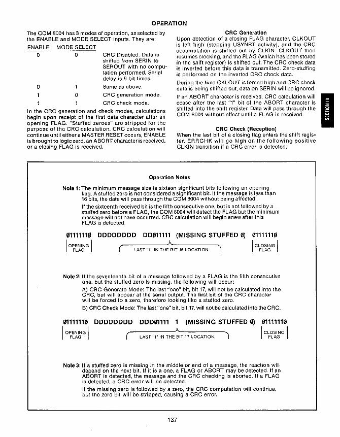
OPERATION
The COM 8004 has 3 modes of operation, as selected by the ENABLE and MODE SELECT inputs. They are:
CRC Generation Upon detection of a closing FLAG character, CLKOUT is left high (stopping USYNRT activity), and the CRC accumulation is shifted out by CLKIN. CLKOUT then resumes clocking, and the FLAG (which has been stored in the shift register) is shifted out. The CRC check data is inverted before this data is transmitted. Zero-stuffing is performed on the inverted CRC check data.
ENABLE MODE SELECT
o
o
o
1
o
CRC Disabled. Data is shifted from SERIN to SEROUT with no computation performed. Serial delay is 9 bit times.
Same as above.
CRC generation mode.
CRC check mode.
During the time CKLOUT is forced high and CRC check data is being shifted out, data on SERIN will be ignored.
In the CRC generation and check modes, calculations begin upon receipt of the first data character after an opening FLAG. "Stuffed zeroes" are stripped for the purpose of the CRC calculation. CRC calculation will continue until either a MASTER RESET occurs, ENABLE is brought to logic zero, an ABORT character is received, or a closing FLAG is received.
If an ABORT character is received, CRC calculation will cease after the last "1" bit of the ABORT character is shifted into the shift register. Data will pass through the COM 8004 without effect until a FLAG is received.
CRC Check (Reception) When the last bit of a closing flag enters the shift register, ERRCHK will go high on the following positive CLKIN transition if a CRC error is detected.
Operation Notes
Note1: The minimum message size is sixteen significant bits following an opening flag. A stuffed zero is not considered a significant bit. If the message is less than 16 bits, the data will pass through the COM 8004 without being affected.
If the sixteenth received bit is the fifth consecutive one, but is not followed by a stuffed zero before a FLAG, the COM 8004 will detect the FLAG but the minimum message will not have occurred. CRC calculation will begin anew after this FLAG is detected.
01111110 00000000 00011111 (MISSING STUFFED 0)
I OPENING I A ..... ______ -..
FLAG ( LAST "1" IN THE BIT 16 LOCATION. 1 01111110
I CLOSING I FLAG
Note 2: If the seventeenth bit of a message followed by a FLAG is the fifth consecutive one, but the stuffed zero is missing, the following will occur:
A) CRC Generate Mode: The last "one" bit, bit 17, will not be calculated into the CRC, but will appear at the serial output. The first bit of the CRC character will be forced to a zero, therefore looking like a stuffed zero.
B) CRC Check Mode: The last "one" bit, bit 17, will not be calculated into the CRC.
01111110 00000000 00001111 1 (MISSING STUFFED 0) 01111110
I OPENING I FLAG
~ _____ ~A ..... ______ ~
( LAST "1" IN THE BIT 17 LOCATION. 1 I CLOSING I FLAG
Note 3: If a stuffed zero is missing in the middle or end of a message, the reaction will depend on the next bit. If it is a one, a FLAG or ABORT may be detected. If an ABORT is detected, the message and the CRC checking is aborted. If a FLAG is detected, a CRC error will be detected.
If the missing zero is followed by a zero, the CRC computation will continue, but the zero bit will be stripped, causing a CRC error.
137
I

MAXIMUM GUARANTEED RATINGS· Operating Temperature Range ......................................................... 0° C to + 70° C Storage Temperature Range ......................................................... -55° C to +150° C Lead Temperature (soldering, 10 sec.) ..........•............................................... +325° C Positive Voltage on any Pin, with respect to ground ............................................... +8.0V Negative Voltage on any Pin, with respect to ground ............................................... -0.3V
·Stresses above those listed may cause permanent damage to the device. This is a stress rating only and functional operation of the device at these or at any other condition above those indicated in the operational sections of this specification is not implied.
NOTE: When powering this device from laboratory or system power supplies, it is important that the Absolute Maximum Ratings not be exceeded or device failure can result. Some power supplies exhibit voltage spikes or "glitches" on their outputs when the AC power is switched on and off. In addition, voltage transients on the AC power line may appear on the DC output. If this possibility exists it is suggested rr~;:;;:-;:;:-::-::::-::--___ _ that a clamp circuit be used. PRELU\II'NARY -
Notice; This is not f
l Som~ parametric limit: mar SP!"cificatlon, __ . are sul:>}ectio Change.
ELECTRICAL CHARACTERISTICS (TA = O°C to 70°C, Vee = +5 Volts ±5%, unless otherwise noted)
PARAMETER
DC CHARACTERISTICS Input Voltage Levels
Low Level High Level
Output Voltage Levels Low Level High Level
Input Capacitance Power Supply Current
AC CHARACTERISTICS Clock Frequency Clock Pulse Width-High Input Set-Up Time Input Hold Time Master Reset Pulse Width Reset Delay Error Flag Delay Error Flag Reset Delay ERRST Pulse Width Clock Propagation Delay SEROUT Propagation Delay
SERIN,MODE ENA. ERFlGR
elKIN
SYMBOL
Vrl VIH
VOL VOH CIN lee
fiN teLKH tDe teD tpw tMR tFD tFR tEW tPD tSD
tDe
MIN TYP MAX UNIT COMMENTS
0.8 V 2.0 V
0.4 V IOL = 1.6 mA 2.4 V IOH = -100 pA
10 25 pf 100 mA
TA = 25°C 2 MHz
350 ns Figure 1 100 ns Figure 1
0 ns Figure 1 250 ns Figure 2
250 ns Figure 2 300 ns Figure 3 100 ns Figure 4
100 ns Figure 4 150 ns Figure 5 150 ns Figure 5
Figure 1
138

Figure 2
tpw • 1/ ~~ V'H
MR -~--1 V'L
tMR ----1 I
OUTPUTS DETERMINED I ALL OUTPUTS BY PREVIOUS CONDITIONS f-+-- UNDEFINED-J RESET STATE I
I
Figure 3
CLOSING FLAG •
SERIAL IN V---- -------X------
1"'--_____ ----- ______
=4." b CLOCK / \ / \ V'H
IN
t VOH CRC ERR
Figure 4
CRC ERR .,1= VOL
-.
i~ .;~ V'H
ERRST 1\ tEW
139

ClKIN
ClKOUT
SEROUT
35 Marcus Blvd .. Hauppauge,NY11783 (516)273-3100 TWX-Sl0-227-8898
Figure 5
~---------------500nsmin---------------~
~---- 350 ns min ----~
1-+---tPD----~
tPD
tSD----~
VDH
VOL
VOH
VOL
We-Ia>piiieiidof' ourtml~tiln soyw C311cee\l:rex! Of '/CIfi
Circuit diagrams utilizing SMC products are included as a means of illustrating typical semiconductor applications; consequently complete information sufficient for construction purposes is not necessarily given. The information has been carefully checked and is believed to be entirely reliable. However, no responsibility is assumed for inaccuracies. Furthermore, such information does not convey to the purchaser of the semiconductor devices described any license under the patent rights of SMC or others. SMC reserves the right to make changes at any time in order to improve design and supply the best product possible.
140

STANDARD MICROSYSTEMS CORPORATION,$
I COM 8017 COM 8502
Universal Asynchronous Receiver/Transmitter UART
FEATURES
o Single +5V Power Supply
o Direct TTL Compatibility- no interfacing circuits required
o Full or Half Duplex Operation-can receive and transmit simultaneously at different baud rates
o Fully Double Buffered-eliminates need for precise external timing
o Start Bit Verification - decreases error rate
o Fully Programmable-data word length; parity mode; number of stop bits: one, one and one-half, or two
o High Speed Operation-40K baud, 200ns strobes
o Master Reset- Resets all status outputs
o Tri-State Outputs- bus structure oriented
o Low Power- minimum power requirements
o Input Protected-eliminates handling problems
o Ceramic or Plastic Dip Package-easy board insertion
o Compatible with COM 2017, COM 2502
o Compatible with COM 8116, COM 8126, COM 8136, COM 8146, COM 8046 Baud Rate Generators
GENERAL DESCRIPTION
The Universal Asynchronous Receiver/Transmitter is an MaS/LSI monolothic circuit that performs all the receiving and transmitting functions associated with asynchronous data communications. This circuit is fabricated using SMC's patented COPLAMOS® technology and employs depletion mode loads, allowing operation from a single +5V supply. The duplex mode, baud rate, data word length, parity mode, and number of stop bits are independently programmable through the use of external controls. There may be 5,6, 7 or 8 data bits, odd/even or no parity, and 1, or 2 stop bits. In addition the COM 8017 will provide 1.5 stop bits when programmed for 5 data bits and 2 stop bits. The UART can operate in either the full or half duplex mode. These programmable features provide the user with the ability to interface with all asynchronous peripherals.
141
TOS 23
Pin Configuration
Vee NC
Gnd ROE R08 R07 R06 R05 R04 R03 R02 R01 RPE RFE ROR SWE RCP
ROA RSI
\.,,/
[ 1 40 bl 2 39 bl 3 38 P 4 37 P 5 36 6 35 7 34 8 33 9 32 100 31 11 30 12 29 13 28 14 27 15 26 16 25 17 24 18 23 19 22
[ 20 21
TCP POE NOB1 NOB2 NSB NPB CS T08 T07 T06 T05 T04 T03 T02 T01 TSO TEOC TOS TBMT MR
PACKAGE: 40-Pin D.I.P.
Functional Block Diagram T01 T02 T03 T04 T05 T06 T07 T08
STATUS WORO BUFFER REGISTER
T50
TEOC
SWE
TBMT RPE RFE ROR ROA
ROAR
21 MR
Vee NC Gnd
I

DESCRIPTION OF OPERATION - TRANSMITTER
At start-up the power is turned on, a clock whose frequency is 16 times the desired baud rate is applied and master reset is pulsed. Under these conditions TBMT, TEOC, and TSO are all at a high level (the line is marking). When TBMT and TEOC are high, the control bits may be set. After this has been done the data bits may be set. Normally, the control bits are strobed into the transmitter prior to the data bits. However, as long as minimum pulse width specifications are not violated, TDS and CS may 0Scur simultaneously. Once the date strobe (TO ) has been pulsed the TBMT signal goes low, indicating that the data bits buffer register is full and unavailable to receive new data. If the transmitter shift register is transmitting previously loaded data the TBMT signal remains low. If the transmitter shift register is empty, or when it is through transmitting the previous character, the data in the buffer register is loaded immediately into the transmitter shift register and data transmission
commences. TSO goes low (the start bit), TEOC goes low, the TBMT goes high indicating that the data in the data bits buffer register has been loaded into the transmitter shift register and that the data bits buffer register is available to be loaded with new data. If new data is loaded into the data bits buffer register atthis time, TBMT goes lowand remainsinthisstate until the present transmission is completed. One full character time is available for loading the next character with no loss in speed oftransmission. This is an advantage of double buffering. Data transmission proceeds in an orderly manner: start bit, data bits, parity bit (if selected), and the stop bit(s). When the last stop bit has been on the line for one bit time TEOC goes high. If TBMT is low, transmission begins immediately. If TBMT is high the transmitter is completely at rest and, if desired, new control bits may be loaded prior to the next data transmission.
TRANSMITTER BLOCK DIAGRAM
CONTROL STROBE
16 x T CLOCK
ODD/EVEN PARITY SELECT
~~--- DATA STROBE
TRANSMITTER BUFFER EMPTY
SERIAL OUTPUT
ENDOF CHARACTER
DESCRIPTION OF OPERATION - RECEIVER
At start-up the power is turned on, a clock whose frequency is 16 times the desired baud rate isapplied and master reset is pulsed. The data available (RDA) signal is now low. There is one set of control bits for both the receiver and transmitter. Data reception begins when the serial input line transitions from mark (high) to space (low). If the RSIline remains spacing for a 1/2 bittime, agenuine start bit is verified. Should the line return to a mark-
142
ing condition priorto a 1/2 bittime, the start bit verification process begins again. A mark to space transition must occur in order to initiate start bit verification. Once a start bit has been verified, data reception proceeds in an orderly manner: start bit verified and received, data bits received, parity bit received (if selected) and the stop bit(s) received. If the transmitted parity bit does not agree with the received parity bit, the parity error flip-flop of the

status word buffer register is set high, indicating a parity error. However, if the no parity mode is selected, the parity error flip-flop is unconditionally held low, inhibiting a parity error indication. If a stop bit is not received, due to an improperlyframed character, the framing error flip-flop is set high, indicating a framing error.
not been read out and the over-run flip-flop is set high. The only way the receiver is aware that data has been read out is by having the data available reset low. At this time the RDA output goes high indicating that all outputs are available to be examined. The receiver shift register is now available to begin receiving the next character. Due to the double buffered receiver, a full character time is available to remove the received character.
Once a full character has been received internal logic looks at the data available (RDA) signal. If, at this instant, the RDA signal is high the receiver assumes that the previously received character has
CONTROL BITS FROM
HOLDING
RECEIVER BLOCK DI.AGRAM
FRAMING ERROR
TRANSMITTER BUFFER EMPTY
REGISTER --________ ----. ______ ---,
SERIAL INPUT
16 x R CLOCK
PIN NO.
2
3
4
5-12
13
14
SYMBOL
Vee
NC
GND
ROE
RD8-RD1
RPE
RFE
DESCRIPTION OF PIN FUNCTIONS
NAME FUNCTION
Power Supply +5 volt Supply
No Connection No Connection
Ground Ground
Received Data A low-level input enables the outputs (RD8-RD1) of the Enable receiver buffer register.
Receiver Data These are the 8 tri-state data outputs enabled by ROE. Outputs Unused data output lines, as selected by NDB1 and NDB2,
have a low-level output, and received characters are right justified, i.e. the LSB always appears on the RD1 output.
Receiver Parity This tri-state output (enabled by SWE) is at a high-level if Error the received character parity bit does not agree with the
selected parity.
Receiver Framing This tri-state output (enabled by SWE) is at a high-level if Error the received character has no valid stop bit.
143
I

DESCRIPTION OF PIN FUNCTIONS
PIN NO. SYMBOL NAME FUNCTION
15 ROR Receiver Over This tri-state output (enabled by SWE) is at a high-level if Run the previously received character is not read (RDA output
not reset) before the present character is'transferred into the receiver buffer register.
16 SWE Status Word A low-level input enables the outputs (RPE, RFE, ROR, Enable RDA, and TBMT) of the status word buffer register.
17 RCP Receiver Clock This input is a clock whose frequency is 16 times (16X) the desired receiver baud rate.
18 RDAR Receiver Data A low-level input resets the RDA output to a low-level. Available Reset
19 RDA Receiver Data This tri-state output (enabled by SWE) is at a high-level Available when an entire character has been received and transferred
into the receiver buffer register.
20 RSI Receiver Serial This input accepts the serial bit input stream. A high-level Input (mark) to low-level (space) transition is required to initiate
data reception.
21 MR Master Reset This input should be pulsed to a high-level after power turn-on. This sets TSO, TEOC, and TBMT to a high-level and resets RDA, RPE, RFE and ROR to a low-level.
22 TBMT Transmitter This tri-state output (enabled by SWE) is at a high-level Buffer Empty when the transmitter buffer register may be loaded with
new data.
23 TDS Transmitter A low-level input strobe enters the data bits into the Data Strobe transmitter buffer register.
24 TEOC Transmitter End This output appears as a high-level each time a full character of Character is transmitted, It remains at this level until the start of
transmission of the next character or for one-half of a TCP period in the case of continuous transmission.
25 TSO Transmitter This output serially provides the entire transmitted Serial Output character. TSO remains at a high-level when no data is
being transmitted.
26-33 TD1-TD8 Transmitter There are 8 data input lines (strobed by TDS) available. Data Inputs Unused data input lines, as selected by NDB1 and NDB2,
may be in either logic state. The LSB should always be placed on TD1.
34 CS Control Strobe A high-level input enters the control bits (NDB1, NDB2, NSB, POE and NPB) into the control bits holding register. This line may be strobed or hard wired to a high-level.
35 NPB No Parity Bit A high-level input eliminates the parity bit from being transmitted; the stop bit(s) immediately follow the last data bit. I n addition, the receiver requires the stop bit(s) to follow immediately after the last data bit. Also, the RPE output is forced to a low-level. See pin 39, POE.
144

PIN NO. SYMBOL
36 NSB
37-38 NDB2, NDB1
39 POE
40 TCP
DESCRIPTION OF PIN FUNCTION
NAME FUNCTION
Number of This input selects the number of stop bits. A low-level input Stop Bits selects 1 stop bit; a high-level input selects 2 stop bits.
Selection of 2 stop bits when programming a 5 data bit word generates 1.5 stop bits from the COM 8017 or COM 8017/H.
Number of Data These 2 inputs are internally decoded to select either 5,6,7, Bits/Character or 8 data bits/character as per the following truth table:
NDB2 NDB1 data bits/character L L 5 L H 6 H L 7 H H 8
Odd/Even Parity The logic level on this input, in conjunction with the NPB Select input, determines the parity mode for both the receiver and
transmitter, as per the following truth table: NPB POE MODE
L L odd parity L H even parity H X no parity
X = don't care
Transmitter This input is a clock whose frequency is 16 times (16X) the Clock desired transmitter baud rate.
TRANSMITTER TIMING-8 BIT, PARITY, 2 STOP BITS
I TBMT ~------------~~ TSO ~A~~il ..... I~~~~~~JSTOPllsTOP21 START
--I Bit f--TEoe ~~ ____ tl_m_e ______________________ ~ __ __
Tep
TRANSMITTER START-UP
~ I 1/16 I ~ Bit I
time
MS -----, TSO L--
Upon data transmission initiation, or when not transmitting at 100% line utilization, the start bit will be placed on the TSO line at the high to low transition of the Tep clock following the trailing edge of TDS.
RSI
CENTER BIT SAMPLE
RDA'
RDA"
RECEIVERTIMING-8 BIT, PARITY, 2 STOP BITS
~AiAl""'ID~T~~~~sToPl STOP 21 START
~ IE- 1/16 Bit time --------------------11 'The RDA line was previously not reset (ROR = high-level).
"The RDA line was previously reset (ROR = low-level).
START BIT DETECTIVERIFY
RCP
RSI
If the RSlline remains spacing for a 1/2 bit time, a genuine start bit is verified. Should the line return to a marking condition prior to a 1/2 bit time, the start bit verification process begins again.
145
I

MAXIMUM GUARANTEED RATINGS· Operating Temperature Range ..................................................... 0° C to + 70° C Storage Temperature Range., .................................................. -55°C to +150°C Lead Temperature (soldering, 10 sec.) ..................................................... +325°C Positive Voltage on any Pin, with respect to ground ........................................... +S.OV Negative Voltage on any Pin. with respect to ground .......................................... -0.3V Stresses above those listed may cause permanent damage to the device. This is a stress rating only and functional operation of the device at these or at any other condition above those indicated in the operational sections of this specification is not implied. NOTE: When powering this device from laboratory or system powersupplies, it is important that the Absolute Maximum Ratings not be exceeded or device failure can result. Some power supplies exhibit voltage spikes or "glitches" on their outputs when the AC power is switched on and off. In addition, voltage transients on the AC power line may appear on the DC output. If this possibility exists it is suggested that at clamp circuit be used.
ELECTRICAL CHARACTERISTICS (TA = 0° C to 70° C, Vcc = +5V ±5%, unless otherwise noted)
Parameter Min. Typ. Max. Unit Comments
D.C. CHARACTERISTICS INPUT VOLTAGE LEVELS
Low-level, VIL 0 O.S V High-level, VIH 2.0 Vcc V
OUTPUT VOLTAGE LEVELS Low-level, VOL 0.4 V 10L = 1.6mA High-level, VOH 2.4 V 10H = -100J,lA
INPUT CURRENT Low-level, IiL 300 J,lA VIN = GND
OUTPUT CURRENT Leakage, ILO ±10 J,lA SWE = ROE = VIH, 0:5 VOUT:5 +5V Short circuit, los** 30 mA VOUT =OV
INPUT CAPACITANCE All inputs, CIN 5 10 pf
OUTPUT CAPACITANCE All outputs, COUT 10 20 pf SWE = ROE = VIH
POWER SUPPLY CURRENT Icc 25 mA All outputs = VOH, All inputs = Vee
A.C. CHARACTERISTICS TA= +25°C CLOCK FREQUENCY
COMS502, COM S017 DC 640 KHz RCP, TCP PULSE WIDTH
Clock 0.7 J,lS RCP, TCP Master reset 500 ns MR Control strobe 200 ns CS Transmitter data strobe 200 ns TDS Receiver data available reset 200 ns ROAR
INPUT SET-UP TIME Data bits :::0 ns TD1-TDS Control bits :::0 ns NPB, NSB, NDB2, NDB1, POE
INPUT HOLD TIME Data bits :::0 ns TD1-TDS Control bits :::0 ns NPB, NSB, NDB2, NDB1, POE
STROBE TO OUTPUT DELAY Load = 20pf +1 TTL input Receive data enable 350 ns ROE: TPD1, TPDO Status word enable 350 ns SWE: TPD1, TPDO
OUTPUT DISABLE DELAY 350 ns RDE,SWE
**Notmore than one output should be shorted at a time.
NOTES: 1. If the transmitter is inactive (TEOC and TBMT are at a high-level) the start bit will appear on the TSO line within one clock period (TCP) after the trailing edge of TDS.
2. The start bit (mark to space transition) will always be detected within one clock period of RCP, guaranteeing a maximum start bit slippage of 1/16th of a bit time.
3. The tri-state output has 3 states: 1 )Iow impedanceto VccJtjEwimpedanceto GND3) high impedance OFF~ 10M ohms The "OFF" state is controlled by the SWE and inputs.
146

DATA/CONTROL TIMING DIAGRAM
DATA INPUTS tr = tf = 20 ns TSET-UP 2:0 THOLD 2:0
CS
CONTROL INPUTS
·Input information (Data/Control) need onl~ be valid during the last Tpw, min time of the input strobes (TITS, CS).
OUTPUT TIMING DIAGRAM
OUTPUTS (RD1-RD8, RDA,
RPE, ROA. RFE, TBMT)
TPD1, TPDO
NOTE: Waveform drawings not to scale for clarity.
ROAR
200ns
VIL ----------
VOL
ADA 300ns
147
TDS
TMBT
VOH
VOL
Outputs Disabled
VIH
VOL
I

FLOW CHART-TRANSMITTER FLOW CHART-RECEIVER
Circuit diagrams utilizing SMC products are included as a means of illustrating typical semiconductor applications; consequently complete information sufficient for construction purposes is not necessarily given. The information has been carefully checked and is believed to be entirely reliable. However. no responsibility is assumed for inaccuracies. Furthermore. such information does not convey to the purchaser of the semiconductor devices described any license under the patent rights of SMC or others. SMC reserves the right to make changes at any time in order to improve design and supply the best product possible.
148

STANDARD MICROSYSTEMS CORPORATION
COM 8251A ILPC FAMILY
Universal Synchronous IAsynchronous Receiver ITransmitter
FEATURES USART
PIN CONFIGURATION
D Asynchronous or Synchronous Operation -Asynchronous:
5-8 Bit Characters Clock Rate-1, 16 or 64 X Baud Rate Break Character Generation 1,1 112 or 2 Stop Bits False Start Bit Detection Automatic Break Detect and Handling
-Synchronous: 5-8 Bit Characters Internal or External Character Synchronization Automatic Sync Insertion Single or Double Sync Characters Programmable Sync Character(s)
D Baud Rate-Synchronous- DC to 64K Baud -Asynchronous-DC to 19.2K Baud
D Baud Rates available from SMC's COM 8116, COM 8126, COM 8136, COM 8146, and COM 8046
D Full Duplex, Double Buffered Transmitter and Receiver
D Odd parity, even parity or no parity bit D Parity, Overrun and Framing Error Flags D Modem Interface Controlled by Processor D All Inputs and Outputs are TTL Compatible
GENERAL DESCRIPTION The COM 8251A is an MaS/LSI device fabricated using SMC's patented COPLAMOS® technology that meets the majority of asynchronous and synchronous data communication requirements by interfacing parallel digital systems to asynchronous and synchronous data communication channels while requiring a minimum of processor overhead. The COM 8251A is an enhanced version of the 8251. The COM 8251A is a Universal Synchronous/ Asynchronous Receiver/Transmitter (USART) designed for microcomputer system data communications. The USART is used as a peripheral and is programmed by the processor to communicate in commonly used asychronous and synchronous serial data transmission techniques including IBM Bi-Sync. The USART receives serial data streams and converts them into parallel data characters for the processor. While receiving serial data, the USART will also accept data characters from the processor in parallel format, convert them to serial format and transmit. The USART will signal the processor when it has completely received or transmitted a character and requires service. Complete USART status, including data format errors and control signals such as TxE and SYNDET, is available to the processor at any time.
149
D2 1 28 D1
D3 2 27 DO
RxD 3 26 Vee
GND 4 25 RxC
D4 5 24 DTR
D5 6 23 RTS
D6 7 22 DSR
D7 8 21 RESET
TxC 9 20 ClK
WR 10 19 TxD
CS 11 18 TxEMPTY
C/O 12 17 CTS
RD 13 16 SYNDET/BD
RxRDY 14 15 TxRDY
PACKAGE: 28-pin D.J.P.
D Compatable with Intel 8251A, NEC IlPD8251A D Single +5 Volt Supply D Separate Receive and Transmit TTL Clocks D Enhanced version of 8251 D 28 Pin Plastic or Ceramic DIP Package D COPLAMOS® N-Channel MaS Technology
BLOCK DIAGRAM
TxD
TxRDY
TxEMPTY
TxC
RxO
RxROY
Rxe
SYNOETI BRKOET
I

INPUT/ PIN NO. SYMBOL NAME OUTPUT FUNCTION
1,2,27, 02,03, DO, DATA BUS I/O An 8-bit, 3-state bi-directional DATA BUS used to interface the 28,5-8 01,04-07 COM 825M to the processor data bus. Data is transmitted or
received by the bus in response to inpuVoutput or Read/Write instructions from the processor. The DATA BUS also transfers Control words, Command words, and Status.
3 RxD RECEIVER DATA I This input receives serial data into the USART.
4 GND GROUND GND Ground
9 TxC TRANSMITTER I The TRANSMITTER CLOCK controls the serial character trans-cmcK mission rate. I n the Asynchronous mode, the TxC frequency is
a multipleofthe actual Baud Rate. Two bits of the Modelnstruc-tion select the multiple to be 1 X, 16X, or 64X the Baud Rate. I n the Synchronous mode, the TxC frequency is automatically se-lected to equal the actual Baud Rate.
Note that for both Synchronous and Asynchronous modes, serial data is shifted out oftheUSART by the falling edgeofTXC::;.
10 WR WRITE DATA I A "zero" on this input instructs the COM 8251A to accept the data or control word which the processor is writing out to the USART via the DATA BUS.
11 CS CHIP SELECT I A "zero" on this input enables the USARTfor reading and writing to the processor. When CS is high, the DATA BUS is in the float state and AD andWR' will have no effect on the chip.
12 C/O CONTROL/DATA I The Control/Data input, in conjunction with the WR and tID inputs, informs the USART to accept or provide either a data character, control word orstatus information via the DATA BUS. 0= Data; 1 = Control/Status
13 RD READ DATA I A "zero" on this input instructs the COM 8251A to placethedata or status information onto the DATA BUS for the processor to read.
14 RxRDY RECEIVER READY 0 The RECEIVER READY output indicates that the Receiver Buffer is ready with an "assembled" character for input to the processor. For polled operation, the processor can check RxRDY using a Status Read orRxRDY can be connected tothe processor interrupt structure. Note that reading the character to the processor automatically resets RxRDY.
15 TxRDY TRANSMITTER READY 0 TRANSMITTER READY signals the processor that the trans-mitter is ready to accept a data character. TxRDY can be used as an interrupt or may be tested through the Status information polled ~aton. TxRDY is automatically reset by the leading edge of when a data character is loaded from the processor.
16 SYNDET/ SYNC DETECT/ I/O The SYNDET feature is only used in the Synchronous mode. BRKDET BREAK DETECT The USART may be programmed through the Mode Instruction
to operate in either the internal or external Sync mode and SYNDET then functions as an output or input respectively. In the internal SYNC mode, the SYNDET output will gotoa "one" when the COM 8251A has located the SYNC character in the Receive mode. If double SYNC character (bi-sync) operation has been programmed, SYNDET will go to "one" in the middle of the last bit of the second contiguously detected SYNC char-acter. SYNDET is automatically reset to "zero" upon a Status Read or RESET. In the external SYNC mode, a "zero" to "one" transition on the SYNDET input is sampled during the negative half cycle of AXe and will cause the COM 8251A to start as-sembling data character on the next rising edge of RxC. The length of the SYNDET input should be at least one AXe period, but may be removed once the COM 825M is in SYNC. When external SYNC DETECT is programmed, the internal SYNC' DETECT is disabled.
150

INPUT/ PIN NO. SYMBOL NAME OUTPUT FUNCTION
16 The SYNDET/BRKDET pin is used in both Synchronous and (cont.) Asynchronous modes. When in SYNC mode the features for
the SYNDET pin described above apply. When in Asynchronous mode, the BREAK DETECT output will go high when an all zero word of the programmed length is received. This word consists of: start bit, data bit, parity bit and one stop bit.Reset only occurs when Rx Data returns to a logic one state or upon chip RESET. The state of BREAK DETECT can also be read as a status bit.
17 CTS CLEAR TO SEND I A "zero" on the CLEAR TO SEND input enables the USART to transmit serial data if the TxEN bit in the Command Instruction register is enabled (one).
If either a TxEN off or CTS off condition occurs while the Tx is in operation, the Tx will transmit all the data in the USARTwritten prior to the Tx Disable command before shutting down. I
18 TxE TRANSMITTER EMPTY 0 The TRANSMITTER EMPTY output signals the processor that the USART has no further characters to transmit. TxE is auto-matically reset upon receiving adatacharacterfrom the proces-sor. In half-duplex, TxE can be used to signal end of a trans-mission and request the processor to "turn the line around". The TxEN bit in the command instruction does not effect TxE.
In the Synchronous mode, a "one" on this output indicates that a SYNC character or characters are about to be automatically transmitted as "fillers" because the next data character has not been loaded; an underflow condition. If the USART is operat-ing in the two SYNC character mode, both SYNC characters will be transmitted before the message can resume. TxE does not go low when the SYNC characters are being shifted out. TxE goes low upon the processor writing a character to the USART.
19 TxD TRANSMITTER DATA 0 This output is the transmitted serial data from the USART. When a transmission is concluded the TxD line will always return to the marking state unless SBRK is programmed.
20 ClK CLOCK PULSE I The ClK input provides for internal device timing. External inputs and outputs are not referenced to ClK, but the ClK frequency must be greater than 30 times the RECEIVER or TRANSMITTER CLOCKS in the 1X mode and greater than 4.5 times for the 16X and 64X modes.
21 RESET RESET I A "one" on this input forces the USART into the "idle" mode where it will remain until reinitialized with a new set of control words. RESET causes: RxRDY=TxRDY=TxEmpty=SYNDETI BRKDET = 0; TxD = DTR = RST = 1. Minimum RESET pulse width is 6 tCY, ClK must be running during RESET.
22 DSR DATA SET READY I The DATA SET READY inp..!!!..£an be tested by the processor via Status information. The DSR input is normally used to test Modem Data Set Ready condition.
23 RTS REQUEST TO SEND 0 The REQUEST TO SEND output is controlled via the Command word. The RTS output is normally used to drive the Modem Request to Send line.
24 DTR DATA TERMINAL 0 The DATA TERMINAL READY output is controlled via the R'EAr5V Command word. The r5TR output is normally used to drive
Modem Data Terminal Ready or Rate Select lines.
RxC 25 RECEIVER CLOCK I The RECEIVER CLOCK is the rate at which the incoming char-acter is received. I n the Asynchronous mode, the 'R'XC frequency may be 1, 16 or 64 times the actual Baud Rate but in the Syn-chronous mode the RxC frequency must equal the Baud Rate. Two bits in the mode instruction select Asynchronous at 1X, 16X or 64X or Synchronous operation at 1X the Baud Rate.
Data is sampled into the USART on the rising edge of RxC.
26 Vcc Vcc SUPPLY VOLTAGE PS +5 volt supply
151

DESCRIPTION OF OPERATION-ASYNCHRONOUS
Transmission -
When a data character is written into the USART, it automatically adds a START bit (low level or "space") and the number of STOP bits (high level or "mark") specified. by the Mode Instruction. If Parity has been enabled, an odd or even Parity bit is inserted just before the STOP bit(s}, as ~ified by the Mode Instruction. Then, depending on CTS and TxEN, the character may be transmitted as a serial data stream at the TxD output. Data is shifted out by ~falling~e of TxC at a transmission rate of TxC, TxC/16 or TxC/64, as defined by the Mode Instruction.
If no data characters have been loaded into the USART, or if all available characters have been transmitted, the TxD output remains "high" (marking) in preparation for sending the START bit of the next character provided by the processor. TxD may be forced to send a BREAK (continuously low) by setting the correct bit in the Command Instruction.
Receive-
The RxD input line is normally held "high" (marking) by the transmitting device. A falling edge (high to low transition) at RxD signals the possible beginning of a START bit and a new character. The receiver is thus prevented from starting in a "BREAK" state. The START bit is verified by testing for a "low" at its nominal center as specified by the BAUD RATE. If a "low" is detected, it is considered valid, and the bit assembling counter starts counting. The bit counter locates the approximate center of the data, parity (if specified), and STOP bits. The parity error flag (PE) is set, if a parity error occurs. Input bits are sampled at the RxD pin with the rising edge of RxC. If a high is not detected for the STOP bit, which normally signals the end of an input character, a framing error (FE) will be set. After the STOP bit time, the input character is loaded into the paralled Data Bus Buffer of the USART and the RxRDY signal is raised to indicate to the processor that a character is ready to be fetched. If the processor has failed to fetch the previous character, the new character replaces the old and overrun flag (OE) is set. All the error flags can be reset by setting a bit in the Command Instruction. Error flag conditions will not stop subsequent USART operation.
DESCRIPTION OF OPERATION -SYNCHRONOUS
Transmission -
As in Asynchronous transmission, the TxD output remains "high" (marking) until the USART receives the first character (usually a SYNC character) from the processor. After a Command Instruction has set TxEN andafter CleartoSend (CTS) goes low, thefirstcharacterisser~ transmitted. Data is shifted out on the falling edge of TxC at the same rate as TxC.
Once transmission has started, Synchronous Data Protocols ~uire that the serial data stream at TxD continue at the TXC rate or SYNC will be lost. If a data character is not provided by the processor beforethe USARTTransmit Buffer becomes empty, the SYNC character(s} loaded directly following the Mode Instruction will be automatically inserted in the TxD data stream. The SYNC character(s} are inserted to fill the line and maintain synchronization until the new data characters are available for transmission. If the USART becomes empty, and must send the SYNC character(s}, the TxEMPTY output is raised to signal the processor that the Transmitter Buffer is empty and SYNC characters are being transmitted. TxEMPTY is automatically reset by the next character from the processor.
Recelve-
In Synchronous receive, character synchronization can be either external or internal. If the internal SYNC mode
has been selected, the ENTER HUNT (EH) bit has been set by a Command Instruction, the receiver goes into the HUNT mode.
Incoming data on the RxD input is sampled on the rising edge of Rxe, and the contents of the Receive Buffer are compared with the first SYNC character after each bit has been loaded until a match is found.lftwoSYNCcharacters have been programmed, the next received character is also compared. When the (two contiguous) SYNC character(s} programmed have been detected, the USART leaves the HUNT mode and is in character synchronization.Atthistime, theSYNDET (output) issethigh.SYNDET is automatically reset by a STATUS READ.
If external SYNC has been specified in the Mode Instruction, a "one" applied to the SYNDET (input) for at least one RxC cycle will synchronize the USART.
Parity and Overrun Errors are treated the same in the Synchronous as in the Asynchronous Mode. If not in HUNT, parity will continue to be checked even if the receiver is not enabled. Framing errors do not apply in the Synchronous format.
The processor may command the receiver to enter the HUNT mode with a Command Instruction which sets Enter HUNT (EH) if synchronization is lost. Under this condition the Rx register will be cleared to all "ones".
152

OPERATION AND PROGRAMMING
The microprocessor program controlling the COM 8251A performs these tasks:
- Outputs control codes - Inputs status - Outputs data to be transmitted -Inputs data which has been received
Control codes determine the mode in which the COM 8251A will operate and are used to set or reset control signals output by the COM 8251A.
The Status register contents will be read by the program monitoring this device's operation in order to determine error conditions, when and how to read data, write data or output control codes. Program logic may be based on reading status bit levels, or control signals may be used to request interrupts.
INITIALIZING THE COM 8251A
Figure 1. Control Word Sequences for Initialization r
C/l)=l ....
>-
C/l) = 0 -<
"-
C/D=l
C/o=o {
MODE CONTROL
COMMAND
DATA
· · COMMAND
DATA
· · ·
}
INITIALING SEQUENCE
ASYNCHRONOUS OPERATION
The COM 8251A may be initialized following a system RESET or prior to starting a new serall/O sequence. The USART must be RESET (external or internal) following power up and subsequently may be reset at any time following completion of one activity and preceding a new set of operations. Following a reset, the COM 8251A enters an idle state in which it can neither transmit nor receive data.
The COM 8251A is initialized with two, three or four control words from the processor. Figure 1 shows the sequence of control words needed to initialize the COM 8251A, for synchronous or for asynchronous operation. Note that in asynchronous operation a mode control is output to the device followed by a command. For synchronous operation, the mode control is followed by one or two SYNC characters, and then a command.
Only a single address is set aside for mode control bytes, command bytes and SYNC character bytes. Forthis to be possible, logic internal to the chip directs control information to its proper destination based on the sequence in which it is received. Following a RESET (external or internal), the first control code output is interpreted as a mode control. If the mode control specifies synchronous operation, then the next one or two bytes (as determined by the
153
C/O = 1
C/O=O -<
C/D= 1
C/D=O {
MODE CONTROL
SYNC #1
SYNC #2 (OPTIONAL)
COMMAND
DATA
· · · · COMMAND
DATA
· · ·
INITIALING SEQUENCE
SYNCHRONOUS OPERATION
mode byte) output as control codes will be interpreted as SYNC characters. For either asynchronous or synchronous operation, the next byte output as a control code is interpreted as a command. All subsequent bytes output as control codes are interpreted as commands. There are two ways in which control logic may return to anticipating a mode control input; following aRESETinputorfoliowing an internal reset command. A reset operation (internal via IR or external via RESET) will cause the USART to interpret the next "control write", which should immediately follow the reset, as a Mode Instruction.
After receiving the control words the USART is ready to communicate. TxRDY is raised to signal the processor that the USART is ready to receive a character for transmission. Concurrently, the USART is ready to receive serial data.
C/O RO WR CS 0 0 1 0 USART - Data Bus 0 1 0 0 Data Bus - USART 1 0 1 0 Status - Data Bus 1 1 0 0 Data Bus - Control X X X 1 Data Bus - 3-State X 1 1 0
I

MODE CONTROL CODES The COM 8251A interprets mode control codes as illustrated in Figures 2 and 3.
Control code bits 0 and 1 determinewhethersynchronous or asynchronous operation is specified. A non-zero value in bits 0 and 1 specifies asynchronous operation and defines the relationship between data transfer baud rate and receiver or transmitter clock rate. Asynchronous serial data may be received or transmitted on every clock pulse, on every 16th clock pulse, or on every 64th clock pulse, as programmed. A zero in both bits 0 and 1 defines the mode of operation as synchronous.
For synchronous and asynchronous modes, control bits 2 and 3 determine the number of data bits which will be present in each data character. In thecaseofaprogrammed character length of less than 8 bits, the least significant DATA BUS unused bits are "don't care" when writing data to the USART and will be "zeros" when reading data. Rx data will be right justified onto DO and the LSB for Tx data isDO.
For synch ronous and asynch ronous modes, bits 4 and 5
determine whether there will be a parity bit in each character, and if so, whether odd oreven paritywill beadopted. Thus in synch ronous mode a character wi II consist offive, six, seven or eight data bits, plus an optional parity bit. In asynchronous mode, the data unit will consist of five, six, seven or eight data bits, an optional parity bit, a preceeding start bit, plus 1,1 112 or 2 trailing stop bits. Interpretation of subsequent bits differs for synchronous or asynchronous modes.
Control code bits 6 and 7 in asynchronous modedetermine how many stop bits will trail each data unit. 1112 stop bits can only be specified with a 16X or 64X baud rate factor. In these two cases, the half stop bit will be equivanlent to 8 or 32 clock pulses, respectively.
In synchronous mode, control bits 6 and 7 determine how character synchronization will be achieved. When SYNDET is an output, internal synchronization is specified ; one or two SYNC characters, as specified by control bit 7, must be detected at the head of a data stream in order to establish synchronization.
COMMAND WORDS
Command words are used to initiate specific functions within the COM 8251A such as, "reset all error flags" or "start searching for sync". Consequently, Command Words may be issued by the processor to the COM 8251 A at any time during the execution of a program in which
specific functions are to be initialized within the communication circuit.
Figure 4 shows the format for the Command Word.
Figure 4. COM 8251A Control Command
7 6 5 4 3 2 O~BitNo.
I If I I I I I I
C
154
TxEN 1 = Enable transmission 0= Disable transmission
DTR 1 = DTR output is forced to 0
RxE 1 = Enable RxRDY 0= Disable RxRDY
SBRK 1 = TxD is forced low 0= Normal operation
ER 1 = Resets all error flags in
Status register (PE, DE. FE)
RTS 1 = RTS output is forced to 0
IR 1 = Reset format
EH 1 = Enter HUNT mode

Figure 2. Synchronous Mode Control Code.
7 6 5 4 3 2 1 O~BitNo.
I I I I I 0 I 0 I ~ "-.-J "-.-J
~sYncmOde 00 5 bits per character 01 6 bits per character 10 7 bits per character 11 8 bits per character I 0= Parity disable, 1 = Parity enable
0= Odd parity, 1 = Even parity
0= SYNDET output 1 = SYNDET input
0=2 SYNC characters 1 = 1 SYNC character
Figure 3. Asynchronous Mode Control Code.
7 6 5 4 3 2 1 O~BitNo.
I I I I I I I "-.-J "-.-J "-.-J
t 00 Invalid (SYNC mode) 01 Async mode, 1 X Baud rate factor 10 Async mode, 16X Baud rate factor 11 Async mode, 64X Baud rate factor
00 5 bits per character 01 6 bits per character 10 7 bits per character 11 8 bits per character
0= Parity disable, 1 = Parity enable
0= Odd parity, 1 = Even parity
00 Invalid 01 1 stop bit 10 1112 stop bits 11 2 stop bits
155

Bit 0 of the Command Word is the Transmit Enable bit (TxEN). Data transmission for the COM 8251A cannot take place unless TxEN is set (assuming CTS = 0) in the command register. The TX Disable command is prevented from halting transmission by the Tx Enable logic until all data previously written has been transmitted. Figure 5 defines the way in which TxEN, TxE and TxRDY combines to control transmitter operations.
Bit 1 is the Data Terminal Ready (DTR) bit. When the DTR command bit is set, the DTR output connection is active (low). DTR is used to advise a modem thatthe data terminal is prepared to accept or transmit data.
Bit 2 is the Receiver Enable Command bit (RxE). RxE is used to enable the RxRDY output signal. RxE, when zero, prevents the RxR DY signal from bei ng generated to notify the processor that a complete character is framed in the Receive Character Buffer. It does not inhibit the assembly of data characters at the input, however. Consequently, if communication circuits are active, characters will be assembled by the receiver and transferred to the Receiver Buffer. If RxE is disabled, the overrun error (OE) will probably be set; to insure proper operation, the overrun error is usually reset with the same com mand that enables RxE.
FigureS. Operation of the Transmitter Section as a Function of TxE, TxRDY and TxEN
TxEN TxE TxRDY 1 1 1 Transmit Output Register and Transmit Character Buffer empty.
TxD continues to mark if COM 8251A is in the asynchronous mode. TxD will send SYNC pattern if COM 8251A is in the Synchronous Mode. Data can be entered into Buffer.
o Transmit Output Register is shifting a character. Transmit Character Buffer is available to receive a new byte from the processor.
o Transmit Register has finished sending. A new character is waiting for transmission. This is a transient condition.
o 0 Transmit Register is currently sending and an additional character is stored in the Transmit Character Buffer for transmission.
o 0/1 0/1 Transmitter is disabled.
Bit 3 is the Send Break Command bit (S BR K). When SBR K is set, the transmitter output (TxD) is interrupted and a continuous binary"O"level, (spacing) isappliedtotheTxD output signal. The break will continue until a subsequent Command Word is sent to the COM 8251A to removeSBRK.
Bit 4 is the Error Reset bit (ER). When a Command Word is transferred with the ER bit set, all three error flags (PE, OE, FE) in the Status Register are reset. Error Reset occurs when the Command Word is loaded into the COM 8251A. No latch is provided in the Command Registerto savethe ER command bit.
Bit 5, the Request To Send Command bit (RTS), sets a latch to reflect the RTS signal level. The output of this latch is created independently of other signals in the COM 8251A. As a result, data transfers may be made by the processor to the Transmit Register, and data may be actively transmitted to the communication line through TxD regardless of the status of RTS.
Bit 6, the Internal Reset (IR), causes the COM 8251A to
return to the Idle mode. All functions within the COM 8251A cease and no new operation can be resumed until the circuit is reinitialized. If the operating mode is to be altered during the execution of a processor program, the COM 8251A must first be reset. Either the RESET input can be activated, or the Internal Reset Command can be sent to the COM 8251A. Internal Reset is a momentary function performed only when the command is issued.
Bit 7 is the Enter Hunt command bit (EH). The Enter Hunt mode command is only effective for the COM 8251A when it is operating in the Synchronous mode. EH causes the receiver to stop assembling characters at the RxD input, clear the Rx register to all "ones", and start searching for the prescribed sync pattern. Once the "Enter Hunt" mode has been initiated, the search for the sync pattern will continue indefinitely until EH is reset when a subsequent Command Word is sent, when the IR command is sent to the COM 8251A, orwhen SYNC characters are recognized. Parity is not checked in the EH mode.
STATUS REGISTER
The Status Register maintains information about the current operational status of the COM 8251A. Status can be read at any time, however, the status update will be inhibited during status read. Figure 6 shows the format of the Status Register.
TxRDY signals the processor that the Transmit Character Buffer is empty and that the COM 8251A can accept a new character for transmission. The TxRDY status bit is not
totally equivalent to the TxRDY output pin, the relationship is as follows:
TxRDY (status bit) = Tx Character Buffer Empty TxRDY (pin 15) = Tx Character Buffer Empty • CTS • TxEN
RxRDY signals the processor that a completed character is holding in the Receive Character Buffer Register for transfer to the processor.
156

Figure 6. The COM 8251A Status Register
7 6 5 4 3 2 O~BitNo.
I I I I I I I II ~ ~
TxE signals the processor that the Transmit Register is empty.
PE is the Parity Error signal indicating to the CPU that the character stored in the Receive Character Buffer was received with an incorrect number of binary "1" bits. PE does not inhibit USART operation. PE is reset by the ER bit. OE is the receiver Overrun Error. OE issetwhenevera byte stored in the Receiver Character Register is overwritten with a new byte before being transferred to the processor. OE does not inhibit USART operation. OE is reset by the ER bit.
FE (Async only) is the character framing error which indicates that the asynchronous mode byte stored in the Receiver Character Buffer was received with incorrect bit format (liD" stop bit), as specified by the current mode. FE does not inhibit USART operaton. FE is reset by the ER bit.
Note: 1. While operating the receiver it is important to realize
that the RxE bit of the Command Instruction only inhibits the assertion of RxRDY; it does not inhibit the actual reception of characters. As the receiver is constantly running, it is possible for it to contain extraneous data when it is enabled. To avoid problems this data should be read from the USART and discarded. This read should be done immediately following the setting of the RxE bit in the asynchronous mode, and following the setting of EH in the synchronous mode. It is not necessary to wait for RxRDY before executing the dummy read.
2. ER should be performed whenever RxE of EH are programmed. ER resets all error flags, even if RxE = o.
t TxRDY
RxRDY
TxE
PE Parity error
OE Overrun error
FE Framing error
SYNDET/BRKDET
DSR
SYNDET is the synchronous mode status bit associated with internal or external sync detection.
DSR is the status bit set by the external Data Set Ready signal to indicate that the communication Data Set is operational. All status bits are set by the functions described for them. SYNDET is reset whenever the processor reads the Status Register. OE, FE, PE are reset by the error reset command or the internal reset command or the RESET input. OE, FE, or PE being set does not inhibit USART operation.
M any of the bits in the status register are copies of external pins. This dual status arrangement allows the USART to be used in both Polled and Interrupt driven environments. Status update can have a maximum delay of 16 tCY periods.
3. The USART may provide faulty RxRDY forthe first read after power-on or for the first read after the receiver is re-enabled by a command instruction (RxE). A dummy read is recommended to clear faulty RxRDY. This is not the case for the first read after hardware or software" reset after the device opration has been established.
4. Internal Sync Detect is disabled when External Sync Detect is progrqmmed. An External Sync Detect Status is provided through an internal flip-flop which clears itself, assuming the External Sync Detect assertion has removed, upon a status read. As long as External Sync Detect is asserted, External Sync Detect Status will remain high.
157
I

MAXIMUM GUARANTEED RATINGS· Operating Temperature Range ............................................................ O°C to +70°C Storage Temperature Range .................................................... " .... -55°C to +150°C Lead Temperature (soldering, 10 sec) ........................................................... +325°C Positive Voltage on any Pin, with respect to ground ................................................. +8.0V Negative Voltage on any Pin, with respect to ground ........ " ...................................... -0.3V ·Stresses above those listed may cause permanent damage to the device. This is a stress rating only and functional operation of the device at these at any other condition above those indicated in the operational sections of this specification is not implied. NOTE: When powering this device from laboratory or system power supplies, it is important that the Absolute Maximum Ratings not be exceeded or device failure can result. Some power supplies exhibit voltage spikes or "glitches" on their outputs when the AC power is switched on and off. In addition, voltage transients on the AC power line may appear on the DC output. If this possibility exists it is suggested that as clamp circuit be used.
ELECTRICAL CHARACTERISTICS (TA = ooe to 70o e, Vee = +5V ±5%, unless otherwise noted)
SYMBOLI PARAMETER I MIN. I MAX. UNIT I TEST CONDITIONS
D.C. Characteristics
VIL Input Low Voltage -D.3 0.8 V
VIH Input High Voltage 2.0 Vee V
VOL Output Low Voltage 0.45 V IOL=2.2 rnA
VOH Output High Voltage 2.4 V IOH = -400/1A
IOFL Output Float Leakage ±10 /1A VOUT = Vee TO 0.45V
IlL Input Leakage ±10 /1A VIN = Vee TO 0.45V
lee Power Supply Current 100 rnA All Outputs = High
Capacitance TA= 25°C, Vee = GND
CIN I Input Capacitance
I I
10 pF IfC=IMHZ CliO I/O Capacitance 20 pF Unmeasured pins returned to GND
A.C. Characteristics Bus Parameters (Note 1) Read Cycle:
tAR Address Stable Before READ (CS, C/O) 0 ns Note 2
tRA Address Hold Time for READ (CS, C/O) 0 ns Note 2
tRR READ Pulse Width 250 ns
tRO Data Delay from READ 200 ns Note 3, CL = 150 pF
tOF READ to Data Floating 10 100 ns
Write Cycle:
tAW Address Stable Before WRITE 0 ns
tWA Address Hold Time for WRITE 0 ns
tww WRITE Pulse Width 250 ns
tow Data Set Up Ti me for WRiTE 150 ns
two Data Hold Time for WRITE 0 ns
tRY Recovery Time Between WRITES 6 tey Note 4
Other Timings:
tey Clock Period .320 1.35 /1s Notes 5, 6
tq, Clock High Pulse Width 120 tey-90 ns
ti Clock Low Pulse Width 90 ns
158

SYMBOL PARAMETER MIN. MAX. UNIT TEST CONDITIONS
tA, tF Clock Rise and Fall Time 5 20 ns
tOTx TxD Delay from Falling Edge of TxC 1 /1s
tSAx Rx Data Set-Up Time to Sampling Pulse 2 /1S
tHAx Rx Data Hold Time to Sampling Pulse 2 /1S
frx Transmitter Input Clock Frequency 1X Baud Rate DC 64 kHz
16X Baud Rate DC 310 kHz 64X Baud Rate DC 615 kHz
trpw Transmitter Input Clock Width 1X Baud Rate 12 tCY
16X and 64X Baud Rate 1 tCY
tTPO Transmitter Input Clock Pulse Delay 1X Baud Rate 15 tCY
16X and 64X Baud Rate 3 tCY
fAx Receiver Input Clock Frequency 1X Baud Rate DC 64 kHz
16X Baud Rate DC 310 kHz 64X Baud Rate DC 615 kHz
tAPW Receiver I nput Clock Pulse Width 1X Baud Rate 12 tCY
16X and 64X Baud Rate 1 tCY
tAPD Receiver Input Clock Pulse Delay 1X Baud Rate 15 tCY
16X and 64X Baud Rate 3 tCY
trxAOY TxRDY Pin Delay from Center of last Bit 8 tCy Note?
trxAOY CLEAA TxRDY I from Leading Edge of WR 150 ns Note?
tAxAOY RxRDY Pin Delay from Center of last Bit 24 tCY Note?
tAxAOY CLEAA RxRDY I from Leading Edge of RD 150 ns Note?
tiS Internal SYNDET Delay from Rising 24 tCY Note? Edge of RxC
tES External SYNDET Set-Up Time Before 16 tCY Note? Falling Edge of RxC
trxEMPTY TxEMPTY Delay from Center of Data Bit 20 tCY Note?
twc Control Delay from Ris.i!!fLEdge of 8 tCY Note? WRITE (TxEn, DTR, RTS)
tCA Control to READ Set-Up Time (DSR, CTS) 20 tCY Note?
NOTES: 1. AC timings mStilsured VOH = 2.0, VOL= 0.8, and with load circuit of Figure 1. 2. Chip Select (CS) and Command/Data (C/O) are considered as Addresses. 3. Assumes that Address is valid before RaJ. 4. This recovery time is for RESET and Mode Initialization. Write Data is allowed only when TxRDY = 1. Recovery Time between
Writes for Asynchronous Mode is 8 tCY and for Synchronous Mode is 16 tcv. 5. The TxC and RxC frequencies have the following limitations with respect to ClK.
For 1X Baud Rate, fTx or fAX:S 1/(30 tcv) For 16X and 64X Baud Rate, fTx or fAX:S 1/(4.5 tCY)
6. Reset Pulse Width = 6 tcv minimum; System Clock must be running during RESET. 7. Status update can have a maximum delay of 28 clock periods from the event affecting the status.
2V
Figure 1.
4200
1N914
6KO
Typical .::l Output Delay Versus
.::l Capacitance (pF)
+20
+10
/ II
-10
-2 0 J -100 -50
/ V " SPEC
+50 +100
TEST LOAD CIRCUIT
159
~ CAPACITANCE (pF)
I

~(1xMODEI
TXt: (16xMODEI
Tx DATA
RxDATA
RxC (1x MODEl
RxC (16xMODEI
INT SAMPLING PULSE
WAVEFORMS
System Clock Input
CLOCK ¢
Transmitter Clock & Data
Receiver Clock & Data
(Rx BAUD COUNTER STARTS HEREI
START BIT
--, .. ---tRpw---~-------t,1
160
DATA BIT DATA BIT

Write Data Cycle (CPU - USART)
I ~~--------I H tbRDY CLEAR
WR --------------~~~-----------
I, tow -\:j two DON'T CARE DON'T CARE
DATA IN (D.B.I -------=-:..:..:....:-=.:.:.:.=-----« OAT A ST ABL E ~~, -------------
C/O ----------------.~~
------------~~ ~r-------"'--_________ .7"
~~------
Read Data Cycle (CPU 4- USART)
RxRDY _____ .....JI 1~ ______________ _ I ~XRDY CLEAR I
~ -----------~~ tRR--y,r-__ __
---I l-tRD -il- tDF
DATA OUT (D.B,I ______ D=..:.A-"-T:...:.A.:...;F L:..:O:.:...;A.;...T ---II1'1~DA~T~A~O~UT~A~C~TI~V;E ..J"rD:...:.AT:...:.A:...:.F..::.LO=..cA..:..;...T
------------~I~ ~Ir-C/O '\ 'I
~ ---------~~~tA_R __________ ~_RA~
Write Control or Output Port Cycle (CPU - USART)
DTR,RTS -----------------------------~X (NOTE "11 ____________________________ -J, L-. ____ _
________ ~ I-tWW--!I:~t-wc-=.1-----WR ~
DATA IN (D.B.I ----------{ '---t---t-.T
tWA
C/O _________ -J
tWA
NOTE "1: TWC INCLUDES THE RESPONSE TIMING OF A CONTROL BYTE,
161

ffi
Tx EMPTY
Tx READY (STATUS BIT)
Read Control or Input Port (CPU - USART)
OsR, CTS -----V; (NOTE"') f"..;<-. _________________ _
___ I-_'CR~_·IL'RR-I--~ ~~ K
-+I 1- IRD - 1- IDF
DAT~g~~ ------------II~Fl' _____ -t~~-----------l'AR I--
c/o __________ -----.JJI - IRA I--
)
~ __________ ~ 'AR I--- -- IRA /;::
~ ~~----------~~ NOTE ",: TCR INCLUDES THE EFFECT OF CTS ON THE TxENBL CIRCUITRY.
Transmitter Control & Flag Timing (ASYNC Mode)
ITxEMPTY 1\-r----~ I'------t-----€l
Tx R~~I~~ ----(1;
C/O
Tx DATA
DATA CHAR 1 DATA CHAR 2 DATACHAR3
EXAMPLE FORMAT· 7 BIT CHARACTER WITH PARITY & 2 STOP BITS.
BREAK DETECT
OVERRUN ERROR ISTATUSBIT)
R_ROV
c/o
Rx DATA
Receiver Control & Flag Timing (ASYNC Mode)
~
- r-:- IA"RDV CHAR 2
LOST Ii- '1:
AdDATA
----dr RxEn f WrERA An
U
~ I,.J
II ~
, Y
DATA CHAR 1 DATA CHAR 2 ~_NM"Il'I!,Q
BREAK
EXAMPLE FORMAT· 7 BIT CHARACTER WITH PARITY & 2 STOP BITS.
162
'G- .... NM"'~U)
.,.DATA CHAR 4
= <{
~ c
,..-~
I~ !------
If ~ Wr,RII.En; Wr RxE,,'
U r-v-~

m
r. READY ----+---~ (STATUSBITI
Tx READY (PIN)
Transmitter Control & Flag Timing (SYNC Mode)
C/D _____ ~~~~~~---4+.~~----~~~4_-_+-~
EXAMPLE FORMAT· S BIT CHARACTER WITH PARITY, 2 SYNC CHARACTERS
Receiver Control & Flag Timing (SYNC Mode)
SYNDET (PIN) NOTE ;:1
SYNDEr (S,81
OVERRUN ERROR IS.81
R .. ROY (PIN)
C/O .-JW,EH '\
R .. En·
---v DON'T CARE
I 'IS_ -
SYNC SYNC DATA CHAR 1 CHAR 2 CHAR 1
8\ ~rE'.!.....J tES_
~ Ir-I-t\--
JDATA CHAH 2 f.\ LOST
~l "'~ Irf-I-
1\ I 1\ Rd';,T:~~S L Ad OATA CHAR 1 CHAR 3 CHAR 1
"-\LtJ II
DATA \Lc hLJ I\~ CHAR 2 CHAR 3 CHAR 1 SYNC CHAR 2 DON'T CARE
:
t-l---
tL-
J
Ad STATUS
1\ r--Rd DATA
DATA \... V--
DATA CHAR 1 CHAR 2 ETC,
X'X'X'X 'X'NoX'X'X'X-X:XoX'X'H-~ ;XoX'H'H ;HH'X-X ·N' X>X' loX ~H'H'X-l ~XoX' X· X ,x-ID,X 'X'X'X'X'X' , °x,x·x,x-nxox, • 'x-x !lUXU 1I11IIIII III r I }l11JAs~!Eb,~sl I I I I III
JlI1fUlJ L EXIT HUNT MODE
SEl SYNC DET
NOTE ·:1 INTERNAL SYNC. 2 SYNC CHARACTERS, 5 BITS. WITH PARITY NOTE ;;2 EXTERNAL SYNC. 5 BITS. WITH PARITY
163
T CHAR ASSY / BEGINS
lUi ru- l11f EXIT HUNT MODE I
SET SYN DEl ISTATUS Bill
rut SET SYNDET (STATUS BIT)
I

APPLICATION OF THE COM8251A
Asynchronous Serial Interface to CRT Terminal, DC to 9600 Baud
Asynchronous Interface to Telephone Lines
PHONE LINE
INTER FACE
1 TelEPHONE
LINE
Synchronous Interface to Terminal or Peripheral Device
SYNCHRONOUS TERMINAL
OR PERIPHERAL DEVICE
Synchronous Interface to Telephone Lines
SYNC MODEM
PHONE LINE
INTER· FACE
1 TELEPHONE
LINE
COM8251A Interface to p.P Standard System Bus
\ ADDRESS BUS \ Ao
I CONTROL BUS \ I/O R I/OW RESET
\ DATA BUS \
~ ~ 8
'< 7 CID C{ 0,-00 IiO iVA RESET ClK
COM8251A
Circuit diagrams utilizing SMC products are included as a means of illustrating typical semiconductor applications; consequently complete information sufficient for construction purposes is not necessarily given. The information has been carefully checked and is believed to be entirely reliable. However, no responsibility is assumed for inaccuracies. Furthermore, such information does not convey to the purchaser of the semiconductor devices described any license under the patent rights of SMC or others. SMC reserves the right to make changes at any time in order to improve design and supply the best product possible.
164

~ Baud Rate Generator All Baud Rate Generators are programmable dividers capable of providing 16 output frequencies' for UARTs or USARTs from either an on-chip crystal oscillator or an external frequency input. "T" versions utilize an external frequency input only. Dual Baud Rate Generators provide two out-
put frequencies simultaneously for full duplex communications.
'except as noted
Part Number Description COM 6016 Dual Baud Rate Generator
COM 6016T(3) Dual Baud Rate r1
COM 6026 Single Baud Rate Generator
COM 5026T ,Vj Single Baud Rate ,..
COM 5036 Dual Baud Rate Generator
COM 6036T (3) Dual Baud Rate Generator
COM 6046 Single Baud Rate Generator
COM 6046T (3) Single Baud Rate Generator
COM 8046 Single Baud Rate Generator
COM 8046T (3) Single Baud Rate Generator
COM B116 Dual Baud Rate Generator
COM B116T(3) Dual Baud Rate Generator
COM B126 Single BaUd Rate Generator
COM 8126T (3) Single Baud Rate Generator
COM 8136 Dual Baud Rate Generator
COM B136T (3) Dual Baud Rate Generator
COM 8146 Single Baud Rate Generator
COM 8146T(3) Single Baud Rate Generator
(3)Ma,y be custom mask programmed
Baud Rate Generators providing all standard baud rates from various popular crystal frequencies are available. In addition the baud rate generator mao' be custom mask programmed for other divisors.
Power Features Supplies Package
~n-chiP~put or external +6.+12 18 DIP
Rrt.AT'nR.l input +6. +12 18 DIP
gn-chip input or external +6. +12 14 DIP
Rvt.AT'TlAl UV~""V4~VJ input +5,+12 14 DIP
16 with .1 +5, +12 18 DIP outP\lt of input ;':;: v~ ~V4WJ -:- 4 COM: 5016T with additional +5. +12 18 DIP output of input frequency -:- 4 COM 5026 .1 +6. +12 14 DIP output of input "V~""'JUVJ -:- 4
-'. .1 +5,+12 14 DIP output of input_;':;:v~""v •• vJ 4 32 baud rates; IX, 16X, 32X clock outputs; single +5 volt +6 16 DIP supply COM 8046 with external +5 16 DIP frequency input only Single +5 volt version of +6 18 DIP COM 6016 Single +5 volt version of +5 18 DIP COM 5016T Single +5 volt version of +5 14 DIP COM 5026 Single +6 volt version of +5 14 DIP COM 5026T Single +5 volt version of +5 18 DIP. COM 5036 Single +6 volt version of +6 18 DIP COM 5036T Single +5 volt version of +5 14 DIP COM 5046 Single +6 volt version of +5 14 DIP COM 5046T
165
Page I 167-168 I 167-168 169-170
169-170 171-172
171-172
173-174
173-174
179·180
179-lBO
IBI-lB2
181-182
183·1B4
183-184
185-186
1B5-186
187-188
187-188

166

STANDARD MICROSYSTEMS CORPORATION
COM 5016 cOM5016T
Dual Baud Rate Generator Programmable Divider
FEATURES PIN CONFIGURATION o On chip crystal oscillator or external
frequency input XTALlEXT1 11
o Choice of 2 x 16 output frequencies +5v 21 016 asynchronous/synchronous baud rates
fR 31 o Direct UART/USRT/ ASTRO/USYNRT com pati bi I ity
o Full duplex communication capability o TTL, MOS compatibility
RA 41
RB 51
Rc 61 RD 71
STR 8
+ 12v 9 r
BLOCK DIAGRAM
SIT
T. Ta Tc
To
XTAUEXTI
XTALlEXT2
R.
Ra Rc
RD
STR
XTAL
~ CLOCK BUFFER
REPROGRAMMABLE FREQUENCY SELECT
ROM
DIVIDER
DIVIDER
167
\J ~ 18 XTAL/EXT2
)17 fr
~ 16 TA
,I 15 TB
14 Tc
13 TD
12 STT
11 GND
10 NC
+2 fr
+2 fR
A A A +sv GND +12V
I

General Description
The Standard Microsystems COM 5016 Dual Baud Rate Generator/Programmable Divider is an N-channel COPLAMOS® MaS/LSI device which, from a single crystal (on-chip oscillator) or input frequency is capable of generating 32 externally selectable frequencies.
The COM 5016 is specifically dedicated to generating the full spectrum of 16 asynchronous/synchronous data communication frequencies as shown in Table 1. One of the sixteen output frequencies is externally selected by four address inputs, on each of the independent dividers, as shown in Table 1.
Internal re-programmable ROM allows the generation of other frequencies from other crystal frequencies or input frequencies. The four address inputs on each divider section may be strobe (150ns) or DC loaded. As the COM 5016 is a dual baud rate generator, full duplex (independent receive and transmit frequencies) operation is possible.
The COM 5016 is basically a programmable 15-stage feedback shift register capable of dividing any modulo up to (21L 1).
By using one of the frequency outputs it is possible to generate additional divisions of the master clock frequency by cascading COM 50 16's. The frequency output is fed into the XT ALlEXT input on a subsequent device. In this way one crystal or input frequency may be used to generate numerous output frequencies.
The COM 5016 can be driven by either an external crystal or TTL logic level inputs; COM 5016T is driven by TTL logic level inputs only.
Pin No. Symbol
XTALlEXT1
2 Vee 3 fR
4-7 RA• RB• Re. Ro
8 STR
9 VOD
10 NC 11 GND 12 STT
13-16 To. Te. TB• TA
17 fr
18 XTALlEXT2
Description of Pin Functions
Name
Crystal or External Input 1 Power Supply
Receiver Output Frequency
Receiver-Divisor Select Data Bits Strobe-Receiver
Power Supply No Connection
Ground Strobe-
Transmitter
Transmitter-Divisor
Select Data Bits Transmitter
Output Frequency Crystal or
External Input 2
Function
This input is either one pin of the crystal package or one polarity of the external input. + 5 volt supply This output runs at a frequency selected by the Receiver divisor select data bits. The logic level on these inputs. as shown in Table 1. selects the receiver output frequency. fRo A high level input strobe loads the receiver data (RA• RB• Re. Rd into the receiver divisor select register. This input may be strobed or hard-wired to a high level. + 12 volt supply
Ground A high level input strobe loads the transmitter data (TA• TB• T e. T D) into the transmitter divisor select register. This input may be strobed or hard-wired to a high level. The logic level on these inputs. as shown in Table 1. selects the transmitter output frequency. fr.
This output runs at a frequency selected by the Transmitter divisor select data bits.
This input is either the other pin of the crystal package or the other polarity of the external input.
For electrical characteristics, see page 175.
168

STANDARD MICROSYSTEMS CORPORATION
COM 5026 cOM5026T
Baud Rate Generator Programmable Divider
FEATURES PIN CONFIGURATION o On chip crystal oscillator or external
frequency input o Choice of 16 output frequencies XTAL/EXT1 11 016 asynchronous/synchronous baud rates
XTAL/EXT2 21 o Direct UART/USRT/ ASTRO/USYNRT compatibility
o TTL, MOS compatibility +5v 31
NC 41
GND 51
NC 61 + 12v 71
BLOCK DIAGRAM
A
B C D
XTALlEXTl
XTALlEXT2
XTAL
~ ~----------~ CLOCK BUFFER
REPROGRAMMABLE FREQUENCY SELECT
ROM
DIVIDER
"-/
~ A A
14 tOUT
13 A
12 B
11 C
10 0
9 ST
8 NC
+5V ,GND +12V
169
fOUT
I

GENERAL DESCRIPTION
The Standard Microsystems COM 5026 Baud Rate Generator/Programmable Divider is an N-channel COPLAMOS~ MaS/LSI device which, from a single crystal (on-chip oscillator) or input frequency is capable of generating 16 externally selectable frequencies.
The COM 5026 is specifically dedicated to generating the full spectrum of 16 asynchronous/synchronous data communication frequencies as shown in Table 1. One of the sixteen output frequencies is externally selected by four address inputs, as shown in Table 1.
Internal re-programmable ROM allows the generation of other frequencies from other crystal frequencies or input frequencies. The four address inputs may be strobe (150ns) or DC loaded.
The COM 5026 is basically a programmable 15-stage feedback shift register capable of dividing any modulo up to (21L 1).
By using the frequency output, it is possible to generate additional divisions of the master clock frequency by cascading COM 5026's. The frequency output is fed into the XTAL/EXT input on a subsequent device. In this way one crystal or input frequency may be used to generate numerous output frequencies.
The COM 5026 can be driven by either an external crystal or TTL logic level inputs; COM 5026T is driven by TTL logic level inputs only.
Description of Pin Functions
Pin No. Symbol Name Function
XTAUEXT1 Crystal or This input is either one pin of the crystal package or one polarity External Input 1 of the external input.
2 XTAUEXT2 Crystal or This input is either the other pin of the crystal package or the External Input 2 other polarity of the external input.
3 Vee Power Supply +5 volt Supply
4,6,8 NC No Connection
5 GND Ground Ground
7 VDD Power Supply + 12 volt Supply
9 ST Strobe A high-level strobe loads the Input Address (AA, AB, Ae, AD) into the Input Address register. This input may be strobed or hard wired to a high-level,
10-13 AD. Ae, AB, AA Input Address The logic level on these inputs. as shown in Table 1, selects the output frequency.
14 fOUT Output This output runs at a frequency as selected by the Input Address. Frequency
For electrical characteristics, see page 175.
170

COM 5036 cOM5036T
Dual Baud Rate Generator Programmable Divider
FEATURES PIN CONFIGURATION o On chip crystal oscillator or external
frequency input XTALlEXT1 1 I
o Choice of 2 x 16 output frequencies +5v 21 o 16 asynch ronousl sync h ronous baud rates
fR 31 o Direct UART/USRTI ASTRO/USYNRT compatibility RA 41
o Full duplex communication capability Rs 51 o High frequency reference output Rc 61 o TTL, MOS compatibility
Ro 71
STR 81 +12v 91
BLOCK DIAGRAM
sn
T. Ts Tc
To
XTAlIEXT1
XTALEXT2
R. Rs Rc Ro
STR
XTAL
.L CLOCK BUFFER
REPROGRAM MABLE FREQUENCY SELECT
DIVIDER
DIVIDER
171
\....-I ~ 18 XTALlEXT2
l17 fT
16 TA
15 TB
14 Tc
13 To
12 STT
11 GND
10 fx/4
+2 fr
fX/4
+2 fR
A A')" +5v GND +12v
I

General Description
The Standard Microsystems COM 5036 Dual Baud Rate Generator/Programmable Divider is an N-channel COPLAMOS® MaS/LSI device which, from a single crystal (on-chip oscillator) or input frequency is capable of generating 32 externally selectable frequencies.
The COM 5036 is specifically dedicated to generating the full spectrum of 16 asynchronous/synchronous data communication frequencies as shown in Table 1. One of the sixteen output frequencies is externally selected by four address inputs, on each of the independent dividers, as shown in Table 1. .
Internal re-programmable ROM allows the generation of other frequencies from other crystal frequencies or input frequencies. The four address inputs on each divider section may be strobe (150ns) or DC loaded. As the COM 5036 is a dual baud rate generator, full duplex (independent receive and transmit frequencies) operation is possible.
The COM 5036 is basically a programmable 15-stage feedback shift register capable of dividing any modulo up to (21L1).
By using one of the frequency outputs it is possible to generate additional divisions of the master clock frequency by cascading COM 5036's. The frequency output is fed into the XTAUEXT input on a subsequent device. In this way one crystal or input frequency may be used to generate numerous output frequencies.
The COM 5036 can be driven by either an external crystal or TTL logic level inputs; COM 5036T is driven by TTL logic level inputs only. .
The COM 5036 provides a high frequency reference output at one-quarter (1/4) the XTAUEXT input frequency.
Description of Pin Functions
Pin No. Symbol Name Function
XTALlEXT1 Crystal or This input is either one pin of the crystal package or one polarity External Input 1 of the external input.
2 Vee Power Supply + 5 volt supply 3 fR Receiver Output This output runs at a frequency selected by the Receiver divisor
Frequency select data bits. 4-7 RA , RB, Re, RD Receiver-Divisor The logic level on these inputs, as showt:l in Table 1, selects the
Select Data Bits receiver output frequency, fRo 8 STR Strobe-Receiver A high level input strobe loads the receiver data (R A, RB, Re, RD) into
the receiver divisor select register. This input may be strobed or hard-wired to a high level.
9 VDD Power Supply + 12 volt supply 10 fx/4 fx/4 1/4 crystal/ clock frequency reference output. 11 GND Ground Ground 12 STT Strobe- A high level input strobe loads the transmitter data (T A, TB, T e, T D)
Transmitter into the transmitter divisor select register. This input may be strobed or hard-wired to a high level.
13-16 TD, Te, TB, T A Transmitter- The logic level on these inputs, as shown in Table 1, selects the Divider transmitter output frequency, fT'
Select Data Bits 17 fT Transmitter This output runs at a frequency selected by the Transmitter divisor
Output select data bits. Frequency
18 XTALlEXT2 Crystal or This input is either the other pin of the crystal package or the External Input 2 other polarity of the external input.
For electrical characteristics, see page 175.
172

STANDARD MICROSYSTEMS CORPORATION/
t COM 5046 cOM5046T
Baud Rate Generator Programmable Divider
FEATURES PIN CONFIGURATION o On chip crystal oscillator or external
frequency input o Choice of 16 output frequencies XTAUEXT1 1 016 asynchronous/synchronous baud rates
XTAUEXT2 2 o Direct UART/USRT/ ASTRO/USYNRT compatibility
o High frequency reference output o TTL, MOS compatibility
+5v 3
NC 41
GND.5
NC 61 +12v 71
BLOCK DIAGRAM
XTAUEXT1
XTAL
~ CLOCK BUFFER
XTAUEXT2
REPROGRAM MABLE FREQUENCY SELECT
ROM
DIVIDER
+4
173
,l +5v
\.J 14 fOUT
13 A
12 B
~11 C
~10 D
~9 ST
~8 fx/4
+2
A J.. GND +12v
fouT
fx/4
I

GENERAL DESCRIPTION
The Standard Microsystems COM 5046 Baud Rate Generator/piogrammable Divider is an N-channel COPLAMOS® MaS/LSI device which, from a single crystal (on-chip oscillator) or input frequency is capable of generating 16 externally selectable frequencies.
The COM 5046 is specifically dedicated to generating the full spectrum of 16 asynchronous/synchronous data communication frequencies as shown in Table 1. One of the sixteen output frequencies is externally selected by four address inputs; as shown in Table 1.
Internal re-programmable ROM allows the generation of other frequencies from other crystal frequencies or input frequencies. The four addres~ inputs may be strobe (150ns) or DC loaded.
The COM 5046 is basically a programmable 15-stage feedback shift register capable of dividing any modulo up to (21L1).
By using the frequency output, it is possible to generate additional divisions of the master clock frequency by cascading COM 5046's. The frequency output is fed into the XTAUEXT input on a subsequent device. In this way one crystal or input frequency may be used to generate numerous output frequencies.
The COM 5046 can be driven by either an external crystal or TIL logic level inputs; COM 5046T is driven by TIL logic level inputs only.
The COM 5046 provides a high frequency reference output at one-quarter (1/4) the XTAUEXT input frequency.
Pin No. Symbol
XTAUEXT1
2 XTAUEXT2
3 Vee
4,6 NC
5 GND
7 VDD
8 fX/4
9 ST
10-13 AD. Ae. AB. AA
14 fouT
Description of Pin Functions
Name
Crystal or External Input 1
Crystal or External Input 2
Power Supply
No Connection
Ground
Power Supply
Reference Frequency
Strobe
Input Address
Output Frequency
Function
This input is either one pin of the crystal package or one polarity of the external input.
This input is either the other pin of the crystal package or the other polarity of the external input.
+5 volt Supply.
Ground
+ 12 volt Supply.
High frequency reference output@ (1/4) fiN
A high-level strobe loads the Input Address (AA, AB, Ac, AD) into the Input Address register. This input may be strobed or hard wired to a high-level,
The logic level on these inputs. as shown in Table 1, selects the output frequency.
This output runs at a frequency as selected by the Input Address.
For electrical characteristics, see page 175.
174

ELECTRICAL CHARACTERISTICS COM5016, COM5016T, COM5026, COM5026T, COM5036, COM5036T, COM5046, COM5046T
MAXIMUM GUARANTEED RATINGS" Operating Temperature Range ............................................................... O°C to + 70°C Storage Temperature Range .............................................................. -55°Cto +150°C Lead Temperature (soldering, 10 sec.) .............................................................. +325°C Positive Voltage on any Pin, with respect to ground .................................................... + 18 .OV Negative Voltage on any Pin, with respect to ground .................................................... -0.3V
·Stresses above those listed may cause permanent damage to the device. This is a stress rating only and functional operation of the device at these or at any other condition above those indicated in the operational sections of this specification is not implied.
ELECTRICAL CHARACTERISTICS (TA=O°C to 70°C, Vce= +5V±5%, VDO= +12V±5%, unless otherwise noted)
Parameter Min. Typ. Max Unit Comments
D.C. CHARACTERISTICS INPUT VOLTAGE LEVELS
Low-level, Vil 0.8 V excluding XT AL inputs High-level, VIH 2.0 Vee V
OUTPUT VOLTAGE LEVELS Low-level,VOL 0.4 V 10l = 1.6ma
0.5 V 10l = 3.2ma High-level, VOH Vee-1.5 4.0 V IOH = 100J1.A
INPUT CURRENT Low-level, III 0.3 mA VIN = GND, excluding XTALinputs
INPUT CAPACITANCE All inputs, CIN 5 10 pf VIN = GND, excluding XTAL inputs
EXT INPUT LOAD 8 10 Series 7400 unit loads POWER SUPPLY CURRENT
lee 28 45 mA IDO 12 22 mA
A.C. CHARACTERISTICS TA = +25°C CLOCK FREQUENCY 5.0688 MHz XTAL,EXT PULSE WIDTH
Clock 50% Duty Cycle ± 5% Strobe 150 DC ns See Note 1.
INPUT SET-UP TIME Address 50 ns See Note 1.
INPUT HOLD TIME Address 50 ns
STROBE TO NEW FREQUENCY DELAY 3.5 J1.S = 1/flN (18)
Note 1: Input set-up time can be decreased to"" Ons by increasing the minimum strobe width by 50ns to a total of 200ns.
NOTE 1
VIH
STROBE CST) I I
,
TIMING DIAGRAM
~---~~--I
I r---;"]-------------""'\ I, ,
VIL---'----J
"Address need only be valid during the last Tpw. Min time olthe input strobe.
175
I

Crystal Operation COM5016 COM5036
5.0688 MHz crystal
Crystal Operation COM5026 COM5046
74XX TIL
74XX TTL
External Input Operation COM5016/COM5016T COM5036/COM5036T
74XX TIL
74XX-totem pole or open collector output (external pull-up resistor required)
External Input Operation COM5026/COM5026T COM5046/COM5046T
74XX TIL
74XX-totem pole or open collector output (external pull-up resistor required)
For ROM re-programming SMC has a computer program available whereby the customer need only supply the input frequency and the desired output frequencies.
The ROM programming is automatically generated.
Crystal Specifications User must specify termination (pin, wire, other)
Prefer: HC-18/U or HC-25/U
Frequency - 5.0688 MHz, AT cut
Temperature range O°C to 70°C
Series resistance <50 n Series Resonant
Overall tolerance ± .01 %
or as required
176
Crystal manufacturers (Partial List)
Northern Engineering Laboratories 357 Beloit Street Burlington, Wisconsin 53105 (414) 763-3591
Bulova Frequency Control Products 61-20 Woodside Avenue Woodside, New York 11377 (212) 335-6000 CTS Knights Inc. 101 East Church Street Sandwich. Illinois 60548 (815) 786-8411 Crystek Crystals Corporation 1000 Crystal Drive Fort Myers, Florida 33901 (813) 936-2109

APPLICATIONS INFORMATION
+5.0v
Charge pump techniques 1.0K 1.0K 1.0K using the + 5 volt power supply can be used to generate the + 12 volt power supply required. The + 12 volt power supply of figure 1 will supply the 22 milli- amps that is typically required.
100pf
When powering this device from laboratory or system power supplies, it is important that the Absolute Maximum Ratings not be exceeded or device failure can result. Some power supplies exhibit voltage spikes or "glitches" on their outputs when the AC power is switched on and off. In addition, voltage transients on the AC power line may appear on the DC output. For example, the bench power supply programmed to deliver + 12 volts may have large voltage transients when the AC power is switched on and off. If this possibility exists it is suggested that the clamp circuit of figure 2 or a Semtech·bi-polarity silicon transient suppressor such as the 1 N611 0 be used.
·SEMTECH CORPORATION 652 Mitchel Road Newbury Park, California 91320 213·628·5392
From Power Supply
1N914 Typ.
177
1OOl1h
+12v OUT
12v 11•O1l1
Figure 1 VOLTAGE CHARGE PUMP
SUPPLY FOR +12v SUPPLY
Figure 2 OVER-VOLTAGE
PROTECTION CIRCUIT
To Chip Power Supply Pin
I

COM5016, COM5016T, COM5026, CO M5026T, COM5036, COM5036T, COM5046, COM5046T
Baud Rate Generator Output Frequency Options
Table 1. (16X clock) Table 2. (16X clock)
CRYSTAL FREQUENCY = 5.0688 MHz CRYSTAL FREQUENCY = 4.9152 MHz Tr'mll/Recelve Theoretical
Address Baud Frequency D C B A Rate 18XCIock
0 0 0 0 50 0.8 KHz 0 0 0 1 75 1.2 0 0 1 0 110 1.76 0 0 1 1 134.5 2.152 0 1 0 0 150 2.4 0 1 0 1 300 4.8 0 1 1 0 600 9.6 0 1 1 1 1200 19.2 1 0 0 0 1800 28.8 1 0 0 1 2000 32.0 1 0 1 0 2400 38.4 1 0 1 1 3600 57.6 1 1 0 0 4800 76.8 1 1 0 1 7200 115.2 1 1 1 o 9600 153.6 1 1 1 1 19.200 307.2
Actual Duty Tr'mll/Recelve Theoretical Frequancy Pereant Cycle Address Baud Frequency 16X Clock Error % Divisor D C B A Rate 16XCIock
0.8 KHz 50/506336 0 0 0 0 50 0.8 KHz 1.2 50/504224 0 0 0 1 75 1.2 1.76 50/502880 0 0 1 0 110 1.76 2.1523 0.016 50/502355 0 0 1 1 134.5 2.152 2.4 50/502112 0 1 0 0 150 2.4 4.8 50/50 1056 0 1 0 1 300 4.8 9.6 50/50 528 0 1 1 0 600 9.6
19.2 50/50 264 0 1 1 1 1200 19.2 28.8 50/50 176 1 0 0 0 1800 28.8 32.081 0.253 50/50 158 1 0 0 1 2000 32.0 38.4 50/50 132 1 0 1 0 2400 38.4 57.6 50/50 88 1 0 1 1 3600 57.6 76.8 50/50 66 1 1 0 0 4800 76.8
115.2 50/50 44 1 1 0 1 7200 115.2 153.6 48/52 33 1 1 1 o 9600 153.6 316.8 3.125 50/50 16 1 1 1 1 19,200 307.2
Table 3. (32X clock)
CRYSTAL FREQUENCY = 5.0688 MHz Tr'mll/Recelve Theoretical Actual
Address Baud Frequency Frequency Percent D C B A Rate 32X Clock 32X Clock Error
0 0 0 0 50 1.6KHz 1.6KHz 0 0 0 1 75 2.4 2.4 0 0 1 0 110 3.52 3.52 0 0 1 1 134.5 4.304 4.306 .06 0 1 0 0 150 4.8 4.8 0 1 0 1 200 6.4 6.4 0 1 1 0 300 9.6 9.6 0 1 1 1 600 19.2 19.2 1 0 0 0 1200 38.4 38.4 1 0 0 1 1800 57.6 57.6 1 0 1 0 2400 76.8 76.8 1 0 1 1 3600 115.2 115.2 1 1 0 0 4800 153.6 153.6 1 1 0 1 7200 230.4 230.4 1 1 1 0 9600 307.2 316.8 3.125 1 1 1 1 19,200 614.4 633.6 3.125
OUTPUT FREQUENCY OPTIONS
Part No.
5016/5016T 5026/5026T 5036/5036T 5046/5046T
Table 1
STD STO STO STO
Dash Number
Table 2
-5 -5 N/A N/A
·When Duty Cycle is not exactly 50%, it is 50%:!: 10%.
178
Table 3
-6 -6 N/A N/A
Duty Cycle
% Divisor
50/503168 50/502112 50/50 1440
1177 50/50 1056 50/50 792 50/50 528 50/50 264 50/50 132 50/50 88 50/50 66 50!50 44
33 50/50 22 50150 16 50/50 8
Actual Duty Frequency Percent Cycle 16X Clock Error % Divisor
0.8 KHz 50/50 6144 1.2 50/504096 1.7589 -0.01 2793 2.152 50/502284 2.4 50/502048 4.8 50/50 1024 9.6 50/50 512
19.2 50/50 256 28.7438 -0.19 171 31.9168 -0.26 50/50 154 38.4 50!50 128 57.8258 0.39 85 76.8 50!50 64
114.306 -0.77 43 153.6 50/50 32 307.2 50/50 16

STANDARD MICROSYSTEMS CORPORATION
Baud Rate Generator Programmable Divider
COM 8046 cOM8046T
FEATURES PIN CONFIGURATION o On chip crystal oscillator or external
frequency input o Single + 5v power supply o Choice of 32 output frequencies o 32 asynchronousl synchronous baud rates o Direct UART IUSRT I ASTRO/USYNRT
compatibility ORe-programmable ROM via CLASp®
technology allows generation of other frequencies
o TTL, MOS compatible o 1 X Clock via fol 16 output o Crystal frequency output via fx and fxl 4
outputs o Output disable via FENA
XTALlEXT1
XTALlEXT2
+5v
fx
GND
fo/16
FENA
E
BLOCK DIAGRAM
ST~--'
A B C D E
XTALlEXT1
XTALlEXT2
REPROGRAM MABLE FREQUENCY SELECT
DIVIDER ROM
DIVIDER
1 I \..J )16
2 15
3 14
4 13
51 12
61 11
71 10
81 9
FENA~------------------------------4------------------------------------------------------------------~----------~
A ,l +5v GND
179
fo
A
B
C
D
ST
fx/4
NC
10
10/16
fx
fx/4
I

General Description
The Standard Microsystems COM 8046 is an enhanced version of the COM 5046 Baud Rate Generator. It is fabricated using SMC's patented COPLAMOS® and CLASp® technologies and employs depletion mode loads, allowing operation ·from a single +5v supply.
The standard COM 8046 is specifically dedicated to generating the full spectrum of 16 asynchronousl synchronous data communication frequencies for 1X, 16X and 32X UART I USRT I ASTRal USYNRT devices.
The COM 8046 features an internal crystal oscillator which may be used to provide the master reference frequency. Alternatively, an external reference may be supplied by applying complementary TTL level signals to pins 1 and 2. Parts suitable for use only with an external TTL reference are marked COM 8046T. TTL outputs used to drive the COM 8046 or COM 8046T should not be used to drive other TTL inputs, as noise immunity may be compromised due to excessive loading.
The reference frequency (fx) is used to provide two high frequency outputs: one at fx and the other at fx/4. The fx/4 output will drive one standard 7400 load, while the fx output will drive two 74LS loads.
The output of the oscillatorlbuffer is applied to the divider for generation of the output frequency fa. The divider is capable of dividing by any integer from 6
to 219 + 1, inclusive. If the divisor is even, the output will be square; otherwise the output will be high longer than it is low by one fx clock period. The output of the divider is also divided internally by 16 and made available at the fo/16 output pin. The fo/16 output will drive one and the fa output will drive two standard 7400 TTL loads. Both the fa and fo/16 outputs can be disabled by supplying a low logic level to the FENA input pin. Note that the FENA input has an internal pull-up which will cause the pin to rise to approximately Vee if left unconnected.
The divisor ROM contains 32 divisors, each 19 bits wide, and is fabricated using SMC's unique CLASp:§: technology. This process permits reduction of turnaround-time for ROM patterns.
The five divisor select bits are held in an externally strobed data latch. The strobe input is level sensitive: while the strobe is high, data is passed directly through to the ROM. Initiation of a new frequency is effected within 3.5,us of a change in any of the five divisor select bits; strobe activity is not required. This feature may be disabled through a CLASp® programming option causing new frequency initiation to be delayed until the end of the current fa half-cycle All five data inputs have pull-ups identical to that of the FENA input, while the strobe input has no pull-up.
Description of Pin Functions
Pin No. Symbol Name Function
XTALlEXT1 Crystal or This input is either one pin of the crystal package or one polarity External Input 1 of the external input.
2 XTALlEXT2 Crystal or This input is either the other pin of the crystal package or the other External Input 2 polarity of the external input.
3 Vee Power Supply + 5 volt supply 4 fx fx Crystal! clock frequency reference output, 5 GND Ground Ground 6 fo/16 fo/16 1 X clock output 7 FENA Enable A low level at this input causes the fo and fo/16 outputs to be
held high. An open or a high level at the FENA input enables the fa and fo/16 outputs.
8 E E Most significant divisor select data bit. An open at this input is equivalent to a logic high.
9 NC NC No connection 10 fx/4 fx/4 V4 crystal! clock frequency reference output. 11 ST Strobe Divisor select data strobe. Data is sampled when this input is high,
preserved when this input is low. 12-15 D,C,B,A D,C,B,A Divisor select data bits. A = LSB. An open circuit at these inputs
is equivalent to a logic high. 16 fa fa 16X clock output
For electrical characteristics, see page 189.
180

STANDARD MICROSYSTEMS CORPORATION
COM 8116 COM 8116T
Dual Baud Rate Generator Programmable Divider
FEATURES PIN CONFIGURATION o On chip crystal oscillator or external
frequency input XTALlExn 11 o Single + 5v power supply +5v 2 o Choice of 2 x 16 output frequencies o 16 asynchronous/synchronous baud rates
fR 3
o Direct UART /USRT / ASTRO/USYNRT compatibility
o Full duplex communication capability ORe-programmable ROM via CLASp®
technology allows generation of other frequencies
o TTL, MaS compatibility o Compatible with COM 5016
RA 4
RB 5
Rc 6
RD 7
STR 8
NC 9
BLOCK DIAGRAM
sn
T. Ts Te To
XTAUEXTl
XTALlEXT2
R. Rs Re RD
STR
XTAL
.L CLOCK BUFFER
REPROGRAMMABLE FREQUENCY SELECT
ROM
DIVIDER
DIVIDER
REPROGRAM MABLE FREQUENCY SELECT
ROM
181
\J ~ 18 XTALlEXT2
l 17 fr
J 16 TA
15 TB
14 Tc
13 TD
12 STT
11 GND
10 NC
.;.2 fr
.;.2 fR
A A ·5v GND
I

General Description
The Standard Microsystem's COM 8116 is an enhanced version of the COM 5016 Dual Baud Rate Generator. It is fabricated using SMC's patented COPLAMOS® and CLASP ® technologies and employs depletion mode loads, allowing operation from a single +5v supply.
other TTL inputs, as noise immunity may be compromised due to excessive loading.
The output of the oscillator/buffer is applied to the dividers for generation of the output frequencies fT' fRo The dividers are capable of dividing by any integer from 6 to 219 + 1, inclusive. If the divisor is even, the output will be square; otherwise the output will be high longer than it is low by one fx clock period. The standard COM 8116 is specifically dedicated to
generating the full spectrum of 16 asynchronous/ synchronous data communication frequencies for 16X UART/USRT devices. A large number of the frequencies available are also useful for 1X and 32X ASTRO/USYNRT devices.
Each of the two divisor ROMs contains 16 divisors, each 19 bits wide, and is fabricated using SMC's unique CLASp® technology allowing up to 32 different divisors on custom parts. This process permits reduction of turn-around time for ROM patterns. Each group of four divisor select bits is held in an externally strobed data latch. The strobe input is level sensitive: while the strobe is high, data is passed directly through to the ROM. Initiation of a new frequency is effected within 3.5,us of a change in any of the four divisor select bits (strobe activity is not required). The divisor select inputs have pull-up resistors; the strobe inputs do not.
The COM 8116 features an internal crystal oscillator which may be used to provide the master reference frequency. Alternatively, an external reference may be supplied by applying complementary TTL level signals to pins 1 and 18. Parts suitable for use only with an external TTL reference are marked COM 8116T. TTL outputs used to drive the COM 8116 or COM 8116T XTALlEXT inputs should not be used to drive
Description of Pin Functions
Pin No. Symbol Name Function
XTALlEXT1 Crystal or This input is either one pin of the crystal package or one polarity External Input 1 of the external input.
2 Vee Power Supply + 5 volt supply 3 fR Receiver Output This output runs at a frequency selected by the Receiver divisor
Frequency select data bits. 4-7 RA, RB, Re, RD Receiver-Divisor The logic level on these inputs, as shown in Table 1, selects the
Select Data Bits receiver output frequency, fRo 8 STR Strobe-Receiver A high level input strobe loads the receiver data (RA, RB, Re, RD) into
the receiver divisor select register. This input may be strobed or hard-wired to a high level.
9 NC No Connection 10 NC No Connection 11 GND Ground Ground 12 STT Strobe- A high level input strobe loads the transmitter data (TA, TB, T e, T D)
Transmitter into the transmitter divisor select register. This input may be strobed or hard-wired to a high level.
13-16 TD, Te, TB, TA Transmitter- The logic level on these inputs, as shown in Table 1, selects the Divisor transmitter output frequency, fT'
Select Data Bits 17 fT Transmitter This output runs at a frequency selected by the Transmitter divisor
Output select data bits. Frequency
18 XTALlEXT2 Crystal or This input is either the other pin of the crystal package or the External Input 2 other polarity of the external input.
For electrical characteristics, see page 189.
182

STANDARD MICROSYSTEMS CORPORAT~IOiN~_
COM 8126 COM 8126T
Baud Rate Generator Programmable Divider
FEATURES PIN CONFIGURATION o On chip crystal oscillator or external
frequency input o Single +5vpowersupply o Choice of 16 output frequencies
XTAL/EXT1 11 '---./
o 16 asynchronous/synchronous baud rates XTALlEXT2 21
+5v 31 o Direct UART/USRT/ ASTRO/USYNRT compatibility
ORe-programmable ROM via CLASp® technology allows generation of other frequencies
o TTL, MaS compatibility o Compatible with COM 5026
NC 41
GND 51
NC 61
NC 71
BLOCK DIAGRAM
A
B C
D
XTALlEXT1
XTALlEXT2
XTAl
~ ~----------~ CLOCK BUFFER
REPROGRAM MABLE FREQUENCY SELECT
ROM
DIVIDER
183
~ A +5v GND
14 fouT
13 A
12 B
11 C
)10 0
)9 ST
8 NC
fOUT
I

General Description
The Standard Microsystem's COM 8126 is an enhanced version of the COM S026 Baud Rate Generator. It is fabricated using SMC's patented COPLAMOS® and CLASp® technologies and employs depletion mode loads, allowing operation from a single +Sv supply.
The standard COM 8126 is specifically dedicated to generating the full spectrum of 16 asynchronousl synchronous data communication frequencies for 16X UART/USRT devices. A large number of the frequencies available are also useful for 1X and 32X ASTRO/USYNRT devices.
The COM 8126 features an internal crystal oscillator which may be used to provide the master reference frequency. Alternatively, an external reference may be supplied by applying complementary TTL level signals to pins 1 and 2. Parts suitable for use only with an external TTL reference are marked COM 8126T. TTL outputs used to drive the COM 8126 or COM 8126T XTALlEXT inputs should not be used to drive other TTL inputs, as noise immunity may be com-
promised due to excessive loading.
The output of the oscillator/buffer is applied to the divider for generation of the output frequency. The divider is capable of dividing by any integer from 6 to 219 + 1, inclusive. If the divisor is even, the output will be square; otherwise the output will be high longer than it is low by one fx clock period.
The divisor ROM contains 16 divisors, each 19 bits wide, and is fabricated using SMC's unique CLASp® technology. This process permits reduction of turnaround time for ROM patterns. The four divisor select bits are held in an externally strobed data latch. The strobe input is level sensitive: while the strobe is high, data is passed directly through to the ROM. Initiation of a new frequency is effected within 3.S,us of a change in any of the four divisor select bits (strobe activity is not required). This feature may be disabled through a CLASp® programming option causing new frequency initiation to be delayed until the end of the current fOUT half-cycle. The divisor select inputs have pull-up resistors; the strobe input does not.
Description of Pin Functions
Pin No. Symbol Name Function
XTALlEXT1 Crystal or This input is either one pin of the crystal package or one polarity External Input 1 of the external input.
2 XTALlEXT2 Crystal or This input is either the other pin of the crystal package or the other External Input 2 polarity of the external input.
3 Vee Power Supply + S volt supply 4,6,7,8 NC No Connection
S GND Ground Ground 9 ST Strobe A high level strobe loads the input data (A, B, C, D) into the input
divisor select register. This input may be strobed or hard-wired to a high level.
10-13 D,C, B,A Divisor Select The logic level on these inputs as shown in Table 1, selects the Data Bits output frequency.
14 fOUT Output This output runs at a frequency selected by the divisor select Frequency data bits.
For electrical characteristics, see page 189.
184

STANDARD MICROSYSTEMS CORPORATIO
COM 8136 COM 8136T
Dual Baud Rate Generator Programmable Divider
FEATURES PIN CONFIGURATION o On chip crystal oscillator or external
frequency input XTALlEXT1 1 l
o Single + 5v power supply +5v 2 ( o Choice of 2 x 16 output frequencies o 16 asynchronousl synchronous baud rates
fR 3 (
RA 4 ( o Direct UART/USRTI ASTRO/USYNRT compatibility
o Full duplex communication capability o High frequency reference output ORe-programmable ROM via CLASp®
technology allows generation of other frequencies
o TTL, MaS compatibility o Compatible with COM 5036
Rs 5 (
Rc 6 [
RD 7 [
STR 8 [
NC 91
BLOCK DIAGRAM
STT
T. Te Te
To
XTALlEXTl
XTAL'EXT2
R.
Re Re
Ro
STR
XTAL
~ CLOCK BUFFER
REPROGRAM MABLE FREQUENCY SELECT
DIVIDER
DIVIDER
185
\.J 18 XTALI EXT2
17 fr
16 TA
15 Ts
14 Tc
13 TD
12 STT
11 GND
10 fx/4
+2 fr
fx/4
+2 fR
,l. ,l. +5v GND
I

General Description
The Standard Microsystem's COM 8136 is an enhanced version of the COM 5036 Dual Baud Rate Generator. It is fabricated using SMC's patented COPLAMOS® and CLASp® technologies and employs depletion mode loads, allowing operation from a single + 5v supply.
The output of the oscillator/buffer is applied to the dividers for generation of the output frequencies fT' fRo The dividers are capable of dividing by any integer from 6 to 219 + 1, inclusive. If the divisor is even, the output will be square; otherwise the output will be high longer than it is low by one fx clock period.
The standard COM 8136 is specifically dedicated to generating the full spectrum of 16 asynchronousl synchronous data communication frequencies for 16X UART/USRT devices. A large number of the frequencies available are also useful for 1 X and 32X ASTRO/USYNRT devices.
The reference frequency (fx) is used to provide a high frequency output at fx/4.
Each of the two divisor ROMs contains 16 divisors, each 19 bits wide, and is fabricated using SMC's unique CLASp® technology allowing up to 32 different divisors on custom parts. This process permits reduction of turn-around time for ROM patterns. Each group of four divisor select bits is held in an externally strobed data latch. The strobe input is level sensitive: while the strobe is high, data is passed directly through to the ROM. Initiation of a new frequency is effected within 3.5,us of a change in any of the four divisor select bits (strobe activity is not required). The divisor select inputs have pull-up resistors; the strobe inputs do not.
The COM 8136 features an internal crystal oscillator which may be used to provide the master reference frequency. Alternatively, an external reference may be supplied by applying complementary TTL level signals to pins 1 and 18. Parts suitable for use only with an external TTL reference are marked COM 8136T. TTL outputs used to drive the COM 8136 or COM 8136T XTAL/EXT inputs should not be used to drive other TTL inputs, as noise immunity may be compromised due to excessive loading.
Pin No. Symbol
XTALlEXT1
2 Vee 3 fR
4-7 RA, RB, Re, Ro
8 STR
9 NC 10 fx/4 11 GND 12 STT
13-16 To, Te, TB, TA
17 fT
18 XTAL/EXT2
Description of Pin Functions
Name
Crystal or External Input 1 Power Supply
Receiver Output Frequency
Receiver-Divisor Select Data Bits Strobe-Receiver
No Connection fx/4
Ground Strobe
Transmitter
TransmitterDivider
Select Data Bits Transmitter
Output Frequency Crystal or
External Input 2
Function
This input is either one pin of the crystal package or one polarity of the external input. + 5 volt supply This output runs at a frequency selected by the Receiver divisor select data bits. The logic level on these inputs, as shown in Table 1, selects the receiver output frequency, fRo A high level input strobe loads the receiver data (RA' RB, Re, RD) into the receiver divisor select register. This input may be strobed or hard-wired to a high level.
114 crystall clock frequency reference output. Ground A high level input strobe loads the transmitter data (T A, TB, T e, T D) into the transmitter divisor select register. This input may be strobed or hard-wired to a high level. The logic level on these inputs, as shown in Table 1, selects the transmitter output frequency, fT'
This output runs at a frequency selected by the Transmitter divisor select data bits.
This input is either' the other pin of the crystal package or the other polarity of the external input.
For electrical characteristics. see page 189.
186
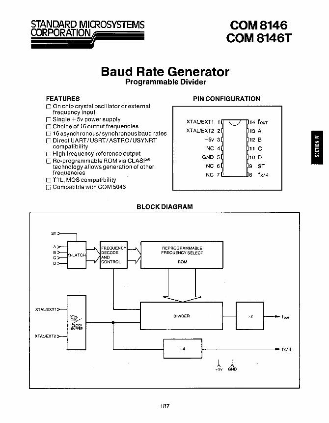
STANDARD MICROSYSTEMS CORPORAT~IO!N~ __
COM 8146 COM 8146T
Baud Rate Generator Programmable Divider
FEATURES PIN CONFIGURATION o On chip crystal oscillator or external
frequency input o Single + 5v power supply o Choice of 16 output frequencies
XTAUEXT1 11 \..J
016 asynchronous/synchronous baud rates XTAUEXT2 21
o Direct UART/USRT/ ASTRO/USYNRT compatibility
o High frequency reference output ORe-programmable ROM via CLASp®
technology allows generation of other frequencies
o TTL, MaS compatibility o Compatible with COM 5046
+5v 31
NC 41
GND 51
NC 61
NC 71
BLOCK DIAGRAM
ST
A
8 C D
XTAUEXT1
XTAUEXT2
, ..
>-->->->--
>-
>--
I h
D·LATCH
~
XTAL
~ CLOCK BUFFER
FREQUENCY ~
REPROGRAMMABLE DECODE FREQUENCY SELECT AND --I CONTROL ROM
""""=--.---::;::00'
DIVIDER I-
+4
A A +5v GND
187
14 fouT
13 A
12 B
11 C
10 D
9 ST
8 fx/4
+2 ~ tOUT
tx/4
I

General Description
The Standard Microsystem's COM 8146 is an enhanced version of the COM 5046 Baud Rate Generator. It is fabricated using SMC's patented COPLAMOS@ and CLASp® technologies and employs depletion mode loads, allowing operation from a single + 5v supply.
The standard COM 8146 is specifically dedicated to generating the full spectrum of 16 asynchronous/ synchronous data communication frequencies for 16X UART/USRT devices. A large number of the frequencies available are also useful for 1X and 32X ASTRO/USYNRT devices.
The COM 8146 features an internal crystal oscillator which may be used to provide the master reference frequency. Alternatively, an external reference may be supplied by applying complementary TTL level signals to pins 1 and 2. Parts suitable for use only with an external TTL reference are marked COM 8146T. TTL outputs used to drive the COM 8146 or COM 8146T XTALlEXT inputs should not be used to drive other TTL inputs, as noise immunity may be compromised due to excessive loading.
The output of the oscillator/buffer is applied to the divider for generation of the output frequency. The divider is capable of dividing by any integer from 6 to 219 + 1, inclusive. If the divisor is even, the output will be square; otherwise the output will be high longer than it is low by one fx clock period.
The reference frequency (fx) is used to provide a high frequency output at fx/4.
The divisor ROM contains 16 divisors, each 19 bits wide, and is fabricated using SMC's unique CLASp® technology. This process permits reduction of turnaround time for ROM patterns. The four divisor select bits are held in an externally strobed data latch. The strobe input is level sensitive: while the strobe is high, data is passed directly through to the ROM. Initiation of a new frequency is effected within 3.51tS of a change in any of the four divisor select bits (strobe activity is not required). This feature may be disabled through a CLASp® programming option causing new frequency initiation to be delayed until the end of the current fOUT half-cycle. The divisor select inputs have pull-up resistors; the strobe input does not.
Description of Pin Functions
Pin No. Symbol Name Function
XTALlEXT1 Crystal or This input is either one pin of the crystal package or one polarity External Input 1 of the external input.
2 XTALlEXT2 Crystal or This input is either the other pin of the crystal package or the other External Input 2 polarity of the external input.
3 Vee Power Supply + 5 volt supply 4,6,7 NC No Connection
5 GND Ground Ground 8 fx/4 fx/4 V4 crystal/ clock frequency reference output. 9 ST Strobe A high level strobe loads the input data (A, B, C, D) into the input
divisor select register. This input may be strobed or hard-wired to a high level.
10-13 D,C,B,A Divisor Select The logic level on these inputs as shown in Table 1, selects the Data Bits output frequency.
14 fOUT Output This output runs at a frequency selected by the divisor select Frequency data bits.
For electrical characteristics, see page 189.
188

ELECTRICAL CHARACTERISTICS COM8046,.COM8046T, COM8116, COM8116T, COM8126,
MAXIMUM GUARANTEED RATINGS COM8126T, COM8136, COM8136T, COM8146, COM8146T
Operating Temperature Range ............................................................... O°C to + 70°C Storage Temperature Range .............................................................. - 55°C to + 150°C Lead Temperature (soldering. 10 sec.) ............................................................... +325°C Positive Voltage on any Pin. with respect to ground .................................................... + B.OV Negative Voltage on any Pin. with respect to ground .................................................... - 0.3V Stresses above those listed may cause permanent damage to the deVice. This is a stress rating only and functional operation of the device at these or at any other condition above those indicated in the operational sections of this specification is not implied.
NOTE: When powering this device from laboratory or system power supplies, it is important that the Absolute Maximum Ratings not be exceeded or device failure can result. Some power supplies exhibit voltage spikes or "glitches" on their outputs when the AC power is switched on and off. In addition, voltage transients on the AC power line may appear on the DC output. If this possibility exists it is suggested that a clamp circuit be used.
ELECTRICAL CHARACTERISTICS (TA=O°C to 70°C, Vcc= +5V::!:5%. unless otherwise noted)
Parameter Min. Typ. Max. Unit Comments
D.C. CHARACTERISTICS INPUT VOLTAGE LEVELS
Low-level, Vil 0.8 V High-level, V,H 2.0 V excluding XTAL inputs
OUTPUT VOLTAGE LEVELS Low-level, VOL 0.4 V IOL = 1.6mA, for fxl 4, fol 16
0.4 V IOL = 3.2mA, for fa, fR' fT 0.4 V IOL = 0.8mA, for fx
High-level, VOH 3.5 V IOH=-100fLA;for fx, IOH=-50fLA
INPUT CURRENT Low-level, III -0.1 mA V,N = GND, excluding XTAL inputs
INPUT CAPACITANCE All inputs, C'N 5 10 pF V", = GND, excluding XTAL inputs
EXT INPUT LOAD 8 10 Series 7400 equivalent loads POWER SUPPLY CURRENT
Icc 50 mA
A.C. CHARACTERISTICS TA= + 25°C CLOCK FREQUENCY, fiN 0.01 7.0 MHz XTAL/EXT, 50% Duty Cycle ±5%
COM 8046, COM 8126, COM 8146 0.01 5.1 MHz XTAL/EXT, 50% Duty Cycle ±5%
COM 8116, COM 8136
STROBE PULSE WIDTH, tpw 150 DC ns INPUT SET-UP TIME
tos 200 ns INPUT HOLD TIME
tDH 50 ns STROBE TO NEW FREQUENCY DELAY 3.5 fLS @fx=5.0MHz
TIMING DIAGRAM
~------ tpw ------.-.1
STROBE
...---------tos ----------t~
DIVISOR V,H SELECT
DATA
189
I

Crystal Operation COM 8116 COM 8136
5.0688 MHz crystal
Crystal Operation COM 8126 COM 8146 COM 8046
74XX TTL
74XX TTL
External Input Operation COM 8116/COM 8116T COM 8136/COM 8136T
74XX TTL
74XX-totem pole or open collector output (external pull-up resistor required)
External Input Operation COM 8126/COM 8126T COM 8146/COM 8146T COM 8046/COM 8046T
74XX TTL
74XX-totem pole or open collector output (external pull-up resistor required)
For ROM re-programming SMC has a computer program available whereby the customer need only supply the input frequency and the desired output frequencies.
The ROM programming is automatically generated.
Crystal Specifications User must specify termination (pin, wire, other)
Prefer: HC-1B/U or HC-25/U
Frequency - 5.0688 MHz, AT cut
Temperature range O°C to 70°C
Series resistance <50 n Series Resonant
Overall tolerance ± .01 %
or as required
190
Crystal manufacturers (Partial list)
Northern Engineering Laboratories 357 Beloit Street Burlington, Wisconsin 53105 (414) 763-3591
BuloV8 Frequency Control Products 61-20 Woodside Avenue Woodside, New York 11377 (212) 335-6000
CTS Knights Inc. 101 East Church Street Sandwich, Illinois 60548 (815) 786-8411 Crystek Crystals Corporation 1000 Crystal Drive Fort Myers, Florida 33901 (813) 936-2109

COM 8046 cOM8046T
Table2 I
REFERENCE FREQUENCY = 5.068800MHz
Divisor Desired Desired Actual Actual Select Baud Clock Frequency Baud Frequency EDCBA Rate Factor (KHz) Divisor Rate (KHz) Deviation
00000 50.00 32X 1.60000 3168 50.00 1.600000 0.0000% 00001 75.00 32X 2.40000 2112 75.00 2.400000 0.0000% 00010 110.00 32X 3.52000 1440 110.00 3.520000 0.0000% 00011 134.50 32X 4.30400 1177 134.58 4.306542 0.0591% 00100 150.00 32X 4.80000 1056 150.00 4.800000 0.0000% 00101 200.00 32X 6.40000 792 200.00 6.400000 0.0000% 00110 300.00 32X 9.60000 528 300.00 9.600000 0.0000% 00111 600.00 32X 19.20000 264 600.00 19.200000 0.0000% 01000 1200.00 32X 38.40000 132 1200.00 38.400000 0.0000% 01001 1800.00 32X 57.60000 88 1800.00 57.600000 0.0000% 01010 2400.00 32X 76.80000 66 2400.00 76.800000 0.0000% 01011 3600.00 32X 115.20000 44 3600.00 115.200000 0.0000% 01100 4800.00 32X 153.60000 33 4800.00 153.600000 0.0000% 01101 7200.00 32X 230.40000 22 7200.00 230.400000 0.0000% 01110 9600.00 32X 307.20000 16 9900.00 316.800000 3.1250% 01111 19200.00 32X 614.40000 8 19800.00 633.600000 3.1250% 10000 50.00 16X 0.80000 6336 50.00 0.800000 0.0000% 10001 75.00 16X 1.20000 4224 75.00 1.200000 0.0000% 10010 110.00 16X 1.76000 2880 110.00 1.760000 0.0000% 10011 134.50 16X 2.15200 2355 134.52 2.152357 0.0166% 10100 150.00 16X 2.40000 2112 150.00 2.400000 0.0000% 10101 300.00 16X 4.80000 1056 300.00 4.800000 0.0000% 10110 600.00 16X 9.60000 528 600.00 9.600000 0.0000% 10111 1200.00 16X 19.20000 264 1200.00 19.200000 0.0000% 11000 1800.00 16X 28.80000 176 1800.00 28.800000 0.0000% 11001 2000.00 16X 32.00000 158 2005.06 32.081013 0.2532% 11010 2400.00 16X 38.40000 132 2400.00 38.400000 0.0000% 11011 3600.00 16X 57.60000 88 3600.00 57.600000 0.0000% 11100 4800.00 16X 76.80000 66 4800.00 76.800000 0.0000% 11101 7200.00 16X 115.20000 44 7200.00 115.200000 0.0000% 11110 9600.00 16X 153.60000 33 9600.00 153.600000 0.0000% 11111 19200.00 16X 307.20000 16 19800.00 316.800000 3.1250%
191

COM 8116 COM 8136 COM 8116T COM 8136T COM 8126 COM 8146
COM 8126T COM 8146T
Table 1 REFERENCE FREQUENCY = 5.068800MHZ
(STANDARD PART)
Divisior Desired Desired Actual Actual Select Baud Clock Frequency Baud Frequency DCBA Rate Factor (KHz) Divisor Rate (KHz) Deviation
0000 50.00 16X 0.80000 6336 50.00 0.800000 0.0000% 0001 75.00 16X 1.20000 4224 75.00 1.200000 0.0000% 0010 110.00 16X 1.76000 2880 110.00 1.760000 0.0000% 0011 134.50 16X 2.15200 2355 134.52 2.152357 0.0166% 0100 150.00 16X 2.40000 2112 150.00 2.400000 0.0000% 0101 300.00 16X 4.80000 1056 300.00 4.800000 0.0000% 0110 600.00 16X 9.60000 528 600.00 9.600000 0.0000% 0111 1200.00 16X 19.20000 264 1200.00 19.200000 0.0000% 1000 1800.00 16X 28.80000 176 1800.00 28.800000 0.0000% 1001 2000.00 16X 32.00000 158 2005.06 32.081013 0.2532% 1010 2400.00 16X 38.40000 132 2400.00 38.400000 0.0000% 1011 3600.00 16X 57.60000 88 3600.00 57.600000 0.0000% 1100 4800.00 16X 76.80000 66 4800.00 76.800000 0.0000% 1101 7200.00 16X 115.20000 44 7200.00 115.200000 0.0000% 1110 9600.00 16X 153.60000 33 9600.00 153.600000 0.0000% 1111 19200.00 16X 307.20000 16 19800.00 316.800000 3.1250%
Table 2 REFERENCE FREQUENCY = 4.915200MHz
(COM81 __ -5)
Divisor Desired Desired Actual Actual Select Baud Clock Frequency Baud Frequency DCBA Rate Factor (KHz) Divisor Rate (KHz) Deviation
0000 50.00 16X 0.80000 6144 50.00 0.800000 0.0000% 0001 75.00 16X 1.20000 4096 75.00 1.200000 0.0000% 0010 110.00 16X 1.76000 2793 109.93 1.758983 0.0100% 0011 134.50 16X 2.15200 2284 134.50 2.152000 0.0000% 0100 150.00 16X 2.40000 2048 150.00 2.400000 0.0000% 0101 300.00 16X 4.80000 1024 300.00 4.800000 0.0000% 0110 600.00 16X 9.60000 512 600.00 9.600000 0.0000% 0111 1200.00 16X 19.20000 256 1200.00 19.200000 0.0000% 1000 1800.00 16X 28.80000 171 1796.49 28.743859 0.1949% 1001 2000.00 16X 32.00000 154 1994.81 31.916883 0.2597% 1010 2400.00 16X 38.40000 128 2400.00 32.000000 0.0000% 1011 3600.00 16X 57.60000 85 3614.11 57.825882 0.3921% 1100 4800.00 16X 76.80000 64 4800.00 76.800000 0.0000% 1101 7200.00 16X 115.20000 43 7144.19 114.306976 0.7751 % 1110 9600.00 16X 153.60000 32 9600.00 153.600000 0.0000% 1111 19200.00 16X 307.20000 16 19200.00 307.200000 0.0000%
192

~ ~ RCP RSI
fR
COM 8017 DUAL COM 2017
BAUD RATE GENERATOR
fT
UART
TCP TSO
t I Typical UART -Dual Baud Rate Generator Configuration
Full Duplex-Split Speed
R.
R, BA ~----.. TSO
R,
COM 1671 ASTRa
BB .... -----RSI
DB
Typical ASTRO-Baud Rate Generator Configuration DD
XTALlEXT1
COM 8XXX
XTALlEXT2
XTAL
D 1-----------1
R R
Typical External Oscillator Hook-Up
[=:JXTAL
50-100P:T
~-----I~XTAL/EXT1
XTAL/EXT2
'---------I~ To System
+v
To System
-v Generation of Communication Reference Frequency and System Clock from a single crystal
Circuit diagrams utilizing SMC products are included as a means of illustrating typical semiconductor applications; consequently complete information sufficient for construction purposes is not necessarily given. The information has been carefully checked and is believed to be entirely reliable. However, no responsibility is assumed for inaccuracies. Furthermore, such information does not convey to the purchaser of the semiconductor devices described any license under the patent rights of SMC or others. SMC reserves the right to make changes at any time in order to improve design and supply the best product possible.
193
I

194

il .... w»~I!I CRT Display TIMING CONTROLLERS
Display Max Power Part Number Description J'eaturel Format Clock Supplies CRT 6027 provides all of the programmable 4 MHz +6,+12 CRT 6037 t1m1n.g and control balanced beam interlace programmable 4 MHz +6,+12 CRT 6047(3) for interlaced and fixed format BOcolumn 4MHz +6,+12
non-interlaced CRT 24 row CRT50S7
displaor line-lock progr8:I?IDable 4 MHz +6,+12
CRT 9007 CRT video processor sequential or row- programmable 4 MHz +6 and controller table driven memory
CRT 96364A/B complete CRT on-chip cursor and 64 column 1.6 MHz +6 processor write control 16 row
VDAC™ DISPLAY CONTROLLERS
Part Number Description Display Attributes
Provides complete f--------i display and attri-
7 x 11 dot matrix, wide graphics, thin graphics, on-chip cursor
reverse video blank
CRT BOOM. (2.3) butes control for alphanumeric and graphics display.
I--------i Consists of 7 x 11 x 128
CRT 8002B (2,3) character generator, video shift register,
I--------i latches, graphics and attributes cirCUits.
CRT B002C (2.3)
blink underline strike-thru
20 MHz
15 MHz
10MHz
CHARACTER GENERATORS Max
+5
Part Number Description Frequency Power SUpply CRT 7004A (3,4) 20 MHz CRT 7004B (3,4)
7 x 11 x 128 character generator, 15MHz +6 latches, video shift regiSter
CRT 7004C (3,4) 10 MHz
ROW BUFFER Max
Part Number Description Row Length Power Supply
CRT 9006-83 8 bit wide serial cascadable single row buffer 83 characters +5
CRT 9006·135 memory for CRT or printer 135 characters
CRT 9212 8 bit wide serial cascadable double row buffer 135 characters +5 memory for CRT or printer
~DEO~TRIBUTESCONTROLLEBS
Max Power Part Number Description Display Attributes Clock Supply
CRT 8021 Provides attributes Alphanumeric, wide Reverse video, 20 MHz +5 and graphics control graphics, thin graphics, blank, bUnk, for CRT video on-chip cursor underline, displays strike-thru
CRT9021B Provides attributes Alphanumeric, wide Reverse video, 28.5 MHz +5 and graphics control graphiCS, thin graphics, blank, blink, for CRT video on-chip cursor, double underline, displays height, double width intensity
(1) For future release (3) May be custom mask programmed
Package 40 DIP 40 DIP
40 DIP
40 DIP 40 DIP
2BDIP
28 DIP
Package
24 DIP
Package
24 DIP
28 DIP
Package
28 DIP
28 DIP
(2) Also available as CRT 8002A,B,C - 001 Katakana CRT 8002A,B,C - 003 5X7 dot matrix
(4) Also available as CRT 7004A,B,C - 003 6X7 dot matrix
195
Page 197-204
197-204
205·206
197·204 207·226
227·234
247-264
236·244
235-244
235-244
Page
266-260
Page
261-266
267·272
Page
273-2BO
2Bl-292

196

STANDARD MICROSYSTEMS CORPORATION,z
t CRT 5027 CRT 5037 CRT 5057
CRT Video Timer and Controller j.LPC FAMILY
FEATURES o Fully Programmable Display Format
Characters per data row (1-200) Data rows per frame (1-64) Raster scans per data row (1-16)
o Programmable Monitor Sync Format Raster Scans/ Frame (256-1023) "Front Porch" Sync Width "Back Porch" I nterlace/ Non-I nterlace Vertical Blanking
o Lock Line Input (CRT 5057) o Direct Outputs to CRT Monitor
Horizontal Sync Vertical Sync
VTAC®
Composite Sync (CRT 5027, CRT 5037) Blanking Cursor coincidence
o Programmed via: Processor data bus External PROM Mask Option ROM
o Standard or Non-Standard CRT Monitor Compatible o Refresh Rate: 60Hz, 50Hz, ... o Scrolling
Single Line Multi-Line
o Cursor Position Registers o Character Format: 5x7, 7x9, ... o Programmable Vertical Data Positioning o Balanced Beam Current Interlace (CRT 5037) o Graphics Compatible
PIN CONFIGURATION
A2 [ 1 \.,J
40 ] A1 A3 [ 2 39 ] AI/) CS [ 3 38 ] H0 A3 [ 4 37 J H1 A2 [ 5 36 ] H2
GND [ 6 35 ~ H3 A1 ( 7 34 P H4 AI{) [ 8 33 ] H5 -[ 9032 J H6
LLl/CSYN [ 10 31 P H7/DA5 VSYN [ 11 30 P DA4
DCC [ 12 29 P DA3 VDO ( 13 28 P DA2 Vee [ 14 27 P DA1
HSYN ( 15 26 P DA0 CAV [ 16 25 P OB~
BL [ 17 24 P DB1 DB? [ 18 23 P DB2 DB6 [ 19 22 P DB3 DB5 [ 20 21 P DB4
PACKAGE: 40-Pin D.I.P.
o Split-Screen Applications Horizontal Vertical
o Interlace or Non-Interlace operation D TTL Compatibility o BUS Oriented o High Speed Operation o COPLAMOS" N-Channel Silicon
Gate Technology o Compatible with CRT 8002 VDACTM o Compatible with CRT 7004
GENERAL DESCRIPTION The CRT Video Timer and Controller Chip (VTAC) R is a user programmable 40-pin COPLAMOS~) n channel MOS/LSI
device containing the logic functions required to generate all the timing signals for the presentation and formatting of interlaced and non-interlaced video data on a standard or non-standard CRT monitor.
With the exception of the dot counter, which may be clocked at a video frequency above 25 MHz and therefore not recommended for MOS implementation, all frame formatting, such as horizontal, vertical, and composite sync, characters per data row, data rows per frame, and raster scans per data row and per frame are totally user programmable. The data row counter has been designed to facilitate scrolling.
Programming is effected by loading seven 8 bit control registersdirectlyoff an 8 bit bidirectional data bus. Fourregister address lines and a chip select line provide complete microprocessor compatibility for program controlled set up. Thedevice can be "self loaded" via an external PROM tied on the data bus as described in the OPERATION section. Formatting can also be programmed by a single mask option.
In addition to the seven control registers two additional registers are provided to store the cursor character and data row addresses for generation of the cursor video signal. The contents of these two registers can also be read out onto the bus for update by the program.
Three versions of the VTAC® are available. The CRT 5027 provides non-interlaced operation with an even or odd number of scan lines per data row, or interlaced operation with an even numberof scan lines perdatarow. TheCRT5037 may be programmed for an odd oreven number of scan lines per data row in both interlaced and non-interlaced modes. Programming the CRT 5037 for an odd number of scan lines per data row eliminates character distortion caused by the uneven beam current normally associated with odd field/even field interlacing of alphanumeric displays.
The CRT 5057 provides the ability to lock a CRT's vertical refresh rate, as controlled by the VTAC's® vertical sync pulse, to the 50 Hz or 60 Hz line frequency thereby eliminating the so called "swim" phenomenon. This is particularly well suited for European system requirements. The line frequency waveform, processed to conform to the VTAC's® specified logic levels, is applied to the line lock input. The VTAC® will inhibit generation of vertical sync until a zero to one transition on this input is detected. The vertical sync pulse is then initiated within one scan line after this transition rises above the logic threshold of the VTAC.®
To provide the pin required for the line lock input, the composite sync output is not provided in the CRT 5057.
197
I

Pin No. Symbol
25-18 DB.0-7
3 CS 39,40,1,2 A.0-3
9 DS
12 DCC
38-32 H0'-6
7,5,4 R1-3
31 H7/DR5
8 R.0'
26-30 DR~-4
17 BL 15 HSYN 11 VSYN 10 CSYNI
LLI
16 CRV 14 Vee 13 Voo
39.40.1.2
CH'~HU:Clr3 ___ -.j
15M'1mIII1"9 ___ -.j
Name
Data Bus
Chip Select Register Address Data Strobe
DOT Counter Carry Character Counter Outputs Scan Counter Outputs H7/DR5
Scan Counter LSB
Data Row Counter Outputs Blank Horizontal Sync Vertical Sync
Description of Pin Functions Inputl output Function
1/0 Data bus. Input bus for control words from microprocessor or PROM. Bidirectional bus for cursor address. Signals chip that it is being addressed Register address bits for selecting one of seven control registers or either of the cursor address registers Strobes DB.0-7 into the appropriate register or outputs the cursor character address or cursor line address onto the data bus Carry from off chip dot counter establishing basic character clock rate. Character clock.
a Character counter outputs.
a Three most significant bits of the Scan Counter; row select inputs to character generator.
a Pin definition is user programmable. Output is MSB of Character Counter if horizontal line count (REG. 0) is ~128; otherwise output is MSB of Data Row Counter.
a Least significant bit of the scan counter. In the interlaced mode with an even number of scans per data row, Rei will toggle at the field rate; for an odd number of scans per data row in the interlaced mode, Rei will toggle at the data row rate.
a
a a a
Data Row counter outputs.
Defines non active portion of horizontal and vertical scans. Initiates horizontal retrace. Initiates vertical retrace.
Composite Sync Output! all Composite sync is provided on the CRT 5027 and CRT 5037. Line Lock Input
Cursor Video a Power Supply PS Power Supply PS
This output is active in non-interlaced mode only. Provides a true RS-170 composite sync wave form. For the CRT 5057, this pin is the Line Lock Input. The line frequency waveform, processed to conform to the VTAC's® specified logic levels, is applied to this pin. Defines cursor location in data field. + 5 volt Power Supply + 12 volt Power Supply
BLOCK DIAGRAM
198

Operation The design philosophy employed was to allow the device to interface effectively with either a microprocessor based or
hardwire logic system. The device is programmed by the user in one of two ways; via the processor data bus as part of the system initialization routine, or during power up via a PROM tied on the data bus and addressed directly by the Row Select outputs of the chip. (See figure 4). Seven 8 bit words are required to fully program the chip. Bit assignments for these words are shown in Table 1. The information contained in these seven words consists of the following:
Horizontal Formatting: Characters/Data Row
Horizontal Sync Delay
Horizontal Sync Width
Horizontal Line Count
Skew Bits
Vertical Formatting: Interlaced/Non-interlaced
Scans/Frame
Vertical Data Start
Data Rows/Frame
Last Data Row
Scans/Data Row
Device Initialization:
A 3 bit code providing 8 mask programmable character lengths from 20 to 132. The standard device will be masked for the following character lengths; 20, 32, 40,64,72,80,96, and 132.
3 bits assigned providing up to 8 character times for generation of "front porch".
4 bits assigned providing up to 15 character times for generation of horizontal sync width.
8 bits assigned providing up to 256 character times for total horizontal formatting.
A 2 bit code providing from a 0 to 2 character skew (delay) between the horizontal address counter and the blank and sync (horizontal, vertical, composite) signals to allow for retiming of video data prior to generation of composite video signal. The Cursor Video signal is also skewed as a function of this code.
This bit provides for data presentation with odd/even field formatting for interlaced systems. It modifies the vertical timing counters as described below. A logic 1 establishes the interlace mode.
8 bits assigned, defined according to the following equations: Let X = value of 8 assigned bits. 1) in interlaced mode-scans/frame = 2X + 513. Therefore for 525 scans, program X = 6 (00000110). Vertical sync will occur precisely every 262.5 scans, thereby producing two interlaced fields. Range = 513 to 1023 scans/frame, odd counts only. 2) in non-interlaced mode-scans/frame = 2X + 256. Therefore for 262 scans, program X = 3 (00000011). Range = 256 to 766 scans/frame, even counts only.
In either mode, vertical sync width is fixed at three horizontal scans (= 3H).
8 bits defining the number of raster scans from the leading edge of vertical sync until the start of display data. At this raster scan the data row counter is set to the data row address at the top of the page.
6 bits assigned providing up to 64 data rows per frame.
6 bits to allow up or down scrolling via a preload defining the count of the last displayed data row.
4 bits assigned providing up to 16 scan lines per data row.
Additional Features
Under microprocessor control-The device can be reset under system or program control by presenting a 1010 address on A3-rj. The device will remain reset at the top of the even field page until a start command is executed by presenting a 1110 address on A3-0.
Via "Self Loading"-In a non-processor environment, the self loading seguence is effected by presenting and holding the 1111 address on A3·j3, and is initiated by the receipt of the strobe pulse (DS). The 1111 address should be maintained long enough to insure that all seven registers have been loaded (in most applications under one millisecond). The timing sequence will begin one line scan after the 1111 address is removed. In processor based systems, self loading is initiated by presenting the ¢111 address to the device. Self loading is terminated by presenting the start command to the device which also initiates the timing chain.
Scrolling-In addition to the Register 6 storage of the last displayed data row a "scroll" command (address 1 rj11 ) presented to the device will increment the first displayed data row count to facilitate up scrolling in certain applications.
199
I

Horizontal Line Count: Characters/Data Row:
Horizontal Sync Delay: Horizontal Sync Width:
Skew Bits
Scans/ Frame
Vertical Data Start:
Data Rows/Frame: Last Data Row:
Mode: Scans/Data Row:
Control Registers Programming Chart
Total Characters/ Li ne = N + 1, N = 0 to 255 (DBO = LSB) DB2 DB1 DBO o d 0 20 Active Characters/Data Row o 0 1 32 o 1 0 40 o 1 1 64 1 0 0 72 1 0 1 80 1 1 0 96 1 1 1 132
= N, from 1 to 7 character times (DBO = LSB) (N = 0 Disallowed) = N, from 1 to 15 character times (DB3 = LSB) (N = 0 Disallowed)
DB7 DB6 o 0 1 0 o 1 1 1
Sync/Blank Delay Cursor Delay
o 1 2 2
(Character Times) o o 1 2
8 bits assigned, defined according to the following equations: Let X = value of 8 assigned bits. (DBO = LSB) 1) in interlaced mode-scans/frame = 2X + 513. Therefore for 525 scans, program X = 6 (00000110). Vertical sync will occur precisely every 262.5 scans, thereby producing two interlaced fields. Range = 513 to 1023 scans/frame, odd counts only. 2) in non-interlaced mode-scans/frame = 2X + 256. Therefore for 262 scans, program X = 3 (00000011). Range = 256 to 766 scans/frame, even counts only. In either mode, vertical sync width is fixed at three horizontal scans (= 3H). N = number of raster lines delay after leading edge of vertical sync of vertical start position. (DBO = LSB) Number of data rows = N + 1, N = 0 to 63 (DBO = LSB) N = Address of last dsplayed data row, N = 0 to 63, ie; for 24 data rows, program N = 23. (DBO = LSB) Register, 1, DB7 = 1 establishes Interlace.
Interlace Mode CRT 5027: Scans per Data Row = N + 1 where N = programmed number of scans/data rows; N = 0 to 15. Scans per data row must be even counts only. CRT 5037, CRT 5057: Scans per data Row = N + 2. N = 0 to 14, odd or even counts.
Non-Interlace Mode CRT 5027, CRT 5037, CRT 5057: Scans per Data Row = N + 1, odd or even count. N = 0 to 15.
DBi' ~
--"' .....
... ~
... --.. .... ~ '" .. '"
.... """'- " .. ("'" DB7 "
.. ,. Ro
LJ
t t t t t l Am A, A, A3 CS DS
SMC CRT 5027, CRT 5037
orCRT 5057 VTAC@
R, R? A3
Figure 4.
SELF LOADING SCHEME FOR VTAC® SET-UP
'1 32x8PROM
HARRIS HM·7602 OR EQUIVALENT HA,I---t--~
HA,f--+5
SLOAD cs (from system)
HA, t---+--t-t--4
ROW SELECTS TO CHARACTER GENERATOR
200
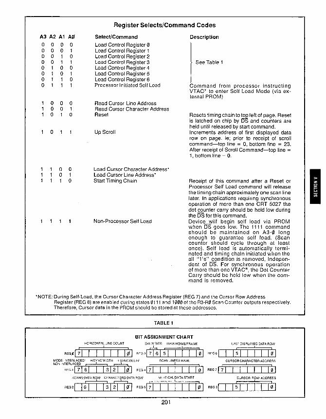
Register Selects/Command Codes
A3 A2 A1 ArJ Select/Command Description
0 0 0 0 0 0 0 0 0 1 0 1 0 1 0 1
0 0 0
0
0 0 0 1 1 0 1 1 0 0 0 1 1 0 1 1
0 0 0 1 1 0
o 0 o 1 1 0
Load Control Register 0 Load Control Register 1 Load Control Register 2 Load Control Register 3 Load Control Register 4 Load Control Register 5 Load Control Register 6 Processor Initiated Self Load
Read Cursor Line Address Read Cursor Character Address Reset
Up Scroll
Load Cursor Character Address· Load Cursor Line Address· Start Timing Chain
Non-Processor Self Load
See Table 1
Command from processor instructing VTACF: to enter Self Load Mode (via external PROM)
Resets timing chain to ~ left of page. Reset is latched on chip by OS and counters are held until released by start command. Increments address of first displayed data row on page. ie; prior to receipt of scroll command-top line = 0, bottom line = 23. After receipt of Scroll Command-top line = 1, bottom line = O.
Receipt of this command after a Reset or Processor Self Load command will release the timing chain approximately one scan line later. In applications requiring synchronous operation of more than one CRT 5027 the dot counter carry should be held low during the OS for this command. Device will begin self load via PROM when OS goes low. The 1111 command should be maintained on A3-'/J long enough to guarantee self load. (Scan counter should cycle through at least once). Self load is automatically terminated and timing chain initiated when the all "1's" ~ndition is removed, independent of OS. For synchronous operation of more than one VTAC'Y9, the Dot Counter Carry should be held low when the command is removed .
• NOTE: During Self-Load, the Cursor Character Address Register (REG 7) and the Cursor Row Address Register (REG 8) are enabled during states 0111 and 1000 of the R3-R0 Scan Counter outputs respectively. Therefore, Cursor data in the PROM should be stored at these addresses.
TABLE 1
BIT ASSIGNMENT CHART HORIZONTAL LINE COUNT SKEW BITS DATA ROWS/FRAME LAST DISPLAYED DATA ROW
REG;I ~ I I i I I I ~ I REG31 ill I 51 i I 1,,1 REG6 L-I .l.-...J......I ~-,-I ---L.I--Li --LI--J,I...,;.-J~ I MODE: INTERLACED/ H SYNC WIDTH H SYNC DELAY NON INTERLACED i I ~
REG 11 71 61 I 31 2JLo/ I REG 41 71
SCAN LINES/FRAME CURSOR CHARACTER ADDRE"SS
i I I I ~ , REG 71 ~ I II I I I ~ I SCANS/DATA ROW CHARACTERS/DATA ROW VERTICAL DATA START CURSOR ROW ADDRESS
R~G 21 I ~ I i I ~ I 2tTI, REG 5 ,....c, ; :;=, ::;:==;::~i :::::;:1 ::::;:1 ==;,::t....0 IRE G 8 L-I -,---,--I ~-,-I ---L.--Li --L1--J,1----,0 I
201
I

AC TIMING DIAGRAMS
FIGURE' VIDEO TIMING --j I - _I r-DDTCOUNTEA I ,. 11r-~---------'~11 '
CARRY I~ __________________________________________ JI I
1~---------------------PWL---------------------4-+~------PWH------~-~1
Hid-? H SYNC. V SYNC, BLANK. CURSOR VIDEO. COMPOSITE SYNC
FIGURE 2 LOAD READ TIMING
os ----------------------------------------~
FIGURE 3 SCAN AND DATA ROW COUNTER TIMING
HSYNC------------~
R0-3 DR0-5 ______________________________ +-________ -J
*R0-3 and DR~-5 may change prior to the falling edge of H sync
LINE LOCK IN (60 HZ, 50 HZ)
CRT 5057 LOGIC THRESHOLD
CRT 5057 LINE LOCK
I I I I t+---,-I/F LINE LOCK __
~I/FLINELOCK ±1Hi
.-------TOEl 1 --------til'"
VERTlg~~ SYNC ________ +-..... ..-+ _______________ '--____________ ---'
HSYNC
I LINE o--~ LOCK~ I
IN TH~~~~gLD r-! '-------3H-------
VERTICAL I SYNC -------------'-OUT
PROGRAM: SCANS/FRAME TO BE GREATER THAN ILiNE LOC: M'N, x H
202
Note: To ensure a stable display when using the line lock mode, the CRT 5057 should be used with DC coupled monitors only.

MAXIMUM GUARANTEED RATINGS' Operating Temperature Range ............................................................... O°C to + 70"C Storage Temperature Range .............................................................. - 55°C to + 150'C Lead Temperature (soldering, 10 sec.) ............................................................... + 325°C Positive Voltage on any Pin, with respect to ground .................................................... -r 1B.OV Negative Voltage on any Pin, with respect to ground .................................................... - 0.3V Stresses above those listed may cause permanent damage to the device. This is a stress rating only and functional operation of the device at these or at any other condition above those indicated in the operational sections of this specification is not implied.
NOTE: When powering this device from laboratory or system power supplies, it is important that the Absolute Maximum Ratings not be exceeded or device failure can result. Some power supplies exhibit voltage spikes or "glitches" on their outputs when the AC power is switched on and off. In addition, voltage transient$ on the AC power line may appear on the DC output. For example, the bench power supply programmed to deliver + 12 volts may have large voltage transients when the AC power is switched on and off. If this possibility exists it is suggested that a clamp circuit be used.
ELECTRICAL CHARACTERISTICS (TA=OcC to 70DC, Vcc= +5V::5%, Voo= + 12V::5%, unless otherwise noted)
Parameter Min. Typ.
D.C. CHARACTERISTICS INPUT VOLTAGE LEVELS
Low Level, VIL High Level, VIH Vce-1.5
OUTPUT VOL TAGE LEVELS Low Level-VoL for R~-3 Low Level-VoL all others High Level-VoH for R~-3, DB.0-7 2.4 High Level-VoH all others 2.4
INPUT CURRENT Low Level, IlL (Address, CS only) Leakage, IlL (All Inputs except Address, CS)
INPUT CAPACITANCE Data Bus, CIN 10 DS, Clock, CIN 25 All other, CIN 10
DATA BUS LEAKAGE in INPUT MODE 108
POWER SUPPLY CURRENT Ice BO 100 40
A.C. CHARACTERISTICS DOT COUNTER CARRY
frequency 0.5 PWH 35 PWL 215 tr,tf 10
DATA STROBE PWfSS 150ns
ADDRESS, CHIP SELECT Set-up time 125 Hold time 50
DATA BUS-LOADING Set-up time 125 Hold time 75
DATA BUS-READING TOEL2 TOEl4 5
OUTPUTS: H~-7, HS, VS, BL, CRV, CS-ToEL1
OUTPUTS: R(t-3, DR~-5 TOEL3 *
*R~-3 and DR~-5 may change prior to the falling edge of H sync
Restrictions
Max.
O.B Vee
0.4 0.4
250 10
15 40 15
10
100 70
4.0
50
1 OilS
125 60
125
750
Unit
V V
V V
fLA fLA
pF pF pF
fLA
mA mA
MHz ns ns ns
ns ns
ns ns
ns ns
ns
ns
Comments
IOL =3.2ma IOL = 1.6ma IOH =BOfLa IOH=40/-ta
VIN=OAV O'SVIN'SVCC
OAV ~ VIN ~ 5.25V
Figure 1 Figure 1 Figure 1 Figure 1
Figure 2
Figure 2 Figure 2
Figure 2 Figure 2
Figure 2, CL=50pF Figure 2, CL= 50pF
Figure 1, CL=20pF
Figure 3, CL=20pF
1. Only one pin is available for strobing data into the device via the data bus. The cursor X and Y coordinates are therefore loaded into the chip by presenting one set of addresses and outputed by presenting a different set of addresses. Therefore the standard WRITE and READ control signals from most microprocessors must be "NORed" externally to present a single strobe (DS) signal to the device. 2. In interlaced mode the total number of character slots assigned to the horizontal scan must be even to insure that vertical sync occurs preCisely between horizontal sync pulses.
203
I

General Timing HORIZONTAL TIMING
START OF LINEN STARTOFLlNEN+l
CHARACTERS PER DATA LINE
HORIZONTAL SYNC DELAY (FRONT PORCH)
Vt=:/77777777~(?E(~~?f77Z77777;ud n lzzzm
HORIZONTAL SYNC WIDTH
HORIZONTAL LINE COUNT= H
VERTICAL TIMING
START OF FRAME M OR ODD FIELD START OF FRAME M+ lOR EVEN FIELD
I • SCAN LINES PER FRAME -I --II V7777777777771llll777777777!7721 n VZZZ
I • -1. ACTIVE VIDEO= • I I--J VERTICAL DATA----.f DATA ROWS PER FRAME ' L VERTICAL SYNC
START =3H
Composite Sync Timing VOH
H ":gl n'-----n'-----<n'-----<!l'-----IL "y~:: ' ! , I::, I::,'
l...--H --"r"-- H-----+-l VOH' --H/2-l:
COMPOSITE SYNC VOL
VERTICAL SYNC
Vertical Sync Timing
1
o 2 4 6 8 iJ 2 4 6 8
9L---O-----.J
rVEATICAL DATA START SCAN =- IREG 5)
~
EXAMPLE BASED ON Non-Interlaced (Reg 1. Bit 7 = 0).24 data rows. 10scans/daia row
Start-up, CRT 5027 When employing microprocessor controlled loading of the CRT 5027'5 registers, the following sequence of instructions is necessary:
ADDRESS COMMAND 1 1 1 0 Start Timing Chain 1 0 1 0 Reset 0 0 0 0 Load Register 0
0 0 Load Register 6 1 0 Start Timing Chain
The sequence of START RESET LOAD START is necessary to insure proper initialization of the registers. This sequence is not required if register loading is via either of the Self Load modes, This sequence is optional with the CRT 5037 or CRT 5057.
Circuit diagrams utilizing SMC products are included as a means of illustrating typical semiconductor applications; consequently complete information sufficient for construction purposes is not necessarily given. The information has been carefully checked and is believed to be entirely reliable. However, no responsibility is assumed for inaccuracies. Furthermore, such information does not convey to the purchaser of the semiconductor devices described any license under the patent rights of SMC or others. SMC reserves the right to make changes at any time in order to improve deSign and supply the best product possible.
204

STANDARD MICROSYSTEMS CORPORATIONj~
I
CRT 5047 J.,Lpc FAMILY
Preprogrammed CRT Video Timer and Controller VTAC®
FEATURES PIN CONFIGURATION o Preprogrammed (Mask-Programmed) Display Format
BO Characters Per Data Row 24 Data Rows Per Frame 9 Scan Lines Per Data Row
o Preprogrammed Monitor Sync Format 262 Scan Lines Per Frame 6 Character Times for Horizontal Front Porch B Character Times for Horizontal Sync Width 6 Character Times for Horizontal Back Porch 16 Scan Lines for Vertical Front Porch 3 Scan Lines for Vertical Sync Width 27 Scan Lines for Vertical Back Porch Non-Interlace 15.720KHz Horizontal Scan Rate 60Hz Frame Refresh Rate
o Fixed Character Rate 1.572MHz Character Rate (636.13ns/Character) 11.004MHz Dot Rate (90.BBns/Dot) for 7 Dot
Wide Character Block o Character Format
5 X 7 Character in a 7 X 9 Block o Compatible with CRT B002B-003 VDAC™ o Compatible with CRT 7004B-003
A2 A1
A3 AfJ
CS HfJ
R3 H1
R2 H2
GND H3
R1 H4
RfJ H5
55 H6
CSYN H7IDR5
VSYN DR4
,DCC DR3
Vee DR2
Vee DR1
HSYN DRfJ
CRV DBfJ
BL DB1
DB? DB2
DB6 DB3
DB5 DB4
PACKAGE: 40-pin D.I.P.
o May be mask-programmed with other display formats
GENERAL DESCRIPTION
The two chip combination of SMC's CRT 5047 and CRT 8002B-003 effectively provide all of the video electronics for a CRT terminal. This chip set along with a pC form the basis for a minimum chip count CRT terminal.
The CRT 5047 Video Timer and Controller is a special version of the CRT 5037 VTAC® which has been ROMprogrammed with a fixed format. It is especially effective for low-cost CRT terminals using an 80 X 24 display format with a 5 X 7 character matrix. The use of a fixed ROM program in the CRT 5047 eliminates the software overhead normally required to specify the display parameters and simplifies terminal software design.
The Cursor Character Address Register and the Cursor Row Address Register are the only two registers acces-
205
sible by the processor. The CRT 5047 is easily initialized by the following sequence of commands:
Reset Load Control Register 6 Start Timing Chain
The parameters of the CRT 5047 have been selected to be compatible with most CRT monitors. The horizontal timing is programmed so that when the two character skew delay of the CRT 8002 VDACTM is taken into account, the effective timing is: Horizontal Front Porch -four characters, and Horizontal Back Porch-eight characters.
Figure 1 shows the contents of the internal CRT 5047 registers. Other mask-programmed versions of the CRT 5037 are available. Consult SMC for more information.
I

VTAC® WORK SHEET
1. H CHARACTER MATRIX (No. of Dots): . _5_ 2. V CHARAC!ER MAT~IX 7
(No. of HOrlz. Scan Lines): ............ __ 3. H CHARACTER BLOCK (Step 1 +
Desired Horiz. Spacing = No. in Dots): .. _7_ 4. V CHARACTER BLOCK (Step 2 +
Des!red Vertic.al Spacing = No. in 9 HOrlz. Scan Lines): .................... __
5. VERTI~AL FRAME (REFRESH) RATE 60 (Freq. In Hz): ......................... __
6. DESIRED NO. OF DATA ROWS: ........ ~ 7. TOTAL NO. OF ACTIVE "VIDEO
DISPLAY" SCAN LINES (Step 4 x Step 6 = No. in Horiz. Scan Lines): ..... ~
8. VERT. ?YNC DELAY (No. in Horiz. 16 Scan Lines): .......................... __
9. VERT. SYNC (No. in Horiz. Scan Lines; 3 T= 190.8 jls*): ......................... __
10. VERT. SCAN DELAY (No. in Horiz. 27 Scan Lines; T= 1.718 ms*): ............ __
ADDRESS REG. # A3 AO FUNCTION
11. TOTAL V,=-RTIC~L FR.AME (Ad? ste~s 262 7 thru 10 - No. In HOrlz. Scan Lines) .... __
12. HORIZONTAL SC~N LlN~ RATE. 15.720 (Step 5 x Step 11 - Freq. In KHz) ....... __
13. DESIRED NO. OF CHARACTERS 80 PER HORIZ. ROW: .................... __
14. HORIZ. SYNC DELAY (No. in Character 6 Time Units; T = 3.817 jls**): ........... __
15. HORIZ. SYNC (No. in Character Time 8 Units; T = 5.090 jls**): ................. __
16. HORIZ. SCAN DELAY (No. in Character 6 Time Units; T = 3.817 jls**): ........... __
17. TOTAL CHARACTER TIME UNITS IN (1) HORIZ. SCAN LINE (Add Steps 13 100 thru 16): .............................. __
18. ~HARA<?TER R~TE (Step 12 x Step 17 1.572 - Freq. In MHz). . ..................... __
19. ~LOCK .(DOT) ~ATE (Step 3 x Step 18 11.004 - Freq. In MHz). . ..................... __
*Vertical Interval **Horizontal Interval
BIT ASSIGNMENT HEX. DEC.
0 0000 HORIZ. LINE COUNT ~ 10111110101011111 63 99
0001 INTERLACE _0 __ H SYNC WIDTH __ 8_
10111010101111101 H SYNC DELAY __ 6_ 46 70
2 0010 SCANS/DATA ROW __ 9_ CHARACTERS/ROW ~ IxI11010101110111 45 69 ---
3 0011 SKEW CHARACTERS ~ DATAROWS~ 10101011101111111 17 23 ---
4 0100 SCANS/FRAME~ 10101010101011111 X =_3_ 03 03 ---
5 0101 VERTICAL DATA START = 3 + VERTICAL SCAN DELAY: SCAN DELAY~
1oT°1011111111101 1E 30 DATASTART~ ---
6' 0110 LAST DISPLAYED DATA ROW 1 X 1 X 1 1 (= DATA ROWS) ---
'Register 6 has an initialization option. It is loaded with the data contained in Register3 by a "Load Register6" command. The "Up Scroll" command can be used to effect scrolling operations.
Figure 1: CRT 5047 Mask Programmed Registers
Circuit diagrams utilizing SMC products are included as a means of illustrating typical semiconductor applica~ions; consequently complete information suf.ficient for construction purposes is not necessarily given. The information has been carefully checked and. IS believed to be entirely reliable. However, no responsibility is assumed for inaccuracies. Furthermore, such information does not convey to the purchaserof the semiconductor devices described any license under the patent rights of SMC or others. SMC reserves the right to make changes at any time in order to improve design and supply the best product possible.
206

STANDARD MICROSYSTEMS CORPORATION
CRT 9007 IlPC FAMILY
CRT Video Processor and Controller VPACTM
FEATURES D Fully Programmable Display Format
Characters per Data Row (8-240) Data Rows per Frame (2-256) Raster Scans per Data Row (1-32)
D Programmable Monitor Sync Format Raster Scans/Frame (4-2048) Front Porch-Horizontal (Negative or Positive)
-Vertical Sync Width-Horizontal (1-128 Character Times)
-Vertical (2-256 Scan Lines) Back Porch-Horizontal
-Vertical D Direct Outputs to CRT Monitor
Horizontal Sync Vertical Sync Composite Sync Composite Blanking Cursor Coincidence
D Binary Addressing of Video Memory D Row-Table Driven or Sequential Video Addressing Modes D Programmable Status Row Position and Address Registers D Bidirectional Partial or Full Page Smooth Scroll D Attribute Assemble Mode D Double Height Data Row Mode D Double Width Data Row Mode D Programmable DMA Burst Mode D Configurable with a Variety of Memory Contention
Arrangements D Light Pen Register D Cursor Horizontal and Vertical Position Registers D Maskable Processor Interrupt Line D Internal Status Register D Three-state Video Memory Address Bus D Partial or Full Page Blank Capability D Two Interlace Modes: Enhanced Video and Alternate
Scan Line
PIN CONFIGURATION
VA21 40GND VAl 0 2 39VA9 VA33 38 VAl
VAl14 37VA8 VA125 36VAO VA46 35CBLANK
VA137 34 CURS VA58 33 ACI<!TS'C VA69 32 C"SVfJC/LPSTB VA710 31 SLD/SLO VLT 11 30 "SIG/SLl VS12 29 WBEN/SL2IC"SVfJC HS13 28 DMARISL3IVBLANK
C"CIK 14 271NT r5Fffi15 26f'fST VD716 25CS VD617 24VDO VD518 23VDl VD419 22VD2 VD320 21 +5V
D Ability to Delay Cursor and Blanking with respect to Active Video
D Programmable for Horizontal Split Screen Applications D Graphics Compatible D Ability to Externally Sync each Raster Line, each Field D Single +5 Volt Power Supply .. D TTL Compatible on All Inputs and Outputs D VT-100 Compatible D RS-170 Interlaced Composite Sync Available
GENERAL DESCRIPTION
The CRT 9007 VPACTM is a next generation video processor/ controller-an MOS LSI integrated circuit which supports either sequential or row-table driven memory addressing modes. As indicated by the features above, the VPACTM provides the user with a wide range of programmable features permitting low cost implementation of high performance CRT systems. Its 14 address lines can directly address up to 16K of video memory. This is equivalent to eight pages of an 80 character by 24 line CRT display. Smooth or jump scroll operations may be performed anywhere within the addressable memory. In addition, status rows can be defined anywhere on the screen. In the sequential video addressing mode, a Table Start Register pOints to the address of the first character of the first data row on the screen. It can be easily changed to produce a scrolling effect on the screen. By using this register in conjunction with two auxiliary address registers and two sequential break registers, a screen roll can be produced with a stable status row held at either the first or last data row position.
207
In the row-table driven video addressing mode, each row in the video display is designated by its own address. This provides the user with greater flexibility than sequential addressing since the rows of characters are linked by pointers instead of residing in sequential memory locations. Operations such as data row insertion, deletion, and replication are easily accomplished by manipulating pointers instead of entire lines. The row table itself can be stored in memory in a linked list or in a contiguous format. The VPACTM works with a variety of memory contention schemes including operation with a Single Row Buffer such as the CRT 9006, a Double Row Buffer such as the CRT 9212, or no buffer at all, in which case character addresses are output during each displayable scan line. User accessable internal registers provide such features as light pen, interrupt enabling, cursor addressing, and VPAC™ status. Ten of these registers are used for screen formatting with the ability to define over 200 characters per pata row and up to 256 data rows per frame. These 10 registers contain the "vital screen parameters".
I

VD7-0
VAl3-0
~--------------j
PROCESSOR INTERFACE:
PIN NO. NAME 7,5,4,2,39, Video Address
37,10,9,8,6, 13-0 3,1,38,36
16,17,18,19, Video Data 7-0 20, 22, 23, 24
25 Chip strobe
26 Reset
27 Interrupt
CHARIHORIZ PERIOD CURSOR. BLANK SKEW
CHARIDAT A ROW DATA ROWS/FRAME
SCAN LINES/DATA ROW
HORIZ SYNC WIDTH SCAN LINES/FRAME
VERT SYNC WIDTH OMA BURST, DELAY COUNT
CURS
CSYNCI LPSTB
14 BIT ADDRESS BUS
TIMING AND
CONTROL
CBLANK INT
SL3/DMARNBLANK
Sl.2WBEN/CSYNC SL1/S[G
SL0/SLD
R5T VLT
CCLK---l ________________ -1~~~--------~
FIGURE 1: CRT 9007 BLOCK DIAGRAM
DESCRIPTION OF PIN FUNCTIONS
SYMBOL FUNCTION VA13-VAO These 14 signals are the binary address presented to the video memory by the CRT 9007.
The function depends on the particular CRT 9007 mode of operation. VA 13-6 are outputs only. VA5-0 are bidirectional. -Double Row Buffer Configuration:
VA 13-0 are active outputs for the DMA operations and are in their high impedance state at all other times.
-Single Row Buffer Configuration: VA 13-0 are active outputs during the first scan line of each data row and are in their high impedance state at all other times.
-Repetitive Memory Addressing Configuration: VA13-0 are active outputs at all times except during horizontal and vertical retrace at which time they are in their high impedance state.
If row table addressing is used for either single row buffer or repetitive memory addressing modes, VA 13-0 are active outputs during the horizontal retrace at each data row boundary to allow the CRT 9007 to retrieve the row table address. For processor read/write operations VA5-0 are inputs that select the appropriate internal register.
VD7-VDO Bidirectional video data bus: during processor Read/write operations data is transferred via VD7-VDO when chip strobe (CS) is active. These lines are in their hi9h impedance state when CS is inactive. During CRT 9007 DMA operations, data from video memory is input via VD7-VDO when a new row table address is being retrieved or when the attribute latch is being updated in the attribute assemble mode. VD7-VDO are outputs when the external row buffer is updated with a new attribute in the attribute assemble mode.
CS Input; this signal when active low, allows the processor to read or write internal CRT 9007 registers. When reading from an internal CRT 9007 register, the chip strobe (CS) enables the output drivers. When writing to an internal CRT 9007 register, the trailing edge of this signal latches the incoming data. Figure 2 shows all processor read/write timing.
RST Input; this active low sign.ill..Puts the CRT 9007 into a known, inactive state and insures that the horizontal sync (HS) output is inactive. Activating this input has the same effect as a RESET command. After initialization, a START command causes normal CRT 9007 opera-tion. See processor addressable registers section, Register 16 for the reset state definition.
INT Output; an interrupt to the processor from the CRT 9007 occurs when this signal is active high. The interrupt returns to its inactive low state when the status register is read.
208

DESCRIPTION OF PIN FUNCTIONS CONT'D CRT INTERFACE:
PIN NO. NAME SYMBOL FUNCTION
11 Visible Line Time VLT Output; this signal is active high during all visible scan lines and during the horizontal trace times at vertical retrace. This signal can be used to gate the character clock (CCLK) when supplying data to a character generator from a single or double row buffer.
12 Vertical Sync VS Open drain output; this signal determines the vertical position of displayed text by initiating a vertical retrace. Its position and pulse width are user programmable. The open drain allows the vertical frame rate to be synchronized to the line frequency when using monitors with DC coupled vertical amplifiers. If the VS output is pulled active low externally before the CRT 9007 itself initiates a vertical synQ,lhe CRT 9007 will start its own vertical sync at the next leading edge of horizontal sync (HS).
13 Horizontal Sync HS Open drain output; this Signal determines the horizontal position of disPlabed text by initiating a horizontal retrace. Its position and pulse width are user programmable. uring hardware and software reset, this signal is inactive high. The open drain allows the horizontal scan rate to be synchronized to an external source. If the HS output is pulled low externally before the CRT 9007 itself initiates a horizontal sync, the CRT 9007 will start its own horizontal sync on the next character clock (CCLK).
14 Character Clock CCLK Input; this signal defines the character rate of the screen and is used by the CRT 9007 for all internal timing. A minimum high voltage of 4.3V must be maintained for proper chip operation.
15 Data Row DRB Output; this signal is active low for one full scan line (from VLT trailing edge to VLT trailin~ Boundary edge) at the top scan line of each new data row. This signal can be used to swap buffers In
the double row buffer mode. It indicates the particular horizontal retrace time that the CRT 9007 outputs addresses (VA13-VAO) for single row buffer operation.
34 Cursor CURS Output; this signal marks the cursor position on the screen as specified by the horizontal and vertical cursor registers. The signal is active for one character time at the particular character position for all scan lines within the data row. For double height or width characters, this sig-nal is active for 2 consecutive CCLK's in every scan line within the data row. For double height characters, this signal can be programmed to be active at the proper position for 2 consecutive data rows. CURS is also used to signal either a double height or double width data row by becoming active during the horizontal retrace (CBLANK active) prior to a double height or double width scan line. The time of activation and deactivation is a function of the addressing mode, buffer configuration and the scan line number. See section of Double height/width for details.
35 Composite Blank CBLANK Output. This si~nal when active high, indicates that a retrace (either horizontal or vertical) will be performed. he signal remains active for the entire retrace interval as programmed. It is used to blank the video to a CRT. I
USER SELECTABLE PINS: (see Tables 4 and 5)
PIN NO. NAME SYMBOL FUNCTION
28,29,30,31 Scan Line 3- SL3-SLO Output; these 4 signals are the direct scan line counter outputs, in binary form, that indicate Scan Line 0 to the character generator the current scan line. These signals continue to be updated
during the vertical retrace interval. SL3 and SL0 are the most and least significant bits respectively.
28 Direct Memory DMAR Output; this signal is the DMA request issued by the CRT 9007. It will only become active if Access Request the acknowledge (ACK) input is inactive. It remains active high throughout the entire
DMA operation.
28 Vertical Blank VBLANK Output; this signal is active high only during the vertical retrace period.
29 Write Buffer WBEN Output; this active hi~h signal is used to gate the clock feeding the write buffer in a double Enable row buffer configuration.
290r32 Composite Sync CSYNC Output; this signal provides a true RS-170 composite sync waveform with equalization pulses and vertical serrations in both interlace and noninterlace formats. Figure 3 illustrates the CSYNC output in both interlaced and noninterlaced formats.
30 Scan Line Gate SLG Output; this active low si~nal is used as a clock gate. It captures the correct 5 or 6 CCLK's and, in con/unction with LD (pin 31), allows scan line information to be loaded serially into an externa shift register.
31 Scan Line Data SLD Output; this signal allows one to load an external shift register with the current scan IiI.l.!L.-count. The count is presented least significant to most significant bit during the 5 or 6 CCLK's framed by SLG. With this form of scan line representation, it is possible to define up to 32 scan lines per data row. The external shift register must be at least 5 bits in length. Even though 6 shifts can occur one should only use the 5 last bits shifted to define the scan line count. The extra shift occurs in interlace or double height character mode to allow the scan line count to be adjusted to its proper value. Figures 4 and 5 illustrate the serial scan line timing.
32 Light Pen Strobe LPSTB Input; this signal strobes the current row/column position into the light pen register at its posi-tive transition.
33 Acknowledge ACK Input; this active high signal acknowledges a DMA request. It indicates that the processor bus has entered its high impedance state and the CRT 9007 may access video memory. It is not recommended to deactivate this signal during a CRT 9007 DMA cycle because the CRT 9007 will not shut down in a predictable amount of time.
33 Three State Control
TSC Input; this signal, when active low, places VA13-VA0 in their high impedance state.
209

OPERATION MODES
Single Row Buffer Operation The CRT 9007 configured with a CRT 9006 Single Row Buffer is shown in figure 6. The use of the CRT 9006 Single Row Buffer requires that the buffer be loaded at the video painting rate during the top scan line of each data row. However, after the CRT 9006 is loaded, the CRT 9007 address lines enter their high impedance state for the remaining N-1 scan lines of the data row, thereby permitting full proces-
sor access to memory during these scan lines. The percentage of total memory cycles available to the processor is approximately [(N-1 )/N] x 100 where N is the total number of scan lines per data row. For a typical system with 12 scan lines per data row this percentage is 92%. Figure 7 illustrates typical timing for the CRT 9007 used with the CRT 9006 Single Row Buffer.
PROCESSOR INTR
pPlpC
ACK
ADDR DATA ~J ~
! ! ! TSC ~ +5VGND INT
A ' 7-
ADDRESS BUS VA1S-0 MEMORY " ROM
RAM A
.... VIDEO RAM
VD7-0
CRT 9007 HS
VPAC" C BLANK
lJll
-
I
}; o R " " ~~ VlT SlS Sl2 Sll Sl0 CURS c=
t D 4 A T A
1 I
B U t S
WArn ~CKEN ClK RS R2 Rl R0 CURSOR VSVNC """ J ... lD/Sll DOUT7-0 ATTRIBUTES CRT 9006
rlS CRTB002
VDC SINGLE VDAC"
~ ROW BUFFER
DIN7-0 or CHARACTER/ATTRIBUTES
A7-0 GENERATOR VIDEO
FIGURE 6: CRT9007 CONFIGURATION WITH SINGLE ROW BUFFER
--, :-------~-----lll L __ L _____ ~J-+
vu --,~ ____________ ~ I
n I
~ CLOCK GENERATOR
M TO
ONITOR
DRB~: :1 , Tse is: ~ : \ .... -----r--------VA13~ +--8(: I!I~~~ 0 0:: 0 Ijlt--~I~M~pH~E~~GA~HN~C~E~-------VD7·. : · ! !: li~il 0 0:: 0 Iii
I ; 5 CLOCKS I 3 CLOCKS 5 CLOCKS CURS ~_t'ijj~!iJ I I n.".,..CURSOR AT 5tH CHARACTER POSITION :-:1.., IF 2XH OR b----{l
(NO SKEW) ~ OR l 5 CLOCKS: 2XW '-------
I 5CLOCKS 2XW ~-------~I.~~IIh------------SL3-0 cl6cd t STABLE COUNT~: II STABLE COUNT
I
FIGURE 7: CRT 9007 SINGLE ROW BUFFER TIMING (32 CHARACTERS PER DATA ROW)
210

Double Row Buffer Operation Figure 8 shows the CRT 9007 used in conjunction with a CRT 9212 Double Row Buffer. The Double Row Buffer has a read buffer which is read at the painting rate of the CRT during each scan line in the data row. While the read buffer is being read and supplying data to the character generator for the current displayed data row, the write buffer is being loaded with the next data row to be displayed. This arrangement allows for relaxed write timing to the write buffer as it may be filled in the time it takes for N scan lines on the CRT to be painted where N is the number of scan lines per data row. Used in this configuration, the CRT 9007 takes advantage of the relaxed write buffer timing by stealing memory cycles from the processor to fill the write buffer (Direct memory access operation). The CRT 9007 sends the DMAR (DMA request) signal, awaits an ACK (acknowledge) signal and then drives out on VA13-VAO the address at which the next video data resides. The CRT 9007 then activates the WBEN (write buffer enable) signal to write the data into the buffer. If for example there are 80 characters per data row, the CRT 9007 performs 80 DMA operations. The user has the ability to program the number of DMA cycles performed during each DMAR-ACK sequence, as well as
PROCESSOR INTR
IlP/IlC ACK
DMARa
ADDR DATA
.t. ..
the delay between each DMAR-ACK sequence, via the DMA CONTROL REGISTER (RA). If 8 DMA operations are performed for each ACK received, 10 such DMAR-ACK sequences must be performed to completely fill the write buffer. The programmed delay allows the user to evenly distribute the DMA operations so as not to hold up the processor for an excessive length of time. This feature also permits other DMA devices to be used and allows the processor to respond to real time events. In addition, the user has the ability to disable the CRT 9007 DMA mechanism. Figure 9 illustrates typical timing for the CRT 9007 used with the CRT 9212 Double Row Buffer.
Since the CRT 9212 Double Row Buffer has separate inputs for read and write clocks (RCLK, WCLK), it is possible to display proportional character widths (variable number of dots per character) by reading out the buffer at a character clock rate determined by the particular character. The writing of the buffer can be clocked from a different and constant character clock. Figure 10 illustrates the CRT 9007 used with two double row buffers and a CRT 9021 Video Attributes Controller chip to provide proportional character display.
l l l DMAR ACK RST +5V GND INT
" MEMORY
ROM RAM
VIDEO RAM A
"
;.-ADDRESS BUS
y '(
D A T A
B U S
~ -----,I
j,.
VA13-0 y CRT 9007
VPAC~
" VD7-0
" WBENDml VLT SLD sm
~!
AS
CBLANK
vs CURS CClJ\
r---
J rlDh
}! o R
~t,'10, ~!3~~ 00 I Y J 1 I J I CLOCK I
1.,"~J~"1 . Jl, L",""L,= j I"T"" CRT9212 -", C ,~""= "~, ,.'" DOUBLE VDAC" VDC
ROW BUFFER DIN 7·, CHARACTERfATIRIBUTES
GENERATOR TO A7-0 VIDEO MO
1i£p--GNO -y NITOR
FIGURE 8: CRT 9007 CONFIGURATION WITH DOUBLE ROW BUFFER
211
I

HS ~===~.=.~-VLTI~ ____ .....
DRB--'~ ______________________________________ ~
DMAR
I l\ : I: I :
"--~r--------;:-t ~J :: LG~~,---------1+-16 DMA CYCLES ~a DELAY~ '--16 DMA CYCLES---H..a DELAY~ ~ REMAINDER OF DMA CYCLES
VA13-0 ----I
VD7-0 x x
WBEN
CURS
FIGURE 9: CRT 9007 DOUBLE ROW BUFFER TIMING (32 CHARACTERS PER DATA ROW)
lNTR
PROCESSOR ACK
OMARa
ADOR DATA
"" ,..
'" ::-./I DMAA ACK INT
MEMORY VA13-0 HS } TO ROM " ADDRESS BUS " CRT 9007-VPAC'· \is MONI
RAM ./I ~ VIDEO RAM V07-0
" v '\r--Y =
TOR
BUFFER CONTROLS
II DATA SCAN LINE DATA
BUS <; ,>
"I WClK RCLK CHARACTER WIDTH A3-A~ CLOCK
-----1'\ CHARACTER ~ GENERATOR
r--V DIN7-0
DOUT7-0 -----l'..,
Al1_A4ROM "\
CRT 9212 --V r---DOUBLE ROW BUFFER r---
t CHAR. ~
CODE ~ CRT 9212
A7-0 CRT 9021
I-~
DOUBLE ROW BUFFER ~ VDC
OIN7-0 CHARACTER ATTRIBUTES
SH[Q :---" DOUT7-0 ATTRIBUTES VIDEO TO MO NITOR
VIDEO ATTRIBUTES CONTROLLER
FIGURE 10: CRT9007 CONFIGURATION FOR PROPORTIONAL CHARACTER DISPLAY
212

Repetitive Memory Addressing Operation In this operation mode, the CRT 9007 will repeat the sequence of video addresses for every scan line of every data row. The CRT 9007 address bus will enter its high impedance state during all horizontal retrace intervals (except the retrace interval at a data row boundary if the CRT 9007 is configured in a row driven addressing mode). This arrangement allows for such low end contention schemes as retrace intervention (the processor is only allowed access to video memory during retrace intervals)
and processor priority (the processor has an unlimited access to video memory). A high end contention scheme can be employed which uses a double speed memory such that in a single character period both the processor and the CRT 9007 are permitted access to video memory at predetermined time slots. Figure 11 illustrates the CRT 9007 configured with a double speed memory. Typical timing for this mode is illustrated in figure 12.
INTRt---------------------.
VIDEO RAM
ADDRESS
CUR
T1~
PROCESSOR I'P/I'C
DATA
ROM RAM
u
VIDEO RAM
T21'--__ --'
ADDR 1--------.
PROCESSOR --~~-___ /~ __ _J·~ ___ J~ ___
c:::J
INT + 5V GND
HS
CRT 9007 VPAC'"
CRT 8002 VDACTM
CHARACTER/A HRI BUTES GENERATOR
VIDEO
CCLK DClK
CLOCK CClK GENERATOR T1
T2
FIGURE 11: CRT 9007 CONFIGURATION WITH DOUBLE SPEED MEMORY
HS ~=~==~- LI===~-VLT IL.....-____ ...J
n
~~----------~--------------------------~ I I I I
o 0 0 I~I I~I~I 0 0
I I ,
1*1 0 0 Iii x o
H
TO MONITOR
L n--L-
I I
0 I~~ ,
Iii x
FIGURE 12: CRT 9007 REPETITIVE MEMORY ADDRESS TIMING (32 CHARACTERS PER DATA ROW)
213
I

Attribute Assemble Operation This configuration allows the user to retain an 8 bit wide video memory in which attributes occupy memory locations but not positions on the CRT. This mode assumes that every other display position in video memory contains an attribute. During one clock cycle, attribute data is latched into the CRT 9007; during the next clock cycle a character location is addressed. The attribute data is driven out along with a WBEN signal allowing the character plus its associated attribute to be written Simultaneously to two 8 bit double row buffers. Figure 13 illustrates the memory organization used for the Attribute Assemble mode. The first entry in each data row must begin with an attribute.
Memory Address (typ) Memory Data (8 bits)
0000
0001
0002
0003
o o o
2N
2N+l
Attribute 0
Character 0
Attribute 1
Character 1
0 0 0
Attribute N
CharacterN
Figure 14 shows the CRT 9007 configured in the Attribute Assemble mode used with two CRT 9212 Double Row Buffers and 8, 16Kx1 dynamic RAMS. This mode, since it retains an 8 bit wide memory while providing all the advantages of a 16 bit wide memory, lends itself to some cost effective designs using dynamic RAMS. The CRT 9007 will refresh dynamic RAMS because twice the number of the programmed characters per data row are accessed sequentially for each data row. * Figure 15 illustrates typical timing of the CRT 9007 used in the Attribute Assemble mode.
Figure 13: Attribute Assemble Memory Organization
*Note: For 50 Hz operation there usually is about 3 milliseconds extra vertical blanking where refreshing might fail. In this situation the CRT 9007 can be programmed with about 5 more "dummy" data rows while extending the vertical blank signal. This allows the CRT 9007 to start addressing video memory much earlier within the vertical blanking interval and hence provide refresh to the dynamic RAMS. When displaying double height or double width data rows, only half as many sequential locations are accessed each data row and dynamic RAM refresh might fail.
PROCESSOR INT
ACK
OMARQ DATA AW AODA . II.
- DMAA ACK INT ;;;l3f+--- - f-~f+--- - MU' " A AND ..
S-,6Kx' A6·0 CONTROL A DR BUS VAl3·0 DYNAMIC " A-~~A
..- CRT 9007 HS RAMS VPAC™ TO
vs MO
~ ..
07·0 lL~ r--V V07-0
o " .. ~ ~" W8EN 5Fi§ VLT = SLD SITi CURS CBlANK A T
NITOR
A B U S
~ "",,J ~~ n r DATA 1Q 2Q 30 40 '--- - ! ! ! ! "')- ? I DOTClOCK11
~I WEN TOG REN ClRCNT RClK WClK ~ RCI Al R2 R3 CURSOR LDSH AETBL VSVNC GENERATOR CRT 9212
---J DIN7-'DOUBLE ROW BUFFERDOUT7-0 ATTRIBUTES VDC (ATTRIBUTES) DE GND
CRT B002 VIDEO -~~NI ~ i ~ * t * VDAC™
TOR
.1 WEN roGRENCl:RCNTAm< = '8 CHARACTER/ATTRIBUTES CRT 9212 GENERATOR
]DIN7-'DOUBLE ROW BUFFERDOUT7-' A7·0
..- I (DISPLAY) DE GND
FIGURE 14: CRT 9007 CONFIGURATION FOR ATTRIBUTE ASSEMBLE MODE
214

Smooth Scroll Operation Smooth scroll requires that all or a portion of the screen move up or down an integral number of scan lines at a time. 2 user programmable registers allow one to define the "start data row" and the "end data row" for the smooth scroll operation. A SMOOTH SCROLL OFFSET REGISTER (R17), when used in conjunction with a CRT 9007 vertically timed interrupt, allows the user to synchronize the update of the offset register to the vertical frame rate. The offset register causes the scan line counter outputs of the CRT 9007 to start at the programmed offset value rather than zero for
VLT ,'-____ ---1
the data row that starts the smooth scroll interval. To allow complete flexibility in smooth scroll direction and rate, one can update the offset register in the positive as well as negative direction and can also offset any number of scan lines each frame. Since a smooth scroll can momentarily result in a partial data row consisting of one scan line, the loading of the write buffer under DMA operations for the start and end data row of the smooth scroll operation is forced to occur in one scan line. This condition overrides the programmable DMA CONTROL REGISTER (RA).
ORB ~'-________________________ ~
II L .------lfr1--------~;t~
VA13·0 o ~o Ijlll~il!~
WBEN 000
• DMA cycles will always end at a character fetch
215
I

ADDRESSING MODES
Row Table Addressing In this addressing mode, each data row in video memory is designated by its own starting address. This provides greater flexibility with respect to screen operations than with other addressing schemes used by previous CRT controllers. The row table, which is a list of starting addresses for each data row, can be configured in one of 2 ways. The choice of row table format is highly dependent upon the particular application and the programmer's preference since each format allows full utilization of the CRT 9007 features.
Contiguous Row Table Format In this format, the TABLE START REGISTER (RC and RD) points to the address where the row table begins. The contents of the first 2 locations define the starting address of the first data row. These 2 bytes define a 14 bit address where the first byte is the low order 8 bits and the second byte is the high order 6 bits. The 2 most significant bits of the second byte define double height/width characteristics to the current data row. The contents of the third and fourth locations define the address where the second data row begins. Figure 16 illustrates the contiguous row table organization in video memory.
Linked List Row Table Format
Row 1 Table In
Memory
1st 1 Data Row
2nd 1 Data Row
3rd 1 Data Row
r-1 Table Start Register
}-A B C }-0
r--E } F
0 0 0
1st Char -2nd Char
0 0 0
Last Char
0 0 0
1st Char
2nd Char
0 0 0
Last Char
0 0
1st Char
2nd Char
0 0 0
Last Char
In this format the TABLE START REGISTER (RC and RD) points to the memory location which starts the entire addressing sequence into operation. The first byte read is the lower 8 bits and the second byte read is the upper 6 bits of the next data row's start address. The 2 most significant bits of the second byte define double height/width characteristics for the data row about to be read. The third, fourth, fifth, etc., bytes read are the first, second, third, etc., characters of the current data row. Figure 17 illustrates the linked list row table organization in video memory.
FIGURE 16: CONTIGUOUS ROW TABLE ADDRESS FORMAT
Table Start Register I Row table address for second data row
~ I Byte 1 I Byte 2 I Byte 3 I Byte 4 I 000 I Byte N I
I ~------~v~------~
characters for first data row
Row table address for third data row
,..---A--..
~ I Byte 1 I Byte 2 I Byte 3 I Byte 4 I 000 I Byte N I
C,O y
characters for second data row
FIGURE 17: LINKED LIST ROW TABLE ADDRESS FORMAT
I
Sequential Addressing In this addressing mode, characters on the display screen are located in successive memory locations. The TABLE
is read by the CRT 9007 for display refresh, the internal video address register is incremented by one to access the next character.
START REGISTER (RC and RD) points to the address of For more versatile systems operation in the sequential the first character of the first data row on the screen. In this addressing mode, SEQUENTIAL BREAK REGISTER 1 mode the TABLE START REGISTER does not point to the (R1 0) and SEQUENTIAL BREAK REGISTER 2 (R12) may start of a table butthe start of the screen. As each character be used to define the data rows at wtiich two additional
216

sequential display areas begin. Note that DATA ROW END REGISTER (R12) is defined as SEQUENTIAL BREAK REGISTER 2 (R12) forthe sequential addressing mode only. The starting addresses for these two additional display areas are defined by AUXILIARY ADDRESS REGISTER 1 (RE and RF) and AUXILIARY ADDRESS REGISTER 2 (R13 and R14). When the raster begins painting a data row equal to the number programmed in one of the sequential break registers, the CRT 9007 addresses the video memory sequentially starting with the address specified by the corresponding auxiliary address register. Figure 18 illustrates a display with 80 characters per data row having sequential breaks at data rows 3 and 6.
Using the sequential addressing mode with 2 breaks, it is possible to roll a portion of the screen and keep the rest of the screen stable. Double height/width characteristics can be attached to the 2 sequentially addressed screens defined by SEQUENTIAL BREAK REGISTERS 1 and 2 by using the 2 most significant bits of AUXILIARY ADDRESS REGISTERS 1 and 2. See the description of these 2 registers for their bit definition.
Double Height/Width Operation When double height/width characters (2XH/2XW) are displayed, the following will occur:
1. the CRT 9007 will address half as many characters for each data row by incrementing its address every other character clock.
2. the high speed video shift register supplying serial video to the CRT must shift out dots at half frequency.
3. For double height, the scan line counter outputs (SL3-SLO or SLG, SLD) are incremented every other scan line.
The CRT 9007 is informed of the double height or double width display modes via the 2 most significant bits of the row table address or the 2 most significant bits of the AUXILIARY ADDRESS registers depending on the selected addressing mode. In any case, once the information is obtained by the CRT 9007, it must initiate the 3 tasks listed above. Tasks 1 and 3 are performed as appropriate and task 2 is performed using the CURS output of the CRT9007 during CBLANK (horizontal retrace) to Signal the external logic that a change in the dot shift frequency is required. The exact time of activation and deactivation of the CURS signal during horizontal retrace is a function of addressing mode, operation mode and actual scan line number to be painted. Tables 1 and 2 show the cursor activation and deactivation times as a function of the buffer configuration and addressing mode for the top scan line of a new data row. Tables 1 and 2 assume a cursor skew of zero. A cursor skew will effect the cursor position during trace as well as retrace time. For all subsequent scan lines, the CURS signal is activated 3 CCLK's after VLT trailing edge and stays active for exactly 1 CCLK assuming no cursor skew. When the cursor is placed on a double height or double width data row, it will become active for 2 CCLK's to allow the cursor to be displayed as double width. If the cursor position is programmed to reside
OPERATION ADDRESSING MODE
MODE Row Driven (linked list or contiguous) Sequential
Repetitive Memory 1 CCLK after high byte 1 CCLK after TSC Addressing of row table read leading edge
1 CCLK after high byte 1 CCLK after TSC Single row buffer of row table read leading edge
1 CCLK after high byte 1 CCLK after ACK Double row buffer of row table read leading edge
TABLE START REGISTER = 1000 AUXILIARY ADDRESS REGISTER 1 = 2000 AUXILIARY ADDRESS REGISTER 2 = 0800 SEQUENTIAL BREAK REGISTER 1 = 3 SEQUENTIAL BREAK REGISTER 2 = 6
Data Row o 1 2 3 4 5 6 7 8
Address range 1000 to 104 F 1050 to 109F 10A0 to 10EF 2000 to 204F (Break 1) 2050 to 209F 20A0 to 20EF 0800 to 084F (Break 2) 0850 to089F 08A0 to08EF
o o o
Figure 18: Sequential Addressing Example With Two Breaks
in the top half of a double height data row, it may become active for all scan lines in both the current and next data row to allow the cursor to be displayed as double height.
For row driven addressing, a particular data row or pair of data rows can appear in one of the following ways as a function of the two most significant bits of the row table address (bits 15 and 14).
-Single height, single width (Row table address bits 15, 14 = 00). The CRT 9007 will display the particular data row as single height, single width.
-Single height, double width (Row table address bits 15, 14 = 01). The CRT 9007 will display the particular data row as single height double width by accessing half as many characters as appear in a single width data row. The CURS Signal becomes active during horizontal retrace in the manner described previously.
-Double height, double width top half (Row table address bits 15, 14 = 10). In addition to providing the special timing associated with single height double width data rows, the scan line counter is started from zero and incremented every other scan line until N scan lines are painted (N is the number of scan lines per single height data row). In this way, new dot information appears every other scan line and the top half of the data row appears in N scan lines.
-Double Height, Double Width Bottom Half (Row table address bits 15, 14 = 11 )-Same as Double Height, Double Width Top except the scan line counter is started from N/2 (or (N-1 )/2 if N is odd), and incremented every other scan line until N scan lines are painted. In single row buffer operation, a double height bottom data row can never stand alone and is assumed to follow a double height top data row.
OPERATION ADDRESSING MODE
MODE Row driven (linked list Sequential or contiguous)
Repetitive Memory at the leading edge of at the leading edge of Addressing VLT VLT
at the leading edge of at the leading edge of Single row buffer VLT VLT
1 CCLK after leading 1 CCLK after leading Double row buffer edge of CURS edge of CURS
Table 1: Double HeightlWidth CURS activation for top scan Table 2: Double HeightlWidth CURS deactivation for top scan line of new data row. line of new data row.
217
I
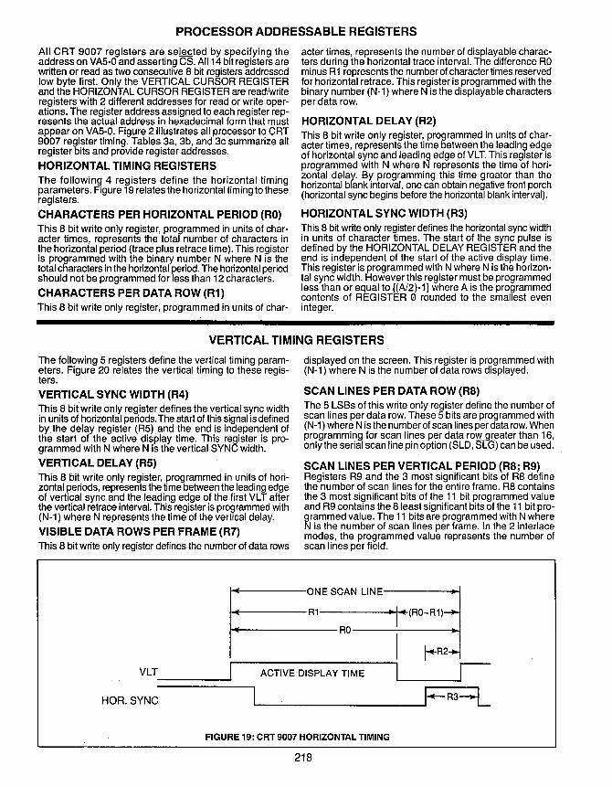
PROCESSOR ADDRESSABLE REGISTERS
All CRT 9007 registers are selected by specifying the address on VAS-O and asserting CS. All 14 bit registers are written or read as two consecutive 8 bit registers addressed low byte first. Only the VERTICAL CURSOR REGISTER and the HORIZONTAL CURSOR REGISTER are read/write registers with 2 different addresses for read or write operations. The register address assigned to each register represents the actual address in hexadecimal form that must appear on VAS-O. Figure 2 illustrates all processor to CRT 9007 register timing. Tables 3a, 3b, and 3c summarize all register bits and provide register addresses.
HORIZONTAL TIMING REGISTERS The following 4 registers define the horizontal timing parameters. Figure 19 relates the horizontal timing to these registers.
CHARACTERS PER HORIZONTAL PERIOD (RD) This 8 bit write only regist.er, programmed in units of character times, represents the total number of characters in the horizontal period (trace plus retrace time). This register is programmed with the binary number N where N is the total characters in the horizontal period. The horizontal period should not be programmed for less than 12 characters.
CHARACTERS PER DATA ROW (R1) This 8 bit write only register, programmed in units of char-
acter times, represents the number of displayable characters during the horizontal trace interval. The difference RO minus R1 represents the number of character times reserved for horizontal retrace. This register is programmed with the binary number (N-1) where N is the displayable characters per data row.
HORIZONTAL DELAY (R2) This 8 bit write only register, programmed in units of character times, represents the time between the leading edge of horizontal sync and leading edge of VLT. This register is programmed with N where N represents the time of horizontal delay. By programming this time greater than the horizontal blank interval, one can obtain negative front porch (horizontal sync begins before the horizontal blank interval).
HORIZONTAL SYNC WIDTH (R3) This 8 bit write only register defines the horizontal sync width in units of character times. The start of the sync pulse is defined by the HORIZONTAL DELAY REGISTER and the end is independent of the start of the active display time. This register is programmed with N where N is the horizontal sync width. However this register must be programmed less than or equal to [(A/2)-1] where A is the programmed contents of REGISTER 0 rounded to the smallest even integer. '
VERTICAL TIMING REGISTERS
The following S registers define the vertical timing parameters. Figure 20 relates the vertical timing to these registers.
VERTICAL SYNC WIDTH (R4) This 8 bit write only register defines the vertical sync width in units of horizontal periods. The start of this Signal is defined by. the delay register (RS), and the end is independent of the start of the active display time. This register is programmed with N where N is the vertical SYNC width.
VERTICAL DELAY (RS) This 8 bit write only register, programmed in units of horizontal periods, represents the time between the leading edge of vertical sync and the leading edge of the first VL T after the vertical retrace interval. This register is programmed with (N-1) where N represents the time of the vertical delay.
VISIBLE DATA ROWS PER FRAME (R7) This 8 bit write only register defines the number of data rows
II(
-
displayed on the screen. This register is programmed with (N-1) where N is the number of data rows displayed.
SCAN LINES PER DATA ROW (RS) The S LSBs of this write only register define the number of scan lines per data row. These S bits are programmed with (N-1) where N is the number of scan lines per data row. When programming for scan lines per data roS[~eater than 16, only the serial scan line pin option (SLD, ) can be used.
SCAN LINES PER VERTICAL PERIOD (RS; R9) Registers R9 and the 3 most significant bits of R8 define the number of scan lines for the entire frame. R8 contains the 3 most significant bits of the 11 bit programmed value and R9 contains the 8 least significant bits of the 11 bit programmed value. The 11 bits are programmed with N where N is the number of scan lines per frame. In the 2 interlace modes, the programmed value represents the number of scan lines per field.
ONE SCAN LINE ~
R1 ~ I ~ (RO-R1)~ RO
I
- .. r-R2-.
VLT I ACTIVE DISPLAY TIME I r-HOR.SYNC I I~R3~
FIGURE 19: CRT 9007 HORIZONTAL TIMING
218

ONE COMPLETE FRAME .. .. R7 x R8 ~I
R9
I ~R5'" VERT. BLANKING I DATA ROW DISPLAY TIME I I I (NO SKEW)
VERT. SYNC I FR4---+-L
FIGURE 20: CRT 9007 VERTICAL TIMING
PIN CONFIGURATION/SKEW BITS REGISTER (R6) This 8 bit write only register is used to select certain pin configurations and to skew (delay) the cursor and the blank signals independently with respect to the video signal sent to the monitor. The bits take on the following definition:
Bit 7, 6 (Pin Configuration)
These 2 bits, as illustrated in tables 4 and 5, define all pinout configurations as a function of double row buffer mode and non double row buffer mode. (The buffer mode is defined in the CONTROL REGISTER bits 3,2, and 1.) The attribute assemble mode is assumed to be a double row buffer mode and obeys table 4.
Bits 5, 4, 3 (Cursor skew)
These three bits define the number of character clocks the cursor signal is skewed (delayed) from the VLTsignal. The
REGISTER R6 BITS CRT 9007 PIN NUMBER
7 6 28 29 30 31 32 33
0 1 DMAR WBEN SLG SLD CSYNC ACK 1 1 DMAR WBEN SLG SLD LPSTB ACK
0 0 NOT PERMITTED 1 0 NOT PERMITTED
Table 4: Pin configuration for double row buffer and attribute assemble modes.
DMA CONTROL REGISTER (RA) This 8 bit write only register allows the user to set up a DMA burst count and delay as well as disable the DMA mechanism of the CRT 9007. The register bits have the following definition:
Bit 7 (DMA Disable)
A logic one will immediately force the CRT 9007 DMA request to the inactive level and the CRT 9007 address bus (VA 13-VAO) will enter its high impedance state. After enabling the DMA mechanism by setting this bit to a logic zero, a start command must be issued (see START COMMAND, R15).
Bits 6, 5, 4 (DMA Burst Delay)
These 3 bits define the number of clock delays (CCLK) between successive DMAR-ACK sequences. Bit 6 is the most and bit 4 is the least significant bit respectively. When programmed with a number N, the CRT 9007 will delay for 4 (N + 1) clock cycles before initiating another DMA request. If 111 is programmed, however, this will result in a zero delay allowing all characters to be retrieved from video RAM in one DMA burst regardless of the value programmed for the DMA burst count.
Bits 3, 2, 1, a (DMA Burst Count)
VL T signal is active for all characters within a data row and a non skewed cursor will always become active within the active VLT time at the designated position. The cursor can be skewed from a to 5 character clocks (Bits 5, 4 and 3 programmed from 000 to 101, bit 5 is the most significant bit; bit 3 is the least significant bit). For double heighVwidth data rows, the cursor signal appearing during horizontal retrace is also skewed as programmed.
Bits 2, 1, a (Blank skew)
These three bits define the number of character clocks the horizontal blank component of the CBLANK signal is skewed (delayed) from the VLT signal. The edges of VLTwili line up I exactly with the edges of the horizontal component of the CBLANK signal if no skew is programmed. The CBLANK -can be skewed from a to 5 character clocks (Bits 2, 1 and a programmed from 000 to 101, bit 2 is the most significant bit; bit a is the least significant bit).
REGISTER 6 BITS CRT 9007 PIN NUMBER
7 6 28 29 30 31 32 33
0 0 SL3 SL2 SL 1 SLO CSYNC TSC 1 0 SL3 SL2 SL 1 SLO LPSTB TSC 1 1 VBLANK CSYNC SLG SLD LPSTB TSC
0 1 NOT PERMITTED
Table 5: Pin configuration for Single Row Buffer and Repetitive Memory Addressing Modes.
These 4 bits define the number of DMA operations in one DMAR-ACK sequence. Bit 3 is the most and bit a is the least significant bit respectively. When programmed with a number N, the CRT 9007 will produce 4 (i\! + 1) DMA cycles before relinquishing the bus. When programmed with 0000, the minimum DMA Burst will occur (4 x 1 = 4) and when programmed with 1111 the maximum DMA Burst will occur (4x 16=64). When bits 6, 5, and 4 are programmed with 111, no DMA delay will occur and the Burst count will equal the number of programmed characters per data row as specified in R1. Refer to figures 9 and 15 which illustrate a DMA burst of 16 and a DMA delay of 8 for double row buffer and attribute assemble modes respectively. For single row buffer operation, no DMA delay is permitted and bits 6, 5, 4 must be programmed with 000.
CONTROL REGISTER (RB) This 7 bit write only register controls certain frame operations as well as specifying the operation mode used. Internal to the CRT 9007, this register is double buffered. Changes in the register are reflected into the CRT 9007 at a particular time during vertical retrace. This allows the user to update the CONTROL REGISTER at any time without running the risk of destroying the frame or field currently being painted.
219

The bits take on the following definition:
Bit 6 (PB/SS) = 0; The smooth scroll mechanism is enabled per
mitting the SMOOTH SCROLL OFFSET REGISTER (R17) to be loaded in the scan line counter (SL3-o or SLG, SLD signals) allowing for a scroll on the screen of a predetermined number of scan lines per frame or field. The starting and ending of the smooth scroll operation is defined by the DATA ROW START REGISTER (R11) and DATA ROW END REGISTER (R12) respectively.
= 1; The page blank mechanism is enabled. The CBLANK signal is made active high for a continuous period of time starting and ending at the data row defined by the DATA ROW START REGISTER (R11) and DATA ROW END REGISTER (R12) respectively.
Bits 5, 4 (Interlace)-these 2 bits define one of 3 displayed modes as illustrated in figure 21
= 00; Non interlaced display
= 10; Enhanced video interlace. This display mode will produce an interlaced frame with the same dot information painted in adjacent odd/even scan lines.
= 11; Normal video interlace. This display mode will produce an interlaced frame with odd scan lines of characters displayed in odd fields and even scan lines displayed in even fields. This mode can be used to allow the screen to show twice as many data rows at half the height since it effectively doubles the character density on the screen.
= 01; This combination is not permitted.
Bits 3,2,1 (Operation modes): These 3 bits define the various buffer configuration modes as follows:
= 000; (Repetitive memory addressing)-In this mode the address information (VA13-VAO) appears during every visible scan line and the address bus enters its high impedance state during all retrace intervals. When using a row driven addressing mode (linked list or contiguous), the address bus is in the high impedance state for all retrace intervals except the horizontal retrace interval prior to the top scan line of a new data row. This period can be disting!,Jished from other retrace intervals because the ORB (data row boundary) signal is active.
= 001; (Double row buffer)-In this mode, the CRT 9007 will address a particular data row from video memory one data row prior to the time when it is displayed on the CRT. During vertical retrace, the first data row is retrieved and loaded into the double row buffer. At the next data row boundary (in this case atthe end of vertical retrace), the first data row feeds the character generator while the second data
row is retrieved from video memory. The address bus will enter its high impedance state in accordance with the DMA mechanism for address bus arbitration.
= 100; (Single row buffer)-In this mode, during the first scan line of each data row, the CRT 9007 will address video memory, load the buffer and feed the character generator at the painting rate of the CRT. If the CRT 9007 is used in a row driven addressing mode, it will drNe the address bus during the retrace period prior to the first scan line of each data row in order to retrieve the row table address. It will automatically enter the high impedance state at the end of the first visible scan line of each data row. If the CRT 9007 is used in a sequential addressing mode, it will drive the address bus only during the visible line time of the first scan line of each data row.
= 111; (Attribute assemble)-In the attribute assemble mode, character data and attribute data are shared in consecutive alternating byte locations in memory. When the CRT 9007 reads an attribute byte, it loads it into its internal attribute latch. During the next memory access, a character byte is fetched. At this time the CRT 9007 isolates its bus from the main system bus and outputs the previously latched attribute. A WBEN signal is produced during every character byte fetch to allow the character and its associated attribute to be simultaneously latched into two double row buffers. This mode assumes that there exists twice as many byte locations as there are displayable character positions on the CRT. The first byte of every data row is assumed to be an attribute.
All other combinations of the CONTROL REGISTER bits 3, 2, 1 are not permitted.
Bit 0 (2XC/1 XC): This bit allows for either single or double height cursor display when the cursor is placed within a double height data row as follows:
= 1; (Single height cursor)-The CURS signal will appear during every scan line for single height data rows and will appear only during the top half or bottom half of a double height data row depending upon where the VERTICAL CURSOR REGISTER (R18, R38) defines the CURSOR data row.
= 0; (Double height cursor)-If the VERTICAL CURSOR REGISTER (R18, R38) places the cursor in the top half of a double height data row, the CURS signal will appear during every scan line of the top half (the current data row) and the bottom half (the next data row) of the double height data row. If the cursor is placed in the bottom half of a double height data row or if it is placed in a single height data row, the CURS signal will only appear during the one particular data row.
CHARACTER CHARACTER CHARACTER SCAN LINE SCAN LINE SCAN LINE 0----- 0 0-----
: roo 0 :~f!iF~ :~f!~~~~~ ~ 4 0 0 0 0 4 0-----5 0 5 -g- -- 4 2 ----------- 1
--{)--------- 5 ----------- 3
~ : ~ ~~~~===~ ~ : ======~~== ~ (a) NON-INTERLACE
Even Field
(b) ENHANCED
Odd Even Odd Field Field Field
(c) NORMAL VIDEO VIDEO INTERLACE INTERLACE
FIGURE 21: CRT 9007 INTERLACE MODES
220

TABLE START REGISTER (RC AND RD) This 16 bit write only register contains a 14 bit address which is used in a variety of ways depending on the addressing mode chosen; the 2 remaining bits define the addressing mode. Register C contains the lower 8 bits of the 14 bit address. The 6 least significant bits of register D contain the upper 6 bits of the 14 bit address. The 2 most significant bits of register D define four addressing modes as follows:
Register D bits 7,6:
= 00; (Sequential addressing mode)-The CRT 9007 will address video memory in a sequential fashion starting with the 14 bit address contained in REGISTER D bits 5-0 and REGISTER C bits 7-0. One break is allowed in the sequential addressing scheme as defined by SEQUENTIAL BREAK REGISTER 1 (R10) and AUXILIARY ADDRESS REGISTER 1 (RE and RF).
= 01; (Sequential roll addressing mode)-The CRT 9007 will address video memory in a sequential fashion starting with the 14 bit address contained in REGISTER D bits 5-0 and REGISTER C bits 7-0. SEQUENTIAL BREAK REGISTER 1 and AUXILIARY ADDRESS REGISTER 1 can be used to cause one sequential break as described in the sequential addressing mode. A second break in the sequential addressing can be defined by SEQUENTIAL BREAK REGISTER 2 (R12) and AUXILIARY ADDRESS REGISTER 2 (R13 and R14) permitting upto 3 separate sequentially addressed screens to be painted.
= 10; (Contiguous row table mode)-The CRT 9007 will address video memory according to the contiguous row table format. The 14 address bits contained in REGISTER D bits 5-0 and REGISTER C bits 7-0 define an address that points to the beginning of the contiguous row table.
= 11; (Linked list row table mode)-The CRT 9007 will address video memory according to the linked list row table format. The 14 address bits contained in REGISTER D bits 5-0 and REGISTER C bits 7-0 define the address at which the second row table entry and the first data row reside.
SEQUENTIAL BREAK REGISTER 1 (R10) This 8 bit write only register defines the data row number in which a new sequential video address begins as specified by AUXILIARY ADDRESS REGISTER 1 (RE and RF). To disable the use of this break, the register should be loaded with a data row count greater than the number of displayable data rows on the screen.
DATA ROW START REGISTER (R11) This 8 bit write only register defines the first data row number at which a page blank or smooth scroll operation will begin. Bit 6 of the CONTROL REGISTER determines if a page blank or smooth scroll operation will occur.
DATA ROW END/SEQUENTIAL BREAK REGISTER 2 (R12)
AUXILIARY ADDRESS REGISTER 1 (RE and RF) This 16 bit write only register contains a 14 bit address. The 6 least significant bits of REGISTER F contain the upper order 6 bits of the 14 bit address and REG ISTER E contains the 8 lower order bits of the 14 bit address. When the current data row equals the value programmed in SEQUENTIALBREAK REGISTER 1 (R10)the remainderofthescreen is addressed sequentially starting at the 14 bit address specified in this register. This sequential break overrides any row driven addressing mode used prior to the sequential break.
The 2 most significant bits of REGISTER F allow one to attach double height and/or double width characteristics to every data row in this sequentially addressed area in the following way:
For Double row buffer or attribute assemble mode REGISTER F Bits 7, 6
= 00; single height single width
= 01; single height double width
= 10; even data rows are double height double width top half odd data rows are double height double width bottom half
= 11; odd data rows are double height double width top half even data rows are double height double width bottom half
For Single row buffer or repetitive memory addressing mode REGISTER F Bits 7,6
= 00; single height single width
= 01; single height double width
= 10; odd data rows are double height double width top half even data rows are double height double width bottom half
= 11; even data rows are double height double width top half odd data rows are double height double width bottom half
defines the data row number which ends either a page blank or smooth scroll operation. The row numerically one less than the row defined by this register is the last data row on which the page blank or smooth scroll will occur. To use the page blank feature to blank a portion of the screen that includes the last displayed data row, this register must be programmed to zero. For sequential addressing, this register can cause a break in the sequential addressing at the data row number specified and a new sequential addressing sequence begins at the address contained in AUXILIARY ADDRESS REGISTER 2.
AUXILIARY ADDRESS REGISTER 2 (R13 and R14) This 16 bit write only register contains a 14 bit address. The 6 least significant bits of REGISTER 14 contain the upper order 6 bits of the 14 bit address and REGISTER 13 contains the 8 lower order bits of the 14 bit address. In the row
This 8 bit write only register has a dual function depending driven addressing mode, this register is automatically loaded on the addressing mode used. For row driven addressing by the CRT 9007 with the current table address. The two (contiguous or linked list as specified by the 2 most signifi- most significant bits of REGISTER 14 specify one of four cant bits of the TABLE START REGISTER) this register combinations of row attributes (for example double height
221
I

'double width) on a row by row basis. Refer to the section entitled Double Height/Double Width operation for the meaning of these 2 bits. In the sequential addressing mode, this register can be loaded by the processor with a 14 bit address and a 2 bit row attributes field. The bit positions are identical for the row driven addressing mode. When the current data row equals the value programmed in DATA ROW END/SEQUENTIAL BREAK REGISTER 2 (R12), the remainder of the screen is addressed sequentially starting at the location specified by the programmed 14 bit address. The 2 most significant bits of register 14 allow one to attach double height and or double width characteristics to every data row in this sequentially addressed area. The bit definitions take on the same meaning as the 2 most significant bits of AUXILIARY ADDRESS REGISTER 1 and affect the display in an identical manner.
START COMMAND (R1S) After all vital screen parameters are loaded, a START command can be initiated by addressing this dummy register location within the CRT 9007. A START command must be issued after the DMA mechanism is enabled (DMA CONTROL REGISTER bit 7).
RESET COMMAND (R16) The CRT 9007 can be reset via software by addressing this dummy location. Activation of the RST input pin or initiating this software command will effect the CRT 9007 in an identical manner. The reset state of the CRT 9007 is defined as follows:
CRT 9007 outputs
VA13-0 VD7-0 HS VS CBLANK CUS VLT DRB INT Pin 28 Pin 29 Pin30 Pin31 Pin 32
Reset state High impedance High impedance High High High Low Low High Low Low Low Low Low Low
SMOOTH SCROLL OFFSET REGISTER (R17) This register is loaded with the scan line offset number to allow a smooth scroll operation to occur. The offset register causes the scan line counter output of the CRT 9007 to start
of a double height data row stand alone in Single Row Buffer Mode by programming the scrolled data row as double height top half and loading R17 with the proper value.
VERTICAL CURSOR REGISTER (R18 or R38) This 8 bit read/write register specifies the data row in which the cursor appears. To write into this register it is addressed as R18 and to read from this register it is addressed as R38.
HORIZONTAL CURSOR REGISTER (R19 or R39) This 8 bit read/write register specifies the character position in which the cursor appears. To write into this register it is addressed as R19 and to read from this register it is addressed as R39. It should be noted that the vertical and horizontal cursor is programmed in an X-Y format with respect to the screen and not dependant upon a particular location in video memory. The cursor will remain stationary during all·scroll operations.
INTERRUPT ENABLE REGISTER (R1A) This 3 bit write only register allows each of the three CRT 9007 interrupt conditions to be individually enabled or disabled according to the following definition:
Bit 6 (Vertical retrace interrupt)-This bit, when set to a logic one, will cause the CRT 9007 to activate the INT signal when a vertical retrace (Le., the start of the vertical blanking interval) begins. Bit 5 (Light pen interrupt)-This bit, when set to a logic one, will cause the CRT 9007 to activate the I NT signal when the LIGHT PEN REGISTER (R3B, R3C) captures an X-Y coordinate. This interrupt, which occurs at the beginning of vertical retrace, reflects the occurrence of a LPSTB input on the frame or field just painted. This interrupt need not be enabled when other CRT 9007 interrupt conditions are enabled since the STATUS REGISTER (R3A) will flag the occurance of a light pen update and servicing can be done off of other interrupts.
Bit a (Frame timer)-This bit, when set to a logic one, allows the CRT 9007 to activate the INT Signal once every frame or field at a time when a potential smooth scroll update may occur. In this way the user can use the frame timer interrupt as both a real time clock and can service smooth scroll updates and other frame oriented operations by using the appropriate status bits. This interrupt will occur after the last row table entry is read by the CRT 9007. In single row buffer operation, this will occur one data row before the start of vertical retrace. In double row buffer operation, this will occur two data rows before the start of vertical retrace.
at the programmed value rather than zero for the data row SSG S ( ) that starts the smooth scroll interval. The start is specified TATU RE ITER R3A in the DATA ROW START REGISTER (R11). Typically, this This 5 bit register flags the various conditions that can register is updated every frame and it ranges from zero (no potentially cause an interrupt regardless of whether the offset) to a maximum of the programmed scan lines per data corresponding condition is enabled for interrupt. In this way row (maximum offset). For example, if 12 scan lines per data some or all of the conditions can be reported to the proces-row are programmed (scan line 0 to scan line 11) an offset sor via the STATUS REGISTER. If some of the conditions of zero will cause an unscrolled display. An offset of one will are enabled for interrupt, the processor, in response to an cause a display starting at scan line 1 and ending at scan interrupt, simply has to read the STATUS REGISTER to line 11 (eleven scan lines total). An offset of eleven will cause determine the cause of the interrupt. The bit definition of the a display starting at scan line eleven. STATUS REGISTER is as follows:
The next scan line will be zero, starting the subsequent data Bit 7 (Interrupt Pending)-This bit will set when any other row. To allow smooth scroll of double height rows, the pro- status bit, having its corresponding interrupt enabled, grammed range of the register is from zero to twice the pro- experiences a a to 1 transition. In this manner, when the grammed scan lines per data row. Whenever the offset processor services a potential CRT 9007 interrupt, it only register if greater than the programmed scan lines per data has to test the interrupt pending bit to determine if the CRT row, bit 7 of the register must be set to a logic 1 (offset over- 9007 caused the interrupt. If it did, the individual bits can flow). It must be set to a logic zero at all other times. The 6 then be tested to determine the details of the CRT 9007 bit offset value occupies bits 6 through 1. Bit a must always interrupt. Any noninterruptable status change (corre-be programmed with a logic zero. By setting the offset over- sponding interrupt enable bit reset to a logic 0) will not be flow (bit 7) to a logic 1, it is possible to have the bottom half reflected in the interrupt pending bit and must be polled by
222

the processor in order to provide service. The interrupt pending bit is reset when the status register is read. All other bits except Light Pen Update are reset to a logic a at the end of the vertical retrace interval. The light pen update bit is reset to a logic a when the HORIZONTAL LIGHT PEN REGISTER is read.
Bit 6 (Vertical Retrace)-A logic 1 indicates that a vertical retrace interval has begun.
Bit 5 (Light Pen Update)-A logic 1 indicates that a new coordinate has been strobed into the LIGHT PEN REGISTER. It is reset to a logic zero when the HORIZONTAL LIGHT PEN REGISTER is read. The light pen coordinates may have to be modified via software depending on light pen characteristics.
Bit 2 (odd/even)-For a normal video interlaced display, this bit is a logic 1 when the field about be painted is an odd field and is a logic zero when the field about be painted is an even field.
ONE CSYNC INTERLACED
Bit a (Frame timer occurred)-This bit becomes a logic 1 either one or two data rows before the start of vertical retrace. Since this bit is set when the CRT has finished reading the row table for the frame or field just painted, it permits row table manipulation to start at the earliest possible time.
VERTICAL LIGHT PEN REGISTER (R3B) This 8 bit read only register contains the vertical coordinate captured at the time the CRT 9007 received a light pen strobe signal (LPSTB).
HORIZONTAL LIGHT PEN REGISTER (R3C) This 8 bit read only register contains the horizontal coordinate captured at the time the CRT 9007 received a light pen strobe signal. When a coordinate is captured, the appropriate status bit is set and further transitions on LPSTB are ignored until this register is read. The reading of this register will reset the light pen status bit in the STATUS REGISTER. The captured coordinate may have to be modified in software to allow for light pen response.
FIELD ! HS
vS------------------------~--------------IL---------------------J+- 3 SCAN LINES BEFORE VS ........- PROG. VSYNC WIDTH ~ 3 SCAN LINES AFTER VS --t
FIELD ! HS TWO --
INTERLACED CSYNC
VS------------------------~
INT~R~~CED I CSY::
vS------------------------~--------------IL---------------------
FIGURE 3: TYPICAL SYNC WAVEFORMS FOR INTERLACED AND NON-INTERLACED MODES
CCLK
VLTl I 1 I I
SLG
I· 5 CLOCKS ·i 5 CLOCKS 1 1
I ... ~I
SLD I~I~I~I@I~I FIGURE 4: SERIAL SCAN LINE TIMING: NON INTERLACE
OR SINGLE WIDTH CHARACTERS
223
CCLK I 1 ,
VLT! 1 I I
1 I 1 I 1
I 6 CLOCKS "r-SLG I
I 5 CLOCKS I 1 I. .,'
!
,
SLD H~I~I~I@I~I FIGURE 5: SERIAL SCAN LINE TIMING: INTERLACE,
DOUBLE HEIGHT OR DOUBLE WIDTH CHARACTERS
I

MAXIMUM GUARANTEED RATINGS· Operating Temperature Range ....................................................................... 0° to + 70°C Storage Temperature Range. . . . . . . . . . . . . . . . . . . . . . . . . . . . . . . . . . . . . . . . . . . . . . . . . . . . . . . . . . . . . . . . . .. - 55°C to + 150°C Lead Temperature (soldering, 10 sec.) .................................................................... + 325°C Positive Voltage on any Pin, with respect to ground ........................................................... + 15V Negative Voltage on any Pin, with respect to ground. . . . . . . . . . . . . . . . . . . . . . . . . . . . . . . . . . . . . . . . . . . . . . . . . . . . . . . .. - 0.3V
*Stresses above those listed may cause permanent damage to the device. This is a stress rating only and functional operation of the device at these or at any other condition above those indicated in the operational sections of this specification is not implied.
NOTE: When powering this device from laboratory or system power supplies, it is important that the Absolute Maximum Ratings not be exceeded or device failure can result. Some power supplies exhibit voltage spikes or "glitches" on their outputs when the AC power is switched on and off. In addition, voltage transients on the AC power line may appear on the DC output. If this possibility exists it is suggested that a clamp circuit be used.
DC ELECTRICAL CHARACTERISTICS TA = O°C to + 70°C, Vee = 5.0V ± 5%
PARAMETER MIN TYP Input voltage
V,L Low V,H1 High 2.0 V,H2 High 4.3
VOL Output voltage
Low VOH High 204
Input leakage current III 1L2
Input capacitance C'N1 10 C'N2 25
Power supply current Icc 100
, AC ELECTRICAL CHARACTERISTICS3 TA = O°C to + 70°C, Vec = 5.0V ± 5%
PARAMETER MIN TYP Clock
tCY clock period 250 tCKL clock low 90 tCKH clock high 130 tCKR clock rise time
tCKF clock fall time
Output delai to! t02 tD3 t04 tVA
tOSL t05 t06 tOSY tvos 50
tVOH 0 tvoo tSLG tSLO
Processor Read/write2 tAS 110 tAH 0 tpw 165 tpos 100 tpOH 0 tpOA tpOH 10 t'RR
Miscellaneous timing tATS
tRW
NOTE: 1. Timing measured from the 1.5V level of the rising edge of CCLK to the 204 V
(high) or OAV (low) voltage level of the output unless otherwise noted. 2. Reference points are 2AV high and OAV low. 3. Loading on all outputs is 30 pF except where noted.
224
MAX UNITS COMMENTS
0.8 V V all inputs except CCLK V CCLKinput
004 V IOL = 1.6 rnA V IOH=40~A
O",;V,N",;VCC; excluding CCLK 10 ~A 50 ~A O",;V,N",;VCC; for CCLK
pF all inputs except CCLK pF CCLKinput
rnA
MAX UNITS COMMENTS
ns ns ns
10 ns measured from 10% to 90%
10 ns points measured from 90% to 10% points
125 ns 125 ns 150 ns 150 ns 100 ns measured to the 2.3V or 0.5V
level on VA13-VAO 500 ns 185 ns 185 ns 185 ns
ns valid for loading auxiliary address register 2 or the attribute latch
ns 185 ns cL=50pF 185 ns 185 ns
ns ns ns ns ns
140 ns 50 ns 400 ns
125 ns measured from the OAV level of ACK or TSC falling edge
4tcy ns measured from the OAV level falling edge to OAV level rising edge

tCKF :t' tCKL '(! ~
VLT, WBEN
DRB
VA13-0
SL3-0
R, I NT (LEADING EDGE ONLY) CSYNC,DMA CBLANK,CU RS
VD7-0
SLG
SLD
tCKH
t?, J
i tOJ
I I
tVA
I
t DS ~ \t-
t DSY .1
X tSLG ..
A tSLD
J tCY
.I { --- J
11 tDZ
1 .-
" J " to. I
I
~ tDSL I
X to.
1
tVDO
~ ,TIm"", I ~l
)( ATTRIBUTE OR )( ROW TABLE DATA IN ~ DATA OUT
r'~=t'.~-::r
FIGURE 22: CRT 9007 TIMING PARAMETERS: OUTPUT SIGNALS
FIGURE 2: CRT 9007 PROCESSOR READ AND WRITE TIMING PARAMETERS
225
ACK, TSC
HIGH IMPEDANCE VA13·0
RST
* tArs is controlled directly from ACK or TSC or from the particular CCLK that ends a DMA burst cycle.
FIGURE 23: CRT 9007 MISCELLANEOUS TIMING PARAMETERS
I

Register Type
WRITE
WRITE
WRITE
WRITE
WRITE
WRITE
WRITE
WRITE
WRITE
WRITE
Register Type
WRITE
WRITE
WRITE
WRITE
WRITE
WRITE
WRITE
WRITE
WRITE
WRITE
WRITE
Register Type
READ OR WRITE
READ OR WRITE
WRITE
WRITE
READ
WRITE
READ
WRITE
READ
READ
READ
VAS
0
0
0
0
0
0
0
0
0
0
VAS
0
0
0
0
0
0
0
0
0
0
0
VAS
0
0
0
0 1
0 1
0
1
1
1
ADDRESS DECODE BIT DEFINITION
VA4 VA3 VA2 VAt VA0 07 06 05 04 03 02 01 00
0 0 0 0 0 MSB I CHARACTERS PE~ HORiZONTAL PERIOD 1 LSB
0 0 0 0 1 MSB I CHARACTERS PER DATA ROW LSB
0 0 0 1 0 1
HORIZONTAL DELAY 1
MSB LSB
0 0 0 1 1 MSB HORIZONtAL SYNC WIDTH 1
1 LSB
0 0 1 0 0 MSB VERTICAL SYNC WIDTH
LSB
0 0 1 0 1 MSB 1 VERTICAL DELAY '.
LSB
0 0 1 1 0 PIN CONFIG-/ CURSOR SKEW 1 BLANK S~EW URATION MSB LSB MSB LSB
0 0 1 ·1 1 MSB VISIBLE DATA ROWS PER FRAME LSB
0 1 0 0 0 SCA~ LINES/FRAME 1 (B10)) (B8) MSB
SCAN LINES PER DATA ROW LSB
0 1 0 0 1 (B7) I SCAN LINES PER FRAME
LSB (BO)
Table 3a: CRT 9007 Screen Format Registers
ADDRESS DECODE BIT DEFINITION
VA4 VA3 VA2 VA1 VA0 07 06 05 04 03 02 01 00 1
DMA 1 I I
0 1 0 1 0 DIS- DMA BURST DELAY DMA BURST COUNT ABLE MSBA LSB MSB LSB
0 1
0 1 1 PBISSI
INTERLACE OPERATION MODES J
X MODES
2J(C/1XC
0 1 1 0 0 MSB TABLE START REGIST~R (LS BYTE)
LSB
0 1 1 0 1 ADDRESS .1 TABLE STAT1 REGISTER (MS BYTE)
MODE MSB LSB
0 1 1 1 0 MSB AUXILIARY ADDRESS REGISTER 1 (LS BYTE) LSB
0 1 1 1 1 ROW ;1 AUXILIARY ADDRESS REGISTER 1 (MS BYTE) ATTRIBUTES MSB LSB
1 0 0 0 0 MSB SEQUENTIAL BREAK REGISTER 1
LSB
1 0 0 0 1 MSB DATA ROW START REGISTER
LSB
1 0 0 1 0 MSB DATA ROW END/SEQUENTIAL BREAK REGISTER 2 LSB
1 0 0 1 1 MSB AUXILIARY ADDRESS REGISTER 2 (LS BYTE)
LSB
1 0 1 0 0 ATT~~'fJ'TES 1 AUXILIARY ADDRESS REGISTER 2 (MS BYTE) "j MSB I _I LSB
Table 3b: Control and Memory Address Registers
ADDRESS DECODE BIT DEFINITION
VA4 VA3 VA2 VA1 VA0 07 06 05 04 03 02 01 00
1 0 1 0 1 START COMMAND
1 0 1 1 0 RESET COMMAND
1 0 1 1 1 OFFSET
I I I , I LSB I OVER- OFFSET VALUE
FLOW MSB 0
1 1 0 0 0
1 1 0 0 0 MSB VERTICAL CURSOR REGISTER (ROW COORD.)
LSB
1 1 0 0 1
1 1 0 0 1 MSB HORIZONTAL CURSOR REGISTER (COL. COORD.)
LSB
1 1 0 1 0
VER- INTERRUPT ENABLE REGISTER I
TICAL I FRAME RE- LIGHT/ TIMER
X TRACE PEN X X X X 1
1 1 0 1 0 I VER- STATUS REGISTER INT TICAL
PEND- RE- LlGHT\ I 000/1
FRAME ING TAACE PEN EVEN X TIMER
1 1 0 1 1 MSB VERTICAL LIGHT PEN REGISTER (ROW COORD.) LSB
1 1 1 0 0 MSB I HORIZONTAL LIGHT PEN REGISTER (COL. COORD.) LSB
Table 3c: Cursor, Light Pen, Offset, and Status Registers
REGISTER NUMBER
(HEX)
RO
R1
R2
R3
R4
RS
R6
A7
AS
R9
REGISTER NUMBER
(HEX)
RA
RB
RC
RD
RE
RF
R10
R11
R12
R13
R14
REGISTER NUMBER
(HEX)
R1S
R16
R17
R1SorR19
R190rR39
R1A
R3A
R3B
R3C
Circuit diagrams utilizing SMC products are included as a means of illustrating typical semiconductor applications, consequently complete information sufficient for construction purposes is not necessarily given. The information has been carefully checked and is believed to be entirely reliable. However, no responsibility is
35 Md"US Blyd. Hauppauge NY 11766 assumed for inaccuracies. Furthermore, such information does not convey to the purchaser of the semiconductor 15161273·3100 TWX51O·22J.6898 devices described any license under the patent rights of SMC or others. SMC reserves the right to make changes
nf nil' N..,.",otitIM so you ca1 keep ahead Of yours, at any time in order to improve design and supply the best product possible.
226

STANDARD MICROSYSTEMS CORPORATION CRT 96364 A
CRT963648 ILPC FAMILY
CRT Controller FEATURES o Single + 5v power supply o 16 line x 64 character display o On chip sync oscillator o Complete cursor control o Automatic scrolling o Erase functions built in o Performs character entry during horizontal sync o Internal blinking cursor o Page linking logic built in o LS-TTL compatible o Compatible with CRT 8002, CRT 7004
GENERAL DESCRIPTION The CRT 96364A/B is a CRT Controller which controls all of the functions associated with a 16line x 64 character video display. Functions include CRT refresh, character entry, and cursor management.
The CRT 96364A/B contains an internal oscillator which produces the composite sync output. The CRT 96364 B generates a 60 Hz vertical sync while the CRT 96364A generates a 50 Hz vertical sync.
PIN CONFIGURATION
X0 1 28 Vee
X1 2 27 EOP
PS 3 26 CSYN
A9 4 25 C2
A8 5 24 C1
A7 6 23 CO
A6 7 22 A4
A5 8 21 A3
DCC 9 20 A2
DCE 10 19 A1
RO 11 18 A0
R1 12 17 W
R2 13 16 OS
GND 14 15 CRV
PACKAGE: 28-Pin D.I.P.
Standard functions such as ERASE PAGE, ERASE LINE, and ERASE TO END OF LINE make the CRT 96364A/B easy to interface to any computer or microprocessor, or to use as a stand-alone video processor.
The CRT 96364AI B requires only + 5v power at less than 100 rnA. It is manufactured in COPLAMOS® N channel silicon gate technology.
CRV C0 Cl C2
~~ GND Vee DCC
227
10
DCE
26
X0 Xl CSYN
I

DESCRIPTION OF PIN FUNCTIONS
PIN NO. NAME SYMBOL FUNCTION
1 Crystal in X0 Pin one is the sync clock input. It may be driven directly from a TIL 2 Crystal out X1 gate or from a parallel mode crystal connected between pins one
and two. When a crystal is used, a 10 Mn resistor should be connected in parallel. For standard 60 Hz line operation, a 1.018 MHz frequency source or crystal is required (with the CRT 96364 B). For 50 Hz line operation, the CRT 96364A requires a 1.008 MHz crystal.
3 Page Select PS PS proviqes automatic page selection when two pages of memory are used. A "zero" output indicates selection of page 1; a logic "one" indicates page 2.
4-8 Memory A9-A5 Upper order memory address lines; A6-A9 determine which lines of Address text are being refreshed or written. AS along with A0-A4 determine
the character position.
9 Character DCC Character clock input. Addresses are changed on the trailing edge Clock of DCC.
10 Dot Clock DCE A logiC zero from DCE is used to inhibit oscillation of the dot clock Enable for retrace blanking.
11-13 Row Address R0-R2 Character Generator row addresses. Blanks are generated by forcing R0-R2 to "000". During character entry, R2 gates data into memory to control the erase function. Row addressing follows the sequence 0-1-2-3-4-5-6-7-0-0-0-0-increment text line-0-1-2-etc.
14 Ground GND Ground
15 Cursor CRV Cursor video output. Indicates cursor location by a 2 Hz blinking underline.
16 Data Strobe DS The rising edge of DS strobes the appropriate C0-C2 control word into the CRT 96364A/B.
17 Write W A positive going signal which indicates that the CRT 96364A/B is allowing a memory write. W is approximately 4 jiS, and occurs during H sync. Memory address lines are latched at the cursor address during W.
18-22 Memory A0-A4 Lower order memory addresses. A~-A4 plus AS (pin 8) determine the Address character position.
23-25 Command C0-C2 Command inputs are strobed into the CRT 96364A/B by DS. Functions Inputs are as follows:
Function C2 C 1 Co Page erase and cursor home (top-left) 0 0 0 Erase to end of line and return cursor (to left) 0 0 1 Line feed (cursor down) 0 1 0 No operation* 0 1 1 Cursor left (one position) 1 0 0 Erasure of cursor-line 1 0 1 Cursor up (one position) 1 1 0 Normal character. Write signal is generated 1 1 1 and cursor position is incremented * In order to suppress non-displayed characters
26 Composite CSYN Positive logic comp"site sync output. Horizontal sync is generated Sync during VSYNC and SYNC time. A vertical sync output may be
generated by logically "ANDing" CSYN and DCE.
27 End of Page EOP This output is used to increment an external page counter when using more than one page of memory.
28 Power Supply Vee + 5 volt supply.
228

OPERATION
The CRT 96364A/B provides all of the control functions required by a CRT display with a minimum of external circuitry. The cursor and erase commands may be decoded from the data bus by a low cost 256 x 4 PROM. The CRT 96364A/B then provides the necessary cursor movement and gates the memory for writing or erasing. Erase is controlled by providing a write signal to RAM, and
gating "zeros" to the RAM input bus. Use of an external PROM allows user selection of control words. The RAM write command, "W", is generated during horizontal retrace. At this time, the RAM address is set to the cursor address. Immediately following the write command, the RAM addresses revert to refresh addressing and the cursor is shifted one character.
CURSOR
The cursor location is indicated by an alternating high on pin 15 (CRV) at row 7, and a low on pin 15 with R0-R2 forced low at rows 0-6. These alternate at a 2 Hz rate. If CRY is used to
force the display on, the result will be a blink of the cursor character position alternating with an underline at a 2 Hz rate.
CHARACTER ENTRY
When a Normal Character code (C2, C1, C0 = 1, 1, 1) and a Data Strobe are received, the write command will be generated during horizontal retrace. If, at the end of the horizontal retrace, the cursor is at the last position on a line, a car-
riage return and line feed will automatically occur. When the cursor is at the last position of the last line, a carriage return and up-scroll will automatically occur.
EXTRA FUNCTIONS
By using the fourth bit of the decoder PROM as a write enable signal, and properly programming the PROM, the additional commands of Home Cursor, Return Cursor, and Roll Screen may be generated. This is done by inhibiting me
W signal to the page memory and inputting the control codes, respectively, of Page Erase and Home Cursor, Erase to end of line and Return Cursor, and Line Feed.
SCROLLING
Scrolling of the screen text will occur under any of the following characteristics:
1. Inputting a line feed command when the cursor is at the bottom line of the screen.
2. Inputting a character when the cursor is at the bottom right hand side of the screen.
Scrolling will result in the entire top line of the
screen being erased and all of the remaining lines shifting up. Alternatively, a Roll (defined as all of the lines shifting up with the previous top line reappearing at the bottom of the screen) may be performed by inhibiting the write signal to the page memory as described in "Extra Functions."
229
I

MAXIMUM GUARANTEED RATINGS Operating Temperature Range .. . ......................................... One to + 700 e Storage Temperature Range ..... ............ . .............................. - 55°e to + 1500 e Lead Temperature (soldering, 10 sec.) .. , ............. . .................. +325°e Positive Voltage on any Pin, with respect to ground .................... . .............................. + 7.0V Negative Voltage on any Pin, with respect to ground .................................................... -0.3V
Stresses above those listed may cause permanent damage to the device. This is a stress rating only and functional operation of the device at these or at any other condition above those indicated in the operational sections of this specification is not implied.
ELECTRICAL CHARACTERISTICS iTA" oe to 70'e, Vee = -'- 5V::,:: 50 o. unless otherwise noted
Parameter Min. Typ. Max.
D.C. CHARACTERISTICS INPUT VOLTAGE LEVELS (except DeC)
Low-level, VIL 0.65 High-level, VIH 2.2
INPUT VOLTAGE LEVELS-DCC Low-level, VIL 0.65 High-level, VIH 3.5
OUTPUT VOLTAGE LEVELS (DCE Only) Low-level, VOl 0.4 High-level, VOH 2.2
OUTPUT VOLTAGE LEVELS (except DCE) Low-level, VOL 0.4 High-level, VOH 2.2
INPUT CURRENT Low-level, I,L 10
INPUT CAPACITANCE All inputs, C,N (except DCE) 5 CIN (DCC Only) 25
POWER SUPPLY CURRENT Icc 100 120
AC CHARACTERISTICS
PARAMETERS SYMBOL
Frequency of control clock DCC focc Crystal Frequency CRT 96364 A fx
CRT 96364B fx DCC pulse width tocc
Rise and fall times tr t f
Refresh memory address access time tCA Character memory address access time tcRO PS access time (read) tcps CRV access time tCRV DCE access time (high to low) tOCE
SYNC period tps
SYNC pulse width twp DeE access time (low to high level) tsc EOP access time (high to low level) tsp W access time (low to high) tsw W pulse width tpw EOP pulse width . t EOP
Address to rising edge of DeE delay tAO Falling edge of DeE to Address delay tOA Row to rising edge of DCE delay t RO Falling edge of DCE to row delay tOR
. PS to rising edge of DCE delay tpSD
230
Unit
V V
V V
V V
V V
/LA
pF pF
mA
MIN.
200
0 0 0
0
0
excluding DCC excluding DCC
1m =1.9 mA IOH=-100 J1.A
IOL=0.36 mA IOH=-100 J1.A
V,N=GND VIN=GND
VALUES TYP. MAX. 1.6
1.008 1.018
20 40
200 250 .
200 250
300 1000
200 250
100
64
4
11
1 1.5
500 1000
4 10
2.1
1
2.1 1
UNIT
MHz MHz MHz
ns
ns
ns
ns
ns
ns
ns ps
J1.S ps
IlS
ns j.JS
IlS
j.JS
ps j.JS
J1.S ps

LINE TIMING
~;-----J ~ ~ h ~ ~ ARENTHESES) I.
~Ioc,
DCC (DISPLAY POSITION IN P
1/
DCE " -+- +1" ..j 1.-1" - /-1"
~_~J' ----x (2) X (~ X (4) )( /I X X (63) (0) X (1) I A0-AS (CHARACTER ADDRESS)
A6-A9 (Y) (Y+1) )( (LINE ADDRESS)
Ie" .... t+- tCRV
CRV 1 \ lcoo .... ~+- f+-Ie.o -+- I-Icoo
R0,R1 ';,
-1 -I" ...... [-I" " II
R2 X f~ I Io;-+- r-
I , , ,
l. I , I I
-l I I '+-1,,,
PERIOD DISPLAY PERIOD
PS
-BLANK I SVNCTIMING
~ tw, II t" -I CSYN
-1 r-t,w W
- -, r----' L--___ -----'r----L-j--tsc
DCE
EOP
tIP
FRAME TIMING
CSYN
DeE
231

PARAMETER DS Pulse Width C0-C2 Set Up Time C0-C2 Hold Time Minimum Strobe Period (Operation Execution Time)
FUNCTION
Page Erase & Cursor Home Erase to End of Line & Return Cursor Line Feed (Cursor Down) No Operation Cursor Left Erasure of Cursor Line Cursor Up Normal Character
DATA INPUT TIMING Asynchronous Operation
SYMBOL tpw teos tose tos
MIN 0.5 1
90
C2 Q!. 0 0 0 0 0 1 0 1 1 0 1 0 1 1 1 1
*Will increase to 8.3 ms when text scroll occurs. See "Scrolling" for conditions.
Synchronous Operation
PARAMETER SYMBOL MIN DS Pulse Width tpw 0.5 CO-C2 Set-Up Time tCDS 1 CO-C2 Hold Time tose 16 DS Set Up Time tsos 1 Minimum Strobe Period tos (Operation Execution Time)
FUNCTION C2 C1 Page Erase & Cursor Home 0 0 Erase to End of Line & Return Cursor 0 0 Line Feed (Cursor Down) 0 1 No Operation 0 1 Cursor Left 1 0 Erasure of Cursor Line 1 0 Cursor Up 1 1 Normal Character 1 1 *Wlllincrease to 8.3 ms when text scroll occurs. See "Scrolling" for conditions.
DATA INPUT TIMING ASYNCHRONOUS OPERATION
Value TYP MAX UNIT
/is /is
/is
C0
0 132 ms 1 4.2 ms 0 130* /is
1 80 /is
0 80 /is
1 8.3 ms 0 80 /is
1 130* /is
Value TYP MAX UNIT
/is
/is
/is
/is
C0
0 132 ms 1 4.2 ms 0 64* /is
1 64 /is
0 64 /is
1 8.3 ms 0 64 /is
1 64* /is
C0-:: ---""""\Ir-+-----w-----~--,-----------,x-----~-SYNCHRONOUS OPERATION
CSYN
C0-C2 ________ ~4---~----~~-----------A------------~------------~--
232

MULTIPLE PAGE DISPLAY When linking two or more pages, the EOP and PS signals may be used to allow a "moving window" text display.
4 PAGE DISPLAY
PS (Page Select) indicates the end of page location. If a scroll has occurred, PS will show the transition from the end of line 15 of page P and the beginning of line 0 of page P + 1.
line 14 line 15
line 0 line 1 line 2
Display Area 0 .-----'--- PS
Page P
Page P + 1
To properly maintain the memory address when displaying more than two pages, EOP pulses low at the point in time when page P is scrolled completely off the screen. At this time, PS will remain low for the entire frame since page P + 1 is now the only displayed page.
All------,
AID
C.0 A2
A4 AI
84 74LSS3 +s
A3 Vee
83
82 GND
CRT 96364 AI 8
A9
AS
A7----...
A6-----.....
AS------.....
A4-------~
27
EOP
A3--------~
A2---------~
Al------------'
08
OA
Vee
GND
The circuit at the right will allow scrolling through 4 pages of memory. A0-----------~
TYPICAL SYSTEM APPLICATION
~--------------.....
233
C 74LS193 D
Clear
Load
DECREMENT PAGE (NEGATIVE PULSE)
+s
I
35 M.Ycus Blvd. Ha.\loaJge.NY 11788 {S16)273-3100 TWX·51Q-227-8898
iikiiP:iieii'Of'CUciii;etiiiiii so 'jDU C3'I k2ep :tle<KI of ycIn.
CD
g~~g~~~~ <0 3
~~~~~5~~ <J)
~ -' ~ ~
W ..J C. :!l «m ><~ WCD Z~ 0(7) -I~a: 00 :J c. c. «
Circuit diagrams utilizing SMC products are included as a means of illustrating typical semiconductor applications; consequently complete information sufficient for construction purposes is not necessarily given. The information has been carefully checked and is believed to be entirely reliable. However, no responsibility is assumed for inaccuracies. Furthermore, such information does not convey to the purchaserofthe semiconductor devices described any license under the patent rights of SMC or others. SMC reserves the right to make changes at any time in order to improve design and supply the best product possible.
234

STANDARD MICROSYSTEMS CORPORATION CRT 8002
JLPC FAMILY
CRT Video Display Attributes Controller Video Generator
VDACTM FEATURES PIN CONFIGURATION
D On chip character generator (mask programmable) 128 Characters (alphanumeric and graphic)
VIDEO 1
LD/SH 2
28 RETBL
27 CURSOR 7 x 11 Dot matrix block
D On chip video shift register Maximum shift register frequency
CRT 8002A 20M Hz CRT 8002B 15MHz CRT 8002C 10MHz Access time 400ns
VDC 3
A0 4 A1 5 A2 6
26 MS~
25 MS1
24 BLINK
23 V SYNC
D On chip horizontal and vertical retrace video blanking
A3 7
A4 8
A5 9
A6 10
A7 11
Vee 12
R2 13
R3 14
22 CHABL
21 REVID
20 UNDLN
19 STKRU
18 ATTBE
17 GND
D No descender circuitry required D Four modes of operation (intermixable)
Internal character generator (ROM) Wide graphics Thin graphics External inputs (fonts/dot graphics)
D On chip attribute logic-character, field Reverse video Character blank Character blink Underline Strike-thru
D Four on chip cursor modes Underline Blinking underline Reverse video Blinking reverse video
D Programmable character blink rate D Programmable cursor blink rate
D Subscriptable D Expandable character set
External fonts Alphanumeric and graphic RAM, ROM, and PROM
D On chip address buffer D On chip attribute buffer D + 5 volt operation D TTL compatible
16 R~
15 R1
D MaS N-channel silicon-gate COPLAMOS® process D CLASp® technology-ROM and options D Compatible with CRT 5027 VTAC®
General Description The SMC CRT 8002 Video Display Attributes Controller (VDAC) is an N-channel COPLAMOS® MaS/LSI device which utilizes CLASP® technology. It contains a 7X11 X128 character generator ROM, a wide graphics mode, a thin graphics mode, an external input mode, character address/data latch, field and/or character attribute logic, attribute latch, four cursor modes, two programmable blink rates, and a high speed video shift register. The CRT 8002 VDAC is a companion chip to SMC's CRT 5027 VTAC®. Together these two chips comprise the circuitry required for the display portion of a CRT video terminal. The CRT 8002 video output may be connected directly to a CRT monitor video input. The CRT 5027 blanking output can be connected directly to the CRT 8002 retrace blank input to provide both horizontal and vertical retrace blanking of the video output. Four cursor modes are available on the CRT 8002. They are: underline, blinking underline, reverse video block, and blinking reverse video block. Anyone of these can be mask programmed as the cursor function. There is a separate cursor blink rate which can be mask programmed to provide a 15 Hz to 2 Hz blink rate.
235
The CRT 8002 attributes include: reverse video, character blank, blink, underline, and strike-thru. The character blink rate is mask programmable from 7.5 Hz to 1.0 Hz and has a duty cycle of 75/25. The underline and strike-thru are similar but independently controlled functions and can be mask programmed to any number of raster lines at any position in the character block. These attributes are available in all modes. In the wide graphic mode the CRT 8002 produces a graphic entity the size of the character block. The graphic entity contains 8 parts, each of which is associated with one bit of a graphic byte, thereby providing for 256 unique graphic symbols. Thus, the CRT 8002 can produce either an alphanumeric symbol or a graphic entity depending on the mode selected. The mode can be changed on a per character basis. The thin graphic mode enables the user to create sin-' gle line drawings and forms. The external mode enables the user to extend the onchip ROM character set and/or the on-Chip graphics capabilities by inserting external symbols. These external symbols can come from either RAM, ROM or PROM.
I

MAXIMUM GUARANTEED RATINGS* Operating Temperature Range ............................................................... O°C to + 70°C Storage Temperature Range .............................................................. - 55°C to + 150°C Lead Temperature (soldering, 10 sec.) ............................................................... +325°C Positive Voltage on any Pin, with respect to ground .................................................... + S.OV Negative Voltage on any Pin, with respect to ground .................................................... -O.3V *Stresses above those listed may cause permanent damage to the device. This is a stress rating only and functional operation of the device at these or at any other condition above those indicated in the operational sections of this specification is not implied.
NOTE: When powering this device from laboratory or system power supplies, it is important that the Absolute Maximum Ratings not be exceeded or device failure can result. Some power supplies exhibit voltage spikes or "glitches" on their outputs when the AC power is switched on and off. In addition, voltage transients on the AC power line may appear on the DC output. If this possibility exists it is suggested that a clamp circuit be used.
ELECTRICAL CHARACTERISTICS (TA=O°C to 70°C, Vcc= +5V±5%, unless otherwise noted)
Parameter Min. Typ. Max" Unit Comments
D.C. CHARACTERISTICS INPUT VOLTAGE LEVELS
Low-level, VIL O.S V excluding VDC High-level, VIH 2.0 V excluding VDC
INPUT VOLTAGE LEVELS-CLOCK Low-level, VIL O.S V High-level, VIH 4.3 V See Figure 6
OUTPUT VOLTAGE LEVELS Low-level, VOL 0.4 V IOL =0.4 rnA, 74LSXX load High-level, VOH 2.4 V IOH= -20p,A
INPUT CURRENT Leakage, IL (Except CLOCK) 10 /.lA o '::;VIN '5:.V cc Leakage, IL (CLOCK Only) 50 pA O'5:.VIN '5:.VCC
INPUT CAPACITANCE Data 10 pF @1MHz LD/SH 20 pF @1MHz CLOCK 25 pF @1MHz
POWER SUPPL Y CURRENT Icc 100 rnA
A.C. CHARACTERISTICS
See Figure 6, 7
SYMBOL PARAMETER CRT 8002A CRT 8002B CRT 8002C
MIN. MAX. MIN. MAX. MIN. MAX.
VDC Video Dot Clock Frequency 1.0 20 1.0 15 1.0 10
PWH VDC-High Time 15.0 23 40
PWL VDC-Low Time 15.0 23 40
tCY LD/SH cycle time 400 533 SOO
tr • t f Rise, fall time 10 10 10
tSET-UP Input set-up time ~O ~O ~O
tHOLD Input hold time 15 "i5 15
tpDI. tpDO Output propagation delay 15 50 15 65 15 100
tl LD/SH set-up time 10 15 20
t2 LD/SH hold time 5 5 5
236
UNITS
MHz
ns
ns
ns
ns
ns
ns
ns
ns
ns

BLOCK DIAGRAM
ADDRESS/ DATA INPUTS
CURSOR-------------.~
RETRACE BLANK
ATTRIBUTE ENABLE
MODE SELECT t' MODE SELECT 1
REVERSE VIDEO
UNDERLINE
BLlNK--------.-1
STRIKE THRU
VIDEO DOT CLOCK LOAD/SHIFT
~r----.., CURSOR RATE V"NC -~ - CHARACTER RATE
VDC
LD/Sf:
ROW ADDRESS R0-R3
ATTRIBUTE LOGIC
VIDEO
4.3V
O.8V
2.0V
----.1 \-_________ --!'~ ~~------ O.8V --, I I
! I I
ALL INPUTS /////////////////~ 1: ,,~2.0V (excepIVDC,LD/sR) =-/ ~"i-i~-----------------+L--IH-Ol-D--r I~...LLLL O.8V
I",.u, f: -, I I
VIDEO OUTPUT _________ x .... _______ II-I __ ... >< .... _________ >< ........ -_-_ -_ -_ -_ -_ -_ -_-_ -_ -_ -_ -_ :~::
I
FIGURE 7 I_ lPO' .\
AC TIMING DIAGRAM
237
I
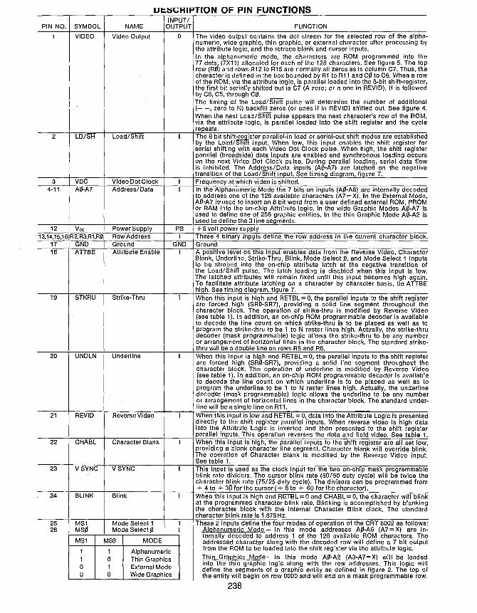
PIN NO. SYMBOL
1 VIDEO
2 LD/SH
3 VDC 4-11 AfJ-A7
12 Vee 13,14,15,Hi R2,R3,R1,R0
17 GND 18 ATTBE
19 STKRU
20
21
22
23
24
25 26
UNDLN
REVID
CHABL
V SYNC
BLINK
MS1 MS~
MS1
1 1 o o
Ut::~(;HIPTION OF PIN FUNCTIONS
NAME INPUT/
OUTPUT
Video Output
Load/Sllffi
Video Dot Clock Address/Data
Power Supply Row Address Ground Attribute Enable
Strike-Thru
Underline
Reverse Video
Character Blank
V SYNC
Blink
Mode Select 1 Mode Select $1
MS0 MODE
1 Alphanumeric o Thin Graphics 1 External Mode o Wide Graphics
o
PS
GND
FUNCTION
The video output contains the dot stream for the selected row of the alphanumeric, wide graphic, thin graphic, or external character after processing by the attribute logic, and the retrace blank and cursor inputs. In the alphanumeric mode, the characters are ROM programmed into the 77 dot~ (7X11) allocated for each of the 128 characters. See figure 5. The top row (Rp) and rows R12 to R15 are normally all zeros as is column C7. Thus, the character is defined in the box bounded by R1 to R11 and C~ to C6. When a row of the ROM, via the attribute logic, is parallel loaded into the 8-bit shift-register, the first bit serially shifted out is C7 (A zero; or a one in REVID). It is followed by C6, C5, through C~. The timing of the Load/Shift pulse will determine the number of additional (- -, zero to N) backfill zeros (or ones if in REVID) shifted out. See figure 4. When the next Load/Shift pulse appears the next character's row of the ROM, via the attribute logic, is parallel loaded into the shift register and the cycle repeats. The 8 bit shift:[email protected] parallel-in load or serial-out shift modes are established by the Load/Sl1iff input. When low, this input enables the shift register for serial shifting with each Video Dot Clock pulse. When high, the shift register parallel (broadside) data inputs are enabled and synchronous loading occurs on the next Video Dot Clock pulse. During parallel loading, serial data flow is inhibited. The Address/Data inputs (A0-A7) are latched on the negative transition of the Load/Shift input. See timing diagram, figure 7. Frequency at which video is shifted. In the Alphanumeric Mode the 7 bits on inputs (A~-A6) are internally decoded to address one of the 128 available characters (A7=X). In the External Mode, A~-A7 is-used to insert an 8 bit word from a user defined external ROM, PROM or RAM into the on-chip Attribute logic. In the wide Graphic Modes A¢-A7 is used to define one of 256 graphic entities. In the thin Graphic Mode ArJ-A2 is used to define the 31ine segments. + 5 volt power supply These 4 binary inPlJts define the row address in the current character block. Ground A positive level on this input enables data from the Reverse Video, Character Blank, Underline, Strike-Thru, Blink, Mode Select ~, and Mode Select 1 inputs to be stro~ into the on-chip attribute latch at the negative transition of the Load/Shift pulse. The latch loading is disabled when this input is low. The latched attributes will remain fixed until this input becomes high again. To facilitate attribute latching on a character by character basis, tie ATTBE high. See timing diagram, figure 7. When this input is high and RETBL = 0, the parallel inputs to the shift register are forced. high (SR~-SR7), providing a solid line segment throughout the character block. The operation of strike-thru is modified by Reverse Video (see table 1). In addition, an on-chip ROM programmable decoder is available to decode the line count on which strike-thru is to be placed as well as to program the strike-thru to be 1 to N raster lines high. Actually, the strike-thru decoder (mask programmable) logic allows the strike-thru to be any number or arrangement of horizontal lines in the character block. The stand~rd strikethru will be a double line on rows R5 and R6. When this input is high and RETBL = 0, the parallel inputs to the shift register are forced high (SR0-SR7), providing a solid line segment throughout the character block. The operation of underline is modified by Reverse Video (see table 1). In addition, an on-chip ROM programmable decoder is available to decode the line count on which underline is to be placed as well as to program the underline to be 1 to N raster lines high. Actually, the underline decoder (mask programmable) logic allows the underline to be any number or arrangement of horizontal lines in the character block. The standard underline will be a single line on R11. When this input is low and RETBL = 0, data into the Attribute Logic is presented directly to the shift register parallel inputs. When reverse video is high data into the Attribute Logic is inverted and then presented to the shift register parallel inputs. This operation reverses the data and field video. See table 1. When this input is high, the parallel inputs. to the shift register are all set low, providing a blank character line segment. Character blank will override blink. The operation of Character Blank is modified by the Reverse Video input. See table 1. This input is used as the clock input for the two on-chfp mask programmable blink rate dividers. The cursor blink rate (50/50 duty cycle) will be twice the character blink rate (75/25 duty cycle). The divisors can be programmed from -;- 4 to -;- 39 for the cursor (-;- 8 to -;- 60 for the character). When this input is high and RETBL = 0 and CHABL = 0, the character will blink at the programmed character blink rate. Blinking is accomplished by blanking the character block with the internal Character Blink clock. The standard character blink rate is 1.875 Hz. These 2 inputs define the four modes of operation of the CRT 8002 as follows:
Alphanumeric Mode - In this mode addresses A¢-A6 (A7=X) are internally decoded to address 1 of the 128 available ROM characters. The addressed character along with the decoded row will define a 7 bit output from the ROM to be loaded into the shift register via the attribute logic. Thin GraRhics Mode - In ~his l11ocleA0-A2 (A3-A7=X) will be loaded into ffie thin graphic logiC along with the row addresses. This logic will define the segments of a graphic entity as defined in figure 2. The top of the entity will begin on row 0000 and will end on a mask programmable row.
238

INPUT! PIN NO. SYMBOL NAME OUTPUT FUNCTION
25 External Mode - In this mode the inputs ArJ-A7 go directly from-the 26 character latch into the shift register via the attribute logic. Thus the user
(cont.) may define external character fonts or graphic entities in an external PROM. ROM or RAM. See figure 3. Wide GraRhics Mode-In this mode the inputs A'/J-A7 will define a graphic entity as described In figure 1. Each line of the graphic entity is determined by the wide graphic logic in conjunction with the row inputs R~ to R3. In this mode each segment of the entity is defined by one of the bits of the 8 bit word. Therefore, the 8 bits can define any 1 of the 256 possible graphic entities. These entities can butt up against each other to form a contiguous pattern or can be interspaced with alphanumeric characters. Each of the entities occupies the space of 1 character block and thus requires 1 byte of memory.
These 4 modes can be intermixed on a per character basis. 27 CURSOR Cursor I When this input is enabled 1 of the 4 pre-programmed cursor modes will be
activated. The cursor mode is on-chip mask programmable. The standard cur-sor will be a blinking (at 3.75 Hz) reverse video block. The 4 cursor modes are:
Underline-In this mode an underline (1 to N raster lines) at the programmed underline position oc'curs. Blinking Underline-In this mode the underline blinks at the cursor rate. Reverse Video Block-In this mode the Character Block is set to reverse video. Blinking Reverse Video Block-In this mode the Character Block is set to reverse video at the cursor blink rate. The Character Block will alternate between normal video and reverse video. The cursor functions are listed in table 1.
28 RETBL Retrace Blank I When this input is latched high, the shift register parallel inputs are uncon-dition~cleared to all zeros and loaded into the shift register on the next Load/ I t pulse. This blanks the video, independent of all attributes, during horizontal and vertical retrace time.
TABLE 1
I CURSOR RETBL REVID CHABL UNDLN* FUNCTION X 1 X X X "a" S.R. All 0 0 0 0 0 D (q.R.)All 0 0 0 0 1 "1" '(S.R.)*
D (S.R.) All others 0 0 0 1 X "0" (S.R.)All 0 0 1 0 0 5 (S.R.)All 0 0 1 0 1 "0" (S.R.)*
5 (S.R.) All others 0 0 1 1 X "1" (S.R.)All
Underline* 0 0 0 X "1" (S.R.)* D (S.R.) All others
Underline* 0 0 1 X "1" (S.R.)* "0" (S.R.) All others
Underline* 0 1 0 X "0" (S.R.)* D (S.R.J All others
Underline* 0 1 1 X "0" (S.R.)* "1" (S.R.) All others
Blinking** Underline* 0 0 0 X "1" (S.R.)* Blinking D (S.R.) All others
Blinking** Underline* 0 0 1 X "1" (S.R.)* Blinking "0" (S.R.) All others
Blinking** Underline* 0 1 0 X "0" (S.R.) * Blinking is (S.R.) All others
Blinking* * Underline* 0 1 1 X "0" (S.R.)* Blinking "1" (S.R.) All others
REVIDBlock 0 0 0 0 D (S.R.)All REVID Block 0 0 0 1 "0" (S.R.)*
5 (S.R.) All others REVIDBlock 0 0 1 X "1" (S.R.)All REVID Block 0 0 0 1 "0" (S.R.)*
is (S.R.) All others REVIDBlock 0 1 0 0 D (S.R.)All REVIDBlock 0 1 0 1 "1" (S.R.)*
D (S.R.) All others REVID Block 0 1 1 X "0" (S,R.)All Blink* * REVID Block 0 0 0 0 Blink* * REVID Block 0 0 0 1 Blink* * REVID Block 0 0 1 X 1 Alternate Normal Vldeo/REVID Blink* * REVID Block 0 1 0 0 At Cursor Blink Rate Blink* * REVID Block 0 1 0 1 Blink* * REVID Block 0 1 1 X
* At Selected Row Decode * * At Cursor Blink Rate Note: If Character is B1Tnking at Character Rate, Cursor will change it to Cursor Blink Rate.
239

· .......... - "
ROM CHARACTER BLOCK FORMAT ROWS R3 R2 R1 R.0'
(ALL ZEROS) ~ 0 0 0 0 0 0 0 0 R0 0 0 0 0 --------------
0 0 0 0 0 0 0 0 R1 0 0 0
0 0 0 0 0 0 0 0 R2 0 0 0
0 0 0 0 0 0 0 0 R3 0 0
0 0 0 0 0 0 0 0 R4 0 0 0
0 0 0 0 0 0 0 0 R5 0 0 1
77 BITS 0 0 0 0 0 0 0 0 R6 0 0 (7x 11 ROM)
0 0 0 R7 0 1 1 0 0 0 0 0
0 0 0 0 0 0 0 0 R8 0 0 0
0 0 0 0 0 0 0 0 R9 0 0
0 0 0 0 0 0 0 0 R10 0 0
0 0 0 0 0 0 0 0 R11 0 --------------
{! 0 0 0 0 0 0 0 R12 1 0 0
0 0 0 0 0 0 0 R13 1 0 1 (ALL ZEROS)
0 0 0 0 0 0 0 R14 1 0
0 0 0 0 0 0 0 R15
*C7 C6 C5 C4 C3 C2 C1 C0 -~ EXTENDED ZEROS (BACK FILL)
*COLUMN 7 IS ALL ZEROS (REVID = 0) FOR INTERCHARACTER SPAC-ING (NUMBER CONTROLLED
COLUMN 7 IS SHIFTED OUT FIRST BY LD/SH, VDC TIMING)
CONSULT FACTORY FOR CUSTOM FONT AND OPTION PROGRAMMING FORMS. 240

FIGURE 1 WIDE GRAPHICS MODE
3 LINES'
3 LINES
3 LINES
3 LINES
ROW ADDRESS I 5 BITS"I
0000
MSO=~ MS1=O
'ON CHIP ROM PROGRAMMABLE TO 2, 3, OR 4 LINE MULTIPLES "CAN BE PROGRAMMED FROM 1 TO 7 BITS
"'LENGTH DETERMINED BY LD/SH, VDC TIMING
EXAMPLE: 10010110
~~ o/'~0. ~
~
FIGURE 2
rur R1 R2
R3 R4
R5
R6
R7
RS
C7 C6 C5 C4 C3 C2 Cl
R11 ~~~~~~~~~~~~ R12 R13~~~~~~K-~~~~~
R14
R15
NOTE: Unselected raster line rows are always filled with ones.
~--------------------~ BF=back fill
THIN GRAPHICS MODE N BITS
I -
f-
I-
MS9=9 MS1=1
ROW 0000
PROGRAMMABLE ROW
lxJxJx I X X I A2 I Al I Aoj
X = DON'T CARE THE INSIDE SEGMENT IS MASK PROGRAMMABLE TO ROW 0000
" LENGTH DETERMINED BY LD/SF!, VDC TIMING
FIGURE 3 EXTERNAL MODE
MSf,J=1 MS1 ="
RP Rl
R2
R3
R4
RS
R6
R7
RS
Rll
C7 C6 CS C4 C3 C2 C1 Cll BF BF ...
R12 L...£...L.I.~'--'+-~;...L...:"";"":~,-'-i R13 I :
R14 I I
R15 L __ J L __ J ___ ..!
NOTE: When A1 ="1", the underline row/rows are deleted. When A 1 = "0", the underline, if selected, will appear.
BF=back fill
C7 C6 CS C4 C3 C2 C1 C0 SF SF
R0' - R1S I A71 A6 I ASI A41 A31 A2 A 1 I A01 A 71 A 7 1 .. ·1 SF=back fill
241
I

FIGURE 4 TYPICAL VIDEO OUTPUT
VDC
r-l 1800rl"9o'Ofl ISO'OT' '"9o'Ofl LD/SH~ 1~ ________________________ ~!l~h~l~~~L! ______________________ ~Il~h~~l~~~~
VIDEO DATA 8 DOT FIELD
VIDEO DATA 9 DOT FIELD
NOTE: Cry X = character number y=column number
XTAL
S.~ '41ro ~~ DDT
CARRY COUNTER l h-N) CHARACTER CLOCK
~ CP
7404 C 7404 BI-DIRECTIONAL DATA BUS 8
VIDEO DOT-- ADDRESS BUS 4 CLOCK
I PAGE CHIP SELECT LOGIC
DATA STROBE
8 CHARACTER COLUMN
L6 CHARACTER ROW , CHARACTER DATA BUS ADDRESS
BUS
MICRO- ADDRESS BUS PROCESSOR SELECTOR
CONTROL BUS WITH ASCII 7
~ OPTIONAL MEMORY DATA MAPPING BUS CIRCUIT ATIRIBUTES ...
(IF REQUIRED)
.Jj. ADDRESS VIDEO DOT CLOCK -
~ -2-PORT RAM lKx8 TO 4Kx8 I DATA CHARACTER TIMING
FRAME OUT FROM BUFFER DOT COUNTER
OR
BF=back fill
DCC H SYNC
DB0-7 V SYNC
A0-3 C SYNC
VTAC CS CRT 5027 BL
OS
H0-7
DR0-5
R0-3 CRV
r RASTER SCAN COUNTER
VDAC CRT 8002
CRT 5027 VTAC CRT 8002 VDAC
HORIZ.SYNC
VERT. SYNC
COMPOSITE SYNC
BLANKING
b (1 JJ -I s:: a z ~ JJ
o ~
-(1 c JJ (J)
a JJ 'T1 r-» __ Gl
RETRACE BLANKING
SERIAL OUTPUT
~~ .1.7 IN -OR 1 PORT RAM CHARACTER JiP CONFIGURATION WITH BI-DIRECT CLOCK
I RAM & ROM (FOR ,..P)
FIGURE 6
CP EXTERNAL ----I
lA--I
PORT
Vee ,..-------------VDC (to chip)
500n
r-~--------~~~CLK
74S74
Qt------I- LD/SH (to chip)
LOAD/SHIFT EXTERNAL-----iD
242

STANDARD MICROSYSTEMS CORPORATION/if
t CRT 8002-001
(KATAKANA) CODING INFORMATION
CRT Video Display-Controller Video Generator VDACTM
WODDDO. 0 ••••• 0 DO •••••• 00000. 800000. 0008000 0000800 80000.0 800000_ aDO_ODD 0000800 8oooeoo 800000e 0008000 0000800 800.000 ••••••• OOo.OOD 0000.00 .0.0000 .00DDoe 0008000 0000.00 •• 0.000 .00000. 0008000 0000.00 .000.00 8000008 0008000 8000eoo .000080 .000Doe 0 ••••• 0 0 ••• 000 .000008 DDDOOOO 0000000 0000000 0000000 0000000 0000000 0000000 0000000
0000000 0000000 0000000 OCDClaoo DDDDODO 0000000 0000000 DDDDoOD 0000000 0000000 0000000 ••••••• 0000000 0000000 0000000 DDDDODD 0000000 DDDDODD aOOOOOD DDOOOOo 0000008 OOODDoa 0000000 0000000 0000000 0000000 DDDDODD 0000000 0000000 0000008 0 ••••• 0 0000.00 000.000 0000000 0000.00 00.0000 0000000 00 •• 000 ••••••• 00000.0 000.000 0 ••••• 0 00 ••• 00 0 ••••• 0 0 ••••• 0 0000000 00 •• 000 000000. 000 •• 00 00 •• 000 0.000.0 000.000 0000.00 00.00.0 0.00000 0000000 00000_0 000.000 0.0.000 00000.0 000.000 000 •• 00 00.0.00 00.0000 0000000 0000.00 000.000 000.000 0000.00 000.000 00.0.00 00.0000 000.000 0000000 00 •• 000 00.0000 000.000 000.000 0 ••••• 0 0.00.00 00.0000 0000000 0000000 0000000 0000000 0000000 0000000 0000000 0000000 0000000 0000000 0000000 0000000 0000000 0000000 0000000 0000000 0000000 0000000
00000.0 000.000 occoooo 0000.00 00.0000 000.000 0000000 0.00000 0000000 0.000.0 0000000 0000000 0000.00 000.000 0 ••••• 0 0000.00 00.0000 000.000 00 ••••• Q.OoOOO ••••••• Q.OOO.O ••• 0000 ••••••• 000.000 ••••••• 000.000 •••••••••••••• 0 ••••• 0 Q.oooo. 0 •••••• oOoDoo •••••••• 0000000 000000_ 00 •• 000 .00000. 000.000 0000.00 00.000. 000.000 .00000 •• 000.00 oom:mo. 0.000.0 000000. 00000.0 0.0.000 .00000. 000.000 000 •• 00 oO.CJOCI. OClO.Ooo 000000. oooO.ClO 000000. 0.000.0 ••• 000. 0000.00 .00.000 000000. 000.000 00.0.00 00.000 •••••••• 00000.0 0000.00 000000. 00000.0 000000. 000.000 000.000 00000.0 000.000 0.00.00 00.000. oao.ooo 0000.00 0000.00 000000. 0000.00 00000.0 00.0.00 000.000 0000.00 •••••••• 000.00 0.0000. 000.000 000.000 000.000 ••••••• 000.000 0000.00 0.000.0 000.000 000.000 0000000 0000.00 .0000.0 000.000 00.0000 00.0000 0000000 OO.OOUO •••• 000 .00000. 0000000 0000000 0000000 ODD 0000 0000000 0000000 DOOOOOO 0000000 0000000 0000000 0000000 0000000 OQDDOOD OOoODOO ODoooeo 0000000 0000000 0000000 0000000 0000000 0000000 0000000 ooQOOOO 0000000
00000.0 0000000 0000000 00.0000 000.000 0 •••• 00 .00.00. 0 ••••• 0 00.0000 000.000 000.000 .00.00. 0000000 00.0000 ••••••• 000.000 eoo.oo •••••••• 00 •• 000 000.000 ••••••• 000000. 000.000 00.0.00 000.000 000.000 000000. 000.000 00.00.0 000.000 000.000 00000.0 aoo.ooo 00.0000 000.000 00.0000 0000.00 00.0000 00.0000 00.0000 0.00000 000.000 0.00000 00.0000 0.00000 0000000 0000000 0000000 0000000 0000000 0000000 0000000 0000000 0000000 0000000
0000000 000.000 00000.0 0000000 .000000 0000000 0000000 •••••••••••••• 00000.0 0000.00 .000000 ••••••• 00.0000
~m!!i ~~mli !!!!ii! ~i~~i~1 ill!!!! ~~n;ii !i!U~~ o.ooa.a .00.00. 00.0000 0.0000 •• 000000 000.000 0000000
8Bg8gg8 gg§g§gg B8§B8B§ gg§B§B8 gggggg8 gg8g§g§ §g§§§§§ 0.00000 0000000 0000000 OODOoOO 00.0000 0000000 OODOoOO 0000000 0000000 00 ••• 00 0000.00 000000 •••••••• 00.0000 0 •••• 00 ••••••• 0 ••••• 0 0.000.0 0000080 000.000 000000. 00.0000 ••••••• 0000.00 oOODDD. 0000000 0.000.0 0.00000 00.0000 0.000.0 00.0000 00.000. 0000.00 000000 •••••••• 0.000.0 oa ••• oo 0.00000 ooao.oo ••••••• 00.00.0 oaoo.oo a •••••• 000000. 0.000.0 00000.0 .000000 000.000 00.0000 DO.O.OO 0000.00 000000. 000000. 0.000.0 0.00000 .00000. 00.0.00 00.0000 00.0000 0000.00 000000. 00000.0 00000.0 00 ••• 00 ••••••• 0.000.0 00.0000 00.0000 •••••••••••••• 0000.00 0000.00 oaooo.o 000000. 8000000 000 •••• 00.0000 0000000 0000000 000.000 000.000 0000000 0000000 0000000 0000000 0000000 0000000 0000000 0000000 0000000 0000000 0000000 0000000 0000000 0000000 0000000 OoOoClOo 0000000 0000000
0000000 aoooooo 0000000 0000000 0.00000 ••••••• • •••••• 0000000 0.00000 .00000 •• 00000 •••• 0000 0.00000 .00000 •• 00000. 000000. oaooooo .00000. 000000. 000000. a.oooo •• 00000. 000000. 00000.0 0.000.0 .00000. 00000.0 0000.00 0.00.00 ••••••• 0000.00 000.000 o ••• oao 0000000 00 •• 000 ••• 0000 ooaClOOO DOOoOoD 0000000 0000000 0000000 0000000 0000000 0000000
WIDE GRAPHICS MODE THIN GRAPHICS MODE
RlI' Rl
R2
R3
R4
R5
R6
R7
RS
Rl3 Rl4 NOTE: Unselecled raster line rows
are always filled with ones. Rl5
~------------------~ BF=back fill
ATTRIBUTES
Rj!'
Rt
R2
R3
R4
RS
R6
R7
RS
R9
Rti
C7 C6 CS C4 C3 C2 Ct cg BF SF ...
NOTE: When A 1 = 'T ,the underline row/rows are deleted When A 1 = "0", the underline, jf selected, will appear
BF=back fill
Underline Blink Rate Underline will be a single horizontal line at row R11 The character blink rate will be 1.875 Hz Cursor Strike-Thru Cursor will be a blinking reverse video block, blinking at 3.75 Hz The strike-thru will be a double line at rows R5 and R6
243
I

~ IAI~UAI<U MICROSYSTEMS CORPORATION CRT 8002-003
(5X7 ASCII) CODING INFORMATION
CRT Video Display-Controller Video Generator VDACTM
Underline
WIDE GRAPHICS MODE
Rl0
Rll
R12
R13
R14
R15
C7 C6 C5 C4 C3 C2 Cl C!il
~~~~~~~~
Note: Rll-R15 are always filled with ones
Underline will be a single horizontal line at R8 Cursor
ATTRIBUTES
Cursor will be a blinking reverse video block, blinking at 3_75 Hz
244
88ggggg g~~gggg gg:gggg gg~~ggg ggggggg :::::8g ••••• 00 0_00000 00_0000 000.000 0000.00 ••••• 00 000.000 .000000 DCOODOD DDDo.ac 0 ••• 000 ••••• 00
~:~~~BB 8~~8Bgg gg:§ggg gg~5§gg ggggggg 5555588 0000000 0000000 0000000 0000000 0000000 0000000 ggggggg ggggggg ggggggg ggggggg ggggggg ggggggg DCCODOD 0000000 0000000 0000000 0000000 0000000
THIN GRAPHICS MODE
R!il
Rl
R2
R3
R4
R5
R6
R7
R8
R9
RlO
Rll
R12
R13
R14
R15
C7 C6 C5 C4 C3 C2 Cl C0 SF
Blink Rate The character blink rate is 1.875 Hz Strike-Thru The strike-thru will be a single horizontal line at R4

STANDARD MICROSYSTEMS CRT 8002-005 (ASCII) CORPORATION
I~ A6 .. A4
Rl
000
Rll
Rl
001
Rll
Rl
010
Rll
Rl
all
Rll
Rl
100
Rll
Rl
101
Rll
Rl
110
Rll
Rl
111
Rll
Underline
CODING INFORMATION
0000
CRT Video Display-Controller Video Generator VDAC ™
0001 0010 0011 0100 0101 0110 0111 1000 1001 1010 1011 1100 1101
C6 . CO C6 ... CO C6 ... CO C6 ... CO C6 ... CO C6 ... CO C6 ... CO C6 ... CO C6 ... CO C6 ... CO C6 ... CO C6 ... CO C6 ... CO C6 ... CO
0 ••• 000 •••• 000 .000000 .000000 o •• ooou ••• 0000 OOO.UOD .ooouuo ••• oon ••••• 00. 000.0.0 000.0.0 0000.00 0000.00 ooo.o.n 000.0.0 00.000. 00.000. eJ()'J[lnIHI 0000000 noooo[Jc DOOOOOO
•••• 000 .1)1l(l(lllll
.oooouo •••• nm) 00 ••••• ouou.oo nuotJ.o() 0000.00 0000000 lJoOUOUU
.000000 • •• 0 •• 0 000.00.
oon.C1 •• 0000 ••• 0000000 0000000
1110 1111
C6 ... CO C6 ... CO
••• 0000 .00.000 .00.000 .00.000 ••• 0000 .00.000 .00.000 .00.000 .000 ••• 0 •• 0 ••• 000.000 000.000 0000 •• 0 0000 •• 0 000000. 000000. 000 ••• 0 000 ••• 0 0000000 0000000 0000000 0000000
ClOOClOOO oooeOOD oeoo.oo ooeoeao Dooeooo (JeOOO[Jn 0 ••• 000 nuo •• ao 0000.00 ooeoooo :JUUOQUO '-.uonouo 0000000 0000000 DDDOODQ DDOODOC 0000000 000.000 oeoo.oo ooeoeoo () ••••••• D.oDO. eoooeoo UDO •• OO ouueoou 000.000 ()ULler llr; :J(JU.OOD 0000000 0000000 0000000 ODOOOU. 0000000 oooeooo oeoo.oo ooeoeoo eooeOOD a.oouer) eOooeoo oooeODO ooeoooo ooooeoo eooeooe c:c:r.:.CC:J 0000000 0000000 0000000 oooooec ODOOOOO 000.000 0000000 ••••••• _ooeOOD [lDoo.nn oeo.ooo [10.0000 ooeOODD OODoeoo o.oeoeo (T:-,.t:[~(J 0000000 0000000 00000[10 Doooeoc 0000000 000.000 0000000 ooeoeoo D ••••• lJ oon.ooo ooeoooo 0000000 aoeoooo 0000.00 OO ••• ljO ••••••• 0000000 ••••••• 0000000 OOO.OOC 0000000 0000000 0000000 ••••••• 000.00. OO.OOOD 0.0.00. 0000000 00.0000 0000.00 0.0.0.0 ouo.OOO 0000000 0000000 0000000 oo.oooe 0000000 0000000 0000000 00.0.00 000.00. 0.000.0 .000 •• 0 0000000 00.0000 0000.00 .00.00. :J'lCl.OOO 0000000 0000000 0000000 O.OOOOC 0000000 000.000 0000000 00.0.00 •••••• 0 .oon.o. .000 •• 0 0000000 000.000 uoo.ooa JOO.OO,'] =::::::).0:)0 00 •• 000 0000000 00 •• 000 .oooooe lJODOOOO 000.000 0000000 00.0.00 000.000 OOOOO.~ 0 ••• 00. noooooo 0000.00 00.0000 OOOOOOU ']oon:;:-TJ 00 •• 000 0000000 00 •• 000 0000000 0000000 0000000 0000000 0000000 ooooeoo onnnrmn 0000000 ooooono 0000000 0000000 0000000 _J'LJrlC;~O 00.0000 0000000 0000000 0000000 0000000 0000000 0000000 0000000 0000000 0000000 0000000 0000000 0000000 0000000 0000000 :-Y1000:JO a.ooooo 0000000 0000000 0000000
0 ••••• 0 000.000 0 ••••• 0 0 ••••• 0 • 00000. 00 •• 000 .00000. .00000.
11116111111111111111 1111111
00000.0 ••••••• 0000 •• 0 .000000 000.0.0 .000000 00.00.0 ••••• 00 0.000.0 00000.0 .0000.0 000000. ••••••• 000000. ooono.o .0000.0 00000.0 0 •••• 00 0000000 0000000 0000000 0000000
00 •••• 0 :JO ••• oo •••••• 0 00 •••• 0 ••••• 00 ••••••• :J.oooo. 0.000.0 0.0000. 0.0000. 0.000.0 .ouuouo .00 •• 0. .00000. 0.0000. .000000 0.0000. .000000 .0.0.0. .00000. 0.0000. .000000 0.0000. .000000 .0.0.0. .00000. 0 ••••• 0 .000000 0.0000. • ••• 000 .0 •••• 0 ••••••• 0.0000. .000000 0.0000. .000000 .000000 .00000. 0.0000. .000000 0.0000. .000000 ::J.Ooooo .00000. 0.0000. 0.0000. 0.000.0 .000000 :10 •••• 0 .00000. • ••••• 0 00 •••• 0 ••••• 00 ••••••• 0000000 0000000 0000000 0000000 0000000 0000000 0000000 0000000 0000000 0000000 0000000 0000000
•••••• 0 00 ••• 00 •••••• 0 0 ••••• 0 ••••••• .00000. .00000. 0.000.0 .00000. .00000. ouu.ouo .00000. .00000. .00000. .00000. .000000 uoo.ooo .00000. .00000. .00000. .onooo. .ooouoo (lOrl.UOO .00000. •••••• c .00000 ••••••• 0 0 ••••• 0 DOO.C[lO .00000. .ooOOoD .00.00. .00.000 000000. OCIO.UUO .00000. .000000 .000.0. .000.00 nooooo. ouo.ooo .00000 • • 000000 0.000.0 .0000.0 .00000. 000.000 .00000. .000000 00 ••• 0. .00000. 0 ••••• 0 rmo.OlJO 0 ••••• 0 'Joooooo 0000000 0000000 0000000 0000000 0000000 )000000 0000000 0000000 0000000 0000000 0000000
lillill 11111I1 1IIIIIIIIIIIIl ••••••• 00 •••• 0 .00000. 0 ••••• 0 .OUUOOL.; 0.0000. .oooeo. 000.000 • 000000 .000000 .00000. 000.000 • 000000 .0UoOoD .00000. 000.000 •••• 000 .000000 ••••••• 000.000 • 000000 .00.... .00000. 000.000 • 000000 .nClDOO. .00000. 000.000 • 000000 0.0000. .00000. 000.000 .000000 00 •••• 0 .0GOoo. 0 ••••• 0 0000000 ::::lDOOOoo 0000000 0000000 0000000 ooooooe 0000000 0000000
OClOoOCCl 0000000 0000.00 0000000 0000000 0000000 000.000 0000000 oonooco 0000000 00.0000 0000000 00 •• 000 00 •• 000 0.00000 0 ••••• 0 oo •• noo 00 •• 000 .000000 0000000 0000000 0000000 0.00000 0 ••••• 0 oonoooo ::::1000000 00.0000 0000000 :IC •• OOO LJO •• ooo 000.000 0000000 00 •• 00::: oO •• l'Jn~ 0000.00 oononnn :Jo:Jr""Jcn:l :]0.000:J 0000000 0000000 :JOoOO:1D :J.OO:::J:JC 0000000 0000000
00..... .00000. .000000 .00000 • 0000.00 .0000.0 .000000 0000.00 .000.00 .000000 .0.0.0 • 0000.00 .00.000 .000000 .00.00 • 0000.00 .0.0000 .000000 .00.00 • 0000.00 •• 0.000 .000000 .00000 • 0000.00 .000.00 .000000 .00000 • • 000.00 .0000.0 .000000 .00000 • 0 ••• 000 .00000. ••••••• .00000. 0000000 0000000 0000000 0000000 0000000 0000000 0000000 0000000
oo.oooe 00 •••• 0 DOO.OOC 0.0000. OCOO.OO 0.0000. 00000.0 000000. 000000. 0000 •• 0 00000.0 000.000 0000.00 000.000 000.000 0000000 nn.nooo 000.000 0000000 ::::100000C OOOOO:]C ooooooe
.00000. :'LC ••• CC •• noco. c...ooc.c .0.Goo. .ccce:: • • 00.00 •• C:;CLC. .000.0. .00000. .0000.. .0000CJ. .00000. .oooOCJ • .00000. oeooo.o .00000. 0.'] ••• 0= 0000000 OOOOlJCJ:J 0000000 .']oooooc::
000.000 0000000 00.0.00 0000000 0.000.0 0000000 .00000. 0000000 0000000 0000000 0000000 0000000 0000000 oooooo~ 0000000 000000L: 0000000 ••••••• 0000000 ooooooe 0000000 ooooooe
00 •• 000 0000000 .000000 0000000 00000.0 0000000 000 •• 00 0000000 .000000 0000000 0000000 .000000 0000000 0000000 00 •• 000 0000000 .000000 [l000000 00000.0 0000000 00.00.0 0000000 .000000 000.000 00000.0 .000000 DUll.OOU 0000000 0000000 0000000 000.000 0000000 .000000 0000000 00000.0 0000000 00.0000 0000000 .000000 0000000 0000000 .000000 OOO.OUO 0000000 0000000 0000000
gggg~gg g~~~~~8 :~~~~~8 ~~~~~~8 ~~~~~:g ~~~~~~g ~~:~~gg ~~~~~:g :~~~~~g gg~:ggg gggg~:g :gg~~gg ggg:ggg :~~~~~~ :~~~~~§ ~~~~~~g
1111111 liIIliI mUi! mmi imm miiilll~I!1I ~IiUII ~lllm millllolol.I.I.lolo ~o!OiO!O!DloID lo!olo~olo!olo iololoiololo:o= ~oloIDlolo~o§o iololololoiolo 0000000 0000000 0000000 0000000 0000000 0000000 OOOOoOQ 0 •••• 00 0000000 0000000
WIDE GRAPHICS MODE
000.000 00 •• 000 000.000 0000.00 000.000 0000.00 0000000 0000.00 0000000 00000.0 000.000 0000.00 000.000 0000.00 000.000 0000.00 0000000 00 •• 000 0000000 0000000 0000000 0000000
THIN GRAPHICS MODE QC6C5C4C3C2C1 Clil ~BF C7 C6 C5 C4 C3 C2 C1 co BF
Rlil
R1
R2
R3
R4
R5
R6
R7
RS
R9
R10
R11
R12
R13
R14
R15
RO
R1
R2
R3
R4
R5
R6
R7
RS
R9
R10
R11 ho--r------!I' L.. __ ..... ,
R 12 1-"'_L--4.--'-=--~-----£-./ R13
R14
R15
ATTRIBUTES Blink Rate
0 •• 0000 0.00.00 .00.00. .00.00. 0000 •• 0 00.00.0 0000000 0.00.00 DOODOOO .00.00. 0000000 00.00.0 0000000 O.lJO.OO 0000000 .00.00. 0000000 00.00.0 0000000 0000000 0000000 0000000
Underline will be a single horizontal line at R12 The character blink rate is 1.875 Hz Cursor Strike-Thru Cursor will be a reverse video block The strike-thru will be a double line at rows R5 and R6
245
I

CRT 8002-011 (ASCII)
CODING INFORMATION
CRT Video Display-Controller Video Generator VDACTM
Underline
WIDE GRAPHICS MODE
R0
R1
R2
R3
R4
R5
R6
R7
RS
R9
R11
Underline will be a single horizontal line at R11 Cursor Cursor will be a blinking reverse video block, blinking at 3.75 Hz
THIN GRAPHICS MODE
R0
R1
R2
R3
R4
R5
R6
R7
R8
R9
R10
R11
R12
R13
R14
R15
ATTRIBUTES Blink Rate The character blink rate is 1.875 Hz Strike-Thru The strike-thru will be a double line at rows R5 and R6
246

STANDARD MICROSYSTEMS CORPORATION CRT8002H
J.LPc FAMILY
CRT Video Display Attributes Controller Video Generator
VDACTM
FEATURES
o On chip character generator (mask programmable) 128 Characters (alphanumeric and graphic) 7 x 11 Dot matrix block
o On chip video shift register Maximum shift register frequency 25 MHz
o ROM Access time 310 ns
PIN CONFIGURATION
VIDEO 28 RETBL LD/SH 2 27 CURSOR
VDC 3 26 MS~ AD 4 25 MS1
A1 5 24 BLINK
o On chip horizontal and vertical retrace video blanking A2 6 23 V SYNC
A3 7 22 CHABL o No descender circuitry required o Four modes of operation (intermixable)
Internal character generator (ROM) Wide graphics Thin graphics External inputs (fonts/dot graphics)
o On chip attribute logic-character, field Reverse video Character blank Character blink Underline Strike-thru
o On chip cursor o Programmable character blink rate o Programmable cursor blink rate o Subscriptable o Expandable character set
External fonts Alphanumeric and graphic RAM, ROM, and PROM
A4 8 21 REVID
A5 9 20 UNDLN A6 10 19 STKRU
A7 11 18 ATTBE
Vee 12 17 GND
R2 13 16 R~
R3 14 15 R1
o On chip address buffer o On chip attribute buffer o +5 volt operation o TTL compatible ON-channel COPLAMOS® Titanium
Oisilicide Process o Compatible with CRT 5027/37 VTAC®
General Description
The SMC CRT 8002H Video Display Attributes Controller (VDAC) is an n-channel COPLAMOS® MaS/LSI device. It contains a 7X11X128 character generator ROM, a wide graphics mode, a thin graphics mode, an external input mode, character address/data latch, field and/or character attribute logic, attribute latch, four cursor modes, two programmable blink rates, and a high speed video shift register. The CRT 8002H VDAC is a companion chip to SMC's CRT 5027/37 VTAC®. Together these two chips comprise the circuitry required for the display portion of a CRT video terminal. The CRT 8002H video output may be connected directly to a CRT monitor video input. The CRT 5027/37 blanking output can be connected directly to the CRT 8002H retrace blank input to provide both horizontal and vertical retrace blanking of the video output. The CRT 8002H attributes include: reverse video, character blank, blink, underline, and strike-thru. The character blink rate is mask programmable from 7.5 Hz to 1.0 Hz and has a duty cycle of 75/25. The underline
and strike-thru are similar but independently controlled functions and can be mask programmed to any number of raster lines at any position in the character block. These attributes are available in all modes.
In the wide graphic mode the CRT 8002H produces a graphic entity the size of the character block. The graphic entity contains 8 parts, each of which is associated with one bit of a graphic byte, thereby providing for 256 unique graphic symbols. Thus, the CRT 8002H can produce either an alphanumeric symbol or a graphic entity depending on the mode selected. The mode can be changed on a per character basis.
The thin graphic mode enables the user to create single line drawings and forms.
The external mode enables the user to extend the onchip ROM character set and/or the on-chip graphics capabilities by inserting external symbols. These external symbols can come from either RAM, ROM or PROM.
247
I

MAXIMUM GUARANTEED RATINGS* Operating Temperature Range ............................................................... O°C to + 70°C Storage Temperature Range .............................................................. -55°C to + 150°C Lead Temperature (soldering, 10 sec.) ............................................................... +325°C Positive Voltage on any Pin, with respect to ground .................................................... +8.0V Negative Voltage on any Pin, with respect to ground .................................................... -0.3V *Stresses above those listed may cause permanent damage to the device. This is a stress rating only and functional operation of the device at these or at any other condition above those indicated in the operational sections of this specification is not implied.
NOTE: When powering this device from laboratory or system power supplies, it is important that the Absolute Maximum Ratings not be exceeded or device failure can result. Some power supplies exhibit voltage spikes or "glitches" on their outputs when the AC power is switched on and off. In addition, voltage transients on the AC power line may appear on the DC output. If this possibility exists it is suggested that a clamp circuit be used.
ELECTRICAL CHARACTERISTICS (TA=O°C to 70°C, Vcc= +5V:':5%, unless otherwise noted)
Parameter Min. Typ. Max. Unit Comments
D.C. CHARACTERISTICS INPUT VOLTAGE LEVELS
Low-level, V,l 0.8 V excluding VDC High-level, V,H 2.0 V excluding VDC
INPUT VOLTAGE LEVELS-CLOCK Low-level, V,l 0.8 V High-level, V,H 4.3 V See Figure 6
OUTPUT VOLTAGE LEVELS Low-level, VOL 0.4 V IOl =0.4 mA, 74LSXX load High-level, VOH 2.4 V IOH= -20p,A
INPUT CURRENT Leakage, IL (Except CLOCK) 10 J.1A O:::::V,N:::::VCC Leakage, Il (CLOCK Only) 50 J.1A O:::::V,N:::::VCC
INPUT CAPACITANCE Data 10 pF @1MHz LD/SH 20 pF @1MHz CLOCK 25 pF @1MHz
POWER SUPPLY CURRENT Icc 100 mA
A.C. CHARACTERISTICS See Figure 6, 7
SYMBOL PARAMETER MIN. MAX.
VDC Video Dot Clock Frequency 1.0 25
PWH VOC- High Time 11.0
PWL VOC-LowTime 11.0
tCY LO/SH cycle time 310
t r, tf Rise, fall time 9
tSET-UP Input set-up time 2:0
tHOLD Input hold time 15
tPDI, tPDO Output propagation delay 15 27
t, LO/SH set-up time 5
t2 LO/SH hold time 5
248
UNITS
MHz
ns
ns
ns
ns
ns
ns
ns
ns
ns

BLOCK DIAGRAM
ADDRESS/DATA INPUTS
CURSOR--------------~
RETRACE BLANK
ATTRIBUTE ENABLE
MODE SELECT i1 MODE SELECT 1
REVERSE VIDEO
UNDERLINE
BLI N K -----------1
STRIKE THRU -
VIDEO DOT CLOCK LOAD/SHIFT
ADDRESS/ DATA
LATCH
~r----.., CURSOR RATE V"NC -~ - CHARACTER RATE
VDC
LD/SH
-1'y--------~ I
: : I I I
ROW ADDRESS RO-R3
ATTRIBUTE LOGIC
VIDEO
4.3V
O.BV
2.0V
~>"'--------- O.BV
ALL INPUTS //////////////////?>V:~ ~; ~2'OV (except VDC, LD/SH) '//// // /// // // / / / / 11''i-ii _____________________ -+: ____ --I
~ ~ IHOlD
_ O.BV
tSET .UP I I
VIDEO OUTPUT
__________ -J~~ ______ _+!---'~,--------------~~',~~~~~~~~~~~~~~::: I
FIGURE 7 I 1.0
, ·1 AC TIMING DIAGRAM
249
I

DESCRIPTION OF PIN FUNCTIONS INPUT/
PIN NO. SYMBOL NAME OUTPUT FUNCTION
1 VIDEO Video Output 0 The video output contains the dot stream for the selected row of the alpha-numeric, wide graphic, thin graphic, or external character after processing by the attribute logic, and the retrace blank and cursor inputs. In the alphanumeric mode, the characters are ROM programmed into the 77 dot¢' (7X11) allocated for each of the 128 characters. See figure 5. The top row (R ) and rows R12 to R15 are normally all zeros as is column C7. Thus, the character is defined in the box bounded by R1 to R11 and C0 to C6. When a row of the ROM, via the attribute logic, is parallel loaded into the 8-bit shift-register, the first bit serially shifted out is C7 (A zero; or a one in REVID). It is followed by C6, C5, through C0. The timing of the Load/Shift pulse will determine the number of additional (- -, zero to N) backfill zeros (or ones if in REVID) shifted out. See figure 4. When the next Load/Shift pulse appears the next character's row of the ROM, via the attribute logic, is parallel loaded into the shift register and the cycle repeats.
2 LD/SFf Load/Sllffi I The 8 bit Shift~ster parallel-in load or serial-out shift modes are established by the Load/ I t input. When low, this input enables the shift register for serial shifting with each Video Dot Clock pulse. When high, the shift register parallel (broadside) data inputs are enabled and synchronous loading occurs on the next Video Dot Clock pulse. During parallel loading, serial data flow is inhibited. The Address/Data inputs (A0-A7) are latched on the negative transition of the Load/Shift input. See timing diagram, figure 7.
3 VDC Video Dot Clock I Frequency at which video is shifted. 4-11 Af/J-A7 Address/Data I In the Alphanumeric Mode the 7 bits on inputs (A0-A6) are internally decoded
to address one of the 128 available characters (A7 = X). In the External Mode, A0-A7 is-used to insert an 8 bit word from a user defined external ROM, PROM or RAM into the on-chip Attribute logic. In the wide Graphic Modes A¢-A7 is used to define one of 256 graphic entities. In the thin Graphic Mode ArJ-A2 is used to define the 3 line segments.
12 Vee Power Supply PS + 5 volt power supply 13,14,15,16 R2,R3,R1,R0 Row Address I These 4 binary inputs define the row address in the current character block.
17 GND Ground GND Ground 18 ATTBE Attribute Enable I A positive level on this input enables data from the Reverse Video, Character
Blank, Underline, Strike-Thru, Blink, Mode Select 0, and Mode Select 1 inputs to be stro~ into the on-chip attribute latch at the negative transition of the Load/Shift pulse. The latch loading is disabled when this input is low. The latched attributes will remain fixed until this input becomes high again. To facilitate attribute latching on a character by character basis, tie ATTBE high. See timing diagram, figure 7.
19 STKRU Strike-Thru I When this input is high and RETBL = 0, the parallel inputs to the shift register are forced' high (SR0-SR7), providing a solid line segment throughout the character block. The operation of strike-thru is modified by Reverse Video (see table 1). In addition, an on-chip ROM programmable decoder is available to decode the line count on which strike-thru is to be placed as well as to program the strike-thru to be 1 to N raster lines high. Actually, the strike-thru decoder (mask programmable) logic allows the strike-thru to be any number or arrangement of horizontal lines in the character block. The standard strike-
I thru will be a double line on rows R5 and R6 20 UNDLN Underline I When this input is high and RETBL = 0, the parallel inputs to the shift register
are forced high (SR0-SR7), providing a solid line segment throughout the character block. The operation of underline is modified by Reverse Video (see table 1). In addition, an on-chip ROM programmable decoder is available to decode the line count on which underline is to be placed as well as to program the underline to be 1 to N raster lines high. Actually, the underline decoder (mask programmable) logic allows the underline to be any number or arrangement of horizontal lines in the character block. The standard under-
I line will be a single line on R11.
21 REVID Reverse Video I When this input is low and RETBL = 0, data into the Attribute Logic is presented directly to the shift register parallel inputs. When reverse video is high data into the Attribute Logic is inverted and then presented to the shift register parallel inputs. This operation reverses the data and field video. See table 1.
22 CHABL Character Blank I When this input is high, the parallel inputs to the shift register are all set low, providing a blank character line segment. Character blank will override blink. The operation of Character Blank is modified by the Reverse Video input. See table 1.
23 VSYNC V SYNC I This input is used as the clock input for the two on-chi'p mask programmable blink rate dividers. The cursor blink rate (50/50 duty cycle) will be twice the character blink rate (75/25 duty cycle). The divisors can be programmed from + 4 to + 30 for the cursor (-;- 8 to + 60 -for the character).
24 BLINK Blink I When this input is high and RETBL = 0 and CHABL = 0, the character will blink at the programmed character blink rate. Blinking is accomplished by blanking
I the character block with the internal Character Blink clock. The standard character blink rate is 1.875 Hz.
25 MS1 Mode Select 1 I These 2 inputs define the four modes of operation of the CRT 8002 as follows: 26 MS¢ Mode Select ¢ I Alphanumeric Mode - In this mode. addresses ArJ-A6 (A7=X) are in-
ternally decoded to address 1 of the 128 available ROM characters. The MS1 MS0 MODE addressed character along with the decoded row will define a 7 bit output
1 1 Alphanumeric from the ROM to be loaded into the shift register via the attribute logic.
1 0 Thin Graphics Thin GraRhics Mode- In this mode M-A2 (A3-A7=X) will be loaded
0 1 External Mode into the thin graphic logic along with the row addresses. This logic will define the segments of a graphic entity as defined in figure 2. The top of
0 0 Wide Graphics the entity will begin on row 0000 and will end on a mask programmable row.
250

PIN NO. SYMBOL NAME
25 26
(cont.)
27 CURSOR Cursor
28 RETBL Retrace Blank
CURSOR
X 0 0
0 0 0
0 Underline*
Underline*
Underline*
Underline*
Blinking** Underline*
Blinking** Underline*
Blinking** Underline*
Blinking** Underline*
REVID Block REVID Block
REVID Block REVID Block
REVID Block REVID Block
REVID Block Blink* * REVID Block Blink** REVID Block Blink** REVID Block Blink** REVID Block Blink** REVID Block Blink* * REVID Block
DESCRIPTION OF PIN FUNCTIONS INPUT/ OUTPUT FUNCTION
External Mode - In this mode the inputs Ar;-A7 go directly from the character latch into the shift register via the attribute logic. Thus the user may define external character fonts or graphic entities in an external PROM, ROM or RAM. See figure 3. Wide GraRhics Mode-In this mode the inputs A0-A7 will define a graphic entity as described in figure 1. Each line of the graphic entity is determined by the wide graphic logic in conjunction with the row inputs R~ to R3. In this mode each segment of the entity is defined by one of the bits of the 8 bit word. Therefore, the 8 bits can define any 1 of the 256 possible graphic entities. These entities can butt up against each other to form a contiguous pattern or can be inters paced with alphanumeric characters. Each of the entities occupies the space of 1 character block and thus requires 1 byte of memory.
These 4 modes can be intermixed on a per character basis. I When this input is enabled 1 of the 4 pre-programmed cursor modes will be
activated. The cursor mode is on-chip mask programmable. The standard cursor will be a blinking (at 3.75 Hz) reverse video block. The 4 cursor modes are:
Underline-In this mode an underline (1 to N raster lines) at the programmed underline position occurs. Blinking Underline-In this mode the underline blinks at the cursor rate. Reverse Video Block-In this mode the Character Block is set to reverse video. Blinking Reverse Video Block-In this mode the Character Block is set to reverse video at the cursor blink rate. The Character Block will alternate between normal video and reverse video. The cursor functions are listed in table 1.
I When this input is latched high, the shift register parallel inputs are uncondition<illLcleared to all zeros and loaded into the shift register on the next Load/Slillf pulse. This blanks the video, independent of all attributes, during horizontal and vertical retrace time.
TABLE 1 RETBL REVID CHABL UNDLN* FUNCTION
1 X X X "0" S.R. All 0 0 0 0 D (&.R.)All 0 0 0 1 "1" (S.R.)*
D (S.R.) All others 0 0 1 X "0" (S.R.)All 0 1 0 0 D (S.R.)All 0 1 0 1 "0" (S.R.)*
D (S.R.) All others 0 1 1 X "1" (S.R.)All 0 0 0 X "1" (S.R.)*
D (S.R.) All others 0 0 1 X "1" (S.R.)*
"0" (S.R.) All others 0 1 0 X "0" (S.R.)*
D (S.R.) All others 0 1 1 X "0" (S.R.)*
"1" (S.R.) All others 0 0 0 X "1" (S.R.)* Blinking
D (S.R.) All others 0 0 1 X "1" (S.R.)* Blinking
"0" (S.R.) All others 0 1 0 X "0" (S.R.)* Blinking
i5 (S.R.) All others 0 1 1 X "0" (S.R.)* Blinking
"1 " (S.R.) All others 0 0 0 0 D (S.R.)All 0 0 0 1 "0" (S.R.)*
D (S.R.) All others 0 0 1 X "1" (S.R.)All 0 0 0 1 "0" (S.R.)*
D (S.R.) All others 0 1 0 0 D (S.R.)All 0 1 0 1 "1" (S.R.)*
D (S.R.) All others 0 1 1 X "0" (S,R.)All 0 0 0 0 0 0 0 1 0 0 1 X 1 Alternate Normal Video/REVID 0 1 0 0 At Cursor Blink Rate 0 1 0 1 0 1 1 X
* At Selected Row Decode * * At Cursor Blink Rate Note: If Character is Blinking at Character Rate, Cursor will change it to Cursor Blink Rate.
251
I

ROM CHARACTER BLOCK FORMAT ROWS R3 R2 R1 R0'
(ALL ZEROS)~ 0 0 0 0 0 0 0 0 R0 0 0 0 0
0 1--------------I 0 0 000 0 0 R1 0 0 0 1
0 I 0 0 0 0 0 0 0 R2 0 0 0
0 I 0 0 0 0 0 0 0 R3 0 0 1 I
0 I 0 0 0 0 0 0 0 R4 0 1 0 0
0 I 0 0 0 0 0 0 0 R5 0 0 1 I
77 BITS 0 I 0 0 0 0 0 0 0 R6 0 0 (7x11 ROM) I 0 R7 0 0 I 0 0 0 0 0 0
0 I 0 0 0 0 0 0 0 R8 0 0 0
0 I 0 0 0 0 0 0 0 R9 0 0 1 I
0 I 0 0 0 0 0 0 0 R10 0 1 0
0 I 0 0 0 0 0 0 0 1 ______ --------
R11 0
{~ 0 0 0 0 0 0 0 R12 0 0
0 0 0 0 0 0 0 R13 0 1 (ALL ZEROS)
0 0 0 0 0 0 0 R14 0
0 0 0 0 0 0 0 R15
*C7 C6 C5 C4 C3 C2 C1 C0 -~ EXTENDED ZEROS (BACK FILL)
*COLUMN 7 IS ALL ZEROS (REVID = 0) FOR INTERCHARACTER SPAC-
COLUMN 7 IS SHIFTED OUT FIRST
••• 0000 .00.000 .00.000 •• 0.000 .00.000 .0 •• 000 .00.000 .00.000 ••• 00.0 .00.00. 0000 •• 0 000.0.0 000.0.0 000 •• 00 00 ••••• 000.0.0 00000.0 000.00. 0000000 0000000 0000000 0000000
000.000 oeooeoo 00.0.00 000.000 u.ooooo 000.000 0.00.00 00.0.00 0...... .0.000. 000.000 0.00.00 00.0.00 .00.000 0.000.0 000.000 0000000 ••••••• .00.000 0000.00 000.000 0000000 00.0.00 0 ••••• 0 000.000 0000000 0000000 ••••••• 000.00. 00.0000 0000000 0000000 00.0.00 000.00. 0.000.0 000.000 0000000 00.0.00 •••••• 0 .000.0. 000.000 0000000 00.0.00 000.000 00000.0 0000000 0000000 0000000 aOODCOO 0000000 0000000 0000000 0000000 0000000 0000000
11111111111111 illlill IIIII1I
0 •• 0000 ••• 0000 ••• 0000 euueooo .00.000 .008000 eoo.ooo eoo.ooo •••• 000 ••• 0000 ••• OO[]O •••• ClOD .00.000 eooeuou .ooeooo .00.000 eooeoo. • •• 0000 ••• 0... .00.000 oooeo.o 000.000 oooeooo 00 ••••• 000 •• 00 oooeooo 0000 •• 0 0000.00 oooeoeo 000.000 000000. 0000.00 000.00. 000.... 000 ••• 0 0000.00 0000000 GOOOOOD 0000000 0000000 0000000 0000000 0000000 0000000
0 ••• 000 •••• 000 0 ••• 000 •••• 000 .000000 .000000 .000000 .000000 0 •• 0000 ••• 0000 .000000 ••• 0000 000.000 .000000 .000000 .000000 • •• 000. • ••••• 0 0 ••• 000 •••• 000 000.0.0 000.00. 000.00. 00.000. 0000.00 000 ••• 0 000 •• 0. 00 •• 0 •• 0000.00 000.00. 000.0.. 00.0.0. 0000.00 000 ••• 0 000.00. 00.000. 0000000 0000000 0000000 0000000 0000000 0000000 0000000 0000000
ING (NUMBER CONTROLLED BY LD/SH, VDC TIMING)
.000000 .000.00 •••• 000 0 ••• 000
.000000 .000.00 .000000 .000000
.000000 .000.00 ••• 0000 .000000 •••• 000 oeO.ODO .000000 .000000 000.... 00.0000 .00 •••• 0 ••••• 0
~§§5~~§ §§§§5§§ §§~5~~~ ~§§5~~i 8888888 ggggggg ggggggg ggggggg 0 ••• 000 •••• 000 •••• 000 0 ••• 000 .000000 .000000 .000000 .000000 0 •• 0000 ••• 0000 ••• 0000 .0 •• 000 000.000 .000000 .000000 .00.000 •••••• 0 •••• 000 .000... 0 •• 0 ••• 000.00. 0000... 000.000 000.000 000 ••• 0 000.000 0000 •• 0 0000 •• 0 000.00. 000.000 000000. 000000. 000 ••• 0 0000... 000 ••• 0 000 ••• 0
B888888 Bg8888g gggg8gg 8gggggg 000 •• 00 0000.00 00.0000 ~oooooo saooooo 0000000 0000000 000 •• 00 000.000 OOO.::::lDO aaa.coc :Joo.ooo 0000000 0000000 000.000 00.0000 0000.00 .00.00. llCO.CCD 0000000 0000000 00.0000 00.0000 0000.00 oeo.o.o ooo.cco 0000000 0000000 0000000 00.0000 0000.00 oo ••• uo ••••••• 0000000 ••••••• 0000000 00.0000 0000.00 0.0.0.0 000.000 0000000 0000000 0000000 00.0000 0000.00 .00.00. :no.ooo 0000000 0000000 0000000 000.000 000.000 :lOO.OOO ::::;DO.OQO 00 •• 000 0000000 0000000 0000.00 00.0000 0000000 :JD00:::100 00 •• 000 0000000 0000000 nO[loonn onnnnnn ooooono JO:JCJOoo 00.0000 0000000 0000000 0000000 0000000 OOOOOD:J TJOo:J:Jo 0.00000 0000000
00 •••• 0 ••••••• 0 ••••• 0 0 ••••• 0
1111111111111111111111I1111
ggggg8g gggg8gg ggggggg ggggggg :8888B: :88~8g: ~~88~~§ :8888:§ .00000. .00.00. 00 •• 000 .0000.0 0.000.0 .00.00. 00 •• 000 .000 •• 0
gg~~~gg ~~~~~ ~~gg~~g g~~~g:g 0000000 0000000 0000000 .0000.0 0000000 0000000 0000000 0 •••• 00
0000.00 0000000 000.000 0000000 00.0000 0000000 0.00000 0 ••••• 0 .000000 0000000 0.00000 0 ••••• 0 00.0000 0000000 000.000 0000000 0000.00 0000000 0000000 0000000 0000000 0000000
.00000. .000000 .00000. 0000.00 .0000.0 .000000 •• 000 •• 0000.00 .000.00 .000000 .0.0.0. 0000.00 .00.000 .000000 .00.00. 0000.00 .0.0000 .000000 .00.00. 0000.00 •• 0.000 .000000 .00000. 0000.00 .000.00 .000000 .00000 • • 000.00 .0000.0 .000000 .00000. 0 ••• 000 .00000. ••••••• .00000. 0000000 0000000 0000000 0000000 0000000 0000000 0000000 0000000
CONSULT FACTORY FOR CUSTOM FONT AND OPTION PROGRAMMING FORMS.
252

FIGURE 1 WIDE GRAPHICS MODE
5 BITS·· MSO=.o MS1 =0
ROW ADDRES_S ~~I __ -;-1 __ -; 0000-
3 LINES· A7
3 LINES
3 LINES
3 LINES
·ON CHIP ROM PROGRAMMABLE TO 2, 3, OR 4 LINE MULTIPLES • ·CAN BE PROGRAMMED FROM 1 TO 7 BITS
••• LENGTH DETERMINED BY LO/SH, VDC TIMING
Ae'
A1
A2
A3
A4
A5
A6
A7
AS
A9
A1.0'
R11
C7 C6 C5 C4 C3 C2 C1
EXAMPLE'10010110
~~ ¥~i
~~~~~~~-7~~~~ A12 A13~~~~~~~~~~~~
~ ~
FIGURE 2
A14
A15
THIN GRAPHICS MODE
NOTE: Unselected raster line rows, are always filled with ones.
BF=back fill
N BITS
I MSB=B' MS1 =1 C7 C6 C5 C4 C3 C2 C1 CJ5 BF BF ...
i--
-R OW 0000
l-
PROGRAMMABLE ROW
I I
I
I I I
I I I
I X I X I X I X X I A2 I A1 I A0 I
RJ5
R1
R2
R3
R4
R5
R6
R7
R8
R9
R1J5
R11
R12
R13
R14
R15 I I L. __ .... ' ___ J ___ J
X = DON'T CARE THE INSIDE SEGMENT IS MASK PROGRAMMABLE TO ROW 0000
•• LENGTH DETERMINED BY LD/~, VDC TIMING
FIGURE 3 EXTERNAL MODE
MSO=1 MS1=0
NOTE: When A1 = "1", the underline row/rows are deleted, When A 1 = "0", the underline, if selected, will appear,
BF=back fill
C7 C6 CS C4 C3 C2 C1 C0 SF SF
Re' - R1S 1 A 71 A61 ASI A41 A3 I A2 A 1 1 AO 1 A 71 A 71· . ·1 SF=back fill
253
I

VIDEO DATA 8 DOT FIELD
VIDEO DATA 9 DOT FIELD
FIGURE 4 TYPICAL VIDEO OUTPUT
NOTE: C,y x = character number y = column number
BF=back fill
XTAL
R R 74160 DOT CARRY SI
~ COUNTER ~ (+N) CHARACTER CLOCK
>- CP
7404 C 7404 BI-DIRECTIONAL DATA BUS 8
VIDEO DOT- ADDRESS BUS 4 CLOCK
I PAGE CHIP SELECT LOGIC
DATA STROBE
8 CHARACTER COLUMN
6 CHARACTER ROW , CHARACTER DATA BUS ADDRESS
BUS
MICRO- ADDRESS BUS PROCESSOR SELECTOR
WITH ASCII 7 CONTROL BUS
~ OPTIONAL MEMORY DATA MAPPING BUS CIRCUIT ATTRIBUTES "-
(IF REQUIRED)
.JJ, ADDRESS VIDEO DOT CLOCK
L....-. ·2-PORT RAM 1Kx8 TO 4Kx8 ~
CHARACTER TIMING
DCC H SYNC
DBC-7 V SYNC
Ml-3 C SYNC
VTAC® cs CRT5027 BL
CRT 5037 DS
HC-7
DRC-5
RC-3 CRV
r RASTER SCAN COUNTER
VDAC'· CRT8002H
HORIZ.SYNC
VERT. SYNC
COMPOSITE SYNC
BLANKING
VIDE o ,.-
I--- () c :n (f)
0 :n -n r » 1_(;)
RETRACE BLANKING
SERIAL OUTPUT
d () :n -i
~ o z =i o :n
~~ FRAME OUT FROM CRT 5027 VT AC BUFFER DOT COUNTER
OR CRT 8002 VDAC & IN ·OR 1 PORT RAM CHARACTER liP CONFIGURATION WITH BI-DIRECT CLOCK
I RAM & ROM ~ PORT (FOR "P)
FIGURE 6 Vee r----------~VDC (to chip)
500n
CP EXTERNAL r-~------~~~CLK Qt------e-LD/SH (to chip)
74S74
LOAD/SHIFT EXTERNAL------4D
3SMII'cusBlvd HauppauQe.NY,,788 (516)273-3100 • TWX·510·2Z7·8838
SO yoo C311c1!eP ahead of '/IUS.
Circuit diagrams utilizing SMC products are included as a means of illustrating typical semiconductor applications; consequently complete information sufficient for construction purposes is not necessarily given. The information has been carefully checked and is believed to be entirely reliable. However, no responsibility is assumed for inaccuracies. Furthermore, such information does not convey to the purchaser of the semiconductor devices described any license under the patent rights of SMC or others. SMC reserves the right to make changes at any time in order to improve design and supply the best product possible.
254

CRT 7004 JLPC FAMILY
Dot Matrix Character Generator 128 Characters of 7 x 11 Bits
FEATURES o On chip character generator (mask programmable)
128 Characters PIN CONFIGURATION 7 x 11 Dot matrix block
o On chip video shift register Maximum shift register frequency
CRT 7004A 20MHz CRT 70048 15MHz CRT 7004C 10MHz Access time 400ns
o No descender circuitry required o On chip cursor o On chip character address buffer o On chip line address buffer o Single + 5 volt power supply o TTL compatible
NC 1 24 GND
SO 2 23 PE
Vee 3 22 NC
LS 4 21 VDC
PRST 5 20 CUR
L1 6 19 AS
CLR 7 18 LCI
L2 8 17 A7
L4 9 16 A6
L8 10 15 A5
A1 11 14 A4 o MaS N-channel silicon-gate COPLAMOS® process A2 12 13 A3 o CLASp® technology- ROM o Compatible with CRT 5027 VTAC® o Enhanced version of CG5004L-1
GENERAL DESCRIPTION
SMC's CRT 7004 is a high speed character generator with a high speed video shift register designed to display 128 characters in a 7 x 11 dot matrix. The CRT 7004 is an enhanced, pin for pin compatible, version of SMC's CG5004L-1. It is fabricated using SMC's patented COPLAMOS® and CLASp® technologies and employs depletion mode loads, allowing operation from a single + 5v supply. This process permits reduction of turn-around time for ROM patterns. The CRT 7004 is a companion chip to SMC's CRT 5027 VTAC®. Together these two chips comprise the circuitry required for the display portion of a CRT video terminal.
Character Address
Lower Case Inhibit
Cursor
PACKAGE: 24-Pin D.I.P.
FUNCTIONAL BLOCK DIAGRAM
Line Address
Parallel, ______ .....
Enable _____ ----<r..L..--~;:;.~=;_--1 Clock
Preset----------------J
Clear----------------.J
255
Senal Output
I

MAXIMUM GUARANTEED RATINGS* Operating Temperature Range ............................................................... O°C to + 70°C Storage Temperature Range .............................................................. - 55°C to + 150°C Lead Temperature (soldering, 10 sec.) ............................................................... +325°C Positive Voltage on any Pin, with respect to ground .................................. :................. + 8.0V Negative Voltage on any Pin, with respect to ground .................................................... -0.3V "Stresses above those listed may cause permanent damage to the device. This is a stress rating only and functional operation of the device at these or at any other condition above those indicated in the operational sections of this specification is not implied.
NOTE: When powering this device from laboratory or system power supplies, it is important that the Absolute Maximum Ratings not be exceeded or device failure can result. Some power supplies exhibit voltage spikes or "glitches" on their outputs when the AC power is switched on and off. In addition, voltage transients on the AC power line may appear on the DC output. If this possibility exists it is suggested that a clamp circuit be used.
ELECTRICAL CHARACTERISTICS (TA=O°C to 70°C, Vcc= +5V±5%, unless otherwise noted)
Parameter Min. Typ. Max. Unit Comments
D.C. CHARACTERISTICS INPUT VOLTAGE LEVELS
Low-level, VIL 0.8 V excluding VDC High-level, VIH 2.0 V excluding VDC
INPUT VOLTAGE LEVELS-CLOCK Low-level, VIL 0.8 V High-level, VIH 4.3 V See AC Timing Diagram
OUTPUT VOLTAGE LEVELS Low-level, VOL 0.4 V IOL = 0.4 mA, 74LSXX load High-level, VOH 2.4 V 'OH=-20J.tA
INPUT CURRENT Leakage,IL 100 /LA VIN = 0, LS, AS. A1-A7, Cursor LCI
10 J.tA O~VIN:!E:.VCC' All others INPUT CAPACITANCE
Data 10 pF @1MHz PE 20 pF @1MHz CLOCK 25 pF @ 1 MHz.
POWER SUPPLY CURRENT Icc 100 mA
':PREt········ :j1::; I"'···· "':1""14::' '! . '! •. '.'
'(i'!I,:N~tlcei/rlil$'J' '.. . .' ~RY °nre PfirarnettlC ~J:h~~$a .final .t;peCifieau ;: I.· .•
. . . , .• re$lJbl~cItO CIJ~9~,
CRT 7004A CRT 7004B CRT 7004C --...... '. SYMBOL PARAMETER UNITS
MIN. MAX. MIN. MAX. MIN. MAX.
VDC Video Dot Clock Frequency 1.0 20 1.0 15 1.0 10 MHz
PWH VDC - High Time 13.5 21 36 ns
PWL VDC - Low Time 13.5 21 36 ns
tcyAS Address strobe to PE high 400 533 800 ns
tcyLS Line strobe to PE high 1.0 1.0 1.0 P.s
tro t f Rise, fall time 10 10 10 ns
tl PE set-up time 5 20 20 ns
t2 PE hold time 15 15 15 ns
AS pw Address strobe pulse width 50 50 50 ns
LSpw Line strobe pulse width 50 50 50 ns
tSET_UP Input set-up time ::="0 ::="0 ::="0 ns
tHOLD Input hold time 15 15 15 ns
tpdl , tpdo Output propagation delay 45 60 90 ns
256

PIN NO. 1 2
3 4
5
6,8,9,10
7
11-17
18
19
20
21 22 23
24
ClK
AS
A1-A7, CUR, lei
so (Video)
SYMBOL NC SO
Vee LS
PRST
L1, L2, L4,L8
CLR
A1-A7
LCI
AS
CUR
CLK NC PE
GND
DESCRIPTION OF PIN FUNCTIONS
NAME FUNCTION No Connection Serial Output The output of the dynamic shift register is clocked out
on this pin. The serial input to this shift register is internally grounded; thus zeros are shifted in while data is shifted out.
Power Supply + 5 volt supply Line Strobe A positive pulse on this input enters data from the L 1,
L2, L4, L8 lines into the line address holding register. The LS input may be left open, in which case it is pulled up to Vee by an internal resistor. Data on the L 1 to L8 inputs is then entered directly into the register without any latching action.
Preset A high level on this input forces the last stage of the shift register and the serial output to a logic high.
Line Address A binary number N, on these four inputs address the Nth line of the character font for N= 1-11.lf lines 0,12,13, 14 or 15 are addressed, the parallel inputs to the shift register are all forced low.
Clear A high level on this input forces the last stage of the shift register and the serial output to a logic low and will be latched (for a character time) by PE. Clear overrides preset.
Character Address The seven-bit word on these inputs is decoded internally to address one of the 128 available characters.
Lower Case Inhibit A high level on this input transforms the address of a lower case character into that of the equivalent upper case character. This is internally achieved by forcing A6 low whenever A7 and LCI are high.
Address Strobe A positive pulse on this input enters data from the A1-A7, LCI and CUR inputs into the holding register. The AS input may be left open, in which case it is pulled up to Vee by an internal resistor. The data on the A1-A7, LCI and CUR inputs is then entered directly into the register without any latching action.
Cursor" A high level on this input causes the cursor pattern to be superimposed on the pattern of the character addressed, i.e., the two patterns are OR-ed to generate the parallel inputs to the shift register. The standard cursor is presented as a double underscore on rows 10 and 11.
Clock Frequency at which video (SO) is shifted. No Connection Parallel Enable A high level on this input loads the word at the output of
the ROM into the shift register. The PE input must then be brought low again to allow the shift register to clock out this word.
Ground Ground
--~----~~-----r·I----tpDl---·~1 tpDO
AC TIMING DIAGRAM
257
4.3v
O.Bv
2.0v
2.4v
O.4v
I

XTAL
CS1
R
7404
DATA BUS
MICRO- ADDRESS BUS PROCESSOR
CARRY 74160
DOT COUNTER
(+N) CP
_
CHARACTER CLOCK ~--------------------IDCC H SYNC
HORIZ.SYNC
V SYNC VERT. SYNC
ADDRESS BUS 4
r;::======================-=t=.~ M-3 C SYNC COMPOSITE
CHIP SELECT ~----------------~CS
n-__________________ D_A_TA __ s_TR_o_B_E ____ ~DS
rr(~8=C=H=A=R=A=C=T=ER=C=O=L=U:::M::N:::j HI1-7
6 CHARACTER ROW I¢;L============:::j DR3-5
SYNC
BL BLANKING
CHARACTER ADDRESS BUS
CRY () ~-------r~----~ c
SELECTOR
:0 (J)
WITH -;::=A~S~C~II~1=.~------~--------' OPTIONAL r, MEMORY DATA
o :0 "TI , ::G'l
MAPPING BUS CIRCUIT
(IF REQUIRED)
ADDRESS VIDEO DOT CLOCK
RETRACE BLANKING
SERIAL
r-~--------------~ OUTPUT
DATA
OUT
·OR 1 PORT RAM WITH BI-DIRECT PORT
TIMING FROM
DOT COUNTER OR
CHARACTER CLOCK
CRT 5027 VTAC CRT 7004 VDAC
tLP CONFIGURATION
VIDEO
*CONSUL T FACTORY FOR CUSTOM FONT AND CURSOR OPTION. 258
-i 0 () :0 -i ;::: 0 z =i 0 :0

1 2 3 4 5 6 7 1/82/1
CLOCK
PE
AS CH rD~~J CH -;=;;_-J 1 '--____ --' '-____ ----' 6
LSfl4J~---------------------------------------------------
PRESET -----------------~
~ __ ~r_l~ ____________ _
CLEAR ----------------------------'
SO VIDEO 7 DOT FI ELD ----'~"---""'___""':.....=_""_....&..>:..__""_=_.J""__1"__"'~'__'_"'__""__'_"'_..J..:::_'
SO VIDEO 8 DOT FIELD ---''''---''''--''''__'_'''-=--''''--'-'''-.l.-'''''-''''--''''---''''--'''~----''''-....L..--'''--'
BF = Back Fill
TYPICAL VIDEO OUTPUT
CP EXTERNAL -----l
Vee ,.-----------11- ClK (to chip)
500n
r-~--------~~____lClK
74S74
Qt-----~ PE (to chip)
lOAD/SHIFT EXTERNAL-------4D
NOTE The differences between the CRT 7004 and CG5004l-1 are detailed below:
CG5004L-1 1. If both the Preset and Clear inputs are
brought high simultaneously the Serial Output is disabled and may be wire-ORed.
2. All Inputs V1H = Vee -1.5v
3. SO VOL = O.4v @ IOL = O.2mA 4. Shift Register is static 5. Clear-directly forces the output low; when
released, the output is determined by the state of the shift register output.
6. General Timing Differences-See Timing Diagram
259
CRT 7004 1. Clear overrides Preset, no output disable is
possible.
2. All inputs (except ClK) V1H = 2.0v, min. ClK V1H = 4.3v, min.
3. SO VOL = O.4v @ IOL = O.4mA 74lSXX load 4. Shift Register is dynamic 5. Clear directly forces the output low and will
be latched (for a character time) by PE.
6. General Timing Differences-See Timing Diagram
I

STANDARD MICROSYSTEMS CORPORATION __ _ CRT 7004-003
(5 x 7 ASCII) CODING INFORMATION
Dot Matrix Character Generator
DO_DODO 0000000 0000000 0000000 0000000 0000000 0000000 OO.ooDD 00.0000 00.0000 0000000 ••••• 00 DoaOODO 0000000 0000000 0000000 0000000 .000.00 0000000 0.00000 00.0000 000.000 0000000 ••••• 00 0 ••• 000 aoooaoo .000.00 eooo.oo .oooeoo .oooeoa ••••• 00 oeooooo DoeOODO OClO.ODD 0000.00 ••••• 00 00.0000 .000.00 eooo.oo aODoeoo oeO.ODD aoooeem 000.000 aOOODOD 0000000 0000.00 0 ••• 000 ••••• 00
iii!i!! illn!! !i!i!!! il!Ii!! mm! illli!! III!!!! ii!ii!! ~~iiii~ ~~!iii! ~~~~iii iiiiii! 0000000 0000000 0000000 0000000 0000000 0000000 0000000 0000000 0000000 0000000 0000000 0000000 0000000 0000000 0000000 0000000 0000000 0000000 0000000 0000000 0000000 0000000 0000000 0000000
The Cursor for the CRT 7004-003 is presented as a double underscore on Rows 8 and 9.
260

STANDARD MICROSYSTEMS CORPORATIONA t
CRT 9006-135 CRT 9006-83
J.1PC FAM ILY
Single Row Buffer SRB
FEATURES: D Low Cost Solution to CRT Memory Contention Problem D Provides Enhanced Processor Throughput for CRT
Display Systems D Provides 8 Bit Wide Variable Length Serial Memory D Permits Active Video on All Scan Lines of Data Row
PIN CONFIGURATION
DOUT3 GND
DOUT2 DOUT4
DOUTl DOUT5
DOUT0 DOUT6
D Dynamically Variable Number of Characters per Data Row... 64,80, 132, ... up to a Maximum of 135
CLK
WREN
DOUT7
BE D Cascadable for Data Rows Greater than 135 Characters D Stackable for Invisible Attributes or Character
Widths of Greater than 8 Bits D Three-State Outputs D 4MHz Typical Read/Write Data Rate D Static Operation D Compatible with SMC CRT 5037, CRT 9007, and other
CRT Controllers D 24 Pin Dual In Line Package D +5 Volt Only Power Supply D TTL Compatible Inputs and Outputs D Available in 135 Byte Maximum Length (CRT 9006-135)
or 83 Byte Maximum Length (CRT 9006-83)
CIRCNT CKEN
DIN0
DINl
DIN2
DIN3
Package: 24-pin D.I.P.
APPLICATIONS: D CRT Data Row Buffer D Block-Oriented Buffer D Printer Buffer
OF
DIN?
DIN6
DIN5
DIN4
+5V
D Synchronous Communications Buffer D Floppy Disk Sector Buffer
GENERAL DESCRIPTION The SMC Single Row Buffer (SRB) provides a low cost solution to memory contention between the system processor and CRT controller in video display systems. The SRB is a RAM-based buffer which is loaded with character data from system memory during the first scan line of each data row. While data is being written into the RAM it is also being output through the multiplexer onto the Data Ouput
(DOUT) Lines. During subsequent scan lines in the data row, the system will disable Write Enable (WREN) and cause data to be read out from the internal RAM for CRT screen refresh, thereby releasing the system memory for processor access for the remaining N-1 scan lines where N is the number of scan lines per data row. The SRB enhances processor throughput and permits a flicker-free display of data.
OCTAL 2TO 1
261
o L U A T T p C
~ H
01
I

DESCRIPTION OF PIN FUNCTIONS
PIN NO. NAME SYMBOL FUNCTION
1-4 DATA OUTPUTS DOUT3-DOUT0 Data Outputs from the internal output latch.
5 CLOCK ClK Character clock. The negative-going edge of ClK clocks the latches. When CKEN (pin 8) is high, ClK will increment the address counter.
6 WR ITE ENABLE WREN When WREN is low, data from the input latch is transferred directly to the output latch and simultaneously written into sequential locations in the RAM.
7 CLEAR COUNTER ClRCNT A negative transition on ClRCNT clearstheRAMaddresscounter. ClRCNT is normally asserted low near the beginning of each scan line.
8 CLOCK ENABLE CKEN When CKEN is high, ClK will clock the address counter. The combination of CKEN high and WREN low will allow the writing of data into the RAM.
9-12 DATA INPUTS DIN0-DIN3 Data Inputs from system memory.
13 POWER SUPPLY Vee +5 Volt supply.
14-17 DATA INPUTS DIN4-DIN7 Data Inputs from system memory.
18 OVERFLOW FLAG OF This output goes high when the RAM address counter reaches its maximum count. If cascaded operation of multipleCRT9006's is desired for more than 135 bytes, OF may be used to drive the CKEN input of the second row buffer chip.
19 OUTPUT ENABLE OE When OE is low, the data outputs DOUT0-DOUT7 are enabled. When OE is high, DOUT0-DOUT7 present a high impedance state.
20-23 DATA OUTPUTS DOUT7-DOUT4 Data Outputs from the internal output latch.
24 GROUND GND Ground.
OPERATION
For CRT operation, the Write Enable (WREN) signal is RAM has been fully loaded (135 bytes). While data is made active for the duration of the top scan line of each being written into the RAM, it is also being output through data row. Clear Counter (ClRCNT) typically occurs at the multiplexer onto the Data Output (DOUT) lines. Each the beginning of each scan line (HSYNC may be used as byte is loaded into the output latch one clock time later input to ClRCNT). Data is continually clocked into the than it is written into the RAM. Output of the data during input latch by ClK. When Clock Enable (CKEN) occurs, the first scan line permits the Video Display Controller the data in the input latch (Write Data) is written into the (such as the CRT 8002) to display video on the first scan first location of RAM. At the negative-going edge of the line. During subsequent scan lines in thedatarow, thesys-next clock, the address counter is incremented, the next tem will disable Write Enable (WREN) and cause data to be input data is latched into the input latch, and the new data read out from the internal RAM, thereby freeing the sys-is then written into the RAM. loading the RAM continues tem memory for processor access for the remaining N-1 until one clock after CKEN goes inactive or until the scanlineswhereNisthenumberofscanlinesperdatarow.
262

MAXIMUM GUARANTEED RATINGS· Operating Temperature Range .................................................................... 0° C to + 70° C Storage Temperature Range ..................................................................... -55° C to + 150° C Lead Temperature (soldering, 10 sec.) .................................................................... +325° C Positive Voltage on any Pin, with respect to ground ......................................................... +8.0V Negative Voltage on any Pin, with respect to ground .......................................................... -0.3V ·Stresses above those listed may cause permanent damage to the device. This is a stress rating only and functional operation of the device at these or at any other condition above those indicated in the operational sections of this specification is not implied.
ELECTRICAL CHARACTERISTICS (TA = 0° C to 70° C, Vcc = +5 ±5%, unless otherwise noted)
PARAMETER MIN TYP MAX UNITS COMMENTS~f''' DC CHARACTERISTICS Pf'e.\"\!!~\:;:'~:~~'O" Input Voltage Levels
Low Level VIL 0.8 V . in\$ IS (\ (11\IS a!O 5
\-\0IiC3~~(11e\lIC II
High Level VIH 2.0 V 50(116 \l
Output Voltage Levels Low Level VOL 0.4 V IOL=2rnA High Level VOH 2.4 V IOH = -100J1A
Input Current 10 J1A O:5VIN :5VCC Leakage, IlL
Output '1' Leakage 10 J1A Output 'a' Leakage 10 J1A
(Off State) Input Capacitance
I CLK 30 45 pF All other inputs 10 15 pF
Power Supply Current Icc (SRB-135) 115 rnA Icc (SRB-83) 100 rnA
AC CHARACTERISTICS tcy
(SRB135) 300 250 ns (SRB83) 400 330 ns
tCKL (SRB135) 240 190 DC ns (SRB83) 320 250 DC ns
tCKH (SRB135) 28 5000 ns (SRB83) 34 5000 ns
CKR (SRB135) 10 ns tcKH = 28ns (SRB83) 10 ns tCKH = 34ns
CKF (SRB135) 10 ns tcKL =240ns (SRB83) 10 ns tCLK = 320ns
DSET 65 ns DHOLD 0 ns ENCKP 0 ns ENCKN
(SRB135) 100 ns (SRB83) 125 ns
ENHOLD 0 ns WRCKN
(SRB135) 100 ns (SRB83) 125 ns
WENHLD 0 ns DOUT 175 ns CL= 50pF TSON 175 ns TSOFF 175 ns OFON 175 ns CL= 30pF CLRS
I (SRB135) 100 ns (SRB83) 125 I ns
I
0 ! CLRH ns 263

FIGURE 1: AC CHARACTERISTICS
i-------lcv--------I
1------ teKL ------1
ClK
DIN7-0 '-LLLL+L.J
CKEN
trSOFF
OF-_~----r+_---J ________ r----hRS
-
ClRCNT t--------~
FIGURE 2: SINGLE ROW BUFFER READ TIMING
CLK
CHAR ADDRESS (HO = 1st VISIBLE CHAR) _. _J"-"" .. ~".' .• ""':/".
ONE ------------------
CKEN :--(~T~)-Y \, ______ n _____ _
~''",~' ~~ CLRCNT ~///// ADDRESS COUNTER
(INTERNAL) ADDR0 ADDR1 ADDR2 ADDR N ADDR N+ (LAST ADDR)
(~~~~R~~Tt) ====>< ROO ~ ~ Notes:N = 134 FORCRT9006-135 ~ ~
N = 82 FOR CRT9006-83 IccR= 1 CLK PERIOD (min) DOUT7-0 I/ZZZZZZZZZZZZZ~ t=x DATAN-1X DATA~~
(LAST DAT~
OF 1~
FIGURE 3: SINGLE ROW BUFFER WRITE TIMING
CHAR ADDRESS - ____ r.-;=,..,..,..,"r---:-.,.,,--_____ ~__,_;_o-, r--,-",---.... ,~-;-:-;:-----.... (HO = 1st VISIBLE CHAR) ADDRMAX HO H1 H2 H3
DIN7-0 __ --"'--__ , "-""DA,,,T.c:.A .... O.../ ,----",DA",Tc..:A-'.1.../ ,~DA-,-,T:...:.A =..2.../ ,--,D",-A.:..:;TA,,--,,-3 .../ v
-------------WREN ~~b--O~N~E~-,----------------~! !~~(~(---------
CKEN :- (~h~) -'{~----------------7~ f-l--.,:-_-_-_-_-_-_-_-_-_-_-_-__
~~li~R~"J~ ---c,~--,/------r-.-cW"'D"0 -----~.-cW"'D·1 -----..·r-iW"'D"'2,---'r--' ~
~~~ .
A~~:~:: ==~l7rm~ RnTTTl/////////////,
COUNTER 7T1TT77IiJJJIii ADDR0~ ~ (INTERNAL) (LAST ADDR)
Notes: N = 134 FOR CRT9006-135 N = 82 FOR CRT9006-83 tetR = 1 CLK PERIOD (min.)
DOUT7-0 1l1l11llllllll11D- THREE ~ D DATA N-1 X DATA N ) TS~:~: ~ (LAST DATA)
OF----------------------~
264

I\) 0'> 01
MEMORY
PROCESSOR IlP/IlC HLDA -
"
OCDl1n AD DR DATA RDWR
<~ / j ! j== "ce"" :"'
TSC RST INT
A RS CRT CONTROLLER
ADDRESS BUS VA13-0
'I V (CRT 5037, CRT 9007, .. j
CBLANK I---
Vt "" .11 r0- IlS
~:-: 1 "I V o 'l VLT SL3 SL2 SL 1 SL0 CURS CCLK
A T
0 A z B « WW
U w z~ U Ul
Z ::::it-S t--
Ul-.J
P :;: a:
u::
~ ! WREN ClRCNT CKEN eLK A3 A2 Al A0 CURSOR o;fflO""" -J
LO/$H ro-
DOUT7-0 ATTRIBUTES VDC
CRT 9006
~ SINGLE CRT8002
ROW BUFFER VDAC®
~ DIN7-0 BE C>-GND
I A7-0 OF I--- y VIDEO
FIGURE 2: TYPICAL CRT CONTROLLER CONFIGURATION WITH SINGLE ROW BUFFER
T
}~ o R
I DOT I CLOCK I GENERATOR
I
'M TO
ONITOR

FIGURE 4: TYPICAL READ TIMING FOR SRB CASCADED CONFIGURATION
CLK~
OFA=CKEN. ----------------------~~~----------~
DOUT~0. ______________________ ~}-------------------~CE~JCQ;~~~~T~H~R~E~E~-S~"~A~T~E----1 ~-----------
Notes: N = 134 FOR CRT9006-135 N = 82 FOR CRT9006-83 EXAMPLE IS FOR N+3 CHARACTERS TOTAL A, B REFER TO DEVICES A&B IN FIGURE 5
FIGURE 5: TYPICAL CASCADE OF SINGLE ROW BUFFERS-270 BYTES TOTAL
ClRCNT
WREN
ClK CKEN
DATA INPUT FROM MEMORY> DIN7-0 ;'
STANDARD MICROSYSTEMS CORPORATION iiiiiiiiiiii
35MarcusB!v(kH~.NY117138 {516}273-3100 TWX-510-227-8898
we keeP n!3d Of CUClJT1)el!tloo.50 '/OIl C31 keeP n!3d Of ycus.
"-
DATA OUT TO CHARACTER GENERAT~/
J t--- ~ ClRCNT
DOUT7-0 r---- '---- WREN DOUT7-0 r----
- ClK ROW BUFFER OF CKEN ROW BUFFER OF -A B
OE o-ov ? OE o--ov DIN7-0
CRT 9006-135 CRT 9006-135
Circuit diagrams utilizing SMC products are included as a means of illustrating typical semiconductor applications; consequently complete information sufficient for construction purposes is not necessarily given. The information has been carefully checked and is believed to be entirely reliable. However, no responsibility is assumed for inaccuracies. Furthermore, such information does not convey to the purchaser of the semiconductor devices described any license under the patent rights of SMC or others. SMC reserves the right to make changes at any time in order to improve design and supply the best product possible.
266

STANDARD MICROSYSTEMS CORPOR~irlioiNF==·
CRT 9212 f.1PC FAMILY
Double Row Buffer ORB
FEATURES
o Low Cost Solution to CRT Memory Contention Problem
o Provides Enhanced Processor Throughput for CRT Display Systems
o Replaces Shift Registers or Several RAM and Counter IC's in CRT Display System
o Permits Display of One Data Row While Next Data Row is Being Loaded
o Data May be Written into Buffer at Less Than the Video Painting Rate
o Double Data Row Buffer Permits Second Data Row to be Loaded Anytime during the Display of the Preceding Data Row
o Permits Active Video on All Scan Lines of Data Row
o Dynamically Variable Number of Characters per Data Row-... 64, 80, 132, ... up to a Maximum of 135
o Cascadable for Data Rows Greater than 135 Characters
o Stackable for "Invisible Attributes" or Character Widths of Greater than 8 Bits
PIN CONFIGURATION
DIN2 1 28 DIN3 DIN1 2 27 WCLK DINO 3 26 OE
DOUT7 4 25 WEN2 DOUT6 5 24 WEN1
DOUT5 6 23 GND DOUT4 7 22 ROF
Vee 8 21 WOF DOUT3 9 20 REN DOUT210 19 CLRCNT DOUT111 18 TOG DOUTO 12 17 RCLK
DIN713 16 DIN4 DIN614 15 DIN5
PACKAGE 28-pin D.I.P.
o Three-State Outputs
o Up to 4 MHz Read/Write Data Rate
o Compatible with SMC CRT 5037, CRT 9007, and other CRT Controllers
028 Pin Dual-In-Line Package
o + 5 Volt Only Power Supply
o TTL Compatible
GENERAL DESCRIPTION
The CRT 9212 Double Row Buffer (ORB) provides while the previous data row is being displayed. The a low cost solution to memory contention between the loading of data may take place during any of the scan system processor and the CRT controller in video dis- line times of the data row. This relaxed time-con-play systems. straint allows the processor to perform additional
The CRT 9212 ORB is a RAM-based buffer which processing on the data or service other high priority provides two rows of buffering. It appears to the sys- interrupt conditions (such as a Floppy Disk DMA tem as two octal shift registers of dynamically vari- request) which may occur during a single video scan able length (2-135 bytes) plus steering logic. line. The result is enhanced processor throughput and
The CRT 9212 permits the loading of one data row flicker-free display of data. 267
I

ADDRESS 1--..,..,....,...,....---'"'-1 COUNTER 1 I--~;;;';"';';""';"'/I
L A
DIN7-0 ------.,/1 6 H
ADDRESS COUNTER 2 ADDR7-0
FIGURE1:
RAM 1 135x8
1/0 CONTROL
RAM 2 135x8
CRT 9212 DOUBLE ROW BUFFER BLOCK DIAGRAM
INTERNAL CLRCNT
REN
~" , -,------, ~ " .... ,'-. '----..' __ __ ..I
_____ ..J! INTERNAL / REN ________ ~
READIWRITE CONTROL
14---- TOG
toI---- CLRCNT
1+---- OE
14---- RCLK
14---- REN
Ioot----WCLK
t----- WEN1
..... ---WEN2
I-----ROF
t----WOF
INTERNAL --...,,..,..,.,,..,..,.,,..,..,..,,..,..,..,,..,.,,.-----~ RAMADDR ~ ADDRO ADDR1 ADDR2 ADDR3 ADDR133 ADDR134
(READ) -
DOUT7-0
ROF =~~~~~~--------------------~l~t --~/
FIGURE 2: CRT 9212 DOUBLE ROW BUFFER READ TIMING
268

DESCRIPTION OF PIN FUNCTIONS
PIN NO. NAME SYMBOL FUNCTION 3-0,28, Data inputs 16-13
DINO-DIN7 DINO-DIN7 are the data inputs from the system memory.
12-9,7-4 Data outputs DOUTO- DOUTO-DOUT7 are the data outputs from the CRT 9212 internal data output DOUT7 latch. Valid information will appear on DOUTO-DOUT7 two ReD< periods after
the rising edge of REN. This introduces two pipeline delays when supplying data to the character generator.
17 Read Clock RCLK RcrR increments the current "read" address register, clocks data through the "read" buffer and moves data through the internal pipeline at the trailing edge.
18 Toggle Signal roo roo alternates the function of each buffer between read and write. roo nor-mall~ occurs at every data row boundary. Switching of the buffers occurs when both roo and CLRCNT are low.
19 Clear Counter CLRCNT Clear Counter clears the current "read" address counter at the next RC[R posi-tive edge. CLRCNT is normally asserted low at the beginning of each horizontal retrace interval. CLRCNT clears the current "write" address counter when the roo is active.
20 Read Enable REN REN enables the loading of data from the selected "read" buffer into the output latch. Data is loaded when Read Clock is active.
21 Write Overflow WOF WOF high indicates that data is being written into the last memory position (posi-tion 135). When WOF is high, further writing into the selected "write" buffer is dis-abled. WOF may be connected to the WEN1 or WEN2 inputs of a second CRT 9212 for cascaded operation where data row lengths of greater than 135 charac-ters are desired. See figure 4.
22 Read Overflow ROF The Read Overflow output is high when data is being read from the last memory position (position 135). ROF high disables further reading from the selected "read" buffer. ROF may be connected to the REN input of a second CRT 9212 for cascaded operation where data row lengths of greater than 135 characters are desired. DOUTO-7 will switch into a high impedance state at the second positive transition of RCLK after ROF goes high. See figure 4.
24,25 Write Enable WEN1, WEN allows input data to be written into the selected "write" buffer during weD< WEN2 active. Both WEN1 and WEN 2 must be high to enable writing. WEN1 has an
internal pullup resistor allowing it to assume a high if pin 24 is left open. 26 Output Enable DE When the DE input is low, the data outputs DOUTO-DOUT7 are enabled. When
DE is high, DOUTO-DOUT7 present a high impedance state. DE has an internal pulldown resistor allowing it to assume a low if pin 26 is left open.
27 Write Clock WCLK WCLK clocks input data into the selected "write" buffer and increments the cur-rent "write" address register when WEN1 and WEN2 are high.
8 Power Supply Vee + 5 Volt supply 23 Ground GND Ground
OPERATION
Figure 1 illustrates the internal architecture of the CRT 9212. It contains 135 bytes of RAM in each of its two buffers. In normal operation, data is written into the input latch on the positive-going edge of Write Clock (WCLK). When both Write Enable (WEN1, WEN 2) signals go high, the next WCLK causes data from the input latch to be written into the selected buffer (1 or 2) and the associated address counter to be incremented by one. Loading of the selected RAM buffer continues until WEN goes inactive dr until the buffer has been fully loaded. At the next data row boundary, the Toggl_e Signal (TOG) will_go low. When Clear Counter (CLRCNT) goes low, the next Read Clock (RCLK) will begin to reset both buffer address counters to zero, switching the buffer just loaded from a "write buffer" to a "read buffer", permitting the next row of data to be written into the other buffer. Data from the current "read" buffer is read out of the buffer and to the output latch whenever Read Enable (REN) is high during a Read Clock (RCLK). Each read-out from
the buffer RAM causes the "read" address counter to be incremented. REN is normally high during the entire visible line time of each scan line of the data row. CLRCNT resets the present "read" address counter. The negative edge of CLRCNT is detected by the CRT 9212 and the internal "read" address counter is cleared independent of the CLRCNT pulse width. The CLRCNT input may be tied to the REN input for proper operation.
Figures 2 and 3 illustrate the functional timing for reading and writing the CRT 9212. It is possible to cascade two or more CRT 9212's to allow for data storage greater than 135 bytes by employing the read overflow (ROF) and write overflow (WaF) outputs. Figure 4 illustrates two CRT 9212's cascaded together.
The CRT 9212 is compatible with the CRT 9007 video processor and controller (VPAC™) and the CRT 8002 video display attributes controller (VDACTM). A typical video configuration employing the three parts is illustrated in figure 5.
269
I

MAXIMUM GUARANTEED RATINGS· Operating Temperature Range . . . . . . . . . . . . . . . . . . . . . . . . . . . . . . . . . . . . . . . . . . . . . . . . . . . . . . . . . . . . . . . . . . . . . . .. O°C to + 70°C Storage Temperature Range. . . . . . . . . . . . . . . . . . . .. . . . . . . . . . . . . . . . . . . . . . . . . . . . . . . . . . . . . . . . . . . . . . . . .. - 55°C to + 150°C Lead Temperature (soldering, 10 sec.) ....................................................................... + 325°C Positive Voltage on any Pin, with respect to ground. . . . . . . . . . . . . . . . . . . . . . . . . . . . . . . . . . . . . . . . . . . . . . . . . . . . . . . . . . . .. + 8.0V Negative Voltage on any Pin, with respect to ground. . . . . . . . . . . . . . . . . . . . . . . . . . . . . . . . . . . . . . . . . . . . . . . . . . . . . . . . . . .. - 0.3V
·Stresses above those listed may cause permanent damage to the device. This is a stress rating only and functional operation of the device at these or at any other condition above those indicated in the operational sections of this specification is not implied.
ELECTRICAL CHARACTERISTICS (TA = O°C to 70°C, Vee = + 5V ± 5%)
PARAMETER MIN TYP MAX
DC CHARACTERISTICS INPUT VOLTAGE LEVELS
Low Level V1L 0.8 High Level V1H1 2.0 High Level V1H2 4.2
OUTPUT VOLTAGE LEVELS Low Level VOL 0.4 High Level VOH 2.4
INPUT LEAKAGE CURRENT High Leakage ILHl 10 Low Leakage ILL1 10 High Leakage ILH2 400 Low Leakage ILL2 400
INPUT CAPACITANCE C1N1 10 C1N2 15
POWER SUPPLY CURRENT Icc 100
AC CHARACTERISTICSl
tcvw 300 tCVR 300 tCKH 247 DC tCKL 33 tCKR 10 tCKF 10 tos 50 tOH 0 tEN12 0 tEN22 100 tENH2 0 tov 175 tOOFF 175 tOON 175 toP! 175 tcs 100 tCH 0 twr4 1tcvw
1 - Refer~nce paints for all AC parameters are 2.4V high and O.4V low. 2 - For REN, referenced from RCLK; for WEN1 or WEN2 referenced to WCLl<. 3 - For ROF, referenced from RCO<; for WOF referenced from WCLK.
~ fT'tJts arel!lIbject 'f:tion. , Change.
UNITS COMMENTS
V V excluding RCLK; weD< V RCIJ<, weD<
V V
/-LA excluding OE /-LA excluding WEN1 /-LA WEN1 /-LA OE
pF excluding RCLK, weD< pF RCLK,weD<
mA
ns Write clock period ns Read clock period ns ns ns measured from 10% to 90% points ns measured from 90% to 10% points ns referenced to weD< ns referenced to weD< ns ns ns ns CL = 50 pF; referenced from RCLK ns ns ns CL = 30pF ns ns
4 - At least 1 WCLK rising edge must occur between crR"CNi or TOO (whichever occurs last) and WEN (= WEN1-WEN2).
270

MEMORY ROM RAM
VIDEO RAM
PROCESSOR pP/pC
INTRI----------------,
ACKI--------,
OMARa 1-----, ADDR DATA
1 1 1 DMAR ACK ~ST j 5V GND INT
V'---""~:""D""'DR~ESf"JS \;'-BU""-S --.l'JVA '3-0 ~
A A
"''1..-----.. ,./1 "'",--_---,./jVD7-0
WBENOIlB VLT
rl
CRT 9007 VPAC'·
CBLANK-RSI----} ~~T VSI-.,..-I-----
SLD sen CURS CITK I ~
4·1 ~~3~~ 0" J f7 I I rlDh I t I I I 1 ~~ J
~D'N7. CRT 9212 DOUBLE
ROW BUFFER
R3 12 1, )0 CURSOR vsL REL J I GENE [RATOR
LD/SH DOUT"]k ATTRIBUTES CRT8002 VDAC'· VDCI------'
CHARACTERIA ITRI BUTES GENERATOR TO
A7-0 VIDEOI-------MONITOR OE ::>+-GND
~------~
FIGURE 5: CRT 9212 CONFIGURED WITH THE CRT 9007 VPAC AND THE CRT 8002 VDACTM
t---------- tCYW, tCYR----------.I
RCLKORWCLK
DIN7-0
REN, WEN 1,2
DOUT7-0
WOF, ROF
CLRCNT OR TOG
WEN1,2
FIGURE 6: CRT 92121/0 TIMING
271
I

WCLK*
RCLK*
·~----------------------~n~--------------------
I I I I I I
~t1k;fg~ 11111/1$ ;);;III!I/$/I/I/ /I!!/!t--AO-OR-O-----.'EjJ AOOR 2 C~I//I/III!II/I!!I/ll WEN ~----~ ~--------il~l--------------------
(= WEN 1-WE_N 2~) ____________ ...J1 '---1 INTERNAL
WEN
DIN7-0
------------~/ ~ JI//II II//!II! 111// III!! III!III!J ~/lI!J I!!II/ /II! IIII!// /II/!!!h
WOF~ tl / * in general WCLK and RCLK can be different
FIGURE 3: CRT 9212 DOUBLE ROW BUFFER WRITE TIMING
+5V -----...WEN 1 -----------+----+t WEN 2 9212 --------~-+U RCLK "A"
DOUT7-0 .MaJ ••• ! ROF
WOF
9212 "8"
DOUT7-0 1m121illill2222illiiliElliI
FIGURE 4: CRT 9212 CASCADED CONFIGURATION FOR DATA ROW LENGTHS UP TO 270 CHARACTERS
272

STANDARD MICROSYSTEMS CORPORATIONA t
CRT 8021 CRT 8021-003
j1PC FAMILY
CRT Video Attributes Controller Video Generator
VAC
FEATURES o ON CHIP VIDEO SHIFT REGISTER
Maximum shift register frequency-20MHz Maximum character clock rate-2.5MHz
o ON CHIP HORIZONTAL AND VERTICAL RETRACE VIDEO BLANKING
o ON CHIP GRAPHICS GENERATION
o ON CHIP ATTRIBUTE LOGIC-CHARACTER, FIELD Reverse video Character blank Character blink Underline Strike-thru
o ON CHIP BLINKING CURSOR
o ON CHIP DATA BUFFER
o ON CHIP ATTRIBUTE BUFFER
0+5 VOLT OPERATION
o TTL COMPATIBLE
o MOS N-CHANNEL SILICON-GATE COPLAMOS® PROCESS
PIN CONFIGURATION
VIDEO 1 28 RETBL
LD/SH 2 27 CURSOR
VDO 3 26 Msa
A0 4 25 MSI
A1 5 24 BLINK
A2 6 23 VSYN A3 7 22 CHABL
A4 8 21 REVID
AS 9 20 UNDLN
A610 19 STKRU
A7 11 18 ATTBE
Vee 12 17 GND
R2 13 16 RO
R314 15 R1
o COMPATIBLE WITH CRT 5027/37 VTAC® AND CRT 9007 VPAC
GENERAL DESCRIPTION The SMC CRT 8021 Video Attributes Controller (VAC) is an n-channel COPLAMOS® MOS/LSI device. It contains wide and thin graphics logic, attributes logic, a data latch, field and character attribute latch, a blinking cursor, and a high speed video shift register. The CRT 8021 VAC isa companion to SMC's CRT 5027/37VTAC® or CRT 9007 VPAC. The CRT 8021 and a character ROM com bined with either a CRT 5027/37 or a CRT 9007 comprises the major circuitry required for the display portion of a CRT video terminal.
The CRT 8021 video output may be connected directly to a CRT monitor video input. The CRT 5027/37 or CRT 9007 blanking output can be connected directly to the CRT 8021 retrace blank input to provide both horizontal and vertical retrace blanking of the video output.
A blinking cursor is available on the CRT 8021. There is a separate cursor blink rate which is twice the character blink rate and has a duty cycle of 50/50.
The CRT 8021 attributes include: reverse video, character blank, blink, underline, and strike-thru. The character blink rate has a duty cycle of 75/25. The underline and
273
strike-thru are similar but independently controlled functions. These attributes are available in all modes.
The thin graphic mode enables the user to create single line drawings and forms.
In the wide graphic mode the CRT 8021 produces a graphic entity the size of the character block. The graphic entity contains 8 parts, each of which is associated with one bit of a graphic byte, thereby providing 256 unique graphic symbols. Thus, the CRT 8021 can produce either alphanumeric symbols or various graphic entities depending on the mode selected. The mode can be changed on a per character basis.
The CRT 8021 is available in two versions. The CRT 8021 provides an eight-part graphic entity which fills the character block. The CRT 8021 is designed for seven dot wide, nine or eleven dot high characters in nine by twelve or ten by twelve character blocks.
The CRT 8021-003 provides a six part graphic entity for five by seven or five by nine characters in character blocks of up to seven by ten dots ..
I

BLOCK DIAGRAM
ADDRESS/DATA INPUTS
CURSOR-------------4~
RETRACE BLANK
ATTRIBUTE ENABLE
MODE SELECT" MODE SELECT 1
REVERSE VIDEO
UNDERLINE
BLiN K---------4~,
STRIKE THRU
VIDEO DOT CLOCK LOAD/SHIFT
VS'fNC
VDC
LD/SH
LOGIC
r-----, CURSOR RATE
CHARACTER RATE
ROW ADDRESS R0-R3
ATTRIBUTE LOGIC
VIDEO
4.3V
O.SV
2.0V
~ ~------------_!"~, "I~--------O.SV : : I I
: i : : ALL INPUTS /////////////////~ Ii ~2.0V
(exceplVDC, LD/§H)'i-!~--------------------IL---IH-Ol-O -=---I~I O.SV
l SET•U, 1= "\ I I
VIDEO OUTPUT ---------· ..... >< ... -----+1--.... >< .... -----------><"" .... -------------------:----- :~::
I
FIGURE 1 I- :: ·1 AC TIMING DIAGRAM
274

MAXIMUM GUARANTEED RATINGS· Operating Temperature Range ........................................................... O°C to + 70°C Storage Temperature Range .......................................................... -55°C to +150° C Lead Temperature (soldering, 10 sec.) ........................................................... +325° C Positive Voltage on any Pin, with respect to ground ................................................. +8.0V Negative Voltage on any Pin, with respect to ground ................................................ -0.3V *Stresses above those listed may cause permanent damage to the device. This is a stress rating only and functional operation of the device at these or at any other condition above those indicated in the operational sections of this specification is not implied. NOTE: When powering this device from laboratory or system power supplies, it is important that the Absolute Maximum Ratings not be exceeded or device failure can result. Some power supplies exhibit voltage spikes or "glitches" on their outputs when the AC power is switched on and off. In addition, voltage transients on the AC power line may appear on the DC output. If this possibility exists it is suggested that a clamp circuit be used.
ELECTRICAL CHARACTERISTICS (TA = O°C to 70°C, Vcc = +5V ±5%, unless otherwise noted)
Parameter Min. Typ. Max. Unit Comments
D.C. CHARACTERISTICS INPUT VOLTAGE LEVELS
Low-level, V1L 0.8 V excluding VDC High-level, V1H 2.0 V excluding VDC
INPUT VOLTAGE LEVELS-CLOCK Low-level, V1L 0.8 V High-level, V1H 4.3 V See Figure 7
OUTPUT VOLTAGE LEVELS Low-level, VOL 0.4 V IOL = 0.4 mA, 74LSXX load High-level, VOH 2.4 V IOH= -20j1A
INPUT CURRENT Leakage, IL (Except CLOCK) 10 j1A 09J1N9JCC Leakage, IL (CLOCK Only) 50 j1A 09J1N 9JCC
INPUT CAPACITANCE Data 10 pF @1 MHz LD/SH 20 pF @1 MHz CLOCK 25 pF @1 MHz
POWER SUPPLY CURRENT Icc 100 mA
A.C. CHARACTERISTICS See Figure 6, 7
SYMBOL PARAMETER CRT 8021
UNITS MIN. MAX.
VDC Video Dot Clock Frequency 1.0 20 MHz
PWH VDC-High Time 15.0 ns
PWL VDC - Low Time 15.0 ns
tCY LD/SH cycle time 400 ns
t" t, Rise, fall time 10 ns
tSET-UP Input set-up time 20 ns
tHOLD Input hold time 15 ns
tPDI, tPDO Output propagation delay 15 50 ns
t, LD/SH set-up time 10 ns
t2 LD/SH hold time 5 ns
275
I
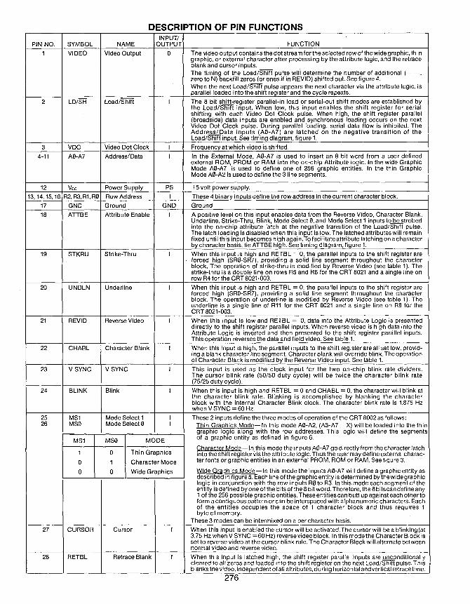
DESCRIPTION OF PIN FUNCTIONS INPUT/
PIN NO. SYMBOL NAME OUTPUT FUNCTION
1 VIDEO Video Output 0 The video output contains the dot stream for the selected row of the wide graphic, thi n graphic, or external character after processing by the attribute logic, and the retrace blank and cursor inputs. The timing of the Load/Shift pulse will determine the number of additional (- -, zero to N) backfill zeros (or ones if in REVID) shifted out. See figure 4. When the next Load/ShIrr pulse appears the next character via the attribute logic, is parallel loaded into the shift register and the cycle repeats.
2 LD/SH Load/Shift I The 8 bit shift-register parallel-in load or serial-out shift modes are established by the Load/Shift input. When low, this input enables the shift register for serial shifting with each Video Dot Clock pulse. When high, the shift register parallel (broadside) data inputs are enabled and synchronous loading occurs on the next Video Dot Clock pulse. During parallel loading, serial data flow is inhibited. The Address/Data inputs (AD-A?) are latched on the negative transition of the Load/Shift input. See timing diagram, figure 1.
3 VDC Video Dot Clock I Frequency at which video is shifted.
4-11 A0-A7 Address/Data I In the External Mode, AO-A7 is used to insert an 8 bit word from a user defined external ROM, PROM or RAM into the on-Chip Attribute logic. In the wide Graphic Mode AO-A7 is used to define one of 256 graphic entities. In the thin Graphic Mode AO-A2 is used to define the 31ine segments.
12 Vee Power Supply PS +5 volt power supply.
13,14,15,16 R2, R3, R1, RO Row Address I These 4 binary inputs define the row address in the current character block.
17 GND Ground GND Ground
18 ATTBE Attribute Enable I A positive level on this input enables data from the Reverse Video, Character Blank, Underline, Strike-Thru, Blink, Mode Select 0, and Mode Select 1 inputs to be strobed into the on-chip attribute latch at the negative transition of the Load/Shift pulse. The latch loading is disabled when this input is low. The latched attributes will remain fixed until this input becomes high again. To facilitate attribute latching on a character by character basis, tie ATTBE high. See timing diagram, figure 1.
19 STKRU Strike-Thru I When this input is high and RETBL = 0, the parallel inputs to the shift register are forced high (SRO-SR7), providing a solid line segment throughout the character block. The operation of strike-thru is modified by Reverse Video (see table 1). The strike-thru is a double line on rows R5 and R6 for the CRT 8021 and a single line on row R4 for the CRT 8021-003.
20 UNDLN Underline I When this input is high and RETBL = 0, the parallel inputs to the shift register are forced high (SRO-SR7), providing a solid line segment throughout the character block. The operation of underline is modified by Reverse Video (see table 1). The underline is a single line of R11 for the CRT 8021 and a single line on R8 for the CRT 8021-003.
21 REVID Reverse Video I When this input is low and RETBL = 0, data into the Attribute Logic is presented directly to the shift register parallel inputs. When reverse video is high data into the Attribute Logic is inverted and then presented to the shift register parallel inputs. This operation reverses the data and field video. See table 1.
22 CHABL Character Blank I When this input is high, the parallel inputs to the shift register are all set low, provid-ing a blank character line segment. Character blank will override blink. The operation of Character Blank is modified by the Reverse Video input. See table 1.
23 V SYNC V SYNC I This input is used as the clock input for the two on-Chip blink rate dividers. The cursor blink rate (50/50 duty cycle) will be twice the character blink rate (75/25 duty cycle).
24 BLINK Blink I When this input is high and RETBL = 0 and CHABL = 0, the character will blink at the character blink rate. Blinking is accomplished by blanking the character block with the internal Character Blink clock. The character blink rate is 1.875 Hz when V SYNC = 60 Hz.
25 MS1 Mode Select 1 I These 2 inputs define the three modes of operation of the CRT 8002 as follows: 26 MSO Mode Select 0 I Thin Grap-hics Mode-In this mode A0-A2, (A3-A7 = X) will be loaded into the thin
graphic logic along with the row addresses. This logic will define the segments
MS1 MSO MODE of a graphic entity as defined in figure 6.
Thin Graphics Character Mode -In this mode the inputs A0-A7 go directly from the character latch
1 0 into the shift register via the attribute logic. Thus the user may define external charac-0 1 Character Mode ter fonts or graphic entities in an external PROM, ROM or RAM. See figure 3.
0 0 Wide Graphics Wide Grap-hics Mode-In this mode the inputs A0-A7 will define a graphic entity as described in figure 5. Each line of the graphic entity is determined by thewide graphic logic in conjunction with the row inputs R0 to R3. In this mode each segment of the entity is defined by one of the bits of the 8 bit word. Therefore, the 8 bits can define any 1 of the 256 possible graphic entities. These entities can butt up against each other to form a contiguous pattern or can be interspaced with alphanumeric characters. Each of the entities occupies the space of 1 character block and thus requires 1 byte of memory.
These 3 modes can be intermixed on a per character basis.
27 CURSOR Cursor I When this input is enabled the cursor will be activated. The cursor will be a blinking (at 3.75 Hz when V SYNC = 60 Hz) reverse video block. In this mode the Character Block is set to reverse video at the cursor blink rate. The Character Block will alternate between normal video and reverse video.
28 RETBL Retrace Blank I When this input is latched high, the shift register parallel inputs are .Y!!.Q9nditionally cleared to all zeros and loaded into the shift register on the next Load/Shift pulse. This blanks the video, independent of all attributes, during horizontal and vertical retrace time.
276

TABLE 1 CURSOR RETBL REVID CHABL UNDLN* FUNCTION
X 1 X X X "0" (S.R.)All a a a a a D (S.R.) All a a a a 1 "1" (S.R.)*
D (S.R.) All others a a a 1 X "0" (S.R.)All a a 1 a a 5 (S.R.)All a a 1 a 1 "0" (S.R.)*
i5 (S.R.) All others a a 1 1 X "1" (S.R.)All
Blink"* REVID Block a a a a
{ Alternate Normal Video/REVID Blink"* REVID Block a a a 1 Blink"" REVID Block a a 1 X Blink"* REVID Block a 1 a a At Cursor Blink Rate Blink"" REVID Block a 1 a 1 Blink"" REVID Block a 1 1 X
* At Selected Row Decode ** At Cursor Blink Rate Note: If Character is Blinking at Character Rate, Cursor will change it to Cursor Blink Rate
FIGURE 2 TYPICAL CHARACTER MODE BLOCK FORMATS
CRT 8021 ROWS R3 R2 R1 RIJ CRT 8021-003
(ALL ZEROS)~ a a a a a a a a - - R0 a a a a a a a a a a a a I a rO-O-O--O--O-o-"()i- - R1 a a a 1 a ro--o--o-o--ol a a a a a a a a a a I - - R2 a a 1 a a : a a a a 0: a a -a a a a a a a a I - - R3 a a 1 1 a I a a a a a I a a a a a a a a a a - - R4 a 1 a a a loa a a a I a a a a a a a a a a - - R5 a 1 a 1 a I a a a a a I a a a a a a a a a ° - - R6 0 1 1 a a lao 0 0 ° I a ° a a a a a a a 0-- R7 a 1 1 1 0LQ __ O __ Q._Q __ O_JO a a a a a a a a a - - R8 1 0 a a a ° a a a a a ° o a a a a a a a - - R9 1 a a 1 a a a a a a a a a 0 a a a a a ° - - R10 1 0 1 a a a a a a ° a a a a a a a a a a - - R11 1 a 1 1 a a ° a a a a a
(ALL ZEROS) {~ ~~--~--~--~-~-~--~ = = =~~ ~ ~ ~ ~ ~ ~ ~ ~ ~ ~ g ~ a ° a a a a a a - - R14 1 1 1 a a ° 0 0 0 a a a o a a a a ° a ° - - R15 1 1 1 1 a a a a a a a a C7 C6 C5 C4 C3 C2 C1 C(J - - C7 C6 C5 C4 C3 C2 C1 C0
\., EXTENDED ZEROS (BACK ~ FILL) FOR INTERCHARACTER
SPACING (NUMBER CONTROLLED BY LD/SH,
COLUMN 7 IS SHIFTED OUT FIRST VDC TIMING)
Note: Dotted line shows typical character display area.
RO-R15
FIGURE 3 CHARACTER MODE
MS0 = 1 MS1= 0
C7 C6 C5 C4 .C3 C2 C1 C0 BF BF
I A71 A61 A51 A41 A31 A2 I A 1 I A0 I A71 A71 ... I BF = back fill
277

FIGURE 4. TYPICAL VIDEO OUTPUT-CHARACTER MODE
VDC II 1----1----1 ISOOTI IsOOT'
LD/SH ----1 IL.. _____________ ---J! ~~h~ l~h~L..! ___________ ---l!.f!.!'hQ.L-U~!:.~
VIDEO DATA 8 DOT FIELD
VIDEO DATA 9 DOT FIELD
FIGURE 5 WIDE GRAPHICS MODE
MSG = G MS1 = G 5 BITS"
ROW ADDRESS I I 0000
3 LINES'
3 LINES
3 LINES
3 LINES
'ON CHIP ROM PROGRAMMABLE TO 2. 3. OR 4 LINE MULTIPLES "CAN BE PROGRAMMED FROM 1 TO 7 BITS
'''LENGTH DETERMINED BY LD/SH. VDC TIMING
EXAMPLE: 10010110
~d0 ifM~ ~
~
fig
Rl
R2
CRT 8021
R3 1t-<~4-+~~~H~_+~
R4
RS
R6
R7
R8
Rll R12 ~~Y~M,-l,."7'++7"h,Lj
R13
R14
R1S
NOTE: Unselected rasler line rOWS are always filled with ones.
~----------------~ BF=back fill
FIGURE 6 THIN GRAPHICS MODE
N"BITS
I -
l-
I---
ROW 0000
PROGRAMMABLE ROW
I X I X I X I X X I A2 I Al I A0 I X=DON'T CARE
THE INSIDE SEGMENT IS MASK PROGRAMMABLE TO ROW 0000
•• LENGTH DETERMINED BY LD/S1't, VDC TIMING
MSG = G MS1 = 1
R/I RI
R2
R3 R4
RS
R6
R7
R8
R9
RIll
CRT 8021
C7 C6 CS C4 C3 C2 C1 CII BF BF , .. -,
::~ ~...L.~~:......c,..L:..o..:..t.~""! RI4
RIS '--____ ~
NOTE: When Al:;;;; "1", the underline row/rows are deleted When A 1 = "0". the underline. if selected. will appear
BF=back fill
278
fig
Rl
CRT 8021-003
C7 C6 CS C4 C3 C2 Cl CII
:: ~-+~~MHio-&4~ R4
RS R6 H>-7+r~~E*+~
R7
RS
R13
R14
R15
Note: R11-R15 are always filled wi1h ones
~------------~
CRT 8021-003
C7 C6 CS C4 C3 C2 CI CfI BF
~ RI
R2
R3 R4
RS
R6
R7
R8
RII
RI2
RI3
RI4 RIS ..... ______ ---L'"

FIGURE 7
Vee ,....----------..~VDC (to chip)
SOOn
CP EXTERNAL --~ r-~--------~~~CLK
74S74
QI-------4I_ LD/SH (to chip)
SYSTEM RAM OR
SINGLE OR DOUBLE ROW
BUFFER
LOAD/SHIFT EXTERNAL-----tD
FIGURE 8 TYPICAL CRT 8021 CONFIGURATION
FOR COMBINED CHARACTER AND GRAPHICS MODES
L A
I 6 I H I I L_
4 CONTROLLER
MSIJ
FROM CRT CONTROLLER , RETRACE
R3-R0 BLANKING CURSOR
CHARACTER I---~--''''''' VIDEO ROM
VAC CRT 8021
ATTRIBUTES (RV, CB, CBLANK, ATTEN,STKTU, MS1)
"LATCH MAY OR MAY NOT BE REQUIRED DEPENDING ON SYSTEM TIMING.
279
TO MONITOR
I

XTAL
t5.~ 74160
R R DOT I CARRY COUNTER ~
Cp(7N) L-~~~~~~ ________________________ _ CHARACTER CLOCK DCC H SYNC HORIZ. SYNC
BI-DIRECTIONAL DATA BUS
7404 ~;:::=============:::=::= II ADDRESS BUS
PAGE CHIP SELECT LOGIC
~DB0-7 AB-3
CS
V SYNC
COMPOSITE C SYNC SYNC
VTAC CRT 5027 BL
DATA STROBE VIDEO
MICROPROCESSOR
DATA BUS
ADDRESS BUS
CONTROL BUS
DS
8 CHARACTER COLUMN H0-7
6 CHARACTER ROW DR0-5
rJ CHARACTER ADDRESS BUS
fT' LA I
r ()
RASTER SCAN COUNTER ~ (JJ
o :Xl
'-...-
~
SELECTOR WITH
OPTIONAL MEMORY MAPPING CIRCUIT
(IF REQUIRED) ASCII DATA
r-rT I C I
UiJ
CHARACTER VIDEO DATA ~ ROM ~
J>.. VAC
CRT 8021
Vlg~ggKO~ ...... _______ ......
RETRACE BLANKING
SERIAL OUTPUT
rTl I A I 1=t=.======!=T: ATIRIBUTES 'I
L---'-O-R-1-P-O-R~T RAM lSI
TIMING FROM
DOT COUNTER OR
CHARACTER CLOCK WITH BI-DIRECT '----'
PORT "Latch may be required depending on system timing.
FIGURE 9. CRT 8021 TYPICALjlP CONFIGURATION (CHARACTER MODE ONLY)
r
-i 0 () :Xl -i
s: 0 z =i 0 :Xl
cO~·~ 0 ~ ~~~g~ ~~:e-g~ o·Ol§.~~ U:>.c.EOl ~~~~E C~'-<l>.9 O(J)O..c .....
. ~ ~ ~~~ ~cg!Q)~ ~oQ)~£ .~ c ~-5 ~ ~.~I :;~
~~~~~ c (/)..c.c Q) •
~ 8.~ oo~ .!: ~ ~ -;~.Ci) ~ c.~g:~ ~ :: §.~ g ~~ o:;::;c U..c u ~gQ)oo-6 ro.!:: a> C"-O Q)~.o~oa. EoooU_ Ol{)-,,~~
~oas5~.o ~~~~~£ -g.~~ E~~ u~.~..E·i::~ '~~-g~~ ~ ~ccag~-g fI).Q" III C.co uro~~~c
~ §~ ~~.~ g o..c <.> Ci>-g"O C\J (J .~£:§ ~ ~
~~~tI~K Ol~~ui2lE c 0 ().~:.='-
:~ u c ~~.8 ~~35:;caQ> ~-.ou-o"O
E~gJ~~O ~ g-..c.~ u.~ Ol(l)COCrlQ)
=6 §:2~~.§ _ u ca Q)C/)-
'3 en E 5 2l ~ ~ C a en'::; ctS
ogE~~ro

STANDARD MICROSYSTEMS CORPORATIO~N~ __ •
CRT9021B J,1PC FAMILY
CRT Video Attributes Controller VAC
FEATURES o On chip video shift register (28.5 MHz max.)
o On chip attributes logic Reverse video Character blank Character blink Underline Full/half intensity
o Four modes of operation Wide graphics Thin graphics Character mode without underline Character mode with underline
o On Chip logic for double height/double width characters
o Accepts scan line information in parallel or serial format
o Four cursor modes dynamically selectable via 2 input pins
Underline Blinking underline Reverse video Blinking reverse video
o Programmable character blink rate
o Programmable cursor blink rate
PIN CONFIGURATION
D0 1 28 D1
MS0 2 27 D2
MS1 3 26 D3
REVID 4 25 D4
CHABL 5 24 D5
BLINK 6 23 D6
INTIN 7 22 D7
+5V 8 21 VSYNC
ATTEN 9 20 GND
INTOUT 10 19 SL0/SLD
CURSOR 11 18 SL1/SLG
RETBL12 17 SL2/BLC
LD/SH 13 16 SL3/BKC
VIDEO 14 15 VDC
PACKAGE 28-pin D.I.P.
o On chip data and attribute latches
o + 5 volt operation
o TTL compatible
o MOS n-Channel silicon gate COPLAMOS® process
o Compatible with CRT 5037 VTAC®; CRT 9007 VPACM
GENERAL DESCRIPTION
The SMC CRT 9021 Video Attributes Controller line, reVerse video character block, and blinking (VAC) is an n-channel COPLAMOS MOS/LSI device reverse video character block. When used in the serial containing Graphics logic, attributes logic, data and scan line input mode, the cursor mode may be selected attributes latches, cursor control, and a high speed via two input pins. When used in the parallel scan line video shift register. The CRT 9021 , a character gen- input mode, the cursor mode is a mask program option erator ROM and a CRT controller such as the CRT and is fixed at the time of manufacture. 9007 provide all of the major circuitry for the display Two graphics modes are provided. In the wide portion of a CRT video terminal. graphics mode, the CRT 9021 produces a graphic
The CRT 9021 serial video output may be con- entity the size of the character block. The graphic entity nected directly to a CRT monitor's video input. The contains eight parts, each of which is associated with maximum video shift register frequency of 28.5 MHz one bit of the input byte, thereby providing 256 unique allows for CRT displays of up to 132 characters per graphic symbols. The thin graphics mode enables the data row. user to create thin line drawings and forms.
The CRT 9021 attributes include: reverse video, In both graphics modes, continuous horizontal and underline, character blank, character blink, and full/ vertical lines may be drawn. Additional flexibility is half intensity selection. In addition, when used in con- provided by allowing the mask programming of the junction with theCRT9007VPAC;M the CRT 9021 will placement and dimensions of the blocks or lines within provide double height or double width characters. a character block. In the thin graphics mode, mask
Four programmable cursor modes are provided on programming allows serrated horizontal or vertical the CRT 9021. They are: underline, blinking under- lines.
281
I

07-00
CURSOR
RETBL
WISH
ATIEN MSO MSI
REVIO CHABL BLINK INTIN
ATTRIBUTE AND
GRAPHIC LOGIC
L A
RO/SLD
R1/SLG
R2/BLC
R3/BKC
J--------- VIOEO
~--------- VOC
T 1----------+ INTOUT C H
FIGURE 1: CRT 9021 BLOCK DIAGRAM
DESCRIPTION OF PIN FUNCTIONS
PIN NO. NAME SYMBOL FUNCTION 1,28,27,26, Data D7-DO In the character mode, the data on these inputs is passed through the Attributes 25,24,23, logic into the 8 bit high speed video shift register. The binary information on D7
22 will be the first bit output after the LD/SH input goes low. In the thin or wide graphics mode these 8 inputs will individually control the onloff condition of the particular portion of the character block or line drawing. Figures 2 and 3 illustrate the wide and thin graphics modes respectively and their relationships to D7 -DO
2 Mode Select 0 MSO These 2 inputs define the four modes of operation of the CRT 9021 as follows: 3 Mode Select 1 MS1 MS1, MSO = 00; Wide graphics mode
= 10; Thin graphics mode = 01; Character mode without underline = 11; Character mode with underline
See section entitled Display Modes for details. 4 Reverse Video REVID When this input and Retrace Blank (RETBL) are both low, data from the
Attributes and Graphics logic is presented directly to the video shift register. When this input is high and RETBL is low, the Attribute and Graphics logic will invert the data before presenting it to the video shift register.
5 Character blank CHABL When this input is high, the parallel inputs to the video shift register are all set low (or high depending on the state of REVID) thus providing a constant video level for the entire length of the character block.
6 Blink BLINK When this input is high and both the RETBL and CHABL inputs are low, the char-acter will blink at the programmed character blink rate. Blinking is accomplished by causing the video to go to the background level during the "off" portion of the Character Blink cycle. This video level may be either the white or black level depending on state of REVID. The duty cycle for the character blink is 75/25 (ani off). This input is ignored if it coincides with the CURSOR input and the cursor is formatted to blink.
7 Intensity In INTIN The INTIN input along with the INTOUT output provides a user controlled general purpose attribute. Data input to INTIN will appear at INTOUT with the same delay as that from any other attribute input to the serial video output (VIDEO). By using an external mixing circuit, it is possible to raise or lower the voltage level of the video output to produce such attributes as "half intensity" or "intensity".
282

DESCRIPTION OF PIN FUNCTIONS CONT'D
PIN NO. NAME SYMBOL FUNCTION 8 Supply Voltage +5V + 5 volt power supply 9 Attribute ATTEN When this if1QJdt is high, the internal attribute latch is updated at the positive going
Enable edge of the LD/SH input with data appearing on the REVID, CHABL, MS1, MSO, BLINK and INTIN inputs. By selectively bringing this input high, the user will update the attribute only at specific character times; all subsequent characters will carry with them the attributes last updated thus allowing "field" or "embed-ded" attributes. When using a wide video memory where attribute bits are attached to every character, the internal attribute latch may be updated at each character by tieing this input high (thus allowing for "invisible" attributes).
10 Intensity Out INTOUT This output is used in conjunction with the INTIN input to provide a three charac-ter pipeline delay to allow for general purpose attributes (such as intensity) to be implemented. See INTIN (pin 7).
11 Cursor CURSOR When this input is high and RETBL is low, the programmed cursor format will be displayed. When this input is high, and RETBL is high, the CRT 9021 enters the double width mode. See section entitled cursor formats for details.
12 Retrace Blank RETBL When this input is high, the parallel inputs to the video shift register are uncondi-tionally cleared to all zeros and loaded on the next LD/SH pulse. This forces the VIDEO output to a low voltage level, independent of all attributes, for blanking the CRT during horizontal and vertical retrace time.
13 Load/Shift LD/SH The 8 bit video shift register parallel-in load or serial-out shift operation is estab-lished by the state of this input. When high, this input enables the shift register for serial shifting with each video dot clock pulse (VDC input). When low, the video shift register is parallel loaded on the next video dot clock pulse and all data and attributes are moved to the next position in the internal pipeline. In addition, input data and attributes are latched on the positive transition of LD/SH.
14 Video VIDEO The Video output provides the serial dot stream to the CRT. Video is shifted out on the rising edge of the video dot clock VDC. The timing of the LD/SH input will determine the number of backfill dots. See figure 5.
15 Video Dot VDC This input clock controls the rate at which video is shifted out on the Clock VIDEO output.
16 Scan line SL3/BKC This input has two separate functions depending on the way scan line informa-3/Block Cursor tion is presented to the CRT 9021.
Parallel scan line mode-This input is the most significant bit of the binary scan I line row address. Serial scan line mode-This input controls the cursor's physical dimensions. If high the cursor will appear as a reverse video block (the entire character cell will be displayed in reverse video). If low, the cursor will appear as an underline on the scan line(s) programmed.
17 Scan line SL2/BLC This input has two separate functions depending on the way scan line informa-2/Blink Cursor tion is presented to the CRT 9021.
Parallel scan line mode-This input is the second most significant bit of the binary scan line row address. Serial scan line mode-This input if high, will cause the cursor to alternate between normal and reverse video at the programmed cursor blink rate. The duty cycle for the cursor blink is 50/50 (on/off). If this input is low, the cursor will be non-blinking.
18 Scan Line SL1/SLG This input has two separate functions depending on the way scan line informa-1/Scan Line tion is presented to the CRT 9021. Gate Parallel scan line mode-This input is the next to the least significant bit of the
binary scan line row address. _ Serial scan line mode-This input will be low for 5 or 6 LD/SH pulses to allow the scan line information to be ser@lly shifted into the serial scan line shift register. If this signal is low for 7 or more LD/SH pulses, the CRT 9021 will assume the par-allel input scan line row address mode.
19 Scan line SLO/SLD This input has two separate functions depending on the way scan line informa-O/Scan Line tion is presented to the CRT 9021. Refer to figure 6. data Parallel scan line mode-This input is the least significant bit of the binary scan
line row address. Serial scan line mode-This input will present the scan line information in serial form (least significant bit first) to the CRT 9021 and permits the Q["9per scan line information to enter the serial scan line shift register during the LD/SH pulses framed by SLG (pin 18).
20 Ground GND Ground 21 Vertical Sync VSYNC This input is typically connected to the vertical sync output of the CRT controller
and is used as the clock input for the two on-Chip mask programmable blink rate dividers. The cursor blink rate (50/50 duty cycle) will always be twice the charac-ter blank rate (75/25 duty cycle). In addition, the internal attributes are reset when this input is low. The VSYNC input is also used to determine the scan line mode (parallel or serial) used. See the section "Scan Line Input Modes".
283

Retrace Blank
ATTRIBUTES FUNCTION
-The RETBL input causes the VIDEO grammed to blink (not controlled by the BLINK input), the video alternates from normal to reverse video at 50% duty cycle. The cursor blink rate always overrides the character blink rate when they both appear at the
to go to the zero (black) level regard-less of the state of all other inputs.
Reverse Video -The REVID input causes inverted data to be loaded into the video shift register.
Character Blank -The CHABL input forces the video to go to the current background level as defined by Reverse Video.
same character position. Intensity (Half Intensity)
Underline -MS 1, MS0 = 1, 1 forces the video to go to the inverse of the background
-The INTIN input and the INTOUT output allow an intensity (or half intensity) attribute to be carried through the pipeline of the CRT 9021. An external mixer can be used to combine VIDEO and INTOUTto create the desired video level. See figure 8.
Blink
level for the scan line(s) pro-grammed for underline.
-The BLINK input will cause charac-ters to blink by forcing the video to the background level 25% of the time and allowing the normal video for 75% of the time. When the cursor is pro-
Table 1 illustrates the effect of the REVID, CHABL, UNDLN attributes as a function of the cursor format and the CURSOR and RETBL inputs.
TABLE 1: CRT 9021 ATTRIBUTE COMBINATIONS CURSOR CRT 9021 INPUTS VIDEO SHIFT REGISTER FORMAT RETBL CURSOR REVID CHABL UNDLN LOADED WITH:
1 X X X X all zero's 0 0 0 0 0 data 0 0 0 0 1 One's for selected scan line(s); Data for all
other scan lines.
X 0 0 0 1 X All zero's 0 0 1 0 0 data 0 0 1 0 1 Zero's for selected scan line(s); data for all
other scan lines. 0 0 1 1 X One's for all scan lines. 0 1 0 0 X, One's for selected scan line(s) for cursor;
data for all other scan lines.
0 1 0 1 X, One's for selected scan line(s) for cursor;
UNDERLlNE2 zero's for all other scan lines. 0 1 1 0 X, Zero's for selected scan line(s) for cursor;
Data for all other scan lines. 0 1 1 1 X, Zero's for selected scan line(s) for cursor;
one's for all other scan lines. --0 1 0 0 X, One's for selected scan line(s) blinking;
Data for all other scan lines. 0 1 0 1 X, One's for selected scan line(s) blinking;
BLiNKING3 zero's for all other scan lines. UNDERLlNE2
0 1 1 0 X, Zero's for selected scan line(s) blinking; Data for all other scan lines.
0 1 1 1 X, Zero's for selected scan line(s) blinking; one's for all other scan lines.
0 1 0 0 0 Data for all scan lines.
0 1 0 0 1 Zero's for selected scan line(s) for underline; data for all other scan lines.
REVIDBLOCK 0 1 0 1 X One's for all scan lines. 0 1 1 0 0 Data for all scan lines 0 1 1 0 1 One's for selected scan line(s) for
underline; data for all other scan lines. 0 1 1 1 X Zero's for all scan lines. 0 1 0 0 0 On Off
Data for all scan lines. Data for all scan lines. 0 1 0 0 1 Zero's for selected One's for selected
scan line(s)JQL scan line(s) for underline; Data for underline; Data for
BLiNKING3 all other scan lines. all other scan lines.
REVID BLOCK 0 1 0 1 X One's for all scan lines. Zero's for all scan lines.
0 1 1 0 0 Data for all scan lines. Data for all scan lines.
0 1 1 0 1 One's for selected Zero's for selected scan line(s); Data scan line(s); Data for all other scan lines. for all other scan lines.
0 1 1 1 X Zero's for all scan lines. One's for all scan lines. 1 -If the programmed scan IIne(s) for cursor and underline COinCide, the cursor takes precedence, otherwise both are displayed. 2 - at programmed scan line(s) for underline 3 - at cursor blink rate Note-cursor blink rate overrides character blink rate.
284

DISPLAY MODES
Inputs MS1 and MSQ) select one of four display modes. All attributes except underline operate independent of the display mode used. Figures 8a and 8b illustrate a typical CRT 9021 configuration which operates in all display modes for both the parallel and serial scan line modes respectively.
the character block. Table 3 shows all programming ranges possible when defining the thin graphics boundaries. No underline is possible in this display mode.
MS1, MSO = 00 -Wide Graphics Mode. In this display mode, inputs 07-00 define a graphics entity as illustrated
MS1, MSO = 01 -Character Mode Without Underline.
in figure 2. Note that individual bits in 07-00 will illuminate particular portions of the character block. Table 2 shows all programming ranges possible when defining the wide graphic boundaries. No underline is possible in this display mode.
MS 1, MSO = 1 0 -Thin Graphics Mode.
In this display mode, inputs 07-00 go directly from the input latch to the video shift register via the Attributes and Graphics logic. This mode requires either a bit mapped system RAM (1 bit in RAM equals 1 pixalon the CRT) or an external character generator as shown in figures 8a and 8b.
In this display mode, inputs 07-00 define a graphic entity as illustrated in figure 3. Note that individual bits in 07-00 will illuminate particular hori-zontal or vertical line segments within
MS1,MSO = 11 -Character Mode With Underline. Same operation as MS1, MSQ) = 01 with the underline attribute appearing on the scan line(s) mask programmed.
SL3-SLO ROW # C7 C6 C5 C4 C3 C2 C1 CO BF BF a 0 a
0000 RO 0001 R1 0010 R2 0011 R3 0100 R4 0101 R5 0110 R6 0111 R7 1000 R8 1001 R9 1010 R10 1011 R11 1100 R12 1101 R13 1110 R14 11.11 R15
07 03
06 02
OS 01
04 00
iT I H3
J I 1 I I H2 I I --1 I I H1 11
1 I I HO
i I W1 1 WO "I
H3, H2, H 1, HO, W1 , WO are mask programmable
FIGURE 2: WIDE GRAPHICS MODE FOR STANDARD CRT 9021
SL3-SLO ROW # C7 C6 C5 C4 C3 C2 C1 CO BF BF a a a VERTICAL HEIGHT* HORIZONTAL POSITION
0000 0001 0010 0011 0100 0101 0110 0111 1000 1001 1010 1011 1100 1101 1110 1111
RO R1 R2 R3 R4 R5 R6 R7 R8 R9 R10 R11 R12 R13 R14 R15
04
07 00
02 03
01
05
'-- '--
-
06
-
-, __ J
1 1 1 1 I 1 J I I I I 1 I
--I
--~ I I I
00 01 06 07
02 03 04 05
RO-R5 PROGRAMMABLE R6-R15 PROGRAMMABLE RO-R15 PROGRAMMABLE RO-R15 PROGRAMMABLE
HORIZONTAL LENGTH* VERTICAL POSITION
C7-C3 PROGRAMMABLE C3-BF PROGRAMMABLE C7-BF PROGRAMMABLE C7-BF PROGRAMMABLE
OATA INPUTON 07-00
'--__ J * These values are fixed
FIGURE 3: THIN GRAPHICS MODE FOR STANDARD CRT9021
285
I

BACKFILL Backfill is a mechanism that allows a character width of greater than 8 dots and provides dot information (usually blanks) for all dot positions b~ond 8. The character width is defined by the period ofthe LD/SH input. For the character modes, backfill is added to the tail end of the character by two methods which are mask programmable. Method A - The backfill (BF) dots will be the same
as the dot displayed in position C7.
Method B - The backfill (BF) dots will be the same as the dot displayed in position CO.
For the wide graphics mode, the backfill dots will always be the same as the dot displayed in position CO (method B) with no programmable option.
CURSOR FORMATS
Four cursor formats are possible with the CRT 9021. If the parallel scan line input mode is used, one of four cursor formats may be selected as a mask programmed option. If the serial scan line input mode is used, the cursor format is selected via input pins 16 and 17 (SL3/BKC, SL2IBLC). See Table 5. The four cursor modes are as follows:
Underline - The cursor will appear as an underline. The position and width of the cursor underline is mask programmed.
Blinking Underline - The cursor will appear as an underline. The underline will alternate between normal and reverse video at the mask programmed cursor blink rate.
Reverse Video - The cursor will appear as a reverse Block video block (The entire character
cell will be displayed in reverse video).
Blinking Reverse - The cursor will appear as a reverse Video Block video block and the entire block
(character plus background) will alternate between normal and reverse video at the masked programmed cursor blink rate.
Scan Line Input Mode Pin 17 Pin 16 Cursor Function
0 0 Underline 0 1 Reverse Video Block
Serial 1 0 Blinking Underline 1 1 Blinking Reverse
Video Block Parallel X X Mask programmable
Only
TABLE 5: CURSOR FORMATS
DOUBLE WIDTH MODE
In order to display double width characters, video must be troller knows when a particular scan line should be double shifted out at half frequency and the video shift register must width and it should activate the CURSOR in the manner just receive new information (parallel load) every other LD/SH described. Double height/double width characters can also input pulse. In order to divide the video dot clock (VDC) and be displayed if the scan line count is incremented by the the LD/SH pulse internally at the proper time, the cursor input CRT controller every other scan line. With respect to the should be pulsed during RETBL prior to the scan line to be . CRT 9021, no distinction between double width and double displayed as double width. The CURSOR input must remain height display is necessary. Figure 4 illustrated timing for low for a minimum of 1 LD/SH period from the leading edge both single and double width modes. The CRT 9007, which of RETBL. The CURSOR input can stay high for the entire supports double height double width characters, will proRETBL time but should not extend into active video. If it does, duce the CURSOR Signal as required by the CRT 9021 with a cursor will be displayed. It is assumed that the CRT con- no additional hardware.
SCAN LINE INPUT MODES Scan line information can be introduced into the CRT 9021 mode will be selected for the next field if the following two in parallel format or serial format. Table 6 illustrates the pin conditions occur during VSYNC low time. First, at least one definition as a function of the scan line input mode. The CRT positive transition must occur oJ!Qin 18 and second, pin 18 9021 will automatically recognize the proper scan line mode must be low for seven or more LD/SH periods. Refer to figby observing the activity on pin 18. In parallel mode, this ure 7 for timing details. input will be stable for at least 1 scan line and in serial mode this input will remain low for about 5 or 6 LD/SH periods. If pin 18 goes active low for less than seven but more than two continuous LD/SH periods during the last scan line that has an active low on the VSYNC input, the serial mode will
Scan Line Input Mode
Serial Parallel
19 SLD SLO
CRT 9021 Pin Number 18 17 16
SLG BLC BKC SL1 SL2 SL3
be locked in for the next field. The parallel scan line input TABLE 6: PIN DEFINITION FOR PARALLEL AND SERIAL SCAN LINE MODES
PROGRAM OPTIONS
The CRT 9021 has a variety of mask programmed options. trates the range of the miscellaneous mask programmed Tables 2 and 3 illustrate the range of these options for the options. In addition, Tables 2, 3 and 4 show the mask prowide and thin graphics modes respectively. Table 4 iIIus- grammed options for the standard CRT 9021.
286

~I
LD/SH
RETBL
D7-DO (NORMAL)
WIDTH
D7-DO (DOUBLE)
WIDTH
D17-D10 (NORMAL)
WIDTH
D17-D10 (DOUBLE)
WIDTH
VIDEO (NORMAL)
WIDTH
VIDEO
x x x
I : i i; ----l--..... X X CHAR 0 X CHAR 1 ~ CHARN/2
VIDEO (N-2)(Ll!..!......!..
I I I I I BLANKING I I
I I
(DOUBLE) WIDTH
BLANKING VIDEO 1 VIDEO (N/2-1)" 1 I VIDEON/2 VIDEO 0
ATTRIBUTE IN1 (NORMAL)
WIDTH
ATTRIBUTE OUP
( NORMAL) WIDTH
ATTRIBUTE IN1
( DOUBLE) WIDTH
ATTRIBUTE OUT1
( DOUBLE) WIDTH
: :I~~r X XX I : : I I I I ~
____ """ -----l ,------:, I I t""'----'-'! ........-----! ~ X X
, I I I I I ____________________________ ~I I I I I I I
---------------------------~ I I I
X X X X ATT 0 X A~ 1 '[
1-Attributes include MSO, MSI, BLINK, CHABL, INTENSITY, REVID
FIGURE 4: CRT 9021 FUNCTIONAL I/O TIMING

MAXIMUM GUARANTEED RATINGS·
Operating Temperature Range . . . . . . . . . . . . . . . . . . . . . . . . . . . . . . . . . . . . . . . . . . . . . . . . . . . . . . . . . . . . . . . . . . . . . . .. O°C to + 70°C Storage Temperature Range. . . . . . . . . . . . . . . . . . . . . . . . . . . . . . . . . . . . . . . . . . . . . . . . . . . . . . . . . . . . . . . . . . . . .. - 55°C to + 150°C Lead Temperature (soldering, 10 sec.) ....................................................................... + 325°C Positive Voltage on any Pin, with respect to ground ................................................................ 15V Negative Voltage on any Pin, with respect to ground. . . . . . . . . . . . . . . . . . . . . . . . . . . . . . . . . . . . . . . . . . . . . . . . . . . . . . . . . . .. - 0.3V
·Stresses above those listed may cause permanent damage to the device. This is a stress rating only and functional operation of the device at these or at any other condition above those indicated in the operational sections of this specification is not implied.
NOTE: When powering this device from laboratory or system power supplies, it is important that the Absolute Maximum Ratings not be exceeded or device failure can result. Some power supplies exhibit voltage spikes or "glitches" on their outputs when the AC power is switched on and off. In addition, voltage transients on the AC power line may appear on the DC output. If this possibility exists it is suggested that a clamp circuit be used.
~ ~~;""f$/J ELECTRICAL CHARACTERISTICS (TA~O°C to 70°C, Vcc~ +5V ± 5%, unless otherwise noted) ,~~~
PARAMETER MIN TYP MAX UNIT COMMENTS ~ ~~II. )'j DC CHARACTERISTICS
!1g~
INPUT VOLTAGE LEVELS Low Level V1L 0.8 V High Level V1H1 2.0 V All inputs except VDC, LD/SH High Level V1H2 4.3 V For VDC, LD/SH input
OUTPUT VOLTAGE LEVELS Low Level VOL 0.4 V IOL =0.4 mA High Level VOH 2.4 V IOH= 1OOf.lA
INPUT LEAKAGE CURRENT Leakagelu 10 f.lA O~VIN<VCC; excludin9..YDC, LD/SH Leakage IL2 50 f.lA O~VIN~V CC; for VDC LD/SH
INPUT CAPACITANCE C1N1 10 pf Excluding VDC, LD/SH C1N2 20 pf For LD/SH C1N3 25 pf ForVDC
POWER SUPPLY CURRENT Icc 50 mA
AC CHARACTERISTICS
PARAMETER MIN TYP MAX UNIT COMMENTS VDC
1 ItCY1 VDC frequency 1.0 28.5 MHZ tcKLVDClow 10 ns lcKH VDC high 10 ns Measured from 10% to 90% points tCKR VDC rise time 7.5 ns Measured from 90% to 10% points lcKF VDC fall time 7.5 ns
LD/SH tCY2 315
I ns
t51 7 ns tH1 0 ns
INPUT SETUP AND HOLD t52 35 ns tH2 0 ns
MISCELLANEOUS TIMING tpo 35 ns CL = 15 pf tow tCY2
288

VDC
[5/SH
ALL INPUTS (EXCEPT VDC, [51
VDC
VIDEOOR INTOUT
RETBL
CURSOR
SH)
(FOR DOUBLE WIDTH)
[5/SH
~lsl- I+-IH1 -n
\ V ..
\~ Ir-
IS2 IH2 -
>: ~~
ICY2
Ct~=1-FIGURE 5: CRT 9021 INPUT/OUTPUT TIMING
LD/SH
X SLD ____ .1'-_1 _ ....... ,'__--I'----J''"--_
FIGURE 6: SERIAL SCAN LINE MODE TIMING
lnnnnnrU-UUlflJ1f I I I
I I :
~l-l --+-----!-<: l~~\ l ! 1;-I I I I
SL1/SLG t~ L,--,--r-!" n t~ ~I , , I / STABLE;> 7 [5/SH I , « « • • l
1, l SET SERIAL
SCAN LINE MODE
FIGURE 7: SERIAL/PARALLEL SCAN LINE MODE SELECTION TIMING
289
SET PARALLEL SCAN LINE MODE
I

TABLE 2 WIDE GRAPHICS MASK PROGRAMMING OPTIONS
OPTION CHOICES STANDARD CRT 9021
Height of graphic block" D7and D3 any scan line(s) RO, R1, R2 D6and D2 any scan line(s) R3,R4,R5 D5 and D1 any scan line(s) R6, R7, R8 D4and DO any scan line(s) R9,R10,R11,R12,R13,R14,R15
Width of D7, D6, D5, D4"" any number of dots 0 to 8 C7, C6, C5, C4 Width of D3, D2, D1, DO"" any number of dots 0 to 8 C3, C2, C1, CO, BF
" Any graphic block pair can be removed by programming for zero scan lines. "" Total number of dots for both must be equal to the total dots per character with no overlap.
TABLE 3 THIN GRAPHICS MASK PROGRAMMING OPTIONS
OPTION CHOICES STANDARD CRT 9021
Backfill C1 or CO CO
Horizontal portion for
D2 and D3 any scan line(s) RO-R15 R5 D4 any scan line(s) RO-R15 RO D5 any scan line(s) RO-R15 R11
Blanked dots for serrated horizontal lines
D2 anydot(s) C7-CO, BF none D3 any dot(s) C7-CO, BF none D4 anydot(s) C7-CO, BF none D5 any dot(s) C7-CO, BF none
Vertical position for
DO and D1 anydot(s) C7-CO, BF C3 D61 any dot(s) C6-CO, BF BF D71 any dot(s) C7-CO C7
Vertical length for
DO any scan line(s) ROto R5 D1 all scan lines not used byDO R6 to R15 D6 no choice; always RO-R15 RO to R15 D7 no choice; always RO-R15 RO to R15
1 - D7 must always come before D6 with no overlap; otherwise D6 is lost.
TABLE 4 MISCELLANEOUS MASK PROGRAMMING OPTIONS
OPTION
Backfill in character mode
Character blink rate (division of VSYNC frequency)
Cursor blink rate2
character underline position
cursor underline3
cursor format4
---1 - Assumes VSYNC input frequency of 60 Hz. 2 - Valid only if the cursor is formatted to blink.
.
3 - Valid only if the cursor is formatted for underline. 4 - Valid for the parallel scan line mode only.
CHOICES STANDARD CRT 9021
C7toCO C7
8 to 60 even numbers 32 (7.5 Hz to 1 HZ)1 (1.875 Hz)1
Twice the character 16 blink rate (3.75 HZ)1
any scan line(s) RO-R15 R11
. any scan line(s) RO-R15 not applicable
underline Blinking underline
Blinking reverse video block Reverse video block
Blinking reverse video block
290

I\) (0 ......
J
SYSTEM RAM OR
SINGLE ROW BUFFER
OR
DOUBLE ROW BUFFER
-'\ THREE STATE
,-
.,/ DRIVER
OE ~
r-
L t-A OE I"'- '7~ -'\ T
~ ) D7-DO C t--
.I H CHARACTER ~ I/"
J ROM CRT 9021 ~ VAC
L ~ SL3-SLO I SL3-SLO
...r VSYNC VSYNC -FROM CRT
CONTROLLER RETBL RETBL VIDEO
CURSOR- CURSOR MSO
... MSI
..... BLINK ->0 CHABL
~ INTIN ...lII REVID
ATTEN
-III LD/SH
I ...a VDC ,.'
1 [ CLOCK ~ GENERATOR
FIGURE Sa: CRT 9021 SYSTEM CONFIGURATION IN PARALLEL SCAN LINE MODE
INTOUT
r-;;-I----'" I
X VIDEO E
~ R TO MONITOR -

!
I t±Jwffi I~I cd;:> :J:I-'a: 1-(/)0
~
:
I
0 0 r.:. 0
~ ..... ~
"" ~ ... l W 0 0:
W I-o~ «0 ~o: I 0
~
C\j ~() I-~ a: ()
/~
a: ~ z
00 W~ 90 >1-
o IW ::> o 2 ::; ~
[0 ~ Zoo Ie.!) 0 >- I-...J...J en W en en > a:
)
0
a: ffi~ 0 :::.:::...J OZI en o_zoo~ ::;Wen a: 0 ::> enen:i~~ ~ ~Ig 0 oa: ~ 0 ~~OOO- > wo
~en ~ ~a: a: <X:::> 0 a:o u. C!Ja: 00 a:u. a.
r---
...... 0: ~o o~
~ 00: ...JW oz
W (!)
""'"---
I ...J<X:I-OI J---/~
~ « 0: ~ W I-en >-en
~311mUNO::> l~::> ~O~::I
3:: 3:: 00: 00:
a: 1~~ O:w 0: WLL o ...JLL 0 ...JLL
(!)::> CD::> ZCD BCD U5 0
Circuit diagrams utilizing SMC products are included as a means of illustrating typical semiconductor applications; consequently complete information sufficient for construction purposes is not necessarily given. The information has been carefully checked and is believed to be entirely reliable. However. no responsibility is assumed for inaccuracies. Furthermore. such information does not convey to the purchaser of the semiconductor devices described any license under the patent rights of SMC or others. SMC reserves the right to make changes at any time in order to improve design and supply the best product possible.
292

Part Number lWM 4732(3)
Microprocessor Peripheral '*Glldltftt ROM
Description Access Time Power Supply 32K lWM; 32,768 bits 460 nsee +6 organiZed 4096x8
lWM 36000(1)(3) 64K ROM; 66,636 bits 260 nsee +6 organiZed 8192x8
tijll,IMlldlilH FLOPPY DISK
Part Sectorf Data Side Select Power Number Description Format Density Bus Output Supplies
FDC1761 Floppy Soft Double Inverted No +5, + 12 ( ,""
_~Illy)~
FDC1763 Floppy Disk Controller! Soft Double True No +5, +12 Formatter (mini-floppy only)
FDC1765 Floppy Disk Controller! Soft Double Inverted Yes +5, + 12 Formatter (mini-floppy only)
FDC1767 FloPPY "" Soft Double True Yes +5, + 12 Formatter ( .-., -..-..-oJ only)
FDC1791 Floppy Disk Controller! Soft Double Inverted No +6, + 12 Formatter
FDC1792 Floppy Disk Controllerl Soft Single Inverted No +5, + 12 Formatter
FDC1793 Floppy Disk Controller! Soft Double True No +6, +12 Formatter
FDC1794 Floppy Disk Controller! Soft Single True No +5, +12 Formatter
FDC1795 Floppy Disk Controller! Soft Double Inverted Yes +5, + 12 Formatter
FDC1797 Floppy Disk Controller/ Soft Double True Yes +5, + 12 Formatter
.l<'lOppy mSl{ Data Handler Hard N/A T.rue NA +5, ,12
1ml1A2HVR .l<'lOppy II( DR,t.!'!. Soft/Hard Double NA NA +5
~ CASSETTE/CARTRIDGE
Max Power Part Number Description Data Rate Features Supply
CCC 3500 Cassette/Cartridge Data Handler 260K bps Sync byte detection, +6, -12 Read While Write
(l)For future release (3)MBiY be custom mask programmed
293
Package Page
24 DIP 347-360
24 DIP 361-354
.Pa~~~ 40 DIP 296-310
40 DIP 296-310
40 DIP 295-310
40 DIP 296-310
40 DIP 311-326 II 40 DIP 311-326 •
40 DIP 311-326 •
40 DIP 311-326
40 DIP 311-326
40 DIP 311-326
40 DIP 331-338
8 DIP 327-330
Package Page 40 DIP 339-346

2·94

STANDARD MICROSYSTEMS CORPORATION
Floppy Disk Controller/Formatter
FOe
FOC 1761-02 FOC 1763-02 FOC 1765-02 FOC 1767-02
j1PC FAMILY
FEATURES
o 1 MHZ VERSION OF FDC 179X o SOFT SECTOR FORMAT COMPATIBILITY o AUTOMATIC TRACK SEEK WITH VERIFICATION o ACCOMMODATES SINGLE AND DOUBLE
DENSITY FORMATS IBM 3740 Single Density (FM) IBM System 34 Double Density (MFM)
o READ MODE Single/Multiple Sector Read with Automatic Search
or Entire Track Read Selectable 128 Byte or Variable Length Record
o WRITE MODE Single/Multiple Sector Write with Automatic Sector
Search Entire Track Write for Diskette Initialization
o PROGRAMMABLE CONTROLS Selectable Track to Track Stepping Time Side Select Compare
o SYSTEM COMPATIBILITY Double Buffering of Data 8 Bit Bi-Directional Bus for
Data, Control and Status DMA or Programmed Data Transfers All Inputs and Outputs are TTL Compatible On-chip Track and Sector Registers/Comprehensive
Status Information o WRITE PRECOMPENSATION (MFM AND FM) o SIDE SELECT LOGIC (FDC 1765, FDC 1767) o WINDOW EXTENSION (IN MFM)
PIN CONFIGURATION
NC ·12V
WE INTRa
cs ORO DDEN
A" WPRT A, iF'
DAL O' TROO DAL l' WF
DAL 2' READY
DAL3' WD
DAL4' WG
DALS' TG43
DAL 6' HlD
DAL 7' RAW READ
STEP RCLK
DIRC RG/SSO
EARLY ClK
LATE HLT
MR TEST
GND ·SV
'INVERTED BUS FOR FOC 1761. FOC 176S PACKAGE 40 Pin D.I.P.
o INCORPORATES ENCODING/DECODING AND ADDRESS MARK CIRCUITRY
o COMPATIBLE WITH FD176X-02 o COPLAMOS® n-CHANNEL MOS TECHNOLOGY o COMPATIBLE WITH THE FDC 9216 FLOPPY DISK
DATA SEPARATOR
GENERAL DESCRIPTION
The FDC 176X is an MOS/LSI device which performs the functions of a Floppy Disk Controller/Formatter in a single chip implementation. The basic FDC 176X chip design has evolved into four specific parts: FDC 1761, FDC 1763, FDC 1765, and the FDC 1767 .. It is a 1 MHz version of the FDC 179X family. '~.~,,)
This FDC family performs all the functions necessary to read or write data to a floppy disk drive. 5114" (minifloppy) drives with single or double density storage capabilities are supported. These n-channel MOS/LSI devices will replace a large amount of discrete logic required for interfacing a host processor to a floppy disk.
The FDC 176X is IBM 3740 compatible in single density mode (FM) and System 34 compatible in double density
295
mode (MFM). The FDC 176X contains enhanced features necessary to read/write and format a double density diskette. These include address mark detection, FM and MFM encode and decode logic, window extension, and write precompensation.
The FDC 1763 is identical to the FDC 1761 except the DAL lines are TRUE for systems that utilize true data busses.
The FDC 1765 adds side select logic to the FDC 1761. The FDC 1767 adds the side select logic to the FDC 1763.
The processor interface consists of an 8 bit bidirectional bus for data, status, and control word transfers. This family of controllers is configured to operate on a multiplexed bus with other bus-oriented devices.
I

DAL
FDC 176X BLOCK DIAGRAM
L-. ___________ -< RCLK
DRO WG
INTRa TG43
WPRf rim WFNFOE
~ jl5
~ TROO
WE COMPUTER CONTROL PLA CONTROL DISK READY
AO INTERFACE CONTROL INTERFACE
STEP CONTROL (230 x 16) CONTROL A1 DIRC
EARLY
LATE
CLK RG!SSO
DDEN HLD HLT
A .. RAW READ
K DATA (8) :> RCLK "" ...
AO RG
A1 LATE
cs EARLY
C RE WD 0 +5 F M L P WE 0 U f 10K
P T MR P E < Y R
FLOPPY DISK WG
0 I CONTROLLER!
WPRT I
N FORMATTER S T
WFNFOE K
E R T5V 0 F t lP R A I C TROO V E E
10K? ~10K READY
~ ~ TG43 < ~
ORO STEP
INTRa DIRC
CLK
1 +sv
'-HLD
I ~ ONE SHOT
K DIAGRAM l DDEN HLT (IF USED)
GND VDD Vee ~
1 ~ ~ l +5V
SYSTEM BLOC
+12 +5V
296

DESCRIPTION OF PIN FUNCTIONS
PIN NO. NAME SYMBOL FUNCTION
1 NO CONNECTION NC This pin is internally connected to the substrate bias generator and must be left open.
20 GROUND Vss Ground
21 POWER SUPPLY Vee +5V ±5%
40 POWER SUPPLY VDO +12V ±5%
19 MASTER RESET MR A logiC low (50 microseconds min.) on this input resets the device and loads HEX 03 into the command register. TlliL,Not Ready (Status Bit 7) is reset during ~R ACTIVE. When MR is brought to a logic high a Restore Command is executed, regardless of the state of the Ready signal from the drive. Also, HEX 01 is loaded into the sector register.
COMPUTER INTERFACE:
2 WRITE ENABLE WE A logic low onJb,is input gates data on the DAL into the selected register when CS is low.
3 CHIP SELECT CS A logic low on this input selects the chip and the parallel data bus (DAL).
4 READ ENABLE RE A logic low on this input controls the p'lacement of data from a selected register on DAL0-DAL7 when CS is low.
5,6 REGISTER SELECT AO, A1 These inputlielect !.illLregister to receive/transfer data on the DAL LINES lines under RE and WE control:
Ics A1 AO RE WE
I~ 0 0 Status Reg Command Reg 0 1 Track Reg Track Reg 1 0 Sector Reg Sector Reg 1 1 Data Reg Data Reg
7-14 DATA ACCESS LINES DALO- Eight bit Bidirectional bus used for trans@Lof data, control, and DAL7 status. ThisJl!!s is a receiver enabled by WE or a transmitter
enabled by RE. The Data Bus is inverted on the FDC 1761, and FDC 1765. Each line will drive 1 standard TTL load.
24 CLOCK CLK This input requires a free-running square wave clock for internal timing reference of 1 MHz ±1% with a 50% duty cycle. I
38 DATA REQUEST DRQ This open drain output indicates that the DR contains assembled data in Read operations, or the DR is empty in Write operations. This signal is rE:set when serviced by the computer through reading or loading the DR in Read or Write operations, respectively. Use a 10K pull-up resistor to +5V.
39 INTERRUPT REQUEST INTRQ This open drain output is set at the completion or termination of any operation and is reset when a new command is loaded into the command register or the status register is read. Use a 10K pull-up resistor to +5V.
FLOPPY DISK INTERFACE:
15 STEP STEP Step and direction motor control. The step output contains a pulse for each step.
16 DIRECTION DIRC Direction Output is active high when stepping in, active low when stepping out.
17 EARLY EARLY Indicates that the write data pulse occurring while Early is active (high) should be shifted early for write precompensation.
18 LATE LATE Indicates that the write data pulse occurring while Late is active (high) should be shifted late for write precompensation.
22 TEST TEST This input is used for testing purposes only and should be tied to +5V or left open by the user unless interfacing to voice coil actuated motors.
23 HEAD LOAD TIMING HLT When a logic high is found on the HLT input the head is assumed to be engaged.
297

PIN NO. NAME SYMBOL FUNCTION
1 25 READ GATE (1761/3) RG This output is used for synchronization of external data separators.
The output goes high after two bytes of zeroes in single density, 1 or four bytes of either zeroes or ones in double density operation. ,
25 SIDE SELECT OUTPUT SSO The logic level of the Side Select Output is directly controlled by (1765, 1767) the'S' flag in Type II or III commands. When S = 1, SSO is set to
a logic 1. When S = 0, SSO is set to a logic O. The SSO is compared with the side information in the sector 1.0. field. If they do not compare, status bit 4 (RNF) is set. The side select output is only updated at the beginning of a type II or III command. It is forced to a logic a upon a MASTER RESET condition.
26 READ CLOCK RCLK A nominal square-wave clock signal derived from the data stream must be provided to this input. Phasing (i.e. RCLK transitions) relative to RAW READ is important but polarity (RCLK high or low) is not.
I 27 RAW READ RAW The data input signals directly from the drive. This input shall be a
READ negative pulse for each recorded flux transition.
I 28 HEAD LOAD HLD The HLD output controls the loading of the Read-Write head
against the media.
29 TRACK GREATER TG43 This output informs the drive that the Read/Write head is positioned THAN 43 between tracks 44-76. This output is valid only during Read and
Write Commands.
30 WRITE GATE WG This output is made valid before writing is to be performed on the diskette.
31 WRITE DATA WD A 400 ns (MFM) or 1000 ns (FM) pulse per flux transition. WD contains the unique Address marks as well as data and clock in both FM and MFM formats.
32 READY READY This input indicates disk readiness and is sampled for a logic high
I before Read or Write commands are performed. If Ready is low the Read or Write operation is not performed and an interrupt is generated. Type I operations are performed regardless of the state
! of Ready. The Ready input appears in inverted format as Status Register bit 7.
I 33 WRITE FAULTI WFIVFOE This is a bi-directional signal used to signify writing faults at the I
i VFO ENABLE d rive, and to enable th~xternal PLO data separator. When WG = 1, i Pin 33 functions as a WF input. If WF=O, any write command will
immediately be terminated. When WG=O, Pin 33 functions as a VFOE output. VFOE will go low during a read operation after the head has loaded and settled (HLT=1). On the 176517, it will remain low until the last bit of the second CRC byte in the 10 field. VFOE will then go high until 8 bytes (MFM) or 4 bytes (FM) before the Address Mark. It will then go active until the last bit of the second CRC byte of the Data Field. On the 1761/3, VFOE will remain low until the end of the Data Field.
34 TRACK 00 TROO This input informs the FDC176X that the Read/Write head is positioned over Track 00.
35 INDEX PULSE IP This input informs the FDC176X when the index hole is encountered on the diskette.
j 36 WRITE PROTECT WPRT This input is sampled whenever a Write Command is received.
A logic low terminates the command and sets the Write Protect
I Status bit.
I 37 DOUBLE DENSITY DDEN This pin selects either single or double densi~ration. When
DDEN=O, double density is selected. When DDEN=1, single density is selected.
298

FUNCTIONAL DESCRIPTION
The FDC 176X-02 major functional blocks are as follows: Data Shift Register- This 8-bit register assembles serial data from the Read Data input (RAW READ) during Read operations and transfers serial data to the Write Data output during Write operations. Data Register- This 8-bit register is used as a holding register during Disk Read and Write operations. In Disk Read operations the assembled data byte is transferred in parallel to the Data Register from the Data Shift Register. In Disk Write operations information is transferred in parallel from the Data Register to the Data Shift Register. When executing the Seek command the Data Register holds the address of the desired Track position. This register is loaded from the DAL and gated onto the DAL under processor control.
Sector Register (SR) - This 8-bit register holds the address of the desired sector position. The contents of the register are compared with the recorded sector number in the 10 field during disk Read or Write operations. The Sector Register contents can be loaded from or transferred to the DAL. This register should not be loaded when the device is busy.
Command Register (CR)-This 8-bit register holds the command presently being executed. This register should not be loaded when the device is busy unless the new command is a Force Interrupt. The command register can be loaded from the DAL, but not read onto the DAL. Status Register (STR) - This 8-bit register holds device Status information. The meaning of the Status bits is a function of the type of command previously executed.
This register can be read onto the DAL, but not loaded from the DAL. CRC Logic- This logic is used to check or to generate the 16-bit Cyclic Redundancy Check (CRC). The polynomial is: G(X)=X 16 +X 12 +X"+1. Track Register- This 8-bit register holds the track number ot the current Read/Write head position. It is incremented by one every time the head stepped in (towards track 76) and decremented by one when the head is stepped out (towards track 00). The contents of the register are compared with the recorded track number in the 10 field during disk Read, Write, and Verify operations. The Track Register can be loaded from or transferred to the DAL. This Register should not be loaded when the device is busy. The CRC includes all information starting with the address mark and up to the CRC characters. The CRC register is preset to ones prior to data being shifted through the circuit. Arithmetic/Logic Unit (ALU) - The ALU is a serial comparator, incrementer, and decrementer and is used for register modification and comparisons with the disk recorded 10 field. Timing and Control-All computer and Floppy Disk Interface controls are generated through this logic. The internal device timing is generated from an external crystal clock. AM Detector-The address mark detector detects 10, data and index address marks during ready and write operations.
OPERATION
The FDC 176X has two modes of operation, according to the state of DDEN. When DDEN = 0, double density (MFM) is assumed. When DDEN = 1, single density (FM) is assumed. In either case the CLK input (Pin 24) is at 1 MHz· and stepping rates of 6, 12, 20 and 30ms can be obtained.
Disk Read Operation Sector lengths of 128, 256, 512 or 1024 are obtainable in either FM or MFM formats. For FM, DDEN should be placed to logical "1." For MFM formats, DDEN should be placed to a logical "a." Sector lengths are determined at format time by a special byte in the "10" field. If this Sector length byte in the 10 field is zero, then the sector length is 128 bytes. If 01, then 256 bytes. If 02, then 512 bytes. If 03, then the sector length is 1024 bytes. For the FDC 1765/67 the sector length may be different according to the state of the b flag in the command word. Refer to Table 1; command summary. The number of sectors per track can be from 1 to 255 sectors. The number of tracks is from a to 255 tracks. For read operations, the FDC 176X requires RAW READ Data (Pin 27) signal which is a 400 ns pulse per flux transition and a Read clock (RCLK) signal to indicate flux transition spacings. The RCLK (Pin 26) signal is provided by some drives but if not, it may be derived
externally by Phase lock loops, one shots, or counter techniques. In addition, a Read Gate Signal is provided as an output (Pin 25) on 1761/63 which can be used to inform phase lock loops when to acquire synchronization. When reading from the media in FM, RG is made true when 2 bytes of zeroes are detected. The FDC 176X must find an address mark within the next 10 bytes; otherwise RG is reset and the search for 2 bytes of zeroes begins allover again. If an address mark is found within 10 bytes, RG remains true as long as the FDC 176X is deriving any useful information from the data stream. Similarly for MFM, RG is made active when 4 bytes of "00" or "FF" are detected. The FDC 176X must find an address mark within the next 16 bytes, otherwise RG is reset and search resumes. During read operations (WG=O), the VFOE (Pin33) is provided for phase lock loop synchronization. VFOE will go active when:
a) Both HLT and HLD are True b) Settling Time, if programmed, has expired c) The 176X is inspecting data off the disk
If WFIVFOE is not used, this pin may be left open, as it has an internal pull up resistor. On Disk Read operations the Data Request is activated (set high) when an assembled serial input byte is transferred in parallel to the Data Register. This bit
299
I

is cleared when the Data Register is read by the processor. If the Data Register is read after one or more characters are lost by having new data transferred into the register prior to processor readout, the Lost Data bit is set in the Status Register. The Read operation continues until the end of sector is reached.
Disk Write Operation .. When writing is to take place on the diskette the Write Gate (WG) output is activated, allowing current to flow into the Read/Write head. As a precaution against erroneous writing the first data byte must be loaded into the Data Register in response to a Data Request from the FDC 176X before the Write Gate signal can be activated. Writing is inhibited when the Write Protect input is a logic low, in which case any Write command is immediately terminated, an interrupt is generated and the Write Protect status bit is set. The Write Fault input, when activated, signifies a writing fault condition detected in disk drive electronics such as failure to detect write current flow when the Write Gate is activated. On detection of this fault the FDC 176X terminates the current command, and sets the Write Fault bit (bit 5) in the Status Word. The Write Fault input should be made inactive when the Write Gate output becomes inactive. For write operations, the FDC 176X provides Write Gate (Pin 30) and Write Data (Pin 31) outputs. Write data consistsofa series of 1000 ns pulses in FM (DDEN=1)
and 400 ns pulses in MFM (DDEN =0). Write Data provides the unique address marks in both formats. Also during write, two additional signals are provided for write precompensation. These are EARLY (Pin 17) and LATE (Pin 18). EARLY is active true when the WD pulse appearing on (Pin 30) is to be written early. LATE is active true whell the WD pulse is to be written LATE. If both EARLY and LATE are low when the WD pulse is present, the WD pulse is to be written at nominal. Since write precompensation values vary from disk manufacturer to disk manufacturer, the actual value is determined by several one shots or delay lines which are located external to the FDC 176X. The write precompensation signals EARLY and LATE are valid for the duration of WD in both FM and MFM formats.
On Disk Write operations the Data Request is activC!~ed when the Data Register transfers its contents to the Data Shift Register, and requires a new data byte. It is reset when the Data Register is loaded with new data by the processor. If new data is not loaded at the time the next serial byte is required by the Floppy Disk, a byte of zeroes is written on the diskette and the Lost Data bit is set in the Status Register.
At the completion of every command an INTRa is generated. INTRa is reset by either reading the status register or by loading the command register with a new command. In addition, INTRa is generated if a Force Interrupt command condition is met.
COMMAND WORDS
The FDC 176X will accept eleven commands. Command words should only be loaded in the Command Register when the Busy status bit is off (Status bit 0). The one exception is the Force Interrupt command. Whenever a command is being executed, the Busy status bit is set. When a command is completed, an interrupt is generated and the Busy status bit is reset. The Status Register indicates whether the completed command encountered an error or was fault free. For ease of discussion, commands are divided into four types. Commands and types are summarized in Table 1.
Table 1. Command Summary
BITS COMMAND TYPE 7 6 5 4 3 2 1 0 Restore I 0 0 0 0 h V r1 ro Seek I 0 0 0 1 h V r1 ro Step I 0 0 1 u h V r1 ro Step In I 0 1 0 u h V r1 ro Step Out I 0 1 1 u h V r1 ro Read Sector II 1 0 0 m F2 E F1 0 Write Sector II 1 0 1 m F2 E F1 ao Read Address III 1 1 0 0 0 E F1 0 Read Track III 1 1 1 0 0 E F1 0 Write Track III 1 1 1 1 0 E F1 0 Force Interrupt IV 1 1 0 1 b b 11 10
300
Type I Commands The Type I Commands are Restore, Seek, Step, Step-In, and Step-Out. Each of the Type I Commands contains a rate field (rOr1), which determines the stepping motor rate as defined in Table 2.
The Type I Commands contain a head load flag (h) which determines if the head is to be loaded at the beginning of the command. If h = 1, the head is loaded at the beginning of the command (HLD output is made active). If h =0, HLD is deactivated. Once the head is loaded, the head will remain engaged until the FDC 176X receives a command that specifically disengages the head. If the FDC 176X is idle (busy=O) for 15 revolutions of the disk, the head will be automatically disengaged (HLD made inactive). The Type I Commands also contain a verification (V) flag which determines if a verification operation is to take place on the destination track. If V = 1, a verification is performed, if V=O, no verification is performed. During verification, the head is loaded and after an internal 30 ms delay, the HLT input is sampled. When HLT is active (logic true), the first encountered 10 field is read off the disk. Tile track address of the 10 field is then compared to the Track Register; if there is a match and a valid 10 CRC, the verification is complete, an interrupt is generated and the Busy status bit is reset. If there is not a match but there is valid 10 CRG, an interrupt

is generated, and Seek Error Status bit (Status bit 4) is set and the Busy status bit is reset. If there is a match but not a valid CRC, the CRC error status bit is set (Status bit 3), and the next encountered 10 field is read from the disk for the verification operation. If an 10 field with a valid CRC cannot be found after five revolutions of the disk, the FDC 176X terminates the operation and sends an interrupt (INTRQ). The Step, Step-In, and Step-Out commands contain an Update flag (u). When u=1, the track register is updated by one for each step. When u =0, the track register is not updated. On the FDC 176517 devices, the SSO output is not affected during Type 1 commands, and an internal side compare does not take place when the (V) Verify Flag is on.
Restore (Seek Track 0) Upon receipt of this command the Track 00 (TROO) input is sampled. if TROO is active low indicating the Read-Write head is positioned over track 0, the Track Register is loaded with zeroes and an interrupt is generated. If TROO is not active low, stepping pulses (pins 15 to 16) at a rate specified by the r,ro field are issued until the TROO input is activated. At this time the Track Register is loaded with zeroes and an interrupt is generated. If the TROO input does not go active low after 255 stepping pulses, the FDC 176X terminates operation, interrupts, and sets the Seek error status bit. A verification operation takes place if the V flag is set. The h bit allows the head to be loaded at the start of command. Note that the Restore command is executed when MR goes from an active to an inactive state.
Seek This command assumes that the Track Registercontains the track number of the current position of the ReadWrite head and the Data Register contains the desired track number. The FDC 176X will update the Track register and issue stepping pulses in the appropriate direction until the contents of the Track register are equal to the contents of the Data Register (the desired track location). A verification operation takes place if the V flag is on. The h bit allows the head to be loaded at the start of the command. An interrupt is generated at the completion of the command. Note: When using multiple drives, the track register must be updated for the drive selected before seeks are issued.
Step Upon receipt of this command, the FDC 176X issues one stepping pulse to the disk drive. The stepping motor direction is the same as in the previous step command. After a delay determined by the r,ro field, a verification takes place if the V flag is on. If the u flag is on, the Track Register is updated. The h bit allows the head to be loaded at the start of the command. An interrupt is generated at the completion of the command.
Step-In Upon receipt of this command, the FDC 176X issues one stepping pulse in the direction towards track 76. If the u flag is on, the Track Register is incremented by one. After a delay determined by the r,ro field, a verification takes place if the V flag is on. The h bit allows the head to be loaded at the start of the command. An interrupt is generated at the completion of the command.
301
Step-Out Upon receipt of this command, the FDC 176X issues one stepping pulse in the direction towards track O. If the u flag is on, the Track Register is decremented by one. After a delay determined by the r,ro field, a verification takes place if the V flag is on. The h bit allows the head to be loaded at the start of command. An interrupt is generated at the completion of the command.
Head Positioning The period of each positioning step is specified by the r field in bits 1 and 0 of the command word. After the last directional step an additional 30 milliseconds of head settling time takes place if the Verify flag is set in Type I commands. If TEST=O, there is zero settling time. There is also a 30 ms head settling time if the E flag is set in any Type II or III command. The rates (shown in Table 2) can be applied to a StepDirection Motor through the device interface.
Step-A 4/1s (MFM) or 8/1s (FM) pulse is provided asan output to the drive. For every step pulse issued, the drive moves one track location in a direction determined by the direction output.
Direction (DIRC)- The Direction signal is active high when stepping in and low when stepping out. The Direction signal is valid 24 /IS before the first stepping pulse is generated.
When a Seek, Step or Restore command is executed an optional verification of Read-Write head position can be performed by setting bit 2 (V = 1) in the command word to a logic 1. The verification operation begins at the end of the 30 millisecond settling time after the head is loaded against the media. The track number from the first encountered ID Field is compared against the contents of the Track Register. If the track numbers compare and the 10 Field Cyclic Redundancy Check (CRC) is correct, the verify operation is complete and an INTRQ is generated with no errors. The FDC176X must find an 10 field with correct track number and correct CRC within 5 revolutions of the media; otherwise the seek error is set and an INTRQ is generated.
Table 2. Stepping Rates
DDEN: 0 1 1 X r, ro TEST=1 fEST=1 TEST =0
0 0 6 ms
I 6 ms 368ps
0 1 12 ms 12 ms 380ps 1 0 20 ms 20 ms 396ps 1 1 30 ms 30 ms 416ps
The Head Load (HLD) output controls the movement of the read/write head against the media. HLD is activated at the beginning of a Type I command if the h flag is set (h = 1), at the end of the Type"1 command if the verify flag (V=1), or upon receipt of any Type II or III command. Once HLD is active it remains active until either a Type I command is received with (h=O and V=O); or if the FDC 176X is in an idle state (non-busy) and 15 index pulses have occurred. Head Load Timing (HLT) is an input to the FDC 176X which is used for the head engage time. When HLT=1, the FDC 176X assumes the head is completely engaged.
I

The head engage time is typically 30 to 100 ms depending on drive. The low to high transition on HLD is typically used to fire a one shot. The output of the one shot is then used for HLT and supplied as an input to the FDC 176X.
HLDJt---oJ
~50TO 100mS~ 1----1 . ., ... -----....;....
j HLT (FROM ONE SHOT)
Head Load Timing
When both HLD and HLT are true, the FDC 176X will then read from or write to the media. The "and" of HLD and HLT appears as a status bit in Type I status.
TYPE I COMMANDS FLAG SUMMARY h = Head Load Flag (Bit 3)
h= 1, Load head at beginning h=O, Unload head at beginning
V=Verifyflag (Bit2) V= 1, Verify on destination track V=O, No verify
r1 ro= Stepping motor rate (Bits 1-0)
Refer to Table 2 for rate summary u= Update flag (Bit 4)
u= 1, Update Track register u=O, No update
EXCEPTIONS On the FDC 1765/7 devices, the SSO output is not affected during Type 1 commands, and an internal side compare does not take place when the (V) Verify Flag is on.
Type II Commands The Type II Commands are the Read Sector and Write Sector commands. Prior to loading the Type II Command into the Command Register, the system must load the Sector Register with the desired sector number. Upon receipt of the Type II command, the busy status Bit is set. If the E flag=1 (this is the normal case) HLD is made active and HLT is sampled until true after a 30 msec delay. If the E flag is 0, HLD is made active and HLT is sampled with no delay until true. The ID field and Data Field format are shown below. When an 10 field is located on the disk, the FDC 176X compares the Track Number on the ID field with the Track Register. If there is not a match, the next encountered 10 field is read and a comparison is again made. If there is a match, the Sector Number of the ID field is compared with the Sector Register. If there is not a Sector match, the next encountered 10 field is read off the disk and
comparisons again made. If the ID field CRC is correct, the data field is then located and will be either written into, or read from depending upon the command. The FDC 176X must find an ID field with a Track number, Sector number, side number, and CRC within four revolutions of the disk; otherwise, the Record not found status bit is set (Status bit 3) and the command is terminated with an interrupt. Each of the Type II Commands contains an (m) flag which determines if multiple records (sectors) are to be read or written, depending upon the command. If m=O, a single sector is read or written and an interrupt is generated at the completion of the command. If m=1, multiple records are read or written with the sector register internally updated so that an address verification can occur on the next record. The FDC 176X will read or write multiple records starting with the sector presently in the sector register. The FDC 176X will continue to read or write multiple records and update the sector register in numerical ascending sequence until the sector register exceeds the number of sectors on the track or until the Force Interrupt command is loaded into the Command Register, which terminates the command and generates an interrupt. 1f the Sector Register exceeds the number of sectors on the track, the Record-Not-Found status bit will be set. The Type II commands also contain side select compare flags. When C=O, no side comparison is made. When C=1, the LSB of the side number is read off the ID Field of the disk and compared with the contents of the (S) flag. If the S flag compares with the side number recorded in the ID field, the 176X continues with the ID search. If a comparison is not made within 5 index pulses, the interrupt line is made active and the RecordNot-Found status bit is set. The Type II and III commands for the FDC 1765/67 contain a side select flag (bit 1). When U = 0, SSO is updated to O. Similarly, U = 1 updates SSO to 1. The chip compares the SSO to the ID field. If they do not compare within 5 revolutions, the interrupt line is made active and the RNF status bit is set. The FDC 1765/7 READ SECTOR and WRITE SECTOR commands include a 'b' flag. The 'b' flag, in conjunction with the sector length byte of the ID Field, allows different byte lengths to be implemented in each sector. For IBM compatibility, the 'b' flag should be set to a one. The 's' flag allows direct control over the SSO Line (Pin 25) and is set or reset at the beginning of the command, dependent upon the value of this flag.
Sector Length Table (1761/3 only) Sector Length Number of Bytes
Field (hex) in Sector (decimal) 00 128 01 256 02 512 03 1024
Field Format
GAP III
10 FIELD DATA FIELD
DATA FIELD
CRC 2
In MFM only, IDAM and DATA AM are preceded by three bytes of A 1 with clock transition between bits 4 and 5 missing. 302

Read Sector Upon receipt of the Read Sector command, the head is loaded, the Busy status bit set, and when an 10 field is encountered that has the correct track number, correct sector number, correct side number, and correct CRC, the data field is presented to the computer. The Data Address Mark of the data field must be found within 30 bytes in single density and 43 bytes in double density of the last 10 field CRC byte; if not, the Record-NotFound status bit is set and the operation is terminated.
When the first character or byte of the data field has been shifted through the DSR, it is transferred to the DR, and ORO is generated. When the next byte is accumulated in the DSR, it is transferred to the DR and another ORO is generated. If the Computer has not read the previous contents of the DR before a new character is transferred that character is lost and the Lost Data Status bit is set. This sequence continues until the complete data field has been inputted to the computer. If there is a CRC error at the end of the data field, the CRC error status bit is set, and the command is terminated (even if it is a multiple record command).
At the end of the Read operation, the type of Data Address Mark encountered in the data field is recorded in the Status Register (Bit 5) as shown below:
STATUS BIT 5
1 o
7 6
1 0
1 0
5
0
1
Deleted Data Mark Data Mark
BIT
432 1 0 COMMAND
m F2 E F, 0 READ SECTOR
m F2 E F, ao WRITE SECTOR
Write Sector Upon receipt of the Write Sector command, the head is loaded (HLD active) and the Busy status bit is set. When an 10 field is encountered that has the correct track number, correct sector number, correct side number, and correct CRC, a ORO is generated. The FDC 176X counts off 11 bytes in single density and 22 bytes in double density from the CRC field and the Write Gate (WG) output is made active if the ORO is serviced (Le., the DR has been loaded by the computer). If ORO has not been serviced, the command is terminated and the Lost Data status bit is set. If the ORO has been serviced, the WG is made active and six bytes of zeros in single density and 12 bytes in double density are then written on the disk. At this time the Data Address Mark is then written on the disk as determined by the ao field of the command as shown below:
ao
1 o
Data Address Mark (Bit O)
Deleted Data Mark Data Mark
The FDC 176X then writes the data field and generates ORa's to the computer. If the ORO is not serviced in time for continuous writing, the Lost Data Status Bit is set and a byte of zeros is written on the disk. The command is not terminated. After the last data byte has been written on the disk, the two-byte CRC is computed internally and written on the disk followed by one byte of logic ones in FM or in MFM. The WG output is then deactivated. For a 1 MHz clock, the INTRa will set 16 or 24 psec after the last CRC byte is written.
L DATA AD DRESS MARK (a )--co=write hex FB (data) into Data Address Mark field o 1 =Write hex F8 (deleted data) into Data AM field
F, (1761/3)
F, (1765/7)
DELAY (E)
~ F2 (1761/3)
'-- F2 (176517)
MULTIPLE
SIDE COMPARE FLAG (C) rO=S!denumber not tested L1=Slde number tested
SIDE SELECT FLAG (S) ---C0=UPdate SSO to 0 1=Update SSO to 1
rO=No delay between HLD activation and HLT Sampling L1 = 15 ms delay between HLD activating and HLT Sampling
SIDE SELECT FLAG (S) JO=Compare for side 0 L1=Compare for side 1
Sector Length Field 00 01 10 11
SECTOR LENGTH FLAG (b)C01=_ 256 512 1024 128 128 256 512 1024
SECTORS (m)JO=Read (or Wr!te) Sing!e Sectors L1 =Read (or Write) Multiple Sectors
Figure 1. Type II and III Flag Summary
303
I

Type III Commands There are three Type III Commands: • READ ADDRESS-Read the next ID field (6 bytes)
into the FDC. • READ TRACK-Read all bytes of the entire track,
including gaps.
• WRITE TRACK-Write all bytes to the entire track, including gaps.
Read Address Upon receipt of the Read Address command, the head is loaded and the Busy Status Bit is set. The next encountered ID field is then read in from the disk, and the six data bytes of the ID field are assembled and transferred to the DR, and a ORO is generated for each byte. The six bytes of the ID field are shown below:
TRACK I SIDE SECTOR SECTOR CRC I C~C ADDR NUMBER ADDRESS lENGTH 1
1 I 2 3 4 5 I 6 I
Although the CRC characters are transferred to the computer, the FDC176X checks for validity and the CRC
w------~LJ~-------
SINGLE SIDED' DOUBLE SIDED, DOUBLE SIDED,
SECTOR NO
01-1A 01-0F 01-08
BYTES/SECTOR FM MFM
128 256 256 512 512 1024
·DR=F5 WRITE 3 TIMES MFM ONLY
error status bit is set if there is a CRC error. The Track Address of the 10 field is written into the sector register. At the end of the operation an interrupt is generated and the Busy Status is reset.
Read Track Upon receipt of the Read Track command, the head is loaded and the Busy Status bit is set. Reading starts with the leading edge of the first encountered index pulse and continues until the next index pulse. As each byte is assembled it is transferred to the Data Register and the Data Request is generated for each byte. No CRC checking is performed. Gaps are included in the input data stream. The accumulation of bytes is synChronized to each Address Mark encountered. Upon completion of the command, the interrupt is activated. RG is not activated during the Read Track Command. An internal side compare is not performed during a Read Track. This command has several characteristics which make it suitable for diagnostic purposes. They are: the Read Gate is not activated during the command; no CRC checking is performed; gap information is included in the data stream; the internal side compare is not per-
1--COMPLETE SECTOR --I DATA GAP ID GAP DATA GAP
FIELD 1 3 FIELD 2 2 FIELD 2 3
SECTOR LENGTH
00 128 01 256 02 512 03 1024
Figure 2. IBM Compatible Sector/Track Format
Table 3. Control Bytes For Initialization DATA PATTERN FDC 176X INTERPRETATION FDC 176X INTERPRETATION
IN DR (HEX) IN FM (DDEN = 1) IN MFM (DDEN = 0)
00 thru F4 Write 00 thru F4 with ClK = FF Write 00 thru F4, in MFM F5 Now Allowed Write A1' in MFM, Preset CRC F6 Not Allowed Write C2" in MFM F7 Generate 2 CRC bytes Generate 2 CRC bytes Fa thru FB Write Fa thru FB, Clk = C7, Preset CRC Write Fa thru FB, in MFM FC Write FC with Clk = D7 Write FC in MFM FD Write FD with Clk = FF Write FD in MFM FE Write FE, Clk = C7, Preset CRC Write FE in MFM FF Write FF with Clk = FF Write FF in MFM
, ,
'Mlssrng clock transition between bits 4 and 5 304 "Missing clock transition between bits 3 and 4,
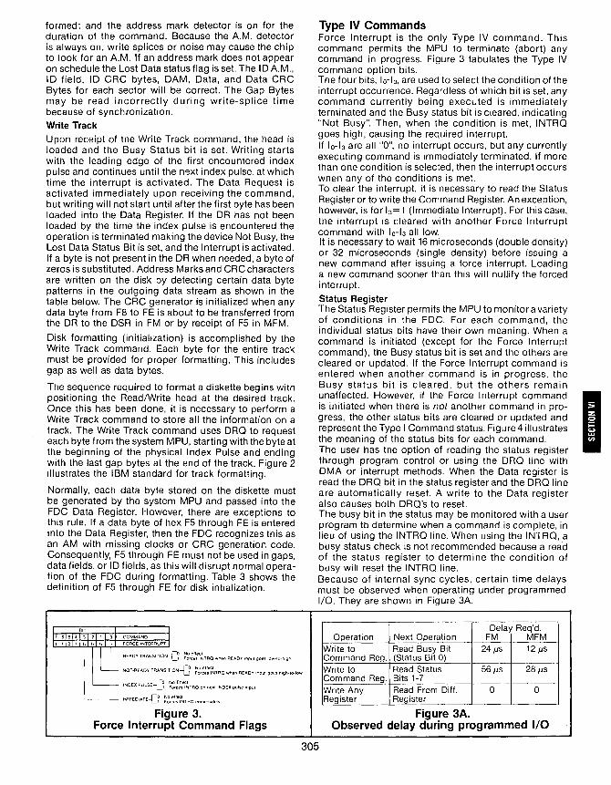
formed; and the address mark detector is on for the duration of the command. Because the A.M. detector is always on, write splices or noise may cause the chip to look for an A.M. If an address mark does not appear on schedule the Lost Data status flag is set. The ID A.M., ID field, ID CRC bytes, DAM, Data, and Data CRC Bytes for each sector will be correct. The Gap Bytes may be read incorrectly during write-splice time because of synchronization.
Write Track Upon receipt of the Write Track command, the head is loaded and the Busy Status bit is set. Writing starts with the leading edge of the first encountered index pulse and continues until the n9xt index pulse, at which time the interrupt is activated. The Data Request is activated immediately upon receiving the command, but writing will not start until after the first byte has been loaded into the Data Register. If the DR has not been loaded by the time the index pulse is encountered the operation is terminated making the device Not Busy, the Lost Data Status Bit is set, and the Interrupt is activated. If a byte is not present in the DR when needed, a byte of zeros is substituted. Address Marks and CRC characters are written on the disk by detecting certain data byte patterns in the outgoing data stream as shown in the table below. The CRC generator is initialized when any data byte from F8 to FE is about to be transferred from the DR to the DSR in FM or by receipt of F5 in MFM.
Disk formatting (initialization) is accomplished by the Write Track command. Each byte for the entire track must be provided for proper formatting. This includes gap as well as data bytes.
The sequence required to format a diskette begins with positioning the Read/Write head at the desired track. Once this has been done, it is necessary to perform a Write Track command to store all the information on a track. The Write Track command uses DRO to request each byte from the system MPU, starting with the byte at the beginning of the physical Index Pulse and ending with the last gap bytes at the end of the track. Figure 2 illustrates the IBM standard for track formatting.
Normally, each data byte stored on the diskette must be generated by the system MPU and passed into the FDC Data Register. However, there are exceptions to this rule. If a data byte of hex F5 through FE is entered into the Data Register, then the FDC recognizes this as an AM with missing clocks or CRC generation code. Consequently, F5 through FE must not be used in gaps, data fields, or ID fields, as this will disrupt normal operation of the FDC during formatting. Table 3 shows the definition of F5 through FE for disk intialization.
r BIT I I 7654 3 2 , 0 COMMAND
110' " I, I, I, FORCE INTERRUPT L.= -CO No olleel AEADY TRANSITION 1 Forces INTRQ wl"len READY Input gops low-ta-hlgh
NOT-READY TRANSITION-[~ ~~r~;~ef~TRQ when READY Input goes hlgh-Io-Iow
INDEX PULSE-[~ ~~rcE;~e;:~TRa on next INDEX pulse Input
L--- IMMEOIATE-[~ ~~r::I~~TAQ Immediately
Figure 3. Force Interrupt Command Flags
Type IV Commands Force Interrupt is the only Type IV command. This command permits the MPU to terminate (abort) any command in progress. Figure 3 tabulates the Type IV command option bits. The four bits, la-b, are used to select the condition of the interrupt occurrence. Regardless of which bit is set, any command currently being executed is immediately terminated and the Busy status bit is cleared, indicating "Not Busy". Then, when the condition is met, INTRa goes high, causing the required interrupt. If la-b are all "0", no interrupt occurs, but any currently executing command is immediately terminated. If more than one condition is selected, then the interrupt occurs when any of the conditions is met. To clear the interrupt, it is necessary to read the Status Register or to write the Command Register. An exception, however, is for 13= 1 (Immediate Interrupt). For this case, the interrupt is cleared with another Force Interrupt command with la-b all low. It is necessary to wait 16 microseconds (double density) or 32 microseconds (single density) before issuing a new command after issuing a force interrupt. Loading a new command sooner than this will nullify the forced interrupt. Status Register The Status Register permits the MPU to monitor a variety of conditions in the FDC. For each command, the individual status bits have their own meaning. When a command is initiated (except for the Force Interrupt command), the Busy status bit is set and the others are cleared or updated. If the Force Interrupt command is entered when another command is in progress, the Busy status bit is cleared, but the others remain unaffected. However, if the Force Interrupt command I is initiated when there is not another command in pro-gress, the other status bits are cleared or updated and -represent the Type I Command status. Figure4 illustrates the meaning of the status bits for each command. The user has the option of reading the status register through program control or using the DRO line with DMA or interrupt methods. When the Data register is read the DRO bit in the status register and the DRO line are automatically reset. A write to the Data register also causes both DRO's to reset. The busy bit in the status may be monitored with a user program to determine when a command is complete, in lieu of using the INTRa line. When using the INTRa, a busy status check is not recommended because a read of the status register to determine the condition of busy will reset the INTRa line. Because of internal sync cycles, certain time delays must be observed when operating under programmed I/O. They are shown in Figure 3A.
Delay Req'd. Operation Next Operation FM MFM
Write to Read Busy Bit 2411S 1211S Command Reg. (Status Bit 0) Write to Read Status 5611S 2811S Command Reg. Bits 1-7
Write Any Read From Ditt. 0 0 Register Register
Figure 3A. Observed delay during programmed I/O
305

Figure 4A. Status Register Summary
COMMAND STATUS BIT
7 6 5 4 3 2 1 0
ALL TYPE I Not Ready Write Protect Head Loaded Seek Error CRC Error Track 0 Index Busy
READ SECTOR Not Ready 0 Record Type Rec not Found CRC Error Lost Data DRO Busy
WRITE SECTOR Not Ready Write Protect Write Fault Rec not Found CRC Error Lost Data DRO Busy
READ ADDRESS Not Ready 0 0 Rec not Found CRC Error Lost Data DRO Busy
READ TRACK Not Ready 0 0 0 0 Lost Data DRO Busy
WRITE TRACK Not Ready Write Protect Write Fault 0 0 Lost Data DRO Busy
Figure 48. Status Description for Type. 1 Commands
BIT NAME MEANING
S7 NOT READY This bit when set indicates the drive is not ready. When reset it indicates that the drive is ready. This bit is an inverted copy of the Ready input and logically 'ored' with MR.
S6 PROTECTED When set, indicates Write Protect is activated. This bit is an inverted copy of WRPT input.
S5 HEAD LOADED When set, it indicates the head is loaded and engaged. This bit is a logical "and" of HLD and HLT signals.
S4 SEEK ERROR When set, the desired track was not verified. This bit is reset to 0 when updated.
S3 CRC ERROR CRC encountered in ID field.
S2 TRACK 00 When set, indicates Read/Write head is positioned to Track O. This bit is an inverted copy of the TROO input.
S1 INDEX When set, indicates index mark detected from drive. This bit is an inverted copy of the fi5 input.
SO BUSY When set command is in progress. When reset no command is in progress.
Figure 4C. Status Description for Type II and III Commands
BIT NAME MEANING
S7 NOT READY This bit when set indicates the drive is not ready. When reset, it indicates that the drive is ready. This bit is an inverted copy of the Ready input and 'ored' with MR. The Type II and III Commands will not execute unless the drive is ready.
S6 WRITE PROTECT On Read Record: Not Used. On Read Track: Not Used. On any Write: It indicates a Write Protect. This bit is reset when updated.
S5 RECORD TYPE/ On Read Record: It indicates the record-type code from data field address mark. WRITE FAULT 1 = Deleted Data Mark. 0= Data Mark. On any Write: It indicates a Write Fault. This bit is
reset when updated.
S4 RECORD NOT When set, it indicates that the desired track, sector, or side were not found. This bit is reset FOUND (RNF) when updated.
S3 CRC ERROR If S4 is set, an error is found in one or more ID fields; otherwise it indicates error in data field. This bit is reset when updated.
S2 LOST DATA When set, it indicates the computer did not respond to DRQ in one byte time. This bit is reset to zero when updated.
S1 DATA REQUEST This bit is a copy of the DRQ output. When set, it indicates the DR is full on a Read Operation or the DR is empty on a Write operation. This bit is reset to zero when updated.
SO BUSY When set, command is under execution. When reset, no command is under execution.
306

I
Write Data Timing:
PARAMETER SYMBOL MIN. TYP. MAX. UNITS
Write Data Pulse Width Twp 900 1000 550 nsec 300 500 250 nsec
Write Gate to Write Data Twg 4 j1sec 2 j1sec
Write data cycle Time Tbc 4,6,or8 j1sec Early (Late) to Write Data Ts 250 nsec Early (Late) From Th 250 nsec Write Data Write Gate off from WD Twf 4 j1sec
2 j1sec WD Valid to Clk TWdl 100 nsec WD Valid after Clk Twd2 100 nsec
WRITE GATE ~ L --l Twg f..--TbC ~ Twp 1--1 .. ----.. ~I Twf ~
WRITE DATA II ..... __ ...... !I .... __ ...... II .... __ _
r .. ---50ons----a ... ~1 elK
(lMHZ) 1'-______ ----'1 L I
TWdl~
307
CONDITIONS
I FM
,MFM FM
MFM ±CLK Error
MFM MFM
FM MFM
I

MAXIMUM GUARANTEED RATINGS· Operating Temperature Range .......................................................... 0° C to + 70° C Storage Temperature Range ........................................................ -55°C to +150°C lead Temperature (soldering, 10 sec.) ........................................................ +325°C Positive Voltage on any Pin, with respect to ground ............................................... +15V Negative Voltage on any Pin, with respect to ground ............................................. -0.3V ·Stresses above those listed may cause permanent damage to the device. This is a stress rating only and functional operation of the device at these or at any other condition above those indicated in the operational sections of this specification is not implied.
NOTE: When powering this device from laboratory or system power supplies, it is important that the Absolute Maximum Ratings not be exceeded or device failure can result. Some power supplies exhibit voltage spikes or "glitches" on their outputs when the AC power is switched on and off. In addition, voltage transients on the AC power line may appear on the DC output. If this possibility exists it is suggested that a clamp circuit be used.
ELECTRICAL CHARACTERISTICS (TA=O°C to 70°C, Vcc=+5V±5%, Voo=+12V±5% unless otherwise noted)
PARAMETER SYMBOL MIN TYP MAX UNIT COMMENTS DC CHARACTERISTICS
Input Voltage levels low level, VIL High level, VIH
Output Voltage levels low level VOL High level VOH
Output leakage, ILO Input leakage, IlL Output Capacitance Input Capacitance Power Dissipation
AC CHARACTERISTICS Processor Read Timing
Address Setup Time Address Hold Time RE Pulse Width (CL=50pF) ORO Reset Time INTRa Reset Time Data Delay Time (CL =50pF) Data Hold Time (CL =50pF)
Microprocessor Write Timing Address Setup Time Address Hold Time WE Pulse Width ORO Reset Time INTRa Reset Tirne Data Setup Time Data Hold Time
Disk Input Data Timing RAWREAD Pulse Width Clock Setup Time Clock Hold Time for MFM Clock Hold Time for FM RAWREAD Cycle Time
RClK High Pulse Width
RClK low Pulse Width
RClK Cycle Time
Miscellaneous Timing ClK low Pulse Width ClK High Pulse Width
STEP Pulse Width
DIRC Setup Time MR Pulse Width IP Pulse Width WF Pulse Width ClK Cycle Time
MFM FM MFM FM MFM FM
MFM FM
tSETR tHLOR
tRE tORR' tlRR
tOACC tOOH
tSETW tHLOW
tWE tORR tlRR tos tOH
2.6
2.8
50 10
400
50
50 10
350
250 70
100 40 40 40
3000 1.6 1.6 1.6 1.6
460 460
4 8
50 10 10
308
5 10
1000
1000
200
2 4 2 4 4 8
500 500
24
1.0
0.8
0.45
10 10
600
500 6000 350 150
500 6000
20000 20000
V V
V V
IJA IJA pf pf
mW
ns ns ns ns ns ns ns
ns ns ns ns ns ns ns
ns ns ns ns ns IJS IJS IJS IJs IJS IJS
ns ns IJS IJs IJS IJs IJs IJS IJS
IOL=1.0 mA IOH=100 IJA
VOUT=VOO VIN=VOO
Figure 5 Figure 5 Figure 5 Figure 5 Figure 5 Figure 5 Figure 5
Figure 6 Figure 6 Figure 6 Figure 6 Figure 6 Figure 6 Figure 6
Figure 7, See Note Figure 7 See Note
Figure 7 Figure 7
3600 at 70° C, Figure 7 Figure 7 Figure 7 Figure 7 Figure 7 Figure 7 Figure 7
Figure 8 Figure 8 Figure 8 Figure 8 Figure 8 Figure 8 Figure 8 Figure 8 Figure 8

Figure 5. ,-
32115 (MFM) or 64115 (FM) -I Microprocessor --j Tonn r-Read Timing
ORO ! ~ 1 TlRn===:j
INTRO~ I ~ cs----± I :TH'F_ - - - - -- ------AD.A, _ _ _ _ _ _ I
FiE ~TSETt-TRE-1
"----J. TOACC-1 t= 1
DALo-OAL, CD ~ToaH~
Figure 6.
I- 32tJS (MFM) or 64115 (FM) -, Microprocessor -i TORR r-Write Timing /
~ 1 ORO
T'RR~
INTRO~ I 4 ~ I T
HLO f:-= cs---- x I I r-------------AD.A, - - - - - - I
WE ~Tsn:t--TwE-i •
"---1 -1 Tos 1-
OALD-OAL, CO -1 TOH r-Figure 7. ~-r--t". the -I Disk Input Timing RAWREAO
U U
--1 t" ~.t:.~ I
RCLK I I I I
~T' -I- T"~ T,
Nuh' Pul~t' width on HAW READ (PHI 27) IS normally 10-300 ns However. pulse may be any wlattl If pulsp IS entirely ""IIU,ln window If pulse uccurs III both wln(1uws. then pulse width must,be less than 600 ns for MI-M i'lt elK 1 MHz and LJUU 11:, for FM at 1 MHl
Figure 8. iP
Miscellaneous I I Timing WF
f--T'p~ I I
MR ~Tw,--j I I
~Tc,c~ ~TMR--1 CLK~
-I+~ TCD2
OIRc--l STEP IN I~
rTa'R-j f---TSTP I-TO'R .j f---- TslP
STEP n H n
309

DISK FORMATS
Disks may be formatted in IBM 3740 or System 34 formats with sector lengths of 128, 256, 512, or 1024 bytes. IBM 3740 Format This single-density (FM) format utilizes 128 bytes/ sector. The bytes to be generated by the system MPU for use in the execution of the Write Track command are shown in Figure 9. IBM System 34 Format This double-density (MFM) format utilizes 256 bytes/sector. The bytes to be generated by the system MPU for use in the execution of the Write Track command are shown in Figure 10. Non-IBM Formats Unique (non-IBM) formats are permissible providing the following restrictions are understood. • Sector length may only be 128, 256, 512, or
1024 bytes. • Gap sizes must conform to Figure 11. In addition, the Index Address Mark is not required for operation by the FOG 176X. Gap 1, 3, and 4 lengths can be as short as 2 bytes for FOG 176X operation, however PLL lock up time, motor speed variation, write-splice area, etc. will add more bytes to each gap to achieve proper operation. It is recommended that the appropriate format be used for highest system reliability.
ONE SECTOR
CD
Figure 9. Byte Sequence for IBM 3740 Formatting
DATA BYTE (hex)
FF
00
FC
FF
00
FE
XX
OX
XX
00
F7
FF
00
FB E5
F7
FF
FF
NO. OF BYTES
4:]-1
':]-1
1
1
1
1
1
1~J 1
128
1
27
247 (i)
COMMENTS
f-Gap 5 (Post Index)
Index AM
Gap 1
IDAM Track Number (0D-4C)
Side Number (00 or 01)
Sector Number (01-1A)
Sector Length (128 bytes)
Causes 2-Byte CRC to be Written
Gap 2 (ID Gap)
Data AM Data Field
Causes 2-Byte CRC to be Written
Part of Gap 3 (Data Gap)
Gap 4 (pre Index)
NOTES: 1 THIS PATTERN MUST BE WRITTEN 26 TIMES PER TRACK. 2. CONTINUE WRITING HEX FF UNTIL FDC COMPLETES
SEQUENCE AND GENERATES INTRQ INTERRUPT
ONE SECTOR
CD
Figure 10. Byte Sequence for IBM System-34 Formatting
GAP
Gap 1
Gap 2
Gap 3
Gap 4
DATA NO.OF BYTE COMMENTS
(hex) BYTES
4E '1 Gap 5 - (Post Index)
00 12 F6 3 Writes C2 FC 1 Index AM 4E 5~J-00 12 -Gap 1
F5 3 WritesA1
FE 1 lOAM XX 1 Track Number
(00-4C) OX 1 Side Number
(00 or 01) XX 1 Sector Number
(01-1A) 01 1 Sector Length
(256 Bytes) F7 1 Causes 2-Byte
CRC to be Written
4E 2~J f-Gap 2 (lD Gap) 00 12 F5 3 Writes A1
FB 1 Data AM 40 256 Data Field F7 1 Causes 2-Byte
CRC to be Written
4E 54 Part of Gap 3
598 (i) (Data Gap)
4E Gap 4 (Pre Index)
NOTES 1. THIS PATTERN MUST BE WRITTEN 26 TIMES PER TRACK.
2. CONTINUE WRITING HEX 4E UNTIL FDC COMPLETES SEQUENCE AND GENERATES INTRQ INTERRUPT.
SINGLE DOUBLE DENSITY DENSITY
(FM) (MFM)
16 bytes FF 16 bytes 4E
11 bytes FF 22 bytes 4F 6 bytes 00 12 bytes 00
3 bytes A1
10 bytes FF 16 bytes 4E 4 bytes 00 8 bytes 00
3 bytes A1
16 bytes FF 16 bytes 4E
NOTES' 1. THESE BYTES COUNTS ARE EXACT 2. THESE BYTES COUNTS ARE MINIMUM
EXCEPT FOR 3 BYTES A1. WHICH IS EXACT.
Figure 11. Gap Size Limitations '
NOTE
2
1
2
2
,J5~~~fr,~ ~ ~~ ~~ OfCilroiriiiiittiii so lOU callil!e!l ahead Of 'jOIn
Circuit diagrams utilizing SMC products are included as a means of illustrating typical semiconductor applications; consequently complete information sufficient for construction purposes is not necessarily given. The information has been carefully checked and is believed to be entirely reliable. However. no responsibility is assumed for inaccuracies. Furthermore, such information does not convey to the purchaser of the semiconductor devices described any license under the patent rights of SMC or others. SMC reserves the right to make changes at any time in order to improve design and supply the best product possible.
310
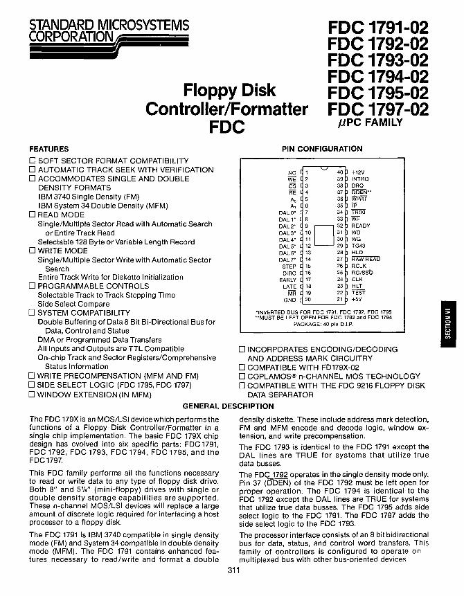
Floppy Oisk Controller/Formatter
FOC
Foe 1791-02 Foe 1792-02 Foe 1793-02 FOC 1794-02 Foe 1795-02 FOC 1797-02
j1PC FAMILY
FEATURES
o SOFT SECTOR FORMAT COMPATIBILITY o AUTOMATIC TRACK SEEK WITH VERIFICATION o ACCOMMODATES SINGLE AND DOUBLE
DENSITY FORMATS IBM 3740 Single Density (FM) IBM System 34 Double Density (MFM)
o READ MODE Single/Multiple Sector Read with Automatic Search
or Entire Track Read Selectable 128 Byte or Variable Length Record
o WRITE MODE Single/Multiple Sector Write with Automatic Sector
Search Entire Track Write for Diskette Initialization
o PROGRAMMABLE CONTROLS Selectable Track to Track Stepping Time Side Select Compare
o SYSTEM COMPATIBILITY Double Buffering of Data 8 Bit Bi-Directional Bus for
Data, Control and Status DMA or Programmed Data Transfers All Inputs and Outputs are TTL Compatible On-chip Track and Sector Registers/Comprehensive
Status Information o WRITE PRECOMPENSATION (MFM AND FM) o SIDE SELECT LOGIC (FDC 1795, FDC 1797) o WINDOW EXTENSION (IN MFM)
PIN CONFIGURATION
NC +12V WE INTRa
cs ORO RE DDEW·
Ao 5 WPRT A, jj5
DALO· TROO DAL 1· WF DAL2· READY DAL3· WD DAL4· WG DAL5· TG43 DAL6· HLD
DALl" RAW READ
STEP RCLK
DIRC RG/SSO EARLY CLK
LATE HLT
MR TEST
GND +5V
·INVERTED BUS FOR FOC 1791, FOC 1792, FDC 1795 ··MUST BE LEFT OPEN FOR FOC 1792 and FDC 1794
PACKAGE: 40 pin D.I.P.
o INCORPORATES ENCODING/DECODING AND ADDRESS MARK CIRCUITRY
o COMPATIBLE WITH FD179X-02 o COPLAMOS® n-CHANNEL MOS TECHNOLOGY o COMPATIBLE WITH THE FDC 9216 FLOPPY DISK
DATA SEPARATOR
GENERAL DESCRIPTION
The FDC 179X is an MOS/LSI device which performs the functions of a Floppy Disk Controller/Formatter in a single chip implementation. The basic FDC 179X chip design has evolved into six specific parts: FDC 1791, FDC 1792, FDC 1793, FDC 1794, FDC 1795, and the FDC 1797.
This FDC family performs all the functions necessary to read or write data to any type of floppy disk drive. Both 8" and 5114" (mini-floppy) drives with single or double density storage capabilities are supported. These n-channel MOS/LSI devices will replace a large amount of discrete logic required for interfacing a host processor to a floppy disk.
The FDC 1791 is IBM 3740 compatible in single density mode (FM) and System 34 compatible in double density mode (MFM). The FDC 1791 contains enhanced features necessary to read/write and format a double
311
density diskette. These include address mark detection, FM and MFM encode and decode logic, window extension, and write precompensation.
The FDC 1793 is identical to the FDC 1791 except the DAL lines are TRUE for systems that utilize true data busses. The FDC 1792 operates in the single density mode only. Pin 37 (DDEN) of the FDC 1792 must be left open for proper operation. The FDC 1794 is identical to the FDC 1792 except the DAL lines are TRUE for systems that utilize true data busses. The FDC 1795 adds side select logic to the FDC 1791. The FDC 1797 adds the side select logic to the FDC 1793.
The processor interface consists of an 8 bit bidirectional bus for data, status, and control word transfers. This family of controllers is configured to operate on multiplexed bus with other bus-oriented devices.
I

DAl
FDC 179X BLOCK DIAGRAM
'--------------< RClK
ORO WG
INTRa TG43
wmr f;TR WFNFOE
CS Jl5 ~ TR<5l:i
WE COMPUTER CONTROL PlA CONTROL DISK READY INTERFACE CONTROL INTERFACE
AO CONTROL (230 x 16) CONTROL STEP A1 DIRC
EARLY
LATE
ClK RG/SSO
DDEN HlD HLT
A ~ RAW READ
K DATA (8) .> RCLK ... .. AO RG
A1 LATE
cs EARLY
C FiE WD 0 +5 F M
WE l
P 0 U P T MR 10K P E . Y R
FLOPPY DISK WG
0 I CONTROlLER/
WPRT I N FORMATTER S T
~tVFOE: K
E +5V R
t 0
F iP R A I C TROO v E E
10K~ ~10K READY
~ ~ TG43 ~ ~ ORa STEP
INTRa DIRC
ClK
SYSTEM BLOC 1 +5V
~ HlD
I K DIAGRAM ~ ONE SHOT
HlT (IF USED) 1 DDEN f--e GND VDD Vee
~ 1 ~ ~ t +5V
+12 +5V
312

DESCRIPTION OF PIN FUNCTIONS
PIN NO. NAME SYMBOL FUNCTION
1 NO CONNECTION NC This pin is internally connected to the substrate bias generator and must be left open.
20 GROUND Vss Ground
21 POWER SUPPLY Vee +5V
40 POWER SUPPLY Voo +12V
19 MASTER RESET MR A logic low on this input resets the device and loads HEX 03 into the command regis~The Not Ready (Status Bit 7) is reset during MR ACTIVE. When MR is brought to a logic high a Restore Command is executed, regardless of the state of the Ready signal from the drive. Also, HEX 01 is loaded into the sector register.
COMPUTER INTERFACE:
2 WRITE ENABLE WE A logic low onJhis input gates data on the DAL into the selected register when CS is low.
3 CHIP SELECT CS A logic low on this input selects the chip and the parallel data bus (DAL).
4 READ ENABLE RE A logic low on this input controls the p'lacement of data from a selected register on DAL0-DAL7 when CS is low.
5,6 REGISTER SELECT AD, A1 These inputuelect the register to receive/transfer data on the DAL LINES lines under RE and WE control:
A1 AD RE WE 0 0 Status Reg Command Reg 0 1 Track Reg Track Reg 1 0 Sector Reg Sector Reg 1 1 Data Reg Data Reg
7-14 DATA ACCESS LINES DALO- Eight bit Bidirectional bus used for transillLof data, control, and DAL7 status. This~s is a receiver enabled by WE or a transmitter
enabled by RE. The Data Bus is inverted on the FDC 1791, FDC 1792 and FDC 1795.
24 CLOCK CLK This input requires a free-running square wave clock for internal timing reference, 2 MHz for 8" drives, 1 MHz for 51f4" drives. I
38 DATA REQUEST DRQ This open drain output indicates that the DR contains assembled data in Read operations, or the DR is empty in Write operations. This signal is reset when serviced by the computer through reading or loading the DR in Read or Write operations, respectively. Use a 10K pull-up resistor to +5V.
39 INTERRUPT REQUEST INTRQ This open drain output is set at the completion or termination of any operation and is reset when a new command is loaded into the command register or the status register is read. Use a 10K pull-up resistor to +5V.
FLOPPY DISK INTERFACE:
15 STEP STEP Step and direction motor control. The step output contains a pulse for each step.
16 DIRECTION DIRC Direction Output is active high when stepping in, active low when stepping out.
17 EARLY EARLY Indicates that the write data pulse occurring while Early is active (high) should be shifted early for write precompensation.
18 LATE LATE Indicates that the write data pulse occurring while Late is active (high) should be shifted late for write precompensation.
---- --22 TEST TEST This input is used for testing purposes only and should be tied to
+5V or left open by the user unless interfacing to voice coil actuated motors.
-- - --- - -------- -- ------- - -- -----23 HEAD LOAD TIMING HLT When a logic high is found on the HL T input the head is assumed
to be engaged. - ---- -- -- ---. ----- .--. -- -- ----- _. --- - - - _. _.
313

PIN NO. NAME SYMBOL FUNCTION
25 READ GATE (1791/3) RG A high level on this output indicates to the data separator circuitry that a field of zeros (or ones) has been encountered, and is used for synchronization.
25 SIDE SELECT OUTPUT SSO The logic level of the Side Select Output is directly controlled by (1795, 1797) the'S' flag in Type II or III commands .. When S=1, SSO is set to
a logic 1. When S=O, SSO is set to a logic O. The Side Select Output is only updated at the beginning of a Type II or III command. It is forced to a logic 0 upon a MASTER RESET condition.
26 READ CLOCK RCLK A nominal square-wave clock signal derived from the data stream must be provided to this input. Phasing (Le. RCLK transitions) relative to RAW READ is important but polarity (RCLK high or low) is not.
27 RAW READ RAW The data input signal directly from the drive. This input shall be a READ negative pulse for each recorded flux transition.
28 HEAD LOAD HLD The HLD output controls the loading of the Read-Write head against the media.
29 TRACK GREATER TG43 This output informs the drive that the Read/Write head is positioned THAN 43 between tracks 44-76. This output is valid only during Read and
Write Commands.
30 WRITE GATE WG This output is made valid before writing is to be performed on the diskette.
31 WRITE DATA WD A 250 ns (MFM) or 500 ns (FM) pulse perflux transition. WD contains the unique Address marks as well as data and clock in both FM and MFM formats.
32 READY READY This input indicates disk readiness and is sampled for a logic high before Read or Write commands are performed. If Ready is low the Read or Write operation is not performed and an interrupt is generated. Type I operations are performed regardless of the state of Ready. The Ready input appears in inverted format as Status Register bit 7.
33 WRITE FAULT/ WFNFOE This is a bi-directional signal used to signify writing faults at the VFO ENABLE drive, and to enable th..!L~xternal PLO data separator. When WG = 1,
Pin 33 functions as a WF input. If WF=O, any write command will immediately be terminated. When WG =0, Pin 33 functions as a VFOE output. VFOE will go low during.a read operation after the head has loaded and settled (HLT=1). On the 1795/7, it will remain low until the last bit of the second CRC byte in the 10 field. VFOE will then go high until 8 bytes (MFM) or 4 bytes (FM) before the Address Mark. It will then go active until the last bit of the second CRC byte of the Data Field. On the 1791/3, VFOE will remain low until the end of the Data Field.
34 TRACK 00 TROO This input informs the FDC179X that the Read/Write head is positioned over Track 00.
35 INDEX PULSE IP This input informs the FDC179X when the index hole is encountered on the diskette.
36 WRITE PROTECT WPRT This input is sampled whenever a Write Command is received. A logic low terminates the command and sets the Write Protect Status bit.
37 DOUBLE DENSITY DDEN This pin selects either single or double densi!Y...9..l2§ration. When DDEN=O, double density is selected. When DDEN=1, single density is selected. This line must be left open on the 1792/4.
314

FUNCTIONAL DESCRIPTION
The FDC 179X-02 major functional blocks are as follows: Data Shift Reglster-This 8-bit register assembles serial data from the Read Data input (RAW READ) during Read operations and transfers serial data to the Write Data output during Write operations. Data Reglster-This 8-bit register is used as a holding register during Disk Read and Write operations. In Disk Read operations the assembled data byte is transferred in parallel to the Data Register from the Data Shift Register. In Disk Write operations information is transferred in parallel from the Data Register to the Data Shift Register.
When executing the Seek command the Data Register holds the address of the desired Track position. This register is loaded from the DAl and gated onto the DAl under processor control.
Sector Register (SR) - This 8-bit register holds the address of the desired sector position. The contents of the register are compared with the recorded sector number in the ID field during disk Read or Write operations. The Sector Register contents can be loaded from or transferred to the DAL. This register should not be loaded when the device is busy.
Command Register (CR)-This 8-bit register holds the command presently being executed. This register should not be loaded when the device is busy unless the new command is a Force Interrupt. The command register can be loaded from the DAl, but not read onto the DAL. Status Register (STR)-This 8-bit register holds device Status information. The meaning of the Status bits is a function of the type of command previously executed.
This register can be read onto the DAl, but not loaded from the DAL.
CRC Loglc-This logic is used to check or to generate the 16-bit Cyclic Redundancy Check (CRG). The polynomial is: G(X)=X16+X12+X5+1.
Track Register-This 8-bit register holds the track number of the current Read/Write head position. It is incremented by one every time the head stepped in (towards track 76) and decremented by one when the head is stepped out (towards track 00). The contents of the register are compared with the recorded track number in the I D field during disk Read, Write, and Verify operations. The Track Register can be loaded from or transferred to the DAL. This Register should not be loaded when the device is busy.
The CRC includes all information starting with the address mark and up to the CRC characters. The CRC register is preset to ones prior to data being shifted through the circuit. Arithmetic/Logic Unit (ALU) - The AlU is a serial comparator, incrementer, and decrementer and is used for register modification and comparisons with the disk recorded I D field. Timing and Control-All computer and Floppy Disk Interface controls are generated through this logic. The internal device timing is generated from an external crystal clock. AM Detector-The address mark detector detects ID, data and index address marks during ready and write operations.
OPERATION
FDC 1791, FDC 1793, FDC 1795 and FDC 1797 have two modes of operation according to the state of DDEN (Pin 37). When 5ISE1'J=1, single density is selected. In either case, the ClK input (Pin 24) is at 2 MHz. However, when interfacing with the mini-floppy, the ClK input is set at 1 MHz for both single density and double density. When the clock is at 2 MHz, the stepping rates of 3, 6, 10, and 15 ms are obtainable. When ClK equals 1 MHz these times are doubled.
DDEN must be left open forthe FDC 1792 and FDC 1794.
Disk Read Operation Sector lengths of 128, 256, 512 or 1024 are obtainable in either FM or MFM formats. For FM, DDEN should be placed to logical "1." For MFM formats, DDEN should be placed to a logical "0." Sector lengths are determined at format time by a special byte in the "ID" field. If this Sector length byte in the ID field is zero, then the sector length is 128 bytes. If 01 then 256 bytes. If 02, then 512 bytes. If 03, then the sector length is 1024 bytes. The number of sectors per track can be from 1 to 255 sectors. The number of tracks is from 0 to 255 tracks. For read operations, the FDC 179X requires RAW READ Data (Pin 27) signal which is a 250 ns pulse per flux
provided by some drives but if not, it may be derived externally by Phase lock loops, one shots, or counter techniques. In addition, a Read Gate Signal is provided as an output (Pin 25) which can be used to inform phase lock loops when to acquire synchronization. When reading from the media in FM, RG is made true when 2 bytes of zeroes are detected. The FDC179X must find an address mark within the next 10 bytes; otherwise RG is reset and the search for 2 bytes of zeroes begins all over again. If an address mark is found within 10 bytes, RG remains true as long as the FDC179X is deriving any useful information from the data stream. Similarly for MFM, RG is made active when 4 bytes of "00" or "FF" are detected. The FDC179X must find an address mark within the next 16 bytes, otherwise RG is reset and search resumes. During read operations (WG =0). the VFOE (Pin 33) is provided for phase lock loop synchronization. VFOE will go active when:
a) Both HlT and HlD are True b) Settling Time, if programmed, has expired c) The 179X is inspecting data off the disk
If WFNFOE is not used, leave open or tie to a 10K resistor to +5.
transition and a Read clock (RClK) signal to indicate On Disk Read operations the Data Request is activated flux transition spacings. The RClK (Pin 26) signal is (set high) when an assembled serial input byte is
315
I

transferred in parallel to the Data Register. This bit is cleared when the Data Register is read by the processor. If the Data Register is read after one or more characters are lost by having new data transferred into the register prior to processor readout, the Lost Data bit is set in the Status Register. The Read operation continues until the end of sector is reached.
Disk Write Operation When writing is to take place on the diskette the Write Gate (WG) output is activated, allowing current to flow into the Read/Write head. As a precaution against erroneous writing the first data byte must be loaded into the Data Register in response to a Data Request from the FDC179X before the Write Gate signal can be activated. Writing is inhibited when the Write Protect input is a logic low, in which case any Write command is immediately terminated, an interrupt is generated and the Write Protect status bit is set. The Write Fault input, when activated, signifies a writing fault condition detected in disk drive electronics such as failure to detect write current flow when the Write Gate is activated. On detection of this fault the FDC179X terminates the current command, and sets the Write Fault bit (bit 5) in the Status Word. The Write Fault input should be made inactive when the Write Gate output becomes inactive. For write operations, the FDC179X provides Write Gate (Pin 30) and Write Data (Pin 31) outputs. Write data consists of a series of 500 ns pulses in FM (DDEN=1)
and 250 ns pulses in MFM (DDEN =0). Write Data provides the unique address marks in both formats. Also during write, two additional signals are provided for write precompensation. These are EARLY (Pin 17) and LATE (Pin 18). EARLY is active true when the WD pulse appearing on (Pin 30) is to be written early. LATE is active true when the WD pulse is to be written LATE. If both EARLY and LATE are low when the WD pulse is present, the WD pulse is to be written at nominal. Since write precompensation values vary from disk manufacturer to disk manufacturer, the actual value is determined by several one shots or delay lines which are located external to the FDC179X. The write precompensation signals EARLY and LATE are valid for the duration of WD in both FM and MFM formats.
On Disk Write operations the Data Request is activated when the Data Register transfers its contents to the Data Shift Register, and requires a new data byte. It is reset when the Data Register is loaded with new data by the processor. If new data is not loaded at the time the next serial byte is required by the Floppy Disk, a byte of zeroes is written on the diskette and the Lost Data bit is set in the Status Register.
At the completion of every command an INTRQ is generated. INTRQ is reset by either reading the status register or by loading the command register with a new command. In addition, INTRQ is generated if a Force Interrupt command condition is met.
COMMAND WORDS
The FDC179X will accept eleven commands. Command words should only be loaded in the Command Register when the Busy status bit is off (Status bit 0). The one exception is the Force Interrupt command. Whenever a command is being executed, the Busy status bit is set. When a command is completed, an interrupt is generated and the Busy status bit is reset. The Status Register indicates whether the completed command encountered an error or was fault free. For ease of discussion, commands are divided into four types. Commands and types are summarized in Table 1.
Table 1. Command Summary
BITS COMMAND TYPE 7 6 5 4 3 2 1 0 Restore I 0 0 0 0 h V r1 ro Seek I 0 0 0 1 h V r1 ro Step I 0 0 1 u h V r1 ro Step In I 0 1 0 u h V r1 ro Step Out I 0 1 1 u h V r1 ro Read Sector II 1 0 0 m F2 E F1 0 Write Sector II 1 0 1 m F2 E F1 ao Read Address III 1 1 0 0 0 E 0 0 Read Track III 1 1 1 0 0 E 0 0 Write Track III 1 1 1 1 0 E 0 0 Force Interrupt IV 1 1 0 1 b 12 11 10
316
Type I Commands The Type I Commands are Restore, Seek, Step, Step-In, and Step-Out. Each of the Type I Commands contains a rate field (rOr1), which determines the stepping motor rate as defined in Table 2. The Type I Commands contain a head load flag (h) which determines if the head is to be loaded at the beginning of the command. If h = 1, the head is loaded at the beginning of the command (HLD output is made active). If h =0, HLD is deactivated. Once the head is loaded, the head will remain engaged until the FDC179X receives a command that specifically disengages the head. If the FDC179X is idle (busy=O) for 15 revolutions of the disk, the head will be automatically disengaged (HLD made inactive). The Type I Commands also contain a verification (V) flag which determines if a verification op'eration is to take place on the destination track. If V = 1, a verification is performed, if V=O, no verification is performed. During verification, the head is loaded and after an internal 15 ms delay, the HLT input is sampled. When HLT is active (logic true), the first encountered ID field if read off the disk. The track address of the ID field is then compared to the Track Register; if there is a match and a valid I D CRC, the verification is complete, an interrupt is generated and the Busy status bit is reset. If there is not a match butthere is valid ID CRC, an interrupt

is generated, and Seek Error Status bit (Status bit 4) is set and the Busy status bit is reset. If there is a match but not a valid CRC, the CRC error status bit is set (Status bit 3), and the next encountered ID field is read from the disk for the verification operation. If an ID field with a valid CRC cannot be found after four revolutions of the disk, the FDC179X terminates the operation and sends an interrupt (INTRQ). The Step, Step-In, and Step-Out commands contain an Update flag (u). When u = 1, the track register is updated by one for each step. When u =0, the track register is not updated. On the FDC 1795/7 devices, the SSO output is not affected during Type 1 commands, and an internal side compare does not take place when the (V) Verify Flag is on ..
Restore (Seek Track 0) Upon receipt of this command the Track 00 (TROO) input is sampled. if TROO is active low indicating the Read-Write head is positioned over track 0, the Track Register is loaded with zeroes and an interrupt is generated. If TROO is not active low, stepping pulses (pins 15 to 16) at a rate specified by the r,ro field are issued until the TROO input is activated. At this time the Track Register is loaded with zeroes and an interrupt is generated. If the TROO input does not go active low after 255 stepping pulses, the FDC179X terminates operation, interrupts, and sets the Seek error status bit. A verification operation takes place if the V flag is set. The h bit allows the head to be loaded at the start of command. Note that the Restore command is executed when MR goes from. an active to an inactive state.
Seek This command assumes that the Track Registercontains the track number of the current position of the ReadWrite head and the Data Register contains the desired track number. The FDC179X will update the Track register and issue stepping pulses in the appropriate direction until the contents of the Track register are equal to the contents of the Data Register (the desired track location). A verification operation takes place ifthe V flag is on. The h bit allows the head to be loaded at the start of the command. An interrupt is generated at the completion of the command.
Step Upon receipt of this command, the FDC179X issues one stepping pulse to the disk drive. The stepping motor direction is the same as in the previous step command. After a delay determined by the r,ro field, a verification takes place if the V flag is on. If the u flag is on, the Track Register is updated. The h bit allows the head to be loaded at the start of the command. An interrupt is generated at the completion of the command.
Step-In Upon receipt of this command, the FDC179X issues one stepping pulse in the direction towards track 76. If the u flag is on, the Track Register is incremented by one. After a delay determined by the r,ro field, a verification takes place if the V flag is on. The h bit allows the head to be loaded at the start of the command. An interrupt is generated at the completion of the command.
317
Step-Out Upon receipt of this command, the FDC179X issues one stepping pulse in the direction towards track O. If the u flag is on, the Track Register is decremented by one. After a delay determined by the r, ro field, a verification takes place if the V flag is on. The h bit allows the head to be loaded at the start of command. An interrupt is generated at the completion of the command.
Head Positioning The period of each positioning step is specified by the r field in bits 1 and 0 of the command word. After the last directional step an additional 15 milliseconds of head settling time takes place if the Verify flag is set in Type I commands. Note that this time doubles to 30 ms for a 1 MHz clock. If TEST=O, there is zero settling time. There is also a 15 ms head settling time if the E flag is set in any Type II or III command. The rates (shown in Table 2) can be applied to a StepDirection Motor through the device interface. Step-A 2jJs (MFM) or4jJS (FM) pulse is provided asan output to the drive. For every step pulse issued, the drive moves one track location in a direction determined by the direction output. Direction (DIRe) - The Direction signal is active high when stepping in and low when stepping out. The Direction signal is valid 12 jJs before the first stepping pulse is generated. When a Seek, Step or Restore command is executed an optional verification of Read-Write head position can be performed by setting bit 2 (V= 1) in the command word to a logic 1. The verification operation begins at the end of the 15 millisecond settling time after the head is loaded against the media. The track number from the I first encountered ID Field is compared against the contents of the Track Register. If the track numbers -compare and the ID Field Cyclic Redundancy Check (CRC) is correct, the verify operation is complete and an INTRQ is generated with no errors. The FDC179X must find an ID field with correct track number and correct CRC within 5 revolutions of the media; otherwise the seek error is set and an I NTRQ is generated.
Table 2. Stepping Rates
elK: 2 MHz 2 MHz 1 MHz 1 MHz 2 MHz 1 MHz
DDEN: 0 1 0 1 X X
r1 ro TEST==1 TEST==1 TEST=':1 TEST==1 TEST==O TEST==O
0 0 3 ms 3 ms 6 ms 6 ms 1841JS 3681JS 0 1 6 ms 6 ms 12 ms 12 ms 190IJS 380ps 1 0 10 ms 10 ms 20 ms 20 ms 1981JS 396ps 1 1 15 ms 15 ms 30 ms 30 ms 2081JS 4161JS
The Head Load (HLD) output controls the movement of the read/write head against the media. HLD is activated at the beginning of a Type I command if the h flag is set (h= 1), at the end of the Type I command if the verify flag (V= 1), or upon receipt of any Type II or III command. Once HLD is active it remains active until either a Type I command is received with (h=O and V=O); or if the FDC179X is in an idle state (non-busy) and 15 index pulses have occurred. Head Load Timing (HLT) is an input to the FDC179X which is used for the head engage time. When HLT= 1, the FDC179X assumes the head is completely engaged.

The head engage time is typically 30 to 100 ms depending on drive. The low to high transition on HLD is typically used to fire a one shot. The output ofthe one shot is then used for HLT and supplied as an input to the FDC179X.
HLDJ"'--~ J.---so TO 100mS ~
f- - - -I r-I------j HLT (FROM ONE SHOT)
Head Load Timing
When both HLD and HLT are true, the FDC179X will then read from or write to the media. The "and" of HLD and HLT appears as a status bit in Type I status.
TYPE I COMMANDS FLAG SUMMARY h = Head Load Flag (Bit 3)
h = 1, Load head at beginning h=O, Unload head at beginning
V=Verifyflag (Bit2) V= 1, Verify on destination track V=O, No verify
r, ro= Stepping motor rate (Bits 1-0)
Refer to Table 2 for rate summary u=Updateflag (Bit4)
u=1, Update Track register u=O, No update
Type II Commands The Type II Commands are the Read Sector and Write Sector commands. Prior to loading the Type II Command into the Command Register, the system must load the Sector Register with the desired sector number. Upon receipt of the Type II command, the busy status Bit is set. If the E flag =1 (this is the normal case) HLD is made active and HLT is sampled until true after a 15 msecdelay. If the E flag is 0, HLD is made active and HLT is sampled with no delay until true. The 10 field and Data Field format are shown below. When an 10 field is located on the disk, the FDC179X compares the Track Number on the 10 field with the Track Register. If there is not a match, the next encountered 10 field is read and a comparison is again made. If there
is a match, the Sector Number of the ID field is compared with the Sector Register. If there is not a Sector match, the next encou'ntered ID field is read off the disk and comparisons again made. If the ID field CRC is correct, the data field is then located and will be either written into, or read from depending upon the command. The FDC179X must find an ID field with a Track number, Sector number, side number, and CRC within four revolutions of the disk; otherwise, the Record not found status bit is set (Status bit 3) and the command is terminated with an interrupt. Each of the Type II Commands contains an (m) flag which determines if multiple records (sectors) are to be read or written, depending upon the command. If m=O, a single sector is read or written and an interrupt is generated at the completion of the command. If m = 1, multiple records are read or written with the sector register internally updated so that an address verification can occur on the next record. The FDC179X will read or write multiple records starting with the sector presently in the sector register. The FDC179X will continue to read or write multiple records and update the sector register until the sector register exceeds the number of sectors on the track or until the Force Interrupt command is loaded into the Command Register, which terminates the command and generates an interrupt. If the Sector Register exceeds the number of sectors on the track, the Record-Not-Found status bit will be set. The Type II commands also contain side select compare flags. WhenC=O, no side comparison is made. When C= 1, the LSB of the side number is read off the ID Field of the disk and compared with the contents of the (S) flag. If the S flag compares with the side number recorded in the ID field, the 179X continues with the ID search. If a comparison is not made within 5 index pulses, the interrupt line is made active and the RecordNot-Found status bit is set. The FDC179517 READ SECTOR and WRITE SECTOR commands include a 'b' flag. The 'b' flag, in conjunction with the sector length byte of the ID Field, allows different byte lengths to be implemented in each sector. For IBM compatability, the 'b' flag should be set to a one. The 's' flag allows direct control over the SSO Line (Pin 25) and is set or reset at the beginning of the command, dependent upon the value of this flag.
Sector Length Table (1791/2/3/4 only) Sector Length Number of Bytes
Field (hex) in Sector (decimal) 00 128 01 256 02 512 03 1024
Field Format
GAP III
CRC 2
In MFM only, lOAM and DATA AM are preceded by three bytes of A 1 with clock transition between bits 4 and 5 missing. 318

Read Sector Upon receipt of the Read Sector command, the head is loaded, the Busy status bit set, and when an ID field is encountered that has the correct track number, correct sector number, correct side number, and correct CRC, the data field is presented to the computer. The Data Address Mark of the data field must be found within 30 bytes in single density and 43 bytes in double density of the last ID field CRC byte; if not, the Record-NotFound status bit is set and the operation is terminated. When the first character or byte of the data field has been shifted through the DSR, it is transferred to the DR, and DRO is generated. When the next byte is accumulated in the DSR, it is transferred to the DR and another DRO is generated. If the Computer has not read the previous contents of the DR before a new character is transferred that character is lost and the Lost Data Status bit is set. This sequence continues until the complete data field has been inputted to the computer. If there is a CRC error at the end of the data field, the CRC error status bit is set, and the command is terminated (even if it is a multiple record command). At the end of the Read operation, the type of Data Address Mark encountered in the data field is recorded in the Status Register (Bit 5) as shown below:
STATUS BIT 5
1 o
7 6
1 0
5
0
BIT
432
Deleted Data Mark Data Mark
1 0 COMMAND
m F2 E F, 0 READ SECTOR
1 0 1 m F2 E F, ao WRITE SECTOR
Write Sector Upon receipt of the Write Sector command, the head is loaded (HLD active) and the Busy status bit is set. When an ID field is encountered that has the correct track number, correct sector number, correct side number, and correct CRC, a DRO is generated. The FDC179X counts off 11 bytes in single density and 22 bytes in double density from the CRC field and the Write Gate (WG) output is made active if the DRO is serviced (Le., the DR has been loaded by the computer). If DRO has not been serviced, the command is terminated and the Lost Data status bit is set. If the DRO has been serviced, the WG is made active and six bytes of zeros in single density and 12 bytes in double density are then written on the disk. At this time the Data Address Mark is then written on the disk as determined by the ao field of the command as shown below:
ao 1 o
Data Address Mark (Bit 0) Deleted Data Mark Data Mark
The FDC179X then writes the data field and generates DRO's to the computer. If the DRO is not serviced in time for continuous writing the Lost Data Status Bit is set and a byte of zeros is written on the disk. The command is not terminated. After the last data byte has been written on the disk, the two-byte CRC is computed internally and written on the disk followed by one byte of logic ones in FM or in MFM. The WG output is then deactivated.
L DATA AD DRESS MARK (a) rO=Write hex FB (data) into Data Address Mark field o L1 =Write hex F8 (deleted data) into Data AM field
F, (179113)
F, (1795/7)
DELAY (E)
r- F2 (1791/3)
L- F2 (1795n)
MULTIPLE
SIDE COMPARE FLAG (C) rO=S~de number not tested L1=Slde number tested
SIDE SELECT FLAG (S) ---C0=UPdate SSO to 0 1=Update SSO to 1
_ ro=No delay between HLD activation and HLT Sampling L1 =15 ms delay between HLD activating and HLT Sampling
SIDE SELECT FLAG (S) -C0=compare for side 0 1=Compare for side 1
Sector Length Field 00 01 10 11
SECTOR LENGTH FLAG (b)C01_: 256 512 1024 128 128 256 512 1024
SECTORS ( ){O=Read (or Write) Single Sectors m 1 =Read (or Write) Multiple Sectors
Figure 1. Type II and III Flag Summary
319
I

Type III Commands There are three Type III Commands: • READ ADDRESS-Read the next ID field (6 bytes)
into the FDC. • READ TRACK-Read all bytes of the entire track,
including gaps. • WRITE TRACK-Write all bytes to the entire track,
including gaps. Read Address Upon receipt of the Read Address command, the head is loaded and the Busy Status Bit is set. The next encountered ID field is then read in from the disk, and the six data bytes of the I D field are assembled and transferred to the DR, and a DRO is generated for each byte. The six bytes of the ID field are shown below:
TRACK ADDR
Although the CRC characters are transferred to the computer, the FDC179X checks for validity and the CRC
iP_--..... u
GAP 3
SINGLE SIDED: DOUBLE SIDED. DOUBLE SIDED.
SECTOR NO.
OHA 01-0F 01-08
'DR=F5 WRITE 3 TIMES MFM ONLY
error status bit is set if there is a CRC error. The Track Address of the ID field is written into the sector register. At the end of the operation an interrupt is generated and the Busy Status is reset. Read Track
Upon receipt of the Read Track command, the head is loaded and the Busy Status bit is set. Reading starts with the leading edge of the first encountered index pulse and continues until the next index pulse. As each byte is assembled it is transferred to the Data Register and the Data Request is generated for each byte. No CRC checking is performed. Gaps are included in the input data stream. The accumulation of bytes issynchronized to each Address Mark encountered. Upon completion of the command, the interrupt is activated. RG is not activated during the Read Track Command. An internal side compare is not performed during a Read Track.
Write Track Upon receipt of the Write Track command, the head is loaded and the Busy Status bit is set. Writing starts with the leading edge of the first encountered index pulse and continues until the next index pulse, at which
\-- COMPLETE SECTOR --I DATA GAP 10 GAP DATA GAP
FIELD 1 3 FIELD 2 2 FIELD 2 3
SECTOR LENGTH
00= 128 01= 256 02= 512 03= 1024
Figure 2. IBM Compatible Sector/Track Format
320

time the interrupt is activated. The Data Request is activated immediately upon receiving the command, but writing will not start until after the first byte has been loaded into the Data Register. If the DR has not been loaded by the time the index pulse is encountered the operation is terminated making the device Not Busy, the Lost Data Status Bit is set, and the Interrupt is activated. If a byte is not present in the DR when needed, a byte of zeros is substituted. Address Marks and CRCcharacters are written on the disk by detecting certain data byte patterns in the outgoing data stream as shown in the table below. The CRC generator is initialized when any data byte from F8 to FE is about to be transferred from the DR to the DSR in FM or by receipt of FS in MFM. Disk formatting (initialization) is accomplished by the Write Track command. Each byte for the entire track must be provided for proper formatting. This includes gap as well as data bytes. The sequence required to format a diskette begins with positioning the Read/Write head at the desired track. Once this has been done, it is necessary to perform a Write Track command to store all the information on a track. The Write Track command uses DRO to request each byte from the system MPU, starting with the byte at the beginning of the physical Index Pulse and ending with the last gap bytes at the end of the track. Figure 2 illustrates the IBM standard for track formatting. Normally, each data byte stored on the diskette must be generated by the system MPU and passed into the FDC Data Register. However, there are exceptions to this rule. If a data byte of hex FS through FE is entered into the Data Register, then the FDC recognizes this as an AM with missing clocks or CRC generation code. Consequently, FS through FE must not be used in gaps, data fields, or ID fields, as this will disrupt normal operation of the FDC during formatting.
BIT
716151413121110 COMMAND
1 11 1011 1 b 1 121 I, 1 10 FORCE INTERRUPT
Type IV Commands Force Interrupt is the only Type IV command. This command permits the MPU to terminate (abort) any command in progress. Figure 3 tabulates the Type IV command option bits. The four bits, la-b, are used to select the condition of the interrupt occurrence. Regardless of which bit is set, any command currently being executed is immediately terminated and the Busy status bit is cleared, indicating "Not Busy". Then, when the condition is met, INTRa goes high, causing the required interrupt. If la-b are all "0", no interrupt occurs, but any currently executing command is immediately terminated. If more than one condition is selected, then the interrupt occurs when any of the conditions is met. To clear the interrupt, it is necessary to read the Status Register or to write the Command Register. An exception, however, is for b= 1 (Immediate Interrupt). For this case, the interrupt is cleared with another Force Interrupt command with la-b all low.
Status Register The Status Register permits the MPU to monitor a variety of conditions in the FOC. For each command, the individual status bits have their own meaning. When a command is initiated (except for the Force Interrupt command), the Busy status bit is set and the others are cleared or updated. If the Force Interrupt command is entered when another command is in progress, the Busy status bit is cleared, but the others remain unaffected. However, if the Force Interrupt command is initiated when there is not another command in progress, the other status bits are cleared or updated and represent the Type I Com mand status. Figu re 4 ill ustrates the meaning of the status bits for each command.
L READY TRANSITION -CO = No effect 1 = Forces INTRa when READY input goes low-to-high
'---- NOT-READY TRANSIT ION-Go=NO effect 1 = Forces INTRa when READY input goes high-to-Iow
INDEX PULSE-[~: No Effect Forces INTRa on next INDEX pulse input
-[ effect
1 = Forces INTRa immediately IMMEDIATE O=No
Figure 3. Force Interrupt Command Flags
321
I

Figure 4A. Status Register Summary
COMMAND STATUS BIT 7 6 5 4 3 2 1 0
ALL TYPE I Not Ready Write Protect Head Loaded Seek Error CRC Error Track 0 Index Busy
READ SECTOR Not Ready 0 Record Type Rec not Found CRC Error Lost Data DRO Busy
WRITE SECTOR Not Ready Write Protect Write Fault Rec not Found CRC Error Lost Data DRO Busy READ ADDRESS Not Ready 0 0 Rec not Found CRC Error Lost Data DRO Busy
READ TRACK Not Ready 0 0 0 0 Lost Data DRO Busy
WRITE TRACK Not Ready Write Protect Write Fault 0 0 Lost Data DRO Busy
Figure 4B. Status Description for Type I Commands
BIT NAME MEANING S7 NOT READY This bit when set indicates the drive is not ready. When reset it indicates that the drive is
ready. This bit is an inverted copy of the Ready input and logically 'ored' with MR.
S6 PROTECTED When set, indicates Write Protect is activated. This bit is an inverted copy of WRPT input
S5 HEAD LOADED When set, it indicates the head is loaded and engaged. This bit is a logical "and" of HLD and HLT signals.
S4 SEEK ERROR When set, the desired track was not verified. This bit is reset to 0 when updated.
S3 CRC ERROR CRC encountered in ID field.
S2 TRACK 00 When set, indicates Read/Write head is positioned to Track O. This bit is an inverted copy of the TROO input.
S1 INDEX ~hen set, indicates index mark detected from drive. This bit is an inverted copy of the IP input.
SO BUSY When set command is in progress. When reset no command is in progress.
Figure 4C. Status Description for Type II and III Commands
BIT NAME MEANING S7 NOT READY This bit when set indicates the drive is not ready. When reset, it indicates that the drive
is ready. This bit is an inverted copy of the Ready input and 'ored' with MR. The Type II and III Commands will not execute unless the drive is ready.
S6 WRITE PROTECT On Read Record: Not Used .. On Read Track: Not Used. On any Write: It indicates a Write Protect. This bit is reset when updated.
S5 RECORD TYPE/ On Read Record: It indicates the record-type code from data field address mark. WRITE FAULT 1 = Deleted Data Mark. 0= Data Mark. On any Write: It indicates a Write Fault. This bit is
reset when updated.
S4 RECORD NOT When set, it indicates that the desired track, sector, or side were not found. This bit is reset FOUND (RNF) when updated.
S3 CRC ERROR If S4 is set, an error is found in one or more ID fields; otherwise it indicates error in data field. This bit is reset when updated.
S2 LOST DATA When set, it indicates the computer did not respond to DRQ in one byte time. This bit is reset to zero when updated.
S1 DATA REQUEST This bit is a copy of the DRQ output. When set, it indicates the DR is full on a Read Operation or the DR is empty on a Write operation. This bit is reset to zero when updated.
SO BUSY When set, command is under execution. When reset, no command is under execution.
322

Write Data Timing:
PARAMETER SYMBOL MIN. TYP. MAX. UNITS
Write Data Pulse Width Twp 450 500 550 nsec 150 200 250 nsec
Write Gate to Write Data Twg 2 fJsec 1 fJsec
Write data cyle Time Tbc 2,3,or4 fJsec Early (Late) to Write Data Ts 125 nsec Early (Late) From Th 125 nsec Write Data Write Gate off from WD Twf 2 fJsec
1 fJsec WD Valid to Clk TWdl 100 nsec
50 nsec WD Valid after Clk Twd2 100 nsec
30 nsec
These values are doubled when CLK= 1 MHz.
Write Data Timing
WRITE GATE --1 L --I Twg I---TbC ---l Twp I ...... ----------.. .-jl Twf j.-
WRITE DATA __ ---IIlL ______ Il ..... ______ Il'--__ _
'----500 ns ----.j.,,1 ClK 1-
(IMHZ) 1 ..... _______ ----', L I
TWdl---j
1---125 ClK I
(2MHZ) IL _______ --li
TWdl--l WRITE DATA/CLOCK RELATIONSHIP
(DDEN=O)
323
125----l
~TWd2
CONDITIONS
FM MFM FM
MFM ±CLK Error
MFM MFM
FM MFM
CLK=1 MHZ CLK=2 MHZ CLK=1 MHZ CLK=2 MHZ
I

MAXIMUM GUARANTEED RATINGS· Operating Temperature Range .......................................................... 0° C to + 70° C Storage Temperature Range ....................... , ................................. -55°C to +150°C lead Temperature (soldering, 10 sec.) ........................................................ +325°C Positive Voltage on any Pin, with respect to ground ............................................... +15V Negative Voltage on any Pin, with respect to ground ............................................. -0.3V *Stresses above those listed may cause permanent damage to the device. This is a stress rating only and functional operation of the device at these or at any other condition above those indicated in the operational sections of this specification is not implied. NOTE: When powering this device from laboratory or system power supplies, it is important that the Absolute Maximum Ratings not be exceeded or device failure can result. Some power supplies exhibit voltage spikes or "glitches" on their outputs when the AC power is switched on and off. In addition, voltage transients on the AC power line may appear on the DC output. If this possibility exists it is suggested that a clamp circuit be used.
ELECTRICAL CHARACTERISTICS (TA=O°C to 70°C, Vcc=+5V±5%, Voo=+12V±5% unless otherwise noted)
PARAMETER SYMBOL MIN TYP MAX UNIT COMMENTS DC CHARACTERISTICS
Input Voltage levels low level, VIL High level, VIH
Output Voltage levels low level VOL High level VOH
Output leakage, lLo Input leakage, IlL Output Capacitance Input Capacitance Power Dissipation
AC CHARACTERISTICS Processor Read Timing
Address Setup Time Address Hold Time RE Pulse Width (CL =50pF) DRO Reset Time INTRQ Reset Time Data Delay Time (CL=50pF) Data Hold Time (CL =50pF)
Microprocessor Write Timing Address Setup Time Address Hold Time WE Pulse Width DRO Reset Time INTRQ Reset Time Data Setup Time Data Hold Time
Disk Input Data Timing RAWREAD Pulse Width Clock Setup Time Clock Hold Time for MFM Clock Hold Time for FM RAWREAD Cycle Time
RClK High Pulse Width
RClK low Pulse Width
RClK Cycle Time
Miscellaneous Timing ClK low Pulse Width ClK High Pulse Width
STEP Pulse Width
MFM FM MFM FM MFM FM
MFM FM
tSETR tHLOR
tAE
tOAA tlAA
tOACC tOOH
tSETW
tHLOW tWE
tOAA tlRR tos tOH
tCOl tC02
tSTP
DIRC Setup Time tOIA
2.6
2.8
50 10
400
50
50 10
350
250 70
100* 40 40 40
1500 0.8 0.8 0.8 0.8
230 200 2* 4*
MR Pulse Width tMA 50* IP Pulse Width tiP 10* WF Pulse Width tWF 10* ClK Cycle Time tCYC
*: These Values are doubled when ClK = 1 MHz.
324
5 10
500*
500*
200
1* 2* 1* 2* 2* 4*
250 250
12
0.5*
0.8
0.45
10 10
500
500 3000* 350 150
500 3000*
20000 20000
V V
V IOL=1.6 rnA V IOH=100 pA
pA VOUT=VOD pA VIN=VOO pf pf
mW
ns Figure 5 ns Figure 5 ns Figure 5 ns Figure 5 ns Figure 5 ns Figure 5 ns Figure 5
ns Figure 6 ns Figure 6 ns Figure 6 ns Figure 6 ns Figure 6 ns Figure 6 ns Figure 6
ns Figure 7, See Note ns Figure 7 See Note ns Figure 7 ns Figure 7 ns 1800 at 70° C, Figure 7 ps Figure 7 ps Figure 7 ps Figure 7 ps Figure 7 ps Figure 7 ps Figure 7
ns Figure 8 ns Figure 8 ps Figure 8 ps Figure 8 ps Figure 8 ps Figure 8 ps Figure 8 ps Figure 8 ps Figure 8

Figure 5. Microprocessor Read Timing
Figure 6. Microprocessor Write Timing
Figure 7. Disk Input Timing
Figure 8. Miscellaneous Timing
, - 16J1s • (MFM) or 32J1S • (FM) -I -i TORR r-DRO-----JI I \\.... ________ ---J/lr-, ---
f--T1RR===:i INTRO-----.l~-------'-I--- 1'-----------~----+ I ---!THlOXb ____________ _
Ao,A, 1:T::I"TR-:-....J - 1-~ ~,---------------------------
T~--j ~...---___ _ DALo-DAL7
~TOOH~
I_ 16J1S • (MFM) or 32ps • (FM) -I
-l TORR r-DRO-----JI I \'-___________ ~Jli-i ---
f--TIRR~
INT:~r-_-_y_-I--.....;!--~--1 THlx' ~ ___________ _
Ao.A, --"- - - - - - - 1-WE----~-~-~~r-------------
-1 Tos ~ DALo-DAL7----------<~r~-----------------------
~-r-t~ tbe -I RAWREAD
U U ~t~~ --l t. tcd
RCLK 1 I I I
~T' . I- Tb=:j Tc Note: Pulse width on RAW READ (Pin 27) is normally 10-300 ns. However, pulse may be any width if pulse is entirely within window. If pulse occurs in both windows. then pulse width must be less than 300 ns for MFM at elK =2 MHz and 600 ns for FM at 2 MHz. Times double for 1 MHz.
~------'I I ~TIP~
WF------~I Ir----------------------I--TWF~
MR------~I Ir---------------------r.-TCYC~ I--™R--i
CLK~
i+f--DIRC----1..---ST-E-P-IN-------~J,~'__ ________ _
rTOI-j I-TSTP j.TOIR.j I--TSTP STEP _____ ~n JI n .... _____ _
325
I

DISK FORMATS
Disks may be formatted in IBM 3740 or System 34 formats with sector lengths of 128, 256, 512, or 1024 bytes. IBM 3740 Format This single-density (FM) format utilizes 128 bytes/ sector. The bytes to be generated by the system MPU for use in the execution of the Write Track command are shown in Figure 9. IBM System 34 Format This double-density (MFM) format utilizes 256 bytes/sector. The bytes to be generated by the system MPU for use in the execution of the Write Track command are shown in Figure 10. Non-IBM Formats Unique (non-IBM) formats are permissible providing the following restrictions are understood. • Sector length may only be 128, 256, 512, or
1024 bytes. • Gap sizes must conform to Figure 11.
ONE SECTOR
CD
Figure 9.
r---
-
I-
Byte Sequence for IBM 3740 Formatting
DATA NO. OF BYTE BYTES COMMENTS (hex)
FF ]- I-Gap 5 (Post Index)
00 FC 1 Index AM
FF ':]- Gap 1
00 FE 1 IDAM
XX 1 Track Number (0D-4C)
OX 1 Side Number (00 or 01)
XX 1 Sector Number (Ol-lA)
00 1 Sector Length (128 bytes)
F7 1 Causes 2-Byte CRC to be Written
FF 1~} Gap 2 (ID Gap)
00 FB 1 Data AM
E5 128 Data Field
F7 1 Causes 2-Byte CRC to be Written
FF 27 Part of Gap 3
0 (Data Gap)
FF 247 Gap 4 (Pre Index)
NOTES: 1. THIS PATTERN MUST BE WRITTEN 26 TIMES PER TRACK.
2. CONTINUE WRITING HEX FF UNTIL FDC COMPLETES SEQUENCE AND GENERATES INTRQ INTERRUPT
ONE SECTOR
CD
Figure 10. Byte Sequence for IBM System-34 Formatting
GAP
Gap 1
Gap 2
Gap 3
Gap 4
DATA NO. OF BYTE COMMENTS (hex) BYTES
4E ':J I-Gap 5 (Post Index)
00 12
F6 3 Writes C2 FC 1 Index AM 4E 5~J-00 12 I-Gap 1
F5 3 WritesAl
FE 1 IDAM XX 1 Track Number
(00-4C) OX 1 Side Number
(00 or 01) XX 1 Sector Number
(Ol-lA) 01 1 Sector Length
(256 Bytes) F7 1 Causes 2-Byte
CRC to be Written
4E 2~J -Gap 2 (ID Gap) 00 12 F5 3 WritesAl
FB 1 Data AM 40 256 Data Field F7 1 Causes 2-Byte
CRC to be Written
4E 54 Part of Gap 3
598 0 (Data Gap)
4E Gap 4 (Pre Index)
NOTES: 1. THIS PATTERN MUST BE WRITTEN 26 TIMES PER TRACK.
2. CONTINUE WRITING HEX 4E UNTIL FDC COMPLETES SEQUENCE AND GENERATES INTRQ INTERRUPT.
SINGLE DOUBLE DENSITY DENSITY
(FM) (MFM)
16 bytes FF 16 bytes 4E
11 bytes FF 22 bytes 4F 6 bytes 00 12 bytes 00
3 bytes A1
10 bytes FF 16 bytes 4E 4 bytes 00 8 bytes 00
3 bytes A1
16 bytes FF 16 bytes 4E
NOTES: 1. THESE BYTES COUNTS ARE EXACT. 2. THESE BYTES COUNTS ARE MINIMUM
EXCEPT FOR 3 BYTES A1. WHICH IS EXACT.
Figure 11. Gap Size Limitations
NOTE
2
1
2
2
Circuit diagrams utilizing SMC products are included as a means of illustrating typical semiconductor applications; consequently complete information sufficient for construction purposes is not necessarily given. The information has been carefully checked and is believed to be entirely reliable. However. no responsibility is assumed for inaccuracies. Furthermore. such information does not convey to the purchaser of the semiconductor devices described any license under the patent rights of SMC or others. SMC reserves the right to make changes at any time in order to improve design and supply the best product possible.
326

STANDARD MICROSYSTEMS CORPORATION
FDC 9216 FDC 92168
J.1.PC FAMILY
Floppy Disk Data Separator FDDS
FEATURES o PERFORMS COMPLETE DATA SEPARATION
FUNCTION FOR FLOPPY DISK DRIVES o SEPARATES FM OR MFM ENCODED DATA
FROM ANY MAGNETIC MEDIA o ELIMINATES SEVERAL SSI AND
MSI DEVICES NORMALLY USED FOR DATA SEPARATION
o NO CRITICAL ADJUSTMENTS REQUIRED o COMPATIBLE WITH STANDARD
MICROSYSTEMS' FDC 1791, FDC 1793 AND OTHER FLOPPY DISK CONTROLLERS
o SMALL 8-PIN DUAL-IN-LiNE PACKAGE 0+5 VOLT ONLY POWER SUPPLY o TTL COMPATIBLE INPUTS AND OUTPUTS
PIN CONFIGURATION
DSKD
SEPCLK
REFCLK
GND
1
2
3 4
8 7
6 5
VOD
SEPD
CD1
coo
GENERAL DESCRIPTION
The Floppy Disk Data Separator provides a low cost solution to the problem of converting a single stream of pulses from a floppy disk drive into separate Clock and Data inputs for a Floppy Disk Controller.
The FDDS consists primarily of a clock divider, a longterm timing corrector, a short-term timing corrector, and reclocking circuitry. Supplied in an 8-pin Dual-In-Line
REFCLK
CDO
CD1
CLOCK DIVIDER
EDGE DSKD DETECTION
LOGIC
package to save board real estate, the FDDS operates on +5 volts only and is TTL compatible on all inputs and outputs.
The FDC 9216 is available in two versions; the FDC 9216, which is intended for 5%" disks and the FDC 92168 for 5114" and 8" disks.
DATNCLOCK SEPARATION
LOGIC
-+SV -GND
PULSE SEPCLK REGENERATION _
LOGIC ~SEPD
FLOPPY DISK DATA SEPARATOR BLOCK DIAGRAM
327
I

PIN NO. NAME 1 Disk Data
2 Separated Clock
3 Reference Clock 4 Ground 5,6 Clock Divisor
7 Separated Data
8 PowerSupply
DESCRIPTION OF PIN FUNCTIONS
SYMBOL FUNCTION DSKD Data input signal direct from disk drive. Contains combined
clock and data waveform. SEPCLK Clock signal output from the FDDS derived from floppy
disk drive serial bit stream. REFCLK Reference clock input GND Ground COO, COO and CD1 control the internal clock divider circuit. The CD1 internal clock is a submultiple of the REFCLK according to
the following table:
CD1 COO Divisor 0 0 1 0 1 2 1 0 4 1 1 8
SEPD SEPD is the data output of the FDDS
Voo +5 volt power supply
FIGURE 1 TYPICAL SYSTEM CONFIGURATION
(5114" Drive, Double Density)
4 MHz CRYSTAL
I OSCILLATOR
I +4 I .1MHz
l J ~ REFCLK REGENERATED DATA
CLK SEPD R7i.W11EAn
FLOPPY DISK DATA DISK DSKD FDC 9216 FDC 1791 or Equiv.
FLOPPY DISK CONTROLLER
DRIVE DERIVED CLOCK -'" SEPCLK RCLK
COO CD1
-, , GND GND
328

OPERATION
A reference clock (REFCLK) of between 2 and a MHz is divided by the FDDS to provide an internal clock. The division ratio is selected by inputs COO and COl The reference clock and division ratio should be chosen per table 1.
The FDDS detects the leading edges of the disk data pulses and adjusts the phase of the internal clock to provide the SEPARATED CLOCK output.
Separate short and long term timing correctors assure accurate clock separation.
The internal clock frequency is nominally 16 times the SEPCLK frequency. Depending on the internal timing correction, the internal clock may be. a minimum of 12 times to a maximum of 22 times the SEPCLK frequency.
The reference clock (REFCLK) is divided to provide the internal clock according to pins COO and CD1.
TABLE 1:
DRIVE (8" or 5114")
a a a 5114 5114 5114 5114 5114
INTCLK
SEPCLK ----.J
SEPD
CLOCK DIVIDER SELECTION TABLE
DENSITY REFCLK (DO or SO) MHz CD1 COO REMARKS
DO a 0 0
} S el eet either one SO a 0 1 SO 4 0 0
DO a 0 1 }seleet either one DO 4 0 0
SO a 1 0 }seleet anyone SO 4 0 1
SO 2 0 0
FIGURE 2
LJ LJ u
W always two internal clock cycles
329
I

MAXIMUM GUARANTEED RATINGS· Operating Temperature Range .......................................................... O°C to + 70°C storage Temperature Range ........................................................ -55°C to +150°C Lead Temperature (soldering, 10 sec.) ......................................................... +325°C Positive Voltage on any Pin, with respect to ground ............................................... +8.0V Negative Voltage on any Pin, with respect to ground .............................................. -0.3V *Stresses above those listed may cause permanent damage to the device. This is a stress rating only and functional operation of the device at these or at any other condition above those indicated in the operational sections of this specification is not implied. NOTE: When powering this device from laboratory or system power supplies, it is important that the Absolute Maximum Ratings not be exceeded or device failure can result. Some power supplies exhibit voltage spikes or "glitches" on their outputs when the AC power is switched on and off. In addition, voltage transients on the AC power line may appear on the DC output. If this possibility exists it is suggested that a clamp circuit be used.
ELECTRICAL CHARACTERISTICS (TA =O°C to 70°C, VDD=+5V±5%, unless otherwise noted) Parameter Min. Typ. Max. Units Comments
D.C. CHARACTERISTICS
Ilsp.!!!~!""NARi1 INPUT VOLTAGE LEVELS Low Level VIL 0.8 V High Level VIH 2.0 V 0/J1$ param~trlc II:Jl: afloal SPecification
OUTPUT VOLTAGE LEVELS -.;.. . ...... resUbltrcl 10 ~hahge,
Low Level VOL 0.4 V IOL 1.6mA . . ..... , -High Level VOH 2.4 V IOH=-100 IlA
INPUT CURRENT Leakage IlL 10 IlA O:SVIN:SVDD
INPUT CAPACITANCE All Inputs 10 pF
POWER SUPPLY CURRENT 100 50 mA
A.C. CHARACTERISTICS Symbol fey REFCLK Frequency 0.2 4.3 MHz FDC 9216 fey REFCLK Frequency 0.2 8.3 MHz FDC 9216B tCKH REFCLK High Time 50 2500 ns tcKL REFCLK Low Time 50 2500 ns tSOON REFCLK to SEPD "ON" Delay 100 ns tSOOFF REFCLK to SEPD "OFF" Delay 100 ns tSPCK REFCLK to SEPCLK Delay 100 ns tOLL DSKD Active Low Time 0.1 100 Ils tOLH DSKD Active High Time 0.2 100 Ils
FIGURE 3: AC CHARACTERISTICS
REFCLK
SEPCLK----------______________ _
-[ '"'J,.-----DSKD __
330

STANDARD MICROSYSTEMS CORPORATI~ON~ __ ii FDC3400
ILPC FAMILY
Floppy Disk Hard Sector Data Handler
HSDH FEATURES
o Hard-Sectored Operation - performs all data operations
o Single or Double Density Operation-recording code independent
o Minifloppy or Standard Floppy compatible o Programmable Sync Byte o Internal Sync Byte Detection and Byte Framing o Fully Double Buffered o Data Overrun/Underrun Detection o Dual Disk Operation - Write on one disk drive
while simultaneously reading from another o Tri-State Output Bus for processor
compatibility o TTL Compatible Inputs and Outputs
GENERAL DESCRIPTION
The FDC3400 is an MOS integrated circuit which simplifies the data interface between a processor and a floppy disk drive. During a write operation, the HSDH receives data from the processor and shifts it out bit-serially to the floppy disk data encoding logic. Similarly, during a read operation the HSDH receives a bit-serial stream of read data from the floppy disk data separator, establishes byte synchronization by detecting the sync byte, and transfers data on a byte by byte basis to the processor. The HSDH detects data overrun and underrun conditions and indicates these conditions on its status lines. A data underrun causes write data to be written onto the disk from a special programmable fill register until new datp is entered into the write data buffer or until the wriie operation is ended. Separate read and write data registers permit simultaneous read and write operations on two different drives for enhanced system throughput. The HSDH is fully double buffered and all inputs and outputs are TTL compatible.
331
. PIN CONFIGURATION \..../
PSBS RD 40
RCK 39 WDS
RDRR 38 WCK
ROE 37 FBS
RDR 36 SBD
RDL 35 RG
RD7 34 WD7
RD6 33 WD6
RD5 ':0:: WD5
RD4 WD4
RD3 11 30 WD3
RD2 12 29 WD2
RD1 13 28 WD1
RD0 14 27 WD0
NC 15 26 VOD
NC 16 25 WDU
NC 17 24 GND
NC 18 23 WD
NC 19 22 WDR
Vee 20 21 NC
PACKAGE: 40-Pin D.I.P.
FUNCTIONAL BLOCK DIAGRAM ~g~ ~~~====~========~~========:::;-,
I

DESCRIPTION OF OPERATION Prior to reading or writing on the disk, the read/write head must be positioned and loaded onto the desired track.
Write Operation
The Write Clock is set at the desired bit rate (usually 125,250, or 500KHz), and the desired fill byte is written into the Write Fill Register. After the external logic makes the write enable to the drive active, the first byte to be written should be loaded into the Write Data Register. This byte is then loaded into the Write Output Register and shifted out bit serially to the external write encoding logic. The first bit shifted out of each byte is the LSB. Whenever a byte is transferred from the Write Data Register to the Write Output Register, Write Data Request becomes active and requests another byte from the processor. If new data is not loaded into the Write Data Register before the Write Output Register becomes empty, then the Write Output Register is loaded with data from the Write Fill Register and the Write Data Underrun status line is set. WDU is reset the next time WDS is pulsed. At the end of the write operation, the processor should return the external write enable line to an inactive state.
Read Operation
The Read Clock is set at the desired bit rate (usually 125, 250, or 500KHz) and the desi red sync byte is loaded into the Sync Byte Register. When the processor wishes to read a sector of data it causes a transition on the Read Gate input to set the read logic into a sync byte search mode. In the search mode the serial read data bit stream is examined on a bit by bit basis until a sync byte is found. A sync byte is found, by definition, when the contents of the Sync Byte Register and the Read Input Register are identical. When this occurs the Sync Byte Detected output is set high. This byte is then loaded into the Read Data Register and the read logic is set into the
byte mode. In this mode each byte read is loaded into the Read Data Register and Read Data Request is made active high for each byte. The processor responds to each Read Data Request by enabling the output bus with Read Data Enable, reading the data byte from the Read Data Register, and resetting Read Data Request by pulsing Read Data Request Reset. If the processor fails to respond to Read Data Request within one byte time, the Read Data Lost status line is set. When the processor has read the required amollnt of data it may reset Read Gate to an inactive-high level.
System Operation - Additional Features
Automatic Sector Fill In some applications, such as the end of a logical file, the system buffer may contain less than a full sector of data. In this case the processor need supply only this data to the FDC3400. The FDC3400 will then underrun, setting the Write Data Underrun Status line and thereby causing the remainder of the sector to fill with bytes taken from the Write Fill Register. This operation continues until the processor returns the disk's write enable signal to an inactive level.
Byte Search After byte synchronization has been established during a read operation, the processor may load a different byte into the Sync Byte Register. Whenever that byte occurs in the data being read, the Sync Byte Detected status line will go high. This feature permits the processor to search for the occurence of a specific byte while reading a sector. Multiple Byte Synchronization
Some systems use two or more contiguous sync bytes to establish byte synchronization. For these applications, the number of Read Data Requests received while Sync Byte Detected remains active-high may be counted by the processor to establish valid synchronization.
FLOW DIAGRAM - WRITE DATA
TURN POWER ON APPLY WCK SET FILL BYTE ONTO WRITE DATA INPUT LINES - PULSE FBS SET FIRST DATA BYTE ONTO WRITE DATA INPUT LlNESPULSE WDS
LOAD WRITE OUTPUT REGISTER FROM WRITE DATA REGISTER WDU=O WDR=1
WRITE 1 BIT
332
SET NEXT DATA BYTE ONTO WRITE DATA INPUT LINESPULSE WDS WDR=O
LOAD WRITE OUTPUT REGISTER FROM WRITE FILL REGISTER WDU=1

TURN POWER ON APPLY RCK
FLOW DIAGRAM - READ DATA
SET SYNC BYTE ONTO WRITE DATA INPUT LINES - PULSE SBS PULSE RG - SETS READ LOGIC INTO SYNC BYTE SEARCH MODE, RDR = RDL = SBD = 0
SHIFT 1 BIT INTO THE READ INPUT REGISTER
NO
SET THE READ LOGIC INTO THE BYTE MODE, SBD = 1
TRANSFER THE CONTENTS OF THE READ INPUT REGISTER TO THE READ DATA REGISTER, RDR = 1
SHIFT 1 BIT INTO THE READ INPUT REGISTER
NO
EXAMINE RDL, SBD
SET SBD = 1
YES
333
NO
SET CONTENTS OF READ DATA REGISTER ONTO READ DATA OUTPUT LINES VIA ROE. PULSE RDRR, RDR = 0
SET SBD = 0
I

DESCRIPTION OF PIN FUNCTIONS
PIN NO. SYMBOL NAME FUNCTION 1 RD Read Data The Read Data input accepts the serial data stream
from the floppy disk data separator. 2 RCK Read Clock The negative-going edge of the Read Clock input
shifts Read Data into the Read Input Register. 3 RDRR Read Data An active-high pulse input on the Read Data Request
Request Reset Reset input resets the RDR output to a low level. 4 RDE Read Data An active-high level on the Read Data Enable line
Enable gates the outputs of the Read Data Register onto the Read Data Output lines.
5 RDR Read Data The Read Data Request output is made active-high when Request an assembled byte is transferred from the Read Input
Register to the Read Data Register. 6 RDL Read Data Lost The Read Data Lost output is made active-high, if the
byte presently in the Read Data Register is not read (RDR not reset) by the processor before the next byte is loaded into the Read Data Register.
7-14 RD7-RD0 Read Data When enabled by RDE the tri-state Read Data Output Output lines present the data in the Read Data Register to the
processor. When RDE is inactive-low the RD7-RDP lines are held at a high-impedance state.
15-19 NC Not Connected 20 Vee Power Supply + 5 volt supply 21 NC Not Connected 22 WDR Write Data The Write Data Request output is made active-high
Request when the Write Data Register becomes empty and requires a data byte. It is reset to a low level when WDS occurs to load the Write Data Register. If WDR is not serviced by the time the next byte is required by the Write Output Register, the byte stored in the Write Fill Register is written onto the disk and the WDU line is made active high.
23 WD Write Data The Write Data output presents the serial stream of data to the external write data encoder. Each byte is normally provided from the Write Data Register provided that a WDS pulse occurs during the presently written byte. If WDS is not pulsed, the next byte to be written will be extracted from the Write Fill Register.
24 GND Ground Ground 25 WDU Write Data The Write Data Underrun output is set active-high when
Underrun the processor fails to respond to the WDR signal within one byte time. When WDU occurs the data written on the disk is extracted from the Write Fill Register. This line is reset when WDS is pulsed.
26 Vee Power Supply -12 volt supply 27-34 WDO-WD7 Write Data The Write Data Input lines present information to the
Input Write Data Register, the Write Fill Register, and the Sync Byte Register under control of their respective strobes. The strobes operate independently of each other. The LSB should always be placed on WD0.
35 RG Read Gate This Input should be pulsed to a high-level atter power turn on to reset RDR, SBD, and RDL to an inactive-low level. The high-to-Iow transition of RG sets the read logic into the sync byte search mode. In this mode the serial Read Data stream is examined on a bit by bit basis until a sync byte is found. A sync byte is found by definition when the contents of the Sync Byte Register and the Read Input Register are identical. When this occurs the SBD output is set active-high. The sync byte just read is then transferred into the Read Data Register; RDR is set high, and the read logic is set into the byte mode. In this mode each byte read is transferred into the Read Data Register.
36 SBD Sync Byte The Sync Byte Detected output is set active-high each Detected time the byte loaded into the Read Data Register is
identical to the byte in the Sync Byte Register. This output is reset low the next time the Read Data Register is loaded with a byte which is not a sync byte.
334

DESCRIPTION OF PIN FUNCTIONS
PIN NO. SYMBOL NAME FUNCTION 37 FBS Fill Byte
Strobe The Fill Byte Strobe is an active-high input strobe which loads the byte on the WDO-WD7 lines into the Write Fill Register.
38 WCK Write Clock Each positive-going edge of this clock shifts one bit out of the Write Output Register onto WD.
39 WDS Write Data The Write Data Strobe is an active-high input strobe Strobe which loads the byte on the WD0-WD7 lines into the
Write Data Register. 40 SBS Sync Byte The Sync Byte Strobe is an active-high input strobe
Strobe which loads the byte on the WDO-WD7 lines into the Sync Byte Register.

HSDH TIMING DIAGRAM
WCK
WDS _______ ....... n Note 1 n<+-\ ___ _
'--------i!~1 Note 1 LU WDR
WDU I ! L-
WD =I=J==I==[=J==I==C=]==t==C=]==l=~~~I~=C=J~~l_~-C~J-_-~l-_~I_-_-i-_-_-L~~~~l~~L~J~~ I ' DATA BYTE • I ' DATA BYTE • I • FILL BYTE • I
RCK I t I I
=I==C=J:==C=J==I==:C=:J=:=:I==C=l-r-I=='=:=l==C=J==I==C±J_LI==C=J==I==C=l==I±J=: I • SYNC BYTE • I ' : DATA BYTE I I oi: DATA BYTE • I !
r1 !!
RD
RG ~ I--------------------~--------------~,-+,--------------~-
RDR ~~ __________________ !~IN-o-te-3---------~~r------------~--
RDRR ___________________________________ ~n~;N_o_te_2 _________ -----~i--
RDL -,~------------------------------------------_+i------------------~!,-SBD -,'--_________________ ~I Note 3
NOTE 1 The Write Output Register is loaded with the next byte at the positive clock transition corresponding to the leading edge of the last bit of the current byte on the WD output. WDR is set high approximately two microseconds after this clock transition. If it is desired that the next byte be extracted from the Write Data Register the leading edge of the WDS should occur at least one microsecond prior to this clock transition.
NOTE 2 In order to avoid an RDL indication the leading edge of the RDRR pulse should occur at least one microsecond prior to the negative clock transition corresponding to the center of the first bit after the last bit of the previous byte on the RD input.
336
: !I~ _____ -------
NOTE 3 The RDL, SBD and RDO-RD7 output are set to their correct levels approximately two microseconds after the negative clock transition corresponding to the center of the first bit after the last bit of the previous byte on the RD input. The RDR output is set high at the next negative clock transition.

MAXIMUM GUARANTEED RATINGS*
Operating Temperature Range ....•................................................... O°C to +70oC Storage Temperature Range ...................................................... -SsoC to + 1S0oC Load Temperature (soldering, 10 sec.) ...................................................... + 32SoC Positive Voltage on any Pin, Vee .............................................................. +0.3V Negative Voltage on any Pin, Vee .............................................................. -2SV
·Stresses above those listed may cause permanent damage to the device. This is a stress rating only and functional operation of the device at these or at any other condition above those indicated in the operational sections of this specification is not implied.
ELECTRICAL CHARACTERISTICS (TA=OoC to 70°C, Vee = +SV ±S% Voo= -12V±S%, unless otherwise noted)
Parameter Min.
D.C. CHARACTERISTICS
INPUT VOLTAGE LEVELS Low-level, V,L VDD High-level, V,H Vee-1.S
OUTPUT VOLTAGE LEVELS Low-level, VOL High-level, VOfi 2.4
INPUT CURRENT Low-level, k
OUTPUT CURRENT Leakage, ILO Short circuit, los"
INPUT CAPACITANCE All inputs, C'N
OUTPUT CAPACITANCE All outputs, COUT
POWER SUPPLY CURRENT lec 100
A.C. CHARACTERISTICS
CLOCK FREQUENCY DC DC
PULSE WIDTH Clock 1
O.S Read Gate 1 Write Data Strobe 200 Fill Byte Strobe 200 Sync Byte Strobe 200 Read Data Request Reset 200
INPUT SET-UP TIME Write Data Inputs 0
INPUT HOLD TIME Write Data Inputs 0
STROBE TO OUTPUT DELAY Read Data Enable
OUTPUT DISABLE DELAY
• ·Not more than one output should be shorted at a time.
NOTES:
Typ.
0.2 4.0
S
10
180
100
1. Under steady state condition no current flows for TTL or MOS interfacing.
Max. Unit
0.8 V Vee V
0.4 V V
1.6 mA
-1 ~A 10 rnA
10 pF
20 pF
28 mA 28 mA
2S0 KHz SOO KHz
~s
~s
~s
ns ns ns ns
ns
ns
2S0 ns
2S0 ns
A switching current of 1.6mA maximum flows during a high to low transition of the input. 2. The tri-state output has 3 states:
1) low-impedance to Vee 2) low-impedance to GND 3) high-impedance OFF == 10M ohms The OFF state is controlled by the RDE input.
337
Conditions
h=1.6mA 10H= -100~A
See note 1
RDE=V'L, O~VOUT~ +SV Vour=OV
V,N=Vee, f=1MHz
RDE=V'L, f=1MHz
All outputs = VOH
TA= +2SoC
RCK, WCK RCK, WCK, FDC3400-1
RCK,WCK RCK, WCK, FDC3400-1 RG WDS FBS SBS RDRR
WD0-WD7
WDO-WD7
Load = 20pf + 1 TTL input RDE: TpDI, TpD<I
RDE
I

w w ex>
IS ~;;t:
§ ~I f§~
i~l ~~! gOl'<
1Iii" :!lii!
~g.~ ag· g ~ ~.~ ~ ~ 0
.. dl33-"§, 3~~g.g~ CDmO:::J(/)(Q
S"Q ~':::T~ m Qg~~~~ ~~g~~£ o~~.:l g~: ~3"£~ @-5.E
"O:::J-nCD-Ul
~~§.~~~ CD c: :::T'< _"
g.~§ g.~a tEo:. a ~ 3 g~ ~~ ~2tU [¥~ ~g'~ ~ a~~5.~· :g ~.~Cii·~Q. -<'§.3 giD"§.
~~~~:~ C"C;;g~g~ ~~c._o'"
~~~ ~~ ~ O~::JCD~~
~~~~~~ .;@ g @'g'~ ~Cnai-<"05i §:~5~~ ~ CD _PJ 0-" . @::rC'"cn::J ~~~~~ ~~ ~Cii·.~. (/):::T~:::J&l
~~~;i« ~~~ g~ . .... :::rO(l)Q OCD~~:J 3~m~g. "'3"0'<0
~8·~~·Q ~5.g~~ ~~~:...~ ~Q ijj'~'f'
PROCESSOR
+5V -12V GND
Vee V,e GND
WCK WRITE CLOCK J WRITE WRITE DATA j,. WD0-7 WRITE DATA DATA
I
l WD ENCODER DATA BUS
I [ RD0-7
READ CLOCK RCK READ READ DATA READ DATA J DATA r----1 WRITE DATA REO
WDR RD SEPARATOR WRITE DATA UNDERAUN
WDU L-- TRI- READ DATA REO RDR - STATE
BUFFER READ DATA lOST RDL FDC3400 HSDH STATUS ENABLE
SYNC BYTE DETECTED SBD ~ ~TASTROBE WDS
...1\ FILL BYTE STROBE FBS ADDRESS BUS
SYNC BYTE STROBE SBS " ADDRESS
READ GATE RG AND
READ DATA ENABLE .. ..1\. CONTROL ROE CONTROL BUS DECODER
FLOPPY READ DATA REQUEST RESET
RDRR ,
DISK DRIVE
t-----l ------, READY
INDEX TRI- SECTOR
STATE BUFFER TRACK 00
DRIVE STATUS ENABLE WRITE PROTECT
I
'----
------, DIRECTION
STEP
HEAD LOAD
j,. WRITE GATE OUTPUT DRIVE SELECT 1 . LATCHES
DRIVE SELECT 2
DRIVE SELECT 3 I TO OTHER DRIVE CONTROL STROBE DRIVE SELECT 4
DAISY-CHAINED Of IN SYSTEM
L-VES
TYPICAL CCC 3500 INTERFACE TO PROCESSOR AND CASSETTE/CARTRIDGE DRIVE

STANDARD MICROSYSTEMS CORPORi~iJliOrNEE=
CCC3500 J.L PC FAMILY
Cassette/Cartridge Data Handler CCDH
FEATURES
D Facilitates Magnetic Tape Cassette or Cartridge to Processor Interfacing
D Performs All Data Operations D Up to 250K bps Data Transfer Rate D Recording Code Independent D Compatible with Standard and Mini Cassettes D Compatible with Standard and Mini 3M-type
Cartridges D Read-While-Write Operation for Write
Verification In Dual Gap Head Systems D Programmable Sync Byte D Internal Sync Byte Detection and Byte Framing D Fully Double Buffered D Data Overrun/Underrun Detection D Tri-State Output Bus for Processor
Compatibility D TTL Compatible Inputs and Outputs
GENERAL DESCRIPTION
The CCC 3500 is an MOS integrated circuit which simplifies the data interface between a processor and a magnetic tape cassette or cartridge drive. During a write operation the CCDH receives data from the processor and shifts it out bit serially to the cassette/ cartridge data encoding logic. Similarly during a read operation the CCDH receives a bit-serial stream of read data from the cassette/ cartridge data recovery circuit, establishes byte synchronization by detecting the sync byte, and transfers data on a byte by byte basis to the processor. The CCDH detects data overrun and underrun conditions and indicates these conditions on its status lines. A data underrun causes data from a special programmable fill register to be written onto the cassette/ cartridge until new data is entered into the write data buffer or until the write operation is ended. Separate read and write data registers permit simultaneous read and write operations. Drives with dual gap heads may utilize this read-whilewrite feature for write data verification thereby enhancing system throughput and reliability. The CCDH is fully double buffered and all inputs and outputs are TTL compatible.
339
PIN CONFIGURATION '-'
RD 40 SBS
RCK 39 WDS
RDRR 38 WCK
ROE 37 FBS
RDR 36 SBD
RDL 35 RG
RD7 34 WD7
RD6 33 WD6
RDS
':0:: WDS
RD4 WD4
RD3 11 30 WD3
RD2 12 29 WD2
RC1 13 28 WD1
RD0 14 27 WD0
NC 15 26 Vee NC 16 25 WDU
NC 17 24 GND
NC 18 23 WD
NC 19 22 WDR
Vee 20 21 NC
PACKAGE: 40-Pin D.i.P.
FUNCTIONAL BLOCK DIAGRAM I

DESCRIPTION OF OPERATION
Write Operation
After power-on, the Write Clock is set at the desired bit rate and the desired fill byte is written into the Write Fill Register. After the external control logic has caused the tape to come up to operating speed and ac!ivated the write enable signal, the first byte to be written should be loaded into the Write Data Register. This byte is then loaded into the Write Output Register and shifted out bit serially to the external write encoding logic. The first bit shifted out of each byte is the LSB. Whenever a byte is transferred from the Write Data Register to the Write Output Register, Write Data Request becomes active and requests another byte from the processor. If new data is not loaded into the Write Data Register before the Write Output Register becomes empty, then the Write Output Register is loaded with data from the Write Fill Register and the Write Data Underrun status line is set. WDU is reset the next time WDS is pulsed. At the end of the write operation, the processor should return the external write enable line to an inactive state.
Read Operation
After power-on, the desired sync byte is loaded into the Sync Byte Register. After the external control logic has initiated forward motion and the tape has come up to operating speed, the processor produces a positiveto-negative transition on the Read Gate input to set the read logic into the sync byte search mode. In the search mode the serial read data bit stream is examined on a bit by bit basis until a sync byte is found. A sync byte is found, by definition, when the contents of the Sync Byte Register and the Read Input Register are identical. When this occurs the Sync Byte Detected output is set high. This byte is then loaded into the Read Data Register and the read logic is set into th"e byte mode. In this mode each byte read is loaded into the Read Data Register and Read Data Request is made active high for each byte. The processor responds to
each Read Data Request by enabling the output bus with Read Data Enable, reading the data byte from the Read Data Register, and" resetting Read Data Request by pulsing Read Data Request Reset. If the processor fails to respond to' Read Data Request within one byte time, the Read Data Lost status line is set. When the processor has read the required amount of data it may reset Read Gate to an inactive-high level and stop tape motion.
System Operation - Additional Features
Automatic Block Fill In some applications, such as the end of a logical file the system buffer may contain less than a full block of data. In this case the processor need supply only this data to the eee 3500. The eee 3500 will then underrun, setting the Write Data Underrun Status line and thereby causing the remainder of the block to fill with. bytes t~ken fro~ the Write Fill Register. This operation continues until the processor returns the drive's write enable signal to an inactive level.
Byte Search
After byte synchronization has been established during a read operation, the processor may load a different byte into the Sync Byte Register. Whenever that byte occurs in the data being read, the Sync Byte Detected status line will go high. This feature permits the processor to search for the occurrence of a specific byte while reading a block.
Multiple Byte Synchronization Some systems use two or more contiguous sync bytes to establish byte synchronization. For these applicatio~s, the number of Read Data Requests received while Sync Byte Detected remains active-high may be counted by the processor to establish valid synchronization.
FLOW DIAGRAM - WRITE DATA
TURN POWER ON APPLYWCK SET FILL BYTE ONTO WRITE DATA INPUT LINES - PULSE FBS SET FIRST DATA BYTE ONTO WRITE DATA INPUT LlNESPULSE WDS
LOAD WRITE OUTPUT REGISTER FROM WRITE DATA REGISTER WDU=Q WDR=1
WRITE 1 BIT
340
SET NEXT DATA BYTE ONTO WRITE DATA INPUT LlNESPULSE WDS WDR=Q
LOAD WRITE OUTPUT REGISTER FROM WRITE FILL REGISTER WDU=1

FLOW DIAGRAM - READ DATA
TURN POWER ON SET SYNC BYTE ONTO WRITE DATA INPUT LINES - PULSE SBS PULSE RG - SETS READ LOGIC INTO SYNC BYTE SEARCH MODE. RDR = RDL = SBD = 0 APPLY RCK
SHIFT 1 BIT INTO THE READ INPUT REGISTER
NO
SET THE READ LOGIC INTO· THE BYTE MODE. SBD = 1
TRANSFER THE CONTENTS OF THE READ INPUT REGISTER TO THE READ DATA REGISTER, RDR = 1
SHIFT 1 BIT INTO THE READ INPUT REGISTER
NO
EXAMINE RDL, SBD
SET SBD = 1
YES NO
341
SET CONTENTS OF READ DATA REGISTER ONTO READ DATA OUTPUT LINES VIA ROE. PULSE RDRR, RDR = 0
SETSBD = 0
I

DESCRIPTION OF PIN FUNCTIONS
PIN NO. SYMBOL NAME FUNCTION 1 RD Read Data The Read Data input accepts the serial data stream
from the cassette/ cartridge data recovery circuit. 2 RCK Read Clock The negative-going edge of the Read Clock input
shifts Read Data into the Read Input Register. 3 RDRR Read Data An active-high pulse input on the Read Data Request
Request Reset Reset input resets the RDR output to a low level. 4 RDE Read Data An active-high level on the Read Data Enable line
Enable gates the outputs of the Read Data Register onto the Read Data Output lines.
5 RDR Read Data The Read Data Request output is made active-high when Request an assembled byte is transferred from the Read Input
Register to the Read Data Register. 6 RDL Read Data Lost The Read Data Lost output is made active-high, if the
byte presently in the Read Data Register is not read (RDR not reset) by the processor before the next byte is loaded into the Read Data Register.
7-14 RD7-RD0 Read Data When enabled by RDE the tri-state Read Data Output Output lines present the data in the Read Data Register to the
processor. When RDE is inactive-low the RD7-RD0Iines are held at a high-impedance state.
15-19 NC Not Connected 20 Vee Power Supply + 5 volt supply 21 NC Not Connected 22 WDR Write Data The Write Data Request output is made active-high
Request when the Write Data Register becomes empty and requires a data byte. It is reset to a low level when WDS occurs to load the Write Data Register. If WDR is not serviced by the time the next byte is required by the Write Output Register, the byte stored in the Write Fill Register is written onto the cassette/ cartridge and the WDU line is made active high.
23 WD Write Data The Write Data output presents the serial stream of data to the external write data encoder. Each byte is normally provided from the Write Data Register provided that a WDS pulse occurs during the presently written byte. If WDS is not pulsed, the next byte to be written will be extracted from the Write Fill Register.
24 GND Ground Ground 25 WDU Write Data The Write Data Underrun output is set active-high when
Underrun the processor fails to respond to the WDR signal within one byte time. When WDU occurs the data written on the disk is extracted from the Write Fill Register. This line is reset when WDS is pulsed.
26 Voo Power Supply -12 volt supply 27-34 WDVJ-WD7 Write Data The Write Data Input lines present information to the
Input Write Data Register, the Write Fill Register, and the Sync Byte Register under control of their respective strobes. The strobes operate independently of each other. The LSB should always be placed on WD0.
35 RG Read Gate This input should be pulsed to a high-level after power turn on to reset RDR, SBD, and RDL to an inactive-low level. The high-to-Iow transition of RG sets the read logic into the sync byte search mode. In this mode the serial Read Data stream is examined on a bit by bit basis until a sync byte is found. A sync byte is found by definition when the contents of the Sync Byte Register and the Read Input Register are identical. When this occurs the SBD output is set active-high. The sync byte just read is then transferred into the Read Data Register; RDR is set high, and the read logic is set into the byte mode. In this mode each byte read is transferred into the Read Data Register.
36 SBD Sync Byte The Sync Byte Detected output is set active-high each Detected time the byte loaded into the Read Data Register is
identical to the byte in the Sync Byte Register. This output is reset low the next time the Read Data Register is loaded with a byte which is not a sync byte.
342
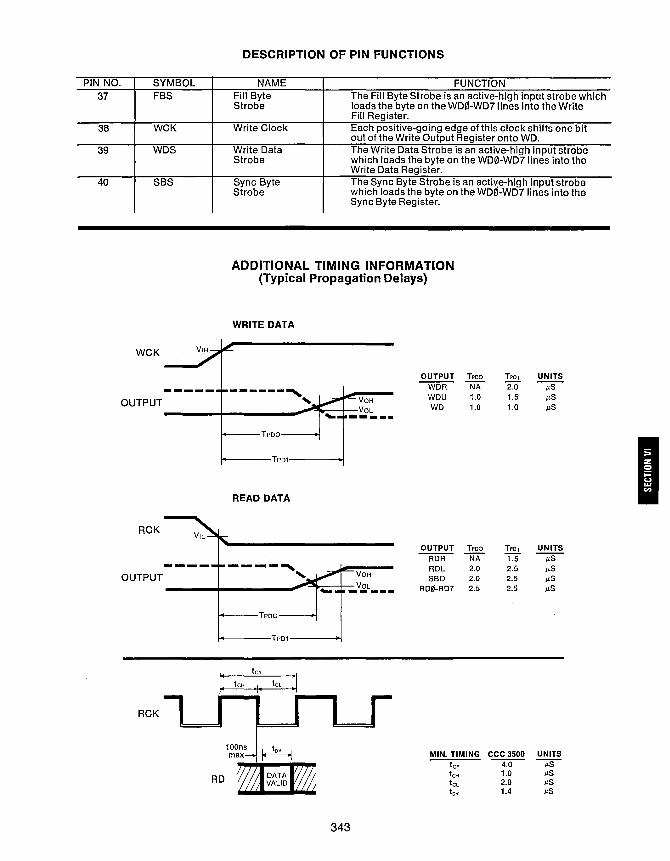
DESCRIPTION OF PIN FUNCTIONS
PIN NO. SYMBOL NAME FUNCTION 37 FBS Fill Byte The Fill Byte Strobe is an active-high input strobe which
Strobe loads the byte on the WDO-WD7Iines into the Write Fill Register.
38 WCK Write Clock Each positive-going edge of this clock shifts one bit out of the Write Output Register onto WD.
39 WDS Write Data The Write Data Strobe is an active-high input strobe Strobe which loads the byte on the WDO-WD7Iines into the
Write Data Register. 40 SBS Sync Byte The Sync Byte Strobe is an active-high input strobe
Strobe which loads the byte on the WD0-WD7 lines into the Sync Byte Register.

MAXIMUM GUARANTEED RATINGS·
Operating Temperature Range, ....................................................... OOC to + 70°C Storage Temperature Range ...................................................... -55°C to + 150°C Load Temperature (soldering, 10 sec.) ..................................................... + 325°C Positive Voltage on any Pin, Vee .............................................................. +0.3V Negative Voltage on any Pin, Vee .............................................................. -25V
*Stresses above those listed may cause permanent damage to the device. This is a stress rating only and functional operation of the device at these or at any other condition above those indicated in the operational sections of this specification is not implied.
ELECTRICAL CHARACTERISTICS (TA=O°C to 70°C, Vee = +5V ±5% Voo= -12V±5%, unless otherwise noted)
Parameter Min. Typ. Max. Unit Conditions
D.C. CHARACTERISTICS
INPUT VOLTAGE LEVELS Low-level, V,L Voo 0.8 V High-level, V,H Vee-1.5 Vee V
OUTPUT VOLTAGE LEVELS Low-level, VOL 0.2 0.4 V 1m=1.6mA High-level, VOH 2.4 4.0 V IOH= -100ttA
INPUT CURRENT Low-level, I,L 1.6 mA See note 1
OUTPUT CURRENT Leakage, ILo -1 ttA RDE=Vll, O~VOUT~ +5V Short circuit, los** 10 mA VOUT=OV
INPUT CAPACITANCE pF All inputs, C'N 5 10 V,N = Vee, f=1MHz
OUTPUT CAPACITANCE All outputs, COUT 10 20 pF RDE=Vll, f=1MHz
POWER SUPPLY CURRENT lee 28 mA All outputs = VOH 100 28 mA
A.C. CHARACTERISTICS TA= +25°C
CLOCK FREQUENCY DC 250 KHz RCK,WCK
PULSE WIDTH Clock 1 ttS RCK,WCK Read Gate, 1 ttS RG Write Data Strobe 200 ns WDS Fill Byte Strobe 200 ns FBS Sync Byte Strobe 200 ns SBS Read Data Request Reset 200 ns RDRR
INPUT SET-UP TIME Write Data Inputs 0 ns WDrfJ-WD7
INPUT HOLD TIME Write Data Inputs 0 ns WD0-WD7
STROBE TO OUTPUT DELAY Load = 20pf + 1 TTL input Read Data Enable 180 250 ns RDE: Tpol, Tpoo
OUTPUT DISABLE DELAY 100 250 ns RDE
* *Not more than one output should be shorted at a time.
NOTES: 1. Under steady state condition no current flows for TTL or MOS interfacing.
A switching current of 1.6mA maximum flows during a high to low transition of the input. 2. The tri-state output has 3 states:
1) low-impedance to Vee 2) low-impedance to GNO 3) high-impedance OFF == 10M ohms The OFF state is controlled by the ROE input.
344

CCDH TIMING DIAGRAM
WCK i
WDS n Note 1 nLt! ___ _
WDA i I Note1 LW WDU, I L-WD =I==C=I==[=T~=I==C=J==t==C=l-=--=-L=-.J-=--=-I-=--=-C-=-J-=--=-l-=--=-C_-J-=-_-l-_-.J_-_-T_-_-C-=-_I.-=..-=t_-=..-r=-J-=:-.
I ... 'I-----DATA BYTE----.. ,·II· ... '----DATA BYTE----.-' I .... '----FILL BYTE----....,'~I
ACK
ADA ~L... _________________________________ .:...oll Note 3 4-JJ ADAA ____________________________________________ ~n~;,N~o~te~2~--------------------,1--
ADL ~! _________________________ 4_----------~1r--i SBD ~L... _____________________________ ~INote3 !I'--_________________________ _
NOTE 1 The Write Output Register is loaded with the next byte at the positive clock transition corresponding to the leading edge of the last bit of the current byte on the WD output. WDR is set high approximately two microseconds after this clock transition. If it is desired that the next byte be extracted from the Write Data Register the leading edge of the WDS should occur at least one microsecond prior to this clock transition.
NOTE 2 In order to avoid an RDL indication the leading edge of the RDRR pulse should occur at least one microsecond priorto the negative clock transition corresponding to the center of the first bit after the last bit of the previous byte on the RD input.
345
NOTE 3 The RDL, SeD and RDO-RD7 output are set to their correct levels approximately two micro· seconds after the negative clock transition corresponding to the center of the first bit after the last bit of the previous byte on the RD input. The RDR output is set high at the next negative clock transition.
I

o z (!)
i':i I" ~ +
r ~ (.J g U
0 -z
(!)
- g >
- ~ >
<{ f-« 0 UJ f-a: ~
a:
~~8 ;:c~
r--W
~ « (.J f-g « 0
U UJ UJ f-f- a: a: ~ ~
~ 0 U ~ ~
~ .... 0 'IS>
0 ~ a: . ~
L-
r--
en => CD « f-« 0
,
<{ f-« 0 0 « UJ a:
>-
~~~§ a:°fa~ .,...!.
~ <{ U f-g « (.J 0
0 0 « « UJ UJ a: a:
~ 0 (.J a: a:
a: 0 ~
0
.. ~ ~
~
I
..... UJ UJ(!) ~OUJ UJa:~ Ulf-a: Ula:O <{<{ UU
>-Ul => CD
=> a: en a: 0 ...I 0
0 en en UJ a: 0 o co coco (!) 0 0
~ a: a: en ~ LJ..en a: a: a:
0
0 :;; ()
9 f-UJ
~ 0
~ UJ en
lJj lJj ~ UJ 0 ~ co a: .. 0 0 co f-..
() a: 00 UJ «
f- ~~ !< z f{l en UJ => <{ (!) « ~ 0 f-
« a:
f-
:rl I~I~I~ 0 f- f-
0 UJ UJ 0 0 0 CD a: « Cii ;::: a. o ..... en g ~ UJ ~ tii 0 f- LJ.. « (!)
a: LJ.. ~
UJa: I I ~~~ en~
~ co « Z UJ Ul => f-« f-en W > a: 0
~
~ f-CD ~ « z UJ W en W UJ f- > a: a: ~ 0
f-en =>UJ a.J: f-U =>f-0::5
7).
ffi~ J:Ul:::; f-UJW O~tii Oa:>-f-OUl
------.
UJ co 0 a: f-en ...I 0 a: f-Z 0 (.J UJ > a: 0
1
w > a: c w (!l c a: ta: c( o ....... w J: w en en c( o c z c(
a: o en en w o o a: ~ ~
II UJa: «
~~~ co co UJ ...I (.J a:
en~ ...I z
0 <{ 0 f-<{ «
D.
o t-
I
u: ~ UJ 0 a: 0
~ !Xl a: .. z
U)
~ to :I: C
" "l en -'a: en Ow woa:o a:zf-O o«z(.J o OUJ « (.Jo
'" ,.
'en" en => => CD CD ...I en 0 en a: W f-a: Z 0 0 0 (.J « . ~ a: 0 en f{l (.J 0 a: a.
I
W o Lf a: w t-2: o o an M o o o ..J c( o a:: > t-
Circuit diagrams utilizing SMC products are included as a means of illustrating typical semiconductor applications; consequently complete information sufficient for construction purposes is not necessarily given. The information has been carefully checked and is believed to be entirely reliable. However. no responsibility is assumed for inaccuracies. Furthermore. such information does not convey to the purchaser of the semiconductor devices described any license under the patent rights of SMC or others. SMC reserves the right to make changes at a~y time in order to improve design and supply the best product possible.
346

ROM 4732 ILPC FAMILY
4096 X a-Bit Static Read-Only Memory 32KROM
FEATURES o 4096 x 8 Organization o All Inputs and Outputs TTL-Compatible o Fully Static (No Clocks, No Refresh) o Single +5v Power Supply o Maximum Access Time .. .450ns o Minimum Cycle Time .. .450ns o Typical Power Dissipation ... 580mW o Three-State Outputs for Wire-OR Expansion o Industry Standard 24 pin DIP Pin Out o Pin Compatible with TMS 4732, TMS 4700,
TMS 2708 and Intel 2316E o Two programmable chip select inputs for Chip
Select Flexibility o Automated Custom Programming-Formats
Media o COPLAMOS® N-Channel MOS Technology
PIN CONFIGURATION
A7 1 24 Vee
A6 2 23A8
AS 3 22A9
A4 4 21 CS2orCS2
A3 5 20 CSl orCSl
A2 6 19 Al0
Al 7 18 All
A0 8 1708
01 9 1607
0210 1506
0311 1405
GND12 1304
PACKAGE: 24-pin D.I.P.
GENERAL DESCRIPTION The ROM 4732 is a 32,768-bit read-only memory organized as 4096 words of 8-bit length. This makes the ROM 4732 ideal for microprocessor based systems. The device is fabricated using N-channel silicon-gate technology for high speed and simple interface with bipolar circuits. All inputs can be driven directly by Series 74 TTL circuits without the use of any external pull-up resistor. Each output can d rive one Series 74 or 74S load without external resistors. The data outputs are three-state for OR-tieing multiple devices on a common bus, facilitating easy memory expansion. Two chip select controls allow data to be read.
These controls are programmable, providing additional system decode flexibility allowing four 32K ROMs to be OR-tied without external decoding. The data is always available, it is not dependent on external CE clocking.
The ROM 4732 is designed for high-density fixedmemory applications such as logic function generation and microprogramming. Systems utilizing 1024 x 8-bit ROMs or 1024 x8-bit EPROMs can expand to the 4096 x 8-bit ROM 4732 with changes only to pins 18, 19, and 21. To upgradefrom the 2316E, simply replace CS2 with A11 on pin 18.
BLOCK DIAGRAM
CS1~ CHIP SELECT LOGIC CS2----L--/ ~~----------------~
Y DECODE
X DECODE
347
DATA OUTPUTS 01-08
I

MAXIMUM GUARANTEED RATINGS* Operating Temperature Range ......................................... 0° C to + 70° C Storage Temperature Range ......................................... -55°C to +150°C Lead Temperature (soldering, 10 sec.) ......................................... +325°C Positive Voltage on any Pin, with respect to ground .............................. +7.0V Negative Voltage on any Pin, with respect to ground .............................. -0.3V
* Stresses above those listed may cause permanent damage to the device. This is a stress rating only and functional operation of the device at these or at any other condition above those indicated in the operational sections of this specification is not implied.
NOTE: When powering this device from laboratory or system powersupplies, it is important that the Absolute Maximum Ratings not be exceeded or device failure can result. Some power supplies exhibit voltage spikes or "glitches" on their outputs when the AC power is switched on and off. In addition, voltage transients on the AC power line may appear on the DC output. If this possibility exists it is suggested that a clamp circuit be used.
ELECTRICAL CHARACTERISTICS (TA = O°C to 70°C, Vee = +5V ±5%, unless otherwise noted)
Parameter Min. Typ. Max. Unit Comments
D.C. CHARACTERISTICS INPUT VOLTAGE LEVELS
Low-level, VIL 0.65 V High-level, VIH 2.0 V
OUTPUT VOLTAGE LEVELS Low-level, VOL 0.4 V IOL = 2.0mA High-level, VOH 2.4 V IOH = -200j.tA
INPUT CURRENT Low-level, IlL 10 j.tA ov:::; VIN:::; Vee
OUTPUT CURRENT IOL ±10 j.tA Chip Deselected
INPUT CAPACITANCE All inputs, CIN 7 pF
OUTPUT CAPACITANCE All Outputs, COUT 10 pF
POWER SUPPLY CURRENT lee 150 mA
A.C. CHARACTERISTICS 1 Series 74 TTL load, CL = 100 pF
Read cycle time, tC(rd) 450 ns Access time from address, ta(ad) 450 ns Access time from chip select,
t a(cs) 200 ns Previous output data valid after
address change, t pvx 450 ns Output disable time from chip
select, tpxz 200 ns
READ CYCLE TIMING
ADDRESSES
'"": .4----tC(rd)-----II~~1 .... 1 •• ----tc(rd)-----II~~I
VIH ~: V \mN . ADDRESSES VALID A ADDRESSES VALID AN::i1:l VIL I ~I -----------
I I I I I I I I I
I I I I
i \ i! Ii II hi I t"""a-(cs-) ----+-1 +I-----------J I I ~ I *-ta(ad)~ I ~ta(ad)~1 t pvx -': I~ I ~ I~tpxz
----HI-Z (VALID XNOTVALlDX .... -V-A-L-ID--t~HI-Z-
VIH
VIL
VOH 01-08
VOL
348
Description of Pin Functions
INPUT/ PIN NO. SYMBOL NAME OUTPUT FUNCTION
1,2,3,4,5,6, A7, A6, AS, A4, Addresses I The 12-bit positive-logic address is 7,8,18,19,22, A3, A2, A1, A0, decoded on-chip to select one of4096
23 A11, A10, A9, words of 8-bit length in the memory A8 array. A0 is the least significant bit and
A11 the most significant bit of the word address. The address valid interval determines the device cycle time.
9,10,11,13, 01, 02, 03, 04, Data 0 The eight outputs must be enabled by 14, 15, 16, 17 05,06,07,08 Outputs both chip select controls before the
output word can be read. Data will remain valid until the address is changed or the outputs are disabled (chip deselected). When disabled, the three-state outputs are in a high-impedance state. 01 is consid-ered the least significant bit, 08 the most significant bit. The out-puts will drive TTL circuits without external components.
12 GND Ground GND Ground I 20,21 CS1, CS2 Chip I Each chip select control can be pro-
Select grammed during mask fabrication to be active with either a high or a low level input. When both chip select Signals are active, all eight outputs are enabled and the eight-bit addressed word can be read. When either chip select is not active, all eight outputs are in a high-impedance state.
24 Vee Power PS +5 volt power supply Supply
349

PROGRAMMING DATA PROGRAMMING REQUIREMENTS: The ROM 4732 is a fixed program memory in which the programming is performed via computer aided techniques by SMC at the factory during the manufacturing cycle to the specific customer inputs supplied in the punched computer card format below. The device is organized as 4096 8-bit words with address locations numbered 0 to 4095. The 8-bit words can be coded as a 2-digit hexadecimal number between 00 and FF. All data words and addresses in the following format are coded in hexadecimal numbers. In coding, all binary words must be in positive logic before conversion to hexadecimal. Q1 is considered the least significant bit and Q8 the most significant bit. For addresses, A0 is least significant bit and A11 is the most significant bit. Every card should include the SMC Custom Device Number in the form ROXXXX (4 digit number to be assigned by SMC) in column 75 through 80. PROGRAMMABLE CHIP SELECTS: The chip select inputs shall be programmed according to the data punched in columns 73 and 74. Every card should include in column 73 a 1 if the output is to be enabled with a high level at CS2 or a 0 (zero) to enable the output with a low level at CS2. The column 74 entry is the same for programming CS1. PROGRAMMED DATA FORMAT: The format for the cards to be supplied to SMC to specify that data to be programmed is provided below. The card deck for each device consists of128 cards with each card containing data for 32 memory locations.
CARD COLUMN 1 t03
4 5 t068
69,70
71,72 73 74
75,76 77 to 80
HEXADECIMAL FORMAT Hexadecimal address of first word on the card Blank Data. Each 8-bit memory byte is represented by two ASCII characters to represent a hexadecimal value of '00' or 'FF'. Checksum. Thechecksum isthe negative of the sum of al18-bit bytes in the record from column 1 t068, evaluate modul0256 (carryfrom high order bit ignored). (For purposes of calculating the checksum, the value of Column 4 is defined to be zero.) Adding together, modulo 256, all 8-bit bytes from Column 1 to 68 (Column 4 = 0), then adding the checksum, results in zero. Blank One (1) or zero (0) for CS2 One (1) or zero (0) for CS1 RO XXXX (4 digit number assigned by SMC)
ALTERNATIVE INPUT MEDIA In addition to the preferred 80 column "IBM Card," customers may submit their ROM bit patterns on 9-track 800-BPI mag tape, 8-channel perforated paper tape, EPROM, ROM, etc. Where one of several nationwide time sharing services is mutually available, arrangements may be made with the factory to communicate the ROM definition data directly through the service computer. Format requirements and other information required to use alternative input media may be obtained through SMC sales personnel.
ALTERNATIVE DATA FILE FORMATS In addition to the standard SMC format, it is possible to furnish data to SMC in other formats if prearranged with the factory. Non-standard formats may be acceptable. Contact SMC sales personnel.
Circuit diagrams utilizing SMC products are included as a means of illustrating typical semiconductor applications; consequently complete information sufficient for construction purposes is not necessarily given. The information has been carefully checked and is believed to be entirely reliable. However. no responsibility is assumed for inaccuracies. Furthermore. such information does not convey to the purchaserof the semiconductor devices described any license under the patent rights of SMC or others. SMC reserves the right to make changes at any time in order to improve design and supply the best product possible.
350

ROM 36000* ILPC FAMILY
8192 X 8-Bit Static Read-Only Memory 64K ROM
FEATURES
08192 X 8 Organization
o All Inputs and Outputs TTL-Compatible o Edge Activated"
o Single +5V±10% Power Supply
o Maximum Access Time ... 250ns o Minimum Cycle Time ... 375ns
o Low Power Consumption ... 220mW max active o Low Standby Power Dissipation ... 35mW typical o Three-State Outputs for Wire-OR Expansion
o Industry Standard 24 Pin DIP Pin Out o Pin Compatible with MOSTEK MK36000-4
o On-Chip Address Latches o Outputs drive 2 TTL loads and 100pf
o COPLAMOS® N-Channel MOS Technology
BLOCK DIAGRAM
CHIP ENABLE LOGIC
Y DECODE
X DECODE
'FOR FUTURE RELEASE
351
PIN CONFIGURATION
A7 1 24 Vee
A6 2 23 A8
A5 3 22 A9
A4 4 21 A12
A3 5 20 CE
A2 6 19 A10
A1 7 18 A11
A,0 8 17 08
01 9 1607
0210 1506
0311 1405
GND 12 1304
PACKAGE: 24-pin D.I.P.
DATA OUTPUTS
01-08
OUTPUT BUFFERS
**Trademark of MOSTEK Corporation
I

GENERAL DESCRIPTION
The ROM 36000 is a new generation N-channel silicon gate MOS Read Only Memory, organized as 8192 words by 8 bits. As a state-of-the-art device, the ROM 36000 incorporates advanced circuit techniques designed to provide maximum circuit density and reliability with the highest possible performance, while maintaining low power dissipation and wide operating margins.
The ROM 36000 utilizes what is fast becoming an industry standard method of device operation. Use of a static storage cell with clocked control periphery allows the circuit to be put into an automatic low power standby mode. This is accomplished by maintaining the chip enable (CE) input at a TTL high level. In this mode, power dissipation is reduced to typically 35mW, as compared to unclocked devices which draw full power continuously. In system operation, a device is selected by the CE input, while all others are in a low power mode, reducing the overall system power. Lower power means reduced power supply cost, less heat to dissipate and an increase in
ABSOLUTE MAXIMUM RATINGS·
device and system reliability.
The edge activated chip enable also means greater system flexibility and an increase in system speed. The ROM 36000 features onboard address latches controlled by the CE input. Once the address hold time specification has been met, new address data can be applied in anticipation of the next cycle. Outputs can be wire- 'OR'ed together, and a specific device can be selected by utilizing the CE input with no bus conflict on the outputs. The CE input allows the fastest access times yet available in 5 volt only ROM's and imposes no loss in system operating flexibility over an unclocked device.
Other system oriented features include fully TTL compatible inputs and outputs. The three state outputs, controlled by the CE input, will drive a minimum of 2 standard TTL loads. The ROM 36000 operates from a single +5 volt power supply with a wide ±10% tolerance, providing the widest operating margins available. The ROM 36000 is packaged in the industry standard 24 pin DIP.
Voltage on Any Terminal Relative to Vss ........................................... -0.5V to +7V Operating Temperature TA (Ambient) ............................................. 0° C to +70°C Storage Temperature-Ceramic (Ambient) .................................... -65° C to +150° C Power Dissipation ...................................................................... 1 Watt
*Stresses greater than those listed under "Absolute Maximum Ratings" may cause permanent damage to the device. This is a stress rating only and functional operation of the device at these or any other conditions above those indicated in the operating sections of this specification is not implied. Exposure to absolute maximum rating conditions for extended periods may affect device reliability.
r",,,'77.';,iP=:R==E~LI7:":"'M~'N~A~R~Y--' ...... ";-: sNolltf!: This Is not II final speCifiCation::
!'.Im~. parjlml,ltric Ilmit~ lItI,lM>j&ct to Chang •.
ELECTRICAL CHARACTERISTICS (TA = O°C to 70°C, Vee = +5V ±10%, unless otherwise noted)
Parameter Symbol Min. Typ. Max. Unit Notes
Power Supply Voltage Vec 4.5 5.0 5.5 Volts 6 Input Logie 0 Voltage VIL -0.5 0.8 Volts Input Logic 1 Voltage VIH 2.0 Vcc Volts
DC ELECTRICAL CHARACTERISTICS
Vec Power Supply Current (Active) Icc1 40 rnA 1 Vee Power Supply Current (Standby) lec2 7 rnA 7 Input Leakage Current II(L) -10 10 pA 2 Output Leakage Current 10(L) -10 10 pA 3 Output Logic "0" Voltage VOL 0.4 Volts
@ lOUT = 3.3mA Output Logic "1" Voltage VOH 2.4 Volts
@ 'OUT = -220pA
352

Parameter Symbol Min. Typ. Max. Unit Notes
AC ELECTRICAL CHARACTERISTICS
Cycle Time tc CE Pulse Width tCE CE Access Time tAC Output Turn Off Delay tOFF Address Hold Time Referenced to CE tAH Address Setup Time Referenced to CE tAS CE Precharge Time tp
CAPACITANCE
Input Capacitance CI Out ut Ca acitance p p CO
NOTES:
1. Current is proportional to cycle rate. leel is measured atthe specified minimum cycle time.
2. VIN = OV to 5.5V.
3. Device unselected; VOUT = OV to 5.5V.
4. Measured with 2 TTL loads and 100pF, transition times = 20ns.
375 ns 4 250 4
250 ns 4 60 ns 4
60 ns 0 ns
125 ns
5 pF 5 7 p F 5
5. Capacitance measured with Boonton Meter or effective capacitance calculated from the equation: L\.Q
C = L\.V with L\.V = 3 volts
6. A minimum lOOIlS time delay is required after the application of Vee (+5) before proper device operation is achieved.
7. CE high.
TIMING DIAGRAM
VIH CHIP ENABLE VIL
ADDRESS
VOH
tAH
VALID
DATA OUTPUT VOL------
tc
OPERATION
The ROM 36000 is controlled by the chip enable (CE) input. A negative going edge at the CE input will activate the device as well as strobe and latch the inputs into the onchip address registers. At
access time the outputs will become active and contain the data read from the selected location. The outputs will remain latched and active until CE is returned to the inactive state.
PROGRAMMING
Standard Microsystems Corporation will accept data input in the form of 8K, 16K, 32K and 64K EPROMS and 8K, 16K, 32K and 64K ROMS. If
other programming media is preferable, please consult the factory.
353
I

Circuit diagrams utilizing SMC products are included as a means of illustrating typical semiconductor applications; consequently, complete information sufficient for construction purposes is not necessarily given. The information has been carefully checked and is believed to be entirely reliable. However, no responsibility is assumed for inaccuracies. Furthermore. such information does not convey to. the purchaser of the semiconductor devices described any license under the patent rights of SMC or others. SMC reserves the right to make changes at any time in order to improve design and to supply the best product possible.
STANDARD MICROSYSTEMS CORPORATION
35 Marcus Blvd., Hauppauge, N.Y. 11787 (516) 273-3100 . TWX-51O-227-8898
our competition so you can keep ahead of yours.
354

:tart 1I1'umber Description CG 4103(3) 6x7x64
SR 601B-XX(3)
(1 )For future release (3)May be custom mask programmed
"ltidddtlltli Printer CHAllACTER GENERATOR
Max Aceen Time 1.2 psec
SHIFT REGISTER
Feature Load, Recirculate, Shift Controls,
Shift Left/Shift Right, Recirculate Controls, Asynchronous clear
355
:Power Supplies +6, -12 or ±12
1 MHz +6
1 MHz +6
l6DIP 361-364
16 DIP 366-368

356

4100 Series
CG4103
CHARACTER GENERATOR 2240-Bit Programmable (ROM) 64 Characters of 5 x 7 Bits
FEATURES PIN CONFIGURATION D Static Operation, no clocks required. D 2240-Bit Capacity, fully decoded· D 64 Characters of 35 Bits (5 x 7) D Column by Column Output-Column
Scan D TTL Compatible D Wired "OR" Capability for memory
expansion D Power Supplies: + 14v, -14v or + 12v,
-12v, or +5v, -12v D Eliminates need for + 12v power supply D Single mask custom programming
APPLICATIONS D Matrix Printers D Vertical Scan Alphanumeric Displays D Billboard and Stock Market Displays D Strip Printer D LED Matrix Arrays
011
NC 2
02 3
NC 4
03 5
NC 6
04 7
NC 8
05 9
NC 10
06 11
NC 12
07 13
Voo 14
BLOCK DIAGRAM
(/) LSBr----...,
fB A1 II: 8 A2
~ A3 W t; A4
~ As
~ A6
CHARACTER ADDRESS DECODE
U MSB'------J
ROM MEMORY MATRIX
(2240 Bits)
357
COLUMN SELECT
C1 C2 C3 C4CS
28 Chip Enable (Al)
27 A1
26 A2
25 A3
24 A4
23 As
22 Cs
21 C4
20 C3
19 C2
18 C1
17 Vss
16 A6 15 VGG
NC = No Connection
...------.
OUTPUT BUFFERS
CE(Al) CHIP ENABLE
Vss Voo VGG
A A A
TOP
02 ~
03 ~ I-
04 5 05 ~
« 06 0
07
BOTTOM

General Description
The CG41 00 Series MOS Read Only Memories (ROMs) are designed specifically for dot-matrix character generation where column by column output data is desired. Each ROM contains 2240 bits of programmable storage, organized as 64 characters, each having 5 columns of 7 bits.
The output word appears as a 5 word sequence on each of the output lines. Sequence is controlled by the 5 Column Select lines. By strobing the first select line, the first group of 7 bits (first column) is obtained at the output. By sequentially strobing C, through Cs the font of the addressed character would be displayed. The character address may remain fixed while the column select changes.
Since only 6 address bits are required in order to decode the 64 stored characters, the seventh bit (A7) may be used as a chip enable. The chip enable (CE) in conjunction with the single ended open drain output buffers allow for memory expansion throu'gh wired "OR" connection.
The CG41 00 Series contains an USASCII character font. Custom memory patterns are provided through the use of customer provided encoding sheets, tapes, or card decks.
MAXIMUM GUARANTEED RATINGS*
Operating Temperature Range ............................... , ............. -25°C to + 85°C Storage Temperature Range . . . . . . . . . . . . . . . . . . . . . . . . . . . . . . . . . . . . . . . . . . . . . .. - 55°C to + 150°C Voltage on any Pin, with respect to Vss ...................................... +0.3V to -30V
*Stresses above those listed may cause permanent damage to the device. This is a stress rating only and functional operation of the device at these or at any other condition above those indicated in the operational sections ofthis specification is not implied.
RECOMMENDED OPERATING CONDITIONS (-25°C,,;;;TA,,;;;+85°C)
Parameter Symbol Min. Typ. Max. Unit
Suppy Voltage Vss 0.0 V Supply Voltage Voo -12.0 -14.0 -16.0 V Supply Voltage VGG -24.0 . -28.0 -29.0 V Input Voltage, logic "0" V,H Vss-1.5 Vss V
Logic "O"=most positive level
Input Voltage, logic "I" V,L Voo Vss-11 V Logic "I"=most negativejlevel
Note: The design of the CG4100 permits a broad range of operation that allows the user to take advantage of readily available power supplies; e.g. +5V, -12V. See "Operational Interface-To/From TTL logic" diagram.
ELECTRICAL CHARACTERISTICS (Vss= + 14v, VGG= -14v, Voo= Ground, TA=25°C, unless otherwise noted)
Parameter Symbol Min. Typ. Max. Units Comments
Output Blank Current lOB 10 p.a Voo applied to output see Note 1.
Output Dot Current 100 2.5 ma Voo applied to output see Note 1.
Input Leakage Current liN 10 p.a VIN=OV Output Voltage Vo 2.0 V 10=0.5ma
5.0 V 10=2.0ma Address Access Time tAA 1200 ns Column Select Access Time tCA 600 ns Chip Enable Access Time tCE 400 ns Power DiSSipation 400 mw Output unconnected
Note 1: An output dot is defined as the ON state of the MOS output transmitter. An output blank is defined as the OFF state.
358

Description of Pin Functions
Pin No. Symbol
1,3,5,7 01,02,03,04 9,11,13 05,06,07
14 Voo
15 VGG
16 A6 17 Vss
18-22 C1-CS 23-27 As·A1
28 CE(A7)
ADDRESS ACCESS TIMING Vss----,
Address \ Input 50%
, I Voo--_..J
'- _______ J
tAAf Output
_____ ~ +1.5V Gnd .
Voo
Only one of the five Column Select inputs is at logic" 1." Chip Enable input is at logic "1."
COLUMN SELECT ACCESS TIMING
50%
teAf _ ____ ...J +1.5V
Gnd .
Name
Outputs
Voo
VGG
Address Vss
Column Select Address Chip Enable
Function
7 Data Outputs
Usually connected to Ground Negative power supply: -14v or -12v
Bit 6 of the character address Positive power supply: + 14v or + 12v or + 5v
Column Select inputs Bits 1 through 5 of the character address Chip Enable for memory expansion
CHIP ENABLE ACCESS TIMING Vss Chip Enable 50% Input Voo
tCf tCL Output
Gnd
+1.5V
Only one of the five Column Select inputs is a logic" 1." Address inputs are set in a dc state.
AC TEST CIRCUIT
All Column Select inputs are at logic "0" except one under test. Address inputs are set in a dc state.
tr = tf < 50 ns for all timing diagram forcing functions. AI~output waveforms are measured at the output of the 7400 TTL gate. Chip Enable input is at logic" 1."
OPTIONAL INTERFACE TO/FROM TTL LOGIC
+5V
+14V
359
INTERFACE TO TTL LOGIC
R'
R'
R'
R'
'The value of R depends on System Speed and Power Requirements.
Mask-programmable - 100K !l on - chip resistors are available.
I

OUTPUT AND COLUMN SELECT ASSIGNMENTS
f-'-1
TO'I""" 02
1 ~~ 1 05 1°6
-07 1'-;'
AI II A2 A3 A4 A5 A6
AI A2 A3
A5 a A6 a I AlII] A2 A3 A4 AS A6 a
AI A2 A3 A4 A5 A6
A2 1 '1 A3 A4 AS A6
AI A2 A3 1 A4 1
A5 A6 I
AlII A2 A3 A4 A5 A6 1
AI A2 a A3 A4 A5 a A6 a
11 !IJ
Alai A2 A3 A4 a AS a A6 a
illl 1111 ;;.1 1 11;1
AI A2 A3
A5 A6 0
AI A2 A3
A5 A6 a
AlII A2 1 A3
A5 A6 a
11:; 1111 AI
A2 A3 A4 A5 A6
a 0 1
0 1
0 I AI
A2 A3 A4 AS A6
AI
A2 A3 a A4 1
AS A6
Alai A2 1
A3 1
A5 A6
AI a
I A2 a A3 1 A4 1 A5 1 A6 1
AI A2 A3 A4 AS a A6 1
L---;'_: _'_I_~ 11! I 1111 Ii 1111 11~1
AlII A2 A3
AS A6 1
AI A2 A3 A4 AS A6 1
AlII A2 1
A3
A5 1 A6 1
AI 1
I A2 a A3 1 A4 1 AS 1 A6 1
Pin-for-Pin Equivalent for: TM8 4103 MK2002 88499. Circuit diagrams utilizing SMC products are included as a means of illustrating typical semiconductor applications; consequently complete information sufficient for construction purposes is not necessarily given. The information has been carefully checked and is believed to be entirely reliable. However, no responsibility is assumed for inaccuracies. Furthermore, such information does not convey to the purchaser of the semiconductor devices described any license under the patent rights of SMC or others. SMC reserves the right to make changes at any time in order to improve design and supply the best product possible.
360

SR S01S-XXX SR 5015-80 SR 5015-81 SR 5015-133
Quad Static Shift Register
FEATURES D COPLAMOS® N Channel Silicon Gate
Technology D Variable Length-Single Mask
Programmable-1 to 134 bits D Directly TTL-compatible on all inputs,
outputs, and clock D Clear function D Operation guaranteed from DC to 1.0 MHz D Recirculate logic on-chip D Single +5.0V power supply D Low clock input capacitance D 16 pin ceramic DIP Package D Pin for Pin replacement for AMI 82182. 83. 85
APPLICATIONS D Memory Buffering D Unique Buffering Lengths D Terminals
REC CONTROL ABC ~"""'--1
INPUT A "">--+--4
BLOCK DIAGRAM
OUTPUT A OUTPUT C
PIN CONFIGURATION
INPUT A OUTPUT A
RECASC RID
CLEAR OUTPUTD
INPUTS INPUTD
OUTPUTS RECD
GND NC
Vee INPUTC
OUTPUTC CLOCK
1----<: INPUT C
1------< RECIRC.INPUT D
'--..J--___ -< REC. CONTROL D
INPUT B INPUT D
CLOCK CLEAR
361
I

General Description
The SMC SR 5015-XXX is a quad static shift register family fabricated using SMC's COPLAMOS@ N channel silicon gate process which provides a higher functional density and speed on a monolithic chip than conventional MaS technology. The COPLAMOS® process provides high speed operation, low power dissipation, low clock input capacitance, and single +5 volt power supply operation.
These shift registers can be driven by either PL circuits or by MaS circuits and provide driving capability to MaS or PL circuits. This device consists of four separate static shift registers with independent input and output terminals and logic for loading, recirculating or shifting information. The SR 5015-80, SR 5015-81, and SR 5015-133 are respectively 80,81, and 133 bit quad shift registers.
The recirculate control pin is common for registers A, B, and C. Register 0 has an independent recirculate control pin as well as a recirculate input pin.
A clear pin has been provided that will cause the shift register to be cleared when the pin is at Vee. A single PL clock is required for operation.
The transfer of data into the register is accomplished on the low-to-high transition of the clock with the recirculate control low. For long term data storage the clock may be stopped and held in either logic state. Recirculate occurs when the recirculate control is high. Output data appears on the low-to-high transition of the clock pulse.
Bits 81 and 133 are available for flag storage.
This device has been designed to be used in high speed buffer storage systems and small recirculating memories.
Special custom configurations are achieved via single mask programming in lengths of 1 to 134 bits.
MAXIMUM GUARANTEED RATINGS* Operating Temperature Range ................................................................ O°C to + 70°C Storage Temperature Range ............................................................... -55°C to + 150°C Lead Temperature (soldering, 10 sec.) ............................................................... +325°C Positive Voltage on any Pin, with respect to ground ...................................................... +8.0V Negative Voltage on any Pin, with respect to ground ..................................................... -0.3V
*Stresses above those listed may cause permanent damage to the device. This is a stress rating only and functional operation of the device at these or at any other condition above those indicated in the operational sections of this specification is not implied.
ELECTRICAL CHARACTERISTICS (TA=O°C to 70°C, Vce= +5V± 5%, unless otherwise noted)
Parameter Min. Typ. Max. Unit Comments
D.C. Characteristics INPUT VOLTAGE LEVELS
Low Level, VIL 0.8 V High Level, VIH Vee-1.5 Vee V
OUTPUT VOLTAGE LEVELS Low Level, VOL 0.4 V IOL=1.6ma High Level, VOH Vee-1.5 4.0 V IOH=100jLa
INPUT LEAKAGE CURRENT 1.0 jLa VIN=Vee CLOCK, CLEAR 25 pf All Other 10 pf
POWER SUPPLY CURRENT 80 rna
A.C. Characteristics TA=+25°C CLOCK
PWH 300 ns PWL 600 ns Transition, tr, tt 0.02 1.0 jLS Repetition Rate, 1fT 0 1.0 MHz tDelay 300 ns
INPUT DATA to, set-up 100 ns to, hold 200 ns PWo 300 ns
OUTPUT DATA to,ACC 200 350 ns
RECIRCULATE CONTROL tR, set-up 200 ns tR, hold 300 ns PWR 500 ns
CLEAR PWeLEAR 20 jLS
362

Pin No. Symbol
A
2 RECABC
3 ClR
4 B 5 OB 6 GND 7 Vcc 8 Oc 9 ClK
10 C 11 NC 12 RECD
13 D 14 00 15 RID
16 OA
TIMING DIAGRAMS
T
Clock
I I
I pw: I . pWo
to. set· up ~ to. hold
Input Data _____ --J~
t):.-.--~ Output Data . ,-. -----
Recirculate Control ~
tR set· up -i r~ r- tR hold ~
PWR
PWclear
Clear~'"
Description of Pin Functions
Name Function
Input A Input signal which is either high or low depending on what word is to be loaded into shift register.
Recirculate ABC Input signal when high disconnects inputs from registers and connects outputs to inputs, thus recirculating data. Recirculates only A, B, C outputs.
Clear Input signal when high forces outputs to a low state immediately and clears all the registers.
InputS Input signal for B register. OutputS Output signal for S register. GND Power supply Ground. +5 Volt 5 volt power supply. OutputC Output signal for C register. Clock Input Input signal which is normally low and pulses high to
shift data into the registers. The data is clocked in on low to high edge of clock.
InputC Input signal for C register. NC Recirculate Input signal which is normally low and, when goes high, Control D disconnects Input D to register and connects
Recirculate Input D to register. InputD Input signal for D register. Output D Output signal for 0 register. Recirculate Input signal which is the input to the 0 register Input 0 when Recirculate Control 0 is high: RECD=1. Output A Output signal for A register.
363
I

"''-'-LI''''' I I V I'" 0::)
Line Buffer for CRT Display ... 80 Characters per line. ClK
~ SRS01S·80
D
r--I I I
D, v,dei,ock _u I DJ
~W ~
klJ~ D.
PAGE t-LJ r-MEMORY SMC so Serial Dala Out put
CG5004L-1 UAS~ To MonllorEle
Ds
.-~ ~ ~
clrontCS
D,
~H r-io-
D,
.-~ I l, L2 L4 La
I
CURSOR DB '"'r MEMORY .-H
ct SRSOI5·80
~ RECIRCULATE
DECODER t--~
A BCD
I SCAN I COUNTER
t End of Line Clock
Line Buffer for Matrix Printer ... 132 Characters per line.
INTERFACE OR
MEMORY
Blvd. ""-oIlilJoe. NY 117118 I 273·3100 TWX-Sl0-227-8898
'iaiii'iieaiiOfiiiiOiiiii!tiitilSO you C311ceep nad Of yQlI'S.
ClK
, SR5015-133
0, I r-f--I I
0, I t-I-L I
03
~f--I I I
D.
-1 I I -
~rr 0,
t-~ 0,
-H 07
t-H I I
De
..... W I I
_ •. SR5015-133
ClK
REC ----< From System Timing
CHARACTER GENERATOR
ROM{s) SMC CG4100
SERIES
End of Line
~ To Print Head
Solenoid Drivers
Circuit diagrams utilizing SMC products are included as a means of illustrating typical semiconductor applications; consequently complete information sufficient for construction purposes is not necessarily given. The information has been carefully checked and is believed to be entirely reliable. However, no responsibility is assumed for inaccuracies. Furthermore, such information does not convey to the purchaser of the semiconductor devices described any license under the patent rights of SMC or others. SMC reserves the right to make changes at any time in order to improve design and supply the best product possible.
364

STANDARD MICROSYSTEMS CORPORATION SR5017
SR5018
Quad Static Shift Right/Shift Left Shift Register Last In First Out Buffer
LIFO FEATURES o COMPLAMOS® N-Channel Silicon
Gate Technology. o Quad 81 bit or Quad 133 bit o Directly Compatible with T2L, MOS o Operation Guaranteed from DC to
1.0MHz o Recirculate logic on-chip o Single + 5.0V power supply o Low clock input capacitance o Single phase clock at T2L levels o Clear function o 16-pin Ceramic DIP Package
APPLICATIONS OBi-Directional Printer o Computers-Push Down
Stack-LIFO o Buffer data storage-memory buffer o Delay lines-delay line processing o Digital filtering
PIN CONFIGURATION
INPUTD RECD
RID GND
OUTPUTD OUTPUTC
CLEAR INPUTC
OUTPUT A INPUTB
URCON OUTPUTB
INPUT A RECABC
CLOCK Vcc
o Telemetry Systems o Terminals o Peripheral Equipment
BLOCK DIAGRAM OUTPUT A
REC CONTROL ABC ">---4 .......... -1
INPUT A ~I---t
INPUTB >----i
OUTPUTC
1------< INPUT C
~--< RECIRC.INPUT D
~J-.-.1"-~ REC. CONTROL D
1----< INPUTD
LlRCONTROL ;>-----------:r--r~~~
CLOCK CLEAR
365
I

General Description
The SMC SR 5017 and SR 5018 are quad 133 (SR 5017) and quad 81 (SR 5018) bit static shift registers utilizing SMC's COPLAMOS® N channel silicon gate process. The COPLAMOS® process provides high speed operation, low power dissipation, low clock input capacitance, and requires only a single + 5 volt power supply.
These shift registers can be driven by either T2L circuits or by MOS circuits and provide driving capability to MOS to T2L circuits.
This device consists of four separate static shift registers with independent input and output terminals and logic for loading, recirculating or shifting information right or left. This shift left/shift right (LIR Control) control input is common to all registers.
The recirculate control input is common for registers A, B, and C. Register D has an independent recirculate control input as well as a Recirculate Input.
A Clear input has been provided that will cause the shift register to be cleared when the input is at Vee. A single T2L clock input is required for operation.
The transfer of data into the register is accomplished on the low-to-high transition of the clock with the recirculate control low. For long term data storage the clock may be stopped and held in either logic state. Recirculate occurs when the recirculate control is high. Output data appears on the low-to-high transition of the clock pulse.
Bits 81 or 133 are available for flag storage.
MAXIMUM GUARANTEED RATINGS*. Operating Temperature Range ............................................................... O°C to + 70°C Storage Temperature Range ............................................................... -55°C to + 150°C Lead Temperature (soldering, 10 sec.) ............................................................... +325°C Positive Voltage on any Pin, with respect to grqund ..................................................... +8.0V Negative Voltage on any Pin, with respect to ground .................................................... -0.3V
*Stresses above those listed may cause permanent damage to the device. This is a stress rating only and functional operation of the device at these or at any other condition above those indicated in the operational sections of this specification is not implied.
ELECTRICAL CHARACTERISTICS (TA""O°C to 70°C, Vee= +5V±5%, unless otherwise noted)
Parameter Min. Typ. Max. Unit Comments
D.C. Characteristics INPUT VOLTAGE LEVELS
Low Level, VIL 0.8 V High Level, VIH Vec-1.5 Vee V
OUTPUT VOLTAGE LEVELS Low Level, VOL 0.4 V IOL=1.6ma High Level, VOH Vec-1.5 4.0 V IOH= 100JLa
INPUT LEAKAGE CURRENT 1.0 JLa VIN=Vee CLOCK, CLEAR 25 pf All Other 10 pf
POWER SUPPLY CURRENT 100 ma
A.C. Characteristics TA=+25°C CLOCK
PWH 300 ns PWL 600 ns Transition, tr, tf 0.02 1.0 JLs Repetition Rate, 1/T 0 1.0 MHz tDelay 500 ns
iNPUT DATA to, set-up 150 ns to, hold 150 ns PWo 300 ns
OUTPUT DATA to,ACC 200 350 ns
RECIRCULATE CONTROL tA, set-up 200 ns tA, hold 300 ns PWA 500 ns
CLEAR PWeLEAA 20 JLS
366

Symbol
D RID
OD ClR
OA L/RCON
A
ClK
Vce RECABC
OB B C Oe GND RECD
Timing Diagram
·I!W~I I I
~I Clock
PWD
tD. set·up ~ tD. hold
Input Data ------.;~'----_+_--------I'D. AC,
_________________ ~~r---------Output Data .
Recirculate Control
Shift Left/Shift Right Control
---Jlr-tR set·up "1-...t.jj- tR hold
PWR
R-------~---~
I .. PWclear .1 Clear~'"
Description of Pin Functions
Name Pin Function
Input D Input signal for D register. Recirculate 2 Input signal which is the input to the D register when recirculate InputD control D is high: RECD = 1. Output D 3 Output signal for D register. Clear 4 Input signal when high forces outputs to a low state immediately
and clears all the registers. Output A 5 Output signal for A register. Shift left/Shift 6 Input Signal which is low for loading data and for shifting right. Right Control When UR CON is high, the register will shift left. Input A 7 Input signal which is either high or low depending on what word
is to be loaded into shift register. Clock Input 8 Input Signal which is normally low and pulses high to shift data
into the registers. The data is clocked in on low to high edge of clock.
5 Volt 9 5 volt power supply. Recirculate 10 Input Signal when high disconnects inputs from registers and ABC connects outputs to inputs, thus recirculating data. Recirculates
only A, B, C outputs. Output B 11 Output signal for B register. InputB 12 Input Signal for B register. InputC 13 Input signal for C register. OutputC 14 Output signal for C register. GND 15 Ground. Recirculate 16 Input signal which is normally low and, when goes high, Control D disconnects Input D to register and connects RECIRCULATE
INPUT D to register.
367
I

REC ABC '---'''-----r-"-''
UR CON
Logic Diagram
APPLICATION
Line Buffer for Bidirectional Matrix Printer ... 80/132 characters per line
INTERFACE OR
MEMORY
ClK
, SR 5017/SR 50,8
0, 1 -1
~ f--I r 02
I ~t-~ r
03 I
~~ r 04
~ 1 . .- 1-=1 I
;-U[= 05
.-R 06
I-H I 07
I t-I--I I
08 1
t-!==I I
J SR 5017/SR 5018
ClK
L- DATA ENTRY REC
AND LOOP CONTROL URCoN LOGIC
CHARACTER GENERATOR
ROMCs) SMC CG4100
SERIES
End of Line
From System Timing
t> To Print Head
Solenoid Drivers
Circuit diagrams utilizing SMC products are included as a means of illustrating typical semiconductor applications; consequently complete information sufficient for construction purposes is not necessarily given. The information has been carefully checked and is believed to be entirely reliable. However, no responsibility is assumed for inaccuracies. Furthermore, such information does not convey to the purchaser of the semiconductor
. devices described any license under the patent rights of SMC or others. SMC reserves the right to make changes at any time in order to improve design and supply the best product possible.
368

tii..~'tl Keyboard Encoder Standard Fonts Power
Part Number No. of Keys Modes Features Suffix Description Supplies Package Page KR-2376 XX(3) 88 3 2 Key Rollover -ST ASCII +5, -12 40 DIP 371-374 KR-3600 XX(3) 90 4 2 Key or -ST ASCII +5,-12 40 DIP 375-382
N Key Rollover -STD ASCII -PRO Binary Sequential
(3)May be custom mask programmed
I
369

370

STANDARD MICROSYSTEMS CORPOR~AT~IO~N~ __ = KR2376-XX
Keyboard Encoder Read Only Memory FEATURES PIN CONFIGURATION
'-../ D Outputs directly compatible with TTUDTL or MOS logic arrays. Vee 1 40 Frequency Control A
o External control provided for output polarity selection.
D External control provided for selection of odd or even parity.
D Two key roll-over operation. D N-key lockout. D Programmable coding with a single mask
change. D Self-contained oscillator circuit. D Externally controlled delay network provided
to eliminate the effect of contact bounce. D One integrated circuit required for complete
keyboard assembly. D Static charge protection on all input and
output terminals. D Entire circuit protected by a layer of glass
passivati on.
Frequency Control 9 2 39
>OJ
Frequency Control C 3 38 Xl
Shift Input 4 37 X2 Keyboard Control Input 5 36 X3 Matrix
Parity Invert Input 6 35 X4 Outputs Parity Output 7 34 X5
Data Output 98 8 33 X6
Data Output 97
190D:~ X7
Data Output 96 YO
Data Output 95 11 30 Yl
Data Output 94 12 29 Y2
Data Output 93 13 28 ~ Y3 Data Output 92 ~ 14 27 Y4 Keyboard
Data Output 91 [ 15 26 Y5 Matrix
Strobe Output 16 25 Y6 Inputs
Ground 17 24 Y7
VGG 18 23 Y8
Strobe Control Input 19 22 Y9
Data & Strobe 20 21 Yl0 Invert Input
PACKAGE: 40-Pin D.I.P.
GENERAL DESCRIPTION any special interface components. TheSMC KR2376-XX isa2376-bit Read Only Memory
with all the logic necessary to encode single pole single throw keyboard closures into a usable 9-bit code. Data and strobe outputs are directly compatible with TTLlDTL or MOS logic arrays without the use of
The KR2376-XX is fabricated with low threshold, P-channel technology and contains 2942 P-channel enhancement mode transistors on a single monolithic chip, available in a 40 pin dual-in-line package.
TYPICAL CONNECTION OF KR2376-XX
KR2376-XX 18'-- --
VGG ---+--;
VGNO~ Vee -+-4
I I I I I I I
YO Yl Y2 Y3 Y4 Y5 Y6 Y7 Y8 Y9 Yl0
31 30 29 28 27 26 25 ~ - -po- po-
~
11 STAGE RING COUNTER r-SHIFT INPUT -,-4+--i: _f----r11<--><---J 11I<-..l<-,;Ill"--'<.--"l<-.1-lIll,-,,"-~ 1
~
~ CONTROL INPUT _5_1~_-+-_~
CONTROt~~~~i 19 I DELAY
2376 BIT ROM (9 BIT X 88 KEYS X 3 MODE) t=
CLOCK CONTROL
1 8
STAGE RING
COUNTER
I I I I I 39 XO 38 Xl 37 X2 36 X3 35 X4 34 X5
• Rl Cl I 33 X6 ~
~
YO Yl0
T I 32 X7 ;r
ec Vee I I :U;8 SPST KEYBOARD SWITCHES I I YO_ - Yl
D~~~:R~~~~~i 3!20~----M'"'-----'-=--lL-TT.lII:U-D...:ITc....U"";Mr....O~SL--'-=--S-~ I X6
PARITY 61 COMPATIBLE OUTPUT DRIVERS I I i TYPICAL SWITCH INVERT INPUT -:----+!.""T'"--=.::.:;:~~:::...::.~~~~~.,.J J \
;~:~:~;:!Jttt!tttt----------------X-7-EX-:-~-;-L:---___ _
~
Fig. 1 DATA OUTPUTS
371
Rl (680KCl), Cl (.OOlJ,1f) provide approx. 1.5 ms delay (see figure 5)
.. R2 (l00KCl), C2 (50pf) provide 50KHz clock frequency (see figure 6)
I

MAXIMUM GUARANTEED RATINGSt Operating Temperature Range ............................................... 0° C to +70° C Storage Temperature Range ............................................. -65° C to +150° C GND and VGG, with respect to Vcc ........................................... -20V to +0.3V Logic Input Voltages, with respect to Vcc ..................................... -20V to +0.3V
t Stresses above those listed may cause permanent damage to the device. This is astress rating only and functional operation of the device at these or at any other condition above those indicated in the operational sections of this specification is not implied.
ELECTRICAL CHARACTERISTICS (TA = O°C to +70°C, Vcc = +5V ±0.5V, VGG = -12V ±1.0V, unless otherwise noted)
Characteristics Min Typ Max Unit Conditions
CLOCK 20 50 100 KHz see fig.1 footnote (**) for typical R-C values
DATA INPUT Logic "0" Level +0.8 V Logic "1" Level Vcc-1.5 V Input Capacitance 10 pf
INPUT CURRENT *Control, Shift & YO thru Y10 10 100 140 pA VIN =+5.0V
*Control, Shift & YO thru Y10 5 30 50 pA VIN = Ground
Data Invert, Parity Invert, .01 1 pA VIN = -5.0V to +5.0V DATA OUTPUT & X OUTPUT
Logic "0" Level +0.4 V 10L = 1.6mA (see fig. 7) Logic "1" Level Vcc-1.0 V IOH = 100 pA
POWER CONSUMPTION 140 200 mW Nom. Power Supp. Voltages (see fig. 8)
SWITCH CHARACTERISTICS Minimum Switch Closure see timing diagram-fig. 2 Contact Closure Resistance
between X1 and Y1 300 Ohm Contact Open Resistance
between X1 and Y1 1 x 10⁷ Ohm
*Inputs with Internal Resistor to VGG
DESCRIPTION OF OPERATION
The KR2376-XX contains (see Fig. 1), a 2376-bit ROM, 8-stage and 11-stage ring counters, an 11-bit comparator, an oscillator circuit, an externally controllable delay network foreliminatingtheeffect of contact bounce, and TTUDTUMOS compatible output drivers.
The ROM portion of the chip is a 264 by 9-bit memory arranged into three 88-word by 9-bit groups. The appropriate levels on the Shift and Control inputs selects one of the three 88-word groups; the 88-individual word locations are addressed by the two ring counters. Thus, the ROM
address is formed by combining the Shift and Control Inputs with the two ring counters.
The external outputs of the 8-stage ring counter and the external inputs to the 11-bit comparator are wired to the keyboard to form an X-V matrix with the 88-keyboard switches as the crosspoi nts. I n the standby condition, when no key is depressed, the two ring counters are clocked and sequentially address the ROM; the absence of a Strobe Output indicates that the Data Outputs are 'not valid' at this time.
372

When a key is depressed, a single path is completed between one output of the 8-stage ring counter (XO thru X7) and one input of the 11-bit comparator (YO-Y10). After a number of clock cycles,acondition will occur where a level on the selected path to the comparator matches a level on the corresponding comparator input from the 11-stage ring counter. When this occurs, the comparator generates a signal to the clock control and to the Strobe Output (via the delay network). The clock control stops the clocks to the ring counters and the Data Outputs
(81-89) stabilize with the selected 9-bit code, indicated by a 'valid' signal on the Strobe Output. The Data Outputs remain stable until the key is released.
As an added feature two inputs are provided for external polarity control of the Data Outputs. Parity Invert (pin 6) provides polarity control of the Parity Output (pin 7) while the Data and Strobe Invert Input (pin 20) provides for polarity control of Data Outputs 81 thru 88 (pins 8 thru 15) and the Strobe Output (pin 16).
SPECIAL PATTERNS
Since the selected coding of each key is defined during the manufacture of the chip, the coding can be changed to fit any particular application of the keyboard. Up to 264 codes of up to 8 bits (plus one parity bit) can be programmed into the KR2376-XX
ROM cov'ering most popular codes such asASC11, E8CD1C, Selectric, etc., aswell as many specialized codes. The ASC11 code is available as a standard pattern. For special patterns, use Fig. 9.
TIMING DIAGRAM
Y KEYBOARD MATRIX OUTPUT
STROBE OUTPUT
VG, f----------------!
L--l .5/15 r--DATA~ VALID
MINIMUM SWITCH CLOSURE = SWITCH BOUNCE + (88 x Y,) + STROBE DELAY + STROBE WIDTH
---:u;-- 0 ~ ~ MAXIMUM DETERMINED DETERMINED BY MINIMUM TIME EXPECTED BY FREQUENCY EXTERNAL RC REQUIRED BY
OF OPERATION EXTERNAL (EXTERNAL RC) CIRCUITRY
Fig.2
POWER SUPPLY CONNECTIONS FOR TTL/DTL OPERATION
OUTPUT DRIVER & "X" OUTPUT STAGE TO KEYBOARD
TILlDTL [ LOGIC OR INPUTS SMC LOW VOLTAGE
MOS LOGIC
-12V +5V Gnd
KR2376-XX ]
TIL/DTL OUTPUTS LOGIC OR
SMC LOW VOLTAGE MOS LOGIC
POWER SUPPLY CONNECTIONS FOR MOS OPERATION
-17V
FROM HIGH OR [ 18 17 LOW VOLTAGE INPUTS
MOS OR TIL/DTL KR2376-XX REFERENCED
TO -5V L...-____ --'
Fig.3
OUTPUTS] TO HIGH OR LOW VOLTAGE MOS
373
q ~r" r~ ~~ou,
INT Vee r Vee
"Y" INPUT STAGE FROM KEYBOARD
~VGG
"Y" TO KEYBOARD INTERNAL
INPUT T GATING
/' T STATIC CHARGE Vee COUNTER
PROTECTION DEVICE INPUT
Fig. 4
I

.0025111
.002111
LU t>
.0015111 Z ~ U
.001111 ~ « t>
.500pl J
/ o o
: l
STROBE DELAY VS.C1
OSCILLATOR FREQUENCY
VS.C2
/ /
V
200
0. 160
LU
\ R I = 100~O T.= 25°C
\ Nom. Supp. Voltage
/ t> 120
~ U 80 ~
\ / R = 680KO
Nom. ;~p~2~:~age-, I "" ........... --(3 40
o o 20 40 60 80 100 DELAY - msec FREQUENCY - KHz
Fig. 5 Fig. 6
CODE ASSIGNMENT CHART KR2376-ST
8 Bit ASCII, odd parity
j'
i·
Fig.9
N S C ,B1 B2 B3 B4 B5 86 B7 B8, PARITY BIT I I I XO r-, I I 1. 2 3 4 5 6 7 8 9 i-.J.-j...--------.- ...... --~ NORMAL
Y9 '-l.----------- __ --~SHIFT i--------.-----~ CONTROL
(Code representative 01 key depression at location XO-Y9 and proper mode selection)
374
TYP. OUTPUT ON RESISTANCE
VS. GATE BIAS VOLTAGE
TYP. POWER CONSUMPTION
VS. TEMPERATURE 160 , .' , ,
Nom. Supp. Voltage
Ul 120 1---+--+--+--+--1-11-1--1 Vcc = +5V
i'-VGG = -12V ~ 150
E o ~80 is
a:
VGS - Volts
N = Normal Mode S = Shift Mode C = Control Mode
Fig.7
.......... " r--.... r-r--.. ........
ffi 3: 140
fr a.: ~ 130
120 o 10 20 30 40 50 60 70
TEMPERATURE - °c
Flg.8
DATA (B1-B8) INVERT TRUTH TABLE
DATA & STROBE CODE. DATA INVERT INPUT ASSIGNMENT OUTPUTS
(Pin 20) CHART (B1-B8)
STROBE INVERT TRUTH TABLE
DATA & STROBE INVERT INPUT INTERNAL
(Pin 20) STROBE
STROBE OUTPUT (Pin 16)
PARITY INVERT TRUTH TABLE
PARITY INVERT INPUT
(Pin 6)
CODE ASSIGNMENT
CHART
PARITY OUTPUT
(Pin7)
MODE SELECTION S C=N S C=S S C=C S C = INVALID (SPURIOUS DATA)
• = Output Logic "1" (see data B1-86) Logic "1" = +5.0V Logic "0" = Ground

STANDARD MICROSYSTEMS CORPORATIONJ~
I KR3600-XX KR3600-ST KR3600-STD KR3600-PRO
Keyboard Encoder Read Only Memory FEATURES PIN CONFIGURATION • Data output directly compatible with TTL • N Key rollover or lockout operation • Quad mode • Lockout! rollover selection externally selected as option • On chip-master/slave oscillator • All 10 output bits available • Fully buffered data outputs • Output enable provided as option • Data compliment control provided as option • Pulse or level data ready output signal provided as an option • Any key down output provided as an option • Contact bounce circuit provided to eliminate contact bounce • Static charge protection on all input! outputs • Pin for Pin replacement for GI AY-5-3600
GENERAL DESCRIPTION The SMC Microsystems KR3600-XX is a Keyboard Encoder
containing a 3600 bit read only memory and all the logic necessary to encode single pole single throw keyboard closures into a 10 bit code.
Function Option
Option I See Option ( "Pin
)
ASSi9nment Option Chart"
Option
Data Output 89
Data Output 88
Data Output 87
Data Output 86
Data Output 85
Data Output 84
Data Output 83
Data Output 82
Data Output 81
Voo
Data Ready
Vo V,
V.
V3
D
Xc
X, X.
X3 x. X,
X6 X7 X8 Delay Node Input
Vee
Shift Input
Control Input
VGG
V. V.
V7
V6 V,
V. The KR3600-XX is fabricated with a low voltage p channel technology and contains the equivalent of 5000 transistors on a monolithic chip in a 40 lead dip ceramic package. PACKAGE: 40-Pin D.I.P.
Yo Y, Yz Y, Y. Y, Y, Y7 Y. Y, BLOCK DIAGRAM 17 18 1920 21 2223242526 r----- ------------,
I lr----------<~+--f~~~~N~5Pil~0.;IK
i CI*
V'G~ 11 II ~ _ 151 I ~ IMt~I~:' IL _______ +=-2 ---11 FREOUENCY
VoD-----,. 10 BIT COMPARATOR OSCILLATORr~ 3 I . CONTROL
Vcc~ RI*
I TTTTTTTiii 1 I II I 10 STAGE I CLOCK r---+1.:..:16~DATA REAOY
RI NG COUNTER CONTROL
I I 1 I I J. I
II rl --: H E:~~:~ ~H ZI~~I~I~ il('c~I.-1lr3':""1 -"'-1 STROBE DELAY
l' **c' I =C2** I =: Voo L..-____ +---' R2': I 1
:;81 ~~~~~~~ ____ ~---~~-r~_v_oD+I'~O~ ____ ~X~O~~~~-rr+;-~+-
SHIFT :: : OE"'c~~\R ~==~~~~===~~::~:=======~:~~==*=*=*~::~~~~~;~~t~~~=~~=~~= CONTROL 37 X3 _ ~
I ). 110 liT ~6: K:~: :0: 1100[1 i'-----I ;o~~G: ~==~~~~===~~::~:=======~X4~====~:~~~~~~~~~~=~~=~~= I .: ~==~~~~===~:34~:=======~::~====~====t~~t~~~=~~=~~: :lD ~==~~~~===~~~:~:=======~;:~====~====;~~t~~~=~~=~~: I ~~~!~!~!~!~!~~--~----I I OUTPUT DATA BUFFER
I ill!!!!!!!
I 4 ANY KEY DOWN I.--~~ OUTPUT
I 90 SPST
KEYBOARD SWITCHES
COMPLEMENT.LI .I TTL/DTL/MOS L CONTROL~"""----~ COMPATABLE i4-------------+-E--CHIP ENABLE (OPTION) (OPTION I I "I OUTPUT DRIVERS
L - - - - - t{tai9tI4"tlztI3tI4f
BoO B9 Be 81 B6B5 B4 83 B2 BI
I '-4- LOCKOUT / ROLLOVER (OPTION) ___________ J-
375
NOTE. REFER TO FIG. I FOR OPTION PIN SELECTION. *RI IIOOK!\I. CI (45pFI PROVIDES APPROll. 50KHZ CLOCK FREQ.
** C2 (1I000S DELAY/ CI'f) R2 SUPPLIEO INTERNALLY. ***DIOOES NECESSARY FOIl COMPLfTE oKEY ROLLOVER OPERATION.
I

DESCRIPTION OF OPERATION The KR3600 contains a 3600 bit ROM, 9-stage and 10-stage ring counters, a 10 bit comparator, timing
circuitry, a 90 bit memory to store the location of encoded keys for n key rollover operation, an externally controllable delay network for eliminating the effect of contact bounce, an output data buffer, and TTL/DTLlMOS compatible output drivers.
The ROM portion of the chip is a 360 by 10 bit memory arranged into four 90-word by 1 O-bit groups. The appropriate levels on the Shift and Control Inputs selects one of the four 90-word groups; the 90-individual word locations are addressed by the two ring counters. Thus. the ROM address is formed by combining the Shift and Control Inputs with the two ring counters.
The external outputs of the 9-stage ring counter and the external inputs to the 10-bit comparator are wired to the keyboard to form an X-V matrix with the 90-keyboard switches as the crosspoints. In the standby conditions, when no key is depressed, the two ring counters are clocked and sequentially address the ROM, thereby scanning the key switches for key closures.
When a key is depressed, a single path is completed between one output of the 9-stage ring counter (XO thru X8) and one input of the 10-bit comparator (YO-Y9 ). After a number of clock cycles, a condition will occur where a level on the selected path to the comparator matches a level on the corresponding comparator input from the 1 O-stage ring counter.
N KEY ROLLOVER - When a match occurs, and the key has not been encoded, the switch bounce delay network is enabled. If the key is still depressed at the end of the selected delay time, the code for the depressed key is transferred to the output data buffer, the data ready signal appears, a one is stored in the encoded key memory and the scan sequence is resumed. If a match occurs at another key location, the sequence is repeated thus encoding the next key. If the match occurs for an already encoded key, the match is not recognized. The code of the last key encoded remains in the output data buffer.
N KEY LOCKOUT - When a match occurs, the delay network is enabled. If the key is still depressed at the end of the selected delay time, the code for the depressed key is transferred to the output data buffer, the data ready signal appears and the remaining keys are locked out by halting the scan sequence. The scan sequence is resumed upon key release. The output data buffer stores the code of the last key encoded.
SPECIAL PATTERNS - Since the selected coding of each key and all the options are defined during the manufacture of the chip, the coding and options can be changed to fit any particular application of the keyboard. Up to 360 codes of up to 10 bits can be programmed into the KR3600 ROM covering most popular codes such as ASCII, EBCDIC, Selectric, etc., as well as many specialized codes.
Pin 1 Pin 2 Pin 3 Pin 4 PinS
Internal Clock r- I -
LO/RO---CC CUSTOM CODING INFORMATION t=::CE The custom coding information for SMC's
3600 Bit Keyboard Encoder ROM should AKO be transmitted to SMC. The Truth Table 810
should be completed on the format supplied. CC CE
I AKO LEGEND 810
CC = Complement Control CE AKO AKO = Any Key Down Output I 810 B10 = B10 (Data) Output
LO/RO = Lockout/Rollover AKO 810 CE = Chip Enable External
Internal Clock = Self Contained Oscillator Clock
External Clock = External Frequency Source LO/R~CC CE AKO
L' I 810
AKO 810
" CE AKO 810 CC CE AKO 810
Pin 1 Pin 2 Pin 3 Pin4 PinS
OPTION SELECTION/PIN ASSIGNMENT
FIGURE 1
376

MAXIMUM GUARANTEED RATINGS* Operating Temperature Range ............................................... . ooe to +70oe
-55°e to +150oe +325°e
+O.3V -25 V
Storage Temperature Range ................................................. . Lead Temperature (soldering, 10 sec.) ......................................... . Positive Voltage on any Pin, Vee .............................................. . Negative Voltage on any Pin, Vee ............................................. .
"Stresses above those listed may cause permanent damage to the device. This is a stress rating only and functional operation of the device at these or any other condition above those indicated in the operational sections of this specification is not implied.
ELECTRICAL CHARACTERISTICS (TA =ooe to 70oe, Vcc= + 5V ±5%, VGG =-12V ±1.0V, Voo=GND, unless otherwise noted)
Characteristics Min Typ** Max Units Conditions
Clock Frequency 10 50 100 KHz See Block diagram footnote" for typical R-C values
External Clock Width 7 - - p's
Data & Clock Input (Shift, Control,
Compliment Control, Lockout/Rollover,
Chip Enable & External Clock)
Logic "0" Level VGG - +0.8 V Logic "1" Level Vee-1.5 - Vee+0.3 V Shift & Control Input
Current 75 150 220 p.A V'N= +5V
X Output (Xo-Xs) Logic "1" Output Current 40 250 500 p.A Vour=Vee (See Note 2)
600 1300 4000 p.A Vour = Vee-1.3V 900 2000 6500 p.A Vour=Vee-2.0V
1500 2000 14,000 p.A Your = Vee-5V 3000 10,000 23,000 p.A Vour=Vee-10V
Logic "0" Output Current 8 30 60 p.A Vour=Vee 6 25 50 p.A Vour=Vee-1.3V 5 20 45 p.A Vour=Vee-2.0V 2 10 30 p.A VoJr = Vee-5V - 0.5 5 p.A Your = Vee-1 OV
V Input (Yo-Yg) Trip Level Vee-5 Vee-3 Vee-2 V V Input Going Positive (See Note 2) Hysteresis 0.5 0.9 1.4 V (See Note 1) Selected Y Input Current 18 100 170 p.A V,N = Vee
14 80 150 p.A V'N=Vee-1.3V 13 50 130 p.A Y,N = Vee-2.0V
5 40 110 p.A V'N=Vee-4.0V Unselected Y Input Current 9 40 80 p.A V'N=Vee
7 30 70 p.A V'N=Vee-1.3V 6 25 60 p.A V'N=Vee-2.0V 3 15 40 p.A V'N=Vee-5V - 0.5 20 p.A V'N=Vee-10V
Input Capacitance - 3 10 pF at OV (All Inputs)
Switch Characteristics Minimum Switch Closure - - - - See Timing Diagram Contact Closure
Resistance - - 300 n Zee 1 X 10⁷ - - n Zeo
Strobe Delay Trip Level (Pin 31) Vee-4 Vee-3 Vee-2 V Hysteresis 0.5 0.9 1.4 V (See Note 1) Quiescent Voltage (Pin 31) -3 -5 -9 V With Internal Switched Resistor
Data Output (81-810), Any Key Down Output, Data Ready
Logic "0" - - 0.4 V 1m=1.6mA Logic "1" Vee-1 - - V IOH=1.0mA
Vee-2 - - V IOH=2.2m A
Power Icc - 12 25 mA Vee = +5V IGG - 12 25 mA VGG=-12V
* *Typical values are at + 25°C and nominal voltages.
NOTE 1. Hysteresis is defined as the amount of return required to unlatch an input. 2. Precharge of X outputs and Y inputs occurs during each scanned clock cycle.
377
I

TIMING DIAGRAM
SWITCH CLOSURE
SWITCH RELEASE
KEY CLOSURE
DATA READY STROBE
MINIMUM SWITCH CLOSURE
l 1 F90 CLOCK CYCLES
SWITCH STROBE--l BOUNCE DELAY I
I FOUR I CLOCK
: ...-j CYCLES :
-------t -------- --: LEVEL}
: --; PULSE n KEY
: I ROLLOVER ~----------~----------~~ ,~~------~,
--.!..-.!..-------' ~----------~----------~~ I
I I I
RESUME SCAN FOR--I n KEY ROLLOVER I
: rRESETS AT FIRST Xo YO]
L LAFTER FIRST XI YI
RESUME SCAN FOR n KEY LOCKOUT
MINIMUM SWITCH CLOSURE· SWITCH BOUNCE + (90Xtl + STROBE DELAY + STROBE WIDTH
MAXtMUM 1 DETERJNED BY 1 EXPECTED EXTERNAL C
DETERMINED MINIMUM TIME BY FREQUENCY REQUIRED BY OF OPERATION EXTERNAL (EXTERNAL RC) CIRCUITRY
"Y" INPUT STAGE FROM KEYBOARD
VGG
"X" OUTPUT STAGE TO KEYBOARD
VGG
·Y· KEYBOARD :---.--+---_...,
INPUT
STATIC/ CHARGE
PROT6~~lg~ Vee COUNTER INPUT
TO INTERNAL GATING
OUTPUT DRIVER
NOTE: Output driver capable of driving one TTL load with no external resistor. Capable of driving two TTL loads using an external 6.SKn resistor to V GG
STROBE DELAY vs. C2
.033
.022 ./ ~
.01 /'
V'
- /' w .005 u Z ~ 0 .003 / ~ « u I T. = 25' C
NOMINAL VOLTAGE .002
.00 11 DElAY =1300nSEC(CPF--
t o o
DELAY (mS)
10 12
378
..... _--_---.::~ OUTPUT
t--t--""--7 TO KEYBOARD
T " STATIC
"",CHARGE '----.--.1 PROTECTION
DEVICE
OSCILLATOR FREQUENCY vs. C 1
200
180
160
140
\ R = 100Kll
\ ~O~~;~ SUPPL Y-VOLTAGE
\ a.
120 w u Z
100 ~ U ~ 80 « u
~
1\ \ \
60
40
20
~ ~,
---o o 20 40 60 80 100
FREQUENCY (KHz)

KR3600-STD Normal Shill Control
XV B-12345878910 B-12345678910 B-12345678910
00 1 1000111001 < 0011111001 1 1000111011 01 q 1000110101 Q 1000100101 q 1000111111 02 a 1000010101 A 1000000101 a 1000011111 03 z 0101110101 Z 0101100101 z 0101111111 04 HT 1001000001 HT 1001000001 HT 1001000001 05 H 0001000101 H 0001000101 H 0001000101 06 + 1101011001 + 1101011001 + 1101011001 07 SO 0111001001 > 0111111001 SO 0111000001 08 P 0000110101 @ 0000000101 NUL 0000000001 09 1 1000111001 ! 1000011001 SOH 1000000001 10 2 0100111001 @ 0000000101 20100111011 11 w 1110110101 W 1110100101 w 1110111111 12 s 1100110101 S 1100100101 s 1100111111 13 x 0001110101 X 0001100101 x 0001111111 14 RS 0111100001 RS 0111100001 RS 0111100001 15 % 1010011001 % 1010011001 % 1010011001 16 m 1011010101 1 1011100101 CR 1011000001 17 SI 1111000001 SIll11000001 SIlll1000001 18 n 0111010101 1\ 0111100101 SO 0111000001 19 2 0100111001 .. 0100011001 STX 0100000001 20 3 1100111001 # 1100011001 3 1100111011 21 e 1010010101 E 1010000101 e 1010011111 22 d 0010010101 D 0010000101 d 0010011111 23 c 1100010101 C 1100000101 c 1100011111 24 - 1111100100 - 1111100100 - 1111100100 25 $ 0010011001 $ 0010011001 $ 0010011001 26 L 0011000101 L 0011000101 L 0011000101 27 US 1111100001 US 1111100001 US 1111100001 28 60110111001 & 0110011001 ACK 0110000001 29 k 1101010101 [ 1101100101 DEL 1111111101 30 4 0010111001 $ 0010011001 40010111011 31 r 0100110101 R 0100100101 r 0100111111 32 f 0110010101 FOIl 00001 01 f 0110011111 33 SP 0000011000 SP 0000011000 SP 0000011000 34 CAN 0001101000 ( 0001011000 CAN 0001100000 35 CR 1011000001 CR 1011000001 CR 1011000001 36 [ 1101111101 [ 1101111101 [ 1101111111 37 VT 1101000000 VT 1101000000 VT 1101000000 38 7 1110111001 • 1110011001 BEL 1110000001 39 .. 0100011001 .. 0100011001 .. 0100011001 40 5 1010111001 % 1010011001 5 1010111011 41 t 0010110101 T 0010100101 t 0010111111 42 g 1110010101 g 1110000101 G 1110011111 43 v 0110110101 V 0110100101 v 0110111111 44 ETX 1100000001 ETX 1100000001 ETX 1100000001 45 1 1011111101 1 1011111101 1 1011111111 46 ? 1111111001 ? 1111111001 ? 1111111011 47 - 1011011001 - 1011111001 - 1011011001 48 ) 1001011001 ) 1001011001 ) 1001011001 49 SP 0000011001 SP 0000011001 SP 0000011001 50 60110111001 > 0111111001 60110111011 51 Y 1001110101 Y 1001100101 Y 1001111111 52 h 0001010101 H 0001000101 h 0001011111 53 b 0100010101 B 0100000101 b 0100011111 54 : 0101111001 • 0101011001 : 0101111011 55 > 0111111001 > 0111111001 > 0111111011 56 ; 1101111001 + 1101011001 ; 1101111011 57 NUL 0000000001 NUL 0000000001 NUL 0000000001 58 • 0101011001 • 0101011001 • 0101011001 59 ! 1000011001 ! 1000011001 ! 1000011001 60 7 1110111001 & 0110011001 7 1110111011 61 u 1010110101 U 1010100101 u 1010111111 62 j 0101010101 J 0101000101 j 0101011111 63 n 0111010101 N 0111000101 n 0111011111 64 = 1011111000 = 1011111000 = 1011111010 65 < 0011111001 < 0011111001 < 0011111011 66 P 0000110101 P 0000100101 P 0000111111 67 o 0000111001 ) 1001011001 o 0000111011 68 & 0110011001 & 0110011001 & 0110011001 69 # 1100011001 # 1100011001 If 1100011001 70 80001111001 • 0101011001 80001111011 71 i 1001010101 I 1001000101 i 1001011111 72 k 1101010101 K 1101000101 k 1101011111 73 m 1011010101 M 1011000101 m 1011011111 74 / 1111011001 ? 1111111001 / 1111011001 75 • 1110011001 .. 0100011001 · 1110011001 76 LF 0101000000 LF 0101000000 LF 0101000000 77 = 1011111001 + 1101011001 = 1011111001 78 FF 0011001001 < 0011111001 FF 0011000001 79 ( 0001011001 ( 0001011001 ( 0001011001 80 9 1001111001 ( 0001011001 9 1001111011 81 o 1111010101 o 1111000101 o 1111011111 82 10011010101 L 0011000101 10011011111 83 .0011011001 • 0011011001 .0011011001 84 .0111011001 .0111011001 · 0111011001 85 ; 1101111001 : 0101111001 ; 1101111001 86 1 1011100101 [ 1101100101 1 1011100101 87 - 1011011001 - 1111100101 - 1011011001 88 o 0000111001 00000111001 o 0000111001 89 9 1001111001 ) 1001011001 HT 1001000001
Options: Internal oscillator (pins 1. 2. 3) Pulse data ready signal Any key down (pin 4) positive output N key rollover only
Internal resistor to Voo on shift and control pins KR3600-STD outputs provides ASC II bits 1-6 on Bl-B6. and bit 7 on B8
379
Shill Control B-12345678910
SUB 0101100001 DLE 0000100001
@ 0000000101 P 0000100101 I 1001000101
H 0001000111 + 1101011011
SO 0111000011 NUL 0000000001 SOH 1000000001 ETB 1110100001
1\ 0011100101 A 1000000101 Q 1000100101
FS 0011100001 % 1010011011
CR 1011000001 SI 1111000011
SO 0111000001 STX 0100000001 NAK 1010100001 DC3 1100100001
B 0100000101 R 0100100101 1\ 0111100100 $ 0010011011 L 0011000111
US 1111100011 ACK 0110000001 DEL 1111111101 DC4 0010100001 ENQ 1010000001
C 1100000101 SP 0000011000 BS 0001000000 M 1011000101 K 1101000101
VT 1101000010 BEL 1110000001
.. 0100011011 STX 0100000001 EOT 0010000001
D 0010000101 S 1100100101
ETX 1100000001 N 0111000101 [ 1101100101
- 1011011011 ) 1001011011
SP 0000011011 SOH 1000000001 DCl 1000100001
E 1010000101 T 0010100101
SYN 0110100001 Z 0101100101 Y 1001100101
NUL 0000000001 • 0101011011 ! 1000011011
ETX 1100000001 BEL 1110000001
F 0110000101 U 1010100101 - 0111111100 W 1110100101 J 0101000101
DC2 0100100001 & 0110011011 # 1100011011
ESC 1101100001 ACK 0110000001
G 1110000101 V 0110100101 • 1110011001
.. 0100011001 I GS 1011100000 + 1101011001
FF 0011000011 ( 0001011011
EM 1001100001 1 1011100101 X 0001100101 .0011011011 .0111011011 : 0101111001 [ 1101100101
- 1111100101 00000111001
HT 1001000001

KR3600-ST Normal
XV 8-123456789
00 \ 000001101 01 = 101111010 02 DC3 110010010 03 - 101101001 04 BS 000100010 05 0000011001 06 ·011101001 07 000000000 08 000000000 09 000000000 10 / 111101010 11 ·011101001 12 ? 001101010 13 m 101101110 14 n 011101110 15 b 010001110 16 v 011011110 17 c 110001101 18 x 000111101 19 z 010111110 20 LF 010100001 21 \ 001110101 22 DEL 111111110 23 [ 110110110 24 7 111011010 25 8000111010 26 9 100111001 27 000000000 28 000000000 29 000000000 30 ; 110111010 31 1001101101 32 k 110101110 33 j 010101101 34 h 000101110 35 g 111001110 36 f 011001101 37 d 001001110 38 s 110011110 39 a 100001110 40 000000000 41 I 110111101 42 GR 101100010 43 • 111001001 44 4001011010 45 5 101011001 46 6011011001 47 000000000 48 000000000 49 000000000 50 P 000011110 51 o 111101101 52 i 100101101 53 u 101011110 54 Y 100111110 55 t 001011101 56 r 010011101 57 e 101001101 58 w 111011101 59 q 100011101 60 000000000 61 000000000 62 DC2 010010001 63 000000000 64 1 100011010 65 2010011010 66 3 110011001 67 000000000 68 000000000 69 000000000 70 0000011001 71 9 100111001 72 8000111010 73 7 111011010 74 6011011001 75 5 101011001 76 4001011010 77 3 110011001 78 2010011010 79 1 100011010 80 000000000 81 000000000 82 000000000 83 000000000 84 000000000 85 SP 000001010 86 000000000 87 DCl 100010001 88 HT 100100001 89 ESC 110110001
Options: Pin 1. 2. 3-lnternal oscillator Pin 4-Lockout (logic 1). rollover (logic 0) Pin 5-Any key down output
Shift 8-123456789
- 011111101 + 110101001
DC3 110010010 - 111110101
BS 000100010 0000011001 .011101001
000000000 000000000 000000000
? 111111001 > 011111010 < 001111001 M 101100101 N 011100101 B 010000101 V 011010101 C 110000110 X 000110110 Z 010110101
LF 010100001 : 001111110
DEL 111111110 1 101110110 7 111011010 8000111010 9 100111001
000000000 000000000 000000000
: 010111001 L 001100110 K 110100101 J 010100110 H 000100101 G 111000101 F 011000110 o 001000101 S 110010101 A 100000101
000000000 I 101111101
GR 101100010 .. 010001001 4001011010 5 101011001 6011011001
000000000 000000000 000000000
P 000010101 o 111100110
I 100100110 U 101010101 Y 100110101 T 001010110 R 010010110 E 101000110
W 111010110 Q 100010110
000000000 000000000
DC2 010010001 000000000
1 100011010 2010011010 3 110011001
000000000 000000000 000000000
) 100101010 ( 000101001 • 010101010
& 011001010 /\ 011110110 % 101001010 $ 001001001 # 110001010
@ 000000110 ! 100001001
000000000 000000000 000000000 000000000 000000000
SP 000001010 000000000
DCl 100010001 HT 100100001
ESC 110110001
All outputs complemented Level data ready
380
Control 8-123456789
NUL 000000001 GS 101110001
DC3 110010010 CR 101100010 BS 000100010
o 000011001 • 011101001
000000000 000000000 000000000
ST 111100001 SO 011100010 FF 001100001
CR 101100010 SO 011100010
STX 010000010 SYN 011010010 ETX 110000001
CAN 000110001 SUB 010110010
LF 010100001 FS 001110010
DEL 111111110 ESC 110110001
7 111011010 8 000111010 9 100111001
000000000 000000000 000000000
ESC 110110001 FF 001100001 VT 110100010 LF 010100001 BS 000100010
BEL 111000010 ACK 011000001 EOT 001000010 DC3 110010010 SOH 100000010
000000000 ESC 110110001
GR 101100010 BEL 111000010
4 001011010 5 101011001 6011011001
000000000 000000000 000000000
DEL 000010010 SI 111100001
HT 100100001 NAK 101010010
EM 100110010 DC4 001010001 DC2 010010001 ENQ 101000001 ETB 111010001 DCl 100010001
000000000 000000000
DC2 010010001 000000000
1 100011010 2 010011010 3 110011001
000000000 000000000 000000000
OLE 000010010 EM 100110010
CAN 000110001 ETB 111010001 SYN 011010010 NAK 101010010 DC4 001010001 DC3 110010010 DC2 010010001 DCl 100010001
000000000 000000000 000000000 000000000 000000000
NUL 000000001 000000000
DCl 100010001 HT 100100001
ESC 110110001
ShllVControl 8-123456789
RS 011110001 VT 110100010
DC3 110010010 US 111110010 BS 000100010 o 000011001 • 011101001
000000000 000000000 000000000
US 111110010 RS 011110001 FS 001110010 CR 101100010 SO 011100010
STX 010000010 SYN 011010010 ETX 110000001
CAN 000110001 SUB 010110010
LF 010100001 FS 001110010
DEL 111111110 GS 101110001
7 111011010 8 000111010 9 100111001
000000000 000000000 000000000
SUB 010110010 FF 001100001 VT 110100010 LF 010100001 BS 000100010
BEL 111000010 ACK 011000001 EOT 001000010 DC3 110010010 SOH 100000010
000000000 GS 101110001 GR 101100010
STX 010000010 4 001011010 5 101011001 6011011001
000000000 000000000 000000000
DEL 000010010 SI 111100001
HT 100100001 NAK 101010010
EM 100110010 DC4 001010001 DC2 010010001 ENQ 101000001 ETB 111010001 DCl 100010001
000000000 000000000
DC2 010010001 000000000
1 100011010 2 010011010 3 110011001
000000000 000000000 000000000
HT 100100001 BS 000100010 LF 010100001
ACK 011000001 RS 011110001
ENQ 101000001 EOT 001000010 ETX 110000001 NUL 000000001 SOH 100000010
000000000 000000000 000000000 000000000 000000000
NUL 000000001 000000000
DCl 100010001 HT 100100001
ESC 110110001
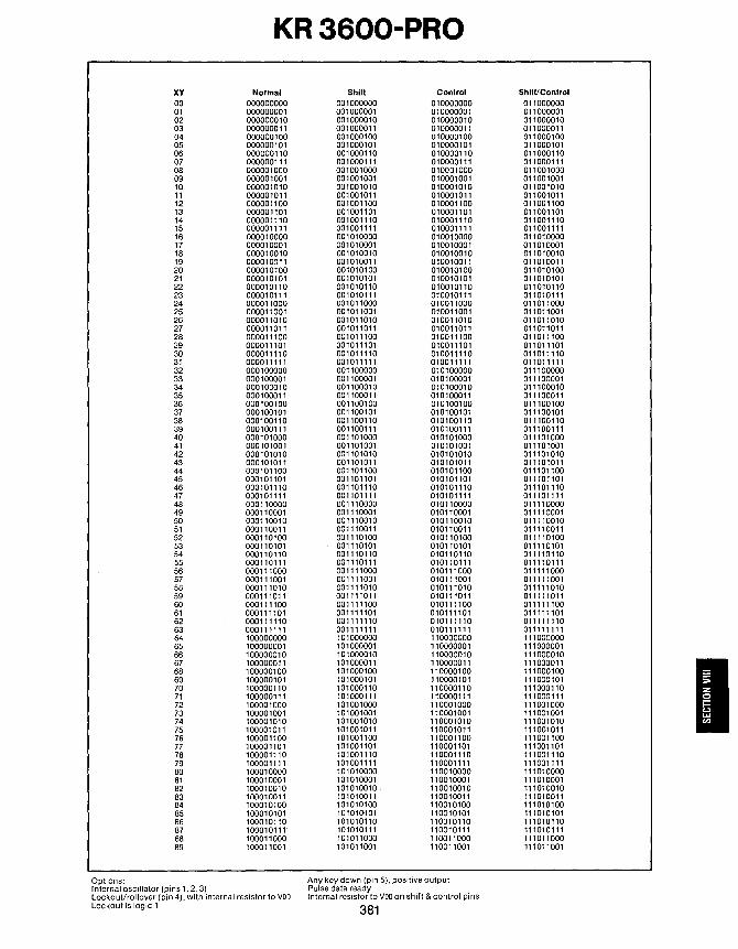
KR3600-PRO
XY Normal 00 000000000 01 000000001 02 000000010 03 000000011 04 000000100 05 000000101 06 000000110 07 000000111 08 000001000 09 000001001 10 000001010 11 000001011 12 000001100 13 000001101 14 000001110 15 000001111 16 000010000 17 000010001 18 000010010 19 000010011 20 000010100 21 000010101 22 000010110 23 000010111 24 000011000 25 000011001 26 000011010 27 000011011 28 000011100 29 000011101 30 000011110 31 000011111 32 000100000 33 000100001 34 000100010 35 000100011 36 000100100 37 000100101 38 000100110 39 000100111 40 000101000 41 000101001 42 000101010 43 000101011 44 000101100 45 000101101 46 000101110 47 000101111 48 000110000 49 000110001 50 000110010 51 000110011 52 000110100 53 000110101 54 000110110 55 000110111 56 000111000 57 000111001 58 000111010 59 000111011 60 000111100 61 000111101 62 000111110 63 000111111 64 100000000 65 100000001 66 100000010 67 100000011 68 100000100 69 100000101 70 100000110 71 100000111 72 100001000 73 100001001 74 100001010 75 100001011 76 100001100 77 100001101 78 100001110 79 100001111 80 100010000 81 100010001 82 100010010 83 100010011 84 100010100 85 100010101 86 100010110 87 100010111' 88 100011000 89 100011001
Options: Internal oscillator (pins 1, 2, 3) Lockout/rollover (pin 4), with internal resistor to VOD Lockout is logic 1
Shift Control 001000000 010000000 001000001 010000001 001000010 010000010 001000011 010000011 001000100 010000100 001000101 010000101 001000110 010000110 001000111 010000111 001001000 010001000 001001001 010001001 001001010 010001010 001001011 010001011 001001100 010001100 001001101 010001101 001001110 010001110 001001111 010001111 001010000 010010000 001010001 010010001 001010010 010010010 001010011 010010011 001010100 010010100 001010101 010010101 001010110 010010110 001010111 010010111 001011000 010011000 001011001 010011001 001011010 010011010 001011011 010011011 001011100 010011100 001011101 010011101 001011110 010011110 001011111 010011111 001100000 010100000 001100001 010100001 001100010 010100010 001100011 010100011 001100100 010100100 001100101 010100101 001100110 010100110 001100111 010100111 001101000 010101000 001101001 010101001 001101010 010101010 001101011 010101011 001101100 010101100 001101101 010101101 001101110 010101110 001101111 010101111 001110000 010110000 001110001 010110001 001110010 010110010 001110011 010110011 001110100 010110100 001110101 010110101 001110110 010110110 001110111 010110111 001111000 010111000 001111001 010111001 001111010 010111010 001111011 010111011 001111100 010111100 001111101 010111101 001111110 010111110 001111111 010111111 101000000 110000000 101000001 110000001 101000010 110000010 101000011 110000011 101000100 110000100 101000101 110000101 101000110 110000110 101000111 110000111 101001000 110001000 101001001 110001001 101001010 110001010 101001011 110001011 101001100 110001100 101001101 110001101 101001110 110001110 101001111 110001111 101010000 110010000 101010001 110010001 101010010 110010010 101010011 110010011 101010100 110010100 10101(}101 110010101 101010110 110010110 101010111 110010111 101011000 110011000 101011001 110011001
Any key down (pin 5), positive output Pulse data ready Internal resistor to VDO on shift & control pins
381
Shift/Control 011000000 011000001 011000010 011000011 011000100 011000101 011000110 011000111 011001000 011001001 011001010 011001011 011001100 011001101 011001110 011001111 011010000 011010001 011010010 011010011 011010100 011010101 011010110 011010111 011011000 011011001 011011010 011011011 011011100 011011101 011011110 011011111 011100000 011100001 011100010 011100011 011100100 011100101 011100110 011100111 011101000 011101001 011101010 011101011 011101100 011101101 011101110 011101111 011110000 011110001 011110010 011110011 011110100 011110101 011110110 011110111 011111000 011111001 011111010 011111011 011111100 011111101 011111110 011111111 111000000 111000001 111000010 111000011 111000100 111000101 111000110 111000111 111001000 111001001 111001010 111001011 I 111001100 111001101 111001110 111001111 111010000 111010001 111010010 111010011 111010100 111010101 111010110 111010111 111011000 111011001

DESCRIPTION
The KR3600 PRO isa MOS/LSI deviceintendedtosimplify the interface of a microprocessor to a keyboard matrix. Like the other KR 3600 parts, the KR 3600 PRO contains all of the logic to de-bounce and encode keyswitch closures, while providing either a 2-key or N-key rollover.
The output of the KR 3600 PRO is a simple binary code which may be converted to a standard information code by a PROM or directly by a microprocessor. This permits a user maximum flexibility of key layout with simple field programming.
The code in the KR 3600 is shown in Table I. The format is simple: output bits. 9, 8, 7, 6, 5, 4 and 1 are a binary sequence. The count starts at XO, YO and increments through XOY1, XOY2 ... X8Y9. Bit 9 is the LSB; bit 1 is the MSB.
FIGURE 1 KR 3600 PRO TYPICAL APPLICATION
64 KEY, 4 MODE
Rollover
+5.-/'-4 lockout XO 40
)('39
)(238
)(331
)(436
)(535
)(634
,.------E 33
~.32 YO 17 Y',e Y2 19
Y3 20
Y4 21
Y5 22
Y6 23
'(724
V8 25
Any Key Down
161---:':-:-___ =.:DO:::.'O;;.:AO=.:Od.:...Y _
:~ "
14 f!!!--NC
13 82
-,~k-6f2'-,f2L.
1283 .
Z F'----....:A3""'f4 ~
~ F'-----'""'i5 ~
i3
8~~ 9~~ 11~g 12~U
13f2!--... 14~
1\ Y9 26 'Sh
~~t
typical sWitch tYPiCal SWitch (N-keyrollover) (2-keyrollover)
y y ~ #x ~x , 'C,r~ +5V
Bits 2 and 3 indicate the mode as follows: Bit2 Bit3 o 0 o 1 1 0 1 1
Normal Shift Control Shift Control
For maximum ease of use and flexibility, an internal scanning oscillator is used, with pin selection of N-key lockout (also known as 2-key rollover) and N-key rollover. An "any-key-down" output is provided for such uses as repeat oscillator keying. Figure 1 shows a PROM-encoded 64 key, 4 mode application, using a 256x8 PROM, and Figure2afull90key,4 mode application, utilizing a 512x8 PROM. If N-key rollover operation is desired, it is recommended that a diode be inserted in series with each switch asshown. This prevents "phantom" key closures from resulting if three or more keys are depressed simultaneously.
FIGURE 2 KR 3600 PRO TYPICAL APPLICATION
90 KEY, 4 MODE
Any Key Down
'5.-/'-' lockout X040
161---:':-.-___ =.:DO:::.'O;;.:RO;;.:Od.:...Y _
:S )(238
)(535
X634
-E33
~32
Vl ,8
Y2 19
Y3 20
Y421
Y522
V623
Y7 24
V8 25
1382
1283
6BO
~~~"" 1\1 ".,._~ ":it (N·'oy,Otlo,.n \ (2·'oy '011o,.'1
H -++ ~ ~ ~Itr +5V
"
'-102~ AO
6f21--
,~
A2 3 8~~ 3 9~~ ~
~ 11~g A5 19 <1i 12~U AS,S
;!
13F--A7 17 14~ A8
'6
8Ml~.NYl1'B8 273·3100 TWX·510-227·8898
canlc2eP ahead of ycIfi.
Circuit diagrams utilizing SMC products are included as a means of illustrating typical semiconductor applications; consequently complete information sufficient for construction purposes is not necessarily given. The information has been carefully checked and is believed to be entirely reliable. However, no responsibility is assumed for inaccuracies. Furthermore, such information does not convey to the purchaser of the semiconductor devices described any license under the patent rights of SMC or others. SMC reserves the right to make changes at any time in order to improve design and supply the best product possible.
382

STANDARD MICROSYSTEMS MPU3870 CORPORATION f-LPC FAMILY
Single Chip a-Bit Microcomputer
FEATURES
o 2K bytes of mask programmable ROM memory
o 64 bytes of scratch pad RAM
032 bits (4 ports) TTL compatible I/O
o Programmable binary timer interval timer mode pulse width measurement mode event counter mode
o External Interrupt Input
o Crystal, LC, RG, or external time base options
o Low Power (275 mW typical)
GENERAL DESCRIPTION
The MPU3870 is a complete 8-bit microcomputer on a single MOS integrated circuit. The MPU3870 can execute a set of more than 70 instructions. The MPU3870 features 2K bytes of ROM, 64 bytes of scratch pad RAM, a programmable binary timer, and 32 bits of I/O.
The programmable binary timer operates by itself
MPU3870 BLOCK DIAGRAM Figure 1
MEMORY ADDRESS BUS
aB ECUTABLE
AM
PIN CONFIGURATION
XTL1 1 XTL2 2 PO-O 3 PO-1 4 J5O:2 5 PO-3 6
STROBE 7 P4-0 8 P4-1 9 P4-210 P4-311 P4-4 12 P4-513 P4-614 P4-715 PO-716 PO-617 PO-518 PO-419 GND20
40~ 39 RESET 38 EXTINT 37 P1-0 36 f51:1 35 P1-2 34 P1-3 33 P5-O 32 P5-1 31 P5-2 30 P5-3 29 P5-4 28 P5-5 27 P5-6 26 P5-7 25 PI-7 24 PI-6 23 PI-5 22 PI-4 21 TEST
in the interval timer mode or in conjunction with the external interrupt input in the pulse width measurement and the event counter modes of operation. Two sources of vectored, prioritized interrupt are provided with the binary timer and the external interrupt input. The user has the option of specifying one of four clock sources: crystal, LC, RC or external clock.
ROM
MAIN CONTROL
lOGIC
TEST
383
I

I 0 PORTS CPU REGISTERS SCRATCHPAD MFMORY
BI:IIARY TIMER
PORT7
INTERRUPT CONTROL PORT
PORT 6
PARALLEL I 0 PORTS
PORT S
ACCUMULATOR
A
STATUS REGISTER iWI
I 0 Z C S N V E A I T ERR G R R 0 R N C F Y N L T 0 R W L
4 __ S BITS .. 0
SCRATCHPAD DEC
~o I
J
HU 10
HL 11
KU 12
KL 13
au 14
aL 1 S
61
62
HEX
o
A
B
C D
3D
3E
OCl
o
11
12
13 14
lS
16
17
75
76
PORT 4 INDIRECT SCRATCHPAD ADDRESS REGISTER
t§ 7 __ 8 BITS ... 0
63 3F 77
PORT 1 I [;j-~ S 32 0
PORT 0 I _6BITS-_
7_8BITS-_O PROGRAM COUNTER
bu PO
POL 1 I 11 87 0 -12BIT5-
MPU 3870 PROGRAMMABLE REGISTERS, PORTS, AND MEMORY MAP Figure 2
MPU3870 MAIN MEMORY
STACK REGISTER
I PU P
Pl I I 11 87 _12BITS_
DATA COUNTER
0
!DCU DIC DCl]
11 87 0 _12RITS_
AUXDATA COUNTER
IDCIU Dr DCILI
11 87 0 _12RIT5_
There are four address registers used to access main memory. These are the Program Counter (PO), the Stack Register (P), the Data Counter (DC), and the Auxiliary Data Counter (DC1). The Program Counter is used to address instructions or immediate operands. The Stack Register is used to save the contents of the Program Counter during an interrupt or subroutine call. Thus, the Stack Register contains the return address at which processing is to resume upon completion of the subroutine or interrupt routine. The Data Counter is used to address data tables. The register is auto-incrementing. Of the two data counters, only Data Counter (DC), can access the ROM. However, the XDC instruction allows the Data Counter and Auxiliary Data Counter to be exchanged.
MAIN MEMORY
~ DEC HEX
0 0 1 1
ROM 1022 3FE 1023 3tF
~ 2046 IFE 2047 7FF
_ROMTDP
I/O PORTS The MPU3870 provides four, 8 bit bidirectional Input/Output ports. These are ports 0, 1,4,5. In addition, the Interrupt Control Port is addressed as Port 6 and the binary timer is addressed as Port 7. The programming of Ports 6 and 7 and the bidirectional 110 pin are covered in the 3870 Technical Manual. The schematic of an I/O pin and available output drive options are shown in Figure 4.
An output ready strobe is associated with Port 4. This flag may be used to signal a peripheral device that the MPU3870 has just completed an output of new data to Port 4. The strobe provides a single low pulse shortly after the output operation is completely finished. so either edge may be used to signal the peripheral. STROBE may also be used as an input strobe to Port 4 after completing the input operation.
384

MPU3870 CLOCKS The time base network used with the MPU3870 may be one of the four different types listed below.
The type of network which is to be used with the MPU3870 is to be specified at the time when mask ROM MPU3870 devices are ordered. The time base specifications for each of the four modes are covered in the 3870 Technical Manual.
Crystal LC RC External Clock
MPU3870 ARCHITECTURE The basic functional elements of the MPU3870 are shown in Figure 1. A programming model is shown in Figure 2. The user is referred to the 3870 Technical Manual for a thor-
ough discussion of the architecture, instruction set, and other features.
DESCRIPTION OF PIN FUNCTIONS PIN NO. NAME DESCRIPTION FUNCTION
3-6,19-16 PO-Q-PO-7 110 PortO PO-O through PO-7, P1-0 through P1-7, P4-0 through P4-7, and PS-O through 37-34, 22-2S P1-Q-P1-7 1/0 Port 1 PS-7 are 32 lines which can be individually used as either TTL compatible
8-1S P4-Q-P4-7 1/0 Port 4 inputs or as latched outputs. 33-26 PS-0-PS-7 1/0 PortS
7 STROBE Ready Strobe STROBE is a ready strobe associated with 1/0 Port 4. This output pin, which is normally high, p-rovides a single low pulse after valid data is present on the P4-0 through P4-7 pins during an output instruction.
38 EXTINT External Interrupt EXT INT is the external interrupt input. Its active state is software programmable. This input is also used in conjunction with the timer for pulse width measurement and event counting.
39 RESET External Reset RESET may be used to externally reset the MK3870. When pulled low the MK3870 will reset. When then allowed to go high the MK3870 will begin program execution at program location H '000'.
1,2 XTL 1, XTL2 Time Base XTL 1 and XTL 2 are the time base inputs to whiCh a crystal, LC network, RC network, or an external single-phase clock may be connected. The time base network must be specified when ordering a mask ROM MK3870. The MK38P70 will operate with any of the four configurations.
21 TEST Test Line TEST is an input, used only in testing the MK3870. For normal circuit functionality this pin may be left unconnected, but it is recommended that TEST be grounded.
40 Vcc Power Supply + S volt supply pin 20 GND Ground Ground
I/O PIN CONCEPTUAL DIAGRAM WITH OUTPUT BUFFER OPTIONS
PORT Z 1/0 0 PIN ;::
~ ... ... " a: a: ;;: ~ ~ z 8 0 0
~ < a: g 0
~ ~
I; Ports 0 and 1 8r8 Standard Output type only
Ports 4 and 5 may both be any of the three output options (mask programmable bit by bit)
The STii'OiiE output is always configured similar to a Direct Drive Output akcapt that it is capable of driving 3 TTL loads
RES'E'T'" and EXT INT may have standard 6KlI (typical) pull-up or may have no pull-up (mask programmable)
385
OUTPUT BUFFER OPTIONS
IMASK PROGRAMMABLE}
~r OPEN DRAIN
OUTPUT
STANOARD OUTPUT
Vce
~ DIRECT DRIVE
OUTPUT
I

ELECTRICAL SPECIFICATIONS MPU3870
ABSOLUTE MAXIMUM RATINGS*
OPERATING VOLTAGES AND TEMPERATURES Dash Number Suffix -00 -05 -10 -15
Operating Voltage Vee +5V±10%* +5V±5% +5V±10%* +5V±5%*
Operating Temperature TA 0°C-70°C 0°C-70°C - 40°C- + 85°C - 40°C- + 85°C
See Ordering Information for explanation of part numbers.
-00, -OS Temperature Under Bias ....................................................... - 20°C to + 85°C
-10, -15 - 50°C to + 100°C
Storage Temperature . . . . . . . . . . . . . . . . . . . . . . . . . . . . . . . . . . . . . . . . . . . . . . . . . . . . . . . . .. - 65°C to + 150°C Voltage on any Pin With Respect to Ground
- 65°C to + 150°C
(Except open drain pins and TEST) .. . . . . . . . . . . . . . . . . . . . . . . . . . . . . . . . . . . . . . . . . .. - 1.0V to + 7V Voltage on TEST with Respect t.o Ground. . . . . . . . . . . . . . . . . . . . . . . . . . . . . . . . . . . . . . . .. - 1.0V to + 9V Voltage on Open Drain Pins With Respect to Ground . . . . . . . . . . . . . . . . . . . . . . . . . . . . . .. - 1.0V to + 13.5V
-1.0Vto +7V -1.0Vto +9V - 1.0V to + 13.5V
Power Dissipation . . . . . . . . . . . . . . . . . . . . . . . . . . . . . . . . . . . . . . . . . . . . . . . . . . . . . . . . . . . .. 1.5W Power Dissipation by anyone I/O pin. . . . . . . . . . . . . . . . . . . . . . . . . . . . . . . . . . . . . . . . . . . .. 60mW Power Dissipation by all I/O pins. . . . . . . . . .. . . . . . . . . . . . . . . . . . . . . . . . . . . . . . . . . . . . . .. 600mW
1.5W 60mW 600mW
·Stresses above those listed under "Absolute Maximum Ratings" may cause permanent damage to the device. This is a stress rating only and functional operation of the device at these or any other condition above those indicated in the operational sections of this specification is not implied. Exposure to absolute maximum rating conditions for extended periods may affect device reliability.
AC CHARCTERISTICS TA , Veewithin specified operating range. I/O power dissipation ",;1 OOmW (Note 2)
-00, -OS -10, -15 SIGNAL SYM PARAMETER MIN MAX MIN MAX UNIT NOTES
XTl1 to Timer Base Period, all clock modes 250 500 250 500 ns 4MHz-2MHz XTl2
teX(H) External clock pulse width high 90 400 100 390 ns tex(L) External clock pulse width low 100 400 110 390 ns
<l> t<l> Internal <l> clock 2to 2to WRITE tw Internal WRITE Clock period 4t<l> 4t<l> Short Cycle
6t<l> 6t<l> long Cycle I/O ~I/O Output delay from internal 0 100 0 1200 ns 50pFplus
WRITE clock one TTL load tsl/O Input setup time to intrenal 1000 1200 ns
WRITE clock
STROBE tI/O_. Output valid to STROBE delay 3t<l> 3t<l> 3t<l> 3t<l> ns I/O load= -1000 +250 -1200 +300 50pF + 1 TTL load
tSL STROBE low time 8t<l> 12t<l> 8t<l> 12t<l> ns STROBE load = -250 +250 -300 +300 50pF + 3TTl loads
RESET tRH RESET hold time, low 6t<l> 6t<l> ns +750 +1000
tRPOC RESET hold time, low for power power ms power clear supply supply
rise rise time time -0.1 +15
EXTINT tEH EXT INT hold time in active and 6t<l> 6t<l> ns To trigger inactive state +750 +1000 interrupt
2t<l> 2t<l> ns To trigger timer
386

DC CHARACTERISTICS TA, Vee within specified operating range 1/0 power dissipation:%;100mW (Note 2)
SYM PARAMETER VIHEX External Clock input high level VILEX External Clock input low level I,HEx External Clock input high current I,LEx External Clock input low current
VIHI/O Input high level, I/O pins
VIHR Input high level, RESET
VIHEI Input high level, EXT INT
VIL Input low level
IlL Input low current, all pins with standard pull-up resistor
IL Input leakage current, open drain pins, and inputs with no pull-up resistor
IOH Output high current pins with standard pull-up resistor
IOHDD Output high current, direct drive pins
IOHs STROBE Output High current IOL Output low current
IOLs STROBE Output Low current
lee Average Power Supply Current
TIMER AC CHARACTERISTICS Definitions: Error = Indicated time value - actual time value tpsc = teI> x Prescale Value
Interval Timer Mode:
-00, -05 -10, -15 MIN MAX MIN MAX UNIT 2.4 5.8 2.4 5.8 V -.3 .6 -.3 .6 V
100 130 Jl.A -100 -130 Jl.A
2.0 5.8 2.0 5.8 V 2.0 13.2 2.0 13.2 V 2.0 5.8 2.2 5.8 V 2.0 13.2 2.2 13.2 V 2.0 5.8 2.2 5.8 V 2.0 13.2 2.2 13.2 V -.3 .8 -.3 .7 V
-1.6 -1.9 mA
+10 +18 Jl.A -5 -8 Jl.A
-100 -89 Jl.A -30 -25 Jl.A -100 -80 Jl.A -1.5 -1.3 mA
-8.5 -11 mA -300 -270 Jl.A 1.8 1.65 mA 5.0 4.5 mA
85 110 mA
CONDITIONS
VIHEx=VOee VILEX = Vss Standard pull-up Open drain (1) Standard pull-up No Pull-up Standard pull-up No Pull-up (1 ) VIN = O.4V
VIN = 13.2V VIN=O.OV VOH=2.4V VOH=3.9V VoH =2.4V VOH = 1.5V VOH=0.7V VOL =2.4V VOL =O.4V VOL =o.4V MK3870/20 Outputs Open
Single interval error, free running (Note 3) . . . . . . . . . . . . . . . . . . . . . . . . . . . . . . . . . . . . . . . . . . . . . . . . . . . . . . . . . . . . . . . . . . . . . . .. :±: 6teI> Cumulative interval error, free running (Note 3) . . . . . . . . . . . . . . . . . . . . . . . . . . . . . . . . . . . . . . . . . . . . . . . . . . . . . . . . . . . . . . . . . . . . . . .. 0 Error between two Timer reads (Note 2) ................................................................... :±: (tpsc + teI» Start Timer to stop Timer error (Notes 1,4) .......................................................... + teI> to - (tpsc + teI» Start Timer to read Timer error (Notes 1, 2) ........................................................ - 5teI> to - (tpsc + 7teI» Start Timer to interrupt request error (Notes 1, 3) ........................................................... - 2teI> to - 8teI> Load Timer to stop Timer error (Note 1) . . . . . . . . . . . . . . . . . . . . . . . . . . . . . . . . . . . . . . . . . . . . . . . . . . . . . . . . . . .. + teI> to - (tpsc + 2teI» Load Timer to read Timer error (Notes 1, 2) ...................................................... - 5teI>:±: to - (tpsc + BteI» Load Timer to interrupt request error (Notes 1, 3) ........................................................... - 2teI> to - 9teI>
Pulse Width Measurement Mode: Measurement accuracy (Note 4) . . . . . . . . . . . . . . . . . . . . . . . . . . . . . . . . . . . . . . . . . . . . . . . . . . . . . . . . . . . . . . . . .. + teI> to - (tpsc + 2teI» Minimum pulse width of EXT INT pin ............................................................................... 2teI>
Event Counter Mode: Minimum active time of EXT INT pin ............................................................................... 2teI> Minimum inactive time of EXT INT pin ............................................................................. 2teI>
Notes: 1. All times which entail loading, starting, or stopping the Timer are referenced from the end of the last machine cycle of the OUT or OUTS I
instruction. 2. All times which entail reading the Timer are referenced from the end of the last machine cycle of the IN or INS instruction. _ 3. All times which entail the generation of an interrupt request are referenced from the start of the machine cycle in which the appropriate
interrupt request latch is set. Additional time may elapse if the interrupt request occurs during a privileged or multicycle instruction. 4. Error may be cumulative if operation is repetitively performed.
387

INPUT/OUTPUT AC TIMING
INTERNAL WRITE CLOCK
SHOWN FOR 4MHz EXTERNAL CLOCK
INTERNAL WRITE CLOCK
INTERNAL WRITE CLOCK
1+-----f4-----.... ~------._\._--_4_-_ ~~~~~~~~I~~NSTRUCTION
OPCODE
FETCHED
PLACED ON DATA BUS
PORT PINS
A. INPUT ON PORT 4 OR 5
t+-----t*"I------_-t-------..J._--_+--_ g~;i~~~~I~?NSTRUCTION
OUTS OPCODE FETCHED
PORT ADDR. ON DATA BUS
ACr.UMULA TOR CONTENTS ON DATA BUS
PORT PINS
STROBF
(ACTIVE FOR PORT 4 ON L YI
B. OUTPUT ON PORT 4 OR 5
C. INPUT ON PORT 0 OR 1
388
NEXT OP CODE FETCHED
STAYS LOW
FOR TWO WRITE CYCLES
tI/O·S
OUTS 0,1 FETCHED
ACC DATA ON BUS
PORT PINS
NEXT OPCODE FETCHED
D. OUTPUT ON PORT 0, 1

AC TIMING DIAGRAM
External Clock
Internal <I> Clock
1/0 Port Output
STROBE .( RESET
EXT INT { 'CPB'T]= 'E" =t= ICP BIT 2 1
Note: All measurements are referenced to VIL max., VIH min., VOL max., or VOH min.
STROBE SOURCE CAPABILITY (TYPICAL AT VCC = 5V, TA = 25°C)
STROBE SINK CAPABILITY (TYPICAL AT VCC = 5V, TA = 25°C)
s 0 U R C E
C U R R E N T
M A
S I N K
C U R R E N T
M A
-15
-10
-5
+100
+50
...... 1-0..,
............ ............
..... r-... ......
1'1-0.., ,... 2 3
OUTPUT VOLTAGE
--i,...o' .....
'/ /
/ 1/
1 2 3
OUTPUT VOL T AG E
389
-I-- I

STANDARD 1/0 PORT SOURCE CAPABILITY (TYPICAL AT VCC = 5V, TA = 25°C)
-1.5
s o U R C E
C U R R E N T
M A
-1.0
-.5
.......
~ "' ......
...... ~
...... r...... ......
r-... ...... r......
i" ~
...........
OUTPUT VOL TAGE
DIRECT DRIVE 1/0 PORT SOURCE CAPABILITY (TYPICAL AT VCC = 5V, TA = 25°C)
1/0 PORT SINK CAPABILITY (TYPICALATVCC = 5V, TA = 25°C)
s o U R C E
c U R R E N T
M A
S I N K
C U R R E N T
M A
-10
-5
+60
+50
+40
+30
+20
+10
I"""r-_ -r--.
...... 1"---........
....... ......
~
OUTPUT VOLTAGE
~-----., ., J"-'
'" OUTPUT VOL TAGE
MAXIMUM OPERATING TEMPERATURE VS. I/O POWER DISSIPATION
100
.... P'~': -s"c 1"""- ..... CfR4M'ic -50
....... I""" ~
100 200 300 400 500 600 1000
PDIIOMW
Circuit diagrams utilizing SMC products are included as a means of illustrating typical semiconductor applications, consequently complete information sufficient for construction purposes is not necessarily given. The information has been carefully checked and is believed to be entirely reliable. However, no responsibility is assumed for inaccuracies. Furthermore, such information does not convey to the purchaserof the semiconductor devices described any license under the patent rights of SMC or others. SMC reserves the right to make changes at any time in order to improve design and supply the best product possible.
390

391 I

STANDARD MICROSYSTEMS CORPORATION
Package Outlines 14, 16, 18, 20 PIN HERMETIC PACKAGE
~[:,:~r;1 ~
~\'1~\ lU ~ ij ij m- I ___ I M'V -I G 1- SEATING PLANE I-L~
24, 28, 40 LEAD HERMETIC DIP
DIM
A
C D
F
G
J K L
M
N
DIM
A
B
C
D
E
F
_I 0750 I
t~ ~ _II~ I~T1yOpO ~ TYP TYP
ALL UNITS INCHES UNLESS OTHERWISE SPECIFIED 392
14 LEAD 16 LEAD 18 LEAD 20 LEAD
MIN MAX MIN MAX MIN MAX MIN MAX
.670 .760 .790 .810 .885 .915 .965 .995
.175 .175 .175 .175
.015 .021 .015 .021 .015 .021 .015 .021
.048 .060 .048 .060 .048 .060 .048 .060
.090 .110 .090 .110 .090 .110 .090 .110
.008 .012 .008 .012 .008 .012 .008 .012
.100 .100 .100 .100
.295 .325 .295 .325 .295 .325 .295 .325
10° 10° 10° 10°
.025 .060 .025 .060 .025 .060 .025 .060
24 LEAD 28 LEAD 40 LEAD
MIN MAX MIN MAX MIN MAX
1.188 1.212 1.386 1.414 1.980 2.020
.568 .598 .568 .598 .568 .598
.590 .610 .590 .610 .590 .610
.070 .090 .070 .090 .070 .090
.025 .060 .025 .060 .025 .060
.100 .100 .100
14 LEAD PLASTIC DIP

16 LEAD PLASTIC DIP 18 LEAD PLASTIC DIP
~PIN1ID
24, 28, 40 PIN PLASTIC DIP
~~~---------~~~
~PIN 1 IDENTIFICATION
~~~---------~~~
I I Tml--------WW C ======== --L- _______ _
-1r-" 10-1 ~ ~, 24 LEAD 28 LEAD 40 LEAD
DIM MIN MAX MIN MAX MIN MAX
A 1.245 1.255 1.445 1.455 2.045 2.055
C .145 .155 .145 .155 .145 .155
D .018 TYP .018 TYP .018 TYP
F .060 TYP .060 TYP .060 TYP
G .099 .101 .099 .101 .099 .101
J .010 .014 .010 .014 .010 .014
K .120 .120 .120
L .645 .675 .645 .675 .645 .675
M .210 .210 .210
ALL UNITS INCHES UNLESS OTHERWISE SPECIFIED 393 I

STANDARD MICROSYSTEMS CORPORATION
SALES REPRESENTATIVES ALABAMA IOWA NEBRASKA OREGON VIRGINIA EMA Quantum Sales S.W Wollard Co. SDR2 Products & Sales Co. Robert Electronic Sales 2309 Starmount Circle 10800 Normandale Blvd. Rural Route I Box 66A 1526 S.E. Claybourne 6407 Frederick Avenue Huntsville, AL 35801 Bloomington, MN 55437 Parker, KS 66072 Portland, OR 97202 Cantonville, MD 21228 (205) 533-6640 (612) 884-4700 (913) 898-6552 (206) 747-9424 (301) 788-2380
ILLINOIS NEVADA PENNSYLVANIA TWX: 710-862-1452
ARIZONA RELCOM Inc. METCOM Associates Corp. RELCOM Inc. (Eastern)
4314 E. Tonto St. Two Talcott Road 4314 E. Tonto St. BRGAssoc. AREA SALES
Phoenix, AZ 85044 Park Ridge, IL 60068 Phoenix, AZ 85044 3001 D Greentree MANAGEMENT OFFICES·
(602) 893-1209 (312) 696-1490 (602) 893-1209 Executive Campus EASTERN AREA
KANSAS NEWJERSEY Marlton, NJ 08053 35 Marcus Boulevard
ARKANSAS (Northern) (609) 428-2440 Hauppauge, NY 11788
Nova Marketing Inc. S.w. Wollard Co.
Lorac Sales Electronics (Western) (516) 273·3100 Rural Route I Box 66A
5728 LBJ Freeway Parker, KS 66072 550 Old Country Rd. Thompson & Associates TWX: 510·227-8898 Suite 400 (913) 898-6552 Room 410 7221 Taylorsville Rd. TELEX 221646 Dallas, TX 75240 Hicksville, NY 11801 Dayton, OH 45424
(214) 385-9669 (513) 237-9422 WESTERN AREA LOUISIANA (516) 681-8746 Turk Enterprises
CALIFORNIA Nova Marketing Inc. (201) 622-4958 RHODE ISLAND 2172 Dupont Dr. 5728 LBJ Freeway (Southern) Mill-Bern Assoc., Inc. Irvine, CA 92715
(Southern) Suite 400 BGR Assoc. 120 Cambridge St. (714) 955·1575 RELCOM Inc. Dallas, TX 75240 3001 D Greentree Suite 8 TWX: 910·595·2635 20335 Ventura Blvd. (214) 385-9669 Executive Campus Burlington, MA 01803 Suite 203 CENTRAL AREA
Woodland Hills, CA 91364 MAINE Marlton, NJ 08053 (617) 273-1313
Microsystems Sales
(213) 340-9143 Mill-Bern Assoc., Inc. (609) 428-2440
SOUTH CAROLINA 16990 Dallas Pkwy
(Northern) 120 Cambridge st. NEW HAMPSHIRE EMA Suite 151
Suite 8 Mill-Bern Assoc., Inc. 6645 Hillandale Dr. DaUas, TX 75248 Costar, Inc.
Burlington, MA 01803 120 Cambridge St. Norcross, GA 30092 (214) 931·5321 Suite SW3-175 10080 N. Wolfe Road (617) 273-1313 Suite 8 (404) 449-9430 TWX: 910·860-9269
Cupertino, CA 95014 Burlington, MA 01803
SOUTH DAKOTA MARYLAND (617)273-1313 WASHINGTON (408) 446-9339 Roberl Electronic Sales Quantum Sales SDR2 Products & Sales Co.
6407 Frederick Avenue NEW MEXICO 10800 Normandale Blvd. COLORADO Cantonville, MD 21228 RELCOM Inc. Bloomington, MN 55437 14230 N.E. 8th Street
WESCOM Mktg. (301) 788-2380 4314 E. Tonto St. (612) 884-4700 Bellevue, WA 98007
7985 Vance Drive Phoenix, AZ 85044 (206) 747-9424
Suite 102 MASSACHUSETTS (602) 893-1209 TENNESSEE Arvada, CO 80003 Mill-Bern Assoc., Inc.
(East) WASHINGTON, D.C. (303) 422-7619 120 Cambridge St.
NEWYORK EMA Robert Electronic Sales
Suite 8 Lorac Sales Electronics Rt. 8 Dogwood Village 6407 Frederick Avenue
CONNECTICUT Burlington, MA 01803 550 Old Country Rd. Jonesboro, TN 37659 Catonville, MD 21228
Orion Group (617) 273-1313 Room410 (615) 753-8861 (301) 788-2380
27 Meriden Ave. Hicksville, NY 11801 (West) TWX: 710-862-1452
Southington, CT 06489 MICHIGAN (516) 681-8746 EMA WEST VIRGINIA
(203) 621-8371 DETROIT AREA (201) 622-4958 2309 Star mount Circle
KRW Sales (Upstate) Huntsville, AL 35801 Thompson & Associates
DELAWARE P.O. Box 347 L-Mar Assoc., Inc. (205) 553-6640 7221 Taylorsville Rd.
BGR Assoc. Farmington Hills, MI48024 216 Tilden Drive Dayton, OH 45424
3001 D Greentree (313) 476-6090 E. Syracuse, NY 13057 TEXAS (513) 237-9422
Executive Campus (315) 437-7779 Nova Marketing Inc. GRAND RAPIDS 5728 LBJ Freeway WISCONSIN
Marlton, NJ 08053 KRWSales L-Mar Assoc., Inc. Suite 400 (East) (609) 428-2440 P.O. Box 163 4515 Culver Rd. Dallas, TX 75240 Metcom Associates Corp.
Grand Rapids, MI49306 Rochester, NY 14622 (214) 385-9669 237 S. Curtis Rd. FLORIDA (616) 363-2925 (716) 544-8000 WAllis, WI 53214 "c" Associates (EI Paso) (414) 476-1300 2500 Hollywood Blvd. MINNESOTA NORTH CAROLINA RELCOM Inc.
Suite 302 Quantum Sales Inc. EMA 4314 E. Tonto St. (West)
Hollywood, FL 33020 10800 Normandale Boulevard Rt. 8 Dogwood Village Phoenix, AZ 85044 Quantum Sales
(305) 922-5230 Bloomington, MN 55437 Jonesboro, TN 37659 (602) 893-1209 10800 Normandale Blvd.
(305) 922-8917 (612) 884-4700 (615) 753-8861
Nova Marketing, Inc. Bloomington, MN 55437
"C" Associates NORTH DAKOTA 11700 S.W Freeway (612) 884-4700
249 Maitland Ave. MISSISSIPPI Quantum Sales Suite 200 WYOMING Suite 305 Altamonte Center EMA 10800 Normandale Blvd. Houston, TX 77031 SDR2 Products & Sales Co. Altamonte Springs, FL 32701 2309 Starmount Circle Bloomington, MN 55437 (713) 933-2636
Huntsville, AL 35801 14230 N.E. 8th Street (305) 831-1717
(205) 533-6640 (612) 884-4700 UTAH Bellevue, WA 98007
GEORGIA OHIO WESCOM Mktg. (206) 747-9424
MISSOURI Thompson & Associates 7985 Vance Drive EMA S. W Wollard Co. 7221 Taylorsville Rd. Suite 102 6445 Hillandale Drive Rural Route I Box 66A Dayton, OH 45424 Arvada, CO 80003 PUERTO RICO Norcross, GA 30092 Parker, KS 66072 (513) 237-9422 (303) 422·7619 Mill-Bern Assoc., Inc. (404) 449-9430 (913) 898-6552 G.P.O. Box 4543
OKLAHOMA VERMONT San Juan, Puerto Rico 00936 IDAHO MONTANA Nova Marketing Inc. Mill-Bern Assoc., Inc. (809) 792-1541 SDR2 Products & Sales Co. SDR2 Products & Sales Co. 5728 LBJ Freeway 120 Cambridge St. 14230N.E. 8th Street 14230 N.E. 8th Street Suite 400 Suite 8 Bellevue, WA 98007 Bellevue, WA 98007 Dallas, TX 75240 Burlington, MA 01803 (206) 747-9424 (206) 747-9427 (214) 385-9669 (617) 273-1313
394

INTERNATIONAL SALES REPRESENTATIVES AND DISTRIBUTORS AUSTRALIA DENMARK HOLLAND JAPAN SWITZERLAND A.J.F. Systems Tage Olsen A/S Auriema Nederland BV Teijin Advanced Prod. Corp. DatacompAG 9 Harker S!. Ballerup Byvej 222 Doornakkersweg 26 1-1 Uchisaiwai-Cho Zurchestr 20 Burwood, Victoria 3125 275D Ballerup 5642MP Eindhoven 2 Chome, Chiyoda-Ku CH-8952 Schileren, Zurich Australia Denmark Nederland Tokyo 100 Japan 41·1·7302165 TLX: 854553533 (03) 288-4044 45·2·658111 Tel. 31·40·816565 506·4670·6 TLX: J23548 TLX: AA 31261 TLX: 85535293 TLX: 84451992 SOUTH KOREA TAIWAN
BELGIUM FINLAND Kortronics Enterprise Multitech Int'l Corp.
Auriema, SA Havulinna HONG KONG Rm. 201·202, 18-Dong, C-Block 977 Min Shen E. Road
Rue Brogniezstraat 172-A Instrumentarium OY Protech #604-1, Guro-Dong, Guro-Gu Taipei 105 Taiwan R.O.C.
B-l070 Brussels, Belgium P.O. Box 357 Wah Sing S!. Seoul, Korea 02·769·1225 TLX: 23756 Maklelankatu 84 32·2·523·6295 00101 Helsinki 10
Wah Sing Ind. Bldg. 634·5497 TLX: MICROS K28484 WEST GERMANY
TLX: 84621646 90·755·4144 TLX: 124426
18F, Flat 1 NORWAY Tekelec Airtronic Gmbh CANADA (OTTAWA) FRANCE
Kwai Chung, N.T. Kowloon National Elektro AlS: Nussbaumstra~e 4 Tel. 12·294721 R.F.Q. Ltd. Tekelec Airtronic TLX: 38396 PLTD HX
Trade Division 8000 Munchen 2 2249 Carling Ave. Cite Des Bruyeres Ulvenveien 75 89·594621 TLX: 05·22241
Suite 204 Rue Carle Vernet ISRAEL P.O. Box 53, Oekern
Ottowa, Ontario B.P. #2, 92310 Sevres Vectronics, Ltd. N. Oslo, 5, Norway
Canada N2B 7E9 33·1·534·7535 69 Gordon Street 02·644970 TLX: 71265
(613) 820-8445 TLX: 204552F P.O. Box 16335, Tel Aviv SPAIN (613) 820·8446
GREAT BRITAIN 23·4424 TLX: 32396 Amitron SA
CANADA (TORONTO) Manhattan (Skyline) Ltd. Loeches,6
R.F.Q. Ltd. Wier Bank ITALY Madrid 8, Spain
385 The West Mall Bray-on-Thames Dott. Ing. Guiseppe 34·1·2485863 TLX: 83145550
Suite 209 Near Maidenhead De Mico S.P.A. SWEDEN Etobicoke, Ontario Berks, United Kingdom Via Vittorio Veneto 8 NAXAB Canada, M9Cl E7 SL62ED 20060 Cassina De Pecchi Box4115 (416) 626·1445 44·628·34281 Milano, Italy 17104 Solna, Sweden TWX: (610) 492·2540 TLX: 851·847591 02·95·20·551 TLX: 330869 08·98·51·40 TLX: 17912
DISTRIBUTORS ARIZONA Western Micro Sales ILLINOIS Falk-Baker Assoc. Quality Components, Inc. Cetec Moltronics 10040 Bubb Road Diplomat Electronics, Inc. 382 Franklin Ave. 6126 Westline 3617 N. 35th Ave. Cupertino, CA 95014 1071 Judson S!. Nutley, NJ 07110 Houston, TX 77036 Phoenix, AZ 85017 (408)725·1660 Bensenville, IL 60106 (201) 661·2430 (713) 772·7100 (602) 272·7951 (312) 595·1000 (201) 661·2431 Quality Components, Inc. Kachina Electronic Dis!. COLORADO Mar-Con NEW MEXICO 2427 Rutland 1425 N. 27th Lane Bell Industries 4836 Main Street Bell Industries Austin, TX 78758 Phoenix, AZ 85009 Electronic Distributor Div. Skokie, IL 60076 Century Electronic Div. (512) 835·0220 (602) 269·6201 8155 W 48th Ave. (312) 675-6450 11728LinnN.E. Diplomat Electronics, Inc. Kachina Electronic Dis!. Wheatridge, CO 80033 Albuquerque, NM 87123 10614 Rockley Road lBl0WGrantNo.l08 (303) 424·1985 MARYLAND (505) 292·2700 Houston, TX 77099 Tucson, AZ 85705 Whitney Distributors, Inc.
NEW YORK (713) 530·1900 (602) 792·2223
Diplomat Electronics, Inc. 6707 Whitestone Road
Diplomat Electronics Diplomat Electronics, Inc. Baltimore, MD 21207 Diplomat/Westates Elec. 96 Iverness Dr., East (301) 944·8080 110 Marcus Dr. 4651 Westgrove Drive
18401 North 25th Ave. UnitR Melville, NY 11747 Dallas, TX 75248 Phoenix, AZ 85023 Englewood, CO 80112 Diplomat Electronics, Inc. (516) 454·6400 (214) 931·3404 (602) 866·7525 (303) 740·8300 9150 Rumsey Rd., Suite A6
CALIFORNIA Columbia, MD 21045 Diplomat Electronics UTAH (301) 995·1226 4610 Wetzel Road Bell Industries
Cetec Moltronics CONNECTICUT Liverpool, NY 130B8 Electronic Distributor Div. 5610 E.lmperial Hwy. Diplomat Electronics, Inc.
MASSACHUSETTS (315) 652·5000 3639 West 2150 South South Gate, CA 90280 52 Federal Road Salt Lake City, UT 84120 (213) 773·6521 Danbury, CT 0681 0 Diplomat Electronics, Inc. Current Components (801) 972-6969 (714) 521·7412 (203) 797·9674 559 East Street 215 Marcus Blvd.
Cetec Moltronics Chicopee, MA 01020 Hauppauge, NY 11788 Diplomat Electronics, Inc.
721 Charcot Ave. J. V. Electronics, Inc. (413) 592·9441 (516) 273·2600 3007 S.W Temple
San Jose, CA 95121 690 Main Street Salt Lake City, UT 84115
(408) 263·7373 East Haven, CT 06512 Diplomat Electronics, Inc. OHIO (801) 486·4134 Kunlholm Drive
Cetec Moltronics (203) 469·2321 Holliston, MA 01746 Target Electronic Corp. CANADA
3940 Ruffin Rd. (617) 429·4120 6230 Cochran Rd. Future Electronics Inc. San Diego, CA 92123 FLORIDA Solon, OH 44139 237 Hymus Blvd. (714) 278·5020 Diplomat Electronics, Inc. RC Components
(216) 248·7930 (Point Claire)
Diplomat Electronics, Inc. 2120 Calumet S!. 10 Cornell Place Applied Data Management Montreal, Quebec
12B3F Mt. View-Alviso Rd. Clearwater, FL 33515 Wilmington, MA 01887 435 Dayton S!. Canada H9R 5C7
Sunnyvale, CA 94086 (813) 443·4514 (617) 657·4310 Cincinnati, OH 45214 (514) 694·7710
(408) 734·1900 (513) 579·8108 Future Electronics Inc.
DiplomaUWestates Elec. Diplomat Electronics, Inc. MICHIGAN 4800 Dufferin Street
3001 Redhill Ave. 115 Palm Bay Road Diplomat Electronics, Inc. OKLAHOMA Downsview, Ontario, M3H5S8
Bldg.3-10B Bldg. 200-Suite 10 3270B W Eight Mile Road Quality Components (416) 663·5563
Costa Mesa, CA 92626 Palm Bay, FL 32905 Farmington, MI48024 9934 E. 21 st SI.
Future Electronics Inc. (714) 549·8401 (305) 725·4520 (313) 477·3200
Tulsa, OK 74129 3070 Kingsway
DiplomatiWestates Elec. (918) 664·8812
Vancouver, B.C. V5R 5J7 20151 BahamaS!. Diplomat Electronics, Inc. MINNESOTA PENNSYLVANIA (604) 438·5545 Chatsworth, CA 91311 6890 NW. 20th Ave. Diplomat Electronics, Inc. QED Electronics, Inc. Future Electronics Inc. (213)341-4411 Fort Lauderdale, FL 33309 271 Commerce Circle South 300 North York Road Baxter Center DiplomatiWestates Elec. (305) 971·7160 Fridley, MN 55432 Hatboro, PA 19040 f050 Baxter Road 9787 Aero Drive (612) 572·0313 (215) 674·9600 Ottawa, Ontario K2C 3P2 San Diego, CA 92123 GEORGIA TEXAS (613) 820·8313
I (714) 292·5693 Diplomat Electronics, Inc. NEW JERSEY Quality Components, Inc. Future Electronics Inc. NESCO 6659 Peachtree Ind. Blvd. Diplomat Electronics, Inc. 4257 Kellway Circle 5809 MacLeod Trail S. 7110 Gerald Ave. SuiteB 490 South Riverview Dr. P.O. Box819 Unit 109 Van Nuys, CA 91406 Norcross, GA 30092 Totowa, NJ 07512 Addison, TX 75001 Calgary, Alberta T2H OJ (800) 423·2664 (404) 449·4133 (201) 785·1830
395 (214) 387·4949 (403) 259·6408


STANDARD MICROSYSTEMS CORPORATIONbj
I 35 Marcus Boulevard, Hauppauge, NY 11788
~)COPYRIGHT 1982