User's Guide - bitsavers.org
72
lor Graphics ntroller Board User's Guide TEXAS INSTRUMENlS SPPU019A
-
Upload
khangminh22 -
Category
Documents
-
view
3 -
download
0
Transcript of User's Guide - bitsavers.org

lor Graphics
ntroller Board User's Guide
~ TEXAS
INSTRUMENlS
SPPU019A

Color Graphics Controller User's Guide
Graphics Products
~ TEXAS
INSTRUMENTS

IMPORTANT NOTICE
Texas Instruments (TI) reserves the right to make changes in the devices or the device specifications identified in this publication without notice. TI advises its customers to obtain the latest version of device specifications to verify, before placing orders, that the information being relied upon by the customer is current.
In the absence of written agreement to the contrary, TI assumes no liability for TI applications assistance, customer's product design, or infringement of patents or copyrights of third parties by or arising from use of semiconductor devices described herein. Nor does TI warrant or represent that any license, either express or implied, is granted under any patent right, copyright, or other intellectual property right of TI covering or relating to any combination, machine, or process in which such semiconductor devices might be or are used.
Copyright © 1986, Texas Instruments Incorporated

Section
1 1 .1 1.2
2
Introduction Functional Overview Features .....
Quick Installation Guide
3 Installation and Operation 3.1 Hardware Configurable Jumpers 3.2 Memory Map ...... . 3.3 Video Memory Organization 3.4 TMS34061 Internal Registers 3.5 x-v Indirect Accesses 3.6 Shift Register Transfer Cycles 3.7 Interrupts ...... .. 3.8 Expansion Bus ...... . 3.9 Video Output Connectors 3.10 Power Consumption 3.11 Sample Jumper Configurations
Theory of Operation PC Bus to TMS34061 Interface CPU to Palette Interface
Contents
4 4.1 4.2 4.3 4.4
TMS34061 to Frame Buffer Interface Frame Buffer to Video Output Interface
5 Programming the CGC Board 5.1 Initializing the TMS34061 Registers ............. . 5.2 x-v Addressing ......... . ............ . 5.2.1 Advantages of X-Y Addressing Over Conventional Addressing 5.2.2 Setting Up the X-Y Address and Offset Registers 5.3 Shift Register Control ......... . 5.3.1 Memory Organization ....... . 5.3.2 Initiating a Shift Register Transfer 5.4 Horizontal Scrolling Using X-Y Addressing 5.5 Pixel Replication Zoom ........ . 5.6 Vector Drawing Using X-Y Addressing ... . 5.7 Clearing the Screen Using Shift Register Transfers 5.8 Vertical Scrolling Using Shift Register Transfers 5.9 Vertical Screen Flip .......... . 5.10 Using the Palette ..... . . . . . .. 5.10.1 Initializing the Palette to Default Values 5.10.2 Using Repeat Mode ........ .
A List of Materials 8 PAL Equations C Schematics
Page
1-1 1-2 1-2
2-1
3-1 3-2 3-3 3-5 3-5 3-7 3-9 3-10 3-10 3-11 3-12 3-12
4-1 4-2 4-5 4-5 4-6
5-1 5-2 5-3 5-3 5-5 5-7 5-8 5-9 5-10 5-12 5-14 5-16 5-18 5-19 5-20 5..:22 5-23
A-1 8-1 C-1
iii

Illustrations
Figure Page
1 -1. Color Graphics Controller Board Block Diagram ........................ " 1-3 3-1. location of Jumpers on the Board . . . . . . . . . . . . . . . . . . . . . . . . . . . . . . . . . . .. 3-3 3-2. Frame Buffer to Display Screen Memory Translation . . . . . . . . . . . . . . . . . . . . . .. 3-5 3-3. Register Select Address Mapping to Address . . . . . . . . . . . . . . . . . . . . . . . . . . .. 3-6 3-4. X-V, None, Nibble, or Byte Function Mapping to PC Address . . . . . . . . . . . . . .. 3-8 3-5. X-V, Two-Word Function Mapping to PC Address ........................ 3-8 3-6. X-Y Double Word Mask to Screen Correlation . . . . . . . . . . . . . . . . . . . . . . . . . .. 3-9 3-7. Shift Register Transfer Addressing . . . . . . . . . . . . . . . . . . . . . . . . . . . . . . . . . . .. 3-10 3-8. Interrupt Jumper J02 . . . . . . . . . . . . . . . . . . . . . . . . . . . . . . . . . . . . . . . . . . . . .. 3-10 4-1. System Address Remapping ......................................... 4-3 4-2. Memory Read/Write PC Bus Timing . . . . . . . . . . . . . . . . . . . . . . . . . . . . . . . . . .. 4-4 4-3. Frame Buffer to Video Output Interface Timing . . . . . . . . . . . . . . . . . . . . . . . . . .. 4-7 5-1. Memory and External Shift Register Organization . . . . . . . . . . . . . . . . . . . . . . . .. 5-8 5-2. Shift Register Transfer Addressing . . . . . . . . . . . . . . . . . . . . . . . . . . . . . . . . . . .. 5-10 5-3. Horizontal Scrolling . . . . . . . . . . . . . . . . . . . . . . . . . . . . . . . . . . . . . . . . . . . . . .. 5-11 5-4. Example of a 2X Pixel Replication Zoom Using X-Y Addressing . . . . . . . . . . . . .. 5-13 5-5. Vector Drawing Using X-Y Addressing . . . . . . . . . . . . . . . . . . . . . . . . . . . . . . . .. 5-15 5-6. Vertical Scrolling Using Shift Register Transfers . . . . . . . . . . . . . . . . . . . . . . . . .. 5-19 5-7. Vertical Screen Flip Using Shift Register Transfers . . . . . . . . . . . . . . . . . . . . . . .. 5-20 5-8. Palette to Screen Mapping . . . . . . . . . . . . . . . . . . . . . . . . . . . . . . . . . . . . . . . . .. 5-21
Tables
Table Page
3-1. Jumper Settings and Features . . . . . . . . . . . . . . . . . . . . . . . . . . . . . . . . . . . . . . .. 3-2 3-2. Color Graphics Controller Board Memory Map . . . . . . . . . . . . . . . . . . . . . . . . . .. 3-4 3-3. latching the Color Palette Modes . . . . . . . . . . . . . . . . . . . . . . . . . . . . . . . . . . . .. 3-4 3-4. TMS34061 Internal Register Addressing . . . . . . . . . . . . . . . . . . . . . . . . . . . . . . .. 3-6 3-5. PC Memory Addressing for X-Y Indirect Access . . . . . . . . . . . . . . . . . . . . . . . . .. 3-7 3-6. I BM/TI PC Bus Pin Assignments . . . . . . . . . . . . . . . . . . . . . . . . . . . . . . . . . . . .. 3-11 4-1. CAS Option Decode ............................................... 4-2 4-2. Operations Encoded on Control Lines CASCTlO - CASCTl2 . . . . . . . . . . . . . . .. 4-4 4-3. latching the Video Palette Modes . . . . . . . . . . . . . . . . . . . . . . . . . . . . . . . . . . .. 4-5 4-4. PAL U47 Truth Table ......................... , . . . . . . . . . . . . . . . . . . .. 4-5
iv

1. Introduction
The Color Graphics Controller Board is a TI PC and I BM PC I/O expansion bus compatible graphics card which allows you to become familiar with the TMS34061 Video System Controller and TMS34070 Color Palette. The board and demonstration software are configured at shipment to support a 640 pixel horizontal by 480 pixel vertical resolution, similar to that of the IBM Professional Graphics Display. By changing the crystal oscillator and reprogramming the TMS34061 control registers, the board can support a maximum resolution of 1024 by 512 pixels, with four bits per pixel.
Note:
Hexidecimal numbers are designated herein by the suffix "h".
1-1

Introduction
1.1 Functional Overview
The Color Graphics Controller Board is a single card designed around the IBM PC I/O Expansion Bus card format. The board is intended to demonstrate the simplicity and strengths of the TMS34061 Video System Controller and TMS34070 Color Palette in controlling text and graphics while showing the ease of hardware design. The board has the capability to drive both digital and analog raster scan color monitors.
The frame buffer consists of 32 TMS4161 multiport memories organized as four color planes, allowing for the possibility of 16 colors per frame from the digital outputs. The color palette incorporates a 12-bit color look-up table which gives the programmer a choic~ of 16 colors from a palette of 4096 colors per frame. Furthermore, the palette incorporates a unique line feature which allows the color look-up table to be reloaded on every line, allowing 16 of 4096 colors per line. The programmer can change this mode under software control.
The maximum resolution that the board can support is 1024 by 512 pixels with four bits per pixel. The memory map shown in Section 2.2 can be changed by reprogramming the memory and control decode PALs (programmable array logic).
1.2 Features
• 256K-byte frame buffer (1024 x 512 pixels, four bits per pixel)
• Direct interface to most digital and analog RGB monitors
• Totally programmable resolution (640 x 480 pixels as shipped)
• IBM and TI PC I/O expansion bus compatible
• 16 of 4096 colors per line color palette
• Palette can be loaded on a line or frame basis under software control
The block diagram for the Color Graphics Controller Board is shown in Figure 1 -1.
1-2

Introduction
~/ __ ~~ ______ ~PC __ ~~ANr-S_IO_N_B_U_S ______ ~ ___ J\P1
I t I ADDRESS BUFFERS
DeCODe LOGIC
I BU~S I
OSC
1 TMS34061 RE~~~ ~ VIDEO f----+ R
~r
Figure 1-1. Color Graphics Controller Board Block Diagram
P3
1-3


2. Quick Installation Guide
The Texas Instrume'nts TMDS3471804000 Color Graphics Controller {CGC} is designed to operate when installed fn a TI Professional Computer or IBM Personal Computer. The following is a step-by-step quick installation guide explaining how to install the CGC card and execute the main demonstration program. See Section 3 for further installation information.
1) The CGC comes configured for display on an IBM Professional Graphics Display or Princeton Graphics SR-12 driven by an IBM PC as the host computer. If a TI PC is being used as the host, then the jumper options will have to be reconfigured. The jumper options are shown below.
2) Make certain the host computer has 256K bytes of system RAM; otherwise, system RAM will overlap CGC R~M, and the demonstration will not operate. The CGC is memory-mapped from 50000h to AFFFFh.
3) Install the CGC in a vacant slot in the host computer, and connect the CGC video output {the top port, P3} to the IBM Professional Graphics Display or the Princeton Graphics SR-12.
4) Boot an MS-DOS system master on the host computer. Make certain that'the version of MS-DOS is version 2.1 or later. Once MS-DOS is loaded, remove the system master and insert the CGC demonstration disk into the drive.
5} Now that everything is configured, type" AUTOEXEC" to start execution of the main demonstration. Once execution begins, press "Q" to terminate. Additional information on the demonstration programs 'is contained in the text file called "READ.ME" located on the demonstration diskette.
HOST: IBM PC MONITOR: OUTPUT PORT:
I BM Professional Graphics Display P3
JUMPERS: J01 J02 J03 J04 J05 J06
HOST: MONITOR:
1 to 2 2 to 3 2 to 3 and 4 to 5 2 to 5 Not Connected Not Connected
TIPe
OUTPUT PORT: IBM Professional Graphics Display P3
JUMPERS: J01 J02 J03 J04 J05 J06
1 to 2 1 to 2 2 to 3 and 4 to 5 2 to 5 Not Connected Not Connected
2-1


3. Installation and Operation
This section describes the necessary configuration procedures for correct operation of the Color Graphics Controller Board. For information on how to program the TMS34061 Video System Controller and the TMS34070 Color Palette, refer to the TMS34061 User's Guide, part number SPPU014, and the TMS34070 User's Guide, part number SPPU016.
3-1

Installation and Operation
3.1 Hardware Configurable Jumpers
3-2
The Color Graphics Controller Board has hardware-configurable jumpers for such things as interrupts and monitor interfaces. Table 3-1 lists the jumpers and the features that they control.
Table 3-1. Jumper Settings and Features
FEATURE ENABLED JUMPER POSITION
On board oscillator J01 1 to 2t
Backplane oscillator J01 2 to 3
Interrupt level 2 (TI PC) J02 1 to 2
Interrupt level 3 (IBM PC) J02 2 to 3t
Negative horizontal sync to P2-8 J03 1 to 2
Positive horizontal sync to P2-8 J03 1 to 4 2 to 3
Negative vertical sync to P2-9 J04 1 to 2
Positive vertical sync to P2-9 J04 1 to 4 2 to 3
Ground to P2-6 (TI PC digital monitor) J05 2 to 3
I to P2-6 (IBM Personal Computer color display) J06 1 to 2t
Negative composite sync to P2~9 J04 2 to 5
Positive composite sync to P2-9 J04 2-to 3 4 to 6
Negative horizontal sync to P3-5 J03 1 to 2
Positive horizontal sync to P3-6 J03 1 to 4 2 to 3
Negative vertical sync to P3-4 J04 1 to 2
Positive vertical sync to P3-4 J04 1 to 4 2 to 3
Negative composite sync to P3-4 J04 2 to 5t
Positive composite sync to P3-4 J04 2 to 3 4 to 5
P3-5 to logic 0 J03 2 to 5
P3-5 to logic 1 J03 2 to 3t 4 to 5
Remove host direct memory from board memory map J06 1 to 2
t Jumper setting as shipped
Figure 3-1 shows the location of the jumpers on the Color Graphics Controller Board.

Installation and Operation
P3
P2
J02
Figure 3-1. Location of Jumpers on the Board
3.2 Memory Map
The TMS34061 allows you to control five functions through the function select lines FSO-FS2:
• Host memory direct access • Shift register to memory • Memory to shift register • TMS34061 register access • x-Y indirect access range
These functions have been placed in the PC memory space on the board. The Color Palette Modes are memory-mapped and programmable under software control. The memory map for the board is determined by the equations programmed in the decode PALs U40, U45, and U48. Table 3-2 defines the memory map and contains a brief description of the function mapped in each area. Table 3-3 defines the palette memory map and how to program the mode by reading a set of addresses.
3-3

Installation and Operation
3-4
Table 3-2. Color Graphics Controller Board Memory Map
MEMORY RANGE TMS34081 FUNCTION FSO FS1 FS2
50000h-8FFFFht HOST MEMORY DIRECT ACCESS 1 1 0
903FOh-903FFh PALETTE MODE CONTROL 1 1 1
90400h-907XXh SHIFT REGISTER TO MEMORY 0 0 1
90800h-9OBXXh MEMORY TO SHIFT REGISTER 1 0 1
9OCOOh-900XXh TMS34061 REGISTER ACCESS 0 0 0
90EOOh-90FOOh* X-V INDIRECT ACCESS RANGE 1 0 0
" + ~XO~ X-Y INDIRECT BYTE ACCESS 1 0 0
~XOO12 X-Y INDIRECT RIGHT NIBBLE 1 0 0
--+X0102 X-V INDIRECT LEFT NIBBLE 1 0 0
--+X0112 X-V INDIRECT NO ACCESS 1 0 0
AOOOOh-AXXXXh * X-V INDIRECT 2-WORD ACCESS 1 0 0
Note: Left nibble = D7 - D4, right nibble = D3 - DO on the host/controller board interface.
t If jumper J06 is installed (1 to 2), all host direct accesses are ignored to allow for a larger memory space for system RAM.
:t: See ~ection 3.5 for determining how to construct an X-Y address.
The three Color Palette modes are latched by reading the addresses listed in Table 3-3. Reading these addresses latches signals PO and P1 as shown.
Table 3-3. Latching the Color Palette Modes
SIGNALS $ET
PALETTE MODE PO I P1 READ ADDRESS
Frame Load Mode 0 0 903FOh and 903F2h
Line Load Mode 0 1 903FOh and 903F6h
High (No Load) 1 0 903F4h and 903F2h
Reserved 1 1 903F4h and 903F6h

Installation and Operation
3.3 Video Memory Organization
The frame buffer (video memory) is comprised of 32 TMS4161 multiport video RAM. These 256K bytes of multiport memory provide the board with the capability of displaying screen sizes up to 1024 x 512 pixels with four bits per pixel.
The memory is organized in packed pixels, with two pixels sharing one byte of memory. Figure 3-2 illustrates the correlation between the contents of two consecutive memory addresses and the pixels they correspond to on the display screen.
Figure 3-2. Frame Buffer to Display Screen Memory Translation
The frame buffer occupies a contiguous block of memory from 50000h to SFFFFh. The memory is not mapped contiguous to the system memory so that the auto-sizing program will not load the operating system into video memory space.
3.4 TMS34061 Internal Registers
The 1S internal registers of the TMS34061 are mapped to the base address 90COOh. The least significant byte of each register is mapped on OOOOOh boundaries, while the most significant byte is mapped on OOOOSh boundaries. The individual register addresses are derived by adding a mUltiple of 00010h to the base address. Table 3-4 lists the addresses of all accessable registers.
3-5
Installation and Operation
A A A 1 1 1 9 8 7
1 0 0
3-6
Table 3-4. TMS34061 Internal Register Addressing
MEMORY ADDRESS AS A7 AS A6 A4 A3
REGISTER NAME PC MEMORY TMS340S1 ADDRESSt BASE ADDRESS C C C C C C
A A A A A A LSB MSB 6 6 4 3 2 1
Horizontal end sync 90COOh 90C08h 0 0 0 0 0 X Horizontal end blank 90C10h 90C18h 0 0 0 0 1 X Horizontal start blank 90C20h 90C28h 0 0 0 1 0 X Horizontal total 90C30h 90C38h 0 0 0 1 1 X
Vertical end sync 90C40h 90C48h 0 0 1 0 0 X Vertical end blank 90C50h 90C58h 0 0 1 0 1 X Vertical start blank 90C60h 90C68h 0 0 1 1 0 X Vertical total 90C70h 90C78h 0 0 1 1 1 X
Display update 90C80h 90C88h 0 1 0 0 0 X Display start 90C90h 90C98h 0 1 0 0 1 X
Vertical interrupt 90CAOh 90CA8h 0 1 0 1 0 X
Control register 1 90CBOh 90CB8h 0 1 0 1 1 X Control register 2 90CCOh 90CC8h 0 1 1 0 0 X
Status register 90CDOh 90CD8h 0 1 1 0 1 X
X-Y offset register 90CEOh 90CE8h 0 1 1 1 0 X X-Y address register 90CFOh 90CF8h 0 1 1 1 1 X
Display address register 90DOOh 90D08h 1 0 0 0 0 X Vertical count register 90D10h 90D18h 1 0 0 0 1 X
t In CA1, when X = 0 the least significant byte is accessed. When X = 1 the most significant byte is accessed.
Figure 3-3 shows how the register select address lines are mapped into a particular PC memory address. Address lines A 19 - A9 are used for address decode, and A8 -A3 are used to select one of the eighteen internal registers in the TMS34061, shown in Table 3-4.
PC M EMORY ADDRESS
A A A A A A A A A A A A A A A A A 1 1 1 1 1 1 1 9 8 7 6 5 4 3 2 1 0 6 5 4 3 2 1 0
1 0 0 0 0 1 1 0 C C C C C C 0 0 0 A A A A A A 6 5 4 3 2 1
Figure 3-3. Register Select Address Mapping to Address

Installation and Operation
3.5 x-v Indirect Accesses
Host initiated X-Y indirect memory cycles are memory-mapped at base address 90EOOh. The 16 associated adjust functions of the X-Y registers after an X-Y indirect cycle are selected by the address formed by the base address plus a multiple of OOOOBh. Table 3-5 shows the addresses for the 16 functions of the X-Y standard indirect byte cycle.
Table 3-5. PC Memory Addressing for X-V Indirect Access
MEMORY ADDRESS A6 A5 A4 A3
VSC TMS34061 ADDRESS PC x-v INDIRECT BYTE C C C C
MEMORY ACCESSES A A A A ADDRESS FUNCTION MODIFICATION 4 3 2 1
90EOOh No adjustment 0 0 0 0 90E08h Increment X 0 0 0 1 90E10h Decrement X 0 0 1 0 90E18h Clear X 0 0 1 1
90E20h Increment Y 0 1 0 0 90E28h I ncrement X, Increment Y 0 1 0 1 90E30h Decrement X, Increment Y 0 1 1 0 90E38h Clear X, Increment Y 0 1 1 1
90E40h Decrement Y 1 0 0 0 90E48h Decrement Y, Increment X 1 0 0 1 90E50h Decrement y, Decrement X 1 0 1 0 90E58h Decrement Y, Clear X 1 0 1 1
90E60h Clear Y 1 1 0 0 ·90E68h Clear Y, Increment X 1 1 0 1 90E70h Clear y, Decrement X 1 1 1 0 90E78h Clear Y, Clear X 1 1 1 1
External hardware has been added in the CAS lines to allow X-Y indirect access to nibbles (4 bits) and double words (32 bits), in conjunction with bytes to be accessed. This has been achieved by mapping the X-Y addresses into several address spaces. Figure 3-4 shows how the X-Y functions modifications are mapped into a PC memory address. The.upper address lines A19 - A7 are used for address decode. Address lines A6 - A3 are used to select one of the sixteen X-V modifications. Address lines A1 and AO are used to select no access, nibble access, or byte access.
3-7

Installation and Operation
PC MEMORY ADDRESS
A A A A A A A A A A A A A A A A A A A A 1 1 1 1 1 1 1 1 1 1 9 8 7 6 5 4 3 2 1 0 9 8 7 6 5 4 3 2 1 0
1 0 0 1 0 0 0 0 1 1 1 0 0 C C C C 0 S S A A A A 1 0 4 3 2 1
CAx = TMS34061's column address line
S1 SO o 0 o 1 1 0 1 1
x -Y byte access X-Y left nibble access DO - D3 X-Y right nibble access 04 - 07 X-Y no access, only changes pointer
Figure 3-4. X-V, None, Nibble, or Byte Function Mapping to PC Address
A A A 1 1 1 9 8 7
1 0 1
Figure 3-5 shows the mapping for X-Y two word accesses. This is for write functions only. With this mode all 32 memories can be written to at once with address lines A 15 - A8 used as a write mask. Figure 3-6 shows the correlation between the mask on an X-Y double word access and the pixel position that is affected. Note that the actual pixels modified on this access come from the TMS34061's internal X-Y registers.
PC MEMORY ADDRESS
A A A A A A A A A A A A A A A A A 1 1 1 1 1 1 1 9 8 7 6 5 4 3 2 1 0 6 5 4 3 2 1 0
0 M M M M M M M M 0 C C C C X X X 0 1 2 3 4 5 6 7 A A A A
4 3 2 1
CAx = TMS34061's column address line
Figure 3-5. X-V, Two-Word Function Mapping to PC Address
3-8

Installation and Operation
PIXEL 0 PIX8.. 1 FRAME BUFFER
Figure 3-6. X-Y Double Word Mask to Screen Correlation
3.6 Shift Register Transfer Cycles
Since the multiport memories are equipped with a 256-bit internal shift register, the TMS34061 supports a shift register transfer from the memory to the shift register and from the shift register to the memory array. The shift register transfer cycles are memory-mapped starting at base addresses 90400h (shift register to memory) and 90800h (memory to shift register). An access to 90400h transfers the contents of the shift registers in bank 0 to row 000 of the memory array. An access to 90800h will transfer the contents of row 000 of the video memories in bank 0 to their internal registers. likewise, an access to the other 255 rows or the other three banks of memories can be done by adding a displacement to the base address. Figure 3-7 illustrates how the row and bank addresses are formed for a shift register transfer cycle.
3-9

Installation and Operation
A A A 1 1 1 9 8 7
1 0 0
X1 XO 0 1 1 0
n BO 0 0 0 1 1 0 1 1
A A A A A 1 1 1 1 1 6 5 4 3 2
1 0 0 0 0
Shift register to memory Memory to shift register
Bank 0 select Bank 1 select Bank 2 select Bank 3 select
A A A A A A A A 1 1 9 8 7 6 5 4 1 0
X1 XO R7 R6 R5 R4 R3 R2
R7 - RO row address select
Figure 3-7. Shift Register Transfer Addressing
A A A A 3 2 1 0
R1 RO B1 BO
3.7 Interrupts
The Color Graphics Controller Board has a jumper-configurable interrupt, which can be set to either interrupt level 2 for the TI PC or for interrupt level 3 for the IBM PC. Figure 3-8 shows the how to configure the interrupt jumper for both of these machines.
J02
IR02 .... 4 --- 10} JUMPER 1-2 FOR TI PC
INTREO ------.~ 20 ~ ___ 3
0} JUMPER 2-3 FOR IBM PC
IR03'4-
Figure 3-8. Interrupt Jumper J02
3.8 Expansion Bus
3-10
The Color Graphics Controller Board fits into the TI PC or IBM PC expansion bus, and into the expansion connector of most IBM-compatible machines. The signals that the board uses are shown in Table 3-6. Note that the only difference between the I BM PC and the TI PC for the Color Graphics Controller Board is the interrupt pins. This difference is handled by a jumper option, as described in Section 3.7.

Installation and Operation
Table 3-6. IBM/TI PC Bus Pin Assignments
SIGNAL NAME IBM TI SIGNAL NAME IBM TI PIN NO. PIN NO. PIN NO. PIN NO.
Ground 81,810,831 81,810,831 RESET 82 82
+5 Volts 83,829 83,82.9 CLOCK 820 820
OSC 830 830
~ 811 811 'Fn5V A10 A10
'mJlR' 812 812 Am A11 A11
TFm2 N/A 824 11m3 825 N/A
DO A9 . A9 01 A8 A8
02 A7 A7 03 A6 A6
04 A5 A5 05 A4 A4
06 A3 A3 07 A2 A2
AO A31 A31 A1 A30 A30
A2 A29 A29 A3. A28 A28
A4 A27 A27 A5 A26 A26
A6 A25 A25 A7 A24 A24
A8 A23 A23 A9 A22 A22
A10 A21 A21 A11 A20 A20
A12 A19 A19 A13 A18 A18
A14 A17 A17 A15 A16 A16
A16 A15 A15 A17 A14 A14
A18 A13 A13 A19 A12 A12
3.9 Video Output Connectors
The Color Graphics Controller Board has two DB9 video output connectors, P2 and P3. Connector P2 outputs a digital RGBlsignal and connector P3 outputs an RGB signal at 1 volt peak to peak with 75-ohm drive capability. Both connectors have positive and negative horizontal syncs and composite sync so that you can interface to a variety of monitors. TheP2 pinout supports a TI or an IBM Personal Computer color graphics display digital color monitor with no cable modification, and the P3 pinout supports the IBM professional graphics display analog color monitor with no cable change. Other monitors can be interfaced easily by making your own cable.
PORT P2 PINOUT PORT P3 PINOUT
PIN SIGNAL PIN SIGNAL NUMBER DESCRIPTION NUMBER DESCRIPTION
1 Ground 1 Red
2 Ground 2 Green
3 Red 3 81ue
4 Green 4 CSYNCt
5 81ue 5 MOOEt
6 lor Groundt 6 Ground
7 Reserved 7 Ground
8 HSYNCt 8 Ground
9 VSYNCt 9 Ground
t Jumper Options: See Table 3-1 for different options.
3-11

Installation and Operation
3.10 Power Consumption
The Color Graphics Controller Board uses only the +5 volt supply. The average current consumption is 1 .2 A.
3.11 Sample Jumper Configurations
3-12
The following are sample jumper configurations for various host PCs and monitors. The Color Graphics Controller Board is shipped with software to support the IBM Professional Graphics Display. Software is also available to support 720 x 300 resolution like that of the TI Professional Computer and 640 x 200 resolution like that of the IBM Personal Computer color display.
HOST: MONITOR: OUTPUT PORT: SOFTWARE: JUMPERS:
HOST:
J01 J02 J03 J04 J05 JOE)
MONITOR: OUTPUT PORT: SOFTWARE: JUMPERS:
HOST:
J01 J02 J03 J04 J05 J06
MONITOR: OUTPUT PORT: SOFTWARE: JUMPERS:
J01 J02 J03 J04 J05 J06
IBM PC I BM Professional Graphics Display P3 TM DS3440879202
1 to 2 2 to 3 2 to 3 and 4 to 5 2 to 5 Not Connected Not Connected
IBM PC IBM Personal Computer Color Display P2 TM DS34408791 02t
2 to 3 2 to 3 1 to 2 1 to 2 1 to 2 Not Connected
IBM PC TI Digital Monitor P2 TM DS3440879002~
1 to 2, change oscillator to 18.432 MHz 2 to 3 1 to 4 and 2 to 3 1 to 2 2 to 3 Not Connected
Installation and Operation
HOST: MONITOR: OUTPUT PORT: SOFTWARE: JUMPERS:
HOST:
J01 J02 J03 J04 J05 J06
MONITOR: OUTPUT PORT: SOFTWARE: JUMPERS:
J01 J02 J03 J04 J05 J06
TI PC IBM Professional Graphics Display P3 TM 053440879202
1 to 2 1 to 2 2 to 3 and 4 to 5 2to 5 Not Connected Not Connected
TI PC TI Digital Monitor P2 TM 053440879002+
1 to 2, change oscillator to 18.432 MHz 1 to 2 1 to 4 and 2 to 3 1 to 2 2 to 3 Not Connected
t Supports 640 x 200 display + Supports 720 x 300 display Contact your local sales office to order this software.
For systems using 512K bytes of system memory, connect jumper J06 1 to 2. This disables host direct accesses to the frame buffer; therefore, only the X-Y mode can be used to read or write to the frame buffer.
3-13


4. Theory of Operation
The following sections explain the theory of operation of the Color Graphics Controller Board. The theory of operation is divided. into four parts: the PC bus to TMS34061 interface, the CPU to palette interface, the TMS34061 to frame buffer interface, and the frame buffer to video ouput interface.
4-1

Theory of Operation
4.1 PC Bus to TMS34061 Interface
4-2
The heart of the interface between the PC bus and the TMS34061 is PAls U48 and U40. The equations for these PALS are shown in Appendix B, with a brief explanation of their function.
The main control signals on the TMS34061 are CEl, CEH, SYSClK, ALE, R/W, and RDY /HOlD. The TMS34061's SYSClK is connected to the PC's,ClK signal from the expansion bus. The TMS34061 is reset when the PC is reset since the TMS34061 's reset is generated from the PC's expansion bus reset. The CS line has been grounded so the TMS34061 is always active. The ALE determines when a CPU request will be generated.
When the host CPU executes a memory access to the memory range in which the Color Graphics Controller Board is mapped, the following actions take place. PAL U48 decodes the address and sends the appropriate FSO - FS2 code to the TMS34061 (Table 3-2 shows the FS codes generated as a function of the memory address location). PAL U48 also sends a two bit binary code (CASOPTO and CASOPT1) to PAL U40 and PAL U45. The information encoded on these lines is shown in Table 4-1.
Finally PAL U48 remaps the memory so that when the system auto-sizes the operating system starts at the bottom of memory (OOOOOh) and looks for the first noncontiguous block. After the hole is found it loads the operating system in the highest section of the contiguous section of memory as possible, T6;'prevent the operating system from being loaded into the Color Graphics Controller Board frame buffer the location between 40000h and 50000h cannot be used.
Since the memory now starts at 50000h the upper most address lines need to be remapped so that it is on a binary value. Figure 4-1 shows the necessary memory system memory map and the Color Graphics Controller Board memory remap.
Table 4-1. CAS Option Decode
~ASOPT1 ~ASOPTO TYPE OF CYCLE
0 0 x-Y double word access
0 1 X-Yaccess
1 0 Palette access
1 1 Other

Theory of Operation
SYSTEM ADDRESS TMS34061 RA7 AND RA6 ADDRESS A19 A18 A17 A16 A17PAL A16PAl
OOOOOh 0 0 0 0 X X System RAM 10000h 0 0 0 1 X X System RAM 20000h 0 0 1 0 X X System RAM 30000h 0 0 1 1 X X System RAM
40000h 0 1 0 0 X X Emptyt 50000h 0 1 0 1 0 0 CG C frame buffert 60000h 0 1 1 0 0 1 CGC frame buffert 70000h 0 1 1 1 1 0 CGC frame buffert
80000h 0 0 0 1 1 CG C frame buffert 90000h 0 0 1 X X CGC registers AOOOOh 0 1 0 X X CGC XY double word BOOOOh 0 1 1 X X Available
COOOOh 1 0 0 X X System or user DOOOOh 1 0 1 X X System or user EOOOOh 1 1 0 X X System or user FOOOOh 1 1 1 X X System or user
t This section of memory can be reclaimed for system use by installing J06.
Figure 4-1. System Address Remapping
After U48 decodes the address, one or more of the FSO - FS2 lines will be active low if the Color Graphics Controller Board is selected. If all of the FS lines are high then the Color Graphics Controller Board is not selected and no host operation will take place. When PAL U40 receives a low input on one of the FS lines, it qualifies the input with AEN from the PC bus and waits for memory read (MEMR) or memory write (MEMW) to go active low.
When either of these signals go active low PAL U40 generates the ALE and eEL signals, which start the TMS34061 on the host operation defined by the FS lines. The TMS34061 R/W line is supplied by the PC bus MEMW line. When ALE falls the TMS34061 will respond to the PC bus by dropping its ROY line, which will cause the PC's CPU to wait until the cycle has completed.
PAL U40 also takes in the CASOPTO and CASOPT1 lines and in conjunction with the two least significant address lines, A 1 and AO, it develops the control lines CASCTlO, CASCTL 1, and CASCTl2. These three control lines are used during X-Y address cycles to control the CAS lines, thus allowing software address control over which memories are written to. This allows a performance increase in· executing algorithms by reducing masking operations and allowing multiple memories to be written to selectively. This technique will be explained in more detail in Section 4.3. Table 4-2 describes the operations encoded on the CASCTlO - CASCTl2 lines as a function of CASOPT1, CASOPT2, A1, and AO.
4-3

Theory of Operation
4-4
Table 4-2. Operations Encoded 0
~ASOPT1 CASOPTO A1
0 0 X
0 1 0
0 1 0
0 1 1
0 1 1
1 1 X
Figure 4-2 shows the PC bus ti TMS34061.
eLK
ADDRESS II I I I I
MEMR/MEMW ~ I
I I I I
RAS I
~ I I I I I I
CAS I I I I I I I I
WAIT \ I I
I i . I
Figure 4-2. Memory R
~ .---
e5ii_ ..t!II-
E5 -- 'I •

Theory of Operation
SYSTEM ADDRESS TMS34061 RA7 AND RA6 ADDRESS A19 A18 A17 A16 A17PAL A16PAl
OOOOOh 0 0 0 0 X X System RAM 10000h 0 0 0 1 X X System RAM 20000h 0 0 1 0 X X System RAM 30000h 0 0 1 1 X X System RAM
40000h 0 1 0 0 X X Emptyt 50000h 0 1 0 1 0 0 CG C frame buffert 60000h 0 1 1 0 0 1 CGC frame buffert 70000h 0 1 1 1 1 0 CG C frame buffert
80000h 1 0 0 0 1 1 CG C frame buffert 90000h 1 0 0 1 X X CGC registers AOOOOh 1 0 1 0 X X CGC XY double word BOOOOh 1 0 1 1 X X Available
COOOOh 1 1 0 0 X X System or user DOOOOh 1 1 0 1 X X System or user EOOOOh 1 1 1 0 X X System or user FOOOOh 1 1 1 1 X X System or user
t This section of memory can be reclaimed for system use by installing J06.
Figure 4-1. System Address Remapping
After U48 decodes the address, one or more of the FSO - FS2 lines will be active low if the Color Graphics Controller Board is selected. If all of the FS lines are high then the Color Graphics Controller Board is not selected and no host operation will take place. When PAL U40 receives a low input on one of the FS lines, it qualifies the input with AEN from the PC bus and waits for memory read (MEMR) or memory write (MEMW) to go active low.
When either of these signals go active low PAL U40 generates the ALE and eEL signals, which start the TMS34061 on the host operation defined by the FS lines. The TMS34061 R/W line is supplied by the PC bus MEMW line. When ALE falls the TMS34061 will respond to the PC bus by dropping its ROY line, which will cause the PC's CPU to wait until the cycle has completed.
PAL U40 also takes in the CASOPTO and CASOPT1 lines and in conjunction with the two least significant address lines, A1 and AO, it develops the control lines CASCTlO, CASCTl1, and CASCTl2. These three control lines are used during X-Y address cycles to control the CAS lines, thus allowing software address control over which memories are written to. This allows a performance increase in· executing algorithms by reducing masking operations and allowing multiple memories to be written to selectively. This technique will be explained in more detail in Section 4.3. Table 4-2 describes the operations encoded on the CASCTlO - CASCTl2 lines as a function of CASOPT1, CASOPT2, A1, and AO.
4-3

Theory of Operation
4-4
Table 4-2. Operations Encoded on Control Lines CASCTLO - CASCTL2
CASCTL
CASOPT1 CASOPTO A1 AO 2 1 0 OPERATION
0 0 x x 0 1 1 x-v Double word
0 1 0 0 1 0 0 X-V Byte Access
0 1 0 1 1 1 0 X-V Access Left nibble
0 1 1 0 1 0 1 X-V Access Right nibble
0 1 1 1 1 1 1 X-V No Access
1 1 X X 0 0 0 o Host Direct
Figure 4-2 shows the PC bus timing for a memory read and memory write to the TMS34061.
tw ts tot CLK
I I
ADDRESS II VALID ADDRESS I I I i I I
" MEMR/MEMW 1\ I
I I I I I I
RAS I
~ t I I I I I I I I
~ It CAS I I I I I I I I I I I I
WArT \ I 1/ I I I
I ! I I I
Figure 4-2. Memory Read/Write PC Bus Timing

Theory of Operation
4.2 CPU to Palette Interface
The TMS34070 Color Palette loads directly from the frame buffer. The blanking signal from the TMS34061 is aligned by two flip-flops to form the DATAEN signal on the palette, which controls the palette loading. The Mode pin on the palette defines if the palette loads at the beginning of a frame (frame load mode), on every line (line load mode), or if it is transparent (no load). The Mode pin has been designed on the Color Graphics Controller Board to be controlled by software program control. The function has been placed in memory space at address 903FOh to 903F6h.
PAL U45 controls the op~ration of the palette by decoding the memory address. There are two latches programmed into U45, PO and P1. These two latches determine the state of the palette Mode pin. Table 4-3 shows the relationship betWeen these latches, the memory locations which control them, and the Mode pin on the palette.
Table 4-3. Latching the Color Palette Modes
SIGNALS SET
PALETTE MODE PO I P1 READ ADDRESS
Frame Load Mode 0 0 903FOh and 903F2h
Line Load Mode 0 1 903FOh and 903F6h
High (No Load) 1 0 903F4h and 903F2h
Reserved 1 1 903F4h and 903F6h
4.3 TMS34061 to Frame Buffer Interface
The TMS34061 makes designing a frame buffer extremely simple since it directly interfaces to the TMS4161. The maximum size frame buffer chosen on the Color Graphics Controller Board is 1024 by 512 pixels with four bits per pixel. This requires 32 TMS4161 memories. The memories are organized in four banks of eight memories each, and are sectioned off by the four RAS outputs, RASO - RAS3, on the TMS34061. These bits are controlled by the least significant address lines of the PC bus, which are connected to the TMS34061 's RSO and RS1 inputs respectively. Because every eighth pixel comes from the same memory, the TMS34061 and multiport memories operate at only one-eighth of the speed of the dotclock.
The address lines are multiplexed by the TMS34061 and are driven out on the MAO - MAS lines. The data bus goes from the PC bus directly to the frame buffer allowing any data bus width to be used. The CEl and CEH inputs on the TMS34061 control the CASHI and CASlO outputs of the TMS34061 to the frame buffer. The CEH input is not used because a trick has been played on the CAS inputs to the memories in X-V mode so that an external PAL (U47) increases performance.
PAL U47 sections the memory into eight blocks of four memories. Therefore every pixel has its own CAS. The CASHI output determines when a shift register transfer is taking place so that all the CAS signals (CASO - CAS7) from U47 are driven low. On any cycle except an X-V cycle, all the CAS signals are driven low when CASlO goes low. But on X-V cycles the code on the CASCTlO - CASCTl2 inputs to U47, along with the mask bits AS - A15, determine which CASO - CAS7 output will go low when CASlO goes low. Table 4-4 shows the truth table for the logic in U47.
4-5

Theory of Operation
Table 4-4. PAL U47 Truth Table
MODE CASHI CASLO CASCTL CASO CAS1 CAS2 CAS3 CAS4 CAS5 CAse
2 1 0
Idle 1 1 X X X 1 1 1 1 1 1 1
SR Update 0 0 X X X 0 0 0 0 0 0 0
Host Direct 1 0 0 0 0 0 0 0 0 0 0 0
X-V 1 0 1 0 0 0 0 0 0 0 0 0
X-V Lnibble 1 0 1 1 0 1 0 1 0 1 0 1
X-V Rnibble 1 0 1 0 1 0 1 0 1 0 1 0
X-V No Access 1 0 1 1 1 1 1 1 1 1 1 1
X-V Ooubleword 1 0 0 1 1 ~ m m m m m m
Notes: 1. Lnibble = left nibble, 04 - 07 Rnibble = right nibble, DO - 03
2. Double word is all memories selected: MO = A 15 M4 = A 11 M1 = A14 M5 = A10 M2 = A13 M6 = A9 M3 = A12 M7 = AS
4.4 Frame Buffer to Video Output Interface
4-6
The CRT timing is generated from the TMS34061. The dot clock is input into the color palette and is divided by two, since the palette operates on two pixels at time because of its parallel architecture. The result is divided by four and fed into the TMS34061 's VI DCLK input. The TMS4161 s are clocked by two clock signals, SCLK1 and SCLKO. These clocks are generated by gating the TMS34061's BLANK output with VIDCLK. This allows the memory shift registers to shut off during blanking so that the shift registers can reload for the next line.
The outputs of the shift registers are input into four 74AS194 shift registers that are configured as eight 2-bit shift registers. These shift registers are reloaded every two pixels. The trick behind this method is wiring two memories together and alternatingly turning the serial outputs on. This is done by creating two output enable clocks, SOEO and SOE1. An example timing diagram is shown in Figure 4-3.
There are eight bits output at a time because the palette operates on two 4-bit pixels at a time. For the digital output a 74AS157 is used to multiplex the a-bit wide color bus back to four bits. The palette drives the analog 75 ohm impedance directly.
CAS7
1
0
0
0
0
1
1
m

Theory of Operation
PO CLKOUT
BReLK
SRLOAD I
VlDCLK J I
l I \ I \ I
SOEOU I U U I I I I
Lr BOE1 W U BLANK \ I
I I
DATAEN \ I I I
BLANK2 \ I I
BCLKO 1. \ I \ I I
BCLI<1 \ / \ / \ I
Figure 4-3. Frame Buffer to Video Output Interface Timing
4-7


5. Programming the CGC Board
This section discusses the following topics:
• Initializing the TMS34061 registers • x-Y addressing • Shift register control • Horizontal and vertical scrolling • Pixel replication zoom • Vector drawing • Clearing the screen • Using the palette
5-1

Programming the CGC Board
5.1 Initializing the TMS34061 Registers
The first thing that needs to be done upon powerup of the Color Graphics Controller Board is to initialize the TMS34061's internal registers according to your current display requirements.
The following code example initializes the Color Graphics Controller Board to produce a display of 640 x 480 pixels; it assumes the display device connected to the board is an IBM Personal Computer Graphics Display or has similar specifications. Since no bulk clear of video RAM is performed here, the monitor will display whatever data happens to be in video RAM after initialization.
j-------------------------------------------------------i Sample subroutine to Initialize TMS34061 registers:
i-------------------------------------------------------i TMS34061 Address Equates
i VSCREG-BASE FIRST-REG
EQU 9000H EQU OCOOH
isegment register pointer iaddress of first TMS34061 register
Initialize Extra Segment register to point to the segment in which the TMS34061 registers are mapped.
MOV AX,VSCREG-BASE MOV ES,AX
Point destination index [DI] to first TMS34061 register address within segment [ES] and then point source index [SI] to the first byte in the Register Initialization table. Set the loop count CX to the number of table entries.
MOV DI,FIRST-REG MOV SI,OFFSET INIT-TBL
Register initialization loop
CX,26
ipoints to first TMS34061 reg. ipoints to first data byte
ILOOP: MOV MOV MOV ADD INC LOOP RET
BL,BYTE PTR CS:[SI] BYTE PTR ES: [DIl"BL 01,8
iloop counter (bytes) iread a byte from table
SI ILOOP
5-2
imove it to TMS34061 register ipoint Dr to next register address ipoint to next table entry idec CX, and continue till done ireturn to caller

Programming the CGC Board
.--------------------------------------------------------, , TMS34061 register initialization table
Register Values for 640 x 480 screen resolution ;----1--------------------------------------------------i ; INIT-TBL DB 03H ;Horizontal End Sync [LSB]
DB OOH [MSB] DB OCH ;Horizontal End Blank DB OOH DB SCH ;Horizontal Start Blank DB OOH DB 64H ;Horizontal Total DB DOH DB 01H ';Vertical End Sync DB OOH DB 1DH ;Vertical End Blank DB OOH
'DB FDH ;Vertical Start Blank DB 01H DB FFH ;Vertical Total DB 01H DB 02H ;Display Update DB DOH DB DOH ;Display Start DB DOH DB DOH ;Vertical Interrupt DB OOH DB DOH ;Control Register 1 DB 10H DB DOH ;Control Register 2 DB 20H
5.2 X-Y Addressing
One of the TMS34061's most useful features is X-Y addressing mode. In brief, the programmer supplies the logical X-Y pixel location to the TMS34061, and the TMS34061 generates the proper address into the video RAM buffer.
Once the logical X-Y address has been loaded into the TMS34061 , the programmer can perform any of ten operations on the logical address without reloading it into the TMS34061. These ten operations include the ability to increment and decrement the X-Y coordinates in any combination just by accessing a memory location.
5.2.1 Advantages of X-V Addressing Over Conventional Addressing
Suppose you want to draw a horizontal line starting at coordinates 80,100 and continuing 20 pixels to the right. The first step is to load the X coordinate (80) and the Y coordinate (100) into the TMS34061. From that point on, when~ver an operation is performed, the TMS34061 will generate the proper address, and after each subsequent read or write operation is finished, the TMS34061 will modify the address accordingly. In this example, the address that contains the pixel located at 80,100 is C828h. Normally, the programmer would have to calculate the address for every pixel, which would be a very time-consuming task. X-Y addressing simplifies this. Once the X-Y coordinate has been loaded into the TMS34061, you need only to write the proper data to the X-Y adjustment address that performs the function INCREMENT X, and the horizontal line is drawn.
5-3

Programming the CGC Board
The formula used to calculate the pixel address without using the TMS34061's X-Y addressing feature is:
PIXEL-ADDRESS = BASE-ADDRESS + (Y * 0200h) + (X/2)
On the Color Graphics Controller Board, the resulting PIXEL-ADDRESS can be a number greater than 16 bits, so the 8088's segment register would also have to be set every time a new pixel address was calculated. But when using X-Y addressing there is no need to worry about the segment register, since the TMS34061 provides a 20-bit address into video RAM. This provides a tremendous advantage to the programmer as it is no longer necessary to keep track of the pointer into VRAM.
The following is a comparison of the code needed to draw a horizontal white line starting at 80,100 and continuing 20 pixels to the right. Note that the version not using X-Y addressing requires an extra instruction in the innermost draw loop, significantly increasing execution time.
Example using X-Y addressing
MOV MOV CALL MOV MOV
istarting X coordinate istarting Y coordinate iload logical coordinates into TMS34061 icolor code for 2 white pixels ieach byte contains 2 pixels
ORAWLOOP: MOV LOOP
AX,80 OX,IOO SETXY AL,OFFH CX,IO ES:1NCX,AL ORAWLOOP
Example using conventional addressing
MOV MOV CALL MOV MOV
OX,80 AX,IOO FINOXY AL,OFFH CX,IO
istarting X coordinate ;starting Y coordinate iload logical coordinates into TMS34061 icolor code for 2 white pixels ieach byte contains 2 pixels
ORAWLOOP: MOV INC LOOP
ES: [S1] ,AL SI ORAWLOOP
;extra instruction to increment pointer
5-4
The next example is similar. This is a vertical white line starting at 80,100 and continuing 20 pixels down. Note the added computations when X-Y addressing is not used. The program must also keep track of whether a segment boundary has been crossed.

Programming the CGC Board
Example using X-Y addressing
MOV MOV CALL MOV MOV
DRAWLOOP: MOV LOOP
Ax,ao DX,lOO SETXY AL,OFFH CX,lO ES:INCY,AL DRAWLOOP
;starting X coordinate ;starting Y coordinate ;load logical coordinates into TMS34061 ;color code for 2· white pixels ;each byte contains 2 pixels ;draw and move down 1 line
Example using conventional addressing
MOV MOV CALL MOV MOV
DRAWLOOP: MOV CLC ADC JNC PUSH MOV ADD MOV POP
SAMESEG: LOOP
Dx,ao AX,lOO FINDXY AL,OFFH CX,lO ES:[SI],AL
SI,0200H SAMESEG AX AX,ES AX,lOOOH ES,AX AX DRAWLOOP
;starting X coordinate ;starting Y coordinate ;find address of X-Y coordinate ;color code for 2 white pixels ;each byte contains 2 pixels
;add offset for next vertical line ;if still in same segment, cont. normally ;else: save color data
get current segment change to next segment write it back restore color data
The above examples clearly show the advantage of X-Y addressing over the more conventional appoach. Consider also that both examples call a subroutine to set the address that contains the desired pixel to be written, but only the conventional method requires a time-consuming multiply and several add instructions.
Also consider that the two examples draw very simple horizontal lines. If a slanted line was to be drawn, then you would have to resort to calling the pixel calculation routine for each new pixel, which would quickly become burdensome.
5.2.2 Setting Up the x-v Address and Offset Registers
The following two code examples show the subroutine required to obtain the proper VRAM address given the logical X-Y coordinates. Note that in the second example there are two instructions that always load the X-Y offset register with the same values. This is to describe how many bits of X and Yare required in a system. Since the resolution of the board is always the same (1024 x 512) these two instructions do not change. Therefore they could be removed from the subroutine and executed only once when the system is powered up and the initial values are loaded into the TMS34061 registers.
5-5

Programming the CGC Board
j-------------------------------------------------------i Calculate Pixel Address in VRAM (conventional method)
This subroutine takes the specified logical X-Y coordinates and calculates the corresponding VRAM address. After execution, ES:[DI] will point to the proper pixel address.
Inputs: AX X DX Y
jOutputs: DI Contains the address offset ES is set to the properVRAM segment
i-------------------------------------------------------i The range of the supplied X is 0-1023 (O-3FFH) which can be specified by 10 bits maximum.
The range of the supplied Y is 0-511 (O-IFFH) which can be specified by 9 bits maximum
5-6
PUSH MOV MOV MUL MOV XCHG SHL ADD POP SHR ADD PUSH MOV MOV POP RET
AX AX,OX BX,0200H BX CL,4 OL,OH DX,CL
iSave X coordinate ;Get Y coordinate ;Vline increment jFind Vertical start address
DX,VRAMBASEjadd VRAM BASE ADDRESS BX jrestore X coordinate BX,l ifind horizontal byte AX,BX jadd to Vertical start address AX isave offset address AX,OX iget segment ES,AX jset segment register DI jset Dr to the offset address

Programming the CGC Board
i-------------------------------------------------------j Set Pointer to Pixel in VRAM (using X-Y addressing)
This subroutine takes the specified logical X-Y coordinates and loads the TMS34061's X-Y address and offset registers with the proper values.
Inputs: DX = Logical X coordinate AX = Logical Y coordinate
Outputs: After execution, the TMS34061's 20-bit X-Y address pointer will point to the memory location that contains the pixel specified by the logical coordinates.
Notes: ES is assumed to point to TMS34061 register segment
MSB---------------------------------LSB Offset reg 0 0 0 0 0 0 X X 0 0 1 0 0 0 0 0
; +-+-+-+-+-+-+-+-+-+-+-+-+-+-+-+-+ ;Address reg Y (9-bit value) X (7 MSBs)
+-+-+-+-+-+-+-+-+-+-+-+-+-+-+-+-+ i-------------------------------------------------------j
The range of the supplied X is 0-1023 (O-3FFH) which can be specified by a maximum of 10 bits.
The range of the supplied Y is 0-511 (O-lFFH) which can be specified by a maximum of 9 bits.
SHR OX,l ;DX=9 MSBs of xl ROR OX,l iDL=7 MSBs of xl ROR OX,l ;DH=2 LSBs of xl ROL OH,l ;Use 2 LSBs of DH ROL OH,l i as bank selects
note that the next two instructions describe the relationship between the X and Y resolution.
MOV BL,20H ;XY addr increment MOV ES:XYOFFSL,BL iload low byte of X-Y offset register MOV ES:XYOFFSH,DH ;load high byte of X-Y offset register
calculate value for TMS34061's XY Address Register
XCHG ROR OR MOV MOV RET
AL,AH ;swap y1 bytes AX,l ialign y1 with xl AL,DL iconcat xl & y1 ES:XYADDRL,AL iload XY ES:XYADDRH,AH ; Address Reg
5.3 Shift Register Control
Another unique and extremely useful feature of the TMS34061 is its ability to control the transfer of data to and from the TMS4161 's internal shift register. The 65,536 bits of memory contained within the TMS4161 are arranged into rows. There are 256 rows each containing 256 bits each. Under control of the TMS34061 the TMS4161 memory can be manipulated in one of two ways. The first is the ability to transfer data contained in any of the 256 rows to the internal shift in a single instruction cycle. The second is the complementary ability to transfer the shift register "data back to any of the 256 rows.
This direct control of the shift register results in extremely fast execution of several functions that normally require a lot of host processor time to execute. For example:
• Screen clear • Screen fill
5-7

Programming the CGC Board
• Vertical scrolling (in either direction) • Block memory moves and copies
Some of these functions are explained later in this document.
5.3.1 Memory Organization
5-8
Various decisions are necessary when designing a memory organization for your system. One of these decisions concerns how shift register transfers will operate. A common VRAM organization is such that a shift register transfer has the ability to move a horizontal scan line of data to another section of the screen. Depending on the needs of a particular system, you might choose to arrange VRAM such that a single shift register transfer will move more than one line of data.
For example, the board is arranged so that a shift register reload loads the shift registers of eight video RAMs. This means that every shift register reload loads enough data for two scan lines of the display. To illustrate this, consider that the horizontal resolution of the board is 1024 pixels, and the data contained in eight shift register reloads is 8x256. That calculates to 2048 pixels of data, or two scan lines of the display. Figure 5-1 shows the organization of the memory and external shift registers and the relationship to the screen display.
Figure 5-1. Memory and External Shift Register Organization

Programming the CGC Board
5.3.2 Initiating a Shift Register Transfer
Turn
The shift register to memory transfers are memory-mapped starting at aadress 90400h, and the memory to shift register transfers start at 90800h. As shown in Figure 5-2, the lower two bits of the address select the appropriate memory bank, the next eight bits select the row address within the TMS4161, and the next two bits determine the direction of the transfer.
Suppose you want to copy the data in Row 0 to Row 1. The first step would be to inhibit automatic generation of the shift register transfer addresses. This is done by setting bit 5 in Control Register 1 to a logical 1. Now you can control the addresses manually. The second step is referencing address 90800h. This will transfer Row 0 of memory to the TMS4161 's internal shift register. The third step is to reference address 90404h, which moves the contents of the shift register to Row 10f memory. The following is an example of the code required to perform this copy.
display update off
MOV AL,020H ibit 5=true MOV CNTRL1L,AL iset control reg-l
MOV 51,08008 ·iread address for Row 0 MOV 01,04048 iwrite address for Row 1 MOV OS: [SI] ,AX iRead Row 0 to shi~t-register MOV OS: [01] ,AX iwrite shift-register to Row 1
Turn display update back on
MOV AL,O ibit 5=false MOV CNTRL1L,AL iset control reg-l
5-9

Programming the CGC Board
( ,~ "'7
WRITE ROW ADDRESS BANK
(
'~"'7 READ ROW ADDRESS BANK
~ ROW 255
.... ROW 0
- I I I I I I II I 1 1 111 1 1 1 111
Figure 5-2. Shift Register Transfer Addressing
5.4 Horizontal Scrolling Using X-V Addressing
5-10
The following is an example of how horizontal screen scrolling can be implemented using the TMS34061 's X-Y addressing feature. The advantage of using this method is that after the initial size of the regio"n to be scrolled has been determined, the region can be moved with a series of move instructions, and the program does not have to monitor and adjust memory pointers. Since the Color Graphics Controller Board memory is arranged so that one byte contains the information for two pixels, movement of data in done a byte at a time for speed. Figure 5-3 shows a representation of the steps involved when scrolling the three rightmost columns of pixels one column to the left.

Programming 1he CGC Board
WRITE READ ~ START (INC X, INC V) (CEC X) HERE leel leel leel leel
leel leel leel leel lH1 leel leel leel lH1 leel leel leel leel leel leel leel le-el leel leel leel
1,,1 lUI 1 •• 1 END E
(INC X, CEC V) (DEC X)
Figure 5-3. Horizontal Scrolling
The first step is to position the X-Y address so it points to the memory location which contains the upper left pixel in the region being scrolled. This position is designated in Figure 5-3 by the words "Start Here". The next step is to read the byte of data from the X-Y adjustment address that decrements X. This moves the pointer over one byte to the left. The data is ready to be written back by writing to the X-Y adjustment location that increments X and decrements Y. The result is that the first element of the first column has been moved to the left and the pointer is positioned such that the entire sequence can be repeated on the second element.
This operation is repeated until the desired number of elements have been moved. Then the pointer is moved to the next column by performing two "dummy" read operations from the X-Y adjustment location that increments X. The sequence is then repeated moving up, and over columns until the entire region has been moved. The following is an example of the code required to perform the scrolling.
5-11

Programming the CGC Board
;
This routine assumes that ES points to segment 9000H, which contains the X-Y adjustment addresses. It also assumes the X-Y pointer has been initialized to the upper-left hand corner of the region "to be scrolled.
MOV DX,Number-of-Columns ;set column counter
NXTCLMN: MOV NXTROWD: MOV
CX,Number-of-Rows AL,ES:DECX ES:INCX-INCY,AL NXTROWD
;set row counter ;read byte and move left
MOV LOOP
DEC JE
MOV MOV
DX ALL DONE
AL,ES:INCX AL,ES:INCX
;write byte and move down and right ;repeat until all rows done
;is this the last column? iif so, exit
iif not, move to next column
MOV NEXROWU: MOV
MOV LOOP
CX,Number-of-Rows AL,ES:DECX ES:INCX-DECY,AL NEXROWU
;set row counter iread byte and move left ;write byte and move up and right ;repeat until all rows done
;
DEC JNE
DX NEXCLMN
;is this the last column iif not, repeat
ALLDONE: RTS
5.5 Pixel Replication Zoom
5-12
The following is an example of how a region of the screen can be zoomed using the TMS34061 's X-Y addressing feature. The advantage in using this method is the programmer no longer has to keep track of and adjust memory pointers. For the sake of simplicity the region to be zoomed is read using direct memory addressing, and then written back in its expanded form using X-Y addressing.
Figure 5-4 shows a repesentation of a 2X zoom. A single pixel of data is read from the source region, and written to the destination region using X-Y adjustment addresses. The following code implements the zoom.

Programming the CGC Board
~. If- 8 PIXa.S---.l
READ ONE
3PI~ "--
(
Plxa
~ DL ~fi-II--""""· ~~~M-~~~CE WRITE BACK _.t
AS FOUR ~. RIGHT
:::l _
/ 8 PIXa.S
~
; ,4;.~; ~ ~~ •. ~;{; ~ ~4~ ~4-~ ~4-~ ~~,~ .. A .... ..A...~~.4 ...... A ... A. .. ~ .i1. .. ..:i.
~ ~ ~~.; ~~ ~~; {; ~~I~;I~~ " A .. ~ .I;,. ... A ... k ... r . v " - '" ~ .~
~,~,,~ ~ .. ~.~ ~",~ ~4~ i.. ~ ~
ry"'''''y~'''
Figure 5-4. Example of a 2X Pixel Replication Zoom Using X-V Addressing
This routine assumes the following:
-DS:S1 points to the byt7 which contains the upper-left hand pixel of the source reg~on.
-ES is assumed to point to segment 9000H, which contains the TMS3406!'s register functions.
-The logical X-Y coordinates of the upper left-hand corner of the destination'region have already been loaded into the TMS34061's X-Y address register.
zoom the even pixel first - this is the upper nibble of the source byte ; ZOOML1NE: MOV
MOV SHR SHR SHR SHR AND OR MOV MOV
AL,DS:[SI] AH,AL AH,! AH,! AH,! AH,! AL,OFOH AL,AH ES:INCY,AL ES:INXDCY,AL
;get byte from source region ;replicate byte ;justify in lower nibble
;strip off old odd pixel data ;duplicate even pixel in both nibbles ;write 2 pixels and move down ;write 2 pixels and move up and right
5-13

Programming the CGC Board
zoom the odd pixel next, this is the lower nibble of the same source byte
MOV MOV SHL SHL SHL SHL AND OR MOV MOV
AL ,OS: [SI] AH,AL AH,l AH,l AH,l AH,l AL,OOFH AL,AH ES:INCY,AL ES:INXDCY,AL
;get two pixels of data ;duplicate pixel ;justify in upper nibble
;strip off old even pixel data ;duplicate odd pixel in both nibbles ;write 2 pixels and move down ;write 2 pixels and move right and up
increment the source address to the byte which contains the next two pixels we wish to zoom.
INC LOOP
SI ZOOMLINE ;repeat until zoom complete
5.6 Vector Drawing Using X-V Addressing
5-14
The following is an example of how a shape or font can be drawn using the TSM34061 's X-Y addressing feature. A representation showing the steps involved in vector drawing are shown in Figure 5-5. The octogon shown at the bottom of the figure is the object being drawn. The graphic data used to describe the octogon is stored in a table as a series of X-Y adjustment addresses follo~d by repeat counts.
For example, if a horizontal line 20 pixels wide was to be drawn, the table would contain two words. The first word would be the X-Y adjustment address for increment X, and the second word would contain the repeat count. In the case of the octogon used in Figure 5-5, the data table contains 16 words of data. The program to display this data would first load the address from the table, and then load the repeat count. The next step would be to write the appropriate color value to the address the number of times specified by the loop count. After the loop was complete, the' next address and repeat count would be loaded from the table and the procedure repeated. A simple way to terminate the table would be to set the address or loop count to zero.

Programming the CGC Board
137 laC B ~ '\
~ '" lSI 4 Iltt~ 1:1. Itt' :! ? ~ ms IBC~
12:14 IDEe RI IR~ V 137 DEC 8
~ ~ fSl4 ICE" 1:1 Cl;C :!I
~ ./ ~ tL
~.
ms DEC:!
~4 I DEC :t Itt' 1::11
Figure 5-5. Vector Drawing Using X-V Addressing
An interesting modification to this routine is storing the X-Y adjustment address as a number instead of the absolute address. Then a table of the adjustment addresses could be kept and the number used as an index to the appropriate address in that table. This modification lends itself well to rotating the figure at 45 degree increments; For example, a lookup table could be defined with its first entry as the absolute address for INCREMENT X, and the number 0 in the graphic data table used to represent it. That way a second lookup table could be defined whose first entry is INCREMENT X and INCREMENT Y. Then when 0 is used to look up the absolute address the vector would no longer be drawn horizontally (INCREMENT X). Instead it would be drawn at a 45 degree angle sloping downwards to the right (INCREMENT X, INCREMENT V).
The following is a code example which draws the octogon shown in Figure 5-5. Even though the octogon doesn't use the MSB of the repeat count, setting it will result in the vector being drawn without actually writing to memory. This is useful for repositioning the X-Y pointer without actually plotting a new vector.
5-15

Programming the CGC Board
This routine assumes BL has already been loaded with the proper color information, and the initial logical X-Y coordinates have been loaded into the TMS34061 XY address register.
MOV SI,OFFSET GRTABLE ;setup pointer to table start
get an entry from the table, which will later be used as our destination address.
; DRAW: MOV
CMP JE ADD
DI,CS: [SI] 01,0
;move first table entry to destination pointer iwas the entry zero?
;
ALL DONE SI,2
i if so, we are done. iincrement pointer to next table address
MOV CX,CS:[SI] iuse repeat value from table as loop counter SHL CH,l iis the upper bit set JC READVEC i if so, just move without drawing
REPVEC: MOV LOOP ADD JMP
ES: [DI],BL ;store color at X-Y adjustment address REPVEC ;repeat until vector is done SI,2 ;increment pointer to next table address DRAW ;repeat process until entire shape is done
; READVEC: MOV
LOOP ADD JMP
AL,ES:[DI] ;dummy read at X-Y adjustment address READVEC ;repeat until vector is done SI,2 iincrement pointer to next table address DCHR ;repeat process until entire shape is done
ALLDONE: RET i=======================================================j
Graphic data table for octogon ;
WORD1: TMS34061 XY operation address (OOOO=terminate); WORD2: Draw count (high bit set means don't plot)
;=======================================================; GRTABLE DW INC-X,0007H imove right 7 times
DW INC-X-INC-Y,0004H imove right and down 4 times DW INC-Y,OOOSH imove down 5 times DW DEC-X-INC-Y,0004H ;move left and down 4 times OW DEC....;.X,0007H imove left 7 times OW DEC-X-OEC-Y,OOO4H imove left and up 4 times OW DEC-Y,OOOSH imove up 5 times OW INC-X-DEC-Y,0004H imove right and up 4 times OW OOOOH
5.7 Clearing the Screen Using Shift Register Transfers
5-16
Manual control of shift register transfers lets you clear the screen very quickly. To perform this operation, the first 1024 bytes of memory are filled with the desired screen color (each scan line line consists of 512 bytes of RAM, therefore the first two scan lines are filled). Shift register writes to RAM are then executed to move this data to every line of the display. A step-by-step procedure and code example are given below that describe how to accomplish this task.

Programming the CGC Board
1) The display screen is blanked by setting bit 13 (813) in Control Register 2 to a zero. It is a good idea to check for the vertical interrupt before initiating this so as not to disable the display in the middle of the active display region. Any manipulation of data in video RAM while the display is active can be perceived to some degree by the human eye and will usually result in a visible flash or glitch.
2) The shift register display update must be turned off; otherwise, the system will continue to move new information to the shift registers. This is done by setting bit 5 (85) in Control Register 1 to a one.
3) RAS override is initiated by setting bits 2 thru 5 of Control Register 2 high. This will cause all four RAS lines to be active at the same time, thus allowing information written to one bank to be written simultaneously into all four banks.
4) The desired screen clear color is written into all 256 bits of ROW 0 in each of the four banks. On the board this is done by filling memory from 5000h to 53FFh. Remember that it takes a bit from each of the four banks to form the pixel. Therefore 256 x 4 (nibbles) is actually 128 x 8 (bytes). Decimal 128 is 80 in hex, and since each bank consists of eight RAMs, memory is from 5000h to 53FFh (80h multiplied by 8).
5) Row 0 is then transferred to the shift register. The shift register data should be transferred back to every row of RAM. Normally you would start with ROW 1 and increment to the next address until all 256 rows have been filled. Since RAS override has been initiated and all four RAS lines are active at the same time, only 256 rows need to be cleared, as the remaining RAMs will get the same access.
6) After the shift register data has been transferred to each of the 256 rows, HAS override is turned off, display update should be re-enabled, and the screen should be unblanked. Just as before, it is good practice to unblank the display during the vertical blanking interval, so as not to cause a visible glitch.
The following sample program follows the steps described above to fill video RAM with zeros, thus clearing the screen. The data contained in register AL is written to all RAM locations. The complete source code for this routine is contained on the TMS34061 demo disk included with the board.
5-17

Programming the CGC Board
DS is assumed to point to the segment which contains the TMS34061 register addresses.
MOV CLD MOV MOV MOV
AL,O
DS:CNTRL1L,020H DS:CNTRL2L,03CH DS:CNTRL2H,000H
;value to fill RAM with ;set flag to inc SI ;inhibit display update ;ras override ;blank display
fill first 1024 bytes of memory with desired color
MOV MOV
SRBLANK: STOSB ADD LOOP MOV MOV MOV
Move shift
MOV SRO: LODSB
ADD LOOP
CX,256 DI,VscMemPtr
DI,3 SRBLANK SI,OFFSET SRLOAD AL, [SI] SI,OFFSET SRSTORE+4
register to each RAM row
CX,255
SI,3 SRO
;do 256 bits/rows ;point to memory ;al ~ es:vsc memory ;di=di+3+1 - next addr ;es: [di] ;load sr - ds: [si] ;row 000 ~ sr irow 001
;255 rows ;sr ~ row ds: [sil ;si=si+3+1 - 255 rows
re-enable display and return to caller
MOV MOV MOV RET
CNTRL1L,020H CNTRL2L,000H CNTRL2H,020H
iturn on disFlay update ;set normal ras select ;enable display
5.8 Vertical Scrolling Using Shift Register Transfers
5-18
Manual control of shift register transfers gives you the ability to scroll the screen in a fast and smooth manner. Figure 5-6 shows the steps needed to scroll a region of the screen with wraparound. Remember that on the Color Graphic Controller Board every shift register transfer manipulates two scan lines of data. In Figure 5-6 the screen is being scrolled up. The first step is labeled with the number 1, and shows the movement of two lines (0-1) of data located at the top of the selected region to a temporary off-screen buffer. The second step shows lines 2-3 moving up when to where lines 0-1 used to be. The third step moves lines 4-5 up to 2-3. This is repeated until the last two lines of the selected region have been moved up. Then the data located in the off-screen buffer is shifted into the last line of the display. The region of the screen has now been scrolled two lines, with the data previously at the top of the region wrapped around to the bottom. To continue to scroll the screen the process is repeated. The following is a program example which scrolls each pair of lines up.

Programming the CGC Board
Turn display update off, set RAS override
MOVEUP:
MOV CNTRL1L,020H ;inhibit display update MOV CNTRL2L,03CH ;ras override
MOV MOV MOV MOV ADD ADD DEC JNE
SI,0804H OI,0400H OS: [SI],AX oS: [01] ,AX SI,04 SI,04 CX MOVE UP
;read address for Lines 2-3 ;write address for Lines 0-1 ;read lines to shift register ;write shift register to lines ;change read address to next pair of lines ;change write address to next pair of lines ;all 15 line pairs done?
Set normal RAS control and turn display update back on
MOV MOV RET
CNTRL1L,020H CNTRL2L,OOOH
;turn on display update ;set normal ras select
1
2 •••••••••••••••••••••••••••••• •••••••••••••••••••••••••••••• 3 •••••••••••••••••••••••••••••• 4 •••••••••••••••••••••••••••••• 5 •••••••••••••••••••••••••••••• 8 •••••••••••••••••••••••••••••• 7 •••••••••••••••••••••••••••••• 8 •••••••••••••••••••••••••••••• 8 •••••••••••••••••••••••••••••• 10 •••••••••••••••••••••••••••••• 11 ........... ~ ................... 12 •••••••••••••••••••••••••••••• 13 •••••••••••••••••••••••••••••• 14 •••••••••••••••••••••••••••••• 15 ~ •••••••••••••••••••••••••••••• 18 OFF l..:: .... ~
Figure 5-6. Vertical Scrolling Using Shift Registe.r Transfers
5.9 Vertical Screen Flip
Manual control of shift register transfers lends itself well to various screen operations. One practical apJ)lication is flipping the entire screen vertically. The steps involved are shown in Figure 5-7. Row 0 (lines 0-1) are moved to the shift register, and then written to the temporary off~screen buffer. The last two lines of the display are then moved to the top, and replaced by the temporary data in the buffer. This process is repeated moving inwards until the. two innermost pairs ·of line on the screen have been exchanged.
5-19
Programming the CGC Board
······························0 ······························1 ....................... ······2 ....................... ······3 ....................... ······4 ....................... ······5 1 ••••••••••••••••••••••••••••• 8
••••••••••••••••••••••• •••• •• 7 ••••••••••••••••••••••••••••• 8 ••••••••••••••••••••••••••••• 9 ••••••••••••••••••••••• •••••• w ••••••••••••••••••••••••••••• fl ....................... ...... ~ ....................... ...... ~ ••••••••••••••••••••••••••••• u ______ ... 15
Figure 5-7. Vertical Screen Flip Using Shift Register Transfers
5.10 Using the Palette
5-20
Figure 5-8 shows how the palette is mapped in relationship to the Color Graphics Controller Board screen. The palette consists of 16 registers, each 16 bits long. These registers are loaded automatically from the first 16 words of display memory. Since each pixel on the Color Graphics Controller Board is represented by a nibble of data, the first 64 pixels are used by the palette. If the palette is in frame load mode, then only the first 64 pixels of Line 0 are used to load the registers, and the palette is only loaded once per frame. If the palette is in line load mode, then it is loaded with fresh data from each line of the display. This means the first 64 pixels (32 bytes) of data on every line is used by the palette.

Programming the CGC Board
RO R1 R2 LINE 0
R3
RO R1 R2 R3 R4 RS R8 R7 R8 R9
~ \oj
0 0 0 0
RS RS R7 R8 R9 R10 R11
E R BLUE GREEN RED i' C
0 0 0
1ST 84 PIXELS
R10 R11 R12 R13 R14 R1S
ACTIVE SCREEN REGION
Figure 5-8. Palette to Screen Mapping
As an example, assume that the palette is configured in frame load mode, and uses the first 32 bytes of data at the beginning of line 0 to load its 16 internal registers. This means that, on the Color Graphics Controller Board, memory locations 50000h and 50001 h define palette register 0, and 50002h and 50003h define register 1, and so forth. A pixel (nibble) in memory can be 0 to F hex. If a pixel is set to 0, then palette register 0 will be selected. If the pixel is set to 1, then palette register 1 is selected, and so forth. If the desired action was to display all nibbles containing the value 0 on the screen as the color black, palette register 0 must contain all zeros, which would mean setting memory bytes 50000h and 50001 h to zeros. If the intent was to display all nibbles containing the value 1 as red, then palette register 1 would have to be loaded with the color code for red. Maximum intensity red would be defined by loading memory location 50002h with zeros, and 50003h with the value OFh. Nibbles containing the value 1 could then be displayed in maximum intensity green by changing memory location 50003h to FOh.
Line load mode is almost identical, except the values located in memory from 50000h to 5001 Fh only define the palette register values to be displayed on line 0 of the display. Line 1 of the display would be defined by the first 32 bytes on that line,
5-21

Programming the CGC Board
50200h through 5021 Fh in memory. Likewise the first 32 bytes on each line are used for the remaining lines of the display.
5.10.1 Initializing the Palette to Default Values
5-22
The first generation boards without the TMS34070 on board used only three bits of every nibble to drive the monitor. These bits directly drove the Red, Green, and Blue inputs of the TI or IBM monitor. Red was represented by the LSB of the nibble (1 hex), blue by 2 hex, and green by 4 hex. The MSB of the nibble representing one pixel was not used. The following is an example of how the palette needs to be initialized in order to duplicate these colors on an analog RG B monitor.
PIXEL BITS XOOO X001 X010 X011 X100 X101 X110 X111 XOOO X001 X010 X011 X100 X101 X110 X111
PALETTE COLOR REGISTER BLACK REG. 0 RED REG. 1 GREEN REG. 2 YELLOW REG. 3 BLUE REG.4 MAGENTA REG. 5 CYAN REG. 6 WHITE REG. 7 BLACK REG. 8 RED REG. 9 GREEN REG. 10 YELLOW REG. 11 BLUE REG. 12 MAGENTA REG. 13 CYAN REG. 14 WHITE REG.15
PALETTE REGISTERS 0000 BLUE GREEN RED 0000 0000 0000 0000 0000 0000 0000 1111 0000 0000 1111 0000 0000 0000 1111 1111 0000 1111 0000 0000 0000 1111 0000 1111 0000 1111 1111 0000 0000 1111 1111 1111 0000 0000 0000 0000 0000 0000 0000 1111 0000 0000 1111 0000 0000 0000 :>.1111 1111 0000 1111 0000 0000 0000 1111 0000 1111 0000 1111 1111 0000 0000 1111 1111 1111
If the palette were initialized in frame mode, then these values would be loaded into memory starting at the beginning of line 0, at 50000h. A memory dump of the first 32 bytes would look like this:
ADDRESS DATA -------50000H: OOOOH 50002H: OOOFH 50004H: OOFOH 50006H: OOFFH 50008H: OFOOH 5000AH: OFOFH 5000CH: OFFOH 5000EH: OFFFH 50010H: OOOOH 50012H: OOOFH 50014H: OOFOH 50016H: OOFFH 50018H: OFOOH 5001AH: OFOFH 5001CH: OFFOH 5001EH: OFFFH
If the palette were initialized in line load mode, then these values would have to be loaded in the first 32 bytes of every line of the display.

Programming the CGC Board
5.10.2 Using Repeat Mode
Repeat mode is a simple function that can be used in a lot of interesting applications. Each of the palette's 16 color lookup registers has a repeat bit associated with it. The position of the repeat bit is shown in Figure 5-8 and is designated by "R". When the repeat bit is set, the palette ignores the color data in that register. For example, the repeat bit is set for palette register 0, and is not set for palette register 1. If the palette receives the color code 1, it wiJIload the O-A outputs with the values located in register 1. If the next color code was 0, the palette would check to see if the repeat bit is set, and since it is, it would not load the O-A outputs with the values in register O. Instead, it would just ignore the request and continue displaying the values it had previously loaded from register 1.
5-23


A. list of Materials ITEM
1 2 3 4 5 6 7 8 9 10 11 12 13 14 15 16 17 18 19 20 21 22 23 24 25 26 27 28 29
PART 74AS194 shift register 74ASOO quad NAND gate 74AS04 hex inverter 74AS74 dual D flip-flop 74AS157 quad 2-input MUX 74ALS245 bidirectional buffer 74ALS541 octal buffer PAL 16L8 programmable logic PAL20L8 programmable logic 74LS125 quad buffer TMS34061 video system controller TMS34070 color palette TMS4161-20 video memory Oscillator, 25 MHz Resistor network 16-pin 8 Resistor 22 ohm Socket 68-pin PLCC Socket 20-pin DIP Socket 14-pin DIP Socket 22-pin 400 MIL Socket 24-pin 300 MIL Stake pins Jumper plug Resistors 1/4 watt 4.7K Resistors Resistors Resistors Connector DB9 pin din female Capacitor tantalum 39 uF 15 Volt Capacitor decoupling 0.01 pF
LOCATION U33,U34,U35,U36
U37 U50
U39,U42 U51 U52 U41
U40,U45,U48 U47 U44 U43 U49
U1 - U32 U46 U38
XU43 XU1 -XU32,XU40,XU45,XU48
XU46 XU49 XU47
J01 - J06
R1 - R1 O,R20 - R22 R11,R14,R17 R12,R15,R18 R13,R16,R19
P2,P3 C34,C37,C51,C58 C1 - C33,C35,C36
D38 - C50,C52 - C56
QUANTITY 4 1 1 2 1 1 1 3 1 1 1 1
32 1 1 1
35 1 1 1 29 9 13 3 3 3 2 4 53
A-1


B. PAL Equations
In the following equations, "&" means logical AND, "#" means logical OR, and "1" means negation.
IBM PC Bus to TMS34061 Control Decode
U48 device P16L8
A19,A18,A17,A16,A15,A14,A13,A12,A11 ,A1 O,A9 CASOPT1 ,CASOPTO,A16PAL,A17PAL,FS2,FS1 ,FSO
pin 1,2,3,4,5,6,7,8,9,11,13 pin 12,14,15,16,17,18,19
!FSO=«A19&!A18&!A17&A16&!A15&!A14&!A13&!A12&!All&AlO)# (A19&!A18&!A17&A16&!A15&!A14&!A13&!A12&All&AlO&!A9»
!FS1=«A19&!A18&!A17&A16&!A15&!A14&!A13&!A12&All&!AlO)#. (A19&!A18&!A17&A16&!A15&!A14&!A13&!A12&!All&AlO)# (A19&!A18&!A17&A16&!A15&!A14&!A13&!A12&All&AlO&!A9)# (A19&!A18&!A17&A16&!A15&!A14&!A13&!A12&All&AlO&A9)# (A19&!A18&A17&!A16»
SR TO MEM REG ACCESS
MEM TO SR SR TO MEM REG ACCESS X-Y X-y 2 WORD
REG ACCESS X-Y
!FS2=«A19&!A18&!A17&A16&!A15&!A14&!A13&!A12&All&AlO&!A9)# (A19&!A18&!A17&A16&!A15&!A14&!A13&!A12&All&AlO&A9) # (A19&!A18&A17&!A16)# (A19&!A18&!A17&!A16)# ( ! A19&A18&A17) # (lA19&A18&A16) )
X-Y 2 WORD HOST DIRECT HOST DIRECT HOST DIRECT
!CASOPTO=«A19&!A18&A17&!A16)# X-Y 2 WORD (A19&!A18&!A17&A16&!A15&!A14&!A13&!A12&!All&!AlO&A9» PALETTE
!CASOPTl=«A19&!A18&A17&!A16)# X-Y 2 WORD (A19&!A18&!A17&A16&!A15&!A14&!A13&!A12&All&AlO&A9» X-Y
!A17PAL=«!A19&A18&!A17&A16)# REMAP 5 (!A19&A18&A17&!A16» REMAP 6
!A16PAL=!A19&A18&A16 REMAP 5 AND 7
8-1

Appendix B
IBM PC TMS34061 Controller
U40 device P16L8
CASOPTO,CASOPT1 ,FSO,FS1,FS2,AO,A1 ,MEMR,MEMW AEN,CASCTL 1 ,CASCTL 1 ,HDOFF,HDSEL,ALE
pin 1,2,3,4,5,6,7,8,9 pin 11,15,16,13,17,19 pin 18,14 CM D,CASCTL2
!HDSEL=(!FS2&FSl&FSO)
!CMD=«!MEMR&!AEN)# ( !MEMW& !AEN) )
!ALE=«!AEN&!FSO&HDOFF&!CMD)# (!AEN&!FSl&HDOFF&!CMD)# (!AEN&!FS2&HDOFF&!CMD)# (!AEN&!FSO&HDSEL&!HDOFF&!CMD)# (!AEN&!FSl&HDSEL&!HDOFF&!CMD)# (!AEN&!FS2&HDSEL&!HDOFF&!CMD»
!CASCTLO=«CASOPTO&!CASOPTl&!Al&IAO)# (!FS2&FSl&FSO)# (CASOPTO&!CASOPTl&!Al&AO»
!CASCTLl=«CASOPTO&!CASOPTl&!Al&!AO)# (!FS2&FSl&FSO)# (CASOPTO&!CASOPTl&Al&!AO»
!CASCTL2=«!CASOPTO&!CASOPTl)# (1 FS2&FSl&FSO) )
B-2
HOST DIRECT CYCLE
COMMAND
SELECT ON !FSO AND HOST DIRECT ON SELECT ON !FSI AND HOST DIRECT ON SELECT ON !FS2 AND HOST DIRECT ON SELECT ON !FSO AND NOT HOST DIRECT SELECT ON !FSI AND NOT HOST DIRECT SELECT ON !FS2 AND NOT HOST DIRECT
x-y HOST DIRECT X-Y LEFT NIBBLE
X-Y HOST DIRECT X-Y RIGHT NIBBLE
X-Y 2 WORD HOST DIRECT
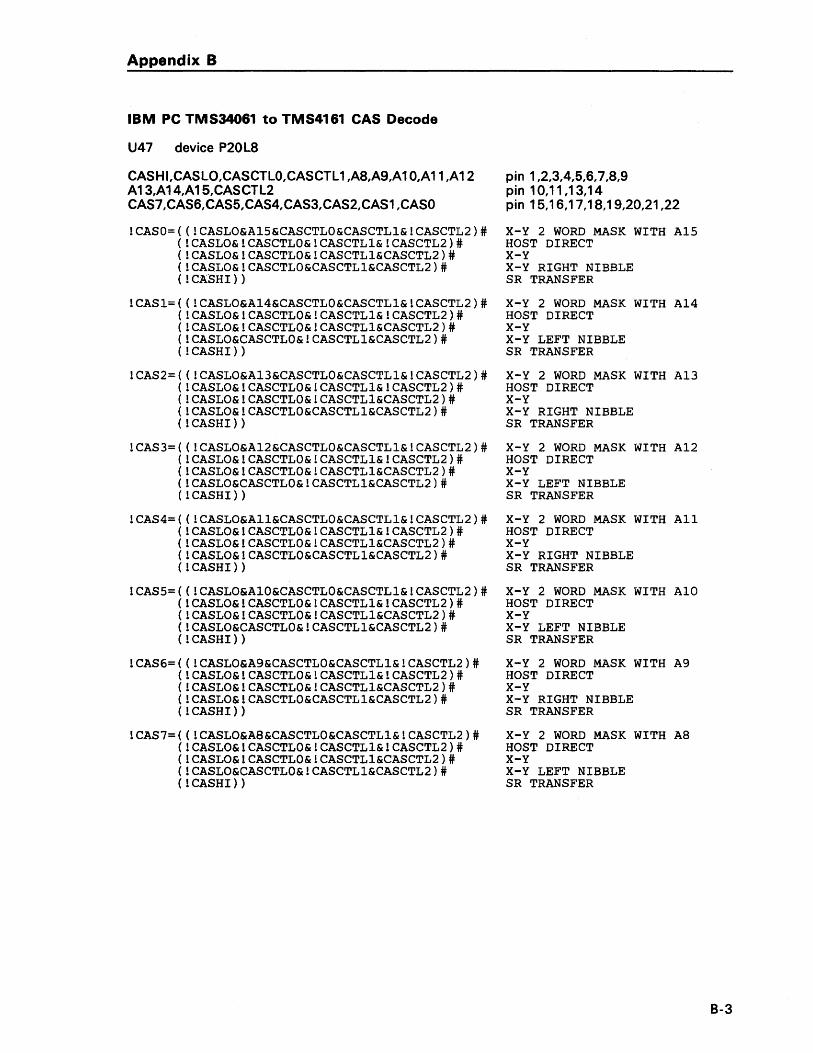
Appendix B
IBM PC TMS34061 to TMS4161 CAS Decode
U47 device P20LS
CAS H I,CASLO,CASCTLO,CASCTL 1 ,AS,A9,A1 0,A11 ,A12 A 13,A 14,A 15,CASCTL2 CAS7,CAS6,CAS5,CAS4,CAS3,CAS2,CAS1,CASO
!CASO=«!CASLO&A15&CASCTLO&CASCTLl&!CASCTL2)# (!CASLO&!CASCTLO&!CASCTLl&!CASCTL2)# (!CASLO&!CASCTLO&!CASCTLl&CASCTL2)# (!CASLO&!CASCTLO&CASCTLl&CASCTL2)# ( ! CASHI) )
!CASl=«!CASLO&A14&CASCTLO&CASCTLl&!CASCTL2)# (!CASLO&!CASCTLO&!CASCTLl&!CASCTL2)# (!CASLO&!CASCTLO&!CASCTLl&CASCTL2)# (!CASLO&CASCTLO&!CASCTLl&CASCTL2)# ( ! CASHI) )
!CAS2=«!CASLO&A13&CASCTLO&CASCTLl&!CASCTL2)# (!CASLO&!CASCTLO&!CASCTLl&!CASCTL2)# (!CASLO&!CASCTLO&!CASCTLl&CASCTL2)# (!CASLO&!CASCTLO&CASCTLl&CASCTL2)# ( ! CASHI) )
!CAS3=«!CASLO&A12&CASCTLO&CASCTLl&!CASCTL2)# (!CASLO&!CASCTLO&!CASCTLl&!CASCTL2)# (!CASLO&!CASCTLO&!CASCTLl&CASCTL2)# (!CASLO&CASCTLO&!CASCTLl&CASCTL2)# ( ! CASHI) )
!CAS4=«!CASLO&All&CASCTLO&CASCTLl&!CASCTL2)# (!CASLO&!CASCTLO&!CASCTLl&!CASCTL2)# (!CASLO&!CASCTLO&!CASCTLl&CASCTL2)# (!CASLO&!CASCTLO&CASCTLl&CASCTL2)# ( ! CASHI) )
!CAS5=«!CASLO&AIO&CASCTLO&CASCTLl&!CASCTL2)# (!CASLO&!CASCTLO&!CASCTLl&!CASCTL2)# (!CASLO&!CASCTLO&!CASCTLl&CASCTL2)# (!CASLO&CASCTLO&!CASCTLl&CASCTL2)# ( ! CASHI) )
!CAS6=«!CASLO&A9&CASCTLO&CASCTLl&!CASCTL2)# (!CASLO&!CASCTLO&!CASCTLl&!CASCTL2)# (!CASLO&!CASCTLO&!CASCTLl&CASCTL2)# (!CASLO&!CASCTLO&CASCTLl&CASCTL2)# ( ! CASHI) )
!CAS7=«!CASLO&A8&CASCTLO&CASCTLl&!CASCTL2)# (!CASLO&!CASCTLO&!CASCTLl&!CASCTL2)# (!CASLO&!CASCTLO&!CASCTLl&CASCTL2)# (!CASLO&CASCTLO&!CASCTLl&CASCTL2)# ( ! CASHI) )
pin 1,2,3,4,5,6,7,8,9 pin 10,11,13,14 pin 15,16,17,18,19,20,21,22
X-y 2 WORD MASK WITH A15 HOST DIRECT X-Y X-Y RIGHT NIBBLE SR TRANSFER
X-Y 2 WORD MASK WITH A14 HOST DIRECT X-Y X-Y LEFT NIBBLE SR TRANSFER
X-Y 2 WORD MASK WITH A13 HOST DIRECT X-Y X-Y RIGHT NIBBLE SR TRANSFER
X-Y 2 WORD MASK WITH A12 HOST DIRECT X-Y X-Y LEFT NIBBLE SR TRANSFER
X-Y 2 WORD MASK WITH All HOST DIRECT X-Y X-Y RIGHT NIBBLE SR TRANSFER
X-Y 2 WORD MASK WITH AIO HOST DIRECT X-Y X-Y LEFT NIBBLE SR TRANSFER
X-Y 2 WORD MASK WITH A9 HOST DIRECT X-Y X-Y RIGHT NIBBLE SR TRANSFER
X-Y 2 WORD MASK WITH AS HOST DIRECT X-Y X-Y LEFT NIBBLE SR TRANSFER
8-3

Appendix B
TMS34070 Palette Controller
U45 device P16L8
CASOPTO,CASOPT1,A8,A7,A6,A5,A4,A3,A2 pin 1,2,3,4,5,6,7,8,9 A1,CSYNC,HSYNC,CMD,VSYNC,P1,ADDEC,PO,PMODE pin 11,12,13,14,15,16,17,18,19
!PMODE=({!VSYNC&!Pl&!PO)# (!PO&Pl»
PASS VSYNC TO MODE PIN MODE PIN LOW
!ADDEC={!CASOPTO&CASOPT1&A8&A7&A6&A5&A4&IA3&!CMD) SELECT ON PO AND Pl
!PO={{!ADDEC&!A2&!Al)# (IADDEC&!PO&A2&Al)# (ADDEC&IPO)# (!ADDEC&!PO&!A2&Al»
!Pl=«!ADDEC&!A2&Al)# (IADDEC&!Pl&A2&Al)# (ADDEC&!Pl)# (!ADDEC&!Pl&!A2&!Al»
ICSYNC=({!HSYNC&VSYNC)# ( ! VSYNC&HSYNC) )
8-4
RESET PO ON ADD SELECT HOLD !PO ON Pl OPERATION HOLD !PO ON NO ADD SELECT HOLD !PO ON Pl OPERATION
RESET Pl ON ADD SELECT HOLD· IPl ON PO OPERATION HOLD !Pl ON NO ADD SELECT HOLD !Pl ON PO OPERATION
COMPOSITE SYNC

(') I .....
~f:~ Pl-AI& PI-RS PI-RS !'I-A? !"I-AS "1-A9
~i:ii8 ~t:A~~ ~l:Ud !"I-R \
~I: ~ PI-R21 PI-R2E1 !'1-IUg PI-Iua !'1-Rl7 Pl-AlS Pl-RIS PHU PHHS Pi-AU
I"I-B2I
1"1-Bll
Pl-912
Pl-Rll
1'1-825
1"1-A18
1"1-82
VClK VCLKI SrfCLK
0'
...
"ALlint
~ ~
ME .. '"' It MEHR.B
RE.
ITlI J82 ~. ~le5 'ICC
, I R9 J ~, ~
OM
~. ROTB ...... , "0',
~ II
" , "''''
a~l. 0' 00.9 ,L 8 n
' " , ' · . , , : " · ; .
'SO
L~ Jm ...... ~
r,mm-
~'f • H
.. ." :17 ," ." ... " lIS OIl
':: m~ II:: Uqa : 1 I!:!.--
J
'.'om ~UI ALE ,IL 01 Ie ." CI2 :1: osJ.u. ~:~ UI,IS::~ . :: ~~ '---J@s' A21
'! ;
<ASOm l~ ~mF ." :~c .. ." ,"
'1: I ~;
II UijS ,It I s :~~ '---
IT " :~~ •• ,.n :: ~ . ..
':: :::2 ,,~ :::' .. 'M ::~ D
'" ~
~ THS31l861 -.. ~ un H- RRSS .. :: :::~ I~ ~ .. l:~XR .. "" :'J 9: '\ "",
'"" ,,~
" C~HI ,."" tUM!
iii g: CAStO
'" "" 11MI -"- U4.3 ~~~ y,,,,,
vnw lISTM .""" ~ 1 ~--l! """ ,co,
~'"""
"~ ~ ~. ,,~
VClK
II
- "" fESI9TOI.F1ICI · ,
· U.8 ,
· '---
.~~ U 01 1 II iii :: :HF=mF II!IGt~
a ~~ : p.c:::tm:; 11 ~~, U47 11,\ I~:!
CA'CTlZ
~
~ ,[,,~= • •
~ un •
7"".8 UII1 u SCLI(1
~ 1211111111\.'
-.~
~
D_BUS
A..JlUS
CTRL_BUS
SYNC..JlUS
ORTREN
BLRNK<
PM ODE CSTNC
0
en (") :T CD 3 Q) .-+ --(") en

() I
N
PI-B3 :3 PI-B29
PI-B31~~-l--l--~-~--~-~--~~ PI-BIB PI-Bl
ORTRENo:===============================================rt1~==~ PMOOE <>
vee
~~,-~eL~K~lN~2 _____ ~ r IJUI
Pl-83Q <>-____ ----'O=5:.:.e ___ 1~,;;;,,.:.--O:::5"'e-"IN'-1
C-BUSo-________________________________________ ~c~~~u~s ______ _<
vee
.-----------~=_-~ P3-1 .-------'="'---0 P3-2
~"---o P3-3
R19
P3-4 P3-5
P3-7 P3-et P3-9
PP3-6
'k'---.!1' 5).o'-t--"'"""'-"---'l.SJ»'------,--------<> SRCLK
.-_____ ....J r--------~ SRLORD
.---------0 VCLK
rr;====~~~ ~------~ SOEe.
,-------<> SOEI*
r------~ VCLK* un'
.. '"
~·1"~~~2 lR 11,1AS1S7
f 1 :: Ir.~:~,~~~~~~~========l~~======= P2-3 l1·~"E~~'ij~: H !I P2-Ll ~ II :: P2-S
BLRNKli <>-________________________ ~====::lijl ~EL US1 I 11e-'.''-JO-5-------'-,.-.-5-'.-C------<D ~~=~ .--___ ~H~O~RS~'~NC~ ____ _<>P2_8
CSTNC<>-----------------------------,
HSl'NC
STNC-BUSo--------------------------'
--<> P2-?
F P2- 2 P2-1
l> 'C 'C CD ::l Q. )(
o

n I
W
CJlUS
SRCLK SRLOAD
Me, 5~19!! ~.
~ SIR 2
3011 19 ~,
i 5111 1 , ~19C 1'82 6 . . 7 TH51.1161 stC~ ,. m~ AS.
RIllE-
"''' 17 AS. y ...
g~: S Lila
~ : Ul DLB " : U2 , ".0 ~ .... '7.r:-~
, .. " . " , PAl , 1 "R . r;; 198 '"
,~ ! 'I' , ~HIC PR2 . 7 THSI!161 SICf!L==T ,. ]g~8~ ". A/Qt.
"'" 17 AS.
~P""Itli"'c=!Jg~: ~~ US
OS, II L-;;c--~
/t':"'::"===:::li "'* L·C • U'-7 '7.t:~
.... 5 SO. R '" . '" , ,
Soiln ro, i '" 5
~19C PD2 , , , 7 T"'S1,I161 SIC~ ,.
~~ , AS. 'VUrM
tASS 17 AS.
~~9. g~~
~ : U9 01.8 .. ~ ".0
'"' Ull .. .. "k:-~
'M .. SO, '" , ". , "SOi!ftl '" , SIB . ~ClI1C PC2
5 7 THSIJ161 SIC !!f----I . S. ~ppt3 I'I/IIE_
"52 , S. ...
eLK
~= U13
V1t:'"::"'::=::::!!i:Cl"I:: U JL.j
~5 ~6
I.:.....-
, .. , SOA 9A "' ,
,
I SIR , ~lgl "' i
5 'Sot SIC f'F2 ,
7 TMSLj161 SIC rr:::=:.=::r . , ,. 1W~ ,.
I'I/lIh CASS 17 AS.
;~~!: 0 ..
'" ~ : U 1 7
01.B ... : U18 I
".0 ~9 .... '"";;"[:'-
~
" . 1 ,
51" SIR
~=U21 ......-c--
~~"E::==:::f"""1
U22
--t"'::"===:::li ~,,~:c U23 . ~
~~~= .. ======.~ ""~L U2~ I.:.....-
AJlUSo---~~-t------------------------~~~-----------------------'-t+-------------------------'
, .. ~19A "" I SIR
~ ~ .. ~,
"SoC lilt !'H2 . 7 TMSl,i161 SIC~ . 5 ..
~~ RS. R/Qf.
CRS1 17 AS.
~~E!. J: ~ ~ U25
01.8 \l,B : U26 .... ~7 .... ~8 ~
-, ... ' SIR
. 'THSIUSl
~U!!L
~E31r.;", ... 17 AS.
vt'"::'::' =::li1!J:B U 3 G
~1 rt~='='====~~~~:D U32 .!-.-
CTRLJlUSc-----~~--------------------------~~r_--------------------------'-t_--------------------------, O-BUSo-______ -' ____________ ~ __ ------------~------------------__________ ~~ __________________________ __'
» "0 "0 CD ~ 0. >< (')


Index B
block diagram 1-2
c clearing the screen 5-16
E
expansion bus 3-10 interface to TMS34061 4-2
F
frame buffer 3-5
H
interface to TMS34061 4-5 interface to'video output 4-6
timing 4-7
horizontal scrolling 5-10
I
interrupts 3-10
J
jumpers features enabled 3-2 location 3 -2 sample configurations 3-12
M
memory map 3-4 memory organization 3-5, 5-8 memory read/write PC bus timing 4-4
p
PAL equations 8-1 PAL U40 4-2 PAL U45 4-5 PAL U47 4-5 PAL U48 4-2 palette 5-20
CPU interface 4-5 initializing 5-22 repeat mode 5-23 screen mapping 5-21
pixel replication zoom 5-12 power consumption 3-12 P2 3-11 P3 3-11
R
register select address lines 3-6 registers 3-5, 3-6
initializing 5-2 repeat mode 5-23
s schematics C-3 sh ift reg isters
control 5-7 organization 5-8 transfers
addressing 3-10 clearing the screen 5-16 cycles 3-9 initiating 5-9 vertical scrolling 5-18
Index-1

Index
v vector drawing 5-14 vertical screen flip 5-19 vertical scrolling 5-18 video output connectors P2, f video palette mode 3-4, 4-5.
Index-2

• TEXAS INSTRUMENTS
Printed in U.S.A. ~PPU019A