COS/MaS - bitsavers.org
169
r . c [; , J ' '0 ' ·. 0 ,C/) , : .- . 3: " . o 'C/) : Ii ' - ,. :; :::s " CD - 1. ; " \ ctJ ;.:,' ... " I ". !. CD ' I , 0. ( ,0 ' i __ • f ... ' (') ,:. ", c· ;,1 \: \ i en ' 3: Q) ::::J 1 ,C Q) " _ i , \ ' .'1 " o ; 3: ;' C/) ' N COS/MaS Integrated Circuits M nual Rcn SOl id State .; N $5.00 Optional . CMS-272 '. Pr i ce
-
Upload
khangminh22 -
Category
Documents
-
view
0 -
download
0
Transcript of COS/MaS - bitsavers.org

r . c [;
, J
''0 ' ·. 0 ,C/) , : .-.3: " . o 'C/) : Ii ' - ,. :; :::s " CD- .~. 1.
; " \ ctJ ;.:,' ... " I
".!. ~. CD ' I ,0. (
, 0 ' i __ • f ... ' (') ,:. ", c · ;,1 \: ::;:~ . \ i en ' 3: Q) ::::J 1 ,C Q) " _ i
, \ ' .'1
"
o ; ~ 3: ;' C/) '
N
COS/MaS Integrated Circuits M nual
Rcn SOlid State
~ . ; ~--------------------------------------------~~ N $5.00 Optiona l . CMS-272 '.
Price
COS/MaS Integrated Circuits Manual
COS/MOS (Complementary-Symmetry Metal-Oxide Semiconductor) devices were developed at the RCA David Sarnoff Research Laboratories in Princeton, New Jersey, in the early 1960's. The first commercial series of integrated COS/MOS circuits was announced by the RCA Solid State Division in 1968.
COS/MOS made possible orders-of-magnitude reduction in the power consumption of digital logic circuits. Perhaps the most dramatic demonstration of the potential of this new technology was the development, in 1970, of a totally new consumer productthe digital wrist watch. Battery-powered and quartz-crystalcontrolled, this watch was an achievement in accuracy and compactness made possible only by COS/MOS integrated-circuit technology .
Today, the original series of COS/MOS integrated circuits has been expanded with increasingly complex designs, so that virtually any digital logic system can be implemented with commer:cially available packaged units. This Manual is intended as a guide to COS/MOS integrated circuits for the systems engineer and logic designer. It discusses the basic principles involved in the design and application of COS/MOS digital integrated circuits, and describes many of the circuit building blocks, ranging from basic NOR and NAND gates to complex phase-locked loops and rate multipliers.
Although this Manual is intended primarily for circuit and system designers working with solid-state circuits, it will also be useful to educators, students, radio amateurs, hobbyists, and others interested in the use of semiconductor devices and circuits.
nOli SOlidi State
Brussels· Buenos Aires· Hamburg· Madrid· Mexico City· Milan Montreal· Paris· Sao Paulo· Somerville NJ • Stockholm Sunbury·on·Thames • Taipei· Tehran· Tokyo

Contents
Page I. COs/MOS Integrated Circuit Fundamentals ............................• 3
Basic MOS transistors, complementary symmetry
II. Basic Circuit Building Blocks ......................................... 6 Inverters, gates, transmission gates, flip-flops, shift registers, memory cells
III. Characteristics of RCA COs/MOS Devices ............................. 17 Features of COSIMOS B-series types, A-series characteristics, B-series characteristics, packages, maximum ratings and recommended operating conditions, extra-value and MIL types
IV. Handling and Operating Considerations ............................... 27 Handling COSIMOS devices, built-in protection networks, operating precautions, voltage and dissipation considerations, noise immunity and noise margin, voltage logic-level definitions, input considerations, output conSiderations, power-supply considerations, clock requirements, cascading considerations
V. Interfacing COS/MOS ............................................... 36 Positivelnegative logic conversion, interfacing with p-channel MOS, interfacing with n-channel MOS, interfacing with saturated bipolar logic, COSIMOS and TIL. COSIMOS and HNIL, COSIMOS and DTL, COSIMOS and ECL. interfacing discrete and electromechanical devices, interfacing op-amps to COSIMOS
VI. Astable and Monostable Multivibrators ................................ 47 Astable circuits, monostable circuits, COSIMOS integrated one-shots, Schmitt-trigger multivibrator circuits
VII. Crystal Oscillators for Digital Timekeeping ............................. 57 Basic oscillator design considerations, practical oscillator-circuits
VIII. Shift Registers and Counters .......... _ ........ _ ........ __ ........... 65 StatiC shift registers, dynamic shift registers, storage registers, FIFO buffer register, binary ripple·carry counters, clock timer, synchronous counters
IX. Display Drivers ................................................... 104 Liquid-crystal displays, light·emitting diode displays
X. Frequency synthesizers ............................................ 109 Phase-locked loop, programmable divide·by-N counter, rate multipliers
XI. Introduction to Microprocessors and Memory Interfacing ................ 122 COSMAC microprocessor internal structure, operation and interfacing
XII. Circuits and Applications ........................................... 133 XIII. Custom LSI Design ................................................ 151
MOS design parameters, fabrication of COSIMOS integrated circuits, custom designs
Index ............................................................ 165
Information furnished by RCA is believed to be accurate and reliable. However. no responsibility is assumed by RCA for its use; nor for any infringements of patents or other rights of third parties which may result from its use. No license is granted by implication or otherwise under any patent or patent rights of RCA.
Trademark (sl® Registered Marca (51 Registrada (51
Copyright 1979 by RCA Corporation (All rights reserved under Pan-American Copyright Convention)
Printed in USA/1-79
I. COS/MOS Integrated Circuit Fundamentals
COS/MOS (Compl~entary-Symmetry MOS) integrated circuits provide a number of significant advantages as compared to integrated circuits using bipolar or singlechannel MOS (PMOS or NMOS) technology. These advantages include ultralow power dissipation (microwatt level), high noise immunity (30 percent of supply voltage), and the use of a single power supply with a wide operating-voltage range (the recommended range is 3 to 18 volts; the maximum rating for B-series devices is 3 to 20 volts).
COS/MOS devices are voltage-controlled switches that have a high input impedance. They differ in both fabrication and operation from bipolar transistors, which are lowimpedance current-switched devices. Although more devices are required to implement logic in COS/MOS than in singlechannel MOS, COS/MOS circuits operate faster and require only a single 'clock' or control signal.
BASIC MOS TRANSISTORS
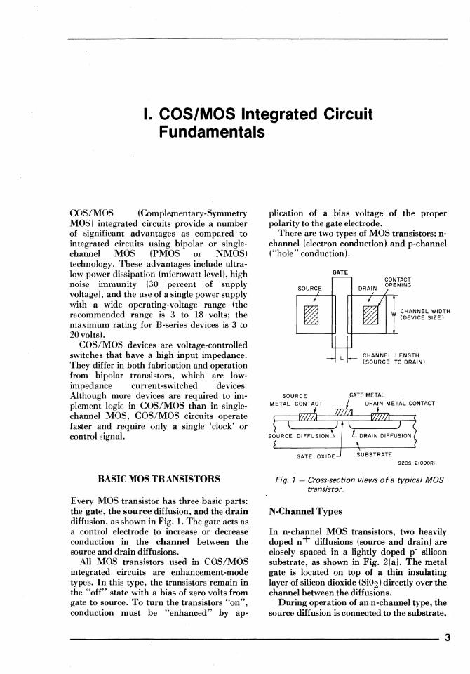
Every MOS transistor has three basic parts: the gate, the source diffusion, and the drain diffusion, as shown in Fig. 1. The gate acts as a control electrode to increase or decrease conduction in the channel between the source and drain diffusions.
All MOS transistors used in COS/MOS integrated circuits are enhancement-mode types. In this type, the transistors remain in the "off" state with a bias of zero volts from gate to source. To turn the transistors "on", conduction must be "enhanced" by ap-
plication of a bias voltage of the proper polarity to the gate electrode.
There are two types of MOS transistors: nchannel (electron conduction) and p-channel ("hole" conduction).
GATE CONTACT
SOURCE DRAIN OPENING
1 CHANNEL WIDTH
!+-__ --'l (DEVICE SIZE)
SOURCE METAL CONTACT
~
GATE OXIDE
CHANNEL LENGTH (SOURCE TO DRAIN)
SUBSTRATE 92CS-21000RI
Fig. 1 - Cross-section views of a typical MOS transistor.
N-Channel Types
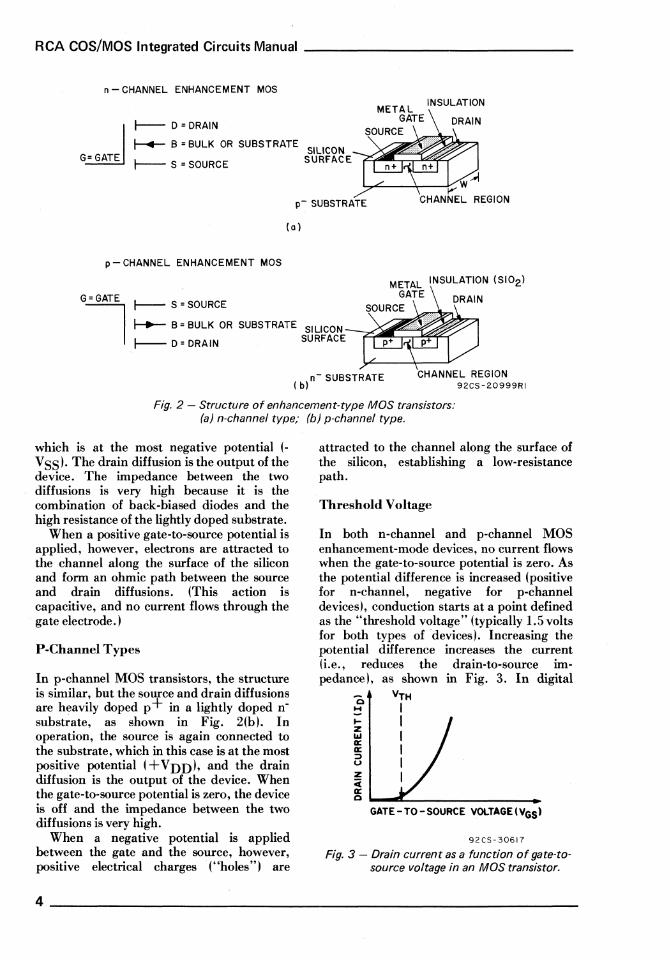
In n-channel MOS transistors, two heavily doped n + diffusions (source and drain) are closely spaced in a lightly doped p- silicon substrate, as shown in Fig. 2(a). The metal gate is located on top of a thin insulating layer of silicon dioxide (Si02) directly over the channel between the diffusions.
During operation of an n-channel type, the source diffusion is connected to the substrate,
3
RCA COS/MaS Integrated Circuits Manual _______________ _
n - CHANNEL ENHANCEMENT MOS
~ r- D=DRAIN
I-+- B = BULK OR SUBSTRATE SILICON
G= GATE r-- S = SOURCE SURFACE
p- SUBSTRATE
(a)
p - CHANNEL ENHANCEMENT MOS
METAL INSULATION (SI02)
G=GATE r-- S = SOURCE GATE DRAIN
I r--.- B = BULK OR SUBSTRATE SI LICON
~ D = DRAIN SURFACE
{bln- SUBSTRATE CHANNEL REGION 92CS-20999RI
Fig. 2 - Structure of enhancement-type MOS transistors: (a) n-channel type; (b) p-channel type.
which is at the most negative potential (V SS). The drain diffusion is the output ofthe device. The impedance between the two diffusions is very high because it is the combination of back-biased diodes and the high resistance of the lightly doped substrate.
When a positive gate-to-source potential is applied, however, electrons are attracted to the channel along the surface of the silicon and form an ohmic path between the source and drain diffusions. (This action is capacitive, and no current flows through the gate electrode.)
P-Channel Types
In p-channel MOS transistors, the structure is similar, but the source and drain diffusions are heavily doped p + in a lightly doped nsubstrate, as shown in Fig. 2(b). In operation, the source is again connected to the substrate, which in this case is at the most positive potential (+ V DD), and the drain diffusion is the output of the device. When the gate-to-source potential is zero, the device is off and the impedance between the two diffusions is very high.
When a negative potential is applied between the gate and the source, however, positive electrical charges ("holes") are
attracted to the channel along the surface of the silicon, establishing a low-resistance path.
Threshold Voltage
In both n-channel and p-channel MOS enhancement-mode devices, no current flows when the gate-to-source potential is zero. As the potential difference is increased (positive for n-channel, negative for p-channel devices), conduction starts at a point defined as the "threshold voltage" (typically 1.5 volts for both types of devices). Increasing the potential difference increases the current (i.e., reduces the drain-to-source impedance), as shown in Fig. 3. In digital
Q H
IZ .... cr:: cr:: ;:) u z C cr::
VTH
I I I I I I
o ~"L---------------__ 4P
GATE-TO-SOURCE VOI..TAGEIVGs)
92CS-30617
Fig. 3 - Drain current as a function of gate-tosource voltage in an MOS transistor.
4 _______________________________________________________ _

_______________ COS/MOS Integrated Circuits Fundamentals
operations, the voltages applied to the gates to turn transistors on are normally at the "supply rails", or the maximum levels in the system. The positive supply +VDD is used for n-channel conduction and the negative supply -V SS for p-channel conduction.
COMPLEMENTARY SYMMETRY
Because n-channel and p-channel transistors have diffusions with opposite polarity dopings, they operate with voltages of opposite polarity. That is, a positive voltage turns an n-channel device on and a p-channel device off; a negative voltage turns a pchannel device on and an n-channel device off. In COS/MOS integrated circuits, both pand n-channel transistors are fabricated in the same semiconductor wafer, with metal connections between the paired inputs (gates) and outputs (drains), as shown in Fig. 4.
G
IN~ OUT
Because the gate of a COS/MOS device is essentially a capacitor (the gate metal and the substrate are the two plates, and the Si02 is the dielectric), there is no input current. When the output of one COS/MOS device drives the capacitive input of another, therefore, no IR drop occurs in the drain as a result of input current, and the output voltages are at full V DD and V SS levels.
Because the gates of the p-channel and nchannel pair are connected, one device must always be off regardless of the polarity of the signal on the gate. Therefore, there is never a direct path from supply to ground, and the only current from VDD to VSS is the very small leakage current of the MOS device that is off.
(More detailed information on device characteristics, wafer processing, and custom IC layout design is. given in Chapter XIII Custom LSI Design.)
METAL INTERCONNECT
92CS - 30330
Fig. 4 - Complementary-symmetry structure used in COS/MaS integrated circuits.
__________________________________________________________ 5

II. Basic Circuit Building Blocks
This chapter describes the building-block units that form the basis for the more complex circuits discussed in the following chapters. These basic building blocks include inverters, gates, transmission gates, flipflops, shift registers, counters, and memory cells.
INVERTERS
The n- and p-channel combination shown in Fig. 4 of the previous chapter is the inverter, the most fundamental of COS/MOS circuits. Fig. 5 shows its logic representation, simplified schematic, and truth table.
t~: ~:UTH TAB~:T A~A A toL."A HIGH (VoO> LOW (Vssl ~ ~ LOW (Vssl HIGH(Vool
~ n 92CS-3054I
-VSS
Fig. 5 - Logic diagram, simplified schematic, and truth table for a COS/MaS inverter.
A high (or positive) voltage (+VDD) on the gate electrode turns the n-channel device on and the p-channel device off, and the output is switched to its low level (-VSS)' Similarly, a low (or negative) voltage (-VSS) on the gate turns the p-channel device on and the n-channel device off, and the output is switched to its high level ( + V DD)'
GATES
Each input to a COS/MOS gate requires a pchannel and n-channel device. In the NOR gate, the p-channel devices of the two inputs
are connected in series and the n-channel devices in parallel, as shown in Fig. 6. A high
+VOD
Al~p Bl~..L TRUTH
'lOUT A
: =[>ouT ~J g
'~9' , TABLE
BOUT
o I o
I o o o
-\Iss 92CS-30542
Fig. 6 - Logic diagram, simplified schematic, and truth table for a COS/MaS NOR gate.
level (+ VDD) at either input (A or B) turns the corresponding p-channel device off and n-channel device on, and the output switches to a low level (-VSS)' Both input signals (A and B) must be low in order to turn both pchannel devices on and both n-channel devices off to switch the output to a high level (+VDD)'
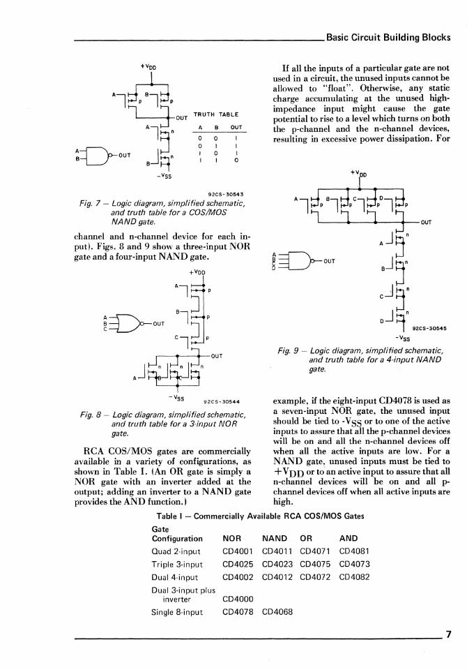
In the NAND gate, the n-channel devices are connected in series and the p-channel devices in parallel, as shown in Fig. 7. A low level (-VSS) at either input (A or B) turns the corresponding n-channel device off and pchannel device on, and switches the output to +VDD' Both inputs (A and B) must be high to turn both n-channel devices on and both pchannel devices off and switch the output to -VSS'
Larger gates can be made by adding additional inputs (but always with a p-
6 ______________________________________________________ __
______________________ Basic Circuit Building Blocks
TRUTH TABLE
A B OUT
0 0 I 0 I I I 0 I I I 0
92CS- 30543
Fig. 7 - Logic diagram, simplified schematic, and truth table for a COS/MaS NAND gate.
channel and n-channel device for each input). Figs. 8 and 9 show a three-input NOR gate and a four-input NAND gate.
Fig. 8 - Logic diagram, simplified schematic, and truth table for a 3-input NOR gate.
RCA COS/MOS gates are commercially available in a variety of configurations, as shown in Table I. (An OR gate is simply a NOR gate with an inverter added at the output; adding an inverter to a NAND gate provides the AND function.)
If all the inputs of a particular gate are not used in a circuit, the unused inputs cannot be allowed to "float". Otherwise, any static charge accumulating at the unused highimpedance input might cause the gate potential to rise to a level which turns on both the p-channel and the n-channel devices, resulting in excessive power dissipation. For
OUT
~D--0UT
Fig. 9 - Logic diagram, simplified schematic, and truth table for a 4-input NAND gate.
example, if the eight-input CD4078 is used as a seven-input NOR gate, the unused input should he tied to -V SS or to one of the active inputs to assure that all the p-channel devices will he on and all the n-channel devices off when all the active inputs are low. For a NAND gate, unused inputs must be tied to + V D D or to' an active input to assure that all n-channel devices will be on and all pchannel devices off when all active inputs are high.
Table I - Commercially Available RCA COS/MOS Gates
Gate Configu ration NOR NAND OR AND
Quad 2-input CD4001 CD4011 CD4071 CD4081
Triple 3-input CD4025 CD4023 CD4075 CD4073
Dual 4-input CD4002 CD4012 CD4072 CD4082
Dual 3-input plus inverter CD4000
Single 8-input CD4078 CD4068
_______________________________________________________ 7
RCA COS/MOS Integrated Circuits Manual _______________ _
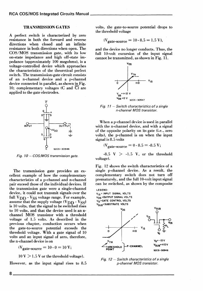
TRANSMISSION GATES
A perfect switch is characterized by zero resistance in both the forward and reverse directions when closed, and an infinite resistance in both directions when open. The COS/MOS transmission gate, with its low on-state impedance and high off-state impedance (approximately 100 megohms), is a voltage-controlled device which approaches the characteristics of the theoretical perfect switch. The transmission-gate circuit consists of an n-channel device and a p-channel device connected in parallel, as shown in Fig. 10; complementary voltages (C and C) are applied to the gate electrodes.
C
~n
IN~UT S· :r ' '"""~ Woo :+:
o ~
l P
C 92CS-30546
Fig. 10 - COS/MOS transmission gate.
The transmISSIon gate provides an excellent example of how the complementary characteristics of a p-channel and n-channel pair exceed those of the individual devices. If the transmission gate were a single-channel device, it could not transmit signals over the full VDD - VSS voltage range. For example, assume that the supply voltage (VDD - VSS) is 10 volts, that the signal to be switched rises to 10 volts, and that the device used is an nchannel MOS transistor with a threshold voltage of 1.5 volts. As described in the previous chapter, conduction occurs when the gate-to-source potential exceeds the threshold voltage. With a gate signal of 10 volts and an input signal of zero, therefore, the n-channel device is on
(V gate-source = 10 - 0 = 10 V;
10 V > 1.5 V or the threshold voltage).
However, as the input signal rises to 8.5
volts, the gate-to-source potential drops to the threshold voltage
(V gate-source = 10 - 8.5 = 1.5 V),
and the device no longer conducts. Thus, the full 10-volt excursion of the input signal cannot be transmitted, as shown in Fig. n.
Vos
VGS-t-IO v
Vss -0 V 92CS-30547
Fig. 11 - Switch characteristics of a single n·channel MOS transistor.
When a p-channel device is used in parallel with the n-channel device, and with a signal of the opposite polarity on its gate (i.e., zero volts), the p-channel is on when the input signal is 8.5 volts
(V gate-source = 0 - 8.5 = -8.5 V;
-8.5 V > -1.5 V, or the threshold voltage).
Fig. 12 shows the switch characteristics of a single p-channel device. As a result, the complementary switch does not turn off prematurely, and the full 10-volt input signal can be switched, as shown by the composite
LEGEND:
ViS-INPUT SIGNAL VOLTS VOS -OUTPUT SIGNAL VOLTS VG"GATE CONTROL VOLTS VSUB"SUBSTRATE VOLTS
VOS
+10
VTH
~HRESHOLD}P-CHANNEL POINT
VG"-IOV
VSUB"tlOV
92CS-30548
Fig. 12 - Switch characteristics of a single p-channel MOS transistor.
8 __________________________________ _
______________________ Basic Circuit Building Blocks
COS/MOS transmission-gate characteristics in Fig. 13.
Vas
o
92CS- 30549
Fig. 13 - Composite switch characteristics of a COS/MaS transmission gate.
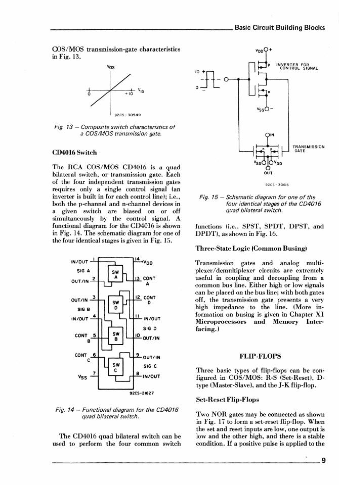
CD4016 Switch .
The RCA COS/MOS CD4016 is a quad bilateral switch, or transmission gate. Each of the four independent transmission gates requires only a single control signal (an inverter is built in for each control line); i.e., both the p-channel and n-channel devices in a given switch are biased on or off simultaneously by the control signal. A functional diagram for the CD4016 is shown in Fig. 14. The schematic diagram for one of the four identical stages is given in Fig. 15.
IN/OUT I
SIG A
OUTIIN 2 I CONT A
OUTIIN 3 CONT 0
SIG B
IN/OUT 4 1/ IN/OUT
SIG 0 CONT 5 10 OUTIIN
B
co NT 6 9 OUTIIN C
SIG C
Vss 7 8 IN/OUT
92C5-21627
Fig. 14 - Functional diagram for the CD4016 quad bilateral switch.
The CD4016 quad bilateral switch can be used to perform the four common switch
INVERTER FOR CONTROL SIGNAL
92CS - 30616
TRANSMISSION GATE
Fig. 15 - Schematic diagram for one of the four identical stages of the CD4016 quad bilateral switch.
functions (i.e., SPST, SPDT, DPST, and DPDT), as shown in Fig. 16.
Three-State Logic tCommon Busing)
Transmission gates and analog multiplexer / demultiplexer circuits are extremely useful in coupling and decoupling from a common bus line. Either high or low signals can be placed on the bus line; with both gates off, the transmission gate presents a very high impedance to the line. (More information on busing is given in Chapter XI Microprocessors and Memory Interfacing.)
FLIP-FLOPS
Three basic iypes of flip-flops can be configured in COS/MOS: R-S (Set-Reset), Dtype (Master-Slave), and the J-K flip-flop.
Set-Reset Flip-Flops
Two NOR gates may be connected as shown in Fig. 17 to form a set-reset flip-flop. When the set and reset inputs are low, one output is low and the other high, and there is a stable condition. If a positive pulse is applied to the
__________________________________________________________ 9

RCA COS/MOS Integrated Circuits Manual ______________ _
set input, its a~ciated n-channel device is turned on; the Q output then goes low and the Q output goes high. After the pulse period both inputs are again low, and the flip-flop is in another stable condition.
Applying a positive pulse to the reset input causes the Q output to go low and the Q
b) SPOT
'is
output to go high; after the pulse period both inputs are again low and the flip-flop is in the original stable condition. Additional positive pulses on the same input do not cause any change in the output, i.e., the pulses must be applied alternately to the inputs to change the condition of the flip-flop.
'-------UVC .Jl..
cl OPST
d) OPOT
VOSAI ()-o
VO~
n c
92CM-30337
Fig. 16 - Basic switch functions using the CD4016 quad bilateral switch. a) Single-pole single-throw, b) Single-pole double throw, c) Double-pole single-throw, and d) Double-pole dOUble-throw.
10 ____________________________________________________ ___

______________________ Basic Circuit Building Blocks
","= RESET
"1I 1"=SET
TRUTH TABLE S R Q "Q 0 0 Q "Q" NO CHANGE , 0 , 0 0 , 0 , , , 0 0
SET~~-------------------------
RESET-------in..sl---------------
92CS-30550
Fig. 17 - Logic diagram, truth table, and associated pulse shapes for a setreset flip-flop using NOR gates.
Two NAND gates may also be used to form a set-reset flip-flop, as shown in Fig. 18. In this configuration, negative-going pulses are used to switch the outputs.
RESET
SET
TRUTH TABLE S R Q Q o I 0 , , 0 , 0 , , Q ~ NO CHANGE o 0 , ,
SET-U RESET -------,U U
92CS-30551
Fig. 18 - Logic diagram, truth table, and associated pulse shapes for a setreset flip-flop using NAND gates.
D Flip-Flops
Fig. 19 shows the circuit for aD-type IMaster-Slave) flip-flop. The block diagram shows a master flip-flop formed from two inverters and two transmission gates Ishown as switches) that feed a slave flip-flop having a similar configuration. The transmissiongate control signal is called the "clock" because it controls the timing of· the operations. When the clock is at a low level, the TG 1 transmission gates are closed and the TG2 gates are open. This configuration allows the master flip-flop to sample incoming data, while the slave holds the data from the previous input and feeds it to the
~~~UTPUT TGI TG2 TG2 TGI
MASTER SLAVE (0)
ALL P - UNIT SUBSTRATES CONNECTED TO VDD; ALL n - UNIT SUBSTRATES TO VSS'
(b)
cL
(e)
92CS- 30332
Fig. 19 - Logic diagram, simplified schematic, and clock-pulse diagrams for aD-type flip-flop.
output. When the clock is high, the TG 1 transmission gates open and the TG2 gates close, so that the data is held in the master and fed to the slave.
________________________________________________________ 11
RCA COS/MaS Integrated Circuits Manual ______________ _
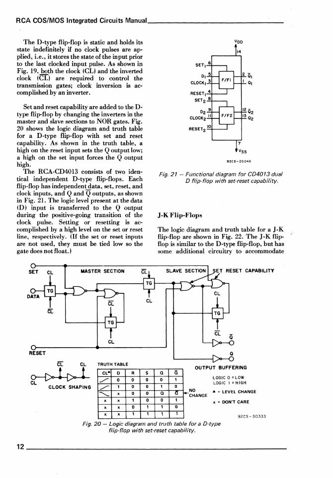
The D-type flip-flop is static and holds its state indefinitely if no clock pulses are applied, i.e., it stores the state ofthe input prior to the last clocked input pulse. As shown in Fig. 19, both the clock (CL) and the inverted clock (eL) are required to control the transmission gates; clock inversion is accomplished by an mverter.
Set and reset capability are added to the Dtype flip-flop by changing the inverters in the master and slave sections to NOR gates. Fig. 20 shows the logic diagram and truth table for a D-type flip-flop with set and reset capability. As shown in the truth table, a high on the reset input sets the Q output low; a high on the set input forces the Q output high.
The RCA-CD4013 consists of two identical independent D-type flip-flops. Each flip-flop has independent data, set, reset, and clock inputs, and Q and Q outputs, as shown in Fig. 21. The logic level present at the data (D) input is transferred to the Q output during the positive-going transition of the clock pulse. Setting or resetting is accomplished by a high level on the set or reset line, respectively. (If the set or reset inputs are not used, they must be tied low so the gate does not float.)
SET CL MASTER SECTION
CL
RESET
CL· 0 R
/" 0 0 ~ TRUTH TABLE
CLOCK SHAPING /" 1 0
"'- x 0
x x 1
x x 0
x x 1
S
0
0
0
0
1
1
SETI-=6+---,
01 5
CLOCK I 3
RESET 1-,4+---,
SET 2 ..:8+---,
02 9 CLOCK2 II
RESET 2 .:.,:IO+---,
Voo
14
1
Vss
92CS-25046
Fig. 21 - Functional diagram for CD4013 dual D flip-flop with set-reset capability.
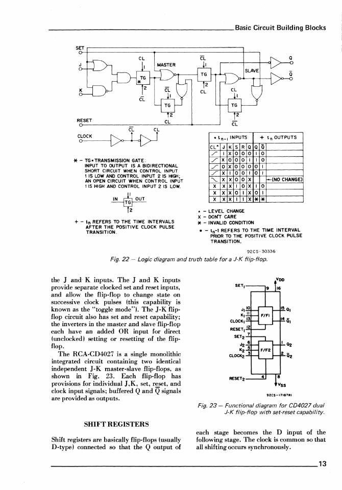
J-K Flip-Flops
The logic diagram and truth table for a J-K flip-flop are shown in Fig. 22. The J-K flipflop is similar to the D-type flip-flop, but has some additional circuitry to accommodate
Q Q
0 1
1 0 Q Q
0 1
1 0
1 1
-OUTPUT BUFFERING
LOGIC 0 = LOW LOGIC I = HIGH
NO • = LEVEL CHANGE CHANGE
x = DON·T CARE
92CS- 30333
Fig. 20 - Logic diagram and truth table for aD-type flip-flop with set-reset capability.
12 _____________________________________________________ _
_______________________ Basic Circuit Building Blocks
snr------------------------------------------,
CL
CL CL
C~
* - TG-TRANSMISSION GATE: INPUT TO OUTPUT IS A BIDIRECTIONAL SHORT CIRCUIT WHEN CONTROL INPUT , IS LOW AND CONTROL INPUT 2 IS HIGH; AN OPEN CIRCUIT WHEN CONTROL INPUT , IS HIGH AND CONTROL INPUT 2 IS LOW.
+ - tn REFERS TO THE TIME INTERVALS AFTER THE POSITIVE CLOCK PULSE TRANSITION.
• tn-I INPUTS + tn OUTPUTS
CL· J K S R Q Q Q
./ I X 0 o 0 I 0
./ X 000 I I 0
../ 0 X 0 0 0 o I
./ X 100 I o I
""- X X 0 0 X ~(NO CHANGE)
X X X I o X I 0
X X X 0 I X o I
X X X I I X * * • - LEVEL CHANGE X - DON'T CARE * - INVALID CONDITION
• - tn-I REFERS TO THE TIME INTERVAL PRIOR TO THE POSITIVE CLOCK PULSE TRANSITION.
92CS-30336
Fig. 22 - Logic diagram and truth table for a J-K flip-flop.
the J and- K inpnts. The J and K inputs provide separate clocked set and reset inputs, and allow the flip-flop to change state on successive clock pulses (this capability is known as the "toggle mode"). The J-K flipflop circuit also has set and reset capability; the inverters in the master and slave flip-flop each have an added OR input for direct (unclocked) setting or resetting of the flipflop.
The RCA-CD4027 is a single monolithic integrated circuit containing two identical independent J -K master-slave flip-flops, as shown in Fig. 23. Each flip-flop has provisions for individual J ,K, set, reset, and clock input signals; buffered Q and Q signals are provided as outputs.
SHIFT REGISTERS
Shift registers are basically flip-flops (usually D-type) connected so that the Q output of
VDD
SET1---'g 16
JI 10 KI II
CLOCK 1 13
RESETI"",12't-~ SET 2 .... 7+---.
"2 6 K2 5
CLOCK2 3
RESET2--...:::41.1 8
Vss
92CS-171e7RI
Fig. 23 - Functional diagram for CD4027 dual J-K flip-flop with set-reset capability.
each stage becomes the D input of the following stage. The clock is common so that all shifting occurs synchronously.
_________________________________________________________ 13
RCA COS/MaS Integrated Circuits Manual __________ ~--~--
Static Shift Registers
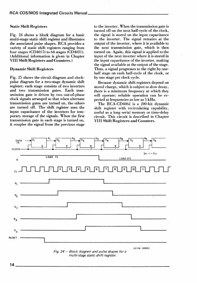
Fig. 24 shows a block diagram for a basic multi-stage static shift register and illustrates the associated pulse shapes. RCA provides a variety of static shift registers ranging from four stages (CD4015) to 64 stages (CD403l). (Additional information is given in Chapter VIII Shift Registers and Counters. )
Dynamic Shift Registers
Fig. 25 shows the circuit diagram and clockpulse diagram for a two-stage dynamic shift register; each stage consists of two inverters and two transmission gates. Each transmission gate is driven by two out-of-phase clock signals arranged so that when alternate transmission gates are turned on, the others are turned off. The shift rEl8ister uses the input capacitance of the inverters for temporary storage of the signals. When the first transmission gate in each stage is turned on, it couples the signal from the previous stage
DATA ~DI IN R
CLOCK i
LOAD liS D
CL
Q,
Q2
Q3
Q4
Qs
RESET
to the inverter. When the transmission gate is turned off on the next half-cycle of the clock, the signal is stored on the input capacitance to the inverter. The signal remains at the output of the inverter, where it is available to the next transmission gate, which is then turned on. Again, this signal is applied to the input of the next inverter where it is stored in the input capacitance of the inverter, making the signal available at the output of the stage. Thus, a signal progresses to the right by onehalf stage on each half-cycle of the clock, or by one stage per clock cycle.
Because dynamic shift registers depend on stored charge, which is subject to slow decay, there is a minimum frequency at which they will operate; reliable operation can be expected at frequencies as low as 5 kHz.
The RCA-CD4062 is a 200-bit dynamic shift register with recirculating capability, useful as a long serial memory or time-delay circuit. This circuit is described in Chapter VIII Shift Registers and Counters.
~ Qc-D_6 __
Qn-I=Dn
LOAD O'S
92CM-30552
Fig. 24 - Block diagram and pulse shapes for a mUlti-stage static shift register.
14 ____________________________________________________ ___

______________________ Basic Circuit Building Blocks
CL
STAGE I STAGE 2
vDD
o~~----~------~----~~ a CL CL ~
I+-J: OUTPUTO
~
CL CL CL J ~----------~----------~~----------~~ __ Ovss
ALL p- UNIT SUBSTRATES CONNECTED TO Voo; ALL n-UNIT SUBSTRATES TO VSS·
Fig. 25 - Circuit diagram and pulse shapes for a two-stage dynamic shift register.
92CS-30335
COUNTERS
Binary (divide-by-two per stage) counters are similar to shift registers except that the Q input to each stage is connected to the Q
output of the stage. The Q and g oukputs of one stage become the Clock and oc inputs of the following stage. Fig. 26 shows the logic diagram, block diagram, and associated pulse shapes for a five-stage binary counter.
Q
Q
CLOCK
RESET ----.J
Q2 _____ --'
Q3~--------------~ L
Q4---------------------------------~
Q5 ____________________________________________________________ ~r___
Fig. 26 - Logic diagram, block diagram, and pulse shapes for a five-stage binary counter.
92CL-30553
________________________________________________________ 15

RCA COS/MaS Integrated Circuits Manual _______________ _
The counter is advanced one count on the negative-going transition of each input pulse.
RCA provides a variety of binary counters ranging from seven stages (CD4024) to 21 stages (CD4045). These circuits are described in Chapter VIII Shift Registers and Counters.
MEMORY CELLS
The basic storage element common to most RCA COS/MOS memories consists of two COS/MOS inverters cross-coupled to form a flip-flop, as shown in Fig. 27. Singletransistor transmission gates are used as a simple and efficient means of pedorming the logic functions associated with storage-cell selection (i.e., the sensing and storing operations).
Fig. 27 - Basic storage element of COS/MaS memories.
The resulting word -organized storage cell, shown in Fig. 28, is composed of six transistors, a word line W, and two digit-sense lines Dl and D2. Addressing is accomplished by energizing a word line; this action turns on
+Voo
w
D2
92CS- 30592
Fig. 28 - A word-organized storage cell (W is the word line; D1 and D2 are data lines).
the p-channel devices on both sides of the selected cell. (Because the cell in Fig. 28 uses p-channel devices, a ground-level voltage is required for selection.)
Fig. 29 shows an eight-transistor bitorganized memory cell that uses X-Y selection. Large memory arrays use a modification of this circuit in which the Y
for each
92CS-30593
Fig. 29 - Eight-transistor bit-organized memory cell with X- Y selection.
16 ______________________________________________________ __
III. Characteristics of RCA COS/MOS Devices
RCA COS/MOS digital integrated circuits are specified in two voltage-supply ranges: Aseries types operate from 3 to 15 volts, and Bseries types operate from 3 to 20 volts.
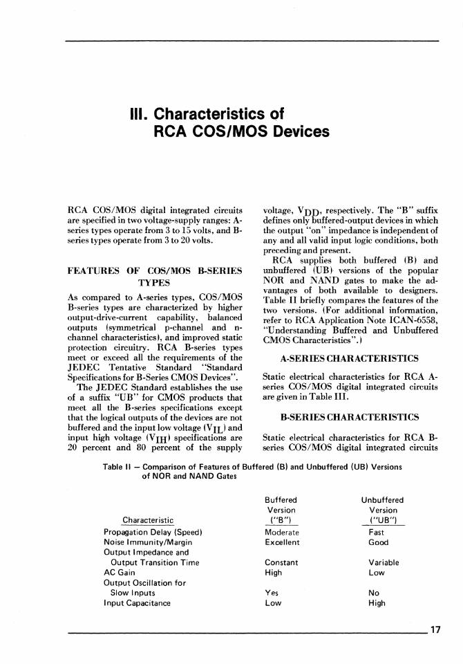
FEATURES OF COS/MOS B-SERIES TYPES
As compared to A-series types, COS/MOS B-series types are characterized by higher output-drive-current capability, balanced outputs (symmetrical p-channel and nchannel characteristics), and improved static protection circuitry. RCA B-series types meet or exceed all the requirements of the JEDEC Tentative Standard "Standard Specifications for B-Series CMOS Devices".
The JEDEC Standard establishes the use of a suffix "UB" for CMOS products that meet all the B-series specifications except that the logical outputs of the devices are not buffered and the input low voltage (V IL) and input high voltage (V IH) specifications are 20 percent and 80 percent of the supply
voltage, VDD, respectively. The "B" suffix defines only buffered-output devices in which the output" on" impedance is independent of any and all valid input logic conditions, both preceding and present.
RCA supplies both buffered (B) and unbuffered (UB) versions of the popular NOR and NAND gates to make the advantages of both available to designers. Table II briefly compares the features of the two versions. (For additional information, refer to RCA Application Note ICAN-6558, "Understanding Buffered and Unbuffered CMOS Characteristics". )
A-SERIES CHARACTERISTICS
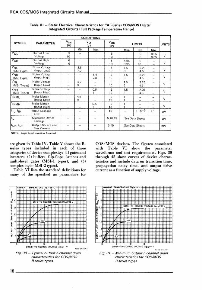
Static electrical characteristics for RCA Aseries COS/MOS digital integrated circuits are given in Table III.
B-SERIES CHARACTERISTICS
Static electrical characteristics for RCA Bseries COS/MOS digital integrated circuits
Table II - Comparison of Features of Buffered (B) and Unbuffered (UB) Versions of NOR and NAND Gates
Buffered Unbuffered Version Version
Characteristic ("B") ("UB")
Propagation Delay (Speed) Moderate Fast Noise Immunity/Margin Excellent Good Output I mpedance and
Output Transition Time Constant Variable AC Gain High Low Output Oscillation for
Slow Inputs Yes No Input Capacitance Low High
17
RCA COS/MaS Integrated Circuits Manual _______________ _
Table III - Static Electrical Characteristics for "A"-Series COS/MaS Digital Integrated Circuits (Full Package-Temperature Range)
CONDITIONS
SYMBOL PARAMETER VIN (V)
Min. VOL Output Low 5 -
Voltage 10 -VOH Output High 0 -
Voltage 0 -
VNL No ise Vo Itage - 3.6 (551 Types) (Input Low) - 7.2
VNH Noise Voltage .- -
(551 Types) (Input High) - -VNL Noise Voltage - 4.2
(MSI Types) (Input Low) - 9
VNH Noise Voltage - -(MSI Types) (Input High) - -
VNML Noise Margin - 4.5 (Input Low) - 9
VNMH Noise Margin - -(Input HiQh) - -
I'L,"H Input Leakage - -Low
'L Quiescent Device - -Leakage
ION,lOp Output Source and - -Sink Current
NOTE: Logic Level Inversion Assumed.
are given in Table IV. Table V shows the Bseries types included in each of three categories of device complexity: (1) gates and inverters; (2) buffers, flip-flops, latches and multi-level gates (MSI-l types); and (3) complex logic (MSI-2 types).
Table VI lists the standard definitions for many of the specified ac parameters for
.. E I
-..J
~30 ... z ::! 25 0:: ~
;! 20 >< z !e ~ 15
9 ... 10 ~ CL
~ 5
AMBIENT TEMPERATURE (TA)·25·C
GATE-TO-SOURCE YOLTAGE (VGS)"5 V
10V
5V
o 5 10 15 DRAIN-TO-SOURCE VOLTAGE (VDS)-V
Vo (V)
92CS-2431SR3
Fig. 30 - Typical output n-channel drain characteristics for COS/MaS B-series types.
VDD LIMITS UNITS (V) Max. Min. TVD. Max. - 5 - 0 0.05 - 10 - 0 0.05 V
- 5 4.95 5 -- 10 9.95 10 V -- 5 1.5 2.25 -- 10 3 4.5 - V
1.4 5 1.5 2.25 -V 2.8 10 3 4.5 -
- 5 1.5 2.25 -- 10 3 4.5 V -
0.8 5 1.5 2.25 -V 1 10 3 4.5 -
- 5 1 - -- 10 1 - - V
0.5 5 1 - -V 1 10 1
- 15 - ± 10-5 ± 1 /lA
- 5,10,15 See Data Sheets /lA
- 5,10 See Data Sheets mA
COS/MOS devices. The figures associated with Table VI show the parameter waveforms and test requirements. Figs. 30 through 45 show curves of device characteristics and include data on transition time, propagation delay time, and output drive current as a function of supply voltage.
AMBIENT TEMPERATURE (TA» 25·C
.. E I
-..J 15 .g lZ 12.5
'" 0:: 0:: a 10 ;;: z !e 7.5
~
9 5 ... ~ CL '5 2.5 o
o
GATE-TO SOURCE VOLTAGE (VGS)"5Y
10V
5'1
5 10 15 ORAIN-TO-SOU.RCE VOLTAGE (VOs)-V
92CS-24319RI
Fig. 31 - Minimum output n-channel drain characteristics for COS/MaS B-series types.
18 ____________________________________________________ ___

_________________ Characteristics of RCA COS/MaS Devices
Table IV - Static Electrical Characteristics for u8u-Series COS/MOS Digital Integrated Circuits (Full Package-Temperature Rangel
LIMITS AT INDICATED TEMPERATURES (oC)
CHARACTER-CONDITIONS Values at -65, +25, +125 Apply to O,F,H Packages
ISTIC Values at -40, +25, +85 Apply to E Pickage
Vo VIN VOO +25 (V) (V) (V) -65 -40 +85 +125 Min. Typ. Max.
Quiescent Device - 0,5 5 0.25 0.25 7.5 7.5 - 0.01 0.25 Current, - 0,10 10 0.5 0.5 15 15 - 0.01 0.5
100 Max. - 0,15 15 1 1 30 30 - 0.01 1 Gates, - 0,20 20 5 5 150 150 - 0.02 5 Inverters
Buffers, Flip·Flops, 0,5 5 1 1 30 30 - 0.02 1 Latches, Multi- 0,10 10 2 2 60 60 - 0.02 2 Level Gates 0,15 15 4 4 120 120 - 0.02 4 (MSI-l Types)
0,20 20 20 20 600 600 - 0.04 20 Complex Logic 0,5 5 5 5 150 150 - 0.04 5
(MSI-2 Types) 0,10 10 10 10 300 300 - 0.04 10 0,15 15 20 20 600 600 - 0.04 20
0,20 20 100 100 3000 3000 - 0.08 100 Output Low 0.4 0,5 5 0.64 0.61 0.42 0.36 0.51 1
(Sink) Current 0.5 0,10 10 1.6 1.5 1.1 0.9 1.3 2.6 -IOLMin. 1.5 0,15 15 4.2 4 2.8 2.4 3.4 6.8 -
Output High 4_6 0,5 5 -0.64 -0.61 -0.42 -0.36 -0.51 -1 -(Source) 2.5 0,5 5 -2 -1.8 -1.3 -1.15 -1.6 -3.2 -Current, 9.5 0,10 10 -1.6 -1.5 -1.1 -0.9 -1.3 -2.6 -
IOH Min. 13.5 0,15 15 -4.2 -4 -2.8 -2.4 -3.4 -6.8 ' -
Output Voltage: - 0,5 5 0.05 - 0 0.05 Low-Level, - 0,10 10 0.05 - 0 0.05
VOL Max. - 0,15 15 0.05 - 0 0.05 Output Voltage: - 0,5 5 4.95 4.95 5 -
High-Level - 0,10 10 9.95 9.95 10 -VOH Min. - 0,15 15 14.95 14.95 15 -
Input Low 0.5,4.5 - 5 1.5 - - 1.5 Voltage, 1,9 - 10 3 - - 3
VIL Max. 1.5,13.5 - 15 4 - - 4 B Types
UB TYPds 0.5,4.5 - 5 1 - - 1 1,9 - 10 2 - - 2
1.5,13.5 - 15 2.5 - - 2.5 Input High 0.5,4.5 - 5 3.5 3.5 - -
Voltage, 1 9 - 10 7 7 - -VIH Min. 1.5,13.5 - 15 11 11 - -B Types
UB Types 0.5,4.5 - 5 4 4 - -1 9 - 10 8 8 - -
1.5,13.5 - 15 12.5 12.5 - -Input Cu rrent - 0,18 18 :to. 1 :to. 1 ±1 ±1 - ±10-b ±0.1
liN Max. 3-State Output
Leakage Cu rrent 0, 18 0,18 18 ±0.4 ±0.4 ±12 ±12 - ±10-4 ±0.4 lOUT Max.
UNITS
IJA
mA
V
.
V
J1.A
J1.A
_________________________________________________________ 19
RCA COS/MaS Integrated Circuits Manual _______________ _
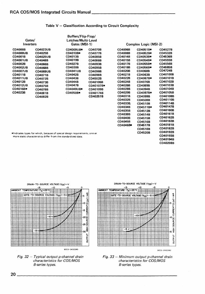
Table V - Classification According to Circuit Complexity
Buffers/Flip-Flop/ Gates/ Latches/Mu Iti-Level
Inverters Gates (MSI-l) Complex Logic (MSI-2)
CD4000B CD4023UB CD4009UB- CD4070B CD4006B CD4051B- CD4527B CD4000UB CD4025B CD4010B- CD4077B CD4008B CD40528- CD4532B CD4001B CD4025UB CD4013B CD4085B CD4014B CD4053B- CD4536B CD4001UB CD4048B CD4019B CD4086B CD4015B CD4054B- CD4555B CD4002B CD4066B CD4027B CD4093B CD4017B CD4055B- CD4556B CD4002UB CD4068B CD4030B CD4095B CD4018B CD4056B- CD4585B CD4007UB CD4069UB CD4041UB CD4096B CD4020B CD4060B CD4724B CD4011B CD4071B CD4042B CD4098B CD4021B CD4063B CD40100B CD4011UB CD4072B CD4043B CD4502B CD4022B CD4067B- CD40101B CD4012B CD4073B CD4044B CD40106B CD4024B CD4076B CD40102B CD4012UB CD4075B CD4047B CD40107B- CD4026B CD4089B CD40103B CD4016B- CD4078B CD4049UB- CD40109B CD4028B CD4094B CD40104B CD4023B CD4081B CD4050B- CD40174B CD4029B CD4097B- CD40105B
CD4082B CD40257B CD4031B CD4099B CD40108B CD4032B CD4508B CD40110B CD4033B. CD4510B CD40114B CD4034B CD4511B- CD40147B CD4035B CD4512B CD40160B CD4038B CD4514B CD40161B CD4040B CD4515B CD40162B CD4045B CD45168 CD401638 CD4046a- CD4517B CD40181B
CD4518B CD40182B
-Indicates types for which, because of special design requirements, one or more static characteristics differ from the standardized data.
CD4520B CD40192B CD40193B
DRAIN-TD-SDURCE VOLTAGE (VDS)-V
-15 -10 -5 o AMBIENT TEMPERATURE (TA)-25°C
GATE-TO-SOURCE VOLTAGE (VGS)o-5V
-IOV
-15V
92CS-24320R3
Fig. 32 - Typical output p-channel drain characteristics for COS/MaS B-series types.
DRAIN-TO-SOURCE VOLTAGE (VDS)-V
-15 -10 -5 AMBIENT TEMPERATURE (TA)-25°C
GATE-TO-SOURCE VOLTAGE (VGS)o-5 V
-IOV
-15 V
CD40194B CD40208B
o
o II: ::> o !!!
15 ~
9ZCS-24321R2
Fig. 33 - Minimum output p-channel drain characteristics for COS/MaS B-series types.
20 ____________________________________________________ ___

________________ Characteristics of RCA COS/MaS Devices
Table VI - Dynamic Electrical Characteristics - Definitions
Characteristic Symbol Limits Notes Max. Min. (Fig.)
Propagation Del ay:
Outputs going high to low tpHL X (A) Outputs going low to high tpLH X
Output Transition Time: Outputs going high to low tTHL X (A) Outputs going low to high tTLH X
Pulse Width-Set, Reset, Preset Enable, Disable, Strobe, Clock tWL or tWH X 1 (B)
Clock Input Frequency fCL X 1,2 (B)
Clock Input Rise and Fall Time trCL, tfCL X (B)
Set-Up Time tsu X 1 (C)
Hold Time tH X 1 (C)
Removal Time - Set, Reset, Preset-Enable tREM X 1 (C)
Three-State Disable Delay Times: High level to high impedance tpHZ X (D)
High impedance to low level tpZL X (D) Low level to high impedance tpLZ X (D) High impedance to high level tpZH X (D)
NOTE: (1) By placing a defining min. or max. in front of definition, the limits can change from min. to max., or vice versa.
(2) Clock input waveform should have a 50% duty cycle and be such as to cause the outputs to be switching from 10% VOO to 90% VOO in accordance with the device truth table.
Fig. A - Transition times and propagation delay times, combination logic.
VDD
--50% I ..' _____ 0 r 'SU(HLl'" I •••
-j ~·'TLH 1-1 t"'HIL r-"oo
OU_T_PU_T --4'1-.--------~-"l*:::::::: ~ -=,~og; 0
~ IpLH ~ J- _lpHl
SET, RESET I OR PRESET !---t- ',.m *(LH) OR (HL) OPTIONAL
VOD~o 92C5- 20069R3
Fig. C - Setup times, hold times, removal time, and propagation delay times for positive-edge triggered sequential logic circuits.
VDD L
Fig. B - Clock·pulse rise and fall times and pulse width.
OUTPuT DIS.BlE:
OUTPUT Alol"l1 fVOO 10f 'PLZ and IpZl
VSS 'Of 'PHZ arid IpIH Cc
"""
Fig. D - Three-state propagation delay wave shapes and test circuit.
_____________________________________________________ 21
RCA COS/MaS Integrated Circuits Manual _____________ --
~ 2.5
!:! .... z '" ~ i3 1.5
" z ., c ::l ~ 0.5
:s z 0
OUTPUT VOLTAGE 1\101' o.~ V
SUPPLY VOLTAGE wool' 10 V,. 15 V
5V 5V
10 V. 15V
-75 -50 -25 0 25 50 7~ 100 12~
AMBIENT TEMPERATURE (T A ) - ·c 92eS-2ei1lORI
Fig. 34 - Variation of normalized sink current (loLl with temperature for COS/MaS B-series types.
OUTPUT VOLTAGE (VoloVoo-0.5 V
11 SUPPLY VOLTAGE (VoololO V. 15 V
5V
~V
10V.ISV
o -75 -50 -25 0 25 50 75 100 12~
AMBIENT TEMPERATURE tTA) - ·C
92CS-25IIIRI
Fig. 35 - Variation of normalized source current (lOH) with temperature for COS/MaS B-series types.
-::. o !:! .... z ... ~ :::> u
" z ., ~ N
~ :s z
10 12 14
SUPPLY VOLTAGE (Vool - V
16
92CS-21U1DRI
Fig. 36 - Variation of normalized sink current (lOL) with supply voltage for COS/MaS B-series types.
OUTPUT VOLTAGE IVol-Voo-0.5V
o 5 10 15 20 SUPPLY VOLTAGE (Vool- VOLTS
92cS-25I01RI
Fig. 37 - Variation of normalized source current (/OH) with supply voltage for COS/MaS B-series types.
LOAD CAPACITANCE tel) = 50 pF , z
1.5 0 .... '" ., z : .... ~-::. -," ..... 0= .... w
~'" "' .... " ~ 0.5 -' .. '" 0: 0 Z
o -7~ -50 -2~ 0 25 50 75 100 125
AMBIENT TEMPERATURE (TAl - ·C
92CS-25113RI
Fig. 38 - Variation of normalized high-to-Iow transition time (tTHLl with temperature for COS/MaS B-series types.
z ~ 1.5
i2 .. 0: .... ,,~
'" " ,,-, I
o~ .... w 3:~ 0 .... -'
~ 0.5 -' .. '" ~
o
LOAD CAPACITANCE ICLI 0 50 pF
-75 -50 -25 0 2~ 50 ~ 100 12~
AMBIENT TEMPERATURE (T A) - ·C
92CS-25112RI
Fig. 39 - Variation of normalized low-to-high transition time (tTLH) with temperature for COS/MaS B-series types.
22 ____________________________________________________ _

________________ Characteristics of RCA COS/MaS Devices
Gi= xli
LOAD CAPACITANCE (CLI" eo pf
~~O.5 --' .. '" a: li!
o -75 -50 -25 0 25 50 75 100 125
AMBIENT TEMPERATURE (T A) - °C
92CS-~5116RI
Fig. 40 - Variation of normalized high-to-Iow propagation delay time (tPHU with temperature for COS/MaS B-series types.
LOAD CAPACITANCE ICLI • 50 pF
o -75 -50 -25 0 25 50 75 100 125
AMBIENT TEMPERATURE (TA) - °C
92CS-25117RI
Fig. 41 - Variation of normalized low-to-high propagation delay time (tPLH) with temperature for COS/MaS B-series types.
I AMBIENT TEMPERATURE RANGE (TAl" -40"C TO +125"C LOAD CAPACITANCE ICt.!" 50 pF
4 10 SUPPLY VOLTAGE IVDOI - VOLTS
92CS-2~I07RI
Fig. 42 - Variation of normalized high-to-Iow transition time (tTHU with supply voltage for COS/MaS B-series types.
n
4 6 10 I SUPPLY VOLTAGE IVDol- V
16
92CS-25108RI
Fig. 43 - Variation of normalized low-to-high transition time (tTLH) with supply voltage for COS/MaS B-series types.
16
SUPPLY VOLTAGE IVDDI - VOLTS'
92CS-26114
Fig. 44 - Variation of normalized propagation delay time (tPHi- tPLH) with supply voltage for COS/MaS B-series types.
I LOAD CAPACITANCE (CLI-pF
92CS-24'322
Fig. 45 - Variation of normalized transition time (tTHL, tTLM with load capacitance at three levels of supply voltage for COS/MaS B-series types.
_______________________________________________________ 23
RCA COS/MaS Integrated Circuits Manual ______________ _
PACKAGES
Maximum ratings for power dissipation and the operating temperature range depend on package type. RCA COS/MOS integrated circuits are available in four types of packages:
Dual-in-line welded-seal or brazed-seal ceramic ..................... D suffix
Dual-in-line frit-seal ceramic ....... F suffix Dual-in-line plastic ............... E suffix Ceramic flat pack (MIL types only I . K suffix
Depending on the requirements of the individual integrated-circuit type, the number of leads may range from 8 to 40 per package. . For bonding on hybrid substrates, unpackaged die (chipsl are also available; they are indicated by an H suffix.
MAXIMUM RATINGS AND RECOMMENDED OPERATING CONDITIONS
The maximum ratings for both A- and Bseries COS/MOS digital integrated circuits are given in Table VII. Ratings which differ because of the package type used are indicated. Table VIII gives the recommended operating conditions for A- and B-series types.
TYPES CLASSIFIED BY FUNCTION
The RCA COS/MOS digital integrated circuit types are classified by function in Table IX. The Table includes A, B, and UB types. Types suitable for more than one of the functions listed are indicated by footnote symbols which cross-refer the type to the additional functional category.
Table VII - Maximum Ratings for "A"- and "B"-Series Types (Absolute-Maximum Values)
DC SUPPLY-VOLTAGE RANGE, (VDD ) (Voltages referenced to VSS Terminal): STANDARD "A"·SERIES TyPES............................ ................. -0.5 to +15 V HIGH-VOLTAGE "S"-SERIES TYPES ......................................... -0.5 to +20 V
INPUT VOLTAGE RANGE, ALL INPUTS .................................... -0.5 to VDD +0.5 V DC INPUT CURRENT, ANY ONE INPUT ............................... ("S"-series only) ±10 mA POWER DISSIPATION PER PACKAGE (PO):
For T A = -40 to +60°C (PACKAGE TYPE E) .....................•.......... 500 mW For T A = +60 to +85°C (PACKAGE TYPE E) ............ Derate Linearly at 12 mWfC to 200 mW For T A = -55 to +1 OO°C (PACKAGE TYPES D,F) . . . . . . . . . . . . . . . . . . . . . . . . . .. 500 mW For T A = +100 to +125°C (PACKAGE TYPES 0, F) .. . . . . . Derate Linearly at 12 mWrC to 200 mW
DEVICE DISSIPATION PER OUTPUT TRANSISTOR For T A = FULL PACKAGE-TEMPERATURE RANGE (All Package Types) .............. 100 mW
OPERATING·TEMPERATURE RANGE (T A): PACKAGE TYPES 0, F, H .,. . . . . . . . . . . . . . . . . . . . . . . . . . . . . . . . . .. -55 to +125°C PACKAGE TYPE E . . • . . . . . . . . . . . . . . . . . . . . . . . . . . . . . . . . • . . . . . . .. -40 to +85°C
STORAGE TEMPERATURE RANGE (Tstg) ............................. --65 to +150°C LEAD TEMPERATURE (DURING· SOLDERING):
At distance 1/16 ± 1/32 inch (1.59 ± 0.79 mm) from case for lOs max ......•........... +265°C
Table VIII - Recommended Operating Conditions for the "A"- and "Bu-Series Types
Characteristic
Supply-voltage range (For T A = Full packagetemperature rangel
"AU series "S" series
Limits Min. Max.
3 12 3 18
Units
volts volts
24 ____________________________________________________________________________________________________ __
________________ Characteristics of RCA COS/MaS Devices
Table IX - RCA COS/MOS Digital Integrated Circuit Types Classified by Function
GATES
Single-Level Multi- Level Buffers & Multi- Decoders! Schmitt
NOR/NAND OR/AND Inverters function/AOI Encoders Trigger
CD4000B CD4012B CD4071B CD4007UB CD4019B CD4028B CD4093B CD4000UB CD4012UB CD4072B CD4007A CD4019A CD4028A CD40106B CD4000A CD4012A CD4073B CD4009UB CD4030B CD4514B CD4001B CD4023B CD4075B CD4009A CD4030A CD4515B CD4001UB CD4023UB CD4081B CD4010B CD4037 A CD4532B CD4001A CD4023A CD4082B CD4010A CD4048B CD4555B" CD4002B CD4025B CD4041UB CD4048A CD4556B" CD4002UB CD4025UB CD4041 A CD4070B- CD40147B CD4002A CD4025A CD4049UB CD4077B-CD4011B CD4068B CD4049A CD4085B CD4011UB CD4078B CD4050B CD4086B CD4011A CD40107B CD4050A
CD4069UB -See "'See
CD4502B Comparators Demultiplexers CD40107B
REGISTERS COUNTERS MULTIPLEXERS! PHASE-DEMULTIPLEXERS LOCKED
FIFO Binary Analog/Digital LOOP
Shift Storage Buffer Ripple Synchronous Data Selectors
CD4006B CD4076B CD40105B CD4020B CD4017B CD4016B· CD4046B CD4006A CD4099B CD4020A CD4017A CD4016A· CD4046A CD4014B CD4724B CD4024B CD4018B CD4019B CD4014A CD40108B. CD4024A CD4018A CD4019A CD4015B CD40208B. CD4040B CD4022B CD4051B CD4015A CD4040A CD4022A CD4052B CD4021B CD4060B CD4029B CD4053B CD4021 A CD4060A CD4029A CD4066B· CD4031B CD4059A CD4066A· CD4031A CD4510B CD4067B CD4034B CD4516B CD4097B CD4034A TIMERS CD4518B CD45558< Co4035B CD4520B CD4556B~
CD4035A CD4045B CD40102B Co40257B Co4062A Co4045A Co40103B Co4094B CD4536B CD40160B Co4517B Co40161B Co40100B • See Co40162B 4 See eSee
Multipart CD40163B Quad Decodersl Register CD40192B Bilateral Encoders
Co40193B Switeh
ARITHMETIC CIRCUITS DISPLAY DRIVERS
Parity For For Adders/ ALU/Rate Generator/ Mu Iti port LCD* LEO-Comparators Multi pi iers Checker Register With Counter Drive Drive
Co4008B Co4057A Co40t01B Co40108B* Co4026B Co4054B Co4511B
Co4008A Co4089B Co402OBB* Co4026A Co4055B Co4030B Co4527B Co4033B Co4056B Co4030A Co40181B Co4033A Co4032B Co40182B Co40110B Co4032A Co4038B Co4038A C04063B Co4070B. .See *See "Liquid- __ Light
Co4077B. Multi!une- Storage crystal Emitting
Co4585B tion/ADI Ragister Display oioda
Ylndicates types designed for special applications. Ratings and characteristics data for these types differ in some aspects from the standardized data for A- and B-series types.
MUL TlVIBRATORS
Flip-Flops/latches
CD4013B CD4096B CD4013A CD4099B" CD4027B CD4508B CD4027A CD4724B"" CD4042B CD40174B CD4042A Astable/ CD4043B Mono-CD4043A stable CD4044B CD4044A CD4047B CD4076B"" CD4047A CD4095B CD4098B
"'·See Storage Registers
QUAD INTER-BILATERAl FACE SWITCHES CIRCUITS
CD4016B. CD4009UB CD4016A. CD4009A CD4066B. CD4010B CD4066M CD4010A
CD4049UB CD4049A CD4050B CD4050A CD40107B CD40109B CD40115
.See Multiplexers
CROSS- MEMORY POINT SWITCHES
C022100'" Co40114B C02210''" C022102 '"
_____________________________________________________ 25

RCA COS/MaS Integrated Circuits Manual _______________ _
EXTRA-VALUE AND MIL TYPES
For sensitive applications requiring devices of extra quality, the RCA COS/MOS ExtraValue Program offers dual-in-line package types with certain special screening and testing. The processing of these types includes a 168-hour burn-in at 125°C at a 12-volt bias to substantially reduce early failures
("infant mortality"). As a result of ·the processing and testing added to the com~ prehensive controls and tests carried out on standard product, AQL's of 0.25 percent parametric and 0.15 percent functional are achieved.
For critical applications, RCA offers a line of COS/MOS devices processed and screened in accordance with MIL-STD-883 and MILM-38510.
26 __________________________________________________ ___
IV. Handling and Operating Considerations
HANDLING COS/MOS DEVICES
The silicon dioxide layer located immediately over the channel and beneath the gate electrode creates the very high input impedance of MOS devices (greater than 1012 ohms). For best device operation, this channel oxide must be extremely thin, i.e., in the order of 1000 angstroms. As a result, it is susceptible to damage by high static electric charges which can accumulate on the surfaces of the devices and on personnel handling them. Unlike semiconductor junction p-n diodes, which can sustain breakdown a number of times without permanent damage, the MOS gate can be shorted by a single voltage excursion to the oxide breakdown point of about 80 volts.
To protect the oxide layer, COS/MOS devices are shipped in either anti-static or conductive carriers. The same technique or other means of minimizing the potential difference between leads should be maintained. Units should be stored in the RCA carriers or with their pins imbedded in conductive foam. The following procedures should be followed during handling, inspection, and test:
1. Use conductive work surfaces. 2. Ground all handling equip!Dent.
(Alternatively, ionized-air blowers can reduce charge build-up in areas where grounding is not feasible. )
3. Require personnel handling units to wear a conductive wrist strap grounded through a I-megohm resistor.
4. Place units in conductive or anti-static
carriers when they are moved from one work station to another.
BUILT-IN PROTECTION NETWORKS
Each COS/MOS device has a built-in protection network. Fig. 46 shows the original protection network incorporated in all CD4000A-series and some CD4000Bseries devices. This network can protect the
Voo
n SUB n SUB
01 01
p+ IN OUT
n+
02 02
P WELL P WELL
Vss VSS 92CS-30554
Fig. 46 - Protection network used in all CD4000A-series and some CD4000Bseries devices.
gate oxide against electrostatic discharges up to I kilovolt. The diode DI is a distributed resistor-diode network that is made up of p+-to-n-substrate material and has a voltage breakdown in the range of 30 to 50 volts. Diode D2 is a separate diode that is built of n+-to-p-well material and has a breakdown in the range of 30 to 40 volts.
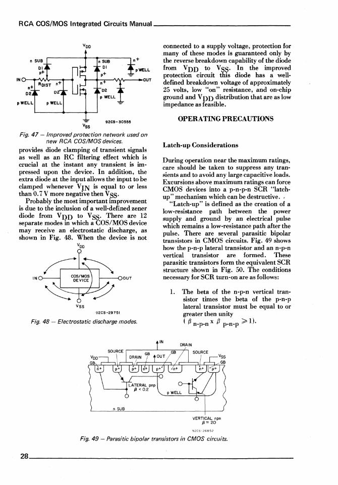
Fig. 47 shows an improved protection network used on new RCA COS/MOS devices which increases the typical gate-oxide protection to 4 kilovolts. The improvement in protection can be attributed to several different phenomena. The addition of a resistor and distributed diode in the output path
_________________________________________________________ 27
RCA COS/MaS Integrated Circuits Manual ______________ _
n SUB
01 p+
IN ')-__ '\N\r--_ ..
n+ ROIST
02
pWELL pWELL
Voo
pWELL
~-'~~~Ar---'OUT
=
= 92CS-30!l5!1 VSS
Fig. 47 - Improved protection network used on new RCA COS/MaS devices.
provides diode clamping of transient signals as well as an RC filtering effect which is crucial at the instant any transient is impressed upon the device. In addition, the extra diode at the input allows the input to be clamped whenever VIN is equal to or less than 0.7 V more negative then V SS.
Probably the most important improvement is due to the inclusion of a well-defined zener diode from VDD to VSS' There are 12 separate modes in which a COS/MOS device may receive an electrostatic discharge, as shown in Fig. 48. When the device is not
Voo
INr'-.----' 1---oOUT
Vss 92CS -29751
Fig. 48 - Electrostatic discharge modes.
connected to a supply voltage, protection for .many of these modes is guaranteed only by the reverse breakdown capability of the diode from VDD to V SS. In the improved protection circuit this diode has a welldefined breakdown voltage of approximately 25 volts, low "on" resistance, and on-chip ground and V D D distribution that are as low impedance as feasible.
OPERATING PRECAUTIONS
Latch-up Considerations
During operation near the maximum ratings, care should be taken to suppress any transients and to avoid any large capacitive loads. Excursions above maximum ratings can force CMOS devices into a p-n-p-n SCR "latchup" mechanism which can be destructive. ,
"Latch-up" is defined as the creation of a low-resistance path between the power supply and ground by an electrical pulse which remains a low-resistance path after the pulse. There are several parasitic bipolar transistors in CMOS circuits. Fig. 49 shows how the p-n-p lateral transistor and an n-p-n vertical transistor are formed. These parasitic transistors form the equivalent SCR structure shown in Fig. 50. The conditions necessary for SCR turn-on are as follows:
1. The beta of the n-p-n vertical transistor times the beta of the p-n-p lateral transistor must be equal to or greater then unity ( f.l x f.l ;;;"1). ,.. n-p-n ,.. p-n-p
VERTICAL npn fJ "" 20
92C5- 26852
Fig. 49 - Parasitic bipolar transistors in CMOS circuits.
28 ____________________________________________ ___

_____________________ Handling and Operating Considerations
92CS-26853
Fig. 50 - Equivalent circuit for the SCR struc-, ture present in CMOS circuits.
2. The lateral p-n-p and vertical n-p-n base-emitter junctions must be forward-biased, usually initiated by high transient currents in the n substrate (see Fig. 50).
3. The bias circuit which applied power to VDD and to the input must be capable of supplying current equal to the holding current of potential SCR's.
Fig. 51 shows a curve of IDD as a function of VDD which illustrates the effect of secondary breakdown and SCR latch-up. Table X shows typical values of breakdown voltage and sustaining voltage and current for COS/MOS A-series and B-series devices.
8 H
SCR TURN-ON CURRENT
I'UI -------------------
92CS-268~4
Fig. 51 - Curve illustrating effect of secondary breakdown and SCR latch-up.
Table X - Typical Breakdown Values for A- and B-Series Devices
Breakdown Voltage (V)
Sustaining Voltage (V)
A Series B Series
17
15
25 22
Sustaining Current (rnA) 2 to 40 50 to 100 (type· dependent)
These values show that B-series devices are harder to latch than A -series types because of their higher breakdown voltage.
Operating-Rule Summary
Observation of the following operating rules will enhance reliable operation of any CMOS system:
1. When a low-impedance pulse generator or separate power supply is used for the device inputs, the main device power supply should always be turned on before the independent
. signal sources are turned on. When a system is being shut down, the independent signal sources should be turned off before the main power supply is turned off. (In other words, VSS ~ VI ~ VDD)· This rule will avoid input-diode damage.
2. In the case of CD4009 and CD40IO, the diode between V CC (pin 1) and VDD (pin 16) should not be forwardbiased. VDD should always be greater than V CC. This rule is especially important during power sequencing.
3. When series resistors are used on power supplies, it is wise to avoid biasing inputs to the non-limited side of the supply. This action will eliminate the potential hazard of forward-biasing the input diodes.
4. The power-supply polarity should not be reversed, i.e., VDD - VSS > -0.5 V. Such reversal could overdissipate the substrate diode.
5. All inputs should be terminated. A floating input can force the CMOS
________________________________________________ 29
RCA COS/MaS Integrated Circuits Manual _______________ _
inverter into a linear mode and cause faulty operation as a result of the large current.
6. When CMOS devices are interfaced in PC cards, a pull-up or pull-down resistor should always be used if there is a possibility of an input becoming open.
7. CMOS outputs should not be connected in the "wire-OR" configuration. Instead, 3-state outputs or transmission gates hould be used.
8. Output loads should not be returned to voltages greater. than V D D or less than V SS; otherwise, the output diodes will be turned on.
VOLTAGE AND DISSIPATION CONSIDERATIONS
Recommended Maximum Operating Voltage
RCA COS/MOS digital integrated circuits have maximum ratings of 15 volts for Aseries types and 20 volts for B-series types. However, because logic systems can experience transient conditions on the powersupply line which, when added to the nominal power-bus voltage, could exceed the safe limits of circuits connected to the power bus, the recommended operating supplyvoltage ranges are 3 to 12 volts for A-series types and 3 to 18 volts for B-series types. (The 3-volt minimum limit is set by the sum of the threshold of the p-channel and nchannel transistors.)
Power Dissipation
Total power dissipation in a COS/MOS device is the sum of the static (or quiescent) dissipation and the dynamic (or ac) dissipation.
Quiescent dissipation, which is due to leakage effects, is much smaller than dynamic dissipation, varying from a few nanowatts to a few microwatts depending upon the complexity of the circuit.
Dynamic dissipation is comprised of two elements: "through" current that exists during the transition from one logic level to another, when both p-channel and n-channel devices are momentarily conducting, and the power-supply current required to charge node and output capacitances during switching. "Through" current is usually only about 10 percent of the charging current, particularly for systems which have fast rise and fall times. Dynamic dissipation P dyn can be expressed as follows:
Because dynamic power dissipation is a function of the supply voltage squared, the system designer seeking to minimize power consumption should specify the lowest possible operating voltage.
NOISE IMMUNITY AND
NOISE MARGIN
AC noise is usually considered to comprise noise spikes with pulse widths shorter than the propagation delay of a logic gate; dc noise spikes are considered to have pulse widths longer than the propagation delay of one gate. AC noise immunity, which varies in direct proportion to dc noise immunity, is largely a function of the propagation delays and output transition times of logic gates and, therefore, is a function of input and output capacitances.
The high dc noise immunity of COS/MOS integrated circuits is a result of the complementary structure of the inverter (common to all COS/MOS devices), which has a near-ideal input-output transfer characteristic. The switching point is typically midway (45 to 50 per cent) between the "0" and "1" output logic levels. Fig. 52 shows the steep transfer characteristic exhibited during transitions.
The noise-immunity voltage (VIL or VIH) is that noise voltage at anyone input that does not propagate through the system. Minimum noise immunity for buffered Bseries COS/MOS devices is 30, 30, and 27 per cent, respectively, for supply voltages of 5,10, and 15 volts; for all unbuffered gates, it
30 _____________________________________________________________________ _____

__________________ Handling and Operating Considerations
SWITCHING POINT
VOH= VOO- 0.01
VOL = vss + 0.01
VO~~~ __ ~ __ ~~~~ .. ~~ Vss VNIL-I I--VNIH--I Voo
VOL VILmax VIHmin VOH INPUT VOLTAGE (VIN) - VOLTS
9ZCS-306Z9
Fig. 52 - Typical inverter transfer characteristic.
is 20 per cent of VDD. The VIL and VIR specifications define the maximum permissible additive noise voltage at an input terminal when input signals are at the supply rails.
Noise margin is the difference between the noise-immunity voltage (V IL or VIR) and the output voltage Vo. Noise-margin voltage is the maximwn voltage that can be impressed upon an input voltage V IN (where V IN is the output voltage of the preceding
stage) at any or all logic 110 terminals without upsetting the logic or causing any output to exceed the noise-immunity ratings. Noise margins for buffered B-series COS/MaS devices are 1, 2, and 2.5 volts, respectively, for supply voltages of 5,10, and 15 volts.
Because noise immunity is proportional to supply voltage, designers aware of noise in the system environment should specify a high enough operating voltage to guarantee immunity. The excellent noise immunity of COS/MaS devices reduces the need for highly regulated and filtered power supplies, as compared to the requirements of other logic families.
VOLTAGE LOGIC-LEVEL DEFINITIONS
The voltage logic-level terms used in the published data for COS/MaS digital devices are defined below and illustrated in Fig. 53.
VOL is the maximum output at low level with no noise at the input. For an inverter, VOL{max) is the output level when the input is tied to VDD, assuming only capacitive loading at the
INDETERMINATE REGION
1.5 - --- ---LOGiC:O-- - - - --- v1L MAX- -----I7777.l~'7T.""7.:I
OUTPUT ~REGION r --VOL
0.01 - - --~_eEl1t-J r--Dl -------VSS------((..(;j~@~~ OJ 92CS-306Z4
Fig. 53 - Output-to-input logic-level characteristics.
______________________________________________________ 31
RCA COS/MOS Integrated Circuits Manual ______________ _
output. For COS/MOS circuits, VOL = VSS - 0.05 volts.
VOH is the minimum output at high level with no noise at the input. For an inverter, VOH(min) is the output level when the input is grounded, assuming only capacitive loading at the output. For COS/MOS circuits, VOH = VDD - 0.05 volt.
VIL(max) is the maximum input at low level for which the output logic level does not change state.
VIH(min) is the minimum input at high level for which the output does not change state.
INPUT CONSIDERATIONS
Unused Inputs
Floating inputs are not permitted with COS/MOS devices. Because the high-inputimpedance COS/MOS gates might rise to a potential that would turn on both p-channel and n-channel devices, floating inputs result in logic malfunction and can also cause excessive power dissipation. All unused inputs must be tied to either +VDD or -VSS; for gates, however, unused inputs may be tied to other used inputs.
Input Signal Swing
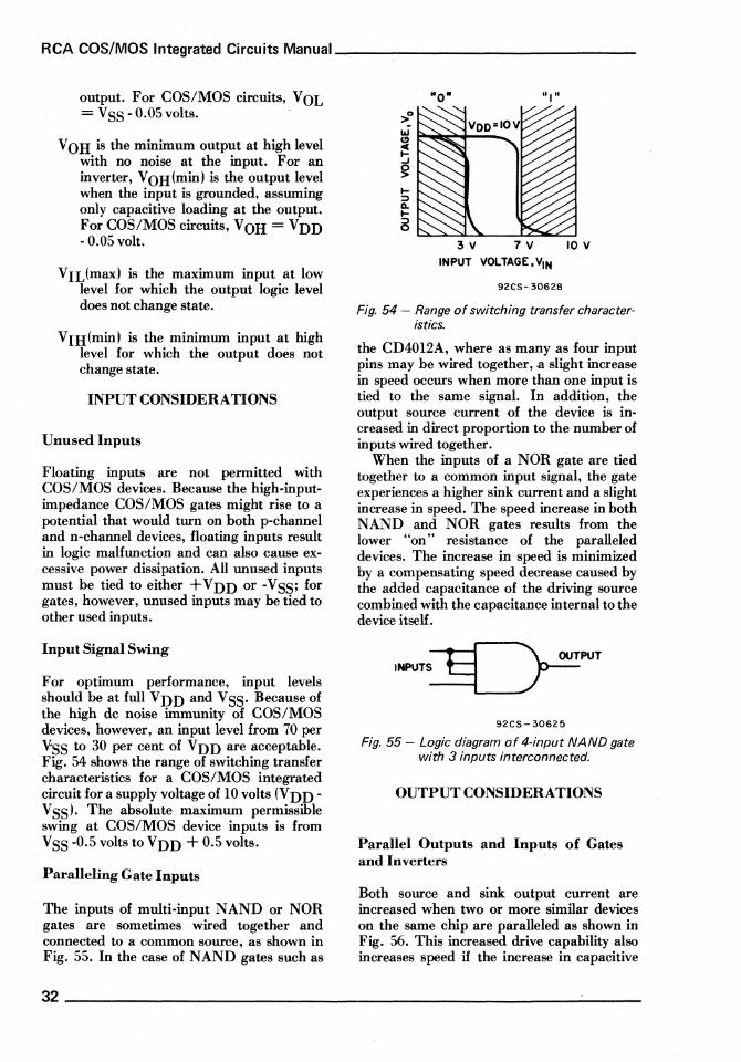
For optimum performance, input levels should be at full VDD and VSS. Because of the high dc noise immunity of COS/MOS devices, however, an input level from 70 per ¥SS to 30 per cent of VDD are acceptable. Fig. 54 shows the range of switching transfer characteristics for a COS/MOS integrated circuit for a supply voltage of 10 volts (VDDVSS). The absolute maximum permissible swing at COS/MOS device inputs is from VSS -0.5 volts to VDD + 0.5 volts.
Paralleling Gate Inputs
The inputs of multi-input NAND or NOR gates are sometimes wired together and connected to a common source, as shown in Fig. 55. In the case of NAND gates such as
3V 7 V 10 V
INPUT VOLTAGE. VIN
92CS-30628
Fig. 54 - Range of switching transfer characteristics.
the CD4012A, where as many as four input pins may be wired together,.a slight increase in speed occurs when more than one input is tied to the same signal. In addition, the output soUrce current of the device is increased in direct proportion to the number of inputs wired together.
When the inputs of a NOR gate are tied together to a common input signal, the gate experiences a higher sink current and a slight increase in speed. The speed increase in both NAND and NOR gates results from the lower "on" resistance of the paralleled devices. The increase in speed is minimized by a compensating speed decrease caused by the added capacitance of the driving source combined with the capacitance internal to the device itself.
U .. ___ ~T INPUTS_ ~ J 92CS-30625
Fig. 55 - Logic diagram of 4-input NAND gate with 3 inputs interconnected.
OUTPUT CONSIDERATIONS
Parallel Outputs and Inputs of Gates and Inverters
Both source and sink output current are increased when two or more similar devices on the same chip are paralleled as shown in Fig. 56. This increased drive capability also increases speed if the increase in capacitive
32 ____________________________________________________ ___
___________________ Handling and Operating Considerations
INPUTS
OUTPUT
(a)
INPUTS
OUTPUT
( b)
INPUT OUTPUT
ee) 92CS- 30627
Fig. 56 - Typical device paralleling arrangements: (a) NOR gates, (b) NAND gates, (c) inverters.
loading is not excessive. When devices are parallel, power dissipation also increases. (Because of variations in threshold voltages between different chips, paralleling should be limited to devices on the same chip only.)
Capacitive Loading
CMOS logic systems should be designed to minimize capacitive loading. Capacitive loading decreases speed and increases power dissipation. In the design of a system, it should be realized that one COS/MOS unit load imposes a capacitance of 7.5 picofarads across the output of the COS/MOS circuit.
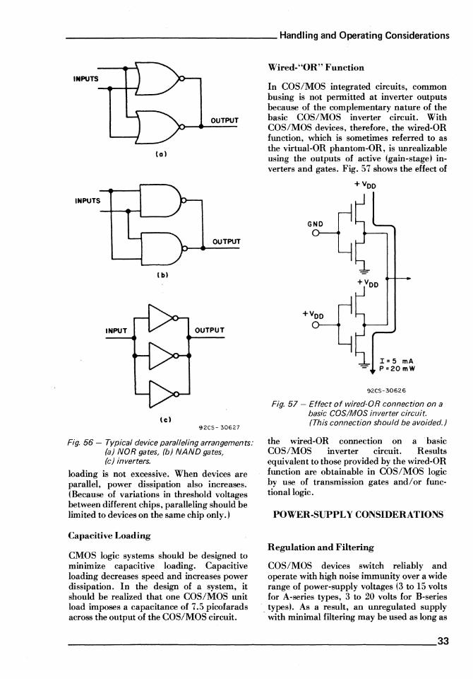
Wired-"OR" Function
In COS/MOS integrated circuits, common busing is not permitted at inverter outputs because of the complementary nature of the basic COS/MOS inverter circuit. With COS/MOS devices, therefore, the wired-OR function, which is sometimes referred to as the virtual-OR phantom-OR, is unrealizable using the outputs of active (gain-stage) inverters and gates. Fig. 57 shows the effect of
+voo
+~ I= 5 mA P=20 mW
92CS-30626
Fig. 57 - Effect of wired-OR connection on a basic COS/MOS inverter circuit. (This connection should be avoided.)
the wired-OR connection on a . basic COS/MOS inverter circuit. Results equivalent to those provided by the wired-OR function are obtainable in COS/MOS logic by use of transmission gates and/or functionallogic.
POWER-SUPPLY CONSIDERATIONS
Regulation and Filtering
COS/MOS devices switch reliably and operate with high noise immunity over a wide range of power-supply voltages (3 to 15 volts for A-series types, 3 to 20 volts for B-series
. types). As a result, an unregulated supply . with minimal filtering may be used as long as
____________________________________________________ 33

RCA COS/MaS Integrated Circuits Manual ________________ _
the maximum voltage limits are not exceeded and the minimum voltage (combination of lowest V D D from unregulated supply and lowest peak of ripple) is sufficient for the required system speed. In other words, maximum system speed is dictated by the minimum power-source excursion. Information on switching speed as a function of supply voltage and load capacitance is given in the published data for COS/MaS integrated circuits.
Battery Operation
Because of- their wide voltage range, COS/MaS logic circuits can be operated directly from inexpensive batteries which have a wide voltage excursion from beginning to end of life. The high noise immunity of COS/MaS devices provides another advantage in battery operation because the internal impedance of a battery is usually
. greater than that of most power supplies.
Zener-Diode-Reference Operation
Operation from zener-diode references not only protects COS/MaS devices from momentary line transients, but can also provide an effective power-supply source from dc sources which exceed maximum device voltage, such as a 28-volt aircraft supply. In the design of zener regulators such as that shown in Fig. 58, both the peak
Voo = 28 V R 10 V I LOAD COS/MOS LOGIC
~ SYSTEM I SOURCE
C
92C5- 30614
Fig. 58 - Zener regulator circuit.
switching currents and the rise and fall times of current must be considered in calculation of the Rand C values.
CLOCK REQUIREMENTS
All sequentially operated. static COS/MaS integrated circuits require a single-phase
clock. The amplitude of the clock pulse should be equal to the single power-supply voltage VDD' Fig. 59 shows the clock-edge
CLOCK EDGE REQUIREMENTS
TRANSITION 0 AND J-K FLIP-FLOPS
POS 7 ALL SHIFT REGISTERS EXCEPT ITIV Co4006A
ALL SYNCHRONOUS COUNTERS
=\ ALL BINARY RIPPLE COUNTERS NEGATIVE 18-STAGE SHIFT REGISTER,
Co4006A
-, r-OPTIONAL',,' STROBED LATCH, Co4042A
" _J \._ 92C5-30605
Fig. 59 - Clock-edge requirement for CD4000-series COS/MaS integrated circuits.
requirements for flip-flops, shift registers, counters, and latches included in the CD4000 series of COS/MaS integrated circuits.
Clock rise and fall times should not exceed 5 to 15 microseconds (depending on supply voltage) because of circuit design and possible cascading considerations. Minimum clock pulse width and maximum operating frequency are functions of the supply voltage and the type of device. Clock requirements for COS/MaS integrated circuits are given in the published data.
CASCADING CONSIDERATIONS
When sequential COS/MaS circuits such as flip-flops and shift registers are connected in cascade, the designer must take care that data .. ' are not lost in the transfer between different devices. Variations in the range, of input switching levels and flip-flop time constants may result in a loss of data.
The input switching level of an active COS/MaS circuit has a 4-volt range (3 to 7 volts) for operation from a 10-volt supply, as shown earlier in Fig. 54. This range of switching levels is the result of the range of threshold variations inherent in present MaS technology. Although these variations present no problem in dc logic usage, they can affect error-free cascading of shiftregister stages.
34 ___________________________________________________ _
__________________ Handling and Operating Considerations
Fig. 60 shows an extreme example. In the circuit shown, stage QI triggers at a lower voltage level than stage Q2. With the slow clock rise time shown, the output of Ql changes before any change occurs in Q2; the input to D of Q2, which should be high, has gone low before Q2 switches, and an error results in the output of Q2.
If two or more COS/MOS flip-flops (e.g., CD4013 or CD4027) or shift registers (e.g.,
0 01
r--
CL
CL ,
CD4006 or CD4014) are cascaded, the clock rise time should be made less than the total of the fixed propagation delay plus the output transition time, as determined from the published data for the specific capacitive loading condition. For several shift-register device types such as in the CD4031, CD4094, or CD40107 this problem is avoided by the use of an internal delayed clock output or outputs clocked by CL.
0 02 r---
~------------YDD
\ SWITCHING POINT· 0.3 YDO
---.--
92CS-30615
Fig. 60 - Error effect that results from a slow clock in cascaded circuits.
_________________________________________________________ 35
RCA COS/MaS Integrated Circuits Manual ______________ _
V. Interfacing COS/MOS
Proper interfacing between different logic families requires that the circuits selected operate at a common supply voltage and have logic-level compatibility. In addition, the devices must maintain safe power-dissipation levels and good noise immunity over the specified operating-temperature range. This chapter, after discussing the relationship between positive- logic and negative-logic systems, covers interfacing COS/MOS circuits with p-channel MOS, n-channel MOS, saturated bipolar logic (TTL, HNIL, DTL, and ECL) systems, and with discrete and electromechanical devices.
POSITIVE/NEGATIVE LOGIC CONVERSION
All published data and application information for COS/MOS circuits reference positive-logic functionality. The relationship between positive and negative logic can be explained with the aid of Table XI, a voltage
Table XI - Voltage Truth Table
Inputs Output
X Y f(x,Y)
L L H
L H L
H L L
H H L
Possible Logic Assignments
Positive: H = logical 1 L = logical 0
Negative: H = logical 0 L = logical 1
truth table. In this table, H represents a high voltage and L a low voltage, X and Y represent inputs, and f(x,y) is the output. If the higher level, H, is assigned the value of logical I, the circuit is said to operate under positive logic. If logical I is assigned to the lower level, L, the logic is negative.
Table XII - Logic Tables
Positive Logic Negative Logic L = 0, H = 1 L=l,H=O
NOR Function NAND Function
X Y f(x,y) X Y flx,y)
0 0 1 1 1 0 0 1 0 1 0 1 1 0 0 0 1 1 1 1 0 0 0 1
f(x,V) =X·Y f(x,y)=X+Y =X+Y = X· Y
The POSItIve and negative logic tables corresponding to the voltage truth table of Table XI are shown in Table XII. A positive-logic NOR gate and a negative-logic N AND gate represent two functions reversed in assignment. Therefore, a COS/MOS CD4001 quad two-input NOR gate used in a negative-logic system acts as a quad twoinput NAND gate. A CD4011 quad twoinput NAND gate acts as a quad two-input NOR gate in a negative-logic system.
The CD4024 is a seven-stage binary counter. In negative logic, the reset acts as a set and will set on a logical O. Because the reset acts as a set, the output is alII's instead of O's, and the counter becomes a downcounter. Fig. 61 shows how some typical
36 __________________________________________________ ___

_______________________ Interfacing COS/MaS
COS/MOS circuit symbols are represented in positive and negative logic systems.
POSITIVE LOGIC NEGATIVE LOGIC
=D- =D-CD40llA
CD400lA
CD4024A
92CS- 30331
Fig. 61 - Common symbols for COS/MOS devices in positive- and negativelogic systems; symbols apply equally to all device types in a series.
INTERFACING WITH P-CHANNEL MOS
P-channel MOS systems utilize negative logic. P-channel MOS-transistor logic levels generally are -6 volts for low-threshold types and -IS volts for high-threshold types. Direct interface with COS/MOS logic circuits is achieved by operating the COS/MOS circuit at a V DD of zero volts and a V SS of either -6 or -IS volts, as required.
Silicon-gate PMOS static shift registers operating from 5-volt and -12-volt supplies are directly compatible with a COS/MOS system operating from the 5-volt supply with V SS at zero volts. The only additional component required is a clamp diode to V SS on the data output; as shown in Fig. 62, because the unloaded PMOS output voltage will go negative in the low output state.
OV +5 V -12 V
Voo
COS/MOS SYSTEM
1-----+1 INI
I------~ IN2
I-----~ RECIRCULATE
I-----~ 4>IN
14---10----; OUT I
14---ir----'---; OUT 2
IN914 IN914
92CS-24642
Fig. 62 - COS/MOS-to-PMOS static-shiftregister interface.
INTERFACING WITH N-CHANNEL MOS
N -channel MOS-transistor logic levels are positive and within the voltage range of COS/MOS devices. Therefore, direct interface is possible.
The increasing use of n-channel MOS memories has brought about considerable interfacing between COS/MOS and NMOS circuits. In a system of I-kilobit memories, such as the type 2102, which employ peripheral COS/MOS circuits for address, read/write, chip select, and data handling, the COS/MOS circuits can be supplied from the 5-volt power supply of the memory. Inputs to the memory are then COS/MOScompatible, and direct interface is permitted. The data output requires only a single pullup resistor, RX, as shown in Fig. 63, to
OV +5 V OV 0 9 IGNO Vss Ivoo Vccl
... AO TO A7
(TYPE 2102)
COS/MaS OI SYSTEM R/W
CE
DO
> ~RX
6 92CS-24640
+5 v Fig. 63 - Direct interface between COS/MOS
and a 1-kilobit memory, type 2102.
__________________________________________________ 37

RCA COS/MOS Integrated Circuits Manual ______________ _
assure an acceptable high-state output voltage.
A 4-kilobit dynamic n-channel RAM, such as the 2107A, has 12-volt and -5-volt supplies as well as the 5-volt V8C supply, as shown in Fig. 64. The COS 1M S peripheral circuitry
OV
12-VOLT COS/MOS SYSTEM
CD4050A BUFFERS
FROM 12 V TO 5 V
-1-5 V -5 V +12 V
OV
VDD Vcc VSS VEE
n-CHANNEL DYNAMIC RAM
(2107A)
~----------~CE DO 12V VDO
5V VCC
'--------\1/4 C040109B 1-------'
= 92CS-24641RI
Fig. 64 - Interface from COS/MaS to an n·channel dynamic RAM.
this system is probably best operated from the 12-volt supply to assure good speed characteristics and noise immunity. The 5-volt input signals to the memory are provided by CD4050 buffers powered by the 5-volt V CC supply. The 12-volt-swing chip-enable signal is directly compatible with the 12-volt COS/MOS system. The data output uses a single level shifter from a CD40109B to generate the required 12-volt logic swing; memories added to provide an increase in word capacity are wire-OR'ed at the data output pin of the memory.
(Further information on memory interfacing is given in Chapter XI, Introduction to Microprocessors and Memory Interfacing.)
Practically all recent developments in NMOS LSI technology are using the NMOS Depletion Load process. NMOS Depletion Load devices, unlike previous NMOS types, require only a single power supply with a voltage ranging from 5 to 7 volts. Direct interfacing of COS/MOS devices to NMOS Depletion Load inputs, therefore, can be
accomplished. However, because of V OH specification of approximately 50 per cent of VDD, all NMOS Depletion Load device outputs require a pull-up resistor similar to that shown in Fig. 63.
INTERFACING WITH SATURATED BIPOLAR LOGIC
A need arises to interface COS/MOS logic with higher-speed, saturated bipolar logic when system logic speeds exceed 5 to 10 MHz. Optimum efficiency in system design is achieved by directly but alternately interfacing COS/MOS circuits and DTL or TTL circuits, i.e., taking full advantage of the superior COS/MOS logic characteristics at lower logic speeds and the high-speed capability of saturated ~ipolar logic where required.
COS/MOS and TTL
When TTL· devices are interfaced with COS/MOS devices with a common power supply of 4.5 to 5.5 volts, the guaranteed active-pull-up TTL output voltage of 2.4 volts is lower than the minimum COS/MOS input voltage required to guarantee switching (3.5 volts), as shown in Fig. 65. This dif-
TTL COS/MOS
0.4 v h-z2~zJ~L~~!.... o v L; ""-'-L.L.<:...o 0 v
LOGIC 0 OUTPUT
9ZCS- Z~26'
Fig. 65 - TTL·to-COS/MOS voltage levels.
ference is overcome by the use of an external resistor RX, as shown in Fig. 66, which also serves as the resistor for open-collectoroutput TTL at a VDD of 5 volts. The minimum value of R X is fixed by the maximum sink current (e.g., 1.6 milliamperes for 74-series TTL and 36 milliamperes for 74LS-series TTL), and its maximum value is determined by IOH' the "off"
38 __________________ ~---------------------------------

_______________________ Interfacing COS/MaS
4.5 TO 5.5 V
92C5-24634
Fig. 66 - TTL-to-COS/MOS interface.
leakage of the output sink transistor. As shown in Table XIII, values of RX between 1.5 and 4.7 kilohms are suitable for all the
Table XIII - Values of RX for TTL-COS/MOS Interface
Characteristic 74 749 74L 74LS 74S
RX min. (ohms) 390 270 15k 820 270 RX max. (kilohms) 4.7 4.7 27 12 4.7
TTL families under worst-case conditions. Because the COS/MOS input impedance is essentially capacitive, many COS/MaS inputs may be driven by a single TTL output; the actual number depends on the frequency of operation.
In the COS/MOS-to-TTL interface shown in Fig. 67, the requirement is to sink sufficient current in the low output state at a maximum output voltage of 0.4 volt. Table XIV shows the current-sinking capability of
4.5 TO 5.5 V
92CS -25252
Fig. 67 - COS/MOS-to- TTL interface.
some CD4000-series devices. All B-series types have the same standard output drive and are capable of sinking one low-power Schottky load, worst case (0.36 milliampere at VOUT = 0.4 V and VDD = 5 V). For higher-power TTL types, the CD4049 and CD4050 buffers may be used. Table XV shows the minimum and typical buffer fanout for each TTL family. These buffers
Table XV - Fanout of CD4049A and CD4050A Buffers to TTL
TIL Family Buffer Fanout 74 749 74L 74LS 74S
Minimum Typical
1 3
1 2
14 28
7 14
1 2
take their power from the 5-volt TTL supply and have the additional advantage of being able to accept input voltage swings of 5 to 15 volts from the preceding COS/MaS system.
In many instances, the designer may wish to use the high-speed capability of a bipolar device with the high-voltage capability of a COS/MOS device. This combination can
Table XIV - Minimum Current-Sinking Capability of COS/MaS Devices
COS/MOS Sink Current (rnA at 25°C Type Description Vo = 0.4 Volt, VDD = 5 Volt)
Ceramic Plastic
CD4000A Dual 3-Input NOR Gate Plus Inverter 0.4 0.3 CD4001A Quad 2-Input NOR Gate 0.4 0.3 CD4002A Dual 4-Input NOR Gate 0.4 0.3 CD4007A Dual Complementary Pair Plus Inverter 0.6 0.3 CD4009A/49A Inverting Hex Buffer 3.0 3.0 CD40l0A/50A Non-Inverting Hex Buffer 3.0 3.0 CD40llA Quad 2-Input NAND Gate 0.2 0.1 CD40l2A Dual 4-Input NAND Gate 0.1 0.05 CD4041A Quad True/Complement Buffer 0.4 0.2 CD403lA 64-Stage Static Shift Register 1.3 1.3 CD4048A Expandable 8-Input Gate 1.6 1.6 CD4XXXB Any B-Type Device Output 0.4 0.4
39

RCA COS/MaS Integrated Circuits Manual _______________ _
easily be achieved by the use of the CD40109B quad low-to-high voltage level shifter, as shown in Fig. 68. The interface
5 VOLTS Q
of the HNIL circuit enable it to interface directly with the COS/MOS input with good noise immunity.
18 VOLTS (
+--_.--~--;-I----__,--- - --I I .-,~--~
<:R ~RI ?' , VCC I
I VDD , CMOS CIRCUITRY
INPUT, I 11'--1 (I) LOW POWER TTL CIRCUITRY (II HIGH SPEE D (2) HIGH CURRENT DRIVE
ILEVEL ~ (2) HIGH VOLTAGE 1_~.....--;t.I_SH_I_FrTE-R--1 I, (3) HIGH NOISE IMMUNITY
'----------,---' ENABL E I J,. : I
1----------' 92CM-30557
1/4 CD40109B
Fig, 68 - Use of level shifter for COS/MOS- to- TTL interface.
from the low-voltage circuitry (if bipolar) would have to include the resistor R to modify the inputs to the CD40109 so that they are COS/MOS-compatible.
In a system using a COS/MOS supply voltage greater than 5 volts, speed and noise immunity can be improved by use of highvoltage open-collector TTL circuits such as the 7416, 7417, or 7426, as shown in Fig. 69. The value of the pull-up resistor R X depends on the value of VDD; at 10 volts, 39 kilohms would he suitable.
+5 V +5 TO +15 V
Fig. 69 - TTL-to-COS/MOS interface at a VDD greater than 5 volts.
COS/MOS and HNIL The wide operating-voltage range and low power consumption of COS/MOS circuits enable them to operate from the 12-volt power supply used for HNIL (high-noiseimmunity logic) circuits. Most CD4000-series circuits will drive the HNIL input directly; in the circuit shown in Fig. 70, for example, the CD4081B output sinks the· required 1.4 milliamperes at an output voltage typically less than 0.5 volt. The output-voltage levels of 0.8 volt and 10 volts
+12V
9
92CS- 24637
Fig. 70 - COS/MOS-to-HNIL·to-COS/MOS interface.
COS/MOS and DTL
A COS/MOS-to-DTL interface requires a buffer, such as the CD4049 shown in Fig. 71, to sink the DTL input current of 1.5 milliamperes at 0.4 volt. Fanout to DTL
+5 V
92CS-24647
Fig. 71 - COS/MOS·to-DTL·to-COS/MOS interface.
circuits depends on the sink current capability of the COS/MOS buffer used. For the CD4049 and CD4050, typical fanout is 3.
A DTL-to-COS/MOS interface requires no special consideration because the internal pull-up resistor in DTL circuits and the extremely low input current of COS/MOS circuits assure a high logic level almost equal to the power-supply voltage.
40 ________________________________________________ _
__________ -------------Interfacing COS/MaS
COS/MOS and ECL
COS/MOS and ECL (emitter-coupled logic) forms can be operated from a common -5-volt ( ± 1 V) supply. However, level-shift interface circuits are required in both directions. Fig. 72 illustrates the COS/MOS-to-ECL logic-l and logic-O level interface requirements.
COs/MOS
Vooa ov Vss a - 5V
lEVEL SHIFT
CIRCUIT SEE FIG. 73
Logic 1 Logic 0
OV .(l.BV
·5V
·1.6V
VIN
ECl
92CS·30600
Fig. 72 - COS/MOS·to·ECL interface.
Fig. 73(a) illustrates a simple voltagedivider interface circuit. Calculation of the values of resistors Rl and R2 is based on COS/MOS source- and sink-current capa-
COS/MOS
-5V
-5V (a)
Eel
(b) 92CS-30598
Fig. 73 - (a) COS/MaS and ECL voltagedivider interface; (b) active level translator.
bility and ECL input loading. This interface suffers from poor temperature tracking and low speed. The active level translator of Fig. 73(b) has a high-speed capability and good temperature tracking.
An active interface circuit is required to shift from ECL output logic levels to COS/MOS logic levels. Figs. 74 and 75 illustrate logic-interface and level-shift
Vo
ECl
Voo· ov Vss --5 V
lEVEL SHIFT
CIRCUIT
SEE FIG. 75)
VIN
COS/MOS
92CS-30601
Fig. 74 - Logic interface required to shift from ECL output logic levels to COS/MaS logic levels.
-5V
-0.8 V / -0.8 V I -1.6V -4.2V
-5V
92CS - 30599
Fig. 75 - Level-shift circuit required to shift from ECL output logic levels to COS/MaS logic levels.
circuits, respectively. An important consideration in these interfaces, as well as in the COS/MOS-to-ECL interface of Figs. 72 and 73, is operation from the common -5-volt supply.
IC level shifters that translate between TTL or DTL logic levels and ECL logic levels are commercially available. Both +5-volt and -5-volt power-supply voltages must be provided when these level shifters are used. COS/MOS CD4049 and CD4050 hex
___________________________________________________ 41

RCA COS/MOS Integrated Circuits Manual ______________ _
buffers may be required to drive the TTL-toECL level-shifter IC's. In this case, a third power supply (up to + 18 volts) may he used to power the COS/MOS logic circuits.
Level Shifting
Four COS/MOS buffers (CD4009, CD4010, CD4049, and CD4050) are designed as level
INPUT
INPUT
n-VDD ...J L GND
(GNO) CONFIGURATION (EACH CIRCUIT):
shifters as well as high-sink-current drivers. This important feature permits operation of COS/MOS logic at supply-voltage values up to + 18 volts and direct interface with TTL or DTL circuits at +5 volts. Fig. 76 shows the schematic diagrams of the CD4009 and CD4010 buffers; VDD is the COS/MOS logic-level voltage and V CC is the +5-volt TIL or DTL connection. Fig. 77 shows the
(0)
Vee
OUTPUT
U Vee -GND
OUTPUTTI-Vee _GND
HEX COS/MOS TO DTL OR TTL CONVERTER (NON -INVERT I NG)
WIRING SCHEDULE: CONNECT VCC TO DTL OR TTL SUPPLY CONNECT VOO TO COS/MOS SUPPLY
(b) 92C5-30612
Fig. 76 - Schematic diagrams of the (a) CD4009, and (b) CD4010.
42 _____________________________________________________ ___

_______________________ Interfacing COS/MOS
logic-interface connections for logic-level conversion. The system advantage of this configuration is manifested in the increased logic speed of COS/MOS circuits when
VOO-+IOV
TTL OR DTL
92CS-30613
Fig. 77 - Logic-interface connections for logiclevel conversion.
operated at higher speed than would be possible in an all +5-volt system. Because of their superior input protection networks, the CD4009 and CD40 I 0 may be preferred over the CD4049 and CD4050 in extremely harsh electrical environments. '
INTERF ACING DISCRETE AND ELECTROMECHANICAL DEVICES
Industrial control systems employ greater logic swings than IC logic systems, such as COS/MOS, to achieve high noise immunity, to enable them to operate from readily available high-voltage supplies, and to, interface with electromechanical equipment.
Fig. 78 shows a simple resistive-divider circuit used to interface a system having a 24-volt logic swing to COS/MOS. The circuit could readily be modified for even higher voltage swings. The capacitor filter enhances the excellent noise immunity of the COS/MOS logic, and the two clamp diodes keep the input signal voltage between VDD and VSS. An alternate circuit using a zener diode is shown in Fig. 79.
A single-transistor level converter interfacing a COS/MOS device to an industrial control system is shown in Fig. 80. The transistor is driven directly from the COS/MOS device output.
INDUSTRIAL CONTROL-24 VOLT LOGIC
SYSTEM
24 VOLT LOGIC SWING
150 k
+10 V COS/MOS SUPPLY
Fig. 78 - Interface from industrial control to COS/MOS.
INDUSTRIAL CONTROL SYSTEM
Vz = VDD 92CS-24644
Fig. 79 - Zener-diode industrial control interface.
+24 V
INDUSTRIAL SWING CONTROL
24-VOLT LOGIC SYSTEM
92CS-24645
Fig. 80 - COS/MOS-to-industrial-control interface.
Schmitt Trigger Usage
The RCA-CD4093B Schmitt trigger is described in detail in Chapter VI Astable and Monostable Multivibrators. Two of its properties, high noise immunity and speedup of slow pulse edges, are very useful in interfacing with industrial control circuits.
The COS/MOS CD4093B consists of four Schmitt triggers; each of the devices is a twoinput NAND gate with Schmitt action on each input. The hysteresis voltage V H shown
___________________________________ 43

RCA COS/MaS Integrated Circuits Manual _______________ _
in Fig. 81 is typically 0.6 volt for a VDD of 5 volts and 2 volts for a V DD of 10 volts.
=l[)r-1/4C04093B
(.) COS/MOS SCHMITT-TRIGGER
Voo OUTPUT
WAVEFORM
Voo
!~T~~~) IN PUT '--_-:-:-_---'
(b) WAVEFORMS 92CS-24646
Fig. 81 - (a) COS/MOS Schmitt trigger; (b) typical waveforms for Schmitt trigger.
The noise immunity of the COS/MOS NAND Schmitt trigger is very high, typically greater than 50 percent of V DD in each state. It is therefore specially suited for circuits that require a very high noise immunity. Because of the hysteresis built into the Schmitt trigger, it can tolerate noise on a slow input edge without false switching at the output, as shown in Fig. 82. This noise immunity permits the construction of an excellent
ll~ . ~r ,.
.... ",'I n' 2VIOivision 2ms/Division
II, .. ,II
It' '''1l 'I~
1''-• '1~.
~ .... ,UI~ 'I,""
92CS-26637
Fig. 82 - Rejection of noise on slow input edge.
interface from' an industrial environment to a COS/MOS logic system, as shown in Fig. 83.
RI
220 k
R2 TYPICAL VALUE
1M
* SAME AS OTHER INPUT.
92CS-25939
Fig. 83 - Industrial-environment-to-COS/MOS interface.
The CD4093B will function under the most severe conditions of input overvoltage and in spite of noise spikes up to hundreds of volts. The input is kept between V SS and V D by clamp diodes Dl and D2; Rl, typically 220 kilohms, functions as a current-limiting resistor. Resistor R2 ties the logic input to V SS in the event that the interface input is accidentally open-circuited, for example by the removal of a PC board from a system. Capacitor Cl, in conjunction with Rl, acts as a filter and enhances the noise-rejection properties of the interface.
Solenoid Drives
A high-power coil such as the solenoid of a printer hammer, which requires about 1 ampere at 70 volts, may be driven from a COS/MOS system by use of a Darlington transistor, as shown in Fig. 84. Because a typical value of VBE for a type 2N6385 transistor is 1.5 volts at a collector current of 1 ampere and a minimum gain of 1000, the output source transistor of the CD4073B has to supply 1.5 milliamperes. The value of resistor R is selected so that V DS is sufficient to assure this output current. Suitable values of R for use with B-series types are given in Fig. 84 for VDD values of 5, 10, and 15 volts.
SCR and Triac Drives
MOS outputs. A sensitive-gate SCR such as the I06Bl controlling directly 2.5 amperes at reverse voltages up to 600 volts may be controlled directly by a COS/MOS gate such as the CD4069B, as shown in Fig. 85.
44 ______________________________________________________ ___
_______________________ Interfacing COS/MaS
VDD
V DD
S V I k 10 V 4.1k 15 V 8.2 k
+v
II HAMMER SOLENOID
IA --l
I I I I I
12 N6380
I I
92C$-24648
Fig. 84 - COS/MaS system driving a printerhammer solenoid with the aid of a Darlington transistor.
VDD 100 V
106BI
92C5- 24649
Fig. 85 - COS/MaS gate directly driving a sensitive-gate SCR.
SCR's and triacs with gate currents in the milliampere region may be controlled by a buffer such as the CD4049. This buffer could, in turn, be controlled by a COS/MOS system or, as shown in Fig. 86, by an optocoupler to provide greater isolation.
HIGHVOLTAGE
LOGIC
+12 V v+
12 k
l 1/6 CD4049A
I I
92CS- 24650
SCR
Fig. 86 - High-voltage logic to COS/MaS driving an SCR.
In cases where a single-gate output source or sink current is sufficient, the inputs and outputs of gates on the same chip can be paralleled, as shown in Fig. 87. Gates not on
92CS-24651
Fig. 87 - Paralleling inputs and outputs.
the same chip and buffer circuits should not be operated in parallel because variations in transition-point voltage may cause overdissipation.
Relay Drives
The CD4049 buffer may be used to drive a sensitive relay directly, as shown in Fig. 88. Typically, the relay would have a coil resistance of 1100 ohms, and a nominal coil current of 10.9 milliamperes. Operating at 12 volts, the n-channel transistor in the CD4049 would sink the current with a voltage drop of only 0.7 volt. An external diode DI connected between the output and +VDD protects against high transient switching voltages. A similar high-current drive device, CD40I07, is available for high-sink-current applications.
INTERFACING OP-AMPS TO COS/MOS
COS/MOS circuits may be connected directly to the output of an operational amplifier operating between the normal
IS-volt supply rails, as shown in Fig. 89, provided clamp diodes to VDD and VSS are used to make sure the COS/MOS input voltage does not go outside the V 55 and VDD range. Resistor R3 limits the op-amp
_____________________________________________________ 45

RCA COS/MOS Integrated Circuits Manual _______________ _
output current in the event that the op-amp output voltage tends toward the negative rail. Fig. 90 shows a CA 741-type op-amp
operated between VDD and VSS with a resistive divider on the non-inverting op-amp input.
IC LOGIC SOURCE
1----I I GATE I
I
12VDC
r 01 I
I I I I
12A MAX.
I I 12A MAX.
I
I I I
L ___ -.J
I I L _______ -.J CD4049A
I OF 6 IDENTICAL UNITS
RELAY No·1 IIOO-OHM COIL
92CS-30334
Fig. 88 - COS/MaS buffer driving a sensitive relay.
R2 +IOV
-15 V
92CS -24652
Fig. 89 - Interface from split-rail op-amp to COS/MaS gate.
92CS-24653
Fig. 90 - Interface of op-amp and COS/MaS . with common supply rail.
46 ____________________________________________________ ___
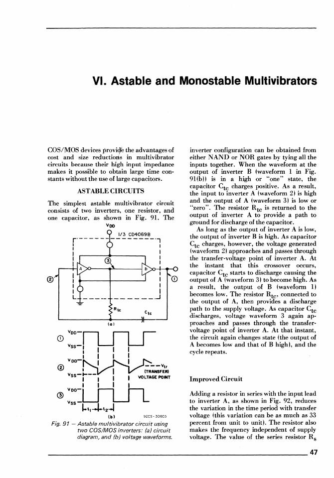
VI. Astable and Monostable Multivibrators
COS/MaS devicesprovi<fe the advantages of cost and size re~'uctio~s in multivibrator circuits because their high input impedance makes it possible to obtain large time constants without the use of large capacitors.
ASTABLE CIRCUITS
The simplest astable multivibrator circuit consists of two inverters, one resistor, and one capacitor, as shown in Fig. 91. The
®
CD
Voo 1/3 CD4069B r'-- ------ ------"l
• 1 • I I I I I
")0-+-...... 0
tal
VDD-1LfLJ
VSS-, I I I I I I I I
VDD-~I ® ---~ I I (TRANSFER)
VSS-;--- , I I VOLTAGE POINT
, I I I VDD-LSUL ® VSS-
1-\.-1.\2-1 (b) 92CS - 30603
Fig. 91 - Astable multivibrator circuit using two COS/MaS inverters: (a) circuit diagram, and (b) voltage waveforms.
inverter configuration can be obtained from either NAND or NOR gates by tying all the inputs together. When the waveform at the output of inverter B (waveform 1 in Fig. 91(b)) is in a high or "one" state, the capacitor Ctc charges positive. As a result, the input to inverter A (waveform 2) is high and the output of A (waveform 3) is low or "zero". The resistor R tc is returned to the output of inverter A to provide a path to ground for discharge of the capacitor.
As long as the output of inverter A is low, the output of inverter B is high. As capacitor Ctc charges, however, the voltage generated (waveform 2) approaches and passes through the transfer-voltage point of inverter A. At the instant that this crossover occurs, capacitor Ctc starts to discharge causing the output of A (waveform 3) to become high. As a result, the output of B (waveform 1) becomes low. The resistor Rtc ' connected to the output of A, then provides a discharge path to the supply voltage. As capacitor Ctc discharges, voltage waveform 3 again approaches and passes through the transfervoltage point of inverter A. At that instant, the circuit again changes state (the output of A becomes low and that of B high), and the cycle repeats.
Improved Circuit
Adding a resistor in series with the input lead to inverter A, as shown in Fig. 92, reduces the variation in the time period with transfer voltage (this variation can be as much as 33 percent from unit to unit). The resistor also makes the frequency independent of supply voltage. The value of the series resistor Rs
_____________________________________________________ 47
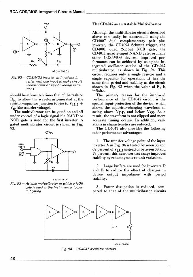
RCA COS/MaS Integrated Circuits Manual _______________ _
Voo
92CS-30602
Fig. 92 - COS/MaS inverter with resistor in series with one input to make circuit independent of supply-voltage variations.
should he at least ten times that of the resistor Rtc to allow the waveform generated at the resistor-capacitor junction to rise to VDD + Vtr (the transfer voltage).
The multi vibrator can be gated on and off under control of a logic signal if a NAND or NOR gate is used for the first inverter. A gated multivibrator circuit is shown in Fig. 93.
etc
92CS-30604
Fig. 93 - Astable multivibrator in which a NOR gate is used as the first inverter to permit gating.
The CD4047 as an Astable Multivibrator
Although the multivibrator circuits described above can easily be constructed using the CD4007 dual complementary pair plus inverter, the CD4093 Schmitt trigger, the CD4001 quad 2-input NOR gate, the CD4011 quad 2-input NAND gate, or many other COS/MOS devices, improved performance can be achieved by using the integrated oscillator section of the CD404 7 multivibrator, as shown in Fig. 94. This circuit requires only a single resistor and a single capacitor for operation. It has the same time period and stability as the circuit shown in Fig. 92 when the value of Rs is infinite.
The primary reason for the improved performance of the CD4047 circuit is the special input-protection of the device, which allows the capacitor-charging waveform to swing above VDD and below VSS' As a result, the waveform is not clipped and more accurate timing occurs. In addition, variations in characteristics are reduced.
The CD4047 also provides the following other performance advantages:
1. The transfer voltage point of the input inverter A in Fig. 94 is tested between 33 and 67 percent of VDD instead of between 30 and 79 percent; this narrower test range improves stability by reducing unit-to-unit variation.
2. Large buffers are used for inverters D and E to reduce the effect of changes in device output impedance with period stability.
3. Power dissipation is reduced, compared to that of the multivibrator circuits
92CS- 22676
Fig. 94 - CD4047 oscillator section.
48 ______________________________________________________ ___
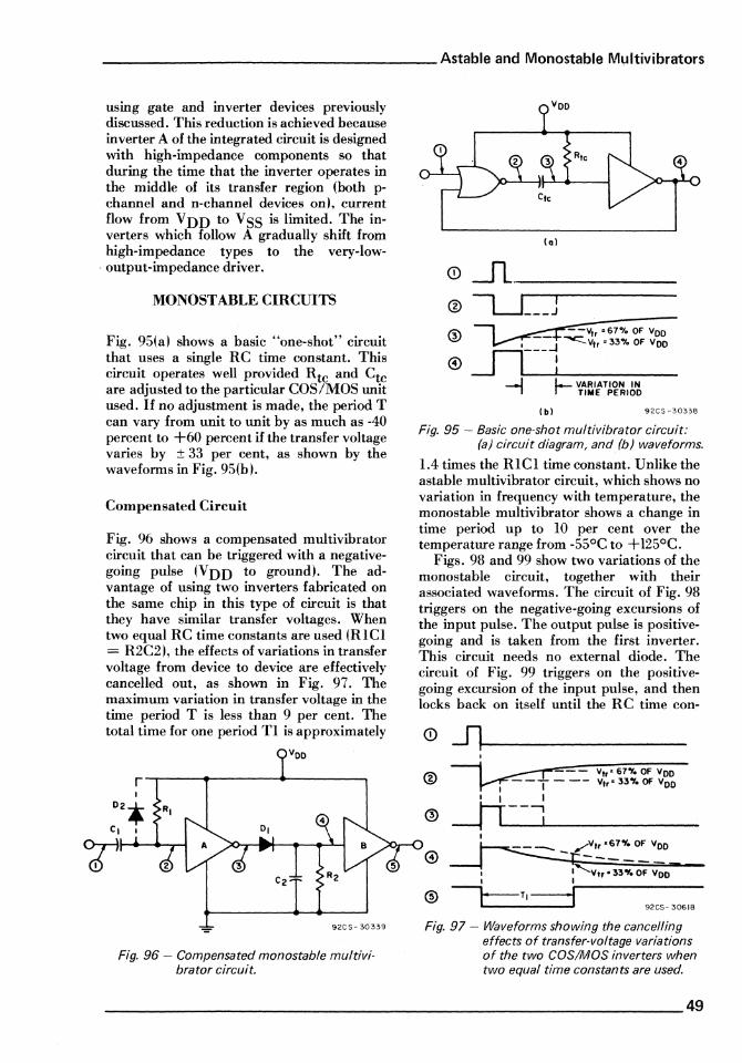
__________________ Astable and Monostable Multivibrators
using gate and inverter devices previously discussed. This reduction is achieved because inverter A of the integrated circuit is designed with high-impedance components so that during the time that the inverter operates in the middle of its transfer region (both pchannel and n-channel devices on), current flow from Vnn to VSS is limited. The inverters which follow A gradually shift from high-impedance types to the very-Iow-
, output-impedance driver.
MONOSTABLE CIRCUITS
Fig. 95(a) shows a basic "one-shot" circuit that uses a single RC time constant. This circuit operates well provided Rtc and Ctc are adjusted to the particular COS/MOS unit used. If no adjustment is made, the period T can vary from unit to unit by as much as -40 percent to +60 percent if the transfer voltage varies by ± 33 per cent, as shown by the waveforms in Fig. 95(b).
Compensated Circuit
Fig. 96 shows a compensated multivibrator circuit that can be triggered with a negativegoing pulse (Vnn to ground). The advantage of using two inverters fabricated on the same chip in this type of circuit is that they have similar transfer voltages. When two equal RC time constants are used (RICI = R2C2), the effects of variations in transfer voltage from device to device are effectively cancelled out, as shown in Fig. 97. The maximum variation in transfer voltage in the time period T is less than 9 per cent. The total time for one period TI is approximately
Voo
92CS- 30339
Fig. 96 - Compensated monostable multivibrator circuit.
lal
o -11 __________ __ ® L-J ___ J __ -:--:--=-::-:--
--v" =67% OF Voo I ...J ~Vt' =33% OF VOO
@ ~-----~:------------' L VARIATION IN -. I TIME PERIOD
(bl 92CS -30338
Fig. 95 - Basic one-shot multivibrator circuit: (a) circuit diagram, and (b) waveforms.
1.4 times the RICI time constant. Unlike the astable multivibrator circuit, which shows no variation in frequency with temperature, the monostable multivibrator shows a change in time period up to 10 per cent over the temperature range from -55°C to +125°C.
Figs. 98 and 99 show two variations of the monostable circuit, together with their associated waveforms. The circuit of Fig. 98 triggers on the negative-going excursions of the input pulse. The output pulse is positivegoing and is taken from the first inverter. This circuit needs no external diode. The circuit of Fig. 99 triggers on the positivegoing excursion of the input pulse, and then locks back on itself until the R C time con-
o -n~----------I
---1 ~ I v"~. 67"1'. OF VDD ® ~--T--- Vt,·33'Y.OFVDD
1 I (
@ -fi-----'..J,..! ---------------
92CS- 30618
Fig. 97 - Waveforms showing the cancelling effects of transfer-voltage variations of the two COS/MaS inverters when two equal time constants are used.
______________________________________________ 49
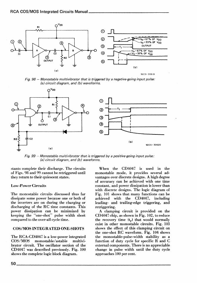
RCA COS/MaS Integrated Circuits Manual _______________ _
__ VIr = 67"4 OF Vee VIr = 33"4 OF Vee
= = (bl (01
92CS- 30619
Fig. 98 - Monostable multivibrator that is triggered by a negative-going input pulse: (a) circuit diagram, and (b) waveforms.
CD Jl'------------I
® r==TI :::1 Q) i--- i =1
• 'I
@j~--tLJc-;:-------® ------------
(b) 92CS-30620
(al
Fig. 99 - Monostable multi vibrator that is triggered by a positive-going input pulse: (a) circuit diagram, and (b) waveforms.
stants complete their discharge. The circuits of Figs. 98 and 99 cannot be retriggered until they return to their quiescent states.
Low-Power Circuits
The monos table circuits discussed thus far dissipate some power because one or both of the inverters are on during the charging or discharging of the R C time constants. This power dissipation can be minimized by keeping the "one-shot" pulse width short compared to the over-all cycle time.
COS/MOS INTEGRATED ONE-SHOTS
The RCA-CD4047 is a low-power integrated COS/MOS monostablel astable multivibrator circuit. The oscillator section of the CD4047 was described previously. Fig. 100 shows the complete logic block diagram.
When the CD4047 is used in the monostable mode, it provides several advantages over discrete designs. A high degree of accuracy can be achieved with one time constant, and power dissipation is lower than with discrete designs. The logic diagram of Fig. 101 shows that many functions can be achieved with the CD4047, including leading- and trailing-edge triggering, and retriggering.
A clamping circuit is provided on the CD4047 chip, as shown in Fig. 102, to reduce the recovery time (tr ) that would normally exist in other monostable circuits. Fig. 103 shows the effect of this clamping circuit on the one-shot RC waveform. Fig. 104 shows the monostable-pulse-width stability as a function of duty cycle for specific Rand C external components. There is no appreciable change in pulse width until the duty cycle approaches 100 per cent.
50 ____________________________________________________ ___

C-TlMING
r-------I RC I COMMON
I >--=::..:..::==---+-~ ASTABLE
4 ASTABLE
GATE CONTROL
Astable and Monostable Multivibrators
92CS-29071
Fig. 100 - CD4047 logic block diagram.
+TRIGGER
-TRIGGER
VDD@
vss(f)-
EXTERNAL RESET
CAUTION: TERMINAL 3 IS MORE SENSITIVE TO STATIC ELECTRICAL DISCHARGE. ** SPECIAL RC COMMON EXTRA HANDLING PRE-
COSIMOS PROTECTION ---
VDD
* INPUTS PROTECTED BY ~ ~~.,."........ PROTECTION NETWORK CAUTIONS ARE RECOMMENDED.
NETWORK
92CM - 29042
VSS
Fig. 101 - CD4047 logic diagram.
A disadvantage of the clamping circuit is that it introduces additional capacitance at the RC common node (pin 3), which may be noticeable for short pulse widths in the monos table mode only. Some diffusion
capacitance present at the base of the n-p-n transistor is used to charge the capacitor C to VDD quickly after the one-shot cycle has terminated. This capacitance is multiplied by the beta of the transistor and is in parallel
____________________________________ ~ _________________ 51
RCA COS/MaS Integrated Circuits Manual _______________ _
I
COIFFUSION * I ~
Voo
92CS-22667
Fig. 102 - CD4047 clamping circuit.
I- + z w o a:
I
~ 0 I
>o : - I ::> o ~ i!: -2
z S! !< -3 :; w o
-4 o
-r---r---r--r--
10 20 30 40 50
2VOO--,.-----------------------
VTR+VOO --+-'...-----------.....----------VoO--~~~--------~-~~---
~R--------~~--~7E~--_+---
VSS-----------r~--~----~---
VTR-VOO __________ -L ____ -+-____ _+---
92CS-22666
Fig. 103 - CD4047 one-shot RC waveform.
I C=IOOOpF -
--....... R=IMn
C=IOOO~ -- R=IOO kn '\ " ~ ,I \
C=IOO~ R=IO kn
\
60 10 80 90 100
DUTY CYCLE -PERCENT 92CM-22659
Fig. 104 - CD4047 monostable accuracy as a function of duty cycle.
with the external capacitor C during the time interval that the transistor is on (V D D - V BE < t < VBEI. As a result, when values of C less than 1000 picofarads are used, the actual pulse width is longer than may have been calculated. Fig. 105 shows actual typical pulse widths as a function of external capacitance. The minimum values of C shown in the graph are the smallest that can be used with the CD4047 to assure proper operation of the circuit.
SCHMITT-TRIGGER MULTIVIBRATOR CIRCUITS
The COS/MOS Schmitt trigger circuit CD4093B accepts inputs with slow rise and fall times and produces output waveforms wit~ very fast edges. It has higher ac and dc noise immunity than other COS/MOS gates
and a lower power dissipation for comparable slow-input signals. Because of these features, it can be used to advantage in multivibrator circuits.
CD4093B Characteristics
The RCA-CD4093B consists of four Schmitt triggers, as illustrated in the functional diagram of Fig. 106. Each of the four devices is a two-input NAND gate with Schmitt action on each input, yielding a typical hysteresis voltage of 2 volts with a 10-volt supply without the need for any external components.
Fig. 107 shows the logic diagram for one of the four Schmitt triggers in the CD4093B. Each input has the standard COS/MOS input protection network and each output is double buffered.
52 ____________________________________________________ ___
----------________ Astable and Monostable Multivibrators
A--'t---,
B
4 K---t---,
C
0-+--'
en a
100
~ 10 <.> OJ en o a: <.> :i I z 5 ~
8
6
4
2
0 8
6
4
2
OJ en -.I :::J Q.
10 8
6
4
2
I
R'I~,,11 A
~ ~'3~~ ~' 1'1
i,.-"i" " / R-IOk
---" " ~~ /'1 MEASURED - " .t!!. IL A I I ~ i"""" //
MEASURED - io' LV MEALR~D " 1-"'1' " " .-!-~ " ~
I .' if THEORJ," THEORJ" THEOR,l"
468 10 468 100 4 6 81000 CAPACITANCE- PICOFARADS
92CS-22660
Fig. 105 - CD4047 pulse width as a function of capacitance,
H
G
L-.-f':'!--M
L
L--+=--F
1(5,B,12)
2(6,9,13)
* ALL INPUTS PROTECTED BY COs/MOS PROTECTION NETWORK
Vss 7 M=G'H
,--_+B_ E
VDO
92CS'23881 Vss
92CS-23BBO
Fig. 107 - Logic diagram for one of the four Schmitt triggers in the CD40938.
Fig. 106 - CD40938 Schmitt trigger functional diagram.
Fig. 108 shows the transfer characteristic of the Schmitt trigger. The general shape of this characteristic is the same for all values of Vnn, but the relative values of the positivegoing signal switching point Vp, the negative-going signal switching point V N, and the difference hetween them VH (or the hysteresis voltage) change with Vnn. As the input is increased from zero (V SS), the output remains high (Vnn) until Vp is reached. At this point the output goes low
VOUT
Vool----. ..... -.,
92CS-25811
Fig. 108 - Transfer characteristic of the CD40938 Schmitt trigger.
------------------------____________________________ 53
RCA COS/MaS Integrated Circuits Manual _______________ _
(VSS) and remains low as the input voltage is raised to Voo. If the input voltage is then reduced, the output stays low (VSS) until VN is reached. At this point the output goes high (VOO) and remains high as the input voltage is reduced to zero (V SS). The hysteresis voltage VH is typically 0.6 volt for a VOO of 5 volts and 2 volts for a VOO of 10 volts. Fig. 109 shows typical hysteresis voltage as a function of supply voltage.
noise immunity in each state exceeds· the supply voltage for pulses shorter than 200 nanoseconds. The energy noise immunity is the product of noise-pulse voltage, noisepulse time, and the appropriate value of the output drive current for the device under tes~ the units of energy are nanojoules (10-joule). At each value of supply voltage, the curves in Fig. 112 show a minimum value. The value of the minimum· energy noise
AMBIENT TEMPERATURE (TA)o25°C
.... ~ u a: ~25 I
~20 x
%1 8 > > - 15 III
iii :5 10 .... III >:I:
5
o 5 10 15 20 SUPPLY VOLTAGE (Voo)-V
92CS-Z4832RI
Fig. 109 - Typical hysteresis as a function of supply voltage.
Fig. 110 shows the input/output characteristics of the C04093B; the output characteristic shown is the same for any COS/MOS device, including the Schmitt trigger. The input characteristic is unique to the Schmitt trigger and shows that when the C04093B is driven by another COS/MOS device it has more than 50-per-cent noise immunity in each state.
Figs. 111 and 112 show measurements of voltage and energy noise immunity for the Schmitt trigger. For a VDD of 5 volts, the
immunity increases with increasing VDD and occurs at a lower value of noise-pulse width.
Another important property of the Schmitt trigger is illustrated in Fig. 113, which compares the supply current consumed by the C04093 with that used by the CD4011 when the input has long rise and fall times. The power dissipated by the Schmitt trigger is clearly much less than that dissipated by the quad NAND gate. Consequently, the Schmitt trigger should be used in ap-
JLVOH V~OD OUTPUT
CHARACTERISTIC INPUT
CHARACTERISTIC
~L 11 ~----------DRIVER LOAD
92CS-23BB3R3
~zn2Z~~~q----VDD-----------~~~~
T ·LOGIC "'I"' jI OUTPUTJ REG ION
------- - Vp - -- --r7":>'""7">.....,....,~,
VOH -------LOGIC "'0"'
- VN ----
OUTPUT j REGION 1 1rz::ZZ2:zzm:zz2f:..L~VO!!::..L - VSS--'-'-"'-~..:....u
Fig. 110 - Input and output characteristics of the CD4093B.
54 __________________________ ~-------------------------
__________________ Astable and Monostable Multivibrators
18 lOW LEVEL 18 HIGH LEVEL
I~
\1 '"
14
~ 0 12 >
\' VOOal5V I ... 10
" \\. I <t ':;
8 0 '--," VOD"IOV > ... 6 '" -'
'" -~ 4 VODaS V
16
'" 14 ~ 0
12 > I ... 10 '" \. <t I--' 8 VOO =15 V 0
\ > , ... '" 6 -' ....... VOO·JOV " ..
-~ 4
'- VOO'SV
2 2
o 100 200 300 400 500 600 o , 100 200 _00 400 500 600 PULSE WIDTH-NANOSECONDS PULSE WIDTH-NANOSECONDS
'32CS-25925 92CS-25926
Fig. 111 - Voltage noise immunity of the CD4093B.
1M 90 LOW LEVEL I i;. 80 x"' j VOO ll15V ... -' .. " ~~ 70
~~ 60 .. z
/ .. I VDO"IOY -'I-
"z "-.. / /' I" ./ ~a 40 i§~ V I~ 30 /" Ill" ~:J: 20 -b if" 10 !Ii! VOO"5V
~ 90 HIGH LEVEL
~'" 8 x",
I VOO"15V .. -' ~~ 70
/ -'0 oz ><t 6 .. " V ",I ~~ 50 I~ / /' ~a 40
/ VVDD>IOV ~~ ./ ~~ 30 - ,/' "''' ,/' 6~ 20 f-""' Zo -----~i 10 .. VOO =5V I-Z .. ..
o 100 200 300 400 500 600 o 100 200 300 400 500 600 PULSE WIDTH-NANOSECONDS PULSE WIDTH-NANOSECONDS
92CS-25927 92C5-25928
Fig. 112 - Energy noise immunity of the CD4093B.
k .....
-(0) CD4093BE: Top vertical - 5 V/Oivision lower vertical - 2 rnA/Division Horizontal - 200 ms/Division
-""'" ~ I-'
l/ r--.... V :--..... r-... ..,.
(b) CD4011AE: Top vertical - 5 V/Division Lower vertical - 2 rnA/Division Horizontal - 200 ms/Division 92CS-26636
Fig. 113 - Power consumption with slow input edge for the CD4093 and the CD4011.
plications in which slow input edges are anticipated.
Slow edges are a common phenomenon in digital systems. Examples include the output from a transducer, the output at the end of a long line, an output with large capacitive load, or the output of a filter. The Schmitt trigger is particularly useful in these ap-
plications in generating a waveform with fast edges. Fig. 114 illustrates the sharpening-up capability of the Schmitt trigger. With an input edge time of 8 milliseconds and an output transition time of 100 nanoseconds, the improvement in edge time is a factor of 107. With longer input edge times the improvement is even greater.
______________________________________________________ 55

RCA COS/MOS Integrated Circuits Manual_' _______________ _
/ "' / \ , , V '" ,'" / "
CD4093BE: 2V/Division 2ms/Division 92CS-26635
Fig. 114 - Sharpening up a slow edge.
Schmitt-Triggered Astable Oscillators
A range of astable oscillators may be easily constructed using the CD4093B COS/MOS quad 2-input NAND Schmitt trigger. Fig. 115 shows the basic circuit and the waveforms associated with it. In this circuit, input and output are at ground potential and capacitor C is discharged before power is applied. When power is applied, the output goes high (VDD) and capacitor C charges through resistor R until Vp is reached; the output then goes low (V SS). C then discharges through R until VN is reached. At this point the output goes high and C again charges through R until it reaches Vp. Thus, the voltage at point A alternately swings between Vp and VN as the output (B) goes high and low.
Schmitt-Triggered Monostable Multivibrators
A typical circuit for a monostable multivibrator using the CD4093B Schmitt trigger is shown in Fig. 116. Monostable operations starts with both inputs high and the output low. A positive pulse turns on the n-channel device in parallel with capacitor C, causing C to discharge through the now low shunt impedance. When the voltage at input point 2 drops to V N the output goes high. When the input pulse goes low, the n-channel device turns off, opening the shunt impedance. Capacitor C then starts to charge through resistor R; when the voltage at input point 2 reaches V p the output goes low.
1/4 CD4093B
VDD~ n ® o JC R
VDD
@~~ I~ vss-Y i ! ! I
®
VDD I I I I
Vss POWER ....j ON
92CS-25936
I-'A -j VDD n r vss-1 L..J
'A -RcIn [~)(~gg=~~)J 50 k.Q S R S I M.Q 100 pF S C S I,...F
FOR THE RANGE OF RAND C GIVEN 2,...s < tA < O.4s
92CS-23887RI
Fig. 115 - CD40938 astable multivibrator.
R I
1/3CD4007A 2 n 3
:DDn J~ 1/4CD4093B
ss Vss
I'~ rI- VDD
...J Lvss
(. VDD ) 'M = RC "" \Voo-Vp
50 k.Q S R S I M.Q 100pFsCs I,...F
FOR THE RANGE OF R ANO C GI VEN 5,...5 < 'M < I.
92CS- 23886RI
Fig. 116 - CD40938 monostable multivibrator.
56 ____________________________________________________ __

VII. Crystal Oscillators for Digital Timekeeping
This chapter on crystal oscillators, together with the two following chapters (VIII. Shift Registers and Counters, and IX. Display Drivers), covers the basic elements of digital timekeeping and the use of COS/MOS devices in electronic watches and clocks.
Quartz crystal oscillators have excellent frequency stability and can be used over a wide range of frequencies. COS/MOS crystal-oscillator circuits provide the additional advantages of low power consumption and stable operation over a wide range of supply voltages. Such oscillators are well suited to digital timekeeping applications.
BASIC OSCILLATOR DESIGN CONSIDERATIONS
A basic oscillator circuit consists of an amplifier and a feedback section, as shown in Fig. 117. For oscillation to occur, the gain
rpHAS~~lFTl
VJJ VOUT
(GAIN' al
Fig. 117 - Basic oscillator circuit. '
( 0:) of the amplifier 'times the attenuation ( (3 ) of the feedback network must be greater than unity (i.e., 0: (3 > 1). In addition, the total phase shift through the amplifier and feedback network must be equal to n times 360 degrees, where n is an integer. These conditions imply that oscillations occur in any system in which an amplified signal is returned in phase to the amplifier input after being attenuated less than it was originally amplified. In such a system, any noise present at the amplifier input causes oscillation to build up at a rate determined by the loop gain (or 0: (3 product) of the over-all circuit.
The frequency stability of an oscillator depends primarily on the phase-changing (or frequency-selective) properties of the feedback network. For high stability, quartz crystals and tuning forks are commonly used as feedback network elements. The quartz crystal is the more popular because of its higher Q or greater inherent frequency stability.
Selection of Crystal Operating Mode
Fig. 118 shows the equivalent circuit of a quartz crystal, and Table XVI lists typical
'2CS- 2050&
Fig. 118 - Equivalent circuit for a quartz crystal.
________________________________________________________ 57

RCA COS/MaS Integrated Circuits Manual _______________ _
Table XVI - Typical Component Values for Common Cuts of Quartz Oscillator Crystals
'FREQUENCY 32 kHz
. Cut XY Bar
Rs (ohms) 40K --- --
L (Hy) 4800
C1 (pF) 0.00491
Co (pF) 2.85
Co/C1 580
Q 25090
component values of the elements included in the equivalent circuit for different crystal cuts and operating frequencies. The basic circuit can be resolved into equivalent resistive (Re) and reactive (Xe ) components. Fig. 119 shows curves of these components as functions of frequency for a typical 32.76BkHz crystal and a crystal load capacitance CL of 10 picofarads. Fig. 119(b) indicates that there are two points at which the crystal appears purely resistive (i.e., points at which Xe = 0). These points are defined as the resonant (fr ) and antiresonant (fa)
8 • • 2
8 0
• 2
8 0
• 2
8 0
.41-'"" 2
104 32.760
1\ I \
/ \
./
./ ....... V
32.770 32.180 32.790 FREQUENCY- KHz
'a I ,2CS-20!502
280 kHz 525 kHz 2MHz
DT DT AT
1820 1400 82
25.9 12.7 0.52
0.0125 0.00724 0.0122
5.62 3.44 4.27
450 475 350
25000 30000 80000
that have high input impedances. As a result, parallel-resonant circuits are most applicable to crystal oscillators that employ COS/MaS amplifiers.
Feedback-Circuit Configuration
A feedback circuit suitable for use with a parallel-resonant oscillator circuit is shown in Fig. 120. This circuit, known as a crystal pi network, is intended for use with an amplifier that provides a lBO-degree phase shift. The pi network is designed to provide the additional
lOB of.-
:~-+- ~~- . -./
!r-- X. -XCL WITH Cl-IO pF 10 7
2
• 4 V 2
• 4
2
i-' I,
2
• • _10 5
32.760 32.770 32.780 FREQUENCY- KHz
I bl 92CS- 20~OO
./
f. ;:.
32.190
Fig. 119 - Impedance characteristics of a quartz crystal: (a) equivalent crystal resistance as a function of frequency; (b) equivalent crystal reactance as a function of frequency.
frequencies. Series-resonant oscillator circuits are designed to oscillate at or near frParallel-resonant circuits oscillate between fr and fa' depending on the value of a parallel loading capacitor CL (as discussed later). In contrast to series-resonant circuits parallelresonant circuits work best with amplifiers
92CS- 20503
Fig. 120 - Crystal pi-type feedback network.
58 ________________________ ~-----------------------------

_________________ Crystal Oscillators for Digital Timekeeping
ISO-degree phase shift required for oscillatiou. The phase angle for this type of feedback circuit is extremely sensitive to a change in frequency, a condition necessary for stable oscillation. If the equivalent resistance of the crystal were in fact zero (infinite Q), a change in the phase angle of the feedback circuit would not cause in oscillator frequency. The frequency, therefore, would be insensitive to any change in the amplifier.
Although practical crystals allow only a slight change in frequency for large variations in phase angle, the amplifier phase angle should, to the extent possible, be made independent of temperature and supplyvoltage variations in order to minimize the phase compensation required of the feedback network. Any required phase compensation will, of course, dictate a corresponding change in the frequency of oscillation consistent with practical values of crystal Q. For this reason, the equivalent resistance of the crystal should be maintained as low as possible, and the amplifier should be designed to roll off at frequencies greater than the crystal frequency.
Oscillator Amplifier
Fig. 121 shows a COS/MOS amplifier circuit that may be used to provide the amplification function in a crystal-controlled oscillator.
VOUT
92CS-20590
Fig. 121 - COS/MaS amplifier.
The MOS devices can be part of the CD4007 dual complementary pair plus inverter. The amplifier is biased so that the output voltage VOUT is equal to the input voltage VIN, or typically is equal to one-half the supply voltage VDD (i.e., VOUT = VIN = VDD/2). Biasing is accomplished by means of a resistor that has a value high enough to prevent loading of the feedback network, yet
low in comparison to the amplifier input resistance. Resistor values of 10 to 500 megohms sfltisfy these criteria. Values at the lower end of this range, in the order of 15 megohms, are generally used to allow greater input leakage without any severe change in bias point.
The gain of the amplifier varies with supply voltage, the size of the n-channel and p-channel MOS transistors, and the sum of the threshold voltages of the transistors. When an oscillator amplifier is designed to roll off at frequencies greater than the crystal frequency, care must be taken to make sure that the transistors are large enough for the particular supply voltage used and the range of threshold voltages expected. For any circuit, however, the sum of the threshold voltages of the n- and p-channel transistors must always be less than the supply voltage.
To a certain extent, the oscillator amplifier governs the selection of the components for the feedback network. The amplifier current consumption depends strongly on the attenuation across the feedback network. As the attenuation becomes greater, the signal at the amplifier input becomes smaller, and the amplifier current increases considerably. Large voltage swings at the amplifier input cause negligible current because the resistance of either the n-channel or the p-channel transistor is high during a large portion of the cycle. On the basis of power considerations, it is best to design the feedback network for a small attenuation.
Equivalent Crystal Resistance
The equivalent resistance Rs of the crystal should be as small as possible in order to obtain minimum attenuation across the feedback network. For any given circuit, the oscillator current always increases with a rise in crystal resistance. This factor and stability considerations provide strong arguments for the use of crystals that have low series resistance, although the usual cost tradeoffs prevail.
Crystal Load Capacitance
Another factor that influences the over-all power consumption is the value of the pinetwork capacitor CT at the amplifier output. For minimum current consumption,
________________________________________________ ~ __ 59

RCA COS/MOS Integrated Circuits Manual _______________ _
this capacitor obviously should be kept small. However, low capacitance does not always imply high frequency stability. The choice of the capacitor value first involves a determination of the over-all crystal load capacitance. The phase angle of the feedback network approaches 180 degrees when the crystal equivalent reactive component Xe is equal to the reactance (XCL) of a capacitor placed in parallel with the crystal. Fig. 120 shows that the effective capacitance across the crystal consists of the two pi-network capacitors in series. If the value of the equivalent reactance Xe at the crystal frequency, as determined from Fig. ll9(b), is equal to the value of the crystal load capacitance CL, then the equivalent value of the two series-connected pi-network capacitors can be calculated from the following relatio.Jlship:
The value of the load capacitance CL is generally selected first, and the crystal manufacturer is required to cut the crystal to oscillate at the desired frequency for the specified value of load capacitance.
The choice of a load capacitance is important in terms of over-all power consumption and frequency stability. Higher values of CL generally improve frequency stability, but also increase power dissipation. The timing industry presently seems to have standardized on values of CL between 10 and 20 picofarads.
The choice of the total. equivalent load capacitance CL only fixes the series sum of the two pi-network capacitors CT and Cs. The values of the individual capacitors can be determined from the following expressions:
CT = 4 CL/(l- 5fReCL)
Cs = 4 CL/(3 + 5fReCL)
The actual value of Cs used in the feedback circuit should be about 7 picofarads less than the calculated value to allow for the amplifier input capacitance. The value of the amplifier output capacitor CT should not normally be fixed. A trimmer capacitor should be placed in parallel with, or used in place of, a fixed output capacitor to compensate for variations
in stray capacitance and circuit components. The mid-range value of the output capacitor (or combination) should be equal to the calculated value of CT.
Frequency-Trimming Capability
The required capacitance range for the oscillator trimmer capacitor is determined by the variation in oscillation frequency with a change in load capacitance. The total frequency-trimming range of a crystal-controlled oscillator circuit is primarily a function of the crystal characteristics or, more explicitly, is inversely proportional to the slope of the crystal reactance curve shown in Fig. ll9(b). The slope of this curve is a function of the difference between the resonant frequency fr and the antiresonant frequency fa. This frequency difference, in turn, is a function of the crystal capacitance ratio CO/Cl' where Co and Cl are the inherent shunt and series capacitances, respectively, of the crystal structure, as shown in Fig. ll8.
The slope of the reactance curve is also a function of the total external crystal load capacitance CL. As shown in Fig. 119(b), this slope decreases as the equivalent reactance increases (i.e., for smaller values of the capacitance CLIo Fig. 122 and Table XVII show trimming-range data for a typical
20 0
01
\
18
I 16
~~ 0 ~j 14
Si ::f5 12 1!0" "'~
0
,,0: 100 Z .. .... x v 8 0
60
0 410
r\ ~
15
TYPE NE WI XY 32.768 KHz TYPICAL PARAMETERS -
R5·40 Kn L.-4800hy -c,· 0.00491 pF
Co· 2.85p' -~
co/c.-sso Q ·25.000
...... :--....,
I"-.. l- i-.. -20 25 30 35 40
LOAD CAPACITANCE-p'
'2CS-2Q4"
Fig. 122 - Frequency as a function of load capacitance for a typical 32-kHz crystal.
32.768-kHz crystal that has a capacitance ratio CO/CI of 580. These data show that smaller values of load capacitance result in greater trimming-range capability.
60 ____________________________________________________ ____
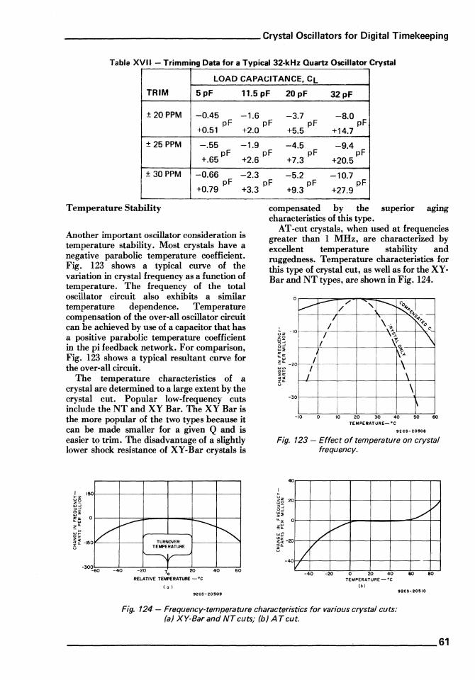
_________________ Crystal Oscillators for Digital Timekeeping
Table XVII - Trimming Data for a Tvpical 32-kHz Quartz Oscillator Crystal
LOAD CAPACITANCE, CL
TRIM 5pF 11.5 pF 20pF 32pF
± 20 PPM "'-0.45 -1.6 -3.7 -8.0 pF pF pF pF
+0.51 +2.0 +5.5 +14.7
± 25 PPM -.55 -1.9 -4.5 -9.4 +.65 pF +2.6 pF
pF pF +7.3 +20.5
± 30 PPM -0.66 -2.3 pF
+0.79 +3.3
Temperature Stability
Another important oscillator consideration is temperature stability. Most crystals have a negative parabolic temperature coefficient. Fig. 123 shows a typical curve of the variation in crystal frequency as a function of temperature. The frequency of the total oscillator circuit also exhibits a similar temperature dependence. Temperature compensation of the over-all oscillator circuit can be achieved by use of a capacitor that has a positive parabolic temperature coefficient in the pi feedback network. For comparison, Fig. 123 shows a typical resultant curve for the over-all circuit.
The temperature characteristics of a crystal are determined to a large extent by the crystal cut. Popular low-frequency. cuts include the NT and XY Bar. The XY Bar is the more popular of the two types because it can be made smaller for a given Q and is easier to trim. The disadvantage of a slightly lower shock resistance of XY-Bar crystals is
1 150 >z ~e ",-, :>-' 22 '"0: 0 ...... ~: "'1-"0: Z .. ~Il. -150
v V-
- --300 -60 40
-.......
'" TURNOVER TEMPERATURE
~ 20 To 20 40 60
RELATIVE TEMPERATURE -'C
I. I utS-tOlO'
-5.2 -10.7 pF
+9.3 pF pF
+27.9
compensated by the superior aging characteristics of this type.
AT-cut crystals, when used at frequencies greater than 1 MHz, are characterized by excellent temperature stability and ruggedness. Temperature characteristics for this type of crystal cut, as well as for the XYBar and NT types, are shown in Fig. 124.
o v - ,,- " r--..~.,~I /
/ I' ~.r.;-\.. \{a
1>... .<'_ , ... -10 uZ zo "'-:>-' 0= "',. f!:ffi ~a. -20 "'u> "I-ZO: .... ,,0. U
-30
/ I
r--!- ~---
I I
-10 0
\":. \ '{ 'i \<oL
\
\ \
10 20 30 40 50 60 TEMPERATURE--C
.2eS-2050B
Fig. 123 - Effect of temperature on crystal frequency.
40
-40
/' V
/ I'
V -40 -20 o 20 40
TEMPERATURE-·C
(.1
../ V
- I-
60 60
SICS-ZOllO
Fig. 124 - Frequency-temperature characteristics for various crystal cuts: (a) XY-Bar and NT cuts; (b) A T cut.
________________________________________ ~ ___________ 61
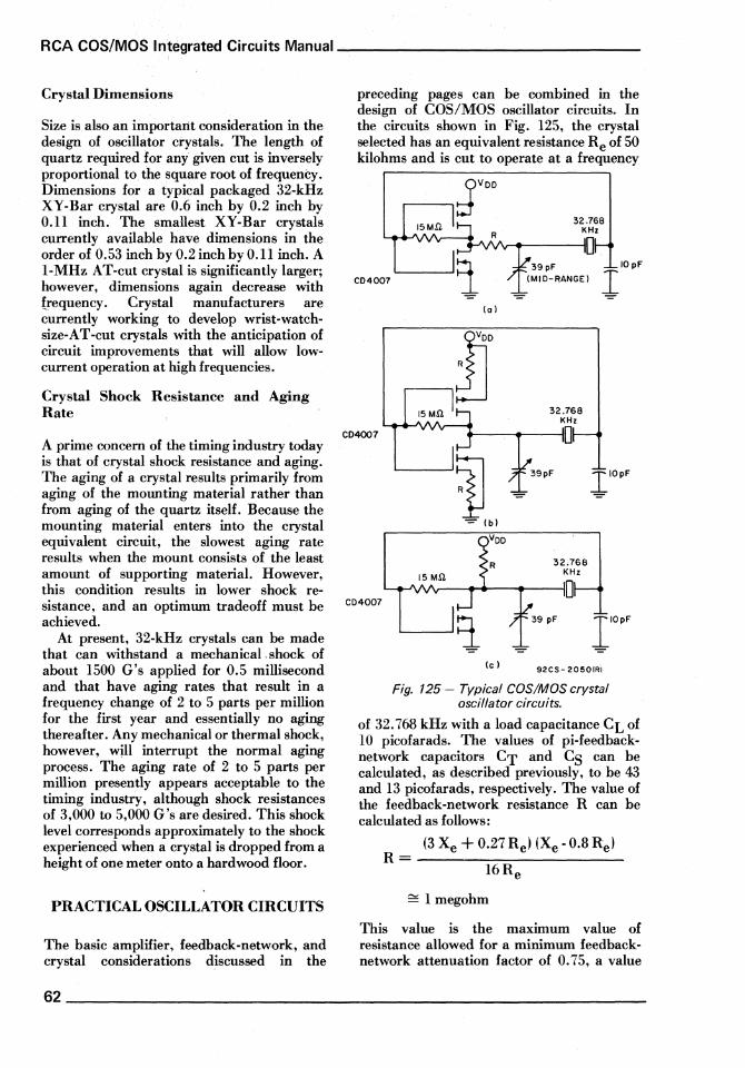
RCA COS/MaS Integrated Circuits Manual """-______________ _
Crystal Dimensions
Size is also an importartt consideration in the design of oscillator crystals. The length of quartz required for any given cut is inversely proportional to the square root of frequenCy. Dimensions for atypical packaged 32-kHz XY-Bar crystal are 0.6 inch by 0.2 inch by O.ll inch. The smallest XY-Bar crystals currently available have dimensions in the order of 0.53 inch by 0.2 inch by 0.11 inch. A I-MHz AT-cut crystal is significantly larger; however, dimensions again decrease with frequency. Crystal manufacturers are currently working to develop wrist-watchsize-AT-cut crystals with the anticipation of circuit improvements that will allow lowcurrent operation at high frequencies.
Crystal Shock Resistance and Aging Rate
A prime concern of the timing industry today is that of crystal shock resistance and aging. The aging of a crystal results primarily from aging of the mounting material rather than from aging of the quartz itself. Because the mounting material enters into the crystal equivalent circuit, the slowest aging rate results when the mount consists of the least amount of supporting material. However, this condition results in lower shock resistance, and an optimum tradeoff must be achieved.
At present, 32-kHz crystals can be made that can withstand a mechanical. shock of about 1500 G's applied for 0.5 millisecond and that have aging rates that result in a frequency change of 2 to 5 parts per million for the first year and essentially no aging thereafter. Any mechanical or thermal shock, however, wjll interrupt the normal aging process. The aging rate of 2 to 5 parts per million presently appears acceptable to the timing industry, although shock resistances of 3,000 to 5,000 G's are desired. This shock level corresponds approximately to the shock experienced when a crystal is dropped from a height of one meter onto a hardwood floor.
PRACTICAL OSCILLATOR CIRCUITS
The basic amplifier, feedback-network, and crystal considerations discussed in the
preceding pages can be combined in the design of COS/MOS oscillator circuits. In the circuits shown in Fig. 125, the crystal selected has an equivalent resistance Re of 50 kilohms and is cut to operate at a frequency
CD4007
CD4007
15 M.o.
(al
32.768 KHz
....-.-----110
(e 1 92CS- 2050lRI
Fig. 125 - Typical COS/MaS crystal oscillator circuits.
of 32.768 kHz with a load capacitance CL of 10 picofarads. The values of pi-feedbacknetwork capacitors CT and Cs can be calculated, as described previously, to be 43 and 13 picofarads, respectively. The value of the feedback-network resistance R can be calculated as follows:
(3 Xe + 0.27 Re) (Xe - 0.8 Re) R = -------=-------
16Re
~ I megohm
This value is the maximum value of resistance allowed for a minimum feedbacknetwork attenuation factor of 0.75, a value
62 ____________________________________________________ ___

__________________ Astable and Monostable Multivibrators
selected on the basis of power and stability considerations. The calculated value of R includes any fixed resistance plus the amplifier output resistance. Because the output resistance is often appreciable and varies with supply voltage, transistor size, and threshold voltages, it is generally best to add resistance experimentally until the desired power consumption and frequency stability are reached. The effect of this resistance on operating current and frequency stability can be predicted from the data given in Table XVIII for the three COS/MOS crystaloscillator circuits shown in Fig. 125. In each circuit, the pi-network capacitors CT and Cs are 39 picofarads and 10 picofarads, respectively. These capacitances are slightly less than the calculated values because of stray and amplifier capacitances.
The circuit shown in Fig. 125(a) combines the amplifier and feedback circuits shown in Figs. 120 and 121. Although theory predicts
that an increase in the values of the feedbacknetwork resistor R will result in increased frequency stability, the circuit performance data given in Table XVIII show no significant improvement in this characteristic. This result indicates that the circuit instability can be attributed almost entirely to phase instabilities of the amplifier.
The assumption is verified by data taken from the circuits shown in Figs. 125(b) and 125(c), in which the required feedbacknetwork resistance is incorporated into the amplifier as a fixed value. The resistors essentially fix the amplifier phase shift so that greater stability results. As the data show, use of these resistors also results in a decrease in the total current consumption. Because of the two fixed resistors, the circuit of Fig. 125 (b) shows the least current consumption and also the greatest stability.
As mentioned previously, the amplifier feedback resistor should not significantly
Table XVIII - Typical Oscillator Data
Change in
Value of Frequency
Circuit VDD Current VOo=1.45 V R(m (Volts) (/JA) to 1.6 V
Fig. 125, (Parts per million)
(a) 0 1.60 4.0 2.8
" 0 1.45 3.1
" lOOK 1.60 3.1 2.6
" " 1.45 2.4
" 200K 1.60 2.9 2.6
" " 1.45 2.1
(b) lOOK 1.60 2.3
" " 1.45 2.0 0.3
" " 1.1 1.5
" 150K 1.60 1.8
" " 1.45 1.6 0.2
" " 1.1 0.95
(e) 200K 1.60 5.0 0.6
" " 1.45 4.4
" 300K 1.60 3.5 0.5
" " 1.45 3.0
______________________________________________________ 63
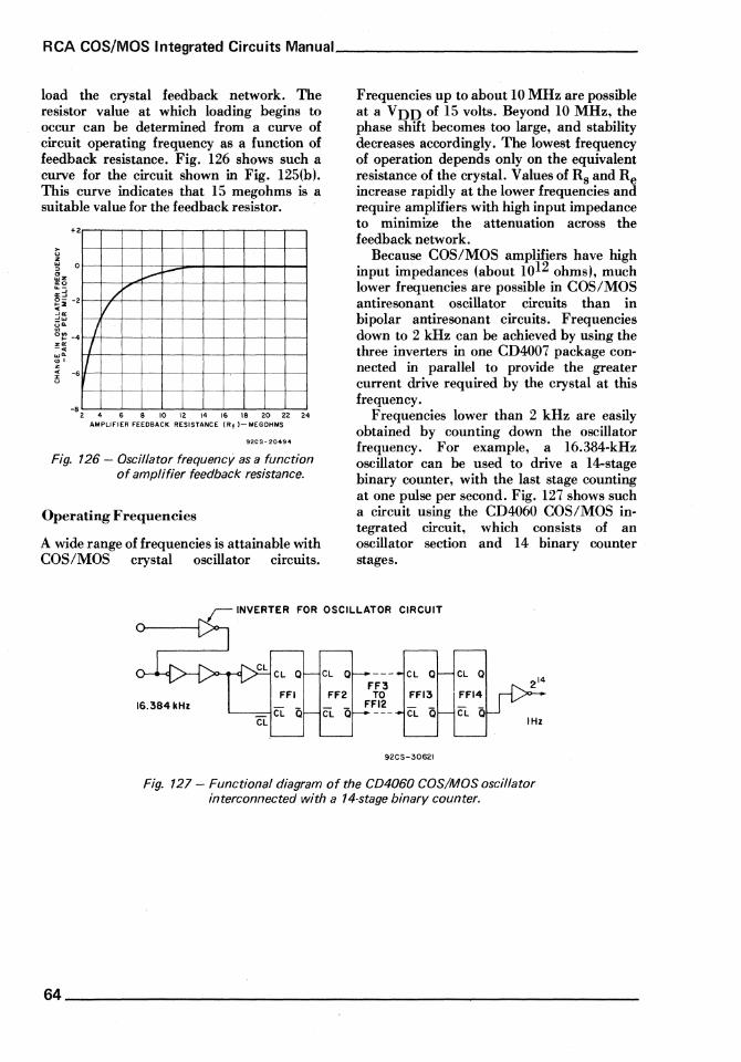
RCA COS/MOS Integrated Circuits Manual ______________ _
load the crystal feedback network. The resistor value at which loading begins to occur can be determined from a curve of circuit operating frequency as a function of feedback resistance. Fig. 126 shows such a curve for the circuit shown in Fig. 125(b). This curve indicates that 15 megohms is a suitable value for the feedback resistor.
,. u Z
+ 2
~ 0
~~ ... -o::l ~i -2
-'0: -' ... v" .. o:! -4 zo: -" ..... "I Z
~ -6
-8
~ -/
V / I
1/
2 4 6 8 10 12 14 16 18 20 22 24 AMPLIFIER FEEDBACK RESISTANCE CRf)- MEGOHMS
92CS-20494
Fig. 126 - Oscillator frequency as a function of amplifier feedback resistance.
Operating Frequencies
A wide range of frequencies is attainable with COS/MOS crystal oscillator circuits.
Frequencies up to about 10 MHz are possible at a VDD of 15 volts. Beyond 10 MHz, the phase shift becomes too large, and stability decreases accordingly. The lowest frequency of operation depends only on the equivalent resistance of the crystal. Values of Rs and Re increase rapidly at the lower frequencies and require amplifiers with high input impedance to minimize the attenuation across the feedback network.
Because COS/MOS amplifiers have high input impedances (about 1012 ohms), much lower frequencies are possible in COS/MOS antiresonant oscillator circuits than in bipolar antiresonant circuits. Frequencies down to 2 kHz can be achieved by using the three inverters in one CD4007 package connected in parallel to provide the greater current drive required by the crystal at this frequency.
Frequencies lower than 2 kHz are easily obtained by counting down the oscillator frequency. For example, a 16.384-kHz oscillator can be used to drive a 14-stage binary counter, with the last stage counting at one pulse per second. Fig. 127 shows such a circuit using the CD4060 COS/MOS integrated circuit, which consists of an oscillator section and 14 binary counter stages.
INVERTER FOR OSCILLATOR CIRCUIT
Q Cl Q
FFI FF2 16.384 kHz
92CS-30621
Cl Q
FFI4
Cl Q 1Hz
Fig. 127 - Functional diagram of the CD4060 COS/MOS oscillator interconnected with a 14-stage binary counter.
64 ___________________________________________________ ___

VIII. Shift Registers and Counters
COS/MOS shift registers generally use the basic static master-slave flip-flop circuit configuration described in Chapter II and reproduced in Fig. 128. The logic level present at the D(Data) input is transferred to the Q output during either the positive- or negative-going transition of the clock, depending on the specific circuit type. Set and reset functions may be included, again depending on circuit type; if they are included, each function is accomplished by a high level at the respective input. In a serial shift register, the Q output of one stage becomes the D input of the following stage.
Ripple-carry binary counters are similar to shift registers except that the D input to each stage is connected to the Q output of the same stage, so that is complements the stage at the clock transistion. The Q and Q outputs of one stage become the Clock and Clock inputs of the following stage.
In a synchronous binary counter, a common clock is used for all stages; the Q output is returned to the D input, as in the ripple counter.
COS/MOS shift registers and counters are available in a number of different integratedcircuit configurations that afford the designer considerable versatility in implementing system designs. The brief descriptions and diagrams shown in this chapter for a wide variety of shift registers and counters can serve as a selection guide to RCA types.
STATIC SHIFT REGISTERS
Dual4-Stage Static Shift Register with Serial Input/Parallel Output
The CD4015 consists of two identical, independent, 4-stage serial-input/parallel-
;.0------00 TRUTH TABLE
o (DATA)
Ro----~--~~--~ (DC RESET)
So----~~=_-+----r~~ (DC SET)
CLo---{>Wo-o ~ . L--oCL
SHAPING
BUFFERED OUTPUTS
d 0 R S 0 is
f 0 0 0 0 I
f I 0 0 I 0
'- x 0 0 0 is
x X I 0 0 I
X X 0 I I 0
X X I I II * (NO CHANGE)
* - INVALID CONDITION .. - LEVEL CHANGE X - DON'T CARE CASE
INPUT TO OUTPUT IS A BIDIRECTIONAL SHORT CIRCUIT WHEN CONTROL- INPUT I IS LOW AND CONTROL-INPUT 2 IS HIGH; AN OPEN CIRCUIT WHEN CONTROL-INPUT I IS HIGH AND CONTROL-INPUT 2 IS LOW.
92CS-30623
Fig. 128 - Basic master-slave flip-flop circuit used in COS/MaS shift registers and counters.
65

RCA COS/MaS Integrated Circuits Manual _______________ _
output registers, as shown in Fig. 129. Each register has independent clock and reset inputs, as well as a single serial data input. Q outputs are available from each of the four stages on both registers. All register stages are D-type master-slave flip-flops.
The logic level present at the data input is transferred into the first register stage and shifted over one stage at each positive-going clock transition. Resetting of all stages is accomplished by a high level on the reset line. The register can be expanded to eight stages using one CD4015 package, or to more than
OATAA 7
CLOCKA 9
RESET A 6
OATAB 15
CLOCKB
RESETB 14
92C5-25048
4
Voo 16
STAGE
4 STAGE
VSS
5 QIA
4 Q2A
3 Q3A
10 Q4A
13 QIB
12 Q2B
" Q3B
Z Q4B
~~:I· .
D Q
eight stages using additional CD4015 packages.
18-Stage Static Shift Register
The CD4006, shown in Fig. 130, consists of 4 separate shift-register sections: two sections of four stages and two sections of five stages with an output tap at the fourth stage. Each section has an independent single-rail data path.
A common clock signal is used for all stages. Data are shifted to the next stage on
TRUTH TABLE
CL 0 R 01 an .../"0 0 0 an-I
.../"1 0 1 an-I
""'- x 0 01 an (N OCHANGEI
X X 1 0 0
X' DON'T CARE CASE
D Q
CL
CL CL
Fig.
L-----.... -yss CL~n
* ALL INPUTS PROTECTED BY COS/MOS INPUT PROTECTION NETWORK
92CM-29383R2
129 - Functional diagram, logic diagram, and truth. table for CD40 15 dual 4·stage static shift register.
66 ____________________________________________________ ___

_______________________ Shift Registers and Counters
Cl Cl
D
Cl Cl
D+I
I Q {>----O L___ OUT
IF 4th OR 5th STAGE
TRUTH TABLE FOR OUTPUT FROMTERM.2
0,+4 CL'" °1+4'
0 ...r 0
I ...r 1 1 ~ HIGH
x "- NC o ~ LOW NC ~ NO CHANGE
TRUTHTABLEFORSHIFTREGISTERSTAGE X ~OON'TCARE
Vss 92CS-25049R2
D
0
1
X
CL'"
\... \... f
D+l '" ~ LEVEL CHANGE
0
1
NC 92CS- 178B7RI
Fig. 130 - Functional diagram, logic diagram, and truth table for CD4006 18-stage static shift register.
negative-going transitions of the clock. Through appropriate connections of inputs and outputs, multiple register sections of 4, 5, 8, and 9 stages or single register sections of 10, 12, 13, 14, 16, and 18 stages can be implemented using one CD4006 package. Longer shift-register sections can be assembled by use of more than one CD4006.
64-Stage Static Shift Register
The CD4031 is a 64-stage static shift register in which each stage is a D-type master-slave flip-flop. The functional diagram, logic diagram, and truth table for the CD4031 are shown in Fig. 131.
The logic level present at the data input is transferred into the first stage and shifted one stage at each positive-going clock transition. Maximum clock frequencies up to 4 MHz (typical) can be obtained. Because fully static operation is allowed, information can be permanently stored with the clock line in either the low or high state. The CD4031 has a mode control input that, when in the high state, allows operation in the recirculating mode. Register packages can be cascaded and the clock lines driven directly for high-
speed operation, as shown in Fig. 132. Alternatively, a delayed clock output (CLD) is provided that makes it possible to cascade register packages while allowing reduced clock drive fanout and transition-time requirements, as shown in Fig. 133.
Data (Q) and Data (Q) outputs are provided from the 64th register stage. The Data (Q) output is capable of driving one TTL or DTL load.
8-Stage Static Shift Regist~r with Synchronous Parallel or Serial Input/Serial Output
Fig. 134 shows the functional diagram, logic diagram, and truth table for the CD4014 8-stage parallel or serial-input/serial-output register. This circuit has common clock and parallel/serial control inputs, a single serial data input, and individual parallel "jam" inputs to each register stage. Each stage is a D-type master-slave flip-flop. Q outputs are available from stages 6 and 7, as well as from stage 8. Parallel or serial entry is made into the register synchronous with the positive clock-line transition and under control of the parallel/ serial control input.
_____________________________________________________ 67

RCA COS/MaS Integrated Circuits Manual _______________ _
>-----+CL
~_gV:D
Q" * ALL INPUTS ARE
PROTECTED BY COSIMOS PROTECTION NETWORK.
DATA I Ie IN
MODE 10 CONTROL CONT. LOGIC
~ml~ I IN
DELAYED CLOCK
VDD = 16 OUT
VSS = 8 NC·3,4,1I,12,13,14
64 STAGES DATA
OUT 6
DATA OUT
7
9lCS - 29039RI
TYPICAL STAGE TRUTH TABLE
o.~ CL Data + 1
0 ...r 0
I ..r 1
X ""- NC
CL
CL 9ZCM- 290~3
INPUT CONTROL CIRCUIT TRUTH TABLE
DATA RECIRC. MODE BIT INTO STAGE I
1 X 0 1
0 X 0 0
X 1 1 1
X 0 1 0
TRUTH TABLE FOR OUTPUT FROM Q' (TERMINAL 51
Data + 64 CL Data + 64%
0 ""\.. 0
1 ""\.. 1
X ..r NC
1 = HIGH LEVEL 0= LOW LEVEL Ne = NO CHANGE
X = DON'T CARE
Fig. 131 - Functional diagram, logic diagram, and truth table for CD4031 64-stage static shift register.
68 ____________________________________________________ ___

____________________ ~. Shift Registers and Counters
MODE CONTROL VOO'" RECIRCULATION
GND' NEW DATA 92CS-29063
o
Fig. 132 - Cascading of CD4031 devices using direct clocking for high-speed operation.
VDD
1 DELAYED CLOCK TO CLOCK NEW DATA INTO FIRST REGISTER -
* FOR RECIRCULATION MODE ONLY. FF TO DELAY DATA UNTIL FIRST REGISTER DELAYED CLOCKING HAS OCCURRED.
o
MOlE CONTROL: Voo -RECIRCULATION GNO-NEW DATA
92CS-29062RI
Fig. 133 - Cascading of CD4031 devices using delayed clocking for reduced clock-drive requirements.
CLrt>J
CL
ps---+-+----'
* ALL INPUTS ARE PROTECTED BY COS/MOS PROTECTION
----- NETWORK. ~VD
VSS
CL
)O>--~--Q
92CM-28673RI
Fig. 134(a) - Logic diagram for CD4014 8-stage static shift register.
08
______________________________________________________ 69

RCA COS/MaS Integrated Circuits Manual _____________ ""--_
~:=:~ CONT.
SER. II IN·
CLOCK.!Q.
92CS-25047
PAR.IN. I ...
2345678
8 VSS
CL"" SER. PAR SER PI·1 PI·n
01
IN CONTROL (INTER· an NAL)
./ x 1 0 0 0 0
./ x 1 1 0 1 0
./ x 1 0 1 0 1
./ x 1 1 1 1 1
./" 0 0 x x 0 °n·1
./ 1 0 X X 1 °n·1
"" X X X X 01 an NC
x = DON'T CARE CASE "" = LEVEL CHANGE
NC = NO CHANGE
92CM-28673
Fig. 134(b) - Functional diagram and truth table for CD4014 a·stage static shift register.
8-Stage Static Shift Register with Asynchronous Parallel or Synchronous Serial Input/Serial Output
The CD4021 , shown in Fig. 135, is an 8-stage parallel- or serial-input/serial-output shift register that has common clock and parallel/serial control inputs, a single serial
F1 n
tJ-o :-{~ ~i':'~-I"NP-U"TS-A-R-E-P-RO-TE-C-TE-O--'
BY COS/MOS PROTECTION VSS NETWORK.
CL
data input, and individual parallel "jam" inputs to each register stage. Each register stage is a D-type master-slave flip-flop. Q outputs are available from the sixth, seventh, and eighth stages.
When the parallel/serial control input is low, data are serially shifted into the 8-stage register synchronously with the positive-
92CM-28674RI
Fig. 135(a) - Logic diagram for CD4021 a·stage static shift register.
70 ___ ~ ______________________________________________ ___
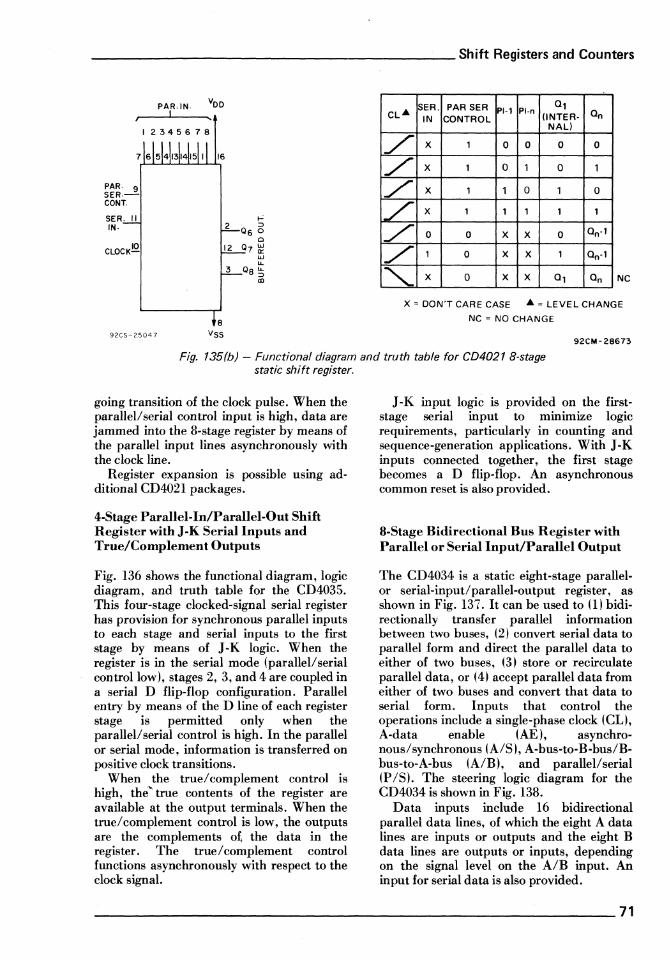
______________________ Shift Registers and Counters
~:~:~ CONT.
SER. II IN·
CLOCK!Q.
PAR. IN. I
12345678
92CS-25047
8 VSS
CLA SER. PAR SER PI.' PI-n
a,
IN CONTROL IINTER- an NALl
./ x , 0 0 0 0
./ x , 0 1 0 1
./ x , 1 0 1 0
V X , , , , , /" 0 0 X X 0 °n-'
./" , 0 x X , °n-'
"- X 0 X X a, an NC
x = DON'T CARE CASE A = LEVEL CHANGE
NC = NO CHANGE
92CM-28673
Fig_ 135(b) - Functional diagram and truth table for CD4021 8-stage static shift register.
going transition of the clock pulse. When the parallel/serial control input is high, data are jammed into the 8-stage register by means of the parallel input lines asynchronously with the clock line.
Register expansion is possible using additional CD4021 packages.
4-Stage Parallel-IniParallel-Out Shift Register with J -K Serial Inputs and True/Complement Outputs
Fig. 136 shows the functional diagram, logic diagram, and truth table for the CD4035. This four-stage clocked-signal serial register has provision for synchronous parallel inputs to each stage and serial inputs to the first stage by means of J-K logic. When the register is in the serial mode (parallel/serial control low), stages 2, 3, and 4 are coupled in a serial D flip-flop configuration. Parallel entry by means of the D line of each register stage is permitted only when the parallel/serial control is high. In the parallel or serial mode, information is transferred on positive clock transitions.
When the true/complement control is high, the" true contents of the register are available at the output terminals. When the true/ complement control is low, the outputs are the complements of, the data in the register. The true/complement control functions asynchronously with respect to the clock signal.
J-K input logic is provided on the firststage serial input to mmumze logic requirements, particularly in counting and sequence-generation applications. With J -K inputs connected together, the first stage becomes a D flip-flop. An asynchronous common reset is also provided.
8-Stage Bidirectional Bus Register with Parallel or Serial Input/Parallel Output
The CD4034 is a static eight-stage parallelor serial-input/parallel-output register, as shown in Fig. 137. It can he used to 0) bidirectionally transfer parallel information between two buses, (2) convert serial data to parallel form and direct the parallel data to either of two buses, (3) store or recirculate parallel data, or (4) accept parallel data from either of two buses and convert that data to serial form. Inputs that control the operations include a single-phase clock (CL), A-data enable (AE), asynchronous/synchronous (A/S), A-bus-to-B-bus/Bbus-to-A-bus (A/B), and parallel/serial (P IS). The steering logic diagram for the CD4034 is shown in Fig. 138.
Data inputs include 16 bidirectional parallel data lines, of which the eight A data lines are inputs or outputs and the eight B data lines are outputs or inputs, depending on the signal level on the A/B input. An input for serial data is also provided.
_________________________________________________________ 71
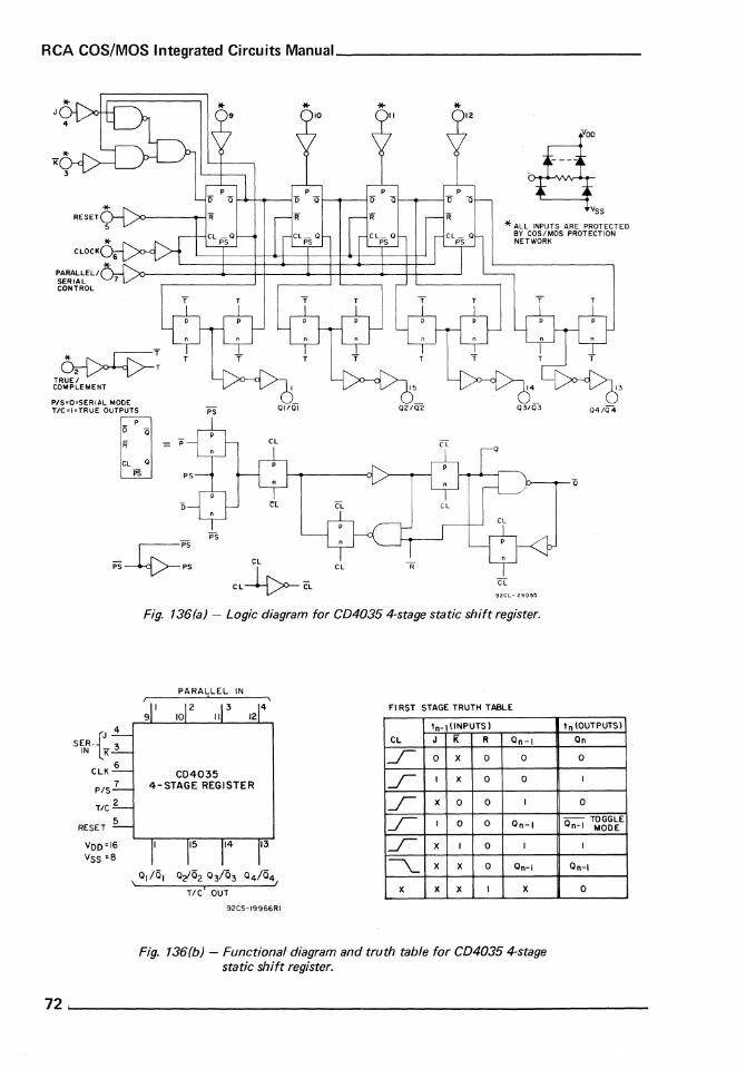
RCA COS/MOS Integrated Circuits Manual _______________ _
* ALL INPUTS ARE PROTECTEO BY COS/MOS PROTECTION NETWORK
J!:.. i'-.. r-r::::=-T ~T
TRUEI COMPLEMENT
SER.{J : IN K J
ClK 6
PIS 7
TIC 2
~ RESET
VOO=16 Vss =8
03/03
CL
CL~CL 92CL-29055
Fig. 136(a) - Logic diagram for CD4035 4-stage static shift register.
CD4035 4-STAGE REGISTER
\ 0 1/01 0<!02 0 3/03 04/04, TIC' OUT
92CS-19966RI
FIRST STAGE TRUTH TABLE
'n-IIiNPUTS)
Cl J K R an-I
f 0 x 0 0
F I X 0 0
F x 0 0 I
F I 0 0 On-I
f X I 0 I
~ X X 0 OR-I
X X X I X
Fig. 136(b) - Functional diagram and truth table for CD4035 4-stage static shift register.
04/04
, n (OUTPUTS)
an
0
I
0
On-I "'"3gg'EE
I
OR-I
0
72~ __________________________________________________ __

______________________ Shift Registers and Counters
All register stages are D-type master-slave flip-flops with separate master and slave clock inputs generated internally to allow synchronous data transfer from master to slave. The logic diagram for one of the eight identical register stages is shown in Fig. 139. Isolation from external noise and the effects of loading is provided by output buffering.
4-Bit Bidirectional Universal Shift Register
Fig. 140 shows the functional diagram and truth table for the CD40194. This universal shift register features parallel inputs, parallel outputs, shift-right and shift-left serial inputs, and a direct overriding clear input. In the parallel-load mode (SO and Sl high), data are loaded into the associated flip-flop and
R 4ss
* INPUTS PROTECTED BY COS/MOS PROTECTIOII NETWORK
PIS
* CLOCK
SI
AE
AlB
AIS
PIS
CL
STEERING LOGIC
UI 1&1 z-+-+I--I :J ~""-+I--I
~"""""---I
6 STAGES
Fig. 92CS-29108
137 - Functional diagram for CD4034 8-stage static bidirectional bus register.
cLs
'----+ClS
ClM
'----+-ClM
92.CS-29109fU
Fig. 138 - Steering logic diagram for CD4034.
appear at the output after the positive transition of the clock input. During loading serial data flow is inhibited.
Shift right and shift left are accomplished synchronously on the positive clock edge with data entered at the shift-right and shift-left serial inputs, respectively. Clocking of the register is inhibited when both mode control inputs are low. The mode controls should be changed only when the clock input is low. When the reset input is low, it resets all stages and forces all outputs low.
4-Bit Bidirectional Universal Register with 3-State Output
The CD40l04, shown in Fig. 141, is a universal register featuring parallel inputs, parallel outputs, shift-right and shift-left serial inputs, and a high-impedance third output state that allows the device to be used in bus-organized systems.
As in the CD40194, data are loaded into the associated flip-flop in the parallel-load
________________________________________________________ 73

RCA COS/MOS Integrated Circuits Manual _______________ _
ONE OF EIGHT STAGES r----~------------------~
I 1
I I
1 :
I K I q Yss
PROTECTION NETWORK ON ALL 'lAM AND "8" DATA INPUTS
I : I I I I
SERIAL DATA
I I I I I I I I I
YSS 1
PROTECTION NETWORK I ON SERIAL DATA INPUT I
~------~------------~----------~I Q (TO N EXT STAGE D) I
T Bn I ________________ - - _________ 1
92CM-2.9110R2
INPUTS OUTPUT
ClM ClS 0 0
"'- """\.. 0 0
J '- 0 0
\... ..r 0 INVALID
CQNOlTlON
..r ..r x 0
'- '- 1 1
..r '- 1 1
"'- J 1 INVALID
CONDITION
1 = High Level 0 = Low Level X = Don't Care
Fig. 139 - Logic diagram and truth table for one of eight identical register stages in CD4034 shift register.
RESET---...,
DO
01
02
3 r-----''----'15
4 14
5 13
03 6 12
SHIFT IN LEFT 7
SHIFT IN RIGHT 2
MODE {so 9 SELECT 51 10
'----,rl'-I ---'
QO
QI
Q2
Q3
Voo =16
VSS = B
CLOCK----' 92CS-24822R2
Cl
X
-F ..s-S
X
SO S1
0 0
1 0
O 1
1 1
X X
RESET
1
1
1
1
0
1 = HIGH LEVEL 0= LOW LEVEL X = DON'T CAR E
ACTION
Do·Nothing
Shift Right (00 toward Q3)
Shift Left (03 toward 00)
Parallel load
Reset
Fig. 140 - Functional diagram and truth table for CD40194 4-bit universal shift register.
74 _____________________________________________________ ___

______________________ Shift Registers and Counters
mode and appear at the output after the positive transition of the clock input. During loading, serial data flow is inhibited. Shiftright and shift-left are accomplished synchronously on the positive clock edge with serial data entered at the shift-right and shiftleft serial inputs, respectively.
CLOCK·
~ --F ~ --F
X
1 = High level 0= Low level
MODE SELECT
So S,
0 0
1 0
0 1
1 1
X X
synchronously with the positive clock edge, provided the left/right control is at a low level, the recirculate control is at a high level, and the clock inhibit is low. If the left/right control is at a high level and the recirculate control is also high, data at the shift-left input is transferred into the 32nd register
OUTPUT ACTION
ENABLE
1 Reset
1 Shift right (00 toward 03)
1 Shift left (03 toward 00)
1 Parallel load
0 Outputs assume high impedance
X = Don't care • = Level change
Fig. 141 - Functional diagram and truth table for CD40104 4-bit universal register with 3-state output.
Clearing the register is accomplished by setting both mode controls low and clocking the register. The mode controls should be changed only when the clock input is low. When the output-enable input is low, all outputs assume the high-impedance state.
32-Stage Left/Right Static Shift Register
Fig. 142 shows the functional diagram for the CD40100, a static shift register containing 32 D-type master-slave flip-flops. The logic diagram and truth tables are shown in Fig. 143.
The data present at the shift-right input are transferred into the first register stage
IN
IN
N
SHIFT RIGHT
II
CLOCK :3
CLOCK INHIBIT
SHIFT 2 LEFT
6 C=I,5,7,
LEFT/RIGHT CONTROL
b
10,14,15 19
RECIRCULATE CONTROL
SHIFT RIGHT 12
SHIFT LEFT 4
VOO=16
VSS=B
9ZCS-Z7567
OUT
OUT
Fig. 142 - Functional diagram for CD40100 32-stage left-right static shift register.
____________________________________________________ 75

RCA COS/MOS Integrated Circuits Manual ______________ _
stage synchronously with the positive clock transition, provided the clock inhibit is low.
Data are shifted one stage left or one stage right (depending on the state of the left/right control) synchronously with the positive clock edge. 'Data clocked into the first or 32nd register stage ~re available at the ap-
CLOCK rJ>--. 'CI.
C~~>-IN-H-IB-IT--[)o-... - _-_-_-_--I'. D-1> l. CL
SHI" RIGHT *"0----1 ~o--'-------I INPUT
LEFT/~IGT *13 ~
CONTROL
S
RECI~RULTE *9 If CONTROL .
R
CL
propriate output on the next negative clock transition. No shifting occurs on the positive clock edge if the clock inhibit line is at a high level. With the recirculate control low, data are shifted from the 32nd stage into the first stage when the left/right control is low and from the first stage to the 32nd stage when the left/right control is high.
R
SHIFT LEFT )0-----04
OUTPUT
VDD
I-------'tt VSS
*ALLINPUTS PROTECTED BY COS/MOS PROTECTION NETWORK
SHI" LEFT
*60----1~>o------------------------------------~ INPUT
DETAIL OF TYPICAL D-TYPE M-S FLIP-FLOP
D
92CL-Z7565R2
Fig. 143(a) - Logic diagram for CD40100 shift register,
76 ___________________________________________________ __

______________________ Shift Registers and Counters
CONTROL TRUTH TABLE
LEFT/RIGHT CLOCK RECIRCULATE ACTION
INPUT BIT CONTROL INHIBIT CONTROL ORIGIN
1 0 1 Shift left Shift left input
1 0 0 Shift left Sta!le 1
0 0 1 Shift right Shift right input
0 0 0 Shift right Stage 32
X 1 X No shift -
DATA TRANSFER TABLE*
INITIAL STATE
DATA CLOCK INTERNAL INPUT INHIBIT STAGE
0 0 X
X 0 0 1 0 X
X 0 1
X 1 1
0= Low level 1 = High level X :: Don't care
* For Shift·Right Mode Data Input = SHIFT-RIGHT INPUT (Term. 10 I nternal Stage = Stage 1 (01) Output = SHIFT-LEFT OUTPUT (Term. 4)
CLOCK RESULTING STATE
LEVEL INTERNAL OUTPUT CHANGE STAGE a ..-r- 0 NC
------ NC 0
----- 1 NC
------NC 1
X NC NC
NC ::: No change
For Shift-Left Mode Data Input = SHIFT-LEFT INPUT (Term. 6) Internal Stage = Stage 32 (032) Output = SHIFT·RIGHT OUTPUT (Term. 12)
Fig. 143(b) - Truth tables for CD40100 shift register.
8-Stage Shift-aDd-Store Bus Register
The CD4094 8-stage serial shift register, shown in Fig. 144, has a storage latch associated with each stage for strobing data from the serial input to parallel buffered 3-state outputs. The parallel outputs may be
DATA 2 ,..----...,
CLOCK 3
STROBE I
OUTPUT ENABLE 15
PARALLEL OUTPUTS QI-Qa
(TERMINALS 4.5,6,7,14,13,12,11. RESPECTIVELY)
92CS - 24564RI
Fig. 144(a) - Functional diagram for CD4094 8-stage shift-and-store bus register.
connected directly to common bus lines. Data are shifted on positive clock transitions. The data in each shift-register stage are transferred to the storage register when the strobe input is high. Data in the storage register appear at the outputs whenever the output-enable signal is high.
Two serial outputs are available for cascading a number of CD4094 devices. Data are available at the Qs serial output terminal on positive clock edges to allow for high-speed operation in cascaded systems in which the clock rise time is fast. The same serial information, available at the Qs terminal on the next negative clock edge, provides a means for cascading CD4094 devices when the clock rise time is slow.
DYNAMIC SHIFT REGISTERS
Fig. 145 shows the functional and logic diagrams for the CD4062 200-stage dynamic shift register, which has provision for either single- or two-phase clock input signals. Single-phase-clocked operation is intended
_____________________________________________________ 77
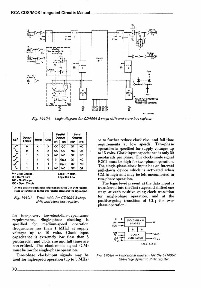
RCA COS/MOS Integrated Circuits Manual _______________ _
STAGES 3-7
TR
SERIAL OUT 9
Os
ATCH TR 8
Voo
*rl 3-f STATE v
8 SS
* ALL INPUTS PROm:TED BY COS/MaS PROTECTION NETWORK
92CL-21J11IRI
Fig. 144(b) - Logic diagram for CD4094 8-stage shift-and-store bus register.
CL" Output E ... ble
.r 0
"'\.. 0
.f 1
J 1
J , "'\.. ,
.. • Level Change X • Don't Care NC = No Change OC • Open Circuit
Strobe D ••
x x x x 0 X , 0 , , , ,
p., ..... s.n.I OutputS ~
01 ON OS- O'S
OC OC 07 NC
OC oc NC 07
NC NC 07 NC
0 ON·, 07 NC
1 ON·' 07 NC
NC NC NC 07
Logic' = High Logic 0 = Low
• At the positive clock edge information in the 7th shift register stage is transferred to the 8th register st.lge and the Os output.
Fig. 144(c) - Truth table for CD4094 8-stage shift-and-store bus register.
for low-power, low-c1ock-line-capacitance requirements, Single-phase clocking is specified for medium-speed operation (frequencies less than I MHz) at supply voltages up to 10 volts. Clock input capacitance is extremely low (less than 5 picofarads), and clock rise and fall times are non-critical. The clock-mode signal (CM) must be low for single-phase operation.
Two-phase clock-input signals may be used for high-speed operation (up to 5 MHz)
or to further reduce clock rise- and fall-time requirements at low speeds. Two-phase operation is specified for supply voltages up to 15 volts. Clock input capacitance is only 50 picofarads per phase. The clock-mode signal (CM) must be high for two-phase operation. The single-phase-clock input has an internal pull-down device which is activated when CM is high and may be left unconnected in two-phase operation.
The logic level present at the data input is transferred into the first stage and shifted one stage at each positive-going clock transition for single-phase operation, and at the positive-going transition of CLI for twophase operation.
0 RC Q
REC
CM CLIO Cl Cli Cl2D Cl2
92CS-24664
Fig. 145(a) - Functional diagram for the CD4062 200-stage dynamic shift register.
78 ______________________________________________________ _

______________________ Shift Registers and Counters
o .,. DATA
2(2)· ,-----STAGE I ---~ ,--STAGE 200~ r-~~;~~~~
" RECIRe RC CONTR
3(3)
REC "'RECIRe
4(4)
ATERMtNAL NUMBERS IN PARENTHESES REFER TO 12-LEAO TO-5 STYLE PACKAGE
CD4062A
~ All INPUTS ARE PROTECTED BY COS/MQS PROTECTION NETWORK
4 V55
CL (b)
CL (b) CL(a)
.. TRANSMISSION GATE
INPUT TO OUTPUT IS:
{al A BIDIRECTIONAL LOW IMPEDANCE WHEN CONTROL INPUT IS "LOW" AND CONTROL INPUT 2 IS U H1GH"
(bl AN OPEN CIRCUIT WHEN CONTROL INPUT liS "HIGH" AND CONTROL INPUT 2 IS "lOW"
CL (a) = INTERNAL CLOCK IN PHASE WITH CL r
CL (b) "INTERNAL CLOCK IN PHASE WITH el2
92CM-22695R2
Fig. 145(b) - Logic diagram for the CD4062 200-stage dynamic shift register.
11(9)6
2-PHASE ~ ell
CLOCK cr----+ CL 2
5(5)
*ALL INPUTS ARE PROTECTED 8'1' caS/MOS PROTECTION NETWORK
Voo
L\-V55
CL (a) = INTERNAL CLOCK IN PHASE WITH CL I
CL (b) = INTERNAL CLOCK IN PHASE WITH CL2
.A.TERMINAL NUMBERS IN PARENTHESES REFER TO 12-LEAD TO-5 STYLE PACKAGE r--
eM
Ht-rl I-PHASE I CLOCK
I
(INPUT TO .
TERMINAL I) , I . I
I
7(6)
CL2
CL (b) I
92CM-221QQR2
Fig. 145(c) - Clock circuit logic diagram for CD4062 200-stage dynamic shift register.
_____________________________________________________ 79
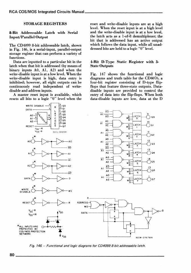
RCA COS/MaS Integrated Circuits Manual _______________ _
STORAGE REGISTERS
8-Bit Addressable Latch with Serial Input/Parallel Output
The CD4099 8-bit addressable latch, shown in Fig. 146, is a serial-input, parallel-output storage register that can perform a variety of functions.
Data are inputted to a particular bit in the latch when that bit is addressed (by means of binary inputs AO, AI, A2) and when the write-disable input is at a low level. When the write-disable input is high, data entry is inhibited; however, all eight outputs can be continuously read independent of writedisable and address inputs.
A master reset input is available, which resets all bits to a logic "0" level when the
WRITE DISABLE 4
DATA ___ ----'3"-1
AO 5 DE B AI 6 ~ A2 7 E
R RESET ___ -'2~
Voo "16 VSS"8
9 00 B 10 01 L II 02 A 1203 T 13 04
~ 14 05 E 15 06 S I 07
92CS-24425RI
4* WRITE A ~ . ~ DISABLE~WD
2* RESET 6--------[>0--[ R ADDRESS
WD
reset and write-disable inputs are at a high level. When the reset input is at· a high level and the write-disable input is at a low level, the latch acts as a l-of-8 demultiplexer; the bit that is addressed has an active output which follows the data input, while all unaddressed bits are held to a logic "0" level.
4-Bit D-Type Static Register with 3-State Outputs
Fig. 147 shows the functional and logic diagrams and truth table for the CD4076, a four-bit register consisting of D-type flipflops that feature three-state outputs. Datadisable inputs are provided to control the entry of data into the flip-flops. When both data-disable inputs are low, data at the D
9
wB LATCH 00 0 R
10 LATCH 01
I
II LATCH 02
2
12 LATCH
3 03
13 LATCH 04
4
14 LATCH 05
5
15 LATCH 06
6
LATCH 07 7
o DATA ----+-+-+
* ALL INPUTS ARE PROTECTED BY COSI MOS PROTECTION NETWORK
VSS
Fig. 146 - Functional and logic diagrams for CD4099 8-bit addressable latch.
80 __________________________________________________ ___
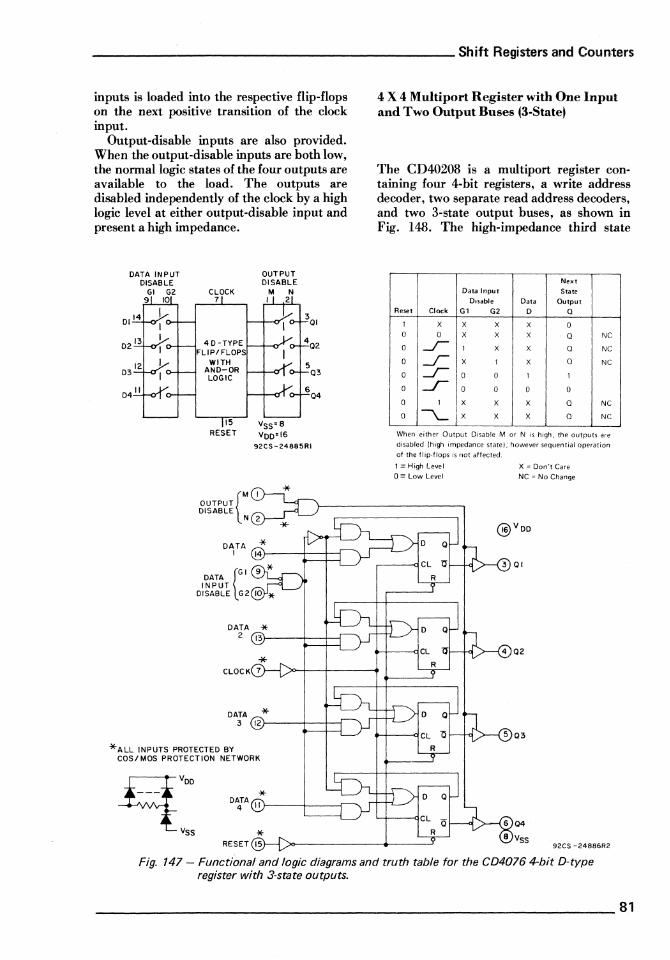
______________________ Shift Registers and Counters
inputs is loaded into the respective flip-flops on the next positive transition of the clock input.
Output-disable inputs are also provided. When the output-disable inputs are both low, the nonnallogic states of the four outputs are available to the load. The outputs are disabled independently of the clock by a high logic level at either output-disable input and present a high impedance.
OUTPUT DISABLE
M N I 2
3QI
4D-TYPE LIP/FLOPS
4Q2
WITH 5 AND-OR Q3 LOGIC
04 11 604
15 VSS=B RESET VDD=16
92CS-24885RI
{M I
OUTPUT DISABLE N
DATA I
DATA 2
DATA 3 * 12)---+-1-,~
*ALL INPUTS PROTECTED BY COS/MOS PROTECTION NETWORK
-9'00 * DATA II 4
VSS *
4 X 4 Multiport Register with One Input and Two Output Buses (3-Statel
The CD40208 is a multiport register containing four 4-bit registers, a write address decoder, two separate read address decoders, and two 3-state output buses, as shown in Fig. 148. The high-impedance third state
Next Data Input State
Disable Data Output Reset Clock Gl G2 0 Q
1 X X X X 0 0 0 X X X Q NC
0 -.r 1 X X Q NC
0 -.r X 1 X Q NC
0 -.r 0 0 1 1
0 -.r 0 0 0 0
0 1 X X X Q NC
0 ~ X X X Q NC
When either Output Disable M or N is high. the outputs are disabled (high impedance state); however sequential operation of the flip,flops is not affected.
1 ::::High Level
0== Low Level x = Don't Care NC = No Change
®V OD
RESET 92CS -24886R2
Fig. 147 - Functional and logic diagrams and truth table for the CD40764-bit D-type register with 3-state outputs.
________________________________________________________ 81
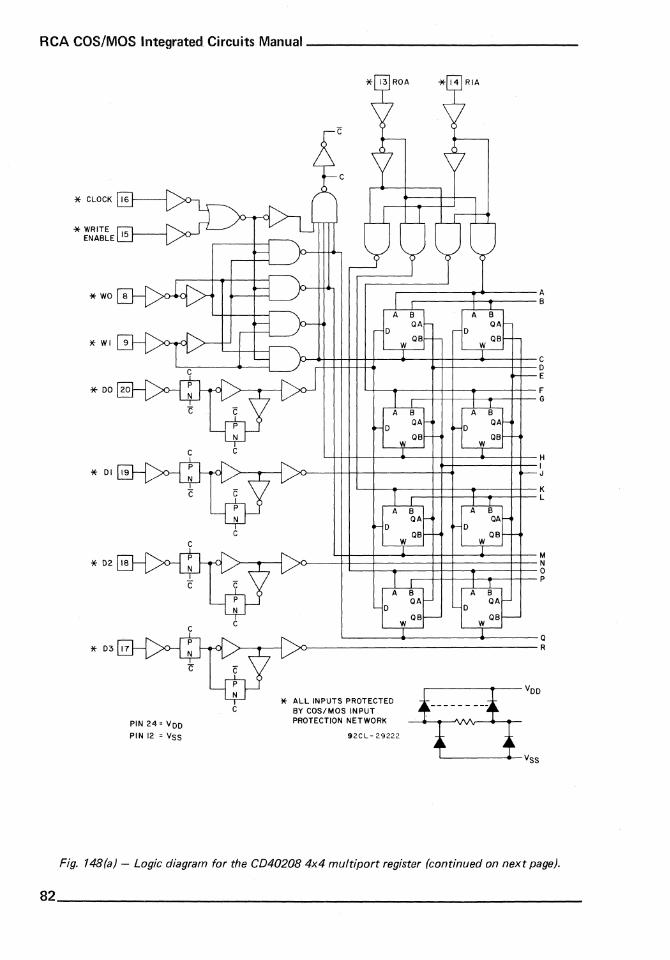
RCA COS/MaS Integrated Circuits Manual _______________ _
* CLOCK
* WRITE ENABLE
* WI
PIN 24 = VDD PIN 12 = VSS
C
C C
C
D QB
W
A B
D QA
QB W
A B QA
D QB
W
A B QA
D W QB
* ALL INPUTS PROTECTED BY COS/MOS INPUT PROTECTION NETWORK
92CL- 29222
A B
A B QA
D QB
W
C D E
F G
A B
D QA
QB W
H I J
K L
A B QA
D QB
W
M N 0 P
A B QA
D W QB
Q R
VDD
VSS
Fig. 14B(a} - Logic diagram for the CD4020B 4x4 multiport register (continued on next page).
82 _____________________________________________________ ___

______________________ Shift Registers and Counters
A 8
A 8 OA
D 08
W
C D E
F G
A .a D
OA
W 08
H
K L
A 8 OA
D 08
W
M N 0 P
A 8 OA
D OS
W
0 R
D
D
D
D
A 8 OA
08 W
A 8 OA
08 W
A B OA
08 W
A 8 OA
08 w
3 -STATE * A ENABLE
3
r----------- ------T ---------- - - --l I A I ~~ ~ I I P I d I I D OA I I I I I
I ~ I I OUT I I PUT I
I 8 1 I I W I I 08 I I VSS I i I I DETAIL OF DETAIL OF I I MEMORY CELL 3-STATE OUTPUTS I L _____________________________ -1 92CL-29222
Fig. 148(a) - Logic diagram for the CD40208 4x4 multipart register (continued from preceding page).
________________________________________________________ 83
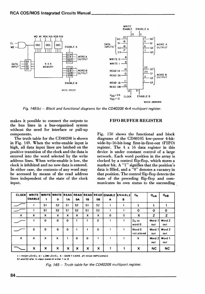
RCA COS/MaS Integrated Circuits Manual ______________ _
WRITE ENABLE ENABLE A
15 3 W9 WI ROA RIA ROB RIB 20 4
"} r DATA 01 19 5
CL QI WORD A WE INPUTS ~2 18 6 Q2 OUTPUT
17 7 Q3
}WORDA 8 OUTPUT WRITE 0
4 X4 WRITE I 9
MEMORY 22
}WORD B READIA 14
~} 23 OUTPUT 13 QI WORD B READ OA 2 Q2 OUTPUT
READ IB II
Q3 ENABLE B
READ OB 10
92CS-29220 16 21
YDD=24 CLOCK ENABLE B Yss = 12
92CS- 28549RI
Fig. 148(b) - Block and functional diagrams for the CD40208 4x4 multipart register.
makes it possible to connect the outputs to the bus lines in a bus-organized system without the need for interface or pull-up components.
The truth table for the CD40208 is shown iIi Fig. 149. When the write-enable input is high, all data input lines are latched on the positive transition of the clock and the data is entered into the word selected by the write address lines. When write-enable is low, the clock is inhibited and no new data is entered. In either case, the contents of any word may be accessed by means of the read address lines independent of the state of the clock input.
CLOCK WRITE WRITE WRITE READ READ READ ENABLE 1 0 1A OA 1B
~ 1 SI S2 SI S2 SI
------ 1 SI S2 SI S2 SI
x x x x x x x
~ 1 0 0 0 1 1
~ 0 0 0 0 1 1
X X X X 1 0 0
---- X X X X X X
FIFO BUFFER REGISTER
Fig. 150 shows the functional and block diagrams of the CD40I05 low-power 4-bitwide-by-I6-bit-Iong first-in-first-out WIFO) register. The 4 x 16 data register in this device is under constant control of a large network. Each word position in the array is clocked by a control flip-flop, which stores a marker bit. A "1" signifies that the position's data is filled, and a "0" denotes a vacancy in that position. The control flip-flop detects the state of the preceding flip-flop and communicates its own status to the succeeding
READ ENABlE ENABLE On OnA OnB OB A B
S2 1 1 1 1 1
52 1 1 0 0 0 x 0 0 X Z Z
0 1 1 On to Word 1 Word 2 word 0 out out
0 1 1 Word 0 Word 1 Word 2 not altered out out
1 1 1 X Word 2 Word 1 out out
X 1 1 X NC NC
I' HIGH LEVEL: O· LOW LEVEL: X • Dmj·T CARE. z: HIGH IMPEDANCE S 1 and S2 ref.r to Input Iiaies of either 1 Of 0
Fig. 149 - Truth table for the CD4020B multiport register.
84 ____________________________________________________ _

______________________ Shift Registers and Counters
3-STATE CONTROL
DO 4
DI 5
D2 6
D3 7
SHIFT IN 3
SHIFT OUT 15
13
12
II
10
14
2
QO
QI
Q2
Q3
DATA-OUT READY DATA-IN READY
INPUT BUFFERS
4Xl6 DATA
REGISTER
OUTPUT BUFFERS
9
MASTER RESET
VDD= 16
VSS= B
3 }---..-----'
SHIFT IN (SI)
92CS-27282R2 MASTER RESET (M.R.l
92CS- 27283R2
Fig. 150 - Functional and block diagrams for the CD40105 FIFO register.
flip-flop. When a control flip-flop is in the "0" state and sees a "1" in the preceding fli pflop, it generates a clock pulse, transferring data from the preceding four data latches into its own four data latches and resetting the preceding flip-flop to "0". The first and last control flip-flops have buffered outputs.
Because all empty locations "bubble" automatically to the input end, and all valid data ripple through to the output end, the status of the first control flip-flop (data-in ready) indicates whether the FIFO register is full, and the status of the last flip-flop (dataout ready) indicates whether the register contains data. Because the earliest data are removed from the bottom of the data stack (the output end), all data entered later
.------i!ll 01
FFI
~DD
___ *INPUTS PROTECTED BY
. COSIMOS PROTECTION NETWORK
VSS
automatically propagate (ripple) toward the output.
BINARY RIPPLE-CARRY COUNTERS
7-Stage Binary Counter with Buffered Reset
The CD4024, shown in Fig. 151, consists of an input-pulse-shaping circuit, reset line driver circuitry, and seven binary counter stages. The counter is reset to zero by a high level on the reset input. Each counter stage is a static master-slave flip-flop. The counter state is advanced one count on the negativegoing transition of each input pulse. All inputs and outputs are buffered.
01
1112 02
FF2
02 03 06 07
92CS-29051RI
Fig. 157 (a) - Logic diagram for the CD4024 7-stage binary counter.
______________________________________________________ 85

RCA COS/MOS Integrated Circuits Manual _______________ _
INPUT I PULSES
2 RESET
NC=8,IO,13
Voo
14
7-STAGE RIPPLE
COUNTER
7
12 QI If)
l-II Q2
:::> 0-I-
9 :::> Q3 0
0 6 IIJ
Q4 It: IIJ IL
5 IL Q5 :::>
III 4
Q6 t-
3 Q7
VSS 92CS-25051R 4
Fig. 151(b) - Functional diagram for the CD4024 7-stage binary counter.
12-Stage Ripple-Carry Binary Counter/Divider
The CD4040 consists of an input-pulseshaping circuit, reset line driver circuitry, and 12 ripple-carry binary counter stages, as shown in Fig. 152. Resetting the counter to the all-zeros state is accomplished by a high level on the reset line. A master-slave flipflop configuration is used for each counter stage. The state of the counter is advanced one step in binary order on the negativegoing transition of the input pulse. All inputs and outputs are buffered.
14-Stage Ripple-Carry Binary Counter/Divider with Buffered Reset
The CD4026, shown in Fig. 153, consists of an input-pulse-shaping circuit, reset line
10 INPUT
PULSES
II RESET
Voo
16
12-STAGE RIPPLE
COUNTER
8
VSS
9 QI
702 (/) 6 03 I-
504 ~ I-
3 05 :::>
206 0
0
407 IIJ It:
13 08 III IL IL
09 :::> III
010 ~ 15 011
I 012
92CS-29066R2
Fig. 152(b) - Functional diagram for the CD4040 12-stage binary counter.
driver circuitry, and 14 ripple-carry binary counter stages. Buffered outputs are available from stages 1 and 4 through 14. The. counter is reset to its all-zeros state by a high level on the reset inverter input line. Each counter stage is a static master-slave flip-flop. The counter is advanced one count on the negative-going transition of each input pulse.
14-Stage Ripple-Carry Binary Counter/Divider with Oscillator Section
Fig. 154 shows the functional and logic diagrams of the CD4060, which consists of an oscillator section and 14 ripple-carry binary counter stages. The oscillator configuration allows design of either RC or crystal oscillator circuits. A reset input is provided which resets the counter to the allzeros state and disables the oscillator. A high
,-----1 ill 01 02 02
* INPUTS PROTECTED BY COSIMOS PROTECTION NETWORK
FFI FF2
01 02 Q3 QII
92CS-290~2RI
Fig. 152(a) - Logic diagram for the CD4040 12-stage binary counter.
QI2
86 _____________________________________________________ ___
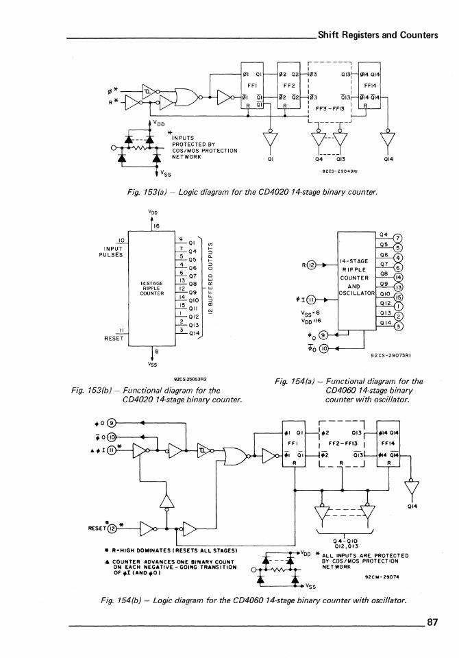
______________________ Shift Registers and Counters
.-----1 III I 0 I
FFI
1lI2 02
FF2
02 02
r------, I I 03 013,
I I I I 1- _ 1 03 013 ,
: FF3 -FFI3 : ~----------------~--~~~~
VDD
*" INPUTS PROTECTED BY COS/MOS PROTECTION NETWORK 04 013 014
9ZCS- 29049RI
Fig. 153(a} - Logic diagram for the CD4020 14-stage binary counter.
10
INPUT PULSES
II
RESET
Voo
16
14·STAGE RIPPLE
COUNTER
8
Vss
9 01
7 04 5 05 4 06
6 07 13 08
12 09
14 010 15 011
I 012
2 013 3 014
92CS-25053R2
'" >-:::> a. >-:::> 0
0
'" Ct:
'" u. u. :::> III
~
Fig. 153(b} - Functional diagram for the CD4020 14-stage binary counter.
• R-HIGH DOMINATES (RESETS All STAGES)
• COUNTER ADVANCES ONE BINARY COUNT ON EACH NEGATIVE - GOING TRANSITION OF+I(AND+O)
R 12 14-STAGE
RIP PLE
COUNTER
AND OSCILLATOR
VSS '8
VDD"'6
Fig. 154{a} - Functional diagram for the CD4060 14-stage binary counter with oscillator.
.-----1+' 0 I
I Q4-010 0/2.013
+14014
FFI4
fl OO * ALL INPUTS ARE PROTECTED
- - -- Vss ~~TC~~~~OS PROTECT/ON
92CIO-29074
Fig. 154(b} - Logic diagram for the CD4060 14-stage binary counter with oscillator.
________________________________________________________ 87
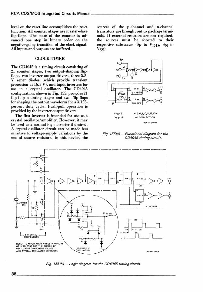
RCA COS/MaS Integrated Circuits Manual _______________ _
level on the reset line accomplishes the reset function. All counter stages are master-slave flip-flops. The state of the counter is advanced one step in binary order on the negative-going transition of the clock signal. All inputs and outputs are buffered.
CLOCK T1ME.R
The CD4045 is a timing circuit consisting of 21 counter stages, two output-shaping flipflops, two inverter output drivers, three 5.5-V zener diodes (which provide transient protection at 16.5 V), and input inverters for use in a crystal oscillator. The CD4045 configuration, shown in Fig. 155, provides 21 flip-flop counting stages and two flip-flops for shaping the output waveform for a 3.125-percent duty cycle. Push-pull operation is provided by the inverter output drivers.
The first inverter is intended for use as a crystal oscillator/amplifier. However, it may be used as a normal logic inverter if desired. A crystal oscillator circuit can be made less sensitive to voltage-supply variations by the use of source resistors. In this device, the
sources of the p-channel and n-channel transistors are brought out to package terminals. If external resistors are not required, the sources must be shorted to· their respective substrates (Sp to VDD, SN to VSS)'
VOO=3
Vss=14
4,5,6,9,10,11,12,13=
NO CONNECTION
92CS-29107
Fig. 155(a) - Functional diagram for the CD4045 timing circuit.
,'-----·-----------------1 ~I I
I
c::J sJ 2.097152 I
21 MHz lOR
I L 4>1
14 VSS
L EXTERNAL ---1 COMPONENTS
REFER TO APPLICATION NOTES ICAN 6086 OR ICAN 6539 FOR THE CHOICE OF OSCILLATOR COMPONENT VALUES AND TYPICAL OSCILLATOR CURRENTS
I
1 Q Q <I>
F/FI F/FI7
---------l I R I
L, ______ CD4045B _-.J
r lSEC --j .~ j ~1I3ZSEC
liZ SEC I--
y+d
92CM- 29106
Fig. 155(b) - Logic diagram for the CD4045 timing circuit.
88 ____________________________________________________ _
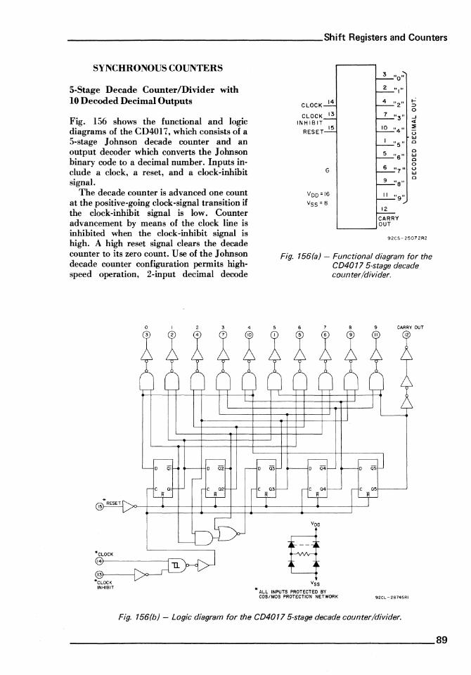
______________________ Shift Registers and Counters
SYNCHRONOUS COUNTERS
5-Stage Decade Counter/Divider with 10 Decoded Decimal Outputs
Fig. 156 shows the functional and logic diagrams of the CD4017, which consists of a 5-stage Johnson decade counter and an output decoder which converts the Johnson binary code to a decimal number. Inputs include a clock, a reset, and a clock-inhibit signal.
The decade counter is advanced one count at the positive-going clock-signal transition if the clock-inhibit signal is low. Counter advancement by means of the clock line is inhibited when the clock-inhibit signal is high. A high reset signal clears the decade counter to its zero count. Use of the Johnson decade counter configuration permits highspeed operation, 2-input decimal decode
a 3 4
o Qj o i52 o i53
CLOCK 14
CLOCK 13 INH IBIT
15 RESET
6
Voo = 16
Vss = 8
3 "0"
2 111"
4 "2" ..,: ::> 0
7 "3 11 ..J «
10 "4 11 ::!! 0 W
115 11 0
5 0 116 11 W
0
6 0
"7 II 0 w
9 0 "8"
II 119 11
12
CARRY OUT
92CS-25072R2
Fig. 156(a) - Functional diagram for the C D40 17 5-stage decade counter/divider.
CARRY OUT
o Q4 o Q5
a VSS
* ALL INPUTS PROTECTED BY COS/MaS PROTECTION NETWORK 92CL-28745RI
Fig. 156(b) - Logic diagram for the CD4017 5-stage decade counter/divider.
_______________________________________________________ 89

RCA COS/MaS Integrated Circuits Manual ______________ _
gating, and spike-free decoded outputs. Antilock gating is provided to assure proper
, co1mting sequence. The ten decoded outputs are normally low and go high only at their respective decimal time slots. Each decoded output remains high for one full clock cycle. A carry-out signal completes one cycle for every 10 clock-input cycles, and is used to clock the succeeding device directly in a multi-device counting chain.
4-Stage Divide-by-8 Counter/Divider with 8 Decoded Outputs
The CD4022 consists of a 4-stage divide-by-8 Johnson counter, associated decode output gating, and a carry-out bit, as shown in Fig. 157. The counter is cleared to its zero count
D Qj
C QI R
*CLOCK 14)---------i
*CLOCK INHIBIT
o Q2
C 02 R
CLOCK 14
CLOCK 13 INHIBIT
15 RESET
VDD= 16
VSS= 8
2 110"
"III
3 "2" ...: ::::l 0
7 113 11 0 ILl
II "4 11 0 0 u
4 115 11 ILl 0
5 IISII
10 "7 11
12
CARRY OUT
92CS-25073R2
Fig. 157(a) - Functional diagram for the CD4022 4-stage divide-byeight counter/divider.
o Q3
C 03 R
o 04
C 041------' R
VDD
VSS
* ALL INPUTS PROTECTED 8Y COS/MOS PROTECTION NETWORK
92CL-2874SRI
Fig. 157(b) - Logic diagram for the CD4022 4-stage divide-by-eight counter/divider.
9o ___________________________________________________ ___

______________________ Shift Registers and Counters
by a high reset signal. The counter is advanced at the positive-going clock-signal transition if the clock-inhibit signal is low.
Use of the Johnson divide-by-8 counter configuration pennits high-speed operation, 2-input decode gating, and spike-free decoder outputs. Anti-lock gating is provided to assure proper counting sequence. The 8 decode gating outputs are nonnally low and go high only at their respective decoded time slots. Each decoded output remains high for one full clock cycle. The carry-out signal completes one cycle for 8 clock-input cycles, and is used as a ripple-carry signal to directly clock a succeeding counter device in a multidevice counting system.
5-Stage Presettable Divide-by-N Counter
Fig. 158 shows the functional and logic diagrams of the CD4018. This type consists of 5 Johnson counter stages, buffered Q
DATA
* I r--+t------i
Ff'OO ~ Uvss
, "2" "4'" "I" "3 11 115"
~~~~u 10
CLOCK
OATA
RESET
14
15
B
Vss
5 QI
4 Q2
6 03
II Q4
13 05
92CS-25074
.,.: ~ 0 0 w II: w "-"-~ m
Fig. 158(a) - Functional diagram for the CD4018 5-stage presettable divide-by-N counter.
* ALL INPUTS PROTECTED BY COS/MOS INPUT PROTECTION NETWORK DETAIL OF TYPICAL STAGE
92CM-28752
Fig. 158(b) - Logic diagram for the CD4018 5-stage presettable divide-by-N counter.
_______________________________________________________ 91
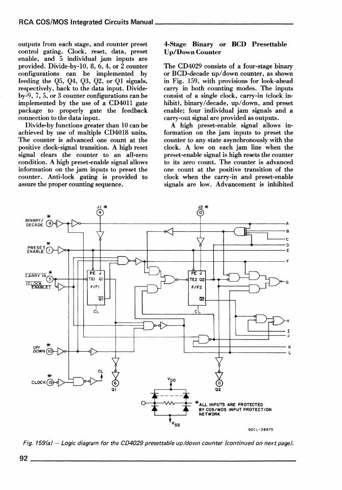
RCA COS/MOS Integrated Circuits Manual _______________ _
outputs from each stage, and counter preset control gating. Clock, reset, data, preset enable, and 5 individual jam inputs are provided. Divide-by-IO, 8,6,4, or 2 counter configurations can be implemented by feeding the Q5, Q4, Q3, Q2, or Q1 signals, respectively, back to the data input. Divideby-9, 7, 5, or 3 counter configurations can be implemented by the use of a CD4011gate package to properly gate the feedback connection to the data input.
Divide-by functions greater than 10 can be achieved by use of multiple CD4018 units. The counter is advanced one count at the positive clock-signal transition. A high reset signal clears the counter to an all-zero condition. A high preset-enable signal allows information on the jam inputs to preset the counter. Anti-lock gating is provided to assure the proper counting sequence.
, BINARYI 9 DECADE
* :~k:CET I
PE J TEl QI
F/FI
Qi
CL
QI
4-Stage Binary or BCD Presettab1e Up/Down Counter
The CD4029 consists of a four-stage binary or BCD-decade up/down counter, as shown in Fig. 159, with provisions for look-ahead carry in both counting modes. The inputs consist of a single clock, carry-in (clock inhibit), binary/decade, up/down, and preset enable; four individual jam signals and a carry-out signal are provided as outputs.
A high preset-enable signal allows information on the jam inputs to preset the counter to any state asynchronously with the clock. A low on each jam line when the preset-enable signal is high resets the counter to its zero count. The counter is advanced one count at the positive transition of the clock when the carry-in and preset-enable signals are low. Advancement is inhibited
A
B
C D E
F
PE J
TE2 Q2 G
F/F2
a2
CL
H
I J
K L
Q2
o-~>--JVlI\r--+- * ALL INPUTS ARE PROTECTED BY COSIMOS INPUT PROTECTION NETWORK
92CL-28675
Fig. 159(a) - Logic diagram for the CD4029 presettable up/down counter (continued on next page).
92 ____________________________________________________ __
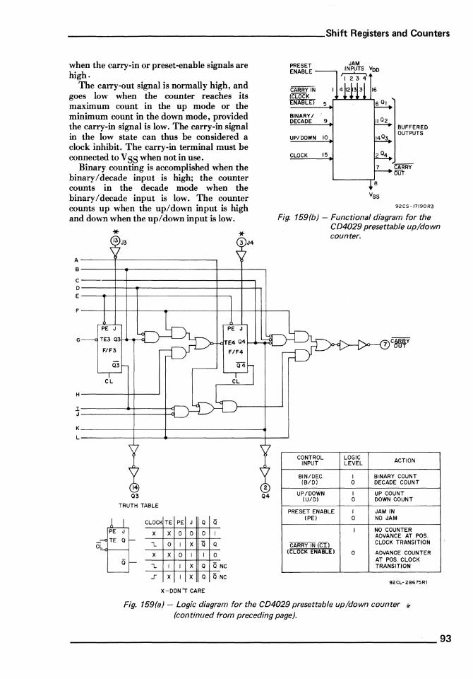
______________________ Shift Registers and Counters
when the carry-in or preset-enable signals are high.
The carry-out signal is normally high, and goes low when the counter reaches its maximum count in the up mode or the minimum count in the down mode, provided the carry-in signal is low. The carry-in signal in the low state can thus be considered a clock inhibit. The carry-in terminal must be connected to V SS when not in use.
Binary counting is accomplished when the binary / decade input is high; the counter counts in the decade mode when the binary / decade input is low. The counter counts up when the up/down input is high and down when the up/down input is low.
* * 3 J4
A
B
C--
0 E
F
PE J
G TE3 Q3
F/F3
Q3
CL
H
1 J
K
L
TRUTH TABLE
NC
fiEJ
_ TE Q
CL
Q
CLOC~ TE PE J 0 Il
x x 0 0 0 I
1- 0 I X Q Q
X X 0 I I 0
1- I I X 0 Q
J"" X I X 0 Q NC
X-DON'T CARE
04
PRESET ENABLE
CARiWiN (CLock ~5
BINARY/ ' DECADE 9
UP/DOWN 10
CLOCK 15
7
B
vss
BUFFERED OUTPUTS
92CS-17190R3
Fig. 159(b) - Functional diagram for the CD4029 presettable up/down counter.
CONTROL LOGIC ACTION INPUT LEVEL
BIN/DEC. I BINARY COUNT (B/D) 0 DECADE COUNT
UP/DOWN I UP COUNT (u/D) 0 DOWN COUNT
PRESET ENABLE I JAM IN (PE) 0 NO JAM
NO COUNTER ADVANCE AT POS.
CARRY IN (CI) CLOCK TRANSITION
(CLOCK ENABLE) 0 ADVANCE COUNTER AT POS. CLOCK TRANSITION
92CL- 28675Rl
Fig. 159(a) - Logic diagram for the CD4029 presettable up/down counter ,. (continued from preceding page).
_______________________________________________________ 93

RCA COS/MOS Integrated Circuits Manual _______________ _
Multiple packages can be connected in either a parallel-clocking or a ripple-clocking arrangements. Parallel clocking provides synchronous control and thus faster response from all counting outputs. Ripple counting allows for longer clock input rise and fall times.
4-Stage Presettable Up/Down Co~nters
The CD4510 and CD4516 presettable up/down counters consist of four synchronously clocked D-type flip-flops (with a gating structure to provide T -type flip-flop capability) connected as counters, as shown in Fig. 160. The CD4510 is a BCD counter; the CD4516 is a binary on(l.
PRESET* I ENABLE
CARRY OUT 0---------, 7
VDD
.~""'~ tS~J~gIED BY Vss PROTECTION NETWORK.
QI_---JI
PI* QI 4 6
PRESET ENABLE
PI QI
P2 12
Q2.
P3 13 14
Q3
P4 3
Q4
15 Voo = 16
CLOCK 'Iss'" 8 UP/DOWN 10
CARRY IN CJiRiiYi5iji'"
RESET 92CS-24824
Fig. 160(a) - Functional diagram for the CD4510 and CD4516 presettable up/down counters.
These counters can be cleared by a high level on the reset line, and can be preset to any binary number present on the jam inputs
P2* Q2 12 II
P3* Q3 13 14
P4* Q4 3 2
92CL-27003R2
Fig. 160(b) - Logic diagram for the CD4510 presettable up/down BCD counter.
94 ____________________________________________________ ___
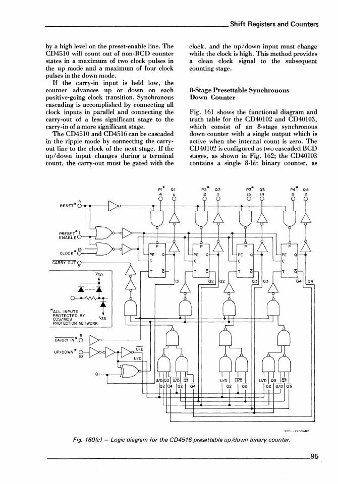
______________________ Shift Registers and Counters
by a high level on the preset-enable line. The CD4510 will count out of non-BCD counter states in a maximwn of two clock pulses in the up mode and a maximwn of four clock pulses in the down mode.
If the carry-in input is held low, the counter advances up or down on each positive-going clock transition. Synchronous cascading is accomplished by connecting all clock inputs in parallel and connecting the carry-out of a less significant stage to the carry-in of a more significant stage.
The CD4510 and CD4516 can be cascaded in the ripple mode by connecting the carryout line to the clock of the next stage. If the up/down input changes during a terminal count, the carry-out must he gated with the
RESET* c9r...-_-----!
PRESET'" I ENABLE
CARRY OUT 0-------, 7
Voo
.~""~ tS~J~g~ED BY Vss PROTECTION NETWORK.
CARRY IN* 5
Ol_~---/I
PI* QI 4 6
clock, and the up/down input must change while the clock is high. This method provides a clean clock signal to the subsequent counting stage.
8-Stage Presettable Synchronous Down. Counter
Fig. 161 shows the functional diagram and truth table for the CD40102 and CD40103, which consist of an 8-stage synchronous down-counter with a single output which is active when the internal count is zero. The CD40102 is configured as two cascaded BCD stages, as shown in Fig. 162; the CD40103 contains a single 8-bit binary counter, as
P2* 02 12 II
P4* 04 3 2
92CL-27004R2
Fig. 160(c) - Logic diagram for the CD4516 presettable up/down binary counter.
_______________________________________________________ 95

RCA COS/MOS Integrated Circuits Manual _______________ _
I I B-STAGE I DOWN I COUNTER
J7 I CO/ZO CLOCK
92CS-28BII
Fig. 161(a) - Functional diagram for the CD40102 and CD40103 presettable synchronous down-counters.
CONTROL INPUTS PRESET
CLR APE SPE cl/CE MODE
1 1 1 1
clock transition regardless of the state of the CIICE input. When the asynchronous preset-enable (APE) input is low, data at the jam inputs are asynchronously forced into the counter regardless of the state of the SPE, CIICE, or clock inputs. Jam inputs JO-17 represent two 4-bit BCD words for the CD40l02 and a single 8-bit binary word for the CD40103. When the clear (CLR)inputis low, the counter is asynchronously cleared to its maximum count (9910 for the CD40102 and 25510 for the CD40103) regardless ofthe state of any other input. The precedence relationship between control inputs is indicated in the truth table shown in Fig. 161.
ACTION
Inhibit counter
1 1 1 0 Synchronous Countdown
1 1 0 X Preset on next positive clock transition
1 0 X X Asynchronous Preset asynchronouslv
0 X X X Clear to maximum count
Notes: I. 0 = Low level 1 = High level x = Don't care
2. Clock connected to clock input 3. Synchronous operation: changes occur on negative-to
positive clock transitions 4. JAM inputs: CD40102B BCD; MSD = J7.J6.J5,J4 (J7 is MSBI
LSD = J3,J2.JI ,JO (J3 is MSB) CD40103B Binary; MSB = J7, LSB = JO
Fig. 161 (b) - Truth table for the CD40102 and CD40103 presettable synchronous down-counters.
shown in Fig. 163. Each type has control inputs for enabling or disabling the clock, for clearing the counter to its maximum count, and for presetting the counter either synchronously or asynchronously. All control inputs and the carry-out/zero-detect output are active-low logic.
In normal operation, the counter is decremented by one count on each positive transition of the clock. Counting is inhibited when the carry-in/clock-enable (CIICE) input is high. If the CIICE input is low, the carry-out/zero-detect (CO/ZD) output goes low when the count reaches zero and remains low for one full clock period.
When the synchronous preset-enable (SPE) input is low, data at the jam input is clocked into the counter on the next positive
The CD40102 and CD40103 may be cascaded, using the CIICE input and the CO/ZD output, in either a synchronous or ripple mode.
4-Stage Presettable Up/Down Counter
The CD40192 and CD40193 presettable up/down counters each consist of four synchronously clocked, gated D-type flipflops connected as counters, as shown in Fig. 164. The inputs consist of four individual jam lines, a preset-enable control, individual clock-up and clock-down inputs, and a master reset. Four buffered Q signal outputs are provided, as well as carry and borrow outputs for multiple-stage counting.
96 __________________________________________________ ___

______________________ Shift Registers and Counters
TO FFI-FF7 ~
~ TO
FFI-FF7
CIICE
3~-----------------q
A
B
C
D
E
J4
10
FF4
J5
Q
FF5
JO
4
FFO
CI
J6
Q
FF6
Q Q
FFI FF2
is CI CI
J7
FF7
J3
7 (MSB)
Q
FF3
is CI
92CL-28812
ALL INPUT TERMINALS (ALL TERMINALS EXCEPT 8, 14, a 16) ARE PROTECTED BY STANDARD COS/MOS PROTECTION NETWORK.
92CL-28S12
Fig. 162 - Logic diagram for CD40102 BCD down-counter.
A
B
C
E
_________________________________________________________ 97
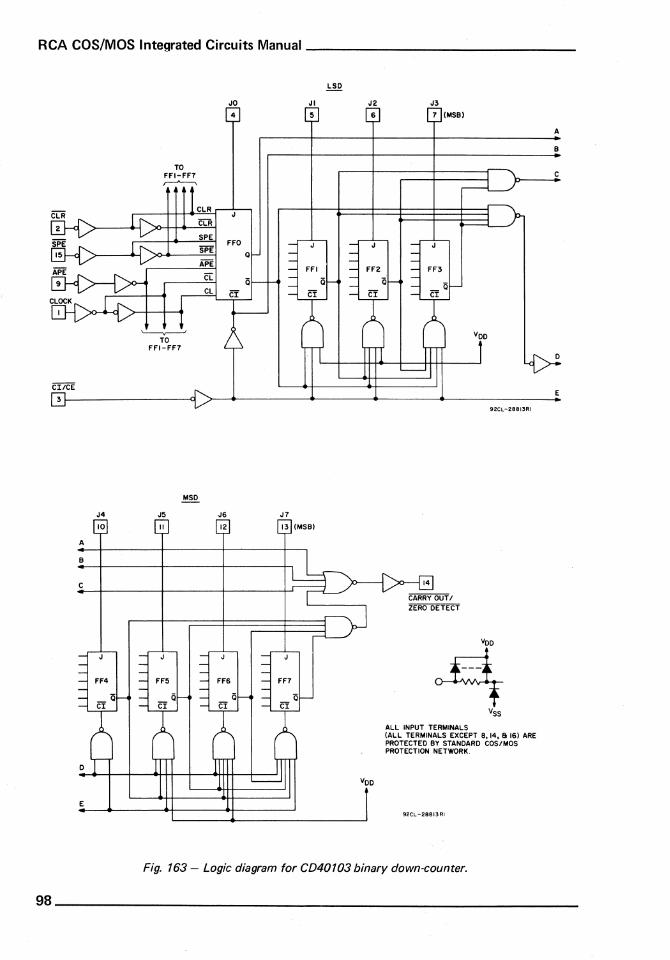
RCA COS/MaS Integrated Circuits Manual _______________ _
TO FFI-FF7 ,-"---\
'--.r-----' TO
FFI-FF7
CllCE
3~-----------------q
A
B
C
J4
10
FF4
J5
II
FF5
J6
12
JO
4
FFO
CI
FF6
Q
0
FF7
JI
5
FFI
CI 0
J2 6
FF2
CI
Voo
J3
7 (MSB)
FF3
0 _0 Cl
VoO
92CL-2S813RI
A~~ INPUT TERMINA~S (A~~ TERMINA~S EXCEPT 8,14, 80 16) ARE PROTECTED BY STANDARD COSIMOS PROTECTION NETWORK.
92CL-28813Rl
Fig. 163 - Logic diagram for CD40103 binary down-counter.
A
B
C
E
98 __________________________________________________ __

______________________ Shift Registers and Counters
The counter can be cleared so that all outputs are in a low state by a high on the reset line. A reset can be accomplished asynchronously with the clock. Each output is individually programmable asynchronously with the clock to the level on the corresponding jam input when the presetenable control is low.
The counter counts up one count on the positive clock edge of the clock-up signal, provided the clock-down line is high. The counter counts down one count on the positive clock edge of the clock-down signal, provided the clock-up line is high.
VDD
Both the carry and borrow signals are normally high. The carry signal goes low when the counter reaches its maximum count in the count-up mode. The borrow signal goes low when the counter reaches its minimum count in the count-down mode.
Cascading of multiple packages is easily accomplished without the need for additional external circuitry by tying the borrow and carry outputs to the clock-down and clock-up inputs, respectively, of the succeeding counterpackage.
6~~~~ VSS
* ALL INPUTS PROTECTED BY COS/MOS PROTECTION NETWORK 92CL-28980
Fig. 164(a) - Logic diagram for the CD40192 presettable up/down BCD counter.
RESET
14r---------------------~----------------~------~--------_. ---,
J2 J3 J4
CONTROL LOGIC I • SAME AS CONTROL LOGIC I
92CM- 28984
R4
S4
Fig. 164(b) - Control logic detail for the CD40192 and CD40193 presettable up/down counters.
_______________________________________________________ 99

RCA COS/MaS Integrated Circuits Manual _______________ _
VDD {j ~VDD ~--+----------+-VSS
* ALL INPUTS PROTECTED BY COS/MOS PROTECTION NETWORK
92Cl-28982
Fig. 164(c) - Logic diagram for the CD40193 presettable up/down binary counter.
PRESET ENABLE
II JI 15 3
01
J2 I 2 02
J3 10 6 03 J4 9 7 04
CLOCK UP 5 13 BORROW
CLOCK DOWN 4 12 CARRY
14 RESET Voo= 16
VSS=8
92CS- 27'561RI
Fig. 164(d) - Functional diagram for the CD40192 and CD40193 presettable up/down counters.
Dua14-Stage Up-Counters
The CD4518 and CD4520 dual up-counters each consist of two identical internally synchronous 4-stage counters, as shown in Fig. 165; the CD4518 contains BCD counters, and the CD4520 contains binary counters. The counter stages are D-type flipflops having interchangeable clock and enable lines for incrementing on either the positive-going or negative-going transitions. For single-unit operation, the enable input is
maintained high and the counter advances on each positive-going transition of the clock. The counters are cleared by high levels on their reset lines.
These counters can be cascaded in the ripple mode by connecting Q4 to the enable input of a subsequent counter while its clock input is held low.
CLOCK A
I
2--"""'-~
ENABLE A
3 OIA +1%16 402A
503A 6 04A
R RESET A
7--------'
CLOCK B
RESET B
;-----,,, OIB
+10/ /+16
R
1202B 13 03B
15 --------'
1404B
Voo= 16 VSS=B
92CS-24506RI
Fig. 165(a) - Functional diagram for the CD4518 and CD45204-stage dual up-counters.
100 __________________________________________________ __

______________________ Shift Registers and Counters
RESET
01 02 03 04
Fig. 165(b) - Logic diagram for one section of the CD4518 BCD dual up-counter.
01 02 03 04
4 * ALL INPUTS PROTECTED BY
COS/MOS PROTECTION NETWORK
nCM- 23773R2
Fig. 165(c) - Logic diagram for one section of the CD4520 binary dual up-counter.
Vss
_____________________________________________________ 101

RCA COS/MaS Integrated Circuits Manual _______________ _
Synchronous Programmable 4-Bit Counters
Fig. 166 shows the functional and logic diagrams for the CD40160, CD40161, CD40162, and CD40163 4-bit synchronous programmable counters. The clear function of the CD40162 and CD40163 is synchronous, and a low level at the clear input sets all four outputs low on the next positive clock edge. The clear function of the CD40160 and CD40161 is asynchronous, and a low level at the clear input sets all four outputs low regardless of the state of the clock, load, or enable inputs. A low level at the load input disables the counter and causes the output to agree with the setup data after the next clock pulse regardless of the enable inputs.
Counting is enabled when both the PE and TE inputs are high. The TE input is fed forward to enable COUTo This enabled output produces a positive output pulse with
PE 7
TE 10
CLEAR
LOAO 9
CLOCK 2
PI 3
P2 4
P3 5
P4 6
VOO = 16
Vss =8
14 QI
13 Q2
12 Q3
II Q4
15 CARRY OUT
92C5 - 28628RI
Fig. 166(a} - Functional diagram for the CD40160, CD40161, CD40162, and CD40163 synchronous programmable 4-bit counters.
a duration approximately equal to the positive portion of the Ql output. This pulse can be used to enable successive cascaded stages.
CD40160B AND CD40162B BCD DECADE COUNTERS
* * * * *
* INPUTS PROTECTED aDD BY C,OSI MOS PROTECTION __ _ NETWORK
Vss 92CL-29224RI
Fig. 166(b} - Logic diagram for the CD40160 and CD40162 programmable BCD decade counters.
102 ____________________________________________________ __

______________________ Shift Registers and Counters
CD40161B ASYNCHRONOUS CLEAR
CD40163B SYNCHRONOUS CLEAR
--* LOAD
*
~~\
CD40161B AND CD40163B BINARY caUNTERS
* * * * *
:>4-------'--\-----+--+--~-___t_____'
* &1 VDD INPUTS PROTECTED
BY COS/II.lOS PROTECTION ___ _ NETWORK
VSS 92CL-29225RI
Fig. 166(c) - Logic diagram for the CD40161 and CD40163 programmable binary counters.
____________________________________________________ 103

IX. Display Drivers
LIQUID-CRYSTAL DISPLAYS
Of all segmented digital displays presently available, liquid-crystal displays (LCD's) are most compatible with COS/MOS circuitry in terms of ultra-low power consumption and operating-voltage ranges. A one-half-inch, 7-segment, 3-112 digit liquid-crystal display draws only a few microamperes when all segments are energized.
The first LCD's were dynamic-scattering types which had operating voltages in the range of 12 to 18 volts. The later development of field-effect LCD's reduced operating voltages to the 3-to-7-volt range, further reduced current levels, and improved view ability .
LCD's turn on when a field is applied between a segment and the back electrode, across the liquid-crystal fluid. To avoid plating effects, the field must be periodically reversed (usually at 32 Hz). Thus, an "on" segment has a square-wave voltage applied which is 180 degrees out of phase with the signal on the back electrode; an "off" segment is in phase with the back electrode. Because of their relatively slow turn-on characteristic, LCD's are usually not multiplexed, and a separate connection is required for each segment; the back electrode is common.
COS/MOS LCD Drivers
RCA COS/MOS liquid-crystal-display drivers have internal level shifting (for use in applications where the logic level is not at the same potential as that required by the display), latching, and BCD decoding.
The CD4055 and CD4056 are single-digit BCD-to-7 -segment decoder I driver circuits that provide level-shifting functions on the chip, as shown in Fig. 167. This feature permits the BCD input-signal swings (VDD to V SS) to be the same as or different from . the 7-segment output-signal swings (VDD to ' VEE)' For example, the BCD input-signal swing (VDD to VSS) may be as low asOto-3 volts, while the output-display drive-signal swing (VDD to VEE) may be from 0 to -15 volts. If VDD to VEE exceeds 15 volts, VDD to V SS should be at least 4 volts.
The 7-segment outputs are controlled by a square wave at the display-frequency (DF) input, as shown in Fig. 168. Selected segments have a square-wave output voltage that is 180 degrees out of phase with the DF
8 7 16 ~vss ~VEE ~VDD
r -- -- -I
I I I I L ___ CE..405~ __
7-SEG· OUT·
ALL INPUTS PROTECTED BY 92CS- 20092RI cosmos PROTECTION NETWORK
Fig. 167(a} - Functional diagram for the CD4055 liquid-crystal BCD-to-7-segment decoder/driver with "display-frequency" output.
104 ______________________________________________ ___
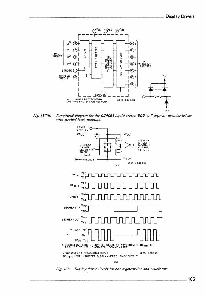
___________________________ Display Drivers
en II: W
BCD f-IL
INPUTS 22 :;: en ...J w > w ...J
STROBE I
f-'ZII: oww
f-::EO • (!I 0 °wu ~'f'~
....
7-SEGMENT OUTPUTS
DISPLAY - VDD FREQ· IN
I I L __ -..£D4056 ____ -.J
ALL INPUTS PROTECTED BY COS/MOS PROTECTION NETWORK
92CS - 2009. RI
Vss Fig. 161(b) - Functional diagram for the CD4056 liquid-crystal BCD-to-l-segment decoder/driver
with strobed-latch function.
LEVELSHIFTED
DFOUT
DISPLAY DRIVER SEGMENT INPUT (0 TOg)
DFOUT
(HIGH=SELECT) '--_.-., __ --' DFOUT
VDD DF'N
VSS
Voo DFOUT
VEE
___ Vo OFOUT
VEE
VOO ,..-------, SEGMENT IN J
VEE:
VOO SEGMENT OUT
VEE
*
(0) 92CS- 20093R.
* ~~~ ~ T ~ ~N+O L L~gUl D:~~~~~i~~~'t".tNJ"N 'f~~~FORM IF DFOUT IS
OF'N =DlSPLAY-FREQUENCY INPUT 92CS- 20094RI
DFOUT= LEVEL-SHIFTED DISPLAY-FREQUENCY OUTPUT
(b)
L
Fig. 168 - Display-driver circuit for one segment line and waveforms.
_____________________________________________________ 105
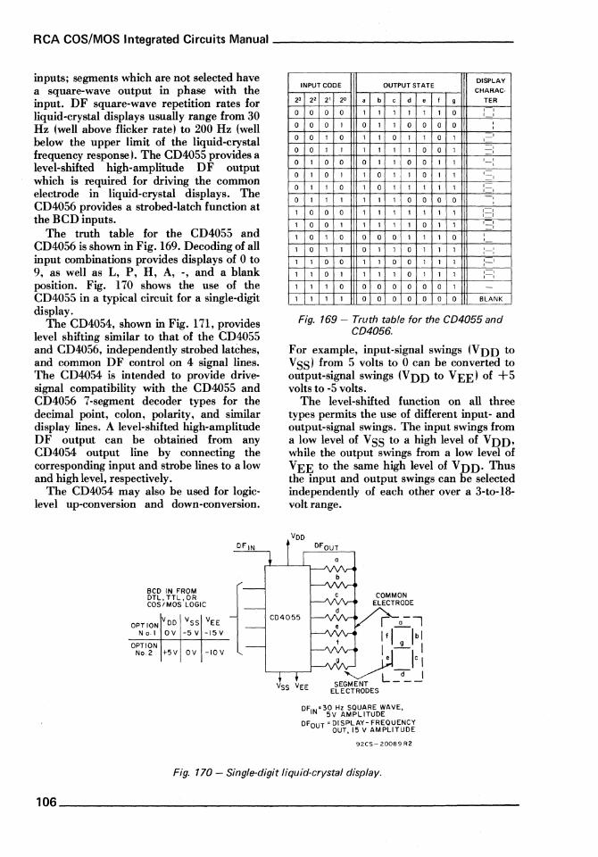
RCA COS/MaS Integrated Circuits Manual _______________ _
inputs; segments which are not selected have a square-wave output in phase with the input. DF square-wave repetition rates for liquid-crystal displays usually range from 30 Hz (well above flicker rate) to 200 Hz (well below the upper limit of the liquid-crystal frequency response). The CD4055 provides a level-shifted high-amplitude DF output which is required for driving the common electrode in liquid-crystal displays. The CD4056 provides a strobed-latch function at the BCD inputs.
The truth table for the CD4055 and CD4056 is shown in Fig. 169. Decoding of all input combinations provides displays of 0 to 9, as well as L, P, H, A, -, and a blank position. Fig. 170 shows the use of the CD4055 in a typical circuit for a single-digit display.
The CD4054, shown in Fig. 171, provides level shifting similar to that of the CD4055 and CD4056, independently strobed latches, and common DF control on 4 signal lines. The CD4054 is intended to provide drivesignal compatibility with the CD4055 and CD4056 7 -segment decoder types for the decimal point, colon, polarity, and similar display lines. A level-shifted high-amplitude D F output can be obtained from any CD4054 output line by connecting the corresponding input and strobe lines to a low and high level, respectively.
The CD4054 may also be used for logiclevel up-conversion and down-conversion.
BCD IN FROM DTL, TTL,OR COS/MOS LOGIC
OPTION V DD Vss VEE No·1 OV -5V -15V
OPTION No.2 +SV OV -IOV
INPUT CODE OUTPUT STATE DISPLAY CHARAC-
23 2' 2' 2" • b c d • f 9 TER
0 0 0 0 1 1 1 1 1 1 0 I I I I
0 0 0 1 0 1 1 0 0 0 0 I I
0 0 1 0 1 1 0 1 1 0 1 - I I
0 0 1 1 1 1 1 1 0 0 1 - , I
0 1 0 0 0 1 1 0 0 1 1 I - I I
0 1 0 1 1 0 1 1 0 1 1 I - I
0 1 1 0 1 0 1 1 1 1 1 I -I I
0 1 1 1 1 1 1 0 0 0 0 I I
1 0 0 0 1 1 1 1 1 1 1 I - I I I
1 0 0 1 1 1 1 1 0 1 1 I - I I
1 0 1 0 0 0 0 1 1 1 0 I I
1 0 1 1 0 1 1 0 1 1 1 I - , , , 1 1 0 0 1 1 0 0 1 1 1 :_1 1 1 0 1 1 1 1 0 1 1 1 I - I
I I
1 1 1 0 0 0 0 0 0 0 1 -1 1 1 1 0 0 0 0 0 0 0 BLANK
Fig. 169 - Truth table for the CD4055 and CD4056.
For example, input-signal swings (VDD to V SS) from 5 volts to 0 can be converted to output-signal swings (VDD to VEE) of +5 volts to -5 volts.
The level-shifted function on all three types permits the use of different input- and output-signal swings. The input swings from a low level of VSS to a high level of VDD, while the output swings from a low level of VEE to the same high level of VDD. Thus the input and output swings can be selected independently of each other over a 3-to-18-volt range.
DFOUT
b
DFIN = 3g :i~~~ffJD~AVE, DFOUT = DISPLAY- FREQUENCY
OUT, IS V AMPLITUDE
92CS- 20089 R2
Fig. 170 - Single-digit liquid-crystal display.
106 __________________________________________________ __

___________________________ Display Drivers
IN 4
(/) Il:
In W l- ll: ... W
::c ~ <Il Il:
0
...J >-W <[ > ...J W a. ...J In
C
STROBE I 10
~Wfa~I~- 2
Fig. 171 - Functional diagram for the CD4055 4-line liquid-crystaldisplay driver.
LIGHT-EMITTING-DIODE DISPLAYS
Light-emitting diodes (LED's) used in digital displays are usually gallium-arsenidephosphide· diffused planar devices. Their extremely fast response time allows them to be multiplexed and thus reduces interconnection wiring. Multiplexing, however, requires an increase in the pulsed current by a factor equal to the duty cycle.
In an eight-digit display, for example, each digit is driven only one-eighth of the time. To maintain equivalent brightness, therefore, a segment with an average dc current requirement of 3 milliamPeres must be pulsed with 24 milliamperes. Sourcing currents of this magnitude are not practicable with conventional COS/MOS geometries.
Fig. 172 shows the functional diagram of the CD4511 latch decoder driver, which combines bipolar n-p-n transistor output devices with COS/MOS logic in a single monolithic structure. The COS/MOS logic includes a BCD latch and a BCD-to-7-segment decoder; the bipolar devices in the driver stage can source up to 25 milliamperes. This capability allows the CD4511 to drive LED's, incande&'entdisplays, and lowvoltage fluorescent displays directly.
The truth table for the CD4511 is shown in Fig. 173, and its logic diagram in Fig. 174.
BCD 7-SEGMENT INPUTS LT OUTPUTS
I 3 I A 7
13 a
0 0 12 b
B I L E R II c A C
I 10 d T 0 c 2 C 0 V
9 e H E E
R R 15 f 0 6
14 g
LEIST ROBE 5
LE
X
X
a
a
a
a
a
a
0
a
a
a
a 0
0
0
0
0
1
VSS=B 92CS- 25083R2
VOO=16
Fig. 172 - Functional diagram for the CD4511 latch decoder driver.
BI LT D C B A a b c d e f 9 Display
X a X X X X 1 1 1 1 1 1 1 8 a 1 X X X X a a a a a a a Blank
1 1 a a a a 1 1 1 1 1 1 a 0 1 1 a a a 1 a 1 1 a a a a I 1 1 a a 1 a 1 1 0 1 1 0 1 2 1 1 0 0 1 1 1 1 1 1 o 0 1 3 1 1 0 1 0 0 o 1 1 0 0 1 1 &f 1 1 a 1 a 1 1 0 1 1 a 1 1 5 1 1 0 1 1 0 o 0 1 1 1 1 1 b 1 1 0 1 1 1 1 1 1 0 0 o 0 7 1 1 1 a 0 a 1 1 1 1 1 1 1 8 1 1 1 a a 1 1 1 1 a 0 1 1 9 1 1 1 0 1 0 a a a a a 0 0 Blank
1 1 1 0 1 1 a 0 o 0 0 o a Blank
1 1 1 1 0 0 o a o 0 a a 0 Blank
1 1 1 1 a 1 a a 000 a a Blank
1 1 1 1 1 a a a a 0 000 Blank
1 1 1 1 1 1 a a a 0 000 Blank
1 1 X X X X * * X '" Oon't Care * Depends on BCD code previously
applied when LE = a Note: Display is blank for all illegal input codes (BCD> 1001).
Fig. 173 - Truth table for the CD4511.
I
_____________________________________________________ 107
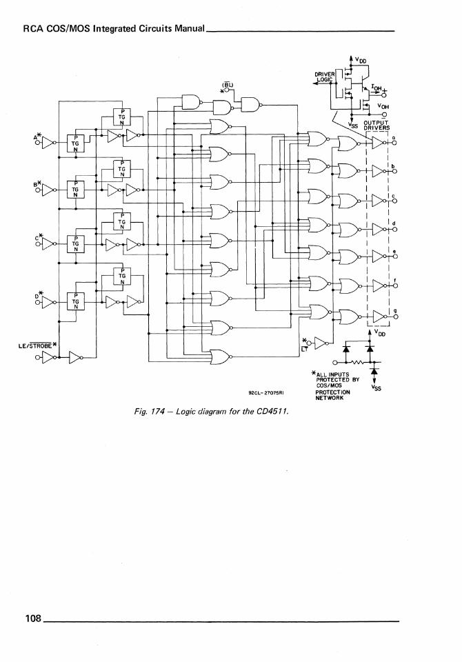
RCA COS/MaS Integrated Circuits Manual _______________ _
92CL- 27075RI
Fig. 174 - Logic diagram for the CD4511.
*ALL INPUTS PROTECTED BY COS/MOS PROTECTION NETWORK
108 ____________________________________________________ __
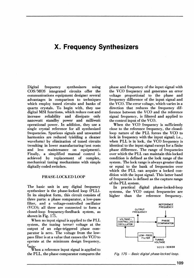
x. Frequency Synthesizers
Digital frequency synthesizers using eOS/MOS integrated circuits offer the communications equipment designer several advantages in comparison to techniques which employ tuned circuits and banks of quartz crystals. To begin with, they use digital MSI functions, which reduce cost and increase reliability and dissipate only nanowatt standby power and milliwatt operational power. In addition, they use a single crystal reference for all synthesized frequencies. Spurious signals and unwanted harmonics are reduced (yielding a cleaner waveform) by elimination of tuned circuits (resulting in lower manufacturingltest costs and less maintenance on equipment). Finally, a simplified manual control is achieved by replacement of complex, mechanical tuning mechanisms with simple digitally coded switches.
PHASE-LOCKED LOOP
The basic unit in any digital frequency synthesizer is the phase-locked loop (PLL). In its simplest form, this circuit consists of three parts: a phase comparator, a low-pass filter, and a voltage-controlled oscillator (VeO); all three are connected to form a closed-loop frequency-feedback system, as shown in Fig. 175;
When no input signal is applied to the PLL system, the tuning (error) voltage at the output of an edge-triggered phase comparator is zero. The voltage from the lowpass filter is at a value that causes the veo to operate at the minimum design frequency, fmin·
When a reference input signal is applied to the PLL, the phase comparator compares the
phase and frequency of the input signal with the veo frequency and generates an error voltage proportional to the phase and frequency difference of the input signal and the yeo. The error voltage, which varies in a direction that reduces the frequency difference between the veo and the reference signal frequency, is filtered and applied to the control input of the yeo.
When the veo frequency is sufficiently close to the reference frequency, the closedloop nature of the PLL forces the veo to lock in frequency with the input signal; i.e., when PLL is in lock, the veo frequency is identical to the input signal except for a finite phase difference. The range of frequencies over which the PLL can maintain this locked condition is defined as the lock range of the system. The lock range is always greater than or equal to the bank of frequencies over which the PLL can acquire a locked condition with the input signal. This latter band of frequencies is defined as the capture range of the PLL system.
In practical digital phase-locked-loop systems, the veo output frequencies are higher than the reference frequency.
REFERENCE FREQUENCY
92CS-30638
Fig. 175 - Basic digital phase-locked loop.
______________________________________________________ 109

RCA COS/MaS Integrated Circuits Manual ______________ _
Addition of a divide-by-N counter between the VCO and the phase comparator, as shown in Fig. 176, permits selection of a wide
OUTPUT FREQUENCY
VOLTAGECONTROLLED OSCILLATOR
FREQUENCYCONTROL
CODE
+ liN II
COUNTER
LOW-PASS
REFERENCE FREQUENCY
PHASE COMPARATOR
FILTER i+-TU-N-I-NG-..J '--__ --' VOLTAGE
92CS- 30637
Fig. 176 - Typical digital phase-locked loop.
range of VCO frequencies, dependent on the programmed counter setting. In this case, the VCO locks at a frequency which is the product of the reference frequency and the countdown factor.
The CD4046 COS/MOS micropower phase-locked-loop (PLL) consists of a lowpower, linear voltage-controlled oscillator (VCO) and two different phase comparators having a common signal-input amplifier and a common comparator input. A 5.2-volt zener diode is provided for supply regulation if necessary. A block diagram of the CD4046 is shown in Fig. 177.
CD4046B
VCOSection
The VCO requires an external capacitor (Cl) and one or two external resistors (Rl, or Rl and R2). Resistor Rl and capacitor Cl determine the frequency range of the VCO, and resistor R2 enables the VCO to have a frequency offset if required. The high input impedance (1012 ohms) of the VCO simplifies the design of low-pass filters by permitting a wide choice of resistor-tocapacitor ratios. A source-follower output of the VCO input voltage is provided at terminal 10 (demodulated output) to prevent loading of the low-pass filter. If terminal 10 is used, a load resistor (RS) of 10 kilohms or more should be connected from terminal 10 to V SS. If it is not used, terminal 10 should be left open.
The VCO can be connected either directly or through frequency dividers to the comparator input of the phase comparators. The full COS/MOS logic swing available at the output of the VCO allows direct coupling to COS/MOS frequency dividers such as the CD4024, CD4018, CD4020, CD4022 , CD4029, and CD4059. The CD4046 phaselocked-loop can be used in combination with one or more CD4018 presettable divide-by-N counters, or CD4029 presettable up/down counters, or CD4059 programmable divideby-N counters, or CD40192/CD40193 presettable up/down counters to build a
CI ..-----{ LOW ~~~~~ r-----~~s
2 FILTER C r
VSS
* ALL INPUTS ARE PROTECTED BY COS/MOS PROTECTION NETWORK
92CS-29172
Fig. 177 - Block diagram of CD4046 COS/MaS micropower phase-locked loop.
110 ___________________________________ -----------------

________________________ Frequency Synthesizers
micropower low-frequency synthesizer. A logic "0" on the inhibit input enables the VCO and the source follower; a logic "1" turns off both to minimize standby power consumption.
Phase Comparators
The phase-comparator signal input (terminal 14) can be direct-coupled provided the signal swing is within COS/MOS logic levels, i.e., logic "O":S:;;; 30% (VDD - VSS), logic "1" ~ 70% (VDD - VSS). For smaller swings, the signal must be capacitively coupled to the self-biasing amplifier at the signal input.
Phase comparator I is an exclusive-OR network; it operates analogously to an overdriven balanced mixer. To maximize the lock range, the signal- and comparator-input frequencies must have a 50-per-cent duty cycle. With no signal or noise on the signal input, this phase comparator has an average output voltage equal to VDD/2. The lowpass filter connected to the output of phase comparator I supplies the average voltage to the VCO input, and causes the VCO to oscillate at the center frequency (fo ).
The frequency range of input signals on which the PLL will lock if it is initially out of lock is defined as the frequency capture range (2fc ). The frequency range of input signals on which the loop will stay locked if it is initially in lock is defined as the frequency lock range (2fL). The capture range is equal to or less than the lock range.
With phase comparator I, the range of frequencies over which the PLL can acquire lock (capture range) depends on the lowpass-filter characteristics, and can be made as large as the lock range. Phase comparator I permits a PLL system to remain in lock in spite of high amounts of noise in the input signal.
One characteristic of this type of phase comparator is that it may lock onto input frequencies that are close to harmonics of the VCO center frequency. A second characteristic is that the phase angle between the signal and the comparator input varies between 0 and 180 degrees, and is 90 degrees at the center frequency. Fig. 178 shows the typical triangular phase-to-output response characteristic of phase comparator I. Typical
AVERAGE OUTPUT VOLTAGE
SIGNAL-TO- COMPARATOR INPUTS PHASE OIFFERENCE
92C5-20009
Fig. 178 - Characteristics of CD4046 phase comparator I at low-pass-filter output.
waveforms for a COS/MOS phase-locked loop employing phase comparator I in a locked condition of fo are shown in Fig. 179.
SIGNAL INPUT (TERM. 141
VCO OUTPUT (TERM 41= COMPARATOR INPUT (TERM 31
PHASE COMPARATOR I OUTPUT (TERM. 2)
VCO INPUT (TERM. 9)= = LOW-PASS FILTER
OUTPUT
~
~
~ -VOO
~
-VSS 92C5-20010RI
Fig. 179 - Typical waveforms for CD4046 with phase comparator I in locked condition fo.
Phase comparator II is an edge-controlled digital memory network. It consists of four flip-flop stages, control gating, and a threestate output circuit comprising p- and ntype drivers that have a common output node. When the p-MOS or noMOS drivers are on, they pull the output up to VDD or down to VSS, respectively. This type of phase comparator acts only on the positive edges of the signal and comparator inputs. The duty cycles of the signal and comparator inputs are not important because positive transitions control PLL systems that use this type of comparator.
If the signal-input frequency is higher than the comparator-input frequency, the p-type output driver is maintained on most of the time, and both the n- and p-type drivers are off (3-state) the remainder of the time. If the signal-input frequency is lower than the comparator-input frequency, the n-type output driver is maintained on most of the time, and both the n- and p-type drivers are off (3-state) the rest of the time. If the signaland comparator-input frequencies are the
_____________________________________________________ 111

RCA COS/MaS Integrated Circuits Manual _______________ _
same, but the signal input lags the comparator input in phase, the n-type output driver is maintained on for a time corresponding to the phase difference. If the signal- and comparator-input frequencies are the same, but the comparator input lags the signal in phase, the p-type output driver is maintained on for a time corresponding to the phase difference. Subsequently, the capacitor voltage of the low-pass filter connected to this phase comparator is adjusted until the signal and comparator inputs are equal in both phase and frequency. At this stable point, both p- and n-type output drivers remain off, and thus the phasecomparator output becomes an open circuit and holds the voltage on the capacitor of the low-pass filter constant.
The signal at the "phase pulses" output is a high level most of the time. Small negative spikes, however, can be seen under normal locked conditions. This output can be used for indicating a locked condition when phase comparator II is used. For phase comparator II, therefore, no phase difference exists between signal and comparator input over the full VCO frequency range. In addition, the power dissipation due to the low-pass filter is reduced when this type of phase comparator is used because both the p- and n-type output drivers are off for most of the signal-input cycle.
It should be noted that the PLL lock range for this type of phase comparator is equal to the capture range, independent of the lowpass filter. With no signal present at the signal input, the VCO is adjusted to its lowest frequency for phase comparator II. Fig. 180
SIGNAL INPUT (TERM. 14)
VCO OUTPUT (TERM 4) = COMPARATOR INPUT (TERM 3)
shows typical waveforms for a COS/MOS PLL employing phase comparator II in a locked condition.
PROGRAMMABLE DIVIDE-BY-N COUNTER
The CD4059 is a divide-by-N down-counter that can be programmed to divide an input frequency by any number (N) from 3 to 15,999. The output signal is a pulse oneclock-cycle wide occurring at a rate equal to the input frequency divided by N. This single output has TTL drive capability. The downcounter is preset by means of 16 jam inputs. A functional block diagram of the CD4059 is shown in Fig. 181.
The three-mode-select inputs Ka, Kb, and Kc determine the modulus (divide-by number) of the first and last counting sections in accordance with the truth table shown in Fig. 182. Every time the first (fastest) counting section goes through one cycle, it reduces by one the number that has been preset (jammed) into the three decades of the intermediate counting section and into the last counting section, which consists of flip-flops that are not needed for operating the first counting section. For example, in the divide-by-2 mode, only one flip-flop is needed in the first counting section. Therefore, the last counting section has three flip-flops that can be preset to a maximum count of seven with a place value of thousands. If divide-by-l0 is desired for the first section, Ka is set to 1, Kb to 1, and Kc to o. Jam inputs n, J2, J3, and J4 are used to preset the first counting section, and there
PHASE COMPARATOR n OUTPUT (TERM. 13)
veo INPUT (TERM. 9) = = LOW-PASS FILTER OUTPUT
_JL- - - ~ - - - ----tl""" -"._-VDD -VSS
____ --~tt!-----~-VDD
-VSS
PHASE PULSE (TERM. I) 11 NOTE: DASHED LINE IS AN OPEN-CIRCUIT
CONDITION (3"1 STATE)
n--y--VDD
-VSS
92CS20011R2
Fig. 180 - Typical waveforms for CD4046 with phase comparator" in locked condition.
112 __________________________________________________ __

________________________ Frequency Synthesizers
CLOCK INPUT
PROGRAM JAM INPUTS (BCD)
P. E.
FIRST COUNTING SECTION
-:-10,8,5,4,2
INTERMEDIATE COUNTING SECTION -------101 LAST
COUNTING SECTION
-71,2,2,4,8
MODE
-:- 10
RECOGNITION '------...-j GATI NG
I I I I ______ J
1
___________ J
CONTROL 1-------+-1 PRESET ENABLE
LATCH ENABLE 2r--------------1-~~~
DIVIDE-BY-N OUTPUT
92CM- 22213 R 1
Fig. 181 - Functional block diagram for the CD4059 programmable divide-by-N counter.
MODE FIRST COUNTING LAST COUNTING COUNTER
SELECT SECTION SECTION RANGE
INPUT DESIGN EXTENDED
MODE Can be
MODE Can be
-- preset -- preset Ka Kb Kc Di· to a Jam· Di· to a JaroA Max. Max.
vides max inputs vides max inputs by: of: used: by: of: used:
1 1 1 2 1 Jl 8 7 J2,J3,J4 15,999 17,331
0 1 1 4 3 Jl,J2 4 3 J3,J4 15,999 18,663
1 0 1 5# 4 Jl,J2,J3 2 1 J4 9,999 13,329
0 0 1 8 7 Jl,J2,J3 2 1 J4 15,999 21,327
1 1 0 10 9 Jl,J2,J3,J4 1 0 - 9,999 16,659
X 0 0 MASTER PRESET MASTER PRESET - -
X = Don't Care #Operation in the ';'5 mode (1st counting section) requires going through the Master Preset mode prior to going into the ';'5 mode. At power turn·on, kc must be a logic "0" for a period of 3 input clock pulses after V DO reaches
• Jl = Least significant bit.
J4 = Most significant bit.
a minimum of 3 volts.
Fig. 182 - Truth table for CD4059.
____________________________________________________ 113
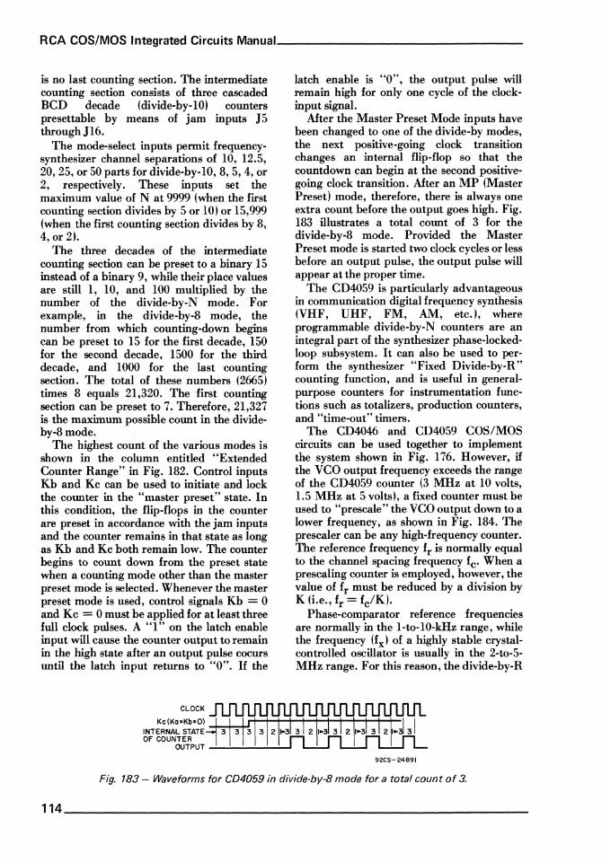
RCA COS/MaS Integrated Circuits Manual, _______________ _
is no last counting section. The intermediate counting section consists of three cascaded BCD decade (divide-by-1O) counters presettable by means of jam inputs J5 through Jl6.
The mode-select inputs permit frequencysynthesizer channel separations of 10, 12.5, 20, 25, or 50 parts for divide-by-l0, 8, 5, 4, or 2, respectively. These inputs set the maximum value of N at 9999 (when the first counting section divides by 5 or 10) or 15,999 (when the first counting section divides by 8, 4, or 2).
The three decades of the intermediate counting section can be preset to a binary 15 instead of a binary 9, while their place values are still 1, 10, and 100 multiplied by the number of the divide-by-N mode. For example, in the divide-by-8 mode, the number from which counting-down begins can be preset to 15 for the first decade, 150 for the second decade, 1500 for the third decade, and 1000 for the last counting section. The total of these numbers (2665) times 8 equals 21,320. The first counting section can be preset to 7. Therefore, 21,327 is the maximum possible count in the divideby-8mode.
The highest count of the various modes is shown in the column entitled "Extended Counter Range" in Fig. 182. Control inputs Kb and Kc can be used to initiate and lock the counter in the "master preset" state. In this condition, the flip-flops in the counter are preset in accordance with the jam inputs and the counter remains in that state as long as Kb and Kc both remain low. The counter begins to count down from the preset state when a counting mode other than the master preset mode is selected. Whenever the master preset mode is used, control signals Kb = 0 and Kc = 0 must be applied for at least three full clock pulses. A "1" on the latch enable input will cause the counter output to remain in the high state after an output pulse cocurs until the latch input returns to "0". If the
latch enable is "0", the output pulse will remain high for only one cycle of the clockinput signal.
After the Master Preset Mode inputs have been changed to one of the divide-by modes, the next positive-going clock transition changes an internal flip-flop so that the countdown can begin at the second positivegoing clock transition. After an MP (Master Preset) mode, therefore, there is always one extra count before the output goes high. Fig. 183 illustrates a total count of 3 for the divide-by-8 mode. Provided the Master Preset mode is started two clock cycles or less before an output pulse, the output pulse will appear at the proper time.
The CD4059 is particularly advantageous in communication digital frequency synthesis (VHF, UHF, FM, AM, etc.), where programmable divide-by-N counters are an integral part of the synthesizer phase-Iockedloop subsystem. It can also be used to perform the synthesizer "Fixed Divide-by-R" counting function, and is useful in generalpurpose counters for instrumentation functions such as totalizers, production counters, and "time-out" timers.
The CD4046 and CD4059 COS/MOS circuits can be used together to implement the system shown in Fig. 176. However, if the VCO output frequency exceeds the range of the CD4059 counter (3 MHz at 10 volts, 1.5 MHz at 5 volts), a fixed counter must be used to "prescale" the VCO output down to a lower frequency, as shown in Fig. 184. The prescaler can be any high-frequency counter. The reference frequency fr is normally equal to the channel spacing frequency fc' When a prescaling counter is employed, however, the value of fr must be reduced by a division by K (Le., fr = fc/K).
Phase-comparator reference frequencies are normally in the I-to-10-kHz range, while the frequency (fx) of a highly stable crystalcontrolled oscillator is usually in the 2-to-5-MHz range. For this reason, the divide-by-R
92CS-24891
Fig. 183 - Waveforms for CD4059 in divide-by-8 mode for a total count of 3.
114 __________________________________________________ ___
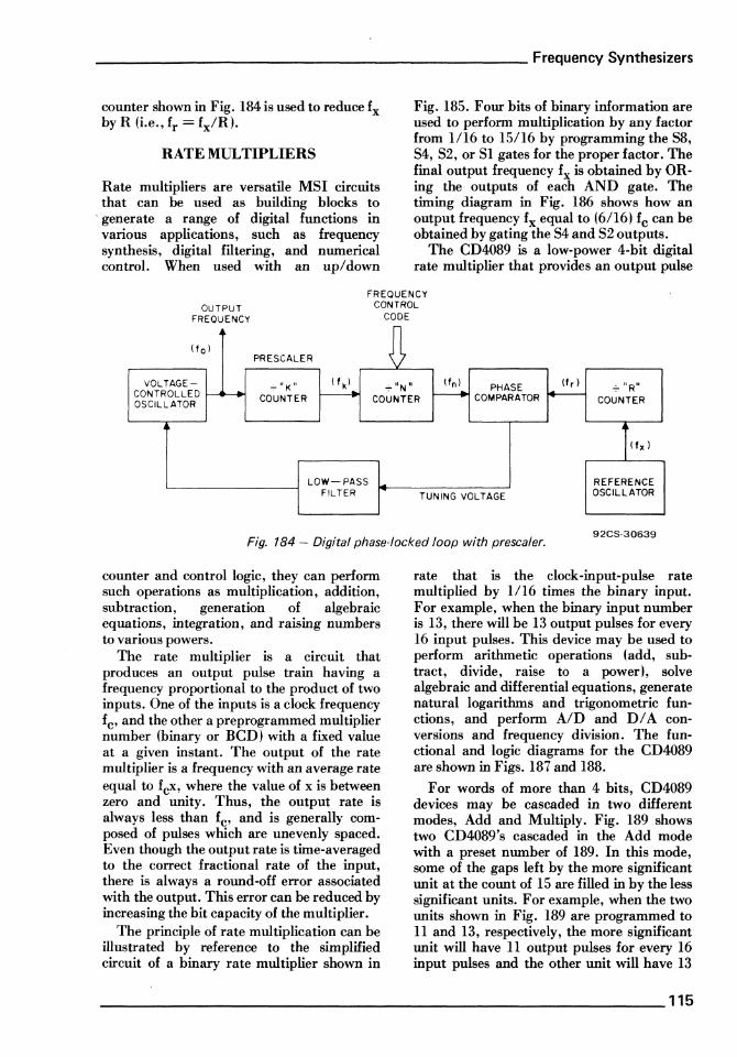
________________________ Frequency Synthesizers
counter shown in Fig. 184 is used to reduce fx by R H.e., fr = fx/R).
RATE MULTIPLIERS
Rate multipliers are versatile MSI circuits that can be used as building blocks to
. generate a range of digital functions in various applications, such as frequency synthesis, digital filtering, and numerical control. When used with an upl down
Fig. 185. Four bits of binary information are used to perform multiplication by any factor from 1116 to 15/16 by programming the S8, S4, S2, or Sl gates for the proper factor. The final output frequency fx is obtained by ORing the outputs of each AND gate. The timing diagram in Fig. 186 shows how an output frequency fx equal to (6/16) fc can be obtained by gating the S4 and S2 outputs.
The CD4089 is a low-power 4-bit digital rate multiplier that provides an output pulse
OUTPUT FREQUENCY
FREQUENCY CONTROL
CODE
(fo) n PRESCALER
VOLTAGE- 7 11 K" (fk) ~IIN" (In) PHASE (fd ~ uRIl CONTROLLED ~~ COUNTER f------4 COUNTER ~ COMPARATOR +-- COUNTER OSCILLATOR
jtfX )
LOW-PASS REFERENCE FILTER TUNING VOLTAGE OSCILLATOR
Fig. 184 - Digital phase-locked loop with prescaler. 92CS-30639
counter and control logic, they can perform such operations as multiplication, addition, subtraction, generation of algebraic equations, integration, and raising numbers to various powers.
The rate multiplier is a circuit that produces an output pulse train having a frequency proportional to the product of two inputs. One of the inputs is a clock frequency fc' and the other a preprogrammed multiplier number (binary or BCD) with a fixed value at a given instant. The output of the rate multiplier is a frequency with an average rate equal to feX' where the value of x is between zero and unity. Thus, the output rate is always less than fc' and is generally composed of pulses which are unevenly spaced. Even though the output rate is time-averaged to the correct fractional rate of the input, there is always a round-off error associated with the output. This error can be reduced by increasing the bit capacity of the multiplier.
The principle of rate multiplication can be illustrated by reference to the simplified circuit of a binary rate multiplier shown in
rate that is the clock-in put-pulse rate multiplied by 1116 times the binary input. For example, when the binary input number is 13, there will be 13 output pulses for every 16 input pulses. This device may be used to perform arithmetic operations (add, subtract, divide, raise to a power), solve algebraic and differential equations, generate natural logarithms and trigonometric functions, and perform AID and DI A conversions and frequency division. The functional and logic diagrams for the CD4089 are shown in Figs. 187 and 188.
For words of more than 4 bits, CD4089 devices may be cascaded in two different modes, Add and Multiply. Fig. 189 shows two CD4089's cascaded in the Add mode with a preset number of 189. In this mode, some of the gaps left by the more significant unit at the count of 15 are filled in by the less significant units. For example, when the two units shown in Fig. 189 are programmed to 11 and 13, respectively, the more significant unit will have 11 output pulses for every 16 input pulses and the other unit will have 13
_____________________________________________________ 115

RCA COS/MOS Integrated Circuits Manual _______________ _
114 C040BI
C04027
A J
C
RESET>-~--~~~~--~~~~--~--~~~
CLOCK>-~~~~~~--~~~~--~--~~--__, fC
fX = (~Si)fC , =1 16 92CS-24859
Fig. 185 - Simplified circuit of binary rate mUltiplier.
fc~~~~~~~~~~~~~~~~~~~~
A
OUTPUT PULSE TRAIN FOR ii
fx =(S4~S2)fc r--L __ -L __ -L~ __ -L~~~~~ ___
92CS-24856
Fig. 186 - Timing diagram for circuit of Fig. 185.
BINARY RATE CLOCK
INHIBIT (CARRY) IN
II
VOO= 16
VSS'B
9
COUNTER
7
SELECT RATE 60UT}
LOGIC 5 OUT }]
RATE J OUTPUTS
1-:------."15" OUT
INHIBIT (CARRY) OUT
92CS-25004RI
Fig. 187 - Functional diagram for CD4089 COS/MOS binary rate multiplier.
116 ______ ----------------------------________________ __
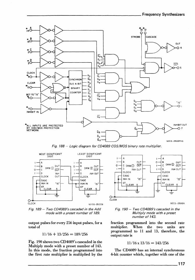
________________________ Frequency Synthesizers
*ALL INPUTS ARE PROTECTED BY COS/MOS PROTECTION NETWORK
BINARY
COUNTER
Qo Qo Qb
Qb Qc OC Qd
Od
Q,j Qc Qb Qo
00 Qb Qo
Ob Qo
Qo
-II * 1012
Fig. 188 - Logic diagram for CD4089 COS/MaS binary rate mUltiplier.
MOST SIGNIFICANT LEAST SIGNIFICANT DIGIT DIGIT
I A I A
I B DRM CD OUT 0 B OUT
0 C OUT C DRM ® OUT
D INH D INH OUT CLOCK OUT
CASC INH IN 111511
CLOCK 92CS-25008
Fig. 189 - Two CD4089's cascaded in the Add mode with a preset number of 189.
output pulses for every 256 input pulses, for a total of
11116 + 13/256 = 189/256
Fig. 190 shows two CD4089's cascaded in the Multiply mode with a preset number of 143. In this mode, the fraction programmed into the first rate multiplier is multiplied by the
A A
I B OUT 0 B OUT
0 C DRMCD OUT C DRM® OUT
D INH OUT D INH OUT CLOCK CLOCK
CASC CASC
INH IN 1115 11 INH IN 1115 11
CLOCK
92CS-25009
Fig. 190 - Two CD4089's cascaded in the MUltiply mode with a preset number of 143.
fraction programmed into the second rate multiplier. When the two units are programmed to 11 and 13, therefore, the output rate is
11116 x 13/16 = 143/256
The CD4089 has an internal synchronous 4-bit counter which, together with one of the
_____________________________________________________ 117

RCA COS/MOS Integrated Circuits Manual ______________ _
four binary input bits, produces pulse trains as shown in Fig. 191.H more than one binary input bit is high, the resulting pulse train is a combination of· the separate pulse trains shown.
The CD4527 ilil· a low-power 4-bit digital rate multiplier that provides an output-pulse
CLOCK
COUNTER STATE 0 I 2 3 4 5 6
(LSB) INPUT A=H
INPUT B=H n INPUT C=H --.ll n
(MSB) INPUT D=H
7
n
programmed to 9 and 4, respectively, the output rate is
9/10 +41100 = 94/100
or 94 output pulses for every 100 clock input pulses.
8 9 10 II 12 13 14 15 0 I
1*1 I OUTPUT
I WAVE
n I TRAINS
(TERM.6) I
n n
*AN OUTPUT BIT MAY BE FILLED IN THIS COUNTER STATE BY A LESS SIGNIFICANT CD4089 CASCADE DIN THE ADD MODE. 92CS-25006RI
Fig. 191 - Timing diagram for CD4089 binary rate multiplier.
rate which is the· clock-input pulse rate multiplied by 1110 times the BCD input. For example, when the BCD input is 8, there will be 8 output pulses for every 10 input pulses. Circuits which use this device perform arithmetic operations (add, subtract, divide, raise to a power), solve algebraic and differential equations, generate natural logarithms and trigononietric functions, and perform AID and DI A conversions and frequency dividion. The functional and logic diagrams for the CD4527 are shown in Fig. 192, and the timing diagram is shown in Fig. 193.
For fractional multipliers with more than one digit, the CD4527 devices may be cascaded in two different modes, Add and Multiply. Fig. 194 shows two CD4527's cascaded in the Add mode with a preset number of 94. In this mode, the BCD multiplier of each subsequent unit is onetenth that of the preceding unit, i.e., the output rate equals (0.1 BCDI + 0.01 BCD2 + 0.001 BCD3 + ... ) times the clock rate. Therefore, if the two units in Fig. 194 are
Fig. 195 shows two CD4527's cascaded in the Multiply mode with a preset number of 36. In this mode, the fraction programmed into the first rate multiplier is multiplied by the fraction programmed into the second one. When the two units are programmed to 9 and 4, therefore, the output rate is
9110 x 4/10 = 36/100 or 36 output pulses for every 100 clock input pulses.
VDD= 16
VSS=8
RATE SELECT LOGIC
RATE OUTPUTS
6 OUTLJ
5 0UTJ
INHIBIT (CARRY) OUT 92CS-24913RI
Fig. 192(a) - Functional diagram for the CD4527 BCD rate multiplier.
118 __________________________________ ~ ________________ __

________________________ Frequency Synthesizers
*" INHIBIT IN
* 9
CLOCK
* 4
*13
CLEAR
* ALL INPUTS PROTECTEO BY COS/MOS PROTECTION CIRCUIT·
Q
a
r-t-------l C
R
Q H";-I-+--t-H
b
H-------lC R
S
Q~---'" c
~_+--------~c Q~---~~~
R
S T Q~--~-~
L++-----IC
VOO=PIN 16 VSS=PIN B
VSS
d
"01--------1--..
R
* * STROBE CASCADE
Fig. 192(b) - Logic diagram for the CD4527 BCD rate multiplier.
92CL-2491BRI
____________________________________________________ 119

RCA COS/MaS Integrated Circuits Manual _______________ _
CLOCK
Qa
Qb
Qc
Qd
RI
R2
R3
R4
OUTPUT (PIN 6) A ENA8LED
B ENABLED
C ENABLED
o ENABLED
INH. OUT
OUTPUT (PIN6)
(PRESET No· OF I)
(PRESET No. OF 2)
(PRESET No. OF 3)
(PRESET No. OF 4)
(PRESET No. OF 5)
(PRESET No. OF 6)
(PRESET No· OF 7)
(PRESET No. OF 8)
(PRESET No. OF 9)
o I 2345678901234
n n rL I I
n rL .Jl n n
U U LJ n fL
J n n
_-----In .... _--I--__ fL
92CM-24915
Fig. 193 - Timing diagrams for CD4527.
120 __ ~------------------------------------__ ------------

_________________________ Frequency Synthesizers
MOST SIGNIFICANT LEAST SIGNIFICANT DIGIT DIGIT
I A DRMeD 0 A
DRM@
0 B OUT 0 B OUT
0 C OUT C OUT D
1It't CLOCK
0 D INH. CLOCK OUT
CASCo CASCo
INH.IN "9" INH.IN II gil
ST ST CLEAR S CLEAR S
= -CLOCK(}--~------------------~
CLOCK 012345678901234567B90
TIMING DIAGRAM SHOWING ONE OF FOUR OUTPUT I PULSES CONTRIBUTED BY DRM ® TO OUTPUT FOR EVERY 100 CLOCK PULSES IN FOR PRESET No.94.
92CS-24917RI
Fig. 194 - Two CD4527's cascaded in the Add mode with a preset number of 94.
DRM I A
DRM 2 I A 0
0 B OUT 0 B OUT
0 C OUT
C OUT D 0 D INH· INH. CLOCK OUT CLOCK OUT
CASCo CASCo
INH.IN "g' INH.IN "9"
ST ST CLEAR S CLEAR S
--
CLOCK 92CS-24916
Fig. 195 - Two CD4527's cascaded in the Multiply mode with a preset number of 36.
_____________________________________________________ 121
XI. Introduction to Microprocessors and Memory Interfacing
The RCA CDP1802 is an LSI registeroriented COS/MaS microprocessor featuring an 8-bit parallel organization with bidirectional data bus, direct memory addressing up to 65,536 bytes (ROM/RAM), 91 instructions, DMA (direct memory access), a 16 x 16 register matrix, and ALU (arithmetic and logic unit). It utilizes the COSMAC architecture. The CDP1802 is designed for use as a general purpose computing or control element in a wide range of storedprogram systems or products. Fig. 196 is a block diagram of a typical system using the CDP1802 microprocessor.
Under program control the CDP1802 can perform operations which include:
a) control of input/output (I/O) devices, b) transfer of data or control information
between I/O and memory (M), c) movement of data bytes between
different memory locations, d) interpretation or modification of bytes
stored in memory.
The COSMAC microprocessor has optional on-chip oscillator circuitry. The selection of crystal or RC oscillator frequency determines the time for each machine cycle. (Each machine cycle consists of eight clock pulses; each instruction requires two or three machine cycles. Thus, with a clock fre,quency of 6.4 MHz, each machine cycle would be
~~~
ROM
Us
ADDR BUS ADDR BUS CLOCK XTAL NO, Nl, N2 =. =. IL =:
TPA TPA TPA,TPB
----
SCO, SCI
MWR CPU DMA·IN, DMA-OUT, INT
RAM CDP1802 1/0
MRD .. MRD MRD
EFl.1:F2,EF3,EF4
CE a
Os Os Os 8-BIT BIDIRECTIONAL DATA BUS
Fig. 196 - Block diagram of typical computer system using the RCA COSMAC Microprocessor CDP1802.
DATA
CONTROL
">
SERIAL DATA
..
">
92CM- 30674
122 ____________________________________________ ~ ______ __

____________ Introduction to Microprocessors and Memory Interfacing
1.25 microseconds, and instructions would be executed in 2.5 to 3.75 microseconds, depending on the instruction.).
COSMAC MICROPROCESSOR INTERNAL STRUCTURE
The COSMAC architecture, Fig. 197, is based on a register array comprising sixteen general purpose 16-bit scratch-pad registers (R(n)), each holding two 8-bit bytes. A 4-bit binary code is used to designate each R scratch-pad register. Three 4-bit registers, labeled N, P, and X, hold the 4-bit binary codes that are used to select individual 16-bit scratch pad registers.
Memory or 110 data used in various COSMAC operations are transferred by means of the common, bidirectional 8-bit, data bus. Memory cycles involve both an address and the data byte itself. Memory addresses are provided by the contents of scratch-pad registers, via 16-bit register A. Register A is used to sequentially place the 16
memory address bits on the 8-bit memory address line, 8 bits at a time.
Either 8-bit byte in a scratch-pad register can be gated to the data bus for subsequent transfer to the 8-bit D register.
The 8-bit ALU performs arithmetic and logical operations. The byte stored in the D register is one operand, the byte on the bus (obtained from memory) is the second operand. The resultant byte replaces the operand in register D. A single-bit Data Flag indicates carry results from an add or shift operation. Two 4-bit registers I and N contain instruction bytes which operate on the Control Logic portion of the CDP1802.
The CDP1802 microprocessor has heen designed to minimize external control circuitry, but some additional devices are necessary to provide gating, latching, and 110 (Input/Output) control. Standard parts from the CD4000 series discussed in this manual can be used to provide many of the systems operations; in addition, a growing family of RCA1800 series devices have been designed specifically to interface with the CDP1802.
MEMORY ADDRESS
1/0 COMMAND OR SERIAL DATA
1/0 BIDIRECTIONAL COMMAND DATA BUS
(16)
(S)
R(9}.1 R(9}.O R(A}.l R(A}.O
R(E}.l
R(F}.l
(S) (S)
(4)
R SELECT
SCRATCH PAD REGISTERS
R
(3)
S·BIT BUS
92CM-30664
Fig. 197 -Internal structure of the CDP1802 microprocessor.
(S)
____________________________________________________ 123
RCA COS/MaS Integrated Circuits Manual _______________ _
Fig. 198 shows one circuit, using standard devices from· the CD4000 series, for controlling the run and load modes of the CDP1802. It includes a power-on reset feature.
WAIT
~
POWER·ON RESET _""'IL:Ar-
cleanly on the next negative-going transition of the clock (Pause mode). Output signals are held at their values indefinitely. This state is useful for several purposes. Using the WAIT line, the CPU can be easily single-stepped for
CPU CDP1802
,..--_.-_.----t--l CLOCK
20pF "..... ...L 22Mn o
20PF~
92CS-30663
Fig. 198 - Simple control interface for CDP1802 microprocessor.
During normal operation, the CLEAR and WAIT lines are both held high. A low level on the CLEAR line will put the machine into the reset mode with I, N, X, P, Q, Data Bus = 0, and IE = 1. Actually, X, P, and R(O) are reset during a special 51 cycle (not available to the programmer) immediately following transition from the reset mode to any of the other modes (load, run, or pause). The clock must be running to effect this cycle. __
If the CLEAR and WAIT lines are both held low, the machine enters the load mode. This mode allows input bytes to be sequentially loaded into memory beginning at M(OOOO). Input bytes can be supplied from a keyboard, tape reader, etc., by way of the DMA facility. This feature permits direct program loading without the use of external "bootstrap" programs in ROM's.
If the WAIT line is brought low (with CLEAR high), the CPU stops operation
debugging purposes or, if stopped early in the machine cycle, the CPU can be ,held off the data bus to allow for multiprocessor systems, etc. Also, the WAIT line can be used as a data-ready signal from a slow memory or peripheral, or signals TP A and TPB can be stretched. When the WAIT line is returned high, the machine resumes running on the next negative-going transition of the clock input. The WAIT signal does not inhibit the on-chip crystal oscillator. DMA's and Interrupts are not acknowledged in the Pause mode.
To load and start a program, the sequence of operations would be as follows: First, press the reset and then the load buttons. The CPU is now ready to load by means of the DMA channel. When loading is completed, pressing the reset and then the run buttons starts program execution at M(OOOO) with R(O) as the program counter (after one machine cycle). If a DMA request is present
124 ____________________________________________________ __

____________ Introduction to Microprocessors and Memory Interfacing
when the run switch is turned on, the machine goes into the DMA state immediately with R(O) as the program counter. The user should therefore inhibit DMA externally until the program has changed to a program counter different from R(O). Interrupts, however, are disabled until the first instruction or DMA request is executed. This delay allows the programmer to place instruction 71 and 00 in the first two memory bytes to inhibit interrupts until he is ready for them. The combined effect of the two bytes is to set IE = O. Interrupts m~t not occur, however, when the machine is in the load mode because they will force the machine into an an anomalous running state. Fig. 199 shows the sequence of events and states involved in loading a program via DMA-IN in the load mode and its subsequent
execution. Fig. 200 provides a summary of the modes discussed, the control levels, and the characteristic features of these modes.
Another circuit that can be used for singlestepping the microprocessor (one machine. cycle per switch depression) is shown in Fig. 201. This capability is often useful as a debugging aid.
External Flag Lines ~ur external flag lines (EF1, EF2, EF3, EF4) are available on the CDP1802. These lines provide the simplest input to the microprocessor. A low on any flag line places it in its true state; short branch instructions allow programs to determine- the states of these flag lines. If the signal to the CPU is initiated by a switch closure, a flip-flop should be used to eliminate switch bounce as
CLaCK 1-_
CYCLE~:::]S'C===::Iis,====r::======:::r::::Jj C~ARIL_------------------------------____________________________________________ __
WA'T---I~------------------------------------TPA:;i;L _____________________________________________ ~nNOTE ,
TPB~ ______________ ~rl~ __________ ~IIL___ __ ~ ____________ ~nL_ _________ ~rIL_ iiiiAiNr - -m NOTE 2
MAZ::Z<;W~4'Z0'A I RO.I-OO I ROb-oo RO.O·OO
~t~~:==================== ==~I~~~b*~fu~M~lo~~~j==I~o~FF[IOw~~~D~~~~~Mm¢9@~[I=:::
WfD~--------------------------------------
MWRZI -i== I RUNtR£5ET 'NITI~L~ATlaN --.I
~~~T~NUED I-_____ --''-'-Y''''L=-E ____________ _ ABOV~~K~-- 5 6 1 0 I :-2 3
CYCLE __ ---'S~I -7·~·}SI:, =::::::J===:3SI2 ===c:==~S2===:::r=S~I: -:--,:-SIC :::-,I.----"""""s~' --------.--"'50,.---
mAR----- ------------------------------------------~ w-ITf----- .-----------------------------------------
.r -------------------TPA----- ___ ---Jn~ _____ ...JnL ___________________ ~
TPB------ _--.-n'--____ ---lnl-_______ ~ _____________ ---ln~ ___ _
DMA IN --?Z!
MA ===1]1 R!Qo·E'-:2!OO[JI]Ro[J.ag::":9:a'C==TII R~a!J:.,.~db!ill1 R@:a.:g:a.:£a~2 ==::::::JIBlRo.1JaE2l.a2::JCZ7~$01 :.~::JJ
iO~A OFF I WORDAT~2::iVooo1Q[1 =:nl wo!QffiRO!:!!*C[TO["!!jI:2!OOO!Qj[n ==:J:jlw~aiBiRDi!''}jTOi:!Mill(0002~L) ==::::::JI:QjOFEfFJ;j:r --::r:----::======::::::TI101EF[:F J;:I ~+.: .',' .--_________ · ___________ · __ .... t:WORD ATMroooz:::I~ __________ WD:::::.:;RD AT MlOooa:1
1iRJj "'--__ -----.J L __ tan- LI ____ __
------------------------- LOAD * WORD GENERATED BY INPUT DEVICE.
NOTE': ~.:,r~~ '1IlPE,~~t ti'.!C'R ARE GENERATED NOTE 2: DNA REQUEST SHOULD BE VALID AT THIS TIME.
~--::-~-I: INITIALIZATION~ R~sE"" I--<--__ C_YC_L_E __ RUN ____ _
NOTE 3: ALL MACHINE CYCLES REQUIRE 8 CLOCK PULSES EXCEPT THE INITIALIZATION CYCLE WHICH REQUIRES AN ADDITIONAL CLOCK PULSE PULSE (00).
~ DON'T CARE 92CI..-301SI
Fig. 199 - Timing diagram for load and run sequences.
______________________________________________________ 125

RCA COS/MOS Integrated Circuits Manual _______________ _
MODE CLEAR WAIT OPERATION
RESET 0 1 I,N, X, P =0, RIO) =0, Q=O, BUS =0, IE = 1 ;TPA and TPB are suppressed; CPU inS1.
RUN 1 1 CPU starts running one machine cycle after CLEAR is released. Execution starts at MlOOOO) , or an S2 cycle follows if DMA was asserted. Internal sampling of interrupt is inhibited during initialization cycle.
RESET 0 1 As above. LOAD 0 0 CPU in IDLE. An I/O device can load memory
without "bootstrap" loader. PAUSE 1 0 Clock:~stops internal operation.
CPU outputs held indefinitely. Permits stretching of machine cycle to match slow devices or memory cycles. DMA and INTERRUPTS not acknowledged.
RUN 1 1 Clock:.....r--\.. _________ ~
Resume operation
Fig. 200 - Truth table for mode control of CDP1802 microprocessor.
TPB TPA
----I I I I I
VOO
CONT
+1:~--ct..~ I S CLK:
~_~I_~ Q I CD4013 S I L..: __________ .J
VOOD-"\M ....... ~j-~)--- CLEAR
EXT. CLeAR -----------4 SR)p----------------------------------------~ Voo
EXT.~--------------------________________________ _4~~~
92CM-30675
Fig. 201 - Circuit for single·stepping the CDP1802 microprocessor.
shown in Fig. 202. Also note the pull-up resistors, which prevent the gate inputs from floating in the "open" switch position.
OPERATION AND INTERFACING
Input/Output Port
The RCA CDPl852 is a parallel, 8-bit, mode-programmable COS/MOS input/output port designed for use in RCA 1800 series microprocessor systems. It is compatible with and directly interfaces the CDP1802 without additional components. A
functional diagram of the CDP1852 is given in Fig. 203.
The mode control is used to program the device as an input port (mode=O) or output port (mode=l). When the CDP1852 is used as an input port (mode=O), data is strobed into its 8-bit register by a high (I) level on the clock line. The negative, high-to-Iow transition of the clock sets the Service Request Flip-Flop (SR=O) and latches the data in the register. The SR output can be used to signal the microprocessor. When CSI • CS2= 1 the three-state output drivers are enabled, the negative high-to-Iow transition of CS I • CS2 resets the Service Request Flip/Flop, and SR=l.
126 ____________________________________________________ __

____________ Introduction to Microprocessors and Memory Interfacing
NOTE: FF SET/RESET' LOW
Q---rg-SET !vec
CPU CDPI802
Q ~RESET 1/2 CD4011
sl-~-I-.., ON..
I
INPUT BYTE a- RI--_--<_...JO~; 1-
92C$-30636
Fig. 202 - Use of a flag line (EFT) as an input command. Note flip-flop debounce circuit.
CSI/CSi* I
CS2
MODE ... 2'--_ ...... ___ --'
CLOCK~I~I-------...J ~~~~----------~
ENABLE DOO DOl
THREE- D02
STATE D03 OUTPUT D04 DRIVERS-
DO!! D06 D07
• POLARITY DEPENDS ON MODE 92CS-27574
Fig. 203 - Functional diagram of CDPT852 input/output port.
If the CDP1852 is used as an output port (mode=I), data is strobed into the port's 8-bit register when CS1· CS2 • CLOCK=l. The three-state output drivers are enabled at all times when the CDP1852 is configured as an output port. The service request signal is ~esrated at the termination of
• CS2 = 1 and will be present, 1 level, until the following negative, high-to-Iow transition of the clock.
A CLEAR control is provided for resetting the port's register and service request flipflop.
Fig. 204 shows the CDP1852 connected as part of a microprocessor system. The CDP-1852 can also be used as an address latch to demultiplex the CDP1802 address bus.
Display Output
Fig. 205 shows how an output instruction might be used to set a byte into a two-digit output LED display device. During the execution cycle of the instruction, when the NO bit is valid, TPB will strobe valid data into the two BCD-to-7 -segment latch decoder drivers.
________________________________________ ~-----------127

RCA COS/MOS Integrated Circuits Manual _______________ _
ROM RAM CDU CDPIB02
92CM-27573
Fig. 204 - Typical CDP1802 microprocessor system showing CDP1852 used as I/O port.
SYSTEM MEMORY
8
MIRIX))
CPU
COPl802 TPB
NO I
8 DATA BUS 0·7
SI
I-I CJ
Voo l\ [ 117
"S-I-...£.I--..,
"1.r C04511 CD4511
D-~=-~~L_E ___ r~~ ~L_E~ ___ ~
4 4' , , 92CM-30673
Fig. 205 - Direct selection of I/O devices-one pair of output display digits.
DMA Operation
The CDP1802 has a built-in direct memory access (DMA) facility which pennits high-speed 110 byte transfer operations independent of nonnal program execution. Two lines, DMA-IN and DMA-OUT, are used to request DMA byte transfer to and from the memory. A specific code is provided on the state code line (SCO,SC 1) to indicate a DMA cycle. In Fig. 206, the CD4076 is used as a holding register (the CD4076 types are 4-bit, D-type registers that feature three-state
outputs thus pennitting isolation from the Data Bus line) and a CD4013 flip-flop is used to clock and hold the DMA request.
Fig. 206(a) illustrates the manner in which DMA-IN might be implemented. The leading edge of an enter pulse clocks an input ~e into the register and activates the DMAIN request.
Serial Interfacing
Fig. 207 shows the CDP1854, a CMOS Universal Asynchronous Receiver-Transmit-
128 ____________________________________________________ __
____________ Introduction to Microprocessors and Memory Interfacing
CLEAR WAIT ENTER IN
1 1 JL U tiD
CPU INPUT
CDPl802 ~ CL REG. 2X
- sea C04076 MWR 00 - ..... r
SYSTEM SCI MEMORY -
MRO - 1/2 C04013
O~VOO -
OMA·IN I--- Q CL R
TO 8 8
~ MIRIO)) J 8 OATA8US()'7
92CM-30665 (a)
OUTPUT BYTE REQUEST DISABLE
.n.
fi CPU
"- 00 CDPI802
TPB CL OUTPUT REGISTER
MWR SCO 2X
~ 10 CD4076
SCI - r SYSTEM MEMORY -
MRO - 1/2 C04013
o-oVOO
OMA·OUT -0 CL R
l M(R(OIl I DATA BUS 0·7
(b) 92CM-30666
Fig. 206 - Implementation of DMA operation (a) DMA-IN (b) DMA-OUT.
ter (DART), interlaced to the CPU in a typical data communication application. The UART consists of a receiver and transmitter designed to provide the necessary formatting and control for interlacing serial asynchronous data to and from peripheral devices. The receiver-transmitter is capable of full duplex operation and is externally programmable.
The transmitter converts parallel data to a serial word containing the data (5-8 bits), a start bit, a parity bit (optional), and stop bits (1, 1-112, or 2), as .illustrated in Fig. 208. The receiver converts a serial input word with start, data, parity, and stop bits into parallel data. It verifies proper code by checking parity and the receipt of a valid stop
_____________________________________________________ 129

RCA COS/MOS Integrated Circuits Manual ______________ _
TELEPHONE LINE
I I DAA I
f l I MODEM
L I VDD
t CS2
, T f 1 1 1 CLEAR MR 50 RT5 CTS 51 MODE
SELECT
r- CS1
N2 CS3 TC - BAUD UART RATE
~ - CDP.1854 GEN. CPU N1 MRD RC -5YSTEM CDPl802 NO RSEL
MEMORY -~
TPB TPB - rs (FROM INTERRUPT INTERRUPT _ m PERIPHERA LSI
EF ¢::4 _ r~ TOEF {
OR 8 ~ INTERRUPT 1"HRE
B B
B
DATA BUS()'7
92CM-30667
Fig. 207 - System configuration for asynchronous serial data communication interface .
.--JPARITY . ·lBIT
92CS-30668
Fig. 208 - Word format in asynchronous serial data communications.
bit. Both the receiver and transmitter are double buffered.
Although the receiver and transmitter can operate with separate data buses, if the MODE SELECT line is high, the UART is directly compatible with the CDP1802 and bidirectional data transfer on a common bus.
There are four registers under program control in the UART. One is loaded from the bus in the transmit mode, one is read to the bus in the receive mode, a Control register is loaded from the bus at initialization, and a Status register is read in the receive mode.
The two-bit code on MRD and RSEL determines which register is selected and the direction of data flow.
The UART is enaiJled to the data bus when the three chip selects are asserted. Therefore, by decoding, a large number of UART's can operate in a system on the same bus.
The CDP1802 can be programmed to emulate a general serial interface. In this configuration, the serial input is an external flag (EF xl and the serial output is Q.
130 __________________________________________________ ___
____________ Introduction to Microprocessors and Memory Interfacing
Memory Interfacing
As shown in Fig. 209, up to 256 bytes of memory can be addressed directly by the CDP1802 through the memory interface lines, because only eight bits of address are required.
For larger memory systems, the addressing appears on the memory address lines in two bytes: first the high-order byte, which must be retained in a latch, then the low-order byte. Latching all eight bits in the high-order byte would provide for a memory of 65,536
8 MA 0-7 MA
STATIC RAM
MWR 256 BYTES TWO eDP1822's + Vee (256 X 4)
eSl
MRD
8 DATA BUS 0-7
bytes; chip select decoding would have to be added to the latch output.
Fig. 210 illustrates the interconnections of a static 4096-byte RAM to the CPU. Twelve memory address bits are required to select one out of 4096 memory byte locations. The high-order byte of a 16-bit memory address appears on the memory address lines first. The four least significant bits are strobed into the latch and decoder circuit CDP1858 by timing pulse TP A. The functional diagram for the CDP1858, a four-bit latch with decode designed for use with RCA1800 series microprocessor systems, is given in Fig. 211.
MA
MWR
CPU CDP1802
MRD Vee
C? C? BUS PULL UP
I I RESISTORS I I (22KOI
92CS-30669
Fig. 209 - Interface for the CDP1822 static RAM to the CDP1802 microprocessor in a 256-byte RAM system.
______________________________________________________ 131
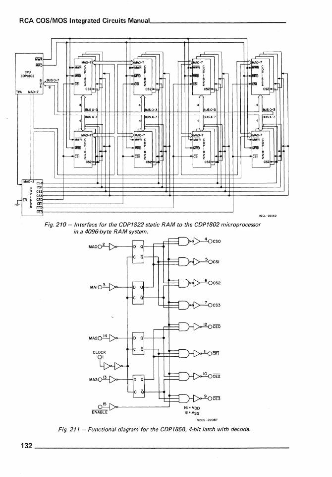
RCA COS/MOS Integrated Circuits Manual _______________ _
~ ~ ~ MWR - ,- P MAO-7 ""'MAO-7 MAO-7 ,.-- r'MAO-7 ;--MRD - r- MWil g ~ MWii g ~ MWil g .. ~.1\Il1q
CPU p I- p I- p - p COPI802 r- MRiiI r- MRO 1 ... iJIIj 1 r-~ ~
B~7 8 B 8
f-oCSi 2
f-oCSi 2 CSi 2 .. CSi 2 joo-~ "e- 2 2 2 2
TPA MAO-7
'-- MAO-3 CS
C CSI 0 CS2 P CS3 _I
.J: EN 8 mI
5 rn 8 m
ffi
CS2 CS2io- CS21-- CS2 ..
4 4 4
~ BUS 0- BUS 0-3 BUS 0-3
jrUS~;h irs~-~ i irs~-~ BUS 4-7
4
~ P MAO-7 MAO-7 "" MAO-7 ~ MAO-7 c..MWRC c..MWRC "MWR C Lo MWR C
0 0 0 D
~ MRiif L....o MRiif L....o MRO f L..." MRiif 8 8 8 8 ........ CSi 2 0--. CSi 2 Csi 2 CSi 2 2 2 2 2 CS2 CS21-- CS21-- CS2joo-
- '---- '--
92CL-290fiO
Fig. 210 - Interface for the COP1822 static RAM to the COP 1802 microprocessor in a 4096-byte RAM system.
MAO 2
C Q
MAl 3 ;>O--+-ID Q
C Q\--H
CEO
MA2 14 D Q
C Q CEI
13 ill MA3 0 Q
C Q ffi
15 16=VDD
ENABLE 8 =.vss
92CS-29057
Fig. 211 - Functional diagram for the COP1858, 4-bit latch with decode.
joo-..-
132 ____________________________________________________ _

XII. Circuits and Applications
The circuits in this section illustrate some of the applications that can be implemented using the RCA CD4000 series of COS/MOS integrated circuits. The selection has been made to show a wide variety of circuit ideas and to indicate the ease with which different logic operations and functions can be realized.
Logic functional diagrams and operating waveforms are shown for a broad range of circuits in which the low quiescent dissipation, well-defined logic levels, high noise immunity, and other features of the CD4000-series devices result in significant advantages. Brief summations are given of the over-all logic function of the various circuits. Detailed information on the
operation of basic circuit elements, such as gates, inverters, flip-flops, counters, and registers, that may be included in the various circuit arrangements is given in earlier sections of this Manual.
In many of these circuits, where an Aseries type is indicated, the type may be replaced by a B-series type if the higher supply-voltage rating of the B-series is required by the specific application. Similarly, where a B-series is specified, it may be replaced by an A-series type if the lower operating voltage of the A-series is adequate for the application. Check the databook RCA COS/MOS Integrated Circuits SSD-250 for information on Aand B-series types.
List of Circuits
Circuit No.
1 2 3 4 5 6 7 8 9 10 11 12 13 14 15 16 17
Pulse stretcher Transition detector !frequency doubler Pulse modulator Demodulator Edge detectors Power-on reset Sine-wave to square-wave converter Frequency doubler Divide-by-2 counter Divide-by-3 synchronous counter with divided outputs Divide-by-4 synchronous counter Divide-by-4 ripple counter Divide-by-5 synchronous counter Divide-by-6 ripple counter Divide-by-N counter with N decoded outputs Noise discriminator using NOR gates Clock edge shaping circuit
Page
134 134 135 136 137 137 138 138 139 139 140 140 141 141 142 142 143
______________________________________________________ 133

RCA COS/MaS Integrated Circuits Manual _______________ _
Circuit No.
18 19 20 21 22 23 24 25 26 27 28
29 30 31
List of Circuits (continued)
Noise discriminator using multivibrator Frequency discriminator Low-pass filter Bandpass filter Envelope detector Voltage-controlled oscillator Voltage-controlled pulse-width circuit Two's complement adder-subtracter Function generator Phase-locked-loop lock-detection circuit Transient-protection circuit for automobile digital logic systems Switch debouncing circuits Nine-bit parity generator/checker Four-bit magnitude comparator
Circuit No. I - PULSE STRETCHER
This circuit illustrates the use of the CD4011 quad 2-input NAND gate as a pulse stretcher. The signals at terminals Sand C are synchronized. The pulse duration of the signal at terminal S, however, is much shorter than that of the signal at terminal C. The feedback loop from the output (terminal A) stretches out the pulse at S to equal the length of the pulse at C. Any time the pulse at S is not present, the output is zero. The repetition rate of C can, therefore, be any convenient multiple of the basic S rate. The output signal has a pulse duration equal to that of the signal applied to terminal C and the same repetition as the signal applied to terminal S. The circuit waveforms shown indicate the relationship between output and input pulses when the repetition rate of the signal at C is three times that of the signal at S.
CD40llA
Circuit No.2 - TRANSITION DETECTOR/FREQUENCY DOUBLER
Page
143 144 144 144 145 146 146 147 147 148
148 149 ISO ISO
92CS-30631
This circuit shows an arrangement for use of the CD4030 or CD4070 quad exclusiveOR gate to detect logic-level changes. A transition from low to high or from high to low produces a pulse at the output terminai
of the gate. The duration of the output pulse can be varied by a change in the time constant of the resistance-capacitance network formed by R I and Cl' The section of this Manual on Astable and Monostable
134 ____________________________________________________ __
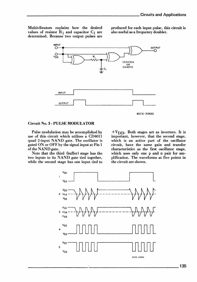
________________________ Circuits and Applications
Multivibrators explains how the desired values of resistor R 1 and capacitor Clare determined. Because two output pulses are
INPUT
Voo
INPUT
produced for each input pulse, this circuit is also useful as a frequency doubler.
~UT
C040:30A OR
C04070
OUTPUT ~ ____________ ~r--l~ __
Circuit No.3- PULSE MODULATOR
Pulse modulation may be accomplished by use of this circuit which utilizes a CD4011 quad 2-input NAND gate. The oscillator is gated ON or OFF by the signal input at Pin 1 of the NAND gate.
Note that the third (buffer) stage has the two inputs to its NAND gate tied together, while the second stage has one input tied to
VOO
2 VrR --
Vss
VOO
:3 VTR--
Vss
Voo
4
Vss
Voo
5
Vss
92CS-:30632
+VDD. Both stages act as inverters. It is important, however, that the second stage, which is an active part of the oscillator circuit, have the same gain and transfer characteristics as the first oscillator stage, which uses only one p and n pair for amplification. The waveforms at five points in the circuit are shown.
L
92CS-22B80
____________________________ ,~~ ________________________________________ 135

RCA COS/MaS Integrated Circuits Manual _______________ _
Circuit No.4 - DEMODULATOR
Demodulation or envelope detection of pulse-modulated waves is performed by this circuit which utilizes the CD4007 dual complementary pair plus inverter. The carrier burst input is inverted (by Inverter A), and its first negative transition at point 2 turns on the diode (D) to provide a charging path for capacitor Ctc through the n-channel resistance to ground. On the positive tran-
sition of the signal (at point 2), the diode is cut off and Ctc discharges through Rtc. The discharge time constant (Rtf; Ctc) is much greater than the time of the burst duration. Point 3, therefore, never reaches the switch point of inverter B until the burst has ended. The waveforms at four points in the circuit are shown.
112 CD40llA
Rtc Ctc
3 jo-"4'--.. OUTPUT
Voo
Vss
Voo 2
Vss
Voo 3
Vss
4voo ~ Vss L
92CS- 22881
136
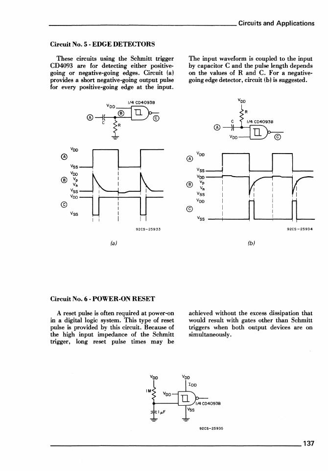
________________________ Circuits and Applications
Circuit No.5- EDGE DETECTORS
These circuits using the Schmitt trigger CD4093 are for detecting either positivegoing or negative-going edges. Circuit (a) provides a short negative-going output pulse for every positive-going edge at the input.
1/4 C04093B
@-ll--~~ c
@:J Voo
® vp Vn
Vss Voo
@ Vss
I I I I
92CS-25933
(a)
Circuit No.6- POWER-ON RESET
A reset pulse is often required at power-on in a digital logic system. This type of reset pulse is provided by this circuit. Because of the high input impedance of the Schmitt trigger, long reset pulse times may be
1M
~I"'F
The input waveform is coupled to the input by capacitor C and the pulse length depends on the values of Rand C. For a negativegoing edge detector, circuit (b) is suggested.
c @-)
Voo
I I I @
vss---l Voo I r r r-® Vp I I
Vn I I Vss I I Voo I
~ I
rL @ I I I I
I Vss i
92CS -25934
(b)
achieved without the excess dissipation that would result with gates other than Schmitt triggers when both output devices are on simultaneously.
92CS-25935
_____________________________________________________ 137
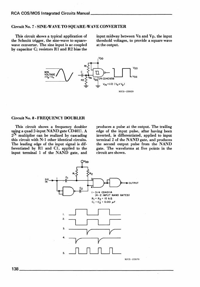
RCA COS/MaS Integrated Circuits Manual _______________ _
Circuit No.7- SINE-WAVE TO SQUARE-WAVE CONVERTER
This circuit shows a typical application of the Schmitt trigger, the sine-wave to squarewave converter . The sine input is ac coupled by capacitor C; resistors R land R2 bias the
MIN. !jJ VOLTAGE >Vp-Vn
Circuit No.8- FREQUENCY DOUBLER
This circuit shows a frequency doubler using a quad 2-input NAND gate CD40ll. A 2N multiplier can be realized by cascading this circuit with N-l other identical circuits. The leading edge of the input signal is differentiated by Rl and Cl, applied to the input terminal 1 of the NAND gate, and
RI
SIGlOl
CI IN .
C2
I.
2.
3.
R2
input midway between Vn and Vp, the input threshold voltages, to provide a square wave at the output.
92CS-25929
produces a pulse at the output. The trailing edge of the input pulse, after having been inverted, is differentiated, applied to input terminal 2 of the NAND gate, and produces the second output pulse from the NAND gate. The waveforms at five points in the circuit are shown.
OUTPUT
1- 3/4 CD401lA (4-2 INPUT NAND GATES)
RI=R2=IOkn CI = C2 = (lOOI p.F
4. -y V
5.
92CS-22879
138 ____________________________________________________ __

________________________ Circuits and Applications
Circuit No.9 - DIVIDE-BY -2 COUNTERS
These circuits illustrate the use of one-half a CD4027 dual J-K master-slave flip-flop and one-half a CD4013A dual "D" type flip-
flop to form two simple divide-by-2 counters. The CD4013A counter is made to toggle by returning the Q output to the D input.
CLOCK
OUTPUT D Q OUTPUT
R RESET
ALL UNUSED INPUTS GROUNDED
112 CD4013A
Q
R
RESET 0-+----'
92CS- 30633
Circuit No. 10 - DIVIDE-BY -3 SYNCHRONOUS COUNTER WITH DECODED OUTPUTS
In this circuit, both sections of a CD4013 dual "D" type flip-flop are interconnected with one gate unit of a CD4001 9uad two-
CD4013A
CLOCKO'----__
input NOR gate to form a divide-by-3 synchronous counter with three decoded outputs.
"I" TIME SLOT
"--__ -+ _____ -<)"2" TIME SLOT
L...-____ --j~·3· TIME SLOT
92CS- 30634
SEQUENCE
Q2 QI TIME SLOT
0 0 "I" 0 I "2 11
I 0 113"
0 0 "1"
____________________________________________ 139

RCA COS/MaS Integrated Circuits Manual _______________ _
Circuit No. 11 - DIVIDE-BY -4 SYNCHRONOUS COUNTER
This circuit illustrates the use of both sections of a CD4013A dual "D" type flipflop in a divide-by-4 synchronous counter. A
1/2 CD4013A 1/2 CD4013A
CLOCK CL CL OUTPUT D QI D Q2
RESET
high level on the reset line forces the counter into the "0" state.
SEQUENCE (JOHNSON) Q2 Q I STATE
0 0 0
0
2
I 0 3
0 0 0 ALL UNUSED SETS GROUNDED
92CS-30635
Circuit No. 12 - DIVIDE-BY -4 RIPPLE COUNTER
In this circuit, the two sections of a CD4013A dual "D" type flip-flop are interconnected to fonn a divide-by-4 ripple counter. A comparison of the truth table for this circuit with that for the synchronous counter (Circuit No. II) shows the variation
1/2 CD4013A 1/2 CD4013A CLOCK
CL CL OUTPUT D QI D Q2
RESET
in the logic sequences for ripple and synchronous counters that provide the same count division. As with the synchronous type, a high level on the reset line forces the divideby-4 ripple counter into the "0" state.
SEQUENCE Q2 QI STATE
0 0 0
0
0 2
I 3
0 0 0 92CS-30636
140 _____________________________________________________ _
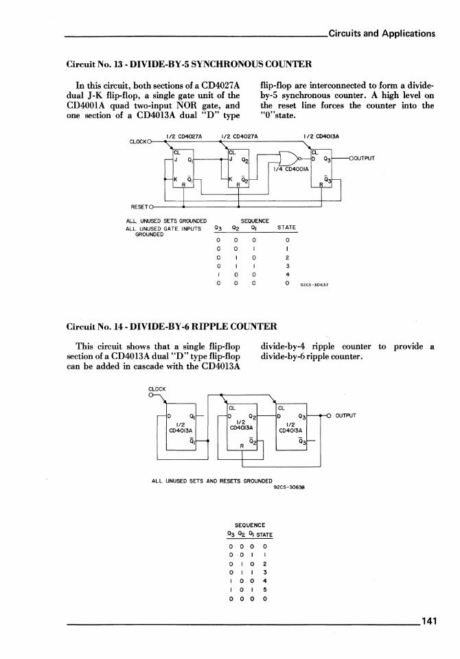
________________________ Circuits and Applications
Circuit No. 13 - DIVIDE-BY -5 SYNCHRONOUS COUNTER
In this circuit, both sections of a CD4027 A dual J-K flip-flop, a single gate unit of the CD4001A quad two-input NOR gate, and one section of a CD4013A dual "D" type
flip-flop are interconnected to fonn a divideby-5 synchronous counter. A high level on the reset line forces the counter into the "0 "state.
112 CD4013A CLOCKo-~ __ --------~----------------,
1/2 CD4027A 1/2 CD4027A
RESET
ALL UNUSED SETS GROUNDED SEQUENCE ALL UNUSED GATE INPUTS 03 02 01 STATE
GROUNDED 0 0 0 0
0 0 I
0 0 2
0 I 3
I 0 0 4
0 0 0 0 92CS-30637
Circuit No. 14 - DIVIDE-BY -6 RIPPLE COUNTER
OUTPUT
This circuit shows that a single flip-flop section of a CD4013A dual "D" type flip-flop can be added in cascade with the CD4013A
divide-by-4 ripple counter to provide a divide-by-6 ripple counter.
CLOCK
'. CL CL
r-D Qlr- r-D Q2 -0 03 1/2 112 1/2
CD4013A CD4013A CD4013A
°lr-----< 02~ 03 R
I I
ALL UNUSED SETS AND RESETS GROUNDED 92CS-3065
SEQUENCE
Q3 02 QI STATE
0 0 0 0
0 0 I I
0 I 0 2
0 I I 3
I 0 0 4
I 0 I 5
0 0 0 0
-----[0 OUTPUT
-
141

RCA COS/MaS Integrated Circuits Manual _______________ _
Circuit No. 15 - DIVIDE-BY -N COUNTER WITH N DECODED OUTPUTS
This circuit illustrates the use of a CD4017A decade counter/divider and a CD400IA dua12-input NOR gate in a divideby-N counter that provides N decoded outputs. When the Nth decoded output is reached (Nth clock pulse), the S-R flip-flop (constructed from two NOR gates of the CD400I) generates a reset pulse which clears the CD4017A to its zero count. If the Nth decoded output is greater than or equal to 6, the clock-output (COUT) line goes high to
clock the next CD4017A counter section. The "0" decoded output also goes high at this time. Coincidence of a low clock and a low decoded "0" output resets the S-R flip-flop to enable the CD4017A. If the Nth decoded output is less than 6, the COUT line will not go high and, therefore, cannot be used to clock the next counter. In this case, the "0" decoded output may be used to perfonn this clocking function.
-.-~~-r----I------- COUT FORN~=6
RESET f =CLOCK";-N
oI.......:C..::....:...:...:....:.."-t------+__ ALTERNATE COOT ..- FORN=21OIO
-------, I I I 1
I L ____________ I
f = CLOCK -7 N
92CS-30644
Circuit No. 16 -,NOISE DISCRIMINATOR USING NOR GATES
In this circuit, the CD4001A quad twoinput NOR gate is used in a noisediscriminator application. The circuit discriminates between noise pulses that last less than a specific duration tl and pulses that have a duration greater than tl' An input pulse that has a duration greater than
tl produces an output of pulse duration t2' The time tl is determined by the time constant of resistor R 1 and capacitor C 1 (i.e., tl = RICI)' The time t2 is determined by the time constant of resistor R2 and capacitor C2 (i.e., t2 = R2C2)' Diodes D1 and D2 allow fast recovery .
OUTPUT
NOISE SIGNAL
INPUT --fl~-------~ I I I
: : :, I I OUTPUT......!I"'"T'"!...' --------...... ---'. ~. ------
LNO CHANGE I I I ---;-t,"1-- t2 ---! 92CS-30643
142 ____________________________________________________ _

__________ .......;.. ____________ Circuits and Applications
Circuit No. 17 - CLOCK EDGE SHAPING CIRCUIT
This circuit illustrates how a CD4001A quad two-input NOR gate may be used to reshape the rise and fall times of clock pulses that have slow transition times. Shorter transition times of the output clock pulse result from the regeneration action of the
INPUT CLOCK
CLOCK INPUT 100 ms -I I
(MAX.)
OUTPUT ___ ...J CLOCK
output flip-flop. Complementary clock outputs are also available. With this circuit, an input clock pulse that has rise and fall times of 100 milliseconds can be reshaped so that the transition times are reduced to 100 nanoseconds.
~ ........ -oCLOCK
--l 1-100 ms (MAX)
OUTPUT ....... -- IrlOlflOlOO ns
92CS- 30640
Circuit No. 18 - NOISE DISCRIMINATOR USING MUL TIVIBRA TOR
This circuit illustrates an application of a CD404 7 A low-power monostablel astable multivibrator in a noise discriminator. By adjusting the external time constant, a pulse width narrower than that determined by the
VINQ)
Q ®
time constant is rejected by the circuit. The output pulse follows the desired input, but the leading edge is delayed by the selected time constant.
Q OUT®~ _____ ...Jn'_ ___ _
1/4 CD4001
92CS-22673
_________ -----------------------143

RCA COS/MaS Integrated Circuits Manual ______________ ...,.-_
Circuit No. 19 - FREQUENCY DISCRIMINATOR
This circuit illustrates the rise of the CD4047A low power monostable/stable multivibrator as a frequency-to-voltage . converter. A waveform of varying frequency is applied to the +TR (triggerl input. The
Circuit No. 20 - LOW-PASS FILTER
This simple circuit uses the CD4047A lowpower monostablel astable multi vibrator as a low-pass filter. The time constant chosen for the multivibrator determines the upper cutoff frequency for the filter. The circuit essentially compares the input frequency with its
R
Circuit No. 21 - BANDPASS FILTER
Two CD4047A low-pass filters can be used to construct a bandpass filter, as illustrated in this circuit. The pass band is determined by the time constants of the two filters. If the output of filter No.2 is delayed by capacitor Cl' the CD4013A flip-flop will clock high
one-shot produces a pulse of constant width for each positive transition on the input. The resultant pulse train is integrated to produce a waveform having an amplitude proportional to the input frequency •.
92CS-22672
own reference. It then produces an output that follows the input for frequencies less than the cut off frequency and a low output for frequencies greater than the cut off frequency.
C I
T=fCUTOFF
92CS-22671
only when the cutoff frequency of filter No.2 has been exceeded; this point is illustrated in the timing waveforms. The Q output of the CD4013A is gated with the output of filter No.1 to produce the desired output.
144 __________________________________________________ ___

_______________________ Circuits and Applications
VIN
VIN
QI
Q2
FILTER I
CD4047
fT-IO kHz
1000pF
C
D
CD4013
TC='OOPF
1000pF
CD4DI3 Q :==========::; Q I
VOUT
Q 1/4 CD4001
~UT __________________ ~rtnJ1A]~ __________________ _
Circuit No. 22 - ENVELOPE DETECTOR
The CD4098 dual monostable multivibrator can be used as an envelope detector by employing it in the retrigger mode, as shown in this circuit. A retriggerable one-shot multivibrator has a time period TX referenced from the ap-
92CS-22668
plication of the last input pulse. The time constant is selected so that the circuit registers at the frequency of the input pulse burst. A dc level appears at the output for the duration of the input pulse train.
I NPUT PULSE TRAIN
RETRIGGERABLE MODE PULSE WIDTH (+ TR MODE)
92CS-30676
_______________________________________________________ 145

RCA COS/MOS Integrated Circuits Manual ______________ _
Circuit No. 23 - VOLTAGE-CONTROLLED OSCILLATOR
This circuit is similar to the RC oscillator shown in Fig. 94, except that the timeconstant resistor Rw is replaced by two components in parallel, Rl and an n-channel device. Both inverters and the n-channel device are available in a single CD4007 package. As the potential at V A varies from VSS to VDD, the impedance of the n-
CD4007A
')()-.---+ OUTPUT
TYPICAL VALUES: RI = 10 kn Cx = 0.001 - 0.004 JLF
RS = 100 kn 0 S VA S VDD 92CS- 22878RI
channel device varies from 109 ohms (OFF) to 1 kilohm (ON). Thus, Rtc will vary from 10 kilohms to 1 kilohm. Ctc' which controls the oscillator center frequency, is varied by adjustment of capacitor Cx' The tabulation shows the variation of the output waveform period as a function of V DD and V A.
VA Period (/ls)
(V) VOO; 5V VOO; 10V VOO; l5V
C 120 54 48
5 115 45 41
10 - 32 30
15 - - 24
Circuit No. 24 - VOLTAGE-CONTROLLED PULSE-WIDTH CIRCUIT
This circuit is a further modification of Fig. 94. In this circuit the pulse width is modulated (by varying VA) only if Rx is sufficiently high. As an example, if C = 0.0022 microfarads, then Rx ~ 35 kilohms. Lower values of Rx cause the frequency to be
R
lol
:::>0--..-+ OUTPUT
C
RS • 100 kn Rx = 35 kn C = 0.0005 - 0.0025 JLF
affected. If Rx is lower than 10 kilohms, there is a value of V A that will cause the oscillator to cut off. The tabulation lists values of pulse width (B) for various values of V A and VDD' The output waveform for the circuit described is also shown.
/--B-j ~ I ,OUTPUT
I------ PERIOD --l Ibl
92CS-22882RI
Pulse Width (B) /lS
VA VOO;5V Voo= 10V Voo= 15V (V) Period -41_5 Period-35 Period-33
0 23 • 19_3 17
5 20 17.7 16.2
10 - 16_2 15.5
15 - - 14_3
Ctc = 0.0016/lF
, 146 __________________________________________________ __

________________________ Circuits and Applications
Circuit No. 25 - TWO'S COMPLEMENT ADDER-SUBTRACTER
This circuit illustrates the use of two CD400SA four-bit full adders together with two CD4030A quad exclusive-OR gates to perform two's-complement addition and subtraction. With a "0" on the Add/Sub line, the number Y1Y2 ... YS is not inverted, and the number X1X2 ... XS is added to the numbers Y1 Y2 ... YS. When "1" is on the Add/Sub line, the number Y 1 Y 2··. Y S is inverted, and the CARRY IN is made a "1" to make the two's complement of the number Y1 Y2···Y8· The number Y1 Y2 ... Y8isadded to the number X1X2 ... XS to complete the subtraction.
Circuit No. 26 - FUNCTION GENERATOR
In this circuit, a CD4029A presettable up/down BCD counter is interconnected with a CD4013A "D"-type flip-flop to generate the "stair-case" waveform shown. As the CD4029A is clocke~ up to its final count, the clock output Co goes from a high
UP/DOWN
CLOCK VDD BINARY/BCD
CD4029A
PRESENT ENABLE GND CL
01 02
2R
2R
=
x 70--+-----1 Y7 Co
XSO--+-----I Ys
54 54
53 53
52 52
51 51
92CS-30642 ~IO" =AOD "I "'SUBTRACT
03
to a low. This output is inverted by the CD4001A and used to toggle the D flip-flop. This toggling action changes the mode of counting from up to down. When the count gets to 0000, Co again goes from high to low, and the mode control goes from down to up.
Co
°4
92CS- 30S41
______________________________________________________ 147
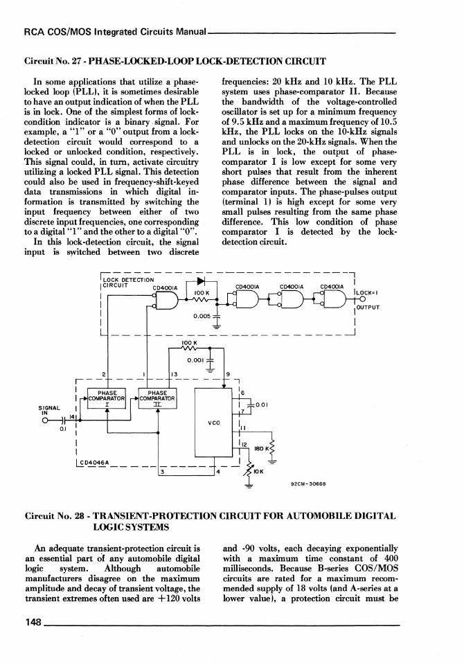
RCA COS/MaS Integrated Circuits Manual----------------
Circuit No. 27 - PHASE-LOCKED-LOOP LOCK-DETECTION CIRCUIT
In some applications that utilize a phaselocked loop (PLL), it is sometimes desirable to have an output indication of when the PLL is in lock. One of the simplest forms of lockcondition indicator is a binary, signal. For example, a "1" or a "0" output from a lockdetection circuit would correspond to a locked or unlocked condition, respectively. This signal could, in turn, activate circuitry utilizing a locked PLL signal. This detection could also be uSed in frequency-shift-keyed data transmissions in which digital information is transmitted by switching the input frequency between either of two discrete input frequencies, one corresponding to a digital "1" and the other to a digital "0".
In this lock-detection circuit, the signal input is switched between two discrete
frequencies: 20 kHz and 10 kHz. The PLL system uses phase-comparator II. Because the bandwidth of the voltage-controlled oscillator is set up for a minimum frequency of 9.5 kHz and a maximum frequency of 10.5 kHz, the PLL locks on the 10-kHz signals and unlocks on the 20-kHz signals. When the PLL is in lock, the output of phasecomparator I is low except for some very short pulses that result from the inherent phase difference between the signal and comparator inputs. The phase-pulses output (terminal 1) is high except for some very small pulses resulting from the same phase difference. This low condition of phase comparator I is detected by the lockdetection circuit.
~------------------------I I LOCK DETECTION I I CIRCUIT CD400IA CD400IA CD400IA CD40DIA I 100 K ILOCK= I
I I I
I OUTPUT
00005 T I
- -- -- ~- ---- -- - - ---~
SIGNAL IN D----ir'-'-l~-+----'
0.1
lOOK
13
0 0 001 1
L£D~6A _________ _
3
92CM-3066B
Circuit No. 28 - TRANSIENT-PROTECTION CIRCUIT FOR AUTOMOBILE DIGITAL LOGIC SYSTEMS
An adequate transient-protection circuit is an essential part of any automobile digital logic system. Although, automobile manufacturers disagree on the maximum amplitude and decay of transient voltage, the transient extremes often used are + 120 volts
and -90 volts, each decaying exponentially with a maximum time constant of 400 milliseconds. Because B-series COS/MOS circuits are rated for a maximum recommended supply of 18 volts (and A-series at a lower value), a protection circuit must be
148 ____________________________________________________ _

________________________ Circuits and Applications
included between the automobile battery and the COS/MOS logic.
This figure shows a transient-voltage protection circuit that is frequently used. The zener diode regulates the voltage supply for the COS/MOS circuits, and the capacitor and series diode prevent voltage loss during negative transients. A small diode capacitor, shown in parallel with the output, gives rf
BATTERY R COS/MOS CIRCUIT SUPPLY
I 10 TO 100p.F TYP.
92CS-30587
protection during transients. For minimum zener current during transients, the maximum value of R should be based on the minimum circuit operating voltage and the peak current drawn by the logic circuit at the minimum battery voltage. The minimum zener breakdown voltage is then determined by subtraction of the product of the minimum current drain at the normal battery voltage and the value of R just chosen from the battery voltage. A zener breakdown greater than this voltage assures that no unnecessary current will be drawn by the zener during normal automobile operation.
Another important characteristic of the zener selected is its dynamic impedance. During a current surge, the voltage across the zener must not rise to a damaging level. A value of 20 volts is safe for COS/MOS Bseries circuits.
Circuit No. 29 - SWITCH DEBOUNCING CIRCUITS
Contact bounce, the uncertainty that occurs as a mechanical switch closes, can cause troublesome transitions in logic circuits. Such uncertainties are normally overcome by providing a delay at the input sufficient to assure that the signal recognized is a true one. The amount of delay needed varies with the type of switch used. The "bounce" can be as long as several hundred milliseconds. Three typical debounce circuits are given.
SWITCH
.A ..It. ~ ..!L 0 0 NC* 0 I 0 I I 0 I 0 I 0 0
*NC= NO CHANGE
-VSS
tVoo
tVoo
0
+vooJyc R
-vss
SWITCH
A B ~ R
0 0 I 0 I 0
0 0 I I NC*
RESET CLOCK Q
S I 0 Q
0 0 0 0
(CIRCUIT OELAY BEFORE RESET!
C04013 92CS-30588
____________________________________________________ 149

RCA COS/MOS Integrated Circuits Manual ______________ ---:
Circuit No. 30 - NINE-BIT PARITY GENERATOR/CHECKER
The RCA-CD40IOI is a nine-bit (eight data bits plus one parity bit) parity generator/checker. It may be used to detect errors in data transmission or data retrieval. Odd and even outputs from the device facilitate odd or even parity generation and checking. When the CD40IOI is used as a parity generator, a parity bit is supplied along with the data to generate an even or odd parity output. When it is used as,a parity
INHIBIT 8 '»0----,
VOO=14
01 I Vss= 7
02 2 0
03 3 E
044 C
0510 0
0611 0
0712 E
0813
095
92CS-27397
checker, the received data bits and parity bits are compared for correct parity. The even or odd outputs are used to indicate an error in the received data.
Word length is expandable by cascading. The CD40IOI is also provided with an inhibit control. If the inhibit control is set at logical "1", the even and odd outputs go to a logical "0" .
Truth Table
Inputs Outputs 01-09 Inhibit Even Odd
L 1's=Even L 1's=Odd
X
0 0 1
X = Don't Care Logic 1 = High Logic 0= Low
1 0 0 1 0 0
Circuit No. 31 - FOUR-BIT MAGNITUDE COMPARATOR
The RCA-CD4063B is a 4-bit magnitude comparator designed for use in computer and logic applications that require the comparison of two 4-bit words. This logic circuit determines whether one 4-bit word (Binary or BCD) is "less than", "equal to", or "greater than" a second 4-bit word.
The CD4063 has eight comparing inputs (A3, B3 through AO, BO), three outputs (A<B, A=B, A>B), and three cascading inputs that permit systems designers to expand the comparator function.
A2 A3 15
WORO-~ {:~ \~
G>8 4 5 A>B CASCADING A-8 3 -8
INPUTS A<8 2 7 A<8
WORO'8-{~~ :1 82 I 83
L..-_---.J
VOO" 16 VSS' 8 92CS-24516RI
150 __________________________________________________ __

XI-II. Custom LSI Design
In the early chapters of this Manual, information was given about the operation and characteristics of COS/MOS devices to assist the designer in using use packaged smallscale and medium-scale integrated COS/MOS devices effectively. Later chapters gave detailed information on the logical functions that many of RCA's commercial COS/MOS units provide. At some point after the successful engineering of a digital logic design (which may incorporate a number of SSI and MSI circuits), the question often arises as to the feasibility of integrating the design into a single LSI custom chip. This chapter will describe the various factors that should be considered in making this decision and the several approaches that can be taken in integrating a design. First, however, it would be appropriateto provide some background information on COS/MOS processing and more detailed information on discrete device characteristics than was necessary for "building-block" engineering. (This next section may be considered a continuation of Chapter I COS/MOS Integrated Circuit Fundamentals ).
MOS DESIGN PARAMETERS
As stated in Chapter I, an enhancementmode MOS transistor is basically a voltagecontrolled device that exhibits a capacitive input and conducts initially when the gate-tosource voltage is equal to the threshold voltage.
Threshold Voltage
The threshold voitage V TH for a p-channel
enhancement-type unit is given by
VTH = VTO - KB [(VBS + 1/11/2) - (1/1 )1/2]
(13-1)
where K B is a function of the carrier concentration of the substrate, V BS is the substrate-to-80urce voltage, 1/1 is the surface potential, and V TO is the negative threshold value for VBS = O. The change in VTH as a function of VBS is plotted for several n-type substrate resistivities in Fig. 212. The
°Ul 5!:i ~ g 6 H-+-+-+-+ IIJI !E-I- ::t: 4 I--If--+-I::"""","""-I ~! IIJIIJ
li~ 2~~~~~~~fft8. ~g ~ 12 20 52
SUBSTRATE -TO-SOURCE VOLTAGE (Ves) -VOLTS
92CS-30653
Fig. 212 - Change in threshold voltage as a function of VBS for several n-type substrate resistivities.
boundary between the regions in which Eqs. (13-1) and (13-2) apply corresponds to the condition V DS = V GS - V TH, and is shown as the dashed line in Fig. 213. The equations given here are ideal in that the finite drain resistance in the saturation region (O~V GS -I VTH I ~ V DS), the series parasitic resistance, the variation of channel mobility with gate-to-source voltage, and the drain-tosource leakage current are all neglected.
Threshold voltage can also be defined as follows:
______________________________________________________ 151

RCA COS/MaS Integrated Circuits Manual ______________ _
(13-2)
where tox is the oxide thickness, € is the electrical permittivity of the oxide, l/J MS is the difference between metal and semiconductor work functions, l/J f is the difference in Fermi potential between the inverted surface and the bulk of semiconductor, and
where l/J ss is the fixed surface-state charge, t/J B is the bulk charge of silicon, and S equals the sum of these charges.
TRIODE 4 I -SATURATION REGION I REGION
/"os'VGs-1 VrI / VGS
ORAIN -TO-SOURCE VOLTAGEIVosl
92CS-30652
Fig. 213 - Drain current as a function of drainto-source voltage in a p-channel enhancement-type MOS transistor.
Current-Voltage Relationships
Fig. 213 shows the theoretical curve of drainto-source current I D as a function of drainto-source voltage V DS and gate-to-source voltage V GS for a p-channel enhancementtype MOS transistor. The "ideal" equations for these characteristics in the various operating regions are as follows:
1. In the triode region, i.e.,
drain-to-source current is defined by the following relationship:
2. In the saturation region, i.e.,
the drain-to-source current is given by
where I.J. is the effective surface mobility of the carriers in the channel, and Wand L are channel dimensions.
3. When the gate-to-source voltage is less than the threshold voltage, i.e., V GS ~ I VTH I , the d.,ain-to-source current becomes
ID=O
These equations can be simplified by introducing a factor which combines those characteristics fixed by the manufacturing process in one component and those determined by device geometry in another component:
K=lJ.eW = (~) W =K' W 2toxL 2tox L L
where
pe K'= 2t
ox
(all characteristics determined by processing) and W IL is the device geometry (channel length "L" is the spacing between the sourCe and drain; channel width "W" is the dimension of the drain edge along the channell.
The range of K' for RCA manufacturing processes is given below for n- and p-type devices.
RangeofK'
K' n
K' p
Min.
6
2
Typ.Max.
8 10
3 4
Units
I.J.A/V2
pA/V2
By use of the K-factor simplification, Eq. (13-3) for the triode region becomes
152 __________________________________________________ __

________________________ Custom LSI Design
and Eq. (13-4) for the saturation region becomes
(13-6)
Transconductance
The transconductance gm is given by the following relation.
alSO
gm = aVGS
or
VOS = constant
By substitution and use of the k factor:
gm = 2K (V GS - I VTH I)
Channel Dimensions
(13-7)
(13-8)
(13-9)
Although the K' factor is set by the manufacturing process and cannot be varied, in the layout design of COS/MOS integrated circuits the length and width of the channel can be increased or decreased, within tolerance specifications, to meet the requirements of particular applications.
For high-transconductance (low-impedance) devices, the channel length is decreased to its minimum value, and the channel width is made as large as required to provide the desired current. Figs. 214 and 215 show the drain characteristics and K' values for the C04007A. Fig. 216 shows the effect of channel width on the drain current of both p and n MOS transistors.
The minimum value of the channel length (source-to-drain spacing), as established by
.. e I
·10 ~
·15 E tr
MIN. LENGTH::: 0.15 mil ·20 B MAX. LENGTH ::: 0.25 mil -+-t--i-25 ~ K'MAX.:::4p.A/V2 g K'MIN. = 2 p.A/V 2 -+--+-t--i-30 ~
VTH '" 0.1 VOLT (MIN.l (,) 2.0 VOLTS (TYP.) .t",0 t--+--+-,--t---j-3!5 ~ 23 VOLTS IMAK) ~'
t--~-+--+-r-~7f~~~~~-+--+-1'40 ~
92CS-21001
Fig. 214 - Maximum and minimum p-device drain current characteristics for type CD4007 A.
2 •. AMBIENT TEMPERATURE ITA }'20'C I __ -H~ro::--I 20 I ...... ...
il, /'" J I 17.5 o~-y.--+-+-CH--t--+---j
'0 ~./ V : 15 : \,~ /. n DEVICE
~ 12.5 ,,:~':/ I i / CHANNECE:J'{[.~;;i :'~S a:: oV/ TRIODE .. X IK1. 8 p.AI v 2 B ~y REGION VI ~ z 10 r-r-~"'I'F--+----+--.. -+I A-++-=' I""'SA.!..,T'--U"'-RAJ,cT""IO'--N +--+--1 Ci .;) -"r ~ REGION
~ 7.!5f---~~ V' ... ,,:'1 I-~ 5 r-... .: I I ~ b~ / ~v TRIODE EQUATION IN
, 2 5 --r SATU IRATIO IN RE IGION -< . If.....-(" h ~
o 6 9 10
DRAIN- TO-SOURCE VOLTAGE (VOSJ-V
92CS-2!002
Fig. 215(a) - Typical n-device drain current characteristics for type CD4001 A.
DRAIN-TO-SOURCE VOLTAGE (Vos)-V
-Ii 10 9 8 6 5 4 3 2 0 - - - - - - - - -~T TE",PERATURE ITA },25·C ~~/
I I I I r---2.5
TRIODE EQUATION IN.y SATUR~TION REGION -5V V .. E
I I II ~ l.«0~--5 I
'0 p-DEVICE TRIODE .... ,:
-7.5 : CHANNEL:WIOTH-19.S MILS l.Z ..... REGION ~" -
LENGTH =0'1 MILS I .... .:s. 15 r-f- K' '3I'A/V "'~ -10 0::
SATJRATION ly ~~"i- tr ::> u r- REGION .. -12.5 z
I "If o~~"~ ;; a:
I / .... 0'<; "15 0 ...
~' u
.... .. .1.. I,...../I"¢' -17.5 >
~
I -20 ;"
-22.5
nCS-21003
Fig. 215(b) - Typical p-device drain current characteristics for type CD4001A.
processing and voltage punch through considerations, is 0.3 mil. The channel width in typical COS/MOS products ranges from approximately 0.4 mil to 200 mils.
For low-transconductance (high-impedance) devices, the channel width is
______________________________________________________ 153

RCA COS/MOS Integrated Circuits Manual ______________ _
AMBIENT TEMPERATURE (TAl-25°C /
4 GATE-TO-SOURCE VOLTAGE (VGSI' 5V
'" .I ... ,¥ E
~ lY(" I-3 z " l. .. ~ '" Q~ o· 0:
~ov"'~~-:Jf ;9 0:
" U
:;; 2 .. c.~ " 0: .,o~ V 0
'" ~rV'" ~-u :; '" I-f---• .,' 1'~· 'i' .z.v _f...-i-"'"" UI~ .• 0.5V_ c
~ ~ ~
o 3 4 5 6 a 9 10 II 12 CHANNEL WIDTH (Wl-MILS IlCS-21004
Fig. 216(a) - Drain current as a function of channel width for an n device at a gate-to-source voltage of 5 volts.
-1.5
'" E
~ I- -I z '" 0: 0: a :;; .. 0: o ",-O.5~...l---+-+ U :; '" 'i' ~
92CS- 21007
Fig. 216(b) - Drain current as a function of channel width for a p device at a gate-to-source voltage of -5 volts.
9 AMBIENT TEMPERATURE (TAlj25 0 C/" ~ATE-TO- SOURCE VOLTAGE
'" 8 !IGSl=I'ov '7 E
3' 7 I I",Y 0·"'::"; V
I- 6 I ,j ~~ z
'" 0: 5 0: I ","-" /' u $)
:;; 4 I "-~ V .l~ ..
0: t1J~V ,/ 0 1"i'P·
'" 3 ,.,0r LV .... ___ ~. i,.1 u
~ 2 ,,0 ~-0 I ~¥.V _VI--"'" _-
c ""'....I':I--"""_!----
o 3456789101112 CHANNEL WIDTH (W)-MILS
92CS-21005
Fig. 216(c) - Drain current as a function of channel width for an n device at a gate-to-source voltage of 10 volts.
decreased to its minimum value, and the channel length is made as long as necessary to provide the required impedance. The minimum channel width, determined by processing and photoengraving con-
_4
'" E .!!. ~ I- -3 z '" 0: 0:
" U
:;; -2 .. 0: 0
'" u :;
-I '" 'i' ~
92C$-21006
Fig. 216(d) - Drain current as a function of channel width for a p device at a gate-to-source voltage of -10 volts.
siderations, is 0.4 mil. Channel length can be varied from a minimum value of 0.3 mil up to several mils. Channel width also affects the source-to-drain transition time as a function of Joad capacitance because of the increased current drive. Figs. 217(a) and (b) show the relationship of these parameters for both nchannel and p-channel MOS transistors.
350 AMBIENT TEMPERATURE ITA )-25°C
r300 SUPPLY VOLTAGE (VOO)·IOV
~ tUN'S 20 nl
I = 2~O '" I .. >= ; z200 0
1~ i
E "' 150 z ..
\\ ~04D 0:
~CE(C I-
:z: 100 ).8C! .. ~
'S:::: __ OO.F
:z: --0
__ :U.F I- 50 20 pF ~ 0 I .J
I o 5 10 15 20 25 30
p-OEVICE CHANNEL WIDTH (W)-MILS 92CS-2100BRI
Fig. 217(a) - Transition time as a function of channel width and load capacitance for p-channel devices.
350 c
AMBIENT TEMPERATURE (fA 1- 25·V SUPPLY VOLTAGE (VOD'-toV
! 300 IUNS20ns ----,~-....,--_+-~-l .J :z: .. = 250r-~-+~~-t '" .. i= 200 z o >= ~ 150f----c\-lI ..... :---c:-· .. e: ~ 100
~ 7 ~~~--t~---+~~-k= :z:
'" 'i: o ~
n-DEVICE CHANNEL WIDTH (W)- MILS 92CS-21009RI
Fig. 217(b) - Transition time asa function of channel width and load capacitance for n-channel devices.
154 __________________________________________________ __

_________________________ Custom LSI Design
Input Capacitance
For switching purposes, it is important to know the input capacitance. As shown in Fig. 218, input capacitance is made up of four elements:
A. The package and pin; bond wire; bond pad
B. Input protective circuit C Metallized conductor leading to gate D. Gate capacitance
Fig. 218 -Input capacitance elements.
A. The bond pad is a 0.4-mil square metallized on thick oxide over the N + region. Its contribution (Cbp) is 0.004 picofarad. The bond wire, package pad, and pin (Cp) add just under 1 picofarad.
B. The protective circuit consists of a diffused resistor (which also forms distributed diodes Dl and D2) and diodes D3 and D4. This capacitance Cr is 0.56 picofarad. Diodes D3 and D4, which are forward biased for fastest response, contrihute about 1 picofarad capacitance each (CD = 2 picofarads).
C. The length of the metallized conductors (including bond pad to protective circuit and protective circuit to gate) will vary with the layout placement of the device. A typical metal run capacitance (CM) value is 0.14 picofarads.
D. As shown in Fig. 219, the metal gate over a device channel is 0.5 mil long (to cover channel length of 0.3 mil plus an overlap of 0.1 mil on each side allowing for mask registration tolerances during manufacture). A typical value of the gate metal oxide capacitance (CG) is 1. 7 picofarads. S~ming up all the above capacitance values, the total fixed (i.e., static) input capacitance (CF is approximately 5 picofarads.
Cbp + Cp + Cr + CD + CM + CG
=CF
0.004+ 1 + 0.56 + 2 + 0.14 + 1.7
= 5 picofarads
Dynamic Capacitance
The overlap of the gate metal over the drain diffusion shown in Fig. 219 and schematically in Fig. 220 'represents the feedback portion of the gate capacitance coupled from the drain (output) to gate (input). During switching, the Miller effect brings about an increase in feedback capacitance proportional to the product of the device transconductance (gm) and the static feedback capacitance (CDG) as shown in Fig. 221.
92CS-30646
Fig. 219 - Dimensions of metal gate over device channel.
______________________________________________________ 155

RCA COS/MaS Integrated Circuits Manual _______________ _
'a
2
92CS-30633
Fig. 220 - Feedback portion of metal gate capacitance.
20
I 15 z U 10
5
0L-----+------2r-----~3------r---~
VIN-VOLTS
Fig. 221 - Capacitance increase caused by product of device transconductance and static feedback capacitance.
Although the curve in this figure peaks at a value of 5-10 times the fixed input capacitance (CF), substitution techniques have established the true effective dynamic capacitance as approximately three times the static capacitance. The effect of this increased capacitance on device transition time should be taken into account in high-speed switching circuits. Fig. 222 illustrates the effect of increased capacitance on edge shape.
FABRICATION OF COS/MOS INTEGRATED CIRCUITS
All the COS/MOS circuits discussed in this Manual are monolithic integrated circuits. The distinguishing feature of any monolithic integrated circuit is that all components required to perform a particular circuit function are combined and interconnected on a common substrate. The constituent elements of the resultant circuits lose their
identities as discrete components, and the over-all circuits, in e~sence, become microminiaturized function blocks. The monolithic technology, which makes possible simultaneous fabrication of conglomerates of solid-state devices within or on a very small chip of semiconductor material (usually silicon), is essentially an extension of the basic planar technology used in the fabrication of discrete silicon transistors.
The manufacture of silicon monolithic integrated circuits involves a series of highly critical operations in which silicon is subjected to carefully controlled, hightemperature chemical processes. The lateral physical dimensions of the chemical reactions in the silicon are controlled by photolithographic techniques. In the manufacture of monolithic integrated circuits, high-precision photomasks represent the assembly tools, jigs, and fixtures.
General IC Wafer Processing
Monolithic integrated circuits are not fabricated singly, but rather "by the wafer" as a minimum "batch". The fabrication process involves a sequence of diffusion and photolithographic engraving steps. Individual silicon wafers are cut from a
90% -r-- --t= 10%+ -1
92CS-30634
Fig. 222 - Effect of increased capacitance on edge shape.
silicon ingot into slices. Each wafer is then polished to a mirror finish. Circuit complexity determines the size of the chip for a particular design. Circuits being produced today use chip sizes up to about 240 mils square. For this range of chip sizes, the number of chips produced per wafer varies from the order of 1,000 down to about 100. Because the cost of processing a wafer is the same regardless of the number of chips it produces, it is evident that small chip area reduces the cost of the individual chips. In addition, defects tend to be random in
156 ____________________________________________________ __
________________________ Custom LSI Design
nature. As a result, the probability of a defect is larger for a large chip area than for a small one. Thus, a smaller chip area increases processing yields and further reduces costs.
The first major step in processing the mirror-finished wafer involves ' the formation of a silicon dioxide layer on the surface of the wafer, as shown in Fig. 223. This thin layer of silicon dioxide protects the silicon surface
>Z'Z;;Z2Z'22Z'2Z;;Z2Z'2Z;;Z2Z'2~ SILICON DIOXIDE SILICON
SUBSTRATE
(a)
"DOPANT" ATMOSPHERE
~=zz;i ;z;;~~~ L~ ~~~i zz;i;z;;zz;1 ~i SILICON y- DIOXIDE
SILICON '--_---'S:..:U:.::B:::.,ST'-'.:Rc.:AT'-'E=---~:----"n- OR p-TYPE
(b) REGION
WINDOW
92CS- 30651
Fig. 223(a) - Formation of the silicon-dioxide layer on the surface of a wafer; (b) -layer used as mask.
of the finished integrated circuit, acts as a barrier to dopants during the semiconductor junction-forming processes, and provides an insulating substrate for the interconnection metals. Silicon dioxide is formed on the silicon wafer by heating it to a temperature of 1000 to 13000 C and passing oxygen over the surface. The silicon dioxide layer also serves as a "pattern mask" in determining the area through which "dopant" atoms may pass freely into the silicon substrate to form regions of either n-type or p-type silicon (depending on the type of dopant material used).
The ability to control the procedures by which "windows" are formed selectively in the silicon dioxide layer is one of the most crucial in integrated-circuit manufacturing. In some instances, the windows may be in the order of only 0.1 mil square. The windows in the silicon dioxide define the geometrical areas in which chemical diffusion reactions are localized. These windows are mechanically positioned and dimensioned by the use of photomasks and photochemical procedures, a system of processing which is dependent on the photosensitive properties of a type of lacquer called photoresist.
Fig. 224(a) illustrates the manner in which an oxide-coated silicon wafer is covered with a layer of photoresist lacquer several thousand angstroms thick. A photomask, in
ULTRAVIOLET EXPOSURE LIGHT
++++++++ MASK PATTERN
,"777777~~""""""J<1'i. ____ GLASS MASK
~~.~~.~~.o/ PHOTORESIST
~~~milillill~!iliftl...- SILICON DIOXIDE
l' SILICON WAFER
EXPOSURE WINDOW IN ( a ) PHOTORESIST
E"·'·······m,,~::,::'~:::'" DEVELOPED PHOTORESIST SILICON WAFER
(b)
~WINDOW IN OXIDE
a· .... M'· . PHOTORESIST
! SILICON DIOXIDE '--------ETCHED OXIDE SILICON WAFER
(e)
r:·1 1.:·:·:·.1 ::t:;II~I~~: ~~O~~~:E WAFER WITH WINDOWS SILICON WAFER
(d) 92CS-30650
Fig. 224 - Photoresist processing of mono-lithic integrated-circuit wafer.
this case a glass plate having a pattern of black spots on it, is placed against the photoresist, and the system is exposed to ultraviolet light. Illuminated areas of the photoresist tend to harden (polymerize), while the areas under the black spots of the photomask remain soft and are removed during a subsequent "photo-development" operation. Fig. 224(b) shows the "exposed" patterns of the windows in the photoresist following the "photo-development" operation. The wafer is then subjected to a chemical etchant (such as diluted hydrofluoric acid), which dissolves the silicon oxide in the photoresist windows without attacking the silicon underneath. The desired windows in the silicon oxide are thus produced, as shown in Fig. 224(c). The remaining photoresist is removed chemically. This "cleaned" wafer, Fig. 224(d), with windows in its oxide coating is then ready for chemical doping procedures using ion implantation diffusion furnaces . to produce regions with either n-type or p-type electrical
_____________________________________________________ 157

RCA COS/MaS Integrated Circuits Manual ______________ _
characteristics in the areas beneath the windows.
Chemical diffusion processes are used to introduce the semiconductor junctionforming dopants into the bulk silicon. A series of these diffusion cycles is performed in processing of integrated-circuit wafers.
COS/MOS IC Wafer Processing
The starting material (substrate) for a monolithic COS/MOS integrated circuit consists of a uniform single crystal of n-type silicon. Diffusion processing techniques (doping) permit introduction of certain impurities to desired depths and surface concentrations. Vertical penetration of the impurities is controlled by the diffusion temperature and time; control of lateral diffusion is made possible by a combination of the masking properties of silicon dioxide and photochemical techniques. The silicondioxide insulating material on the surface of the substrate is selectively opened (windows are formed) for each diffusion step. The oxide is subsequently replaced except in metal-contact areas.
Basic Device Formation and Interconnection Processes
The following paragraphs summarize the basic processes involved in the formation and interconnection of electronic components on a basic COS/MOS integrated circuit, such as the one shown in Fig. 225. The fabrication of a simple n-channel and p-channel device pair with gate protection is described.
As the initial step in the formation of a COS/MOS IC, p-type material is diffused vertically into the n-type substrate to form ptype regions (p-wells) in which the n-channel MOS device will be located. This initial step is shown in Fig. 226. Low-resistance p -of -type pockets, such as those shown in Fig. 227, are diffused into the n-type substrate to form the source and drain regions of the pchannel devices and into the well (p- region) to form guard bands for n-channel devices. Low-resistance n + -type pockets, like those shown in Fig. 228, are diffused into the p-
Fig. 225 - Photograph of a COS/MaS integrated circuit.
I p-WELL I n-SUBSTRATE
92CS-30649
Fig. 226 - Formation of p-type regions in which n-channel MaS devices will be located.
n-SUBSTRATE
92CS-30648
Fig. 227 - Low-resistance P+-type pockets in the n-type substrate.
92CS-30647
Fig. 228 - Low-resistance n+-type pockets in the p-well region.
well regions to form the source and drain regions of the n-channel devices and into the substrate to form guard bands for p-channel devices. As has been described, silicon dioxide (Si02) is necessary in integratedcircuit processing as a diffusion mask. However, in MOS processing, Si02 plays an
158 ____________________________________________________ __

_________________________ Custom LSI Design
additional and more important role as a dielectric used to cover the channel region and insulate it from the metal gate. The processing technology by means of which a suitable oxide layer is obtained is the key to fabricating MOS devices.
It has been found that Si02 usually • contains some ion contamination (most often
sodium ions), and that these ions are positively charged. The positive charge carried by the ions can affect the characteristics of MOS devices significantly. In many instances this charge is fixed; in others, it is movable when stressed with voltage at elevated temperatures. The presence of a movable charge is very undesirable because it can cause serious problems in device stability and reliability. Therefore, clean-oxide technology has been developed to eliminate the contamination. This technology has made possible the fabrication of reliable nchannel and p-channel enhancement devices and thus is responsible for the development of the complementary-symmetry arrangement in integrated MOS devices.
Another important use of Si02 in MOS integrated circuits is as a field oxide, a thick oxide that insulates all non-active regions of the MOS Ie from the interconnection metal. This insulation is needed to raise the threshold voltage of the inactive regions to a level beyond the operating voltage of the system so that undesired leakage currents are eliminated. The threshold voltage of the field oxide is usually referred to as the field threshold voltage.
Metallization of Completed Wafers
The series of oxidation and diffusion operations culminates in an integrated-circuit wafer that contains the desired electronic elements. High-conductivity metallic paths are then needed to interconnect these elements. The process by which these paths are fabricated is called metallization.
The metallization process is comprised of metal deposition, interconnection pattern delineation, and alloying. Metal deposition is performed by placing the processed wafer in a vacuum of about 10-6 torr (10-9 atmosphere). The source material (usually
aluminum), which is also in the vacuum chamber, is then heated above its vaporization point by an electron beam heating source. As a result, metal is released by vaporization and condensed on the integrated-circuit wafer, coating it completely to a controlled thickness. The metal-coated wafer is then subjected to photolithographic procedures, including application of photoresist lacquer, exposure to ultraviolet light through a photomask having the desired pattern, and the removal of unwanted metal by acid etching. The resulting interonnnection patterns are similar to that shown in Fig. 229. Finally, in order to assure excellent electric contact between the
Fig. 229 - Integrated-circuit chip mounted with chip connected to package terminals.
aluminum and the electronic elements, the metallized wafers are heated in a furnace for a controlled period to permit a slight alloying of the aluminum with the semiconductor junctions.
Seven mask levels are normally used:
well p+ n+ stepped oxide contact metal protective glass
_____________________________________________________ 159

RCA COS/MOS Integrated Circuits Manual _______________ _
As shown in Fig. 225, the metallic interconnections terminate at the edges of the integrated-circuit chip as pads to which very fine wires connect the chip to the package terminals as shown in Fig. 229.
Probe Testing of Metallized Wafers
Elaborate automatic equipment has been developed to test chips while they are constituents of a complete wafer. The test procedure is frequently called ".waferprobing". A large number of needle-tipped probes make simultaneous electrical contact
. with the aluminum electrode pads on each chip. The probing equipment is designed so that the wafer is indexed automatically, with the probes contacting the individual chips sequentially. A spot of ink is automatically placed on each chip which fails electrical test, so that it can be easily discarded after the wafer is separated into chips.
Assembly and Final Testing
Mter the probe testing of the wafer is completed, the individual circuit chips must be separated and assembled into integratedcircuit packages. The packaged devices are then subjected to hermeticity, environmental, and final electrical testing. The sequence of events employed for these operations is as follows:
Separation of Chips - The individual chips in a wafer are separated by a technique similar to that used in glass cutting. A fine diamond point is used to "scribe" the wafer with its constituent chip pattern. The actual separation into chips is accomplished by an operation called "dicing", which is simply a system of mechanical fixturing by which stress is applied to the wafer in such a manner that mechanical separations occur along the scribed lines. With new techniques, using a diamond saw blade or laser beam, both "scribing" and "dicing" are performed in a single operation. "Sorting" is the rejection of chips which were found to be defective in wafer-probing or dicing operations. Microscopic inspection of each chip is also performed to cull out circuits with visible imperfections.
Chip Bonding In the bonding procedure, the chip is securely mounted in the package by means of a silver-filled conductive epoxy.
Lead Bonding - After the chip is firmly affixed in the package, electrical connections are made to the terminal-post leads. Aluminum wires of about 1.5-mil diameter • are commonly used to make these connections. Recent development of accurate, computer-controlled equipment has led to "automatic bonding" systems.
Capping and Sealing - The lead-bonded chip assembly (header) is usually subjected to cleaning and vacuum bake-out operations prior to sealing. Actual hermetic sealing is accomplished by a variety of means, depending to some extent on the package design. Local application of heat (e.g., welding) is used to seal the cap to the package header. This step is conducted in a dry atmosphere. In the case of non-hermetic packages like plastic, the lead-bonded chip assembly is encapsulated in plastic or epoxy materials.
Hermeticity and Environmental Testing - Hermeticity testing is used to confirm the leak resistance of the package. The helium leak-detection technique is frequently used. In this method, completed packages are placed in an atmosphere of helium pressure for a period of time. Helium is able to penetrate through any imperfections which may exist in the package. Mter removal from the helium pressurization chambers, sensitive mass-spectrograph leak detectors are used to detect helium "oozing" out of any imperfection in the package.
Mechanical shock, vibration, acceleration, and thermal shock tests are used to screen out devices that have inadequate margins against anticipated stresses for the particular class of service in which the integrated circuit is to be applied.
Final Electrical Testing - Wafer-probing of COS/MOS integrated-circuit chips is usually limited to static parameter tests and dc functional tests because the length of probe leads and other factors prevent meaningful ac, rf, or pulse testing. Consequently, any ac testing required is performed on packaged units only. Test equipment presently used on COS/MOS integrated circuits is almost entirely automated.
160 ____________________________________________________ _

________ ~--------------- Custom LSI Design
CUSTOM DESIGNS
Creating the Layout Drawing
The major task in implementing a logic design as a custom LSI chip is the creation of the layout drawing. This drawing must show every transistor in the array (using color coding for the different levels) with all interconnections to the rest of the circuitry. As determined by load and speed requirements, the channel width for each transistor must be specified. (Except for high-impedance devices, channel length is fixed at 0.3 mil by punchthrough and processing considerations). Fig. 230 shows the layout of 16 transistors in a flip-flop; this figure represents a small portion of the layout drawing, because an average LSI array might have a total of 1500 transistors.
A firm set of design rules defines minimum spacing and sizes for diffusions, metal lines, oxide openings, etc. Because these rules are fixed by a combination of phy~ical parameters (side diffusion, etch angles, hght scattering) and processing technology (mask registration, run-out, photo-resist resolution) and have been established over a considerable period of COS/MaS device manufacture, no deviations can be allowed. Fig. 231 shows some design minimums for line widths and separations.
p+ GUARD BAND
:1.'::::::::::::::(::::::::
Master Making and Testing
Once the layout is completed and checked, each layer is "digitized"; this step converts all dimensions and lines on the drawing to numerical values which are stored in a computer memory. This digital information
" I "f can be used to generate pen-p ots or further checking of the layers and registration between layers. After checking and correcting, the digital data is used to drive a pattern-generator camera which creates a set of mask reticles. Each mask reticle represents one layer at ten times final size.
To generate the multiple patterns that enable many chips to be processed simultaneously on a single wafer, the reticles are placed in a "step-and-repeat" camera which exposes a master plate for each layer. Glass prints of the master, called working plates, are actually used in wafer processing.
Every custom-designed chip needs two special computer test programs. One is for a fast "functional" test for wafer probing to grossly screen out defective chips. The other is a complete program for final test of bonded and packaged units.
Functional Design Considerations
Before a logic design is implemented as a layout drawing, it should be reviewed from
SOURCE VDD
92CS-21029
Fig. 230 - Typical layout for a "D"-type flip-flop circuit.
_____________________________________________ 161

RCA COS/MaS Integrated Circuits Manual _______________ _
Q 0.1
Y L CHANNEL OXIDE REGION
X 2 MILS = I INCH
J 0.3
METAL INTERCONNECT
n+ GUARD BAND
H
p+ GUARD BAND
92CS- 21018RI
Fig. 231 - Typical design minimums for line widths and separations used in layout of COS/MaS IC arrays.
the point of view of minimizing the device count. Because of the differences between a logic design using "building-block" NAND and NOR gates and one which creates the same logic function using "tree" or "functional-gating" logic, the saving in devices can be considerable. As an example, Fig. 232 shows eight devices (four p and n pairs)
+VDD
A
Fig. 232 - "Tree" or "functional gating" logic.
performing the same logical function as eighteen devices in Fig. 233. arranged as NAND and NOR gates. The savings would be 44%, translated directly into area savings on the chip.
A-~r-_
B
C
o
Fig. 233 - "Building-block" design using NAND and NOR gates.
The Boolean expression for this logic function is
Factoring the common term:
CIA • B + D) (Apply ton devices)
Complementing for the p devices:
(C + (A + B) • D (Apply to p devices)
Note that all devices must be complemented, that is, each input signal must appear on the gates of both a p and an n device.
162 ____________________________________________________ __

_________________________ Custom LSI Design
The engineering, drafting, and maskmaking costs involved in a custom design must be balanced against the savings of the single chip in production volume over the cost of standard parts, including substrate board, assembly, interconnection, and test. Special considerations such as the importance of size (as in a wrist watch) or the improved reliability of an integrated circuit (intra-chip connections are more reliable than inter-chip connections) must also be evaluated. These factors can be discussed with an RCA Field Sales Representative who can provide cost information on the three techniques RCA has developed for custom designs: Universal Array, APAR (computercontrolled automatic placement and routing interconnections of standard cells), and Manual Layout. These three techniques are briefly discussed in the following material.
Gate Universal Array:
A Gate Universal Array consists of a fixed placement of p devices, n devices, and tunnels in a repetitive ordered structure on a silicon or sapphire substrate. All drains, sources, and tunnel ends are accessible. All the mask definition levels, except the metal mask, are fixed. The metal definition mask uniquely defines the device interconnect metal for each application. The Gate
Universal Array Technique provides the following features: single mask definition, quick turnaround time, high reliability, low design cost, and the quick correction of errors or logic changes. It does not require that the user have processing experience or knowledge of IC layout design rules.
As shown in Table XIX, the Gate Universal Array is available in several sizes and technologies. As described in the COS/MOS Array User's Manual and in the SOS COS/MOS Universal Array User's Manual, there are three approaches at different interface levels that the designer may use. In the Level I approach, the customer supplies the required logic in any form together with other necessary specifications. In the Level II approach, the customer supplies a logic diagram annotated in Gate Universal Array logic cells as defined in the User's Manuals together with any other necessary specifications. In the Level III approach, the customer does the logic layout on special plastic sheets provided by RCA for that purpose and supplies an annotated logic diagram, test pattern, and other necessary specifications. In all three, RCA will fabricate, package, test, and deliver a quantity of working units.
The Gate Universal Array Technique emphasizes low initial design cost, quick turnaround time, and rapid error correction at the expense of a somewhat larger chip.
Table XIX - Summary of Gate Universal Array
Type No. of No. of Technology No. Gates* Pads
Metal-Gate CMOS TCC 040 168 40 (MG COS/MaS) TCC 051 276 48
Silicon-Gate CMOS TCC 220 168 40 (c2L COS/MaS) TCC 221 276 48
TCC 222 410 48 TCC 223 576 64
Silicon-Gate CMOS TCS 090 182 40 on Sapphire TCS 091 300 48 (SOS COS/MaS) TCS 092 452 64
TCS 093 632 64
* A gate consists of two p and two n devices and is the equivalent of a two-input gate.
163

RCA COS/MaS Integrated Circuits Manual _______________ _
AP AR (Automatic Placement and Routing)
In the AP AR technique (AP AR is an acronym for Automatic Placement And Routing), a sophisticated computer program utilizing an extensive growing library of Standard Cells stored in memory optimizes the placement of cells so as to minimize the lengths of interconnecting metal rons. The library includes metal-gate, C2L, and siliconon-sapphire cells of either the single-ended or double-ended type. In the single-ended cells connections are made at one end; in the double-ended cells connections can be made at both ends thereby facilitating a more compact design. The program inputs are based on the Boolean expressions for the complete logical function of the array. A companion program generates the test programs.
AP AR is more efficient in chip-area utilization than the Universal Array, but not as efficient as Manual Layout. The time period required to reach the working chip stage is considerably shorter than that of the Manual Layout technique. One of the reasons for this time advantage is the fact that AP AR uses only Standard Library Cells. These Cells have proven themselves over
many years of use so that almost all AP AR arrays work on the first go-around.
Many customers use AP AR to take advantage of its fast delivery cycle and moderate costs to build prototypes with integrated circuits as a final check on systems and product design. Then, before entering the high-production-volume stage, a more efficient Manual Layout design is made.
Manual Layout
For the Manual Layout Technique, an RCA specialist will review the customer's logic design, minimize device count and lead lengths, specify device sizes, and supervise the layout of the chip by an experienced draftsman. Because this approach provides the most compact array, and, consequently the highest potential yield per wafer, it should be used for high-volume circuits.
The computer test program is written while the masks are being made in RCA's inhouse mask-making facility and a sample wafer ron is then processed. Wafers are tested, debugged if necessary, and engineering samples supplied for customer evaluation.
If the customer chooses to create his own layout design, he should make an intensive study of the COS/MOS custom layout practices as a first step.
164 ___________________________________________________ __

Index
ACnoise ................................... 30 Digital timekeeping .................... 57,65,104 Adder-subtracter, two's-complement ........... 147 Diode-Transistor logic (DTL) ................... 40 APAR (automatic Placement and Routing) ...... 165 Direct Memory Address (DMA) ............. 122, 128 A-series types ............................... 17 Discrete device interfacing .................... 43 Astable circuits ........................... 47,56 Display drivers .............................. 104
BandPass filter ............................. 144 Dissipation ................................. 30 Divide-by-counter ........................... 139
Basic COS/MaS building blocks ................. 6 Divide-by-3 synchronous counter Counters ................................. 15 with divided outputs ......................... 139 D flip-flops ................................ 11 Divide-by·4 synchronous counter .............. 140 Dynamic shift register ...................... 14 Divide-by-4 ripple counter .................... 140 Flip·flps ................................... 9 Divide-by-5 synchronous counter .............. 141 Gates ..................................... 6 Divide-by-6 ripple counter .................... 141 Inverters ................................... 6 Divide-by-N counter ................... 91,112,142 J-K flip-flops .............................. 12 Divide-by-N counter, programmable ............ 112 Memory cells .............................. 16 Dopant .................................... 156 NAND gates ................................ 6 Dynamiccapacitance ....................... 155 NOR gates ................................. 6 Dynamic shift registers .................... 14, 77 Set-reset flip·flops .......................... 9 Shift registers ............................. 13 Ec1ge detectors ............................. 137 Transmission gates ......................... 8, Electrical characteristics ................ 18,19,21
Basic MaS transistors ......................... 3 Electromechanical devices interfacing .......... 43 Batteryoperation ............................ 34 Emitter-Coupled logic (ECl) ................... 41 Binary counter, ripple·carry ............... , .... 85 , Envelope detection .......................... 146 Breakdown, secondary ........................ 29 , External flag lines ........................... 125 B-series types ............................... 17 Buffered types ............................... 17 Fabrication of COs/MOS IC's ................. 156 Buffer, three-state ......... _ ............ _ ..... 84 FI FO buffer reg isters ......................... 84 Built-in protection networks ................... 27 Filtering .................................... 33
Capacitive loading ....................... 33,155 Flip-flops .................................... 9 Floating inputs ........................... 29,32
Cascading considerations ..................... 34 Four-bit magnitude comparator ............... 150 Central Processing Unit (CPU) ................. 122 Frequency discriminat.or ...................... 144 Channel ................................. 3,153 Frequency doubler ...................... 134, 138 Characteristics of COS/MaS devices ............ 17 Frequency-synthesized loop .................. 109 Clock-edge shaping circuit ................... 143 Frequency synthesizers ...................... 109 Clock frequency ......................... 34, 122 Functional classification of Clocking requirements .................... 34, 122 COS/MOS IC's ............................... 25 Clock timer .................................. 88 Function generator .......................... 147 Complementary symmetry ...................... 5 Fundamentals of COS/MaS IC's ................ 3 COSMAC microprocessors ................... 122 Circuits .................................... 133 Gate-to-source voltage ........................ 4 Common busing .............................. 9 Gates ....................................... 6 Compensated multivibrator .................... 49 Gate universal array ........................ 163 Counter circuits ................... 15,65,139-142 Guard bands ............................... 158 Counters and registers ........................ 65 Counter/dividers ...................... 86, 90, 139 Handling COS/MOSdevices ................... 27 Counters,synchronous ....................... 89 High-Noise-Immunity Logic (HNll) .............. 40 Crystal oscillators ............................ 57 Current sinking capability ..................... 39 Input capacitance ......................... 5, 155 Custom lSI design ...................... 151,161 Input/Output 110 ............................ 126
Dc noise ................................... 30 Input/output port ............................ 126 Input protection ............................. 27
Decade counter .......................... 89,102 Inputs Demodulator ............................... 136 Floating ........................... , ...... 32 Design parameters .......................... 151 Paralleled gate ............................ 32 DeSign and layout of COS/MOS circuits ......... 156 Paralleled inverter, ......................... 32 Dflip-flops .................................. 11 Unused ................................... 32 DiffUSion ................................ 3, 158 Input switching levels ......................... 34 Digital displays ............................. 104 Interfacing COS/MOS ......................... 36 Digital frequency synthesizers ................ 109 Inverter .... , ................................ 31
____________________________________________________ 165

Index (cont'd)
J-k flip-flop ..................•.......... _ .. _ 12 Power dissipation
K-factor ............................... " .. 152_ Dynamic .................................. 30 Quiescent ................................. 30
Latch-up ................................... 28-Power-on reset ............................. 137 Power requirements
Level shifters ...... " ........................ 42 Batteryoperation .......................... 34 Light-Emitting Diodes (LED) .................. 107 Filtering .................................. 33 Liquid Crystal Displays (LCD) ................. 104 Regulation ................................ 33 Liquid crystal display drivers .................. 104 Zener operation ............................ 34 Logic conversion ............................. 36 - Power-source considerations .................. 33 Logic-level definitions ........................ 31 Prescaling ....................... , ......... 115 Low-pass filter .............................. 144 Probe testing ............................... 160
Manual layout ............................. 164 Programmable divide-by-N counter ............ 112 Propagation delay ........................... ,21
Master-slave flip-flop ......................... 65 Protection networks ............... , .......... 27 Maximum ratings ............................ 24 Pulse modulator ......... , .................. 135 Memory cells .............................. _ .. 16 Pulse stretcher ...... , ...................... 134 Memory interfacing ...................... 122,131 Metallization ............................... 159 Quad bilateral switch ......................... 9 Microprocessors ............................ 122 Quartz crystals ......... , ...... , .......... 37,58 MILtypes ................................... 26 Monostable circuits ....................... 49,56 Random Access Memory (RAM ........... 122, 132 MOSTransistors .............................. 3 Rate multipliers ............................. 115
Basic principles of .......................... 3 Ratings, maximum .................... , ...... 24 Basic structure ............................. 4 Read-Only Memory (ROM) ................ 122, 128 Current-voltage relationships ............. 6, 152 Register circuits ...................... , , .. 65,80 Depletion type .............................. 4 Register, scratch-pad ........................ 123 Design equations ......................... 152 Regulation .................................. 33 Enhancementtype ...................... 4, 151 Relay drivers ................................ 45 Theory of operation ......................... 3' Ripple-carry binary counters ................. , .85
Multivibrators, astable ........... , ............ 47 Multivibrators, monostable .................... 49 Saturated bipolar logic ....................... 38 Multivibrators, Schmitt-triggered ......... , ..... 52 Saturation region ........................ , .. 1_52
NAND gates ................................. 6 Schmitt trigger ............................ 43,52 Schmitt-trigger multivibrator ................ 52,56
N-channel MOS , . " ............. , .......... 3,37 SCRdrives ........................... , ...... 44 Nine-bit parity generator/checker ............. 150, Secondary breakdown ........................ 29 Noise discriminator ......... , ........... 142,143 Sequential counters ........ , , ........ , ...... 139 Noise immunity .... , ......................... 30 Serial interfacing ....... , ................ 128, 130 NOR gates ............................. , ..... 6 Set-reset flip-flops .......... , ..... , ........... 9
One-shot multivibrator ....... , ............ 49,50 Shift-Ieft/shift-right register .................... 75 Shift registers .......................... , .13,65
Op-amp interfacing ..................... , ..... 45 Signal swing, input, .......................... 32 Operating precautions ........................ 28 Sine-wave to square-wave converter ...... , .. , .. 138 Operating rule summary ....................... 29 Solenoid drives .............................. 44 Oscillators ............................... 48,57 Static shift registers ....................... 14,65
COS/MOS crystal ............ , ............. 62 Storage registers .................. , ......... 80 Crystal ....................... ' ........... 57 Switch, CD4016 ............................... 9 Phase-locked voltage-controlled, ............ 109 Switch debouncing circuits .............. , .... 149
Oxide, gate. . . . . . . . . . . . . . . . . . . . . . . . . . . . . . . . .. 3 Synchronous counters ........................ 89
Packages ................................. 24 P-channel MOS ................ ' ............ 4,37 Paralleling inputs ............................ 32 Paralleling outputs ........... , ............... 32 Phase comparators ........ ,., .............. 111 Phase-locked loops ............... " ..... 109, 148
Temperature stability ................. " .... 61 Testing .................. , . , ....... , ........ 60 Three-static logic ............. , ............... 9 Three-state output ........................ 80,84 Threshold voltage .................. , .. , ... 4, 151 Timekeeping oscillator circuits .... , ............ 57
Phase-locked loop detection circuit ............ 148 Photomask ................................. 157,
Timer, clock ................. , ............... 88 Transconductance (gm) ....... , ... , .......... 153
Photoresist ., .............................. 157 Transient-protection circuit for Positive-negative logic conversion .............. 36 automobile digital logic systems .............. 148
166 ______________________________________________ ___
Index (cont'd)
Transition detector ......................... 134 Up/down counters ........................... 92 Transmission gates ........................... 8 Triac drives ................................. 44 Voltage-Controlled Oscillator (VeO) ....... 109, 146 Triode region ............................... 152 Voltage-controlled pulse-width circuit .......... 146 TTL (Transistor-Transistor Logic) ............... 38 Two's-complement adder-subtracter ........... 147 Wafer processing .......................... 156
Windows .................................. 157 Unbuffered types ............................ 17 Wired-OR function ........................... 33 Universal Asynchronous Receiver Word-organized storage cell ................... 16 Transmitter (UART) ... _ ...................... 128 Unused inputs .... _ .......................... 32 Zener-diode reference operation ............... 34
___________________________________________________ 167