feelin' YAMAHA - bitsavers.org
84
feelin' YAMAHA LSI CONDENSED CATALOG CATALOG No.7400001 1990. 10
-
Upload
khangminh22 -
Category
Documents
-
view
0 -
download
0
Transcript of feelin' YAMAHA - bitsavers.org

feelin' YAMAHA
LSI CONDENSED CATALOG
CATALOG No.7400001
1990. 10

INDEX DIGITAL AUDIO
voe I 0 I SPC6
VM7 I 2 I 8 SPC5
VM7402 CDVP
VM3805 SPC
VM3437C DIT2
VM34368 DIR2
VM7 I 36 DIR3
VM36238 DIR
VM3434 AFUDF
VM34338 ALCDF
VM34 I 4 ACDDF
VM34048 CDDF
VM3608 DEQ
GDR I 0 I ASP
DIA CONVERTER YM3020 YM3016 YM3015
SOUND CHIP
2 4 6 8
10 12 14 16 18 20 22 24 26 28
30 32 34
VM66 I 6 ADPCM Record & Replay 36 VM7 I 40 ADPCM Replay 38 VM64AXX FM MUSIC 40
GRAPHICS V63888 VPDC 42 V6377 EPDC 44 V6366C-F PCDC 46 VGV603 AMDC 48 V9978 E-VDP-III 50 V9958 E-VDP-II 52 V9938C E-VDP- I 54 __ " ___
COMMUNICATION VTF405 FAXC 56 YTM401 MD96DX 58 VM7 I 09C MD96FX 60 VM3802 MCS 62
SOUND SIGNAL PROCESSOR VSS205-F KP
VM73068 DPLD
YM7 I 28 SP2
YM3428 SP-B
VM34 I 28 COMP
CD-I/CD-ROM VM60638 CDC
VM6064 ADP
VM7302 MPC
Recommendation for Surface-mount LSI
64 66 68 70 72
74 76 78

Seeking the i>est in sound reproduction, Yamaha has captured sound as digital infc•rmation and created its own sound-oriented semiconduci·or technology. By combinin,, its experience ,in building electronic musical instruments with high-tec~h R & D work, Yamaha has mastered the art of making sophisticated LSI chips for graphics processing, commµnications, and fullcustom a11d semicustom applications.
·41111,• • Milesto~ries in Yamaha®LSI Technology
The Yamaha plant at Toyooka, Japan, procJ'ucei; Electone digital keyboard instruments, wind instruments, and LSI circuits. This plant contains our primary LSI Research and Development La.b.
The Yamaha plant in Kagoshima, Japan - ,known as the Yamaha Kagoshima Semiconductor Company - produces LSI circuits.
1969 •IC manufacturing project initiated.
1970 •Construction of first IC manufacturing plant, at Toyooka, Japan, started. •IC production started.
1976 •Construction of second IC manufacturing plant, at Kagoshima, Japan, completed. • Detlelo/»nent of FM sound generators Initiated.
1978 •Dry etcher added to production equipment. •Projection aligner-device that aligns the mask, via projection, to allow more dice
per water to be obtained-added to production equipment.
1980 • VLSI circuit production Initiated. •Automatic layout program developed. •Manufacturing process simulator developed.
1983 • Ma1·ketlng of semiconductor products started-devices marketed Include LSI circuits for advanced high-density discs, compact discs, FM musical sound generation, digital-to-analog conversion, and pressure sensors for printing press control.
•Automatic LSI dlslgn system developed-performs mask-pattern generation; device layout, and standard-cell routing.
1984 • Mal"ketlng of custom LSI circuits Initiated.
1987 •Production facility at Kagoshima Incorporated as Yamaha Kagoshima Semi-conductor Company.
• Yamaha Corporation of America established Systems Technology Division to market components, boards and system In The United States.
1988 • C/a:ss 1 clean room completed • YST moved to San Jose, California •Operation of 1.2µ rule CMOS production line started •Marketing of LSI for teletext broadcasting started •Marketing of LSI for CD/ started
1989 •Marketing of 2M, 4M bit high-speed ROM started •Marketing of LSI for 9600bps FAX modem started •Marketing of LSI set for LV player started •Marketing of LSI for ISDN started •Marketing of Dolby Pro Logic decorder started
1990 •Operation of 0.8µrule CMOS production line started •Marketing of karaoke surround processor started •High speed SRAM Introduced •Marketing of facsimile controller started
/BM, Hercules, and Microsoft are registered trademarks of IBM, Hercules Computer Technology and Microsoft Corporation.

2
DIGITAL AUDIO Signal Processor & Controller (& RAM) for Compact Disc player
YDCl Cll SPCB
•OUTLINE YDCIOI is one-chip LSI to provide various servo control and signal processing capabilities needed in compact disc player. It has a clock regeneration circuit of EFM signals and 16K RAM to perform EFM demodulation, error detection and correction and jitter absorption. Furthermore, it performs various servo controls for focusing, tracking, feeding and discmotor. This LSI also has capability for various applications by its function of double-speed play-back, peak-level detections, digital di-emphasis and digital attenuator, digital audio interface output capability conforming to EIAJ format and 8 times oversampling digital filter.
•FEATURES • X'tal (16.9344MHz or 33.8688MHz in double speed mode) is connected to generate standard clock and
timing signals for play-back and double-speed play-back. •The built-in VCO oscillation and slice level control circuit perform clock regeneration of EFM •
signals, sync. signal separation and EFM demodulation. e.In addition to sub code separation and output conformed to EIAJ format, Q sub codes are CRC
checked for output to a microprocessor. •Phase between reproduced and standard clock signals is detected to control the disc motor with
PWM. •By the function of focus search control, auto search, one track kick and track-counting, each servo
can be controled with a little burden of software. •The built-in RAM buffers of the EFM demodulation signals to absorb wow and flutter of the disc
(Jitter absorption range : ± 4 frames) and performs deinterleave. •Error detection and correction as well as flag processing for digital audio signals (Double error
correction for both Cl and C2) •Linear interpolation is used to replace the uncorrectable error data (up to a maximum 8 consecutive
errors). And preceding data hold is applied for errors over eight. And for application as CD-ROM, prohibition of interpolation and output of error flag are possible ..
•The data output is MSB first format. Digital di-emphasis processing circuit and 8 times (with noise shaper)/ 4 times oversampling digital filter are built in.
•Digital audio interface signal is output as conformed to EIAJ. •Peak level detect function which outputs maximum voice level is available. • 240 step (0.4dB resolution)digital attenuator is built-in. •Zero cross muting which holds down mute noise of voice is available. e5V single power supply, CMOS, 80-pin QFP.
•PIN ASSIGNMENT
u u U' u H H JI u 33 u JI
l/Hf'LL Yf'LL rco Yll rFlll /[Fiii
ITUT•I ,., FCI
"zc nor uu

....................................... --1 ......................................................................... ..
• OUTLINE DIMENSIONS
~-0.2TVP
2.75±0.2 Annnnnonnn~
• BLOCK DIAGRAM
TllOI', TllHD, TltftL ICP•,ICP-
TO, Tl
,.CDRO" UP, DOllM, ,nUTE
.2,IDO,IDSV,DTFLG
16K RAM
mror data interpolation digital attenuator
data control
calculation circuit
!:1ndardclockoscillation L timing control
CI ,C2 error
detection· correction
flag processing
RAM address control
DIT output
interface
DEP
tlUB, SUV, IFSV
RCK
1•n,SSft, NO,DB
,ICFIV, ••
Cll'LO
Dlf
•e,DGL,DGR L;lt, WllCIC DFOL, DFOR
3
4
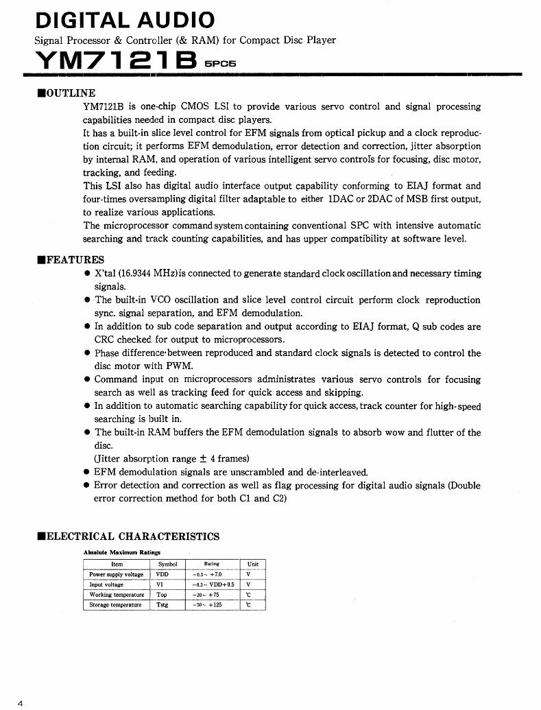
DIGITAL AUDIO Signal Processor & Controller (& RAM) for Compact Disc Player
YM7121B 6PC6
•OUTLINE YM7121B is one-chip CMOS LSI to provide various servo control and signal processing capabilities needed in compact disc players. [t has a built-in slice level control for EFM signals from optical pickup and a clock reproduction circuit; it performs EFM demodulation, error detection and correction, jitter absorption by internal RAM, and operation of various intelligent servo controfs for focusing, disc motor, tracking, and feeding. This LSI also has digital audio interface output capability conforming to EIAJ format and four-times oversampling digital filter adaptable to either lDAC or 2DAC of MSB first output, to realize various applications. The microprocessor command system containing conventional SPC with intensive automatic :searching and track counting capabilities, and has upper compatibility at software level.
•FEATURES • X'tal (16.9344 MHz) is connected to generate standard dock oscillation and necessary timing
signals. • The built-in VCO oscillation and slice level control circuit perform clock reproduction
sync. signal separation, and EFM demodulation. • In addition to sub code separation and output according to EIAJ format, Q sub codes are
CRC checked for output to microprocessors. • Phase difference· between reproduced and standard clock signals is detected to control the
disc motor with PWM. • Command input on microprocessors administrates various servo controls for focusing
search as well as tracking feed for quick access and skipping. • In addition to automatic searching capability for quick access, track counter for high- speed
searching is built in. • The built-in RAM buffers the EFM demodulation signals to absorb wow and flutter of the
disc. (Jitter absorption range ± 4 frames)
• EFM demodulation signals are unscrambled and de-interleaved. • Error detection and correction as well as flag processing for digital audio signals (Double
error correction method for both Cl and C2)
•ELECTRICAL CHARACTERISTICS Absolute Maximum Ratinas
--· Item Symbol Rating Unit
Power supply voltage VDD -0.3- +7.0 v ---
Input voltage VI -0.3- VDD+0.5 v -----
Working temperature Top -20- +75 ·c ------· --·---·
Storage temperature Tstg -50- + 125 ·c

...................................... 1 ................................................................ ..
Recommended Operatlna Conditions (Ca1ndltlon:Ta= +2s·c, VDD:m5.0±0.25V)
Power supply volta;:em 1~5~ 1--C-loc_k_fr_eq_u_e-nc-y-------1 TX(I
Working temperature =i
mbol Minimum Typical
m 4.75 5.00
16.9 -- t-----1 f-· >P 0 25
Efectrlcal Characteristics (Condition: Ta• + 2s··c, VDD • 5.0 ± 0.2SV)
Item Power supply voltage Output voltage H level Output voltage L level
Input voltage H level (1)
Input voltage L level (I )
Input voltage II level (2) Input voltage L level (2)
! Sy mbol
D ·7r>i. tyc, H r-vo I.
-< ~· E l ~~
=J~ v1; '--·
L 1
E 2 L 2
Condition -VDD==5V IDH•20µA
IOL=lmA
--
Maximum Unit
5.25 v MHz
75 ·c
Minimum Typical
4.0
3.5
2.0
Note l:Applicable to EFMI, FZC, FRF, EF and TER Terminal. Note 2:Applicable to RCK, DIN, SCK.
• OUTLINE DIMENSIONS
• BLOCK DIAGRAM
. .
0
i 1 0
I
SDO.SOSY ,f2,CITFLG I \....ro __ ..._ ___ _
SOI I ,.,....._....,. ____ _.
4-times oversampling digital filter
._., .. _Ill'~
0
ii ·~~
. J
r.
XIN XOUT.lfl6
Xffi'
"8.DGL.DGR
L/R. WDCI< DFOO DEOI
.._,------MIDEP
I I
DIF
--------------------- ----- ----- -- ------------'
Maximum Unit Remarks
mA v
0.4 v v Note 1
1.5 v Note l
v Note 2
0.5 v Note 2
5

6
DIGllTAL AUDIO CD/CDV Digital Audio Processor
YM7402 CDVP
•OUTLINE YM7 402 is a one-chip LSI containing various circuits for digital audio signal processing used in optical multi disc compatible players as well as servo control and signal processing capabilities needed in CD players. In addition, sequential control of tracking/feed for high speed searching, digital audio interface output, digital volume adjustment, and peak holding functions are included for use in high-grade CD players and compatible players.
•FEATURES • X'tal (16.9344 MHz) is connected to generate standard clock oscillation and timing signals. • EFM-PLL circuit with built-in VCO reproduces bit clock pulses. • Built-in slice level controller • Two switchable modes (CD/LD) are available for EFM input. • Linear interpolation is used to replace the uncorrectable error data (up to a maximum if 8
consecutive errors). And preceding data hold is applied for errors over eight. • The data output is in MSB first format and four-times oversampling digital filter with stop
band attenuation of 40 dB or more is built in. • EFM data demodulation and intensive error correction capabilities (double error correction
for both Cl and C2). • Buffering of EFM demodulation signals by 16K built-in RAM (Jitter absorption range :t 4
frames) • Sub code separation and output conforming to EIAJ. • Digital audio interface output conforming to EIAJ with arbitrary setting of channel status
code. • MSB first audio data output with switchable audio output method adaptable for bilingual
laser disc. • Facusing servo control compatible with external equipment. • Tracking & feed servo controls by direct and automatic sequence controls for high-speed
searching and linear motor. • Built-in tracking counter allowing adjustment with a unit of one track. • PWM spindle servo control containing FG mode realized by frequency generator connec-
tion. • VCXO control for compatible players. • High performance microprocessor serial interface enabling precise control. • Digital attenuator for 0.4 dB and 240 steps is built in. • Zero cross mute functions to suppress mute noises. • Peak holding capability to output maximum audio level for peak level searching and level
meter. • Error flag output without interpolation for CD-ROM. • 80-pin flat packaged silicone gate CMOS LSI, operated by + 5V power supply.
•ELECTRICAL CHARACTERISTICS Absolute Maximum Ratings -·---··- ···----·····-··--·-.-·.-··-~~-~ i-Item ~~bol ____ Rating ----~~
Power supply voltage VDD - 0.3- + 7.0 v --- ---
Input voltage VI -0.3-VDD+0.5 v ---- --------
Working temperature Top - 20 - + 75 t ---- - ~---~- -
Storage temperature Tasg - 50 - + 125 t . ----------------·-··- --
(Condition: Ta=+ 25"C. VDD= 5. O ± O. 25V)

................................... --1 ............................................................................. .... Recommended Operating Conditions
Item Symbol Power supply voltage VDD
Clock frequency XI
Working temperature TOP
Mi~~wf ~f:~Yl-M-ax-5i.·_;_5u--m"-+--~-~~ o f 25 75 ·cg
(Condition: Ta•+ 25'C. VDD•S, 0±0.)
Electrical Characteristics
Item Symbol Condition Minimum Ty pica! Maximum Unit Remarks
Power supply voltage IDD 1 VDD=5V
Output voltage H level VOH I OL=20µA 4.0
Output voltage L level VOL I OL=lmA
Input voltage H level (1) VIHl 3.5
Input vqltage L level (1) VILl
Input voltage H level (2) VIH2 2.0
Input voltage L level (2) VIL2
Notel: Must be applied for other terminals than those given in Note2. Note2: Must be applied for /CS, DIN, I SCK, R/W terminals .
• OUTLINE DIMENSIONS -10-0
mA
v 0.4 v
v Notel
1.5 v Notel
v Note2
o:s v Note2
• BLOCK DIAGRAM
0.ZTfP .Aon11mmnrum~nonononn~ 21S!01
LEFMl,CEFMI
EFMX. /EFMX
SYEQ
FG
/PLL.DSV
CDM+.CDM
LXT+.LXT-
/FZC,FRF,TER,HF
FCS KP+,KP-,TRDF
TllHD,TRGL
FEM+ ,FEM - .FEOF DFCT. JMPTM
/BUSY
/ANLS
¢2,SDSY
Vl.UP,VLOW
soo
SLVL
data conversion
Cl6M PCO VPLL Cl 7M CK YOO VSS
~ ~
Q code RAM
µCOM interface
standard clock oscillation timing control
RAM address control
Cl, C2 error detection correction flag processing
+-0 /RES
+-0 /TSTE./TRTl,/TCL
SUB,SBSY,SFSY
RCK
DEF
/CS./SCK,R/W DIN
OOUT
WQ
XIN
XOUT,¢16,¢4
/XFSY
FLG
DIT encoder DIF
7

8
DIG~TAL AUDIO Signal Processor & Controller for Compact Disc Player
YMSB05 SPC
•OUTLINE The YM3805 is a compact disc player signal processor (SGP) and servo controller CMOS JLSI developed by Yamaha. The YM3805 carries out the digital filtering and other signal processing useful for optical pick-up EFM signal .demodulation and erroneous signal detection and correction and improved audio quality, as well all servo control (e. g .. focus. disc. tracking, feed). J[t is used in conjunction with the special serial input DAC YM3015 or YM 3020.
•FUNCTlONS 1. Simple external connection of a crystal activates reference clock oscillations and the nec-
essary internal timing signals. 2. Digitalizes the EFM signal, and based on that carries out clock regeneration and synchronizing
signal isolation. 3. EFM demodulates this digital signal. 4. Isolates the Q sub-code from the EFM demodulated signal, and after carrying out a CRC
check. outputs it to an external microprocessor. 5. Outputs a frame phase difference signal derived from the regenerated clock and the reference
clock and controls the rotation speed of the disc motor. 6. Carries out tracking as well as feed servo control for calling up the beginning of a selection
and for fast forward, etc., upon input of a command from an external microprocessor. 7. Uses EFM demodulated signal buffering to absorb fluctuations in the rotation of the dnsc
and interfaces the external RAM and signals ( ±4 frame jitter absorption). 8. Carries out unscrambling and de-interleaving of EFM demodulated signals in a set order. 9. Detects erroneous signals and corrects them and performs flag processing as well (dou-
ble-error correction). Performs signal compensation, hold, and even muting.
10. Carries out digital filtering (signal break at 20 KHz) by doubling the sampling period (88.2 KHz for both the left and right channels), outputting a DAC signal. (Modes in which digital filtering is not carried out are also available.)
•FEATURES 1. Silicon gate CM OS construction 3. 5 V single power supply 2. 80 pin flat plastic package (saves space)
•ELECTRICAL CHARACTERISTICS Absolute !\taxlmum Radnas
nm ~BOL RATING ~,__'!!'ITS~ Supply voltage ___yoo -0.3 - +7.0 V
~!_voltage J V1 -0.3 - Voo +0.5 V
_ Oper_ating temperature ±Top -20 - +75 •c Storage temperature ------ Ts1;-- ----.::So-~-+rn------+---~-
1
•::-" Opomd .. C...Udou
Oper
--ITEM SYMBOL MIN. TYP MAX. UNITS
ly voltal!e Voo 4.75 5.00 S.2S v ating temperature Top 0 25 1S ·c
Electrical Chmracteristlcs
~ ITEM SYMBOL CONDITIONS MIN. TYP. MAX. UNITS Rn1A~1
Supi!IY cwrent IDD Voo - SV 25 40 mA
' Output high level voltaic VOH IOH - 20µA 4.0 v Output low level \"Olta1e
·+--- r--
(No<~jd VOL IOL •I mA ~ v ---Input high le\·el voltaae (I) VIHI 3.S v Input low level voltal!e (!} Vlll l.S v (Note l)_-1
Input high lc\·el voltaae (2) VIH2 2.0 v (Note 2l ---j
Input low level voltage (2) YIU 0.8 v (Note 2)
Input leal::aie current ILK Vr - 5V 10 µA ..
Cond111on: Voo - 5.0V ± 5%, Top - + o - 1o·c Note I: Aprlicable to terminal~ 3.VCOI 8.EFMI 14.FZC 15.FRF 16.HF 17.TER. Note 2: Applicable to termiC1als 33.ro:'R: 38.0IN 39.~ 54.DS- 61.DI.

______________ ! ________________________ _
• OUTLl[IMENSIONS
~
• BLOCK DIAGRAM
D'.\I t, D'.\1--
FCS F"-i'.'.. FRI"
Kl'+.Kl'-TROF. TRGL. TRHD
HF.TEii
J A: '.\I
Slice le\·el control
Sub-code Sl'B. \'FS\' i Synchronous detection isolation
I :!nd EFM demodulati<m QCRC ~ µCO;\I
Disc servo control (CLV) Om:-i
OOL'l" i µCOM interface R \\' i µC0'.\1 .time difference
\\'Q I focus servo control
computation circuit ---a~
.-.l.-....L.--1-.._ __ .,__~~--LJXI~
EFM demodulated sipal rulTerina
RAM adreas control
Cl, C2 error . detection, correction, -------,·--------! and naa processina
DATA control
Diaitai filter DAC output interface
1-----1--1XOlJT
~
1--+--t JEFLG
-4. SA'.\IPI. I SAMP2 I DAC QOUT. QS\"~C
DEP
9

10
DIGITAL AUDIO
YMS4S7C IPRELIMINARYI Digital Audio Interface Transmitter
CDIT2l
•OUTLINE The YM3437C is· a serial digital audio transmitter LSI. The YM3437C can convert 4 different kinds of serial digital audio data into AES or EIAJ digital audio interface format. In addition, the YM3437C can add a validity bit (V bit), user data bit (U bit), and channel status bit (C bit) to the data.
•FEATURES •All internal and external timing is defined by the external master clock (MCLK). •The sampling frequency can be from 30 kHz to 50 kHz. •Four serial digital audio data input formats. •With audio auxiliary control, the length of the audio sample word can be changed from 20 bits of
data with 4 audio auxiliary bits to 24 bits of data with no audio auxiliary bits. • V, C, and U bits can be added with appropriate input pins. •The control code may be input serially or in parallel. With serial input, the first 4 bytes (32 bits) of
channel status bits and the first 4 bytes (32 bits) of user data bits may be input. With parallel input, the V, U, and C bits may be input.
•The digital audio interface data output can be forced to zero with the MUTE signal input. •CMOS 5V single power supply. e 16 pin DIP , SOP.
•ELECTRICAL CHARACTERISTICS
Absolute Maximum Ratings
Item Symbol Rating Units
Supply voltage Voo-Vss -0.3-+7.0 v Input voltage V1 V ss-0.3-V oo +0.5 v Operating temperature Top o-+85 oc
--------1
Storage temperature Tstg -50-+125 oc
Recommended Operating Conditions
Item
I
Symbol Min. Typ Ma
pply voltage Voo-Vss 4.5 5.00 5.
x. I Units I 5 v
Electrical Characteristics
Item Symbol Conditions Min. Typ. Max. Units
Operating current loo Voo=5V fc = 6,144MHz
High-level output voltage VoH loH=0.4mA 4.0
Low-level output voltage VoL loL=2mA
High-level input voltage Vrn 2.2
Low-level input voltage V1L
Input leakage current L~-- V1=5V -10
The specifications of this product are subject to improvement changes without prior notice.
5 mA _ ____,
v 0.4 v
v _ ____,
0.8 v 10 µA

...................................................... 1 .................................................................. ..
• OUTLINE DIMENSIONS (1 )YM3437C-D
.--~~~~2_0_.0M~
ltE-~~-__13h;!§_~
12 11 18 9
2 3 4 ~ G 7 B
(2)YM3437C-F
C")
0 +I 00
........
• BLOCK DIAGRAM
WC IN q------·---------··--L l l:r·-·-----· l -i INPUT DATA
DJN[j--· I FORMAT CONVERSION
MPX
C J N,.UDB l CLD,.AUXEN b CONTROL CODE
CNTR,.BLK IN i CONVERSION UFL j
----~:::: O.~
1 .8 ±0.2
<O
0
MCLK DMO,DMt ,...,
TIMING GENERATION
BIPHASE MODULATION
CCK,.CSB ~ c--l ... -~r·6·--==r.- .. ······· ················ ·-· ··-· ··6····.!
UDD USS CSM MUTE RSTN
DOUT
11

12
DIGITAL AUDIO
YMS4SBB [PRELIMINARY! Digital Audio Interface Receiver
DIR2
•OUTLINE YM3436B is a digital audio interface receiver IC which converts a digital audio interface format signal as defined by AES or EIAJ to one of four serial digital audio data output formats. At the same time, the chip generates a validity flag (V flag), user data bit (U bit), and channel status bit (C bit), and various system clocks.
•FEATURES •Separates the audio data and generates various control codes from bi-phase digital audio interface
format signals. •Generates various system clocks with internal PLL. •The sampling frequency of the audio interface signal received can be from 30KHz to 50KHz .. •The received digital audio data is formatted into one of 4 serial output formats. • 3 other serial input formats can be received in addition to bi-phase digital audio interface format. •Noise is suppressed by an effective data error detection circuit. •The V flag, U bit and C bit are output with each subframe. In addition, the first 32 bits of U and C
bits can be read for each block with the microprocessor. •With the internal data buffer, multiple asynchronous digital audio interface format signals can be
received. •The C bit format is available for both consumer use and broadcast studio use. •CMOS +5V single power supply. • 44 pin QFP package
• ELEC~fRICAL CHARACTERISTICS
Maximum Ratings
ITEM SYMBOL RATING UNIT
Supply voltage Voo -0.3-7.0 v Input voltage V1 Vss-0.3-Voo+0.5 v Ambient operating temperature Top 0-+10 oc Storage temperature Tstg -50-+125 oc
-------' -------'----------'--
Recommended Operating Conditions
ITEM SYMBOL Min. Typ. Max. UNIT !--· ----1
Supply voltage Voo 4.75 5.00 5.25 v Ambient operating temperature Top 0 25 70 oc
_ _,
DC Characteristics(CONDITIONS : Ta= 25°C , V 00 = 5.0 ± 0.25V)
ITEM SYMBOL CONDITION Min. Typ. Max. ·--f--
Supply current loo Voo=5.0V High-level input voltage (1) Vrn1 (Note 1) 2.0 Low-level input voltage (1) V1Ll (Note 1) 0.8 High-level input voltage (2) Vrn2 (Note 2) 3.5 Low-level input voltage (2) V1L2 (Note 2) 1.0 Input leak current ILK -10 10 High-level output voltage VoH IoH=-50µA 4.0 Low-level output voltage VoL loL=2.0mA 0.4 Input capacitance C1 10 Output capacitance Co 10
UNIT --mA v v v v
µA v v pF pF
Note 1: Any input terminal except XI Note 2: XI terminal

..................................... 1 ................................................................................... ..
The specifications of this product are subject to improvement changes without notice.
• OUTLINE DIMENSIONS
:k fa
~ 'U
14.0 ±0.4
AnJ1DJ~n_n_Qt[~ . lllf 1.2 lYP --E-• BLOCK DIAGRAM
• "' . Cl II:
u tll Ill
E>Cfll
DDIH
EHR EHP
FSI. D
., _,
...-..--------DIGITAL AUDIO
INTERFACE
DECOR DER
--c-l -~ lMICROCOMPUTER INTER::!
.............. ==rr==········ Q 0 x _, Q ::ll u u Cl
• Q
"' u u
Cl Ill II: _, et.. "'
SYSTEM CLOCK
TIMING GENERATOR
L, __ __,
ncA.nce.ncc I WC,SYNC,OPI
~ .... ~TSIN
-1JTST2
I I
i----t---- 1 UF L
ASYNCHRONOUS
BUFFER P/S DOUT
~
0 I+ 0 :ii.
13

14
DIGITAL AUDIO
YM7136 ~ELIMINARYI Digital Audio Interface Receiver
DIRS
•OUTLINE The YM7136 is an LSI device, which receives and demodulates the Digital Audio Interface signals that are used between digital audio equipments. The YM7136 has error operation circuit for transferred data and oversampling digital filter which makes it easy to constitute DA conversion circuit with a few external components.
•FUNCTIONS AND FEATURES •The YM7136 has 4 channels of bi-phase input terminals, and each of these has bias circuit which
enables you to input from coaxial and optical line with a few external components. •It has an internal PLL circuit which generates clock and demodulates bi-phase signal. •It can detect unlock of PLL and parity error, it keeps previous audio data and mutes when it detects
error. •It outputs channel status information of emphasis, copy prohibition and sampling frequency type. •Output terminal of sampling frequency type can drive LED directly. •It has digital di-emphasis function internally. •It has 4 times and 8 times oversampling digital filter, which has following characteristics
Pass band ripple : within ± 0.03dB Stop band attenuation : At least 60dB
•It can interface for 1 DAC(4 times) or 2 DAC(4 times, 8 times) of 16 or 18 bit. •CMOS, Single 5V single power supply, 64pin QFP.
• ELECTRICAL CHARACTERISTICS
Absolute Maximum Ratings
ITEM
Supply voltage Ambient operating temperature Storage temperature
SYMBOL
VDD Top Tstg
Recommended Operating Conditions
RATIN~iJIT --- ·------
-0.3-+7.0 v -40-+85 ·c -50-+125 ·c -- -
ITEM SYMBOL Mi~~] Typ. Supply voltage V DD 4. 75 5.00 Ambient operating temperature Top 0 25 ~~~~~~-~~~~--~-----'--
DC Characteristics conditions ---.-·-··
ITEM SYMBOL CONDITION Min. Typ. Max. UNIT -+--·---- --~-+--~~+-------t-~--~
Power co~sumption w High-level input voltage (1) Vrn1 Low-level input voltage (1) V1u High-level input voltage (2) Vrn2 Low-level input voltage (2) V1L2 Input Peak to Peak voltage VIPP High-level output voltage VoH Low-level output voltage VoL Output current lo Input leak current I1L Input capacitance C1 Output capacitance Ca
Notel : Any input terminal except DINO-DIN3,CV,RV,XI Note2 : XI terminal Note3: DINO-DIN3 terminal N ote4 : 32K,44.1K,48K terminal
VDD=5.0V 2.0
3.5
loH=0.4mA 4.0 lo=2mA
V1=5V
150 mW V(Notel)
0.8 V(N otel) V(Note2)
0.8 V(Note2) V(Note3)
v 0.4 v
mA(Note4) 10 µA 10 pF 10 pF

.................................................... 1 .................................................................................. ..
The specifications of this product are sudject to improvement changes without prior notice.
• OUTLINE DIMENSIONS
iJ :;c:
(/) C')
c: Cii AIC 'Tl -I J) -; tJ) 0 I'll :?
.J
24.8 :te.4 ·~~~~~----~
20. 0 TVP
48K,U.tK,32K
• BLOCK DIAGRAM SELl,SELI! PLLER PARER RCI nuTE DEP,COPV ,TEST ,le j'" ........................................ ~~ ............................ 9... ........... .. ............... ?........ .... . .......... ¥ ................................... ~ ........ ! ......... ]
D
1
NO ; SELF ~r n DE~:~~ON ~ ! DJNt l l"R
i BIAS MF' X j wco
:::: ~1 L lr CSHT:~~~ Jt'. o~~ i - DECODE 8TIMES i ::~
OUT dE _J OVER SAMPLING l SHR
I 161-PH;;-DEMODULATION DIGITAL FILTER i '"'' IN 0 PARITY CHECK I ST
j PLL ER
'.1. ~;--HASE ;}-= I DIGITAL I DI-EMPHASIS
I COMPARATOR ] L-~-.-~-' i PCO qc -- TIMING GENERATION !
'"t13- ~· .. ,.:: b~_:: __ ;~. --=cL~~~EL~c~1i •... LlJ. .. . . . .. . .J::: AUDD AUSS >CJ >CO t&A SDO (j C SDSV SDI
15

16
DIGITAL AUDIO Digital Audio Interface Receiver
YMS62SB DIR
•OUTLINE The YM3623B is an LSl device, which receives and regenerates the Digital Audio Interface
Format signals that arc transferred between digital audio equipment. Use of the YM3623B eliminates the need for a special externally- mounted circuit for playback, thereby greatly facilitating the: playback of Digital Audio signals.
•FUNCTIONS 1) The YM3623B has an internal PLL circuit which synchronizes with the Digital Audio Format
signals that are sent in from the external equipment. 2) It outputs Audio signals starting with the MSB (Most Significant Bit). In sync with that
output, it outputs the Timing clocks for the D/ A output sample-and-hold operations and the signals indicating the L or R channel.
3) It has a terminal for outputting a Subcodc, making possible the retrieval of Subcode data. 4) It is capable of outputting the sampling frequency, Emphasis ON/OFF status, Copy
Enable/Disable status, as well as the Error status of transmitted Audio signals. 5) In case an error is detected in the Digital Audio Interface Format signals, the Audio data
preceding the detected error is output again.
•FEATURES 1) Silicon gate CMOS construction (low power consumption) 2) 28-pin Dual-Inline Package (DIP) 3) +5V power supply
• ELECTRICAL CHARACTERISTICS 1. Absolute Maximum Ratings
Item
Supply voltage
Input voltage
Operating temperature
Storage temperature
Symbol
Voo-Vss
VI
TOP
Tstg
2. Recommended Operating Conditions
Item Symbol
Supply voltage· Voo-Vss
3. Electrical Characteristics
Rating
-0.3- +7.0
Vss - 0.3 -voo + 0.5
-20- +75
-so- +125
Min. Typ. Max.
4.75 5.00 5.25
Item Symbol Conditions Min. Typ.
Voo=5V Operating current loo 01N=SV 6
fc = 16.9344MHz
High-level output voltage VOH IOH=0.4mA 4.0
Low-level output voltage VOL loL=2mA
High-level input voltage VIH X1 pin excluded 2.0
XI pin 4.5
Low-level input voltage VIL
Input leakage current ILK V1=5V
NOTE: The analog VCO pin and the ADJ pin are excluded.
Units
v --
v
oc oc
Units
v
Max. Units
8 mA
v
0.4 v
v
0.8 v
10 µA

........................................ 1 ................ 1 .................................................. ...
• OUTLINE DIMENSIONS 38.QMA>C:
14
z x ~ ~ 0.25TYP ~ " DIMENSIONS IN MM
Prm~· . o ]SEATING U U PLANE
2.54 T -I 0.48 TYP i
• BLOCK DIAGRAM 4.VSS2
9 6. XI 5.XO
~ N
7.KMODE 8. ~A
13.SYNC
15.L/R
19.DIGR
20.DIGL
Jfuiie difference L_ deio:tion circuit "-----------i~D 9.¢8
28.0IN
10.11G
11.T2~
l.VODl~ 14.VSSID-i
-.C P11rity check
S/J' conversion
=LATCH~
LATCH
12.BCO
Latch synchronization
17.00
~21.ERR
Sub-code output
D 22.SEL :!4.S2 23.Sl 16.DEF 26.SSYNC 25.SCK 27.SDO
17

18
DIGITAL AUDIO 2-Channel 8-times Oversampling Digital Filter
YMS4S4 AFUDF
•OUTLINE The digital filter's own system clock rate must be considerably faster than the input bit clock rate and at the same time synchronism is required in the system as a whole. Thus what is normally required is a high-speed clock which is synchronous with the signal handling pre-processor. Then the major application problem is how to interface these different clock rates. YM3434 is a high quality 2-channel 8-times oversampling digital filter which has been developed to solve such problems. It can be used easily as an interface in a wide range of digital audio systems. Its filtering capabilities are equivalent to the YM3414. Since the system clock of this LSI can be different from the serial input signal and it operates normally at any clock rate above 400 clocks for each input sampling frequency ( fs ), it is not necessary to change the clock rate even if the sampling frequency is changed. For example, by connecting a 20MHz crystal oscillator, there is no need to change the clock rate even when the sampling frequency is changed to 32KHz, 44.lKHz or 48KHz.
•FEATURES • Operation at an independent system clock from the serial input signal • Input signals can be handled at any of the following input bit clock rates without adding any
circuit: 32fs, 48fs, 64fs, 80fs, 96fs, 112fs, 128fs, 144fs, 160fs, 176fs, and 192fs, • Capable to cope with sampling frequencies 32KHz, 44.1 KHz and 48KHz. • Linear phase FIR type filters connected in three vertical stages
1st filter : 225-order FIR filter 2nd filter: 41-order FIR filter 3rd filter : 21-order FIR filter
• Built-in 19 x 18 bit multiplier, floating point calculation with a coefficient of 18 bits • Built-in overflow limiter • Filter characteristics (at 8-times)
Pass band ripple : Within ± O.OOOldB at 0 to 0.4535 x f s Stop band attenuation: At least lOOdB at 0.5465 x fs to 7.4535 x fs
• Output data switchable between 16 bit and 18 bit (directly connectable to PCM56 and PCM58).
• Switchable between 1 DAC (4-times) and 2 DAC (8-times). • CMOS process, Single 5V power supply, 16-pin DIP package.
• ELECTIUCAL CHARACTERISTICS Absolute Maximum Ratings
lwm Symbol Minimum Maximum Unit
Pftoer eupply voltage VDO -0.3 +7.0 V 1--------r---------~+--~·-t---~
Input voltagoe _v_1 __ ..___-_o.a ____ ·-+--v_o11+_0.~_, --~ Working temperature 1'op -20 +75 •c
1--------+------+---·---·---t-·----·-+-------1 St.or.,. temperature 'l'•tg -Ml +125 •c -------·--'-----~----L-------'~--------'
Recommended Operating Conditions r-------..----.----.-----,.---.------.
Item Symbol Minimum Typical MaxiMum Unit 1---------------1------1----f------+----+-----
l'ower eupply volt.age Yoo 4.711 5.00 5.25 V _ __.
XIN 12.2 441>0 F•l 20.0 MHz
Working temperatur• 1'cip 0 2& +70 •c - -·-·-- ·-·-----'-----'--------''-----'---·--''-------J
Electrical Characteristics ---.---......----r-
ILem Symbol Conditions Unit Minimum Typical Mulmum I-----.. --·---+----t----+----+---·-+----+-----l
300 l'ower conawnption W Vnus+r;V mW --- ------+·---t----+-----lt-------t------1
Input vnltajie H level VIH tXl.16118. STI 3.5 tUCI. SDSY, SDll 2.7
Input voltage I. level VII.
Output voltege II lev~I-. - ---voit-· - ·-- 2.4
Output voli.ase I. Level VOL
Von Von
0.8
VIII>
0.4
v v v v v
1---------·--' ·--·---------+-·-- -l-----+----l m.o. llllO MtUp tlnw DLO. DRO hold tim•
Input d•t.a eel.up time Uliae of RCll
Input data hold time tRiee nf BCll
15 15
1111 IUI
Ill
1------------+----+-----1-----·i--·---------1 XI ON/OFF tim..-tDutyl 60
BCI ON/OFF time tDutyl 50 ....... -----·-----------' ----'-------'-·----'------~-----'

-• OUTLINE DIMENSIONS
20.0MAX
SHL SHR
XO 16/ 18
XI ST
VDD2 vss
BCI BOO
SDSY wco INDEX
SDI DRO MARK ARE·~
VDDI DLO DIMENSIONS IN MM
z 2.54 TYP ~
Ln 0.47 TYP
N 16 pin plastic DIP
PK16DP1-20.1
• BLOCK DIAGRAM
VDD2 ----------~----1
I
lo~ :---.:'~--;M _________ .:~'!: 1 (400Fs or more) I I
sosvQ----
BCI I I
VSS 6-1 I
VDD lQ--1 I I
SDI 6-1
BCI
BCI
Coefficient ROM
Multiplier Accumulator
Shifter
Temporary RAM
WCO. SHL SHR generation
Timing circuit Micro-program
;: 0
;;::: Q; >
0
> io 0 c. E 2:l ..... :J e-:J
0
p
s
I L ______________________________ J I
~-----------------------------------------------------J
wco SHL SHR
16/ 18
BCO
DLO
DRO
19

20
DIGllTAL AUDIO 2 channel 8 times oversampling digital filter operates via serial input signal and independent system clod
YM3433B ALOOF
•OUTLJNE This oversampling digital filter operates by repeating the input sample cycle through a sum of products computation process. This calculation must be repeated numerous times for :reliable operation. A high speed bit clock rate is required, but only for the part to be oversampled from the input bit clock. Because of these requirements, the system clock in the digital filter itself operates at a high :speed appropriate for the input clock rate. Because it was normal for the cycles to be :synchronized by the system, it has been necessary in the past .to synchronize the si~,nal
processor at the previous step (which received the request) with the high speed clock, and designs used to interface the synchronized high speed clock presented some problems with :regard to practical applications. This LSI chip has solved these problems, resulting in a high grade 2 channel 8 times oversampling digital filter that can be interfaced easily with a wide range of digital audio systems, and it is pin compatible with the YM3434. This particular LSI chip permits use of a system clock which operates independently from the :serial input signal. The input sampling cycle (fs) will operate normally even with input from docks with more than 400 ticks-for example, even if the sampling. frequency is switched between fs = 32kHz, 44.lkHz, and 48kHz when connected with a 20MHz crystal oscillator, there is no need to switch to any other clock.
•FEATURES • Because this operates with a serial input signal and an independent system dock, this can
handle all of the input bit clock rates which follow with no supplementary circuit: input signals-32fs, 48 fs, 64 fs, 80 fs, 96 fs, 112 fs, 128 fs, 144 fs, 160 fs, 176 fs, 192fs.
• Linear phase FIR type filter connected in line at 3 levels 1st filter:: 161 order FIR filter, 2nd filter: 33 order FIR filter, 3rd filter: 17 order FIR filter
• Built-in overflow limiter • Filter capacity (when 8-times)
Passband ripple 0-0.4535X fs: ± 0.002 dB or less Cutoff band reduced capacity 0.5465Xfs -7.4535xfs: 70dB or more
• 16 bit/18 bit output switching (compatible with PCM56/PCM58) • lDAC( 4-times)/2DAC( 8-times) switching • CMOS process, +5V power supply, 16 pin DIP, 24 pin SOP
•ELECT:RICAL CHARACTERISTICS ABSOLUTE MAXIMUM RATINGS
Item Symbol Min
Supply voltage V DD - 0.3
Max
+7.0
Unit
v 1--------------+-----------+-·---------r---------+------t
Input voltage VI - 0.3 Voo+0.5 v ,_____ _______ __, --------;-------·-----+---
Operating temperature TOP - 20 +75 ·c --·---+----
Storage temperature TSTG -50 + 125 ·c
RECOMMENDED OPERATING CONDITIONS
Item Symbol Min Typ Max Unit -·
Supply voltage VDD 4.75 5.00 5.25 v --1----------1 -· ----
Clock frequency XIN 12.2 (400 fs) 20.0 MHz -
Operating temperature TOP -40 25 +85 ·c ----' ---- ·-

..................................... 1 ........................................................................ ..
ELECTRICAL CHARACTERISTICS (Ta= 25°C' v DD= 5 ± 0.25V)
Ite m
Power consumpti< m
High input voltag e (XI, 16/18, ST)
(BCI, SDSY, SDI)
Low input voltage
High output volta ge
ge Low output volta
DLO,DRO setup t' 1me
me DLO,DRO hold ti
Input data setup t: ime (BCI leading edge
Input data hold ti me (BCI leading edge )
XI ON/OFF time
BCI ON/OFF tim
(Duty)
e (Duty)
• OUTLINE DIMENSIONS
SHL
XO
XI
VDD2
BCI
SDSY
SDI
VDDI
SHR
"16/18
ST
VSS
BCO
wco DRO
DLO
Symbol Condition Min Typ
w Voo=+5V
VIH 3.5
2.7
VIL 0
VOH 2.4
VOL 0
15
15
50
20
50
50
16 15 14 13 12 11 10 9
~::E~t 2 3 4 5 6 7 8
Max Unit
125 mW
Voo v Voo v 0.8 v
Voo v 0.4 v
nS
nS
nS
nS
% %
0-15"
DIMENSIONS IN MM
* 24 pin SOP is available
• BLOCK DIAGRAM
~~l~o r--- ·- , --------------------, -(>o---+ ¢ M : (400 Fs or more) I (or 384 Fs)
SOSY 0-- ---·-------01-JM
1 ___ , ____ BC_I __ _. __
BCI
I I I I I I I I I I I I
I I I
vssQ+ I I
VOOI~ I I I I I 0
Multiplier
accumulator
shifter
soi Q--= Temporary
ST VD02
----------9---i I I
WCO, SHL
p / s
I RAM : ~------------------------------------- I ~------------------------------------------------~
wco SHL
SHR
16/18
BCO
DLO
ORO
21

22
DIG~TAL AUDIO 2-Channel 8-times Oversampling Digital Filter
YM34 l 4 ACDDF
•OUTLINE The YM3414 (ACDDF) is a super-high performance 8-times oversampling digital filter for use with
the digital audio systems developed by Yamaha.
It is connectable directly to LSI, DIT, DIR, etc. for digital audio systems, and can exhibit its
excellent performance through simple procedures.
•FEATURES • 8-times oversampling in two channels
• Linear phase FIR type filters connected in three vertical stages
1 'st filter: 225-order FIR filter
2'nd filter: 41-order FIR filter
3 'rd filter: 21-order FIR filter
• 19 x 18 bits multiplier built in
• Floating p~int multiplier and accumlater having a coefficient of 18 bits
• Overflow limiter built in
• Filter characteristics (fs=44.1 kHz)
Pass band ripple: Within±0.0001 dB at 0 to 20 kHz
(Within quantizationerror in 16 bits)
Stop band attenuation: At least 100 dB at 24.1 kHz and higher
• High precision oscillator specially designed for use with the filter
• C-MOS process
• Single 5 V power supply
• 16-pin DIP package
• ELECTRICAL CHARACTERISTICS • ABSOLUTE MAXIMUM RATINGS
Item Symbol Minimum Maximum Unit --·------- -~-
Power supply voltage VDD -0.3 +7.0 v -------··-·------+----
Input voltage VI -0.3 Vdd+0.5 v 1--------------1------1---·-
Working temperatur.e Top -20 +75 oc
Storage temperature Tstg -50 +125 oc
• RECOMMEND OPERATING CONDITIONS
Item Symbol Minimum Typical Maximum Unit !--------------+--------+------- --~---+--- ---+-------1
Power supply voltage VDD 4. 75 5.0 5.25 v -·-----1--------1------- -----+--------·----
Clock frequency XIN 12.2 16.93 18.5 MHz
Working temperature Top 0 25 70
•ELECTRICAL CHARACTERISTICS (Ta=25°C, Voo=5±0.25V) ..------~----~....---~.---~··,..---·--....,..~-~_,.--·---.-~----,
Item Symbol Condition Minimum Typical Maximum Unit ~·
Power consumption W Vdd,,,+6V 200 270 mW !----------------+------- ···>--·--··---+-------+--· ·--+-------+------- -- -
Input voltage H level VIH CXI. TD) 3.6 Vdd cBCI. SDSY. SDI. SyncS) 2.7 Vdd
v v
!---·-----·---~----+------+-----+-- --+------+--------! Input voltage L level VIL 0 0.8 v
!-------------+--·------+--·--·--·. ·-+-------- -------+----····---+------Output voltage H level VOH 2.4 Vdd V
,___ __________ __,__ ----·--t--····. -··· ------;---.·------4-----·--~
Output voltage L level VOL O 0.4 V 1--- ·----t--·---~·---··-+-------1
Output delay Cdelay from BCO) 6 36 nsec !-----------·-·- --·-----+---··----+---·-·· . --+-------.__ __ ___.
Input data setup time CRise of BCI>
nsec
t--· ·-------+-----------·+------t--------+--- ---1-------
lnput data hold time CRise of BCll
20 nsec
J--- ···----- .... ---+--- --·----· ·-· -----+-------1--------t----- ---+-----XI ONtOFF time CDut.>·I 60
1--------·-- ··--·--+-------·----- - ~--4-----+-----+------1 BCI ON/OFF time CDuty) 60 %

...........................................................................................................................................................
• OUTLINE DIMENSIONS
1-----='9=.35::_'~-1 ! 15oMAX
16 1S 14 13 12 11 10 91
INDEX MARK~_E_~
~rrr; Q.25 TYP
:==;~ H SEATING --i ' PLANE ' i i -~
DIMENSIONS IN MM
__ __.... ___ --..+-1+0_.4_7_rvP ~I
• BLOCK DIAGRAM
Coefficient~
·- ] SDI DA TA Multiplier Over
SDSY S/P RI IM t-+- Accumlater I-+- flow 1---
BCI L ,R Shifter l1m1ter ·-Temporary
1....-1 1--
RANI
Timing
Address
control I
_j_ _! • ' TD Syncs XI XO
~
Output
Buffer
l ---.,...
-------P/S
-----....
------.....
DLO ORO
BCO wco
SHL
SHR
23

24
DIGITAL AUDIO 2-Channel 4-times Oversampling Digital filter
YMS404B CDDF
•OUTLINE The YM3404B (CDDF) is a super-high performance 4-times oversampling digital filter for use with
the digital audio systems developed by Yamaha.
It is connectable directly to LSI, DIT,DIR, etc. for digital audio systems, and can exhibit its excellent
performance through simple procedures.
•FEATURES • 4-times oversampling in two channels
•Linear phase FIR type filters connected in two vertical stages
1 'st filter: 225-order FIR filter
2 'nd filter: 41-order FIR filter
• 19 x 18 bits multiplier built in
• Floating point multiplier and accumlater having a coefficient of 18 bits
• Overflow limiter built in
• Filter characteristics (fs=44.l kHz)
Pass band ripple: Within± 0.0001 dB at 0 to 20 kHz
(Within quantization error in 16 bits)
Stop band attenuation: At least 100 dB at 24.1 to 64.1 kHz
At least 99 dB at 64.1 kHz and higher
• High precision oscillator specially designed for use with the filter
c Clock providing 8.6426 MHz output
• C-MOS process
• Single 5 V power supply
• 16-pin DIP package
• ELECTRICAL CHARACTERISTICS • ABSOLUTE MAXIMUM RATINGS
Item Symbol Minimum Maximum Unit .. --t-------t-----Power supply voltage Vdd -0.3 +7.0 v
--t-·----!--Input voltage VI -0.3 Vdd+0.5 v --t-·-----I--Working temperature Top -20 +75 oc Storage temperature Tstg -50 +125 oc
• RECOMMENDED OPERATING CONDITIONS Item Symbol Minimum Typical Maximum Unit
Power supply voltage VDD 4.75 5.0 5.25 v ----r--------Clock frequency XIN 12.2 16.93 18.5 MHz
Working temperatw·e Top 0 25 70 oc • ELECTRICAL CHARACTERISTICS (Ta=25°C, Voo=5±0.25V)
Item Symbol Condition Minimum Typical Maximum Unit
Power consumption w Vdd=+5V 200 270 mW
Input voltage H level VIH (XI, FEN, ST) 3.5 Vdd v (BCI, SDSY, SDI) 2.7 Vdd v
Input voltage L level VIL 0 0.8 v . ·--1 ------t---
Output voltage H level VOH 2.4 Vdd v --t----
Output voltage L level VOL 0 0.4 v -
Output delay (delay from BCOI 5 35 nsec ··-+--
Input data setup time 50 nsec (Rise of BCll
Input data hold time 20 (Rise of BCI) nsec
XI ON/OFF time IDut;f) 50 %
BCI ON/OFF time (Duty) 50 %

..................................... 1 ................................................................. ...
• OUTLINE DIMENSIONS 20.0MAX
15•MAX
Ill II 14 13 12 11 10 9
~~ 1!")--=f~ f d Ill SEATING
• BLOCK DIAGRAM
SDI.,.__
M_......_......_ I ll Ill N
,_ .. -DAl .A
SDSY 1-- S/P ~ RA M
BCI t-- L, ... _ IR ,_
PLANE
~
..._.
0.25 TV,
DIMENSIONS IN MM
Coefficient ~
MultipNeir Over
Accumlater H,_ flow 1-------.j
Shifter limiter
Temporary
~
RAM
Timing
Address
cont roll
I T ST FEN XI XO
~ ;i;. ;Jj
Output
Buffer
T P/S
DLO ORO
BCO wco
SHL
SHR
25

26
DIGITAL AUDIO Digital Equalizer
YMSSOB DEC
•OUTLINE The YM3608 is as pecial digital processor developed by Yamaha Corp. for use with digital filters.
This processor makes it possible to easily configure IIR and FIR filters for serial sound signals using the internal microprogram. This processor also makes possible high accuracy calculations and the freedom to rewrite microprogram functions and coefficients using SCI"'.
"' SCI: Serial Control Interface •FEATURES
e All microprogrammable function for digital filter.
e Multiplication is performed with one clock for Data 16 bits x Coefficient 32 bits. (2 clocks for Data 32 bits x Coefficient 32 bits) (This is 5-clock pipeline processing.)
e There are 2 serial input terminals and 2 serial output tenninals, both of which can be used with any desired timing. The MSB/LSB first and shift clocks can be selected independently for input and output. Inp111t and output are also possible using an external clock.
e A SO-bit accumulator with 4 bits of head margin and overflow detect is provided.
e The master c:lock operates at a maximum phase of 4.4MHz and a minimum phase of 2MHz.
e Microprogram and coefficients can be controlled with SCI (Serial Control Interface).
e Up to 128 steps can be used with microprogram.
e Higher calculation performance is possible by making a serial connection to YM3608 (DEQ).
e Operates on a single SV power supply.
• 24-pin DIP.
• ELECTIUCAL CHARACTERISTICS Absolute Maximum Ratings
Item Symbol Ratin1
Power supply voltaic VDD -0.3-7.0V ---Input voltaic V1 - 0.3 - VDD + 0 . .5V
Operating temperature TOP o-1o•c Storaae temperature Tats -.so-12.s·c
Recommended Operating Conditions
Item Symbol Minimum Typical Maximum Unit
Power supply voltaae Voo 4.7.5 .5.00 .5.2.5 v Operating tcmperat\.~re TOP 0 70 ·c
D.C. Characteristics
Item Symbol Minimum Typical Maximum Unit
Input clock frequen<:y fc 2 4.4 MHZ
Input clock High le\•el time Tn. 90 n sec
Input clock Low level time Tn 100 D ICC
Input data set-up tirne Tos ,0 n sec
Input data hold time ToH 10 n sec
Output delay time •l Too 100 n sec
Bypass delay time •1 TPD 70 n ICC
Conditions: Voo-S.OV±5%, TOP-o-10°c A.C. Characteristics
Item Symbol Condition Minimum Typical Maximum Unit Output voltage H level VoH loH - - 0.4mA 3.5 Voo v Output voltage L le,•el VoL loL-lmA Vu 0.4 v Input voltaae· H level V1H 2.4 v Input voltage L level V1L 0.4 v Input leak current ILK V1-.5V 0.1 ~
•t: with lOOpF capacitance added.

.................................................... 1 ............................................................................................. ...
•OUTLINE DIMENSIONS 32.5 ....
~-----------31.3"' ...... ~~...;;;__~~~-----
~ 13
~J;l 12
MARK AREA ~ ~
·~~rt&i~~· "'
• BLOCK DIAGRAM ELD EC:LK
~[f Input Buff:-i
NOTE : The four end leads. # 1. # 12. # 13. ind # 24 m1y tlke the shape des· crlbed below.
CEMD XMD XCLK CRS
COi
Input 8 words_j SC I
Sl1
co
C1
C2
TRG
soo
S01
Coefficieint RAM
T ..,,.,,--:-]
Buffer
---
Seri a I Diata
Output
Multiplier
Accumulator
Q Shifter
Q Register
Output Buffer 8 word!
ESL 0--Timing
Control
c:LK Sync IC
Parameter Control
Micro
Program
RAM
Random Number Generator
DD Vdd Vas
ROM
7 words
DATA RAM
128 words
Address Counter
coo
27

28
DIGITAL AUDIO Analog Servo Processor
GDRlOl ASP
•OUTLINE GDRlOl is a bipolar LSI for analog signal processing and for servo control of compact disc players, suitable for 3-beam system. CD player system can be constructed easily by combining with YM3805(SPC), YM7121B(SPC5), YDC101(SPC6), YM7 402(CDVP).
•FEATURES •Single power supply(+ SV) or dual power supply system(± SV) are selectable. •CD player system can be made by using Digital Signal Processor such as YM7121B. •Almost all the functions for analog system are incorporated.
RF amplifier focus error amp tracking error amp slice level control (SLC) amplifier VCO control amplifier focus (FCS) switch tracking switch( TSOF, TRFD, TRGL ) laser on/ off switch
•Timing signals FRF, /FZC, HF, TWR are output. e48 pin QFP.
•ELECTRICAL CHARACTERISTICS •Absolute mnximum ratings
--Pa-ra-m-et-er---~-S-y_m_l_>o-1 ~C-o-nd-it-io-~-_s~_-__ -R-a-ti_-n_g_s __ --U~
Maximum Powe~· supply voltage VCC/VEE - ± 7 - --m-yW-Power consumption Pd max Ta::;;75'C 430 Operating temperature Top -25-+ 75 'C Storage tempeTature____ Tstg -40-+125 ·c
< Peak hold circuit section > Offset voltage V35-36 41,42 pins open Output voltage V35-0 41,42 pins input
current=5µA < Bottom hold circuit section >
•Recommended operating conditions __ P_a_
Power supply v rameter Symbol Min. Typ. Max. Unit ·oltage VCCop +4 +5 +6 v
VEEop -6 -5 -4 v 1erature Top 0 25 75 ·--~
Offset voltage V34-35 41,42 pins open Output voltage V34-0 41,42 pins input
current=5µA < FRF comparator section > Comparator output V27H 41,42 pins iuput
current=3µA
•Operating characteristics (Condition; Ta=25'C, VCC=±5V, VEE=-5V) V27L 41,42 pins input
Parameter Symbol Conditions Min. Typ. Consumption - ICC 12 17
current IEE LDSW off 11 15.5 < RF amp. sec:tion >
·----
Offset ~ltage - V36-0 41,42 pins open -300 -120 0 mV Voltage gain GV36 36-....37 pins: 22KO 25 28 31 dB
41,42 pins: Rg=lOKO f=200KHz
Maximum output V36H RL=lOKO +4.0 +4.2 +4.3 v amplitude V36L RL=lOKO -1.6 -1.3 -1.2 v
Frequency lMHz/200KHz -3.0 -0.5 +3.0 dB characteristics
< Focus error- amp. section > Offset voltage -- V31-0 41,42 pins open -150 +150 mV Voltage gain GV31 33 pin-GND==l20KO 31 34 37 dB
31-32 pins=l20KO f=lKHz
Voltage gain dGV 41 pin input and -1.0 +LO dB difference 42 pin input
Maximum output V31H RL=lOKO +4.1 +4.25 +4.6 v amplitude V31L RL=lOKO -4.6 -4.25 -4.l v
Frequency fmax -3.0 -0.5 +3.0 dB characteristics
current= lµ A Offset voltage V35-1 35 pin voltage when
V27=H V35-2 35 pin voltage when
V27=L < /FZC comparator section > Comparator output V18H 41,42 pins open
V18L 42 pin input current
=lµA Offset voltage V31-1 31 pin voltage when
V18=H V31-2 31 pin voltage when
V18=L < HF comparator > Comparator output V17H 41,42 pins open
V17L 35 pin=0.8V 34 pin=OV
Offset volcage V35-l 35 pin voltage when V17=L, 34 pin=OV
V35-2 35 pin voltage when Vl7=H, 34 pin=OV
Maximum operating fmax frequency
1.0 1.2 1.4 v -lo<ir-40 I ,. r·v--100 0 100 r~v 1.0 1.2 1.4
4.0 4.2 4.5 v
0 0 0.5 v
0.7 v
0.1 v
4.0 4.2 4.5 v 0 0.5 v
-0.35 v
-0.65 v
---- ---4.0 4.2 4.5 v 0 0 0.5 v
0.7 v
0.3 v
100 500 KHz
~his LSI can be supplied only ~ombination with YAMAHA signal processors such as L_~DClOl, YM7121B, YM3805 etc. Please contact YAMAHA before design start.
. . - -

............................................... 1 .................... 1 ...................................................... ...
• OUTLINE DIMENSIONS
.... 0 +I an (Cl
~ 0 +I Q
on .... 0 +I an
!!'.?:£ oc +I-+---•
an C")
Q
16.5±0.5
1. 5±0.25
+0.15 0.15-0.05
2.15±0.1
2.5MAX
+0.15 0.1-0.1
DIMENSIONS IN MM
16rmmn11nn rroru ~~ (0.75)-J+ 15.0±0.• ~.Jl.<o.75)
• BLOCK DIAGRAM
RFSLOSWn-----11:1
LOO
vcc ACr~-+-+-"
BOLI--~1-....
VEE
VRI VR2
EO
ELt--·--t-....._
F
:I I/) IL a:
9 iE
I
~ ~ 8 IL IL. >
~h CJ 0:: > IL
~~--------uFCS
VEE
,__....,~-~·-------~...._~~~-.....,....>-----n/FZC
'--+-----------a/HF 1C1r"-t--i.......,r-...... -t-+--::::::---------OTER
O « ""' + I II.I II.I 0:: D. Q. .......... > 1-1-
0 Q. .....
.A~--------uTROF
~~------.nTRGL
""1-J------nTRHO
I/) I/)
~ ~ ..... .....
I + D. D. lil: lil:
SOK
29

30
D/A CONVERTER 2-Channel Serial & Binary input Floating D/ A Converter
YM3020 DACCCDl
•OUTLINE The YM 3020 : DAC-FS is a floating DIA converter (referred to as DAC hereafter) with the 2-chaimel
serial and 16-bit binary input or 2's complement input. It can produce analog output (16-bit dynamic
range) which has 13-bit mantissa and 7-step exponent characteristic for the input digital signal.
•FEATURES • 16-bit input format can select either binary or 2 's complement (equipped with a built-in floating
converter logic).
• Externally equipped with buffer operational amplifier it allows easy analog output.
• 16-bit wide dynamic range.
• Capable of processing PCM sound source up to 2 channels.
• Equipped with a built-in analog switch for sample hold.
• Lower noise and less harmonic distortion and outstanding temperature characteristics. Zero cross
distortion is extremely little.
•Made by the monolithic process of highly accurate thin film resistance and CMOS and enclosed
in the 16-pin plastic D IL package.
•Electrical characteristics 1. Absolute Maximum Rating
Item Rating Unit
Supply voltage -0.3 - +15.0 v High-level input voltage Voo +0.3 v Low-level input voltage Vss -0.3 v Operating ambient temperature 0-70 oc Storing temperature -50-+125 oc
2. Recommended Operating Conditions
Item Symbol Min Typ Max Unit
Supply voltage Voo 9.0 12.0 12.0 v Vss 0 0 0 v
Input signal voltage CLOCK} SD 0 - Voo v SMPl, 2 ICL
Operating ambient temperature Ta 0 - 70 oc
3. DC Characteristics
Item Symbol Measuring Conditions Min Typ Max Unit
High-level input voltage VIH Voo ~ 9.0V 1/3 Voo - - v Low-level input; voltage VIL Voo ~ 9.0V - - 1.0 v Input current IJN Voo = 12.0V - - 10- 3 µA Analog output voltage VouT - 0.50Voo - Vp-p Supply current loo Voo = 12.0V - - 6 mA

----------------------------!------------·-------------------------------------• OUTLINE DIMENSIONS
19.2~8· 8 ._.... ___________ ~
2 3 4 5 6 7 8
;;: ----~--------------o::t::
• BLOCK DIAGRAM
,---------
7
~ <.O 0
I/)
0
CN
M
I/)
M
0
SEAT!'.\:(; J>LA'.\:E
CLOCKO--I I I I ----
----15
DIGITAL SHIFT
12--.9
(mm)
SMPI SMP2
~ TIMING
I MSB
[ANALOG
_SHIFT-EXP
RBH i -{
MANTISSA ·
13-•IO BIT :~~~J
RBL r-- BIAS-R oCHI
ANALOG oCH2 SW I
·-----C-- 0-0------......1 l __
MP TO BUFF COM
31

32
D/A CONVERTER 2-Channel Serial & Binary input Floating D/A Converter
YMSO l 6 DACCCD]
•OUTLINE The YM3016 : DAC·GS is a Floating D/A converter (referred to as DAC hereafter) with the 2·
channel serial and 16-bit binary input or 2's complement input. It can produce analog output (16-b:it
dynamic range) which has 10-bit mantissa and 7-step exponent characteristic for the input digital
signal.
•FEATURES • 16-bit input format can select either binary or 2's complement (due to built-in floating convertur
logic).
• Analog output can be obtained easily by adding a buffer operatiohal amplifier, etc.
• 16-bit wide dynamic range.
• Capable of processing PCM sound source up to 2 channels.
• Equipped witlh a built-in analog switch for sample hold.
• Lower noise and less harmonic distortion and outstanding temperature characteristics.
• Made by the monolithic process of highly accurate thin film resistor and CMOS.
• Package type: 16 pin plastic SOP: YM3016F
DIP : YM3016D • +sv single JPOwer supply.
• Electric·al characteristics G) Absolute Maximum Ratings
Item Rating J Unit --r-------
Supply voltage -0.3 - +15.0 I V High-level input voltage Vuo +0.3 I v Low-level input voltage Vss -0.3
l v
Operating ambient temperature 0-70 oc Storing temperature -50- +125 oc
@ Recommended Operating Conditions
Item Symbol Min Max Supply voltage Vuo 4.75* 5.0 5.25
Vss 0 0 0 Input signal voltage CLOCK
SD 0 - VDD I
SMPl, 2 ICL
Operating ambi,ent temperature Ta 0 - 70
(3) DC Charactel'istics
ltE~m Symbol Measuring Conditions Min
High-level input voltage VIH 0.66VDD Low-level input voltage VJL -Input current JIN VDIJ = 5.0V -Analog output voltage Vou1' I -Supply current Iun VDD = 5.0V I -
Unit
v v
v
oc
Typ Max
- -- 0.30VDD - 10-3
0.50Vno -- 6
Unit
v v
µA Vp-p
mA

---------------------------!-----------------------------------------------•OUTLINE DIMENSIONS
YM3016-F YM3016-D
c z :::j
~-1 Clai
C]<D
• BLOCK DIAGRAM ,--- ·---------
IE--
SD _ _:_HIFT REGISTER
I -- LATCH
FORM!. __ ·Jf:-01RM MSB -----1 s SELECT~--~-'------6----~--...._ ______ __
I [-PRIORITY 7 --D-IG_l_T_A_L __
I DETECT SHIFT ...____. ________ , MSB
7 9
_ c~\JALOG MANTISSA . ICL r _SHIFT-EXP I 0 BIT :~~~j
Rat--[ s1As._-_R __ -·----. I i • A~~LOG I -c-
scL_. __ FEED-BAC,_K_-R ___ -_ ---o -o -A-~~LOG MP TO BUFF COM
U1
i > )(
CHI
oCH2 I
33

34
D/A CONVERTER 2-Channel Serial & Binary input Floating D/ A Converter
YMSO l 5 DACCCD]
•OUTLINE The YM3015: DAC·GS is a floating D/A converter (referred to as DAC hereafter) with the 2-channel
serial and 16-bit binary input or 2's complement input. It can produce analog output (16-bit dynamic
range) which has 10-bit mantissa and 7-step exponent characteristic for the input digital sign.al.
•FEATUJRES • 16-bit input format can select either binary or 2's complement (equipped with a built-in floating
converter logic:).
• Externally equipped with buffer operational amplifier it allows easy analog output.
• 16-bit wide dynamic range.
• Capable of processing PCM sound source up to 2 channels.
• Equipped with a built-in analog switch for sample hold.
• Lower noise and less harmonic distortion and outstanding temperature characteristics.
• Made by the monolithic process of highly accurate thin film resistor and CMOS and enclosed
in the 16-pin plastic flat package.
• ELECTRICAL CHARACTERISTICS © Absolute Maximum Ratings
Item
Supply voltage High-level input voltage Low-level input voltage Operating ambient temperature Storing temper.ature
Rating Unit
-0.3 - +15.0 v Voo +0.3 v Vss -0.3 v
0-70 oc -50-+125 oc
(2) Recommended Operating Conditions Jt,em Symbol Min Typ
Supply voltage Voo 9.0 12.0 Vss 0 0
Input signal voltage CLOCK SD 0 -SMPl, 2 ICL
Operating ambient temperature Ta 0 -@ DC Charach:ristics
Item Symbol Measuring Conditions
High-level inpu.t voltage Vrn Voo ~ 9.0V Low-level input voltage VIL Voo ~ 9.0V Input current IIN Von= 12.0V Analog output voltage VouT Supply current loo Voo = 12.0V
Max Unit
12.0 v 0 v
Voo v
70 oc
Min Typ Max Unit
113 Voo - - v - - 1.0 v - - 10 3 µA - 0.50Voo - Vp-p - - 6 mA

---------------------------!------------------------------------------------
0.18MAX::::
0.68MAX --+--+----
• BLOCK DIAGRAM
2.15 MAX
0.6
1.0
,------------
rt-
SD SHIFT REGISTER ---
1 - LATCH
SEC~~~ o-~FO,_R_M----i.-MSB .----1 5
I [-PRIORITY 7 --D-IG_l_T_A_L __
I DETECT SHIFT -----...--------- I MSB
7
- [ ANALOG ICL r- _SHIFT-EXP
Ref-{ BIAS-R
9
MANTISSA . I i ·----10---BIT :~~~J
Ii . ANALOG SW
I -[-scr L __ FEEOBACK-R A~~LOG
L_ ·----C-- 0 -MP TO BUFF COM
oCHI
oCH2 !
35 .

36
Sour1d generator ADPCM Voice Analysis/Synthesis LSI
YMBBlB IPRELIMINARYI
•OUTLINE The YM6616 is a voice recording and playing back LSI using the ADPCM analysis/synthesis method. With this method, the difference between voice data and expected data within the required bandwidth is coded in quantized width (appropriate quantized width), which varies flexibly with voice waveform deviation, to maintain sound quality at reasonable levels and enable compression of bit rate required for play. Using this LSI enables incorporation of record/play functions of human voices and innate sounds of the natural world using a comparatively simple circuit.
•FEATURES •Adoption of 4-bit ADPCM voice analysis/synthesis method •Built-in 12-bit AD/DA converter •Can interface to DRAM and ROM as external memory
The external memory can be composed of 256k bit x 4 pieces or lM qit x 4pieces for both DRAM and ROM.
•Can interface to a 4-bit CPU. •Built-in 2-bit general purpose output port •Play repeat capability • 4 types of sampling frequency can be selected by software for the same master clock .
(Fs=4, 5, 6, 8, KHz when master clock is 4MHz) Master clock is lOMHz in maximum. •Built-in quartz oscillation circuit. •Low power consumption due to CMOS technology • 64 pin QFP package • + 5V single power supply
• ELECTRICAL CHARACTERISTICS
1 . Absolute Maximum Ratings(VSS = OV) --
ITEM SYMBOL RATING
UNIT MIN MAX
--Supply voltage VDD -0.5 -7.0 v
--------1------·---------r--- --Input voltage Vi -0.5 VDD+0.5 v Output voltage Vo -0.5 VDD+0.5 v
f---------
Input current Ii -20 +20 mA ------1---
Storage temperature TSTG -50 +125 oc '--- --
2.Recommended Operating Conditions(VSS = OV)
ITEM SYMBOL Supply voltage VDD
- ---Operating temperature TOP Clock frequency <PM
M!Nj TY_P_. - MAX. UNVIT l 4.7~ _5_;_~ __ 5;~ ·c
4 10 MHz - - ----~--
Operations of the LSI may not be guaranteed if it is used underconditions other than those given above.
The specifications of this product are subject to improveme"'lt changes without prior notice.

.................................... 1 ..................................................................... ....
• OUTLINE DIMENSIONS
""" ci fl. -H ~: CX) 0 ~ 0 N N
b
51
1 .OlYP
20
---- + ------1-t====:=lf--
I
64 14.0lYP
18.8±0.4 ~Ill.. LO ~ LO .- N,......
l ~ ~1_j_ _ _L I\__ .J\l n n n n n nfn n n n n nrz=c ====t::--7-r-
-,-~--~ -- --- 11- 7 0 0 N
• BLOCK DIAGRAM
AIN AOC SH
AOUT
/CS /RO NIR
/PRST TEST
0 If~ (l'J 0 w w (/.!
~ ~ ~ ~:
1 .2 PKG BOTTOM
SURFACE
n----------. AO PCM
LOGIC CONTROLLER
MEMORY CONTROL
RAMSZ ROMSZ
A16-AO
R07-ROO
ODO
IRAS /CAS3-ICASO /OWE
37

38
Sound generator ADPCM Sound Generating LSI [E8ELIMINARYI YMl7140 •OUTLINE
•This LSI is a sound reproduction LSI using ADPCMl cell (Yamaha Standerd-cell for sound reproduction).
•This AD PCM Sound Generator series has built-in ROM and customers can implement arbitrary sound data.
•LSI chip including following DRUM sound is available as an example. CD Bass drum ® Snare drum ® Tom Tom @ Cymbal ® Hi-hat
•Sampling frequency · · · · · · · · · · · · · · · · · · · · · · · · · · · · · · · · · · · · · · · · · · · · · · · · · · · · · · 8KHz •ROM capacity · · · · · · · · · · · · · · · · · · · · · · · · · · · · · · · · · · ··· · · · · · · · · · · · · · · · · · · · · · · · · 64Kbit •Total sound generating duration ································· 2seconds • Start trigger input · · · · · · · · · · · · · · · · · · · · · · · · · · · · · · · · · · · · · · · · · · · · · · · · · · · · · · · · · · · · · · · 5 •Built-in Chattering canceller •Built-in 8bit DA converter •Master clock · · · · · · · · · · · · · · · · · · · · · · · · · · · · · · · · · · · · · · · · · · · · · · · · · · · · · · · · · · · · · · · 4KHz • + 5V power supply e 18pin DIP
• ELECTRICAL CHARACTERISTICS
Maximum Ratings
ITEM
Supply voltage Input voltage Output voltage Input current Storage temparature
Recommended Operating Conditions
ITEM
SYMBOL
Voo Vi Vo Ii
TsTG
SYMBOL Min.
RATING
Min.
Vss-0.5 Vss-0.5 Vss-0.5
-20 -50
Typ.
Max.
Vss+7.0V Voo+0.5 Voo+0.5
+20 125
Max.
UNIT
v v v
mA oc
(Vss=OV)
UNIT ······-···--·- ··---····-t-··-
Supply voltage Ambient opera.ting temparature
Voo Top
··--·-··-··-··-·····L- -·········--
DC Characteristics
4.75 0
ITEM SYMBOL Min. ------------·----t·-·-----·----Input high le. vel voltage . All input Vrn Input low level voltage All input V1L Input leak current
----·- -----
3.5
-10
5.00 25
5.25 70
Typ. Max. UNIT
v 1.0 v +10 MA
The specifications of this product are subject to improvement changes without prior notice.

_____________________________ ! ____________ , ______________________________________ __
• OUTLINE DIMENSIONS
18
23.0±0.25
P2:.54TVP
• BLOCK DIAGRAM
--, DATA
ROM
I 11 o.46±0.05
ADPCM1
10
N c:i I
LO ('I)
LO
N -c:i
+I LO
""" -~ M -LON
o~ LO __ C'\I
('I)
~M J~._________Add-ress_____. ~ _ Register
---y XIN CLOCK XOUT ~~ation
I
7 .62TYP
II o.25±0.os II
c 0 N T R 0 L
TO s
T7
'--------------<>---0----0-0----0---<'I---------'
A T V 1 E S
s s T
v v D R D 0
v R 5
0-15°MAX
39

40
SOUND CHIP FM MUSIC
YM 64AXX series
•OUTLINE The YM64AXX Series is a product line of ICs designed for automatic performance employing
FM sound sources.
The IC stores timbre data and performance data in a built-in ROM, and is capable of automatic
performance in up to 511 steps (4 melodies selectable), with 4 sounds generated simultaneously
and in 3 full octaves of sound range.
Rewriting of this ROM data allows the user to produce various ltinds of FM music.
A built-in DAC and crystal oscmation .c.ll:cui.t for the simplified cir.cu.it configur.ation also make
low cost development of an automatic performance system possible.
•FEATURES • Realistic sounds that employ FM sound sources (2-operator mode)
• Number of simultaneous sounds ... Up to 4 sounds (4 independent timbres possible)
• Melody data ... 4 melodies (or 4 phrases) selectable within up to 511 steps)
• Timbre data* ... Up to 4 timbres can be set for 1 melody (or l phrase).
Maximum of 16 timbre presets for 4 melodies.
* 14 timbres are supplied by the manufacturer.
• Performance modes ... Repeated performance of all melodies or of specified melody is possible.
• Repeated performance is also possible by using the JUMP command.
• Built-in DAC and crystal oscillation circuit.
• C-MOS low power consumption
• + 5V power supply
• 16-pin DIP package (plastic)
• ELECTRICAL CHARACTERISTICS 1. Absolute maximum ratings
Paramete.r Raing
Input terminal voltage -3.0-7.0
Operating tempel'ature 0-70
Storage temperature -50-125
2. Recommended. operating conditions
Unit
v •c •c
·Parameter Symbol Minimum Typical Maximum Unit
Power supply voltage VDD .C.75 5.0 6.25 v GND 0 0 0 v
3. DC characteristics
Paramieter Symbol Condition Minimum
liow·level input voltage VIL -0.3 High-level input -roltage VIH 2.0r
Low·level clock input voltage VCL -0.3 High-level clock input voltage VCH 2.0
Input current leak llL VJN•0-5V -10 Low-level output voltage VOL High-level output voltage VOH 4.0 Analog output voltage VOA AOUT maximum
amplitude Power supply cur·rent lDD Input capacitance C1 f•lMHz Output capacitance co
Typica,1 Maximum
0.8 VDD 0.8
VDD
10 0.4
2.5
18 10 10
Unit
v v v v
p.A.
v v
Vp.p
mA pF
pF

................................ 1 ......................................................... ...
• BLOCK DIAGRAM
....--
MELODY ROM
so .....
SI ST ....
c ONTiROL LOGilC
VOICE ROM
• EXAMPLES (for referenc~e) Example of standard circuit
+5V
16 8 Voo
XI Vss
OP
EG
1/50 : 1 AO.,_·~~~---~-
6 TSTO so 15 --0 54
51 14 --0 53
s;: 1 --o ~-5--2 -"
$1 : Power SW S2: Start s·w (ON: Start, OFF: Stop) $3} 54 Melody select SW
VR10KQ
X1 : 500KHz R1+R2iii:1 K.'2
~XI ~XO
DAC AO
.,..l(i;----V DD
... ~F---Vss
... -..---IC
P.Amp.-.--------
+5VReg. 51
~ l
41

42
GRt~PHICS Versatile Panel Display Controller
VBSBBB VPDC
•OUTLINE The versatile panel display controller (VPDC) is a high-level display controller with functions for controlling large-capacity flat panel displays (hereinafter simply "panels") and for controlling raster-scanning CRT displays. In addition, since application software written for CRTs can be used as is when the VPDC BIOS is used, portable and transportable computers with panels can be configured easily. (Display switching between CRT and panel as necessary is possible.)
This VPDC is completely· compatible with the. IBM-PS/2 video graphics array(VGA). When a
standard monitor is used, this compatibility requires no change to the BIOS or software whatsoever. Even if a non-standard monitor is used, compatibility can be achieved by simply setting the values of switches with the VPDC BIOS. There is no need to change the software at all. For example when an IBM monochrome monitor and 2-tone panel are used, color display software can be executed. (Monitors that can not display colors handle this with gray scaling and hatching.)
It can also be easily configured for higher level display systems, with a built-in color look-up table(LUT) for color mapping.
•FEATURES • Compatible with the IBM VGA m register level (when CRT is used); CPU interface is
PC-BUS specification. • Since all the functions of the VGA have been included, the VGA board functions can be
realized with few parts for IBM PC compatibles. Furthermore, LCD, plasma displays, and EL displays can be controlled as well.
• The VPDC can be connected to the following CRTs:
• IBM monochrome display • IBM color display • IBM enhanced color display • IBM 8503 monochrome display • IBM 8512 color display • IBM 8513 color display
• NEC Multisync monitor (and models from other manufactmrers that have the same
functions)
• The VPDC can be connected to panels(LCD, plasma, EL and various other panels) with the following resolutions: • 640 x 200 • 320 x 200 . 640 x 400 • 720 x 400 • 640 x 480 • 640 x 350
• Eight 64K x 4 dynamic RAM chips or eight 32K x 8 static RAM chips can be used for video RAM (for a maximum of 256 KB)
• Up to 16 colors can be displayed for 640 x 480 dots. • I-screen panels and 2-screen panels can be used. • The duty cycle can be set as high as 1/512 when a 2-screen panel is used. • The AC signal for the LCD panel can be set freely in units of 1 Horizontal scan (with a
maximum pulse width of 1024h). • Data can be sent to the panel in parallel 4 or 8 bits at a time or serially. • Color liquid crystal displays can be used (320 x 200 dots by 8 colors) • 16-shade display is possible with panels and monochrome monitors. (Of these 16, 9 can be
converted into 9 hatching patterns.)
• Screen display position compensation is possible when using panels the same as for CRTs (Screen center can also be adjusted).
• Multi-raster scan function (display taking into account the aspect ratio) • Built-in look-up table (LUT) for color mapping • CMOS, 128-pin QFP

....................................... 1 ................ 1 .................................................... .
•ELECTRICAL CHARAC'I'EIUSTICS Absolute Maximum Ratings (with Vss = O.OV as the standard)
Power supply I~::age I S:::o
1 Min. Max. Unit
-0.3 7.0 v Input voltage Vr -0.3 Vrm+0.3 v Output voltage Vo -0.2 VDD+0.3 v Operating ambient temperature Vop 0 70 ·c Storage temperature TsTG -50 125 ·c
Recommended Operating Condltio1H (with Vss = O.OV as the standard)
Item
Li 1bol Min. Typ. Max.
Power supply voltage Operating ambient temperature Low level input voltage' High l~vel input voltage'
• OUTLINE DIMENSIONS
• BLOCK DIAGRAM
DD 4.75 5.00 OP 0 25 IL
IH 2.0
[·-~-'----------1 ___ l!___Ol'!!' ___ -----j
"
JfMooooooooooooaaonommooaomUJJiBt 16T:!' ~l·Ol
r -· - - - - ~•te~Cont~u.:__ - ~ - - - ...,
I I I I I I I
I I L- - - - - - - - - - -- -- -- - _ _J
5.25 70 0.8
_______ ..J
Unit.
v ·c v v • : except for clock input
+-.tB 0'--10·
43

44
GRAPHICS Enhanced Panel Display Controller
•OUTLINE The enhanced panel display controller (EPDC) is a high-level display controller with functions for controlling large-capacity flat panel displays (hereinafter simply "'panels") and for controlling raster-scanning CRT displays. In addition, since application software written for CRTs can be used as is when the EPDC BIOS is used, portable and transportable computers with panc~ls can be configured easily. (Display switching between CRT and panel as necessary is possible.) This EPDC is completely compatible with the IBM-PC enhanced graphics adapter (EGA). When a standard monitor is used, this compatibility requires no change to the BIOS or software whatsoever. Even if a non-standard monitor is used, compatibility can be achieved by simply setting the valuc~s of switches with the EPDC BIOS. There is no need to change the software at all. For example when an IBM monochrome monitor and 2-tone panel are used, color display software can be executed. (Monitors that can not display colors handle this with gray scaling and hatching.) In addition to EGA display capacity, the EPDC has expanded display functions, so it can also display 640 x 480 dots. It can also be easily configured for higher level display systems, with a built-in color look-up table (LUT) for color mapping.
•FEATURES
• Since IBM EGA CRT-controller functions have been included, the EGA board function is
realized with few parts. Furthermore, LCDs, plasma displays, and EL displays can be controlled as well.
• The EPDC can be connected to the following CRTs: · IBM monochrome display · IBM color display
· IBM enhanced color display
· NEC Multisync monitor (and models from other manufacturers that have the same functions)
• The EPDC can be connected to panels (LCD, plasma, EL) with the following resolutions: . 640 x 200, . 320 x 200. . 640 x 400, . 640 x 480'
• Eight 64K x 4 dynamic RAM chips or eight 32K x 8 static RAM chips can be used for video RAM (for a maximum of 256 KB)
• Up to 16 colors can be displayed for 640 x 480 dots. • I-screen pam:ls and 2-screen panels can be used.
• The duty cycle can be set as high as 1/512 when a 2-screen panel is used.
• The AC signal for the LCD panel can be set freely in units of 1 Horizontal scan (with a maximum pulse width of 1024H).
• Data can be sent to the panel in parallel 4 or 8 bits at a time or serially. • Color liquid ,crystal displays can be used (320 x 200 dots by 8 colors)
• 16-shade display is possible with panels and monochrome monitors. (Of these 16, 9 can be converted into 9 hatching patterns.)
• Screen display position compensation is possible when using panels the same as for CR Ts (Screen center can also be adjusted).

...................................... 1 ................ 1 .................................................. ...
•ELECTRICAL CHARACTERISTICS Absolute Maximum Ratings (with Vss " O.OV as the standard)
lt•m rmOOI Min. Max.
Power supply voltage Vim 0.3 7.0 Input voltage V1 0.3 V1m+0.3 Output voltage Vo 0.2 V1m+0.3 Operating ambient temperature Vol' 0 70 Storage temperature TsTG 50 125
Recommended Operating Conditions (with Vss = O.OV as the standard)
bol Item J Sym
Power supply voltage VI JI)
Operating ambient temperature Tc ll' Low level input voltage" V1 L
Iligh level input voltage* V1 II
• OUTLINE DIMENSIONS
0 0
Min. Typ.
4.75 5.00 0 25
2.0
0
tf nooooooaooaooooaaounacooaooaodh. '''~. -~•01
Unit
v v v ·c ·c
Max.
5.25 70 0.8
• BLOCK DIAGRAM r _____ ~'''!..'°""...!..°11':_ _____ 1
I I I I I I 1·
I I L- - - - - - - - - - - - - -- - - _J
-;.~tr••;;;
, _____ _J
Unit.
v ·c v v • : except for clock input
45

46
GRA~PHICS Panel Display & CRT Display Controller
vsassc-F PCDC
•OUTLINE The PCDC (Panel Display & CRT Display Controller) is a display controller that has the
two functions: ( 1) the display control of a high-capacity flat-panel display (hereafter referred to as a "Panel") and (2) the display control of a raster-scan type CRT. By merely performing initialization, however, even the Panel can be used without changing the software for conventiol1lal CRTs, enabling the simple system configuration of a handheld or portable computer which uses the Panel. (If so required, the PCDC can also be used to switch the display monitor between a CRT and a Panel.)
The PCDC is compatible with the CGA (Color Graphics Adapter), MDA (Monochrome Display Adapter), and HGC (Hercules Graphics Card), all for IBM PC application. In case the software and hardware for connecting a regular monitor come as a pair, the PCDC offers compatibility without requiring software changes (initialization is also unnecessary). Even in case of connecting different monitors, initialization will only be: performed once at Power Start-Up, then compatibility will be available without requiring any software changes. It is thus possible, for example, to run CGA software using an IBM monochrome monitor and the Panel. (A gray scaling/hatching display can be used with a monochrome monitor.)
Because the PCDC has the display capacity of the IBM PC as well as numerous other expansion functions, including Kanji display, Color Palette, and the capability to simultaneously display up to 256 colors, a high-performance display system can be easily configured.
•FEATURES • All functions of MC6845 are built in (excluding the Interlacing & Video Mode and the Skew function). • In addition to a CRT or LCD, an EL and Plasma Display can also be connected.
• A 640 by 400 PEL (picture element or pixel ). Panel can be driven (a 720 by 350 PEL Panel can also be driven).
• A one-screen Panel or two-screen Panel (split into upper and lower halves) can be used.
• A two-screen panel allows, at a maximum duty, display of up to 512 lines (1/256).
• Selection of 1-, 2-, 4- or 8-bit parallel transmission of data to the Panel.
• A gray scaling/hatching display can be used with the Panel or a monochrome monitor.
• IBM PC software for 640 by 200 PELs can be directly displayed on a 640 by 400 PEL screen.
(An 8 by 16 character font can be used, and can be displayed even in Double Scan Mode.)
• In addition to the standard IBM PC Graphics Modes, a variety of other Graphics Modes are provided: 320 by 200 PELs x 16 or 256 colors, 320 by 400 PELs x 4 or 16 colors, 1540 by 200 PELs x 4 or 16 colors.
640 by 400 PELs x 4 colors, 640 by 350 PELs x 16 colors, and so on.
• A Protect Bit is provided for software protection.
• An SRAM or DRAM can be used as the VRAM. (Because the timing for display and the CPU are
separate, the CPU can access VRAM at any time (without awaiting the retrace~timing.))
• Built-in interface for the Light Pen
• With a linear RGB monitor, 16 out of 512 colors can be simultaneously displayed.
• With an EGA monitor, 16 out of 64 colors can be simultaneously displayed.
• A Color Lookup Table can even be used with an IBM color monitor. • A Standby function is provided to conserve power dissipation.
• Kanji display capacity of 16 by 16, 24 by 24 or 32 by 32 "PELs~
(Attributes can also be used).
• The font configuration can be selected. Horizontal: 6, 7, 8, 9, 10, or [8 x integer] PELs (capable of a mixed display of half-width and full-width text); Vertical: 1 to 32 PELs.
• Capable of smooth scrolling and (in Interlace Mode only) external synchronization. • Simultaneous display capability with an IBM color monitor and a one-screen LCD of 640 x 200. • CMOS, 5V power supply, 100-pin QFP

...................................................... 1 .................................................. ...
• ELECTRICAL CHARACTEIUSTICS • OUTLINE DIMENSIONS Absolute Maximum Ratlings.
Jy::or~~~~ ~:~~ UUnlt
V1 -0.3 Voo+0.3 V
Vo -0.3 Voo+0.3 V
TOP 0 +70 °C
Storage temperature Tero - 50 + 125 •c L----'------- (BBSed on the reference voltage of Vss • O.OV)
Item
Supply voltage
Input voltage
Output voltage
Operating temperature
Recommended Operating Conditions Supply voltage:
r~------.
+5V±5% (based on Vss=O.OV)
0- 70°C Operating temperature·:
DC Characteristics (VDU> - 5V ± 5%, TOP• o-70°C) Item
g)
High-level output voltage (for TTL driving)
Low-level output voltage (for TTL driving)
High-level output voltage (for CMOS drivin
Low-level output voltage (for CMOS drivin ti)
High-level input voltage
Low-level input voltage
Input leak current
OFF status leak current
Power current (during normal operation)
Power current (during Standby)
Symbol
VoH
VOL
VoH
VOL
V1H
VIL
IL
ILZ
IDD
loo
Condition Min.
loH= -0.4mA 2.7
loL•O.BmA
lloHI < 10µA Voo-0.4
lloLI < 10µA
2.2
-10
-10
Max. Unit
v 0.4 v
v 0.4 v
v 0.8 v 10 µA
10 µA
70 mA
10 mA
NOTE: ILZ applies while the CDO-CD7, ROO-RD15, X2. RA4, or ESY pins are in Input status or while the ADO/XR - AD15/GPE or MEMIRDY pins are in high-impedance status.
• BLOCK DIAGRAM
r=· I
Vertical
Control
RA. .. ,
Rastttr
Control Cursor
Control Refresh Address Gen.
Liaht Pen
Int.
EC OE-CCL ESY
Timing Gen.
Register
Array
Reg. Adr
Control
Clock Gen.
----------LL-L-~ Vu Voo RESET X,.,
xA. WE MEMROY MEMW MEMR IOW IOR IOSEL
CD1-1
BDIR
Ao-1
47

48
GRAPHICS
YGVBOS [EgELIMINARYj Advanced Monochrome Display Controller
•OUTLINE
The AMDC is compatible with the IBM-PC CGA (Color Graphics Adapter), the MDA (Monochrome Display Adapter), and the HGC (Hercules Graphic Card). Only the IBM monochrome monitor can be connected to the AMDC, so when using MDA and HGC software, full compatibility is provided without making any modifications to the software (including initial settings). When the CGA software package is used, the software type is recognized by the internal hardware and Emulation Mode~ is entered. When this mode is entered, the registers of the MC6845 are initialized automatically. In the Graphics Mode, a 5-level gray-scale display is produced. Furthermore, a built-in font ROM allows easy configuration of a display system by adding only a few external components.
•FEATURES
•Compatibility with MDA, HGC, and CGA is provided at the register level. HGC supports both Page 0 and Page 1. With CGA, only a monochrome monitor can be connected. (Color monitors are not supported.) •A 132 Column Mode is supported among the MDA expansion modes. • All MC6845 functions are built in (except for RS) • A 5-level gray··scale display is possible with a monochrome monitor. • A Protect bit is used to provide software protection. • Only a DRAM can be used for the VRAM. (Since the timing for the display and that for the CPU are separate, the CPU can access the VRAM at any point (without waiting for line retracing). • The ljght pen iinterface is built in. • The printer board is built in. • A smooth-scroll function is provided (only in 132 Column Mode). • A font ROM for the MDA is built in (external fonts can also be connected). • An auto-switching circuit is built in. • A 16 MHz crystal generator circuit "is built in. • A 25 M.Hz crystal generator circuit is built in. • CMOS, SV single power supply, 100-pin Qf P
The specifications of this product are subject to improvement changes without prior notice.

..................... ~ ..................... I ......................................................................... ..
• ELECTRICAL CHARACTERISTICS
Absolute Maximum R;3tings
Item JSymbll Min MaxTI U~nit Supply voltage V0 ,, -0.8 +7.0 Input voltage V, -0.3 Voo+0.3 Output voltage Vo -0.3 Vno+0.3 Operating temperature Top 0 + 70 'C
Storage temperature T sTG _-_5_0_~_+_1_2_5~-- 'C
(Based on the reference voltage of V55 =0.0V)
Recommended Operating Conditions
=r +5±5% (based on V55 =0.0V)
0-70'C -·
Supply voltage
Operating temperature
DC Characteristics (Voo=5V±5%, Tor=0-70'C)
Item
High·level output voltage (for TTL driving) Low-level output voltage (for normal output) Low-level output voltage (Power outpu High-level input voltage Low-level input voltage Input leak current OFF status leak current
t)
Power current (during normal operatio n)
• BLOCK DIAGRAM
RA0·3
Horizontal ~ '""} Control Control
~
Vertical
Control
''"'] Gen.
/V sync.
H sync.
Symbol Condition Min.
VoH IoH=-0.4mA 2.4
VoL IoL=l.6mA
VoL IoL=8.0mA
Vrn 2.0
VIL IL -10
I1.z -10
loo
/RAS./CAS
/WE. AD0-7
VRAM
Address
Cursor
Control
Printer
Int.
IRQ7 Video
Pl· 17 Intensity
• OUTLINE DIMENSIONS
03T't'P 06ITVP
0
0 0
•. Max. Unit
v 0.4 v 0.4 v
v 0.8 v 10 µA
10 µA
70 mA
Register Light Address Pen Control
A0-19
AEN
/MEMW
/MEMR
/IOW
/IOR
MEMRDY
D0-7
BDIR
RD0·7
CC0·7
FD0·7
RESET 16MHz 25MHz
49

50
GRAPHICS Enhanced Video Display Processor
VSS7B E-VOP-fil I PRELIMINARY!
• OUTL][NE The VH978 is a video display processor (VDP) which features as follows. Having a high-speed draw
ing and animation functions, it provides various screen modes which can be used for games, AV
and OA purposes. Also, as a monitor, it supports many types of display units such as home TV
sets, CRT for personal computers and LCD panels.
•FEATURES Game Specifications:
For this type, there are two pattern display modes as follows.
• Pl (Display resolution 256 x 212 2 screens)
• P2 (Display resolution 512 x 212)
Various highly advanced functions are available such as powerful sprite function and omnidirec
tional scroll function.
AV S~1ecifications:
For this type, there are four kinds of bit map display modes which can be displayed on the NTSC
or PAL frequency monitor as follows.
• Bl (Display resolution 256 x 212)
• B2 (Display resolution 384 x 240)
• B3 (Display resolution 512 x 212)
• B4 (Display resolution 768 x 240)
• Capable of doubling the resolution in the vertical direction by using the interlace.
• Display is possible up to 32, 768 colors/dot.
• Bu:ilt-in color palette (64 colors selected out of 32, 768 colors).
• Omnidirectional smooth scrolling is possible.
• Superimposition and digitization are possible.
• Allows use of the monitor screen to the fullest extent in four directions as the display range
by using the over-scan mode (B2, B4) in such application as for the telopper.
• Supports the high-speed hardware drawing commands such as the screen transfer, font color
development and line.
• The hardware cursor display function is available.
OA S11>ecifications:
For this type, there are two kinds of bit map display modes which can be displayed on the high
resolution monitor as follows.
• B5 (Display resolution 640 x 400)
• B6 (Display resolution 640 x 480)
• Capable of displaying up to 16 colors/dot (Selectyable out of 32,768 colors depending on the
color palette).
• Omnidirectional smooth scrolling is possible.
• Supports the high-speed hardware drawing commands such as the screen transfer, font color
development and line.
• The hardware cursor display function is available.

................................... __ ................................................................. --Others:
• Built-in DA converter
• Linear RGB output
• Direct connection of CG ROM such as KANJI ROM is possible.
• Useable VRAM
64K x 4 l 128K x 8 Dual port DRAM (The access time is 120ns, but lOOns for the B6 mode.)
256K x 4
• As the VRAM capacity, 128KB, 256KB and 512KB configurations are possible.
• Capable of direct access from CPU to VRAM by means of the 16 bit bus.
• Use of the LCD panel (1 scr·een panel and single drive type of 2 screen panels) is possible.
• BLOCK DIAGRAM CPU
____ ll ___ __ CPU INTERFACE
VRAM INTERFACE
VRAM KANJI ·ROM
• SYSTEM CONFIGURATION
01-0---- CD7-0
CPU
~lODEJ-8
WAIT---- WXIT
TNT----- "D.'Tf.il
XTALI
XTAL2
SPRITE
TG/CRTC
LUT/YJK PANEL
SYNC
PANEL
'----D-AC--~~CRT
im'£1------------------, KAl7-91---------------. nWY.1------..---------.
~!------"?-+-+-----. 'VTRASl----....-t--+-11------. \' 0AM-01----.-~-+-+-------+-1-+-+-----.
.;: :>:
?: ~ ~ ~ ;:;! > ~ 9J~ i!J
> > I ::: .. ~
,;,
~ ;:? "' l? v: s iii ~ ~ "'' , "'1 :: r o o;-111---_.._.+--1-+----=_.....-+--+-+-----'
\" U Si· II ,__ __ ..____,I------' \' use,__ ___ _._ ____ _ TI"!m'.'1------...._ ___ __,
\'IW~t-------..---...-----.
~1------.-1-+-------. 1'11m'i----~-t-11------.
V 9 9 7 8 \' I A•-o I--;;-. ~J::.:!'"::!::.!:".1"::;-;:::-~....,_..~ ~ :~s.1~;; :;.1~1~~
~ :! iii~ n ~~ \. I l)j- u 1-----"-+---I-+--~--' \' I ~i··Ol----+---+-1-------'
v 1sci--------+------~t-------'-----~
> ~ ...
51

52
GRAPHICS Enhanced Video Display Processor
V995B E-VDP-Il
•OUTLINE V9958 (E-VDP-11) is a video display processor using an N-channel silicon gate MOS and a 64-pin shrink OIL plastic package. It is software compatible with TMS99 I 8A and V9938.
•FEATURES • Outputs linear RGB. • Built-in color palette for display in up to 512 colors. • Capable of simultaneous display of 19,268 colors by using YJK system display. • Capable of displaying up to 512 x 424 pixels and 16 colors. • Bit mapped graphics. • Capable of displaying maximum of 256 colors simultaneously. • 16K byte - 128K byte useable for display memory. • 16K x lb, 16K x 4b, 64K x lb and 64K x 4b DRAMs are useable. • 256 addresses, 4ms auto refresh function of DRAM. • Expansion video memory can be connected. • Eight sprites can be displayed for each horizontal line. • Colors for sprites can be specified for each horizontal line. • Area move, line, search and other commands. • Command function usable in every display mode. • Logical operation function. • Addresses can be specified by coordinates. • Capable of external synchronization. • Capable of superimposition. • Capable of digitization. • Multi E-VDP-·11 configurations are possible.
• External color palettes can be added by utilizing color-bus output. • Vertical and horizontal scroll function. • Wait function to CPU. • 5V power supply.
• ELECTRICAL CHARACTERISTICS
1. Maximum Ratings Symbol Item Rating Unit
Vnn Power supply voltage -0.5- +7.0 v Vin Input voltage -0.5-+7.0 v Ts Stcirage temperature -50- + 125 oc To Operating temperature 0- +70 oc
2. Recommended Operating Conditions Symbol Item Minimum Typical Maximum
Vnn Power supply voltage 4.75 5.00 Vss Power supply voltage 0 TA Operating ambient temperature 0
VIL 1 Low level input voltage (group 1) -0.3
VIL 2 Low level input voltage (group 2) -0.3
V1L 3 External clock low level input voltage (group 3) -0.3 Vrn 1 Hi.gh level input voltage (group 1) 2.2
Vrn 2 High level input voltage (group 2) 2.2 Vrn 3 External clock high level input voltage (group 3) 3.5
Note: Group 1 Group 2 Group 3
CSR:, RD0·7, co-7, '.LPS, ~S~ESET, I'.>Lrn:X, VRESET, HRESET CD0·7, MODE 0, MODE 1, XTAL l, XTAL 2
5.25
70
0.8
0.8
0.8
Von Von Voo
Unit v v oc v v v v v v

................................... --1 .. ..i ............................................................. ... 3. DC Characteristics
Symbol
VoL 4
VoL 5
VoL 6
VOL 7
VoL 4
VoL 5
ILi
ILO
Ion
em
Low lev1 voltage (group 4)
Low lev1 voltage (group 5)
Low lev1 voltage (group 6)
Low lev1 voltage (group 7)
High lev
It !l output
~l output
!l output
!l output
el output
el output
ak curren
ea.k curre
con:sump
· voltage (group 4)
High lev voltage (group 5)
Input le. t
Output ll nt (when floating)
Current ti on
Condition
loL-l.6mA
loL-1.6mA
loL-lOmA
loL-l.6mA
Iott-lOOµA
Iott-60µA
Minimum Typical Maximum Unit ----·· -
0.4 v -----·--··-
0.4 v 0.4 v 0.4 v
2.4 v ·-j
2.7 v 10 µA
---25 µA 230 mA
Note: Group 4 Group 5 Group 6 Group "I
CD0·'7, RD0-7, AD0-7, VDS, CBDR, CPUCLKNDS, C0-7, HSYNC, CSYNC, WAIT, YS RAS, CASO, CA'Si, CASX, R/W DLCl.K, DHCLK INT
• OUTLINE DIMENSIONS 58 .. 7 Mi'x (including burr) --------------SEl.QTYP
1
/INDEX MARK ARE~
DIMENSIONS IN MM
• BLOCK DIAGRAM
Cl'U INTERNAL DAT A BUS \' HAM
Cl.T INTElffACE
[ INTEl<FACE
VIDEO CPU
TIMING TM<;
CONTIWL
INTERNAi. COl.OI~ HUS
COLOK
RUS I ()
Sl'l<ITE
CONTROL CONT KOL
,, A c
~ J c; II H ILINEAl<I
53

54
GRAPHICS Enhanced Video Display Processor
VSSSBC E-VDP-I
•OUTLINE V9938(E-VDP-I)is a video display processor µsing an N-channel· silicon gate MOS and a 64-pin shrink D IL plastic package. TMS99 l 8A is software compatible.
• FEATURES • Linear RGB and composite video output • Built-in palette for displays in up to 512 colors. • Maximum of 512 x 424 pixels and 16 colors. • Bit mapped graphics • A maximum of 256 colors can be displayed at the same time. • 16 k-byte - 128 k-byte display memory • 16K x lb, 16K x 4b, 64K x lb, 64K x 4b DRAMs can be used. • 256 address, 4ms DRAM auto refresh. • Expansion video memory can be connected. • Built-in mouse and light pen interfaces. • Eight sprites can be displayed for each horizontal line. • Colors for sprites can be specified for each horizontal line. • Area move, line, search and other commands. • Logical operation function. • Addresses can be specified by coordinates. • External sync is possible. • Superimpose is possible. • Digitize is possible. • Multi E-VDP-I configurations are possible. • Additional external color palettes using the Color-Bus output. • 5V power supply
• ELECTRICAL CHARACTERISTICS 1. Maximum Ratln2s
1---S-"ym_bo_l _+----·---It_em ____ ·------+--_!,atln1__ Unit
1---Vix: ___ +-Po_w_er_s_u0p_,p'""ly'-v_o_lta..::;g_e --·-----+------~--·s_-_+_?_.o_ t----V __ --1
1---Vi_n __ --+-_In-=-pu_t_v_ol~a."""s_e --------~------0 __ .s_-_+_1_.o_ t----V-·-·--Ts Storage t•:mperature - SO - + 12S •c To Operating temperature o- +70 •c
2. Recommended Operating Conditions Symbol Item MlnlmllDI Typical
Vee Power supply voltage 4. 1S S.00
Vss Power supply voltage 0 ---1-
TA Operatin5: ambient temperature 0
VIL I Low level input voltage (group I) -0.3 ··~·-~
VIL 2 Low level input voltage (group 2) -0.3
VIL 3 External •:lock low level Input voltage (group 3} -0.3
VIH I High level input voltaae (group I} 2.2
VIH 2 High level input voltage (group 2) 2.2
VIH 3 External clock high level input voltage (group 3) 3.S
Note: Group I ~. RD0-7, C0-7, ~.~RESET, m Group 2 CD0-7, MODE 0, MODE I, cSW Group 3 XTAL I, XTAL 2
3. AC Characteristics Symbol Item Coaclltton Minimum TJPlcal
VOL4 Low level output voltage (group 4) IOL•l.6mA
VOLS Low level output voltage (group S) loL-1.6mA
VOi. 6 Low· level output voltage (group 6) IOL•IOmA t--· t-;-----1 ----+-
VOL 7 Low level output voltaae (group 7) IOL-l.6mA
VoH 4 High level output voltage (group 4) loH-IOOµA 2.4
VOH 5 High level output voltage (group S) IOH=60µA 2.7
Ill Jo-put leak current ----·---- ·--ILO Output leak current (when floating)
lee Current consumption
Note: Group 4 Group S Group 6 Group 7
CD0-7, RD0-7, AD0-7, Vl5!, CBDR, CPUCLK, C0-7 ~. ~. l!i\n, ~. R/'W ~,1511CIX
--1--·
Maximum
S.25
70
0.8
0.8
0.8
Vee
Vcc
Ve<:
Maximum
0.4
0.4
0.4
0.4
10
25
230
Unit
v v •c v v v v v v
~~ v v v
------! v
-----1 v v
µA
µA
mA

.................................... 1 ............................................................................ ...
• OUTLINE DIMENSIONS P-1.mn•
11.0llOOO~OoQOO
0
[~ ........ I
l ~ o.ou•
•BLOCK DIAGRAM
CLT
m -r·-. ___________ •N_T_ER_N_A_i._uA_T_A_e_u_s ________ ......,.,,.,.
"T£""1.-· -
Tl=l-C=~-
TMG
INTERNAL COLOR RUS
[
-;LOR L COLOR
PALETTE J ENCODER
n--r c~9
G R B VIDEO ICOMP.l
SPRITF.
CONTROL
\'RAM
INTEllFACE
MOUSE &
LIGHT t'EI\
COLOR
BUS l:'O
CONT MOL
ADR
MOUSE
LIGHT Pl::N
55

56
COl\llMUNICATION
YTF405 I PRELIMINARY] Facsimile Controller LSI
FAXC
•OUTLINE YTF405 is a fax controller LSI that integrates on a single chip, the controls for all of the major components that comprise a standard Group 3 (Giii) fax machine, including modem, image sensor, thermal printer and feeder motors. The YTF405 supports the Group 3's standard T.4 control functions for image scanning and print-out, data compression, and T.30 standard binary protocols. Also, with its built-in modem interface, when used in set with Yamaha's MD96FX Modem LSI (YM7109C), the YTF405 Fax LSI provides complete support for CCITT V.29, V.27ter, and V.21ch2 standard data communications.
The YTF405 Fax LSI packs in all necessary commands, protocols and interfaces on one chip, allowing for the design of more efficient and compact fax machines.
•FEATURES •Modem Interface
Connects directly via parallel bus with the YM7109C Modem LSI, and features command functions for CCITT Recommendations V.29, V.27ter, and V.21ch2 communcations.
•Group 3 Fax Data Transmission Protocols CCITT T.30 binary protocols (Phase B, C, D) built-in, freeing the host processor from protocol handling tasks.
•Data Compression Data compression/decompressions by Modified Huffman (MH) codification.
• B4 Size Transmissions Sends and receives fax transmissions in B4 document size. Automatic B4-to-A4 conversion for machines using smaller width A4 recording paper.
•Main Scan Density 8 dots per mm.
•Sub Scan Density 3.85 lines per mm, standard mode. 7.7 lines per mm, fine mode.
•Minimum transmission Time Per Line 5/10/20/40 msec. •Image Sensor Interface
Built-in circuitry for handling binary image data inputs and timing various sensor unit control. Supports both contact and CCD sensors.
•Printer Thermal Head Interface Built-in circuitry for handling printout data and for controlling the printer unit's thermal head.
•Feeder Motors Interface Generates commands for document feeder and printer motor drives.
•External Memory Interface Supports up to 8Mbits capacity external memory. This allows for additional memory needed for multiple-destination transmissions, and for plural page data send and data receive buffers.
• Host CPU Interface Connects to either 4-bit or 8-bit host processor.
•Built-in Crystal Pulse Generator Generates system clock pulses for modem.
• 5 V single power supply. Low power consumption (CMOS). e 100-pin QFP package.
! The specifications of this product are subject to improvement changes without : prior notice.

..................................... 1 ................................................................. ...
•ELECTRICAL CHARACTERISTICS Absolute Maximum R:atings(V ss = O.OV)
ITEM SYMBOL
Supply voltage Voo
Input voltage V1 ---1
Output voltage Vo
Ambient operating temperat ure Top ---I
Storage temperature TsTG
Recommended Operc:itin.g Conditions(V ss = 0.0V)
ITEM SYMBOL
Supply voltage Vno
Ambient operating temperature Tap
Min. Max.
-0.3 7.0
-0.3 Voo+0.3
-0.2 Voo+0.3
0 70
-50 125
Min. Typ. Max.
4.75 5.00 5.25
0 25 70
DC Characteristics(Givt~n under the recommended operating conditions)
I TEM SYMBOL CONDITIONS
High-level out1 mt volta ge VoH IoH=-80µA --+-
Low-level outp ut voltag ,e VoL IoL=l.6mA
Low-level inpu t voltage V1L
High-level inpt it vol1tag< ~ Vm ---+--
Input leak cun ·ent h
Supply current loo
• SYSTEM CONFIGURATION
Moter
driver
YTF405
r·-·-·---·-·-.. =-·-·-·-···-.... --·····--·········-···-·-···-·-·-···-.... ·--·-·-·-·-·-·-···-·-·1·'·
Code/Decode
(CODEC)
1••. •. (Compression/Expansion of) Modem
GITI protocol
T.30 Phase·B,C,D
Modem protocol
V29, V27ter, V2 I ch2
Original controller
l/F
j_[Pui;";;;;; \~trol
~--l ................... = .......................................................................................................... .! [-- ----,
[~t='.~L~~ry I !IE Memory type can be used from following b type of memories
[_;~;~] [;;:~~~i.~]
YM7109
Minx. Max.
2.4
2.0
-10
(
Operation panel
Paper sensor
NCU control
0.4
0.8
10
UNIT
v
v
v --oc
oc
UNIT
v oc
UNIT
v
v
v
v
µA ---
mA
57

58
COMMUNICATION 9600 bps FAX MODEM LSI with HDLC
YT'M40 1 MDSBDX
•OUTLINE
MD96DX is a one-chip MODEM LSI of 9600 bps, which is upper compatible with our FAX MODEM-LSI MD96FX (YM7109) in pin arrangement and software. It is also provid1ed with HDLC function, power saving functions, simple UART and external clock synchronization function. MD96DX can execute HDLC function on hardware for any half-duplex communications mode, realizing high speed data transmission without transmission errors. This is the most suitable modem for 03 facsimile machines using ECM (error correction mode). Incorporation of a simple UART enables non-synchronous full-duplex communications with a simple external circuit. MD96DX has hardware power saving mode with an external terminals and software power saving mode with register control. Thus, in addition to reduced power consumption during operation (300 mW at max.), considerable power saving is enabled even when MD96DX is not in use. This makes the product suitable for use in portable~machines. MD96DX is package:d as 40-pin DIP, 64-pin QFP and 68-pin PLCC, and operated by + 5V power supply to provide you a great advantage in board design.
•FEATURES • Upper compatible with YM7109 (our FAX MODEM) in software and terminal ar
rangement • CCITT V.29 (9600/7200 bps) - Half-duplex, synchronous
V.27ter (4800/2400 bps) - Half-duplex, synchronous · V.2lch2 (300 bps) - Half-duplex, synchronous V .23 backward ch (7 5 bps) - Transmission only V.21 (300 bps) - Full-duplex
• BELL 103 (300 bps) - Full-duplex • Full-duplex communication of V. 27ter reception and V. 23 (75 bps) transmission is
available in CAPTAIN mode. ©Incorporated HDLC framing function enables use of ECM mode on 03 facsimile • Compatible with public switched telephone network (two-wire) • Dual-tone generation (programmable) • Tone detection (programmable) • DTMF detection (programmable) • V.21 ch2 flag pattern detection • Transmission level: 0 to - 15 dBm (programmable) • Reception dynamic range: 0 to - 43 dBm (programmable) • Automatic equalization and subscriber cable equalization • Bandpass filter, A/D converter, D/A converter, and automatic gain control (AOC) in
corporated for transmission and reception • Parallel and serial interfaces © The serial interface can be used as general purpose input/output terminal when it is not
in use. co1 External clock synchronization function ©Incorporated simple UART for start/stop mode (300 bps full duplex) • 40-·pin DIP, 64-pin QFP, or 68-pin PLCC package • Low power consumption due to CMOS • Single 5 V power supply © Power saving mode with external terminal and interface register (When power saving
applied: 5 µA) New features of MD96DX is marked with ©

......................................... 1 ......................................................................... ..
• ELECTRICAL CHARACTERISTICS 1. Maximum Ratings (Vss shall be OV) 2. Recommended Operating Conditions (Vss shall be OV)
•
•
RATING ITEM SYMBOL I-- __ ____,
UNIT ITEM SYMBOL Min. Max. Min.
---""" -----Supply voltage VDD -0.5 7.0 v Supply voltage VDD 4.75
Input voltage VJ -0.5 VDD + 0.5 v Ambient operating Ta 0
Output voltage Vo -0.5 VDD + 0.5 v temperature
Stora~e temperature TSTG -50 + 125 oc Clock frequency fCLK 9.82942
PIN ASSIGNMENT
SYSTEM
VDD 40 /IRQ
/RESET 39 /CS EVEPAT
/TEST 38 /WR RSI
DO 31 /RD EVECLK RS2
DI 36 /CABLE! ST RSI
D! 31 /CABLE I
D3 34 /CD RSO
D4 33 RXD
D5 YTM401 32 TXD
D6 40DIP 31 /CTS /RTS DI
DI 30 /RTS YTM401 RSO 29 RT /CTS 64QFP RSI-· 13 28 ST RS!- ll 21 - EYECLK
RS3 15 !i - EYEPAT
AVOO - i& 25 XTAL!
MNT- ii 24 XTALI D4
TXO- 18 23 PSV D3
RXI - 19 22 v .. 21 - MP /CABLE I 02
-----~~~~~ 8 I- I- 8 0
> ~ ~ CONFIGURATION ~
DTE MODEM I - - - - - .. - - .. , @ST ... - - - - - - - - - - - - - - - - - - - - - - ~ r·----·---,_,. I I I I I I I
I L..
RT I I ! I !ATS I
I I I I
I I I tCTS : USAAT I l (1)
I (OPTIONllL) I TXD
MNT (2) I : j_ RXD I (1) I i ci_
·CD l I I ... --,- - ..... I
I
DO I I @IP
D1 : (2)
D2 : (1) @OPI, 2 !
., D3 I I
I I D• + i ~ ANALOG D5 I CIRCUIT
I D6 I
~ I --: I ~
D7 I I RSO I
MICRO· I
PROCESSOR I RSi I I
: RS2 I
MD96DX I RS3 : I ·cs I
•RD + iWR
~ ti RO D
_i_ tRESET _i ..... T
@)PSV I I
{cRYSTALJ: XTAL 1
XTAL 2 ·--------- 1osc .-------
CABLE· CABLE EQ
CABLE{ SELECT SW
I 1....------· I
EYE PA' i
EYE- - EVE CL~ I
PATTERN + CIRCUIT I
---..I L--------------------
ANALOG CIRCUIT &SPEAKER
....----,
TXA - r---RXA
NCU LIN
I---
,____
+12V
-12V
+&V
GND
.,
Note) (1) becomes OPl and OP2 in parallel mode and/CTS, RXD in serial mode. (2) becomes IP in parallel mode and TXD in serial mode. '.~ Shows the pine added to or changed for MD96DX.
E
RATING
Typ. Max.
5.0 5.25
25 70
9.83040 9.83138
UNIT
v
oc
MHz
59

60
COl\llMUNICATION 9600bps FAX MODEM
YM7109C MDBBFX
• OUTLINE The YM7 l 09C LSI is a one-chip modem for half-duplex synchronous data transfer at 9600 bps, 7200 bps, 4800 bps, 2400 bps, and 300 bps (CCITT V.29, V.27ter, V.21 ch2). With its built-in programmable dual tone originating function and programmable tone detection function, this LSI is designed for use with a public telephone line network and is ideal for modem applications for G3 facsimile machines. In addition, the YM7109C is equipped with function for modulation into full duplex (CCITf V.21 and BELL 103) and a 75 bps (CCITT V.23 Backward channel) transmission function. It can thus also be used as 'the modem for telecommunications by personal computer or as a CAPTAIN adapter. The YM7 l 09C also has a built-in interface register which can connect to the data bus of a microprocessor, allowing reading and writing to and from that data bus. By accessing this interface register via a parallel interface, you can set the operating mode, set various parameters, read status flags, transfer the data to be transmitted or received, operate the modem and so on. The transfer of the transmit and receive data as well as modem operation can also be perfom1ed via a serial interface. The YM7 l 09C is fabricated in a 40 pin dip unit. Because of its low power consumption thanks to CMOS, the full capability of the LSI can be facilitated with SV battery power supply, allowing much space to work with in terms of designing. This is a great plus for portability.
•FEATURES • CCITT V.29 (9600 bps/7200 bps) Half duplex, synchronous
V .27ter ( 4800 .bps/2400 bps) Half duplex, synchronous V.21 ch 2 (300 bps) Half duplex, synchronous V.23 Backward Channel (75 bps) Transmission only V.21 (300 bps) Full duplex
• BELL 103 (300 bps) Full duplex • In CAPTAIN mode, full-duplex reception using V.27ter and full-duplex transmission
using V.23 (75 bps) is possible. • Compatible with the public phone line network (two-wire system) • Dual tone originating function (programmable) • Tone detection function (programmable) • DTMF detection function (fixed) • Function for detecting flag patterns of V.21 ch2 • Transmission level: 0 dBm to - 15 dBm (programmable) • Reception dynamic level: 0 dBm to -43 dBm (programmable) • Auto equalizer function, and subscriber cable equalizer function • Built-in bandpass filter for transmission and reception, A/D converter, D/A converter,
and AGC (Automatic Gain Control) • Parallel interface and serial (CCIIT V.24) interface • 40-pin DlP. 64-pin QFP, 68-pin PLCC package • Low power consumption due to CMOS use (Typ. 200mw. Max. 300mw)
• 5V single power supply
• ELECTRICAL CHARACTERISTICS 1. Maximum Ratings (VSS shall be OV)
RATING ITEM SYMBOL UNIT
Min. Max. ~--~~~--~~---+--~--.. -+--~~-----i~--------1
Supply voltage Voo -o.s 7.0 v
Input. voltage Vt -0.S Voo + o.s v Output voltage Vo -o.s Voo + o.s v t--~~~---+~~~~+-~~--.. -+--··~~~+-~---~
Storage temper.i.ture TSTG -50 + 125 oc

................................... --1 .. mll ............................................................. ..
2. Recommended Operath11g Conditions (Vss shall be OV)
RATING ITEM SYM 801 J UNIT
Min. Typ. Max.
Supply voltage Vr >D 4.75 5.0 5.25 v
Ambient operating temperature
T a 0 25 70 oc
Clock frequency fCI .K 9.82942 9.83040 9.83138 MHz
• OUTLINE DIMENSIONS 54MAX
• SYSTEM CONFIGURATION
DTE MODEM ,-----------i I ST2 r---------------------,
I L
I RT
i /ATS
USART .-.:_ ICTll
{optional) I TXD
l_ RXO l. .: /CO .i I I
T I I I I
00 I
"'.": 01 L J 02 .i I 03 l. 1 04 .i
I 05 !
.: 06 r I 07 l I RSO I
MICRO- I
PROCESSOR : RS1 1 : RS2 l I RS3 : : /CS :~
: /RO l : /WR T : /IRQ j_ J /RESET l I I
I I
I I I I I
_________ .,
CABLE EQ. /CABLE1
SELECT SW. /CABLE2 ,--(optional)
EYE· EYEPAT
PATTERN _. EYECL.K + CIRCUIT {optional) .....
-··
YM7109
ANALOG __ M_M_r __ • __ ........_ __ _. CIRCUIT
XTAL 1
XTAL 2
TXA ANALOG i...-..:.......;..;..._....i
CIRCUIT PXA
+ 12V
·12V
+sv
GNO
&SPEAKER (optional)
NCU LINE
61

62
C0~'11MUNICATION MIDl(Musical Instrument digital Interface) Communication & Service Controller
YNISB02 MCS
•OUTLINE The YM3802 is an LSI device featuring an asynchronous serial communication interface, a
frequency divider that acts a communicaticm rate generator, an interface for the cassette tape
recorder, transmit/receive data buffers, timers, counters and a parallel input/output port. With this LSI a part of the MIDI data processing can be performed by hardware. The YM3802 LSI has two output pins and three counters that synchronize with the MIDI
clock and the tape SYNC can be easily realized. The MIDI clock is generated by the MIDI clock timer, the tape SYNC signal or the clock message which is contained in the receiv1ed serial data. Another way of the generation of the MIDI clock is a process with the host CPU
control. This LSI has the priority transmission and reception capability of the MIDI syste:m real-time message over other messages and also can support the processing of the system
exclusive message. Each of the MIDI counters can be utilized as general-purpose timer/counter.
•FEATURES • Serial communication
7- or 8-bits .......... Character I- or 4-bits .......... Parity bit, I- or 2-bits .......... Stop bit, Start bit error detection, Automatic break detection and break character generation, Character length, Types of parity and stop bits and communication rate are selectable for transmission and reception.separately.
• MIDI support functions SYNC out. CLOCK out; output of a pulse signal synchronized to the system real-time message. Automatic transmitting function, priority transmitting function and priority receiving function (without involving the receiving FIFO buffer) of the system real-time message.
• 8- and 15-bit counters for counting the interpolated, high-accuracy signal of the MIDI clock. • Special 14-bit timer for determining MIDI clock generation timing. Detecting function of the
MIDI clock from the received serial data. • Tape SYNC function. • Automatic output of the tape SYNC signal • Active sense function • ID code check function for the system exclusive message.
• ELECTlUCAL CHARACTERISTICS Absolute Maximum Ratings
ITEM SYMBOL RATING UNITS
Supply voltage Voo -0.3 - +7.0 v -Input voltage VI -0.3 - +0.5 v Operating temperature Top 0 - 70 oc Storage temperature Tstg -50 - 125 oc
Recommended Operating Conditions (Ta - o-700C)
ITEM SYMBOL MIN. TYP MAX. UNITS
Supply voltage Voo 4.75 5.00 5.25 v Operating temperature TOP 0 70 oc l

..................................... 1 ......................................................................................... ..
DC characteristics ·--r---···-·
lTEM SYMBOL CONDITIONS ·-I--·-lnpµt low level vol.tage VIL
Input high lev~I voltage VIH
VJ - 0-5V
Input leakage current ILK (Except for the
pins with pull-up registers)
Pull-up resister Ru (;rESTO- TEST2.
IC)
IOL - 2mA Output low level voltage VOL (PO-P7, D0-07,
'tRQ) -lOL - lmA
Output low level voltage VOL (Output tenninals oth-er than shown above)
Output hi1h. level voltage IOL IOH - -lmA
(Except for IRQ)
Output !!_uk~ cWTent IOL Vo - 0 - 5V -·--Inr VDD - ·sv p,~wcr supply current --- --· -· -t--
ln1">ut capacitance Cr
CLI
Output load capac:itance CL2
• OUTLINE DIMENSIONS S4MAX ------j SZ.8 . -------
0 0 I
; I
r - IMHz
PO-P7. D0-07, IRQ
Output terminals oth-er than shown above
'lr'Pon-rl""l"""l"'l'"""""1=rl"l("'J"l~~7'!'?'""'"7"1"7'f'l"'{"l"f1"'rl"'r:~·-=--:LL
• BLOCK DIAGRAM
MIN. TYP. MAX. UNITS
-0.3 - 0.8 v 2.0 ··- Voo•0.5 v
- - 10 µA
100 ·- 1000 Kn
Vss - 0.4 v
vss ·- 0.4 v
4.0 - Voo v
-- - 10 µA
- 6 10 mA
10 pF
100 pF
so pF
r·------··----·-·-·-·-·-----·--------------------------1 . r•HQ4 . ! Ortak Detector Ofl line Oetect0< IRQ 4 8 VDD
! vss
RxD lif!ce1ver
~Sill Oemocul•t•:JJC RxF SYNC Detector
',,l MtOl-clot:k Timer
IRQ-1
CLICK .-.-+~_, ______ _
Click Controller
TxF Idle Oetttetor
Tr.tn$tt'l1tler
Arklr•ss Hunter fll-O·R•
r.eneral Timer
IHQ·O/I
IRQ Controller
,...----- - --So®en<:er. --- -- - -., I t
Pfay·bacl< Counter
, .._ ____ _, I Recordin1 Countttr I I '--------------------..1
00-07
AO-A2
cs WR iIB VR
iRa
~iC
~~=M CLKF
CLKI
FIFO·T• ~ ffiT=O ~E:T~~
PO- p7 0 • 1/0 controller Tffi=-2 :_·-·-·-·-·-·-----------------·---·-·-·---------·-------j
63
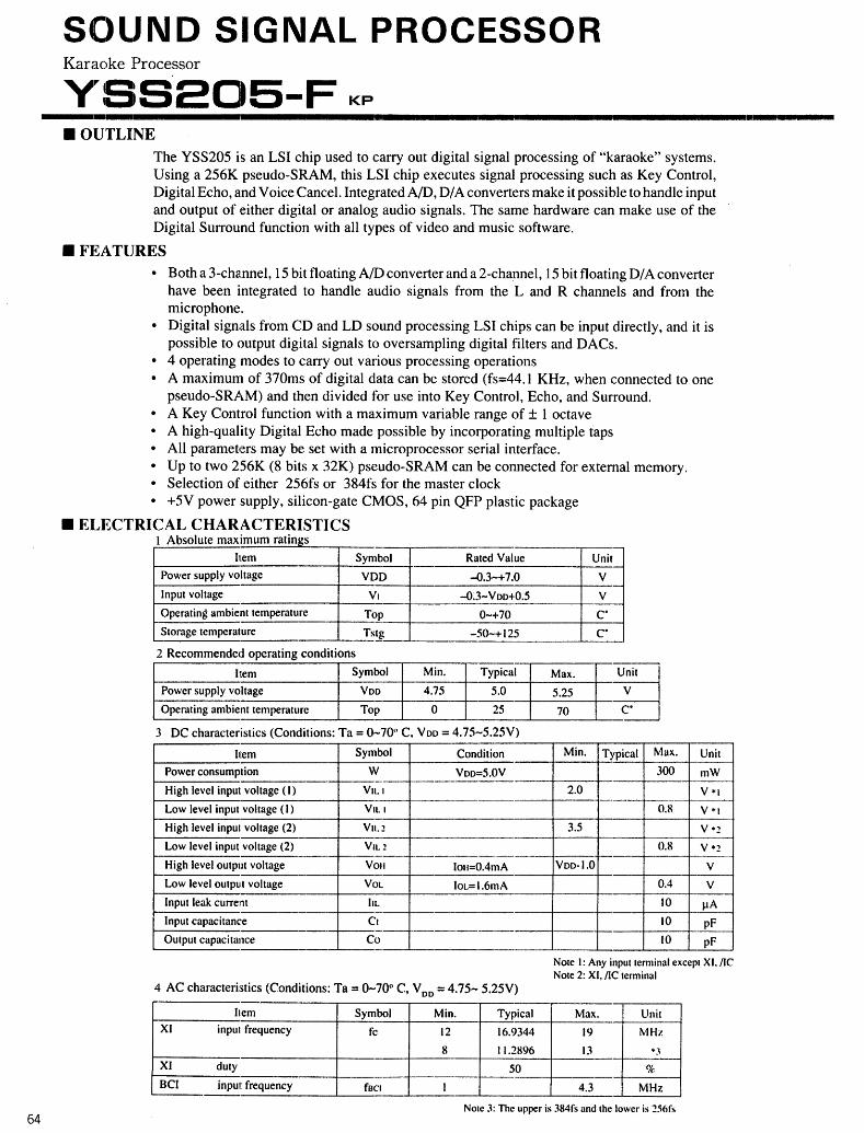
64
SOLJND SIGNAL PROCESSOR Karaoke Processor
YSS205-F KP
•OUTLINE The YSS205 is an LSI chip used to carry out digital signal processing of "karaoke" systems. Using a 256K pseudo-SRAM, this LSI chip executes signal processing such as Key Control, Digital Echo, and Voice Cancel. Integrated A/D, DI A converters make it possible to handle input and output of either digital or analog audio signals. The same hardware can make use of the Digital Surround function with all types of video and music software.
•FEATURES • Both a 3-channel, 15 bit floating AID converter and a 2-channel, 15 bit floating D/ A converter
have been integrated to handle audio signals from the L and R channels and from the microphone.
• Digital signals from CD and LD sound processing LSI chips can be input directly, and it is possible to output digital signals to oversampling digital filters and DACs.
• 4 operating modes to carry out various processing operations • A maximum of 370ms of digital data can be stored (fs=44. l KHz, when connected to one
pseudo-SRAM) and then divided for use into Key Control, Echo, and Surround. • A Key Control function with a maximum variable range of ± 1 octave • A high-quality Digital Echo made possible by incorporating multiple taps • All parameters may be set with a microprocessor serial interface. • Up to two 2.56K (8 bits x 32K) pseudo-SRAM can be connected for external memory. • Selection of either 256fs or 384fs for the master clock • +5V power supply, silicon-gate CMOS, 64 pin QFP plastic package
• ELECTRICAL CHARACTERISTICS I Absolute maximum ratm_g_s
···-· Item Symbol Rated Value
Power supply voltage VDD -0.3-+7.0 Input voltage V1 -0.3-Voo+0.5 Operating ambient temperature Top 0-+10 Storage temperature Tstg -50-+125
-..J •
2 Recommended operating conditions
hem Symbol Min. Typical
Power supply voltage Voo 4.75 5.0
Operating ambient temperature Top 0 25
3 DC characteristics (Conditions: Ta= 0-70" C, Yoo= 4.75-5.25V)
Item Symbol Condition
Power consumption w Voo=5.0V -- --·-·----·--· High level input voltage (I) VILI
Low level input voltage ( I ) VILI
High level inpul voltage (2) Vn.2
Low level input voltage (2) V1L2 - ·--------·-·-~···-·-· .... -··--
High level output voltage VoH lou=0.4mA Low level output voltage VOL loL=l.6mA Input leak current llL
·--... Input capacitance Cl
--.----·------Output capacitance Co
-
Unit
Max.
5.25
70
Min.
2.0
3.5
----Voo-1.0
v v C"
c·
~ =d
Typical Max.
300
\.--· --0.8
0.8 +-----~-----
0.4
10
10
10
Unit
mW
V *I
V *I
v .. ., v •2
+-----------v v
µA
pF
pF
Note I: Any input terminal except XI, /IC Note 2: XI, /IC terminal
4 AC characteristics (Conditions: Ta= 0-7011 C, V DD= 4.75- 5.25V)
hem Symbol Min. Typ~cal Max. Unit XI input frequency fc 12 16.9344 19 MHz
8 11.2896 13 *'J
XI duty 50 %
BCI input frequency fec1 1 4.3 MHz
Note 3: The upper is 384fs and the lower is :?56fs

.................................... 1 .................................................................. ...
• EXTERNAL DIMENSIONS (YSS205-F)
~ 32 II --.-------·-
52
1.QTYP
19
18.8±0.4 -------------~·-------------i
•BLOCK DIAGRAM
Pseudo-SAAM Interface
PKG BOTTOM
SURFACE
DIMENSIONS IN mm
65

66
SOUND SIGNAL PROCESSOR Dolby Pro-Logic Decoder
YM7SOBB DPLD
•OUTLINE This LSI is a Dolby Pro Logic decoder based on latest Digital Signal Processing technology.
The LSI is capable of digital signal processing for almost all functions needed in Pro Logic. Thi~
allows construction of a highly reliable decoder with a small quantity of components.
This LSI also has a sound field simulation circuit with 12 digital delay lines (370 ms at max.),
which allows you to design a 2in-4out surround system easily.
•FEATURES • Highly accurate signal processing with internal operation word length of 32 hits
• Adaptive matrix, noise sequencer, 7 KHz low pass filter, modified B-type N.R. decoder and
AID & DI A converter are built-in.
• Sound field simulation function using digital delay (maximum delay time: 370 ms)
• Ext&rnal 256K DRAM interface for 16 bits linear digital delay (page mode access)
• Serial interface with microprocessor for parameter control.
• Analog signal processing for the front three channels.
• Master clock frequency is 8.46 MHz and sampling frequency is 44.1 KHz.
• Interface signal output for Automatic Balance Control.
• Dolby reference operate level 300 mVr.m.s.
• 64 pin QFP package, silicon gate CMOS, 5V power supply. (Note)
Dolby is a trademark of Dolby Laboratories Licensing Corporation. This IC is available only to
licensses of Dolby Laboratories Licensing Corporation.
• ELECTRICAL CHARACTERISTICS • ABSOLUTE MAXIMUM RATINGS
Parameter Symbol Power supply voltage VDD
Input voltage VI
Input current II
Operating temperature Top
Storage temperature Tstg
Min. Max. -0.3 +7.0 -0.3 VDD +0.5
10
-20 +75 -50 +125
• RECOMMENDED OPERATING CONDITIONS Parameter Symbol Min. Typ. Max.
t--Power supply voltage VDD 4.75 5.0 5.25
Operating temperature Top 0 25 70
Unit v v
mA oc oc
Unit v oc
• ELECTRICAL CHARACTERISTICS (CONDITIONS: Ta=25°C, Voo=5.0±0.25V) Parameter Symbol Condition Min. Typ. Max.
Power consumption w VDD=5.0V 200 300
Input Voltage H level VIH
TTL level 2.7 VDD
CMOS level 3.5 VDD
Input Voltage L level VIL
TTL level 0 0.4 COMS level 0 1.0
Input leakage current IIL 10
Output voltage L level VOL !OH= -2mA 0 0.4
Output voltage H level VOH IOH=200µA 3.0 VDD
XI frequency XIN 8.0 8.46 9.0
XI clock duty 40 50 60
BCI frequency 2.0
Unit mW
v
v
µA
v v
MHz
%
MHz

----------------------!------------------------------------...-• EXTERNAL DIMENSIONS~ 32 II
l.OTYP
20 ----
~52 ~064 I ~
18.8±0.4
• BLOCK DIAGRAM DGND DVDD AGND AVDD Sync I. XI XO /IC
r-··-···9··-~··9--Cf·--··Cf TlL~:.!~!I-~.... --- ···---------9-----: i i I Timing pulse I I generation I LRS/OVF I , css
LINM9-----. ! LINSL_J--- rf VREP
·~:~S=f ;t ~---PVRL f f- I •
CHLQ-CHRQ--cvti AID
I t l
! I
i i l i I I
i
i t ! So11md field I Simul1atlon circuit
I -i r;!:xte1,_.n_al_R_A_M._
j L__:ontrol
l---··----&-=------··
Adaptive Matrix (Steering Ch'cult)
Noise pnerator
Parameter Control Microprocessor Interface
! l I I
' I I I
VORP
SR
SL
RS
LS
A0·1.RAS.CAS,/OE,/WE DH BCKWCK CD " 'Ntii.~i'fRiEL.NOISE
MCON ~.fJh)f/~M,COFF,STROFF
67

68
SOUND SIGNAL PROCESSOR Surround Processor 2
YM712B SP-2
•OUTLINE YM7128 is an LSI which has quality digital surround sound capabilities realized by Yamaha's digital audio technology. The LSI has built-in A/D and DI A converters which enable digital surround sound processing for analog input/ output without using any additional devices. Its eight digital delay lines may provide delay time of up to 100 msec. for each, and digital adding up of delay line signals for two-channel output assures a wide range of application.
•FEATURES 1t The built-in RAM realizes digital delay time of 100 msec*, at the maximum. 1t Feedback loop can be constructed for reverberation. 1t Various surround effect can be obtained by controlling this processor with serial data from
micro processors. 1t Digital attenuator is built in for surround sound volume control. 1t Sampling frequency is 23.6 kHz*, and 14 bit floating A/D converter is built in. • Two-times oversampling digital filter and 14 bit floating D/ A converter are built in. 1t 16 pin DIP packaged silicone gate CMOS LSI, operated by 5V.
NOTE:When XI clock frequency is 7.16 MHz (304 fs is required for XI clock)
•ELECTRICAL CHARACTERISTICS 1. Absolute Maximum Ratings
Item Symbol Rating
TI Supply voltage VDD -0.3 - +7.0
Operating Top -20 - +85 ·c temperature
Storage temperature Tstg -50 - +125 ·c -- ---
2. Recommended Operating Conditions (Ta== 25 'C. voo = 5.0v)
Item
Supply voltage
Operating temperature Top o 25 70 ·c s:~1 I ~1Efi~ =:~: .:[-;; I u~<
, ____ ____.__ -- ·-·--- -- -
3. DC Characteristics -----~----··,--·-----..--------..-------
I Item Symbol
Supply Current IDD
High-level input voltage (1) VIHl
Low-level input voltage (1) VILl
High-level input voltage (2) VIH2
Low-level input voltage (2) VIL2
High-level output voltage VOH
Low-level output voltage VOL
Input current leak IIL
Input capacitance Cl
Output eapacitance co
•JIE 1: Applicable to input terminals except XI
:!IE 2: Applicable to XI terminal
Condition Min Typ Max Unit
50 mA
2.0 v llE 1
0.8 v llE 1
4.0 v llE2
0.8 v llE2
IO H = - 0.4mA 4.0 v I OL=0.2mA 0.4 v Vl=0-5V -10 10 µA
5.0 12.0 .:>F
10.0 pF ..

....................................... 1 .................................................................. ...
• OUTLINE DIMENSIONS 0-15·
16 15 14 13 10 9
2 3 4 5 6 7 8 =f 0.25±0.05
• BLOCK DIAGRAM
---------------------------------------, XI
XO
/IC
AIN
cu cuo
SCI
AO DIN
timing generation
Cl
-~ [
+digital delay
A/D 1--1;,....,...c.+
TO
Conversion T8 T7 T6 TS T 4 T3 T2 Tl
standard voltage ] generation
• I I I
._ __ in-~e-~0_f::_J I I I '--•·
2fs
2fs
D/A Conversion
D/A Conversion
UDD
USS
AUDD
AUSS
LO
RO
69

70
SOL,ND SIGNAL PROCESSOR Surround Processor-B
YMIS42B SP-B
•OUTLINE The YM3428, a 16-pin DIP CMOS LSI, permits to implement quality digital surround sound
capabilities realized by Yamaha's digital audio technology.
As the LSl includes AID and DIA converters, you can easily implement digital surround func
tions without any additional analog devices.
It has four delay lines each of which may be set for the maximum delay time of 30.24 msec, and
outputs are two channels each of which is produced in each pair of delay channels added up
digitally. So, the range of application is wide.
• FEATUJlES • Three kinds of surround mode are possible as preset modes without the use of any micro
processors.
• With a use ofmicroprocessor,. it is possible to set the four delay lines at different delay times and different volumes and to define parameters of a primary IIR digital low-pass filter.
• The internal signal format is of 14-bit floating point numbers. • The built-in AID and DIA converters are of floating type with high linearity. • The built-in reference voltage generator for AID Converter permits an easy interface with
analog circuits. • The sampling frequency of AID conversion is 24.9 kHz, so the bandwidth needed for surround
sounds is secured. • The DIA converter operates at the sampling frequency of 99.4 kHz, following a built-in quatd
ruple oversampling digital filter, so that high cost external output low•pass filter is not needed.
• Distortion is as low as 0.22% (typical) at the maximum output at 1 kHz.
• ELECTRICAL CHARACTERISTICS 1. Absolute Maximum Ratings (VSS = O.OV) ---------....----------------------.--~----------------1----~I_te_m ____ ~~~S~y __ m_b_o_l ___ ,,_ ..__RaEin~-+-___!:!_~----< ._!_erminal voltage --+--.Y-~J?.-=~~~- - O.~_ - 7 .0 1--__ V ___ ---'
Operating temperature +-J0~·-----~70 °C Storage temperature Tstg - 50 - 125 oc
2. Recommended Operating Conditions (VSS=O.OV, TOP=0-70 °C) Item Symbol MIN. TYP. MAX. Unit
~eply voltage VDD 4.75 5.00 5.25 v - ··--- -------- ... --1
VSS, AGND 0 0 0 v
3. DC Characteristics(VDD=4. 75 - 5.25V, TOP=O- 70 °C) Item Symbol Condition MIN. TYP. MAX. Unit
-+-----1 Low-level input voltage VIL -0.3 0.8 v High-level input voltage VIH Except XI 2.0 VDD v High-level input voltage VIH XI 4.0 VDD v Low-level output voltage VOL XO : IOL=0.2 mA -0.3 0.4 v High-level output voltage VOH XO: IOH=0.4 mA 4.0 v Input current leak ILK Vl=5V 10 µA Supply current IDD 20.0 30.0 mA
Input capacitance CI f=l MHz 10 pF
Output capacitance co 10 pF Pullup resistance RPU /IC, MDO, MDI. 50 400 KO

...................................... 1 ................. 1 ..................................................... .
• OUTLINE DIMENSIONS
15'"'""
INDEX MARK AREA
~l~: 0.25TVP
- -t-b ~~- SEATING r PLANE
! _ ........ ;__ ~~
DIMENSIONS IN IAM
• BLOCK DIAGRAM r-- - - - - -·-- -------- - - -------- ---- -------- --- - -- - -- -- --,
XIO--: :[-~ XO~ ·~ng generator ·
AIN
I I I I I
Cl
~
Di,gital
LPF
4
MDCI
Digital! delay line
• I I
Digital delay line
• I I
Digital delay line
+
MDl
Digital volume control
• Digital volume control
• I I I
SCI AO
interface
-----------------~ DIN
LO
RO
71

72
SOUND SIGNAL PROCESSOR Digital Compressor
YM3412B COMP
•OUTLINE Wide dynamic range is one of the most significant features of digital audio signals. However, this feature can be a disadvantage of the total system, when digital audio is used with analog system having limited dynamic range such as car CD, portable CD or headphone CD, or when recording CD to a cassette tape. There is also a problem when part of a low volume signal is lost during attenuation of digital output or during digital volume processing. The latest Yamaha digital sound processing technology has been used to create an LSI chip with a compressor function (which includes a volume processing option) that will automatically respond to the input level and compress the dynamic range of the digital audio signal.
•FEATURES • An input signal emulation compressor based on digital sound processing technology.
Automatic emulation of low or high volume input signals, based on a unique input signal level detection circuit.
• Capable to cope with MSB first 2's complementary input signals with fs at 32 KHz, 44.1 KHz, 48 KHz or double fs.
• Capability in 2 modes: <Mode I> (Compressor) Four different compression ratios can be employed, determined by the setting of the compression switching terminals (SELO,SELl). Compression ratios vary when detected input level is between - 54dB and -18dB. Below -:>4dB, the input and output values are equal, and beyond -18dB, attenuation is carried out. DCR (DCR is the dynamic compression ratio when the detected input level is between -54dB and -18dB.) Jl. 1/1 Input and output levels are equal. 2. 3/ 4 When the detected input level is over -18dB, the reduced rate is fixed at -9dB. ~t 2/3 When the detected input level is over -18dB, the reduced rate is fixed at -12dB. 4. 1/2 When the detected input level is over -18dB, the reduced rate is fixed at -18dB. <Mode 2> (Digital Attenuator with compressing) When an external microprocessor is used to input volume data (8bit, attenuation at 0.375dlB), attenuation of sound of volume is carried out while still maintaining the compressor function. (During initial clear, muting condition is set with the volume value "oo".) 1• CMOS, 18 pin , plastic DIP, + 5V power supply
•ELECTRICAL CHARACTERISTICS (1) Absolute Maximum Ratings
l Item ~~ Min _ CMax Unit Supply voltag-e ----i-Vn~ /--=-3.0-J---~~-- V
I Input voltage I Vi I -0.3 ~o+0.5 V
Ambient operating t~mperature' TOP ! -_c_1 _-L_+ 70 ·c [_Storage temperatu~e ---~:~~-_J _____ :~9. ____ J ______ :~~---- _ ___:_<;_ ______ _

.................................... 1 .................................................................... ..
(2) Recommended Operating Co~1ditions
'bol Item S}' Min l Typ Max Unit Too Supply voltage ' 4.75 I 5.00 5.25 v
Ambient operating temperature' T Op 0 I 25 +70 ·c (3) DC Characteristics
Item Sy mbol Condition Min Typ Max Unit
Supply voltage loo Voo=5V mA High output voltage ToH loH=20µA 4.0 v Low output voltage i OL I loL=lmA 0.4 v High input voltage 1 IHI 3.5 v Low input voltage 1 TJLl 1.5 v High input voltage 2 IH2 2.0 v Low input voltage 2 IL2 0.8 v
Input current leakage lJL -10 10 mA
• OUTLINE DIMENSIONS
------~~~~-~
• BLOCK DIAGRAM
M1/M2
:I U) 0 Lei SEATING
'-'it+-~-+~+-.......... ~PLANE
DIN
18 pin plastic DIP PK18DP1·20.1
/SCK WE
--{( ~ SELO
VDD
vss Tl T2
[~~ ~,-~-µ-C~O-M~l-/-F~---
: : (M2)
IL---- - - - ·--- - -- -------------·
SDI
SYNC
BCLK
/IC
I I
: (Ml) I .------,-~
Level detection
1/0 data format switches
SEL1
/CR
SDO
F1
FO
73

74
CD-~/CD-ROM CD-I Data Controller
YMBOBSB CDC
•OUTLINE The CDC (CD-I Data Controller) is a data processor capable of handling data from both CD-I and CD-ROM sources. This receives data read out from a CD-I disk and detects the synchronous pattern, then descrambles the data and puts it in a buffer. File and chan.nel selection, and data distribution can be done through use of an 8 bit microcomputer. lt is also possible to create a compact CD-I system configuration by using this together with the YM6064 (ADP) and YM7302 (MPC).
•FEATURES • Capacity to handle either CD-I or CD-ROM. • Real time errors can be detected and corrected by the hardware. • Interface can be accomplished with any CD audio signal processing
format. regardless of the maker--e.g. Yamaha. Sony, Sanyo. NEC, Mitsubishi, Toshiba, Hitachi, or Matsushita.
• CD-I ADPCM data can be transferred directly to the audio processor (ADP).
• When used with the YM7302 (MPC), data can be transferred at a rate of 1170 bytes/msec.
• An optimal system can be set up when connected with a 68000- type bus. • CMOS, 5V power supply, 80 PIN QFP
• ELECTJRICAL CHARACTERISTICS 1. Absolute Maximum Ratings
Mfn Max --f-·.
Supply voltage Vdd -0.3 7.0
Power consumption Pd 150
Input voltage Vin -0.3 Vdd+0.5
Input current Iin 10
Ambient operating temperature Top 0 70
Storage tem~erature Tstg -50 125
2. Recommended Operating Conditions
r Supply voltage Vdd 4.75 5.25
[ Ambient temperature To_I?_ 0 70
3. DC Characteristics
--·-v
mW
v mA oc oc
v oc
• Input terminals (Numbers shown in () are CK, BCI, and RTCLK terminal coef-ficients.)
Min Max
Low level input voltage Vil -0.3 0.8 (0.4) v High level input voltage Vih 2.0 (2.4) Vdd +0.5 v I1!Q_ut leak current Iii 10 µA
• Output terminals
Min Max
Low level output voltage Vol Yss 0.4 v High level output voltage Voh 4.0 Vdd v Output leak current Ilo. 10 µA
• Power terminals Min Max
Power current Idd 30 (Vdd= 5.0V) mA

...................................... 1 ............... 1 ............................................ ..
e I ~ I
•EXTERNAL DIMENSIONS
PKG BOTTOM SURFACE
•SAMPLE CD-I CONFIGURA1rION
•BLOCK DIAGRAM
, ........................................................ ,. .................................................................. . i WRITE ECC/EDC READ I ! 1ddrcss iddreu 1Jdrn1 , I 1•11emor 1•n•ru1or tenol11or _-_1 _ ~~~ •.
j : SAO-SA12 RCI
Sl>SY SDI
...-------------=,- SDO-SD7
SFSEL MSEL PSEL-~--
C2FG--+--~----'----
DCS• DR• DW• DA2 DAI DAO
DD7-Dl>O
DINT• DREST• SM PUCK i
! I
EC:C/EDC processina circuil
CDC control re1i11er1
I RTREQO. RTREQI * RTDATA RTCLK RTACK•
r-----...__,__ DONE•
6BK
CDREQ• CDACK• READY•
CDO-CD7
CCS• RIW• LDS• RSO RSI RS2 DTACK•
CDINT• RCINT•
1 .... -··-·-··-"'""'"'""""'""""""'""""'""''""'""'"""-'"''"-""""""'"'"'""'''"""""'..t
(•lndlc11u 1 terminal which i11c1ive when low.I
CPU CD audio (68000)
8K S-RAM
Real time Audio ADP (YM6064) ADPCM decode processor
Audio output • DAC
CD mechanical control CPU
Remote controlt----light receiver
Mouse
MPC (YM7302) •OMA •Timer etc.
System ROM
(CD-RTOS) +NV-RAM
Display
75

76
CD-I/CD-ROM CD-I ADPCM Decode Processor
YM6064 ADP
•OUTLINE
This ADP is an LSI chip used for processing CD-I audio signals (ADPCM decoding). Reproduction of real time audio and of sound map audio can be done simultaneously by using this in conjunction with the YM6063 (CDC)
•FEATURES
• CD-I format ADPCM data is converted to 16 bits linear PCM data. LEVEL A fs = 37.8 KHz 8 bits LEVEL B fs = 37 .8 KHz 4 bits LEVEL C fs= 18.9 KHz 4 bits
• A circuit has been integrated specifically for digital mixing of real time audio and sound map audio.
• A double oversampling digital filter builtin to the CD-I format for LEVEL c
• A built-in ldB x 127 step digital attenuation circuit • A built-in overflow limiter • A mute control terminal • A CD audio digital signal input terminal • A silicon gate CMOS, 80 PIN QFP, 5V power supply
•ELECTRICAL CHARACTERISTICS I. Absolute MaxHmum Ratings
Item Symbol Minimum
Supply voltage Voo -0.3
Input voltage V1N -0.3
Ambient operating temperature ToP 0
Stora_g_e tem~rature Tsr -50
(Based on the reference voltage of Vss. A Vss == 0.0V)
2. Recommended Operating Conditions
Maximum
+7.0
Voo +0.3 +70
+ 125
Supply voltage +5V ±5%
Unit
v v oc oc
(Based on the reference voltage ofV ss, AV ss = 0.0\T) Ambient operating temperature
3. DC Character:istics (V oo = + SV ± 5%, TOP = 0 - 70°C)
Item Symbol Condition Minimum Maximum Unit
High level output voltage VoH loH• -0.4mA 2.7 v Low level output voltage VoL loL=r 0.SmA 0.4 v High !eve) input voltage (TTL level) V1H 2.2 v Low level input voltage (TTL level) v,l 0.8 v High level input voltage (CMOS level) V1H 3.5 v Low level input voltage (CMOS level) v,l 1.0 v Input leak current IL -10 ro µA
OFF Input leak current- lu -10 10 µA
Pull-up resistance RU 60 600 KO Power current loo 50 mA
4. Terminal Capacitances (f= lMHz)
Item Symbol Condition Minimum Maximum Unit
Input teminal c, 8 pF Output terminal Co No load 10 pF 1/0 terminal C.o No load 12 pf Output load capacitance CL 100 pf

................................... --........................................................................... . • EXTERNAL DIMENSIONS
lf~·p
23
~ ~ ~ ~
b 0 0
N
0
~==t--"til a a on nan on n a on n ~-lt!mo--, -=-=,===::i:-""+-Cl. 21
l'K<i BOTTOM SURFACI-:
• ADP BLOCK DIAGRAM
RT·lmlh
RT·ACI\ * RTl>ATA
RT·CLI\
()().l)i
RSO·l~S:I
Cl-:• Ll>S• Rt\\'• IJTACI\ * RST•
nm~"' l>ACI\ * REAU\'* IRQ•
limFFER MEMORY L <SR.AM 8KBytel
8 13
from QHM EMI' BCI SDSY SDI
:··················· ............ . ,,, .. ''''"'''''' '" .......................................................................................... . i i i i j :
I i j
WRITE .... _,,....11--..P.+-=-=--t ~EAi> Al>URESS A1>1>1mss GEN. <:EN
CDC INTERFACE
SYSTEM INTER·
FACE
S RAM INTER·
FACE
ADPC:\I B-·-----==---4 DECODER l>ICI TAI. Fil. Tim
~llXIN<i CON TR. UNIT
to l>l<:ITAI. Fil.TEI~
~--... SIX) i-;..--.... Bco a-.:....--t.1R ~--... DEMI'
1.1!'\I •
--------------------------'---+---1.,.. CD·IJA
·------·----------------...;....---Mtrn:•
TIMING GENERATOR J.----a.--.., DF·CLK
77

78
CD-~/CD-ROM Master Peripheral Controller
YM7302MPC •OUTLINE
The MPC (Master Peripheral Controller) is a single chip integrated circuit used to provide compact yet effective control of the peripheral circuits (mouse, DMA, timer, interrupt, etc.) in a CD-I configuration.
•FEATURES • Direct interface capability with a 68000 MPU • An integrated single channel DMA controller • A built-in 1200 bps mouse interface circuit (when using a 16 MHz master
clock) • Built-in memory and 1/0 type address decode circuit • An integrated 6 level order of priority interrupt handler • A built-in 1.95 K-31.25 Kbps serial interface (when using a 16 MHz master
clock) • Integrated bus arbitration function • A built-in 40 bit timer counter (battery back-up capacity) • A built-in 32. 768 KHz calendar clock oscillator circuit (battery back-up
capacity) • A built-in 16 MHz master clock oscillator circuit • An integrated watch-dog timer • An integrated 16 bit pre-scaling timer counter • A built-in reset sequence circuit • CMOS, 5V power supply, 100 PIN QFP
• ELECTRICAL CHARACTERISTICS J. Absolute MaxJmum Ratlap
Jtnl SJMol Rad_lll Ulllt
Supply vol~ Vao -o.3 ... +7.o v ln~t terminal volt11.1_e Vir -o.3 ... Vao+0.1 v AmlMcot ~ratl~:tem~raturc o ... +10 ec Stora_t_e temperature -.so ... +12s ec
2. Recommended Operatlna Coadltlo111
lteia S,.W Mia. T-11!._ Max. Ualt
Su!!2!r_ volta..J!. 4.7' s.o S.2S v TCLKl
t CON'r v .. 3.S - v. v CKI v .. -0.3 - 1.0 v TEST-
I Other terminal• v .. 2.0 - v. v V11. -0.3 - 0.1 v
Data 1tora..J_C volta..J_C 2.0 - S.2S v Clock~ue~· - 32.768 - KHz OpcratlnJ temperature 0 2S 70 ec
3. DC Cbaracterlstl«» .... s,.w Mia. ~ Max. Ualt ColldldOll
1f TCLKl CON'r v .. -0.3 - 1.0 v CKI
!.J TESTt' Other terminal• V11. -0.3 0.1 ----- v
1f TCLK2 CON'r v .. 3.S - Vao v CKI
1.1 TEST* Other terminal• v .. 2.0 - Vao v
lnp~t leak current IL -10 - 10 1&A (NQIC I)
Tri·atat.e Input current lia -10 - 10 l&A (when OFF)
~u 49 ... 6' t.emdnal1
Voi. - - 0.4 v loi.•1.6mA 68 ... 73 temdoal1 n Other tenni1nal1 Voi. - - 0.4 v loi.•3.6mA H.!Jh. lcvcl ou!e_ut vol~1e VON 2.7 - Vao v IOM•-0.4mA Power current~toni~) so ~ Power cumnt~1tl111) so mA Input capacitance 12 pp
(Nole I) lotcroal pull-up nal11.1ace of' lhe TESTt' and RXD()4' termloala: 100 ... SOO KO

.......................................................................................................... • EXTERNAL DIMENSIONS -- ll:IT]I, O.ti5TYI'
•BLOCK DIAGRAM
c I
Ill
:11
~ ;;.. 1--Ir":
;;
~ ~ .. ,
..... l~
1--,_ '="i d
l_L_ l'K<; BOTTOM
7::14;=-__,Ann onnnnnn nnnnnnnnnllrl=C_.......,...===F-"-r-s uR FACE
.., ufr
EXTIW'.\11• m:.
----11,..·· ..... ··· .... ····· ............................................................ " ....... ,
-~-n;co • \'SCI•
ROMO• IWMI• EXTO•
·--+:--1 i
----:-1
\'DI'• 1':XTI• j
N\' RA~h ..,., __ .i.;.'.--1 PIA• :
FOC• ... _,_._.....__
OMA• CDC• ADP• VSR•
10\\'R• IORIJ • ...,, ______ _
A:!:\.AOI .. ,--+---i
Adress lkcndt•r
I--"'
-ll'.\IA ncm
.-....... - .... J Mou!'t' l.__..,. __ •H lntt•rfacl'_J Li--.....,;.-.. 1
Timer Calendar
__J__
AS• ... , ___ ..... ,-. ·-Ul>~· * .. ,--.:;---i Ll)S,• ... , ___ _
R W• !>TACK* ... ,--..:......-,i
FC2 FCI FCO
BER~:* .. , __ ...._ ........ .,.
07·1>0 .. , __ ............
ctm
fi!llHIO
lnlcrh1n•
Divide• Circuit
CKI :. ~]µ1 -1 l:LKOIJT ·-·
!. ·------: r-··-----.
S\'SRST • _1
Ml'Ul<E\'il-:T * ··---+-""! Cirrnit Ml'UllALT•
St·rial lntt•rface
11--_,.._..... ..
lntt•rrupt llandler
'------~ l j
i ....................................... 11••···· .. ·······················-· ................ J
(* indicates a terminal which is active when low.)
BR• B<;• ll<iACK• 111.l>RQ 111.l>AK DR<J• OACK• READY• lllB\'TE• EXT or IR<J•
RXI>l RTS
TCl.Kl TCl.K:! COl'T• B\"
RXllU TXllO
EXTIACK• \'PA•
11'1.2• 11'1.I• ll'LO•
IR<J6* IR<Ja• IRQa IRQ:I• IRQ2• IH<JI•
79

80
Recc>mmendation for surface-mount LSI
1. When using Soldering Iron; Temperature at the device lead part shall be controlled as 260 °C per 10 seconds or below.
2. Using Flow Soldering I Solder Dip; It is not appropriate to use this method for QFP devices and some of SOP devices.
3. By Infra-Red Reflow • To avoid character-deterioration or package crack by the absorbed moisture, PRE-BAKE
shall be applied at the condition of 125 °C for 8 to 24 hours. • To avoid damaging local heating,
Up-down heating is recommended. • Temperatures of the surface of package and
PCB shall be below 235 °C and less than 10 seconds. • Please ref er to Figure 1 for
recommended Temperature Profile.
4. By VPS (Vapor Phase) Reflow • To apply PRE-BAKE as explained in 3. • Ambient Temperature shall be;
Max. 215 °C, less than 30 seconds. • Please refer to Figure 2 for Recommended Temperature Profile.
INFRA-RED REFLOW max235 "C /1 Os Recommended Temperature Profile ~ 2-5 "C/sec ~
~ E 2 s
~ 60s -180s --.! C'tl "t:
:::::i en
~ i
Figure I --+ Time t (sec)
VAPOR PHASE REFLOW (VPS) ~ .a
Recommended Temperature Profile e ~ § s C'tl
"t: iSi! ~
':!> ~ 60s-180s
i Figure 2
--+ Time t (sec)


YAMAHA YAMAHA CORPORATION
The specifications of these products arc subject to improvement changes without prior notice.
YAMAHA CORPC)RATIOI\ Address inquires to: Electronic System Division •Tokyo Office 3-1. Kanda Surugadai. Chiyoda-ku.
Tokyo, 104 Ryumeikan Bldg .. ff Tel. 03-255-4481. Fax. o:J-255-4488
•Osaka Office 3-12-9. Minamisenba. Chuo-ku Osaka-city, Osaka. 512 Shinsaibashi Plaza Bldg. 4F Tel.06-252-7980 Fax.06-252-:1615
• IIEAD Office 203, Matsunokijima. Toyooka-mura. Iwata-gum. Shizuoka-ken. 4:38-01 Electronic Equipment business section Tel. 0:139-62-4918 Fax.o:i:l9-62 :JO:J4
• YJ\MJ\IIJ\ Systems Technology 981 Ridder Park Drive. San Jose. CA951:ll U.S.A Tel.408-437 :ll:l'.l Fax.408-4:17-8791