Burroughs - bitsavers.org
114
FIELD ENGINEERING TECHNICAL MANUAL Burroughs B 471 DISK FILE ELECTRONICS UNIT PROPERTY OF AND TO BE RETURNED TO Burroughs PRINTED IN U.S.A. 7-1-.64 B 471.51 INTRODUCTION PRINCIPLES OF OPERATION FUNCTIONAL DESCRIPTION- ELECTRONIC FUNCTIONAL DESCRIPTION- MECHANICAL ASSEMBLY- DISASSEM BLY- ADJUSTMENTS MAINTENANCE PROCEDURES AND AIDS INSTALLATION PROCEDURES OPTIONAL FEATURES
-
Upload
khangminh22 -
Category
Documents
-
view
4 -
download
0
Transcript of Burroughs - bitsavers.org

FIELD ENGINEERING TECHNICAL MANUAL
Burroughs
B 471 DISK FILE ELECTRONICS UNIT
PROPERTY OF AND TO BE RETURNED TO
Burroughs
PRINTED IN U.S.A. 7-1-.64 B 471.51
INTRODUCTION
PRINCIPLES
OF
OPERATION
FUNCTIONAL
DESCRIPTION
ELECTRONIC
FUNCTIONAL
DESCRIPTION
MECHANICAL
ASSEMBLY
DISASSEM BLY
ADJUSTMENTS
MAINTENANCE
PROCEDURES
AND AIDS
INSTALLATION
PROCEDURES
OPTIONAL
FEATURES

~ FIELD ENGINEERING TECHNICAL MANUAL ____ --t-~B ...... 47 ..... l;;;;..;, ....... 5.::..l_~ll;;..:.~O_-~1____1 February 1, 1965
INDEX - SECTION I
1 INTRODUcrION
1.1 General Description • • • • • • • • • • • • • • • • • • • • • • • • • • • • • July 1, 1964
1.2 Equipment Specifications • • • • • • • • • • • • • • • • • • • • • • • • July 1, 1964
1.3 Physical Description • • • • • • • • • • • • • • • • • • • • • • • • • • • • Dec. 1, 1964
1.4 Glossary • • • • • • • • • • • • • • • • • • • • • • • • • • • • • • • • • • • • • • • • Feb. 1, 1965
Printed in u. S.A.

~ FIELD ENGINEERING TECHNICAL MANUAL ____ '""'"'"':--+-._B .... 4_.7 .... 1 __ • 5 ..... 1 ______ .-.1,;,.;.1 ... -...... 1;...... ..... July 15 , 1965
1.1 GENERAL DESCRIPTION
Fi gure 1.1-1 shows the Disk File Electronics Unit (E.U.) with one Disk File Storage Unit (S. U.). One E.U. can control from one to five S. U.'s, while up to ten E.U.'s may be connected to one Disk File Control Uni t (D.F.C.U.). A maximum Disk File Subsystem wil l consist of one D.F.C .U., 10 E.U.'s, and 50 S.U.'s. Only one Disk File Subsystem can be controlled by the B200j the B5500 can control two Subsystems.
FIGURE 1.1-1 E.U. IN DISK FILE SUBSYSTEM
Prlnted in U.S.A.

1.1-2
FIGURE 1.1-2 E.U. IN DISK FILE SUBSYSTEM
An E.U. provides the power, air pressure, motor starting controls, basic head switching and gating logic for one to five S.U.'s. See Figure 1.1-2 for the E.U. placement within the Disk File Subsystem.
The E.U. is the B471. However, the E.U. and the first S.U. are called a B472. The Subsystem can be expanded easily by adding additional S.U.'s. The first E.U. is connected directly to the D.F.C.U.; however, when there is more than one E.U. in the Subsystem, they are connected through an Exchange to the D.F.C.U.
In the Disk File Subsystem, the E.U. supplies the logic for reading and writing. Before an operation may take place, a segment (record) must be located on the disk. Each segment has an address which is read and compared with the desired address. When the correct seg~lent address is found, the operation proceeds.
A ,write operation transfers characters from the Processor to the D.F.C.U., to the E.U., and finally to a disk in the S.U. The E.U. accepts a six-bit character from the D.F.C.U. parallel by bit, then

~ FIELD ENGINEERING TECHNICAL MANUAL _____ ........ B._4 ..... 7liiiiool ... 5;",;;;1 ____ ...a..-....;;1 ........ 1-..... 3 __ -t July 1, 1964
passes the character to the Module serially by bit since data is written serially on the disk.
In a read operation, the serial by bit information read from the disk is accumulated into a character in the E.U. and then sent to the D.F.e.U. and on to the Processor.
Printed in U.S.A.

~ FIELD ENGINEERING TECHNICAL MANUAL _____ i-..;:B._47_l:;.:.:..;5;.:l-.a.I......;:1;;.:. .• .:.2_-1=--~ JUl~ It 1964
1.2 EQUIPMENT SPECIFICATlqNS
Height Width Length Weight
· . . . . · . . . . · . . . . • • • • •
53 inches 23 inches 45 inches
450 pounds
POWER REQUIREMENTS
208VAC or 230VAC from two phases and neutral. Maximum current. 63 amps for five S.U.'s.
Maximum cable length to D.F.C.U. - 50 feet.
Printed in U.S.A.

~ FIELD ENGINEERING TECHNICAL MANUAL _____ +-'B;;;o.4 ..... 7;..,;;;;1;;..:. • ._5.-,1 ...... ___.1.:..,;. 3;;..-..;;;1;;.-. .... July 1, 1964
1.3 PHYSICAL DESCRIPTION
The Electronics Unit supplies the power and power controls for the Storage Units as well as providing the read/write logic. All operator controls are located Qn the front of the E.U. Figure 1.3-1 shows the left side of the E.U. The logic gate contains co~trol logic for the E.U. and S.U.'s. The Maintenance Panel to the right allows the engineer quick access to information on the status of the E.U. and associated S.U.'s.
Printed in u. B.A.
FIGURE 1.3-1 COMPONENT LAYOUT - E.U.

1.3-2
The Control Panel on the E.U. (Figure 1.3-2) provides the operator controls for the E.U. and its Modules.
FIGURE 1.3-2 E.U. CONTROL PANEL
The switches and indicators on the Control Panel are listed below;
1. POWER ON - switch and indicator - green
2. POWER OFF - switch - black
3. DC ON - switch and indicator - green a. The DC ON switch will cause DC to be supplied to the
logic gate in the E.U. and the S.U.ts and also fly the heads in the S.U. 1 s.
4. DC OFF - switch - black a. The DC OFF sWitch retracts the heads and removes DC
from the E.U. and theS.U.'s.
5. NOT READY - indicator - white a. The NOT READY indicator is lit when:
1. The heads are not flying. 2. The air pressure is not normal. 3. The E.U. LOCAL/REMOTE switch is in LOCAL.
6. MASTER LOCKOUT - indicator - red a. The MASTER LOCKOUT indicator is lit when the MASTER
LOCKOUT switch is thrown.
7. DISK LOCKOUT - indicator - red a. The DISK LOCKOUT indicator is lit when any of the
individual Lockout switches are thrown.
The Key Lock releases the cover over the Lockout switches at the top of the E.U. There are 20 separate Lockout switches for the individual disks and one MASTER LOCKOUT switch.

~ FIELD ENGINEERING TECHNICAL MANUAL _____ ~B;;;..4;;.;;7;..;;;1;.;..~5;;;.l--l..I--.;;.1.;.. .. 3;;;...-...;;3~ .... December 1, 1964
The Maintenance Panel (Figure 1.3-3) has the following:
1. A POWER ON meter.
2. Five NOT READY indicators for the S.U. 's.
3. The AC ON and DC ON indicators which parallel POWER ON and DC ON on the Control Panel.
4. RELAY SUPPLY ON indicator.
5. The LOCAL/REMOTE switch.
6. DC LOCKOUT switch.
7. A CLOCK switch which must be on for normal operation. It is off for single pulsing with the BITP and W~p buttons.
8. Indicators for flip-flops in the E.U.
9. Test points.
10. A voltmeter for monitoring the power supplies.
11. An AIR PRESSURE meter.
Printed in U.S.A.
Qb Qb 1 Z :I 4 5
©©©©© ~TORACOE UNITS NOT READY
AC ON
DC RELAY SUPPL'I
g ON ON
00 CLOCK DC
i NORMAL REMOTE
<@ <@ OFF LOCKOUT LOCAL
@"::;'_SINGLE@:OOMP ~ PULSE-
CLEAR@ @RESET
SU REGISTER
"0 0 INFFO OsPFf
AO OeMI'
eO CI'FO 0"A2
40 O"AI
zO Oc SLI'O ~SRI'
IRO OIW ~
INlCP@ @SCOL
SW1L@ @ACFF
@w
-100 -4.5 _24~-ZO -12
~ -120 ""2
AIR PRESSURE
Off ... 20 Tl00
FIGURE 1.3-3 MAINTENANCE PANEL

1.3-4
Figure 1 . 3-4 shows a B471 and one B475 viewed from t he front with the skins removed to show the physical location of many of the components.
Note t he Winchester type connector mounted j ust above and behind the compressor. This is the connector for t he logic cable from the ass ociated. D.F.e . U.
FIGURE 1.3-4 B47l AND B475

~ FIELD ENGINEERING TECHNICAL MANUAL _____ +--=B;..;:4;.:.7.:;.1:..;. 5:;;.;:1:;....a.~1:...:.~4~-.;:.1--' February 1, 1965
1.4 GLOSSARY
ACFF Action FF is on during a disk file access except duri.ng a second revolution cross-over.
ASRL ASRL/ Address Read Levels from the Storage Module.
ASRS Cross-coupled switches set by the Address Read Levels at ASRS/ BITP time. The outputs of the switches are set into SUBF
when ICFF is off.
BAIF BA2F BA4F
BCLP
BITL-OI BITL-02 BITL-03 BITL-04 BITL-05
BITP
BSPL
BUDP
CBAS
CCEL-C
CCIL-A
CSIL-A
CSUS
Printed in U.S.A.
Address Count FFs. Normally only count to three. BA4F indicates a Maintenance Segment address.
Output of the Bit Clock Multi. Pulse width 150 nanoseconds. Input is BITP or DBIT.
Bit pulse levels from the five possible modules.
Delayed output of the Bit Pulse Multi. Pulse width 150 nanoseconds. Input is BITL-nn. Produces a BeLP delayed 250 nanoseconds after input.
Bit Single Pulse Level. Effectively, this is the output of the Bit Single Pulse switch to BITM.
Undelayed output of Bit Pulse Multi. Pulse width is 250 nanoseconds. Input is BITL-nn.
Count Address Count Switch. Negative output causes a count-up of BAnFs.
Continuous Clock Enable Level. Makes CCIL-A negative when Clock Switch is ON.
Continuous Clock Inhibit Level. Ground when Clock Switch is OFF.
Clock Single Inhibit Level. ON. (This should be SCIL.
Ground when Clock Switch is See SCEL.)
Clears SUIFR, SU2F, SU4F and SUSF.

1.4-2
CSILI CS2LI
DBIT
DFSLI
DFSS
DISC-OIl DISC-02/ DISC-03/ DISC-04/
DIXP
DOlL/ D02LI D04LI D08LI Dl6LI
ECCS
FWLS-ORI FWLS-OR2 FWLS-OR3
GLAF
GSLF
GSSL
Characters per Segment Levels.
Both ground for 96 characters per segment. I negative and 2 ground for 240 characters per segment. 1 'ground and 2 negative for 480 characters per segment.
Delayed Bit Pulse from an adjustable multi. Output is a negativ~ pulse 675 nanoseconds after BUDP. Used to fire BCLP while reading an active word.
Disk Face Select Level. Negative to select a clock head on the lower face of a disk--tracks 00=)49. Must be opposite of DFSS.
Disk Face Select Switch. Negative to select a clock head on the upper face of a disk--tracks 50=)99. Must be opposite of DFSL/.
Disk Select Levels. Ground to select disk "n " in eaCh Storage Module. Only one line ground at one time. Derived from the decoded outputs of the Disk Switches.
Delayed Index Pulse from DIXM. DIXM is 600 microseconds and is set during second revolution cross-over. In case the cross-over results in a Not Ready condition (nonexistent disk), DIXP resets INFF and produces one more SCLP.
Disk Switch Levels inverted from Disk File Control address levels.
Enable Character Clock Switch. If a BITP was missed, ECCS ensures that SCLP cannot occur out of sync due to the set of SUCF by the BITP that occurs at W0MP.
File Write Lockout decoding.
Gain Latch FFlatches the Gain Select circuit.
Gain Select FF is set to the state of TSRF at each Word Mark (SPFF).
Gain Select Switch Level is negative to select low gain in the Module read amplifiers.

o FIELD ENGINEERING TECHNICAL MANUAL _____ +--B_.4 .... 7 ..... 1;;.,;, ...... 5._.1-.....1_·, "..1..:...4.-.-...;;;3;....,....-f
February I. 1965
HFML-Ol/ HFML-02/ HFML-03/ HFML-04/ HFML-05/
HSDL-OO thru
HSDL-99
HSTL-OO/ HSTL-IO/ HSTL-20/
thru HSTL-90/
HSUL-OO/ thru
HSUL-09/
ICFF
INFF
INHS
INXP
IRAL IRAL/
IRAS IRAS/
L0SW-OI/ thru
L9JSW-20/
ML0S/
MOIL M02L M03L M04L M05L
Printed in u. S.A.
Stort'ge Module Ready Levels are positive when;
a. Unit is Ready (disks up to speed, no touch circuits triggered, air pressure up, heat exchange blowers on).
b. Unit is in LOCAL and not designated.
Head Select Drive Level is positive to select track "nn" .. Only one line can be positive at a time.
Head Select Tens Levels.
Head Select Units Levels.
Interlace Control FF is set during the active word and is reset dur ing the inact i ve word or tt id Ie" condition ..
Index FF is set during first and second revolution crossovers. I ts purpose is to "blank out " the maintenance segments and to index the continuation of the operation on the correct word.
Index Holdover Switch. The output level is a gate to the holdover of IXHM and is used to produce the pseudo INXP in a second rveolution cross-over.
Index Pulse. The output of the Index Holdover Multi when it times out. IXHM = BCLP· INHS.
Information Read Levels from the Storage Module~
Cross-coupled switches set by the Information Read Levels by BCLPs (DBIT). The switch outputs are set into SUBF when ICFF is on.
Write Lockout Switches 1 through 20 for each of the possible 20 disks. Ground level when disk is locked out.
Master Lockout Switch. Ground level when the whole file is locked out.
Module Designate Levels derived from the five Disk Switch Levels.

1.4-4
RDHM
REMS/
RIHS
SARLI
SCEL-A
SCLP
SC0L/
SC0S
SEQ-LOC-OUT
SPBL-OI SPBL-02
SPFF
SRAL
SRBL SR8L SR4L SR2L SRIL
SRIL-INDI SR2L-IND/ SR3L-IND/ SR4L-IND/ SR5L-INDI
Read Delay Holdover Multi. 32 micros~cond multi is set to inhibit BITPs during a second revolution cross-over when clock tracks are being changed.
Remote Level. Ground when the LOCAL-REMOTE switch is in REMOTE.
Read Inhibit Holdover Switch. Controlled by RDHM.
Segment Address Read Level. Ground level to D.F.C.V. after the Address Count FFs indicate an address has been read.
Single Clock Enable Level. Negative when the Clock switch is off to enable the use of the single pulse button.
Storage Clock Pulse (Character Clock) is a negative pulse for each character. Is also sent to D.F.C.U. to generate clock pulses.
Segment Coinc1.dence Level 1.s ground from D.F.C.U. when address coincidence has been found.
SC0L/ switched for gating logic in the E.V.
Normally a ground level to enable a DC ON cycle in the E.U. When the DC Lockout switch is thrown, the ground level 1.s removed inhih1.ting DC ON.
The output levels of two cross-coupled switches which, when in Single Pulse Mode, will provide a negative pulse from SPBL-Ol to produce one BITP for each depressi.on of the single pulse button.
Space FF. Set by W0MP and cleared by the next BITP (second space bit). Is the first "flag" bit for each word.
Storage Read A Level. Negative level to D.F.C.V. when SUAF is set at Character Clock time (SCLP).
Storage Read Levels. Negative level to D.F.C.D. when associated FF is set.
Storage Ready "n" Level Indicators. When ground, the associated indicator will light. They correspond to HFML-nnl inputs.

~ FIELD ENGINEERING TECHNICAL MANUAL _____ -+-__ B_4_7....,1_., ...... 51--..&...-..;;.1_.,. _4-_5~~ February 1, 1965
SSUD
SUlFR
SUIFW
SU2F SU4F SU8F SUAF SUBF
SUCF
SUID
SURL/
SWlL SW2L SW4L SW8L SWAL SWBL
SWLL
TDlL TD2L TD3L TD4L TD5L
TSRF
TOIL/ T02L/ T04L/ T08L/ TlOL/ T20L/ T40L/
Printed in u. s. A.
Shift SUnFs Driver.
Storage Unit 1 Read FF.
Storage Unit 1 Write FF.
Storage Unit "n" FFs.
Storage Unit Character FF. This FF is set to indicate character time; that is, a complete character. It generates an SCLP.
Storage Unit Input Strobe. The character to be written is set into the SUnFs.
Storage Unit Ready Level. Ground level through a relay contact from SURS/. SURS/ is deri.ved from HFML-nn, Clock On and REMOTE.
Storage Write Levels. Negative level will cause the appropriate SUnF to be set by SUID.
Storage Write Lockout Level. Negative level to D.F.C.U. when an attempt is made to write to a locked out disk.
Threshold Detect Levels. Negative pulses from a Module set the gain control circuit for low gain.
Threshold Store FF. Set by TDnL from a designated Module.
Track Select Levels.. Ground levels from D.F.C.li. to select Track 00 through 99 when combined with DFSLI and DFSS.

1.4-6
WICD
W0HF
W0HM
W0HSI
W0MD
W0MP
WRSD!
WSPL-Ol
Z01L/ Z02L/
Write Information Control Level. Negative during the active word to enable information to be written on the selected track.
Word Mark FF. Set by the Word Mark Multi. Reset by W0HS! (W0HM after time out). Used to inhibit the generation of W0MPs by flux changes when an address is being read.
Word Mark Multi. The multi has 7.8 microseconds duration and is fired and held over by any flux changes read from the address track.
Word Mark Switch. The switched output of W0HM.
Word Mark Driver. The negative output is the Word Mark pulse to the D.F.C.U.
Word Mark Pulse. Generated by a flux change in the address track corresponding to the beginning of each word~
Write Storage Level. When positive, indicates a write operation is to be performed~
Word Single Pulse Level. The output of the Word Single Pulse switch.
Zone I and 2 Levels from the D.F.C.D. These are decoded to form three levels--Z0IL-OI/, Z02L-OI/ and Z03L-Ol/ which are used to select the correct zone.

0) FIELD ENGINEERING TECHNICAL MANUAL ____ --+--=B~4_.:71:::.::._.;;5_1_.a......1..;;;.2.;;..;;. O;....-..;;;.I~ February 1, 1965
INDEX - SECTION II
2 PRINCIPLES OF OPERATION
2.1
2.2
Electronics
Disk Format
Printed in u. s. A.
Un1 t ••••••••••••••••••••••••••••••••
• • • • • • • • • • • • • • • • • • • • • • • • • • • • • • • • • • • • •
Feb. 1, 1965
Dec. 1, 1964 I

~ FIELD ENGINEERING TECHNICAL MANUAL _____ ~--B4--7 ..... 1 ...... --5 ...... l .......... ---2 ..... -1--1--..... July 15, 1965
2.1 ELECTRONICS UNIT
GENERAL OPERATION
The Disk File Subsystem provides the B200 and B5500 systems with a very large capacity storage device with rapid access to any record~ In the Subsystem the Electronics Unit provides the local logi.cal control of up to five Storage Modules.
To write on a disk, first a specified area is identified by its unique address and then the six-bit BeL characters are written serially by bit in that area. The B5500 can write in the binary mode if required~ All characters may be written.
To read from the disk, the area to be read must first be located by head selection and address comparison. Then the serial bit information is assembled into characters which are transferred to the Processor one at a time.
Head selection entails the selection of the Module, disk, face, zone and track. Each information track is found in three zones so three heads are designated. Each zone has unique clock tracks and an address will be read for each segment in the selected zone. Once the required segment is located 1 the read or t'l1ri.tc cp-erattoa begins.. The E.U. provides logic for head selection, clocking, information read and information write.
HEAD SELECTION
An address is shifted into the A Register in the D .. F.C.U. by the Processor. This is the unique address of one segment; 96, 240 or 480 characters on one side of one disk, in one Module, in one E.U. The decoded output levels of A Register are sent to the E.U. which further decodes them into head select lines to the Module and disk face. The levels from the D.F .. e.U. are: (Refer to Figure 2.1-1.)
1. The DnnLts which select one Module of five and one of four disks in that Module.
2. Disk Face Select Level (DFSL/) to select the lower or upper face.
3. The ZnnLts which select the 100 heads in one zone (both sides of the disk).
4. The TnnL's whi.ch select one of 50 tracks in each zone.
The E.U. decodes the fifty TnnL's and DFSLI into 100 center tap levels called HSDL's to enable the center taps of the information heads.
Printed in U.S.A.

2.1-2
E.U.
r----ff-. 0 F S S
OF 5L/--ir---\ 't--...
DOlL / --ft----41Pf
004 L / --ft---l~
o 08 L / --II-----l~
DIG L I' --It----t~
Z OIL I' --It---l~
z 0 ~ L I' --tI---l...-t
T01LI
TO~LI
T04 L/
T08L/
Tl0LI
T2.0L/
T40L/
CS 1 L / ......-!i-----+r-
C S ~L/ 4-iI----+__
FIGURE 2.1-1 E.U. IN THE DISK FILE SUBSYSTEM
Each HSDL enables 12 heads; disk. With the 480 option, can read and write segments can read and write segments can read and write segments wll1 have segments 50 - 99.
one head in each zone of one face of each the information head enabled in zone 1 o - 11. The corresponding head in zone 2 12 - 27 and the enabled bead in zone 3 28 - 49. The oPPosite face on the disk
Refer to Figure 2.1-2.
The ZnnL's and Disk-nn will select the 100 heads in one zone of one disk (both faces). These levels will also enable the center taps of the four clock heads for that zone of the disk (both faces). The desired face is selected by DFSL/ and DFSS.

~ FIELD ENGINEERING TECHNICAL MANUAL _____ ....... .;;:;B..;;;.47.;...;1=..1,~5~1__a.__=2~ .... 1..;..;:-3~_I December 1, 1964
480 OPTION 240 OPTION 96 OPTION
ZONE DISK 1 DISK cw/ccw FACE ONE FACE
C W FACE CCW FACE CW FACE
1 0_11 50-til 0- Z3 0-59 250-309 750-809
2 12-+27 62--77 24-55 60 - 139 310---389 810-889
3 28--49 78-99 56 -99 140 -249 390 -499 890 ~,)99
ADDRESS SEARCH
FIGURE 2.1-2 SEGMENT ADDRESSES BY OPTION
2 c..CW FACE
500 - 559
560 - 639
640-749
The selected Word Mark clock head reads three digit addresses from the Word Mark track and sends them serially by bit, serially by digit, to the E.U. From the point of view of timing, these addresses are read during the word time preceding the first word of the segment. When an address is read by the Word Mark clock head, a new segment will pass under the selected information head after the next Word Mark. The segment address is sent back to the D.F.e,U. to be compared with the address in the A Register. If the segment address compares, Segment Coincidence Level (SC0L/) is sent to the E.U~ to indicate that the segment has been found. The E.U. will now go into an active read or write operation. Figure 2.1-3 shows the block diagram of the Address Search operation.
The selected Bit clock track in the S.U~ will generate clock pulses which are sent to the E.U. The EsU. uses these Bit pulses for all clocking purposes. Information and addresses are handled in similar ways by the EeU.; that is, either information levels or address levels are strobed into the Stack-Up Register (SUnF's) by Bit pulses~ When a complete character has been assembled, it is sent to the D.F~C.U. parallel by bit.
The Word Mark track generates Word Mark pulses (W0MP) as well as segment addresses. The Bit track generates timing for writing or reading one bit at a time. Each zone has its own Word Mark and bit tracks since, to maintain a reasonably constant packing density in all three zones, the frequency must vary. There are a total of six clock tracks on each disk face located between zone 2 and zone 3.
Refer to Figure 2.1-8 for the EeU. logical flow diagram ..
The Interlace Control Flip-Flop (ICFF) is the control to determine active and inactive words. ICFF is off until segment coincidence is found. After SC0L to the E.U., ICFF is complemented by each W0MP until the write or read operation is completed. When ICFF is off, the Word Mark track (ASRL) is scanned for an address (inactive word). When ICFF is on, reading or writing is being done during the active word.
The S.U. Register is comp~ised of seven flip-flops - 1, 2, 4, 8, A, B, C. The function during write is to receive a character at a time from
Printed in U. S.A.

2.1-4
E.u.
S 1 L/ 4+----"*-'C S 1 L/
S2L/ CS2L/
"SRL
"SRL/
FIGURE 2.1-3 INFORMATION FLOW - ADDRESS SEARCH
the D.F.C.U. and send it serially by bit to the S.U. During read, the bits are stacked up in the S.U. Register until the character is complete and then it is sent to the D.F.C.U.
Address Read Level, ASRL, will produce a W~P (Word Mark Pulse) with the following logic:
WflMP • ASRS • W0HF/ • BITP
ASRS is also the segment address input to the E.U. after W~P has been recognized and W0HF inhibits W~P being generated by address information.
W~P triggers the Space Flip-Flop (SPFF). SPFF signifies the beginning of a word, either active or inactive.
SPFF - W~P • SPFF/
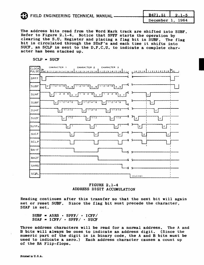
~ FIELD ENGINEERING TECHNICAL MANUAL _____ -I-~B:;;.;4;:.:7_=1r..&.,.&5.;:;..1__'___=2:.&. • .:;.1,;;;.-5~_I December 1, 1964
The address bits read from the Word Mark Refer to Figure 2.1-4. Notice that SPFF clearing the S.U. Register and placing a bit is circulated through the SUnF's and SUCF, an SCLP is sent to the D.F.C.U. to acter has been stacked up.
seLP • SUCF
CLOCK CHARACTER 1
PULSE
SPFF
SUBF
SUAF
SU8F
SU4F
SU2F
SU1FR F F
SUCF F F
SCLP
BA1F
BA2F
SARS
SC{25L
track are shifted into SUBF. starts the operation by flag bit in SUBF. The flag each time it shifts into indicate a complete char-
r' 4 I 5 I 6 I 1 I 2 I 3 I 4 ! 5 I 6 !WM I I
5 U-s
5
s
5
s
s
s
(CLC=6 )
I I
I I I.
u
FIGURE 2.1-4 ADDRESS DIGIT ACCUMULATION
Reading continues after this transfer so that the next bit will again set or reset SUBF. Since the flag bit must precede the character, SUAF is set.
SUBF • ASRS • SPFF/ • ICFF/ SUAF • ICFF/ • SPFFI • SUCF
Three address characters will be read for a normal address. The A and B bits will always be ones to indicate an address digit. (Since the numeric part of the digit is in binary code, the A and B bits must be used to indicate a zero.) Each address character causes a count up of the BA Flip-flops.
Printed in u. S.A.

2.1-6
BAnF's serve as a counter for the number of address characters read. Address coincidence cannot be made until three characters have been compared. The addresses of the maintenance segments have more than three digits; therefore, BA4F will be set to indicate a maintenance function.
When three characters have been read, Segment Address Read Level (SARL) is sent to the D.F.C.U. to indicate a complete address.
SARL • BAIF • BA2F
If segment coincidence is found, then two SCLPts later, SC0L is sent to the E.U. to initiate action on the next WftMP.
With SC0L true, the next W~p sets ICFF and ACFF (Action). ACFF will remain set during the Read or Write operation unless there is a change of track. ICFF is complemented with each W~P for the inactive words interlaced with the active words.
FIGURE 2.1-5 READ/WRITE INFORMATION FLOW

~ FIELD ENGINEERING TECHNICAL MANUAL _____ +--.._B_47 ..... 1..., ...... 5 .... 1--.... ......... 2 ...... .._1_-7___.-4 July 15, 1965
INFORMATION WRITE
Refer to Figure 2.1-5 fo·r the READ/WRITE Information Flow.
The level SWRL from the D.F.e.U. will denote a Write operation. SWRL/ indicates a Read operation. With SWRL, ACFF • ICFF true, WRSD/ will be false to the S.U. for a Write operation.
During a Write operation, the S.U. Register will receive a character at a time from the D.F.e.U. Each bit pulse shifts the character through the Register. SUIFw replaces SUIFr during a Write operation. The output of SU1Fw will condition the Bit flip-flop in the S.U. to write a one or a zero on the disk. Refer to the timing diagram, Figure 2.1-6.
CHARACTER 1 LOCK
PULSE
SPFF
SUBF B F
SUAF F
SU8F F
SU4F F
SU2F
SU1Fw
SUCF F
SCLP
CHARAC.TER 3
F
F
F
F F
F
FIGURE 2.1-6 WRITE TIMING
CHARACTERS CHARACTER P 4 THRU 8 I Iw
J 214181AIBl1214181AIBMI I
j Lr
5
5
5
5
w
I I
U U-I I
5~----rl~--------rl :
With SPFF, ACFF, ICFF and a Write operation, the first character from the D.F.C.U. is strobed into the S.U. Register and a flag bit is set into suer by Storage Unit Input Strobe Driver (SUID).
SUID • SPFF • ACFF • ICFF • SWRS SUnF+-SWnL's • SUID • BeLP SUCF - SUID • BCLP
With the S.U. Register loaded, the next BITP will write the state of SUlFw OD the disk. The next BCLP will shift the S.U. Register; SUCF to SUBF, SUBF to SUAF, etc.
SSUD • SUID!
Pr1Iltecl1n U.S.A.

2.1-8
The flag bit is also shifted through the S.U. Register. When it reaches SU2F, the last bit of the character is in SUlFw being written on the disk. The next BCLP will strobe in the next character from D.F.C.U. and set a new flag bit in SUCF.
SUID • SU2F- SU4F/ • SU8F! • SUAFI • SUBFI • SUCFI
The Write operation will continue until from 1 to 10 segments have been written when the B200 Processor is connected. The B5500 is capable of writing from 1 to 63 segments wi,th one instruction.
INFORMATION READ
The Read operation is similar to the Address Search operation previously discussed. Instead of ASRL, the Information Read Level, IRAL. which is conditioned by the information track, is strobed into SUBF.
CLOCK PULSE
SPFF
SU8F
SUAF
SU8F
SU4F
SU2F
SU1FR
5UCF
SCLP
SSUD
F 1
IF F 1 F
FIGURE 2.1-7 READ TIMING
CHARACTERS CHARACTER P 4 THRU 8 I IW
SI214ISIAIBlI214ISIAIB;MI
5~--------------~Ls-I
512141siAIsl112141sIAIBL
D 11214 1s L::J1 '2 14 18
~11214 L.:Jl1214
~112 ~112
J ~1 ~1
5 ~ U-I I
j U U-I I
So n r1-
The Information Read Timing Chart, Figure 2.1-7, starts with the flag bit set into SUBF and the remaining flip-flops being cleared. SUlFr replaces SUIFw for Read. The first BCLP after SPFF has been reset will place the first information bit into SUBF and will shift the S.U. Register.
SUBF • lRAS • SPFF/ • WRSDI • ICFF
I.

C) FIELD ENGINEERING TECHNICAL MANUAL _____ +--B_4_7_l_._51_...-_.2 ..... l_..-..,9_ ... December 1, 1964
Since the information was written on the disk with word interlace, it must be read in a similar manner. ICFF is set to read the infonnation word and then reset to allow reading of the address track.
As each bit is read off the disk, the S.U. Register is shifted. When the flag bit reaches SUCF, a complete character has been assembled in the S.ll. Register and SUCF gates the character to the D.F.e.U.
SRnL - SUnF • SUCF
The Read operation will continue until the number of segments specified have been read.
Printed in U.S.A.

t.r1 . C!~ ~
0 t"4~
SET INITIAL 8;; >CAG {
~ CLEAR SU"F 5 <it\:)
~I-' COLLECT BITS
t"4 I 000 WORD/ADDRESS
~ TRACK
Ul COUNT ADDRESS CHARACTERS
SECONDARY FLAG
SEGMENT ADDRESS HAS BEEN READ
START ACTIVE: OPE RA TION NOW
BACK TO ACT I VE
FLOATI NG~ LOGIC
BCLP BITP 1
SPFF -"- 0
STORAGE CLOCK SCLP SUCF 2
SUCF""'- 0 BCLP + OBIT 1 3
BA4F""'- 0 4 CLEAR PRIOR TO ADDRESS READ BA2F L- 0 + SPFF· ACFF/· BCLF
SPFF·INFF/·BCLP 1 5
SUBF -"- 1 -SUAF:z..:O- - ----
SU[S=>lRJ""-O
f SUnF (SHIFT)
SUBF-ASRS
BA COUNTER + 1
SUAF ~ 1
SARL
., UNCLOCKED
BA1F""'- 0 + INXp· INFF 6
END OF OPERATION ACFF ~ 0 SC0L/' BA2F' BA 1 F' SUCF' BCLP J CLEAR IJtsU1FW ""'- 0 W0MP 8
SET FLAG *SPFF""'- 1 SPFF/ 9
*INFF""'- 1 ACFF'BA4F I 10
*INFF""'-O ACFF'BA4F/! 11
*ICFF""'-O INXP 12
* BA4F ""'- 0 13
*BA2F""'- 0 INFF 14
SPFF· BCLP *BA1F L- 0 15
WR ITE OPERATION 18
19 * ACFF ""'- 0 (ACFF· BA4F· BA2F) + SC0LI I 16 SET FLAG BIT
START OF WORD AFTER EACH CHARACTER
CSUS'BCLP
(CSUS=SPFF + SUCF)
20
21
SSUD·BCLP 22
(SSUD=SPFF/.SUCFI) 23
SPFF/.BCLP 24
CBAS'BCLP
*INFF L- 0
[C BAS=SUAF 'SUBF • SUCF' (BA2F /+ BA4F/)
'SPFF/.(INFF/+ACFF/)]
SPFF/'SUCF'BCLP
. INFF' ACFF + BA4F· ACFFI
29
30
ACFF/· DIXSI J
25 26
27
17
STROBE IN NEW CHARACTER
SHIFT FLAG BIT (UNTIL IT REACHES SU2F) CLEAR B-A-8-4 IN TURN
SHIFT OUT BITS
FLUX CHANGE ON BIT CHANGE
READ OPERATION
SET INITIAL FLAG
CLEAR FOR CHARACTER COLLECTION
W0Mp· INFFI 31
SC0S . ACFFI
ACFF· BA4FI
NOTES:
CSUS SSUD
CBAS
SUID
ECCS
32
33
34
CLEAR STORAGE UNIT FLIP-FLOPS SHIFT STORAGE UNIT FLIP-FLOPS
COUNT ADDRESS CHARACTERS
STORAGE UNIT FLIP-FLOP INPUT STROBE
ENABLE CHARACTER CLOCK
INFO BIT
LOOK FOR FLAG
COLLECT CHARACTER
SECO NDARY FLAG
! ICFF· ACFF l--
*ICFF L- 0
WRSD
SUCF"'- 1
SUnF-SWnL
SUBF-- SUCF
tsunF (SHIFT)
SUF-- SU1FW
WRSD/
SuBF"- 1
SUAF"'- 0
SU [S~1 RJ ""-0
SUCF~ 0
SUBF- IRAS
SUCF "'- SU 1 F R
fsunF (SH I FT)
SUAF 1
W0MP I 35
SWRL I 36
SUID' ECCS' BCLP I (SUID=SPFF+SU2F 'SU [c ~4J=0) (ECCS=ASRS/+ W0'HF)
SUID'BCLP! 40
41
SSUD·BCLP 42 (SSUD = SUBF + SUAF + SU8F 43
+ SU4F + SU2F/) 44
45
SWRL/l 46
SPFF'BCLP I 47
48
CSUS'BCLP I) 49
(CSUS=SPFF + suCF) 50
SPFF/'BCLPI 51
52
SPFF/'SUCF/'BCLP! 53
SUCF·SPFF/·BCLP I 54
37
38
39
..... I ..... o

CONTROL UN IT
sE~"'ENT ADDRESS
sOUC.HT = SE~"'ENT ADDRESS fOUND
SARL t---. ~~l TnOLI
4~ sCLP
~ 'On" ,:J ~} l0nLI
SRl L
SR2L
SR4L
SReL
SRAL
SRBL
BCLP
sARL/
I BCLP
.. I NXD
ELECTRONIC UNIT
(TOIL ~ T49L)·DfSLI = HSDL-OO ~HSDL-49
(TOll -> T49L)·DfSL =HSDL-50 =>HSDL-99
OOOL ~ D03L
D04l -> Dl6L
-12V
~ DISC-Ol .D1SC-04
= MtillL ~M0SL
SUlfW
SU IFW/
SURL DISK FILE READy
JCl= + SUIFR·SPfF/.1CFF/.ECCS + SU I FR -SPFF/ - WRSD/· ICFF + surD-ECCS
(ECCs= AsRS-wI/lHF/)
(SUID= SPFF'ACFF'ICFF'SWRS
+SU2F' [SU4F/·8/-A/'B/.C/] 'ACFF' ICFF'SWRS)
(SSUD = SUCF/' ICff/· SPFfl + SUCf/-WRSD/ - S PFFI
+ NOT Sl"ROBE)
SWAL'SUID
Ieff I-SPfF
sPFF -SWRSI
SWBL -SUID
IRAS' SPFF/·WR S[)Io ICFF
ASRS· SPFF I·ICfF I SUC F· SSUD·SWRS·ICFF
r:;:;;::;::-'l -11 SPFF' ACFF/'INFF/: .... >-W=0M=D ______________ ~ SPFF'ICFF _
WI/lMP-01'CAG-107
CCIL-A·W0HSI Wli!HM'CCIL-A
BITP'ASRS
CCIL -A'ASRS' BITP'Wi!lHF/
W0HF/.WSPS-NO - CAG-l 07 W0MP-Ol
-12V
SC0L/.BA 1 F. BA2F.sucr
INXp.ACFF· BA2F. BMF INXP·
W0MP·ACFF-ICFF/·INFF/·BA4FI
W0MP'SCli!L'ICFF/'INFF/'ACrF/
INXP
W0Mp·ICFF
}",,-o~ DFSL/
DFSS
~i!0"LI
DL
SU1FW su 1 F WI
ICFF
WRSDI IXHSI
C) FIELD ENGINEERING TECHNICAL MANUAL -----........ ~ ......... .a.w...--L...:.:~~___f
INPUT LINES TO ALL STORAGE UNITS
UNIT TRACKS TAP liNES TO 1 INDINGS IN EACH MODULE)
100 CENTER TAP LINES HSDL {
SELECTEO 1 AT A TIME ~------~~~~~~~~------~--------------1I------------------l
LOWER UPPER
i!ONE 3 50 TRACKS 4.'3=52
(2 SPARES)
WORD CLOCK TRACK
~ BIT CLOCK TRACK
1 EACH PE R lONE IN
1 HEAD ASSEMBLY
~ 50 TRACKS
ZONE 1
50 TRACKS
FIGURE 2.1-9 SUBSYSTEM BLOCK SCHEMATIC

C) FIELD ENGINEERING TECHNICAL MANUAL _____ +-B_..4 .... 7 .... l ..... .-.5...,1 ~j_2::;;".:..:. 2:;.,.-..:;;1--t December 1, 1964
2.2 DISK FORMAT
Information on the disk is organized in words and segments. One word consists of 8 characters plus a longitudinal parity character. There is a two bit space between words so that a word time is a total of 56 bit pulses. During a write or read operation an active word is followed by an inactive word. Interlace is controlled by ICFF. The words from two segments are interlaced to allow the address track to be scanned during the inactive word. The bit frequency on the disk varies from I mc in zone 1 to approximately 1.8 mc in zone 3.
The segment layout for a track in zone 1 using the 480 option is as follows:
0+6 1 + 7 2 + 8 .3 + 9 4 + 10 5 + 11
Each word of segment 0 is followed by a word of segment 6, completely interlacing the two segments* The following diagram depicts this word interlace:
WORD 59
SEG 6
WORD 60
SEG 0
WORD 60
5 E G 6
WORD 1
5 EG 1
WO R D 1
S E G 7
WORD 2
SEG 1
The address for each segment is written in the word mark track during the word time preceding the first word of that segment. The following diagram illustrates this:
NOTE
The address digits are in REVERSE order.
IW0MP iii iii 100 700
WORD 59 WORD 60 WORD 60 WORD 1 WORD 1 WORD 2 SEG 6 SE<; 0 SEG 6 SEG 1 SEG 7 SEG 1
It takes two revolutions of the disk to completely read or write one track. On each revolution a dead space is encountered which is a physical reference on the disk. One maintenance segment can be operated on in each revolution~ The first revolution may read segments 0 through 5 or MSl, and the second revolution will read segments 6 through 11 or MS2.
Preceding the dead space on each track are the two maintenance" segments which are available to the engineer for checking purposes. The maintenance segments are 96 characters long regardless of the S.U. option. -
Printed in U.S.A.

2.2-2
When a read or write operation is in progress, the dead space and maintenance segments must be taken into account. Refer to Figure 2.2-1 for first revolution crossover. The figure reflects the 480 option, though the action is similar for the 240 and 96 options.
READ/ ISEG 5 WRITE
W!25MP
SCLP
SA
SARL
SC0L
ACFF
ICFF
INFF
INXP
SC
WD 601 IMS1 WD ,I; ~ ; 1
M3 J I I
164 PUSHERS
1000 I I I
I~ /
20J.JS.DEAD SPACE
t.-~~~I-· ISEG 6 WD 11
1600 I I I
J 1I1111I1I1I11II111111 1111111111111111111 5 10 lT13
(rNXP) '----.....
j~---------------~'----..... J
j
j
.: J~r----------------~--------------------
----------------~ J~'--------------------------~~I 2120
FIGURE 2.2-1 FIRST REVOLUTION CROSSOVER
Assume the operation has proceeded through the last word of segment 5 (the 6th segment)" The next W0MP Signals the start o.f an inactive word during which the address for Maintenance Segment 1 will be read. The address consists of four binary 10's. The 4 character address results in BA4F being set. INFF will be set by the next W~p to inhibit further action during the maintenance segments and dead space. BA4F is cleared by INXP, which is generated by the absence ot BITPs.
INFF = W~p • ACFF • BA4F
Notice that ACFF remains set to indicate further action is reqUired on this track. INFF is reset by the first W0MP after dead space so that ICFF will not be set until the second word after the dead space. This second word is the first word of segment 6.
ICFF = W0MP • INFF/
SCLP pulses occur each time SUCF is set with the flag bit.. The flag bit circulates until cleared by W~P; therefore SCLP pulses are produced up to the dead space. Sixty four extra bit pulses occur after the last word of MS2 and before the dead space occurs. They are called "pusher" pulses and create SCLPs for the pseudo word time during which is read the address of the first segment after the dead space.

~ FIELD ENGINEERING TECHNICAL MANUAL _____ ~B ..... 47-...,;;1;..&.-=5-=-1-a...-=-2 &.I' 2;:....-..:;:;,3----1 December 1, 1964
The crossover on the second revolution involves the selection of another information head and different clock tracks. The "A" Register in the DFCU is counted up as each segment is completed. After two revolutions on one track, the address in the "A" Register will activate new head select lines. The new address may be on another disk face or disk, so dead space is used to ensure the logic stays in sync.
READI WRITE
SARL
SC0L
ACFF
ICFF
INFF
INXP
RIHSI
SC
ISEG11 WD601
3211S
~----------------------~
I M3 S I I I 1
210 I I I
)11111111111111111
~3 f01j213
~ n 5
J
J
j
j
J
10
ISEG 13 WD 11
1020 I I I
1111111111111
-------1
____ --.JI
~~ ___________ 23~rul~20 _____ 2~0~ J:
FIGURE 2.2-2 SECOND REVOLUTION CROSSOVER
Refer to Figure 2.2-2. After the last word of the last segment on the track the six digit (all binary 12's) MS2 address is read during the inactive word. The 6 digit address will set BA4F • BA2F to indicate a change of track. INFF is set by W~P and, with BA4F and BA2F, enables a simulated INXP to be generated. This INXP will reset ACFF and the "A" Register counts up the segment address and a new head is selected. DIXM is fired by INXP. BITPs are inhibited by RIHS/ to prevent extraneous pulses occurring during the clock track change.
RIHS/ • RDHM (32 microseconds) • IXHS! • DIXM
With INFF on, no further action can take place until it is reset by INXPc This will occur when the newly selected head reads into de~d space. SC0L from the DFCU will permit the first W~P after dead space to set ACFF and ICFF, and the operation will continue in sequence on the new track.
Prlnteclill u. s. A.
I

0) FIELD EN GIN EER IN G TECH N I CAL MAN U AL _____ ~B=-4:.:::7:..:l;.&., .:.5l=--L-..:3:=.1·UlQ~-.. l---l February 1, 1965
INDEX - SECI'ION III
3 FUNCI'IOHAL DESCRIPTION - ELECI'RONIC
3.1 Disk File Electronics and Storage Units Power Sequencing ••• " •••••• "".,., •••••••• , •••••••••• Feb. 1, 1965
3.2 Cabling ••••••••• , •••••••••••••••••••••••••• , •••• July 1, 1964
3.3 Power Supplies •••••••••••••••••••••••••••••••••• Feb, 1, 1965
3.4 Addressing •••••••••••••••••••••••••••••••••••••• July 1, 1964
3.5
3.6
Clocking ••••••••••••••••• , •••••••••••••••••••••• Feb. 1, 1965
Ready Circuits ••••••••••••••••• , •••••••••••••••• July 1, 1964
3.7 Write Lockout ., ••••••••••••••• , •••••••••••• , •••• July 1, 1964
3.8 Read Signal Automatic Step Gain Control ••••••••• Feb. 1, 1965
Prlnted in U.S.A.
I

~ FIELD ENGINEERING TECHNICAL MANUAL _____ +--__ B .... 47 ..... 1 ......... 5 .... 1 _____ 3 _. 1-..-..-1_ ..... \ July 15, 1965 _
3.1 DISK FILE ELECTRONICS AND STORAGE UNITS POWER SEQUENCING
Reference Figure 3.1-1.
Power for an Electronics Unit and its associated Storage Modules is supplied from the E.U. power supplies. Disk drive motors in the Storage Modules start in consecutive sequence from the first Module. Successive Modules can only start after the motor in the preceeding Module is up to speed. No DC voltages can be applied to the E.U. gate or the Modules until the disk drive motors in all Modules associated with that E.U. are up to normal running speed. If the Motor Run Switch of a Module is in the Off position, that Module's motor will not start and the sequence continues with the next Module in line.
UNDER VOLTAGE FAIL SENSOR
Each E.U. has a voltage fail sensor which monitors the DC output voltages of the power supplies. When the supplies are correct, a ground level is supplied to the power sequencing which allows a normal DC On cycle. If any DC voltage falls below normal, DC power will cycle off as in a normal DC Off cycle. Ref. Fig. 3.1-2 for detailed schematic.
ELECTRONICS UNIT DC LOCKOUT SWITCH
Each E.U. has a lockout switch which disables the DC On sequence. With DC locked out, AC may be applied but no DC voltages will be supplied to the Modules and E.U. gate.
ELECTRONICS LOCAL-REMOTE SWITCH
Each E.U. has a Local-Remote switch. In the Remote position the -24V to start the DC On cycle may come from either the associated Disk File Control or the DC On switch on the E.U. control panel. If the switch is in the Local position, the -24V must come from the DC On switch on the E.U. control panel only.
MODULE MOTOR RUN SWITCH
Each Module has a motor run switch which, if on, enables the pick of its motor power relay when SMIL (Start Motor Input Level) from the preceeding Module is present. If off, it disables the pick of the motor power relay and transfers SMIL to the next Module as SMOL (Start Motor Output Level).
Printed in u. S.A.
I

3.1-2
ELECTRONICS UNIT POWER SEQUENCING PANEL
Inputs
208VAC Leg A 208VAC Leg B AC Neutral
Remote-DC-ON Remote-DC-OFF Emergency-Power-Off Pwr-Cont-Comm
AC-ON-IND AC-ON AC-OFF DC-ON-INn DC-ON DC-OFF LOC-REM-DC-ON DC-Sense-Control SEQ-LOC-OUT
Power Supply Voltages (Rack F)
Power Supply Voltages (Rack G)
Power Supply Voltages (Rack H)
SMOL
-24D
Outputs
Electronics Gate and Modules:
-4.5V -20V +20V +l2V -12V -24D
Modules:
208VAC
Main line voltage inputs.
Remote power control lines from associated Disk File Control cabinet.
Power control levels from switches and indicators on E.U. Control Panel and Under-Voltage Fail Sensor.
+lOOV, -lOOV, -120V, -24V, GND
-12V, +12V, -4.5V, GND
+20V, -20V, GND
Ground level from last storage module in a file to E.U. power sequencing panel.
Return from Air Compressor Pressure Switch.
Legs A and B to disk drive motors and heat exchange fans (2 per module), garage fans (3 per module) and Running Time Meter.

C) FIELD ENGINEERING TECHNICAL MANUAL _____ +-.=.B_47_l .... _5;.:l-"'---:;3~ • .::.1-...;;3:;......_I1 July 15, 1965 _
ll5VAC
SMIL
208VAC Leg A for convenience outlets.
Ground level to Motor Run Switch in first module.
Electronics Unit Maintenance Panel:
+100V -lOOV -120V
208VAC Legs A and B l15VAC (Leg A 208VAC) l15VAC (Leg B 208VAC)
Indicator drivers.
Running Time Meter. Convenience outlets and air compressor. E.D. fans (2 per unit).
All voltages metered at E.U. panel.
POWER ON SEQUENCE
Conditions:
70 Amp. Circuit Breaker On. E.U. Local-Remote switch in Local or Remote position. E.U. DC Lockout switch off. Motor Run switches in all Modules in Run position.
AC-ON-Cycle
AC Circuit Breaker "ON" (15 Amp.)
-24V Power Supply
AC Circuit Breaker "ON" (50 Amp.)
AC-On-Switch "ON" EFJO contacts 8-10
contacts 7-9
Printed in U. S.A.
208VAC Legs A and B to -24V power supply in E.U. and air compressor motor. Leg A to contact 8 ECJO, convenience outlets in E.U. and modules. Leg B to contact 10 ECJO.
Supplies relay control voltage to E.U. and modules. 208VAC Legs A and B to motor power relay contacts in all Modules.
Pick EFJO (ground pin I coil circuit). Hold EF'JO. (ground pin 1 coil circuit through NC contacts 7-8 EFKO and NC AC-Off-Switch).
SMIL to first Module (ground to Module Motor Run Switch. Picks Motor Power Relay and starts disk drive motor).
Pick ECJO (ground pin 1 coil circuit).
I

3.1-4
ECJO contacts 5-6
contacts 3-4
contacts 7-8
Enable pick and hold EFJl circuit. (Close line from DC-On and Local-Remote switch to pin 1 EFJl coil and contact 10 EFJI through NC contacts 6-8 EFKl.)
AC-On-Indicator lit (-24V to indicator).
208VAC Legs A and B to DC Power Supplies, Running Time Meter, and E.U. and module garage fans.
When all module disk drive motors are up to speed, SMOL from last module in sequence supplies ground level to contact 7 EFJl and enables pick of ECMO.
DC-ON-Cycle
DC-ON-Switch "ON" or Remote DC "ON"
EFJl contacts 14-16
contacts 7-9
contacts 8-10
contacts 13-15
EFKI contacts 7-9
contacts 6-8
ECMO contacts 17-18
contacts 15-16
Pick EFJl (-24V to pin 1 coil circuit through contacts 5-6 ECJO and 6-8 EFKl). Ground to pin 4 coil EFJI supplied from Under-Voltage Fail Sensor (ground when Power Supply voltages normal) through NC DC-Off-Switch, NC DC-Lockout-Switch, NC AC-Off-Switch, NC contacts 3-4 EFKO, and NC contacts 6-8 EFJ2.
Enable pick EDMO and EDJI. (Ground pin 1 coil circuit on both relays.)
Pick ECMO (ground pin 2 coil circuit with SMOL from last module when module motors up to speed).
Hold EFJl (-24V to pin 1 coil circuit).
Pick EFKI (-24V to pin 1 coil circuit through contacts 3-4 ECJO). Ground to pin 4 EFKI coil circuit supplied through NC contacts 5-7 EFJ2 and NC DC-Off-Switch.
Hold EFKl (-24V to pin 1 coil circuit through contacts 3-4 ECJO).
Open -24V line from DC-On-Switch to pin 1 coil 'circuit EFJI.
Pick EDMO (-24V to pin 2 coil circuit).
-4.5V to E.U. gate and modules.

~ FIELD ENGINEERING TECHNICAL MANUAL _____ ........ _B4_.7_l_._5_l.---._3 ......... 1-_5_ .... July 15, 1965
contacts 13-14 -20V to E.U. gate and Modules. 11-12
contacts 7-8 +20V to E.U. gate and Modules. 9-10
contacts 5-6 Hold ECJO (ground pin 1 coil circuit).
contacts 3-4 -24D to E.U. gate and Modules when Air Compressor Pressure Switch is closed.
EDMO contacts 9-10 Hold ECMO (ground pin 2 coil circuit).
contacts 7-8 Pick EDJI (-24V to pin 2 coil circuit).
contacts 5-6 +12V to E.U. gate and Modules.
contacts 3-4 -12V to E.D. gate and Modules.
EDJl contacts 13-14 DC-On-Indicator lit (-24V to indicator).
contacts 11-12 Hold ECMO (ground pin 2 coil circuit).
contacts 7-8 -120V to Maintenance Panel.
contacts 5-6 -lOOV to Maintenance Panel.
contacts 3-4 +IOOV to Maintenance Panel.
Relays EFJO, ECJO, EFJl, EFK1, ECMO and EDJI are energized, EFKO and EFJ2 are de-energized. Module motors all running and power supply voltages normal.
DC-OFF-Cycle (Local)
Depress DC-Off-Switch
Open EFJl contacts 14-16
contacts 7-9
Prlnteclln U.S.A.
Drop EFJI (remove ground from pin 1 coil circuit through NC contacts 3-4 EFKO and 8-6 EFJ2).
Drop EFKl (remove ground from pin 4 coil circuit through NC contacts 5-7 EFJ2).
Drop EDJI (remove ground from pin I coil circuit).
Drop EDMO (remove ground from pin I coil circuit).
Remove SMOL ground to pin 2 coil circuit ECMO. ECMD will hold until EDJI and EDMO drop.
I

3.1-6
contacts 8-10
contacts 13-15
Open EFK1 contacts 7-9
close contacts 6-8
Open EDJ1 contacts 13-14
contacts 11-12
contacts 7-8
contacts 5-6
contacts 3-4
Open EDMO contacts 9-10
contacts 7-8
contacts 5-6
contacts 3-4
Open ECMO contacts 17-18
contacts 15-16
contacts 13-14 11-12
contacts 7-8 9-10
contacts 5-6
contacts 3-4
Open hold EFJl line (remove -24V from pin 1 coil circuit).
Open pick EFKl line (-24V to pin 1 EFKl coil circuit).
Open hold EFKl line (remove -24V pin 1 coil circuit).
Enable pick EFJl line.
DC-On-Indicator off (remove -24V from indicator).
Open one hold ECMO line (remove ground. from pin 2 coil circuit).
Remove -120V from Maintenance Panel.
Remove -lOOV from Maintenance Panel.
Remove +lOOV from Maintenance Panel.
Drop ECMO (remove ground from pin 2 coil circuit). Last hold ECMO in DeOff-Cycle.
Open pick EDJl line (remove-24V from pin 2 coil circuit).
Remove +12V from E.U. gate and Modules.
Remove -l2V from E.U. gate and Modules.
Open pick EDMO line (remove -24V fronl pin 2 coil circuit).
Remove -4.5V from E.U. gate and Modules.
Remove -20V from E.U. gate and Modules.
Remove +20V from E.U. gate and Modules.
Open hold ECJO line (remove ground from pin 1 coil circuit).
Remove -24D from E.U. gate, Air Pressure Switch and Modules.

,~ FIELD ENGINEERING TECHNICAL MANUAL _____ ....... B;;o.,4 ..... 7 ...... 1 .... -.5_..1-.-... ___ 3 ..... 1 ... -.1_ .... July 15, 1965
AC-OFF-Cycle (Local)
Depress AC-Off-Switch
Open EFJO contacts 8-10
contacts 1-9
Open ECJO contacts 5-6
contacts 3-4
contacts 7-8 9-10
DC-OFF-Cycle (Remote)
Remote DC-Off pulse from D.F.C.U.
Open EFJ2 contacts 8-10
contacts 5-1
Drop EFJO (open hold EFJO line and r~move ground from pin 1 coil circuit, through NC contacts 1-8 EFKO). Start nonnal DC-Off-Cycle by dropping EFJl (AG-Off,-Swi tch and DC-Off-Swi tch in series). See "Drop EFJ1" in DC-OffCycle (Local).
Open hold EFJO line (remove ground from pin 1 coil circuit).
Open pick ECJO. Drop ECJO only when ECMO (last relay to drop in DC-OffCycle) removes ground from'pin 1 coil circuit ,ECJO; Module motors will stop due to loss of ground level (SMIL) to motor power relays.
Open pick EFJl line from DC-On-Switch to pin 1 coil circuit EFJl.
AC-On-Indicator off (remove -24V to indicator).
Open hold EFKl line (remove -24V from contact 9 EFK1). Open pick EFKl line (remove -24V from contact 15 EFJ1).
DC power supplies off (remove 208VAC Legs A and B to power supply racks F, G and H).
Running Time Meter and E.U. fans off. (Remove 208VAC Legs A and B to RTM and Leg B to fans.)
Pick EFJ2 (-24V pulse from Processor to pin 4 coil circuit).
Drop EFJl (remove ground from pin 4 coil circuit).
Drop EFKl (remove ground from pin 4 coil circuit).
Dropping EFJl and EFKl starts normal DC-Off-Cycle. Refer to "Open EFJ1" in DC-Off-Cycle (Local) for further details. Note that the AC On condition is not affected and the Module motors continue to run.
Printed in u. s. A.
I

3.1-8
Emergency-Power-Off-Cycle
Emergency-Power-Off pulse from Processor
Open EFKO CQntacts 3-4
contacts 7-8
Pick EFKO (-24V pulse from Processor to pin 1 coil circuit).
Drop EFJ1 (remove ground from pin 1 coil circuit through contacts 8-6 EFJ2, NC AC-OFF-Switch, NC DC-OFF-Switch and DC Lockout-Switch from the Under Voltage Fail Sensor).
Drop EFJO (open hold EFJO line from NC AC-OFF-Switch to contact 10 EFJO).
Dropping EFJl and EFJO starts AC and DC Off-Cycles. Refer to "Open EFJ1" in DC-Off-Cyc1e (Local) and "Open EFJO" in AC-Off-Cycle (Local) for further details.


.., i l S' ~ !» ~
c:: ~ trd ~
<~ 0 ..... ~G) >~ G)t:rj t:rj
w t,:j. > .... ..... 1 t"4f:\.:) l"Jl t:rj Z l"Jl 0 ~
-?r:1I
CR2 C R33
16V ZENER 1'YP E 5 IN9678
R1 1.6K
+12V
-4.511 I R2. 348
CR30
R29 1.67K
+20V
-12V
R25· 1.2.1 K
CR27
R26 2.Z6K
+20V
+20V
CRZ2
R34 18.7K
-12V
-1ZV
R8 1.6K
+IZV
R31 8Z.5K
+20V
R24
2.0K
R5 100K
+ZOV
-12V
- 20V INPUT
R3 2K GND
CR4
!>ENSE OUTPUT
Q1 TYPE F
-24V INPUT
NOTE:
-12.V
R23 ZK
QZ TYPE F
-1 ZV
RZ1 6.19K
R19 100 K
+20V
CONNECTOR-WIRE SIDE
0 2 3 4 5 6 6 9 lOR) i ; 9 AN /
B prO 0 0 0 0
8 0 0 0 0 0
C R 0 0 0 0 0 \0
0 /0
OS \ 0 0 0 0 o 0 0 0 0
ET 0 0 0\ 0 o 0 0 0 0
F U 0 0 0 0 0 o 0 0 0 0
HV \ 0 0 0 0 0 0 0 10 JW 0 0 0 0 0 0 0 /0 0
K X \ 0 0 0 0 0 0 0 0 0
L Y A A
ALL DIODES ARE TYPE 11 UNLESS OTHERWISE SPECI FI ED.
-
0 .." -ITI
-24V r-C ITI Z ~
Z ITI
TO ITI POWER :::0
SEQUENCING -RACK "E" Z ~
-f ITI n :x: z -n > r-3: > z c:: > r-
+IZV INPUT
12V INPU,
+ZOV INPUT
ttJ -4.5V ~ INPUT
~ -..l .... ~ •
C1I .... I-'
!oe ~
I-' (0 W en • ~ ....
1 .... ....

C) FIELD ENGINEERING TECHNICAL MANUAL _____ ...-B_4_7_1 ..... _5_1_ ... 1 _3_ ..... 2_-_1----4:1 July 1 t 1964 _
3.2 CABLING
All the lines in the logic and power cables associated with an Electronics Unit are shown on pin cross-reference tables. The following is a list of the cables with table references. Refer to Figure 3.2-1 for sub-system cabling diagram.
LOGIC CABLES INTER-UNIT
Table 3.2-1.
ACBON7-----GAK4 ACBON2-----GAL4 ACB()A7-----GAJ4
Table 3.2-2.
B450 Panel K AABOA2-----(C.U. 1 or 3)
B450 Panel N (C.U. 2 or 4)
Figure 3.2-2.
Infonnation center tap select cables from E.U. logic gate to center tap distribution board in Module 1.
E.U. logic gate to Control.
AABON2-----AABOA2 (Module 1) E.U. logic gate to first Module.
LOGIC CABLES INTERNAL
Table 3.2-3.
AAAOA2-----Maintenance Panel E.U. logic gate to Maintenance Panel.
Table 3.2-4.
AAAOA7-----Write Lockout Panel
POWER CABLES INTER-UNIT
Table 3.2-5.
Switch and indicator levels.
E.U. logic gate to Write Lockout Panel. Switch levels.
Rack E _____ Motor power relay AC power cables from E.U. sequence Panel A in Modules 1 panel to each Module.
through 5
Table 3.2-6.
Rack E _____ AABON2 (Modules Panel B 1 through 5)
PrlDted ill u. S.A.
DC power cables from E.U. sequence panel to each Module.
I

3.2-2 July 1, 1964
POWER CABLES INTERNAL
Table 3.2-7.
AAAON2-----Maintenance Panel Maintenance Panel power· cable.
Table 3.2-8.
Rack E -----AACOA2 Panel B
Table 3.2-9.
Rack E -----AACON2 Panel B
Table 3.2-10.
Rack E -----ACAOA2 Panel B
Power control cable.
DC - Panels A and B.
DC - Panels C and D.

m FIELD ENGINEERING TECHNICAL MANUAL---_--+--B;;;;...;.;;..;....;;;..:~__L_......;...;;;;...._____I
MODULE MODULE 2 MODULE 3 MODULE 4 MODULE 5 -------------------------------.------------------------------r-------------------------- ----------------_-=-_-_-_-==-_-_-~_-_-_-_+-----===--------_:-_-~_=;_------------I
I ,-----------------~-----------------. r-
.-______________ ~~M~O~D~U~L~E~LO~G~I~C----~AABOA2
I I
.-____ ~~ ______ ~AABON2
L __________________ _
~----------------_T----------------~AABOA2
.-____ -'D'-'C~ __ __(>AA 80 N2 r-____ ~ ____ ~AABON2
MOTOR RELAY BOX
~----------------~~M~0~DU~L~E~L~0~G~IC~--~AA~A2
r--__ ---'D"'C~ __ _<) AA BO N2
r---"'~--__<lAE~~~O:OX
I
---------~--
="'-"-"-"-__ --{>8ACKPlANE BACKPLA.NE BACKPLANE _________ ~: ______________ ~ _______ -=-_______________ ~ ____________ B~ _____________________ ~ __
=-'-"-'= __ </BACKPLANE
______ B_US ____________________ ~
DC
AC
AC
ELECTRONICS UNIT CONTROL POWER CONTROL TO 84510-2 (BDL6)
,-- ------------------------- -------~ j---------s4so-------------------------- ---- ----------------;;;O~;S~_;_-C~E---- ------------ ---- ------ ----- -- -------1 I ' I I
1.A0D LE I
AC MODULE 2
MODULE 3
MODULE 4
~OOULE 5
LOGIC GND
MODULE , LOGIC GNO
DC MO OU LE 2
LOGIC GND DC MOOULE 3
LOGIC GND DC MODULE 4
LOGIC GND DC MODULE 5
L-______________________ ~M~O~O~UL~E~L~O~G~I~C ____ ~ AABON2
L-______________ ~H~S~O~L_-~IN~f~D~-~C~E~N~T~ER~T~A~P~S~E~L~E~CT~~~BON2
H5DL -
L-__________________ ~H~S~0~L_-____________________ ,_9ACBOA7
AACOA2
tf-------~ AA CO N2
ACAOAZ
POWER CONTROL
DC-PANELS A ~ B
DC-PANELS C t 0
WRITE I I LOCKOUT : PANEL .
: C~~~~CT~R PROCESSOR 2 CABLE
PROCESSOR 1 CKLl
E.U. 1
£.U.3
CKJ 1 £.U.4
E.U, S
PROC~S50R 2 CNL7
£.U. 6
CNK7 E.U. 7
CHK6 E.U. 8
LU. 9
CNJ8 £.U.10
E.U.l CABLE IF NO EXCHANGE r------ --------- --- -- - -- - - --- -------------- --- ----- ----- ----------- --- - - -- - ----- - - - -- - ------ -- - - ---------- --, i ;---~-~ =--~~-~ __ -~_=~-~ __ -~-~~-~~_=~-_=_~_=~~~--e:u .. -cABLE1F-No-eXcHANG-E- - - - --- --~--=--=-~i-iT-i;~~~~-=-3--=:iciFc--=~_i:~i-::::'--: - --- - - - - - , I : I DISPLAY 1 OR 3 poweR
1-____ -1'---'-' ..... ' __ -'-~AEBO~Z EXCHANGE' I DISPLAY PANEL
II-____ --JI'--.-__ -'-~ AE co N2
1-------'1'---"---c-----<> A( 00""2
AE 00 NZ
r------------I EXCHANGE .2
n---------~--_TI ~ E E BO ~2 I--------------c-----<> E E CO AZ EE AO "2
1--____________ :---<) E E CO NZ EEAON2 2
"£ AO N7
AE eo A 7 cr-,----------, AEBON7~"-----_.
I --------~
~~~~~~~l CA8LES I
I EEAOA7 I
I EE~ON7~~I------~~~----------__,
I-__________ ---:~ E E 00 AZ E E CO A7 0='----'11'-' E 80 A 7 Q-l-1 _--,
I--____________ ;.-i -<) E E DO N2 E E CO N7 X4 EE BO N 7 I
~-----------------------~
AA 80 HZ AHN1
AA eo /4.2 L ____ _ AC 80 "'2
Ae BO ~z AC AO H2
I L ________________ 1 __________ ..J
EHK1 fA BO N1
EHNl EC 80 "1
EHL1
EHh.41 EC 80 ... 2
EC AO HZ
I
----p~~~ ;-~- - ---- --=~B~O) OR -E~= ~8~oo-)---- --------- ---: -=::N:OL:T:OLF TO EXCHANGE 1 PROCESSOR I CABLE OOJ4 (B5OO0)OR EAK-JI2(8Z00) I POWE~R~C!o.!O~NT~RO..5cL~T-O-E-XC-HA-N-CE-Z----------------H-;-J
L ___________________ ------=--~A:E~ ____________________________ J
FIGURE 3.2-1 SUBSYSTEM CABLING DIAGRAM

~ FIELD ENGINEERING TECHNICAL MANUAL B471.51 I 3.2-5
Ju~1y 1, 1964
ELECTRONICS UNIT MODULE 1 MODULE 2 MODULE 3 MODULE 4 MODULE 5 AABON2 MBOA2 AABOA7 AABOA2 AABOA7 AABOA2 AABOA7 AABOA2 AABOA7 AABOA2 AA80A7 INO M!l1L lAo.
~ .~ it'S MiJ2L MiJ2L lAO - ~AS MiJ3 L MiJ3L lAO he-:;: lAS MIlJ4L MiJ4L lAO
~ .~ ~S MiJSL MiJ5L lAO
~ ,,,~ lAS
l./~ '0, ~2L IB04 ~BS MQJ3 L MQJ3L IBO jBs MiJ4L MQJ4L lBo, LBS MIlJ5L MIlJSL IBO lBS leo las RO, MiJ3L Icol
~ '-~.~ ~s MiJ4L MIlJ4L Icq
. .# fS Ico JFS Ico, ~ ~"'~ ~CS leo
~ -~ .:~ LC5 ~-- ." ~.-v",'" MiJSL MIlJSL L.."'.~ r- . - I-- .-"" r -I-" .-# ,0 M(64L 100,
~-~,,-~ ~05 MiJ5L loq ~ -v.~ ~05 100
1- -~,,-"" loS 100
1- -~ .-" lOS 100
1--" .-" lDS
'0 MQJSL lEO, ~ES lEO, ~fS lEO ~E5 lEO ~E5 lEO lES ~
_ ,-v -r- .-1-" I r .-~ r ·-v UO DISC-01 Ifo. ,fS Ifq ,., ~5 'q
-~ ,fS IfO, r- .-.. ,f5 IFO ..... .F"S ~ . .,. ~ - ~ ~ -.-VO, DISC-02 IHo, ,HS IHo, .H5 HO, ~H5 HO, I"S H~ lH5 ~ .~ ~ - ~ ~ ,- ,~ .-+4 ~ .- ~
WO, DISC-03 IJOj .JS IJo, r- ,~ IJ5 JO, ~s J04 ,JS J~ ~s V' ......... ,~ ~- ,~ ~ -r-'~ ~ - .~
XO DISC-04 II<°c 11<5 IK01 .KS KOI >KS KOI ~KS I<q ~
,K5 ~ ,~ ~ - ~ ;t- ,- ~ ~ .- ~ ~-'0 OF"SL/ LO, .LS ILo, - .- ~ .LS LOI ~
lL5 ILOI ~ ,- ..... IL 5 :~~c r - ~ .L5
It OFSS Al, /'-' ..... )A6 1M, .-+4 ,A6 A1, ,...-.c >A6 IMI .-.- )M I- ..... lA6 n r .- r - )- -
IB14 r -
PI li!iJ 1 L ,Bl r .~ lB6 IB1, r - ~ \B6 B1 las IB " r .- --.. ~B6 r I- . ...., lB6
11 i!iJ2L IC1, .... ' ~C6 ICI ,~ .C6 C1, r- ,~ ~C6 ICI ~. r- ,~ If.e Ic '.
~ r- ~ ~e r r - ~
i 1 i!1lJ3L 101 ,~
~os 101 .~ 106 101
,~ 106 101 ,--.. )OS 101. .~
l01 ~ r - ~ - r ,-
'1 SU1FW IE 1 r --. lE6 lEI r .- . -.. >E6 lEI ~ .- ..... ~E6 IEl r .- r- '-.. ~E6 IE I ~ .- r- .... lE6
" ISU1FW/ IF 1
~ ~ ~F6 IFI r .- '-.. ~f6 IF1, ~ - ...... )f6 IF1 r- )F6 I F1. r- r ...... lFe
" ICFF IH ,~ ~H6 IH1, . -.- IH6 IH'4 .~ ~6 IHI r-- .-.- >H6 IH1, r ...... LH6
~ -.- r- ~ -(1. SPfF/ IK ~ ~6 IKI . -.. IK6 IK'4 ...... >K6 IKI .-.- ~K6 IK1, ....... lKe
P'i -.- r .-(1 WRSOI IJ 1 . ......, ~J6 IJ r- - .... IJ6 IJ -r-- . ..... ~J6 IJI J6 I J 1 r .- ........ lJe .
~ IJ3 LJB IW3 IXHSI IJ3, r-'- ~8 IJ3 ~ ,- ...... ~J8 IJ31 r-- .- r ..... ~J8 J3, ' ..... ~J8
X3 TRSLI IK3, ~ . -.- ~K8 11<3 lK8 IK3, lK8 IK3. ..... ~K8 IK3 lKB
IW4 IGSSL IJ4, r :~ ~9 IJ4, n . -.. )J9 IJ41 P '9 1.14, ~ .JQ IJ4 ~ r ...... LJi
~ U2 HFML-01/ Fl, .F7 HFML-02/ HFML-02/ F2, :r--..., ~F7 HFML-03/ HFML-031 If21 ,,--....., ~F7 IHFML-04/ HfML-04/ IF2, r--..
;~ )F7 IHFML-OS HFML-05 IF~ ",-"
~ t7
'2 IHFML-021 IH2, ..-
,H7 HFML-03/ HFML-03/ IH2, ",'"
,H7 HFML-041 HFML-041 IH2( ./
lH7 IHFML-OSI IHFML-oS/ IH2, lH7 IH2, lH7 ~-. ~ ,/ ~ - ~'" ~ .-~/~ ,~ "'~ r----IJ2.
.---W2. iHfML-031 IJ2 ~ .-~ ./ .J7 HFML-041 - HFML-041 J21 ... V'" .J7 HfML-OSI IHFML-oS/ J2. rJ7 J2, )J7 P
"..-1 ". .. / .~ "-'
",/ N3. IHFML-041 IA31 ~ .- ... / .14.8 HFML-OSI HFML-OS/ 14.3, ... '" ('-8 1A3, ,14.'3 IA3, ~--"'./
",e IA3, ..... -- t.a --- ..... ...-1 ,---- . .....-< .... '/ P3, IHFML-OSI IB3
~ .. ,B8 183, ,B8 IB3,
h ...... ~B8 IB3, ~B8 IB3, ,Be
R3, - IBITL-Ol IC3. lC8 Iel. ~ IC8 IC31 f8 it3 , ~ IC8 ~ Fe BITL-02 BITL-02 BITL-03 BITL-03
l,,// BITL-04 BITL-04 BITL-05 BITL-OS II..~
.. ..J -" ....... ~,,-~ 103, pe !o3 BITL-02 103, ~ ~/~
,08 BITL-03 BITL-03 103, ~-. ~'" ~D8 BITL- 04 BITL-04 103e ~ .- >08 BITL-05 BPL-05 103, )De ~.- ". .... .....J """ ~ ./ .....
IElc ,EB '3 BITL-03 1£3, ~ ,- IE8 BITL-04 BITL-04 IE3, ~ ""'.",-,,, "1=8 BITL- 05 BITL-05 IE3 ~ .- ~E8 IE3, ~E8 ~-- .... ....,J f' ./
v'/ ~
I-'" ./ U3 BITL-04 IF3, )f8 BITL-OS BITL-OS IF34 >+- ~f8 IF3, )F8 ~ IF3, ~F8 I F3, ~
,,- lFe ~-~'./ ...... ", ~ .-~.~ ~ ./
IH3 .... ...-1
~B V3 BITL-OS IH3
~ ~/ ~8 IH3 ~H8 IH3, n ~8 IH3
~ I-'" ~H8
~ ~ .. I
", i
ASRL IL. 1 lL6 - 1'-'4 ~ \L6 10.
~ \L6 10. 1 )L6 1L1 lL8
R2 ~SRLI IC2, ~ ~ IC7 IC24 ~ ~ IC7 Icl, ~ ~C7 Icl, ~ ~ f.7 Iq ~ ~ ~7 S2 IIRAL 102 ~ t: ~7 1024 ~ ~ \07 102e ~ ~ )07 102, lr" ~ )07 102 r,r-.. ~ L07
r2 IIRALI IE2 ~ ~E7 IE2i ~ ~ ~7 IE2e ~ ~ ~7 IE2, ~ ~ >E7 IE2 ~ ~ lE7
R4 IT01L IC4, ~ ~ ~9 TD2L T02L Ic~ ~ ~ ~C9 T03L T03L [c44 ~ ~ ~9 TD4L T04L IC4, lr" ~ ~9 T05L TDSL IC4 ~ )<:9 .'" ~"-"",, ... ,,) ... " ....... S4 IT02L 104 ~ .-v " ~9 T03L IT03L 1041 >-+- .- ~9 T04L TD4L 104, ~.-
... ~09 T05L TOSL 104, ~-. v ..... ~09 104, >- .- ~ ..... ~9 ." ,,--- ... ,) ",'" T4 IT03L IE4 >- -- I-'" .'"
~9 T04L IT04L IE41 ~ V .... ~9 T05L T05L IE4, ~.-~" ~9 IE4, >- .. 1-'"' ~9 IE4, >+- v ..... ~E9 ", ..... ..
1.-"'" • ..J U4 ITD4L IF4 \F9 TOSL T05L !F4( .. ",:...-1 \F"9 IF4, ,,-
IF9 1.4, .......... -" ~9 F4, ~9 )4-- ~ ,'" ~- ,-- ./0 >0--- r- .- ... '" V4, :T05L IH4 ~.- f.- IH9 IH4c ... ( ~H9 IH4c ~-- '" ~H9 :H41 ~-1--- ..... )H9 H4, ~ .-" ..... ~9
LEVELS WITHIN MODULE LEVELS WITHIN MODULE LEVELS WITHIN MODULE LEVELS WITHIN MODULE LEVELS WITHIN MODULE
FIGURE 3.2-2 MODULE LOGIC CABLE

~ FIELD ENGINEERING TECHNICAL MANUAL _____ +--_B4_7_1 ...... _5_1 _____ 3 ..... 2_.-_7_-4 July 1, 1964
TABLE 3.2-1 *E. U. • ... OD. *E.U. ** ·E. U. ** MOO. MOD. MOD. MOO. MOD.
ACBOA7 GAJ5 LEVEL
GAJ4 ACBON2 GAL5 LEVEL
GAL4 ACBON7 GAK5 LEVEL
GAK4
A5 19 HSDL-90 1 NO 19 HSDL-08 1 19 N5 HSDL-13 1 85 18 HSDL-88 2 PO 18 HSDL-06 2 18 P5 HSDL-ll 2 C5 17 HSDL-74 3 RO 17 HSDL-12 3 17 R5 HSDL-33 3
D5 16 HSDL-98 4 SO 16 HSDL-OO 4 16 S5 HSDL-05 4
E5 15 HSDL-96 5 TO 15 HSDL-26 5 15 T5 HSDL-03 5
F5 14 HSDL-89 6 UO 14 HSDL-16 6 14 U5 HSDL-29 6 H5 13 HSDL-67 7 VO 13 HSDL-32 7 13 V5 HSDL-45 7 J5 12 HSDL-69 8 WO 12 HSDL-34 8 12 W5 HSDL-47 8
K5 11 HSDL-85 9 XO 11 HSDL-20 9 11 X5 HSDL-25 9
A6 10 HSDL-59 10 Nl 10 HSDL-40 10 10 N6 HSDL-60 lU
B6 9 HSDL-61 11 PI 9 HSDL-42 11 9 P6 HSDL-54 11
C6 8 HSDL-81 12 Rl 8 HSDL-24 12 8 R6 HSDL-52 12 I D6 7 HSDL-51 13 SI 7 HSDL-48 13 7 S6 HSDL-64 13
E6 6 HSDL-53 14 Tl 6 HSDL-23 14 6 T6 HSDL-78 14
F6 5 HSDL-77 15 Ul 5 HSDL-39 15 5 U6 HSDL-80 15
H6 4 HSDL-99 16 VI 4 HSDL-17 16 4 V6 HSDL-68 16
J6 3 HSDL-97 17 WI 3 HSDL-15 17 3 W6 HSDL-86 17
A7 2 GND-03 18 N2 2 GND-Ol 18 2 N7 GND-02 18
87 1 GNU-03 19 P2 1 GND-Ol 19 1 P7 GND-02 19
A8 37 HSDL-72 20 N3 37 HSDL-I0 20 37 N8 HSDL-35 20
88 36 HSDL-94 21 P3 36 HSDL-04 21 36 P8 HSDL-09 21
C8 35 HSDL-92 22 R3 35 HSDL-02 22 35 R8 HSDL-07 22
D8 34 HSDL-91 23 S3 34 HSDL-14 23 34 S8 HSDL-31 23
E8 33 HSDL-71 24 T3 33 HSDL-28 24 33 T8 HSDL-01 24
F8 32 HSDL-73 25 U3 32 HSDL-30 25 32 U8 HSDL-43 25
H8 31 HSDL-87 26 V3 31 HSDL-18 26 31 V8 HSDL-27 26
J8 30 HSDL-63 27 W3 30 HSDL-36 27 30 W8 HSDL-49 27
K8 29 HSDL-65 28 X3 29 HSDL-38 28 29 X8 HSDL-58 28
A9 28 HSDL-83 29 N4 28 HSOL-22 29 28 N9 HSDL-56 29
89 27 HSDL-55 30 P4 27 HSDL-44 30 27 P9 HSOL-62 30
C9 26 HSDL-57 31 R4 26 HSDL-46 31 26 R9 HSOL-50 31
09 25 HSOL-79 32 S4 25 HSDL-41 32 25 89 HSOL-76 32
E9 24 HSDL-95 33 T4 24 HSDL-21 33 24 T9 HSOL-66 33
F9 23 HSDL-93 34 U4 23 HSOL-19 34 23 U9 HSDL-82 34
J9 22 HSDL-75 35 W4 22 HSDL-37 35 22 W9 HSOL-84 35
L9 21 SPARE-2 36 X4 21 SPARE-l 36 21 Xg HSDL-70 36
L7 20 GND-03 37 X2 20 GNO-Ol 37 20 X7 GND-02 37
·3 Center Tap Cables from E.U. to 1st Module.
ACBOA7~ ACBuN2 Quad Connectors 1n E.U. Logic Gate ACBON7
··3 Center Tap cables from a Module to the U(;xt Module.
GAJ5U-GAL5 Connectors - Rack G Storage Module. GAK5.
Printed in U. S. A.

3.2-8
TABLE 3.2-2 ELECTRONICS UNIT B450 BXCBAlfGi: 1 or 2
B.U. 1 thru 5 ACBOA2 B. U. lOWLY AABOA2 WINCHESTER PAlfBL K ~EBOA2 - E. U. 1 • 6 LEVEL
B.U. 1 tbru 10 B.U. 1 thru 10 AJ:COA2 - B. U. 2 " 1 B.U. 6 thru 10 AEDOA2 - B.U. 4 " 9
PAlfEL N ABCON2 - E.U. 3 " 8 AEDON2 - B.U. S "
Ie PIN NO. SIGNAL GND PIN SIGNAL GND PIN A2 N2
E" 104 111 REM-POW-ON 104 III E4 T4
Hi 115 121 REM-PWR-OFF 115 121 H4 V4 K~ 82 87 EMERG-PWR-OFF 82 87 K3 X3
8" 93 100 PWR-CONT-COW 93 100 84 P4
C3 65 60 DFSL/ 65 60 C3 R3
H3 75 71 DOlL/ 75 71 H3 V3
L3 8" 79 D02L/ 84 79 L3 Y3
C4 95 90 D04L/ 95 90 C4 R4
F4 101 102 D08L/ 107 102 F4 U4 K4 117 113 DI6L/ 117 113 K4 X4
DO 7 2 ZOlL/ 7 2 DO SO
JO 16 12 Z02L/ 16 12 JO WO
B1 25 21 SWIL 25 21 B1 PI
F1 33 29 SW2L 33 29 F1 U1
1.0 23 27 SW4L 23 27 LO YO
D1 31 35 SW8L 31 35 D1 Sl
J2 57 53 SWAL 57 53 J2 "2 D3 66 62 SWBL 66 62 D3 S3
J3 76 72 SWRL/ 76 72 J3 W3
A" 85 80 SCfi')L/ 85 80 A4 N3
co 5 1 T01L/ 5 1 co RO
HO 15 11 T02L/ 15 11 HO VO
Al 2" 20 T04L/ 24 20 Al HI El 32 28 T08L/ 32 28 El T1
Xl 40 36 T10L/ 40 36 Kl Xl
D2 48 44 T20L/ 48 44 D2 S2
H2 56 52 T40L/ 56 52 H2 V2
D4 97 92 INXP 97 92 D4 S4
Jl 39 43 WD)(P 39 43 J1 WI L4 120 114 SWLL 120 114 L4 Y4
AO 3 8 SRIL 3 8 AO NO
EO 13 17 SR2L 13 17 EO TO
XO 22 26 SR4L 22 26 KO XO
C1 30 34 SR8L 30 34 Cl R1
HI 38 42 SRAL 38 42 HI VI
Ll 46 50 SRBL 46 50 Ll Y1
E2 54 58 SCLP 54 58 E2 T2
A3 63 67 SURL/ 63 67 A3 N3
E3 73 77 SARL/ 73 77 E3 T3
DO 4 10 CS1L/ 4 10 BO PO
FO 14 18 CS2L/ 14 18 FO UO

~ FIELD ENGINEERING TECHNICAL MANUAL _____ +--B_4_7_l;...;, • ..;.5 __ l ...... ~3..;..;. 2-..-...,;;;9;....... ..... July 1, 1964
TABLE 3.2-3 TABLE 3.2-4 AAAOA2 MAINTENANCE PANEL AAAOA7 LOCKOUT PANLL RACK B
LEVEL PIN LOCATION PIN
LEVEL PIN LOC UNIT DISK PIN
EO SRSL-IKD/ DAKO ( IND) 2 AS L0SW-Ol/ BAJO 1 1
DO SR4L-IKD/ DAKI ( IKD) 2 B5 L0SW-02/ BAJI 1 2
CO SR3L-IND/ DAK2 ( IND) 2 C5 L0SW-03/ BAJ2 1 3
BO SR2L-IND/ DAK3 (IND) 2 D5 L0SW-u4/ BAJ3 1 4
AO SRIL-IND/ DAK4 ( IND) 2 E5 L0SW-05/ BBJU 2 1
E2 sats DDJO (JT) 1 F5 L0SW-06/ BBJI 2 2
LI INXP-Ol DDJ2 (JT) 1 HS !..,j6SW-U7/ BBJ2 2 3
F2 ACFF DDKO (JT) 1 JS ~SW-08/ BBJ3 2 4
C2 Wf/JIIP-Ol DDK2 (JT) I K5 L0SW-U9/ BCJU 3 1 3
H2 ICFF-2A/ DDLO (JT) I L5 L0SW-lO/ BCJl 3 2
D2 BITP-D DDL2 (JT) 1
El SPFF-IKD DCJOA2 (DRI) 7
KI BA2F-IND DCLOA2 (DRI) 7
_"6 L0SW-ll/ BCJ2 3 3
B6 1 .. ji')SN-12/ BCJ3 3 4 C6 I..0S',Y-13/ BDJu 4 1 I
Jl BAIF-IND DCIIOA2 (DRI) 7 iii:> L0:::lW-14/ BDJ 1 4 2
DI INFF-IKD DCJIA2 (DRI) 7 LO !..,j6SW-15/ BDJ2 4 3
FI ACFF-IND DCLIA2 (DRI) 7 1"6 L0SW-16/ BDJ3 4 4
HI ICFF-IlfD OCIllA 2 (DRI) 7 H6 L0SW-17/ BLJv 5 1
F4 SPFF-MC UCJOA2 (DRI) 2 .J6 L0ISW-1H/ BEJl 5 ~
L4 BA2F-MC DCLOA2 (DRI) ~ J\6 L0SW-l~/ BEJ2 5 3
K4 BAIF-MC DCIIOA2 (DRI) 2 I..) L0~;\'i-2U/ BEJ3 5 4
E4 INFF-MC DCJIA2 (DRI) 2 \:7 v.L0S/ IWJU MASTER LOCKOUT 3
H4 ACFF-MC DCLIA2 (DRI) 2 lJ7 S\\'RL-IND/ CAJ3 IN}) I CATon 2
J4 ICFF-MC DCIIIA2 (DRI) 2
Cl SUCF-IND DCN2A2 (DRI) 7
Bl SUIFW-IND DCP2A2 (DRI) 7
FO SUBF-IND DC.J3A2 (DRI) 7
HO SUAF-IND DCK3A2 (DRI) 7
JO SUBF-IND DCL3A2 (DRI) 7
KO SU4F-IND DCII3A2 (DRI) 7
LO SU2F-IND' DCN3A2 (DRI) 7 TABLE 3.2-5 Al SUIFR-IND DCP3A2 (DRI) 7 E.U. MODULE D4 SUCF-MC DCN2A2 (DRI) ~ RACK E PANEL A
VOLTAGE CAJO
C4 SUIFW-MC DCP2A2 (DRI) 2 EARO -24V A H3 SUBF-IIC DC.J3A2 (DRI) 2 EAMO 11OVAC-CONV. B J3 SUAF-MC DCX3A2 (DRI) 2 EAJO 20 BVAC-A D K3 SUBF-IIC DCL3A2 (DRI) 2 EAKO 20 BVAC-B E
L3 SU4F-IIC DCII3A2 (DRI) 2 EANO NEUTRAL F A4 SU2F-MC DCN3A2 (DRI) 2 ECLO SMIL G
B4 SUIFR-MC DCP3A2 (DRI) 2 ECKO SM0L H
Printed in U. S.A.

3.2-10
TABLE 3 2-7 • AAAON2 MAINTENANCE PANEL
LEVEL PIN LOCATION PIN S3 CLOCK-SWITCH DBK2 1
Xl CLOCK-SWITCH DBK2 6
T3 WORD-SP DBLO A&,A2 VI BIT-SP DBL2 A5.A2 J2 LOCAL-REMOTE DBKO 5
YI CLOCK-SWITCH DBK2 2 R2 CLOCK-SWITCH DBK2 5 U3 WOBD-SP DBLO 5 V3 WORD-SP DBLO 2
TABLE 3.2-6 Ul BIT-SP DBL2 B5
J.:.LLCTIWN IC~ UNIT MODUU; Tl BIT-BP DBL2 B2
SJ.:;(~UENCl. PANEL RACK A VOLTAGJ<. RO -4.5VDC-A-P DBKO (LOC-REII) 6
RACK 1': PANEL B AABUN2 CA.Jl ( IND) 2 TO -24VDC-A-P CAJ2 (INn) 2
~BNO +12V - AB NO
GND - AB UO
GND - CD VO .c;BRO GND - E WO
CAJ3 (INn) 2 Dal2A2 (DRI) 3 DCP2A2 (DR I) 3
GND - F XO
GND - G YO
DC.J3A2 (DRI) 3 DCX3A2 (DRI) 3
-4.5Vl.JC - AB N3
-4.5VDC - CD P3
DCLJA2 (DRI) 3 DCM3A2 (DRI) 3
iBJO -4.5VDC - E H3 SO +20VDC-A-P DClf3A2 (DRI) 3
-4.5VDC - F S3 DCP3A2 (DRI) 3
-4.5VlJC - G '1'3 DCJOA2 (DRI) 3
-20VDC - AS U3 DCLOA2 (DR I) 3 LBI\O
-2uVDC - CD V3 DCMOA2 (DRI) 3
-12VDC - AB N4 Dc.JIA2 (DRI) 3
-l2VDC - CD P4 DCLIA2 (DRI) 3
J~BP(J -l2VDC - E R4 DCMlA2 (DRI) 3
-.l2YDC - F S4 HI -leJVDC-A-P *SEE NOTE 1
-.l2VDC - G '1'4 .SE.E NOTE 8
+2UVlJC - AS U4 JO +lOOVDC-A-P DBMO (BIT-RES) A2
+20VlJC - CD V4 DCJ2 (CAP) K
t.BLC +20VDC - E W4 .SEE NOTE 5
T:~l·Vl.JC - F X4 VO -lOOVDC-A-P DBIIO (BIT-RES) A5
+2UVVC - G Y4 DBM2 (CLEAR) A5
DAKO (IND) 1
DAKI (INn) 1
DAK2 (DiD) 1
WO -120VDC-A-P DAK3 (INn) 1
DAK4 (INn) I DDJO ( IND) 1
DDJ2 ( INn) 1
DDKO (IND) 1
DDK2 (IND) 1
DDLO (INn) 1
DDL2 ( IND) I .S.l:.E NarE 4
" . .LLlCtI1 IONS ARE IDENTICAL TO THE +20VAC-:\-P U;VEL.

~ FI ElO ENG I NEERI NG TECHN ICAl MAN UAl _____ +-::;.B4.;;.;7;;..;:1-= • ...;;;5.::;.1....a..--:;;3~. 2=--....;:1:.:1~ July 1, 1964
TABLE 3.2-8 TABLE 3.2-10 AAC\JA'.!. RACK E
VOLTAGE LEVEL ACAUA2 RACK E
VOLTAGE LEVEL PIN LOC PIN PIN LOC PIN
AU +l2VDC-A-J EBNU 4 A3 -4.5V ACDA-L EBJU 4 Al -24VDC-A-J
EBMO 4 B1 -24VDC-B-J
B2 +12V ACDA-Y C2 +12V ACDB-L EBNO 4
A2 +IUUVAC-A-J 2 1>2 +12V ACDB-Y F2 TRSL S Al -12V ACDA-L J2 -24VDC SENSI-.. 13 BJ REM-POW-0N 14
Bl -l2V ACDA-Y 4 I!:BPU
Cl -l2V ACDB-L CJ REM-DC-OFF 16 D1 -12V ACDB-Y lJ3
EEJO EMERG-l-' IYR-~)Fr' 17 A4 +20V ACDA-L
E3 PWR-CONT-COMM 1M F3 -lOOVDC-A-J 3
A4 -120VDC-A-J 4
E4 DC-SENSE-CONT IS
B4 +2UV ACDA-Y hBLO 4
C4 +2UV ACDB-L
D4 +2()V ACDB-Y I 1"4 +20V AC SENSI!: 10
H4 -20VDC SENSE 11
J4 +12VDC :~.)'",;~~ 1)
K4 -l2VlJC SENSE. !:J
L4 -4.SVDC SENSE 12
TABLE 3.2-9 AACUN:2 RACK E.
VOLTAGE LEVEL PIN LOC PIN Nu -20VDC-A-J EBKU 4
Nl -l2V AABA-L
PI -l2V AABA-Y
Rl -12V AABB-L EBPU 4
::)1 -12V AABB-Y
Vl -12V AABC-L
WI -l2V AABC-Y
N3 -4. 5V AABA-L P3 -4.5V AABA-Y R3 -4.SV AABB-L
EBJO 4 S3 -4.5V AABB-Y
V3 -4.SV AABC-L W3 - •• SV AABD-L
N4 +2UV AABA-L P4 +20V AABA-Y
R4 +20V AABB-L EBLO 4
S4 +2UV AABB-Y V4 +2UV AABC-L
W4 +2UV AABC-Y
Printed in U. S. A.

~. FIELD ENGINEERIN·GTECHN'ICAL MANUAL ____ -.....·I ......... B .... 47'-ii·
l;,.;._5.;;.l_.1 ..... 3.a.:.3111iij,;.. ... 1_, ---4
.a1 . December 1, 1964
3.3 POWER SUPPLIES
CONSTANT VOLTAGE TRANSFORMERS (c;. V. TR.)
The C.V. Tr. is a ferroresonant type operating on a nominal line voltage of 208VAC at 60 C.P.S. + 1%. Line voltage regulation, measured at the secondary windlligat full lo~d, is + 1.25% for 90% to 110% line voltage range and + 3% over the range of 70% to 90%.
Line Voltage
228.8VAC ---208VAC 187.2VAC ---
145.6VAC ---
110% 100% 90%
70%
+ 1.25%
+ 3%
Load regulation measured at the DC output of the rectifier filter circuit used should not exceed 5%.
C.V. TR. TUNING CAPACITORS
Tuning capacitors for the C.V. Trs. are rated at 660V.Each C.V. Tr. is designed in such a manner that the peak voltage measured across the capacitor does not exceed 590¥.
+20V, -20V P.S. - RACK H
Reference Figure 3.3-1.
+20V
-20V
C. V. Tr. Tl and tuning c"apaci tor C4. Full wave rectifier: CRl and CR3. Filter network: Cl, C2, L2 and a 100 ohm resistor~ Output: +20 + IV. Ripple: .01V-at full load.
. ,
C.V. Tr·. Tl and tuning capacitor C4. Full wave rectifier: CR2 and CR4. Filter network: C3, C5, Ll and a 200 ohm resistor. Output: -20V + IV. Ripple: .01V at full load.
PrlIlteci ill u. S.A.
I

+ tv o <:
TUNI NG CA P
8
2
T1
12
11
10
9
8
2
:J;HASS'5 GND
CRI 3
CR2 8
C5
CR4
CR3
L2
Lt
100 SW
2
4
200 2W
3
+ C3
TPI
TP~
.\ - "'.
TP2
HAJO
01
03
02
+20VDC
@1.0AMPS
GND
-20VDC
@0.5 AMP
------------------ _______________ -+-0("')7 1 A C
~ _____________________________ ~ ________________________________________________________________ ~08 ~ INPUT
NOTE: CRt ~ CR3 ON TB1. ALL OTHER ·COMPONENTS WITH PIN NUV,BERING ON TB2.
•

~ FIELD ENGINEERING TECHNICAL MANUAL ____ -.....-.B_47;;..;;l;.: • .,;;;;,5,;;.l_a.....;;;.13.:.;;. 3;..,-,.;;3;.,.· ---I February 1, 1965
+lOOV, -lOOV, -120V AND -24V P.S.
Reference Figure 3.3-2.
-l20V
c.v. Tr. T2 and tuning capacitor C5. Full wave rectifier: CR2 and CR4. Filter network: 12K ohm resistor and a 10 micro-farad capacitor. Output: -120V + 6V.
+lOOV
C.V. Tr. T2 and tuning capacitor C5. Full wave rectifier: CR5 and CRG. Filter network: C2 and a 2.5K ohm resistor. Output: +lOOV + 5V.
-lOOV
-24V
C.v. Tr. T2 and tuning capacitor C5. Full wave rectifier: CR7 and CRB. Filter network: C3 and a 2.5K ohm resistor. output: -lOOV + 5V.
C.V. Tr. Tl and tuning capacitor C4. Full wave rectifier: CRl and CR3. Filter network: Cl and RI (25 ohm). Output: -24V + l.2V.
+12V, -l2V AND -4.SV P.s.
Reference Figure 3.3-3.
+l2V
-l2V
C.V. Tr. Tl and tuning capacitor CB. Full wave rectifier: CR2 and CR4. Filter network: C7 and a 240 ohm resistor. Output: +l2V + .5V.
C.V. Tr. Tl and ·tuning capacitor CB. Full wave rectifier: CRl and CR3. Filter network: RIO, C3, C4, CS and CG. output: -12V + .5V.
Printed in U.S.A.
I

+ ~ o o <
TUNIN<; CAP
£]4
C4
3
.. .. .. .. (~
Tl
NOTE:
12",
~~ ~
I. CRI E. CR3 ON TBI.
2. ALL OTHER COMPONENTS WITH PI N NUMBER I NG ON TB2.
Rl 25 "'_==C1 30W '+
TP4
•
TP5
_4~GND
'r 9~ 05 ~> ___ -J.I'-~II~o-________ JI'~ ____ ~ ____ -1~ _________ -~_ GNO
)-~
... ~ ~ ~ .... _---
5
CR3 2 .... . .....
1'1 l':pCUT
07 }
~--------------------------------------------------------~ru~
TUNING CAP
8 2
T2 15
14
13
11
10
CR2 13
CR4 17
CR5 11
CR7
9
CR8 19
C R6 15
CHASSIS C;ND
12
10
18
14
2
2.5K 5W
+ C2
- 800}J'F
TPJ
TP2
TPI
2 -100YDC @0.17AMP
05 GND
09 } AC
10 INPUT ~-------------------------------------------------------+O
w W I ~

0) FI ElO EN GIN EER IN G TECH N I CAL MAN U AL _____ t----B-4-..7 -.,1,;,,..;. 5;.;;;;1~a....;;3;..:. • .;;.3,..;-5;::;..-. ..... 1 July 1 ,1964 _
-4.5V REGULATOR
The -4.5V regulator is a shunt type consisting of a 5.3V Zener (IN705A); power diode IN3208; transistors 2N1557, 2N1172, 2N444A and 2Nll93; and resistors and capacitors associated with the circuit.
The 2N444A acts as a sensing transistor to fluctuations in the -l2V felt at its base through the action of the 2Nll93, and the -4.5 tied directly to its emitter. A fluctuation in either voltage is amplified through the 2Nl172 which in turn affects the conduction of the 2Nl557 and compensates the -4.5V output. The lN705A is used to keep the base of 2Nll93 at a constant voltage.
Output: -4.5V + .2V.
PrlatedlD U.S.A.
I

+ ....., t\:)
< I~ ....., .... t\:)c;'l <<== >::0
~: IW ~I
• W CJ1 < "d
til
T1
NOTES: 1. CR1 ? -2. 1 N320BC~3N 0
N 1B 1.
3. 2N1557 0 TB2. 4. 2N11 72 N 1B3.
5.ALL OTH~~ TB4. ,-OMPONENTS WITH NO PI 'J NOS. ARE O'J 1B5.
GAJO
+12VDC

3) FIELD ENGINEERING TECHNICAL MANUAL _____ -+-__ B .... 4_7 __ 1 ..... 5 __ 1_~_3 __ . 4 __ -_1_-1
July I! 1964
3.4 ADDRESSING
Address decoding accomplishes the following:
1. Selects one of five Modules.
2. Selects one of four disks in a Module.
3. Selects the disk face.
4. Selects one of three zones on a disk face.
5. Selects one of fifty information heads in a zone.
Reference Figure 3.4-1.
MODULE SELECTION
The Module is selected by Disk Select Levels D04L/, D08L/ and DI6L/. A binary configuration of zero selects Module 1, one selects Module 2 •.••• four selects Module 5~
DISK SELECTION
The Disk is selected by Disk Levels DOIL/ and D02L/. A binary configuration of zero selects Disk l •..•. three selects Disk 4.
DISK FACE SELECTION
The disk face is selected by DFSL/ and DFSS (DFSL switched). The state of DFSL/ is determined by address decoding in the D.F.C.U.
ZONE SELECTION
The Zone is selected by the levels ZOlL/ and Z02L. A binary configuration of zero selects Zone 1, one selects Zone 2 and two selects Zone 3.
INFORMATION HEAD SELECTION
The information head is selected by the combination of DFSL! and the track levels. These levels make up the Head Select Units and Tens Levels which are gated into the Head Select Drivers to produce HSDn OO~9.
Printed in U. B.A.
I

3.4-2
D.F.C.U.
I D01l/
D02l/
D04l/
D08l/
D16l/
I ..
I TO 1 L/ .. T02L/
T04l/
T08l/
I T10L/
-"'
T20l/
T40L/
{
I L
OFSL/ DFSS SW
Z01L/ ... z" 2l/ -
ELECTRONIC UNIT
DISK SELECT MATRIX
MODULE SELECT MATRIX
HSUl- 00/ ... HEAD HSUL-OV
SELECT HSUL-02/ UNITS
MATR I X H5U L-03/
HSUL-04/ HEAD
HSUL-05/ SELECT HSUL-06/ DRIVERS HSUL-07/ (ORCH)
HSUL-08/
HSUL-09/
HSTL- 00/ -HEAD HSTL-l0/
SELECT HSTL-20/ -HSTL-30/
HSTL-40/
1------ HSTL-SO/
TENS HSTl-60/
MATRIX HSTL- 70/
HSTl-80/
HSTL-90/
ZONE SELECT MATRI X
FIGURE 3.4-1 ADDRESS DECODING
DISC-01/
DISC- 02/
015C-03/
DI5C-04/
M0'll .. MfjJ2L
MfjJ3l -M"4L -M"Sl
HSDD -00
HSDD- 01
HSDD-02
HSDO- 03
I HSDD-04
THRU HSOD-95
, H50D- 96
HSDO- 97
HSDD - 98 -HSDD-99
Z0'I L-01/
Z02l-0V
Z03L-OV
I
I
I
I
I
MODULE
}
TO CLOCK HEAD CENTE R TAP SELECTION $ I NFORMATION READ/WRITE DRIVERS.
}
TO WRITE CURRENT CONTROL) ADDRES5 ~ INFORMATION AMPS.
-
I-TO INFORMATION HEAD CENTER TAPS.
1-
}
TO CLOCK HEAD CENTER TAP SELECTION, INFO RMATION READ/WRITE: DRIVERS £. I NFORMATIO N PRE-AMPS.

~ FIELD ENGINEERING TECHNICAL MANUAL _____ -t-_B..;;.47 ...... 1;;.,j ...... 5 __ 1 ____ ~~~~ , ..... 5_-....... 1_.-..t
Yebruary 1. 1965
3.5 CLOCKING
There are two basic clock pulses used in the E.U. which are received from the module being addressed. Each face of each disk has two clock tracks for each of the three zones on that face. One track output is used to generate BITL (Bit Level). The other track will generate a pulse at Word Mark time and also address information. Word Mark Pulses (W0MPs) and address information are transferred to the E.U. on the ASRL lines (Address Read Level). From BITL and ASRL the E.U. will generate the following clock pulses: INXP, W0MP, BITP, BCLP, BUDP and DBIT.
INXP
Index Pulse is generated once per revolution of the disk. It is the basic reference point of each disk face. INXP is generated in the E.U. when the beginning of the dead space is determined by the absence of BCLPs. The absence of bit pulses will permit IXHM (Index Holdover Multi) to time out after 3 microseconds, generating two pulses by use of a multi and a pulse compressor. Refer to Figure 3.5-1. INXP-OI, 400 nanoseconds and INXP-02, 150 nanoseconds. INXP-OI is used to enable a driver to send INXP to the D.F.e.U.
BCLP
INHS
W0Mp·
FIGURE 3.5-1 INXP CIRCUIT
INXD
INXP-02
INXP-01
A Word Mark Pulse is generated to indicate the beginning of a word. Refer to Figure 3.5-2. A W0MP is generated in Local with the Clock Switch off by depressing the W0MP single pulse button. The normal enabling logic will come from the ASRL lines. W0HF/ is the controlling logic which inhibits the generation of W0MPs from address information. The pulse width of W0MP is 150 nanoseconds.
BITP
Refer to Figure 3.5-2. Bit Pulse is a 150 nanosecond pulse and is generated in the E.U. by BITL from a selected S.U. The delay between BITL and BITP is necessary to prevent a marginal strobing condition during active read time in zone three.
Printed in U. B.A.

3.5-2
The pulse rate of BITP will be determined by the selected zone of the addressed S.U. The bit frequency for zone one is 1.043 MC; zone two, 1.380 MC; and zone three, 1.884 MC.
BCLP
Bit Clock Pulse is a 150 nanoseconds clock pulse occurring at the bit time or delayed bit time depending on gating. Refer to Figure 3.5-3. The gating for BCLP will enable an output for Read, Write, Inactive Word and Word Mark Times.
SPFF
BITP
ICFF
DBIT
JCFF/
SWRS
BUDP
1ll BIT AFTER WO RD MARK TIME.
(READ)
(INACTIVE WORD)
(WR ITE)
FIGURE 3.5-3 BCLP CIRCUIT
BCLP
Refer to Figure 3.5-2. The Bit Undelayed Pulse is a 250 nanosecond pulse which is generated in the E.U. by BITL from a selected S.U. A BUDP will produce a DBIT during the active word of a read operation.
DBIT
Delayed Bit Time is a BUDP delayed 675 nanoseconds and generates BCLP which is used to clock the SUnFs during the active word of a read operation. DBIT is a 150 nanosecond pulse. Refer to Figure 3.5-4. The delay is necessary for correct strobing~of information into the S.U. register.
BUDP
ICFF
SPFF/
SWRL/
R4A
I I DC L
100.20.0 I 00.20.0
FIGURE 3.5-4 DBIT CIRCUIT
DBIT .-

REM0TE/L0CAL -4.!lV_-~-:>-_
00.20.0 ___ -----"'";;;...;..;.--~
RIA
00.25.1
SWH
-"---
00.36.6 HFML-Ol
00.17.0 M01L
~ FIELD ENG I NEERI NG TECHN ICAl MANUAL ____ --iI--.:B..;:,4 7.:....:1:..:.~5;.:.1....J1L.-...:::.3.:... 5:::,:-::3:........1 February 1. 1965
00.48.1 CCIL-A R5A
00.46.0 BITL-Ol
00.21.1 RXHS/ 00.20.1
00.36.6 HF'ML-02
00.17.0 M02L 01
00.48.1 CCIL-A -00.46.0 BITL-02
00.21.1 RIHSI
R5A 02.
00.20.1 {
03
0NE INPUT F0R EAC: M0DULE ---....;~~:::...-~ 60
00.20.1
BUDP
BITP
MUAJ
- 00.20.1
-l.!IT S.P. 00.20.1 -4.5V ~ -.,,/"'.......... ~ '" ()!.:!N.:I! .. a ~ .. _____ .... __ ., R3A
~
SPBL-Ol .. : : -- 00.20.1 ~
-'--SPBL- 01
R1Aj3 SW
--~
SW 00.20.1 0020.1
-00.25.1 SP8L-02
-- R2A" SW
CLOCK REMS/ R2A0 --' ... ----
0N CAG107 '" -- 00.20.1 00.20.1
..... CSIL-A 00.25.1 ~
0FF I'L ... :~ ~ CCIL-A
RIA0
. :~ ~
--00.20.1
SPBL-Ol --4.5V
0
--00.25.1
o
00.25.1
~ ____ ~Jr~FFF7'-~W~0~H~r.~~_-e~~ ______ ~~.r--R4A-0~
W0H BITP_ --... ... WSPL-OI
-4.5V _ ......... ... '" MUFW
W0MP
ASRSI --L
L--oo ~'------------------~ W0RD MARK S.P.
W0HF 00.46.1 - CCIL-A
00.46.0 _--I-'-:=.:..:.=----f 00.32.0
7. B ~s
00.32.0 ASRS 2A DulII RIA
W0H W0HM SW
~ .... 9.0~s
00.20.1 BITP
~ 00.25.0 00.25.0 ooZl.O 00.25.0
00.46.0-e---~;:':";;"-'--i
00.48.1 SWH
__ --+-~~~ IAS~1
00.32.0
CCIL-A R2A0
--W0HSI.
00.25.1
R2A0
CCIL.-A 00.~.1
L R2A0
CAG107 00.25.1
.....-- 0025.1
:~ .c: ~~
-'---
R3A0
L,.. 00.25.1
ASRS
r-- 0025.1 00.~.1
FIGURE 3.5-2 W~P & BITP CIRCUITRY
I

~ FIELD ENGINEERING TECHNICAL MANUAL _____ +--B_4_7_l __ ._5_1--a..1_3_. 5_-_5_ ..... February l~ 1965
MULTI AJ
The Multi AJ is used to provide both an undelayed bit pulse and a 250 nanosecond delayed bit pulse. BUDP (BIT UNDELAYED) is 250 nanoseconds in width and becomes true at BITL time. BITP (BIT PULSE) is 150 nanoseconds wide, delayed 250 nanoseconds from BITL. Refer to Figure 3.5-5.
With a false input, Ql and Q3 are on; Q2 is cutoff. Both Out 1 and out 2 are false. Base drive is supplied to Q2 with a true input at CR7. The positive change across Cl removes base drive from Ql. Ql remains off for the HC time constant of CI, R26 and R27. out 1, BUDP, is true for 250 nanoseconds as adjusted by R27. With the turn on of QI, a positive charge across Cl9 removes base drive from Q3. Out 2, BITP, is true, clamped to -4.5V by CRI3. Q3 remains off for 150 nano- I seconds, the RC time constant of C19 and RIS.
Printed in U.S.A.

3.5-6
-12V
R22 6.81K
CR7 IN
(OR)
A N
B P
+20V
C R I IN
o S
E T
CR6
TyPE 12
R20 237
R5 56.2K
+20V
-12V
GND
CONNECTOR-WIRE SIDE
o
,-
0 0
0'-
" 0
0 0
(OR) 7
Y
0
0
0
0
/0 0 0
4
0
0
0
0
F U I" 0 0 0 0
OUT I
H V I 0' 0 0 0
J W " 0 0 0 0
-12 V
OUT 2
K X 0 0 /0 0
L Y ft
-12V
GND
R21 237
- 4.5v
IOPF
CR24
CRIO
R26 1.7c9K
CR2
R27 5K IW
R4 lOOK
+20V
-12V
GNO
IOPF
-12V
RI8 3.16K
CRI7
4. ALL CAPACITORS ARE 5%.IOOV. 3. ALL TRANSISTORS ARE TYPE L 2. ALL DIODES ARE TYPE II.
RI6 lOOK
+20V
t. ALL RESISTORS ARE 2%. 112 W.
NOTE: UNLESS OTHERWISE SPECIFIED
FIGURE 3.5-5 MULTI AJ
-12 V
RI2 I K
OUT I
-4.5V
CRI3
.--... .... ---....... ---c OUT 2
GND

~ FIELD ENGINEERING TECHNICAL MANUAL _____ -t-...... B .... 4;;.;;,7..;;l ..... .-.5_.l _______ 3,.,;.. -.,6-....,;1 __ ..... July 1, 1964
3.6 READY CIRCUITS
The Ready Circuit in the E4U. is shown in Figure 3.6-1. The logic to produce SURLI is as follows:
-0-SURL/
-I-REMS-HFML-Ol·HFML-02-HFML-03·HFML-04·HFML-05-CCIL-A
The three requirements are that the LOCAL/REMOTE switch be in REMOTE, the heads must be flying and the CLOCK sWitch must be ON. A false level SURL/ to the D.F.C.U. indicates that the E.U. and its associated I S.U.'s are ready.
REMS
HFML-01
HFML-02
HFML-03
HFML-04
R6A
HFML-05 lOO.36.0)
CCIL-A
Printed in U. B.A.
t--~=-~ TO DFCU
FIGURE 3.6-1 READY CIRCUIT LOGIC
(-24VDC)-A-P ..

~ FIELD ENGINEERING TECHNICAL MANUAL _____ +-_;&..14 ... 7 ... 1 ........ S &.ol......a.........&3 ........ 7-... l~ ..... July 1 t 1964
3.7 WRITE LOCKOUT
The Write Lockout Panel on the E.U~ has one MASTER and 20 individual DISK LOCKOUT switches. Any or all of the possible 20 disks associated with the S.U. may be disabled as far as writing is concerned. The Lockout switches protect master files or other permanent data. In the 96 option the disks should be locked out two at a time since segment addresses pertain to pairs of disks.
Refer to Figure 3.7-1 for the logic associated with the Lockout switches. With the MASTER LOCKOUT and DISK LOCKOUT switches as shown, SWLL will be false. If the signal SWRLI is also false, a write operation will be initiated by WRSD. When the MASTER LOCKOUT switch is thrown, SWLL is true holding WRSD! true thus inhibiting writing regardless of SWRL/. If a locked out disk is addressed. SWLL will be true and will stay true as long as that disk is being addressed.
The two red indicators on the Control Panel in the EaU~ show the condition of the MASTER LOCKOUT switch and any DISK LOCKOUT switch.
GND
-24V
·24V
Prlnted in U. S.A.
FIGURE 3.7-1 WRITE LOCKOUT LOGIC
00.35.0
SWLL
I

;l) FI ELD EN GIN EER I NG TECH N I CA L MA N U AL _____ -t-..... B"Ij4 ..... 7 .. 1 .... ¥oI51ill--","-.:.3.:,.. S::..-....::l=----1 February 1, 1965
3.S READ SIGNAL AUTOMATIC STEP GAIN CONTROL
An automatic "normal/hi" gain control is part of the information read circuitry. Each module has its own amplitude sensing. The gain is selected by a level generated in the E.U. as a result of feed-back from the module. Refer to the block diagram in Figure 3.8-1 during the following description.
The Storage Module components used in the gain control circuitry are the Information Sense Amp, Clipper and Gain Threshold Detector. The E.U. has the Threshold Store Flip-flop (TSRF), Gain Select Flip-flop (GSLF) , Gain Latch Flip-flop (GLAF), and a switch to supply the output level (GSSL).
The gain of the Information Sense Amp is controlled by the true or false state of the Gain Select Level, GSSL. Normal sense amp gain is selected until GSSL goes false to select high gain. The GC Sense Amp "0" and "1" outputs are sent to the GC Clipper package. One out-put from the Clipper is routed to the Gain Threshold Detector. The Threshold Detector produces a true output 150 nanosecond pulse at bit rate if the Signal level received from the Clipper does not fall below 1.2 volts, zero to peak. The TD pulse is sent through the logic cable to the E.U. where the pulse is ANDED with SPFF/ and M0nL for the same module. The absence of TD pulses will cause a switch to high gain.
The E.U. is constantly monitoring the TD output from the particular module being selected by the Control Unit. (During System Idle, Module 1, Track 00, Zone 1 is selected.)
The correct gain for a track is selected before the required record is read from that track. Whichever gain is selected is held until there is a change of track or the end of the Read operation occurs. The Gain Latch Flip-flop, GLAF, controls this sequence. GLAF cannot be turned on except at segment address time. Once on, it latches GSLF to hold the gain condition selected. GSLF is ordinarily latched in the "ON" state during Read which indicates normal gain is adequate. If high gain is required, GSLF must be latched off. The Action FF, ACFF, prevents GLAF from being reset until a track change is made or the Read operation is terminated. For any track, the gain is selected by the signal amplitude in the word preceding the address of the segment desired. Each time a new track is selected, the gain must be re-checked. In a crossover to a new track, ACFF will be set by the W0MP after dead space. In that case, gain must be selected from the signal amplitude in the last word of MSl. The "worst case" time available for completing a change in gain selection occurs during a track crossover in Zone 3. A change at that time must be completed in approximately SO microseconds in order for the Sense Amp to be in the proper condition to read the first word after dead space. There is ample time, however, since the recovery time of the Sense Amp after a gain selection change is only 20 - 30 microsecond$.
Printed in U.S.A.
I

3.8-2
The following step-by-step descriptions are given as examples of the gain control operation during System Idle, Read, and Read with a track crossover. In each case, arbitrary assumptions are made as to the signal levels of the tracks selected.
SYSTEM IDLING (CONTROL SEC • 00)
This example describes how the gain circuitry would try to select high gain at segment address time if Track 00, Zone 1 of Module 1 had a signal level below the threshold. Between segment addresses, the gain level would return to normal because the circuit could not latch.
Assume the disk is being read somewhere in the middle of a Zone 1 segment. TDlL is false.
TSRF has been reset by SPFF.
GSLF is set to 0 due to TSRF being off.
One leg of the input gate to GSSL SW is true from GSLF/, but GLAF is false, keeping GSSL true.
GSSL being true selects normal gain.
An address is encountered in the address track and a complete address character is stacked up in the S.U. register making CBAS true.
GLAF is set with CBAS.
GSLF is latched in the off state with GLAF/.
Both GLAF and GSLF/ are true at the input gate to GSSL SW making GSSL false to select high gain.
Sense Amp gain goes high 20 - 30 microseconds after GSSL goes false.
TDlL will then go true for 150 nanoseconds with each information bit.
BA counter reaches full address count, is reset by following SPFF since INFF is off, tallies next address since addresses are recorded back to back, and finally is reset again by the following SPFF. TSRF goes true during this time, but has no effect on GSLF due to the latch gate.
GLAF is reset by next SPFF following BA • 0 since ACFF is off.
GLAF being false causes GSSL to go true and also releases the latch on GSLF.
GSSL true allows the gain to return to normal and, after the 20 - 30 microsecond Sense Amp recovery, TDlL goes false again since the disk is idling on a low signal amplitude track.

~ FIELD ENGINEERING TECHNICAL MANUAL _____ -+-...:;B;..;4;;..;.7..;;;;1_._5.;;.1--L.~3...:;. • ...;;;.8_-3;;..._.~ February 1, 1965
This cycle will repeat each time segment addresses are encountered. The gain will not remain latched in the high state beyond segment address time while the system is idling since ACFF is off.
READ OPERATION (CONTROL SEC • 10, 11, 13 AND 14)
This example describes how the gain circuitry would latch in normal gain if the track being addressed had normal signal amplitude.
Assume the disk is being read somewhere between segment addresses searching for coincidence.
TDnL is true at bit time with normal signal amplitude.
TSRF is set by TDnL.
GSLF is turned on at the next SPFF. (This same SPFF resets TSRF, but TDnL turns TSRF on immediately following SPFF/.)
When a segment address is encountered, GLAF is set with CBAS.
GSLF is latched on by false from GLAF/.
If the address did not compare, ACFF remains off and SPFF resets the BA counter.
The interlaced segment address·would be read immediately after and, if it did not compare, ACFF remains off and SPFF resets the BA counter.
GLAF is reset by·the next SPFF following BA. 0 since ACFF is off. This cycle will repeat until address coincidence is found.
Control SEC • 15, 20 and 21 - coincidence found, read (n) segments.
GLAF is set with CBAS.
GSLF is latched on and the GSSL output remains true.
ACFF will go on with SC0L and prevent the reset of GLAF until the end of the Read operation.
ACFF will go off at the end of the last segment of the Read.
READ OPERATION (CONTINUED)
This example describes how the gain circuitry would select high gain after a track change if the new track addressed had a signal level below the threshold.
Control SEC • 23, 22 and 20 - end of second revolution with N ~ o.
Printed in u. S.A.
I

3.8-4
SA counter = 6 since the address for Maintenance Segment 2 is the last address read at the end of the second revolution.
A simulated index pulse (INXP) is generated due to SA counter • 6 with INFF and ACFF on.
SA counter is reset by the simulated INXP.
ACFF is reset by the simulated INXP.
GLAF is reset by the next SPFF following SA • 0 and ACFF/.
GLAF/ being true releases the latch on GSLF. The track selection change is made while reading the maintenance segments.
TDnL goes false since the signal amplitude of the track now selected is below the Threshold.
TSRF is false after reset by SPFF.
GSLF is turned off by the following SPFF. Nothing further happens until Maintenance Segment 3 address is encountered in the address track of the new zone/disk.
GLAF goes on with CSAS to latch GSLF.
GSSL goes false due to true inputs from GSLF/ and GLAF. Approximately 20 - 30 microseconds after GSSL goes false, Sense Amp gain goes high.
TSRF resets at the next SPFF, but GSLF is latched as GLAF cannot be reset.
SA counter is reset by SPFF when SA = 3 because ACFF is off; when the address for the next active segment is read during the next word time, the SA counter tallies up to 3. TSRF goes true during this time but has no effect on GSLF due to the latch gate. The dead space is encountered at the end of the segment address word time and INXP resets the BA counter and INFF.
The first W~P after dead space turns on ACFF and ICFF.
ACFF on prevents SPFFs from reseting GLAF.
The Read operation continues until the last segment has been read at which time SEC is set to 00.
SC0L is lost and ACFF goes false.
GLAF will reset with the next SPFF following ACFF/.
With GLAF false, GSSL is true, selecting normal gain.
The system goes into an idle condition addressing Module 1, Zone 1, Track 00.

STORAGE MODULES
r -- ---, I INFO L
• PRE-AMPI - i FEEDBACK (SSSL-TRUE FOR NORMAL SENSE AMP GAIN) I
• • I
I .' I ZONE 1 r- -,--" L ____ ..I I :
I
I I r----' I I I NI'"O. I I
: PRE-A"'PI--~-I-- --~ <i.C. • I, I SENSE-A~ P I I I I I ZONE Z r--I- -t-- --~ L - - - - ..I I "--,r---
I
r----' I
• INFO l--oJ I PRI!:-AMP I
I I
I I • I I ~ ___ ...J I ZONE l I '- ____ J
.. TO MODULES 2 THRU 5
MODULE l TYPICAL OF ALL 5 MODULES)
r---' r----, r----'
I
I I
C.C. t-- - -t ~- - ~"HRESHOLD~ - -~ LINE t- .!.~L_. CLI PPER I DIFF. I (LIP-FLOP 1 I DRlVER I
I I
t- - -.f ~ - ---I ~ - -~ I- !R~L.l .. I ____ I--. ~ ___ .J L ___ ..J L ____ J
THRESHOLD DETECTOR
TRUE OUT IF 1.2V THRESHOLD EXCEEDED
I I I
TD1L I
TD2L
I
I J
I
I I I
TD3L J I
I I
rD4L J I
I I I
iD5L J I
I I I I I I I I I
--
• SPF'F'/
~01L
M02L
M03L
M04L
M05L
~ FIELD ENGINEERING TECHNICAL MANUAL _____ +--_B..:;;.47_1::.:.:...;;;5_1....&.--..;;3~._8-_5 __ .... 1 February I. 1965 _
R3A
1------
R3A r---
00.ZO.8
~
R3A
----- -R3A
r---
00.20.8
R3A
00.20.8
BA1 F/
BA2FI
SPFF
ACFF/
CBAS
ELECTRONICS
S PFF
FF-7
5r1l Y5- TSRF 0
,..---
~ ~
00.20.8 00.20.8
R4A F F-7 -- 0
GLAF
~
t-----R1A ~ ~ ,
00.ZO.8 00.20.8
BlTP
UNIT
SW- H
GSSL
Oo.ZO.S
R3A
------R3A
00.ZO.8
RZA
00.20.8
FF-7
C;SLF Or-
---00.20.8
FIGURE 3.8-1 AUTOMATIC STEP GAIN CONTROL
I

~ FI ELD ENG I N EERI NG TECHN ICAl MAN UAl _____ +-...... B..;;,4 ..... 71-.;._5;....;,;1-....._4..._, • ..;.,0_-.;;.1---4 July 1, 1964
INDEX - SECTION IV
4 FUNCTIONAL DESCRIPTION - MECHANICAL
4.1 Air System •••••••••••••••••••••••••••••••••••••• July 1, 1964
Printed in U.S.A.

~ FIELD ENGINEERING TECHNICAL MANUAL _____ +-_B_4_7_1 ..... _51 ...... __ 4.;;..;.1_-_1~ July 1, 1964
4.1 AIR SYSTEM
The Disk File Storage Modules require a sealed, filtered, compressed air system to actuate the heads. The Electronics Unit contains the air source and is capable of supplying up to five Modules with filtered air regulated to 50 pSi. "Tn connections, with snap-in air fittings, are provided for each Module along the output air trunk line from the E.U.
Refer to Figure 4.1-1. The air supply components are located in the front of the E.U. A 1/4 H.P., 20SV, single phase motor drives the compressor directly. The compressor is an "oil-less", single stage (one cylinder) type. Its piston has graphite rings to eliminate the need for oil base lubricants which would tend to contaminate the air. All motor and compressor bearings are permanently lubricated and sealed. An unloader valve is provided to release cylinder pressure during idle periods and a check valve in the output manifold prevents line pressure from backing up into the cylinder. A disposable filtermuffler cleans and silences the air intake.
The output line from the compressor is connected to a tank where the air supply for the Modules is maintained at 60 - SO pSi. There is a sediment bowl assembly at the bottom of the tank to collect moisture condensation. A pressure sensitive switch connected to the bowl assembly monitors the tank pressure. This switch starts the compressor motor if tank pressure drops to 60 psi and stops the motor when the pressure rises to 80 psi.
The output air line leaves the top of the tank through a pressure swi~ch. This is a safety device which de-energizes the Storage Module Air Solenoids by removing -24V if an air supply malfunction allows the tank pressure to drop below 50 psi.
The output line goes to another 10 micron, bowl-type filter. The filtered air then passes through a pressure gauge which registers the tank pressure. Finally, the air goes through the output regulator. This adjustable regulator maintains 50 psi in the Storage Module air trunk line. The Maintenance Panel has a pressure gauge which monitors the regulator output to display the air trunk line pressure.
Printed in U.S.A.
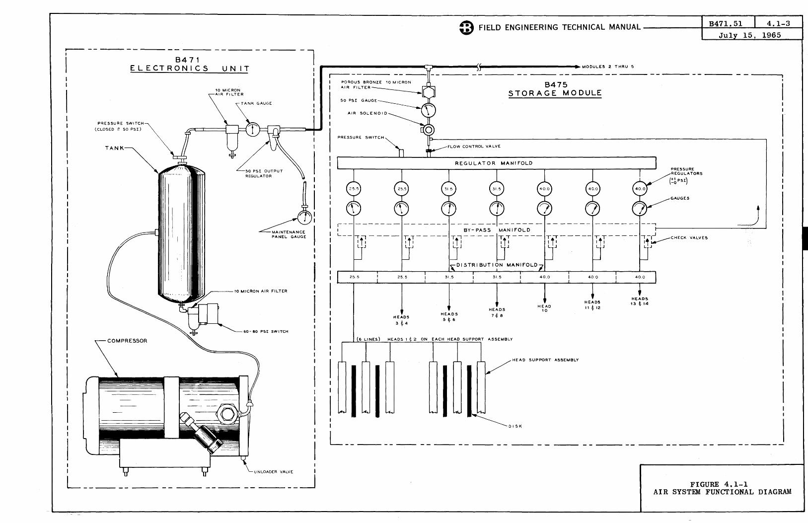
~ I
I
I I
8471 ELECTRONICS
PRESSURE SWITCH
(CLOSED::! 50 PSI)
TANK
COMPRESSOR
L ____ _
UNIT
10 MICRON IR FILTER
_--10 MICRON AIR FILTER
I I
---~
~ FIELD ENGINEERING TECHNICAL MANUAL _____ -+-__ B_..4;,.;.7.-1..;.. ...... 5_..1_L..o-....;;4,;.;. • ..;;;;,1_-3..;.....-....... Ju1 15, 1965
.............................. ~~ .. --------.(~~ .... --.. ----------------~MODULES 2 THRU 5
AIR FILTER
50 PSI GAUGE
AIR SOLENOID
PRESSURE SWITCH
25.5 25.5
HEADS
3 ~ 4
FLOW CONTROL VA LVE
8475 STORAGE MODULE
REGULATOR MANIFOLD
HEADS
5 ~ 6
HEADS
7 ¢ 8
2 ON EACH HEAD SUPPORT ASSEMBLY
HEAD 10
HEAD SUPPORT ASSEMBLY
~DISK L ________ _
PRESSURE EGULATORS
(:b PSI)
GAUGES
VALVES
FIGURE 4.1-1 AIR SYSTEM FUNCTIONAL DIAGRAM

CD FIELD ENGINEERING TECHNICAL MANUAL ____ -+-..... Biiioooi4 .... 7 ..... 1 ..... 5iioiiiiiiil ....... I' ........ 5 ..... 0 .. - ... 1---t February 1, 1965
INDEX - SECTION V
5 ASSEMBLY - DISASSEMBLY - ADJUSTMENTS
5.1
5.3
5.4
5.5
5.6
60-SO Air Switch ••••••••••••••••••••••••••••••••
Power Supplies ••••••••••••••••••••••••••••••••••
Relays ••••••••••••••••••••••••••••••••••••••••••
Fans ••••••••••••••••••••••••••••••••••••••••••••
Compressor Assembly • • • • • • • • • • • • • • • • • • • • • • • • • • • • •
July 1, 1964
July 1, 1964
Feb. 1, 1965
July 1, 1964
July 1, 1964
5.7 General Precautions for Air Connections ••••••••• July 1, 1964
5.11 Power Supply Adjustments •••••••••••••••••••••••• July 1, 1964
5.12 Variable Bias Adjustments ••••••••••••••••••••••• Feb. 1, 1965
5.13 Multi Adjustments ••••••••••••••••••••••••••••••• Feb. 1, 1965
5.21 60-80 Air Switch Check and Adjustment ••••••••••• July 1, 1964
5.22 Air Line Regulator Adjustments •••••••••••••••••• July 1, 1964
Printed 1n U.S.A.

~ FIELD ENGINEERING TECHNICAL MANUAL _____ +-_B_47_1_._5_1 _____ 5_._I_-I_--...t July 15, 1965
5.1 60-80 AIR SWITCH - REMOVAL AND REPLACEMENT
The following procedure should be followed for the removal and replacement of the 60 - 80 Air Switch.
Removal:
CAUTION
Refer to Section 5.7 of this Manual when working on the Air System.
1. Turn off the Electronic Unit DC and AC power. 2. Turn off the 70 amp main AC Circuit Breaker. 3. Bleed off the Tank pressure~ 4. Remove the cover from the 60 - 80 Switch. 5. Remove the leads, capacitors, and arc suppressor from the switch
terminals. Refer to Figure 5.1-1.
208VAC FROM FILTER L2(WHITE) 208V AC FROM FILTER L 1 (B~ACK)
FROM FILTER MOUNTING BRACKE T(GREEN)
0.0511f
TO COMPRESSOR FRAME(GREEN)
TO COMPRESSOR(WHITE) TO COMPRESSOR(BLACK) 208V AC
FIGURE 5.1-1 60 - 80 SWITCH CONNECTIONS
6. Remove the 60 - 80 Switch from the Air System plumbing. Use a 3/4" wrench to turn the Switch Assembly and a 9/16" wrench to' prevent the pipe nipple from turning. Do NOT remove the nipple.
Replacement:
1. Ensure the 70 amp main AC Circuit Breaker is off. 2. Install the 60 - 80 Switch on the pipe coming from the Tank Sed
iment Bowl. Use a 9/16" wrench to hold the nipple and a 3/4" wrench to tighten the Switch Assembly. Ensure the Switch is oriented with the Adjustment Spring at the top after the Assembly
Printed in u. s. A.
I

5.1-2
has been tightened. 3. Connect the leads, capacitors, and arc suppressor to the switch
terminals. Refer to Figure 5.1-1. 4. Install the cover on the Switch Assembly. 5. Turn the 70 amp AC Circuit Breaker on. The Compressor should
go on, pressurize the Tank, and go off when the pressure reaches 80 PSI.
6. Ensure there is no air leak at the pipe connection made in Step 2.
7. Refer to Section 5.21 of this Manual for the 60 - 80 Switch check and adjustment procedure.
8. Restore the Electronic Unit to normal operation.

{i) FIELD ENGINEERING TECHNICAL MANUAL _____ -+-_B_4_7_1~. _51_.a.-5_._3 -_1_---I
July 15, 1965
5.3 POWER SUPPLIES - REMOVAL AND REPLACEMENT
Power supply assemblies, Racks F, G and H, are removed and replaced in the following manner.
REMOVAL
1. Cycle down all power and open the 15, 50 and 70 amp AC circuit breakers.
2. Unscrew the two knurled bolts which secure the power supply assembly to the frame.
3. Slide assembly out until the terminal board on the base of the assembly is clear of the frame. Slack is provided in the power supply harness for approximately seven inches of movement.
4. Remove screws which secure harness to terminal board.
5. Remove and carry assembly by handles provided.
REPLACEMENT
To replace an assembly, reverse the above procedure.
Care should be taken not to drop or jar the power supplies. If the assembly is laid on its base on a work bench, a soft pad should be inserted between bench and terminal board to prevent damage to the plastic terminal strip.
Printed in u. S.A.
I

~ FIELD ENGINEERING TECHNICAL MANUAL _____ ~B __ 4-7 ..... 1-.-51=---!"I----5 ...... 4:...--=I___l July 15, 1965
5.4 RELAYS - REMOVAL AND REPLACEMENT
All relays in the Electronics Unit are mounted on the Power Sequence Panel, Rack E. Reference Figure 5.4-1.
REMOV AL AND REPLACEMENT
1. Before removing any relay, cycle all power down and throw AC circuit breakers off.
2. Remove protective shield from sequence panel.
3. DC contactor relays ECJO, ECMO, EDJI and EDMO are mounted to the panel with screws and weldnuts. Telephone type relays EFKO, EFJO, EFKI, EFJl and EFJ2 are mounted to a bracket with locknuts. All relays may be removed and replaced from the front of the panel without removing cables or harnesses.
4. Check unit for loose connections, fallen washers, etc., and shorts before replacing protective shield and applying power.
Prlnted ill u. S.A.
I

J
J
@ @ @ @
PANEL A RACK E
J
K
L
R
o
ECJO
.Ell:! I C.ND(COIL) 2 -24V (COIL) 3-4 -24I1lAC-ON-INI).) .2 -6 -24V(0(:ON-SW)
7 - 8 208VAC-A ( p, s.l 9-10 20811AC-B lP.S.)
D D
D D
o ECKO
K
2 4 5 6
I MOO. 51 RS.-F
D
PANEL PIN -'::-C; NO (SM0L) 2-MOO-5(SM0L) 3-MOD-4(SM0Ll 4-MOO-3( SM0Ll
M
J
K
L
M R4Dl ~
N
P
~ R~
@
o c
ECMO
-2411 (COIL) C.ND (COILl
3-4 -240(C.ATE-~ 5·6 C.NO(HOLO ECJO) 2
~:I~} +20 «(,ATE' MODS)
11-121_20 (C.ATE-MODS) 13-14/ I
!>-MOD-2(SM0~) 6-1.400- I ( SM0Ll
EeLO ~ r-,-----~~~------~'I-C.NO(SM0L)
IS'16 -4.511(;ATE-MOOS) 17-18 -24V (PICK EOMO)
o EDJO
~ PIN 1-208VAC-A
2-20811A(.-A
3-208I1AC-A
14-208I1AC-B
5-208VA('-B
6-208VA('-6
L
EDJ1 PIN .- GNO (COIL) 2 -24V (COl Ll 3·4 +10011
-6 -10011 7-8 -ll~OV
9-10 11-12 GNO(HOLO EeMO) 13-14 -24V(DC-ON-IND)
2
4 5 6
2-MOO-5 tSMIL) 3-MOO-4 (SMIL) 4- MOD-J (SMI L) 5-MOO-2(SMILl
o
K~':O ;'N~NO \SJI B, A
H -24V C COMMON
~ ! 1:::-:
~EDLO ~INJ
~ r-~FJ1-16 L B A
H EOMO-2 C EOJ I-I r J
o PANEL 0
EOMO PIN 1 C.NO (COIL) 2 -24Y (COl L)
-1 3'4 -12Y (GATE-MODS) 5-6 +1211 (C.ATE-WDS) 2
M 7-8 -2411 (PICK EDJ1) 9'10 GNO (HOLD [CMO)
L o EDMO~8
J r
--1- ~ LOc./REM SW L ECJO-6
~ 5 4-3 W FIELD ENGINEERING TECHNICAL MANUAL ------I~~~~ ........ 1--...1...,;;;,9--65----1
@ @
PANEL B
~ ~
~ ~
PANEL F PIN 0 EFJ2(FRONTl -1 4 5- 7 6-8
GNO. (COIL) (]) -24V. (R EM - OC- OFF) GNO. (OC-OFF-SW) GNO. (OC-OFF-SW)
2
3 ® ®
EFJO(6ACK)
EFJ 1 (M'IOOLE)
I 4 6-8 7-9
N
P
EFKl (FRONT)
-24V (COIL) C.NO (OC-OFF-SW) -2411 (DC-ON- SW) -2411 HOLD EFKl (])
(j) EFKO (BACK) --o
~,;o i'" ~-o,,-,w H EFJI-I3 C REM- DC-OFF I J o COMMON J I E EFKO-5
~EOPO ~I}FKO-I
~ ~ ~Fj1-4 B A H EFK1-8 C 0 I "'WVOC o C J AC-ON-5W E K
4
f5EOl E::J
~ ~
@
o PANEL E
EEJO
2 + 100\1 2
-10011 3
4 -12011 4
+1211 6
t1211 8
-12V 9
10 +20V 10
II -2011 II
12 12
13 -2411 13
14
15 ::;:E-OCT
N 14
15
16 REM. - DC -OFF 16 I
17 EMERC..-POW.-OFF I 7
I 18 POW-COMMON II!
19 -240 19
20 20
E EJ1
tl00V
-IOOV
-120V
GND
AC-ON-IN
LOCAL/REMOTE
OC-ON-SW
AC-ON-SW
AC-OFF-SW
AC-OFF-SW
DC-ON-IND
LOCAL/REMOTE
DC-L.O.-SW
20811AC-A
20I!VAC-B
AIR PRESSURE SW. I
AIR PRESSURE SW
~ ~:~~~~ .. --.. --------------~--------------..
OPPOSITE SICE
TYPICAL OF RELAYS ECJO, ECMO, EDJI ~ EDMO
WIRING SIDE
TYPICAL OF RELAYS EFK1,EFJO,EFJt a EFJ2
<DEl.!:! 1 5
3-4
7-6
®f.lli 1 4
7- 9 8-10
13-15 14-16
s..EAQ
-24V (COl Ll GNO (COIL) GND (AC-OFF-'SW)
GND (HOLD EFJO)
EFJ1
-24V (COIL) GND (OC-ON- SW) GND (SMtZlL) -24V (HOLD EFJ 1) -24V (PICK EFK1) GND (DC RELAYS)
~ @.e!!:!
1 GND (COIL) 4 -24V (COl L)
7 - 9 GND (PICK ECJO)
6-10 GND (HOLD EF ,)0)
@GNO TO P.S.-F E.U. MAINTENANCE PANEL, SEQUENCE PANEL RELAYS ~ 1.100.1 GATE E. BACKPLANE.
@C.NO TO P.S.-G, MOD.2 t3 GATE t MOD.2 BACKPLANE.
® C.NO TO P.S.-H, MOD. 4 E. 5 GATE t MOD. :3 BACKPLANE.
ill +12VDC TO GATE t SEQUENCE PANEL.
® GND TO MOD. 4 to 5 BACKPLANE E. E.U. BACKPLANE
FIGURE 5.4-1 RACK E COMPONENT LOCATOR
I

~ FIELD ENGINEERING TECHNICAL MANUAL _____ -t-_B_47_1_._5_1 ....... _5 ...... _5_-I_ .....
July 15, 1965
5.5 FANS - REMOVAL AND REPLACEMENT
Before removing fans, cycle down all power and open AC circuit breakers.
The two muffin fans located on the inside of the rear skin are accessible by removing the side skin and opening the logic gate. The fans are held to the rear skin by mounting clips with spring tabs which may be sprung apart with a screwdriver far enough to allow the fan to be removed from the clip. If complete removal is necessary, the two AC wires must be removed from the small terminal board below the fan.
PrlDtecllD u. S.A.
I

C) FIELD ENGINEERING TECHNICAL MANUAL _____ +-... B ... 4 ... 7 .. 1A.l1. 511(o111 ....... ......:5~.~6~-.. 1---1 July 15, 1965
5.6 COMPRESSOR ASSEMBLY - REMOVAL AND REPLACEMENT
The following procedure should be followed for the removal and replacement of the compressor.
REMOVAL
CAUTION
Refer to Section 5.7 for general precautions when working on the air system.
1. Turn off the E.U. DC and AC power.
2. Turn off the 70 amp main AC circuit breaker.
3. Bleed off the tank pressure.
4. Disconnect the output air line.
5. Remove the nuts (under the E.U. base) from the four compressor assembly mounting studs. Move the compressor for better access to the motor leads.
6. Disconnect the frame ground lead from the top of the compressor.
7. Remove the motor lead cover plate. The motor ground lead (green) is disconnected at the same time.
8. Disconnect the black power lead from the black motor lead by removing the "wire nut" and separating the leads. Separate the white leads in the same manner.
9. Remove the compressor assembly from the cabinet.
REPLACEMENT
1. Ensure the 70 amp main circuit breaker is off.
2. Place the compressor assembly in the E.U. cabinet but do not mount to the base at this time.
3. Pass the incoming black, white and green motor leads through the motor lead hole.
4. Connect the black power lead to the black motor lead using a "wire nut". Connect the white leads in the same manner.
PrtntecllD u. s. A.

5.6-2
5. Install the motor lead cover plate. The green motor ground lead must be connected at the same time with one of the cover plate mounting screws.
6. Mount the compressor assembly in the E.U. cabinet.
7. Connect the frame ground lead to the top of the compressor assembly.
8. Connect the output air line to the compressor output manifold.
9. Turn on the 70 amp main circuit breaker. The compressor should go on, pressurize the tank and turn off when the tank pressure reaches 80 pSi.
10. Ensure there is no air leak from the output air line to manifold connection before restoring the E.U. to normal operation.

B471,51 . 5:1' .. 1
I July 1 , 1964 ~ FIELD ENGINEERING TECHNICAL MANUAL ------------l~~:....=.&.~......a-.....:::;..:..:....,;;~ ......
5.7 GENERAL PRECAUTIONS FOR AIR CONNECTIONS
The following precautions should be observed when performing work requiring the removal and replacement of any air fitting and connection.
1. Turn off the E.U. DC and AC power.
2. Turn off the E.U. 70 amp main AC circuit breaker to de-activate the compressor motor prior to the removal of any air connection, except the snap-on type used on the S.U. air trunk line.
CAl1rION
Bleed off the tank pressure completely before disconnecting or opening any air connection, except the snap-on type. A convenient method of bleeding tank pressure is to "crack" loose the tank sediment bowl drain cock.
3. Whenever any air pipe fitting is disconnected, plastic sealant (PIN 11117165) should be used on the threads before replacement.
4. Polyethylene tube fittings do not require sealant. Refer to I Figure 5.7-1. These fittings should be tightened finger tight and then up to 1/2 turn with a wrench, if required.
Printed In U.S.A.
Do not overtighten or the plastic ring seal may be damaged.
BLACK POLYETHYLENE TUBING
l PLASTIC .,.G
FIGURE 5.7-1 POLYETHYLENE TUBE FITTING

5.7-2
5. Check for air leaks after any air fitting is reconnected and the System pressurized. Apply a small amount of liquid leak detector around the joint and then check for bubbles. Use a cloth to catch any excess liquid and wipe off the joint after the test.

C) FIELD ENGINEERING TECHNICAL MANUAL _____ ~B ..... 4 ... 7 .... ] ........ 5J"--..&.....:;.:5.:.;;1:.:1:...;-.:.1~1 July 1, 1964 _
5.11 POWER SUPPLY ADJUSTMENTS
RACK F
+lOOV, -lOOV, -120V and -24V
None.
RACK H
+20V and "'!"20V
None.
RACK G
+12V, -12V and -4.5V
The -4.5V may be adjusted by potentiometer R6 mounted on the face of the power supply rack.
Prlntecl1ft U.S.A.

C) FIELD ENGINEERING TECHNICAL MANUAL _____ ......... B .. 4 ... 7 .. l .... .a;.,~1-1 ......... 5 ...... 1;;;,:2:...--=1---1q I Febru!ry 1, 1965 _
5.12 VARIABLE BIAS ADJUSTMENTS
Before making the Variable Bias Adjustments, check the -4.5V supply. It must be -4.5V + O.25V.
The three VB supplies are adjusted as follows:
Printed III U.S.A.
MUVB-01 MUVB-02 VB
Word Mark Multi Bias BCLP Bias Flip-flop Bias
AAC6X2 AAA7X7 AAC1X2
-O.2V -O.2V -1.2V

~ FIELD ENGINEERING TECHNICAL MANUAL _____ t--_B;..;;;;4.;.,7_l._5_l;......&.....;5;;,.:.;.,;;;;1;.;;,3_-,:.l ....... July 15, 1965
5. 13 MUL--TI ADJUSTMENTS
Before making any of the following adjustments, check the -4.5V Supply. It must be -4.5V ± 0.25V. Then check the Variable Bias adjustments. Refer to Section 5.12.
1. LOCAL/REMOTE Switch to LOCAL.
2. CLOCK ON/OFF Switch to OFF.
3. Depress BIT SINGLE PULSE button for checking the following: a. IXHM (AA4N2) should be 2 microseconds + 0.1. Scope at
AA4UO, sync internal negative. -
b. RDHM (AC5A2) should be 32 microseconds + 5. Scope at AC5FO, sync internal negative. -
c. W0HM (AB6N7) should be 7.86 microseconds + 0.25. Scope at AB6U5, sync internal negative. Ground input to ASRS at AC7FO.
d. DIXM (BB1A2) should be 600 microseconds + 20. Set ACFF, INFF, BA2 and BA4. -Hold ACFF and BA2 ON or they will reset. Scope at AA9WO (DIXS/), sync internal positive.
4. Return LOCAL/REMOTE Switch to REMOTE. 5. Return CLOCK ON/OFF Switch to ON.
6. BITP/DBIT - Bit Pulse and Delay Bit Pulse multis are to be adjusted by observing the time delay between BITL and BCLP. The adjustment of these two multis is performed in the following manner:
a. Connect A trace to BCLP (AAB8JO).
b. Connect B trace to BITL-Ol (AAA6V2). c. Sync on BITL-Ol.
d. With ICFF false, the delay between BITL-Ol and BCLP should be 250 nanoseconds. Adjust at AAA6N7 (MUAJ) if necessary.
e. Hold ICFF ON. The delay between BITL-Ol and BCLP should be 675 nanoseconds. Adjust at ABAON2 (DCL) if necessary.
PrlDtecl in U.S.A.
I

C) FIELD ENGINEERING TECHNICAL MANUAL ____ ~t--B-4-7-l-. 5_1_1...0-5 ___ 2_1_-1---1
July 1, 1964
5.21 60-80 AIR SWITCH CHECK AND ADJUSnfENT
The 60-80 Air Switch has a built in 20 PSI differential between its actuated (points closed) and de-actuated (points open) positions. The switch is set by adjusting it to ACTUATE at the proper pressure.
The following procedure should be followed when performing the Check and Adjustment:
1. Depress the DC OFF Switch to retract the heads on the Module(s). 2. Depress the AC OFF Switch. 3. Loosen the Drain Cock on the Tank Sediment Bowl and slowly re
lease the air from the Tank. As the pressure falls, watch the gauge to determine when the switch actuates to turn the Compressor ON. THE COMPRESSOR SHOULD GO ON AT 60 ±2 PSI.
4. Tighten the Drain Cock on the Sediment Bowl and let the pressure build up until the switch de-actuates.
5. Repeat Steps 3 • 4 to verify the actuation point of the switch. 6. If the switch actuates at 60 ±2PSI, bring up Power and restore
the System to normal operation. If the switch is NOT actuating at the proper pressure, proceed to Step 7.
CAUTION With the 70 amp main AC and the 20 amp Circuit Breakers ON, 208VAC is present inside the 60-80 switch box.
7. Turn OFF the 70 amp main AC Circuit Breaker. 8. Remove the cover of the 60-80 switch. 9. Use a 11/32" spin-tight to turn the nut on the Adjustment Spring.
Tightening the spring raises the switch actuation point; loosening the spring lowers the actuation poiat. Turn the nut approximately one turn.
10. Replace the switch cover as a safety measure. 11. Turn ON the 70 amp main AC Circuit Breaker which applies AC
through the 20 amp Circuit Breaker to the 60-80 switch. 12. Begin this procedure again at Step 3.
Printed in u. S.A.

~ FIELD ENGINEERING TECHNICAL MANUAL _____ I--B-4-7-1--5_1_10..00.-5 ___ 2_2_-1--1\ July 1, 1964 _
5_22 AIR LINE REGULATOR ADJUSTMENT
The Air Line Regulator is set to maintain 50 PSI +2 -0 on the Air Trunk Line as indicated by the Maintenance Panel Air Gauge.
Adjustments are made by turning the screw at the bottom of the regulator in or out to increase or decrease the pressure, respectively.
While under pressure, the regulator does not respond accurately to manual adjustment intended to lower the pressure of the output. Therefore, to make that adjustment, it is ~ecessarJ to de-pressurize the input, back out the Adjustment Screw, re-pressurize and increase the pressure output to the proper operating point.
The following procedure should be followed when making adjustments on the Air Line Regulator:
1. Turn OFF DC to retract the heads in the Module(s).
2. Turn OFF AC. 3. Use a 1/2" wrench to loosen the Lock Nut on the Adjustment Screw. 4. To INCREASE the pressure, turn the Adjusting Screw IN until the
Maintenance Panel Air Gauge reads 50 PSI +2 -0. Turn the screw slowly to prevent regulator overshoot. An offset screw driver is useful as an adjustment tool. I
5. To DECREASE the pressure, perform the following Steps. a. Turn OFF the 70 amp main AC Circuit Breaker. b. Bleed off the Tank pressure by loosening the Sediment Bowl
Drain Cock. Retighten the Drain Cock. c. Back out the regulator Adjustment Screw one or two turns. d. Turn ON the 70 amp Circuit Breaker. e •. When the Tank pressure has been in the normal operating
range for five minutes, slowly increase the pressure to 50 PSI +2 -0 by turning the Adjustment Screw in. Check the pressure at the Maintenance Panel Air Gauge as the adjustment is being made.
f. To ensure the adjustment has stabilized, re-check the pressure output approximately five minutes after performing the adjustment.
8. After the adjustment has been completed, tighten the Lock Nut on the Adjustment Screw.
PrlDtecllll U.S.A.

o FIELD ENGINEERING TECHNICAL MANUAL ____ -+-..IiiIIBI,3.47 ..... 1 .. :&51 ....... ,..LI...I6w..¥O-:.Il~_I February 1, 1965
INDEX - SECTION VI
6 MAINTENANCE PROCEDURES AND AIDS
6.1 Weekly Preventive Maintenance •••••••••••••••••••
6.2 Monthly Preventive Maintenance ••••••••••••••••••
6.3 Quarterly Preventive Maintenance ••••••••••••••••
6.4 Semi-Annual Preventive Maintenance ••••••••••••••
6.5 Annual Preventive Maintenance •••••••••••••••••••
6.6 Signals and Test Points •••••••••••••••••••••••••
6.7 Maintenance Panel •••••••••••••••••••••••••••••••
6.8 Test Routines •••••••••••••••••••••••••••••••••••
6.9 Component Locations •••••••••••••••••••••••••••••
6.10 Control Simulator •••••••••••••••••••••••••••••••
6.11 RIN Index ••••••••••••• ~.- •••••••••••••••••••••••
PrlIlted ID u. S.A.
Feb.
Feb.
Feb.
July
Feb.
Feb.
Feb.
Feb.
1, 1965
1, 1965
1, 196.5
1, 1964
1, 1965
1, 1965
1, 1965
1, 1965
I

~ FIELD ENGINEERING TECHNICAL MANUAL _____ t--=B=--=4=..;.7 ... l.a.,::. 5::;.;;~~........::6w ... 2 ..... - .... 1---l1 Jul~ 1 t 1964 _
6.2 MONTHLY PREVENTIVE MAINTENANCE
1. FILTER
There is one fiberglass disposable filter located at the bottom front of the unit. It should be checked frequently and changed at least once a month or when necessary.
Since the filter is readily accessible by removing the front skin, power need not be dropped from the unit or normal operation interrupted during changing.
2. POWER SUPPLIES
3.
Power Supply output voltages should be checked on a monthly basis. Test jacks are provided on the power supply assemblies for all voltages.
Rack H
+20V ± IV
-20V ± IV
Rack F
+IOOV ± 5V
-lOOV ± 5V
-120V ± 6V
-24V ± 1.2V
Rack G
+12V ± .5V
-12V ± .5V
-4.5V ± .2V
PRESSURE TO AIR TRUNK LINE
The pressure applied to the S.U. air trunk line should be 50 psi +2 -0. This pressure should be checked at the air gauge on the
Prlnted III U.S.A.
I

6.2-2
Maintenance Panel. If the pressure is not within tolerance, perform the output regulator adjustment procedure as outlined in Section 5.22.
NOTE
Whenever the tank pressure has been released and then re-pressurized, always allow approximately five minutes for the regulator to stabilize before taking a reading.
4. TANK SEDIMENT BOWL
The Tank Sediment Bowl should be removed and cleaned. The amount of moisture which collects in the bowl will vary with the environment and how often the compressor runs. Do not allow the bowl to become more than approximately 1/3 full of water. Use the drain cock to empty the bowl as needed between P.M. periods. (Have a large absorbent cloth available to catch the moisture when the drain cock is loosened.) The following steps should be performed when the Sediment Bowl is removed:
a. Turn off DC and AC power.
b. Turn off the 70 amp main AC circuit breaker.
c. Loosen the drain cock to discharge the tank and relieve the pressure on the bowl retainer ring. Use an absorbent cloth to catch the moisture.
d. Unscrew the large retainer ring which holds the bowl to the metal part of the assembly.
e. Remove the bowl and clean by wiping it out with a lint free cloth.
f. Replace the bowl by reversing the above procedure. Do not over tighten the retainer ring. Turn on the 70 amp circuit breaker to pressurize the tank and check for leaks before DC and ACpower are restored. Apply liquid leak detector around the bowl at the retainer ring and watch for bubbles. Wipe off any remaining liquid after the test.

C) FIELD ENGINEERING TECHNICAL MANUAL _____ +-,;;o,B ..... 47 .... 1-..._5_1 ........ ........;:6;.&.-=2....;-3~__1 February I. 1965
5. 60-80 AIR SWITCH
The 60-80 Air Switch should maintain tank pressure between 60 and 80 ± 2 pSi. Check the operation of this switch. Refer to Section 5.21 for the check and adjustment procedure.
6. VARIABLE BIAS
On a monthly basis, the three VB packages in the E.U. should be checked for proper output level.
Test point and desired output are as follows:
MUVB-01 MUVB-02 VB
7. MULTIS
Word Mark Multi Bias BCLP Bias Flip-flop Bias
AAC6X2 AAA7X7 AACIX2
-0.2V -0.2V -1.2V
Verify mu1tis for proper timing. Refer to Multi Adjustments, page 5.13-1.
Printed in u. S.A.
I

~ FIELD ENGINEERING TECHNICAL MANUAL _____ +-..... B~4::;.;7_=1 .... _5l:.....l~.;;,6 ..... 4.:.;-;;.:;:1=---1 Februarv 1, 1965
6.4 SEMI-ANNUAL PREVENTIVE MAINTENANCE
1. COMPRESSOR FILTER
The intake filter on the compressor should be replaced semiannually. Unscrew the filter from the brass elbow on the intake manifold and replace with a new filter.
Printed in U.S.A.
I

C) FIELD ENGINEERING TECHNICAL MANUAL _____ ...... B-4-7-l-.5-l-I ...... 6-.... 5---l ---l
February 1, 1965
6.5 ANNUAL PREVENTIVE MAINTENANCE
1. 10 MICRON AIR FILTER
The 10 micron filter element should be replaced annually. The following procedure should be followed when replacing the element:
a. Turn off DC and AC power.
b. Turn off the 70 amp main AC circuit breaker.
c. Bleed off the tank pressure by loosening the drain cock on the sediment bowl.
CAUTION
Do not use the drain cock on the 10 micron filter to discharge the tank even when the element is being replaced. Contaminants which normally are trapped in the sediment bowl are apt to be forced into the filter assembly.
d. Unscrew the retaining ring which holds the bowl to the assembly. Remove the bowl. Refer to Figure 6.5-1.
e. Remove the brass, knurled retaining nut at the bottom of the I shaft.
f. Unscrew and remove the baffle.
g. Remove the shield, washer and filter element.
h. Install the new 10 micron element by reversing steps e, f and g of the above procedure.
i. Wipe out the filter bowl with a clean, lint-free cloth.
j. Replace the filter bowl. Do not overtighten the retaining ring.
k. Turn on the 70 amp breaker to repressurize the tank and check for leaks before restoring AC and DC power. Apply liquid leak detector around the top of the bowl and then watch for bubbles. Wipe off any remaining liquid after the test is completed.
Printed 1n U. S.A.

6.5-2
2. FANS
"0" RING --_ ...... dl BOWL RETAING RING
SHIELD---_ .... J:t-I-+M----10MICRON POROUS
BAFFLE
PLASTIC BOWL ----\
DRAIN COCK
FIGURE 6.5-1 10 MICRON AIR FILTER
BRONZE ELEMENT
WASHER
RETAINING NUT
The two cabinet exhaust fans located on the inside of the rear skin should be oiled annually using the following procedure:
Oil Oil injector
EDD Part #11838596 EDD Part #11838588
a. Remove air from oil injector by holding the needle up and pressing on the plunger.
b. Project the injector needle through the louvres (in back skin) and place the needle at the center of circle marked on the gold label.
c. Position the needle at an angle of approximately 450 to the label surface and point it toward the center of the rubber cap. (These fans are lubed by inserting the oil injector needle through a self-sealing rubber cap located in the center of the motor hub.)
d. Pierce the label and the concealed self-sealing rubber cap located under the label.
e. Insert the needle approximately 1/4".
f. Depress the plunger of the oil injector approximately 1/16" to force the oil to flow. Rotating the fan will relieve air pressure and allow oil to flow into the oil chamber.

C) FIELD ENGINEERING TECHNICAL MANUAL ____ --+ ___ B __ 4_7l_._5_l ____ I ___ 6_.6_-_l_~1 July 1, 1964 ,.
6.6 SIGNALS AND TEST POINTS
The following is a list of signals with test point locations. The listing includes input levels as monitored at the output of the input switches, output levels as monitored at the last output switch or driver and internal levels as monitored at the outputs of Flip-Flops, Multi's, Delays, etc. HSDL (Information Center Tap Driver) outputs are not covered in this list; refer to DA Schematics, pages 00.07.0 through 00.16.0.
INPUT LEVELS FRCIt D.F.C.U. OUTPUT LEVELS TO D.F.C.U.
Level Test Point Level Test Point
DOlS AAA9C4 SRIL AAC2B7 D02S AAA9CO SR2L AAC2H5 D04S AAA9D2 SR4L AAC2H9 D08S AAA9H4 SR8L AAC3B7 D16S AAA9JO SRAL AAClB7
SRBL AAClH5 ZDIL/ AAB9C9 z02L/ AAB9C5 CSlL/ AABOBO Z03L/ AAB9D7 CS2L/ AABOFO
TOlS ACAlC9 SCLP AACIH9 T02S ACAlC5 T04S ACAlD7 SURL/ AAA4R5 T08S ACAIH9 TlOS ACA4C9 SARL/ AAC8C9 T20S ACA4C5 T40S ACA4D7 SWLL AAA4H4
SWlL/ AAB2C9 WdtfD AAB6H5 SW2L/ AAB2C5 SW4L/ AAB2D7 INXD AAA4B2 S1f8L/ AAB2H9 SWAL/ AAB2J5 SWBL/ AAA2R9
DFSS ACA4H9
SWRS AAA2R5
SC0L AAA2V9
Printed in u. S.A.
I

6.6-2
OUTPUT LEVELS TO STORAGE MODULES INPUT LEVELS FR<»f STORAGE MODULES
Level Test Point Level Test Point
Mf(jIL ABBOP7 HFML-Ol AAA8C4 M02L ABBOV5 HFML-02 AAA8CO M03L ABBOV9 HFML-03 AAA8D2 M04L ABBIP7 HFML-04 AAA8H4 Mf(j5L ABBIV5 HFML-05 AAA8JO
DISC-OI/ AAA9R4 BITL-O1 AABOR3 DISC-02/ AAA9RO BITL-02 AABOS3 DISC-03/ AAA9S2 BITL-03 AABOT3 DISC-04/ AAA9V4 BITL-04 AABOU3
BITL-05 AABOV3 Z01L-Ol/ AAB9C9 ZftJ2L-OI/ AAB9C5 TDIL AABOR4 Z03L-Ol/ AAB9D7 TD2L AABOS4
TD3L AABOT4 DFSL/ AABOYO TD4L AABOU4 DFSS ACA4H9 TD5L AABOV4
SUlFW AABIU9 CSIL/ AABON4 SUIFW/ AABlU6 CS2L/ AABOP4
ICFF-IB AAA5W9 ASRS AAC7D2 ASRS/ AAC7H4
WRSD/ AAB6B7 IRAS AAC7C4
SPFD AAA4HO IRAS/ AAC7CO
IXHS/ AAA4R9
TRSL/ AAC8J5
GSSL AAB9H9
INTERNAL LEVELS
Level Test Point Level Test Point
ACFF AAAlU9 GLAF AAC4U9 ASRS AAC7D2 GSLF AAC5WO BAIF AAB9U9 GSSL AAB9H9 BA2F AAC9F9 TRSF AAC3U9 BA4F AAC9U9 W0HF AAB7F6 CBAS AAC8C5 BCLP AAB8JO CSUS AAA2W5 BITP AAA6W5 DBIT ABAOW3 INXP-Ol AAA3V4 DID ABBIFO RIHS/ AAC8U7 DIXP AAA3S4 RDHM AAC5FO ECCS AAC8H9

en FIELD ENGINEERING TECHNICAL MANUAL ____ ~ ......... B __ 4--7-l-..-5l~ ....... 6-.-7---l___l J"ulY 15 , 196Q-
6.7 MAINTENANCE PANEL
Reference Figure 6.9-2.
The Maintenance Panel (Rack D) consists of switches, indicators, indicator-switches and test jacks for power control and maintenance functions. A DC meter with switch, power on time meter and air pressure gauge are also provided.
POWER CONTROL
Switches
DC LOCKOUT
MAINTENANCE
Switches
LOCAL/REMOTE CLOCK BITP (PB) WIMP (PB) CLEAR (PB) RESET (PB)
Indicator-Switches
S.U. Register INFF - Index FF ACFF - Action FF
Indicators
AC ON DC ON RELAY SUPPLY ON
Indicators
Storage Units 1 through 5 Not Ready
Test Jacks
INXP - Index Pulse SWlL - FERL (S04F) during Read SC0L - Segment Coincidence ACFF - Action FF ICFF/- Interlace Control
ICFF - Interlace Control FF GSLF - Gain Select FF SPFF - Space FF BAl, BA2 and BA4 - BA Counter TRSF - Threshold Store FF GLAF - Gain Latch FF
Printed in u. S.A.
I

6.7-2
LOCAL/REMOTE SWITCH
Reference Figure 6.7-1.
Remote
Local
1. Couples REM-DC-ON-E pulse from D.F.C.U. to Rack E.
2. REMS-A true to Gate A enabling ready levels (HFML-nn) from Modules to control SURL/ (Storage Units Ready Level) when CLOCK switch is ON.
3. REMS/ false to CAG 107 disabling Bit and Word Mark Single Pulse switches.
1. Opens REMOTE DC ON line to Rack E. DC can be cycled on from operator's panel only.
2. REMS-A false to Gate A making SURLI true (Storage Units Not Ready).
3. REMS/ true to CAG 107 enabling Bit and Word Mark Single Pulse switches.
CLOCK SWITCH
On
Off
1. CCIL-A true enabling ready levels (HFML-nn) from Modules to control SURLI when in REMOTE.
2. CCIL-A true to clock logic enables BITP and W~P to be generated from Module inputs (BITL-nn and ASRS).
3. CSIL-A false to CAG 107 disabling Bit and Word Mark Single Pulse switches.
1. CCIL-A false making SURL/ true (Storage Units Not Ready).
2. Disables Module inputs (BITL-nn and ASRS) from generating BITP and W~P in clock logic.
3. CSIL-A true to CAG 107 enabling Bit and Word Mark Single Pulse switches.

LOCAL/REMOTE SWI TCH (SHOW N I N REMOTE)
01.08.0 - 4 5V ....
: ~ Ir ------------------------O :
...J... I "-~ REM-DC-ON-E _ ~
~
o
.... LOC-REM-DC-ON
CLOCK SWI TCH ( SHOW N I N ON )
01.08.0 ...L.------........... ~'" .--___ ---"C;.;:C;.;:E;,.:L=--..,;:C"--,J ~
I p-__ S~C~E=L_-~A~~~__ :
I"
CSIL-A
CCIL A
R1A
00.25.1
R2A
00.25.1
--a. YSB
--~ 00.25.1
YSB --r-+
00.20.1
~ ________ ~ ______ I ... ~~S~W __ ~~~------..,;:S~U~R~L~/~~.~ 1 00.36.0 •
SHUNT AND lA
C) FIELD ENGINEERING TECHNICAL MANUAL ____ --+--=B..:.4:'7~1~ • ..:.5=__1~16;:;..::.:..;.7_-;;..3___1 February 1. 1965
YSB
(COMPONENT STI CK)
00.36.0 r---------------------------------------~.r__ -I A -N r\
r SW
1 00.25.1
CAG 107 R3A
~ WSPS-A
10 WSPL- 01
WORD SI NGLE 00.25.1 PULSE SWITCH
01.08.0
--'-WSPS-N.O. I ~ ...., I I I
WSPS-N.C. I I ~ -
~ BSPS-A
10 BSPL- 01 -
BIT SINGLE 00.20.1 PULSE SWITCH
01.08.0
--1-BSPS-N.O. I ~ ,., I I I
BSPS-N.C. I I -
-4.5 V CLOCK LOGIC BITP ..
REFERENCE D.A. SCHEMATICS;
00.20.1 W¢MP
OUT-1 6.81 K
B-P I"\..
I _I
I -"1
I .-J
00.25.0
00.25.1
_ ..... ...:..:...:.-!!!.!::'-.!..!.!..!._---If - ~ - -.--.. HfML-nn _
BITL-nn
M(llnL
RIHS/
ASRS
TERMS
REM- DC-ON- E
HfML-nn
REMS-A SURL/ ASRS
RIHS/
BITL-nn
CCEL-C
SC EL-A
SCIL
CC!L-A
WSPS-A
WSPL-01
WSPS-N.O.} WSP5-N.C.
BSPS-A BSPL-Ol
BSPS-N.O.} BSPS-N.C.
SPBL-01
M0nL
WII'MP
BITP
I SPBL-01
.. OUT-2
OUT-3
1101-3
GN 0
IN-l
IN-2
GND
OUT-4
DEFINITIONS
REMOTE DC ON PULSE fROM DfCU VIA RACK "E"
READY LEVELS fROM MODULES
REMOTE LEVEL STORAGE UNITS READY LEVEL
ADDRESS READ SWITCH
READ INHIBIT SWITCH
BI T LEVELS FROM MODULES
CONTINUOUS CLOCK ENABLE LEVEL
SINGLE CLOCK ENABLE LEVEL
SINGLE CLOCK INHIBIT LEVEL
CONTINUOUS CLOCK INHIBIT LEVEL
WORD SINGLE PULSE VOLTAGE LEVEL
WORD SINGLE PULSE LEVEL
WORD SINGLE PULSE SWITCH
BI T 51 NGLE PULS E VOLTAGE LEVE L
BIT SINGLE PULSE LEVEL
BIT SINGLE PULSE SWITCH
BIT SINGLE PULSE LEVEL
MODULE SELECT LEVEL
WORD MARK PULSE
BIT PULSE
6.81K ,. C-R ..., "''''
5.51 0-5 ... ...."'''''''
.. !.!I. E-T : .. 'V. I f-U
TYPE 11
H - Y ~cr----__i ..... -·~------__. - .... . J - W 1"\..U-_____ 04.1~.~2~1~K~----.
......
4.22K
K - XO-~-----~ .... W"'''' .. ''' .. ------..
L-y ~~ _________ J
FIGURE 6.7-1 MAINTENANCE PANEL SWITCHES
AND LOGIC

C) FIELD ENGINEERING TECHNICAL MANUAL _____ +---B_4_7_l ..... _5l_..a..-_6 ..... 8_-_1_-4\ February 1, 1965 _
6.8 TEST ROUTINES
The following are the Test Routines available for use with the Disk File Subsystem and a brief description of their use.
B200 - TR 2122
B5500 - TR 5561
Printed in U.S.A.
This routine will test the subsystem under the control of the B200. The operator has control of the program section to be run by use of the Operator's Panel. The routine is made up of eight sections and will test any and all subsystem configurations and character options.
This routine will test the subsystem under control of the B5500. The operator has control of the program section to be run by the use of the Supervisory Printer. The routine is made up of three sections and will test any and all subsystem configurations and character options.

~ FIELD ENGINEERING TECHNICAL MANUAL _. ____ ~ ___ B4--7 ...... 1 ..... --5--1---.......... 6 .......... 9--1---__t July 1. 1964
6.9 COMPONENT LOCATIONS
1. ELECTRONICS UNIT DA RACK LOCATOR - Figure 6.9-1
2. ELECTRONICS UNIT RACK D DETAIL - Figure 6.9-2
3. ELECTRONICS UNIT RACK A COMPONENTS - Figure 6.9-3
4. ELECTRONICS UNIT POWER SUPPLY COMPONENTS - Figure 6.9-4
Printed in u. S.A.

6.9-2
FIGURE 6.9-1 ELECTRONICS UNIT DA RACK LOCATOR

o FIELD ENGINEERING TECHNICAL MANUAL _____ +----B_.,4,;;;;..;7 .... 1 ...... ._.5_.1..--___ 6,&,.;. 9 ... -..,;;3 __ -1
December 1, 1964
Qb 1 2 J 4 5
©©©©© foTORA"E UNITS NOT READY
AC DC RELAY SUPPL'I
000 CLOCK DC
ON NORMAL REMOTE
~ ~ ~ OFF LOCKOUT LOCAL
@'~DITP SINGLE _@:oOMP
M - PULSE
CLEAR@ @RESET
SU REGISTER
eO 0 INFFO ()sPfP'
... 0 ~F
'0 ACFFO 0llA2
40
ICFFO 08Al
2 0 Oc SLFO ~SRF
RACK D PANEL A
- o'lTzT3T4 -
K.~ e e e e - T
PANEL B
IRO OIW ~
Printed in U.S.A.
INlCP@ ~SCOL
SW1L@ @ACFF
@iCff
_~~~-20 :'~~5 S -120 +12
AIR PRESSURE
OFf +20 ..,100
~:. (;)0 ~: 4 0 0 4 0; + _ 5
FIGURE 6.9-2 ELECTRONICS UNIT RACK D DETAIL
I

DR 9
M~4 0
M" 5 0
M U J
OI'ltM
(
OCL
I 8 I T CLOCK DE LAY
DR - I)
MI1H 0
M-'2D
M~3D
SW- H
ZIIJ15 01
Z12I25- 02
SW-H
Z/!I1S-0l
zihs-ol zihs-Ol
GS5L
F F - 7
BAIF
F F - 7
BA2F
SW H 0015
D025
D045
D08S
D16S
5W-H
5W H
II~ HFt.AS-Ol HFMS- 02
HFMS- 03
HFMS- 04
H Ft.AS- 05
SW- H
~ r~:r::r:ll:tll:::::::}:1 OSL SOl
OSLS-02 OSLS-02
DSLS-03 DSLS-03
OSL5-04 [:::: DSLS-04
OIxS [:::: INHS
SW-H
SARS
CBAS
RIHS ECCS
T R5S
MUAJ
BCLP
ORIN
SU R 0
VB
MUVB 02
1
F F - 7 ~:::
ORAN
SRIL
5 R 2L
5R3L
SR4L
SR5L
MUFW
BIT P
DR-9
WRSO
W~MD
g) FIELD ENGINEERING TECHNICAL MANUAL ____ -+-..;;:B--.4-..71:;:;;;..&",;;;5;;.;;1-........ 6 ........ 9--... 5---t Februar 1 1965
At.AFF SW H
I C F F - 0 1 il111: (: I X H 5 I C F F 0 1 ;:::;. SU R 5
:;::: S PBS - 0 1 1:1:::::::K::ti::;:::::f::::~::.:::J S PBS - 0 2
W~HS
FF-7 FF-7
SUC F SU AF
DR - I)
INXO S P F 0
SWLO
OU 1
IXHM
3
F F - 7
5U4 F
F F - 7
INFF
SW-H
SW8S SWRS
SC /!IS SCUB
5W-H
SW1 S SW2S SW4S SVV8S SWAS
FF-7
ICFF
F F 7
A CFF
F F - 7
SU IF - R
II! C 5 0 LOCKOUT PANEL CABLE
(
C50
t.AAINT PANEL CABLE
CSO
~AINT
PANEL CA8LE
CSO
c.-----~~----~------+-----~~-----*~ F F - 7
BA4F
F F - 7
,"5LF
S W - 1'1 5 W - H t:::: s W - H 1:: I}: 5 W - H .:~ S W - 1'1 5 W - H
H'S'i'S'=To H"S"FS'=Oo it T 1 os !r: H SUS - 05 1'15 U 5 -00 T 0 I S
~ HSTS-l0 T205 H5US-06:::::::::: ~ T025
~ ~ T40S ~7 ~ T04S
eso POWER
C'-'BLE
A ~------~~~~------~
iii! D RCH
r __ -1 __ ~~~-l~~~ __ Jl~ __ ~ __ ~~~r--Jl-__ ~ __ -J~~~ __ -1JH~st;S~-~8~0~@t~]J~~~H~S!!TS~-~3~OLJi.l~~ilitilll __ ~D~F~S~S~-t~~JlJJ~H~S~U~S~-iO~8tj~}1Ji~Jl~-1£H~S~U~S~-~0~3~~JJ©l::tt:::il __ ~T~0~&~S~-t~~~j?~:~ ____ ~t4 ________ -l A '=' HSTS-I)O HST5-40 H5US-09It~[::1:::::~:::~ HSUS-04 t::::
DR C H 11111 0 R e HID R C 1'1 DR e 1'1 l::::l:;::K:} 0 R C H 0 R C H 0 R C H 0 R e H 0 R C H;:;:; DRCH
HSDD-90 H50D-91 H50D- 92
ORCH
HSOO-93 H50D-94 HSDO-95
1'1500-&1 H50D-82 H~OO- 83
ORCH
H50D-&4 HSOD- 85
H5DD-72 ::: HSDD-63 HSDD-54 HSDO-45 t:;K;t::~ HSDD-36 H5DD-27 H5DD-18 1'1500-09 HSOO-OO HSOO-73 HSOO-64 HSOO-55 HSOO-46 MSOO-37 HSOO-28 HSOO-19 HSOO-10 HSOO-Ol
H$D 0-1' H5 0 0- " H 500-" H500-41 t""'" HSO 0- ,. !rn:m HSO 0- 2·I!i::!:!: H500- Z 0 [tnt! H500-" 1'1'1 H500- OZ ~h;
ORCH
HSDO-75 1'1500-76 HSOO-77
~+--+------~~~--~------+
H:DROC:66 f !. HSOO-67 H~1D0-6e
DRe H
1'1500-57 HSOO- 58
ORCH
HSOD-48 HSOD-49 HSO 0- 50
ORCH
HSOD-39 HSOD-40 H5DD-41
ORCH
MSOO-30 ~ilii~iH HSOO-31 H500-32
DRCH
HSDO-21 HSOO-22 MSOD-Z3
DRCI'l
H500-12 HSOO-13 MSOO-14
DRCH
HSOD-03 HSOO- 04
HSDO-05
CSO
MEAD SELECT CA8LE II·roo
-"
B t-M-5-0D-R-~-_H-9-9~HS~~~:~C::~6~~H~:~0~RO~~~:~7~[jlliitillhlI~~H:::~:~~~_H~7~8~rttl IH::D~:9 HSD 0- 97 HSO~ 88 ::::I:::::t:::::1 MSOO- 79 HSOO- 70
"500-.. H500-•• III.1 H 500- 00 1ft"""" I.: HSOO- 11
ORe 1'1
H500-60 HSOO-61 HSOO-62
III ORCH DRCH ORCM DRCH ORCH ORCH ,,*,.·:;r-·I~"'---C-5-0--+---C-5--0---I B
HSOO-51 1'1500-42 t1500-33 ·;lJf=j HSOO-24 MSOO-15 MSOO-06 HEAD MEAD
HSOO-52 1'1500-43 HSOO-34 1'1500-25 (i!i!lj!j!li!jil HSOD- 16 l~iiiiEilljli) MSOO-O 7 SE LECT SE LE CT
H500-S' JIIIiII ...... A.H.S.0.0.-.4.4 .. JIIIIIl. ~~ .. ~H_s_0_0_-_3_5 ... I .. ili .. ~1~ .. ~H_s_0 .. 0_-_2_6_ .. rili~fl~~1~ __ ~H_S_0_D_-.l_7~I~t~~llit .. M .... _H_S_0_0_-_0_8 .... ~ ..... ~~~I .. C_A.8_L.E .. ~_C .. A.8_L.E ...
FIGURE 6.9-3 ELECTRONICS UNIT
RACK A COMPONENT LOCATOR
I

a::
(\J
CO I-
ID I-
0 ~;1 z '" .:>
... ,.,
CD, U C\I «
u «
10
co 0
'" z I- ~
S'
::
~
...
Ul
CDl 0
z '" ~ «~ u ':2 «
11.
.., _ '" m
0 .... 00-00 10
'" :! « u
" ~ z Z
o;r j
I-
C\J ° ° ° O~ 0 ''l 10 9!_ 0 00
'" ~ '::
(\J 0
I- m Z ~
e :: ,., I\J
l-u C\I « ~ u «
0 ° o 00 <I' GO ~ ~
0 ,.,
U ('f) a:: a:: !--Uo b 0
C\I
0 r--
____ ,0
, I -, L _______________ J~
POWER SUPPLY
:!: 1 00, -120 t 24VDC
FAJO
PIN I
2 3 4
5
8
9 10
=
+ 100voe (0.17 AMP)
- 100VOC (0.11 AMP) - 120VOe {0.05 AMP) - 24VOC (3.5 AMP) GNO
AC} Tl AC
AC} T2 AC
~I:~oc@ 000 ",OmO ... O
an ,.... = - - t\I
~a:: ! ~ ~ 'f 10 9 a.. OW
~: ~ 0 1-1- r-I-Z
ow IU
CDU 0'0 0 Ll)
C\I m ~ ~ i\j CO ('f)<;T l-COin I-r- I\J 10 a
'" -0-01> 0 0
~ 0 I-I- 0... 00 CDI-..... (\J
COlD 1-1-
m FI ELD EN GIN EER I NG TECH ~ I CAL. MA N UA L ------t--=-=;..:..:..:....:.:=--..a.-~6.&..9:;:..;-;;;..:7i....____1 Ju1 1965
10
'" 0
I- m Z .:>
~
:: ~
C9
POWER SUPPLY
! 12 ~ -4.SVDC
GAJO
PIN 1
2 4
5 6
7 8
= + 12 VOC (.25 AMP)
-12VOC (10 AMP) -4.5VOC(2 AMP)
GNO -to 2.0VOC
AC}Tl AC
0
z '" .:>
o;r
t")
~ C\I
U _
«
II: 0 I-V « ll. « u ~ z Z ~ l-
j:
ID ....
0 t\I ... 0 10 CI 0 o 0 0
(\j
In r-
0 0 0 0 - 1"1 oil ....
0
10
0 t")
co ....
9
II: o !:::: u « IL « u
" z Z :I I-
v 0
:: go §O ~
~ '" u _ «
U")
tD
r-------- ____ -,0
I I :i L-------------...1I
~OWER SUPPLY
:t20VDC
PIN 1 2 3
8
HAJO
+20VOC (1 AMP)
-20VOe to.S AMP) C.NO
Ae} Tl AC.
FIGURE 6.9-4 ELECTRONICS UNIT
POWER SUPPLIES COMPONENT LOCATOR
I

~ FIELD EN GIN EE R I N G TECH N I CA L MAN U AL _____ t--B-.4.;.;..;7;...;;1;.;. • ..;;.5.;;;.1--&.1...;.6..:., • .;;;.;11;:..-..:;:1::"""-1 February 1, 1965
6.11 RIN INDEX FOR DISK FILE ELECTRONICS UNIT 11980224
INSTALL. RIN TIME IN PRE- UNITS NO. HOURS REQUISITE AFFECTED DESCRIPTION
4802 0.5 None 103 ~ 127 Undervoltage fail sensor pkg. improvement.
4804 1.0 None 103 =+ 127 Compressor sw. sup. network improvemen t •
4807 2.0 None 103 + 127 Compressor line shield & filter improvement.
4809 0.5 None 103 =+ 127 -20V supply fuse change.
4812 2.5 None 103 + 127 Document update & wiring com-patibility change.
4823 0.5 None 103 =9 127 E.U. Backplane noise reduction.
Printed in u. S.A.

~ FIELD EN GIN EE RING TECH N I CA L MAN U A L _____ -+-_B:::;.4_.7 ..... 1-.:.;..;;;;5;.,;;1___.......;6;;..:.:..,;;1;.:;;;;1:.--.;;.,3---1 February 1, 1965
RIN INDEX FOR DISK FILE 60 CYCLE POWER KIT 11106739
INSTALL. RIN TIME IN PRE- UNITS NO. HOURS REQUISITE AFFECTED DESCRIPTION
4818 0.5 None 103 .. 175 Corrects wiring error to con-venience outlet.
I
Printed in u. s. A.

~ FI ELD EN GIN EER I NG TECH N I CA L MA N U AL _____ +-11 .. 4.:.;7:....;:1::.& • .,:5;.:.1 ____ ..--:.7..:. • .:.,0 -~1~--I February 1, 1965
INDEX - SECTION VII
7 INSTALLATION
7.1 Installation ••••••••••••••••••••••••••••••••••• Feb. 1, 1965
I
Printed in U.S.A.

m FIELD ENGINEERING TECHNICAL MANUAL _____ +--,;,B-..47 ..... l .... .._5._.l--l.___.7.:.,. =-l-.l=--.... February 1, 1965
7.1 INSTALLATION
This procedure begins after the E.U. has been unpacked and is in place. For pre-installation information, refer to Installation Planning, Field Facilities, Pasadena, California.
PRIMARY POWER
Primary power may be supplied from a 208 or 230VAC, single phase, 60 cycle, four-wire source (two AC legs, one neutral and a building ground). Power cabling from source to the E.U. must be furnished by the customer. The number of Storage Modules attached to an E.U. will determine the power cable size and circuit breaker rating. An E.U. with one S.U. will require 35 amps at a maximum load. Each additional Module will require another 8 amps.
Refer to Figure 7.1-1
The power cable should be routed under the E.U. and enter through the small access hole provided in the base. The two AC legs and neutral line enter the 70 amp circuit breaker box through the knock-o.lt hole in the back; the two AC legs go to terminals 1 and 2 and the neutral line goes to terminal 3. The power cable building ground routes directly to terminal 7 of the line filter L3.
An auto-transformer is provided to allow use of 208 or 230VAC inputs. The wire from terminal 4 of L3 must be connected to the proper terminal on the auto-transformer; to auto-transformer terminal 1 for 208VAC or to auto-transformer terminal 3 for 230VAC.
LOGIC CABLES
There is one logic cable connecting the D.F.C.U. to the E.U. It should be routed under the E.U. and enter through the hole provided. The two-piece metal plate covering the hole must be removed in order to get the Winchester connector through the base. This plate should be replaced after the cable is connected.
MODULE CABLING
The following cables, plus an air line to the first S.U., are routed through the access hole in the side of the E.U.
Power
From sequence panel (Rack E) to each module:
Printed in u. s. A.

r ----, r------, 70A I L3 AUTO-XFMR
I A I I I ~L=E~G~A __ ~~20 I o~9~1~--~~IO o-2-4 ______ ~--------~_
I
SOURCE
A I ~L~EG~B __ ~~IO O~IO~----~~30 4
I 6 I _N~E~U_T __ +1~3+lo O~I_8~1~--~~50
L __ J I I
__ J _B~L_D_G._G_N~D ______________ -+~70
4 1I++HIfI .... 5
9 10
6 7
o 8
L_
NOTE: TERMINAL 2 COMMON TO TERMINALS 178 19. TERMINAL 16 COMMON TO TERMINALS 18820.
3 4 567 8 910 11121314
10000000000001
_____ ...J
17 18 19 20
70 AMP CIRCUIT BREAKER
15 a 50AMP CIRCUIT BREAKER
r -;-o;-l I rh. I
I O.:..:19~r-----_"""' •• I I
A 20 1 ~~I~ O~~I-----' SEQUENCE PANEL
I 3----....... 4 I ~~~-----4.
L_- ..J r -15A --,
AI : 0 17 I
I L __ J • COMPRESSOR
r;-O L2 O~.,;.....I ....:..-____ }
r- - --, MOTOR 2 LI ~i I
16 0-18--J<----~0 O~--~. ~ _ _ L __ J
LI
'4 ~2 L2
'1 ~2 L3
7
6
INPUT LINE FILTER

~ FIELD ENGINEERING TECHNICAL MANUAL _____ I--=-B4--7o...:l-• .-.5-l-l....---7.:..;;.1;;;;..-..;;.3~ February 1, 1965
Logic
1 AC cable (Cannon)
1 DC cable (quad) 1 ground wire
From E.U. logic gate to first S.U.:
3 head select cables (Amphenol C37) 1 logic cable (quad)
Complete the Module installation before PRE-POWER CHECK. Refer to Section 7 of the B475 Technical Manual.
PRE-POWER CHECKS
1. Pull power supply racks out and check for loose nuts, bolts, terminal board screws, etc.
2. Check for tightness and correct location of plug-ins on logic rack. Refer to Figure 6.9-3.
3. Make sure drain cock on bottom of sediment bowl is tight.
INITIAL POWER-ON
70 amp circuit breaker ON - AC to 15 and 50 amp circuit breakers.
15 amp circuit breaker ON - Air compressor, garage fans and -24 relay power. Relay Supply indicator on.
50 amp circuit breaker ON - Module motor power.
Prlnteclill U.S.A.
I