MU9511 - bitsavers.org
59
MU9511 .. • I • lP -'\J I ,
-
Upload
khangminh22 -
Category
Documents
-
view
0 -
download
0
Transcript of MU9511 - bitsavers.org

MU9511
..
• I • lP -'\J
I ,

CONTENTS
• IMPORTANT SERVICE SAFETY PRECAUTION ............................................. 2
• SPECiFiCATION ...................................................................... 5
• THEORY OF OPERATION .............................................................. 10
• DISASSEMBLY INSTRUCTIONS ......................................................... 15
• BLOCK DIAGRAM .................................................................... 17
• ALIGNMENT INSTRUCTIONS ........................................................... 19
• TROUBLESHOOTING GUIDE ........................................................... 24
• WIRING DIAGRAM AND PARTS LOCATION ............................................... 30
• PRINTED CIRCUIT BOARD ............................................................. 32
• EXPLODED VIEW AND PARTS LIST ...................................................... 38
• REPLACEMENT PARTS LIST ........................................................... 40
• SCHEMATIC DIAGRAM ................................................................ 56
• WAVEFORMS ........................................................................ 65
• SEMICONDUCTOR LEAD IDENTIFICATION ............................................... 66
• I.C INNER BLOCK DIAGRAM ........................................................... 67
• MEMO .............................................................................. 69
-1-

IMPORTANT SERVICE SAFETY PRECAUTIONS
Service work should be performed only by qualified service technicians who are thoroughly familiar with all of the following safety checks and servicing guidelines:
PLEASE READ BEFORE ATTEMPTING SERVICE
1. Line voltage must be kept within ± 10% of the rated voltage.
2. When operating at line voltage, confirm the DC
voltage at TP1 is 108V ± 0.5 V (Adjust VR601).
3. DO NOT DISCHARGE, ARC, OR MEASURE HIGH
VOLTAGE WHEN HIGHT VOLTAGE LEAD IS
CONNECTED TO CRT. DISCHARGE 2ND ANODE
OF CRT ONLY AFTER HIGH VOLTAGE LEAD
HAS BEEN DISCONNECTED. DO NOT DIS
CHARGE HIGH VOLTAGE LEAD AT ANY TIME,
DAMAGE TO COMPONENTS MAY RESULT.
4. While the monitor is in operation, do not attempt
to connect or disconnect any wires.
5. Disconnect all power before attempting any
repairs.
6. When the power is on, do not attempt to short
any portion of the cricuit. This shorting may cause
damage to the components of the circuits.
WARNING
1. For continued safety, do not attempt to modify
the circuit.
2. Disconnect the AC power before servicing.
3. Semiconductor heat sinks are potential shock
hazards when the chassis is operating.
SERVICING THE HIGH VOLTAGE SYSTEM AND PICTURE TUBE
When servicing the high voltage system, remove
the static charge by connecting a 10kohm resistor
in series with an insulated wire (such as a test
probe) between the chassis and the anode lead.
(The AC line cord should be disconnected from
the AC outlet.)
-2-
1. The picture tube in this display monitor employs
integral implosion protection.
2. Replace with a tube of the same type and number
for continued safety.
3. Do not lift the picture tube by the neck.
4. Handle the picture tube only when wearing shatter
proof goggles and after discharging the high
voltage anode completely.
X-RADIATION AND HIGH VOLTAGE LIMITS
1. Be sure all service personnel are aware of the
procedures and instructions covering X-radiation.
The only potential source of X-ray in a current solidstate display monitor is the tube. However,the
picture tube does not emit measurable X-ray
radiation if the high voltage is as specified in the
"high voltage check" instruction. It is only when
high voltage is excessive that X-radiation is
capable of penetrating the shell of the picture
tube, including the lead in glass material. The
important precaution is to keep the high voltage
below the maximum level specified.
2. It is essential that servicemen have available at
all times an accurate high voltage meter. The
calibration of this meter should be checked pe
riodically.
3. High voltage should always be kept at the rated
value -no higher. Operation at high voltages may
cause a failure of the picture tube or high voltage
circuitry and,also under certain conditions,may
produce radiation in excess of desirable levels.
4. When the high voltage regulator is operating
properly there is no possibility of an X-radiation
problem. Everytime a color chassis is serviced,the bright
ness should be tested while monitoring the high
voltage with a meter to be certain that the high
voltage does not exceed the specified value and
that it is regulating correctly.
5. Do not use a picture tube other than that specified
or make unrecommended circuit modifications to
the high voltage circuitry.
6. When trobleshooting or taking test measurements
on a display monitor with excessively high volt
age, avoid being unnecessarily close to the dis
play monitor. Do not operate the display monitor
longer than is necessary to locate the cause of
excessive voltage.
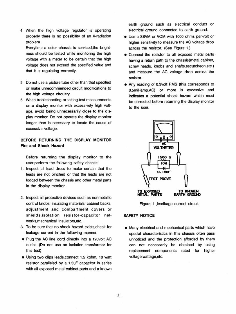
BEFORE RETURNING THE DISPLAY MONITOR
Fire and Shock Hazard
Before returning the display monitor to the
user,perform the following safety checks:
1. Inspect all lead dress to make certain that the
leads are not pinched or that the leads are not
lodged between the chassis and other metal parts
in the display monitor.
2. Inspect all protective devices such as nonmetallic
control knobs, insulating materials, cabinet backs,
adjustment and compartment covers or
shields, isolation resistor-capacitor net
works, mechanical insulators,etc.
3. To be sure that no shock hazard exists,check for
leakage current in the following manner:
• Plug the AC line cord directly into a 120volt AC
outlet. (Do not use an isolation transformer for
this test)
• Using two clips leads,connect 1.5 kohm, 10 watt
resistor paralleled by a 1.5uF capacitor in series
with all exposed metal cabinet parts and a known
-3-
earth ground such as electrical conduct or
electrical ground connected to earth ground.
• Use a SSVM or VOM with 1000 ohms per-volt or higher sensitivity to measure the AC voltage drop
across the resistor. (See Figure 1.)
• Connect the resistor to all exposed metal parts having a return path to the chassis(metal cabinet,
screw heads, knobs and shafts,escutcheon,etc.)
and measure the AC voltage drop across the
resistor.
• Any reading of 0.3volt RMS (this corresponds to 0.5milliamp.AC) or more is excessive and
indicates a potential shoc~ hazard which must be corrected before returning the display monitor
to the user.
10 EXPOSED tElA'- PARTS
Figure 1 ,Ieadkage current circuit
SAFETY NOTICE
• Many electrical and mechanical parts which have
special characteristics in this chassis often pass
unnoticed and the protection afforded by them can not necessarily be obtained by using
replacement components rated for higher
voltage, wattage, etc .

• Replacement .parts that have these special safety
characteristics are identified in this manual,and
its supplement; . electrical components having
such features are identified by a ! In the Parts
List and Schematic Diagrams .
• Before replacing any of these components,read
the Parts List In this manual carefully. The use of
substitute replacement parts that do not have the
same safety characteristics as specified in the
Parts List may create shock, fire, or other hazards.
-4-

SPECFICATIONS
MONITOR DESCRIPTION
This 19" Dual Page Monitor is operated in separate drive mode input and it is compatible with IBM
1. AC Power Input(Universal power input)
: This power input shall be operated with in
AC 99 '" AC 264V automatically.
• 110/120 Vac : 99 '" 132 Vac,60Hz .
• 220/240 Vac : 198 '" 264 Vac,50 Hz.
2. Power Consumption : 80 W Max
3. Signal Input
Horizontal Sync
o Polarity o Signal Level o Frequency
Vertical Sync
o Polarity o Signal Level o Frequency
Video Signal
o Signal Level o Band width
4.1nput frequency
Horizontal Vertical
5. Picture Tube
Size Deflection Angle Phosphor
6. Resolution
Horizontal Vertical
7. Display size
: Negative : TTL : 64.63 Khz
: Negative : TTL : 60.69 Hz
:ECL : 100 MHz at 3dB
:64.63 Khz :60.69 Hz
: CE755M20C104GKZ
(Clinton) : 19 Inch : 110° : P104
: 1280 Dots : 1024 Lines
-5-
Horizontal Vertical
8. Dimension
Height Width Depth
9. Weight
: 360 ± 4mm : 275 ± 4 mm
: 436.5mm :444mm : 399mm
: 24 Kg Max
10. ENVIRONMENTAL CHARACTERISTICS
1) Operating Condition
Temperature Humidity
Altitude
2) Storage Condition
Temperature Humidity Altitude
3) Drop
Height Method
4) Vibration
Amplitude Vibration Sweep
: DoC ~50°C : 5% ~95% (non-condensing)
: Up to 3,000 meter
: -4Q°C '" 60°C : 5%"'95% : Up to 12,000 meter
:46cm : 6 Surface, 3 Side, 1 Angle
:3mm : 10"'20 Hz : 1 Minute
11. ELECTRICAL DESCRIPTION
1) Tilt : Max OS

2) High Voltage 2) Pincushion
Anode Voltage : 18.0 KV ± 1 KV
3) Display Centering
Vertical
Horizontal
4m
INNER BEZEL
: The valid video area data
zone shall be centered
within 4 mm.
: The valid video area data
zone shall be centered
within 4mm.
Display
centering
DISPLAY AREA
12. Geometric Distortion
1)Trapezoid
A,B,C,D: less than 4.0mm
~ ----,-
t
t D
- -B
A,B,C,D: less than 4.0mm
3) Barrel
-r-t
A,B,C,D: less than 4.0mm
4) Rotation
rI T
HI
.n ISPLAY AREA
T S
H2
ENTER
CAN LINE
7777777~ GROUND
PLANE
H1-H2: less than 4.0mm

5) Parallelogram
The edge of the image is within the area
indicated by the dotted line below.
I I
II..-----f-tl ~ A,B: less than 4.0mm
6) Linearity
Horizontal and vertical linearity shall be less
than 6 %.
See Figure
t-+-+-+--I--+-+-I--+-~I-+-+-IJ x I
Horizontal Linearity :
Xmax - Xmin
Xmean
Vertical Linearity
Ymax - Ymin
Ymean
7)Bright Output
X 0.5 x 100(%) <6%
X 0.5 x 100(%) <6%
Min luminance : 0 F/l
Max luminance :Over 30 F/l
Condition : After 30 minutes warm
up full white pattern.
8) Screen Attribute
Input level Output Screen Attribute
VO V1 level
1 1 0 Black (0%)
1 0 1 Dark Gray (33% ± 12%)
0 1 2 Light Gray (67% ± 12%)
0 0 3 White (100%)
9) Raster Size Regulation
Raster size shall change less than 0.5% with
a CRT luminance from min to max.
10) Signal input pin connection
A CDC19M VIDEO CARD 9 PIN D-SUB 9 PIN D-SUB
(TO CPU) (TO MONITOR) DESCRIPTION
PIN NO. PIN NO.
1 1 VIDEO ( + )
2 2 NC
3 3 H-SYNC
4 4 V-SYNC
5 5 NC
6 6 VIDEO ( - ) 7 7 GND
8 8 GND
9 9 GND
B. SDA1280M2 VIDEO CARD/lOOO VIDEO CARD
9 PIN D-SUB 9 PIN D-SUB
(TO CPU) (TO MONITOR) DESCRIPTION
PIN NO. PIN NO.
1 1 GND
2 2 VIDEO 1(ECl+)
3 3 VIDEO 1 (ECl - )
4 4 VIDEO O(ECl + )
5 5 VIDEO O(ECl - )
6 6 GND
7 7 GND
8 8 H-SYNC
9 9 V-SYNC
-7-

11)Signal timing chart.
A. HORIZONTAL PERIOD
t H-PERIOD
B. VERTICAL PERIOD
H-BP
H-SYNC
H-FP
t V-PERIOD ~~ ___ ~V_-~DI~S_P~I~A~Y ___ ~~
-----i~ V-By I
--+--, -0/ ~ V-BP
V-SYNC
V-FP
CDC19M VIDEO CARD
SYMBOL DESCRIPTION
H-PERIOD HORIZONTAL FREQUENCY
H-FP HORIZONTAL FRONT PORCH
H-SYNC HORIZONTAL SYNC
H-BP HORIZONTAL BACK PORCH
H-DISPLAY HORIZONTAL DISPLAY
V-PERIOD VERTICAL FREQUENCY
V-FP VERTICAL FRONT PORCH
V-SYNC VERTICAL SYNC
V-BP VERTICAL BACK PORCH
V-DISPLAY VERTICAL DISPLAY
-8-
TIME
15.34 uS
0.36 uS
0.72 uS
2.68 uS
11.58 uS
15.34 mS
92.04 uS
0.37 mS
15.71 mS
r--~ VIDEO
r---- H-SYNC
VIDEO
V-SYNC
FREQUENCY REMARKS
65.19 KHz
1280 DOTS
61.60 Hz
1024 LINES

SDA1280M2 VIDEO CARD
SYMBOL DESCRIPTION TIME FREQUENCY REMARKS
H-PERIOD HORIZONTAL FREQUENCY 15.30 uS 64.63 KHz
H-FP HORIZONTAL FRONT PORCH 0.76 uS
H-SYNC HORIZONTAL SYNC 0.76 uS
H-BP HORIZONTAL BACK PORCH 1.89 uS
H-BL HORIZONTAL BLANK 3.40 uS
H-DISPLAY HORIZONTAL DISPLAY 12.08 uS 1280 DOTS
V-PERIOD VERTICAL FREQUENCY 16.48 mS 60.69 Hz
V-FP VERTICAL FRONT PORCH 92.84 uS
V-SYNC VERTICAL SYNC 77.36 uS
V-BP VERTICAL BACK PORCH 464.18 uS
V-BL VERTICAL BLANK 0.63 mS
V-DISPLAY VERTICAL DISPLAY 15.85 mS 1024 LINES
1000 VIDEO CARD
SYMBOL DESCRIPTION TIME FREQUENCY REMARKS
H-PERIOD HORIZONTAL FREQUENCY 15.30 uS 65.36 KHz
H-FP HORIZONTAL FRONT PORCH 0.09 uS
H-SYNC HORIZONTAL SYNC 0.75 uS
H-BP HORIZONTAL BACK PORCH 2.46 uS
H-BL HORIZONTAL BLANK 3.30 uS
H-DISPLAY HORIZONTAL DISPLAY 12.00 uS 1280 DOTS
V-PERIOD VERTICAL FREQUENCY 16.14 mS 62.00 Hz
V-FP VERTICAL FRONT PORCH o uS
V-SYNC VERTICAL SYNC 91.80 uS
V-BP VERTICAL BACK PORCH 382.54 uS
V-BL VERTICAL BLANK 474.30 uS
V-DISPLAY VERTICAL DISPLAY 15.67 mS 1024 LINES
-9-

THEORY OF OPERATION
I.POWER SECTION
1. LINE INPUT STAGE The input section converts the AC line voltage into a crudely filtered and unregulated DC voltage
which powers the switching regulator.
1)Filter
To keep noise from being conducted down the
power line a low-pass filter isolates the switcher.
The conducted noise is mostly differential and
can be reduced by 'X' capacitors and a common mode transformer.
2)Power supply
This design utilizes a discontinuous flyback topology operating in current mode. This results in a
multiple output switcher who's outputs track well.
No output filter chokes are needed and slower
diodes can be used. The fast transit response
maintains picture integrity. Cycle by cycle current
limiting makes the switcher short circuit proof.
2. P.W.M IC STAGE
1) p.w.m. integrated circuit
The UC3842 (1C601) is an integrated current mode
pulse width modulator. It consists of an oscil
lator,error amplifier, current-sense comparator,
under-voltage lockout,and an output MOSFET
driver stage.
2)Oscillator
The oscillator consists of a pull up resistor from
the 5V reference to pin 4 and a timing capacitor
to ground. When the voltage on pin 4 lamps up
to 2.8V a flip flop is set. An internal current source
is activated which pulls down,discharging the
-10-
timing capacitor to a 1.0V level. This resets the
current source and starts the next cycle. Oscillator frequency is approximately equal to 1/0.55RC.
The discharge time is a function of the internal
current source and the timing capacitor. The
discharge time should start when the horizontal switch is turned off. It should time out in about
the center of the flyback pulse. The discharge time should equal the storage delay of Q303 plus
one half of the flyback time. Synchronization can be achieved by means of adding timing pulses
to the timing ramp from a reference.
3) Output
The UC3842(I C601 ) has a single totem-pole out
put capable of driving 1.0A peaks and 200mA
average. The peak current is self limiting.
4) Current sense comparator
Current mode controllers inherently keep close watch over the switching transistors current. Pin3
is connected to a voltage comparator which shuts
off the output when current reaches the desired
level,as prescribed by the error amplifier. This way the controller will only let the needed amount
of current be stored on the output transformer.
5)Error amplifier
Voltage on pin2 is compared with an internal 2.5V
2% source. Errors in output voltage are amplified
to pin1 where they are frequency compansated
by an RC back to pin2. This error voltage is
internally dropped by 1.4V ~nd divided by 3 before
being fed to the current comparator.
6)Vcc
The UC3842(I C604} draws very little current in
start up mode. There is enough power. from the
line bleeders R632 and R607 to slowly charge
C618 to the 16 volts need to start the switcher.

When switching begins the Vcc falls quickly but
before it drops to the 10 volt turn off level the
phase lock loop section of the monitor should
be up and running sending power through the
sync transformer to keep the UC3842 alive.
3. Swiching Power Trans Stage
1) Power Transformer
Transistor MTP4N85(Q601) starts off a cycle by
allowing current to flow into the primary of T603.
As current ramps up with time, the voltage across
current sense resistor R621 also ramps to a point
where IC604 determines enough power has been
stored and turn off Q601. As the voltage on Q601
flies upward, power dumped through the main
power transformer and through diodes into the
different supplies. Primary ringing which could
over voltage Q601 is clamped by 0610. To keep
radio frequency radiation to a minimum and
reduce transistor heating, a turn off snubber net
work is placed across Q601. The transformer has
a center leg gap with no gap in the outer legs.
This greatly reduces the flux radiating from the
cores. There also may be a large copper strap
around T603 to short out stray flux.
2) Rectification and Filters
Current from the secondary windings are rectified
and filtered to create the desired Voltages. Low
internal series resistance electrolytic capacitors
keep the ripple voltage low. Small high current
capacitors quickly return charging current to the
source.
II.MAIN SECTION
1.HORIZONTAL STAGE
1)PLL
A phase lock loop is used to synchronize the
horizontal switch to the timing pulses from the
computer. Storage delay in MJH16010A(Q303) is
compensated for by the PLL. Incomming H.sync
is level translated by MPS2222A(Q301) then fed
into the input of the phase comparator. Transistor
PN2907(Q304) watches the falling edge of the
flyback pulse. When the flyback pulse falls to
within a few volts of ground a raising edge is
sent to the other input of the PLL phase com
parator. The phase comparator is used in an edge
lock mode. Integrated circuit MC14046B(IC301)
pin 13 is in a high impedance mode most of the
time. If the raising edges fed into pin 3 and 14
do not coincide, pin 13 goes into a low impedance
stats for the time difference. Depending on which
edge leads the other, current will be fed into or
pulled out of the filter capacitors C308 and C309
2) Horizontal-Drive Transistor VN0606M(Q302) when turned on drives
off the horizontal switch MJH16010A(Q303). At
the same time current is stored on the trans
former T301. When VN0606M(Q302) opens up,
this stored charge kicks up and supplies turn on
current for MJH16010A(Q303). Resistor R302 sets
the average power level to the base drive circuit.
Transformer T301 is surrounded by snubbing cir
cuits.
3)Horizontal-Output
- 11-
On the right hand side of the screen, transistor
MJH16010A(Q303) conducts current through the
deflection yoke to ground. This current comes
from the "S" correction capacitor,C316 and C317,
which have a charge approximately equal to the
supply Voltage. Diode MUR8100(D303) allows cur-

rent, for the left hand side of the screen, to flow
from ground back through the deflection yoke to
C316 and C317.
4)Flyback Capacitor
The flyback capacitor connects the hot side of
the yoke to ground. This component determines
the size and length of the fJyback pulse. If any
adjustment is needed in second anode voltage
this capacitor can be altered. Capacitors C312
and C313 must be prcision high voltage high
current components.
5)"S" Correction
Capasitor C316,C317 are used to correct for
outside versus center linearity in the horizontal
scan. The voltage on C316,C317 have about 33
volts of parabola plus the DC horizontal supply.
If the val ue of C316, C317 are red uced this
parabola will increase, reducing the size of the
outside characters and increasing the size of the
center characters.
6) Horizontal-Linearity
In the yoke current path there is a saturable coil.
Just like a size coil any inductance in series with
the yoke will reduce the size of the picture. This
saturable coil will change inductance depending
on the at the start of trace, the linearity coil has
. an inductance of 20 percents of that of the yoke.
By the center of trace the linearity inductance
has decreased to about 4 percent of the yoke
where it remains for the rest of the trace. This
variable inductor should be adjusted so the right
and left sides of the picture are the same size.
7) HN Regulator Section
The patented hight voltage regulator sits between
the supply and the top of the primary of the
flyback transformer. An onboard switching
regulator is powered from the 12 volt supply. It
watches the second anode voltage through a 300
mega ohm resistor in the flyback transformer.
During flYback the regulator pulls the top of the
fJYback transformer negative some amount at the
same time the flyback pulse is raising the other
end. In this way the size of the pulse as seen by
the fJyback transformer can be varied to keep the
second anode voltage constant under load.
8) Focus Modulation
Each part of a cathode ray tube focuses at a
different voltage. The focus voltage at the center
may be several hundred volts below the top
and bottom with the right and left sides being at
a defferent level. To get the best looking picture
over the entire tube, the focus voltage is modulated with both a vertical and horizontal signal.
The vertical parabola is fed into a high voltage
amplifier 2SC3675(Q401 ). 2SC3675(Q401 ) swings
the focus voltage at the vertical rate. Mixed in
with this signal is another parabola at the horizon
tal rate which comes from L401. The focus ad
justment VR401 sets the do focus voltage and
bias on 2SC3675(Q401).
9) Sub-Brightness
The fJyback pulse is voltage doubled to get 1200
+ volts to run the master brightness poten
tiometer that controls G2.
2. VERTICAL STAGE
The TDA 1670(IC201) incorporates all of the neces
sary functions for providing the yoke of a monitor c'
or television receiver with the current required for
vertical deflection. Incorporated in silicon are a
synchronizqble oscillator, ramp generator, voltage
regulator, vOrtage doubler and power amplifier.
1) Osctllator
-12-
The oscillator is an integrator (pins 4 to 3) and
a two threshold comparator which swiches pin 6
high or low to allow the charging/discharging of
C201. 0201 allows the charge and discharge
ramps to have defferent slopes. Vertical sync
pulses sent in on pin 8.

2) Ramp Generator
The ramp generator is mode up of a current
generator, controlled by current in pin 7, and the
capacitor from pin 9 to ground. The slope,and thus the size of the linear ramp is adjustable by
varying the current pulled from pin 7. This ramp is buffered on pin 10.
3) Power Amplifier
A power amplifier, with input on pin 12, compares
the ramp on pin 10 to the current ramp through
the yoke, R210 and C204 stabilizes the hight gain
power amplifier. Yoke current flows from pin 1,
through the yoke, the DC blocking capacitor, a current sampling resistor, and to ground. Voltage
representing yoke current is then fed back to the input of the amplifier to be compared with the
reference ramp.
4) Voltage Doubler
In order to obtain sufficiently short flyback time,
a voltage greater then that required during scan
ning, must be applied to the yoke. The flyback
generator, during flyback only, applies to the
power amplifier a voltage equal to double the
supply voltage. Pin 15 charges a capacitor up to
the supply vOltage during trace and then sets this
capacitor in top of the power supply during retrace, thus doubling the available Voltage.
5) Vertical Linearity
The ramp from pin 10 is subtracted from the ramp
across R214 and the results are fed back to the
size input of the TDA1670(IC201).
6) Vertical "5"
The TL431 (1C401) and C402 with R215 from an
integrator. The vertical ramp across R214 in
tegrated becomes the vertical parabola on the
output of TL431 (1C401). This parabola is fed back
to the vertical size input of the TDA1670(IC201)
to compensate for "5" distortion. The parabora is also used to drive the vertical focus modulator.
Diode D401 resistors R215,R402,R404 and
capacitor C401 develop a bias voltage.
7) V-Centering A current sources is connected to the cold side
of the vertical yoke. Transistor MPSU01 (Q201) can pull a DC current from the yoke causing the
picture to move up. Potentiometer VR204 should be set to vertically center the data, net the raster,
on the screen.
III. VIDEO SECTION
1.Sync stage
1) Sync processing
To help understand the complex sync processing, please refer to both the schematic and timing
diagrams at the end of this document.
a) Vertical sync
Vertical sync is detected by a low pase filter and
an 'XOR' gate. Pin 8 of CN4A contains vertical
sync.
b) Horizontal sync
Horizontal sync undergoes several stage of
prccessing.
c) Polarity Restoration
-13 -
The polarity restoration circuit, an XOR gate, will
restore sync polarity if it was fed inverted into
the TIL sync input. The RC time constant in the
low pass filter is about 1 second. If the input is
low with short positive pulses a low pass filter
inputs a low to the XOR input B. The output of
the XOR gate will be the same as the input.
Likewise if the input is hight with short low going
pulses the low pass filter will input a high to the B input of the XOR gate causing it to invert the

sync. This way the syncs coming out of the
polarity restoration circuit will always have short
positive pulses except during vertical.
2) H-PHASTE
The second half of the 74LS221 is used for data
centering. The one shot triggers with the reading
edge of sync and time out with the back edge
of the flyback pulse. The data centering poten
tiometer should be set to center the picture within
the raster
3) Video-amplifier
The video amplifier card resides on the neck of
the tube.
4) Pre-amplifier
The MC10H125(IC112) is a quad translator for
interfacing data and control signals between the
MECL section and saturated logic sections of
digital systems. The MC10H125(IC112) incor
porates differential input and schotky TTL ''totem
pole" outputs.
2) Power Video Amplifier
This two transistor cascade amplifier has both
emitter and collector peaking to get the best
frequency respose. The resistor on the base
reduces the chance of oscillation and also helps
to protect the amplifier from tube arcs. The output
of the amplifier is further isolated from tube arcing
by a carbon composition resistor and an arc
arrestor.
3) Regulators
Three voltafges are used to run the video amplifier
and sync processing circuit. The 50 volts is used
by the video power output amplifier. The -8 volts
is reduced to -5 volts by the 7905 regulator for
used by MC10H125.
-14-

DISASSEMBLY INSTRUCTIONS
1. Remove four screws (A) to remove back-cover
from the front.
2. Full the rear cover backward as pushing the two
points (8) in the direction of the arrows to
separate from the front cover.
3. Remove twelve screws (C) to remove top
chassis-frame from the main chassis-frame.
4. Remove two screws (D) to remove stands from
the chassis-frame.
5. Remove six screws (E) to remove bottom
chassis-frame from the main chassis-frame.
NOTE: Refer to the EXPLODED VIEW for a more detailed disassembly procedure.
-15-
Dr----------------~~
-16-

BLOCK DIAGRAM MODEL NO MU9511 -SV 1 IC REGULATOR 1~_-8=-V'--___ f5\
1 IC114 1 ~
I S~:~~C~riRUT 111-_V:...,:I:,:Oc::.E=-O_-.jJ ECL TO TTL 11-____ -.jJ VIDEO OUT 1 CN13AI IC112 I . -I Q115 I
'---,.----r---J
H-SYNC V-SYNC
1 SYNC INVERSION'I
IC112.IC113
~ONTRAST CONTRO IQ1ii. QU6 VR110
~ERT OSCILLATIO~ ~ IC201 11-_______ --,
+50V 3
.--______ ..:..+.,;;.5_V_-I' IC REGULATOR I. +8V I IC102 I
J S-PARAMETER I I GENERATR
IC401
2 +251,1
I ,....---,------~OJ. V-OY
J IC REGULATOR 1"--~+1::..::2~V_""--.lJ VERT. CENTER l 3 ' CONTROL -I IC 02 1 -I Q201. VR204 r 1
FOCUS 1 MOOULA TION ~----'
Q401. VR401. L40~
VIDEO I I
6 HEATER J,. I I I I
1 G1 G2
1
G1 BIAS
1 CONTROL
IHORIl.FEEO BACK .----~ ~----------~----------~---------, 1 Q304
1 1 RECT~}%ATION ,
061B. C62B. C634
cb
., H-PHASE VR101
1 NOISE FILTER I T601. C601. C603 1 C604 C602
AC INPUT 1
, -BV il RECTIFICA TION 0620. C630. C636
cb - 17-
HORIlONTAL OSC ILLA TION
IC301
I! RECTIFICATION SMOOTHING CIRCUI
0605.C610
1 +BV il RECTIF ICA TION
0619. C629. C635
cb
I
HORIl. DRIVE T301. Q302
H-ORIVE.FEEO BACK T602
SWITCHING OSCILLATION
IC604
, ~~~ +25V R CTIFICATION 0617. C627.C633
cb
SWITCHING OUTPUT
Q601
I 1
RECTW~~ATION I 0616. C626. C6321
cD
J HORIl.OUTPUT I I Q303 I
1 1
H-UN. H-SIlE I CONTROL
SWITCHING TRANSI T603 I
1 PHOTO COUPLER 1 I IC605
1 +10BV I I RECTIF ICA TION 1------------'
0615. C625.C631J o -18-
~ I I CRT I
G4 ~r--
G2 BIAS
I CONTROL
I F B T II H/V REC~3MOOULE.~ T401
S+ +10BV
4
OJ H-OY

ALIGNMENT INSTRUCTIONS
1. PARTS LOCATION AND CONTROL FOUCTION.
Q601
CN6
0000
CN1
000
MAIN PCB
VR601
e[]
-19-
o o o o o o CN4 o o o o
, , i,
T603
VR301 H-HOLD
@J
o o o CN10 o o
CN2
VR203 V-LIN
~ VR201 V-HOLD
000
o o CN5 o
CN11
1000 0 0 L301
H-LIN
VR301 H/V-ADJe[]
Q303
T401
VIDEO PCB
(0000001
CN12A
CN2A
o o o
( 0000000000
CN4A
CRT-SOKET 0 ICU3
0 0 0 0
CN13A 0 0 0
o 0
000 o 0
00 0
0
0 IC112
SUB-PCB
VR402 1000 0 OICN11A ( 00000000 ICN10A
L302 H-WIDTH
SUB-BRIGHT
LED PCB
o
o
- 20-
@J@J@J@J VR401 VR101 VR204 VR202 FOCUS H-PHASE V-CENTER V-SIZE

2. PRE-ASSEMBLY INSPECTION AND HANDLING INSTRUCTIONS
Caution:
Be sure all handing of the CRT display is
done by the CRT mounting brackets. At no
time should the wires be used as a means
of moving or carrying a given CRT display.
The CRT neck is the most fragile part of the
CRT display module and extreme care
should be taken not to bump, tap, or other
wise excess force on this neck.
Before applying power to the CRT display
an inspection should be performed to insure
that any foreign material has not been
dropped in any part of the CRT display.
1. Insure that the proper signal and power con
nections are, made in accordance.
2. Apply power to CRT display under test and
allow CRT display to stabilize for a minimum
of 30 minutes.
Note: All adjustments have at the factory.
This procedure is to insure that these adjustments have been made correctly.
3. When turn external brightness control to max
imum and raster should be slightly visible.
4. Check CRT display for proper centering.
5. Check CRT display for the specified active
charater area per page 5'" 6 of this manual.
6. Check geometric distortion.
7. Check focus.
S. Check power supply voltages in accordance
per page 5 of this manual.
- 21-
3. CAUTION FOR SERVICING
Be sure to provide power supply sequence
of more than 100mS.
power ON-OFF
Do not turn OFF power supply when the
CRT heater is not sufficiently heated. Other
wise, CRT may be burned in spot.
In case of servicing or replacing CRT, high
voltage sometime remains in the anode of
CRT. So, completely discharge high voltage
before servicing or replacing CRT so as to
prevent a shock to the serviceman.
In this case, discharge to the external con
ductive coating(aquadac) of CRT.
Discharging to other places will cause
troubles. The heat sink of horizontal output
transistor is applied with B +. So, do not
earth it in case of servicing. In case of storaging or transporting it, be
sure to take some countermeasures for
static electricity. When using a soldering
iron, be sure to connect it to the earth.
The unused terminal should be soldered
without fail.
4. ADJUSTMENT PROCEDURE
(1) Condition of adjustment procedure
1) Input power 120VAC,60 Hz
220 VAC/240 VAC, 50 Hz
2) Warm up time : More than 30 minutes
3) Contrast
4) Brightness
5) Pattern
(2) Caution
: Max
: 25 F/L
: Unless otherwise specified,
cross-hatch pattern.
1) Unless otherwise specified,adjustment and
check should be made under the standard
condition. 2) To be sure image width, height and distor
tion,proceed as below:
'Scale * CRT fase : west * Measure level with respect to tube axis.
3) Unless otherwise specified, make DC voltage
measurement using a digital voltmeter.
4) Hold the CRT surface illumination to 2S F/L at
the time of adjusting the brightness and also
confirm them.
(3)Adjustment Item
-22-
1) Power Supply Adjustment
a. Condition: Without Signal b. First adjust the power supply unit before ad
justing all controls. Also connect the power
supply unit to the display unit and turn the
unit on. c. Turn VR601/(B+ ADJ) to adjust the voltage
across the TP1 and the ground to 10SV ±
O.SV.
2) H-HOLD Adjustment
a. Condition: Without Signal b. Turn VR301 (H-HOLD VR) to adjust the fre
quency count between the H-DY wire (blue)
and ground (chassis bracket)to 62.S±0.SKHz.
3) V-HOLD Adjustment
a. Condition: Without Signal b. Turn VR201 (V-HOLD VR ) to adjust the fre
quency count between the V-DY wire (yel
low) and ground (chassis bracket)to 55±2Hz.
4) Raster-Centering Adjustment
a. Condition: Without Signal b. Locate VR402 (SUB-BRIT.vR) and EXT-BRIT.
VR to max position. c. Turn Centering-magnet until raster comes to
the center of the screen.
t--Inner bazel
I---t----Haster
A=A'
B=B'

5) H-PHASE Adjustment
a. Condition: Cross-Hatch Pattern
b. Locate VR402 (SUB-BRIT.vR) EXT-BRIT. VR
and EXT-CaNT. VR to max position.
c. Adjust display area to horizontal center of
raster using VR101 (H-PHASE VR).
B
Raster
A A Display A=A'
area B'
B=B'
6) V-CENTER ADJUSTMENT
Adjust VR204 to locate display area at the
CRT center. (B = B')
7) Tilt Adjustment
Loosen the deflection yoke clamp, and turn
in the arrow directions to adjust the tilt within 0.5.
8) Geometric Distortion Adjustment
Adjust each correcting magnet to set rightly
until the square line of the Cross-Hatch pat
tern becomes to be linear. (to come within
Over Lay jig).
9) High Voltage Adjustment
a. Condition: With Signal
b. Locate EXT-BRIT.VR and EXT-CONT.VR to
max position.
c. Connect HN meter prove ( - ) terminal to
ground (chassis bracket) and ( + ) terminal
to anode cap of CRT.
d. Turn VR302 (HN-ADJ VR )to adjust 18KV±
1KV.
- 23-
10) H-Linearity, V-linearity Adjustment
a. Condition: Cross-Hatch Pattern
b. Adjust L301 (H-LiN. COIL) to make same
character size of horizontal axis.
c. Adjust VR203 (V-LIN VR)to make same char
acter size of vertical axis.
11) H-Size,V-Size Adjustment
a. Condition: Cross-Hatch pattern
b. Adjust L302 (H-WIDTH COIL) to come
within Over-Lay Jig.
c. Adjust VR202(H-Size VR) to come within
Over-Lay Jig.
12) Sub-Brightness Adjustment
a. Condtion : Full White Pattern
c. Turn VR402 (SUB-BRIT VR) to adjust 33 F/L
Min.
13) Focus Adjustment
a. Condition: Full u@" Character at 20 F/L.
b. Adjust VR401 (FOCUS VR) to set best condi
tion.

TROUBLE SHOOTING GUIDE
NO Character Image
Turn the VR402 (SUS-SRITVR),
EXT-SRIT.VR EXT-CO NT VR to max
position.
Check 50VDC line.
- 24-
NO
Refer to no raster.
NO
Check input signal or logic.
NO
Check 0110,0111, IC112.

NO Raster
Turn the brightness control
max position.
Abnormal
Trouble in peripheral circuit of
D615,D617.
- 25-
YES
Replace Fuse, F601,0601.
Abnormal
NO
Trouble video circuit.
Normal
Trouble in 0302,0303.

NO HN Regulation
TURN THE BRIGHTNESS
CONTROL MAX POSITION.
Trouble in HN REG. MOOULE.
- 26-
Abnormal
Check 0607,0608,0609.
Abnormal
Trouble in 1C605.

NO Horizontal Sync
Abnormal
Trouble in PC(Video card).
Normal
NO Replace IC102.
Abnormal
YES
Abnormal Trouble in IC101.
Abnormal
Abnormal Trouble in IC301.
- 27-

NO Vertical Sync
Abnormal
Trouble in PC.
Normal
NO Replace IC102.
YES Abnormal
Abnormal Trouble in IC101.
Abnormal
Normal Trouble in IC201.
- 28-

NO Vertical Sync
Abnormal
Trouble in IC201.
Abnormal Trouble in Q201.
Normal
Abnormal
Normal
Replace 0617.
- 29-

WIRING DIAGRAM AND PARTS LOCATION.
~~HV CRT RED
N y~tl MAIN PCB BLU
VR203 CN5 I I V-LIN - r: J ~
~
18 @] I CNI2A r--~ 1 (<!>(
IC201 ~<j)(j> <j> I ( ) ( ~ ( ~ ( ~ <!> I Q601 VR601 @] 1 I CN4A ~ L/V ADJ r--- GT2 VR201
G- T603 V-HOLD
=00] o 0 CN 1 3A "':'
00lQ r:::'\ ,I c!> c!> c!> CNII
~OO ;:... r-- ~
o 0 0 ~ L::...J
I @] VR202 CN2A
r--~ GI C~ CNI4 ~ V-SIZE ;=~ &--
GTIA ~
~115 ~~ CN4 ;:...
~@] VR204
- r-'" V-CENT. - Q303
.=1
~@] VRIOI
VIDEO PCB H-PHASE ~ '--
II CN8 T401
~ ~- ~@] VR401 '\ 1'0 l1 H~ 1 FOCUS
'--~ ..., ~
~ ,CN6 1 =~dn.. ~
VR402 I i> ( CNI VR-301 S! '" '-'I~ ( I I ( I CN2
SUB-H-HOLD BRIT
@) L302
II H-WIDTH
II ~ LED PCB l J 0 f::::J SUB PCB I I I I I I -
0 1 1 1 1 1 1 -===0
-==-1111111111111 1111111 111111 1111111111111
-====>
1'll1 POWER CORD-AC.INT
B BRIT-VR S/W
ElCE: ~ ~ 0 p [ I ~ CONT-VR SIGNAL CABLE-INT
L J -SOCKET AC-INPUT;NOISE FILTER POWER CORD AC
SIGNAL CABLE EXT-INT q IIIIII~ CABLE EXTQIIIIII ~ - 30- - 31-

PRINTED CIRCUIT BOARD
MAIN PCB (TOP VIEW)
:zp n--i ~--i ~I'l U1Z ;'--i ~~ ~Oi:\f
fi ?= -L~ ~ -0 TB -u> > ::0 ::0
::3: C rrJ Z (f)
co -,., ::0 c: rrJ (f) _ 0
CDfTl
fTl U)
"'run - c: tn:u > -, --< ru tTltn ISln <0
z 0--< C ::0
fTl 3: 1"11)[-
C501 :;.----1 ~
3:fT1 eN5 fTl(f)
CAUTION: CN~~: CONTINUED PROTECTION AGAINST FIRE HAZARD,REPLACE ONLY wiTH SAME TYPE 2.5A-250V
- 32-
0403 ..L -l>I- .:;;; D404 (j-r
.. -l>I- • R323
-,/\/V'-·.i
- 33-

MAIN PCB (BOnOM VIEW)
- 34- - 35-

VIDEO PCB (TOP VIEW)
SUB PCB (TOP VIEW)
SUB PCB (BOlTOM VIEW)
VIDEO PCB (BOrrOM VIEW)
CODE No.:3006-700-020
LED PCB (TOP VIEW) LED PCB (BOlTOM VIEW)
o
-36- - 37-

SCREW-RH -----~-
NET-HEX
+M3X I~~_~~ __
I-~~~_~-
~ 02149-~-700 FE!...--.__ MT~~l'I~ ___ .L. 5807304-701-110 WASHER-REC ~c:.~~ __ 59 07048-130-121 SCREW-RH +M3X12 FE FZY
60 02449-735-110 COIL-LINEARITY 3-8UH
MSU1 FDJ37
~ 02879-=~?~:_L.!~ T~S-S/W, M~_ PO-3535
.~ OM9~-000=-~~_I.E... ~SSY-PWB,MAIN MU95) 1 I
64 ~?052=2~:~_L:~_~_ 65 06000-722-010
66 07 !l~~~~-: ~!_
COVE~:~~, ASSY
SCREW-TAP,TH __
67 08033-734-910 ~~~~~~~LA~B~El-RATING _
68 07128-540-101 SCRE~:.!~. TH .
MU9511 -----~--"
2~_:.:!~~~.~~ _ 4
POL YE'3TER~166 ~
2S-4X I 0 FE FZY_ .. 2
69 08302-701-010 ~TAND-S!OPPER __ . NORYL f1-1005
70 07148-230-081 SC~~~~.RH 2S-3X8 FE FZY
7) 066~±:2Q±=-~£.... CLAMP-CABLE AJ050S~_~~ 1
72 08300-703-011 STANO-TOP NORYL PX-1005
~ ~~~~~~~7-+~O=~~~~~W-o~~"'::';"~~THc---I"'~""~~":XCc'll :,X;~ O~~Y ~ ~ --~.--
~~ 03053-403-610 SIGNAL -CABL,,,E_+E,,,X'_-I,,N.'
7~ O_~:>~_~~L?~ POWER-CORO,ASSY LS-13L ~---.-
79 07118-530-083 SCREW-TAP,FH 2S-3X8 FE FZB
80 07093-700-130 SCREW-M.HEX M4X8 FE f~ ___ ._ 81 06634-704-210 CLAMP-CABLE AI050S HI4 TO.B
82 07093-~~~..:~1~ SCREW-M,_~~ __
83 l!:3g~~::;)_~9_-~2..._ GROUND.-~IRE ,ASSY
- -------M4X8 FE~ __
STAND SHIELD
8~ 0712!:_~~-=-I..9L SCREW-TAP.TH •.. ___ 2S-_~~J'?:! __
85 07304-101- 190 ~~~~~.R-PL~ ____ 1.§53..!~ FE FZY
86 O~~~_?.~~~.~_~_. ~IELD-STAND ?Ec:r:=-l.].~ __ _ 87 0~.:-~O-710 F~_. __ " __ . ____ NEOPRENE GRE~ __ l~ 88 071 54=.?30-08 !... SCREYI- TAP ,PH ___ . 2S:-3X8 FE FZY _.l~
EXPLODED VIEW ( MD-1951 U )
-38-
I ~
-39-

REPLACEMENT PARTS LIST
Components identified by the international symbol have A special characteristics important for safety.
When Replacing any of these components use only manufacturer's specified parts.
Note: Tolerance G: ±2% J: ±5% K: ±10% L: ±15% M: ±20% Z:+80/-20% C~ ±0.25pF
MU9511* 19" MONO MONITOR;MU9511*
OM901-***-**** ASSY MONO MONITOR;MU9511*
04541-702-210 SHIELD-TOP;A1050S TO.5
04542-707-210 SHIELD-SIDE;A1050S TO.5
CH+GNC 07048-140-081 SCREW-RH; + M4X8 FE.FZV
ST+MC 07108-126-041 SCREW-TAP PH;2S-3X6 FE FZV W/WASHER
SS+MC 07108-126-041 SCREW-TAP PH;2S-3X6 FE FZV W/WASHER
CH+STD 07128-540-161 SCREW-TAP,TH;2S-4X16 FE FZV
C/R+CH 07128-540-161 SCREW-TA!:',TH;2S-4X16 FE FZY
CH+GNO 07324-100-320 WASHER-TOOTHED;AB-T14.3,PI8.5 FE FZY
OM902-***-**** ASSY COVER REAR;MU9511*
06000-714-010 COVER-REAR,A;NORYL PX1005 VO BGE
06000-715-010 COVER-REAR,B;NORYL PX1005 VO BGE
06052-701-610 DOOR-CONTROL;NORYL PX-1005 VO BGE
08033-734-910 LABEL-RATING;POL YESTER TO.166'&'
OM902-***-**** ASSY STAND;MU9511A*
03053-300-410 GROUND WIRE ASSY;STAND SHIELD
03053-403-610 SIGNAL-CABLE;EXT-INT(600MM)
03053-608-310 GROUND-WIRE ASSY;GRN!YEL 450MM
03053-817-31 0 POWER-CORD,ASSY;LS-13L SVT 3/18AWG USED 120V AC VERSION
03053-817-810 POWER-CORD,ASSY;LS-13L H05W-F 3/0.75 USED 220V AC VERSION
03354-706-410 SOCKET AC-INLET;ACOO8(0.8T)
04541-702-310 SHIELD-STAND;SECC TO.8
06074-700-710 FOOT;NEOPRENE RUBBER GRY
06634-701-81 0 CABLE-TIE;PLT.7M/T18S
06634-704-210 CLAMP-CABLE;A1050S H14 TO.8
07093-700-130 SCREW-M,HEX;M4X8 FE FZB
07118-530-083 SCREW-TAP,FH;2S-3X8 FE FZB
07128-540-101 SCREW-TAP,TH;2S-4X10 FE FZV
07128-540-101 SCREW-TAP,TH;2S-4X10 FE FZY
07148-230-081 SCREW-TAP,RH;2-3X8 FE FZV
07154-230-081 SCREW-TAP,PH;2S-3X8 FE FZV W/WASHER
07304-101-190 WASHER-PLAIN;165216 FE FZV
08300-702-010 STAND-BASE;NORYL PX1005 VO BGE
08300-703-010 STAND-TOP;NORYL PX1005 VO BGE
08300-704-010 STAND-PLATE;NORYL PX1005 VO BGE
08301-703-710 STAND-ASSY;MU9511
08302-701-010 STAND-STOPPER;ACCETAL WHT
- 40-

OM902-***-**** ASSY-CHASSIS;MU9511*
03053-606-510 CONN-SUB,ASSY;300MM(MD-1951 U)
03053-606-810 CONN-GRID,ASSY;200MM(MD-1951 U)
03053-606-910 CONN-8 + ,ASSY;200MM (MD-1951U)
03053-607-010 CONN-SUB,ASSY;200MM(MD-1951 U)
03054-649-120 CONNECTOR-GROUND,1 P ASSY;200MM
03933-701-41 0 BARRIER-SUB,PCB;PVC SHEETTO.8
04034-701-01 0 MAGNET-RUBBER;FERRITE POWER 10GAUSS
04034-701-020 MAGNET-RUBBER;FERRITE POWER 20GAUSS
04034-701-030 MAGNET-RUBBER;FERRITE POWER 30GAUSS
04034-701-110 MAGNET-RUBBER;FERRITE POWER 40GAUSS
04034-701-120 MAGNET-RUBBER;FERRITE POWER 50 GAUSS
06021-702-710 CHASSIS-FRAME;SECC TO.8
06463-703-610 BOSS-SUPPORT;ABS;UBE;KJC V2 PLTNM 34187
SU+CH 07148-540-081 SCREW-TAP,RH;2S-4X8 FE FZY
06604-706-910 HOLDER-WIRE;RICHICO STL-12-o1-600
06634-701 -81 0 CABLE-TIE;PLT.7M!T1SS
MC+CH 07148-230-081 SCREW-TAP,RH;2-3X8 FE FZY
PCB+CH 07148-230-081 SCREW-TAP,RH;2-3X8 FE FlY
SUB-PC 07148-230-081 SCREW-TAP,RH;2-3X8 FE FZY
MC+CF 07148-230-081 SCREW-TAP,RH;2-3X8 FE FlY
PCB+CH 07148-230-081 SCREW-TAP,RH;2-3X8 FE FZY
OM903-***-**** ASSY PWB SUB;MU9511*
VR402 01242-115-001 VR-SEMI;H1621C B4M
VR204 01246-101-180 VR-SEMI ;67360-006/0004 1 K-M
VR101 01246-101-181 VR-SEMI ;67360-006/0007 10K-M
VR401 01246-101-181 VR-SEMI ;67360-006/0007 10K-M
VR202 01246-101-182 VR-SEMI ;67360-006/0011 220K-M
L302 02449-434-810 COIL-HOR,WIDTH;10UH
03006-700-020 PCB-VR SUB;FR-4 DOUBLE 35X10
CN11A 03344-112-040 CONNECTOR-WAFER;5273-o5A(MOLEX)
CN10A 03344-156-1 80 CONNECTOR-WAFER ;5267 -08A(MOLEX}
OM903-***-**** ASSY COVER FRONT;MU9511*
FC+LED 07148-230-081 SCREW-TAP,RH;2-3X8 FE FlY
OM904-*** -**** ASSY COVER-FRONT;MU9511A
06000-713-010 COVER-FRONT;NORY PX1 005 VO BGE #50924
07653-701-411 LENZ-LED;ACRYL CLEAR
OM904-***-**** ASSY PWB LED;MU9511*
02309-11 0-040 LED;LD701 MG
03006-700-040 PCB-LED;25.6X23, FR-4(S/S) MU9511
03053-608-010 CONN-LED,ASSY;LD701 MG,XH-2 600MM
OM903-***-**** ASSY-PWB, VIDEO;MU9511*
IC113 021 09-1 04-700 IC;KS74HCTLS86N
IC112 02119-103-480 IC;MC10H125P
03053-300-610 SHIELD-WIRE ASSY;100MM MU9511
- 41 -

03053-300-810 SHIELD, WIRE ASSY;0.16X5X24 120MM
04542 -709-81 0 SHIELD-CRT, PCB;SPTE TO.35
OM904-***-**** ASSY HIS VIDEO;MU9511*
0115 02149-302-580 TRANSISTOR;2SC3597
05684-706-51 0 HEATSINK-VIDEO;A1050S H14 T1.0
07048-130-101 SCREW-RH; + M3Xl0 FE FZY
07208-113-001 NUT-HEX;1-M3 FE FZY
OM904-***-**** ASSY-PWB, VIDEO UNFIN;MU9511*
R134 01043-827-201 R-METAL,OXIDE;RS 5P 200-J
R135 01043-827-201 R-METAL,OXIDE;RS 5P 200-J
R133 01045-527-471 R-METAL OXIDE;RS 2P 470-J
R136 01045-527-821 R-METAL,OXIDE;RS 2P 820-J
R127 01045-627-510 R-METAL,OXIDE;RS 3P 51-J
C138 01416-768-472 C-CERAMIC HK;DE 1510BEK 4722 2K
C142 01609-403-670 C-ELECTROL YTIC;CE04W 350V 2.2M
C141 01609-404-1 00 C-ELECTROL YTIC;CE04W 63V 100M
IC114 02119-602-100 IC-REGULATOR;MC7905(SST)
0116 02139-104-220 TRANSISTOR;MPS2222A
0111 02139-401-230 TRANSISTOR;PN4258
0112 02139-401-230 TRANSISTOR;PN4258
0117 02139-601-550 TRANSISTOR;2N5550
FB111 02428-048-010 COIL-CHOKE;1.5UH + -20%
FB112 02429-048-010 COIL-CHOKE;1.5UH + -20%
FB113 02429-048-010 COIL-CHOKE;1.5UH + -20%
CN4A 03344-156-1 00 CONNECTOR-WAFER;5267-10A MOLEX
CN12A 03344-156-160 CONNECTOR-WAFER;5267-06A MOLEX
CN13A 03344-156-190 CONNECTOR-WAFER;5267-09A MOLEX
CN2A 03344-159-020 CONNECTOR-WAFER;5096-03C MOLEX
IC113 03354-705-920 SOCKET -IC;WSDIF-14PIN
IC112 03354-705-930 SOCKET -IC;WSDIF-16PIN
03354-706-31 0 SOCKET-CRT;19MP MD-1503P
SGll0 04569-002-210 SPARK GAP;DSP-301 N
SG111 04569-002-210 SPARK GAP;DSP-301 N
OM905-***-**** ASSY-PWB VIDEO AUTO;MU9511 *
J110 00509-400-116 WIRE-SO,COPPER;TA 0.6 SN
Jl11 00509-400-116 WIRE-SO,COPPER;TA 0.6 SN
J113 00509-400-116 WIRE-SO,COPPER;TA 0.6 SN
R126 00509-400-116 WIRE-SO,COPPER;TA 0.6 SN
R115 01018-277-103 R-CARBON;RD 1/4T 10K-J
R117 01018-277-105 R-CARBON;RD 1/4T lM-J
R143 01018-277-111 R-CARBON;RD 1/4T 110-J
R145 01018-277-111 R-CARBON;RD 1/4T 110-J
Rl46 01018-277-111 R-CARBON;RD 1/4T 110-J
R142 01018-277-120 R-CARBON;RD 1/4T 12-J
Rl05 01018-277-181 R-CARBON;RD 1/4T 180-J
-42-

R129 01018-277-182 R-CARBON;RD 1/4T 1.8K-J
Rl18 01018-277-222 R-CARBON;RD 1/4T 2.2K-J
R147 01018-277-222 R-CARBON;RD 1/4T 2.2K-J
Rl16 01018-277-223 R-CARBON;RD 1/4T 22K-J
R144 01018-277-223 R-CARBON;RD 1/4T 22K-J
R132 01018-277-223 R-CARBON;RD 1/4T 22K-J
Rl09 01018-277-331 R-CARBON;RD 1/4T 330-J
Rlll 01018-277-331 R-CARBON;RD 1/4T 330-J
Rl13 01018-277-331 R-CARBON;RD 1/4T 330-J
Rl14 01018-277-331 R-CARBON;RD 1/4T 330-J
R128 01018-277-331 R-CARBON;RD 1/4T 330-J
R139 01028-378-103 R-COMPOSITION;RC 1/2T 10K-K
R141 01028-378-103 R-COMPOSITION;RC 1/2T 10K-K
R137 01028-378-390 R-COMPOSITION;RC 1/2T 39-K
R131 01028-378-390 R-COMPOSITION;RC 1/2T 39-K
R138 01028-378-474 R-COMPOSITION;RC 1/2T 470K-K
R148 01028-378-47S R-COMPOSITION;RC 1/2T 4.7M-J
R12S 01048-27S-180 R-METAL,FILM;RM 1/4T 18-F
Rl19 01048-27S-220 R-METAL,FILM;RM 1/4T 22-F
R121 01048-27S-220 R-METAL,FILM;RM 1/4T 22-F
R126 01048-27S-220 R-METAL,FILM;RM 1/4T 22-F CDC19M VIDEO CARD VERSION
R124 01048-27S-270 R-METAL,FILM;RM 1/4T 27-F CDC19M VIDEO CARD VERSION
R124 01048-27S-829 R-METAL,FILM;RM 1/4T 8.2-F SDA1280M2 VIDEO CARD VERSION
Rl12 01048-276-100 R-METAL,FILM;RM 1/4T 10-G
R101 01048-277 -471 R-METAL,FILM;RM 1/4T 470-J
Rl02 01048-277-471 R-METAL,FILM;RM 1/4T 470-J
Rl03 01048-277-471 R-METAL,FILM;RM 1/4T 470-J
Rl04 01048-277-471 R-METAL,FILM;RM 1/4T 470-J
C128 01407-017-101 C-CERAMIC,TEMP;CC4S(T) SL SOV 100-J
C129 01407-017-101 C-CERAMIC,TEMP;CC4S(T) SL SOV 100-J
Cl19 01407-017-101 C-CERAMIC,TEMP;CC4S(T) SL SOV 100-J
C131 01407-OS7-121 C-CERAMIC ,TEMP;CC4S(T) CH SOV 120-J SDA 1280M2 VIDEO CARD VERSION
Cl17 01417-344-104 C-CERAMIC,HK;CK4S(T) FSOV 0.1 M-Z
CllS 01417-344-104 C-CERAMIC,HK;CK4S(T) FSOV 0.1 M-Z
Cl18 01417-344-104 C-CERAMIC,HK;CK4S(T) FSOV 0.1 M-Z
C122 01417-344-104 C-CERAMIC,HK;CK4S(T) FSOV 0.1 M-Z
C124 01417-344-104 C-CERAMIC,HK;CK4S(T) FSOV 0.1 M-Z
C12S 01417-344-104 C-CERAMIC,HK;CK4S(T) FSOV 0,1 M-Z
C133 01417-344-104 C-CERAMIC,HK;CK4S(T) FSOV 0.1 M-Z
C136 01417-344-104 C-CERAMIC,HK;CK4S(T) FSOV 0.1 M-Z
Cl12 01417-344-104 C-CERAMIC,HK;CK4S(T) FSOV 0.1 M-Z
C114 o lS0S-723-1 03 C-POLYESTER;CQ921 M(T) 100V O.Ol-J
C137 o lS0S-723-1 04 C-POL YESTER;CQ921 M(T) 100V 0.1 M-J
C139 o lS0S-723-1 04 C-POLYESTER;CQ921 M(T) 100V 0.1 M-J
C13S 01608-903-1 01 C-ELECTROL YTIC;CE04W(T) 16V 100M
-43-
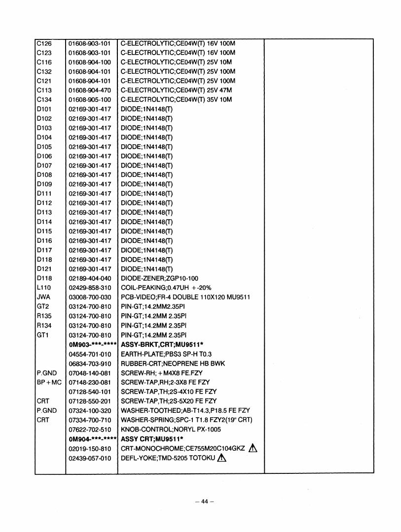
C126 0160S-903-101 C-ELECTROLYTIC;CE04W(T) 16V 100M C123 o 160S-903-1 01 C-ELECTROLYTIC;CE04W(T) 16V 100M
C116 0160S-904-100 C-ELECTROLYTIC;CE04W(T) 25V 10M C132 0160S-904-1 01 C-ELECTROLYTIC;CE04W(T) 25V 100M C121 o 160S-904-1 01 C-ELECTROL YTIC;CE04W(T) 25V 100M C113 0160S-904-470 C-ELECTROL YTIC;CE04W(T) 25V 47M C134 0160S-905-100 C-ELECTROLYTIC;CE04W(T) 35V 10M
0101 02169-301-417 DIODE;1N414S(T) 0102 02169-301-417 DIODE;1N414S(T)
0103 02169-301-417 DIODE;1N414S(T) 0104 02169-301-417 DIODE;1N414S(T) 0105 02169-301-417 DIODE; 1 N414S(T) 0106 02169-301-417 DIODE;1 N414S(T) 0107 02169-301-417 DIODE;1N414S(T) D10S 02169-301-417 DIODE; 1 N414S(T) 0109 02169-301-417 DIODE; 1 N414S(T) 0111 02169-301-417 DIODE;1N414S(T) 0112 02169-301-417 DIODE; 1 N414S(T) 0113 02169-301-417 DIODE;1N414S(T) 0114 02169-301-417 DIODE;1N414S(T) 0115 02169-301-417 DIODE; 1 N414S(T) 0116 02169-301-417 DIODE; 1 N414S(T) 0117 02169-301-417 DIODE;1N414S(T) D11S 02169-301-417 DIODE;1N414S(T) 0121 02169-301-417 DIODE; 1 N414S(T) D11S 02189-404-040 DIODE-ZENER;ZGP1 0-1 00 L110 02429-85S-310 COIL-PEAKING;0.47UH + -20% JWA 0300S-7OO-030 PCB-VIDEO;FR-4 DOUBLE 110X120 MU9511 GT2 03124-700-S10 PIN-GT; 14.2MM2.35PI R135 03124-700-S10 PIN-GT;14.2MM 2.35PI R134 03124-700-S10 PIN-GT;14.2MM 2.35PI GT1 03124-700-S10 PIN-GT;14.2MM 2.35PI
OM903-***-**** ASSY-BRKT,CRT;MU9511*
04554-701-010 EARTH-PLATE;PBS3 SP-H TO.3
06834-703-910 RUBBER-CRT;NEOPRENE HB BWK P.GND 0704S-14O-OS1 SCREW-RH; + M4XS FE.FZV BP+MC 0714S-230-OS1 SCREW-TAP,RH;2-3XS FE FZV
0712S-54O-101 SCREW-TAP,TH;2S-4X10 FE FZV CRT 0712S-550-201 SCREW-TAP,TH;2S-5X20 FE FZV P.GND 07324-100-320 WASHER-TOOTHED;AB-T14.3,P1S.5 FE FZV
CRT 07334-700-710 WASHER-SPRING;SPC-1 T1.S FZV2(19" CRT)
07622-702-510 KNOB-CONTROL;NORYL PX-1005
OM904-***-**** ASSY CRT;MU9511*
02019-150-S10 CRT -MONOCHROME;CE755M20C1 04GKZ A 02439-057-010 DEFL-YOKE;TMD-S205 TOTOKU A.
-44-

03053-300-310 GROUND-CRT,ASSY;MD-1 951 U
03054-643-110 CONNECTOR 4P ASSY;JST 4P-LV-
06634-701-81 0 CABLE-TIE;PLT.7M{f18S
OM904-***-**** ASSY MOUNT,CRT;MU9511 *
01201-900-010 VR-ROUND,SGL;18SN 20F B1K(M8)
VR111 01201-900-010 VR-ROUND,SGL;18SN 20F B1 K(M8)
')3053-606-41 0 CONN-POWER S/W ASSY;350MM
03053-607-110 CONN-VR,ASSY;400MM (MD-1951U)
SW2 03529-703-010 SWITCH-PUSH;70100-000-0-0033
06600-700-010 BRKT-CRT,ASSY;MD-1951 U
OM904-***-**** ASSY-BRKT;POWER MU9511*
03053-403-710 SIGNAL CABLE;INT ASSY (85M/M) CDC19M VIDEO CARD VERSION
03053-404-310 CABLE-SIGNAL;85MM 5264-09, MU9511A SDA1280M2 VIDEO CARD VERSION
03053-606-710 CONN-AC,INPUT ASSY;l 00M(MD-1 951 U)
03054-223-030 GND-WIRE,ASSY;GRN/YEL,L-100mm
03354-707-110 SOKET-AC,INLET;1133-S22 NOISE FILTER U/C
06612-709-110 BRACKET-POWER;SECC Tl.0
PC+BP 07118-530-083 SCREW-TAP,FH;2S-3X8 FE FZB
SC+BP 07148-530-081 SCREW-TAP,RH;2S-3X8 FE FZY
OM903-***-**** ASSY-PWB, MAIN;MU9511*
C102 01508-513-471 C-POL YSTYRENE;C0922M 50V 470-J
IC101 02109-104-600 IC;SN74LS221
IC603 02109-104-850 IC-CMOS TIMER;TLC555M(TI)
IC301 02109-307-050 IC-CMOS PLL;MC14046B
IC604 0211 9-60 1 -940 IC-PWM CONTROLLER;UC3842
CN3 03006-900-010 HN REGULATOR MODULE;15" 29P64 A FOOl 04709-088-080 FUSE;51 S 250V 2.5A 20MMU/C &. USED 120V AC VERSION
F601 04709-084-950 FUSE;50T 250V 2.5A 20MM-C(SEMKO) £ USED 220V AC VERSION
08114-874-640 LABEL-FUSE;T2.5A-250V &.. USED 220V AC VERSION
OM904-***-**** ASSY HIS TR;MU9511*
0601 02149-60 1-700 FET;MTP4N85(WITH MICA) MOTOROLA A 0601 03914-100-340 PLATE-MICA;5-13X19 TO.09 RECT
03934-1 03-11 0 INSULATOR-TR;4.5-8D 2-2H N68 V-O
05683-707-510 HEATSINK-IC;A1050S-H14 Tl.6
07048-130-121 SCREW-RH;+M3X12 FE FZV
07208-113-001 NUT-HEX;1-M3 FE FZV
07304-700-920 WASHER-PLAIN;954810 FE FZW
07304-701-110 WASHER-REC.;SBC-l T1.5 NI
OM904-***-**** ASSY HIS IC;MU9511*
IC201 02119-101-200 IC-VERT;TDA 1670
IC201 05682-704-410 HEATSINK-IC;A1050S T2.0
07108-126-041 SCREW-TAP PH;2S-3X6 FE FZV W/WASHER
OM904-***-**** ASSY HIS FBT;MU9511*
0303 02149-302-280 TRANSISTOR;MJHl6010A(WITH MICA) £ 0303 04542-707-310 SHIELD-CASE,FBT;A 1 050S Tl.5
-45-

06673-702-310 SPRING-TR(A);STS301 TO.4
OMS04-***-**** ASSY-H/S DIODE;MU9511*
D303 02169-301-880 DIODE;MUR8100 (MOTOROLA) A 05683-708-010 HEATSINK-TR,VIDEO;A1050P H14 T1
07048-130-101 SCREW-RH; +M3X10 FE FZV
07208-113-001 NUT-HEX;1-M3 FE FZV
07304-700-920 WASHER-PLAIN;954810 FE FZW 07304-701-110 WASHER-REC.;SBC-1 T1.5 NI
OM904-***-**** ASSY.PWB, MAIN UNFIN;MU9511*
R321 01028-378-474 R-COMPOSITION;RC 1/2T 470K-K
R621 01038-217-033 R-WIRE;RW IL 0.33-J
R302 01039-427 -820 R-CEMENT,WIRE;RP 3P 82-J
R313 01045-427-221 R-METAL,OXIDE;RS 1 P 220-J
R212 01 045-427-301 R-METAL,OXIDE;RS 1P 300-J
R607 01 045-627-154 R-METAL,OXIDE;RS 3P 150K-J
R632 01 045-627-154 R-METAL,OXIDE;RS 3P 150K-J
R617 01045-627 -503 R-METAL,OXIDE;RS 3P 50K-J
R631 01045-627-503 R-METAL,OXIDE;RS 3P 50K-J
R622 01085-427-682 R-METAL,OXIDE;RS 1P 6.8K-J(S)
R623 01085-427-682 R-METAL,OXIDE;RS 1P 6.8K-J(S)
R209 01085-527-151 R-METAL,OXIDE;RS 2P 150-J(S)
VR601 01241-108-002 VR-SEMI;CET 92A B500
VR201 01241-108-007 VR-SEMI;CET 92A B10K
VR203 01241-108-007 VR-SEMI;CET 92A B10K
VR301 01241-108-007 VR-SEMI;CET 92A B10K
VR302 01241-110-005 VR-SEMI;CET l17A B50K
C314 01416-618-102 C-CERAMIC,HK;CK45B 1 KV 1000-K
C3l5 01416-618-102 C-CERAMIC,HK;CK45B 1 KV 1000-K
C403 01416-618-102 C-CERAMIC,HK;CK45B lKV 1000-K
C637 01416-649-472 C-CERAMIC,HK;DE7150F 472M VA-l-KC A C638 01418-649-472 C-CERAMIC,HK;DE7150F 472M VA-1-KC A C318 01416-780-103 C-CERAMIC,HK;CK45 E2KV 0.01 UF-P
C405 01418-780-103 C-CERAMIC,HK;CK45 E2KV 0.01 UF-P
C406 01416-780-103 C-CERAMIC,HK;CK45 E2KV 0.01 UF-P
C407 01418-780-103 C-CERAMIC,HK;CK45 E2KV 0.01 UF-P
C619 01416-780-103 C-CERAMIC,HK;CK45 E2KV 0.01 UF-P
C409 01416-780-103 C-CERAMIC,HK;CK45 E2KV 0.01 UF-P
C621 01419-901-220 C-CERAMIC,HK;CK45 B 1 KV 220-K
C639 01461-137-806 C-CERAMIC,AC;DE 7100F 222MVAI ~ C640 01461-137-806 C-CERAMIC,AC;DE 7100F 222MVAI ~ C641 01461-137-806 C-CERAMIC,AC;DE 7100F 222MVAI ~ C642 01461-137-806 C-CERAMIC,AC;DE 7100F 222MVAI ~ C612 01502-323-682 C-POL YPROPYLENE;CQ922M 100V 6800-J
C3D5 01502-513-152 C-POLYPROPYLENE;CQ922M 50V 0.0015M-J
C202 01502-523-473 C-POLYPROPYLENE;CQ922M 100V 0.047M-J
- 46-

C210 01502-523-563 C-POL YPROPYLENE;CF922M 100V 0.056UF-J C316 01502-553-223 C-POL YPROPYLENE;C0922M 630V 0.022M-J h. C313 01502-573-392 C-POL YPROPYLENE;C0922M 1.6KV 3900P-J 6 CDC19M VIDEO CARD VERSION C312 01502-573-392 C-POL YPROPYLENE;C0922M 1.6KV 3900P-J ~ CDC19M VIDEO CARD VERSION C313 01502-573-222 C-POL YPROPYLENE;C0922M 1.6KV 2200P-J ~ SDA1280M2 VIDEO CARD VERSION C312 01502-573-472 C-POLYPROPYLENE;C0922M 1.6KV 4700P-J ~ SDA1280M2 VIDEO CARD VERSION C317 01507-543-274 C-POL YPROPYLENE;C0922M 400V 0.27M-J C201 01517-323-104 C-M,POLYESTER;CF922 100V 0.1 M-J C310 01517-323-109 C-M,POL YESTER;CF922M l00V 1.0M-J C204 01517-323-224 C-M,POLYESTER;CF922M 100VO.22M-J C207 01517-323-473 C-M,POL YESTER;CF 922M 100V 0.047UF-J C601 01535-828-474 C-M,PAPER;PME271 M 647(0.47UF) A C602 01535-828-474 C-M,PAPER;PME271 M,647(0.47UF) £. C603 01535-829-472 C-M,PAPER;PME271Y 447(0.OO47UF) A C604 01535-829-472 C-M,PAPER;PME271Y 447(0.0047UF) ~ C633 01607-905-102 C-ELEC 105'C;CE04W 35V 1000UF KM C631 01607-908-331 C-ELEC 105'C;CE04W 100V330UF 105'C RA/KM C632 01607-908-331 C-ELEC 105'C;CE04W 100V330UF 105'C RA/KM C610 01607-912-221 C-ELEC105'C;CE04W 400V 220UF 105'C HA C209 01609-401-530 C-ELECTROL YTIC;CE04W 16V 2200M C'J03 01609-402-1 00 C-ELECTROL YTIC;CE04W 35V 100M C635 01609-404-1 00 C-ELECTROL YTIC;CE04W 63V 100M C636 01609-404-100 C-ELECTROL YTIC;CE04W 63V 100M C634 01609-404-1 00 C-ELECTROL YTIC;CE04W 63V 100M C205 01609-404-100 C-ELECTROL YTIC;CE04W 63V 100M 1C605 021 09-1 04-450 IC-OPTO COUPLER;TIL113 1C401 02119-601-420 IC-SHUNT REGULATOR;TL431C 1C601 02119-601-420 IC-SHUNT REGULATOR;TL431C 1C606 02119-601-420 IC-SHUNT REGULATOR;TL431C IC302 02119-601-700 IC-REGULATOR ;MC7812C,SST IC102 02119-602-010 IC-REGULATOR;MC7805(SST) 1C602 02119-901-261 IC-OPTION COUPLER;4N25 (MOTOROLA) ~ 0301 02139-1 04-220 TRANSISTOR;MPS2222A
0602 02139-104-220 TRANSISTOR;MPS2222A
0304 02139-104-290 TRANSISTOR;PN2907 0201 02139-204-060 TRANSISTOR;MPSU01 0401 02139-305-200 TRANSISTOR;2SC3675
0302 02139-307-060 TRANSISTOR;VN0606M D605 02169-21 0-040 DIODE;2KBP06M(GI) V601 02189-102-010 VARISTOR;V150-LA10A V602 02189-102-010 VARISTOR;V150-LA10A RT601 02189-601-290 NTC THERMISTOR;10SP010M
RT602 02189-601-290 NTC THERMISTOR;lOSPOlOM FB301 02429-048-010 COIL-CHOKE;1.5UH + -20% T60l 02429-647-810 COIL-LlNE,FILTER;39UH(125X32)
-47 -

L401 02449-735-010 COIL-HOR,MOD;EE-1614S (MD-1951U) l301 02449-735-110 COIL-lINEARITY;3-8UH (MD-1951U) T301 02849-032-710 TRANS-HOR,DRIVE;E12218S (MD-1951U) T401 02849-130-310 TRANS-FL YBAK;MSU1 FDJ37 A TOO3 02879-004-110 TRANS-S/W, MODE;PQ-3535 (MD-1951U)~ TOO2 02899-004-310 TRANS-SYNC;3MH (11X16MM)A CN11 03344-112-040 CONNECTOR-WAFER;5273-05A(MOLEX) CN3 03344-112-080 CONNECTOR-WAFER;5273-09A CN8 03344-131-140 CONNECTOR-WAFER;B2B-XH (2P 2.5MM) CN5 03344-155-940 CONNECTOR-PIN BASE;B4P-LV-TN CN4 03344-156-100 CONNECTOR-WAF~R;5267-10A MOLEX CN14 03344-156-130 CONNECTOR-WAFER;5267-03A MOLEX CN10 03344-156-150 CONNECTOR-WAFER;5267-05A MOLEX CN1 03344-159-020 CONNECTOR-WAFER;5096-03C MOLEX CN2 03344-159-020 CONNECTOR-WAFER;5096-03C MOLEX CN6 03344-159-030 CONNECTOR-WAFER;5096-04C MOLEX IC101 03354-705-930 SOCKET -IC;WSDIF-16PIN IC301 03354-705-930 SOCKET-IC;WSDIF-16PIN 1C603 03354-706-000 SOCKET-IC;DICS-aAT 1C604 03354-706-000 SOCKET -IC;DICS-aAT FOOl 03364-700-210 HOLDER-FUSE;FC51 E,20M/M FUSE
OM 905-***-**** ASSY PWB MAIN AUTO;MU9511*
ROO 1 01016-377-224 R-CARBON;RD 1/2T 220K-J(S) R303 01018-277-100 R-CARBON;RD 1/4T 10-J R317 01018-277-102 R-CARBON;RD 1/4T 1K-J R319 01018-277-102 R-CARBON;RD 1/4T 1 K-J R404 01018-277-102 R-CARBON;RD 1/4T lK-J R407 01018-277-102 R-CARBON;RD 1/4T lK-J ROO5 01018-277-102 R-CARBON;RD 1/4T 1K-J R620 01018-277-102 R-CARBON;RD 1/4T 1K-J R318 01018-277-103 R-CARBON;RD 1/4T 10K-J R610 01018-277-103 R-CARBON;RD 1/4T 10K-J R619 01018-277-104 R-CARBON;RD 1/4T 100K-J ROO3 01018-277-104 R-CARBON;RD 1/4T 100K-J R215 01018-277-104 R-CARBON;RD 1/4T 100K-J ROO9 01018-277-104 R-CARBON;RD 1/4T 100K-J R413 01018-277-105 R-CARBON;RD 1/4T 1M-J R414 01018-277-105 R-CARBON;RD 1/4T 1M-J R213 01018-277-122 R-CARBON;RD 1/4T 1.2K-J R150 01018-277-153 R-CARBON;RD 1/4T 15K-J R201 01018-277-153 R-CARBON;RD 1/4T 15K-J R406 01018-277-183 R-CARBON;RD 1/4T 18K-J
R311 01018-277-220 R-CARBON;RD 1/4T 22-J
R208 01018-277-221 R-CARBON;RD 1/4T 220-J
R629 01018-277-221 R-CARBON;RD 1/4T 220-J
-48-

R151 01018-277-222 R-CARBON;RD 1/4T 2.2K-J R305 01018-277-222 R-CARBON;RD 1/4T 2.2K-J R306 01018-277-222 R-CARBON;RD 1/4T 2.2K-J R307 01018-277-222 R-CARBON;RD 1/4T 2.2K-J R320 01018-277-222 R-CARBON;RD 1/4T 2.2K-J R606 01018-277-222 R-CARBON;RD 1/4T 2.2K-J R608 01018-277-222 R-CARBON;RD 1/4T 2.2K-J R402 01018-277-224 R-CARBON;RD 1/4T 220K-J R618 01018-277-229 R-CARBON;RD 1/4T 2.2-J R211 01018-277-242 R-CARBON;RD 1/4T 2.4K-J R205 01018-277-244 R-CARBON;RD 1/4T 240K-J R207 01018-277-244 R-CARBON;RD 1/4T 240K-J R403 01018-277-272 R-CARBON;RD 1/4T 2.7K-J R405 01018-277-273 R-CARBON;RD 1/4T 27K-J R312 01018-277-332 R-CARBON;RD 1/4T 3.3K-J R206 01018-277-334 R-CARBON;RD 1/4T 330K-J R611 01018-277-392 R-CARBON;RD 1/4T 3.9K-J R324 01018-277-471 R-CARBON;RD 1/4T 470-J R202 01018-277-472 R-CARBON;RD 1/4T 4.7K-J R203 01018-277-472 R-CARBON;RD 1/4T 4.7K-J R204 01018-277-472·' 'R-CARBON;RD 1/4T 4.7K-J R613 01018-277-474 R-CARBON;RD 1/4T 470K-J R301 01018-277-561 R-CARBON;RD 1/4T 560-J R152 01018-277-562 R-CARBON;RD 1/4T 5.6K-J R304 01018-277-682 R-CARBON;R~ 1/4T 6.8K-J R602 01018-277-682 R-CARBON;RD 1/4T 6.8K-J R314 01018-277-689 R-CARBON;RD 1/4T 6.8-J R310 01018-277-822 R-CARBON;RD 1/4T 8.2K-J R309 01018-277-823 R-CARBON;RD 1/4T 82K-J R315 01018-377-331 R-CARBON;RD 1/2T 330-J I
R316 01018-377-331 R-CARBON;RD 1/2T 330-J R409 01018-377-334 R-CARBON;RD 1/2T 330K-J R410 01018-377-334 R-CARBON;RD 1/2T 330K-J R411 01018-377-334 R-CARBON;RD 1/2T 330K-J R408 01018-377-334 R-CARBON;RD 1/2T 330K-J R323 01018-377-470 R-CARBON;RD 1/2T 47-J R401 01018-377-752 R-CARBON;RD 1/2T 7.5K-J R626 01 048-275-103 R-METAL,FILM;RM 1/4T 10K-F R628 01048-275-123 R-METAL,FILM;RM 1/4T 12K-F R308 01048-275-203 R-METAL,FILM;RM 1/4T 20K-F R614 01048-275-472 R-METAL,FILM;RM 1/4T 4.7K-F R612 01048-275-513 R-METAL,FILM;RM 1/4T 51K-F R322 01048-275-753 R-METAL,FILM;RM 1/4T 75K-F
R630 01048-276-823 R-METAL,FILM;RM 1/4T 82K-G R625 01048-277-225 R-METAL,FILM;RM 1/4T 2.2M-J
- 49-

R624 01048-277-225 R-METAL,FILM;RM 1/4T 2.2M-J
R210 01048-277 -229 R-METAL,FILM;RM 1/4T 2.2-J
R627 01048-277-303 R-METAL,FILM;RM 1/4T 30K-J
R214 01048-375-082 R-METAL,FILM;RM 1/2T 0.82-F
R615 01048-375-393 R-METAL,FILM,RM 1/2T 39K-F
R616 01048-375-393 R-METAL,FILM;RM 1/2T 39K-F
R604 01048-375-393 R-METAL,FILM;RM 1/2T 39K-F
R412 01058-070-000 R-ZERO OHM;ZERO OHM
C608 01417-318-331 C-CERAMIC HK;CK45(T) B 50V 330-K
C644 01417-318-331 C-CERAMIC HK;CK45(T) B 50V 330-K
C611 01417-318-471 C-CERAMIC HK;CK45(T) B 50V 470-K
C620 01417-318-471 C-CERAMIC HK;CK45(T) B 50V 470-K
C101 01417-344-104 C-CERAMIC,HK;CK45(T) F50V 0.1 M-Z
C206 01417-344-104 C-CERAMIC,HK;CK45(T) F50V 0.1 M-Z
C302 01417-344-104 C-CERAMIC,HK;CK45(T) F50V 0.1 M-Z
C304 01417-344-104 C-CERAMIC,HK;CK45(T) F50V 0.1 M-Z
C606 01417-344-104 C-CERAMIC,HK;CK45(T) F50V 0.1 M-Z
C622 01417-344-104 C-CERAMIC,HK;CK45(T) F50V 0.1 M-Z
C624 01417-344-104 C-CERAMIC,HK;CK45(T) F50V 0.1 M-Z
C614 01505-723-1 02 C-POLYESTER;C0921 M(T) 100V 0.001-J
C607 01505-723-1 02 C-POLYESTER;C0921 M(T) 100V 0.OO1-J
C103 01505-723-103 C-POLYESTER;C0921 M(T) 100V 0.01-J
C307 01505-723-1 03 C-POL YESTER;C0921 M(T) 100V 0.01-J
C319 01505-723-1 03 C-POL YESTER;C0921 M(T) 100V 0.01-J
C402 01505-723-103 C-POL YESTER;C0921 M(T) 100V 0.01-J
C613 01505-723-1 04 C-POL YESTER;C0921 M(T) 100V 0.1 M-J
C625 01505-723-104 C-POL YESTER;C0921 MIT) 100V 0.1 M-J
C626 01505-723-1 04 C-POLYESTER;C0921 M(T) 100V 0.1 M-J
C627 01505-723-104 C-POLYESTER;C0921 M(T) 100V 0.1 M-J
C628 01505-723-104 C-POL YESTER;C0921 M(T) 100V 0.1 M-J
C629 01505-723-1 04 C-POLYESTER;C0921 M(T) 100V 0.1 M-J
C630 01505-723-104 C-POLYESTER;C0921 M(T) 100V 0.1 M-J
C404 01505-723-104 C-POLYESTER;C0921 M(T) 100V 0.1 M-J
C308 01505-723-223 C-POLYESTER;C0921 M(T) 100V 0.022-J
C311 01505-723-223 C-POLYESTER;C0921 M(T) 100V 0.022-J
C105 01608-903-101 C-ELECTROLYTIC;CE04W(T) 16V 100M
C301 01608-903-470 C-ELECTROLYTIC;CE04W(T) 16V 47M
C617 01608-904-100 C-ELECTROLYTIC;CE04W(T) 25V 10M
C623 01608-904-1 00 C-ELECTROLYTIC;CE04W(T) 25V 10M
C615 01608-904-1 00 C-ELECTROL YTIC;CE04W(T) 25V 10M
C634 01608-904-101 C-ELECTROL YTIC;CE04W(T) 25V 100M
C401 01608-905-479 C-ELECTROL YTIC;CE04W(T) 35V 4.7M
C203 01608-906-047 C-ELECTROL YTIC;CE04W(T) 50V 0.47M
C309 01608-906-109 C-ELECTROL YTIC;CE04W(T) 50V 1 M
C616 01608-906-1 09 C-ELECTROL YTIC;CE04W(T) 50V 1 M
- 50-

C643 01608-906-109 C-ELECTROL YTIC;CE04W(T) 50V 1 M
C104 01608-908-109 C-ELECTROL YTIC;CE04W(T) 50V 1 M
C618 01608-906-339 C-ELECTROL YTIC;CE04W(T) 50V 3.3M
C605 01608-906-470 C-ELECTROL YTIC;CE04W(T) 50V 47M
C306 01608-906-470 C-ELECTROL YTIC;CE04W(T) 50V 47M
D202 02169-101-490 DIODE;1 N4937GP
D301 02169-101-490 DIODE; 1 N4937GP
D302 02169-101-490 DIODE; 1 N4937GP
D612 02169-101-490 DIODE;1N4937GP
D613 02169-101-490 DIODE; 1 N4937GP
D615 02169-101-490 DIODE;1 N4937GP
D616 02169-101-490 DIODE;1N4937GP
D617 02169-101-490 DIODE;1 N4937GP
D618 02169-101-490 DIODE; 1 N4937GP
D619 02169-101-490 DIODE; 1 N4937GP
D620 02169-101-490 DIODE;1 N4937GP
D305 02169-206-020 DIODE;RGP 01-12
D306 02169-210-177 DIODE;BA 159(T)
D403 02169-210-177 DIODE;BA159(T)
D404 02169-210-177 DIODE; BA 159(T)
D405 02169-210-177 DIODE;BA 159(T)
D610 02169-210-177 DIODE;BA 159(T)
D611 02169-210-177 DIODE;BA 158(T)
D402 02169-210-177 DIODE;BA159(T)
D201 02169-301-417 DIODE;1 N4148(T)
D304 02169-301-417 DIODE;1 N4148(T)
D401 02169-301-417 DIODE; 1 N4148(T)
D602 02169-301-417 DIODE; 1 N4148(T)
D603 02169-301-417 DIODE; 1 N4148(T)
D606 02169-301-417 DIODE; 1 N4148(T)
D607 02169-301-417 DIODE; 1 N4148(T)
D614 02169-301-417 DIODE;1 N4148(T)
D601 02169-301-417 DIODE; 1 N4148(T)
D604 02169-401-590 DIODE-ZENER;BZX 79C 5V1
D608 02169-40 1-590 DIODE-ZENER;BZX 79C 5V1
D609 02169-40 1-590 DIODE-ZENER;BZX 79C 5V1
D621 02169-406-247 DIODE-ZENER;1 N5242B(T)
JWA 03006-700-010 PCB-MAIN;FR-4 DOUBLE 300X220 MD1951U
G1 03124-700-810 PI N-GT; 14.2MM2.35PI
TP1 03124-700-810 PIN-GT;14.2MM 2.35PI
03124-700-810 PIN-GT;14.2MM 2.35PI
OM901-***-**** ASSY PACKING;MU9511*
08611-717-210 PACKING-CASE;CB-DW3 WHT(MD-1951U)
08653-702-210 PE-BAG;PE SHEET TO.015
08711-718-310 CUSHION;EXPENDED LDPE 45M (MD-1951U)
- 51-

OM901-***-**** ASSY ACCESSORY;MU9511* 03053-404-410 CABLE-SIGNAL;1200MM CONN(9P MALE) 03053-815-610 POWER-CORD;LS-14/LS-13 SVT 18AWGx3C 4FT IMTEC-1910DP
03054-812-510 POWER-CORD;LP-34(A)/LS-13 H05 6FT USED 220V AC VERSION
03054-809-710 POWER-CORD KP-550,GTSA-30.75MM MU9511 AU ONLY USED
03054-812-520 POWER-CORD,ASSY;EXT-LP 31 HS-B USED 120V AC VERSION
08124-710-210 CARD-WARRANTY;MM-1464W 08136-700-010 INSTRUCTION;MU9511 IMTEC-1910DP
08136-700-020 INSTRUCTION;MU9511 MU9511 F MU9511 F,MU9511AU 08136-700-030 INSTRUCTION;MU9511 MU9511 G MU9511G
08136-700-040 INSTRUCTION;MU9511 MU9511A MU9511A
- 52-

A'SSY CODE NO. BY MODEL
MU9511A 19" MONOMONITOR OM901-000-9320 ASSY-MONO MONITOR
OM901-000-9330 ASSY-PACKING
OM901-000-9340 ASSY-ACCESSORY
OM902-000-8670 ASSY-CHASSIS
OM902-000-6690 ASSY-STAND
OM902-000-6600 ASSY-COVER,REAR
OM903-000-7550 ASSY-PWB,MAIN
OM903-000-5720 ASSY-PWB,SUB
OM903-000-7460 ASSY-BRKT,CRT
OM903-000-5740 ASSY-COVER,FRONT
OM903-000-7450 ASSY-PWB,VIDEO
OM904-000-5990 ASSY-PWB,MAIN UNFIN
OM904-000-4760 ASSY-HEAT SINK,TR
OM904-000-4770 ASSY-HEAT SINK,IC
OM904-000-4780 ASSY-SHIELD,FBT
OM904-000-4930 ASSY-HEATSINK,DIODE
OM904-000-4790 ASSY-CRT
OM904-000-4000 ASSY-MOUNTING,CRT
OM904-000-5870 ASSY-BRACKET,POWER
OM904-000-4820 ASSY-COVER,FRONT
OM904-000-4830 ASSY-PWB,LED
OM904-000-4840 ASSY-HEATSINK,VIDEO
OM904-000-5680 ASSY-PWB,VIDEO UNFIN
OM905-000-3130 ASSY-PWB, MAIN AUTO
OM905-000-3830 ASSY-PWB, VIDEO AUTO
IMTEC-1910DP 19" MONO MONITOR OM901-001-0650 ASSY-MONO MONITOR
OM901-001-0660 ASSY-PACKING
OM901-001-0980 ASSY-ACCESSORY
OM902-000-6670 ASSY-CHASSIS
OM902-000-6690 ASSY-STAND
OM902-000-7670 ASSY -COVER, REAR
OM903-000-5710 ASSY-PWB,MAIN
OM903-000-5720 ASSY-PWB,SUB
OM903-000-5730 ASSY-BRKT,CRT
OM903-000-7670 ASSY -COVER,FRONT
OM903-000-5750 ASSY-PWB,VIDEO
OM904-000-4750 ASSY-PWB,MAIN UNFIN
OM904-000-4760 ASSY-HEAT SINK,TR
OM904-000-4770 ASSY-HEAT SINK,IC
OM904-000-4700 ASSY-SHIELD,FBT
OM904-000-4930 ASSY-HEATSINK,DIODE
OM904-000-4790 ASSY-CRT
OM904-000-4800 ASSY-MOUNTING,CRT
- 53-
OM904-000-4810 ASSY-BRACKET,POWER
OM904-000-5990 ASSY -COVER, FRONT
OM904-000-4830 ASSY-PWB,LED
OM904-000-4840 ASSY-HEATSINK,VIDEO
OM904-000-4850 ASSY-PWB,VIDEO UNFIN
OM905-000-3130 ASSY-PWB, MAIN AUTO
OM905-000-3140 ASSY-PWB, VIDEO AUTO
1920M 19" MONO MONITOR OM901-001-2710 ASSY-MONO MONITOR
OM901-001-2530 ASSY-PACKING
OM901-001-2700 ASSY -ACCESSORY
OM902-000-8950 ASSY-CHASSIS
OM902-000-6690 ASSY -STAN D
OM902-000-8900 ASSY-COVER,REAR
OM903-000-7550 ASSY-PWB,MAIN
OM903-000-5720 ASSY-PWB,SUB
OM903-000-7460 ASSY-BRKT,CRT
OM903-000-7740 ASSY-COVER,FRONT
OM903-000-7450 ASSY-PWB,VIDEO
OM904-000-5990 ASSY-PWB,MAIN UNFIN
OM904-000-4760 ASSY-HEAT SINK,TR
OM904-000-4770 ASSY-HEAT SINK,IC
OM904-000-4780 ASSY-SHIELD,FBT
OM904-000-4930 ASSY-HEATSINK,DIODE
OM904-000-4790 ASSY -CRT
OM904-000-4800 ASSY-MOUNTING,CRT
OM904-000-5870 ASSY -BRACKET, POWER
OM904-000-6030 ASSY-COVER,FRONT
OM904-000-4830 ASSY-PWB,LED
OM904-000-4840 ASSY-HEATSINK,VIDEO
OM904-000-5860 ASSY-PWB,VIDEO UNFIN
OM905-000-3130 ASSY-PWB, MAIN AUTO
OM905-000-3830 ASSY-PWB, VIDEO AUTO
MU9511G 19" MONO MONITOR OM901-000-9810 ASSY-MONO MONiTOR
OM90 1-000-9330 ASSY -PACKI NG
OM901-001-1870 ASSY -ACCESSORY
OM902-000-8660 ASSY-CHASSIS
OM902-000-7410 ASSY-STAND
OM902-000-7020 ASSY-COVER,REAR
OM903-000-7560 ASSY-PWB,MAIN
OM903-000-5720 ASSY-PWB,SUB
OM903-000-7460 ASSY-BRKT,CRT
OM903-000-5740 ASSY-COVER,FRONT
OM903-000-7450 ASSY-PWB,VIDEO

OM904-000-5900 ASSY-PWB,MAIN UNFIN OM904-000-4760 ASSY-HEAT SINK,TR
OM904-000-4770 ASSY-HEAT SINK,IC OM904-000-4780 ASSY-SHIELD,FBT OM904-000-4930 ASSY-HEATSINK,DIODE OM904-000-4790 ASSY-CRT
OM904-000-4800 ASSY-MOUNTING,CRT
OM904-000-5870 ASSY-BRACKET,POWER OM904-000-4820 ASSY-COVER,FRONT OM904-000-4830 ASSY-PWB,LED OM904-000-4840 ASSY-HEATSINK,VIDEO OM904-000-5860 ASSY-PWB,VIDEO UNFIN OM905-OO0-3130 ASSY-PWB, MAIN AUTO OM905-000-3830 ASSY-PWB, VIDEO AUTO MU9511F 19" MONO MONITOR
OM901-001-0670 ASSY-MONO MONITOR OM901-001-1730 ASSY-PACKING OM901-000-9820 ASSY-ACCESSORY
OM902-000-7010 ASSY-CHASSIS OM902-000-7410 ASSY-STAND OM902-000-7660 ASSY-COVER,REAR OM903-000-6020 ASSY -PWB,MAIN OM903-000-5720 ASSY-PWB,SUB OM903-000-5730 ASSY -BRKT,CRT OM903-000-5740 ASSY-COVER,FRONT OM903-000-5750 ASSY-PWB,VIDEO OM904-000-4750 ASSY-PWB,MAIN UNFIN
OM904-000-4760 ASSY-HEAT SINK,TR OM904-000-4770 ASSY-HEAT SINK,IC OM904-000-4780 ASSY-SHIELD,FBT OM904-000-4930 ASSY-HEATSINK,DIODE
OM904-000-4790 ASSY-CRT OM904-000-4800 ASSY-MOUNTING,CRT OM904-000-4810 ASSY-BRACKET,POWER OM904-000-4820 ASSY-COVER,FRONT
OM904-000-4830 ASSY-PWB,LED OM904-000-4840 ASSY-HEATSINK, VIDEO OM904-000-4850 ASSY-PWB,VIDEO UNFIN OM905-000-3130 ASSY-PWB, MAIN AUTO
OM905-000-3140 ASSY-PWB, VIDEO AUTO MU9511AU 19" MONO MONITOR
OM901-001-1580 ASSY-MONO MONITOR OM901-000-9330 ASSY-PACKING
OM901-001-1540 ASSY-ACCESSORY OM902-000-7010 ASSY-CHASSIS
-54-
OM902-000-7410 ASSY-STAND OM902-000-6680 ASSY-COVER,REAR
OM903-000-6020 ASSY-PWB,MAIN OM903-000-5720 ASSY-PWB,SUB OM903-000-5730 ASSY -BRKT, CRT OM903-000-5740 ASSY-COVER,FRONT
OM903-000-5750 ASSY-PWB,VIDEO
OM904-000-4750 ASSY-PWB,MAIN UNFIN OM904-000-4760 ASSY-HEAT SINK,TR OM904-000-4770 ASSY-HEAT SINK,IC OM904-000-4780 ASSY-SHIELD,FBT OM904-000-4930 ASSY-HEATSINK,DIODE OM904-000-4790 ASSY-CRT OM904-000-4800 ASSY-MOUNTING,CRT OM904-000-4810 ASSY-BRACKET,POWER OM904-000-4820 ASSY -COVER,FRONT
OM904-OO0-4830 ASSY-PWB,LED OM904-000-4840 ASSY-HEATSINK,VIDEO OM904-000-4850 ASSY-PWB,VIDEO UNFIN OM905-000-3130 ASSY-PWB, MAIN AUTO OM905-000-3140 ASSY-PWB, VIDEO AUTO MU95111TF 19" MONO MONITOR
OM901-001-2520 ASSY-MONO MONITOR OM901-000-9330 ASSY -PACKI NG OM901-001-1870 ASSY -ACCESSORY
OM902-000-8660 ASSY-CHASSIS OM902-000-7410 ASSY-STAND
OM902-000-8960 ASSY -COVER,REAR OM903-000-7560 ASSY -PWB,MAIN OM903-000-5720 ASSY-PWB,SUB OM903-000-7460 ASSY-BRKT,CRT OM903-000-5740 ASSY-COVER,FRONT OM903-000-7450 ASSY-PWB,VIDEO OM904-000-5900 ASSY-PWB,MAIN UNFIN OM904-000-4760 ASSY-HEAT SINK,TR
OM904-000-4770 ASSY-HEAT SINK,IC OM904-000-4780 ASSY-SHIELD,FBT OM904-000-4930 ASSY-HEATSINK,DIODE OM904-000-4790 ASSY -CRT OM904-000-4800 ASSY -MOUNTING,CRT OM904-000-5870 ASSY-BRACKET,POWER
OM904-000-4820 ASSY -COVER,FRONT OM904-000-4830 ASSY-PWB,LED OM904-000-4840 ASSY-HEATSINK,VIDEO OM904-000-5860 ASSY-PWB,VIDEO UNFIN
OM905-000-3130 ASSY-PWB, MAIN AUTO OM905-000-3830 ASSY-PWB, VIDEO AUTO MU9511F(NO) 19" MONO MONITOR
OM901-001-2540 ASSY-MONO MONITOR OM901-001-2550 ASSY-PACKING OM901-001-1870 ASSY-ACCESSORY OM902-000-8970 ASSY-CHASSIS OM902-000-7410 ASSY-STAND
OM902-000-7660 ASSY-COVER,REAR OM903-000-7560 ASSY-PWB,MAIN OM903-000-5720 ASSY-PWB,SUB
OM903-000-7460 ASSY-BRKT,CRT OM903-000-7680 ASSY-COVER,FRONT OM903-000-7450 ASSY-PWB,VIDEO OM904-000-5900 ASSY-PWB,MAIN UNFIN OM904-000-4760 ASSY-HEAT SINK,TR
OM904-000-4770 ASSY-HEAT SINK,IC OM904-000-4780 ASSY-SHIELD,FBT OM904-000-4930 ASSY-HEATSINK,DIODE OM904-000-4790 ASSY-CRT
OM904-000-4800 ASSY-MOUNTING,CRT OM904-000-5870 ASSY-BRACKET,POWER OM904-000-5990 ASSY -COVER,FRONT OM904-000-4830 ASSY-PWB,LED OM904-000-4840 ASSY-HEATSINK,VIDEO OM904-000-5860 ASSY-PWB,VIDEO UNFIN
OM905-000-3130 ASSY-PWB, MAIN AUTO OM905-000-3830 ASSY-PWB, VIDEO AUTO
-55-

L GN
HIP
PIP
2 9/22 6/26
~ll PILOT 1/~
E/S ,
ill!
REV.NO
SCHEMATIC DIAGRAM MODEL NO: MU9511
CHASSIS NO: JWA
WARNING : BEFORE SERVICING THIS CHASSIS READ THE 'X-RAY RADIATION PRECAUTION' SAFETY PRECAUTI OM , AND' PRODUCT SAFETY' NOTICE IN MANUAL
ttoey .~ y
...... .- -- .. tV +-I.J.-r-~ ......... -;;t---,
~Li.J~
~~J ~ IC601 .. TL431C P
-..
ca,
- 56-
WARNING : 'THIS EQUIPMENT CONTAINS SAFETY CRITICAL COMPONENTS. ALL PARTS SHOWN IN THE SHADED AREAS OF THE SCHEMATIC ARE IMPORTENT TO SAFETY. REPLACE SAFETY-CRITICAL COMPONENT ONLY WITH MANUFACTURER'S RECONENOEO PArRS LIST FOR nAC T REPLACENEN TS. '
-.'.ll-LS ra:" 47""11'\", ...
..
CAUTION : 'THE SHADED AREA AND MARKS IN THE
SCHEMATIC DIAGRAM AND PARTS LIST COMPONENTS THAT HAVE SPECIAL CHARACTERISTICS IMPORTANT IN THE ORIGINAL CIRCUIT OR SPECIFIED IN THE PARTS LIST, BEFORE REPLACING ANY OF THESE COMPONENTS, READ CAREFULLf THE PROOUC T SAFETY NOTICE. DO NOT DEGRADE IN THE SAFETY OF THE EOIJIPMENT THROUGH IMPROPER SERV It INS.
_.
, 0401
.2S;367-©
.... f .. t--~-+~
IC606 TL431CLP ... ....
e
r-____ ~-----·~~~,fL~II~I~.~~=_~-~I.~UM'. ..... , ~, .!MI.\ .... 0 filii ....
to
0601 em MTP4N8S 1111 .....
If
NOTE I. RESISTANCE IS SHONN IN DHM K-I,OOO
M-l, 000, 000, RATED POIIER OF RESISTEA NOT NOTED IN SCHEMATIC DIA6RAS S 1/411
2, CAPACITANCE IS SHOIIN IN UF P-UUF. RATED VOLTAGE OF CONDENSER NOT NOTED IN SCHEMATIC DIAGRAM S SOV
1
I TPI (>IOBV)
3. ABBREVIATION B SYMBOL
T TANTAL CAPACITOR 0 A-METAL OXIDE , C-POL YESTER @I R-CEMENT IR-COMPOSITION @I R-METAL FILM
NON POLAR CAPACITOR to R-FUSIBLE C-METAL POLYESTEA!6 C-POLYSTYRENE C -POL YPROYLENE ~ R -iliAI'
4. VOLTAGE IS READ IIITH V.T.V.M. FROM INICATED POINT TO SIGNAL 6ROUNO AND IIAVEFORM TAKEN USING PERSONAL WITH ALL.
5. THIS SCHEMATIC DIAGRAM IS SUBJECT TO CHANGE WITHOUT NOTICE FOR FAR FURTHER IMPROVEMENT.
... '.Il ... .... .....
i31 .... ..... .. .. ••
QUt 0
o
••
II
c ••
" .. ...
o 0 0 J-ICN2 G1 G4G2
O~~----------~---I VR402 414
II SUB-BRIGHT
." HOI
MSUIFDJ37
~----------~~~~--~-.-v---------------b-------
: ~l,'?:,
- 57-
~ I ,
L.!Ji I
I~: ,
l(h : I
LJ __ L_..J1L~ --j-....I--... -M-------4 - IAlH

POWER PART
~ 50V J8 IC606 108 TL431CLP
~ K A604 0621 ~ A602 A603 0602
R 1N5242 A 5 A624 6.BK lOOK 39K rl'1N414B
~ .... ,
,~~ <n 1/2W ~ 2.2M @ T602 2.2M L G N SYNC-TRANS A6~9~~643 A626 ® ~ ..1 ..1 < 82K 1U 10K e607
llW'll -=- @ 50V @ \---1') 1000 e60B IC605 ,.--- ,w,MF IT 100V 330
TIL113 61 1 ~A 4 3 0 K r---'
~ 060B ,;, 0601 ZP05.1
~ A6(S ~ 71N414
0~4 D~03 ~ R616 ':ll2 5 rJ~
t- 2. K R
~ lN414B 14 15 1N4937 l.C622 A627 H~
ZPD5.1 8 @ r· 1 30K 1]602
AST eON VOD < ® MPS2222A 0.1 ,J OUTl C 6 0 3HAES .L. A615 z~~~jB € ~~ -=- ~~05 ~A601 50V
1;623 R62B 500 47U 555 D607 39K 10U 12K CN1 1 IC60 1 TRIG 2 ~71N414 ~W -AOJ 50V ,1 OSCH 25V ®
, 0614 N GlD MF
D6j3 A629 1N4148 0 TL431CLP CS16 cIs';;-G ~ 1 A61~ ~C160~5 Z ~ J&v ,~ ,'" ;;;;
470K C61J~~ 060~~ 1N4937 220
=l: 0 W 25V 10U 0.1
~~~* 0 @
25V ZPD5.1 , , ~ - F6 ~3 2.5A A605
\ 25 A60B
1 lK 2.2K R609
'" T603
~15 P • 2 ITI 1m 0 tL-
~tl toOK )...
~c1 "2 IC602 < 1N4937 ~g~I5 Z IZC631 I' c>--- 0 3 4N25 C~:4
~ 3 330U IC602
Ip619 < 1000 100V I 0 2 4N25 1/2 ~~ ~ 1/2
!~ rO.0 1 0~16
~~ C601
\ 1000® 2KV 4 +50V t- 0 1
o~t-" 1N4937 f626 Z 2~~50 ( A612 R631 A617 0610 o.~{p) 100 P 100V CN6 A601
1 - 51K @ P~ 5 GNO 5 50K 501<0 BA159 D117 sw 220K V601 3W 3W 6 + 1fl!j V150-LA10A
A61~ ~'601 J:p627 I:633 D MTP4NB5 1N4937 1 3, lit:~1 C640 10.1 1000U T60~ ~~%%v G C621 100V 35V lc~% V 2 C611 A632 R6g~ \ ci 6 220 D618 2 4 ~
~ 1KV • 8
~ "W ~ 470 0 150K 150 2.2 .. +16V 3W 3W M 7 tL- A619 1N4937 :!:P62B I~634 ~t-~~ « 100K 10.1 100U 0 0605
\B IC604 :=~644 illOV0 63V - 4 2KBP06M 1 C613 A620 D611 . a:[J) C\J
~5 3 330 0619 ~ P C603 C604 ;: ~/ ~C610 ~.1
UC3B42 9 I ~
J:,C629 Ii635 ~T > 0 220U 1K 8A159 1N4937 In
0.1 100U 0.0047 0.0047 ... C642 3 C639 400V ® R6H 4 tL- 1100V® 63V > 2200 2200 3.9K (> AC250V AC250V ~~n° ?-~621 R622 R623 10 01°6 j>0.33 6.BK 6.BK GNO ~~2 1W 1W ..
@ ~ 0620 .1. C630 .C636
10~OM 1N414B ® ® 1'0.10 100U A610 C612 12 1N4937 100 63V 10K lo.006B -BV 100V @ C637 SIT C63B
I !t-4700 4700. VA-1-KC VA-1-KC
- 58- - 59-

HORIZONTALNERTICAL PART + 1 'V
IC101 7 4LS221 8~8r0
1 6 100V R150 u:-sYN7h---- 0 ~ E ~I ~ 12' 7" 15K ~--Ot"'~--~ ~01 10 16
~--oh ~ rnQJ-- O~ .L
11 R151
2.2K
I +16(1--O~ r:illYJ ~ I -Bv:l-- 0 f--a 1 -BV J ~
l±=1. 14 C102
1--,
1 GNOJ-- oh '"~~_~ 15 470
",R201 :<-15K
R203 4.7K
R204 4.7K
5
R210 2.2
@
3
CN5
v-o.Y
R406 ~C401 1BK Z 4.7U 35V
CN5
R409 330K 1/2W
G401
2SC367~
~
R404
1K
0401 1N414B
R402 R407 220K R403 ,. 1K
2.7K
R410 R411 C406 r---~~----JW~----+-~"'~~r-~
330K 0.'01 5 1/2W l"OK
R40B 370K 1 2W
R405 27K
1!2W 2KV
0402 BA159
0404 .. BA159
C407 = 0.01 2KV
0405
BA159
1 +50v:l-- 0 ~ [illY] R152 5.6K
1 +BV d:- 0 19 I 1 ~ 3 1 r-
r- ~~ H~~~~; z~ngo~5~~1;~ro04
0202 1N4937
C206 ~ R20E 0.1! 240~
Q201 MPSU01
~0~i2~ __ -~--f--~ r 0~01 ~
100V L",-=""
® ~ri9 R215 R ~ C403
T1000 1KV
R412 o
CN~
2KV r=5~gI
S 16V I 50V
U era-- 0 2 ~ ,17 ,J,. ,I,-B 3ra-- 0 1 r--=----=----=--+--=---+-------+-t-------' I 1f--- 0 1'2-~---.:.:..:...---+-+-------+_--+------__t_--' C o
9
~ ~ ~ 100K Ie40! M "t' @Q3037"HF CN5, .--_H_-_O_._Y_--,T~N:3}§LP L-.--;-r~-:------I
6
SUB- ~. ~
CNU
0 1
~RIGHT VR40 o CN11 414
N ra-- 0 ~2 ------t-~ T .fra-- 0 ~1 ____ RV\40fV1-..._t-~ I R 'ff--- 0 t--=-3_7_. 5_K_+-t ___ +_---"
E ~f--- 0 r-:.4--.:,1:...:/2-:-li::--r+_---===
R302 B2 3W
! MJH16010A 00 :/- . ,J, C310 r--'':'':::'':'':''::''':::''::'''~-'-----I.+-i ~-L~~~~OIic314 ~,..-----~ R414 R413
4 ........ B ~ T1000 2 .-----W,rl--i---"\fVIr----' '-...--~ 1~---7-t.:!..., .-'''i--_---l t--..--........,.-1~H. R315 1KV L401 114 114
::01 e~~V 330 H-HOO Z~570Bv6 ~10 ~ MP R314 L1.o,.. ...;
5 R20B S f--- 0 r-=--.A./v'v--+-t---<t-'3~UT I 1
CN10 220 + .S'D----CNtoA
+12V
IC302 HC7B12C
T60;! .= 1 1
I 2
1=
f!: 6.B H-SIZE R31 03'01 0
, 2: ~..:z. 1N4937 C311
.0 . T 1N4937 , 1KV ~ 1
~ 0305 C313 ~-5 T401
MSU1FDJ37
CN2
.EO G~ 0
G1 0
~30 1 0rc;2 I~~' :=n&g ?t L30
~ ~ RGP01-12 2200 Q304 1@KVR316 5
10 G)PN2907 R31B .. C312 PP t-________ -.--t',304 :::4700 'T 330
.---1f--("!'l - -,-.... +, J-:l-i, --------r--t ..... L~NO~'VCA~ I
I 0.1 R320 ~ 10K 1. 6KV ~ n, 2.2K 0304 c R317 -~'.. 1/211 C317
C301 1- 71N414B' 1K {PP) 0303 :r=0.27 47U + -y:'3~c C303 + C305 '-------, 'f"?- HURB10n 400V 16V zt% 1°·1 100UZ~ I ~o FB301 '" u
z >U1 I
R303 35V tEJ R319 BEAD ® 10 -I,- •
I R304 6.BK
, ~ J . '1vK 16 21 10 151 6 7 5 B
R305 2.2K MdS~~~B
'--f---' R306 t--_-;---"411< 11 11 ~ , q11~ R~J1 (l~r 2.2K 1 y l 302
CNB LrI 2 R301 K l' I~ ~ I ~r---~5V\6{'y0---. Q3P 1 ~3~B ~~ 9 0-- ~~~~ -" 0606M On PS; 222A. ~ r ----J ~ -- ~ C30B R312
L0701MG ~~g~ R324 r-: VR30 r~2G 3.3K B 470 B10K + I,-
~H-HOLO C309
7 ~ '" J~v L-~~ __________ ~
, ,
,
C3H ro.O 2 630
®
4 3
I
I
Lf1 ij
B' I I I
I I I
9
:1
J Cl
R3~k;: 75K~
< VR30 B50K
~D' Ig~&~ p::' . 100V o R321
I 1Jg~ 'lL--,6,,-1_-+-i-__ °tl~:t-6 __ ---1 @
'- -- _..J BA159
I=8~a~
R323
47 1/211 CN3
2KV
-,000000000
IIfi 10BYI ~ : t : : : : : : t I 4 3 2 1Pf 7 B 6 9 I
-60- - 61-

VIDEO PART
PIN CONNECTION SDA1280M2 VIDEO CARD 1
0 2
0 3
0 4
0 I 2 3 " 5 5
0 ~ ) I) ) CV 6 0 .9 9 00 b
6 7 0 8
0 9
0 CONNECTOR '---
1: GND 2: VIDEO ECl P (1)
3: VIDEO ECl N (1) 4: VIDEO ECl P (0)
5: VIDEO ECl N (0) 6: GND 7: GND 8: H-SYNC' 9: V-SYNC
CDC19M VIDEO CARD .-----
1 0
~{o 11 2 0 ~f-o~ f..- ~ 0 3
~~o-4 L 0 9...... fL--
~~ L 0 6
0 7
0 8
0 L---
9 0 D-SUB
1: VIDEO (+) 2: NC 3: H-SYNC 4: H-SYNC 5: NC 6: VIDEO (-) 7: GND 8: GND 9: GND
- 62-
1J-t16V ~~ QU1 ;. PN425 r--........ ---.----.------O ..... " 4 RU9
CN13A ,-L- RIOI kJI02 .1.. 0101
"70 'I'IN"t"B'~ IN414B
0 0 01=2 ___ ....J ~ 0103 ~I..Dl04 'I'iN414B ~ IN"14B
:::~ 22 1C112 tMF'I
MC10H12SC" 1/4
B.2@
RI25
IB
@
JUI !> J
RI27
o ~3 ___ ----<--+ __ --+-_-.-j~_......1 I C 112 Q 112 6~1~~J25 PN4258
o 1-='54~-----I-R--IIP-2.....-R-10-"-HJ-05-....... I..,..'0-1-06-----(j7 5 R121 t; o "Jji "70 '''t~414B'~ IN414B rat 9 22
O~ I ,., "--'~~~-1 8 16 @
17 ,j, '~~~~4B ~7~~~~4B 00 0~8 __ --.
O~
RI09 330 ~ 0112 ~"D1I3
IN"I"B lN414B
Rill 330
FB11 BEAD
r CI25 zftiA~3 10.1 16Y ,., R132 22k
, 0116 ~MPS2222A /1./ 11 Rq~ RI33 I-' 200 470
R112 ..----~ rC~~E~ ~ ~P115 Z~?1?6 RI29 AI20 R2010~4 RBI36 rO. l 2105~ t.8k " ..... ~ 20 14 ...... FBI12 5W 2W '''2 \ ~ I C 11 BEAD I'j4\ I'j4\
~~-~-~--~--~----~R-I-16--~1 ~~HC8E ~ ~ ~ ~M-""""'1r-1U-l / 3 lN414E
]CVl R113 0114 0115
" 100Y 330 IN" 1~1 ~ IN" I~~" ,0 ,~ ~ 3\ ~~
R114 330
,~
R115 10k
22k J:.I L-.-/
I CI17 O. I
R142.~CI35 12 .rzioou
16Y
RI43 110 L110
:; 0.47UH
B Hi
S6110 DSP
R131 300Y 39 1/2W
CD
LDI17 • I'IN41"B
1~13 ro. 1 100
C~2® I ~. 21u C 139 ItC 141 1~~ l~B 350Y
5~D-1tl II 6 T 41 .
~~.~ ::!::C119
RI17
I I I CE755M20C I I I
G1GcG~ ~ 2)'3"1''' L~
;~\ 300Y i (v
R13B "70k 1/2W
(5)
R139 R14 10k 10k t/2W I~~ ~I~
'""-'
4700 2kV
I l'O~Y lJal00U .It- ~144 fP\ 63Y 22k \:.....J ~~ 0119 ,. .......---4>----c'~..._I--..... IN4 76
Jlt.r I 100 -5V ",
tz ~~~~ C 124
: 16V ~.1 frV
CN4A 7 61 4flef1Jto 1 5 3 9
~ RI4B
t~ll~~ [ Rl"5 R;fs'
110 110 11 1 2 3 4 61 "'5
Q 117 4 7M 2N5550 t/2W
RI47 @ 2.2k
CN2A G 1 G4 G2 000000 : CN12A I 0 0 0 ~t-
~~-~~-~I-~J.~-~I~
'--______ ---1: 0 0 0 0 0 0 0 0 0 0
: -BV~ 1 ~cO~~i~SIT CDC 19M VIDEO CARD/USED
V~\~1 BRIGHT RI26:22---> JUMPER
C131: 120PF--->DELETE
RI2":B.2--->27 +16V +8V I +50V 11-----------' '-------l! V-SYNCl IT 401 H/vlnL)------'
I H - SYNC 11-------------------' '-------II +5 V
-63-

HIGH VOLTAGE REGULATOR
000000000
+HORIZ . SUPPLY ~3 ) i 51 71 B 6 9
~"l 0-----
RU "" T1 I === I 220K~ UJ U'l
L('V"V"'..J ID ...J >-::>
£2 ...JQ. ....
RiO iN4937 220K 05
BAi59 w
02 en z
~~ KSA1220A w
A9 04 ~ R7 220K faA i59
5.iK J~go 003 iN4937
toOi R6 o 1 ~8 \\'tN4 i48 iK MPS2222~
R5 C5 20K O.Oi J, R4 5. iK
8 7 E 9 5 4 10 13
U1 TL494
Ri4
R\Ki 1 2 16 14 3 11 1.: 15 fL iK .J..C2
330 Ri
5. iK 3 Z~~~U C1 iOK :0. i C3 .
R2 iaU
47K
}-Pi
z :a 0 0 I I-::> :I: U'l
>-... cr I
x
SUB-CONTROL CN10A
VR202 B220K V-SIZE
VR401 B10K
FOCUS
VR10i BiOK
H-PHASE
VR204 B1K
L-_____ -' V-CENT
"" to
I

WAVEFORMS
WAVEFORM MWASUREMENT CONDITIONS
1. The voltage level and waveform at each point are given below on 120/AC power when this set is connected
to a personal computer with a signal input at a white pattren with contrast max.
2 Indicates the waveform check points.(ln the chart, waveforms are measured from the point indicated to
chassis ground.}
UNIT: Vp-p
CD ® @
fJLJL 6O~ fJLJl @ ® ®
tTY TIillIIIIll1 .J-3~
(j) ® ®
1m frm IT1f1 @ Q) ®fJU r v: ~ ,lor! ~ 43
iJ ~ L- t
@ G @
~ .- -
~ 12
L '--
@ Ol~ ~ @
IITLJL ~ t .,.
-65-

SEMICONDUCTOR LEAD IDENTIFICATION
... 74HC86 IC113 I MUR8100 D303
1
- 74LS221 IC101
RAK' TL431 IC401
MC10H125 IC112 IC606
1 MC14046B IC301 1C601
•• EB' MPS2222A 0116,0602,0301
UC3842 IC604 2N5550 0117
TLC555M IC603 PN2907 0304
PN4258 0111,0112
~ jJ " TIL113 IC606 MPSU01 0201
4N25 IC602 E B
f{J Q 2KBP06M D605
TDA1670 IC201
IGol MC7805 IC102 I.? MC7812 IC302 2SC3597 0115
Giol MC7905 IC114 B
C MJH16010A 0303 E
BeEI .> ////'§/
/' .J'j' VN0606M 0302 2SC3597 0115 . /'/./
Ii
Gol MTP4N85 0601
-66-

14 PCA'H
PCB'H 3
VCO'H 9
INH 5
VI'''' -PIN 16 V'II -PIN 8
=i C5 Co. ~,
~, C~ ~~
8 ." a~
c= ... " :iI~ :iI~ .. (.~ ..
MC14046B LOW-POWER COMPLEMENTARY MOS
SELF BIAS PHASE f- f-o CIRCUIT COMPARATOR 1
PHASE - f-o COMPARATOA 2 - f-o
VOLTAGE - f-o CONTROLLEO - f-o OSCILLATOR - f-o
VCO -~ -
SOURCE FOLLOWER - f-o
V .. ....... Y\.
UC3842 OFF-LINE CURRENT MODE PWM CONTROLLER
74LS221 EACH MONOSTABLE MULTI VIBRATOR
2 PC 1 OUT
16 vee
T'''.''[ INPUTS
2 15 13 PC20UT J TIM,H.
LD DIRfCT 3 14 P'H AESET .. '''''''T
4 13 4 VCO OUT
OUTPUTI( 5 12 J OUTPUTS 11 R1
12 R2
6 C1. 7 C2.
6 11 .. DIRECT REsn r--
TIM'NI [ 'NPUT P'H 7
CO
10 I 10 SFOUT J T.' ....
INPUTS ... 8 9
15 ZENER
74LS221 BLOCK DIAGRAM nMINI PINS
DIMeT
'--Do_ofTPUT •

MC10H125 QUAD MECL - TO- TTL
TRANSLATOR 74HC86
16 HCTTL QUAD XOR
VBB GND
2 vcc 14 15
2 1.3 14
3 12 13 6
4 11 l 12 4 I
5 10 11
I 3
6 9 7 10
7 8 B 9 GND
(-5 2 VDCI VEE VCC (+5.0 VDcl
.
TDA1670A 13 1
BLANK GENERATOR VOLT AGE I---
AND CRT PROTECTION REGULATOR
I
CLOCK
T PULSE
~ l OSCILLATOR RAMP GENERATOR
T ,....-L--
SYNC I BUFFER STAGE
f---
- --+ 7 19 10
2
,------
FLYBACK
GENERATOR
~ POWER r-V
THERMAL PROTECTION
B
1 I
~
N~
I
15
11
1
12
OJ <0 ,

MEMO
-69-


Head Office:
416. Maetan-dong Suweon.
Kyung Ki-Do.Korea
Telex. SECOND K24580
Tel. (0331) 30-1114
Printed in Korea Date: Nov.1989 Code No.: 08146-700-010