Propelling GaN power electronics - Compound Semiconductor
64
Building better switches with GaN Veeco Propelling GaN power electronics Exposing SiC with Raman microscopy Reducing droop with V-shaped pits Making III-V cells cost-competitive Using silicon lines to slash SiC costs News Review, News Analysis, Features, Research Review and much more. Free Weekly E News round up , go to www.compoundsemiconductor.net Volume 21 Issue VII October 2015 @compoundsemi www.compoundsemiconductor.net
-
Upload
khangminh22 -
Category
Documents
-
view
3 -
download
0
Transcript of Propelling GaN power electronics - Compound Semiconductor

Building better switches with GaN
VeecoPropelling GaN power electronics
Exposing SiC with Raman microscopy
Reducing droop with V-shaped pits
Making III-V cells cost-competitive
Using silicon lines to slash SiC costs
News Review, News Analysis, Features, Research Review and much more.
Free Weekly E News round up , go to www.compoundsemiconductor.net
Volume 21 Issue VII October 2015 @compoundsemi www.compoundsemiconductor.net
Front Cover CS v5RS.indd 1 28/09/2015 14:23

LCOO_210x297_mm_PDF_X3.indd 2 02.04.15 11:34

Copyright Compound Semiconductor October 2015 www.compoundsemiconductor.net 3
editorialviewby Dr Richard Stevenson, Editor
Compound Semiconductor is published eight times a year on a controlled circulation basis. Non-qualifying individuals can subscribe at: £105.00/e158 pa (UK & Europe), £138.00 pa (air mail), $198 pa (USA). Cover price £4.50. All information herein is believed to be correct at time of going to press. The publisher does not accept responsibility for any errors and omissions. The views expressed in this publication are not necessarily those of the publisher. Every effort has been made to obtain copyright permission for the material contained in this publication. Angel Business Communications Ltd will be happy to acknowledge any copyright oversights in a subsequent issue of the publication. Angel Business Communications Ltd © Copyright 2015. All rights reserved. Contents may not be reproduced in whole or part without the written consent of the publishers. The paper used within this magazine is produced by chain of custody certified manufacturers, guaranteeing sustainable sourcing.US mailing information: Compound Semiconductor, ISSN 1096-598X, is published 8 times a year, Jan/Feb, March, April/May, June, July, August/September, October, November/ December by Angel Business Communications Ltd, Unit 6, Bow Court, Fletchworth Gate, Burnsall Rd, Coventry CV5 6SP. UK. The 2015 US annual subscription price is $198. Airfreight and mailing in the USA by agent named Air Business Ltd, c/o Worldnet Shipping Inc., 156-15, 146th Avenue, 2nd Floor, Jamaica, NY 11434, USA. Periodicals postage paid at Jamaica NY 11431. US Postmaster: Send address changes to Compound Semiconductor, Air Business Ltd, c/o Worldnet Shipping Inc., 156-15, 146th Avenue, 2nd Floor, Jamaica, NY 11434, USA. Printed by: Pensord Press. ISSN 1096-598X (Print) ISSN 2042-7328 (Online) © Copyright 2015.
Editor Richard Stevenson [email protected] +44 (0)1291 629640Contributing Editor Rebecca Pool [email protected] Editor Christine Evans-Pughe [email protected] Publisher Jackie Cannon [email protected] +44 (0)1923 690205Senior Sales Executive Robin Halder [email protected] +44 (0)2476 718109Sales Manager Shehzad Munshi [email protected] +44 (0)1923 690215USA Representatives Tom Brun Brun Media [email protected] +001 724 539-2404 Janice Jenkins [email protected] +001 724-929-3550Director of Logistics Sharon Cowley [email protected] +44 (0)1923 690200Design & Production Manager Mitch Gaynor [email protected] +44 (0)1923 690214Circulation Director Jan Smoothy [email protected] +44 (0)1923 690200
Chief Operating Officer Stephen Whitehurst [email protected] +44 (0)2476 718970Directors Bill Dunlop Uprichard – CEO, Stephen Whitehurst – COO, Jan Smoothy – CFO, Jackie Cannon, Scott Adams, Sharon Cowley, Sukhi Bhadal, Jason Holloway.
Published by Angel Business Communications Ltd, Hannay House, 39 Clarendon Road, Watford, Herts WD17 1JA, UK. T: +44 (0)1923 690200 F: +44 (0)1923 690201 E: [email protected]
Angel Business Communications Ltd, Unit 6, Bow Court, Fletchworth Gate, Burnsall Road, Coventry CV5 6SP, UK. T: +44 (0)2476 718 970 F: +44 (0)2476 718 971 E: [email protected]
Raman revolutionOFTEN you will learn a skill that you need to accomplish a particular task, and when your career has moved on and taken you in a new direction, you will never make use of that particular expertise again.
In general, that has certainly been the case for me. Producing this magazine doesn’t draw on my skills of programming growth recipes for MOCVD reactors, constructing scanning probe microscopes or changing the wavelength of an argon ion laser.
But I did make use of the skills that I had acquired nearly 20 years ago during a visit earlier this month to Renishaw, to find out about the capabilities of their Raman microscope for characterising SiC.
The instrument that they are promoting for this is a descendent of the tool that I used to gather spectra during my days as a PhD student. The overall design has not changed that much, so thanks to my background, I did not have to spend time understanding the principles of operation.
While the latest Raman microscope may look quite similar to the tool that I worked with in a lab in the late 1990s, in terms of capability and ease-of-use, it is in a completely different league.
Where this is most apparent is in the tasks that must be performed to change the laser coupled to the instrument, so that a new sample is scrutinised by a source that generates stronger Raman spectra. When I was a PhD student, this was not a trivial task: It required replacing one notch filter with another and realigning optics. Together, these tasks could take the best part of a day, although with experience, shorter delays were possible. Fast forward to today, and with the inVia Raman microscope, switching between lasers requires just the click of a mouse.
Another breakthrough is a slashing of the time taken to acquire Raman spectra. The lasers that are used for these measurements are now an order of magnitude more powerful than they were in my PhD days, and detector sensitivity has improved, making it practical to now conduct a Raman map of a wafer – for 3-inch SiC, this takes just 75 minutes.
For conducting this interview, I am convinced that my familiarity with this technique proved useful. But I am painfully aware that if I had used my very limited expertise to
make a call on the capabilities of Raman microscopy prior to my visit, I would have woefully underestimated what it can do today – highlighting that a while
a little knowledge might be useful, it can also be a very dangerous thing.
Editorial View v2RS.indd 3 29/09/2015 09:18

4 www.compoundsemiconductor.net October 2015 Copyright Compound Semiconductor
contentsfeaturesCONNECTING THE COMPOUND SEMICONDUCTOR COMMUNITY Volume 21 Issue VII 2015
18 Propelling the power industry with single-wafer systems Single-wafer systems combine uniformity with minimal maintenance, with an easy route from development to high-volume production
24 SiC: Identifying imperfections A revolution in Raman microscopy allows routine mapping of SiC wafers in little more than an hour
30 Vertical GaN - The pathway to power switching efficiency Efficient power switching devices are required to meet the energy demands over the next 20 years
37 Boosting normally-off power switches To lower losses in power conversion units, HiPoSwitch has established processes and infrastructure for low- cost manufacture of GaN-on-silicon HEMTs
42 Slashing the cost of SiC MOSFETs SiC MOSFETs can be made cheaply by processing 150 mm epiwafers on silicon lines
48 Boosting brightness Optimising V-shaped pits combats droop by preventing carriers from disappearing into non-radiative threading dislocations
55 Using SIMS to scrutinise HEMTs From the buffer layer to the very top of the device, a novel form of SIMS can uncover troublesome impurities in GaN-on-silicon HEMTs
18
COVER STORY
Contents v1.indd 4 29/09/2015 09:19

Copyright Compound Semiconductor October 2015 www.compoundsemiconductor.net 5
contentsnews 06 SiC technology is proving its value
07 GaN substrates market to exceed $4 billion by 2020
08 LED lighting needs vary widely by sector, says IHS
10 Macom and MIT field test next generation phased array radar
11 Seoul Semiconductor to mass-produce chip scale packaged LEDs
news analysis 12 Photovoltaics: Designing for tomorrow
14 SiC comes of age?
research review 59 Optimising GaN substrates for power devices
60 Increasing efficiency in the green with a dot and well combo
61 Trimming traps in the gate
30
37
48
42
Contents v1.indd 5 29/09/2015 09:20

6 www.compoundsemiconductor.net October 2015 Copyright Compound Semiconductor
NEWS REVIEW
SiC technology is proving its valueAFTER SEVERAL YEARS of delays and questions, SiC technology is proving its added-value, compared to existing silicon technologies, according to Yole Développement’s latest report.GaN and SiC Devices for Power Electronics Applications (July 2015 edition) reveals penetration of SiC, from low to high voltage (600 to 3300V), in Power Factor Correction (PFC), photovoltaics, diodes with electric and hybrid electric vehicles (EV/HEV), wind, Uninterruptible Power Supplies (UPS) and motor drives.
“Today SiC diodes represent more than 80 percent of the global market. And in 2020, diodes will remain the main contributor across various applications, including electric and hybrid electric vehicles (EV/HEV), PV, PFC, wind, UPS and motor drives,” said Hong Lin, technology and market analyst at Yole.
“Challenges must be overcome prior to the adoption of pure SiC solutions for EV power train inverters, which is nevertheless expected by 2020. Including the growth in both diodes and transistors,
at Yole, we expect the total SiC market to more than treble by 2020, reaching $436 million,” confirms Lin.
In 2014, the SiC chip business was worth more than $133 million, with PFC and PV the leading applications.
The electric and hybrid electric vehicle (EV/HEV) market is the most promising SiC market segment according to the report. Indeed, Yole expects a rapid growth, especially from 2016. Yole’s analysts highlight the huge R&D investments made by the automotive companies within the wide bandgap (WBG) area.
“Such strategies will clearly make innovations easier and trigger more and more business opportunities”, says Pierric Gueguen, business unit manager at Yole. “In the automotive area, numerous R&D departments are currently working on the development of new solutions. At Yole, we stay convinced that such strategies will allow an important breakthrough in this sector, in a near future”, he adds.
In parallel several SiC devices makers are now offering or are going to offer automotive-qualified devices. This step underlines their willingness to enter the automotive industry and answer to the specific needs of automotive players.In the past, some car makers complained about the lack of large volume SiC devices suppliers.
IQE licenses Translucent’s III-V-on-silicon technologyIQE has signed an agreement with Silex System’s subsidiary, Translucent, for the exclusive licence of Translucent’s crystalline Rare Earth Oxide (cREO) semiconductor technology, and taken an option to subsequently acquire the technology.
Translucent’s cREO technology offers a new approach to the manufacture of a wide range of compound semiconductor on silicon products, including GaN on silicon for the growing power switching and RF technologies markets. It is protected by a wide ranging IP portfolio consisting of 74 granted patents, and 13 additional patent applications.
Translucent’s crystalline rare earth epitaxial layers are designed to be high quality templates for the MOCVD growth of III-V and III-N devices on silicon substrates. Available in both 150 mm and 200 mm diameters, the templates have been used for the grown of power GaN HEMT epiwafers. These templates provide an entry point for new adopters
of power GaN supporting both AlN first MOCVD but also enabling GaN first growth processes not currently available for MOCVD growth on silicon.
Since the template is grown independently of the III-N, its properties can be designed to support the upstream MOCVD process – for example the buried oxide can take a portion of the vertical breakdown or can be used to offset some of the mechanical stresses imparted traditional GaN-on-silicon. Focused on serving the power GaN market this technology also has applicability to both RF GaN and GaN LEDs on silicon.
CEO Drew Nelson said: “This is a first class deal and great opportunity for IQE. We are at the forefront of a new era in the semiconductor industry which is bringing to market unique high performance compound semiconductor materials required for the modern ‘Internet of Things’ world. At the same time we are leveraging the low cost and large wafer size benefits of the silicon industry that
has been at the core of the information technology revolution over the last 40 years. We are very excited to be able to take Translucent’s unique cREO technology to market, and thereby create a significant new platform to drive our business into several new large volume areas”.
Silex CEO Dr Michael Goldsworthy said: “This is a great outcome for Translucent, representing an excellent path to market for the cREO technology after an extensive research and development program over the past decade by our team in Palo Alto, California. IQE is the world’s leading epiwafer supplier, and epitaxy is the key technology for the introduction of new high performance materials required for the continued evolution of the global semiconductor industry. IQE is very well positioned to capitalise on the introduction of new semiconductor materials, and is the best commercial partner to take Translucent’s unique technology to market.”
News CS v2.indd 6 29/09/2015 09:24

Copyright Compound Semiconductor October 2015 www.compoundsemiconductor.net 7
NEWS REVIEW
GaN substrates market to exceed $4 billion by 2020ACCORDING to a new report by IndustryArc, the global GaN substrates market will cross $4 billion by 2020.Gallium Nitride (GaN) Substrates Market Analysis, With Forecast (2015 - 2020) is a study of different types of substrates, devices, and end use industries, which employ GaN. There are four types of substrates, namely, GaN on Sapphire, GaN on Si, GaN on SiC and GaN on GaN.
The market size in 2014 was $2.2 billion, with 4-inch substrates the major contributor. However, there is demand for larger diameter substrates. Making devices on smaller diameters leads to wastage of space and edges whereas larger diameters help in not only saving wastage but also efficient devices. The US, Japan, Korea and some European countries are already adopting larger diameters.
Leading countries in LED market, China and Taiwan are in the transition phase, shifting to 6-inch and 4-inch
substrates from 2-inch substrates. LED manufacturers in these countries are now actively making efforts to bring efficiency in production costs and the production process.
It is estimated that in China, by 2020, number of LED making MOCVD reactors making devices on 6-inch substrate will be highest.
Moreover, production of larger bulk substrates is also estimated to start by 2018 and grow significantly by 2020. Therefore, in the next five years, the market is projected to incline towards larger diameters such as 6-inch and 8-inch.
Currently, the GaN substrates market is led by the LED and Lasers, but, in the period of 2015-2020, power electronics are forecast to be the growth segment. In this industry too, players are looking out for larger diameter substrates to bring cost efficiency in production.
GaN Systems shows 100 A, 650 V GaN transistors in Montreal
GAN SYSTEMS, a Canadian developer of GaN power switching semiconductors, displayed its new GS66540C 650 V, 100 A high current GaN power transistor at the ECCE’15, the IEEE Energy Conversion Congress & Expo in Montreal, September 20 - 24 2015.
GaN Systems’ new GS66540C high current power transistor is based on proprietary Island Technology and belongs to its 650 V family of high density devices that achieve efficient power conversion with fast switching speeds of more than100 V/nS and ultra-low thermal losses.
The GS66540C is supplied in a form of GaNPX packaging specially developed for higher operating currents, providing lower inductance and greater surface mount mechanical robustness required by power modules for the industrial and automotive markets.
The near-chipscale parts have no wirebonds and offer step-change improvements in switching and conduction performance over traditional silicon MOSFETs and IGBTs.
Parts are now sampling with major customers, including OEMs and Tier 1 manufacturers, and are being designed in to solar, industrial and automotive applications as global manufacturers race to use the power of GaN to secure competitive advantage.
Also on display were multiple customer platforms, including an exciting 2 kW commercial vehicle inverter from the leading global transportation technology company, Ricardo, and a new 3 kW, 800/380 V DC/DC bidirectional converter to enable energy efficient power systems in the home, developed by NextHome, a US consortium of consumer electronics manufacturers.
K-Space introduces new temperature profile tool
K-SPACE ASSOCIATES, a company supplying thin-film metrology tools for the semiconductor, compound semiconductor and solar markets, has announced the kSA Scanning Pyro in-situ tool, designed to measure temperature variations across Veeco K465i wafer carriers.
MOCVD fabs generally perform spot temperature measurements on wafer carriers to help tune the heater zones in an attempt to achieve uniform temperature profiles, says the firm. Making use of the K465i’s slit viewport, the kSA Scanning Pyro utilises a custom dual pyrometer to acquire a complete, high resolution carrier temperature map in a single scan. The tool can be adapted to other MOCVD tools, including the Aixtron G4 and G5, and the Veeco EPIK700.
“This tool is designed to quickly, easily, and accurately generate full carrier temperature maps on Veeco K465i and
EPIK700 production MOCVD reactors. The kSA Scanning Pyro generates high-resolution, full carrier temperature maps to facilitate near real-time temperature adjustments and to identify hot/cold spots on carriers and wafers. MOCVD fabs with this tool can expect to have a competitive advantage in terms of yield, wafer uniformity and device performance,” said Darryl Barlett, CEO of k-Space Associates.
The new tool uses technology that combines simultaneous temperature measurements from two scanning sensor heads to map the entire carrier, from centre through the outer edge, says the firm. Users can acquire either a full wafer carrier scan or a select sub-set of the full scan, and can then perform analysis with proprietary kSA software to identify problem areas. With this information, engineers can make process and/or hardware adjustments to improve their product.
News CS v2.indd 7 29/09/2015 09:24

8 www.compoundsemiconductor.net October 2015 Copyright Compound Semiconductor
NEWS REVIEW
A RECENT SERIES of three reports from IHS found that the needs for lighting vary greatly by sector. Security is a significant watchword in transportation, increasing sales is important in retail and the up-front and lifetime costs of installation, electricity and maintenance is critical in office environments.
Each of the following three areas offers a similar opportunity, but each requires different marketing strategies to win, explains Jamie Fox IHS’ principal analyst for Lighting and LEDs.
In the $18.1 billion global market for street and transportation lighting, the most important requirement is that the users of the space feel a sense of safety and security. They need the right lighting to feel relaxed, whether they are walking by the side of a road, or waiting at a bus stop or train station. Bright lighting without glare or shadowed areas meets this need.
Other success factors include the quality of light, up-front costs, running costs and ease of maintenance. In the IHS Transportation Lighting report, it is not just the frequency of replacement that matters, but also the ease of access to difficult-to-service locations - although longer lifetimes for LED bulbs can mitigate maintenance costs.
In the $17.6 billion retail market this year, the key requirement is to light the product – not the space – to increase sales. Food, clothing and many other items require a high colour-rendering index. In fact, “the three most important factors of successful lighting are the right
amount of lumens, the right placement of the lights and the right light colour,” according to one retail lighting designer interviewed for the IHS Retail Lighting Applications report. There are two types of lighting in the retail environment: product lighting and the illumination of floor spaces.
Product lighting is more focused on quality and sales; whereas floor space lighting, especially in larger spaces such as supermarkets, is often focused more on cost. While lighting quality is not as critical, a uniform white look tends to make a store look more attractive.
In a market of $18.8 billion for lighting in offices according to the IHS Office Lighting Applications report, cost is especially important. While lighting cost is an important consideration in all sectors, in office environments the cost argument overrides all others. Installation cost, running cost, and maintenance
cost will inform most choices; quality and design issues tend not to rank as highly. The light quality only needs to be good enough, that it is not seen as an issue by users.
Bad lighting can have an effect on employee productivity and morale, but providing exceptionally good lighting is often not considered to be worth the extra investment. Boutique and stylish companies employing lighting designers represent a minority of companies.
In some cases, reception areas of offices are more focused on style and quality, than the non-public areas.
Accel-RF ‘unplugs’ SMART fixture from accelerated life-test platform
ACCEL-RF INSTRUMENTS, a San Diego-based developer of test systems for characterising compound semiconductors, has made the RF SMART Fixture from its automated test platform available for bench-top testing.
“Unplugging the SMART Fixture from our accelerated life-test platform for use on a benchtop allows for a quantum reduction in the traditional semiconductor technology development roadmap,” said Roland Shaw, president and CEO of Accel-RF.
“Implementing Accel-RF’s Quantum SMART solution provides both accelerated and enhanced return on investment (ROI) by launching products into the market at a much faster pace. The streamlined productivity of this test solution is crucial for rapid insertion of the new generation of GaN and SiC compound semiconductor technologies envisioned in key commercial and military market sectors” concluded Shaw.
The Quantum SMART fixture is a programmable self-contained DC bias and RF stimulus control module capable of synchronising independent pulsed-bias and pulsed-RF signals to a device-under-test (DUT) or remote subsystem. The signals are controlled from a user-interface compatible with Accel-RF’s LIFETEST software. The fixture is capable of ‘active’ temperature control and monitoring of a remote DUT through embedded firmware in the microprocessor.
Accel-RF has recently opened a new permanent office in the Innovation Centre in Jackson Technology Park, Devens, Massachusetts. The new location will be focused on application support and equipment maintenance service for customers in the Eastern United States.
LED lighting needs vary widely by sector, says IHS
News CS v2.indd 8 29/09/2015 09:24

Change is Here. Propel into a Cleaner Future.
PowerGaN MOCVD
PowerGaN MOCVD
Veeco
Propel PowerGaN MOCVD
The Future of Electric Vehicles, Alternative Energy and More Change Driven by GaN Power DevicesAdvances in MOCVD technology are resulting in major breakthroughs for power IC R&D markets. Compound semiconductor based power electronic devices show enormous potential in delivering cost-effective and energy-efficient solutions for a broad range of applications, including automotive, solar and wind power, consumer electronics, power supplies and IT servers. Veeco is propelling these advancements with an entirely new MOCVD platform.
Veeco is Enabling Power Electronics With Excellent Yield and Superior Film QualityVeeco’s Propel™ PowerGaN™ MOCVD system, designed specifically to advance the power electronics industry, features a single-wafer reactor platform that is capable of processing six and eight-inch wafers. The Propel system deposits high-quality GaN films for the production of highly-effective power electronic devices.
Learn more at www.veeco.com/Propel.
Untitled-1 1 26/05/2015 09:15
10 www.compoundsemiconductor.net October 2015 Copyright Compound Semiconductor
NEWS REVIEW
Macom and MIT field test next generation phased array radarRF, MICROWAVE, Macom and the Massachusetts Institute of Technology (MIT) Lincoln Laboratory, have announced successful field tests of Multifunction Phased Array Radar technology (MPAR). The first MPAR-based system was successfully deployed by the National Severe Storms Laboratory in Oklahoma, USA.
MPAR technology, a dual-polarized S-Band (2 GHz to 4 GHz) system, integrates eight separate existing radar functions into a single multifunction platform that performs terminal air surveillance, en-route air surveillance, weather radar and terminal Doppler radar.
Developed by MIT Lincoln Laboratory under sponsorship of the Federal Aviation Administration (FAA) and National Oceanic and Atmospheric Administration (NOAA), the system uses an array of Macom-manufactured phased array tiles (based on GaAs MMICs) to transmit and receive pulses of radar energy to detect and track weather systems, while providing civil air surveillance. Used by NOAA, MPAR-based systems can increase forecast
accuracy for severe weather events and facilitate earlier major storm warnings. It can also be used in air traffic control. Upgrading to MPAR-based systems, it is hoped, will provide improved awareness in air traffic patterns, increasing safety and flight efficiencies.
“This successful test deployment is a significant milestone for the MPAR technology initiative, demonstrating the maturity of the technology and the manufacturing processes that underpin it,” said Doug Carlson, Vice President of Strategy, Macom. “The next step is to move to volume commercial manufacturing that can support the scale of production of civil and defence deployments in the field.”
“MPAR technology holds great promise for weather and civil aviation radar
applications, and will ultimately improve the safety and security of citizens across the nation,” said Jeff Herd, group leader for RF Technology, MIT Lincoln Laboratory. “The successful MPAR field testing is an important step forward in demonstrating the commercial and functional viability of this sophisticated technology.”
Infineon Introduces first GaN-on-SiC RF power transistors
INFINEON TECHNOLOGIES has introduced its first devices in a family of GaN-on-SiC RF power transistors at this year’s European Microwave Week, which ran from September 6-11 in Paris.
Infineon says these new devices will allow manufacturers of mobile base stations to build smaller, more powerful and more flexible transmitters.
With higher efficiency, improved power density and more bandwidth than currently used RF power transistors, the new devices are said to improve the economics of building infrastructure to support today’s cellular networks. Additionally, they will pave the way for the transition to 5G technology with higher data volumes and thus, enhanced user-experience. “This new device family combines innovation with knowledge of
the application requirements for cellular infrastructure to provide our global customer base with next-generation RF power transistors.
They allow significant improvement in the operating performance and reduction in size of the transmitter side of mobile base stations,” said Gerhard Wolf, vice president and general manager of Infineon’s RF Power product line.
“Additionally, with the transition to wide bandgap semiconductor technology, we are setting the pace for the continued evolution of the cellular infrastructure.”The new RF power transistors use GaN technology to achieve ten percent higher efficiency and five times the power density of the LDMOS transistors commonly used today. This translates to smaller footprints and power
requirements for the power amplifiers (PA) of base station transmitters in use today, which operate in either the 1.8 GHz - 2.2 GHz or 2.3 GHz - 2.7 GHz frequency range. Future GaN on SiC devices will also support 5G cellular bands up to the 6 GHz frequency range.
This roadmap allows Infineon to build on its long-standing expertise and state-of-the-art production technologies for RF transistor technology.
Infineon says that the new devices also have twice the RF bandwidth of LDMOS, so that one PA can support multiple operating frequencies. They also have increased instantaneous bandwidth available for transmitters, which lets a carrier offer higher dates using the data aggregation technique specified for 4.5G cellular networks.
News CS v2.indd 10 29/09/2015 09:29
Copyright Compound Semiconductor October 2015 www.compoundsemiconductor.net 11
NEWS REVIEW
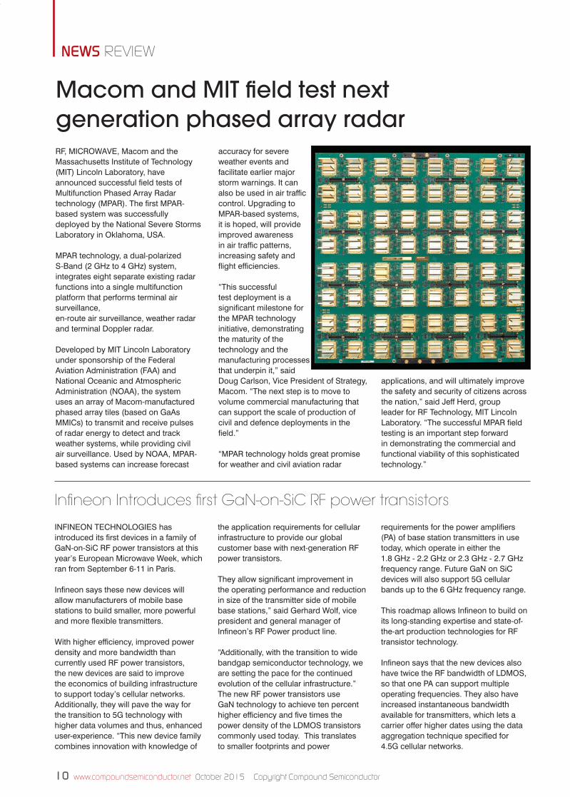
Seoul Semiconductor to mass-produce chip scale packaged LEDsSEOUL SEMICONDUCTOR has announced that it is mass producing LEDs in a new kind of chip scale packaging (CSP) which does not need processes such as die bonding, wire bonding or component parts such as lead frames, gold wire and so on.
According to the company, its patented Wicop (Wafer Level Integrated Chip on PCB) package is designed to directly connect the LED chip to the PCB with no intermediate substrate. In effect, the package and chip are the same size.
Generally, when the size of a chip package does not exceed more than 1.2 times the chip, it is classified as CSP, a technology first applied to LEDs in 2012. However, at that time because products using such technology need die bonding equipment, intermediate substrates or ceramic or silicon material to attach the chip to the PCB, it was difficult to see
the technology as a complete CSP. Seoul Semiconductor says it has been supplying Wicop-packaged products to major customers since 2013 for use in LCD backlighting, camera flashlights and also in vehicle head lamps.
Now the company plans to target the LED lighting-source market in lights, vehicles, and IT parts currently estimated to be $20 billion with the Wicop concept.
Kibum Nam head Seoul Semiconductor’s Central Research Centre said: “Through the development of Wicop which is an innovative small sized, highly efficient LED technology, the effective value of packaging equipment which was once essential in semiconductor assembly process will noticeably decrease. As all of
the parts which had been used for more than 20 years will not be necessary any more, there will be a huge change in the future LED industry”.
He added: “Seoul Semiconductor already has acquired hundreds of global patent portfolio regarding Wicop and takes a close look at how other manufacturers would develop the similar products using the similar technology”.
“Now offering Germanium Reclaim”
News CS v2.indd 11 29/09/2015 09:29

12 www.compoundsemiconductor.net October 2015 Copyright Compound Semiconductor
NEWS ANALYSIS
Photovoltaics: Designing for tomorrow
‘VirtualLab’ from Fraunhofer and CEA will pioneer photovoltaics to strengthen European solar cell markets. Will industry bite, asks Rebecca Pool?
AS EUROPEAN solar cell manufacturers strive for worldwide market share, the leaders of new photovoltaic development hub, VirtualLab, hope to help.
With traditional crystalline-silicon solar cells reaching theoretical conversion limits, many industry players are certain that alternative technologies are, at last, set to truly join the market.
One such player is III-V epitaxy and solar cell researcher, Frank Dimroth. Earlier this year his institution, Fraunhofer
ISE, Germany, revealed plans to strengthen collaboration with long-standing partner CEA Tech, France, by establishing a European ‘VirtualLab’.
Already famed for breaking PV efficiency record after record with their multi-junction cells, the alliance’s researchers aim is clear; to push commercial products.
The laboratory will be managed from three locations, Fraunhofer ISE in
Freiburg, CEA-LETI in Grenoble and CEA-LITEN in Le Bourget du Lac. But as Dimroth highlights: “Fraunhofer and CEA have very different infrastructures in place.”
According to the researcher, each has vast compound semiconductor knowledge but Fraunhofer’s strengths lie in epitaxy and solar cell engineering while CEA has a lot of process experience in engineering substrates, microelectronics and CMOS device manufacture.
News Analysis v4RS.indd 12 28/09/2015 14:18

Copyright Compound Semiconductor October 2015 www.compoundsemiconductor.net 13
NEWS ANALYSIS
“Materials teams are developing modules on both sides, but we will now share knowledge and infrastructure across both places; we’re only 350 km apart,” he says. “This is the starting phase, but we will make this a long-term partnership.”
CEA Tech and Fraunhofer ISE combine forces in near-industry research with French-German ‘Virtual Lab’.
But starting-phase or not, developments are well underway as would be expected from one of Europe’s leading PV research teams. As Dimroth highlights: “High concentration PV has a limited market, so our target is ultra-high efficiency photovoltaics.”
And to achieve this, two key themes have emerged; new concepts for III-V multi-junction solar cells and advanced CPV module prototyping. Right now, Dimroth is looking at using III-V materials on flat-plate PV modules, rather than CPV modules. High materials costs instantly appear prohibitive, but as Dimroth highlights, California-based Alta Devices is already doing a very good job of delivering high-efficiency thin film, flexible GaAs-based solar cells to mass markets.
“In principle, the solar cell structure is typically in the range of four to five microns, not a lot of III-V material is being used,” he says. “But [like Alta Devices] it is important to re-use the substrate, so we are working on lift-off processes.”
His team is also sampling multi-junction solar cells deposited on conductive foil; these electrically conductive carrier substrates ease solar cell manufacturing and mounting of devices onto receivers. And at the same time, III-V-on-silicon growth, for PVs, is underway.
“We’ve been doing this at Fraunhofer for seven years and it could have a massive impact,” highlights Dimroth. “We are looking into reducing epitaxy costs. Perhaps we won’t need the homogeneity of layers required for lasers and LEDs... so this could lead to a new generation of epitaxy for PVs.”
Driving CPV forwardMathieu Baudrit is head of Concentrator Photovoltaics at CEA Tech and intends
to develop highly integrated modules for low and medium concentrator PVs that will give European industry a competitive edge for future success in renewable energy markets.
His team is applying straightforward assembling techniques to Dimroth’s flexible III-V multi-junction solar cells.
Here, the cells are directly laminated onto the rear side of a concentrator mirror, a novel set-up that is all about cutting system costs. The mirror acts as a heat sink and CPV receiver, reducing component count and assembly cost.
Indeed, as Baudrit highlights: “We have reduced the number of the most expensive components in the system − the front cover glass, the cell substrate and heatsink have all been merged.”
The researcher is also confident that the Virtual Lab’s flexible solar cells could be integrated to consumer electronics devices, including smartphones, to charge batteries.
“When we think about integrating photovoltaics into a smartphone, we think about organic PVs, but these are not sufficiently efficient,” he says. “And silicon is the same. Look at the power you need
to charge a smartphone; considering the area available on a device for PVs, you are going to need very high efficiency cells.”
“For these small areas, you have to go to III-V cells and when you look at the cost of the III-V solar cell compared to a smartphone, it is very cheap,” he adds.
But relatively cheap or not, the technologies under developed at the VirtualLab undoubtedly need more cash to come to fruition.
Fraunhofer and CEA have each provided €1m to set up the new endeavour, but more funds twinned with industry input will be required to ensure long-term success.
“We intend to create innovation and job opportunities in this industry, but we also need long-term research and development funds from government organisations and industry,” explains Dimroth. “Soitec has been, and is, an important industrial partner but isn’t the only company we will be targeting.”
“Our competence is high-efficiency PVs that will go well beyond what silicon can deliver,” he adds. “And we are open to collaborate with anyone interested in our technology.”
News Analysis v4RS.indd 13 28/09/2015 14:18

14 www.compoundsemiconductor.net October 2015 Copyright Compound Semiconductor
SiC comes of age?After years of doubt and delay, SiC device sales are set to soar. Rebecca Pool talks to Yole Développement to find out more
As Cree delivers 900 V SiC MOSFETs, GE releases automotive-qualified SiC MOSFETs, and SiC diodes reach PV markets and more, industry pundits predict boom time has come for this wide bandgap semiconductor.
In a recent report from France-based Yole Développement, Pierric Gueguen and colleagues outlined how SiC at last offers added-value compared to existing silicon
technologies, following years of doubt and delays.
As the Yole analyst tells Compound Semiconductor: “For the SiC diode, this past year has seen numerous changes. Reliability has evolved and we now have applications where the cost of the SiC diode is no longer an issue.”
“The market has plenty of [diode]
suppliers, and the device is easy to integrate,” he adds. “SiC diodes take almost 80 percent of the overall market for SiC devices and we are confident that we will see more growth.”
Indeed, Yole expects the total SiC market for both diodes and transistors to treble by 2020, reaching a hefty $436 million. For now, the SiC diode has most medium voltage markets covered,
NEWS ANALYSIS
News Analysis v4RS.indd 14 28/09/2015 14:18

Copyright Compound Semiconductor October 2015 www.compoundsemiconductor.net 15
NEWS ANALYSIS
including PV inverters, motor control, electric and hybrid electric vehicles, and uninterruptible power supplies.
And while the diode is expected to remain the SiC device of choice to 2020, the electric and hybrid electric vehicle market holds the most promise for both the diode and transistor. Automotive companies, across the board, have already invested heavily
in wide bandgap materials research, which Gueguen reckons can only trigger business opportunities. Manufacturers have already integrated SiC diodes into electric vehicle chargers with power factor corrector topologies, and will continue to do so. Meanwhile further device development should soon see both diodes and transistors in SiC converters, for electric power train inverters.
“We have SiC diodes that are automotive-compliant and companies such as Toyota are pushing transistor [integration] to take full benefit of SiC capabilities at the converter level,” says Gueguen.
Without a doubt, Japan-based Toyota has driven SiC device adoption to date. Earlier this year, the automotive heavyweight started trialing diodes and transistors in its Camry hybrid prototype and fuel cell bus, after declaring some 20 percent of hybrid electric vehicle electrical power losses come from power semiconductors.
The company already confirms a 5 percent increase in fuel efficiency, and as Gueguen highlights: “This trial is a success. Toyota definitely wants to integrate SiC and is now solving [transistor] integration issues before launching [these devices] in a car.”
Indeed, mass-produced SiC inverters are expected to emerge around 2020, after Toyota and most other automotive manufacturers have finished qualifying such systems, and ensured suppliers can provide devices at mass volumes.
Device leadersBut who are the key suppliers right now? According to Yole, industry ringleaders Infineon and Cree − with its new RF and power arm, Wolfspeed − have a majority market-share of some 68 percent.
What’s more Cree’s recent acquisition of power module and electronics applications pioneer, APEI, is expected to have a profound impact on SiC markets. Together, the companies now intend to target the industry issues of integrating SiC devices into power modules and converters, while providing packaging specifically designed for these SiC systems.
“Cree has said in the past that you have these state-of-the-art power devices within thirty year old packages that just can’t capture all of silicon carbide’s benefits,” highlights Gueguen. “But now the company is more able to provide an entire solution, rather than just the power device. Infineon already has the required background to develop dedicated power modules for its power devices, and now Cree is developing its power business supply chain as it did for its LED business,” he adds.
But while the latest moves are set to accelerate the rate of SiC adoption, the big two are not expected to retain such strong market dominance in the future. As Gueguen predicts: “Infineon and Cree have the large amount of market share as they were first to the market. But Rohm, STMicroelectronics and such companies are now going to capture more and more market-share.”
“Manufacturers have already integrated SiC diodes into electric vehicle chargers with power factor corrector topologies,
and will continue to do so
”
News Analysis v4RS.indd 15 28/09/2015 14:19

The 6th CS International conference will be held at the Sheraton Brussels Airport Hotel, in Belgium on Tuesday 1 & Wednesday 2 March 2016.
CS International will build on the success of its predecessors, with industry-leading insiders delivering more than 30 presentations spanning sectors.
Together, these talks will detail breakthroughs in device technology; offer insights into the current status and the evolution of compound semiconductor devices; and provide details of advances in tools and processes
that will help to drive up fab yields and throughputs.Attendees at this two-day conference will gain an up-to-date overview of the status of the CS industry, and have many opportunities to meet many other key players within this community.
Connecting, informing and inspiring the compound semiconductor industry.
6th CS International Conference SPEAKERS ANNOUNCED!
CS International 2016 will provide timely, comprehensive coverage of every important sector within the compound semiconductor industry.
Supported by
Book your place now at: www.cs-international.net/register
Platinum Sponsors
Delegate Bag Sponsor Lanyard Sponsor Portfolio Sponsor Exhibitor Sponsor Wi-Fi Sponsor
Early bird discountBook your place before 30.11.2015
and receive a e100 discount.
Gold Sponsor
CS 2016 DPS 420 x 297 v10.indd 2 29/09/2015 09:31

Conference Chair: Drew Nelson President, CEO, IQE
All speakers and presentations are subject to change. ©Angel Business Communications Ltd.
This two day event covers five themes
The Quest for 5GWhat challenges will GaAs and CMOS power amplifiers face in making the transition from 4G to 5G? And will faster data links play into the hands of GaN-based amplifiers for base stations?
KEYNOTE £ James Klein- Qorvo Compound semiconductors: At the core of 5GANALYST £ Eric Higham - Strategy Analytics Will chipmakers and foundries benefit from 5G?
SPEAKERS£ Duncan Pilgrim – Peregrine Semiconductor CMOS: Game on!£ Peter Gammel – Skyworks Inc Technology requirements and initiatives for 5G smartphones£ Takahisa Kawai – SEDI GaN for 5G base stations
Driving deployment of wide bandgap power devicesIs SiC set to displace silicon in electric cars? And how will this material help to revolutionise the efficiency and operation of electrical grids?
KEYNOTE £ Daniel Fernandez – EU Project SPEED Silicon carbide wide band-gap devices for energy applicationsANALYST £ Pallavi Madakasira – Lux Research Hype versus reality: driving adoption of wide band gap power electronics
SPEAKERS£ Peter Ward - Anvil Semiconductors Driving down the cost of SiC devices for consumer applications£ Markus Behet – EpiGaN GaN on silicon – a truly revolutionary semiconductor technology matures£ Hans-Joachim Würfl – FBH Berlin GaN normally-off devices for highly efficient power switching £ Marta Borasio – Laytec Reliability and yield limiting variances in power-electronic manufacturing – early detection by advanced in-situ monitoring£ Chris Hodson – Oxford Instruments Plasma Technology Presentation Title TBC
Exploiting opportunities for LEDs and lasersCan LED bulbs meet the most demanding lighting applications, such as those found in the retail sector? And what are the opportunities for infrared and ultra-violet LEDs?
KEYNOTE £ Abdelmalek Hanafi - BMW Doubling driver visibility with laser-based headlights
ANALYST £ Pars Mukish – Yole Développement Opportunities for IR LEDsSPEAKERS£ David Cheskis – Anadigics 6-inch VCSEL wafer fabrication manufacturing advances£ Augustinas Vizbaras – Brolis Semiconductors Mid-infrared light sources: manufacturability and applications£ Paul Crump - Ferdinand-Braun-Institut High-power, high-efficiency lasers for fiber lasers and other markets£ Reinhard Windemuth – Panasonic Solutions for LED Manufacturing
Making heterogenous integration a hitIII-V channels are poised to make an introduction in next-generation logic circuits. But how will they be introduced, and what impact will they have?
KEYNOTE £ Yanning Sun – IBM III-V/Si integration: Moore and moreANALYST £ Nadine Collaert – IMEC Heterogeneous integration of high mobility materials on a 300mm Si platformSPEAKERS£ Suresh Venkatesan – POET Technologies A comprehensive technology platform for opto-electronic integration£ Lukas Czornomaz – IBM Hybrid IIIV/SiGe technology for CMOS and beyond, opportunities for 3D monolithic integration£ Thomas Uhrmann – EVG Heterogeneous integration enabled by advanced wafer bonding
Capturing light & generating cashWhat is needed to kick-start significant deployment of concentrating photovoltaic technology? And what are the opportunities for III-V detectors operating in the infrared?
KEYNOTE £ Carlos Algora – Technical University of Madrid Perspectives of concentrator photovoltaic technologyANALYST £ Frank Dimroth – Fraunhofer ISE Terrestrial III-V solar cells - challenges and opportunitiesSPEAKERS£ Paul Sharps – Solaerotech High efficiency multi-junction solar cells - what’s next?£ Andreas Umbach – Finisar Propelling detectors to 100 Gb/s and beyond
CS 2016 DPS 420 x 297 v10.indd 3 29/09/2015 09:31

18 www.compoundsemiconductor.net October 2015 Copyright Compound Semiconductor
INDUSTRY MOCVD
Propelling the power industry with
single-wafer systemsSingle-wafer systems combine great levels of uniformity with minimal maintenance and an easy route from development to high-volume
production, making them ideal for the production of GaN-on-silicon HEMTs
BY SUDHAKAR RAMAN, SOMIT JOSHI AND GEORGE PAPASOULIOTIS FROM VEECO INSTRUMENTS
There is a growing demand for better power electronics. Engineers throughout the world are wanting devices with higher efficiencies, smaller footprints, higher operating temperatures, faster switching and, of course, greater reliability.
Companies manufacturing devices that meet these criteria are in an enviable position because the list of potential applications that they can target is growing ever longer. There are emerging opportunities for increasing efficiency in IT servers, electrical motors, electrical vehicle recharging systems, windmills and solar inverters.
The soaring demand for greater energy efficiency is coming at a time when many believe that the incumbent technology – silicon-based power devices – is reaching its limits. This is spurring the development of a new breed of power electronics, based on new materials that will set a new benchmark for energy efficiency.
Those that are pursuing this goal include teams of engineers at several integrated device manufacturers (IDMs), and also those that are working for industry cooperative groups – including the well-known imec that is based in Europe, and PowerAmerica, a new comer based in the United States.
PowerAmerica has been formed through a public-private partnership between the US Department of Energy, industry and academia, with the latter led by North Carolina State University. Highlighting the importance of advanced power device development, the Energy Department has pumped $70 million into PowerAmerica.
To develop a new generation of power devices that are smaller, far more efficient and capable of operating at far higher temperatures than those made from silicon, PowerAmerica and imec are turning to wide bandgap materials. Efforts of both institutions are not limited to new device architectures,
and include the introduction of new manufacturing processes. The devices that PowerAmerica, imec, and many IDMs are developing are based on either SiC, grown on a native substrate, or GaN-on-silicon (GaN substrates are very pricy and limited in availability, so many developers of power electronics consider them unsuitable for device manufacture).
With a bandgap that is about three times that for silicon, these wide bandgap devices can deliver faster switching with less energy loss, a smaller component size and potentially greater reliability – attributes that lead to system-level benefits (see the panel “The promise of GaN-on-silicon” for more details).
To speed the development of GaN-on-silicon power devices, our team at Veeco Instruments has developed the Propel PowerGaN single-wafer manufacturing system. It is based on the core MOCVD technologies used in our multi-wafer TurboDisc EPIK700 and MaxBright batch systems. The Propel, a 200 mm-wafer-capable system, allows makers of power devices to leverage our many years of technical experience in MOCVD, as well as our market expertise. Thanks to this, chipmakers purchasing the Propel are able to accelerate their development of next-generation GaN-on-silicon devices.
Figure 1. Photoluminescence mapping on an 8-inch GaN-on-silicon wafer reveals that the standard deviation in the aluminium composition in the AlGaN layer is 0.29 percent.
Veeco v5_RS.indd 18 28/09/2015 14:19

Copyright Compound Semiconductor October 2015 www.compoundsemiconductor.net 19
INDUSTRY MOCVD
Veeco v5_RS.indd 19 28/09/2015 14:19

20 www.compoundsemiconductor.net October 2015 Copyright Compound Semiconductor
INDUSTRY MOCVD
Why single wafers?One of the biggest factors for determining the performance of GaN power devices is the quality of the epitaxial film. To optimize this, we advocate the use of single-wafer reactors, which have a proven and successful track record for rapid, cost-effective research and development. Compared to batch systems, single-wafer reactors provide a superior film quality of critical layers, much better run-to-run repeatability, higher production
availability and a lower consumption of spare parts. Another strength is that in a cluster tool configuration, they can transition more cost-effectively into a high-volume production tool.
We have designed our Propel reactor to maximize production flexibility. One of its strengths is that it is designed to be integrated into a multi-chambered cluster tool on a single backbone. With this approach, the capital investment for development can be recouped when it is
used to make products. This would follow a seamless transfer of the process recipe from pilot production to volume production.
Another attribute of the system is that although the reactor is currently configured for both 6- and 8-inch wafers, the architecture is extendable: When the industry roadmap requires a 12-inch capability, the platform will be able to address it in the future without losing productivity. There is also flexibility in terms of substrate material, as the Propel can be used to form GaN-on-SiC structures.
Figure 2. Triple-axis X-ray diffraction reveals the variation in thickness of the AlGaN barrier. This variation is two-to-three times less than it would be for an epiwafer produced in a multi-wafer system.
Figure 3. Run-to-run repeatability of a full HEMT structure; run-to-run repeatability of full stack thickness, AlGaN barrier thickness and aluminium composition, and thickness/composition uniformity.
Veeco v5_RS.indd 20 28/09/2015 14:19

Copyright Compound Semiconductor October 2015 www.compoundsemiconductor.net 21
INDUSTRY MOCVD
Advocating the use of single-wafer systems may raise a few eyebrows. Those of you that have been in the compound semiconductor industry for a long time will recollect that some of the first systems for production were single-wafer tools housing 2-inch wafers. Since then, to increase productivity and lower the cost-of ownership, MOCVD systems have increased in capacity by accommodating multiple wafers of larger sizes.
Why, then, are we behind a switch back to single-wafer systems? Well, because history attests that it is the best way to
increase productivity. In the silicon industry of the 1990s, the batch tool reigned supreme for performing the epitaxial processes for silicon-based ICs. In this era, the 130 nm/90 nm node took over from the 180 nm node, while the batch systems were left unchanged. This approach was viewed as a practical solution for transitioning from the development of the device to volume production.
It was a fine plan in theory, but a failure in practice. The repeatability and uniformity of the batch systems were unsatisfactory, problems that were exacerbated by the
introduction of new technology, such as smaller design nodes and larger wafer sizes. After wasting much time and money, companies cut their losses by switching to single-wafer tools.
This transition worked out better than many expected, thanks to the configuring of single-wafer tools as a cluster tool system, easing the path to volume production. These systems, which provided an overall cost-of-ownership that is lower than that for batch tools, proved flexible enough to serve the industry over the next ten to twelve years.
Veeco v5_RS.indd 21 28/09/2015 14:19

22 www.compoundsemiconductor.net October 2015 Copyright Compound Semiconductor
INDUSTRY MOCVD
The promise of GaN-on-SiliconCOMPARED to silicon transistors, those made by depositing GaN-based layers on silicon substrates promise a smaller form factor, superior thermal properties and greater efficiency – ideal for applications such as IT servers, where heat generation is an ever-increasing problem as server banks become larger, and where emphasis on heat management and energy efficiency continue to rise.
It is anticipated that as production ramps and costs fall, GaN-on-silicon power ICs will target a far broader range of applications, including consumer electronics, solar and wind power, power supplies and automotive applications.
If current product development efforts stay on schedule, device shipments in 2016 should rise, with the greatest success involving higher-end, less price-sensitive applications. Many market analysts are expecting this to happen. IHS Research, for example, is predicting a 90 percent compound annual growth rate between 2015 and 2020. Demand is also growing for SiC-on-SiC power devices − but primarily for automotive and PV applications.
Today, GaN-on-silicon devices are predominantly in development, although a few 200 V GaN-on-silicon devices are starting to appear. One or two chipmakers have introduced long-anticipated 600 V GaN HEMTs to the market, but these products are still in their infancy. The latest data suggests that products such as servers and white-box goods that are using these GaN power ICs are yet to ship. The good news, however, is that these device makers are currently perfecting the architectures of their transistors and developing manufacturing processes to enable the production of GaN-on-silicon devices that can address the market for power devices in the 600 V – 900 V range within the next one-to-two years.
Superior resultsThe superiority of the singe-wafer system is demonstrated in the far greater uniformity of the epilayers. Greater uniformity stems from the unique design of its wafer heating and gas injection subsystems.
Improving the uniformity of the layers is a major breakthrough, because it increases the device’s performance and reliability. Properties of the two-dimensional electron gas that arises at the interface between AlGaN and GaN are determined by the thickness and the composition of the AlGaN barrier. This barrier influences the transistor’s threshold voltage, on-state resistance and drain current − and to ensure a high yield, it is essential for it to have a highly uniform composition and thickness.
Characterising an 8-inch wafer featuring an AlGaN layer with an average aluminium composition of 23.7 percent demonstrates the capability of our single-wafer system. According to photoluminescence measurements, this thickness uniformity, evaluated in terms of ‘1σ›, is just 0.29 percent (see Figure 1). Meanwhile, the thickness profile of a typical AlGaN barrier, determined by high-resolution X-ray diffraction measurements
of 27 points on this wafer, has an average value of 21.4 nm and a range of 1.2 nm (see Figure 2). These results are two-to-three times better than existing batch tool performance.
While this result is encouraging, process engineers working in high-volume fabs know that they don’t just need highly uniform wafers now and again, but run after run after run.
Our system does not disappoint: Based on the Turbodisc family, it has unique architectural features and a stable, wide process operational space, enabling it to combine clean operation with excellent run-to-run repeatability. It is capable of carrying out more than 150 growth runs between preventative maintenance procedures, compared to typically 20 for a batch system.
Excellence in terms of run-to-run repeatability is illustrated by thickness measurements on a full HEMT structure, repeated without any chamber
conditioning or chamber opening between the runs (see Figure 3). Run-to-run variation in full stack thickness, AlGaN barrier thickness, and aluminium composition are 0.27 percent, 1.0 percent, and 0.55 percent, respectively. Meanwhile, the average uniformity for stack thickness and aluminium composition, assessed in terms of 1σ, are 0.46 percent and 0.27 percent, respectively. For a batch tool, the typical value would be 2 percent or more.
In addition to the strengths already outlined, our single-wafer system offers faster run times and allows engineers to spend more of their time refining the IC design and the process recipe.
To drive the development of GaN-on-silicon technology for power electronics, we are providing Propel reactors, epiwafers and our expertise in MOCVD, in partnership with other industry associations and leaders.
Our industrial partners are working to improve the quality of the epitaxial layers, because this will improve device performance and increase yield. Their efforts are also being directed at developing advanced vertical devices, and developing new isolation modules that can increase the level of integration.
We hope that our efforts, and those of our industry partners, will help to position GaN power device manufacturers for successful product introductions in 2016, followed by a smooth ramp to high-volume production for GaN power devices in 2017. Ideally, these GaN-based devices will address the 600 V to 900 V operation range, where we anticipate the greatest demand for consumer and industrial applications.
Veeco v5_RS.indd 22 28/09/2015 14:19

For more information and prices please contact the sales team.
Robin Halder
T: +44 (0)2476 718970E: [email protected]
Shehzad Munshi
T: +44 (0)1923 690215E: [email protected]
Reprints are a valuable sales tool
Benefit from a reprint featuring your company
They can be ordered after publication and can be customised to your exact needs
Untitled-16 1 29/09/2015 15:22

24 www.compoundsemiconductor.net October 2015 Copyright Compound Semiconductor
INDUSTRY CHARACTERISATION
SiC: Identifying imperfections with
Raman spectroscopyA revolution in Raman spectroscopy allows routine mapping of SiC wafers in little more than an hour.
RAMAN SPECTROSCOPY is a tremendously powerful technique for scrutinising SiC. It can determine different polytypes, quantify stress and strain, reveal carrier levels and identify the origin of defects.
But is this insightful form of spectroscopy available to all? Or is it only suitable for researchers with Raman expertise?
Acquiring Raman spectra is by no means a trivial task, because these signals are incredibly weak. The technique involves directing a monochromatic beam of light at a sample, collecting the back-scattered radiation, and passing this through a spectrometer. The vast majority of the light that is scattered from the sample will be at exactly the same wavelength as the incident source, but a very small proportion of it – perhaps a few parts in a million – will be at a slightly different frequency, due to the interactions of photons with atomic vibrations within the material under investigation.
In decades gone by, collecting Raman spectra would be the job of a dedicated experimentalist, skilled in the art of aligning optical components. They would toil away in an incredible dark lab housing a bulky triple-grating spectrometer. Every few hours, so long as they kept topping up their detector with liquid nitrogen, they could acquire a spectrum with an acceptable signal-to-noise ratio.
By the 1990s, the situation improved dramatically, thanks to the launch of a Raman microscope by Renishaw, a UK company headquartered at Wotton-under-Edge. Developed in partnership with the late David Batchelder of Leeds University, this relatively compact instrument featured holographic notch
filters, which offered a neat solution to preventing the vast majority of the backscattered laser light from entering the spectrometer and overloading the thermo-electrically cooled detector.
Even with these advances, optics skills were still needed. Many labs would have more than one laser for their Raman microscope, allowing the experimentalist to select the best sources for a particular sample. To reconfigure the microscope so that it operated with a different laser required the replacing of one notch filter with another and the realignment of the instrument. With practice, this could be done within an hour, but for inexperienced users, it could take the best part of a day.
Another step-change in simplicity came after the turn of the millennium, with the launch of a new generation of Raman microscope.
“With the inVia [Raman Microscope], all the complexity is taken away by having an automated system,” explains Ian Hayward, Raman Product Marketing Manager. “Switching between lasers is one click of a button, using a mouse.”
This latest instrument, which continues to be refined, acquires spectra incredibly quickly. Now users not only take individual Raman spectra, as they would have done in the past, but also map areas in reasonable timeframes. For example, the mapping of a 3-inch SiC wafer takes just 75 minutes.
Renishaw v3RS.indd 24 28/09/2015 14:20

Copyright Compound Semiconductor October 2015 www.compoundsemiconductor.net 25
INDUSTRY CHARACTERISATION
The substantial reductions in mapping times partly results from the availability of more powerful lasers, including a 532 nm source that is ideal for analysing SiC.
“532 nm is where you get your best bang-per-buck for laser power,” explains Tim Batten, Applications Scientist at Renishaw. Acording to him, in the past these sources had an output power of typically 20 mW, but now 200 mW sources are readily available.
Helping to drive down acquisition times for Raman spectra are improvements in the efficiency of the detectors, and a higher level of automation that includes a maintaining of the optimal alignment of the optics.
The increased automation also allows the tool to be used more efficiently. “Now you can queue up a series of measurements and leave the instrument running overnight,” says Hayward.
Making these measurements is incredibly straightforward, with the user only needing to know how to operate a microscope and use a PC.
“The main difficulty is analysis, and that
depends on what you want to do,” explains Batten. “We sell to a wide range of industries, and sometimes they’ll have an expert there who sets up the initial analysis parameters, and writes a procedure.” Technicians can then follow this, taking measurements day by day.
Supporting the SiC industry Often it is the interest of potential customers in Raman microscopy that triggers the team at Renishaw to investigate a particular use of this technique. That was certainly the case for SiC, with companies showing interest in using Raman microscopy to expose problems that could occur during the manufacture of substrates and the growth of epiwafers. Those interested parties included a vertically integrated firm. “For them, it is of great importance that they can determine where the problems are occurring, because they can remedy them,” says Batten.
If one of the problems that they have involves the presence of more than one polytype within the material, this will come to light in the Raman spectra.
By delivering high-speed mapping of SiC wafers, the Renishaw inVia Raman microscope enables a relatively quick identification of defects, polytypes, strain and carrier concentration.
Renishaw v3RS.indd 25 28/09/2015 14:20

26 www.compoundsemiconductor.net October 2015 Copyright Compound Semiconductor
INDUSTRY CHARACTERISATION
That’s because different polytypes have Raman peaks at different frequencies, due to differences in stacking geometry that produce atomic vibrations at different frequencies. As the Raman spectra for all the common polytypes are well known, it is possible to identify all the crystalline phases with a SiC film.
“You can also identify the orientation of the grain,” says Hayward, “because you have a polarised laser, and you can analyse the polarised Raman light.”
As well as the polytype, the vibrational modes within the crystal are influenced by the local environment of the atoms in a unit cell. So the spectra can uncover strain, defects, and damage to symmetry. “As a result of being able to measure strain, we are also able to infer stress in the material,” explains Batten.
Some of these Raman peaks are electronically sensitive, with their position and peak width influenced by the free carrier concentration. This allows spectra to reveal the type of doping, and also its level. “I think it is difficult to be very accurate with those numbers,” warns Batten. “Normally, to get the best values, people use a mixture of Raman and PL. This is fine as our instrument can also collect PL.”
A great strength of the Raman technique is that it can determine the quality of material beneath the surface. “Effectively, all we are doing is mapping a surface, and then adjusting our focus into the material, and repeating the measurements while going deeper, to create a cube rather than a rectangle of data,” says Batten.
“By having the three-dimensional capability, it means that rather than saying that there is a carrot defect there, we can say that it’s a carrot defect and it originated from this location,” explains Hayward. This allows engineers to distinguish between defects originating in the epitaxial layers, and those that can be traced back to imperfections in the substrate.
The resolution of the inVia Raman Microscope depends on the magnification of the objective lens. With the lens offering the highest magnification, later resolution is limited by diffraction, and it cannot exceed about 300 nm. Meanwhile, the depth-wise resolution, which varies with the refractive index of the material, and is of the order of a micron in SiC.
Classifying defects is possible with Raman, but it can also be carried out by various other techniques. “I think with Raman, one of the nice things is that the measurements are quite quick, so we can quickly classify them,” says Batten.
Modest requirementsHeads of SiC labs and fabs that are considering installing this tool will be glad to hear that its needs are very modest. The instrument can be placed in a space where variations in temperature can be as high as a few degrees, and thanks to an enclosure, there is no need to turn off room lights when making measurements. Another attractive feature is that, for the vast majority of measurements, there is no need to place the instrument on a vibration isolation table. That’s partly because the inVia is positioned
The Princess Royal opened the Renishaw Innovation Centre in July 2015. This building, built on the company’s headquarters in Wotton-under-Edge, Gloucestershire, is designed to have a low-carbon footprint. There are photovoltaic panels mounted to the roof and south facing walls that are expected to produce an estimated 280,000 kWh per year. The building is lit by LEDs that are automatically controlled by day lighting and movement sensors.
Renishaw v3RS.indd 26 28/09/2015 14:20

your!EPITAXIAL GROWTH!
partner!
Enabling advanced technologiesWorld leading technology
Complete materials range
MOCVD, MBE, CVD
Advanced semiconductor wafer products
Advanced R&D capabilities
Multiple, manufacturing sites (Europe, Asia, USA)
www.iqep.com
Untitled-1 1 02/07/2014 11:05
28 www.compoundsemiconductor.net October 2015 Copyright Compound Semiconductor
INDUSTRY CHARACTERISATION
Simplifying the use of the instrument has made it accessible to a broader range of researchers and technicians, who benefit from software that is far easier to use than its predecessors. This software can gather vast amounts of data, due to the opportunity to map large areas and volumes of material. The data sets can easily be 100 GB, putting strain on data storage. “I’ve collected some two terabyte data sets. You could fill a hard drive every couple of days,” remarks Batten.
The opportunity for statistical analysis is unleashed with the larger data sets. “A more powerful technique to analyse data is to look for variations and trends,” says Batten. “Before, we were using very simple qualitative measurements, say peak width or peak position or peak intensity.”
Potential users will find the ease of acquiring so much data appealing. However, they might be reluctant to invest in a Raman microscope, feeling that if the alignment of the instrument were to go astray, they might not notice, or would not know how to correct this issue. There is no need to worry about this, however, because the inVia Microscope has a health-check feature that can gauge the condition of the instrument. “If there are any health-related issues, it is possible for someone from the UK office, for example, to log on to the instrument remotely over the internet and perform any necessary adjustments.”
This level of support will be welcome by those considering the inVia microscope for studying SiC – and also for those that are thinking of using it for scrutinising other compound semiconductor materials, such as GaN.
One of the great strengths of GaN, and also SiC, is that it allows the fabrication of devices with far higher operating temperatures than those made from silicon. To understand the capabilities and limitations of these wide bandgap devices, there is a need to accurately measure the local temperatures within these devices. “[Raman] gives you a very accurate temperature of a small volume, whereas if you use something like infra-red, you probe quite a large volume, so you massively underestimate the peak temperature,” says Batten.
LEDs and lasers could also benefit from this approach to measuring device temperature, and Raman may also be a useful tool for measuring the strain within these devices, which may be formed by hetero-epitaxial growth. So there are clearly many opportunities for using Raman within our industry, and with acquisition times that are a fraction of what they were in the past, this technique has more appeal than ever before.
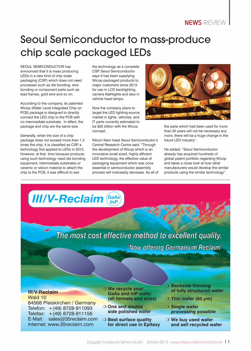
An approximately 1 mm2 Raman image revealing inclusions of 6H-SiC, 3C-SiC or silicon (red), voids (black) and strain distribution (red).
A comet defect. The image show the 4H- SiC substrate (green), the 4H-SiC epilayer (blue), and 3C-SiC inclusion (red/orange). Dimensions of the mapped region are 70 μm by 25 μm by 7 μm.
on an isolation baseplate that keeps all the elements in position; and it is partly because optical stability is aided by a very careful design of the instrument, with all components mounted to a back plane, an architecture that minimises their relative movement.
Renishaw prides itself on looking after its customers. After installing the instrument, recipients receive a great deal of support in learning how to use the inVia microscope. This begins with a couple of days of on-site basic instruction directly following installation, and continues with more detailed training courses.
“We are running a course called Raman Revealed – we normally run it about twice a year,” explains Hayward. “Customers or potential customers can come and learn how to use the instrument in detail. Our applications experts explain why you would do things in a certain way, the benefits of certain lasers, and how they would approach addressing a sample they hadn’t come across before.”
Renishaw v3RS.indd 28 28/09/2015 14:20

SlcnSmcndctr-SEMI_210x297mm_PQ.pdf 1 9/11/15 9:22 AM
Untitled-2 1 14/09/2015 09:39

30 www.compoundsemiconductor.net October 2015 Copyright Compound Semiconductor
TECHNOLOGY GaN POWERED DEVICES
The pathway to power switching efficiency
More efficient power switching devices are required to meet the energy demands forecasted over the next 20 years.
BY BRYAN BOTHWELL, DAVID DRUMMOND AND MANYAM PILLA FROM QORVO, AND HUILI GRACE XING AND DEBDEEP JENA FROM CORNELL UNIVERSITY
POWER SEMICONDUCTOR DEVICES are critical for the world’s energy infrastructure as it is projected that by 2030, as much as 80 percent of the electricity generated will pass through one or more power conversion stages from generation to consumption (an increase from 30 percent today). That will propel switching devices, which are already playing a critical role, to even greater prominence.
Modern high-efficiency switching power conversion solutions were enabled by the development of silicon-based power MOSFET switching devices. Power switch device switching and on-resistance (Ron) are two key characteristics that impact the maximum conversion efficiency; their impact is magnified at higher voltage and current levels.
It is here that the drum beats the loudest for higher efficiency, lower-loss switching devices that can
Vert
ica
l GaN
service markets ranging from motor drives to electric vehicles and power generation and transmission. These markets are not only looking for greater performance – they are also very cost conscious.
Significant improvements in efficiency will not result from further refinements to silicon devices as their performance is already approaching the material limits. Instead, industry is turning to the superior material properties of wide bandgap (WBG) GaN and SiC devices to meet the requirements of tomorrow’s high-efficiency, low-loss systems.
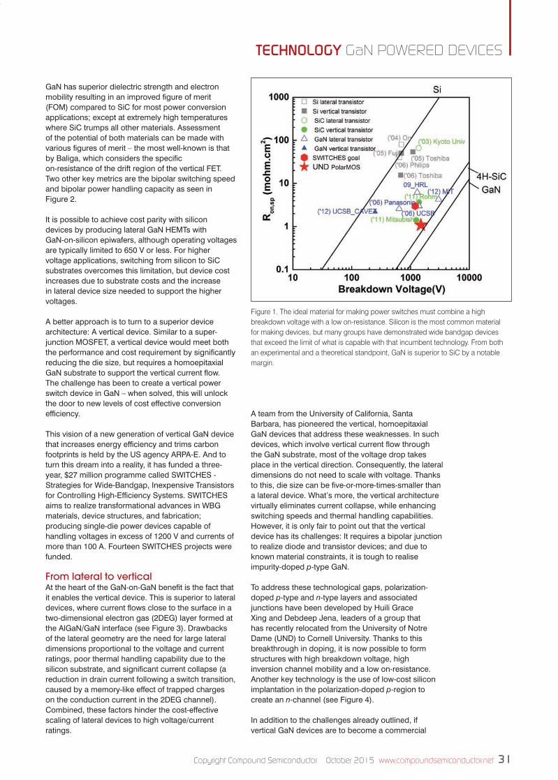
Devices using SiC and GaN have been commercially available for several years, but widespread adoption has been hampered by high cost and unproven reliability compared to silicon incumbents. But in terms of potential performance, the WBG materials are vastly superior (see, for example, Figure 1).
Qorvo v8RS.indd 30 29/09/2015 09:32
Copyright Compound Semiconductor October 2015 www.compoundsemiconductor.net 31
TECHNOLOGY GaN POWERED DEVICES
GaN has superior dielectric strength and electron mobility resulting in an improved figure of merit (FOM) compared to SiC for most power conversion applications; except at extremely high temperatures where SiC trumps all other materials. Assessment of the potential of both materials can be made with various figures of merit – the most well-known is that by Baliga, which considers the specific on-resistance of the drift region of the vertical FET. Two other key metrics are the bipolar switching speed and bipolar power handling capacity as seen in Figure 2. It is possible to achieve cost parity with silicon devices by producing lateral GaN HEMTs with GaN-on-silicon epiwafers, although operating voltages are typically limited to 650 V or less. For higher voltage applications, switching from silicon to SiC substrates overcomes this limitation, but device cost increases due to substrate costs and the increase in lateral device size needed to support the higher voltages.
A better approach is to turn to a superior device architecture: A vertical device. Similar to a super-junction MOSFET, a vertical device would meet both the performance and cost requirement by significantly reducing the die size, but requires a homoepitaxial GaN substrate to support the vertical current flow. The challenge has been to create a vertical power switch device in GaN – when solved, this will unlock the door to new levels of cost effective conversion efficiency.
This vision of a new generation of vertical GaN device that increases energy efficiency and trims carbon footprints is held by the US agency ARPA-E. And to turn this dream into a reality, it has funded a three-year, $27 million programme called SWITCHES - Strategies for Wide-Bandgap, Inexpensive Transistors for Controlling High-Efficiency Systems. SWITCHES aims to realize transformational advances in WBG materials, device structures, and fabrication; producing single-die power devices capable of handling voltages in excess of 1200 V and currents of more than 100 A. Fourteen SWITCHES projects were funded.
From lateral to verticalAt the heart of the GaN-on-GaN benefit is the fact that it enables the vertical device. This is superior to lateral devices, where current flows close to the surface in a two-dimensional electron gas (2DEG) layer formed at the AlGaN/GaN interface (see Figure 3). Drawbacks of the lateral geometry are the need for large lateral dimensions proportional to the voltage and current ratings, poor thermal handling capability due to the silicon substrate, and significant current collapse (a reduction in drain current following a switch transition, caused by a memory-like effect of trapped charges on the conduction current in the 2DEG channel). Combined, these factors hinder the cost-effective scaling of lateral devices to high voltage/current ratings.
A team from the University of California, Santa Barbara, has pioneered the vertical, homoepitaxial GaN devices that address these weaknesses. In such devices, which involve vertical current flow through the GaN substrate, most of the voltage drop takes place in the vertical direction. Consequently, the lateral dimensions do not need to scale with voltage. Thanks to this, die size can be five-or-more-times-smaller than a lateral device. What’s more, the vertical architecture virtually eliminates current collapse, while enhancing switching speeds and thermal handling capabilities. However, it is only fair to point out that the vertical device has its challenges: It requires a bipolar junction to realize diode and transistor devices; and due to known material constraints, it is tough to realise impurity-doped p-type GaN.
To address these technological gaps, polarization-doped p-type and n-type layers and associated junctions have been developed by Huili Grace Xing and Debdeep Jena, leaders of a group that has recently relocated from the University of Notre Dame (UND) to Cornell University. Thanks to this breakthrough in doping, it is now possible to form structures with high breakdown voltage, high inversion channel mobility and a low on-resistance. Another key technology is the use of low-cost silicon implantation in the polarization-doped p-region to create an n-channel (see Figure 4).
In addition to the challenges already outlined, if vertical GaN devices are to become a commercial
Figure 1. The ideal material for making power switches must combine a high breakdown voltage with a low on-resistance. Silicon is the most common material for making devices, but many groups have demonstrated wide bandgap devices that exceed the limit of what is capable with that incumbent technology. From both an experimental and a theoretical standpoint, GaN is superior to SiC by a notable margin.
Qorvo v8RS.indd 31 29/09/2015 09:32

32 www.compoundsemiconductor.net October 2015 Copyright Compound Semiconductor
TECHNOLOGY GaN POWERED DEVICES
success, they must also overcome issues related to maturity and the supply chain. This class of GaN device has a promising future in motor drives, solar inverters, electric-vehicle charging, telecom DC-to-DC conversion, and within the military – but success hinges on a multitude of factors. Of these, performance is paramount, as there is a need for vertical GaN devices delivering higher-efficiency switching while operating at higher frequencies and temperatures. If they can do this, there will be a trimming of size and a cutting of cost at the system level, while critical reliability requirements set by industry are fulfilled.
A two-pronged approachThose of us from Qorvo are subcontractors on two
SWITCHES projects: The first project is led by Huili Grace Xing and Debdeep Jena, and includes IQE and the United Technologies Research Center (see Figure 5 for details); and the second project is led by Microlink, a company specializing in epitaxial lift-off technology that could prove critical in cutting device cost through the re-use of bulk GaN substrates. The small sizes and high costs of GaN substrates have led many leaders in industry and academia to pay minimal attention to GaN-on-GaN devices formed using bulk substrates, but the efforts of Microlink could address this.
Progress to date has been impressive with UND/Cornell having successfully designed and fabricated GaN-on-GaN polar p-n diodes using IQE SWITCHES
Figure 2. The great opportunities for wide bandgap devices, and those made from GaN in particular, are evident from the superior figures of merit compared to those based on silicon and GaAs.
Figure 3. The conventional configuration for a GaN transistor is a lateral architecture (a). Downsides of this approach include an increase in die size with power handling requirements, poor thermal handling and current collapse. All these issues are addressed by turning to a vertical architecture (b).
Qorvo v8RS.indd 32 29/09/2015 09:32

Copyright Compound Semiconductor October 2015 www.compoundsemiconductor.net 33
TECHNOLOGY GaN POWERED DEVICES
epi with blocking voltages of more than 1200 V as well as p-n diodes with blocking voltages in excess of 3000 V. These fabricated polarization-induced GaN-on-GaN p-n diodes show near perfect I-V behavior and avalanche capability. PolarMOSH devices have been demonstrated with a threshold voltage of 1.3 V, a maximum on current of 250 mA/mm and a maximum gate voltage of more than 15 V. Beyond this, Qorvo has recently shown blocking voltages of more than 700 V on MBE-regrown JFETs, with plans for a transition to a 4-inch platform in 2015 to address manufacturing maturity and further cost reduction. Key SWITCHES programme milestones continue to be achieved, leading to increased confidence in this technology core.
There are still many challenges ahead. One immediate goal is to build on recent successes in substrate and epiwafer improvements, and to demonstrate vertical polar JFETs that can handle 300 V and 10 A. This effort will involve various risk reduction plans at the wafer processing level − mainly targeted at processing control and calibration.
Another challenge is to fabricate large JFETs, capable of operating at 10 A or more, on large-diameter bulk GaN wafers in a 4-inch fab. An aggressive plan is in place to push substrate vendors to 4-inch wafer diameters, which will enable us to accelerate process development and maturation at Qorvo’s 4-inch/6-inch fab.
Our next major task is to integrate the polarMOSH and polarJFET processes, and to fabricate polar vertical MOSHFETs − PolarMOS. Although we have demonstrated as-grown material with a blocking voltage in excess of 1200 V, this needs to be repeated with regrown or implanted channels. The good news is that we have developed new technology and intellectual property that enables higher blocking voltages, and combines sufficient margin with improved reliability. Beyond this, integrating the epitaxial lift-off with the new device architecture is planned.
The final challenge will be at the system level to develop packaging solutions for high-power devices in a small form-factor, along with component integration. Qorvo is working with members of both projects to develop packaging solutions that maximize the
Figure 4. The PolarMOS technology combines p-n junction devices with MOSH and JFET technologies.
“Another challenge is to fabricate large JFETs, capable of operating at 10 A or more, on large-diameter bulk GaN wafers in
a 4-inch fab. An aggressive plan is in place to push substrate vendors to 4-inch wafer diameters, which will enable us to accelerate process
development and maturation at Qorvo’s 4-inch/6-inch fab
”Qorvo v8RS.indd 33 29/09/2015 09:32

34 www.compoundsemiconductor.net October 2015 Copyright Compound Semiconductor
TECHNOLOGY GaN POWERED DEVICES
Further readingH. G. Xing et. al. “Unique opportunity to harness polarization in GaN to override the conventional power electronics figure-of-merits”. Device Research Conference, June 2015, http://arxiv.org/abs/1505.04651ARPA-E. “Strategies for Wide-BandGap, Inexpensive Transistors for Controlling High Efficiency Systems (SWITCHES)’, 2013S. Chowdhury et. al. Semicond. Sci. Technol. 28 074014 (2013)J. Simon et. al. Science 327 60 (2010)D. Jena et. al. Phys. Stat. Solidi. 208 1511 (2011)
performance of vertical GaN-on-GaN devices at the system level.
The appeal of these devices is intensifying, thanks to their capability to fulfil the need for low-cost, high-efficiency switching that can trim electricity consumption and accelerate alternative-energy deployments on a global scale.
This places those of us at Qorvo in an enviable position, thanks to our involvement in: a differentiated core device technology; a world-class supply chain and system partners; a high-volume manufacturing infrastructure; and parallel paths, including substrate re-use that addresses cost parity. By developing go-to-market solutions, often a stumbling block for ubiquitous deployment of WBG power devices, an exciting future is on the horizon in power conversion.
Figure 5. The SWITCHES team led by Huili Grace Xing and Debdeep Jena − who have both recently moved their groups from the University of Notre Dame to Cornell University − is very strong and highly complimentary. Xing and Jena are the inventors of the background IP for a differentiated device architecture that addresses the doping issues problematic with vertical GaN devices; IQE is a major epiwafer supplier to the III-V semiconductor industry and possesses not only a world-class engineering background, but also a commercial cost structure needed for a long-term production ramp; UTRC is the research arm of UTC and acts as the technology incubator for their business units who have rich experience in designing power systems for aerospace, defence and commercial applications; and Qorvo is the world’s leading supplier of RF devices into the mobile, infrastructure, and defense markets with over 15 years of GaN manufacturing and product development experience. UTRC provides not only a commercial outlet for products from the SWITCHES programme, but more importantly is the partner that helps define product performance, specifications, and overall system level requirements.
£ The authors wish to thank Tim Heidel and Dave Henshall from ARPA-E, who are leading the SWITCHES program. Award No. DE-AR0000454 (CFDA No.81.135).
Qorvo v8RS.indd 34 29/09/2015 09:32

Renishaw plc, Spectroscopy Products Division, New Mills, Wotton-under-Edge, Gloucestershire, GL12 8JR, UK T +44 (0)1453 524524 F +44 (0)1453 523901 E [email protected]
www.renishaw.com/raman
Visualise SiC using Raman spectroscopyRenishaw’s Raman systems help you understand the growth mechanisms of compound semiconductors, including SiC
For more information visit www.renishaw.com/sic
Characterise your SiC - investigate stress/strain, defects, polytypes and electronic properties,
such as free carrier concentration.
No sample preparation - analyse at any stage of the production process, whether whole
wafers of bulk material, epi-layers, or functioning devices.
Image entire wafers in practical timescales - quickly reveal the locations of defects and
strain/stress.
Probe at any depth and image in 3D - comprehensively characterise your epi-layer and the
underlying wafer bulk with sub-micrometre resolution.
AD166(EN)-01-A.indd 1 15/09/2015 07:51:45

Reasons to sponsor CS International Conference 2016
Connecting, informing and inspiring the compound semiconductor industry
CALL NOW +44 (0)24 76718970email [email protected] or view the online
sponsorship pack at mediapack.cs-international.net
www.cs-international.net
ü Senior management networking opportunities
ü Increased company and brand awareness
ü Access to the top strategists within the compound semiconductor industry
ü Create, develop and support customer relationships
ü Engage in debate, share insight and expertise on industry challenges
ü Gain visibility and recognition as an industry leader
ü Leverage exposure in multiple industry media
ü Demonstrate market innovation and leadership by launching new services, products and systems
CS International 8 Benefits A4 Ad 2016 v2.indd 1 22/04/2015 16:49

Copyright Compound Semiconductor October 2015 www.compoundsemiconductor.net 37
INDUSTRY POWER ELECTRONICS
AT THE GLOBAL, national and local level, efforts are being directed at curbing carbon dioxide emissions and making the very best use of all energy resources. Although there are many ways to do this, they all involve using electrical energy as efficiently as possible.
This is by no means a trivial task. The rise in renewable sources has led to growth in energy generated in a DC form, although this is still overshadowed by AC sources. One must also note that transferring electricity from its point of generation
Boosting normally-off
POWER SWITCHESTo lower losses in power conversion units, European project HiPoSwitch has established processes and infrastructure for
low-cost manufacture of GaN-on-silicon HEMTs.
BY JOACHIM WÜRFL FROM THE FERDINAND-BRAUN-INSTITUT (FBH), BERLIN
to where it is consumed tends to involve stepping up and down the voltage, and while many appliances can be directly plugged into a power supply, electronic goods often have transformers that are built in to them to provide a low-level, DC source.
For efficient use of energy, the conversion of electrical energy at all these points in the chain from generation to consumption must be carried out with minimal
HiPOSwitch v8RS.indd 37 28/09/2015 14:22

38 www.compoundsemiconductor.net October 2015 Copyright Compound Semiconductor
INDUSTRY POWER ELECTRONICS
losses. And if these energy converters can also be made smaller and lighter, they will be better at serving some emerging high-tech applications, such as mobile, air-, and space-borne systems.
A very promising class of device for meeting these demanding targets is the GaN-based power switching device. It has great material characteristics, including a high breakdown strength and electron velocity, and compared to the silicon incumbent, it can turn on more efficiently, be more compact, and switch at far faster speeds.
These attributes translate into a superior performance for the power converter. Those that incorporate GaN transistors have less than half the losses of existing technologies and make conversion efficiencies of over 98 percent practical. If these converters were widely deployed, it would lead to tremendous savings in primary energy consumption.
A simple calculation can illustrate the level of these savings. In Europe, more than 3000 terawatt hours of electrical power are generated every year. Assuming that only a quarter of this electricity is converted to different energy levels and efficiency is increased by just two percentage points, this would allow at least two coal-fired plants to be turned off. In other words,
this emerging technology can have a huge impact.To address the technological challenges of making devices with this wide bandgap technology, the European Community has funded a three-year project called HiPoSwitch. Kicking off in 2012, this effort, backed by €5.6 million, has focused on the development of GaN power switching transistors as the centre-piece of modern electronic energy conversion systems.
Co-ordinated by FBH (Ferdinand-Braun-Institut, Leibniz-Institut für Höchstfrequenztechnik), this programme involved eight institutional and industrial project partners and succeeded in developing GaN prototype, normally-off, power switching transistors. The manufacturability of these devices on a large-scale industrial production line has recently been demonstrated within this project.
Together, the complimentary players in theHiPoSwitch consortium spanned the full value-added chain towards an efficient energy conversion system (see the panel “Roles within HiPoSwitch” for details). Expertise ranged from epitaxial wafer growth to device design, processing, circuit design, low-inductance packaging and the final implementation of developed devices into a converter system environment. Tasks that were performed included thorough device characterization − static and dynamic performance and reliability testing.
Efforts focused on the industrialization and rapid exploitation of the results. For example, during the project, the diameter for GaN-on-silicon epiwafers increased from 4-inch to 150 mm and finally to 200 mm. This eases the transfer of this new technology to a commercial process line.
Starting conditionsThose working within the project did not have to start from scratch − instead, they were able to draw on their previous experiences in GaN microwave and power-switching transistors. However, the power switching
Figure 1: Performance of 60 mΩ GaN power switching device fabricated on a SiC substrate (left); pulsed output characteristics (1 μs pulse duration) (right): Evolution of dynamic on-state resistance and drain leakage with drain voltage.
Table 1. GaN transistors are superior to their silicon counterparts on many fronts.
HiPOSwitch v8RS.indd 38 28/09/2015 14:22
Copyright Compound Semiconductor October 2015 www.compoundsemiconductor.net 39
INDUSTRY POWER ELECTRONICS
devices were not ready for system implementation at the outset, because they lacked the requested stability and current-switching ability, and were also suffering from dispersion effects upon power switching.
The HiPoSwitch programme tackled these issues, focusing on the development of normally-off GaN power-switching devices for 600 V operation in a 3 kW telecom rectifier demonstrator system. The switches for this were developed on silicon and SiC substrates, enabling a fair comparison between the two different substrate types, based on nominally the same device architecture.
EpiGaN, working closely with MOCVD tool manufacturer Aixtron, developed and fabricated GaN epitaxial structures on silicon substrates with ultra-low leakage currents at 650 V and breakdown higher than 1000 V, while FBH focused on GaN-on-SiC epitaxial growth. Manufacture on SiC substrates was never intended − transfer to silicon substrates would follow, allowing a trimming of production costs and improved manufacturability.
For the continuous optimisation of normally-off GaN HEMTs on silicon substrates and the benchmarking of them against GaN-on-SiC equivalents, EpiGaN constantly delivered 4-inch GaN-on-silicon wafers to FBH. In parallel and in close cooperation with Aixtron, wafer diameters were increased from 150 mm to 200 mm, a necessary step towards cost-effective industrial production. At its Austrian location in Villach, chip-manufacturer Infineon implemented the newly developed GaN technology on its silicon process line, enabling industrial production of these power semiconductors.
All devices for the final demonstrator were fabricated on FBH´s 4-inch GaN processing line and assembled in Infineon’s low-inductance ThinPak housing. These transistors were designed for 600 V power switching with a very limited dynamic on-state resistance increase. Another target was a turn-on resistance below 75 mΩ, which turned out to be challenging.
During the course of the project, devices strongly benefited from a combination of significant advancements in GaN epitaxial growth on SiC and silicon substrates, and an improved understanding of dynamic device behaviour. Thanks to this, at 600 V the dynamic on-state resistance increase during power switching plummeted from a factor of 100 at the beginning of the project to just 1.25 after its completion. Demonstrator chips, which featured a gate length of 214 mm, were able to switch up to 120 A if operated at pulsed conditions (see Figure 1 for details, and table 1 for benchmarking of devices against Infineon’s state-of-the-art Si-CoolMOS devices, which had nominally the same turn-on resistance).
Figure 2: Comparison of GaN-on-silicon and GaN-on SiC devices designed for 60 mΩ turn-on resistance. Static transfer characteristics (left); pulsed output characteristics of 60 mΩ normally-off devices taken at a gate voltage of +5 V (middle and right).
Figure 3: 3 kW telecom rectifier powered with prototype GaN transistors mounted in ThinPak housings.
HiPOSwitch v8RS.indd 39 28/09/2015 14:22

40 www.compoundsemiconductor.net October 2015 Copyright Compound Semiconductor
INDUSTRY POWER ELECTRONICS
Tremendous improvements in the performance of GaN devices during the HiPoSwitch project were enabled by excellent co-operation between the partners. Sharing of simulation results, measurements and reliability data underpinned advances in critical areas, such as epitaxy and device processing. A key part of this was the comprehensive investigations of drift and degradation effects by researchers at the University of Padova and the Vienna University of Technology.
One of the most fascinating parts of the entire programme involved the comparison of normally-off GaN HEMTs fabricated on GaN-on-silicon and GaN-on-SiC substrates. Both classes of transistor were formed using nominally the same epitaxy of the active layers and an identical processing sequence. Normally-off behaviour is quite comparable, with turn-on at about +1 V (see Figure 2). As expected, the maximum drain current capability is higher for the SiC-based devices, and inferior thermal properties of the silicon-based transistors are apparent when HEMTs are driven into saturation. However − and this is very good news − there is not a significant difference in
the behaviour of both types of device when they are operated at an on-state bias point that is typical for an energy converter.
The systems-level partner in HiPoSwitch, Artesyn of Vienna, Austria, has used the GaN-on-silicon HEMTs to build a 3 kW rectifier (see Figure 3). The resulting unit, designed for telecommunication applications that include cellular base stations, converts line voltage to DC with an efficiency of 98 percent. Thanks to this increase in efficiency, this rectifier can cut down conversion losses by 50 percent compared to the more conventional converters. Part of its strength stems from the specialized switching topology, which is matched to the properties of the GaN switching transistors. The result is great performance at the system level, realised by units that are smaller and lighter than existing converters. They can address a broad range of applications, including those related to aerospace.
In addition to preparing GaN to go to market, the HiPoSwitch project excelled on other fronts, including the development of completely new techniques and processes. Work carried out by researchers at Vienna University of Technology and the Slovak Academy of Sciences in Bratislava led to successful testing of promising ideas for producing semiconductors based on MISFET approaches. The transistors that resulted, which feature a novel epitaxial layer structure, demonstrated true inversion-type, normally-off behaviour. Producing a turn-on voltage of +1.5 V at a current capability of 0.7 A/mm device width, the transistors open up new possibilities for the manufacture of low-leakage, normally-off GaN devices.
What’s next?One of the triumphs of HiPoSwitch is that it will ensure the availability of GaN power switching technology within Europe in the next couple of years. These chips are destined to incorporate enhanced functionalities and will underpin the introduction of very high switching speeds. After this, there will be a move to monolithic integration of a driver and free-wheeling diode, which will unlock the door to a new wave of improvements, based on even higher conversion speeds and smaller conversion systems.
As this happens, novel power switching architectures will be tested and unleashed. It is expected that this will include the introduction of vertical devices, which have already been explored in HiPoSwitch. FBH and Infineon, for example, have already developed quasi-vertical GaN device topologies that offer the possibility to realize either source-down or drain-down devices. This indicates that the advances made by HiPoSwitch look set to leave a lasting legacy.
Roles within HiPoSwitchThe following industrial and institutional partners seamlessly cooperated for three years to finally demonstrate cutting-edge GaN power switching devices with impressive performance data:£ Ferdinand-Braun-Institut, Berlin, Germany: GaN normally-off device development, GaN epitaxy on SiC substrates, chip delivery for the demonstrator£ Infineon Technologies Austria AG, Villach, Austria: Full in-system modelling of GaN device performance. Implementation of GaN technology on its 150 mm process line, low-inductance packaging£ EpiGaN NV, Hasselt, Belgium: Development of GaN epitaxy on 150 mm silicon wafers for 650 V devices with reduced leakage current and demonstration on 200 mm wafers£ Aixtron SE, Aachen, Germany: Implementation of novel epitaxial reactor designs for high-throughput 200 mm GaN epitaxy with superior homogeneity£ Artesyn Austria GmbH&Co KG, Vienna, Austria: Realization of 3 kW telecom rectifier as system demonstrator£ University of Padova, Italy: Test, analysis and physical interpretation of device drift effects and long-term degradation effects£ Vienna University of Technology, Austria: Explorative GaN normally-off MISFETs, thermal device characterization£ Slovak Academy of Science, Bratislava, Slovakia: Explorative normally-off transistors by GaN heterostructure engineering, device characterization and reliability testing
HiPOSwitch v8RS.indd 40 28/09/2015 14:22

www.evatecnet.com
LEDs • ADVANCED PACKAGING • POWER DEVICES • MEMS • TELECOMS • PHOTOVOLTAICS • EVATEC - THE THIN FILM POWERHOUSE
COMPLETE THIN FILM DEP & ETCH SOLUTIONS
MORE INFO
Let Evatec engineers help you solve your manufacturing puzzles. From raising
throughput in Under Bump Metallisation (UBM) processes on 12 inch, to delivering
plasma damage free sputter processing on GaN for LEDs and Power Devices,
Evatec platforms with Advanced Process Control (APC) raise yields and lower
Cost of Ownership. For more information about Evatec visit our website at
www.evatecnet.com or contact your local sales agent.
Growth and device fabrication of arsenide/antimonide based III-V semiconductors notably:
• Narrow bandgap materials (InSb up to AlAs) • Antimonide doping capability • InGaAs/AlInAs structures lattice matched to InP
substrates • AlInGaAsSb lattice matched to InAs, GaSb or InP
substrates • Quantum dots/wells on GaAs substrates • Antimonides on GaAs substrates using relaxed
buffer layers
Contact Tel - + 44 (0) 1236 781 900 Email – [email protected]
West of Scotland Science Park, Glasgow, G20 0SP
Supplier of low volume wafer requirements. Research work enquiries welcome.
MBE GROWTH SPECIALISTS
Untitled-3 1 28/09/2015 12:26

42 www.compoundsemiconductor.net October 2015 Copyright Compound Semiconductor
INDUSTRY SIC MOSFETS
Slashing the cost of the
SiC MOSFETSiC MOSFETs can be made as cheaply as silicon IGBTs by processing 150 mm epiwafers on silicon lines
BY SUJIT BANERJEE, KEVIN MATOCHA AND KIRAN CHATTY FROM MONOLITH SEMICONDUCTOR
POWER ENGINEERS are striving to fulfil an ever-increasing demand for compact, high-efficiency power conversion systems. To succeed in this endeavour, they are considering the use of advanced power devices, such as SiC power MOSFETs that enable an increase in operating frequency, a shrinking of passive components and a trimming of the heat sink size. Although SiC MOSFETs retail for far more than the
silicon IGBTs that they replace, savings at the system level and an increase in overall performance overshadowed this.
At Monolith Semiconductor of Round Rock, Texas, we believe that engineers should not have to pay a great deal more for SiC MOSFETs than silicon IGBTs, and we have introduced a new business model that will enable this, based on the manufacture of SiC devices on 150 mm
silicon lines. We expect this move to slash SiC MOSFET costs by 80 percent within the next five-to-eight years, a move that will enable these devices to reach price parity with silicon IGBTs. This should unlock the door to a market worth more than $1 billion a year, according to analysts from Yole Development, Gartner and IHS.
Our cost savings are enabled by the recent availability of larger wafers. Not that long ago, the vast majority of SiC devices were produced on 100 mm wafers, using low-volume, dedicated fabrication facilities. This limited the availability of SiC MOSFETs, which retail for high prices. Savings are possible by turning to the high-quality 150 mm SiC substrates and epitaxial wafers that have been offered by suppliers over the last few years. Armed with these, there are benefits that extend beyond lower epitaxial costs per unit area, and include those associated with the manufacturing of SiC devices in 150 mm fabs.
Fabs that might be suitable for this include those that do not have an
Figure 1. The off-state and on-state performance of Monolith Semi’s SiC MOSFETs, which have an on-resistance of 50 mΩ and blocking voltage greater than 1200 V.
Monolith v4RS.indd 42 29/09/2015 09:34

Copyright Compound Semiconductor October 2015 www.compoundsemiconductor.net 43
INDUSTRY SIC MOSFETS
established, dedicated SiC line. After considering the specific requirements for SiC MOSFET processing, we have concluded that more than 90 percent of SiC device processes are compatible with processes that are available in a silicon CMOS fab. This means that by adopting properly designed process integration techniques and introducing a few SiC-specific tools, it is possible to fabricate SiC MOSFETs in silicon CMOS fabs with the same set of tools and processes that are used for processing silicon wafers at high volumes.
Such a move will dramatically change the paradigm for producing SiC devices, by opening up the opportunity for low-cost manufacture on fully depreciated, high-quality silicon fabs. It is a path that we are taking that has previously paid dividends for the makers of silicon power discretes and ICs − over the last two decades, they have exploited this fabless model and slashed the cost of silicon devices.
The X-fab factorOur partner for manufacturing SiC MOSFETs on 150 mm wafers is X-Fab, which has a line near to us in Lubbock, TX. By working with them, we believe that we can immediately reduce the manufacturing cost of SiC MOSFETs by 40 percent. This will result from a combination of savings associated with the costs of manufacturing, and that of the SiC epitaxial wafers sourced from an external supplier; and gains on the gross die per wafer, and the expected die yield (see table 1). By the start of the next decade, our model suggests that manufacturing costs could plummet to below 20 percent of what they are today.
This model highlights that the price of the epiwafers dominates the cost of the SiC MOSFET. The quality of the epiwafer is similar for 100 mm and 150 mm products, but supply of the latter is limited to just three vendors: Cree, Dow Corning and II-VI. In contrast, between eight and ten vendors are offering 100 mm SiC wafers.
However, thanks to investment in 150 mm SiC substrates and epitaxy, this
Monolith v4RS.indd 43 29/09/2015 09:34

Figure 2. Monolith’s MOSFETs, switched at 700 V and 30 A, produced a total switching loss per cycle of less than 0.5 mJ − an order of magnitude lower than that for a high-speed silicon IGBTs
44 www.compoundsemiconductor.net October 2015 Copyright Compound Semiconductor
INDUSTRY SIC MOSFETS
state of affairs will change − additional suppliers will join the ranks, and existing ones will increase their capacity. As has been the case for 100 mm SiC wafers, this expansion in the supply base for 150 mm SiC materials will drive down prices. During the next five years it is possible that prices will fall to, or even below, those of today’s 100 mm wafers.
This expectation should not raise eyebrows, because this is what has happened in the silicon and sapphire wafer markets, where growing volumes have gone hand-in-hand with falling prices and an increase in the number of suppliers. Further falls in SiC MOSFET production costs will result from an
increasingly mature manufacturing process that will drive up yields and enable smaller die size.
We are not alone in claiming that the cost of producing SiC MOSFETs will plummet during the coming years. Anant Agarwal, a Senior Advisor for Wide Bandgap Technology in the Energy Efficiency & Renewable Energy division of the US Department of Energy, predicted last year in a presentation to delegates at the Materials Research Society that the cost of the SiC MOSFET has the potential to drop well below that of the silicon IGBT in the next five years. And the rate of price decline may be even faster than we expect if the 200 mm SiC substrates that have been demonstrated by II-VI are manufactured in significant numbers.
To make low-cost SiC MOSFET manufacturing on a 150 mm silicon line a reality, we have assembled a team of experts with complementary skills. Some of our engineers have expertise in SiC power devices, while others have an intricate knowledge of high-volume, fabless manufacturing of high-voltage silicon devices. While the concept of processing SiC wafers on a CMOS line is quite simple, it is by no means trivial to implement this in a manner that delivers success.
Creating common groundWe have developed SiC diode and MOSFET designs and process that are compatible with a 150 mm CMOS production line and do not disrupt the high-volume silicon production that is running on the same tools. To realise this, we thought very carefully about how to integrate well-established CMOS processes with our SiC MOSFET process flow. The devices that we make, which offer excellent performance and reliability, exploit well-established, high-voltage device design techniques that are based on decades of silicon knowledge.
The primary near-term target markets for our SiC diodes and MOSFETs are photovoltaic inverters, datacentre power supplies and electric vehicle chargers. Looking further ahead, we anticipate opportunities in automotive traction inverters and motor drives.
Based on this outlook, our initial products are targeting blocking voltages ranging from 900 V to 1700 V and on-state currents between 20 A and 50 A. One example of such a product is a MOSFET that combines an on-resistance of 50 mΩ with a blocking voltage greater than 1200 V and a switching loss per cycle that is an order of magnitude lower than that of high-speed silicon IGBTs (see Figures 1 and 2 for further details of the device).
Holding back MOSFET sales are concerns over device reliability. Some power engineers have reservations related to either the gate oxide lifetime or the high-temperature threshold-voltage stability.
Our SiC MOSFETs address these concerns by delivering tremendous reliability at high temperatures. What’s more, we have taken advantage of the excellent quality control of X-Fab’s automotive qualified CMOS line. This has enabled us to demonstrate reliable, stable SiC MOSFETs.
According to high-voltage accelerated testing of our SiC MOSFET gate oxide at 300°C, wear out lifetimes are similar to those for silicon devices. Accelerated testing of our gate oxide at 300°C indicates a lifetime of more than 100 years at the expected operating voltage of less than 25 V (see Figure 3). We have also verified a stable threshold voltage at 175°C − 750-hour tests at a gate-
Figure 3. Results from accelerated testing of our gate oxide at 300°C indicates a lifetime of more than 100 years at the expected operating voltage of less than 25 V.
Monolith v4RS.indd 44 29/09/2015 09:34

Copyright Compound Semiconductor October 2015 www.compoundsemiconductor.net 45
INDUSTRY SIC MOSFETS
source voltage of -10 V indicate a shift of less than 100 mV (see Figure 4). We are now working toward full 1000-hour qualification testing at 175°C.
These results highlight the promise of our low-cost approach to making high-quality MOSFETs. We are now scaling our SiC MOSFET process to the production of 100 A die capable of handling 900 V, 1200 V and 1700 V. These products will serve in high power modules that will help to drive increasing adoption of SiC devices in power electronics.
£ The authors acknowledge the support of ARPA-E, ARL, DOE, PowerAmerica, Xin Wu (UTRC) and NIST.
Figure 4. Stable threshold voltage at 175°C − 750-hour tests at a gate-source voltage of -10 V indicate a shift of less than 100 mV. Full 1000-hour qualification testing in progress.
Table 1. The cost of manufacturing SiC MOSFETs in a dedicated 100 mm SiC fab is far higher than that involving a 150 mm CMOS foundry. In the foundry, costs are considered for 2015 and for within next five-to-eight years, during which time the supply chain will matures. For the matured cost model, it is assumed that the number of good dies in a wafer will increase by 50 percent as the technology and processes mature. The cost model considers: the cost of SiC epitaxial wafers from an external supplier; the manufacturing cost; the gross die per wafer (using 5 mm edge exclusion); and the expected die yields (assuming the same for 100 mm and 150 mm in this analysis). For 100 mm wafers, a low-volume (approximately 1000 wafers/month), dedicated SiC fab is assumed and for 150 mm wafers a shared high-volume (roughly 20,000 wafer/month) CMOS foundry has been assumed.
Further reading A. Agarwal, “Manufacturing Perspective on Wide Bandgap Devices: Can WBG prices compete with today’s Si prices?” MRS 2014, Boston.
K. Matocha et. al.: “Advanced SiC Power MOSFETs Manufactured on 150 mm SiC wafers”, Int’l Conference on SiC and Related Materials 2015.
Z. Chbili et. al. “Time dependent dielectric breakdown in high quality SiC MOS capacitors,” Int’l Conference on SiC and Related Materials 2015.
Monolith Semi’s 150 mm SiC MOSFET wafer out of the fab, and packaged MOSFET sample.
Monolith v4RS.indd 45 29/09/2015 09:34

Early bird discountBook your place before 30.11.2015
and receive a e200 discount.
Creating and strengthening links between chipmakers and network builders
PIC International Conference SPEAKERS ANNOUNCED!PIC International 2016 will provide timely, comprehensive coverage of every important sector within the Photonics Integrated Circuits industry.
PIC International Conference is being launched to strengthen
the relationships between the makers and the users of
Photonics Integrated Circuits.
PIC International will be held and co-located with the highly
successful 6th CS International conference at the
Sheraton Brussels Airport Hotel, Belgium on
Tuesday 1 & Wednesday 2 March 2016.
Attendees at PIC International will hear industry-leading
insiders delivering more than 30 presentations spanning
six key themes which collectively provide complete coverage
of the Photonic Integrated Circuits industry and offer
many opportunities to meet many other key players within
this community.
Platinum Sponsors Gold Sponsor Supported by
Book your place now at: www.picinternational.net/register
PIC 2015 DPS 420 x 297 v10.indd 2 25/09/2015 12:18

Where Should the Laser go?Is heterogeneous integration the best option for lighting up the IC? Or is it better to couple the laser’s emission onto the chip?
£ William Ring – BB Photonics High speed photonic integrated receivers for 100G and above£ Gregory Fish - Aurrion Heterogeneous integration: creating photonic circuits for advanced systems-in-package£ Shinji Matsuo – NTT Photonics Lab Excelling in the efficiency of lasers formed on silicon£ Fang Wu – ArtIC Photonics How far does monolithic integration go?£ Hamid Arabzadeh – Ranovus Turning to quantum dot lasers for terabit communication? Driving deployment of PICs in datacentresPICs are a solution to the rocketing demands facing datacentres. But what do they need to deliver, and how can they be put to best use?
£ Brad Booth – Microsoft Lighting up the Cloud£ Arlon Martin – Mellanox Technologies Using Silicon Photonics to support next-generation cloud computing, data centre and high performance computing connectivity£ Di Liang – HP Constructing very large scale PICs for data centres £ Jason Orcutt – IBM Towards cost-effective 100 Gb/s optical transceivers£ Craig Thompson – Finisar Creating the building blocks for better datacentres£ Katharine Schmidtke – Facebook What components do we need to build the datacentres of tomorrow? Increasing the capability of optical networksAre PICs about to dominate the landscape of optical networks? And is there room for different forms of device? £ Silvio Abrate - ISMB How can silicon photonics benefit optical access deployment? An example from the FABULOUS EU Project£ David Plant – McGill University Photonic circuits enabling multi-dimensional IM/DD systems for short reach optical interconnects£ Harald Bock – Coriant Silicon photonics in optical networking – yesterday’s hype, today’s reality, tomorrow’s vision.
What’s the role of the foundry?Can companies afford to make PICs in-house? And if they do outsource, what should they look for from a foundry? £ René Heideman – LioniX LioniX: Aid the growth of photonics with the TriPleX integrated optics platform
£ Katarzyna Ławniczuk - JePPIX Accelerating photonic ASICs development£ Samuel Wang – Global Communication Semiconductors Can foundries underpin the success of the PIC?£ Luc Augustin – Smart Photonics Enabling a broad range of applications with a generic integration platform on InP £ Philippe Absil – IMEC Imec’s flexible, state-of-the-art silicon photonics platform overview
Do we have the tools for designing, making, packaging and testing PICs?The silicon CMOS industry sets a benchmark for chipmaking. How can the PICs industry catch up?
£ Sean Anderson – CISCO Bringing first-time-right design to silicon photonics£ Stefano Grillanda – Politecnico di Milano Taking a close, damage-free look at the light in photonic integrated circuits£ Twan Korthorst – PhoeniX Software Overview of the current status of photonic and electronic design tools and flows£ Pieter Dumon – Luceda Photonics Make photonic IC designers re-use 40 years of electronic IC design experience: challenges and opportunities£ André Richter – VPI Photonics From circuit-level to mask layout and back – design, analysis and optimization of large-scale PICs
A question of material: InP, silicon or something else?InP is fragile and expensive, but a great material for integrating all the components on one chip. Silicon can’t do this, but is a larger, more mature platform. So is it the case of selecting the right material for the particular application, or can there be a universal, long-term winner?
£ Thomas Collins – Huawei Surveying silicon photonics technologies: Identifying strengths and weaknesses and likely future trends£ Meint Smit – TU Eindhoven InP and silicon: a strong combination for integration of photonics and electronics£ Ronald Broeke – Bright Photonics Selecting materials for PIC production£ Vincent Reboud – CEA-Leti A bright future for germanium-on-insulator wafers?£ Martijn Heck – Aarhus University Hybrid and heterogeneous PICs for high performance applications£ Martin Guy – TeraXion InP or silicon photonics or both? Choosing the right material platform for the target application£ Martin Eibelhuber – EVG Advanced wafer bonding techniques for photonic integration
Conference Chair: Michael Lebby – Chair in Optoelectronics - Glyndwr University^
All speakers and presentations are subject to change. ©Angel Business Communications Ltd.
This two day event covers six themes
PIC 2015 DPS 420 x 297 v10.indd 3 25/09/2015 12:18

TECHNOLOGY LED DROOP
Boosting brightness with
V-shaped pitsOptimising V-shaped pits combats droop by preventing carriers from disappearing into non-radiative threading dislocations
BY CHIAO-YUN CHANG, HENG LI AND TIEN-CHANG LU FROM THE NATIONAL CHIAO TUNG UNIVERSITY
1110
48 www.compoundsemiconductor.net October 2015 Copyright Compound Semiconductor
NCTU Droop v5RS.indd 48 29/09/2015 09:35

TECHNOLOGY LED DROOP
1110
Copyright Compound Semiconductor October 2015 www.compoundsemiconductor.net 49
TALK OF A LOOMING energy crisis is fuelling efforts throughout the world to trim carbon dioxide emissions and energy consumption.
There are many opportunities that are available for succeeding on both these fronts, including the uptake of efficient lighting. This could make a big difference: According to the US International Energy Agency, in 2007 illumination accounted for 20 percent of global electricity consumption, and while this figure may have fallen since then, it will still be significant.
Recently, lighting has undoubtedly become more efficient, thanks in part to the banning of the sale of the incandescent bulb in many countries. Fluorescents are now the biggest seller, but sales of solid-state sources are rising fast, spurred by the great attributes of the LED: It is free from mercury; it has a small foot print; its electro-optical conversion efficiency is very high; and it lasts for many years.
Since the first GaN-based LED emerged out of the labs in the 1990s, the efficiency of this source has rocketed. By 2010, the GaN-based white LED, which is formed by combining a blue LED with fluorescent powders, could produce more than 150 lm/W and operate with an electro-optical conversion efficiency of 60 percent. And since then, even higher figures have been reported.
However, there is still work to do. If higher efficiencies can be reached, this will reduce energy consumption. And if the LED can deliver this efficiency at a far higher current density, then fewer chips will be needed to build the light source, making it a cheaper and more attractive purchase.
Delivering high efficiencies at high current densities is very tough, however. That’s because a mysterious malady known as droop is wreaking havoc with LEDs, causing emission efficiency to plummet as the current through the chip
is cranked up. A detailed understanding of its origin would help to address this, as it could aid the design of droop-busting LED architectures.
Given the importance of droop, it is of no surprise that its cause is hotly debated, with the research community offering a wide range of possible theories. Explanations that have been proposed include those involving: the polarization field that results from the quantum confined Stark effect (QCSE); carrier overflow; non-uniform carrier injection and distribution within the active region; and Auger recombination.
One topic that has not received that much attention, however, is the role that defects play in droop. Growing the epitaxial layers on a native substrate minimizes these imperfections, while diminishing droop at very high current densities. However, GaN substrates are very expensive. Consequently, the vast majority of today’s LEDs are formed on a foreign substrate. Sapphire is widely
NCTU Droop v5RS.indd 49 29/09/2015 09:35

50 www.compoundsemiconductor.net October 2015 Copyright Compound Semiconductor
TECHNOLOGY LED DROOP
used, despite its significant lattice and thermal-expansion mismatches with GaN that give rise to a high density of threading dislocations, typically ranging from 108 – 1010 cm-2. Reductions in the defect density are possible by turning to growth on GaN templates formed by epitaxially lateral overgrowth or HVPE, but the penalty to pay for both these approaches is a relatively high fabrication cost.
To reduce threading dislocations and enhance photon extraction efficiency, today’s GaN LEDs are manufactured on patterned sapphire. As a result, epitaxial layers are better, but they are still riddled with defects: Threading dislocation densities are typically in the range 107 – 108 cm-2, which is equivalent to having one of these dislocations in every micron square.
Since the diffusion length of carriers is on the order of a micrometre, it would be a gross oversight to neglect the influence of threading dislocations on the luminescence efficiency. It is well known that these dislocations have a strong influence on carrier leakage paths and trap centres. They are also responsible for the dark areas – that is, areas with relatively low emission efficiency – that
have a radius comparable to the carrier diffusion length. These regions result from carriers diffusing into non-radiative, deep-level states associated with threading dislocations.
V-shaped pitsOne of the consequences of threading dislocations is that they lead to the formation of V-shaped pits within the GaN-based LED. These imperfections, known simply as V-pits, are hexagonal, and they form at an open core at the apex of threading dislocations, with facets inclining to six sidewalls on (1011) planes at an oblique angle of approximately 60˚.
An awareness of these V-pits is not new – as far back as 1997, Andreas Hangleiter’s group at the University of Stuttgart found that threading dislocations could easily induce the formation of V-pits during the growth of InGaN multiple quantum wells for the active layer of LEDs. These V-pits would form more easily when reducing the temperature for the growth of the active region, or when increasing the indium content in the quantum well. It has been suggested that the formation of these pits is related to indium segregation on the (1011) surfaces around the dislocation core.
A key characteristic of the V-pit is that its growth rate on the sidewall of the quantum wells along the (1011) plane tends to be slower than that on the c-plane, which is the plane of the epitaxial film. The slower growth rate results in a reduction in the thickness of the wells on the inclined V-pit semi-polar planes, and an emission of photons with higher energies. The latter phenomenon has been seen in the emission spectra of LEDs that were scrutinised by Andreas Hangleiter’s group from the Technical University of Braunschweig (results were reported in 2005).
Narrowing the quantum well thickness is good news, because it creates an energy barrier that can prevent carriers from entering the luminescence-quenching threading dislocations. This offers an explanation for the relatively high emission efficiency of InGaN LEDs with such a high defect density.
In 2014, a group from South Korea, led by researchers at Samsung Advanced Institute of Technology, observed this carrier-blocking capability of V-pits
with different barrier heights. The team employed a one-dimensional model, using a k.p ap proximation to determine how droop is influenced by the height of the energy barrier created by V-pits. Calculations revealed that higher-energy barriers can combat droop by decreasing the likelihood of tunnelling at high-injection currents. What’s more, the presence of inverted hexagonal pyramids could help light scattering; and it could aid the electrical characteristics of InGaN LEDs, by hindering magnesium incorporation of p-type GaN in the capping on top of V-pits. This reduced magnesium incorporation would increase local resistance, and thus resist carrier transportation to the threading dislocations.
Boosting brightnessWhile other groups have shown that the formation of V-pits can aid LED performance by undermining the impact of threading dislocations, the quantitative impact of the V-pit structures is still unclear.
To address this shortcoming, our group at National Chiao Tung University in Taiwan has undertaken a systematic investigation of the relationship between the emission efficiency of InGaN/GaN quantum wells and the nanoscale structure of V-pits along threading dislocations.
Figure 1. Top-view, scanning electron microscope images of InGaN/GaN multi-quantum wells that reveal the formation of V-pits on the templates of (a) 10 pairs (b) 15 pairs (c) 30 pairs and (d) 60 pairs of an InGaN superlattice. These images, taken at a magnification of 3000, reveal that the average diameters of V-pit sizes in the InGaN multiple quantum wells with 10 to 60 pairs in the superlattice are 170 nm , 220 nm , 280 nm and 370 nm, respectively.
Figure 2. Cross-sectional transmission electron microscopy images of V-pits for InGaN multi-quantum wells with (a) 10 pairs (b) 15 pairs (c) 30 pairs and (d) 60 pairs of InGaN superlattice layers. Increasing with the V-pit size is the thickness of sidewall multi-quantum wells, which are estimated to be 1.14 nm, 1.16 nm, 1.23 nm and 1.35 nm on semi-polar planes for 10, 15, 30 and 60 pairs of InGaN superlattice layers, respectively.
NCTU Droop v5RS.indd 50 29/09/2015 09:35

Copyright Compound Semiconductor October 2015 www.compoundsemiconductor.net 51
TECHNOLOGY LED DROOP
An important aspect of this work has been the use of embedded InGaN/GaN superlattices with low indium composition under the active region. Inserting these superlattices under quantum wells assists the formation of V-pits along the threading dislocations. Their size can be adjusted by varying the number of superlattice pairs.
We have studied V-pits by examining our samples with electron microscopes and measuring the photoluminescence they produce. A quick glance at a top-view SEM image of the V-pits on our quantum wells suggests that they are distributed randomly (see Figure 1). However, that is not the case, with spatial frequency mapping after Fourier transformation revealing hexagonal lattices related to the underlying patterned sapphire. In other words, the V-pits are highly correlated to the substrate. Their density is similar in all our samples, and is typically 1.7 x 108 cm-2.
Our TEM offers another insight into the defects in the samples (see Figure 2). Images reveal that threading dislocations extend along the c-direction, originating from the flat c-plane region of patterned sapphire; and that the formation of V-pits is triggered by the termination of threading edge dislocations. The V-pits start to appear on the surface of the superlattice, and their size increases with the number of pairs in this heterostructure. And as the size of the V-pit increases, there is a gradual increase in the growth rate of the sidewall of the quantum-well region.
Our samples, which have superlattices ranging from 10 pairs to 60 pairs, have been subjected to power-dependent photoluminescence measurements at 10K. At lower excitation powers, light emission came predominantly from planar quantum wells, but at higher powers an extra shoulder peak appears, due to emission from the narrow sidewall wells of V-pits.
As the V-pits get bigger, they provide a smaller barrier to carriers entering the non-radiative recombination centres of the threading dislocations. Consequently, in general the samples with the bigger V-pits have a lower internal quantum efficiency (see Figure 3(c) and (d)).
An insight into droop is provided by the normalized photoluminescence emission
efficiency from our range of InGaN quantum wells (see Figure 3(b)). The efficiency droop kicks in at the same time as the onset of the emission from the sidewall quantum wells on V-pits. At high excitation powers, these hot, high-energy carriers are more likely to jump over the energy barriers around the V-pits, leading to more pronounced droop of the photoluminescence. One way to reduce droop, therefore, is to introduce a superior V-pit structure.
One peculiarity associated with our results is that it is the InGaN quantum wells above the 10-pair superlattice that
have the lowest value for the internal quantum efficiency, despite having the smallest pit size and the largest energy barrier. This abnormality shows that the barrier energy of the V-pit cannot, on its own, account for the relationship between quantum efficiency and V-pit size.
To develop a better understanding of the influence of threading dislocations and V-pits on the photoluminescence spectra of our range of samples, we constructed a two-dimensional model for the spatial carrier distribution. This model drew on the carrier rate equation and the diffusion effect, by carefully considering the
NCTU Droop v5RS.indd 51 29/09/2015 09:35

52 www.compoundsemiconductor.net October 2015 Copyright Compound Semiconductor
TECHNOLOGY LED DROOP
diffusion length, carrier generation rate and carrier life time.
According to this model, the emission intensity gradually decreases near the non-radiative recombination centres of threading dislocation (see Figure 4).
Our calculations also show that the benefit of a higher barrier results from smaller V-pits can be overshadowed by the shorter diffusion distance between the centre of the threading dislocation and the V-pit boundary. This explains why the active region above the 10 period superlattice did not produce the brightest emission.
Heading in the opposite direction with thicker sidewall quantum wells and a larger V-pit size leads to lower local-energy barriers, a smaller emission area, and a lower internal quantum efficiency. Somewhere in between, however, there is a sweet spot – and our calculations indicate that it is possible to combine a higher-energy barrier with weaker carrier diffusion effects, leading to passivation of the non-radiative centres. Experiments by our team suggest that the optimised V-pit, which leads to an internal quantum efficiency of 70 percent, has a diameter of about 220 nm and can be formed by growing wells on a 15-period superlattice.
Our work offers another lever for manufacturers of LEDs that are looking to minimise droop: Control the formation of V-pit structures, which can provide a barrier to carriers entering non-radiative threading dislocations. This approach is hopefully a stopgap, however, that will be superseded by the growth of low-defect density materials. Whether this is practical will depend on cost, and it may be that the control of V-shaped defects is not just used for blue LEDs, but their green and ultraviolet cousins too.
Further readingA detailed account of the formation of threading dislocation and V-pits can be found in the following papers:F. Scholz et al. Mater. Sci. Eng. B50 238 (1997)X. Wu et al. Appl. Phys. Lett. 72 692 (1998)Y. Chen et al. Appl. Phys. Lett. 72 710 (1998)Y. Kawaguchi et al. J. Cryst. Growth. 189 24 (1998)J. Northrup et al. Appl. Phys. Lett. 74 2319 (1999)N. Sharma et al. Appl. Phys. Lett. 77 1274 (2000)K. Watanabe et al. Appl. Phys. Lett. 82 718 (2003)
Relation between V-pits and LED performance can be found in the following papers:A. Hangleiter et al. Phys. Rev. Lett. 95 127402 (2005)J. Kim et al. Opt. Express 22 A857 (2014)K. Kayo et al. IEEE Photon. Technol. Lett. 24 449 (2012)W. Rhode et al. J. Appl. Phys. 116 103513 (2014)
Manipulating V-pits in InGaN MQWs is detailed in the following papers:C.Y. Chang et al. Appl. Phys. Lett. 106 091104 (2015).C.Y. Chang et al. SPIE OPTO. 93631Q-93631Q-6 (2015)
Figure 4. The two-dimensional distribution of the emission intensity for InGaN multi-quantum wells with the presence of V-pits and threading dislocations.
Figure 3. (a) Photoluminescence emission spectra of InGaN multi-quantum wells with 370 nm V-pits at excitation powers of 5 mW and 20 mW at 10K. (b) The normalized efficiency of the photoluminescence emission for InGaN multi-quantum wells with different V-pit sizes as a function of excitation power. (c) The emission peak energy of sidewall InGaN multi-quantum wells as a function of V-pit size at the temperature of 10K and the high excitation power. (d) The internal quantum efficiency of InGaN/GaN multi-quantum wells with varying V-pit size.
NCTU Droop v5RS.indd 52 29/09/2015 09:35

Vistec Electron Beam I www.vistec-semi.com
Based on broad experience gathered over many years of developing, manufacturing and world- wide servicing field-proven electron-beam lithography systems, a team of highly-motivated employees, excellent researchers and creative engineers are constantly doing their best to fulfil our customers‘ requirements.
We understand E-Beam.
Enjoy Infinite Possibilities.
Research EngineerMicro and Nanotechnology Laboratory
College of EngineeringUniversity of Illinois at Urbana-Champaign
The Micro and Nanotechnology Laboratory at the University of Illinois at Urbana-Champaign seeks
applicants for a Research Engineer to facilitate research efforts being conducted in a cleanroom laboratory
environment and to provide support and direction to laboratory users and co-workers by managing equipment and tools involving hands-on equipment maintenance of
the chemical vapor deposition systems and other equipment as assigned, conducting day to
day growth runs grown to customer specifications and training of new users as required.
Information about the Micro and Nanotechnology Laboratory can be found here:
http://mntl.illinois.edu/
Please visit http://jobs.illinois.edu to view the complete position announcement and application instructions.
The closing date for this position is 30 September 2015. Illinois is an EEO Employer/Vet/Disabled -
www.inclusiveillinois.illinois.edu
New CS APP ready for Download NOW!
Wafer-bonding for telco VCSELs
GaN HEMTsDitching the package
Extending the life of fab tools
GaAs will fend off the CMOS threat
UCSB: Auger causes LED droop
Scrutinizing GaN HEMT interfaces
News Review, News Analysis, Features, Research Review and much more.
Free Weekly E News round up , go to www.compoundsemiconductor.net
Volume 19 Issue 4 2013 @compoundsemi www.compoundsemiconductor.net
Wafer-bonding for telco VCSELs
GaN HEMTsDitching the package
Extending the life of fab tools
GaAs will fend off the CMOS threat
UCSB: Auger causes LED droop
Scrutinizing GaN HEMT interfaces
News Review, News Analysis, Features, Research Review and much more.
Free Weekly E News round up , go to www.compoundsemiconductor.net
Volume 19 Issue 4 2013 @compoundsemi
www.compoundsemiconductor.net
Continuing our aim of ‘connecting the compound semiconductor industry’, Compound Semiconductor has a Free app for Android, iPhone and iPad to allow you keep up to date wherever you are.
Available FREE from the App Store or Google Play, the app allows you to access: Latest Compound Semiconductor, CS China and CS Taiwan magazines Latest features Latest news and more...
For further information contact: [email protected]
www.compoundsemiconductor.net
Untitled-3 1 28/09/2015 12:37

INNOVATION FOR A BRIGHT FUTURE
MODULES
FROM CONCEPT TO PRODUCT
COMPACTCLEANEFFICIENT
SERVICES
24/7 GLOBAL SUPPORT
SPARE PARTSLOCAL REPAIRUPGRADES
VALVES
LEADING TECHNOLOGY
HIGH PURITYENGINEERED SOLUTIONSCUTTING-EDGE TECHNOLOGY
LEARN MORE BY VISITING
OUR WEBSITE
www.vatvalve.com
Available with: up to 6 micro-manipulated probe arms • temperatures from 1.5 K to 675 K • cryogen-free cooling •vertical or horizontal �eld magnets up to 3 T • up to 4-inch wafer probing • high vacuum to 10-7 torr • DC to 67 GHz measurement – coming soon: a THz arm for 75 GHz & up
614.891.2243 | www.lakeshore.com
Advancing Semiconductor R&DLake Shore’s cryogenic probe stations enable non-destructive measurement in precisely controlled environments
Ideal for: transition metal dichalcogenide & 2D material transistors • MEMS & NEMS • CNT & nanowire devices • GaN & other wide-bandgap devices • LED/OLED materials • piezo & ferroelectric materials • superconducting mixers • SiGe & other high-speed integrated circuits
Visit our booth at the MRS Fall Meeting & Exhibit in Boston
Untitled-5 1 28/09/2015 12:39

Copyright Compound Semiconductor October 2015 www.compoundsemiconductor.net 55
INDUSTRY CHARACTERISATION
Using SIMS
to scrutinise HEMTsFrom the buffer layer to the very top of the device, a novel form of SIMS can uncover troublesome impurities in GaN-on-silicon HEMTs
BY TEMEL H. BUYUKLIMANLI AND CHARLES W. MAGEE FROM EVANS ANALYTICAL GROUP
ONE OF THE DEVICES attracting the most interest in the compound semiconductor manufacturing industry is the GaN-based HEMT. Its capability to operate at high voltages and deliver high powers at microwave frequencies makes it an attractive candidate for deployment in base stations, and in a range of defence applications, including radar.
The impressive performance of this wide bandgap HEMT stems from the specific material properties associated with GaN. Compared to GaAs-based materials, which have also been used for generating power in the microwave region, GaN has a larger peak electron velocity; a higher thermal stability; and a larger band gap. All of these traits make GaN a very appropriate material for the channel of a HEMT. In such structures it is often paired with AlGaN to form a two-dimensional electron gas (2DEG), which lies at the very heart of the device, dictating its electrical characteristics.
Selecting the best substrate for the manufacture of GaN HEMTs is far from easy. From a performance perspective, GaN is ideal, because it ensures a perfect lattice match between the epilayers and the foundation. If such a substrate were practical, it would allow the use of a relatively thin buffer layer, because its role would only be to isolate the 2DEG from the substrate – it would not be needed to prevent high levels of defects in the active region of the device. But today GaN substrates cannot be grown in sufficiently large sizes to make their price commercially viable.
Consequently, GaN HEMTs have to be grown on foreign substrates. One common choice is single-crystal SiC, which combines good electrical and thermal conductivity with a lattice constant that is close to that of GaN – the difference is just 3 percent. However, while not as expensive as GaN, SiC is still pricey.
Figure 1. The PCOR-SIMS technique that has been pioneered by Evans Analytical Group can be used to compare the centre and edge of a GaN-on-silicon HEMT. Note that although the profile provides accurate values for the aluminium and gallium atomic fractions and layer thicknesses, the 2DEG region of the structure is almost imperceptible at the surface. However, as shown in latter figures, its nature can be revealed by PCOR-SIMS.
EAG v4RS.indd 55 28/09/2015 14:23
56 www.compoundsemiconductor.net October 2015 Copyright Compound Semiconductor
INDUSTRY CHARACTERISATION
A cheaper alternatives is sapphire, but it has a poor thermal conductivity − a disadvantage for high-power devices − and its lattice mismatch with GaN is 13 percent. Due to these drawbacks, a more popular low-cost option is silicon, which is now drawing a great deal of attention. Its great strength is that it has a large base of established manufacturing tools and processes. However, it also has its weaknesses, including a very large lattice mismatch with GaN
that gives rise to a high density of defects in the epilayers. To prevent the defect density in the active layers from being so high that device performance is unacceptable, thick AlGaN buffer layers are inserted between the substrate and the 2DEG-forming layers.
Scrutinising the HEMTA characterisation technique that can reveal a great deal about GaN-on-silicon HEMTs is a variant of secondary ion mass spectrometry known as ‘Point-by-point CORrected’ SIMS, or PCOR-SIMS. We have developed this at Evans Analytical Group, which is headquartered in Santa Clara, CA. Compared to regular SIMS, it can determine layer thickness, composition and doping profile more accurately, because, at every data point, a calibration is undertaken with respect to alloy composition.
In the remainder of this article, we will take a journey through a GaN HEMT grown on 150 mm silicon, beginning with the buffer layer and finishing with the region around the 2DEG (see Figure 1). During this trip we will comment on the influence of pits on device profiling; uncover impurities that can hamper device performance; and understand the composition of the channel of the device.
We start our journey with the buffer layer, which is made of AlN. This material is not welllattice-matched to the underlying silicon, but it serves two important purposes: it provides an insulating layer that isolates those above from the substrate; and it acts as a seed layer, aiding the growth of subsequent layers of AlGaN with successively diminishing aluminium content. By decreasing the proportion of aluminium in AlGaN, the defect density is reduced to acceptable levels for subsequent growth of the GaN barrier.
Another insight provided by the PCOR-SIMS profile, shown in Figure 1, is that the bottom half of the GaN barrier layer is doped with carbon. This compensates for unintentional n-type doping by impurities (mainly silicon and oxygen) in the AlGaN buffer, and leads to an increase in the breakdown field strength. Unfortunately, at the edge of the wafer, the carbon doping in the GaN portion of the buffer is ten times higher than it is in the centre (Figure 1). This has considerable implications on the capability of the barrier layer to reduce the electric field, which varies across the 150 mm wafer.
The good news is that at a greater vertical distance above the substrate, where the growth of AlGaN begins, variations in thickness and doping level between the centre and the edge of the wafer are far smaller. It is important to monitor the level of carbon,
Figure 2. Cross-sectional transmission electron microscopy images reveal the generation of surface pits (above) and the higher magnification of the details (below).
Figure 3. SIMS profiles enforce the importance of cleaning before measuring a profile of carbon.
EAG v4RS.indd 56 28/09/2015 14:23

Copyright Compound Semiconductor October 2015 www.compoundsemiconductor.net 57
INDUSTRY CHARACTERISATION
as well as that of silicon and oxygen, because if carbon is excessively high, it will lead to leakage in the device.
According to reports, carbon doping is a major issue in the vicinity of the 2DEG, because it promotes a vertical leakage current. This is highly undesirable, because it degrades the carrier density and the carrier mobility of the 2DEG channel electrons, leading to an increase in dynamic on-resistance and current collapse. All these changes are to the detriment of device performance and reliability.
Despite the detrimental character of carbon doping on the 2DEG and the device properties, there are only a few reports that consider the residual carbon level in the active layers (the AlN spike and the AlGaN barrier layer). Perhaps this is because the measurements of carbon in this near-surface region are severely hampered by surface pits, which are always present, due to threading dislocations that originate deep in the buffer layer and reach the surface (see Figure 2).
In this region it is not easy to measure the carbon profile accurately. Carbon-containing species are adsorbed onto the air-exposed top surface, and are not entirely removed by the SIMS sputtering process until the entire pit is sputtered through. This leads to an artificially deep carbon profile, which can totally obscure the real carbon distribution in the 2DEG region.
To circumvent this problem, we have developed a proprietary surface-cleaning procedure that removes the vast majority of carbon from the surface, thus eliminating the deep tail of the carbon profile (see Figure 3). Thanks to this, true measurements are possible for the carbon concentration in the AlGaN barrier layer just above the 2DEG, as well as in the AlN spike just below it.
Iron and magnesium can also be used to dope the buffer layer. For these elements, SIMS provides very low detection limits. This is evident in Figure 4, which shows a peak in the iron profile just inside the GaN barrier. This peak is absent at the edge of the wafer, highlighting another difficultly in growing uniform layers across large substrates.
It is also important to control non-metallic impurities in the GaN barrier layer. The level of silicon in the GaN directly below the 2DEG must be as low as possible, because the device is designed to function in the absence of dopants. SIMS can be capable of silicon detection limits in the mid 1014 atom/cm3 range, which is low enough to see the troublesome 2 x 10¹⁵atom/cm3 silicon level just beneath the 2DEG
in a GaN HEMT (see Figure 5). Another concern raised by this profile, shown in Figure 5, is the level of hydrogen in the GaN barrier. Hydrogen can have deleterious effects on device reliability, so it is critical to keep its levels as low as possible. In this case, PCOR-SIMS reveals a higher hydrogen-level in the carbon-doped portion of the barrier that is lightly elevated in carbon content. Presumably, this arises from the precursor used for carbon doping.
To the 2DEGNear the surface of the structure is the two-dimensional electron gas, which is responsible for current flow in the transistor. This 2DEG results from a conduction-band discontinuity between a thin, top, doped AlGaN layer and an undoped GaN layer. This creates a triangular quantum well that accumulates electrons. The active region is exceedingly thin, with a
Figure 4. Iron and magnesium impurities are uncovered in HEMTs by SIMS measurements.
Figure 5. Low-detection-limit measurements by PCOR-SIMS reveal the presence of hydrogen and silicon in the GaN barrier layer of a GaN-on-silicon HEMT.
EAG v4RS.indd 57 28/09/2015 14:23

58 www.compoundsemiconductor.net October 2015 Copyright Compound Semiconductor
INDUSTRY CHARACTERISATION
thickness of just 20-30 nm. Consequently, measuring this accurately by SIMS requires great care. However, with PCOR-SIMS, it is possible to identify the aluminium level in the top AlGaN layer, as well as the impurity levels of carbon, hydrogen, oxygen and silicon (see Figure 6).
Since this AlGaN layer is on the top of the structure, it is important to take steps to minimize the effects of surface contamination, which is always present on air-exposed surfaces. To achieve this, we use our proprietary surface-cleaning procedure to remove the carbon initially present on the sample surface. This
enables a determination of the carbon doping level in the AlGaN layer of 1-2x10¹⁷ atoms/cm3, within the top 15 nm of the sample.
This particular measurement also yields another important piece of information for the device engineer – the thickness of the AlGaN barrier layer (see the inset to Figure 6). It is through this layer that the potential on the gate acts to control the electron density in the 2DEG, and thus the conductance of the device.
Another way to look at this region is to overlay the profiles of aluminium and carbon on a cross-sectional transmission electron microscopy image of the same region (see Figure 7). With this approach, it is possible to see the location of the AlN delta layer. Its role is to improve the carrier mobility in the 2DEG, by mitigating coulomb scattering from donors in the AlGaN. The micrograph reveals that the actual thickness of the AlN delta layer is correctly measured by the full-width-half maximum of the aluminium profile above the constant level in the AlGaN layer. However, there is a tail into the underlying GaN, due to surface pits (shown in Figure 3).
A plot of the carbon concentration reveals the location of the doping with respect to the exact vertical location of the interface, which is shown by the aluminium profile. Note that transmission electron microscopy cannot be used to detect carbon, even with energy dispersive X-ray spectrometry or electron energy-loss spectroscopy.
Also shown in Figure 7 is a plot of conductivity. This is influenced by the instantaneous surface potential, from which can be inferred the surface conductivity. The 2DEG is formed just inside the GaN, at the depth at which sample conductivity recovers after passing through a zone of decreased conductivity, just inside the barrier layer where the holes accumulate.
Our study of the HEMT, from the buffer to the 2DEG, show the tremendous capability that PCOR-SIMS has for determining accurate concentrations of matrix elements and dopants within GaN HEMTs. This technique can be used to optimise epitaxial layer growth, aid failure analysis, and thus support the growth of the GaN HEMT industry.
AcknowledgementsThe authors wish to thank Ozgur Celik, Wei Ou, Andrew Klump, Wei Zhao, Yun Qi, Jeffrey Serfass and Mike Salmon from Evans Analytical Group
Further readingFor details of PCOR-SIMS see: http://www.eag.com/documents/BRO16.pdf
Figure7. By overlaying SIMS and cross-sectional transmission electron microscopy images, it is possible to produce a detailed analysis of the HEMT channel region, including an arbitrary conductivity change curve.
Figure 6. PCOR-SIMS can reveal the thickness of the channel, and the levels of various elements in this region.
EAG v4RS.indd 58 28/09/2015 14:23

Copyright Compound Semiconductor October 2015 www.compoundsemiconductor.net 59
RESEARCH REVIEW
Optimising GaN substrates for power devicesHVPE growth of GaN on native, ammonothermal seeds forms low-resistivity, non-polar substrates with very few defects
A Japanese team is claiming to have produced the best-ever substrates for fabricating GaN power devices with a vertical architecture.
Corresponding author of the paper describing this work, Kazunobu Kojima from Tohuku University, told Compound Semiconductor that the team’s free-standing, HVPE-grown GaN substrates excel into two important areas, by combining device-ready crystal quality with good electric properties.
Armed with these attributes, the substrates promise to enable vertical GaN devices to outperform their conventional, lateral cousins. More conventional devices are held back by: large sizes, which add to chip costs; and current collapse – a reduction in drain current following a switch transition.
It is a combination of oxygen doping, the key to low-resistivity, and a non-polar m-plane orientation, that equips the team’s substrates with the good electrical properties that are required for making vertical devices.
“Because the m-plane provides no piezoelectric and spontaneous polarizations, hetero-interfaces should have no carriers,” explains Kojima. Doping can then control the concentration of the two-dimensional electron gas, allowing fabrication of normally-off transistors, which are preferred to the more common, normally-on devices.
To realise device-ready crystal quality, the GaN substrates made by researchers at Tohuku University, Mitsubishi Chemical Corporation and the University of Tsukuba have a threading dislocation density below 104 cm-2.
The density of these threading dislocations needs to be in this ballpark
to ensure good devices. That’s because this type of imperfection can penetrate into the epilayers, creating dislocations that run through the device and act as conducting wires that are to blame for current collapse at high voltages.
Kojioma and his colleagues created their substrates by HVPE-growth of a GaN film on a nearly bowing-free bulk GaN seed wafer. This seed was formed by ammonothermal growth in supercritical ammonia using an acidic mineralizer.
X-ray diffraction measurements of the HVPE-grown film, which after its growth was separated from the seed, produced peaks along the c and a-axes of 18 arcsec and 25 arcsec, respectively. These values are so close to the resolution of the system that they prevented the use of this method for estimating the density of threading dislocations with screw or edge components.
To uncover these values, the team turned to spatially resolved cathodoluminescence. This led to estimates of a threading dislocation density of 104 cm-2 and a basal plane stacking fault density of less than 1 cm-2.
Electrical properties of the HVPE-grown film, which has a controlled
oxygen-doping concentration during growth of 4 x 1018 cm-3,
were assessed by the van der Pauw method. This technique revealed a mobility of 85 cm2 V-1 s-1 for temperatures below 70K. At higher temperatures, mobility increased, reaching 300 cm2 V-1 s-1 at room temperature.
The researchers point out that the mobility must be limited by impurity scattering, given the low threading dislocation density.
Based on this finding and considerations based on dopant energies, they think that the Fermi level is within the conduction band.
Near-band-edge cathodoluminescence spectra at 300 K using a low-intensity 3.5 keV electron beam produced a peak at 3.382 eV. This is 30 meV lower than the free exciton peak energy in strain-free bulk GaN, suggesting that the team’s sample is influenced by the formation of donor-induced band-tail states.
The internal quantum efficiency for the near-band edge cathodoluminescence emission is 1.4 percent, which is comparable to the 2.3 percent reported by members of the team for a high-quality, c-plane, free-standing GaN sample.
Room-temperature, time-resolved photoluminescence uncovered a record-long fast-component lifetime of 2.07 ns, indicating a low concentration of non-radiative recombination centres, while positron annihilation spectroscopy. revealed a low level of gallium vacancies in the n-type GaN.
Low resistivity substrates with a high crystal quality could aid the manufacture of vertical power devices, which promise to
increase the efficiency of power supplies
K. Kojima et. al. Appl. Phys. Express 8 095501 (2015)
Research Review v4RS.indd 59 28/09/2015 13:21

60 www.compoundsemiconductor.net October 2015 Copyright Compound Semiconductor
RESEARCH REVIEW
J. Yu et. al. Appl. Phys. Express 8 094001 (2015)
Increasing efficiency in the green with a dot and well comboGreen-emitting quantum dots generate more light when they sit above a quantum well
RESEARCHERS at Tsinghua University in China have more than doubled the internal quantum efficiency of green-emitting quantum dots by inserting a quantum well beneath them. The efficiency of the dots increased due to improved carrier transport, with electrons entering the dots via tunnelling from the wells.
“To my best knowledge, this is the first time the effect in such a structure has been reported,” says corresponding author Lai Wang.
The efforts of this Beijing-based team could aid the development of high-efficiency, high-colour-quality white light sources made from red, blue and green LEDs. The performance of these white-light sources is held back by the relatively low internal quantum efficiency of the conventional, quantum-well-based green LED. The efficiency of this green emitter is hampered on two fronts: In the active region, there is a high degree of strain stemming from thermal and lattice mismatches that gives rise to light-quenching defects; and in the wells, strong piezoelectric polarisation fields pull apart electrons and holes, reducing their likelihood of radiative recombination.
Replacing wells with dots addresses both these issues by reducing strain and the strength of the internal electric field. However, introducing these three-dimensional island-like structures reduces the carrier capture cross-section – and in devices, this means that many of the carriers that are injected into the active region would leak out, leading to a low quantum efficiency.
Initially, the team from Tsinghua University tried to improve carrier capture by incorporating between five and ten layers of quantum dots in their LEDs. “However, carrier leakage still exists,” explains Wang, pointing out that thicker active regions with more layers can induce more defects, such as V-shaped pits and dislocations that arise from
strain relaxation. These imperfections are detrimental to device performance.
To increase carrier capture without compromising the quality of the active region, the researchers switched to structures that feature an InGaN quantum well before the quantum dot layer. Efforts to determine the ideal thickness and composition of this well, and the thickness of the barrier that separates it from the dots, have involved assessing a range of structures.
One option for doing this is to optimise the architecture through modelling. However, this was ruled out, because it is difficult to simulate the growth dynamics of the quantum dots.
Instead, the researchers produced eight coupled quantum well-quantum dot samples, formed by MOCVD growth on c-plane patterned sapphire. Each sample had a 30 nm-thick low-temperature GaN buffer layer, a 2 μm-thick undoped GaN layer, an active region, and a 9 nm-thick GaN capping layer.
To create a range of samples, the team produced heterostructures with InGaN quantum wells with different thicknesses (either 3.5 nm, 4.5 nm or 5.5 nm) and
different indium compositions (either 6 percent, 12 percent or 24 percent), along with barrier widths that ranged from 2 nm to 8.5 nm.
Quantum dots were formed by two-step growth, with a 1.5 nm-thick In0.3Ga0.7N film deposited on the barriers, followed by a 20 s interruption in growth, during which time the film reformed to island-like quantum dots.
Measuring the photoluminescence intensity at 300K and 13K, and comparing these two, provided values for the internal quantum efficiency of all the samples. The highest figure, an efficiency of 45 percent, came from a heterostructure with a 4.5 nm-thick In0.12Ga0.88N quantum well and a 4.5 nm thick barrier. In comparison, the control sample, which had an active region without any quantum dots and a 4.5 nm In0.12Ga0.88N quantum well, produced an internal quantum efficiency of 21 percent.
Wang believes that it is possible to further optimise the structure. “Our optimization results are only valid for this kind of InGaN quantum dot – nominally 1.5-nm-high and 30 percent indium composition − grown by MOCVD through the ‘two-step’ growth interruption method.” Different quantum dots are thought to have different values for the optimal well width, barrier thickness and dot composition.
“Moreover, our structure has only one cycle of coupled quantum wells and quantum dots. If we increase the cycle of the coupled well-dot structure, the internal quantum efficiency may be further improved.”
Recently, the team grew laser diode structures featuring between three and five pairs of quantum wells and dots. “Now, we are undergoing device processing,” says Wang.
Inserting a well beneath the green-emitting dots leads to an internal quantum efficiency of 45 percent
Research Review v4RS.indd 60 28/09/2015 13:21

Copyright Compound Semiconductor October 2015 www.compoundsemiconductor.net 61
RESEARCH REVIEW
S.-K. Wang et. al. Appl. Phys. Express 8 091201 (2015)
A TEAM OF ENGINEERS from China are claiming to have produced the lowest interface trap density in a stack made from the pairing of Al2O3 and InP.
They realised this stack with a novel, low-temperature thermal process that will aid the development of III-V MOSFETs, which are promising candidates for maintaining the march of Moore’s Law at the end of this decade and beyond.
The team’s work will aid attempts at producing a gate of sufficient quality in a III-V MOSFET. Atomic layer deposition of a high-κ dielectric on a compound semiconductor surface results in a high defect density at the interface. To address this, research groups tend to insert a barrier layer between the dielectric and the channel. Although this helps the quality of the channel, there are still defects at the barrier-dielectric interface – but they can be reduced by the process developed by the team, a partnership between researchers at the Chinese Academy of Sciences and Guilin University of Electronic Technology.
Corresponding author of the paper describing the work, Sheng-Kai Wang from the Chinese Academy of Sciences, says that the novel aspect of their process is the skipping of high-temperature, ex-situ, post-deposition annealing.
“Generally, post-deposition annealing at relatively high temperatures, such as more than 400 degrees Celcius, is used to form a high quality dielectric,” says Wang. “However, we have proved that the high-temperature process is harmful to the Al2O3/InP interface through thermal desorption spectroscopy and X-ray photoelectron spectroscopy.”
Wang and co-workers demonstrated the capability of their process by assessing the performance of MOS capacitors on n-type InP substrates. To form these devices, they chemically cleaned these substrates to remove the native oxide and passivate the surface, and then added a 3 nm-thick layer of Al2O3 by
Trimming traps in the gateLow-temperatures annealing can drive down the density of interface traps in the gates of next-generation MOSFETs
atomic layer deposition. Post-deposition annealing in a vacuum at 200 °C for 10 minutes followed, before electron-beam evaporation defined 200 nm-thick aluminium contacts with an area of 7.85 x 10⁻⁵ cm2.
To assess the impact of post-metallisation annealing, some devices were not subjected to this process while others were annealed for 30 s under nitrogen gas at temperatures ranging from 250 °C to 350 °C.
The engineers investigated the quality of all the MOS capacitors by measuring the capacitance as a function of voltage at frequencies ranging from 100 Hz to 1 MHz.
According to Wang, the results revealed that capacitors made by their process produced the lowest frequency dispersion within the accumulation regime, when considering capacitance-voltage curves for an Al2O3/InP stack.
These curves were used to determine the interface trap density in the capacitors.
Without a post-metallisation anneal, this ranged from 1.5-2.5 x 1012 cm-2 eV-1. Annealing these devices drove down the density of these traps, with the lowest value, 1.2 x 1011 cm-2 eV-1, associated with a MOS capacitor undergoing post-metallisation treatment at 300 °C.
Wang and his colleagues also measured the gate leakage current density of their capacitors, again finding that the devices annealed at 300 °C produced the best results.
To understand why the sweet-spot for annealing capacitors is 300 °C, the team went on to scrutinise their samples with thermal desorption spectroscopy and X-ray photoelectron spectroscopy. These techniques revealed that annealing at 200 °C, performed immediately after Al2O3 deposition, did not prevent water from being present in the sample – but it is driven off with post-metallisation annealing at 300 °C.
Go higher than this, however, and the changes for the capacitor are detrimental. When the temperature is cranked up to 350 °C, phosphor desorbs, due to decomposition of the InP substrate.
Based on all their findings, the team advises restricting thermal treatments to below 350 °C to prevent the emission of phosphorous atoms from the substrate. Interface traps, capacitance frequency dispersion at accumulation and gate leakage are thought to be due to carbon contamination and residual phosphorous oxides that can be removed by post-metallisation annelaing at 300 °C.
Armed with their promising process for making the gate, the team are now working with large silicon wafers and forming high-κ/InP stacks on InGaAs-FinFETs.
“Our team has recently succeeded in demonstrating a 20 nm-width, high-quality buried-channel InGaAs-fin structure with about a 1 nm equivalent-oxide-thickness dielectric, on an 8-inch silicon substrate,” reveals Wang.
A 20 nm-width, high-quality buried-channel InGaAs-Fin structure formed on an 8-inch silicon substrate using a low-temperature annealing processes
Research Review v4RS.indd 61 28/09/2015 13:21

CORPORATE PARTNERS DIRECTORY
To promote your Products and Services contact: Robin Halder T: +44 (0)2476 718 979E: [email protected]
62 www.compoundsemiconductor.net October 2015 Copyright Compound Semiconductor
Corporate Partners v1.indd 62 28/09/2015 12:47

CORPORATE PARTNERS DIRECTORY
To promote your Products and Services contact: Robin Halder T: +44 (0)2476 718 979E: [email protected]
Copyright Compound Semiconductor October 2015 www.compoundsemiconductor.net 63
Submit your Lab & Fab article
www.compoundsemiconductor.net
Research is the foundation for the growth of the compound semiconductor industry.
If you want to highlight the important breakthroughs that you make, submit your latest research stories to [email protected] It is imperative that Compound Semiconductor remains a timely resource for this industry, so we are only interested in highlighting very recent work reported in academic papers.
Therefore, please only consider writing a short piece highlighting your work if you have a journal paper that has been accepted and about to appear in press, or a paper that has been published within the last month.
Corporate Partners v1.indd 63 28/09/2015 12:47

Pick your size.The Temescal UEFC-4900–ultimate lift-o� metallization
performance like the UEFC-5700, but optimized for smaller wafers and smaller production volumes.
It’s the elephant in the room. With our Auratus™ deposition
enhancement methodology and the UEFC-5700, we brought
you huge metallization process improvements including near
perfect uniformity; but UEFC-5700 is a high-volume production
tool. Now we’ve packed this performance into a mid-sized system,
the UEFC-4900, because sometimes the elephant is just too big.
Harmonize your process to the vapor cloud and experience the
huge performance bene�ts, even if you run smaller wafers and
smaller production volumes.
A Temescal system can bring near perfect uniformity to your
lift-o� metallization coating process. To �nd out more, visit
www.temescal.net/auratus-elephant or call +1-925-371-4170.
Pick your size.The Temescal UEFC-4900–ultimate lift-o� metallization
performance like the UEFC-5700, but optimized for smaller wafers and smaller production volumes.
It’s the elephant in the room. With our Auratus™ deposition
enhancement methodology and the UEFC-5700, we brought
you huge metallization process improvements including near
perfect uniformity; but UEFC-5700 is a high-volume production
tool. Now we’ve packed this performance into a mid-sized system,
the UEFC-4900, because sometimes the elephant is just too big.
Harmonize your process to the vapor cloud and experience the
huge performance bene�ts, even if you run smaller wafers and
smaller production volumes.
A Temescal system can bring near perfect uniformity to your
lift-o� metallization coating process. To �nd out more, visit
www.temescal.net/auratus-elephant
© 2015 Ferrotec (USA) Corporation. All rights reserved. Temescal is a registered trademark and Auratus is a trademark of Ferrotec (USA) Corporation.
TemescalUEFC–4900
C
M
Y
CM
MY
CY
CMY
K
CompoundSemiAd-050815-press.pdf 1 5/8/15 4:19 PM
Untitled-1 1 11/05/2015 09:42