A Pathway to Efficient GaN Electr - eScholarship
193
UNIVERSITY OF CALIFORNIA Santa Barbara First Developments of AlSiO Gate Dielectrics by MOCVD: A Pathway to Efficient GaN Electronics A dissertation submitted in partial satisfaction of the requirements for the degree Doctor of Philosophy in Materials by Silvia H. Chan Committee in charge: Professor Umesh K. Mishra, Co-Chair Professor Steven P. DenBaars, Co-Chair Professor Chris G. Van de Walle Professor James S. Speck Dr. Stacia Keller September 2018
-
Upload
khangminh22 -
Category
Documents
-
view
1 -
download
0
Transcript of A Pathway to Efficient GaN Electr - eScholarship

UNIVERSITY OF CALIFORNIA
Santa Barbara
First Developments of AlSiO Gate Dielectrics by MOCVD:
A Pathway to Efficient GaN Electronics
A dissertation submitted in partial satisfaction of the
requirements for the degree Doctor of Philosophy
in Materials
by
Silvia H. Chan
Committee in charge:
Professor Umesh K. Mishra, Co-Chair
Professor Steven P. DenBaars, Co-Chair
Professor Chris G. Van de Walle
Professor James S. Speck
Dr. Stacia Keller
September 2018

The dissertation of Silvia H. Chan is approved.
_____________________________________________ Stacia Keller
_____________________________________________ James S. Speck
_____________________________________________ Chris G. Van de Walle
_____________________________________________ Steven P. DenBaars, Committee Co-Chair
_____________________________________________ Umesh K. Mishra, Committee Co-Chair
June 2018

iii
First Developments of AlSiO Gate Dielectrics by MOCVD:
A Pathway to Efficient GaN Electronics
Copyright © 2018
by
Silvia H. Chan

iv
Dedicated to my parents Kam Lin and Yiu Ben Chan,
and my grandma Chun Qiong Ma.

v
Acknowledgments
My deepest gratitude goes out to an extraordinary group of people who provided
me with immeasurable and unconditional support in my six-year journey to reach this
very moment. I realize that the words to truly communicate my heartfelt thanks have
yet to be invented, so please bear with me while I try. First, I must thank my teacher,
the one and only Professor Umesh Mishra, for adopting a wanderer like me into his
wonderful GaN family, for trusting me and granting me enormous freedom with an
important project, for empowering me to leave my own unique footprint in the
research world, for being a relentless cheerleader. You’re disruptive and kind to a
fault, and exactly in a way that inspires generations of compassionate leaders. I am
extremely fortunate and very grateful to have known you as my advisor. In addition,
I thank Dr. Stacia Keller, for your infectious optimism and for always being there when
we need you. You went above and beyond to not only teach me about MOCVD growth,
but the whole nine yards of what being a proper scientist involves. With your kind and
meticulous coaching each step of the way, I felt there was no growth obstacle that was
insurmountable, no paper too hard to write, no reviewer that couldn’t be defeated.
I thank Davide, who helped me thoroughly measure many of the gate oxides I grew
and helped me make sense of it all. You were an absolute joy to work with. Most of
what I have learned about gate dielectrics and proper research practices I have
gathered from you. You are a gentle soul and a stellar friend. I thank Maher and
Chirag, whom with I have shared many all-day mad rushes back and forth between
the cleanroom and MOCVD lab to minimize sample contamination. You trusted me
to produce high-quality oxides and were their early adopters for your transistors.
Working together as a team to make devices come to life was some of the most difficult
but rewarding times.
I thank the ambitious ARPA-E “SWITCHES”, PowerAmerica, and ONR “DEFINE”
programs and program directors Dr. Timothy Heidel, Dr. Isik Kizilyalli, and Dr. Paul
Maki. This work would not have been possible without their mission statements to
support research for dielectric development. The countless reviews were a valuable
source of feedback and growth. The work on oxide reliability characterization was

vi
conducted in collaboration with Dr. Davide Bisi and Prof. Enrico Zanoni from the
University of Padova, under the ONR project N000141410647 “GaN HEMT reliability
physics: from failure mechanisms to testing methods, test structures and acceleration
laws," which is supervised by Dr. Paul Maki.
I also thank Professors Steven DenBaars, Jim Speck, and Chris Van de Walle for
being on the committee for my dissertation work and asking excellent questions that
introduced new dimensions in my research I had not thought of before. I have enjoyed
working alongside their students and staff in the lab. Our common struggles on
growth machines have united us to become chatty and cheerful friends. Especially
thanks to David Whitlatch, who has repaired the Oxide/Veeco reactor countless times
and taught me the ins and outs of the MOCVD machines– I am truly indebted to you
for your service. I also thank my past mentors, Professors Cherie Kagan (UPenn),
Taiichi Otsuji (Tohoku University, Japan), Brian Wardle (MIT), David Kim and great
friend Kevin Xu for their tremendous support and being the catalyst that propelled my
leap into graduate school.
I’d like to thank all the members of the Mishra group, past and present, for being
some of the most gifted, diligent, and compassionate people I’ve ever had the pleasure
to work with. I give special thanks to the following: Haoran and Xiang, you were the
first ones to patiently teach me how to grow. Matt Laurent and Jeong, you were the
first faces to greet me warmly into the group and set things up right for me to work
comfortably. You two had the biggest hearts and were the most fun people to pull long
hours at night with. Steve, as the group clown, you are the greatest hindrance to
productivity with all your nonstop talk about DBZ and working out. Thanks for always
putting a smile on my face. Nirupam, I can’t begin to thank you for all the home-
cooked meals, the endless laughs, and conversation. Thanks for always believing in
me and checking in with me when I was going through tough times. Onur, you’ve
always been easy to talk to and willing to help when I’m stuck. Anchal, Pawana,
Elaheh, Shubhra, for always checking in during the get-together lunches. I thank
Brian, Matt Guidry, Xun, Cory, Yuuki, Ryo, Geetak, Trey, Karine, Jing, Ramya, Shalini,
Yusuke, Takuro, Christian Bayless, Christian Wurm, Athith, Weiyi, Adityaraj, Islam
and more for all the shared expertise and conversations on all kinds of topics. The
camaraderie I’ve experienced in this community is nothing short of amazing.

vii
My heartfelt appreciation to my UCSB friends who have been with me from the
beginning. Mishel, Danil, Asad, and Weikang together, you pranksters fill my life with
so much fun and joy. The orchestrated trouble, the failed experiments, the total
disregard for privacy—I’ve never felt more alive and extremely cared for. Mishel,
you’ve come to know me just about better than anybody else and it’s been fun being
on this adventure together. I feel overwhelmingly lucky to have known my partner
Weikang, who has been by my side the entire time since we met as classmates in
Materials. You’ve gone through what I consider, very unusual, excessive and
extraordinary lengths to populate my life with encouragement, love, and laughter.
Thank you for bringing so much color and vibrancy to my life.
To my dearest childhood friends Rhoda, Yu, and Mei Yu on the East Coast: you are
the best friends anyone could ask for. Our conversations pick up as if just saw each
other a few hours ago. I can’t describe how much it means to me to keep receiving
your cute care packages throughout all these years, always bundled full of tea, snacks,
cat stickers, hand-written notes, care products, and more. Though we’ve spent more
time apart than together, you guys are my true North Star: steady, bright, and always
there for me. It’s been so much fun growing up with all of you and I can’t wait to see
what it’s like for us next.
Lastly and most importantly, I thank my family, the Chan Clan, for it would not
have been possible for me to have gotten to where I am today without them. In
particular, I thank my sisters Samantha, Hui Xiao, Hui Yan, Cynthia and my brothers-
in-law Justin and Jose Luis for the unconditional love and support given to me
throughout my entire life. Thank you, Grandma, for raising me. Happy 101-years old!
To my parents, I am filled with immense gratitude for all the sacrifices that you made
in order for your daughters to succeed. They had to leave their homeland and start
over from scratch in New York City. With no money, education, nor the ability to
speak English, they still somehow accomplished the amazing feat of raising all five
daughters to become extremely smart, hard-working and well-adjusted people.
They’ve endured so many difficult times and had to especially so within the past few
years during my studies. But they didn’t give up and neither did I. Mom, Dad, and
Grandma, this Ph.D. is for you. I love you all.

viii
Vita of Silvia H. Chan
September 2018
Education
Ph.D., Electronic Materials September 2018 University of California, Santa Barbara M.S., Electronic Materials June 2014 University of California, Santa Barbara B.S.E., Materials Science & Engineering May 2012 University of Pennsylvania
Professional Appointments
Graduate Student Researcher Sept. 2012 – June 2018 Electrical & Computer Engineering Dept., University of California, Santa Barbara Undergraduate Student Researcher May 2009 – May 2012 Materials Science & Engineering Dept., University of Pennsylvania NSF Scholar Intern Summer 2011 Aeronautics & Astronautics Dept., Massachusetts Institute of Technology NSF Research Intern (NanoJapan Program) Summer 2010 Research Institute of Electrical Communication, Tohoku University, Japan
Patents
(US 2017/0125574 A1) Filing Date: May 5, 2015, patent pending. Trenched Vertical Power Field-Effect Transistors with Improved On-Resistance and Breakdown (US Patent 09281183) Filing Date: Jan 15, 2014. Metalorganic Chemical Vapor Deposition of Oxide Dielectrics on N-polar III-nitride Semiconductors with High Interface Quality and Tunable Fixed Interface Charge

ix
Publications
D. Ji, W. Li, A. Agarwal, S. H. Chan, J. Haller, D. Bisi, M. Labrecque, C. Gupta, B. Cruse, R. Lal, S. Keller, U. K. Mishra, S. Chowdhury, “Improved Dynamic Ron of GaN Vertical Trench MOSFETs (OG-FETs) Using TMAH Wet Etch,” IEEE Elec. Dev. Lett 39 (7), 1030-1033 (2018). D. Ji, C. Gupta, A. Agarwal, S. H. Chan, C. Lund, W. Li, S. Keller, U. K. Mishra, S. Chowdhury, “Large Area In-Situ Oxide, GaN Interlayer Based Vertical Trench MOSFET (OG-FET),” IEEE Elec. Dev. Lett. 39 (5), 711-714 (2018). S. H. Chan, D. Bisi, M. Tahhan, C. Gupta, S. P. DenBaars, S. Keller, E. Zanoni, U. K. Mishra, “Comparing electrical characteristics of in situ and ex situ Al2O3/GaN interfaces formed by metalorganic chemical vapor deposition,” Appl. Phys. Express 11, 041002 (2018). D. Ji, C. Gupta, S. H. Chan, A. Agarwal, W. Li, S. Keller, U. K. Mishra, S. Chowdhury, “Demonstrating >1.4 kV OG-FET performance with a novel double field-plated geometry and the successful scaling of large-area devices,” IEEE 6rd International Electron Devices Meeting, p.9.4.1-9.4.4 (2018).
S. H. Chan, D. Bisi, X. Liu, R. Yeluri, M. Tahhan, S. Keller, S. P. DenBaars, M. Meneghini, U. K. Mishra, “Impact of oxygen precursor flow on the forward bias behavior of MOCVD-Al2O3 dielectrics grown on GaN,” J. Appl. Phys. 122 (17), 174101 (2017). C. Gupta, S. H. Chan, A. Agarwal, N. Hatui, S. Keller, U. K. Mishra, “First demonstration of AlSiO as gate dielectric in GaN FETs; applied to a high performance OG-FET,” IEEE Elec. Dev. Lett. 38 (11), 1575-1578 (2017). C. Gupta, D. Ji, S. H. Chan, A. Agarwal, W. Leach, S. Keller, S. Chowdhury, U. K. Mishra, “Impact of trench dimensions on the device performance of GaN vertical trench MOSFETs,” IEEE Elec. Dev. Lett. 38 (11), 1559-1562 (2017). C. Gupta, C. Lund, S. H. Chan, A. Agarwal, J. Liu, Y. Enatsu, S. Keller, U. K. Mishra, “In-situ Oxide, GaN interlayer based vertical trench MOSFET (OG-FET) on bulk GaN substrates,” IEEE Elec. Dev. Lett. 38 (3), 353–355 (2017). S. H. Chan, S. Keller, O. S. Koksaldi, C. Gupta, S. P. DenBaars, U. K. Mishra, “Exploring metalorganic chemical vapor deposition of Si-alloyed Al2O3 dielectrics using disilane,” J. Cryst. Growth 464 (2017) p.54–58.
C. Gupta, S. H. Chan, C. Lund, A. Agarwal, O. S. Koksaldi, J. Liu, Y. Enatsu, S. Keller, U. K. Mishra, “Comparing electrical performance of GaN trench-gate
MOSFETs with a-plane (1120) and m-plane (1100) sidewall channel,” Appl. Phys. Express 9, 121001 (2016).

x
C. Gupta, S. H. Chan, Y. Enatsu, A. Agarwal, C. Lund, S. Keller, U. K. Mishra, “OG-FET: An in-situ Oxide, GaN interlayer based trench MOSFET,” IEEE Elec. Dev. Lett. 37 (12), 1601–1604 (2016). D. Bisi, S. H. Chan, M. Tahhan, O. S. Koksaldi, S. Keller, M. Meneghini, G. Meneghesso, E. Zanoni, U. K. Mishra, “Quality and Reliability of in-situ Al2O3 MOS capacitors for GaN-based Power Devices,” IEEE Proceedings of the 28th International Symposium on Power Semiconductor Devices and ICs, p.119–122 (2016). S. H. Chan, S. Keller, M. Tahhan, H. Li, B. Romanczyk, S. P. DenBaars, U. K. Mishra, “High electron mobility recovery in AlGaN/GaN 2DEG channels regrown on etched surfaces,” Semicond. Sci. Technol. 31, 065008 (2016). D. Bisi, S. H. Chan, X. Liu, R. Yeluri, S. Keller, M. Meneghini, G. Meneghesso, E. Zanoni, U. K. Mishra, “On Trapping Mechanisms at Oxide-Traps in Al2O3/GaN Metal-Oxide-Semiconductor Capacitors,” App. Phys. Lett. 108, 112104 (2016). M. Tahhan, J. Nedy, S. H. Chan, C. Lund, H. Li, G. Gupta, S. Keller, U. K. Mishra, “Optimization of a Chlorine-Based Deep Vertical Etch of GaN Demonstrating Low Damage and Low Roughness,” J. Vac. Sc. Tech. 34, 031303 (2016). S. H. Chan, M. Tahhan, X. Liu, D. Bisi, C. Gupta, O. S. Koksaldi, H. Li, T. Mates, S. P. DenBaars, S. Keller, U. K. Mishra, “Metalorganic chemical vapor deposition and characterization of (Al,Si)O dielectrics for GaN-based devices,” Jpn. J. Appl. Phys. 55, 021501 (2016). S. Keller, C. Lund, T. Whyland, Y. Hu, C. Neufeld, S. Chan, S. Wienecke, F. Wu, S. Nakamura, J. Speck, S. DenBaars, U. Mishra, “InGaN lattice constant engineering via growth on (In,Ga)N/GaN nanostripe arrays,” Semicond. Sci. Technol. 30, 105020 (2015). H. Li, S. Keller, S. H. Chan, J. Lu, S. P. DenBaars, U. K. Mishra, “Unintentional gallium incorporation in AlN and its impact on the electrical properties of GaN/AlN and GaN/AlN/AlGaN heterostructures,” Semicond. Sci. Technol. 30, 055015 (2015). X. Liu, S. H. Chan, F. Wu, Y. Li, S. Keller, J. S. Speck, U. K. Mishra, “Metalorganic chemical vapor deposition of Al2O3 using trimethylaluminum and O2 precursors: Growth mechanism and crystallinity,” J. Cryst. Growth. 408 (2014), p.78–84. X. Liu, J. Kim, D. J. Suntrup, S. Wienecke, M. Tahhan, R. Yeluri, S. H. Chan, J. Lu, H. Li, S. Keller, U. K. Mishra, “In situ metalorganic chemical vapor deposition of Al2O3 on N-face GaN and evidence of polarity induced fixed charge,” Appl. Phys. Lett. 104, 263511 (2014).

xi
D. K. Kim, A. T. Fafarman, B. T. Diroll, S. H. Chan, T. R. Gordon, C. B. Murray, C. R. Kagan, “Solution-based Stoichiometric Control over Carrier Statistics in Nanocrystalline CdSe Devices,” ACS Nano 7 (10) (2013) p.8760–8770. S. Boubanga-Tombet, S. Chan, T. Watanabe, A. Satou, V. Ryzhii, T. Otsuji, “Ultrafast carrier dynamics and terahertz emission in optically pumped graphene at room temperature,” Phys. Rev. B 85, 035443 (2012).
Conferences
S. H. Chan, H. Li, C. Gupta, N. Hatui, S. Keller, U. K. Mishra, “Towards normally-off GaN power devices: Impact of GaN polarity and (Al,Si)O gate dielectrics on the MOS flat-band voltage" 44th International Symposium on Compound Semiconductors, May 2017, Berlin, Germany. S. H. Chan, S. Keller, U. K. Mishra, “Mapping the Growth Design Space of (Al,Si)O Dielectrics via MOCVD,” 18th International Conference on Metalorganic Vapor Phase Epitaxy, July 2016, San Diego, CA, USA. S. H. Chan, D. Bisi, O. S. Koksaldi, C. Gupta, A. Agarwal, S. Keller, U. K. Mishra, “MOCVD Based Amorphous Dielectrics in GaN MOS capacitors: A Route to Improved Interface and Bulk Properties,” 58th Electronic Materials Conference, June 2016, Newark, DE, USA. S. H. Chan, S. Keller, M. Tahhan, H. Li, U. K. Mishra, “High mobility AlGaN/GaN HEMT channels regrown on etched GaN surfaces for device applications,” 11th International Conference on Nitride Semiconductors, August 2015, Beijing, China. S. H. Chan, D. Bisi, X. Liu, R. Yeluri, M. Tahhan, S. Keller, U. K. Mishra, “Impact of Oxygen Flow and Post-Deposition Annealing on the Electrical Properties of Al2O3 Dielectrics on GaN by MOCVD" 42nd International Symposium on Compound Semiconductors, June 2015, Santa Barbara, CA, USA.

xii
Abstract
First Developments of AlSiO Gate Dielectrics by MOCVD:
A Pathway to Efficient GaN Electronics
by
Silvia H. Chan
High-quality gate dielectrics are key to securing the performance and reliability needed in
GaN-based electronics to drive widespread adoption. GaN has emerged as a strong contender
to serve a range of applications in the rapidly growing field of power electronics due to its
attractive wide-bandgap and high mobility. As power devices regularly experience high levels
of current and high fields, a robust gate dielectric offers the only gating solution that can permit
long-term, stable switching operations under these strenuous electrical conditions. However,
GaN does not possess a high-quality native oxide, and despite more than a decade of research
efforts, a definitive agreement on a preferred gate dielectric material and its deposition
technique have yet to be reached. As it currently stands, the long-term performance of GaN
transistors is limited by the gate dielectric and its interface with GaN. Hence, the technical
development of high-quality gate dielectrics, such as the work illustrated here, will be a
prerequisite to the success of GaN for energy-efficient power electronics.
This dissertation documents the material selection, growth, and characterization of gate
dielectrics, as well as the development of the gate integration process into GaN power

xiii
transistors. This work describes the first uses of metalorganic chemical vapor deposition
(MOCVD) to explore the growth design space of in situ gate oxides on III-nitride epitaxy. In
addition, MOCVD growth was used to tune the crystallinity and interfacial/bulk properties of
the gate oxides. Metal-oxide-semiconductor (MOS) capacitors served as test structures for
electrically characterizing various MOCVD gate oxides for the following features: oxide
leakage current, breakdown field, fixed charge, interface and border trap density, charge-to-
breakdown, and time-to-breakdown capabilities.
MOCVD growth studies commenced with Al2O3 gate dielectrics on GaN and tuning of
their electrical properties. A turning point came in the technical development of Al2O3 when
the growth space of amorphous Al2O3 was found to be limited. Investigations progressed to
AlSiO dielectrics, which was formed by supplying Si into the Al2O3 growth process. This
alloying growth strategy extended the amorphous stability as well as improved the electrical
properties. Amorphous Al2O3 and AlSiO exhibited superior characteristics over crystalline
Al2O3 dielectrics, with lower leakage, higher breakdown, and reduced interface-state and
border trap densities. Moreover, AlSiO excelled with a predicted lifetime of 20 years for high
electric fields >3 MV/cm based on time-dependent dielectric breakdown measurements.
A gate regrowth process was developed to integrate MOCVD dielectrics into vertical GaN
trench MOSFETs. The process consisted of an annealing treatment to repair processing
damage, followed by a GaN regrowth prior to dielectric deposition to recreate the in situ, high-
quality dielectric/GaN interface. This work reports the first growth developments of AlSiO
gate dielectrics for GaN-based devices and concludes with the first demonstration of a high-
performance AlSiO-gated GaN power FET.

xiv
Table of Contents
List of Figures xvi
List of Tables xxii
Abbreviations xxiii
Chapter Introduction to Gate Dielectrics for GaN .............................................................. 1
1.1 GaN for Power Electronics ............................................................................... 1
1.2 Role of Gate Dielectrics .................................................................................... 3
1.3 Criteria and Underlying Challenges .................................................................. 6
1.4 Materials Selection.......................................................................................... 10
1.5 Pioneering In-Situ Dielectrics by MOCVD .................................................... 17
1.6 Next Chapters in Brief .................................................................................... 20
Chapter MOCVD Growth and Characterization Basics ................................................... 21
2.1 Reactor and Precursors ................................................................................... 21
2.2 Features of Growth ......................................................................................... 23
2.3 Material Characterization Methods................................................................. 27
2.4 Electrical Characterization Methods ............................................................... 34
2.4.1. I–V measurements ................................................................... 36
2.4.2. C–V measurements .................................................................. 40
Chapter Al2O3 Dielectrics ................................................................................................. 48
3.1 Introduction ..................................................................................................... 48
3.2 Growth Kinetics and Design Space ................................................................ 49
3.3 Impact of Oxygen Precursor Flow .................................................................. 50
3.4 Crystallization ................................................................................................. 65
3.5 Amorphous Growth Strategies ........................................................................ 73
3.6 Electrical Characteristics of Amorphous Al2O3 .............................................. 75
3.7 Limitations ...................................................................................................... 83
Chapter AlSiO Dielectrics ................................................................................................ 85
4.1 Introduction ..................................................................................................... 85
4.2 Growth Studies with Silane ............................................................................ 89
4.3 Electrical Characteristics of Silane-based AlSiO ........................................... 98
4.4 Growth Studies with Disilane ....................................................................... 103
4.5 Electrical Characteristics of Disilane-based AlSiO ...................................... 111
4.6 Growing Research Interest in AlSiO ............................................................ 122

xv
Chapter Gate Regrowth and Integration in GaN FETs ................................................... 124
5.1 Introduction ................................................................................................... 124
5.2 Regrowth Considerations for Vertical GaN Devices .................................... 125
5.3 Mobility Recovery Experiments on Etched GaN ......................................... 127
5.4 Characteristics of in situ versus ex situ formed Al2O3/GaN interfaces ........ 138
5.5 Gate Regrowth in GaN FETs ........................................................................ 149
5.6 Performance of OG-FETs with Gate Dielectrics .......................................... 151
Appendix 156
References 159

xvi
List of Figures
Figure 1.1 Presence of non-ideal defect trap states and fixed charge in a metal-oxide-semiconductor
(MOS) junction. .............................................................................................................................. 5
Figure 1.2 Energy bandgap versus permittivity (dielectric constant) for various insulators and (Al)GaN.
......................................................................................................................................................... 11
Figure 1.3 Energy band lineups of various insulators in relation to GaN calculated by Robertson and
Falabretti. ........................................................................................................................................ 12
Figure 1.4 Charge balance across MOS junction with (left) Al2O3 and (right) SiO2 insulators. ............. 15
Figure 1.5 Dielectric constant (k), breakdown field (EBD), and their product (k×EBD) as a function of the
Si fraction (XSi) in AlSiO. ............................................................................................................. 16
Figure 2.1 Trend of refractive index versus oxide thickness measured on Al2O3, AlSiO, and SiO2 films.
% fTMA is the TMA molar flow of the total (TMA + Si2H6) molar flow. ............................... 28
Figure 2.2 Trend of refractive index versus oxide thickness measured at various wavelength windows
for an AlSiO film. ......................................................................................................................... 29
Figure 2.3 Refractive index and its mean square error measured in AlSiO films at various wavelength
windows. The variable λ represents the starting wavelength in the graphs labelled (a) and the
ending wavelength in the graphs labelled (b). ............................................................................ 30
Figure 2.4 Conventional 2θ-ω measurements of a 100-nm-thick Al2O3 on Si(001). The signal from the
oxide film is obscured by that of the underlying substrate. ...................................................... 32
Figure 2.5 Cross-section schematic of the grown and fabricated Al2O3/GaN MOS capacitor. .............. 35
Figure 3.1 Al2O3 growth rate versus (a) growth temperature, (b) TMA flow, and (c) O2 flow. ............. 49
Figure 3.2 C–V characteristics of three distinct GaN MOS capacitors with Al2O3 dielectric grown under
high O2 flow, low O2 flow, or low O2 followed by high O2 flow (bilayer). ........................... 53
Figure 3.3 C–V characteristics of GaN MOS capacitors from forward bias stressing of the Al2O3
dielectrics grown under (a) high O2 flow and (b) low O2 flow. ............................................... 54

xvii
Figure 3.4 Flat-band shifting with positive stress in the Al2O3 dielectrics grown under high O2 flow and
low O2 flow. ................................................................................................................................... 54
Figure 3.5 Frequency dependent C–V characteristics of the Al2O3 dielectrics grown under (a) high O2
film and (b) low O2 film. .............................................................................................................. 55
Figure 3.6 Reduction in accumulation capacitance dispersion with low O2 grown Al2O3 dielectrics. .. 56
Figure 3.7 Frequency dependent G-V characteristics of the Al2O3 dielectrics grown under (a) high O2
film and (b) low O2 film. .............................................................................................................. 56
Figure 3.8 Areal density of electrons emitted back from oxide border traps during the recovery phase of
step-stress/recovery measurements. ............................................................................................ 57
Figure 3.9 Linear relationship between VFB and Al2O3 thickness of high O2 grown films (black dot) and
low O2 grown films (open dot). ................................................................................................... 59
Figure 3.10 I–V characteristics of 25-nm-thick high O2 and low O2 grown Al2O3 films along with their
FG-annealed counterparts. ........................................................................................................... 62
Figure 3.11 EDX composition maps of the high O2 Al2O3/GaN interface region. .................................. 63
Figure 3.12 Cross-sectional HRTEM image of the high O2 Al2O3/GaN interface. ................................. 63
Figure 3.13 GIXRD spectra of 100-nm-thick Al2O3 grown on Si(001) (left) and GaN(0001) (right)
substrates at MOCVD growth temperatures of 600 to 1050°C. .............................................. 68
Figure 3.14 GIXRD spectra of the Al2O3/GaN films shown with the γ-Al2O3 (PDF 10-0425) reference
patterns (blue lines) and corresponding crystal planes (in blue). ............................................. 69
Figure 3.15 Cross-sectional HRTEM images of the in situ 900°C Al2O3/GaN film taken along the zone
axes of (a) GaN [1120] and (b) GaN [1100]. ............................................................................ 70
Figure 3.16 Cross-sectional HRTEM images of the in situ 1050°C Al2O3/GaN film taken along the zone
axes of (a) GaN [1120] and (b) GaN [1100]. ............................................................................ 70
Figure 3.17 GIXRD spectra of Al2O3 grown on GaN at 700°C with a low TMA flow of 1.6 μmol/min
(in dimers). ..................................................................................................................................... 71
Figure 3.18 HRTEM image of Al2O3 grown at 700°C with a slow growth rate ~1 nm/min shown (a) as-
imaged, (b) with visuals denoting local areas with crystalline order. ...................................... 72

xviii
Figure 3.19 I–V characteristics of Al2O3 grown at 700, 900, and 1000°C with PDA-treatment in forming
gas. .................................................................................................................................................. 73
Figure 3.20 GIXRD spectra indicate amorphous Al2O3 for films grown at 700°C and 650°C under high
TMA flow. ..................................................................................................................................... 74
Figure 3.21 I–V characteristics of 25-nm-thick amorphous Al2O3 as-deposited at 650 and 700°C (red)
and their post-deposition annealed counterparts (blue). ............................................................ 75
Figure 3.22 Example plot of interface-state density vs. distance from GaN conduction band, for Al2O3
as-deposited at 650°C and its annealed comparison. ................................................................ 77
Figure 3.23 Frequency dependent C–V characteristics of Al2O3 as-deposited at (a) 650°C and (b) 700°C.
......................................................................................................................................................... 78
Figure 3.24 (a) Example of a C-V stress test (increasing VG, MAX at each step) performed on the 700°C
amorphous Al2O3. At each stress step, the gate voltage is held for 10 min at VG, MAX. (b) Flat-
band voltage shift ΔVFB as a function of VG, MAX. ...................................................................... 79
Figure 3.25 (a) Example of constant current stress (CCS) tests performed at 10 mA/cm2 on Al2O3 as-
deposited at 650 and 700°C. (b) Corresponding Weibull distribution of charge-to-breakdown
(QBD) and shape factor (β). ........................................................................................................... 81
Figure 3.26 (a) Example of constant voltage stress (CVS) tests performed at different gate voltages near
oxide breakdown on Al2O3 as-deposited at 650°C. (b) Time-to-breakdown (tBD) as a function
of gate voltage. Dielectric lifetime is extrapolated both with the field-based E-model (solid
line) and with the current-based 1/E-model (dashed line). ....................................................... 83
Figure 4.1 Transformation sequences of Si alloyed alumina and unalloyed alumina thin films. (*) marks
phases detected in traces. “a” is amorphous and “M” is mullite. ............................................. 86
Figure 4.2 (a) Growth rates and (b) refractive indices of Al2O3 and SiO2 deposited on Si(001) from 600
to 1000°C. ...................................................................................................................................... 91
Figure 4.3 (a) Growth rates and (b) refractive indices of (Al,Si)O deposited on Si(001) versus % TMA
flow of the total flow (TMA + SiH4). ......................................................................................... 93
Figure 4.4 Growth rates and refractive indices of (Al,Si)O as a function of (a) % TMA flow and (b) O2
flow. ................................................................................................................................................ 95

xix
Figure 4.5 XPS composition of (Al,Si)O films as a function of (a) % TMA flow and (b) O2 flow. ...... 97
Figure 4.6 GIXRD profiles of the Al2O3/GaN (top) and Al1.9Si1.5O6.7/GaN (bottom) films. .................. 98
Figure 4.7 C–V sweeps of (a) Al1.9Si1.5O6.7/GaN and (b) Al2O3/GaN MOS capacitor. (Black) The first
sweep from depletion (-10V) was held for 10 min in accumulation (+4 V) before the return
sweep to depletion. (Magenta) The post-UV curve obtained from depletion to accumulation.
......................................................................................................................................................... 99
Figure 4.8 Interface state density (Dit) as a function of band bending at the Al2O3/GaN and
Al1.9Si1.5O6.7/GaN interface. ....................................................................................................... 101
Figure 4.9 Forward bias I–V characteristics of Al2O3/GaN and Al3.3Si0.5O6.2/GaN MOS capacitors with
25-nm-thick dielectrics. .............................................................................................................. 102
Figure 4.10 Temperature-dependent growth rates of (a) Al2O3 and (b) SiO2 using disilane (solid square)
and silane (open square) as the Si precursors. .......................................................................... 104
Figure 4.11 Growth rate (top) and refractive index (bottom) versus (a) TMA flow and (b) O2 flow of
AlSiO, Al2O3, and SiO2 films grown at 900°C. ....................................................................... 106
Figure 4.12 Growth rate (top) and refractive index (bottom) versus (a) TMA flow and (b) O2 flow of
AlSiO, Al2O3, and SiO2 films grown at 900°C. ....................................................................... 107
Figure 4.13 Si % of (Al,Si)O films mapped to their corresponding refractive index values. Refractive
values measured from ellipsometry λ range of 193–1700 nm (black) and from λ range of
450–1500 nm (red). .................................................................................................................... 110
Figure 4.14 GIXRD profiles of Al2O3 and AlSiO (28% Si) films grown at 700°C on GaN. ............... 111
Figure 4.15 I–V characteristics of AlSiO (28% Si) and various grown Al2O3 dielectrics with 25-nm
thicknesses. .................................................................................................................................. 113
Figure 4.16 Larger voltage difference between the shifted dark and post-UV C–V curves in (a)
nanocrystalline Al2O3 than in (b) AlSiO indicates a higher density of interface states. ...... 115
Figure 4.17 Comparison of charge-to-breakdown (QBD) as a function of gate voltage between AlSiO
and various grown Al2O3 dielectrics. ........................................................................................ 117

xx
Figure 4.18 Comparison of gate current kinetics from constant voltage stress tests of (a) nanocrystalline
Al2O3 and (b) amorphous AlSiO. .............................................................................................. 118
Figure 4.19 Weibull distribution of the time-to-breakdown (tBD) of AlSiO for different gate stress
voltages during CVS testing. ..................................................................................................... 118
Figure 4.20 Time-to-breakdown (tBD) as a function of gate voltage of AlSiO compared with various
grown Al2O3 dielectrics. The predicted range of dielectric lifetime is extrapolated with the
field-based E-model (solid line) and with the current-based 1/E-model (dashed line)........ 119
Figure 4.21 (a) Temperature-dependent CVS measurements performed on AlSiO and (b) time-to-
breakdown of AlSiO as a function of gate voltage at room temperature and 150°C. ......... 120
Figure 5.1 Schematics of (a) in situ grown HEMT, (b) regrown HEMT structure in annealing and GaN
interlayer regrowth experiments, (c) fabricated HEMT device: regrown on etched GaN, (d)
Al2O3 MOS-HEMT: regrown on etched GaN. Regrown layers are indicated in color. .... 128
Figure 5.2 AFM images of 25-nm-thick Al0.24Ga0.76N layers grown at reduced temperatures on GaN.
The height range of the image is 6 nm. ..................................................................................... 131
Figure 5.3 Electron mobility of samples with 25-nm-thick Al0.24Ga0.76N layers grown at reduced
temperatures on GaN. ................................................................................................................. 131
Figure 5.4 5×5 μm2 AFM image of a semi-insulating GaN surface after a vertical dry-etch of 500 nm by
Cl2/Ar ICP. The height range of the image is 4 nm; RMS 0.4 nm. ...................................... 134
Figure 5.5 Dependence of electron mobility on (a) annealing duration of etched GaN in N2+NH3 prior
to 20nm Al0.24Ga0.76N layer deposition and (b) annealing temperature of etched GaN in
N2+NH3 prior to deposition of 2 nm GaN interlayer + 20 nm Al0.24Ga0.76N. ....................... 134
Figure 5.6 Mobility (top) and sheet resistance (bottom) dependence on GaN interlayer thickness on
annealed, etched GaN. In the mobility plot, experiments conducted on the same etched GaN
base wafer are marked in one color. .......................................................................................... 135
Figure 5.7 I–V characteristics of a regrown HEMT: (top) gate-lag pulsed I–V and (bottom) ID-VG and
gm-VG curves. .............................................................................................................................. 137

xxi
Figure 5.8 Schematics of the MOS capacitors structure for devices with (a) in situ Al2O3 on n− GaN, (b)
in situ Al2O3/UID GaN interlayer regrown on n− GaN, and (c) ex situ Al2O3 regrown on n−
GaN. Regrown layers are indicated in color. ........................................................................... 139
Figure 5.9 C–V characteristics of Al2O3/GaN MOS capacitors with regrown layers feature more negative
flat-band voltages than that of an in-situ-grown MOS capacitor. .......................................... 141
Figure 5.10 Interface-state density (Dit) near band edge and integrated Dit of MOS capacitors with in-
situ-grown Al2O3 on GaN (squares), reformed in situ Al2O3/GaN interface via GaN interlayer
(triangles), and ex-situ-grown Al2O3 on GaN (circles). .......................................................... 143
Figure 5.11 Forward-bias I–V and breakdown characteristics of 25-nm-thick oxide MOS capacitors
show that all devices, with or without an in-situ-formed Al2O3/GaN interface, exhibit
breakdown fields of ∼7 MV/cm. .............................................................................................. 144
Figure 5.12 Reverse-bias I–V and breakdown characteristics of MOS capacitors with the GaN interlayer
exhibited lower leakage and higher breakdown than did devices with an ex situ oxide/GaN
interface. ....................................................................................................................................... 144
Figure 5.13 Schematics of charge density (ρ) and electric field (E) profiles in the MOS capacitor under
reverse bias for (left) high positive QF and (right) low positive QF at the Al2O3/GaN interface.
....................................................................................................................................................... 146
Figure 5.14 Schematic band diagrams demonstrate voltage partitioning across Al2O3 (Vox) and GaN
(VGaN) under reverse bias for (left) high positive QF and (right) low positive QF at the
Al2O3/GaN interface. .................................................................................................................. 146
Figure 5.15 Schematic of (a) conventional trench gate MOSFET and (b) a modified trench gate
MOSFET with a GaN interlayer inserted prior to the in situ gate dielectric cap. ................ 150
Figure 5.16 (a) Output I–V characteristics and (b) Transfer I–V characteristics (at VDS = 1 V) of the AlSiO-
gated OG-FET. ............................................................................................................................ 154

xxii
List of Tables
Table 1-I: Material properties of Al2O3 and SiO2: Bandgap Eg, the conduction band offset ΔEC and
valence band offset ΔEV to GaN, dielectric constant k, and theoretical breakdown field
strength EBD. .................................................................................................................................. 12
Table 2-I I–V and C–V measurements, metrics, parameters, and desired numbers. ................................. 36
Table 3-I Flat-band voltage hysteresis of unannealed and annealed Al2O3 films. .................................... 60
Table 3-II Interface-state density of Al2O3 dielectrics as-deposited and annealed. .................................. 77
Table 4-I Growth conditions for as-deposited Al2O3 dielectrics (a–c) and AlSiO dielectric (d). .......... 112
Table 4-II Fixed charge, trap states, and breakdown of amorphous AlSiO compared with various
amorphous Al2O3 and nanocrystalline Al2O3. ......................................................................... 114
Table 4-III Near band-edge Dit and integrated Dit of AlSiO and various grown Al2O3 dielectrics. ..... 116
Table 5-I MOCVD surface pretreatments explored on unetched GaN surfaces prior to 20 nm AlGaN
deposition. Listed are the corresponding sheet resistance Rsh, sheet carrier density ns, and
electron mobility μ obtained from Hall measurements. .......................................................... 132
Table 5-II Extracted C–V properties of MOS capacitors with ex-situ- and in-situ-formed Al2O3/GaN
interfaces. ..................................................................................................................................... 142
Table 5-III Breakdown voltage (VBD), electric field in Al2O3 dielectric (EBD,ox), and electric field in GaN
(EBD,GaN) at moment of breakdown in reverse bias, gate current (IG), and field in oxide (Eox)
at −20V gate bias, along with corresponding GaN n− doping density (ND)......................... 147
Table 5-IV FET characteristics of a traditional trench MOSFET and modified trench MOSFET with
GaN interlayer (OG-FET). Metrics are drain current density (ID), on-resistance (RON),
channel mobility (μ), gate threshold voltage (VTH), gate hysteresis (ΔVTH), and subthreshold
slope (SS). ..................................................................................................................................... 151
Table 5-V (Top) Material and process descriptions for four generation trench GaN MOSFET devices
and (Bottom) their corresponding FET characteristics. Highlighted in green are metrics that
are directly impacted by insulated gate quality. ....................................................................... 153

xxiii
Abbreviations
2DEG Two Dimensional Electron Gas
AFM Atomic Force Microscopy
Al2O3 Aluminum Oxide
ALD Atomic Layer Deposition
AlSiO Aluminum Silicon Oxide
CCS Constant Current Stress
CMOS Complementary Metal-Oxide-Semiconductor
C–V Current-Voltage
CVD Chemical Vapor Deposition
CVS Constant Voltage Stress
EDX Energy Dispersive X-ray Spectroscopy
GaN Gallium Nitride
GIXRD Grazing Incidence X-ray Diffraction
HEMT High Electron Mobility Transistor
HRTEM High-Resolution Transmission Electron Microscopy
ICP–RIE Inductively Coupled Plasma Reactive Ion Etching
I–V Current-Voltage
xxiv
MOCVD Metal Organic Chemical Vapor Deposition
MOS Metal Oxide Semiconductor
MOSFET Metal Oxide Semiconductor Field Effect Transistor
OG–FET In-Situ Oxide, GaN Interlayer-Based Vertical Trench MOSFET
PDA Post Deposition Annealing
SiC Silicon Carbide
SIMS Secondary-Ion Mass Spectrometry
SiO2 Silicon Oxide
TMA Trimethylaluminum
TDDB Time-Dependent Dielectric Breakdown
UID Unintentionally Doped
XPS X-ray Photoelectron Spectroscopy

1
Introduction to Gate Dielectrics for GaN
1.1 GaN for Power Electronics
Gallium nitride, a remarkable wide-bandgap semiconductor renowned for revolutionizing
the white lighting and RF communication industries, is now poised to transform the power
electronics industry. Prior to 2010, demand for power electronics was mainly driven by
consumer electronics (e.g., power supply for laptops, smartphones) and photovoltaics. Now
in 2018, interest in power electronics has grown tremendously in many areas, notably in
automotive and computing. Power electronics systems in hybrid/electric vehicles or in large
data centers lose efficiency over the course of multiple power conversions. It is estimated that
10% of the total electricity generated in the world is wasted in the conversion processes of
existing silicon-based power electronics [1]. Research into new materials, device
architectures, and systems is needed to improve efficiency at every level and reduce overall
power delivery and consumption requirements.
While advanced silicon-based power semiconductor devices (e.g., Cool-MOS,
superjunction MOSFETs) continue to push Si to the material’s limit, attention has turned to
wide-bandgap alternatives to reduce size and costs while improving the efficiency of power
conversion systems [2]. Gallium nitride (GaN) has risen as a forefront candidate for power
switching since its material parameters are vastly superior to that of Si and even better than
that of SiC. With a large bandgap of 3.4 eV, GaN permits high operating temperatures in
excess of 500°C [3]. GaN offers excellent properties such as high critical breakdown electric

Chapter 1 Introduction to Gate Dielectrics for GaN
2
field (of at least 3.5 MV/cm [4]), high saturation velocity, and high thermal conductivity. In
addition, its remarkable polarization properties allow for an ultra-low resistance, 2-
dimensional electron gas (2DEG) channel to form at AlGaN/GaN heterojunctions, which
enabled the emergence of GaN-based high-electron-mobility transistors (HEMTs). Lateral
GaN HEMTs have demonstrated excellent performance in low to medium power applications.
However, for GaN transistors to penetrate higher power markets (>1200V), the device design
and supporting materials need further development to realize high current and high voltage
operations.
The core component driving every power conversion process is a transistor, which is better
known as a “switch”. The performance requirements for a power transistor are low resistance
to minimize conduction losses, high breakdown (blocking) voltage, and low capacitance for
fast switching. Power transistors can be fabricated laterally or vertically, however, vertical
topologies are better suited to address the higher power range of power electronics
applications. Since conduction is vertical and breakdown does not depend on lateral scaling,
vertical devices can be packed into a high cell density to increase current and reduce on-
resistance. The current-aperture vertical electron transistor (CAVET) [5]–[7], the trench
metal-oxide-semiconductor field-effect-transistor (trench MOSFET) [8]–[10], and the vertical
Fin-FET [11]–[13] are prominent examples of vertical GaN power transistor designs currently
pursued. Each device design brings a unique set of materials growth and processing
challenges. On the materials front, efforts often fall under the following major themes:
developing low-cost high-quality GaN substrates, controlling low n-doping of the drift region,
and improving p-GaN quality. The final challenge is developing a reliable, high-performance

Chapter 1 Introduction to Gate Dielectrics for GaN
3
dielectric for gating GaN FETs. The quality of the gate dielectric and the interface it forms
with GaN is critical to ensure high current density and low channel on-resistance, both aspects
of which is required to reduce conduction losses and improve device efficiency.
1.2 Role of Gate Dielectrics
High power applications run at either high voltages (>1200V), high currents (>100A) or
both. At these levels, the increase in voltage noise could cause faulty gate turn-on. Because
gate insulators enable high current, high breakdown, while providing voltage noise tolerance,
they play an integral part of meeting power transistor specifications. However, the introduction
of a gate dielectric comes with additional challenges like threshold voltage shifts and
hysteresis. It is generally difficult to make reliable gate dielectrics for GaN devices. To
understand why this is the case, it may be helpful to compare several gating designs.
The fundamental components of any transistor can be distilled into two primary parts: the
current controlling module and the voltage blocking module. Transistors are typically
distinguished from each other based on how they control current or block voltage. The current-
controlling module, also known as the “gate” of the transistor, takes on one of several gating
structures. In most cases, it is either a Schottky gate, a p-type gate, or a metal-insulator-
semiconductor (MIS) gate. Schottky and p-type gates are reliable under reverse bias.
However, forward biasing the gate beyond a few volts often leads to excessive leakage and
degraded power efficiency. These gating structures are employed in low-voltage GaN devices
at the expense of a limited gate bias range because reliable performance is more easily

Chapter 1 Introduction to Gate Dielectrics for GaN
4
obtained. However, these gate structures would not have suited high-voltage GaN devices.
What is needed are MIS gates which enable both large voltage swing and low gate leakage
during the device on-state. As long as the applied gate voltage is well below the breakdown
strength of the gate insulator, devices can reach higher output current with increasing forward
bias without generating threshold voltage instabilities.
The on-state operation of an MIS (or MOS) gate in a transistor normally requires forward
biasing carriers at a gate voltage beyond the threshold voltage (VG > VTH) into inversion to
form a channel near the dielectric/semiconductor interface. Since the minority generation of
holes in GaN is low and bulk p-GaN is not feasibly produced, channels are almost always
formed solely due to electron accumulation in n-type GaN devices. Under the application of
a gate voltage, the insulator mirrors the change in charge in GaN, thereby altering the GaN
band-bending and the capacity for current to flow from source to drain. Because of this
functionality, channel properties are significantly influenced by the quality of gate dielectrics
and the interfaces that dielectrics form with the semiconductor. Channel properties typically
degrade via one or more of the following ways: 1) Mobile carriers experience Coulombic
scattering at fixed charges located at/near the interface, thereby reducing channel mobility; 2)
Interface-states/border traps trap and detrap carriers, causing variability in the channel
resistance; 3) Carriers tunnel, assisted by traps, through the dielectric bulk, promoting gate
leakage and conduction loss in the process. Figure 1.1 shows an example band diagram of an
MOS junction illustrating defect states (interface, border, bulk) and fixed charge. In most
cases, gradual degradation and catastrophic failure in the transistor takes place in proximity of
the gate, since this is where the electric field is at maximum during the device off-state (voltage

Chapter 1 Introduction to Gate Dielectrics for GaN
5
blocking state). The technical development of high-quality gate dielectrics that reduces
trapping mechanisms will be key in advancing the gate performance, stability, and operational
lifetime of the next generation GaN-based transistors.
Figure 1.1 Presence of non-ideal defect trap states and fixed charge in a metal-oxide-semiconductor (MOS) junction.
A parallel lesson can be drawn from the silicon semiconductor industry to highlight the
value of gate dielectrics. The billion-dollar silicon CMOS market owes its tremendous success
to SiO2, an excellent gate insulator that forms natively on silicon. The controllable high quality
of SiO2 and the insulator/Si interface has enabled the diversity, ubiquity, and dominance of Si
products in modern electronics. Obtaining a robust gate dielectric for GaN transistors would

Chapter 1 Introduction to Gate Dielectrics for GaN
6
be equivalently necessary, if not mandatory, to pave a roadmap for GaN-based electronics.
Unfortunately, unlike Si or SiC, GaN does not form a high-quality native oxide.
Over the past decade, much effort has been devoted to synthesizing high-quality dielectrics
on GaN. The research continues today as the preferred choice of dielectric and deposition
technique remain unclear. The lack of a suitable gate dielectric remains as one of the most
important material problems hindering GaN devices from achieving long-term reliability and
high performance. In perspective, the CMOS industry spent more than twenty years to gain
proficiency in SiO2 development alone. The SiC industry also spent approximately twenty
years to develop SiO2 gate insulators to the state they are today; the quality of which is still
limiting the functionality of SiC MOS devices to low/medium power applications. It is to be
expected that the challenge to identify and develop a gate dielectric appropriate for GaN
electronics will demand as much resource, attention, and diligence.
1.3 Criteria and Underlying Challenges
The requirements that gate dielectrics should meet in GaN power transistors are discussed
below. The importance of each criterion is explained as it relates to impact on power device
characteristics and long-term performance. Challenges in meeting these requirements are
presented.

Chapter 1 Introduction to Gate Dielectrics for GaN
7
A. High-Quality Interface
First and foremost, the dielectric should form a high-quality interface with the plane of
GaN on which the fabrication of the channel is intended. The outcome will depend on several
factors such as the chemical compatibility of the heterointerface, surface processing and
dielectric deposition conditions. A high-quality interface comprises of low roughness with a
low density of interface-states and border traps, which will reduce sources of threshold voltage
(gate) instability and improve dynamic on-resistance (RON). There are several mechanisms
that can cause gate instability. Electron injection into trap states in the gate dielectric causes
tremendous shifting of the threshold voltage. Since discharging and charging of traps changes
with time, the threshold voltage will also drift with time, leading to unstable operating
characteristics. Some electrons can become permanently trapped in deep states and
subsequently act as fixed charges, scattering other mobile carriers and resulting in a lower
channel mobility (higher on-resistance).
B. Highly Insulating
Second, the dielectric should be stable against electron and hole injection. The gate’s long-
term stability and reliability under forward and reverse bias injection can be improved by
implementing barriers to leakage. Choosing dielectrics with large band-offsets and developing
dielectrics to have low bulk defect density are effective ways for reducing parasitic conduction
paths. Polycrystalline materials should be avoided since the grain boundaries defects that make
up their structure are notorious pathways for leakage. As oxide breakdown often initiates at
defect centers, fewer defects will help reduce the probability of electrical failure.

Chapter 1 Introduction to Gate Dielectrics for GaN
8
C. High Tolerance to Electric Stress
Finally, the dielectric should be able to sustain the high electric fields necessary to achieve
large on-state gate swing and to prevent premature breakdown of the gate-drain under
operating conditions. For this, it is desirable to deposit thick layers (ranging from 50 to more
than 100 nm) using convenient methods. The dielectric of choice should possess high
breakdown strength and high dielectric constant (k). The aim of the high-k dielectric is to shift
more of the voltage partitioning load to the GaN—the intended material for holding (blocking)
voltage in reverse bias. This also reduces the possibility of the dielectric prematurely breaking
down before GaN does.
If a power transistor is designed correctly, the MIS gate will be protected from excessive
stress, with most of the large off-state bias directed to depleting the GaN drift layer. Ideally,
the transistor should also have a sink to drain generated holes away from the dielectric/GaN
interface. Otherwise, the accumulation of holes will increase the field across the dielectric and
bring the gate to catastrophic breakdown.
Challenges
The criteria pose challenges to both material selection and growth. The difficulty of finding
a suitable dielectric is generally compounded in wide-bandgap semiconductors. One reason is
that there exist few prospective candidates with a large enough bandgap to form useful
conduction and valence barriers to the semiconductor. Moreover, the barriers to conduction
are easier to overcome at high temperatures and high electric fields, making the large band
offset requirement even more stringent.

Chapter 1 Introduction to Gate Dielectrics for GaN
9
Another reason is that the dielectric/wide-bandgap semiconductor interface is susceptible
to large amounts of charge trapping. Due to a significant sharing of the dielectric bandgap
with the semiconductor, trap states with energy levels spanning the shared spectrum naturally
exist. Hence interfaces formed by dielectrics to wide-bandgap semiconductors usually have a
higher density of interface-states compared to those formed by dielectrics to smaller bandgap
materials. Typical numbers reported for the interface-state density (Dit) of dielectrics/GaN are
on the order of 1011–1013 cm–2 eV–1 compared with 1010–1011 cm–2 eV–1 reported in SiO2/Si.
Note, however, that comparing Dit values may be problematic since the measurement and
reporting methods are not standardized among studies. Some studies report the minimum
measured value which may not accurately represent the distribution of states across the band
gap. Also depending on the range of the probing technique, the value may not be the actual
minimum value [14]. Moreover, the techniques relevant for quantifying Dit in oxide/Si
structures are sometimes inadequately used for quantifying Dit in insulators on wide-bandgap
semiconductors, which underestimates the actual density of states.
In addition to native defects that form at a heterointerface, defects introduced from surface
treatments, processing, and growth also introduce trap states into the bandgap. A dielectric
that is theoretically attractive can be limited in practice by under-optimized processing and
growth methods. For example, a large body of research is devoted to developing surface
treatments to manage the contamination at the GaN surface before the dielectric is deposited.
In another example, carbon incorporation into the dielectric films has long been recognized as
an issue arising from low-temperature deposition techniques.

Chapter 1 Introduction to Gate Dielectrics for GaN
10
The deposition technique is one of the keys to controlling sources of fixed charge and trap
states at both the dielectric interface and in the bulk. The method that can achieve
manufacturability and production of excellent quality films ultimately dictates which of the
candidates enjoy wide acceptance. Acknowledging this, this dissertation work explores the
first uses of a metalorganic chemical vapor deposition (MOCVD) system for growing in situ
oxide-based dielectrics on III-nitrides. The ability to control interfacial and bulk properties of
gate dielectrics via growth is presented. First, the following section reviews the selection
process for the gate dielectric.
1.4 Materials Selection
A. Band offset
Large dielectric band offsets for suppressing carrier tunneling and leakage are a serious
requirement warranting first consideration in power devices. Adopted from Yatabe et al.’s
review on insulated gate structures, Figure 1.2 shows the bandgap energy versus specific
permittivity (dielectric constant) for various dielectrics with respect to GaN and AlGaN. The
severe bandgap requirement narrows the selection pool of dielectrics to those which form the
largest bandgap difference, such as Al2O3, SiO2, AlN, and MgO. The usefulness of each
bandgap depends on whether it can establish adequate band discontinuity, that is, both
conduction and valence barriers are high enough to block electron and hole conduction,
respectively, in MOS structures. In the very least, barriers should be at least 1 eV to sufficiently
eliminate high leakage current due to Schottky emission [15].

Chapter 1 Introduction to Gate Dielectrics for GaN
11
Adopted from the same review, Figure 1.3 shows the energy band lineups of various
insulators/GaN interfaces. SiNx, a popular passivation material on GaN, provides a conduction
barrier against forward-biased electrons but possesses a negligible valence barrier that allows
holes to freely conduct (leak) under reverse bias.
Ideally, a dielectric should possess both a large bandgap and high dielectric constant (k).
However, the bandgap and dielectric constant are often trade-offs of one another, as illustrated
in Figure 1.2. Candidates that fall in the category of larger bandgap and lower k are generally
favored for power devices. In design, the drawbacks of lower k are partially compensated by
employing a thicker dielectric, which is intended to help alleviate the electric field stress. Gate
dielectrics (e.g., AlN/SiN, Al2O3, SiO2) from 70 to 100 nm in thickness have been deposited
in fabricated vertical GaN power MOSFETs [10], [11], [16], [17].
Figure 1.2 Energy bandgap versus permittivity (dielectric constant) for various insulators and (Al)GaN.

Chapter 1 Introduction to Gate Dielectrics for GaN
12
Figure 1.3 Energy band lineups of various insulators in relation to GaN calculated by Robertson and Falabretti.
Based on the considerations so far, Al2O3 and SiO2 are very attractive candidates. In
addition, they are abundant, easy to deposit, and known to be chemically stable on GaN.
Consequently, they are among some of the most well-studied contenders for GaN power
devices. Both have the highest field strength and largest conduction and valence band offsets
among the mentioned candidates so far. The bandgap Eg, the conduction band offset ΔEC and
valence band offset ΔEV to GaN, dielectric constant k, and theoretical breakdown field strength
EBD are listed in Table 1-I.
Table 1-I: Material properties of Al2O3 and SiO2: Bandgap Eg, the conduction band offset ΔEC and valence band offset ΔEV to GaN, dielectric constant k, and theoretical breakdown field strength EBD.
Eg
(eV)
ΔEC
(eV)
ΔEV
(eV)
Refs
k
EBD
(MV/cm)
Refs
Al2O3 6.7 1.6 1.7 [18] 9 11.2–13.8 [19]*
8.8 2.1 3.4 [20]* 7.1–10.5 [21]
SiO2 9.0 3.2 2.4 [18] 3.9 15 [19]*
2.5 3.2 [20]*
*Theoretical calculations

Chapter 1 Introduction to Gate Dielectrics for GaN
13
A range of values in the bandgap, dielectric constant, and breakdown field is reported for
Al2O3. A more comprehensive survey of the various band offset values (from calculations and
experimental measurements) of Al2O3 is reported by Eller et al. [14]. A spread in values of
these material properties is believed to be the result of various coordination geometries and
crystalline structures that can be adopted by Al2O3. For instance, amorphous Al2O3 has a
smaller bandgap (Eg ~ 6.2 eV) compared to crystalline α-Al2O3 (Eg ~ 8.8 eV) [14]. The
reduced bandgap in amorphous Al2O3 has been associated with defect-induced states
encroaching in the bandgap region, where the upper valence band states are derived from O 2p
states and the lower conduction band states are derived from Al 3s, 2p states [22].
Rehybridization between these orbitals are seen in the upper valence band and affects the
position of the valence band minimum [23]. This may explain the notable dispersion in the
experimentally derived values for the valence band offset of Al2O3 (with GaN) while derived
values for the conduction band offset are relatively close together.
First-principles calculations suggest the bandgap reduction in amorphous Al2O3 is due to a
lower coordination number which affects the local potential changes on the Al and O sites [24].
It is thought that certain amorphous oxides such as SiO2 do not experience a bandgap reduction
because their coordination number does not change across polymorphs due to their covalent
bonding. However, high-k dielectrics such as Al2O3, ZrO2, and HfO2 have ionic bonding, and
differences in the coordination distribution among amorphous and crystalline phases can
significantly influence bandgap size and other physical properties [25]. The dispersion in the
predicted breakdown strength of Al2O3 is also due to the ability of a metal-ion to take on more
than one coordination number. Generally higher coordination numbers are associated with

Chapter 1 Introduction to Gate Dielectrics for GaN
14
higher breakdown strength [19]. Discrepancies between the experimental and theoretical
values have been observed and could be related to extrinsic factors such as impurity
incorporation, the formation of interfacial oxide layers, among others.
B. K value
At first glance, SiO2 appear to be a superior dielectric over Al2O3 for power applications
when only considering the higher breakdown strength and larger band offsets. However, a
more quantitative analysis of breakdown and dielectric constant reveals some nuanced
advantages in selecting Al2O3. SiO2, which has the lowest dielectric constant (k=3.9) of any
binary dielectric, will invariably lend itself to a much higher critical field during the device
off-state compared to any other gate dielectrics with a higher k (or ���) value. Illustrated in
Figure 1.4 is a charge balance calculation across an MOS junction to estimate the maximum
electric field (��� = ������/���) that a gate dielectric will see in a GaN-based transistor.
This calculation assumed modest values for the Al2O3 dielectric constant (k=7) and breakdown
strength. Under the assumption that GaN reaches its breakdown limit at 3 MV/cm, the
calculations show that the electric field present in Al2O3 (EOX = 3.8 MV/cm) utilizes 35% of
its theoretical breakdown strength, compared to the field in SiO2 (EOX = 6.8 MV/cm), which
utilizes 45% of its breakdown strength. Thus, even though the oxide breakdown strength is
much higher, the safe operation of GaN devices would limit the field in Al2O3 to under 3.8
MV/cm.
Due to time-dependent dielectric breakdown concerns, the dielectric must anyway operate
at several MV/cm below its breakdown strength. Operation within a ‘safe’ voltage regime

Chapter 1 Introduction to Gate Dielectrics for GaN
15
(characterized by low gate leakage and low voltage instabilities) helps prolong reliable gate
performance. Since high fields in the dielectric are particularly severe in power MOSFETs,
termination schemes and device designs must be devised carefully to shield the gate dielectric
from them.
Figure 1.4 Charge balance across MOS junction with (left) Al2O3 and (right) SiO2 insulators.
One useful quantity to compare among dielectrics is the product of the dielectric constant
(k) and breakdown field (EBD), which describes how much charge can be mirrored from the
gate metal to the semiconductor before the dielectric breaks down. The product k × EBD is
calculated for the ternary oxide (Al,Si)O of varying Si composition (XSi) assuming an EBD – k
power law [19] and a linear k relationship between Al2O3 and SiO2 [26]. The trends for k, EBD

Chapter 1 Introduction to Gate Dielectrics for GaN
16
(in MV/cm), and k × EBD illustrated in Figure 1.5 show the potential of Al-rich AlSiO
dielectrics to modulate higher charge densities before breakdown.
Figure 1.5 Dielectric constant (k), breakdown field (EBD), and their product (k×EBD) as a function of the Si fraction (XSi) in AlSiO.
C. Interface Quality
It has been reported that Al2O3 is preferentially deposited on GaN over SiO2 since it forms
a better interface [26]. Studies on bilayer stacks consisting of SiO2/Al2O3 or Al2O3/SiO2
revealed lower interface-state densities at Al2O3/GaN interfaces than at SiO2/GaN interfaces
[27], [28]. The improved interface compatibility could be related to the group III chemical
similarity of Al and Ga. However, this is difficult to ascertain since the interface quality is
also impacted by processing and deposition conditions. Nevertheless, a chemically stable
contact with a low density of interface-states is one of the most important attributes.
Chapter 1 Introduction to Gate Dielectrics for GaN
17
D. Crystalline vs. Amorphous Oxides
The limitation of Al2O3 however, is that the oxide tends to crystallize between the
temperatures of 550 and 750°C. It is important for gate oxides to withstand high processing
temperatures up to 1000°C without changing its state [29]. Films that crystallize are likely to
form grain boundaries which enhance leakage and charge trapping. One way to circumvent
the crystallization problem is to alloy Al2O3 films with Si to form aluminum silicate oxide gate
dielectrics. This would raise the thermal stability of amorphous Al2O3 as well as increase the
bandgap, although at the expense of reducing the k value. The advantage of Si alloying is that
Si sites in silicates are covalently bonded to oxygen, which significantly lowers the oxygen
diffusion rate. The arrest in diffusion processes impedes crystallization, thereby extending the
phase stability. Although stacked bilayers such as Al2O3/SiO2 combine the interfacial
compatibility of Al2O3 with the high bandgap of SiO2, the Al2O3 layer could still be susceptible
to crystallizing. A mixed oxide that introduces minor amounts of Si into Al2O3 to enhance
thermal stability without losing much of the Al2O3 advantages is an option worth investigating.
More details on the benefits of Si-alloyed Al2O3 gate dielectrics and associated growth studies
are introduced in Chapter 4.
1.5 Pioneering In-Situ Dielectrics by MOCVD
Why MOCVD?
MOCVD is widely recognized for its versatile, commercial production of compound
semiconductor materials, virtually producing all III-V and II-VI based semiconductors and

Chapter 1 Introduction to Gate Dielectrics for GaN
18
alloys for LEDs, lasers, transistors, and solar cells. Capable of large-scale production of high
purity films, it has become the workhorse for growing high-quality III-nitride epitaxy today.
Thin epitaxial films are produced with precise composition, conformal coverage, and excellent
uniformity over large substrate areas. These qualities also make for a promising deposition
technique for dielectrics. Zirconium oxide (ZrO2), aluminum oxide (Al2O3), hafnium oxide
(HfO2), and gadolinium scandium oxide (GdScO3) were among the earliest gate dielectrics
grown by MOCVD for III-nitride MOS-HEMTs [30]–[35]. Gate dielectrics for III-nitride
devices are also commonly produced by other methods such as atomic layer deposition (ALD),
sputtering, and other types of CVD (e.g., plasma-enhanced (PECVD) low-pressure (LPCVD)).
However, all the techniques mentioned above were used to prepare ex situ dielectrics.
Why In Situ Dielectrics?
Since most of these other methods cannot grow or are poor for growing III-nitride epitaxy,
dielectrics and III-nitrides are typically grown in separate tools, which comes certain
drawbacks. In the early developments of nitride HEMTs, it became well known that
modifications to the AlGaN/GaN epitaxial surfaces, as a result from air exposure and/or
processing, led to reproducibility issues in device performance. Thus, it was preferable to
passivate the nitride surfaces with a dielectric in the same growth sequence so that the
AlGaN/GaN surface state conditions can be controlled. SiNx was the first insulator to be
deposited in situ on III-nitride layers in the same MOCVD reactor, first as a passivation layer
[36], [37], then later, also as a gate dielectric [38], [39]. Although SiNx is an important
passivation material for GaN-based transistors, its relatively small bandgap (~5 eV) does not
permit its use as a very effective gate insulator.

Chapter 1 Introduction to Gate Dielectrics for GaN
19
The Mishra group at UCSB was among the early few who were devoted to in situ SiNx
growth on III-nitride transistors by MOCVD. Soon after, developments were underway to
extend the MOCVD capability to growing in situ gate oxide dielectrics, a move that split its
dielectric development approach from the rest of the nitride community working on ex situ
dielectrics. Dielectric growth processes developed using a commercial MOCVD technology
shared with GaN-based manufacturing can afford numerous advantages such as easier process
integration, the formation of low-defect interfaces, and in situ passivations of surfaces. Aside
from SiNx at that point, MOCVD had remained an untapped opportunity for growing in situ
dielectrics. The modification of a commercial Thomas Swan 1x2’’ closed-coupled
showerhead system to accommodate oxidizing precursors was spearheaded by then post-
doctorate researcher Dr. Xiang Liu. The Mishra group later published seminal papers on the
pioneering work of in situ, MOCVD grew Al2O3 gate dielectrics from 2013 to 2016. A
summary of the early works on Al2O3 can be found in the Appendix .
Thanks to this essential groundwork, the stage is set for this work to be the first dissertation
thesis documenting the novel MOCVD growth and characterization studies of in situ (Al,Si)O
gate dielectrics for GaN-based devices. These studies map new growth design spaces and
investigate the impact of various growth parameters on dielectric properties and performance.
The purpose of this dissertation is to help familiarize the nitride community with the limitations
and advantages of the MOCVD growth platform. Ultimately this technique offers fine control
over the quality of grown dielectric/III-nitride junctions, with significant implications such as
improved gate stability and longer time-to-failure capabilities. This work contributes to a
better understanding of whether MOCVD is a viable tool for dielectric research and

Chapter 1 Introduction to Gate Dielectrics for GaN
20
production, and if, with further effort, can eventually establish a preferred role in the
technological landscape.
1.6 Next Chapters in Brief
This dissertation documents the MOCVD growth and characterization of gate dielectrics
for GaN-based transistors, starting with Al2O3 and progressing to Si-alloyed Al2O3 (referred to
as AlSiO). Chapter 2 introduces the basic features of MOCVD oxide growth and techniques
for characterizing the dielectric film. Chapter 3 covers the technical development of Al2O3,
from identification of growth mechanisms to improvement of electrical properties. Due to
concerns of crystallization potentially limiting the aluminum oxide’s effectiveness as a gate
dielectric, development work on amorphous Al2O3 was introduced. Chapter 4 covers the
technical development of AlSiO dielectrics, a novel dielectric for GaN which offers
opportunities for extending the amorphous stability of Al2O3 and improving insulating
performance. The growth and characterization studies are presented. Chapter 5 covers
regrowth processes for integrating MOCVD grown gate dielectrics into vertical GaN power
devices. Finally, a high-performance AlSiO-gated GaN FET was demonstrated for the first
time.

21
MOCVD Growth and Characterization Basics
This chapter discusses fundamentals on the MOCVD reactor and precursors (Section 2.1),
features of MOCVD growth of aluminum-based oxide dielectrics (Section 2.2) and the material
and electrical techniques for characterizing insulator properties and performance (Section 2.3
and Section 2.4).
2.1 Reactor and Precursors
The MOCVD reactor used for III-nitrides and oxide growths is a commercial Thomas Swan
1 x 2’’ system with a vertical cold-wall chamber and close-coupled showerhead design. In a
close-coupled showerhead MOCVD system, high-purity metalorganic precursors are injected
vertically through small gas channels in the reactor ceiling into a chamber containing a heated
semiconductor wafer on a rotating disk susceptor. The high temperature decomposes the
gaseous metalorganic groups and the desired atoms are deposited layer by layer onto the wafer
surface. Metalorganic species are transported to the chamber by flowing carrier gas through a
heated bubbler source. MOCVD depends on precursor chemistry, vapor pressures, chamber
pressure, carrier gases, III-V gas ratios, and among others to achieve viable growth conditions.
The CVD of aluminum oxide has been studied in the past few decades using various
alumina sources. Among those include aluminum chloride, aluminum isopropoxide (A1(O-
iC3I-I7)3), aluminum tert-butoxide (Al(Ot-C4H9)3), aluminum acetylacetonate

Chapter 2 MOCVD Growth and Characterization Basics
22
(2Al(C5H7O2)3), aluminum hexafluoroacetylacetonate, trimethylaluminum (Al(CH3)3), and
aluminum 2-ethylhexanoate. Of these, trimethylaluminum (TMA) is more attractive since it
is a highly volatile liquid whereas the other sources produce relatively low vapor pressures
[40]. Though Al2O3 dielectrics have been grown by MOCVD using aluminum acetylacetonate
“Al(acac)3” and O2 gas in GaN and InAlN/GaN MOS structures [33], [41], the aluminum
source requires a bubbler temperature of 100°C [42]. In comparison, TMA typically does not
require bubbler temperatures above 20°C. More recently, dimethylaluminumhydride (DMAH)
has been introduced as another volatile alumina source for Al2O3 growth, which requires a
relatively low bubbler temperature of 30°C [43].
In this work, certain precursors that are commonly used for nitride growth are also utilized
for dielectric growth. The aluminum and oxygen sources for Al2O3 deposition are TMA and
O2 gas, respectively. TMA is a promising choice since it is a commercially available, standard
precursor that is frequently used for CVD and ALD growth of Al2O3 and for MOCVD growth
of AlGaN. The oxidizing precursor O2 is of 99.9999% purity. The Al2O3 growths are
performed under excess of O2. With TMA flow supplied in μmol/min and O2 flow, in
mmol/min, the growth rate is largely determined by the former input. The silicon precursors
for depositing AlSiO are discussed in a later chapter.
The carrier gas for delivering the metalorganic vapor species during nitride growth are
either H2 or N2. For oxide growth, only N2 is used. An interlock on the H2 line was installed
to prevent unintended H2 injection when O2 flow is present. In the intermediate step between
growth processes involving H2 carrier gas and the start of oxide growth, sufficient time is
provided to purge out the remaining hydrogen before the O2 flow is introduced. The total gas

Chapter 2 MOCVD Growth and Characterization Basics
23
(N2 + O2) flow is approximately 7 slm (standard liters per minute) for the oxide growths. The
chamber pressure is kept at 100 Torr in all studies unless otherwise noted. Lower pressures
reduce TMA’s tendency to pre-react in the gas phase and improve the growth efficiency.
So far, there are no notable issues associated with the use of O2 gas in a reactor that grows
III-nitrides. While as-grown GaN films may experience surface oxidation when sitting in
residual O2, which come from either ambient air or the O2 gas, they do not readily incorporate
O into the lattice. The presence of background O during nitride growth does not pose
significant concerns provided that the unintentional O incorporating into “unintentionally
doped” (UID) GaN is sufficiently lower than the targeted doping density. UID GaN templates
(~2 μm thick) grown in this oxide reactor consistently yield net carrier concentrations of ~ 2 ×
1015 cm–3. Thus, intentional doping of layers is controllable above this UID carrier
concentration. Etching of the SiC-coated graphite susceptor has not been observed with the
extensive use of the O2 gas precursor.
2.2 Features of Growth
There are multiple features of MOCVD that make it an attractive growth engineering
technique, namely its high temperature, high growth rate, and ability to grow in situ, and
multicomponent oxides. The advantages of these features are discussed below and compared
with ALD. ALD has become one of the most prominent tools for depositing oxides on III-
nitrides, likely because in works preceding III-nitride dielectrics, ALD delivered relatively
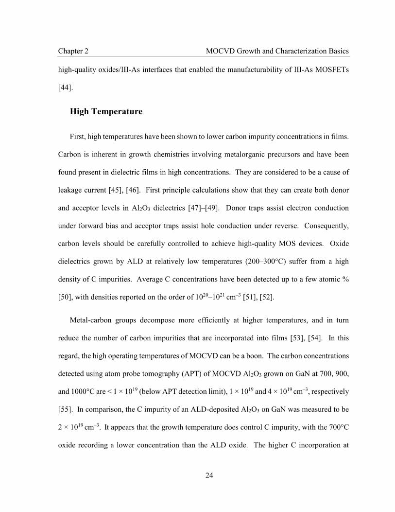
Chapter 2 MOCVD Growth and Characterization Basics
24
high-quality oxides/III-As interfaces that enabled the manufacturability of III-As MOSFETs
[44].
High Temperature
First, high temperatures have been shown to lower carbon impurity concentrations in films.
Carbon is inherent in growth chemistries involving metalorganic precursors and have been
found present in dielectric films in high concentrations. They are considered to be a cause of
leakage current [45], [46]. First principle calculations show that they can create both donor
and acceptor levels in Al2O3 dielectrics [47]–[49]. Donor traps assist electron conduction
under forward bias and acceptor traps assist hole conduction under reverse. Consequently,
carbon levels should be carefully controlled to achieve high-quality MOS devices. Oxide
dielectrics grown by ALD at relatively low temperatures (200–300°C) suffer from a high
density of C impurities. Average C concentrations have been detected up to a few atomic %
[50], with densities reported on the order of 1020–1021 cm–3 [51], [52].
Metal-carbon groups decompose more efficiently at higher temperatures, and in turn
reduce the number of carbon impurities that are incorporated into films [53], [54]. In this
regard, the high operating temperatures of MOCVD can be a boon. The carbon concentrations
detected using atom probe tomography (APT) of MOCVD Al2O3 grown on GaN at 700, 900,
and 1000°C are < 1 × 10¹⁹ (below APT detection limit), 1 × 10¹⁹ and 4 × 1019 cm–3, respectively
[55]. In comparison, the C impurity of an ALD-deposited Al2O3 on GaN was measured to be
2 × 1019 cm–3. It appears that the growth temperature does control C impurity, with the 700°C
oxide recording a lower concentration than the ALD oxide. The higher C incorporation at

Chapter 2 MOCVD Growth and Characterization Basics
25
temperatures higher than 700°C is not yet known but could be related to temperature-dependent
formation of CO, CO2, or aluminum carbide species and the carbon species’ different
probabilities to result in C incorporation.
High Growth Rate
The growth rates in MOCVD are controlled by varying the precursor flows. The high (or
variable) growth rates provide two advantages. One, the ability to deposit very thin to very
thick insulators allows MOCVD growth to serve a wider range of electronic applications. High
power devices that require very thick gate oxides ~100 nm can be more feasible and
economically served by MOCVD. Two, interfacial and insulating properties of the dielectric
can be engineered via growth rates. In contrast, conventional ALD features slow and steady,
monolayer by monolayer growth rates. ALD is preferably operated where saturation
conditions prevail, in which the growth rate per cycle is determined by the number of
chemisorption sites on the growth surface, and not by the magnitude of the precursor flow. As
a result, the self-limiting steps make ALD impractical for growing thick films.
Multicomponent Oxides
The growth of higher order (e.g., ternary, quaternary) group V semiconductors is easily
achieved using MOCVD since multiple precursors can be injected into the growth chamber.
The composition is tuned by adjusting the relative injection flows of the constituent precursors.
Conventional ALD is unable to grow multicomponent oxides in this way since precursors are
pulsed successively into the chamber. Instead, efforts to achieve multicomponent oxides by
ALD typically constitutes alternating layers of different metal-oxides [56]. An average film

Chapter 2 MOCVD Growth and Characterization Basics
26
composition can be achieved; however, since the deposition sequence changes with different
target compositions, the spatial distribution of the different elements can be nonuniform along
the growth direction.
Several methods to control the distribution of doping elements have been mentioned [57].
One study carried out annealing of oxide bilayers to create disordering in the periodicity [18],
[26]. The study also suggested interfacial roughness between bilayers contributes adequate
disorder if the bilayer period is thinner than 0.5 nm. More recent developments of spatial ALD
however, allows for co-injection of metal precursors to grow multicomponent oxides at faster
growth rates [57]. It remains a challenge, however, to grow ternary and quaternary materials
in existing ALD systems.
In-Situ Growth
Finally, the in situ growth capability is a major advantage for improving the
dielectric/nitride interface quality. For most GaN transistors, the gate dielectric is often
deposited in an environment separate from the growth of nitride layers, either because the
device fabrication process requires it or because ex situ dielectric deposition tools are more
readily available, or both. Prior to the gate dielectric deposition, the exposed GaN surface is
prone to collecting impurities that may negatively impact the gate performance in a MOSFET.
If the GaN was processed by etching or other damaging steps, defects may have already
formed. The unpredictable impact from ex situ factors can lead to variations in the dielectric
performance; separating their contributions to the electrical behavior from intrinsic growth
effects is not simple. Consequently, cleaning and pretreatments protocols to manage the GaN

Chapter 2 MOCVD Growth and Characterization Basics
27
surface has grown into an important field of research. Several review works have summarized
various interface control schemes used to obtain low contamination and low trap density in
GaN insulated-gate transistors [14], [44], [58]. With in situ growth, however, surface cleanings
and treatments are no longer needed. Rather, opportunities arise for studying the native
charges generated at or near the dielectric/GaN interface during growth.
2.3 Material Characterization Methods
Ellipsometry
There are a variety of methods for characterizing the structural and material properties of
thin films. Ellipsometry, a quick optical technique that measures and models the change of
polarization upon reflection or transmission in the film, is frequently used to determine film
thickness and dielectric properties such as refractive index. The refractive index (n) is a
particularly useful marker for indicating the relative composition of ternary oxides since
ternary oxides should exhibit intermediate index values between that set by their constituent
binary oxides. Similarly, the dielectric constant also approximately follows a linear rule of
mixtures with composition [29]. The oxide films grown on Si substrates were characterized
by variable angle spectroscopic ellipsometry (VASE) using a J. A. Woolam M2000DI
ellipsometer. The film thickness was determined using CompleteEASE software by assuming
an oxide/native SiO2/Si structure that follows a Cauchy dispersion model. The refractive index
n was extracted from a wavelength of 632.8 nm. Ellipsometer measurements on Al2O3, AlSiO,
and SiO2 were performed over a wavelength range of 193 to 1700 nm initially. However,

Chapter 2 MOCVD Growth and Characterization Basics
28
dispersion in the n values was observed over a range of oxide thickness. Specifically, below
an oxide film thickness of ~ 30 nm, the n value deviated with respect to the relatively constant
n value extracted from larger thicknesses. This is shown in Figure 2.1, where the n values
generally increased within the lower thickness range highlighted in gray and the trend appears
significant for the aluminum-based oxides.
Figure 2.1 Trend of refractive index versus oxide thickness measured on Al2O3, AlSiO, and SiO2 films. % fTMA is the TMA molar flow of the total (TMA + Si2H6) molar flow.
The wavelength range required revising to improve the modeling of n values. The goal is
to establish a more precise relationship between the refractive index and the ternary oxide
composition. In doing so, the use of more time-intensive and costly techniques to measure
composition can be reconsidered in favor of ellipsometry. Films were remeasured at various
wavelength windows. Shorter wavelengths were removed from the measurement window in
Figure 2.2, which plots the n value versus oxide thickness results for an AlSiO film.
Interestingly, this figure shows that the n value will converge at larger oxide thicknesses

Chapter 2 MOCVD Growth and Characterization Basics
29
regardless what wavelength window is used. At thicknesses smaller than 20 nm, the spread in
n values is high and implies inconsistency in values derived from this range. It was speculated
that this may be related to initial composition inhomogeneity at the AlSiO/native–SiO2/Si
interface. However, a similar spread of n values in purely SiO2 deposited films (thicknesses <
20 nm) was obtained with various wavelength measurement windows and disproved that
theory. The current modeling of n values may not be suitable for ultrathin films.
Figure 2.2 Trend of refractive index versus oxide thickness measured at various wavelength windows for an AlSiO film.
At thicknesses > 20 nm, however, removing wavelengths shorter than 300 nm seems to
result in an improved precision of n values. This is more clearly illustrated in Figure 2.3(a),
where the mean square error (MSE) of the measurement is also observed to decrease with the
removal of shorter wavelengths. On the other hand, Figure 2.3(b) shows that the MSE
increases when more of the higher wavelengths are removed. However, the n value remains

Chapter 2 MOCVD Growth and Characterization Basics
30
largely unchanged. Since the wavelength window started at a low λ of 193 nm, the n value
remained artificially high for the small thickness films. From this, it was reasoned that an
appropriate wavelength window must be selected to exclude shorter wavelengths, but it was
not necessary to remove the higher wavelengths extensively.
Figure 2.3 Refractive index and its mean square error measured in AlSiO films at various wavelength windows. The variable λ represents the starting wavelength in the graphs labelled (a) and the ending wavelength in the graphs labelled (b).
After several optimization measurements, the wavelength window of 450–1500 nm was
chosen as the range to measure the refractive index in AlSiO films in later studies. The

Chapter 2 MOCVD Growth and Characterization Basics
31
decrease in the mean square error is insignificant beyond 450 nm, and removal of wavelengths
higher than that will result in loss of ellipsometry information. The discrepancy in the mapping
of AlSiO composition to n value between a wavelength measurement window of 193–1700
nm and 450–1500 nm is discussed in Chapter 4. It is noted that the measured thickness values
do not vary significantly (Δtox < 2 nm) with the investigated wavelength ranges. Only artificial
increases in n values are observed in thin films with thicknesses smaller than 30 nm.
GIXRD
X-ray diffraction (XRD) is a rapid, analytical technique that detects whether a material is
crystalline or amorphous. If the material is crystalline, the technique can identify the phase
and provide information on the crystal grain size. X-ray diffraction measurements using
conventional 2θ-ω measurements scans of thin (< 100 nm) films generally detect weak signals
from the film and intense signals from the substrate (see Figure 2.4), which can return
erroneous conclusions about a dielectric film’s crystallinity. Performing a 2θ scan with a fixed
grazing angle of incidence is better known as “Grazing incidence” XRD (GIXRD) and is one
way to increase the intensity signal from the film relative to the signal from the substrate sitting
underneath. This angle is above the critical angle for total internal reflection in the film.
The oxide films were characterized by GIXRD using a Rigaku SmartLab X-ray
diffractometer fixed at a grazing incident angle of 0.2° and 0.33° for oxide-on-Si and oxide-
on-GaN substrates, respectively. A typical GIXRD profile of intensity vs 2θ contains two
useful pieces of information. One, the positions of the intensity peaks can be mapped to index
planes characteristic to a crystal phase, and in this way, one or several phases can be identified

Chapter 2 MOCVD Growth and Characterization Basics
32
in the film. Two, the broadening (full-width at half maximum) of the characteristic peaks can
be used to approximate the crystal grain size via the Scherrer formula. However, due to the
many assumptions that go into the approximation, the grain size is more accurately verified by
alternative methods such as high-resolution imaging in transmission electron microscopy
(TEM). For quickly gaining relative measures of grain size, GIXRD is still a more practical
and less labor-intensive method.
Figure 2.4 Conventional 2θ-ω measurements of a 100-nm-thick Al2O3 on Si(001). The signal from the oxide film is obscured by that of the underlying substrate.
XPS
X-ray photoelectron spectroscopy (XPS) is a surface sensitive technique that determines
the elemental composition, chemical state (bonding) and electronic states of elements within a
film. The oxide films were characterized by XPS using a Kratos Axis Ultra XPS system with

Chapter 2 MOCVD Growth and Characterization Basics
33
a monochromated Al X-ray source to excite the sample surface. A typical XPS survey
spectrum is a plot of intensity (emitted photoelectrons that were detected) versus binding
energy. Each element produces a characteristic set of peaks. The peak intensity relates to how
much of the element is at the surface and the peak position corresponds to a specific electronic
configuration (2s, 2p, etc.) of the element with other atoms (chemical bonding information).
Peak analysis of composition was carried out using CASAXPS software. Through angle tilt
measurements in XPS that varied the sampling depth from 4 to 8 nm into the film, the measured
composition (of Al and Si elements for instance) was found to be within the instrument error
(+/−5%). An empirical formula for a multicomponent oxide can be approximated from the
relative composition surveyed for each element. Impurities such as carbon, while detectable
by XPS, do not have accurately quantified concentrations since carbon levels are limited by
what is carried from the sample into the XPS chamber.
SIMS
Secondary-ion mass spectroscopy (SIMS) is a technique that can better resolve impurity
concentrations in films. A primary ion beam sputters off the surface of the specimen and the
secondary ions ejected from the sample are collected for analysis. This technique requires thin
films to have a sufficient thickness (upwards to 100 nm and greater) to accurately probe
concentration depth profiles of bulk and impurity elements.
TEM/EDX
Transmission electron microscopy (TEM) is a powerful, high-resolution tool for imaging
at the atomic scale, capable of resolving fine crystal grains and their crystal orientations. TEM

Chapter 2 MOCVD Growth and Characterization Basics
34
is also often performed to examine the interface of dielectric/III-nitrides for abruptness and
possible interlayer formation. Energy-dispersive X-ray spectroscopy (EDX) can also be
carried out in conjunction with TEM to provide a detailed map of the local composition. For
imaging surface morphological features at the nanometer to micrometer scale, atomic force
microscopy (AFM) is a suitable technique. AFM is often used for investigating film coverage
and smoothness.
2.4 Electrical Characterization Methods
Electrical measurements performed on metal-oxide-semiconductor (MOS) capacitors is the
most direct method to assess the intrinsic properties and performance of the oxide dielectric.
The simple structure of the (2-terminal) MOS capacitor ensures that the measured electrical
behaviors are extracted from the dielectric layer alone. Yet, there are relatively few studies on
the electrical characterization of GaN MOS capacitor devices. Many more studies conclude
on the quality of the dielectric through the testing of gate-insulated AlGaN/GaN transistors,
though the evaluation of dielectric quality is more complicated in a 3-terminal device structure.
One complication is that the extra processing steps associated with transistor fabrication can
increase the probability of extrinsic failure (rather than an intrinsic failure of the dielectric).
The additional interfaces and defects that come with them can introduce other failure modes.
Studies comparing the electrical characteristics between transistors and MOS capacitors are
recommended to distinguish the effect of the dielectric more clearly.

Chapter 2 MOCVD Growth and Characterization Basics
35
MOS capacitors were fabricated in this dissertation work for quick testing of the MOCVD
grown oxides. A schematic of a MOS capacitor is shown in Figure 2.5. The oxide layer is
grown in situ on the GaN epitaxial structure consisting of, from top to bottom: 600 nm of n–
GaN/800 nm of n+ GaN/400 nm UID GaN, deposited on a semi-insulating GaN-on-sapphire
substrate. To form the gate from the planar structure, mesa isolation down to the n+ GaN layer
was performed using CF4/O2-based ICP–RIE for the oxide removal and BCl3/Cl2-based RIE
for the GaN removal. A non-alloyed Al/Au metal stack was deposited as both the ohmic
contact on the n+ GaN (cathode) and the gate contact on top of the mesa (anode).
Figure 2.5 Cross-section schematic of the grown and fabricated Al2O3/GaN MOS capacitor.
Current-voltage (I–V) and capacitance-voltage (C–V) are two major electrical
characterization techniques, when combined, provide a wealth of vital information on
dielectric quality. I–V measurements chiefly provide information on the dielectric’s ability to
handle charge injection while C–V measurements primarily provide information on border and
interface traps. The various types of I–V and C–V measurements, their intended purposes,

Chapter 2 MOCVD Growth and Characterization Basics
36
metrics, and parameters are described in the following sections. A summary is provided in
Table 2-I.
Table 2-I I–V and C–V measurements, metrics, parameters, and desired numbers.
Measurement Metrics Parameter Desired Target
I–V
Forward– and reverse– sweep
Leakage IG Low < nA/cm2
Breakdown field EBD High > 7 MV/cm
Constant current stress Charge-to-breakdown QBD High > 1 C/cm2 a)
Constant voltage stress Time-to-breakdown tBD High > 20 years b)
C–V
Single sweep Flat-band voltage /
Fixed charge density VFB / QF Low QF < 1011 cm–2
Double sweep Flat-band hysteresis (fast trap density)
ΔVFB Low QT < 1011 cm–2
Multiple sweeps (with stress hold)
Flat-band shift (slow trap density)
ΔVFB Low QT < 1011 cm–2
UV-assisted Interface state density Dit Low < 1012 cm–2
a) High QBD value for SiO2 on Si is > 10 C/cm2 [59], [60]. b) Required time-to-breakdown for automotive applications [61].
2.4.1. I–V measurements
A basic I–V sweep from zero bias to breakdown can be conducted in either forward or
reverse bias. Under forward bias, all the applied voltage is dropped solely in the oxide. Thus,
the obtained breakdown voltage relates to the experimental breakdown field strength (EBD) of
the oxide. An I–V plot typically starts with a low-leakage regime, ending at a visible knee that
is featured by a continuous upward tick of leakage thereafter. This knee correlates with the

Chapter 2 MOCVD Growth and Characterization Basics
37
onset of flat-band voltage instability and irreversible oxide degradation. Thus, the operating
gate voltages for an oxide should not exceed this “safe” voltage point. Prior to the breakdown
point, the leakage (IG) characteristics are often analyzed to determine the mechanisms by which
carriers leak to the gate metal (e.g., via Fowler-Nordheim tunneling, trap-assisted tunneling).
Under reverse bias, it is not always straightforward to separate leakage effects of the oxide
from that of the GaN layer. The breakdown voltage in reverse bias (VBR) is partitioned by the
voltage drop across the oxide and GaN by the following Equation [1].
��� = ��������� � ��� + ���� + �����
2� ! [1]
ND = net doping density tox = dielectric thickness w = depletion width
εox = oxide dielectric constant εsc = GaN dielectric constant
where the first two terms represent the voltage partition in the oxide and the latter term is the
voltage partition in the GaN. If the device and materials are properly designed, the breakdown
of the MOS capacitor should be limited by the breakdown field in GaN. Under well-behaved
circumstances, the maximum field reached in the oxide under reverse bias is less than the actual
oxide breakdown field strength (determined from forward bias breakdown).
Although gate dielectrics are often stressed well below their material breakdown strength,
they may experience time-dependent dielectric breakdown (TDDB)—that is, the dielectric
could undergo breakdown due to trap-generation and/or bond-breakage when an electrical
stress (applied voltage or injected current) is imposed on it for prolonged periods of time. The

Chapter 2 MOCVD Growth and Characterization Basics
38
time-dependent process relies on accumulating a critical amount of damage before electrical
failure is triggered. TDDB testing is a cornerstone of reliability measurements and is carried
out to predict long-term gate stability and operation. TDDB measurements are typically
performed by recording the times-to-failure when a group of identically processed capacitors
is stored under a constant field (current density) that is less than EBD (IBD). A constant current
stress (CCS) or a constant voltage stress (CVS) is applied until catastrophic breakdown is
reached. The CVS and CCS tests may provide complementary information since oxide
breakdown may involve a combination of field- and current-based breakdown mechanisms.
Devices stressed at smaller voltages or smaller currents experience longer time-to-breakdown
(tBD). Desired operating lifetimes of devices can be on the order of decades long. To ascertain
the reliability within a more practical measurement timescale, accelerated measurements are
typically performed by stressing the oxide at a current density or voltage close to its
catastrophic breakdown point. Modeling is used afterward to extrapolate and predict a
maximum operating voltage (or current density) for which a time-to-breakdown, of 20 years
for instance, can be confidently obtained.
In CVS testing, the device is biased with a constant VG and the gate current IG is acquired
over time. The amount of injected charge estimated by integrating the gate current from t = 0
s to the time-to-breakdown is commonly known as charge-to-breakdown (QBD). Conversely,
in CCS testing, the device is injected with a constant current IG and the gate voltage VG is
acquired over time. The constant current density multiplied by the time-to-breakdown yields
the charge-to-breakdown. Charge-to-breakdown and time-to-breakdown are common metrics
used to describe dielectric reliability.

Chapter 2 MOCVD Growth and Characterization Basics
39
Oxide failure statistics are frequently modeled using the Weibull distribution. The Weibull
model is based on the “weakest link in the chain” assumption, in which degradation or failure
initiated at a local point causes subsequent failure of the entire device. A two-parameter
Weibull distribution, described by the following Equation [2], is used to analyze dielectric
lifetime data.
"(#) = 1 − exp (− )#*+,- [2]
F = cumulative function, β = shape factor, λ = scale factor
F is the cumulative function that describes the percentage of failed devices at a given charge
injection. The β and λ parameters quantitatively describe the statistical breakdown behavior.
β is the shape factor that describes breakdown uniformity. β > 1 indicates a narrow distribution
and high breakdown uniformity. In contrast, β < 1 indicates a broad distribution and defect-
related, extrinsic breakdown. λ is the scale factor that represents the charge-to-breakdown at
the 63% of failed devices. TDDB measurements can be performed in either forward or reverse
bias. The most straightforward way to analyze the robustness of the dielectric is from forward
bias TDDB measurements on MOS capacitors. These are the measurements carried out in this
work. Reverse bias breakdown results tend to have lower statistical uniformity than forward
breakdown results, likely due to the inclusion of breakdown effects from both the oxide and
GaN layer. In the case of gate-insulated GaN transistors like a MIS-HEMT, the electric field
distributions are significantly different between on-state and off-state conditions and time-
dependent breakdown processes occur within different regions of the device in addition to the
gate. Comprehensive reliability testing of transistors should include both forward and reverse

Chapter 2 MOCVD Growth and Characterization Basics
40
bias measurements. For power MOSFETs, the reliability of the dielectric under reverse stress
determines the maximum blocking voltage while the reliability of the dielectric under forward
stress determines the minimum on-resistance.
Transient stress/recovery I–V measurements can be performed to determine the density of
border traps near the GaN conduction band minimum. In these measurements, the oxide is
subjected to a gate bias VG > 0 and then allowed to relax at zero bias VG = 0. A longer relaxation
period enables electrons to empty from oxide border traps located further in the bulk. The gate
current is monitored during both the stress and relaxation (recovery) phase. In a low field
regime, where electrons do not leak from the GaN layer to the gate metal, stress and relaxation
currents are equivalent to each other. Integrating the relaxation current over time provides the
total amount of electrons emitted back from oxide traps. By counting returned electrons, the
lower bound density of active near-conduction band border traps can be approximated.
2.4.2. C–V measurements
Trap states have an associated time constant (or response time) which influences the
capacitance measured in C–V techniques. Traps are distinguishable by their response times
and are done so by varying the frequency, sweep rates, and/or holding times in C–V
measurements. The response time of a trap state decreases exponentially with distance from
the interface (or with energy from band edge). The time constant for electron emission (τe)
from an interface state follows Equation [3].

Chapter 2 MOCVD Growth and Characterization Basics
41
./(�) = 10/123�! 4#5 ��! − �
67 � [3]
σe = capture cross section for electrons υth = electron thermal velocity Nc = effective density of states in conduction band
Ec–E = energy of interface state from conduction band edge k = Boltzmann’s constant T = absolute temperature
Because bulk traps located far away from the dielectric/GaN interface have long emission
times, their capacitances are not measurable on a practical timescale. C–V measurements are
suited for probing traps with relatively short emission times and can differentiate interface
traps from border traps, shallow traps from deeper traps.
Several useful pieces of information can be extracted from a basic C–V sweep of a MOS
capacitor from the depletion to the accumulation region. The doping density (ND) of the GaN
interlayer is determined from the depletion capacitance following Equation [4] and the oxide
layer’s dielectric constant (εox) is determined from the accumulation capacitance following
Equation [5].
�� = 2����8� �91/:�
9 � � [4]
q = electron charge, A = gate area, C = capacitance, VG = gate voltage
��� = :������<8 [5]
Cox = accumulation capacitance, ε0 = vacuum permittivity

Chapter 2 MOCVD Growth and Characterization Basics
42
The presence of interface traps is indicated by a “stretch-out” in the C–V region between
weak depletion and weak accumulation. When the voltage is increased beyond depletion
conditions, the MOS device will reach a state of flat-band (where the energy bands are flat in
the GaN semiconductor) before the onset of strong accumulation. The voltage at which flat-
band conditions occur, termed flat-band voltage (VFB), is a useful parameter to extract from the
curve. The ideal flat-band voltage is the material work function difference between the gate
metal and the semiconductor (�=>?@ABC = DE − DF). However, under real circumstances, non-
ideal fixed charges exist within the oxide or at the oxide/GaN interface, which leads to a flat-
band deviation from the ideal voltage (seen as a position shift of C–V curve relative to the ideal
flat-band voltage). The total fixed charge (QF) is determined from the real flat-band voltage
following Equation [6].
��� = − �G���� ��� + ���?@ABC [6]
The calculated ideal flat-band voltage used in this work assumes the work function of the Al
gate and the electron affinity of GaN to be 4.08 and 3.3 eV [20], respectively. Analysis of
multiple MOS capacitors is needed to determine the physical location of the fixed charge. If
the fixed charges are located at or near the oxide/GaN interface, there will be no dependence
on the thickness and could be calculated from a linear fit of VFB vs thickness without knowledge
of �=>?@ABC.
When a flat-band voltage difference occurs between a go sweep (depletion to
accumulation) and a return sweep (accumulation to depletion), the difference is considered
here as flat-band hysteresis ΔVFB. Trap states responsible for imparting hysteresis lie within

Chapter 2 MOCVD Growth and Characterization Basics
43
modulation of the Fermi level. Faster sweep rates, which suppress the response of slower traps,
typically yields a smaller hysteresis than if a slower sweep rate was to be used. The magnitude
of hysteresis also reduces with successive, multiple C–V sweeps. It is therefore important to
have a consistent method of measuring devices as the bias history influences the flat-band
voltage. Fixed charge and initially filled slow traps do not contribute to C–V hysteresis. A C–
V characterization method was developed to measure the density of traps with fast electron
emission rates (fast traps) and traps with slow electron emission rates (slow traps) [21], [62],
[63] and is summarized here. Two hystereses, ΔVFB1 and ΔVFB2 are measured from the first
and second full C-V sweeps (from depletion to accumulation and back) respectively, where
ΔVFB1 is measured with a device 10-min holding time in accumulation and ΔVFB2 is measured
with no holding time. The difference ΔVFB1 – ΔVFB2 can be used to estimate the density of
initially empty slow traps, and ΔVFB2 can be used to estimate the density of empty fast traps
(ΔQI) following the Equation [7].
Δ��� = − �ΔGI��� ��� [7]
The density of fixed charge QF is equal to QI if all slow traps are assumed to be donor-like.
Since both donor and acceptor type traps are likely to exist, QF is usually greater than QI.
C–V stress tests are often carried out to assess gate stability. The C–V stress tests in this
work involves systematically stressing the oxide to higher voltages and recording the shift in
the flat-band voltage. Electron trapping into oxide trap states results in a positive flat-band
voltage shift. When empty slow traps are filled, or new trap states are generated (in a
degradation process), the voltage shift is often permanent and irreversible. Pronounced flat-

Chapter 2 MOCVD Growth and Characterization Basics
44
band voltage shifting contributes to threshold-voltage shifting in during transistor operation.
Evaluating the dielectric response to stress can aid in identifying the dielectric’s role in device
degradation [64].
Frequency-dependent C–V sweeps can determine the presence of both interface and border
traps. The presence of interface traps is indicated by a stretch-out of the measured C–V profile
in the region prior to accumulation at VG ~ VFB, whereas the presence of border traps is
indicated by dispersion in the accumulation region. At lower frequencies, slower traps (e.g.,
trap states farther in depth from the interface) participate in the storing and releasing of charge,
which adds to the measurable accumulation capacitance. Border trap effects contributing to
accumulation dispersion is an assumption valid for relatively thick oxides > 5 nm. For very
thin oxides, where interfacial effects start to dominate over bulk properties, interface traps will
strongly affect accumulation dispersion as well.
The various C–V techniques mentioned so far only probe trap states that are close enough
to be in electrical communication with the GaN conduction band. While the common high-
frequency C–V technique, also known as the Terman technique, is a simple and quick method
for measuring the fixed charge density and interface state density at the SiO2/Si interface, it
significantly underestimates the actual interface state density (Dit) at dielectric/wide-bandgap
semiconductor interfaces at room temperature [65]. The extremely long carrier emission times
(such as states near mid-gap or sufficiently far from band-edge) in wide-bandgap
semiconductors prevent the Terman method from evaluating the density of interface states at
energies below EC–1.0 eV from C–V measurements at room temperature [66]. High-

Chapter 2 MOCVD Growth and Characterization Basics
45
temperature Terman measurements cover a more substantial portion of the bandgap but are
insufficient for probing the entirety of the bandgap spectrum.
Other methods such as the simultaneous high-low C–V technique and the AC conductance
technique, while much more accurate and sensitive, can only obtain accurate data over a small
portion of the bandgap. Photo-assisted C–V techniques, on the other hand, can obtain densities
of interface states across the bandgap. In contrast to the Terman technique, which is based on
the comparison between calculated and experimental C–V curves and thus relies on knowledge
of ideal semiconductor material parameters, the photo-assisted C–V technique extracts Dit
directly from an experiment by comparing the dark and post-UV C–V measured curves.
A UV-assisted C–V technique had been developed to measure the density and distribution
of interface states formed between positive valence band offset dielectrics (such as Al2O3) and
wide bandgap semiconductors [67]. This method relies on tracking the occupancy of interface
states and yields a measure of Dit as a function of distance (energy separation) from the
conduction-band edge [68]. The measurement procedure consists of driving the MOS device
from accumulation to depletion and then illuminating the device with UV light while it is held
under a constant depletion bias. The UV illumination functions to (1) ensure full ionization of
traps across the GaN bandgap and (2) generate electron-hole pairs that can be recombined by
means of interface-state mediated hole capture. Under the depletion bias, the generated free
holes are confined to the MOS interface. The increase in the photo-generated carriers is
manifested as an increase in the depletion capacitance in the post-UV C–V curve. After the
light is turned off and the device is swept back toward accumulation. During this sweep, the
post-UV C–V curve encounters an “interface state ledge”, which is the result from empty

Chapter 2 MOCVD Growth and Characterization Basics
46
interface states capturing electrons from the conduction band as they move below the Fermi
level under accumulation bias. The electrons trapped in interface states then recombine with
the generated holes, reducing the interface charge and shifting the C–V curve in the negative
voltage direction. The Dit can be calculated by comparing the voltage differences at any
capacitance between the dark and post-UV C–V curves following Equation [8].
JK2 = :���8 �L�LM � [8]
Cox = oxide capacitance ΔV = voltage difference between dark and post-UV curves ψs = surface potential of the semiconductor
Summary
To summarize, the important fundamental measures of MOS properties are: 1) insulator
leakage current (IG) as a function of voltage bias (electric field) and 2) insulator breakdown
field (EBD), both of which are measured from I–V techniques; 3) the fixed charge density (QF),
4) slow and fast border trap density (NBT), and 5) interface state density (Dit), all of which are
measured by C–V techniques. Moreover, there are also measures of reliability for MOS
devices. For instance, VFB shift as a function of voltage bias is measured from C–V stress
testing methods. Charge-to-breakdown (QBD) and time-to-breakdown (tBD) are measured from
time-dependent dielectric breakdown measurements. Use of these measurements are present
throughout this work and leads to an informative overview of dielectric performance. These
measurements, however, by no means represent an exhaustive list of techniques for evaluating
MOS quality and reliability. Measurements such as temperature-dependent I–V can be used

Chapter 2 MOCVD Growth and Characterization Basics
47
to assess activation energies for oxide traps and gate thermal stability, for instance, and are
highly recommended for future investigations.

48
Al2O3 Dielectrics
3.1 Introduction
The starting point for investigating qualified dielectrics for GaN devices begins with Al2O3.
As mentioned earlier, the combination of attractive properties such as large bandgap, relatively
high dielectric constant, high breakdown field, and good contact formation with GaN makes
Al2O3 a strong candidate. Section 3.2 first presents on growth studies which varied the
temperature, precursor flows, and reactor pressure to determine the Al2O3 deposition windows
and growth mechanisms. Section 3.3 focuses on a case study that detailed the impact of oxygen
precursor flow on the electrical properties of in situ grown Al2O3 on GaN, including forward
bias stability, leakage, breakdown field, and formation of interface-states and border trap
states. The performance of Al2O3 films were shown to improve with oxygen flow tuning,
however, the films were found to be moderately crystallized. X-ray diffraction studies were
carried out in Section 3.4 to identify the growth temperature range over which Al2O3
crystallizes. Growth strategies to overcome this limitation were implemented in Section 3.5,
and two case studies detailing the properties and performance of amorphous Al2O3 are
presented in Section 3.6. Lastly, Section 3.7 examines the limitations of amorphous Al2O3,
paving the road for the introduction of AlSiO in Chapter 4.

Chapter 3 Al2O3 Dielectrics
49
3.2 Growth Kinetics and Design Space
Figure 3.1 Al2O3 growth rate versus (a) growth temperature, (b) TMA flow, and (c) O2 flow.
The growth space of Al2O3 using TMA and O2 precursors was investigated. Growth rates
were studied as a function of temperature, precursor flows, and growth pressure [69]. The
growths were carried out on Si(001) substrates for ease of film characterization using
ellipsometry. Plots in Figure 3.1 show Al2O3 growth rates as a function of temperature, TMA
flow and O2 flow. Three distinct temperature-dependent regions are identified: a low-
temperature kinetically controlled region, a mid-temperature mass-transport limited region,
and a high-temperature pre-reaction limited region. In the kinetic region (< 800°C), growth
rate increases with temperature. The sublinear dependence of growth rate on TMA and O2
flows shown at 600°C indicates that growth is limited by surface kinetics following the
Langmuir-Hinshelwood mechanism. In the mass-transport region (800 – 900°C), there is a
weak dependence of growth rate on temperature. Mass-transport growth is evidenced by the

Chapter 3 Al2O3 Dielectrics
50
linear dependence of growth rate with TMA flow shown at 900°C. In the pre-reaction limited
region (> 900°C), the growth rate decreases with increasing temperature and O2 flow. Higher
temperatures tend to promote more reactions between precursor species in the gas-phase and
the increase of available oxygen species also increases the likelihood of gas-phase activity.
Similarly, the decrease in growth rate with higher growth pressure can be explained by a rise
in parasitic pre-reactions that deplete Al2O3 growth efficiency. Such pre-reaction driven
behaviors have been previously observed in AlN growths that employ TMA as a precursor
[70].
3.3 Impact of Oxygen Precursor Flow
One of the interesting features discovered about MOCVD is that the flow rate of the oxygen
precursor has a direct influence on the dielectric properties and performance. Early
investigations constituted 700°C Al2O3 films grown under a high supply of oxygen (at 480
sccm). The implemented flow was termed “high oxygen flow” as it is near the capacity limit
of the 500 sccm range MFC in use. The MOSCAPs fabricated with the high oxygen flow
dielectrics exhibited promising traits such as high stability in reverse bias, low interface trap
density, and low carbon concentration. However, the dielectrics demonstrated anomalous
behavior under forward bias, notably reductions in the accumulation capacitance with positive
stress.
As oxide stability under forward bias conditions is crucial for any transistor operation in
the on-state, this was an important problem to address. Initial approaches involved depositing

Chapter 3 Al2O3 Dielectrics
51
Ti contacts first and pre-injecting TMA prior to oxide growth but proved unsuccessful in
eliminating this anomaly. Reducing the oxygen precursor flow instead was found effective in
tailoring this forward bias instability to a well-behaved accumulation response. Other
electrical behavior aspects such as flat-band voltage shift, frequency dispersion, and gate
leakage, also differed significantly between dielectrics formed under high and low oxygen flow
growth conditions, which further evidences the significant impact that oxygen flow has on
controlling electrical performance. The details of the study are presented in the following
sections.
First, two 25-nm-thick Al2O3 films were grown under different oxygen flows, one at 480
sccm (21 mmol/min) and one at 100 sccm (4.4 mmol/min), which will be referred to as the
“high O2 flow” and “low O2 flow,” respectively. Note that growth under different oxygen
flows does not imply dissimilar oxygen concentrations nor non-stoichiometry in the films.
During both growths, the TMA flow was a constant at 3.2 μmol/min (1.6 μmol/min if reported
in dimers). Under such a low TMA flow at the deposition temperature of 700°C, the growth
rates of the two oxides are nearly comparable: 1.08 nm/min and 0.96 nm/min for the high and
low O2 flow films, respectively.
The dielectrics were grown onto GaN-on-sapphire substrates following the MOS capacitor
structure. Samples from both types of films were selected to undergo PDA in forming gas (5%
H2/N2) for 2 min at 700°C. The devices under test had 200 μm x 200 μm gates, fabricated
using the standard mesa isolation and metallization process developed for the GaN MOS
capacitor (See Section 2.4).

Chapter 3 Al2O3 Dielectrics
52
Forward-bias Instability
The C–V profile in Figure 3.2 depicts the forward bias instability in the high O2 film during
a virgin sweep from depletion to accumulation. The film exhibits an unusually high
capacitance at the onset of accumulation which reduces to a lower value when the gate is
forward biased beyond ~3 V. It is suspected that the high capacitance could be related to the
presence of defect states, however, the underlying mechanisms responsible for this behavior
are unclear at this point. The dielectric properties appear to change in response to the injection
of charge into the oxide layer, and the filling of available trap states could play a role in altering
the polarizability of the oxide. On the other hand, adopting a lower oxygen flow eliminated
the forward bias instability feature and led to films stable in accumulation under the same bias
conditions. To assess whether the interface formed by the low O2 Al2O3 to n-GaN is the source
of the C–V instability, a bilayer of equivalent dielectric thickness consisting of a low O2 grown
Al2O3 layer (3 nm) followed by a high O2 grown Al2O3 layer (22 nm) was characterized. The
results illustrated in the same C–V figure showed that the instability persisted in the bilayer but
demonstrated intermediate behavior between the high and low O2 extremes.
At this point, it is then questioned whether the low O2 layer was an effective barrier against
excess oxygen potentially diffusing to the GaN surface to form trap states during the growth
process. From GIXRD measurements, the low O2 Al2O3 films grown under these slow rates
were not amorphous but were determined to be of a cubic spinel polymorph (γ-Al2O3). An
oxygen diffusion study has shown O isotope tracers rapidly decreasing over shallow
penetration depths (< 2 nm) in γ-Al2O3 at 700°C and do not readily diffuse through γ-Al2O3
compared to ALD-deposited amorphous Al2O3 [71]. While this has evidence to suggest that

Chapter 3 Al2O3 Dielectrics
53
O migration is not very pronounced under similar crystal phases and temperatures, it is difficult
to completely rule out its role in defect formation and associated capacitance instability.
Figure 3.2 C–V characteristics of three distinct GaN MOS capacitors with Al2O3 dielectric grown under high O2 flow, low O2 flow, or low O2 followed by high O2 flow (bilayer).
It is also possible that the instability may stem from material changes or trapping within
the high O2 region instigated by high forward injection. A permanent flat-band shift observed
in both the bilayer and high O2 film following the capacitance drop, suggests that deep traps
have been filled under forward injection, and subsequently behave in a manner like fixed
charges. The results of a brief stress test portrayed in Figure 3.3 revealed a monotonic
reduction in the capacitance and a positive push-out (increase) of the flat-band voltage with
increasing positive bias in high O2 films. Low O2 films, on the other hand, were well-behaved,
experiencing smaller flat-band shifts for the same applied stress bias while remaining stable in
its accumulation capacitance. Filling of trap states beyond 3 nm of the interface can cause
irreversible flat-band shift. Similarly, filling of empty trap states far below the Fermi level can
Chapter 3 Al2O3 Dielectrics
54
also lead to permanent shifts. However, these traps should already be filled under the initial
accumulation bias. The continuous positive shifting of the flat-band voltage with higher
applied bias (See Figure 3.4) suggests that trapping states further in the dielectric bulk is likely
the dominant contributor.
Figure 3.3 C–V characteristics of GaN MOS capacitors from forward bias stressing of the
Al2O3 dielectrics grown under (a) high O2 flow and (b) low O2 flow.
Figure 3.4 Flat-band shifting with positive stress in the Al2O3 dielectrics
grown under high O2 flow and low O2 flow.

Chapter 3 Al2O3 Dielectrics
55
Border and Interface States
Figure 3.5 compares the C–V dispersion behavior between the high and low O2 film in the
frequency range of 1 kHz– 1 MHz. The more pronounced C–V dispersion in the accumulation
region of high O2 films (Figure 3.6) evidences a higher density of border traps in the oxide
relative to low O2 films. Border traps, oxide traps, and leakage are mostly stimulated beyond
the onset of accumulation, which contributes to a higher conductance signal at VG > VFB.
Figure 3.5 Frequency dependent C–V characteristics of the Al2O3 dielectrics grown
under (a) high O2 film and (b) low O2 film.

Chapter 3 Al2O3 Dielectrics
56
Figure 3.6 Reduction in accumulation capacitance dispersion with low O2 grown Al2O3 dielectrics.
Figure 3.7 Frequency dependent G-V characteristics of the Al2O3 dielectrics grown
under (a) high O2 film and (b) low O2 film.
The conductance-voltage (G–V) profiles in Figure 3.7 show that high O2 films display
higher conductance compared to low O2 films for VG > VFB at low frequencies of a few kHz,

Chapter 3 Al2O3 Dielectrics
57
which is consistent with the theory of higher border trap density causing C–V dispersion in the
strong accumulation region [72].
One method employed to determine the density of border traps is transient I–V
stress/recovery measurements, which monitors the relaxation gate current after removing an
applied stress VG. The relaxation current is the result of electron emission from oxide border
traps (i.e., traps close enough to the interface to communicate with the GaN conduction band
minimum) that became filled during the accumulation stress step. An observation of non-
exponential decay in the relaxation current indicates a slow depopulation of electrons within
proximity to the GaN conduction band during the 1000 seconds of discharging. Integration of
this current provides the total number of electrons emitted back from the oxide. A 1000 second
discharge (recovery) time is estimated to sample border traps located ~5 nm away from the
Al2O3/GaN interface [73] via a tunneling-front model [74].
Figure 3.8 Areal density of electrons emitted back from oxide border traps during the recovery phase of step-stress/recovery measurements.

Chapter 3 Al2O3 Dielectrics
58
Figure 3.8 plots the areal density of emitted electrons after each incremental stress period
for both types of films that have undergone post-deposition annealing in forming gas. Results
show that a higher density of electrons was recovered from the high O2 films than from the
low O2 films for every step-stress. For instance, at a stress of 5 V, the electron emission
exceeds 4 × 1012 cm–2 in high O2 films, compared to ~3 × 1012 cm–2 in low O2 films. This
indicates an order of magnitude difference in the density of active border traps in those two
types of films under identical stress conditions. Beyond a conservative application of voltage,
this method does not distinguish between the pre-existing trap states (from growth) and the
additional trap states generated from high stress.
After the first C–V sweep that applies 10-min accumulation stress on a virgin device, high
O2 films experienced a positive flat-band shift of ~1.8 V caused by the injection of electrons
from the GaN accumulation layer into border oxide traps. This large, irreversible shift
corresponds to a permanent, trapped charge density between 2.9–4.1 × 1012 cm–2, a range which
is cautiously estimated from the varying capacitance of the forward bias instability. In contrast,
the small positive flat-band shift in low O2 films relates to a trapped charge of 3.6 × 1011 cm–
2. The flat-band voltage extracted from the second C–V sweep displays a linear relationship
with Al2O3 thickness (Figure 3.9). The net negative fixed charge density was calculated from
this linear relation to be 5.2 × 1012 cm–2 and 1.7 × 1012 cm–2 for the high and low O2 films,
respectively.
When compared with the trapped charge density, most of the contributions to the negative
fixed charge in the high O2 films are from the forward bias trapping, while in low O2 films the
contributions to negative fixed charge from trapping are insignificant in comparison.

Chapter 3 Al2O3 Dielectrics
59
Figure 3.9 Linear relationship between VFB and Al2O3 thickness of high O2 grown films (black dot)
and low O2 grown films (open dot).
The diminished trapping behavior in low O2 films confirms a smaller density of pre-
existing defect traps, and that most of the extracted negative fixed charges are growth generated
rather than stress generated. It can be reasoned that the less severe flat-band shift experienced
by the low O2 films are commensurate with a reduced density of slow border traps. First
principle calculations of the energy levels of various native point defects, assumed to be at or
near the Al2O3/GaN interface, suggest a possible source of the negative fixed charge is an Al
vacancy [17]. Al vacancies form acceptor trap states near the valence band minimum (VBM)
that acquire negative charge states when filled, for example, under a forward bias stress.
However, this defect level is far enough below the GaN conduction band that it is unlikely to
behave as a border trap that induces leakage in MOS structures.
Interestingly, while there is a smaller flat-band shift (fewer slow traps) in the low O2 film,
the hysteresis is more pronounced (more fast traps) compared with the high O2 film. This may

Chapter 3 Al2O3 Dielectrics
60
be partially related to the presence of high Dit. Interface traps are mostly stimulated between
weak-depletion and the onset of accumulation and manifest as a peak at VG ~ VFB in the
conductance-voltage measurement profile. However, due to the sufficiently high accumulation
conductance, the conductance peaks from the interface traps were not observable in Figure 3.7.
The Dit measured by the UV-assisted C–V technique was higher in the low O2 film, where the
integrated Dit from 0.15 to 2 eV below the GaN conduction band is ~5.0 × 1012 cm–2 compared
to ~2.0 × 1012 cm–2 reported for the high O2 film [64]. Dit near band-edge at EC–0.15 eV is
estimated to be 8 × 1012 cm–2 eV–1 and 3 × 1012 cm–2 eV–1 for the high and low O2 films,
respectively. Post-deposition annealing was found to significantly reduce the hysteresis in
both types of films; however, the forward bias instability characteristics and the large flat-band
shift remained in the high O2 films. After annealing, the integrated Dit was measured to be 1.2
× 1012 cm–2 and 2.6 × 1012 cm–2 in the high and low O2 films, respectively. Dit near band-edge
was estimated to be 2 × 1012 cm–2 and 4 × 1012 cm–2 in the high and low O2 films, respectively.
Table 3-I lists the hysteresis values for the high and low O2 films (both unannealed and
annealed). The hysteresis was extracted from the second C-V sweep, which was performed
after the first C-V sweep that applied stress at +5 V for 10-mins.
Table 3-I Flat-band voltage hysteresis of unannealed and annealed Al2O3 films.
Oxide O2 flow
(sccm) Post-anneal
Hysteresis
(mV)
High O2 480 – 640
High O2 480 Forming gas 187
Low O2 100 – 1320
Low O2 100 Forming gas 185

Chapter 3 Al2O3 Dielectrics
61
Leakage and Breakdown
Figure 3.10 displays the forward I–V characteristics and breakdown for the high and low
O2 films and their annealed counterparts. While PDA did help delay (improve) the catastrophic
breakdown voltage for both types of films, the annealed high O2 film still exhibited
significantly poorer I–V characteristics than the low O2 film. The leakage current is observed
to accelerate to ~μA/cm2 at an applied +3 V in the high O2 film, which coincides with the
triggering of the capacitance instability.
The possible near-CBM native defect candidates that can assist in carrier leakage include
Al dangling bonds (DBs) and O vacancies. Because Al dangling bonds were previously
suspected to be fast near-interface states [18], the long emission times in recovery
measurements suggests that electrons may be emptying from slower acting traps and narrows
the possibilities to O vacancies. Note that the discussions do not rule out the existence of other
types of defects and impurities, which may also contribute to the observed leakage behavior,
but would need more extensive investigations to identify. It is likely that forming gas annealing
could passivate interfacial traps such as Al DBs since the treatment was found to reduce the
hysteresis prominence. The forming gas annealing, however, could not reduce the density of
the slow traps nor alleviate their detrimental trapping effects significantly. Only by adopting
a lower oxygen flow was the leakage current largely mitigated, suppressed by nearly three
orders of magnitude around the onset of capacitance instability. The annealed low O2 film
demonstrated both low leakage and the highest breakdown field of ~7 MV/cm.

Chapter 3 Al2O3 Dielectrics
62
Figure 3.10 I–V characteristics of 25-nm-thick high O2 and low O2 grown Al2O3 films along with their FG-annealed counterparts.
Oxide/GaN Interface
The high density of interface traps and related device threshold instabilities are often
ascribed in the literature to the uncontrolled formation of a low-quality GaOx interfacial layer
[66], [75], which commonly occurs when GaN is exposed to air or when an oxide is deposited
[76], [77]. High-resolution transmission electron microscopy (HRTEM) and energy-
dispersive X-ray spectroscopy (EDX) studies were performed to examine the Al2O3/GaN
interface formation for possible intermixing or unintentional GaN oxidation. EDX
composition maps of Ga, N, Al, and O at the interface region of a high O2 Al2O3/GaN sample
is shown in Figure 3.11. Within the resolution of the EDX measurements, no significant

Chapter 3 Al2O3 Dielectrics
63
intermixing or gallium oxide formation is evident beyond 1–2 nm of the interface.
Additionally, the HRTEM image of the high O2 Al2O3/GaN interface shown in Figure 3.12
denotes a relatively abrupt interface (transition region < 1 nm) and no evidence of a significant
gallium oxide interfacial layer between Al2O3 and GaN. It is concluded that the defects
responsible for the observed forward bias behavior is not easily identifiable from standard
HRTEM/EDX measurements.
Figure 3.11 EDX composition maps of the high O2 Al2O3/GaN interface region.
Figure 3.12 Cross-sectional HRTEM image of the high O2 Al2O3/GaN interface.

Chapter 3 Al2O3 Dielectrics
64
Summary
In summary, one of the earliest process parameters discovered to be responsible for
controlling dielectric quality is the oxygen precursor flow supplied during growth of oxide
dielectrics. In this study, it was shown to control defect formation near the Al2O3/GaN
interface, influencing its stability and insulating performance under forward bias. Al2O3 films
grown under high O2 suffered from a high pre-existing density of slow traps, high leakage, and
degradation at lower biases than low O2 grown Al2O3 films. These features were significantly
mitigated by adopting a lower oxygen flow, which stabilized the capacitance under
accumulation, suppressed parasitic leakages and introduced greater resiliency under forward
bias stress. While unable to eliminate the forward bias instability, post-deposition annealing
in forming gas was effective in reducing the hysteresis in both high and low O2 films, likely
because of reducing unsatisfied dangling bonds at the interface. The combination of low O2
growth and post-deposition annealing resulted in improved electrical characteristics, which
included low hysteresis and flat-band shifts of less than 0.2 V, low gate leakage, high
breakdown field ~7 MV/cm, and enhanced robustness under accumulated stress.
The HRTEM/EDX investigations of the high O2 grown Al2O3/GaN interface neither
showed a notable interfacial layer nor prominent intermixing beyond 1–2 nm from the
interface. This study showed that differences in the quality of the oxide/nitride interface were
better resolved via electrical characterization. The comprehensive set of measurements
employing various C–V and I–V tests helped characterize flat-band shift, frequency dispersion,
electron emission behavior, and unearthed a wealth of information into trapping behavior in

Chapter 3 Al2O3 Dielectrics
65
MOCVD gate dielectrics. This study on the impact of oxygen precursor flow on the forward
bias behavior of MOCVD Al2O3 dielectrics grown on GaN is published in Ref. [78].
3.4 Crystallization
There is a downside to MOCVD despite the diverse ways it can be exploited to engineer
dielectric properties. The temperatures typically required to decompose metal-organic
precursors efficiently and produce high-quality nitride material are too hot to produce
amorphous Al2O3. Instead, unwanted forms of crystallization may occur near those
temperatures, which may create problems for the dielectric performance. For example, grain
boundaries, which are typically formed at points where the borders of randomly oriented
crystallites meet, can extend throughout the dielectric bulk and become fast avenues for
leakage and charge trapping. Grain boundary assisted leakage is exacerbated in thinner
dielectrics as the thickness approaches dimensions comparable to the crystal grain size. Thus,
polycrystalline dielectrics, which embody these defects, are highly undesirable candidates.
Why Amorphous?
Many believe dielectrics must be either amorphous or single-crystalline. However, in
practice, single-crystalline dielectrics are the less favorable of the two choices, mainly because
they are also prone to forming crystallographic defects. Strain is incurred by the single-
crystalline dielectric when there is a lattice mismatch of the dielectric/semiconductor
heterointerface, and if relaxed, is often done through the formation of point and line defects.
These defects reduce the resistivity and breakdown field sustainable in the material. To realize

Chapter 3 Al2O3 Dielectrics
66
the growth of defect-free single-crystalline dielectrics is challenging, especially at a
manufacturing production level.
Amorphous dielectrics, on the other hand, do not form macro crystallographic defects such
as dislocations or grain boundaries. Coordination defects, which involve faulty coordination
of an atom as compared to the other atoms of similar type in the structure, are the main type of
defect in amorphous structures and could give rise to dangling bonds. Even so, an amorphous
oxide could reconfigure its bonding to minimize electrically active defects. In addition, stress
can also be taken up by modest topological variations in the random network. Amorphous gate
dielectrics are desirable for all these reasons mentioned. However, obtaining amorphous
dielectrics is not always trivial. Simple binary metal oxides are the most common type of
candidate for dielectrics, but many have the severe problem of undergoing a crystalline
transformation at low processing temperatures. Simple binary IVB oxides (TiO2, ZrO2, HfO2)
for instance, undergo an amorphous to polycrystalline phase transformation at modest
temperatures of 300–700°C and therefore become polycrystalline in most device applications
after post-deposition annealing in CMOS fabrication processes. Although Al2O3 is still a better
glass former than these oxides, its usefulness in devices can be improved by enhancing its
stability against unintended crystallization.
Previous studies have shown varying degrees of crystallization with temperature from the
MOCVD growth of Al2O3 [79], with some reports of amorphous films obtained up to 600°C
while other reports of crystalline films (crystalline phases in a mainly amorphous film)
obtained between 550 and 750°C. Al2O3 was found to have a large number of
microcrystallization regions after experiencing annealing at 800°C [80]. Post-deposition
Chapter 3 Al2O3 Dielectrics
67
annealing of MOS structures is frequently carried out between 600 and 750°C to avoid the
crystalline transformation [26], [27], [81]. Deposition and processing steps are also limited to
such temperatures to preserve the amorphous character.
Crystallization of MOCVD Al2O3
The following study was performed to identify the growth conditions that promote
crystallization of Al2O3 in an MOCVD system using TMA and O2 precursors. The growth
experiments consisted of growing Al2O3 layers at temperatures ranging from 600 to 1000°C
on GaN(0001) substrates and measuring the samples by grazing incidence X-ray diffraction
(GIXRD). The growth experiments are identical to the ones in Section 3.2, which was carried
out on Si(001) substrates. The GIXRD profiles of Al2O3 grown on Si(001) and GaN(0001) are
shown side-by-side as Figure 3.13(a) and Figure 3.13(b), respectively.
The GIXRD profiles show that the transformation from an amorphous to crystalline oxide,
indicated by the emergence of intensity peaks, occurs ~800°C on GaN and ~900°C on Si. The
differences in the crystallization threshold temperature could be related to how Al2O3 nucleates
on the surface of epitaxial GaN versus on the native amorphous oxide surface of Si substrates.
However, in a study where the native silicon oxide was stripped from the substrate, the
appearance of long-range order still occurred in Al2O3 at an annealing temperature of 900°C
[82]. For Al2O3 on GaN substrates, the threshold temperature here is similar to that found in
another study, which reported the appearance of XRD crystal peaks of Al2O3 on GaN at an
annealing temperature of 850°C [81].

Chapter 3 Al2O3 Dielectrics
68
Figure 3.13 GIXRD spectra of 100-nm-thick Al2O3 grown on Si(001) (left) and GaN(0001) (right) substrates at MOCVD growth temperatures of 600 to 1050°C.
In Figure 3.14, the GIXRD characteristic peaks of the Al2O3 films grown at temperatures
≥ 800°C matched indexed patterns belonging to the cubic spinel crystal structure (γ-Al2O3).
Cross-sectional HRTEM investigations were performed on a 900°C and 1050°C grown
Al2O3/GaN sample to corroborate the presence of crystal grains with GIXRD results.
Polycrystalline domains with grain sizes ranging from 2 to 10 nm were observed in the 900°C
Al2O3 film along the imaging [112N0] GaN zone axis (Figure 3.15). In contrast, the Al2O3 film
is single-crystalline at 1050°C, though line defects through the crystal can be seen extending
from the oxide/GaN interface (Figure 3.16).

Chapter 3 Al2O3 Dielectrics
69
Figure 3.14 GIXRD spectra of the Al2O3/GaN films shown with the γ-Al2O3 (PDF 10-0425) reference patterns (blue lines) and corresponding crystal planes (in blue).

Chapter 3 Al2O3 Dielectrics
70
Figure 3.15 Cross-sectional HRTEM images of the in situ 900°C Al2O3/GaN film taken along the zone axes of (a) GaN [112N0] and (b) GaN [11N00].
Figure 3.16 Cross-sectional HRTEM images of the in situ 1050°C Al2O3/GaN film taken along the zone axes of (a) GaN [112N0] and (b) GaN [11N00].

Chapter 3 Al2O3 Dielectrics
71
The agreement between TEM fast Fourier transformation (FFT) patterns with the indexed
planes of the GIXRD profiles confirms that crystallization into the cubic spinel phase occurred
at these temperatures. Details of the study on the MOCVD growth kinetics and crystallinity
of Al2O3 using trimethylaluminum and O2 precursors are published by Liu et al. in Ref. [69].
While the Al2O3/GaN GIXRD profiles showed that crystalline transformation takes place
~800°C, the previous study (on the impact of oxygen precursor flow, Section 3.3) disclosed
that Al2O3 also crystallized at 700°C under very slow growth rates ~1 nm/min. The slower
growth employed a TMA flow of 1.6 µmol/min while the faster growth in the current study
had a TMA flow of 64 µmol/min. The GIXRD profile of the slow grown 700°C oxide is shown
in Figure 3.17. Figure 3.18 shows an HRTEM image of a 700°C oxide deposited under slow
growth rates on GaN, which reveals areas of nanocrystals embedded in an amorphous matrix.
The individual grain sizes appear to be ≤ 5 nm.
Figure 3.17 GIXRD spectra of Al2O3 grown on GaN at 700°C with a low TMA flow of 1.6 μmol/min (in dimers).

Chapter 3 Al2O3 Dielectrics
72
Figure 3.18 HRTEM image of Al2O3 grown at 700°C with a slow growth rate ~1 nm/min shown (a) as-imaged, (b) with visuals denoting local areas with crystalline order.
Leakage and Breakdown
Al2O3/GaN MOS-capacitors were fabricated to compare the electrical performance of
crystallized 25-nm-thick Al2O3 dielectrics grown at 700, 900 and 1000°C. The dielectrics were
annealed in forming gas at 700°C after deposition. As seen from the forward I–V and
breakdown characteristics illustrated in Figure 3.19, the polycrystalline 900°C and single-
crystalline 1000°C oxide sustained lower breakdown voltages than the nanocrystalline 700°C
oxide. The leakage of the polycrystalline Al2O3 rises several orders of magnitude when the
thickness approaches the crystal grain size [83]. The better insulating and breakdown
performance of the 700°C dielectric may suggest that an amorphous matrix containing isolated
nanocrystals provides a more resistive medium than polycrystalline and single-crystalline
films. The challenges and solutions arising from the pursuit of fully amorphous, high-
performance Al2O3 by MOCVD are discussed in the next section.

Chapter 3 Al2O3 Dielectrics
73
Figure 3.19 I–V characteristics of Al2O3 grown at 700, 900, and 1000°C with PDA-treatment in forming gas.
3.5 Amorphous Growth Strategies
The crystallinity studies conducted so far have concluded that the temperatures permissible
for growing amorphous Al2O3 are below 800°C, or below 700°C if conditions include
relatively fast growth rates. The latter circumstance suggests that temperature and growth rate
could deliver competing processes for crystallization. Lower temperatures tend to favor
amorphous formation when the thermal energy is prohibitive enough to limit surface diffusion
of adatoms towards a crystal framework. Adatoms of a certain thermal energy, however, given
enough time, can still diffuse to create energetically favorable higher order structures.
The two takeaway strategies for arresting the process of crystallization is to conduct growth
at 1) moderate, reduced temperatures (between 600 to 800°C) and/or 2) high TMA flow to
combat the crystallizing effects under slow growth. Based on this, two experiments were
arranged. In one, Al2O3 was grown at 700°C at a TMA flow of 15.6 μmol/min (in monomers),

Chapter 3 Al2O3 Dielectrics
74
which is a 5x increase of the TMA flow rate used for the 700°C nanocrystalline oxide and
corresponds to a 3x higher growth rate of ~3.3 nm/min. In the second, the TMA flow of 15.6
μmol/min was kept the same, but the temperature was reduced to 650°C. O2 flows remained
at 100 sccm for all oxide growths. GIXRD measurements shown in Figure 3.20 indicate that
the growth conditions of both experiments have successfully resulted in the amorphous
deposition of Al2O3. The corresponding electrical characteristics and performance are
discussed in the following section.
Figure 3.20 GIXRD spectra indicate amorphous Al2O3 for films grown at 700°C and 650°C under high TMA flow.

Chapter 3 Al2O3 Dielectrics
75
3.6 Electrical Characteristics of Amorphous Al2O3
Four MOS-capacitors were fabricated consisting of the (25-nm-thick) amorphous Al2O3
as-deposited at 650 and 700°C, and their annealed versions. The post-deposition annealing
(PDA) was carried out in the MOCVD chamber at 1000°C in N2/O2 gas (7L/0.1L).
Leakage and Breakdown
Figure 3.21 I–V characteristics of 25-nm-thick amorphous Al2O3 as-deposited at 650 and 700°C (red) and their post-deposition annealed counterparts (blue).

Chapter 3 Al2O3 Dielectrics
76
The I–V characteristics of the four MOS-capacitors are shown in Figure 3.21. The
measurements were performed at a sweep rate of 0.2 V/s. The PDA treatment was shown to
reduce gate leakage and enhance device breakdown voltage under both forward and reverse
bias. The low-field regimes are characterized by low gate current (IG < 10 nA/cm2). The high-
field regimes are characterized by the onset of conduction processes beyond a critical voltage
(VG > VCRIT). The amorphous Al2O3 grown at 700°C reached forward breakdown within a
similar range of applied voltages (12–14 V) as that of the crystallized Al2O3 grown at 700°C
(11–13V). However, since the amorphous 700°C oxide has a negative flat-band voltage
difference of –3 V with respect to that of the crystalline oxide, the field reached in the
amorphous oxide is higher.
The 650°C oxide is the more superior dielectric due to its lower leakage and higher
breakdown. The applied breakdown field in the unannealed 700 and 650°C oxides are 5.4 and
6.8 MV/cm, respectively. The values for the annealed 700 and 650°C oxides are 7.0 and 8.8
MV/cm, respectively.
Interface States
The interface state densities of the various Al2O3 dielectrics are listed in Table 3-II. The
as-deposited 650 and 700°C oxide show comparable Dit near the band-edge (1.7 × 1012 cm–2
eV–1) and integrated from EC–0.15 eV to EC–2 eV (6.9 × 1011 cm–2). These values are
significantly lower than what had been observed for the crystalline films, whose near band-
edge Dit varies between 1.5 – 8 × 1012 cm–2 eV–1 and whose integrated Dit varies between 1.2–
3.2 × 1012 cm–2 [64]. Additionally, the integrated Dit is also 71% less than the Dit reported with

Chapter 3 Al2O3 Dielectrics
77
the same technique on ex situ deposited ALD-Al2O3 (2.4 × 1012 cm–2) [67]. The PDA was
shown to increase the Dit by 6–8 × 1011 cm–2 eV–1 and 2–3 × 1011 cm–2. An example Dit plot
comparing the as-deposited and PDA 650°C oxide is shown in Figure 3.22. The Dit profile of
the annealed oxide shows a non-monotonic trend with band bending, with an apparent peak
around EC–0.4 eV. This “hump” feature has been observed in previous works and is ascribed
to the presence of holes at the MOS interface. This effect may be exacerbated in the PDA
sample due to having lower oxide conductivity that can lead to higher retention of holes at the
interface.
Table 3-II Interface-state density of Al2O3 dielectrics as-deposited and annealed.
Oxide Dit at EC–0.15 eV
(cm–2 eV–1)
Integrated Dit from EC–0.15 eV to EC–2 eV
(cm–2)
650°C 1.7 × 10¹² 6.9 × 10¹¹
650°C (PDA) 2.5 × 10¹² 1.0 × 10¹²
700°C 1.7 × 10¹² 6.8 × 10¹¹
700°C (PDA) 2.3 × 10¹² 8.8 × 10¹¹
Figure 3.22 Example plot of interface-state density vs. distance from GaN conduction band, for Al2O3 as-deposited at 650°C and its annealed comparison.

Chapter 3 Al2O3 Dielectrics
78
Figure 3.23 shows excellent C-V characteristics for both as-deposited oxides. The
accumulation capacitance dispersion is significantly less pronounced than the dispersion
observed in the crystalline oxides (see Section 3.3) within the same frequency range. This
indicates a lower density of near conduction-band border traps in these amorphous oxides. The
downside of these amorphous oxides, however, is that both contain a high density of
preexisting positive fixed charges, which manifests as a negative flat-band voltage. The 650
and 700°C Al2O3 exhibited a VFB of –4.6 V and –3.4 V, which corresponds to a fixed charge
density of +8.9 × 10¹² and +7.1 × 1012 cm–2, respectively. The PDA treatment was shown to
reduce the positive fixed charge density. The PDA-treated 650 and 700°C Al2O3 exhibited a
VFB of –1.9 V and –2.0 V, which corresponds to a fixed charge density of +3.9 × 10¹² and +4.2
× 1012 cm–2, respectively.
Figure 3.23 Frequency dependent C–V characteristics of Al2O3 as-deposited at (a) 650°C and (b) 700°C.

Chapter 3 Al2O3 Dielectrics
79
Flat-band Voltage Stability
The stability of the flat-band voltage is evaluated by C-V step-stress tests. The MOS
capacitors are (i) swept from depletion (VG = – 10V) to accumulation (D to A), (ii) held for 10
minutes at accumulation, then (iii) swept back from accumulation to depletion (A to D). The
maximum gate voltage (VG, MAX) at accumulation is incrementally increased from 0 V up to
+16 V. An example of a visual C-V stress-test is shown in Figure 3.24(a). The effect of the
positive bias stress on the flat-band voltage shift (ΔVFB) is evaluated. ΔVFB is obtained by
comparing the virgin VFB from the first D to A with the VFB extracted from each A to D sweep
after the accumulation bias at VG, MAX. The ΔVFB obtained after each VG, MAX is shown in Figure
3.24(b).
Figure 3.24 (a) Example of a C-V stress test (increasing VG, MAX at each step) performed on the 700°C amorphous Al2O3. At each stress step, the gate voltage is held for 10 min at VG, MAX.
(b) Flat-band voltage shift ΔVFB as a function of VG, MAX.

Chapter 3 Al2O3 Dielectrics
80
The results show the existence of a critical gate voltage (VCRIT) below which the flat-band
shift is less than 100 mV. Beyond this, a significant positive flat-band shift occurs, which can
be caused either by (i) injection of electrons at preexisting border traps in the oxide or (ii) the
stress-induced generation of negatively charged oxide traps, or both. PDA of the oxides
resulted in push-out (increase) of the VCRIT bias point. This correlates with the push-out of the
voltage knee observed in the annealed oxides’ I–V characteristics, which shows that a higher
bias needed to trigger the onset of accelerated leakage (and charge trapping). The VCRIT is +4
V (1.6 MV/cm) and +7 V (2.8 MV/cm) for the annealed 650 and 700°C oxide, respectively.
The critical voltage is discussed to remind that the maximum field in the dielectric must be
kept below this point to ensure adequate long-term gate reliability. Degradation of the oxide
caused by field-induced leakage and charge trapping begins at fields far below that of the oxide
breakdown strength. Bisi et al., have reported a high correlation between the VTH shift and the
leakage current under forward bias stress [73]. It was shown that the onset of significant VTH
shift (>100 mV) correlated with the onset of increased gate leakage, marking the transition
from a low to high field regime. Chen et al. have stated that shallow interface traps near the
conduction band do not impact device stability in practical operations. For instance, at an
operating frequency of 1 MHz, deep interface traps at energies below ~EC–0.3 eV affect VTH
stability, whereas traps above EC–0.3 eV have sufficient time to emit electrons during
switching operations [75].

Chapter 3 Al2O3 Dielectrics
81
Time-Dependent Dielectric Breakdown
A depiction of the gate voltage kinetics monitored during a constant current stress (CCS)
test is shown in Figure 3.25(a). A high stress current of 10 mA/cm2 is injected into the oxide
and the constant current is maintained until catastrophic breakdown is reached. During the
measurement, VG is observed to increase with time. The injected electrons are captured at
oxide traps, which increases the potential barrier. Thus, to maintain the constant current
density, VG is forced to increase. Once oxide breakdown occurs due to a formation of a
conductive path, the VG drops rapidly and marks the end of the measurement.
Figure 3.25 (a) Example of constant current stress (CCS) tests performed at 10 mA/cm2 on Al2O3 as-deposited at 650 and 700°C. (b) Corresponding Weibull distribution
of charge-to-breakdown (QBD) and shape factor (β).
Figure 3.25(b) shows that the room temperature characteristics of the charge-to-breakdown
(QBD) required to trigger the dielectric breakdown follow a Weibull distribution. The as-
deposited 650 and 700°C oxide show a QBD of 13.63 and 4.73 C/cm2 and a Weibull shape
factor β of 2.19 and 4.45. respectively. The high shape factor β > 1 indicate good statistical

Chapter 3 Al2O3 Dielectrics
82
uniformity and highly predictive intrinsic breakdown behavior. The 650°C oxide has a much
better breakdown uniformity as well as a superior charge-to-breakdown capability.
Owing to the better electrical characteristics with respect to the 700°C Al2O3 in terms of
IG, EBD, and QBD, the 650°C Al2O3 was down-selected for a dielectric lifetime evaluation. The
dielectric lifetime as a function of gate voltage is assessed by constant voltage stress (CVS)
tests. A depiction of the gate current kinetics monitored during a CVS test at various gate
voltages is shown in Figure 3.26(a). During the measurement, IG decreases with time.
Electrons injected forward into the oxide are captured at oxide traps, which increases the
potential barrier and suppresses the leakage current. At the point of oxide breakdown, IG rises
abruptly beyond compliance and marks the end of the measurement. This transient behavior
of IG has also been observed in ALD-deposited Al2O3 dielectrics [84]. The TDDB behavior
contrasts with that of SiNx gate dielectrics, which exhibited rising IG over time. This is
evidence that poorer insulating quality of SiNx is likely due to its smaller conduction offset
barrier.
The time-to-breakdown (tBD) versus gate voltage of the as-deposited and PDA-treated
650°C Al2O3 is shown in Figure 3.26(b). The dielectric lifetime in the low-field regime is
extrapolated with the E-model (field-based model) and with the 1/E model (current-based
model). In the PDA-treated 650°C oxide, a time-to-breakdown of 20 years can be achieved at
a VG ≤ 9.3 V (3.7 MV/cm). As these are the results for 25-nm-thick oxides, the time-to-
breakdown can be expected to increase with a thicker dielectric. Details on the quality and
reliability of the in-situ-grown 650°C Al2O3 dielectrics are published by Bisi et al. in Ref. [85].

Chapter 3 Al2O3 Dielectrics
83
Figure 3.26 (a) Example of constant voltage stress (CVS) tests performed at different gate voltages near oxide breakdown on Al2O3 as-deposited at 650°C. (b) Time-to-breakdown (tBD) as a
function of gate voltage. Dielectric lifetime is extrapolated both with the field-based E-model (solid line) and with the current-based 1/E-model (dashed line).
3.7 Limitations
While high performance amorphous Al2O3 dielectrics were successfully grown by
MOCVD, their growth conditions were largely restricted to a narrow range of temperatures
and TMA flow rates. At temperatures colder than 600°C, deposition rates will become too low
to be useful. The likelihood of carbon incorporation will also increase since TMA methyl
groups will decompose less efficiently. Al2O3 can neither be grown inconsequentially fast
under high TMA injection to compensate for the slowed growth. The fast growth rates
typically reduce the time needed for complete TMA pyrolysis, which then also results in an
unintentional increase of carbon into the growing oxide film. While new growth parameter
permutations can always be explored within the boundary conditions set by temperature and
TMA flow, eventually the useful growth space for developing amorphous Al2O3 will be
exhausted. Though not further pursued in the scope of this work, there are several

Chapter 3 Al2O3 Dielectrics
84
opportunities to redesign the MOCVD growth space to conceive amorphous Al2O3; for
instance, by investigating different precursors to tailor the growth chemistry to be amenable at
lower temperatures. Instead, the next chapter will explore a different strategy for attaining
amorphous oxides at high growth temperatures.

85
AlSiO Dielectrics
4.1 Introduction
Elemental Alloying to Restrain Crystallization
In the last chapter, the crystallization of Al2O3 dielectrics was discussed as a drawback of
the high-temperature MOCVD growth. To combat crystallization processes, an “alloying”
strategy, which consists of incorporating one (or several) foreign elements in Al2O3, is
proposed here. The elements integrated in the lattice serve to disrupt bonding coordination
and arrest the process of crystallization. Instances of alloying binary oxides to prolong the
stability of their amorphous phase have been reported in multiple studies. Such an example is
HfO2, a desirable high-k dielectric that crystallizes at very low process temperatures (< 500°C).
To delay the crystallization transition temperature, Al was added to HfO2 to form HfAlO [70],
[71]. HfAlO oxide containing 45.5% Al was reported to increase the crystallization
temperature to 1000°C [88]. Other alloying elements such as Si and N were also used to form
novel Hf alloy systems such as Hf oxynitride [89], Hf silicate [90], or nitrodized Hf silicate
[91]; all of which obtained a higher crystallization temperature. The retention of amorphous
stability in Zr silicates (ZrSiO) beyond 1000°C has also been demonstrated in similar studies
[92].
In this work, an alloying agent precursor will be introduced during the MOCVD growth of
Al2O3 to attain an amorphous mixed oxide. The effect of Si alloying on delaying the phase

Chapter 4 AlSiO Dielectrics
86
transformation and enhancing the thermal stability of metastable phases in Al2O3 films has
been investigated previously [93]. The phases of alumina have been thought to progress in the
order of γ (cubic spinel) – δ (tetragonal or orthorhombic) – θ (monoclinic) – α (rhombohedral)
[94]. With the addition of Si of 0.7 to 2 at.%, the phase transformation of γ- to δ- and θ-Al2O3
is delayed by 100°C. Moreover, the thermal stability range of the δ- and θ-phase is increased
by ≥ 200°C and the formation of α-Al2O3 is delayed by 200°C with respect to the unalloyed
Al2O3 films. Adapted from the study is Figure 4.1 which illustrates the phase transformation
ranges in (Si-alloyed) aluminum oxides. This shows promise for the use of Si to extend the
amorphous state of Al2O3.
Figure 4.1 Transformation sequences of Si alloyed alumina and unalloyed alumina thin films. (*) marks phases detected in traces. “a” is amorphous and “M” is mullite.
In this dissertation study, silicon (Si) was selected to be the alloying element for Al2O3.
The expectations with Si alloying is two-fold: 1) to secure an amorphous oxide over a larger

Chapter 4 AlSiO Dielectrics
87
temperature range and 2) to improve the electrical properties of Al2O3. This chapter will cover
the developments of AlSiO as the new amorphous alloy dielectric from growth to material and
electrical characterization. While only Si is studied here, it is important to note that there may
be multiple suitable elements that can achieve the desired structural or electrical characteristics.
Opportunities also exist for exploring multicomponent oxides consisting of more than one
alloying element.
Why Si?
There are a few reasons why Si makes for an attractive alloying candidate for Al2O3. As a
periodic table neighbor, Si is similar in size and chemical properties to Al, which introduces a
gentler disruption to the Al2O3 crystal lattice compared with elements whose disproportionate
size may create excessive strain or elements whose bonding introduces more defects than it
compensates. The additional electron brought into the lattice with each Si replacing an Al site
can compensate for some missing electrons where vacancies exist. The neutralization of
electrically active defects will reduce trap-assisted mechanisms that promote leakage and
degradation events. The bandgap is also expected to increase with increasing Si content,
although this comes at the expense of reducing the dielectric constant. The predicted bandgap
and defect engineering from Si alloying are expected to result in suppressed charge transport
through the conduction and valence band barriers as well as the oxide bulk layer.
AlSiO, also known as aluminum silicates, are by no means a unique material system. They
commonly exist in nature and are commercially harnessed in ceramics and thermal insulation
applications. In electronics and electrical engineering, aluminum silicates are useful as IC chip

Chapter 4 AlSiO Dielectrics
88
packaging materials and insulators in multilevel interconnections. Owing to their improved
thermal stability over alumina films and their retention of the amorphous structure over a larger
temperature range, aluminum silicate films have also been previously proposed as gate
insulators for MOS devices [95]. One of the early studies was carried out by Manchanda et al.
in 1998, which showed Si-added Al2O3 films, sputtered on Si substrates, had lower leakage
and lower interface state density compared to non-doped Al2O3 films [96]. Later in 2010,
Komatsu et al. reported a reduction in the flat-band shift and hysteresis in sputtered AlSiO/Si
MIS structures as well as suppression of leakage in AlSiO/n-SiC MIS structures [97].
Poor mobility has been commonly observed in channels formed by high-k dielectric/Si
interfaces; this has been attributed to carrier scattering caused by the highly polarized bonding
characteristic of high-k dielectrics. It was proposed that incorporating Si into high-k dielectrics
to form high-k silicates can reduce scattering [98]. This is likely related to the fact that an
amorphous oxide and its dielectric constant are isotropic so that the fluctuations in
polarizations arising from randomly oriented oxide grains will not scatter carriers [29].
Alternatively, thin SiO2 interfacial layers inserted between a high-k dielectric and the Si
channel could also be used to boost electron mobility. Experiments have confirmed mobility
increases in Si-MOSFET channels when Hf-silicate dielectrics were implemented instead of
non-alloyed HfO2 dielectrics [99].
Although not discussed in these works, the improvements to the dielectric bulk and
interfacial quality in SiC and Si MOS structures may also have been because of the better
chemical compatibility of the silicate dielectric with the underlying semiconductor– comprised
of (all) Si. It is worth noting that SiO2 is currently the preferred dielectric for Si and SiC MOS

Chapter 4 AlSiO Dielectrics
89
technologies, which ultimately suffices despite improvements made to high-k-silicate
dielectrics. While no consensus has been reached on the preferable dielectric for GaN, high-k
silicate dielectrics may still prove beneficial to GaN technologies if proven to be higher
performing than non-alloyed, binary oxide dielectrics. The first challenge is to successfully
grow AlSiO by MOCVD using the standard precursors adapted from III-nitride growth
technology.
Overview
Growth studies of AlSiO using silane as the Si source precursor are first presented in
Section 4.2 and their electrical characteristics are presented in the following Section 4.3.
Although silane was shown to successfully produce AlSiO films, its pyrolytic limitations led
to restricted control over composition manipulation. Disilane was subsequently considered as
a replacement Si source precursor. The new AlSiO growth studies adopting disilane are shown
in Section 4.4. The differences in growth kinetics between AlSiO films grown with silane and
AlSiO films grown by disilane were also compared. The electrical characteristics of the
disilane grown AlSiO dielectrics are presented in Section 4.5.
4.2 Growth Studies with Silane
The MOCVD deposition of aluminum silicates have been demonstrated previously using
various precursors such as single-source aluminum siloxide [Al(OSiEt3)3]2, aluminum-tri-sec-
butoxide [Al(OCH(CH3)C2H5)3, ATSB] as the alumina source, and tetraethyl orthosilicate
[Si(OC2H5)4, TEOS] or hexamethyldisilazane [(CH3)3-SiNHSi(CH3)3, HMDSN] as the silica

Chapter 4 AlSiO Dielectrics
90
sources [100]–[102]. The studies here will employ TMA as the alumina source, O2 as the
oxidizing source, and silane (SiH4, 1% in N2) as the silica source. Silane has traditionally been
used to n-type dope III-nitrides in MOCVD. Trimethylaluminum, oxygen, and silane are all
standard precursors which are simpler in their chemical structure compared to the previously
studied precursors in the literature. They are also all available in very high purity. No reports
to date have demonstrated AlSiO growth by MOCVD using this set of precursors, nor have
there been reports on applying AlSiO dielectrics as gate dielectrics to GaN devices.
The development of high-k-silicate dielectrics for GaN-based devices is a novel field.
Systematic growth studies must be conducted first to establish the process window range and
the conditions for controlling alloy composition and properties. A growth study of (Al,Si)O is
presented here to determine factors affecting Si incorporation and ranges for Si tunability.
Binary Oxide Growth Regimes
Figure 4.2 plots the binary growth rates of Al2O3 and SiO2 over the temperature range of
600–1000°C. The TMA and SiH4 flows were 16 and 8 μmol/min respectively, while the O2
flow was 100 sccm. The graph shows the kinetic growth regimes, ranging from 600–800°C
for Al2O3 and 800–1000°C for SiO2, clearly do not overlap. In addition, the viable growth
window for AlSiO is limited by the allowed deposition range of SiO2 (above 800°C). From
an Arrhenius replotting of the kinetic regimes, the activation energies of both Al2O3 and SiO2
formation processes was calculated to be 33.8 and 113.3 kJ/mol, respectively. Although lower
values such as 2.8 kJ/mol [103] and 41.8 ± 8.4 kJ/mol [104] have been obtained for SiO2 using
similar SiH4 and O2 precursors, this extracted value is closer to the activation energy reported

Chapter 4 AlSiO Dielectrics
91
for the pyrolysis of silane (1.55 ± 4.2 kJ/mol) [105], which may suggest that the silane
decomposition is the majority rate-limiting step for SiO2 formation under these growth
conditions. Figure 4.2(b) depicts the refractive indices of the grown Al2O3 and SiO2 films
shown in Figure 4.2(a).
Figure 4.2 (a) Growth rates and (b) refractive indices of Al2O3 and SiO2 deposited on Si(001) from 600 to 1000°C.

Chapter 4 AlSiO Dielectrics
92
The refractive indices were extracted at a wavelength of 632.8 nm from a Cauchy
dispersion modeling of the ellipsometry measurement performed over the wavelength range of
193–1700 nm (more details on this for AlSiO measurements in Section 4.4). Under these
measurement parameters, the refractive indices were found to vary from 1.65 to 1.70 for Al2O3,
and from 1.45 to 1.47 for SiO2 (input commentary on thickness); (Al,Si)O films of varying Si
content are expected to exhibit refractive index values in between. A higher n is indicative of
more Al content, while a lower n is indicative of more Si.
The AlSiO growths must be carried out at temperatures ≥ 700°C if amorphous grown
oxides are to be demonstrated convincingly in the temperature regime where Al2O3
crystallization occurs. The temperature was further down-selected to 900°C to balance the risk
of potential crystallization at higher temperatures (if any) and the growth rate limiting Si–O
kinetics at lower temperatures. The growth of AlSiO was performed at 900°C in a two-part
series experiment. In the first series, the O2 flow was fixed at 100 sccm while the TMA flow
varied from 0 to 16 μmol/min. In the second series, the TMA flow was fixed at 2.8 μmol/min
while the O2 flow was varied from 50 to 480 sccm.
Identification of AlSiO Growth Window
Figure 4.3(a) plots the growth rate of AlSiO versus the % TMA flow, defined locally here
as the percentage of TMA molar flow over the total molar flow TMA + SiH4. Except for pure
Al2O3 growth, where no SiH4 was injected, the SiH4 flow was fixed at 8 μmol/min. Figure
4.3(b) maps the corresponding refractive indices from the films depicted in Figure 4.3(a). Two

Chapter 4 AlSiO Dielectrics
93
distinct growth regimes emerged when the TMA flow is varied from 0% (SiO2 growth) to
100% (Al2O3 growth).
Figure 4.3 (a) Growth rates and (b) refractive indices of (Al,Si)O deposited on Si(001) versus % TMA flow of the total flow (TMA + SiH4).
The first regime, spanning from 0 to 33% TMA flow (4 μmol/min), show 1) a decrease in
the growth rate and 2) an increase in the refractive index, with increasing TMA input. The
former trend suggests that the addition of decomposed Al species, now competing with Si for
Chapter 4 AlSiO Dielectrics
94
oxygen bonds, are promoting pre-reactions that subtract from the deposition rate efficiency.
Pre-reactions in the gas phase have been observed for Al2O3 deposition under similar
temperature and pressure conditions [69]. Similar pre-reactions have also been reported in the
deposition of AlN using TMA precursors [70]. Al species in this ternary system can either
pre-react with oxygen to form gaseous by-products or bond to oxygen at the growing surface.
The latter trend suggests both are non-exclusive and probable avenues that can increasingly
limit Si–O reactions, leading to the increased Al incorporation with TMA flow. Note that in
this regime, at least twice the SiH4 flow was required than TMA flow to overcome dominating
Al–O reactions and to obtain any significant incorporation of Si into the films at 900°C.
The second regime, spanning 33 to 100% TMA flow, show 1) a linear increase of growth
rate and 2) relatively constant refractive indices at ~1.67. The linearity indicates mass-
transport growth of Al2O3 and the constant refractive index values indicate little to no Si
incorporation beyond a critical TMA:SiH4 ratio. The deposition kinetics may differ
considerably amongst precursors and growth environment, as other cited works have identified
different conditions that influence the Al:Si ratio [100], [101].
Controlling Composition
The AlSiO growth rate and refractive index results of the first series (changing TMA flow)
and second series (changing O2 flow) are shown in Figure 4.4. Figure 4.4(a) is a graphing of
the results of the viable AlSiO growth regime from Figure 4.3. Figure 4.4(b) depicts the results
of films grown at 26% TMA flow. In direct contrast to the growth trend with TMA flow, the
AlSiO growth rate increases with O2 flow. From the Al2O3 growth kinetics study, it was

Chapter 4 AlSiO Dielectrics
95
observed that the Al2O3 growth rate decreases with increasing O2 flow at 900°C (see Section
3.2) because the higher amounts of O2 promoted even more pre-reactions with TMA in the gas
phase.
Figure 4.4 Growth rates and refractive indices of (Al,Si)O as a function of (a) % TMA flow and (b) O2 flow.

Chapter 4 AlSiO Dielectrics
96
The new findings suggest that the addition of oxygen, assuming it consumes the Al supply
in pre-reactions, still leaves an increasingly available amount to react with Si to promote Si–O
deposition. This is evidenced by the simultaneous ~4x increase in growth rate and decrease in
the refractive index when O2 flow was increased, keeping TMA and SiH4 flows fixed. Since
it appears that O reacts preferentially with Al until the Al supply is exhausted, the two
approaches found to ensure favorable Si–O incorporation are to reduce the TMA flow and
increase the quantity of available O2. This is valid so long as the SiH4 flow is at least 2x higher
than the TMA flow at this temperature and pressure.
The absolute Al, Si, and O composition extracted from XPS spectra are plotted in Figure
4.5 as a function of TMA flow and O2 flow. The trends of Al and Si composition aligned
closely with those gathered from a refractive index comparison from Figure 4.4, lending
credence to ellipsometry as a quick, reliable technique for determining relative amounts of Si
content. The O has incorporated with respect to the changing (Al,Si) ratio, varying from a
composition of 62% in an Al-rich, Si-deficient film to 73% in a Si-rich, Al-deficient film. The
highest achieved Al composition is 33% while the highest achieved Si composition is 25% in
(Al,Si)O films. Both ellipsometry and XPS analysis corroborated that higher Si–O
concentrations were achieved by increasing oxygen flow.

Chapter 4 AlSiO Dielectrics
97
Figure 4.5 XPS composition of (Al,Si)O films as a function of (a) % TMA flow and (b) O2 flow.
Crystallinity
Figure 4.6 compares the GIXRD profiles of an Al2O3 versus a nominally Al1.9Si1.5O6.7 film
grown on GaN. The suppression of the Al2O3 crystalline peaks is apparent from the AlSiO
profile and indicates that the addition of Si prevented the oxide from crystallizing into the

Chapter 4 AlSiO Dielectrics
98
gamma-phase. These results underscore the realization of new amorphous growth space
achievable with high-temperature MOCVD.
Figure 4.6 GIXRD profiles of the Al2O3/GaN (top) and Al1.9Si1.5O6.7/GaN (bottom) films.
4.3 Electrical Characteristics of Silane-based AlSiO
The following dielectrics were grown at 900 °C on GaN for MOSCAP characterization:
(1) a reference Al2O3 with a TMA flow of 3.2 μmol/min and O2 flow of 100 sccm, (2) AlSiO
with a TMA flow of 2.8 μmol/min, O2 flow of 100 sccm, and a SiH4 flow of 8 μmol/min, and
(3) AlSiO with a TMA flow of 4.0 μmol/min, keeping O2 flow and SiH4 flow the same as (2).
Dielectrics (1), (2), and (3) will be addressed as Al2O3, Al1.9Si1.5O6.7, and Al3.3Si0.5O6.2 in the
discussion section. Nominal thicknesses were ≤ 25 nm.
Hysteresis and Interface States
Figure 4.7 shows the C–V plots of an Al1.9Si1.5O6.7 and Al2O3 MOSCAP. A flat-band
hysteresis (ΔVFB) of 371 mV was extracted from the Al2O3/GaN MOSCAP after a 10 min

Chapter 4 AlSiO Dielectrics
99
stress in accumulation. In addition, stretch-out of the dark Al2O3 C–V curve is present, which
is associated with the presence of fast interfacial states. Both the hysteresis and the stretch-out
are drastically reduced (extracted ΔVFB of 3 mV) in (Al,Si)O/GaN MOSCAPs.
Figure 4.7 C–V sweeps of (a) Al1.9Si1.5O6.7/GaN and (b) Al2O3/GaN MOS capacitor. (Black) The first sweep from depletion (-10V) was held for 10 min in accumulation (+4 V) before the return
sweep to depletion. (Magenta) The post-UV curve obtained from depletion to accumulation.

Chapter 4 AlSiO Dielectrics
100
The flat-band voltage determined prior to the stress on the sweep from depletion to
accumulation is −1.2 V and −2.4 V for the Al2O3 and (Al,Si)O, respectively. The shift towards
more negative flat-band voltages is possibly the result of a favored formation of positive fixed
charges under these growth conditions. At this point, we have no direct observation of Si
diffusion into the near GaN surface. An annealing study of Si-implanted GaN has shown no
measurable extent of Si diffusion at MOCVD temperatures from 900–1000 °C [106]. For
MOCVD Al2O3 deposition on GaN at 900 and 1000 °C, atom probe tomography measured
relatively abrupt interface depths of 1.4–1.5 nm, respectively [63]. It is reasonable to expect
that if Si diffusion occurs, it is unlikely to proceed significantly further than what atom probe
studies show is possible for Al in GaN.
Additionally, (Al,Si)O exhibits a small ledge in the post-UV C–V curve (magenta line)
compared to that of Al2O3. This ledge results from interfacial states capturing electrons as they
move below the Fermi level under accumulation bias and subsequently recombine with UV
generated holes previously generated under depletion. While the possibility of bulk GaN traps
capturing electrons under post-UV illumination cannot be ruled out, since the bulk growth
conditions and doping profiles are identical, substantial differences between the observable
ledge characteristics were attributed to the impact from distinct dielectric/GaN interfaces. The
more pronounced ledge in Al2O3 suggests a larger concentration of generated holes piled at the
interface. A possible source of extra holes can originate from defects, where a large density of
deep-level trap states can facilitate a higher generation rate of carriers. These holes are kept
confined to the interface under a depletion bias. Figure 4.8 presents the Dit as a function of
band bending for both dielectrics, where the integration of the “hump” provides the

Chapter 4 AlSiO Dielectrics
101
concentration of holes at the interface and the integration below that region provides the
interfacial trap density per area. The Dit calculation is considered valid for energies below
EC−0.15 eV, where the depletion capacitance dominates. The results of this analysis confirm
that, compared to Al2O3/GaN, the (Al,Si)O/GaN interface has both (i) a lower density of
generated holes and (ii) a lower density of trap states existing for all energy levels extending
to at least 1.5 eV from the GaN conduction band. The integrated Dit from 0.15 to 2 eV for
Al2O3/GaN is 4.9 × 1012 cm−2, while for Al1.9Si1.5O6.7/GaN the Dit is calculated to be 6.4 × 10¹¹
cm−2, a significant reduction by nearly an order of magnitude. Such a low interfacial trap
density was obtainable because of the clean in situ deposition and the amorphous structure
achieved on GaN.
Figure 4.8 Interface state density (Dit) as a function of band bending at the Al2O3/GaN and Al1.9Si1.5O6.7/GaN interface.

Chapter 4 AlSiO Dielectrics
102
Leakage and Breakdown
Figure 4.9 compares the forward-bias I–V characteristics of nominally 25-nm-thick
dielectrics in Al2O3/GaN and Al3.3Si0.5O6.2/GaN MOSCAPs. Distinct degradation behavior at
higher voltages is observable, which can be largely related to differences in their crystallinity.
(Al,Si)O produced much more effective suppression of gate leakage (IG) compared with Al2O3
for operating voltages < 7 V. For instance, IG = 1.5 × 10⁻⁷ and 2.2 × 10⁻⁹ A/cm2 for Al2O3 and
(Al,Si)O respectively, at an applied VG of 6V. The estimated electric field strength also
increased from 5 to 7MV/cm, indicating a 40% higher breakdown capability. Correspondingly,
the dielectric constant εox decreased from 6.5 to 6.0 at the expense of (Si) alloying.
Figure 4.9 Forward bias I–V characteristics of Al2O3/GaN and Al3.3Si0.5O6.2/GaN MOS capacitors with 25-nm-thick dielectrics.
Compared with the more heavily alloyed Al1.9Si1.5O6.7 film analyzed before, the lighter
alloyed Al3.3Si0.5O6.2 nonetheless still retained a low measured Dit of 9.3 × 1011 cm−2, an ultra-

Chapter 4 AlSiO Dielectrics
103
low hysteresis of 11 mV after stress, and similar amorphous characteristics. The results show
minor amounts of alloying yielded significant gains to the interfacial and bulk properties. This
study on the MOCVD growth and electrical characterization of (Al,Si)O dielectrics on GaN is
published in Ref. [107].
4.4 Growth Studies with Disilane
Limitations of Silane
Despite the positive results in the AlSiO amorphous oxide study, there remain several
aspects of the Si alloying process which can be improved. Most notably, the growth conditions
for AlSiO at 900°C are limited and the control of Si incorporation into the films is coarse
within that narrow process window. SiH4 must already be provided in excess of TMA flow in
order to incorporate any substantial Si. The Si incorporation efficiency will further decrease
below 900°C, likely making it even more challenging to grow AlSiO. In coming up with
solutions to expand the AlSiO growth space and gain control over Si incorporation efficiency,
the Si precursor was then reconsidered for disilane. Disilane is a common source for the n-
type doping of (Al)GaN and has mostly replaced silane as the preferred n-doping precursor for
many III–V material systems. A growth study of (Al,Si)O using disilane is presented here
and a comparative analysis will be made between the two Si precursors.

Chapter 4 AlSiO Dielectrics
104
Si Precursor Cracking Temperature
Figure 4.10 plots the growth rates of Al2O3 and SiO2 as a function of temperature. SiO2
deposited using silane and disilane are plotted in the same figure for comparison. This
comparison shows distinct pyrolysis thresholds for each precursor, where disilane cracks at a
much lower temperature ~550°C compared with silane ~800°C. This result agrees with
findings from the literature, where disilane has been found to be more reactive at lower
temperatures than silane [108], [109]. As seen in the previous study, the higher thermal
stability of silane led to kinetically limited SiO2 growth up to 1000°C, which did not coincide
with the kinetic growth regime of Al2O3. In contrast, the kinetically controlled growth regimes
of disilane grown SiO2 and Al2O3 coincided, and at 800°C, both binary oxides transitioned into
mass-transport growth. The similar growth kinetics allow for improved AlSiO growth control
across a wide range of temperatures.
Figure 4.10 Temperature-dependent growth rates of (a) Al2O3 and (b) SiO2 using disilane (solid square) and silane (open square) as the Si precursors.

Chapter 4 AlSiO Dielectrics
105
Growths in the Kinetic Regime
Figure 4.11 and Figure 4.12 compare the growth of disilane-based AlSiO with its binary
oxides at 700°C and 900°C, respectively. Each figure plots oxide growth rates and refractive
indices n as a function of (a) TMA flow and (b) O2 flow. In Figure 4.11(a), the growth rate of
AlSiO rises monotonically with TMA flow, and the simultaneous rise in n indicates an
increased incorporation of Al. In Figure 4.11(b), the binary growth rates show a weak
dependence on O2 flow, which is to be the well-behaved case since O2 is provided in excess of
the metal precursor species. At the lowest O2 flow of 50 sccm (~2.2 mmol/min), the O/Al ratio
and O/Si ratio is ~275. AlO preferentially forms in the case of AlSiO growth at low O2,
possibly related to surface kinetic processes. This is also supported by the observation that the
AlSiO growth rate is lower than the sum of the binary Al2O3 and SiO2 growth rates for all
investigated O2 flows, which suggests that there is competitive adsorption of Al and Si species
on the growing surface. For the same molar flow, Al incorporation efficiency is higher than
that of Si at lower oxygen flows. Surface reactions between adsorbed species via the
Langmuir-Hinshelwood mechanism have been identified as the rate-limiting step in the binary
Al2O3 growth by MOCVD using the same precursors at the same temperature [69]. The
introduction of Si most likely affects the interaction between adsorbed species at the surface.

Chapter 4 AlSiO Dielectrics
106
Figure 4.11 Growth rate (top) and refractive index (bottom) versus (a) TMA flow and (b) O2 flow of AlSiO, Al2O3, and SiO2 films grown at 900°C.
Growths in the Mass Transport Regime
At a higher temperature of 900 °C, both Al and Si incorporation efficiencies increase, as
evidenced from Figure 4.12(b), where the binary growth rates increased and were largely
additive for the formation of (Al,Si)O. All growth rates show little dependence on the O2 flow
as oxygen was provided in excess of the metal precursors.

Chapter 4 AlSiO Dielectrics
107
Figure 4.12 Growth rate (top) and refractive index (bottom) versus (a) TMA flow and (b) O2 flow of AlSiO, Al2O3, and SiO2 films grown at 900°C.
Note that unintentional thermal oxidation of the Si substrate can become prominent at very
high temperatures, and the substrate itself can become a source for Si incorporation. At 900 °C
with a low TMA flow ~0.9 μmol/min (growth rate ~0.6 nm/min), an unexpectedly low n≅1.49
was measured for the Al2O3 film. In comparison, at 700 °C with the same TMA flow (now
growth rate ~0.4 nm/min), n was measured to be 1.63. The unintentional oxidation was
mitigated at higher TMA flows (i.e. faster growth rates) since the rapidly growing film

Chapter 4 AlSiO Dielectrics
108
thickness above the Si substrate can limit Si diffusion and oxygen consumption at the surface,
leading to purer Al2O3 films.
At 900 °C, the growth rate of Al2O3 slightly decreased with higher oxygen flow, a
phenomenon that has been associated with parasitic pre-reactions in the gas phase. The pre-
reactions are less severe in this work since the investigated TMA molar flows were smaller,
thereby decreasing the available amount of Al species to pre-react with oxygen. Very stable
deposition rates and Si concentration for (Al,Si)O were achieved over the wide range of
investigated oxygen flow. In contrast, deposition studies carried out with silane precursors at
the same temperature gave rise to (Al,Si)O growth rates and Si concentrations that drastically
varied over the same range of oxygen flow. (Al,Si)O deposition was achievable within a
narrow range of TMA flow, where growth was tremendously affected by pre-reactions and
characterized by dominating Al-O reactions that led to coarse control over Si incorporation.
Such behavior is likely driven by the co-interactions of dissimilar growth mechanisms, where
the mass transport of Al species ultimately limited Si-O formation that was still governed by
surface kinetics. Here, the disilane-based (Al,Si)O growths are well-behaved as the binary
oxide growths follow similar growth mechanisms in the same temperature range. The strong
temperature dependence of silane pyrolysis had been a concern in many works, for it could
lead to an inhomogeneous doping profile if temperature variations existed across a substrate.
It has been shown in these works that disilane led to stable Si doping concentrations in GaAs,
GaN, and InGaP over a wide range of temperatures [110]–[112]. Similarly observed in this
study, disilane resulted in composition uniformity over a wider range of oxygen flow and

Chapter 4 AlSiO Dielectrics
109
growth stability over a wider temperature range compared to the use of silane. This study on
the MOCVD growth of Si-alloyed Al2O3 dielectrics using disilane is published in Ref. [113].
Refractive Index – Composition Relation
The composition of the (Al,Si)O films was determined by XPS. Angle tilt measurements
in XPS varied the sampling depth from 4 to 8 nm and found the measured Al and Si
composition to be within the instrument error (+/– 5%). High-resolution XPS peaks show Al
and Si to be fully oxidized. A SIMS measurement performed on an 80-nm-thick (Al,Si)O film
revealed a steady Al/Si ratio throughout the bulk that varied by less than 4% from what was
measured near the surface. Figure 4.13 plots the Si % (reported as % of Si/(Si+Al)) of an oxide
film to its measured refractive index. The data points are taken of oxide films with thicknesses
greater than 30 nm. The plot shows n measured at a wavelength window of 193–1700 nm and
at a wavelength window of 450–1500 nm. As discussed in Section 2.4, the inclusion of very
short wavelengths in the measurement window resulted in artificially inflated n. This causes
a slight deviation from the expected linear relationship between refractive index and
composition of a mixed ternary. On the other hand, the wavelength measurement ranges from
450–1500 nm produced a highly linear fit (R2 = 0.9935) between the Si concentration and n,
where 1.45 < n < 1.65. A grown AlSiO film of the unknown composition can now be estimated
from the linear fit equation once n is determined from ellipsometry. For example, a difference
of 0.01 in n is equivalent to an approximate change of 4–6 % of the Si % (i.e. change in the
relative composition of the III-IV sites).

Chapter 4 AlSiO Dielectrics
110
Figure 4.13 Si % of (Al,Si)O films mapped to their corresponding refractive index values. Refractive values measured from ellipsometry λ range of 193–1700 nm (black)
and from λ range of 450–1500 nm (red).
Crystallinity
Because disilane supplies Si at lower temperatures, the issue of Al2O3 crystallizing at
700°C (and possibly lower temperatures) can be addressed. To verify the addition of Si
(provided by disilane) is successful in suppressing crystallization at 700°C, both an Al2O3 and
an AlSiO film was grown for GIXRD characterization. The nanocrystalline Al2O3 (iterated
from the previous study) was grown at 700°C with a TMA flow of 3.2 μmol/min and O2 flow
of 100 sccm. The AlSiO was grown with the exact same conditions, except with an added
Si2H6 flow of 1.4 μmol/min. This growth condition produced an AlSiO film with an average
composition of 28% Si (as determined from the refractive index – composition relation). The
growth rates of the Al2O3 and AlSiO are considered slow, at 1.08 and 1.38 nm/min,

Chapter 4 AlSiO Dielectrics
111
respectively. The absence of intensity peaks in the GIXRD profile in Figure 4.14 showed that
28% Si was sufficient to suppress crystallization. For future work, it would be interesting to
perform systematic studies to determine the maximum temperature(s) for which the amorphous
phase remains stable in Si-alloyed Al2O3 dielectrics.
Figure 4.14 GIXRD profiles of Al2O3 and AlSiO (28% Si) films grown at 700°C on GaN.
4.5 Electrical Characteristics of Disilane-based AlSiO
A MOS capacitor was grown and fabricated consisting of a 25-nm-thick AlSiO (28% Si)
dielectric grown at 700°C. Though AlSiO can be grown at even higher temperatures, it may
currently be of interest to investigate growths at colder temperatures to reduce TMA pre-
reactions, mitigate GaN re-flow on non-planar devices during regrowth, and keep a generally
low processing thermal budget. In the following discussions, the electrical characteristics of
the AlSiO dielectric are compared with the other Al2O3 dielectrics investigated previously in
Section 3.6. Table 4-I below lists the dielectrics of interest for comparison, with the

Chapter 4 AlSiO Dielectrics
112
nanocrystalline Al2O3 as a reference for the rest of the amorphous oxides. The comparisons
are made among as-deposited (unannealed) dielectrics.
Table 4-I Growth conditions for as-deposited Al2O3 dielectrics (a–c) and AlSiO dielectric (d).
Oxide Phase TMA
(μmol/min)
Si2H6
(μmol/min)
O2
(sccm)
a 700°C Al2O3 Nanocrystalline 3.2 – 100
b 700°C Al2O3 Amorphous 15.6 – 100
c 650°C Al2O3 Amorphous 15.6 – 100
d 700°C AlSiO (28% Si) Amorphous 3.2 1.4 100
Leakage and Breakdown
Figure 4.15 shows similar I–V characteristics among the amorphous oxides, depicting what
appears to be the onset of Fowler-Nordheim leakage tunneling (>4 V) following the low-field
regime. In contrast, the nanocrystalline Al2O3 exhibit higher leakage at low fields. At higher
fields, gate leakage increases and becomes noisy prior to its hard breakdown. This noisy
behavior is consistent among all the nanocrystalline oxide capacitors, although the hard
breakdown point varies between 11 to 13 V. All amorphous oxides survived to higher forward
gate voltages, with the AlSiO achieving the lowest leakage and highest breakdown among the
amorphous oxides.

Chapter 4 AlSiO Dielectrics
113
Figure 4.15 I–V characteristics of AlSiO (28% Si) and various grown Al2O3 dielectrics with 25-nm thicknesses.
Table 4-II shows the flat-band voltage, fixed charge density, trap states and breakdown
field of the oxides. Like the amorphous Al2O3 dielectrics, the AlSiO also exhibited a large,
negative VFB. The large negative VFB of the amorphous oxides corresponded to a high positive
fixed charge density of 7–9 × 1012 cm–2. It is of great interest to determine the origin of this
positive fixed charge and to find ways of reducing this density. The high positive fixed charge
prevents the formation of normally-off (positive threshold voltage) devices and causes a large,
preexisting field in the oxide that decreases the amount of voltage that can be held under
reverse bias. On the other hand, this higher positive fixed charge can partially contribute to a
higher forward breakdown field. Obtaining fewer net fixed charges in the gate dielectric has
been the focus of many efforts in MOS-based devices. Annealing, as shown in Section 3.6,
has proved effective in reducing the net positive fixed charges (producing a less negative VFB)
in amorphous Al2O3. For future work, SIMS or APT characterizations on MOCVD grown
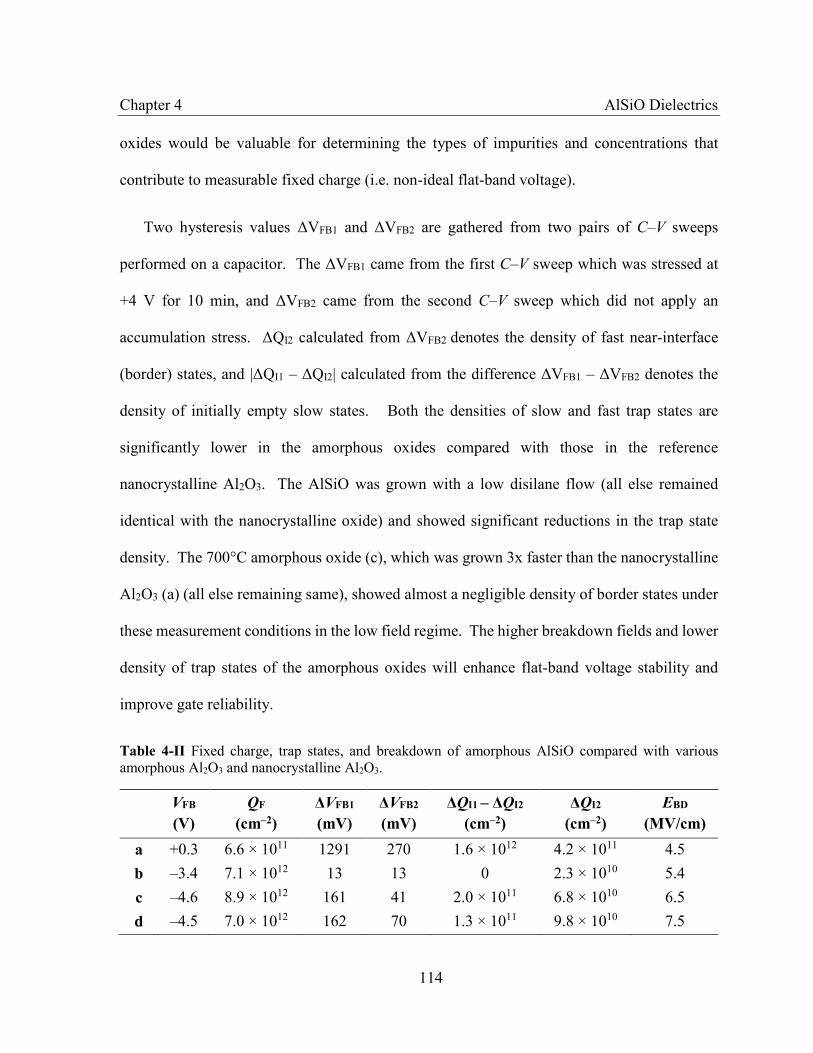
Chapter 4 AlSiO Dielectrics
114
oxides would be valuable for determining the types of impurities and concentrations that
contribute to measurable fixed charge (i.e. non-ideal flat-band voltage).
Two hysteresis values ΔVFB1 and ΔVFB2 are gathered from two pairs of C–V sweeps
performed on a capacitor. The ΔVFB1 came from the first C–V sweep which was stressed at
+4 V for 10 min, and ΔVFB2 came from the second C–V sweep which did not apply an
accumulation stress. ΔQI2 calculated from ΔVFB2 denotes the density of fast near-interface
(border) states, and |ΔQI1 – ΔQI2| calculated from the difference ΔVFB1 – ΔVFB2 denotes the
density of initially empty slow states. Both the densities of slow and fast trap states are
significantly lower in the amorphous oxides compared with those in the reference
nanocrystalline Al2O3. The AlSiO was grown with a low disilane flow (all else remained
identical with the nanocrystalline oxide) and showed significant reductions in the trap state
density. The 700°C amorphous oxide (c), which was grown 3x faster than the nanocrystalline
Al2O3 (a) (all else remaining same), showed almost a negligible density of border states under
these measurement conditions in the low field regime. The higher breakdown fields and lower
density of trap states of the amorphous oxides will enhance flat-band voltage stability and
improve gate reliability.
Table 4-II Fixed charge, trap states, and breakdown of amorphous AlSiO compared with various amorphous Al2O3 and nanocrystalline Al2O3.
VFB
(V)
QF
(cm–2)
ΔVFB1
(mV)
ΔVFB2
(mV)
ΔQI1 – ΔQI2
(cm–2)
ΔQI2
(cm–2)
EBD
(MV/cm)
a +0.3 6.6 × 10¹¹ 1291 270 1.6 × 10¹² 4.2 × 10¹¹ 4.5
b –3.4 7.1 × 10¹² 13 13 0 2.3 × 10¹⁰ 5.4
c –4.6 8.9 × 10¹² 161 41 2.0 × 10¹¹ 6.8 × 10¹⁰ 6.5
d –4.5 7.0 × 10¹² 162 70 1.3 × 10¹¹ 9.8 × 10¹⁰ 7.5

Chapter 4 AlSiO Dielectrics
115
Interface States
Figure 4.16 shows an example comparing the post-UV C–V curve between the AlSiO (28%
Si) dielectric and the (reference) nanocrystalline Al2O3. The dielectric constant is 7.1 and 6.4
for the reference nanocrystalline Al2O3 and amorphous AlSiO, respectively. A shorter ledge in
the post-UV curve relates to a smaller voltage difference between the post-UV and shifted dark
curve. This smaller voltage difference in the AlSiO film indicates a lower density of interface
states. Table 4-III lists Dit values of the AlSiO and the nanocrystalline Al2O3 along with the
amorphous Al2O3 grown and characterized in Section 3.6. While the interface-state density of
the AlSiO exceeds that of the amorphous Al2O3 films by 2 × 1011 cm–2 eV–1 (near band-edge)
and by ~4 × 1011 cm–2 (integrated Dit), the near band-edge value, for example, is ~64% less
than that of the crystallized Al2O3. All the amorphous oxides show substantially lower
interface-state densities than the nanocrystalline Al2O3.
Figure 4.16 Larger voltage difference between the shifted dark and post-UV C–V curves in (a) nanocrystalline Al2O3 than in (b) AlSiO indicates a higher density of interface states.

Chapter 4 AlSiO Dielectrics
116
Table 4-III Near band-edge Dit and integrated Dit of AlSiO and various grown Al2O3 dielectrics.
Dit at EC–0.15 eV
(cm–2 eV–1)
Integrated Dit from EC–0.15 eV to EC–2 eV
(cm–2)
a 5.3 × 10¹² 3.3 × 10¹²
b 1.7 × 10¹² 6.8 × 10¹¹
c 1.7 × 10¹² 6.9 × 10¹¹
d 1.9 × 10¹² 1.1 × 10¹²
Time-Dependent Dielectric Breakdown
Charge-to-breakdown (QBD) as a function of gate voltage was measured in AlSiO and the
various Al2O3 dielectrics (all are 25-nm-thick oxides) at room temperature. The results in
Figure 4.17 show that the amorphous Al2O3 dielectrics reached higher QBD than the
nanocrystalline Al2O3 did, despite sustaining higher gate voltages. At a gate voltage of 11 V,
for instance, the QBD of the 700°C amorphous Al2O3 is three orders of magnitude higher than
the QBD reached by the 700°C nanocrystalline Al2O3. It is interesting to note that although the
650°C amorphous Al2O3 and the AlSiO can sustain similar gate voltages near breakdown, the
QBD for the AlSiO is much lower (< 1 C/cm2). This could be related to the lower k-value of
the AlSiO. However, it can be expected from extrapolating to lower operating gate voltages,
the QBD will be significantly higher than that of the crystallized Al2O3 dielectric.

Chapter 4 AlSiO Dielectrics
117
Figure 4.17 Comparison of charge-to-breakdown (QBD) as a function of gate voltage between AlSiO and various grown Al2O3 dielectrics.
Depictions of the gate current kinetics of the nanocrystalline Al2O3 and the AlSiO film
from CVS tests are shown in Figure 4.18. It is observed that the catastrophic breakdown of
the crystalline oxide was preluded by a soft breakdown regime, characterized by gradual, noisy
leakage increases over time. In contrast, the catastrophic breakdown of the amorphous AlSiO
is abrupt following a monotonic decrease in gate current over time. No indicator for the early
breakdown was observed. These characteristics are similar to the TDDB behavior witnessed
in the amorphous Al2O3 dielectrics. It is suspected that the noisy leakage is related to multiple
partial conduction paths created in the crystalline matrix. More studies may be needed to
connect specific breakdown behaviors to films with varying degrees of crystallinity. This

Chapter 4 AlSiO Dielectrics
118
TDDB behavior, however, was foreshadowed by the noisy breakdown observed in an I–V
sweep of the crystalline oxide (see in Figure 4.15 for example).
Figure 4.18 Comparison of gate current kinetics from constant voltage stress tests of (a) nanocrystalline Al2O3 and (b) amorphous AlSiO.
Figure 4.19 Weibull distribution of the time-to-breakdown (tBD) of AlSiO for different gate stress voltages during CVS testing.
The CVS tests were performed at various gate voltages on multiple AlSiO capacitor
devices with gate diameter of 50 µm. The time-to-breakdown statistics shown in Figure 4.19
follow a Weibull distribution for each of the voltages, with 1.3 < β < 1.9, indicating statistical

Chapter 4 AlSiO Dielectrics
119
uniformity in the intrinsic oxide breakdown. Similar β values likely point to similar failure
modes at these high fields.
Figure 4.20 Time-to-breakdown (tBD) as a function of gate voltage of AlSiO compared with various grown Al2O3 dielectrics. The predicted range of dielectric lifetime is extrapolated with the field-
based E-model (solid line) and with the current-based 1/E-model (dashed line).
Time-to-breakdown as a function of gate voltage for the AlSiO and the various Al2O3
dielectrics are shown in Figure 4.20. A dielectric lifetime range is predicted with the E-model
(field-based breakdown model) which provides the most conservative estimate, and the 1/E
model (current-based breakdown model) which provides the least conservative estimate. All
amorphous oxides are predicted to achieve a dielectric lifetime of 20 years, generally at applied
fields greater than the operating field range of nanocrystalline Al2O3. The nanocrystalline
oxide achieves tBD of 20 years if the field in the oxide, EOX is kept below 2.2–2.9 MV/cm.
The AlSiO exhibited the best results, with a predicted tBD of 20 years if the oxide field EOX is
kept below the range of 3.4–4.4 MV/cm. Even the conservative value of 3.4 MV/cm is a very
high field for a dielectric to be able to reach on GaN, considering GaN breakdown fields

Chapter 4 AlSiO Dielectrics
120
achieved in a FET has only been reported to be ~2 MV/cm or less, which limits the field
reached in the dielectric. However, because threshold instabilities and related degradation can
still occur at fields much lower than the breakdown strength, it is important for oxides to
achieve a lifetime of 20 years at as high of a field as possible, thereby having an extended
voltage regime for safe, reliable gate operations.
Figure 4.21 (a) Temperature-dependent CVS measurements performed on AlSiO and (b) time-to-breakdown of AlSiO as a function of gate voltage at room temperature and 150°C.
The CVS tests were also performed at elevated temperatures to assess temperature
dependent time-to-breakdown characteristics. A depiction of the gate current kinetics of AlSiO
is shown in Figure 4.21(a) where AlSiO capacitors were stressed at a gate voltage of 15 V at
100, 150, and 200°C. As expected, gate current rises and tBD decreases with temperature due
to thermally enhanced conduction mechanisms that include Fowler-Nordheim tunneling and
trap-assisted conductions (tunneling, hopping, Poole-Frenkel) for instance. The temperature
dependent TDDB activation energy (Ea) was found to be ~0.4 eV.

Chapter 4 AlSiO Dielectrics
121
The time-to-breakdown as a function of gate voltage is shown in Figure 4.21(b) for the
AlSiO capacitors measured at RT and at 150°C. To achieve a tBD of 20 years at 150°C, the
conservative estimate for EOX in AlSiO must be lower than 2.4 MV/cm, which is 1 MV/cm
less than the EOX estimated for RT operation.
In automotive applications, a dielectric lifetime of more than 20 years at operating
temperatures up to 250°C is required. The time-to-breakdown of Si power devices is typically
evaluated at 3 MV/cm for these applications. It is expected for GaN power devices to be able
to satisfy the same criteria. Due to these strict power requirements, it is necessary to further
improve the high-temperature time-to-breakdown characteristics of the AlSiO films.
Exploring various annealing treatments is one future strategy that can potentially improve the
TDDB characteristics of AlSiO dielectrics.
Summary
So far, these various amorphous growth conditions have demonstrated very promising gate
insulators. In particular, the Si-alloying of Al2O3 permitted the amorphous stability of AlSiO
at 700°C and the reduction of interfacial and border trap states to densities on par with
amorphous binary Al2O3 dielectrics. Moreover, the lightly Si-alloyed Al2O3 dielectric
demonstrated low leakage and increased breakdown field strength, which helps to attain a time-
to-breakdown of 20 years at electric fields higher than what is predicted possible for the various
grown Al2O3. Further developments will be needed to improve high-temperature TDDB

Chapter 4 AlSiO Dielectrics
122
characteristics of AlSiO films to meet requirements of power devices such as those used in
automotive applications.
4.6 Growing Research Interest in AlSiO
The work carried out in this dissertation at UCSB has led to the first mention of AlSiO
dielectrics for GaN-based devices that was published in early 2016. Later in the same year,
Kikuta et al. and Ito et al. of Toyota Central R&D Labs also published research work on AlSiO
as gate oxides for GaN. The works investigated the TDDB and Dit of AlSiO (termed
“Al2O3/SiO2 nanolaminates”) [26], and evaluated the conduction and valence band-offset of
Al1-xSixOy to GaN using hard XPS [18]. In contrast to this work which deposited in situ AlSiO
by high-temperature MOCVD, their AlSiO gate oxides were deposited ex situ with low-
temperature (250°C) ALD. AlSiO was formed by growing alternating layer stacks of Al2O3
and SiO2 to control the Al/Si composition ratio. For fabrication and testing of the MOS
capacitors, the gate oxides were annealed at temperatures below the crystallization point
(650°C).
In 2017, Gupta et al. reported the first demonstration of AlSiO as a gate dielectric (grown
by MOCVD) in GaN high power FETs. Further details on the AlSiO-gated FET performance
will be presented in Section 5.6. These above studies show early, but burgeoning efforts for
developing this novel gate dielectric for nitride devices. As research on AlSiO gate oxides for
GaN-based devices have only emerged within the last two years, this field holds great potential
for further development. Many more studies will be needed to form a complete picture of the

Chapter 4 AlSiO Dielectrics
123
material and electrical properties, as well as determine what may become the preferred
deposition technique.

124
Gate Regrowth and Integration in GaN FETs
5.1 Introduction
The redeposition of material is often needed to create the desired functionality in many
GaN-based electronic devices. It is rare for the epitaxial structure and sub-components (such
as gate and contacts) of modern devices to be grown entirely in situ with no further regrowth
steps. GaN power devices with vertical topologies, for instance, require a deep etching step
(typically several microns) to physically define the current-spreading drift region, which is
often followed by a regrowth of the (Al)GaN layer and dielectric to complete the formation of
the channel and insulator gate. However, not all devices have equal regrowth demands since
each one imposes a different set of material and architectural constraints. For example,
although both are vertical power devices, the CAVET demands a more intensive regrowth
process than the trench MOSFET. The CAVET requires filling GaN material in a deep trench,
while the trench MOSFET requires a simple blanket deposition.
Regardless of regrowth process, vertical devices share general issues related to the etching
of GaN and the ex situ deposition of gate oxides. In vertical devices, regrowth is often carried
out on etch-damaged GaN surfaces. When damaged, the GaN crystal becomes rife with
nitrogen vacancies—nitrogen has shown to be notoriously difficult to resupply back into the
lattice. If necessary measures are not taken to treat the damage or clear impurity contamination
from the GaN surface, the performance of the best dielectric can be compromised by a poor
contact with the GaN surface. In some cases, interface quality can limit gate performance more

Chapter 5 Gate Regrowth and Integration in GaN FETs
125
than the dielectric quality can. It is therefore of great interest to repair GaN etch damage as
much as possible. MOCVD pre-deposition treatments such as annealing in N2/NH3 has shown
to be effective in this regard. Section 5.2 and Section 5.3 discuss the damage recovery study.
Even when a gate oxide regrowth is performed on GaN surfaces not damaged by etch (e.g., as-
grown on ex situ, cleaned surfaces), the advantages of having an in situ, low-defect
dielectric/GaN interface can still be lost. Section 5.4 discusses the increase in positive fixed
charges, interface-state density and oxide field stress for an ex situ deposited oxide.
A key development in both studies was the regrowth of thin GaN interlayers on ex situ
surfaces prior to the oxide deposition. This step recreated the in situ oxide/GaN interface and
led to much improved electrical properties over devices without the GaN interlayer. This key
regrowth is then harnessed in the fabrication of vertical trench MOSFETs to improve channel
mobility. The latter sections of this chapter will cover the gate oxide regrowth process (Section
5.5) to the final gate dielectric demonstrations in GaN MOSFETs (Section 5.6).
5.2 Regrowth Considerations for Vertical GaN Devices
The regrowth considerations for vertical topology GaN devices ultimately dictate the basis
for a highly effective regrowth. The first goal is to design a pre-growth treatment to repair
etch-damaged GaN surfaces inside the MOCVD chamber while keeping the profiles of etched
non-planar structures (as in the case with vertically formed devices) intact. The pre-growth
treatment plan draws on the capabilities of MOCVD to treat samples in combination gas
mixtures comprising of N2, NH3, and/or H2 at different temperatures. This strategy was derived

Chapter 5 Gate Regrowth and Integration in GaN FETs
126
from many studies that report the use of nitrogen plasma and nitrogen/ammonia-based
annealing for reducing nitrogen-related defects in impacted GaN areas [114]–[117]. Other
studies have demonstrated the use of H2 to clean GaN-based surfaces at low temperatures
[118], [119] and to remove sub-surface damage in bulk GaN [120]. Here, the treatment
experiments carried out will determine which gas (mixtures) will be the most effective in
repairing the damage. The strategy for repairing etch damage by MOCVD gas treatments also
differs from some traditional methods that are more widespread, such as wet etching, plasma,
and chemical passivation. To also preserve the sharp, etch-defined profiles of mesas and
trenches during the treatments, lower temperature studies will be investigated to prevent the
mass flow redistribution of GaN. Mass transport of GaN has been observed to occur at
temperatures above 1000°C, which then resulted in the redeposition of GaN into trench
corners. This is a scenario to avoid since corners can become highly doped and could evolve
into vulnerable breakdown points in a device.
An unconventional procedure is introduced here for evaluating the material recovery
resulting from the surface treatments. Mainly, thin AlGaN or AlGaN/GaN test structures were
grown directly on the MOCVD-treated surfaces to generate a 2DEG at/near the regrowth
interface. This is unusual since whole AlGaN/GaN micron-thick buffer heterostructures are
normally grown without breaking vacuum in order for HEMTs to benefit from superior 2DEG
charge and transport. In this case, the 2DEG is intentionally generated at a short distance from
the regrown interface, such that measurable 2DEG transport properties (e.g. mobility, charge,
and sheet resistance) can be used to assess the impact of surface treatments. The 2DEG is very
sensitive to scattering. If a 2DEG channel is formed near a regrown interface, its transport

Chapter 5 Gate Regrowth and Integration in GaN FETs
127
properties could degrade, possibly from nearby damage or impurities introduced from external
processes. These effects can be seen if the mobility is affected by changing the proximity of
the 2DEG to regrowth interface, for instance, by inserting a GaN spacer (interlayer). This
detection technique is similar to that used in another study, which looked at the influence of an
undoped AlGaN spacer thickness on reducing scattering between a Si-doped AlGaN layer and
the GaN buffer [121]. Otherwise, the proposed approach for characterizing etch damage in
GaN differs significantly from some of the more conventional techniques. Diode current and
photoluminescence measurements are more common for assessing etch damage, however, they
typically capture bulk effects. The following section describes the regrowth experiments and
their results.
5.3 Mobility Recovery Experiments on Etched GaN
Regrowth experiments were conducted to examine the influence of the following factors
on 2DEG mobility: (Al)GaN deposition temperature, annealing gas mixture, annealing
temperature and duration, and GaN interlayer thickness. An overview of the experimental
design is discussed before the results. The first set of experiments comprised of AlGaN/GaN
HEMT heterostructures grown entirely in situ on sapphire substrates, where only the AlGaN
deposition temperature was varied. The HEMT structure consisted of 2 μm of semi-insulating
(S.I.) GaN, followed by 25 nm of Al0.24Ga0.76N and a 2-nm-thick GaN cap layer (Figure 5.1(a)).
X-ray diffraction was used to determine AlGaN compositions and layer thicknesses. SI GaN
layers were grown using a standard two-step method with Fe doping [121] at a temperature of
1170 °C. Then the temperature was reduced for the AlGaN deposition layer to temperatures of

Chapter 5 Gate Regrowth and Integration in GaN FETs
128
850, 900 and 950°C. From the AlGaN series, the temperature that yielded the smoothest
morphology (lowest roughness) and highest mobility was chosen as the upper temperature
limit for subsequent experiments involving the gas pretreatments, annealing, and GaN
regrowth.
Figure 5.1 Schematics of (a) in situ grown HEMT, (b) regrown HEMT structure in annealing and GaN interlayer regrowth experiments, (c) fabricated HEMT device: regrown on etched GaN, (d)
Al2O3 MOS-HEMT: regrown on etched GaN. Regrown layers are indicated in color.
The rest of the experiments on gas pretreatments, annealing, and (Al,Ga)N regrowth were
performed on ex situ GaN samples. The term ex situ GaN here refers to GaN templates that
had been removed from the MOCVD chamber after growth. Several of the ex situ GaN
templates were selected for dry etching. These samples were etched 500 nm deep using Cl2/Ar
based ICP. Further information on the etch development conditions are published elsewhere
[122]. All ex situ templates, etched or unetched, were subjected to UV-exposure followed by
an HF dip clean of the surfaces prior to being loaded into the MOCVD chamber for the
pretreatment and regrowth. A 20-nm-thick Al0.24Ga0.76N gating layer was deposited for all ex
situ GaN experiments.

Chapter 5 Gate Regrowth and Integration in GaN FETs
129
To distinguish factors introduced by the removal of the sample from the growth chamber
from those introduced by etching, a variety of surface pretreatments were first performed on
unetched GaN templates. Based on the results, the most effective pretreatment process to
sufficiently recover high mobility and low sheet resistance was then transferred to etched
samples, where mobility properties were expected to degrade. Hereafter, the gas pretreatment
was combined with an annealing duration series and an annealing temperature series. The
annealing duration experiments only annealed the etched samples prior to AlGaN growth. This
differs from the annealing temperature experiments, which deposited an additional 2-nm-thick
GaN interlayer in the step after annealing but prior to AlGaN growth. Based on the mobility
improvement observed from the addition of the 2-nm-thick GaN interlayer in the annealing
temperature experiments, the last set of experiments were designed to vary the thickness of the
regrown GaN interlayer up to 10 nm. The structure schematic used in the various ex situ studies
is illustrated in Figure 5.1(b).
The finalized treatment process, composed of the most effective gas pretreatment, pre-
annealing conditions, and GaN regrowth, was applied to a HEMT structure regrown on etched
GaN. A 4-nm-thick GaN interlayer was deposited prior to the 20 nm Al0.24G0.76N gating layer.
This sample was then fabricated into a device per the following process flow: source and drain
contacts were deposited using electron beam evaporation of a Ti/Al/Ni/Au (20/100/10/50 nm)
metal stack and then subjected to a 30-s rapid thermal anneal at 870 °C in an N2 environment.
A Cl2-based reactive ion etch was used to isolate transistors. Next, the Schottky gate was
deposited using electron beam evaporation of a Ni/Au/Ni (30/500/30 nm) metal stack. Finally,
the devices were passivated using 1.5 nm of Al2O3 by atomic layer deposition followed by 160

Chapter 5 Gate Regrowth and Integration in GaN FETs
130
nm of PECVD SiNx. The HEMT device schematic is illustrated in Figure 5.1(c). The
processed transistors were characterized using DC and pulsed I–V measurements. The latter
is a common technique to evaluate trap-related dispersion in transistor devices [28–30]. A
MOS-HEMT structure was also regrown on etched GaN under the same conditions as the
HEMT device, with the exception of an in situ 20-nm-thick Al2O3 top layer instead of the 2
nm GaN cap (Figure 5.1(d)). The results and discussion of each experiment are presented.
AlGaN Deposition Temperature
Figure 5.2 shows AFM images of the 25-nm-thick Al0.24Ga0.76N surface morphology grown
at different growth temperatures. Step-flow growth is observed in samples grown at
temperatures as low as 900°C. By 850°C however, ad-atom mobility had decreased
significantly enough to create prominent step-bunching at the surface. The RMS surface
roughness also increased from 0.7 to 1.4 nm while the temperature dropped from 950 to 850°C.
At the same time, the measured 2DEG mobility decreased from 1587 to 198 cm2/Vs (Figure
5.3). Though the AFM morphology appears smooth at 900°C, the measured mobility and sheet
carrier density had degraded to 1026 cm2/Vs and 1.4 × 1012 cm–2, respectively. The reduction
in sheet carrier density at lower temperatures suggests an increase of acceptor-like traps, most
likely due to an increase of carbon into the AlGaN layers [49], [54], [123]. Since 950°C was
found to be the coldest temperature that upholds both smooth morphology and high electron
mobility, all subsequent (Al)GaN deposition experiments were conducted at this temperature.
Note that the mobility of 1587 cm2/Vs obtained at 950°C is comparable to values obtained for
the typical high-temperature growth of AlGaN/GaN HEMTs. In addition, no mass reflow of
GaN was observed at this regrowth temperature.

Chapter 5 Gate Regrowth and Integration in GaN FETs
131
Figure 5.2 AFM images of 25-nm-thick Al0.24Ga0.76N layers grown at reduced temperatures on GaN. The height range of the image is 6 nm.
Figure 5.3 Electron mobility of samples with 25-nm-thick Al0.24Ga0.76N layers grown at reduced temperatures on GaN.
Gas Mixture Pretreatments of Unetched GaN
In the first set of ex situ GaN experiments, unetched GaN samples were treated by various
gas mixtures during the temperature ramp up to 950°C. A sample with 20 nm Al0.24Ga0.76N

Chapter 5 Gate Regrowth and Integration in GaN FETs
132
grown in situ at 950 °C on 2 μm S.I. GaN provided a reference of mobility, sheet charge, and
sheet resistance (Rsh) to samples with regrown (Al)GaN on surface-treated ex situ GaN
samples. The Hall results from the various gas mixture treatments are summarized in Table
5-I.
Table 5-I MOCVD surface pretreatments explored on unetched GaN surfaces prior to 20 nm AlGaN deposition. Listed are the corresponding sheet resistance Rsh, sheet carrier density ns, and electron mobility μ obtained from Hall measurements.
Temperature
ramp-up
Gas mixture flows
(L = SLM a)
)
Rsh
(Ω/sq)
ns
(cm–2)
μ
(cm2 V–1s–1)
In situ n/a n/a 471 8.45 × 10¹² 1569
Regrown 0°C–950°C 5L N2 + 2L NH3 705 8.79 × 10¹² 1007
Regrown 0°C–950°C 5L N2 + 2L NH3 + 1L H2 693 1.54 × 10¹³ 586
Regrown 0°C–450°C 1L H2 (anneal 5 min) 835 9.29 × 10¹² 806
450°C–930°C 5L N2 + 2L NH3
Regrown 0°C–930°C 5L N2 + 2L NH3 (anneal 30min) 559 8.02 × 10¹² 1392
a) SLM = standard liters per minute
Mobility improved from 586 to 1007 cm2/Vs by the exclusion of H2 from an N2+NH3
mixture, suggesting that the presence of H2 was detrimental to the surface quality. This could
be expected as it is well documented that hydrogen can also decompose GaN, etch dislocations,
and roughen surfaces [124]–[126]. Hydrogen etch-induced formation of native donor defects
such as nitrogen vacancies [127] can possibly explain the ~6.6 × 1012 cm–2 added charge and
40% mobility loss. The results from the temperature ramp to a 450°C in H2 followed by a
temperature ramp to 950°C in N2+NH3 further evidenced that H2 still introduced damage even
at low temperatures, but the surface quality is partially recovered under the elevated
temperatures in N2+NH3. This part H2, part N2+NH3 treatment resulted in a higher mobility of

Chapter 5 Gate Regrowth and Integration in GaN FETs
133
806 cm2/Vs than the concurrent H2+N2+NH3 treatment. A temperature ramp to 930°C
exclusively in N2+NH3 followed by a 30 min anneal produced the greatest mobility recovery
of 1392 cm2/Vs and minimal change in ns, resulting in a low sheet resistance of 559 Ω/sq. The
surface healing effects of N2 and NH3 on GaN reported in the literature are corroborated with
the findings here. This annealing gas mixture treatment was then applied to etched samples in
the next set of experiments.
Annealing of Etched GaN Surfaces
The dry etching from the ICP conditions resulted in GaN surfaces with a low RMS
roughness of ~0.4 nm, which is comparable to the roughness of an as-grown surface. An AFM
image of the etched surface is depicted in Figure 5.4. These etched samples were used for an
annealing duration series at 930 °C and annealing temperature series where the annealing time
was kept for 30 min. As mentioned before, the annealing temperature series included an
additional 2 nm GaN interlayer grown prior to the AlGaN layer to enhance the mobility. The
mobility results are plotted in Figure 5.5. Both series exhibit optimum mobility within the
annealing time range from 10 to 40 min and the temperature range from 910 to 950°C. The
mobility degradation at longer times and higher temperatures may be partially attributed to the
decomposition of NH3 into H2 which was shown to play a significant role in the desorption of
N- and Ga-surface atoms [128], [129]. The lowest mobility of 425 cm2/Vs was attained at an
annealing temperature of 950°C for 30 min. On the other hand, an etched sample annealed at
930°C for 30 min yielded μ of 863 cm2/Vs. This mobility was further improved to an average
of 945 cm2/Vs when a 2 nm thin GaN interlayer was deposited at 950°C following the anneal.

Chapter 5 Gate Regrowth and Integration in GaN FETs
134
However, all values remain lower than what was measured for the unetched counterpart (1392
cm2/Vs).
Figure 5.4 5×5 μm2 AFM image of a semi-insulating GaN surface after a vertical dry-etch of 500 nm by Cl2/Ar ICP. The height range of the image is 4 nm; RMS 0.4 nm.
Figure 5.5 Dependence of electron mobility on (a) annealing duration of etched GaN in N2+NH3
prior to 20nm Al0.24Ga0.76N layer deposition and (b) annealing temperature of etched GaN in N2+NH3 prior to deposition of 2 nm GaN interlayer + 20 nm Al0.24Ga0.76N.

Chapter 5 Gate Regrowth and Integration in GaN FETs
135
GaN Interlayer Regrowth
The insertion of a GaN interlayer (IL) recovers high mobility since it spaces the 2DEG
channel further away from the damaged regrowth interface. To find an optimal thickness,
interlayers up to 10 nm were deposited on annealed, etched GaN samples. The results plotted
in Figure 5.6 show that for an IL thickness greater than 3 nm, the 2DEG mobility gained
sharply from an average value below 1000 to ~1400 cm2/Vs. For 2 nm IL samples, the Rsh
varied from 777 to 830 Ω/sq. In comparison, for 3 nm IL and thicker samples, the Rsh decreased
to values ranging from 570 to 600 Ω/sq.
Figure 5.6 Mobility (top) and sheet resistance (bottom) dependence on GaN interlayer thickness on annealed, etched GaN. In the mobility plot, experiments conducted
on the same etched GaN base wafer are marked in one color.

Chapter 5 Gate Regrowth and Integration in GaN FETs
136
These experiments suggest that defect/impurity scattering at the regrowth interface was a
dominant factor limiting the 2DEG mobility at room temperature. Spacing of the 2DEG as
little as 3 nm from the etch-damaged interface significantly reduced scattering losses.
Regrown HEMT & MOS-HEMT Demonstration
A Schottky-gated HEMT device was fabricated on a sample that was treated by the
optimized N2+NH3 anneal and had a 4 nm regrown GaN IL. The output and transfer
characteristics are shown in Figure 5.7 for a device with 0.5 μm LGS, 1 μm LG, 2 μm LGD, and
150 μm WG. Low dispersion is revealed in the gate-lag pulsed I–V measurements that were
taken along a 50 Ω load line, evidenced by current reductions of only 5% for the 200 ns pulses.
This suggests minute trapping effects near the 2DEG channel, despite the channel being near
the buried regrowth interface. As shown in the ID–VG characteristics, the device demonstrated
601 mA/mm of maximum drain current (ID, MAX) at VG = 2 V and 211 mS/mm of maximum
transconductance (gM, MAX). The minimum subthreshold slope was found to be 123 mV/dec.
These results indicate the regrowth process successfully mitigated material deterioration
caused by sample removal from chamber and etching. The remaining impurity and defects at
this interface did not significantly degrade the electrical performance under such measurement
conditions.
The regrowth process was then applied to the fabrication of a MOS-gated HEMT with an
Al2O3 gate dielectric. The 20 nm Al2O3/20 nm AlGaN/ 4 nm GaN IL was regrown
consecutively without interruption. This sample exhibited μ of 1336 cm2/Vs and Rsh of 564

Chapter 5 Gate Regrowth and Integration in GaN FETs
137
Ω/sq. While lower than that of GaN-capped HEMTs, the electron mobility is sufficiently high
to set the stage for the fabrication of MOS-HEMTs on etched surfaces.
Figure 5.7 I–V characteristics of a regrown HEMT: (top) gate-lag pulsed I–V and (bottom) ID-VG and gm-VG curves.
Summary
This gate regrowth development work has shown that even simple removal and exposure
of unprocessed samples to air reduces surface mobility despite the implemented cleaning
procedure. As demonstrated here, MOCVD can provide the in situ annealing treatments to

Chapter 5 Gate Regrowth and Integration in GaN FETs
138
heal surfaces and the regrowth to further recover transport properties close to that of samples
fabricated without growth interruption. The Hall measurements clearly discerned differences
in the quality of the buried regrowth interfaces and proved more effective than AFM imaging.
The Hall results quantitively described the extent to which N2, NH3, and GaN interlayers
impact surface recovery near a channel. The pretreatment with N2+NH3 annealing and GaN
interlayer growth helped recover lateral transport properties near etch-damaged regions (>
1400 cm2/Vs in GaN-capped HEMT structures, 1336 cm2/Vs in MOS-HEMT). Rsh has
reduced to below 600 Ω/sq in structures with a GaN IL thicker than 2 nm. This study on
recovering high electron mobility in AlGaN/GaN 2DEG channels regrown on etched surfaces
is published in Ref. [130]. The regrowth technique will prove useful for enhancing gate
performance in vertical GaN MOSFETs.
5.4 Characteristics of in situ versus ex situ formed Al2O3/GaN
interfaces
In many GaN transistors, the gate dielectric is often deposited ex situ. Consequently, it is
common to develop GaN surface cleaning protocols to prevent the dielectric/GaN interface
from severely trapping impurities and forming defects that can negatively affect the gate
performance in a MOSFET. However, the relative progress towards obtaining an impurity-
and defect-free interface is difficult to assess without having an in situ reference.
Previously, only SiNx layers were grown extensively by MOCVD, under both in situ and
ex situ conditions, and were studied as passivation layers and gate dielectrics for III-nitride

Chapter 5 Gate Regrowth and Integration in GaN FETs
139
devices [36], [38], [131]. However, no study has compared the electrical differences between
in situ and ex situ MOCVD-grown oxide dielectrics on GaN. As a result, the benefits of in situ
oxide/GaN interfaces reported so far may be unconvincing or go unrecognized. To address
this gap in knowledge, a study is performed to compare key differences in the fixed charge,
interface-state density, and breakdown voltage of GaN MOS capacitors among devices with in
situ and ex situ gate Al2O3 dielectrics formed by MOCVD. In addition, MOS capacitor devices
consisting of a reformed in situ interface between the Al2O3 and GaN interlayer (regrown on
top of ex situ GaN surfaces) are also evaluated. Here, the GaN interlayer impact on vertical
properties such as MOS breakdown is discussed.
Figure 5.8 Schematics of the MOS capacitors structure for devices with (a) in situ Al2O3 on n− GaN, (b) in situ Al2O3/UID GaN interlayer regrown on n− GaN, and (c) ex situ Al2O3 regrown on n− GaN.
Regrown layers are indicated in color.
The schematics of the three types of MOS structures under test (in situ, ex situ, GaN
interlayer-based MOS) are shown in Figure 5.8. The n– doping of the in-situ-grown device is
1.5 × 1017 cm–3. The latter two ex situ samples were prepared by growing a base GaN wafer

Chapter 5 Gate Regrowth and Integration in GaN FETs
140
in another MOCVD machine that produced n– doping of 3 × 1017 cm–3. The base GaN wafer
was then divided into two pieces and each was subjected to the same UV-ozone and HF
cleaning procedure in the previous section. After, the devices were immediately loaded into
the MOCVD chamber for growth. Aluminum oxide was deposited directly on one GaN wafer
piece while a 10-nm-thick GaN interlayer followed by aluminum oxide was deposited on the
other. The GaN interlayer allowed for the Al2O3/GaN interface to be formed in situ while
providing some separation from the ex situ regrowth interface. The UID GaN interlayer was
deposited at 950°C. All the MOS structures had a nominally 20-nm-thick Al2O3 dielectric
grown at 700°C. The dielectric constant was approximately 7.
Influence on Flat-band Voltage
The C–V measurements were carried out at a sweep rate of 0.2 V/s. The frequency and
amplitude of AC signals were 1 MHz and 50 mV, respectively. Figure 5.9 shows the
representative C–V profiles of the three types of MOS capacitors. The differences in measured
flat-band voltage (ΔVFB = Vfb, ex-situ − Vfb, in-situ) and fixed charge (ΔQF = QF, ex-situ − QF, in-situ)
with respect to in situ capacitors are shown in Table 5-II. Small variation in the thickness was
due to the slight radial nonuniformity of the growth rate. Capacitors with ex situ oxides
featured a higher net positive fixed charge density, which manifests as a negative shift of the
flat-band voltage relative to that of capacitors with an in situ oxide. Linear dependences of the
flat-band voltage on oxide thickness observed previously in in-situ-grown MOS capacitors
indicated that the centroid of fixed charge effectively lies at or near the Al2O3/GaN interface
[63], [132]. The ex situ oxide capacitors exhibited a large flat-band shift of –2.1 V,
corresponding to a positive fixed charge increase of 4.1 × 1012 cm–2. In addition, a ledge in its

Chapter 5 Gate Regrowth and Integration in GaN FETs
141
C–V curve was observed between weak depletion and the onset of accumulation, which
indicates a presence of interface states that may be pinning the surface Fermi level [127]. It is
interesting that MOS capacitors containing the GaN interlayer also feature a negative flat-band
shift in C–V even though the Al2O3/GaN interface is separated from the regrowth interface by
10 nm. These devices demonstrated a smaller flat-band voltage shift of –1.1 V (a positive
charge increase of 2.2 × 1012 cm–2) compared with the in situ devices. These positive fixed
charges could potentially be caused by the migration of defects and/or impurities (remaining
after the regrowth of the 10-nm-thick GaN interlayer) closer to the in-situ-formed Al2O3/GaN
interface. Nevertheless, compared to the ex situ oxides, the (near) interface quality is improved
by having fewer positive fixed charges.
Figure 5.9 C–V characteristics of Al2O3/GaN MOS capacitors with regrown layers feature more negative flat-band voltages than that of an in-situ-grown MOS capacitor.

Chapter 5 Gate Regrowth and Integration in GaN FETs
142
Table 5-II Extracted C–V properties of MOS capacitors with ex-situ- and in-situ-formed Al2O3/GaN interfaces.
Al2O3/GaN interface ΔVFB = VFB,ex-situ – VFB,in-situ
(V)
ΔQF = QF,ex-situ – QF,in-situ
(cm–2)
Thickness
(nm)
a In situ 0 0 21.4
b w/ GaN interlayer –1.1 2.2 × 10¹² 21.0
c Ex situ –2.1 4.1 × 10¹² 20.5
Interface States
Figure 5.10 shows Dit of the three MOS capacitors at the near band edge (EC − E = 0.15
eV) and integrated Dit from 0.15 to 2 eV. The devices with the GaN interlayer show a slightly
higher Dit near the band edge (7 × 10¹² vs 5.3 × 1012 cm−2 eV−1) and integrated Dit (4 × 10¹² vs
3.3 × 1012 cm−2) than the measured Dit equivalent in in-situ-grown capacitors. The ex situ
oxides, however, demonstrated a significantly higher Dit, ~1 × 1013 cm−2 eV−1 higher interface-
state density at the band edge and 2.6 × 1012 cm−2 eV−1 higher integrated Dit compared with
the devices grown in situ. The high Dit at the ex situ Al2O3/GaN interface corroborates with
the visible interface-state ledge in the C–V profile. Although devices with the newly formed
in situ Al2O3/GaN interface do not show a full reduction of Dit to values achieved in devices
grown in situ, the GaN interlayer introduces a pathway to further improve devices with ex situ
oxide/GaN interfaces.

Chapter 5 Gate Regrowth and Integration in GaN FETs
143
Figure 5.10 Interface-state density (Dit) near band edge and integrated Dit of MOS capacitors with in-
situ-grown Al2O3 on GaN (squares), reformed in situ Al2O3/GaN interface via GaN interlayer (triangles), and ex-situ-grown Al2O3 on GaN (circles).
Leakage and Breakdown
Forward- and reverse- bias I–V measurements were performed at sweep rates of 0.2 and
0.4 V/s, respectively on MOS capacitors with 100 × 100 μm2 gates until catastrophic (hard)
breakdown was reached. Figure 5.11 shows the representative forward I–V characteristics of
the three types of MOS capacitors. Regardless of the type of Al2O3/GaN interface, the
breakdown field of the dielectric in all devices was ~7 MV/cm under forward bias. However,
both regrown devices experienced the onset of increased leakage at earlier gate biases than the
in-situ-grown device.

Chapter 5 Gate Regrowth and Integration in GaN FETs
144
Figure 5.11 Forward-bias I–V and breakdown characteristics of 25-nm-thick oxide MOS capacitors show that all devices, with or without an in-situ-formed Al2O3/GaN interface, exhibit breakdown
fields of ∼7 MV/cm.
Figure 5.12 Reverse-bias I–V and breakdown characteristics of MOS capacitors with the GaN interlayer exhibited lower leakage and higher breakdown than did devices
with an ex situ oxide/GaN interface.

Chapter 5 Gate Regrowth and Integration in GaN FETs
145
Reverse-bias I–V characteristics in Figure 5.12 show that GaN interlayer devices had lower
gate leakage and higher breakdown than devices with ex situ oxides. The measured breakdown
voltages (VBD) and the calculated electric fields in the dielectric (EBD, ox) and in GaN (EBD, GaN)
at breakdown are recorded in Table 5-III along with measured gate leakage current (IG) and
the calculated field in the dielectric (Eox) at −20V gate bias. The breakdown voltage in reverse
bias is partitioned by voltage drops across the oxide and GaN following equation [from section
2.4.1]. The schematic of the charge density and electric field profiles shown in Figure 5.13
and the schematic band diagram shown in Figure 5.14 both illustrate how a high positive fixed
charge (QF) negatively impacts the voltage partitioning across the oxide and GaN. The
additional flat-band voltage component arising from the high positive charge is assumed by
the oxide gate dielectric, resulting in a higher preexisting built-in field in the oxide. Therefore,
at a –20 V gate bias, the capacitors with ex situ oxides experience an oxide field of 2.9 MV/cm,
compared to the capacitors with GaN interlayers which experience an oxide field of 2.5
MV/cm. The field is the lowest in the in situ oxide capacitors, calculated to be 1.9 MV/cm
assuming the n− doping density is identical to that of the regrown capacitors (ND = 3 × 1017 cm–
3). Note that under all conditions, the extracted fields are well below the breakdown field of
the oxide. The breakdown of the capacitors is determined by the field in the GaN layer, which
reached 1.5–1.7 MV/cm at breakdown without edge termination. Similar field values have
been observed for GaN p–n diodes fabricated on sapphire: 1.75 [133] and ~1.6 MV/cm [134].
As a result, the voltage (and electric field) reached in the ex situ oxide at breakdown is indeed
higher than those reached in the other oxides. These trends are also summarized in Table 5-III.

Chapter 5 Gate Regrowth and Integration in GaN FETs
146
Figure 5.13 Schematics of charge density (ρ) and electric field (E) profiles in the MOS capacitor under reverse bias for (left) high positive QF and (right) low positive QF at the Al2O3/GaN interface.
Figure 5.14 Schematic band diagrams demonstrate voltage partitioning across Al2O3 (Vox) and GaN (VGaN) under reverse bias for (left) high positive QF and (right) low positive QF at the Al2O3/GaN
interface.

Chapter 5 Gate Regrowth and Integration in GaN FETs
147
Table 5-III Breakdown voltage (VBD), electric field in Al2O3 dielectric (EBD,ox), and electric field in GaN (EBD,GaN) at moment of breakdown in reverse bias, gate current (IG), and field in oxide (Eox) at −20V gate bias, along with corresponding GaN n− doping density (ND).
VBD
(V)
EBD, OX
(MV/cm)
EBD,GaN
(MV/cm)
IG at –20 V
(A/cm2)
EOX at –20V
(MV/cm) ND (cm–3)
a –48.0 2.2 1.6 6.1 × 10⁻⁹ 1.5 1.5 × 10¹⁷
n/a n/a n/a n/a 1.9 a) 3 × 10¹⁷ a)
b –29.1 2.8 1.7 4.4 × 10⁻⁸ 2.5 3 × 10¹⁷
c –24.0 3.1 1.5 2.6 × 10⁻⁶ 2.9 3 × 10¹⁷
a) Relating to calculation of EOX at –20V for in situ oxide assuming a doping of 3 × 1017 cm–3.
On Breakdown Mechanisms
Several experiments have led to the hypothesis that the presence of holes at the
dielectric/GaN interface is a probable cause of oxide breakdown in reverse bias. Holes can be
generated from dislocations and will pile at the dielectric/GaN interface when in the presence
of a reverse bias field. The hole confinement occurs in dielectrics with a positive valence band
offset to GaN such as Al2O3, SiO2, or AlSiO, and may increase the electric field across the
oxide to the point of physical breakdown.
In contrast, dielectrics with a negative valence band offset to GaN are unlikely to
experience this breakdown mechanism. For example, capacitors fabricated with SiNx, a
dielectric which has no valence (hole) barrier, have exhibit a gradual increase in leakage rather
than a more immediate, hard breakdown. This gradual leakage is likely attributed to free hole
current from the GaN layer to the gate contact under reverse bias.
In another experiment, the breakdown of oxide dielectrics decreases significantly with
exposure to UV-light, providing more compelling evidence for the hole-induced breakdown

Chapter 5 Gate Regrowth and Integration in GaN FETs
148
theory. Lastly, the dielectric breakdown significantly improves on bulk GaN substrates, which
are known to contain a lower dislocation density and thus a lower hole generation density. If
the breakdown is dependent on hole generation and mobility, MOS breakdown will be severe
in capacitors or transistors without a sink to properly manage hole concentrations.
Consequently, it will be important to identify the breakdown mechanisms in (Al,Si)O
dielectrics in future work.
Summary
This study has shown that in-situ-grown MOS capacitors exhibited notably lower positive
fixed charge at the Al2O3/GaN interface and reduced interface-state density compared with
devices with ex-situ-formed Al2O3/GaN interfaces. Positive fixed charges that are collected
or formed at the ex situ interfaces could negatively impact the threshold voltage and electric
field distribution in a MOSFET gate. However, capacitors in which a thin GaN interlayer was
regrown directly prior to oxide deposition exhibited fewer positive fixed charges, lower
leakage, and higher breakdown voltages than did capacitors with ex situ Al2O3/GaN interfaces.
This GaN interlayer provides a pathway to advance gate performance in devices for which this
regrowth process can be adopted. An example of this regrown gate implementation in vertical
GaN trench MOSFETs is described in the next sections. This study on comparing the
electrical characteristics of in situ and ex situ Al2O3/GaN interfaces formed by MOCVD is
published in Ref. [135].

Chapter 5 Gate Regrowth and Integration in GaN FETs
149
5.5 Gate Regrowth in GaN FETs
A gate regrowth process, adopted from the optimized electron mobility recovery studies,
will be used to integrate the in situ gate dielectrics into the fabrication process of GaN FETs.
Specifically, a vertical trench MOSFET is the device of interest, which consists of a dielectric
deposited on an n-p-n trenched epitaxial structure. A schematic of the traditional trench
MOSFET is shown in Figure 5.15(a). In this device, the channel forms on the sidewall at the
onset of inversion in the p-type layer. However, the channel mobility is poor for two reasons:
the electron mobility in p-type GaN is low and the gate insulator is formed directly on the etch-
damaged, vertically inclined sidewalls. This leads to low current density and high on-
resistance. The regrowth process described here helps improve upon these issues.
Additionally, the simplicity of the blanket regrowth process makes the trench MOSFET
advantageous over other regrowth-intensive devices.
The gate regrowth process consists of three steps. First, pre-annealing of the etched GaN
surface (in N2+NH3 at 930°C for 30 min) is performed to aid in the partial recovery of the etch
damage. Second, a 10-nm-thick targeted UID GaN interlayer is regrown (at 950°C) on top of
the annealed surface. The GaN interlayer was found by TEM inspection to be thinner on the
trench sidewalls (~5 nm) than on the trench bottom (~10 nm). The final step is an in situ
deposition of either an Al2O3 or AlSiO gate dielectric (at 700°C) on top of the GaN interlayer.
The in situ dielectric growth onto the GaN interlayer allows the interface to have a lower trap
density compared to an interface formed by the deposition of ex situ dielectrics. Moreover,
the channel is now formed in the newly regrown GaN interlayer, as opposed to in the etch-

Chapter 5 Gate Regrowth and Integration in GaN FETs
150
damaged GaN region in devices without the GaN interlayer. The trench MOSFET device with
the GaN interlayer modification is shown in Figure 5.15(b).
Figure 5.15 Schematic of (a) conventional trench gate MOSFET and (b) a modified trench gate MOSFET with a GaN interlayer inserted prior to the in situ gate dielectric cap.
With the gate regrowth process, the accumulation of electrons at a more pristine
dielectric/GaN interface enhances electron mobility and reduces on-resistance. Note that even
in traditional trench GaN MOSFETs without the GaN interlayer, the turn-on of the channel is
likely due to an electron accumulation layer. Many studies posit that this is because the etching
in trench MOSFETs type converts the p-GaN layer into n-GaN by forming donor-like defects.
This theory is supported by consistent observations of a discrepancy in the gate threshold
voltage between simulations and experiments. This modified device with the GaN interlayer
is termed in-situ Oxide GaN interlayer-based vertical trench MOSFET or “OG-FET” for short.
The improved electrical characteristics of OG-FETs over that of traditional trench MOSFETs
(without the regrown GaN interlayer) are shown in the next section.

Chapter 5 Gate Regrowth and Integration in GaN FETs
151
5.6 Performance of OG-FETs with Gate Dielectrics
Impact of GaN Interlayer
Details of the OG-FET device fabrication process, measurements, and results are published
by Gupta et al. in Ref. [9]. This study compares the FET performance characteristics between
a device with a regrown GaN interlayer and a device without. The FET devices were fabricated
on sapphire substrates. Both devices had undergone the pre-annealing for partial etch-damage
recovery. Afterward, one device underwent an ex situ Al2O3 growth while the other underwent
a regrown GaN interlayer followed by an in situ Al2O3 growth. The Al2O3 layers are 50-nm-
thick. The single-cell devices tested have dimensions of 2 μm trench width × 220 μm gate
width. The active area is 8 μm × 116 μm gate width, which accounts for current spreading.
The FET metrics of both devices are compared in Table 5-IV. Both types of devices had
low gate leakage (IG) of < 100 pA/mm, excellent ION/IOFF ratio of 108, a voltage breakdown
(VBD) range of 150–200 V which corresponded to a GaN breakdown field (EBD,GaN) range of
0.6–0.9 MV/cm for a drift region of 6 μm.
Table 5-IV FET characteristics of a traditional trench MOSFET and modified trench MOSFET with GaN interlayer (OG-FET). Metrics are drain current density (ID), on-resistance (RON), channel mobility (μ), gate threshold voltage (VTH), gate hysteresis (ΔVTH), and subthreshold slope (SS).
ID
a)
(A/cm2)
RON b)
(mΩ.cm2)
μ
(cm2 V–1s–1)
VTH c)
(V)
ΔVTH d)
(V)
SS
(mV/dec)
Traditional ~125 9.3 7–10 5.8 ~1.3 500
OG-FET ~800 3.8 25–40 2.0 ~0.3 400
a) ID value at VD = 15 V b) RON calculated at VD = 0.25 V
c) VTH defined at ID = 1μA/mm d) ΔVTH after VG sweep to 15 V

Chapter 5 Gate Regrowth and Integration in GaN FETs
152
The significant improvements in drain current density, on-resistance, channel mobility,
hysteresis, and subthreshold slope evidence the benefits of forming the channel in the GaN
interlayer as opposed to in the etch-damaged GaN region. These performance outcomes are
likely the result of reduced scattering at both the in-situ-grown dielectric/GaN interface and at
the p-GaN region. Note that all previously Dit have been measured on planar MOS devices.
However, since the dielectric is formed at the vertically inclined sidewall, it is difficult to
ascertain the expected decrease in interface trap density at the in-situ dielectric/GaN interface
compared with the interface trap density at an ex-situ/etched GaN interface, though this was
proven on planar MOS capacitors. Moreover, it is estimated (from the threshold voltage
difference between experimental and theoretical values) that the density of fixed charge
residing at the sidewall after etching is close to 1013 cm–2, which must also be considered a
significant factor other than interface trap density that limits channel mobility and drain
current.
Al2O3– and AlSiO–Gated FET Characteristics
To improve device performance, the next generation of OG-FETs assumed the following
process changes: a lower power etch to reduce sidewall damage, fabrication on bulk GaN
substrates to lower dislocation density, and growth of a thicker drift region to increase the
breakdown voltage. To further push device performance, an in situ 58-nm-thick AlSiO gate
dielectric with 24% Si (±4%) was employed instead of Al2O3 in the last generation of OG-
FETs. Devices were isolated and edge-terminated using a spin-on-glass based field plate
process. Details of the last two generations of OG-FET device fabrication process,
measurements, and results are published by Gupta et al. in Ref. [9] and Ref. [136], respectively.

Chapter 5 Gate Regrowth and Integration in GaN FETs
153
The material and process descriptions for all four generation devices (traditional trench
MOSFET, OG-FET, OG-FET on bulk GaN, and AlSiO-gated OG-FET on bulk GaN) and the
corresponding device characteristics are shown in Table 5-V. Drain current, on-resistance,
channel mobility, threshold voltage hysteresis, and subthreshold slope are FET characteristics
that are impacted by the insulated gate quality. In the table summary, these metrics are
highlighted in green. The output I–V and transfer I–V characteristics of the AlSiO-gated OG-
FET device is shown in Figure 5.16.
Table 5-V (Top) Material and process descriptions for four generation trench GaN MOSFET devices and (Bottom) their corresponding FET characteristics. Highlighted in green are metrics that are directly impacted by insulated gate quality.
Trench
Device Insulator Substrate
Etch
Power
Edge
Termination
Drift
region
(μm)
Drift doping
ND–NA
(cm–3)
a Traditional Al2O3 Sapphire 75 W No 6 5 × 10¹²–1 × 10¹⁶
b OG-FET Al2O3 Sapphire 75 W No 6 5 × 10¹²–1 × 10¹⁶
c OG-FET Al2O3 Bulk GaN 15 W No 9 7 × 10¹⁵
d OG-FET AlSiO Bulk GaN 15 W Yes 12 1.1 × 10¹⁶
ID
a)
(A/cm2)
RON b)
(mΩ.cm2)
μ
(cm2
V–1s–1)
VTH c)
(V)
ΔVTH d)
(V)
SS
(mV/
dec)
VBD
(V)
EBD,GaN
(MV/cm)
ION/IOFF
a ~125 9.3 7–10 5.8 ~1.3 500 150–200 0.6–0.9 108
b ~800 3.8 25–40 2.0 ~0.3 400 150–200 0.6–0.9 108
c ~700 2.4 25–40 3.0 ~0.4 330 875 1.6 109
d >1500* 2.0* 30–50* 1.5 ~0.1* 230 1050–1300 2.15–2.40 109
a) ID value at VD = 15 V b) RON calculated at VD = 0.25 V, VG = 15 V
c) VTH defined at ID = 1μA/mm d) ΔVTH after VG sweep to 15 V * Measured at VG = 12 V

Chapter 5 Gate Regrowth and Integration in GaN FETs
154
Figure 5.16 (a) Output I–V characteristics and (b) Transfer I–V characteristics (at VDS = 1 V) of the AlSiO-gated OG-FET.
The drain current is significantly higher in the AlSiO-gated device than in all the Al2O3-
gated devices even though the gate was biased to 12 V instead of 15 V. The on-resistance and
subthreshold slope decreased to the lowest value attained in all the experiments: 2 mΩ.cm2 and
230 mV/dec, respectively. The very low hysteresis ~0.1 V from a gate sweep up to 12 V
evidenced a reduction in fast trap density on the sidewall. Moreover, the channel mobility
increased to 30–50 cm2/Vs. This range of mobility was achieved in SiC MOS devices that
possessed near band-edge (EC–0.2 eV) Dit values in the low 1012 cm–2 eV–1 to high 1011 cm–2
eV–1 [137]. Based on this, the Dit responsible for the obtained mobility values is likely within
a similar range, and interestingly, is comparable with the Dit measured in AlSiO dielectrics
grown in situ on c-plane GaN capacitors.
The above improvements are likely attributed to the improved interface quality formed by
the amorphous AlSiO than by the modestly crystallized Al2O3 on the GaN sidewall. The
Chapter 5 Gate Regrowth and Integration in GaN FETs
155
increase in drain current and reduction in on-resistance will help minimize conduction losses,
paving the path to achieve more energy efficient GaN devices.
The incremental progress with each FET generation is clearly seen as a result of the
insertion of a GaN interlayer, the formation of an in situ dielectric/GaN interface, and the use
of an amorphous AlSiO dielectric. With edge termination, a high field of 3.7 MV/cm was
reached in the AlSiO insulator. As a result of the proper management of the electric field at
the trench corners of the device, 1.2 kV class operation was achieved. The majority of devices
experienced breakdown between 1050–1300 V. The highest GaN breakdown field is 2.4
MV/cm, which corresponds to ~70% of the critical electric field of GaN. This is among one
the highest reported breakdown fields for a GaN FET and is very close to the field value
reported to trigger avalanche breakdown (at ~2.6 MV/cm [122] and > 2.4 MV/cm [138]), a
capability that has only been achieved in GaN p-n diodes thus far.

156
Appendix
Early MOCVD Developments of Al2O3 at UCSB
Under the “Dielectric Enhancements for Innovative Nitride Electronics Multi-University
Research Initiatives” (DEFINE MURI), the Mishra team pioneered the growth and
development of Al2O3 and AlSiO gate dielectrics on a metalorganic chemical vapor deposition
(MOCVD) platform. At the inception of the program, atomic layer deposition (ALD) systems
were initially used to deposit Al2O3 dielectrics as they are a ubiquitous workhorse for growing
thin, conformal insulating layers on III-N epitaxy. Work began on pretreatments of the GaN
surface by modifying the oxide precursor injection sequence in the ALD chamber to obtain
low interface-state density (Dit). An “H2O precursor first” approach with saturated growth
produced the best oxide/GaN interface quality. However, hysteresis remained high ~1 V and
Dit near-band-edge was reported in the mid-high 1012 cm–2 eV–1.1) The Dit was measured using
a UV-assisted capacitance-voltage (C–V) technique, which was developed to more accurately
probe the interface-states formed between positive valence band offset dielectrics and wide
bandgap semiconductors.2)
Due to the limited growth engineering capabilities in ALD, it was difficult to create growth
conditions that can flexibly tune interface-state density, border trap density, and bulk impurity
concentrations. In contrast, MOCVD offers a multivariable growth space which opened
prospects for impurity control, variable growth rates, interface charge and trap-state
engineering. One other important distinction is that in situ growth of oxide dielectrics on III-

Appendix
157
N was possible, which eliminated ambient exposure and pretreatments of nitride surfaces.
Moving forward, the Mishra team transitioned dielectric development work from ALD to the
more versatile MOCVD tool.
The first MOS studies of MOCVD-Al2O3 grown on the Ga-polar orientation of GaN at ≥
900 °C revealed very small hysteresis and charge trapping, with reduced near-band-edge Dit
compared to ALD-Al2O3 in the previous work.3) The oxides were verified to be stoichiometric,
with an interfacial abruptness of ≤ 2 nm by atom probe tomography (APT). In addition, Al2O3
grown at 900 °C or below showed carbon concentrations ≤ 1×1019 cm–3, compared to 2×10¹⁹
cm–3 measured for ALD Al2O3.4) Various net fixed near-interface charges were produced
depending on the oxide deposition temperature.5) The MOS studies were repeated on the N-
polar orientation, and it was concluded that formation of near-interface fixed charge was
significantly influenced by the GaN polarity, while the formation of trap states was relatively
independent of this variable.6) Post-deposition annealing (PDA) studies of Al2O3 in forming
gas was shown to reduce fixed charge at the interface, thereby improving performance under
reverse bias stress. However, PDA did not improve the forward bias performance.7)
Through grazing incidence X-ray diffraction (GIXRD) studies, Al2O3 films were found to
readily crystallize when deposited at MOCVD temperatures above 700 °C. Crystallization
also occurred at 700 °C under slow deposition rates ~1 nm/min. High-resolution transmission
electron microscopy (HRTEM) revealed polycrystalline domains in 900 °C Al2O3 and
crystalline layers in 1050 °C Al2O3.8) Leakage currents were high when the grain size was
comparable to the dielectric thickness. In collaboration with Ohio State University, further Dit
studies on the crystallized Al2O3/GaN interfaces were performed using constant capacitance

Appendix
158
deep level transient spectroscopy (CC-DLTS) and constant capacitance deep level optical
spectroscopy (CC-DLOS) to analyze the partial origin of polarization charge compensation
due to the filling of interface-states.9)
Appendix References
1. X. Liu, R. Yeluri, J. Lu, and U. K. Mishra, “Effects of H2O Pretreatment on the Capacitance-Voltage Characteristics of Atomic-Layer-Deposited Al2O3 on Ga-Face GaN Metal–Oxide–Semiconductor Capacitors,” J. Electron. Mater., vol. 42, no. 1, pp. 33–39, Oct. 2012.
2. R. Yeluri, X. Liu, B. L. Swenson, J. Lu, S. Keller, and U. K. Mishra, “Capacitance-voltage characterization of interfaces between positive valence band offset dielectrics and wide bandgap semiconductors,” J. Appl. Phys., vol. 114, no. 8, p. 083718, Aug. 2013.
3. X. Liu et al., “In-situ metalorganic chemical vapor deposition and capacitance-voltage characterizations of Al2O3 on Ga-face GaN metal-oxide-semiconductor capacitors,” Appl. Phys. Lett., vol. 103, no. 5, p. 053509, Jul. 2013.
4. B. Mazumder, X. Liu, R. Yeluri, F. Wu, U. K. Mishra, and J. S. Speck, “Atom probe tomography studies of Al2O3 gate dielectrics on GaN,” J. Appl. Phys., vol. 116, no. 13, p. 134101, Oct. 2014.
5. X. Liu et al., “Fixed charge and trap states of in situ Al2O3 on Ga-face GaN metal-oxide-semiconductor capacitors grown by metalorganic chemical vapor deposition,” J.
Appl. Phys., vol. 114, no. 16, p. 164507, Oct. 2013. 6. X. Liu et al., “In situ metalorganic chemical vapor deposition of Al2O3 on N-face GaN
and evidence of polarity induced fixed charge,” Appl. Phys. Lett., vol. 104, no. 26, p. 263511, Jun. 2014.
7. R. Yeluri et al., “Dielectric stress tests and capacitance-voltage analysis to evaluate the effect of post-deposition annealing on Al2O3 films deposited on GaN,” Appl. Phys.
Lett., vol. 105, no. 22, p. 222905, Dec. 2014. 8. X. Liu et al., “Metalorganic chemical vapor deposition of Al2O3 using
trimethylaluminum and O2 precursors: Growth mechanism and crystallinity,” J. Cryst.
Growth, vol. 408, pp. 78–84, Dec. 2014. 9. X. Liu et al., “Electrical and structural characterizations of crystallized Al2O3/GaN
interfaces formed by in situ metalorganic chemical vapor deposition,” J. Appl. Phys., vol. 119, no. 1, p. 015303, Jan. 2016.

159
References [1] “Better Transformers Save Billions In Wasted Electricity.” [Online]. Available:
https://www.forbes.com/sites/joshwolfe/2014/09/03/better-transformers-save-billions-in-wasted-electricity/#359e993076fe. [Accessed: 17-Apr-2018].
[2] T. P. Chow, I. Omura, M. Higashiwaki, H. Kawarada, and V. Pala, “Smart Power Devices and ICs Using GaAs and Wide and Extreme Bandgap Semiconductors,” IEEE
Trans. Electron Devices, vol. 64, no. 3, pp. 856–873, Mar. 2017. [3] D. Maier, M. Alomari, N. Grandjean, J. F. Carlin, M. A. Diforte-Poisson, C. Dua, A.
Chuvilin, D. Troadec, C. Gaquiere, U. Kaiser, S. L. Delage, and E. Kohn, “Testing the Temperature Limits of GaN-Based HEMT Devices,” IEEE Trans. Device Mater.
Reliab., vol. 10, no. 4, pp. 427–436, Dec. 2010. [4] I. C. Kizilyalli, A. P. Edwards, H. Nie, D. Disney, and D. Bour, “High Voltage Vertical
GaN p-n Diodes With Avalanche Capability,” IEEE Trans. Electron Devices, vol. 60, no. 10, pp. 3067–3070, Oct. 2013.
[5] I. Ben-Yaacov, Y.-K. Seck, U. K. Mishra, and S. P. DenBaars, “AlGaN/GaN current aperture vertical electron transistors with regrown channels,” J. Appl. Phys., vol. 95, no. 4, pp. 2073–2078, Jan. 2004.
[6] S. Chowdhury, M. Hoi Wong, B. L. Swenson, and U. K. Mishra, “CAVET on Bulk GaN Substrates Achieved With MBE-Regrown AlGaN/GaN Layers to Suppress Dispersion,” IEEE Electron Device Lett., vol. 33, no. 1, pp. 41–43, Jan. 2012.
[7] H. Nie, Q. Diduck, B. Alvarez, A. P. Edwards, B. M. Kayes, M. Zhang, G. Ye, T. Prunty, D. Bour, and I. C. Kizilyalli, “1.5-kV and 2.2-mΩ-cm2 Vertical GaN Transistors on Bulk-GaN Substrates,” IEEE Electron Device Lett., vol. 35, no. 9, pp. 939–941, Sep. 2014.
[8] T. Oka, T. Ina, Y. Ueno, and J. Nishii, “1.8 mΩ·cm2 vertical GaN-based trench metal–oxide–semiconductor field-effect transistors on a free-standing GaN substrate for 1.2-kV-class operation,” Appl. Phys. Express, vol. 8, no. 5, p. 054101, May 2015.
[9] C. Gupta, S. H. Chan, Y. Enatsu, A. Agarwal, S. Keller, and U. K. Mishra, “OG-FET: An In-Situ Oxide, GaN Interlayer-Based Vertical Trench MOSFET,” IEEE Electron
Device Lett., vol. 37, no. 12, pp. 1601–1604, Dec. 2016. [10] R. Li, Y. Cao, M. Chen, and R. Chu, “600 V/1.7 Ω Normally-Off GaN Vertical Trench
Metal-Oxide-Semiconductor Field-Effect Transistor,” IEEE Electron Device Lett., vol. 37, no. 11, pp. 1466–1469, Nov. 2016.
[11] M. Sun, Y. Zhang, X. Gao, and T. Palacios, “High-Performance GaN Vertical Fin Power Transistors on Bulk GaN Substrates,” IEEE Electron Device Lett., vol. 38, no. 4, pp. 509–512, Apr. 2017.
[12] W. Li and S. Chowdhury, “Design and fabrication of a 1.2 kV GaN‐based MOS vertical transistor for single chip normally off operation,” Phys. Status Solidi A, vol. 213, no. 10, pp. 2714–2720, Oct. 2016.
[13] M. B. Tahhan, “Modeling, Fabrication, and Analysis of Vertical Conduction Gallium Nitride Fin MOSFET,” PhD Thesis, 2017.

References
160
[14] B. S. Eller, J. Yang, and R. J. Nemanich, “Electronic surface and dielectric interface states on GaN and AlGaN,” J. Vac. Sci. Technol. A, vol. 31, no. 5, p. 050807, Sep. 2013.
[15] J. Robertson, “Band offsets of wide-band-gap oxides and implications for future electronic devices,” J. Vac. Sci. Technol. B Microelectron. Nanometer Struct. Process.
Meas. Phenom., vol. 18, no. 3, pp. 1785–1791, May 2000. [16] H. Otake, K. Chikamatsu, A. Yamaguchi, T. Fujishima, and H. Ohta, “Vertical GaN-
Based Trench Gate Metal Oxide Semiconductor Field-Effect Transistors on GaN Bulk Substrates,” Appl. Phys. Express, vol. 1, no. 1, p. 011105, Jan. 2008.
[17] T. Oka, Y. Ueno, T. Ina, and K. Hasegawa, “Vertical GaN-based trench metal oxide semiconductor field-effect transistors on a free-standing GaN substrate with blocking voltage of 1.6 kV,” Appl. Phys. Express, vol. 7, no. 2, p. 021002, Feb. 2014.
[18] K. Ito, D. Kikuta, T. Narita, K. Kataoka, N. Isomura, K. Kitazumi, and T. Mori, “Band offset of Al1−xSixOy mixed oxide on GaN evaluated by hard X-ray photoelectron spectroscopy,” Jpn. J. Appl. Phys., vol. 56, no. 4S, p. 04CG07, Mar. 2017.
[19] J. W. McPherson, J. Kim, A. Shanware, H. Mogul, and J. Rodriguez, “Trends in the ultimate breakdown strength of high dielectric-constant materials,” IEEE Trans.
Electron Devices, vol. 50, no. 8, pp. 1771–1778, Aug. 2003. [20] J. Robertson and B. Falabretti, “Band offsets of high K gate oxides on III-V
semiconductors,” J. Appl. Phys., vol. 100, no. 1, p. 014111, Jul. 2006. [21] X. Liu, R. Yeluri, J. Kim, S. Lal, A. Raman, C. Lund, S. Wienecke, J. Lu, M. Laurent,
S. Keller, and U. K. Mishra, “In-situ metalorganic chemical vapor deposition and capacitance-voltage characterizations of Al2O3 on Ga-face GaN metal-oxide-semiconductor capacitors,” Appl. Phys. Lett., vol. 103, no. 5, p. 053509, Jul. 2013.
[22] I. Costina and R. Franchy, “Band gap of amorphous and well-ordered Al2O3 on Ni3Al(100),” Appl. Phys. Lett., vol. 78, no. 26, pp. 4139–4141, Jun. 2001.
[23] R. H. French, “Electronic Band Structure of Al2O3, with Comparison to AlON and AIN,” J. Am. Ceram. Soc., vol. 73, no. 3, pp. 477–489, Mar. 2005.
[24] H. Momida, T. Hamada, Y. Takagi, T. Yamamoto, T. Uda, and T. Ohno, “Theoretical study on dielectric response of amorphous alumina,” Phys. Rev. B, vol. 73, no. 5, p. 054108, Feb. 2006.
[25] S. Oktyabrsky and P. Ye, Fundamentals of III-V Semiconductor MOSFETs. Springer Science & Business Media, 2010.
[26] D. Kikuta, K. Itoh, T. Narita, and T. Mori, “Al2O3/SiO2 nanolaminate for a gate oxide in a GaN-based MOS device,” J. Vac. Sci. Technol. Vac. Surf. Films, vol. 35, no. 1, p. 01B122, Dec. 2016.
[27] H. Kambayashi, T. Nomura, H. Ueda, K. Harada, Y. Morozumi, K. Hasebe, A. Teramoto, S. Sugawa, and T. Ohmi, “High Quality SiO2/Al2O3 Gate Stack for GaN Metal–Oxide–Semiconductor Field-Effect Transistor,” Jpn. J. Appl. Phys., vol. 52, no. 4S, p. 04CF09, Apr. 2013.
[28] J. Gao, M. Hao, W. Li, Z. Xu, S. Mandal, R. Nemanich, and S. Chowdhury, “Al2O3 Insertion Layer for Improved PEALD SiO2/(Al)GaN Interfaces,” Phys. Status Solidi A, vol. 215, no. 5, p. 1700498, Mar. 2018.
[29] J. Robertson, “High dielectric constant gate oxides for metal oxide Si transistors,” Rep.
Prog. Phys., vol. 69, no. 2, p. 327, 2006.
References
161
[30] J. Kuzmík, G. Konstantinidis, S. Harasek, Š. Haščík, E. Bertagnolli, A. Georgakilas, and D. Pogany, “ZrO2/(Al)GaN metal–oxide–semiconductor structures: characterization and application,” Semicond. Sci. Technol., vol. 19, no. 12, p. 1364, 2004.
[31] G. Pozzovivo, J. Kuzmik, S. Golka, W. Schrenk, G. Strasser, D. Pogany, K. Čičo, M. Ťapajna, K. Fröhlich, J.-F. Carlin, M. Gonschorek, E. Feltin, and N. Grandjean, “Gate insulation and drain current saturation mechanism in InAlN∕GaN metal-oxide-semiconductor high-electron-mobility transistors,” Appl. Phys. Lett., vol. 91, no. 4, p. 043509, Jul. 2007.
[32] S. Abermann, G. Pozzovivo, J. Kuzmik, G. Strasser, D. Pogany, J.-F. Carlin, N. Grandjean, and E. Bertagnolli, “MOCVD of HfO2 and ZrO2 high-k gate dielectrics for InAlN/AlN/GaN MOS-HEMTs,” Semicond. Sci. Technol., vol. 22, no. 12, p. 1272, Dec. 2007.
[33] K. Čičo, J. Kuzmík, D. Gregušová, R. Stoklas, T. Lalinský, A. Georgakilas, D. Pogany, and K. Fröhlich, “Optimization and performance of Al2O3/GaN metal–oxide–semiconductor structures,” Microelectron. Reliab., vol. 47, no. 4, pp. 790–793, Apr. 2007.
[34] P. Kordoš, D. Gregušová, R. Stoklas, Š. Gaži, and J. Novák, “Transport properties of AlGaN/GaN metal–oxide–semiconductor heterostructure field-effect transistors with Al2O3 of different thickness,” Solid-State Electron., vol. 52, no. 6, pp. 973–979, Jun. 2008.
[35] K. Čičo, K. Hušeková, M. Ťapajna, D. Gregušová, R. Stoklas, J. Kuzmík, J.-F. Carlin, N. Grandjean, D. Pogany, and K. Fröhlich, “Electrical properties of InAlN/GaN high electron mobility transistor with Al2O3, ZrO2, and GdScO3 gate dielectrics,” J. Vac. Sci.
Technol. B Nanotechnol. Microelectron. Mater. Process. Meas. Phenom., vol. 29, no. 1, p. 01A808, Jan. 2011.
[36] J. Derluyn, S. Boeykens, K. Cheng, R. Vandersmissen, J. Das, W. Ruythooren, S. Degroote, M. R. Leys, M. Germain, and G. Borghs, “Improvement of AlGaN∕GaN high electron mobility transistor structures by in situ deposition of a Si3N4 surface layer,” J.
Appl. Phys., vol. 98, no. 5, p. 054501, Sep. 2005. [37] E. Cho, S. Seo, C. Jin, D. Pavlidis, G. Fu, J. Tuerck, and W. Jaegermann, “Impact of in
situ SiNx layer grown with metal organic vapor phase epitaxy on the electrical and optical properties of AlN/GaN metal insulator semiconductor field effect transistor structures,” J. Vac. Sci. Technol. B Microelectron. Nanometer Struct. Process. Meas.
Phenom., vol. 27, no. 5, pp. 2079–2083, Aug. 2009. [38] M. Higashiwaki, Z. Chen, R. Chu, Y. Pei, S. Keller, U. K. Mishra, N. Hirose, T. Matsui,
and T. Mimura, “A comparative study of effects of SiNx deposition method on AlGaN/GaN heterostructure field-effect transistors,” Appl. Phys. Lett., vol. 94, no. 5, p. 053513, Feb. 2009.
[39] X. Lu, J. Ma, H. Jiang, and K. May Lau, “Characterization of in situ SiNx thin film grown on AlN/GaN heterostructure by metal-organic chemical vapor deposition,” Appl.
Phys. Lett., vol. 104, no. 3, p. 032903, Jan. 2014. [40] W. Koh, S.-J. Ku, and Y. Kim, “Chemical vapor deposition of Al2O3 films using highly
volatile single sources,” Thin Solid Films, vol. 304, no. 1, pp. 222–224, Jul. 1997.

References
162
[41] K. Čičo, J. Kuzmík, J. Liday, K. Hušeková, G. Pozzovivo, J.-F. Carlin, N. Grandjean, D. Pogany, P. Vogrinčič, and K. Fröhlich, “InAlN∕GaN metal-oxide-semiconductor high electron mobility transistor with Al2O3 insulating films grown by metal organic chemical vapor deposition using Ar and NH3 carrier gases,” J. Vac. Sci. Technol. B
Microelectron. Nanometer Struct. Process. Meas. Phenom., vol. 27, no. 1, pp. 218–222, Jan. 2009.
[42] Q.-Y. Shao, A.-D. Li, H.-Q. Ling, D. Wu, Y. Wang, Y. Feng, S.-Z. Yang, Z.-G. Liu, M. Wang, and N.-B. Ming, “Growth and characterization of Al2O3 gate dielectric films by low-pressure metalorganic chemical vapor deposition,” Microelectron. Eng., vol. 66, no. 1, pp. 842–848, Apr. 2003.
[43] G. He, X. Wang, M. Oshima, and Y. Shimogaki, “Metalorganic Chemical Vapor Deposition of Al2O3 Thin Films from Dimethylaluminumhydride and O2,” Jpn. J. Appl.
Phys., vol. 49, no. 3R, p. 031502, Mar. 2010. [44] Z. Yatabe, J. T. Asubar, and T. Hashizume, “Insulated gate and surface passivation
structures for GaN-based power transistors,” J. Phys. Appl. Phys., vol. 49, no. 39, p. 393001, 2016.
[45] J. Schaeffer, N. V. Edwards, R. Liu, D. Roan, B. Hradsky, R. Gregory, J. Kulik, E. Duda, L. Contreras, J. Christiansen, S. Zollner, P. Tobin, B.-Y. Nguyen, R. Nieh, M. Ramon, R. Rao, R. Hegde, R. Rai, J. Baker, and S. Voight, “HfO2 Gate Dielectrics Deposited via Tetrakis Diethylamido Hafnium,” J. Electrochem. Soc., vol. 150, no. 4, pp. F67–F74, Apr. 2003.
[46] H. S. Chang, S.-K. Baek, H. Park, H. Hwang, J. H. Oh, W. S. Shin, J. H. Yeo, K. H. Hwang, S. W. Nam, H. D. Lee, C. L. Song, D. W. Moon, and M.-H. Cho, “Electrical and Physical Properties of HfO2 Deposited via ALD Using Hf(OtBu)4 and Ozone atop Al2O3,” Electrochem. Solid-State Lett., vol. 7, no. 6, pp. F42–F44, Jun. 2004.
[47] M. Choi, J. L. Lyons, A. Janotti, and C. G. V. de Walle, “Impact of carbon and nitrogen impurities in high-κ dielectrics on metal-oxide-semiconductor devices,” Appl. Phys.
Lett., vol. 102, no. 14, p. 142902, Apr. 2013. [48] H. D. Tailor, J. L. Lyons, M. Choi, A. Janotti, and C. G. V. de Walle, “Carbon-induced
trapping levels in oxide dielectrics,” J. Vac. Sci. Technol. A, vol. 33, no. 1, p. 01A120, Jan. 2015.
[49] J. L. Lyons, A. Janotti, and C. G. Van de Walle, “Effects of carbon on the electrical and optical properties of InN, GaN, and AlN,” Phys. Rev. B, vol. 89, no. 3, p. 035204, Jan. 2014.
[50] J. Koo, Y. Kim, and H. Jeon, “ZrO2 Gate Dielectric Deposited by Plasma-Enhanced Atomic Layer Deposition Method,” Jpn. J. Appl. Phys., vol. 41, no. 5R, p. 3043, May 2002.
[51] S. Kamiyama, T. Miura, and Y. Nara, “Electrical properties of ultrathin HfO2 films for replacement metal gate transistors, fabricated by atomic layer deposition using Hf(N(CH3)(C2H5))4 and O3,” Appl. Phys. Lett., vol. 87, no. 13, p. 132904, Sep. 2005.
[52] K. Kukli, M. Ritala, V. Pore, M. Leskelä, T. Sajavaara, R. I. Hegde, D. C. Gilmer, P. J. Tobin, A. C. Jones, and H. C. Aspinall, “Atomic Layer Deposition and Properties of Lanthanum Oxide and Lanthanum-Aluminum Oxide Films,” Chem. Vap. Depos., vol. 12, no. 2–3, pp. 158–164, Mar. 2006.

References
163
[53] K. Kukli, M. Ritala, M. Leskelä, and J. Jokinen, “Atomic layer epitaxy growth of aluminum oxide thin films from a novel Al(CH3)2Cl precursor and H2O,” J. Vac. Sci.
Technol. Vac. Surf. Films, vol. 15, no. 4, pp. 2214–2218, Jul. 1997. [54] G. Parish, S. Keller, S. P. Denbaars, and U. K. Mishra, “SIMS investigations into the
effect of growth conditions on residual impurity and silicon incorporation in GaN and AlxGa1−xN,” J. Electron. Mater., vol. 29, no. 1, pp. 15–20, Jan. 2000.
[55] B. Mazumder, X. Liu, R. Yeluri, F. Wu, U. K. Mishra, and J. S. Speck, “Atom probe tomography studies of Al2O3 gate dielectrics on GaN,” J. Appl. Phys., vol. 116, no. 13, p. 134101, Oct. 2014.
[56] J. W. Elam and S. M. George, “Growth of ZnO/Al2O3 Alloy Films Using Atomic Layer Deposition Techniques,” Chem. Mater., vol. 15, no. 4, pp. 1020–1028, Feb. 2003.
[57] A. Illiberi, R. Scherpenborg, Y. Wu, F. Roozeboom, and P. Poodt, “Spatial Atmospheric Atomic Layer Deposition of AlxZn1–xO,” ACS Appl. Mater. Interfaces, vol. 5, no. 24, pp. 13124–13128, Dec. 2013.
[58] S. Yang, S. Liu, C. Liu, M. Hua, and K. J. Chen, “Gate stack engineering for GaN lateral power transistors,” Semicond. Sci. Technol., vol. 31, no. 2, p. 024001, 2016.
[59] J. F. Verweij and J. H. Klootwijk, “Dielectric breakdown I: A review of oxide breakdown,” Microelectron. J., vol. 27, no. 7, pp. 611–622, Oct. 1996.
[60] T. Nigam, R. Degraeve, G. Groeseneken, M. M. Heyns, and H. E. Maes, “Constant current charge-to-breakdown: Still a valid tool to study the reliability of MOS structures?,” in 1998 IEEE International Reliability Physics Symposium Proceedings.
36th Annual (Cat. No.98CH36173), 1998, pp. 62–69. [61] T. Kachi, “Recent progress of GaN power devices for automotive applications,” Jpn. J.
Appl. Phys., vol. 53, no. 10, p. 100210, Sep. 2014. [62] X. Liu, R. Yeluri, J. Lu, and U. K. Mishra, “Effects of H2O Pretreatment on the
Capacitance–Voltage Characteristics of Atomic-Layer-Deposited Al2O3 on Ga-Face GaN Metal–Oxide–Semiconductor Capacitors,” J. Electron. Mater., vol. 42, no. 1, pp. 33–39, Jan. 2013.
[63] X. Liu, J. Kim, R. Yeluri, S. Lal, H. Li, J. Lu, S. Keller, B. Mazumder, J. S. Speck, and U. K. Mishra, “Fixed charge and trap states of in situ Al2O3 on Ga-face GaN metal-oxide-semiconductor capacitors grown by metalorganic chemical vapor deposition,” J.
Appl. Phys., vol. 114, no. 16, p. 164507, Oct. 2013. [64] R. Yeluri, X. Liu, M. Guidry, O. S. Koksaldi, S. Lal, J. Kim, J. Lu, S. Keller, and U. K.
Mishra, “Dielectric stress tests and capacitance-voltage analysis to evaluate the effect of post deposition annealing on Al2O3 films deposited on GaN,” Appl. Phys. Lett., vol. 105, no. 22, p. 222905, Dec. 2014.
[65] J. A. Cooper, Jr, “Advances in SiC MOS Technology,” Phys. Status Solidi A, vol. 162, no. 1, pp. 305–320, Jul. 1997.
[66] T. Hashizume, S. Ootomo, T. Inagaki, and H. Hasegawa, “Surface passivation of GaN and GaN/AlGaN heterostructures by dielectric films and its application to insulated-gate heterostructure transistors,” J. Vac. Sci. Technol. B, vol. 21, no. 4, pp. 1828–1838, Jul. 2003.
[67] R. Yeluri, X. Liu, B. L. Swenson, J. Lu, S. Keller, and U. K. Mishra, “Capacitance-voltage characterization of interfaces between positive valence band offset dielectrics

References
164
and wide bandgap semiconductors,” J. Appl. Phys., vol. 114, no. 8, p. 083718, Aug. 2013.
[68] B. L. Swenson and U. K. Mishra, “Photoassisted high-frequency capacitance-voltage characterization of the Si3N4/GaN interface,” J. Appl. Phys., vol. 106, no. 6, p. 064902, Sep. 2009.
[69] X. Liu, S. H. Chan, F. Wu, Y. Li, S. Keller, J. S. Speck, and U. K. Mishra, “Metalorganic chemical vapor deposition of Al2O3 using trimethylaluminum and O2 precursors: Growth mechanism and crystallinity,” J. Cryst. Growth, vol. 408, pp. 78–84, Dec. 2014.
[70] D. G. Zhao, J. J. Zhu, D. S. Jiang, H. Yang, J. W. Liang, X. Y. Li, and H. M. Gong, “Parasitic reaction and its effect on the growth rate of AlN by metalorganic chemical vapor deposition,” J. Cryst. Growth, vol. 289, no. 1, pp. 72–75, Mar. 2006.
[71] T. Nabatame, T. Yasuda, M. Nishizawa, M. Ikeda, T. Horikawa, and A. Toriumi, “Comparative Studies on Oxygen Diffusion Coefficients for Amorphous and γ-Al2O3 Films using 18O Isotope,” Jpn. J. Appl. Phys., vol. 42, no. 12R, p. 7205, Dec. 2003.
[72] Y. Yuan, B. Yu, J. Ahn, P. C. McIntyre, P. M. Asbeck, M. J. W. Rodwell, and Y. Taur, “A Distributed Bulk-Oxide Trap Model for Al2O3 InGaAs MOS Devices,” IEEE Trans.
Electron Devices, vol. 59, no. 8, pp. 2100–2106, Aug. 2012. [73] D. Bisi, S. H. Chan, X. Liu, R. Yeluri, S. Keller, M. Meneghini, G. Meneghesso, E.
Zanoni, and U. K. Mishra, “On trapping mechanisms at oxide-traps in Al2O3/GaN metal-oxide-semiconductor capacitors,” Appl. Phys. Lett., vol. 108, no. 11, p. 112104, Mar. 2016.
[74] Z. Xu, L. Pantisano, A. Kerber, R. Degraeve, E. Cartier, S. D. Gendt, M. Heyns, and G. Groeseneken, “A study of relaxation current in high-κ dielectric stacks,” IEEE Trans.
Electron Devices, vol. 51, no. 3, pp. 402–408, Mar. 2004. [75] K. J. Chen, S. Yang, Z. Tang, S. Huang, Y. Lu, Q. Jiang, S. Liu, C. Liu, and B. Li,
“Surface nitridation for improved dielectric/III-nitride interfaces in GaN MIS-HEMTs,” Phys. Status Solidi A, vol. 212, no. 5, pp. 1059–1065, May 2015.
[76] Y. Dong and R. M. Feenstra, “Electronic states of oxidized GaN(0001) surfaces,” Appl.
Phys. Lett., vol. 89, no. 17, p. 171920, Oct. 2006. [77] T. L. Duan, J. S. Pan, and D. S. Ang, “Interfacial chemistry and valence band offset
between GaN and Al2O3 studied by X-ray photoelectron spectroscopy,” Appl. Phys.
Lett., vol. 102, no. 20, p. 201604, May 2013. [78] S. H. Chan, D. Bisi, X. Liu, R. Yeluri, M. Tahhan, S. Keller, S. P. DenBaars, M.
Meneghini, and U. K. Mishra, “Impact of oxygen precursor flow on the forward bias behavior of MOCVD-Al2O3 dielectrics grown on GaN,” J. Appl. Phys., vol. 122, no. 17, p. 174101, Nov. 2017.
[79] S. K. Pradhan, P. J. Reucroft, and Y. Ko, “Crystallinity of Al2O3 films deposited by metalorganic chemical vapor deposition,” Surf. Coat. Technol., vol. 176, no. 3, pp. 382–384, Jan. 2004.
[80] Y. Hori, C. Mizue, and T. Hashizume, “Process Conditions for Improvement of Electrical Properties of Al2O3/n-GaN Structures Prepared by Atomic Layer Deposition,” Jpn. J. Appl. Phys., vol. 49, no. 8R, p. 080201, Aug. 2010.
[81] K.-W. Kim, S.-D. Jung, D.-S. Kim, K.-S. Im, H.-S. Kang, J.-H. Lee, Y. Bae, D.-H. Kwon, and S. Cristoloveanu, “Charge trapping and interface characteristics in normally-

References
165
off Al2O3/GaN-MOSFETs,” Microelectron. Eng., vol. 88, no. 7, pp. 1225–1227, Jul. 2011.
[82] S. Jakschik, U. Schroeder, T. Hecht, M. Gutsche, H. Seidl, and J. W. Bartha, “Crystallization behavior of thin ALD-Al2O3 films,” Thin Solid Films, vol. 425, no. 1, pp. 216–220, Feb. 2003.
[83] X. Liu, C. M. Jackson, F. Wu, B. Mazumder, R. Yeluri, J. Kim, S. Keller, A. R. Arehart, S. A. Ringel, J. S. Speck, and U. K. Mishra, “Electrical and structural characterizations of crystallized Al2O3/GaN interfaces formed by in situ metalorganic chemical vapor deposition,” J. Appl. Phys., vol. 119, no. 1, p. 015303, Jan. 2016.
[84] G. Meneghesso, M. Meneghini, I. Rossetto, D. Bisi, S. Stoffels, M. V. Hove, S. Decoutere, and E. Zanoni, “Reliability and parasitic issues in GaN-based power HEMTs: a review,” Semicond. Sci. Technol., vol. 31, no. 9, p. 093004, 2016.
[85] D. Bisi, S. H. Chan, M. Tahhan, O. S. Koksaldi, S. Keller, M. Meneghini, G. Meneghesso, E. Zanoni, and U. K. Mishra, “Quality and reliability of in-situ Al2O3 MOS capacitors for GaN-based power devices,” in 2016 28th International Symposium on
Power Semiconductor Devices and ICs (ISPSD), 2016, pp. 119–122. [86] G. He, L. D. Zhang, G. W. Meng, G. H. Li, Q. Fang, and J. P. Zhang, “Temperature-
dependent structural stability and optical properties of ultrathin Hf–Al–O films grown by facing-target reactive sputtering,” J. Appl. Phys., vol. 102, no. 9, p. 094103, Nov. 2007.
[87] Y.-E. Hong, Y.-S. Kim, K. Do, D. Lee, D.-H. Ko, J.-H. Ku, and H. Kim, “Thermal stability of Al- and Zr-doped HfO2 thin films grown by direct current magnetron sputtering,” J. Vac. Sci. Technol. Vac. Surf. Films, vol. 23, no. 5, pp. 1413–1418, Aug. 2005.
[88] W. J. Zhu, T. Tamagawa, M. Gibson, T. Furukawa, and T. P. Ma, “Effect of Al inclusion in HfO2 on the physical and electrical properties of the dielectrics,” IEEE Electron
Device Lett., vol. 23, no. 11, pp. 649–651, Nov. 2002. [89] C. S. Kang, H.-J. Cho, R. Choi, Y.-H. Kim, C. Y. Kang, S. J. Rhee, C. Choi, M. S.
Akbar, and J. C. Lee, “The electrical and material characterization of hafnium oxynitride gate dielectrics with TaN-gate electrode,” IEEE Trans. Electron Devices, vol. 51, no. 2, pp. 220–227, Feb. 2004.
[90] J. Zhu, Z. G. Liu, and Y. Feng, “Thermal stability and electrical properties of pulsed laser-deposited Hf-silicate thin films for high-k gate dielectric applications,” J. Phys.
Appl. Phys., vol. 36, no. 23, p. 3051, 2003. [91] M. Koyama, A. Kaneko, T. Ino, M. Koike, Y. Kamata, R. Iijima, Y. Kamimuta, A.
Takashima, M. Suzuki, C. Hongo, S. Inumiya, M. Takayanagi, and A. Nishiyama, “Effects of nitrogen in HfSiON gate dielectric on the electrical and thermal characteristics,” in Digest. International Electron Devices Meeting, 2002, pp. 849–852.
[92] G. D. Wilk, R. M. Wallace, and J. M. Anthony, “Hafnium and zirconium silicates for advanced gate dielectrics,” J. Appl. Phys., vol. 87, no. 1, pp. 484–492, Dec. 1999.
[93] F. Nahif, D. Music, S. Mráz, H. Bolvardi, L. Conrads, and J. M. Schneider, “The effect of Si alloying on the thermal stability of Al2O3 films deposited by filtered cathodic arc,” Surf. Coat. Technol., vol. 235, pp. 250–258, Nov. 2013.

References
166
[94] K. J. Morrissey, K. K. Czanderna, R. P. Merrill, and C. B. Carter, “Transition alumina structures studied using HREM,” Ultramicroscopy, vol. 18, no. 1, pp. 379–385, Jan. 1985.
[95] W. S. R. Jr, CVD of Nonmetals. John Wiley & Sons, 2008. [96] L. Manchanda, W. H. Lee, J. E. Bower, F. H. Baumann, W. L. Brown, C. J. Case, R. C.
Keller, Y. O. Kim, E. J. Laskowski, M. D. Morris, R. L. Opila, P. J. Silverman, T. W. Sorsch, and G. R. Weber, “Gate quality doped high K films for CMOS beyond 100 nm: 3-10 nm Al2O3 with low leakage and low interface states,” in Electron Devices Meeting,
1998. IEDM ’98. Technical Digest., International, 1998, pp. 605–608. [97] N. Komatsu, K. Masumoto, H. Aoki, C. Kimura, and T. Sugino, “Characterization of
Si-added aluminum oxide (AlSiO) films for power devices,” Appl. Surf. Sci., vol. 256, no. 6, pp. 1803–1806, Jan. 2010.
[98] M. V. Fischetti, D. A. Neumayer, and E. A. Cartier, “Effective electron mobility in Si inversion layers in metal–oxide–semiconductor systems with a high-κ insulator: The role of remote phonon scattering,” J. Appl. Phys., vol. 90, no. 9, pp. 4587–4608, Nov. 2001.
[99] Z. Ren, M. V. Fischetti, E. P. Gusev, E. A. Cartier, and M. Chudzik, “Inversion channel mobility in high-κ high performance MOSFETs,” in Electron Devices Meeting, 2003.
IEDM ’03 Technical Digest. IEEE International, 2003, pp. 33.2.1-33.2.4. [100] A. W. Apblett, L. K. Cheatham, and A. R. Barron, “Chemical vapour deposition of
aluminium silicate thin films,” J. Mater. Chem., vol. 1, no. 1, pp. 143–144, Jan. 1991. [101] D.-H. Kuo and P.-Y. Chuang, “Growth behaviors of low-pressure metalorganic
chemical vapor deposition aluminum silicate films deposited with two kinds of silicon sources: Hexamethyldisilazane and tetraethyl orthosilicate,” J. Vac. Sci. Technol. A, vol. 20, no. 5, pp. 1511–1516, Sep. 2002.
[102] H. Y. Ha, J. S. Lee, S. W. Nam, I. W. Kim, and S.-A. Hong, “Alumina composite membranes prepared by MOCVD,” J. Mater. Sci. Lett., vol. 16, no. 12, pp. 1023–1026, Jun. 1997.
[103] B. J. Baliga and S. K. Ghandhi, “Growth of silica and phosphosilicate films,” J. Appl.
Phys., vol. 44, no. 3, pp. 990–994, Mar. 1973. [104] M. Maeda and H. Nakamura, “Deposition kinetics of SiO2 film,” J. Appl. Phys., vol. 52,
no. 11, pp. 6651–6654, Nov. 1981. [105] B. A. Joyce and R. R. Bradley, “Epitaxial Growth of Silicon from the Pyrolysis of
Monosilane on Silicon Substrates,” J. Electrochem. Soc., vol. 110, no. 12, pp. 1235–1240, Dec. 1963.
[106] R. Jakiela, A. Barcz, E. Dumiszewska, and A. Jagoda, “Si diffusion in epitaxial GaN,” Phys. Status Solidi C, vol. 3, no. 6, pp. 1416–1419, Jun. 2006.
[107] S. H. Chan, M. Tahhan, X. Liu, D. Bisi, C. Gupta, O. Koksaldi, H. Li, T. Mates, S. P. DenBaars, S. Keller, and U. K. Mishra, “Metalorganic chemical vapor deposition and characterization of (Al,Si)O dielectrics for GaN-based devices,” Jpn. J. Appl. Phys., vol. 55, no. 2, p. 021501, Feb. 2016.
[108] M. Bowrey and J. H. Purnell, “The Pyrolysis of Disilane and Rate Constants of Silene Insertion Reactions,” Proc. R. Soc. Lond. Math. Phys. Eng. Sci., vol. 321, no. 1546, pp. 341–359, Feb. 1971.

References
167
[109] A. E. Wickenden, L. B. Rowland, K. Doverspike, D. K. Gaskill, J. A. Freitas, D. S. Simons, and P. H. Chi, “Doping of gallium nitride using disilane,” J. Electron. Mater., vol. 24, no. 11, pp. 1547–1550, Nov. 1995.
[110] T. F. Kuech, B. S. Meyerson, and E. Veuhoff, “Disilane: A new silicon doping source in metalorganic chemical vapor deposition of GaAs,” Appl. Phys. Lett., vol. 44, no. 10, pp. 986–988, May 1984.
[111] L. B. Rowland, K. Doverspike, and D. K. Gaskill, “Silicon doping of GaN using disilane,” Appl. Phys. Lett., vol. 66, no. 12, pp. 1495–1497, Mar. 1995.
[112] H. Hotta, I. Hino, and T. Suzuki, “Low pressure MOVPE growth of Si-doped Ga0.5In0.5P using Si2H6,” J. Cryst. Growth, vol. 93, no. 1, pp. 618–623, Jan. 1988.
[113] S. H. Chan, S. Keller, O. S. Koksaldi, C. Gupta, S. P. DenBaars, and U. K. Mishra, “Exploring metalorganic chemical vapor deposition of Si-alloyed Al2O3 dielectrics using disilane,” J. Cryst. Growth, vol. 464, pp. 54–58, Apr. 2017.
[114] J.-M. Lee, K.-M. Chang, S.-W. Kim, C. Huh, I.-H. Lee, and S.-J. Park, “Dry etch damage in n-type GaN and its recovery by treatment with an N2 plasma,” J. Appl. Phys., vol. 87, no. 11, pp. 7667–7670, Jun. 2000.
[115] Z. Mouffak, A. Bensaoula, and L. Trombetta, “The effects of nitrogen plasma on reactive-ion etching induced damage in GaN,” J. Appl. Phys., vol. 95, no. 2, pp. 727–730, Jan. 2004.
[116] Y.-T. Moon, D.-J. Kim, J.-S. Park, J.-T. Oh, J.-M. Lee, and S.-J. Park, “Recovery of dry-etch-induced surface damage on Mg-doped GaN by NH3 ambient thermal annealing,” J. Vac. Sci. Technol. B, vol. 22, no. 2, pp. 489–491, Mar. 2004.
[117] S. Keller, C. Schaake, N. A. Fichtenbaum, C. J. Neufeld, Y. Wu, K. McGroddy, A. David, S. P. DenBaars, C. Weisbuch, J. S. Speck, and U. K. Mishra, “Optical and structural properties of GaN nanopillar and nanostripe arrays with embedded InGaN∕GaN multi-quantum wells,” J. Appl. Phys., vol. 100, no. 5, p. 054314, Sep. 2006.
[118] S. W. King, J. P. Barnak, M. D. Bremser, K. M. Tracy, C. Ronning, R. F. Davis, and R. J. Nemanich, “Cleaning of AlN and GaN surfaces,” J. Appl. Phys., vol. 84, no. 9, pp. 5248–5260, Nov. 1998.
[119] E. L. Piner, M. K. Behbehani, N. A. El-Masry, J. C. Roberts, F. G. McIntosh, and S. M. Bedair, “Impurity dependence on hydrogen and ammonia flow rates in InGaN bulk films,” Appl. Phys. Lett., vol. 71, no. 14, pp. 2023–2025, Oct. 1997.
[120] T. H. Myers, B. L. VanMil, L. J. Holbert, C. Y. Peng, C. D. Stinespring, J. Alam, J. A. Freitas Jr., V. A. Dmitriev, A. Pechnikov, Y. Shapovalova, and V. Ivantsov, “Use of high temperature hydrogen annealing to remove sub-surface damage in bulk GaN,” J.
Cryst. Growth, vol. 246, no. 3–4, pp. 244–251, Dec. 2002. [121] S. Keller, G. Parish, P. T. Fini, S. Heikman, C.-H. Chen, N. Zhang, S. P. DenBaars, U.
K. Mishra, and Y.-F. Wu, “Metalorganic chemical vapor deposition of high mobility AlGaN/GaN heterostructures,” J. Appl. Phys., vol. 86, no. 10, pp. 5850–5857, Nov. 1999.
[122] M. Tahhan, J. Nedy, S. H. Chan, C. Lund, H. Li, G. Gupta, S. Keller, and U. Mishra, “Optimization of a chlorine-based deep vertical etch of GaN demonstrating low damage and low roughness,” J. Vac. Sci. Technol. A, vol. 34, no. 3, p. 031303, May 2016.

References
168
[123] J. L. Lyons, A. Janotti, and C. G. V. de Walle, “Carbon impurities and the yellow luminescence in GaN,” Appl. Phys. Lett., vol. 97, no. 15, p. 152108, Oct. 2010.
[124] D. D. Koleske, A. E. Wickenden, R. L. Henry, J. C. Culbertson, and M. E. Twigg, “GaN decomposition in H2 and N2 at MOVPE temperatures and pressures,” J. Cryst. Growth, vol. 223, no. 4, pp. 466–483, Mar. 2001.
[125] Y.-H. Yeh, K.-M. Chen, Y.-H. Wu, Y.-C. Hsu, and W.-I. Lee, “Hydrogen etching on the surface of GaN for producing patterned structures,” J. Cryst. Growth, vol. 314, no. 1, pp. 9–12, Jan. 2011.
[126] B. Wang, Z. Zhao, W. Xu, Y. Sui, and G. Yu, “Influence of annealing porous templates in an ammonia atmosphere on gallium nitride growth behaviors in hydride vapor phase epitaxy,” Mater. Sci. Semicond. Process., vol. 27, pp. 541–545, Nov. 2014.
[127] T. Hashizume and R. Nakasaki, “Discrete surface state related to nitrogen-vacancy defect on plasma-treated GaN surfaces,” Appl. Phys. Lett., vol. 80, no. 24, pp. 4564–4566, Jun. 2002.
[128] E. Bartram and J. R. Creighton, “GaN CVD Reactions: Hydrogen and Ammonia Decomposition and the Desorption of Gallium,” in Symposium G – GaN and Related
Alloys, 1998, vol. 537. [129] H. Shin, E. Arkun, D. B. Thomson, P. Miraglia, E. Preble, R. Schlesser, S. Wolter, Z.
Sitar, and R. F. Davis, “Growth and decomposition of bulk GaN: role of the ammonia/nitrogen ratio,” J. Cryst. Growth, vol. 236, no. 4, pp. 529–537, Mar. 2002.
[130] S. H. Chan, S. Keller, M. Tahhan, H. Li, B. Romanczyk, S. P. DenBaars, and U. K. Mishra, “High electron mobility recovery in AlGaN/GaN 2DEG channels regrown on etched surfaces,” Semicond. Sci. Technol., vol. 31, no. 6, p. 065008, 2016.
[131] M. J. Tadjer, T. J. Anderson, K. D. Hobart, M. A. Mastro, J. K. Hite, J. D. Caldwell, Y. N. Picard, F. J. Kub, and C. R. Eddy, “Electrical and Optical Characterization of AlGaN/GaN HEMTs with In Situ and Ex Situ Deposited SiNx Layers,” J. Electron.
Mater., vol. 39, no. 11, pp. 2452–2458, Nov. 2010. [132] X. Liu, J. Kim, D. J. Suntrup, S. Wienecke, M. Tahhan, R. Yeluri, S. H. Chan, J. Lu, H.
Li, S. Keller, and U. K. Mishra, “In situ metalorganic chemical vapor deposition of Al2O3 on N-face GaN and evidence of polarity induced fixed charge,” Appl. Phys. Lett., vol. 104, no. 26, p. 263511, Jun. 2014.
[133] Gupta Chirag, Enatsu Yuuki, Gupta Geetak, Keller Stacia, and Mishra Umesh K., “High breakdown voltage p–n diodes on GaN on sapphire by MOCVD,” Phys. Status Solidi A, vol. 213, no. 4, pp. 878–882, Apr. 2016.
[134] A. Agarwal, C. Gupta, Y. Enatsu, S. Keller, and U. Mishra, “Controlled low Si doping and high breakdown voltages in GaN on sapphire grown by MOCVD,” Semicond. Sci.
Technol., vol. 31, no. 12, p. 125018, 2016. [135] S. H. Chan, D. Bisi, M. Tahhan, C. Gupta, S. P. DenBaars, S. Keller, E. Zanoni, and U.
K. Mishra, “Comparing electrical characteristics of in situ and ex situ Al2O3/GaN interfaces formed by metalorganic chemical vapor deposition,” Appl. Phys. Express, vol. 11, no. 4, p. 041002, Mar. 2018.
[136] C. Gupta, S. H. Chan, A. Agarwal, N. Hatui, S. Keller, and U. K. Mishra, “First Demonstration of AlSiO as Gate Dielectric in GaN FETs; Applied to a High

References
169
Performance OG-FET,” IEEE Electron Device Lett., vol. 38, no. 11, pp. 1575–1578, Nov. 2017.
[137] F. Roccaforte, P. Fiorenza, G. Greco, M. Vivona, R. Lo Nigro, F. Giannazzo, A. Patti, and M. Saggio, “Recent advances on dielectrics technology for SiC and GaN power devices,” Appl. Surf. Sci., vol. 301, pp. 9–18, May 2014.
[138] Z. Hu, K. Nomoto, B. Song, M. Zhu, M. Qi, M. Pan, X. Gao, V. Protasenko, D. Jena, and H. G. Xing, “Near unity ideality factor and Shockley-Read-Hall lifetime in GaN-on-GaN p-n diodes with avalanche breakdown,” Appl. Phys. Lett., vol. 107, no. 24, p. 243501, Dec. 2015.