Optical properties of GaN nanopillar and nanostripe arrays with embedded InGaN/GaN multi quantum...
7
Optical and structural properties of GaN nanopillar and nanostripe arrays with embedded InGaN / GaN multi-quantum wells S. Keller, a C. Schaake, N. A. Fichtenbaum, C. J. Neufeld, Y. Wu, K. McGroddy, A. David, S. P. DenBaars, C. Weisbuch, J. S. Speck, and U. K. Mishra Department of Electrical and Computer Engineering, University of California, Santa Barbara, California 93106 and Materials Departments, University of California, Santa Barbara, California 93106 Received 14 February 2006; accepted 16 May 2006; published online 14 September 2006 GaN nanopillar and nanostripe arrays with embedded InGaN / GaN multi-quantum wells MQWs were fabricated by holographic lithography and subsequent reactive ion etching. Etch related damage of the nanostructures was successfully healed through annealing in NH 3 /N 2 mixtures under optimized conditions. The nanopatterned samples exhibited enhanced luminescence in comparison to the planar wafers. X-ray reciprocal space maps recorded around the asymmetric 101 ¯ 5 reflection revealed that the MQWs in both nanopillars and nanostripes relaxed after nanopatterning and adopted a larger in-plane lattice constant than the underlying GaN layer. The pillar relaxa- tion process had no measurable effect on the Stokes shift typically observed in MQWs on c-plane GaN, as evaluated by excitation power dependent photoluminescence PL measurements. Angular-resolved PL measurements revealed the extraction of guided modes from the nanopillar arrays. © 2006 American Institute of Physics. DOI: 10.1063/1.2234812 I. INTRODUCTION The fabrication of semiconductor nanostructures through patterning of planar layers is a well known technique. Using this top-down approach, well-ordered nanostripe and nano- pillar compound semiconductor arrays have been demonstrated. 1 The nanofeatures were either directly etched using a focused ion beam FIB or created through a combi- nation of lithography and large area etching procedures such as reactive ion beam, inductively coupled plasma ICP, or wet chemical etching. In addition to electron beam lithography, 2 in the past years other nanopatterning tech- niques were developed, for example, nanoimprinting, 3 the use of nonporous masking materials, 4 or self-assembled masks. 5 With the group-III nitrides emerging as one of the most investigated semiconductor materials, nitride nanostructures have also gained increasing attention in the past years. Cov- ering a wavelength range from 6.2 eV for AlN to about 0.7 eV for InN, the alloy system Al,Ga,InN is of great in- terest for a wide range of applications, in particular, for light emitting diodes LEDs and laser diodes operating in the visible and UV range of the electromagnetic spectrum. 6,7 The majority of investigations were directed towards bottom-up growth of group-III nitride nanowires or nanocolumns, using techniques such as catalyst assisted, 8–10 catalyst-free growth, 11–14 or selective area deposition. 15,16 Thereby results on GaN nanowire p-n junctions, 17,18 LEDs based on single nanowires or dense nanorod arrays, 19–22 AlGaN / GaN nano- cavities with AlN / GaN Bragg reflectors, 23 and optically stimulated lasing from GaN nanowires were obtained. 24,25 Fewer studies were conducted to explore group-III nitride nanostructure fabrication through etching, 26–28 although bright luminescence was observed from etched GaN and InGaN / GaN nanorod arrays. 29–31 Interestingly, nonradiative recombination at free surfaces of GaN and its alloys was seen to be significantly less pro- nounced than for Al,Ga,InAs,P semiconductors. 32 Experi- ments also indicated that group-III nitrides are less suscep- tible to sidewall damage. 33 Etched nanorod arrays are, in particular, of interest for optoelectronic devices as, similar to micron-sized array LEDs, increased light extraction is ex- pected from nanowires and nanorods over planar structures due to a higher surface area and reduced absorption. 34–36 Moreover, the light extraction can be further engineered us- ing photonic crystal concepts. 37,38 In this paper we present a comprehensive study on the optical and structural properties of GaN nanopillar and nanostripe arrays with embedded InGaN / GaN multi- quantum wells MQWs, fabricated by holographic lithogra- phy and subsequent reactive ion etching RIE to allow large area processing. Strong light emission was seen from the nanostructure arrays after annealing in a mixture of nitrogen and ammonia. For nanopillar arrays guided modes were ob- served in angular-resolved PL measurements. High resolu- tion x-ray diffraction analysis revealed changes in the in- plane lattice parameter for both nanopillar and nanostripes after nanostructure fabrication. II. EXPERIMENT All epitaxial layers in this study were grown by metal- organic chemical vapor deposition MOCVD using the pre- cursors trimethylgallium TMGa, trimethylindium TMIn, ammonia, and disilane and c-plane sapphire as substrate. The growth was initiated with a 20-nm-thick GaN nucleation layer at 620 °C, followed by the growth of 1.7 m of GaN at a temperature of 1150 ° C. Afterwards, the carrier gas was a Electronic mail: [email protected] JOURNAL OF APPLIED PHYSICS 100, 054314 2006 0021-8979/2006/1005/054314/7/$23.00 © 2006 American Institute of Physics 100, 054314-1
Transcript of Optical properties of GaN nanopillar and nanostripe arrays with embedded InGaN/GaN multi quantum...
JOURNAL OF APPLIED PHYSICS 100, 054314 �2006�
Optical and structural properties of GaN nanopillar and nanostripe arrayswith embedded InGaN/GaN multi-quantum wells
S. Keller,a� C. Schaake, N. A. Fichtenbaum, C. J. Neufeld, Y. Wu, K. McGroddy,A. David, S. P. DenBaars, C. Weisbuch, J. S. Speck, and U. K. MishraDepartment of Electrical and Computer Engineering, University of California, Santa Barbara, California93106 and Materials Departments, University of California, Santa Barbara, California 93106
�Received 14 February 2006; accepted 16 May 2006; published online 14 September 2006�
GaN nanopillar and nanostripe arrays with embedded InGaN/GaN multi-quantum wells �MQWs�were fabricated by holographic lithography and subsequent reactive ion etching. Etch relateddamage of the nanostructures was successfully healed through annealing in NH3/N2 mixtures underoptimized conditions. The nanopatterned samples exhibited enhanced luminescence in comparison
to the planar wafers. X-ray reciprocal space maps recorded around the asymmetric �101̄5� reflectionrevealed that the MQWs in both nanopillars and nanostripes relaxed after nanopatterning andadopted a larger in-plane lattice constant than the underlying GaN layer. The pillar relaxa-tion process had no measurable effect on the Stokes shift typically observed in MQWs on c-planeGaN, as evaluated by excitation power dependent photoluminescence �PL� measurements.Angular-resolved PL measurements revealed the extraction of guided modes from the nanopillararrays. © 2006 American Institute of Physics. �DOI: 10.1063/1.2234812�
I. INTRODUCTION
The fabrication of semiconductor nanostructures throughpatterning of planar layers is a well known technique. Usingthis top-down approach, well-ordered nanostripe and nano-pillar compound semiconductor arrays have beendemonstrated.1 The nanofeatures were either directly etchedusing a focused ion beam �FIB� or created through a combi-nation of lithography and large area etching procedures suchas reactive ion beam, inductively coupled plasma �ICP�, orwet chemical etching. In addition to electron beamlithography,2 in the past years other nanopatterning tech-niques were developed, for example, nanoimprinting,3 theuse of nonporous masking materials,4 or self-assembledmasks.5
With the group-III nitrides emerging as one of the mostinvestigated semiconductor materials, nitride nanostructureshave also gained increasing attention in the past years. Cov-ering a wavelength range from 6.2 eV for AlN to about0.7 eV for InN, the alloy system �Al,Ga,In�N is of great in-terest for a wide range of applications, in particular, for lightemitting diodes �LEDs� and laser diodes operating in thevisible and UV range of the electromagnetic spectrum.6,7 Themajority of investigations were directed towards bottom-upgrowth of group-III nitride nanowires or nanocolumns, usingtechniques such as catalyst assisted,8–10 catalyst-freegrowth,11–14 or selective area deposition.15,16 Thereby resultson GaN nanowire p-n junctions,17,18 LEDs based on singlenanowires or dense nanorod arrays,19–22 AlGaN/GaN nano-cavities with AlN/GaN Bragg reflectors,23 and opticallystimulated lasing from GaN nanowires were obtained.24,25
Fewer studies were conducted to explore group-III nitride
a�
Electronic mail: [email protected]0021-8979/2006/100�5�/054314/7/$23.00 100, 0543
nanostructure fabrication through etching,26–28 althoughbright luminescence was observed from etched GaN andInGaN/GaN nanorod arrays.29–31
Interestingly, nonradiative recombination at free surfacesof GaN and its alloys was seen to be significantly less pro-nounced than for �Al,Ga,In��As,P� semiconductors.32 Experi-ments also indicated that group-III nitrides are less suscep-tible to sidewall damage.33 Etched nanorod arrays are, inparticular, of interest for optoelectronic devices as, similar tomicron-sized array LEDs, increased light extraction is ex-pected from nanowires and nanorods over planar structuresdue to a higher surface area and reduced absorption.34–36
Moreover, the light extraction can be further engineered us-ing photonic crystal concepts.37,38
In this paper we present a comprehensive study on theoptical and structural properties of GaN nanopillar andnanostripe arrays with embedded InGaN/GaN multi-quantum wells �MQWs�, fabricated by holographic lithogra-phy and subsequent reactive ion etching �RIE� to allow largearea processing. Strong light emission was seen from thenanostructure arrays after annealing in a mixture of nitrogenand ammonia. For nanopillar arrays guided modes were ob-served in angular-resolved PL measurements. High resolu-tion x-ray diffraction analysis revealed changes in the in-plane lattice parameter for both nanopillar and nanostripesafter nanostructure fabrication.
II. EXPERIMENT
All epitaxial layers in this study were grown by metal-organic chemical vapor deposition �MOCVD� using the pre-cursors trimethylgallium �TMGa�, trimethylindium �TMIn�,ammonia, and disilane and c-plane sapphire as substrate. Thegrowth was initiated with a 20-nm-thick GaN nucleationlayer at 620 °C, followed by the growth of 1.7 �m of GaN
at a temperature of 1150 °C. Afterwards, the carrier gas was© 2006 American Institute of Physics14-1
054314-2 Keller et al. J. Appl. Phys. 100, 054314 �2006�
switched to nitrogen and the temperature reduced to880–900 °C for the deposition of the five to eight periodInGaN/GaN MQW structures comprised of 2.7-nm-thickwells with an indium mole fraction, xIn, between 0.18 and0.23, and 8.3-nm-thick GaN barriers. The TMGa, TMIn, andNH3 flows during MQW growth amounted to 4 and12 �mol/min and 0.22 mol/min, respectively. On top of theMQWs a 35-nm-thick GaN cap was grown at 900 °C. Theentire structure was Si doped ��Si��2�1018 cm−3�.
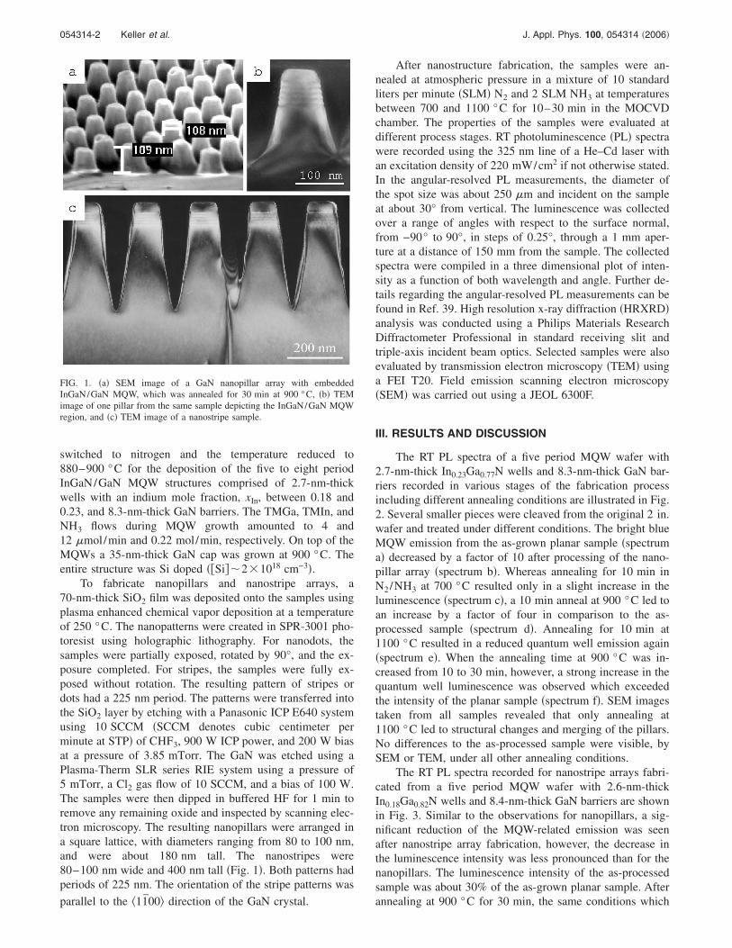
To fabricate nanopillars and nanostripe arrays, a70-nm-thick SiO2 film was deposited onto the samples usingplasma enhanced chemical vapor deposition at a temperatureof 250 °C. The nanopatterns were created in SPR-3001 pho-toresist using holographic lithography. For nanodots, thesamples were partially exposed, rotated by 90°, and the ex-posure completed. For stripes, the samples were fully ex-posed without rotation. The resulting pattern of stripes ordots had a 225 nm period. The patterns were transferred intothe SiO2 layer by etching with a Panasonic ICP E640 systemusing 10 SCCM �SCCM denotes cubic centimeter perminute at STP� of CHF3, 900 W ICP power, and 200 W biasat a pressure of 3.85 mTorr. The GaN was etched using aPlasma-Therm SLR series RIE system using a pressure of5 mTorr, a Cl2 gas flow of 10 SCCM, and a bias of 100 W.The samples were then dipped in buffered HF for 1 min toremove any remaining oxide and inspected by scanning elec-tron microscopy. The resulting nanopillars were arranged ina square lattice, with diameters ranging from 80 to 100 nm,and were about 180 nm tall. The nanostripes were80–100 nm wide and 400 nm tall �Fig. 1�. Both patterns hadperiods of 225 nm. The orientation of the stripe patterns was
¯
FIG. 1. �a� SEM image of a GaN nanopillar array with embeddedInGaN/GaN MQW, which was annealed for 30 min at 900 °C, �b� TEMimage of one pillar from the same sample depicting the InGaN/GaN MQWregion, and �c� TEM image of a nanostripe sample.
parallel to the �1100� direction of the GaN crystal.
After nanostructure fabrication, the samples were an-nealed at atmospheric pressure in a mixture of 10 standardliters per minute �SLM� N2 and 2 SLM NH3 at temperaturesbetween 700 and 1100 °C for 10–30 min in the MOCVDchamber. The properties of the samples were evaluated atdifferent process stages. RT photoluminescence �PL� spectrawere recorded using the 325 nm line of a He–Cd laser withan excitation density of 220 mW/cm2 if not otherwise stated.In the angular-resolved PL measurements, the diameter ofthe spot size was about 250 �m and incident on the sampleat about 30° from vertical. The luminescence was collectedover a range of angles with respect to the surface normal,from −90° to 90°, in steps of 0.25°, through a 1 mm aper-ture at a distance of 150 mm from the sample. The collectedspectra were compiled in a three dimensional plot of inten-sity as a function of both wavelength and angle. Further de-tails regarding the angular-resolved PL measurements can befound in Ref. 39. High resolution x-ray diffraction �HRXRD�analysis was conducted using a Philips Materials ResearchDiffractometer Professional in standard receiving slit andtriple-axis incident beam optics. Selected samples were alsoevaluated by transmission electron microscopy �TEM� usinga FEI T20. Field emission scanning electron microscopy�SEM� was carried out using a JEOL 6300F.
III. RESULTS AND DISCUSSION
The RT PL spectra of a five period MQW wafer with2.7-nm-thick In0.23Ga0.77N wells and 8.3-nm-thick GaN bar-riers recorded in various stages of the fabrication processincluding different annealing conditions are illustrated in Fig.2. Several smaller pieces were cleaved from the original 2 in.wafer and treated under different conditions. The bright blueMQW emission from the as-grown planar sample �spectruma� decreased by a factor of 10 after processing of the nano-pillar array �spectrum b�. Whereas annealing for 10 min inN2/NH3 at 700 °C resulted only in a slight increase in theluminescence �spectrum c�, a 10 min anneal at 900 °C led toan increase by a factor of four in comparison to the as-processed sample �spectrum d�. Annealing for 10 min at1100 °C resulted in a reduced quantum well emission again�spectrum e�. When the annealing time at 900 °C was in-creased from 10 to 30 min, however, a strong increase in thequantum well luminescence was observed which exceededthe intensity of the planar sample �spectrum f�. SEM imagestaken from all samples revealed that only annealing at1100 °C led to structural changes and merging of the pillars.No differences to the as-processed sample were visible, bySEM or TEM, under all other annealing conditions.
The RT PL spectra recorded for nanostripe arrays fabri-cated from a five period MQW wafer with 2.6-nm-thickIn0.18Ga0.82N wells and 8.4-nm-thick GaN barriers are shownin Fig. 3. Similar to the observations for nanopillars, a sig-nificant reduction of the MQW-related emission was seenafter nanostripe array fabrication, however, the decrease inthe luminescence intensity was less pronounced than for thenanopillars. The luminescence intensity of the as-processedsample was about 30% of the as-grown planar sample. After
annealing at 900 °C for 30 min, the same conditions which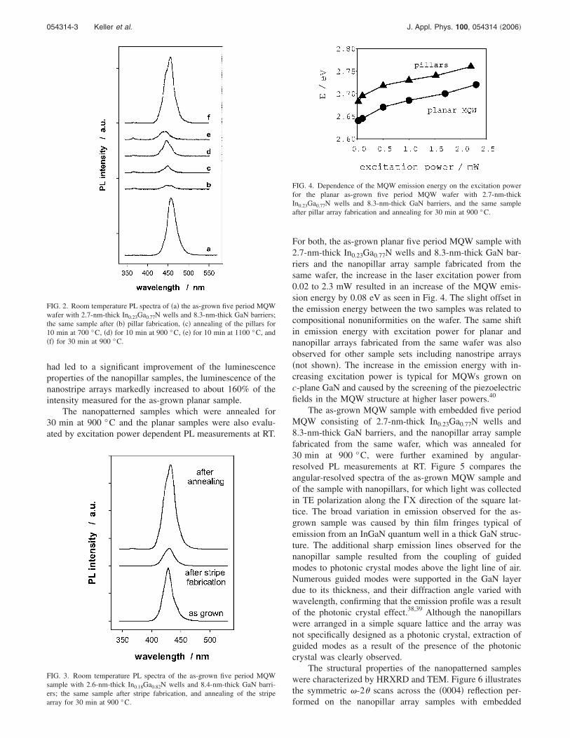
054314-3 Keller et al. J. Appl. Phys. 100, 054314 �2006�
had led to a significant improvement of the luminescenceproperties of the nanopillar samples, the luminescence of thenanostripe arrays markedly increased to about 160% of theintensity measured for the as-grown planar sample.
The nanopatterned samples which were annealed for30 min at 900 °C and the planar samples were also evalu-ated by excitation power dependent PL measurements at RT.
FIG. 2. Room temperature PL spectra of �a� the as-grown five period MQWwafer with 2.7-nm-thick In0.23Ga0.77N wells and 8.3-nm-thick GaN barriers;the same sample after �b� pillar fabrication, �c� annealing of the pillars for10 min at 700 °C, �d� for 10 min at 900 °C, �e� for 10 min at 1100 °C, and�f� for 30 min at 900 °C.
FIG. 3. Room temperature PL spectra of the as-grown five period MQWsample with 2.6-nm-thick In0.18Ga0.82N wells and 8.4-nm-thick GaN barri-ers; the same sample after stripe fabrication, and annealing of the stripe
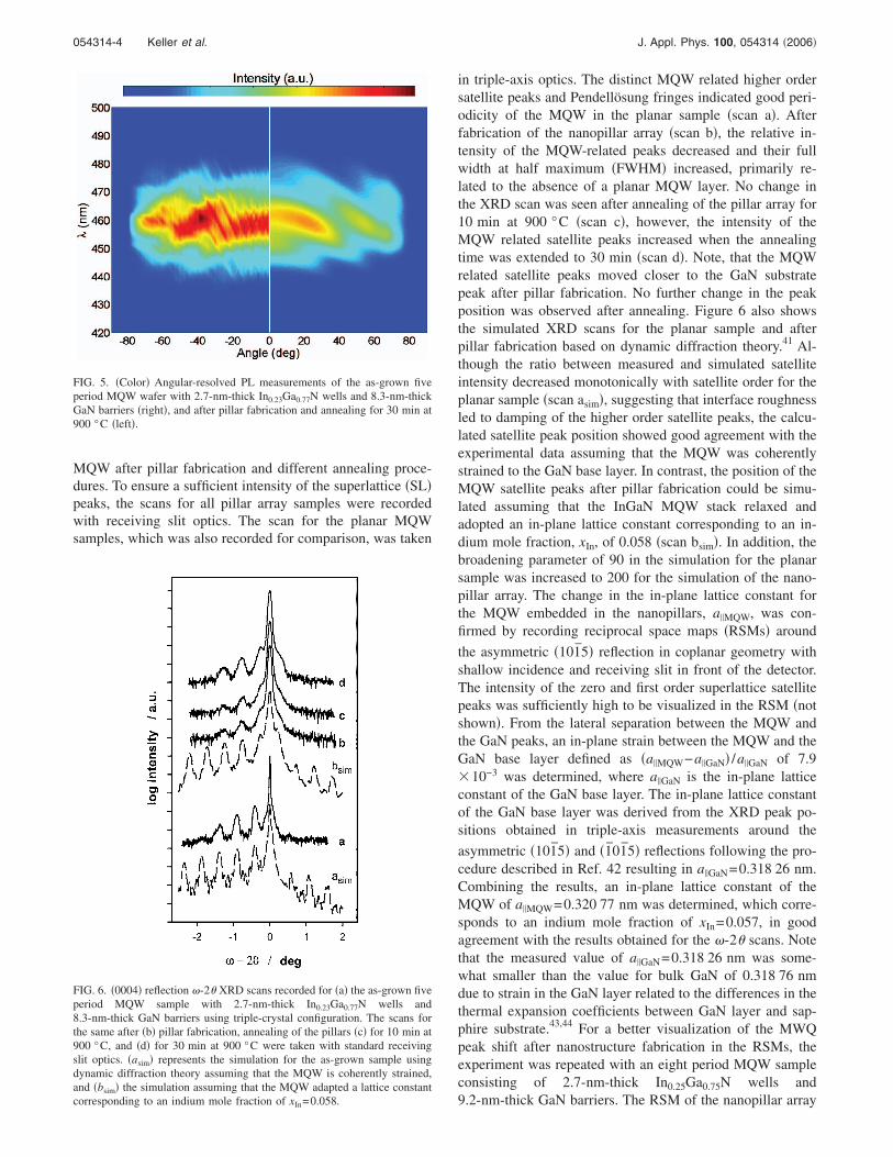
array for 30 min at 900 °C.For both, the as-grown planar five period MQW sample with2.7-nm-thick In0.23Ga0.77N wells and 8.3-nm-thick GaN bar-riers and the nanopillar array sample fabricated from thesame wafer, the increase in the laser excitation power from0.02 to 2.3 mW resulted in an increase of the MQW emis-sion energy by 0.08 eV as seen in Fig. 4. The slight offset inthe emission energy between the two samples was related tocompositional nonuniformities on the wafer. The same shiftin emission energy with excitation power for planar andnanopillar arrays fabricated from the same wafer was alsoobserved for other sample sets including nanostripe arrays�not shown�. The increase in the emission energy with in-creasing excitation power is typical for MQWs grown onc-plane GaN and caused by the screening of the piezoelectricfields in the MQW structure at higher laser powers.40
The as-grown MQW sample with embedded five periodMQW consisting of 2.7-nm-thick In0.23Ga0.77N wells and8.3-nm-thick GaN barriers, and the nanopillar array samplefabricated from the same wafer, which was annealed for30 min at 900 °C, were further examined by angular-resolved PL measurements at RT. Figure 5 compares theangular-resolved spectra of the as-grown MQW sample andof the sample with nanopillars, for which light was collectedin TE polarization along the �X direction of the square lat-tice. The broad variation in emission observed for the as-grown sample was caused by thin film fringes typical ofemission from an InGaN quantum well in a thick GaN struc-ture. The additional sharp emission lines observed for thenanopillar sample resulted from the coupling of guidedmodes to photonic crystal modes above the light line of air.Numerous guided modes were supported in the GaN layerdue to its thickness, and their diffraction angle varied withwavelength, confirming that the emission profile was a resultof the photonic crystal effect.38,39 Although the nanopillarswere arranged in a simple square lattice and the array wasnot specifically designed as a photonic crystal, extraction ofguided modes as a result of the presence of the photoniccrystal was clearly observed.
The structural properties of the nanopatterned sampleswere characterized by HRXRD and TEM. Figure 6 illustratesthe symmetric �-2� scans across the �0004� reflection per-
FIG. 4. Dependence of the MQW emission energy on the excitation powerfor the planar as-grown five period MQW wafer with 2.7-nm-thickIn0.23Ga0.77N wells and 8.3-nm-thick GaN barriers, and the same sampleafter pillar array fabrication and annealing for 30 min at 900 °C.
formed on the nanopillar array samples with embedded
054314-4 Keller et al. J. Appl. Phys. 100, 054314 �2006�
MQW after pillar fabrication and different annealing proce-dures. To ensure a sufficient intensity of the superlattice �SL�peaks, the scans for all pillar array samples were recordedwith receiving slit optics. The scan for the planar MQWsamples, which was also recorded for comparison, was taken
FIG. 5. �Color� Angular-resolved PL measurements of the as-grown fiveperiod MQW wafer with 2.7-nm-thick In0.23Ga0.77N wells and 8.3-nm-thickGaN barriers �right�, and after pillar fabrication and annealing for 30 min at900 °C �left�.
FIG. 6. �0004� reflection �-2� XRD scans recorded for �a� the as-grown fiveperiod MQW sample with 2.7-nm-thick In0.23Ga0.77N wells and8.3-nm-thick GaN barriers using triple-crystal configuration. The scans forthe same after �b� pillar fabrication, annealing of the pillars �c� for 10 min at900 °C, and �d� for 30 min at 900 °C were taken with standard receivingslit optics. �asim� represents the simulation for the as-grown sample usingdynamic diffraction theory assuming that the MQW is coherently strained,and �bsim� the simulation assuming that the MQW adapted a lattice constant
corresponding to an indium mole fraction of xIn=0.058.in triple-axis optics. The distinct MQW related higher ordersatellite peaks and Pendellösung fringes indicated good peri-odicity of the MQW in the planar sample �scan a�. Afterfabrication of the nanopillar array �scan b�, the relative in-tensity of the MQW-related peaks decreased and their fullwidth at half maximum �FWHM� increased, primarily re-lated to the absence of a planar MQW layer. No change inthe XRD scan was seen after annealing of the pillar array for10 min at 900 °C �scan c�, however, the intensity of theMQW related satellite peaks increased when the annealingtime was extended to 30 min �scan d�. Note, that the MQWrelated satellite peaks moved closer to the GaN substratepeak after pillar fabrication. No further change in the peakposition was observed after annealing. Figure 6 also showsthe simulated XRD scans for the planar sample and afterpillar fabrication based on dynamic diffraction theory.41 Al-though the ratio between measured and simulated satelliteintensity decreased monotonically with satellite order for theplanar sample �scan asim�, suggesting that interface roughnessled to damping of the higher order satellite peaks, the calcu-lated satellite peak position showed good agreement with theexperimental data assuming that the MQW was coherentlystrained to the GaN base layer. In contrast, the position of theMQW satellite peaks after pillar fabrication could be simu-lated assuming that the InGaN MQW stack relaxed andadopted an in-plane lattice constant corresponding to an in-dium mole fraction, xIn, of 0.058 �scan bsim�. In addition, thebroadening parameter of 90 in the simulation for the planarsample was increased to 200 for the simulation of the nano-pillar array. The change in the in-plane lattice constant forthe MQW embedded in the nanopillars, a�MQW, was con-firmed by recording reciprocal space maps �RSMs� around
the asymmetric �101̄5� reflection in coplanar geometry withshallow incidence and receiving slit in front of the detector.The intensity of the zero and first order superlattice satellitepeaks was sufficiently high to be visualized in the RSM �notshown�. From the lateral separation between the MQW andthe GaN peaks, an in-plane strain between the MQW and theGaN base layer defined as �a�MQW−a�GaN� /a�GaN of 7.9�10−3 was determined, where a�GaN is the in-plane latticeconstant of the GaN base layer. The in-plane lattice constantof the GaN base layer was derived from the XRD peak po-sitions obtained in triple-axis measurements around the
asymmetric �101̄5� and �1̄01̄5� reflections following the pro-cedure described in Ref. 42 resulting in a�GaN=0.318 26 nm.Combining the results, an in-plane lattice constant of theMQW of a�MQW=0.320 77 nm was determined, which corre-sponds to an indium mole fraction of xIn=0.057, in goodagreement with the results obtained for the �-2� scans. Notethat the measured value of a�GaN=0.318 26 nm was some-what smaller than the value for bulk GaN of 0.318 76 nmdue to strain in the GaN layer related to the differences in thethermal expansion coefficients between GaN layer and sap-phire substrate.43,44 For a better visualization of the MWQpeak shift after nanostructure fabrication in the RSMs, theexperiment was repeated with an eight period MQW sampleconsisting of 2.7-nm-thick In0.25Ga0.75N wells and
9.2-nm-thick GaN barriers. The RSM of the nanopillar array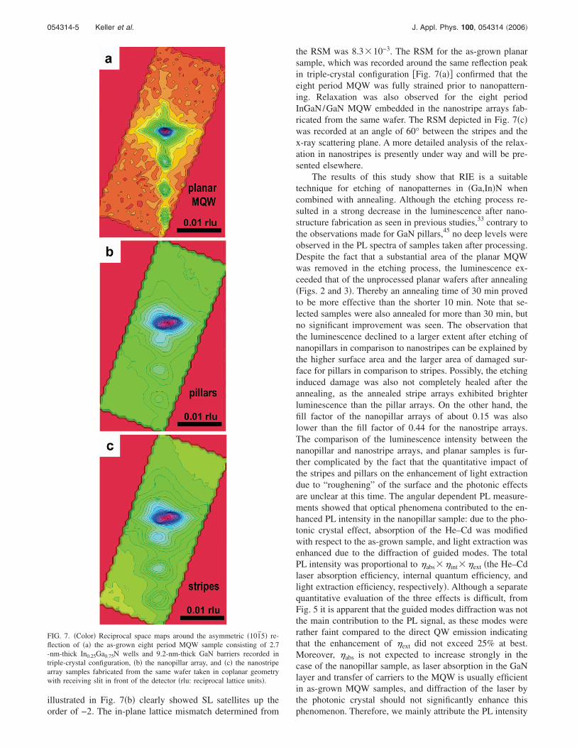
054314-5 Keller et al. J. Appl. Phys. 100, 054314 �2006�
illustrated in Fig. 7�b� clearly showed SL satellites up the
FIG. 7. �Color� Reciprocal space maps around the asymmetric �101̄5� re-flection of �a� the as-grown eight period MQW sample consisting of 2.7-nm-thick In0.25Ga0.75N wells and 9.2-nm-thick GaN barriers recorded intriple-crystal configuration, �b� the nanopillar array, and �c� the nanostripearray samples fabricated from the same wafer taken in coplanar geometrywith receiving slit in front of the detector �rlu: reciprocal lattice units�.
order of −2. The in-plane lattice mismatch determined from
the RSM was 8.3�10−3. The RSM for the as-grown planarsample, which was recorded around the same reflection peakin triple-crystal configuration �Fig. 7�a�� confirmed that theeight period MQW was fully strained prior to nanopattern-ing. Relaxation was also observed for the eight periodInGaN/GaN MQW embedded in the nanostripe arrays fab-ricated from the same wafer. The RSM depicted in Fig. 7�c�was recorded at an angle of 60° between the stripes and thex-ray scattering plane. A more detailed analysis of the relax-ation in nanostripes is presently under way and will be pre-sented elsewhere.
The results of this study show that RIE is a suitabletechnique for etching of nanopatternes in �Ga,In�N whencombined with annealing. Although the etching process re-sulted in a strong decrease in the luminescence after nano-structure fabrication as seen in previous studies,33 contrary tothe observations made for GaN pillars,45 no deep levels wereobserved in the PL spectra of samples taken after processing.Despite the fact that a substantial area of the planar MQWwas removed in the etching process, the luminescence ex-ceeded that of the unprocessed planar wafers after annealing�Figs. 2 and 3�. Thereby an annealing time of 30 min provedto be more effective than the shorter 10 min. Note that se-lected samples were also annealed for more than 30 min, butno significant improvement was seen. The observation thatthe luminescence declined to a larger extent after etching ofnanopillars in comparison to nanostripes can be explained bythe higher surface area and the larger area of damaged sur-face for pillars in comparison to stripes. Possibly, the etchinginduced damage was also not completely healed after theannealing, as the annealed stripe arrays exhibited brighterluminescence than the pillar arrays. On the other hand, thefill factor of the nanopillar arrays of about 0.15 was alsolower than the fill factor of 0.44 for the nanostripe arrays.The comparison of the luminescence intensity between thenanopillar and nanostripe arrays, and planar samples is fur-ther complicated by the fact that the quantitative impact ofthe stripes and pillars on the enhancement of light extractiondue to “roughening” of the surface and the photonic effectsare unclear at this time. The angular dependent PL measure-ments showed that optical phenomena contributed to the en-hanced PL intensity in the nanopillar sample: due to the pho-tonic crystal effect, absorption of the He–Cd was modifiedwith respect to the as-grown sample, and light extraction wasenhanced due to the diffraction of guided modes. The totalPL intensity was proportional to �abs��int��ext �the He–Cdlaser absorption efficiency, internal quantum efficiency, andlight extraction efficiency, respectively�. Although a separatequantitative evaluation of the three effects is difficult, fromFig. 5 it is apparent that the guided modes diffraction was notthe main contribution to the PL signal, as these modes wererather faint compared to the direct QW emission indicatingthat the enhancement of �ext did not exceed 25% at best.Moreover, �abs is not expected to increase strongly in thecase of the nanopillar sample, as laser absorption in the GaNlayer and transfer of carriers to the MQW is usually efficientin as-grown MQW samples, and diffraction of the laser bythe photonic crystal should not significantly enhance this
phenomenon. Therefore, we mainly attribute the PL intensity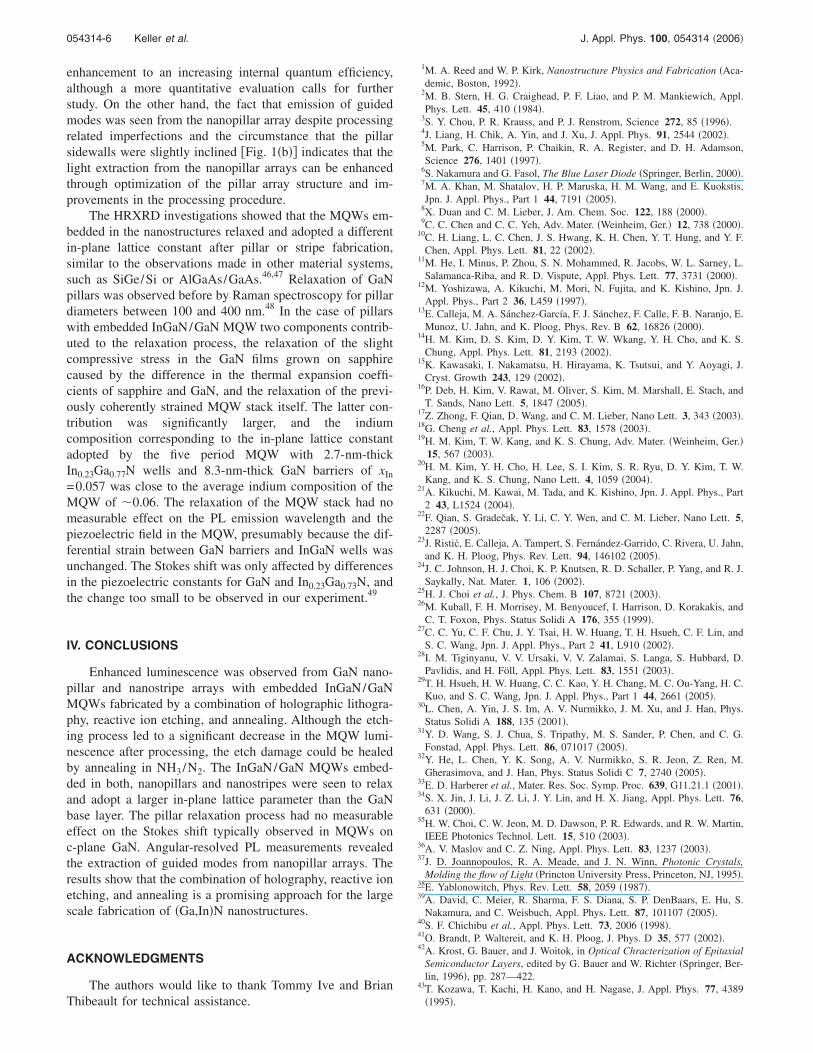
054314-6 Keller et al. J. Appl. Phys. 100, 054314 �2006�
enhancement to an increasing internal quantum efficiency,although a more quantitative evaluation calls for furtherstudy. On the other hand, the fact that emission of guidedmodes was seen from the nanopillar array despite processingrelated imperfections and the circumstance that the pillarsidewalls were slightly inclined �Fig. 1�b�� indicates that thelight extraction from the nanopillar arrays can be enhancedthrough optimization of the pillar array structure and im-provements in the processing procedure.
The HRXRD investigations showed that the MQWs em-bedded in the nanostructures relaxed and adopted a differentin-plane lattice constant after pillar or stripe fabrication,similar to the observations made in other material systems,such as SiGe/Si or AlGaAs/GaAs.46,47 Relaxation of GaNpillars was observed before by Raman spectroscopy for pillardiameters between 100 and 400 nm.48 In the case of pillarswith embedded InGaN/GaN MQW two components contrib-uted to the relaxation process, the relaxation of the slightcompressive stress in the GaN films grown on sapphirecaused by the difference in the thermal expansion coeffi-cients of sapphire and GaN, and the relaxation of the previ-ously coherently strained MQW stack itself. The latter con-tribution was significantly larger, and the indiumcomposition corresponding to the in-plane lattice constantadopted by the five period MQW with 2.7-nm-thickIn0.23Ga0.77N wells and 8.3-nm-thick GaN barriers of xIn
=0.057 was close to the average indium composition of theMQW of �0.06. The relaxation of the MQW stack had nomeasurable effect on the PL emission wavelength and thepiezoelectric field in the MQW, presumably because the dif-ferential strain between GaN barriers and InGaN wells wasunchanged. The Stokes shift was only affected by differencesin the piezoelectric constants for GaN and In0.23Ga0.73N, andthe change too small to be observed in our experiment.49
IV. CONCLUSIONS
Enhanced luminescence was observed from GaN nano-pillar and nanostripe arrays with embedded InGaN/GaNMQWs fabricated by a combination of holographic lithogra-phy, reactive ion etching, and annealing. Although the etch-ing process led to a significant decrease in the MQW lumi-nescence after processing, the etch damage could be healedby annealing in NH3/N2. The InGaN/GaN MQWs embed-ded in both, nanopillars and nanostripes were seen to relaxand adopt a larger in-plane lattice parameter than the GaNbase layer. The pillar relaxation process had no measurableeffect on the Stokes shift typically observed in MQWs onc-plane GaN. Angular-resolved PL measurements revealedthe extraction of guided modes from nanopillar arrays. Theresults show that the combination of holography, reactive ionetching, and annealing is a promising approach for the largescale fabrication of �Ga,In�N nanostructures.
ACKNOWLEDGMENTS
The authors would like to thank Tommy Ive and Brian
Thibeault for technical assistance.1M. A. Reed and W. P. Kirk, Nanostructure Physics and Fabrication �Aca-demic, Boston, 1992�.
2M. B. Stern, H. G. Craighead, P. F. Liao, and P. M. Mankiewich, Appl.Phys. Lett. 45, 410 �1984�.
3S. Y. Chou, P. R. Krauss, and P. J. Renstrom, Science 272, 85 �1996�.4J. Liang, H. Chik, A. Yin, and J. Xu, J. Appl. Phys. 91, 2544 �2002�.5M. Park, C. Harrison, P. Chaikin, R. A. Register, and D. H. Adamson,Science 276, 1401 �1997�.
6S. Nakamura and G. Fasol, The Blue Laser Diode �Springer, Berlin, 2000�.7M. A. Khan, M. Shatalov, H. P. Maruska, H. M. Wang, and E. Kuokstis,Jpn. J. Appl. Phys., Part 1 44, 7191 �2005�.
8X. Duan and C. M. Lieber, J. Am. Chem. Soc. 122, 188 �2000�.9C. C. Chen and C. C. Yeh, Adv. Mater. �Weinheim, Ger.� 12, 738 �2000�.
10C. H. Liang, L. C. Chen, J. S. Hwang, K. H. Chen, Y. T. Hung, and Y. F.Chen, Appl. Phys. Lett. 81, 22 �2002�.
11M. He, I. Minus, P. Zhou, S. N. Mohammed, R. Jacobs, W. L. Sarney, L.Salamanca-Riba, and R. D. Vispute, Appl. Phys. Lett. 77, 3731 �2000�.
12M. Yoshizawa, A. Kikuchi, M. Mori, N. Fujita, and K. Kishino, Jpn. J.Appl. Phys., Part 2 36, L459 �1997�.
13E. Calleja, M. A. Sánchez-García, F. J. Sánchez, F. Calle, F. B. Naranjo, E.Munoz, U. Jahn, and K. Ploog, Phys. Rev. B 62, 16826 �2000�.
14H. M. Kim, D. S. Kim, D. Y. Kim, T. W. Wkang, Y. H. Cho, and K. S.Chung, Appl. Phys. Lett. 81, 2193 �2002�.
15K. Kawasaki, I. Nakamatsu, H. Hirayama, K. Tsutsui, and Y. Aoyagi, J.Cryst. Growth 243, 129 �2002�.
16P. Deb, H. Kim, V. Rawat, M. Oliver, S. Kim, M. Marshall, E. Stach, andT. Sands, Nano Lett. 5, 1847 �2005�.
17Z. Zhong, F. Qian, D. Wang, and C. M. Lieber, Nano Lett. 3, 343 �2003�.18G. Cheng et al., Appl. Phys. Lett. 83, 1578 �2003�.19H. M. Kim, T. W. Kang, and K. S. Chung, Adv. Mater. �Weinheim, Ger.�
15, 567 �2003�.20H. M. Kim, Y. H. Cho, H. Lee, S. I. Kim, S. R. Ryu, D. Y. Kim, T. W.
Kang, and K. S. Chung, Nano Lett. 4, 1059 �2004�.21A. Kikuchi, M. Kawai, M. Tada, and K. Kishino, Jpn. J. Appl. Phys., Part
2 43, L1524 �2004�.22F. Qian, S. Gradečak, Y. Li, C. Y. Wen, and C. M. Lieber, Nano Lett. 5,
2287 �2005�.23J. Ristić, E. Calleja, A. Tampert, S. Fernández-Garrido, C. Rivera, U. Jahn,
and K. H. Ploog, Phys. Rev. Lett. 94, 146102 �2005�.24J. C. Johnson, H. J. Choi, K. P. Knutsen, R. D. Schaller, P. Yang, and R. J.
Saykally, Nat. Mater. 1, 106 �2002�.25H. J. Choi et al., J. Phys. Chem. B 107, 8721 �2003�.26M. Kuball, F. H. Morrisey, M. Benyoucef, I. Harrison, D. Korakakis, and
C. T. Foxon, Phys. Status Solidi A 176, 355 �1999�.27C. C. Yu, C. F. Chu, J. Y. Tsai, H. W. Huang, T. H. Hsueh, C. F. Lin, and
S. C. Wang, Jpn. J. Appl. Phys., Part 2 41, L910 �2002�.28I. M. Tiginyanu, V. V. Ursaki, V. V. Zalamai, S. Langa, S. Hubbard, D.
Pavlidis, and H. Föll, Appl. Phys. Lett. 83, 1551 �2003�.29T. H. Hsueh, H. W. Huang, C. C. Kao, Y. H. Chang, M. C. Ou-Yang, H. C.
Kuo, and S. C. Wang, Jpn. J. Appl. Phys., Part 1 44, 2661 �2005�.30L. Chen, A. Yin, J. S. Im, A. V. Nurmikko, J. M. Xu, and J. Han, Phys.
Status Solidi A 188, 135 �2001�.31Y. D. Wang, S. J. Chua, S. Tripathy, M. S. Sander, P. Chen, and C. G.
Fonstad, Appl. Phys. Lett. 86, 071017 �2005�.32Y. He, L. Chen, Y. K. Song, A. V. Nurmikko, S. R. Jeon, Z. Ren, M.
Gherasimova, and J. Han, Phys. Status Solidi C 7, 2740 �2005�.33E. D. Harberer et al., Mater. Res. Soc. Symp. Proc. 639, G11.21.1 �2001�.34S. X. Jin, J. Li, J. Z. Li, J. Y. Lin, and H. X. Jiang, Appl. Phys. Lett. 76,
631 �2000�.35H. W. Choi, C. W. Jeon, M. D. Dawson, P. R. Edwards, and R. W. Martin,
IEEE Photonics Technol. Lett. 15, 510 �2003�.36A. V. Maslov and C. Z. Ning, Appl. Phys. Lett. 83, 1237 �2003�.37J. D. Joannopoulos, R. A. Meade, and J. N. Winn, Photonic Crystals,
Molding the flow of Light �Princton University Press, Princeton, NJ, 1995�.38E. Yablonowitch, Phys. Rev. Lett. 58, 2059 �1987�.39A. David, C. Meier, R. Sharma, F. S. Diana, S. P. DenBaars, E. Hu, S.
Nakamura, and C. Weisbuch, Appl. Phys. Lett. 87, 101107 �2005�.40S. F. Chichibu et al., Appl. Phys. Lett. 73, 2006 �1998�.41O. Brandt, P. Waltereit, and K. H. Ploog, J. Phys. D 35, 577 �2002�.42A. Krost, G. Bauer, and J. Woitok, in Optical Chracterization of Epitaxial
Semiconductor Layers, edited by G. Bauer and W. Richter �Springer, Ber-lin, 1996�, pp. 287—422.
43T. Kozawa, T. Kachi, H. Kano, and H. Nagase, J. Appl. Phys. 77, 4389
�1995�.
054314-7 Keller et al. J. Appl. Phys. 100, 054314 �2006�
44L. T. Romano, C. G. Van de Walle, J. W. Ager III, W. Götz, and S. R.Kern, J. Appl. Phys. 87, 7745 �2000�.
45F. Demangeot et al., J. Appl. Phys. 91, 6520 �2002�.46P. Van der Sluis, M. J. Verheijen, and J. Haisma, Appl. Phys. Lett. 64,
3605 �1994�.
47A. A. Darhuber, V. Holy, G. Bauer, P. D. Wang, Y. P. Song, C. M. Soto-mayor Torres, and M. C. Holland, Physica B 227, 11 �1997�.
48F. Demangeot et al., J. Appl. Phys. 91, 2866 �2002�.49F. Bernardini, V. Fiorentini, and D. Vanderbilt, Phys. Rev. B 56, R10024
�1997�.