
Ballistic transport in InGaN-based LEDs: impact on efficiency
13
Ballistic transport in InGaN-based LEDs: impact on efficiency This article has been downloaded from IOPscience. Please scroll down to see the full text article. 2011 Semicond. Sci. Technol. 26 014022 (http://iopscience.iop.org/0268-1242/26/1/014022) Download details: IP Address: 128.172.52.254 The article was downloaded on 17/04/2012 at 16:10 Please note that terms and conditions apply. View the table of contents for this issue, or go to the journal homepage for more Home Search Collections Journals About Contact us My IOPscience
-
Upload
independent -
Category
Documents
-
view
0 -
download
0
Transcript of Ballistic transport in InGaN-based LEDs: impact on efficiency

Ballistic transport in InGaN-based LEDs: impact on efficiency
This article has been downloaded from IOPscience. Please scroll down to see the full text article.
2011 Semicond. Sci. Technol. 26 014022
(http://iopscience.iop.org/0268-1242/26/1/014022)
Download details:
IP Address: 128.172.52.254
The article was downloaded on 17/04/2012 at 16:10
Please note that terms and conditions apply.
View the table of contents for this issue, or go to the journal homepage for more
Home Search Collections Journals About Contact us My IOPscience
IOP PUBLISHING SEMICONDUCTOR SCIENCE AND TECHNOLOGY
Semicond. Sci. Technol. 26 (2011) 014022 (12pp) doi:10.1088/0268-1242/26/1/014022
Ballistic transport in InGaN-based LEDs:impact on efficiencyU Ozgur1, X Ni1, X Li1, J Lee1, S Liu1, S Okur1, V Avrutin1,A Matulionis2 and H Morkoc1
1 Department of Electrical and Computer Engineering, Virginia Commonwealth University, Richmond,VA 23284, USA2 Semiconductor Physics Institute, Center for Physical Sciences and Technology, A. Gostauto 11,01108 Vilnius, Lithuania
E-mail: [email protected] and [email protected]
Received 9 June 2010, in final form 22 September 2010Published 29 November 2010Online at stacks.iop.org/SST/26/014022
AbstractHeterojunction light-emitting diodes (LEDs) based on the InGaN/GaN system have improvedconsiderably but still suffer from efficiency degradation at high injection levels which unlessovercome would aggravate LED lighting. Although Auger recombination has been proposedas the genesis of the efficiency degradation, it appears that the premise of electron overflowand non-uniform distribution of carriers in the active region being the immediate impedimentis gaining popularity. The lack of temperature sensitivity and sizeable impact of the barrierheight provided by an electron blocking layer and the electron cooling layer prior to electroninjection into the active region suggest that the new concept of hot electrons andballistic/quasi-ballistic transport be invoked to account for the electron overflow. The electronoverflow siphons off the electrons before they can participate in the recombination process. Ifthe electrons are made to remain in the active region e.g. by cooling them prior to injectionand/or blocking the overflow by an electron blocking layer, they would have to eitherrecombine, radiatively or nonradiatively (e.g. Shockley–Read–Hall and Auger), or accumulatein the active region. The essence of the proposed overflow model is in good agreement withthe experimental electroluminescence data obtained for m-plane and c-plane LEDswith/without electron blocking layers and with/without staircase electron injectors.
(Some figures in this article are in colour only in the electronic version)
1. Introduction
Performance of InGaN-based light-emitting diodes (LEDs)has improved considerably to the point where they nowpenetrate outdoor general lighting applications and are poisedto penetrate indoor lighting applications as well. Lightingby LEDs is advantageous in terms of energy savings andlong operation lifetime. One pivotal issue surrounding theapplication of the InGaN LEDs for general lighting is thelack of retention of the electroluminescence (EL) efficiencyat high injection currents [1]. This manifests itself as theexternal quantum efficiency (EQE) reaching a peak valueat relatively small current densities, such as 50 A cm−2 orlower, followed by a monotonic decrease even under low dutycycle short pulsed current operation [2]. It is essential for the
physical mechanisms behind this degradation in efficiency tobe understood and the problem mitigated. A fitting commentis that none of the above would have come into being if it werenot for the seminal pioneering work done on heterostructures[3–5].
The physical origin of the EL efficiency loss at highcurrents in InGaN LEDs is heretofore not clearly understoodand controversial, and thus the topic is open to furtherinvestigations. Carrier loss through nonradiative Augerrecombination at high injection currents has initially beenproposed for the efficiency degradation [6–8]. The Augerrecombination coefficient deduced from a fit of the rateequation to the experimental photoluminescence (PL) datain an earlier effort is 1.4–2.0 × 10⁻³⁰ cm6 s−1 for quasi-bulk InGaN layers [6], but varies several orders of magnitude
0268-1242/11/014022+12$33.00 1 © 2011 IOP Publishing Ltd Printed in the UK & the USA

Semicond. Sci. Technol. 26 (2011) 014022 U Ozgur et al
among different reports, 10−27–10−24 cm6 s−1, the latter groupof figures being some three orders of magnitude or morehigher than the other reported values [6, 8–11]. Note thatthe Auger recombination coefficient decreases exponentiallywith the bandgap energy if the process involves transitionsacross the gap owing to a seminal contribution [12], whichis supported by a fully microscopic many body model [13].This suggests that the carrier losses due to the Auger effectin InGaN-based LEDs, particularly in those emitting atenergies away from the resonant conduction band state situated2.5 eV above the bottom of the conduction band [8], wouldnot necessarily be dominant.
There are also other experimental observations whichare not consistent with the Auger recombination proposal.For example, in below-the-barrier resonant photo excitationexperiments, in which the photons are absorbed only inthe InGaN active region with ensuing generation of equalnumber of cool electrons and holes followed by either radiativeor nonradiative recombination only in the same region, theinternal quantum efficiency (IQE) degradation has not beennoted at photocarrier generation rates comparable to, if notbeyond, the electrical injection levels where the EL efficiencydegrades [14, 15]. Rather the IQE increases with opticalgeneration and in fact reaches over 95% for carrier generationrates of 2 × 1018 cm−3, the density being dependent on theradiative recombination coefficient used. This would thensuggest that the EL efficiency degradation is of electrical natureand that it is very likely to be related to carrier injection,transport and leakage processes.
The above discussion narrows the choices to electronoverflow as being responsible in structures that are employedat the moment. It has been observed that a substantial ELefficiency reduction (by four to five times) occurs when anelectron blocking layer (EBL) is not employed, regardless ofwhether polar or non-polar surfaces of GaN are used [16]. InInGaN LEDs, while not being the entire reason at this juncture,relatively low hole injection (due to relatively low hole dopingof p-GaN) and/or poor hole transport inside the active region(due to large hole effective mass if quantum wells constitutethe active region) could exacerbate the electron overflow, aselectrons need accompanying holes in the active region forrecombination [15, 17]. Theoretical calculations also indicatethat electron density in equilibrium with the lattice evenwell above the room temperature would not have a sufficientBoltzmann tail to surpass the barrier present for notableelectron spillover [18]. This further narrows the discussion inthat the non-equilibrium processes must be invoked to accountfor electron overflow. In this regard, this paper treats ballisticand quasi-ballistic electron transport across the InGaN activeregion as a substantial source for electron overflow and theassociated EL efficiency loss, as those electrons escape theradiative recombination in the active region. Evidence forballistic transport and the associated electron leakage has beenobtained from the temperature-dependent characteristics ofInGaN LEDs and laser diodes [19–21]; however, ballisticelectron transport has so far been included in the analysisof electronic devices only [1, 22]. Moreover, we demonstratethat an InGaN staircase electron injector (SEI, with a step-like
increased In composition, each corresponding an energy stepequal to or greater than an LO phonon energy) on the n-sideof the active region reduces if not fully eliminates the ballisticand quasi-ballistic electron overflow. The SEI structure servesto cool the electrons and bring them into equilibrium with thelattice in the active region where their radiative recombinationwith holes takes place if the holes are present. Ultimately,though, holes must be present for radiative recombination withelectrons, and increase of the hole density is naturally expectedto improve the efficiency in LEDs featuring designs to curbthe ballistic transport and thus the ensuing electron overflow.
It should be noted that the concept of non-equilibriumhot electrons in the context of light emitters is non-conventional and represents a major departure from theproverbial treatments. One might then suggest that models,particularly the commercially available software packagesused to model the LEDs under discussion, which are voidof the treatment of hot electrons, would be off target. Weshould also point out that the hot electron transport discussedhere would also apply to semiconductor injection lasers.
2. Experimental procedures
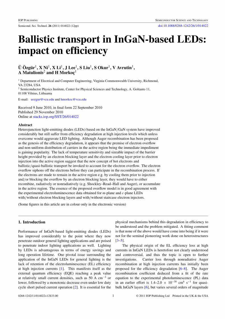
The investigated LED structures were grown on m-plane(1 1 0 0) GaN or c-plane (0 0 0 1) sapphire substrates in avertical low-pressure metalorganic chemical vapor deposition(MOCVD) system. In the case of m-plane, the ∼500 μmthick m-plane freestanding GaN substrates, sliced from boulesgrown in the c-direction (produced at Kyma Technologies,Inc.) had a threading dislocation density of <5 × 106 cm−2
and were off-cut by 0.2◦ toward the GaN a-axis and 0.3◦ towardthe GaN c-axis. The sapphire substrates were commerciallyobtained and not subjected to any special treatment prior togrowth. When grown on sapphire, templates on which theLED structure was grown consisted of a low-temperature GaNlayer, a high-temperature GaN layer followed by in situ SiNx
deposition and an epitaxial laterally overgrown GaN layer[1, 23]. The LED structures contained a 6 nm undopedIn0.20Ga0.80N (emitting at λpeak ∼440 nm) or In0.15Ga0.85Nactive region (emitting at λpeak ∼410 nm) with a 3 nm undopedIn0.01Ga0.99N top layer. Immediately beneath the active layer,a 60 nm Si-doped (2 × 1018 cm−3) In0.01Ga0.99N under-layerwas inserted for improved quality of the active region. Ininvestigations exploring the hot electron ballistic and quasi-ballistic transport across the active region [24] an ∼10 nmEBL of p-AlxGa1−xN (x = 15%, 8% or 0%) with varyingbarrier heights was deposited on top of the active layer. Instructures which aid to cool the electrons prior to the activeregion, an InGaN SEI, n-type doped with Si to an electrondensity of 2 × 1018 cm−3, was inserted under the InGaNactive region to thermalize the electrons [25]. The staircasestructure consists of three 5 nm InGaN layers (resulting in afour-step staircase) with In compositions of 3%, 6% and 10%,respectively, in the given order, as shown in figure 1, wherethe steps having potential energy drop by more than one LOphonon energy cause efficient electron thermalization. Forthe structures containing an SEI, a six-period In0.01Ga0.99N(7 nm)/In0.06Ga0.94N(3 nm) multiple quantum well (MQW)
2
Semicond. Sci. Technol. 26 (2011) 014022 U Ozgur et al
c-sapphire or m-plane GaN
n-GaN
n-GaN
low temp. GaNif on sapphire
SiNx ELOif on sapphire
Light emission
Ti/Al/Ni/Au
Ni/Au pad
p-GaNGZO or 5/5 nm Ni/Au
p-AlGaN EBLif needed
SEIactive region
underlayer
Energy
Ec
Figure 1. Structures of LEDs used in the course of thisinvestigation. As indicated in section 2, some LEDs utilizedelectron blocking layers (EBLs) while some did not. Those that didnot, incorporated a staircase electron injector (SEI) to cool theelectrons before being injected into the active region. For improvingthe quality further, the in situ epitaxial lateral overgrowth (ELO)method as well as an In0.01Ga0.99N under-layer (beneath the activeregion) was incorporated. In some cases the InGaN under-layer wassubstituted by a superlattice of varying In composition(In0.01Ga0.99N/In0.05Ga0.95N). The right panel shows thecorresponding simplified flatband conduction band edge energydiagram.
under-layer (instead of a 60 nm In0.01Ga0.99N structure, seefigure 1), again n-doped, was employed prior to the active layerunderneath the 12 nm thick In0.01Ga0.99N layer and the InGaNSEI to circumvent the quality degradation by the SEI layers.The final Mg-doped p-GaN layer was about 100 nm thick witha nominal hole density of 7 × 1017 cm−3. The p-layer wasactivated ex situ at 950 ◦C in N2 atmosphere for 1 min. In somesamples, this was followed by deposition of Ga-doped ZnO(GZO) (400 nm thick) for transparent conducting oxide bymolecular beam epitaxy in order to enhance current spreadingand reduce the differential ‘on’ resistance [26, 27]. After mesaetching (250 μm diameter), Ti/Al/Ni/Au (30/100/40/50 nm)metallization annealed at 800 ◦C for 60 s was used for n-typeohmic contacts. A Ni/Au (5/5 nm) semi-transparent p-contactmetal laminate was deposited for samples not utilizing GZO.This step was skipped for those which used GZO. Finally,50 μm diameter Ni/Au (30/50 nm) contact pads weredeposited on part of the mesa tops for on-wafer ELmeasurements. Again, a schematic diagram elaborating thevarious structures used in the course of this study is shown infigure 1.
The IQE was determined from excitation-power-dependent PL [28] measured at room temperature usinga frequency-doubled 80 MHz repetition rate femtosecondTi:sapphire laser. The excitation wavelength was 370–390 nm to ensure below the gap excitation and thus photo-excited electron–hole pair generation only in the InGaN activelayer to circumvent complexities involving carrier transportand skewed carrier injection which favor the electrons[14, 15]. On-wafer EL measurements were performed withpulsed current (1 μs pulse width, 0.1% duty cycle) withoutany special means to enhance light extraction. The PL resultsshow that all LEDs in comparative studies have essentially
the same IQE for the same injected carrier density [29]. It isinstructive to note that the c-plane LED structures exhibit IQEsas high as 71% for samples not featuring in situ ELO, and thosehaving gone through the aforementioned in situ ELO exhibitedefficiencies up to 96% at injection levels corresponding to justabout 2 × 1018 cm−3 carrier density which is very respectableindeed. High IQEs reported here serve to refute any argumentthat reduced or the lack of efficiency loss at high injectionlevels is somehow related to low quality.
3. Theoretical and experimental data
At the onset with no a priori-predilection, the electronoverflow might have its origin in two possible routes:(i) thermionic emission of equilibrium electrons from thebottom of the active region over the barrier into the p-layer(the large band discontinuities preclude this process) and(ii) ballistic and quasi-ballistic transport of the injectedelectrons. The calculations discussed associated withthe thermionic emission process, immediately below, areconvincingly indicative of this process not being responsiblefor electron overflow. Below, following the discussion of thethermionic emission process, we will treat the hot electronmitigated electron overflow.
3.1. Electron overflow due to thermionic emission
The simulations with Silvaco Atlas R© software forthe p-GaN/In0.20Ga0.80N/n-GaN LED without an EBLtake into account thermionic emission of equilibriumelectrons and tunneling within the Wentzel–Kramers–Brillouin approximation. The commonly accepted materialparameters were used for the In0.20Ga0.80N active layer:Shockley–Read–Hall (SRH) recombination coefficient of 1 ×10⁷ s−1 and spontaneous radiative recombination coefficientof 1 × 10⁻¹¹ cm3 s−1. An Auger recombination coefficientof 1 × 10⁻³⁰ cm6 s−1 was assumed. For p-GaN, the SRHcoefficient of 1 × 10¹⁰ s−1 (corresponding to a lifetime of100 ps) was used. The conduction band offset �Ec =0.5 eV was taken to be 70% of the total band gap discontinuitybetween InGaN and p-GaN. The calculations show that evenat an uncharacteristically elevated junction temperature of1000 K and at an unreasonably high current density of 1 ×10⁴ A cm−2, the thermionic emission driven overflow electroncurrent into the p-GaN region due to electrons in thermalequilibrium with the lattice is only ∼11% of the total currentdensity. At the same current density of 1 × 10⁴ A cm−2,the corresponding values are ∼1% and ∼0% for junctiontemperatures of 700 K and 500 K, respectively [18, 30].Considering the large discrepancy for the Auger coefficient[6–8, 12], the calculated electron overflow values will be0%, 3% and 36% for junction temperatures of 500, 700 and1000 K, respectively, if an Auger coefficient of 1 ×10⁻³⁴ cm6 s−1 is assumed instead.
The thermionic emission being inconsequential suggeststhat we must turn our attention to non-equilibrium electronsin the active region. The injected hot electrons can traversethe active layer by ballistic or quasi-ballistic transport, unless
3
Semicond. Sci. Technol. 26 (2011) 014022 U Ozgur et al
0 500 1000 1500 2000 25000
5
10
15
20
25
w/o EBL
Al0.08Ga0.92N EBL
Al0.15Ga0.85N EBL
Current density (A/cm2)
Rel
ativ
e E
QE
(a.
u)
m-plane DH-LEDs (λpeak
∼440nm)
6nm In0.20Ga0.80N active region
0 4 8 12 16
500
1000
1500
2000
2500
Cu
rren
t d
ensi
ty (
Acm
-2)
Voltage (V)
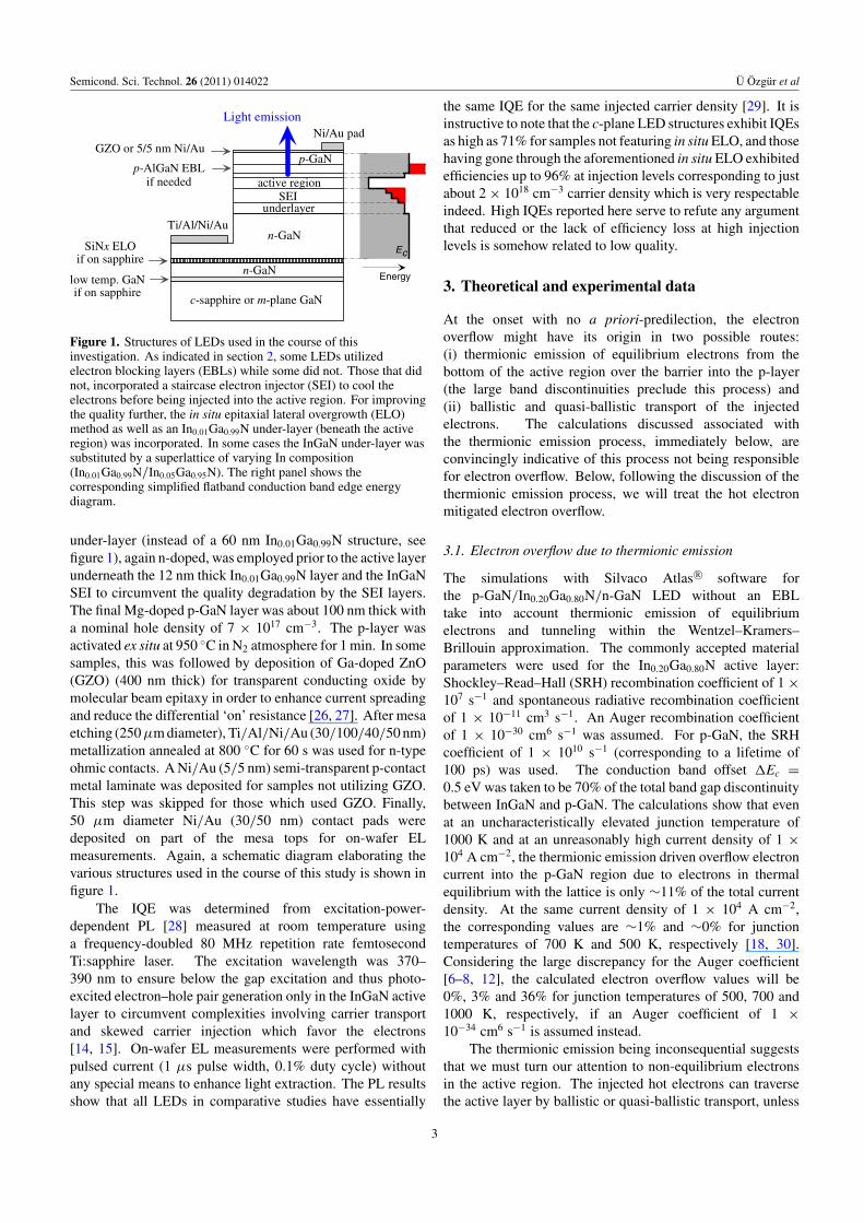
Figure 2. Relative EQE of m-plane In0.20Ga0.80N LEDs withAlxGa1−xN EBLs having Al compositions x = 15%, 8%, and 0%,measured under pulsed current, 1 μs pulse width and 0.1% dutycycle. Emission wavelength is λpeak ∼ 440 nm. The inset shows thecurrent–voltage dependence for the LED with 15% Al in the EBL.
blocked by an EBL, and recombine in the p-GaN regioninstead of the active region and do not contribute to lightemission at the desired wavelength. Below, we discuss ourfirst-order calculations of ballistic and quasi-ballistic transportof electrons through the active region and attempt to explainour data with varying barrier heights of the EBL layer in thisframework.
3.2. Electron overflow due to hot electron transport
To set the stage for us to segue into the calculation ofhot electron-induced electron overflow, figure 2 displays theexperimental relative EQE as a function of the current densityfor three m-plane LEDs with varying EBL barrier heights.Because the IQE is independent of the composition of theEBL barrier height (confirmed by resonant PL experiments),the observed difference in EQE can, therefore, be safelyassumed to originate from mechanisms having to do withcarrier injection and overflow rather than the quality variationamong the active regions of the samples tested. The EQE forthe m-plane LED with 15% Al in the EBL shows a pronouncedpeak at approximately 80 A cm−2 which proceeds to dropby ∼45% with increasing current injection. A negligibleefficiency degradation (∼3–5%) is observed for the structurewithout an EBL (represented by 0% Al in the EBL) albeitits relative EQE is approximately three to five times lowerthan that with 15% Al EBL. Intermediate values for EQE andefficiency degradation (∼10%) are obtained for the LED with8% Al within the EBL.
We assume that the LED with 15% Al EBL has negligibleelectron overflow at the current density of 80 A cm−2 wherethe EQE peaks. Thus, in the LED without an EBL, lessthan one fifth of the overall current is contributing to the ELand approximately four fifths of the current passes the activeregion without contributing to light emission. After refutingthe thermionic emission route, in our opinion, we focus ourattention on hot electron transport as the cause for carrier
overflow. In the hot electron scenario, after the electrons areinjected from the n-GaN layer into the active region, they gainan additional kinetic energy equal to the conduction band offsetbetween the n-GaN and the In0.20Ga0.80N active layers (�Ec,∼0.5 eV). The hot electrons either undergo thermalization andlose their excess energy (mainly through their interaction withLO phonons [31]) or leave the active region. Let us considerthe electrons that experience ballistic motion (no scattering inthe active region) and quasi-ballistic motion (scattering eventswith LO phonons). Our calculations show that LEDs withoutan EBL suffer from serious electron overflow accounting for∼67% of the total electron current under flatband conditionsfor a 6 nm thick active region. These spillover electrons arecomposed of both ballistic and quasi-ballistic electrons, whereonly less than 1% of the injected electrons enter the p-GaNlayer after two scattering events. Therefore, the contributionof spillover electrons resulting from two or more scatteringevents can be ignored.
The probability of the ballistic transport at a given energyis proportional to exp(−t/τsc), where t is the transit timeand τsc is the electron–LO-phonon scattering time given byτsc = 1/(1/τabs + 1/τem), where τ abs and τ em are the LO-phonon absorption and emission times, respectively [24].If the acceleration and deceleration of the electrons by theelectrons in the active region are neglected, the percentage ofthe overflow electrons is then given by
P1 =∫ +∞
max{0,(φEBL−qV )} f (E)N(E) exp(−L/v(E+�Ec)
τsc
)dE∫ +∞
0 f (E)N(E) dE,
(1)
where E depicts the excess electron energy with respect tothe bottom of the conduction band of the n-GaN layer, L is theactive region thickness (6 nm in our case), V is the net potentialdrop across the InGaN region, φEBL is the barrier height of theEBL (i.e. the conduction band offset between the EBL andthe p-GaN, and is 0 for the LEDs without an EBL), N(E) is theconduction-band density of states, f (E) is the Fermi–Diracdistribution function, v(E + �Ec) = √
2(E + 0.5 eV)/me
is the electron velocity with an initial energy of E plusthe gained energy due to the 0.5 eV band offset and me
is the electron effective mass. For simplicity, we assumethat the electrons move only in the normal direction to thehetero-interface, which would insignificantly overestimate thespillover probability.
In addition to fully ballistic electrons, quasi-ballisticelectrons undergoing a certain scattering event, such as oneLO phonon emission or one LO phonon absorption, can alsocontribute to the overflow. The total percentage of the overflowelectrons that experience one scattering event is given by
P2 =[∫ +∞
0f (E)N(E)dE
]−1
×∫ +∞
max{0,(φEBL−qV ±hωLO)}f (E)N(E)
×∫ L
0· 1
v(E + �Ec) · τphexp
(−x/v(E + �Ec)
τsc
)
· exp
[− (L − x)/v(E + �Ec ∓ hωLO)
τsc
]· dx · dE, (2)
4

Semicond. Sci. Technol. 26 (2011) 014022 U Ozgur et al
0.00 0.05 0.10 0.15 0.200
20
40
60
80
100
0.50 0.55 0.60 0.65
0
20
40
60
80
100
8%Alin EBL 15%Al
in EBL
Ove
rflo
w c
urre
nt /
tota
l cur
rent
(%
)
EBL barrier height φEBL
(eV)
0%Alin EBL
Al0.15
GaN EBL
Al0.08
GaN EBL
Ove
rflo
w c
urre
nt p
erce
ntile
Applied voltage across the active region (V)
w/o EBL
Figure 3. Calculated ratio of the overflow electron current to thetotal current as a function of the EBL barrier height (φEBL) underflatband conditions in the active region (the applied external voltagecompensates the built-in potential, ∼0.5 V) for m-plane LEDs withEBLs: w/ 0% Al, 8% Al and 15% Al. The inset shows the same asa function of the applied voltage (forward direction) across theInGaN active region.
where +hωLO and −hωLO in the lower integration limitcorrespond to phonon emission (τ ph = τ em) and absorption(τ ph = τ abs), and hωLO = 88 meV is the LO phonon energy inInGaN. Equation (2) takes into account energy conservationand the probabilities for an electron to reach the position xwithout being scattered, to be scattered near x and to exit theactive region without being scattered between x and L. Theintegration over dx and dE accounts for all possible paths andall suitable electrons.
Figure 3 depicts the ratio of the overflow electron currentto the total current calculated in m-plane LEDs within theframework of equations (1) and (2) as a function of theEBL barrier height for flatband (in the active region) reachedthrough compensation of the built-in electric field of the p–n junction by the applied voltage. The phonon emissiontime (τ em), the phonon absorption time (τ abs) and the phononscattering time (τ sc) of 0.01 ps, 0.1 ps, 0.009 ps, respectively[32], have been used for the calculation. As mentioned,
0 600 1200 1800 2400
m-plane DH-LEDswith 3-layer SEIλ
peak= 440nm
Rel
ativ
eE
QE
(a.u
.)
Current density (A/cm2)
w/ EBLw/o EBL
(a) (b)
Figure 4. (a) Relative EQE of two m-plane LEDs grown on freestanding m-plane (1 1 0 0) GaN substrates with a three-layer SEI: one withand one without the EBL. (b) A schematic depiction of the conduction band structure and the enhancement of electron thermalization in thepresence of a three-layer SEI.
the calculated probabilities for the overflow electrons thatexperience two or more scattering events are negligible (�1%).For the LED without an EBL (i.e. 0% Al in the EBL), asignificant portion (∼67%) of the total electron current is theoverflow electron current, while almost no electron overflowwas found to occur when an EBL with 15% Al is used. Theresults of calculations are consistent with the experimentalobservations for the LED without an EBL: approximately fourfifths of the current is the overflow current while only one fifthof the electron current is captured by the InGaN active regionas evident from figure 2.
The inset of figure 3 shows the ratio of the calculatedoverflow electron current to the total current as a function of theapplied voltage (forward direction) across the active region forthe m-plane LEDs with different EBLs. Note that 0.5 V appliedvoltage corresponds to the flatband condition owing to thecompensation of the built-in voltage inside the active region,and higher applied voltages would lower the effective EBLbarrier height. The latter increases the overflow current. Forthe LED with 15% Al in the EBL, the overflow current is nearlyzero under the flatband condition and gradually increases withincreasing bias. This gives a possible explanation for theobserved efficiency loss with the increased injection current:the efficiency drops by 45% when the current density increasesto 2400 A cm−2 (figure 2). Considering that what is shownin the figure 3 inset is only a simple first-order treatment ofthe problem, an exact correlation with the experimental datais not to be anticipated. However, the increase in the overflowcurrent component with decreasing EBL barrier height and itsweaker dependence on the applied bias for lower EBL barrierheights are consistent both with theory and experiment.
3.3. Staircase electron injector to eliminate electron overflow
Figure 4(a) shows that the relative EQE values of the two m-plane LEDs with the SEI, one with and the other without anEBL, are essentially the same for the same current injectionlevels. This is substantially different from that observed inLEDs without the SEI, where the EL intensity from the LEDwithout an EBL is approximately one fifth of that from theLED with the EBL (see figure 2). It is, therefore, reasonableto suggest convincingly that the InGaN SEI either reduces
5

Semicond. Sci. Technol. 26 (2011) 014022 U Ozgur et al
or eliminates the electron overflow due to ballistic or quasi-ballistic electron transport across the active region by efficientthermalization of the injected electrons in the SEI as illustratedin figure 4(b).
In order to account for the reduced, if not totallyeliminated, electron overflow in the InGaN-based LEDs witha SEI, we performed first-order calculations of the electronoverflow at different applied forward voltages across theactive region. For simplicity of calculation and a moretransparent demonstration of the SEI effect, a one-layerSEI with one intermediate composition of In0.10Ga0.90N wasemployed. The SEI has a total thickness of 15 nm—thesame as the total thickness of the three-layer SEI of theLEDs investigated experimentally. The percentage of overflowelectrons due to ballistic transport in the LED with a SEI is thengiven by
P0 =∫ +∞max{0,(φEBL−qV )} f (E)N(E)·exp
(− d/v1(E+�Ec1)+L/v2(E+�Ec2)
τsc
)dE∫ +∞
0 f (E)N(E) dE,
(3)
where d = 15 nm and L = 6 nm are the thicknesses andv1(E + �Ec1) = √
2(E + 0.25 eV)/me and v2(E + �Ec2) =√2(E + 0.5 eV)/me are the electron velocities in the SEI
(In0.10Ga0.90N) and the active region under flatband conditions,respectively. The energies, �Ec1 = 0.25 eV and �Ec2 =0.5 eV, in the velocity expressions represent the excess energygained by electrons from the conduction band discontinuitiesupon injection into the In0.10Ga0.90N SEI layer and into theIn0.20Ga0.80N active layer, respectively. As mentioned before,for simplicity, we assume that the electron transport is normalto the hetero-interfaces.
For electrons experiencing one scattering event a total offour different cases, corresponding to emission or absorptionof only one LO phonon in the SEI and the active regions,can be envisioned. For example, the probability of overflowresulting from only one phonon emission in the SEI is givenby
P3 =[∫ +∞
0f (E)N(E) dE
]−1
×∫ +∞
max{0,(φEBL−qV +hωLO)}f (E)N(E)
×∫ d
0
exp(−[x/v1(E + �Ec1)]/τsc)
v1(E + �Ec1) · τem
× exp(−[(d − x)/v1(E + �Ec1 − hωLO)
+ L/v2(E + �Ec2 − hωLO)]/τsc) · dx · dE. (4)
Equation (4) takes into account the probabilities for a suitableelectron (e.g. with energy hωLO higher than the bottom ofconduction band of n-GaN for the case of no EBL andflatbands) to reach the position x (0 � x � d = 15 nm)without being scattered, to emit a phonon near x and to exitthe active region without being scattered between x and L. Theprobability of overflow due to only one phonon emission inthe active region is given by
4 6 8 10 12 14 160
20
40
60
80
100
Ove
rflo
wcu
rren
tper
cent
ile
Applied bias on the device (V)
w/o SEI & w/o EBL
one-layer SEI & w/o EBL
Figure 5. Calculated overflow electron current/total electroncurrent as a function of the applied forward voltage across the 6 nmthick In0.20Ga0.80N active region for the LED without a SEI andwithout an EBL and the other LED with a one-layer In0.10Ga0.90NSEI and without an EBL. Solid lines are guides to the eye. The insetshows the band diagrams for the LEDs with and without (dashedline) the SEI.
P4 =[∫ +∞
0f (E)N(E) dE
]−1
×∫ +∞
max{0,(φEBL−qV +hωLO)}f (E)N(E)
×∫ d
0
exp(−[d/v1(E + �Ec1)]/τsc)
v2(E + �Ec2) · τem
× exp(−[(x − d)/v2(E + �Ec2) + (d + L − x)/
v2(E + �Ec2 − hωLO)]/τsc) · dx · dE. (5)
Similarly, we can obtain the probabilities for one-phononabsorption events. Again, the contribution of two scatteringevents to the overflow electrons was found to be negligible forthis SEI (<1%). The total electron overflow is then obtainedby summing the ballistic and quasi-ballistic contributions.
Figure 5 shows the percentile overflow electron currentfor the two LEDs without an EBL (φEBL = 0): one withand the other without the SEI, calculated using τ em = 10 fs,τ abs = 100 fs and τ sc = 9 fs [32]. For flatband, a significantportion (∼62%) of the total electron current is the overflowelectron current for the LED without the SEI. However, forthe LED with the SEI, the electron overflow is substantiallyreduced to ∼8%. In addition, the thermionic emission inthe LEDs with the SEI even in the absence of an EBL isfound to be negligible (<1%). A SEI causes the electrons tohave a longer transit time owing to lower velocity resultingfrom lower kinetic energy gained from a relatively small banddiscontinuity. Expectedly, a longer time helps thermalizationthrough interaction with LO phonons, dramatically reducingthe electron overflow. Obviously, more layers in the SEI (threelayers used in our LEDs) provide more freedom for designingthe optimal SEI.
6
Semicond. Sci. Technol. 26 (2011) 014022 U Ozgur et al
0.14 0.12 0.10 0.08
-0.5
0.0
0.5
acti
vere
gio
n
EBL p-GaN
m-planec-plane
Ene
rgy
(eV
)
Distance from surface (μm)
Ec
J = 1200Acm-2
VEBL
n-GaN
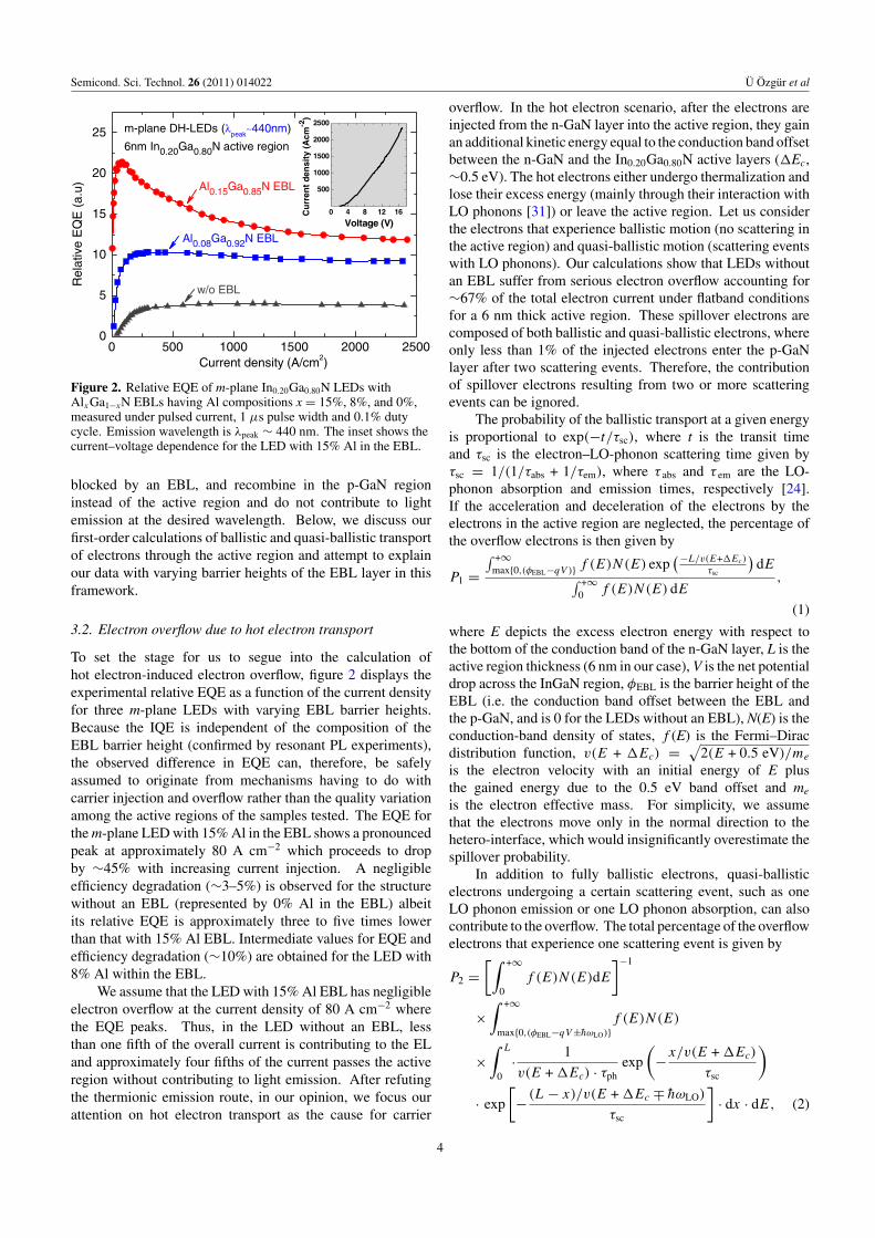
Figure 6. Calculated conduction band edge of c-plane (solid line)and m-plane (dotted line) InGaN LEDs with a 6 nm In0.15Ga0.85Nactive region and a 10 nm Al0.15Ga0.85N EBL. The injection currentdensity for both LEDs is 1200 A cm−2.
3.4. Polarization effects on electron overflow
Because the polar c-plane orientation is dominantly used, itis prudent to incorporate the polarization-induced field inthe hot-electron-inspired theory under discussion. This canbe accomplished by including the polarization-induced bandbending in the InGaN active region and EBL which in turnwould pave the way to obtain the potential energy differencesof the conduction bands of n-GaN (where the electrons areinjected) and EBL under various bias conditions. In the instantcase, this task was accomplished with the aid of the Silvaco-Atlas commercial software package. For input parameterspolarization charge densities of 4 × 1012 cm−2 and 1 ×1013 cm−2 were used for the InGaN active region and EBLwith 15% Al, respectively, which are 60% of predictions[1], in order to facilitate the numerical convergence ofSilvaco-Atlas. The other parameters are the same as thoseenumerated in section 3.1. It should be noted here that theequilibrium parameters, inclusive of the carrier concentrations,determine the band edge profiles. Figure 6 shows the so-simulated conduction band edge profile for a c-plane doubleheterostructure (DH) LED with a 6 nm active region and 15%Al in the EBL, along with its m-plane counterpart under thesame injection current (1200 A cm−2) for comparison. Dueto the polarization-induced field in the AlGaN EBL as well asthe InGaN active region in the c-plane case, the conductionband edge of the EBL is ‘pulled down’ at the active-regionside (due to the immobile positive polarization charge at theactive region/EBL interface) even at a high current density of1200 A cm−2. Recalling that equilibrium carriers must beused for determining the band edge profiles, let us note thatthe thermionic emission is the mechanism for the electronsto surpass the EBL, which has a probability proportionalto exp(−VEBL/kT), where VEBL is the potential drop in theEBL (see figure 6). The total electron overflow percentile istherefore given by the product of the probability for electronstraversing the active region without recombination and thethermionic emission term exp(−VEBL/kT). It should also be
4 6 8 10 12 140
20
40
60
80
100
w/o EBL, w/ SEI
w/ Al0.15
Ga0.85
N EBL
Ove
rflo
wcu
rren
tper
cent
ile
Applied voltage on the device (V)
w/o EBL
c-plane LEDs
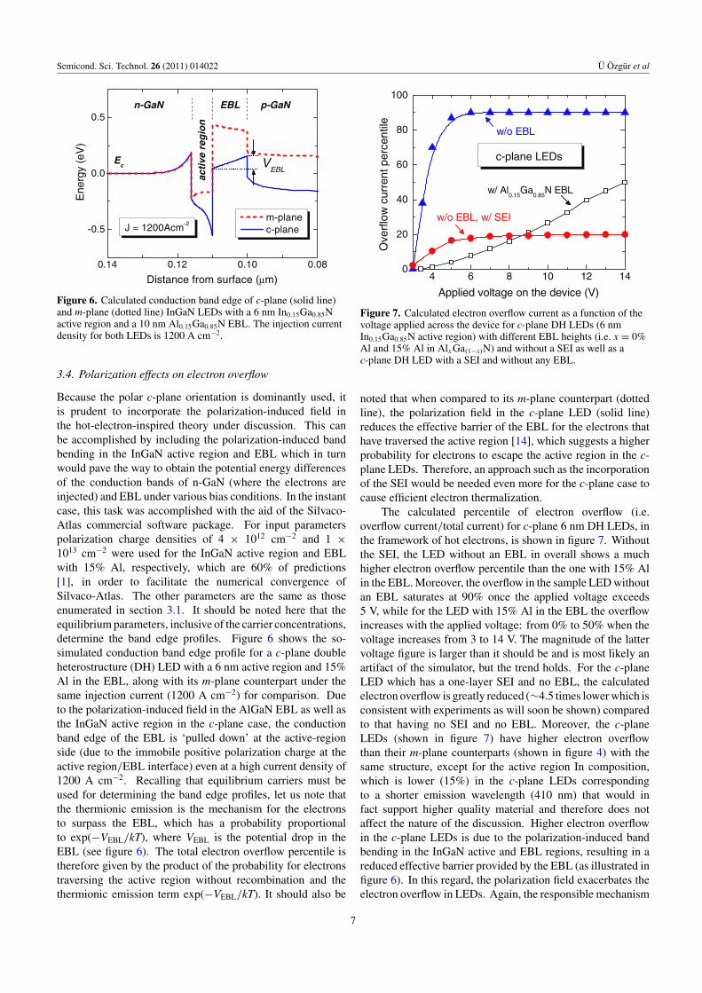
Figure 7. Calculated electron overflow current as a function of thevoltage applied across the device for c-plane DH LEDs (6 nmIn0.15Ga0.85N active region) with different EBL heights (i.e. x = 0%Al and 15% Al in AlxGa(1−x)N) and without a SEI as well as ac-plane DH LED with a SEI and without any EBL.
noted that when compared to its m-plane counterpart (dottedline), the polarization field in the c-plane LED (solid line)reduces the effective barrier of the EBL for the electrons thathave traversed the active region [14], which suggests a higherprobability for electrons to escape the active region in the c-plane LEDs. Therefore, an approach such as the incorporationof the SEI would be needed even more for the c-plane case tocause efficient electron thermalization.
The calculated percentile of electron overflow (i.e.overflow current/total current) for c-plane 6 nm DH LEDs, inthe framework of hot electrons, is shown in figure 7. Withoutthe SEI, the LED without an EBL in overall shows a muchhigher electron overflow percentile than the one with 15% Alin the EBL. Moreover, the overflow in the sample LED withoutan EBL saturates at 90% once the applied voltage exceeds5 V, while for the LED with 15% Al in the EBL the overflowincreases with the applied voltage: from 0% to 50% when thevoltage increases from 3 to 14 V. The magnitude of the lattervoltage figure is larger than it should be and is most likely anartifact of the simulator, but the trend holds. For the c-planeLED which has a one-layer SEI and no EBL, the calculatedelectron overflow is greatly reduced (∼4.5 times lower which isconsistent with experiments as will soon be shown) comparedto that having no SEI and no EBL. Moreover, the c-planeLEDs (shown in figure 7) have higher electron overflowthan their m-plane counterparts (shown in figure 4) with thesame structure, except for the active region In composition,which is lower (15%) in the c-plane LEDs correspondingto a shorter emission wavelength (410 nm) that would infact support higher quality material and therefore does notaffect the nature of the discussion. Higher electron overflowin the c-plane LEDs is due to the polarization-induced bandbending in the InGaN active and EBL regions, resulting in areduced effective barrier provided by the EBL (as illustrated infigure 6). In this regard, the polarization field exacerbates theelectron overflow in LEDs. Again, the responsible mechanism
7

Semicond. Sci. Technol. 26 (2011) 014022 U Ozgur et al
Figure 8. A schematic for the conduction band of a LED with aone-intermediate layer SEI (of thickness d and step height �Ec).After being injected into the SEI from the n-GaN region, someelectrons will have ballistic and quasi-ballistic (only one phononemission or absorption) transport through the SEI [process (a)],while the others (experiencing two or more scattering events) areconsidered to be thermalized in the SEI [process (b)]. Under highbias conditions and with a small step height �Ec, the thermalizedelectrons from process (b) might contribute to the overflow currentthrough ballistic or quasi-ballistic transport (process (c)). For thecalculations, the conduction band discontinuity between the activeregion and p-GaN is assumed to be 0.5 eV and no EBL is employed.
behind the electron overflow is the ballistic and quasi-ballisticelectron transport since the EL efficiency loss caused byelectron overflow is also present in the m-plane LEDs, whichis free of polarization-induced field. We should note that theinstant calculations do not take the effect of acceleration ofelectrons under the electrical field within the active regioninto consideration, when band bending exists, which wouldunderestimate the overflow. It is worth noting that in the c-plane case under consideration here even without consideringthe acceleration of the electron velocity by the electric field,the probability for the electron to traverse the active region andreach the EBL (before surpassing the EBL) is already ∼90%(in both 0% Al and 15% Al EBL cases due to the lowering ofthe barrier in the p-region by the polarization-induced electricfield. Marginal (3–5%) enhancement of the ballistic or quasi-ballistic electron transport is gained by adding the electricfield acceleration effect on the electron velocity in the presentcase.
3.5. Optimization of the staircase electron injector
To recap, incorporation of a SEI causes the electrons tothermalize before entering the active region, and the electronoverflow is substantially reduced, if not totally eliminated, bythe processes in the SEI. The question we would like to focuson here is the optimum design of the SEI. For the one-layerSEI, meaning one intermediate composition before enteringthe active region, a relatively small step height (conductionband discontinuity between the SEI and n-GaN, �Ec as shownin the schematic in figure 8) would result in lower electronvelocity in the SEI region, therefore a larger probability ofbeing thermalized. However, a smaller step height betweenthe n-side and the subsequent InGaN layer would result inlarger conduction band discontinuity between the intermediateInGaN layer and the active region. Consequently, the
probability of electrons traversing the active region withoutrecombining would increase. As stated, in this section wewill optimize the step height (�Ec) and thickness (d) (seefigure 8) for the one intermediate-layer SEI structure with thegoal of minimizing the electron overflow when no EBL isemployed. Note that in section 3.3 (regarding the theoreticalmodel of the one-layer SEI), the overflow contributed by theelectrons experiencing two or more scattering events was nottaken into account for a simpler treatment. However, thosemultiple scattering events should be taken into considerationfor a more accurate calculation especially for the case of ashallow-step SEI at high applied voltages [see figure 8]. Inother words, the contribution of the overflow current due tothe ballistic or quasi-ballistic transport across the active regionfrom the thermalized electrons within the SEI is significanteven with the reduced barrier height at the p-side causedby the applied voltage. It should be noted that in thetheoretical model described in section 3.3, the step in the SEI is0.25 eV below the bottom of p-GaN conduction band which issufficiently large for the contribution of the electron overflowdue to the thermalized electrons from the SEI to be safelyneglected.
For the purpose of optimization, the electrons that obeyneither the ballistic (no scattering) nor the quasi-ballistictransport (i.e. only one phonon emission or one phononabsorption) within the SEI region will be considered asthermalized down to the bottom of the conduction bandof the SEI layer. The percentile of these thermalizedelectrons (see process ‘(b)’ in the schematic in figure 8) canbe described as (1 − Pbal 1 − Pabs 1 − Pem 1), where Pbal 1,Pabs 1 and Pem 1 are the probabilities of ballistic transport (i.e.undergoing no scattering) and quasi-ballistic transport withone-phonon absorption and one phonon emission within theSEI region, respectively. After being injected from the SEIinto the active region, these thermalized electrons will have acertain probability to transit ballistically or quasi-ballisticallyacross the active region, depending on the conduction banddiscontinuity between the SEI and the active region and alsothe voltage drop across the active region (see process ‘(c)’in the schematic in figure 8). This could be described as(Pbal 2 + Pabs 2 + Pem 2), where Pbal 2, Pabs 2 and Pem 2 are theprobabilities of ballistic transport and quasi-ballistic transportwith one phonon absorption and one phonon emission withinthe active region, respectively. Therefore, the amount ofoverflow due to the thermalized electrons from the SEIcan then be described as (1 − Pbal 1 − Pabs 1 − Pem 1) ×(Pbal 2 + Pabs 2 + Pem 2) which is added to the overflowpercentile calculated with the SEI theoretical model asdescribed in section 3.3 to obtain the total electron overflowpercentile. The calculation of these probabilities is similar tothose described in section 3.2.
The calculated percentiles of electron overflow for theone-intermediate layer SEI with varying step heights (�Ec)and thicknesses (d) are shown in table 1. Under the flatbandcondition (i.e. the net potential drop across the active regionV = 0), the 15 nm thick SEIs with step heights of 0.1, 0.2and 0.3 eV all result in an overflow percentile of 11% forthe cases enumerated in the table. It should be noted that
8

Semicond. Sci. Technol. 26 (2011) 014022 U Ozgur et al
Table 1. Calculated electron overflow percentiles for aone-intermediate layer SEI (see the schematic in figure 8), withvarying SEI step heights (�Ec) and SEI thicknesses (d) underflatband conditions (V = 0) for a LED with a 6 nm thick InGaNactive region. The values in parenthesis are for V = 0.1 V.
�Ec (eV) d = 3 nm d = 9 nm d = 15 nm
0.1 36% (70%) 18% (66%) 11% (61%)0.2 37% (52%) 18% (38%) 11% (21%)0.3 39% (51%) 21% (36%) 11% (22%)0.4 41% (52%) 24% (39%) 13% (26%)0.5 42% (53%) 26% (42%) 18% (29%)
the 0.5 eV step height case, which basically correspondsto an increased active region thickness that would enhancethermalization of electrons within the active region, resultsin an increased electron overflow percentile of 18%. Underthe applied bias corresponding to V = 0.1 V drop across theactive region, the overflow percentile for the 15 nm thickSEI having a step height of 0.1 eV increases to 61% dueto a significant increase of overflow contribution from theelectrons thermalized in the SEI but traversing the active regionballistically and or quasi-ballistically without recombination.This results from the V = 0.1 V drop across the active regionthat lowers the conduction band of p-GaN to the same levelas that of the SEI. For the same bias condition correspondingto V = 0.1 V, the SEI structures with the step heights of0.2 eV or 0.3 eV and a thickness of 15 nm have comparableelectron overflow percentiles (21% versus 22%). Therefore,both could be regarded as the optimum one-layer SEI designfor this particular SEI thickness. However, at higher appliedvoltages (e.g. V = 0.2 V) across the active region, it is expectedthat 0.3 eV or larger step height will yield a reduced overflowpercentile for a certain SEI terrace thickness.
These above-discussed results suggest that for the one-intermediate layer SEI case, a sufficiently large step heightand a larger SEI thickness will reduce the electron overflow (anoptimum step height for the SEI will provide a balance betweenthe gained electron kinetic energy in the staircase regionand the overflow contribution from the electrons thermalizedwithin the SEI). However, growth-related issues in terms of theeffect of the SEI on the material quality and strain inside theactive region [33, 34] should also be taken into considerationwhen optimizing the SEI layer stack.
We now turn our attention to the case of the multiple-layer SEI. Let us assume a constant total SEI thickness andalso a constant conduction band discontinuity between theactive region and the SEI. Note that more steps within the SEIwould result in smaller step heights and thus reduced gainedkinetic energy for the electrons from the potential and thusreduced electron overflow, providing that the energy steps areequal to or larger than the LO phonon energy. As an example,we will compare the electron overflow percentile from a one-layer SEI structure and a two-layer SEI structure under theflatband conditions (see figure 9). For both SEI structures,the total SEI thickness is kept at 9 nm, and the conductionband discontinuity between the active region and the SEI is0.2 eV (i.e. the step height for the one-layer SEI is �Ec =0.3 eV). The overflow percentile for the one-layer SEI case
Figure 9. Schematics for one-layer and two-layer SEIs. For theone-layer SEI, the total SEI thickness is 9 nm and the energy stepheight is 0.3 eV. For the two-layer SEI, each energy step height is0.15 eV and each layer thickness is 4.5 nm.
is 21% (according to table 1) and 16% for the two-layer SEI.The value for the two-layer SEI was calculated taking intoaccount the overflow electron contribution from the electronsthermalized in the SEI.
The overflow percentile due to the ballistic and quasi-ballistic electron transport from point A to point C (referto figure 9) is 16%. A total of 19% of the electrons arethermalized by the first SEI layer and the probability of ballisticand quasi-ballistic transport of these thermalized electronsfrom point B to point C (refer to figure 9) is 0.8%. Theproduct of the two probabilities (19% × 0.8%), representingthe overflow, gives a negligible electron overflow percentile of∼0.2%. The electron overflow contributed by the thermalizedelectrons in the two-layer SEI layer is expected to be evensmaller and therefore can be safely neglected. The totaloverflow percentile for the two-layer SEI is (16% + 0.2%) ≈16%, which is mainly due to the ballistic and quasi-ballisticelectron transport from point A to point C. Therefore, itis reasonable to suggest that more layers in the SEI (withpotential steps no less than one LO phonon energy) wouldresult in smaller electron overflow percentile. Again, the SEIeffect on the material quality and strain of the active regionshould also be taken into consideration while maximizing theLED efficiency.
4. Experimental results
4.1. Efficiency of InGaN LEDs without the SEI
We already exhibited the experimental data in figure 2 whichdepicts the relative EQE as a function of the current densityfor the m-plane LEDs with different Al compositions in theirEBLs, the structures of which are described in section 2. Ingeneral, the EQE decreases as the Al mole fraction in theEBL is reduced. According to our resonant PL measurementsdescribed above, the three LED structures have essentially thesame IQE for the same injected carrier density (IQE of 50–56%at a carrier density of 1 × 1018 cm−3 under the assumption thatthe radiative recombination coefficient B is 1 × 10⁻¹¹ cm3 s−1.To reiterate, the EQE for the m-plane LED with 15% Al in theEBL peaks at approximately 80 A cm−2 and the efficiencydrops by ∼45% with increasing current injection up to
9

Semicond. Sci. Technol. 26 (2011) 014022 U Ozgur et al
6 8 10 12 14 160
20
40
60
80
100
No EBL
Al0.08Ga0.92N EBL
Al0.15Ga0.85N EBLEL
Effi
cien
cy lo
ss (
%)
Voltage on the device (V)
Figure 10. The EL efficiency loss as a function of the externalapplied voltage across the p–n junction of the LEDs, assumingnegligible electron overflow at the current density (∼80 A cm−2)corresponding to the peak efficiency for the LED with 15% Al in theEBL, which is very reasonable according to our calculations. Linesare guides to the eye.
2400 A cm−2. Although the LED with no EBL shows anegligible efficiency drop (∼3–5%) with increasing injection,its relative EQE is less than 30% of that with 15% Al in theEBL.
If we assume that the LED with an EBL having 15%Al has negligible electron overflow at a current density of80 A cm−2 and also that the relatively low EL efficiency atcurrents before reaching the peak efficiency for each LED isdue to SRH recombination, we can then obtain the efficiencyloss due to electron overflow inspired by the data in figure 2.Figure 10 shows the percentile EL efficiency loss due to theelectron overflow as a function of the applied voltage acrossthe LEDs. The applied voltage values are consistent with themeasured series resistance of devices (12–20 �) (see figure 2inset for the typical pulsed I--V characteristics). In the LEDwithout the EBL, 20% of the overall current contributes to theEL and approximately 80% of the current is due to electronstraversing the active region without contributing to the lightemission. As we mentioned above, the voltage drop across theactive region reduces the effective barrier by the p-side for theelectrons and therefore results in increased electron overflowwith increasing applied voltage. In the LED with 15% Al inthe EBL, the efficiency loss at 16 V is ∼45%, which means that∼45% of the injected electrons are the overflow electrons sincewe have assumed, reasonably so, that this LED has negligibleelectron overflow at current densities at or below 80 A cm−2.The results are in good overall agreement with the theoreticalestimations (figure 3 inset): the increase in the overflow currentcomponent with decreasing EBL barrier height and its weakerdependence on the applied bias for lower EBL barrier heightsare both predicted by our theory. A more accurate estimationof the loss of the EL efficiency needs to take into accountthe dependence of IQE on the injected carrier concentration,electron and hole wavefunction overlap inside the active regionand phonon lifetime dependence on the electron density,etc.
0 500 1000 1500 20000
5
10
15
20
w/o EBL
Rel
ativ
e E
QE
(a.
u.)
Current density (Acm-2)
w/ Al0.15
Ga0.85
N EBL
c-plane LEDs on sapphire6nm In
0.15Ga
0.85N DH
λpeak
∼410nm
Figure 11. Relative EQE of c-plane DH LEDs with and without anEBL layer. The LEDs were measured under pulsed current, 1 μspulse width and 0.1% duty cycle. The LEDs were grown on c-planeGaN templates on sapphire, and their active regions are composedof a 6 nm thick undoped In0.15Ga0.85N layer (peak emissionwavelength, λpeak ∼410 nm). Lines are guides to the eye.
It should be noted that the polarization-induced electricfield in the c-plane InGaN active region and the EBL has alsobeen proposed to cause electron overflow to the p-GaN layer[14]. In this regard, we studied the c-plane LEDs as well asinvestigated the correlation between the polarization field andLED EL efficiency. Figure 11 shows the relative EQE data fortwo c-plane DH LEDs: one with a 10 nm Al0.15Ga0.85N EBLand one without any EBL. The LED with an EBL exhibitsthree to four times higher EL intensity than that without anyEBL. This indicates that as in the case of m-plane LEDs, theabsence of the EBL has resulted in a comparable degree of lossin the EL efficiency which can be attributed to the increasedelectron overflow in the case without an EBL.
4.2. Efficiency of InGaN LEDs with a SEI
In order to test our premise in regard to hot electrons and theensuing ballistic and quasi-ballistic electron transit across theactive region without partaking in the recombination process,(without complete thermalization and reaching equilibriumwith the lattice), two m-plane LEDs, to be followed by thec-plane counterparts, were investigated (see section 2 forthe structural details and figure 1 for device schematics): oneLED with a 10 nm p-AlGaN EBL with 15% Al, while theother without any EBL at the p-region, with both having a SEIunder the InGaN active region to cause the thermalization ofthe injected electrons. The choice for m-plane variety first isto avoid any complications brought on by polarization charge-induced field besetting the c-plane counterparts. As will beseen below, we extended this study to include the c-planevariety as well. The first step height going from n-In0.01GaNto the first SEI layer, In0.03GaN, is very close to or smallerthan an LO phonon energy (88 meV); therefore, the first twoSEI layers may be considered as a single step for electroncooling via LO phonon emissions. The step heights for othersteps in the SEI are more than the LO phonon energy asdesired.
10

Semicond. Sci. Technol. 26 (2011) 014022 U Ozgur et al
0 500 1000 1500 2000
4
8
12
c-plane DH LEDs6nm In
0.15Ga
0.85N
with 3-layer SEIλ
peak ~ 410nm
Rel
ativ
e E
QE
(a.
u.)
Current density (A cm-2)
w/o EBL
w/ Al0.15
Ga0.85
N EBL
Figure 12. Relative EQEs of the two c-plane LEDs with a SEI: onewith and one without an EBL. The LEDs were measured underpulsed current with 1 μs pulse width and 0.1% duty cycle. The SEIincludes three intermediate InGaN layers with In compositions of3%, 6% and 10%, in the given order.
The relative EQEs of the two m-plane LEDs with a SEI,one with and one without an EBL at the p-region, are shownin figure 4(a). The results confirm that the EL intensity (i.e.relative EQE) is the same in LEDs with the SEI regardlessof the EBL status as the electron overflow due to ballisticand quasi-ballistic electron transport across the active regionis significantly reduced, if not eliminated, due to efficientthermalization in the SEI. This is reasonable considering thatthe electron overflow solely due to thermionic emission isnegligible (even for the LED without an EBL) according tothe discussion in section 3.1.
Similar to the m-plane case, the significant differencebetween the LEDs with and without an EBL is eliminatedwhen an InGaN-based SEI structure is employed in the c-plane LED case as well. The c-plane LEDs investigatedcontain the same three-layer SEI and the MQW under-layeras in the m-plane LEDs and have essentially the same IQEat the same carrier density (IQE of 46–50% at a carrierdensity of 1 × 1018 cm−3 under the assumption of aradiative recombination coefficient B of 1 × 10⁻¹¹ cm3 s−1).Figure 12 shows the relative EQE data for the two c-planeLEDs with a SEI: one with an EBL (15% Al) and the otherwithout any EBL. When the SEI structure is employed, thedifference between the LEDs with and without an EBL issignificantly reduced as compared to that in LEDs with noSEI in figure 11. This once again suggests that by using aSEI structure the ballistic and quasi-ballistic electron transportacross the active region is substantially reduced. Moreover,the injection current dependence of the efficiency in the c-plane LEDs with a SEI deviates somewhat from that of them-plane LEDs with a SEI, where essentially the same EQEvalues were observed for the LEDs with and without an EBLfor all injection current levels. Somewhat unexpectedly, in thec-plane case the LED without an EBL shows even higherEQE than that with the EBL when the current density isbelow 1700 A cm−2. At low currents (<500 A cm−2),the EQE from the LED without an EBL is as much as 2.5times higher than the one with an EBL. For current densities
above 1700 A cm−2, the former shows slightly lower EQEvalues, within nominal variations due to e.g. processes suchas current filamentation. The removal of the EBL has amore significant improvement in terms of EQE for the c-planeLEDs than for the m-plane ones, which might result from amore inferior hole transport across the EBL in the c-planecase due to relatively larger hole effective mass comparedto that in the m-plane LEDs and or relatively lower holeconcentrations. Additionally, the 22% efficiency degradationobserved for the LED with a SEI and without an EBL when thecurrent density is increased up to 2500 A cm−2 might suggestthat the c-plane orientation requires more thermalizationdue to its polarization field in order to avoid the electronoverflow-induced EL efficiency loss, assuming of coursethat processes such as current filamentation are not in playhere.
5. Conclusions
The role of ballistic and quasi-ballistic electrons in efficiencyreduction of InGaN LEDs has been investigated as a functionof injection current density using LED structures of m-planeand c-plane varieties with varying electron blocking layer(EBL) (0–15% Al) barriers. We developed first-order modelsutilizing the LO phonon scattering rates deduced from dataobtained in field effect transistors, considering the electronscattering and transport in this new realm. For simplicity,we assumed a constant LO phonon lifetime, which in realitydepends on electron concentration. In both m- and c-planeorientations, the InGaN LEDs without an EBL show three tofive times lower EL intensity than the LEDs with Al0.15Ga0.85NEBL. This has been attributed to the electron overflow tothe p-type region. As noted, the difference in EL could beexplained in terms of the ballistic and quasi-ballistic electrontransport. An InGaN SEI structure, with stepwise-increasedIn composition, was inserted before the active region forenhanced thermalization of the injected electrons to reducethe electron overflow. For m-plane LEDs incorporating theSEI, removal of the EBL resulted in essentially the sameEL performance as for the LEDs with an EBL. For the c-plane case, the use of the SEI resulted in an even betterEL efficiency at current densities below 1700 A cm−2 forthe LEDs without any EBL due possibly to relatively moreefficient hole injection since the EBL also impedes the holetransport. This demonstrates a feasible method to preventballistic and quasi-ballistic transport of the injected electronsacross the active region of InGaN LEDs and thereby to reducethe electron overflow responsible for the efficiency degradationin these devices. We should note that hot electron conceptsdiscussed here in the context of LEDs also apply to injectionlasers. Finally, the theory and the data presented here illustratethe importance of non-equilibrium carrier physics, which islacking in the commercial software codes commonly usednowadays to model InGaN LEDs.
Acknowledgments
The work at VCU is funded by grants from the Air ForceOffice of Scientific Research (Dr K Reinhardt) and the National
11
Semicond. Sci. Technol. 26 (2011) 014022 U Ozgur et al
Science Foundation, and that at the Semiconductor PhysicsInstitute is funded by the Air Force Office of ScientificResearch. One of us (AM) is grateful to Window of Scienceprogram supported by AFMC (ITO-TEL-037). The m-plane GaN wafers were provided by Dr T Paskova of KymaTechnologies, Inc., Raleigh, NC, USA.
References
[1] Morkoc H 2008 Handbook of Nitride Semiconductors andDevices vol 3 (Berlin: Wiley-VCH)) chapters 1 and 3
[2] Krames M R, Shchekin O B, Mueller-Mach R, Mueller G O,Zhou L, Harbers G and Craford M G 2007 J. Disp. Tech.3 160
[3] Alferov Zh I and Garbuzov D Z 1966 Fiz. Tverd. Tela 7 1919[4] Alferov Zh I, Andreev V M, Korolkov V I, Portnoi E L
and Tretyakov D N 1969 Fiz. Tekh. Poluprovodn. 2 843[5] Alferov Zh I, Andreev V M, Korolkov V I, Portnoi E L
and Tretyakov D N 1969 Fiz. Tekh. Poluprovodn. 2 1289[6] Shen Y C, Mueller G O, Watanabe S, Gardner N F,
Munkholm A and Krames M R 2007 Appl. Phys. Lett.91 141101
[7] Gardner N F, Muller G O, Shen Y C, Chen G and Watanabe S2007 Appl. Phys. Lett. 91 243506
[8] Delaney K T, Rinke P and Van de Walle C G 2009 Appl. Phys.Lett. 94 191109
[9] Chen G, Craven M, Kim A, Munkholm A, Watanabe S,Camras M, Gotz W and Steranka F 2008 Phys. Status SolidiA 205 1086
[10] Bulashevich K A and Karpov S Y 2008 Phys. Status SolidiC 5 2066
[11] Ryu H, Kim H and Shim J 2009 Appl. Phys. Lett. 95 081114[12] Beattie A R and Landsberg P T 1958 Proc. R. Soc.
A 249 16[13] Hader J, Moloney J V, Pasenow B, Koch S W, Sabathil M,
Linder N and Lutgen S 2008 Appl. Phys. Lett.92 261103
[14] Kim M H, Schubert M F, Dai Q, Kim J K, Schubert E F,Piprek J and Park Y 2007 Appl. Phys. Lett. 91 183507
[15] Xie J, Ni X, Fan Q, Shimada R, Ozgur U and Morkoc H 2008Appl. Phys. Lett. 93 121107
[16] Lee J, Li X, Ni X, Ozgur U, Morkoc H, Paskova T,Mulholland G and Evans K R 2009 Appl. Phys. Lett.95 201113
[17] Ni X, Fan Q, Shimada R, Ozgur U and Morkoc H 2008 Appl.Phys. Lett. 93 171113
[18] Ozgur U, Liu H, Li X, Ni X and Morkoc H 2010 GaN-basedlight-emitting diodes: efficiency at high injection levelsSpecial issue of Proc. of IEEE on Challenges andOpportunities in GaN and ZnO Devices and Materialsvol 98 ed H Morkoc p 1180
[19] Lee J, Eliseev P G, Osinski M, Lee D S, Florescu D Iand Pophristic M 2003 InGaN-based ultraviolet emitting
heterostructures with quaternary AlInGaN barriers IEEE J.Sel. Top. Quantum Electron. 9 1239
[20] Eliseev P G, Lee J and Osinski N 2004 Electro-opticalproperties of UV-emitting InGaN heterostructuresconsidering injection-induced conductivity Quant. Electron.34 1127
[21] Swietlik T et al 2006 Anomalous temperature characteristicsof single wide quantum well InGaN laser diode Appl. Phys.Lett. 88 071121
[22] Ishibashi T 2001 Nonequililbrium electron transport in HBTsIEEE Trans. Electron Devices 48 2595
[23] Xie J, Ozgur U, Fu Y, Ni X, Morkoc H, Inoki C K, Kuan T S,Foreman J V and Everitt H O 2007 Low dislocationdensities and long carrier lifetimes in GaN thin films onSiNx nanonetwork Appl. Phys. Lett. 90 41107
[24] Ni X, Li X, Lee J, Liu S, Avrutin V, Ozgur U, Morkoc H,Matulionis A, Paskova T, Mulholland G and Evans K R2010 The effect of ballistic and quasi-ballistic electrons onthe efficiency droop of InGaN light emitting diodes Phys.Stat. Sol. Rapid Res. Lett. 4 194
[25] Ni X, Li X, Lee J, Liu S, Avrutin V, Ozgur U, Morkoc H,Matulionis A, Paskova T, Mulholland G and Evans K R2010 InGaN staircase electron injector for reduced electronoverflow in InGaN light emitting diodes Appl. Phys. Lett.97 031110
[26] Liu H, Avrutin V, Izyumskaya N, Reshchikov M A, Ozgur Uand Morkoc H 2010 Highly conductive and opticallytransparent GZO films grown under metal-rich conditionsby plasma-assisted molecular beam epitaxy Phys. Stat. Sol.Rapid Res. Lett. 4 70
[27] Li X, Liu H Y, Liu S, Ni X, Wu M, Avrutin V, Izyumskaya N,Ozgur U and Morkoc H 2010 InGaN-based light emittingdiodes with Ga doped ZnO as transparent conducting oxidePhys. Status Solidi A 207 1993
[28] Dai Q et al 2009 Appl. Phys. Lett. 94 111109[29] Ni X, Li X, Lee J, Liu S, Avrutin V, Matulionis A, Ozgur U
and Morkoc H 2010 Pivotal role of ballistic andquasi-ballistic electrons on LED efficiency SuperlatticesMicrostruct. 48 133
[30] Ni X, Li X, Lee J, Liu S, Avrutin V, Ozgur U, Morkoc Hand Matulionis A 2010 Hot electron effects on efficiencydegradation in InGaN light emitting diodes and designs tomitigate them J. Appl. Phys. 108 033112
[31] Tsen K T, Joshi R P, Ferry D K, Botchkarev A, Sverdlov B,Salvador A and Morkoc H 1996 Appl. Phys. Lett. 68 2990
[32] Liberis J, Matulioniene I, Matulionis A, Ramonas Mand Eastman L F 2009 Hot phonons in high-powermicrowave HEMT and FET channels AdvancedSemiconductor Materials and Devices Research: SiC andIII-Nitrides ed H-Y Cha (Kerala, India: TransworldResearch Network) p 18
[33] Akasaka T, Gotoh H, Saito T and Makimoto T 2004 Appl.Phys. Lett. 85 3089
[34] Huang C, Liu T, Lu Y, Shiao W, Chen Y, Wang J, Lu Cand Yang C C 2008 J. Appl. Phys. 104 123106
12


![Navy Ohio Replacement (SSBN[X]) Ballistic Missile ...](https://static.fdokumen.com/doc/165x107/6322a5b0887d24588e045283/navy-ohio-replacement-ssbnx-ballistic-missile-.jpg)