gan-on-Silicon Efficient mm-wave euRopean systEm ...
19
gan - on - S ilicon E fficient mm - wave eu R opean syst E m i N tegration pl A tform The SERENA project has received funding from the European Union’s Horizon 2020 research and innovation programme under grant agreement No 779305. Rémy Leblanc OMMIC [email protected]
-
Upload
khangminh22 -
Category
Documents
-
view
1 -
download
0
Transcript of gan-on-Silicon Efficient mm-wave euRopean systEm ...

gan-on-Silicon Efficient mm-wave euRopean systEm iNtegration plAtform
The SERENA project has received funding from the European Union’s Horizon 2020 research
and innovation programme under grant agreement No 779305.
Rémy Leblanc
OMMIC


Welcome and introduction Rémy Leblanc OMMIC 5 min
GaN-on-Si process and design tools for mm-wave front ends
Rémy Leblanc OMMIC 15 min
GaN-on-Si substrates for RF and mm-wave applications
Marianne Germain SOITEC 15 min
60 nm GaN-on-Si based mm-wave amplifiers for RF sensing and wireless communication
Robert Malmqvist FOI 15 min
Q&A and wrap-up 10 min
3gan-on-Silicon Efficient mm-wave euRopean systEm iNtegration plAtformRL, 4 Nov 2021

gan-on-Silicon Efficient mm-wave euRopean systEm iNtegration plAtform
The SERENA project has received funding from the European Union’s Horizon 2020 research
and innovation programme under grant agreement No 779305.
Rémy Leblanc
OMMIC

• Created in 2000, III-V activities started in 1970
• Former Philips Semiconductor division
• Over 50 years of experience in III-V semiconductors, including GaAs and InP
• Unique GaN Process best suited for upcoming 5G
• Only foundry in Europe offering complete service including Epitaxial Growth, Process
Development, MMIC Design & Fabrication, Test & Product Qualification
gan-on-Silicon Efficient mm-wave euRopean systEm iNtegration plAtformRL, 4 Nov 2021

6
Workshop #1 slide of last week (K.Andersson, Ericsson)
Above "some" GHz, III-V processes are required to reach the power.
Conventional P-HEMT processes could be used, but GaN allows…
• higher power density
=> smaller MMIC size
• higher Power Added Efficiency
=> better thermal management
Anyhow, the commercial offer for microwave GaN is limited
gan-on-Silicon Efficient mm-wave euRopean systEm iNtegration plAtformRL, 4 Nov 2021

7gan-on-Silicon Efficient mm-wave euRopean systEm iNtegration plAtform
"on-Si" Pros…
• Lower cost, larger diameters, compatible with 5G
• Lower risk of import/export restrictions
• Compatible with heterogeneous integration
"on-Si" Cons…
• Higher Rth (≈ x2), but limited impact for medium power at mm-wave
• Higher microwave losses, but limited impact, as epi is good (0.3dB/mm @30GHz)
Most suppliers provide GaN-on-SiC
RL, 4 Nov 2021

8
Electrical Characteristic 100 nm 60 nmFrequency Cut-off (H21) 105 GHz 130 GHz
Maximum Stable Gain @30 GHz 13 dB 13.5 dB
Min Noise Figure @35 GHz 1.5 dB / 8 dB 1.1 dB / 10 dB *
RF Power Density3.3 W/mm(5.7 W/mm meas. peak)
3.3 W/mm
Extrinsic Transconductance 800 mS/mm 950 mS/mm
Source Resistance 0.18 Ohms.mm 0.18 Ohms.mm
Extrinsic Drain Source resistance Vds=0V (Ron) 0.6 Ohms.mm 0.6 Ohms.mm
Gate Drain voltage for 300µA/mm >40 V >40V
Quiescent Voltage 12 V 12V
…has all the performances and
features of a conventional MMIC
PHEMT process (Gain, Noise, Ft)
… plus power !
*W. Ciccognani, EuMw 2019
gan-on-Silicon Efficient mm-wave euRopean systEm iNtegration plAtformRL, 4 Nov 2021

9
Electrical Characteristic 100 nm 60 nmFrequency Cut-off (H21) 105 GHz 130 GHz
Maximum Stable Gain @30 GHz 13 dB 13.5 dB
Min Noise Figure @35 GHz 1.5 dB / 8 dB 1.1 dB / 10 dB *
RF Power Density3.3 W/mm(5.7 W/mm meas. peak)
3.3 W/mm
Extrinsic Transconductance 800 mS/mm 950 mS/mm
Source Resistance 0.18 Ohms.mm 0.18 Ohms.mm
Extrinsic Drain Source resistance Vds=0V (Ron) 0.6 Ohms.mm 0.6 Ohms.mm
Gate Drain voltage for 300µA/mm >40 V >40V
Quiescent Voltage 12 V 12V
…has all the performances and
features of a conventional MMIC
PHEMT process (Gain, Noise, Ft)
… plus power !
*W. Ciccognani, EuMw 2019
gan-on-Silicon Efficient mm-wave euRopean systEm iNtegration plAtformRL, 4 Nov 2021
Short gate length
Regrown Ohmic contacts
10
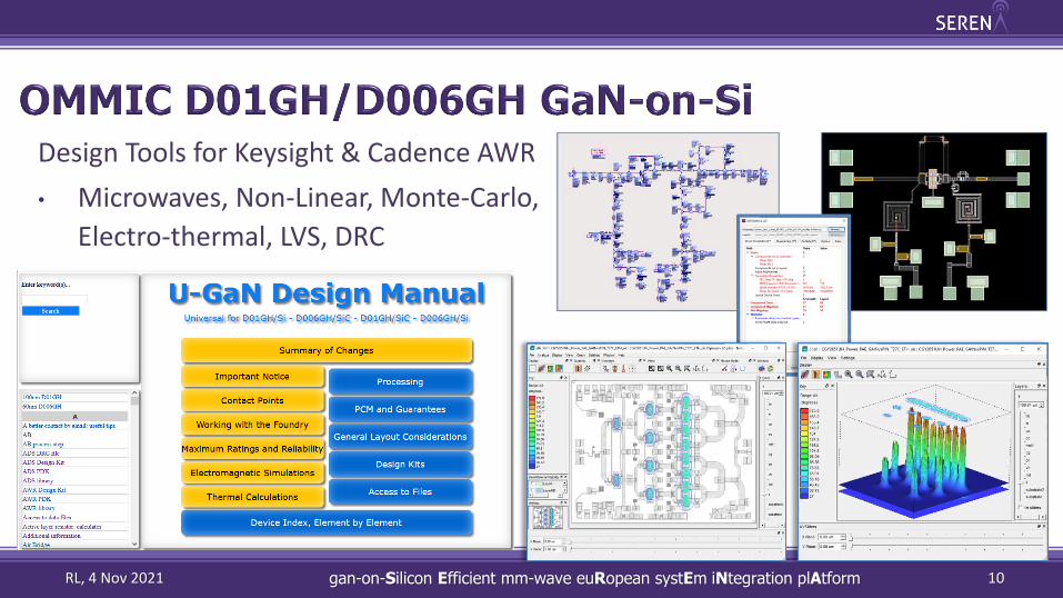
Design Tools for Keysight & Cadence AWR
• Microwaves, Non-Linear, Monte-Carlo,
Electro-thermal, LVS, DRC
gan-on-Silicon Efficient mm-wave euRopean systEm iNtegration plAtformRL, 4 Nov 2021

11
• Reliability assessment successfully
completed through Thales/DGA
contract in 2019
• Running Space evaluation through
H2020 MiGaNSOS programme (TAS,
UTV, VTT, OMMIC)
The MIGANSOS project has received funding from the European Union’s Horizon 2020
research and innovation programme under grant agreement No 779305
gan-on-Silicon Efficient mm-wave euRopean systEm iNtegration plAtformRL, 4 Nov 2021

12
Examples of MMICs, not only PAs but
also LNAs and multi-function chips
gan-on-Silicon Efficient mm-wave euRopean systEm iNtegration plAtformRL, 4 Nov 2021

Examples of MMICs, not only PAs but
also LNAs and multi-function chips
13
SERENA T/R Chip
gan-on-Silicon Efficient mm-wave euRopean systEm iNtegration plAtformRL, 4 Nov 2021

14gan-on-Silicon Efficient mm-wave euRopean systEm iNtegration plAtformRL, 4 Nov 2021

15gan-on-Silicon Efficient mm-wave euRopean systEm iNtegration plAtformRL, 4 Nov 2021

16
Summary of test results@39GHz
including input and output switches :
• Rx: 14dB Gain, 3dB NF
• Tx: 28dB Gain, 35dBm Pout,
16% PAE
gan-on-Silicon Efficient mm-wave euRopean systEm iNtegration plAtformRL, 4 Nov 2021

• GaN-on-Si is the path for a cost effective solution to
increase the transmitter mm-wave output power
• GaN-on-Si is compatible with heterogeneous integration
• GaN-on-Si is compatible with European sourcing
• Short gate length (100nm, 60nm) and regrown ohmic
contacts gives the required performance margin for 5G
28 & 39 GHz and E/W band backhaul
17gan-on-Silicon Efficient mm-wave euRopean systEm iNtegration plAtformRL, 4 Nov 2021

“The SERENA project has received funding from the European Union’s Horizon 2020 research and innovation programme
under grant agreement No 779305.”
If you need further information, please contact the coordinator:TECHNIKON Forschungs- und Planungsgesellschaft mbH
Burgplatz 3a, 9500 Villach, AUSTRIATel: +43 4242 233 55 Fax: +43 4242 233 55 77
E-Mail: [email protected]
The information in this document is provided “as is”, and no guarantee or warranty is given that the information is fit for any particular purpose.
The content of this document reflects only the author`s view – the European Commission is not responsible for any use that may be made of
the information it contains. The users use the information at their sole risk and liability.
18gan-on-Silicon Efficient mm-wave euRopean systEm iNtegration plAtformRL, 4 Nov 2021

Welcome and introduction Rémy Leblanc OMMIC 5 min
GaN-on-Si process and design tools for mm-wave front ends
Rémy Leblanc OMMIC 15 min
GaN-on-Si substrates for RF and mm-wave applications
Marianne Germain SOITEC 15 min
60 nm GaN-on-Si based mm-wave amplifiers for RF sensing and wireless communication
Robert Malmqvist FOI 15 min
Q&A and wrap-up 10 min
19gan-on-Silicon Efficient mm-wave euRopean systEm iNtegration plAtformRL, 4 Nov 2021