High-speed electroabsorption modulation of composite-resonator vertical-cavity lasers

Violet to deep-ultraviolet InGaN/GaN and GaN/AlGaN quantum structuresfor UV electroabsorption modulatorsTuncay Ozel, Emre Sari, Sedat Nizamoglu, and Hilmi Volkan Demir Citation: J. Appl. Phys. 102, 113101 (2007); doi: 10.1063/1.2817954 View online: http://dx.doi.org/10.1063/1.2817954 View Table of Contents: http://jap.aip.org/resource/1/JAPIAU/v102/i11 Published by the American Institute of Physics. Related ArticlesContactless electroreflectance study of the Fermi level pinning on GaSb surface in n-type and p-type GaSb VanHoof structures J. Appl. Phys. 112, 123513 (2012) Electro-optic effect of lithium niobate in piezoelectric resonance J. Appl. Phys. 112, 124105 (2012) Reversible superconductivity in electrochromic indium-tin oxide films Appl. Phys. Lett. 101, 252603 (2012) Optical absorption in highly strained Ge/SiGe quantum wells: The role of Γ→Δ scattering J. Appl. Phys. 112, 123105 (2012) Electron spin relaxation in rippled graphene with low mobilities J. Appl. Phys. 112, 073709 (2012) Additional information on J. Appl. Phys.Journal Homepage: http://jap.aip.org/ Journal Information: http://jap.aip.org/about/about_the_journal Top downloads: http://jap.aip.org/features/most_downloaded Information for Authors: http://jap.aip.org/authors
Downloaded 23 Dec 2012 to 139.179.112.198. Redistribution subject to AIP license or copyright; see http://jap.aip.org/about/rights_and_permissions

Violet to deep-ultraviolet InGaN/GaN and GaN/AlGaN quantum structuresfor UV electroabsorption modulators
Tuncay Ozel, Emre Sari, Sedat Nizamoglu, and Hilmi Volkan Demira�
Department of Physics, Department of Electrical and Electronics Engineering, and NanotechnologyResearch Center, Bilkent University, Ankara TR-06800, Turkey
�Received 2 August 2007; accepted 3 October 2007; published online 3 December 2007�
In this paper, we present four GaN based polar quantum structures grown on c-plane embedded inp-i-n diode architecture as a part of high-speed electroabsorption modulators for use in opticalcommunication �free-space non-line-of-sight optical links� in the ultraviolet �UV�: the firstmodulator incorporates �4–6 nm thick GaN /AlGaN quantum structures for operation in thedeep-UV spectral region and the other three incorporate �2–3 nm thick InGaN /GaN quantumstructures tuned for operation in violet to near-UV spectral region. Here, we report on the design,epitaxial growth, fabrication, and characterization of these quantum electroabsorption modulators.In reverse bias, these devices exhibit a strong electroabsorption �optical absorption coefficientchange in the range of 5500–13 000 cm−1 with electric field swings of 40–75 V /�m� at theirspecific operating wavelengths. In this work, we show that these quantum electroabsorptionstructures hold great promise for future applications in ultraviolet optoelectronics technology suchas external modulation and data coding in secure non-line-of-sight communication systems. © 2007American Institute of Physics. �DOI: 10.1063/1.2817954�
INTRODUCTION
To date, significant progress has been achieved in GaNbased optoelectronics industry.1,2 In the visible spectralrange, light emitting diodes,3 laser diodes,4 and electroab-sorption modulators5 have been demonstrated. Nowadays, aspecial interest of scientific research is also focused on thedemonstration of ultraviolet �UV� optoelectronic devices.Such devices hold promise for applications especially innon-line-of-sight �NLOS� communication systems. A chip-scale UV light source is considered as one of the strongestcandidates for use in such NLOS communication.6 However,for future high-speed NLOS communication, the introduc-tion of external modulation is necessary if higher bit ratedata links are desired to be achieved. Today, although rfwireless communication technology is well developed andcommonly used,7 it fails in fulfilling the security aspects ofthe communication. In NLOS UV communication, the atmo-spheric and particle scattering effectively entangles un-wanted incoming links, making this type of communicationsystems absolutely secure.8,9 This promising application fieldnecessitates the demonstration of high-speed quantum elec-troabsorption modulators that incorporate GaN based quan-tum structures for use in high bit rate data links in UV. ForNLOS communication systems, such a quantum electroab-sorption modulator is a chip-scale solution, providing theimportant advantages of portability and low power consump-tion as required by specific applications �for example, in au-tonomous vehicles�. However, material related problemscomplicate the growth of such optoelectronic devices oper-ating at short wavelengths. With the use of InGaN /GaNquantum structures, optoelectronic devices operating in vis-
ible to near UV are feasible, whereas deep-UV optoelec-tronic devices require the use of GaN /AlGaN quantumstructures.10–12 AlGaN based quantum structures, however,exhibit technical difficulties such as relatively slow growthrates, high dislocation densities of Al, and insufficient con-ductivity of doped layers.13 In this work, to this end, wedemonstrate four different quantum electroabsorption modu-lators with their operating wavelengths spanning from400 to 270 nm by using InGaN and AlGaN based quantumstructures in their active region as required for operating invisible to near-UV and deep-UV spectral ranges, respec-tively. Based on our proof-of-concept demonstrations here,such UV electroabsorption quantum structures hold greatpromise for use in future high-speed NLOS communicationapplications.
In this paper, we present the design, epitaxial growth,fabrication, and characterization of such quantum electroab-sorption modulators operating in their specific wavelengthranges ��400 nm�. The electroabsorption properties ofGaN /AlGaN quantum structures in the UV ��350 nm� werepreviously characterized successfully in the work of Friel etal.14 Here, for the first time, we report on the electroabsorp-tion characterization of polar InGaN /GaN quantum struc-tures in the violet ��400 nm� and polar GaN /AlGaN quan-tum structures in the deep UV ��300 nm�, all grown onsapphire.
EXPERIMENTAL
For the growth of our epitaxial layer designs, we use aGaN dedicated Aixtron RF-200 metal organic chemical va-por deposition system located at Bilkent University Nano-technology Research Center. We use double side-polishedc-plane sapphire as the substrate and TE-Ga �for Ga in quan-tum structures�, TM-Ga �for Ga in bulk layers�, TM-Al, TM-
a�Tel.: ��90��312� 290-1021. FAX: ��90��312� 290-1015. Electronic mail:[email protected]
JOURNAL OF APPLIED PHYSICS 102, 113101 �2007�
0021-8979/2007/102�11�/113101/5/$23.00 © 2007 American Institute of Physics102, 113101-1
Downloaded 23 Dec 2012 to 139.179.112.198. Redistribution subject to AIP license or copyright; see http://jap.aip.org/about/rights_and_permissions

In, and NH3 as the precursors. Our quantum electroabsorp-tion modulator designs are based on p-i-n diode architectureswith the intrinsic region incorporating unintentionally dopedInGaN /GaN or GaN /AlGaN quantum structures. ForGaN /AlGaN based quantum electroabsorption modulator�QEM-1�, we start the epitaxial growth with 15 nm thick lowtemperature AlN nucleation and 150 nm thick high tempera-ture AlN buffer layers. Following an undoped 150 nm Al-GaN layer, we grow 150 nm Si doped n-type AlGaN layer.The active region houses an unintentionally doped AlGaNmultiple quantum well structure �four sets of 4 nm thick welland 6 nm thick barrier.� Active region is capped with a40 nm thick p-type AlGaN layer. Finally, a very thin 10 nmhighly Mg doped p-type contact layer is grown. For theInGaN /GaN based quantum electroabsorption modulators�QEM-2, -3, and -4�, we start the epitaxial growth with14 nm thick GaN nucleation layer and 200 nm thick GaNbuffer layer; QEM-3 structure is shown in Fig. 1. A 690 nmthick Si doped n-type GaN layer is subsequently grown. Theactive regions embody multiple quantum wells and barriers,each with �2–3 nm thick grown consecutively. Differentgrowth temperatures are used for the active region to modifythe operation wavelength of our modulators. For QEM-2,QEM-3, and QEM-4, the growth temperatures of 705, 710,and 720 °C are used, respectively, which tunes the amountof In incorporation and thus the absorption band edge �i.e.,the operating wavelength�, as also studied in our previouswork.15,16 The epitaxial growth is monitored at all times byin situ optical reflectance, and the growth temperature is fur-ther controlled using two infrared pyrometers. For QEM-2,
we only grow 4 nm thick Mg doped p-type contact layer. ForQEM-3 and QEM-4, following the active region, we grow50 nm thick p-type AlGaN layer and finally 120 nm thickMg doped p-type GaN layer on the top. For the activation ofMg dopants, we anneal the wafers at 750 °C for 15 min.
We use standard semiconductor fabrication processes17
including photolithography, reactive ion etching �RIE�, metaldeposition, and rapid thermal annealing using class-100cleanroom facilities of Bilkent University Advanced Re-search Laboratories and Nanotechnology Research Center, asalso described in our previous work.18–20 We use RIE to etchdown to the middle of n layer to define device mesas, asillustrated in Fig. 1. We lay down Ni /Au �10 /100 nm� andTi /Al �10 /250 nm� for p and n contacts, respectively. Weperform p-contact rapid thermal annealing to form theOhmic contact at 700 °C for 30 s for InGaN based QEMsand 825 °C for 60 s for AlGaN based QEM. The contactsare finally annealed at 600 °C for 1 min under N2 purge. Thefabricated devices have mesa sizes varying from 10�10 to 300�300 �m2 and also feature open optical win-dows to couple light into the device from the top and tocollect the output light from the transparent substrate on the
FIG. 2. Scanning electron microscope image of one of our fabricated quan-tum electroabsorption modulators.
FIG. 3. Optical transmission spectrum of our epitaxially grown quantumelectroabsorption modulators.
FIG. 4. Atomic force microscope image of one of our quantum electroab-sorption modulators.
FIG. 1. Illustration of the epitaxial layer design of our InGaN /GaN basedquantum electroabsorption modulator �QEM-3 and QEM-4� along with thefabricated contacts.
113101-2 Ozel et al. J. Appl. Phys. 102, 113101 �2007�
Downloaded 23 Dec 2012 to 139.179.112.198. Redistribution subject to AIP license or copyright; see http://jap.aip.org/about/rights_and_permissions
bottom during operation. Figure 2 depicts the scanning elec-tron microscope image of our fabricated device, whichshows the device mesa with its p contact on the top and its ncontact on the bottom.
RESULTS AND DISCUSSIONS
We perform the characterization in two steps: first, sur-face and optical characterizations on the unprocessed wafer,and second, electrical characterization on the processed de-vices. We obtain optical transmission spectra of the epitaxi-ally grown wafers with the use of a UV-visible xenon lampand a spectrometer. As depicted in Fig. 3, the optical trans-mission spectra of our AlGaN based design have absorptionband edge around 265 nm and InGaN based designs around360 nm, which also confirms that our epitaxial structures aredesigned with the right band edge for operation in the ex-pected UV spectral range.
We use an atomic force microscope �AFM� for surfacecharacterization of the QEM wafers to detect if any growthrelated cracks exist. In Fig. 4, we observe that the root-mean-square roughness of our epitaxially grown structures is less
than 1 nm. The roughness level of the wafer surface confirmsthat our epitaxial growth is successfully controlled. In AFMcharacterization, no cracking is observed.
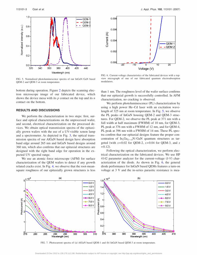
We perform photoluminescence �PL� characterization byusing a high power He–Cd laser with an excitation wave-length of 325 nm at room temperature. In Fig. 5, we observethe PL peaks of InGaN housing QEM-2 and QEM-3 struc-tures. For QEM-2, we observe the PL peak at 371 nm with afull width at half maximum �FWHM� of 10 nm, for QEM-3,PL peak at 376 nm with a FWHM of 12 nm, and for QEM-4,PL peak at 396 nm with a FWHM of 14 nm. These PL spec-tra confirm that our epitaxial designs feature the proper con-centration of InxGa�1−x�N /GaN quantum structures as tar-geted �with x=0.02 for QEM-2, x=0.04 for QEM-3, and x=0.12�.
Following the optical characterization, we perform elec-trical characterization on the fabricated devices. We use HP4142 parameter analyzer for the current-voltage �I-V� char-acterization of the diode. As shown in Fig. 6, the generaldiode performance for InGaN based QEMs features a turn-onvoltage at 3 V and the in-series parasitic resistance is mea-
FIG. 5. Normalized photoluminescence spectra of our InGaN /GaN basedQEM-2 and QEM-3 at room temperature.
FIG. 7. Photocurrent spectra of �a� AlGaN based QEM-1 and �b� InGaN based QEM-3 at room temperature.
FIG. 6. Current-voltage characteristics of the fabricated devices with a top-view micrograph of one of our fabricated quantum electroabsorptionmodulators.
113101-3 Ozel et al. J. Appl. Phys. 102, 113101 �2007�
Downloaded 23 Dec 2012 to 139.179.112.198. Redistribution subject to AIP license or copyright; see http://jap.aip.org/about/rights_and_permissions

sured to be �80 �. Such low in-series parasitic resistanceovercomes the local heating problem of the diode. On theother hand, AlGaN based diode features a turn on at 6 V andits in-series parasitic resistance is measured to be �600 �.This considerably high resistance is due to the insufficientconductivity of p-type AlGaN layer.13 This resistance level isone of the issues that reduce the performance of the QEM-1structure. Given their mesa size of 10�10 �m2, their corre-sponding device capacitance is �0.15–0.3 pF, correspond-ing to RC time constants of �90 ps for QEM-1 and �25 psfor QEM-2, -3, and -4, respectively. In principle, this wouldsafely enable these devices to operate in the gigahertz range.
We perform photocurrent measurements with an opticalsetup that consists of a xenon light source, a monochromator,a chopper, and a lock-in amplifier by applying reverse biasesacross the devices. Figures 7�a� and 7�b� show the photocur-rent spectrum of QEM-1 and QEM-3 parametrized at reversebiases from 0 to 9 V swing �in 1.5 V steps�, respectively. Inthis measurement, the level of dark current is in the range ofa few nanoamperes. Here, we encounter carrier collectionproblem in the AlGaN based QEM-1. This carrier collectionproblem is one of the major issues that undesirably affect thedevice operation.21
We calculate the electroabsorption spectra by using thephotocurrent data at various levels of the applied voltages.
We process the electroabsorption data and convert into theabsorption coefficient spectrum. We simply measure thequantum efficiencies of the devices by using the spectral re-sponsivity curve. We take the Fresnel reflection into accountand assume that all generated electron-hole pairs due to theoptical absorption process contribute to the photocurrent.12,13
Here, we take the thickness of the total absorption layer asthe thickness of whole active region including all the quan-tum wells and barriers. �In the previous characterization of aUV modulator by Friel et al., the thickness of the absorbinglayer is considered to consist of only the thickness of onlyquantum wells.14 However, it should be noted that the in-coming light is also absorbed by the barriers �as these aretypically coupled quantum structures and the wavefunctionspenetrate well into the barriers��. Figure 8 shows the opticalabsorption coefficient change of QEM-1 incorporating Al-GaN at each applied bias level with respect to the 0 V curve.As depicted in Fig. 8, AlGaN based QEM-1 exhibits a9500 cm−1 absorption coefficient change at 275 nm with anapplied reverse bias of 9 V �corresponding to an electric fieldswing of 50 V /�m� in the spectral range where it is trans-missive, as also shown in the transmission spectrum in Fig.3. This GaN /AlGaN based quantum electroabsorptionmodulator operating at 270 nm features a sufficiently highabsorption coefficient change, which is comparable to theprevious work of Friel et al. for operation at �355 nm.14
�Here, note that if only wells were taken as the thickness ofthe absorbing layer, this absorption coefficient change wouldbe calculated to be 2.4�104 cm−1.� For the InGaN basedQEMs, we observe that QEM-2 exhibits an absorption coef-ficient change of 13 000 cm−1 at 380 nm, QEM-3 exhibits anabsorption coefficient change of 6500 cm−1 at 385 nm, andQEM-4 exhibits an absorption coefficient change of5500 cm−1 at 400 nm with an applied reverse bias of 9 V�corresponding to electric field swings of 75, 50, and40 V /�m, respectively�, as shown in Fig. 9. This achievedelectromodulation is the highest in InGaN /GaN based quan-tum structures compared to the previous reports.5,22,23 �Also,here note that if only wells were taken as the thickness of theabsorbing layer, these absorption coefficient changes wouldthen be calculated to be even further larger with the respec-tive values of 3.1�104, 1.5�104, and 1.3�104 cm−1.� Theabsorption coefficient changes of these GaN /AlGaN basedand InGaN /GaN based quantum electroabsorption modula-tors implies that an �50 �m long waveguide modulator with
FIG. 8. Absorption coefficient change spectrum of AlGaN based deep-UVQEM-1.
FIG. 9. Absorption coefficient change spectra of InGaN based �a� near-UV QEM-2, �b� near-UV QEM-3, and �c� violet QEM-4.
113101-4 Ozel et al. J. Appl. Phys. 102, 113101 �2007�
Downloaded 23 Dec 2012 to 139.179.112.198. Redistribution subject to AIP license or copyright; see http://jap.aip.org/about/rights_and_permissions

a reasonable overlap integral of the waveguide mode withthe quantum structures �e.g., ��0.1� is expected to achievea 10 dB contrast ratio for a 2 V /�m field swing.
Moreover, in forward bias operation, QEM-1 features anelectroluminescence �EL� peak at 313 nm with a FWHM of14 nm, as shown in Fig. 10. However, there is a wide andunexpected emission around 380 nm, which is possiblycaused by the impurities introduced during the epitaxialgrowth. QEM-2 features an EL peak at 375 nm with aFWHM of 13 nm, QEM-3 features an EL peak at 386 nmwith a FWHM of 12 nm, and QEM-4 features an EL peak at405 nm with a FWHM of 15 nm. For QEM-2 and QEM-3,EL peaks are sharp and in good agreement with the PL spec-trum shown in Fig. 5. As expected, compared to the PL peaksin Fig. 5, we observe a redshift in EL peaks of QEMs in Fig.10. The output power collected from one side of the QEM-1is in the submicrowatt range and from QEM-2, -3, and -4, itis in the submilliwatt range.
CONCLUSIONS
In this work, we developed and demonstrated four quan-tum electroabsorption modulators: one AlGaN based modu-lator operating in the deep UV �270 nm�, two InGaN basedmodulator operating at near UV �375 and 385 nm�, and oneInGaN based modulator operating in the violet �400 nm�spectral region with high absorption coefficient changes from5500 up to 13 000 cm−1 for an applied reverse bias change of9 V �corresponding to 40–75 V /�m electric field swing�.These quantum electroabsorption modulators also emit lightas a second mode of operation when forward bias is appliedacross the devices. Here, for the first time, we demonstratedand characterized InGaN based violet quantum electroab-sorption modulators and AlGaN based deep-UV quantumelectroabsorption modulators. With this work, we realizedstrong electroabsorption using AlGaN based modulators inthe UV range, suggesting that there is a high potential fortheir use in future non-line-of-sight communication applica-tions.
ACKNOWLEDGMENTS
This work is supported by EU-PHOREMOST Networkof Excellence 511616 and Marie Curie European Reintegra-tion Grant No. MOON 021391 within the 6th EuropeanCommunity Framework Program and TUBITAK under theProject Nos. EEEAG 104E114, 106E020, 105E065, and105E066. The authors acknowledge additional support fromthe Turkish National Academy of Sciences DistinguishedYoung Scientist Award �TÜBA GEBİP�, European Young In-vestigator �EURYI� Award, and TUBITAK Fellowship Pro-grams. The authors also thank Yilmaz Dikme, Serkan Butun,and Nihan Kosku Perkgoz for their fruitful discussions anduseful contributions. The authors are pleased to acknowledgethe Bilkent University Nanotechnology Research Center andAdvanced Research Laboratories for allowing them to usetheir facilities for this work.
1S. P. Denbaars, Proc. IEEE 85, 1740 �1997�.2M. A. Khan, M. Shatalov, H. P. Maruska, H. M. Wang, and E. Kuokstis,Jpn. J. Appl. Phys., Part 1 44, 7191 �2005�.
3E. Fred Schubert, Light Emitting Diodes �Cambridge University Press,New York, 2006�.
4S. Nakamura, G. Fasol, and S. J. Pearton, The Blue Laser Diode: TheComplete Story �Springer, New York, 2000�.
5E. Sari, S. Nizamoglu, T. Ozel, and H. V. Demir, Appl. Phys. Lett. 90,011101 �2007�.
6A. M. Siegel, G. A. Shaw, and J. Model, Proc. SPIE 5417, 214 �2004�.7T. S. Rappaport, Wireless Communications: Principles and Practice�IEEE, Piscataway, NJ, 1996�.
8G. A. Shaw, A. M. Siegel, and J. Model, IEEE LEOS Newsletter 19, 5�2005�.
9D. E. Sunstein, “A Scatter Communications Link at Ultraviolet Frequen-cies,” Thesis, MIT, 1968.
10S. F. Chichibu, A. Shikanai, T. Deguchi, A. Setoguchi, R. Nakai, H. Na-kanishi, K. Wada, S. P. DenBaars, T. Sota, and S. Nakamura, Jpn. J. Appl.Phys., Part 1 39, 2417 �2000�.
11D. M. Graham, A. Soltani-Vala, P. Dawson, M. J. Godfrey, T. M. Smeeton,J. S. Barnard, M. J. Kappers, C. J. Humphreys, and E. J. Thrush, J. Appl.Phys. 97, 103508 �2005�.
12A. A. Allerman, M. H. Crawford, A. J. Fischer, K. H. A. Bogart, S. R.Lee, D. M. Follstaedt, P. P. Provencio, and D. D. Koleske, J. Cryst.Growth 272, 227 �2004�.
13I. Akasaki and H. Amano, Jpn. J. Appl. Phys., Part 1 36, 5393 �1997�.14I. Friel, C. Thomidis, and T. D. Moustakas, J. Appl. Phys. 97, 123515
�2005�.15S. Nizamoglu, T. Ozel, E. Sari, and H. V. Demir, Nanotechnology 18,
065709 �2007�.16H. V. Demir, S. Nizamoglu, T. Ozel, E. Mutlugun, I. O. Huyal, E. Sari, E.
Holder, and N. Tian, New J. Phys. 9, 362 �2007�.17P. Schlotter, J. Baur, Ch. Hielscher, M. Kunzer, H. Obloh, R. Schmidt, and
J. Schneider, Mater. Sci. Eng., B 59, 390 �1999�.18H. V. Demir, V. A. Sabnis, O. Fidaner, J. S. Harris, D. A. M. Miller, and
J. F. Zheng, IEEE J. Sel. Top. Quantum Electron. 11, 86 �2005�.19H. V. Demir, V. A. Sabnis, J. F. Zheng, O. Fidaner, J. S. Harris, and D. A.
B. Miller, IEEE Photonics Technol. Lett. 16, 2305 �2004�.20V. A. Sabnis, H. V. Demir, O. Fidaner, J. S. Harris, D. A. B. Miller, J. F.
Zheng, N. Li, T. C. Wu, H. T. Chen, and Y. M. Houng, Appl. Phys. Lett.84, 469 �2004�.
21H. Shichijo, R. M. Kolbas, N. Holonyak, R. D. Dupuis, and P. D. Dapkus,Solid State Commun. 27, 10 �1978�.
22A. E. Oberhofer, J. F. Muth, M. A. L. Johnson, Z. Y. Chen, E. F. Fleet, andG. D. Cooper, Appl. Phys. Lett. 83, 2748 �2003�.
23M. Kneissl, T. L. Paoli, P. Kiesel, D. W. Treat, M. Teepe, N. Miyashita,and N. M. Johnson, Appl. Phys. Lett. 80, 3283 �2002�.
FIG. 10. Normalized electroluminescence spectrum of all quantum electro-absorption modulators �QEM-1, −2, −3, and −4�.
113101-5 Ozel et al. J. Appl. Phys. 102, 113101 �2007�
Downloaded 23 Dec 2012 to 139.179.112.198. Redistribution subject to AIP license or copyright; see http://jap.aip.org/about/rights_and_permissions
Copyright © 2022 FDOKUMEN