Diamond/GaN HEMTs: Where from and Where to? - MDPI
46
Citation: Mendes, J.C.; Liehr, M.; Li, C. Diamond/GaN HEMTs: Where from and Where to? Materials 2022, 15, 415. https://doi.org/10.3390/ ma15020415 Academic Editor: Fabrizio Roccaforte Received: 8 October 2021 Accepted: 30 December 2021 Published: 6 January 2022 Publisher’s Note: MDPI stays neutral with regard to jurisdictional claims in published maps and institutional affil- iations. Copyright: © 2022 by the authors. Licensee MDPI, Basel, Switzerland. This article is an open access article distributed under the terms and conditions of the Creative Commons Attribution (CC BY) license (https:// creativecommons.org/licenses/by/ 4.0/). materials Review Diamond/GaN HEMTs: Where from and Where to? Joana C. Mendes 1, * , Michael Liehr 2 and Changhui Li 2 1 Instituto de Telecomunicações e Departamento de Eletrónica, Telecomunicações e Informática, Universidade de Aveiro, 3810-193 Aveiro, Portugal 2 W&L Coating Systems GmbH, Bingenheimer Str. 32, D-61203 Reichelsheim, Germany; [email protected] (M.L.); [email protected] (C.L.) * Correspondence: [email protected] Abstract: Gallium nitride is a wide bandgap semiconductor material with high electric field strength and electron mobility that translate in a tremendous potential for radio-frequency communications and renewable energy generation, amongst other areas. However, due to the particular architecture of GaN high electron mobility transistors, the relatively low thermal conductivity of the material induces the appearance of localized hotspots that degrade the devices performance and compromise their long term reliability. On the search of effective thermal management solutions, the integration of GaN and synthetic diamond with high thermal conductivity and electric breakdown strength shows a tremendous potential. A significant effort has been made in the past few years by both academic and industrial players in the search of a technological process that allows the integration of both materials and the fabrication of high performance and high reliability hybrid devices. Different approaches have been proposed, such as the development of diamond/GaN wafers for further device fabrication or the capping of passivated GaN devices with diamond films. This paper describes in detail the potential and technical challenges of each approach and presents and discusses their advantages and disadvantages. Keywords: diamond; GaN; HEMT; thermal management; GaN-on-diamond; CVD 1. Introduction Gallium nitride (GaN) is a wide bandgap compound III-V semiconductor with high breakdown electric field, high electron mobility, and high electron saturation velocity that translate in a tremendous potential for high power and high frequency applications (Table 1). The GaN high electron mobility transistor (HEMT) is a device that takes advantage of the two-dimensional electron gas (2DEG) that spontaneously forms at an aluminum gallium nitride (AlGaN)/GaN heterojunction thanks to the strong internal piezoelectric and spontaneous polarization. This 2DEG typically exhibits high values of sheet carrier density (≈10 13 cm -2 ) and carrier mobility (1000–2000 cm 2 /(V·s)) [1]. GaN HEMTs can be used in power switching for information technologies, automotive, healthcare, and industrial manufacturing applications [1–3]. Thanks to the large bandgap, leakage currents in GaN power devices are orders of magnitude smaller than in silicon (Si), allowing for operation at higher temperature without thermal runaway and reducing the cooling requirements. The high breakdown electric field allows shorter drift distances for a given blocking voltage, when compared to Si devices, yielding to a drastic reduction in the specific on-resistance that in turn translates into smaller device area and correspondingly lower capacitance. This reduces switching losses and enables higher switching frequencies. GaN HEMTS have also paved their way into mobile and satellite communications and radar systems [4]. In addition to the properties listed above, the high breakdown electric field of GaN allows higher matching impedances and circuits with broader bandwidth and high power-added efficiency (PAE)[5]. The ability of GaN to withstand higher temperatures further increases the power density of a given HEMT device and power amplifiers with absolute power levels of tens to hundreds of Watts have been reported [6]. Materials 2022, 15, 415. https://doi.org/10.3390/ma15020415 https://www.mdpi.com/journal/materials
-
Upload
khangminh22 -
Category
Documents
-
view
3 -
download
0
Transcript of Diamond/GaN HEMTs: Where from and Where to? - MDPI

Citation: Mendes, J.C.; Liehr, M.; Li,
C. Diamond/GaN HEMTs: Where
from and Where to? Materials 2022,
15, 415. https://doi.org/10.3390/
ma15020415
Academic Editor: Fabrizio Roccaforte
Received: 8 October 2021
Accepted: 30 December 2021
Published: 6 January 2022
Publisher’s Note: MDPI stays neutral
with regard to jurisdictional claims in
published maps and institutional affil-
iations.
Copyright: © 2022 by the authors.
Licensee MDPI, Basel, Switzerland.
This article is an open access article
distributed under the terms and
conditions of the Creative Commons
Attribution (CC BY) license (https://
creativecommons.org/licenses/by/
4.0/).
materials
Review
Diamond/GaN HEMTs: Where from and Where to?Joana C. Mendes 1,* , Michael Liehr 2 and Changhui Li 2
1 Instituto de Telecomunicações e Departamento de Eletrónica, Telecomunicações e Informática,Universidade de Aveiro, 3810-193 Aveiro, Portugal
2 W&L Coating Systems GmbH, Bingenheimer Str. 32, D-61203 Reichelsheim, Germany;[email protected] (M.L.); [email protected] (C.L.)
* Correspondence: [email protected]
Abstract: Gallium nitride is a wide bandgap semiconductor material with high electric field strengthand electron mobility that translate in a tremendous potential for radio-frequency communicationsand renewable energy generation, amongst other areas. However, due to the particular architectureof GaN high electron mobility transistors, the relatively low thermal conductivity of the materialinduces the appearance of localized hotspots that degrade the devices performance and compromisetheir long term reliability. On the search of effective thermal management solutions, the integration ofGaN and synthetic diamond with high thermal conductivity and electric breakdown strength shows atremendous potential. A significant effort has been made in the past few years by both academic andindustrial players in the search of a technological process that allows the integration of both materialsand the fabrication of high performance and high reliability hybrid devices. Different approacheshave been proposed, such as the development of diamond/GaN wafers for further device fabricationor the capping of passivated GaN devices with diamond films. This paper describes in detail thepotential and technical challenges of each approach and presents and discusses their advantagesand disadvantages.
Keywords: diamond; GaN; HEMT; thermal management; GaN-on-diamond; CVD
1. Introduction
Gallium nitride (GaN) is a wide bandgap compound III-V semiconductor with highbreakdown electric field, high electron mobility, and high electron saturation velocitythat translate in a tremendous potential for high power and high frequency applications(Table 1). The GaN high electron mobility transistor (HEMT) is a device that takes advantageof the two-dimensional electron gas (2DEG) that spontaneously forms at an aluminumgallium nitride (AlGaN)/GaN heterojunction thanks to the strong internal piezoelectricand spontaneous polarization. This 2DEG typically exhibits high values of sheet carrierdensity (≈1013 cm−2) and carrier mobility (1000–2000 cm2/(V·s)) [1].
GaN HEMTs can be used in power switching for information technologies, automotive,healthcare, and industrial manufacturing applications [1–3]. Thanks to the large bandgap,leakage currents in GaN power devices are orders of magnitude smaller than in silicon (Si),allowing for operation at higher temperature without thermal runaway and reducing thecooling requirements. The high breakdown electric field allows shorter drift distances for agiven blocking voltage, when compared to Si devices, yielding to a drastic reduction in thespecific on-resistance that in turn translates into smaller device area and correspondinglylower capacitance. This reduces switching losses and enables higher switching frequencies.
GaN HEMTS have also paved their way into mobile and satellite communications andradar systems [4]. In addition to the properties listed above, the high breakdown electricfield of GaN allows higher matching impedances and circuits with broader bandwidth andhigh power-added efficiency (PAE) [5]. The ability of GaN to withstand higher temperaturesfurther increases the power density of a given HEMT device and power amplifiers withabsolute power levels of tens to hundreds of Watts have been reported [6].
Materials 2022, 15, 415. https://doi.org/10.3390/ma15020415 https://www.mdpi.com/journal/materials
Materials 2022, 15, 415 2 of 46
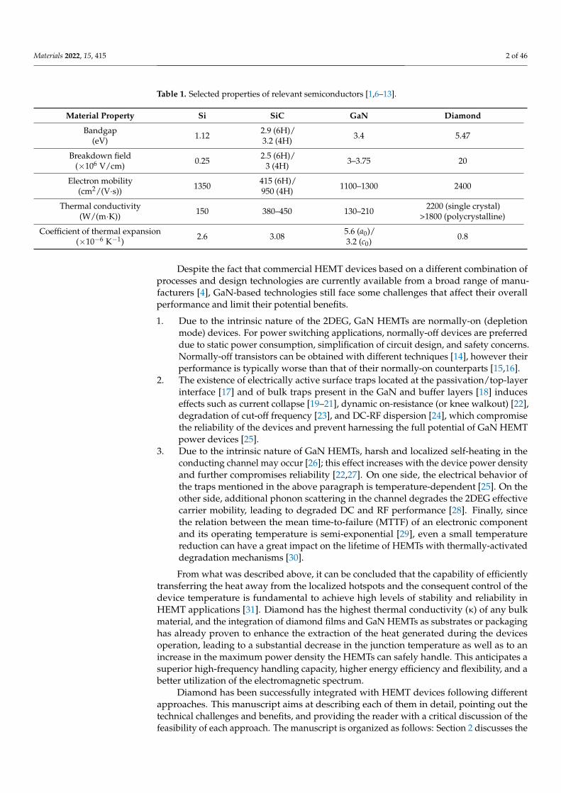
Table 1. Selected properties of relevant semiconductors [1,6–13].
Material Property Si SiC GaN Diamond
Bandgap(eV) 1.12 2.9 (6H)/
3.2 (4H) 3.4 5.47
Breakdown field(×106 V/cm) 0.25 2.5 (6H)/
3 (4H) 3–3.75 20
Electron mobility(cm2/(V·s)) 1350 415 (6H)/
950 (4H) 1100–1300 2400
Thermal conductivity(W/(m·K)) 150 380–450 130–210 2200 (single crystal)
>1800 (polycrystalline)
Coefficient of thermal expansion(×10−6 K−1) 2.6 3.08 5.6 (a0)/
3.2 (c0) 0.8
Despite the fact that commercial HEMT devices based on a different combination ofprocesses and design technologies are currently available from a broad range of manu-facturers [4], GaN-based technologies still face some challenges that affect their overallperformance and limit their potential benefits.
1. Due to the intrinsic nature of the 2DEG, GaN HEMTs are normally-on (depletionmode) devices. For power switching applications, normally-off devices are preferreddue to static power consumption, simplification of circuit design, and safety concerns.Normally-off transistors can be obtained with different techniques [14], however theirperformance is typically worse than that of their normally-on counterparts [15,16].
2. The existence of electrically active surface traps located at the passivation/top-layerinterface [17] and of bulk traps present in the GaN and buffer layers [18] induceseffects such as current collapse [19–21], dynamic on-resistance (or knee walkout) [22],degradation of cut-off frequency [23], and DC-RF dispersion [24], which compromisethe reliability of the devices and prevent harnessing the full potential of GaN HEMTpower devices [25].
3. Due to the intrinsic nature of GaN HEMTs, harsh and localized self-heating in theconducting channel may occur [26]; this effect increases with the device power densityand further compromises reliability [22,27]. On one side, the electrical behavior ofthe traps mentioned in the above paragraph is temperature-dependent [25]. On theother side, additional phonon scattering in the channel degrades the 2DEG effectivecarrier mobility, leading to degraded DC and RF performance [28]. Finally, sincethe relation between the mean time-to-failure (MTTF) of an electronic componentand its operating temperature is semi-exponential [29], even a small temperaturereduction can have a great impact on the lifetime of HEMTs with thermally-activateddegradation mechanisms [30].
From what was described above, it can be concluded that the capability of efficientlytransferring the heat away from the localized hotspots and the consequent control of thedevice temperature is fundamental to achieve high levels of stability and reliability inHEMT applications [31]. Diamond has the highest thermal conductivity (κ) of any bulkmaterial, and the integration of diamond films and GaN HEMTs as substrates or packaginghas already proven to enhance the extraction of the heat generated during the devicesoperation, leading to a substantial decrease in the junction temperature as well as to anincrease in the maximum power density the HEMTs can safely handle. This anticipates asuperior high-frequency handling capacity, higher energy efficiency and flexibility, and abetter utilization of the electromagnetic spectrum.
Diamond has been successfully integrated with HEMT devices following differentapproaches. This manuscript aims at describing each of them in detail, pointing out thetechnical challenges and benefits, and providing the reader with a critical discussion of thefeasibility of each approach. The manuscript is organized as follows: Section 2 discusses the
Materials 2022, 15, 415 3 of 46
critical aspects that impact the thermal management of GaN HEMTs; Section 3 describesthe different strategies that have been followed by different groups to integrate diamondand GaN into high performance devices; Section 4 describes the challenges faced by eachintegration technology and discusses their feasibility; Section 5 draws the main conclusionsand Appendix A summarizes the performance of the different GaN/diamond HEMTsreported so far.
2. Thermal Management of GaN HEMTs2.1. GaN HEMT
The concept of mobility enhancement through modulation doping of an aluminumgallium arsenide (AlGaAs)/gallium arsenide (GaAs) multilayer heterojunction was intro-duced by Dingle et al. in 1978 [32]. Since the energy of the GaAs conduction band is lowerthan the energy of the AlGaAs donor states, electrons from the later move into the GaAsregions, forming a 2DEG. By introducing a rectifying contact on top of the heterojunction,Mimura et al. [33] were able to control, by field effect, the concentration of the 2DEG. Soonafter the deposition of high quality GaN films on sapphire substrates by MetalorganicChemical Vapor Deposition (MOCVD) [34] and using the same principle, the AlGaN/GaNHEMT was reported by Khan and co-workers [35]. In a conventional AlGaN/GaN HEMT,the current flowing in the 2DEG channel between the source and drain Ohmic electrodes ismodulated by a negative bias applied to the gate Schottky contact.
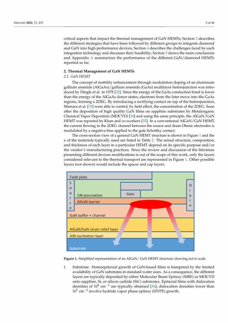
The cross-section view of a general GaN HEMT structure is shown in Figure 1 and theκ of the materials typically used are listed in Table 2. The actual structure, composition,and thickness of each layer in a particular HEMT depend on its specific purpose and/orthe vendor’s manufacturing practices. Since the review and discussion of the literaturepresenting different devices modifications is out of the scope of this work, only the layersconsidered relevant to the thermal transport are represented in Figure 1. Other possiblelayers (not shown) would include the spacer and cap layers.
Materials 2022, 15, x FOR PEER REVIEW 4 of 46
5. Barrier layer. The typically 5–25 nm-thick barrier layer can be made of AlN [42], in-
dium gallium nitride (InGaN) [43], or other high bandgap alloys, but AlxGa1-xN with
an aluminum (Al) fractional content in the range of 22–32% [6] is the most widely
reported material.
6. Passivation layer. A thin dielectric layer, typically silicon nitride (Si3N4), compensates
the surface/interface states responsible for the current collapse issue by introducing
shallow donors [44].
7. Field plate. The source and gate-connected field plates are usually employed to re-
duce the strength of the electric field near the gate terminal, reducing the gate tun-
neling injection current responsible for charging the surface traps [45].
Figure 1. Simplified representation of an AlGaN/ GaN HEMT structure; drawing not to scale.
Table 2. Typical thermal conductivity of the materials present in an AlGaN/GaN HEMT [1,7,9–
11,46–48].
Material Thermal Conductivity
(W/(mK))
Sapphire 46
Si 150
SiC 380–450
Single-crystal diamond 2200
Polycrystalline diamond >1800
GaN 130–210
AlN 130
AlxGa1-xN 10–11
InxGa1-xN 5–11
SiN 1.6
2.2. Getting the Heat Out
Thanks to the high breakdown voltage and saturation velocity of carriers in the
2DEG, AlGaN/GaN HEMTs are able to handle substantial power densities, which result
in self-heating and highly-localized power densities (in some cases as high as 105 W/cm2)
[49]. The resulting high temperatures decrease the MTTF, the performance, and the relia-
bility of HEMT devices—and this makes the implementation of efficient thermal manage-
ment techniques mandatory. This is particularly important for devices that have inher-
ently small features yet process large power densities, such as high-power RF/millimeter-
wave transistors and single-mode visible semiconductor lasers.
Most of the heat generated during device operation will diffuse from the hotspot
through the different layers represented in Figure 1 until it reaches the heat sink attached
to the back of the substrate. A few intrinsic obstacles hinder the transfer of the heat
Figure 1. Simplified representation of an AlGaN/ GaN HEMT structure; drawing not to scale.
1. Substrate. Homoepitaxial growth of GaN-based films is hampered by the limitedavailability of GaN substrates in standard wafer sizes. As a consequence, the differentlayers are typically deposited by either Molecular Beam Epitaxy (MBE) or MOCVDonto sapphire, Si, or silicon carbide (SiC) substrates. Epitaxial films with dislocationdensities of 108 cm−2 are typically obtained [36]; dislocation densities lower than107 cm−2 involve hydride vapor phase epitaxy (HVPE) growth.

Materials 2022, 15, 415 4 of 46
2. Nucleation layer. The deposition of high quality epitaxial GaN films with smoothsurfaces and low dislocation density is not a straightforward task due to latticemismatch and to the difference in the coefficients of thermal expansion (CTEs) ofGaN and substrate [37]. A nucleation layer, typically 40–200 nm of aluminum nitride(AlN) [38], is thus initially deposited on the substrate surface for strain accommodationand increased interface resistivity [39,40].
3. Strain relief layer. AlGaN/GaN transition layers, often up to 1 µm thickness, fur-ther accommodate the lattice mismatch during the growth of GaN on the foreignsubstrate [41].
4. GaN layer. A 0.6–1.5 µm-thick GaN buffer layer that provides electrical isolation toreduce substrate leakage and prevents the propagation of threading dislocations andcontaminants that might migrate from the substrate into the top high quality channelregion follows.
5. Barrier layer. The typically 5–25 nm-thick barrier layer can be made of AlN [42],indium gallium nitride (InGaN) [43], or other high bandgap alloys, but AlxGa1−xNwith an aluminum (Al) fractional content in the range of 22–32% [6] is the most widelyreported material.
6. Passivation layer. A thin dielectric layer, typically silicon nitride (Si3N4), compensatesthe surface/interface states responsible for the current collapse issue by introducingshallow donors [44].
7. Field plate. The source and gate-connected field plates are usually employed to reducethe strength of the electric field near the gate terminal, reducing the gate tunnelinginjection current responsible for charging the surface traps [45].
Table 2. Typical thermal conductivity of the materials present in an AlGaN/GaN HEMT [1,7,9–11,46–48].
Material Thermal Conductivity(W/(m·K))
Sapphire 46
Si 150
SiC 380–450
Single-crystal diamond 2200
Polycrystalline diamond >1800
GaN 130–210
AlN 130
AlxGa1−xN 10–11
InxGa1−xN 5–11
SiN 1.6
2.2. Getting the Heat Out
Thanks to the high breakdown voltage and saturation velocity of carriers in the 2DEG,AlGaN/GaN HEMTs are able to handle substantial power densities, which result in self-heating and highly-localized power densities (in some cases as high as 105 W/cm2) [49].The resulting high temperatures decrease the MTTF, the performance, and the reliabilityof HEMT devices—and this makes the implementation of efficient thermal managementtechniques mandatory. This is particularly important for devices that have inherentlysmall features yet process large power densities, such as high-power RF/millimeter-wavetransistors and single-mode visible semiconductor lasers.
Most of the heat generated during device operation will diffuse from the hotspotthrough the different layers represented in Figure 1 until it reaches the heat sink attachedto the back of the substrate. A few intrinsic obstacles hinder the transfer of the heattowards the heat sink. The AlGaN/GaN strain relief transition layers improve the electrical

Materials 2022, 15, 415 5 of 46
performance at the top of the GaN layer, however, if the concentration of Al is higherthan 5%, the κ of the AlGaN decreases to around 1/10th that of bulk GaN, hampering thetransfer of heat from the GaN buffer layer to the underlying substrate [41].
The thermal transport across the strain-relief layer/nucleation layer/substrate inter-faces also plays an important role in determining the overall κ of the GaN HEMT materialsystem. The existence of an interface between two solids results in the scattering of thermalenergy carriers (electrons and phonons), which translates in the appearance of a thermalboundary resistance (TBR) between the different materials and in a temperature disconti-nuity across the interface [50,51].
Despite its low thickness in comparison to the GaN layer, the nucleation layer pro-foundly impacts the transport of heat from the strain relief layer towards the underlyingsubstrate. Instead of being composed of high quality AlN, this layer contains dislocations,grain boundaries, and point defects (impurity atoms and vacancies) [52,53], within theitself or near the interfaces, that hinder heat transport by increasing phonon scattering ratesand reducing the phonon mean free path [54].
The interfacial and nucleation layer thermal resistances contribute with an effectiveTBR between the strain relief layers and the substrate between 10 and 70 m2·K/GW [38] thatmay cause an additional 30–50% channel temperature rise in AlGaN/GaN HEMTs [38,55].
2.3. Why GaN-Diamond HEMTs?
In the search of good thermal conductors, carbon-based materials, such as highlyoriented pyrolytic graphite (HOPG), graphene, and diamond, are obvious candidates.
HOPG is an anisotropic material with high in-plane κ (κin-plane ≈ 2000 W/(m·K))but a much lower out-of-plane κ (κout-of-plane ≈ 6–9 W/(m·K)) [56]. Despite being also anelectrical conductor, graphite already found its place for thermal management of electroniccomponents at system level, and high κ graphite films for assembling integrated circuitsor CPUs, for example, are available from a few vendors. Other examples include graphiteheat sinks [57] and composite graphite/metal laminates [58].
Graphene is another anisotropic material with even higher in-plane κ
(κin-plane > 3000 W/(m·K)) [59]. However, the particular value of κ depends significantlyon the preparation method and can be reduced greatly up to one order of magnitudecompared to that of pristine graphene because of poor alignment and structural defectsin the material [60]. Due to its intrinsic 2D nature, electrically conductive graphene filmsare more suited for integration at device level. In 2012 Yan et al. [61] reported the use ofgraphene quilts for the thermal management of GaN HEMTs, obtaining a ≈20 C decreasein the hot spot temperature in transistors operating at ≈13 W/mm.
Diamond is an isotropic material with high κ (2200 W/(m·K), increasing to 3300 W/(m·K)in the case of isotopically pure material) while being electrically insulating, with a break-down field 60 times greater that of Si (2 × 10⁷ V/cm [13])—Table 1. Single-crystal diamond(SCD), grown by high pressure high temperature (HPHT) method, has the best thermal andelectric properties; however its area is limited to a few mm2. Alternatively, polycrystallinediamond (PCD) films can be grown by chemical vapor deposition (CVD) on large-areasubstrates such as Si, overcoming the area limitation while still guaranteeing κ values inthe range 1000–1800 W/(m·K) [62].
3. Integration of Diamond and GaN
The integration of diamond and GaN for the fabrication of HEMTs with superiorthermal handling capability has been an active research topic involving academic andindustrial institutions for more than 20 years. Generally speaking, the integration of bothmaterials can be done in two ways: replacing the GaN substrate with diamond or placingthe diamond on top of the device, close to the gate hotspot.
The fabrication of GaN-on-diamond wafers can be made using three fundamentally dif-ferent approaches: (i) depositing diamond films by CVD directly on the back of GaN wafers,following the substrate removal (hereafter referred to as GaN-on-diamond); (ii) bonding

Materials 2022, 15, 415 6 of 46
GaN HEMT wafers and diamond substrates (bonded wafers); and (iii) growing the epitaxialGaN layers directly on diamond substrates (GaN epitaxy). Placing the diamond on topof the HEMT device can be done simply by growing the diamond films directly on thepassivated surface of the device (capping diamond).
The historical evolution of each approach is presented in detail in the following paragraphs.
3.1. GaN-on-Diamond
The GaN-on-diamond concept was initially introduced in 2003 [49]. The original idearelied on the deposition of the PCD film directly on the back of the GaN layer. The firstGaN-on-diamond wafer pieces were produced in 2004 by etching the Si substrate of a GaNwafer initially deposited by MOCVD, followed by depositing a 50 nm-thick dielectric layer,and then by growing a 25 µm-thick PCD film by hot filament CVD (HFCVD). The PCDwas deposited on the Ga-face, leaving behind an N-face GaN-on-diamond wafer after theetching of the temporary Si carrier. The fabrication process remains fundamentally thesame till today and is represented in Figure 2. The required steps involved (i) performingthe GaN epitaxy on a Si substrate, (ii) bonding the GaN HEMT epilayers onto a temporarySi carrier, (iii) etching away the original host Si substrate, (iv) depositing a 50 nm-thicklayer of SiN onto the exposed rear face of the GaN, and (v) depositing a 25 µm-thick PCDfilm by HFCVD onto the dielectric. Finally, by (vi) removing the temporary Si carrier, afree-standing GaN-on-diamond wafer was obtained.
Materials 2022, 15, x FOR PEER REVIEW 6 of 46
The fabrication of GaN-on-diamond wafers can be made using three fundamentally
different approaches: (i) depositing diamond films by CVD directly on the back of GaN
wafers, following the substrate removal (hereafter referred to as GaN-on-diamond); (ii)
bonding GaN HEMT wafers and diamond substrates (bonded wafers); and (iii) growing
the epitaxial GaN layers directly on diamond substrates (GaN epitaxy). Placing the dia-
mond on top of the HEMT device can be done simply by growing the diamond films di-
rectly on the passivated surface of the device (capping diamond).
The historical evolution of each approach is presented in detail in the following par-
agraphs.
3.1. GaN-on-Diamond
The GaN-on-diamond concept was initially introduced in 2003 [49]. The original idea
relied on the deposition of the PCD film directly on the back of the GaN layer. The first
GaN-on-diamond wafer pieces were produced in 2004 by etching the Si substrate of a GaN
wafer initially deposited by MOCVD, followed by depositing a 50 nm-thick dielectric
layer, and then by growing a 25 µm-thick PCD film by hot filament CVD (HFCVD). The
PCD was deposited on the Ga-face, leaving behind an N-face GaN-on-diamond wafer af-
ter the etching of the temporary Si carrier. The fabrication process remains fundamentally
the same till today and is represented in Figure 2. The required steps involved (i) perform-
ing the GaN epitaxy on a Si substrate, (ii) bonding the GaN HEMT epilayers onto a tem-
porary Si carrier, (iii) etching away the original host Si substrate, (iv) depositing a 50 nm-
thick layer of SiN onto the exposed rear face of the GaN, and (v) depositing a 25 µm-thick
PCD film by HFCVD onto the dielectric. Finally, by (vi) removing the temporary Si carrier,
a free-standing GaN-on-diamond wafer was obtained.
Figure 2. GaN-on-diamond fabrication steps.
By 2006, the process had been optimized to fabricate a Ga-face (i.e., right side up)
GaN-on-Diamond HEMT epitaxial wafer and the operation of an AlGaN/GaN HEMT
with a 25 µm-thick PCD film located 1.2 µm below the electron channel was reported [63].
The scanning electron microscope (SEM) cross-section of the GaN-on-diamond wafer is
shown in Figure 3a. These first unpassivated HEMTs had a high contact resistance that
translated in low current capability (maximum drain current ID max = 306 mA/mm) and low
peak transconductance (gm peak = 70 mS/mm). Further iterations improved the performance
of the HEMTs [64,65], nevertheless, and in spite of having half the thermal resistance Rth
of GaN-on-SiC HEMTs (6 against 12 Kmm/W, respectively), in 2007 GaN-on-diamond
HEMTs were still outperformed by GaN-on-SiC technology—Figure 3b. By 2009 GaN
HEMTs with 75 µm of PCD showed cut-off (fT) and maximum oscillation (fmax) frequencies
of 85 and 95 GHz, respectively [66], and soon after that the first RF power amplifier mod-
ule [67] was reported.
Figure 2. GaN-on-diamond fabrication steps.
By 2006, the process had been optimized to fabricate a Ga-face (i.e., right side up)GaN-on-Diamond HEMT epitaxial wafer and the operation of an AlGaN/GaN HEMT witha 25 µm-thick PCD film located 1.2 µm below the electron channel was reported [63]. Thescanning electron microscope (SEM) cross-section of the GaN-on-diamond wafer is shownin Figure 3a. These first unpassivated HEMTs had a high contact resistance that translatedin low current capability (maximum drain current ID max = 306 mA/mm) and low peaktransconductance (gm peak = 70 mS/mm). Further iterations improved the performance ofthe HEMTs [64,65], nevertheless, and in spite of having half the thermal resistance Rth ofGaN-on-SiC HEMTs (≈6 against ≈12 K·mm/W, respectively), in 2007 GaN-on-diamondHEMTs were still outperformed by GaN-on-SiC technology—Figure 3b. By 2009 GaNHEMTs with 75 µm of PCD showed cut-off (f T) and maximum oscillation (f max) frequenciesof 85 and 95 GHz, respectively [66], and soon after that the first RF power amplifiermodule [67] was reported.
In 2011 DARPA introduced the Near Junction Thermal Transport (NJTT) concept thataimed at extracting the heat from within 1 µm of a transistor’s active region. The low κ
AlN/AlGaN nucleation/transition layers under the GaN channel were eliminated [41,68,69],allowing the deposition of the films within a few hundreds of nanometers away from thehot junction, and the thermal conductance between the GaN and the diamond was morethan doubled. Continuous wave (CW) load-pull tests performed at 10 GHz showed thatthe GaN-on-diamond HEMTs reached over 7 W/mm output power density (PD) and 46%PAE at 40 V drain bias (VD) [70]; however, and despite showing a 25% lower temperaturerise for the same thermal power than their GaN-on-SiC counterparts, these devices had a

Materials 2022, 15, 415 7 of 46
high gate leakage current associated with residual surface defects in the gate region whichstill prevented the harnessing of the full potential of the technology.
Materials 2022, 15, x FOR PEER REVIEW 7 of 46
(a)
(b)
Figure 3. (a) SEM cross-section of a GaN-on-diamond wafer (© 2006 IEEE. Reprinted, with permis-
sion, from G. H. Jessen et al., “AlGaN/GaN HEMT on diamond technology demonstration,” Tech.
Dig.—IEEE Compd. Semicond. Integr. Circuit Symp. CSIC, pp. 271–274, 2006 [63]). (b) Electrical
characteristics of similar GaN-on-diamond (solid symbols) and GaN-on-SiC (open symbols)
HEMTs; output power and PAE measured at 10 GHz CW class B operation and 20 V VD (© 2007
IEEE. Reprinted, with permission, from J. G. Felbinger et al., “Comparison of GaN HEMTs on dia-
mond and SiC substrates,” IEEE Electron Device Lett. [65]).
In 2011 DARPA introduced the Near Junction Thermal Transport (NJTT) concept that
aimed at extracting the heat from within 1 µm of a transistor’s active region. The low
AlN/AlGaN nucleation/transition layers under the GaN channel were eliminated
[41,68,69], allowing the deposition of the films within a few hundreds of nanometers away
from the hot junction, and the thermal conductance between the GaN and the diamond
was more than doubled. Continuous wave (CW) load-pull tests performed at 10 GHz
showed that the GaN-on-diamond HEMTs reached over 7 W/mm output power density
(PD) and 46% PAE at 40 V drain bias (VD) [70]; however, and despite showing a 25% lower
temperature rise for the same thermal power than their GaN-on-SiC counterparts, these
devices had a high gate leakage current associated with residual surface defects in the gate
region which still prevented the harnessing of the full potential of the technology.
The of the diamond films was further improved by replacing the HFCVD process
with microwave plasma CVD (MPCVD) and by the end of the NJTT program, in 2014, the
GaN-on-diamond technology had allowed the reduction of the junction temperature by
40–45% and the tripling of the areal RF power density in comparison with GaN-on-SiC
[71].
At the same time the bottleneck of the heat extraction was recognized to be the TBR
between GaN and diamond (TBRGaN/diamond) [72] and most of following research focused
on decreasing it, whether by decreasing the dielectric thickness, by using a different die-
lectric, or by optimizing the diamond nucleation layer [10,72–84]. The impact of the thick-
ness of the GaN buffer layer on the Rth of the HEMT devices [85–90] and the effects of the
stress caused by the difference in the CTEs of GaN and diamond [91–96] were also evalu-
ated by different research groups. A more detailed description and discussion of the main
findings is included in Section 4.1. The mechanical and thermo-mechanical integrity of the
diamond/GaN interface, which impacts profoundly the reliability of the devices, was also
addressed [97–99]. As a general finding, Liu et al. concluded that the GaN/diamond inter-
face has a high mechanical stability, showing the potential of this material system for the
fabrication of reliable devices [97].
The performance of more recent HEMT devices was thoroughly analyzed by Ranjan
and co-workers [28,100], who evaluated the effect of the bias conditions on the self-heating
and transport properties of GaN-on-Si and GaN-on-diamond (with 30 nm of SiN) HEMTs.
A 4 times improvement in the DC and RF performances of the later was observed. The
DC PD of GaN-on-diamond HEMTs was 27.56 W/mm for 55 V applied VD, whereas GaN-
on-Si devices were burnt at 9 W/mm for 20 V VD. The reduction of ID max due to channel
self-heating for GaN-on-diamond and GaN-on-Si HEMTs was 10% and 33%, and for VD =
Figure 3. (a) SEM cross-section of a GaN-on-diamond wafer (© 2006 IEEE. Reprinted, with permission,from G. H. Jessen et al., “AlGaN/GaN HEMT on diamond technology demonstration,” Tech. Dig.—IEEE Compd. Semicond. Integr. Circuit Symp. CSIC, pp. 271–274, 2006 [63]). (b) Electricalcharacteristics of similar GaN-on-diamond (solid symbols) and GaN-on-SiC (open symbols) HEMTs;output power and PAE measured at 10 GHz CW class B operation and 20 V VD (© 2007 IEEE.Reprinted, with permission, from J. G. Felbinger et al., “Comparison of GaN HEMTs on diamond andSiC substrates,” IEEE Electron Device Lett. [65]).
The κ of the diamond films was further improved by replacing the HFCVD processwith microwave plasma CVD (MPCVD) and by the end of the NJTT program, in 2014, theGaN-on-diamond technology had allowed the reduction of the junction temperature by40–45% and the tripling of the areal RF power density in comparison with GaN-on-SiC [71].
At the same time the bottleneck of the heat extraction was recognized to be theTBR between GaN and diamond (TBRGaN/diamond) [72] and most of following researchfocused on decreasing it, whether by decreasing the dielectric thickness, by using a differentdielectric, or by optimizing the diamond nucleation layer [10,72–84]. The impact of thethickness of the GaN buffer layer on the Rth of the HEMT devices [85–90] and the effectsof the stress caused by the difference in the CTEs of GaN and diamond [91–96] were alsoevaluated by different research groups. A more detailed description and discussion of themain findings is included in Section 4.1. The mechanical and thermo-mechanical integrityof the diamond/GaN interface, which impacts profoundly the reliability of the devices, wasalso addressed [97–99]. As a general finding, Liu et al. concluded that the GaN/diamondinterface has a high mechanical stability, showing the potential of this material system forthe fabrication of reliable devices [97].
The performance of more recent HEMT devices was thoroughly analyzed by Ranjanand co-workers [28,100], who evaluated the effect of the bias conditions on the self-heatingand transport properties of GaN-on-Si and GaN-on-diamond (with 30 nm of SiN) HEMTs.A ≈4 times improvement in the DC and RF performances of the later was observed. TheDC PD of GaN-on-diamond HEMTs was 27.56 W/mm for 55 V applied VD, whereasGaN-on-Si devices were burnt at ≈9 W/mm for 20 V VD. The reduction of ID max dueto channel self-heating for GaN-on-diamond and GaN-on-Si HEMTs was 10% and 33%,and for VD = 10 V f T/f max were 10.2/31.4 GHz and 7/18.2 GHz, respectively. The GaN-on-diamond HEMT had an almost constant small signal gain for VD between 10 and 40 V.Finally, the increase rate of the gate current with VD was 3.3 times smaller for GaN-on-diamond devices. Figure 4a–c show some of the devices’ electrical characteristics.

Materials 2022, 15, 415 8 of 46
Materials 2022, 15, x FOR PEER REVIEW 8 of 46
10 V fT/fmax were 10.2/31.4 GHz and 7/18.2 GHz, respectively. The GaN-on-diamond HEMT
had an almost constant small signal gain for VD between 10 and 40 V. Finally, the increase
rate of the gate current with VD was 3.3 times smaller for GaN-on-diamond devices. Figure
4a–c show some of the devices’ electrical characteristics.
(a)
(b)
(c)
Figure 4. (a) ID versus VD characteristics, (b) Transfer characteristics for different VD, and (c) Tem-
perature rise versus PD for similar GaN-on-diamond and GaN-on-Si HEMTs (reprinted from [28];
permission conveyed through CCBY 4.0).
In 2019, HEMTs fabricated on latest generation Element Six GaN-on-diamond wafers
(with a 30 nm-thick dielectric layer) showed 2.95 Kmm/W Rth, 56 W/mm DC power capa-
bility, and average/maximum channel temperature of 176/205 °C [101]. Nevertheless,
these devices had high leakage currents which ultimately limited their breakdown volt-
age, showing there is still some room for optimizing the fabrication process and maxim-
izing the performance of GaN-on-diamond HEMTs. In the same year, researchers from
RFHIC [102] reported the fabrication of 4″ GaN-on-diamond wafers with a TBRGaN/diamond
of 31.0 m2K/GW and an uniformity of ±10%. The development of an inner slot via hole
process allowed the opening of 10 µm-diameter holes in the diamond using a laser drilling
process—Figure 5. On-wafer pulsed load-pull tests performed at 2 GHz revealed 18.1
W/mm PD for an encapsulated 10 200 µm gate HEMT.
Figure 5. Inner slot via hole shape on source pad (© 2019 IEEE. Reprinted, with permission, from
W. S. Lee, et al., “A GaN/Diamond HEMTs with 23 W/mm for Next Generation High Power RF
Application,” in IEEE MTT-S International Microwave Symposium Digest, 2019, vol. 2019-June, pp.
1395–1398 [102]).
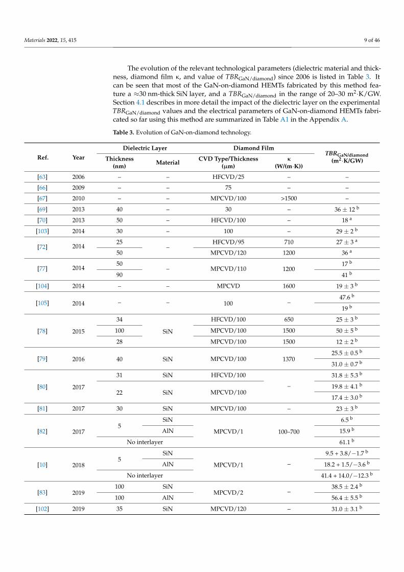
The evolution of the relevant technological parameters (dielectric material and thick-
ness, diamond film , and value of TBRGaN/diamond) since 2006 is listed in Table 3. It can be
seen that most of the GaN-on-diamond HEMTs fabricated by this method feature a ≈30
nm-thick SiN layer, and a TBRGaN/diamond in the range of 20–30 m2K/GW. Section 4.1 de-
scribes in more detail the impact of the dielectric layer on the experimental TBRGaN/diamond
Figure 4. (a) ID versus VD characteristics, (b) Transfer characteristics for different VD, and (c) Tem-perature rise versus PD for similar GaN-on-diamond and GaN-on-Si HEMTs (reprinted from [28];permission conveyed through CCBY 4.0: https://creativecommons.org/licenses/by/4.0/~ (accessedon 7 October 2021)).
In 2019, HEMTs fabricated on latest generation Element Six GaN-on-diamond wafers(with a 30 nm-thick dielectric layer) showed 2.95 K·mm/W Rth, 56 W/mm DC powercapability, and average/maximum channel temperature of 176/205 C [101]. Neverthe-less, these devices had high leakage currents which ultimately limited their breakdownvoltage, showing there is still some room for optimizing the fabrication process and maxi-mizing the performance of GaN-on-diamond HEMTs. In the same year, researchers fromRFHIC [102] reported the fabrication of 4” GaN-on-diamond wafers with a TBRGaN/diamondof 31.0 m2·K/GW and an uniformity of ±10%. The development of an inner slot viahole process allowed the opening of 10 µm-diameter holes in the diamond using a laserdrilling process—Figure 5. On-wafer pulsed load-pull tests performed at 2 GHz revealed18.1 W/mm PD for an encapsulated 10 × 200 µm gate HEMT.
Materials 2022, 15, x FOR PEER REVIEW 8 of 46
10 V fT/fmax were 10.2/31.4 GHz and 7/18.2 GHz, respectively. The GaN-on-diamond HEMT
had an almost constant small signal gain for VD between 10 and 40 V. Finally, the increase
rate of the gate current with VD was 3.3 times smaller for GaN-on-diamond devices. Figure
4a–c show some of the devices’ electrical characteristics.
(a)
(b)
(c)
Figure 4. (a) ID versus VD characteristics, (b) Transfer characteristics for different VD, and (c) Tem-
perature rise versus PD for similar GaN-on-diamond and GaN-on-Si HEMTs (reprinted from [28];
permission conveyed through CCBY 4.0).
In 2019, HEMTs fabricated on latest generation Element Six GaN-on-diamond wafers
(with a 30 nm-thick dielectric layer) showed 2.95 Kmm/W Rth, 56 W/mm DC power capa-
bility, and average/maximum channel temperature of 176/205 °C [101]. Nevertheless,
these devices had high leakage currents which ultimately limited their breakdown volt-
age, showing there is still some room for optimizing the fabrication process and maxim-
izing the performance of GaN-on-diamond HEMTs. In the same year, researchers from
RFHIC [102] reported the fabrication of 4″ GaN-on-diamond wafers with a TBRGaN/diamond
of 31.0 m2K/GW and an uniformity of ±10%. The development of an inner slot via hole
process allowed the opening of 10 µm-diameter holes in the diamond using a laser drilling
process—Figure 5. On-wafer pulsed load-pull tests performed at 2 GHz revealed 18.1
W/mm PD for an encapsulated 10 200 µm gate HEMT.
Figure 5. Inner slot via hole shape on source pad (© 2019 IEEE. Reprinted, with permission, from
W. S. Lee, et al., “A GaN/Diamond HEMTs with 23 W/mm for Next Generation High Power RF
Application,” in IEEE MTT-S International Microwave Symposium Digest, 2019, vol. 2019-June, pp.
1395–1398 [102]).
The evolution of the relevant technological parameters (dielectric material and thick-
ness, diamond film , and value of TBRGaN/diamond) since 2006 is listed in Table 3. It can be
seen that most of the GaN-on-diamond HEMTs fabricated by this method feature a ≈30
nm-thick SiN layer, and a TBRGaN/diamond in the range of 20–30 m2K/GW. Section 4.1 de-
scribes in more detail the impact of the dielectric layer on the experimental TBRGaN/diamond
Figure 5. Inner slot via hole shape on source pad (© 2019 IEEE. Reprinted, with permission, fromW. S. Lee, et al., “A GaN/Diamond HEMTs with 23 W/mm for Next Generation High Power RFApplication,” in IEEE MTT-S International Microwave Symposium Digest, 2019, vol. 2019-June,pp. 1395–1398 [102]).
Materials 2022, 15, 415 9 of 46
The evolution of the relevant technological parameters (dielectric material and thick-ness, diamond film κ, and value of TBRGaN/diamond) since 2006 is listed in Table 3. Itcan be seen that most of the GaN-on-diamond HEMTs fabricated by this method fea-ture a ≈30 nm-thick SiN layer, and a TBRGaN/diamond in the range of 20–30 m2·K/GW.Section 4.1 describes in more detail the impact of the dielectric layer on the experimentalTBRGaN/diamond values and the electrical parameters of GaN-on-diamond HEMTs fabri-cated so far using this method are summarized in Table A1 in the Appendix A.
Table 3. Evolution of GaN-on-diamond technology.
Ref. YearDielectric Layer Diamond Film
TBRGaN/diamond(m2·K/GW)Thickness
(nm) Material CVD Type/Thickness(µm)
κ
(W/(m·K))
[63] 2006 – – HFCVD/25 – –
[66] 2009 – – 75 – –
[67] 2010 – – MPCVD/100 >1500 –
[69] 2013 40 – 30 – 36 ± 12 b
[70] 2013 50 – HFCVD/100 – 18 a
[103] 2014 30 – 100 – 29 ± 2 b
[72] 201425
–HFCVD/95 710 27 ± 3 a
50 MPCVD/120 1200 36 a
[77] 201450
– MPCVD/110 120017 b
90 41 b
[104] 2014 – – MPCVD 1600 19 ± 3 b
[105] 2014 – – 100 –47.6 b
19 b
[78] 2015
34
SiN
HFCVD/100 650 25 ± 3 b
100 MPCVD/100 1500 50 ± 5 b
28 MPCVD/100 1500 12 ± 2 b
[79] 2016 40 SiN MPCVD/100 137025.5 ± 0.5 b
31.0 ± 0.7 b
[80] 2017
31 SiN HFCVD/100
–
31.8 ± 5.3 b
22 SiN MPCVD/10019.8 ± 4.1 b
17.4 ± 3.0 b
[81] 2017 30 SiN MPCVD/100 – 23 ± 3 b
[82] 20175
SiN
MPCVD/1 100–700
6.5 b
AlN 15.9 b
No interlayer 61.1 b
[10] 20185
SiN
MPCVD/1 –
9.5 + 3.8/−1.7 b
AlN 18.2 + 1.5/−3.6 b
No interlayer 41.4 + 14.0/−12.3 b
[83] 2019100 SiN
MPCVD/2 –38.5 ± 2.4 b
100 AlN 56.4 ± 5.5 b
[102] 2019 35 SiN MPCVD/120 – 31.0 ± 3.1 b
Materials 2022, 15, 415 10 of 46
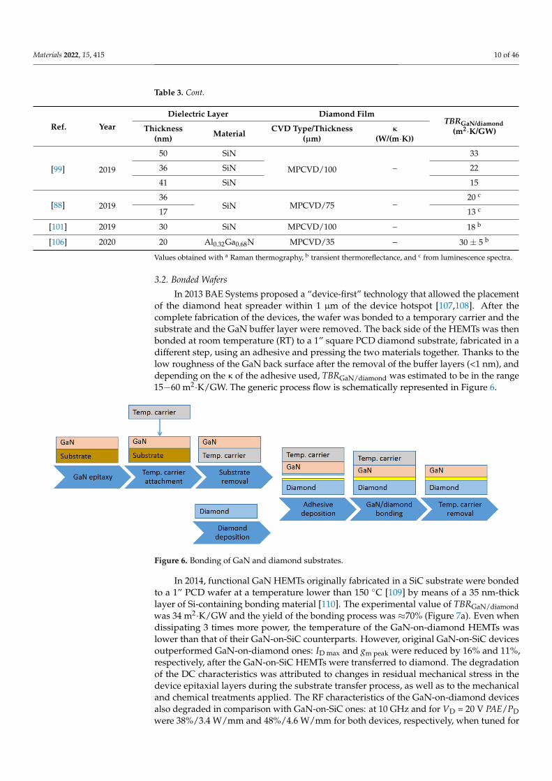
Table 3. Cont.
Ref. YearDielectric Layer Diamond Film
TBRGaN/diamond(m2·K/GW)Thickness
(nm) Material CVD Type/Thickness(µm)
κ
(W/(m·K))
[99] 2019
50 SiN
MPCVD/100 –
33
36 SiN 22
41 SiN 15
[88] 201936
SiN MPCVD/75 –20 c
17 13 c
[101] 2019 30 SiN MPCVD/100 – 18 b
[106] 2020 20 Al0.32Ga0.68N MPCVD/35 – 30 ± 5 b
Values obtained with a Raman thermography, b transient thermoreflectance, and c from luminescence spectra.
3.2. Bonded Wafers
In 2013 BAE Systems proposed a “device-first” technology that allowed the placementof the diamond heat spreader within 1 µm of the device hotspot [107,108]. After thecomplete fabrication of the devices, the wafer was bonded to a temporary carrier and thesubstrate and the GaN buffer layer were removed. The back side of the HEMTs was thenbonded at room temperature (RT) to a 1” square PCD diamond substrate, fabricated in adifferent step, using an adhesive and pressing the two materials together. Thanks to thelow roughness of the GaN back surface after the removal of the buffer layers (<1 nm), anddepending on the κ of the adhesive used, TBRGaN/diamond was estimated to be in the range15−60 m2·K/GW. The generic process flow is schematically represented in Figure 6.
Materials 2022, 15, x FOR PEER REVIEW 10 of 46
3.2. Bonded Wafers
In 2013 BAE Systems proposed a “device-first” technology that allowed the place-
ment of the diamond heat spreader within 1 µm of the device hotspot [107,108]. After the
complete fabrication of the devices, the wafer was bonded to a temporary carrier and the
substrate and the GaN buffer layer were removed. The back side of the HEMTs was then
bonded at room temperature (RT) to a 1″ square PCD diamond substrate, fabricated in a
different step, using an adhesive and pressing the two materials together. Thanks to the
low roughness of the GaN back surface after the removal of the buffer layers (<1 nm), and
depending on the of the adhesive used, TBRGaN/diamond was estimated to be in the range
15−60 m2K/GW. The generic process flow is schematically represented in Figure 6.
Figure 6. Bonding of GaN and diamond substrates.
In 2014, functional GaN HEMTs originally fabricated in a SiC substrate were bonded
to a 1″ PCD wafer at a temperature lower than 150 °C [109] by means of a 35 nm-thick
layer of Si-containing bonding material [110]. The experimental value of TBRGaN/diamond was
34 m2K/GW and the yield of the bonding process was 70% (Figure 7a). Even when dis-
sipating 3 times more power, the temperature of the GaN-on-diamond HEMTs was lower
than that of their GaN-on-SiC counterparts. However, original GaN-on-SiC devices out-
performed GaN-on-diamond ones: ID max and gm peak were reduced by 16% and 11%, respec-
tively, after the GaN-on-SiC HEMTs were transferred to diamond. The degradation of the
DC characteristics was attributed to changes in residual mechanical stress in the device
epitaxial layers during the substrate transfer process, as well as to the mechanical and
chemical treatments applied. The RF characteristics of the GaN-on-diamond devices also
degraded in comparison with GaN-on-SiC ones: at 10 GHz and for VD = 20 V PAE/PD were
38%/3.4 W/mm and 48%/4.6 W/mm for both devices, respectively, when tuned for maxi-
mum power, and 42%/3.0 W/mm and 57%/4.1 W/mm (when tuned for efficiency). Accord-
ing to the authors, this was primarily due to the omission of air-bridge structures in the
GaN-on-diamond devices with the unconnected device channels acting as RF parasitics
during power measurements.
Upon solving these issues, the PAE of 12 50 µm GaN/diamond HEMTs increased
to 51% and PD to 11.0 W/mm at 10 GHz. For the same VD, the PD of 4 50 µm GaN-on-SiC
HEMTs was only 9.2 W/mm, showing a 3.5 times areal power increase with GaN-on-dia-
mond HEMTs (Figure 7b) [111]. Even under these conditions, the temperature at the cen-
ter gates was slightly lower for the GaN-on-diamond HEMT than for the GaN-on-SiC
HEMT (195 against 202 °C, respectively). The main challenge of this process was identified
as the ability to achieve large area bonding with very low TBRGaN/diamond [110].
Figure 6. Bonding of GaN and diamond substrates.
In 2014, functional GaN HEMTs originally fabricated in a SiC substrate were bondedto a 1” PCD wafer at a temperature lower than 150 C [109] by means of a 35 nm-thicklayer of Si-containing bonding material [110]. The experimental value of TBRGaN/diamondwas 34 m2·K/GW and the yield of the bonding process was ≈70% (Figure 7a). Even whendissipating 3 times more power, the temperature of the GaN-on-diamond HEMTs waslower than that of their GaN-on-SiC counterparts. However, original GaN-on-SiC devicesoutperformed GaN-on-diamond ones: ID max and gm peak were reduced by 16% and 11%,respectively, after the GaN-on-SiC HEMTs were transferred to diamond. The degradationof the DC characteristics was attributed to changes in residual mechanical stress in thedevice epitaxial layers during the substrate transfer process, as well as to the mechanicaland chemical treatments applied. The RF characteristics of the GaN-on-diamond devicesalso degraded in comparison with GaN-on-SiC ones: at 10 GHz and for VD = 20 V PAE/PDwere 38%/3.4 W/mm and 48%/4.6 W/mm for both devices, respectively, when tuned for

Materials 2022, 15, 415 11 of 46
maximum power, and 42%/3.0 W/mm and 57%/4.1 W/mm (when tuned for efficiency).According to the authors, this was primarily due to the omission of air-bridge structures inthe GaN-on-diamond devices with the unconnected device channels acting as RF parasiticsduring power measurements.
Materials 2022, 15, x FOR PEER REVIEW 11 of 46
(a) (b)
Figure 7. (a) GaN HEMTs bonded to a 1″ PCD substrate (© 2014 IEEE. Reprinted, with permission,
from K. K. Chu et al., “S2-T4: Low-temperature substrate bonding technology for high power GaN-
on-diamond”, Lester Eastman Conf. 2014 - High Perform. Devices, LEC 2014, pp. 1–4, 2014 [109]).
(b) Comparison of input-output power curves obtained at 10 GHz for GaN/diamond HEMT with 3
times larger gate periphery than GaN-on-SiC HEMT (© 2015 IEEE. Reprinted, with permission, from
K. K. Chu et al., “High-Performance GaN-on-Diamond HEMTs Fabricated by Low-Temperature
Device Transfer Process,” 2015 IEEE Compd. Semicond. Integr. Circuit Symp. CSICS 2015, pp. 7–10,
2015 [111]).
In 2017, Liu and co-workers [112] bonded HEMT devices previously fabricated on
SiC substrates to a 3″ commercial PCD wafer at a temperature of 180 °C and obtained a
functional device yield over 80%. The experimental TBRGaN/diamond (51 m2K/GW) was still
relatively high and the DC current showed a 12−19% reduction due to self-heating; nev-
ertheless, the peak junction temperature of a 10 × 125 µm HEMT with compressed gate
pitch of 20 µm decreased from 241 to 191 °C after being transferred from the SiC to the
diamond substrate, suggesting a 20% reduction in Rth. CW load-pull measurements were
performed at 10 GHz and class AB operation on 4 × 125 µm/40 µm gate pitch HEMTs;
after being transferred to the PCD substrate, the same HEMT delivered 5.5 W/mm PD with
a PAE of 50.5% (against 4.8 W/mm and 50.9% when on the original SiC substrate).
The RT bonding of GaN and PCD films [113] or SCD substrates [114,115] has also
been achieved using surface-activated-bonding (SAB). SAB is a direct solid state covalent
bonding method that takes place in ultra-high vacuum conditions without obvious inter-
facial chemical reactions. The previous bombardment of the to-be-bonded surfaces with
an argon (Ar) ion beam induces the surface activation, generating surface dangling bonds
and making it possible to bond the surfaces at RT [116]. A few nm-thick Si interlayer is
typically sputtered on the diamond and GaN surfaces to improve the adhesion. The two
activated surfaces are then pressed together at RT and the dangling bonds form covalent
bonds at the interface. Transmission electron microscope (TEM) images of the resulting
uniform GaN/diamond interface can be seen in Figure 8a (from [113]). After the bonding
process the Si layer was 24 nm-thick. The bombardment of the diamond surface with Ar
ions induced its amorphization, creating an additional 3 nm-thick amorphous diamond
layer. The thickness of the Si layer was further reduced to 10 nm [115] (Figure 8b), creat-
ing an interface with a TBRGaN/diamond of 19 m2∙K/GW. In a slightly different experimental
setup, the surfaces activation was performed with a mixed beam of Si and Ar ions; the
thickness of both Si interlayer and amorphous diamond layer was reduced to 2 nm (Fig-
ure 8c) and the TBRGaN/diamond was as low as 11 m2∙K/GW. Despite these interesting pre-
liminary results, functional HEMTs on this GaN/diamond material stack are yet to be re-
ported.
Figure 7. (a) GaN HEMTs bonded to a 1” PCD substrate (© 2014 IEEE. Reprinted, with permission,from K. K. Chu et al., “S2-T4: Low-temperature substrate bonding technology for high power GaN-on-diamond”, Lester Eastman Conf. 2014—High Perform. Devices, LEC 2014, pp. 1–4, 2014 [109]).(b) Comparison of input-output power curves obtained at 10 GHz for GaN/diamond HEMT with3 times larger gate periphery than GaN-on-SiC HEMT (© 2015 IEEE. Reprinted, with permission,from K. K. Chu et al., “High-Performance GaN-on-Diamond HEMTs Fabricated by Low-TemperatureDevice Transfer Process,” 2015 IEEE Compd. Semicond. Integr. Circuit Symp. CSICS 2015, pp. 7–10,2015 [111]).
Upon solving these issues, the PAE of 12 × 50 µm GaN/diamond HEMTs increased to51% and PD to 11.0 W/mm at 10 GHz. For the same VD, the PD of 4 × 50 µm GaN-on-SiCHEMTs was only 9.2 W/mm, showing a 3.5 times areal power increase with GaN-on-diamond HEMTs (Figure 7b) [111]. Even under these conditions, the temperature at thecenter gates was slightly lower for the GaN-on-diamond HEMT than for the GaN-on-SiCHEMT (195 against 202 C, respectively). The main challenge of this process was identifiedas the ability to achieve large area bonding with very low TBRGaN/diamond [110].
In 2017, Liu and co-workers [112] bonded HEMT devices previously fabricated onSiC substrates to a 3” commercial PCD wafer at a temperature of 180 C and obtained afunctional device yield over 80%. The experimental TBRGaN/diamond (51 m2·K/GW) wasstill relatively high and the DC current showed a 12−19% reduction due to self-heating;nevertheless, the peak junction temperature of a 10 × 125 µm HEMT with compressed gatepitch of 20 µm decreased from 241 to 191 C after being transferred from the SiC to thediamond substrate, suggesting a 20% reduction in Rth. CW load-pull measurements wereperformed at 10 GHz and class AB operation on 4 × 125 µm/40 µm gate pitch HEMTs;after being transferred to the PCD substrate, the same HEMT delivered 5.5 W/mm PD witha PAE of 50.5% (against 4.8 W/mm and 50.9% when on the original SiC substrate).
The RT bonding of GaN and PCD films [113] or SCD substrates [114,115] has alsobeen achieved using surface-activated-bonding (SAB). SAB is a direct solid state covalentbonding method that takes place in ultra-high vacuum conditions without obvious interfa-cial chemical reactions. The previous bombardment of the to-be-bonded surfaces with anargon (Ar) ion beam induces the surface activation, generating surface dangling bonds andmaking it possible to bond the surfaces at RT [116]. A few nm-thick Si interlayer is typicallysputtered on the diamond and GaN surfaces to improve the adhesion. The two activated
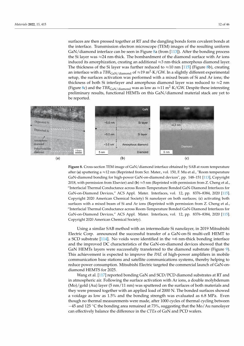
Materials 2022, 15, 415 12 of 46
surfaces are then pressed together at RT and the dangling bonds form covalent bonds atthe interface. Transmission electron microscope (TEM) images of the resulting uniformGaN/diamond interface can be seen in Figure 8a (from [113]). After the bonding processthe Si layer was ≈24 nm-thick. The bombardment of the diamond surface with Ar ionsinduced its amorphization, creating an additional ≈3 nm-thick amorphous diamond layer.The thickness of the Si layer was further reduced to ≈10 nm [115] (Figure 8b), creatingan interface with a TBRGaN/diamond of ≈19 m2·K/GW. In a slightly different experimentalsetup, the surfaces activation was performed with a mixed beam of Si and Ar ions; thethickness of both Si interlayer and amorphous diamond layer was reduced to ≈2 nm(Figure 8c) and the TBRGaN/diamond was as low as ≈11 m2·K/GW. Despite these interestingpreliminary results, functional HEMTs on this GaN/diamond material stack are yet tobe reported.
Materials 2022, 15, x FOR PEER REVIEW 12 of 46
(a)
(b)
(c)
Figure 8. Cross-section TEM image of GaN/diamond interface obtained by SAB at room tempera-
ture after (a) sputtering a 12 nm (Reprinted from Scr. Mater., vol. 150, F. Mu et al., "Room temper-
ature GaN-diamond bonding for high-power GaN-on-diamond devices", pp. 148-151 [113], Copy-
right 2018, with permission from Elsevier) and (b) 5 nm (Reprinted with permission from Z. Cheng
et al., “Interfacial Thermal Conductance across Room-Temperature Bonded GaN-Diamond Inter-
faces for GaN-on-Diamond Devices,” ACS Appl. Mater. Interfaces, vol. 12, pp. 8376–8384, 2020
[115]. Copyright 2020 American Chemical Society) Si nanolayer on both surfaces; (c) activating both
surfaces with a mixed beam of Si and Ar ions (Reprinted with permission from Z. Cheng et al.,
“Interfacial Thermal Conductance across Room-Temperature Bonded GaN-Diamond Interfaces for
GaN-on-Diamond Devices,” ACS Appl. Mater. Interfaces, vol. 12, pp. 8376–8384, 2020 [115]. Copy-
right 2020 American Chemical Society).
Using a similar SAB method with an intermediate Si nanolayer, in 2019 Mitsubishi
Electric Corp. announced the successful transfer of a GaN-on-Si multi-cell HEMT to a SCD
substrate [114]. No voids were identified in the 6 nm-thick bonding interface and the
improved DC characteristics of the GaN-on-diamond devices showed that the GaN
HEMTs layers were successfully transferred to the diamond substrate (Figure 9). This
achievement is expected to improve the PAE of high-power amplifiers in mobile commu-
nication base stations and satellite communications systems, thereby helping to reduce
power consumption. Mitsubishi Electric targeted the commercial launch of GaN-on-dia-
mond HEMTS for 2025.
(a)
(b)
Figure 9. (a) Cross-section TEM image of GaN/diamond interface obtained by SAB. (b) ID-VD char-
acteristics of GaN-on-Si (dashed lines) and GaN/diamond (solid lines) HEMTs (reprinted from [114],
Copyright 2019 The Japan Society of Applied Physics).
Wang et al. [117] reported bonding GaN and SCD/PCD diamond substrates at RT
and in atmospheric air. Following the surface activation with Ar ions, a double
Figure 8. Cross-section TEM image of GaN/diamond interface obtained by SAB at room temperatureafter (a) sputtering a ≈12 nm (Reprinted from Scr. Mater., vol. 150, F. Mu et al., "Room temperatureGaN-diamond bonding for high-power GaN-on-diamond devices", pp. 148–151 [113], Copyright2018, with permission from Elsevier) and (b) ≈5 nm (Reprinted with permission from Z. Cheng et al.,“Interfacial Thermal Conductance across Room-Temperature Bonded GaN-Diamond Interfaces forGaN-on-Diamond Devices,” ACS Appl. Mater. Interfaces, vol. 12, pp. 8376–8384, 2020 [115].Copyright 2020 American Chemical Society) Si nanolayer on both surfaces; (c) activating bothsurfaces with a mixed beam of Si and Ar ions (Reprinted with permission from Z. Cheng et al.,“Interfacial Thermal Conductance across Room-Temperature Bonded GaN-Diamond Interfaces forGaN-on-Diamond Devices,” ACS Appl. Mater. Interfaces, vol. 12, pp. 8376–8384, 2020 [115].Copyright 2020 American Chemical Society).
Using a similar SAB method with an intermediate Si nanolayer, in 2019 MitsubishiElectric Corp. announced the successful transfer of a GaN-on-Si multi-cell HEMT toa SCD substrate [114]. No voids were identified in the ≈6 nm-thick bonding interfaceand the improved DC characteristics of the GaN-on-diamond devices showed that theGaN HEMTs layers were successfully transferred to the diamond substrate (Figure 9).This achievement is expected to improve the PAE of high-power amplifiers in mobilecommunication base stations and satellite communications systems, thereby helping toreduce power consumption. Mitsubishi Electric targeted the commercial launch of GaN-on-diamond HEMTS for 2025.
Wang et al. [117] reported bonding GaN and SCD/PCD diamond substrates at RT andin atmospheric air. Following the surface activation with Ar ions, a double molybdenum(Mo)/gold (Au) layer (5 nm/11 nm) was sputtered on the surfaces of both materials andthey were pressed together with an applied load of 2000 N. The bonded surfaces showeda voidage as low as 1.5% and the bonding strength was evaluated as 6.8 MPa. Eventhough no thermal measurements were made, after 1000 cycles of thermal cycling between−45 and 125 C the bonding area remained at 73%, suggesting that the Mo/Au nanolayercan effectively balance the difference in the CTEs of GaN and PCD wafers.

Materials 2022, 15, 415 13 of 46
Materials 2022, 15, x FOR PEER REVIEW 12 of 46
(a)
(b)
(c)
Figure 8. Cross-section TEM image of GaN/diamond interface obtained by SAB at room tempera-
ture after (a) sputtering a 12 nm (Reprinted from Scr. Mater., vol. 150, F. Mu et al., "Room temper-
ature GaN-diamond bonding for high-power GaN-on-diamond devices", pp. 148-151 [113], Copy-
right 2018, with permission from Elsevier) and (b) 5 nm (Reprinted with permission from Z. Cheng
et al., “Interfacial Thermal Conductance across Room-Temperature Bonded GaN-Diamond Inter-
faces for GaN-on-Diamond Devices,” ACS Appl. Mater. Interfaces, vol. 12, pp. 8376–8384, 2020
[115]. Copyright 2020 American Chemical Society) Si nanolayer on both surfaces; (c) activating both
surfaces with a mixed beam of Si and Ar ions (Reprinted with permission from Z. Cheng et al.,
“Interfacial Thermal Conductance across Room-Temperature Bonded GaN-Diamond Interfaces for
GaN-on-Diamond Devices,” ACS Appl. Mater. Interfaces, vol. 12, pp. 8376–8384, 2020 [115]. Copy-
right 2020 American Chemical Society).
Using a similar SAB method with an intermediate Si nanolayer, in 2019 Mitsubishi
Electric Corp. announced the successful transfer of a GaN-on-Si multi-cell HEMT to a SCD
substrate [114]. No voids were identified in the 6 nm-thick bonding interface and the
improved DC characteristics of the GaN-on-diamond devices showed that the GaN
HEMTs layers were successfully transferred to the diamond substrate (Figure 9). This
achievement is expected to improve the PAE of high-power amplifiers in mobile commu-
nication base stations and satellite communications systems, thereby helping to reduce
power consumption. Mitsubishi Electric targeted the commercial launch of GaN-on-dia-
mond HEMTS for 2025.
(a)
(b)
Figure 9. (a) Cross-section TEM image of GaN/diamond interface obtained by SAB. (b) ID-VD char-
acteristics of GaN-on-Si (dashed lines) and GaN/diamond (solid lines) HEMTs (reprinted from [114],
Copyright 2019 The Japan Society of Applied Physics).
Wang et al. [117] reported bonding GaN and SCD/PCD diamond substrates at RT
and in atmospheric air. Following the surface activation with Ar ions, a double
Figure 9. (a) Cross-section TEM image of GaN/diamond interface obtained by SAB. (b) ID-VD char-acteristics of GaN-on-Si (dashed lines) and GaN/diamond (solid lines) HEMTs (reprinted from [114],Copyright 2019 The Japan Society of Applied Physics).
Minoura and his colleagues from Fujitsu Limited [118] bonded AlGaN/GaN andindium aluminum gallium nitride (InAlGaN)/GaN-on-SiC HEMTs to SCD substrates bya modified SAB method. A thin (<10 nm) titanium (Ti) layer was previously depositedon the surface of the SCD substrate to prevent the amorphization of the diamond surfaceduring the bombardment with the Ar ions. The TEM image of the SiC/diamond interfaceis shown in Figure 10a. Using this method, the TRB at the diamond/SiC interface was66 m2·K/GW and the Rth of the AlGaN/GaN HEMT bonded to the SCD substrate wasabout 1/3 compared to that without diamond. The PD of InAlGaN/GaN HEMTs measuredwith pulsed load-pull measurements (for VD = 50 V, a pulse width of 10 µs, and 10%duty cycle) increased from 14.8 to 19.8 W/mm with the bonding of the SCD heat spreaderstructure. With 1% duty cycle, the SCD-bonded HEMT showed a PD of 22.3 W/mm.Figure 10b,c show the variation of the normalized PD with the duty-cycle and the PD as afunction of VD, respectively.
Materials 2022, 15, x FOR PEER REVIEW 13 of 46
molybdenum (Mo)/gold (Au) layer (5 nm/11 nm) was sputtered on the surfaces of both
materials and they were pressed together with an applied load of 2000 N. The bonded
surfaces showed a voidage as low as 1.5% and the bonding strength was evaluated as 6.8
MPa. Even though no thermal measurements were made, after 1000 cycles of thermal cy-
cling between −45 and 125 °C the bonding area remained at 73%, suggesting that the
Mo/Au nanolayer can effectively balance the difference in the CTEs of GaN and PCD wa-
fers.
Minoura and his colleagues from Fujitsu Limited [118] bonded AlGaN/GaN and in-
dium aluminum gallium nitride (InAlGaN)/GaN-on-SiC HEMTs to SCD substrates by a
modified SAB method. A thin (<10 nm) titanium (Ti) layer was previously deposited on
the surface of the SCD substrate to prevent the amorphization of the diamond surface
during the bombardment with the Ar ions. The TEM image of the SiC/diamond interface
is shown in Figure 10a. Using this method, the TRB at the diamond/SiC interface was
66 m2K/GW and the Rth of the AlGaN/GaN HEMT bonded to the SCD substrate was about
1/3 compared to that without diamond. The PD of InAlGaN/GaN HEMTs measured with
pulsed load-pull measurements (for VD = 50 V, a pulse width of 10 µs, and 10% duty cycle)
increased from 14.8 to 19.8 W/mm with the bonding of the SCD heat spreader structure.
With 1% duty cycle, the SCD-bonded HEMT showed a PD of 22.3 W/mm. Figure 10b,c
show the variation of the normalized PD with the duty-cycle and the PD as a function of
VD, respectively.
(a)
(b)
(c)
Figure 10. (a) Cross-section TEM image of SiC/SCD interface obtained by SAB after protecting the
diamond surface with a Ti film. (b) Normalized PD vs. duty-cycle. (c) PD as a function of VD (re-
printed from [118], Copyright 2020 The Japan Society of Applied Physics).
SAB of GaN HEMTs and diamond was also achieved by sputtering a 450 nm-thick
AlN layer on both GaN AlN nucleation layer (after removal of the Si substrate) and dia-
mond surfaces, followed by surface activation with an Ar+-based plasma and by thermo-
compression at 160 °C [119]. The strain relief layers and the AlN nucleation layer pre-
vented the flow of heat from the top GaN layer into the diamond substrate; as a conse-
quence, the temperature of the HEMT on the diamond substrate was higher than that on
the Si substrate [120].
Figure 10. (a) Cross-section TEM image of SiC/SCD interface obtained by SAB after protectingthe diamond surface with a Ti film. (b) Normalized PD vs. duty-cycle. (c) PD as a function of VD
(reprinted from [118], Copyright 2020 The Japan Society of Applied Physics).

Materials 2022, 15, 415 14 of 46
SAB of GaN HEMTs and diamond was also achieved by sputtering a 450 nm-thick AlNlayer on both GaN AlN nucleation layer (after removal of the Si substrate) and diamondsurfaces, followed by surface activation with an Ar+-based plasma and by thermocom-pression at 160 C [119]. The strain relief layers and the AlN nucleation layer preventedthe flow of heat from the top GaN layer into the diamond substrate; as a consequence,the temperature of the HEMT on the diamond substrate was higher than that on the Sisubstrate [120].
Van der Waals (VdW) bonding, a process first employed for GaAs thin films [121],has also been used to bond GaN devices and SCD/PCD substrates at temperatures below300 C [122,123]. This technique guarantees a good thermal interface (TBRGaN/SCD wasestimated to be as low as 10 m2·K/GW [122]) without the observation of stress or degrada-tion. RF-devices operating at 3 GHz with improved efficiency (PAE of 54.2% against 50.6%for GaN-on-Si HEMTs)) were demonstrated with SCD; on the other hand, the bondingobtained with PCD was not reproducible [123].
The evolution of the relevant technological parameters of GaN/diamond bondedwafers is summarized in Table 4. The TBR of the GaN/diamond interface obtained after theSAB and VdW bonding of GaN and SCD can be as low as 11 and 10 m2·K/GW, respectively.Functional HEMTs have been fabricated on GaN bonded to SCD and PCD substrates. Theelectrical parameters of HEMTs fabricated using this method are summarized in Table A2in the Appendix A.
Table 4. Evolution of GaN/diamond bonded wafers technology.
Ref. YearAdhesive Layer
Diamond Substrate Bonding Process TBR(m2·K/GW)Thickness
(nm) Material
[107] 2013 – Si-based 1” × 1” PCD Pressing at RT –
[109] 2014 35 Si-based 1” PCD wafer Pressing <150 C 34 ± 5 a
[112] 2017 30–40 – 3” PCD wafer Pressing 180 C 51 b
[113] 2018 24 Si 900 µm-thick PCD on Si SAB RT –
[114] 2019 6 Si 1 cm × 1 cm SCD SAB RT –
[115] 202010
Si SCD SAB RT19 a
2 11 a
[117] 2020 2 × 5/11 Mo/Au PCD/SCD SAB RT –
[118] 2020 10 Ti/Si 5 mm × 5 mm SCD SAB RT 66 c
[119] 2020 2 × 450 AlN – SAB 160 C –
[122] 2018 No interlayer SCD VdW bonding 10 d
Values obtained with a transient thermoreflectance, b on-wafer IR imaging system, c periodic heating method, andd estimated from simulations.
3.3. GaN Epitaxy
The last technique to fabricate GaN-on-diamond wafers involves the epitaxial depo-sition of GaN on the diamond substrate. However, the deposition of epitaxial GaN filmson SCD on PCD substrates is inherently difficult, however, due to a series of factors [124].First, the large lattice mismatch between the two materials (around 13%) can generatedefects and lead to poor crystal quality. It should be mentioned, however, that the latticemismatch between GaN and sapphire is even higher (16% [36]), so this fact alone is notdeterminant. In addition to the lattice mismatch, the large difference in the CTEs of dia-mond and GaN (0.8 × 10⁻⁶ K−1 against 5.6 × 10⁻⁶ K−1, respectively, whereas the CTE ofsapphire is 7.5 × 10⁻⁶ K−1) can lead to a highly stressed interface that will further impactthe dislocating density and lead to the possible cracking of the GaN layer. Finally, in the

Materials 2022, 15, 415 15 of 46
case of PCD substrates, the absence of a fixed epitaxial relationship between the GaN andthe diamond increases the difficulty of nucleating a continuous epitaxial GaN layer.
Nevertheless, different groups have tried to grow GaN on diamond substrates. Firstreports date from 2003, when Hageman and co-workers [125] reported the growth of2.5 µm-thick polycrystalline and hexagonal GaN films on (100) natural SCD by a dual step.A thin GaN layer was initially grown by MOCVD on a 10 nm-thick AlN nucleation layerpreviously deposited on the SCD substrate. Subsequently, the MOCVD pre-grown sampleswere used as templates for the growth of thick GaN layers using HVPE. The group laterreported the growth of 0.07−1.55 µm-thick GaN films on (001) SCD HPHT substrates byMOCVD [126].
Using a different method, Dussaigne et al. [127] reported the growth of 1 µm-thickGaN epilayers on 100 nm-thick AlN layers previously deposited on (111) HPHT SCDsubstrates by ammonia (NH3)-source MBE. The films displayed a low RMS roughness of1.3 nm and some cracks due to the difference in the CTEs of diamond and GaN; crackswere not formed for GaN epilayers with thicknesses lower than 250 nm. In a subsequentwork [128], 200 nm-thick AlN and GaN strain engineered interlayers were deposited on topof the AlN buffer layer. An 800 nm-thick GaN layer with 8 × 109 cm−2 dislocation densitywas then grown, followed by 24 nm of AlGaN (with an Al content of 28%). A 2DEG formedat the interface, allowing the fabrication of HEMT structures with ID max = 730 mA/mm,gm peak = 137.5 mS/mm, and f T/f max = 21/42.5 GHz [129].
Following a different approach, researchers from NTT Corporation reported the for-mation of a 2DEG in an AlGaN/GaN heterostructure formed on a 600 nm-thick GaNlayer epitaxially grown on a type Ib (111) SCD substrate by metalorganic vapor-phaseepitaxy (MOVPE) [130] with similar dislocation density (8.4 × 109 cm−2 [131]). TheAlN/GaN stress-relief layers were deposited on a 180 nm-thick single crystal AlN bufferlayer deposited on the diamond substrate and the fabricated AlGaN/GaN HEMTs showedID max = 220 mA/mm and f T/f max = 3/7 GHz. The Rth of GaN-on-diamond HEMTs was4.1 K·mm/W, against 7.9 K·mm/W for similar GaN-on-SiC structures. By depositingthe GaN layer on type IIa (111) SCD diamond substrates, Rth was further decreased to1.5 K·mm/W and RF operation with 2.13 W/mm output power density and 46% PAE wasachieved [131]. The impact of the misorientation angle of the (111) SCD surface on thesurface morphology of the HEMT structures was also studied by the authors [132,133].
Other groups reported growth of GaN on PCD and NCD substrates. The benefits of thisapproach would be twofold: large-area PCD substrates are available from a few vendors,and the price/area is significantly lower than the one of HPHT SCD substrates. However,only polycrystalline GaN films could be initially deposited. Van Dreumel et al. [134] de-posited polycrystalline GaN layers by MOCVD on the surface of nanocrystalline diamond(NCD) films previously deposited by HFCVD on Si substrates, while Zhang et al. [135]deposited fine grained polycrystalline GaN films by MOCVD on the nucleation surfacesof freestanding PCD films prepared by glow discharge. The final goal in this last workwas the fabrication of diamond/GaN surface acoustic wave devices, though, and not thefabrication of AlGaN/GaN HEMTs.
More recently, Webster et al. [124] reported the ability to grow epitaxially-orientedGaN films on thick PCD substrates by MOVPE. An AlN layer was previously depositedat 650 C as nucleation layer for the subsequent growth of a 1.5 µm-thick GaN layer athigher temperature, on top of which the AlGaN/GaN HEMTs structures were fabricated.SiN stripes were then deposited on the AlGaN/GaN stack and the unmasked regions wereetched down to the PCD substrate. After an epitaxial layer overgrowth (ELO) re-growthcycle the dislocation density of the GaN layer was reduced by two orders of magnitude(from ≈7 × 10⁻⁹ to <108 cm−2). With this technique the team was able to grow GaN witha significant degree of epitaxial orientation on an area up to 15 µm2 on a PCD substrate—Figure 11. The appearance of some cracks on the GaN surface was attributed to the largedifference between CTEs of diamond and GaN.

Materials 2022, 15, 415 16 of 46Materials 2022, 15, x FOR PEER REVIEW 16 of 46
(a)
(b)
Figure 11. (a) SEM image of masked and ELO growth of GaN. (b) TEM image showing original and
ELO growth of GaN; arrows indicate boundary between original (right of boundary) and ELO (left
of boundary) growth (reprinted from [124]; permission conveyed through CCBY 3.0).
Later the team proposed a different approach [136]; the (111) Si substrate from com-
mercial diamond-on-Si substrates was etched, exposing the back surface of the PCD sub-
strate that was shown to feature a thin SixC layer formed during the deposition of the PCD
on the Si substrate. According to the authors, this SixC layer provides sufficient crystallo-
graphic information for the epitaxial growth process to occur. Following the etching of the
Si substrate, the PCD films exhibited some curvature, due to the thermal stress caused by
the high diamond deposition temperatures and the difference in the CTEs of both materi-
als. AlN or Al0.75Ga0.25N nucleation layers were grown on the SiC layer and GaN was de-
posited by MOVPE. Interestingly, the growth on the nucleation surface of the curved di-
amond substrate was shown to effectively remove the surface defects induced by the non-
single crystalline nature of the SixC layer and to reduce the tensile stress induced by the
CTE mismatch, allowing the growth of crack-free GaN epitaxial layers up to 1.1 µm thick.
As the thickness of the GaN layers increased, the dislocation density was significantly
reduced (Figure 12). Upon optimization of the whole process, the tensile strain inherent
in GaN epitaxial layers grown on PCD can be further reduced, and thicker crack-free GaN
layers can be deposited. Since the increase of the thickness of the GaN epitaxial layer is
usually accompanied by reductions in the dislocation density, the use of thicker GaN lay-
ers is expected to have a positive impact on the performance of HEMT devices fabricated
using PCD substrates.
(a)
(b)
Figure 12. SEM images showing improvement in surface morphology of thicker GaN films. (a)
300 nm- and (b) 1.1 µm-thick GaN films (republished with permission of IOP Publishing, from
“Growth of GaN epitaxial films on polycrystalline diamond by metal-organic vapor phase epitaxy,"
Q. Jiang, D. W. E. Allsopp, and C. R. Bowen, vol. 50, no. 16, 2017 [136]; permission conveyed through
Copyright Clearance Center, Inc.).
Figure 11. (a) SEM image of masked and ELO growth of GaN. (b) TEM image showing originaland ELO growth of GaN; arrows indicate boundary between original (right of boundary) andELO (left of boundary) growth (reprinted from [124]; permission conveyed through CCBY 3.0:https://creativecommons.org/licenses/by/3.0/ (accessed on 7 October 2021)).
Later the team proposed a different approach [136]; the (111) Si substrate from commer-cial diamond-on-Si substrates was etched, exposing the back surface of the PCD substratethat was shown to feature a thin SixC layer formed during the deposition of the PCD on theSi substrate. According to the authors, this SixC layer provides sufficient crystallographicinformation for the epitaxial growth process to occur. Following the etching of the Si sub-strate, the PCD films exhibited some curvature, due to the thermal stress caused by the highdiamond deposition temperatures and the difference in the CTEs of both materials. AlNor Al0.75Ga0.25N nucleation layers were grown on the SiC layer and GaN was depositedby MOVPE. Interestingly, the growth on the nucleation surface of the curved diamondsubstrate was shown to effectively remove the surface defects induced by the non-singlecrystalline nature of the SixC layer and to reduce the tensile stress induced by the CTEmismatch, allowing the growth of crack-free GaN epitaxial layers up to 1.1 µm thick. Asthe thickness of the GaN layers increased, the dislocation density was significantly reduced(Figure 12). Upon optimization of the whole process, the tensile strain inherent in GaNepitaxial layers grown on PCD can be further reduced, and thicker crack-free GaN layerscan be deposited. Since the increase of the thickness of the GaN epitaxial layer is usuallyaccompanied by reductions in the dislocation density, the use of thicker GaN layers isexpected to have a positive impact on the performance of HEMT devices fabricated usingPCD substrates.
In 2020 Ahmed et al. [137] also proposed the use of ELO to integrate GaN and PCDdiamond; the processing steps are represented in Figure 13. Unlike the procedure describedin [124], where the GaN was deposited directly on the PCD by MOVPE, the AlGaN/GaNstack capped with a thin SiN layer was initially deposited on a Si substrate by MOCVD.500 nm-thick stripes of PCD were then selectively deposited on the SiN by HFCVD fol-lowing the procedure described in [138]; the exposed SiN was then removed by reactiveion etching (RIE) and the GaN surface was made accessible (step 4 in Figure 13a). Thewafer was then returned to the MOCVD reactor for the ELO of GaN (step 5 in Figure 13a).Figure 13b,c show the SEM images of the final structure before and after the regrowth step,respectively. A continuous GaN film formed across 5 µm-wide diamond stripes separatedby 5 µm-wide GaN windows oriented along the
⟨1100
⟩direction of the initial GaN. The
dislocation density on ELO GaN (≈107 cm−2) was ≈2 orders of magnitude lower thanon initial GaN (≈109 cm−2). Although coalescence was achieved, several voids, pinholes,and cracks were visible in some locations along the coalescence regions; the cracks weregenerated due to the release of thermal stress energy upon cooling of the wafer following

Materials 2022, 15, 415 17 of 46
GaN growth. In order to obtain the final GaN/PCD final devices, some steps are furtherrequired: MOCVD growth of the HEMT structure, removal of Si substrate and exposure ofdiamond strip.es surface, thick diamond CVD, and transistor fabrication.
Materials 2022, 15, x FOR PEER REVIEW 16 of 46
(a)
(b)
Figure 11. (a) SEM image of masked and ELO growth of GaN. (b) TEM image showing original and
ELO growth of GaN; arrows indicate boundary between original (right of boundary) and ELO (left
of boundary) growth (reprinted from [124]; permission conveyed through CCBY 3.0).
Later the team proposed a different approach [136]; the (111) Si substrate from com-
mercial diamond-on-Si substrates was etched, exposing the back surface of the PCD sub-
strate that was shown to feature a thin SixC layer formed during the deposition of the PCD
on the Si substrate. According to the authors, this SixC layer provides sufficient crystallo-
graphic information for the epitaxial growth process to occur. Following the etching of the
Si substrate, the PCD films exhibited some curvature, due to the thermal stress caused by
the high diamond deposition temperatures and the difference in the CTEs of both materi-
als. AlN or Al0.75Ga0.25N nucleation layers were grown on the SiC layer and GaN was de-
posited by MOVPE. Interestingly, the growth on the nucleation surface of the curved di-
amond substrate was shown to effectively remove the surface defects induced by the non-
single crystalline nature of the SixC layer and to reduce the tensile stress induced by the
CTE mismatch, allowing the growth of crack-free GaN epitaxial layers up to 1.1 µm thick.
As the thickness of the GaN layers increased, the dislocation density was significantly
reduced (Figure 12). Upon optimization of the whole process, the tensile strain inherent
in GaN epitaxial layers grown on PCD can be further reduced, and thicker crack-free GaN
layers can be deposited. Since the increase of the thickness of the GaN epitaxial layer is
usually accompanied by reductions in the dislocation density, the use of thicker GaN lay-
ers is expected to have a positive impact on the performance of HEMT devices fabricated
using PCD substrates.
(a)
(b)
Figure 12. SEM images showing improvement in surface morphology of thicker GaN films. (a)
300 nm- and (b) 1.1 µm-thick GaN films (republished with permission of IOP Publishing, from
“Growth of GaN epitaxial films on polycrystalline diamond by metal-organic vapor phase epitaxy,"
Q. Jiang, D. W. E. Allsopp, and C. R. Bowen, vol. 50, no. 16, 2017 [136]; permission conveyed through
Copyright Clearance Center, Inc.).
Figure 12. SEM images showing improvement in surface morphology of thicker GaN films.(a) 300 nm- and (b) 1.1 µm-thick GaN films (republished with permission of IOP Publishing, from“Growth of GaN epitaxial films on polycrystalline diamond by metal-organic vapor phase epitaxy,"Q. Jiang, D. W. E. Allsopp, and C. R. Bowen, vol. 50, no. 16, 2017 [136]; permission conveyed throughCopyright Clearance Center, Inc.).
Materials 2022, 15, x FOR PEER REVIEW 17 of 46
In 2020 Ahmed et al. [137] also proposed the use of ELO to integrate GaN and PCD
diamond; the processing steps are represented in Figure 13. Unlike the procedure de-
scribed in [124], where the GaN was deposited directly on the PCD by MOVPE, the Al-
GaN/GaN stack capped with a thin SiN layer was initially deposited on a Si substrate by
MOCVD. 500 nm-thick stripes of PCD were then selectively deposited on the SiN by
HFCVD following the procedure described in [138]; the exposed SiN was then removed
by reactive ion etching (RIE) and the GaN surface was made accessible (step 4 in Figure
13a). The wafer was then returned to the MOCVD reactor for the ELO of GaN (step 5 in
Figure 13a). Figure 13b,c show the SEM images of the final structure before and after the
regrowth step, respectively. A continuous GaN film formed across 5 µm-wide diamond
stripes separated by 5 µm-wide GaN windows oriented along the < 1100 > direction of
the initial GaN. The dislocation density on ELO GaN (107 cm−2) was 2 orders of magni-
tude lower than on initial GaN (109 cm−2). Although coalescence was achieved, several
voids, pinholes, and cracks were visible in some locations along the coalescence regions;
the cracks were generated due to the release of thermal stress energy upon cooling of the
wafer following GaN growth. In order to obtain the final GaN/PCD final devices, some
steps are further required: MOCVD growth of the HEMT structure, removal of Si sub-
strate and exposure of diamond strip.es surface, thick diamond CVD, and transistor fab-
rication.
(a)
(b)
(c)
Figure 13. (a) Processing steps of epitaxial growth of GaN on PCD. SEM images of (b) selectively
deposited PCD stripes (after step 4) and (c) same features after ELO of GaN (after step 5) (reprinted
with permission from R. Ahmed et al., “Integration of GaN and Diamond Using Epitaxial Lateral
Overgrowth,” ACS Appl. Mater. Interfaces, vol. 12, no. 35, pp. 39397–39404, 2020 [137]. Copyright
2020 American Chemical Society).
The experimental results obtained so far are compiled in Table 5. As a summary one
can say that research efforts focused on both SCD and PCD substrates, however functional
HEMTs have only been fabricated on SCD substrates. Despite promising results, the in-
terest on these substrates faded away and more recent research focused on the ELO of
GaN films on PCD substrates with reduced dislocation density. The electrical parameters
of HEMTs fabricated on GaN films deposited on SCD substrates are summarized in Table
A3 in the Appendix A.
Figure 13. (a) Processing steps of epitaxial growth of GaN on PCD. SEM images of (b) selectivelydeposited PCD stripes (after step 4) and (c) same features after ELO of GaN (after step 5) (reprintedwith permission from R. Ahmed et al., “Integration of GaN and Diamond Using Epitaxial LateralOvergrowth,” ACS Appl. Mater. Interfaces, vol. 12, no. 35, pp. 39397–39404, 2020 [137]. Copyright2020 American Chemical Society).

Materials 2022, 15, 415 18 of 46
The experimental results obtained so far are compiled in Table 5. As a summary onecan say that research efforts focused on both SCD and PCD substrates, however functionalHEMTs have only been fabricated on SCD substrates. Despite promising results, the intereston these substrates faded away and more recent research focused on the ELO of GaN filmson PCD substrates with reduced dislocation density. The electrical parameters of HEMTsfabricated on GaN films deposited on SCD substrates are summarized in Table A3 in theAppendix A.
Table 5. GaN epitaxy on diamond substrates.
Ref. Year DiamondGaN
Deposition Method Type Thickness(µm)
Disl. Dens.(cm−2)
[125] 2003 Natural SCD MOCVD on 10 nmAlN layer + HVPE Polycryst. 2.5 –
[126] 2011 (011) SCD MOCVD on AlN layer Polycryst. 0.07–1.55 –
[127] 2009 (111) SCD NH3-MBE on 100 nm AlN layer Epilayer 1 –
[128,129] 2010 (111) SCD NH3-MBE on 200 nm AlN + GaNstrain engineered interlayers Epilayer 0.8 8.4 × 10⁹
[130] 2011 Ib (111) SCD MOVPE on 180 nm single crystalAlN + 400 nm AlN/GaN Epilayer 0.6 –
[131] 2012 IIa (111) SCD MOVPE on 180 nm single crystalAlN + 500 nm AlN/GaN Epilayer 0.6 8.4 × 10⁹
[132,133] 2012 Ib (111) SCD MOVPE on 180 nm single crystalAlN + 500 nm AlN/GaN Epilayer 0.6 –
[134] 2009 NCD MOCVD on 50 nm GaN Polycryst. 3 –
[135] 2010 PCD MOCVD Polycryst. 0.8 –
[124] 2015 PCDMOVPE on 70 nm AlN
layer + deposition of SiNstripes/etching + ELO
15 µm wide epilayer 1.5 ≈7 × 10⁻⁹ → <108
[136] 2017 PCD thin films Etching of Si substrate + MOVPE on10–40 nm AlN/Al0.75Ga0.25N layers Epilayer 0.2–1.1 –
[137] 2020 Post-deposited PCDMOCVD of SiN-capped
AlGaN/GaN stack on Si + selectivedeposition of PCD stripes + ELO
5 µm wide epilayer ≈1–5 ≈109 →≈107
3.4. Capping Diamond
The capping diamond concept was initially proposed in 1991 [139]. This approachrelies on the deposition of the PCD film directly on the device die, immediately on top of thepassivation layers, bringing the diamond film in close contact with the hot spots—Figure 14.Initial calculations predicted a 50 C reduction in the channel temperature of a 2 W/mmGaAs device caused by “thermally shorting” the source, gate and drain contacts with ahighly thermally conductive diamond film [140].
Despite no experimental works reported the direct growth of PCD films on GaAs FETs,the concept was picked up by the GaN community and the first successfully diamond-coated working GaN device was reported 10 years later, in 2001, by researchers fromthe Fraunhofer Institute and from DaimlerChrysler high frequency electronics labs [46].Diamond films with thicknesses between 0.7 and 2 µm were deposited directly on the SiNpassivation layer of GaN FETs using an MPCVD ellipsoid reactor operating at 2.45 GHz ata temperature lower than 500 C—Figure 15a. Since the regular ultrasonic seeding withdiamond particles was found to damage the SiN protective layer, an alternate seedingmethod based on the sedimentation of fine diamond particles from an agitated emulsionwas used. The output and transfer characteristics of the devices were measured before andafter the deposition of the 0.7 µm-thick PCD film, showing that the coated FETs remainedfully operational—Figure 15b.
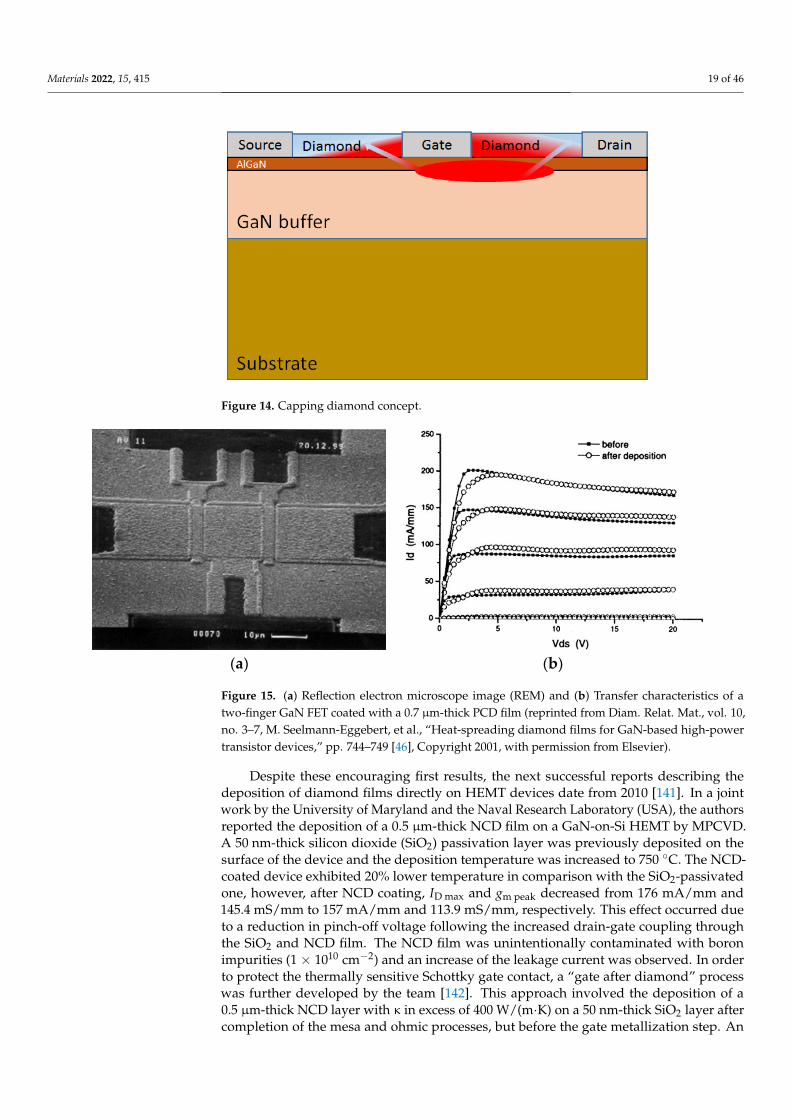
Materials 2022, 15, 415 19 of 46
Materials 2022, 15, x FOR PEER REVIEW 18 of 46
Table 5. GaN epitaxy on diamond substrates.
Ref. Year Diamond
GaN
Deposition Method Type Thickness
(µm)
Disl. dens.
(cm-2)
[125] 2003 Natural SCD MOCVD on 10 nm AlN layer +
HVPE Polycryst. 2.5 --
[126] 2011 (011) SCD MOCVD on AlN layer Polycryst. 0.07–1.55 --
[127] 2009 (111) SCD NH3-MBE on 100 nm AlN layer Epilayer 1 --
[128,129] 2010 (111) SCD NH3-MBE on 200 nm AlN + GaN
strain engineered interlayers Epilayer 0.8 8.4 109
[130] 2011 Ib (111) SCD MOVPE on 180 nm single crystal
AlN + 400 nm AlN/GaN Epilayer 0.6 --
[131] 2012 IIa (111) SCD MOVPE on 180 nm single crystal
AlN + 500 nm AlN/GaN Epilayer 0.6 8.4 109
[132,133] 2012 Ib (111) SCD MOVPE on 180 nm single crystal
AlN + 500 nm AlN/GaN Epilayer 0.6 --
[134] 2009 NCD MOCVD on 50 nm GaN Polycryst. 3 --
[135] 2010 PCD MOCVD Polycryst. 0.8 --
[124] 2015 PCD MOVPE on 70 nm AlN layer + depo-
sition of SiN stripes/etching + ELO
15 µm wide
epilayer 1.5
7 10-9 →
<108
[136] 2017 PCD thin films Etching of Si substrate + MOVPE on
10–40 nm AlN/Al0.75Ga0.25N layers Epilayer 0.2–1.1 --
[137] 2020 Post-deposited
PCD
MOCVD of SiN-capped AlGaN/GaN
stack on Si + selective deposition of
PCD stripes + ELO
5 µm wide
epilayer ≈1-5
109 →
107
3.4. Capping Diamond
The capping diamond concept was initially proposed in 1991 [139]. This approach
relies on the deposition of the PCD film directly on the device die, immediately on top of
the passivation layers, bringing the diamond film in close contact with the hot spots—
Figure 14. Initial calculations predicted a 50 °C reduction in the channel temperature of a
2 W/mm GaAs device caused by “thermally shorting” the source, gate and drain contacts
with a highly thermally conductive diamond film [140].
Figure 14. Capping diamond concept.
Despite no experimental works reported the direct growth of PCD films on GaAs
FETs, the concept was picked up by the GaN community and the first successfully dia-
mond-coated working GaN device was reported 10 years later, in 2001, by researchers
from the Fraunhofer Institute and from DaimlerChrysler high frequency electronics labs
[46]. Diamond films with thicknesses between 0.7 and 2 µm were deposited directly on
the SiN passivation layer of GaN FETs using an MPCVD ellipsoid reactor operating at
Figure 14. Capping diamond concept.
Materials 2022, 15, x FOR PEER REVIEW 19 of 46
2.45 GHz at a temperature lower than 500 °C—Figure 15a. Since the regular ultrasonic
seeding with diamond particles was found to damage the SiN protective layer, an alter-
nate seeding method based on the sedimentation of fine diamond particles from an agi-
tated emulsion was used. The output and transfer characteristics of the devices were
measured before and after the deposition of the 0.7 µm-thick PCD film, showing that the
coated FETs remained fully operational—Figure 15b.
(a)
(b)
Figure 15. (a) Reflection electron microscope image (REM) and (b) Transfer characteristics of a two-
finger GaN FET coated with a 0.7 µm-thick PCD film (reprinted from Diam. Relat. Mat., vol. 10, no.
3–7, M. Seelmann-Eggebert, et al., “Heat-spreading diamond films for GaN-based high-power tran-
sistor devices,” pp. 744–749 [46], Copyright 2001, with permission from Elsevier).
Despite these encouraging first results, the next successful reports describing the
deposition of diamond films directly on HEMT devices date from 2010 [141]. In a joint
work by the University of Maryland and the Naval Research Laboratory (USA), the au-
thors reported the deposition of a 0.5 m-thick NCD film on a GaN-on-Si HEMT by
MPCVD. A 50 nm-thick silicon dioxide (SiO2) passivation layer was previously deposited
on the surface of the device and the deposition temperature was increased to 750 °C. The
NCD-coated device exhibited 20% lower temperature in comparison with the SiO2-pas-
sivated one, however, after NCD coating, ID max and gm peak decreased from 176 mA/mm
and 145.4 mS/mm to 157 mA/mm and 113.9 mS/mm, respectively. This effect occurred
due to a reduction in pinch-off voltage following the increased drain-gate coupling
through the SiO2 and NCD film. The NCD film was unintentionally contaminated with
boron impurities (1 1010 cm−2) and an increase of the leakage current was observed. In
order to protect the thermally sensitive Schottky gate contact, a “gate after diamond” pro-
cess was further developed by the team [142]. This approach involved the deposition of a
0.5 m-thick NCD layer with in excess of 400 W/(m∙K) on a 50 nm-thick SiO2 layer after
completion of the mesa and ohmic processes, but before the gate metallization step. An
oxygen (O2)-based plasma etch was then used to recess etch the diamond in the gate re-
gion before metal deposition. Similarly to what happened in the previous approach, ID max
decreased from 360 to 270 mA/mm after the deposition of the NCD film. The process
was further optimized to allow the deposition of the NCD layer directly on the GaN sur-
face [143,144], which improved the performance of the 2DEG in comparison with a refer-
ence HEMT passivated with SiN (2DEG density/mobility of 1.02 1013 cm−2/1280 cm2/(Vs)
against 8.92 1012 cm−2/1220 cm2/(Vs), respectively), increased ID max and gm peak from 380
to 445 mA/mm and from 114 to 127 mS/mm, respectively, and decreased the device on-
resistance from 14.6 to 11.9 mm. At 5 W/mm DC power, the temperature of the NCD-
capped HEMT was 20% lower than that of the SiN-capped one and the Rth was 0.98
Kmm/W, 3.75 times lower. The use of a p-type diamond gate electrode was also pro-
posed [145]. Again ID max increased from 290 mA/mm (with a nickel (Ni)/Au gate) to 430
mA/mm (with the NCD gate), the on-resistance decreased from 29.4 to 12.1 mm and the
leakage gate current decreased by nearly one order of magnitude at a gate voltage of −10
Figure 15. (a) Reflection electron microscope image (REM) and (b) Transfer characteristics of atwo-finger GaN FET coated with a 0.7 µm-thick PCD film (reprinted from Diam. Relat. Mat., vol. 10,no. 3–7, M. Seelmann-Eggebert, et al., “Heat-spreading diamond films for GaN-based high-powertransistor devices,” pp. 744–749 [46], Copyright 2001, with permission from Elsevier).
Despite these encouraging first results, the next successful reports describing thedeposition of diamond films directly on HEMT devices date from 2010 [141]. In a jointwork by the University of Maryland and the Naval Research Laboratory (USA), the authorsreported the deposition of a 0.5 µm-thick NCD film on a GaN-on-Si HEMT by MPCVD.A 50 nm-thick silicon dioxide (SiO2) passivation layer was previously deposited on thesurface of the device and the deposition temperature was increased to 750 C. The NCD-coated device exhibited 20% lower temperature in comparison with the SiO2-passivatedone, however, after NCD coating, ID max and gm peak decreased from 176 mA/mm and145.4 mS/mm to 157 mA/mm and 113.9 mS/mm, respectively. This effect occurred dueto a reduction in pinch-off voltage following the increased drain-gate coupling throughthe SiO2 and NCD film. The NCD film was unintentionally contaminated with boronimpurities (1 × 1010 cm−2) and an increase of the leakage current was observed. In orderto protect the thermally sensitive Schottky gate contact, a “gate after diamond” processwas further developed by the team [142]. This approach involved the deposition of a0.5 µm-thick NCD layer with κ in excess of 400 W/(m·K) on a 50 nm-thick SiO2 layer aftercompletion of the mesa and ohmic processes, but before the gate metallization step. An

Materials 2022, 15, 415 20 of 46
oxygen (O2)-based plasma etch was then used to recess etch the diamond in the gate regionbefore metal deposition. Similarly to what happened in the previous approach, ID maxdecreased from ≈360 to ≈270 mA/mm after the deposition of the NCD film. The processwas further optimized to allow the deposition of the NCD layer directly on the GaN sur-face [143,144], which improved the performance of the 2DEG in comparison with a referenceHEMT passivated with SiN (2DEG density/mobility of 1.02 × 1013 cm−2/1280 cm2/(V·s)against 8.92 × 1012 cm−2/1220 cm2/(V·s), respectively), increased ID max and gm peak from380 to 445 mA/mm and from 114 to 127 mS/mm, respectively, and decreased the deviceon-resistance from 14.6 to 11.9 Ω·mm. At 5 W/mm DC power, the temperature of theNCD-capped HEMT was ≈20% lower than that of the SiN-capped one and the Rth was0.98 K·mm/W, ≈3.75 times lower. The use of a p-type diamond gate electrode was alsoproposed [145]. Again ID max increased from ≈290 mA/mm (with a nickel (Ni)/Au gate)to ≈430 mA/mm (with the NCD gate), the on-resistance decreased from 29.4 to 12.1 Ω·mmand the leakage gate current decreased by nearly one order of magnitude at a gate voltageof −10 V. In a later process development, the SiO2 layer was replaced with a 10 nm-thickSiN layer [146]. The capping of a SiN-passivated GaN-on-SiC HEMT with 500 nm NCDlead to an ≈8% reduction in the peak temperature, less than the 20% obtained with thegate-after-diamond approach due to the SiN passivation layer and the resulting increasedTBRGaN/diamond [147].
Following a different approach in 2011 Alomari et al. [148] reported the depositionof a 0.5 µm-thick NCD film on In0.17AlN0.83/GaN HEMTs by bias-enhanced nucleation(BEN) and HFCVD at temperatures of 750–800 C—Figure 16a. The HEMT structuresincluded the dielectric passivation and stress control layers based on SiO2 and Si3N4 anda thin sputtered Si layer for BEN step (Figure 16b). The DC characteristics of the devicesremained fundamentally similar after the NCD deposition. f T and f max were 4.2 and 5 GHz,respectively, and the RF-tested device showed high gate leakage. In 2014 the NCD layerthickness had been increased to 2.8 µm [149].
Materials 2022, 15, x FOR PEER REVIEW 20 of 46
V. In a later process development, the SiO2 layer was replaced with a 10 nm-thick SiN
layer [146]. The capping of a SiN-passivated GaN-on-SiC HEMT with 500 nm NCD lead
to an 8% reduction in the peak temperature, less than the 20% obtained with the gate-
after-diamond approach due to the SiN passivation layer and the resulting increased
TBRGaN/diamond [147].
Following a different approach in 2011 Alomari et al. [148] reported the deposition
of a 0.5 m-thick NCD film on In0.17AlN0.83/GaN HEMTs by bias-enhanced nucleation
(BEN) and HFCVD at temperatures of 750–800 °C—Figure 16a. The HEMT structures in-
cluded the dielectric passivation and stress control layers based on SiO2 and Si3N4 and a
thin sputtered Si layer for BEN step (Figure 16b). The DC characteristics of the devices
remained fundamentally similar after the NCD deposition. fT and fmax were 4.2 and 5 GHz,
respectively, and the RF-tested device showed high gate leakage. In 2014 the NCD layer
thickness had been increased to 2.8 m [149].
(a)
(b)
Figure 16. (a) SEM top view of a GaN HEMT coated with a 0.5 µm-thick NCD layer. (b) TEM cross
section of the NCD film showing no voids at the passivation/growth interface (reprinted from Diam.
Relat. Mater., vol. 20, no. 4, M. Alomari et al., “Diamond overgrown InAlN/GaN HEMT,” pp. 604–
608 [148], Copyright 2011, with permission from Elsevier).
Zhou et al. [150] deposited 155–1000 nm-thick PCD films onto Si3N4-passivated Al-
GaN/GaN-on-Si HEMT structures and used transient thermoreflectance experimental re-
sults, together with device thermal simulations, to evaluate the impact of the diamond
capping layer thickness on the maximum device temperature. A 12% maximum reduction
in peak channel temperature could be achieved with a 16 × 125 µm/50 µm gate-pitch Al-
GaN/GaN-on-Si HEMT with a 1 µm-thick PCD film deposited on the source-drain open-
ing. If the TBRGaN/diamond was not included, a further 10% temperature reduction could be
expected. Little further thermal benefit was predicted when using PCD films thicker than
2 µm, with only a maximum 15% temperature reduction. If PCD could be grown on both
source-drain opening and metal contacts, a 1.5% better thermal benefit would be achieved
for thicker films by increasing the area of the heat spreader. The quality of the initial few
µm of the capping diamond layer was also shown to play an important role in reducing
the channel temperature [151].
In 2019, researchers from the Power and Wide-Band-Gap Electronics Research La-
boratory and Lake Diamond SA deposited 3 m-thick PCD heat spreaders on the top of
vertical GaN PiN diodes using a 30 nm-thick SiN adhesion layer [152]. With 0.9 W of dis-
sipated power, the temperature of the coated device was 64% lower than the temperature
of a reference uncoated device.
The appearance of biaxial strain in the Al(Ga)N layers due to the high diamond dep-
osition temperatures, the lattice mismatch between the layers, and the different CTEs of
the stack materials was studied in detail by Siddique et al. [91]. In their study, a 46 nm-
thick SiN layer was used to protect the III-nitride layers beneath the AlGaN barrier layer
during the diamond CVD. Figure 17 shows scanning transmission electron microscope
Figure 16. (a) SEM top view of a GaN HEMT coated with a 0.5 µm-thick NCD layer. (b) TEMcross section of the NCD film showing no voids at the passivation/growth interface (reprinted fromDiam. Relat. Mater., vol. 20, no. 4, M. Alomari et al., “Diamond overgrown InAlN/GaN HEMT,”pp. 604–608 [148], Copyright 2011, with permission from Elsevier).
Zhou et al. [150] deposited 155–1000 nm-thick PCD films onto Si3N4-passivatedAlGaN/GaN-on-Si HEMT structures and used transient thermoreflectance experimen-tal results, together with device thermal simulations, to evaluate the impact of the diamondcapping layer thickness on the maximum device temperature. A 12% maximum reductionin peak channel temperature could be achieved with a 16 × 125 µm/50 µm gate-pitchAlGaN/GaN-on-Si HEMT with a 1 µm-thick PCD film deposited on the source-drain open-

Materials 2022, 15, 415 21 of 46
ing. If the TBRGaN/diamond was not included, a further 10% temperature reduction could beexpected. Little further thermal benefit was predicted when using PCD films thicker than2 µm, with only a maximum 15% temperature reduction. If PCD could be grown on bothsource-drain opening and metal contacts, a 1.5% better thermal benefit would be achievedfor thicker films by increasing the area of the heat spreader. The quality of the initial fewµm of the capping diamond layer was also shown to play an important role in reducingthe channel temperature [151].
In 2019, researchers from the Power and Wide-Band-Gap Electronics Research Labora-tory and Lake Diamond SA deposited 3 µm-thick PCD heat spreaders on the top of verticalGaN PiN diodes using a 30 nm-thick SiN adhesion layer [152]. With 0.9 W of dissipatedpower, the temperature of the coated device was 64% lower than the temperature of areference uncoated device.
The appearance of biaxial strain in the Al(Ga)N layers due to the high diamonddeposition temperatures, the lattice mismatch between the layers, and the different CTEs ofthe stack materials was studied in detail by Siddique et al. [91]. In their study, a 46 nm-thickSiN layer was used to protect the III-nitride layers beneath the AlGaN barrier layer duringthe diamond CVD. Figure 17 shows scanning transmission electron microscope (STEM)images of the SiN layer (a) before and (b) after the diamond deposition; even though the SiNlayer was partially degraded during the deposition of the diamond and was thinned downto 20 nm in some regions, it remained continuous across the entirety of the AlGaN barrierlayer. The deposition of the diamond film was seen to increase the biaxial tensile stress inthe AlN and GaN layers by 3%, which caused a 4.5% reduction of the total 2DEG sheetcharge density (from 1.04 × 10¹³ to 0.99 × 1013 cm–2). A 52.8 m2·K/GW TBRGaN/diamondwas measured (including the SiN, GaN cap, AlGaN, and AlN layers).
Materials 2022, 15, x FOR PEER REVIEW 21 of 46
(STEM) images of the SiN layer (a) before and (b) after the diamond deposition; even
though the SiN layer was partially degraded during the deposition of the diamond and
was thinned down to 20 nm in some regions, it remained continuous across the entirety
of the AlGaN barrier layer. The deposition of the diamond film was seen to increase the
biaxial tensile stress in the AlN and GaN layers by 3%, which caused a 4.5% reduction of
the total 2DEG sheet charge density (from 1.04 × 10¹³ to 0.99 × 1013 cm–2). A 52.8 m2K/GW
TBRGaN/diamond was measured (including the SiN, GaN cap, AlGaN, and AlN layers).
(a)
(b)
Figure 17. Bright-field STEM images showing the Al(Ga)N/SiN layer interfacial region (a) before
and (b) after diamond growth (reprinted with permission from A. Siddique et al., “Structure and
Interface Analysis of Diamond on an AlGaN/GaN HEMT Utilizing an in Situ SiNx Interlayer Grown
by MOCVD,” ACS Appl. Electron. Mater., vol. 1, pp. 1387–1399, 2019 [91]. Copyright 2019 American
Chemical Society).
In order to prevent the modulation of the 2DEG due to the stress induced in the chan-
nel by the capping diamond layer, Arivazhagan et al. [153] proposed depositing the dia-
mond layer on the drain electrode alone (instead of directly on the device channel). The
impact of this approach was evaluated using thermo-electrical simulations. The results
suggest that the deposition of the PCD film on the drain electrode will lower self-heating
and allow higher ID max than in conventional GaN-on-Si HEMTs—without inducing any
change in the 2DEG sheet charge density or in the device threshold voltage.
Despite the technological difficulties inherent to this technological approach, a break-
through has been recently achieved by Fujitsu Limited. In 2021 Yaita et al. reported a dia-
mond-coated GaN-on-SiC HEMT with improved DC characteristics [154]. A 2.5 µm-thick
PCD film was deposited by HFCVD on a 100 nm-thick SiN capping layer at 700 C. In
order to prevent the degradation by the elevated temperatures required to deposit the
diamond film, the Schottky gate contact was replaced by a 40 nm-thick SiN insulating
layer, followed by a Ni/Au gate contact. In addition, metal heat spreaders were attached
to the deposited PCD. The ID and gm of the diamond-coated HEMT increased from 0.9 to
1.1 A/mm and from 102 to 148 mS/mm, respectively (Figure 18a). At the same time, for 25
W/mm PD the hotspot temperature lowered by more than 100 C, which corresponds to a
decrease in Rth from 12.7 to 7.4 Kmm/W, and to a 40% reduction in the amount of heat
generated by the diamond-coated GaN HEMT (Figure 18b). Fujitsu aims to commercialize
improved-heat-dissipation GaN HEMT amplifiers in year 2022 for use in weather radar
systems and next-generation wireless communication systems [155].
Figure 17. Bright-field STEM images showing the Al(Ga)N/SiN layer interfacial region (a) beforeand (b) after diamond growth (reprinted with permission from A. Siddique et al., “Structure andInterface Analysis of Diamond on an AlGaN/GaN HEMT Utilizing an in Situ SiNx Interlayer Grownby MOCVD,” ACS Appl. Electron. Mater., vol. 1, pp. 1387–1399, 2019 [91]. Copyright 2019 AmericanChemical Society).
In order to prevent the modulation of the 2DEG due to the stress induced in thechannel by the capping diamond layer, Arivazhagan et al. [153] proposed depositing thediamond layer on the drain electrode alone (instead of directly on the device channel). Theimpact of this approach was evaluated using thermo-electrical simulations. The resultssuggest that the deposition of the PCD film on the drain electrode will lower self-heatingand allow higher ID max than in conventional GaN-on-Si HEMTs—without inducing anychange in the 2DEG sheet charge density or in the device threshold voltage.

Materials 2022, 15, 415 22 of 46
Despite the technological difficulties inherent to this technological approach, a break-through has been recently achieved by Fujitsu Limited. In 2021 Yaita et al. reported adiamond-coated GaN-on-SiC HEMT with improved DC characteristics [154]. A 2.5 µm-thick PCD film was deposited by HFCVD on a 100 nm-thick SiN capping layer at 700 C.In order to prevent the degradation by the elevated temperatures required to deposit thediamond film, the Schottky gate contact was replaced by a 40 nm-thick SiN insulatinglayer, followed by a Ni/Au gate contact. In addition, metal heat spreaders were attachedto the deposited PCD. The ID and gm of the diamond-coated HEMT increased from 0.9 to1.1 A/mm and from 102 to 148 mS/mm, respectively (Figure 18a). At the same time, for25 W/mm PD the hotspot temperature lowered by more than 100 C, which corresponds toa decrease in Rth from 12.7 to 7.4 K·mm/W, and to a ≈40% reduction in the amount of heatgenerated by the diamond-coated GaN HEMT (Figure 18b). Fujitsu aims to commercializeimproved-heat-dissipation GaN HEMT amplifiers in year 2022 for use in weather radarsystems and next-generation wireless communication systems [155].
Materials 2022, 15, x FOR PEER REVIEW 22 of 46
(a)
(b)
Figure 18. (a) Transfer curve and transconductance vs. gate voltage. (b) Hotspot temperature calcu-
lated from the Raman peak shift (reprinted from [154], Copyright 2021 The Japan Society of Applied
Physics.
Experimental results presented so far have been limited to the scope of single or dual-
gate HEMTs. Zhang and co-workers implemented 3D thermal simulations to evaluate the
impact of capping multi-finger HEMTs with PCD layers [156]. They observed that the
capping diamond layer reduced the junction temperature and the temperature non-uni-
formity in the near-junction region across the channel; the efficiency of the capping dia-
mond layer was also observed to increase with increasing thickness but with a decreasing
trend. The largest thermal benefit could be expected under challenging conditions, such
as high PD, narrow gate pitch, high TBR, as well as for traditional GaN-on-Si HEMTs. In
the particular case of a 12-finger GaN-on-diamond HEMT operating at of 6 W/mm PD per
gate, 20 µm gate pitch, and assuming a similar TBR between both GaN/diamond interfaces
of 15 m2K/GW, the inclusion of a 20 µm-thick PCD capping layer would reduce the junc-
tion temperature from 195.8 to 172.2 °C, which corresponds to a net decrease of 23.6 °C.
By reducing the thickness of the PCD layer to 1 µm, the reduction of junction temperature
would still be as high as 14.9 °C.
The impact of capping double-channel HEMTs was also evaluated with thermo-elec-
trical simulations [157]. The authors observed that the PCD layer provides a lateral heat
conduction path close to the hot spot located at near the drain side of the gate edge, mod-
ulating the channel lattice temperature distribution and making it become more uniform.
For a PD of 46 W/mm the peak lattice temperature was reduced by 64 °C, indicating that
the PCD layer plays an important role in device heat dissipation. Similar to what was
observed in [156], the effect of lattice temperature reduction increases with increasing
PCD layer thickness. Taking the effect of temperature reduction and cost into considera-
tion, the authors proposed the optimum thickness for the PCD layer to be 1 µm.
The impact of capping a pulsed-mode AlGaN/GaN HEMT with a PCD layer has been
also evaluated with thermal 3D simulations [158]. The PCD capped layer not only reduced
significantly the peak junction temperature but also suppressed its oscillation in the pulse
mode operation, smoothing the temporal variation of the junction temperature. Again the
cooling performance of the PCD capped layer was observed to increase with rising thick-
ness but with a decreasing trend. The overall efficiency of this approach was shown to be
more effective under harsh thermal conditions, including smaller duty cycle, higher TRB,
and lower substrate.
The evolution of the relevant experimental results has been compiled in Table 6.
While experimental results and functional HEMTs were reported between 2001 and 2014,
most recent work focused on evaluating the biaxial strain induced by the diamond depo-
sition temperatures (typically in excess of 500 °C) and on anticipating the thermal benefit
of the diamond layer using thermal simulations. The electrical parameters of diamond-
capped HEMTS are summarized in Table A4 in the Appendix A.
Figure 18. (a) Transfer curve and transconductance vs. gate voltage. (b) Hotspot temperaturecalculated from the Raman peak shift (reprinted from [154], Copyright 2021 The Japan Society ofApplied Physics.
Experimental results presented so far have been limited to the scope of single ordual-gate HEMTs. Zhang and co-workers implemented 3D thermal simulations to evaluatethe impact of capping multi-finger HEMTs with PCD layers [156]. They observed thatthe capping diamond layer reduced the junction temperature and the temperature non-uniformity in the near-junction region across the channel; the efficiency of the cappingdiamond layer was also observed to increase with increasing thickness but with a decreasingtrend. The largest thermal benefit could be expected under challenging conditions, such ashigh PD, narrow gate pitch, high TBR, as well as for traditional GaN-on-Si HEMTs. In theparticular case of a 12-finger GaN-on-diamond HEMT operating at of 6 W/mm PD per gate,20 µm gate pitch, and assuming a similar TBR between both GaN/diamond interfaces of15 m2·K/GW, the inclusion of a 20 µm-thick PCD capping layer would reduce the junctiontemperature from 195.8 to 172.2 C, which corresponds to a net decrease of 23.6 C. Byreducing the thickness of the PCD layer to 1 µm, the reduction of junction temperaturewould still be as high as 14.9 C.
The impact of capping double-channel HEMTs was also evaluated with thermo-electrical simulations [157]. The authors observed that the PCD layer provides a lateralheat conduction path close to the hot spot located at near the drain side of the gate edge,modulating the channel lattice temperature distribution and making it become more uni-form. For a PD of 46 W/mm the peak lattice temperature was reduced by 64 C, indicatingthat the PCD layer plays an important role in device heat dissipation. Similar to what was
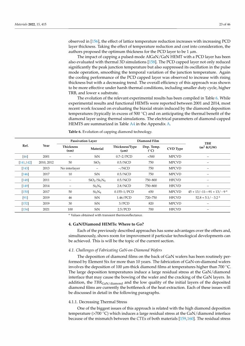
Materials 2022, 15, 415 23 of 46
observed in [156], the effect of lattice temperature reduction increases with increasing PCDlayer thickness. Taking the effect of temperature reduction and cost into consideration, theauthors proposed the optimum thickness for the PCD layer to be 1 µm.
The impact of capping a pulsed-mode AlGaN/GaN HEMT with a PCD layer has beenalso evaluated with thermal 3D simulations [158]. The PCD capped layer not only reducedsignificantly the peak junction temperature but also suppressed its oscillation in the pulsemode operation, smoothing the temporal variation of the junction temperature. Againthe cooling performance of the PCD capped layer was observed to increase with risingthickness but with a decreasing trend. The overall efficiency of this approach was shownto be more effective under harsh thermal conditions, including smaller duty cycle, higherTRB, and lower κ substrate.
The evolution of the relevant experimental results has been compiled in Table 6. Whileexperimental results and functional HEMTs were reported between 2001 and 2014, mostrecent work focused on evaluating the biaxial strain induced by the diamond depositiontemperatures (typically in excess of 500 C) and on anticipating the thermal benefit of thediamond layer using thermal simulations. The electrical parameters of diamond-cappedHEMTS are summarized in Table A4 in the Appendix A.
Table 6. Evolution of capping diamond technology.
Ref. YearPassivation Layer Diamond Film
TBR(m2·K/GW)Thickness
(nm) Material Thickness/Type(µm)
Dep. Temp.(C) CVD Type
[46] 2001 – SiN 0.7–2/PCD <500 MPCVD –
[141,142] 2010, 2012 50 SiO2 0.5/NCD 750 MPCVD –
[143] 2013 No interlayer – –/NCD 750 MPCVD –
[146] 2017 10 SiN 0.5/NCD 750 MPCVD –
[148] 2011 – SiO2/Si3N4 0.5/NCD 750–800 HFCVD –
[149] 2014 – Si3N4 2.8/NCD 750–800 HFCVD –
[150] 2017 50 Si3N4 0.155–1/PCD 650 MPCVD 45 + 13/–11—91 + 13/−9 a
[91] 2019 46 SiN 1.46/PCD 720–750 HFCVD 52.8 + 5.1/−3.2 a
[152] 2019 30 SiN 3/PCD 820 MPCVD –
[154] 2021 100 SiN 2.5/PCD 700 HFCVD –a Values obtained with transient thermoreflectance.
4. GaN/Diamond HEMTs: Where to Go?
Each of the previously described approaches has some advantages over the others and,simultaneously, shows room for improvement if particular technological developments canbe achieved. This is will be the topic of the current section.
4.1. Challenges of Fabricating GaN-on-Diamond Wafers
The deposition of diamond films on the back of GaN wafers has been routinely per-formed by Element Six for more than 10 years. The fabrication of GaN-on-diamond wafersinvolves the deposition of 100 µm-thick diamond films at temperatures higher than 700 C.The large deposition temperatures induce a large residual stress at the GaN/diamondinterface that may cause the bowing of the wafer and the cracking of the GaN layers. Inaddition, the TBRGaN/diamond and the low quality of the initial layers of the depositeddiamond films are currently the bottleneck of the heat extraction. Each of these issues willbe discussed in detail in the following paragraphs.
4.1.1. Decreasing Thermal Stress
One of the biggest issues of this approach is related with the high diamond depositiontemperature (>700 C) which induces a large residual stress at the GaN/diamond interfacebecause of the mismatch between the CTEs of both materials [159,160]. The residual stress

Materials 2022, 15, 415 24 of 46
depends on the GaN thickness, on the diamond growth temperature, and on the sacrificialcarrier wafer [91,92]. Residual stresses larger than 1 GPa at the free surface of the GaN havebeen reported [93]; these elevated stress conditions induce layer cracking and wafer bow,and impact the electrical performance of the devices [161–164]. A large thermal stress atthe GaN-diamond interface causes a significant reliability concern when considering thefunction and lifetime of GaN-on-diamond devices.
To avoid the issues related with the residual stress, a slightly modified approachhas been recently proposed [94]. The GaN was initially grown on an AlN nucleationlayer deposited on a Si substrate. The Si substrate was selectively etched, leaving behind0.5 mm-diameter GaN membranes with the AlN nucleation layer exposed onto which50 µm-thick diamond films were further grown. The high quality diamond/AlN interfaceshowed no visible voids or cracks, confirming the strong bond between both materials. Thisapproach presents no technological barrier to the incorporation of an AlN “initiation” layerinto the GaN buffer close to the device channel; however, due to the low thickness of theGaN membranes and the simultaneously high temperatures required for diamond growth,the bowing of the membranes during the diamond deposition step cannot be neglected.This phenomenon was recently analyzed in detail in [95] using commercial GaN-on-Siwafers as the starting material. The processing steps are described in Figure 19a. The GaNmembrane diameter was shown to impact the maximum displacement from the originalplane (bowing) before and after diamond deposition, as well as the membrane stress. The5 mm-diameter membranes allowed a larger displacement with a subsequent lower stressvalue, however the larger bowing “pushed” the GaN surface further into the plasma duringdiamond deposition, exposing it to high temperatures and resulting in thermal runawayand damage to the GaN/III-N film—Figure 19b. In addition, the large membrane bowspresent a big challenge for device manufacturing using contact lithography. A possibleway to prevent the bowing would be the use of pre-stressed GaN-on-Si wafers as thestarting material.
Materials 2022, 15, x FOR PEER REVIEW 24 of 46
growth, the bowing of the membranes during the diamond deposition step cannot be ne-
glected. This phenomenon was recently analyzed in detail in [95] using commercial GaN-
on-Si wafers as the starting material. The processing steps are described in Figure 19a. The
GaN membrane diameter was shown to impact the maximum displacement from the orig-
inal plane (bowing) before and after diamond deposition, as well as the membrane stress.
The 5 mm-diameter membranes allowed a larger displacement with a subsequent lower
stress value, however the larger bowing “pushed” the GaN surface further into the plasma
during diamond deposition, exposing it to high temperatures and resulting in thermal
runaway and damage to the GaN/III-N film—Figure 19b. In addition, the large membrane
bows present a big challenge for device manufacturing using contact lithography. A pos-
sible way to prevent the bowing would be the use of pre-stressed GaN-on-Si wafers as the
starting material.
(a) (b)
Figure 19. (a) Fabrication steps of a GaN-on-diamond membrane. (b) Image of the 5 mm-diameter
membrane inside the MPCVD system and corresponding thermally-induced mechanical displace-
ment (reprinted from [95]; permission conveyed through CCBY 4.0.).
Following a radically different approach, represented in Figure 20, Jia et al. [96] re-
ported a low stress GaN-on-diamond wafer fabricated by dual sided deposition of dia-
mond. In this process, the temporary carrier represented in Figure 2 was a 2 µm-thick Si
layer followed by 100 µm of low-quality PCD deposited by CVD. A thin SiN layer was
deposited on the surface after the substrate removal, followed by high-quality PCD. The
final free-standing GaN-on-diamond wafer was obtained by removing the low-quality
PCD and Si layers. The surface and quality of the GaN layer after the etching of the low
quality PCD and Si layers remained the same while the stress was reduced to 0.5 GPa.
However, it should be mentioned that the AlN buffer layer was not removed and this may
have helped to reduce the internal stress caused by diamond growth.
Figure 20. Fabrication of GaN-on-diamond wafers by dual-sided diamond deposition.
Figure 19. (a) Fabrication steps of a GaN-on-diamond membrane. (b) Image of the 5 mm-diametermembrane inside the MPCVD system and corresponding thermally-induced mechanical displace-ment (reprinted from [95]; permission conveyed through CCBY 4.0: https://creativecommons.org/licenses/by/4.0/ (accessed on 7 October 2021)).
Following a radically different approach, represented in Figure 20, Jia et al. [96]reported a low stress GaN-on-diamond wafer fabricated by dual sided deposition ofdiamond. In this process, the temporary carrier represented in Figure 2 was a 2 µm-thickSi layer followed by 100 µm of low-quality PCD deposited by CVD. A thin SiN layer wasdeposited on the surface after the substrate removal, followed by high-quality PCD. Thefinal free-standing GaN-on-diamond wafer was obtained by removing the low-quality PCDand Si layers. The surface and quality of the GaN layer after the etching of the low quality
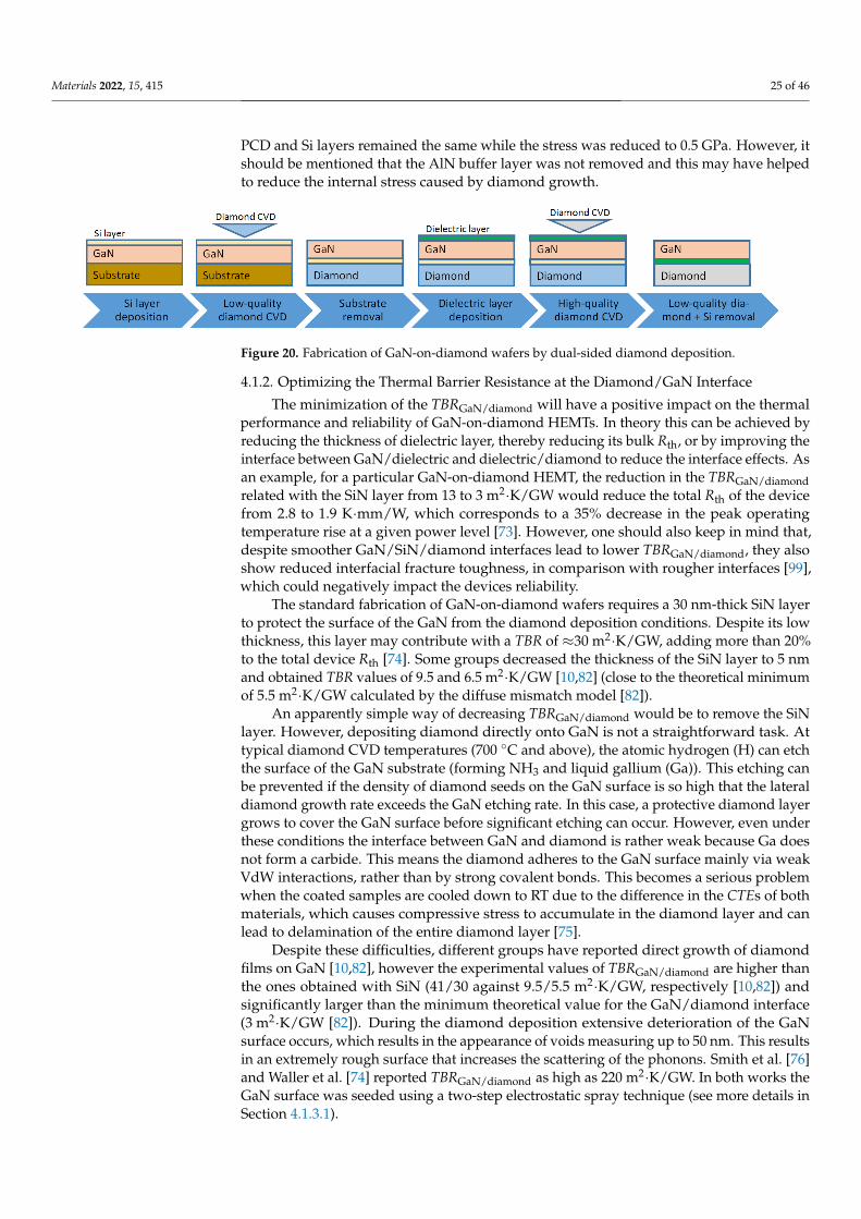
Materials 2022, 15, 415 25 of 46
PCD and Si layers remained the same while the stress was reduced to 0.5 GPa. However, itshould be mentioned that the AlN buffer layer was not removed and this may have helpedto reduce the internal stress caused by diamond growth.
Materials 2022, 15, x FOR PEER REVIEW 24 of 46
growth, the bowing of the membranes during the diamond deposition step cannot be ne-
glected. This phenomenon was recently analyzed in detail in [95] using commercial GaN-
on-Si wafers as the starting material. The processing steps are described in Figure 19a. The
GaN membrane diameter was shown to impact the maximum displacement from the orig-
inal plane (bowing) before and after diamond deposition, as well as the membrane stress.
The 5 mm-diameter membranes allowed a larger displacement with a subsequent lower
stress value, however the larger bowing “pushed” the GaN surface further into the plasma
during diamond deposition, exposing it to high temperatures and resulting in thermal
runaway and damage to the GaN/III-N film—Figure 19b. In addition, the large membrane
bows present a big challenge for device manufacturing using contact lithography. A pos-
sible way to prevent the bowing would be the use of pre-stressed GaN-on-Si wafers as the
starting material.
(a) (b)
Figure 19. (a) Fabrication steps of a GaN-on-diamond membrane. (b) Image of the 5 mm-diameter
membrane inside the MPCVD system and corresponding thermally-induced mechanical displace-
ment (reprinted from [95]; permission conveyed through CCBY 4.0.).
Following a radically different approach, represented in Figure 20, Jia et al. [96] re-
ported a low stress GaN-on-diamond wafer fabricated by dual sided deposition of dia-
mond. In this process, the temporary carrier represented in Figure 2 was a 2 µm-thick Si
layer followed by 100 µm of low-quality PCD deposited by CVD. A thin SiN layer was
deposited on the surface after the substrate removal, followed by high-quality PCD. The
final free-standing GaN-on-diamond wafer was obtained by removing the low-quality
PCD and Si layers. The surface and quality of the GaN layer after the etching of the low
quality PCD and Si layers remained the same while the stress was reduced to 0.5 GPa.
However, it should be mentioned that the AlN buffer layer was not removed and this may
have helped to reduce the internal stress caused by diamond growth.
Figure 20. Fabrication of GaN-on-diamond wafers by dual-sided diamond deposition.
Figure 20. Fabrication of GaN-on-diamond wafers by dual-sided diamond deposition.
4.1.2. Optimizing the Thermal Barrier Resistance at the Diamond/GaN Interface
The minimization of the TBRGaN/diamond will have a positive impact on the thermalperformance and reliability of GaN-on-diamond HEMTs. In theory this can be achieved byreducing the thickness of dielectric layer, thereby reducing its bulk Rth, or by improving theinterface between GaN/dielectric and dielectric/diamond to reduce the interface effects. Asan example, for a particular GaN-on-diamond HEMT, the reduction in the TBRGaN/diamondrelated with the SiN layer from 13 to 3 m2·K/GW would reduce the total Rth of the devicefrom 2.8 to 1.9 K·mm/W, which corresponds to a 35% decrease in the peak operatingtemperature rise at a given power level [73]. However, one should also keep in mind that,despite smoother GaN/SiN/diamond interfaces lead to lower TBRGaN/diamond, they alsoshow reduced interfacial fracture toughness, in comparison with rougher interfaces [99],which could negatively impact the devices reliability.
The standard fabrication of GaN-on-diamond wafers requires a 30 nm-thick SiN layerto protect the surface of the GaN from the diamond deposition conditions. Despite its lowthickness, this layer may contribute with a TBR of ≈30 m2·K/GW, adding more than 20%to the total device Rth [74]. Some groups decreased the thickness of the SiN layer to 5 nmand obtained TBR values of 9.5 and 6.5 m2·K/GW [10,82] (close to the theoretical minimumof 5.5 m2·K/GW calculated by the diffuse mismatch model [82]).
An apparently simple way of decreasing TBRGaN/diamond would be to remove the SiNlayer. However, depositing diamond directly onto GaN is not a straightforward task. Attypical diamond CVD temperatures (700 C and above), the atomic hydrogen (H) can etchthe surface of the GaN substrate (forming NH3 and liquid gallium (Ga)). This etching canbe prevented if the density of diamond seeds on the GaN surface is so high that the lateraldiamond growth rate exceeds the GaN etching rate. In this case, a protective diamond layergrows to cover the GaN surface before significant etching can occur. However, even underthese conditions the interface between GaN and diamond is rather weak because Ga doesnot form a carbide. This means the diamond adheres to the GaN surface mainly via weakVdW interactions, rather than by strong covalent bonds. This becomes a serious problemwhen the coated samples are cooled down to RT due to the difference in the CTEs of bothmaterials, which causes compressive stress to accumulate in the diamond layer and canlead to delamination of the entire diamond layer [75].
Despite these difficulties, different groups have reported direct growth of diamondfilms on GaN [10,82], however the experimental values of TBRGaN/diamond are higher thanthe ones obtained with SiN (41/30 against 9.5/5.5 m2·K/GW, respectively [10,82]) andsignificantly larger than the minimum theoretical value for the GaN/diamond interface(3 m2·K/GW [82]). During the diamond deposition extensive deterioration of the GaNsurface occurs, which results in the appearance of voids measuring up to 50 nm. This resultsin an extremely rough surface that increases the scattering of the phonons. Smith et al. [76]and Waller et al. [74] reported TBRGaN/diamond as high as 220 m2·K/GW. In both works theGaN surface was seeded using a two-step electrostatic spray technique (see more details inSection 4.1.3.1).
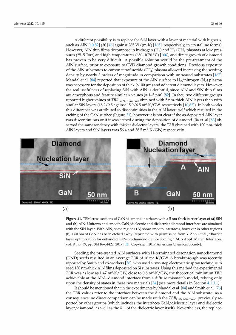
Materials 2022, 15, 415 26 of 46
A different possibility is to replace the SiN layer with a layer of material with higher κ,such as AlN [10,82] (30 [46] against 285 W/(m·K) [165], respectively, in crystalline forms).However, AlN thin films decompose in hydrogen (H2) and H2/CH4 plasmas at low pres-sures (25–5 Torr) and high temperatures (650–1070 C) [166], and direct growth of diamondhas proven to be very difficult. A possible solution would be the pre-treatment of theAlN surface, prior to exposure to CVD diamond growth conditions. Previous exposureof the AlN substrates to carbon tetrafluoride (CF4) plasma allowed increasing the seedingdensity by nearly 3 orders of magnitude in comparison with untreated substrates [167].Mandal et al. [84] reported that exposure of the AlN surface to H2/nitrogen (N2) plasmawas necessary for the deposition of thick (>100 µm) and adherent diamond layers. However,the real usefulness of replacing SiN with AlN is doubtful, since AlN and SiN thin filmsare amorphous and feature similar κ values (≈1–5 nm) [82]. In fact, two different groupsreported higher values of TBRGaN/diamond obtained with 5 nm-thick AlN layers than withsimilar SiN layers (18.2/9.5 against 15.9/6.5 m2·K/GW, respectively [10,82]). In both worksthis difference was attributed to discontinuities in the AlN layer itself which resulted in theetching of the GaN surface (Figure 21); however it is not clear if the as-deposited AlN layerwas discontinuous or if it was etched during the deposition of diamond. Jia et. al [83] ob-served the same tendency with thicker dielectric layers: the TBR obtained with 100 nm-thickAlN layers and SiN layers was 56.4 and 38.5 m2·K/GW, respectively.
Materials 2022, 15, x FOR PEER REVIEW 26 of 46
with similar SiN layers (18.2/9.5 against 15.9/6.5 m2K/GW, respectively [10,82]). In both
works this difference was attributed to discontinuities in the AlN layer itself which re-
sulted in the etching of the GaN surface (Figure 21); however it is not clear if the as-de-
posited AlN layer was discontinuous or if it was etched during the deposition of diamond.
Jia et. al [83] observed the same tendency with thicker dielectric layers: the TBR obtained
with 100 nm-thick AlN layers and SiN layers was 56.4 and 38.5 m2K/GW, respectively.
(a)
(b)
Figure 21. TEM cross-sections of GaN/diamond interfaces with a 5 nm-thick barrier layer of (a) SiN
and (b) AlN. Uniform and smooth GaN/dielectric and dielectric/diamond interfaces are obtained
with the SiN layer. With AlN, some regions (A) show smooth interfaces, however in other regions
(B) 60 nm of GaN has been etched away (reprinted with permission from Y. Zhou et al., “Barrier
layer optimization for enhanced GaN-on-diamond device cooling,” ACS Appl. Mater. Interfaces,
vol. 9, no. 39, pp. 34416–34422, 2017 [82]. Copyright 2017 American Chemical Society).
Seeding the pre-treated AlN surfaces with H-terminated detonation nanodiamond
(DND) seeds resulted in an average TBR of 16 m2K/GW. A breakthrough was recently
reported by Smith and co-workers [76], who used a two-step electrostatic spray technique
to seed 130 nm-thick AlN films deposited on Si substrates. Using this method the experi-
mental TBR was as low as 1.47 m2K/GW, close to 0.8 m2·K/GW, the theoretical minimum
TBR achievable at the AlN−diamond interface from a diffuse mismatch model, relying
only upon the density of states in these two materials [84] (see more details in Section
4.1.3.1).
It should be mentioned that in the experiments by Mandal et al. [84] and Smith et al.
[76] the TBR values refer to the interface between the diamond and the AlN substrate: as
a consequence, no direct comparison can be made with the TBRGaN/diamond previously re-
ported by other groups (which includes the interfaces GaN/dielectric layer and dielectric
layer/diamond, as well as the Rth of the dielectric layer itself). Nevertheless, the replace-
ment of the low amorphous SiN layer with crystalline AlN is a promising approach.
Ideally, the AlN layer should be integrated just below the GaN channel. This layer would
act as an etch stop during the device epitaxy, as well as a seed layer for the diamond
growth [168]. This is the approach proposed by Field and co-workers [106]; since integrat-
ing a thin AlN or high Al content AlGaN layers at this point in the epitaxy is challenging
because of alloying with surrounding layers, they used a relatively low Al content crys-
talline Al0.32Ga0.68N layer as the etch stop and interlayer and grew diamond following the
same procedure as in [84]. Due to the sample layout, a 10 nm-thick SiC layer was formed
between the Al0.32Ga0.68N/diamond interface, which improved the heat transport across
the two materials. A TBR of 30 m2K/GW was measured, a value still much higher than
the theoretical minimum of 4 m2K/GW obtained for this interface [106].
4.1.3. Optimizing Diamond CVD for Thermal Management Applications
The initial layers of a diamond film typically feature small grains and feature a cor-
respondingly low . This effect, combined with the TBR at the diamond/dielectric inter-
face, may contribute to an additional TBR of 10 m2K/GW [79]. The importance of the
Figure 21. TEM cross-sections of GaN/diamond interfaces with a 5 nm-thick barrier layer of (a) SiNand (b) AlN. Uniform and smooth GaN/dielectric and dielectric/diamond interfaces are obtainedwith the SiN layer. With AlN, some regions (A) show smooth interfaces, however in other regions(B) ≈60 nm of GaN has been etched away (reprinted with permission from Y. Zhou et al., “Barrierlayer optimization for enhanced GaN-on-diamond device cooling,” ACS Appl. Mater. Interfaces,vol. 9, no. 39, pp. 34416–34422, 2017 [82]. Copyright 2017 American Chemical Society).
Seeding the pre-treated AlN surfaces with H-terminated detonation nanodiamond(DND) seeds resulted in an average TBR of 16 m2·K/GW. A breakthrough was recentlyreported by Smith and co-workers [76], who used a two-step electrostatic spray technique toseed 130 nm-thick AlN films deposited on Si substrates. Using this method the experimentalTBR was as low as 1.47 m2·K/GW, close to 0.8 m2·K/GW, the theoretical minimum TBRachievable at the AlN−diamond interface from a diffuse mismatch model, relying onlyupon the density of states in these two materials [84] (see more details in Section 4.1.3.1).
It should be mentioned that in the experiments by Mandal et al. [84] and Smith et al. [76]the TBR values refer to the interface between the diamond and the AlN substrate: as aconsequence, no direct comparison can be made with the TBRGaN/diamond previously re-ported by other groups (which includes the interfaces GaN/dielectric layer and dielectriclayer/diamond, as well as the Rth of the dielectric layer itself). Nevertheless, the replace-

Materials 2022, 15, 415 27 of 46
ment of the low κ amorphous SiN layer with crystalline AlN is a promising approach.Ideally, the AlN layer should be integrated just below the GaN channel. This layer wouldact as an etch stop during the device epitaxy, as well as a seed layer for the diamondgrowth [168]. This is the approach proposed by Field and co-workers [106]; since integrat-ing a thin AlN or high Al content AlGaN layers at this point in the epitaxy is challengingbecause of alloying with surrounding layers, they used a relatively low Al content crys-talline Al0.32Ga0.68N layer as the etch stop and interlayer and grew diamond following thesame procedure as in [84]. Due to the sample layout, a 10 nm-thick SiC layer was formedbetween the Al0.32Ga0.68N/diamond interface, which improved the heat transport acrossthe two materials. A TBR of 30 m2·K/GW was measured, a value still much higher thanthe theoretical minimum of 4 m2·K/GW obtained for this interface [106].
4.1.3. Optimizing Diamond CVD for Thermal Management Applications
The initial layers of a diamond film typically feature small grains and feature a corre-spondingly low κ. This effect, combined with the TBR at the diamond/dielectric interface,may contribute to an additional TBR of 10 m2·K/GW [79]. The importance of the qualityof the diamond nucleation layer was highlighted in a recent work by Song et al. [169],who showed that the Rth of a 12 finger/30 µm gate pitch GaN-on-diamond HEMT dis-sipating 5 W/mm would lower from 13.0 to ≈11.0 K·mm/W in the absence of phononscattering by external defects in the GaN layer and interface (a value ≈49% lower thanthat of a state-of-the-art similar GaN-on-SiC structure). If the κ of the diamond nucle-ation layer were the same as its bulk conductivity, the Rth of this devices would furtherdecrease to ≈10.0 K·mm/W (≈54% lower than the Rth of a similar GaN-on-SiC HEMT).Following the same trend, in the case of a HEMT with one finger gate, if the TBR atthe GaN/diamond interface decreased from 13 to 3 m2·K/GW, the device Rth would gofrom 2.8 to 1.9 K·mm/W, which corresponds to a ≈30% reduction in the peak operatingtemperature at a given power level [73].
The morphology and properties of the diamond nucleation layer are intrinsicallyrelated with the process of depositing diamond films on non-diamond substrates. Thedeposition of diamond on a foreign substrate requires a seeding step, during which thesubstrate surface is enriched with diamond nanoparticles (DNP). Different techniquescan be used for this purpose, such as ultrasonic agitation in a suspension containingDNP or spin-coating of a solution saturated with the same. Once exposed to diamondgrowth conditions, the diamond seeds grow three-dimensionally and eventually coalesce,forming a closed diamond film. At this stage the individual crystallites start growingperpendicularly to the surface, following the Van der Drift model [170], until growthterminates. The incubation time for the onset of the formation of diamond crystallites canbe 15–45 min, depending on the growth parameters.
The growth of the diamond crystals from individual diamond seeds translates in theexistence of a so-called diamond nucleation region which contains a high concentrationof defects and grain boundaries that increase the phonon scattering and consequentlydecrease the thermal conductance. The thickness of this nucleation layer ranges typicallybetween 10 and 50 nm, depending on the seeding method and deposition conditions, andits κ can be as low as 3 W/(m·K) [78]. The appearance of voids at the diamond/substrateinterface at the locations where the enlarged diamond seeds touch one another is alsocommon. This effect is represented schematically in Figure 22a [84]. Figure 22b shows ahigh-angle annular dark-field STEM (HAAD-STEM) image of the interface where suchvoids can be easily identified.
The size of the diamond grains is typically a few nm close to the substrate andincreases with the thickness of the film. The evolution of the grain size has been studiedcomputationally [171,172] and experimentally [173]; it has been shown that, dependingon the growth conditions, the lateral size of the grains and their aspect ratio are stronglychanging with the film thickness. As a consequence, the grain boundary density varieswith the depth of the PCD layer, translating into an inhomogeneous κin-plane. On the other

Materials 2022, 15, 415 28 of 46
hand, in columnar PCD films κout-of-plane is typically higher than κin-plane [174]. However,this condition does not necessarily hold true in the nucleation region, where κin-plane can behigher than κout-of-plane and vice-versa for a given PCD film thickness [175]. The grain sizedependence of κ, which is especially pronounced near the nucleation region, is therefore acritical parameter for maximizing the heat-spreading capabilities of PCD films on hybriddiamond/GaN devices. The dependence of the in-plane and out-of-plane κ with the PCDfilm thickness is shown in Figure 23.
Materials 2022, 15, x FOR PEER REVIEW 27 of 46
quality of the diamond nucleation layer was highlighted in a recent work by Song et al.
[169], who showed that the Rth of a 12 finger/30 µm gate pitch GaN-on-diamond HEMT
dissipating 5 Wmm would lower from 13.0 to 11.0 Kmm/W in the absence of phonon
scattering by external defects in the GaN layer and interface (a value 49% lower than that
of a state-of-the-art similar GaN-on-SiC structure). If the of the diamond nucleation layer
were the same as its bulk conductivity, the Rth of this devices would further decrease to
10.0 Kmm/W (54% lower than the Rth of a similar GaN-on-SiC HEMT). Following the
same trend, in the case of a HEMT with one finger gate, if the TBR at the GaN/diamond
interface decreased from 13 to 3 m2K/GW, the device Rth would go from 2.8 to 1.9
Kmm/W, which corresponds to a 30% reduction in the peak operating temperature at a
given power level [73].
The morphology and properties of the diamond nucleation layer are intrinsically re-
lated with the process of depositing diamond films on non-diamond substrates. The dep-
osition of diamond on a foreign substrate requires a seeding step, during which the sub-
strate surface is enriched with diamond nanoparticles (DNP). Different techniques can be
used for this purpose, such as ultrasonic agitation in a suspension containing DNP or spin-
coating of a solution saturated with the same. Once exposed to diamond growth condi-
tions, the diamond seeds grow three-dimensionally and eventually coalesce, forming a
closed diamond film. At this stage the individual crystallites start growing perpendicu-
larly to the surface, following the Van der Drift model [170], until growth terminates. The
incubation time for the onset of the formation of diamond crystallites can be 15–45 min,
depending on the growth parameters.
The growth of the diamond crystals from individual diamond seeds translates in the
existence of a so-called diamond nucleation region which contains a high concentration
of defects and grain boundaries that increase the phonon scattering and consequently de-
crease the thermal conductance. The thickness of this nucleation layer ranges typically
between 10 and 50 nm, depending on the seeding method and deposition conditions, and
its can be as low as 3 W/(m∙K) [78]. The appearance of voids at the diamond/substrate
interface at the locations where the enlarged diamond seeds touch one another is also
common. This effect is represented schematically in Figure 22a [84]. Figure 22b shows a
high-angle annular dark-field STEM (HAAD-STEM) image of the interface where such
voids can be easily identified.
(a) (b)
Figure 22. (a) Schematic of diamond film growth with low nucleation density; (b) HAAD-STEM
image of the interface where the voids are clearly seen (reprinted from [84]; permission conveyed
through CCBY 4.0.).
Figure 22. (a) Schematic of diamond film growth with low nucleation density; (b) HAAD-STEMimage of the interface where the voids are clearly seen (reprinted from [84]; permission conveyedthrough CCBY 4.0: https://creativecommons.org/licenses/by/4.0/ (accessed on 7 October 2021)).
Materials 2022, 15, x FOR PEER REVIEW 28 of 46
The size of the diamond grains is typically a few nm close to the substrate and in-
creases with the thickness of the film. The evolution of the grain size has been studied
computationally [171,172] and experimentally [173]; it has been shown that, depending
on the growth conditions, the lateral size of the grains and their aspect ratio are strongly
changing with the film thickness. As a consequence, the grain boundary density varies
with the depth of the PCD layer, translating into an inhomogeneous in-plane. On the other
hand, in columnar PCD films out-of-plane is typically higher than in-plane [174]. However, this
condition does not necessarily hold true in the nucleation region, where in-plane can be
higher than out-of-plane and vice-versa for a given PCD film thickness [175]. The grain size
dependence of , which is especially pronounced near the nucleation region, is therefore
a critical parameter for maximizing the heat-spreading capabilities of PCD films on hybrid
diamond/GaN devices. The dependence of the in-plane and out-of-plane with the PCD
film thickness is shown in Figure 23.
Figure 23. Evolution of in-plane and out-of-plane with diamond film thickness (© 2016 IEEE. Re-
printed, with permission, from J. Anaya, et al., “Thermal management of GaN-on-diamond high
electron mobility transistors: Effect of the nanostructure in the diamond near nucleation region,” in
15th IEEE Intersociety Conference on Thermal and Thermomechanical Phenomena in Electronic
Systems (ITherm), 2016, pp. 1558 1–8 [175]).
4.1.3.1. Impact of the Seeding Procedure
It is obvious that the deposition conditions (CH4/H2 ratio, substrate temperature, and
pressure) impact directly the growth rate as well as the macro-level characteristics/quality
of the diamond deposits. Similarly, the seeding step has a considerable impact on the
quality of the diamond film in the nucleation region, close to the interface with the sub-
strate.
Increasing the seeding density has been the motto of researchers during the past
years. Given their small size, which allows for homogeneous and high density seeding,
DND seeds are the most frequently used diamond particles. The seeding methods that
lead to the highest seeding densities include the ultrasonic agitation in a suspension con-
taining DND seeds and the enhancement of the electrostatic attraction between the DND
seeds and the substrate.
1. Ultrasonic agitation in a suspension containing DND seeds. Ultrasonic seeding has
been widely used since the early 1990s [176]. Seeding can be performed with different
sized diamond grit, as well as with a mixture of diamond grit and metal particles. As
an example, the adhesion of 0.25 µm tungsten (W) and Ti particles to a nanodiamond
suspension was reported to increase the seeding density and the adhesion of dia-
mond films deposited on Si and Si3N4 substrates [177]. A significant improvement
Figure 23. Evolution of in-plane and out-of-plane κ with diamond film thickness (© 2016 IEEE.Reprinted, with permission, from J. Anaya, et al., “Thermal management of GaN-on-diamond highelectron mobility transistors: Effect of the nanostructure in the diamond near nucleation region,”in 15th IEEE Intersociety Conference on Thermal and Thermomechanical Phenomena in ElectronicSystems (ITherm), 2016, pp. 1558 1–8 [175]).
4.1.3.1. Impact of the Seeding Procedure
It is obvious that the deposition conditions (CH4/H2 ratio, substrate temperature, andpressure) impact directly the growth rate as well as the macro-level characteristics/qualityof the diamond deposits. Similarly, the seeding step has a considerable impact on the qualityof the diamond film in the nucleation region, close to the interface with the substrate.

Materials 2022, 15, 415 29 of 46
Increasing the seeding density has been the motto of researchers during the past years.Given their small size, which allows for homogeneous and high density seeding, DNDseeds are the most frequently used diamond particles. The seeding methods that lead tothe highest seeding densities include the ultrasonic agitation in a suspension containingDND seeds and the enhancement of the electrostatic attraction between the DND seedsand the substrate.
1. Ultrasonic agitation in a suspension containing DND seeds. Ultrasonic seeding hasbeen widely used since the early 1990s [176]. Seeding can be performed with differentsized diamond grit, as well as with a mixture of diamond grit and metal particles. Asan example, the adhesion of 0.25 µm tungsten (W) and Ti particles to a nanodiamondsuspension was reported to increase the seeding density and the adhesion of diamondfilms deposited on Si and Si3N4 substrates [177]. A significant improvement wasachieved with DND particles colloidal solutions, which enabled seeding densities inexcess of 1012 cm−2 [178].
2. Enhancement of electrostatic attraction between DND seeds and substrate. By prop-erly tuning the ζ-potentials of seeds and/or substrates, one can benefit from enhancedelectrostatic attraction between the DND seeds and the substrate. This can be achievedby terminating the DND seeds with oxygen (O) or H atoms [179] or by preparingpolymer/nanodiamond colloids [180,181]. This effect can be further enhanced by ex-posing the substrate to a plasma treatment in order to guarantee that the ζ-potentialsof diamond seeds and substrate have opposite signs [84].
Despite leading to the highest reported seeding densities, DND particles may not bethe best choice for thermal management applications, which rely on the minimization ofthe TBR between diamond and substrate. DND particles possess an amorphous shell [182],which may contribute to the increase of sp2 bonds close to the interface, which in turn willenhance phonon scattering, thus compromising the thermal transport across the interface.In addition, while it is true that a high seeding density guarantees a lower coalescencetime, it is not absolutely clear that this is an advantage for thermal applications. A veryhigh density of seeds means that they are not allowed to grow significantly before theycoalesce with each other; as a consequence the amount of defects and grain boundariesfurther increases—and so does the scattering of the phonons.
If seeding is performed with larger sized particles, the grain/grain boundaries ratiomight be maximized. Following this reasoning, in 2017 Liu and co-workers evaluatedthe effect of seeding GaN substrates with a 30 nm-thick SiN protective layer with 30 and100 nm diamond seeds [81]. Unlike what happened with the smaller 30 nm particles,seeding with 100 nm particles damaged the SiN layer, which resulted in the etching ofthe GaN surface and appearance of pin holes during diamond growth. More recently,Bai et al. [183] evaluated the impact of seeding with 4 and 20 nm seeds on the κ of diamondfilms deposited in Si substrates. Seeding with the larger 20 nm seeds resulted in a smallerseeding density (7 × 109 cm−2 in contrast with 3 × 1011 cm−2 with the 4 nm seeds) butresulted in larger-sized grains near the interface region, and in a correspondingly higherin-plane κ as measured by Raman thermography.
In order to overcome the limitations of the standard seeding procedures, Smith et al. [76]proposed a two-step electrostatic spray technique to seed 130 nm-thick AlN films depositedon Si substrates. Using this method, the surface of the AlN was initially seeded with 2 µmdiamond particles with smooth facets, which guaranteed a large contact area with the AlNsurface and favored the thermal transport across the AlN/diamond interface. Followingthis step, the substrate was electrostatically sprayed again with 3.3 nm DNP, which filledin the gaps between the larger seeds and prevent the formation of voids. The schematicdiagram explaining the rationale for the two-step seeding is shown in Figure 24. Theadvantages of this method are twofold: the microparticles of diamond guarantee a lowergrain boundary ratio (when compared to conventional seeding with DND particles) and theDNP fill the voids between the larger particles, protecting the AlN surface from the plasma.This layer of electrosprayed seeds replaces the highly defective diamond nucleation layer

Materials 2022, 15, 415 30 of 46
characteristic of heteroepitaxial diamond films. Using this method, an extremely low TBRof 1.47 m2·K/GW (close to the theoretical minimum of 0.8 m2·K/GW [84]) was obtained ata diamond/AlN interface.
Materials 2022, 15, x FOR PEER REVIEW 30 of 46
(a) (b) (c)
Figure 24. Rationale behind the two-step seeding: seeding with (a) ND particles alone, (b) diamond
microparticles alone, and (c) diamond microparticles followed by ND (reprinted from Carbon, vol
167, E. J. W. Smith et al., “Mixed-size diamond seeding for low-thermal-barrier growth of CVD di-
amond onto GaN and AlN”, pp. 620–626 [76], Copyright 2020, with permission from Elsevier).
4.1.4. Optimizing the Thickness of the GaN Epilayers
The determination of the GaN buffer layer thickness typically takes into account the
electrical performance of the device and material quality requirements, instead of thermal
requirements [184]. In latest generation GaN-on-diamond devices the low thermally con-
ductive nucleation and strain relief layers are removed before the deposition of the dia-
mond film, and as a consequence the thickness of the GaN buffer layer has a non-negligi-
ble impact on the total Rth of the device. In fact, in a joint work between the University of
Bristol and Element Six [88], the thickness of the GaN buffer layer was reduced from 700
to 354 nm and the thickness of the dielectric layer to 17 nm, leading to a device Rth of 9
Kmm/W, a value significantly lower than the Rth of GaN-on-SiC devices (16 Kmm/W).
Besides lowering the maximum temperature, the thinning of the GaN layer decreased self-
heating, resulting in a smaller change in output conductance and providing a means to
reduce the thermally-generated device non-linearities.
Taking into account these results, it might initially be assumed that the GaN layer
should be as thin as possible. If it is too thick, the Rth associated with the GaN layer and
consequently the Rth of the device increase. However, if the GaN layer is too thin (espe-
cially when the heat source length is comparable to the device length and for small
TBRGaN/diamond values), the concentrated heat flux coming out from the heat source reaches
the GaN/diamond interface without spreading, causing the region right under the heat
source to heat up significantly and leading to an increased Rth [85]. As an example, the
peak channel temperature of a 4 125 µm/40 µm gate pitch GaN-on-diamond HEMT dis-
sipating 10 W/mm is shown in Figure 25 for different values of TBRGaN/diamond and GaN
layer thicknesses (from [185]). It can be seen that thinner GaN layers may lead to lower or
higher peak channel temperatures, depending on the particular value of the TBRGaN/diamond.
Simulations have systematically shown that the device Rth monotonically decreases
with increasing GaN layer thickness until it reaches a minimum. The higher the of the
diamond, the lower the TBRGaN/diamond [86,87,89], and the smaller the hotspot area [85], the
more important this dependence becomes.
In 2020, Song and co-workers [90] have shown that, while the device Rth is fairly low
at a typical GaN thickness of 1 µm (12.9 and 16.4 Kmm/W for TBRGaN/diamond of 6.5 and
30 m2K/GW, respectively), a reduction in the GaN thickness below 1 µm may result in a
substantial increase in the device Rth, in particular when TBRGaN/diamond is high (31% and
118% increase for TBRGaN/diamond of 6.5 and 30 m2K/GW, respectively, and 0.1 µm GaN
thickness). For the same TBRGaN/diamond values, the GaN thickness that minimizes the Rth of
the device is 3.6 and 5.8 µm, respectively, and the minimum Rth is 5% and 19% the
Rth with 1 µm of GaN.
Figure 24. Rationale behind the two-step seeding: seeding with (a) ND particles alone, (b) diamondmicroparticles alone, and (c) diamond microparticles followed by ND (reprinted from Carbon, vol 167,E. J. W. Smith et al., “Mixed-size diamond seeding for low-thermal-barrier growth of CVD diamondonto GaN and AlN”, pp. 620–626 [76], Copyright 2020, with permission from Elsevier).
4.1.4. Optimizing the Thickness of the GaN Epilayers
The determination of the GaN buffer layer thickness typically takes into account theelectrical performance of the device and material quality requirements, instead of thermalrequirements [184]. In latest generation GaN-on-diamond devices the low thermallyconductive nucleation and strain relief layers are removed before the deposition of thediamond film, and as a consequence the thickness of the GaN buffer layer has a non-negligible impact on the total Rth of the device. In fact, in a joint work between theUniversity of Bristol and Element Six [88], the thickness of the GaN buffer layer wasreduced from 700 to 354 nm and the thickness of the dielectric layer to 17 nm, leading to adevice Rth of 9 K·mm/W, a value significantly lower than the Rth of GaN-on-SiC devices(16 K·mm/W). Besides lowering the maximum temperature, the thinning of the GaN layerdecreased self-heating, resulting in a smaller change in output conductance and providinga means to reduce the thermally-generated device non-linearities.
Taking into account these results, it might initially be assumed that the GaN layershould be as thin as possible. If it is too thick, the Rth associated with the GaN layerand consequently the Rth of the device increase. However, if the GaN layer is too thin(especially when the heat source length is comparable to the device length and for smallTBRGaN/diamond values), the concentrated heat flux coming out from the heat source reachesthe GaN/diamond interface without spreading, causing the region right under the heatsource to heat up significantly and leading to an increased Rth [85]. As an example, the peakchannel temperature of a 4× 125 µm/40 µm gate pitch GaN-on-diamond HEMT dissipating10 W/mm is shown in Figure 25 for different values of TBRGaN/diamond and GaN layerthicknesses (from [185]). It can be seen that thinner GaN layers may lead to lower or higherpeak channel temperatures, depending on the particular value of the TBRGaN/diamond.
Simulations have systematically shown that the device Rth monotonically decreaseswith increasing GaN layer thickness until it reaches a minimum. The higher the κ of thediamond, the lower the TBRGaN/diamond [86,87,89], and the smaller the hotspot area [85],the more important this dependence becomes.
In 2020, Song and co-workers [90] have shown that, while the device Rth is fairly low ata typical GaN thickness of 1 µm (≈12.9 and ≈16.4 K·mm/W for TBRGaN/diamond of 6.5 and30 m2·K/GW, respectively), a reduction in the GaN thickness below 1 µm may result in asubstantial increase in the device Rth, in particular when TBRGaN/diamond is high (≈31%and ≈118% increase for TBRGaN/diamond of 6.5 and 30 m2·K/GW, respectively, and 0.1 µmGaN thickness). For the same TBRGaN/diamond values, the GaN thickness that minimizesthe Rth of the device is ≈3.6 and ≈5.8 µm, respectively, and the minimum Rth is ≈5% and≈19% the Rth with 1 µm of GaN.

Materials 2022, 15, 415 31 of 46Materials 2022, 15, x FOR PEER REVIEW 31 of 46
Figure 25. Peak channel temperature of a 4 125 µm/40 µm gate pitch GaN-on-diamond HEMT
dissipating 10 W/mm for different TBRGaN/diamond values and GaN layer thicknesses (Copyright ©
2014 IEICE. Reprinted, with permission, from M. Kuball, J. A. Calvo, R. B. Simon, and J. W. Pomeroy,
“Novel thermal management and its analysis in GaN electronics,” Asia-Pacific Microw. Conf., pp.
920–922, 2014 [185]).
From what was presented above, it can easily be concluded that in order to take the
most benefit of the diamond substrate, the impact of the GaN buffer layer thickness on
the overall Rth of the device should also be taken into account in the design phase, in ad-
dition to the traditionally considered electrical performance and material quality require-
ments.
4.2. Challenges of Bonding GaN and Diamond Wafers
SAB and VdW bonding are the most promising methods for bonding diamond GaN
and diamond substrates. Both methods have a few advantages in comparison to the fab-
rication of GaN-on-diamond wafers by direct diamond CVD. To begin with, the GaN wa-
fers without the nucleation and strain relief layers can be bonded to SCD plates that fea-
ture an extremely high , whereas the of the films close to the GaN on the GaN-on-
diamond wafers is quite low. In addition, only an extremely thin Si layer (or no layer, in
the case of VdW bonding) is required to bond the two materials, which allows the
TBRGaN/diamond to be significantly reduced. Finally, the bonding is performed at a tempera-
ture significantly lower than the 700–800 °C required to deposit good quality PCD (RT in
the case of SAB, 300 °C in the case of VdW bonding), which means there is no residual
stress (or that it is minimal) at the diamond/GaN interface.
But the bonding of the wafers also presents some drawbacks. The area of available
SCD substrates is quite small (only a few mm2), which seriously compromises the scala-
bility of the process. Bonding GaN wafers with large area PCD substrates could in princi-
ple overcome this limitation; however, bonding with PCD substrates is not reproducible
in the case of VdW bonding. In a recent work, the SAB of GaN and PCD with a Mo/Au
interlayer has been reported and the mechanical strength of the interface was evaluated,
but the thermal characterization is still lacking.
Despite these limitations, the potential of the technique has been recognized by Fu-
jitsu and Mitsubishi, and it is expected that commercial devices will be available in a near
future. The SAB of GaN HEMTs and large area PCD substrates is also regarded as an area
worth of investigation, since the successful bonding of GaN and PCD would allow the
fabrication of large area GaN/diamond wafers with improved heat extraction.
4.3. Challenges of Epitaxially Growing GaN on Diamond
The GaN epitaxy allows the deposition of the GaN layers directly onto high thermally
conductive diamond substrates without the need of any dielectric layer. However, the
required AlN nucleation and stress-relief AlGaN/GaN stacked layers with lower will
Figure 25. Peak channel temperature of a 4 × 125 µm/40 µm gate pitch GaN-on-diamond HEMTdissipating 10 W/mm for different TBRGaN/diamond values and GaN layer thicknesses (Copyright ©2014 IEICE. Reprinted, with permission, from M. Kuball, J. A. Calvo, R. B. Simon, and J. W. Pomeroy,“Novel thermal management and its analysis in GaN electronics,” Asia-Pacific Microw. Conf.,pp. 920–922, 2014 [185]).
From what was presented above, it can easily be concluded that in order to take themost benefit of the diamond substrate, the impact of the GaN buffer layer thickness on theoverall Rth of the device should also be taken into account in the design phase, in additionto the traditionally considered electrical performance and material quality requirements.
4.2. Challenges of Bonding GaN and Diamond Wafers
SAB and VdW bonding are the most promising methods for bonding diamond GaNand diamond substrates. Both methods have a few advantages in comparison to thefabrication of GaN-on-diamond wafers by direct diamond CVD. To begin with, the GaNwafers without the nucleation and strain relief layers can be bonded to SCD plates thatfeature an extremely high κ, whereas the κ of the films close to the GaN on the GaN-on-diamond wafers is quite low. In addition, only an extremely thin Si layer (or nolayer, in the case of VdW bonding) is required to bond the two materials, which allowsthe TBRGaN/diamond to be significantly reduced. Finally, the bonding is performed at atemperature significantly lower than the 700–800 C required to deposit good quality PCD(RT in the case of SAB, 300 C in the case of VdW bonding), which means there is noresidual stress (or that it is minimal) at the diamond/GaN interface.
But the bonding of the wafers also presents some drawbacks. The area of availableSCD substrates is quite small (only a few mm2), which seriously compromises the scalabilityof the process. Bonding GaN wafers with large area PCD substrates could in principleovercome this limitation; however, bonding with PCD substrates is not reproducible inthe case of VdW bonding. In a recent work, the SAB of GaN and PCD with a Mo/Auinterlayer has been reported and the mechanical strength of the interface was evaluated,but the thermal characterization is still lacking.
Despite these limitations, the potential of the technique has been recognized by Fujitsuand Mitsubishi, and it is expected that commercial devices will be available in a near future.The SAB of GaN HEMTs and large area PCD substrates is also regarded as an area worth ofinvestigation, since the successful bonding of GaN and PCD would allow the fabrication oflarge area GaN/diamond wafers with improved heat extraction.

Materials 2022, 15, 415 32 of 46
4.3. Challenges of Epitaxially Growing GaN on Diamond
The GaN epitaxy allows the deposition of the GaN layers directly onto high thermallyconductive diamond substrates without the need of any dielectric layer. However, therequired AlN nucleation and stress-relief AlGaN/GaN stacked layers with lower κ willthemselves hamper the flow of the heat from the top HEMT structures to the back of thediamond substrates. In addition, if the epitaxy is performed on SCD substrates, the area willbe limited to a few mm2. This means that the true benefit of GaN epitaxy is doubtful whencompared with the direct bonding of the HEMT structures and the diamond substrates.
A breakthrough has been achieved with the ELO of the GaN layers on PCD substrates,thus overcoming the small area availability of the SCD substrates. Nevertheless, if theGaN is deposited directly on the PCD substrate, as proposed by Webster et al. [124], thelow thermally conductive stress-relief layers will once again compromise the flow of heat.In the approach followed by Ahmed et al. [137], on the other side, the GaN is initiallydeposited on a Si substrate and selectively deposited PCD stripes replace the SiN stripesused in [124] for the ELO step. The final integration of the ELO grown GaN epilayerswith the thick diamond heat spreaders will require a few more steps: (i) the MOCVD ofthe HEMT structures, (ii) the removal of the Si substrate and AlGaN/GaN stress-relieflayers, and (iii) the direct CVD of the diamond film. While (ii) allows placing the diamonddirectly in contact with the GaN epilayers, (iii) will require the deposition of a dielectriclayer on the exposed GaN, as in the case of direct diamond CVD. The structure of the finalGaN-on-diamond wafers fabricated using this method will be similar to the structure ofGaN-on-diamond wafers described in Section 3.1, but with a difference, since the diamondstripes embedded in the ELO GaN can be overgrown by the thick diamond without theneed of a protective dielectric layer. Despite this improvement, the evaluation of thepotential of this approach needs to take into consideration that the fabrication procedure issignificantly more complex than that of standard GaN-on-diamond wafers.
4.4. Challenges of Capping GaN HEMTs with Diamond
The capping of the HEMT devices with a diamond film is the technically simplestapproach. In theory, the GaN HEMTs can be capped with the diamond film after thepassivation steps without any changes in the fabrication procedure. However, due to thenature of the diamond CVD process, the diamond-capped HEMTs face some of the sameissues as the GaN-on-diamond wafers.
On one side, the passivation layer, though preventing the degradation of III-nitride lay-ers in the harsh CVD environment, contributes with a non-negligible TBR which hampersthe flow of heat towards the diamond heat spreader. On the other side, the quality—andhence the κ—of the diamond film close to the interface also play a critical role. In this sense,the discussion presented in Sections 4.1.2 and 4.1.3 holds valid for the capping diamondapproach. In addition, the top AlGaN barrier layer features a low κ (Table 2) and introducesa non-negligible Rth between the hot spot and the capping diamond layer.
Finally, thermal stresses will inevitably accumulate at the GaN/diamond interfacedue to the CTEs mismatch. Any change in the stress−strain state in AlGaN/GaN het-erostructures, especially in the fully strained pseudomorphically grown AlGaN barrierlayer, would have a significant impact on the 2DEG characteristics. Therefore, the properunderstanding of the impact the stress-strain state induced by the diamond CVD on the2DEG characteristics will require a thorough evaluation of the barrier layer stress.
Nevertheless, these limitations did not prevent Fujitsu from developing diamondcapped GaN HEMTs with improved heat dissipating capabilities, meaning that cappingHEMTs with diamond may provide a valuable way of improving the thermal managementof these devices.
4.5. What Is the Best Approach?
From what was described in the previous sections, it can be concluded that there is nouniversally best approach, and each one has its own pros and cons.

Materials 2022, 15, 415 33 of 46
GaN-on-diamond is undoubtedly the more mature technology. Large-area depositioncapability is a significant advantage and, despite being relatively complex, the fabricationprocess has been optimized and the main issues have, at least partially, been solved. Othercompanies, in addition to Element Six, have been involved in the process. In 2019 RFHICreported a manufacturing procedure that allows the fabrication of 4” GaN-on-diamondHEMTs using a laser drilling process [102]. GaN-on-diamond HEMTs and RF poweramplifiers can be currently purchased from Qorvo and Akash Systems, Inc. However, anddespite the maturity and success of this technology, some room for improvement still exists(namely the decrease of the gate leakage current), and exciting improvements are expectedin the coming years.
The bonding of GaN and diamond SCD substrates is also reaching a high level ofmaturity, and companies such as Mitsubishi Electric Corp. and Fujitsu Limited have re-ported the successful transfer of GaN and GaN-on-SiC HEMTS to diamond substrates.This anticipates a bright future for bonded GaN/diamond devices. On one side, thesedevices show a potential for decreasing the TBRGaN/diamond below the minimum achiev-able with GaN-on-diamond technology, since the 30 nm-thick SiN dielectric layer can bereplaced by a 2–10 nm-thick Si-based layer. However, since the reported GaN HEMTshave been bonded to SCD substrates, this technique will have a significantly lower yieldthan the GaN-on-diamond approach and the full scaling up of the technology will bemore challenging. If, however, future research deems the bonding of GaN HEMTs andlarge area PCD substrates feasible and reproducible this technique may compete with theGaN-on-diamond technology.
The epitaxy of GaN on diamond substrates, though feasible, may not bring any realisticadvantage. On one side, the best quality GaN films have been grown on low-area SCDsubstrates. The ELO of GaN has made growth of GaN films with low dislocation densitypossible on PCD substrates, however functional HEMTs are yet to be demonstrated. Onthe other side, in the majority of approaches reported so far the nucleation and strain relieflayers are part of the final HEMT material stack, and they will hinder the transport of heatto the diamond substrate.
Despite the low κ of the AlGaN barrier layer the capping of passivated HEMTs with athin diamond film is expected to decrease the peak temperature of the devices between8% and 20% in comparison with GaN-on-SiC and GaN-on-Si HEMTs, respectively. Despitebeing a relatively modest number—if compared with the improvement obtained withlatest generation GaN-on-diamond devices—this approach is technologically simple, sincethe diamond can be deposited directly on the passivation layer, and allows for large areagrowth. A bright future is anticipated also for this approach, as proven by the work recentlyreported by Fujitsu researchers.
The comparative advantages and disadvantages of each approach are further summa-rized in Table 7.

Materials 2022, 15, 415 34 of 46
Table 7. Current advantages and disadvantages of each approach.
GaN-on-DiamondBonded Wafers GaN Epitaxy Capping Diamond
SCD PCD SCD PCDLarge area Yes No Yes No Yes Yes
κdiamond at interface Low High High High ELO GaN-after-PCD: high LowPCD-after-ELO GaN: evaluation required
TBRGaN/diamond Large Small VdW: not reproducible Evaluation required ELO GaN-after-PCD: evaluation required Large
SAB: evaluation required PCD-after-ELO GaN: evaluation requiredRemoval of AlGaN/GaN
stress-relief layersPossible Possible Possible Not possible ELO GaN-after-PCD: not possible Not relevant
PCD-after-ELO GaN: possibleAlGaN top barrier layer Not relevant Not relevant Not relevant Not relevant Not relevant PresentInduced thermal stress Relevant Not relevant Not relevant Not relevant ELO GaN-after-PCD: not relevant Relevant
PCD-after-ELO GaN: evaluation requiredManufacturing
complexityFair Fair Fair Simple ELO GaN-after-PCD: fair Simple
PCD-after-ELO GaN: complex
AdvantageLimitationSevere limitation

Materials 2022, 15, 415 35 of 46
5. Conclusions
The integration of diamond and GaN devices has been an active research topic for20 years. The involvement of companies like Fujitsu and Mitsubishi, for instance, isrepresentative of the impact that hybrid GaN/diamond electronic devices can have onsome applications.
The integration of diamond and GaN has been achieved by different methods: thedirect CVD of the diamond films on the back of GaN wafers, the bonding of HEMTs anddiamond substrates, the direct epitaxy of the GaN layers on diamond substrates, andthe diamond capping of passivated HEMTs. The technological advances, the room forimprovement, and the advantages/disadvantages of each method have been presentedand discussed.
Generally speaking, the fabrication of diamond-on-GaN wafers by direct diamondCVD on the back of the GaN wafers has been quite successful and commercial RF poweramplifiers fabricated on GaN-on-diamond wafers are currently available for satellite com-munications. The bonding of GaN HEMTs and SCD substrates and the capping of GaNHEMTs have also been raising interest from companies such as Mitsubishi Electric Corp.and Fujitsu Limited. Recent advances in the epitaxial growth of GaN layers on PCD sub-strates anticipate interesting technological developments in a near future. Far from havingreached the limits of the technology, it can be thus said that the integration of diamondand GaN will remain an active research topic in the years to come, involving academic andindustrial players, with the ultimate goal of increasing the power density and reliability ofGaN HEMTs.
Author Contributions: Conceptualization, J.C.M.; investigation, J.C.M.; writing—original draftpreparation, J.C.M.; writing—review and editing, J.C.M., M.L. and C.L. All authors have read andagreed to the published version of the manuscript.
Funding: This research was co-funded by EU funds under the project UIDB/50008/2020-UIDP/50008/2020. Joana C. Mendes was hired by Instituto de Telecomunicações under the decree law Nr. 57/2016.
Institutional Review Board Statement: Not applicable.
Informed Consent Statement: Not applicable.
Data Availability Statement: Not applicable.
Conflicts of Interest: The authors declare no conflict of interest.

Materials 2022, 15, 415 36 of 46
Appendix A. Performance of Diamond/GaN HEMT Transistors
Table A1. Relevant electrical parameters of HEMTs fabricated on GaN-on-diamond wafers.
Ref. Year HEMT Dimensions aDC Measurements Small-Signal Large Signal
Rth(K·mm/W)ID max
(mA/mm)gm peak
(mS/mm)PD, DC
(W/mm)VD(V)
f T(GHz)
f max(GHz) Conditions PAE
(%)PD
(W/mm)
[63] 2006 NF/WG/LSD/LG 2/150/4.5/1.5 306 70 – – 8 11.46 – – – –
[64] 2007NF/WG/LSD/LG 1/50/4.5/1.2 800 180 – – – – – – – –
NF/WG/LSD/LG 2/37.5/4.5/1.2 – – – 10 12.3 21.8 – – – –
[65] 2007 NF/WG/LSD/LG 2/125/5.3/0.25 670 187 – – 27.4 –Class B; VD = 25 V 47 2.79 6
Class B; VD = 20 V 44 1.92 –
[66] 2009 NF/WG/LGD/LSG/LG
2/50/2.5/0.5/0.04 580 220 – – 85 91 – – – –
[70,186] 2013NF/WG/LSD/LG 1/50/4/0.25 1100 300 – – – – – – – –
NF/WG/LSD/LG 2/100/4/0.25 – – – 30 30 – 10 GHz; VD = 40 V >46 >7 –
[28] 2019 NF/WG/LGD/LSG/LG 2/100/3/2/2 662 199 27.56 10 10.2 31.4 – – – 6.7
[101] 2019 – – – – 56 – – – – – – 2.95
[102] 2019
NF/WG/LG 2/300/0.5 – – – – – – Pulsed; PW = 50 µs;DC = 10%; VD = 100 V – 22.5 –
NF/WG/LG 10/50/0.5 – – – – – – Pulsed; PW = 50 µs;DC = 10%; VD = 100 V – 23.2 –
NF/WG/LG 10/200/0.5 b – – – – – Pulsed; PW = 50 µs;DC = 10%; VD = 80 V – 18.1 –
a NF—number of fingers; LG—gate length (µm); WG—gate width (µm); LSD—source-drain spacing (µm); LGD—gate-drain spacing (µm); LSG—source-gate spacing (µm); PW—pulsewidth; DC—duty cycle). b Fully packaged device.
Table A2. Relevant electrical parameters of HEMTs fabricated on GaN/diamond bonded wafers.
Ref. Year HEMT Dimensions aDC Measurements Small-Signal Large Signal
ID max(mA/mm)
gm peak(mS/mm)
VD(V)
f T(GHz)
f max(GHz) Conditions PAE
(%)PD
(W/mm)
[109] 2014 NF/WG 2/100 1000 330 – – –10 GHz; VD = 20 V; tuned for PD 38 3.4
10 GHz; VD = 20 V; tuned for PAE 42 3.0

Materials 2022, 15, 415 37 of 46
Table A2. Cont.
Ref. Year HEMT Dimensions aDC Measurements Small-Signal Large Signal
ID max(mA/mm)
gm peak(mS/mm)
VD(V)
f T(GHz)
f max(GHz) Conditions PAE
(%)PD
(W/mm)
[109] 2014 NF/WG 2/100 1000 330 – – –10 GHz; VD = 40 V; tuned for PD 30 6.0
10 GHz; VD = 40 V; tuned for PAE 33 5.4
[111] 2016 NF/WG 12/50 1200 390 – – – 10 GHz; VD = 40 V 51 11.0
[112] 2017NF/WG 10/125
1000 – – – – – – –
NF/WG 4/125 Class AB; 10 GHz; VD = 28 V 50.5 5.5
[114] 2019 NF/WG 4 × 8/180 640 – – – – – – –
[118] 2020 WG/Pg 1000/30 – – – – –Pulsed; PW = 10 µs; DC = 10%; VD = 50 V
–19.8
Pulsed; PW = 10 µs; DC = 1%; VD = 50 V 22.3
[119,120] 2020 NF/WG/LG 2/75/0.08 690 325 4 85 106 – – –
[122] 2018 NF/WG/LG 2/300/0.5 – – – – –
3 GHz; VD = 50 V; tuned for PD 46.5 6.63
3 GHz; VD = 50 V; tuned for PAE 54.2 5.39
Pulsed; VD = 50 V; tuned for PD 53.5 7.44
Pulsed; VDS = 50 V; tuned for PAE 59.1 5.91a NF—number of fingers; LG—gate length (µm); WG—gate width (µm); PG—gate pitch (µm); PW—pulse width.
Table A3. Relevant electrical parameters of HEMTs fabricated on GaN layers deposited on diamond substrates.
Ref. Year HEMT Dimensions aDC Measurements Small-Signal Large Signal
Rth(K·mm/W)ID max
(mA/mm)gm peak
(mS/mm)VD(V)
f T(GHz)
f max(GHz) Conditions PAE
(%)PD
(W/mm)
[129] 2010 NF/WG/LG/LSD 1/50/0.2/4.5 730 137.5 10 21 42.5 – – – –
[130] 2011NF/WG/LG/LSD 1/100/3/20 220 – 10 3 7 – – – –
NF/WG/LG 1/630/6 – – – – – – – – 4.1
[131] 2012NF/WG/LGD/LSG/LG/LSD 2/100/2.3/2.3/0.4/5 770 160 15 25 18 – – – –
NF/WG/LGD/LSG/LG/LSD 2/400/2.3/2.3/0.4/5 – – – – – 1 GHz; VD = 50 V 46 2.13 1.5

Materials 2022, 15, 415 38 of 46
Table A3. Cont.
Ref. Year HEMT Dimensions aDC Measurements Small-Signal Large Signal
Rth(K·mm/W)ID max
(mA/mm)gm peak
(mS/mm)VD(V)
f T(GHz)
f max(GHz) Conditions PAE
(%)PD
(W/mm)
[132] 2012 NF/WG/LGD/LSG/LG/LSD 1/100/7.5/7.5/5/20 275 60 – – – – – – –
[133] 2012 NF/LG/LGD/LSG/LSD 1/0.4/2.3/2.3/5 800 160 – – – – – – –a NF—number of fingers; LG—gate length (µm); WG—gate width (µm); LSD—source-drain spacing (µm); LGD—gate-drain spacing (µm); LSG—source-gate spacing (µm).
Table A4. Relevant electrical parameters of HEMTs featuring capping diamond.
Ref. Year HEMT Dimensions aDC Measurements Small-Signal
Rth(K·mm/W)ID max
(mA/mm)gm peak
(mS/mm)f T
(GHz)f max
(GHz)
[46] 2001 NF 2 190 100 – – –
[141] 2010 – – 150 113.9 – – –
[142] 2012 – – 270 – – – –
[143,144] 2013, 2014 – – 445 127 – – 0.96
[145] 2013 NF/WG/LG/LSD 1/100/3/20 430 – – – –
[148] 2011 NF/WG/LG 1/50/0.25 400 170 4.2 5 –
[154] 2021 – – 1100 148 – – 7.4a NF—number of fingers; LG—gate length (µm); WG—gate width (µm); LSD—source-drain spacing (µm).

Materials 2022, 15, 415 39 of 46
References1. Roccaforte, F.; Fiorenza, P.; Nigro, R.L.; Giannazzo, F.; Greco, G. Physics and technology of gallium nitride materials for power
electronics. Riv. Del Nuovo Cim. 2018, 41, 625–681.2. Longobardi, G. GaN for power devices: Benefits, applications, and normally-off technologies. In Proceedings of the 2017 Interna-
tional Semiconductor Conference, Sinaia, Romania, 9 November 2017, pp. 11–18.3. Kuball, M. GaN-on-Diamond Technology Recent UK Successes. In Proceedings of the Diamond D-Day—Workshop hosted by
the Centre for Device Thermography and Reliability of the University of Bristol and the GaNDaME Programme, Bristol, UK,29 January 2019.
4. Amano, H.; Baines, Y.; Beam, E.; Borga, M.; Bouchet, T.; Chalker, P.R.; Charles, M.; Chen, K.J.; Chowdhury, N.; Chu, R.; et al. The2018 GaN power electronics roadmap. J. Phys. D Appl. Phys. 2018, 51, 163001. [CrossRef]
5. Lin, Y.Q.; Patterson, A. Design Solutions for 5G Power Amplifiers using 0.15 µm and 0.25 µm GaN HEMTs. In Proceedings ofthe 2020 International Symposium on VLSI Design, Automation and Test (VLSI-DAT), Hsinchu, Taiwan, 10–13 August 2020;pp. 31–33.
6. Iucolano, F.; Boles, T. GaN-on-Si HEMTs for wireless base stations. Mater. Sci. Semicond. Process 2019, 98, 100–105. [CrossRef]7. Chow, T.P.; Omura, I.; Higashiwaki, M.; Kawarada, H.; Pala, V. Smart power devices and ICs using GaAs and wide and extreme
bandgap semiconductors. IEEE Trans. Electron Devices 2017, 64, 856–873. [CrossRef]8. Millán, J. Wide band-gap power semiconductor devices. IET Circ. Devices Syst. 2007, 1, 372–379. [CrossRef]9. Gracio, J.J.; Fan, Q.H.; Madaleno, J.C. Diamond growth by chemical vapour deposition. J. Phys. D Appl. Phys. 2010, 43, 374017.
[CrossRef]10. Yates, L.; Anderson, J.; Gu, X.; Lee, C.; Bai, T.; Mecklenburg, M.; Aoki, T.; Goorsky, M.S.; Kuball, M.; Piner, E.L.; et al. Low Thermal
Boundary Resistance Interfaces for GaN-on-Diamond Devices. ACS Appl. Mater. Interfaces 2018, 10, 24302–24309. [CrossRef]11. Diamond Materials, The CVD Diamond Booklet. Available online: https://www.diamond-materials.com/site/assets/files/1095
/cvd_diamond_booklet.pdf (accessed on 7 October 2021).12. Watanabe, H.; Yamada, N.; Okaji, M. Linear thermal expansion coefficient of silicon from 293 to 1000 K. Int. J. Thermophys. 2004,
25, 221–236. [CrossRef]13. Stockmeier, M.; Müller, R.; Sakwe, S.A.; Wellmann, P.J.; Magerl, A. On the lattice parameters of silicon carbide. J. Appl. Phys. 2009,
105, 033511. [CrossRef]14. He, J.; Cheng, W.C.; Wang, Q.; Cheng, K.; Yu, H.; Chai, Y. Recent Advances in GaN-Based Power HEMT Devices. Adv. Electron.
Mater. 2021, 7, 2001045. [CrossRef]15. Palacios, T.; Suh, C.-S.; Chakraborty, A.; Keller, S.; DenBaars, S.P.; Mishra, U.K. High-Performance E-Mode AlGaN/GaN HEMTs.
IEEE Electron Device Lett. 2006, 27, 428–430. [CrossRef]16. Lu, B.; Saadat, O.I.; Palacios, T. High-Performance Integrated Dual-Gate AlGaN/GaN Enhancement-Mode Transistor. IEEE
Electron Device Lett. 2010, 31, 990–992. [CrossRef]17. Longobardi, G.; Udrea, F.; Sque, S.; Croon, J.; Hurkx, F.; Šonskỳ, J. Investigation of surface charges and traps in gallium
nitride/aluminium gallium nitride/gallium nitride high-voltage transistors via measurements and technology computer-aideddesign simulations of transfer characteristics of metal-insulator-semiconductor. IET Power Electron. 2015, 8, 2322–2328. [CrossRef]
18. Hu, J.; Stoffels, S.; Lenci, S.; Groeseneken, G.; Decoutere, S. On the identification of buffer trapping for bias-dependent dynamicRON of AlGaN/GaN schottky barrier diode with AlGaN:C back barrier. IEEE Electron Device Lett. 2016, 37, 310–313. [CrossRef]
19. Mizutani, T.; Ohno, Y.; Akita, M.; Kishimoto, S.; Maezawa, K. A study on current collapse in AlGaN/GaN HEMTs induced bybias stress. IEEE Trans. Electron Devices 2003, 50, 2015–2020. [CrossRef]
20. Meneghesso, G.; Meneghini, M.; Zanoni, E. Reliability and instabilities in GaN-based HEMTs. In Proceedings of the 2014 IEEEInternational Conference on Electron Devices and Solid-State Circuits, EDSSC 2014, Chengdu, China, 18–20 June 2014; pp. 5–6.
21. Wang, M.; Yan, D.; Zhang, C.; Xie, B.; Wen, C.P.; Wang, J.; Hao, Y.; Wu, W.; Shen, B. Investigation of surface- and buffer-inducedcurrent collapse in GaN high-electron mobility transistors using a soft switched pulsed I-V measurement. IEEE Electron DeviceLett. 2014, 35, 1094–1096. [CrossRef]
22. Jin, D.; del Alamo, J.A. Mechanisms responsible for dynamic ON-resistance in GaN high-voltage HEMTs. In Proceedings of the2012 24th International Symposium on Power Semiconductor Devices and ICs, Bruges, Belgium, 3–7 June 2012; pp. 333–336.
23. Ubochi, B.; Faramehr, S.; Ahmeda, K.; Igic, P.; Kalna, K. Operational frequency degradation induced trapping in scaled GaNHEMTs. Microelectron. Reliab. 2017, 71, 35–40. [CrossRef]
24. McGovern, P.; Tasker, P.J.; Powell, J.R.; Hilton, K.P.; Glasper, J.L.; Balmer, R.S.; Martin, T.; Uren, M.J. Analysis of DC-RF Dispersionin AlGaN/GaN HFETs Using Pulsed I-V and Time-Domain Waveform Measurements. In Proceedings of the IEEE MTT-SInternational Microwave Symposium Digest, Long Beach, CA, USA, 17 June 2005; pp. 513–516.
25. Gomes, J.L.; Nunes, L.C.; Goncalves, C.F.; Pedro, J.C. An Accurate Characterization of Capture Time Constants in GaN HEMTs.IEEE Trans. Microw. Theory Technol. 2019, 67, 2465–2474. [CrossRef]
26. Gaska, R.; Osinsky, A.; Yang, J.W.; Shur, M.S. Self-heating in high-power AlGaN-GaN HFETs. IEEE Electron Device Lett. 1998, 19,89–91. [CrossRef]
27. Azarifar, M.; Donmezer, N. A multiscale analytical correction technique for two-dimensional thermal models of AlGaN/GaNHEMTs. Microelectron. Reliab. 2017, 74, 82–87. [CrossRef]
Materials 2022, 15, 415 40 of 46
28. Ranjan, K.; Arulkumaran, S.; Ng, G.I.; Sandupatla, A. Investigation of Self-Heating Effect on DC and RF Performances inAlGaN/GaN HEMTs on CVD-Diamond. IEEE J. Electron Devices Soc. 2019, 7, 1264–1269. [CrossRef]
29. Kraus, A.D.; Bar-cohen, A. Thermal Analysis and Control of Electronic Equipment; Hemisphere Pub. Corp.: Washington, DC, USA, 1983.30. Joshin, K.; Kikkawa, T. High-power and high-efficiency GaN HEMT amplifiers. In Proceedings of the 2008 IEEE Radio and
Wireless Symposium, Orlando, FL, USA, 22–24 January 2008; pp. 65–68.31. Darwish, A.M.; Bayba, A.J.; Hung, H.A. Thermal resistance calculation of AlGaN-GaN devices. IEEE Trans. Microw. Theory
Technol. 2004, 52, 2611–2620. [CrossRef]32. Dingle, R.; Störmer, H.L.; Gossard, A.C.; Wiegmann, W. Electron mobilities in modulation-doped semiconductor heterojunction
superlattices. Appl. Phys. Lett. 1978, 33, 665–667. [CrossRef]33. Mimura, T.; Hiyamizu, S.; Fujii, T.; Nanbu, K. A New Field-Effect Transistor with Selectively Doped GaAs/n-AlxGa1-xAs
Heterojunctions. Jpn. J. Appl. Phys. 1980, 19, L225–L227. [CrossRef]34. Nakamura, S.; Harada, Y.; Seno, M. Novel metalorganic chemical vapor deposition system for GaN growth. Appl. Phys. Lett. 1991,
58, 2021–2023. [CrossRef]35. Khan, M.A.; Bhattarai, A.; Kuznia, J.N.; Olson, D.T. High electron mobility transistor based on a GaN-AlxGa 1-xN heterojunction.
Appl. Phys. Lett. 1993, 63, 1214–1215. [CrossRef]36. Keller, S. Substrates and Materials. In Power GaN Devices: Materials, Applications and Reliability; Meneghini, M., Meneghesso, G.,
Zanoni, E., Eds.; Springer International Publishing: Cham, Switzerland, 2017; pp. 27–52.37. Amano, H.; Sawaki, N.; Akasaki, I.; Toyoda, Y. Metalorganic vapor phase epitaxial growth of a high quality GaN film using an
AlN buffer layer. Appl. Phys. Lett. 1986, 48, 353–355. [CrossRef]38. Manoi, A.; Pomeroy, J.W.; Killat, N.; Kuball, M. Benchmarking of thermal boundary resistance in AlGaN/GaN HEMTs on SiC
substrates: Implications of the nucleation layer microstructure. IEEE Electron Device Lett. 2010, 31, 1395–1397. [CrossRef]39. Chang, S.; Zhao, M.; Spampinato, V.; Franquet, A.; Chang, L. The influence of AlN nucleation layer on RF transmission loss of
GaN buffer on high resistivity Si (111) substrate. Semicond. Sci. Technol. 2020, 35, 035029. [CrossRef]40. Chen, J.-T.; Pomeroy, J.W.; Rorsman, N.; Xia, C.; Virojanadara, C.; Forsberg, U.; Kuball, M.; Janzén, E. Low thermal resistance of a
GaN-on-SiC transistor structure with improved structural properties at the interface. J. Cryst. Growth 2015, 428, 54–58. [CrossRef]41. Pomeroy, J.; Bernardoni, M.; Sarua, A.; Manoi, A.; Dumka, D.C.; Fanning, D.M.; Kuball, M. Achieving the best thermal
performance for GaN-on-diamond. In Proceeding of the IEEE Compound Semiconductor Integrated Circuit Symposium, CSICS,Monterey, CA, USA, 13–16 October 2013; pp. 1–4.
42. Smorchkova, I.P.; Chen, L.; Mates, T.; Shen, L.; Heikman, S.; Moran, B.; Keller, S.; DenBaars, S.P.; Speck, J.S.; Mishra, U.K.AlN/GaN and (Al,Ga)N/AlN/GaN two-dimensional electron gas structures grown by plasma-assisted molecular-beam epitaxy.J. Appl. Phys. 2001, 90, 5196–5201. [CrossRef]
43. Lee, D.S.; Gao, X.; Guo, S.; Kopp, D.; Fay, P.; Palacios, T. 300-GHz InAlN/GaN HEMTs With InGaN Back Barrier. IEEE ElectronDevice Lett. 2011, 32, 1525–1527. [CrossRef]
44. Yang, S.; Tang, Z.; Hua, M.; Zhang, Z.; Wei, J.; Lu, Y.; Chen, K.J. Investigation of SiNx and AlN Passivation for AlGaN/GaNHigh-Electron-Mobility Transistors: Role of Interface Traps and Polarization Charges. IEEE J. Electron Devices Soc. 2020, 8, 358–364.[CrossRef]
45. Brannick, A.; Zakhleniuk, N.A.; Ridley, B.K.; Shealy, J.R.; Schaff, W.J.; Eastman, L.F. Influence of Field Plate on the TransientOperation of the AlGaN/GaN HEMT. IEEE Electron Device Lett. 2009, 30, 436–438. [CrossRef]
46. Seelmann-Eggebert, M.; Meisen, P.; Schaudel, F.; Koidl, P.; Vescan, A.; Leier, H. Heat-spreading diamond films for GaN-basedhigh-power transistor devices. Diam. Relat. Mater. 2001, 10, 744–749. [CrossRef]
47. Mitterhuber, L.; Hammer, R.; Dengg, T.; Spitaler, J. Thermal Characterization and Modelling of AlGaN-GaN Multilayer Structuresfor HEMT Applications. Energies 2020, 13, 2363. [CrossRef]
48. Kucukgok, B.; Wu, X.; Wang, X.; Liu, Z.; Ferguson, I.T.; Lu, N. The structural properties of InGaN alloys and the interdependenceon the thermoelectric behavior. AIP Adv. 2016, 6, 25305. [CrossRef]
49. Ejeckam, F.; Francis, D.; Faili, F.; Twitchen, D.; Bolliger, B.; Babic, D.; Felbinger, J. S2-T1: GaN-on-diamond: A brief history. InProceedings of the Lester Eastman Conference 2014—High Perform. Devices, LEC, Ithaca, NY, USA, 5–7 August 2014; pp. 1–5.
50. Swartz, E.T.; Pohl, R.O. Thermal boundary resistance. Rev. Mod. Phys. 1989, 61, 605–668. [CrossRef]51. Bao, W.; Wang, Z.; Tang, D. Phonon transport across GaN/AlN interface: Interfacial phonon modes and phonon local non-
equilibrium analysis. Int. J. Heat Mass Transf. 2022, 183, 122090. [CrossRef]52. Zhao, Y.; Zhu, C.; Wang, S.; Tian, J.Z.; Yang, D.J.; Chen, C.K.; Cheng, H.; Hing, P. Pulsed photothermal reflectance measurement of
the thermal conductivity of sputtered aluminum nitride thin films. J. Appl. Phys. 2004, 96, 4563–4568. [CrossRef]53. Zou, J.; Kotchetkov, D.; Balandin, A.A.; Florescu, D.I.; Pollak, F.H. Thermal conductivity of GaN films: Effects of impurities and
dislocations. J. Appl. Phys. 2002, 92, 2534–2539. [CrossRef]54. Riedel, G.J.; Pomeroy, J.W.; Hilton, K.P.; Maclean, J.O.; Wallis, D.J.; Uren, M.J.; Martin, T.; Forsberg, U.; Lundskog, A.; Kakanakova-
Georgieva, A.; et al. Reducing thermal resistance of AlGaN/GaN electronic devices using novel nucleation layers. IEEE ElectronDevice Lett. 2009, 30, 103–106. [CrossRef]
55. Sarua, A.; Ji, H.; Hilton, K.P.; Wallis, D.J.; Uren, M.J.; Martin, T.; Kuball, M. Thermal boundary resistance between GaN andsubstrate in AlGaN/GaN electronic devices. IEEE Trans. Electron Devices 2007, 54, 3152–3158. [CrossRef]
56. Inagaki, M.; Kaburagi, Y.; Hishiyama, Y. Thermal management material: Graphite. Adv. Eng. Mater. 2014, 16, 494–506. [CrossRef]

Materials 2022, 15, 415 41 of 46
57. Chu, R.C.; Ellsworth, J.M.J.; Marotta, E.; Singh, P. Graphite-Based Heat Sinks and Apparatus for the Manufacture Thereof.U.S. Patent 6,907,917 B2, 21 June 2005.
58. Huang, Y.; Ouyang, Q.; Guo, Q.; Guo, X.; Zhang, G.; Zhang, D. Graphite film/aluminum laminate composites with ultrahighthermal conductivity for thermal management applications. Mater. Des. 2016, 90, 508–515. [CrossRef]
59. Balandin, A.A. Thermal properties of graphene and nanostructured carbon materials. Nat. Mater. 2011, 10, 569–581. [CrossRef][PubMed]
60. Huang, P.; Li, Y.; Yang, G.; Li, Z.-X.; Li, Y.-Q.; Hu, N.; Fu, S.-Y.; Novoselov, K.S. Graphene film for thermal management: A review.Nano Mater. Sci. 2021, 3, 1–16. [CrossRef]
61. Yan, Z.; Liu, G.; Khan, J.M.; Balandin, A.A. Graphene quilts for thermal management of high-power GaN transistors. Nat.Commun. 2012, 3, 827–828. [CrossRef] [PubMed]
62. Mukherjee, D.; Mendes, J.C.; Alves, L.N. Diamond for Future (Power) Electronics. Power Electron. Eur. 2020, 4, 6–8.63. Jessen, G.H.; Gillespie, J.K.; Via, G.D.; Crespo, A.; Langley, D.; Wasserbauer, J.; Faili, F.; Francis, D.; Babic, D.; Ejeckam, F.; et al.
AlGaN/GaN HEMT on diamond technology demonstration. In Proceedings of the Technical Digest—IEEE Compound Semicon-ductor Integrated Circuit Symposium, CSIC, San Antonio, TX, USA, 12–15 November 2006; pp. 271–274.
64. Dumka, D.C.; Saunier, P. AlGaN/GaN HEMTs on diamond substrate. In Proceedings of the 65th DRC Device Research Conference,South Bend, Indiana, 18–20 June 2007; pp. 31–32.
65. Felbinger, J.G.; Chandra, M.V.S.; Sun, Y.; Eastman, L.F.; Wasserbauer, J.; Faili, F.; Babic, D.; Francis, D.; Ejeckam, F. Comparison ofGaN HEMTs on diamond and SiC substrates. IEEE Electron Device Lett. 2007, 28, 948–950. [CrossRef]
66. Diduck, Q.; Felbinger, J.; Eastman, L.F.; Francis, D.; Wasserbauer, J.; Faili, F.; Babic, D.I.; Ejeckam, F. Frequency performanceenhancement of AlGaN/GaN HEMTs on diamond. Electron. Lett. 2009, 45, 758–759. [CrossRef]
67. Babic, D.I.; Diduck, Q.; Yenigalla, P.; Schreiber, A.; Francis, D.; Faili, F.; Ejeckam, F.; Felbinger, J.G.; Eastman, L.F. GaN-on-diamondfield-effect transistors: From wafers to amplifier modules. In Proceedings of the International Convention on Information andCommunications Technology, Electronics and Microelectronics (MIPRO), Opatija, Hrvatska, 24–28 May 2010; pp. 60–66.
68. Dumka, D.C.; Chowdhury, U.; Jimenez, J.L.; Chou, T.-M.; Ketterson, A.; Fanning, D.M.; Murdock, B.; Faili, F.; Francis, D.;Ejeckam, F. Near-Junction Thermal Management in High Power GaN HEMTs. In Proceedings of the Government MicrocircuitApplications and Critical Technology Conf. (GOMACTech 2012), Las Vegas, NV, USA, 19–22 March 2012; Volume 556, pp. 6–9.
69. Cho, J.; Li, Z.; Bozorg-Grayeli, E.; Kodama, T.; Francis, D.; Ejeckam, F.; Faili, F.; Asheghi, M.; Goodson, K.E. Improved thermalinterfaces of GaN-Diamond composite substrates for HEMT applications. IEEE Trans. Compon. Packag. Manuf. Technol. 2013, 3,79–85. [CrossRef]
70. Dumka, D.C.; Chou, T.M.; Jimenez, J.L.; Fanning, D.M.; Francis, D.; Faili, F.; Ejeckam, F.; Bernardoni, M.; Pomeroy, J.W.; Kuball, M.Electrical and thermal performance of AlGaN/GaN HEMTs on diamond substrate for RF applications. In Proceedings of the2013 IEEE Compound Semiconductor Integrated Circuit Symposium (CSICS), Monterey, CA, USA, 13–16 October 2013; pp. 1–4.
71. Altman, D.; Tyhach, M.; McClymonds, J.; Kim, S.; Graham, S.; Cho, J.; Goodson, K.; Francis, D.; Faili, F.; Ejeckam, F.; et al.Analysis and characterization of thermal transport in GaN HEMTs on Diamond substrates. In Proceedings of the IntersocietyConference on Thermal and Thermomechanical Phenomena in Electronic Systems (ITherm), Orlando, FL, USA, 27–30 May 2014;pp. 1199–1205.
72. Pomeroy, J.W.; Bernardoni, M.; Dumka, D.C.; Fanning, D.M.; Kuball, M. Low thermal resistance GaN-on-diamond transistorscharacterized by three-dimensional Raman thermography mapping. Appl. Phys. Lett. 2014, 104, 083513. [CrossRef]
73. el Helou, A.; Tadjer, M.; Hobart, K.; Raad, P.E. Effects of Thermal Boundary Resistance on the Thermal Performance of GaNHEMT on Diamond. In Proceedings of the 2020 IEEE International Reliability Physics Symposium (IRPS), Dallas, TX, USA,28 April–30 May 2020; pp. 2–5.
74. Waller, W.M.; Pomeroy, J.W.; Field, D.; Smith, E.J.W.; May, P.W.; Kuball, M. Thermal boundary resistance of direct van der Waalsbonded GaN-on-diamond. Semicond. Sci. Technol. 2020, 35, 095021. [CrossRef]
75. Wu, Q.; Wu, Q.; Xu, Y.; Zhou, J.; Kong, Y.; Chen, T.; Wang, Y.; Lin, F.; Fu, Y.; Jia, Y.; et al. Performance Comparison of GaN HEMTson Diamond and SiC Substrates Based on Surface Potential Model. ECS J. Solid State Sci. Technol. 2017, 6, Q171–Q178. [CrossRef]
76. Smith, E.J.W.; Piracha, A.H.; Field, D.; Pomeroy, J.W.; Mackenzie, G.R.; Abdallah, Z.; Massabuau, F.C.P.; Hinz, A.M.; Wallis, D.J.;Oliver, R.A.; et al. Mixed-size diamond seeding for low-thermal-barrier growth of CVD diamond onto GaN and AlN. Carbon N. Y.2020, 167, 620–626. [CrossRef]
77. Pomeroy, J.W.; Simon, R.B.; Sun, H.; Francis, D.; Faili, F.; Twitchen, D.J.; Kuball, M. Contactless thermal boundary resistancemeasurement of GaN-on-diamond wafers. IEEE Electron Device Lett. 2014, 35, 1007–1009. [CrossRef]
78. Sun, H.; Simon, R.B.; Pomeroy, J.W.; Francis, D.; Faili, F.; Twitchen, D.J.; Kuball, M. Reducing GaN-on-diamond interfacial thermalresistance for high power transistor applications. Appl. Phys. Lett. 2015, 106, 111906. [CrossRef]
79. Sun, H.; Pomeroy, J.W.; Simon, R.B.; Francis, D.; Faili, F.; Twitchen, D.J.; Kuball, M. Temperature-Dependent Thermal Resistanceof GaN-on-Diamond HEMT Wafers. IEEE Electron Device Lett. 2016, 37, 621–624. [CrossRef]
80. Cho, J.; Francis, D.; Altman, D.H.; Asheghi, M.; Goodson, K.E. Phonon conduction in GaN-diamond composite substrates. J. Appl.Phys. 2017, 121, 055105. [CrossRef]
81. Liu, D.; Francis, D.; Faili, F.; Middleton, C.; Anaya, J.; Pomeroy, J.W.; Twitchen, D.J.; Kuball, M. Impact of diamond seeding on themicrostructural properties and thermal stability of GaN-on-diamond wafers for high-power electronic devices. Scr. Mater. 2017,128, 57–60. [CrossRef]

Materials 2022, 15, 415 42 of 46
82. Zhou, Y.; Anaya, J.; Pomeroy, J.; Sun, H.; Gu, X.; Xie, A.; Beam, E.; Becker, M.; Grotjohn, T.A.; Lee, C.; et al. Barrier layeroptimization for enhanced GaN-on-diamond device cooling. ACS Appl. Mater. Interfaces 2017, 9, 34416–34422. [CrossRef]
83. Jia, X.; Wei, J.-J.; Kong, Y.; Li, C.-M.; Liu, J.; Chen, L.; Sun, F.; Wang, X. The influence of dielectric layer on the thermal boundaryresistance of GaN-on-diamond substrate. Surf. Interface Anal. 2019, 51, 783–790. [CrossRef]
84. Mandal, S.; Yuan, C.; Massabuau, F.; Pomeroy, J.W.; Cuenca, J.; Bland, H.; Thomas, E.; Wallis, D.; Batten, T.; Morgan, D.; et al.Thick, Adherent Diamond Films on AlN with Low Thermal Barrier Resistance. ACS Appl. Mater. Interfaces 2019, 11, 40826–40834.[CrossRef]
85. Park, K.; Bayram, C. Thermal resistance optimization of GaN/substrate stacks considering thermal boundary resistance andtemperature-dependent thermal conductivity. Appl. Phys. Lett. 2016, 109, 151904. [CrossRef]
86. Guo, H.; Kong, Y.; Chen, T. Thermal simulation of high power GaN-on-diamond substrates for HEMT applications. Diam. Relat.Mater. 2017, 73, 260–266. [CrossRef]
87. Guo, H.; Kong, Y.; Chen, T. Impact of thermal boundary resistance on the thermal design of GaN-on-diamond HEMTs. InProceedings of the 2019 IEEE 69th Electronic Components and Technology Conference (ECTC), Las Vegas, NV, USA, 28–31 May2019; Volume 2019-May, pp. 1842–1847.
88. Middleton, C.; Chandrasekar, H.; Singh, M.; Pomeroy, J.W.; Uren, M.J.; Francis, D.; Kuball, M. Impact of thinning the GaN bufferand interface layer on thermal and electrical performance in GaN-on-diamond electronic devices. Appl. Phys. Express 2019,12, 024003. [CrossRef]
89. Zou, B.; Sun, H.; Guo, H.; Dai, B.; Zhu, J. Thermal characteristics of GaN-on-diamond HEMTs: Impact of anisotropic andinhomogeneous thermal conductivity of polycrystalline diamond. Diam. Relat. Mater. 2019, 95, 28–35. [CrossRef]
90. Song, C.; Kim, J.; Cho, J. The effect of GaN epilayer thickness on the near-junction thermal resistance of GaN-on-diamond devices.Int. J. Heat Mass Transf. 2020, 158, 119992. [CrossRef]
91. Siddique, A.; Ahmed, R.; Anderson, J.; Nazari, M.; Yates, L.; Graham, S.; Holtz, M.; Piner, E.L. Structure and Interface Analysis ofDiamond on an AlGaN/GaN HEMT Utilizing an in Situ SiNx Interlayer Grown by MOCVD. ACS Appl. Electron. Mater. 2019, 1,1387–1399. [CrossRef]
92. Hancock, B.L.; Nazari, M.; Anderson, J.; Piner, E.; Faili, F.; Oh, S.; Twitchen, D.; Graham, S.; Holtz, M. Ultraviolet micro-Ramanspectroscopy stress mapping of a 75-mm GaN-on-diamond wafer. Appl. Phys. Lett. 2016, 108, 211901. [CrossRef]
93. Hines, N.J. Advanced Solutions for Thermal Management and Reliabiliy of Gallium Nitride-Based High Electron MobilityTransistors on Diamond Substrates. Doctoral Thesis, Georgia Institute of Technology, Atlanta, GA, USA, 2019.
94. Smith, M.D.; Cuenca, J.A.; Field, D.E.; Fu, Y.C.; Yuan, C.; Massabuau, F.; Mandal, S.; Pomeroy, J.W.; Oliver, R.A.; Uren, M.J.; et al.GaN-on-diamond technology platform: Bonding-free membrane manufacturing process. AIP Adv. 2020, 10, 035306. [CrossRef]
95. Cuenca, J.A.; Smith, M.D.; Field, D.E.; Massabuau, F.C.-P.; Mandal, S.; Pomeroy, J.; Wallis, D.J.; Oliver, R.A.; Thayne, I.;Kuball, M.; et al. Thermal stress modelling of diamond on GaN/III-Nitride membranes. Carbon 2021, 174, 647–661. [CrossRef]
96. Jia, X.; Wei, J.; Huang, Y.; Shao, S.; An, K.; Kong, Y.; Liu, J.; Chen, L.; Li, C. Fabrication of low stress GaN-on-diamond structurevia dual-sided diamond film deposition. J. Mater. Sci. 2021, 56, 6903–6911. [CrossRef]
97. Liu, D.; Sun, H.; Pomeroy, J.W.; Francis, D.; Faili, F.; Twitchen, D.J.; Kuball, M. GaN-on-diamond electronic device reliability:Mechanical and thermo-mechanical integrity. Appl. Phys. Lett. 2015, 107, 251902. [CrossRef]
98. Zhai, W.; Zhang, J.; Chen, X.; Bu, R.; Wang, H.; Hou, X. FEM thermal and stress analysis of bonded GaN-on-diamond substrate.AIP Adv. 2017, 7, 095105. [CrossRef]
99. Liu, D.; Fabes, S.; Li, B.S.; Francis, D.; Ritchie, R.O.; Kuball, M. Characterization of the Interfacial Toughness in a Novel‘GaN-on-Diamond’ Material for High-Power RF Devices. ACS Appl. Electron. Mater. 2019, 1, 354–369. [CrossRef]
100. Ranjan, K.; Ing, N.G.; Arulkumaran, S.; Vicknesh, S.; Foo, S.C. Enhanced DC and RF performance of AlGaN/GaN HEMTson CVD-Diamond in high power CW operation. In Proceedings of the 2019 Electron Devices Technology and ManufacturingConference (EDTM 2019), Singapore, 12–15 March 2019; pp. 97–99.
101. Tadjer, M.J.; Anderson, T.J.; Ancona, M.G.; Raad, P.E.; Komarov, P.; Bai, T.; Gallagher, J.C.; Koehler, A.D.; Goorsky, M.S.;Francis, D.A.; et al. GaN-On-Diamond HEMT Technology with TAVG = 176 C at PDC,max = 56 W/mm Measured by TransientThermoreflectance Imaging. IEEE Electron Device Lett. 2019, 40, 881–884. [CrossRef]
102. Lee, W.S.; Lee, K.W.; Lee, S.H.; Cho, K.; Cho, S. A GaN/Diamond HEMTs with 23 W/mm for Next Generation High Power RFApplication. In Proceedings of the IEEE MTT-S International Microwave Symposium Digest, Boston, MA, USA, 2–7 June 2019;pp. 1395–1398.
103. Cho, J.; Won, Y.; Francis, D.; Asheghi, M.; Goodson, K.E. Thermal interface resistance measurements for GaN-on-diamondcomposite substrates. In Proceedings of the 2014 IEEE Compound Semiconductor Integrated Circuit Symposium (CSICS),La Jolla, CA, USA, 19–22 October 2014; pp. 1–4.
104. Bolliger, B.; Ejeckam, F.; Dodson, J.; Faili, F.; Francis, D.; Lowe, F.; Twitchen, D. CVD diamond for enhanced GaN devices. InProceedings of the 2014 Asia-Pacific Microwave Conference, Sendai, Japan, 4–7 November 2014.
105. Tyhach, M.; Altman, D.; Bernstein, S.; Korenstein, R.; Cho, J.; Goodson, K.E.; Francis, D.; Faili, F.; Ejeckam, F.; Kim, S.; et al. S2-T3:Next generation gallium nitride HEMTs enabled by diamond substrates. In Proceedings of the 2014 Lester Eastman Conferenceon High Performance Devices (LEC), Ithaca, NY, USA, 5–7 August 2014.
Materials 2022, 15, 415 43 of 46
106. Field, D.E.; Cuenca, J.A.; Smith, M.; Fairclough, S.M.; Massabuau, F.C.-P.; Pomeroy, J.W.; Williams, O.; Oliver, R.A.; Thayne, I.;Kuball, M. Crystalline Interlayers for Reducing the Effective Thermal Boundary Resistance in GaN-on-Diamond. ACS Appl.Mater. Interfaces 2020, 12, 54138–54145. [CrossRef]
107. Chao, P.C.; Chu, K.; Creamer, C. A new high power GaN-on-diamond HEMT with low-temperature bonded substrate technology.In Proceedings of the 2013 International Conference on Compound Semiconductor Manufacturing Technology, CS MANTECH2013, New Orleans, LA, USA, 13–16 May 2013; pp. 179–182.
108. Chu, K.K.; Yurovchak, T.; Chao, P.C.; Creamer, C.T. Thermal modeling of high power GaN-on-diamond HEMTs fabricatedby low-temperature device transfer process. In Proceedings of the 2013 IEEE Compound Semiconductor Integrated CircuitSymposium (CSICS), Monterey, CA, USA, 13–16 October 2013; pp. 6–9.
109. Chu, K.K.; Chao, P.C.; Diaz, J.A.; Yurovchak, T.; Creamer, C.T.; Sweetland, S.; Kallaher, R.L.; McGray, C. S2-T4: Low-temperaturesubstrate bonding technology for high power GaN-on-diamond HEMTs. In Proceedings of the 2014 Lester Eastman Conferenceon High Performance Devices (LEC), Ithaca, NY, USA, 5–7 August 2014; pp. 1–4.
110. Chao, P.C.; Chu, K.; Diaz, J.; Creamer, C.; Sweetland, S.; Kallaher, R.; McGray, C.; Via, G.D.; Blevins, J. GaN-on-Diamond HEMTswith 11 W/mm Output Power at 10 GHz. MRS Adv. 2016, 1, 147–155. [CrossRef]
111. Chu, K.K.; Chao, P.C.; Diaz, J.A.; Yurovchak, T.; Schmanski, B.J.; Creamer, C.T.; Sweetland, S.; Kallaher, R.L.; McGray, C.;Via, G.D.; et al. High-Performance GaN-on-Diamond HEMTs Fabricated by Low-Temperature Device Transfer Process. InProceedings of the 2015 IEEE Compound Semiconductor Integrated Circuit Symposium (CSICS), New Orleans, LA, USA,11–14 October 2015; pp. 7–10.
112. Liu, T.; Kong, Y.; Wu, L.; Guo, H.; Zhou, J.; Kong, C.; Chen, T. 3-inch GaN-on-Diamond HEMTs with Device-First TransferTechnology. IEEE Electron Device Lett. 2017, 38, 1417–1420. [CrossRef]
113. Mu, F.; He, R.; Suga, T. Room temperature GaN-diamond bonding for high-power GaN-on-diamond devices. Scr. Mater. 2018,150, 148–151. [CrossRef]
114. Hiza, S.; Fujikawa, M.; Takiguchi, Y.; Nishimura, K.; Yagyu, E.; Matsumae, T.; Kurashima, Y.; Takagi, H.; Yamamuka, M.High-Power GaN-on-Diamond HEMTs Fabricated by Surface-Activated Room-Temperature Bonding. In Proceedings of the 2019International Conference on Solid State Devices and Materials, Aichi, Japan, 2–5 September 2019; Volume 4, pp. 467–468.
115. Cheng, Z.; Mu, F.; Yates, L.; Suga, T.; Graham, S. Interfacial Thermal Conductance across Room-Temperature Bonded GaN-Diamond Interfaces for GaN-on-Diamond Devices. ACS Appl. Mater. Interfaces 2020, 12, 8376–8384. [CrossRef] [PubMed]
116. Suga, T.; Mu, F. Direct Bonding of GaN to Diamond Substrate at Room Temperature. In Proceedings of the 2020 IEEE 70thElectronic Components and Technology Conference (ECTC), Orlando, FL, USA, 3–30 June 2020; pp. 1328–1331.
117. Wang, K.; Ruan, K.; Hu, W.; Wu, S.; Wang, H. Room temperature bonding of GaN on diamond wafers by using Mo/Au nano-layerfor high-power semiconductor devices. Scr. Mater. 2020, 174, 87–90. [CrossRef]
118. Minoura, Y.; Ohki, T.; Okamoto, N.; Yamada, A.; Makiyama, K.; Kotani, J.; Ozaki, S.; Sato, M.; Nakamura, N. Surface activatedbonding of SiC/diamond for thermal management of high-output power GaN HEMTs. Jpn. J. Appl. Phys. 2020, 59, SGGD03.[CrossRef]
119. Abou Daher, M.; Lesecq, M.; Tilmant, P.; Defrance, N.; Rousseau, M.; Cordier, Y.; De Jaeger, J.C.; Tartarin, J.G. AlGaN/GaN highelectron mobility transistors on diamond substrate obtained through aluminum nitride bonding technology. J. Vac. Sci. Technol. B2020, 38, 033201. [CrossRef]
120. Abou Daher, M.; Lesecq, M.; Defrance, N.; Okada, E.; Boudart, B.; Guhel, Y.; Tartarin, J.G.; de Jaeger, J.C. Electrical and thermalanalysis of AlGaN/GaN HEMTs transferred onto diamond substrate through an aluminum nitride layer. Microw. Opt. Technol.Lett. 2021, 63, 1–5. [CrossRef]
121. Yablonovitch, E.; Hwang, D.M.; Gmitter, T.J.; Florez, L.T.; Harbison, J.P. Van der Waals bonding of GaAs epitaxial liftoff films ontoarbitrary substrates. Appl. Phys. Lett. 1990, 56, 2419–2421. [CrossRef]
122. Gerrer, T.; Cimalla, V.; Waltereit, P.; Müller, S.; Benkhelifa, F.; Maier, T.; Czap, H.; Ambacher, O.; Quay, R. Transfer of AlGaN/GaNRF-devices onto diamond substrates via van der Waals bonding. Int. J. Microw. Wirel. Technol. 2018, 10, 666–673. [CrossRef]
123. Cimalla, V. Low Temperature Bonding of GaN electronics on diamond heat spreaders. In Proceedings of the Diamond D-Day—Workshop hosted by the Centre for Device Thermography and Reliability of the University of Bristol and the GaNDaMEProgramme, Bristol, UK, 29 January 2019.
124. Webster, R.F.; Cherns, D.; Kuball, M.; Jiang, Q.; Allsopp, D. Electron microscopy of gallium nitride growth on polycrystallinediamond. Semicond. Sci. Technol. 2015, 30, 114007. [CrossRef]
125. Hageman, P.R.; Schermer, J.J.; Larsen, P.K. GaN growth on single-crystal diamond substrates by metalorganic chemical vapordeposition and hydride vapour deposition. Thin Solid Films 2003, 443, 9–13. [CrossRef]
126. van Dreumel, G.W.G.; Tinnemans, P.T.; van Den Heuvel, A.A.J.; Bohnen, T.; Buijnsters, J.G.; ter Meulen, J.J.; van Enckevort, W.J.P.;Hageman, P.R.; Vlieg, E. Realising epitaxial growth of GaN on (001) diamond. J. Appl. Phys. 2011, 110, 013503. [CrossRef]
127. Dussaigne, A.; Malinverni, M.; Martin, D.; Castiglia, A.; Grandjean, N. GaN grown on (111) single crystal diamond substrate bymolecular beam epitaxy. J. Cryst. Growth 2009, 311, 4539–4542. [CrossRef]
128. Dussaigne, A.; Gonschorek, M.; Malinverni, M.; Py, M.A.; Martin, D.; Mouti, A.; Stadelmann, P.; Grandjean, N. High-mobilityAlGaN/GaN two-dimensional electron gas heterostructure grown on (111) single crystal diamond substrate. Jpn. J. Appl. Phys.2010, 49, 061001. [CrossRef]

Materials 2022, 15, 415 44 of 46
129. Alomari, M.; Dussaigne, A.; Martin, D.; Grandjean, N.; Gaquière, C.; Kohn, E. AlGaN/GaN HEMT on (111) single crystallinediamond. Electron. Lett. 2010, 46, 299–301. [CrossRef]
130. Hirama, K.; Taniyasu, Y.; Kasu, M. AlGaN/GaN high-electron mobility transistors with low thermal resistance grown onsingle-crystal diamond (111) substrates by metalorganic vapor-phase epitaxy. Appl. Phys. Lett. 2011, 98, 162112. [CrossRef]
131. Hirama, K.; Kasu, M.; Taniyasu, Y. RF high-power operation of AlGaN/GaN HEMTs epitaxially grown on diamond. IEEE ElectronDevice Lett. 2012, 33, 513–515. [CrossRef]
132. Hirama, K.; Kasu, M.; Taniyasu, Y. Growth and device properties of AlGaN/GaN high-electron mobility transistors on a diamondsubstrate. Jpn. J. Appl. Phys. 2012, 51, 01AG09. [CrossRef]
133. Hirama, K.; Taniyasu, Y.; Kasu, M. Epitaxial growth of AlGaN/GaN high-electron mobility transistor structure on diamond (111)surface. Jpn. J. Appl. Phys. 2012, 51, 090114. [CrossRef]
134. van Dreumel, G.W.G.; Buijnsters, J.G.; Bohnen, T.; ter Meulen, J.J.; Hageman, P.R.; van Enckevort, W.J.P.; Vlieg, E. Growth of GaNon nano-crystalline diamond substrates. Diam. Relat. Mater. 2009, 18, 1043–1047. [CrossRef]
135. Zhang, D.; Bai, Y.Z.; Qin, F.W.; Bian, J.M.; Jia, F.C.; Wu, Z.L.; Zhao, J.J.; Jiang, X. Preparation and characteristics of GaN films onfreestanding CVD thick diamond films. Chin. Phys. Lett. 2010, 27, 018102.
136. Jiang, Q.; Allsopp, D.W.E.; Bowen, C.R. Growth of GaN epitaxial films on polycrystalline diamond by metal-organic vapor phaseepitaxy. J. Phys. D Appl. Phys. 2017, 50, 165103. [CrossRef]
137. Ahmed, R.; Siddique, A.; Anderson, J.; Gautam, C.; Holtz, M.; Piner, E. Integration of GaN and Diamond Using Epitaxial LateralOvergrowth. ACS Appl. Mater. Interfaces 2020, 12, 39397–39404. [CrossRef]
138. Ahmed, R.; Siddique, A.; Anderson, J.; Engdahl, C.; Holtz, M.; Piner, E. Selective Area Deposition of Hot Filament CVD Diamondon 100 mm MOCVD Grown AlGaN/GaN Wafers. Cryst. Growth Des. 2019, 19, 672–677. [CrossRef]
139. Rotter, S. Diamond and Diamond-Like-Carbon Films for Electronics. In Workshop on Compound Semiconductor Devices and IntegratedCircuits 91 (WOCSDICE 91); Sandia National Labs.: Albuquerque, NM, USA, 1991.
140. Rotter, S. A proposed novel application of thin overlay diamond films for improved thermal management budget of short gatehigh power devices. In Proceedings of the Fourth International Conference on New Diamond Science and Technology, Kobe,Japan, 18–22 July 1994; pp. 665–668.
141. Tadjer, M.J.; Anderson, T.J.; Hobart, K.D.; Feygelson, T.I.; Mastro, M.A.; Caldwell, J.D.; Hite, J.K.; Eddy, C.R., Jr.; Kub, F.J.;Butler, J.E.; et al. Reduced Self-heating in AlGaN/GaN HEMTs Using Nanocrystalline Diamond Heat Spreading Films. InProceedings of the 68th Device Research Conference, Notre Dame, IN, USA, 21–23 June 2010; pp. 125–126.
142. Tadjer, M.J.; Anderson, T.J.; Hobart, K.D.; Feygelson, T.I.; Caldwell, J.D.; Eddy, C.R.; Kub, F.J.; Butler, J.E.; Pate, B.; Melngailis, J.Reduced self-heating in AlGaN/GaN HEMTs using nanocrystalline diamond heat-spreading films. IEEE Electron Device Lett.2012, 33, 23–25. [CrossRef]
143. Anderson, T.J.; Hobart, K.D.; Tadjer, M.J.; Koehler, A.D.; Feygelson, T.I.; Hite, J.K.; Pate, B.B.; Kub, F.J.; Eddy, C.R., Jr. Nanocrys-talline diamond for near junction heat spreading in GaN power HEMTs. In Proceedings of the Technical Digest—IEEE CompoundSemiconductor Integrated Circuit Symposium, CSIC, Monterey, CA, USA, 13–16 October 2013; pp. 8–11.
144. Anderson, T.J.; Hobart, K.D.; Tadjer, M.J.; Koehler, A.D.; Feygelson, T.I.; Pate, B.B.; Hite, J.K.; Kub, F.J.; Eddy, C.R., Jr. Nanocrys-talline Diamond for Near Junction Heat Spreading in GaN Power HEMTs. ECS Trans. 2014, 61, 45–49. [CrossRef]
145. Anderson, T.J.; Koehler, A.D.; Hobart, K.; Tadjer, M.J.; Feygelson, T.I.; Hite, J.K.; Pate, B.B.; Kub, F.J.; Eddy, C.R., Jr. NanocrystallineDiamond-Gated AlGaN/GaN HEMT. IEEE Electron Device Lett. 2013, 34, 1382–1384. [CrossRef]
146. Anderson, T.J.; Hobart, K.D.; Tadjer, M.J.; Koehler, A.D.; Imhoff, E.A.; Hite, J.K.; Feygelson, T.I.; Pate, B.B.; Eddy, C.R., Jr.; Kub, F.J.Nanocrystalline Diamond Integration with III-Nitride HEMTs. ECS J. Solid State Sci. Technol. 2017, 6, Q3036–Q3039. [CrossRef]
147. El Helou, A.; Komarov, P.; Tadjer, M.J.; Anderson, T.J.; Francis, D.A.; Feygelson, T.; Pate, B.B.; Hobart, K.D.; Raad, P.E. High-Resolution Thermoreflectance Imaging Investigation of Self-Heating in AlGaN/GaN HEMTs on Si, SiC, and Diamond Substrates.IEEE Trans. Electron Devices 2020, 67, 5415–5420. [CrossRef]
148. Alomari, M.; Dipalo, M.; Rossi, S.; Diforte-Poisson, M.A.; Delage, S.; Carlin, J.F.; Grandjean, N.; Gaquiere, C.; Toth, L.; Pecz, B.; et al.Diamond overgrown InAlN/GaN HEMT. Diam. Relat. Mater. 2011, 20, 604–608. [CrossRef]
149. Kohn, E.; Alomari, M.; Gao, Z.; Rossi, S.; Dussaigne, A.; Carlin, J.-F.; Grandjean, N.; Aretouli, K.; Adikimenakis, A.; Konstantinidis,G.; et al. Direct Integration of Diamond Heat Spreader with GaN-Based HEMT Device Structures. In Proceedings of the HighPerformance Devices. Lester Eastman Conference (LEC), Ithaca, NY, USA, 5–7 August 2014; pp. 1–4.
150. Zhou, Y.; Ramaneti, R.; Anaya, J.; Korneychuk, S.; Derluyn, J.; Sun, H.; Pomeroy, J.; Verbeeck, J.; Haenen, K.; Kuball, M. Thermalcharacterization of polycrystalline diamond thin film heat spreaders grown on GaN HEMTs. Appl. Phys. Lett. 2017, 111, 041901.[CrossRef]
151. Wang, A.; Tadjer, M.J.; Anderson, T.J.; Baranyai, R.; Pomeroy, J.W.; Feygelson, T.I.; Hobart, K.D.; Pate, B.B.; Calle, F.; Kuball, M.Impact of intrinsic stress in diamond capping layers on the electrical behavior of AlGaN/GaN HEMTs. IEEE Trans. ElectronDevices 2013, 60, 3149–3156. [CrossRef]
152. Soleimanzadeh, R.; Khadar, R.A.; Naamoun, M.; Van Erp, R.; Matioli, E. Near-junction heat spreaders for hot spot thermalmanagement of high power density electronic devices. J. Appl. Phys. 2019, 126, 165113. [CrossRef]
153. Arivazhagan, L.; Jarndal, A.; Nirmal, D. GaN HEMT on Si substrate with diamond heat spreader for high power applications.J. Comput. Electron. 2021, 20, 873–882. [CrossRef]

Materials 2022, 15, 415 45 of 46
154. Yaita, J.; Yamada, A.; Kotani, J. Growth of microcrystalline diamond films after fabrication of GaN high-electron-mobilitytransistors for effective heat dissipation. Jpn. J. Appl. Phys. 2021, 60, 076502. [CrossRef]
155. Fujitsu. Fujitsu Successfully Grows Diamond Film to Boost Heat Dissipation Efficiency of GaN HEMT. Press Release 2019.Available online: https://www.fujitsu.com/global/about/resources/news/press-releases/2019/1205-01.html%202019 (accessedon 7 October 2021).
156. Zhang, H.; Guo, Z.; Lu, Y. Enhancement of Hot Spot Cooling by Capped Diamond Layer Deposition for Multifinger AlGaN/GaNHEMTs. IEEE Trans. Electron Devices 2020, 67, 47–52. [CrossRef]
157. Zhu, T.; Zheng, X.-F.; Cao, Y.-R.; Wang, C.; Mao, W.; Wang, Y.-Z.; Mi, M.-H.; Wu, M.; Mo, J.-H.; Ma, X.-H.; et al. Study on theEffect of Diamond Layer on the Performance of Double-Channel AlGaN/GaN HEMTs. Semicond. Sci. Technol. 2020, 35, 055006.[CrossRef]
158. Zhang, H.; Guo, Z. Thickness Dependence and Anisotropy of Capped Diamond Thermal Conductivity on Cooling of Pulse-Operated GaN HEMTs. IEEE Trans. Compon. Packag. Manuf. Technol. 2021, 11, 233–240. [CrossRef]
159. Moelle, C.; Klose, S.; Szücs, F.; Fecht, H.J.; Johnston, C.; Chalker, P.R.; Werner, M. Measurement and calculation of the thermalexpansion coefficient of diamond. Diam. Relat. Mater. 1997, 6, 839–842. [CrossRef]
160. Reeber, R.R.; Wang, K. Lattice parameters and thermal expansion of GaN. J. Mater. Res. 2000, 15, 40–44. [CrossRef]161. Tripathy, S.; Chua, S.J.; Chen, P.; Miao, Z.L. Micro-Raman investigation of strain in GaN and AlxGa 1-xN/GaN heterostructures
grown on Si(111). J. Appl. Phys. 2002, 92, 3503. [CrossRef]162. Ahmad, I.; Holtz, M.; Faleev, N.N.; Temkin, H. Dependence of the stress-temperature coefficient on dislocation density in epitaxial
GaN grown on α-Al2O3 and 6H-SiC substrates. J. Appl. Phys. 2004, 95, 1692–1697. [CrossRef]163. Choi, S.; Heller, E.; Dorsey, D.; Vetury, R.; Graham, S. The impact of mechanical stress on the degradation of AlGaN/GaN high
electron mobility transistors. J. Appl. Phys. 2013, 114, 164501. [CrossRef]164. Kang, B.S.; Kim, S.; Kim, J.; Ren, F. Effect of external strain on the conductivity of AlGaN/GaN high-electron-mobility transistors.
Appl. Phys. Lett. 2003, 83, 4845. [CrossRef]165. Slack, G.A.; Tanzilli, R.A.; Pohl, R.O.; Vandersande, J.W. The intrinsic thermal conductivity of AIN. J. Phys. Chem. Solids 1987, 48,
641–647. [CrossRef]166. Pobedinskas, P.; Degutis, G.; Dexters, W.; Hardy, A.; van Bael, M.K.; Haenen, K. Influence of hydrogen and hydrogen/methane
plasmas on AlN thin films. Appl. Phys. Lett. 2014, 104, 081917. [CrossRef]167. Pobedinskas, P.; Degutis, G.; Dexters, W.; Janssen, W.; Janssens, S.D.; Conings, B.; Ruttens, B.; D’Haen, J.; Boyen, H.-G.; Hardy, A.;
et al. Surface plasma pretreatment for enhanced diamond nucleation on AlN. Appl. Phys. Lett. 2013, 102, 201609. [CrossRef]168. Smith, M.D.; Li, X.; Uren, M.J.; Thayne, I.G.; Kuball, M. Polarity dependence in Cl2-based plasma etching of GaN, AlGaN and
AlN. Appl. Surf. Sci. 2020, 521, 146297. [CrossRef]169. Song, C.; Kim, J.; Lee, H.; Cho, J. Fundamental limits for near-junction conduction cooling of high power GaN-on-diamond
devices. Solid State Commun. 2019, 295, 12–15. [CrossRef]170. van der Drift, A. Evolutionary selection, a principle governing growth orientation in vapour-deposited layers. Philips Res. Rep.
1967, 22, 267–288.171. Ophus, C.; Ewalds, T.; Luber, E.J.; Mitlin, D. The role of self-shadowing on growth and scaling laws of faceted polycrystalline thin
films. Acta Mater. 2010, 58, 5150–5159. [CrossRef]172. Smereka, P.; Li, X.; Russo, G.; Srolovitz, D.J. Simulation of faceted film growth in three dimensions: Microstructure, morphology
and texture. Acta Mater. 2005, 53, 1191–1204. [CrossRef]173. Liu, T.; Raabe, D.; Mao, W.-M. A review of crystallographic textures in chemical vapor-deposited diamond films. Front. Mater. Sci.
China 2010, 4, 1–16. [CrossRef]174. Graebner, J.E.; Jin, S.; Kammlott, G.W.; Bacon, B.; Seibles, L.; Banholzer, W. Anisotropic thermal conductivity in chemical vapor
deposition diamond. J. Appl. Phys. 1992, 71, 5353–5356. [CrossRef]175. Anaya, J.; Sun, H.; Pomeroy, J.; Kuball, M. Thermal management of GaN-on-diamond high electron mobility transistors: Effect of
the nanostructure in the diamond near nucleation region. In Proceedings of the 15th IEEE Intersociety Conference on Thermaland Thermomechanical Phenomena in Electronic Systems (ITherm), Las Vegas, NV, USA, 31 May–3 June 2016; pp. 1558–1565.
176. Iijima, S.; Aikawa, Y.; Baba, K. Early formation of chemical vapor deposition diamond films. Appl. Phys. Lett. 1990, 57, 2646–2648.[CrossRef]
177. Liu, J.; Hei, L.F.; Chen, G.C.; Li, C.M.; Song, J.H.; Tang, W.Z.; Lu, F.X. Influence of seeding pre-treatments on mechanical propertiesof ultrananocrystalline diamond films on silicon and Si3N4 substrates. Thin Solid Films 2014, 556, 385–389. [CrossRef]
178. Williams, O.A.; Douhéret, O.; Daenen, M.; Haenen, K.; Osawa, E.; Takahashi, M. Enhanced diamond nucleation on monodispersednanocrystalline diamond. Chem. Phys. Lett. 2007, 445, 255–258. [CrossRef]
179. Mandal, S.; Thomas, E.L.H.; Middleton, C.; Gines, L.; Griffiths, J.T.; Kappers, M.J.; Oliver, R.A.; Wallis, D.J.; Goff, L.E.;Lynch, S.A.; et al. Surface Zeta Potential and Diamond Seeding on Gallium Nitride Films. ACS Omega 2017, 2, 7275–7280.[CrossRef]
180. Kim, J.H.; Lee, S.K.; Kwon, O.M.; Hong, S.I.; Lim, D.S. Thickness controlled and smooth polycrystalline CVD diamond filmdeposition on SiO2 with electrostatic self assembly seeding process. Diam. Relat. Mater. 2009, 18, 1218–1222. [CrossRef]
181. Scorsone, E.; Saada, S.; Arnault, J.C.; Bergonzo, P. Enhanced control of diamond nanoparticle seeding using a polymer matrix.J. Appl. Phys. 2009, 106, 014908. [CrossRef]

Materials 2022, 15, 415 46 of 46
182. Osawa, E. Monodisperse single nanodiamond particulates. Pure Appl. Chem. 2008, 80, 1365–1379. [CrossRef]183. Bai, T.; Wang, Y.; Feygelson, T.I.; Tadjer, M.J.; Hobart, K.D.; Hines, N.J.; Yates, L.; Graham, S.; Anaya, J.; Kuball, M.; et al. Diamond
Seed Size and the Impact on Chemical Vapor Deposition Diamond Thin Film Properties. ECS J. Solid State Sci. Technol. 2020,9, 053002. [CrossRef]
184. Nochetto, H.C.; Jankowski, N.R.; Bar-Cohen, A. The impact of GaN/substrate thermal boundary resistance on a HEMT device.In Proceedings of the ASME 2011 International Mechanical Engineering Congress and Exposition. Volume 10: Heat and MassTransport Processes, Parts A and B., Denver, CO, USA, 11–17 November 2011; Volume 10, pp. 241–249.
185. Kuball, M.; Calvo, J.A.; Simon, R.B.; Pomeroy, J.W. Novel thermal management and its analysis in GaN electronics. In Proceedingsof the 2014 Asia-Pacific Microwave Conference, Sendai, Japan, 4–7 November 2014; pp. 920–922.
186. Dumka, D.C.; Chou, T.M.; Faili, F.; Francis, D.; Ejeckam, F. AlGaN/GaN HEMTs on diamond substrate with over 7 W/mm outputpower density at 10 GHz. Electron. Lett. 2013, 49, 1298–1299. [CrossRef]