Metamorphic In0.4Al0.6As/In0.4Ga 0.6As HEMTs on GaAs substrate
Upload
khangminh22Category
view
4download
0
HAL Id: tel-01643704https://tel.archives-ouvertes.fr/tel-01643704
Submitted on 21 Nov 2017
HAL is a multi-disciplinary open accessarchive for the deposit and dissemination of sci-entific research documents, whether they are pub-lished or not. The documents may come fromteaching and research institutions in France orabroad, or from public or private research centers.
L’archive ouverte pluridisciplinaire HAL, estdestinée au dépôt et à la diffusion de documentsscientifiques de niveau recherche, publiés ou non,émanant des établissements d’enseignement et derecherche français ou étrangers, des laboratoirespublics ou privés.
Trapping and Reliability investigations in GaN-basedHEMTs
Agostino Benvegnù
To cite this version:Agostino Benvegnù. Trapping and Reliability investigations in GaN-based HEMTs. Electronics. Uni-versité de Limoges; Università degli studi (Padoue, Italie), 2016. English. NNT : 2016LIMO0064.tel-01643704

ECOLE DOCTORALE SCIENCES ET INGÉNIERIE POUR L’INFORMATION
Discipline: Électronique des Hautes Fréquences, Photonique et Systèmes
SCUOLA DI DOTTORATO DI RICERCA IN: Ingegneria dell’Informazione
INDIRIZZO: Scienza e Tecnologia dell’Informazione
CICLO XXVIII
Submitted in fulfilment of the requirements for
the Degree of Doctor of Philosophy
Trapping and Reliability Investigations
in GaN-based HEMTs
by
Agostino Benvegnù
Advisors: Denis Barataud, Enrico Zanoni and Raymond Quéré
Dissertation committee:
Olivier Latry, Assistant professor (HDR) at University of Rouen, Referee
Nathalie Malbert, Professor at University of Bordeaux 1, Referee
Dominique Baillargeat, Professor at University of Limoges, XLIM, President
Denis Barataud, Professor at University of Limoges, XLIM, Examiner
Gaudenzio Meneghesso, Professor at University of Padova, Examiner
Raymond Quéré, Professor at University of Limoges, XLIM, Examiner
Jean-Luc Roux, Engineer at CNES Toulouse, Examiner
Olivier Jardel, Engineer at Thalès Alenia Space Toulouse, Invite
Didier Floriot, Engineer at UMS Semiconductors, Invite
Jean-Luc Muraro, Engineer at Thalès Alenia Space Toulouse, Invite
September 28th, 2016


Copyright
This work is licensed under the Contract:
"Attribution-NonCommercial-NoDerivs 3.0 Unported (CC BY-NC-ND 3.0)"
Available online: http://creativecommons.org/licenses/by-nc-nd/3.0/


To my family & friends
« A winner is a dreamer who never gives up! »
Nelson Mandela


Acknowledgements
I’d like to begin by thanking my supervisors Professor Denis Barataud and Professor
Raymond Quéré from the University of Limoges and Professor Enrico Zanoni from the
University of Padova for their advice and continuing support throughout my Ph.D.
thesis.
In addition, to the director of the XLIM, Professor Dominique Baillargeat, for
welcoming me to the XLIM Research Institute and presiding over the dissertation
committee. I’d like to thank the jury members, Professor Olivier Latry, Professor
Nathalie Malbert, Professor Gaudenzio Meneghesso, Jean-Luc Roux, Dr. Jean-Luc
Muraro, Dr. Olivier Jardel and Dr. Didier Floriot, for reviewing this dissertation.
Having worked on my Ph.D. at both the University of Limoges and Padova and Thales
Alenia Space, I got the chance to meet a lot people who guided me, supported me and
inspired me. I would like to express my sincere gratitude to them because the success of
this work would not have been the same without them. I would like to thank all the
Ph.D. students of Limoges, Arnaud, Julien, Pierre, Karthik, Clement, Lotfi, Nicolas,
Paul, Johann and Yoann, for introducing me to the RF world and for being my family
both in the laboratory and also during daily life. I am extremely grateful to my
department secretary Marie Claude Lerouge for her patience and her kindness.
And many thanks to all my colleagues in Brive, Anthony, Frederique, Romain, Amed
and Karim, for having hosted me and for the good times we spent together. Special
thanks to Dr. Sylvain Laurant for supporting me and for the long days spent performing
LSNA measurements.
A sincere thanks to the microelectronic group of University of Padova, Isabella, Carlo,
Riccardo, Antonio, Stefano and Davide, for introducing me to the HEMT world and for
always being ready to help me. Special thanks go to Professor Matteo Meneghini for his
willingness and for the many discussions on the physics of electronic semiconductors.
I’d also like to thank Dr. Dominique Langlez for welcoming me to the LEMMIC group
at Thales Alenia Space. I would like to thank Dr. Jean-Luc Muraro for his involvement
and for always setting a good mood.

I am also thankful to my roommates, Claudio, Thomas and Alexander, who made the
first floor of 19th Boulevard Gambetta a very fun place and for the organization of
many pizza parties in our living room.
And many thanks to my family, Mum, Dad and Simone, for giving me the opportunity
to be here.
And last, but certainly not least, I'd like to thank Francesca for supporting this long-
distance relationship and for always being there for me.

Table of contents
1 Background ........................................................................................... 1
Introduction .................................................................................................... 1
GaN based semiconductors ............................................................................ 1
1.2.1 Two-dimensional electron gas .................................................................... 3
GaN technology for satellite equipment ....................................................... 6
GH50-10 process ............................................................................................. 7
Conclusion ....................................................................................................... 8
2 Investigation of trapping phenomena ................................................. 9
Introduction .................................................................................................... 9
Basics of trapping phenomena ...................................................................... 9
Trapping characterization methodology .................................................... 13
2.3.1 Pulsed I/V characterization ....................................................................... 13
2.3.2 Drain current transient spectroscopy ........................................................ 23 2.3.3 Nonlinear microwave drain current transient spectroscopy ..................... 31
2.3.4 Low-frequency dispersion measurements ................................................ 57
Identification of deep-levels ......................................................................... 61
Conclusions ................................................................................................... 64
3 Nonlinear Electro-Thermal model of AlGaN/GaN HEMT ............ 68
Introduction .................................................................................................. 68
Modeling methods for HEMTs .................................................................... 68
Modeling methodology ................................................................................. 70
Device modeling process .............................................................................. 71
3.4.1 Small-signal model ................................................................................... 71 3.4.2 Nonlinear model ....................................................................................... 78 3.4.3 Nonlinear trapping and thermal current source model ............................. 84
3.4.4 Model validation ....................................................................................... 96
Conclusion ..................................................................................................... 99
4 Time-domain large-signal reliability investigation of AlGaN/GaN
HEMT ....................................................................................................... 101
Introduction ................................................................................................ 101
Reliability Testing ....................................................................................... 102

4.2.1 Analysis of reliability ............................................................................. 102
4.2.2 Accelerated life test ................................................................................ 103 4.2.3 Physical failure mechanisms .................................................................. 106
Time-domain continuous RF waveform monitoring under stress
overdrive condition ................................................................................................. 110
4.3.1 Time-domain continuous RF waveform stress set-up ............................ 111
4.3.2 Reliability test procedure ........................................................................ 114 4.3.3 Time-domain stress test results .............................................................. 118
Conclusion ................................................................................................... 134
5 Conclusion ......................................................................................... 136
6 Publications ....................................................................................... 139
7 References ......................................................................................... 141

Thesis overview
The excellent physical properties of Gallium Nitride (GaN), Aluminium Nitride (AlN)
and related alloys (AlGaN) make the solid-state electronic devices based on an
AlGaN/GaN heterojunction the most interesting candidate for the next generation of
power electronics, in particular for space applications. Unfortunately, this young
technology suffers from reliability difficulties and memory effects (i.e. charge-trapping
phenomena). In the last decades, much effort has been devoted to investigating the
reliability and trapping effects of this technology. These investigations have identified
several physical and technological challenges and have contributed to improve the
maturity of the technology. The most significant effort to develop this technology for
space applications was made by the American and European space agencies: the
national aeronautics and space administration (NASA) and the european space agency
(ESA). In particular, in Europe, this research was initially funded through national
agencies, innovative component development activities at ESA and EU defense
initiatives, such as the Korrigan, and great² (GaN Reliability Enhancement and
Technology Transfer Initiative) projects [1], [2]. An important step towards using the
European GaN technology in satellites has been done by ESA with the first in-orbit
demonstration of an X-band transmitter using GaN monolithic microwave integrated
circuit (MMIC) technology on board the PROBA-V mission. This transmitter has now
been successfully operating in space for image and data transmission for more than 24
months, as shown in [2]. Among the industries supported by ESA and French space
agency (centre national d’études spatiales (CNES)), Thales Alenia Space in Toulouse
has currently developed a new generation of RF Front-End chain in GaN (MMIC)
technology.
In this context, the present joint Ph.D. collaboration between the XLIM laboratory and
the University of Padova was developed in order to make some improvements in
reliability measurements and trapping characterization.
This work was supported on the one hand by the Thales Alenia Space in Toulouse
through the “DEFIS-RF” ANR project (ANR-13-CHIN-0003) under the supervision of
Dr. Jean-Luc Muraro and on the other hand by the French space agency (CNES)
through contract 131223/00 under the supervision of Jean-Luc Roux. This joint Ph.D.
collaboration has benefited from two different environments based on both the

university and industrial approaches. Moreover, this Ph.D. research has brought
together the knowledge and skills of distinguished universities, namely, the University
of Padova and the University of Limoges, the former on reliability and the latter on RF
device modeling.
The main topics of this Ph.D. research concerned the characterization and the modeling
of charge-trapping dynamic dispersion and reliability studies with an advanced time-
domain methodology of GaN-based high electron mobility transistors.
Chapter 1 includes a brief introduction to the properties and capabilities of GaN
technology and its promising applications in the space world.
In Chapter 2, a new investigation of charge-trapping is discussed from DC to radio-
frequency operation mode, based on pulsed I/V measurements, DC and RF drain current
measurements, and low-frequency dispersion measurements. An extensive analysis of
the main charge-trapping mechanisms and the related deep levels identified in state-of-
art GaN-based high electron mobility transistors are presented.
In Chapter 3, the determination and validation of a nonlinear electro-thermal
AlGaN/GaN model for CAD application is described with a new additive thermal trap
model to take into account the nonlinear dynamic behavior of trap states and their
associated temperature variation.
In Chapter 4, an advanced time-domain methodology is introduced to investigate device
reliability and determine its safe operating area for different overdrive conditions and
different output load impedance conditions.
Lastly, the key points and the novel experimental results of this Ph.D. research are
presented.


Background
1
1 Background
Introduction
In this first part of this chapter a brief overview of the properties and capabilities of the more
promising wide band-gap semiconductors based on AlGaN/GaN high-electron mobility
transistors for the gamut of power electronics applications, from power conditioning to
microwaves, is presented. In the second part, the potential usage of this technology in satellite
equipment for telecommunications, navigation, Earth observation and science missions is
illustrated.
GaN based semiconductors
The greatest scientific and technological revolution of the last century has no doubt changed
the world. Nowadays, the need of communication and data processing are fulfilled thanks to
the field effect transistor (FET) introduced in the beginning of 20th century. Its principle was
filed by Julius Lilienfeld in 1925. After the Second World War, at AT&T Bell Labs, William
Shockley at the head of a research group decided to attempt the building of a triode
(transistor’s precursor) like solid-state electronic device.
Later, the history of solid-state electronic devices was marked by the introduction of the high-
electron mobility transistor (HEMT). The HEMT was first demonstrated by Mimura et al. at
Fujitsu Labs in 1980 [3]. The invention of the HEMT represented the latest triumph of band-
gap engineering and molecular beam epitaxy. Moreover, the HEMT in III-V compound
semiconductors was based on the concept of modulation doping first demonstrated by Dingle
et al. at Bell Labs in 1978 [4]. A modulation-doped structure creates a two-dimensional
electron gas at the interface between two semiconductors of different band-gaps, which is the
principle of a heterostructure device.
Today, RF and microwave applications are satisfied by different mature semiconductor
technologies, such as Si, GaAs, and other III-V semiconductors. However, the wide band-gap
semiconductors, in particular those based on GaN, are the most promising technologies for
the next generation applications in communications, signal processing, electrical power
management and imaging. Its performance has attracted attention as a highly promising

2
GaN based semiconductors
material for electronic applications because of its excellent transport properties, high critical
electric field, robustness and thermal stability when compared to GaAs.
Figure 1-1: Comparison of GaN with Si and GaAs semiconductors [5].
TABLE 1 COMPARISON OF THERMAL AND ELECTRONIC PROPERTIES FOR DIFFERENT SEMICONDUCTORS AND HETEROSTRUCTURES [6]
Characteristic Silicon Gallium
Arsenide
Indium
Phosphide
Silicon
Carbide
Gallium
Nitride
Bandgap (eV) 1.1 1.42 1.35 3.25 3.49
Electron Mobility at
300 °K (cm²/Vs)
1500 8500 5400 700 1000-2000
Saturated Electron
Velocity (x107cm/s)
1 1.3 1 2 2.5
Critical Breakdown
Field (MV/cm)
0.3 0.4 0.5 3 3.3
Thermal Conductivity
(W/cm °K)
1.5 0.5 0.7 4.5 >1.5
Relative Dielectric
Constant εr
11.8 12.8 12.5 10 9
The GaN-based devices currently have advantages for high-cost microwave applications
where device performance is more critical. When compared with other highly commercialized
Maximum frequency Due to factors including
high electric field
saturation speed and low
parasitic capacity
High breakdown Due to wide bandgap
High maximum current density
Due to factors including high carrier
density and high electron mobility
Noise Factor Due to factors including low
carrier scattering and low RF
losses.
High operating temperature
Due to factors including wide
bandgap and high potential barrier.
Power Supply Circuit RF Circuit
100
200
300
400
100200
300400
0.5
1.0
1.5
2.0
1.5
1.0
0.5
0.0
10
100
(°C)
(GHz)
dB
(V/µm)
(A/mm)
GaN
GaAs
Si

Background
3
semiconductors such as Si and GaAs, GaN-based semiconductors have five key advantages:
high operating temperatures, high critical electric field, high current densities, high-speed
switching, and low on-resistances. A schematic comparison of these five figures of merit is
given in Figure 1-1. These different materials can be compared using the Johnson figure of
merit (JFoM), which gives a power-frequency limit based on material properties:
𝐽𝐹𝑜𝑀 =
𝑣𝑠𝑎𝑡𝐸𝐵𝐷2𝜋
(1-1)
where 𝑣𝑠𝑎𝑡 is the saturation velocity and 𝐸𝐵𝐷 is the electric field at which impact ionization
initiates breakdown. The GaN JFoM is approximately 27.5 times higher than Si and more
than 10 times better than GaAs [7]. Si and GaAs materials are expected to be replaced by
wide-band gap GaN material due to the increase of power and frequency request for future
communication applications. The GaN material demonstrates promising superior
performances over its competitors as shown in Table 1, due to piezoelectric and spontaneous
polarization induced effects, the two-dimensional electron gas (2DEG) sheet carrier
concentration (ns) of AlGaN/GaN structure is very high (experimental values up to 1013 cm-2)
in comparison with III-V semiconductors. Furthermore, an exciting prospect in the near future
is the monolithic integration of GaN HEMT and III-V CMOS devices to give a new lease on
life to Moore’s Law. The lack of bulk GaN source material has to the need for GaN growth on
mismatched substrates such as Si, SiC and sapphire. Moreover, the development of GaN for
RF electronics was significantly aided by the intense development of light-emitting diodes
(LEDs).
1.2.1 Two-dimensional electron gas
As described in the previous section, the unique feature of AlGaN/GaN HEMTs is 2DEG
channel formation. The sheet carrier density and the confinement of the two-dimensional
electron gas located close to the interface of undoped and doped AlGaN/GaN heterostructures
is due to the bending of the bands. The accumulation of attracted mobile carriers (electrons in
the case of a positive sheet charge σ) in this two-dimensional electron gas is confined in a
quantum well along the heterojunction and relies both on piezoelectric and spontaneous
polarization induced effects, as shown in Figure 1-2. The piezoelectric effects can exert a
substantial influence on the concentration and distribution of free carriers in strained group-III
nitride heterostructures. Indeed, in AlGaN/GaN based transistor structures, the piezoelectric

4
GaN based semiconductors
polarization of the strained AlGaN barrier layer is more than five times that of AlGaAs/GaAs
structures, which corresponds to an increasing current density. The very high mobility of
confined electrons in the quantum well and high saturation velocity associated to GaN make
up the key feature of AlGaN/GaN HEMTs.
Figure 1-2: Polarization and charges in AlGaN/GaN HEMTs [5].
The induced sheet charge σ created at the interface between the AlGaN layer and the GaN
layer of AlGaN/GaN heterostructures grown along the [0001] direction (c-axis) (GaN), shown
in Figure 1-2, can be written as the sum of spontaneous and piezoelectric polarization charges
at AlGaN and GaN layers (the piezoelectric polarization 𝑃𝑃𝐸−𝐺𝑎𝑁 is considered negligible).
|𝜎| = |𝑃𝑆𝑃−𝐴𝑙𝐺𝑎𝑁 + 𝑃𝑃𝐸−𝐴𝑙𝐺𝑎𝑁 − 𝑃𝑆𝑃−𝐺𝑎𝑁| (1-2)
In order to compensate this induced positive sheet charge at the AlGaN interface, an
accumulation of free electrons will appear at the GaN interface, as illustrated in Figure 1-2.
The sheet electron concentration nS(x) can be calculated by using the total bound sheet charge
(x) (illustrated in Figure 1-3) and the following equation [8]:
𝑛𝑠(𝑥) =𝜎(𝑥)
𝑞−휀0휀𝑟(𝑥)
𝑞2𝑑[𝑞𝛷𝑏(𝑥) + 𝐸𝐹(𝑥) − ∆𝐸𝑐(𝑥)] (1-3)
where σ is the polarization induced sheet charge density, q is the electron charge, (ε0, εr) are
the vacuum and relative permittivities, d is the thickness of the AlGaN barrier, qb is the
Schottky barrier of the gate contact on top of AlGaN, EF is the position of the Fermi level
with respect to the edge of the GaN conduction band energy, and ΔEc(x) is the offset of
conduction band energy at the AlGaN/GaN interface.

Background
5
Figure 1-3: Charge distribution, electric field and energy band diagram of an
AlGaN/GaN HEMT heterostructure [5].
x
x
x
x
GaN
Bu
ffer
AlG
aN
Gate
Su
bst
rate
(S
iC)
GATE
x1 x20
d1 d2
q.ns-σmetal/AlGaN
+σAlGaN/GaN
σ (C/m-2
)
E(x) (V/m)
E2
E1
EC
EV
EgGaN2DEG
Δ EC
EF
q.ΦbAlGaN
-q.Vgs
Δ EV
EgAlGaN
0 εAlGaN

6
GaN technology for satellite equipment
GaN technology for satellite equipment
As already mentioned, GaN technology is currently under development and qualification not
only for high power amplifier (HPA) module but also for other applications like low noise
amplifier (LNA), mixer and local oscillator in a space environment. This technology offers
significant advantages for space industries in terms of size reduction/integration, DC power
consumption, linearity and RF power.
Solid-state power transistors have, over the past 40 years, started to replace vacuum
technology in the vast majority of microwave systems, but the revolution is not complete. In
particular, the high RF power microwave and millimeter-wave radar and communications
transmitter applications are dominated by microwave tubes for frequency capabilities greater
than 100 GHz, and for high device operating temperature capabilities greater than about 250
C. Nowadays, at lower frequency ranges (L/C/S band), GaN-based solid state power
amplifiers (SSPA) obtain impressive RF performance, such as for a Galileo-like navigation
satellite 230 W [9], a 170 W L-Band achieved by Thales Alenia Space [10] and the 80 W C-
band, which are comparable to a travelling-wave amplifier tube (TWTA) solution but with a
smaller size and more flexible architecture.
Figure 1-4: Improvements along the RF chain of satellite receivers [11].
The improvements along the RF chain of satellite receivers are shown in [11], the majority of
the functions of the equipment can be replaced by GaN technology with a reduction in the
number of MMICs, thus lower equipment cost and increased robustness and linearity of HPA,
LNA and mixer modules.

Background
7
GH50-10 process
In this thesis, the modeled and characterized device is an 8x250 µm AlGaN/GaN GH50-10
HEMTs (from the UMS foundry). A schematic cross section of the active region of a GH50-
10 transistor is shown in Figure 1-5.
Figure 1-5: Schematic cross section of the active region of GH50-10 transistor [12].
The major features of the GH50-10 process extracted from [12] are the following:
HEMT MOCVD active layer on 3-inch semi-insulating SiC substrate with high sheet-
resistance uniformity
Isolation by ion implantation
0.5 μm T and Γ shaped gold gate with diffusion barriers with low resistance suitable
for high frequency operation. The gate foot lithography is made with an e-beam
whereas the gate head lithography is made with an I-line stepper.
30Ω/sq TaN resistors, 640Ω/sq semiconductor resistors and 1000Ω/sq TiWSi resistors
Thick gold electroplating for interconnects and line reinforcement
Air bridges to overcome device topography
SiN-protection of the wafer front side
100 μm substrate thickness with via interconnects for source contacting / connection
to ground pads
Power density 5 W/mm @ 2 GHz
Operating frequencies up to 6 GHz
Operating voltage Vds = 50 V
Maximum voltage Vdsmax = 150 V
Pinch-off voltage Vp = -2.2 V

8
Conclusion
Drain saturation current Idss = 420 mA/mm
Transconductance Gm= 190 mS/mm @ Vgs = 0V
Gate and Drain leakage currents Igl, Idl< 200 μA/mm @ Vds = 50 V, Vgs = -7 V
Conclusion
This chapter briefly introduced the properties and advantages of GaN in microwave systems
with a particular emphasis on space applications. An example of an RF chain of a satellite
receiver was presented, but is currently under development to replace most of the functions of
the equipment with GaN technology. The presented Ph.D. research was focused on this
context, more specifically on HPA modules. At the end of this chapter, further details on the
technology process of the studied GaN device was also presented.

Investigation of trapping phenomena
9
2 Investigation of trapping phenomena
Introduction
The AlGaN/GaN HEMTs, as described in the first chapter, have shown impressive
performance in terms of high electron mobility, high power density, high cut-off frequency
and high thermal conductivity. As a consequence, HEMT devices should replace the
preceding technologies in most RF and power commercial markets. However, GaN
technology suffers severely from dispersion phenomena called trapping effects that, combined
with thermal effects (self-heating), limit their initial expectation.
The aim of this chapter is the understanding of the trapping phenomena, in particular the
reduction of their effects during real operation mode using appropriate bias conditions.
This chapter presents a detailed trap investigation protocol to obtain a complete overview of
trap behavior from DC to radio-frequency operation mode based on combined pulsed I/V
measurements, DC and RF drain current measurements and low-frequency (LF) dispersion
measurements. The thermal pulsed I/V measurement technique is used to determine the
thermal resistance, something which is necessary to calculate the Arrhenius plot. Finally, a
discussion and comparison of the Arrhenius plot results of these trap investigation techniques
are depicted.
Basics of trapping phenomena
Traps, in solid-state physics, are any locations within a material (generally in a
semiconductor) that limit the movement of holes (i.e., energy levels, related to the absence of
an electron/hole within a crystal structure and present between the forbidden energy-gap of
semiconductor). Trapping effects have required many years to be understood in several
semiconductor technologies like FET and GaAs MESFETs. However, in spite of extensive
investigation of trapping phenomena, the physics of the active defects is not completely
understood in GaN HEMTs. So, a deep knowledge of the origin of the traps, their location,
and the physical mechanisms of a trap are important for the optimization of the performance
of these devices. The GaN material contains high densities of defects, mostly due to
crystalline imperfections, which result from the growth of the material (like impurities in the
crystal lattice, dangling bonds on the surface, and lattice mismatches with foreign substrates

10
Basics of trapping phenomena
such as SiC and sapphire and impurities in the crystal lattice) and the processing of the
device.
These imperfections generate trap centers within the band-gap of a semiconductor that
facilitate the creation of a free electron in the conduction band and a hole in the valance band.
These processes need a smaller amount of energy than a direct band-to-band transition. There
are two types of traps: donors and acceptors. A donor-like state can be both positive (ability to
emit an electron) or neutral (when filled). Acceptor-like states can be both negative
(possibility of capturing an electron) or neutral (when empty).
The defects can be classified in terms of their energy level: the traps with an energy-level
close to the conduction or valence bands (<1eV) are called shallow-level traps, which are
responsible for parasitic doping effects. Traps with an energy level deeper within the
forbidden band-gap are called deep level traps. The process of trapping and de-trapping
follows the Shockley–Read–Hall theory [13]–[15] which describes the interactions between
the free-carriers (electrons and holes) and the generation/recombination mechanisms for a
deep level transition to or from a band (as illustrated in Figure 2-1).
Figure 2-1: The basic processes of transition: (a) hole emission (an electron jumps from
the valence band to the trapped level), (b) hole capture (an electron drops from an
occupied trap to the valence band, and a hole disappears), (c) electron emission (an
electron jumps from the trapped level to the conduction band) and (d) electron capture
(an electron drops from the conduction band to an unoccupied trap).
In particular, we focus only on the traps related to the conduction band, the same argument
can be used for the valence band. To calculate the rate of an occupied trap’s density or a
function of time, an analysis of the capture and emission processes needs to be considered.
Considering all recombination–generation processes, the overall occupancy trap rate in the
conduction band is equal to

Investigation of trapping phenomena
11
𝜕𝑛𝑇𝜕𝑡
= (𝑐𝑛(𝑁𝑇 − 𝑛𝑇) − 𝑒𝑛𝑛𝑇) (2-1)
where 𝑐𝑛, 𝑁𝑇 , 𝑛𝑇 and 𝑒𝑛 are respectively the electron capture rate, the number of defect states,
the number of defect states filled with electrons and the electron emission rate. In thermal
equilibrium where every process is balanced by its inverse process, in Equation (2-1) the
number of emitted electrons from traps must be equal to the number of those captured
(thus 𝜕𝑛𝑇 / 𝜕𝑡 = 0). Therefore, the relationship between the capture and the emission rate for
the conduction band can be defined as
𝑒𝑛𝑐𝑛= (
𝑁𝑇𝑛𝑇
− 1) (2-2)
The occupancy probability of trap’s energy level is given by the Fermi-Dirac distribution:
𝑁𝑇𝑛𝑇
=1
1 + 𝑒𝑥𝑝 (𝐸𝑇 − 𝐸𝐹𝑘𝑇
)
(2-3)
where 𝐸𝑇 is the energy level, 𝐸𝐹 is a reference energy called the Fermi level, 𝑘 is the
Boltzmaann constant (in eV T−1) and T is the temperature (in K). Considering the Fermi
equations, Equation (2-2) can be rewritten as
𝑒𝑛𝑐𝑛= 𝑒𝑥𝑝 (
𝐸𝑇 − 𝐸𝐹𝑘𝑇
) (2-4)
The capture rate of electrons 𝑐𝑛, which represents the ratio of the trapped electrons density to
unoccupied trap states, can be expressed as
𝑐𝑛 = 𝜎𝑛𝑣𝑛𝑛 (2-5)
where 𝜎n, 𝑣𝑛 and 𝑛 represent respectively the capture cross-section, the thermal velocity of
the electrons, and the number of free-electrons in the conductance band. The last two
parameters can be expressed as
𝑣𝑛 = (
3𝑘𝑇
𝑚∗)1/2
(2-6)
and
𝑛 = 𝑁𝑐𝑒𝑥𝑝 (−
𝐸𝐶 − 𝐸𝐹𝑘𝑇
) (2-7)

12
Basics of trapping phenomena
The conduction-band effective density of state Nc is expressed as
𝑁𝑐 = 2𝑀𝑐 (
2𝜋𝑚∗𝑘𝑇
ℎ2)3/2
(2-8)
where 𝑚∗ is the effective mass of the electron, ℎ is the Planck’s constant, and 𝑀𝐶 is the
number of conduction band minima.
Substituting Equations (2-5), (2-6), (2-7) and (2-8) in to Equation (2-4), we obtain the
expression of emission electron rate of deep level:
1
𝜏𝑛= 𝑒𝑛 = 𝛾𝑇2𝜎𝑛𝑒𝑥𝑝 (−
𝐸𝑛𝑘𝑇)
(2-9)
where
𝛾 = 2√3(2𝜋)3/2𝑘2𝑚∗ℎ−2 (2-10)
and
𝜎𝑛 = 𝜎∞𝑒𝑥𝑝 (
∆𝐸𝜎𝑘𝑇
) (2-11)
where 𝜏𝑛 represents the electron emission time constant, 𝜎∞ the capture cross section at 𝑇 =
∞, 𝐸𝑛 the apparent activation energy, which is in this case may significantly differ from the
zero-field binding energy of the trap with respect to the conduction-band, and Δ𝐸𝜎 is the
activation energy of the capture cross-section.
In order to obtain the properties of traps (such as their physical location in the structure of the
device), it is necessary to extrapolate the Arrhenius plots of the traps and their signatures in
terms of activation energies and capture cross-sections. The determination of the emission
time constant for different techniques, drain current transient (DCT) and LF dispersion
measurements, is fully discussed in the following.
The activation energy and capture cross-section parameters are the fundamental
characteristics of a trapping center. In fact, a comparison with other identified activation
energies and capture cross-sections in different devices can help to understand the
mechanisms of charge-trapping and to determine the location of the trapping centers in a
device.
In GaN-based transistors, the parasitic charge moving of the traps on the surface and/or in the
bulk affects the density of the 2DEG channel, causing a modulation of the drain current that is

Investigation of trapping phenomena
13
determined by the effective channel thickness as well as the output conductance and
transconductance in the low-frequency range [16]. For this reason, an advanced trapping
characterization protocol is proposed in the following paragraph and is based on:
Pulsed I/V measurements, carried out at several quiescent bias points to quantify the
current-collapse (CC), to obtain a preliminary characterization and to understand
which trapping mechanisms may affect the transistor’s performance [17];
DC and RF drain current transient spectroscopy [18], [19] through stretched multi-
exponential fitting of the DCT measurements [20] can provide information about the
activation energy and capture cross-section of the trap levels;
Output conductance frequency dispersion and transconductance frequency
dispersion [21], [22] based on low-frequency 2-port S-parameter measurements can
provide information on the characteristics of the trap levels (such as 𝐸𝐴 and 𝜎𝑐)
promoted by small–signal excitation at a fixed bias point.
Trapping characterization methodology
2.3.1 Pulsed I/V characterization
Pulsed I/V measurement is carried out to obtain a preliminary and quick characterization in
order to understand which trapping mechanisms may affect the transistor’s performance. This
technique is very useful because it allows distinguishing the trapping effects from the thermal
effects (normally these effects have time constants with the same order of magnitude) and
then evaluate only the electrical phenomena of a trap state. One of the most common trap
effects is called CC [23], as shown in Figure 2-2.
The ID-VD characteristics in Figure 2-2 obtained before and after the application of a high
drain bias with quiescent point Q’ show a dynamic increase of the knee voltage and a
decrease of the drain current due to large gate-drain voltage swings [24], [25]. These two
phenomena are still sufficient to cause a substantial reduction in output power (shown in
Figure 2-2), where the maximum output power is proportional to the product of the maximum
current and voltage swings and in Class A is equal to
𝑝 ≅
1
8∆𝑉∆𝐼
(2-12)

14
Trapping characterization methodology
Thus, these CC effects are related to the presence of deep level which promotes the specific
trapping phenomena. The main effects related to CC are the gate-lag effect and the drain-lag
effect [26].
Figure 2-2: Schematic of ID-VD characteristics before (dashed curves) and after (full
curves) the application of a high drain bias. The maximum device output power with
and without trap effects is plotted in red and yellow rectangles respectively.
The gate-lag effect is a delayed response of the drain current when a gate voltage variation is
applied and this is due principally to two mechanisms [17], [27]. The first one has been
associated with the ionized donor states located on the surface between the gate and the drain
electrodes [25], [28] which influence the series resistances in the source and drain access
regions. The ionized donor states can capture a free electron and thus reduce the 2DEG
density. Vetury et al.[25] explains that the extension of the depletion region is due to the
increase of ionized donor states. This effect can be modeled as a second virtual gate when a
negative gate pulse is applied. The de-trapping transient associated to this effect shows a slow
constant time (in the order of milliseconds-seconds) [27]. The mechanism of a virtual gate is
shown in Figure 2-3.

Investigation of trapping phenomena
15
Figure 2-3: Schematic of gate-lag mechanism: (case 1) presence of ionized donor traps,
(case 2) trap charged with reduction of the 2DEG density [25].
The second one is related to the positive shift of the pinch-off voltage for negative gate bias
that is due to charge trapping under the gate [17]. These traps are normally located in the
AlGaN or GaN layers and have faster de-trapping kinetic processes.
In a recent work [29], using a simple simulation framework, it has been demonstrated that a
passivation dielectric that minimizes surface leakage and creates a high density of shallow
traps at the surface is necessary to minimize the formation of a virtual gate and eliminate gate-
lag phenomena. The use of a passivation layer and gate field plating in the last generation of
GaN-based transistors has allowed the almost complete reduction of gate-lag effects.
The drain-lag effect is a delayed response of the drain current induced when a very high
drain voltage and very negative gate voltage (higher than the pinch-off voltage VP) during DC
pulses are applied. It produces a modulation of the depletion layer into the active region due
to free electrons’ being injected into the buffer. The drain-lag mechanism is explained in
Figure 2-4 when the drain pulse is applied. Figure 2-4 shows the impact of traps related to the
buffer on the 2DEG channel when the drain pulsed is applied: (1) the initial state, the device
is at equilibrium 𝑁𝑑+=𝑁𝑎
− the density of ionized donors is equal to the density of ionized
acceptor when 𝐸=0. (2) A very high drain voltage and very negative gate voltage are applied.
They produce a very strong vertical electric field due to the high drain voltage and high
leakage current due to very negative gate voltage. These two phenomena induce a capture of
free-electrons in the 2DEG channel by the donor trap, thus the density of ionized donors is
reduced to 𝑁𝑑′+ and becomes neutral. (3) The device comes back to initial state when the VGS
and VDS are pulsed down. The device is no longer submitted to a strong vertical electric field

16
Trapping characterization methodology
Figure 2-4: Schematic of trapping and de-trapping process of traps located in the buffer
(hypothesis 𝐍𝐃 > 𝐍𝐚) [5], [30].

Investigation of trapping phenomena
17
and high leakage current, so the captured electrons in the last step are re-emitted with a slow
emission process. Therefore, the capture and emission processes are asymmetric. Hence, in a
GaN-based transistor the capture time constants are in the order of a few nanoseconds and the
emission time constants on the order of a few microseconds to minutes.
Pulsed measurement test bench
A schematic of the set-up used for pulsed I/V characterization is shown in Figure 2-5. The
set-up is based on a 250V/10A pulsed I/V BILT AMCAD system [31]. The pulsed I/V
measurements obtained with this set-up can be used for trapping investigation and the
extraction of a nonlinear current source model of the transistor. The gate and drain current
measurements are made using differential voltage measurements at the terminals of a
resistance into the gate (10 Ω) and drain (0.5 Ω) probe respectively. The pulse generation and
the voltage/current measurement are synchronized by an internal trigger. In the system, it is
possible also to consider parasitic effects (introduced by the cable, connector, bias tees…)
with a special DC calibration. This DC calibration consists of measuring the resistance path
from probe head (I/V original reference planes) to on-wafer probing. The use of bias tees is
conditioned by the type of device under test (DUT), e. g. it is recommended for transistors
with large areas. It must also be considered that the use of bias tees introduces a degradation
of the ID-VD characteristic especially in the ohmic region.
Figure 2-5: Block diagram of pulsed I/V experimental set-up.

18
Trapping characterization methodology
The principle of pulsed I/V measurements is shown in Figure 2-6. Pulsed I/V measurements
are carried out in quasi isothermal conditions. Therefore, the gate and drain of the device are
pulsed from a quiescent-bias point (𝑉𝐺𝑄 , 𝑉𝐷𝑄) corresponding to a fixed trapping state to the
measurement-bias point (𝑉𝐺𝑀, 𝑉𝐷𝑀). In order to overcome the self-heating effect and therefore
to investigate principally the electrical phenomena due to the trapping effects, the pulse-width
of the gate and drain are chosen as small as possible, within the limit of pulse generation.
Moreover, the duration of the pulse period must be much longer than the pulse-width, so as to
be sure that the device returns to its steady-state conditions. The timing specification used for
the following pulsed I/V measurement is described in Figure 2-7 with a pulse duty cycle
(defined as 𝑃𝑊𝐺𝐴𝑇𝐸 𝑃𝐸𝑅𝐼𝑂𝐷⁄ ) equal to 99 and the I/V TRACE WINDOW represents the part
of the pulse employed to determine the average currents and voltages for every measurement-
bias point.
Figure 2-6: Principle of pulse I/V measurement.
Figure 2-7: Pulse timing diagram of pulse I/V measurement.

Investigation of trapping phenomena
19
Pulsed I/V characterization for trapping investigation
In order to identify and quantify the trapping effects a specific trapping pulsed I/V protocol
has been developed, based on pulsed I/V characterization for different quiescent bias points:
Q1: (VGQ, VDQ)=(0V,0V) which corresponds to negligible electron trapping;
Q2: (VGQ, VDQ)=( -5V,0V) which may favor the trapping of electrons under the gate
region (gate-lag);
Q3: (VGQ, VDQ)=( -5V,40V) which may favor the trapping of electrons under the gate-
drain region (drain-lag);
Q4: (VGQ, VDQ)=( -1.9V,40V) which is representative of electron trapping under class
AB bias condition (IDS=50mA at VDQ=40V).
Figure 2-8(a) reports the results of pulsed ID-VD characterization and Figure 2-8(b) shows the
gm variation (extracted from ID-VG measurements). The results of pulsed ID-VD measurements
indicate that the device is less sensitive to gate-lag than to drain-lag: the gate filling pulse VGQ
has a negligible effect on the device characteristics, while the application of VDQ induces a
strong CC and degrades the RON value. By comparing the OFF-state quiescent bias point (-5V,
40 V) with the SEMI-ON state, class AB bias condition (same VDQ but VGQ=-1.9 V), it can be
noticed that the CC is relatively unchanged but the RON degradation is enhanced.
Figure 2-8: (a) ID-VD and (b) gm (derived from ID-VG) pulsed characterizations for
different quiescent bias points of 8x250x0.5µm² AlGaN/GaN HEMT.
Transconductance (gm) measurements, shown in Figure 2-8(b), show that the drain-lag (point
Q3) induces both a positive threshold voltage shift and a reduction in gm (-15% at peak and
more pronounced at higher VGS). The Q4 quiescent point presents the same threshold voltage
shift and a slightly more pronounced decrease in gm with respect to Q3. The threshold voltage
shift and a reduction in gm for Q3 and Q4 quiescent point conditions suggest that CC is related
to negative charge trapping both under the gate and in the access regions.
(b)

20
Trapping characterization methodology
One figure of merit to evaluate and quantify the impact of trapping effects on the device’s
characteristics is the slump ratio (SR), defined as the saturation drain current in trapping
conditions such as Q2, Q3 and Q4 measured at (𝑉𝐺𝑀; 𝑉𝐷𝑀) = (0𝑉; 10𝑉) divided by the
saturation drain current in negligible trapping condition Q1 measured at (𝑉𝐺𝑀; 𝑉𝐷𝑀) =
(0𝑉; 10𝑉).
Table 2 summarizes the drop of saturation current due to CC. Notice that the SR has a strong
decrease in the drain-lag and Class AB operation bias point. This indicates that traps excited
by a high electric field will cause dispersion in RF performance.
TABLE 2
SLUMP RATIO UNDER PULSED I/V
COLD (Q1) GATE-LAG (Q2) DRAIN-LAG
(Q3)
CLASS AB
BIAS (Q4)
𝐼𝐷𝑆(𝑉𝐺𝑀;𝑉𝐷𝑀)=(0𝑉;10𝑉)(𝐴) 0,90 0,88 0,66 0,65
SR // 0,98 0,73 0,72
Pulsed I/V characterization for channel temperature
investigation
In order to estimate the junction temperature of GaN-based HEMTs, something which is
essential to deteremine the Arrhenius plot, an electrical methodology to determine the thermal
resistance is used [32]. This methodology is based on pulsed I/V measurements, which uses a
small pulse-width. Thus, the self-heating of the device can be assumed negligible and the
junction temperature can be considered dependent of the dissipated power of the quiescent
bias point. The extraction of RTH consists in the characterization of the on-resistance (RON)
and saturation drain current (IDS,SAT) variations with respect to the temperature and is based on
two steps:
Thermal calibration. RON and IDS,SAT are measured at cold quiescent bias point
condition (VGQ, VDQ)=(0V,0V) and at different chuck temperatures. At this condition,
there is no dissipated power and the channel temperature can be considered the same
as the chuck temperature.
The thermal pulsed I/V measurements are carried out in cold network condition (VGQ,
VDQ)=(0V,0V) and for 25°C-150°C temperature range (Figure 2-9(a)).
Dissipation power calibration. In this case, RON and IDS,SAT are measured at a fixed
chuck temperature (25°C) and the pulses are issued from different quiescent bias

Investigation of trapping phenomena
21
points. The power dissipation and consequently the channel temperature are set by the
quiescent bias point (VGQ VDQ). The pulsed I/V measurements are carried out at
various bias points (VGQ=-1V, VDQ= 4-40V) and at 25°C chuck temperature (Figure
2-9(b)).
This technology has very slow trapping phenomena. Hence, between successive
measurements a relaxation period is applied to the device without any electric bias. The
estimated RON and IDS,SAT in Figure 2-10 present for both conditions a linear relationship with
temperature and power dissipation: a negative slope for IDS,SAT and a positive slope for RON.
The thermal resistance can be defined classically as the relationship between the channel
temperature and power dissipation [33]:
𝑅𝑇𝐻 =
∆𝑇
∆𝑃𝐷𝐼𝑆𝑆
(2-13)
Thus, the thermal resistance is simply the ratio of the slope of the temperature and of the
power dissipation. The thermal resistance can be extracted from the linear region (RON) and
from the saturation region (IDS,SAT). In our case the thermal resistance is determined from the
saturation region (IDS,SAT) because the linear region, where RON is calculated, has a parasitic
effect introduced by the bias tees. The thermal resistance extracted from the IDS,SAT
measurement is estimated to be 14 C°/W.
Figure 2-9: (a) Pulsed I/V characteristics (@VGS=-1V) at cold network (VGQ,
VDQ)=(0V,0V) with zero power condition (in red circles) and at different chuck
temperatures. (b) Pulsed I/V characteristics (@VGS=-1V) from various bias points
(VGQ=-1V, VDQ= 4-40V) (in red circles) and at a chuck temperature equal to 25°C.

22
Trapping characterization methodology
Figure 2-10: (a) Extracted pulsed IDS,SAT (@VDS=30V) and RON as a function of chuck
temperature TAMB (@ PDISS=0 W), (b) Extracted pulsed IDS,SAT (@VDS=30V) and RON
versus power dissipation.
The measured device is soldered onto a copper tungsten mount. The 3-D finite-element
simulations with ANSYS software are performed separately on a 0.5x8x250 μm² AlGaN/GaN
HEMT (Figure 2-11) and on a copper tungsten mount (Figure 2-12). The overall thermal
resistance obtained by the finite-element simulations is
𝑅𝑇𝐻_𝐴𝑁𝑆𝑌𝑆 = 𝑅𝐷𝐸𝑉𝐼𝐶𝐸 + 𝑅𝑀𝑂𝑈𝑁𝑇 =
15
2.5+25
4≅ 12.25 °𝐶/𝑊
(2-14)
In the first approximation, the channel temperature determined with these two techniques
gives similar results. Thus, the estimated thermal resistance is validated with 3-D finite-
element simulations.
Figure 2-11: Thermal resistance for a 0.5x8x250 μm² AlGaN/GaN HEMT by 3-D finite
element simulation with ANSYS software for a dissipated power equal to 2.5 W.

Investigation of trapping phenomena
23
Figure 2-12: Thermal resistance for a copper tungsten mount by 3-D finite element
simulation with ANSYS software for a dissipated power equal to 4 W.
2.3.2 Drain current transient spectroscopy
The previous pulsed I/V characterization is very useful for investigating the CC. But, its
measurement window (<1 ms) does not provide any information about the dynamic behavior
of the trap state. For this reason, DCT spectroscopy [18]–[20], [34]–[36], known as current
mode deep level transient spectroscopy (I-DLTS), is used to investigate the time evolution of
carriers in the trapping process and therefore to identify the associated deep level.
Drain current transient set-up
The experimental set-up used for DCT measurements is shown in Figure 2-13. In this set-up,
the drain current transient is determined by measuring the differential voltage on a resistive
load (RSENSE=10Ω) connected between the drain of transistor and the drain pulser (Agilent
33220A arbitrary waveform generator). The drain pulse signal is linearly amplified to reach
the required values of drain current and voltage. The digital sampling oscilloscope (Tektronix
TDS 645C) and gate pulser (Agilent 33220A arbitrary waveform generator) are trigged by a
synchronous pulsed signal generated by a drain pulser. The delay introduced by the linear DC
PA (FLC voltage amplifier) has a negligible effect on the synchronized biasing and DC
measurement of the transistor.

24
Trapping characterization methodology
Figure 2-13: Block diagram of thermal DCT measurement set-up.
The principle of drain current measurement technique is shown in Figure 2-14. The device is
biased for 100 s in filling condition (VGS,F;VDS,F), thus inducing a specific trapping state.
Subsequently, the device is switched to a different bias point in a low-field and low-power on-
state (VGS,M;VDS,M); the recovery of drain current related to charge de-trapping is measured
over 7 time decades (from 10 µs to 100 s) with multiple recording techniques by means of a
digital sampling oscilloscope. The measured drain current transients are later elaborated with
dedicated fitting to obtain the associated time-constant spectrum.
Figure 2-14: Principle of the drain current transient measurement technique: the device
is biased for 100 s in filling condition (VGS,F;VDS,F), then it is biased in de-trapping
condition (VGS,M;VDS,M), for another 100 s to measure drain current transient and to
obtain a trapping analysis with the related time-constant spectrum [37].

Investigation of trapping phenomena
25
Time constant extraction methodology
In the literature, several mathematical approaches to fit the de-trapping transient data and to
extrapolate both time constants and trap amplitudes are reported:
polynomial: the fitting of transient data with a polynomial function and the
extrapolation of time constant from the peak of associated drain current derivative
[20];
multi-exponential: the fitting of transient data with a least mean square function by
the sum of 100 exponentials with fixed time constants and variable amplitude
coefficients, and the determination of the time constant by the analysis of the peak of
associated drain current derivative [18];
stretched multi-exponential: the fitting of the data by a stretched multi-exponential
function and the determination of the time constant by the analysis of the peak of the
derivative that corresponds to the time constant of the de-trapping behavior [20].
Bisi et al. [20] implemented and compared these three methods to evaluate which method has
the best performance and precision in determining the time constant. The comparison of the
different fitting algorithms is depicted in Figure 2-15. It appears that the three methods
involve three different behaviors: the quasi-ideal exponential transient labeled “T1” in Figure
2-15 is correctly detected by all fitting methods. On the contrary, the “T2D” process has a
complex stretched multi-exponential behavior. In this case, it is only with the stretched multi-
exponential fitting that the time constants are correctly extracted: the polynomial and the
multi-exponential fits present spectral dispersion introducing additional parasitic components
in more to the real time constant. In conclusion, the best method in terms of precision and
physical sense is the stretched multi-exponential fit. Following these considerations, this
method has been adopted to extract the time constant in our study. The stretched multi-
exponential function can be expressed as
𝐼𝐷𝑆,𝑓𝑖𝑡𝑡𝑖𝑛𝑔(𝑡) =∑𝐴𝑖𝑒
−(𝑡𝜏𝑖)𝛽𝑖
𝑁
𝑖
+ 𝐼𝐷𝑆,𝑓𝑖𝑛𝑎𝑙
(2-15)
where 𝐴𝑖, 𝜏𝑖 and 𝛽𝑖, are fitting parameters corresponding respectively to the trap amplitude,
time constant and stretching parameter (0<𝛽𝑖<1) of N detected charge-trappings. In the
trapping (de-trapping) behavior, 𝐴𝑖>0 (𝐴𝑖<0) corresponds to emission and 𝐴𝑖<0 (𝐴𝑖>0)

26
Trapping characterization methodology
corresponds to the capture process. These parameters are numerically calculated and the plot
obtained gives a time constant spectrum [20].
Figure 2-15: Comparison between the three data fitting solutions: though the pure-
exponential T1 process is correctly detected by all the fitting methods, the non-
exponential T2D signal is properly detected only by stretched exponential fit, since its
detection by polynomial fit and fixed-tau-multi-exponential fit is affected by spectral
dispersion [20].
Another point that strongly affects the DCT results is the choice of the de-trapping bias point.
The de-trapping bias point (or measuring-bias point) can be chosen in the linear region or in
the saturation region, depending on the intended application of the device, i.e., in the linear
region for switch operation mode and in the saturation region for RF operation mode.
As shown by Bisi et al. [20] in Figure 2-16, the choice of the de-trapping bias point can
impact the transient results. The device measured in the linear region presents one weak
emission process, on the contrary the transient measured in the saturation region presents two
emission processes. This difference in the measured peaks is due to the fact that the DUT in
Bisi et al. [20] are sensitive principally to the threshold voltage. This threshold voltage shift
impacts the value of the current more seriously in the saturation region than in the linear
(ohmic) region.

Investigation of trapping phenomena
27
Figure 2-16: (a) Drain current transients performed in the linear and saturation regions
and (b) related differential signals: in good agreement with pulsed measurement,
transients recorded in linear region detect only a weak emission process, while those
recorded in saturation region reveal much higher current collapse and the presence of
two emission processes-labeled T1 and T2 [20].
Drain current transient results
To achieve complementary information about the CC, DCT measurements are carried out,
starting from three different filling bias conditions (VGS,F;VDS,F) (corresponding to the
quiescent bias points used in the previously described pulsed I/V measurements). The results
are shown in Figure 2-17. The OFF-state condition defined by (VGS,F;VDS,F)=(-5V;10V)
induces negligible trapping. The emission process “E4” shows a high drain voltage
dependence and clearly appears for the two following conditions: OFF-state defined by
(VGS,F;VDS,F)=(-5V;40V) and SEMI-ON state defined by (VGS,F;VDS,F)=(-1.9V;40V).
Furthermore, the emission process “E2” and the capture process “E3” are mostly induced by
the (VGS,F;VDS,F)=(-1.9V;40V) bias condition. In order to investigate the properties of traps for
the SEMI-ON state, the DCT measurements are carried out at different temperatures.
Therefore, the determined time constants with applied temperature correction (the
determination of the thermal resistance is presented in Section 2.3.1.3) allows us to determine
the activation energy 𝐸𝐴 and the capture cross-section 𝜎𝑐 by using Equation (2-9).The time
spectrum analysis and Arrhenius plot are represented in Figure 2-18(b) and Figure 2-18(c),
respectively. The analysis for the SEMI-ON state is very interesting because it gives
information about which traps will affect the class AB operation bias point of the transistor in
a power amplifier. It can be noticed that all emission and capture processes “E2”, “E3” and
“E4” will take place in this class AB operation bias point. The Arrhenius plot analysis will be
discussed in Section 2.4.

28
Trapping characterization methodology
Figure 2-17: (a) DCT recorded and fitting for three different trapping conditions at
80°C. (b) Related time spectrum analysis (measured for a 8x250x0.5 µm² AlGaN/GaN
HEMT).
Figure 2-18: (a) DCT recorded and fitting in SEMI-ON state condition for 80°C to
130°C temperature range, (b) related time spectrum analysis and (c) related Arrhenius
plot.

Investigation of trapping phenomena
29
Filling Time Dependence
To obtain more information on the dynamic behaviour of trap, the evolution of the “E2”,
“E3”, and “E4” time spectrum results is reported versus the duration of the filling pulse in
Figure 2-19(a). For this investigation, the trapping phenomena were induced by applying
(VGS,F,VDS,F)= (-1.9V, 40V) at constant temperature (100°C). The width of filling time varies
from 100 µs to 100 s. As described in Figure 2-19, the “E4” amplitude increases with time
and saturates for a long pulse width. This behavior can be explained by two possible
hypotheses. The first one is related to the presence of linear line defects, possibly due to
dangling bonds along dislocation core sites. As described in [38], the concentration of the
ionized defects has a logarithmic dependency on the duration of the filling pulse (tp)
according to the following formula:
𝑛𝑇(𝑡𝑝) = 𝑐𝑛𝜏𝑁𝑇𝑙𝑛 (1 +
𝑡𝑝
𝜏)
(2-16)
where cn, ,τ and NT respectively represent the capture probability, the characteristic time for
the capture barrier build-up and the total concentration of the defects. Before the saturation of
trap occupancy, the charge filling-time may produce a reduction in the capture rate due to the
repulsive interaction between the free electrons and the increased negatively charged traps.
The second one is related to the presence of acceptor-like traps, where the filling-time is
associated with the emission of holes to the valence-band [39]. Simultaneously, the “E2”
amplitude decreases when the pulse width increases up to a value which corresponds to the
saturation of ionized trap “E4”. The evolution of “E4” and “E2” amplitudes with the filling
time suggests that there may exist an equilibrium between the ionization of the two trap states.
Figure 2-19: (a) E2 and E4 time spectrum analysis and (b) related amplitude processes
dependency on the filling pulse duration.

30
Trapping characterization methodology
Capture Mechanism: Dependence on Gate Bias and
Temperature
To further investigate the trapping behavior due to the RF working conditions, a complete
analysis of the dependence of the CC on the gate quiescent bias point (swept from -5V to -
1.5V) is performed. It allows emulating the RF sweep condition (that corresponds to a
constant DC value of VDS and an increase DC value of IDS with the increase of input power
level). The results of this CC analysis (evaluated at VGS=0V and VDS=10V) are summarized
in Figure 2-20. It shows that for the OFF-state (VGS<-2,4V) the CC is constant and for the
ON-state (VGS>-2,4V) the CC increases significantly with the drain current IDS. These
variations cannot be due to the temperature increase when the drain current increases because
Figure 2-20 proves that the CC does not depend on the temperature of the device. The CC
increase for the ON-state can rather be attributed to the injection of hot electrons towards
traps located in the buffer. This hypothesis is also proposed in [40], which demonstrated an
increase of the amplitude of the process with an increase of the gate quiescent bias point. It
was then demonstrated that the CC is strongly correlated to the value of the gate quiescent
bias conditions in the ON- state.
Figure 2-20: Thermal dependence of CC and IDS on the gate quiescent bias point for a 40
V drain quiescent bias point.
The CC measured with this method should possibly be attributed to the trap “E4” which
makes a major contribution to the overall current collapse of the transient, as shown in Figure
2-17.

Investigation of trapping phenomena
31
2.3.3 Nonlinear microwave drain current transient spectroscopy
In the last years, many research groups [41]–[46] have shown that the nonlinear dynamics of
the dispersion effects play a major role in the modification of the large-signal performances
when the device is fed by modulated signals like RF pulses or telecommunications signals.
The time constants associated to these dynamic effects can cover a large range of values from
tenths of ns to several minutes and are related to the characteristics of the RF signal in a very
complex way.
In order to get an insight into the impact of the trapping effects responsible for the
modifications in the RF performance, a drain current analysis under RF operation mode is
used. The analysis of the charge-trapping through the bias drain current monitoring during RF
excitation is of fundamental importance as it provides information about the nonlinear
dynamics of the trapping effects in the RF large-signal operation mode. Moreover, this
information can be introduced into a CAD model to predict the RF dispersion of the devices.
In this case, the previously developed trapping investigation techniques (such as pulsed I-V,
drain current transient spectroscopy, and admittance spectroscopy) can give complementary
information. All these methods suffer from the fact that the device does not work under real
large-signal conditions. In this section, the RF trapping analysis is carried out with different
combinations of DC and RF signal excitations to involve different trapping effects:
Pulsed RF drain current transient measurement (DC continuous and RF pulse);
Pulsed DC and RF drain current transient measurement (DC pulse and RF pulse);
CW RF drain current transient measurement (DC continuous and CW RF).
Pulsed RF drain current transient measurement
The first set of measurements used for the trapping investigation due to RF excitation is based
on drain current evaluation when a RF pulse is applied. Thus, this trapping analysis technique
can be applied to GaN-based HEMT for radar application.
2.3.3.1.1 Pulsed RF drain current transient set-up
The experimental set-up used for both RF waveforms and drain current measurements is
shown in Figure 2-21. In order to characterize the DUT under a single pulse measurement, the
RF signal must have the shape shown in Figure 2-22. This pulse has a variable width (PW)

32
Trapping characterization methodology
and magnitude. The total acquisition time, which allows monitoring the average drain current,
has a range between ms to tenths of seconds in order to identify very slow de-trapping
phenomena.
Figure 2-21: Block diagram of the RF experimental set-up based on LSNA system.
Moreover, the measurement algorithm requires the periodicity of the RF pulse which is
contradictory with this approach. In order to overcome this difficulty, a two-step
characterization protocol has been developed. It allows managing the large duration of the
transients, which can run from seconds to hundreds of seconds.
Figure 2-22: Drain current measurement principle for RF trapping characterization for
a single pulse RF excitation.
The first step of the measurement method consists in performing CW time-domain large-
signal load-pull RF measurements using the LSNA. The details of LSNA set-up and
calibration are depicted in Section 4.3.1. The time-domain RF voltages and currents and the
CW power performance are obtained by the LSNA at the DUT planes. Of course, the output
tuner allows modifying the RF loading of the device and thus the shapes of the drain and gate
voltages and currents which could impact the trapping effects.
The second step consists in the measurement of the slow transient variations of the bias drain
current when a single pulse large-signal excitation is applied or removed. Typical RF PWs
range from 1 ms to 200 ms, which is sufficient to excite the traps, as the de-trapping time
constants are much slower than the trapping ones. One assumes that the load conditions do

Investigation of trapping phenomena
33
not differ between the CW conditions in the first step of measurement and the single RF
filling pulse in the second step. This ensures that the large-signal RF waveforms are very
close in the two experiments. The quiescent point is applied to the DUT by means of two
external bias tees connected to the DC power supply. The DC-path frequency bandwidth of
these bias tees allows applying pulses of 200 ns time duration (a value below the time
constants sought in the single pulse experiment). The broadband current sensor (120 MHz 5 A
AC/DC hall current probe) connected to a digital sampling scope Tektronix DPO7054 (500
MHz bandwidth, 10 GS/s, 8 bit) allows the measurement of the drain current when the RF
input signal is turned OFF. The whole system is calibrated in DC by comparison of its
measurement with a DC ampmeter. The results are analyzed through the mathematical
approach described in Section 2.3.2.2 to extract the time constants of the traps.
All the measurements are performed on-wafer with a probe station equipped with a thermal
chuck. The devices are soldered onto a copper tungsten mount which is assembled on the
chuck thanks to a thermal paste. The temperature of the chuck is recorded through a
temperature sensor assembled at the base of the transistor mounting.
2.3.3.1.2 Pulsed RF drain current transient measurements’ results
Several studies on DC trapping effects in GaN transistor have noticed that some parameters
play a fundamental role for the traps such as filling bias conditions, filling time and
temperature [18], [20]. The objective of this research is to investigate the influence of the
following RF measurements’ parameters on the charge trap behavior:
Input power level;
PW;
Output load impedance;
Temperature.
In Figure 2-23, CW time-domain load-pull characterization of the transistor operating in class
AB (IDS=25 mA/mm at VDS=40 V) at a frequency of 4 GHz is presented for two different
output load impedances:
Impedance corresponding to the matching of the transistor for maximum PAE (shown
in Figure 2-23 in solid line) ZLOAD_maxPAE(f0)= 20.5+j44 Ω.
Fifty Ohm impedance (shown in Figure 2-23 in solid line with circle) ZLOAD_50Ohm(f0)=
50Ω corresponding to a mismatched impedance for the transistor considered.

34
Trapping characterization methodology
Figure 2-23: RF power performances measured at 4 GHz (class AB operation mode), in
solid line, for maximum PAE at impedance equal to ZLOAD_maxPAE(f0)= 20.5+j44 Ω and in
solid line with circle for impedance equal to ZLOAD_50Ohm(f0)= 50Ω.
Input power level dependence
Bias drain current measurements at different single pulse RF input power levels are
performed for a fixed PW= 200 ms, as shown in Figure 2-24. Figure 2-24 shows the value of
the average drain current immediately after the cut-off of the RF excitation. This reveals an
increasing number of electrons trapped when the input power increases. The load-cycle
shown in the insert of Figure 2-24 exhibits drain voltage excursion up to 80 V at maximum
output power and a drain current excursion up to 1.5 A.
Figure 2-24: (a) Bias drain current measurements during single pulse excitation for
fixed PW=200 ms, ZLOAD_maxPAE and at 25°C. While the time range measurement is 10 s,
results are shown for a reduced time range to exhibit the linear shape of the pulses. (b)
Corresponding extrinsic CW output load-lines derived from wave measurement at f0, 2f0
and 3f0.

Investigation of trapping phenomena
35
The results obtained for fixed PW, Zload_maxPAE and input power variation are summarized in
Figure 2-25. They indicate the presence of two traps in the trapping/de-trapping process. At
relatively low input power only the trap, labeled “T1” in the Figure 2-25(b), is observed. As
the input power increases, the number of electrons trapped increases as previously mentioned
and the trap, labeled as “T2” in Figure 2-25(b), becomes predominant. Moreover, for the high
compression gain (Pin = 25 dBm (7 dB comp.) and Pin=27 dBm (9 dB comp.)), there can be
observed a saturation of drain current during the pulse (in Figure 2-24) that produces an
equivalent saturation of the CC (in Figure 2-25(a)) evaluated at 1 ms after the RF pulse is
OFF. This indicates that the majority of the traps are ionized under such high compression
levels. It must be noted that for an input power above 22 dBm a decrease of the magnitude of
“T1” is observed while the magnitude associated with “T2” keeps increasing. Moreover, the
“T1” has an emission time constant significantly lower than “T2”.
Figure 2-25: (a) De-trapping drain current transient measurements and stretched multi-
exponential fitting (PW=200 ms, ZLOAD_maxPAE and at 25°C). (b) Time constant analysis
of de-trapping transient.
The increasing magnitude of the peak associated to “T2”, as shown in Figure 2-25(b),
indicates that the ionization of this trap appears for large voltage excursion. This is due to a
selective ionization of those deep level traps which are located in the buffer [28]. The detailed
mechanism of the physical process remains to be determined. Moreover, the decrease of the
magnitude of the peak associated to “T1” for input power above 22 dBm suggests that some

36
Trapping characterization methodology
of the electrons trapped at this level are re-emitted during the 200 ms RF pulse. More
surprisingly, the time constants of the traps are increasing when the power level is increased.
This is in contradiction with Shockley-Read-Hall model: the expected increase of the
temperature of the device which should lead to a decrease of those time constants.
Pulse-width dependence
Bias drain current transient measurements are carried out, in order to achieve complementary
information on the trapping phenomena (“T1” and “T2”), for a PW variation from 1 ms to
200 ms at fixed Pin=25 dBm (7 dB comp.) as shown in Figure 2-26.
Figure 2-26: Bias drain current measurements during single pulse excitation for
different PWs and at fixed Pin=25 dBm, ZLOAD_maxPAE and 25°C. While the time range
measurement is 10 s, results are shown for a reduced time range to exhibit the linear
shape of the pulses.
As in the previous section, the two trap emission processes: “T1” and “T2” are identified in
Figure 2-27. The time constant associated to “T1” is constant with the PW duration and its
amplitude decreases with the PW duration while the time constant and amplitude associated
to “T2” increase with PW duration. Moreover, the initial and final values of the drain current
variations remain constant whatever the PW is. Also, the sum of the amplitudes Ai of “T1”
and “T2” is constant with PW variations (as shown in Figure 2-27(a)). One can conclude that
the number of electrons trapped, for PWs above 1ms, depend only on the input power.
However, the results shown in Figure 2-27 clearly demonstrate that the PW changes the
repartition of these electrons between the two trap phenomena at the end of the RF pulse. This
is due to the fact that the capture time constant of “T2” is in the range of the duration of the
pulses. Once again this measurement clearly confirms that the trapping process and not the
higher temperatures reached during RF excitation is responsible for the CC. A careful
examination of Figure 2-27(b) and Figure 2-28(b), reveals that the time constant of “T1” does

Investigation of trapping phenomena
37
not change with the PW. Considering the extreme sensitivity of this time constant to
temperature changes, this signifies that the temperature at 1 ms after the RF OFF is the same
for all the PW considered. For a filling pulse of 1 ms “T1” are completely ionized while most
of “T2” are not ionized. Therefore, when the PW increases some of the electrons captured by
“T1” are re-emitted and captured by “T2” before they are finally released in the channel with
emission time constant of “T2”. This experiment clearly demonstrates the strong interaction
between the two trap phenomena. This remains to be modeled through physical simulation.
Figure 2-27: De-trapping drain current transient measurements and stretched multi-
exponential fitting (Pin=25 dBm, ZLOAD_maxPAE and at 25°C). (b) Time constant analysis
of de-trapping transient.
Figure 2-28: (a) “T1” and “T2” amplitude processes versus PW durations (b) “T1” and
“T2” time constant processes versus PW durations.

38
Trapping characterization methodology
Output load impedance dependence
To study the trapping phenomena as a function of the output load impedance, two different
load impedances are chosen: the maximum of PAE impedance (that is normally the one
chosen for HPA design) and one of 50 Ω. Results for maximum PAE impedance have been
presented previously.
Figure 2-29: (a) Bias drain current measurements during single pulse excitation for
fixed PW=200 ms, ZLOAD_50Ohm and at 25°C. While the time range measurement is 100 s,
results are shown for a reduced time range to exhibit the linear shape of the pulses. (b)
Corresponding extrinsic CW output load-lines derived from wave measurement at f0, 2f0
and 3f0.
Figure 2-30: (a) De-trapping drain current transient measurements and stretched multi-
exponential fitting (PW=200 ms, ZLOAD_50Ohm and at 25°C). (b) Time constant analysis of
de-trapping transient.

Investigation of trapping phenomena
39
In Figure 2-29, the bias drain current measurement at different RF input power levels (for
fixed PW=200 ms and ZLOAD_50Ohm) is reported. The time constant spectrum in Figure 2-30(b)
shows the presence of “T1” and “T2”. The amplitude and time constant of “T1” and “T2”
have a similar trend to the traps in case of maximum PAE impedance, with lower time
constants (the experimental values are compared in Section 2.3.3.1.4).
Temperature dependence
Temperature dependence was investigated using single pulse RF measurement at maximum
of PAE impedance, at fixed PW=200 ms and fixed Pin=25 dBm (7dB comp.) for several
temperatures. The results described in Figure 2-31 therefore indicate that for fixed 25 dBm
input power level, the drain current value during single pulse RF excitation has decreased
slightly with the increase of temperature. Figure 2-32(a) shows that the CC at 1 ms after RF
OFF decreases with the increase of temperature because the emission process is activated by
temperature and at that time a number of electrons have already been released.
Figure 2-31: Bias drain current measurements during single pulse excitation for
different temperatures at fixed Pin=25 dBm, PW=200 ms and ZLOAD_maxPAE. While the
time range measurement is 10 s, results are shown for a reduced time range to exhibit
the linear shape of the pulses.
The time constant spectrum in Figure 2-32(b) shows that the peak related to “T2” shifts
leftwards when the temperature increases and this shift is in agreement with DCT. In this case
only the “T2” is activated for temperatures above 40°C. At 25°C, it can be observed that “T1”
is detected and that the amplitude of “T2” peak for this temperature is lower than expected.
As already observed, there is a strong interaction between the two trapping phenomena “T1”
and “T2”; the fact that the trap “T1” is present at 25°C suggests that there is a transfer of
electrons from trap “T1” to trap “T2” at 25°C, indeed the amplitude of “T2” peak is increased
and “T1” has disappeared at 40°C, thus “T1” may be not a trap signature.

40
Trapping characterization methodology
Figure 2-32: (a) De-trapping drain current transient measurements and stretched multi-
exponential fitting (Pin=25 dBm, PW=200 ms & ZLOAD_maxPAE). (b) Time constant
analysis of de-trapping transient.
2.3.3.1.3 Comparison of the RF pulse and DC pulse trapping effects
Gate DC pulse drain current transient set-up
To investigate the CC due to single pulse RF excitation, the DC drain current pulse technique
is used. This technique is based on single gate pulsing from semi-on state (VG_QP in Figure
2-33) to on-state voltage (VG_PULSE in Figure 2-33). By choosing VG_QP and VD_QP in such a
way that the quiescent bias point is the same as for the single RF pulse experiment, the initial
trap state of the device is the same for the two experiments. The on-state gate voltage is
selected in order to get the same value of the drain current as the average one obtained when
the DUT is driven by single pulse RF excitation. The drain voltage is fixed to the same value
of class AB quiescent point. This technique is already used in [47] to explain the CC and the
attendant trapping effects under RF excitation.
The measurement set-up (in Figure 2-33) is based on the use of an Agilent 33220A arbitrary
waveform generator for gate pulsing and a BILT AMCAD power supply to apply the DC
drain value. The drain and gate voltages are applied to the DUT by means of two external bias
tees with RF port connected to 50 Ω. Therefore, the state of the device is the same as in the

Investigation of trapping phenomena
41
previous experiment apart from the fact that there is no RF signal applied. The bias drain
current is measured with a large bandwidth current sensor (120 MHz 5 A AC/DC current
probe) connected to a digital sampling scope Tektronix TDS 5104 (1 GHz bandwidth, 5 GS/s,
8 bit). The output pulse signal generated by the gate pulse power supply (Sync signal in
Figure 2-33) is used to trigger the digital sampling scope. The system was controlled remotely
and automatically by a SCILAB program.
Figure 2-33: Block diagram of experimental set-up for gate DC pulse mode.
Gate DC pulse drain current transient measurements’
results
The DC investigation is carried out on the same device by means of the drain current pulse
technique based on gate DC pulse mode (described in the following), to highlight the de-
trapping transient characteristics when a gate DC pulse and constant drain voltage are applied.
Figure 2-34: Bias drain current measurements during single gate pulse excitation for
different gate voltage values during the pulse, at fixed PW=200 ms and with RF port of
bias tees connected to 50 Ω. While the time range measurement is 10 s, results are shown
for a reduced time range to exhibit the linear shape of the pulses.

42
Trapping characterization methodology
As shown in Figure 2-33, the RF port of the bias tees are connected to 50 Ω to ensure that the
transistor is in the same RF loading as in the single pulse RF measurement with 50 Ω load
impedance.
The results of this DC investigation are summarized in Figure 2-34. The values of VG_QP and
VD_QP are chosen to bias the device in class AB operation mode (-1.98 V and 40 V for gate
voltage and drain voltage respectively, for this GaN technology). The results of de-trapping
transient for different gate pulse voltage values are presented in Figure 2-35. The magnitude
of the CC (in Figure 2-35(a)) and the time constant associated to “T2” (in Figure 2-35(b))
show a significant increase with an increase of VG-PULSE. This increase can rather be attributed
to the injection of hot electrons towards traps located in the buffer [40]. This is the same
mechanism seen with pulsed I/V measurement in Section 2.3.2.5. It can be observed that the
CC at 1 ms after the gate DC pulse is OFF increases with the amplitude of the gate filling
pulse.
Figure 2-35: (a) De-trapping drain current transient measurements and stretched multi-
exponential fitting for different gate voltage values during the pulse (PW=200 ms & RF
port of bias tees connected to 50 Ω). (b) Time constant analysis of de-trapping transient.

Investigation of trapping phenomena
43
2.3.3.1.4 Discussion of the results
The results of comparing the CCs, trap amplitudes and time constants as a function of
variations in the values of the drain current pulses are summarized in Figure 2-36. It can be
observed that at high drain currents there are large differences in the amplitudes and time
constants of the “T2” time spectrum between pulse DC measurements and pulse RF
measurements.
This is due to the fact that the DC testing has a fixed drain voltage value and thus the electric
field is constant. In RF testing the high gate and the high drain voltage excursions are applied
simultaneously and promote very deep trapping processes [28]. The results of comparing the
trap amplitudes and time constants as functions of the input power level variation for different
output load impedances are presented in Figure 2-37. For high gain compression, the “T2”
time constants in ZLOAD_50Ω case are quite one decade higher than in the ZLOAD_maxPAE case.
This appears to be in disagreement with the fact that for Pin=25 dBm the extrinsic drain
voltage excursion is 50 V (in Figure 2-29(b)) for the ZLOAD_50Ω case and in the ZLOAD_maxPAE
case is equal to 80 V (in Figure 2-24(b)). Thus, a higher drain voltage excursion results in a
slower relaxation time. But in this case the drain current level during single pulse RF
excitation is higher. For the time being, it is difficult to draw a general conclusion about the
impact of RF voltage and current excursions on the emission time constants.
Figure 2-36: Comparison of (a) CC, (b) “T2” amplitude and (c) “T2” time constant
between DC drain current pulse measurement in red and 50 load impedance single pulse
RF measurement in blue.
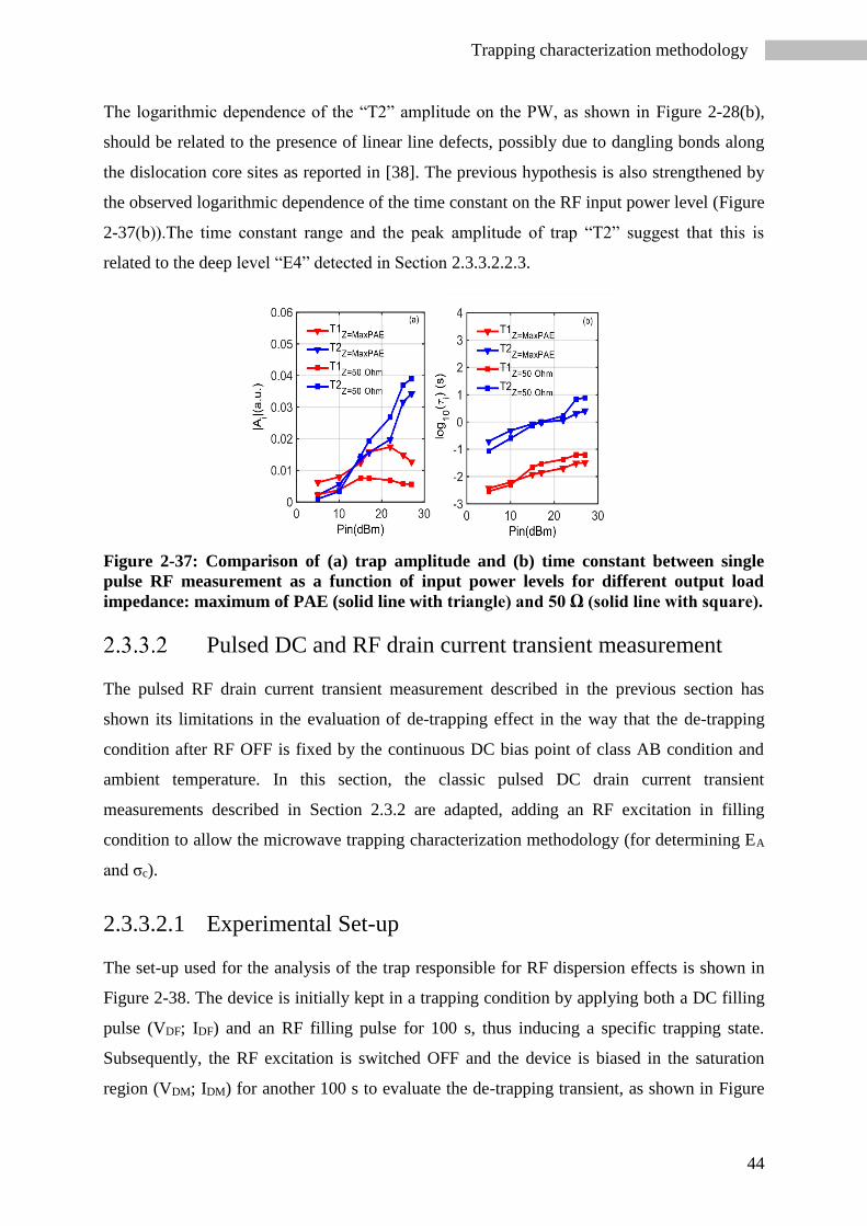
44
Trapping characterization methodology
The logarithmic dependence of the “T2” amplitude on the PW, as shown in Figure 2-28(b),
should be related to the presence of linear line defects, possibly due to dangling bonds along
the dislocation core sites as reported in [38]. The previous hypothesis is also strengthened by
the observed logarithmic dependence of the time constant on the RF input power level (Figure
2-37(b)).The time constant range and the peak amplitude of trap “T2” suggest that this is
related to the deep level “E4” detected in Section 2.3.3.2.2.3.
Figure 2-37: Comparison of (a) trap amplitude and (b) time constant between single
pulse RF measurement as a function of input power levels for different output load
impedance: maximum of PAE (solid line with triangle) and 50 Ω (solid line with square).
Pulsed DC and RF drain current transient measurement
The pulsed RF drain current transient measurement described in the previous section has
shown its limitations in the evaluation of de-trapping effect in the way that the de-trapping
condition after RF OFF is fixed by the continuous DC bias point of class AB condition and
ambient temperature. In this section, the classic pulsed DC drain current transient
measurements described in Section 2.3.2 are adapted, adding an RF excitation in filling
condition to allow the microwave trapping characterization methodology (for determining EA
and σc).
2.3.3.2.1 Experimental Set-up
The set-up used for the analysis of the trap responsible for RF dispersion effects is shown in
Figure 2-38. The device is initially kept in a trapping condition by applying both a DC filling
pulse (VDF; IDF) and an RF filling pulse for 100 s, thus inducing a specific trapping state.
Subsequently, the RF excitation is switched OFF and the device is biased in the saturation
region (VDM; IDM) for another 100 s to evaluate the de-trapping transient, as shown in Figure

Investigation of trapping phenomena
45
2-39. The recovery of drain current related to charge de-trapping is measured over 5 time
decades (from 1 ms to 100 s) with a current sensor connected to a digital sampling scope.
Thereafter, the de-trapping transient results are fitted with a stretched multi-exponential
function to extrapolate the time constant from the peak of the ∂IDS/∂log(t) curves.
Figure 2-38: Block diagram of microwave drain current spectroscopy set-up.
Figure 2-39: Timing diagram of microwave drain current spectroscopy.
The RF waveforms are continuously measured at the DUT planes during the filling phase
using an LSNA. The generation of DC (by gate and drain pulsers) and RF (by pulsed-RF
generator) excitations and the measuring of the DC current and RF waveforms are
synchronized by an arbitrary waveform generator.

46
Trapping characterization methodology
2.3.3.2.2 Experimental Results and Discussion
For this trapping investigation the 8x250µm GH 50-10 AlGaN/GaN HEMT was operated in
class AB (IDS=25 mA/mm at VDS=40 V) at a frequency of 4 GHz for an optimum PAE
impedance ZLOAD_opt,PAE(f0)=19.5+j68Ω. The CW RF power performance (shown in Figure
2-40) was measured before the trapping investigation. One of the trapping mechanisms
responsible of the modification of the large-signal RF performance is shown in Figure 2-41.
The ID-VG characterization is performed before and several times after 100 s of RF stress at
Pin equal to 27 dBm in class AB operation mode – this input power corresponds to a high
compression level of 12 dB. The results of gm (derived from ID-VG) measurements in Figure
2-41 show a threshold voltage (VTH) positive shift after RF stress. This VTH positive shift
indicates an accumulation of negative charges trapped under gate region [20]. In order to
further investigate the trapping phenomena responsible for the VTH shift, microwave drain
current transient measurements are carried out. In the following, we investigate the influence
of the bias point (VDM; IDM) in de-trapping condition, the input power level and the
temperature on the dynamic behavior of the charge-trapping.
Figure 2-40: RF power performances at 4 GHz (class AB operation mode) for maximum
PAE at ZLOAD_opt,PAE(f0)=19.5+j68Ω.

Investigation of trapping phenomena
47
Figure 2-41: Variation of gm (derived from ID-VG characteristic) before and after 100 s
of RF stress at Pin equal to 27 dBm in class AB operation mode.
Bias point dependence in de-trapping condition
The dependence of the de-trapping behavior is investigated by drain current transient
measurements for different bias point (VDM; IDM) in the de-trapping condition as shown in
Figure 2-42. The trap state is fixed with a DC filling bias condition equal to (VDF; IDF)=(40 V;
50 mA) and with a RF filling condition with Pin equal to 27 dBm. The shape of the current in
Figure 2-42 shows that for a fixed IDS and an increase of VDS, the de-trapping processes are
accelerated. In the same way, for a fixed VDS and increase of IDS the time constants become
faster. These accelerations of emission process are firstly due to the increase of the power
dissipation for fixed VDM, leading to an increase of the operating temperature of device, and
secondly to the Poole-Frenkel effect when VDM increases. Indeed, the measurement results in
Figure 2-43 obtained for a fixed IDS show that the emission rate increases exponentially with
the square root of the applied field, according to the Poole-Frenkel model [48]. In Figure 2-43
the error bar indicates the estimated variation of de-trapping time constant due to the channel
temperature increases. In the following measurements, (VDM; IDM)= (5 V; 100 mA) is chosen.
The low drain voltage allows to minimize the electric-field effect during the monitoring while
a drain current equal to 100 mA allows a better investigation of trapping effects.

48
Trapping characterization methodology
Figure 2-42: De-trapping drain current transient measurements and stretched multi-
exponential fitting for different bias points (VDM; IDM) in de-trapping condition with a
DC filling bias condition of (VDF; IDF)=(40 V, 50 mA) and an RF filling condition of Pin
equal to 27 dBm.
Figure 2-43: Emission rate as a function of the square root of the applied voltage (VDM)
during the de-trapping condition for a fixed IDS equal to 50 mA (min–max time constants
variation with junction temperature estimation reported on the error bars).
RF Input power level dependence
In order to investigate the trapping effects due to DC and RF excitations, the drain current
measurements are carried out firstly with no RF excitation and then with increasing RF input
power, as shown Figure 2-44(a). The associated load-lines responsible to RF trapping effects
are illustrated in Figure 2-44(c). In particular, the de-trapping drain current transient
measurements and the associated time constant analysis are depicted respectively in Figure
2-44(b) and Figure 2-44 (d). The DC mode gives rise to two trapping phenomena: one capture
process and one emission process labeled, respectively, “E3” and “E4”. The capture process
“E3” disappears with an increase of input power. The increase of CC versus Pin at 1 ms after
the filling phase, which corresponds consequently to the increase of “E4” trap density, is due
to the fact that more and more trap centers “E4” have been excited by the increasing electric
field (capture process). The electric field increases promote an increase in the high gate and

Investigation of trapping phenomena
49
high drain voltage excursions [42]. The trap centers “E4” are possibly located in the buffer
[28].
Figure 2-44: (a) Drain current measurements recorded with and without a variable level
of RF excitation at 60°C. (c) Corresponding extrinsic output load-lines derived from
waveforms at f0, 2f0 and 3f0 measured at 90 s after starting RF pulse. (b) De-trapping
drain current transient measurements and stretched multi-exponential fitting without
RF excitation and with an increase to power input level at 60°C. (d) Related time
spectrum analysis of de-trapping transient.
In the time range [100 ms – 100 s] “E4” emission process is observed and shown in Figure
2-44(d). The electric field is fixed by the bias point (VDM; IDM) and does not vary. Moreover,
the junction device temperature can be considered as stabilized (i.e. determined only by the
bias point (VDM; IDM), and independent of the previous filling excitations). Then, we do not
expect the emission time constant to vary with the different previous filling excitations. In
Figure 2-44(d), it is observed that the emission time constant has only a small variation in the
time range [~2.5 – ~6 s] with increasing input power level and exhibits a saturation when the
input power level is above 21 dBm. This emission time constant variation is negligible with
respect to the ones of Arrhenius plot in Figure 2-47, which is equal to two decades with only
40 °C temperature variation. Thus, to a approximation, only the amplitude of current recovery
varies, due to the increasing of ionized trap density with respect to Pin in the filling phase. In

50
Trapping characterization methodology
Figure 2-44(b), it is also possible to evaluate the impact of the trapping effect due to DC and
RF excitations: the CC at 1 ms after filling condition and the “E4” trap density for a RF filling
pulse at Pin equal to 27 dBm are 25% more important than the DC ones.
Temperature dependence
For a deeper understanding of the properties of the involved levels “E3” and “E4”, the drain
current transients are measured at several temperatures in DC and RF filling conditions (with
Pin equal to 27 dBm), in Figure 2-45(a), respectively, Figure 2-46(a), to extrapolate the
Arrhenius plot. The results of the Arrhenius plot shown in Figure 2-47 present two trap
signatures, namely “E3” and “E4”, obtained from DC excitation with apparent activation
energies of 0.73 eV and 0.75 eV and capture cross section of 1.4×10⁻¹⁵ cm-2 and 1.4×10⁻¹⁴
cm-2. Figure 2-45 shows also that the trap “E3” gives only a minor contribution to overall
temperature de-trapping transients. One trap signature “E4” is identified from the RF
excitation with activation energy 0.85 eV and cross section 9.4×10⁻¹⁵ cm-2. The Arrhenius plot
results are corrected to consider device self-heating.
Figure 2-45: (a) De-trapping drain current measurement recorded and stretched multi-
exponential fitting without RF excitation (VDF; IDF)=(40 V; 50 mA) for 50°C to 90°C
temperature range, (b) Related time spectrum analysis of de-trapping transient.

Investigation of trapping phenomena
51
As was noticed in the last section, the emission process “E4” obtained from RF excitation
presents a similar dynamic behavior to the one obtained from DC excitation. Remarkably, the
trap signal amplitude is higher under RF excitation, while the time constant is longer. Thus,
we suppose that level “E4” obtained from DC excitation and from RF excitation has the same
nature, while the density of the ionized traps changes with the excitation conditions.
.
Figure 2-46: (a) De-trapping drain current measurement recorded and stretched multi-
exponential fitting at (VDF; IDF)=(40 V; 50 mA) with RF Pin=27 dBm for 50°C to 90°C
temperature range, (b) Related time spectrum analysis of de-trapping transient.
Figure 2-47: Arrhenius plot of the signature detected from RF excitation (Pin=27dBm)
and DC excitation with apparent activation energies (EA) and capture cross sections (σc).

52
Trapping characterization methodology
CW RF drain current transient measurement
One way to characterize these trapping phenomena on new SSPA generation based on
AlGaN/GaN HEMTs under CW large-signal excitations is based on multiple and consecutive
power sweep measurements and a drain current transient measurement after the last power
sweep. The set-up used for these characterizations is shown in Section 2.3.3.1.1 based on an
LSNA system, but it is possible use a cheaper solution based on VNA and a scope.
Figure 2-48: Three consecutive RF power performances until 10 dBc measured at 4 GHz
(class AB operation mode) for maximum PAE at impedance equal to ZLOAD_maxPAE(f0)=
22.5+j58Ω. Corresponding extrinsic CW output load-lines derived from wave
measurement at f0, 2f0 and 3f0 of the first power sweep.
In order to understand how the class operation mode is sensitive to trapping effects, we have
carried out three consecutive power sweep measurements up to 10 dB compression in class
AB operation mode (IDS=25 mA/mm at VDS=50 V) at a frequency of 4 GHz and for an
impedance corresponding to the matching of the transistor for maximum PAE
ZLOAD_maxPAE(f0)= 22.5+j58 Ω. The measurement results in Figure 2-48 (a) and (b) show
principally that after the first power sweep, the output power, gain and drain current present
an important drop for low input power level due to trapping phenomena which are excited by
varying large-signal excitations in high compression gain, as shown by the CW output load-
lines in Figure 2-48(c). Subsequently, the second and third power sweeps indicate that the

Investigation of trapping phenomena
53
device changes its class operation mode from class AB to class B. This class operation
changing is due to trapping effects which impacts the drain current at low input power.
Indeed, as shown in Figure 2-49, the extrinsic CW output load-lines at an input power level
equal to -5 dBm present a strong reduction for the second and third power sweeps.
Figure 2-49: Extrinsic CW output load-lines derived from wave measurement at f0, 2f0
and 3f0 for Pin=-5 dBm for the three power sweeps.
In order to further investigate the effect of the bias point on these trapping phenomena, two
consecutive power sweep measurements and drain current transient measurements are carried
out for fixed IDS and for fixed VDS conditions. The analysis of the recovery drain current
transient measurements by the multiexponential fit (in Equation (2-15)), already used in the
lasts sections, allows to extract the time constant.
To analyze the RF degradation due to trapping effects, the figures of merit, for a fixed input
power level (𝑃𝐼𝑁) are defined as
𝐼𝐷𝑆 𝐷𝑅𝑂𝑃(𝑃𝐼𝑁) =
𝐼𝐷𝑆,1𝑆𝑊𝐸𝐸𝑃(𝑃𝐼𝑁) − 𝐼𝐷𝑆,2𝑆𝑊𝐸𝐸𝑃(𝑃𝐼𝑁)
𝐼𝐷𝑆,1𝑆𝑊𝐸𝐸𝑃(𝑃𝐼𝑁)∙ 100
(2-17)
𝐺𝑎𝑖𝑛 𝐷𝑅𝑂𝑃(𝑃𝐼𝑁) = 𝐺𝑎𝑖𝑛1𝑆𝑊𝐸𝐸𝑃(𝑃𝐼𝑁) − 𝐺𝑎𝑖𝑛2𝑆𝑊𝐸𝐸𝑃(𝑃𝐼𝑁)
(2-18)
𝑃𝑜𝑢𝑡 𝐷𝑅𝑂𝑃(𝑃𝐼𝑁) = 𝑃𝑜𝑢𝑡1𝑆𝑊𝐸𝐸𝑃(𝑃𝐼𝑁) − 𝑃𝑜𝑢𝑡2𝑆𝑊𝐸𝐸𝑃(𝑃𝐼𝑁)
(2-19)
and the time constant.
The first characterization consists of an RF performance measurements for a fixed IDS equal to
50 mA and an increasing VDS, first 30 V, then 40 V and 50 V. As shown in Figure 2-50 and
more clearly summarized in Table 3, the power gain, drain current and output power decrease
at low input power level with respect to the increasing of VDS. It must be noticed that the
trapping effects and consequently their time constants decrease with increasing VDS due to the
Poole–Frenkel effect, as shown in Section 2.3.3.2.2.1.
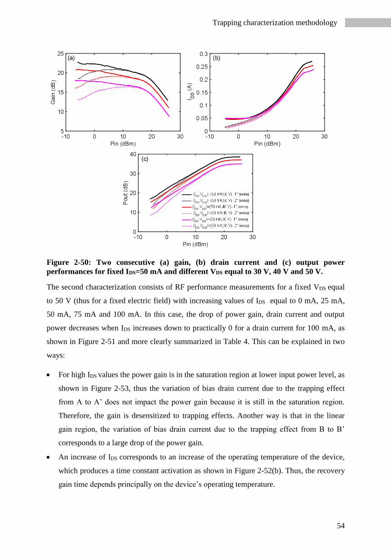
54
Trapping characterization methodology
Figure 2-50: Two consecutive (a) gain, (b) drain current and (c) output power
performances for fixed IDS=50 mA and different VDS equal to 30 V, 40 V and 50 V.
The second characterization consists of RF performance measurements for a fixed VDS equal
to 50 V (thus for a fixed electric field) with increasing values of IDS equal to 0 mA, 25 mA,
50 mA, 75 mA and 100 mA. In this case, the drop of power gain, drain current and output
power decreases when IDS increases down to practically 0 for a drain current for 100 mA, as
shown in Figure 2-51 and more clearly summarized in Table 4. This can be explained in two
ways:
For high IDS values the power gain is in the saturation region at lower input power level, as
shown in Figure 2-53, thus the variation of bias drain current due to the trapping effect
from A to A’ does not impact the power gain because it is still in the saturation region.
Therefore, the gain is desensitized to trapping effects. Another way is that in the linear
gain region, the variation of bias drain current due to the trapping effect from B to B’
corresponds to a large drop of the power gain.
An increase of IDS corresponds to an increase of the operating temperature of the device,
which produces a time constant activation as shown in Figure 2-52(b). Thus, the recovery
gain time depends principally on the device’s operating temperature.

Investigation of trapping phenomena
55
Following these considerations, it is suggested to bias the device at IDS equal to 100 mA in
order to reduce the trapping effects.
Figure 2-51: Two consecutive (a) gain, (b) drain current and (c) output power
performances for fixed VDS=50 V and different IDS equal to 0 mA, 25 mA, 50 mA, 75 mA
and 100 mA.
Figure 2-52: Recovery drain current transient measurement after second power sweep
with varying of VDS (a) and IDS (b).

56
Trapping characterization methodology
TABLE 3
FIGURE OF MERIT AT FIXED IDS
VDS (V) IDS DROP (%)
[Pin=-5dBm]
Gain DROP (dB)
[Pin=-5dBm]
Pout DROP (dBm)
[Pin=-5dBm] Time constant (s)
30 76.3 4.47 2.58 186.2
40 68.8 4.16 2.53 93.32
50 57.6 3.97 1.69 65.31
TABLE 4
FIGURE OF MERIT AT FIXED VDS
IDS (mA) IDS DROP (%)
[Pin=-5dBm]
Gain DROP (dB)
[Pin=-5dBm]
Pout DROP (dBm)
[Pin=-5dBm] Time constant (s)
0 // 11.9 14.1 //
25 65.4 6.85 5.36 106.6
50 57.6 3.97 1.69 65.3
75 36.5 0.38 0.48 17.5
100 21.9 0 0 8
Figure 2-53: Schematic of trapping effect on power gain as a function of the drain
current.
With this technique, we demonstrated that it is possible to control the trapping phenomena by
choosing the value of the bias point and thus identify a trapping desensitization operating
zone. Indeed for (IDS; VDS)=(100 mA; 50 V) the gain drop is cancelled and the time constant
is noticeably reduced, so the trapping effect can be considered neutralized. Whereas for very
low IDS the RF performances are more impacted, with the consequence that the trapping
effects are exacerbated. Lastly, one notices that the trapping effect are more sensitive to
varying IDS than to varying VDS.

Investigation of trapping phenomena
57
2.3.4 Low-frequency dispersion measurements
The output conductance and transconductance of GaN HEMTs have been observed to change
significantly at low-frequencies (10 Hz - 100 MHz) [16], [49]. So, in order to gather
complementary information on trapping effects under class AB biasing, the dispersion of the
LF Y-parameters are investigated through measurements of the small-signal S-parameters in
the 100 Hz to 1 GHz frequency range. These S-parameter measurements were carried out at
several temperatures using an Agilent E5061b LF-HF vector network analyzer [50] to
determine the dispersion of gd(f) and gm(f). As illustrated in Figure 2-54, the VGS is applied to
an external LF bias tee with a DC port connected to the power supply and the RF port
connected to port 2 of the VNA. In order to cover the broadband from 100 Hz to 1 GHz LF
Y-parameter measurements are performed in two sub-bands: with an LF home-made resistive
bias tee [49] from 100 Hz to 10 MHz and with a commercial bias tee (Picosecond 5546) from
10 MHz to 1 GHz. The characteristics of the bias tees in terms of return and insertion loss are
shown in Figure 2-55. The drain terminal is connected to an internal bias system (port 1) in
the network analyzer. An on-wafer SOLT calibration is performed at each individual
temperature.
Figure 2-54: Block diagram of the LF Y-parameters measurement set-up in 2-port
configuration for the characterization of gd(f) and gm(f).

58
Trapping characterization methodology
Figure 2-55: (a) Return loss and (b) insertion loss of LF bias tees used for LF Y-
parameter measurements.
So, the Y-parameters are calculated from measured S-parameters [51]. Empirically, the effect
of carrier trapping on the frequency dispersion of the output conductance and
transconductance can be modeled as reported in [21]. The dispersion effects are taken into
account with an additional voltage dependent current source (which represents the injection
mechanism in trap state) in an RC circuit as shown in Figure 2-56.
Figure 2-56: Empirically equivalent circuit model for output conductance and
transconductance dispersions.
According to this small-signal model at low-frequency, gm(f) and gd(f) can be deduced from
the Y-parameters of the DUT, respectively Y21 and Y22 parameters by the following
equations:
22
2
2111
)(n
nmn
n
nmnm
gj
ggY
(2-20)
22
2
2211
)(n
nnmn
n
nnmnd
ggj
gggY
(2-21)
τn=Cn/gn corresponds to the time constant of the trapping process. For the determination of the
time constants, the derivative forms of the imaginary part of Y21 and Y22 are used. In this way,

Investigation of trapping phenomena
59
the time constants due to gm(f) dispersion can be determined either from the peak values of the
imaginary part of Y21 (fimag[Y21]=1/2πτn) and the time constants due to gd(f) dispersion can be
determineed from the peak values of the imaginary part of Y22 (fimag[Y22]=1/2πτn). The number
of traps of gm(f) (gd(f)) is defined by the number of peaks of the imaginary part of Y21 (Y22) or
by the number of inflexion points of the real part of Y21 (Y22) [9]. As has been demonstrated,
the peak values of the imaginary parts of Y21 and Y22 at several temperatures allows
determining the EA and c (associated respectively to gm(f) and gd(f) dispersion) using the
Arrhenius formula (2-11) and substituting the emission rate with the reciprocal of the time
constant (en=1/τn). A temperature correction is applied to determine EA and c.
LF Y-parameter measurement results
LF Y-parameter measurements for the SEMI-ON state (VGS; VDS)=(-1.9V,40V) were carried
out at different temperatures to obtain the Arrhenius plots shown in Figure 2-57 and Figure
2-58. This analysis is focused only on Y21 and Y22 because the experimental data of Y11 and
Y12 do not show any dispersion. The Y-parameters, depicted in Figure 2-57 and Figure 2-58,
show that above 100 MHz, the contribution of the intrinsic capacitances of the small-signal
model is not negligible. The Y21-measurement shows two distinct transition frequencies in
Real[Y21] and two distinct peaks in Imag[Y21], proving that gm(f) dispersion presents two
trapping phenomena. The peak of the imaginary part of Y21 corresponds to the transitions in
the transconductance (the real part of Y21). Figure 2-57(a) shows a significant decrease of the
transconductance (Real[Y21]) amplitude with the increase of the temperature due to thermal
effects. On the one hand, the first transition appears at LF (approximately 5-10 KHz for
80°C). On the other hand Real[Y21] increases when the frequency decreases. The conclusion
of these two last observations is that the trap (labeled “E2”) can be associated to an emission
process. Considering that Real[Y21] decreases when the frequency decreases and considering
that the time constant of trap “E1” is approximately 1µs, the trap “E1” can be associated to a
capture process. Output conductance dispersion for the same device is presented in Figure
2-58. The real part of Y22 (Real[Y22]) corresponding, to a first approximation, to the output
conductance, shows one inflection point. So gd(f) dispersion presents one trap that
corresponds to trap “E2” found by gm(f) dispersion according to [52].

60
Trapping characterization methodology
Figure 2-57: (a) Real [Y21] versus frequency for 80°C to 130°C temperature range, (b)
Imag[Y21] versus frequency for 80°C to 130°C temperature range and (c) related
Arrhenius plot .
Figure 2-58: (a) Real [Y22] versus frequency for 80°C to 130°C temperature range, (b)
Imag [Y22] versus frequency for 80°C to 130°C temperature range and (c) related
Arrhenius plot.

Investigation of trapping phenomena
61
Moreover, for the process “E2” we found the same time constants by gd(f) and gm(f)
dispersions. Thus, the traps “E1” and “E2” are promoted by two mechanisms: the first one
appears only when the small-signal is applied to the gate port, this suggests that the trap is
located under the gate. The second trapping mechanism is due to hot electrons as explained in
Section 2.3.2.5. The transconductance and output conductance frequency dispersions
promoted by the process “E2” can be explained in this way: if the de-trapping time constant is
much higher than the signal period (the traps are frozen), the traps cannot respond as quickly
as the applied voltage. On the other hand, when the de-trapping time constant is of the same
order as the signal period, trapped electrons due to the injection of highly energetic (hot)
electrons are emitted and they participate in the RF current-carrying process giving rise to
frequency dispersion in the device.
Identification of deep levels
Figure 2-59: Summary of Arrhenius plot of the deep levels, obtained from different
drain current transient measurements performed during the research for this thesis.
A summary of the Arrhenius plot obtained from different drain current transient
measurements performed during the research for this thesis is shown in Figure 2-59. The deep
levels “E4”=1 eV, “E3”=0.86 eV and “E2”=0.64 eV are identified by DC drain current
transient measurements carried out using the set-up at the University of Padova described in
Section 2.3.2.1. The deep levels “E4”=0.75 eV, and “E3”=0.73 eV are identified with DC
drain current transient measurements and the deep level “E4”=0.83 eV is identified with RF

62
Identification of deep levels
drain current transient measurements carried out using the set-up at the XLIM laboratory
described in Section 2.3.3.2.1. All XLIM laboratory measurements are carried out with use of
bias tees. Thus, due to the parasitic effects of the bias tees, the drain current recording is
started at 1 ms. Therefore, the trapping effect labeled “E2” is outside of the time windows for
the measurements and it cannot be detected. Moreover, the differences between the EA and σc
of deep level “E4” between DC drain current transient measurements carried out at the
University of Padova and at the XLIM laboratory can be explained by the fact that the
characterized DUTs came from the same technology but different production runs. In
conclusion, the deep levels “E3” and “E4” detected by the conventional DC DLTS
measurement set-up and by the DC DLTS measurement set-up with bias tees involve the
same trap-center.
In order to understand and interpret the possible physical origin of a trap, the trap properties
(EA and σc) are compared to deep levels previously reported in the literature, which are
summarized in Figure 2-60 and Table 5.
Figure 2-60: Arrhenius plot of deep levels “E1”, “E2”, “E3” and “E4” detected within
this thesis research. Presentation of trap states reported in previous papers for
comparison (data taken from [20] and references therein).
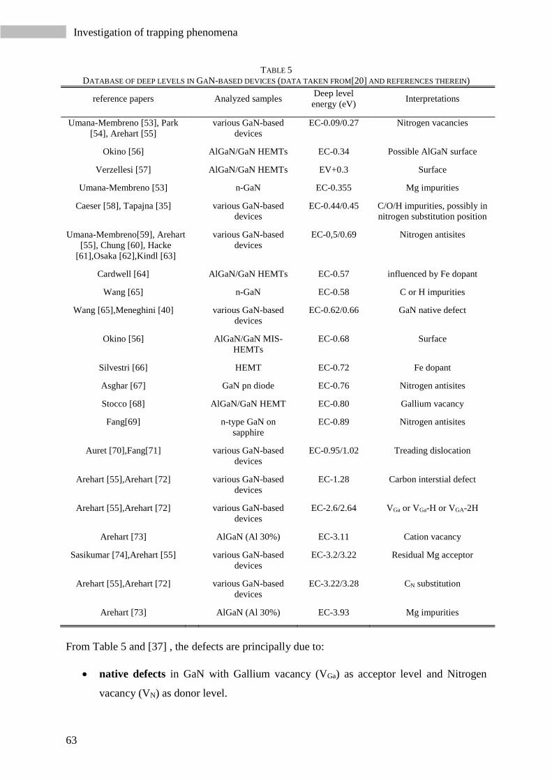
Investigation of trapping phenomena
63
TABLE 5
DATABASE OF DEEP LEVELS IN GAN-BASED DEVICES (DATA TAKEN FROM[20] AND REFERENCES THEREIN)
reference papers
Analyzed samples Deep level
energy (eV) Interpretations
Umana-Membreno [53], Park
[54], Arehart [55]
various GaN-based
devices
EC-0.09/0.27 Nitrogen vacancies
Okino [56] AlGaN/GaN HEMTs EC-0.34 Possible AlGaN surface
Verzellesi [57] AlGaN/GaN HEMTs EV+0.3 Surface
Umana-Membreno [53] n-GaN EC-0.355 Mg impurities
Caeser [58], Tapajna [35] various GaN-based
devices
EC-0.44/0.45 C/O/H impurities, possibly in
nitrogen substitution position
Umana-Membreno[59], Arehart
[55], Chung [60], Hacke
[61],Osaka [62],Kindl [63]
various GaN-based
devices
EC-0,5/0.69 Nitrogen antisites
Cardwell [64] AlGaN/GaN HEMTs EC-0.57 influenced by Fe dopant
Wang [65] n-GaN EC-0.58 C or H impurities
Wang [65],Meneghini [40] various GaN-based
devices
EC-0.62/0.66 GaN native defect
Okino [56] AlGaN/GaN MIS-
HEMTs
EC-0.68 Surface
Silvestri [66] HEMT EC-0.72 Fe dopant
Asghar [67] GaN pn diode EC-0.76 Nitrogen antisites
Stocco [68] AlGaN/GaN HEMT EC-0.80 Gallium vacancy
Fang[69] n-type GaN on
sapphire
EC-0.89 Nitrogen antisites
Auret [70],Fang[71] various GaN-based
devices
EC-0.95/1.02 Treading dislocation
Arehart [55],Arehart [72] various GaN-based
devices
EC-1.28 Carbon interstial defect
Arehart [55],Arehart [72] various GaN-based
devices
EC-2.6/2.64 VGa or VGa-H or VGA-2H
Arehart [73] AlGaN (Al 30%) EC-3.11 Cation vacancy
Sasikumar [74],Arehart [55] various GaN-based
devices
EC-3.2/3.22 Residual Mg acceptor
Arehart [55],Arehart [72] various GaN-based
devices
EC-3.22/3.28 CN substitution
Arehart [73] AlGaN (Al 30%) EC-3.93 Mg impurities
From Table 5 and [37] , the defects are principally due to:
native defects in GaN with Gallium vacancy (VGa) as acceptor level and Nitrogen
vacancy (VN) as donor level.

64
Conclusions
high presence of hydrogen impurities in GaN (complexes with VGa and C-H).
carbon atoms can be incorporated with gallium substitutionals (CGa) or nitrogen
substitutionals(CN) in order to obtain a highly insulating GaN layer.
oxygen impurity in nitrogen substitutional (ON) that has a shallow donor level.
iron impurities is commonly presented in GaN technology to reach a semi-insulating
GaN.
The overall Arrhenius plot provided by I-DLTS, transconductance and output-conductance
frequency dispersion measurements is shown in Figure 2-60. From Figure 2-60, the emission
process “E2” obtained from DCT measurements is characterized by EA=0.64eV and σc
=3.9x10⁻¹⁴cm2. The emission trap process obtained from transconductance and output-
conductance frequency dispersion measurements is characterized by EA=0.61eV and σc
=1.2x10⁻¹⁴ cm2. For the first time, to our knoweledge, the correspondence of the trap
characteristics allows concluding that the same trap level “E2” is determined from the two
different measurements. Moreover, the imaginary parts of Y21 and the Y22 in Figure 2-57 and
Figure 2-58 show a rightward shift of the peaks when the temperature increases. This
frequency shift, from 5 kHz (at 80°C) to 65 kHz (at 130°C), converted in the time-domain
corresponds to the same time constant shift observed in the DCT measurements (Figure
2-18(a)) when the temperature increases. This level “E2” is supposed to be due to a native
defect of GaN, based on comparison with previous reports [20], [40], [68]. The level “E3”
(EA=0.86eV; σc =8.7x10⁻¹³ cm2) obtained from DCT measurements, reveals a similar
signature to the deep levels already associated to nitrogen-related defects [19], [35], [61], [72]
present in the GaN layer. The level “E4” (EA=1eV; σc =5.0x10⁻¹³ cm2) characterized by DCT
measurements, shows a correspondence with the signature of the deep levels associated to
extended defects in GaN [7], [20], [27], [62]. Finally, the level “E1” (EA=0.25eV; σc =1.6x10-
17 cm2) characterized by LF Y21 measurements, shows again a correspondence with the
signature of the deep levels associated to nitrogen-related defects [30], [31].
Conclusions
In this chapter, a detailed and innovative investigation of the trapping processes in
AlGaN/GaN HEMTs from DC to radio-frequency range is described. The first part of this
chapter introduced the theoretical concepts on electron capture/emission phenomena needed
to understand and characterize the trap mechanism and the determination of an Arrhenius
plot.

Investigation of trapping phenomena
65
Successively, the methods and the associated set-ups for the trapping investigation developed
during the research for this Ph.D. thesis have been presented. This trapping investigation is
based on combined pulsed I/V measurements (which provide an identification of the possible
trap position), DCT investigation (which provide data on the large-signal voltage steps de-
trapping transient, suitable for deep level analysis), nonlinear microwave DCT investigation
(which provide the RF deep level analysis) and LF transconductance and output-conductance
measurements (which provide small-signal trap analysis). The conclusions of this chapter on
trapping investigation are summarized below:
The pulsed I/V measurements under class AB bias condition detected a shift in the
threshold voltage, a significant increase in the resistivity of the gate–drain access
region, and a decrease in the transconductance peak. Moreover, pulsed I/V
characterization carried out at several temperatures shows that the CC increases when
the gate quiescent bias point increases (due to hot electrons), in accordance with [83].
The properties of the trap responsible for CC are investigated with DC DCT. This
technique has evidenced three traps with the following activation energies: “E4”=1
eV, “E3”= 0.86 eV and “E2”=0.64 eV.
The transconductance and output-conductance frequency technique principally
identified a trap level “E2”=0.61 eV which has been found to have a good matching
with the trap level “E2” identified by the DC DCT technique. The trap level “E2”
corresponds to the faster trap phenomena detected by the DC DCT technique. The trap
level “E2” is supposed to be due to a native defect in GaN. The features of the pulsed
I/V measurement suggest that these defects are located in the GaN buffer layer.
The DC DCT technique is very powerful because of the sensitivity of the drain current
to the trap parameter analysis. The time constant and amplitude of the traps are
determined from the Arrhenius plot for trapping or de-trapping phenomena. Real-time
trapping behavior is observed thanks to accurate records over a 7-decade time scale
allowing the investigation of slow and fast trapping phenomena.
The transcondutance and output-conductance frequency dispersion technique can
provide trap information (EA and c) using small-signal excitations close to real CW
RF operation mode. This trapping determination method (LF Y21 and LF Y22) is based
on the 2-port S-parameters measurement that directly provides information about the
current corresponding to gm and gd (to a first approximation). The advantage of this
method lies in the sensitivity of gm and gd to the drain-lag trapping effects. LF Y-

66
Conclusions
parameter characterization is very accurate because it is based on the use of VNA
measurements. This method provides a fast characterization of trapping phenomena
but suffers from the lack of a quantitative determination of the trap density. The
complexity of the LF dispersion characterization and the scarcity of its analysis makes
it difficult to determine at the moment a detailed theoretical model of trap “E1”. But,
the technique for determining the activation energies and capture cross-sections for the
detected traps, based on temperature-dependent measurements of the imaginary parts
of Y22 and Y21, is demonstrated.
The nonlinear microwave DCT measurements allow investigating the trapping
characteristics corresponding to the nonlinear RF dynamics of the dispersion effects in
GaN HEMTs. The method consists of the measurement and analysis of de-trapping
drain current transients after 100 s of RF excitation.
It is demonstrated how the choice of bias point in the de-trapping condition allows
accelerating the slow emission process for the increase in power dissipation and for
the Poole–Frenkel effect.
The nonlinear microwave DCT measurement results show also that the increase of the
load-line excursions produce a stronger impact of the de-trapping behavior in terms of
CC after RF OFF and trap amplitude. Therefore, an increase in the RF level involves
the excitation of more and more “E4” trap centers. The trapping mechanism due to RF
excitation is attributed to a positive threshold voltage shift that indicates a negative
charge-trapping under the gate region.
The comparison between the DC and RF testing results demonstrated that the impact
of trapping phenomena appears more severe under single pulse large-signal RF
excitation than under only single pulse DC excitation.
The nonlinear microwave DCT load-pull measurements for two different output load
impedances (maximum of PAE and mismatched impedances) have revealed that the
trapping phenomena impact is lower when the transistor is optimally matched at its
output port to reach maximum PAE performance.
The nonlinear microwave DCT analysis has evidenced the deep level “E4”=0.75 eV.
The level “E4” is also detected in DC excitation but with an increase of the density of
the ionized traps.
The nonlinear microwave DCT results have put in evidence the sensitivity of the traps
to the:

Investigation of trapping phenomena
67
Input power level;
Pulse-width;
Temperature;
Load impedance;
Operating bias point.
The nonlinear microwave DCT measurements have demonstrated that it is possible to
control the trapping phenomena by choosing the value of operating bias point and thus
identify a trapping desensitization operating zone.
In conclusion, in this chapter we have identified the trap levels present in this commercial
GaN GH50 technology from UMS foundry due principally to native defects of the GaN.
Moreover, we have also demonstrated the strong impact on the RF performance of the
trapping effects and their sensitivity to many factors. Thus, this thesis research has identified a
way to make the SSPA insensitive to trapping effects in real RF operating conditions, by
choosing the correct operating bias point value in order to reach the trapping desensitization
operating zone.

68
Introduction
3 Nonlinear Electro-Thermal model of
AlGaN/GaN HEMT
Introduction
The new SSPA generation based on AlGaN/GaN HEMTs is currently under development for
replacing the preceding technologies. As described in the previous chapter, GaN technology is
still subject to memory effects, such as trapping and thermal effects. The aim of electrical
modeling is to allow designers to simulate the nonlinear behavior of the device under complex
electrical signals. Thus, it is of fundamental importance to provide a compact model in CAD
tools which takes into account the dispersion phenomena of GaN-based HEMT in order to
predict correctly the RF performance during real RF operating conditions. The resultant
nonlinear electro-thermal AlGaN/GaN HEMT model including large-signal dynamic trapping
effects becomes a necessary tool for designers to assess the performance of the high
efficiency solid state power amplifier required by the market [84].
In this chapter a modeling methodology for AlGaN/GaN HEMTs is presented, in particular
our contribution with respect to previous works [30], [41]. This contribution mainly consists
in the introduction of a new additive thermal-trap model which takes into account the
dynamic behavior of trap states and their associated temperature variation and the validation
of the model at different temperatures. The building of the new thermal-trapping model is
based on the large trapping investigation and measurements carried out in the last chapter.
Modeling methods for HEMTs
There are different kinds of models that can be less or more complex according to the goal of
modeling the device. For example, for understanding the physical phenomena, such as the
charging mechanisms between the semi-conductor layers due to trapping and thermal effects,
a physical model is used. This model is described by physical laws and includes technological
parameters (e.g., device layout, doping, and layer size). The physical model is generally
performed using 2-D solving of charge transport equations for the electrical characteristics. In
the case of thermal simulation, a 3-D finite element simulation involves meshes with
thousands of nodes in order to take into account the various effects. This modeling approach
requires a heavy simulation load and does not fit with circuit simulation.

Nonlinear Electro-Thermal model of AlGaN/GaN HEMT
69
A phenomenological model or compact transistor model allows decreasing the number of
parameters used. The purpose of the model is to reproduce the phenomena involved in the
device, with a simplification of the complexity of the physical structure. This modeling
approach is proposed in [85] and depicted in Figure 3-1. This model is also called a semi-
physical model because the equations are determined from the physics (in the case of
definition of the diodes) or following a mathematical law for a better modeling of the
phenomenon (e.g., CGS and CGD) and a better convergence of the model. With the emerging
new generations of characterization methods and instruments, a new type of model is
developed that is called a behavioral model. This behavioral model [86] is based on the neural
network (NN) approach [87] and/or X-parameter measurements [88], [89] and it can be
determined directly from large-signal measurements. It also allows more rapid determination
and correct prediction of the physical phenomena involved in the device. But it does not
provide access to the model parameters, as it is described by a large number of parameters
which have no direct physical meaning. Behavioral models are considered “black box”
models, where only the responses of the component to some controlled stimuli are known,
and are consequently validated only under the operating conditions measured. For research
purposes, we have chosen the phenomenological or compact model, which provides a good
trade-off between simulation speed and modeling flexibility.
Figure 3-1: Identification of intrinsic and extrinsic parameters based on physical
structure of HEMT for a phenomenological model.

70
Modeling methodology
Modeling methodology
The equivalent device circuit used to describe the nonlinear AlGaN/GaN HEMT characteristic
including trapping and thermal effects is shown in Figure 3-2. The modeling methodology
flow, required for a complete device extraction is based on four different steps, as shown in
Figure 3-3.
Figure 3-2: Structure of the nonlinear model including trapping and thermal effects.
Figure 3-3: Modeling methodology flow for the extraction of a nonlinear model
including trapping and thermal effects.

Nonlinear Electro-Thermal model of AlGaN/GaN HEMT
71
The method for parameters extraction shown in Figure 3-3 is developed as follows
1. Determination of extrinsic (Rg, Lg, Cpg, Rd, Lg, Cpd, Rs and Ls) and intrinsic (Cgs, Cgd,
Cds, Ri, Rgd, Gm, Gd and τ) parameters of small-signal model for a fixed bias point.
2. Determination of the large-signal model:
2.1. Definition of drain current source, gate-source diode and gate-drain diode by the
fitting of pulsed I/V characteristic.
2.2. Extraction of nonlinear capacitances CGS and CGD from S-parameter measurements at
different bias points located on an ideal load-line.
3. Addition of the trapping modeling blocks that modulate the instantaneous drain current
value through the variation of intrinsic gate voltage and pinch-off voltage.
4. Addition of the thermal dependency of the drain current source, trapping model, gate-
source diode and gate-drain diode.
Device modeling process
3.4.1 Small-signal model
The equivalent small-signal model or linear model of HEMT is shown in Figure 3-4. It is
composed of two kinds of parameter: the intrinsic and the extrinsic parameters. The last one
corresponds to the parasitic elements due to access lines and metallization.
Figure 3-4: Equivalent small-signal model of HEMT.
The quality of the nonlinear model is strongly dependent on the accuracy of the extrinsic
parameters. Thus, for the extraction of the small-signal model, an optimization method

72
Device modeling process
(developed in XLIM laboratory) is used [30]. The small-signal model is extracted from small-
signal pulsed S-parameter measurements.
Pulsed S-parameters measurements
The S-parameters are measured under pulsed condition to extract the small-signal model at
fixed quiescent bias point close to real operation condition. The measurement set-up is similar
to the previously described pulsed I/V test bench in 2.3.1.1 with the addition of a pulsed VNA
(Rohde & Schwarz ZVA40 and ZVAx modules) to measure pulsed S-parameters as shown in
Figure 3-5. An on-wafer calibration is performed to obtain the pulsed S-parameters at both
ports of the DUT. This calibration is performed in CW mode (SOLT, TRM, etc…) because
the pulsed calibration can deteriorate due to the linearity and dynamic range of the receiver’s
mixer and the losses due to the internal switch in the ZVAX.
The principle of pulsed S-parameter measurements consists of generating the RF signal for
each measurement bias point (VGS,M ;VDS,M ) of the pulsed I-V network and performing the S-
parameters acquisition as depicted in Figure 3-6. Thus as previous discussed, the thermal and
trap states are fixed by the quiescent bias point (VGS,Q ;VDS,Q ). The pulsed RF signal is
synchronized with the pulsed I/V excitation with a reference signal generated by the pulsed
I/V system (BILT AMCAD). The dynamic range from CW to pulsed mode decreases when
the duty cycle of the pulses is reduced as indicated in Equation (3-1).
𝑟𝑒𝑑𝑢𝑐𝑡𝑖𝑜𝑛 (𝑑𝐵) = − 20. log [
𝑃𝑢𝑙𝑠𝑒 𝑝𝑒𝑟𝑖𝑜𝑑
𝑃𝑢𝑙𝑠𝑒 𝑤𝑖𝑑𝑡ℎ]
(3-1)
Thus, the pulse-period and pulse-width are chosen in order to limit the dynamic reduction
while maintaining a quasi-isothermal state and a fixed trapping state. The measurement
condition for pulsed S-parameter measurements are summarized in Figure 3-7 (1 µs of RF
pulse-width, 1.2 µs of gate pulse-width and 1.4 µs of drain pulse-width with an identical pulse
period of 10 µs).

Nonlinear Electro-Thermal model of AlGaN/GaN HEMT
73
Figure 3-5: Block diagram of pulsed S-parameters experimental set-up.
Figure 3-6: Principle of pulse S-parameter measurement.

74
Device modeling process
Figure 3-7: Pulse timing diagram of pulse S-parameter measurement.
Extraction of the small-signal model
The method for the model extraction allows the direct determination of extrinsic parameters
provided the intrinsic parameters are frequency independent. The procedure is the following:
The intrinsic admittance parameters [YINT] are obtained from the measured S-
parameters by successive transformation of the matrix of measured S-parameters (as
depicted in Figure 3-8).
Then, the extrinsic parameters are analytically calculated at each frequency, from the
[YINT] matrix using the following equations:
𝐶𝑔𝑑 =−𝐼𝑚(𝑌12)
𝜔[1 + (
𝑅𝑒(𝑌12)
𝐼𝑚(𝑌12))2
] (3-2)
𝑅𝑔𝑑 =−𝑅𝑒(𝑌12)
(𝐶𝑔𝑑. 𝜔)2[1 + (
𝑅𝑒(𝑌12)
𝐼𝑚(𝑌12))2
] (3-3)
𝐶𝑔𝑠 =𝐼𝑚(𝑌11) + 𝐼𝑚(𝑌12)
𝜔[1 + (
𝑅𝑒(𝑌11) + 𝑅𝑒(𝑌12)
𝐼𝑚(𝑌11) + 𝐼𝑚(𝑌12))2
] (3-4)
𝐺𝑑 = 𝑅𝑒(𝑌12) + 𝑅𝑒(𝑌22) (3-5)
𝐶𝑑𝑠 =𝐼𝑚(𝑌12) + 𝐼𝑚(𝑌22)
𝜔
(3-6)
𝑅𝑖 =𝑅𝑒(𝑌11) + 𝑅𝑒(𝑌12)
(𝐶𝑔𝑠. 𝜔)2[1 + (
𝑅𝑒(𝑌11) + 𝑅𝑒(𝑌12)
𝐼𝑚(𝑌11) + 𝐼𝑚(𝑌12))2
] (3-7)
𝐺𝑚 = √(𝐴2 + 𝐵2)(1 + 𝑅𝑖2𝐶𝑔𝑠2𝜔2) (3-8)
𝜏 =−1
𝜔. 𝑎𝑟𝑐𝑡𝑎𝑛 [
𝐵 + 𝐴. 𝑅𝑖. 𝐶𝑔𝑠. 𝜔
𝐴 − 𝐵. 𝑅𝑖. 𝐶𝑔𝑠. 𝜔]
(3-9)

Nonlinear Electro-Thermal model of AlGaN/GaN HEMT
75
where:
𝐴 = 𝑅𝑒(𝑌21) − 𝑅𝑒(𝑌12) (3-10)
𝐵 = 𝐼𝑚(𝑌21) − 𝐼𝑚(𝑌12) (3-11)
An optimization algorithm process allows adjusting the extrinsic parameters in order the
intrinsic parameters be frequency independent, thus validating the small-signal circuit
topology [30].
Figure 3-8: Extraction algorithm used to determine the intrinsic Y-parameters matrix
[90].
Generally, the extraction methods used to determine the extrinsic parameters are based on S-
parameter measurements at different bias point conditions [91]. A simplified approach used in
[92] for a first determination of intrinsic parameters, was adapted for the GaN device in
collaboration with K. Kahil [ K. Kahil personal communication] at the XLIM laboratory for
use in this research thesis. LF S-parameter measurements allow estimating the ranges of
values of the intrinsic parameters, which are introduced in the optimization loop in order to
determine the extrinsic parameters. In the LF range, the extrinsic parameters, in Figure 3-4,
can be considered negligible, therefore the intrinsic parameter equations (3-2)-(3-11) become

76
Device modeling process
𝐶𝑔𝑑 =−𝐼𝑚(𝑌12)
𝜔
(3-12)
𝑅𝑔𝑑 =−𝑅𝑒(𝑌12)
(𝐶𝑔𝑑. 𝜔)2
(3-13)
𝐶𝑔𝑠 =𝐼𝑚(𝑌11) + 𝐼𝑚(𝑌12)
𝜔
(3-14)
𝐺𝑑 = 𝑅𝑒(𝑌12) + 𝑅𝑒(𝑌22) (3-15)
𝐶𝑑𝑠 =𝐼𝑚(𝑌12) + 𝐼𝑚(𝑌22)
𝜔
(3-16)
𝑅𝑖 =𝑅𝑒(𝑌11) + 𝑅𝑒(𝑌12)
(𝐶𝑔𝑠. 𝜔)2
(3-17)
𝐺𝑚 = 𝑅𝑒(𝑌21) (3-18)
𝜏 =−1
𝜔. 𝑎𝑟𝑐𝑡𝑎𝑛 [
𝐵 + 𝐴. 𝑅𝑖. 𝐶𝑔𝑠. 𝜔
𝐴 − 𝐵. 𝑅𝑖. 𝐶𝑔𝑠. 𝜔]
(3-19)
where:
𝐴 = 𝑅𝑒(𝑌21) − 𝑅𝑒(𝑌12) (3-20)
𝐵 = 𝐼𝑚(𝑌21) − 𝐼𝑚(𝑌12) (3-21)
These equations are applied to the LF CW S-parameters measured at (IDS;VDS)=(50 mA;40
V), using the set-up in Section 2.3.4. The intrinsic parameter results extracted using this
approach are shown in Figure 3-9.
It can be observed from the previous results that this LF approach give good results and
provides thermally dependent intrinsic parameters. Thus, they constitute very good starting
values for the global optimization of the S-parameters at higher frequencies which include the
parasitic access.

Nonlinear Electro-Thermal model of AlGaN/GaN HEMT
77
Figure 3-9: The intrinsic parameter results extracted by LF S-parameters measured at
(IDS;VDS)=(50 mA;40 V) for different temperatures.
Extraction of extrinsic and intrinsic parameters
The bias dependent small-signal parameters are extracted for I/V network issued from a
quiescent bias point equal to the one used in the RF condition. The quiescent bias point
chosen for the determining the small-signal model corresponds to (IDS,Q ; VDS,Q)= (50 mA, 40
V).
TABLE 6
VALUES OF EXTRINSIC AND INTRINSIC PARAMETERS AT
(IDS,Q ; VDS,Q)= (IDS,M ; VDS,M)= (50 mA, 40V) & TCHUCK=25°C
EXTRINSIC PARAMETERS
Rg (Ω) Rd (Ω) Rs (Ω) Lg (pH) Ld (pH) Ls (pH) Cpg (pF) Cpd (fF)
0.4 0.9 0.2 39.5 34 2 0.52 1.69
INTRINSIC PARAMETERS
Cgs (pF) Cgd (fF) Ri (Ω) Rgd (Ω) Cds (pF) τ (ps) gm (mS) gd (mS)
3.88 66.3 1.55 73 57.6 3.97 245 1.69

78
Device modeling process
The pulsed S-parameter measurements are carried on all measurement bias points of the I/V
network under quiescent bias point (IDS,Q ; VDS,Q)= (50 mA, 40 V). The values of the elements
of the small-signal equivalent circuit obtained at a bias point (IDS,M ; VDS,M)= (50 mA, 40 V),
are summarized in Table 6 and a comparison between the measured and modeled S-
parameters is given in Figure 3-10. Once the extrinsic elements are determined the process
can be repeated for the set of bias points chosen to obtain the multi-bias small-signal circuit.
Figure 3-10: Measurements (red solid line) and simulation results (black dotted line) of
pulsed S-parameter measurements at (IDS,Q ; VDS,Q)= (IDS,M ; VDS,M)= (50 mA, 40V) from
0.5 GHz to 12 GHz.
3.4.2 Nonlinear model
The nonlinear HEMT model includes the intrinsic nonlinear current sources shown in Figure
3-11. It consists of the access resistances (Rg, Rd, Rs), the main drain current source IDS, the
two Schottky gate diodes (IGS, IGD) and the breakdown current source IBK.
Figure 3-11: Intrinsic nonlinear current sources of HEMT.

Nonlinear Electro-Thermal model of AlGaN/GaN HEMT
79
Nonlinear current source model
The fundamental effect of FET is described by a nonlinear current source controlled by VDS
and VGS. The model (derived from the model proposed by Tajima [93]) has been modified to
take into account the HEMT effect as shown in [90]. Moreover, an accurate current source
model has been developed in the XLIM laboratory by Jardel et al. [94], which allows to
predict the IDS-VDS characteristic for positive and negative values of the drain voltage. The
model equations are:
𝐼𝐷 = 𝐼𝐷𝑆 − 𝐼𝐺𝐷 = 𝐼𝐷𝑆𝑆 ∙ 𝑑ℎ𝑦𝑝[𝑉𝐷𝑆𝑁 + 𝐴 ∙ 𝑉𝐷𝑆𝑁3] ∙ 𝑉𝐺𝑆𝑁 (3-22)
with
𝑉𝐺𝑆𝑁 = 𝑉𝐺𝑆𝑁𝑙𝑖𝑛 ∙ [1 +𝑉𝑃0𝑣𝑃]𝑁
(3-23)
𝑉𝐷𝑆𝑁 =𝑉𝐷𝑆
𝑉𝐷𝑆𝑁 ∙ [1 +𝑊 ∙ (𝑉𝐺𝑆𝑁 − 1)] (3-24)
𝑣𝑝 = 𝑉𝑃0 + 𝑎𝑏𝑜𝑣𝑒 [−𝑉𝐷𝑆, 𝛽𝑁𝐸𝐺 , 0] + 𝑃 ∙ 𝑉𝐷𝑆 (3-25)
𝑉𝐺𝑆𝑁𝑙𝑖𝑛 = 𝑎𝑏𝑜𝑣𝑒 [𝑉𝐺𝐶𝑂𝑀 + 𝑣𝑝
𝑎𝑏𝑜𝑣𝑒 (𝑉𝑆𝐴𝑇𝑃𝑂𝑆 + 𝑣𝑃 + 𝑣𝑃0, 𝑉𝑆𝐴𝑇𝑁𝐸𝐺 ,−𝑣𝑃𝑣𝑃0
), 𝛼𝑉𝑝, 0] (3-26)
𝑉𝐺𝐶𝑂𝑀 = 𝑢𝑛𝑑𝑒𝑟 [
1
2𝑉𝐺𝑆 + 𝑢𝑛𝑑𝑒𝑟 (
𝑉𝐺𝑆2, 𝑆𝑆𝐴𝑇1𝑃𝑂𝑆, 𝑉𝐺𝑆𝐴𝑇1𝑃𝑂𝑆) , 𝑆𝑆𝐴𝑇1𝑃𝑂𝑆, 𝑉𝐺𝑆𝐴𝑇1𝑃𝑂𝑆] (3-27)
𝑉𝐷𝑆𝑁 =
𝑉𝐷𝑆𝑉𝐷𝑆𝑁 ∙ [1 +𝑊 ∙ (𝑉𝐺𝑆𝑁 − 1)]
(3-28)
𝛼𝑉𝑝 = 𝑎𝑏𝑜𝑣𝑒 (𝑢𝑛𝑑𝑒𝑟 (− 𝑉𝐷𝑆, 𝑆𝑆𝐴𝑇𝑁𝐸𝐺 , 𝑉𝑆𝐴𝑇𝑁𝐸𝐺), 10−4, −𝑔𝑀𝑠𝑚𝑜𝑜𝑡ℎ) (3-29)
𝐴 = 𝑐𝑣𝑎𝑙 (𝐴𝑃𝑂𝑆, 𝐴𝑁𝐸𝐺 , 𝑉𝐷𝑆, 𝑅𝐻𝑂) (3-30)
𝑊 = 𝑐𝑣𝑎𝑙 (𝑊𝑃𝑂𝑆,𝑊𝑁𝐸𝐺 , (𝑉𝐺𝑆 + 𝑉𝑃0), 𝑅𝐻𝑂) (3-31)
Equations (3-22)-(3-31) are composed of continuous mathematical functions: the function
dhyp (Equation (3-32)) allows reconstructing the envelope of the current (it is similar to a
hyperbolic tangent). The function cval (Equation (3-33)) allows changing the value of the
variable a when the third parameter V reaches 0 V, with a “smooth” transition, the nature of
which is governed by the parameter αTRVAL. Lastly, the functions above (Equation (3-35)) and
under (Equation (3-36)) allow a saturation at the values xn and xp respectively, with a
“smooth” transition governed by the parameter a. An example of the behavior of the last two

80
Device modeling process
functions for different values of the parameter a and for a given xn and xp equal to 1 are shown
in Figure 3-12.
𝑑ℎ𝑦𝑝(𝑥) = 𝑥
√1 + 𝑥2 (3-32)
𝑐𝑣𝑎𝑙(𝑥𝑃𝑂𝑆, 𝑥𝑁𝐸𝐺 , 𝑉, 𝛼𝑇𝑅𝑉𝐴𝐿) =𝑥𝑃𝑂𝑆 − 𝑥𝑁𝐸𝐺
2∙ tanh(𝛼𝑇𝑅𝑉𝐴𝐿 ∙ 𝑉) +
𝑥𝑃𝑂𝑆 − 𝑥𝑁𝐸𝐺2
(3-33)
ℎ𝑦𝑝𝑓𝑛𝑒𝑔(𝑥) =
1
2 ∙ (√1 + 𝑥2 − 𝑥) 𝑖𝑓 𝑥 > 1
−1
2 ∙ 𝑥 ∙ (1 + √1 +1𝑥2)
𝑒𝑙𝑠𝑒 (3-34)
𝑎𝑏𝑜𝑣𝑒(𝑥, 𝑎, 𝑥𝑛) =
𝑥 + 𝑎 ∙ ℎ𝑦𝑝𝑓𝑛𝑒𝑔 (
−(𝑥 + 𝑥𝑛)
𝑎) 𝑖𝑓 𝑥 > −𝑥𝑛
−𝑥𝑛 + 𝑎 ∙ ℎ𝑦𝑝𝑓𝑛𝑒𝑔 ((𝑥 + 𝑥𝑛)
𝑎) 𝑒𝑙𝑠𝑒
(3-35)
𝑢𝑛𝑑𝑒𝑟(𝑥, 𝑎, 𝑥𝑝) =
𝑥𝑝 − 𝑎 ∙ ℎ𝑦𝑝𝑓𝑛𝑒𝑔 (
(𝑥𝑝 − 𝑥)
𝑎) 𝑖𝑓 𝑥 > 𝑥𝑝
𝑥 − 𝑎 ∙ ℎ𝑦𝑝𝑓𝑛𝑒𝑔 ((𝑥 − 𝑥𝑝)
𝑎) 𝑒𝑙𝑠𝑒
(3-36)
Figure 3-12: Comparison of the function (a) above(x,a,xn) with xn equal to 1 and varying
the value of the parameter a and of the function (b) under(x,a,xp) with xp equal to 1, also
varying a.
The output current source modeled by 19 parameters is therefore more accurate than the
modified Tajima model which is modeled by only 13 parameters. In the following, the
description of the parameter roles in the non-linear model equations is given by
IDSS: drain current saturation;
P: output conductance parameter (gd);
Vp0: pinch-off voltage;

Nonlinear Electro-Thermal model of AlGaN/GaN HEMT
81
Vdsp: slope in the ohmic area (corresponds to RON);
Wpos: curvature of knee zone (for positive drain voltages values);
Wneg: curvature of knee zone (for negative drain voltages values);
Aneg: linear slope in the ohmic area (for negative drain voltage values);
Apos: linear slope in the ohmic area (for positive drain voltages values);
Vsat1pos: gate voltage for first gm saturation (at high VGS values and for positive
drain voltages values);
Ssat1pos: smoothness of gm saturation due to the value of the parameter Vsat1pos;
Vsat2pos: gate voltage for second gm saturation (at halfway VGS values and for
positive drain voltages);
Ssat2pos: smoothness of current saturation governed by the parameter Vsat2pos;
N: curvature of gm in the middle of I/V network;
Ssatneg: smooth of current saturation (for negative drain voltages);
Vsatneg: gate voltage for current saturation;
gmsmth: smoothing around pinch-off voltage area;
Rho: smooth transition between the two parameters of the function cval.
The parameter values of nonlinear current source model are determined from pulsed I/V
measurements in hot condition and are shown in Table 7.
TABLE 7 PARAMETER VALUES OF OUTPUT CURRENT SOURCE
OUTPUT CURRENT SOURCE
IDSS P Vp0 Vdsp Wpos Wneg Apos Aneg
0.95 0.0009 1.54 2.73 1.5 0 0.01 0.01
Ssat1pos Ssat2pos Vsat1pos Vsat2pos N Ssatneg Vsatneg gmsmth
0.02 0.85 5 1.72 2.08 0.87 0.993 0.14
Rho
1
The gate contact is modeled by the gate-drain and gate-source diode equations including both
forward and reverse conductions of gate current. The diodes are modeled by the classical
equations:
𝐼𝑔𝑠 = 𝐼𝑠𝑔𝑠. [𝑒𝑞.𝑉𝑔𝑠𝑁𝑔𝑠.𝑘.𝑇 − 1] (3-37)
82
Device modeling process
𝐼𝑔𝑑 = 𝐼𝑠𝑔𝑑. [𝑒𝑞.𝑉𝑔𝑑𝑁𝑔𝑑.𝑘.𝑇 − 1] (3-38)
The parameter values for the gate-drain and gate-source diodes are extracted from pulsed I/V
measurements in hot condition for high gate-source voltages and are shown in Table 8.
TABLE 8
PARAMETER VALUES OF GATE-DRAIN AND GATE-SOURCE DIODE
GATE-DRAIN AND GATE-SOURCE DIODE
𝐼𝑠𝑔𝑠 Ngs 𝐼𝑠𝑔𝑑 Ngd
1.12·10-14 1.5 1.6·10-14 1.5
The drain-to-gate breakdown phenomenon is modeled by a current source Ibk, which gives an
exponential increase in the gate-to-drain current when the breakdown voltage VGD is reached.
For modeling this exponential increase a soft quasi-exponential function (exp_soft) is used to
improve the simulation convergence [94].
𝐼𝑏𝑘 = 𝐼𝑎𝑣𝑔𝑑. [𝑒𝑥𝑝_𝑠𝑜𝑓𝑡(𝛼𝑔𝑑𝑉𝑑𝑠)] (3-39)
However, for the GaN technology studied in this thesis, the nonlinear breakdown source is not
considered because the breakdown voltages are far beyond the operating voltages.
Nonlinear capacitances model
The gate-to-source and gate-to-drain capacitances Cgs and Cgd present a nonlinear
dependence on both control voltages VGS and VGD [94] which can be modeled with a one
dimensional model. Moreover, the one dimensional capacitance model provides better
convergence than 2D models. Thus, the nonlinear Cgs and Cgd are extracted under operation
condition which for power amplifier application, are along the ideal large-signal operating
load-line. Generally, from the multi-bias measured S-parameters, the resulting values of Cgs
and Cgd along the estimated load-line behave similarly to the one shown in Figure 3-13.
These shapes can be precisely fitted with hyperbolic tangent equations:
𝐶𝑔𝑥 = 𝐶0 +𝐶1 − 𝐶02
[1 + tanh(𝑎(𝑉𝑔𝑥 + 𝑉𝑚))] −𝐶22[1 + tanh(𝑏(𝑉𝑔𝑥 + 𝑉𝑝))] (3-40)
where Cgx and VGx stand for the gate-to-x capacitance and voltage, respectively, i.e. (Cgs and
VGS) or (Cgd and VGD). The seven modeling parameters (C0, C1, C2, a, b, Vp and Vm) are
different for each of the capacitance models.

Nonlinear Electro-Thermal model of AlGaN/GaN HEMT
83
Figure 3-13: Typical shapes of (a) Cgd VS VGD and (b) Cgs VS VGS.
The Cgs and Cgd parameters are extracted from multi-bias pulsed S-parameter measurements
issuing from the I/V hot network bias point (IDS,Q ; VDS,Q)= (50 mA, 40V). The comparison
between of the extracted Cgs and Cgd values along the estimated load-line and the modeled
Cgs and Cgd are shown in Figure 3-14. The values of the different parameters of the Cgs and
Cgd models are shown in Table 9.
Figure 3-14: Comparison of experimental (red solid line with circle) values and modeled
(black dotted line) values of (a) CGS and (b) CGD versus VGS and VGD , respectively, along
the estimated load-line.
TABLE 9 PARAMETER VALUES OF CGS AND CGD
Parameter values of Cgs 1D equation
C0 (pF) C1 (pF) C2 (pF) A B Vm(V) Vp (V)
1.2 3.2 -5 4 0.5 2.2 -0.5
Parameter values of Cgd 1D equation
C0 (pF) C1 (pF) C2 (pF) A B Vm(V) Vp (V)
0.06 2.84 10 0.083 1 -4 -3

84
Device modeling process
3.4.3 Nonlinear trapping and thermal current source model
As already established, AlGaN/GaN HEMTs are still subject to memory and thermal effects.
In particular, these trapping effects that have been deeply studied in the previous chapter
present a nonlinear dynamic variation of the dispersion effects under modulated signals such
as RF pulses. This dynamic behavior plays a major role in the modification of its large-signal
performance. Moreover, self-heating also plays a major role under large-signal operation
mode of transistors and affects their reliability. Indeed, several parameters such as carrier
mobility and saturation velocity, are sensitive to temperature, leading to a reduction of drain
current and power gain. Furthermore, traps are also very sensitive to temperature. So, there is
a need to integrate the nonlinear RF dynamic effects and their thermal variation into a large-
signal electro-thermal HEMT model.
The trapping effects are modeled through the modulation of the drain current source by gate
and drain stimulus. The AlGaN/GaN model employed an intrinsic output current given by
Equation (3-41). It is a nonlinear parametric function of the instantaneous intrinsic gate and
drain voltages VGS(t) and VDS(t), temperature, intrinsic gate voltage that corresponds to the
gate-lag effect and intrinsic pinch–off voltage VP0_INT that corresponds to the drain-lag effect.
These gate-lag and drain-lag components have a strong dependency on the trap charge, firstly,
and on the temperature, secondly.
𝐼𝐷𝑆(𝑡) = 𝑓𝑁𝐿 (𝑉𝐺𝑆(𝑡), 𝑉𝐷𝑆(𝑡), 𝑇°, 𝑉𝐺𝑆_𝐼𝑁𝑇, 𝑉𝑃0_𝐼𝑁𝑇(𝑡, 𝑉𝐶(𝑡), 𝑇°)) (3-41)
Thus, the gate-lag and the drain-lag effects are modeled by adding trap sub-circuits to the
nonlinear circuit model that dynamically modify the actual gate and pinch-off control
voltages, respectively.
In the following part the trapping model based on gate-lag and drain-lag sub-circuits and the
parameter extraction of the drain-lag model will be presented. Lastly, the temperature
dependent parameters of the current source and trapping model will be determined.
The gate-lag sub-circuit
The gate-lag sub-circuit, that is depicted in schematic form in Figure 3-15, operates as an
envelope detector on the gate-to-source voltage VGS(t) so as to modify itself and calculate the
new intrinsic gate-to-source voltage VGS_INT(t) of the current source by the
charging/discharging of the capacitance CTRAP according to a physical exponential law.

Nonlinear Electro-Thermal model of AlGaN/GaN HEMT
85
During a capture process that corresponds to a decrease of VGS, the capacitance CTRAP charges
through the resistance RCAP (with a capture time constant τCAP≅RCAP ·CTRAP as RCAP≪ 𝑅𝐸𝑀𝐼 ).
In contrast, during an emission process, which corresponds to an increase of VGS, the
capacitance CTRAP discharges through the resistance REMI (with an emission time constant
τEMI≅ REMI · CTRAP). This model also takes into account the following assumption of a strong
dissymmetry of GaN technology between the capture and emission time constants. The
capture time constant is assumed to fall into the nanoseconds-microseconds range while the
emission time constant is assumed to fall into the microseconds-seconds range in GaN
HEMTs.
Figure 3-15: Schematic of gate-lag model [94].
Finally, the intrinsic actual gate-to-source voltage VGS_INT(t) is calculated as the instantaneous
capacitor voltage VC(t) multiplied by a factor k shown in Figure 3-15. This factor controls the
amplitude of the trap and is calculated as
𝑘(𝐼𝐷𝐸𝑆𝑇) = 𝑘𝑟𝑒𝑙 ∙ 𝐼𝐷𝐸𝑆𝑇(𝑉𝐺𝑆) ∙ 𝐴𝐷𝐿 (3-42)
with
𝐼𝐷𝐸𝑆𝑇(𝑉𝐺𝑆) = 𝐺𝑚𝐷𝐶 ∙ [𝑉𝐺𝑆 − 𝑉𝑃𝐼𝑁𝐶𝐻−𝑂𝐹𝐹] (3-43)
where 𝐺𝑚𝐷𝐶 and ADL are fitting parameters while krel is the sum of each trap contribution
kreln in the case of n different trap states.
𝑘𝑟𝑒𝑙 =∑𝑘𝑟𝑒𝑙𝑛
𝑛
1
(3-44)
Therefore, the instantaneous gate control voltage VGS_int obtained from the gate-lag model is
defined by the following equation:
𝑉𝐺𝑆_𝑖𝑛𝑡 = 𝑉𝐺𝑆 + 𝑘(𝐼𝑑𝐸𝑆𝑇). (𝑉𝐺𝑆 − 𝑉𝐶) (3-45)
So that the actual drain current will be expressed as

86
Device modeling process
𝐼𝐷𝑆 = 𝑓(𝑉𝐺𝑆_𝑖𝑛𝑡, 𝑉𝑑𝑠) (3-46)
The gate-lag effect in this AlGaN/GaN technology has been reduced strongly by passivation
and field plate as shown in Section 2.3.1.2. Thus, the gate-lag model is not implemented in
our intrinsic output current source model.
The drain-lag sub circuit
As already shown in the previous chapter, the drain-lag effect still remains the main trap
phenomenon that affects the large-signal operation mode. Thus, this paragraph focuses on the
development of an accurate additive trap model mainly based on the recent work of Jardel et
al. [41]. The model implemented in this thesis allows predicting the dynamic behavior of trap
states from DC to the radio-frequency operation mode. The trap dynamic behavior is taken
into account by the modification of correction term to the pinch-off voltage. The pinch-off
voltage shift has been identified in this technology as the main cause of the trapping effects
during RF large signal operation as shown in Figure 2-41. The nonlinear current source
equations presented in Section 3.4.2.1 have been modified in order to add a correction term to
the pinch-off voltage (VP0) formulation and also to the parameter IDSS (determining the steady
state current). To ensure, as much as possible a physical behavior summarized by the
expression of the density of carriers in the channel as shown in Equation (3-47), both
contributions are written in order to maintain the proportionality relationship between VP0
(VTH in Equation (3-47)) and IDSS (qns in Equation (3-47)).
𝑞𝑛𝑠(𝐸𝑓 , 𝑉𝐺𝑆) = 𝐶0[𝑉𝐺𝑆 − 𝑉𝑇𝐻] (3-47)
The new nonlinear current source equations taking into account the trapping effects are
𝐼𝐷 = 𝐼𝐷𝑆𝑆,𝑇𝑅𝐴𝑃 ∙ 𝑑ℎ𝑦𝑝[𝑉𝐷𝑆𝑁 + 𝐴 ∙ 𝑉𝐷𝑆𝑁3] ∙ 𝑉𝐺𝑆𝑁 (3-48)
𝑣𝑝 = 𝑉𝑃0𝐼𝑁𝑇(𝑡, 𝑉𝑐(𝑡)) + 𝑎𝑏𝑜𝑣𝑒 [−𝑉𝐷𝑆, 𝛽𝑁𝐸𝐺 , 0] + 𝑃 ∙ 𝑉𝐷𝑆 (3-49)
𝐼𝐷𝑆𝑆,𝑇𝑅𝐴𝑃 = 𝐼𝐷𝑆𝑆 ∙ (
𝑉𝑃0𝐼𝑁𝑇(𝑡, 𝑉𝑐(𝑡))
𝑉𝑃0)
(3-50)
where 𝑉𝑃0𝐼𝑁𝑇(𝑡, 𝑉𝑐(𝑡)) is the instantaneous output voltage of the drain-lag sub-circuit depicted
in Figure 3-16. This thermal-trap model is based on the same charging/discharging principle

Nonlinear Electro-Thermal model of AlGaN/GaN HEMT
87
as the gate-lag model. The instantaneous capacitor voltage VC(t) modifies the pinch-off
voltage in order to control the nonlinear drain current source. In the model, the amplitude of
the capture and emission processes of each trap is controlled by the ATRAP parameter whereas
the constant factor KVP is used to adjust the weight of all trap effects into VP0_INT(t).
Figure 3-16: Schematic of drain-lag model.
An example of a chronogram of the drain-lag impact observed in dynamic I/V conditions is
presented in Figure 3-17. It shows the evaluation of the internal voltages in the drain-lag
model. For this example VDS,HIGH is assumed large enough to involve a capture process and
the pulse-width is large enough to observe emission and capture process:
1) The emission process appears when the drain voltage varies from VDS,HIGH to VDS,LOW,
the diode of the drain-lag sub-circuit is blocked and the capacitor CTRAP is discharged
through REMI with an associated time constant τEMI. The instantaneous capacitor
voltage is multiplied by ATRAP,EMI and subtracted from VDS. The resulting transient is
multiplied by KVP and subtracted from VP0. The final output voltage VP0_INT directly
shapes the transient of the IDS drain current.
2) The capture process appears when the drain voltage varies from VDS,LOW to VDS,HIGH
assuming that the emission process is completed. The diode of the drain-lag sub-
circuit conducts and the capacitor CTRAP is charged through RCAP with an associated
time constant τCAP. The instantaneous capacitor voltage is multiplied by ATRAP,CAP and
subtracted from VDS. The resulting transient is multiplied by KVP and subtracted from
VP0. The final output voltage VP0_INT directly shapes the transient of the IDS drain
current.

88
Device modeling process
Figure 3-17: Chronogram of internal voltages and drain current in the drain-lag sub-
circuit model.
Extraction of drain-lag sub-circuit
The method for the drain-lag model extraction is based on pulsed I/V measurements, LF CW
S-parameter measurements and DCT measurements. It is possible to identify one trap state
from LF CW S-parameter measurements and two other different trap states from DCT
measurements. Therefore, three trap states are modeled in the drain-lag sub-circuit. The trap
state sub-circuit model is represented in Figure 3-16.
The first step of the extraction method is based firstly on LF CW S-parameter measurements.
It consists more specifically in the output conductance frequency dispersion analysis that is
very sensitive to the drain-lag phenomenon. This characterization allows determining the time
constant of trap by the frequency peak value of imaginary part of Y22, as demonstrated in
Section 2.3.4. Then, it is easy to implement the trap model with the deduced time constants
(τ=REMI × CTRAP) from the results of the measurements of the imaginary part of Y22. This low-

Nonlinear Electro-Thermal model of AlGaN/GaN HEMT
89
frequency S-parameter measurements method has the major advantage, in addition to pulsed
I/V measurements, of making the traps only dependent on the biasing of the transistor. Figure
3-18 shows the comparison of low-frequency Y22-parameter variation between measured and
simulated results at 80°C. In the following, this trapping phenomenon is labeled “E2”.
Figure 3-18: Measurement (blue solid line) and simulation results (black dotted line) of
imaginary part of Y22 from 100 Hz to 10 MHz frequency range at IDS =25 mA/mm and
VDS=40 V at 80°C.
The second step of modeling the trap consists of analyzing the bias drain current measured
during DC excitation. The trap model described in Jardel et al. [41], is then modified to
simplify and make easier the extraction of the parameter values of the drain-lag model (ATRAP
and τ in Figure 3-16) by fitting the drain current transient measurement results after stress DC
condition. The stretched multi-exponential function used to fit the measured results is
described by Equation (2-15). The measurement and simulation results of drain current
analysis consists in 100 s of DC filling pulse (VDF; IDF)=(40V;50mA) and another 100 s in the
DC de-trapping condition (VDM; IDM)=(5V;100mA) are shown in Figure 3-19. In particular,
the de-trapping transient simulation exhibits the CC after the transition and the time constants
of the two trapping phenomena: the capture process labeled “E3” and the emission process
labeled “E4” (the impact of “E3” is minimal). The capture process is implemented with
negative trap amplitude. The modeling of the drain current is realized on ADS software using
a transient simulation. In order to simplify the parameter extraction of the drain-model for
modeling the drain current transient, we have added a diode branch with REMI in this way the
τEMI= REMI × CTRAP. Therefore, the emission time constant does not depend on RCAP. This
modification is used only for the trap state model that issues from DCT measurement.
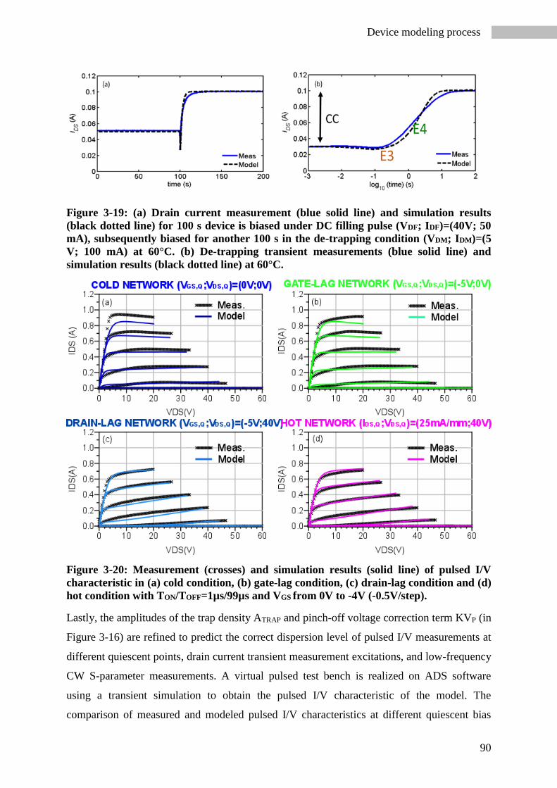
90
Device modeling process
Figure 3-19: (a) Drain current measurement (blue solid line) and simulation results
(black dotted line) for 100 s device is biased under DC filling pulse (VDF; IDF)=(40V; 50
mA), subsequently biased for another 100 s in the de-trapping condition (VDM; IDM)=(5
V; 100 mA) at 60°C. (b) De-trapping transient measurements (blue solid line) and
simulation results (black dotted line) at 60°C.
Figure 3-20: Measurement (crosses) and simulation results (solid line) of pulsed I/V
characteristic in (a) cold condition, (b) gate-lag condition, (c) drain-lag condition and (d)
hot condition with TON/TOFF=1µs/99µs and VGS from 0V to -4V (-0.5V/step).
Lastly, the amplitudes of the trap density ATRAP and pinch-off voltage correction term KVP (in
Figure 3-16) are refined to predict the correct dispersion level of pulsed I/V measurements at
different quiescent points, drain current transient measurement excitations, and low-frequency
CW S-parameter measurements. A virtual pulsed test bench is realized on ADS software
using a transient simulation to obtain the pulsed I/V characteristic of the model. The
comparison of measured and modeled pulsed I/V characteristics at different quiescent bias

Nonlinear Electro-Thermal model of AlGaN/GaN HEMT
91
points is shown in Figure 3-20. As shown in Figure 3-20 the model shows a good match with
the measurements in drain-lag and hot conditions. However, in cold and gate-lag conditions,
the amplitude of the drain current for a high gate voltage is not attained (the trap amplitude is
too weak for high gate voltages).
Thermal electrical model extraction
The trap states are strongly sensitive to the device’s operating temperature. It is then
necessary to accurately estimate the junction temperature to predict the dynamic behavior of
the traps at several temperatures.
In order to model the temperature evolution, the thermal analog circuit shown in Figure 3-21
is used. The temperature rises exponentially as a function of time for a fixed dissipated power.
Thus, a suitable electrical representation consists of parallel R-C cells with different time
constants (τn= Rn×Cn). The dissipated power, calculated in the intrinsic current source, is
represented as a current source in the input of the R-C network, and the self-heating is
implemented by the output circuit voltage. The ambient temperature is associated with an
initial voltage. The junction temperature device is dependent on the power dissipation by
adding the room temperature as a voltage source.
To estimate the thermal impedance versus time, a 3-D finite-element simulation with ANSYS
software was performed by applying a dissipated power of 2.25 W/mm. Thus, the equivalent
thermal RC-network model is determined by the 3-D finite-element simulation, as shown in
Figure 3-22. The 3-D finite element simulations were provided by R. Sommet.
Figure 3-21: Thermal analog circuit implemented in the nonlinear current source model.

92
Device modeling process
Figure 3-22: Thermal impedance versus time. The solid line with square in red
corresponds to 3-D finite element simulation for a dissipated power equal to 2.25 W/mm
obtained by ANSYS software. The solid line in blue corresponds to the values given by
the electrical model with four RC cells.
3.4.3.4.1 Thermal dependence of output current source
The thermal dependence of the output current source is extracted from pulsed I/V network
measurements in hot condition (VDS,Q; IDS,Q)=(40 V; 50 mA) at different temperatures as
shown in Figure 3-23. It can be observed that the saturation drain current decreases when the
temperature increases. It can be also seen that the pinch-off shifts leftward with an increase in
temperature. In order to model the thermal variation of the pulsed IDS-VDS and IDS-VGS
characteristics a thermal linear dependency is applied on the drain current saturation
parameter, output conductance parameter and pinch-off voltage parameter:
𝐼𝐷𝑆𝑆 = 𝐼𝐷𝑆𝑆0 ∙ (1 + 𝛼𝐼𝑑𝑠𝑠 ∙ 𝑇) (3-51)
𝑃 = 𝑃0 ∙ (1 + 𝛼𝑃0 ∙ 𝑇) (3-52)
𝑉𝑃0 = 𝑉𝑃00 ∙ (1 + 𝛼𝑉𝑝0 ∙ 𝑇) (3-53)
The parameters for the thermal dependence of the output current source are shown in Table
10.

Nonlinear Electro-Thermal model of AlGaN/GaN HEMT
93
Figure 3-23: Measurement (solid line) and simulation results (crosses) at several
temperatures of pulsed (a) IDS-VDS characteristic in hot condition (VDS,Q;
IDS,Q)=(40V;50mA) at VGS=0V, (b) IDS-VGS characteristic at VDS=40 V and (c) zoom of
IDS-VGS characteristic at VDS=40 V.
TABLE 10 THERMAL DEPENDENCY PARAMETERS OF OUTPUT CURRENT SOURCE
IDSS0 αIdss P0 αP0 VP0 αVP0
1.02 -0.0025 0.0001 -0.00001 1.6 0.0008
3.4.3.4.2 Thermal-trap model
In the thermal-trap model, it is assumed that each defect is represented by a capacitance CTRAP
and that the values of the resistances RCAP and REMI determine respectively the capture and
emission time constants [95]. Hence, a change of capture/emission time constant due to an
increase of temperature corresponds to a change of capture/emission resistance. Therefore, in
this drain-lag model, the temperature dependence of the traps is incorporated into the capture
RCAP(T°) and emission REMI(T°) resistances. Assuming that the trap density does not change
with temperature, the multiplying factor ATRAP remains constant with respect to the
temperature variation. This model also makes the assumption of a strong dissymmetry of GaN
technology between the capture and emission time constants. Indeed, the capture time
constant usually falls into the nanoseconds-microseconds range during the trapping phase
while the emission time constant falls into the microseconds-seconds range during the de-
trapping phase in GaN HEMTs. With this assumption on the capture time constants, the

94
Device modeling process
temperature dependence of the capture process is not applied. To summarize, three charge-
trapping RC networks coupled with diodes were implemented in thermal drain-lag model.
The first one takes into account the small-signal dispersion that has a fast emission time
constant (in the microseconds-milliseconds range) as trap phenomenon “E2”. The second and
third RC networks are used to model the slow dispersion due to the large-signal operation
mode, where the associated slow time constants are in the milliseconds-minutes range, such
as trap phenomena “E3” and “E4”.
The new drain-lag sub-circuit including the thermal dependence is shown in Figure 3-24.
Each resistance follows a thermal dependence as given in Equation (3-54).
𝑅𝐸𝑀𝐼(𝑇) = 𝑅𝐸𝑀𝐼0 ∙ 𝑒(𝛼𝐸𝑀𝐼∙𝑇) (3-54)
Figure 3-24: Schematic of thermal drain-lag model.
TABLE 11 THERMAL DEPENDENCE OF EMISSION RESISTANCES
REMI0_E2 αEMI_E2 REMI0_E3 αEMI_E3 REMI0_E4 αEMI_E4
0.015 -0.0055 4.7 -0.076 101.5 -0.065
The thermal activation of traps “E2”, “E3” and “E4” and therefore their emission resistance
variations are determined by LF Y22 measurements for “E2” and DCT measurements for “E3”
and “E4” at different temperatures. The parameter values of Equation (3-54) are shown in
Table 11 for the three traps identified. In the case of capture process “E3” during the de-
trapping transient, as described before, the trap amplitude (ATRAP) is assumed to be negative,
so as to predict the drain current reduction. Consequently, the thermal dependence of the trap
is applied to REMI to produce the correct temperature variation of the emission process.
The leftward frequency shift of trap “E2” and the rightward time constant shift of trap “E3”
and “E4” with increasing temperature are correctly modeled.

Nonlinear Electro-Thermal model of AlGaN/GaN HEMT
95
Figure 3-25(a) compares the LF Y22-parameter of the measured and simulated results when
the temperature varies from 80°C to 130°C.
Figure 3-26(a) presents the comparison of DCT measurements and corresponding transient
simulation for DC pulse excitation (shown in Figure 2-14) with the two voltage levels (VDS,F;
IDS,F)=(40 V; 50 mA) and (VDS,M; IDS,M)=(5 V; 100 mA) at different temperatures.
Figure 3-27(a) compares the measurement and envelope simulation results of GaN HEMT
driven by an RF pulse signal (corresponding to a 27 dBm input average power) at different
temperatures. In this experiment, the GaN HEMT is also biased with a synchronized DC pulse
signal with voltage levels (VDS,F; IDS,F)=(40 V; 50 mA) and (VDS,M; IDS,M)=(5 V; 100 mA). For
both DCT comparison results are only shown during the de-trapping transients as shown in
Figure 3-26(a) and Figure 3-27(a) and demonstrated a good agreement between measured and
simulated results validating the new developed electro-thermal model with the new thermally
dependent trapping model.
This new model accurately predicts the increase of average drain current due to the slow
emission processes after DC transition and after cut-off of the pulsed RF excitation. Thanks to
the determination of the trapping model parameter assisted with stretched multi-exponential
fitting, the de-trapping phenomena shown in Figure 3-26(a) and in Figure 3-27(a) improved
the model accuracy with respect to [41]. Moreover, for each trapping analysis simulation, the
related Arrhenius plot is determined by substituting the simulated emission rate in the
Arrhenius formula (2-11). The good agreement between the measured and simulated
Arrhenius plots of the “E2”, “E3” and “E4” trap signatures are shown in Figure 3-25(b),
Figure 3-26(b) and Figure 3-27(b).
Figure 3-25: (a) Measurement (solid line) and simulation results (black dotted line) of
imaginary part of Y22 from 100 Hz to 10 MHz frequency range at IDS =25 mA/mm and
VDS=40 V for different temperatures. (b) Related Arrhenius plot.

96
Device modeling process
Figure 3-26: (a) DCT Measurement (clear solid line) and simulation results (black
dotted line) of de-trapping average drain current transients in (VDS,M;
IDS,M)=(5V;50mA/mm) condition after 100 s in (VDS,F; IDS,F)=(40V;25mA/mm) for
different temperatures. (b) Related Arrhenius plot.
Figure 3-27: (a) DCT Measurement (clear solid line) and simulation results (black
dotted line) of de-trapping average drain current transients in (VDS,M;
IDS,M)=(5V;50mA/mm) condition after 100 s in (VDS,F; IDS,F)=(40V;25mA/mm) for
different temperatures and when the HEMT is driven by a pulse signal (27 dBm input
average power). (b) Related Arrhenius plot.
3.4.4 Model validation
The thermal nonlinear model is firstly validated under small-signal excitation for the bias
point corresponding to the RF application operation mode (IDS; VDS)= (50 mA, 40V). Indeed,
some model parameters are adjusted (e.g. CGS, CGD, gm and gd) during the successive
nonlinear modeling phases. Finally, the comparison between measured and simulated S-
parameters are shown in Figure 3-28.

Nonlinear Electro-Thermal model of AlGaN/GaN HEMT
97
Figure 3-28: Measurement (red solid line) and simulation results (black dotted line) of
pulsed S-parameter measurement at (IDS,Q ; VDS,Q)= (IDS,M ; VDS,M)= (50 mA, 40V) from
0.5 GHz to 12 GHz frequency range.
The more important model validation step is the one performed under large-signal operating
mode. In this case, the nonlinear model is expected to be as faithful as possible to the RF
measurement. Figure 3-29 shows the good agreement between the measured CW RF
performances for 4 GHz in class AB operation mode (IDS =25 mA/mm at VDS=40 V for a
fixed temperature of 25°C and maximum PAE impedance ZloadMAXPAE(f0) equal to 20.5+j44
Ω) and the electro-thermal model with thermal drain-lag circuits.
Figure 3-29: Measurements (blue solid line) and simulation results (black dotted line) of
the CW RF performances in class AB operation mode at 4 GHz, temperature 25°C and
ZloadMAXPAE(f0)=20.5+j44 Ω.
To validate the large-signal dynamic, the drain current transient measurements during pulsed-
DC and pulsed-RF excitation are compared with new model in Figure 3-30. This comparison
shows that the increase of average drain current, time constant and trap amplitude after the

98
Device modeling process
filling phase with respect to the input power’s increasing is correctly modeled and is due to
the capture and emission trap process excited by gate and drain large-signal voltage
excursions during the RF excitation.
Figure 3-30: (a) Drain current measurement (solid line) and simulation results (black
dotted line) of 100s under DC filling pulse (VDS,F; IDS,F)=(40V;50mA) and different input
power and without input power and after another 100 s under de-trapping condition
(VDS,M; IDS,M)=(5V;100mA) at 60°C. (b) De-trapping transient measurements (solid line)
and simulation results (black dotted line) at 60°C.
Unfortunately, the model has an inconsistency in the trap modeling. It can be observed with
the comparison of LF Y22 parameter measurements and the simulation results presented in
Figure 3-31. This figure shows that the simulated results of the real part of Y22, when “E2”,
“E3” and “E4” trap models are activated, do not agree with the measurement results. But it
can be noted that the gd value determined from the measurement is closer to the gd value
determined from the simulation with “E2” only activated. This inconsistency of the trapping
model during small-signal operation mode can be explained firstly by the model’s simplicity
and secondly by the fact that we simulate several trapping phenomena detected with different
operating modes which may be not involved during this operation mode. At the moment, the
role of the trapping phenomena in LF Y-parameter dispersion is not completely clear, so
complementary physical simulations are necessary to understand these trapping phenomena
and consequently propose a new trap model which agrees with the LF Y22-parameter
measurements.

Nonlinear Electro-Thermal model of AlGaN/GaN HEMT
99
Figure 3-31: (a) Measurement (red solid line), simulation results (black solid line) with
all traps activated and modeling (black dotted line) with different traps activated of (a)
real and (b) imaginary parts of Y22 at IDS =25 mA/mm and VDS=40 V at 80°C.
Conclusion
This chapter presents a method and an operating process to extract the nonlinear electro-
thermal AlGaN/GaN model for CAD application with a new additive thermal-trap model to
take into account the dynamic behavior of the trap states and their associated temperature
variation. The extraction of a nonlinear electro-thermal model of AlGaN/GaN HEMT and its
performance evaluation are based on pulsed I/V measurements, multi-bias pulsed S-parameter
measurements and pulsed large-signal measurements. In particular, a new method for the
extraction method of the intrinsic parameters is used. It is based on LF S-parameter
measurements. One challenge of this work is to propose a new thermal-trap model which
takes into account the dynamic behavior and to reach a good agreement for low-frequency
small-signal CW S-parameter results on the one hand and for large-signal pulsed-RF results

100
Conclusion
on the other hand at different temperatures. This thermal-trap model allows accurately
predicting the physical temperature activation of the traps and also the thermal signature of
the traps. It is also demonstrated that the extrapolation of trap model parameters by stretched
multi-exponential function of drain current transient measurements during pulsed-RF
excitations allows greatly improving the low-frequency simulations of the drain current. The
presented thermal-trap model correctly models the pinch–off voltage shift due to trapping
phenomena and temperature. Unfortunately, the trap model has an inconsistency in the
simulation of real part of Y22. A possible perspective for the continuation of this research
would certainly be the resolution of the trap model’s inconsistency, but also the introduction
of a pulse-width dependence into the trap amplitude and time constant parameters of the
thermal-trap model for radar and telecommunication applications.

Time-domain large-signal reliability investigation of AlGaN/GaN HEMT
101
4 Time-domain large-signal reliability
investigation of AlGaN/GaN HEMT
Introduction
As is well established, AlGaN/GaN HEMTs are a promising candidate for RF power
applications in space equipment due to their excellent performance. However, this technology
requires extensive study of its reliability and its conditions of use. Reliability is a prerequisite
for space equipment, because it must work for at least 15 years (satellite operating lifetimes
can range from five to ten years for Earth observation missions and up to eighteen years for
telecommunication satellites [2]). Moreover, the power amplifier is a circuit function that
must work under constraining operating conditions (high currents, high temperatures, high-
frequency operation, high gate-source and drain-source voltage excursions, and high power).
Therefore, reliability aspects are of paramount importance. So, the wear out failure
mechanisms must be understood and modeled to achieve some advances for design tools. One
of the failure mechanisms recently identified in GaN HEMTs is the generation of deep levels
due to a trapping effect which is extensively discussed in Chapter 2.
The aim of this chapter is to report an advanced time-domain methodology to investigate the
device reliability and determine its safe operating area (SOA). This methodology was applied
(by the Thales Alenia Space company) in order to carry out a further assessment of GH 50-10
AlGAN/GaN for the SiC HFET technology already qualified [96]. The presented technique is
based on the continued monitoring of the RF waveforms and DC parameters in order to assess
the degradation of the transistor characteristics in RF power amplifiers. Moreover, a complete
characterization protocol is associated to the time-domain methodology in order to obtain a
nonlinear electro-thermal model that takes into account the RF performance variations during
the RF stress and its degradation. This reliability model can be used by designers to predict
the RF degradation during real RF overdrive operation conditions in the design phase.
The first part of the chapter provides an overview of reliability test methodology and failure
mechanisms.
The second part presents first the set-up to determine the time-domain large-signal RF
waveforms and secondly the complete characterization protocol for the reliability
investigation.

102
Reliability Testing
The last part of this chapter shows the reliability results carried out in class AB operation
mode under RF power step-stress and 240 hours RF life stress with time-domain waveform
monitoring at high drain bias voltages and overdrive conditions (12 dB compression) for two
different output load impedances corresponding to the optimum of PAE and to a mismatched
impedance.
Reliability Testing
Before presenting an accelerated reliability testing of AlGaN/GaN HEMTs, the following
section summarizes some basic concepts to understand reliability analysis.
4.2.1 Analysis of reliability
The reliability of a population of devices (R) is defined as the number of devices
𝑁(𝑡) surviving until the time (𝑡) divided by the total number of devices 𝑁 (i.e. R = 𝑁(𝑡) 𝑁⁄ ).
The cumulative failure distribution function 𝐹(𝑡) is the probability that an item operating at
time t=0 under the stated condition, fails at or before time 𝑡. Therefore, it is defined as 𝐹(𝑡) =
1 − 𝑅(𝑡). Its derivate represents the failure probability distribution function 𝑓(𝑡) = 𝜕𝐹(𝑡) 𝜕𝑡⁄
and the probability of device failure between 𝑡 and 𝑡 + 𝜕𝑡 is equal to 𝑓(𝑡)𝜕𝑡. The mean time
to failure (MTTF) is the average time to first failure under the specified experimental
condition. It is calculated by integrating between 0 and ∞ the device lifetime (i. e. 𝑡 ∙ 𝑓(𝑡)𝜕𝑡)
as shown in the following equation:
𝑀𝑇𝑇𝐹 = ∫ 𝑡 ∙ 𝑓(𝑡)𝜕𝑡∞
0
(4-1)
For electronic devices generally two specific probability distribution function are considered
the “lognormal” and the “Weibull” [97] in order to analyze reliability results and to
characterize the failure mechanism. The measurement of reliability for semiconductors
generally involves failure rates. The evolution of the failure rates for a population of
semiconductor components (or any other sort of population) as a function of time is
described by the “bathtub” curve [98] in Figure 4-1. In particular, the Weibull distribution is
used to mimic the “bathtub” curve.

Time-domain large-signal reliability investigation of AlGaN/GaN HEMT
103
Figure 4-1: Bathtub curve describing the time dependence of failure rate for an
electronic device.
The initial region that begins at time zero when a device begins to be used is characterized by
a high but rapidly decreasing failure rate. This region is known as the early failure period or
“infant mortality” period. “Infant mortality” failures are due to defects of the component
occurring before the expected end of life. Defect-related problems are principally induced by
manufacturing flaws (such as a missing process step, contamination, undetected excursions,
wide variation, fabrication processes…). In order to weed out those defects, the manufacturers
will often perform a “burn in” on all components. In the next region, the failure rate remains
roughly constant and low. This period of a low failure rate is usually identified as the
“random” failure period, and it characterizes the useful life of components where the lowest
failure rate occurs. Finally, the failure rate begins to increase as materials wear out and
degradation occurs at an ever increasing rate. This is known as the “wear out” failure period.
End of life wear out refers to the natural process where components will begin to develop
faults and problems. Gradual degradation in the parameters of a device is typically mimicked
with accelerated life-test conditions.
4.2.2 Accelerated life test
Satellite communication systems (such as HPAs) are expected to have a long life and it is
quite impractical to measure their reliability under ordinary conditions. Accelerated tests are
used to obtain reliability predictions in a much shorter time than that required to produce a
significant number of failures under normal operating conditions. So in general, the median
time to failures are extrapolated by means of an accelerated factor [99] to induce a specific
electrical constraint, such as
Temperature acceleration,

104
Reliability Testing
Current acceleration (one of the principal wear out failure mechanisms is electro-
migration),
Voltage acceleration (involves the transistor but also the overall components around it,
such as MIM capacitors sensitive to breakdown voltage, the voltage acceleration
subsequently induces an electric field acceleration),
RF bias acceleration (one of major failure mechanisms is hot carrier injection).
In order to determine the MTTF, the corresponding acceleration law depends on the involved
failure mechanism (e.g. accelerated by temperature), the Arrhenius law is adopted and the
MTTF is given by
𝑀𝑇𝑇𝐹 = 𝛾0𝑒𝑥𝑝 (𝐸𝑎𝑘𝑇)
(4-2)
where 𝛾0 is constant, 𝐸𝑎is the activation energy(eV), 𝑘 is Boltzmann’s constant and 𝑇 is
absolute temperature (K). Both 𝛾0 and 𝐸𝑎 depend on the specific failure mechanism involved.
The definition of “failure” is one of the most subjective and arbitrary aspects in measuring
reliability, yet it is necessary to evaluate the median time to failure. The failure can be defined
as, e.g., a reduction in the drain current by 10%, a increase in the leakage current by 10%, a
reduction in gain by 1 dB, a reduction in output power by 1 dBm, a reduction in gain
compression by 1 dBc.
An example of accelerated testing of GaN-based heterojunction field effect transistors
submitted to a three high temperatures operating life test is shown in Figure 4-2. Cumulative
failure rates are recorded and the MTTF for each of the three temperatures is established. The
Arrhenius plots of the MTTF determined at three different temperatures is shown in Figure
4-2, which leads to an activation energy of about 2 eV and an extrapolated MTTF value
greater than 107 hours at 150 °C.
In the following, we summarize the main accelerated life tests:
HTS (high temperature storage test): The device is unbiased and stored at different
temperatures. This test allows studying the thermal activation of the failure
mechanism.
HTO (high temperature operating-life test): The device is biased under normal
conditions and stored at different temperatures. This allows studying the combined
effects of thermal and electrical stresses.

Time-domain large-signal reliability investigation of AlGaN/GaN HEMT
105
HTRB (high temperature reverse bias): The device is biased under reverse condition
close to breakdown voltage at high temperature. This allows to study the effects of
high electric fields and temperatures.
Figure 4-2: (Top) Three-temperature (3T) lifetime test data showing the cumulative
failure rates versus time obtained at three different temperatures, namely, 180 °C, 285
°C, and 310 °C. The σ values for 180 °C and 285 °C are approximately 1 but that at 310
°C is 1.5, which might imply contribution by infant failure. (Bottom) Arrhenius plot of
the MTTF determined at three different temperatures, namely,180 °C, 285 °C, and 310
°C, which lead to an activation energy of about 2 eV and an extrapolated MTTF value
greater than 107 hours at 150 °C [100].
In particular, the HTO test can be performed under either DC or RF operating conditions.
Normally, DC testing is used for a preliminary investigation of the reliability, which is, in
general, easier to set up and less expensive. In the other way, the RF life test can drive the
device in real working conditions.
In order to induce an accelerated degradation, these tests are performed with step-stress
techniques (e.g., reverse gate step-stress, VDS step-stress, PIN step-stress and VDS step-stress
with fixed PIN).

106
Reliability Testing
4.2.3 Physical failure mechanisms
As a relatively new semiconductor technology, a lot of research groups have devoted much
effort to the identification and understanding of the failure mechanisms of AlGaN/GaN
HEMTs. In the following, we discuss some of the key failure mechanisms presented in the
literature which have been identified though DC and/or RF characterization techniques. A
recent publication, Meneghesso et al. [26] has highlighted failure mechanisms identified on
GaN based HEMTs. They are reported on a cross-section in Figure 4-3. These mechanisms
have never been clearly identified in the other semiconductors.
Figure 4-3: Failure mechanisms recently identified on GaN HEMTs. Mechanisms
identified in red (5, 6, 7, 8) are thermally activated mechanisms. Mechanisms 2 and 3 are
related to the presence of hot electrons under high bias conditions. Mechanisms 1 and 4
(green) are peculiar to GaN devices due to the polar and piezoelectric nature of this
semiconductor [26].
These failure mechanisms can be divided into three main categories:
Failure mechanisms which can be associated with the properties of GaN based
material. (mechanisms 1 and 4 in Figure 4-3)
Hot-electron induced degradation mechanisms (mechanisms 2 and 3 in Figure 4-3).
Thermally-activated mechanisms (mechanisms from 5 to 8 in Figure 4-3).

Time-domain large-signal reliability investigation of AlGaN/GaN HEMT
107
Gate edge degradation
Under RF operating conditions, the large RF gate and drain voltage swings can involve high
electric fields particularly concentrated at the edge of the gate contact, which may producee a
degradation of the reliability. This high electric field condition can also be studied under DC
excitation (when high reverse bias voltages are applied to the gate, with the drain and gate
voltages set to zero). Consequently, a degradation of the electrical characteristics can appear:
an increasing of gate leakage and CC;
an increase of drain-source resistance;
a decrease of saturation drain current.
This degradation involves the presence or the generation of defects at the edge of the gate by
higher electric fields which can produce an injection of electrons from the gate to the AlGaN
barrier layer through a tunneling mechanism. A reverse-bias step-stress is carried out in OFF-
state with VD=VS=0 V, in order to verify the presence of this failure mechanism that appears
when a strong gate leakage increase is obtained for a certain reverse voltage. Another
powerful tool for reliability investigation that is normally used for the detection of hot-
electron phenomena is electroluminescence (EL) microscopy. EL microscopy is used to
detect the locations of a reverse current injection point and damaged areas. An example of
false-color EL micrographs is shown in Figure 4-4. In the transfer length method (TLM), the
device is submitted to a reverse bias step-stress with source and drain to ground. Figure 4-4
shows that after the step at -40 V, the EL spot and IG increase by 100x after starting being
observed. An increase in VG shows an increase of the point density of the defects and an
increase in the damage around each point. Moreover, the spots detected by EL were always
located at the edge of the gate towards the drain and source, where the electric field is
maximal.

108
Reliability Testing
Figure 4-4: EL microscopy images of a representative gated TLM HEMT sample.
Images were taken at VG =10 V (with VS = VD = 0 V) after each step-stress. Dashed lines
identify the device’s active area [26].
Thermally activated failure mechanism
Figure 4-5 shows a DC life test carried out at VDS=40 V and IDS=200 mA for different base-
plate temperatures. To investigate the degradation, the bias was stopped at regular intervals in
order to carry out DC and pulsed I/V measurements of the device. The devices show in Figure
4-5 and Figure 4-6 an increase of gate leakage and a decrease of drain current. Moreover,
Figure 4-7 shows an enhancement of the trapping effects.
Figure 4-5: Relative decrease in drain current for the four junction temperature of the
DC test stress test at VDS = 40 V, ID = 200 mA. Devices periphery is 1.2 mm, gate length
LG = 0.5 µm, and the source-to-drain distance LSD=3.7µm [26].

Time-domain large-signal reliability investigation of AlGaN/GaN HEMT
109
Figure 4-6: Comparison of the gate leakage current in off-state in untreated (gray) and
aged devices at VDS = 40 V, ID = 200 mA at different temperatures. Devices periphery is
1.2 mm, gate length LG = 0.5 mm, and thesource-to-drain distance LSD = 3.7 mm.
Figure 4-7: Pulsed DC characteristics measured in a representative device after 200 h of
DC testing at 245 °C, with VDS = 40 V, ID = 200 mA. Devices periphery is 1.2 µm, gate
length LG = 0.5 µm, and the source-to-drain distance LSD = 3.7 µm [26].
Hot electron degradation
Hot electron degradation is another failure mechanism that is involved when the device is
driven in on-state at high VDS. Thus, the 2DEG channel of electrons is accelerated by a high
electric field and reaches a high energy. The electron become “hot” when the electron can
overcome the energy barrier and when its energy decreases due to collision with the crystal
and with the formation of defects or dangling bonds (i.e. the trapping effect in the surface or
in the GaN buffer). In order to assess the reliability with respect to hot electron degradation,
the EL microscopy is used.
In order to characterize hot electron effects, the EL measurements were carried out in [101] at
different VGS and VDS levels as shown in Figure 4-8. At fixed VDS EL intensity has a non-
monotonic “bell-shaped” behavior. In OFF-state, VGS is smaller than the pinch-off value.
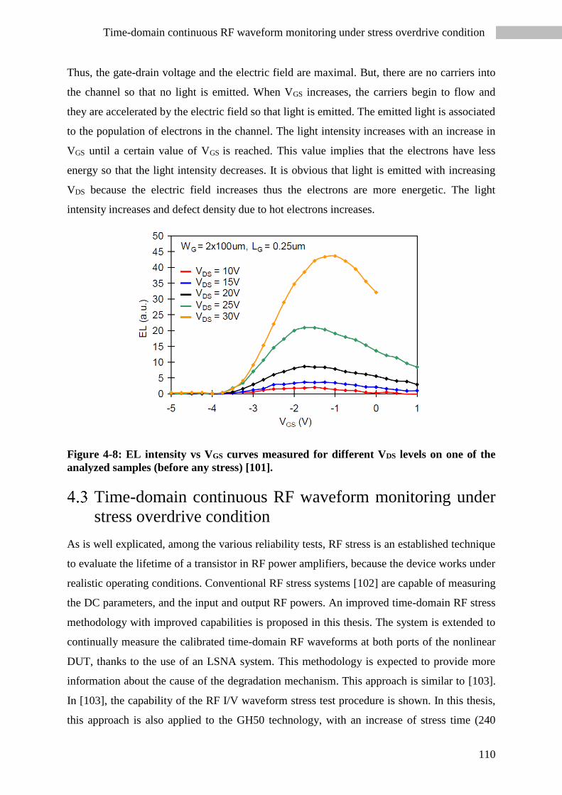
110
Time-domain continuous RF waveform monitoring under stress overdrive condition
Thus, the gate-drain voltage and the electric field are maximal. But, there are no carriers into
the channel so that no light is emitted. When VGS increases, the carriers begin to flow and
they are accelerated by the electric field so that light is emitted. The emitted light is associated
to the population of electrons in the channel. The light intensity increases with an increase in
VGS until a certain value of VGS is reached. This value implies that the electrons have less
energy so that the light intensity decreases. It is obvious that light is emitted with increasing
VDS because the electric field increases thus the electrons are more energetic. The light
intensity increases and defect density due to hot electrons increases.
Figure 4-8: EL intensity vs VGS curves measured for different VDS levels on one of the
analyzed samples (before any stress) [101].
Time-domain continuous RF waveform monitoring under
stress overdrive condition
As is well explicated, among the various reliability tests, RF stress is an established technique
to evaluate the lifetime of a transistor in RF power amplifiers, because the device works under
realistic operating conditions. Conventional RF stress systems [102] are capable of measuring
the DC parameters, and the input and output RF powers. An improved time-domain RF stress
methodology with improved capabilities is proposed in this thesis. The system is extended to
continually measure the calibrated time-domain RF waveforms at both ports of the nonlinear
DUT, thanks to the use of an LSNA system. This methodology is expected to provide more
information about the cause of the degradation mechanism. This approach is similar to [103].
In [103], the capability of the RF I/V waveform stress test procedure is shown. In this thesis,
this approach is also applied to the GH50 technology, with an increase of stress time (240
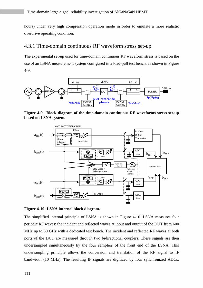
Time-domain large-signal reliability investigation of AlGaN/GaN HEMT
111
hours) under very high compression operation mode in order to emulate a more realistic
overdrive operating condition.
4.3.1 Time-domain continuous RF waveform stress set-up
The experimental set-up used for time-domain continuous RF waveform stress is based on the
use of an LSNA measurement system configured in a load-pull test bench, as shown in Figure
4-9.
Figure 4-9. Block diagram of the time-domain continuous RF waveforms stress set-up
based on LSNA system.
Figure 4-10: LSNA internal block diagram.
The simplified internal principle of LSNA is shown in Figure 4-10. LSNA measures four
periodic RF waves: the incident and reflected waves at input and output of the DUT from 600
MHz up to 50 GHz with a dedicated test bench. The incident and reflected RF waves at both
ports of the DUT are measured through two bidirectional couplers. These signals are then
undersampled simultaneously by the four samplers of the front end of the LSNA. This
undersampling principle allows the conversion and translation of the RF signal to IF
bandwidth (10 MHz). The resulting IF signals are digitized by four synchronized ADCs.
Reference
Clock
10 MHz
Filtre
Passe basd’échantillonnage
Amplificateur
à gain variable
Mise en forme
d’impulsions
FI Output
Synthétiseur
(Frac N)
CAN
23 bits
CAN
23 bits
CAN
23 bits
Microprocesseur
DC - 4 MHz
DC - 4 MHz
DC 4 MHz
Down conversion circuit
Filter
Amplifier
Synthesizer
(Frac N)
23 bits
23 bits
ADC23 bits
Microprocessor
DC - 4 MHz
DC - 4 MHz
ADC
ADC
SRD Diode =
Pulse generator
Analog
Digital
Converter
a1RF(t)
Pulse
shaping
b1RF(t)
b2RF(t)
a2RF(t)
a1BFb1BF
a2BF b2BF

112
Time-domain continuous RF waveform monitoring under stress overdrive condition
Finally, a computer processes all the data to get the absolute phases and absolute amplitudes
of the fundamental and harmonic frequencies [104]. The principle of frequency conversion-
translation is shown in Figure 4-11. In this example, the fundamental frequency is equal to
FRF=1 GHz, the frequency of the FrancN synthesizer is equal to FLO=19.6 MHz.
Consequently, the IF frequency is calculated as FIF = FRF − N × FLO with N the number of
periods required to obtain the final digitalized signal. In the given example, the IF frequency
corresponding to the FRF frequency is FIF=400 KHz. The same calibration is performed for
other harmonics [104]. In order to obtain the calibrated RF voltage and current waveforms at
the DUT planes, the LSNA needs a specific calibration protocol based on relative and
absolute calibration. The error model used in the LSNA system is described in [106]. The
error model in Equation (4-3) is only available for connectorized devices. The extension of
the measurement system from connectorized devices to on-wafer devices implies an
additional calibration between the a1 and b1 ports of the LSNA and the test set port1 RF
input, because there are no power sensors or reference generators available on-wafer which
can be used to determine 𝐾(𝑓) [107], [108].
Figure 4-11: LSNA Frequency down-converter principle [105].

Time-domain large-signal reliability investigation of AlGaN/GaN HEMT
113
[
𝑎1𝐷𝑈𝑇(𝑓)𝑎2𝐷𝑈𝑇(𝑓)𝑎3𝐷𝑈𝑇(𝑓)𝑎4𝐷𝑈𝑇(𝑓)
] = |𝐾(𝑓)| ∙ 𝑒𝑗∙𝜑(𝐾(𝑓))
[
1 𝛽1(𝑓)𝛾1(𝑓) 𝛿1(𝑓)
0 00 0
0 00 0
𝛼2(𝑓) 𝛽2(𝑓)𝛾2(𝑓) 𝛿2(𝑓)
] ∙ [
𝑎1𝑚(𝑓)𝑎2𝑚(𝑓)𝑎3𝑚(𝑓)𝑎4𝑚(𝑓)
]
(4-3)
The absolute calibration elements, the power meter sensor and the harmonic phase reference
(HPR) are therefore connected to the port1 RF input (as shown in Figure 4-13) and the
measurement results are transformed to the port1 probe tip according to Equation (4-4).
[𝑎1𝑝𝑜𝑟𝑡1(𝑓)
𝑎2𝑝𝑜𝑟𝑡1(𝑓)] = 𝐿(𝑓) ∙ [
1 𝜆(𝑓)
µ(𝑓) 𝜈(𝑓)] ∙ (𝐾(𝑓) ∙ [
1 𝛽1(𝑓)𝛾1(𝑓) 𝛿1(𝑓)
])−1
∙ [𝑎1𝐷𝑈𝑇(𝑓)𝑎2𝐷𝑈𝑇(𝑓)
] (4-4)
The error coefficients 𝛽1(𝑓), 𝛾1(𝑓), 𝛿1(𝑓), 𝛼2(𝑓), 𝛽2(𝑓)𝛾2(𝑓) and 𝛿2(𝑓) are calculated from
the on-wafer relative (SOLT) calibration. The error coefficient µ(𝑓), 𝜆(𝑓) and 𝜈(𝑓) are
known after execution of the SOL calibration at the port1 RF input. 𝐿(𝑓) is known after
connecting the harmonic phase and a power meter at port1 RF input.
Figure 4-12: Configuration for on-wafer relative calibration.
Figure 4-13: Configuration for on-wafer absolute magnitude and phase calibration.

114
Time-domain continuous RF waveform monitoring under stress overdrive condition
4.3.2 Reliability test procedure
The measurements of the continuous RF waveforms during the RF stress under overdrive
condition consists on recording (every 10 minutes) the calibrated time-domain voltage and
current waveforms of the DUT driven by a CW large signal and loaded with a fixed
impedance at fundamental and harmonic frequencies. The DUT used for all stress tests is an
8×250 µm GH 50 AlGaN/GaN HEMT. The reliability test procedure includes a monitored RF
stress considering a 24 h or a 240 h step stress under overdrive condition at different given
compression levels. A specific characterization protocol is carried out before and after each
RF step-stress. The reliability test procedure is an adaptation of the one used in [102].
Characterization protocols
Two characterization protocols have been performed: the first, called the “short
characterization protocol” is associated to a 24 h RF step-stress under overdrive operating
condition. The second one, called the “full characterization protocol” is associated to 240 h
step-stress under overdrive operating condition at a given compression value.
The short characterization protocol is carried out before and after each RF 24 h step-stress at
different compression gain values. This protocol, in addition to a DC I/V characterization for
classic device degradation assessments, is extended with pulsed I/V measurements to quantify
trapping effects, with pulsed S-parameter measurements, and with power sweep
measurements. This short characterization protocol is also used to determine a nonlinear
electro-thermal model [69] taking into account the RF performance variation during the RF
stress and its degradation. Thus, the short characterization protocol is composed of the
following measurements:
DC I/V measurements are carried out with a Keithley 4200 semiconductor
characterization system (SCS) [109] equipped with two 4210 high power source
measurement units (SMUs) for the gate and drain probes. In addition, the 4225-RPM
(remote amplifier/switch module) are connected to the 4210 SMU that is at the gate,
allowing a highly accurate characterization of the gate current. The DC I/V
measurement allows the following characterizations:
o Diode gate-source characterization with a VGS sweep from -8 V to 1 V with a
0.05 V voltage step.
o ID-VD characterization with a VDS sweep from 0 to 10 V and VGS sweep from
-4 V to 0 V with a 0.5 V voltage step.

Time-domain large-signal reliability investigation of AlGaN/GaN HEMT
115
o ID-VG characterization with a VGS sweep from -8 V to 1 V and with VDS at 1 V,
2 V, 5 V and 10 V.
Pulsed I/V measurements are carried out with the BILT AMCAD system described
in Section 2.3.1.1 in order to quantify the impact of RF stress on trapping effects. The
specific trapping pulsed I/V protocol developed in Section 2.3.1.2 is employed for this
objective. The pulsed I/V measurements are performed at the following different
quiescent bias points:
o Cold network at bias point (VGQ, VDQ)=(0 V, 0 V);
o Gate-lag network at bias point (VGQ, VDQ)=(-5 V, 0 V);
o Drain-lag network at bias point (VGQ, VDQ)=(-5 V, 50 V);
o Hot network at bias point (VGQ, VDQ)=(-1.9 V, 50 V) (under class AB bias
condition with IDQ=50 mA and VDQ=50 V).
Pulsed S-parameter measurements are carried out with the same BILT AMCAD
system and a Rohde & Schwarz ZVA40 VNA [110] equipped with ZVAx modules as
described in Section 3.4.1.1. The pulsed S-parameters are determined for different
biasing points corresponding to an ideal load-line (from 0.5 GHz to 20 GHz with
frequency step of 0.5 GHz) obtained under the large-signal operating mode (quiescent
point : VDQ=50 V and IDQ=50 mA).
Time-domain power sweep measurements are carried out with the properly
calibrated LSNA system in the same conditions defined in the step-stress protocol.
The full characterization protocol includes all the measurements of the short characterization
protocol with the addition of a thermal resistance characterization based on thermal pulsed
I/V measurements and a trap characterization based on LF Y22 measurements. The advanced
and full characterization protocol is performed before and after each 240 h RF step-stress
under overdrive operating conditions at the same compression gain value. Thus, the full
characterization protocol is composed of the following measurements:
DC I/V measurements identical to the DC I/V measurements performed in the short
characterization protocol.
Pulsed I/V measurements identical to the pulsed I/V measurements performed in the
short characterization protocol.
Pulsed S-parameter measurements identical to the pulsed S-parameter
measurements performed in the short characterization protocol.

116
Time-domain continuous RF waveform monitoring under stress overdrive condition
Time-domain power sweep measurements identical to the time-domain power
sweep measurements performed in the short characterization protocol.
Additive RTH measurements are carried out with the BILT AMCAD system at
different temperatures and different quiescent bias points, as described in Section
2.3.1.3.
Additive LF Y22 measurements are carried out with an LF-HF vector network
analyzer (Agilent E5061b) in 1-port configuration at different temperatures, as
described in Section 2.3.4.
24-hour RF step-stress in overdrive condition
An RF step-stress test is carried out in order to have a preliminary and quick evaluation of the
degradation of the component’s performance when driven by a large RF CW signal at
different compression gain values (in the high overdrive region). The large RF signal
excitations drive the transistor to ensure that it works with forward and reverse gate current
and that it operates at high drain voltage peak values. This operating condition corresponds to
a compressed mode allowing an accelerated RF life test under a high electric field. The 24 h
RF step-stress condition is summarized below:
The device is biased in class AB operation mode (50 mA of drain current at 50 V
of drain voltage) at a 4 GHz fundamental frequency.
The 24 h RF step-stress is carried out at 4 dB, 8 dB and 12 dB compression gain.
Each RF operating test is carried out on two devices coming from the same wafer
with similar characteristics.
Two load impedances are used during this 24 h RF operating test in order to
emulate different operating conditions corresponding to:
o PAE optimum load (ZLOAD_(f0)= 20.8+j44 Ω );
o mismatched impedance for the transistor equals to 50 Ω (ZLOAD(f0)= 50 Ω).
The complete reliability test procedure with 24 h RF step-stress and the short characterization
protocol is depicted in Figure 4-14.

Time-domain large-signal reliability investigation of AlGaN/GaN HEMT
117
Figure 4-14: Reliability test procedure with 24 h RF step-stress and short
characterization protocol.
240-hour RF step-stress in overdrive condition
A 240-hours RF step-stress test in the overdrive region is a more realistic operation life stress
condition for space equipment under a very high overdrive condition. The 12 dB compression
step-stress corresponds to the last and the highest compression gain level applied during the
24 h step-stress protocol. The 240 h RF overdrive conditions (corresponding to the same
stress conditions as the ones used in the previously described 24 h step-stress) are summarized
below:
The devices are biased in class AB operation mode (50 mA of drain current at 50
V of drain voltage) at a 4 GHz fundamental frequency.
240 hours of RF overdrive stress are carried out at 12 dB compression.

118
Time-domain continuous RF waveform monitoring under stress overdrive condition
Each RF operating test is carried out on two devices coming from the same wafer
with similar characteristics.
Two load impedances are used during this 240 h RF operating test in order to
emulate different operating conditions correspond to:
o PAE optimum load (ZLOAD_(f0)= 20.8+j44 Ω );
o mismatched impedance for the transistor equals to 50 Ω (ZLOAD(f0)= 50 Ω).
In order to detect an irreversible wear out mechanism, the full characterization protocol T3
described in Figure 4-15 (after the 240 h RF overdrive stress) is performed after seven days of
the end of RF stress.
In order to measure the calibrated waveforms during the 240 hours, a calibration protocol is
executed every 80 h. This value corresponds to the period for which the calibration
coefficients remain valid in the XLIM laboratory environment. The completed reliability test
procedure with 240 h RF overdrive stress and the full characterization protocol is depicted in
Figure 4-15.
Figure 4-15: Reliability test procedure with 240-hour RF overdrive stress and full
characterization protocol.
4.3.3 Time-domain stress test results
In this section, the time-domain results are presented firstly for the preliminary 24h RF step-
stress test and secondly for the 240 h RF overdrive stress test. The results are shown for the
two different load conditions (PAE optimum impedance and mismatched impedance). To

Time-domain large-signal reliability investigation of AlGaN/GaN HEMT
119
ensure a reliable characterization protocol all the measurements are carried out first on the
reference sample and secondly on the stressed simple.
24-hour RF step-stress test results
The time-domain RF performance measured during three consecutive applications of 24 hours
of RF stress under PAE optimum load impedance and 50 Ω load impedance at 4 dB, 8 dB and
12 dB compression gains are shown in Figure 4-16 and Figure 4-17 for the two tested devices.
The monitored parameters during the stress are: the output power, the DC drain and gate
currents, and the modulus and phase of the I2, V2, I1 and V1 RF waveforms (as depicted in
Figure 4-9). They have not shown any important degradation (e.g., output power varying
during the stress but with a final minor variation for all stress of 0.2 dBm under PAE optimum
load impedance in Figure 4-16(a) and of 0.3 dBm under 50 Ω load impedance in Figure
4-17(a)). In order to evaluate the degradation, the following figures of merit are determined
by the short characterization protocol:
DC figures of merit include saturation drain current (at VDS equal to 10 V), peak of
transconductance (at VDS equal to 4 V), and threshold voltage.
Trapping figures of merit include S.R. calculated in gate-lag, drain-lag and AB class
condition.
RF figures of merit include small-signal parameters at 4 GHz, output power, PAE and
drain current in saturation condition (at 3 dBc).

120
Time-domain continuous RF waveform monitoring under stress overdrive condition
Figure 4-16: (a) Output power, (b) modulus and phase of I1 at f0 extracted from I1 RF
waveforms curves, (c) drain current and (d) modulus and phase of I2 at f0 extracted
from I2 RF waveforms curves monitored during RF Pin step-stress with PAE optimum
load impedance.
Figure 4-17: (a) Output power, (b) modulus and phase of I1 at f0 extracted from I1 RF
waveforms curves, (c) drain current and (d) modulus and phase of I2 at f0 extracted
from (I2 RF waveforms curves) monitored during RF Pin step-stress with 50 Ω load
impedance.

Time-domain large-signal reliability investigation of AlGaN/GaN HEMT
121
Figure 4-18: Comparison of figures of merit extracted from short characterization
protocol before (T0) and after (T2, T4 and T6) each 24 h RF step-stress under the PAE
optimum load impedance condition: (a) DC IV figures of merit, (b) trapping figures of
merit (pulsed I/V measurements), (c) nonlinear power figures of merit and (d) small-
signal figure of merit at 4 GHz for device Q64 (solid line) and device U64 (dashed line).
Figure 4-19: Comparison of figures of merit extracted from short characterization
protocol before (T0) and after (T2, T4 and T6) each 24 h RF step-stress under the 50 Ω
load impedance condition: (a) DC IV figures of merit, (b) trapping figures of merit
(pulsed I/V measurements), (c) nonlinear power figures of merit and (d) small-signal
figure of merit at 4 GHz for device AC64 (solid line) and device Y64 (dashed line).

122
Time-domain continuous RF waveform monitoring under stress overdrive condition
In Figure 4-18 and Figure 4-19 are shown respectively the comparison of these figures of
merit before and after the 24 h RF step-stress (T1, T3 and T5) under PAE optimum
impedance and mismatched impedance (50 Ω). The step-stress results are very different for
the two devices and it is difficult to conclude whether or not they have the same degradation
behavior. But, the comparison of the short characterization protocol before and after each 24 h
step-stress in Figure 4-18 and Figure 4-19 for both load output impedances does not show any
reduction of RF and DC performance and trapping effects. In conclusion, the short 24h stress
period is not long enough to degrade the devices. Therefore, a longer stress period is applied.
240-hour RF overdrive stress test results
The 240 h RF overdrive stress tests are applied to ensure that the device operates in a more
realistic condition in order to determine an SOA during high overdrive condition at 12 dB
compression. It corresponds to a constant 29 dBm input power applied to the devices under
PAE optimum load impedance condition. But under the 50 Ω impedance load condition, it
corresponds to a constant 31 dBm input power applied to the devices. The monitoring of the
RF performance during the stress test is the same as that used for the 24 h step-stress, and is
shown in Figure 4-20 and Figure 4-21, respectively for the PAE optimum load impedance
condition and for 50 Ω load impedance condition. The variation of the RF and DC parameters
during 240 hours of RF overdrive stress are summarized in Table 12 and Table 13
respectively for the PAE optimum load impedance condition and for the 50 Ω load impedance
condition.
TABLE 12
VARIATION OF RF AND DC PARAMETERS DURING 240 HOURS OF RF OVERDRIVE STRESS AT PAE OPTIMUM LOAD
IMPEDANCE CONDITION
DEVICE ΔPout (dB) ΔIDS (mA) Δ|I2(f0)| (A)
M52 0.5 28 0.07
M64 0.4 19 0.03
TABLE 13
VARIATION OF RF AND DC PARAMETERS DURING 240 HOURS OF RF OVERDRIVE STRESS AT 50 Ω LOAD
IMPEDANCE CONDITION
DEVICE ΔPout (dB) ΔIDS (mA) Δ|I2(f0)| (A)
Q40 0.6 43 0.045
Q76 0.8 60 0.05
Q28 // // //

Time-domain large-signal reliability investigation of AlGaN/GaN HEMT
123
The time-domain stress results under the PAE optimum load impedance condition are shown
in Figure 4-20. A decreasing trend for both devices (i.e., output power variation of 0.4 dB for
device M64 and of 0.5 dB for device M52) is observed. In Figure 4-20, there can be observed
a slight increase of drain current, output power and magnitude and phase of I2 during the first
hour and a decrease of the same parameters after the first calibration at 80 hours of device
M52. This variation is not observed with device M64. It can be concluded that the RF
performance is not really affected by the stress. The time-domain stress results under 50 Ω
load impedance condition are presented in Figure 4-21. A decreasing trend is seen for both
devices: i.e., output power variation of 0.6 dB for the device Q40 and of 0.8 dB for the device
Q76, which is twice as important a decrease of drain current than was observed under the
PAE optimum load impedance condition. A catastrophic failure occurs for device Q28, as is
clearly seen in Figure 4-22. After 200 hours of RF stress under the 50 Ω load impedance
condition, device Q28 presents an increase of static gate current and an increase of static gate
voltage that in dynamic behavior corresponds to increasing excursions of the input load
cycles, as shown in Figure 4-22(a). This increase in the input load cycle excursion probably
involves a degradation in the gate-source region which modifies the input impedance and that
corresponds also to an increase of the input power of the device (the available power of the
RF power generator is constant during the stress). Moreover, this increase in the input load
cycle excursion corresponds to an increase of compression gain (until 18 dB compression
before the catastrophic failure) and thus a decrease of output power and of output load cycles.
Therefore, the static negative gate voltage increases until -6.5 V (Figure 4-22(f)) which in
dynamic behavior corresponds to an increase of the V1 excursion until -30 V (Figure 4-22(a))
before catastrophic failure. The degradation and catastrophic failure of device Q28 is assumed
to be due to the high compression operating condition during the overdrive condition and the
higher device operating junction temperature (estimated to be 210 °C in Figure 4-23). The
device operating junction temperature is estimated by using the following equation:
𝑇𝐽 = (𝑃𝐼𝑁 − 𝑃𝑂𝑈𝑇 + 𝑃𝐷𝐶) ∙ 𝑅𝑇𝐻 + 𝑇𝐴𝑀𝐵 (4-5)
This equation is applied to the monitoring of the DC and RF parameters during the 240 hours
of RF overdrive stress and RTH is calculated as described in Section 2.3.1.3. The variations of
estimated device operating junction temperatures during the 240 hours of RF overdrive stress
under the PAE optimum load impedance condition and for the 50 Ω load condition are shown
in Figure 4-23. It is possible to conclude that the wear out of device Q28 is probably due to

124
Time-domain continuous RF waveform monitoring under stress overdrive condition
destruction by breakdown of the gate-source diode by the high reverse breakdown voltage (-
6.5 V in static voltage and -30 V in dynamic voltage) applied in the gate to source terminals.
The results of the full characterization protocol carried out before and after the 240 hours of
RF overdrive stress under the PAE optimum load impedance condition are shown in Figure
4-24-Figure 4-28 and those under the 50 Ω load impedance condition are shown in Figure
4-29-Figure 4-33.

Time-domain large-signal reliability investigation of AlGaN/GaN HEMT
125
Figure 4-20:(a) Output power, (b) modulus and phase of I1 at f0 extracted from
recorded extrinsic I1 RF waveforms, (c) drain current, (d) modulus and phase of I2 at f0
extracted from recorded extrinsic I2 RF waveforms, (e) extrinsic I1 RF waveforms vs
extrinsic V1 RF waveforms and (f) extrinsic I2 RF waveforms vs. extrinsic V2 RF
waveforms monitored during 240 hours of RF overdrive stress under the PAE optimum
load impedance condition.

126
Time-domain continuous RF waveform monitoring under stress overdrive condition
Figure 4-21: (a) Output power, (b) modulus and phase of I1 at f0 extracted from
recorded extrinsic I1 RF waveforms, (c) drain current, (d) modulus and phase of I2 at f0
extracted from recorded extrinsic I2 RF waveforms, (e) extrinsic I1 RF waveforms vs
extrinsic V1 RF waveforms and (f) extrinsic I2 RF waveforms vs. extrinsic V2 RF
waveforms monitored during 240 hours RF overdrive stress under the 50 Ω load
impedance condition.

Time-domain large-signal reliability investigation of AlGaN/GaN HEMT
127
Figure 4-22: Measurement window zoom (from 160 hours to 240 hours) of failure of
device Q28 during 240 hours RF overdrive stress at 50 Ω impedance load (a) I1 RF
waveforms vs. extrinsic V1 RF waveforms, (b) I2 RF waveforms vs. extrinsic V2 RF
waveforms, (c) input power, output power, gain, (d) ΓIN, (e) drain and gate current and
(f) drain and gate current variations.
Figure 4-23: Junction device temperature estimation during 240 hours RF overdrive
stress at (a) PAE optimum impedance and (b) 50 Ω impedance.

128
Time-domain continuous RF waveform monitoring under stress overdrive condition
Figure 4-24: Comparison of DC I/V measurements before (solid line) and after (dashed
line) 240 hours RF overdrive stress under the PAE optimum load impedance condition:
(a) gate to source diode characteristics, (b) IDS vs. VGS characteristics at VDS=4 V, (c) IDS
vs. VDS characteristics (VGS sweep from 0 V to -3 V, -0.5 V/step) and (d) gm
characteristics (extracted by IDS vs. VGS characteristics).
Figure 4-25: Comparison of pulsed S-parameter measurements at quiescent bias point
(IDQ, VDQ)=(50 mA, 50 V) and pulsed bias point (VGM, VDM)=(-2 V, 50 V) before (solid
line) and after (dashed line) 240 hours RF overdrive stress under the PAE optimum load
impedance condition: (a) S21, (b) S11 and S22.

Time-domain large-signal reliability investigation of AlGaN/GaN HEMT
129
Figure 4-26: Comparison of time-domain RF power sweep measurements under class
AB condition (Ids0=50 mA and Vds0=50 V) before (solid line) and after (dashed line) 240
hours RF overdrive stress under the PAE optimum load impedance condition: (a)
output power vs. input power, (b) PAE vs. input power, (c) Gain vs. input power and (d)
drain current vs. input power characteristics.
Figure 4-27: Comparison of pulsed I/V measurements before (solid line) and after
(dashed line) 240 hours RF overdrive stress under the PAE optimum load impedance
condition: (a) cold network, (b) gate-lag network, (c) drain-lag network, and (d) class
AB network.

130
Time-domain continuous RF waveform monitoring under stress overdrive condition
TABLE 14
RTH ESTIMATION AT PRE- AND POST- 240 HOURS RF OVERDRIVE STRESS FOR PAE OPTIMUM LOAD IMPEDANCE
CONDITION
DEVICE RTH (°C/W)at T0 (pre-stress) RTH (°C/W)at T2 (post-stress)
M52 ~14 ~14
M64 ~14 ~14
Figure 4-28: Comparison of LF Y22 measurements before (in blue) and after (in red)
240 hours RF overdrive stress at PAE optimum load impedance (a) of device M52 and
(b) of device M64.
Figure 4-29: Comparison of DC I/V measurements before (solid line) and after (dashed
line) 240 hours RF overdrive stress under the 50 Ω load impedance condition: (a) gate to
source diode characteristics, (d) IDS vs. VGS characteristics at VDS=4 V, (c) IDS vs. VDS
characteristics (VGS sweep from 0 V to -3 V, -0.5 V/step) and (d) gm characteristics
(extracted by IDS vs. VGS characteristics).

Time-domain large-signal reliability investigation of AlGaN/GaN HEMT
131
Figure 4-30: Comparison of pulsed S-parameter measurements at quiescent bias point
(IDQ, VDQ)=(50 mA, 50 V) and pulsed bias point (VGM, VDM)=(-2 V, 50 V) before (solid
line) and after (dashed line) 240 hours RF overdrive stress under the 50 Ω load
impedance condition: (a) S21, (b) S11 and S22.
Figure 4-31: Comparison of time-domain RF power sweep measurements under class
AB condition (IDS0=50 mA and VDS0=50 V) before (solid line) and after (dashed line) 240
hours RF overdrive stress under the 50 Ω load impedance condition: (a) output power
vs. input power, (b) PAE vs. input power, (c) Gain vs. input power and (d) drain current
vs. input power characteristics.

132
Time-domain continuous RF waveform monitoring under stress overdrive condition
Figure 4-32: Comparison of pulsed I/V measurements before (solid line) and after
(dashed line) 240 hours RF overdrive stress under the 50 Ω load impedance condition:
(a) cold network, (b) gate-lag network, (c) drain-lag network and (d) class AB network.
TABLE 15
RTH ESTIMATION AT PRE- AND POST- 240 HOURS RF OVERDRIVE STRESS FOR 50 Ω LOAD IMPEDANCE CONDITION
DEVICE RTH (°C/W)at T0 (before stress) RTH (°C/W)at T2 (after stress)
Q40 ~14 ~13
Q76 ~14 ~13
Figure 4-33: Comparison of LF Y22 measurements before (in blue) and after (in red)
240 hours RF overdrive stress under the 50 Ω load impedance condition (a) of device
Q40 and (b) of device Q76.

Time-domain large-signal reliability investigation of AlGaN/GaN HEMT
133
The comparison of the DC I/V curves and CW RF performance before and after 240 hours of
RF overdrive stress under the 50 Ω load impedance condition (in Figure 4-29 and Figure 4-31
respectively) shows a positive threshold voltage shift (around ΔVTH=0.05 V) in the IDS-VGS
characteristic (Figure 4-29(b)) which corresponds to a saturation drain current drop in the IDS-
VDS characteristic (Figure 4-29(c)). Consequently, the average drain current, output power,
gain and PAE versus input power curve are affected, as shown in Figure 4-31. This
degradation mechanism is supposed to be strongly thermally activated; in fact, the stress has a
stronger effect under the 50 Ω load condition, corresponding to a lower drain voltage
excursion, higher average current, and thus higher device operating junction temperature (the
average estimate during RF stress is around 220°C and 200°C from Figure 4-23). Under the
optimum PAE load impedance condition, as shown in Figure 4-20, the DC and RF parameters
during the RF life test have a minor variation, then the comparison of the DC I/V curves
shows a slight positive threshold voltage shift which corresponds to a slight degradation of the
average drain current versus input power characteristic (Figure 4-26(d)) at lower input power
levels, indeed the device operating junction temperature obtained with the optimum PAE load
impedance is 50% less than that reached with 50 Ω load impedance. The positive and
negative pinch-off voltage shifts are one more common degradation and have been noticed
during DC stress[111], [112] and RF stress [113]. In our case a positive pinch-off voltage
shift is observed. This mechanism is similar to the trapping pinch-off voltage shift observed in
Section 2.3.3.2.2 but in the stress study-case, it is irreversible.
A decrease of static gate current in forward zone is observed in Figure 4-24(a) and Figure
4-29(a) for both load output impedance condition. That is probably due to the high VGS sweep
excursion (in Figure 4-20(e) and Figure 4-21(e)) under overdrive operating conditions.
The trapping measurements (pulsed I/V measurements and LF Y22 measurements) included in
the full characterization protocol show any trapping effects variation between the
measurements carried out before and after stress. Indeed, the pulsed I/V measurements at
different bias different quiescent bias points in Figure 4-27 and Figure 4-32, respectively for
stress under the PAE optimum load impedance condition and under the 50 Ω load condition
(the VGQ is corrected in post-stress measurements of the Class AB network to reach the same
drain current used in the pre-stress measurements) do not show any important variations. This
is also in accordance with the dynamic study of trapping phenomena with CW LF Y22
measurements. The LF Y22 measurements carried out at different temperatures do not show
any variations of frequency peaks between the pre-stress and post-stress measurements for
both load impedance conditions in Figure 4-28 and Figure 4-33 (the VGS0 is corrected in the

134
Conclusion
post-stress measurements to reach the same drain current used in the pre-stress
measurements).
Therefore, the 240 hours RF overdrive stress test does not impact the trapping effect when the
gate voltage in the post-stress measurements is corrected to reach the same drain current used
in the pre-stress measurements.
The results for the S-parameters measured at the quiescent bias point (IDQ, VDQ)=(50 mA, 50
V) and the measurement bias point (VGM, VDM)=(-2 V, 50 V) are shown Figure 4-25 and
Figure 4-30 respectively for stress under the PAE optimum load impedance condition and
under the 50 Ω load condition. The change in the S-parameters after the stress under the 50 Ω
load condition is probably due to the fact that the measurement bias point (VGM, VDM)=(-2 V,
50 V) has not been corrected to reach the same drain current used in the pre-stress
measurements.
The estimation of the thermal resistance is obtained with an electrical method described in
Section 2.3.1.3 based on thermal pulsed I/V measurements. The results of the thermal
resistance estimation are summarized in Table 14 and Table 15 respectively for stress under
the PAE optimum load impedance condition and under the 50 Ω load condition. For both
stresses under the different load impedance conditions, RTH is not impacted.
Conclusion
In this chapter, a continuous monitoring of RF waveforms during an RF operating life test
under overdrive conditions to assess the degradation of devices for space applications is
presented. This time-domain methodology is applied first to a 24 h step-stress (short stress)
and secondly to a 240 h RF overdrive stress (long stress). A short and full characterization
protocol have been performed respectively in order to determine the nonlinear electro-thermal
model described in the previous chapter.
The first part of this chapter presented some methods of performing reliability analysis and
tests. Moreover, an overview of the failure modes and mechanisms in GaN technology is also
described.
The second part of this chapter presents the time-domain reliability set-up based on an LSNA
measurement system in load-pull configuration and the results of a 24 h step-stress and a 240
h RF overdrive stress and their respective characterization protocols. The monitoring of RF
waveforms during the 24 h step-stress for both load impedance conditions shows no variation
of RF and DC performances. It is possible to conclude that the short step-stress period (24 h)

Time-domain large-signal reliability investigation of AlGaN/GaN HEMT
135
is not long enough to degrade the devices. Indeed, the monitoring of 240 hours of RF
overdrive stress has shown that in this GaN technology, the RF degradation in class AB
operation mode is due principally to a threshold voltage shift, which is more important under
the 50 Ω condition with lower drain voltage excursion and higher average drain current
(higher operating temperature) than for the PAE optimum load condition with higher drain
voltage excursion. For future investigation one has the perspective of employing this time-
domain methodology to perform the same stress protocol at a high temperature fixed with a
thermal chuck in order to investigate the effects of temperature on the degradation
mechanisms.
In conclusion, the potential of this set-up for analysing failures is demonstrated. For a more
realistic reliability study, it is necessary to perform the time-domain RF stress with more
devices and it will also be interesting to increase the period of stress.
Due to the complexity of the set-up and the numerous calibrations required to cover the whole
of the stress period, it is suggested to combine this time-domain technique with classic RF
stress: using firstly the classical accelerated RF stress for a preliminary stress to identify the
degradation, and then using the time-domain RF stress to obtain supplementary information
on the degradation mechanism based on the analysis of time-domain RF waveforms.

136
Conclusion
5 Conclusion
The work of this thesis is focused on three main topics: a trapping characterization
methodology, a nonlinear electro-thermal model with a new thermal-trap model, and a time-
domain methodology to investigate the device reliability of GaN-based HEMTs.
After a brief introduction of the properties and capabilities of GaN technology for space
applications, the second chapter presented several characterization techniques in order to
cover a broad frequency analysis from DC to radio-frequency range of the charge-trapping
phenomena and the related parasitic effects in GaN-based HEMTs. This trapping
characterization methodology is based on pulsed I/V measurements, DC and RF drain current
measurements, and low-frequency dispersion measurements. This allows quantifying the
effects of charge-trapping phenomena and the related mechanisms. These measurements are
also used to identify the involved deep trap states and their location in the structure of the
HEMT, through the analysis of their activation energy and their capture cross-section. With
this trapping investigation, four deep levels are detected and labeled as “E1”, “E2”,”E3” and
“E4.” In particular, deep level “E2” was identified with a DC DCT technique and LF
dispersion technique. Furthermore, the deep level “E4” was detected with the DCT technique
during DC and RF excitations but with an increasing density of ionized traps. The trap
sensitivity has been investigated as a function of the input power level, pulse-width,
temperature, load impedance (for two different output load impedances corresponding to the
optimum of PAE and to a mismatched impedance) and operating bias points. The analysis of
the dependence of the trapping effect on the bias during the RF CW mode operation condition
has demonstrated that the choice of the correct operating bias point value allows making the
GaN-based HEMTs insensitive to trapping effects.
The third chapter presents a methodology to extract a nonlinear electro-thermal model with a
new additional thermal-trap model to take into account the dynamic behavior of the trap states
and their associated temperature variations. For the extraction of a linear model of GaN-based
HEMTs, a new technique, based on LF S-parameter measurements, is used. The new thermal-
trap model allows accurately modeling the physical pinch–off voltage shift and the trap
temperature activation. The nonlinear electro-thermal model also allows accurately predicting
the dynamic behavior during large-signal RF excitation.

Conclusion
137
A time-domain RF waveform monitoring during an RF operating life test under overdrive
conditions for reliability investigation is presented in the fourth chapter. The monitoring of
RF waveforms is carried out for different step-stress periods of 24 h and 240 h and for two
different output load impedances corresponding to the optimum of PAE and to a mismatched
impedance. The RF waveform monitoring has shown the robustness, the capability to
withstand very RF excitation, and great stability at very high compression levels without
important degradation of this technology during 24h step-stress for both output load
impedances. The conclusions are the same for 240 h step-stress for the optimum PAE load
condition. But the 240 h step-stress, in overdrive condition, with a mismatched load
impedance shows a stronger degradation, with a positive threshold voltage shift and a drop in
saturation drain current, due principally to the high junction temperature reached by the
devices during the RF stress. The time-domain reliability set-up has also shown its abilities to
monitor failure events, for reliability analysis.
In conclusion, both the trapping and reliability investigations show that the trapping effects
and RF degradation respectively are more important under mismatched impedance conditions
with lower drain voltage excursions and higher average drain currents (higher operating
temperatures) than for the optimum PAE load condition with higher drain voltage excursions.

138
Conclusion

Publications
139
6 Publications
Journals A. Benvegnù, S. Laurent, O. Jardel, J-L., Muraro, M. Meneghini, D. Barataud, G. Meneghesso, E.
Zanoni, and R. Quere, "Characterization of Defects in AlGaN/GaN HEMTs Based on Nonlinear
Microwave Current Transient Spectroscopy," in IEEE Transactions on Electron Devices, vol. 64, no.
5, pp. 2135-2141, May 2017.
A. Benvegnù, D. Bisi, S. Laurent, M. Meneghini, G. Meneghesso, D. Barataud, E. Zanoni and R.
Quere, “Drain current transient and low-frequency dispersion characterizations in AlGaN/GaN
HEMTs,” International Journal of Microwave and Wireless Technologies, available on CJO2016.
doi:10.1017/S1759078716000398.
A. Benvegnù, S. Laurent, M. Meneghini, D. Barataud, G. Meneghesso, E. Zanoni, and R. Quere, “On-
Wafer Single-Pulse Thermal Load–Pull RF Characterization of Trapping Phenomena in AlGaN/GaN
HEMTs,” IEEE Trans. Microw. Theory Tech., pp. 1–9, 2016.
Conference Proceedings
A. Benvegnù, S. Laurent, M. Meneghini, R. Quere, J.-L. Roux, E. Zanoni and D. Barataud
"Continuous Time-Domain RF waveforms monitoring under overdrive stress condition of
AlGaN/GaN HEMTs" ESREF 2016, vo. 64, pp 535-540, Sep 2016.
A. Benvegnù, O. Jardel, S.Laurent, D. Barataud, E. Zanoni and R.Quere,” Non-linear electro-thermal
GaN Model Including Large-Signal Dynamic Thermal-Trapping effects ” in IEEE MTT-S Int.
Microw. Symp. Dig., San Francisco, CA, USA, May 2016, pp. 1–4.
A. Benvegnù, D. Bisi, S. Laurent, M. Meneghini, G. Meneghesso, J.-L. Muraro, D. Barataud, E.
Zanoni, and R. Quere, “Trap investigation under class AB operation in AlGaN/GaN HEMTs based on
output-admittance frequency dispersion, pulsed and transient measurements,” in 2015 10th European
Microwave Integrated Circuits Conference, pp. 136–139.
A. Benvegnù, S. Laurent, R. Quere, J.-L. Roux, J.-L. Muraro, E. Zanoni and D. Barataud, “Étude de
la fiabilité de transistors de Nitrure de Gallium pour des applications spatiales: mesures de formes
d’ondes temporelles en régime d’overdrive” in 2015 XIXèmes Journées Nationales Micro-ondes,
Bordeaux, France, Jun 2015.
A. Benvegnù, S. Laurent, M. Meneghini, G. Meneghesso, J.-M. Muraro, D. Barataud, E. Zanoni and
R. Quere, "Trap characterization of AlGaN/GaN HEMTs through Drain Current Measurements under
Pulsed-RF Large-Signal excitation," in IEEE MTT-S Int. Microw. Symp. Dig., Phoenix, AZ, USA,
May 2015, pp. 1–4.
A. Benvegnù, S. Laurent, R. Quere, J.-L. Roux, J.-L. Muraro, E. Zanoni and D. Barataud, and
“Protocole de de caractérisations avancées pour l’étude de la fiabilité de transistor GaN” in JNRDM
2015, Bordeaux, France, May 2015.
A. Benvegnù, S. Laurent, T. Reveyrand, R. Quere, J.-L. Roux, J.-L. Muraro and D. Barataud,“Time-
Domain Waveform Measurements under Large Signal RF Overdrive Stress in HEMT Technology” in
7th Space Agency–MOD Workshop on Wideband Gap Semiconductors and Components.

140
Conclusion

References
141
7 References
[1] T. Reveyrand et al., “GaN transistor characterization and modeling activities performed
within the frame of the KorriGaN project,” Int. J. Microw. Wirel. Technol., vol. 2, no.
01, p. 51, Mar. 2010.
[2] A. R. Barnes and F. Vitobello, “ESA perspective on the industrialisation of European
GaN technology for space application,” in European Microwave Integrated Circuit
Conference (EuMIC), 2014 9th, 2014, pp. 233–236.
[3] Takashi Mimura, Satoshi Hiyamizu, Toshio Fujii, and Kazuo Nanbu, “A New Field-
Effect Transistor with Selectively Doped GaAs/n-Al x Ga 1- x As Heterojunctions,” vol.
19, no. 5, p. L225, 1980.
[4] R. Dingle, H. L. Störmer, A. C. Gossard, and W. Wiegmann, “Electron mobilities in
modulation-doped semiconductor heterojunction superlattices,” Appl. Phys. Lett., no. 33,
p. 665, 1978.
[5] P. Nakkala, “pulsed I-V and RF characterization and modeling of AlGaN/GaN HEMTs
and graphene FETs,” Université de Limoges, 2015.
[6] D. W. Runton, B. Trabert, J. B. Shealy, and R. Vetury, “History of GaN: High-Power RF
Gallium Nitride (GaN) from Infancy to Manufacturable Process and Beyond,” IEEE
Microw. Mag., vol. 14, no. 3, pp. 82–93, 2013.
[7] U. K. Mishra, P. Parikh, and Y.-F. Wu, “AlGaN/GaN HEMTs–An overview of device
operation and applications,” Proc.-IEEE, vol. 90, no. 6, pp. 1022–1031, 2002.
[8] O. Ambacher et al., “Two dimensional electron gases induced by spontaneous and
piezoelectric polarization in undoped and doped AlGaN/GaN heterostructures,” J. Appl.
Phys., vol. 87, no. 1, p. 334, 2000.
[9] R. Giofré et al., “A first step towards a 230 W SSPA for Galileo System exploiting
European GaN technology,” in 2015 10th European Microwave Integrated Circuits
Conference, pp. 317–320.
[10] B. Lefebvre et al., “GaN For Space Applications: Ready for Commercial Use,” 8th Wide
Bandgap Semiconductors and Components Workshop, ESA-ECSAT, Harwell, United
Kingdom, 12 Sep. 2016.
[11] J.-L. Muraro et al., “GaN for space application: Almost ready for flight,” Int. J. Microw.
Wirel. Technol., vol. 2, no. 01, p. 121, Apr. 2010.
[12] K. Hirche et al., “GaN Reliability Enhancement and Technology Transfer Initiative
(GREAT2).”
[13] W. Shockley and W. T. Read, Jr., “Statistics of the recombinations of holes and
electrons,” Phys. Rev., vol. 87, no. 5, p. 835, 1952.
[14] R. N. Hall, “Electron-hole recombination in germanium,” Phys. Rev., vol. 87, no. 2, p.
387, 1952.
[15] H. Morkoc, Handbook of Nitride Semiconductors and Devices, vol. 1. Wiley-VCH,
2008.
[16] S. D. Nsele, L. Escotte, J.-G. Tartarin, S. Piotrowicz, and S. L. Delage, “Broadband
Frequency Dispersion Small-Signal Modeling of the Output Conductance and
Transconductance in AlInN/GaN HEMTs,” IEEE Trans. Electron Devices, vol. 60, no.
4, pp. 1372–1378, Apr. 2013.
[17] M. Meneghini et al., “Investigation of trapping and hot-electron effects in GaN HEMTs
by means of a combined electrooptical method,” Electron Devices IEEE Trans. On, vol.
58, no. 9, pp. 2996–3003, 2011.

142
Conclusion
[18] J. Joh and J. A. del Alamo, “A Current-Transient Methodology for Trap Analysis for
GaN High Electron Mobility Transistors,” IEEE Trans. Electron Devices, vol. 58, no. 1,
pp. 132–140, Jan. 2011.
[19] J. G. Tartarin, S. Karboyan, F. Olivie, G. Astre, L. Bary, and B. Lambert, “I-DLTS,
electrical lag and low frequency noise measurements of trapping effects in AlGaN/GaN
HEMT for reliability studies,” in 2011 European Microwave Integrated Circuits
Conference, pp. 438–441.
[20] D. Bisi et al., “Deep-Level Characterization in GaN HEMTs-Part I: Advantages and
Limitations of Drain Current Transient Measurements,” IEEE Trans. Electron Devices,
vol. 60, no. 10, pp. 3166–3175, Oct. 2013.
[21] J. M. Golio, M. G. Miller, G. N. Maracas, and D. A. Johnson, “Frequency-dependent
electrical characteristics of GaAs MESFETs,” IEEE Trans. Electron Devices, vol. 37,
no. 5, pp. 1217–1227, May 1990.
[22] G. A. Umana-Membreno et al., “Low-temperature shallow-trap related output-
admittance frequency dispersion in AlGaN/GaN MODFETs,” in Proceedings of the
1998 Conference on Optoelectronic and Microelectronic Materials Devices., pp. 252–
255.
[23] P. B. Klein and S. C. Binari, “Photoionization spectroscopy of deep defects responsible
for current collapse in nitride-based field effect transistors,” J. Phys. Condens. Matter,
vol. 15, no. 44, p. R1641, 2003.
[24] S. C. Binari, P. B. Klein, and T. E. Kazior, “Trapping effects in GaN and SiC microwave
FETs,” Proc. IEEE, vol. 90, no. 6, pp. 1048–1058, 2002.
[25] R. Vetury, N. Q. Zhang, S. Keller, and U. K. Mishra, “The impact of surface states on
the DC and RF characteristics of AlGaN/GaN HFETs,” Electron Devices IEEE Trans.
On, vol. 48, no. 3, pp. 560–566, 2001.
[26] G. Meneghesso et al., “Reliability issues of Gallium Nitride High Electron Mobility
Transistors,” Int. J. Microw. Wirel. Technol., vol. 2, no. 01, p. 39, Apr. 2010.
[27] G. Meneghesso et al., “Trapping phenomena in AlGaN/GaN HEMTs: A study based on
pulsed and transient measurements,” Semicond. Sci. Technol., vol. 28, no. 7, p. 074021,
Jul. 2013.
[28] O. Mitrofanov and M. Manfra, “Mechanisms of gate lag in GaN/AlGaN/GaN high
electron mobility transistors,” Superlattices Microstruct., vol. 34, nos. 1–2, pp. 33–53,
Jul. 2003.
[29] N. Ramanan, B. Lee, and V. Misra, “Device Modeling for Understanding AlGaN/GaN
HEMT Gate-Lag,” IEEE Trans. Electron Devices, vol. 61, no. 6, pp. 2012–2018, Jun.
2014.
[30] O. Jardel, “Contribution à la Modélisation des Transistors pour l’Amplification de
Puissance aux Fréquences Microondes. Développement d’un nouveau Modèle
Electrothermique de HEMT AlGaN/GaN incluant les Effets de Pièges,” Université de
Limoges, 2008.
[31] Pulsed IV Bilt AMCAD System datasheet, http://www.amcad-
engineering.com/IMG/File/PIV%20Gate%20and%20Drain%20Probe%20Heads%20Spe
cifications.pdf.
[32] J. Joh, J. A. Del Alamo, U. Chowdhury, T.-M. Chou, H.-Q. Tserng, and J. L. Jimenez,
“Measurement of channel temperature in GaN high-electron mobility transistors,” IEEE
Trans. on Electron. Devices, vol. 56, no. 12, pp. 2895–2901, 2009.
[33] G. Mouginot, R. Sommet, R. Quéré, Z. Ouarch, S. Heckmann, and M. Camiade,
“Thermal and trapping phenomena assessment on AlGaN/GaN microwave power
transistor,” in 2010 EuropeanMicrowave Integrated Circuits Conference, pp. 110–113.

References
143
[34] A. Chini, F. Soci, M. Meneghini, G. Meneghesso, and E. Zanoni, “Deep Levels
Characterization in GaN HEMTs—Part II: Experimental and Numerical
Evaluation of Self-Heating Effects on the Extraction of Traps Activation Energy,” IEEE
Trans. Electron Devices, vol. 60, no. 10, pp. 3176–3182, Oct. 2013.
[35] M. Ťapajna, R. J. T. Simms, Yi Pei, U. K. Mishra, and M. Kuball, “Integrated Optical
and Electrical Analysis: Identifying Location and Properties of Traps in AlGaN/GaN
HEMTs During Electrical Stress,” IEEE Electron Device Lett., vol. 31, no. 7, pp. 662–
664, Jul. 2010.
[36] T. Mizutani, T. Okino, K. Kawada, Y. Ohno, S. Kishimoto, and K. Maezawa, “Drain
current DLTS of AlGaN/GaN HEMTs,” Phys. Status Solidi A, vol. 200, no. 1, pp. 195–
198, Nov. 2003.
[37] D. Bisi, “Characterization of Charge Trapping Phenomena in GaN-based HEMTs,”
2015.
[38] H. K. Cho, C. S. Kim, and C.-H. Hong, “Electron capture behaviors of deep level traps
in unintentionally doped and intentionally doped n-type GaN,” J. Appl. Phys., vol. 94,
no. 3, p. 1485, 2003.
[39] D. Bisi et al., “Trapping mechanisms in GaN-based MIS-HEMTs grown on silicon
substrate: Trapping mechanisms in GaN-based MIS-HEMTs,” Phys. Status Solidi A, vol.
212, no. 5, pp. 1122–1129, May 2015.
[40] M. Meneghini et al., “Buffer Traps in Fe-Doped AlGaN/GaN HEMTs: Investigation of
the Physical Properties Based on Pulsed and Transient Measurements,” IEEE Trans.
Electron Devices, vol. 61, no. 12, pp. 4070–4077, Dec. 2014.
[41] O. Jardel et al., “Modeling of Trap Induced Dispersion of Large Signal Dynamic
Characteristics of GaN HEMTs,” in IEEE International Microwave Symposium, 2013.
[42] R. Quéré et al., “Low frequency parasitic effects in RF transistors and their impact on
power amplifier performances,” in Wireless and Microwave Technology Conference,
2012, pp. 1–5.
[43] J. Delprato, D. Barataud, M. Campovecchio, G. Neveux, C. Tolant, and P. Eudeline,
“Measured and Simulated Impact of Irregular Radar Pulse Trains on the Pulse-to-Pulse
Stability of Microwave Power Amplifiers,” IEEE Trans. Microw. Theory Tech., vol. 62,
no. 12, pp. 3538–3548, Dec. 2014.
[44] G. Avolio, G. Pailloncy, D. Schreurs, M. V. Bossche, and B. Nauwelaers, “On-Wafer
LSNA measurements including dynamic-bias,” in 2009 European Microwave
Conference, pp. 930–933.
[45] J. Brinkhoff and A. Parker, “Charge trapping and intermodulation in HEMTs,” in IEEE
MTT S International Microwave Symposium Digest, 2004, vol. 2, pp. 799–802.
[46] O. Axelsson et al., “Application Relevant Evaluation of Trapping Effects in AlGaN/GaN
HEMTs With Fe-Doped Buffer,” IEEE Trans. Electron Devices, vol. 63, no. 1, pp. 326–
332, Jan. 2016.
[47] G. Meneghesso et al., “Surface-Related Drain Current Dispersion Effects in AlGaN/GaN
HEMTs,” IEEE Trans. Electron Devices, vol. 51, no. 10, pp. 1554–1561, Oct. 2004.
[48] O. Mitrofanov, “Poole–Frenkel electron emission from the traps in AlGaN/GaN
transistors,” J. Appl. Phys., vol. 95, no. 11, p. 6414, 2004.
[49] A. El Rafei et al., “DC (10 Hz) to RF (40 GHz) output conduction by S-parameters
measurements for in-depth characterization of AlInN/GaN HEMTS, focusing on low
frequency dispersion effects,” in Microwave Integrated Circuits Conference (EuMIC),
2011 European, 2011, pp. 5–8.
[50] E5061B ENA Series Network Analyzer Manual,
http://cp.literature.agilent.com/litweb/pdf/E5061-90008.pdf.

144
Conclusion
[51] D. A. Frickey, “Conversions between S, Z, Y, H, ABCD, and T parameters which are
valid for complex source and load impedances,” IEEE Trans. Microw. Theory Tech.,
vol. 42, no. 2, pp. 205–211, Feb. 1994.
[52] S. S. Islam, A. F. M. Anwar, and R. T. Webster, “A physics-based frequency dispersion
model of GaN MESFETs,” IEEE Trans. Electron Devices, vol. 51, no. 6, pp. 846–853,
Jun. 2004.
[53] G. A. Umana-Membreno et al., “Co gamma-irradiation-induced defects in n-GaN,”
Appl. Phys. Lett., vol. 80, no. 23, p. 4354, 2002.
[54] Y. S. Park et al., “Deep level transient spectroscopy in plasma-assisted molecular beam
epitaxy grown AlGaN/GaN interface and the rapid thermal annealing effect,” Appl.
Phys. Lett., vol. 97, no. 11, p. 112110, 2010.
[55] A. R. Arehart et al., “Comparison of deep level incorporation in ammonia and rf-plasma
assisted molecular beam epitaxy n-GaN films,” Phys. Status Solidi C, vol. 5, no. 6, pp.
1750–1752, May 2008.
[56] T. Okino, M. Ochiai, Y. Ohno, S. Kishimoto, K. Maezawa, and T. Mizutani, “Drain
Current DLTS of AlGaN& 8211;GaN MIS-HEMTs,” IEEE Electron Device Lett.,
vol. 25, no. 8, pp. 523–525, Aug. 2004.
[57] G. Verzellesi, A. Mazzanti, C. Canali, G. Meneghesso, A. Chini, and E. Zanoni, “Study
on the origin of dc-to-RF dispersion effects in GaAs-and GaN-based beterostructure
FETs,” in Proceedings of the 2003 GaAs Reliability Workshop., pp. 155–156.
[58] M. Caesar et al., “Generation of traps in AlGaN/GaN HEMTs during RF-and DC-stress
test,” in 2012 IEEE International Reliability Physics Symposium, p. CD–6.
[59] G. A. Umana-Membreno, G. Parish, N. Fichtenbaum, S. Keller, U. K. Mishra, and B. D.
Nener, “Electrically Active Defects in GaN Layers Grown With and Without Fe-doped
Buffers by Metal-organic Chemical Vapor Deposition,” J. Electron. Mater., vol. 37, no.
5, pp. 569–572, May 2008.
[60] H. M. Chung et al., “Electrical characterization of isoelectronic In-doping effects in GaN
films grown by metalorganic vapor phase epitaxy,” Appl. Phys. Lett., vol. 76, no. 7, pp.
897–899, 2000.
[61] P. Hacke, T. Detchprohm, K. Hiramatsu, N. Sawaki, K. Tadatomo, and K. Miyake,
“Analysis of deep levels in type GaN by transient capacitance methods,” J. Appl. Phys.,
vol. 76, no. 1, pp. 304–309, Jul. 1994.
[62] J. Osaka, Y. Ohno, S. Kishimoto, K. Maezawa, and T. Mizutani, “Deep levels in n-type
AlGaN grown by hydride vapor-phase epitaxy on sapphire characterized by deep-level
transient spectroscopy,” Appl. Phys. Lett., vol. 87, no. 22, pp. 222112–222112–3, Nov.
2005.
[63] D. Kindl et al., “Deep defects in GaN/AlGaN/SiC heterostructures,” J. Appl. Phys., vol.
105, no. 9, p. 093706, 2009.
[64] D. W. Cardwell et al., “Spatially-resolved spectroscopic measurements of Ec − 0.57 eV
traps in AlGaN/GaN high electron mobility transistors,” Appl. Phys. Lett., vol. 102, no.
19, p. 193509, 2013.
[65] C. D. Wang et al., “Deep level defects in n-type GaN grown by molecular beam
epitaxy,” Appl. Phys. Lett., vol. 72, no. 10, 1998.
[66] M. Silvestri, M. J. Uren, and M. Kuball, “Dynamic Transconductance Dispersion
Characterization of Channel Hot-Carrier Stressed 0.25- AlGaN/GaN HEMTs,” IEEE
Electron Device Lett., vol. 33, no. 11, pp. 1550–1552, Nov. 2012.
[67] M. Asghar, P. Muret, B. Beaumont, and P. Gibart, “Field dependent transformation of
electron traps in GaN p–n diodes grown by metal–organic chemical vapour deposition,”
Mater. Sci. Eng. B, vol. 113, no. 3, pp. 248–252, Nov. 2004.

References
145
[68] A. Stocco et al., “Proton induced trapping effect on space compatible GaN HEMTs,”
Microelectron. Reliab., Aug. 2014.
[69] Z.-Q. Fang et al., “Deep centers in a free-standing GaN layer,” Appl. Phys. Lett., vol. 78,
no. 15, p. 2178, 2001.
[70] F. D. Auret, S. A. Goodman, F. K. Koschnick, J.-M. Spaeth, B. Beaumont, and P.
Gibart, “Electrical characterization of two deep electron traps introduced in epitaxially
grown n-GaN during He-ion irradiation,” Appl. Phys. Lett., vol. 73, no. 25, p. 3745,
1998.
[71] Z.-Q. Fang, D. C. Look, D. H. Kim, and I. Adesida, “Traps in AlGaN∕GaN∕SiC
heterostructures studied by deep level transient spectroscopy,” Appl. Phys. Lett., vol. 87,
no. 18, p. 182115, 2005.
[72] A. R. Arehart, T. Homan, M. H. Wong, C. Poblenz, J. S. Speck, and S. A. Ringel,
“Impact of N- and Ga-face polarity on the incorporation of deep levels in n-type GaN
grown by molecular beam epitaxy,” Appl. Phys. Lett., vol. 96, no. 24, p. 242112, Jun.
2010.
[73] A. R. Arehart, A. A. Allerman, and S. A. Ringel, “Electrical characterization of n-type
Al0.30Ga0.70N Schottky diodes,” J. Appl. Phys., vol. 109, no. 11, p. 114506, 2011.
[74] A. Sasikumar et al., “Access-Region Defect Spectroscopy of DC-Stressed N-Polar GaN
MIS-HEMTs,” IEEE Electron Device Lett., vol. 33, no. 5, pp. 658–660, May 2012.
[75] N. M. Shmidt et al., “Effect of annealing on defects in as-grown and symbol (g)-ray
irradiated n-GaN layers,” Phys. Status Solidi(B), vol. 216, no. 1, pp. 533–536, 1999.
[76] A. Y. Polyakov et al., “Electrical properties and deep traps spectra of a-plane GaN films
grown on r-plane sapphire,” Mater. Sci. Eng. B, vol. 166, no. 3, pp. 220–224, Feb. 2010.
[77] G. Verzellesi et al., “False surface-trap signatures induced by buffer traps in AlGaN-
GaN HEMTs,” in Reliability Physics Symposium, 2009 IEEE International, 2009, pp.
732–735.
[78] S. DasGupta et al., “Slow Detrapping Transients due to Gate and Drain Bias Stress in
High Breakdown Voltage AlGaN/GaN HEMTs,” IEEE Trans. Electron Devices, vol. 59,
no. 8, pp. 2115–2122, Aug. 2012.
[79] K. Tanaka, M. Ishida, T. Ueda, and T. Tanaka, “Effects of Deep Trapping States at High
Temperatures on Transient Performance of AlGaN/GaN Heterostructure Field-Effect
Transistors,” Jpn. J. Appl. Phys., vol. 52, no. 4S, p. 04CF07, Apr. 2013.
[80] M. R. Hogsed, “Deep level defects in electron-irradiated aluminum gallium nitride
grown by molecular beam epitaxy,” DTIC Document, 2005.
[81] A. Armstrong, A. Chakraborty, J. S. Speck, S. P. DenBaars, U. K. Mishra, and S. A.
Ringel, “Quantitative observation and discrimination of AlGaN- and GaN-related deep
levels in AlGaN∕GaN heterostructures using capacitance deep level optical
spectroscopy,” Appl. Phys. Lett., vol. 89, no. 26, p. 262116, 2006.
[82] P. Kamyczek, E. Placzek-Popko, V. Kolkovsky, S. Grzanka, and R. Czernecki, “A deep
acceptor defect responsible for the yellow luminescence in GaN and AlGaN,” J. Appl.
Phys., vol. 111, no. 11, p. 113105, 2012.
[83] T. Brazzini et al., “Electroluminescence of hot electrons in AlGaN/GaN high-electron-
mobility transistors under radio frequency operation,” Appl. Phys. Lett., vol. 106, no. 21,
p. 213502, May 2015.
[84] S. Rochette et al., “A high efficiency 140W power amplifier based on a single GaN
HEMT device for space applications in L-band,” in 2012 7th European Microwave
Integrated Circuits Conference, pp. 127–130.
[85] C. A. Liechti, “Microwave Field-Effect Transistors,” IEEE Trans. Microw. Theory
Tech., vol. 27, no. 6, pp. 279–300, Jun. 1976.

146
Conclusion
[86] W. Demenitroux, C. Mazière, T. Gasseling, B. Gustavsen, M. Campovecchio, and R.
Quéré, “A new multi-harmonic and bilateral behavioral model taking into account short
term memory effect,” in 2010 European Microwave Conference, pp. 473–476.
[87] I. Angelov and H. Zirath, “A New Empirical Nonlinear Model for HEMT and MESFET
Devices,” IEEE Trans. Microw. Theory Tech., vol. 40, no. 12, Dec. 1992.
[88] P. Roblin, D. E. Root, J. Verspecht, Y. Ko, and J. P. Teyssier, “New Trends for the
Nonlinear Measurement and Modeling of High-Power RF Transistors and Amplifiers
With Memory Effects,” IEEE Trans. Microw. Theory Tech., vol. 60, no. 6, pp. 1964–
1978, Jun. 2012.
[89] J. Verspecht et al., “Extension of X-parameters to include long-term dynamic memory
effects,” in Microwave Symposium Digest, 2009, pp. 741–744.
[90] C. Charbonniaud, “Caractérisation et modélisation électrothermique non linéaire de
transistors à effet de champ GaN pour l’amplification de puissance micro-onde,”
Université de Limoges, France, 2005.
[91] G. Dambrine, A. Cappy, F. Heliodore, and E. Playez, “A new method for determining
the FET small-signal equivalent circuit,” IEEE Trans. Microw. Theory Tech., vol. 36,
no. 7, pp. 1151–1159, 1988.
[92] H. S. Sodhi, “Measuring and Modeling Low Frequency in GaAs MESFET’s,”
Massachusetts Institute of Technology, 1996.
[93] Y. Tajima, B. Wrona, and K. Mishima, “GaAs FET large-signal model and its
application to circuit designs,” Electron Devices IEEE Trans. On, vol. 28, no. 2, pp.
171–175, 1981.
[94] O. Jardel et al., “An Electrothermal Model for AlGaN/GaN Power HEMTs Including
Trapping Effects to Improve Large-Signal Simulation Results on High VSWR,” IEEE
Trans. Microw. Theory Tech., vol. 55, no. 12, pp. 2660–2669, Dec. 2007.
[95] H. Reisinger, T. Grasser, W. Gustin, and C. Schlunder, “The statistical analysis of
individual defects constituting NBTI and its implications for modeling DC-and AC-
stress,” in 2010 IEEE International Reliability Physics Symposium, pp. 7–15.
[96] B. Lambert et al., “Reliability data’s of 0.5 μm AlGaN/GaN on SiC technology
qualification,” Microelectron. Reliab., vol. 52, no.s 9–10, pp. 2200–2204, Sep. 2012.
[97] M. Ohring, Reliability and Failure of Electronic Materials and Devices. Academic
Press, 1988.
[98] R. Trew, D. Green, and J. Shealy, “AlGaN/GaN HFET reliability,” IEEE Microw. Mag.,
vol. 10, no. 4, pp. 116–127, Jun. 2009.
[99] L. John, Handbook of RF and Microwave Power Amplifiers. Cambridge University
Press, 2012.
[100]J. H. Leach and H. Morkoc, “Status of reliability of GaN-based heterojunction field
effect transistors,” Proc. IEEE, vol. 98, no. 7, pp. 1127–1139, 2010.
[101]M. Meneghini, A. Stocco, R. Silvestri, N. Ronchi, G. Meneghesso, and E. Zanoni,
“Impact of hot electrons on the reliability of AlGaN/GaN high electron mobility
transistors,” in 2012 IEEE International Reliability Physics Symposium, p. 2C–2.
[102]J. Joh and J. A. Del Alamo, “RF power degradation of GaN high electron mobility
transistors,” in 2010 IEEE International Electron. Devices Meeting, pp. 20–22.
[103]W. McGenn, M. J. Uren, J. Benedikt, and P. J. Tasker, “Development of an RF IV
waveform based stress test procedure for use on GaN HFETs,” Microelectron. Reliab.,
vol. 52, no. 12, pp. 2880–2883, Dec. 2012.
[104]J. Verspecht, “Large-signal network analysis,” Microw. Mag. IEEE, vol. 6, no. 4, pp.
82–92, 2005.

References
147
[105]J.-P. Teyssier and F. De Groote, “An embedded controller for the LSNA with pulsed
measurement capabilities,” in Proceedings IEEE 2007 Instrumentation and
Measurement Technology Conference, pp. 1–4.
[106]F. De Groote, “Mesures de formes d’ondes temporelles en impulsions : application à la
caractérisation de transistors micro-ondes de forte puissance,” Université de Limoges,
2007.
[107]J. Faraj, “Développement et validation d’un banc de caractérisation de transistors de
puissance en mode temporel impulsionnel,” Université de Limoges, 2010.
[108]J. Verspecht, “Calibration of a Measurement System for High Frequency Nonlinear
Devices,” Vrije Universiteit Brussel, 1995.
[109]Keithley 4200 Semiconductor Characterization System Manual,
http://www.imperial.ac.uk/media/imperial-college/research-centres-and-groups/centre-
for-bio-inspired-technology/7290999.PDF.
[110]Rohde & Schwarz ZVA40 VNA Datasheet,
http://www.testequipmenthq.com/datasheets/Rohde-Schwarz-ZVA40-Datasheet.pdf.
[111]M. Dammann et al., “Reliability status of GaN transistors and MMICs in Europe,” in
2010 IEEE International Reliability Physics Symposium, pp. 129–133.
[112]J. Joh and J. A. del Alamo, “Mechanisms for electrical degradation of GaN high-
electron mobility transistors,” in International Electron Devices Meeting, 2006, pp. 1–4.
[113]A. M. Conway, M. Chen, P. Hashimoto, P. J. Willadsen, and M. Micovic, “Failure
mechanisms in GaN HFETs under accelerated RF stress,” in CS MANTECH Conference,
2007.


Trapping and Reliability Investigations in GaN-based HEMTs
Abstract : GaN-based high electron mobility transistors (HEMTs) are promising candidates
for future microwave equipment, such as new solid state power amplifiers (SSPAs), thanks to
their excellent performance. A first demonstration of GaN-MMIC transmitter has been
developed and put on board the PROBA-V mission. But this technology still suffers from the
trapping phenomena, principally due to lattice defects. Thus, the aim of this research is to
investigate the trapping effects and the reliability aspects of the GH50 power transistors for C-
band applications. A new trap investigation protocol to obtain a complete overview of trap
behavior from DC to radio-frequency operation modes, based on combined pulsed I/V
measurements, DC and RF drain current measurements, and low-frequency dispersion
measurements, is proposed. Furthermore, a nonlinear electro-thermal AlGaN/GaN model with
a new additive thermal-trap model including the dynamic behavior of these trap states and
their associated temperature variations is presented, in order to correctly predict the RF
performance during real RF operating conditions. Finally, an advanced time-domain
methodology is presented in order to investigate the device’s reliability and to determine its
safe operating area. This methodology is based on the continual monitoring of the RF
waveforms and DC parameters under overdrive conditions in order to assess the degradation
of the transistor characteristics in the RF power amplifier.
Keywords: Gallium nitride, HEMTs, large-signal network analyzer (LSNA), microwave
measurement, low-frequency dispersion, trapping effects, modeling, reliability.
Investigation des effets de pièges et des aspects de fiabilité des transistors à haute
mobilité d’électrons en Nitrure de Gallium
Résumé : Les transistors à haute mobilité d’électrons (HEMTs) en nitrure de gallium (GaN)
s’affirment comme les candidats prometteurs pour les futurs équipements à micro-ondes - tels
que les amplificateurs de puissance à état solide (SSPA), grâce à leurs excellentes
performances. Une première démonstration d'émetteur en technologie GaN-MMIC a été
développée et embarquée dans la mission spatiale PROBA-V. Mais cette technologie souffre
encore des effets de pièges par des défauts présents au sein de la structure. L’objectif de ce
travail est donc l'étude d’effets de pièges et des aspects de fiabilité des transistors de
puissance GH50 pour des applications en bande C. Un protocole d’investigation des
phénomènes de pièges est présenté, qui permet l’étude des dynamiques des effets de pièges du
mode de fonctionnement DC au mode de fonctionnement radiofréquence, basé sur la
combinaison des mesures IV impulsionnelles, des mesures de transitoires du courant de drain
avec des impulsions DC et RF et des mesures de paramètres [S] en basse fréquence. Un
modèle de HEMT AlGaN/GaN non-linéaire électrothermique est présenté, incluant un
nouveau modèle thermique de pièges restituant le comportement dynamique de ces pièges et
leurs variations en température afin de prédire correctement les performances en conditions
réelles de fonctionnement RF. Enfin, une méthodologie temporelle pour l’évaluation de la
fiabilité et de limites réelles d'utilisation de transistors dans l'amplificateur de puissance RF en
régime d’overdrive (très forte compression), basée sur la mesure monitorée de Formes d'Onde
Temporelles (FOT), est proposée.
Mots clés : Nitrure de Gallium, HEMTs, large signal network analyzer (LSNA), mesures
micro-ondes, dispersion basse fréquence, effets de pièges, modélisation, fiabilité.
Copyright © 2022 FDOKUMEN