Luminescence properties of defects in GaN
95
APPLIED PHYSICS REVIEWS Luminescence properties of defects in GaN Michael A. Reshchikov a! and Hadis Morkoç Department of Electrical Engineering and Physics Department, Virginia Commonwealth University, Richmond, Virginia 23284 sReceived 13 July 2004; accepted 18 January 2005; published online 15 March 2005d Gallium nitride sGaNd and its allied binaries InN and AIN as well as their ternary compounds have gained an unprecedented attention due to their wide-ranging applications encompassing green, blue, violet, and ultraviolet sUVd emitters and detectors sin photon ranges inaccessible by other semiconductorsd and high-power amplifiers. However, even the best of the three binaries, GaN, contains many structural and point defects caused to a large extent by lattice and stacking mismatch with substrates. These defects notably affect the electrical and optical properties of the host material and can seriously degrade the performance and reliability of devices made based on these nitride semiconductors. Even though GaN broke the long-standing paradigm that high density of dislocations precludes acceptable device performance, point defects have taken the center stage as they exacerbate efforts to increase the efficiency of emitters, increase laser operation lifetime, and lead to anomalies in electronic devices. The point defects include native isolated defects svacancies, interstitial, and antisitesd, intentional or unintentional impurities, as well as complexes involving different combinations of the isolated defects. Further improvements in device performance and longevity hinge on an in-depth understanding of point defects and their reduction. In this review a comprehensive and critical analysis of point defects in GaN, particularly their manifestation in luminescence, is presented. In addition to a comprehensive analysis of native point defects, the signatures of intentionally and unintentionally introduced impurities are addressed. The review discusses in detail the characteristics and the origin of the major luminescence bands including the ultraviolet, blue, green, yellow, and red bands in undoped GaN. The effects of important group-II impurities, such as Zn and Mg on the photoluminescence of GaN, are treated in detail. Similarly, but to a lesser extent, the effects of other impurities, such as C, Si, H, O, Be, Mn, Cd, etc., on the luminescence properties of GaN are also reviewed. Further, atypical luminescence lines which are tentatively attributed to the surface and structural defects are discussed. The effect of surfaces and surface preparation, particularly wet and dry etching, exposure to UV light in vacuum or controlled gas ambient, annealing, and ion implantation on the characteristics of the defect-related emissions is described. © 2005 American Institute of Physics. fDOI: 10.1063/1.1868059g TABLE OF CONTENTS I. INTRODUCTION............................ 3 II. FORMATION AND ENERGY LEVELS OF POINT DEFECTS IN GaN.................... 5 A. Theoretical approach.................... 5 B. Native point defects..................... 6 1. Vacancies........................... 6 a. Gallium vacancy.................... 7 b. Nitrogen vacancy................... 7 c. Divacancy......................... 7 2. Interstitials and antisite defects.......... 7 a. Gallium interstitial.................. 7 b. Nitrogen interstitial.................. 7 c. Gallium antisite.................... 8 d. Nitrogen antisite.................... 8 C. Impurities............................. 8 1. Shallow donors...................... 8 2. Substitutional acceptors................ 8 3. Isoelectronic impurities................ 9 4. Hydrogen........................... 9 D. Complexes............................. 9 1. Shallow donor—gallium vacancy complexes........................... 10 2. Shallow acceptor—nitrogen vacancy complexes........................... 10 3. Hydrogen-related complexes............ 10 4. Other complexes..................... 11 E. Role of dislocations in the point defect formation.............................. 11 III. LUMINESCENCE METHODS................ 12 A. Steady-state photoluminescence............ 12 1. Recombination statistics............... 12 2. Effect of temperature on PL intensity..... 13 3. Estimates of quantum efficiency......... 14 4. Effect of excitation intensity on PL intensity............................ 14 JOURNAL OF APPLIED PHYSICS 97, 061301 s2005d 0021-8979/2005/97~6!/061301/95/$22.50 © 2005 American Institute of Physics 97, 061301-1 Downloaded 05 Jun 2008 to 128.172.168.214. Redistribution subject to AIP license or copyright; see http://jap.aip.org/jap/copyright.jsp
Transcript of Luminescence properties of defects in GaN
APPLIED PHYSICS REVIEWS
Luminescence properties of defects in GaNMichael A. Reshchikova! and Hadis MorkoçDepartment of Electrical Engineering and Physics Department, Virginia Commonwealth University,Richmond, Virginia 23284
sReceived 13 July 2004; accepted 18 January 2005; published online 15 March 2005d
Gallium nitridesGaNd and its allied binaries InN and AIN as well as their ternary compounds havegained an unprecedented attention due to their wide-ranging applications encompassing green, blue,violet, and ultraviolet sUVd emitters and detectorssin photon ranges inaccessible by othersemiconductorsd and high-power amplifiers. However, even the best of the three binaries, GaN,contains many structural and point defects caused to a large extent by lattice and stacking mismatchwith substrates. These defects notably affect the electrical and optical properties of the host materialand can seriously degrade the performance and reliability of devices made based on these nitridesemiconductors. Even though GaN broke the long-standing paradigm that high density ofdislocations precludes acceptable device performance, point defects have taken the center stage asthey exacerbate efforts to increase the efficiency of emitters, increase laser operation lifetime, andlead to anomalies in electronic devices. The point defects include native isolated defectssvacancies,interstitial, and antisitesd, intentional or unintentional impurities, as well as complexes involvingdifferent combinations of the isolated defects. Further improvements in device performance andlongevity hinge on an in-depth understanding of point defects and their reduction. In this review acomprehensive and critical analysis of point defects in GaN, particularly their manifestation inluminescence, is presented. In addition to a comprehensive analysis of native point defects, thesignatures of intentionally and unintentionally introduced impurities are addressed. The reviewdiscusses in detail the characteristics and the origin of the major luminescence bands including theultraviolet, blue, green, yellow, and red bands in undoped GaN. The effects of important group-IIimpurities, such as Zn and Mg on the photoluminescence of GaN, are treated in detail. Similarly, butto a lesser extent, the effects of other impurities, such as C, Si, H, O, Be, Mn, Cd, etc., on theluminescence properties of GaN are also reviewed. Further, atypical luminescence lines which aretentatively attributed to the surface and structural defects are discussed. The effect of surfaces andsurface preparation, particularly wet and dry etching, exposure to UV light in vacuum or controlledgas ambient, annealing, and ion implantation on the characteristics of the defect-related emissionsis described. ©2005 American Institute of Physics. fDOI: 10.1063/1.1868059g
TABLE OF CONTENTS
I. INTRODUCTION. . . . . . . . . . . . . . . . . . . . . . . . . . . . 3II. FORMATION AND ENERGY LEVELS OF
POINT DEFECTS IN GaN. . . . . . . . . . . . . . . . . . . . 5A. Theoretical approach. . . . . . . . . . . . . . . . . . . . 5B. Native point defects. . . . . . . . . . . . . . . . . . . . . 6
1. Vacancies. . . . . . . . . . . . . . . . . . . . . . . . . . . 6a. Gallium vacancy.. . . . . . . . . . . . . . . . . . . 7b. Nitrogen vacancy.. . . . . . . . . . . . . . . . . . 7c. Divacancy.. . . . . . . . . . . . . . . . . . . . . . . . 7
2. Interstitials and antisite defects. . . . . . . . . . 7a. Gallium interstitial.. . . . . . . . . . . . . . . . . 7b. Nitrogen interstitial.. . . . . . . . . . . . . . . . . 7c. Gallium antisite.. . . . . . . . . . . . . . . . . . . 8d. Nitrogen antisite.. . . . . . . . . . . . . . . . . . . 8
C. Impurities. . . . . . . . . . . . . . . . . . . . . . . . . . . . . 81. Shallow donors. . . . . . . . . . . . . . . . . . . . . . 8
2. Substitutional acceptors. . . . . . . . . . . . . . . . 83. Isoelectronic impurities. . . . . . . . . . . . . . . . 94. Hydrogen. . . . . . . . . . . . . . . . . . . . . . . . . . . 9
D. Complexes. . . . . . . . . . . . . . . . . . . . . . . . . . . . . 91. Shallow donor—gallium vacancy
complexes. . . . . . . . . . . . . . . . . . . . . . . . . . . 102. Shallow acceptor—nitrogen vacancy
complexes. . . . . . . . . . . . . . . . . . . . . . . . . . . 103. Hydrogen-related complexes. . . . . . . . . . . . 104. Other complexes. . . . . . . . . . . . . . . . . . . . . 11
E. Role of dislocations in the point defectformation. . . . . . . . . . . . . . . . . . . . . . . . . . . . . . 11
III. LUMINESCENCE METHODS. . . . . . . . . . . . . . . . 12A. Steady-state photoluminescence. . . . . . . . . . . . 12
1. Recombination statistics. . . . . . . . . . . . . . . 122. Effect of temperature on PL intensity. . . . . 133. Estimates of quantum efficiency. . . . . . . . . 144. Effect of excitation intensity on PL
intensity. . . . . . . . . . . . . . . . . . . . . . . . . . . . 14
JOURNAL OF APPLIED PHYSICS97, 061301s2005d
0021-8979/2005/97~6!/061301/95/$22.50 © 2005 American Institute of Physics97, 061301-1
Downloaded 05 Jun 2008 to 128.172.168.214. Redistribution subject to AIP license or copyright; see http://jap.aip.org/jap/copyright.jsp
5. Estimates of acceptor concentration inn-type GaN. . . . . . . . . . . . . . . . . . . . . . . . . . 15
B. Time-resolved luminescence. . . . . . . . . . . . . . 15C. Vibrational properties of deep-level defects. . 16D. Photoluminescence excitation spectra. . . . . . . 17E. Spatially and depth-resolved
cathodoluminescence. . . . . . . . . . . . . . . . . . . . 18F. Optically detected magnetic resonance. . . . . . 18
IV. LUMINESCENCE RELATED TO POINTDEFECTS IN UNDOPED GaN. . . . . . . . . . . . . . . . 18
A. Yellow luminescence band. . . . . . . . . . . . . . . . 191. Effect of temperature. . . . . . . . . . . . . . . . . . 202. Effect of excitation intensity. . . . . . . . . . . . 223. Effect of hydrostatic pressure. . . . . . . . . . . 224. Effect of electron irradiation. . . . . . . . . . . . 235. Time-resolved PL. . . . . . . . . . . . . . . . . . . . . 236. Resonant excitation. . . . . . . . . . . . . . . . . . . 257. Vibrational model of the YL. . . . . . . . . . . . 268. Comparison with the positron
annihilation results. . . . . . . . . . . . . . . . . . . . 269. ODMR on the YL. . . . . . . . . . . . . . . . . . . . 27
10. Effect of doping on the YL. . . . . . . . . . . . . 27B. Yellow and green luminescence in
high-purity GaN. . . . . . . . . . . . . . . . . . . . . . . . 281. Effect of excitation intensity. . . . . . . . . . . . 292. Resonant excitation. . . . . . . . . . . . . . . . . . . 303. Time-resolved PL. . . . . . . . . . . . . . . . . . . . . 314. Effect of temperature. . . . . . . . . . . . . . . . . . 33
C. Ultraviolet sshallow DAPd band. . . . . . . . . . . 341. Steady-state PL. . . . . . . . . . . . . . . . . . . . . . 342. Time-resolved PL. . . . . . . . . . . . . . . . . . . . . 363. ODMR and identification of the shallow
acceptor. . . . . . . . . . . . . . . . . . . . . . . . . . . . 37D. Blue luminescence band. . . . . . . . . . . . . . . . . . 38
1. Steady-state PL. . . . . . . . . . . . . . . . . . . . . . 382. Time-resolved PL. . . . . . . . . . . . . . . . . . . . . 403. Spatially and depth-resolved
cathodoluminescence. . . . . . . . . . . . . . . . . . 404. Origin of the BL band in undoped GaN... 40
E. Red luminescence band. . . . . . . . . . . . . . . . . . 41F. Red and green luminescence bands in
Ga-rich GaN grown by MBE. . . . . . . . . . . . . . 421. Effect of excitation intensity. . . . . . . . . . . . 422. Effect of temperature. . . . . . . . . . . . . . . . . . 433. Time-resolved PL. . . . . . . . . . . . . . . . . . . . . 444. Resonant excitation of the GL2 and RL2
bands. . . . . . . . . . . . . . . . . . . . . . . . . . . . . . 455. Origin and model of the GL2 and RL2
bands. . . . . . . . . . . . . . . . . . . . . . . . . . . . . . 45G. Other broad bands in undoped GaN. . . . . . . . 46H. Characteristics and identification of
radiative defects in undoped GaN. . . . . . . . . . 47V. INTENTIONALLY INTRODUCED IMPURITIES
AND NATIVE DEFECTS. .. . . . . . . . . . . . . . . . . . . 48A. Luminescence in Zn-doped GaN. . . . . . . . . . . 48
1. Blue luminescence band. . . . . . . . . . . . . . . 49a. Effect of temperature.. . . . . . . . . . . . . . . 49b. Effect of excitation intensity.. . . . . . . . . 50c. Time-resolved PL.. . . . . . . . . . . . . . . . . . 51
d. Resonant excitation and vibrationalproperties.. . . . . . . . . . . . . . . . . . . . . . . . 51
e. ODMR and defect identification.. . . . . . 522. Green, yellow, and red luminescence
bands. . . . . . . . . . . . . . . . . . . . . . . . . . . . . . 52B. Luminescence in Mg-doped GaN. . . . . . . . . . 52
1. Ultraviolet luminescence band in lightlyMg-doped GaN. . . . . . . . . . . . . . . . . . . . . . 53
2. Effect of potential fluctuations on PL. . . . . 543. UVL and BL bands in compensated and
heavily Mg-doped GaN. . . . . . . . . . . . . . . . 56a. Effects of growth conditions and
annealing.. . . . . . . . . . . . . . . . . . . . . . . . . 56b. Effect of excitation intensity.. . . . . . . . . 57c. Effect of temperature.. . . . . . . . . . . . . . . 58d. Time-resolved PL.. . . . . . . . . . . . . . . . . . 60e. Effect of hydrostatic pressure.. . . . . . . . 60f. Effect of electron irradiation.. . . . . . . . . 60g. Optically detected magnetic resonance... 61h. DLTS, positron annihilation, and the
infrared spectra.. . . . . . . . . . . . . . . . . . . . 614. Yellow and red luminescence bands. . . . . . 625. Luminescence in GaN:Mg codoped with
shallow donors. . . . . . . . . . . . . . . . . . . . . . . 626. Identification of defects in Mg-doped
GaN. . . . . . . . . . . . . . . . . . . . . . . . . . . . . . . 62C. Luminescence in GaN doped with other
impurities. . . . . . . . . . . . . . . . . . . . . . . . . . . . . 621. Doping with shallow donors. . . . . . . . . . . . 62
a. Silicon doping.. . . . . . . . . . . . . . . . . . . . . 62b. Oxygen doping.. . . . . . . . . . . . . . . . . . . . 63c. Selenium doping.. . . . . . . . . . . . . . . . . . . 63d. Germanium doping.. . . . . . . . . . . . . . . . . 63
2. Doping with acceptors. . . . . . . . . . . . . . . . . 63a. Carbon doping.. . . . . . . . . . . . . . . . . . . . 63b. Beryllium doping.. . . . . . . . . . . . . . . . . . 64c. Calcium doping.. . . . . . . . . . . . . . . . . . . 64d. Cadmium doping.. . . . . . . . . . . . . . . . . . 65e. Manganese doping.. . . . . . . . . . . . . . . . . 65f. Other acceptors in GaN.. . . . . . . . . . . . . 65
3. Doping with isoelectronic impurities. . . . . 65a. Arsenic doping.. . . . . . . . . . . . . . . . . . . . 65b. Phosphorus doping.. . . . . . . . . . . . . . . . . 66
4. Radiative defects introduced byirradiation. . . . . . . . . . . . . . . . . . . . . . . . . . . 66
5. Transition and rare-earth elements. . . . . . . 67a. Transition metals.. . . . . . . . . . . . . . . . . . 67b. Rare-earth elements.. . . . . . . . . . . . . . . . 67
VI. DEFECT-RELATED LUMINESCENCE INCUBIC GaN. .. . . . . . . . . . . . . . . . . . . . . . . . . . . . . 67A. Undoped material. . . . . . . . . . . . . . . . . . . . . . . 67
1. Exciton emission. . . . . . . . . . . . . . . . . . . . . 672. Shallow DAP band. . . . . . . . . . . . . . . . . . . 673. Deep defects. . . . . . . . . . . . . . . . . . . . . . . . . 68
B. Doped material. . . . . . . . . . . . . . . . . . . . . . . . . 681. Carbon doping. . . . . . . . . . . . . . . . . . . . . . . 682. Magnesium doping. . . . . . . . . . . . . . . . . . . 693. Silicon doping. . . . . . . . . . . . . . . . . . . . . . . 69
VII. EXCITONS BOUND TO POINT DEFECTS. . . . 69
061301-2 M. A. Reshchikov and H. Morkoç J. Appl. Phys. 97, 061301 ~2005!
Downloaded 05 Jun 2008 to 128.172.168.214. Redistribution subject to AIP license or copyright; see http://jap.aip.org/jap/copyright.jsp
A. Free excitons. . . . . . . . . . . . . . . . . . . . . . . . . . . 69B. Bound excitons. . . . . . . . . . . . . . . . . . . . . . . . . 71
1. Excitons bound to shallow donors. . . . . . . 712. Excitons bound to acceptors. . . . . . . . . . . . 733. Haynes rule in GaN. . . . . . . . . . . . . . . . . . . 74
VIII. UNUSUAL LUMINESCENCE LINES INGaN. . . . . . . . . . . . . . . . . . . . . . . . . . . . . . . . . . . . 75A. Yi lines. . . . . . . . . . . . . . . . . . . . . . . . . . . . . . . 75
1. Effects of sample treatments andexperimental conditions on theYi lines. . . 76a. Effect of hot wet chemical etching.. . . . 76b. Effect of photoelectrochemical
etching.. . . . . . . . . . . . . . . . . . . . . . . . . . . 77c. Evolution of PL and memory effect.. . . 77d. Effect of excitation intensity.. . . . . . . . . 77e. Effect of temperature.. . . . . . . . . . . . . . . 77
2. Characteristics of theYi lines. . . . . . . . . . . 78a. The 3.45-eV linesY1d.. . . . . . . . . . . . . . 78b. The 3.42-eV linesY2d.. . . . . . . . . . . . . . 79c. The 3.38-eV linesY3d.. . . . . . . . . . . . . . 79d. The 3.35-eV linesY4d.. . . . . . . . . . . . . . 79e. The 3.34-eV linesY5d.. . . . . . . . . . . . . . 79f. The 3.32-eV linesY6d.. . . . . . . . . . . . . . 79g. The 3.21-eV linesY7d.. . . . . . . . . . . . . . 80h. The 3.08-, 2.85-, 2.80- and 2.66-eV
lines sY8–Y11d.. . . . . . . . . . . . . . . . . . . . . 803. Yi lines and structural defects. . . . . . . . . . . 80
a. Atomic force microscopy.. . . . . . . . . . . . 80b. X-ray diffraction.. . . . . . . . . . . . . . . . . . . 80c. Transmission electron microscopy.. . . . . 81
B. Oil-related 3.31- and 3.36-eV lines. . . . . . . . . 81C. Identification of theYi lines. . . . . . . . . . . . . . . 82
IX. UNSTABLE LUMINESCENCE FROMDEFECTS. . . . . . . . . . . . . . . . . . . . . . . . . . . . . . . . . 82A. Unstable luminescence bands. . . . . . . . . . . . . . 82
1. Blue band from the etched GaN surface. . 832. Blue and yellow unstable bands. . . . . . . . . 83
B. Manifestation of surface states inphotoluminescence. . . . . . . . . . . . . . . . . . . . . . 851. Band bending at the surface of GaN. . . . . 852. Effect of UV illumination on PL. . . . . . . . 863. Effect of ambient on intensity and shape
of PL bands. . . . . . . . . . . . . . . . . . . . . . . . . 864. Effect of passivation on PL. . . . . . . . . . . . . 87
X. SUMMARY. . . . . . . . . . . . . . . . . . . . . . . . . . . . . . . . 88
I. INTRODUCTION
Gallium nitride and its alloys with InN and AIN haveemerged as important semiconductor materials with applica-tions to green, blue, and ultraviolet portions of the spectrumas emitters and detectors and as high-power/temperature ra-dio frequency electronic devices. However, further improve-ments in device performance hinge on understanding andreduction of extended and point defects. The lack of nativesubstrates makes the fabrication of efficient and reliable de-vices particularly difficult, which is typified by dislocation
densities in the range of 109–1010 cm−2 on sapphire sub-strates unless special precautions are taken. Isolated pointdefects and defects related to dislocations are responsible fora variety of ailments in devices. In detectors, they manifestthemselves as excess dark current, noise, and reduced re-sponsivity. In light-emitting devices, they reduce radiativeefficiency and operation lifetime. Furthermore, the point de-fects and complexes are generally the culprits for parasiticcurrent paths. Moreover, they decrease the gain and increasethe noise—particularly the low-frequency noise—in elec-tronic devices, increase the threshold current, the slope effi-ciency and operation lifetime of lasers, and are source ofinstability particularly in devices relying on charge controland high electric fields such as field-effect transistors.
It is customary to bring a variety of techniques to probethe optical and electrical signatures associated with point de-fects. Luminescence is a very strong tool for detection andidentification of point defects in semiconductors, especiallyin wide-band-gap varieties where application of electricalcharacterization is limited because of large activation ener-gies that are beyond the reach of thermal means. In spite ofconsiderable progress made in the last decade in light-emitting and electronic devices based on GaN, understandingand identification of point defects remain surprisingly enig-matic. One of the reasons is a vast number of controversialresults in the literature. Therefore, a critical review of thestate of understanding of point defects, particularly the issuesdealing with their manifestation in luminescence experi-ments, is very timely. Even though the optical properties ofGaN have been reviewed by Monemar,1–4 only a small frac-tion of those reviews concerned themselves with defect-associated luminescence in GaN. It should also be noted thata brief review of point defects and their optical properties inGaN can be found in earlier reviews and books prepared aspart of the general properties of GaN.5–13 In many originalworks and reviews, analysis of the luminescence is limited toexcitonic emission, a field which is well understood, leavingout an earnest discussion of point defects in GaN which stillremain unidentified. Traditionally bypoint defectsone meansnative defects, impurities, and complexes with the size com-parable to the nearest atomic distance. Besides point defects,the crystal lattice may containextended defects, such as dis-locations, clusters, domains, voids, etc. The latter commonlydo not contribute to the luminescence, although may signifi-cantly affect the optical and electronic properties of the ma-terial by trapping carriers or gettering the point defects.
In order to illustrate the myriad of optical transitions thatcould be and have been observed in the luminescence spectraof GaN associated with defects, we present a table summa-rizing themsTable Id as well as a figuresFig. 1d showing aschematic description of the related transitions and energypositions within the gap of the defect levels we are about todiscuss in detail throughout the review. In addition to theluminescence energy-band positions, Table I tabulates theirnomenclature and provides brief comments and references tothe sections of this review where these lines and bands arediscussed in detail. The energy position of the luminescencelines and bands may depend on strain in thin GaN layers,temperature, and excitation intensity. Therefore, in Table IadElectronic mail: [email protected]
061301-3 M. A. Reshchikov and H. Morkoç J. Appl. Phys. 97, 061301 ~2005!
Downloaded 05 Jun 2008 to 128.172.168.214. Redistribution subject to AIP license or copyright; see http://jap.aip.org/jap/copyright.jsp
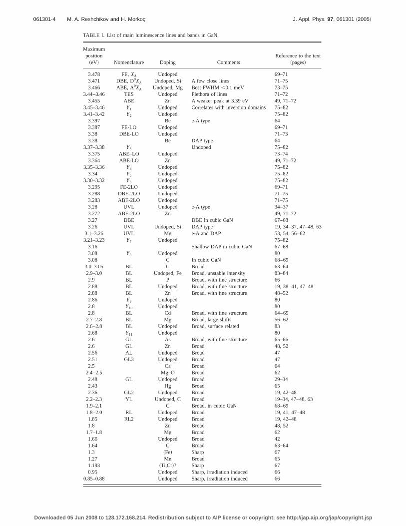
TABLE I. List of main luminescence lines and bands in GaN.
Maximumposition
seVd Nomenclature Doping CommentsReference to the text
spagesd
3.478 FE,XA Undoped 69–713.471 DBE, D0XA Undoped, Si A few close lines 71–753.466 ABE, A0XA Undoped, Mg Best FWHM,0.1 meV 73–75
3.44–3.46 TES Undoped Plethora of lines 71–723.455 ABE Zn A weaker peak at 3.39 eV 49, 71–72
3.45–3.46 Y1 Undoped Correlates with inversion domains 75–823.41–3.42 Y2 Undoped 75–82
3.397 Be e-A type 643.387 FE-LO Undoped 69–713.38 DBE-LO Undoped 71–733.38 Be DAP type 64
3.37–3.38 Y3 Undoped 75–823.375 ABE–LO Undoped 73–743.364 ABE-LO Zn 49, 71–72
3.35–3.36 Y4 Undoped 75–823.34 Y5 Undoped 75–82
3.30–3.32 Y6 Undoped 75–823.295 FE-2LO Undoped 69–713.288 DBE-2LO Undoped 71–753.283 ABE-2LO Undoped 71–753.28 UVL Undoped e-A type 34–373.272 ABE-2LO Zn 49, 71–723.27 DBE DBE in cubic GaN 67–683.26 UVL Undoped, Si DAP type 19, 34–37, 47–48, 63
3.1–3.26 UVL Mg e-A and DAP 53, 54, 56–623.21–3.23 Y7 Undoped 75–82
3.16 Shallow DAP in cubic GaN 67–683.08 Y8 Undoped 803.08 C In cubic GaN 68–69
3.0–3.05 BL C Broad 63–642.9–3.0 BL Undoped, Fe Broad, unstable intensity 83–842.9 BL P Broad, with fine structure 662.88 BL Undoped Broad, with fine structure 19, 38–41, 47–482.88 BL Zn Broad, with fine structure 48–522.86 Y9 Undoped 802.8 Y10 Undoped 802.8 BL Cd Broad, with fine structure 64–65
2.7–2.8 BL Mg Broad, large shifts 56–622.6–2.8 BL Undoped Broad, surface related 832.68 Y11 Undoped 802.6 GL As Broad, with fine structure 65–662.6 GL Zn Broad 48, 522.56 AL Undoped Broad 472.51 GL3 Undoped Broad 472.5 Ca Broad 64
2.4–2.5 Mg–O Broad 622.48 GL Undoped Broad 29–342.43 Hg Broad 652.36 GL2 Undoped Broad 19, 42–48
2.2–2.3 YL Undoped, C Broad 19–34, 47–48, 631.9–2.1 C Broad, in cubic GaN 68–691.8–2.0 RL Undoped Broad 19, 41, 47–481.85 RL2 Undoped Broad 19, 42–481.8 Zn Broad 48, 52
1.7–1.8 Mg Broad 621.66 Undoped Broad 421.64 C Broad 63–641.3 sFed Sharp 671.27 Mn Broad 651.193 sTi,Crd? Sharp 670.95 Undoped Sharp, irradiation induced 66
0.85–0.88 Undoped Sharp, irradiation induced 66
061301-4 M. A. Reshchikov and H. Morkoç J. Appl. Phys. 97, 061301 ~2005!
Downloaded 05 Jun 2008 to 128.172.168.214. Redistribution subject to AIP license or copyright; see http://jap.aip.org/jap/copyright.jsp
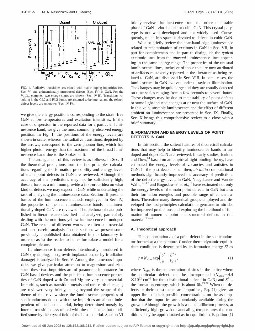
we give the energy positions corresponding to the strain-freeGaN at low temperatures and excitation intensities. In thecase of dispersion in the reported data for a particular lumi-nescence band, we give the most commonly observed energyposition. In Fig. 1, the positions of the energy levels areshown in scale, whereas the radiative transitions, depicted bythe arrows, correspond to the zero-phonon line, which hashigher photon energy than the maximum of the broad lumi-nescence band due to the Stokes shift.
The arrangement of this review is as follows: in Sec. IIthe theoretical predictions from the first-principles calcula-tions regarding the formation probability and energy levelsof main point defects in GaN are reviewed. Although theaccuracy of the predictions may not be sufficiently high,these efforts as a minimum provide a first-order idea on whatkind of defects we may expect in GaN while undertaking thetask of analyzing the luminescence data. Section III presentsbasics of the luminescence methods employed. In Sec. IV,the properties of the main luminescence bands in uninten-tionally doped GaN are reviewed. The plethora of data pub-lished in literature are classified and analyzed, particularlydealing with the notorious yellow luminescence in undopedGaN. The results of different works are often controversialand need careful analysis. In this section, we present somepreviously unpublished data obtained in our laboratory inorder to assist the reader to better formulate a model for acomplete picture.
Luminescence from defects intentionally introduced inGaN sby doping, postgrowth implantation, or by irradiationdamaged is analyzed in Sec. V. Among the numerous impu-rities we give particular attention to magnesium and zincsince these two impurities are of paramount importance forGaN-based devices and the published luminescence proper-ties of GaN doped with Zn and Mg are very controversial.Impurities, such as transition metals and rare-earth elements,are reviewed very briefly, being beyond the scope of thetheme of this review since the luminescence properties ofsemiconductors doped with these impurities are almost inde-pendent of the host material, being determined mostly byinternal transitions associated with these elements but modi-fied some by the crystal field of the host material. Section VI
briefly reviews luminescence from the other metastablephase of GaN—zinc-blende or cubic GaN. This crystal poly-type is not well developed and not widely used. Conse-quently, much less space is devoted to defects in cubic GaN.
We also briefly review the near-band-edge luminescencerelated to recombination of excitons in GaN in Sec. VII, inpart for completeness and in part to distinguish thetypicalexcitonic lines from theunusualluminescence lines appear-ing in the same energy range. The properties of the unusualluminescence lines, inclusive of those that are now attributedto artifacts mistakenly reported in the literature as being re-lated to GaN, are discussed in Sec. VIII. In some cases, theluminescence in GaN evolves under ultraviolet illumination.The changes may be quite large and they are usually detectedon time scales ranging from a few seconds to several hours.These changes may be due to metastability of point defectsor some light-induced changes at or near the surface of GaN.In this vein, unstable luminescence and the effect of differentambient on luminescence are presented in Sec. IX. Finally,Sec. X brings this comprehensive review to a close with abrief summary.
II. FORMATION AND ENERGY LEVELS OF POINTDEFECTS IN GaN
In this section, the salient features of theoretical calcula-tions that may help to identify luminescence bands in un-doped and doped GaN are reviewed. In early studies, Jenkinsand Dow,14 based on an empirical tight-binding theory, haveestimated the energy levels of vacancies and antisites inGaN. In the past decade since then,ab initio computationalmethods significantly improved the accuracy of predictionsof the defect energy levels in GaN. Neugebauer and Van deWalle,15–17and Boguslawskiet al.,18 have estimated not onlythe energy levels of the main point defects in GaN but alsotheir formation energies and possible range of concentra-tions. Thereafter many theoretical groups employed and de-veloped the first-principles calculations germane to nitridesfor improved predictions and exploring the likelihood of for-mation of numerous point and structural defects in thismaterial.19–24
A. Theoretical approach
The concentrationc of a point defect in the semiconduc-tor formed at a temperatureT under thermodynamic equilib-rium conditions is determined by its formation energyEf as
c = NsitesexpSSf
k−
Ef
kTD , s1d
whereNsites is the concentration of sites in the lattice wherethe particular defect can be incorporatedsNsites<4.431022 cm−3 for the substitutional defects in GaNd andSf isthe formation entropy, which is about 6k.19,20 When the de-fects or their constituents are impurities, Eq.s1d gives anupper limit of their possible concentrations on the assump-tion that the impurities are abundantly available during thegrowth. Although the growth is a nonequilibrium process, atsufficiently high growth or annealing temperatures the con-ditions may be approximated as in equilibrium. Equations1d
FIG. 1. Radiative transitions associated with major doping impuritiessseeSec. Vd and unintentionally introduced defectssSec. IVd in GaN. For theVGaON complex, two charge states are shownsSec. IV Bd. Transitions re-sulting in the GL2 and RL2 bands are assumed to be internal and the relateddefect levels are unknownsSec. IV Fd.
061301-5 M. A. Reshchikov and H. Morkoç J. Appl. Phys. 97, 061301 ~2005!
Downloaded 05 Jun 2008 to 128.172.168.214. Redistribution subject to AIP license or copyright; see http://jap.aip.org/jap/copyright.jsp
shows thatEf is the key parameter for estimating likelihoodof defect formation. Obviously, the defects with high forma-tion energies have less probability to form.
The formation energy can be calculated in the formalismof Zhang and Northrup25 as
Efsq,EFd = Etotsqd − Ebulktot − o
i
nimi + qEF, s2d
whereEtotsqd is the total energy of a supercell containing onedefect in the charge stateq, Ebulk
tot is the total energy of thedefect-free supercell,ni is the number of atoms of typei inthis supercell,mi is the chemical potential of atoms of typei,EF sthe Fermi leveld is the electron chemical potential withrespect to the valence-band maximum. The chemical poten-tials for Ga and N are usually considered for extreme growthor annealing conditions:mGa=mGasbulkd for the Ga-rich caseandmN=mN2
for the N-rich case. Note that these values arenot independent in thatmGa+mN=mGaN. The formation en-ergy of the charged defects depends on the charge and theFermi level at the time of defect formationsduring growth orannealingd. As can be seen from Eq.s2d, the formation en-ergy of the positivelysnegativelyd charged defects increasessdecreasesd as the Fermi level moves from the valence-bandmaximum towards the conduction band. The slope of thisvariation is proportional to the charge state of the defect. Theenergy at which the levels corresponding to different chargestates intersect determines the ionization level of the defect.Note that the calculations of the total energy may in generalgive an error of up to a few tenths of eV, and a variety ofcorrections is often used to improve the accuracy. The detailson the first-principles calculations used for defects in GaNcan be found in the recent review by Van de Walle andNeugebauer.26
The above approach enables one to calculate not onlythe formation energies and positions of the defect levels butalso the binding and dissociation energies of complex de-fects, local modes of vibrations, and migration barriers ordiffusivity of point defects. Any agreement between differentgroups, using slightly different approaches, increases confi-dence in the reliability of the results.
B. Native point defects
Native defects are always present in semiconductors andnotably affect the electrical and optical properties of the hostmaterial. They are often formed as compensation sourceswhen dopants are introduced, or as a result of nonstoichio-metric growth or annealing. The isolated native defects takethe form of vacancies, interstitials, and antisites. Complexdefects formed through interaction of isolated native defects,and combinations of native defects and impurities are con-sidered in Sec. II D.
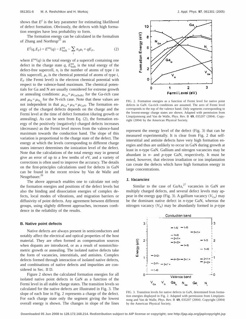
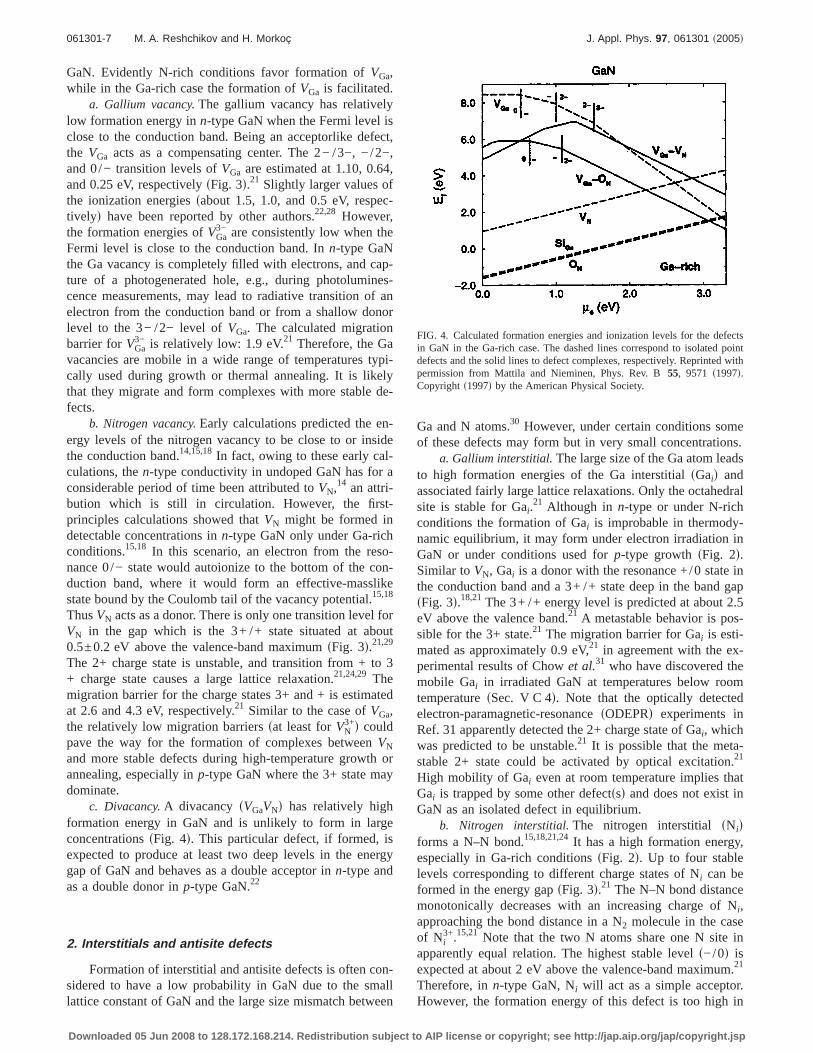
Figure 2 shows the calculated formation energies for allisolated native point defects in GaN as a function of theFermi level in all stable charge states. The transition levels socalculated for the native defects are illustrated in Fig. 3. Theslope of each line in Fig. 2 represents a charge of the defect.For each charge state only the segment giving the lowestoverall energy is shown. The changes in slope of the lines
represent the energy level of the defectsFig. 3d that can bemeasured experimentally. It is clear from Fig. 2 that self-interstitial and antisite defects have very high formation en-ergies and thus are unlikely to occur in GaN during growth atleast inn-type GaN. Gallium and nitrogen vacancies may beabundant inn- and p-type GaN, respectively. It must benoted, however, that electron irradiation or ion implantationcan create the defects which have high formation energy inlarge concentrations.
1. Vacancies
Similar to the case of GaAs,27 vacancies in GaN aremultiply charged defects, and several defect levels may ap-pear in the energy gapsFig. 3d. A gallium vacancysVGad maybe the dominant native defect inn-type GaN, whereas thenitrogen vacancysVNd may be abundantly formed inp-type
FIG. 2. Formation energies as a function of Fermi level for native pointdefects in GaN. Ga-rich conditions are assumed. The zero of Fermi levelcorresponds to the top of the valence band. Only segments corresponding tothe lowest-energy charge states are shown. Adapted with permission fromLimpijumnong and Van de Walle, Phys. Rev. B69, 035207s2004d. Copy-right s2004d by the American Physical Society.
FIG. 3. Transition levels for native defects in GaN, determined from forma-tion energies displayed in Fig. 2. Adapted with permission from Limpijum-nong and Van de Walle, Phys. Rev. B69, 035207s2004d. Copyrights2004dby the American Physical Society.
061301-6 M. A. Reshchikov and H. Morkoç J. Appl. Phys. 97, 061301 ~2005!
Downloaded 05 Jun 2008 to 128.172.168.214. Redistribution subject to AIP license or copyright; see http://jap.aip.org/jap/copyright.jsp
GaN. Evidently N-rich conditions favor formation ofVGa,while in the Ga-rich case the formation ofVGa is facilitated.
a. Gallium vacancy.The gallium vacancy has relativelylow formation energy inn-type GaN when the Fermi level isclose to the conduction band. Being an acceptorlike defect,the VGa acts as a compensating center. The 2− /3−, −/2−,and 0/− transition levels ofVGa are estimated at 1.10, 0.64,and 0.25 eV, respectivelysFig. 3d.21 Slightly larger values ofthe ionization energiessabout 1.5, 1.0, and 0.5 eV, respec-tivelyd have been reported by other authors.22,28 However,the formation energies ofVGa
3− are consistently low when theFermi level is close to the conduction band. Inn-type GaNthe Ga vacancy is completely filled with electrons, and cap-ture of a photogenerated hole, e.g., during photolumines-cence measurements, may lead to radiative transition of anelectron from the conduction band or from a shallow donorlevel to the 3− /2− level ofVGa. The calculated migrationbarrier forVGa
3− is relatively low: 1.9 eV.21 Therefore, the Gavacancies are mobile in a wide range of temperatures typi-cally used during growth or thermal annealing. It is likelythat they migrate and form complexes with more stable de-fects.
b. Nitrogen vacancy.Early calculations predicted the en-ergy levels of the nitrogen vacancy to be close to or insidethe conduction band.14,15,18In fact, owing to these early cal-culations, then-type conductivity in undoped GaN has for aconsiderable period of time been attributed toVN,14 an attri-bution which is still in circulation. However, the first-principles calculations showed thatVN might be formed indetectable concentrations inn-type GaN only under Ga-richconditions.15,18 In this scenario, an electron from the reso-nance 0/− state would autoionize to the bottom of the con-duction band, where it would form an effective-masslikestate bound by the Coulomb tail of the vacancy potential.15,18
ThusVN acts as a donor. There is only one transition level forVN in the gap which is the 3+ /+ state situated at about0.5±0.2 eV above the valence-band maximumsFig. 3d.21,29
The 2+ charge state is unstable, and transition from + to 3+ charge state causes a large lattice relaxation.21,24,29 Themigration barrier for the charge states 3+ and + is estimatedat 2.6 and 4.3 eV, respectively.21 Similar to the case ofVGa,the relatively low migration barrierssat least forVN
3+d couldpave the way for the formation of complexes betweenVN
and more stable defects during high-temperature growth orannealing, especially inp-type GaN where the 3+ state maydominate.
c. Divacancy.A divacancy sVGaVNd has relatively highformation energy in GaN and is unlikely to form in largeconcentrationssFig. 4d. This particular defect, if formed, isexpected to produce at least two deep levels in the energygap of GaN and behaves as a double acceptor inn-type andas a double donor inp-type GaN.22
2. Interstitials and antisite defects
Formation of interstitial and antisite defects is often con-sidered to have a low probability in GaN due to the smalllattice constant of GaN and the large size mismatch between
Ga and N atoms.30 However, under certain conditions someof these defects may form but in very small concentrations.
a. Gallium interstitial.The large size of the Ga atom leadsto high formation energies of the Ga interstitialsGaid andassociated fairly large lattice relaxations. Only the octahedralsite is stable for Gai.
21 Although in n-type or under N-richconditions the formation of Gai is improbable in thermody-namic equilibrium, it may form under electron irradiation inGaN or under conditions used forp-type growth sFig. 2d.Similar toVN, Gai is a donor with the resonance +/0 state inthe conduction band and a 3+ /+ state deep in the band gapsFig. 3d.18,21The 3+ /+ energy level is predicted at about 2.5eV above the valence band.21 A metastable behavior is pos-sible for the 3+ state.21 The migration barrier for Gai is esti-mated as approximately 0.9 eV,21 in agreement with the ex-perimental results of Chowet al.31 who have discovered themobile Gai in irradiated GaN at temperatures below roomtemperaturesSec. V C 4d. Note that the optically detectedelectron-paramagnetic-resonancesODEPRd experiments inRef. 31 apparently detected the 2+ charge state of Gai, whichwas predicted to be unstable.21 It is possible that the meta-stable 2+ state could be activated by optical excitation.21
High mobility of Gai even at room temperature implies thatGai is trapped by some other defectssd and does not exist inGaN as an isolated defect in equilibrium.
b. Nitrogen interstitial.The nitrogen interstitial sNidforms a N–N bond.15,18,21,24It has a high formation energy,especially in Ga-rich conditionssFig. 2d. Up to four stablelevels corresponding to different charge states of Ni can beformed in the energy gapsFig. 3d.21 The N–N bond distancemonotonically decreases with an increasing charge of Ni,approaching the bond distance in a N2 molecule in the caseof Ni
3+.15,21 Note that the two N atoms share one N site inapparently equal relation. The highest stable levels−/0d isexpected at about 2 eV above the valence-band maximum.21
Therefore, inn-type GaN, Ni will act as a simple acceptor.However, the formation energy of this defect is too high in
FIG. 4. Calculated formation energies and ionization levels for the defectsin GaN in the Ga-rich case. The dashed lines correspond to isolated pointdefects and the solid lines to defect complexes, respectively. Reprinted withpermission from Mattila and Nieminen, Phys. Rev. B55, 9571 s1997d.Copyright s1997d by the American Physical Society.
061301-7 M. A. Reshchikov and H. Morkoç J. Appl. Phys. 97, 061301 ~2005!
Downloaded 05 Jun 2008 to 128.172.168.214. Redistribution subject to AIP license or copyright; see http://jap.aip.org/jap/copyright.jsp
GaN grown under equilibrium Ga-rich conditions. The mi-gration barrier for Ni is only about 1.5 eV for the − and3+ charge states,21 so that diffusion of nitrogen interstitials islikely to occur in GaN at temperatures slightly above roomtemperature.
c. Gallium antisite.The gallium antisitesGaNd introducesa few deep levels in GaNsFig. 3d.18,21 The 4+ /3+ level ofGaN is expected at about 0.9 eV above the valence band.21
Therefore, inp-type GaN this native defect may be respon-sible for significant compensation if the Ga-rich conditionsare used. Large outward lattice relaxation around the GaN
has been noted by several theorists.18,23
d. Nitrogen antisite.The nitrogen antisitesNGad appar-ently introduces three21 or perhaps even four32 deep levels inthe energy gap of GaNsFig. 3d. It can behave as a compen-sating double donor inp-type GaN or an acceptor inn-typeGaN. The formation energy of NGa is very high regardless ofthe position of the Fermi level, especially under Ga-rich con-ditions sFig. 2d. It should be pointed out that Mattilaet al.32
predicted a reasonably low formation energy of NGa3− in
stronglyn-type GaN grown under N-rich conditions.The neutral NGa defect may exhibit a metastable behav-
ior, similar to its analog in GaAs which is known as the EL2defect.33,34 Mattila et al.32 and Gorczycaet al.23 predictedthat the neutral NGa defect can transform intoVGaNi defect incubic GaN.
C. Impurities
Generally, C, Si, and Ge on the Ga sites and O, S, and Seon the N sites are considered as shallow donors in GaN,whereas Be, Mg, Ca, Zn, and Cd on the Ga sites and C, Si,and Ge on the N sites could potentially give rise to relativelyshallow acceptors in this semiconductor. Below we brieflyreview the formation energies and energy levels calculatedfrom first principles and by using the effective-mass method.While the former could predict which defect is easier toform, the latter could provide a much better accuracy in de-termining the ionization energy.
1. Shallow donors
Wang and Chen35 calculated the energy levels of substi-tutional shallow donors in GaN in the effective-mass ap-proximation accounting for such effects as mass anisotropy,central-cell potential correction, and the conduction-band-edge wave function of the host material. They deduced thefollowing donor ionization energies in wurtzite GaN: 34.0,30.8, and 31.1 meV for C, Si, and Ge on the Ga site, and32.4, 29.5, and 29.5 meV for O, S, and Se on the N sites.Boguslawski and Bernholc20 considered substitutional C, Si,and Ge impurities in wurtzite GaN in the framework of first-principles calculations. They have found that formation en-ergies of SiGa and GeGa donors are reasonably smalls0.9 and2.3 eV, respectively, for Ga-rich conditionsd, while formationof CGa donor has a low probability. In various theoreticalinvestigations the formation energy of neutral CGa has beenestimated as 4–4.7 eV for the N-rich case and 5.7–6.5 eV forthe Ga-rich case.20,23,36Neugebauer and Van de Walle17 andMattila and Nieminen22 have obtained small formation ener-
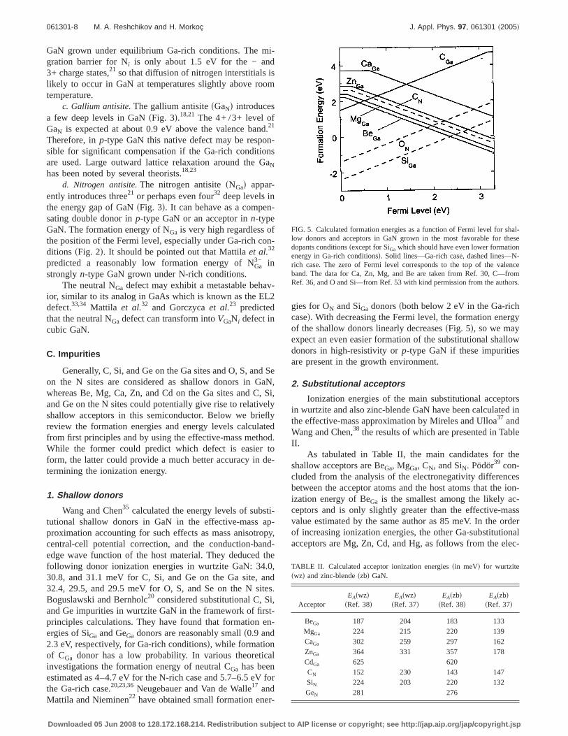
gies for ON and SiGa donorssboth below 2 eV in the Ga-richcased. With decreasing the Fermi level, the formation energyof the shallow donors linearly decreasessFig. 5d, so we mayexpect an even easier formation of the substitutional shallowdonors in high-resistivity orp-type GaN if these impuritiesare present in the growth environment.
2. Substitutional acceptors
Ionization energies of the main substitutional acceptorsin wurtzite and also zinc-blende GaN have been calculated inthe effective-mass approximation by Mireles and Ulloa37 andWang and Chen,38 the results of which are presented in TableII.
As tabulated in Table II, the main candidates for theshallow acceptors are BeGa, MgGa, CN, and SiN. Pödör39 con-cluded from the analysis of the electronegativity differencesbetween the acceptor atoms and the host atoms that the ion-ization energy of BeGa is the smallest among the likely ac-ceptors and is only slightly greater than the effective-massvalue estimated by the same author as 85 meV. In the orderof increasing ionization energies, the other Ga-substitutionalacceptors are Mg, Zn, Cd, and Hg, as follows from the elec-
FIG. 5. Calculated formation energies as a function of Fermi level for shal-low donors and acceptors in GaN grown in the most favorable for thesedopants conditionssexcept for SiGa which should have even lower formationenergy in Ga-rich conditionsd. Solid lines—Ga-rich case, dashed lines—N-rich case. The zero of Fermi level corresponds to the top of the valenceband. The data for Ca, Zn, Mg, and Be are taken from Ref. 30, C—fromRef. 36, and O and Si—from Ref. 53 with kind permission from the authors.
TABLE II. Calculated acceptor ionization energiessin meVd for wurtziteswzd and zinc-blendeszbd GaN.
AcceptorEAswzd
sRef. 38dEAswzd
sRef. 37dEAszbd
sRef. 38dEAszbd
sRef. 37d
BeGa 187 204 183 133MgGa 224 215 220 139CaGa 302 259 297 162ZnGa 364 331 357 178CdGa 625 620CN 152 230 143 147SiN 224 203 220 132GeN 281 276
061301-8 M. A. Reshchikov and H. Morkoç J. Appl. Phys. 97, 061301 ~2005!
Downloaded 05 Jun 2008 to 128.172.168.214. Redistribution subject to AIP license or copyright; see http://jap.aip.org/jap/copyright.jsp
tronegativity difference between these impurities and Gaatom.39 Park and Chadi29 examined the atomic and electronicstructures of substitutional Be, Mg, and C acceptors in GaNthrough first-principles calculations and concluded that theseimpurities would give effective-mass states in GaN, notAXstates. The calculated formation energies of some of thesesubstitutional acceptors are shown in Fig. 5. The formationenergies of MgGa and BeGa and their ionization energies arethe lowest. One problem for Be, however, is that the atom istoo small and can incorporate efficiently on the interstitialsite, where it acts as a double donor.30,40–42Therefore, amongthe group-II impurities, Mg and Be are the most promisingp-type dopants for GaN, and Be appears to be the best can-didate, provided that the conditions that suppress formationof Bei donors can be established. This is technologicallychallenging to say the least. The formation energies of ac-ceptors from group-IV impurities, such as SiN and GeN, arerelatively high, so that formation of these acceptors is un-likely in GaN under equilibrium conditions.20,30 The forma-tion energy of CN could be sufficiently low in Ga-richconditions.19,20,23,36,43However, the CN acceptor might becompensated by interstitial C when the Fermi level is closeto the conduction band.36 Note also that the formation ener-gies of the acceptors decrease with increasing Fermi level, sothat we may expect efficient formation of CN and SiN accep-tors in undoped orn-type doped GaN when these impuritiesare present in the growth environment.
Neugebauer and Van de Walle30 also examined the for-mation energies of acceptors from group-I impurities, suchas KGa, NaGa, and LiGa. They predicted that these acceptorshave relatively high formation energies and large ionizationenergies, and are therefore not likely to be candidates forsuccessfulp-type dopants. Moreover, the formation energiesof the Na and Li interstitials are much lower inp-type GaN,so that these alkali impurities would rather behave as singledonors.30
3. Isoelectronic impurities
Arsenic and phosphorus could substitute nitrogen atomsin GaN to form isovalent defects, AsN and PN. In silicon,germanium, and most of III-V semiconductors isovalent im-purities do not introduce deep energy levels in the band gap.However, the theory predicts formation of deep gap states byisovalent impurities in GaN, similar to the situation in II-VIcompounds, due to large size mismatch of the isovalent at-oms in GaN.44,45The first-principles calculations have shownthat the AsN and PN defects may exist in neutral, +, and2+ charge states in GaN. Mattila and Zunger45 predicted the21/1 and +/0 energy levels of AsN to be 0.24 and 0.41 eVabove the valence-band maximum, and those of PN to be0.09 and 0.22 eV, respectively.45 Van de Walle andNeugebauer46 obtained the values for the same as 0.11 and0.31 eV for the 21/1 and +/0 levels of AsN, respectively.The formation energy of AsN is quite large, and under themost favorable conditionssGa rich and Fermi level above2.3 eVd, the first-principles calculations predict the formationenergy of AsN of about 4.5 eV. Inp-type GaN, and/or inN-rich conditions, formation of AsGa antisite-type defect ismuch more likely.46 This defect is a double donor with the
2+ /0 level at about 2.5 eV above the valence-band maxi-mum. In addition, the formation energy is very small whenthe Fermi level is close to the valence band.46 Therefore, thepresence of As can cause significant compensation duringgrowth of p-type GaN.
4. Hydrogen
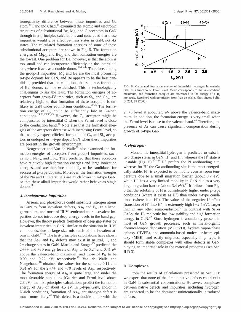
Monatomic interstitial hydrogen is predicted to exist intwo charge states in GaN: H+ and H−, whereas the H0 state isunstablesFig. 6d.47–49 H+ prefers the N antibonding site,whereas for H− the Ga antibonding site is the most energeti-cally stable. H+ is expected to be mobile even at room tem-perature due to a small migration barriersabout 0.7 eVd,while H− has a very limited mobility in GaN due to a verylarge migration barriersabout 3.4 eVd.47 It follows from Fig.6 that the solubility of H is considerably higher underp-typeconditionsswhere it exists as H+d than undern-type condi-tions swhere it is H−d. The value of the negative-U effectstransition of H− into H+d is extremely highs22.4 eVd, largerthan in any other semiconductor.47 In contrast with Si orGaAs, the H2 molecule has low stability and high formationenergy in GaN.47 Since hydrogen is abundantly present inmost of GaN growth processes, such as metal-organicchemical-vapor depositionsMOCVDd, hydrate vapor-phaseepitaxy sHVPEd, and ammonia-based molecular-beam epi-taxy sMBEd, and easily migrates, especially inp type, itshould form stable complexes with other defects in GaN,playing an important role in the material propertiesssee Sec.II D 3d.
D. Complexes
From the results of calculations presented in Sec. II Bwe expect that none of the simple native defects could existin GaN in substantial concentrations. However, complexesbetween native defects and impurities, including hydrogen,are expected to be the dominant unintentionally introduceddefects.
FIG. 6. Calculated formation energy of interstitial hydrogen in wurtziteGaN as a function of Fermi level.EF=0 corresponds to the valence-bandmaximum, and formation energies are referenced to the energy of a H2
molecule. Reprinted with permission from Van de Walle, Phys. Status SolidiB 235, 89 s2003d.
061301-9 M. A. Reshchikov and H. Morkoç J. Appl. Phys. 97, 061301 ~2005!
Downloaded 05 Jun 2008 to 128.172.168.214. Redistribution subject to AIP license or copyright; see http://jap.aip.org/jap/copyright.jsp
1. Shallow donor—gallium vacancy complexes
The gallium vacancy is the dominant native defect inn-type sin particular, undopedd GaN because the formationenergy ofVGa is low in this casesFig. 2d. However, as notedin Sec. II B 1, VGa could easily diffuse even at moderatetemperatures of growth or thermal annealing and wouldreadily form complexes with other defects. It should be un-derscored that formation of complexes is driven by electro-static forces. The impurities that are most likely to formstable complexes withVGa are donors. A negatively chargedacceptorsthe charge ofVGa is 3- in n-type GaNd and a posi-tively charged donor are attracted to each other. According tothe calculations of Neugebauer and Van de Walle,17 VGaON
andVGaSiGa complexes act as double acceptors in GaN, andtheir −/2− energy levelssat 1.1 and 0.9 eV, respectivelyd areclose to the 2−/3− transition level of the isolatedVGa sat 1.1eVd. The electronic structure of Ga vacancy dominates theelectronic structure of theVGa-shallow donor complexes,very similar to the situation inn-type GaAs.50–52 Formationof theVGaON complex is even more favorable than formationof isolatedVGa.
17 Similar results have been obtained by Mat-tila and Nieminen,22 who compared the formation energies ofthe isolatedVGa and theVGaON complex for different posi-tions of the Fermi levelsFig. 4d. The VGaON complex has abinding energy of,1.8 eV, as compared to,0.23 eV forthe VGaSiGa complex.17 This indicates that theVGaON com-plex is much more stable and it may be the dominant com-pensating acceptor inn-type GaN. TheVGaCN complex has alow formation energy, but is unstable inn-type GaN becauseboth constituents are acceptors and repeal each other.17,36
2. Shallow acceptor—nitrogen vacancycomplexes
The situation with N vacancy and shallow acceptors inp-type GaN is essentially the same as for the Ga vacancy,and shallow donors inn-type GaN. N vacancy,VN, being amobile and dominant compensating donor inp-type GaN,would be attracted by negatively charged acceptors duringgrowth and cooling down or thermal annealing. The bindingenergy for a neutral MgGaVN complex is about 0.5 eV,29,53
although Gorczycaet al.54 obtained a value of 2.8 eV. Theformation energy of the MgGaVN complex is significantlylower than the sum of the formation energies of the isolatedMgGa andVN.54 Park and Chadi29 assumed that the MgGaVN
complex is responsible for the persistent photoconductivityin GaN:Mg55 and attributed the bistability to the neutral and2+ states of this complex. Van de Walleet al.53 argued thatthe relatively low binding energy of the MgGaVN complexprevents abundant formation of these complexes inp-typeGaN in thermal equilibrium. However, their formation canbe enhanced by kinetically driven processes on the samplesurface during growth. It is not clear where in the band gapthe energy level of MgGaVN is. Kaufmannet al.56 assumedthat MgGaVN is a deep donor with an energy level at about0.4 eV below the conduction band. Park and Chadi29 esti-mated the energy level ofsMgGaVNd2+ at about 0.7 eV abovethe valence band, while Gorczycaet al.54 obtained an energylevel much closer to the valence band. Note that in the latter
report the energy level ofVN was also much lower than thatobtained in Refs. 29 and 53. Similar to the MgGaVN com-plexes in GaN:Mg, the BeGaVN complexes are expected toform in Be-doped GaN.57
Lee and Chang58 examined the possibility of formationof MgiVN complexes inp-type GaN. While incorporation ofthe isolated Mgi is unlikely in GaN due to large atomic ra-dius of Mg, formation of the MgiVN complexes has lowenough formation energy when the Fermi level is close to thevalence band.58 The charge state of the MgiVN complex is 3+in this case, and therefore it can efficiently compensate MgGa
acceptors.58 The energy level of the MgiVN complexsor eventhree close levelsd is about 2.8 eV above the valence-bandmaximum. Similar results have been obtained by Gorczycaet al.54 Therefore, MgiVN might be the compensating donorin p-type GaN:Mg, apparently not MgGaVN. The energy levelof the compensating donor has been determined in the pho-toluminescence study of Kaufmannet al.56 at about 0.4 eVbelow the conduction band. Note that the MgiVN complexcould be formed only under Ga-rich conditions and when theFermi level is very close to the valence band.58 This meansthat passivation with hydrogen or N-rich conditions wouldprevent formation of this compensating donor. Lee andChang58 also assumed that hydrogen passivation can stabi-lize formation of the MgiVN complex at higher positions ofthe Fermi level. However, this conclusion is somewhatquestionable.54
3. Hydrogen-related complexes
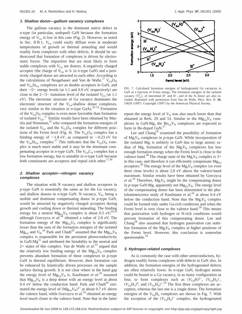
As is commonly the case with other semiconductors, hy-drogen readily forms complexes with defects in GaN also. Inaddition, the formation energies of the hydrogenated defectsare often relatively lower. Inn-type GaN, hydrogen atomscould be bound to a Ga vacancy, in as many configuration asfour, to form complexes such assVGaHd2−, sVGaH2d−,sVGaH3d0, and sVGaH4d+.59 The first three complexes are ac-ceptors, whereas the last one is a single donor. The formationenergies of theVGaHn complexes are shown in Fig. 7. Withthe exception of thesVGaH4d+ complex, the hydrogenated
FIG. 7. Calculated formation energies of hydrogenated Ga vacancies inGaN as a function of Fermi energy. The formation energies of the isolatedvacancysVGa
3−d, of interstitial H+ and H−, and of the Si donor are also in-cluded. Reprinted with permission from Van de Walle, Phys. Rev. B56,10020s1997d. Copyrights1997d by the American Physical Society.
061301-10 M. A. Reshchikov and H. Morkoç J. Appl. Phys. 97, 061301 ~2005!
Downloaded 05 Jun 2008 to 128.172.168.214. Redistribution subject to AIP license or copyright; see http://jap.aip.org/jap/copyright.jsp
vacancies have lower formation energies than the isolatedVGa, which points to the importance of these complexes inGaN. The calculated energy levels of thesVGaHd2− andsVGaH2d− complexessat about 1.0 eV above the valencebandd are close to that of the isolatedVGa, while the level ofsVGaH3d0 is near the valence-band maximum.59 It must bepointed out that inn-type GaN, formation of complexes withseveral H atoms, such assVGaH3d0 andsVGaH4d+, is unlikelysince inn-type GaN the isolated hydrogen atom exists as H−
which would be repelled from the negatively charged Gavacancy.59 Dissociation of theVGaHn complexes is unlikelydue to the large associated binding energies.59 Therefore,once formed during growth in the presence of hydrogen,these complexes cannot dissociate during postgrowth ther-mal annealing.
In p-type GaN, hydrogen passivates the dominant accep-tor sMgGad, as well as the dominant compensating donorsVNd.47,59 In the case of Mg, the electrically neutral Mg–Hcomplex has a binding energy of 0.7 eV, with the H atomlocated in an antibonding site behind the N neighbor of theacceptor.47 During postgrowth annealing, the Mg–H complexdissociates, and H diffuses either to the surface or to theextended defects.47 Similarly, in Be-doped GaN, the Be–Hcomplexes may form with a binding energy of 1.81 eV and adissociation energy of 2.51 eV.40 A postgrowth annealingwould also be required to remove the hydrogen from Beacceptors.
The N vacancy inp-type GaN may also be passivated byhydrogen during the growth to form thesVNHd2+ complexwith the binding energy of 1.56 eV.59 The formation energyof the sVNHd2+ complex is lower than the formation of theisolated H+ andVN when the Fermi level is low in the gap.59
The VNH complexes can be formed only during growth asdiffusion of H+ towardsVN is highly unlikely in p-type GaNsince they repel each other. Formation of thesVNH2d+ com-plex is also possible, while thesVNH3d0 complex isunstable.60 The VNH complex is expected to have a 2+ /0transition level at about 2.5 eV above the valence band and a0/2− level close to the conduction band,60 while earlier cal-culations predicted the 0/+ transition level ofVNH to be nearor in resonance with the conduction band.59 Both VN
3+ andsVNHd2+ could be formed in abundance inp-type GaN andcompensate the dominant acceptor. Note that the hydrogen-ated vacancies may lose their hydrogen after the sample isgrown, either during cooling down or during postgrowth an-nealing, andVN
3+ could also migrate during high-temperatureannealing.21
4. Other complexes
The other element, in addition to H, that is unintention-ally present in any growth systems is O which must be dealtwith. While O is a ubiquitous problem for all semiconduc-tors, O in GaN takes on a new dimension. The O atom in Nsite is a shallow donor in GaN and it might hamper attemptsto obtainp-type material in addition to causing undesirablebackground donors. The formation energy of the MgGaON
complexes is very low.54 Therefore, these complexes canreadily form in Mg-doped GaN when oxygen is present inthe growth environment. Gorczycaet al.54 predicted that for-
mation of these complexes would result in semi-insulatingGaN, since both ON and MgGa levels would be pushed out ofthe energy gap. However, the relatively low binding energyof the MgGaON complexs0.6 eVd is unfavorable for the com-plex formation, unless the kinetically driven processes on thesurface result in the preferential incorporation of MgGaON.53
In Be-doped GaN, BeGaON complex could be formed,which is neutral.40,41 Moreover, the BeGaONBeGa complexcould be formed with the 0/− transition level at 0.14 eVabove the valence-band maximum.40 Along with the forma-tion of Bei
2+ donors, thesBeGaBeid+ donor complexes mightform in Be-doped GaN which end up compensating the Beacceptor.40 However, the postgrowth annealing at tempera-tures above 600 °C should result in dissociation of thesecomplexes.40
E. Role of dislocations in the point defect formation
Due to large lattice mismatch, heteroepitaxy of GaN onsapphire substrates results in films containing threading dis-locations with the densities from,108 to ,1010 cm−2, de-pending on growth method and conditions, and whether dis-location reducing methods are employed. The situation is notmuch different if other substrates with seemingly smaller lat-tice mismatches are used. These dislocations are mainly par-allel to thec axis, and their Burgers vectors are equal toasedge-typed, c sscrew-typed, or a+c smixed-typed. The first-principles calculations enable comparison of formation ener-gies and structures of different types of dislocations andpoint defects that can be trapped by the stress fields associ-ated with the dislocations.
In contrast to the earlier prediction that threading dislo-cations are electrically inactive in GaN,61 later calculationsindicated that various types of dislocations may introducenumerous energy levels in the gap.62–64 In particular, thread-ing dislocations are expected to behave as deep donors inn-type material and deep acceptors inp type.62 Under Ga-rich conditions dislocations decorated with Ga vacancieshave the lowest formation energy inn-type GaN, while inN-rich conditions dislocations decorated with Ga vacancieshave the lowest formation energy inp-type GaN.62,65 To afirst extent these results are consistent with the experimentalfindings from a scanning-capacitance microscopy study, in-dicating the presence of negatively charged dislocations inn-type GaN.66 Note that deep donors inn-type material anddeep acceptors inp-type material usually do not contribute toluminescence,67 therefore dislocations are not expected tomanifest themselves in luminescence experiments, unlesspoint defects are trapped at them due to the large stress fieldsnear dislocations.
The behavior of point defects trapped at threading-edgedislocations in GaN was examined by Elsneret al.68 First-principles calculations indicated thatVGa and its complexeswith one or more ON have very low formation energies atdifferent positions near the threading-edge dislocations. Theresults indicate that the formation energies ofVGa, ON, andtheir complexes at different sites near the threading-edge dis-location are much lower than the formation energies of thecorresponding defects in the bulk. Energy levels of the de-
061301-11 M. A. Reshchikov and H. Morkoç J. Appl. Phys. 97, 061301 ~2005!
Downloaded 05 Jun 2008 to 128.172.168.214. Redistribution subject to AIP license or copyright; see http://jap.aip.org/jap/copyright.jsp
fects trapped at dislocations generally shift as compared tothe point defects in bulk, however, the shift is not large.68 Inshort, the stress field of threading-edge dislocations is likelyto trap Ga vacancies, oxygen, and their complexes. A varietyof the VGa-containing complexes may form acceptorlike de-fect levels in the lower half of the band gap and therefore beresponsible for some transitions observed in luminescenceexperiments. Note that a similar situation might take place inp-type GaN, where the dislocations may trapVN andVN-related complexes.
III. LUMINESCENCE METHODS
PhotoluminescencesPLd and cathodoluminescencesCLdhave been the most widely used experimental methods ap-plied to investigations of GaN. Defects in GaN have beenstudied by analyzing the steady-state PLsSSPLd, time-resolved PLsTRPLd, and PL excitationsPLEd spectra. Opti-cally detected magnetic resonancesODMRd, a variant of thePL technique, along with the positron annihilation methodhas been extensively used for identification of point defectsin GaN.
A. Steady-state photoluminescence
The SSPL spectroscopy is widely used for qualitativeanalysis of GaN and its alloys. Commonly, the SSPL is gen-erated in GaN by illuminating it with a He–Cd lasers325nmd beam with optical power levels of up to approximately60 mW. In investigating defects, however, special precautionmust be taken to employ a sufficiently low excitation densitysince the defect-related PL often saturates at power densitiesof the order of 10−2–10−1 W/cm2. Failure to do so wouldvery likely cause skewing of the PL spectrum in favor ofexcitonic emission at higher excitation densities, giving thefalse impression about the relative strength of defect-inducedtransitions. Similarly, focusing the laser beam and usingsmall slit widths of a monochromator for the entire PL spec-trum would also distort the PL in favor of excitonic transi-tions. In such a case, the chromatic dispersion of lenses usedto collect the PL, as well as the different effective sizes of theemission spots for the ultravioletsUVd and visible emissionattributed, in particular, to photon-recycling process,69 maylead to a marked, but artificial, enhancement of the UVsnearband edged over the visible part in the PL spectrumsmainlydefect-relatedd.
Qualitative terms, such as “very intense PL that confirmshigh quality of the material,” are omnipresent in the litera-ture regarding GaN. However, there have been very few at-tempts to estimate the absolute value of the PL intensity orits quantum efficiencysQEd for a quantitative analysis. Al-though the direct measurement of the QE is not straightfor-ward, attempts have been made to estimate this importantparameter for GaN.70,67 Göldneret al.70 simultaneously de-tected the calorimetric absorptionsmeasure of nonradiativerecombination which results in heating of the sampled, trans-mission, reflection, and excitation power, and reported theQE to be below 20% for thin GaN layers grown by MOCVDon sapphire and up to 75% for bulk GaN crystal grown byHVPE. An indirect method based on quantitative analysis of
the competition of radiative and nonradiative recombinationchannels was suggested by Reshchikov and Korotkov,67 andis presented in Sec. III A 3.
Quantitative studies of point defects in GaN by PL haverarely been undertaken. Often, qualitative estimations of theacceptor concentration inn-type GaN were made by compar-ing the ratios between the defect and near-band-edge emis-sion intensities.71,72 However, this ratio is shown to dependnot only on the defect concentration but also on the experi-mental conditions, in particular, on the excitationintensity,67,73,74as was mentioned above. Temperature depen-dence of the defect-related PL intensity in GaN has oftenbeen used to determine the nature of a given optical transi-tion. For example, the donor-acceptor-pairsDAPd transitionshave been distinguished from the conduction-band-acceptorse-Ad transitions by the thermal behavior of PL.75–77 How-ever, the thermal behavior of PL may be complicated by acompetition between several recombination channels as isshown below using a simple phenomenological approach.67
1. Recombination statistics
Let us now consider ann-type semiconductor containingseveral radiative acceptorsAi with concentrationsNAi
. Theelectron-hole pairs are excited with a generation rateGfcm−3 s−1g. The concentration of the photogenerated holesin the valence band isp, the concentration of equilibriumsn0d and photogeneratedsdnd free electrons isn=n0+dn. Af-ter optical excitation, the holes are captured by acceptors atthe rateCpiNAi
− p, whereCpi fcm3 s−1g is the hole-capture co-efficient for theith acceptor andNAi
− is the concentration ofionized acceptors of typei. A competing process is the for-mation of excitons with the rateCexnp, where the coefficientCex describes the efficiency of the exciton formation. In ad-dition to radiative processes, some of the holes recombinenonradiatively. For simplicity, the nonradiative recombina-tion rate can be introduced asCpsNS
−p, whereCps andNS− are
the average hole-capture coefficient and the concentration ofthe nonradiative centers, respectively. Thus, in general, thehole-capture rate can be expressed asCiNi
−p, whereCi =Cex,Cpi, or Cps andNi
−=n, NAi
− , or NS− for excitons, radiative ac-
ceptors, and nonradiative defects, respectively.At elevated temperatures, the bound holes may return to
the valence band as a result of thermal activation or excitondissociation. The probability of this process,Qi fs−1g, is pro-portional to exps−Ei /kTd, whereEi is the thermal activationenergy for the radiative acceptorssEAi
d, nonradiative centerssESd, or the exciton dissociation energysEexd. Taking intoaccount all these processessFig. 8d, the detailed balanceequation for the hole concentration in the valence band insteady state in the case ofN recombination channels can bewritten in the form
]p
]t= G − o
i=1
N
CiNi−p + o
i=1
N
QiNi0 = 0, s3d
where Ni0=NAi
0 , NS0, and Nex is the concentration of holes
bound to radiative acceptors, nonradiative centers, or form-ing excitons, respectively. At sufficiently low excitation in-
061301-12 M. A. Reshchikov and H. Morkoç J. Appl. Phys. 97, 061301 ~2005!
Downloaded 05 Jun 2008 to 128.172.168.214. Redistribution subject to AIP license or copyright; see http://jap.aip.org/jap/copyright.jsp
tensities,Ni0!Ni
−<Ni, the steady-state equation for the con-centration of holes bound to theith defect can be written as
]Ni0
]t= CiNip −
Ni0
tRi
− QiNi0 = 0, s4d
where the second term describes recombination via theithchannel and the parametertRi
characterizes the recombina-tion lifetime sin general case it may evolve in time in tran-sient processesd.
The capture rates are usually much faster than recombi-nation rates. As a result, the efficiency of each of the recom-bination channels is proportionalto the rate of capture of theminority carriers sholes in n-type GaNd. Therefore, in thelow-temperature limit, where both the thermal release of thebound holes and the exciton dissociation are negligible, theQE of each recombination channel,his0d, is given by theratio of hole-capture rate for a specific recombination chan-nel to the total escape rate of holes from the valence band
his0d =CiNip
oj=1
N
CjNjp
=CiNi
oj=1
N
CjNj
. s5d
With the above assumptions, an expression for the intensityof PL via each defect can be determined as67
I iPL =
Ni0
tRi
= hiG =hi
*
1 + s1 − hi*dtRi
Qi
G, s6d
where
hi* = his0dF1 − o
jÞi
Nh js0dtRjQj
1 + tRjQjG−1
, s7d
andhi is the QE of theith channel accounting for dissocia-tion of excitons and thermal escape of holes from the defectsto the valence band.
2. Effect of temperature on PL intensity
It is evident from Eqs.s6d and s7d that the temperaturedependence of the PL intensity inn-type GaN is largely de-termined by exciton dissociation and thermal escape of holesfrom the defects to the valence band. Although the exactexpressions for the exciton dissociation can also bederived,78 it is much easier to account for the contribution ofthe exciton dissociation into the defect-related PLsthe termtRexQexd by taking the temperature dependence of the inte-grated exciton emission intensity from the experiment.67
The probability of thermal activation of holes from anacceptor,QAi
can be obtained from a detailed balance as
QAi= Cpig
−1NV expS−EAi
kTD s8d
with
NV = 2SmhkT
2p"2D3/2
s9d
and
Cpi = spinp = spiÎ 8kT
pmh, s10d
whereg is the degeneracy factor of the acceptor level,NV isthe density of states in the valence band,mh is the effectivemass of the holes in the valence band,np is the hole thermalvelocity, andspi is, by definition, the hole-capture cross sec-tion of theith acceptor. An analysis of Eqs.s6d ands8d showsthat the temperature dependence of PL intensity for theithacceptor involves a region of thermal quenching with an ac-tivation energyEAi
at temperaturesT satisfying the conditions1−hi
*dtRiQi .1. Variation of the parameterhi
* in the regionof thermal quenching of PL related toith acceptor can beignored if the quenching regions for different defects do notoverlap significantly. ParametersEAi
andCpi sor spid can beobtained by fitting Eq.s6d to the experimental dependence ofthe PL intensity in the region of thermal quenching of the PLband related to theith acceptor. Note that the value ofEAicalculated from the fit to the experimental data using Eq.s6dis somewhat different from the ionization energy obtainedfrom the slope of the Arrhenius plot ofIPLsT−1d due to thetemperature dependence ofNV andCpi. The temperature de-pendence of the acceptor energy level may also lead to somediscrepancy between the value ofEAi
at temperatures of PLquenching and the value ofEAi
sT=0d obtained from the low-temperature spectroscopy.
An analysis of Eqs.s6d–s8d also indicates that the inte-grated PL intensity for the given recombination channel at agiven temperature depends on the quenching state of the restof the recombination channels. Therefore, several increases
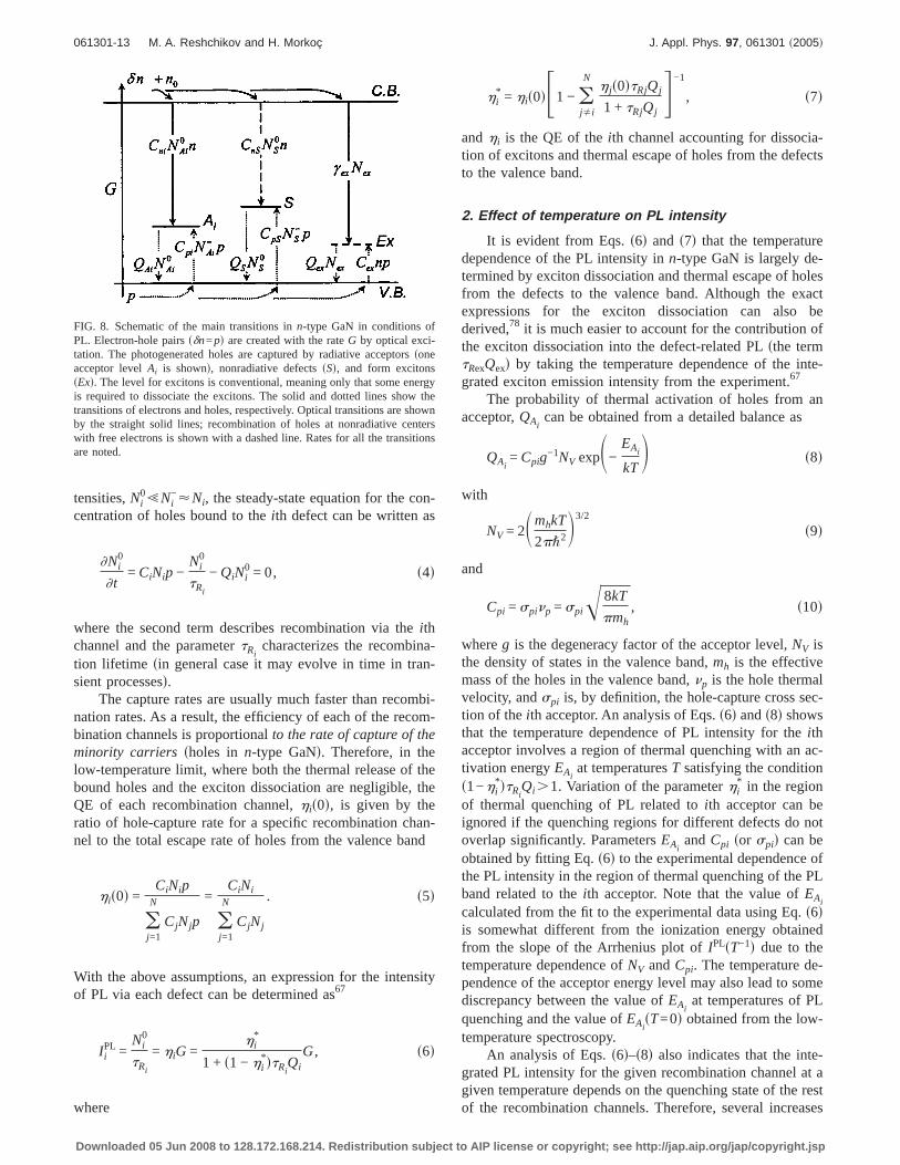
FIG. 8. Schematic of the main transitions inn-type GaN in conditions ofPL. Electron-hole pairssdn=pd are created with the rateG by optical exci-tation. The photogenerated holes are captured by radiative acceptorssoneacceptor levelAi is shownd, nonradiative defectssSd, and form excitonssExd. The level for excitons is conventional, meaning only that some energyis required to dissociate the excitons. The solid and dotted lines show thetransitions of electrons and holes, respectively. Optical transitions are shownby the straight solid lines; recombination of holes at nonradiative centerswith free electrons is shown with a dashed line. Rates for all the transitionsare noted.
061301-13 M. A. Reshchikov and H. Morkoç J. Appl. Phys. 97, 061301 ~2005!
Downloaded 05 Jun 2008 to 128.172.168.214. Redistribution subject to AIP license or copyright; see http://jap.aip.org/jap/copyright.jsp
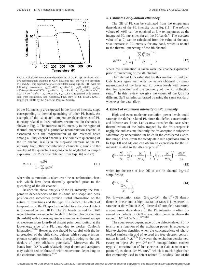
of the PL intensity are expected in the form of intensity stepscorresponding to thermal quenching of other PL bands. Anexample of the calculated temperature dependencies of PLintensity related to three radiative recombination channels isshown in Fig. 9. The increase in PL intensity in the region ofthermal quenching of a particular recombination channel isassociated with the redistribution of the released holesamong all unquenched channels. The complete quenching ofthe ith channel results in the stepwise increase of the PLintensity from other recombination channelsRi times, if theoverlap of the quenching regions can be neglected. A simpleexpression forRi can be obtained from Eqs.s6d and s7d
Ri < 1 +his0d
1 − oj
h js0d, s11d
where the summation is taken over the recombination chan-nels which have been thermally quenched prior to thequenching of theith channel.
Besides the above analysis of the PL intensity, the tem-perature dependencies of the PL band line shape and peakposition can sometimes provide useful information on thenature of transitions and the type of a defect. The effect oftemperature on the PL spectrum related to a deep-level defectis discussed in Sec. III D. The PL bands caused by DAPrecombination are expected to shift to higher photon energiessblueshiftd with increasing temperature due to thermal escapeof electrons from long-lived distant pairs contributing at thelow-energy side of a PL band due to weaker Coulombinteraction.79,80 However, one should be careful with the in-terpretation of the shift since defects with strong electron-phonon coupling often exhibit a blueshift owing to the par-ticulars of their adiabatic potentials.81 Moreover, the PLbands from DAPs with relatively deep donors and acceptorsmay exhibit red or blueshift with temperature, depending onthe excitation conditions.80,82
3. Estimates of quantum efficiency
The QE of PL can be estimated from the temperaturedependence of the PL intensity using Eq.s11d. The relativevalues ofhis0d can be obtained at low temperatures as theintegrated PL intensities for all the PL bands.67 Theabsolutevalue ofhis0d can be calculated from the value of the step-wise increase in PL intensity for any band, which is relatedto the thermal quenching of theith channel
his0d =F 1
Ri − 1+
oj
I jPLs0d
I iPL
G−1
, s12d
where the summation is taken over the channels quenchedprior to quenching of theith channel.
The internal QEs estimated by this method in undopedGaN layers agree well with the values obtained by directmeasurement of the laser and PL power levels with correc-tion for reflection and the geometry of the PL collectionsetup.67 In this review, we give the values of the QEs fordifferent GaN samples calibrated by using the same standard,whenever the data allow.
4. Effect of excitation intensity on PL intensity
High and even moderate excitation power levels couldsaturate the defect-related PL since the defect concentrationand lifetime are finite. Let us now consider the case whenthermalization of the holes trapped by theith acceptor isnegligible and assume that only theith acceptor is subject tosaturation by nonequilibrium holes in the considered excita-tion range. Then, from the steady-state rate equations similarto Eqs.s3d and s4d one can obtain an expression for the PLintensity related to theith acceptor as67
I iPL =
Ni0
tRi
=1
2SG +Ni
hitRi
D −1
2ÎSG +
Ni
hitRi
D2
−4GNi
tRi
,
s13d
which for the case of low QE of theith channelshi !1dsimplifies to
I iPL <
G
GtRi
Ni+
1
hi
. s14d
For low-excitation ratessGtRihi !Nid, the I i
PLsGd depen-dence is linear and at high excitation rates it is expected tosaturate at the value ofNitRi
−1. Instead of complete saturation,a square-root dependence of the PL intensity is often ob-served for defects in GaN at excitation densities above therange of 10−2–1 W/cm2.67,74,83
The square-root dependence of the defect-related PL in-tensity as a function of the excitation power is expected athigh-excitation densities when the concentrations of photo-excited carrierssdn and pd exceed the free-electron concen-tration in darksn0d.67,74 However, the excitation density nec-essary to injectdn, p,1018-cm−3 nonequilibrium carriersstypical concentration of free electrons in GaN at room tem-peratured, is about 105 W/cm2,84 which is much higher thanthat commonly used in defect-related PL studies. One of the
FIG. 9. Calculated temperature dependencies of the PL QE for three radia-tive recombination channels in GaN: excitonicsexd and via two acceptorssA1 andA2d. The dependences were calculated using Eqs.s6d–s10d with thefollowing parameters: hexs0d=0.2; hA1s0d=0.2; hA2s0d=0.08; tRexQex
=250 exps−10 meV/kTd, tR1=10−5 s, tR2=5310−5 s, Cp1=10−6 cm3 s−1,Cp2=4310−7 cm3 s−1, EA1=0.34 eV,EA2=0.8 eV. Reprinted with permis-sion from Reshchikov and Korotkov, Phys. Rev. B64, 115205 s2001d.Copyright s2001d by the American Physical Society.
061301-14 M. A. Reshchikov and H. Morkoç J. Appl. Phys. 97, 061301 ~2005!
Downloaded 05 Jun 2008 to 128.172.168.214. Redistribution subject to AIP license or copyright; see http://jap.aip.org/jap/copyright.jsp
reasons for the square-root dependence of the defect-relatedPL at moderate excitation powers is recombination throughnonradiative donors that may be present in GaN in relativelyhigh concentrations, particularly near the surface.67 Anotherpossibility is the reabsorption of the UV emission by deep-level defects, which is known as photon recycling.
5. Estimates of acceptor concentration in n-type GaN
Once the hole-capture coefficientsCpi are evaluated fordifferent acceptorssSec. IV H for defects in undoped GaNd,the ratio between the concentrations of each acceptor can bedetermined from an analysis of the low-temperature PL spec-trum. This is a simple and effective method for estimatingthe relative concentrations of unintentional acceptors inn-type GaN, and one that could be widely employed for asample characterization. Indeed, all that is necessary is theability to measure the PL spectrum at sufficiently low tem-peratures and excitation intensities85 followed by finding theintegrated intensity for each band in relative units. Then, theratio between the concentrations of theith and j th acceptorscan be found as67
NAi
NAj
=I iPL
I jPL
Cpj
Cpi. s15d
To determine the absolute values of the acceptor concentra-tions, the concentration of one of the acceptors should befound independently by fitting the dependence of the PL in-tensity on excitation intensity, as described in Sec. III A 4.
B. Time-resolved luminescence
By measuring the PL intensity at a given photon energyas a function of time delay after an excitation pulse, valuableinsight can be garnered about the recombination mecha-nisms. A full emission spectrum can also be measured atdifferent decay times. A spectral analysis helps to distinguishthe overlapped PL bands and investigate the evolution of thePL band shape and its shift with time.
The luminescence decay in GaN is often nonexponential,especially at low temperatures. The most plausible cause forthe nonexponential decay of PL is the DAP recombination.When an electron bound to a donor recombines with a pho-togenerated hole bound to an acceptor, the radiative recom-bination rateW is not constant but depends exponentially onthe separation, R, between the donor and acceptorinvolved,79,86
WsRd = WmaxexpS−2R
aDD . s16d
where Wmax is the transition probability in the limitR→0andaD is the Bohr radius for a more weakly bound particlesan electron on the shallow donor in GaNd. It is evident fromEq. s16d that the lifetime of the bound hole,t=W−1, is muchlonger for distant pairs than for close ones. This results in anincrease of the instantaneous lifetime of the measured PLwith the time delay. The transient PL depends on the detailsof the spatial distribution of pairs. Thomaset al.79 obtained
the following expression for the PL intensity decay in thecase of a random distribution of DAP:
Istd ~ N expH4pNE0
`
fe−WsRdt − 1gR2dRJ3E
0
`
WsRde−WsRdtR2dR, s17d
whereN is the concentration of the majority constituent inDAPs. Equations17d combined with Eq.s16d describes wellthe nonexponential decay of low-temperature PL in undopedGaN.76,87
From simple reasoning, we expect an increase ofWmax
with increasing ionization energy of an acceptorEA due toincreasing localization of the bound hole. Indeed, the maxi-mum rate of the DAP transitions in the effective-mass ap-proximation upon neglecting many-body effects is givenby80,88
Wmax= 64AS aA
aDD3
, s18d
where the parameterA depends on the optical properties ofthe semiconductor and on the photon energy"v sAfs−1g<4.53108"v feVg for GaNd, andaA is the Bohr radius forthe bound hole given by89
aA ="
Î2mhEA
. s19d
Although the effective-mass approximation may not be agood choice for deep-level defects, it nevertheless providessurprisingly good results.88,90
Note that potential fluctuations, typically present inhighly compensated and/or heavily doped semiconductors asa result of the random charge distribution,91 also result in anonexponential PL decay. This is due to localization of car-riers in potential wells, very similar in nature to their local-ization on spatially separated donors and acceptors. Theproblem of the potential fluctuations is discussed in moredetail in Sec. V B 2.
With increasing time delay, PL bands originating fromthe DAP-type transitions, especially those involving deepdonors, are expected to shift to lower energies.79,80 This ef-fect is caused by a faster recombination in close pairs, whichcontribute to the high-energy side of the band due to a stron-ger Coulomb interaction. The deeper the donor, the larger theshift is expected, but it still remains below the value of ion-ization energy of the donor.80 The absence of a noticeableshift of a PL band with the time delay may indicate thatshallow donors are involved.
With increasing temperature, the electrons from shallowdonors thermalize to the conduction band, and the DAP tran-sitions are gradually replaced by transitions from the conduc-tion band to the same acceptorse-A transitionsd. For the e-Atransitions, the decay is commonly exponential and the char-acteristic radiative lifetime,tR, depends on the free-electronconcentrationn0, provided thatn0@dn. The electron-capturecoefficient for the acceptorCn can then be expressed as
061301-15 M. A. Reshchikov and H. Morkoç J. Appl. Phys. 97, 061301 ~2005!
Downloaded 05 Jun 2008 to 128.172.168.214. Redistribution subject to AIP license or copyright; see http://jap.aip.org/jap/copyright.jsp
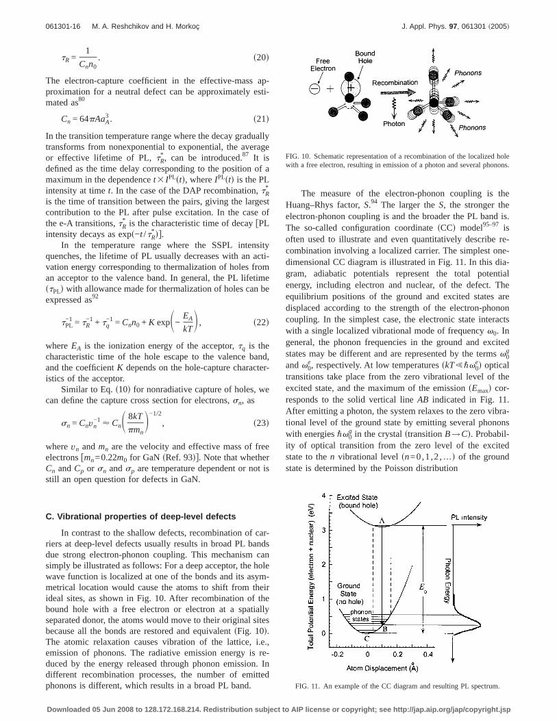
tR =1
Cnn0. s20d
The electron-capture coefficient in the effective-mass ap-proximation for a neutral defect can be approximately esti-mated as80
Cn = 64pAaA3 . s21d
In the transition temperature range where the decay graduallytransforms from nonexponential to exponential, the averageor effective lifetime of PL,tR
* , can be introduced.87 It isdefined as the time delay corresponding to the position of amaximum in the dependencet3 IPLstd, whereIPLstd is the PLintensity at timet. In the case of the DAP recombination,tR
*
is the time of transition between the pairs, giving the largestcontribution to the PL after pulse excitation. In the case ofthe e-A transitions,tR
* is the characteristic time of decayfPLintensity decays as exps−t /tR
* dg.In the temperature range where the SSPL intensity
quenches, the lifetime of PL usually decreases with an acti-vation energy corresponding to thermalization of holes froman acceptor to the valence band. In general, the PL lifetimestPLd with allowance made for thermalization of holes can beexpressed as92
tPL−1 = tR
−1 + tq−1 = Cnn0 + K expS−
EA
kTD , s22d
whereEA is the ionization energy of the acceptor,tq is thecharacteristic time of the hole escape to the valence band,and the coefficientK depends on the hole-capture character-istics of the acceptor.
Similar to Eq.s10d for nonradiative capture of holes, wecan define the capture cross section for electrons,sn, as
sn = Cnvn−1 < CnS 8kT
pmnD−1/2
, s23d
wherevn andmn are the velocity and effective mass of freeelectronsfmn=0.22m0 for GaN sRef. 93dg. Note that whetherCn andCp or sn andsp are temperature dependent or not isstill an open question for defects in GaN.
C. Vibrational properties of deep-level defects
In contrast to the shallow defects, recombination of car-riers at deep-level defects usually results in broad PL bandsdue strong electron-phonon coupling. This mechanism cansimply be illustrated as follows: For a deep acceptor, the holewave function is localized at one of the bonds and its asym-metrical location would cause the atoms to shift from theirideal sites, as shown in Fig. 10. After recombination of thebound hole with a free electron or electron at a spatiallyseparated donor, the atoms would move to their original sitesbecause all the bonds are restored and equivalentsFig. 10d.The atomic relaxation causes vibration of the lattice, i.e.,emission of phonons. The radiative emission energy is re-duced by the energy released through phonon emission. Indifferent recombination processes, the number of emittedphonons is different, which results in a broad PL band.
The measure of the electron-phonon coupling is theHuang–Rhys factor,S.94 The larger theS, the stronger theelectron-phonon coupling is and the broader the PL band is.The so-called configuration coordinatesCCd model95–97 isoften used to illustrate and even quantitatively describe re-combination involving a localized carrier. The simplest one-dimensional CC diagram is illustrated in Fig. 11. In this dia-gram, adiabatic potentials represent the total potentialenergy, including electron and nuclear, of the defect. Theequilibrium positions of the ground and excited states aredisplaced according to the strength of the electron-phononcoupling. In the simplest case, the electronic state interactswith a single localized vibrational mode of frequencyv0. Ingeneral, the phonon frequencies in the ground and excitedstates may be different and are represented by the termsv0
g
andv0e, respectively. At low temperaturesskT!"v0
ed opticaltransitions take place from the zero vibrational level of theexcited state, and the maximum of the emissionsEmaxd cor-responds to the solid vertical lineAB indicated in Fig. 11.After emitting a photon, the system relaxes to the zero vibra-tional level of the ground state by emitting several phononswith energies"v0
g in the crystalstransitionB→Cd. Probabil-ity of optical transition from the zero level of the excitedstate to then vibrational levelsn=0,1,2,…d of the groundstate is determined by the Poisson distribution
FIG. 10. Schematic representation of a recombination of the localized holewith a free electron, resulting in emission of a photon and several phonons.
FIG. 11. An example of the CC diagram and resulting PL spectrum.
061301-16 M. A. Reshchikov and H. Morkoç J. Appl. Phys. 97, 061301 ~2005!
Downloaded 05 Jun 2008 to 128.172.168.214. Redistribution subject to AIP license or copyright; see http://jap.aip.org/jap/copyright.jsp
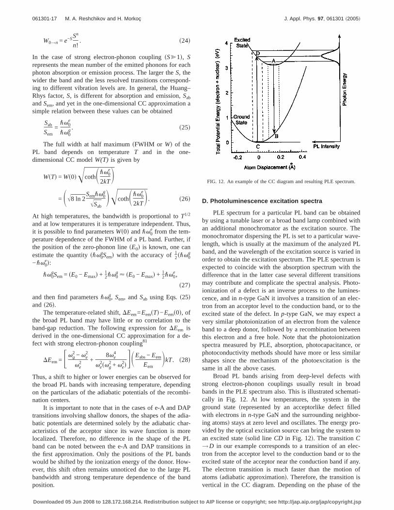
W0→n = e−SSn
n!. s24d
In the case of strong electron-phonon couplingsS@1d, Srepresents the mean number of the emitted phonons for eachphoton absorption or emission process. The larger theS, thewider the band and the less resolved transitions correspond-ing to different vibration levels are. In general, the Huang–Rhys factor,S, is different for absorption and emission,Sab
andSem, and yet in the one-dimensional CC approximation asimple relation between these values can be obtained
Sab
Sem=
"v0e
"v0g . s25d
The full width at half maximumsFWHM or Wd of thePL band depends on temperatureT and in the one-dimensional CC modelW(T) is given by
WsTd = Ws0dÎcothS"v0e
2kTD
= SÎ8 ln 2Sem"v0
g
ÎSabDÎcothS"v0
e
2kTD . s26d
At high temperatures, the bandwidth is proportional toT1/2
and at low temperatures it is temperature independent. Thus,it is possible to find parametersWs0d and"v0
e from the tem-perature dependence of the FWHM of a PL band. Further, ifthe position of the zero-phonon linesE0d is known, one canestimate the quantitys"v0
gSemd with the accuracy of12s"v0g
−"v0ed:
"v0gSem= sE0 − Emaxd + 1
2"v0g < sE0 − Emaxd + 1
2"v0e,
s27d
and then find parameters"v0g, Sem, andSab using Eqs.s25d
and s26d.The temperature-related shift,DEem=EemsTd−Eems0d, of
the broad PL band may have little or no correlation to theband-gap reduction. The following expression forDEem isderived in the one-dimensional CC approximation for a de-fect with strong electron-phonon coupling81
DEem= Fvg2 − ve
2
ve2 +
8ve4
ve2svg
2 + ve2dGSEabs− Eem
EemDkT. s28d
Thus, a shift to higher or lower energies can be observed forthe broad PL bands with increasing temperature, dependingon the particulars of the adiabatic potentials of the recombi-nation centers.
It is important to note that in the cases of e-A and DAPtransitions involving shallow donors, the shapes of the adia-batic potentials are determined solely by the adiabatic char-acteristics of the acceptor since its wave function is morelocalized. Therefore, no difference in the shape of the PLband can be noted between the e-A and DAP transitions inthe first approximation. Only the positions of the PL bandswould be shifted by the ionization energy of the donor. How-ever, this shift often remains unnoticed due to the large PLbandwidth and strong temperature dependence of the bandposition.
D. Photoluminescence excitation spectra
PLE spectrum for a particular PL band can be obtainedby using a tunable laser or a broad band lamp combined withan additional monochromator as the excitation source. Themonochromator dispersing the PL is set to a particular wave-length, which is usually at the maximum of the analyzed PLband, and the wavelength of the excitation source is varied inorder to obtain the excitation spectrum. The PLE spectrum isexpected to coincide with the absorption spectrum with thedifference that in the latter case several different transitionsmay contribute and complicate the spectral analysis. Photo-ionization of a defect is an inverse process to the lumines-cence, and inn-type GaN it involves a transition of an elec-tron from an acceptor level to the conduction band, or to theexcited state of the defect. Inp-type GaN, we may expect avery similar photoionization of an electron from the valenceband to a deep donor, followed by a recombination betweenthis electron and a free hole. Note that the photoionizationspectra measured by PLE, absorption, photocapacitance, orphotoconductivity methods should have more or less similarshapes since the mechanism of the photoexcitation is thesame in all the above cases.
Broad PL bands arising from deep-level defects withstrong electron-phonon couplings usually result in broadbands in the PLE spectrum also. This is illustrated schemati-cally in Fig. 12. At low temperatures, the system in theground statesrepresented by an acceptorlike defect filledwith electrons inn-type GaN and the surrounding neighbor-ing atomsd stays at zero level and oscillates. The energy pro-vided by the optical excitation source can bring the system toan excited statessolid line CD in Fig. 12d. The transitionC→D in our example corresponds to a transition of an elec-tron from the acceptor level to the conduction band or to theexcited state of the acceptor near the conduction band if any.The electron transition is much faster than the motion ofatomssadiabatic approximationd. Therefore, the transition isvertical in the CC diagram. Depending on the phase of the
FIG. 12. An example of the CC diagram and resulting PLE spectrum.
061301-17 M. A. Reshchikov and H. Morkoç J. Appl. Phys. 97, 061301 ~2005!
Downloaded 05 Jun 2008 to 128.172.168.214. Redistribution subject to AIP license or copyright; see http://jap.aip.org/jap/copyright.jsp
zero-level oscillations, the system may be closer or fartherfrom the equilibrium point in the excited statesas shown bythe dashed lines on both sides of transitionCDd. Therefore,after numerous photoexcitation processes the absorption en-ergy evolves into a broad band. In the case of a strongelectron-phonon coupling, which causes the minima of theground and excited states to be sufficiently displaced, theshape of the absorption band is nearly Gaussian. However,for a weak electron-phonon coupling and small displacementof the adiabatic potential minima the shape of the absorptionband is asymmetric with an abrupt edge near the zero-phonon transition line,E0. After the excitation, the systemrelaxes to its minimal energy position by emitting severallocal or lattice phononsstransitionD→Ad. Then the systemstays at the zero level at low temperatures and after a periodof time sPL lifetimed it returns to the ground state by emis-sion of a photonsA→Bd and consequent emission of a fewphononssB→Cd.
For transitions of electrons from the defect level to theconduction band the shape of the PLE or absorption spec-trum may depart from the Gaussian shape and have an ex-tended shoulder at the high-energy side due to the possibletransitions to the quasicontinuous states in the conductionband. When the energy of the excitation becomes equal orexceeds the band gap, transitions of electrons from the va-lence band to the conduction band and subsequent nonradi-ative capture of a hole by a deep acceptorsnonresonant ex-citation of the acceptord would give a step in the PLEspectrum corresponding to the band-to-band absorption. Therelative contribution of the resonant and nonresonant transi-tions in the PLE spectrum depends on the thickness of thesample and specific values of the nonradiative and opticalsphotoionizationd capture cross sections for a particular ac-ceptor. The energy displacement of the emission and absorp-tion maximasStokes shiftd facilitates the measurement of thePLE spectra.
The PLE spectra from deep-level defects, including con-tributions from the resonant and nonresonant excitations,have been studied in GaNsRefs. 76 and 98–100d, and arediscussed in Secs. IV A 6 and IV B 2.
E. Spatially and depth-resolved cathodoluminescence
CL is produced by absorption of high-energy electronsand resultant spontaneous emission of light corresponding tospecific transitions in a semiconductor. It can be detected asa CL spectrum or as a distribution of CL intensity over acertain area of the semiconductor surfacesCL imaged. Thelatter case is conveniently facilitated by a combination of ascanning electron microscope and a luminescence collectionsystem. When an incident electron beam bombards the semi-conductor under test, it first causes the emission of secondaryelectrons from a thin surface layer which is on the order of10 nm causing that region to be positively charged.101 Thesecondary electrons also penetrate into the sample to somedepth which depends on the acceleration voltagesVbd. Thisnegatively charged layer is much thicker than the positivelycharged surface layer from which the secondary electronsescaped. The electron penetration depth in GaN increases
from about 0.2 to more than 4µm asVb is increased from 5to 35 kV.102,103Note that the energy-loss depth profile maxi-mizes at approximately 30% of the penetration depth.104 Thepenetration depth increases with increasingVb, and theelectron-hole pair generation rate is proportional to the beampowersEbIbd. The CL intensity is determined not only by thegeneration rate but also by the penetration depth through theprocess of self-absorption,105 surface recombination, compe-tition of different recombination mechanisms, and migrationof charges with time.101,103
Depth-resolved CL experiments are usually conductedunder constant beam power or constant power-density con-ditions. The penetration depth is varied by varying the accel-erating voltage. Depth-dependent CL spectra can be takenalso from the edge of a cleaved sample. Since the radiatedarea is about 0.1–1mm2, depth profiling is especially condu-cive for thick layers or bulk samples since electrons cannotpenetrate deeper than,5 mm.
To obtain a CL image at a certain photon energy whichcan be varied, the electron beam is scanned over an area ofup to 0.130.1 mm2. Such images may help identify the lu-minescence bands and determine their spatial distributionand relation to structural defects.
F. Optically detected magnetic resonance
Electron paramagnetic resonancesEPRd and its variant,ODMR, provide information on the ground state and micro-scopic origin of defects through obtaining the values andangular dependencies of the Zeeman splittingsg tensord andinterpretation of any hyperfine structure. Compared to EPR,ODMR relates the magnetic information to particular lumi-nescence bands and assists their identification.
The g value of the free electron isge=2.0023. In thefirst-order perturbation theory the deviation of theg value fora particular center is given byl /DE, wherel is the spin-orbit interaction constant.106 Usually donors showg valuessmaller than free electrons, and acceptors have a positivegshift. However, there are exceptions to this simple rule.107
Donors in GaN are typically characterized byg factors be-tween 1.949 and 1.962, showing a small anisotropysgi−g'
,0.003–0.006d. Acceptors are characterized by a relativelylarger value and anisotropy of theg factor.108,109
IV. LUMINESCENCE RELATED TO POINT DEFECTS INUNDOPED GaN
Typical low-temperature PL spectra from selected unin-tentionally doped GaN samples are shown in Fig. 13. Inaddition to the near-band-edge emission due to bound andfree exciton transitions and their phonon replicas, the PLspectrum from undoped GaN almost always contains a broadyellow luminescencesYL d band with a maximum at about2.2 eVsFig. 13d. The YL band is by far the most studied PLband in GaN. Despite this inordinate effort, it is still not clearhow many and what kind of defects contribute to that broademission bandssee Sec. IV Ad. In high-purity GaN grown byHVPE, the YL band is replaced by a green luminescencesGLd band at about 2.5 eV under certain experimental
061301-18 M. A. Reshchikov and H. Morkoç J. Appl. Phys. 97, 061301 ~2005!
Downloaded 05 Jun 2008 to 128.172.168.214. Redistribution subject to AIP license or copyright; see http://jap.aip.org/jap/copyright.jsp
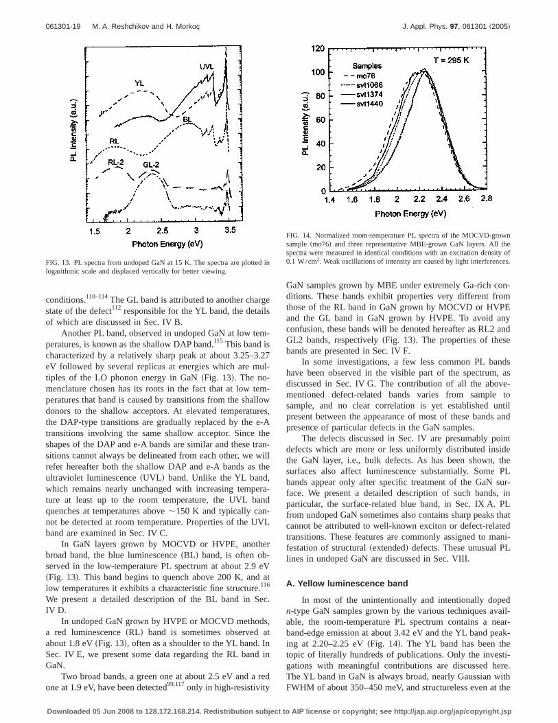
conditions.110–114The GL band is attributed to another chargestate of the defect112 responsible for the YL band, the detailsof which are discussed in Sec. IV B.
Another PL band, observed in undoped GaN at low tem-peratures, is known as the shallow DAP band.115 This band ischaracterized by a relatively sharp peak at about 3.25–3.27eV followed by several replicas at energies which are mul-tiples of the LO phonon energy in GaNsFig. 13d. The no-menclature chosen has its roots in the fact that at low tem-peratures that band is caused by transitions from the shallowdonors to the shallow acceptors. At elevated temperatures,the DAP-type transitions are gradually replaced by the e-Atransitions involving the same shallow acceptor. Since theshapes of the DAP and e-A bands are similar and these tran-sitions cannot always be delineated from each other, we willrefer hereafter both the shallow DAP and e-A bands as theultraviolet luminescencesUVL d band. Unlike the YL band,which remains nearly unchanged with increasing tempera-ture at least up to the room temperature, the UVL bandquenches at temperatures above,150 K and typically can-not be detected at room temperature. Properties of the UVLband are examined in Sec. IV C.
In GaN layers grown by MOCVD or HVPE, anotherbroad band, the blue luminescencesBLd band, is often ob-served in the low-temperature PL spectrum at about 2.9 eVsFig. 13d. This band begins to quench above 200 K, and atlow temperatures it exhibits a characteristic fine structure.116
We present a detailed description of the BL band in Sec.IV D.
In undoped GaN grown by HVPE or MOCVD methods,a red luminescencesRLd band is sometimes observed atabout 1.8 eVsFig. 13d, often as a shoulder to the YL band. InSec. IV E, we present some data regarding the RL band inGaN.
Two broad bands, a green one at about 2.5 eV and a redone at 1.9 eV, have been detected99,117only in high-resistivity
GaN samples grown by MBE under extremely Ga-rich con-ditions. These bands exhibit properties very different fromthose of the RL band in GaN grown by MOCVD or HVPEand the GL band in GaN grown by HVPE. To avoid anyconfusion, these bands will be denoted hereafter as RL2 andGL2 bands, respectivelysFig. 13d. The properties of thesebands are presented in Sec. IV F.
In some investigations, a few less common PL bandshave been observed in the visible part of the spectrum, asdiscussed in Sec. IV G. The contribution of all the above-mentioned defect-related bands varies from sample tosample, and no clear correlation is yet established untilpresent between the appearance of most of these bands andpresence of particular defects in the GaN samples.
The defects discussed in Sec. IV are presumably pointdefects which are more or less uniformly distributed insidethe GaN layer, i.e., bulk defects. As has been shown, thesurfaces also affect luminescence substantially. Some PLbands appear only after specific treatment of the GaN sur-face. We present a detailed description of such bands, inparticular, the surface-related blue band, in Sec. IX A. PLfrom undoped GaN sometimes also contains sharp peaks thatcannot be attributed to well-known exciton or defect-relatedtransitions. These features are commonly assigned to mani-festation of structuralsextendedd defects. These unusual PLlines in undoped GaN are discussed in Sec. VIII.
A. Yellow luminescence band
In most of the unintentionally and intentionally dopedn-type GaN samples grown by the various techniques avail-able, the room-temperature PL spectrum contains a near-band-edge emission at about 3.42 eV and the YL band peak-ing at 2.20–2.25 eVsFig. 14d. The YL band has been thetopic of literally hundreds of publications. Only the investi-gations with meaningful contributions are discussed here.The YL band in GaN is always broad, nearly Gaussian withFWHM of about 350–450 meV, and structureless even at the
FIG. 13. PL spectra from undoped GaN at 15 K. The spectra are plotted inlogarithmic scale and displaced vertically for better viewing.
FIG. 14. Normalized room-temperature PL spectra of the MOCVD-grownsamplesmo76d and three representative MBE-grown GaN layers. All thespectra were measured in identical conditions with an excitation density of0.1 W/cm2. Weak oscillations of intensity are caused by light interferences.
061301-19 M. A. Reshchikov and H. Morkoç J. Appl. Phys. 97, 061301 ~2005!
Downloaded 05 Jun 2008 to 128.172.168.214. Redistribution subject to AIP license or copyright; see http://jap.aip.org/jap/copyright.jsp
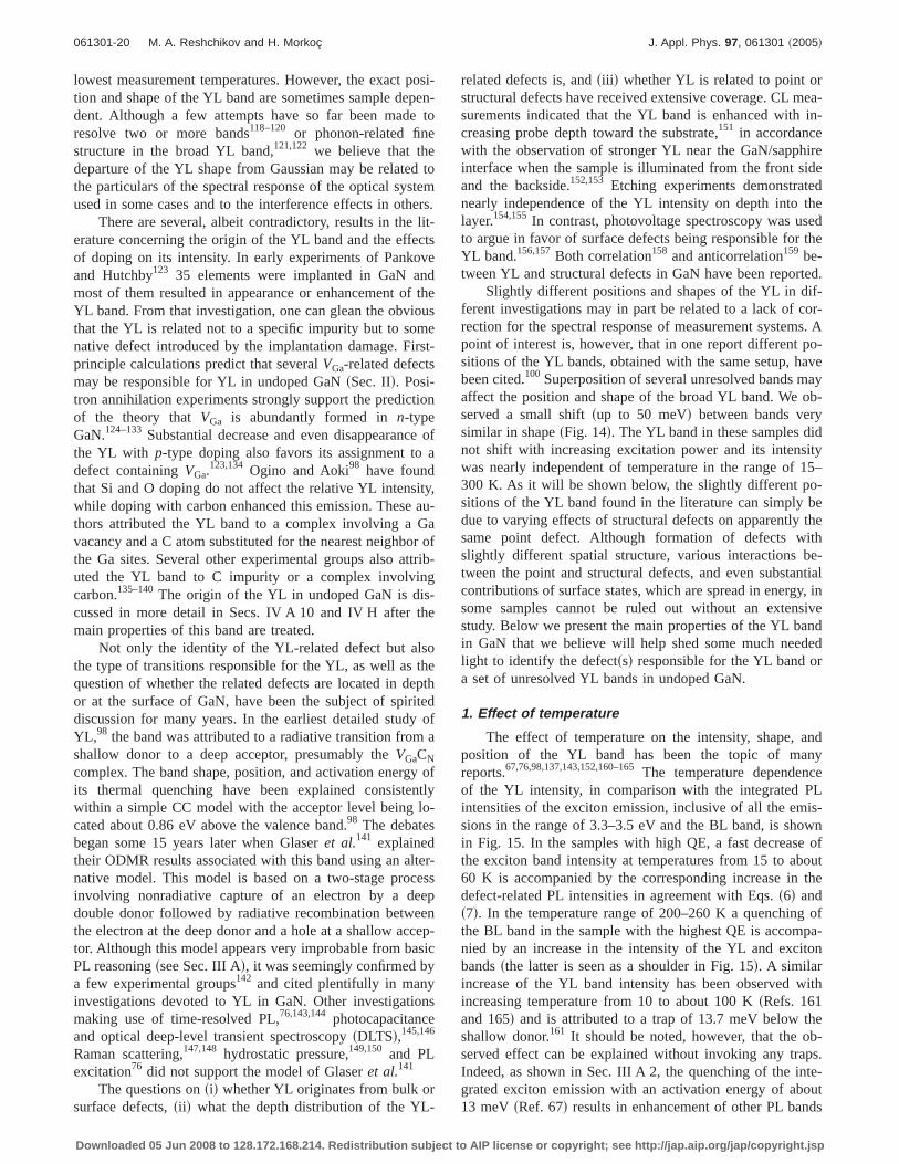
lowest measurement temperatures. However, the exact posi-tion and shape of the YL band are sometimes sample depen-dent. Although a few attempts have so far been made toresolve two or more bands118–120 or phonon-related finestructure in the broad YL band,121,122 we believe that thedeparture of the YL shape from Gaussian may be related tothe particulars of the spectral response of the optical systemused in some cases and to the interference effects in others.
There are several, albeit contradictory, results in the lit-erature concerning the origin of the YL band and the effectsof doping on its intensity. In early experiments of Pankoveand Hutchby123 35 elements were implanted in GaN andmost of them resulted in appearance or enhancement of theYL band. From that investigation, one can glean the obviousthat the YL is related not to a specific impurity but to somenative defect introduced by the implantation damage. First-principle calculations predict that severalVGa-related defectsmay be responsible for YL in undoped GaNsSec. IId. Posi-tron annihilation experiments strongly support the predictionof the theory thatVGa is abundantly formed inn-typeGaN.124–133Substantial decrease and even disappearance ofthe YL with p-type doping also favors its assignment to adefect containingVGa.
123,134 Ogino and Aoki98 have foundthat Si and O doping do not affect the relative YL intensity,while doping with carbon enhanced this emission. These au-thors attributed the YL band to a complex involving a Gavacancy and a C atom substituted for the nearest neighbor ofthe Ga sites. Several other experimental groups also attrib-uted the YL band to C impurity or a complex involvingcarbon.135–140The origin of the YL in undoped GaN is dis-cussed in more detail in Secs. IV A 10 and IV H after themain properties of this band are treated.
Not only the identity of the YL-related defect but alsothe type of transitions responsible for the YL, as well as thequestion of whether the related defects are located in depthor at the surface of GaN, have been the subject of spiriteddiscussion for many years. In the earliest detailed study ofYL,98 the band was attributed to a radiative transition from ashallow donor to a deep acceptor, presumably theVGaCN
complex. The band shape, position, and activation energy ofits thermal quenching have been explained consistentlywithin a simple CC model with the acceptor level being lo-cated about 0.86 eV above the valence band.98 The debatesbegan some 15 years later when Glaseret al.141 explainedtheir ODMR results associated with this band using an alter-native model. This model is based on a two-stage processinvolving nonradiative capture of an electron by a deepdouble donor followed by radiative recombination betweenthe electron at the deep donor and a hole at a shallow accep-tor. Although this model appears very improbable from basicPL reasoningssee Sec. III Ad, it was seemingly confirmed bya few experimental groups142 and cited plentifully in manyinvestigations devoted to YL in GaN. Other investigationsmaking use of time-resolved PL,76,143,144 photocapacitanceand optical deep-level transient spectroscopysDLTSd,145,146
Raman scattering,147,148 hydrostatic pressure,149,150 and PLexcitation76 did not support the model of Glaseret al.141
The questions onsid whether YL originates from bulk orsurface defects,sii d what the depth distribution of the YL-
related defects is, andsiii d whether YL is related to point orstructural defects have received extensive coverage. CL mea-surements indicated that the YL band is enhanced with in-creasing probe depth toward the substrate,151 in accordancewith the observation of stronger YL near the GaN/sapphireinterface when the sample is illuminated from the front sideand the backside.152,153 Etching experiments demonstratednearly independence of the YL intensity on depth into thelayer.154,155In contrast, photovoltage spectroscopy was usedto argue in favor of surface defects being responsible for theYL band.156,157Both correlation158 and anticorrelation159 be-tween YL and structural defects in GaN have been reported.
Slightly different positions and shapes of the YL in dif-ferent investigations may in part be related to a lack of cor-rection for the spectral response of measurement systems. Apoint of interest is, however, that in one report different po-sitions of the YL bands, obtained with the same setup, havebeen cited.100 Superposition of several unresolved bands mayaffect the position and shape of the broad YL band. We ob-served a small shiftsup to 50 meVd between bands verysimilar in shapesFig. 14d. The YL band in these samples didnot shift with increasing excitation power and its intensitywas nearly independent of temperature in the range of 15–300 K. As it will be shown below, the slightly different po-sitions of the YL band found in the literature can simply bedue to varying effects of structural defects on apparently thesame point defect. Although formation of defects withslightly different spatial structure, various interactions be-tween the point and structural defects, and even substantialcontributions of surface states, which are spread in energy, insome samples cannot be ruled out without an extensivestudy. Below we present the main properties of the YL bandin GaN that we believe will help shed some much neededlight to identify the defectssd responsible for the YL band ora set of unresolved YL bands in undoped GaN.
1. Effect of temperature
The effect of temperature on the intensity, shape, andposition of the YL band has been the topic of manyreports.67,76,98,137,143,152,160–165The temperature dependenceof the YL intensity, in comparison with the integrated PLintensities of the exciton emission, inclusive of all the emis-sions in the range of 3.3–3.5 eV and the BL band, is shownin Fig. 15. In the samples with high QE, a fast decrease ofthe exciton band intensity at temperatures from 15 to about60 K is accompanied by the corresponding increase in thedefect-related PL intensities in agreement with Eqs.s6d ands7d. In the temperature range of 200–260 K a quenching ofthe BL band in the sample with the highest QE is accompa-nied by an increase in the intensity of the YL and excitonbandssthe latter is seen as a shoulder in Fig. 15d. A similarincrease of the YL band intensity has been observed withincreasing temperature from 10 to about 100 KsRefs. 161and 165d and is attributed to a trap of 13.7 meV below theshallow donor.161 It should be noted, however, that the ob-served effect can be explained without invoking any traps.Indeed, as shown in Sec. III A 2, the quenching of the inte-grated exciton emission with an activation energy of about13 meVsRef. 67d results in enhancement of other PL bands
061301-20 M. A. Reshchikov and H. Morkoç J. Appl. Phys. 97, 061301 ~2005!
Downloaded 05 Jun 2008 to 128.172.168.214. Redistribution subject to AIP license or copyright; see http://jap.aip.org/jap/copyright.jsp
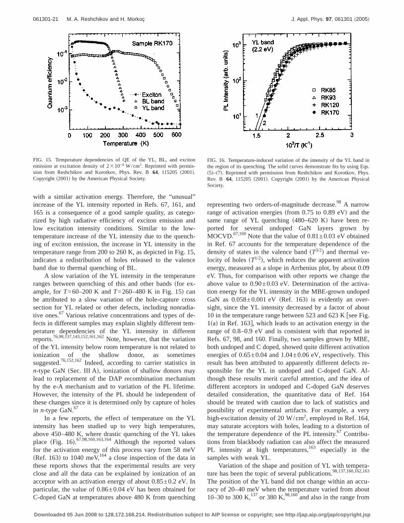
with a similar activation energy. Therefore, the “unusual”increase of the YL intensity reported in Refs. 67, 161, and165 is a consequence of a good sample quality, as catego-rized by high radiative efficiency of exciton emission andlow excitation intensity conditions. Similar to the low-temperature increase of the YL intensity due to the quench-ing of exciton emission, the increase in YL intensity in thetemperature range from 200 to 260 K, as depicted in Fig. 15,indicates a redistribution of holes released to the valenceband due to thermal quenching of BL.
A slow variation of the YL intensity in the temperatureranges between quenching of this and other bandssfor ex-ample, forT=60–200 K andT=260–480 K in Fig. 15d canbe attributed to a slow variation of the hole-capture crosssection for YL related or other defects, including nonradia-tive ones.67 Various relative concentrations and types of de-fects in different samples may explain slightly different tem-perature dependencies of the YL intensity in differentreports.76,98,137,143,152,161,162Note, however, that the variationof the YL intensity below room temperature is not related toionization of the shallow donor, as sometimessuggested.76,152,162 Indeed, according to carrier statistics inn-type GaNsSec. III Ad, ionization of shallow donors maylead to replacement of the DAP recombination mechanismby the e-A mechanism and to variation of the PL lifetime.However, the intensity of the PL should be independent ofthese changes since it is determined only by capture of holesin n-type GaN.67
In a few reports, the effect of temperature on the YLintensity has been studied up to very high temperatures,above 450–480 K, where drastic quenching of the YL takesplace sFig. 16d.67,98,160,163,164Although the reported valuesfor the activation energy of this process vary from 58 meVsRef. 163d to 1040 meV,164 a close inspection of the data inthese reports shows that the experimental results are veryclose and all the data can be explained by ionization of anacceptor with an activation energy of about 0.85±0.2 eV. Inparticular, the value of 0.86±0.04 eV has been obtained forC-doped GaN at temperatures above 480 K from quenching
representing two orders-of-magnitude decrease.98 A narrowrange of activation energiessfrom 0.75 to 0.89 eVd and thesame range of YL quenchings480–620 Kd have been re-ported for several undoped GaN layers grown byMOCVD.67,160Note that the value of 0.81±0.03 eV obtainedin Ref. 67 accounts for the temperature dependence of thedensity of states in the valence bandsT3/2d and thermal ve-locity of holessT1/2d, which reduces the apparent activationenergy, measured as a slope in Arrhenius plot, by about 0.09eV. Thus, for comparison with other reports we change theabove value to 0.90±0.03 eV. Determination of the activa-tion energy for the YL intensity in the MBE-grown undopedGaN as 0.058±0.001 eVsRef. 163d is evidently an over-sight, since the YL intensity decreased by a factor of about10 in the temperature range between 523 and 623 Kfsee Fig.1sad in Ref. 163g, which leads to an activation energy in therange of 0.8–0.9 eV and is consistent with that reported inRefs. 67, 98, and 160. Finally, two samples grown by MBE,both undoped and C doped, showed quite different activationenergies of 0.65±0.04 and 1.04±0.06 eV, respectively. Thisresult has been attributed to apparently different defects re-sponsible for the YL in undoped and C-doped GaN. Al-though these results merit careful attention, and the idea ofdifferent acceptors in undoped and C-doped GaN deservesdetailed consideration, the quantitative data of Ref. 164should be treated with caution due to lack of statistics andpossibility of experimental artifacts. For example, a veryhigh-excitation density of 20 W/cm2, employed in Ref. 164,may saturate acceptors with holes, leading to a distortion ofthe temperature dependence of the PL intensity.67 Contribu-tions from blackbody radiation can also affect the measuredPL intensity at high temperatures,163 especially in thesamples with weak YL.
Variation of the shape and position of YL with tempera-ture has been the topic of several publications.98,137,160,162,163
The position of the YL band did not change within an accu-racy of 20–40 meV when the temperature varied from about10–30 to 300 K,137 or 380 K,98,160and also in the range from
FIG. 15. Temperature dependencies of QE of the YL, BL, and excitonemission at excitation density of 2310−4 W/cm2. Reprinted with permis-sion from Reshchikov and Korotkov, Phys. Rev. B64, 115205 s2001d.Copyright s2001d by the American Physical Society.
FIG. 16. Temperature-induced variation of the intensity of the YL band inthe region of its quenching. The solid curves demonstrate fits by using Eqs.s5d–s7d. Reprinted with permission from Reshchikov and Korotkov, Phys.Rev. B 64, 115205 s2001d. Copyright s2001d by the American PhysicalSociety.
061301-21 M. A. Reshchikov and H. Morkoç J. Appl. Phys. 97, 061301 ~2005!
Downloaded 05 Jun 2008 to 128.172.168.214. Redistribution subject to AIP license or copyright; see http://jap.aip.org/jap/copyright.jsp
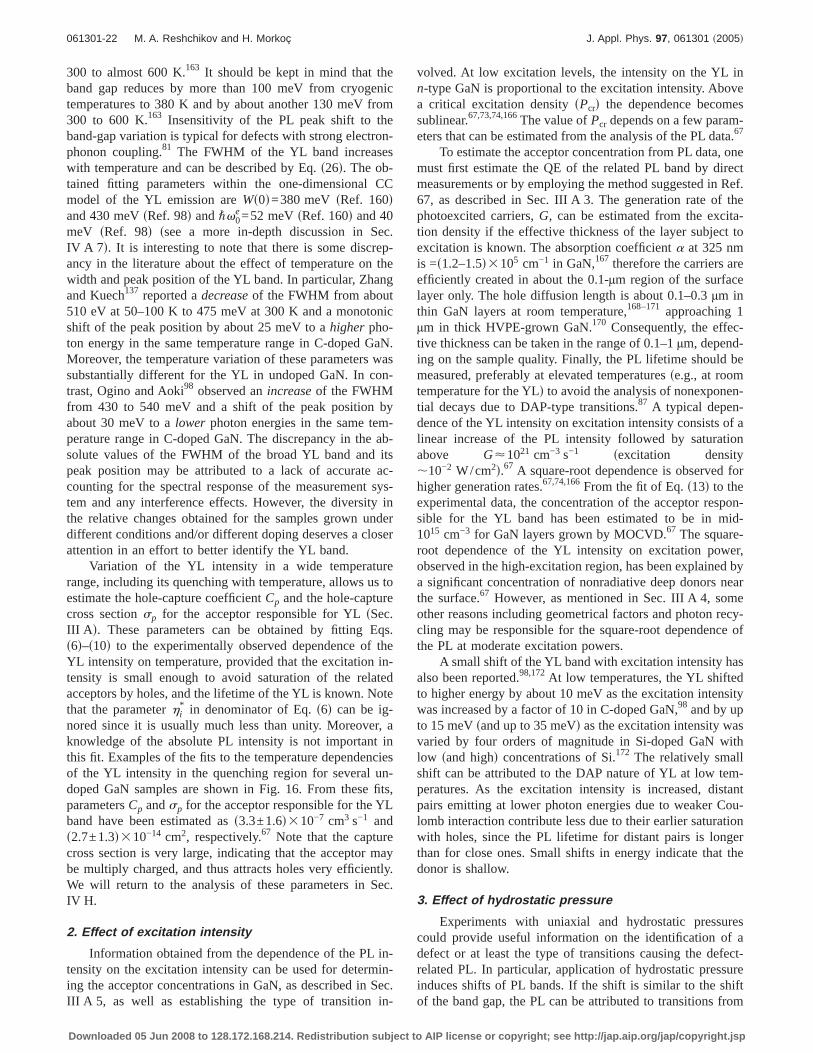
300 to almost 600 K.163 It should be kept in mind that theband gap reduces by more than 100 meV from cryogenictemperatures to 380 K and by about another 130 meV from300 to 600 K.163 Insensitivity of the PL peak shift to theband-gap variation is typical for defects with strong electron-phonon coupling.81 The FWHM of the YL band increaseswith temperature and can be described by Eq.s26d. The ob-tained fitting parameters within the one-dimensional CCmodel of the YL emission areWs0d=380 meV sRef. 160dand 430 meVsRef. 98d and"v0
e=52 meVsRef. 160d and 40meV sRef. 98d ssee a more in-depth discussion in Sec.IV A 7 d. It is interesting to note that there is some discrep-ancy in the literature about the effect of temperature on thewidth and peak position of the YL band. In particular, Zhangand Kuech137 reported adecreaseof the FWHM from about510 eV at 50–100 K to 475 meV at 300 K and a monotonicshift of the peak position by about 25 meV to ahigher pho-ton energy in the same temperature range in C-doped GaN.Moreover, the temperature variation of these parameters wassubstantially different for the YL in undoped GaN. In con-trast, Ogino and Aoki98 observed anincreaseof the FWHMfrom 430 to 540 meV and a shift of the peak position byabout 30 meV to alower photon energies in the same tem-perature range in C-doped GaN. The discrepancy in the ab-solute values of the FWHM of the broad YL band and itspeak position may be attributed to a lack of accurate ac-counting for the spectral response of the measurement sys-tem and any interference effects. However, the diversity inthe relative changes obtained for the samples grown underdifferent conditions and/or different doping deserves a closerattention in an effort to better identify the YL band.
Variation of the YL intensity in a wide temperaturerange, including its quenching with temperature, allows us toestimate the hole-capture coefficientCp and the hole-capturecross sectionsp for the acceptor responsible for YLsSec.III A d. These parameters can be obtained by fitting Eqs.s6d–s10d to the experimentally observed dependence of theYL intensity on temperature, provided that the excitation in-tensity is small enough to avoid saturation of the relatedacceptors by holes, and the lifetime of the YL is known. Notethat the parameterhi
* in denominator of Eq.s6d can be ig-nored since it is usually much less than unity. Moreover, aknowledge of the absolute PL intensity is not important inthis fit. Examples of the fits to the temperature dependenciesof the YL intensity in the quenching region for several un-doped GaN samples are shown in Fig. 16. From these fits,parametersCp andsp for the acceptor responsible for the YLband have been estimated ass3.3±1.6d310−7 cm3 s−1 ands2.7±1.3d310−14 cm2, respectively.67 Note that the capturecross section is very large, indicating that the acceptor maybe multiply charged, and thus attracts holes very efficiently.We will return to the analysis of these parameters in Sec.IV H.
2. Effect of excitation intensity
Information obtained from the dependence of the PL in-tensity on the excitation intensity can be used for determin-ing the acceptor concentrations in GaN, as described in Sec.III A 5, as well as establishing the type of transition in-
volved. At low excitation levels, the intensity on the YL inn-type GaN is proportional to the excitation intensity. Abovea critical excitation densitysPcrd the dependence becomessublinear.67,73,74,166The value ofPcr depends on a few param-eters that can be estimated from the analysis of the PL data.67
To estimate the acceptor concentration from PL data, onemust first estimate the QE of the related PL band by directmeasurements or by employing the method suggested in Ref.67, as described in Sec. III A 3. The generation rate of thephotoexcited carriers,G, can be estimated from the excita-tion density if the effective thickness of the layer subject toexcitation is known. The absorption coefficienta at 325 nmis =s1.2–1.5d3105 cm−1 in GaN,167 therefore the carriers areefficiently created in about the 0.1-µm region of the surfacelayer only. The hole diffusion length is about 0.1–0.3µm inthin GaN layers at room temperature,168–171 approaching 1µm in thick HVPE-grown GaN.170 Consequently, the effec-tive thickness can be taken in the range of 0.1–1µm, depend-ing on the sample quality. Finally, the PL lifetime should bemeasured, preferably at elevated temperaturesse.g., at roomtemperature for the YLd to avoid the analysis of nonexponen-tial decays due to DAP-type transitions.87 A typical depen-dence of the YL intensity on excitation intensity consists of alinear increase of the PL intensity followed by saturationabove G<1021 cm−3 s−1 sexcitation density,10−2 W/cm2d.67 A square-root dependence is observed forhigher generation rates.67,74,166From the fit of Eq.s13d to theexperimental data, the concentration of the acceptor respon-sible for the YL band has been estimated to be in mid-1015 cm−3 for GaN layers grown by MOCVD.67 The square-root dependence of the YL intensity on excitation power,observed in the high-excitation region, has been explained bya significant concentration of nonradiative deep donors nearthe surface.67 However, as mentioned in Sec. III A 4, someother reasons including geometrical factors and photon recy-cling may be responsible for the square-root dependence ofthe PL at moderate excitation powers.
A small shift of the YL band with excitation intensity hasalso been reported.98,172At low temperatures, the YL shiftedto higher energy by about 10 meV as the excitation intensitywas increased by a factor of 10 in C-doped GaN,98 and by upto 15 meVsand up to 35 meVd as the excitation intensity wasvaried by four orders of magnitude in Si-doped GaN withlow sand highd concentrations of Si.172 The relatively smallshift can be attributed to the DAP nature of YL at low tem-peratures. As the excitation intensity is increased, distantpairs emitting at lower photon energies due to weaker Cou-lomb interaction contribute less due to their earlier saturationwith holes, since the PL lifetime for distant pairs is longerthan for close ones. Small shifts in energy indicate that thedonor is shallow.
3. Effect of hydrostatic pressure
Experiments with uniaxial and hydrostatic pressurescould provide useful information on the identification of adefect or at least the type of transitions causing the defect-related PL. In particular, application of hydrostatic pressureinduces shifts of PL bands. If the shift is similar to the shiftof the band gap, the PL can be attributed to transitions from
061301-22 M. A. Reshchikov and H. Morkoç J. Appl. Phys. 97, 061301 ~2005!
Downloaded 05 Jun 2008 to 128.172.168.214. Redistribution subject to AIP license or copyright; see http://jap.aip.org/jap/copyright.jsp
the conduction band or from a shallow donor to an acceptorlevel. Indeed, the pressure shift of the shallow donor level isabout the same as the shift of the conduction-band minimum,whereas the pressure shift of an acceptor level should besimilar to the shift of the top of the valence band, or even aweak negative shift of the acceptor level with respect to thetop of the valence band may be expected.173 A much weakerpressure shift of a given PL band is expected for transitionsfrom a deep donor to an acceptor, or for internal transitionswithin the defect. The effect of hydrostatic pressure on YLwas studied for bulk GaN unintentionally doped withoxygen149,150and nominally undoped GaN layers grown byMBE sRefs. 149 and 150d and MOCVDsRefs. 174–176d onsapphire. All these reports noted large shifts of YL at least upto 6 GPa having a pressure coefficient between 30 and 40meV/GPa, which is very similar to the shift of the band gaphaving a pressure coefficient of about 40meV/GPa.149,150,174,175At pressures above approximately 20GPa, the shift of the YL band saturated, which has beenattributed to an emergence of a resonance level from theconduction band into the gap, leading to a change of themechanism of the YL in that transitions from the conductionband to a deep acceptor level, were replaced by transitionsfrom the resonant level to the same acceptor.149,150
The intensity of the YL band decreased withpressure174–176and became barely measurable at 18 GPa.176
An interesting observation is that with cooling to low tem-peratures under hydrostatic pressure, the YL intensitystrongly decreases,176 which is to be contrasted with its smallincrease upon cooling under ambient pressure. Michaeletal.176 explained this effect by contribution of two DAP-typetransitions involving the same acceptor and two different do-nors, with one of them having aDX-like behavior.
4. Effect of electron irradiation
Electron irradiation is widely used in studies of semicon-ductors because it artificially creates point defects that maybe present in an as-grown material but in an amount insuffi-cient for their analysis.177 Look177 has estimated that theelectron energy of the order of 1 MeV is already high enoughto create VN-Ni and VGa-Gai Frenkel pairs. However,Kuriyamaet al.162 argued that much higher energies may beneeded to create Ga vacancies. Saarinenet al.178 have estab-lished experimentally that 2-MeV electron irradiation at 300K does create Ga vacancies in GaN. The electron irradiationwith relatively low power can be used also as a source ofelectron-hole pairs to probe point defects at different depthsin the luminescence experiments. So, low-energy electron-excited nanoscale luminescencesLEENd employing energiesfrom 100 eV to 5 keV,179 and CL typically employing ener-gies between 1 and 35 keV,103,180–183have been extensivelyemployed to investigate defects in GaN. More results ob-tained by LEEN and CL investigations of GaN are presentedin Secs. IV D 3, IV E, andV B 3 f. Here we limit ourselvesto showing how irradiation with relatively high energy ofelectrons, in the range of 2.5–30 MeV, affects YL inn-typeGaN.
After irradiation with 2.5-MeV electrons to a dose ofabout 1018 cm−2, the YL intensity markedly decreased.184,185
However, the decrease in the near-band-edge emission wasmuch stronger.185 Irradiation with 7-MeV electrons caused asubstantial increase of the YL intensity and decrease of thenear-band-edge emission.186 The variation of PL intensity inRef. 186 was proportional to the electron dose in the rangefrom 1015 to 1017 cm−2. Irradiation with 30-MeV electronscompletely destroyed PL in the entire spectrum. However, asubsequent annealing at temperatures ranging from 500 to1000 °C led to substantial increase of the YL intensity of upto five times compared to the value in as-grown sample.162
An increase of the YL intensity after electron irradiation wasattributed to the creation of Ga vacancies in GaN.162,186Highstability of YL with annealing was explained162 by the for-mation of gallium vacancy-shallow donorsVGaDd complexesthat are much more stable than isolatedVGa.
Fast proton irradiation of GaN at room temperature hasbeen performed by using 25- and 55-MeV protons.187 Whilethe YL intensity after irradiation increased in the 160-µm-thick freestanding template grown by HVPE, no increasewas observed for the 10-µm-thick GaN layer grown byHVPE on sapphire and in MBE-grown GaN layer. The YLintensity in the freestanding template gradually increasedwith increasing proton fluence from 131014 to 2.731014 cm−2. The enhancement of YL has been attributed toa radiation-induced creation of Ga vacancies in GaN.187
5. Time-resolved PL
As discussed in Sec. III B, TRPL has the potential togive clues to recombination mechanism in effect, e.g.,whether it is e-A or DAP transition, and whether deep-levelor shallow defects constitute the DAP. TRPL may also give aclue in identifying the deep acceptor through the values ofthe electron-capture cross section. It also helps in delineatingthe PL bands which are overlapped in the SSPL spectrum.Transient PL for the YL band in GaN has been investigatedby several authors,76,87,110,142,143,152,161,166,188–192and the re-sults have often been controversial. For example, the re-ported PL lifetime for the YL ranges from 20 pssRef. 166dand 1 nssRef. 143d to the microsecondss50–700µsd sRefs.87 and 142d and even up to 300 ms.161 Measurements at 15K revealed a nonexponential decay of the YL band, typicalfor the DAP transitions,76,87,142,152,190whereas at room tem-perature the decay was nearly exponential.87 Single exponen-tial decay with a characteristic time of 250–260µs has beenobserved in time-resolved CL experiments at 87 K.189 Belowwe present TRPL results for the YL band in undoped GaNand comment on the unusually small and large values of thereported lifetimes of this emission.
A typical intensity decay curve for the YL band is shownin Fig. 17 along with the decays of other PL bands present inthe same sample. The instantaneous lifetime of PL changesfrom several microseconds to milliseconds at low tempera-tures. The decay curves are nonexponential at 15 K and be-come nearly exponential above 150 K. The nonexponentialdecay is a signature of the DAP recombination, as discussedin Sec. III B. The DAP transitions are expected at low tem-peratures, and e-A transitions are expected at elevated tem-peratures when ionization of the shallow donor is significant.Excellent fits of the PL decay to Eq.s17d for the YL band
061301-23 M. A. Reshchikov and H. Morkoç J. Appl. Phys. 97, 061301 ~2005!
Downloaded 05 Jun 2008 to 128.172.168.214. Redistribution subject to AIP license or copyright; see http://jap.aip.org/jap/copyright.jsp
with minimal number of fitting parameters, demonstrated inRefs. 188 and 76, support the assignment of this band totransitions from a shallow donor to a deep acceptor at lowtemperatures. The value ofWmax in a set of four samples wasobtained to be on the order of 106 s−1 sRef. 188d, although amuch higher value of 2.53107 s−1 has also been reported.76
The time-resolved PL spectra for different delay timesare shown in Fig. 18. No difference is seen between theSSPL and TRPL spectra for small delay times.188 With in-creasing delay time, no shift or change in the band shape isobserved within the experimental accuracy of,30 meV.Similar results have been reported in Refs. 76 and 191. ThePL bands originating from the DAP transitions involvingdeep donors are expected to redshift significantly with delaytime.79,80This is a result of the faster recombination in closepairs, which contribute to the high-energy side of the band
due to stronger Coulomb interaction. The deeper the donor,the larger the possible shift, but it still remains below thevalue of the ionization energy of the donor.80 The absence ofa noticeable shift of the bands with time delay indicates thatonly shallow donors are involved. However, the shift of theYL band to a lower photon energy by about 30–40 meV at adelay time of about 1 ms compared to the YL band positionin the SSPL spectrum has been observed by Monteiroetal.,192 who attributed this observation to a competition of twobands peaking at 2.05 and 2.28 eV. An attempt to resolve the2.27- and 2.04-eV peaks in the decay of the YL band wasmade also by Chtchekineet al.142 Further, an apparent shiftof the YL band maximum from 2.25 to 2.35 eV at a delaytime of ,10 ms after a light pulse has been observed inundoped GaN and attributed to the emergence of anotherband at 2.35 eV having a decay time of the order of 300ms.161 The complex nature of the YL band has also beennoted in time-resolved CL studies where two bands at 2.03and 2.22 eV have apparently been resolved by transientmeasurements.189
The measured decay curve undergoes a considerablechange and becomes nearly exponential with increasingtemperature.87 Therefore, the recombination mechanism alsochanges with temperature. The concentration of free elec-trons increases and the DAP transitions are gradually re-placed by the e-A transitions at temperatures above 100–200K. The change in the recombination mechanism at tempera-tures above 100 K is consistent with the Hall data for un-dopedn-type GaN. Temperature dependence of the effectivelifetime of PL, tR
* sas defined in Sec. III Bd, for the YL bandin comparison withtR
* for other bands inn-type GaN isshown in Fig. 19. The effective lifetime of PL has a weaktemperature dependence up to,500 K for the YL band. In alarger set of samples, the value oftR
* ranged from 25 to 60µsat 300 K. The longer lifetime was observed in the sampleswith lower free-electron concentrations,87 in agreement withtheory fsee Eq.s20d in Sec. III Bg.
FIG. 17. Intensity of the YL, BL, and UVL bands at 15 K in undoped GaNgrown by MOCVD. The curves are calculated using Eq.s17d. Reprintedwith permission from Korotkovet al., Physica B273, 80 s1999d. Copyrights1999d by Elsevier.
FIG. 18. Steady-state PL spectrumssolid curved and time-resolved PL spec-tra spointsd at time delays of 10−6, 10−5, and 10−4 s for undoped GaN samplegrown by MOCVD. Reprinted with permission from Korotkovet al.,Physica B 273, 80 s1999d. Copyrights1999d by Elsevier.
FIG. 19. Temperature dependence of the effective lifetime of the YLs2.2eVd, BL s2.9 eVd, and UVL s3.27 eVd bands in undoped GaN grown byMOCVD. Reprinted with permission from Korotkovet al., Physica B325,1 s2003d. Copyrights2003d by Elsevier.
061301-24 M. A. Reshchikov and H. Morkoç J. Appl. Phys. 97, 061301 ~2005!
Downloaded 05 Jun 2008 to 128.172.168.214. Redistribution subject to AIP license or copyright; see http://jap.aip.org/jap/copyright.jsp
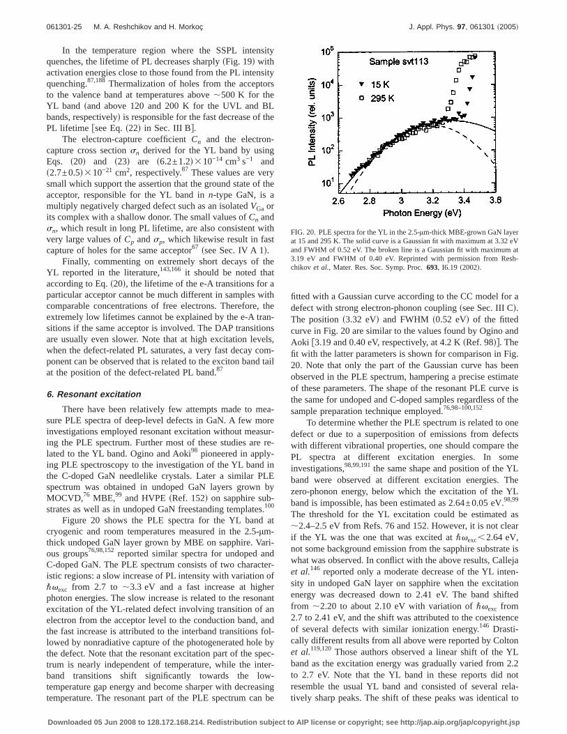
In the temperature region where the SSPL intensityquenches, the lifetime of PL decreases sharplysFig. 19d withactivation energies close to those found from the PL intensityquenching.87,188 Thermalization of holes from the acceptorsto the valence band at temperatures above,500 K for theYL band sand above 120 and 200 K for the UVL and BLbands, respectivelyd is responsible for the fast decrease of thePL lifetime fsee Eq.s22d in Sec. III Bg.
The electron-capture coefficientCn and the electron-capture cross sectionsn derived for the YL band by usingEqs. s20d and s23d are s6.2±1.2d310−14 cm3 s−1 ands2.7±0.5d310−21 cm2, respectively.87 These values are verysmall which support the assertion that the ground state of theacceptor, responsible for the YL band inn-type GaN, is amultiply negatively charged defect such as an isolatedVGa orits complex with a shallow donor. The small values ofCn andsn, which result in long PL lifetime, are also consistent withvery large values ofCp andsp, which likewise result in fastcapture of holes for the same acceptor67 ssee Sec. IV A 1d.
Finally, commenting on extremely short decays of theYL reported in the literature,143,166 it should be noted thataccording to Eq.s20d, the lifetime of the e-A transitions for aparticular acceptor cannot be much different in samples withcomparable concentrations of free electrons. Therefore, theextremely low lifetimes cannot be explained by the e-A tran-sitions if the same acceptor is involved. The DAP transitionsare usually even slower. Note that at high excitation levels,when the defect-related PL saturates, a very fast decay com-ponent can be observed that is related to the exciton band tailat the position of the defect-related PL band.87
6. Resonant excitation
There have been relatively few attempts made to mea-sure PLE spectra of deep-level defects in GaN. A few moreinvestigations employed resonant excitation without measur-ing the PLE spectrum. Further most of these studies are re-lated to the YL band. Ogino and Aoki98 pioneered in apply-ing PLE spectroscopy to the investigation of the YL band inthe C-doped GaN needlelike crystals. Later a similar PLEspectrum was obtained in undoped GaN layers grown byMOCVD,76 MBE,99 and HVPEsRef. 152d on sapphire sub-strates as well as in undoped GaN freestanding templates.100
Figure 20 shows the PLE spectra for the YL band atcryogenic and room temperatures measured in the 2.5-µm-thick undoped GaN layer grown by MBE on sapphire. Vari-ous groups76,98,152reported similar spectra for undoped andC-doped GaN. The PLE spectrum consists of two character-istic regions: a slow increase of PL intensity with variation of"vexc from 2.7 to ,3.3 eV and a fast increase at higherphoton energies. The slow increase is related to the resonantexcitation of the YL-related defect involving transition of anelectron from the acceptor level to the conduction band, andthe fast increase is attributed to the interband transitions fol-lowed by nonradiative capture of the photogenerated hole bythe defect. Note that the resonant excitation part of the spec-trum is nearly independent of temperature, while the inter-band transitions shift significantly towards the low-temperature gap energy and become sharper with decreasingtemperature. The resonant part of the PLE spectrum can be
fitted with a Gaussian curve according to the CC model for adefect with strong electron-phonon couplingssee Sec. III Cd.The positions3.32 eVd and FWHM s0.52 eVd of the fittedcurve in Fig. 20 are similar to the values found by Ogino andAoki f3.19 and 0.40 eV, respectively, at 4.2 KsRef. 98dg. Thefit with the latter parameters is shown for comparison in Fig.20. Note that only the part of the Gaussian curve has beenobserved in the PLE spectrum, hampering a precise estimateof these parameters. The shape of the resonant PLE curve isthe same for undoped and C-doped samples regardless of thesample preparation technique employed.76,98–100,152
To determine whether the PLE spectrum is related to onedefect or due to a superposition of emissions from defectswith different vibrational properties, one should compare thePL spectra at different excitation energies. In someinvestigations,98,99,191the same shape and position of the YLband were observed at different excitation energies. Thezero-phonon energy, below which the excitation of the YLband is impossible, has been estimated as 2.64±0.05 eV.98,99
The threshold for the YL excitation could be estimated as,2.4–2.5 eV from Refs. 76 and 152. However, it is not clearif the YL was the one that was excited at"vexc,2.64 eV,not some background emission from the sapphire substrate iswhat was observed. In conflict with the above results, Callejaet al.146 reported only a moderate decrease of the YL inten-sity in undoped GaN layer on sapphire when the excitationenergy was decreased down to 2.41 eV. The band shiftedfrom ,2.20 to about 2.10 eV with variation of"vexc from2.7 to 2.41 eV, and the shift was attributed to the coexistenceof several defects with similar ionization energy.146 Drasti-cally different results from all above were reported by Coltonet al.119,120Those authors observed a linear shift of the YLband as the excitation energy was gradually varied from 2.2to 2.7 eV. Note that the YL band in these reports did notresemble the usual YL band and consisted of several rela-tively sharp peaks. The shift of these peaks was identical to
FIG. 20. PLE spectra for the YL in the 2.5-µm-thick MBE-grown GaN layerat 15 and 295 K. The solid curve is a Gaussian fit with maximum at 3.32 eVand FWHM of 0.52 eV. The broken line is a Gaussian fit with maximum at3.19 eV and FWHM of 0.40 eV. Reprinted with permission from Resh-chikov et al., Mater. Res. Soc. Symp. Proc.693, I6.19 s2002d.
061301-25 M. A. Reshchikov and H. Morkoç J. Appl. Phys. 97, 061301 ~2005!
Downloaded 05 Jun 2008 to 128.172.168.214. Redistribution subject to AIP license or copyright; see http://jap.aip.org/jap/copyright.jsp
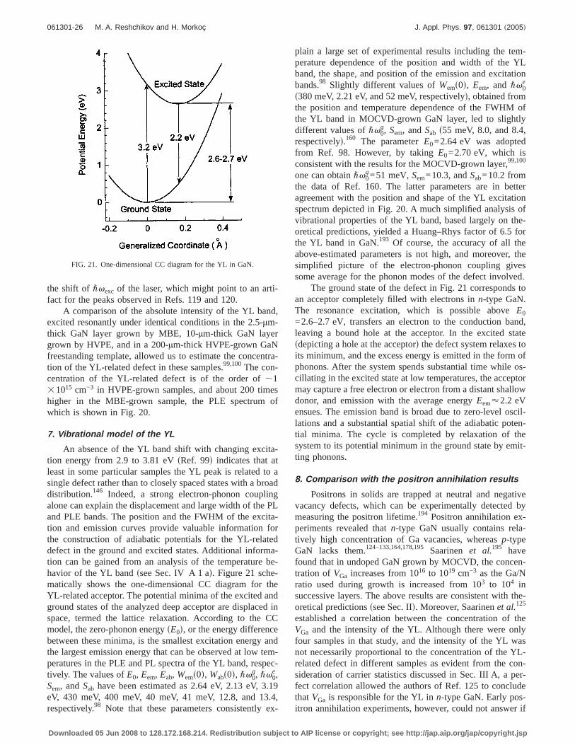
the shift of"vexc of the laser, which might point to an arti-fact for the peaks observed in Refs. 119 and 120.
A comparison of the absolute intensity of the YL band,excited resonantly under identical conditions in the 2.5-µm-thick GaN layer grown by MBE, 10-µm-thick GaN layergrown by HVPE, and in a 200-µm-thick HVPE-grown GaNfreestanding template, allowed us to estimate the concentra-tion of the YL-related defect in these samples.99,100The con-centration of the YL-related defect is of the order of,131015 cm−3 in HVPE-grown samples, and about 200 timeshigher in the MBE-grown sample, the PLE spectrum ofwhich is shown in Fig. 20.
7. Vibrational model of the YL
An absence of the YL band shift with changing excita-tion energy from 2.9 to 3.81 eVsRef. 99d indicates that atleast in some particular samples the YL peak is related to asingle defect rather than to closely spaced states with a broaddistribution.146 Indeed, a strong electron-phonon couplingalone can explain the displacement and large width of the PLand PLE bands. The position and the FWHM of the excita-tion and emission curves provide valuable information forthe construction of adiabatic potentials for the YL-relateddefect in the ground and excited states. Additional informa-tion can be gained from an analysis of the temperature be-havior of the YL bandssee Sec. IV A 1 ad. Figure 21 sche-matically shows the one-dimensional CC diagram for theYL-related acceptor. The potential minima of the excited andground states of the analyzed deep acceptor are displaced inspace, termed the lattice relaxation. According to the CCmodel, the zero-phonon energysE0d, or the energy differencebetween these minima, is the smallest excitation energy andthe largest emission energy that can be observed at low tem-peratures in the PLE and PL spectra of the YL band, respec-tively. The values ofE0, Eem, Eab, Wems0d, Wabs0d, "v0
g, "v0e,
Sem, andSab have been estimated as 2.64 eV, 2.13 eV, 3.19eV, 430 meV, 400 meV, 40 meV, 41 meV, 12.8, and 13.4,respectively.98 Note that these parameters consistently ex-
plain a large set of experimental results including the tem-perature dependence of the position and width of the YLband, the shape, and position of the emission and excitationbands.98 Slightly different values ofWems0d, Eem, and "v0
e
s380 meV, 2.21 eV, and 52 meV, respectivelyd, obtained fromthe position and temperature dependence of the FWHM ofthe YL band in MOCVD-grown GaN layer, led to slightlydifferent values of"v0
g, Sem, andSab s55 meV, 8.0, and 8.4,respectivelyd.160 The parameterE0=2.64 eV was adoptedfrom Ref. 98. However, by takingE0=2.70 eV, which isconsistent with the results for the MOCVD-grown layer,99,100
one can obtain"v0g=51 meV,Sem=10.3, andSab=10.2 from
the data of Ref. 160. The latter parameters are in betteragreement with the position and shape of the YL excitationspectrum depicted in Fig. 20. A much simplified analysis ofvibrational properties of the YL band, based largely on the-oretical predictions, yielded a Huang–Rhys factor of 6.5 forthe YL band in GaN.193 Of course, the accuracy of all theabove-estimated parameters is not high, and moreover, thesimplified picture of the electron-phonon coupling givessome average for the phonon modes of the defect involved.
The ground state of the defect in Fig. 21 corresponds toan acceptor completely filled with electrons inn-type GaN.The resonance excitation, which is possible aboveE0
=2.6–2.7 eV, transfers an electron to the conduction band,leaving a bound hole at the acceptor. In the excited statesdepicting a hole at the acceptord the defect system relaxes toits minimum, and the excess energy is emitted in the form ofphonons. After the system spends substantial time while os-cillating in the excited state at low temperatures, the acceptormay capture a free electron or electron from a distant shallowdonor, and emission with the average energyEem<2.2 eVensues. The emission band is broad due to zero-level oscil-lations and a substantial spatial shift of the adiabatic poten-tial minima. The cycle is completed by relaxation of thesystem to its potential minimum in the ground state by emit-ting phonons.
8. Comparison with the positron annihilation results
Positrons in solids are trapped at neutral and negativevacancy defects, which can be experimentally detected bymeasuring the positron lifetime.194 Positron annihilation ex-periments revealed thatn-type GaN usually contains rela-tively high concentration of Ga vacancies, whereasp-typeGaN lacks them.124–133,164,178,195Saarinen et al.195 havefound that in undoped GaN grown by MOCVD, the concen-tration of VGa increases from 1016 to 1019 cm−3 as the Ga/Nratio used during growth is increased from 103 to 104 insuccessive layers. The above results are consistent with the-oretical predictionsssee Sec. IId. Moreover, Saarinenet al.125
established a correlation between the concentration of theVGa and the intensity of the YL. Although there were onlyfour samples in that study, and the intensity of the YL wasnot necessarily proportional to the concentration of the YL-related defect in different samples as evident from the con-sideration of carrier statistics discussed in Sec. III A, a per-fect correlation allowed the authors of Ref. 125 to concludethat VGa is responsible for the YL inn-type GaN. Early pos-itron annihilation experiments, however, could not answer if
FIG. 21. One-dimensional CC diagram for the YL in GaN.
061301-26 M. A. Reshchikov and H. Morkoç J. Appl. Phys. 97, 061301 ~2005!
Downloaded 05 Jun 2008 to 128.172.168.214. Redistribution subject to AIP license or copyright; see http://jap.aip.org/jap/copyright.jsp
isolatedVGa or VGa involved in a complex, such asVGaON orVGaSiGa, is present inn-type GaN. According to calculations,both the isolatedVGa and VGa-donor complexes are abun-dantly created inn-type GaNssee Sec. IId. However, it wasnot clear if an isolatedVGa is stable enough to survive duringcooling down of the crystals without forming a complex withdonors noting that the stability of theVGaD complexes ismuch higher. To address this problem, Saarinenet al.129,178
createdVGa in bulk GaN crystals, containing high concentra-tion of oxygen, by 2-MeV electron irradiation at room tem-perature and subsequently annealed the samples at differenttemperatures. The concentration ofVGa increased linearlywith irradiation fluence up to 1018 cm−2. The createdVGa-Gai Frenkel pairs are expected to break at relatively lowtemperature since the Ga interstitial is already mobile atroom temperature.31 Annealing experiments demonstratedthat VGa becomes mobile in a temperature window of 500–600 K, a band which is much lower than the typical GaNgrowth temperatures. These results indicated that the isolatedVGa would not survive during cooling down of the samplesand the observations should associate with other defects,most probably with shallow donors that attract triply nega-tively charged mobileVGa by their positive charge. Anothercontroversial question to be addressed is whether theVGaON
or VGaSiGa is preferably formed during growth if both shal-low donors are present in equal amounts. Calculations pre-dict that the formation energy of theVGaON complex is muchlower ssee Sec. IId. In line with this prediction, Oilaet al.127
discovered that in O-doped GaN, either bulk or epilayer, theconcentration ofVGa is very highsabout 1018 cm−3d, whereasin Si-doped GaN the Ga vacancies are undetectablesnotmore than 1016 cm−3d. This result was naturally interpretedasVGa easily forming a complex with oxygen and failing tocomplex with silicon. However, Uedonoet al.128 reportedthat the concentration ofVGa increases with Si doping, al-though one cannot rule out the possibility that the sampleshad been contaminated with oxygen.
In another report,131 positron annihilation, secondary-ion-mass spectroscopysSIMSd, and PL were employed tostudy theVGa-related defects in undoped and Si-dopedscon-taining also oxygend GaN, grown by MBE on GaN templateprepared by HVPE. From the analysis ofW and S param-eters, extracted from the positron annihilation time experi-ments, Laukkanenet al.131 have concluded that theVGa-related defect in the MBE-grown samples is not thesame as that observed in MOCVD layers. This new defectdisplayed properties similar to a vacancy cluster, and its con-centration decreased with Si doping.131 Interestingly, the YLintensity increased with increasing concentration of Si inthese samples, implying no connection between the vacancyclusters and the YL band. Annealing experiments indicatedthat the vacancy clusters are stable up to at least 1050 K,ruling out their identification as isolatedVGa.
131 Note that thevacancy clusters with open space larger than divacanciessVGaVNd have also been detected by positron annihilation inundoped MOCVD-grown GaN.128 Finally, a decrease of theVGa-related defects from more than 1019 to 231016 cm−3 hasbeen observed in the HVPE-grown layers when the distancefrom the GaN/sapphire interface region increased.133 The
depth profile of oxygen was similar to that ofVGa, implyingthat VGa is likely to associate with oxygen in these samples.In the thickest freestanding 300-µm sample, the concentra-tion of VGa decreased to 231015 cm−3, perfectly matchingthe total acceptor concentration196,197 and the concentrationof the YL-related acceptors in these samples112 ssee also PLresults in Sec. IV Bd.
In contrast with the above investigations where the YLcorrelated with concentrations ofVGa, ON, and SiGa, Armit-ageet al.164 reported that the YL band is weaker in the un-doped GaN sample with relatively higher concentration ofoxygen andVGa, as compared to the C-doped sample. Thisresult may indicate that theVGaON complexsor theVGaSiGa
complex which is expected to behave nearly identically butis less probable to formd is not the only defect responsible forthe broad emission near 2.2 eV inn-type GaN.
9. ODMR on the YL
Glaseret al.141,198detected two increasing luminescenceresonances for the YL band. A strong and sharp resonancewith gi=1.9515±0.0002 andg'=1.9485±0.0002 was attrib-uted to the effective-mass donor, while a broader resonancewith gi=1.989±0.001 andg'=1.992±0.001 was attributedto a deep donor. The proposed model of the YL, as being dueto optical transitions from the deep donor to a shallow ac-ceptorsaccompanied by a nonradiative spin-dependent tran-sition from the shallow donor to a singly ionized double-donor stated,141,198 failed to agree with numerous resultssupporting solely the shallow donor-deep acceptor model forthe YL band.67,76,143–150In particular, transitions from thedeep donor to the shallow acceptor would have an extremelylow probability in undoped GaN due to negligible overlap ofthe hole and electron wave functions at distant deep donorsand acceptors.
Koschnicket al.144 performed mapping of YL by ODMRover the sample area. The YL intensity was distributed uni-formly, whereas the intensity ratio of the two dominantODMR signalsswith gi=1.9515 and 1.989d varied strongly.This experimental finding indicated that the two dominantODMR signals cannot belong to transition between two de-fects which results in YL. The authors of Ref. 144 proposedthat the resonances are due to two relatively shallow donorscompeting for recombination with the hole bound to a deepacceptor. As for the missing signal from the deep acceptor, itwas speculated that it is barely seen as a weak broad signalunderneath the donor signals.144 Attribution of the signalwith gi=1.952 to the shallow donorsONd has also been sup-ported by ODMR studies under high hydrostatic pressure.176
10. Effect of doping on the YL
There have been many attempts aimed at revealing theorigin of the YL band by intentional doping. Pankove andHutchby123 implanted 35 elements in GaN and 23 of themled to a strong YL band peaking at 2.15±0.03 eV. Implanta-tion with carbon resulted in the strongest YL band, althoughthe intensity of the YL band in the Li-, Be-, Al-, and Si-doped GaN was also very high.123 Skromme andco-workers199–202also observed a substantial increase of the
061301-27 M. A. Reshchikov and H. Morkoç J. Appl. Phys. 97, 061301 ~2005!
Downloaded 05 Jun 2008 to 128.172.168.214. Redistribution subject to AIP license or copyright; see http://jap.aip.org/jap/copyright.jsp
YL band in GaN implanted with C or Be, but not with Ar, Al,P, O, N, P, As, Ne, or Mg. Note that Dewsnipet al.203 alsoreported an enhancement of the YL in Be-doped GaN.
Ogino and Aoki98 have established that C doping en-hances YL greatly, whereas Si and O doping did not affectthe YL intensity in their experiment. Several other experi-mental groups observed enhancement of the YL band inC-doped GaN and attributed the YL band to C impurity or acomplex involving carbon.135–140,164,204–206Although thepeak position and shape of the YL band in the C-dopedsamples were similar to those in undoped GaN, differenttemperature dependencies for these parameters were ob-served in undoped and C-doped GaN.137 It appears that Cintroduces a defect contributing to the YL band in C-dopedGaN, whereas theVGa-containing complex, such asVGaON,is responsible for the YL band in undoped GaN, although theposition and shape of the YL from two different defects maybe quite similar.164 It is also plausible that the C-related de-fect also containsVGa. For instance, if theVGaCGa is formedin GaN, it would have nearly the same properties asVGaON
since both ON and CGa are shallow donors. However, thefirst-principles theory predicts a low probability of formationfor CGa in n-type GaNsSec. IId.
The effect of Si doping on the absolute and relative in-tensities of the YL band has also been studied extensively. Inconcert with results of Pankove and Hutchby,123 Dai et al.207
reported a significant enhancement of YL in GaN after im-plantation with Si and postannealing. In several other inves-tigations, Si doping caused an increase in the YLintensity.71,131,172,208Important to note, however, is that theratio of the YL intensity to the near-band-edge emission in-tensity increased in some experiments,208,209but decreased inothers,131,207,210 or remained nearly unchanged.71 At veryhigh levels ofn-type dopingsn0.1019 cm−3d, the YL inten-sity decreased in Si-doped209,211and Ge-doped GaN.212 Thesuppression of the YL band has been attributed to the substi-tution of VGa by donors in Ga sites.212
Doping with another shallow donor, SeN, also resulted inan enhancement of the YL band.213,214Chenet al.213 reportedthat Se doping decreased the Ga/N ratio substantially andmoreover, they attributed the YL band to the NGa antisite. Itis obvious, however, that the concentration ofVGa also in-creases with decreasing Ga/N ratio. Therefore, creation oftheVGa-related acceptors is also able to explain the observedenhancement of the YL band in Se-doped GaN.
What can be gleaned from the above discussion is thatthere is still no model which fully describes the defect ordefects that are responsible for the YL band in undoped orn-type doped GaN. On the one hand, there are extensive datasupporting the assignment of the YL band emission to a na-tive defect, which also can be introduced by implantationdamage or irradiation. In this case, theVGaON complex is themain candidate, as well asVGa andVGaON trapped at dislo-cations or other structural defects. On the other hand, carbonis a strong candidate for the YL-related defect in C-dopedGaN. Although experimentally difficult, an investigation ofthe YL band GaN with controllably different concentrationsof C and VGa is desperately needed to delineate the rootcause for the YL emission in GaN.
What is firmly established is that the YL band in alln-type GaN samples is related to transitions from the con-duction band or from a shallow donor to a deep acceptor. Theionization energy of this acceptor is about 0.8−0.9 eV. Itscapture cross section for holes is much larger than that forelectrons. Thus, it might be a multiply charged acceptor.From this point of view, theVGa-shallow donor complex is avery strong candidate. The shape of the YL band and itsposition in this case should be determined byVGa due to itsstrong electron-phonon coupling. The situation is very simi-lar to theVGa-shallow donor complexes in GaAs, where theshallow donors mostly change the charge state ofVGa butbarely affect the energy level and vibrational characteristicsof the defect.215 Similarly, the properties ofVGa may not bestrongly affected by the strain field of a dislocation that maytrap theVGa-containing complex. It is important to under-stand that inVGaD complex the transitions take place notfrom D to VGa as often interpreted, but from a distant donoror from the conduction band to theVGaD complex because insuch a complex the hole wave function would cover bothdefects.
B. Yellow and green luminescence in high-purity GaN
Thick GaN layers grown by HVPE demonstrate substan-tially improved quality,12 as determined by structural, elec-trical, and optical characterizations, and paved the way forinvestigating defects with more confidence. Liliental-Weberet al.216 showed that the dislocation density drastically de-creases with increasing thickness of GaN. The concentrationof point defects, including impurities and Ga vacancies, alsogradually decreases with distance from the GaN/sapphireinterface.133,217,218Among thick GaN layers grown by differ-ent groups, 200–300-µm-thick laser-separated freestandingGaN templates grown by HVPE at Samsung Advanced Insti-tute of TechnologysSAITd in Korea have the superior qualityto date, combining the highest bulk mobility ofelectrons,196,197,219the lowest concentration of uncontrolleddonors s0.6–1.831016 cm−3d and acceptors s1.7–2.431015 cm−3d,196,197,219very low density of dislocations nearthe Ga facesless than 106 cm−2d,220,221and exceptional opti-cal properties.222,223 We studied PL from a few GaN tem-plates prepared at SAIT and observed that PL results werevery reproducible in different samples. Some of these tem-plates were also studied by positron annihilation,133 Halleffect,196,197,219and SIMSsRef. 223d methods. The compre-hensive study of very similar GaN templates allows us to usethe results from various investigations in order to reliablyquantify the PL results.
The low-temperature PL spectrum from the freestandingGaN templates produced by SAIT contains multiple excitonpeaks above 3.3 eV,222–224the UVL band with the main peakat 3.26 eV, and a broad yellow-green bandsFig. 22d. Veryweak BL sat about 2.9 eVd and RL sat about 1.8 eVd aremasked by neighboring bands in these samples but can bedetected under special conditionssin TRPL, under resonantexcitation of PL, or at intermediate temperaturesd. At roomtemperature, most of the bands thermally quench. Only thenear-band-edge emission peaking at about 3.41 eV and the
061301-28 M. A. Reshchikov and H. Morkoç J. Appl. Phys. 97, 061301 ~2005!
Downloaded 05 Jun 2008 to 128.172.168.214. Redistribution subject to AIP license or copyright; see http://jap.aip.org/jap/copyright.jsp
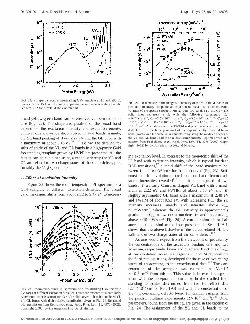
broad yellow-green band can be observed at room tempera-ture sFig. 22d. The shape and position of the broad banddepend on the excitation intensity and excitation energy,while it can always be deconvolved in two bands, namely,the YL band peaking at about 2.22 eV and the GL band witha maximum at about 2.48 eV.111,112 Below, the detailed re-sults of study of the YL and GL bands in a high-purity GaNfreestanding template grown by HVPE are presented. All theresults can be explained using a model whereby the YL andGL are related to two charge states of the same defect, pre-sumably theVGaON complex.
1. Effect of excitation intensity
Figure 23 shows the room-temperature PL spectrum of aGaN template at different excitation densities. The broadband maximum shifts from about 2.22 to 2.47 eV to increas-
ing excitation level. In contrast to the monotonic shift of thePL band with excitation intensity, which is typical for deepDAP transitions,82 a rapid shift of the band maximum be-tween 1 and 10 mW/cm2 has been observedsFig. 23d. Self-consistent deconvolution of the broad band at different exci-tation intensities revealed112 that it is composed of twobands:sid a nearly Gaussian-shaped YL band with a maxi-mum at 2.22 eV and FWHM of about 0.58 eV andsii dslightly asymmetric GL band with a maximum at 2.48 eVand FWHM of about 0.53 eV. With increasingPexc, the YLintensity increases linearly and saturates abovePexc
=1 mW/cm2, whereas the GL intensity is approximatelyquadratic inPexc at low-excitation densities and linear inPexc
above,10 mW/cm2 sFig. 24d. A consideration of the bal-ance equations, similar to those presented in Sec. III A 1,shows that the above behavior of the defect-related PL is ahallmark of two charge states of the same defect.112
As one would expect from the viewpoint of probability,the concentrations of the acceptors binding one and twoholes are, respectively, linear and quadratic functions ofPexc
at low excitation intensities. Figures 23 and 24 demonstratethe fit of rate equations, developed for the case of two chargestates of an acceptor, to the experimental data.112 The con-centration of the acceptor was estimated asNA=1.531015 cm−3 from this fit. This value is in excellent agree-ment with the acceptor concentration in the studied free-standing templates determined from the Hall-effect datas2.431015 cm−3d sRef. 196d and with the concentration ofthe VGa-containing defects found for similar samples fromthe positron lifetime experimentss231015 cm−3d.133 Otherparameters, found from the fitting, are given in the caption ofFig. 24. The assignment of the YL and GL bands to the
FIG. 22. PL spectra from a freestanding GaN template at 15 and 295 K.Exciton part at 15 K is cut in order to present better the defect-related bands.See Ref. 222 for details of the exciton part.
FIG. 23. Room-temperature PL spectrum of a freestanding GaN templatesGa faced at different excitation densities. Points are experimental datasonlyevery tenth point is shown for clarityd; solid curves - fit using modeled YLand GL bands with their relative contribution given in Fig. 24. Reprintedwith permission from Reshchikovet al., Appl. Phys. Lett.81, 4970s2002d.Copyright s2002d by the American Institute of Physics.
FIG. 24. Dependence of the integrated intensity of the YL and GL bands onexcitation intensity. The points are experimental data obtained from decon-volution of the spectra shown in Fig. 23 onto two bandssYL and GLd. Thesolid lines represent a fit with the following parameters:Cn1
=10−13 cm3 s−1, Cn2=2.5310−12 cm3 s−1, Cp1=3.3310−7 cm3 s−1, Cp2=1.5310−7 cm3 s−1, B=5310−7 cm3 s−1, NA=1.531015 cm−3, n0=1.331016 cm−3. Also shown are the FWHM and position of maximumsafterdeduction of 2 eV for appearanced of the experimentally observed broadbandspointsd and the same values simulated by using the modeled shapes ofthe YL and GL bands and their relative contributions. Reprinted with per-mission from Reshchikovet al., Appl. Phys. Lett.81, 4970s2002d. Copy-right s2002d by the American Institute of Physics.
061301-29 M. A. Reshchikov and H. Morkoç J. Appl. Phys. 97, 061301 ~2005!
Downloaded 05 Jun 2008 to 128.172.168.214. Redistribution subject to AIP license or copyright; see http://jap.aip.org/jap/copyright.jsp
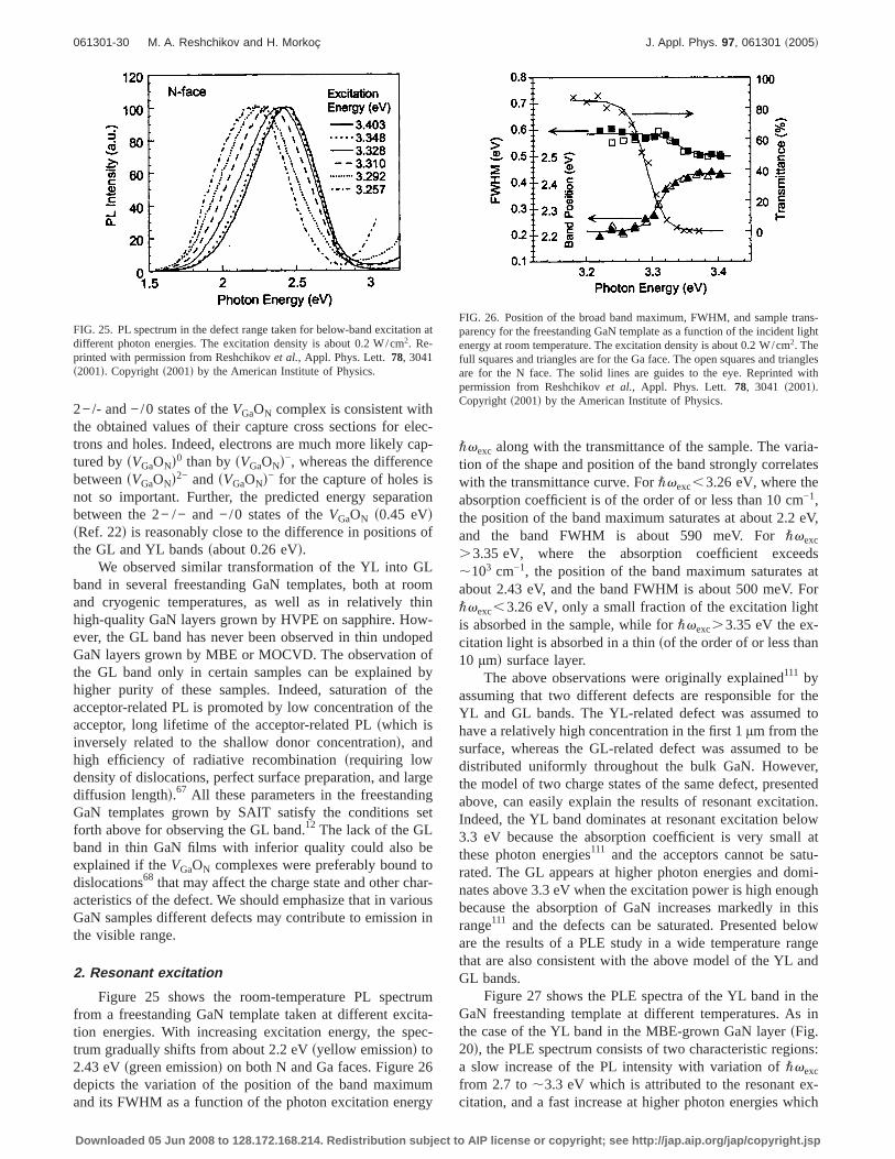
2−/- and −/0 states of theVGaON complex is consistent withthe obtained values of their capture cross sections for elec-trons and holes. Indeed, electrons are much more likely cap-tured bysVGaONd0 than bysVGaONd−, whereas the differencebetweensVGaONd2− andsVGaONd− for the capture of holes isnot so important. Further, the predicted energy separationbetween the 2− /− and −/0 states of theVGaON s0.45 eVdsRef. 22d is reasonably close to the difference in positions ofthe GL and YL bandssabout 0.26 eVd.
We observed similar transformation of the YL into GLband in several freestanding GaN templates, both at roomand cryogenic temperatures, as well as in relatively thinhigh-quality GaN layers grown by HVPE on sapphire. How-ever, the GL band has never been observed in thin undopedGaN layers grown by MBE or MOCVD. The observation ofthe GL band only in certain samples can be explained byhigher purity of these samples. Indeed, saturation of theacceptor-related PL is promoted by low concentration of theacceptor, long lifetime of the acceptor-related PLswhich isinversely related to the shallow donor concentrationd, andhigh efficiency of radiative recombinationsrequiring lowdensity of dislocations, perfect surface preparation, and largediffusion lengthd.67 All these parameters in the freestandingGaN templates grown by SAIT satisfy the conditions setforth above for observing the GL band.12 The lack of the GLband in thin GaN films with inferior quality could also beexplained if theVGaON complexes were preferably bound todislocations68 that may affect the charge state and other char-acteristics of the defect. We should emphasize that in variousGaN samples different defects may contribute to emission inthe visible range.
2. Resonant excitation
Figure 25 shows the room-temperature PL spectrumfrom a freestanding GaN template taken at different excita-tion energies. With increasing excitation energy, the spec-trum gradually shifts from about 2.2 eVsyellow emissiond to2.43 eVsgreen emissiond on both N and Ga faces. Figure 26depicts the variation of the position of the band maximumand its FWHM as a function of the photon excitation energy
"vexc along with the transmittance of the sample. The varia-tion of the shape and position of the band strongly correlateswith the transmittance curve. For"vexc,3.26 eV, where theabsorption coefficient is of the order of or less than 10 cm−1,the position of the band maximum saturates at about 2.2 eV,and the band FWHM is about 590 meV. For"vexc
.3.35 eV, where the absorption coefficient exceeds,103 cm−1, the position of the band maximum saturates atabout 2.43 eV, and the band FWHM is about 500 meV. For"vexc,3.26 eV, only a small fraction of the excitation lightis absorbed in the sample, while for"vexc.3.35 eV the ex-citation light is absorbed in a thinsof the order of or less than10 µmd surface layer.
The above observations were originally explained111 byassuming that two different defects are responsible for theYL and GL bands. The YL-related defect was assumed tohave a relatively high concentration in the first 1µm from thesurface, whereas the GL-related defect was assumed to bedistributed uniformly throughout the bulk GaN. However,the model of two charge states of the same defect, presentedabove, can easily explain the results of resonant excitation.Indeed, the YL band dominates at resonant excitation below3.3 eV because the absorption coefficient is very small atthese photon energies111 and the acceptors cannot be satu-rated. The GL appears at higher photon energies and domi-nates above 3.3 eV when the excitation power is high enoughbecause the absorption of GaN increases markedly in thisrange111 and the defects can be saturated. Presented beloware the results of a PLE study in a wide temperature rangethat are also consistent with the above model of the YL andGL bands.
Figure 27 shows the PLE spectra of the YL band in theGaN freestanding template at different temperatures. As inthe case of the YL band in the MBE-grown GaN layersFig.20d, the PLE spectrum consists of two characteristic regions:a slow increase of the PL intensity with variation of"vexc
from 2.7 to,3.3 eV which is attributed to the resonant ex-citation, and a fast increase at higher photon energies which
FIG. 25. PL spectrum in the defect range taken for below-band excitation atdifferent photon energies. The excitation density is about 0.2 W/cm2. Re-printed with permission from Reshchikovet al., Appl. Phys. Lett.78, 3041s2001d. Copyrights2001d by the American Institute of Physics.
FIG. 26. Position of the broad band maximum, FWHM, and sample trans-parency for the freestanding GaN template as a function of the incident lightenergy at room temperature. The excitation density is about 0.2 W/cm2. Thefull squares and triangles are for the Ga face. The open squares and trianglesare for the N face. The solid lines are guides to the eye. Reprinted withpermission from Reshchikovet al., Appl. Phys. Lett. 78, 3041 s2001d.Copyright s2001d by the American Institute of Physics.
061301-30 M. A. Reshchikov and H. Morkoç J. Appl. Phys. 97, 061301 ~2005!
Downloaded 05 Jun 2008 to 128.172.168.214. Redistribution subject to AIP license or copyright; see http://jap.aip.org/jap/copyright.jsp
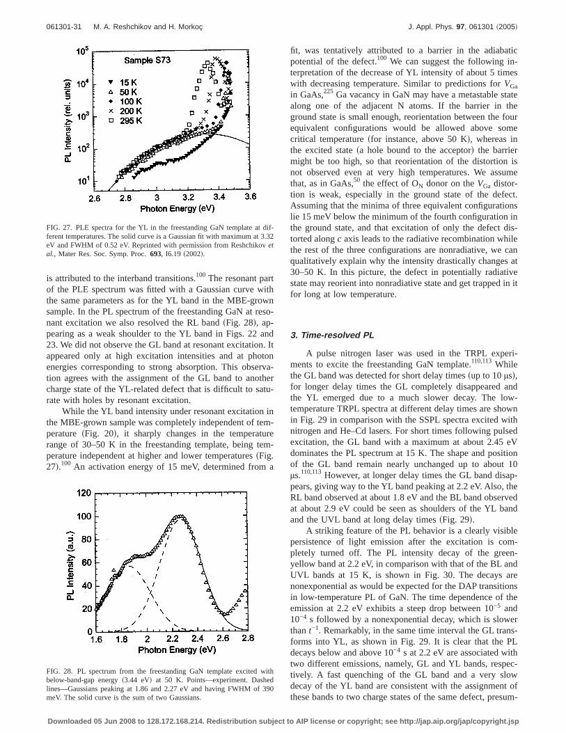
is attributed to the interband transitions.100 The resonant partof the PLE spectrum was fitted with a Gaussian curve withthe same parameters as for the YL band in the MBE-grownsample. In the PL spectrum of the freestanding GaN at reso-nant excitation we also resolved the RL bandsFig. 28d, ap-pearing as a weak shoulder to the YL band in Figs. 22 and23. We did not observe the GL band at resonant excitation. Itappeared only at high excitation intensities and at photonenergies corresponding to strong absorption. This observa-tion agrees with the assignment of the GL band to anothercharge state of the YL-related defect that is difficult to satu-rate with holes by resonant excitation.
While the YL band intensity under resonant excitation inthe MBE-grown sample was completely independent of tem-peraturesFig. 20d, it sharply changes in the temperaturerange of 30–50 K in the freestanding template, being tem-perature independent at higher and lower temperaturessFig.27d.100 An activation energy of 15 meV, determined from a
fit, was tentatively attributed to a barrier in the adiabaticpotential of the defect.100 We can suggest the following in-terpretation of the decrease of YL intensity of about 5 timeswith decreasing temperature. Similar to predictions forVGa
in GaAs,225 Ga vacancy in GaN may have a metastable statealong one of the adjacent N atoms. If the barrier in theground state is small enough, reorientation between the fourequivalent configurations would be allowed above somecritical temperaturesfor instance, above 50 Kd, whereas inthe excited statesa hole bound to the acceptord the barriermight be too high, so that reorientation of the distortion isnot observed even at very high temperatures. We assumethat, as in GaAs,50 the effect of ON donor on theVGa distor-tion is weak, especially in the ground state of the defect.Assuming that the minima of three equivalent configurationslie 15 meV below the minimum of the fourth configuration inthe ground state, and that excitation of only the defect dis-torted alongc axis leads to the radiative recombination whilethe rest of the three configurations are nonradiative, we canqualitatively explain why the intensity drastically changes at30–50 K. In this picture, the defect in potentially radiativestate may reorient into nonradiative state and get trapped in itfor long at low temperature.
3. Time-resolved PL
A pulse nitrogen laser was used in the TRPL experi-ments to excite the freestanding GaN template.110,113Whilethe GL band was detected for short delay timessup to 10µsd,for longer delay times the GL completely disappeared andthe YL emerged due to a much slower decay. The low-temperature TRPL spectra at different delay times are shownin Fig. 29 in comparison with the SSPL spectra excited withnitrogen and He–Cd lasers. For short times following pulsedexcitation, the GL band with a maximum at about 2.45 eVdominates the PL spectrum at 15 K. The shape and positionof the GL band remain nearly unchanged up to about 10µs.110,113However, at longer delay times the GL band disap-pears, giving way to the YL band peaking at 2.2 eV. Also, theRL band observed at about 1.8 eV and the BL band observedat about 2.9 eV could be seen as shoulders of the YL bandand the UVL band at long delay timessFig. 29d.
A striking feature of the PL behavior is a clearly visiblepersistence of light emission after the excitation is com-pletely turned off. The PL intensity decay of the green-yellow band at 2.2 eV, in comparison with that of the BL andUVL bands at 15 K, is shown in Fig. 30. The decays arenonexponential as would be expected for the DAP transitionsin low-temperature PL of GaN. The time dependence of theemission at 2.2 eV exhibits a steep drop between 10−5 and10−4 s followed by a nonexponential decay, which is slowerthant−1. Remarkably, in the same time interval the GL trans-forms into YL, as shown in Fig. 29. It is clear that the PLdecays below and above 10−4 s at 2.2 eV are associated withtwo different emissions, namely, GL and YL bands, respec-tively. A fast quenching of the GL band and a very slowdecay of the YL band are consistent with the assignment ofthese bands to two charge states of the same defect, presum-
FIG. 27. PLE spectra for the YL in the freestanding GaN template at dif-ferent temperatures. The solid curve is a Gaussian fit with maximum at 3.32eV and FWHM of 0.52 eV. Reprinted with permission from Reshchikovetal., Mater Res. Soc. Symp. Proc.693, I6.19 s2002d.
FIG. 28. PL spectrum from the freestanding GaN template excited withbelow-band-gap energys3.44 eVd at 50 K. Points—experiment. Dashedlines—Gaussians peaking at 1.86 and 2.27 eV and having FWHM of 390meV. The solid curve is the sum of two Gaussians.
061301-31 M. A. Reshchikov and H. Morkoç J. Appl. Phys. 97, 061301 ~2005!
Downloaded 05 Jun 2008 to 128.172.168.214. Redistribution subject to AIP license or copyright; see http://jap.aip.org/jap/copyright.jsp
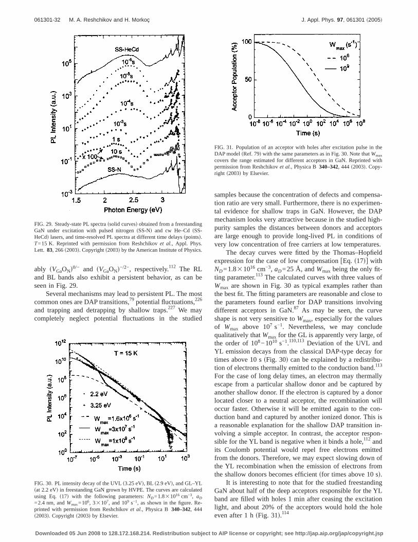
ably sVGaONd0/− and sVGaONd−/2−, respectively.112 The RLand BL bands also exhibit a persistent behavior, as can beseen in Fig. 29.
Several mechanisms may lead to persistent PL. The mostcommon ones are DAP transitions,79 potential fluctuations,226
and trapping and detrapping by shallow traps.227 We maycompletely neglect potential fluctuations in the studied
samples because the concentration of defects and compensa-tion ratio are very small. Furthermore, there is no experimen-tal evidence for shallow traps in GaN. However, the DAPmechanism looks very attractive because in the studied high-purity samples the distances between donors and acceptorsare large enough to provide long-lived PL in conditions ofvery low concentration of free carriers at low temperatures.
The decay curves were fitted by the Thomas–Hopfieldexpression for the case of low compensationfEq. s17dg withND=1.831016 cm−3, aD=25 Å, andWmax being the only fit-ting parameter.113 The calculated curves with three values ofWmax are shown in Fig. 30 as typical examples rather thanthe best fit. The fitting parameters are reasonable and close tothe parameters found earlier for DAP transitions involvingdifferent acceptors in GaN.87 As may be seen, the curveshape is not very sensitive toWmax, especially for the valuesof Wmax above 107 s−1. Nevertheless, we may concludequalitatively thatWmax for the GL is apparently very large, ofthe order of 108−1010 s−1.110,113 Deviation of the UVL andYL emission decays from the classical DAP-type decay fortimes above 10 ssFig. 30d can be explained by a redistribu-tion of electrons thermally emitted to the conduction band.113
For the case of long delay times, an electron may thermallyescape from a particular shallow donor and be captured byanother shallow donor. If the electron is captured by a donorlocated closer to a neutral acceptor, the recombination willoccur faster. Otherwise it will be emitted again to the con-duction band and captured by another ionized donor. This isa reasonable explanation for the shallow DAP transition in-volving a simple acceptor. In contrast, the acceptor respon-sible for the YL band is negative when it binds a hole,112 andits Coulomb potential would repel free electrons emittedfrom the donors. Therefore, we may expect slowing down ofthe YL recombination when the emission of electrons fromthe shallow donors becomes efficientsfor times above 10 sd.
It is interesting to note that for the studied freestandingGaN about half of the deep acceptors responsible for the YLband are filled with holes 1 min after ceasing the excitationlight, and about 20% of the acceptors would hold the holeeven after 1 hsFig. 31d.114
FIG. 29. Steady-state PL spectrassolid curvesd obtained from a freestandingGaN under excitation with pulsed nitrogensSS-Nd and cw He–CdsSS-HeCdd lasers, and time-resolved PL spectra at different time delaysspointsd.T=15 K. Reprinted with permission from Reshchikovet al., Appl. Phys.Lett. 83, 266s2003d. Copyrights2003d by the American Institute of Physics.
FIG. 30. PL intensity decay of the UVLs3.25 eVd, BL s2.9 eVd, and GL–YLsat 2.2 eVd in freestanding GaN grown by HVPE. The curves are calculatedusing Eq. s17d with the following parameters:ND=1.831016 cm−3, aD
=2.4 nm, andWmax=106, 33107, and 109 s−1, as shown in the figure. Re-printed with permission from Reshchikovet al., Physica B 340–342, 444s2003d. Copyrights2003d by Elsevier.
FIG. 31. Population of an acceptor with holes after excitation pulse in theDAP modelsRef. 79d with the same parameters as in Fig. 30. Note thatWmax
covers the range estimated for different acceptors in GaN. Reprinted withpermission from Reshchikovet al., Physica B340–342, 444 s2003d. Copy-right s2003d by Elsevier.
061301-32 M. A. Reshchikov and H. Morkoç J. Appl. Phys. 97, 061301 ~2005!
Downloaded 05 Jun 2008 to 128.172.168.214. Redistribution subject to AIP license or copyright; see http://jap.aip.org/jap/copyright.jsp
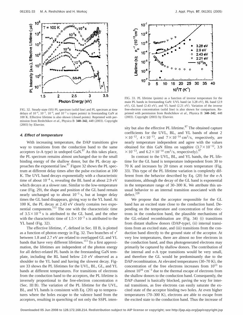
4. Effect of temperature
With increasing temperature, the DAP transitions giveway to transitions from the conduction band to the sameacceptorsse-A typed in undoped GaN.87 As this takes place,the PL spectrum remains almost unchanged due to the smallbinding energy of the shallow donor, but the PL decay ap-proaches the exponential law.87 Figure 32 shows the PL spec-trum at different delay times after the pulse excitation at 100K. The UVL band decays exponentially with a characteristictime of about 10−4 s, revealing the BL band at about 2.9 eVwhich decays at a slower rate. Similar to the low-temperaturecasesFig. 29d, the shape and position of the GL band remainnearly unchanged up to about 10−5 s, but at longer delaytimes the GL band disappears, giving way to the YL band. At100 K, the PL decay at 2.43 eV clearly contains two expo-nential components.113 The one with the characteristic timeof 3.5310−6 s is attributed to the GL band, and the otherwith the characteristic time of 1.5310−3 s is attributed to theYL band sFig. 32d.
The effective lifetime,t* , defined in Sec. III B, is plottedas a function of photon energy in Fig. 32. Two branches oft*
between 1.8 and 2.7 eV are related to overlapped GL and YLbands that have very different lifetimes.113 To a first approxi-mation, the lifetimes are independent of the photon energyfor all defect-related PL bands in the freestanding GaN tem-plate, including the RL band below 2.0 eV observed as ashoulder to the YL band and having the slowest decay. Fig-ure 33 shows the PL lifetimes for the UVL, BL, GL, and YLbands at different temperatures. For transitions of electronsfrom the conduction band to the acceptors, the PL lifetime isinversely proportional to the free-electron concentrationnsSec. III Bd. The variation of the PL lifetime for the UVL,BL, and YL bands is consistent with Eq.s20d up to tempera-tures where the holes escape to the valence band from theacceptors, resulting in quenching of not only the SSPL inten-
sity but also the effective PL lifetime.87 The obtained capturecoefficients for the UVL, BL, and YL bands of about 2310−12, 4310−13, and 7310−14 cm3/s, respectively, arenearly temperature independent and agree with the valuesobtained for thin GaN films on sapphires3.7310−12, 3.9310−13, and 6.2310−14 cm3/s, respectivelyd.87
In contrast to the UVL, BL, and YL bands, the PL life-time for the GL band is temperature independent from 30 to70 K and increases by 20 times at room temperaturesFig.33d. This type of the PL lifetime variation is completely dif-ferent from the behavior described by Eq.s20d for the e-Atransitions, although the decay of the GL band is exponentialin the temperature range of 30–300 K. We attribute this un-usual behavior to an internal transition associated with thedefect.228
We propose that the acceptor responsible for the GLband has an excited state close to the conduction band. De-pending on the temperature and concentration of free elec-trons in the conduction band, the plausible mechanisms ofthe GL-related recombination aresFig. 34d sid transitionsfrom distant shallow donorssDAP-typed, sii d internal transi-tions from an excited state, andsiii d transitions from the con-duction band directly to the ground state of the acceptor. Atvery low temperatures, there are almost no free electrons inthe conduction band, and thus photogenerated electrons mayprimarily be captured by shallow donors. The contribution ofthe internal and e-A type transitions would be very small,and therefore the GL would be predominantly due to theDAP recombination. At elevated temperaturess30–70 Kd, theconcentration of the free electrons increases from 1013 toalmost 1016 cm−3 due to the thermal escape of electrons fromthe shallow donors to the conduction band. Consequently, theDAP channel is basically blocked, paving the way for inter-nal transitions, as free electrons can easily saturate the ex-cited state of the acceptor binding two holes. At even highertemperaturess70–300 Kd, electrons are able to escape fromthe excited state to the conduction band. Thus the increase of
FIG. 32. Steady-statesSSd PL spectrumssolid lined and PL spectrum at timedelays of 10−6, 10−5, 10−4, and 10−3 s sopen pointsd in freestanding GaN at100 K. Effective lifetime is also shownsclosed pointsd. Reprinted with per-mission from Reshchikovet al., Physica B340–342, 448s2003d. Copyrights2003d by Elsevier.
FIG. 33. PL lifetimespointsd as a function of inverse temperature for themain PL bands in freestanding GaN: UVL bandsat 3.28 eVd, BL bands2.9eVd, GL bands2.43 eVd, and YL bands2.21 eVd. Variation of the inversefree-electron concentrationssolid lined is also shown for comparison. Re-printed with permission from Reshchikovet al., Physica B 340–342, 448s2003d. Copyrights2003d by Elsevier.
061301-33 M. A. Reshchikov and H. Morkoç J. Appl. Phys. 97, 061301 ~2005!
Downloaded 05 Jun 2008 to 128.172.168.214. Redistribution subject to AIP license or copyright; see http://jap.aip.org/jap/copyright.jsp
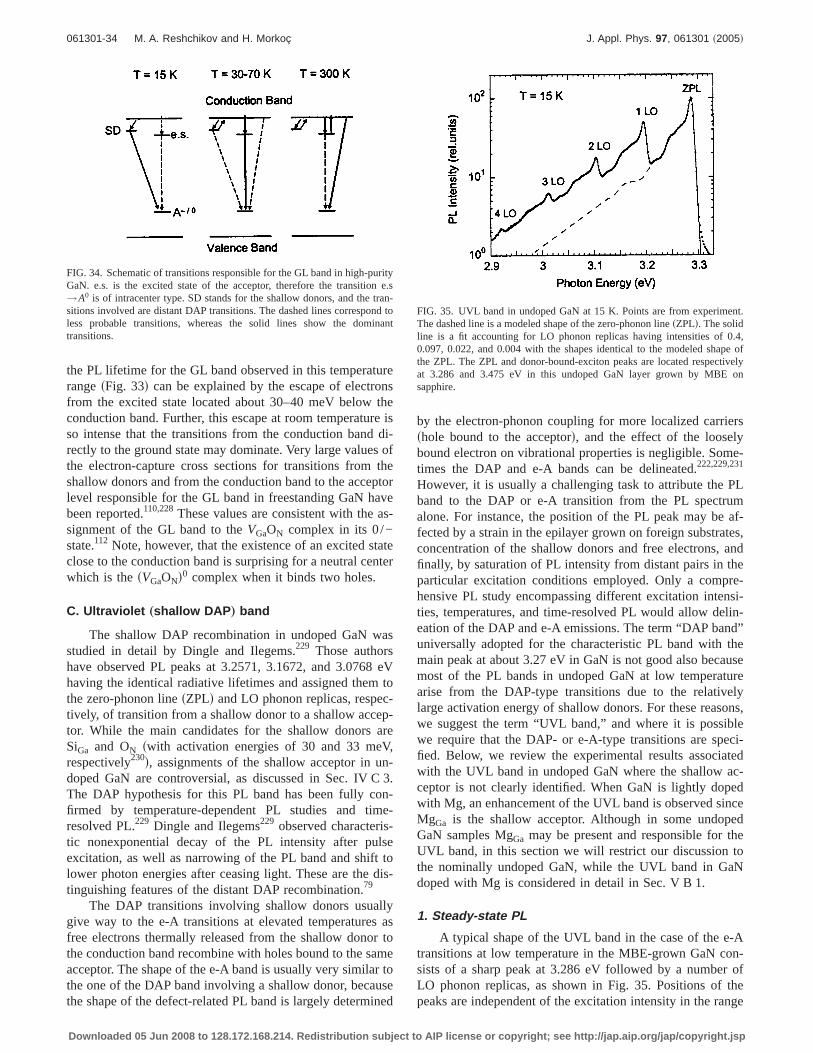
the PL lifetime for the GL band observed in this temperaturerangesFig. 33d can be explained by the escape of electronsfrom the excited state located about 30–40 meV below theconduction band. Further, this escape at room temperature isso intense that the transitions from the conduction band di-rectly to the ground state may dominate. Very large values ofthe electron-capture cross sections for transitions from theshallow donors and from the conduction band to the acceptorlevel responsible for the GL band in freestanding GaN havebeen reported.110,228These values are consistent with the as-signment of the GL band to theVGaON complex in its 0/−state.112 Note, however, that the existence of an excited stateclose to the conduction band is surprising for a neutral centerwhich is thesVGaONd0 complex when it binds two holes.
C. Ultraviolet „shallow DAP … band
The shallow DAP recombination in undoped GaN wasstudied in detail by Dingle and Ilegems.229 Those authorshave observed PL peaks at 3.2571, 3.1672, and 3.0768 eVhaving the identical radiative lifetimes and assigned them tothe zero-phonon linesZPLd and LO phonon replicas, respec-tively, of transition from a shallow donor to a shallow accep-tor. While the main candidates for the shallow donors areSiGa and ON swith activation energies of 30 and 33 meV,respectively230d, assignments of the shallow acceptor in un-doped GaN are controversial, as discussed in Sec. IV C 3.The DAP hypothesis for this PL band has been fully con-firmed by temperature-dependent PL studies and time-resolved PL.229 Dingle and Ilegems229 observed characteris-tic nonexponential decay of the PL intensity after pulseexcitation, as well as narrowing of the PL band and shift tolower photon energies after ceasing light. These are the dis-tinguishing features of the distant DAP recombination.79
The DAP transitions involving shallow donors usuallygive way to the e-A transitions at elevated temperatures asfree electrons thermally released from the shallow donor tothe conduction band recombine with holes bound to the sameacceptor. The shape of the e-A band is usually very similar tothe one of the DAP band involving a shallow donor, becausethe shape of the defect-related PL band is largely determined
by the electron-phonon coupling for more localized carriersshole bound to the acceptord, and the effect of the looselybound electron on vibrational properties is negligible. Some-times the DAP and e-A bands can be delineated.222,229,231
However, it is usually a challenging task to attribute the PLband to the DAP or e-A transition from the PL spectrumalone. For instance, the position of the PL peak may be af-fected by a strain in the epilayer grown on foreign substrates,concentration of the shallow donors and free electrons, andfinally, by saturation of PL intensity from distant pairs in theparticular excitation conditions employed. Only a compre-hensive PL study encompassing different excitation intensi-ties, temperatures, and time-resolved PL would allow delin-eation of the DAP and e-A emissions. The term “DAP band”universally adopted for the characteristic PL band with themain peak at about 3.27 eV in GaN is not good also becausemost of the PL bands in undoped GaN at low temperaturearise from the DAP-type transitions due to the relativelylarge activation energy of shallow donors. For these reasons,we suggest the term “UVL band,” and where it is possiblewe require that the DAP- or e-A-type transitions are speci-fied. Below, we review the experimental results associatedwith the UVL band in undoped GaN where the shallow ac-ceptor is not clearly identified. When GaN is lightly dopedwith Mg, an enhancement of the UVL band is observed sinceMgGa is the shallow acceptor. Although in some undopedGaN samples MgGa may be present and responsible for theUVL band, in this section we will restrict our discussion tothe nominally undoped GaN, while the UVL band in GaNdoped with Mg is considered in detail in Sec. V B 1.
1. Steady-state PL
A typical shape of the UVL band in the case of the e-Atransitions at low temperature in the MBE-grown GaN con-sists of a sharp peak at 3.286 eV followed by a number ofLO phonon replicas, as shown in Fig. 35. Positions of thepeaks are independent of the excitation intensity in the range
FIG. 34. Schematic of transitions responsible for the GL band in high-purityGaN. e.s. is the excited state of the acceptor, therefore the transition e.s→A0 is of intracenter type. SD stands for the shallow donors, and the tran-sitions involved are distant DAP transitions. The dashed lines correspond toless probable transitions, whereas the solid lines show the dominanttransitions.
FIG. 35. UVL band in undoped GaN at 15 K. Points are from experiment.The dashed line is a modeled shape of the zero-phonon linesZPLd. The solidline is a fit accounting for LO phonon replicas having intensities of 0.4,0.097, 0.022, and 0.004 with the shapes identical to the modeled shape ofthe ZPL. The ZPL and donor-bound-exciton peaks are located respectivelyat 3.286 and 3.475 eV in this undoped GaN layer grown by MBE onsapphire.
061301-34 M. A. Reshchikov and H. Morkoç J. Appl. Phys. 97, 061301 ~2005!
Downloaded 05 Jun 2008 to 128.172.168.214. Redistribution subject to AIP license or copyright; see http://jap.aip.org/jap/copyright.jsp
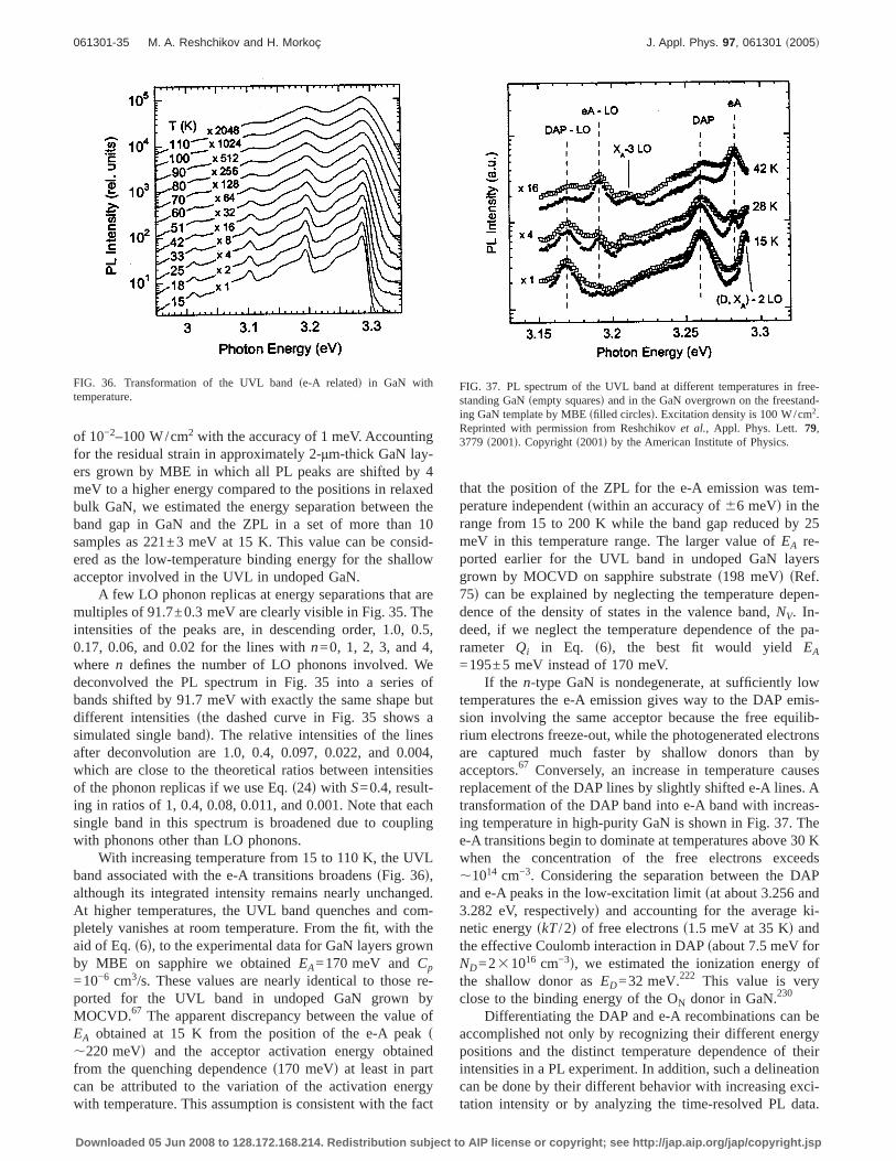
of 10−2–100 W/cm2 with the accuracy of 1 meV. Accountingfor the residual strain in approximately 2-µm-thick GaN lay-ers grown by MBE in which all PL peaks are shifted by 4meV to a higher energy compared to the positions in relaxedbulk GaN, we estimated the energy separation between theband gap in GaN and the ZPL in a set of more than 10samples as 221±3 meV at 15 K. This value can be consid-ered as the low-temperature binding energy for the shallowacceptor involved in the UVL in undoped GaN.
A few LO phonon replicas at energy separations that aremultiples of 91.7±0.3 meV are clearly visible in Fig. 35. Theintensities of the peaks are, in descending order, 1.0, 0.5,0.17, 0.06, and 0.02 for the lines withn=0, 1, 2, 3, and 4,where n defines the number of LO phonons involved. Wedeconvolved the PL spectrum in Fig. 35 into a series ofbands shifted by 91.7 meV with exactly the same shape butdifferent intensitiessthe dashed curve in Fig. 35 shows asimulated single bandd. The relative intensities of the linesafter deconvolution are 1.0, 0.4, 0.097, 0.022, and 0.004,which are close to the theoretical ratios between intensitiesof the phonon replicas if we use Eq.s24d with S=0.4, result-ing in ratios of 1, 0.4, 0.08, 0.011, and 0.001. Note that eachsingle band in this spectrum is broadened due to couplingwith phonons other than LO phonons.
With increasing temperature from 15 to 110 K, the UVLband associated with the e-A transitions broadenssFig. 36d,although its integrated intensity remains nearly unchanged.At higher temperatures, the UVL band quenches and com-pletely vanishes at room temperature. From the fit, with theaid of Eq.s6d, to the experimental data for GaN layers grownby MBE on sapphire we obtainedEA=170 meV andCp
=10−6 cm3/s. These values are nearly identical to those re-ported for the UVL band in undoped GaN grown byMOCVD.67 The apparent discrepancy between the value ofEA obtained at 15 K from the position of the e-A peaks,220 meVd and the acceptor activation energy obtainedfrom the quenching dependences170 meVd at least in partcan be attributed to the variation of the activation energywith temperature. This assumption is consistent with the fact
that the position of the ZPL for the e-A emission was tem-perature independentswithin an accuracy of66 meVd in therange from 15 to 200 K while the band gap reduced by 25meV in this temperature range. The larger value ofEA re-ported earlier for the UVL band in undoped GaN layersgrown by MOCVD on sapphire substrates198 meVd sRef.75d can be explained by neglecting the temperature depen-dence of the density of states in the valence band,NV. In-deed, if we neglect the temperature dependence of the pa-rameter Qi in Eq. s6d, the best fit would yield EA
=195±5 meV instead of 170 meV.If the n-type GaN is nondegenerate, at sufficiently low
temperatures the e-A emission gives way to the DAP emis-sion involving the same acceptor because the free equilib-rium electrons freeze-out, while the photogenerated electronsare captured much faster by shallow donors than byacceptors.67 Conversely, an increase in temperature causesreplacement of the DAP lines by slightly shifted e-A lines. Atransformation of the DAP band into e-A band with increas-ing temperature in high-purity GaN is shown in Fig. 37. Thee-A transitions begin to dominate at temperatures above 30 Kwhen the concentration of the free electrons exceeds,1014 cm−3. Considering the separation between the DAPand e-A peaks in the low-excitation limitsat about 3.256 and3.282 eV, respectivelyd and accounting for the average ki-netic energyskT/2d of free electronss1.5 meV at 35 Kd andthe effective Coulomb interaction in DAPsabout 7.5 meV forND=231016 cm−3d, we estimated the ionization energy ofthe shallow donor asED=32 meV.222 This value is veryclose to the binding energy of the ON donor in GaN.230
Differentiating the DAP and e-A recombinations can beaccomplished not only by recognizing their different energypositions and the distinct temperature dependence of theirintensities in a PL experiment. In addition, such a delineationcan be done by their different behavior with increasing exci-tation intensity or by analyzing the time-resolved PL data.
FIG. 36. Transformation of the UVL bandse-A relatedd in GaN withtemperature.
FIG. 37. PL spectrum of the UVL band at different temperatures in free-standing GaNsempty squaresd and in the GaN overgrown on the freestand-ing GaN template by MBEsfilled circlesd. Excitation density is 100 W/cm2.Reprinted with permission from Reshchikovet al., Appl. Phys. Lett. 79,3779 s2001d. Copyrights2001d by the American Institute of Physics.
061301-35 M. A. Reshchikov and H. Morkoç J. Appl. Phys. 97, 061301 ~2005!
Downloaded 05 Jun 2008 to 128.172.168.214. Redistribution subject to AIP license or copyright; see http://jap.aip.org/jap/copyright.jsp
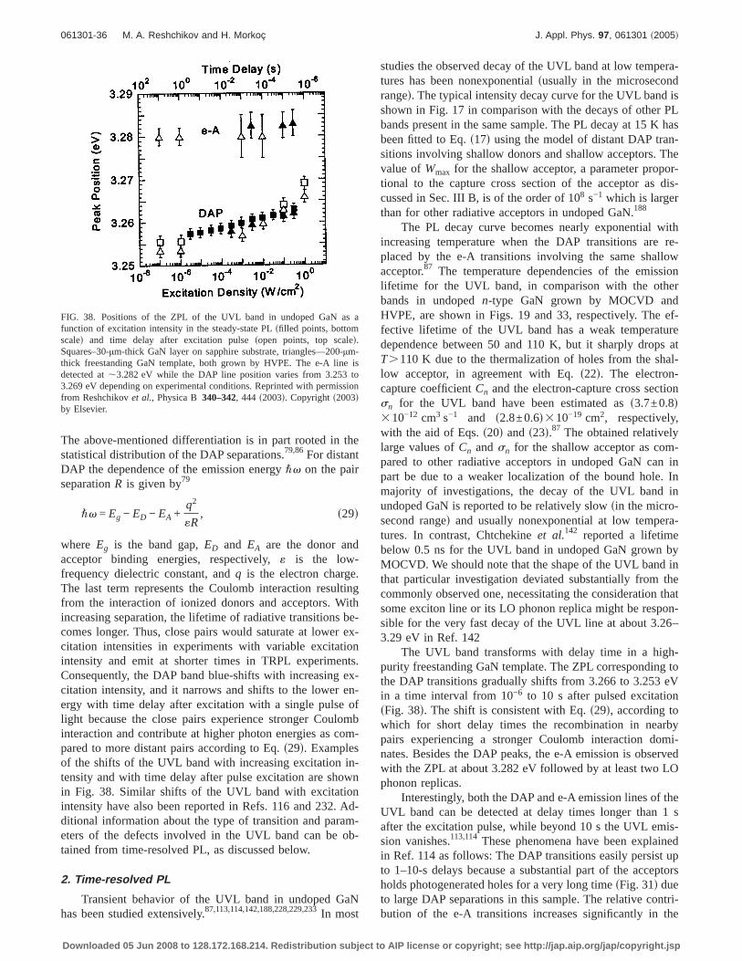
The above-mentioned differentiation is in part rooted in thestatistical distribution of the DAP separations.79,86For distantDAP the dependence of the emission energy"v on the pairseparationR is given by79
"v = Eg − ED − EA +q2
«R, s29d
where Eg is the band gap,ED and EA are the donor andacceptor binding energies, respectively,« is the low-frequency dielectric constant, andq is the electron charge.The last term represents the Coulomb interaction resultingfrom the interaction of ionized donors and acceptors. Withincreasing separation, the lifetime of radiative transitions be-comes longer. Thus, close pairs would saturate at lower ex-citation intensities in experiments with variable excitationintensity and emit at shorter times in TRPL experiments.Consequently, the DAP band blue-shifts with increasing ex-citation intensity, and it narrows and shifts to the lower en-ergy with time delay after excitation with a single pulse oflight because the close pairs experience stronger Coulombinteraction and contribute at higher photon energies as com-pared to more distant pairs according to Eq.s29d. Examplesof the shifts of the UVL band with increasing excitation in-tensity and with time delay after pulse excitation are shownin Fig. 38. Similar shifts of the UVL band with excitationintensity have also been reported in Refs. 116 and 232. Ad-ditional information about the type of transition and param-eters of the defects involved in the UVL band can be ob-tained from time-resolved PL, as discussed below.
2. Time-resolved PL
Transient behavior of the UVL band in undoped GaNhas been studied extensively.87,113,114,142,188,228,229,233In most
studies the observed decay of the UVL band at low tempera-tures has been nonexponentialsusually in the microsecondranged. The typical intensity decay curve for the UVL band isshown in Fig. 17 in comparison with the decays of other PLbands present in the same sample. The PL decay at 15 K hasbeen fitted to Eq.s17d using the model of distant DAP tran-sitions involving shallow donors and shallow acceptors. Thevalue ofWmax for the shallow acceptor, a parameter propor-tional to the capture cross section of the acceptor as dis-cussed in Sec. III B, is of the order of 108 s−1 which is largerthan for other radiative acceptors in undoped GaN.188
The PL decay curve becomes nearly exponential withincreasing temperature when the DAP transitions are re-placed by the e-A transitions involving the same shallowacceptor.87 The temperature dependencies of the emissionlifetime for the UVL band, in comparison with the otherbands in undopedn-type GaN grown by MOCVD andHVPE, are shown in Figs. 19 and 33, respectively. The ef-fective lifetime of the UVL band has a weak temperaturedependence between 50 and 110 K, but it sharply drops atT.110 K due to the thermalization of holes from the shal-low acceptor, in agreement with Eq.s22d. The electron-capture coefficientCn and the electron-capture cross sectionsn for the UVL band have been estimated ass3.7±0.8d310−12 cm3 s−1 and s2.8±0.6d310−19 cm2, respectively,with the aid of Eqs.s20d and s23d.87 The obtained relativelylarge values ofCn and sn for the shallow acceptor as com-pared to other radiative acceptors in undoped GaN can inpart be due to a weaker localization of the bound hole. Inmajority of investigations, the decay of the UVL band inundoped GaN is reported to be relatively slowsin the micro-second ranged and usually nonexponential at low tempera-tures. In contrast, Chtchekineet al.142 reported a lifetimebelow 0.5 ns for the UVL band in undoped GaN grown byMOCVD. We should note that the shape of the UVL band inthat particular investigation deviated substantially from thecommonly observed one, necessitating the consideration thatsome exciton line or its LO phonon replica might be respon-sible for the very fast decay of the UVL line at about 3.26–3.29 eV in Ref. 142
The UVL band transforms with delay time in a high-purity freestanding GaN template. The ZPL corresponding tothe DAP transitions gradually shifts from 3.266 to 3.253 eVin a time interval from 10−6 to 10 s after pulsed excitationsFig. 38d. The shift is consistent with Eq.s29d, according towhich for short delay times the recombination in nearbypairs experiencing a stronger Coulomb interaction domi-nates. Besides the DAP peaks, the e-A emission is observedwith the ZPL at about 3.282 eV followed by at least two LOphonon replicas.
Interestingly, both the DAP and e-A emission lines of theUVL band can be detected at delay times longer than 1 safter the excitation pulse, while beyond 10 s the UVL emis-sion vanishes.113,114 These phenomena have been explainedin Ref. 114 as follows: The DAP transitions easily persist upto 1–10-s delays because a substantial part of the acceptorsholds photogenerated holes for a very long timesFig. 31d dueto large DAP separations in this sample. The relative contri-bution of the e-A transitions increases significantly in the
FIG. 38. Positions of the ZPL of the UVL band in undoped GaN as afunction of excitation intensity in the steady-state PLsfilled points, bottomscaled and time delay after excitation pulsesopen points, top scaled.Squares–30-µm-thick GaN layer on sapphire substrate, triangles—200-µm-thick freestanding GaN template, both grown by HVPE. The e-A line isdetected at,3.282 eV while the DAP line position varies from 3.253 to3.269 eV depending on experimental conditions. Reprinted with permissionfrom Reshchikovet al., Physica B340–342, 444 s2003d. Copyrights2003dby Elsevier.
061301-36 M. A. Reshchikov and H. Morkoç J. Appl. Phys. 97, 061301 ~2005!
Downloaded 05 Jun 2008 to 128.172.168.214. Redistribution subject to AIP license or copyright; see http://jap.aip.org/jap/copyright.jsp
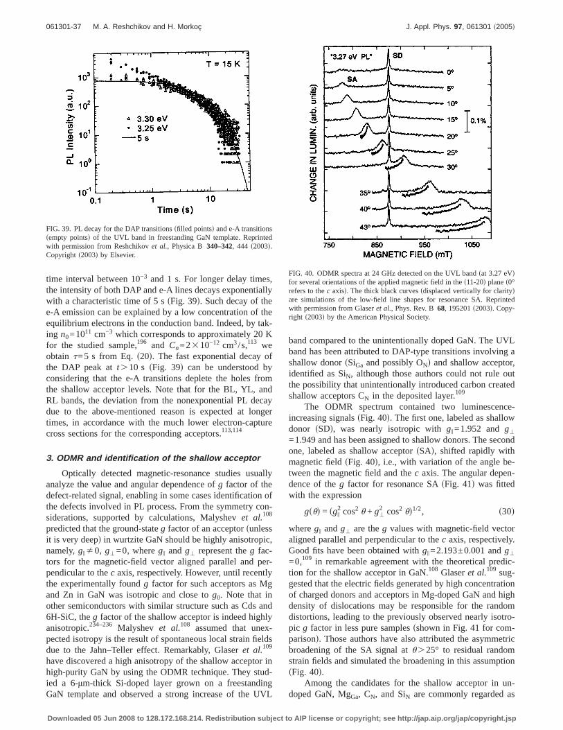
time interval between 10−3 and 1 s. For longer delay times,the intensity of both DAP and e-A lines decays exponentiallywith a characteristic time of 5 ssFig. 39d. Such decay of thee-A emission can be explained by a low concentration of theequilibrium electrons in the conduction band. Indeed, by tak-ing n0=1011 cm−3 which corresponds to approximately 20 Kfor the studied sample,196 and Cn=2310−12 cm3/s,113 weobtain t=5 s from Eq.s20d. The fast exponential decay ofthe DAP peak att.10 s sFig. 39d can be understood byconsidering that the e-A transitions deplete the holes fromthe shallow acceptor levels. Note that for the BL, YL, andRL bands, the deviation from the nonexponential PL decaydue to the above-mentioned reason is expected at longertimes, in accordance with the much lower electron-capturecross sections for the corresponding acceptors.113,114
3. ODMR and identification of the shallow acceptor
Optically detected magnetic-resonance studies usuallyanalyze the value and angular dependence ofg factor of thedefect-related signal, enabling in some cases identification ofthe defects involved in PL process. From the symmetry con-siderations, supported by calculations, Malyshevet al.108
predicted that the ground-stateg factor of an acceptorsunlessit is very deepd in wurtzite GaN should be highly anisotropic,namely,giÞ0, g'=0, wheregi andg' represent theg fac-tors for the magnetic-field vector aligned parallel and per-pendicular to thec axis, respectively. However, until recentlythe experimentally foundg factor for such acceptors as Mgand Zn in GaN was isotropic and close tog0. Note that inother semiconductors with similar structure such as Cds and6H-SiC, theg factor of the shallow acceptor is indeed highlyanisotropic.234–236 Malyshev et al.108 assumed that unex-pected isotropy is the result of spontaneous local strain fieldsdue to the Jahn–Teller effect. Remarkably, Glaseret al.109
have discovered a high anisotropy of the shallow acceptor inhigh-purity GaN by using the ODMR technique. They stud-ied a 6-µm-thick Si-doped layer grown on a freestandingGaN template and observed a strong increase of the UVL
band compared to the unintentionally doped GaN. The UVLband has been attributed to DAP-type transitions involving ashallow donorsSiGa and possibly ONd and shallow acceptor,identified as SiN, although those authors could not rule outthe possibility that unintentionally introduced carbon createdshallow acceptors CN in the deposited layer.109
The ODMR spectrum contained two luminescence-increasing signalssFig. 40d. The first one, labeled as shallowdonor sSDd, was nearly isotropic withgi=1.952 andg'
=1.949 and has been assigned to shallow donors. The secondone, labeled as shallow acceptorsSAd, shifted rapidly withmagnetic fieldsFig. 40d, i.e., with variation of the angle be-tween the magnetic field and thec axis. The angular depen-dence of theg factor for resonance SAsFig. 41d was fittedwith the expression
gsud = sgi2 cos2 u + g'
2 cos2 ud1/2, s30d
wheregi andg' are theg values with magnetic-field vectoraligned parallel and perpendicular to thec axis, respectively.Good fits have been obtained withgi=2.193±0.001 andg'
=0,109 in remarkable agreement with the theoretical predic-tion for the shallow acceptor in GaN.108 Glaseret al.109 sug-gested that the electric fields generated by high concentrationof charged donors and acceptors in Mg-doped GaN and highdensity of dislocations may be responsible for the randomdistortions, leading to the previously observed nearly isotro-pic g factor in less pure samplessshown in Fig. 41 for com-parisond. Those authors have also attributed the asymmetricbroadening of the SA signal atu.25° to residual randomstrain fields and simulated the broadening in this assumptionsFig. 40d.
Among the candidates for the shallow acceptor in un-doped GaN, MgGa, CN, and SiN are commonly regarded as
FIG. 39. PL decay for the DAP transitionssfilled pointsd and e-A transitionssempty pointsd of the UVL band in freestanding GaN template. Reprintedwith permission from Reshchikovet al., Physica B 340–342, 444 s2003d.Copyright s2003d by Elsevier.
FIG. 40. ODMR spectra at 24 GHz detected on the UVL bandsat 3.27 eVdfor several orientations of the applied magnetic field in thes11-20d planes0°refers to thec axisd. The thick black curvessdisplaced vertically for claritydare simulations of the low-field line shapes for resonance SA. Reprintedwith permission from Glaseret al., Phys. Rev. B68, 195201s2003d. Copy-right s2003d by the American Physical Society.
061301-37 M. A. Reshchikov and H. Morkoç J. Appl. Phys. 97, 061301 ~2005!
Downloaded 05 Jun 2008 to 128.172.168.214. Redistribution subject to AIP license or copyright; see http://jap.aip.org/jap/copyright.jsp
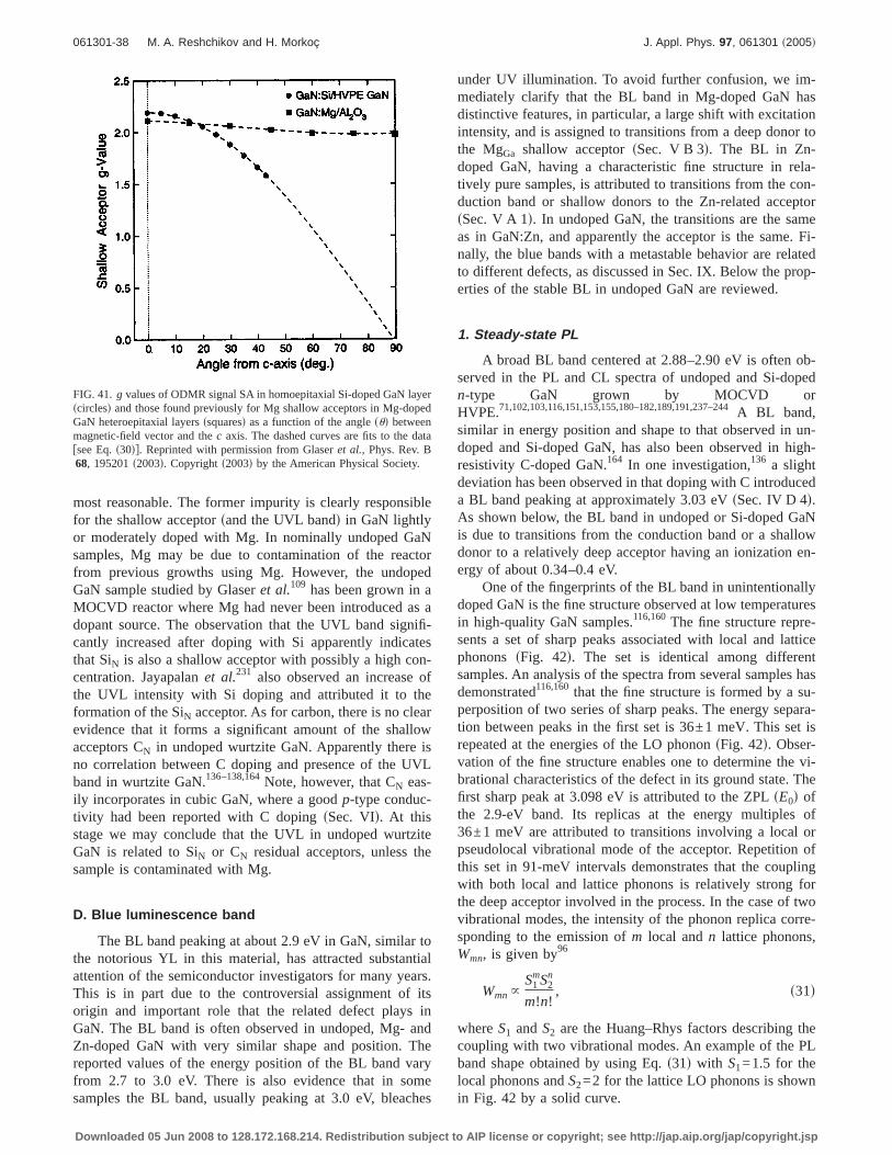
most reasonable. The former impurity is clearly responsiblefor the shallow acceptorsand the UVL bandd in GaN lightlyor moderately doped with Mg. In nominally undoped GaNsamples, Mg may be due to contamination of the reactorfrom previous growths using Mg. However, the undopedGaN sample studied by Glaseret al.109 has been grown in aMOCVD reactor where Mg had never been introduced as adopant source. The observation that the UVL band signifi-cantly increased after doping with Si apparently indicatesthat SiN is also a shallow acceptor with possibly a high con-centration. Jayapalanet al.231 also observed an increase ofthe UVL intensity with Si doping and attributed it to theformation of the SiN acceptor. As for carbon, there is no clearevidence that it forms a significant amount of the shallowacceptors CN in undoped wurtzite GaN. Apparently there isno correlation between C doping and presence of the UVLband in wurtzite GaN.136–138,164Note, however, that CN eas-ily incorporates in cubic GaN, where a goodp-type conduc-tivity had been reported with C dopingsSec. VId. At thisstage we may conclude that the UVL in undoped wurtziteGaN is related to SiN or CN residual acceptors, unless thesample is contaminated with Mg.
D. Blue luminescence band
The BL band peaking at about 2.9 eV in GaN, similar tothe notorious YL in this material, has attracted substantialattention of the semiconductor investigators for many years.This is in part due to the controversial assignment of itsorigin and important role that the related defect plays inGaN. The BL band is often observed in undoped, Mg- andZn-doped GaN with very similar shape and position. Thereported values of the energy position of the BL band varyfrom 2.7 to 3.0 eV. There is also evidence that in somesamples the BL band, usually peaking at 3.0 eV, bleaches
under UV illumination. To avoid further confusion, we im-mediately clarify that the BL band in Mg-doped GaN hasdistinctive features, in particular, a large shift with excitationintensity, and is assigned to transitions from a deep donor tothe MgGa shallow acceptorsSec. V B 3d. The BL in Zn-doped GaN, having a characteristic fine structure in rela-tively pure samples, is attributed to transitions from the con-duction band or shallow donors to the Zn-related acceptorsSec. V A 1d. In undoped GaN, the transitions are the sameas in GaN:Zn, and apparently the acceptor is the same. Fi-nally, the blue bands with a metastable behavior are relatedto different defects, as discussed in Sec. IX. Below the prop-erties of the stable BL in undoped GaN are reviewed.
1. Steady-state PL
A broad BL band centered at 2.88–2.90 eV is often ob-served in the PL and CL spectra of undoped and Si-dopedn-type GaN grown by MOCVD orHVPE.71,102,103,116,151,153,155,180–182,189,191,237–244A BL band,similar in energy position and shape to that observed in un-doped and Si-doped GaN, has also been observed in high-resistivity C-doped GaN.164 In one investigation,136 a slightdeviation has been observed in that doping with C introduceda BL band peaking at approximately 3.03 eVsSec. IV D 4d.As shown below, the BL band in undoped or Si-doped GaNis due to transitions from the conduction band or a shallowdonor to a relatively deep acceptor having an ionization en-ergy of about 0.34–0.4 eV.
One of the fingerprints of the BL band in unintentionallydoped GaN is the fine structure observed at low temperaturesin high-quality GaN samples.116,160The fine structure repre-sents a set of sharp peaks associated with local and latticephonons sFig. 42d. The set is identical among differentsamples. An analysis of the spectra from several samples hasdemonstrated116,160that the fine structure is formed by a su-perposition of two series of sharp peaks. The energy separa-tion between peaks in the first set is 36±1 meV. This set isrepeated at the energies of the LO phononsFig. 42d. Obser-vation of the fine structure enables one to determine the vi-brational characteristics of the defect in its ground state. Thefirst sharp peak at 3.098 eV is attributed to the ZPLsE0d ofthe 2.9-eV band. Its replicas at the energy multiples of36±1 meV are attributed to transitions involving a local orpseudolocal vibrational mode of the acceptor. Repetition ofthis set in 91-meV intervals demonstrates that the couplingwith both local and lattice phonons is relatively strong forthe deep acceptor involved in the process. In the case of twovibrational modes, the intensity of the phonon replica corre-sponding to the emission ofm local andn lattice phonons,Wmn, is given by96
Wmn~S1
mS2n
m!n!, s31d
whereS1 andS2 are the Huang–Rhys factors describing thecoupling with two vibrational modes. An example of the PLband shape obtained by using Eq.s31d with S1=1.5 for thelocal phonons andS2=2 for the lattice LO phonons is shownin Fig. 42 by a solid curve.
FIG. 41. g values of ODMR signal SA in homoepitaxial Si-doped GaN layerscirclesd and those found previously for Mg shallow acceptors in Mg-dopedGaN heteroepitaxial layersssquaresd as a function of the anglesud betweenmagnetic-field vector and thec axis. The dashed curves are fits to the datafsee Eq.s30dg. Reprinted with permission from Glaseret al., Phys. Rev. B68, 195201s2003d. Copyrights2003d by the American Physical Society.
061301-38 M. A. Reshchikov and H. Morkoç J. Appl. Phys. 97, 061301 ~2005!
Downloaded 05 Jun 2008 to 128.172.168.214. Redistribution subject to AIP license or copyright; see http://jap.aip.org/jap/copyright.jsp
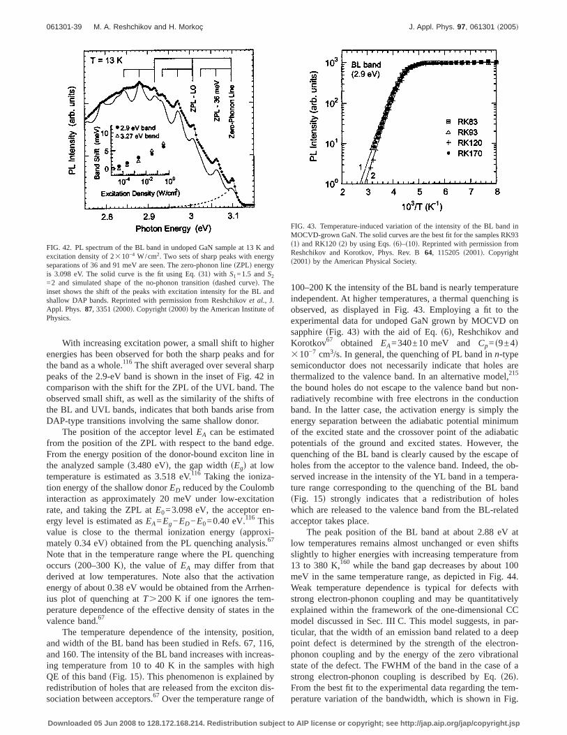
With increasing excitation power, a small shift to higherenergies has been observed for both the sharp peaks and forthe band as a whole.116 The shift averaged over several sharppeaks of the 2.9-eV band is shown in the inset of Fig. 42 incomparison with the shift for the ZPL of the UVL band. Theobserved small shift, as well as the similarity of the shifts ofthe BL and UVL bands, indicates that both bands arise fromDAP-type transitions involving the same shallow donor.
The position of the acceptor levelEA can be estimatedfrom the position of the ZPL with respect to the band edge.From the energy position of the donor-bound exciton line inthe analyzed samples3.480 eVd, the gap widthsEgd at lowtemperature is estimated as 3.518 eV.116 Taking the ioniza-tion energy of the shallow donorED reduced by the Coulombinteraction as approximately 20 meV under low-excitationrate, and taking the ZPL atE0=3.098 eV, the acceptor en-ergy level is estimated asEA=Eg−ED−E0=0.40 eV.116 Thisvalue is close to the thermal ionization energysapproxi-mately 0.34 eVd obtained from the PL quenching analysis.67
Note that in the temperature range where the PL quenchingoccurss200–300 Kd, the value ofEA may differ from thatderived at low temperatures. Note also that the activationenergy of about 0.38 eV would be obtained from the Arrhen-ius plot of quenching atT.200 K if one ignores the tem-perature dependence of the effective density of states in thevalence band.67
The temperature dependence of the intensity, position,and width of the BL band has been studied in Refs. 67, 116,and 160. The intensity of the BL band increases with increas-ing temperature from 10 to 40 K in the samples with highQE of this bandsFig. 15d. This phenomenon is explained byredistribution of holes that are released from the exciton dis-sociation between acceptors.67 Over the temperature range of
100–200 K the intensity of the BL band is nearly temperatureindependent. At higher temperatures, a thermal quenching isobserved, as displayed in Fig. 43. Employing a fit to theexperimental data for undoped GaN grown by MOCVD onsapphiresFig. 43d with the aid of Eq.s6d, Reshchikov andKorotkov67 obtained EA=340±10 meV and Cp=s9±4d310−7 cm3/s. In general, the quenching of PL band inn-typesemiconductor does not necessarily indicate that holes arethermalized to the valence band. In an alternative model,215
the bound holes do not escape to the valence band but non-radiatively recombine with free electrons in the conductionband. In the latter case, the activation energy is simply theenergy separation between the adiabatic potential minimumof the excited state and the crossover point of the adiabaticpotentials of the ground and excited states. However, thequenching of the BL band is clearly caused by the escape ofholes from the acceptor to the valence band. Indeed, the ob-served increase in the intensity of the YL band in a tempera-ture range corresponding to the quenching of the BL bandsFig. 15d strongly indicates that a redistribution of holeswhich are released to the valence band from the BL-relatedacceptor takes place.
The peak position of the BL band at about 2.88 eV atlow temperatures remains almost unchanged or even shiftsslightly to higher energies with increasing temperature from13 to 380 K,160 while the band gap decreases by about 100meV in the same temperature range, as depicted in Fig. 44.Weak temperature dependence is typical for defects withstrong electron-phonon coupling and may be quantitativelyexplained within the framework of the one-dimensional CCmodel discussed in Sec. III C. This model suggests, in par-ticular, that the width of an emission band related to a deeppoint defect is determined by the strength of the electron-phonon coupling and by the energy of the zero vibrationalstate of the defect. The FWHM of the band in the case of astrong electron-phonon coupling is described by Eq.s26d.From the best fit to the experimental data regarding the tem-perature variation of the bandwidth, which is shown in Fig.
FIG. 42. PL spectrum of the BL band in undoped GaN sample at 13 K andexcitation density of 2310−4 W/cm2. Two sets of sharp peaks with energyseparations of 36 and 91 meV are seen. The zero-phonon linesZPLd energyis 3.098 eV. The solid curve is the fit using Eq.s31d with S1=1.5 andS2
=2 and simulated shape of the no-phonon transitionsdashed curved. Theinset shows the shift of the peaks with excitation intensity for the BL andshallow DAP bands. Reprinted with permission from Reshchikovet al., J.Appl. Phys.87, 3351s2000d. Copyrights2000d by the American Institute ofPhysics.
FIG. 43. Temperature-induced variation of the intensity of the BL band inMOCVD-grown GaN. The solid curves are the best fit for the samples RK93s1d and RK120s2d by using Eqs.s6d–s10d. Reprinted with permission fromReshchikov and Korotkov, Phys. Rev. B64, 115205 s2001d. Copyrights2001d by the American Physical Society.
061301-39 M. A. Reshchikov and H. Morkoç J. Appl. Phys. 97, 061301 ~2005!
Downloaded 05 Jun 2008 to 128.172.168.214. Redistribution subject to AIP license or copyright; see http://jap.aip.org/jap/copyright.jsp
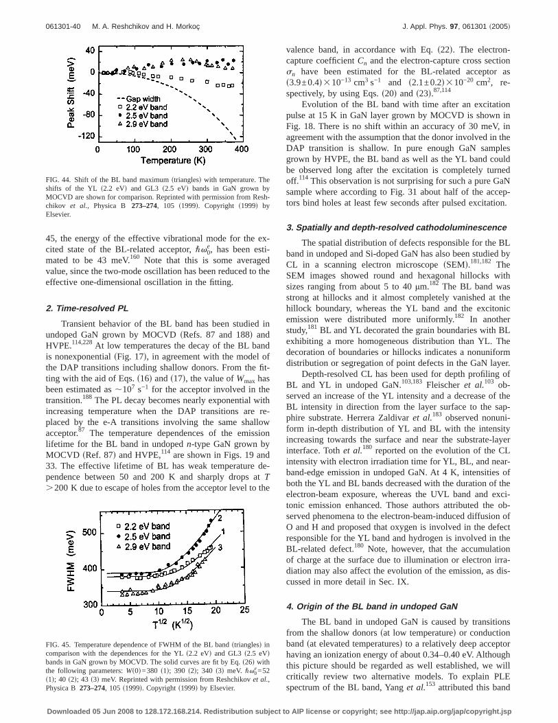
45, the energy of the effective vibrational mode for the ex-cited state of the BL-related acceptor,"v0
e, has been esti-mated to be 43 meV.160 Note that this is some averagedvalue, since the two-mode oscillation has been reduced to theeffective one-dimensional oscillation in the fitting.
2. Time-resolved PL
Transient behavior of the BL band has been studied inundoped GaN grown by MOCVDsRefs. 87 and 188d andHVPE.114,228At low temperatures the decay of the BL bandis nonexponentialsFig. 17d, in agreement with the model ofthe DAP transitions including shallow donors. From the fit-ting with the aid of Eqs.s16d ands17d, the value ofWmax hasbeen estimated as,107 s−1 for the acceptor involved in thetransition.188 The PL decay becomes nearly exponential withincreasing temperature when the DAP transitions are re-placed by the e-A transitions involving the same shallowacceptor.87 The temperature dependences of the emissionlifetime for the BL band in undopedn-type GaN grown byMOCVD sRef. 87d and HVPE,114 are shown in Figs. 19 and33. The effective lifetime of BL has weak temperature de-pendence between 50 and 200 K and sharply drops atT.200 K due to escape of holes from the acceptor level to the
valence band, in accordance with Eq.s22d. The electron-capture coefficientCn and the electron-capture cross sectionsn have been estimated for the BL-related acceptor ass3.9±0.4d310−13 cm3 s−1 and s2.1±0.2d310−20 cm2, re-spectively, by using Eqs.s20d and s23d.87,114
Evolution of the BL band with time after an excitationpulse at 15 K in GaN layer grown by MOCVD is shown inFig. 18. There is no shift within an accuracy of 30 meV, inagreement with the assumption that the donor involved in theDAP transition is shallow. In pure enough GaN samplesgrown by HVPE, the BL band as well as the YL band couldbe observed long after the excitation is completely turnedoff.114 This observation is not surprising for such a pure GaNsample where according to Fig. 31 about half of the accep-tors bind holes at least few seconds after pulsed excitation.
3. Spatially and depth-resolved cathodoluminescence
The spatial distribution of defects responsible for the BLband in undoped and Si-doped GaN has also been studied byCL in a scanning electron microscopesSEMd.181,182 TheSEM images showed round and hexagonal hillocks withsizes ranging from about 5 to 40µm.182 The BL band wasstrong at hillocks and it almost completely vanished at thehillock boundary, whereas the YL band and the excitonicemission were distributed more uniformly.182 In anotherstudy,181 BL and YL decorated the grain boundaries with BLexhibiting a more homogeneous distribution than YL. Thedecoration of boundaries or hillocks indicates a nonuniformdistribution or segregation of point defects in the GaN layer.
Depth-resolved CL has been used for depth profiling ofBL and YL in undoped GaN.103,183 Fleischeret al.103 ob-served an increase of the YL intensity and a decrease of theBL intensity in direction from the layer surface to the sap-phire substrate. Herrera Zaldivaret al.183 observed nonuni-form in-depth distribution of YL and BL with the intensityincreasing towards the surface and near the substrate-layerinterface. Tothet al.180 reported on the evolution of the CLintensity with electron irradiation time for YL, BL, and near-band-edge emission in undoped GaN. At 4 K, intensities ofboth the YL and BL bands decreased with the duration of theelectron-beam exposure, whereas the UVL band and exci-tonic emission enhanced. Those authors attributed the ob-served phenomena to the electron-beam-induced diffusion ofO and H and proposed that oxygen is involved in the defectresponsible for the YL band and hydrogen is involved in theBL-related defect.180 Note, however, that the accumulationof charge at the surface due to illumination or electron irra-diation may also affect the evolution of the emission, as dis-cussed in more detail in Sec. IX.
4. Origin of the BL band in undoped GaN
The BL band in undoped GaN is caused by transitionsfrom the shallow donorssat low temperatured or conductionbandsat elevated temperaturesd to a relatively deep acceptorhaving an ionization energy of about 0.34–0.40 eV. Althoughthis picture should be regarded as well established, we willcritically review two alternative models. To explain PLEspectrum of the BL band, Yanget al.153 attributed this band
FIG. 44. Shift of the BL band maximumstrianglesd with temperature. Theshifts of the YL s2.2 eVd and GL3 s2.5 eVd bands in GaN grown byMOCVD are shown for comparison. Reprinted with permission from Resh-chikov et al., Physica B 273–274, 105 s1999d. Copyright s1999d byElsevier.
FIG. 45. Temperature dependence of FWHM of the BL bandstrianglesd incomparison with the dependences for the YLs2.2 eVd and GL3 s2.5 eVdbands in GaN grown by MOCVD. The solid curves are fit by Eq.s26d withthe following parameters:Ws0d=380 s1d; 390 s2d; 340 s3d meV. "v0
e=52s1d; 40 s2d; 43 s3d meV. Reprinted with permission from Reshchikovet al.,Physica B 273–274, 105 s1999d. Copyrights1999d by Elsevier.
061301-40 M. A. Reshchikov and H. Morkoç J. Appl. Phys. 97, 061301 ~2005!
Downloaded 05 Jun 2008 to 128.172.168.214. Redistribution subject to AIP license or copyright; see http://jap.aip.org/jap/copyright.jsp

to transitions from the resonant state of ON located 0.25 eVabove the conduction-band minimum to theVGaON acceptorlevel located 0.8 eV above the valence band. We note that theresonant excitation of the BL band with above the band-gapphotons is very unlikely due to the large absorption coeffi-cient at 3.54–3.75 eV, and the peak in the PLE spectra ob-served in Ref. 153smoving from 3.54 to 3.75 eV with varia-tion of the emission energy from 2.75 to 2.91 eVd isapparently some feature of the scattered light. In anotherreport, Kaufmannet al.172 suggested that the BL band inundoped or Si-doped GaN is due to transitions from a deepdonor to the shallow acceptor. This model is unacceptable forundoped GaN where the overlap between the wave functionsof a hole bound to the shallow acceptor and electron local-ized at a deep donor would be extremely small to explain thehigh intensity of the BL band in samples with concentrationsof acceptors in the 1015-cm−3 range.67,116
Various proposals have been made as to the nature of thedefect responsible for the BL band in undoped GaN. The BLband was attributed to aVGa-related complex,67 in particular,to VGaON sRefs. 153 and 242d and VGaHn.
180 Although theband is often observed in Si-doped GaN, it is not enhancedby Si doping.71 This band should not be confused with theBL band in GaN heavily doped with Mg, to be discussed inSec. V B 3, and with the band peaking at about 3.03 eV inC-doped GaN.136 The clue for the origin of the acceptor canbe found in the fact that the BL band with the aforemen-tioned properties was observed only in GaN grown byMOCVD or HVPE but never in the layers grown by MBE.Therefore, it is unlikely that a native defect is involved.Moreover, we doubt that hydrogen is involved in the defectcomplex,180 because the BL band has not been revealed inGaN layers grown by MBE with ammonia as the nitrogensource.
The most plausible explanation for the BL band in un-doped GaN is contamination with Znssee Sec. V A 1d.245
Very large hole-capture cross section for this acceptors,10−13 cm2d explains why the BL is often observed in GaNsamples with the Zn concentration of,1015 cm−3 and evenless.67,245 We may speculate that GaN can be contaminatedwith Zn from impure gases used in MOCVD and HVPEgrowth or from intentional Zn doping sometimes used in thebuffer layer for improved growth.
E. Red luminescence band
The RL band with its emission in the range of,1.5–2.0 eV is less studied and less common in undopedGaN as compared to the YL, BL, and UVL bands. The en-ergy positions of the RL band differ in different reports, andit appears that several defects contribute to emission in thisenergy range. We have observed a few RL bands having verydifferent properties. In this section, the RL band observed atroom and cryogenic temperatures in GaN grown by HVPEand MBE is discussed, while Sec. IV F deals with specificred and green bands observed only in Ga-rich GaN grown byMBE at relatively low temperatures. The red band observedin the Mg-doped GaN is discussed in Sec. V B 4.
In GaN samples grown by HVPE, the RL band peakingat about 1.85 eV and having a FWHM of about 0.4 eV isobserved if the YL band is sufficiently weak, as displayed inFig. 13.114,246 In some HVPE-GaN samples, the RL bandappears as a shoulder to the YL band and can be resolvedonly at very low excitation intensitiessFig. 46d, because theRL band usually saturates at very low excitation intensities.99
In the high-purity freestanding GaN templates, the RL bandcould be detected as a weak shoulder to the YL bandsFig.22d and it is better resolved in the below-band-gap excitationcasesFig. 28d. The effective lifetime of the RL is the longestamong other defect-related PL bands in the visible part of thespectrum.189,228For example, at 100 K the lifetime of RL isabout 5 ms in a freestanding templatesFig. 32d, resulting inthe smallest electron-capture cross-section coefficient of 2310−14 cm3/s.228 In sufficiently pure GaN, the RL band canbe observed seconds after the excitation pulse,113,114see Fig.1 in Ref. 114 for the 200-µm-thick freestanding GaN tem-plate and 30-µm-thick GaN layer grown on sapphire. A verylong lifetime of the RL band explains why it saturates at verylow excitation intensitiessFig. 23d. No energy shift of the RLband was detected with delay time,113,114,189indicating thatthe RL band is due to transitions from a shallow donorsatlow temperaturesd or the conduction bandsat elevated tem-peraturesd to a deep acceptor level. The ODMR studies havealso revealed that the RL band in GaN grown by HVPE iscaused by transitions from the shallow donors to a deep-leveldefect at low temperatures.247 Owing to a nearly Gaussianshape of the RL band, we conclude that the electron-phononcoupling is very strong for the deep acceptor involved, andits ZPL should be near 2.2 eV. Therefore, the acceptor levelis located at about 1.2–1.3 eV above the valence band. Deepenergy position of the acceptor level is consistent with thePL intensity being independent of temperature.113,114,189,228
The above-analyzed RL band should not be confused withthe very short-livedsthe lifetime is 12 nsd broad band peak-ing at about 1.93 eV.248 The latter has been attributed torecombination of excitons bound to a neutral defect center.248
FIG. 46. Room-temperature PL spectrum of GaN layer grown by HVPE onsapphiresH966 for usd excited at"vexc=3.41 eV. The points are experimen-tal data taken atPexc=1 s1d and 0.001 W/cm2 s2d. The curves are self-consistent deconvolution of the experimental curves into two bandssa RLwith a maximum at 1.92 eV and a GL with the maximum at 2.39 eVd.Reprinted with permission from Reshchikovet al., Mater. Res. Soc. Symp.Proc. 680, E5.6 s2001d.
061301-41 M. A. Reshchikov and H. Morkoç J. Appl. Phys. 97, 061301 ~2005!
Downloaded 05 Jun 2008 to 128.172.168.214. Redistribution subject to AIP license or copyright; see http://jap.aip.org/jap/copyright.jsp
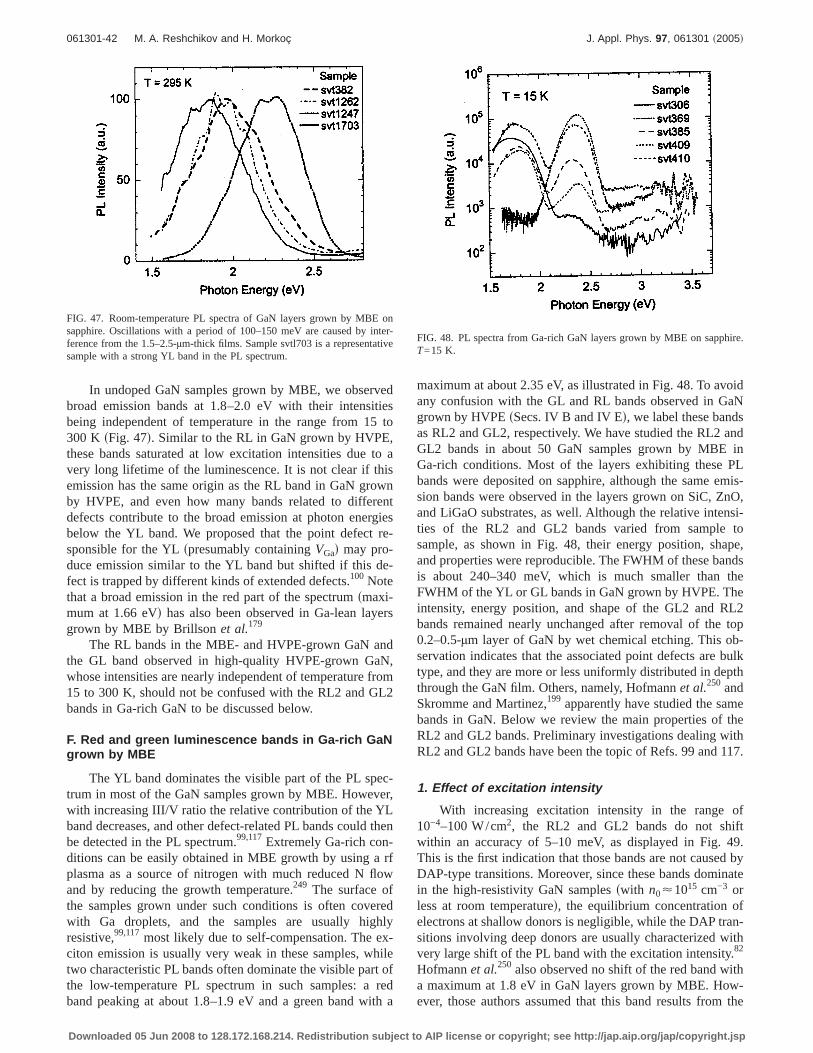
In undoped GaN samples grown by MBE, we observedbroad emission bands at 1.8–2.0 eV with their intensitiesbeing independent of temperature in the range from 15 to300 K sFig. 47d. Similar to the RL in GaN grown by HVPE,these bands saturated at low excitation intensities due to avery long lifetime of the luminescence. It is not clear if thisemission has the same origin as the RL band in GaN grownby HVPE, and even how many bands related to differentdefects contribute to the broad emission at photon energiesbelow the YL band. We proposed that the point defect re-sponsible for the YLspresumably containingVGad may pro-duce emission similar to the YL band but shifted if this de-fect is trapped by different kinds of extended defects.100 Notethat a broad emission in the red part of the spectrumsmaxi-mum at 1.66 eVd has also been observed in Ga-lean layersgrown by MBE by Brillsonet al.179
The RL bands in the MBE- and HVPE-grown GaN andthe GL band observed in high-quality HVPE-grown GaN,whose intensities are nearly independent of temperature from15 to 300 K, should not be confused with the RL2 and GL2bands in Ga-rich GaN to be discussed below.
F. Red and green luminescence bands in Ga-rich GaNgrown by MBE
The YL band dominates the visible part of the PL spec-trum in most of the GaN samples grown by MBE. However,with increasing III/V ratio the relative contribution of the YLband decreases, and other defect-related PL bands could thenbe detected in the PL spectrum.99,117Extremely Ga-rich con-ditions can be easily obtained in MBE growth by using a rfplasma as a source of nitrogen with much reduced N flowand by reducing the growth temperature.249 The surface ofthe samples grown under such conditions is often coveredwith Ga droplets, and the samples are usually highlyresistive,99,117most likely due to self-compensation. The ex-citon emission is usually very weak in these samples, whiletwo characteristic PL bands often dominate the visible part ofthe low-temperature PL spectrum in such samples: a redband peaking at about 1.8–1.9 eV and a green band with a
maximum at about 2.35 eV, as illustrated in Fig. 48. To avoidany confusion with the GL and RL bands observed in GaNgrown by HVPEsSecs. IV B and IV Ed, we label these bandsas RL2 and GL2, respectively. We have studied the RL2 andGL2 bands in about 50 GaN samples grown by MBE inGa-rich conditions. Most of the layers exhibiting these PLbands were deposited on sapphire, although the same emis-sion bands were observed in the layers grown on SiC, ZnO,and LiGaO substrates, as well. Although the relative intensi-ties of the RL2 and GL2 bands varied from sample tosample, as shown in Fig. 48, their energy position, shape,and properties were reproducible. The FWHM of these bandsis about 240–340 meV, which is much smaller than theFWHM of the YL or GL bands in GaN grown by HVPE. Theintensity, energy position, and shape of the GL2 and RL2bands remained nearly unchanged after removal of the top0.2–0.5-µm layer of GaN by wet chemical etching. This ob-servation indicates that the associated point defects are bulktype, and they are more or less uniformly distributed in depththrough the GaN film. Others, namely, Hofmannet al.250 andSkromme and Martinez,199 apparently have studied the samebands in GaN. Below we review the main properties of theRL2 and GL2 bands. Preliminary investigations dealing withRL2 and GL2 bands have been the topic of Refs. 99 and 117.
1. Effect of excitation intensity
With increasing excitation intensity in the range of10−4–100 W/cm2, the RL2 and GL2 bands do not shiftwithin an accuracy of 5–10 meV, as displayed in Fig. 49.This is the first indication that those bands are not caused byDAP-type transitions. Moreover, since these bands dominatein the high-resistivity GaN samplesswith n0<1015 cm−3 orless at room temperatured, the equilibrium concentration ofelectrons at shallow donors is negligible, while the DAP tran-sitions involving deep donors are usually characterized withvery large shift of the PL band with the excitation intensity.82
Hofmannet al.250 also observed no shift of the red band witha maximum at 1.8 eV in GaN layers grown by MBE. How-ever, those authors assumed that this band results from the
FIG. 47. Room-temperature PL spectra of GaN layers grown by MBE onsapphire. Oscillations with a period of 100–150 meV are caused by inter-ference from the 1.5–2.5-µm-thick films. Sample svtl703 is a representativesample with a strong YL band in the PL spectrum.
FIG. 48. PL spectra from Ga-rich GaN layers grown by MBE on sapphire.T=15 K.
061301-42 M. A. Reshchikov and H. Morkoç J. Appl. Phys. 97, 061301 ~2005!
Downloaded 05 Jun 2008 to 128.172.168.214. Redistribution subject to AIP license or copyright; see http://jap.aip.org/jap/copyright.jsp
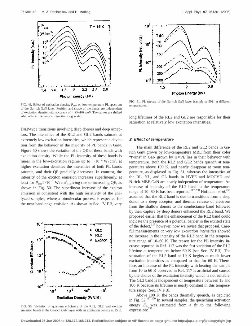
DAP-type transitions involving deep donors and deep accep-tors. The intensities of the RL2 and GL2 bands saturate atextremely low excitation intensities, which represent a devia-tion from the behavior of the majority of PL bands in GaN.Figure 50 shows the variation of the QE of these bands withexcitation density. While the PL intensity of these bands islinear in the low-excitation regime up to,10−4 W/cm2, athigher excitation densities the intensities of both PL bandssaturate, and their QE gradually decreases. In contrast, theintensity of the exciton emission increases superlinearly, atleast forPexc.10−1 W/cm2, giving rise to increasing QE, asshown in Fig. 50. The superlinear increase of the excitonemission is consistent with the high resistivity of the ana-lyzed samples, where a bimolecular process is expected forthe near-band-edge emission. As shown in Sec. IV F 3, very
long lifetimes of the RL2 and GL2 are responsible for theirsaturation at relatively low excitation intensities.
2. Effect of temperature
The main difference of the RL2 and GL2 bands in Ga-rich GaN grown by low-temperature MBE from their color“twins” in GaN grown by HVPE lies in their behavior withtemperature. Both the RL2 and GL2 bands quench at tem-peratures above 100 K, and nearly disappear at room tem-perature, as displayed in Fig. 51, whereas the intensities ofthe RL, YL, and GL bands in HVPE and MOCVD andN-rich-MBE GaN are nearly independent of temperature. Anincrease of intensity of the RL2 band in the temperaturerange of 10–60 K has been reported.117,250Hofmannet al.250
assumed that the RL2 band is due to transitions from a deepdonor to a deep acceptor, and thermal release of electronsfrom the shallow donors to the conductance band followedby their capture by deep donors enhanced the RL2 band. Weproposed earlier that the enhancement of the RL2 band couldindicate the presence of a potential barrier in the excited stateof the defect,117 however, now we revise that proposal. Care-ful measurementsat very low excitation intensitiesshowedno increase in the intensity of the RL2 band in the tempera-ture range of 10–60 K. The reason for the PL intensity in-crease reported in Ref. 117 was the fast variation of the RL2lifetime at temperatures below 60 Kssee Sec. IV F 3d. Thesaturation of the RL2 band at 10 K begins at much lowerexcitation intensities as compared to that for 60 K. There-fore, an increase of the PL intensity with heating the samplefrom 10 to 60 K observed in Ref. 117 is artificial and causedby the choice of the excitation intensity which is not suitable.The GL2 band is independent of temperature between 15 and100 K because its lifetime is nearly constant in this tempera-ture rangesSec. IV F 3d.
Above 100 K, the bands thermally quench, as depictedin Fig. 52.117,250In several samples, the quenching activationenergy EA was estimated from a fit to the followingexpression:251
FIG. 49. Effect of excitation density,Pexc, on low-temperature PL spectrumof the Ga-rich GaN layer. Position and shape of the bands are independentof excitation density with accuracy of6 s5–10d meV. The curves are shiftedarbitrarily in the vertical directionslog scaled.
FIG. 50. Variation of quantum efficiency of the RL2, GL2, and excitonemission bands in the Ga-rich GaN layer with an excitation density at 15 K.
FIG. 51. PL spectra of the Ga-rich GaN layerssample svt591d at differenttemperatures.
061301-43 M. A. Reshchikov and H. Morkoç J. Appl. Phys. 97, 061301 ~2005!
Downloaded 05 Jun 2008 to 128.172.168.214. Redistribution subject to AIP license or copyright; see http://jap.aip.org/jap/copyright.jsp
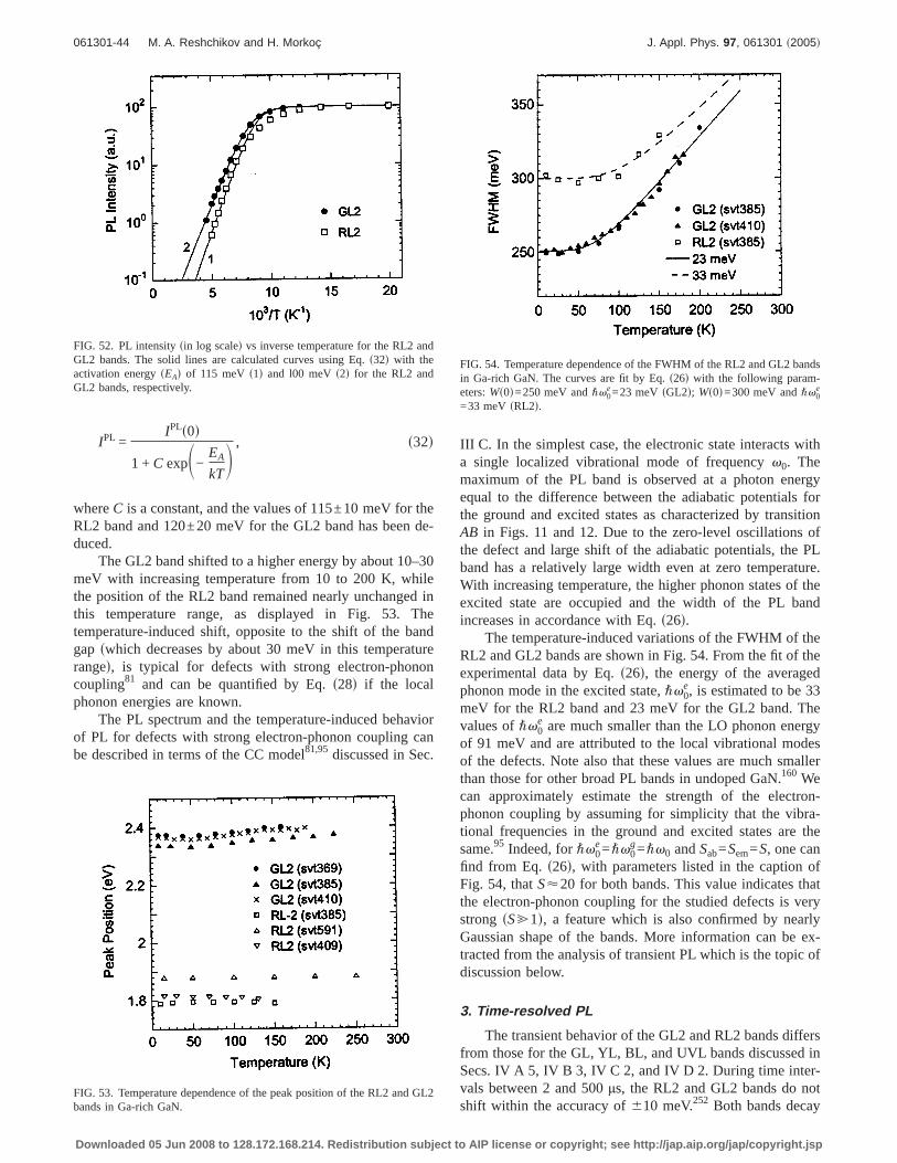
IPL =IPLs0d
1 + C expS−EA
kTD , s32d
whereC is a constant, and the values of 115±10 meV for theRL2 band and 120±20 meV for the GL2 band has been de-duced.
The GL2 band shifted to a higher energy by about 10–30meV with increasing temperature from 10 to 200 K, whilethe position of the RL2 band remained nearly unchanged inthis temperature range, as displayed in Fig. 53. Thetemperature-induced shift, opposite to the shift of the bandgap swhich decreases by about 30 meV in this temperatureranged, is typical for defects with strong electron-phononcoupling81 and can be quantified by Eq.s28d if the localphonon energies are known.
The PL spectrum and the temperature-induced behaviorof PL for defects with strong electron-phonon coupling canbe described in terms of the CC model81,95 discussed in Sec.
III C. In the simplest case, the electronic state interacts witha single localized vibrational mode of frequencyv0. Themaximum of the PL band is observed at a photon energyequal to the difference between the adiabatic potentials forthe ground and excited states as characterized by transitionAB in Figs. 11 and 12. Due to the zero-level oscillations ofthe defect and large shift of the adiabatic potentials, the PLband has a relatively large width even at zero temperature.With increasing temperature, the higher phonon states of theexcited state are occupied and the width of the PL bandincreases in accordance with Eq.s26d.
The temperature-induced variations of the FWHM of theRL2 and GL2 bands are shown in Fig. 54. From the fit of theexperimental data by Eq.s26d, the energy of the averagedphonon mode in the excited state,"v0
e, is estimated to be 33meV for the RL2 band and 23 meV for the GL2 band. Thevalues of"v0
e are much smaller than the LO phonon energyof 91 meV and are attributed to the local vibrational modesof the defects. Note also that these values are much smallerthan those for other broad PL bands in undoped GaN.160 Wecan approximately estimate the strength of the electron-phonon coupling by assuming for simplicity that the vibra-tional frequencies in the ground and excited states are thesame.95 Indeed, for"v0
e="v0g="v0 andSab=Sem=S, one can
find from Eq. s26d, with parameters listed in the caption ofFig. 54, thatS<20 for both bands. This value indicates thatthe electron-phonon coupling for the studied defects is verystrong sS@1d, a feature which is also confirmed by nearlyGaussian shape of the bands. More information can be ex-tracted from the analysis of transient PL which is the topic ofdiscussion below.
3. Time-resolved PL
The transient behavior of the GL2 and RL2 bands differsfrom those for the GL, YL, BL, and UVL bands discussed inSecs. IV A 5, IV B 3, IV C 2, and IV D 2. During time inter-vals between 2 and 500µs, the RL2 and GL2 bands do notshift within the accuracy of610 meV.252 Both bands decay
FIG. 52. PL intensitysin log scaled vs inverse temperature for the RL2 andGL2 bands. The solid lines are calculated curves using Eq.s32d with theactivation energysEAd of 115 meVs1d and l00 meVs2d for the RL2 andGL2 bands, respectively.
FIG. 53. Temperature dependence of the peak position of the RL2 and GL2bands in Ga-rich GaN.
FIG. 54. Temperature dependence of the FWHM of the RL2 and GL2 bandsin Ga-rich GaN. The curves are fit by Eq.s26d with the following param-eters:Ws0d=250 meV and"v0
e=23 meV sGL2d; Ws0d=300 meV and"v0e
=33 meVsRL2d.
061301-44 M. A. Reshchikov and H. Morkoç J. Appl. Phys. 97, 061301 ~2005!
Downloaded 05 Jun 2008 to 128.172.168.214. Redistribution subject to AIP license or copyright; see http://jap.aip.org/jap/copyright.jsp
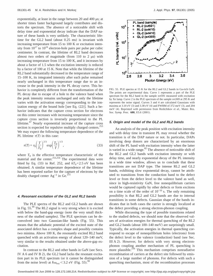
exponentially, at least in the range between 20 and 400µs; atshorter times faster background largely contributes and dis-torts the spectrum. The absence of a noticeable shift withdelay time and exponential decay indicate that the DAP na-ture of these bands is very unlikely. The characteristic life-time for the GL2 bandsabout 0.25 msd is invariant withincreasing temperature from 15 to 100 K or excitation inten-sity from 1017 to 1019 electron-hole pairs per pulse per cubiccentimeter. In contrast, the lifetime of RL2 band decreasesalmost two orders of magnitudesfrom 110 to 2 µsd withincreasing temperature from 15 to 100 K, and it increases byabout a factor of 1.5 when the excitation intensity is reducedby a factor of 100 at 15 K. Note that while the lifetime of theRL2 band substantially decreased in the temperature range of15–100 K, its integrated intensity after each pulse remainednearly unchanged in this temperature range due to an in-crease in the peak intensity in the PL decay curve. This be-havior is completely different from the transformation of thePL decay due to escape of a hole to the valence band whenthe peak intensity remains unchanged and only the lifetimevaries with the activation energy corresponding to the ion-ization energy of the bound holefsee Eq.s22dg. Such a be-havior indicates that the capture cross section for electronson this center increases with increasing temperature since thecapture cross section is inversely proportional to the PLlifetime.67 Nearly exponential increase of the capture crosssection is expected for repulsive multiply charged centers.253
We may expect the following temperature dependence of thePL lifetime tsTd in this case:
tsTd = t0S T
T0D2/3
expST0
TD1/3
, s33d
where T0 is the effective temperature characteristic of thematerial and the center.253,254 The experimental data werefitted by Eq. s33d in Ref. 252, andkT0=2.5 eV has beenobtained. A similar temperature dependence of the lifetimehas been reported earlier for the capture of electrons by thedoubly charged center Ag−2 in Ge.255
4. Resonant excitation of the GL2 and RL2 bands
The PLE spectra of the RL2 and GL2 bands are shownin Fig. 55.99 The RL2 signal is very strong when it is excitedwith below the band-gap energysnote the very small thick-ness of the studied samplesd. The PLE spectrum can be de-convolved into two Gaussian-like bandssFig. 55d. Thismeans that the adiabatic potential of the excited state of theassociated defect has a complex shape and possibly containstwo minima. Above 100 K, the resonantly excited RL2 bandquenched with an activation energy of about 120–140 meV,very similar to the results obtained under the above-gap ex-citation.
In contrast to the RL2 and other bands in GaNssee Secs.IV A 6 and IV B 2d, the GL2 band lacks the resonant excita-tion part in its PLE spectrumsor it cannot be distinguishedfrom the noise leveld at "vexc,3.2 eV sFig. 55d.99
5. Origin and model of the GL2 and RL2 bands
An analysis of the peak position with excitation intensityand with delay time in transient PL may reveal whether thetransition is of the DAP nature or not. In particular, DAPsinvolving deep donors are characterized by an enormousshift of the PL band with excitation intensity when the latteris varied in a wide range.82 The absence of noticeable shift ofthe RL2 and GL2 bands with excitation intensity or withdelay time, and nearly exponential decay of the PL intensityin a wide time window, allows us to conclude that thesetransitions are not DAP type. The intense RL2 and GL2bands, exhibiting slow exponential decay, cannot be attrib-uted to transitions from the conduction band to the defectlevel or from the defect level to the valence band as well,since in high-resistivity GaN, free nonequilibrium carrierswould be captured rapidly by other defects or form excitonson a time scale of the order of 10−10 s. The only remainingpossibility is that RL2 and GL2 bands are due to internaltransitions in some defects. Gaussian shape of the bands in-dicates that in both cases the carrier is strongly localized atthe defect providing a strong electron-phonon coupling.
While discussing the type of possible transitions relatedto the studied defects, we should note that the observed val-ues of activation energies for thermal quenching of the RL2and GL2 bandssabout 100–140 meVd are surprisingly small.Typically, the activation energies in thermal quenching cor-respond to escape of nonequilibrium holesselectronsd fromthe defect level to the valencesconductiond band ssee Sec.III A 2 d. However, for defects with very strong electron-phonon coupling another mechanism of PL quenching ismore plausible.256 This mechanism comprises nonradiativerecombination of carriers at the defect site followed by emis-sion of a large number of phonons. For defects with such aquenching mechanism, most of the recombination processes
FIG. 55. PLE spectra at 15 K for the RL2 and GL2 bands in Ga-rich GaN.The points are experimental data. Curve 1 represents a part of the PLEspectrum for the RL2 band in the sample svt591 measured with excitationby Xe lamp. Curve 2 is the PLE spectrum of the sample svt369 at 295 K andrepresents the noise signal. Curves 3 and 4 are calculated Gaussians withmaxima at 3.10 eVs3d and 3.38 eVs4d and FWHM of 372 meVs3d, and 204meV s4d. Reprinted with permission from Reshchikovet al., Mater. Res.Soc. Symp. Proc.680, E5.6 s2001d.
061301-45 M. A. Reshchikov and H. Morkoç J. Appl. Phys. 97, 061301 ~2005!
Downloaded 05 Jun 2008 to 128.172.168.214. Redistribution subject to AIP license or copyright; see http://jap.aip.org/jap/copyright.jsp
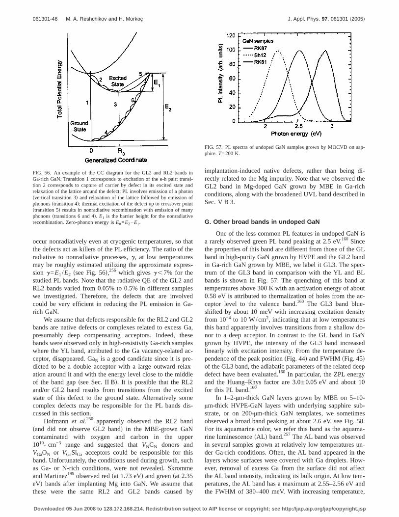
occur nonradiatively even at cryogenic temperatures, so thatthe defects act as killers of the PL efficiency. The ratio of theradiative to nonradiative processes,g, at low temperaturesmay be roughly estimated utilizing the approximate expres-sion g=E1/E2 ssee Fig. 56d,256 which givesg,7% for thestudied PL bands. Note that the radiative QE of the GL2 andRL2 bands varied from 0.05% to 0.5% in different sampleswe investigated. Therefore, the defects that are involvedcould be very efficient in reducing the PL emission in Ga-rich GaN.
We assume that defects responsible for the RL2 and GL2bands are native defects or complexes related to excess Ga,presumably deep compensating acceptors. Indeed, thesebands were observed only in high-resistivity Ga-rich sampleswhere the YL band, attributed to the Ga vacancy-related ac-ceptor, disappeared. GaN is a good candidate since it is pre-dicted to be a double acceptor with a large outward relax-ation around it and with the energy level close to the middleof the band gapssee Sec. II Bd. It is possible that the RL2and/or GL2 band results from transitions from the excitedstate of this defect to the ground state. Alternatively somecomplex defects may be responsible for the PL bands dis-cussed in this section.
Hofmann et al.250 apparently observed the RL2 bandsand did not observe GL2 bandd in the MBE-grown GaNcontaminated with oxygen and carbon in the upper1019- cm−3 range and suggested thatVNCN donors andVGaON or VGaSiGa acceptors could be responsible for thisband. Unfortunately, the conditions used during growth, suchas Ga- or N-rich conditions, were not revealed. Skrommeand Martinez199 observed redsat 1.73 eVd and greensat 2.35eVd bands after implanting Mg into GaN. We assume thatthese were the same RL2 and GL2 bands caused by
implantation-induced native defects, rather than being di-rectly related to the Mg impurity. Note that we observed theGL2 band in Mg-doped GaN grown by MBE in Ga-richconditions, along with the broadened UVL band described inSec. V B 3.
G. Other broad bands in undoped GaN
One of the less common PL features in undoped GaN isa rarely observed green PL band peaking at 2.5 eV.160 Sincethe properties of this band are different from those of the GLband in high-purity GaN grown by HVPE and the GL2 bandin Ga-rich GaN grown by MBE, we label it GL3. The spec-trum of the GL3 band in comparison with the YL and BLbands is shown in Fig. 57. The quenching of this band attemperatures above 300 K with an activation energy of about0.58 eV is attributed to thermalization of holes from the ac-ceptor level to the valence band.160 The GL3 band blue-shifted by about 10 meV with increasing excitation densityfrom 10−4 to 10 W/cm2, indicating that at low temperaturesthis band apparently involves transitions from a shallow do-nor to a deep acceptor. In contrast to the GL band in GaNgrown by HVPE, the intensity of the GL3 band increasedlinearly with excitation intensity. From the temperature de-pendence of the peak positionsFig. 44d and FWHMsFig. 45dof the GL3 band, the adiabatic parameters of the related deepdefect have been evaluated.160 In particular, the ZPL energyand the Huang–Rhys factor are 3.0±0.05 eV and about 10for this PL band.160
In 1–2-µm-thick GaN layers grown by MBE on 5–10-µm-thick HVPE-GaN layers with underlying sapphire sub-strate, or on 200-µm-thick GaN templates, we sometimesobserved a broad band peaking at about 2.6 eV, see Fig. 58.For its aquamarine color, we refer this band as the aquama-rine luminescencesAL d band.257 The AL band was observedin several samples grown at relatively low temperatures un-der Ga-rich conditions. Often, the AL band appeared in thelayers whose surfaces were covered with Ga droplets. How-ever, removal of excess Ga from the surface did not affectthe AL band intensity, indicating its bulk origin. At low tem-peratures, the AL band has a maximum at 2.55–2.56 eV andthe FWHM of 380–400 meV. With increasing temperature,
FIG. 56. An example of the CC diagram for the GL2 and RL2 bands inGa-rich GaN. Transition 1 corresponds to excitation of the e-h pair; transi-tion 2 corresponds to capture of carrier by defect in its excited state andrelaxation of the lattice around the defect; PL involves emission of a photonsvertical transition 3d and relaxation of the lattice followed by emission ofphononsstransition 4d; thermal excitation of the defect up to crossover pointstransition 5d results in nonradiative recombination with emission of manyphononsstransitions 6 and 4d. E1 is the barrier height for the nonradiativerecombination. Zero-phonon energy isE0=E2−E1.
FIG. 57. PL spectra of undoped GaN samples grown by MOCVD on sap-phire.T=200 K.
061301-46 M. A. Reshchikov and H. Morkoç J. Appl. Phys. 97, 061301 ~2005!
Downloaded 05 Jun 2008 to 128.172.168.214. Redistribution subject to AIP license or copyright; see http://jap.aip.org/jap/copyright.jsp
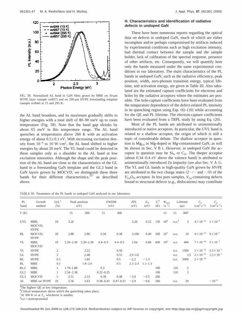
the AL band broadens, and its maximum gradually shifts tohigher energies with a total shift of 80–90 meV up to roomtemperaturesFig. 58d. Note that the band gap shrinks byabout 65 meV in this temperature range. The AL bandquenches at temperatures above 260 K with an activationenergy of about 0.5±0.1 eV. With increasing excitation den-sity from 10−4 to 10 W/cm2, the AL band shifted to higherenergies by about 20 meV. The YL band could be detected inthese samples only as a shoulder to the AL band at lowexcitation intensities. Although the shape and the peak posi-tion of the AL band are close to the characteristics of the GLband in a freestanding GaN template and the GL3 band inGaN layers grown by MOCVD, we distinguish these threebands for their different characteristics,257 as describedabove.
H. Characteristics and identification of radiativedefects in undoped GaN
There have been numerous reports regarding the opticaldata on defects in undoped GaN, much of which are eitherincomplete and/or perhaps compromised by artifacts inducedby experimental conditions such as high excitation intensity,bad thermal contact between the sample and the sampleholder, lack of calibration of the spectral response, presenceof other artifacts, etc. Consequently, we will quantify hereonly the bands measured under the same experimental con-ditions in our laboratory. The main characteristics of the PLbands in undoped GaN, such as the radiative efficiency, peakposition, width, zero-phonon transition energy, typical life-time, and activation energy, are given in Table III. Also tabu-lated are the estimated capture coefficients for electrons andholes by the radiative acceptors where the estimates are pos-sible. The hole-capture coefficients have been evaluated fromthe temperature dependence of the defect-related PL intensityin its quenching region using Eqs.s6d–s10d while accountingfor the QE and PL lifetime. The electron-capture coefficientshave been evaluated from a TRPL study by using Eq.s20d.
Most of the PL bands are attributed to unintentionallyintroduced or native acceptors. In particular, the UVL band isrelated to a shallow acceptor, the origin of which is still atopic of considerable debate. The shallow acceptor in ques-tion is MgGa in Mg-doped or Mg-contaminated GaN, as willbe shown in Sec. V B 1. However, in undoped GaN the ac-ceptor in question may be SiN or CN. The deeper acceptorsabout 0.34–0.4 eV above the valence bandd is attributed tounintentionally introduced Zn impurityssee also Sec. V A 1d.The YL and GL bands in high-quality GaN grown by HVPEare attributed to the two charge statess2− /− and −/0d of theVGaON acceptor. In less pure samples,VGa-containing defectsbound to structural defectsse.g., dislocationsd may contribute
FIG. 58. Normalized AL band in GaN films grown by MBE on 10-µmHVPE layer ssample svt857d and on 200-µm HVPE freestanding templatessample svt844d at 15 and 295 K.
TABLE III. Parameters of the PL bands in undoped GaN analyzed in our laboratory.
PLband
Growthmethod
Q.E.a
s%dPeak position
seVdFWHM
seVdZPLseVd
EA
seVdTc
b
sKdWmax
ss−1dLifetime
sµsdCn
scm3 s−1dCp
scm3 s−1d
T sKd 15 300 15 300 15 15 300c
UVL MBE,MOCVD,HVPE
10 3.26 3.26 0.22 130 108 n.e.d 3 4310−12 1310−6
BL MOCVD,HVPE
20 2.88 2.86 0.34 0.38 3.100 0.40 200 107 n.e. 10 4310−13 9310−7
YL MBE,MOCVD
10 2.20–2.30 2.20–2.30 0.4–0.5 0.4–0.5 2.64 0.86 600 106 n.e. 400 7310−14 3310−7
YL HVPE 2 2.22 0.58 n.e. 1500 1310−13 3.3310−7
GL HVPE 2 2.48 0.53 2.9–3.0 n.e. 3.5 2310−12 1.5310−7
RL HVPE 0.1 1.85 0.5 ,2.2 ,1.3 n.e. 5000 2310−14
RL MBE 0.1 1.8–2.0 0.5 2.2–2.4 1.1–1.3RL2 MBE 1 1.79–1.88 0.3 100 110 2GL2 MBE 1 2.34–2.38 0.22–0.25 100 110 2GL3 MOCVD 5 2.51 2.53 0.39 0.48 ,3.0 ,0.5 280AL MBE on HVPE 10 2.56 2.63 0.38–0.41 0.47–0.51,2.9 ,0.6 260 n.e. 20 ,10−6
aThe highest QE at low temperature.bCritical temperature above which the quenching takes place.cAt 300 K or atTc, whichever is smaller.dn.e.5nonexponential
061301-47 M. A. Reshchikov and H. Morkoç J. Appl. Phys. 97, 061301 ~2005!
Downloaded 05 Jun 2008 to 128.172.168.214. Redistribution subject to AIP license or copyright; see http://jap.aip.org/jap/copyright.jsp
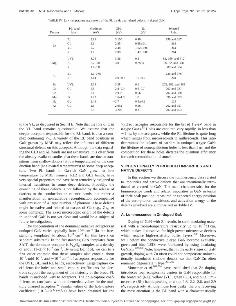
to the YL, as discussed in Sec. II E. Note that the role of C inthe YL band remains questionable. We assume that thedeeper acceptor, responsible for the RL band, is also a com-plex containingVGa. A variety of the RL band positions inGaN grown by MBE may reflect the influence of differentstructural defects on this acceptor. Although the data regard-ing the GL3 and AL bands are not exhaustive, it is clear fromthe already available studies that these bands are due to tran-sitions from shallow donorssat low temperaturesd or the con-duction bandsat elevated temperaturesd to some deep accep-tors. Two PL bands in Ga-rich GaN grown at lowtemperature by MBE, namely, RL2 and GL2 bands, havevery special properties and have been tentatively assigned tointernal transitions in some deep defects. Probably, thequenching of these defects is not followed by the release ofcarriers to the conduction or valence bands, but rather amanifestation of nonradiative recombination accompaniedwith emission of a large number of phonons. These defectsmight be native and related to excess of Gase.g., GaN orsome complexd. The exact microscopic origin of the defectsin undoped GaN is not yet clear and would be a subject offuture investigations.
The concentration of the dominant radiative acceptors inundoped GaN varies typically from 1015 cm−3 sin the free-standing templatesd to about 1017 cm−3 sin thin layers onsapphire substrated. In the freestanding GaN templates fromSAIT, the dominant acceptor isVGaON complex at a densityof abouts1–2d31015 cm−3. By using Eq.s15d, we can to afirst order estimate that these samples also contain about1015, mid-1014, and,1014 cm−3 of acceptors responsible forthe UVL, BL, and RL bands, respectively. Large capture co-efficients for holes and small capture coefficients for elec-trons support the assignment of the majority of the broad PLbands in undoped GaN to acceptors. The hole-capture coef-ficients are consistent with the theoretical values for the mul-tiply charged acceptors.67 Similar values of the hole-capturecoefficient s10−7–10−6 cm3/sd have been obtained for the
VGaTeAs acceptor responsible for the broad 1.2-eV band inn-type GaAs.92 Holes are captured very rapidly, in less than,1 ns, by the acceptors, while the PL lifetime is quite longwhich ranges from microseconds to milliseconds. This ratiodetermines the balance of carriers in undopedn-type GaN:the lifetime of nonequilibrium holes is less than l ns, and thecompetition for these holes dictates the quantum efficiencyfor each recombination channel.
V. INTENTIONALLY INTRODUCED IMPURITIES ANDNATIVE DEFECTS
In this section we discuss the luminescence data relatedto impurities and native defects that are intentionally intro-duced or created in GaN. The main characteristics for theluminescence bands and related impurities in GaN in termsof their peak position, measured or expected energy positionof the zero-phonon transitions, and activation energy of thedefects involved are summarized in Table IV.
A. Luminescence in Zn-doped GaN
Doping of GaN with Zn results in semi-insulating mate-rial with a room-temperature resistivity up to 1012 V cm,which makes it attractive for high-power microwave deviceswhich require high-resistivity buffer layers.258 Moreover,well before the conductivep-type GaN became available,green and blue LEDs were fabricated by using insulatingGaN:Zn.259,260Note, however, that in the early stages of GaNgrowth, doping with Zn often could not compensate uninten-tionally introduced shallow donors, so that GaN:Zn oftenremained degeneraten type.261,262
Monemaret al.263,264 have established that Zn dopingintroduces four acceptorlike centers in GaN responsible forthe broad redsRLd, yellow sYL d, greensGLd, and blue lumi-nescencesBLd bands peaking at about 1.8, 2.2, 2.6, and 2.9eV, respectively. Among those four peaks, the one receivingthe most attention is the BL band with a characteristically
TABLE IV. Low-temperature parameters of the PL bands and related defects in doped GaN.
DopantPL band
labelMaximum
seVdZPLseVd
EA
seVdSelected
Refs.
Zn
BL 2.88 3.100 0.40 199 and 267GL 2.6 2.85 0.65±0.1 264YL 2.2 2.48 1.02±0.05 264RL 1.8 2.08 1.42±0.08 264
MgUVL 3.26 3.26 0.2 82, 199, and 312BL 2.7–3.0 ,3.0 0.2;0.4 56, 82, and 308RL 1.7–1.8 309 and 354
CBL 3.0–3.05 136 and 376RL 1.64 2.0±0.2 1.5±0.2 204
Be UVL 3.38 3.38 0.1 203, 382, and 383Ca GL 2.5 2.8–2.9 0.6–0.7 202 and 387Cd BL 2.8 2.937 0.56 202 and 388Mn IR 1.27 1.6–1.8 1.8 396 and 393Hg GL 2.43 ,2.7 0.8±0.2 123As GL 2.6 2.952 0.56 202 and 397P BL 2.9 3.200 0.31 202 and 403
061301-48 M. A. Reshchikov and H. Morkoç J. Appl. Phys. 97, 061301 ~2005!
Downloaded 05 Jun 2008 to 128.172.168.214. Redistribution subject to AIP license or copyright; see http://jap.aip.org/jap/copyright.jsp
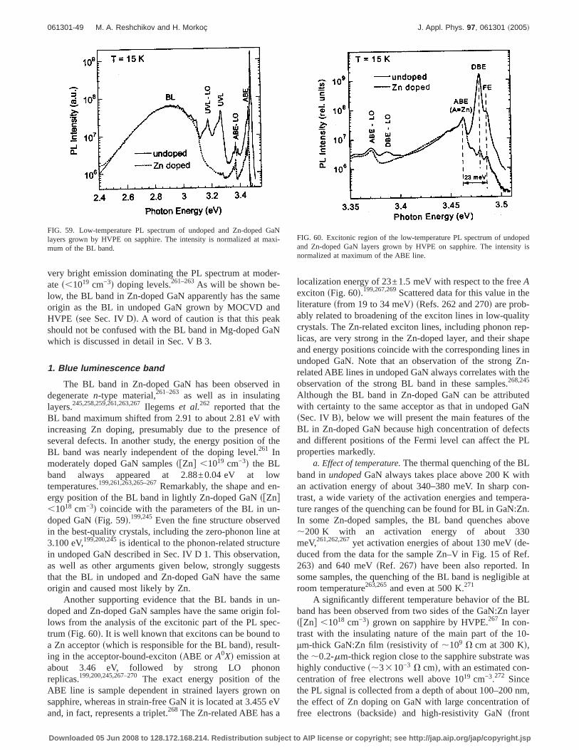
very bright emission dominating the PL spectrum at moder-ate s,1019 cm−3d doping levels.261–263As will be shown be-low, the BL band in Zn-doped GaN apparently has the sameorigin as the BL in undoped GaN grown by MOCVD andHVPE ssee Sec. IV Dd. A word of caution is that this peakshould not be confused with the BL band in Mg-doped GaNwhich is discussed in detail in Sec. V B 3.
1. Blue luminescence band
The BL band in Zn-doped GaN has been observed indegeneraten-type material,261–263 as well as in insulatinglayers.245,258,259,261,263,267Ilegemset al.262 reported that theBL band maximum shifted from 2.91 to about 2.81 eV withincreasing Zn doping, presumably due to the presence ofseveral defects. In another study, the energy position of theBL band was nearly independent of the doping level.261 Inmoderately doped GaN samplessfZng ,1019 cm−3d the BLband always appeared at 2.88±0.04 eV at lowtemperatures.199,261,263,265–267Remarkably, the shape and en-ergy position of the BL band in lightly Zn-doped GaNsfZng,1018 cm−3d coincide with the parameters of the BL in un-doped GaNsFig. 59d.199,245Even the fine structure observedin the best-quality crystals, including the zero-phonon line at3.100 eV,199,200,245is identical to the phonon-related structurein undoped GaN described in Sec. IV D 1. This observation,as well as other arguments given below, strongly suggeststhat the BL in undoped and Zn-doped GaN have the sameorigin and caused most likely by Zn.
Another supporting evidence that the BL bands in un-doped and Zn-doped GaN samples have the same origin fol-lows from the analysis of the excitonic part of the PL spec-trum sFig. 60d. It is well known that excitons can be bound toa Zn acceptorswhich is responsible for the BL bandd, result-ing in the acceptor-bound-excitonsABE or A0Xd emission atabout 3.46 eV, followed by strong LO phononreplicas.199,200,245,267–270The exact energy position of theABE line is sample dependent in strained layers grown onsapphire, whereas in strain-free GaN it is located at 3.455 eVand, in fact, represents a triplet.268 The Zn-related ABE has a
localization energy of 23±1.5 meV with respect to the freeAexcitonsFig. 60d.199,267,269Scattered data for this value in theliteraturesfrom 19 to 34 meVd sRefs. 262 and 270d are prob-ably related to broadening of the exciton lines in low-qualitycrystals. The Zn-related exciton lines, including phonon rep-licas, are very strong in the Zn-doped layer, and their shapeand energy positions coincide with the corresponding lines inundoped GaN. Note that an observation of the strong Zn-related ABE lines in undoped GaN always correlates with theobservation of the strong BL band in these samples.268,245
Although the BL band in Zn-doped GaN can be attributedwith certainty to the same acceptor as that in undoped GaNsSec. IV Bd, below we will present the main features of theBL in Zn-doped GaN because high concentration of defectsand different positions of the Fermi level can affect the PLproperties markedly.
a. Effect of temperature.The thermal quenching of the BLband inundopedGaN always takes place above 200 K withan activation energy of about 340–380 meV. In sharp con-trast, a wide variety of the activation energies and tempera-ture ranges of the quenching can be found for BL in GaN:Zn.In some Zn-doped samples, the BL band quenches above,200 K with an activation energy of about 330meV,261,262,267yet activation energies of about 130 meVsde-duced from the data for the sample Zn–V in Fig. 15 of Ref.263d and 640 meVsRef. 267d have been also reported. Insome samples, the quenching of the BL band is negligible atroom temperature263,265and even at 500 K.271
A significantly different temperature behavior of the BLband has been observed from two sides of the GaN:Zn layersfZng ,1018 cm−3d grown on sapphire by HVPE.267 In con-trast with the insulating nature of the main part of the 10-µm-thick GaN:Zn filmsresistivity of ,109 V cm at 300 Kd,the,0.2-mm-thick region close to the sapphire substrate washighly conductives,3310−3 V cmd, with an estimated con-centration of free electrons well above 1019 cm−3.272 Sincethe PL signal is collected from a depth of about 100–200 nm,the effect of Zn doping on GaN with large concentration offree electronssbacksided and high-resistivity GaNsfront
FIG. 59. Low-temperature PL spectrum of undoped and Zn-doped GaNlayers grown by HVPE on sapphire. The intensity is normalized at maxi-mum of the BL band.
FIG. 60. Excitonic region of the low-temperature PL spectrum of undopedand Zn-doped GaN layers grown by HVPE on sapphire. The intensity isnormalized at maximum of the ABE line.
061301-49 M. A. Reshchikov and H. Morkoç J. Appl. Phys. 97, 061301 ~2005!
Downloaded 05 Jun 2008 to 128.172.168.214. Redistribution subject to AIP license or copyright; see http://jap.aip.org/jap/copyright.jsp
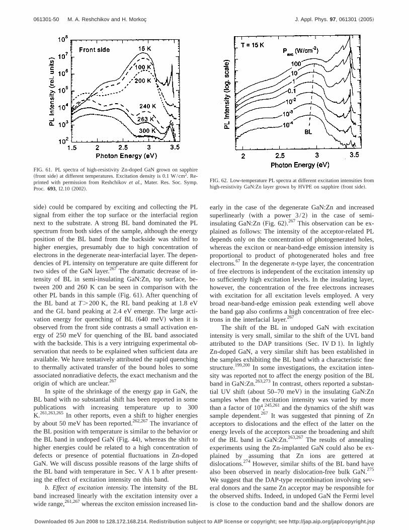
sided could be compared by exciting and collecting the PLsignal from either the top surface or the interfacial regionnext to the substrate. A strong BL band dominated the PLspectrum from both sides of the sample, although the energyposition of the BL band from the backside was shifted tohigher energies, presumably due to high concentration ofelectrons in the degenerate near-interfacial layer. The depen-dencies of PL intensity on temperature are quite different fortwo sides of the GaN layer.267 The dramatic decrease of in-tensity of BL in semi-insulating GaN:Zn, top surface, be-tween 200 and 260 K can be seen in comparison with theother PL bands in this samplesFig. 61d. After quenching ofthe BL band atT.200 K, the RL band peaking at 1.8 eVand the GL band peaking at 2.4 eV emerge. The large acti-vation energy for quenching of BLs640 meVd when it isobserved from the front side contrasts a small activation en-ergy of 250 meV for quenching of the BL band associatedwith the backside. This is a very intriguing experimental ob-servation that needs to be explained when sufficient data areavailable. We have tentatively attributed the rapid quenchingto thermally activated transfer of the bound holes to someassociated nonradiative defects, the exact mechanism and theorigin of which are unclear.267
In spite of the shrinkage of the energy gap in GaN, theBL band with no substantial shift has been reported in somepublications with increasing temperature up to 300K.261,263,265In other reports, even a shift to higher energiesby about 50 meV has been reported.262,267The invariance ofthe BL position with temperature is similar to the behavior orthe BL band in undoped GaNsFig. 44d, whereas the shift tohigher energies could be related to a high concentration ofdefects or presence of potential fluctuations in Zn-dopedGaN. We will discuss possible reasons of the large shifts ofthe BL band with temperature in Sec.V A 1 b after present-ing the effect of excitation intensity on this band.
b. Effect of excitation intensity.The intensity of the BLband increased linearly with the excitation intensity over awide range,261,267whereas the exciton emission increased lin-
early in the case of the degenerate GaN:Zn and increasedsuperlinearly swith a power 3/2d in the case of semi-insulating GaN:ZnsFig. 62d.267 This observation can be ex-plained as follows: The intensity of the acceptor-related PLdepends only on the concentration of photogenerated holes,whereas the exciton or near-band-edge emission intensity isproportional to product of photogenerated holes and freeelectrons.67 In the degeneraten-type layer, the concentrationof free electrons is independent of the excitation intensity upto sufficiently high excitation levels. In the insulating layer,however, the concentration of the free electrons increaseswith excitation for all excitation levels employed. A verybroad near-band-edge emission peak extending well abovethe band gap also confirms a high concentration of free elec-trons in the interfacial layer.267
The shift of the BL in undoped GaN with excitationintensity is very small, similar to the shift of the UVL bandattributed to the DAP transitionssSec. IV D 1d. In lightlyZn-doped GaN, a very similar shift has been established inthe samples exhibiting the BL band with a characteristic finestructure.199,200 In some investigations, the excitation inten-sity was reported not to affect the energy position of the BLband in GaN:Zn.263,273In contrast, others reported a substan-tial UV shift sabout 50–70 meVd in the insulating GaN:Znsamples when the excitation intensity was varied by morethan a factor of 104,245,261and the dynamics of the shift wassample dependent.267 It was suggested that pinning of Znacceptors to dislocations and the effect of the latter on theenergy levels of the acceptors cause the broadening and shiftof the BL band in GaN:Zn.263,267 The results of annealingexperiments using the Zn-implanted GaN could also be ex-plained by assuming that Zn ions are gettered atdislocations.274 However, similar shifts of the BL band havealso been observed in nearly dislocation-free bulk GaN.275
We suggest that the DAP-type recombination involving sev-eral donors and the same Zn acceptor may be responsible forthe observed shifts. Indeed, in undoped GaN the Fermi levelis close to the conduction band and the shallow donors are
FIG. 61. PL spectra of high-resistivity Zn-doped GaN grown on sapphiresfront sided at different temperatures. Excitation density is 0.1 W/cm2. Re-printed with permission from Reshchikovet al., Mater. Res. Soc. Symp.Proc. 693, I2.10 s2002d.
FIG. 62. Low-temperature PL spectra at different excitation intensities fromhigh-resistivity GaN:Zn layer grown by HVPE on sapphiresfront sided.
061301-50 M. A. Reshchikov and H. Morkoç J. Appl. Phys. 97, 061301 ~2005!
Downloaded 05 Jun 2008 to 128.172.168.214. Redistribution subject to AIP license or copyright; see http://jap.aip.org/jap/copyright.jsp

mostly filled with electrons at low temperatures. The prob-ability of the DAP transition decreases exponentially fordeeper donors due to a smaller overlap of the electron andhole wave functions. Note also the relatively high concentra-tion of shallow donors in undoped GaN. Therefore, the con-tribution to the BL band from deeper donors may be ne-glected inn-type conductive GaN. In contrast, the shallowdonors may contribute much less due to their smaller occu-pancy in semi-insulating GaN:Zn. The transitions fromdeeper donors are slower and, hence, with increasing excita-tion density the intensity of transitions involving the deeperdonors would begin to saturate at relatively lower excitationlevels, causing a shift of the broad band with excitation in-tensity. Another manifestation of this effect is the shift of thePL band with the delay time, as discussed below.
c. Time-resolved PL.TRPL studies have revealed a nearlyexponential decay of the BL band in GaN:Zn with a lifetimeof about 300–400 ns,262,266 which is independent of Zndoping.262 Slower decays have been observed in insulatingGaN:Zn.245,261,267Some of the experimental observations ap-pear unusual and need further explanation. According to Eq.s20d, the PL lifetime should be inversely proportional to theelectron concentration inn-type GaN. In the semi-insulatingmaterial, however, the lifetime may be sensitive to the exci-tation intensity since the latter may affect the concentrationof electrons in the conduction band. However, the decay ofthe BL in high-resistivity GaN:Zn did not change when theexcitation intensity was varied by a factor of 105.267 More-over, similar lifetimess300–400 nsd have been obtained forthe conductiven-type GaN:Zn samples with the free-electronconcentrations of ,1018 cm−3 sRef. 266d and s1–6d31019 cm−3.262 Earlier, we suggested that BL in GaN:Zn in-volves transitions not from the conduction band but from theexcited state of the Zn-related defect, which would result in alifetime independent of carrier concentration. However, nowit is firmly established that in undoped and lightly Zn-dopedGaN the BL band is caused by transitions from the shallowdonorssat low temperatured and from the conduction bandsat elevated temperaturesd to the Zn-related acceptor. More-over, in different semi-insulating GaN:Zn samples the decayof the BL is not identical, as displayed in Fig. 63. In thisfigure we also show, for comparison, the decay of the BLband in undoped and Si-doped GaN samples with concentra-tion of the shallow donors of 631017 and 331018 cm−3,respectively. The decays are nonexponential as it is expectedfor the DAP recombination at low temperatures. Inn-typeconductive material, the decay rate correlates with the con-centration of shallow donorsssee Sec. III Bd. In semi-insulating Zn-doped layers, the decay is distinctive for eachsample because the distribution of the shallow and not veryshallow donor states may be different in these samples.245
Similar to the TRPL results on the BL band in undoped GaNsSec. IV D 2d, the lifetime of BL in GaN:Zn decreases above,200 K with an activation energy of about 300–400 meV,245
consistent with Eq.s22d.No shift in the BL band with delay time has been de-
tected in degenerate GaN:Zn.262 In contrast, Khanet al.265
observed a redshift of,20 meV after 0.8µs, as well as twopeaks in the TRPL spectrum. We also observed a redshift of
up to 50 meV at 10µs after the excitation pulse in semi-insulating GaN:Zn. These shifts are consistent with themodel that several donors with ionization energies up toabout 100 meV contribute to the PL decay in high-resistivityGaN:Zn. Note that the origin of the shift of the BL band withexcitation intensity is different in Zn- and Mg-doped GaN, asdiscussed in Sec. V B 3.
d. Resonant excitation and vibrational properties.Mone-mar et al.264 investigated the BL band in Zn-doped GaNunder resonantsbelow-band-gapd excitation. In the PLEspectrum related to the BL band, a steep increase of theoptical cross sectionsabout four orders of magnituded hasbeen observed at photon energies between 3.0 and 3.25 eV.This PLE spectrum has been attributed to transitions fromthe Zn-related acceptor to the conduction band.264 With theaid of an analysis of the absorption spectrum, Monemaretal.264 have also estimated the absolute value of the opticalcross section for the BL band as approximately 10−16 cm2.
Although Monemaret al.263,264 identified the type oftransitions in GaN:Zn and thoroughly examined the role ofthe electron-phonon coupling in these transitions, their quan-titative results regarding the vibrational characteristics needto be revised in light of the recent data. It is well establishedthat interaction with locals,36 meVd and lattices91 meVdphonons is responsible for the characteristic fine structure ofthe BL band in undoped and Zn-doped GaN.116,199,200Thehigh-energy side of the BL band contains sharp peaks whilethe low-energy side is structurelesssFig. 42d, similar to otherclassical cases of the electron-phonon coupling insemiconductors.276 The fine structure observed in Ref. 263may actually be some sort of artifact rather than the result ofthe electron-phonon coupling for the following reasons:sidThe energy separation between peaks is 74±2 meV, which isdifferent from the known phonon modes in GaN;sii d thepeaks at the low-energy side are better resolved than those atthe high-energy side, which contradicts the commonobservations;116,276 siii d the zero-phonon line is very broad
FIG. 63. PL intensity decay of the BLsat 2.9 eVd in undopeds1011d,Si-dopeds1721d, and two Zn-dopeds560 and 1394d GaN layers grown byHVPE on sapphire. Note the logarithmic scales. Reprinted with permissionfrom Reshchikovet al., Mater. Res. Soc. Symp. Proc.693, I2.10 s2002d.
061301-51 M. A. Reshchikov and H. Morkoç J. Appl. Phys. 97, 061301 ~2005!
Downloaded 05 Jun 2008 to 128.172.168.214. Redistribution subject to AIP license or copyright; see http://jap.aip.org/jap/copyright.jsp
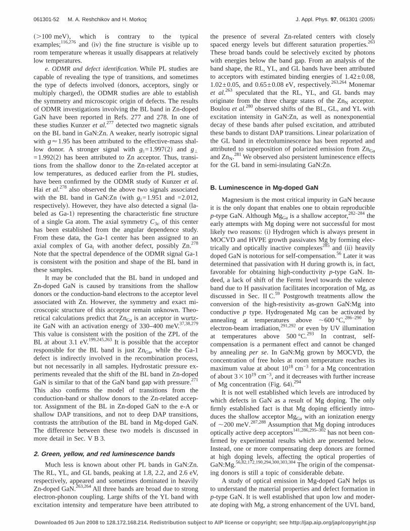
s.100 meVd, which is contrary to the typicalexamples;116,276 and sivd the fine structure is visible up toroom temperature whereas it usually disappears at relativelylow temperatures.
e. ODMR and defect identification.While PL studies arecapable of revealing the type of transitions, and sometimesthe type of defects involvedsdonors, acceptors, singly ormultiply chargedd, the ODMR studies are able to establishthe symmetry and microscopic origin of defects. The resultsof ODMR investigations involving the BL band in Zn-dopedGaN have been reported in Refs. 277 and 278. In one ofthese studies Kunzeret al.277 detected two magnetic signalson the BL band in GaN:Zn. A weaker, nearly isotropic signalwith g<1.95 has been attributed to the effective-mass shal-low donor. A stronger signal withgi=1.997s2d and g'
=1.992s2d has been attributed to Zn acceptor. Thus, transi-tions from the shallow donor to the Zn-related acceptor atlow temperatures, as deduced earlier from the PL studies,have been confirmed by the ODMR study of Kunzeret al.Hai et al.278 also observed the above two signals associatedwith the BL band in GaN:Znswith gi=1.951 and =2.012,respectivelyd. However, they have also detected a signalsla-beled as Ga-1d representing the characteristic fine structureof a single Ga atom. The axial symmetryC3v of this centerhas been established from the angular dependence study.From these data, the Ga-1 center has been assigned to anaxial complex of Gai with another defect, possibly Zn.278
Note that the spectral dependence of the ODMR signal Ga-1is consistent with the position and shape of the BL band inthese samples.
It may be concluded that the BL band in undoped andZn-doped GaN is caused by transitions from the shallowdonors or the conduction-band electrons to the acceptor levelassociated with Zn. However, the symmetry and exact mi-croscopic structure of this acceptor remain unknown. Theo-retical calculations predict that ZnGa is an acceptor in wurtz-ite GaN with an activation energy of 330–400 meV.37,38,279
This value is consistent with the position of the ZPL of theBL at about 3.1 eV.199,245,263It is possible that the acceptorresponsible for the BL band is just ZnGa, while the Ga-1defect is indirectly involved in the recombination process,but not necessarily in all samples. Hydrostatic pressure ex-periments revealed that the shift of the BL band in Zn-dopedGaN is similar to that of the GaN band gap with pressure.271
This also confirms the model of transitions from theconduction-band or shallow donors to the Zn-related accep-tor. Assignment of the BL in Zn-doped GaN to the e-A orshallow DAP transitions, and not to deep DAP transitions,contrasts the attribution of the BL band in Mg-doped GaN.The difference between these two models is discussed inmore detail in Sec. V B 3.
2. Green, yellow, and red luminescence bands
Much less is known about other PL bands in GaN:Zn.The RL, YL, and GL bands, peaking at 1.8, 2.2, and 2.6 eV,respectively, appeared and sometimes dominated in heavilyZn-doped GaN.263,264All three bands are broad due to strongelectron-phonon coupling. Large shifts of the YL band withexcitation intensity and temperature have been attributed to
the presence of several Zn-related centers with closelyspaced energy levels but different saturation properties.263
These broad bands could be selectively excited by photonswith energies below the band gap. From an analysis of theband shape, the RL, YL, and GL bands have been attributedto acceptors with estimated binding energies of 1.42±0.08,1.02±0.05, and 0.65±0.08 eV, respectively.263,264Monemaret al.263 speculated that the RL, YL, and GL bands mayoriginate from the three charge states of the ZnN acceptor.Boulou et al.280 observed shifts of the BL, GL, and YL withexcitation intensity in GaN:Zn, as well as nonexponentialdecay of these bands after pulsed excitation, and attributedthese bands to distant DAP transitions. Linear polarization ofthe GL band in electroluminescence has been reported andattributed to superposition of polarized emission from ZnGa
and ZnN.281 We observed also persistent luminescence effectsfor the GL band in semi-insulating GaN:Zn.
B. Luminescence in Mg-doped GaN
Magnesium is the most critical impurity in GaN becauseit is the only dopant that enables one to obtain reproduciblep-type GaN. Although MgGa is a shallow acceptor,282–284theearly attempts with Mg doping were not successful for mostlikely two reasons:sid Hydrogen which is always present inMOCVD and HVPE growth passivates Mg by forming elec-trically and optically inactive complexes285 and sii d heavilydoped GaN is notorious for self-compensation.56 Later it wasdetermined that passivation with H during growth is, in fact,favorable for obtaining high-conductivityp-type GaN. In-deed, a lack of shift of the Fermi level towards the valenceband due to H passivation facilitates incorporation of Mg, asdiscussed in Sec. II C.59 Postgrowth treatments allow theconversion of the high-resistivity as-grown GaN:Mg intoconductivep type. Hydrogenated Mg can be activated byannealing at temperatures above,600 °C,286–290 byelectron-beam irradiation,291,292or even by UV illuminationat temperatures above 500 °C.293 In contrast, self-compensation is a permanent effect and cannot be changedby annealingper se. In GaN:Mg grown by MOCVD, theconcentration of free holes at room temperature reaches itsmaximum value at about 1018 cm−3 for a Mg concentrationof about 331019 cm−3, and it decreases with further increaseof Mg concentrationsFig. 64d.294
It is not well established which levels are introduced bywhich defects in GaN as a result of Mg doping. The onlyfirmly established fact is that Mg doping efficiently intro-duces the shallow acceptor MgGa with an ionization energyof ,200 meV.287,288Assumption that Mg doping introducesoptically active deep acceptors141,286,295–302has not been con-firmed by experimental results which are presented below.Instead, one or more compensating deep donors are formedat high doping levels, affecting the optical properties ofGaN:Mg.56,82,172,190,294,300,303,304The origin of the compensat-ing donors is still a topic of considerable debate.
A study of optical emission in Mg-doped GaN helps usto understand the material properties and defect formation inp-type GaN. It is well established that upon low and moder-ate doping with Mg, a strong enhancement of the UVL band,
061301-52 M. A. Reshchikov and H. Morkoç J. Appl. Phys. 97, 061301 ~2005!
Downloaded 05 Jun 2008 to 128.172.168.214. Redistribution subject to AIP license or copyright; see http://jap.aip.org/jap/copyright.jsp
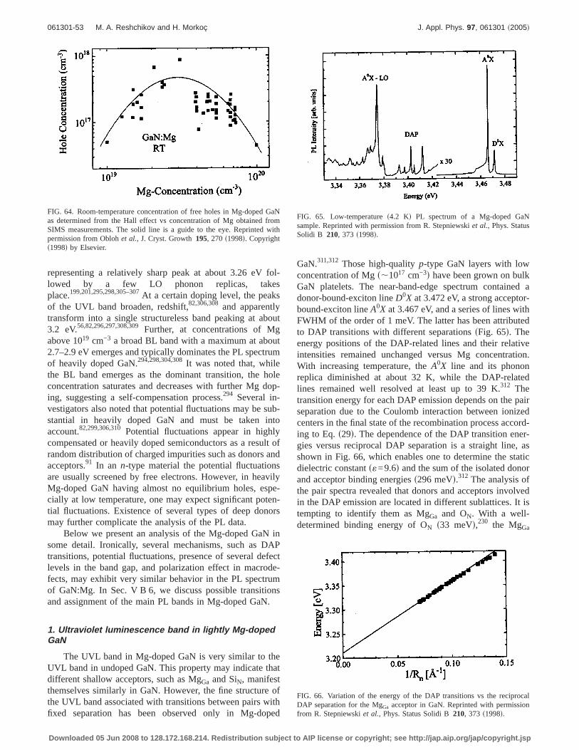
representing a relatively sharp peak at about 3.26 eV fol-lowed by a few LO phonon replicas, takesplace.199,201,295,298,305–307At a certain doping level, the peaksof the UVL band broaden, redshift,82,306,308and apparentlytransform into a single structureless band peaking at about3.2 eV.56,82,296,297,308,309Further, at concentrations of Mgabove 1019 cm−3 a broad BL band with a maximum at about2.7–2.9 eV emerges and typically dominates the PL spectrumof heavily doped GaN.294,298,304,308It was noted that, whilethe BL band emerges as the dominant transition, the holeconcentration saturates and decreases with further Mg dop-ing, suggesting a self-compensation process.294 Several in-vestigators also noted that potential fluctuations may be sub-stantial in heavily doped GaN and must be taken intoaccount.82,299,306,310Potential fluctuations appear in highlycompensated or heavily doped semiconductors as a result ofrandom distribution of charged impurities such as donors andacceptors.91 In an n-type material the potential fluctuationsare usually screened by free electrons. However, in heavilyMg-doped GaN having almost no equilibrium holes, espe-cially at low temperature, one may expect significant poten-tial fluctuations. Existence of several types of deep donorsmay further complicate the analysis of the PL data.
Below we present an analysis of the Mg-doped GaN insome detail. Ironically, several mechanisms, such as DAPtransitions, potential fluctuations, presence of several defectlevels in the band gap, and polarization effect in macrode-fects, may exhibit very similar behavior in the PL spectrumof GaN:Mg. In Sec. V B 6, we discuss possible transitionsand assignment of the main PL bands in Mg-doped GaN.
1. Ultraviolet luminescence band in lightly Mg-dopedGaN
The UVL band in Mg-doped GaN is very similar to theUVL band in undoped GaN. This property may indicate thatdifferent shallow acceptors, such as MgGa and SiN, manifestthemselves similarly in GaN. However, the fine structure ofthe UVL band associated with transitions between pairs withfixed separation has been observed only in Mg-doped
GaN.311,312 Those high-qualityp-type GaN layers with lowconcentration of Mgs,1017 cm−3d have been grown on bulkGaN platelets. The near-band-edge spectrum contained adonor-bound-exciton lineD0X at 3.472 eV, a strong acceptor-bound-exciton lineA0X at 3.467 eV, and a series of lines withFWHM of the order of 1 meV. The latter has been attributedto DAP transitions with different separationssFig. 65d. Theenergy positions of the DAP-related lines and their relativeintensities remained unchanged versus Mg concentration.With increasing temperature, theA0X line and its phononreplica diminished at about 32 K, while the DAP-relatedlines remained well resolved at least up to 39 K.312 Thetransition energy for each DAP emission depends on the pairseparation due to the Coulomb interaction between ionizedcenters in the final state of the recombination process accord-ing to Eq.s29d. The dependence of the DAP transition ener-gies versus reciprocal DAP separation is a straight line, asshown in Fig. 66, which enables one to determine the staticdielectric constants«=9.6d and the sum of the isolated donorand acceptor binding energiess296 meVd.312 The analysis ofthe pair spectra revealed that donors and acceptors involvedin the DAP emission are located in different sublattices. It istempting to identify them as MgGa and ON. With a well-determined binding energy of ON s33 meVd,230 the MgGa
FIG. 64. Room-temperature concentration of free holes in Mg-doped GaNas determined from the Hall effect vs concentration of Mg obtained fromSIMS measurements. The solid line is a guide to the eye. Reprinted withpermission from Oblohet al., J. Cryst. Growth195, 270 s1998d. Copyrights1998d by Elsevier.
FIG. 65. Low-temperatures4.2 Kd PL spectrum of a Mg-doped GaNsample. Reprinted with permission from R. Stepniewskiet al., Phys. StatusSolidi B 210, 373 s1998d.
FIG. 66. Variation of the energy of the DAP transitions vs the reciprocalDAP separation for the MgGa acceptor in GaN. Reprinted with permissionfrom R. Stepniewskiet al., Phys. Status Solidi B210, 373 s1998d.
061301-53 M. A. Reshchikov and H. Morkoç J. Appl. Phys. 97, 061301 ~2005!
Downloaded 05 Jun 2008 to 128.172.168.214. Redistribution subject to AIP license or copyright; see http://jap.aip.org/jap/copyright.jsp
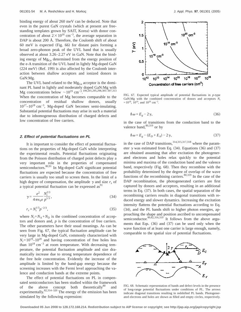
binding energy of about 260 meV can be deduced. Note thateven in the purest GaN crystalsswhich at present are free-standing templates grown by SAIT, Koread with donor con-centration of about 231016 cm−3, the average separation inDAP is about 200 Å. Therefore, the Coulomb shift of about60 meV is expectedsFig. 66d for distant pairs forming abroad zero-phonon peak of the UVL band that is usuallyobserved at about 3.26–2.27 eV in GaN. Note that the bind-ing energy of MgGa determined from the energy position ofthe e-A transition of the UVL band in lightly Mg-doped GaNs224 meVd sRef. 199d is also affected by the Coulomb inter-action between shallow acceptors and ionized donors inGaN:Mg.
The UVL band related to the MgGa acceptor is the domi-nant PL band in lightly and moderately doped GaN:Mg withMg concentrations below,1019 cm−3.199,201,295,298,305–307,313
When the concentration of Mg becomes comparable to theconcentration of residual shallow donors, usually1017–1018 cm−3, Mg-doped GaN becomes semi-insulating.Substantial potential fluctuations may arise in such a materialdue to inhomogeneous distribution of charged defects andlow concentration of free carriers.
2. Effect of potential fluctuations on PL
It is important to consider the effect of potential fluctua-tions on the properties of Mg-doped GaN while interpretingthe experimental results. Potential fluctuations originatingfrom the Poisson distribution of charged point defects play avery important role in the properties of compensatedsemiconductors.80,91 In Mg-doped GaN significant potentialfluctuations are expected because the concentration of freecarriers is usually too small to screen them. In the limit of ahigh degree of compensation, the amplitudeg and sizers ofa typical potential fluctuation can be expressed as91
g =e2
4p«0«
Nt2/3
p1/3 , s34d
rs = Nt1/3p−2/3, s35d
whereNt=NA +ND is the combined concentration of accep-tors and donors and,p is the concentration of free carriers.The other parameters have their usual meanings. As can beseen from Fig. 67, the typical fluctuation amplitude can bevery large in Mg-doped GaN, commonly characterized withNt=1019–1020 and having concentration of free holes lessthan 1018 cm−3 at room temperature. With decreasing tem-perature, the potential fluctuation amplitude and size dra-matically increase due to strong temperature dependence ofthe free hole concentration. Evidently the increase of theamplitude is limited by the band-gap energy because thescreening increases with the Fermi level approaching the va-lence and conduction bands at the extreme points.
The effect of potential fluctuations on PL in compen-sated semiconductors has been studied within the frameworkof the above concept both theoretically80 andexperimentally.82,314–320The energy of the emission has beensimulated by the following expression:
"v = Eg − 2g, s36d
in the case of transitions from the conduction band to thevalence band,80,319or by
"v = Eg − sED + EAd − 2g, s37d
in the case of DAP transitions,314,315,317,318where the param-eterg was estimated from Eq.s34d. Equationss36d ands37dare obtained assuming that after excitation the photogener-ated electrons and holes relax quickly to the potentialminima and maxima of the conduction band and the valenceband, respectivelysFig. 68d. Then they recombine with theprobability determined by the degree of overlap of the wavefunctions of the recombining carriers.80,319In the case of theDAP recombination, the photogenerated carriers are firstcaptured by donors and acceptors, resulting in an additionalterms in Eq.s37d. In both cases, the spatial separation of therecombining carriers results in diagonal transitions with re-duced energy and slower dynamics. Increasing the excitationintensity flattens the potential fluctuations according to Eq.s34d, and the PL bands shift to higher photon energies, ap-proaching the shape and position ascribed to uncompensatedsemiconductor.80,82,316,319It follows from the above argu-ments that Eqs.s36d and s37d can be used only when thewave function of at least one carrier is large enough, namely,comparable to the spatial size of potential fluctuations.
FIG. 67. Expected typical amplitude of potential fluctuations inp-typeGaN:Mg with the combined concentration of donors and acceptorsNt
=1018, 1019, and 1020 cm−3.
FIG. 68. Schematic representation of bands and defect levels in the presenceof long-range potential fluctuations under conditions of PL. The arrowsindicate diagonal transitions resulting in redshifted PL bands. Photogener-ated electrons and holes are shown as filled and empty circles, respectively.
061301-54 M. A. Reshchikov and H. Morkoç J. Appl. Phys. 97, 061301 ~2005!
Downloaded 05 Jun 2008 to 128.172.168.214. Redistribution subject to AIP license or copyright; see http://jap.aip.org/jap/copyright.jsp
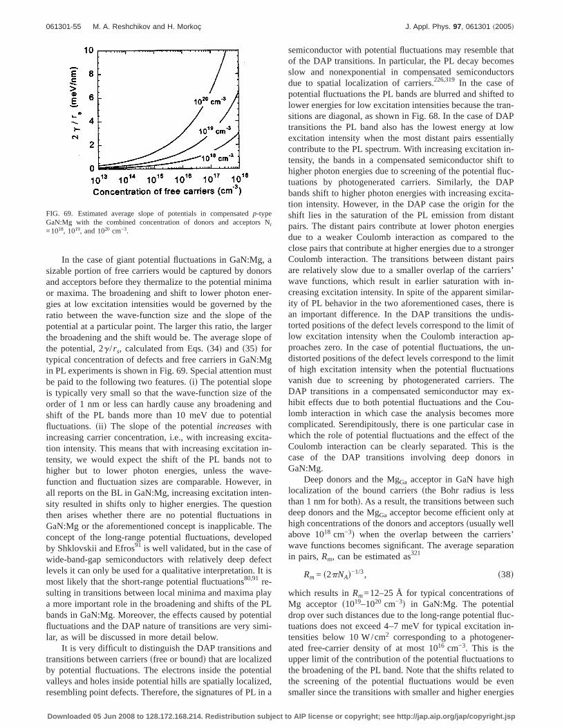
In the case of giant potential fluctuations in GaN:Mg, asizable portion of free carriers would be captured by donorsand acceptors before they thermalize to the potential minimaor maxima. The broadening and shift to lower photon ener-gies at low excitation intensities would be governed by theratio between the wave-function size and the slope of thepotential at a particular point. The larger this ratio, the largerthe broadening and the shift would be. The average slope ofthe potential, 2g / rs, calculated from Eqs.s34d and s35d fortypical concentration of defects and free carriers in GaN:Mgin PL experiments is shown in Fig. 69. Special attention mustbe paid to the following two features.sid The potential slopeis typically very small so that the wave-function size of theorder of 1 nm or less can hardly cause any broadening andshift of the PL bands more than 10 meV due to potentialfluctuations.sii d The slope of the potentialincreaseswithincreasing carrier concentration, i.e., with increasing excita-tion intensity. This means that with increasing excitation in-tensity, we would expect the shift of the PL bands not tohigher but to lower photon energies, unless the wave-function and fluctuation sizes are comparable. However, inall reports on the BL in GaN:Mg, increasing excitation inten-sity resulted in shifts only to higher energies. The questionthen arises whether there are no potential fluctuations inGaN:Mg or the aforementioned concept is inapplicable. Theconcept of the long-range potential fluctuations, developedby Shklovskii and Efros91 is well validated, but in the case ofwide-band-gap semiconductors with relatively deep defectlevels it can only be used for a qualitative interpretation. It ismost likely that the short-range potential fluctuations80,91 re-sulting in transitions between local minima and maxima playa more important role in the broadening and shifts of the PLbands in GaN:Mg. Moreover, the effects caused by potentialfluctuations and the DAP nature of transitions are very simi-lar, as will be discussed in more detail below.
It is very difficult to distinguish the DAP transitions andtransitions between carrierssfree or boundd that are localizedby potential fluctuations. The electrons inside the potentialvalleys and holes inside potential hills are spatially localized,resembling point defects. Therefore, the signatures of PL in a
semiconductor with potential fluctuations may resemble thatof the DAP transitions. In particular, the PL decay becomesslow and nonexponential in compensated semiconductorsdue to spatial localization of carriers.226,319 In the case ofpotential fluctuations the PL bands are blurred and shifted tolower energies for low excitation intensities because the tran-sitions are diagonal, as shown in Fig. 68. In the case of DAPtransitions the PL band also has the lowest energy at lowexcitation intensity when the most distant pairs essentiallycontribute to the PL spectrum. With increasing excitation in-tensity, the bands in a compensated semiconductor shift tohigher photon energies due to screening of the potential fluc-tuations by photogenerated carriers. Similarly, the DAPbands shift to higher photon energies with increasing excita-tion intensity. However, in the DAP case the origin for theshift lies in the saturation of the PL emission from distantpairs. The distant pairs contribute at lower photon energiesdue to a weaker Coulomb interaction as compared to theclose pairs that contribute at higher energies due to a strongerCoulomb interaction. The transitions between distant pairsare relatively slow due to a smaller overlap of the carriers’wave functions, which result in earlier saturation with in-creasing excitation intensity. In spite of the apparent similar-ity of PL behavior in the two aforementioned cases, there isan important difference. In the DAP transitions the undis-torted positions of the defect levels correspond to the limit oflow excitation intensity when the Coulomb interaction ap-proaches zero. In the case of potential fluctuations, the un-distorted positions of the defect levels correspond to the limitof high excitation intensity when the potential fluctuationsvanish due to screening by photogenerated carriers. TheDAP transitions in a compensated semiconductor may ex-hibit effects due to both potential fluctuations and the Cou-lomb interaction in which case the analysis becomes morecomplicated. Serendipitously, there is one particular case inwhich the role of potential fluctuations and the effect of theCoulomb interaction can be clearly separated. This is thecase of the DAP transitions involving deep donors inGaN:Mg.
Deep donors and the MgGa acceptor in GaN have highlocalization of the bound carrierssthe Bohr radius is lessthan 1 nm for bothd. As a result, the transitions between suchdeep donors and the MgGa acceptor become efficient only athigh concentrations of the donors and acceptorssusually wellabove 1018 cm−3d when the overlap between the carriers’wave functions becomes significant. The average separationin pairs,Rm, can be estimated as321
Rm = s2pNAd−1/3, s38d
which results inRm=12–25 Å for typical concentrations ofMg acceptors1019–1020 cm−3d in GaN:Mg. The potentialdrop over such distances due to the long-range potential fluc-tuations does not exceed 4–7 meV for typical excitation in-tensities below 10 W/cm2 corresponding to a photogener-ated free-carrier density of at most 1016 cm−3. This is theupper limit of the contribution of the potential fluctuations tothe broadening of the PL band. Note that the shifts related tothe screening of the potential fluctuations would be evensmaller since the transitions with smaller and higher energies
FIG. 69. Estimated average slope of potentials in compensatedp-typeGaN:Mg with the combined concentration of donors and acceptors Nt
=1018, 1019, and 1020 cm−3.
061301-55 M. A. Reshchikov and H. Morkoç J. Appl. Phys. 97, 061301 ~2005!
Downloaded 05 Jun 2008 to 128.172.168.214. Redistribution subject to AIP license or copyright; see http://jap.aip.org/jap/copyright.jsp
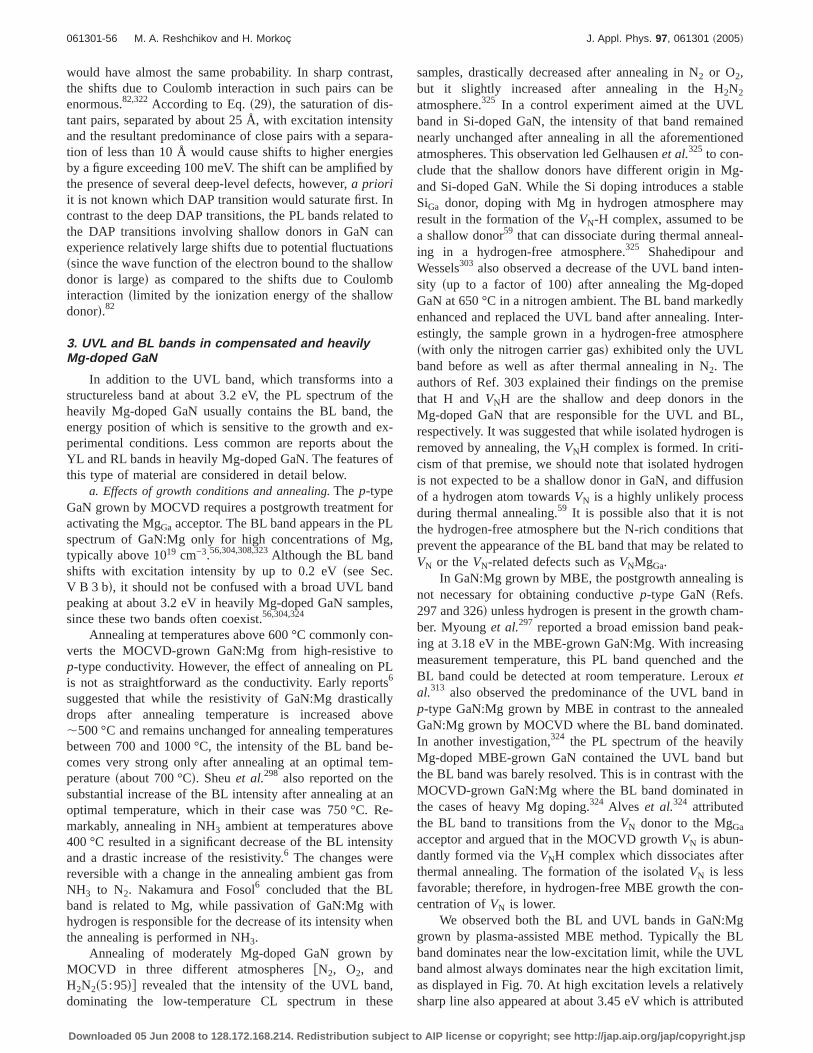
would have almost the same probability. In sharp contrast,the shifts due to Coulomb interaction in such pairs can beenormous.82,322According to Eq.s29d, the saturation of dis-tant pairs, separated by about 25 Å, with excitation intensityand the resultant predominance of close pairs with a separa-tion of less than 10 Å would cause shifts to higher energiesby a figure exceeding 100 meV. The shift can be amplified bythe presence of several deep-level defects, however,a prioriit is not known which DAP transition would saturate first. Incontrast to the deep DAP transitions, the PL bands related tothe DAP transitions involving shallow donors in GaN canexperience relatively large shifts due to potential fluctuationsssince the wave function of the electron bound to the shallowdonor is larged as compared to the shifts due to Coulombinteractionslimited by the ionization energy of the shallowdonord.82
3. UVL and BL bands in compensated and heavilyMg-doped GaN
In addition to the UVL band, which transforms into astructureless band at about 3.2 eV, the PL spectrum of theheavily Mg-doped GaN usually contains the BL band, theenergy position of which is sensitive to the growth and ex-perimental conditions. Less common are reports about theYL and RL bands in heavily Mg-doped GaN. The features ofthis type of material are considered in detail below.
a. Effects of growth conditions and annealing.The p-typeGaN grown by MOCVD requires a postgrowth treatment foractivating the MgGa acceptor. The BL band appears in the PLspectrum of GaN:Mg only for high concentrations of Mg,typically above 1019 cm−3.56,304,308,323Although the BL bandshifts with excitation intensity by up to 0.2 eVssee Sec.V B 3 bd, it should not be confused with a broad UVL bandpeaking at about 3.2 eV in heavily Mg-doped GaN samples,since these two bands often coexist.56,304,324
Annealing at temperatures above 600 °C commonly con-verts the MOCVD-grown GaN:Mg from high-resistive top-type conductivity. However, the effect of annealing on PLis not as straightforward as the conductivity. Early reports6
suggested that while the resistivity of GaN:Mg drasticallydrops after annealing temperature is increased above,500 °C and remains unchanged for annealing temperaturesbetween 700 and 1000 °C, the intensity of the BL band be-comes very strong only after annealing at an optimal tem-peraturesabout 700 °Cd. Sheuet al.298 also reported on thesubstantial increase of the BL intensity after annealing at anoptimal temperature, which in their case was 750 °C. Re-markably, annealing in NH3 ambient at temperatures above400 °C resulted in a significant decrease of the BL intensityand a drastic increase of the resistivity.6 The changes werereversible with a change in the annealing ambient gas fromNH3 to N2. Nakamura and Fosol6 concluded that the BLband is related to Mg, while passivation of GaN:Mg withhydrogen is responsible for the decrease of its intensity whenthe annealing is performed in NH3.
Annealing of moderately Mg-doped GaN grown byMOCVD in three different atmospheresfN2, O2, andH2N2s5:95dg revealed that the intensity of the UVL band,dominating the low-temperature CL spectrum in these
samples, drastically decreased after annealing in N2 or O2,but it slightly increased after annealing in the H2N2
atmosphere.325 In a control experiment aimed at the UVLband in Si-doped GaN, the intensity of that band remainednearly unchanged after annealing in all the aforementionedatmospheres. This observation led Gelhausenet al.325 to con-clude that the shallow donors have different origin in Mg-and Si-doped GaN. While the Si doping introduces a stableSiGa donor, doping with Mg in hydrogen atmosphere mayresult in the formation of theVN-H complex, assumed to bea shallow donor59 that can dissociate during thermal anneal-ing in a hydrogen-free atmosphere.325 Shahedipour andWessels303 also observed a decrease of the UVL band inten-sity sup to a factor of 100d after annealing the Mg-dopedGaN at 650 °C in a nitrogen ambient. The BL band markedlyenhanced and replaced the UVL band after annealing. Inter-estingly, the sample grown in a hydrogen-free atmosphereswith only the nitrogen carrier gasd exhibited only the UVLband before as well as after thermal annealing in N2. Theauthors of Ref. 303 explained their findings on the premisethat H andVNH are the shallow and deep donors in theMg-doped GaN that are responsible for the UVL and BL,respectively. It was suggested that while isolated hydrogen isremoved by annealing, theVNH complex is formed. In criti-cism of that premise, we should note that isolated hydrogenis not expected to be a shallow donor in GaN, and diffusionof a hydrogen atom towardsVN is a highly unlikely processduring thermal annealing.59 It is possible also that it is notthe hydrogen-free atmosphere but the N-rich conditions thatprevent the appearance of the BL band that may be related toVN or theVN-related defects such asVNMgGa.
In GaN:Mg grown by MBE, the postgrowth annealing isnot necessary for obtaining conductivep-type GaN sRefs.297 and 326d unless hydrogen is present in the growth cham-ber. Myounget al.297 reported a broad emission band peak-ing at 3.18 eV in the MBE-grown GaN:Mg. With increasingmeasurement temperature, this PL band quenched and theBL band could be detected at room temperature. Lerouxetal.313 also observed the predominance of the UVL band inp-type GaN:Mg grown by MBE in contrast to the annealedGaN:Mg grown by MOCVD where the BL band dominated.In another investigation,324 the PL spectrum of the heavilyMg-doped MBE-grown GaN contained the UVL band butthe BL band was barely resolved. This is in contrast with theMOCVD-grown GaN:Mg where the BL band dominated inthe cases of heavy Mg doping.324 Alves et al.324 attributedthe BL band to transitions from theVN donor to the MgGa
acceptor and argued that in the MOCVD growthVN is abun-dantly formed via theVNH complex which dissociates afterthermal annealing. The formation of the isolatedVN is lessfavorable; therefore, in hydrogen-free MBE growth the con-centration ofVN is lower.
We observed both the BL and UVL bands in GaN:Mggrown by plasma-assisted MBE method. Typically the BLband dominates near the low-excitation limit, while the UVLband almost always dominates near the high excitation limit,as displayed in Fig. 70. At high excitation levels a relativelysharp line also appeared at about 3.45 eV which is attributed
061301-56 M. A. Reshchikov and H. Morkoç J. Appl. Phys. 97, 061301 ~2005!
Downloaded 05 Jun 2008 to 128.172.168.214. Redistribution subject to AIP license or copyright; see http://jap.aip.org/jap/copyright.jsp
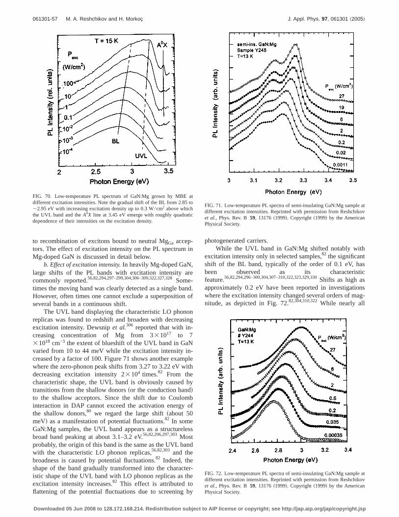
to recombination of excitons bound to neutral MgGa accep-tors. The effect of excitation intensity on the PL spectrum inMg-doped GaN is discussed in detail below.
b. Effect of excitation intensity.In heavily Mg-doped GaN,large shifts of the PL bands with excitation intensity arecommonly reported.56,82,294,297–299,304,306–309,322,327,328Some-times the moving band was clearly detected as a single band.However, often times one cannot exclude a superposition ofseveral bands in a continuous shift.
The UVL band displaying the characteristic LO phononreplicas was found to redshift and broaden with decreasingexcitation intensity. Dewsnipet al.306 reported that with in-creasing concentration of Mg from 331017 to 731018 cm−3 the extent of blueshift of the UVL band in GaNvaried from 10 to 44 meV while the excitation intensity in-creased by a factor of 100. Figure 71 shows another examplewhere the zero-phonon peak shifts from 3.27 to 3.22 eV withdecreasing excitation intensity 23104 times.82 From thecharacteristic shape, the UVL band is obviously caused bytransitions from the shallow donorssor the conduction banddto the shallow acceptors. Since the shift due to Coulombinteraction in DAP cannot exceed the activation energy ofthe shallow donors,80 we regard the large shiftsabout 50meVd as a manifestation of potential fluctuations.82 In someGaN:Mg samples, the UVL band appears as a structurelessbroad band peaking at about 3.1–3.2 eV.56,82,296,297,303Mostprobably, the origin of this band is the same as the UVL bandwith the characteristic LO phonon replicas,56,82,303 and thebroadness is caused by potential fluctuations.82 Indeed, theshape of the band gradually transformed into the character-istic shape of the UVL band with LO phonon replicas as theexcitation intensity increases.82 This effect is attributed toflattening of the potential fluctuations due to screening by
photogenerated carriers.While the UVL band in GaN:Mg shifted notably with
excitation intensity only in selected samples,82 the significantshift of the BL band, typically of the order of 0.1 eV, hasbeen observed as its characteristicfeature.56,82,294,296–300,304,307–310,322,323,329,330Shifts as high asapproximately 0.2 eV have been reported in investigationswhere the excitation intensity changed several orders of mag-nitude, as depicted in Fig. 72.82,304,310,322While nearly all
FIG. 70. Low-temperature PL spectrum of GaN:Mg grown by MBE atdifferent excitation intensities. Note the gradual shift of the BL from 2.85 to,2.95 eV with increasing excitation density up to 0.3 W/cm2 above whichthe UVL band and theA0X line at 3.45 eV emerge with roughly quadraticdependence of their intensities on the excitation density.
FIG. 71. Low-temperature PL spectra of semi-insulating GaN:Mg sample atdifferent excitation intensities. Reprinted with permission from Reshchikovet al., Phys. Rev. B59, 13176s1999d. Copyright s1999d by the AmericanPhysical Society.
FIG. 72. Low-temperature PL spectra of semi-insulating GaN:Mg sample atdifferent excitation intensities. Reprinted with permission from Reshchikovet al., Phys. Rev. B59, 13176s1999d. Copyright s1999d by the AmericanPhysical Society.
061301-57 M. A. Reshchikov and H. Morkoç J. Appl. Phys. 97, 061301 ~2005!
Downloaded 05 Jun 2008 to 128.172.168.214. Redistribution subject to AIP license or copyright; see http://jap.aip.org/jap/copyright.jsp

researchers who investigated the effect of the excitation in-tensity on the BL band attributed the BL band to transitionsfrom a deep donor to the shallow MgGa acceptor, a contro-versy still remains about that assignment for the giant shift.Most researchers propose that the Coulomb interaction in theDAP is responsible for the shift in the BLband,82,294,298,304,308,322,330while others point to potentialfluctuations as the main reason for the shift.299,310 As dis-cussed in Sec. V B 2, the strong Coulomb interaction be-tween the deep-level DAP in heavily doped GaN alone canexplain the giant shifts of this band, whereas the potentialfluctuations perhaps play only a secondary role which can benegligible. Note that a good quantitative agreement betweenthe BL band position and the room-temperature hole concen-tration once obtained within the model of potentialfluctuations310 is apparently just a coincidence. In reality, theaverage size of the potential fluctuations in the analyzedGaN:Mg is about 100 nm at room temperature which dra-matically increases as the temperature is reduced. The wavefunctions of the bound electron and hole are less than 1 nm,so that their overlap at distances exceeding 100 nm is com-pletely negligible. The scatter in the reported BL band posi-tion, which has been attributed in Ref. 310 to differentscreening effects, is apparently related to the scatter in theconcentration of defects that affects the average pair separa-tion in DAP.
We can estimate the position of the energy level of theunperturbed deep donor responsible for the BL band in thefollowing manner. The Coulomb interaction term in Eq.s29dfor the DAP with an average distance of about 25 Å for thetypical concentrations of Mg in mid-1019 cm−3 can be esti-mated as,0.1 eV. The energy of the ZPL for the broad BLband can be approximately estimated as,3.0 eV from theband shape in the limit of low excitation intensitiesssee Fig.72d. UsingEg=3.5 eV for the low-temperature band gap andEA=0.2 eV, we obtainED=0.4±0.1 eV from Eq.s29d.
A very interesting observation regarding the effect ofexcitation intensity on the BL and UVL structureless bandsin p-type GaN:Mg, which has long been reported,56 remainsunexplained. Namely, the intensity of the BL band increasedlinearly with excitation intensity, whereas the increase of theUVL intensity was quadratic.56 We also observed similar de-pendencies in a few GaN:Mg samples grown by MBEsseeFig. 70d. From an analysis of the rate equationsswithin theconcept presented in Sec. III Ad, we expect that in conduc-tive p-type GaN:Mg the intensity of PL bands resulting fromthe transitions of electronssfree or boundd to the shallowMgGa acceptor level should increase linearly with excitationintensity. Indeed, the concentration of holes bound to theMgGa acceptor remains nearly constant in the nominal rangeof excitation intensitiessand roughly equal concentration ofthe compensating donorsd, so that the intensity of the UVLand BL bands should be proportional to the concentration ofthe photogenerated electrons captured by the shallow anddeep donors. Therefore, inp-type GaN:Mg, where the Fermilevel is pinned to the shallow acceptor level, we expect alinear IsPexcd dependence for both the BL and UVL bands.The above reasoning indicates that the observations in Ref.56 may seem to contradict the Hall-effect results contained
therein, revealing thep-type conductivity. However, invok-ing the concept of long-range potential fluctuations can eas-ily remove the discrepancy. The potential fluctuations dividethe sample into areas where the MgGa acceptor is filled withholes sin the hillsd and empty of holessin the valleysd indark, as shown in Fig. 68. Photogenerated electrons that arecaptured by the shallow donors can escape to the conductionband since their activation energy is not too largespossibilityof diagonal transitions leading to long carrier lifetimes en-hances this probabilityd. After multiple capture and thermalrelease, the electrons would be collected at the shallow donorstates in the valleys where there are no equilibrium holes.Recombination of the electrons from the shallow donors withphotogenerated holes at the shallow acceptors in these areasof the sample may be responsible for the quadraticIsPexcddependence of the UVL intensity. In contrast, electrons cap-tured by deep donors cannot be thermally releasedsdue tothe larger activation energy and smaller size of the electronwave functiond, and therefore, the BL band will be observedmostly from the hills where the concentration of holes boundto the shallow acceptor is abundant even in dark. Thus, theBL intensity would increase linearly with the excitationintensity.
From an analysis of the PL spectra at different excitationintensities, it can be concluded that at least in some GaN:Mgsamples more than two bandssthe above-discussed BL andUVL d present in the photon range from 2.5 to 3.3 eV. Eckeyet al.308 resolved three broad bands in this range. In the limitof low excitation intensity, these bands peaked at about 2.5,2.8, and 3.0 eV, and all three bands substantially shifted withincreasing excitation intensity, as displayed in Fig. 73. Thosethree bands have been attributed to transitions from the threedistinct deep donors to the shallow MgGa acceptor. A broadband peaking at about 3.3 eV was observed as a shoulder onthe UVL bandssee Fig. 71d.82 Another broad band peaking at3.0 eV was detected in GaN:Mg after electronirradiation.325,328The band gradually shifted to higher photonenergies and reached 3.2 eV upon increasing excitation in-tensity by a factor of 400. This 3.0-eV band has been attrib-uted to transitions from a deep donorsapparentlyVNd to theshallow MgGa acceptor.325
c. Effect of temperature.With increasing temperature, thePL bands in Mg-doped GaN shift and quench. However, thetemperature-related transformations are different for the BLband and the UVL band. The UVL band begins quenching atrelatively low temperatures and by the time the room tem-perature is reached it either disappears under the tail of theBL band82,295,297,313or transforms into a structureless band atabout 3.2 eV with its intensity reduced by a factor of about1000 as compared to that at low temperature.56,82 The acti-vation energy of this quenching,,200 meV, is similar to thevalues obtained for the UVL band in undoped and lightlydopedn-type GaN.82,310,313It may seem surprising that in thep-type GaN:Mg samples56,82,313the UVL band quenches in afashion similar to that inn-type GaN. Indeed, one wouldexpect the abundance of holes at the shallow MgGa acceptorsites at any temperature. Therefore, the thermal escape ofsmall fraction of the bound holes would not affect the PLintensity of the UVL band up to room temperature. A pos-
061301-58 M. A. Reshchikov and H. Morkoç J. Appl. Phys. 97, 061301 ~2005!
Downloaded 05 Jun 2008 to 128.172.168.214. Redistribution subject to AIP license or copyright; see http://jap.aip.org/jap/copyright.jsp
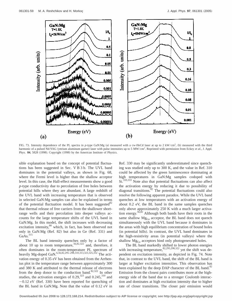
sible explanation based on the concept of potential fluctua-tions has been suggested in Sec.V B 3 b. The UVL banddominates in the potential valleys, as shown in Fig. 68,where the Fermi level is higher than the shallow acceptorlevel. In this case, the Hall-effect measurements show a goodp-type conductivity due to percolation of free holes betweenpotential hills where they are abundant. A large redshift ofthe UVL band with increasing temperature that is observedin selected GaN:Mg samples can also be explained in termsof the potential fluctuation model. It has been suggested82
that thermal release of free carriers from the shallower short-range wells and their percolation into deeper valleys ac-counts for the large temperature shifts of the UVL band inGaN:Mg. In this model, the shift increases with decreasingexcitation intensity,80 which, in fact, has been observed notonly in GaN:Mg sRef. 82d but also in GesRef. 331d andGaAs.315
The BL band intensity quenches only by a factor ofabout 10 up to room temperature,56,82,322 and, therefore, itoften dominates in the room-temperature PL spectrum ofheavily Mg-doped GaN.6,56,82,295–298,310,313,323,325,332The acti-vation energy of 0.35 eV has been obtained from the Arrhen-ius plot in the temperature range between approximately 300and 380 K and attributed to the thermal release of electronsfrom the deep donor to the conduction band.82,322 In otherstudies, the activation energies of 0.29,323 and 0.245,310 and,0.12 eV sRef. 330d have been reported for quenching ofthe BL band in GaN:Mg. Note that the value of 0.12 eV in
Ref. 330 may be significantly underestimated since quench-ing was studied only up to 300 K, and the value in Ref. 310could be affected by the green luminescence dominating athigh temperatures in GaN:Mg samples codoped withSi.310,333Note also that potential fluctuations can also affectthe activation energy by reducing it due to possibility ofdiagonal transitions.82 The potential fluctuations could alsoresolve the following apparent paradox. While the UVL bandquenches at low temperatures with an activation energy ofabout 0.2 eV, the BL band in the same samples quenchesonly above approximately 250 K with a much larger activa-tion energy.56,82Although both bands have their roots in thesame shallow MgGa acceptor, the BL band does not quenchsimultaneously with the UVL band because it dominates inthe areas with high equilibrium concentration of bound holessin potential hillsd. In contrast, the UVL band dominates inthe high-resistivity areassin potential valleysd where theshallow MgGa acceptors bind only photogenerated holes.
The BL band markedly shifted to lower photon energieswith increasing temperature,82,295,298,322yet the shift was de-pendent on excitation intensity, as depicted in Fig. 74. Notethat, in contrast to the UVL band, the shift of the BL band islarger at higher excitation intensities. This observation hasbeen explained by the deep DAP character of the BL band.82
Emission from the closest pairs contributes more at the high-energy side of the band due to a stronger Coulomb interac-tion and dominates at high excitation intensity due to higherrate of closer transitions. The closer pair emission would
FIG. 73. Intensity dependence of the PL spectra inp-type GaN:Mgsad measured with a cw-HeCd laser at up to 2 kW/cm2, sbd measured with the thirdharmonic of a pulsed Nd:YAGsyttrium aluminum garnetd laser with pulse intensities up to 5 MW/cm2. Reprinted with permission from Eckeyet al., J. Appl.Phys. 84, 5828s1998d. Copyrights1998d by the American Institute of Physics.
061301-59 M. A. Reshchikov and H. Morkoç J. Appl. Phys. 97, 061301 ~2005!
Downloaded 05 Jun 2008 to 128.172.168.214. Redistribution subject to AIP license or copyright; see http://jap.aip.org/jap/copyright.jsp
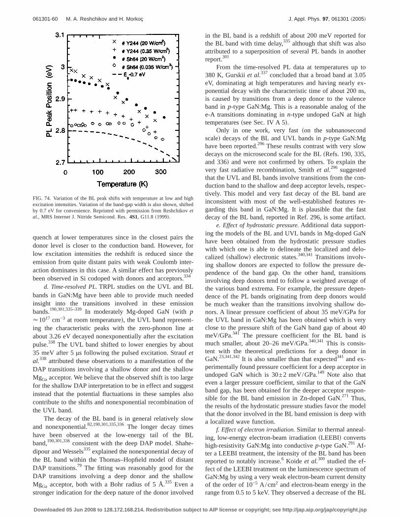
quench at lower temperatures since in the closest pairs thedonor level is closer to the conduction band. However, forlow excitation intensities the redshift is reduced since theemission from quite distant pairs with weak Coulomb inter-action dominates in this case. A similar effect has previouslybeen observed in Si codoped with donors and acceptors.334
d. Time-resolved PL.TRPL studies on the UVL and BLbands in GaN:Mg have been able to provide much neededinsight into the transitions involved in these emissionbands.190,301,335–339In moderately Mg-doped GaNswith p<1017 cm−3 at room temperatured, the UVL band represent-ing the characteristic peaks with the zero-phonon line atabout 3.26 eV decayed nonexponentially after the excitationpulse.338 The UVL band shifted to lower energies by about35 meV after 5µs following the pulsed excitation. Straufetal.338 attributed these observations to a manifestation of theDAP transitions involving a shallow donor and the shallowMgGa acceptor. We believe that the observed shift is too largefor the shallow DAP interpretation to be in effect and suggestinstead that the potential fluctuations in these samples alsocontribute to the shifts and nonexponential recombination ofthe UVL band.
The decay of the BL band is in general relatively slowand nonexponential.82,190,301,335,336The longer decay timeshave been observed at the low-energy tail of the BLband,190,301,336consistent with the deep DAP model. Shahe-dipour and Wessels335 explained the nonexponential decay ofthe BL band within the Thomas–Hopfield model of distantDAP transitions.79 The fitting was reasonably good for theDAP transitions involving a deep donor and the shallowMgGa acceptor, both with a Bohr radius of 5 Å.335 Even astronger indication for the deep nature of the donor involved
in the BL band is a redshift of about 200 meV reported forthe BL band with time delay,335 although that shift was alsoattributed to a superposition of several PL bands in anotherreport.301
From the time-resolved PL data at temperatures up to380 K, Gurskiiet al.337 concluded that a broad band at 3.05eV, dominating at high temperatures and having nearly ex-ponential decay with the characteristic time of about 200 ns,is caused by transitions from a deep donor to the valenceband inp-type GaN:Mg. This is a reasonable analog of thee-A transitions dominating inn-type undoped GaN at hightemperaturesssee Sec. IV A 5d.
Only in one work, very fastson the subnanosecondscaled decays of the BL and UVL bands inp-type GaN:Mghave been reported.296 These results contrast with very slowdecays on the microsecond scale for the BLsRefs. 190, 335,and 336d and were not confirmed by others. To explain thevery fast radiative recombination, Smithet al.296 suggestedthat the UVL and BL bands involve transitions from the con-duction band to the shallow and deep acceptor levels, respec-tively. This model and very fast decay of the BL band areinconsistent with most of the well-established features re-garding this band in GaN:Mg. It is plausible that the fastdecay of the BL band, reported in Ref. 296, is some artifact.
e. Effect of hydrostatic pressure.Additional data support-ing the models of the BL and UVL bands in Mg-doped GaNhave been obtained from the hydrostatic pressure studieswith which one is able to delineate the localized and delo-calized sshallowd electronic states.340,341 Transitions involv-ing shallow donors are expected to follow the pressure de-pendence of the band gap. On the other hand, transitionsinvolving deep donors tend to follow a weighted average ofthe various band extrema. For example, the pressure depen-dence of the PL bands originating from deep donors wouldbe much weaker than the transitions involving shallow do-nors. A linear pressure coefficient of about 35 meV/GPa forthe UVL band in GaN:Mg has been obtained which is veryclose to the pressure shift of the GaN band gap of about 40meV/GPa.341 The pressure coefficient for the BL band ismuch smaller, about 20–26 meV/GPa.340,341 This is consis-tent with the theoretical predictions for a deep donor inGaN.23,341,342It is also smaller than that expected341 and ex-perimentally found pressure coefficient for a deep acceptor inundoped GaN which is 30±2 meV/GPa.149 Note also thateven a larger pressure coefficient, similar to that of the GaNband gap, has been obtained for the deeper acceptor respon-sible for the BL band emission in Zn-doped GaN.271 Thus,the results of the hydrostatic pressure studies favor the modelthat the donor involved in the BL band emission is deep witha localized wave function.
f. Effect of electron irradiation.Similar to thermal anneal-ing, low-energy electron-beam irradiationsLEEBId convertshigh-resistivity GaN:Mg into conductivep-type GaN.291 Af-ter a LEEBI treatment, the intensity of the BL band has beenreported to notably increase.6 Koide et al.300 studied the ef-fect of the LEEBI treatment on the luminescence spectrum ofGaN:Mg by using a very weak electron-beam current densityof the order of 10−5 A/cm2 and electron-beam energy in therange from 0.5 to 5 keV. They observed a decrease of the BL
FIG. 74. Variation of the BL peak shifts with temperature at low and highexcitation intensities. Variation of the band-gap width is also shown, shiftedby 0.7 eV for convenience. Reprinted with permission from Reshchikovetal., MRS Internet J. Nitride Semicond. Res.4S1, G11.8s1999d.
061301-60 M. A. Reshchikov and H. Morkoç J. Appl. Phys. 97, 061301 ~2005!
Downloaded 05 Jun 2008 to 128.172.168.214. Redistribution subject to AIP license or copyright; see http://jap.aip.org/jap/copyright.jsp
band intensity by about 20% with electron exposure. Re-markably, the UVL band increased by about a factor of 2after the LEEBI treatment of GaN:Mg samples. Koideetal.300 explained the changes by dissociation of the MgH andVNH complexes under electron irradiation. Congruous withthe assignments made in Ref. 303, these authors attributedthe UVL and BL bands to transitions from the shallow donor,which was assumed to be H, and from a deep donor whichwas assumed to beVNH, respectively, to the shallow MgGa
acceptor.By contrast, Gelhausenet al.325 observed a drastic de-
crease of the UVL intensity under LEEBI treatment. TheUVL band decreased under electron irradiation only in as-grown GaN:Mg sample and in a sample annealed in H2N2
ambient. The effect of electron irradiation was negligible inthe GaN:Mg samples annealed in N2 or O2 ambient. Thesame was shown to hold for the Si-doped samples before andafter annealing. Those authors assumed that the shallow do-nor responsible for the UVL band in GaN:Mg samples is theVNH complex that can dissociate during LEEBI treatment.Besides the bleaching of the UVL band, Gelhausenetal.325,328 detected an emergence of a broad band at around3.05 eV under electron irradiation. The broad band shiftedfrom 3.0 to 3.2 eV with increasing excitation densitysby afactor of 400d. That broad band has been attributed to tran-sitions from a deep donor, presumablyVN, to the shallowMgGa acceptor.328 The LEEBI treatment also shifted the BLband to lower energies325 and activated a weak yellow lumi-nescence band328 in these GaN:Mg samples.
g. Optically detected magnetic resonance.The ODMRspectra measured on the UVL and BL bands in GaN:Mgusually contain two lines: one withgi <2.1 attributed toMgGa and another withgi <1.95–1.96 attributed to a com-pensating donor.141,277,309,343–345The spectral distribution ofboth signals reproduces the shape of the BL band with amaximum at 2.9 eV observed in heavily doped GaN:Mg.141
The Mg-related signal is anisotropic. The values ofgi andg'
which are typically in the range of 2.058–2.114 and 1.94–2.022, respectively, are sample dependent.277,309,343–346More-over, the differencegi−g' decreases with decreasing detec-tion energy across the broad BL band.309,346The anisotropyof theg tensor, expected for the shallow acceptor in GaN,108
is reduced by symmetry-lowering local distortions originat-ing from structural defects or random distribution of chargedimpurities leading to potential fluctuations.309,346Note that inearly studies the above-mentioned small anisotropy of thegtensor of the Mg-related defect was inappropriately assignedto a so thought deep Mg-related level.141,344The nearly iso-tropic signal withg<1.95–1.96 has been attributed to theshallow effective-mass donor in GaN.141,309,345Such an as-signment is consistent with the attribution of the UVL bandto transitions from the shallow donor to the shallow MgGa
acceptor. However, assignment of the donor-related signal tothe shallow donor contradicts the above-described propertiesof the BL band ascribed to transitions from a deep donor tothe shallow MgGa acceptor. One possibility is that the ODMRsignal from the deep donor is similar to that from theeffective-mass shallow donor. Note that this signal in theheavily Mg-doped GaN exhibiting the BL band is much
broader than that in the lightly Mg-doped GaN where theUVL band dominates.309 Another possibility is that the spin-dependent capture of an electron from the shallow donor orpossibly from the conduction band to a deep donor first takesplace, followed by radiative transition from the deep donorto the shallow MgGa acceptor. In the case the first process isdetected by magnetic resonance the effective-mass resonancewould be observed in the form of increasing BL signal.
h. DLTS, positron annihilation, and the infrared spectra.ADLTS study of undoped and Mg-doped GaN revealed a char-acteristic deep level at 0.62 eV below the conductionband.347 The concentration of this defect increased from,231013 to 331014 cm−3 after moderate Mg doping ofGaN that remainedn type. Additionally, a defect level at,0.4 eV below the conduction band with a concentration ofabout 1013 cm−3 appeared in one Mg-doped sample. The cap-ture cross section is of the order of 10−14 cm2 for both of theaforementioned deep levels.347
Positron annihilation studies have shown that the cre-ation ofVGa is suppressed by Mg doping.124,195,348This resultis consistent with theoretical predictionssSec. IId. When theFermi level is close to the valence band during the growth,donors, such asVN, VNMg, or VNH, are more likely to incor-porate in GaN, and not acceptors such asVGa. Positron an-nihilation experiments are able in principle to detect and dis-tinguishVGa andVN, as well as complex defects containingthese vacancies. However, the detection ofVN in p-type GaNby positron annihilation is hampered even when this defect isabundant. The reason lies in a small difference in the posi-tron lifetime in defect-free andVN-containing GaN, as wellas repulsion of positrons from the positively chargeddefects.124 Nevertheless, Hautakangaset al.349 were able todetect a neutralVN-related defect inp-type GaN grown byMOCVD. This should be contrasted with no vacancy-relateddefects having been observed inp-type GaN grown by MBE.The defect has been identified as the neutralVNMgGa com-plex. Thermal annealing at 500–800 °C led to disappearanceof this defect. A value of about 2.5 eV for the migrationenergy of VN has been estimated by assuming that theVNMgGa complex dissociates andVN migrates to the surfaceduring annealing. The absence of theVN-related defects inp-type GaN:Mg grown by MBE has been attributed to betterstability of theVNMgGa complexes when the Fermi level isclose to the midgap during the growth, a condition corre-sponding to the MOCVD but not MBE growth conditions.
Local vibrational modes of the Mg–H complex havebeen found in GaN:Mg at 3125 cm−1.350 The hydrogen atompreferentially incorporates at an antibonding site of the nitro-gen atom.47,351 Consequently, the vibrational frequency isprimarily determined by the N–H vibrational mode. Thermalannealing converts the high-resistivity GaN top-type con-ductivity and results in a sizable decrease of this localmode.350 A series of local modes in the range of about2200 cm−1 was also detected in the Raman spectra ofGaN:Mg and attributed to various defect complexes involv-ing hydrogen.352,353
061301-61 M. A. Reshchikov and H. Morkoç J. Appl. Phys. 97, 061301 ~2005!
Downloaded 05 Jun 2008 to 128.172.168.214. Redistribution subject to AIP license or copyright; see http://jap.aip.org/jap/copyright.jsp

4. Yellow and red luminescence bands
The YL band peaking at 2.2–2.3 eV usually vanisheswith Mg doping, in agreement with its attribution to theVGa-containing defectsssee Secs. IV A and IV Bd. However,the YL band sometimes persists in GaN:Mg when the sampleremainsn type298,354or semi-insulating.6 The weak YL bandappeared also after electron irradiation ofp-type GaN:Mg.328
A relatively strong YL has been reported inp-type GaNgrown by MBE.355 Note that the reports about the YL peak inp-type GaN are extremely rare and must be treated with cau-tion.
The RL band having a maximum at about 1.7–1.8 eV issometimes observed in heavily Mg-dopedp-typeGaN.309,354,356The ODMR studies of this band indicate thatthe transition involves deep donors and the shallow MgGa
acceptor.309 Two signals, namely, an isotropic one withg=2.003 sfrom deep donord and an anisotropic one withgi
=2.10 andg'<2 sfor the shallow MgGa acceptord have beendetected for the RL band.309 The RL band has also beenattributed to deep donor-deep acceptor transitions.172,354
5. Luminescence in GaN:Mg codoped with shallowdonors
Codoping of GaN:Mg with shallow donors has beenconsidered as a means to increase the solubility of Mg andreduce its binding energy.357 Through codoping with oxygenthe concentration of holes has been increased up to 231018 cm−3 while decreasing the resistivity of the GaN:Mgsample down to 0.2V cm.358,359Incorporation of oxygen inGaN:Mg suppressed the BL band, and a broad GL emergedat 2.4–2.5 eV as a shoulder to the BL band.358 Similarly, aGL band appeared in GaN:Mg codoped with Si upon increas-ing the temperature up to room temperature.333 While the BLintensity increased linearly with excitation intensity, the GLintensity in O- and Si-codoped GaN:Mg increased superlin-early, asPexc
n with n=1.4−1.7.333 The intensity of the GLband increased with increasing temperature from 200 to 260K. In an effort to explain this unusual effect, Hanet al.333
proposed that the GL band arises from transitions between ametastable deep donor and the shallow MgGa acceptor. Thoseauthors assumed that both oxygen and silicon would behaveasDX centers in GaN, and theirDX states form deep levelswithin the band gap. Kaufmannet al.172 also observed theBL bandsat about 2.8 eVd and RL bandsat about 1.8 eVd inGaN:Mg codoped with Si. The red band has been attributedto transitions from a deep donor to a deep acceptor.
6. Identification of defects in Mg-doped GaN
In spite of the plethora of activity, only two observationsare well established, both from theoretical and experimentalviewpoints regarding the defects in GaN:Mg:sid Mg dopingsuppressesVGa-related defects which are common inn-typeGaN and introduces compensating deep donors andsii d a Mgatom replaces a Ga atom forming a shallow acceptor with anactivation energy of about 0.2 eV.
As for the optical transitions contributing to the PL spec-trum of GaN:Mg, only the following are undeniably estab-lished up to date:sid In moderately Mg-doped GaN, transi-
tions from the shallow donor to the shallow MgGa acceptor,which are responsible for the UVL band with the zero-phonon line at about 3.27 eV and the characteristic set of LOphonon replicas dominate,sii d transitions from one or moredeep donors to the shallow MgGa acceptor in heavily Mg-doped GaN are responsible for the dominant BL band whichshifts substantially with excitation intensity,siii d the previ-ously proposed model for the BL band as being due to tran-sitions from the conduction band or from a shallow donor toa deep Mg-related defect141,286,295–300,302must be rejectedsince it fails to explain very critical experimental observa-tions, sivd the BL bands in Mg- and Zn-doped or undopedGaN have different origins, andsvd potential fluctuations dueto random distribution of charged defects play an importantrole in the PL properties of heavily Mg-doped GaN. Otherdeductions reported in the literature are more speculative.Nevertheless, we briefly review them below for the sake ofcompleteness.
There are strong indications that the dominant shallowdonor in Mg-doped GaN is hydrogen related, rather than SiGa
or ON as in the case of undopedn-type GaN.300,303,325Aproposal that the shallow donor isVNH complex59,325appearsmuch more likely than the assumption that isolated H is theshallow donor,300,303since the latter contradicts the expecta-tions grounded in the first-principles calculations.59 As forthe deep donors playing an important role in self-compensating thep-type GaN:Mg, theVNMgGa complex,294
and hydrogenatedVN sRef. 303d are the major candidates.Vennéguèset al.329 have proposed that structural defects
but not the point defects are responsible for the BL band inMg-doped GaN. This supposition is based on the fact thathigh densitysup to ,1017 cm−3d of pyramidal structural de-fects appears in heavily Mg-doped GaN.329,360–366The pyra-mids represent Mg-rich inversion domains329,360,361 andtherefore may form potential wells with carriers due to thepolarization effect.329,366However, the attribution of the BLband to diagonal transitions of free electrons from thesequantum wells to the shallow MgGa acceptors outside thepyramidal defect329 fails to explain the relatively constantposition of the BL bands2.8±0.1 eV at low temperaturesand low excitation intensitiesd in various samples with alarge scatter in the size of the pyramidal defects. Nonethe-less, that accumulation of Mg at the pyramidal inversion do-main boundaries can play a significant role in autocompen-sating Mg-doped GaN.366
C. Luminescence in GaN doped with other impurities
In Secs. V A and V B we considered the PL properties ofGaN doped with Zn and Mg in some detail. Below we re-view the main contributions by shallow donors, acceptors,other than Zn and Mg, and isoelectronic impurities to the PLin GaN. Main contributions to the optical transitions in tran-sition and rare-earth elements are briefly mentioned as well.
1. Doping with shallow donorsa. Silicon doping.Silicon is the major dopant forn-type
GaN since the electron concentration can be controllablychanged from,1017 to 231019 cm−3 by varying the flow
061301-62 M. A. Reshchikov and H. Morkoç J. Appl. Phys. 97, 061301 ~2005!
Downloaded 05 Jun 2008 to 128.172.168.214. Redistribution subject to AIP license or copyright; see http://jap.aip.org/jap/copyright.jsp
rate of SiH4 in MOCVD growth.6 A similar case is applicableto MBE as well. The activation energy of SiGa donor is 30meV.230 Typically, the YL band intensity increases with Sidoping.6,71,131,172,208–210However, at high doping levels theYL band intensity decreases.6,209 The initial enhancement ofthe YL band with Si doping can be explained by an inadvert-ent increase in the concentration of theVGa-related acceptors,such asVGaON and VGaSiGa, facilitated by the shift of theFermi level to higher energies during growthssee Sec. IId.Unlike ON with features of aDX centersSec.V C 1 bd, SiGa
behaves like a standard hydrogenic donor at high pressures.Silicon is an amphoteric impurity, and it may appear as a
shallow acceptor upon substituting a N atom. Although thefirst-principles calculationssSec. IId predict that in thermo-dynamical equilibrium the formation of SiN is less probablethan SiGa, there are a few experimental observations support-ing the existence of SiN acceptors in GaN. Consequently, theintensity of the UVL band, which is attributed to transitionsfrom the shallow donors to the shallow acceptors, increaseswith Si doping.109,231,367In n-type GaN, the intensity of theDAP transitions depends only on the concentration of theacceptors involvedsSec. IIId. Therefore, the enhancement ofthe UVL band indicates that at least some shallow acceptorsincorporate as a result of Si doping. Moreover, the increaseof the shallow acceptor concentration with Si doping is con-firmed by an increase of the emission intensity from the ex-citon bound to the shallow acceptor.231 The SiN acceptorbinding energy of 224 meV has been estimated from theposition of the ZPL of the UVL band in GaN:Si.231 AnODMR study of Si-doped GaN has revealed a highly aniso-tropic resonance on the UVL band,109 in concert with thetheoretical predictions for an effective-mass shallow acceptorin wurtzitic GaN.108
b. Oxygen doping.Oxygen is a shallow donor in GaNwith an activation energy of 33 meV.230 However, with in-creasing concentration of O, the associated donor levelmoves closer to the conduction band, merging with it atn0
.331018 cm−3. Further, the Fermi level increases with in-creasing donor concentration to the point that for concentra-tions of O exceeding 1019 cm−3 one may expect optical tran-sitions blueshifted by 0.1 eVsthe Burstein–Moss shift368d.However, the band-gap renormalization369 effectively com-pensates this effect, and consequently, a very small shift isobserved for optical transitions in degenerate GaN:O.370
Note that the solubility of O in GaN is approximately1019 cm−3, forcing the excess oxygen to form precipitates insurface microcavities.370
Sometimes oxygen is present in high concentrations inundoped GaN. For example, in bulk GaN grown under highpressures and at high temperatures the concentration of O isof the order of 1020 cm−3.371 The YL band is very strong inthese bulk samples.372 The correlation between the intensityof the YL band and concentration of O has been noted alsoby Slacket al.373 This is in agreement with the attribution ofthe YL band to theVGaON complexsSecs. IV A and IV Bd.Note that the concentration of bothVGa and ON increaseswith O dopingsSec. IId. Oxygen in GaN shows characteristicfeatures of theDX center. Namely, a strongly localized levelassociated with a distorted O configuration emerges from the
conduction band for hydrostatic pressures above 20 GPa.371
The pressure dependence of the YL band energy positionexperiences a change of slope at these pressures,150 thus con-firming the attribution of the YL band to transitions from theO donor to a deep acceptorspresumably VGaONd. No otherPL bands related to O have been reported in the literature.
c. Selenium doping.Other dopants that have been at-tempted for achievingn-type conductivity are Se and Ge,both shallow donors when they replace nitrogen and galliumatoms, respectively. Free-electron concentrations of up to1.731018 cm−3 sRef. 213d and 631019 cm−3 sRef. 214dhave been reported with Se doping. The Ga-to-N ratio de-creased about 15% with increasing concentration of Se. Al-though the authors of Ref. 213 attributed the change in Ga/Nratio to the formation of NGa defects, formation ofVGa due toself-compensation is more likely in view of theoretical pre-dictionssSec. II Bd. The YL band intensity increased with Sedoping.213,214 This is consistent with the YL band havingVGa-related defect originssee Sec. IV A 1d. Yi and Wessels214
suggested that the increase in electron concentration inGaN:Se as the cube root of the H2Se partial pressure forn0
.231018 cm−3 is due to compensation by a triply chargedVGa. Note, however, that the results of this experiment do notprove that the compensating defect is the isolated triplychargedVGa but not, for instance, the doubly chargedVGaON.Indeed, theNA~ND
1/n dependence, wheren is the charge ofthe compensating defect,374 is valid only for a nondegeneratesemiconductor, which may not hold forn0.231018 cm−3 inGaN.
d. Germanium doping.The electron concentration in-creased from approximately 1017 to approximately 1019 cm−3
when the flow rate of GeH4 was varied by a factor of 100 inMOCVD growth.6 The intensity of both the excitonic emis-sion and the YL band increased with Ge doping. Doping ofGaN with Ge above approximately 1020 cm−3 leads toquenching of the YL band.212 Zhanget al.212 argued that thiseffect is due to reduction of theVGa concentration in heavilyGe-doped GaN.
2. Doping with acceptorsa. Carbon doping.Incorporation of C in GaN introduces
mostly CN acceptorsssee Sec. II C 2d which compensate theresidual shallow donors, resulting in semi-insulatingGaN.205,375,376However, as C doping is increased, the resis-tivity of GaN decreases, apparently due to the formation ofcompensating donors.375 Several deep-level defects havebeen detected in C-doped GaN by thermally stimulated cur-rent spectroscopy,375 photoionization spectroscopy,377 anddeep-level optical spectroscopy.378,379 However, most ofthese defects are apparently not directly related to carbon.375
Several authors noted a correlation between the YL bandintensity and C doping ssee also Sec.IV A 10d,98,135,136,139,140,204–206although the properties of theYL band in undoped and C-doped GaN were apparentlydifferent.137,164 An enhancement of the YL band has alsobeen observed in GaN after implantation withcarbon.123,199,201However, ion implantation certainly createsother defects, such asVGa, which would result in the YLband, along with many other possibly known and unknown
061301-63 M. A. Reshchikov and H. Morkoç J. Appl. Phys. 97, 061301 ~2005!
Downloaded 05 Jun 2008 to 128.172.168.214. Redistribution subject to AIP license or copyright; see http://jap.aip.org/jap/copyright.jsp
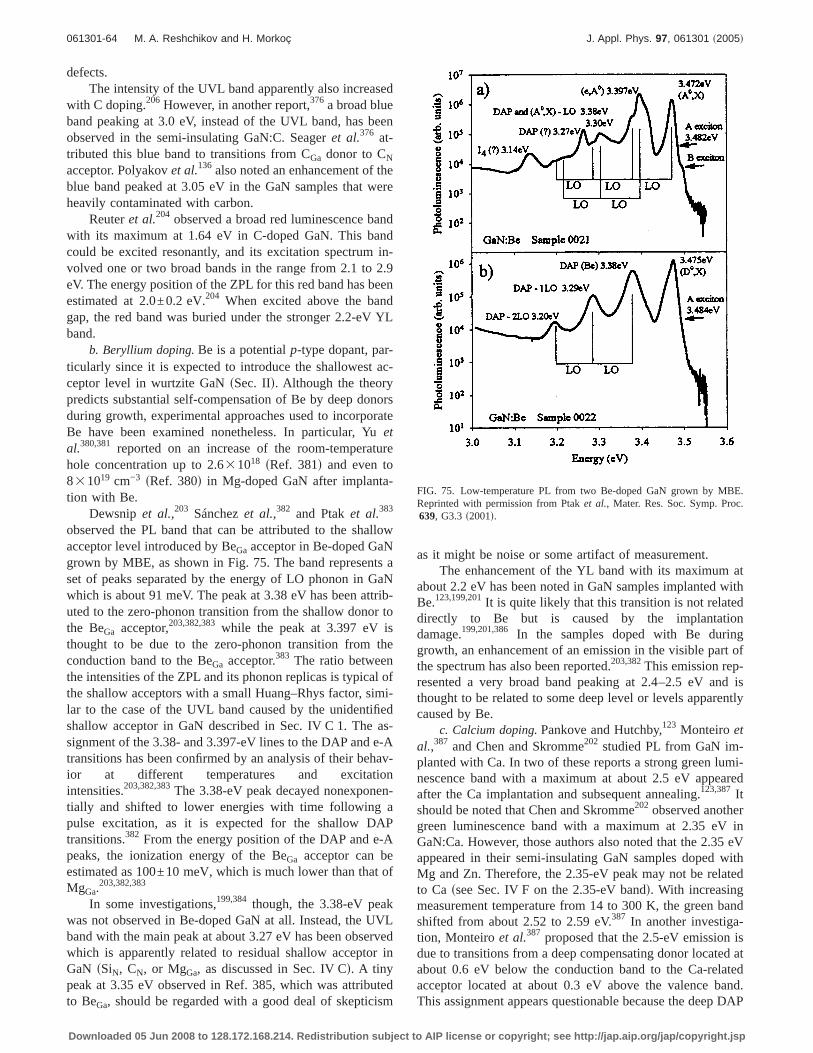
defects.The intensity of the UVL band apparently also increased
with C doping.206 However, in another report,376 a broad blueband peaking at 3.0 eV, instead of the UVL band, has beenobserved in the semi-insulating GaN:C. Seageret al.376 at-tributed this blue band to transitions from CGa donor to CN
acceptor. Polyakovet al.136 also noted an enhancement of theblue band peaked at 3.05 eV in the GaN samples that wereheavily contaminated with carbon.
Reuteret al.204 observed a broad red luminescence bandwith its maximum at 1.64 eV in C-doped GaN. This bandcould be excited resonantly, and its excitation spectrum in-volved one or two broad bands in the range from 2.1 to 2.9eV. The energy position of the ZPL for this red band has beenestimated at 2.0±0.2 eV.204 When excited above the bandgap, the red band was buried under the stronger 2.2-eV YLband.
b. Beryllium doping.Be is a potentialp-type dopant, par-ticularly since it is expected to introduce the shallowest ac-ceptor level in wurtzite GaNsSec. IId. Although the theorypredicts substantial self-compensation of Be by deep donorsduring growth, experimental approaches used to incorporateBe have been examined nonetheless. In particular, Yuetal.380,381 reported on an increase of the room-temperaturehole concentration up to 2.631018 sRef. 381d and even to831019 cm−3 sRef. 380d in Mg-doped GaN after implanta-tion with Be.
Dewsnip et al.,203 Sánchezet al.,382 and Ptaket al.383
observed the PL band that can be attributed to the shallowacceptor level introduced by BeGa acceptor in Be-doped GaNgrown by MBE, as shown in Fig. 75. The band represents aset of peaks separated by the energy of LO phonon in GaNwhich is about 91 meV. The peak at 3.38 eV has been attrib-uted to the zero-phonon transition from the shallow donor tothe BeGa acceptor,203,382,383while the peak at 3.397 eV isthought to be due to the zero-phonon transition from theconduction band to the BeGa acceptor.383 The ratio betweenthe intensities of the ZPL and its phonon replicas is typical ofthe shallow acceptors with a small Huang–Rhys factor, simi-lar to the case of the UVL band caused by the unidentifiedshallow acceptor in GaN described in Sec. IV C 1. The as-signment of the 3.38- and 3.397-eV lines to the DAP and e-Atransitions has been confirmed by an analysis of their behav-ior at different temperatures and excitationintensities.203,382,383The 3.38-eV peak decayed nonexponen-tially and shifted to lower energies with time following apulse excitation, as it is expected for the shallow DAPtransitions.382 From the energy position of the DAP and e-Apeaks, the ionization energy of the BeGa acceptor can beestimated as 100±10 meV, which is much lower than that ofMgGa.
203,382,383
In some investigations,199,384 though, the 3.38-eV peakwas not observed in Be-doped GaN at all. Instead, the UVLband with the main peak at about 3.27 eV has been observedwhich is apparently related to residual shallow acceptor inGaN sSiN, CN, or MgGa, as discussed in Sec. IV Cd. A tinypeak at 3.35 eV observed in Ref. 385, which was attributedto BeGa, should be regarded with a good deal of skepticism
as it might be noise or some artifact of measurement.The enhancement of the YL band with its maximum at
about 2.2 eV has been noted in GaN samples implanted withBe.123,199,201It is quite likely that this transition is not relateddirectly to Be but is caused by the implantationdamage.199,201,386 In the samples doped with Be duringgrowth, an enhancement of an emission in the visible part ofthe spectrum has also been reported.203,382This emission rep-resented a very broad band peaking at 2.4–2.5 eV and isthought to be related to some deep level or levels apparentlycaused by Be.
c. Calcium doping.Pankove and Hutchby,123 Monteiro etal.,387 and Chen and Skromme202 studied PL from GaN im-planted with Ca. In two of these reports a strong green lumi-nescence band with a maximum at about 2.5 eV appearedafter the Ca implantation and subsequent annealing.123,387Itshould be noted that Chen and Skromme202 observed anothergreen luminescence band with a maximum at 2.35 eV inGaN:Ca. However, those authors also noted that the 2.35 eVappeared in their semi-insulating GaN samples doped withMg and Zn. Therefore, the 2.35-eV peak may not be relatedto Ca ssee Sec. IV F on the 2.35-eV bandd. With increasingmeasurement temperature from 14 to 300 K, the green bandshifted from about 2.52 to 2.59 eV.387 In another investiga-tion, Monteiroet al.387 proposed that the 2.5-eV emission isdue to transitions from a deep compensating donor located atabout 0.6 eV below the conduction band to the Ca-relatedacceptor located at about 0.3 eV above the valence band.This assignment appears questionable because the deep DAP
FIG. 75. Low-temperature PL from two Be-doped GaN grown by MBE.Reprinted with permission from Ptaket al., Mater. Res. Soc. Symp. Proc.639, G3.3 s2001d.
061301-64 M. A. Reshchikov and H. Morkoç J. Appl. Phys. 97, 061301 ~2005!
Downloaded 05 Jun 2008 to 128.172.168.214. Redistribution subject to AIP license or copyright; see http://jap.aip.org/jap/copyright.jsp
transitions are characterized with enormous shifts of the bandwith excitation intensity82 or with time following a pulseexcitation.335 Note that no shift of the green band with exci-tation intensity or time following pulse excitation was de-tected in Ca-doped GaN.387 We propose that the 2.5-eV bandis related to transitions from the conduction band, or shallowdonors at low temperatures, to the CaGa acceptor. If so, theionization energy of CaGa can be estimated at about 0.6–0.7eV. Indeed, the ZPL for the 2.5-eV band can be expected at2.8–2.9 eV from the shape of this band at low temperature.
d. Cadmium doping.Cadmium at the Ga sitesCdGad is anacceptor. The PL due to Cd has been studied in Refs. 123,202, 266, 388, and 389. Simply, doping with Cd results in theemergence of a broad blue band peaking at 2.7–2.9 eV. La-gerstedt and Monemar388 observed the fine structure on thehigh-energy side of the band with the ZPL at 2.937 eV and aset of LO and apparently local phonon replicas. The finestructure, caused by electron-phonon coupling, is similar tothat in the Zn-related BL band, shown in Fig. 42, althoughthe energy position of the PL band in Cd-doped GaN isshifted to lower photon energies by about 0.1 eV.202,388 Alower photon energy of the Cd-related PL, as compared toZn-related PL, is consistent with the theoretical predictionsfor the ionization energies of these two acceptorssSec.II C 2d. The ionization energy of Cd should be about 0.56–0.57 eV, provided that the assignment of the 2.937-eV peakin Ref. 388 is accurate.
At 77 K the time-decay of the Cd-related blue band isnonexponential in the microsecond range.266 No obviousvariation in the shape and position of this band has beenobserved at different delay times following a pulse excita-tion. It is possible that the transitions from the conductionband to the CdGa acceptor overlapped with transitions fromthe shallow donors to the same acceptor cause the nonexpo-nential decay of PL.266
e. Manganese doping.Extrapolating the carrier-mediatedmagnetic interaction from dilute GaAs:Mn to GaN:Mn, Dietlet al.390 predicted high-temperature ferromagnetism in diluteMnxGa1−xN with x<0.05 in assumption that the free holeconcentrations of the order of 1020 cm−3 can be achieved insuch a material. This prediction paved the way for a plethoraof activity for potential application of this material to spin-transport electronicssspintronicsd. However, in contrast withGaAs where Mn is a relatively shallow acceptorsEA
<0.1 eVd which sets the stage for high concentration of freeholes to be obtained at room temperature, the Mn level inGaN is almost in the middle of the band gap,391–394and onecannot expect any detectable transport of holes bound to theMn acceptor even at very high concentrations of Mn. Grafetal.393,394 have unambiguously demonstrated that in contrastwith GaAs,395 holes bound to Mn in GaN:Mn are located inthe d shell. The Mn3+/2+ acceptor level is located at 1.8 eVabove the valence band.393,394 Those authors also showedthat the characteristic absorption spectrum with the ZPL at1.42 eV, observed earlier by Korotkovet al.,391,392 resultsfrom an internal5E→5T transition in Mn3+ sconfigurationd4d. The transition of holes from Mn3+ to the valence bandhas also been seen in the absorption spectrum for photon
energies above 1.8 eV.393,394 Note that when the GaN:Mnsample is codoped with Si, an electron is captured by a Mnacceptor, transforming it into the Mn2+ sd5d state.
Korotkov et al.396 observed a PL signal related to Mnacceptor. That band appeared as a broad structureless bandwith its maximum at 1.27 eV with a FWHM of about 0.26eV. With increasing temperature from 13 to 300 K, the Mnpeak position remained nearly unchanged. A transient PLstudy of this band revealed a very slow exponential decay ofthe PL intensity with a characteristic lifetime of about 8ms.391 A slow exponential decay of the PL is typical of in-ternal transitions. Consequently, it is most likely that the1.27-eV band is caused by transitions of holes from the ex-cited states of Mn3+, located close to the valence band, to itsground5T level.
f. Other acceptors in GaN.In addition to the above-mentioned acceptors in GaN, Pankove and Hutchby123 exam-ined the effect of Hg implantation on the PL in GaN. Implan-tation of Hg resulted in a broad green band with a maximumat 2.43 eV. Assuming that this band is due to a transitionfrom the conduction band or shallow donor to the HgGa ac-ceptor, the activation energy of the HgGa acceptor can beestimated as 0.8±0.2 eV based on the position and shape ofthis broad band.
Pankove and Hutchby123 also implanted several other el-ements in GaN that might possibly act as acceptors, such asCu, Ag, Au, Sr, Ba, Li, Na, K, Sc, Zr, Fe, Co, Ni, Dy, and Er.All of these elements resulted in broad PL bands withmaxima ranging from 1.5 to 2.2 eV. In all cases deep levelsare responsible for the observed PL. However, it is difficultto distinguish the emission bands associated with these ele-ments from those arising from native defects formed by theimplantation damage. In the case of transition metals or rare-earth elements, the emission in the red portion of the spec-trum might also be caused by internal transitions ind or fshellsssee Sec. V C 5d.
3. Doping with isoelectronic impurities
Isoelectronic impurities, such as AsN and PN, have beenconsidered as promising candidates for the mixed anion ni-tride alloys such as GaAsxN1−x and GaPxN1−x. However, for-mation of deep levels in these alloys, attributed to AsN andPN, would induce discontinuous changes in the size of theband gap.45
a. Arsenic doping.Arsenic introduces a broad blue bandwith its peak at about 2.6 eV in GaN.123,202,397–400It is usu-ally structureless, but a well-defined phonon-related finestructure has also been reported.202 The intensity of the2.6-eV band increases monotonically with increasing Asdoping,398,400 while the concentration of free electrons re-mains nearly unchanged.401,402Several authors noted that theintensity of this band is nearly insensitive to temperature inthe range of,10–300 K.397–399 An activation energy of,50 meV has been estimated for quenching of the 2.6-eVband between 100 and 300 K.397 Note that the total decreaseof the intensity in Ref. 397 was only a factor of 2; therefore,the small decrease might be related to the variation in the
061301-65 M. A. Reshchikov and H. Morkoç J. Appl. Phys. 97, 061301 ~2005!
Downloaded 05 Jun 2008 to 128.172.168.214. Redistribution subject to AIP license or copyright; see http://jap.aip.org/jap/copyright.jsp

capture cross section,67 and the real quenching of this bandmight take place above room temperature with yet an un-known activation energy.
A time-resolved PL study revealed that the decay of the2.6-eV band is nearly exponential even at low temperatureswith a characteristic time of about 0.1µs.397,399The lifetimedecreased from 92 to approximately 77 ns with increasingtemperature from 8 to 100 K, and subsequently increased upto 148 ns with further increase of temperature up to 300 K.399
Such a behavior of the PL is typical for internal transitionsrather than transitions involving the states in the conductionor valence bands.
Chen and Skromme202 observed the fine structure on thehigh-energy side of the blue band related to As implantation,as depicted in Fig. 76. The ZPL was observed at 2.952 eVfollowed by two LO phonon replicas. Besides, the spectrumcontained peaks separated from the ZPL by 38 and 75 meVthat were attributed to other lattice phonon modes.202 If the2.6-eV band is due to the recombination of an exciton boundto the As-related defect, as it was suggested in Refs. 202,397, and 399, its localization energy can be estimated as 535meV which represents the energy difference between thezero-phonon line and free-exciton line.202 However, if thetransitions from the conduction band to the As-related defectwere responsible for the 2.6-eV emission, the energy level ofthe As-related defect would be at about 560 meV above thevalence band. A more detailed analysis, including compari-son of the PL lifetime with concentration of free electrons atdifferent temperatures, is warranted and would be able toprovide the ultimate answer on identification of the 2.6-eVband in As-doped GaN.
b. Phosphorus doping.Implantation of P in GaN results ina broad blue-violet luminescence band peaking at about 2.9eV.123,202,403,404This band quenched above 100–150 K withan activation energy of about 168–180 meV.403 Chen andSkromme202 observed the fine structure of the blue-violetband in GaN:P, as shown in Fig. 77. The ZPL at 3.200 eV isfollowed by two LO phonon replicass91 meVd and a fewother phonon replicas, separated by 39, 59, and 77 meV fromthe ZPL, that have been attributed to various lattice phonon
modes.202 The energy separation of 287 meV between theZPL and the free-exciton line yields the exciton localizationenergy, provided that the blue-violet band is due to the iso-electronic PN bound exciton.202
4. Radiative defects introduced by irradiation
Native point defects, such as interstitials and vacancies,can be created by high-energy electron irradiation. However,a threshold energy, of the order of,1 MeV, must be over-come to produce atomic displacements.177 This forms themotivation for using 1–2.5-MeV electrons in studies of de-fects created by irradiation. To remove the additional crystaldamage caused by irradiation the samples are subsequentlyannealed before conducting the intended studies.
The PL signal from defects created by electron irradia-tion has been a topic of investigation in a number ofreports.31,184,185,405–408Of particular interest, two infrared PLbands at about 0.85 and 0.95 eV emerge in the low-temperature PL spectrum after irradiation of GaN with 2.5-MeV electrons at doses above,1018 cm−2 at roomtemperature.31,184,185,407,408The former contains a sharp ZPLat 0.88 eV accompanied by a rich phonon structure. Thelatter is relatively broad and apparently structureless. Buy-anovaet al.408 proposed that the 0.88-eV emission is relatedto the internal transition between an excited and groundstates of a deep defect, but the identity of the defect was notrevealed. Relying on the thermal quenching of this PL bandhaving an activation energy of,30 meV, those authors con-cluded that the excited state is close to the conduction bandand, therefore, the ground state is located 0.91 eV below theconduction band.
Paramagnetic-resonance studies of the PL signal led tothe identification of the infrared bands. Four EPR signalslabeled L1–L4 have been observed via ODMR experimentsin these bands.31,405The L1, L3, and L4 signals correspond-ing to theS= 1
2 centers were detected in the 0.95-eV band,while the L2 signal corresponding to theS=1 center matchedthe 0.88-eV band extremely well.405 A well-resolved hyper-fine interaction structure observed for the L3 and L4 signalsindicates that interstitial Ga atomsapparently by pairing with
FIG. 76. Low-temperature PL spectrum of the As-implanted GaN, showingthe no-phononsNPd line and its phonon replicas. Reprinted with permissionfrom Chen and Skromme, Mater. Res. Soc. Symp. Proc.743, L11.35s2003d.
FIG. 77. Low-temperature PL spectrum of the P-implanted GaN, showingthe no-phononsNPd line and its phonon replicas. Reprinted with permissionfrom Chen and Skromme, Mater. Res. Soc. Symp. Proc.743, L11.35s2003d.
061301-66 M. A. Reshchikov and H. Morkoç J. Appl. Phys. 97, 061301 ~2005!
Downloaded 05 Jun 2008 to 128.172.168.214. Redistribution subject to AIP license or copyright; see http://jap.aip.org/jap/copyright.jsp
some other defectd is responsible for the 0.95-eV band.405 Insitu irradiation with 2.5-MeV electrons at 4.2 K resulted inthe appearance of the 0.95-eV band while the 0.88-eV bandbecame absent.31 Surprisingly, none of the L1–L4 signalswas detectable by ODMR in this case, implying that none ofthe related defects had been created immediately followingthe 4-K in situ irradiation. Instead, the effective-mass donorand a new L5 signal were detected. The latter was unambigu-ously identified as the isolated Gai
2+.31 Upon a low-temperature annealingsbelow room temperatured theeffective-mass donor and L5-related signals quenched, whilethe L1 and L2 signals emerged. This led Chowet al.31 toconclude that Gai
2+ is formed by the low-temperature irradia-tion, but it easily migrates and eventually forms complexeswith other defects at elevated temperatures. Therefore, boththe 0.88- and 0.95-eV bands are considered related to somecomplexes involving Ga interstitials.
5. Transition and rare-earth elements
Optical properties of transition metals and rare-earth el-ements are mainly determined by internal transitions ratherthan by transitions between the host bands and the defectlevels. The PL spectrum from transition and rare-earth ele-ments usually contains a set of sharp lines corresponding tooptical transitions between different states of the metal ion.The energy positions of these lines for a particular metal varyonly weakly between different semiconductors. For this rea-son we confine the review of the PL from transition andrare-earth elements to a brief listing of the relevant refer-ences with only minimal comments.
a. Transition metals.Metals Zn, Cd, Hg, Cu, Ag, and Auare formally considered as transition metals. However, thedshells of these particular metals are normally filled com-pletely. Consequently, these metals do not exhibit internaltransitions in GaNssee Sec. IV B for Zn in GaN and Sec.IV D 2 for Cd- and Hg-doped GaNd. A very common transi-tion metal, Mn, and the PL transitions associated with it inthe GaN host are reviewed in Sec. IV D 2 e.Among the othertransition metals, the PL lines due to Fe, Cr, Ti, and V havebeen investigated. Generally, these transition metals are in-advertently incorporated into GaN as a result of contamina-tion during the growth.
The ZPL due to the internal4T1→6A1 transition in 3dshell of Fe3+ on Ga sites3d5d has been observed at 1.30 eVin GaN.152,409–412FeGa is an acceptor in GaN, and its2/0level is located at 2.5 eV above the valence band.413
The line at 1.193 eV has often beenobserved152,409,414–416and assigned either to1E→3A2 transi-tion of Ti2+ s3d2d sRef. 416d or to 3T2→3A2 transition ofCr4+ s3d2d.415 The line at 1.047 eV can be attributed to the4T2→4A2 transition of Co2+ on Ga site s3d7d.412 The0.931-eV line has been assigned to the 3d shell transition3T2→3A2 of V3+ s3d2d.415 However, no correlation betweenvanadium doping and the 0.931-eV line has been noted.417
Vanadium followed by annealing has been reported to giverise to a sharp and intense line at 0.820 eV.417
b. Rare-earth elements.Rare-earth elements are incorpo-rated into GaN to fabricate efficient light-emitting devices
whose wavelength is determined by internal transitions asso-ciated with the impurity while GaN acting as a host.418 Theluminescence properties of the partially filled 4f shell asso-ciated with rare earths, which is electrically shielded fromthe surrounding host material, are to a first extent insensitiveto the nature of the host. Blue,419–421 green,420,422–426
red,426–435turquoise,436 yellow, and orange437 colors of lumi-nescence from GaN doped with rare earth have been demon-strated. In GaN, Tm3+ is commonly used for blue, Er3+ forgreen and infrared, and Eu3+ or Pr3+ for red emission.
VI. DEFECT-RELATED LUMINESCENCE IN CUBIC GaN
The present review focuses mainly on wurtzite or hex-agonal GaN, but we briefly review the defect-related PL incubic GaN below for completeness. The discussion isdeemed useful for understanding the physics of defects inGaN, both with hexagonal and cubic symmetries, since de-fects in these two lattice configurations are expected to havemany common features. Moreover, optical transitions inwurtzite GaN are sometimes attributed to recombination incubic inclusions, which necessities some level of knowledgein this less studied polytype.
Zinc-blendescubicd GaN is a metastable phase. It is usu-ally obtained by MBE growth on cubic substrates. The bandgap of cubic GaN is 3.300±0.004 eV at lowtemperatures,438,439 which is about 200 meV smaller thanthat in hexagonal GaN. This material is attractive, in particu-lar, due to high mobilities and controlled doping concentra-tions of free carriers already achieved in bothn and ptypes.440,441
A. Undoped material
1. Exciton emission
A line at 3.27 eV, which can be seen in Fig. 78, is attrib-uted to an exciton bound to the shallow donor in cubicGaN.438,442–444The position of this line is independent of theexcitation intensity and follows the band gap with increasingtemperature.438,444–447With increasing temperature, this lineis gradually replaced by the free-exciton emission, althoughthese transitions have not been resolved as distinctlines.438,443,444,447Utilizing temperature-induced quenchingof the 3.27-eV line, Strausset al.442 have estimated the lo-calization energy of the donor-bound exciton as 4±2 meV.Assignment of the 3.27-eV line to the donor-bound excitonat low temperatures is in agreement with its very short life-time of about 30 ps.442,448Above 50 K, the free-exciton emis-sion quenches with an activation energy of 22–26 meV,which is attributed to the binding energy of the freeexciton.444,447
2. Shallow DAP band
A line at about 3.16 eVsFig. 78d observed in cubic GaNis assigned to the zero-phonon transition of the shallow DAPband.77,438,443,444,446,447,449–451Up to two LO phonon replicascan be seen which are separated by about 86 meV from thezero-phonon line.438 A very small electron-phonon coupling,with a Huang–Rhys factor of about 0.02,438 is typical for theeffective-mass acceptors, as seen in Fig. 78. The DAP emis-
061301-67 M. A. Reshchikov and H. Morkoç J. Appl. Phys. 97, 061301 ~2005!
Downloaded 05 Jun 2008 to 128.172.168.214. Redistribution subject to AIP license or copyright; see http://jap.aip.org/jap/copyright.jsp
sion shifted markedly to higher photon energies both withexcitation intensity438,443,445–447,451 and withtemperature,438,445–447demonstrating a behavior typical ofthe DAP-type transitions. Aset al.444 observed transforma-tion of the DAP transition into an e-A transition involvingthe same shallow acceptor and determined the activation en-ergies of the shallow donor and acceptor in cubic GaN as25±5 and about 130 meV, respectively.
Two PL lines at 3.08 and 2.99 eV have been identified asthe ZPL and LO phonon replica, respectively, of the DAPtransition involving another deeper donor.452 The electron-phonon coupling for this emission, with a Huang–Rhys fac-tor of about 0.4, is stronger than that for the shallowestacceptor.452 The 3.08-eV line should not be confused withthe first LO phonon replica of the 3.16-eV line, appearing asa very weak peak in selected samples, as depicted in Fig.78.438,452Wu et al.446 also attributed the weak lines observedat 3.056 and 3.088 eV to a deeper acceptor in cubic GaNbased, owing to their temperature and excitation intensitydependencies. Possibly the 3.08-eV line is caused by residualcarbon, as discussed in Sec. VI B 1.
3. Deep defects
In addition to the common emission lines in cubic GaN,Xu et al.445 observed two relatively broad lines at 2.926 and2.821 eV. These lines shifted by about 40 meV to higherenergies with increasing excitation intensity by two orders ofmagnitude. With increasing temperature, the lines shifted tolower energies faster than the band gap decreased andquenched above,100 K with an activation energy of about18 meV. Xuet al.445 proposed that the 2.926- and 2.821-eVlines are caused by transitions between a shallow donor andtwo deep acceptor levels located at about 0.34 and 0.45 eVabove the valence band.
Goldyset al.453 observed a broad red luminescence bandpeaking at about 1.9 eV in undoped cubic GaN. The red bandshifted by 32 meV to higher energies with increasing excita-tion intensity by a factor of 10, demonstrating a behaviortypical of DAP transitions.453 With increasing temperature,the red band quenched with an activation energy of 15 meV,although its intensity decreased by only,25% up to roomtemperature.453 The decay of the red band is slow and non-exponential, in agreement with its assignment to DAPrecombination.453
B. Doped material
1. Carbon doping
As et al.440,454,455reportedp-type doping of cubic GaNwith carbon by plasma-assisted MBE on GaAs substrates.The reported hole concentration and hole mobilities were6.131018 cm−3 and 23.5 cm2/V s, respectively, inc-GaN.440
In samples with a hole concentration below approximately1017 cm−3 the hole mobility exceeded 200 cm2/V s.440
Doping with carbon results in a relatively narrow PLband at about 3.08 eV and a very broad band between 1.8and 2.3 eV, as depicted in Fig. 79.456 The intensity of the3.08-eV band monotonously increases with C dopingsFig.79d.455 In fact, the band consists of two lines separated byabout 25 meV. The lower-energy component is attributed tothe DAP transition and the higher-energy component to thee-A transition involving the same CN acceptor with a bindingenergy of 215 meV.455,456 The donor, having a binding en-ergy of 25 meV, is apparently the same as in undoped cubicGaN.444
As and co-workers440,454,456–458also observed a broadred-yellow luminescence band with peaks at about 2.12 and1.89 eV in C-doped GaN. As can be seen in Fig. 79, theintensity of this red-yellow band monotonously increaseswith C doping.457 Those authors assigned the double-peakband to transitions from a deep C-related donor which islocated 1.185 eV below the conduction band to the shallowC acceptor and the valence band.454,456,458,459Note, however,that there are no equilibrium holes in the valence band at 2K. Therefore, transitions of photogenerated electrons from adeep donor to the valence band are highly unlikely. However,transitions from a deep donor to the shallow CN acceptor areplausible for the heavily C-doped cubic GaN. This is in someways similar to the assignment of the BL band in heavilyMg-doped GaN in hexagonal GaN discussed in Sec. V B 3.As et al.440,454proposed that the deep donor is a CNCi com-
FIG. 78. CL spectra of a cubic GaN crystal at 5 K.sad andsbd correspond todifferent points on the same crystal. The solid lines in the insets are fits tothe data points, using Gaussians. The FWHM of the exciton line amounts to8 meVsad and 11 meVsbd. Reprinted with permission from Mennigeret al.,Phys. Rev. B53, 1881s1996d. Copyrights1996d by the American PhysicalSociety.
061301-68 M. A. Reshchikov and H. Morkoç J. Appl. Phys. 97, 061301 ~2005!
Downloaded 05 Jun 2008 to 128.172.168.214. Redistribution subject to AIP license or copyright; see http://jap.aip.org/jap/copyright.jsp
plex. Note that the energy level of this donor could be esti-mated from the high-energy cutoff of the yellow band wherethe ZPL is expected at about 2.3 eV, accounting for the Cou-lomb interaction in deep DAP which may be rather strong.Overall, an estimate of 1.1±0.2 eV is a plausible figure. Ex-periments with varying excitation intensities can verify theproposed model and possibly improve the estimate of thedonor energy level.
2. Magnesium doping
In contrast with C-doped cubic GaN where carbon incor-porates with concentrations above 1020 cm−3 and the room-temperature hole concentration reaches 631018 cm−3 sRef.440d, incorporation of Mg in cubic GaN saturates at about531018 cm−3 and the room-temperature hole concentrationdoes not exceed 1016 cm−3 sRef. 460d. With increasing Mgdoping a blue band peaking at 2.8 eV and two barely re-solved peaks at 3.04 and 3.07 eV emerge in the PLspectrum.460 The origin of the blue band may be similar tothe BL band in hexagonal GaNsSec. V B 3d, although ex-periments with variation of temperature and excitation inten-sity as well as time-resolved PL study are needed for confir-mation. Note that Xuet al.461 observed the blue band incubic GaN that noticeably shifted with the excitation inten-sity in much the same way as the BL band in hexagonalGaN.82 However, those authors attributed the oscillatoryshape of the blue band to contributions from five transitionswith different behavior on the intensity of excitation. Onecan argue that the oscillatory behavior could also be due tointerference effects from the 1.5-µm-thick layer. The 3.04-
and 3.07-eV bands have been attributed to the DAP and e-Atransitions, respectively, involving the same MgGa acceptorwith an activation energy of 0.23 eV.460
3. Silicon doping
As in the case of wurtzitic polytype, Si is a very efficientdonor in cubic GaN. With increasing Si doping, it has beenreported that the exciton emission peak shifted to lower en-ergies with an accompanying increase in its width.462,463Forimpurity concentrations near 1020 cm−3, band-to-band transi-tions dominated in degenerate GaN:Si at lowtemperatures.463 The 3.15-eV band, assigned to DAP transi-tions involving an unidentified shallow acceptor, exhibited ashift to higher energies with increasing Si doping.441,463Thatshift has been attributed to increased Coulomb interaction indonor-acceptor pairs with smaller separation.441
VII. EXCITONS BOUND TO POINT DEFECTS
In this section a very brief review of the salient experi-mental results on exciton-related PL in wurtzitic GaN withan emphasis on excitons bound to shallow defects is pre-sented. Excitonic transitions in GaN are very efficient. Exci-tons can be bound not only to shallow donors and acceptorsbut also to deep point defects and structural defects. Thelatter case is discussed in Sec. VIII.
A. Free excitons
Since the review is devoted to defects in GaN, and freeexcitons are not related to defects at all, the discussion in thissection is mostly limited to the properties of free excitonsthat are imperative to understanding of PL from bound exci-tons.
The valence band in wurtzitic GaN is split into threesubbands,A, B, andC, due to the crystal-field splitting andspin-orbit coupling. Free excitons may involve a hole fromeach of the subbands. Accordingly the freeA, B, andC ex-citons are denoted asXA, XB, andXC. The fine structure ofthe exciton spectrum includes the excited statessn=2,3,…d. The fine structure is affected by crystal aniso-tropy, intersubband coupling, polar interactions with opticalphononssFig. 80d,464 as well as electron-hole exchange, anddipole-dipole interaction.464,465 In particular, the 1S state oftheA exciton is split by the short-range exchange interactioninto a dipole-forbiddenG6 state swith energy E6d and adipole-activeG5, stateswith energyE5=E6+D56, whereD56
is the energy of the electron-hole exchange interactiond.465
The exciton fine structure depends on the geometrical con-figuration of the optical experimentsFig. 81d. When the ex-citon wave vectork¢ is parallel to the hexagonal axisc, bothG5 components are transverseG5T states. On the other handwhenk¢ 'c, one of the components is a longitudinalG5L statewhich is shifted to a higher energyE5+DLT by the dipole-dipole interaction. HereDLT denotes the longitudinal-transverse splitting of the exciton. The longitudinal excitonG5L and the forbidden excitonG6 have zero oscillatorstrength unless they are mixed with allowed states of theBexciton. Further, interaction of the transverse excitonsG5T
with the radiation field results in the formation of lower,
FIG. 79. PL spectra of C-doped cubic GaN layers grown with differentfluxes of C. The topmost spectrum has been multiplied by a factor of 25.Reprinted with permission from Aset al., Mater. Res. Soc. Symp. Proc.693, I2.3 s2002d.
061301-69 M. A. Reshchikov and H. Morkoç J. Appl. Phys. 97, 061301 ~2005!
Downloaded 05 Jun 2008 to 128.172.168.214. Redistribution subject to AIP license or copyright; see http://jap.aip.org/jap/copyright.jsp
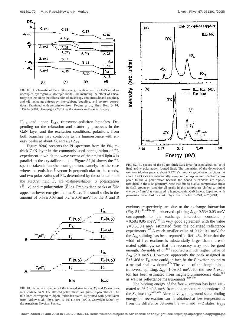
G5T1, and upper,G5T2, transverse-polariton branches. De-pending on the relaxation and scattering processes in theGaN layer and the excitation conditions, polaritons fromboth branches may contribute to the luminescence with en-ergy peaks at aboutE5 andE5+DLT.
Figure 82sad presents the PL spectrum from the 80-µm-thick GaN layer in the commonly used configuration of PLexperiment in which the wave vector of the emitted lightk¢ isparallel to the crystallinec axis. Figure 82sbd shows the PLspectra taken in another configuration, namely, for the casewhere the emissionk¢ vector is perpendicular to thec axis,and two polarizations of PL, determined by the orientation of
the electric field E¢ , are distinguishable:s polarization
sE¢ 'cd andp polarizationsE¢ icd. Free-exciton peaks atE¢ ic
appear at lower energies than atE¢ 'c. The small shifts in theamount of 0.53±0.03 and 0.24±0.08 meV for theA and B
excitons, respectively, are due to the exchange interactionsFig. 81d.465,466The observed splittingD56=0.53±0.03 meVcorresponds to the exchange interaction constantg=0.58±0.05 meV,465 in very good agreement with the valueg=0.6±0.1 meV estimated from the polarized reflectanceexperiments.467 A much smaller value of 0.12±0.1 meV fortheD56 splitting has been reported in Ref. 464. Note that thewidth of free excitons is substantially larger than the esti-mated splittings, so that the accuracy may not be goodenough. Reynoldset al.468 reported a much higher value ofD56 s2.9 meVd. However, apparently the peak assigned inRef. 468 toG6 state could, in fact, be theB exciton bound toa neutral shallow donor.465 The value of the longitudinal-transverse splitting,DLT =1.0±0.1 meV, for the freeA exci-ton has been estimated from magnetoluminescence data,464
as well as reflectance measurements.469,470
The binding energy of the freeA exciton has been esti-mated as 26.7±0.3 meV from the temperature dependence oftheXA intensity.471,472Alternatively, the ground-state bindingenergy of free exciton can be obtained at low temperaturesfrom the difference between then=1 andn=2 states:EA,1S
FIG. 80. A schematic of the exciton energy levels in wurtzite GaN insad anuncoupled hydrogenlike isotropic model,sbd including the effect of aniso-tropy, scd including the effects both of anisotropy and intersubband coupling,and sdd including anisotropy, intersubband coupling, and polaron correc-tions. Reprinted with permission from Rodinaet al., Phys. Rev. B 64,115204s2001d. Copyrights2001d by the American Physical Society.
FIG. 81. Schematic diagram of the internal structure ofXA andXB excitonsin a wurtzite GaN. The allowed polarizations are given in parentheses. Thethin lines correspond to dipole-forbidden states. Reprinted with permissionfrom Paskovet al., Phys. Rev. B64, 115201s2001d. Copyrights2001d bythe American Physical Society.
FIG. 82. PL spectra of the 80-µm-thick GaN layer fors polarizationssolidlined and p polarizationsdotted lined. The intensities of the donor-boundexcitonssdouble peak at about 3.477 eVd and acceptor-bound excitonssatabout 3.473 eVd are substantially lower in thep-polarized spectrum com-pared to thes polarization because the boundA excitons are dipole-forbidden in theE ic geometry. Note that due to biaxial compressive stressin GaN grown on sapphire all peaks in this sample are shifted to higherenergy by 7 meV as compared to homoepitaxial GaN layers. Reprinted withpermission from Paskovet al., Phys. Status Solidi B228, 467 s2001d.
061301-70 M. A. Reshchikov and H. Morkoç J. Appl. Phys. 97, 061301 ~2005!
Downloaded 05 Jun 2008 to 128.172.168.214. Redistribution subject to AIP license or copyright; see http://jap.aip.org/jap/copyright.jsp
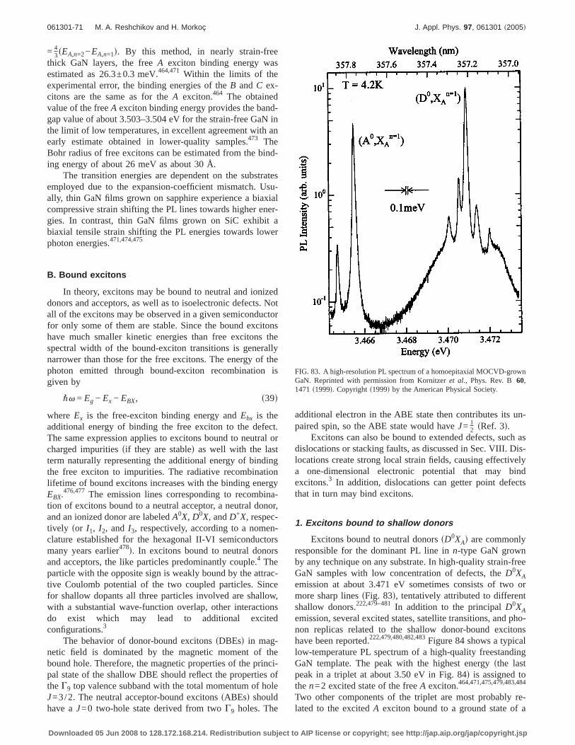
= 43sEA,n=2−EA,n=1d. By this method, in nearly strain-free
thick GaN layers, the freeA exciton binding energy wasestimated as 26.3±0.3 meV.464,471 Within the limits of theexperimental error, the binding energies of theB andC ex-citons are the same as for theA exciton.464 The obtainedvalue of the freeA exciton binding energy provides the band-gap value of about 3.503–3.504 eV for the strain-free GaN inthe limit of low temperatures, in excellent agreement with anearly estimate obtained in lower-quality samples.473 TheBohr radius of free excitons can be estimated from the bind-ing energy of about 26 meV as about 30 Å.
The transition energies are dependent on the substratesemployed due to the expansion-coefficient mismatch. Usu-ally, thin GaN films grown on sapphire experience a biaxialcompressive strain shifting the PL lines towards higher ener-gies. In contrast, thin GaN films grown on SiC exhibit abiaxial tensile strain shifting the PL energies towards lowerphoton energies.471,474,475
B. Bound excitons
In theory, excitons may be bound to neutral and ionizeddonors and acceptors, as well as to isoelectronic defects. Notall of the excitons may be observed in a given semiconductorfor only some of them are stable. Since the bound excitonshave much smaller kinetic energies than free excitons thespectral width of the bound-exciton transitions is generallynarrower than those for the free excitons. The energy of thephoton emitted through bound-exciton recombination isgiven by
"v = Eg − Ex − EBX, s39d
whereEx is the free-exciton binding energy andEbx is theadditional energy of binding the free exciton to the defect.The same expression applies to excitons bound to neutral orcharged impuritiessif they are stabled as well with the lastterm naturally representing the additional energy of bindingthe free exciton to impurities. The radiative recombinationlifetime of bound excitons increases with the binding energyEBX.
476,477 The emission lines corresponding to recombina-tion of excitons bound to a neutral acceptor, a neutral donor,and an ionized donor are labeledA0X, D0X, andD+X, respec-tively sor I1, I2, and I3, respectively, according to a nomen-clature established for the hexagonal II-VI semiconductorsmany years earlier478d. In excitons bound to neutral donorsand acceptors, the like particles predominantly couple.4 Theparticle with the opposite sign is weakly bound by the attrac-tive Coulomb potential of the two coupled particles. Sincefor shallow dopants all three particles involved are shallow,with a substantial wave-function overlap, other interactionsdo exist which may lead to additional excitedconfigurations.3
The behavior of donor-bound excitonssDBEsd in mag-netic field is dominated by the magnetic moment of thebound hole. Therefore, the magnetic properties of the princi-pal state of the shallow DBE should reflect the properties oftheG9 top valence subband with the total momentum of holeJ=3/2. Theneutral acceptor-bound excitonssABEsd shouldhave aJ=0 two-hole state derived from twoG9 holes. The
additional electron in the ABE state then contributes its un-paired spin, so the ABE state would haveJ= 1
2 sRef. 3d.Excitons can also be bound to extended defects, such as
dislocations or stacking faults, as discussed in Sec. VIII. Dis-locations create strong local strain fields, causing effectivelya one-dimensional electronic potential that may bindexcitons.3 In addition, dislocations can getter point defectsthat in turn may bind excitons.
1. Excitons bound to shallow donors
Excitons bound to neutral donorssD0XAd are commonlyresponsible for the dominant PL line inn-type GaN grownby any technique on any substrate. In high-quality strain-freeGaN samples with low concentration of defects, theD0XAemission at about 3.471 eV sometimes consists of two ormore sharp linessFig. 83d, tentatively attributed to differentshallow donors.222,479–481In addition to the principalD0XAemission, several excited states, satellite transitions, and pho-non replicas related to the shallow donor-bound excitonshave been reported.222,479,480,482,483Figure 84 shows a typicallow-temperature PL spectrum of a high-quality freestandingGaN template. The peak with the highest energysthe lastpeak in a triplet at about 3.50 eV in Fig. 84d is assigned tothen=2 excited state of the freeA exciton.464,471,475,479,483,484
Two other components of the triplet are most probably re-lated to the excitedA exciton bound to a ground state of a
FIG. 83. A high-resolution PL spectrum of a homoepitaxial MOCVD-grownGaN. Reprinted with permission from Kornitzeret al., Phys. Rev. B60,1471 s1999d. Copyrights1999d by the American Physical Society.
061301-71 M. A. Reshchikov and H. Morkoç J. Appl. Phys. 97, 061301 ~2005!
Downloaded 05 Jun 2008 to 128.172.168.214. Redistribution subject to AIP license or copyright; see http://jap.aip.org/jap/copyright.jsp
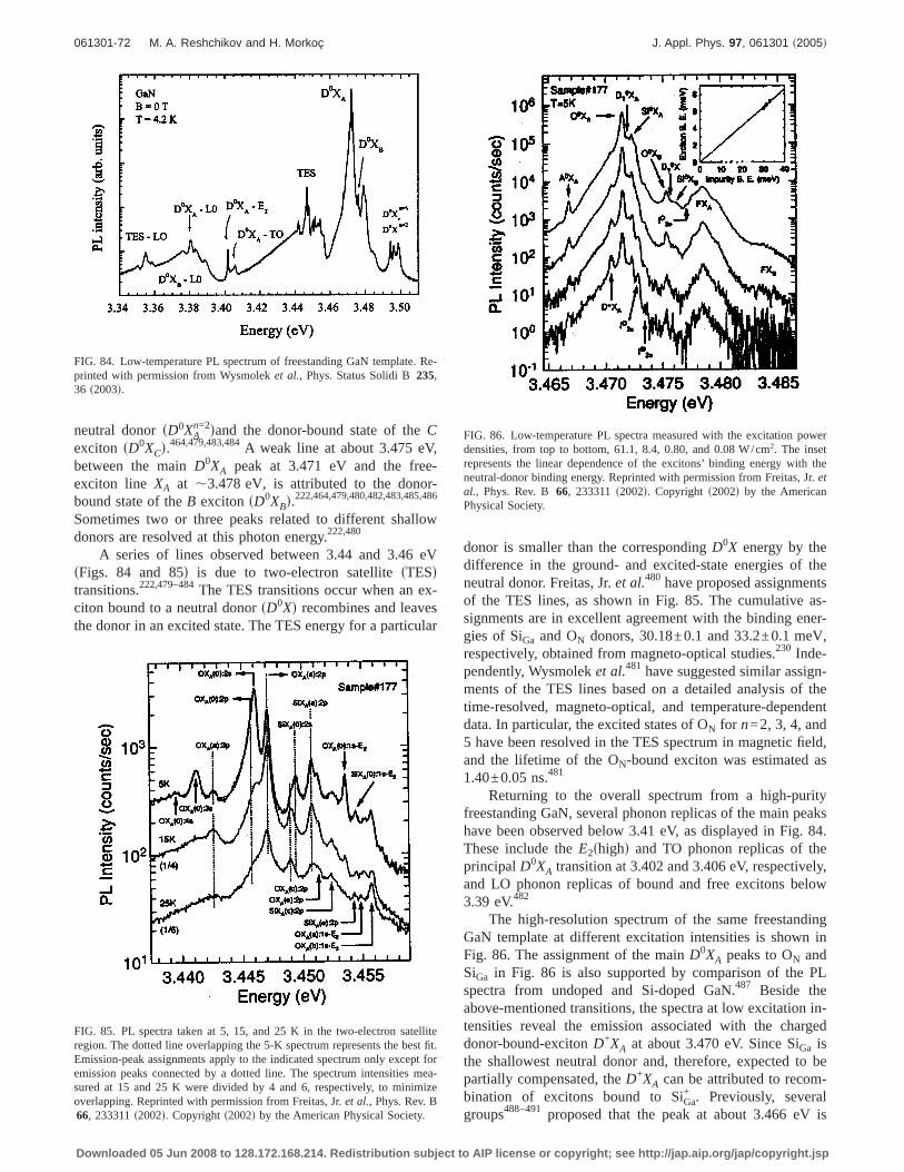
neutral donorsD0XAn=2dand the donor-bound state of theC
exciton sD0XCd.464,479,483,484A weak line at about 3.475 eV,between the mainD0XA peak at 3.471 eV and the free-exciton line XA at ,3.478 eV, is attributed to the donor-bound state of theB excitonsD0XBd.222,464,479,480,482,483,485,486
Sometimes two or three peaks related to different shallowdonors are resolved at this photon energy.222,480
A series of lines observed between 3.44 and 3.46 eVsFigs. 84 and 85d is due to two-electron satellitesTESdtransitions.222,479–484The TES transitions occur when an ex-citon bound to a neutral donorsD0Xd recombines and leavesthe donor in an excited state. The TES energy for a particular
donor is smaller than the correspondingD0X energy by thedifference in the ground- and excited-state energies of theneutral donor. Freitas, Jr.et al.480 have proposed assignmentsof the TES lines, as shown in Fig. 85. The cumulative as-signments are in excellent agreement with the binding ener-gies of SiGa and ON donors, 30.18±0.1 and 33.2±0.1 meV,respectively, obtained from magneto-optical studies.230 Inde-pendently, Wysmoleket al.481 have suggested similar assign-ments of the TES lines based on a detailed analysis of thetime-resolved, magneto-optical, and temperature-dependentdata. In particular, the excited states of ON for n=2, 3, 4, and5 have been resolved in the TES spectrum in magnetic field,and the lifetime of the ON-bound exciton was estimated as1.40±0.05 ns.481
Returning to the overall spectrum from a high-purityfreestanding GaN, several phonon replicas of the main peakshave been observed below 3.41 eV, as displayed in Fig. 84.These include theE2shighd and TO phonon replicas of theprincipalD0XA transition at 3.402 and 3.406 eV, respectively,and LO phonon replicas of bound and free excitons below3.39 eV.482
The high-resolution spectrum of the same freestandingGaN template at different excitation intensities is shown inFig. 86. The assignment of the mainD0XA peaks to ON andSiGa in Fig. 86 is also supported by comparison of the PLspectra from undoped and Si-doped GaN.487 Beside theabove-mentioned transitions, the spectra at low excitation in-tensities reveal the emission associated with the chargeddonor-bound-excitonD+XA at about 3.470 eV. Since SiGa isthe shallowest neutral donor and, therefore, expected to bepartially compensated, theD+XA can be attributed to recom-bination of excitons bound to SiGa
+ . Previously, severalgroups488–491 proposed that the peak at about 3.466 eV is
FIG. 84. Low-temperature PL spectrum of freestanding GaN template. Re-printed with permission from Wysmoleket al., Phys. Status Solidi B235,36 s2003d.
FIG. 85. PL spectra taken at 5, 15, and 25 K in the two-electron satelliteregion. The dotted line overlapping the 5-K spectrum represents the best fit.Emission-peak assignments apply to the indicated spectrum only except foremission peaks connected by a dotted line. The spectrum intensities mea-sured at 15 and 25 K were divided by 4 and 6, respectively, to minimizeoverlapping. Reprinted with permission from Freitas, Jr.et al., Phys. Rev. B66, 233311s2002d. Copyrights2002d by the American Physical Society.
FIG. 86. Low-temperature PL spectra measured with the excitation powerdensities, from top to bottom, 61.1, 8.4, 0.80, and 0.08 W/cm2. The insetrepresents the linear dependence of the excitons’ binding energy with theneutral-donor binding energy. Reprinted with permission from Freitas, Jr.etal., Phys. Rev. B66, 233311s2002d. Copyright s2002d by the AmericanPhysical Society.
061301-72 M. A. Reshchikov and H. Morkoç J. Appl. Phys. 97, 061301 ~2005!
Downloaded 05 Jun 2008 to 128.172.168.214. Redistribution subject to AIP license or copyright; see http://jap.aip.org/jap/copyright.jsp
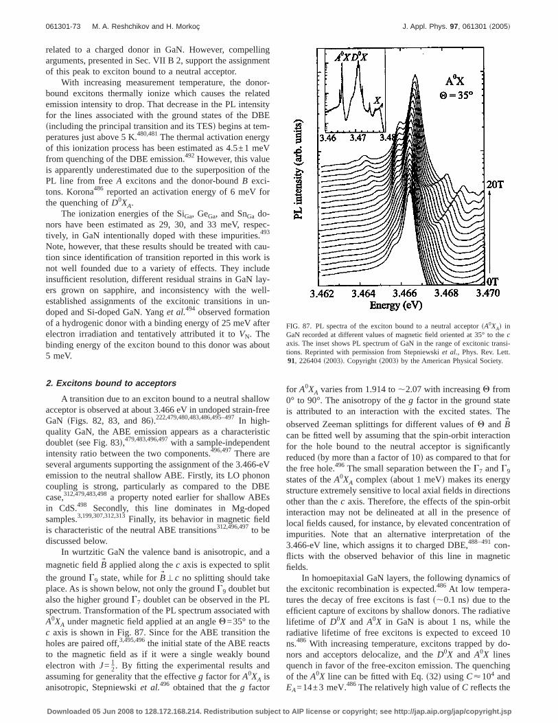
related to a charged donor in GaN. However, compellingarguments, presented in Sec. VII B 2, support the assignmentof this peak to exciton bound to a neutral acceptor.
With increasing measurement temperature, the donor-bound excitons thermally ionize which causes the relatedemission intensity to drop. That decrease in the PL intensityfor the lines associated with the ground states of the DBEsincluding the principal transition and its TESd begins at tem-peratures just above 5 K.480,481The thermal activation energyof this ionization process has been estimated as 4.5±1 meVfrom quenching of the DBE emission.492 However, this valueis apparently underestimated due to the superposition of thePL line from freeA excitons and the donor-boundB exci-tons. Korona486 reported an activation energy of 6 meV forthe quenching ofD0XA.
The ionization energies of the SiGa, GeGa, and SnGa do-nors have been estimated as 29, 30, and 33 meV, respec-tively, in GaN intentionally doped with these impurities.493
Note, however, that these results should be treated with cau-tion since identification of transition reported in this work isnot well founded due to a variety of effects. They includeinsufficient resolution, different residual strains in GaN lay-ers grown on sapphire, and inconsistency with the well-established assignments of the excitonic transitions in un-doped and Si-doped GaN. Yanget al.494 observed formationof a hydrogenic donor with a binding energy of 25 meV afterelectron irradiation and tentatively attributed it toVN. Thebinding energy of the exciton bound to this donor was about5 meV.
2. Excitons bound to acceptors
A transition due to an exciton bound to a neutral shallowacceptor is observed at about 3.466 eV in undoped strain-freeGaN sFigs. 82, 83, and 86d.222,479,480,483,486,495–497In high-quality GaN, the ABE emission appears as a characteristicdoubletssee Fig. 83d,479,483,496,497with a sample-independentintensity ratio between the two components.496,497There areseveral arguments supporting the assignment of the 3.466-eVemission to the neutral shallow ABE. Firstly, its LO phononcoupling is strong, particularly as compared to the DBEcase,312,479,483,498a property noted earlier for shallow ABEsin CdS.498 Secondly, this line dominates in Mg-dopedsamples.3,199,307,312,313Finally, its behavior in magnetic fieldis characteristic of the neutral ABE transitions312,496,497to bediscussed below.
In wurtzitic GaN the valence band is anisotropic, and a
magnetic fieldB¢ applied along thec axis is expected to split
the groundG9 state, while forB¢ 'c no splitting should takeplace. As is shown below, not only the groundG9 doublet butalso the higher groundG7 doublet can be observed in the PLspectrum. Transformation of the PL spectrum associated withA0XA under magnetic field applied at an angleQ=35° to thec axis is shown in Fig. 87. Since for the ABE transition theholes are paired off,3,495,496the initial state of the ABE reactsto the magnetic field as if it were a single weakly boundelectron withJ= 1
2. By fitting the experimental results andassuming for generality that the effectiveg factor forA0XA isanisotropic, Stepniewskiet al.496 obtained that theg factor
for A0XA varies from 1.914 to,2.07 with increasingQ from0° to 90°. The anisotropy of theg factor in the ground stateis attributed to an interaction with the excited states. The
observed Zeeman splittings for different values ofQ andB¢
can be fitted well by assuming that the spin-orbit interactionfor the hole bound to the neutral acceptor is significantlyreducedsby more than a factor of 10d as compared to that forthe free hole.496 The small separation between theG7 andG9
states of theA0XA complexsabout 1 meVd makes its energystructure extremely sensitive to local axial fields in directionsother than thec axis. Therefore, the effects of the spin-orbitinteraction may not be delineated at all in the presence oflocal fields caused, for instance, by elevated concentration ofimpurities. Note that an alternative interpretation of the3.466-eV line, which assigns it to charged DBE,488–491con-flicts with the observed behavior of this line in magneticfields.
In homoepitaxial GaN layers, the following dynamics ofthe excitonic recombination is expected.486 At low tempera-tures the decay of free excitons is fasts,0.1 nsd due to theefficient capture of excitons by shallow donors. The radiativelifetime of D0X and A0X in GaN is about 1 ns, while theradiative lifetime of free excitons is expected to exceed 10ns.486 With increasing temperature, excitons trapped by do-nors and acceptors delocalize, and theD0X and A0X linesquench in favor of the free-exciton emission. The quenchingof theA0X line can be fitted with Eq.s32d usingC<104 andEA=14±3 meV.486 The relatively high value ofC reflects the
FIG. 87. PL spectra of the exciton bound to a neutral acceptorsA0XAd inGaN recorded at different values of magnetic field oriented at 35° to thecaxis. The inset shows PL spectrum of GaN in the range of excitonic transi-tions. Reprinted with permission from Stepniewskiet al., Phys. Rev. Lett.91, 226404s2003d. Copyrights2003d by the American Physical Society.
061301-73 M. A. Reshchikov and H. Morkoç J. Appl. Phys. 97, 061301 ~2005!
Downloaded 05 Jun 2008 to 128.172.168.214. Redistribution subject to AIP license or copyright; see http://jap.aip.org/jap/copyright.jsp
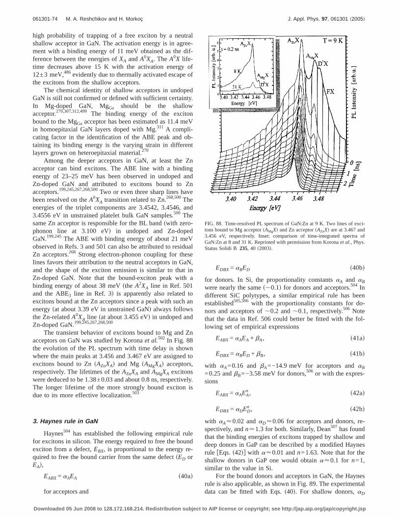
high probability of trapping of a free exciton by a neutralshallow acceptor in GaN. The activation energy is in agree-ment with a binding energy of 11 meV obtained as the dif-ference between the energies ofXA andA0XA. TheA0X life-time decreases above 15 K with the activation energy of12±3 meV,486 evidently due to thermally activated escape ofthe excitons from the shallow acceptors.
The chemical identity of shallow acceptors in undopedGaN is still not confirmed or defined with sufficient certainty.In Mg-doped GaN, MgGa should be the shallowacceptor.270,307,312,499The binding energy of the excitonbound to the MgGa acceptor has been estimated as 11.4 meVin homoepitaxial GaN layers doped with Mg.311 A compli-cating factor in the identification of the ABE peak and ob-taining its binding energy is the varying strain in differentlayers grown on heteroepitaxial material.270
Among the deeper acceptors in GaN, at least the Znacceptor can bind excitons. The ABE line with a bindingenergy of 23–25 meV has been observed in undoped andZn-doped GaN and attributed to excitons bound to Znacceptors.199,245,267,268,500Two or even three sharp lines havebeen resolved on theA0XA transition related to Zn.268,500Theenergies of the triplet components are 3.4542, 3.4546, and3.4556 eV in unstrained platelet bulk GaN samples.500 Thesame Zn acceptor is responsible for the BL bandswith zero-phonon line at 3.100 eVd in undoped and Zn-dopedGaN.199,245The ABE with binding energy of about 21 meVobserved in Refs. 3 and 501 can also be attributed to residualZn acceptors.268 Strong electron-phonon coupling for theselines favors their attribution to the neutral acceptors in GaN,and the shape of the exciton emission is similar to that inZn-doped GaN. Note that the bound-exciton peak with abinding energy of about 38 meVsthe A2XA line in Ref. 501and the ABE3 line in Ref. 3d is apparently also related toexcitons bound at the Zn acceptors since a peak with such anenergysat about 3.39 eV in unstrained GaNd always followsthe Zn-relatedA0XA line sat about 3.455 eVd in undoped andZn-doped GaN.199,245,267,268,500
The transient behavior of excitons bound to Mg and Znacceptors on GaN was studied by Koronaet al.502 In Fig. 88the evolution of the PL spectrum with time delay is shownwhere the main peaks at 3.456 and 3.467 eV are assigned toexcitons bound to ZnsAZnXAd and Mg sAMgXAd acceptors,respectively. The lifetimes of theAZnXA andAMgXA excitonswere deduced to be 1.38±0.03 and about 0.8 ns, respectively.The longer lifetime of the more strongly bound exciton isdue to its more effective localization.503
3. Haynes rule in GaN
Haynes504 has established the following empirical rulefor excitons in silicon. The energy required to free the boundexciton from a defect,EBX, is proportional to the energy re-quired to free the bound carrier from the same defectsED orEAd,
EABX= aAEA s40ad
for acceptors and
EDBX = aBED s40bd
for donors. In Si, the proportionality constantsaA and aB
were nearly the sames,0.1d for donors and acceptors.504 Indifferent SiC polytypes, a similar empirical rule has beenestablished505,506 with the proportionality constants for do-nors and acceptors of,0.2 and,0.1, respectively.506 Notethat the data in Ref. 506 could better be fitted with the fol-lowing set of empirical expressions
EABX= aAEA + bA, s41ad
EDBX = aBED + bB, s41bd
with aA=0.16 andbA=−14.9 meV for acceptors andaB
=0.25 andbB=−3.58 meV for donors,506 or with the expres-sions
EABX= aAEAn , s42ad
EDBX = aDEDn , s42bd
with aA<0.02 andaD<0.06 for acceptors and donors, re-spectively, andn<1.3 for both. Similarly, Dean507 has foundthat the binding energies of excitons trapped by shallow anddeep donors in GaP can be described by a modified Haynesrule fEqs.s42dg with a<0.01 andn=1.63. Note that for theshallow donors in GaP one would obtaina<0.1 for n=1,similar to the value in Si.
For the bound donors and acceptors in GaN, the Haynesrule is also applicable, as shown in Fig. 89. The experimentaldata can be fitted with Eqs.s40d. For shallow donors,aD
FIG. 88. Time-resolved PL spectrum of GaN:Zn at 9 K. Two lines of exci-tons bound to Mg acceptorsAMgXd and Zn acceptorsAZnXd are at 3.467 and3.456 eV, respectively. Inset: comparison of time-integrated spectra ofGaN:Zn at 8 and 31 K. Reprinted with permission from Koronaet al., Phys.Status Solidi B235, 40 s2003d.
061301-74 M. A. Reshchikov and H. Morkoç J. Appl. Phys. 97, 061301 ~2005!
Downloaded 05 Jun 2008 to 128.172.168.214. Redistribution subject to AIP license or copyright; see http://jap.aip.org/jap/copyright.jsp
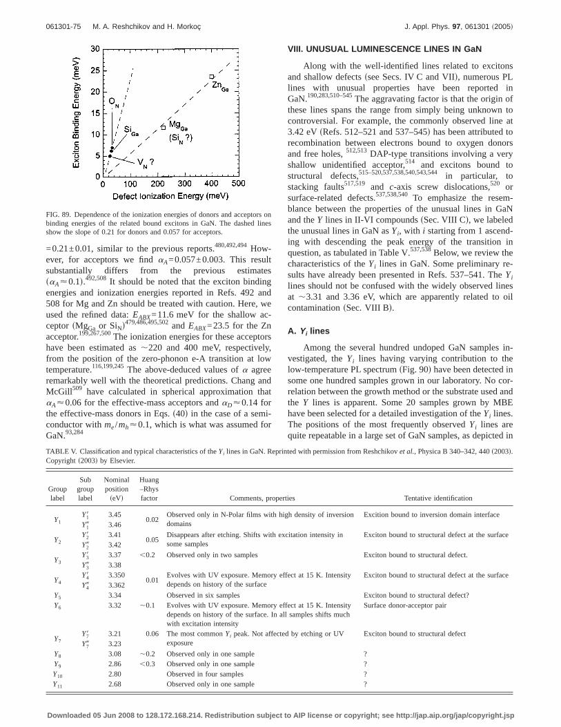
=0.21±0.01, similar to the previous reports.480,492,494How-ever, for acceptors we findaA=0.057±0.003. This resultsubstantially differs from the previous estimatessaA<0.1d.492,508 It should be noted that the exciton bindingenergies and ionization energies reported in Refs. 492 and508 for Mg and Zn should be treated with caution. Here, weused the refined data:EABX=11.6 meV for the shallow ac-ceptorsMgGa or SiNd479,486,495,502andEABX=23.5 for the Znacceptor.199,267,500The ionization energies for these acceptorshave been estimated as,220 and 400 meV, respectively,from the position of the zero-phonon e-A transition at lowtemperature.116,199,245The above-deduced values ofa agreeremarkably well with the theoretical predictions. Chang andMcGill 509 have calculated in spherical approximation thataA<0.06 for the effective-mass acceptors andaD<0.14 forthe effective-mass donors in Eqs.s40d in the case of a semi-conductor withme/mh<0.1, which is what was assumed forGaN.93,284
VIII. UNUSUAL LUMINESCENCE LINES IN GaN
Along with the well-identified lines related to excitonsand shallow defectsssee Secs. IV C and VIId, numerous PLlines with unusual properties have been reported inGaN.190,283,510–545The aggravating factor is that the origin ofthese lines spans the range from simply being unknown tocontroversial. For example, the commonly observed line at3.42 eVsRefs. 512–521 and 537–545d has been attributed torecombination between electrons bound to oxygen donorsand free holes,512,513DAP-type transitions involving a veryshallow unidentified acceptor,514 and excitons bound tostructural defects,515–520,537,538,540,543,544in particular, tostacking faults517,519 and c-axis screw dislocations,520 orsurface-related defects.537,538,540 To emphasize the resem-blance between the properties of the unusual lines in GaNand theY lines in II-VI compoundssSec. VIII Cd, we labeledthe unusual lines in GaN asYi, with i starting from 1 ascend-ing with descending the peak energy of the transition inquestion, as tabulated in Table V.537,538Below, we review thecharacteristics of theYi lines in GaN. Some preliminary re-sults have already been presented in Refs. 537–541. TheYi
lines should not be confused with the widely observed linesat ,3.31 and 3.36 eV, which are apparently related to oilcontaminationsSec. VIII Bd.
A. Yi lines
Among the several hundred undoped GaN samples in-vestigated, theYi lines having varying contribution to thelow-temperature PL spectrumsFig. 90d have been detected insome one hundred samples grown in our laboratory. No cor-relation between the growth method or the substrate used andthe Y lines is apparent. Some 20 samples grown by MBEhave been selected for a detailed investigation of theYi lines.The positions of the most frequently observedYi lines arequite repeatable in a large set of GaN samples, as depicted in
FIG. 89. Dependence of the ionization energies of donors and acceptors onbinding energies of the related bound excitons in GaN. The dashed linesshow the slope of 0.21 for donors and 0.057 for acceptors.
TABLE V. Classification and typical characteristics of theYi lines in GaN. Reprinted with permission from Reshchikovet al., Physica B 340–342, 440s2003d.Copyright s2003d by Elsevier.
Grouplabel
Subgrouplabel
Nominalposition
seVd
Huang–Rhysfactor Comments, properties Tentative identification
Y1Y18 3.45
0.02Observed only in N-Polar films with high density of inversiondomains
Excition bound to inversion domain interfaceY19 3.46
Y2Y28 3.41
0.05Disappears after etching. Shifts with excitation intensity insome samples
Exciton bound to structural defect at the surfaceY29 3.42
Y3Y38 3.37 ,0.2 Observed only in two samples Exciton bound to structural defect.Y39 3.38
Y4Y48 3.350
0.01Evolves with UV exposure. Memory effect at 15 K. Intensitydepends on history of the surface
Exciton bound to structural defect at the surfaceY49 3.362
Y5 3.34 Observed in six samples Exciton bound to structural defect?Y6 3.32 ,0.1 Evolves with UV exposure. Memory effect at 15 K. Intensity
depends on history of the surface. In all samples shifts muchwith excitation intensity
Surface donor-acceptor pair
Y7Y78 3.21 0.06 The most commonYi peak. Not affected by etching or UV
exposureExciton bound to structural defect
Y79 3.23Y8 3.08 ,0.2 Observed only in one sample ?Y9 2.86 ,0.3 Observed only in one sample ?Y10 2.80 Observed in four samples ?Y11 2.68 Observed only in one sample ?
061301-75 M. A. Reshchikov and H. Morkoç J. Appl. Phys. 97, 061301 ~2005!
Downloaded 05 Jun 2008 to 128.172.168.214. Redistribution subject to AIP license or copyright; see http://jap.aip.org/jap/copyright.jsp
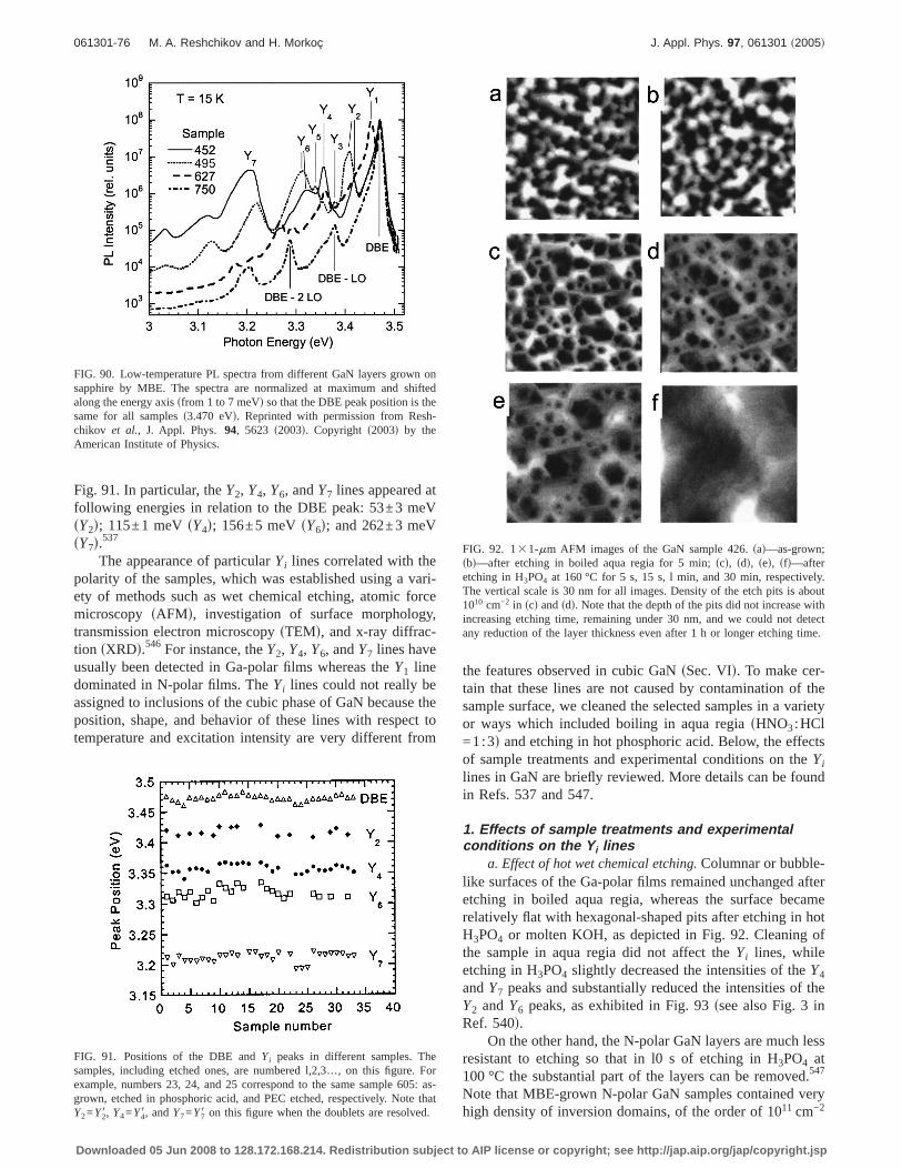
Fig. 91. In particular, theY2, Y4, Y6, andY7 lines appeared atfollowing energies in relation to the DBE peak: 53±3 meVsY2d; 115±1 meVsY4d; 156±5 meVsY6d; and 262±3 meVsY7d.537
The appearance of particularYi lines correlated with thepolarity of the samples, which was established using a vari-ety of methods such as wet chemical etching, atomic forcemicroscopy sAFMd, investigation of surface morphology,transmission electron microscopysTEMd, and x-ray diffrac-tion sXRDd.546 For instance, theY2, Y4, Y6, andY7 lines haveusually been detected in Ga-polar films whereas theY1 linedominated in N-polar films. TheYi lines could not really beassigned to inclusions of the cubic phase of GaN because theposition, shape, and behavior of these lines with respect totemperature and excitation intensity are very different from
the features observed in cubic GaNsSec. VId. To make cer-tain that these lines are not caused by contamination of thesample surface, we cleaned the selected samples in a varietyor ways which included boiling in aqua regiasHNO3:HCl=1:3d and etching in hot phosphoric acid. Below, the effectsof sample treatments and experimental conditions on theYi
lines in GaN are briefly reviewed. More details can be foundin Refs. 537 and 547.
1. Effects of sample treatments and experimentalconditions on the Y i lines
a. Effect of hot wet chemical etching.Columnar or bubble-like surfaces of the Ga-polar films remained unchanged afteretching in boiled aqua regia, whereas the surface becamerelatively flat with hexagonal-shaped pits after etching in hotH3PO4 or molten KOH, as depicted in Fig. 92. Cleaning ofthe sample in aqua regia did not affect theYi lines, whileetching in H3PO4 slightly decreased the intensities of theY4
andY7 peaks and substantially reduced the intensities of theY2 andY6 peaks, as exhibited in Fig. 93ssee also Fig. 3 inRef. 540d.
On the other hand, the N-polar GaN layers are much lessresistant to etching so that in l0 s of etching in H3PO4 at100 °C the substantial part of the layers can be removed.547
Note that MBE-grown N-polar GaN samples contained veryhigh density of inversion domains, of the order of 1011 cm−2
FIG. 90. Low-temperature PL spectra from different GaN layers grown onsapphire by MBE. The spectra are normalized at maximum and shiftedalong the energy axissfrom 1 to 7 meVd so that the DBE peak position is thesame for all sampless3.470 eVd. Reprinted with permission from Resh-chikov et al., J. Appl. Phys. 94, 5623 s2003d. Copyright s2003d by theAmerican Institute of Physics.
FIG. 91. Positions of the DBE andYi peaks in different samples. Thesamples, including etched ones, are numbered l,2,3…, on this figure. Forexample, numbers 23, 24, and 25 correspond to the same sample 605: as-grown, etched in phosphoric acid, and PEC etched, respectively. Note thatY2=Y28, Y4=Y48, andY7=Y78 on this figure when the doublets are resolved.
FIG. 92. 131-mm AFM images of the GaN sample 426.sad—as-grown;sbd—after etching in boiled aqua regia for 5 min;scd, sdd, sed, sfd—afteretching in H3PO4 at 160 °C for 5 s, 15 s, l min, and 30 min, respectively.The vertical scale is 30 nm for all images. Density of the etch pits is about1010 cm−2 in scd andsdd. Note that the depth of the pits did not increase withincreasing etching time, remaining under 30 nm, and we could not detectany reduction of the layer thickness even after 1 h or longeretching time.
061301-76 M. A. Reshchikov and H. Morkoç J. Appl. Phys. 97, 061301 ~2005!
Downloaded 05 Jun 2008 to 128.172.168.214. Redistribution subject to AIP license or copyright; see http://jap.aip.org/jap/copyright.jsp
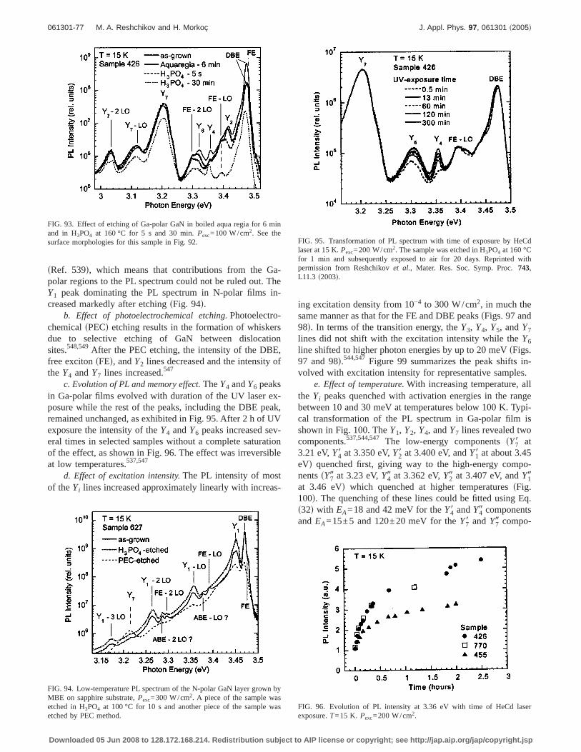
sRef. 539d, which means that contributions from the Ga-polar regions to the PL spectrum could not be ruled out. TheY1 peak dominating the PL spectrum in N-polar films in-creased markedly after etchingsFig. 94d.
b. Effect of photoelectrochemical etching.Photoelectro-chemicalsPECd etching results in the formation of whiskersdue to selective etching of GaN between dislocationsites.548,549After the PEC etching, the intensity of the DBE,free excitonsFEd, andY2 lines decreased and the intensity ofthe Y4 andY7 lines increased.547
c. Evolution of PL and memory effect.TheY4 andY6 peaksin Ga-polar films evolved with duration of the UV laser ex-posure while the rest of the peaks, including the DBE peak,remained unchanged, as exhibited in Fig. 95. After 2 h of UVexposure the intensity of theY4 andY6 peaks increased sev-eral times in selected samples without a complete saturationof the effect, as shown in Fig. 96. The effect was irreversibleat low temperatures.537,547
d. Effect of excitation intensity.The PL intensity of mostof theYi lines increased approximately linearly with increas-
ing excitation density from 10−4 to 300 W/cm2, in much thesame manner as that for the FE and DBE peakssFigs. 97 and98d. In terms of the transition energy, theY3, Y4, Y5, andY7
lines did not shift with the excitation intensity while theY6
line shifted to higher photon energies by up to 20 meVsFigs.97 and 98d.544,547 Figure 99 summarizes the peak shifts in-volved with excitation intensity for representative samples.
e. Effect of temperature.With increasing temperature, allthe Yi peaks quenched with activation energies in the rangebetween 10 and 30 meV at temperatures below 100 K. Typi-cal transformation of the PL spectrum in Ga-polar film isshown in Fig. 100. TheY1, Y2, Y4, andY7 lines revealed twocomponents.537,544,547 The low-energy componentssY78 at3.21 eV,Y48 at 3.350 eV,Y28 at 3.400 eV, andY18 at about 3.45eVd quenched first, giving way to the high-energy compo-nentssY79 at 3.23 eV,Y49 at 3.362 eV,Y29 at 3.407 eV, andY19at 3.46 eVd which quenched at higher temperaturessFig.100d. The quenching of these lines could be fitted using Eq.s32d with EA=18 and 42 meV for theY48 andY49 componentsandEA=15±5 and 120±20 meV for theY78 andY79 compo-
FIG. 93. Effect of etching of Ga-polar GaN in boiled aqua regia for 6 minand in H3PO4 at 160 °C for 5 s and 30 min.Pexc=100 W/cm2. See thesurface morphologies for this sample in Fig. 92.
FIG. 94. Low-temperature PL spectrum of the N-polar GaN layer grown byMBE on sapphire substrate,Pexc=300 W/cm2. A piece of the sample wasetched in H3PO4 at 100 °C for 10 s and another piece of the sample wasetched by PEC method.
FIG. 95. Transformation of PL spectrum with time of exposure by HeCdlaser at 15 K.Pexc=200 W/cm2. The sample was etched in H3PO4 at 160 °Cfor 1 min and subsequently exposed to air for 20 days. Reprinted withpermission from Reshchikovet al., Mater. Res. Soc. Symp. Proc.743,L11.3 s2003d.
FIG. 96. Evolution of PL intensity at 3.36 eV with time of HeCd laserexposure.T=15 K. Pexc=200 W/cm2.
061301-77 M. A. Reshchikov and H. Morkoç J. Appl. Phys. 97, 061301 ~2005!
Downloaded 05 Jun 2008 to 128.172.168.214. Redistribution subject to AIP license or copyright; see http://jap.aip.org/jap/copyright.jsp

nents, respectively. Activation energies of the otherYi linesdid not exceed 30 meV at temperatures up to 120 K, andthese lines could be barely detected at highertemperatures.547
The temperature dependencies of the energy positions ofthe Yi lines are shown in Fig. 101 in comparison with theshift of the FE line. All theYi lines shift in agreement withthe temperature shrinkage of the GaN band gap,473 support-ing the assumption that theYi lines originate from GaN.
2. Characteristics of the Y i linesa. The 3.45-eV linesY1d. The 3.45-eV peak, labeled asY1,
appeared only in the N-polar films containing a high densityof inversion domainss,1011 cm−2d and relatively low den-sity of dislocationss,109 cm−2d.550,551 Schucket al.510 re-lated this peak to the inversion domain boundaries. A verysmall Huang–Rhys factor552 for the Y1 peak sabout 0.02d
supports the assignment of theY1 line to excitons bound toinversion domain boundaries.537 Narrow Ga-polar domainsin N-polar media might create high and narrow potentialhumps near the surface due to essentially different bandbending near the surface in Ga- and N-polar films.553 How-ever, this remains to be confirmed before it can be treatedwith sufficient level of confidence. The exact potential pro-file may be sample dependent, explaining the slightly differ-
FIG. 97. Low-temperature PL spectrum of Ga-polar GaN layer grown byMBE on top of the HVPE-grown 10-µm-thick GaN on sapphire substrate.Excitation density was attenuated from 100 to 1 W/cm2 by neutral densityfilters. The spectra are shifted arbitrary along the vertical axis for betterviewing. Reprinted with permission from Reshchikovet al., Mater. Res.Soc. Symp. Proc.693, I6.28 s2002d.
FIG. 98. Low-temperature PL spectrum of N-polar GaN layer grown byMBE on sapphire substrate. The spectra are normalized at maximum. Re-printed with permission from Reshchikovet al., Mater. Res. Soc. Symp.Proc. 743, L11.3 s2003d.
FIG. 99. Dependence of the PL peak shift on excitation density at 15 K.
FIG. 100. Temperature dependence of PL spectrum atPexc=100 W/cm2 foras-grown Ga-polar GaN layer by MBE on top of the HVPE-grown 10-µm-thick GaN on sapphire substrate. Temperatures are 15, 35, 60, 100, 140, 195K ssolid curvesd, 25, 50, 80, 120, 160 Ksdashed curvesd, and 240 Ksdottedcurved. Reprinted with permission from Reshchikovet al., Mater. Res. Soc.Symp. Proc.693, I6.28 s2002d.
061301-78 M. A. Reshchikov and H. Morkoç J. Appl. Phys. 97, 061301 ~2005!
Downloaded 05 Jun 2008 to 128.172.168.214. Redistribution subject to AIP license or copyright; see http://jap.aip.org/jap/copyright.jsp
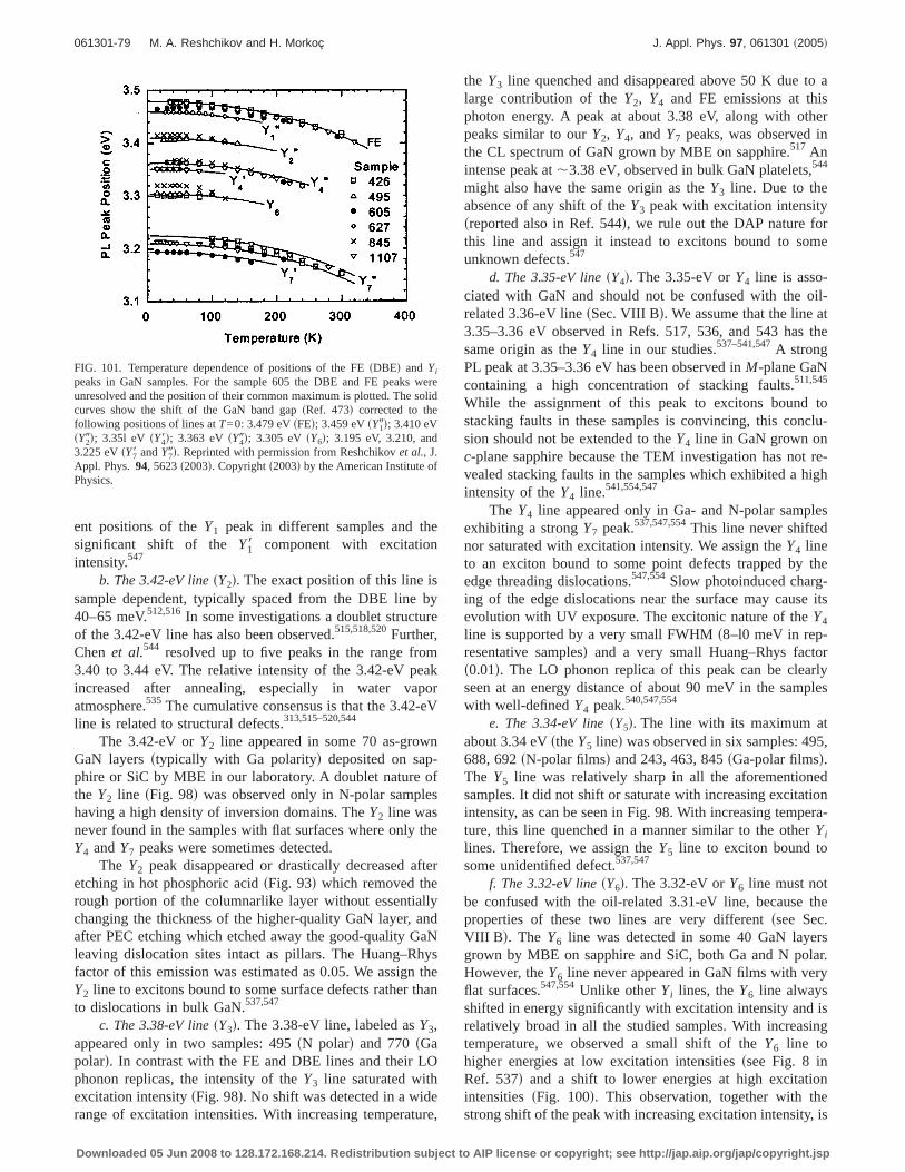
ent positions of theY1 peak in different samples and thesignificant shift of the Y18 component with excitationintensity.547
b. The 3.42-eV linesY2d. The exact position of this line issample dependent, typically spaced from the DBE line by40–65 meV.512,516In some investigations a doublet structureof the 3.42-eV line has also been observed.515,518,520Further,Chenet al.544 resolved up to five peaks in the range from3.40 to 3.44 eV. The relative intensity of the 3.42-eV peakincreased after annealing, especially in water vaporatmosphere.535 The cumulative consensus is that the 3.42-eVline is related to structural defects.313,515–520,544
The 3.42-eV orY2 line appeared in some 70 as-grownGaN layersstypically with Ga polarityd deposited on sap-phire or SiC by MBE in our laboratory. A doublet nature ofthe Y2 line sFig. 98d was observed only in N-polar sampleshaving a high density of inversion domains. TheY2 line wasnever found in the samples with flat surfaces where only theY4 andY7 peaks were sometimes detected.
The Y2 peak disappeared or drastically decreased afteretching in hot phosphoric acidsFig. 93d which removed therough portion of the columnarlike layer without essentiallychanging the thickness of the higher-quality GaN layer, andafter PEC etching which etched away the good-quality GaNleaving dislocation sites intact as pillars. The Huang–Rhysfactor of this emission was estimated as 0.05. We assign theY2 line to excitons bound to some surface defects rather thanto dislocations in bulk GaN.537,547
c. The 3.38-eV linesY3d. The 3.38-eV line, labeled asY3,appeared only in two samples: 495sN polard and 770sGapolard. In contrast with the FE and DBE lines and their LOphonon replicas, the intensity of theY3 line saturated withexcitation intensitysFig. 98d. No shift was detected in a widerange of excitation intensities. With increasing temperature,
the Y3 line quenched and disappeared above 50 K due to alarge contribution of theY2, Y4 and FE emissions at thisphoton energy. A peak at about 3.38 eV, along with otherpeaks similar to ourY2, Y4, andY7 peaks, was observed inthe CL spectrum of GaN grown by MBE on sapphire.517 Anintense peak at,3.38 eV, observed in bulk GaN platelets,544
might also have the same origin as theY3 line. Due to theabsence of any shift of theY3 peak with excitation intensitysreported also in Ref. 544d, we rule out the DAP nature forthis line and assign it instead to excitons bound to someunknown defects.547
d. The 3.35-eV linesY4d. The 3.35-eV orY4 line is asso-ciated with GaN and should not be confused with the oil-related 3.36-eV linesSec. VIII Bd. We assume that the line at3.35–3.36 eV observed in Refs. 517, 536, and 543 has thesame origin as theY4 line in our studies.537–541,547A strongPL peak at 3.35–3.36 eV has been observed inM-plane GaNcontaining a high concentration of stacking faults.511,545
While the assignment of this peak to excitons bound tostacking faults in these samples is convincing, this conclu-sion should not be extended to theY4 line in GaN grown onc-plane sapphire because the TEM investigation has not re-vealed stacking faults in the samples which exhibited a highintensity of theY4 line.541,554,547
The Y4 line appeared only in Ga- and N-polar samplesexhibiting a strongY7 peak.537,547,554This line never shiftednor saturated with excitation intensity. We assign theY4 lineto an exciton bound to some point defects trapped by theedge threading dislocations.547,554Slow photoinduced charg-ing of the edge dislocations near the surface may cause itsevolution with UV exposure. The excitonic nature of theY4
line is supported by a very small FWHMs8–l0 meV in rep-resentative samplesd and a very small Huang–Rhys factors0.01d. The LO phonon replica of this peak can be clearlyseen at an energy distance of about 90 meV in the sampleswith well-definedY4 peak.540,547,554
e. The 3.34-eV linesY5d. The line with its maximum atabout 3.34 eVstheY5 lined was observed in six samples: 495,688, 692sN-polar filmsd and 243, 463, 845sGa-polar filmsd.The Y5 line was relatively sharp in all the aforementionedsamples. It did not shift or saturate with increasing excitationintensity, as can be seen in Fig. 98. With increasing tempera-ture, this line quenched in a manner similar to the otherYi
lines. Therefore, we assign theY5 line to exciton bound tosome unidentified defect.537,547
f. The 3.32-eV linesY6d. The 3.32-eV orY6 line must notbe confused with the oil-related 3.31-eV line, because theproperties of these two lines are very differentssee Sec.VIII B d. The Y6 line was detected in some 40 GaN layersgrown by MBE on sapphire and SiC, both Ga and N polar.However, theY6 line never appeared in GaN films with veryflat surfaces.547,554Unlike otherYi lines, theY6 line alwaysshifted in energy significantly with excitation intensity and isrelatively broad in all the studied samples. With increasingtemperature, we observed a small shift of theY6 line tohigher energies at low excitation intensitiesssee Fig. 8 inRef. 537d and a shift to lower energies at high excitationintensities sFig. 100d. This observation, together with thestrong shift of the peak with increasing excitation intensity, is
FIG. 101. Temperature dependence of positions of the FEsDBEd and Yi
peaks in GaN samples. For the sample 605 the DBE and FE peaks wereunresolved and the position of their common maximum is plotted. The solidcurves show the shift of the GaN band gapsRef. 473d corrected to thefollowing positions of lines atT=0: 3.479 eVsFEd; 3.459 eVsY19d; 3.410 eVsY29d; 3.35l eV sY48d; 3.363 eVsY49d; 3.305 eVsY6d; 3.195 eV, 3.210, and3.225 eVsY78 andY79d. Reprinted with permission from Reshchikovet al., J.Appl. Phys.94, 5623s2003d. Copyrights2003d by the American Institute ofPhysics.
061301-79 M. A. Reshchikov and H. Morkoç J. Appl. Phys. 97, 061301 ~2005!
Downloaded 05 Jun 2008 to 128.172.168.214. Redistribution subject to AIP license or copyright; see http://jap.aip.org/jap/copyright.jsp
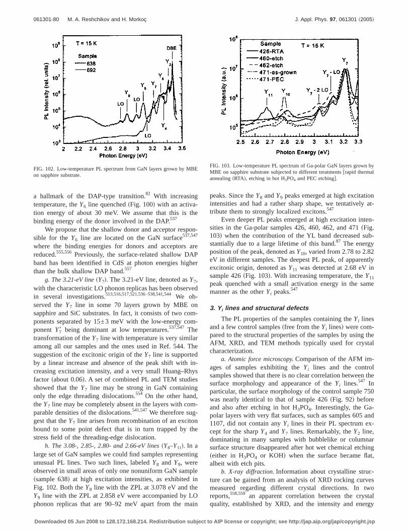
a hallmark of the DAP-type transition.82 With increasingtemperature, theY6 line quenchedsFig. 100d with an activa-tion energy of about 30 meV. We assume that this is thebinding energy of the donor involved in the DAP.537
We propose that the shallow donor and acceptor respon-sible for theY6 line are located on the GaN surface537,547
where the binding energies for donors and acceptors arereduced.555,556 Previously, the surface-related shallow DAPband has been identified in CdS at photon energies higherthan the bulk shallow DAP band.557
g. The 3.21-eV linesY7d. The 3.21-eV line, denoted asY7,with the characteristic LO phonon replicas has been observedin several investigations.513,516,517,521,536–538,541,544We ob-served theY7 line in some 70 layers grown by MBE onsapphire and SiC substrates. In fact, it consists of two com-ponents separated by 15±3 meV with the low-energy com-ponent Y78 being dominant at low temperatures.537,547 Thetransformation of theY7 line with temperature is very similaramong all our samples and the ones used in Ref. 544. Thesuggestion of the excitonic origin of theY7 line is supportedby a linear increase and absence of the peak shift with in-creasing excitation intensity, and a very small Huang–Rhysfactor sabout 0.06d. A set of combined PL and TEM studiesshowed that theY7 line may be strong in GaN containingonly the edge threading dislocations.554 On the other hand,theY7 line may be completely absent in the layers with com-parable densities of the dislocations.541,547We therefore sug-gest that theY7 line arises from recombination of an excitonbound to some point defect that is in turn trapped by thestress field of the threading-edge dislocation.
h. The 3.08-, 2.85-, 2.80- and 2.66-eV linessY8–Y11d. In alarge set of GaN samples we could find samples representingunusual PL lines. Two such lines, labeledY8 and Y9, wereobserved in small areas of only one nonuniform GaN samplessample 638d at high excitation intensities, as exhibited inFig. 102. Both theY8 line with the ZPL at 3.078 eV and theY9 line with the ZPL at 2.858 eV were accompanied by LOphonon replicas that are 90–92 meV apart from the main
peaks. Since theY8 andY9 peaks emerged at high excitationintensities and had a rather sharp shape, we tentatively at-tribute them to strongly localized excitons.547
Even deeper PL peaks emerged at high excitation inten-sities in the Ga-polar samples 426, 460, 462, and 471sFig.103d when the contribution of the YL band decreased sub-stantially due to a large lifetime of this band.87 The energyposition of the peak, denoted asY10, varied from 2.78 to 2.82eV in different samples. The deepest PL peak, of apparentlyexcitonic origin, denoted asY11 was detected at 2.68 eV insample 426sFig. 103d. With increasing temperature, theY11
peak quenched with a small activation energy in the samemanner as the otherYi peaks.547
3. Yi lines and structural defects
The PL properties of the samples containing theYi linesand a few control samplessfree from theYi linesd were com-pared to the structural properties of the samples by using theAFM, XRD, and TEM methods typically used for crystalcharacterization.
a. Atomic force microscopy.Comparison of the AFM im-ages of samples exhibiting theYi lines and the controlsamples showed that there is no clear correlation between thesurface morphology and appearance of theYi lines.547 Inparticular, the surface morphology of the control sample 750was nearly identical to that of sample 426sFig. 92d beforeand also after etching in hot H3PO4. Interestingly, the Ga-polar layers with very flat surfaces, such as samples 605 and1107, did not contain anyYi lines in their PL spectrum ex-cept for the sharpY4 andY7 lines. Remarkably, theY2 line,dominating in many samples with bubblelike or columnarsurface structure disappeared after hot wet chemical etchingseither in H3PO4 or KOHd when the surface became flat,albeit with etch pits.
b. X-ray diffraction.Information about crystalline struc-ture can be gained from an analysis of XRD rocking curvesmeasured regarding different crystal directions. In tworeports,558,559 an apparent correlation between the crystalquality, established by XRD, and the intensity and energy
FIG. 102. Low-temperature PL spectrum from GaN layers grown by MBEon sapphire substrate.
FIG. 103. Low-temperature PL spectrum of Ga-polar GaN layers grown byMBE on sapphire substrate subjected to different treatmentsfrapid thermalannealingsRTAd, etching in hot H3PO4 and PEC etchingg.
061301-80 M. A. Reshchikov and H. Morkoç J. Appl. Phys. 97, 061301 ~2005!
Downloaded 05 Jun 2008 to 128.172.168.214. Redistribution subject to AIP license or copyright; see http://jap.aip.org/jap/copyright.jsp
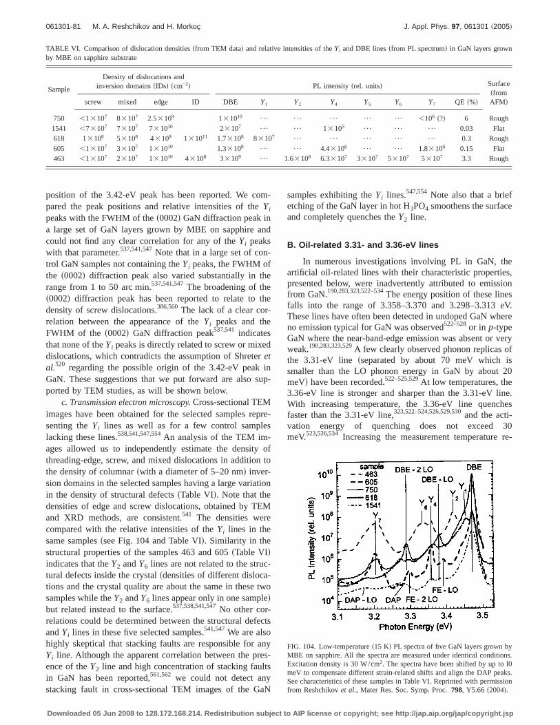
position of the 3.42-eV peak has been reported. We com-pared the peak positions and relative intensities of theYi
peaks with the FWHM of thes0002d GaN diffraction peak ina large set of GaN layers grown by MBE on sapphire andcould not find any clear correlation for any of theYi peakswith that parameter.537,541,547Note that in a large set of con-trol GaN samples not containing theYi peaks, the FWHM ofthe s0002d diffraction peak also varied substantially in therange from 1 to 50 arc min.537,541,547The broadening of thes0002d diffraction peak has been reported to relate to thedensity of screw dislocations.386,560The lack of a clear cor-relation between the appearance of theYi peaks and theFWHM of the s0002d GaN diffraction peak537,541 indicatesthat none of theYi peaks is directly related to screw or mixeddislocations, which contradicts the assumption of Shreteretal.520 regarding the possible origin of the 3.42-eV peak inGaN. These suggestions that we put forward are also sup-ported by TEM studies, as will be shown below.
c. Transmission electron microscopy.Cross-sectional TEMimages have been obtained for the selected samples repre-senting theYi lines as well as for a few control sampleslacking these lines.538,541,547,554An analysis of the TEM im-ages allowed us to independently estimate the density ofthreading-edge, screw, and mixed dislocations in addition tothe density of columnarswith a diameter of 5–20 nmd inver-sion domains in the selected samples having a large variationin the density of structural defectssTable VId. Note that thedensities of edge and screw dislocations, obtained by TEMand XRD methods, are consistent.541 The densities werecompared with the relative intensities of theYi lines in thesame samplesssee Fig. 104 and Table VId. Similarity in thestructural properties of the samples 463 and 605sTable VIdindicates that theY2 andY6 lines are not related to the struc-tural defects inside the crystalsdensities of different disloca-tions and the crystal quality are about the same in these twosamples while theY2 andY6 lines appear only in one sampledbut related instead to the surface.537,538,541,547No other cor-relations could be determined between the structural defectsandYi lines in these five selected samples.541,547We are alsohighly skeptical that stacking faults are responsible for anyYi line. Although the apparent correlation between the pres-ence of theY2 line and high concentration of stacking faultsin GaN has been reported,561,562 we could not detect anystacking fault in cross-sectional TEM images of the GaN
samples exhibiting theYi lines.547,554 Note also that a briefetching of the GaN layer in hot H3PO4 smoothens the surfaceand completely quenches theY2 line.
B. Oil-related 3.31- and 3.36-eV lines
In numerous investigations involving PL in GaN, theartificial oil-related lines with their characteristic properties,presented below, were inadvertently attributed to emissionfrom GaN.190,283,323,522–534The energy position of these linesfalls into the range of 3.358–3.370 and 3.298–3.313 eV.These lines have often been detected in undoped GaN whereno emission typical for GaN was observed522–528or in p-typeGaN where the near-band-edge emission was absent or veryweak.190,283,323,529A few clearly observed phonon replicas ofthe 3.31-eV line sseparated by about 70 meV which issmaller than the LO phonon energy in GaN by about 20meVd have been recorded.522–525,529At low temperatures, the3.36-eV line is stronger and sharper than the 3.31-eV line.With increasing temperature, the 3.36-eV line quenchesfaster than the 3.31-eV line,323,522–524,526,529,530and the acti-vation energy of quenching does not exceed 30meV.523,526,534Increasing the measurement temperature re-
TABLE VI. Comparison of dislocation densitiessfrom TEM datad and relative intensities of theYi and DBE linessfrom PL spectrumd in GaN layers grownby MBE on sapphire substrate
Sample
Density of dislocations andinversion domainssIDsd scm−2d PL intensitysrel. unitsd Surface
sfromAFMdscrew mixed edge ID DBE Y1 Y2 Y4 Y5 Y6 Y7 QE s%d
750 ,13107 83107 2.53109 131010¯ ¯ ¯ ¯ ¯ ,106 s?d 6 Rough
1541 ,73107 73107 731010 23107¯ ¯ 13105
¯ ¯ ¯ 0.03 Flat618 13108 53108 43108 131011 1.73108 83107
¯ ¯ ¯ ¯ ¯ 0.3 Rough605 ,13107 33107 131010 1.33108
¯ ¯ 4.43106¯ ¯ 1.83106 0.15 Flat
463 ,13107 23107 131010 43108 33109¯ 1.63108 6.33107 33107 53107 53107 3.3 Rough
FIG. 104. Low-temperatures15 Kd PL spectra of five GaN layers grown byMBE on sapphire. All the spectra are measured under identical conditions.Excitation density is 30 W/cm2. The spectra have been shifted by up to l0meV to compensate different strain-related shifts and align the DAP peaks.See characteristics of these samples in Table VI. Reprinted with permissionfrom Reshchikovet al., Mater Res. Soc. Symp. Proc.798, Y5.66 s2004d.
061301-81 M. A. Reshchikov and H. Morkoç J. Appl. Phys. 97, 061301 ~2005!
Downloaded 05 Jun 2008 to 128.172.168.214. Redistribution subject to AIP license or copyright; see http://jap.aip.org/jap/copyright.jsp
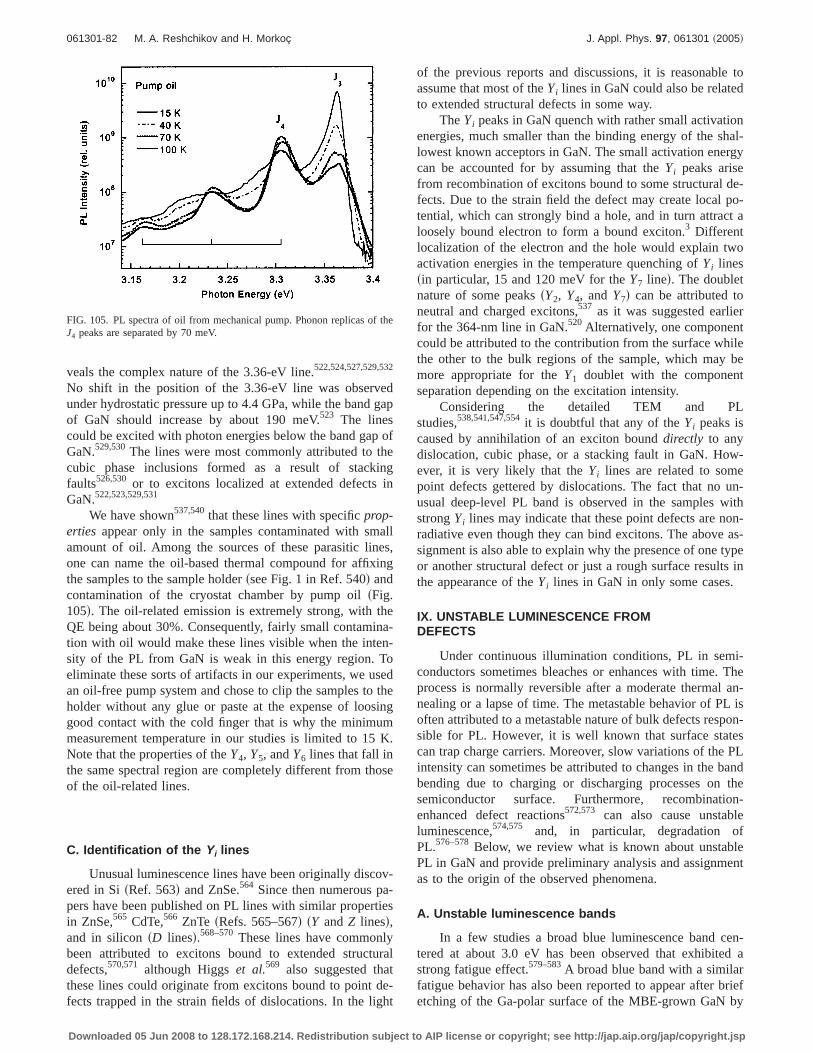
veals the complex nature of the 3.36-eV line.522,524,527,529,532
No shift in the position of the 3.36-eV line was observedunder hydrostatic pressure up to 4.4 GPa, while the band gapof GaN should increase by about 190 meV.523 The linescould be excited with photon energies below the band gap ofGaN.529,530The lines were most commonly attributed to thecubic phase inclusions formed as a result of stackingfaults526,530 or to excitons localized at extended defects inGaN.522,523,529,531
We have shown537,540that these lines with specificprop-erties appear only in the samples contaminated with smallamount of oil. Among the sources of these parasitic lines,one can name the oil-based thermal compound for affixingthe samples to the sample holderssee Fig. 1 in Ref. 540d andcontamination of the cryostat chamber by pump oilsFig.105d. The oil-related emission is extremely strong, with theQE being about 30%. Consequently, fairly small contamina-tion with oil would make these lines visible when the inten-sity of the PL from GaN is weak in this energy region. Toeliminate these sorts of artifacts in our experiments, we usedan oil-free pump system and chose to clip the samples to theholder without any glue or paste at the expense of loosinggood contact with the cold finger that is why the minimummeasurement temperature in our studies is limited to 15 K.Note that the properties of theY4, Y5, andY6 lines that fall inthe same spectral region are completely different from thoseof the oil-related lines.
C. Identification of the Yi lines
Unusual luminescence lines have been originally discov-ered in SisRef. 563d and ZnSe.564 Since then numerous pa-pers have been published on PL lines with similar propertiesin ZnSe,565 CdTe,566 ZnTe sRefs. 565–567d sY andZ linesd,and in siliconsD linesd.568–570These lines have commonlybeen attributed to excitons bound to extended structuraldefects,570,571 although Higgset al.569 also suggested thatthese lines could originate from excitons bound to point de-fects trapped in the strain fields of dislocations. In the light
of the previous reports and discussions, it is reasonable toassume that most of theYi lines in GaN could also be relatedto extended structural defects in some way.
TheYi peaks in GaN quench with rather small activationenergies, much smaller than the binding energy of the shal-lowest known acceptors in GaN. The small activation energycan be accounted for by assuming that theYi peaks arisefrom recombination of excitons bound to some structural de-fects. Due to the strain field the defect may create local po-tential, which can strongly bind a hole, and in turn attract aloosely bound electron to form a bound exciton.3 Differentlocalization of the electron and the hole would explain twoactivation energies in the temperature quenching ofYi linessin particular, 15 and 120 meV for theY7 lined. The doubletnature of some peakssY2, Y4, and Y7d can be attributed toneutral and charged excitons,537 as it was suggested earlierfor the 364-nm line in GaN.520 Alternatively, one componentcould be attributed to the contribution from the surface whilethe other to the bulk regions of the sample, which may bemore appropriate for theY1 doublet with the componentseparation depending on the excitation intensity.
Considering the detailed TEM and PLstudies,538,541,547,554it is doubtful that any of theYi peaks iscaused by annihilation of an exciton bounddirectly to anydislocation, cubic phase, or a stacking fault in GaN. How-ever, it is very likely that theYi lines are related to somepoint defects gettered by dislocations. The fact that no un-usual deep-level PL band is observed in the samples withstrongYi lines may indicate that these point defects are non-radiative even though they can bind excitons. The above as-signment is also able to explain why the presence of one typeor another structural defect or just a rough surface results inthe appearance of theYi lines in GaN in only some cases.
IX. UNSTABLE LUMINESCENCE FROMDEFECTS
Under continuous illumination conditions, PL in semi-conductors sometimes bleaches or enhances with time. Theprocess is normally reversible after a moderate thermal an-nealing or a lapse of time. The metastable behavior of PL isoften attributed to a metastable nature of bulk defects respon-sible for PL. However, it is well known that surface statescan trap charge carriers. Moreover, slow variations of the PLintensity can sometimes be attributed to changes in the bandbending due to charging or discharging processes on thesemiconductor surface. Furthermore, recombination-enhanced defect reactions572,573 can also cause unstableluminescence,574,575 and, in particular, degradation ofPL.576–578Below, we review what is known about unstablePL in GaN and provide preliminary analysis and assignmentas to the origin of the observed phenomena.
A. Unstable luminescence bands
In a few studies a broad blue luminescence band cen-tered at about 3.0 eV has been observed that exhibited astrong fatigue effect.579–583A broad blue band with a similarfatigue behavior has also been reported to appear after briefetching of the Ga-polar surface of the MBE-grown GaN by
FIG. 105. PL spectra of oil from mechanical pump. Phonon replicas of theJ4 peaks are separated by 70 meV.
061301-82 M. A. Reshchikov and H. Morkoç J. Appl. Phys. 97, 061301 ~2005!
Downloaded 05 Jun 2008 to 128.172.168.214. Redistribution subject to AIP license or copyright; see http://jap.aip.org/jap/copyright.jsp
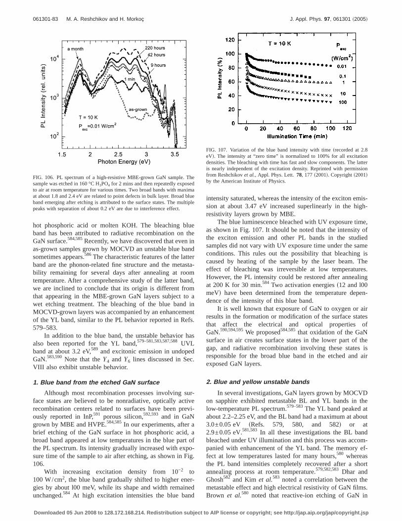
hot phosphoric acid or molten KOH. The bleaching blueband has been attributed to radiative recombination on theGaN surface.584,585Recently, we have discovered that even inas-grown samples grown by MOCVD an unstable blue bandsometimes appears.586 The characteristic features of the latterband are the phonon-related fine structure and the metasta-bility remaining for several days after annealing at roomtemperature. After a comprehensive study of the latter band,we are inclined to conclude that its origin is different fromthat appearing in the MBE-grown GaN layers subject to awet etching treatment. The bleaching of the blue band inMOCVD-grown layers was accompanied by an enhancementof the YL band, similar to the PL behavior reported in Refs.579–583.
In addition to the blue band, the unstable behavior hasalso been reported for the YL band,579–581,583,587,588UVLband at about 3.2 eV,589 and excitonic emission in undopedGaN.583,590 Note that theY4 and Y6 lines discussed in Sec.VIII also exhibit unstable behavior.
1. Blue band from the etched GaN surface
Although most recombination processes involving sur-face states are believed to be nonradiative, optically activerecombination centers related to surfaces have been previ-ously reported in InP,591 porous silicon,592,593 and in GaNgrown by MBE and HVPE.584,585In our experiments, after abrief etching of the GaN surface in hot phosphoric acid, abroad band appeared at low temperatures in the blue part ofthe PL spectrum. Its intensity gradually increased with expo-sure time of the sample to air after etching, as shown in Fig.106.
With increasing excitation density from 10−2 to100 W/cm2, the blue band gradually shifted to higher ener-gies by about l00 meV, while its shape and width remainedunchanged.584 At high excitation intensities the blue band
intensity saturated, whereas the intensity of the exciton emis-sion at about 3.47 eV increased superlinearly in the high-resistivity layers grown by MBE.
The blue luminescence bleached with UV exposure time,as shown in Fig. 107. It should be noted that the intensity ofthe exciton emission and other PL bands in the studiedsamples did not vary with UV exposure time under the sameconditions. This rules out the possibility that bleaching iscaused by heating of the sample by the laser beam. Theeffect of bleaching was irreversible at low temperatures.However, the PL intensity could be restored after annealingat 200 K for 30 min.584 Two activation energiess12 and l00meVd have been determined from the temperature depen-dence of the intensity of this blue band.
It is well known that exposure of GaN to oxygen or airresults in the formation or modification of the surface statesthat affect the electrical and optical properties ofGaN.590,594,595We proposed584,585 that oxidation of the GaNsurface in air creates surface states in the lower part of thegap, and radiative recombination involving these states isresponsible for the broad blue band in the etched and airexposed GaN layers.
2. Blue and yellow unstable bands
In several investigations, GaN layers grown by MOCVDon sapphire exhibited metastable BL and YL bands in thelow-temperature PL spectrum.579–583The YL band peaked atabout 2.2–2.25 eV, and the BL band had a maximum at about3.0±0.05 eV sRefs. 579, 580, and 582d or at2.9±0.05 eV.581,583 In all these investigations the BL bandbleached under UV illumination and this process was accom-panied with enhancement of the YL band. The memory ef-fect at low temperatures lasted for many hours,580 whereasthe PL band intensities completely recovered after a shortannealing process at room temperature.579,582,583Dhar andGhosh582 and Kim et al.583 noted a correlation between themetastable effect and high electrical resistivity of GaN films.Brown et al.580 noted that reactive-ion etching of GaN in
FIG. 106. PL spectrum of a high-resistive MBE-grown GaN sample. Thesample was etched in 160 °C H3PO4 for 2 mins and then repeatedly exposedto air at room temperature for various times. Two broad bands with maximaat about 1.8 and 2.4 eV are related to point defects in bulk layer. Broad blueband emerging after etching is attributed to the surface states. The multiplepeaks with separation of about 0.2 eV are due to interference effect.
FIG. 107. Variation of the blue band intensity with timesrecorded at 2.8eVd. The intensity at “zero time” is normalized to 100% for all excitationdensities. The bleaching with time has fast and slow components. The latteris nearly independent of the excitation density. Reprinted with permissionfrom Reshchikovet al., Appl. Phys. Lett.78, 177s2001d. Copyrights2001dby the American Institute of Physics.
061301-83 M. A. Reshchikov and H. Morkoç J. Appl. Phys. 97, 061301 ~2005!
Downloaded 05 Jun 2008 to 128.172.168.214. Redistribution subject to AIP license or copyright; see http://jap.aip.org/jap/copyright.jsp
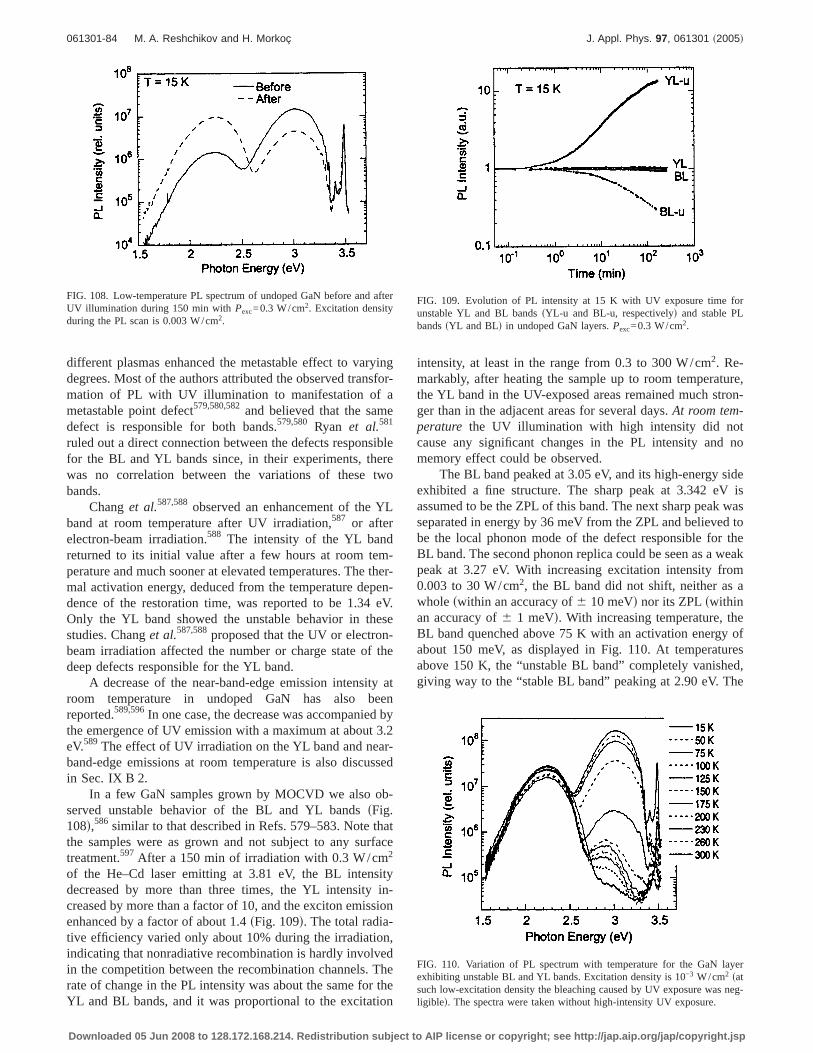
different plasmas enhanced the metastable effect to varyingdegrees. Most of the authors attributed the observed transfor-mation of PL with UV illumination to manifestation of ametastable point defect579,580,582and believed that the samedefect is responsible for both bands.579,580 Ryan et al.581
ruled out a direct connection between the defects responsiblefor the BL and YL bands since, in their experiments, therewas no correlation between the variations of these twobands.
Changet al.587,588 observed an enhancement of the YLband at room temperature after UV irradiation,587 or afterelectron-beam irradiation.588 The intensity of the YL bandreturned to its initial value after a few hours at room tem-perature and much sooner at elevated temperatures. The ther-mal activation energy, deduced from the temperature depen-dence of the restoration time, was reported to be 1.34 eV.Only the YL band showed the unstable behavior in thesestudies. Changet al.587,588proposed that the UV or electron-beam irradiation affected the number or charge state of thedeep defects responsible for the YL band.
A decrease of the near-band-edge emission intensity atroom temperature in undoped GaN has also beenreported.589,596In one case, the decrease was accompanied bythe emergence of UV emission with a maximum at about 3.2eV.589 The effect of UV irradiation on the YL band and near-band-edge emissions at room temperature is also discussedin Sec. IX B 2.
In a few GaN samples grown by MOCVD we also ob-served unstable behavior of the BL and YL bandssFig.108d,586 similar to that described in Refs. 579–583. Note thatthe samples were as grown and not subject to any surfacetreatment.597 After a 150 min of irradiation with 0.3 W/cm2
of the He–Cd laser emitting at 3.81 eV, the BL intensitydecreased by more than three times, the YL intensity in-creased by more than a factor of 10, and the exciton emissionenhanced by a factor of about 1.4sFig. 109d. The total radia-tive efficiency varied only about 10% during the irradiation,indicating that nonradiative recombination is hardly involvedin the competition between the recombination channels. Therate of change in the PL intensity was about the same for theYL and BL bands, and it was proportional to the excitation
intensity, at least in the range from 0.3 to 300 W/cm2. Re-markably, after heating the sample up to room temperature,the YL band in the UV-exposed areas remained much stron-ger than in the adjacent areas for several days.At room tem-perature the UV illumination with high intensity did notcause any significant changes in the PL intensity and nomemory effect could be observed.
The BL band peaked at 3.05 eV, and its high-energy sideexhibited a fine structure. The sharp peak at 3.342 eV isassumed to be the ZPL of this band. The next sharp peak wasseparated in energy by 36 meV from the ZPL and believed tobe the local phonon mode of the defect responsible for theBL band. The second phonon replica could be seen as a weakpeak at 3.27 eV. With increasing excitation intensity from0.003 to 30 W/cm2, the BL band did not shift, neither as awholeswithin an accuracy of6 10 meVd nor its ZPLswithinan accuracy of6 1 meVd. With increasing temperature, theBL band quenched above 75 K with an activation energy ofabout 150 meV, as displayed in Fig. 110. At temperaturesabove 150 K, the “unstable BL band” completely vanished,giving way to the “stable BL band” peaking at 2.90 eV. The
FIG. 108. Low-temperature PL spectrum of undoped GaN before and afterUV illumination during 150 min withPexc=0.3 W/cm2. Excitation densityduring the PL scan is 0.003 W/cm2.
FIG. 109. Evolution of PL intensity at 15 K with UV exposure time forunstable YL and BL bandssYL-u and BL-u, respectivelyd and stable PLbandssYL and BLd in undoped GaN layers.Pexc=0.3 W/cm2.
FIG. 110. Variation of PL spectrum with temperature for the GaN layerexhibiting unstable BL and YL bands. Excitation density is 10−3 W/cm2 satsuch low-excitation density the bleaching caused by UV exposure was neg-ligibled. The spectra were taken without high-intensity UV exposure.
061301-84 M. A. Reshchikov and H. Morkoç J. Appl. Phys. 97, 061301 ~2005!
Downloaded 05 Jun 2008 to 128.172.168.214. Redistribution subject to AIP license or copyright; see http://jap.aip.org/jap/copyright.jsp
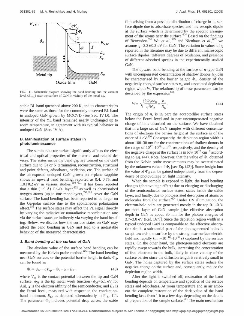
stable BL band quenched above 200 K, and its characteristicswere the same as those for the commonly observed BL bandin undoped GaN grown by MOCVDssee Sec. IV Dd. Theintensity of the YL band remained nearly unchanged up toroom temperature, in agreement with its typical behavior inundoped GaNsSec. IV Ad.
B. Manifestation of surface states inphotoluminescence
The semiconductor surface significantly affects the elec-trical and optical properties of the material and related de-vices. The states inside the band gap are formed on the GaNsurface due to Ga or N termination, reconstruction, structuraland point defects, adsorbates, oxidation, etc. The surface ofthe air-exposed undoped GaN grown onc-plane sapphireshows an upward band bending, reported as 0.4, 0.75, and1.0±0.2 eV in various studies.598–601 It has been reportedthat a thins,9 Åd Ga2O3 layer,602 as well as chemisorbedoxygen atomssup to one monolayerd,598,603 cover the GaNsurface. The band bending has been reported to be larger onthe Ga-polar surface due to the spontaneous polarizationeffect.553 The surface states may affect the PL signal directlyby varying the radiative or nonradiative recombination ratevia the surface states or indirectly via varying the band bend-ing. Below, we discuss how the surface states on GaN mayaffect the band bending in GaN and lead to a metastablebehavior of the measured characteristics.
1. Band bending at the surface of GaN
The absolute value of the surface band bending can bemeasured by the Kelvin probe method.604 The band bendingnear GaN surface, or the potential barrier height in dark,Fd,can be found as
Fd = fM − qVcp − Fs − x + EF, s43d
whereVcp is the contact potential between the tip and GaNsurface,fM is the tip metal work functionsfM =5.1 eV forAud, x is the electron affinity of the semiconductor, andEF isthe Fermi level, measured with respect to the conduction-band minimum,EC, as depicted schematically in Fig. 111.The parameterFs includes potential drop across the oxide
film arising from a possible distribution of charge in it, sur-face dipole due to adsorbate species, and microscopic dipoleat the surface which is determined by the specific arrange-ment of the atoms near the surface.604 Based on the findingsof Bermudez,598 Wu et al.,599 and Nienhauset al.,605 weassumex=3.3±0.3 eV for GaN. The variation in values ofxreported in the literature may be due to different microscopicsurface dipoles, different degrees of oxidation, and presenceof different adsorbed species in the experimentally studiedGaN.
The upward band bending at the surface ofn-type GaNwith uncompensated concentration of shallow donorsND canbe characterized by the barrier heightFd, density of thenegatively charged surface statesns, and associated depletionregion widthW. The relationship of these parameters can bedescribed by the expression606
W=Î2Fd««0
q2ND=
ns
ND. s44d
The origin of ns is in part the acceptorlike surface statesbelow the Fermi level and in part uncompensated negativecharge of ions adsorbed on the surface. We have obtainedthat in a large set of GaN samples with different concentra-tions of electrons the barrier height at the surface is of theorder of 1 eV.600 Consequently, the depletion region width isabout 100–30 nm for the concentrations of shallow donors inthe range of 1017–1018 cm−3, respectively, and the density ofthe negative charge at the surface is in low 1012 cm−3 accord-ing to Eq.s44d. Note, however, that the value ofFd obtainedfrom the Kelvin probe measurements may be overestimatedby the unknown value ofFs fsee Eq.s43dg. Some insight intothe value ofFd can be gained independently from the depen-dence of photovoltage on light intensity.
When the sample is exposed to light, the band bendingchangessphotovoltage effectd due to charging or dischargingof the semiconductor surface states, states inside the oxidelayer, and finally, due to photoassisted desorption of atoms ormolecules from the surface.604 Under UV illumination, theelectron-hole pairs are generated mostly in the top 0.1–0.3-µm-thick layer of GaN samplefthe effective absorptiondepth in GaN is about 80 nm for the photon energies of3.7–3.8 eVsRef. 167dg. Since the depletion region width in atypical undoped GaN is comparable to the effective absorp-tion depth, a substantial part of the photogenerated holes isswept towards the surface by the strong near-surface electricfield and rapidlysin ,10−10–10−8 sd captured by the surfacestates. On the other hand, the photogenerated electrons arerapidly swept towards the bulk, increasing the concentrationof free electrons in the bulk, likely in close vicinity of thesurface barrier since the diffusion length is relatively small inGaN. The holes captured by the surface states reduce thenegative charge on the surface and, consequently, reduce thedepletion region width.
After the light is switched off, restoration of the bandbending depends on temperature and specifics of the surfacestates and adsorbates. At room temperature and in air ambi-ent the complete restoration of the dark value of the bandbending lasts from 1 h to a fewdays depending on the detailsof preparation of the sample surface.601 The main mechanism
FIG. 111. Schematic diagram showing the band bending and the vacuumlevel sEVACd near the surface of GaN in vicinity of the metal tip.
061301-85 M. A. Reshchikov and H. Morkoç J. Appl. Phys. 97, 061301 ~2005!
Downloaded 05 Jun 2008 to 128.172.168.214. Redistribution subject to AIP license or copyright; see http://jap.aip.org/jap/copyright.jsp
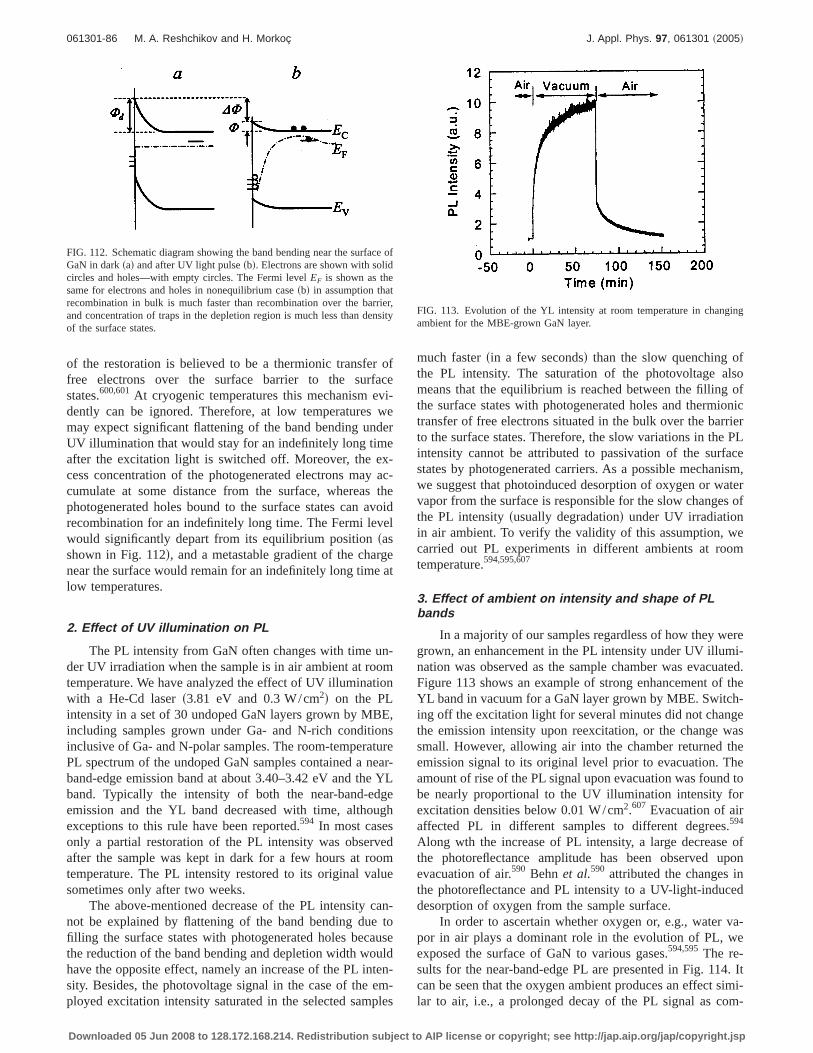
of the restoration is believed to be a thermionic transfer offree electrons over the surface barrier to the surfacestates.600,601At cryogenic temperatures this mechanism evi-dently can be ignored. Therefore, at low temperatures wemay expect significant flattening of the band bending underUV illumination that would stay for an indefinitely long timeafter the excitation light is switched off. Moreover, the ex-cess concentration of the photogenerated electrons may ac-cumulate at some distance from the surface, whereas thephotogenerated holes bound to the surface states can avoidrecombination for an indefinitely long time. The Fermi levelwould significantly depart from its equilibrium positionsasshown in Fig. 112d, and a metastable gradient of the chargenear the surface would remain for an indefinitely long time atlow temperatures.
2. Effect of UV illumination on PL
The PL intensity from GaN often changes with time un-der UV irradiation when the sample is in air ambient at roomtemperature. We have analyzed the effect of UV illuminationwith a He-Cd lasers3.81 eV and 0.3 W/cm2d on the PLintensity in a set of 30 undoped GaN layers grown by MBE,including samples grown under Ga- and N-rich conditionsinclusive of Ga- and N-polar samples. The room-temperaturePL spectrum of the undoped GaN samples contained a near-band-edge emission band at about 3.40–3.42 eV and the YLband. Typically the intensity of both the near-band-edgeemission and the YL band decreased with time, althoughexceptions to this rule have been reported.594 In most casesonly a partial restoration of the PL intensity was observedafter the sample was kept in dark for a few hours at roomtemperature. The PL intensity restored to its original valuesometimes only after two weeks.
The above-mentioned decrease of the PL intensity can-not be explained by flattening of the band bending due tofilling the surface states with photogenerated holes becausethe reduction of the band bending and depletion width wouldhave the opposite effect, namely an increase of the PL inten-sity. Besides, the photovoltage signal in the case of the em-ployed excitation intensity saturated in the selected samples
much fastersin a few secondsd than the slow quenching ofthe PL intensity. The saturation of the photovoltage alsomeans that the equilibrium is reached between the filling ofthe surface states with photogenerated holes and thermionictransfer of free electrons situated in the bulk over the barrierto the surface states. Therefore, the slow variations in the PLintensity cannot be attributed to passivation of the surfacestates by photogenerated carriers. As a possible mechanism,we suggest that photoinduced desorption of oxygen or watervapor from the surface is responsible for the slow changes ofthe PL intensitysusually degradationd under UV irradiationin air ambient. To verify the validity of this assumption, wecarried out PL experiments in different ambients at roomtemperature.594,595,607
3. Effect of ambient on intensity and shape of PLbands
In a majority of our samples regardless of how they weregrown, an enhancement in the PL intensity under UV illumi-nation was observed as the sample chamber was evacuated.Figure 113 shows an example of strong enhancement of theYL band in vacuum for a GaN layer grown by MBE. Switch-ing off the excitation light for several minutes did not changethe emission intensity upon reexcitation, or the change wassmall. However, allowing air into the chamber returned theemission signal to its original level prior to evacuation. Theamount of rise of the PL signal upon evacuation was found tobe nearly proportional to the UV illumination intensity forexcitation densities below 0.01 W/cm2.607 Evacuation of airaffected PL in different samples to different degrees.594
Along wth the increase of PL intensity, a large decrease ofthe photoreflectance amplitude has been observed uponevacuation of air.590 Behnet al.590 attributed the changes inthe photoreflectance and PL intensity to a UV-light-induceddesorption of oxygen from the sample surface.
In order to ascertain whether oxygen or, e.g., water va-por in air plays a dominant role in the evolution of PL, weexposed the surface of GaN to various gases.594,595The re-sults for the near-band-edge PL are presented in Fig. 114. Itcan be seen that the oxygen ambient produces an effect simi-lar to air, i.e., a prolonged decay of the PL signal as com-
FIG. 112. Schematic diagram showing the band bending near the surface ofGaN in darksad and after UV light pulsesbd. Electrons are shown with solidcircles and holes—with empty circles. The Fermi levelEF is shown as thesame for electrons and holes in nonequilibrium casesbd in assumption thatrecombination in bulk is much faster than recombination over the barrier,and concentration of traps in the depletion region is much less than densityof the surface states.
FIG. 113. Evolution of the YL intensity at room temperature in changingambient for the MBE-grown GaN layer.
061301-86 M. A. Reshchikov and H. Morkoç J. Appl. Phys. 97, 061301 ~2005!
Downloaded 05 Jun 2008 to 128.172.168.214. Redistribution subject to AIP license or copyright; see http://jap.aip.org/jap/copyright.jsp
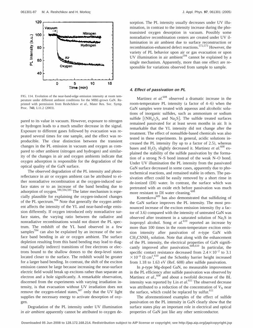
pared to its value in vacuum. However, exposure to nitrogenor hydrogen leads to a much smaller decrease in the signal.Exposure to different gases followed by evacuation was re-peated several times for one sample, and the effect was re-producible. The clear distinction between the transientchanges in the PL emission in vacuum and oxygen as com-pared to other ambientsnitrogen and hydrogend and similar-ity of the changes in air and oxygen ambients indicate thatoxygen adsorption is responsible for the degradation of theoptical quality of the GaN surface.
The observed degradation of the PL intensity and photo-reflectance in air or oxygen ambient can be attributed to ei-ther nonradiative recombination at the oxygen-induced sur-face states or to an increase of the band bending due toadsorption of oxygen.590,594,595The latter mechanism is espe-cially plausible for explaining the oxygen-induced changesof the PL spectrum.594 Note that generally the oxygen ambi-ent affects the intensity of the YL and near-band-edge emis-sion differently. If oxygen introduced only nonradiative sur-face states, the varying ratio between the radiative andnonradiative recombinations would not distort the PL spec-trum. The redshift of the YL band observed in a fewsamples594 can also be explained by an increase of the sur-face band bending in air or oxygen ambient. The surfacedepletion resulting from this band bending may lead to diag-onal sspatially indirectd transitions of free electrons or elec-trons bound to the shallow donors to the deep-level stateslocated closer to the surface. The redshift would be greaterfor a larger band bending. In contrast, the shift of the excitonemission cannot be large because increasing the near-surfaceelectric field would break up excitons rather than separate anelectron and a hole significantly. A remarkable observation,discerned from the experiments with varying irradiation in-tensity, is that evacuation without UV irradiation does notremove the oxygen-related states,607 only that the UV lightsupplies the necessary energy to activate desorption of oxy-gen.
Degradation of the PL intensity under UV illuminationin air ambientapparently cannot be attributed to oxygen de-
sorption. The PL intensity usually decreases under UV illu-mination, in contrast to the intensity increase during the pho-toassisted oxygen desorption in vacuum. Possibly somenonradiative recombination centers are created under UV il-lumination in air ambient due to surface reconstruction orrecombination-enhanced defect reactions.572,573However, thevariety of PL behavior upon air or gas evacuation or uponUV illumination in air ambient594 cannot be explained by asingle mechanism. Apparently, more than one effect are re-sponsible for variations observed from sample to sample.
4. Effect of passivation on PL
Martinez et al.608 observed a dramatic increase in theroom-temperature PL intensitysa factor of 4–6d when theGaN samples were treated with aqueous and alcoholic solu-tions of inorganic sulfides, such as ammonium or sodiumsulfide fsNH4d2Sx and Na2Sg. The sulfide treated surfacesremained passivated for at least seven months in air. It isremarkable that the YL intensity did not change after thetreatment. The effect of nonsulfide-based chemicals was alsotested in these experiments. In general, acidic solutions in-creased the PL intensitysby up to a factor of 2.5d, whereasbases and H2O2 slightly decreased it. Martinezet al.608 ex-plained the stability of the sulfide passivation by the forma-tion of a strong N–S bond instead of the weak N–O bond.Under UV illumination the PL intensity from the passivatedGaN surface decreased in some cases, apparently due to pho-tochemical reactions, and remained stable in others. The pas-sivation effect could be easily removed by a short rinse inde-ionizedsDId water. In contrast, the surface which waspretreated with an oxide etch before passivation was muchmore resistant to DI water cleaning.608
Konenkova609 has also demonstrated that sulfidizing ofthe GaN surface improves the PL intensity. The most pro-nounced increase of the exciton emission intensitysby a fac-tor of 3.6d compared with the intensity of untreated GaN wasobserved after treatment in a saturated solution of Na2S inisopropyl alcohol. Songet al.610 reported an increase bymore than 100 times in the room-temperature exciton emis-sion intensity after passivation ofn-type GaN withCH3CSNH2 solution. Note that along with the enhancementof the PL intensity, the electrical properties of GaN signifi-cantly improved after passivation.608,610 In particular, thespecific contact resistance decreased from 2.4310−2 to 3.1310−6 V cm2,610 and the Schottky barrier height increasedfrom 1.18 to 1.63 eVsRef. 608d after sulfide passivation.
In p-type Mg-doped GaN, no measurable improvementin the PL efficiency after sulfide passivation was observed byMartinez et al.,608 and about a twofold decrease of the BLintensity was reported by Linet al.611 The observed decreasewas attributed to a reduction of the concentration ofVN nearthe surface, which could be replaced by sulfur.611
The aforementioned examples of the effect of sulfidepassivation on the PL intensity in GaN clearly show that thesurface states play an important role in electrical and opticalproperties of GaN just like any other semiconductor.
FIG. 114. Evolution of the near-band-edge emission intensity at room tem-perature under different ambient conditions for the MBE-grown GaN. Re-printed with permission from Reshchikovet al., Mater Res. Soc. Symp.Proc. 743, L11.2 s2003d.
061301-87 M. A. Reshchikov and H. Morkoç J. Appl. Phys. 97, 061301 ~2005!
Downloaded 05 Jun 2008 to 128.172.168.214. Redistribution subject to AIP license or copyright; see http://jap.aip.org/jap/copyright.jsp
X. SUMMARY
Point defects affect optical and electrical properties ofGaN to a greater extent than perhaps recognized. Lumines-cence methods are particularly advantageous for detectionand revealing the nature of point defects, however, great ef-forts must be extended to identify numerous defects in GaN.Even in unintentionally doped GaN a plethora of lumines-cence bands is discovered that are attributed to residual im-purities, native defects, complexes, and structural defects. Inthis review, we provide a comprehensive analysis of the be-havior of numerous luminescence bands associated with de-fects in GaN. Special attention was given to the notoriousluminescence bands such as the yellow band in undopedGaN, and the blue band observed in undoped, Zn-, and Mg-doped GaN. It should be noted that the previous assignmentsas to the origin of most of the luminescence bands in GaNwere very preliminary and often based largely on specula-tions without much basis or on controversial theoretical pre-dictions rather than on convincing experimental evidence.By analyzing a large body of published literature, combinedwith “hands on experience” in this field we have attemptedto shed light on the identity and properties of many pointdefects in GaN. Typical concentrations of uncontrolled ac-ceptors, responsible for spontaneous emission in the visiblepart of the spectrum in undoped GaN, are of the order of1015 cm−3, even in the purest available material. In dopedGaN the situation is not much clearer because the dopinguniversally results in the creation of yet unknown compen-sating defects. Among the defects inp-type GaN that areexplored the most, properties of luminescence bands due toMg doping are established with high degree of certainty. Theimportance of potential fluctuations, which are unavoidablein heavily Mg-doped GaN, has been treated in detail. A classof luminescence lines in GaN, most probably related in someway or another to structural defects, has been discussed indetail. The stability of several luminescence bands with timeand ambient conditions has also been examined.
ACKNOWLEDGMENTS
This work was funded by AFOSRsDr. G. L. Witt andDr. T. Steinerd, NSF sDr. L. Hess and Dr. U. Varshneyd, andONR sDr. C. E. C. Woodd, and was motivated to a largeextent by the Wood-Witt program. Due to space limitationwe thank our close collaborators and those who providedtheir papers: Dr. D. Huang, Dr. F. Yun, Dr. P. Visconti, Dr. J.Jasinski, Dr. R. J. Molnar, Dr. C. G. Van de Walle, Dr. J. E.Northrup, Dr. R. Y. Korotkov, Dr. Z. Liliental-Weber, Dr. B.W. Wessels, Dr. F. Shahedipour, Dr. S. S. Park, Dr. K. Y. Lee,Dr. V. Dmitriev, Dr. D. C. Reynolds, Dr. C. W. Litton, Dr. D.C. Look, Dr. Z. Fang, Dr. D. K. Johnstone, Dr. Y. T. Moon,Dr. K. Saarinen, Dr. J. Freitas, Jr., Dr. E. Glaser, and Dr. A. J.Steckl, and graduate students S. Sabuktagin and Lei He.
1B. Monemar, inOptical Properties of GaN, Semiconductors and Semimet-als Vol. 50sAcademic, San Diego, 1998d, pp. 305–368.
2B. Monemar, J. Mater. Sci.: Mater. Electron.10, 227 s1999d.3B. Monemar, J. Phys.: Condens. Matter13, 7011s2001d.4B. Monemaret al., Mater. Sci. Eng., B93, 112 s2002d.5S. Strite and H. Morkoç, J. Vac. Sci. Technol. B10, 1237s1992d.
6S. Nakamura and G. Fosol,The Blue Laser DiodesSpringer, Berlin, 1998d.7H. Morkoç, Nitride Semiconductors and DevicessSpringer, Heidelberg,1999d.
8In Properties, Processing, and Applications of Gallium Nitride and Re-lated Semiconductors, edited by J. H. Edgar, S. Strite, I. Akasaki, H.Amano, and C. WetzelslNSPEC, UK, 1999d.
9S. J. Pearton, J. C. Zolper, R. J. Shul, and F. Ren, J. Appl. Phys.86, 1s1999d.
10S. C. Jain, M. Willander, J. Narayan, and R. Van Overstraeten, J. Appl.Phys. 87, 965 s2000d.
11A. K. Viswanath,Growth and Optical Properties of GaN, Semiconductorsand Semimetals Vol. 73, edited by R. Willardson, and H. S. NalwasAca-demic, San Diego, 2001d, pp. 63–150.
12H. Morkoç, Mater. Sci. Eng., R.33, 135 s2001d.13J. K. Sheu and G. C. Chi, J. Phys.: Condens. Matter14, 657 s2002d.14D. W. Jenkins and J. D. Dow, Phys. Rev. B39, 3317s1989d.15J. Neugebauer and C. G. Van de Walle, Phys. Rev. B50, 8067s1994d.16J. Neugebauer and C. G. Van de Walle, Appl. Phys. Lett.68, 1829s1996d.17J. Neugebauer and C. G. Van de Walle, Appl. Phys. Lett.69, 503 s1996d.18P. Boguslawski, E. L. Briggs, and J. Bernholc, Phys. Rev. B51, 17255
s1995d.19P. Boguslawski, E. L. Briggs, and J. Bernholc, Appl. Phys. Lett.69, 233
s1996d.20P. Boguslawski and J. Bernholc, Phys. Rev. B56, 9496s1997d.21S. Limpijumnong and C. G. Van de Walle, Phys. Rev. B69, 035207
s2004d.22T. Mattila and R. M. Nieminen, Phys. Rev. B55, 9571s1997d.23I. Gorczyca, A. Svane, and N. E. Christensen, Phys. Rev. B60, 8147
s1999d.24J. Neugebauer and C. G. Van de Walle, inFestkörperprobleme/Advances
in Solid State Physics, edited by R. HelbigsVieweg, Braunschweig, 1996d,Vol. 35, p. 25.
25S. B. Zhang and J. E. Northrup, Phys. Rev. Lett.67, 2339s1991d.26C. G. Van de Walle and J. Neugebauer, J. Appl. Phys.95, 3851s2004d.27G. A. Baraff and M. Schlüter, Phys. Rev. Lett.55, 1327s1985d.28I. Gorczyca, N. E. Christensen, and A. Svane, Phys. Rev. B66, 075210
s2002d.29C. H. Park and D. J. Chadi, Phys. Rev. B55, 12995s1997d.30J. Neugebauer and C. G. Van de Walle, J. Appl. Phys.85, 3003s1999d.31K. H. Chow, G. D. Watkins, A. Usui, and M. Mizuta, Phys. Rev. Lett.85,
2761 s2000d.32T. Mattila, A. P. Seitsonen, and R. Nieminen, Phys. Rev. B54, 1474
s1996d.33D. J. Chadi and K. J. Chang, Phys. Rev. Lett.60, 2183s1988d.34J. Dabrowski and M. Scheffler, Phys. Rev. Lett.60, 2183s1988d.35H. Wang and A.-B. Chen, J. Appl. Phys.87, 7859s2000d.36A. F. Wright, J. Appl. Phys.92, 2575s2002d.37F. Mireles and S. E. Ulloa, Phys. Rev. B58, 3879s1998d.38H. Wang and A.-B. Chen, Phys. Rev. B63, 125212s2001d.39B. Pödör, Semicond. Sci. Technol.11, 827 s1996d.40C. G. Van de Walle, S. Limpijumnong, and J. Neugebauer, Phys. Rev. B
63, 245205s2001d.41C. D. Latham, R. M. Nieminen, C. J. Fall, R. Jones, S. Öberg, and P. R.
Briddon, Phys. Rev. B67, 205206s2003d.42S. Limpijumnong, C. G. Van de Walle, and J. Neugebauer, Mater. Res.
Soc. Symp. Proc.639, G4.3 s2001d.43L. E. Ramos, J. Furthmüller, L. M. R. Scolfaro, J. R. Leite, and F. Bech-
stedt, Phys. Rev. B66, 075209s2002d.44L. Bellaiche, S.-H. Wei, and A. Zunger, Phys. Rev. B56, 10233s1997d.45T. Mattila and A. Zunger, Phys. Rev. B58, 1367s1998d.46C. G. Van de Walle and J. Neugebauer, Appl. Phys. Lett.76, 1009s2000d.47J. Neugebauer and C. G. Van de Walle, Phys. Rev. Lett.75, 4452s1995d.48A. F. Wright, C. H. Seager, S. H. Myers, D. D. Koleske, and A. A.
Allerman, J. Appl. Phys.94, 2311s2003d.49C. G. Van de Walle, Phys. Status Solidi B235, 89 s2003d.50N. S. Averkiev, A. A. Gutkin, E. B. Osipov, M. A. Reshchikov, and V. R.
Sosnovskii, Defect Diffus. Forum103–105, 31 s1993d.51H. Xu and U. Lindefelt, J. Appl. Phys.68, 4077s1990d.52C. W. Myles and O. F. Sankey, Phys. Rev. B29, 6810s1984d.53C. G. Van de Walle, J. Neugebauer, C. Stampel, M. D. McCluskey, and N.
M. Johnson, Acta Phys. Pol. A96, 613 s1999d.54I. Gorczyca, A. Svane, and N. E. Christensen, Phys. Rev. B61, 7494
s2000d.55J. Z. Li, J. Y. Lin, H. X. Jiang, A. Salvador, A. Botchkarev, and H.
061301-88 M. A. Reshchikov and H. Morkoç J. Appl. Phys. 97, 061301 ~2005!
Downloaded 05 Jun 2008 to 128.172.168.214. Redistribution subject to AIP license or copyright; see http://jap.aip.org/jap/copyright.jsp
Morkoç, Appl. Phys. Lett.69, 1474s1996d.56U. Kaufmann, M. Kunzer, M. Maier, H. Obloh, A. Ramakrishnan, B.
Santic, and P. Schlotter, Appl. Phys. Lett.72, 1326s1998d.57C. D. Latham, R. Jones, S. Öberg, R. M. Nieminen, and P. R. Briddon,
Phys. Rev. B68, 205209s2003d.58S.-G. Lee and K. J. Chang, Semicond. Sci. Technol.14, 138 s1999d.59C. G. Van de Walle, Phys. Rev. B56, R10020s1997d.60B. Szûcs, A. Gali, Z. Hajnal, P. Deák, and C. G. Van de Walle, Phys. Rev.
B 68, 085202s2003d.61J. Elsneret al., Phys. Rev. Lett.79, 3672s1997d.62A. F. Wright and U. Grossner, Appl. Phys. Lett.73, 2751s1998d.63S. M. Lee, M. A. Belkhir, X. Y. Zhu, Y. H. Lee, Y. G. Hwang, and T.
Frauenheim, Phys. Rev. B61, 16033s2000d.64J. E. Northrup, Phys. Rev. B66, 045204s2002d.65K. Leung, A. F. Wright, and E. B. Stechel, Appl. Phys. Lett.74, 2495
s1999d.66P. J. Hansenet al., Appl. Phys. Lett.72, 2247s1998d.67M. A. Reshchikov and R. Y. Korotkov, Phys. Rev. B64, 115205s2001d.68J. Elsner, R. Jones, M. I. Heggie, P. K. Sitch, M. Haugk, Th. Frauenheim,
S. Öberg, and P. R. Briddon, Phys. Rev. B58, 12571s1998d.69L. W. Tu, Y. C. Lee, D. Stocker, and E. F. Schubert, Phys. Rev. B58,
10696s1998d.70A. Göldneret al., Mater. Res. Soc. Symp. Proc.482, 637 s1998d.71E. F. Schubert, I. D. Goepfert, and J. M. Redwing, Appl. Phys. Lett.71,
3224 s1997d.72I.-H. Lee, J. J. Lee, P. Kung, F. J. Sanchez, and M. Razeghi, Appl. Phys.
Lett. 74, 102 s1999d.73R. Singh, R. J. Molnar, M. S.Űnlü, and T. D. Moustakas, Appl. Phys.
Lett. 64, 336 s1994d.74W. Grieshaber, E. F. Schubert, I. D. Goepfert, R. F. Karlicek, Jr., M. J.
Schurman, and C. Tran, J. Appl. Phys.80, 4615s1996d.75D. A. Turnbull, X. Li, S. Q. Gu, E. E. Reuter, J. J. Coleman, and S. G.
Bishop, J. Appl. Phys.80, 4609s1996d.76D. M. Hofmannet al., Phys. Rev. B52, 16702s1995d.77J. Krüger, D. Corlatan, C. Kisielowski, Y. Kim, R. Klockenbrink, G. S.
Sudhir, M. Rubin, and E. Weber, Mater. Sci. Forum258–263, 1191s1997d.
78O. Brandt, J. Ringling, K. H. Ploog, H.-J. Wünsche, and F. Henneberger,Phys. Rev. B58, R15977s1998d.
79D. G. Thomas, J. J. Hopfield, and W. M. Augustyniak, Phys. Rev.140,A202 s1965d.
80A. P. Levanyuk and V. V. Osipov, Usp. Fiz. Nauk133, 427 s1981d fSov.Phys. Usp.24, 187 s1981dg.
81S. Shinoya, T. Koda, K. Era, and H. Fujiwara, J. Phys. Soc. Jpn.19, 1157s1964d.
82M. A. Reshchikov, G.-C. Yi, and B. W. Wessels, Phys. Rev. B59, 13176s1999d.
83P. W. Mason, A. Dörnen, V. Haerle, F. Scholz, and G. D. Watkins, Mater.Res. Soc. Symp. Proc.449, 793 s1997d.
84F. Binet, J. Y. Duboz, J. Off, and F. Scholz, Phys. Rev. B60, 4715s1999d.85The temperature should be low enough that the considered PL bands do
not quench, and the excitation should be chosen below the saturationregion.
86F. E. Williams, J. Phys. Chem. Solids12, 265 s1960d; Phys. Status Solidi25, 493 s1968d.
87R. Y. Korotkov, M. A. Reshchikov, and B. W. Wessels, Physica B325, 1s2003d.
88W. A. Barry and G. D. Watkins, Phys. Rev. B54, 7789s1996d.89A. G. Milnes, Deep Impurities in SemiconductorssWiley, New York,
1973d, p. 6.90F. C. Rong, W. A. Barry, J. F. Donegan, and G. D. Watkins, Phys. Rev. B
54, 7779s1996d.91B. I. Shklovskii and A. L. Efros,Electronic Properties of Doped Semicon-
ductorssSpringer, Berlin, 1984d, pp. 53–73 and 253–313.92V. I. Vovnenko, K. D. Glinchuk, K. Lukat, and A. V. Prokhorovich, Fiz.
Tekh. Poluprovodn.sS.-Peterburgd 14, 1003s1980d fSov. Phys. Semicond.14, 596 s1980dg.
93W. J. Moore, J. A. Freitas, Jr., and R. J. Molnar, Phys. Rev. B56, 12073s1997d.
94K. Huang and A. Rhys, Proc. R. Soc. London, Ser. A204, 406 s1950d.95C. C. Klick and J. H. Schulman, Solid State Phys.5, 97 s1957d.96K. K. Rebane,Impurity Spectra of SolidssPlenum, New York, 1970d.97A. M. Stoneham,Theory of Defects in SolidssClarendon, Oxford, 1975d.98T. Ogino and M. Aoki, Jpn. J. Appl. Phys.19, 2395s1980d.
99M. A. Reshchikov, R. J. Molnar, and H. Morkoç, Mater. Res. Soc. Symp.Proc. 680, E5.6 s2001d.
100M. A. Reshchikov, H. Morkoç, S. S. Park, and K. Y. Lee, Mater. Res.Soc. Symp. Proc.693, I6.19 s2002d.
101J. Cazaux, J. Appl. Phys.59, 1418s1986d.102X. Li and J. J. Coleman, Appl. Phys. Lett.70, 438 s1997d.103K. Fleischer, M. Toth, M. R. Phillips, J. Zou, G. Li, and S. J. Chua, Appl.
Phys. Lett. 74, 1114s1999d.104M. Toth and M. R. Phillips, Scanning20, 425 s1998d.105K. Knobloch, P. Perlin, J. Krueger, E. R. Weber, and C. Kisielowski,
MRS Internet J. Nitride Semicond. Res.3, 4 s1998d.106G. E. Pake and T. L. Estle,The Physical Properties of Electron Paramag-
netic ResonancesBenjamin, Reading, MA, 1973d.107E. R. Weber, H. Ennen, U. Kaufmann, J. Windscheif, J. Schneider, and T.
Wosinski, J. Appl. Phys.53, 6140s1982d.108A. V. Malyshev, I. A. Merkulov, and A. V. Rodina, Fiz. Tverd. Tela
sS.-Peterburgd 40, 1002s1998d fPhys. Solid State40, 917 s1998dg.109E. R. Glaser, J. A. Freitas, Jr., B. V. Shanabrook, and D. D. Koleske,
Phys. Rev. B68, 195201s2003d.110M. A. Reshchikov, H. Morkoç, S. S. Park, and K. Y. Lee, Appl. Phys.
Lett. 78, 2882s2001d.111M. A. Reshchikov, H. Morkoç, S. S. Park, and K. Y. Lee, Appl. Phys.
Lett. 78, 3041s2001d.112M. A. Reshchikov, H. Morkoç, S. S. Park, and K. Y. Lee, Appl. Phys.
Lett. 81, 4970s2002d.113M. A. Reshchikov, M. Zafar Iqbal, H. Morkoç, S. S. Park, and K. Y. Lee,
Appl. Phys. Lett.83, 266 s2003d.114M. A. Reshchikov, M. Zafar Iqbal, S. S. Park, K. Y. Lee, D. Tsvetkov, V.
Dmitriev, and H. Morkoç, Physica B340–342, 444 s2003d.115R. Dingle and M. Ilegems, Solid State Commun.9, 175 s1971d.116M. A. Reshchikov, F. Shahedipour, R. Y. Korotkov, M. P. Ulmer, and B.
W. Wessels, J. Appl. Phys.87, 3351s2000d.117M. A. Reshchikov, M. H. Zhang, J. Cui, P. Visconti, F. Yun, and H.
Morkoç, Mater. Res. Soc. Symp. Proc.639, G6.7 s2001d.118S. Christiansenet al., MRS Internet J. Nitride Semicond. Res.1, 19
s1996d.119J. S. Colton, P. Y. Yu, K. L. Teo, E. R. Weber, P. Perlin, I. Grzegory, and
K. Uchida, Appl. Phys. Lett.75, 3273s1999d.120J. S. Colton, P. Y. Yu, K. L. Teo, P. Perlin, E. R. Weber, I. Grzegory, and
K. Uchida, Physica B273–274, 75 s1999d.121D. C. Reynolds, D. C. Look, B. Jogai, J. E. Van Nostrand, R. Jones, and
J. Jenny, Solid State Commun.106, 701 s1998d.122J. Kang, Y. Shen, and Z. Wang, Mater. Sci. Eng., B91–92, 303 s2002d.123J. I. Pankove and J. A. Hutchby, J. Appl. Phys.47, 5387s1976d.124L. V. Jorgensen, A. C. Kruseman, H. Schut, A. Van Veen, M. Fanciulli,
and T. D. Moustakas, Mater. Res. Soc. Symp. Proc.449, 853 s1997d.125K. Saarinenet al., Phys. Rev. Lett.79, 3030s1997d.126K. Saarinenet al., Physica B273–274, 33 s1999d.127J. Oilaet al., Phys. Rev. B63, 045205s2001d.128A. Uedonoet al., J. Appl. Phys.90, 181 s2001d.129K. Saarinen, T. Suski, I. Grzegory, and D. C. Look, Physica B308–310,
77 s2001d.130K. Saarinen, V. Ranki, T. Suski, M. Bockowski, and I. Grzegory, J. Cryst.
Growth 246, 281 s2002d.131P. Laukkanenet al., J. Appl. Phys.92, 786 s2002d.132J. Oila, K. Saarinen, A. E. Wickenden, D. D. Koleske, R. L. Henry, and
M. E. Twigg, Appl. Phys. Lett.82, 1021s2003d.133J. Oilaet al., Appl. Phys. Lett.82, 3433s2003d.134X. Zhang, P. Kung, D. Walker, A. Saxler, and M. Razeghi, Mater. Res.
Soc. Symp. Proc.395, 625 s1996d.135R. Niebuhr, K. Bachem, K. Bombrowski, M. Maier, W. Plerschen, and U.
Kaufmann, J. Electron. Mater.24, 1531s1995d.136A. Y. Polyakov, M. Shin, J. A. Freitas, Jr., M. Skowronski, D. W. Greve,
and R. G. Wilson, J. Appl. Phys.80, 6349s1996d.137R. Zhang and T. F. Kuech, Appl. Phys. Lett.72, 1611s1998d.138R. Armitage, Q. Yang, H. Feick, S. Y. Tzeng, J. Lim, and E. R. Weber,
Mater. Res. Soc. Symp. Proc.743, L10.7 s2003d.139S. O. Kucheyev, M. Toth, M. R. Phillips, J. S. Williams, C. Jagadish, and
G. Li, J. Appl. Phys.91, 5867s2002d.140E. Silkowski, Y. K. Yeo, R. L. Hengehold, M. A. Khan, T. Lei, K. Evans,
and C. Cerny, Mater. Res. Soc. Symp. Proc.395, 813 s1996d.141E. R. Glaseret al., Phys. Rev. B51, 13326s1995d.142D. G. Chtchekineet al., J. Appl. Phys.81, 2197s1997d.143M. Godlewskiet al., Mater. Sci. Forum258–263, 1149s1997d.
061301-89 M. A. Reshchikov and H. Morkoç J. Appl. Phys. 97, 061301 ~2005!
Downloaded 05 Jun 2008 to 128.172.168.214. Redistribution subject to AIP license or copyright; see http://jap.aip.org/jap/copyright.jsp
144F. K. Koschnick, K. Michael, J.-M. Spaeth, B. Beaumont, and P. Gibart,Appl. Phys. Lett.76, 1828s2000d.
145P. Muret, A. Phillipe, E. Monroy, E. Munoz, B. Beaumont, F. Omnès, andP. Gibart, J. Appl. Phys.91, 2998s2002d.
146E. Callejaet al., Phys. Rev. B55, 4689s1997d.147M. Ramsteiner, J. Menniger, O. Brandt, H. Yang, and K. H. Ploog, Appl.
Phys. Lett. 69, 1276s1996d.148S. Tripathy, R. K. Soni, H. Asahi, and S. Gonda, Physica B275, 301
s2000d.149T. Suskiet al., Appl. Phys. Lett.67, 2188s1995d.150P. Perlinet al., Phys. Rev. Lett.75, 296 s1995d.151C. Trager-Cowan, K. P. O’Donnell, S. E. Hooper, and C. T. Foxon, Appl.
Phys. Lett. 68, 355 s1996d.152A. Hoffmannet al., Solid-State Electron.41, 275 s1997d.153H. C. Yang, T. Y. Lin, and Y. F. Chen, Phys. Rev. B62, 12593s2000d.154L. W. Tu, Y. C. Lee, S. J. Chen, I. Lo, D. Stocker, and E. F. Schubert,
Appl. Phys. Lett.73, 2802s1998d.155D. Basak, M. Lachab, T. Nakanishi, and S. Sakai, Appl. Phys. Lett.75,
3710 s1999d.156I. Shalish, L. Kronik, G. Segal, Y. Shapira, M. Eizenberg, and J. Salzman,
Appl. Phys. Lett.77, 987 s2000d.157I. Shalish, L. Kronik, G. Segal, Y. Rosenwaks, Y. Shapira, U. Tisch, and
J. Salzman, Phys. Rev. B59, 9748s1999d.158G. Li, S. J. Chua, S. J. Xu, W. Wang, P. Li, B. Beaumont, and P. Gibart,
Appl. Phys. Lett.74, 2821s1999d.159X. Li, P. W. Bohn, and J. J. Coleman, Appl. Phys. Lett.75, 4049s1999d.160M. A. Reshchikov, F. Shahedipour, R. Y. Korotkov, M. P. Ulmer, and B.
W. Wessels, Physica B273–274, 105 s1999d.161R. Seitz, C. Gaspar, T. Monteiro, E. Pereira, M. Leroux, B. Beamont, and
P. Gibart, MRS Internet J. Nitride Semicond. Res.2, 36 s1997d.162K. Kuriyama, H. Kondo, and M. Okada, Solid State Commun.119, 559
s2001d.163A. P. Young and L. J. Brillson, Appl. Phys. Lett.77, 699 s2000d.164R. Armitage, W. Hong, Q. Yang, H. Feick, J. Gebauer, E. R. Weber, S.
Hautakangas, and K. Saarinen, Appl. Phys. Lett.82, 3457s2003d.165V. Guénaud, E. Deleporte, M. Voos, C. Delalande, B. Beaumont, M.
Leroux, P. Gibart, and J. P. Faurie, MRS Internet J. Nitride Semicond.Res. 2, 10 s1997d.
166H. Haag, B. Hönerlage, O. Briot, and R. L. Aulombard, Phys. Rev. B60,11624s1999d.
167G. Yu, G. Wang, H. Ishikawa, M. Umeno, T. Soga, T. Egawa, J. Wa-tanabe, and T. Jimbo, Appl. Phys. Lett.70, 3209s1997d; J. F. Muth, J. H.Lee, I. K. Shmagin, R. M. Kolbas, H. C. Casey, Jr., B. P. Keller, U. K.Mishra, and S. P. DenBaars,ibid. 71, 2572s1997d.
168Z. Z. Bandić, P. M. Bridger, E. C. Piquette, and T. C. McGill, Appl. Phys.Lett. 72, 3166s1998d.
169P. M. Bridger, Z. Z. Bandić, E. C. Piquette, and T. C. McGill, Appl. Phys.Lett. 73, 3438s1998d.
170L. Chernyaket al., Appl. Phys. Lett.77, 2695s2000d.171N. Yamamotoet al., J. Appl. Phys.94, 4315s2003d.172U. Kaufmann, M. Kunzer, H. Obloh, M. Maier, Ch. Manz, A. Ramakrish-
nan, and B. Santic, Phys. Rev. B59, 5561s1999d.173J. Chadi, inProceedings of the 22nd International Conference on the
Physics of Semiconductors, Vancouver, Canada, 16–19 August 1994, ed-ited by D. J. LockwoodsWorld Scientific, Singapore, 1995d, p. 2311.
174W. Shan, T. J. Schmidt, R. J. Hauenstein, J. J. Song, and B. Goldenberg,Appl. Phys. Lett.66, 3492s1995d.
175S. Kim, I. P. Herman, J. A. Tuchman, K. Doverspike, L. B. Rowland, andD. K. Gaskill, Appl. Phys. Lett.67, 380 s1995d.
176K. Michael, U. Rogulis, F. K. Koschnick, Th. Tröster, J.-M. Spaeth, B.Beaumont, and P. Gibart, Physica B308–310, 85 s2001d.
177D. C. Look, Phys. Status Solidi B228, 293 s2001d.178K. Saarinen, T. Suski, I. Grzegory, and D. C. Look, Phys. Rev. B64,
233201s2001d.179L. J. Brillson et al., Physica B273–274, 70 s1999d.180M. Toth, K. Fleischer, and M. R. Phillips, Phys. Rev. B59, 1575s1999d.181A. Cremades, J. Piqueras, C. Xavier, T. Monteiro, E. Pereira, B. K.
Meyer, D. M. Hofmann, and S. Fischer, Mater. Sci. Eng., B42, 230s1996d.
182M. Herrera Zaldivar, P. Fernandez, and J. Piqueras, J. Appl. Phys.83,462 s1998d.
183M. Herrera Zaldivar, P. Fernandez, and J. Piqueras, J. Appl. Phys.83,2796 s1998d.
184I. A. Buyanova, Mt. Wagner, W. M. Chen, B. Monemar, J. L. Lindström,
H. Amano, and I. Akasaki, Appl. Phys. Lett.73, 2968s1998d.185M. Linde, S. J. Uftring, G. D. Watkins, V. Härle, and F. Scholz, Phys.
Rev. B 55, R10177s1997d.186Y. Hayashi, T. Soga, M. Umeno, and T. Jimbo, Physica B304, 12 s2001d.187Q. Yang, H. Feick, R. Armitage, and E. R. Weber, Mater. Res. Soc.
Symp. Proc.693, I11.36 s2002d.188R. Y. Korotkov, M. A. Reshchikov, and B. W. Wessels, Physica B273,
80 s1999d.189C. Diaz-Guerra, J. Piqueras, and A. Cavallini, Appl. Phys. Lett.82, 2050
s2003d.190Y.-H. Kwon, S. K. Shee, G. H. Park, S. J. Hwang, and J. J. Song, Appl.
Phys. Lett. 76, 840 s2000d.191Z. Chine, B. Piriou, M. Oueslati, T. Boufaden, and B. El. Jani, J. Lumin.
82, 81 s1999d.192T. Monteiroet al., J. Lumin. 72–74, 696 s1997d.193B. K. Ridley, J. Phys.: Condens. Matter10, L461 s1998d.194K. Saarinen, P. Hautojärvi, and C. Corbel, inIdentification of Defects in
Semiconductors, edited by M. StavolasAcademic, New York, 1998d, p.209.
195K. Saarinen, P. Seppälä, J. Oila, P. Hautojärvi, C. Corbel, O. Briot, and R.L. Aulombard, Appl. Phys. Lett.73, 3253s1998d.
196D. Huanget al., Solid-State Electron.45, 711 s2001d.197D. C. Look and J. R. Sizelove, Appl. Phys. Lett.79, 1133s2001d.198E. R. Glaser, T. A. Kennedy, H. C. Crookham, J. A. Freitas, Jr., M. Asif
Khan, D. T. Olson, and J. N. Kuznia, Appl. Phys. Lett.63, 2673s1993d.199B. J. Skromme and G. L. Martinez, Mater. Res. Soc. Symp. Proc.5S1,
W9.8 s2000d.200B. J. Skromme, G. L. Martinez, A. Sukhanov, L. Krasnobaev, and D. B.
Poker, in State-of-the-Art Program on Compound SemiconductorsXXXIII, edited A. G. Baca and P. C. ChangsElectrochemical Society,Pennington, NJ, 2000d, PV Vol. 2000-18, p. 120.
201B. J. Skromme, G. L. Martinez, L. Krasnobaev, and D. B. Poker, Mater.Res. Soc. Symp. Proc.639, G11.39s2001d.
202L. Chen and B. J. Skromme, Mater. Res. Soc. Symp. Proc.743, L11.35s2003d.
203G. J. Dewsnipet al., Semicond. Sci. Technol.13, 500 s1998d.204E. E. Reuter, R. Zhang, T. F. Kuech, and S. G. Bishop, MRS Internet J.
Nitride Semicond. Res.4S1, G3.67s1999d.205H. Tang, J. B. Webb, J. A. Bardwell, S. Raymond, J. Salzman, and C.
Uzan-Saguy, Appl. Phys. Lett.78, 757 s2001d.206U. Birkle, M. Fehrer, V. Kirchner, S. Einfeldt, D. Hommel, S. Strauf, P.
Michler, and J. Gutowski, MRS Internet J. Nitride Semicond. Res.4S1,G5.6 s1999d.
207L. Dai, J. C. Zhang, Y. Chen, G. Z. Ran, and G. G. Qin, Physica B322,51 s2002d.
208I.-H. Lee, I.-H. Choi, C. R. Lee, and S. K. Noh, Appl. Phys. Lett.71,1359 s1997d.
209I.-H. Lee, I.-H. Choi, C.-R. Lee, S.-J. Son, J.-Y. Leem, and S. K. Noh, J.Cryst. Growth 182, 314 s1997d.
210S. Li, C. Mo, L. Wang, C. Xiong, X. Peng, F. Jiang, Z. Deng, and D.Gong, J. Lumin.93, 321 s2001d.
211R. Seitz, C. Gaspar, T. Monteiro, E. Pereira, M. Leroux, B. Beamont, andP. Gibart, J. Cryst. Growth189/190, 546 s1998d.
212X. Zhang, P. Kung, A. Saxler, D. Walker, T. C. Wang, and M. Razeghi,Appl. Phys. Lett.67, 1745s1995d.
213H. M. Chen, Y. F. Chen, M. C. Lee, and M. S. Feng, Phys. Rev. B56,6942 s1997d.
214G.-C. Yi and B. W. Wessels, Appl. Phys. Lett.69, 3028s1996d.215E. W. Williams, Phys. Rev.168, 922 s1968d.216Z. Liliental-Weber, J. Jasinski, and J. Washburn, J. Cryst. Growth246,
259 s2002d.217D. C. Look, C. E. Stutz, R. J. Molnar, K. Saarinen, and Z. Liliental-
Weber, Solid State Commun.1l7, 571 s2001d.218Z.-Q. Fang, D. C. Look, J. Jasinski, M. Benamara, Z. Liliental-Weber,
and R. J. Molnar, Appl. Phys. Lett.78, 332 s2001d.219A. Saxleret al., Mater. Res. Soc. Symp. Proc.639, G7.2 s2001d.220P. Visconti, K. M. Jones, M. A. Reshchikov, F. Yun, R. Cingolani, H.
Morkoç, S. S. Park, and K. Y. Lee, Appl. Phys. Lett.77, 3743s2000d.221J. Jasinskiet al., Appl. Phys. Lett.78, 2297s2001d.222M. A. Reshchikov, D. Huang, F. Yun, L. He, H. Morkoç, D. C. Reynolds,
S. S. Park, and K. Y. Lee, Appl. Phys. Lett.79, 3779s2001d.223J. A. Freitas, Jr., W. J. Moore, B. V. Shanabrook, G. C. B. Braga, S. K.
Lee, S. S. Park, J. Y. Han, and D. D. Koleske, J. Cryst. Growth246, 307s2002d.
061301-90 M. A. Reshchikov and H. Morkoç J. Appl. Phys. 97, 061301 ~2005!
Downloaded 05 Jun 2008 to 128.172.168.214. Redistribution subject to AIP license or copyright; see http://jap.aip.org/jap/copyright.jsp
224M. A. Reshchikov, F. Yun, D. Huang, L. He, H. Morkoç, S. S. Park, andK. Y. Lee, Mater. Res. Soc. Symp. Proc.722, K1.4 s2002d.
225G. A. Baraff and M. Schluter, Phys. Rev. Lett.55, 2340s1985d.226I. Kuskovsky, G. F. Neumark, V. N. Bondarev, and P. V. Pikhitsa, Phys.
Rev. Lett. 80, 2413s1998d.227A. M. Gilinsky and K. S. Zhuravlev, Appl. Phys. Lett.79, 3455s2001d.228M. A. Reshchikov, S. S. Park, K. Y. Lee, and H. Morkoç, Physica B
340–342, 448 s2003d.229R. Dingle and M. Ilegems, Solid State Commun.9, 175 s1971d.230W. J. Moore, J. A. Freitas, Jr., S. K. Lee, S. S. Park, and J. Y. Han, Phys.
Rev. B 65, 081201s2002d.231J. Jayapalan, B. J. Skromme, R. P. Vaudo, and V. M. Phanse, Appl. Phys.
Lett. 73, 1188s1998d.232P. W. Yu, C. S. Park, and S. T. Kim, J. Appl. Phys.89, 1692s2001d.233H. Teisseyreet al., Phys. Status Solidi B198, 235 s1996d.234U. Kaufmann, M. Kunzer, C. Merz, I. Akasaki, and H. Amano, inGal-
lium Nitride and Related Materials, MRS Symposia Proceedings No.395, edited by R. D. Dupuis, J. A. Edmond, F. A. Ponce, and S. Naka-mura sMaterials Research Society, Pittsburgh, 1996d, p. 633, and refer-ences therein.
235J. L. Patel, J. E. Nicholls, and J. J. Davies, J. Phys. C14, 139 s1981d.236L. S. Dang, K. M. Lee, G. D. Watkins, and W. J. Choyke, Phys. Rev. Lett.
45, 390 s1980d.237A. Y. Polyakov, N. B. Smirnov, A. S. Usikov, A. V. Govorkov, and B. V.
Pushnyi, Solid-State Electron.42, 1959s1998d.238R. Niebuhr, K. H. Bachem, U. Kaufmann, M. Maier, C. Merz, B. Santic,
P. Schlotter, and H. Jürgensen, J. Electron. Mater.26, 1127s1997d.239J. C. Carrano, P. A. Grudowski, C. J. Eiting, R. D. Dupuis, and J. C.
Campbell, Appl. Phys. Lett.70, 1992s1997d.240M. Herrera Zaldivar, P. Fernandez, J. Piqueras, and J. Solis, J. Appl. Phys.
85, 1120s1999d.241C.-C. Tsai, C.-S. Chang, and T.-Y. Chen, Appl. Phys. Lett.80, 3718
s2002d.242H. C. Yang, T. Y. Lin, and Y. F. Chen, Phys. Rev. B62, 12593s2000d.243M. R. Phillips, H. Telg, S. O. Kucheyev, O. Gelhausen, and M. Toth,
Microsc. Microanal.9, 144 s2003d.244A. S. Zubrilov, Yu. V. Mel’nik, D. V. Tsvetkov, V. E. Bugrov, A. E.
Nikolaev, S. I. Stepanov, and V. A. Dmitriev, Semiconductors31, 523s1997d.
245M. A. Reshchikov, D. Huang, H. Morkoç, and R. J. Molnar, Mater. Res.Soc. Symp. Proc.743, L11.1 s2003d.
246W. Götz, L. T. Romano, B. S. Krusor, N. M. Johnson, and R. J. Molnar,Appl. Phys. Lett.69, 242 s1996d.
247C. Bozdoget al., Phys. Rev. B59, 12479s1999d.248E. M. Goldys, M. Godlewski, T. Paskova, G. Pozina, and B. Monemar,
MRS Internet J. Nitride Semicond. Res.6, 1 s2001d.249C. Adelmann, J. Brault, D. Jalabert, P. Gentile, H. Mariette, G. Mula, and
B. Daudin, J. Appl. Phys.91, 9638s2002d.250D. M. Hofmannet al., Phys. Status Solidi A180, 261 s2000d.251This expression is similar to Eq.s6d, however, the factorC is assumed to
be temperature independent because, as will be shown below, the quench-ing is most probably not related to escape of holes to the valence band.
252M. A. Reshchikov and H. Morkoç, Mater. Res. Soc. Symp. Proc.831,E3.8 s2005d.
253V. L. Bonch-Bruevich, Fiz. Tverd. TelasLeningradd 11, 182s1959d; V. L.Bonch-Bruevich and E. G. Landsberg, Phys. Status Solidi29, 9 s1968d.
254V. N. Abakumov, V. Karpus, V. I. Perel, and I. N. Yassievich, Fiz. Tekh.Poluprovodn.sS.-Peterburgd 22, 262 s1988d.
255I. G. Aksyanov, V. G. Ivanov, S. K. Novoselov, M. A. Reshchikov, andY. S. Smetannikova, Fiz. Tekh. Poluprovodn.sS.-Peterburgd 21, 2018s1987d fSov. Phys. Semicond.21, 1223s1987dg.
256W. Hayes and A. M. Stoneham,Defects and Defect Processes in Nonme-tallic Solids sWiley, New York, 1985d, pp. 202–209.
257M. A. Reshchikov, L. He, R. J. Molnar, S. S. Park, K. Y. Lee, and H.Morkoç, Mater. Res. Soc. Symp. Proc.831, E9.8 s2005d.
258N. I. Kuznetsov, A. E. Nikolaev, A. S. Zubrilov, Y. V. Melnik, and V. A.Dmitriev, Appl. Phys. Lett.75, 3138s1999d.
259J. I. Pankove, E. A. Miller, and J. E. Berkeyheiser, J. Lumin.5, 84s1972d.
260J. I. Pankove, E. A. Miller, Richman, and J. E. Berkeyheiser, J. Lumin.4,63 s1971d.
261J. I. Pankove, J. E. Berkeyheiser, and E. A. Miller, J. Appl. Phys.45,1280 s1973d.
262M. Ilegems, R. Dingle, and R. A. Logan, J. Appl. Phys.43, 3797s1972d.
263B. Monemar, O. Lagerstedt, and H. P. Gislason, J. Appl. Phys.51, 625s1980d.
264B. Monemar, H. P. Gislason, and O. Lagerstedt, J. Appl. Phys.51, 640s1980d.
265M. R. H. Khan, N. Sawaki, and I. Akasaki, Semicond. Sci. Technol.7,472 s1992d.
266P. Bergman, G. Ying, B. Monemar, and P. O. Holtz, J. Appl. Phys.61,4589 s1987d.
267M. A. Reshchikov, D. Huang, H. Morkoç, and R. J. Molnar, Mater. Res.Soc. Symp. Proc.693, I2.10 s2002d.
268B. J. Skromme, K. Palle, C. D. Poweleit, H. Yamane, M. Aoki, and F. J.DiSalvo, J. Cryst. Growth246, 299 s2002d.
269K. P. Korona, R. Doradzinski, M. Palczewska, M. Pietras, M. Kaminska,and J. Kuhl, Phys. Status Solidi B235, 40 s2003d.
270C. Merz, M. Kunzer, U. Kaufmann, I. Akasaki, and H. Amano, Semi-cond. Sci. Technol.11, 712 s1996d.
271H. Teisseyre, P. Perlin, T. Suski, I. Grzegory, J. Jun, and S. Porowski, J.Phys. Chem. Solids56, 353 s1995d.
272D. C. Look and R. J. Molnar, Appl. Phys. Lett.70, 3377s1997d.273L. A. Marasina, A. N. Pikhtin, I. G. Pinchugin, and A. V. Solomonov,
Phys. Status Solidi A38, 753 s1976d.274T. Suskiet al., J. Appl. Phys.84, 1155s1998d.275T. Suski and P. Perlinsprivate communicationd.276R. Dingle, Phys. Rev. Lett.23, 579 s1969d.277M. Kunzer, J. Baur, U. Kaufmann, J. Schneider, H. Amano, and I.
Akasaki, Solid-State Electron.41, 189 s1997d.278P. N. Hai, W. M. Chen, I. A. Buyanova, B. Monemar, H. Amano, and I.
Akasaki, Phys. Rev. B62, Rl0607s2000d.279F. Bernardini, V. Fiorentiti, and R. M. Nieminen, inProceedings of the
23rd International Conference on the Physics of Semiconductors, Berlin,July 21-26, 1996, edited by M. Scheffler and R. ZimmermansWorldScientific, Singapore, 1996d, p. 2881.
280M. Boulou, G. Jacob, and D. Bois, Rev. Phys. Appl.13, 555 s1978d.281V. V. Rossin, V. G. Sidorov, A. D. Shagalov, and Y. K. Shalabutov, Fiz.
Tekh. Poluprovodn.sS.-Peterburgd 15, 1021s1981d.282I. Akasaki and H. Amano, J. Electrochem. Soc.141, 2266s1994d.283W. Götz, N. M. Johnson, J. Walker, D. P. Bour, and R. A. Street, Appl.
Phys. Lett. 68, 667 s1996d.284P. Kozodoy, H. Xing, S. P. DenBaars, U. K. Mishra, A. Saxler, R. Perrin,
S. Elhamri, and W. C. Mitchel, J. Appl. Phys.87, 1832s2000d.285S. Nakamura, N. Iwasa, M. Senoh, and T. Mukai, Jpn. J. Appl. Phys., Part
1 31, 1258s1992d.286S. Nakamura, M. Senoh, T. Mukai, and N. Iwasa, Jpn. J. Appl. Phys., Part
2 31, L139 s1992d.287H. Harima, T. Inoue, S. Nakashima, M. Ishida, and M. Taneya, Appl.
Phys. Lett. 75, 1383s1999d.288S. M. Myers, A. F. Wright, G. A. Petersen, W. R. Wampler, C. H. Seager,
M. H. Crawford, and J. Han, J. Appl. Phys.89, 3195s2001d.289O. Ambacher, H. Angerer, R. Dimitrov, W. Rieger, M. Stutzmann, G.
Dollinger, and A. Bergmaier, Phys. Status Solidi A159, 105 s1997d.290E. Litwin-Staszewskaet al., J. Appl. Phys.89, 7960s2001d.291H. Amano, M. Kitoh, K. Hiramatsu, and I. Akasaki, Jpn. J. Appl. Phys.,
Part 2 28, L2112 s1989d.292S. M. Myers, C. H. Seager, A. F. Wright, B. L. Vaandrager, and J. S.
Nelson, J. Appl. Phys.92, 6630s2002d.293Y. Kamiura, Y. Yamashita, and S. Nakamura, Physica B273–274, 54
s1999d.294H. Obloh, K. H. Bachem, U. Kaufmann, M. Kunzer, M. Maier, A. Ra-
makrishnan, and P. Schlotter, J. Cryst. Growth195, 270 s1998d.295A. K. Vismanath, E.-J. Shin, J. I. Lee, S. Yu, D. Kim, B. Kim, Y. Choi,
and C.-H. Hong, J. Appl. Phys.83, 2272s1998d.296M. Smith et al., Appl. Phys. Lett.68, 1883s1996d.297J. M. Myoung, K. H. Shim, C. Kim, O. Gluschenkov, K. Kim, S. Kim, D.
A. Turnbull, and S. G. Bishop, Appl. Phys. Lett.69, 2722s1996d.298J. K. Sheu, Y. K. Su, G. C. Chi, B. J. Pong, C. Y. Chen, C. N. Huang, and
W. C. Chen, J. Appl. Phys.84, 4590s1998d.299E. Oh, H. Park, and Y. Park, Appl. Phys. Lett.72, 70 s1998d.300Y. Koide, D. E. Walker, Jr., B. D. White, L. J. Brillson, M. Murakami, S.
Kamiyama, H. Amano, and I. Akasaki, J. Appl. Phys.92, 3657s2002d.301R. Seitz, C. Gaspar, T. Monteiro, E. Pereira, M. Leroux, B. Beamont, and
P. Gibart, Mater. Sci. Forum258–263, 1155s1997d.302C. Lee, J.-E. Kim, H. Y. Park, S. T. Kim, and H. Lim, J. Phys.: Condens.
Matter 10, 11103s1998d.303F. Shahedipour and B. W. Wessels, Appl. Phys. Lett.76, 3011s2000d.
061301-91 M. A. Reshchikov and H. Morkoç J. Appl. Phys. 97, 061301 ~2005!
Downloaded 05 Jun 2008 to 128.172.168.214. Redistribution subject to AIP license or copyright; see http://jap.aip.org/jap/copyright.jsp
304S. Hess, R. A. Taylor, J. F. Ryan, N. J. Cain, V. Roberts, and J. Roberts,Phys. Status Solidi B210, 465 s1998d.
305H. Amano, M. Kitoh, K. Hiramatsu, and I. Akasaki, J. Electrochem. Soc.137, 1639s1990d.
306D. J. Dewsnipet al., Semicond. Sci. Technol.13, 927 s1998d.307M. Leroux, B. Beaumont, N. Grandjean, P. Lorenzini, S. Haffouz, P.
Vennegues, J. Massies, and P. Gibart, Mater. Sci. Eng., B50, 97 s1997d.308L. Eckeyet al., J. Appl. Phys.84, 5828s1998d.309E. R. Glaseret al., Phys. Rev. B65, 085312s2002d.310B. Han, J. M. Gregie, and B. W. Wessels, Phys. Rev. B68, 045205
s2003d.311R. Stepniewski and A. Wysmolek, Acta Phys. Pol. A90, 681 s1996d.312R. Stepniewskiet al., Phys. Status Solidi B210, 373 s1998d.313M. Leroux, N. Grandjean, B. Beaumont, G. Nataf, F. Semond, J. Massies,
and P. Gibart, J. Appl. Phys.86, 3721s1999d.314H. P. Gislason, B. H. Yang, and M. Linnarsson, Phys. Rev. B47, 9418
s1993d.315P. W. Yu, J. Appl. Phys.48, 5043s1977d.316P. Bäume, J. Gutowski, D. Wiesmann, R. Heitz, A. Hoffmann, E. Kurtz,
D. Hommel, and G. Landwehr, Appl. Phys. Lett.67, 1914s1995d.317M. Behringer, P. Bäume, J. Gutowski, and D. Hommel, Phys. Rev. B57,
12869s1998d.318C. Kothandaraman, G. F. Neumark, and R. M. Park, J. Cryst. Growth
159, 298 s1996d.319Zh. I. Alferov, V. M. Andreev, D. Z. Garbuzov, and M. K. Trukan, Fiz.
Tekh. Poluprovodn.sS.-Peterburgd 6, 2015s1972d fSov. Phys. Semicond.6, 1718s1972dg.
320P. W. Yu and Y. S. Park, J. Appl. Phys.50, 1097s1979d.321F. Williams, Phys. Status Solidi25, 493 s1968d.322M. A. Reshchikov, G.-C. Yi, and B. W. Wessels, MRS Internet J. Nitride
Semicond. Res.4S1, G11.8s1999d.323B. Z. Qu et al., J. Vac. Sci. Technol. A21, 838 s2003d.324H. Alves, M. Böhm, A. Hofstaetter, H. Amano, S. Einfeldt, D. Hommel,
D. M. Hofmann, and B. K. Meyer, Physica B308–310, 38 s2001d.325O. Gelhausen, M. R. Phillips, E. M. Goldys, T. Paskova, B. Monemar, M.
Strassburg, and A. Hoffmann, Mater. Res. Soc. Symp. Proc.798, Y5.20s2004d.
326M. E. Lin, G. Xue, G. L. Zhou, J. E. Greene, and H. Morkoç, Appl. Phys.Lett. 63, 932 s1993d.
327C.-K. Shuet al., Jpn. J. Appl. Phys., Part 240, L306 s2001d.328O. Gelhausen, H. N. Klein, M. R. Phillips, and E. M. Goldys, Appl. Phys.
Lett. 83, 3293s2003d.329P. Vennegueset al., Mater. Sci. Eng., B93, 224 s2002d.330L. S. Wang, W. K. Fong, C. Surya, K. W. Cheah, W. H. Zheng, and Z. G.
Wang, Solid-State Electron.45, 1153s2001d.331V. P. Dobrego and I. S. Shlimak, Phys. Status Solidi33, 805 s1969d.332S.-W. Kim, J.-M. Lee, C. Huh, N.-M. Park, H.-S. Kim, I.-H. Lee, and
S.-J. Park, Appl. Phys. Lett.76, 3079s2000d.333B. Han, J. M. Gregie, M. P. Ulmer, and B. W. Wessels, Mater. Res. Soc.
Symp. Proc.743, L5.8 s2003d.334A. S. Kaminskii and Y. E. Pokrovskii, Fiz. Tekh. Poluprovodn.sS.-
Peterburgd 3, 1766s1969d fSov. Phys. Semicond.3, 1496s1970dg.335F. Shahedipour and B. W. Wessels, MRS Internet J. Nitride Semicond.
Res. 6, 12 s2001d.336M. Godlewski, T. Suski, I. Grzegory, S. Porowski, J. P. Bergman, W. M.
Chen, and B. Monemar, Physica B273–274, 39 s1999d.337A. L. Gurskii et al., Phys. Status Solidi B228, 361 s2001d.338S. Strauf, S. M. Ulrich, P. Michler, J. Gutowski, T. Böttcher, S. Figge, S.
Einfeldt, and D. Hommel, Phys. Status Solidi B228, 379 s2001d.339V. Yu. Nekrasov, L. V. Belyakov, O. M. Sreseli, and N. N. Zinov’ev, Fiz.
Tekh. Poluprovodn.sS.-Peterburgd 33, 1428s1999d fSemiconductors33,1284 s1999dg.
340S. Ves, U. D. Venkateswaran, I. Loa, K. Syassen, F. Shahedipour, and B.W. Wessels, Appl. Phys. Lett.77, 2536s2000d.
341H. Teisseyreet al., Phys. Rev. B62, 10151s2000d.342C. Wetzel, W. Walukiewicz, E. E. Haller, J. W. Ager, I. Grzegory, S.
Porowski, and T. Suski, Phys. Rev. B53, 1322s1996d.343D. M. Hofmannet al., Physica B273–274, 43 s1999d.344E. R. Glaser, T. A. Kennedy, J. A. Freitas, Jr., B. V. Shanabrook, A. E.
Wickenden, D. D. Koleske, R. L. Henry, and H. Obloh, Physica B273–274, 58 s1999d.
345E. R. Glaseret al., Mater. Sci. Eng., B93, 39 s2002d.346H. Alves, F. Leiter, D. Pfisterer, D. M. Hofmann, B. K. Meyer, S. Ein-
feldt, H. Heinke, and D. Hommel, Phys. Status Solidi C0, 1770s2003d.
347P. Hacke, H. Nakayama, T. Detchprohm, K. Hiramatsu, and N. Sawaki,Appl. Phys. Lett.68, 1362s1996d.
348K. Saarinen, J. Nissilä, P. Hautojärvi, J. Likonen, T. Suski, I. Grzegory, B.Lucznik, and S. Porowski, Appl. Phys. Lett.75, 2441s1999d.
349S. Hautakangas, J. Oila, M. Alatalo, K. Saarinen, L. Liszkay, D. Seghier,and H. P. Gislason, Phys. Rev. Lett.90, 137402s2003d.
350W. Götz, N. M. Johnson, D. P. Bour, M. D. McCluskey, and E. E. Haller,Appl. Phys. Lett.69, 3725s1996d.
351B. Clerjaud, D. Côte, A. Lebkiri, C. Naud, J. M. Baranowski, K. Pakula,D. Wasik, and T. Suski, Phys. Rev. B61, 8238s2000d.
352A. Hoffmann, A. Kaschner, and C. Thomsen, Phys. Status Solidi C0,1783 s2003d, and references therein.
353A. Kaschneret al., Appl. Phys. Lett.74, 3281s1999d.354M. W. Bayeret al., Phys. Rev. B63, 125203s2001d.355G. Salviatiet al., MRS Internet J. Nitride Semicond. Res.5S1, W11.50
s2000d.356M. W. Bayerl, M. S. Brandt, T. Suski, I. Grzegory, S. Porowski, and M.
Stutzmann, Physica B273–274, 120 s1999d.357H. Katayama-Yoshida, T. Nishimatsu, T. Yamamoto, and N. Orita, Phys.
Status Solidi B210, 429 s1998d.358R. K. Korotkov, J. M. Gregie, and B. W. Wessels, Mater. Res. Soc. Symp.
Proc. 639, G6.39s2001d.359R. K. Korotkov, J. M. Gregie, and B. W. Wessels, Appl. Phys. Lett.78,
222 s2001d.360P. Vennegues, M. Benaissa, B. Beaumont, E. Feltin, P. De Mierry, S.
Dalmasso, M. Leroux, and P. Gibart, Appl. Phys. Lett.77, 880 s2000d.361M. Benaissa, P. Vennegues, B. Beaumont, E. Feltin and P. Gibart, Appl.
Phys. Lett. 77, 2115s2000d.362M. Hansen, L. F. Chen, S. H. Lim, S. P. DenBaars, and J. S. Speck, Appl.
Phys. Lett. 80, 2469s2002d.363Z. Liliental-Weber, J. Jasinski, M. Benamara, I. Grzegory, S. Porowski,
D. J. H. Lampert, C. J. Eiting, and R. D. Dupuis, Phys. Status Solidi B228, 345 s2001d.
364Z. Liliental-Weber, M. Benamara, I. Grzegory, and S. Porowski, Phys.Rev. Lett. 83, 2370s1999d.
365S. Figge, R. Kröger, T. Böttcher, P. L. Ryder, and D. Hommel, Appl.Phys. Lett. 81, 4748s2002d.
366P. Vennegueset al., Phys. Rev. B68, 235214s2003d.367M. R. H. Khan, Y. Ohshita, N. Sawaki, and I. Akasaki, Solid State
Commun. 57, 405 s1986d.368E. Burstein, Phys. Rev.93, 632 s1954d.369H. Haug and S. W. Koch, Phys. Rev. A39, 1887s1989d.370R. Y. Korotkov, F. Niu, J. M. Gregie, and B. W. Wessels, Physica B
308–310, 26 s2001d.371C. Wetzelet al., Phys. Rev. Lett.78, 3923s1997d.372A. Gassmannet al., J. Appl. Phys.80, 2195s1996d.373G. A. Slack, L. J. Schowalter, D. Morelli, and J. A. Freitas, Jr., J. Cryst.
Growth 246, 287 s2002d.374W. Walukiewicz, Appl. Phys. Lett.54, 2094s1989d.375Z.-Q. Fang, D. C. Look, R. Armitage, Q. Yang, and E. R. Weber, Mater.
Res. Soc. Symp. Proc.798, Y5.27 s2004d.376C. H. Seager, A. F. Wright, J. Yu, and W. Götz, J. Appl. Phys.92, 6553
s2002d.377P. B. Klein, S. C. Binari, K. Ikossi, A. E. Wickenden, D. D. Koleske, and
R. L. Henry, Appl. Phys. Lett.79, 3527s2001d.378A. Armstrong, A. R. Arehart, S. A. Ringel, B. Moran, S. P. DenBaars, U.
K. Mishra, and J. S. Speck, Mater. Res. Soc. Symp. Proc.798, Y5.38s2004d.
379A. Armstrong, A. R. Arehart, B. Moran, S. P. DenBaars, U. K. Mishra, J.S. Speck, and S. A. Ringel, Appl. Phys. Lett.84, 374 s2004d.
380C.-C. Yu, C. F. Chu, J. Y. Tsai, C. F. Lin, and S. C. Wang, J. Appl. Phys.92, 1881s2002d.
381C.-C. Yu, C. F. Chu, J. Y. Tsai, and S. C. Wang, Mater. Sci. Eng., B82,82 s2001d.
382F. J. Sánchezet al., Semicond. Sci. Technol.13, 1130s1998d.383A. J. Ptaket al., Mater. Res. Soc. Symp. Proc.639, G3.3 s2001d.384A. Salvador, W. Kim, Ö. Aktas, A. Botchkarev, Z. Fan, and H. Morkoç,
Appl. Phys. Lett.69, 2692s1996d.385C. Ronning, E. P. Carlson, D. B. Thomson, and R. F. Davis, Appl. Phys.
Lett. 73, 1622s1998d.386H. Heinke, V. Kirchner, S. Einfeidt, and D. Hommel, Appl. Phys. Lett.
77, 2145s2000d.387T. Monteiro, C. Boemare, M. J. Soares, E. Alves, and C. Liu, Physica B
308–310, 42 s2001d.
061301-92 M. A. Reshchikov and H. Morkoç J. Appl. Phys. 97, 061301 ~2005!
Downloaded 05 Jun 2008 to 128.172.168.214. Redistribution subject to AIP license or copyright; see http://jap.aip.org/jap/copyright.jsp
388O. Lagerstedt and B. Monemar, J. Appl. Phys.45, 2266s1974d.389M. Ilegems, R. Dingle, and R. A. Logan, J. Appl. Phys.43, 3797s1972d.390T. Dietl, H. Ohno, F. Matsukura, J. Cibert, and D. Ferrand, Science287,
1019 s2000d.391R. Y. Korotkov, J. M. Gregie, and B. W. Wessels, Physica B308–310, 30
s2001d.392R. Y. Korotkov, J. M. Gregie, and B. W. Wessels, Appl. Phys. Lett.80,
1731 s2002d.393T. Graf, M. Gjukic, M. S. Brandt, M. Stutzmann, and O. Ambacher,
Appl. Phys. Lett.81, 5159s2002d.394T. Graf, M. Gjukic, M. Hermann, M. S. Brandt, M. Stutzmann, L. Gör-
gens, J. B. Phillip, and O. Ambacher, J. Appl. Phys.93, 9697s2003d.395N. S. Averkiev, A. A. Gutkin, N. M. Kolchanova, and M. A. Reshchikov,
Fiz. Tekh. Poluprovodn.sS.-Peterburgd 18, 1629 s1984d fSov. Phys.Semicond.18, 1019s1984dg.
396R. Y. Korotkov, J. M. Gregie, and B. W. Wessels, Mater. Res. Soc. Symp.Proc. 639, G3.7 s2001d.
397X. Li, S. Kim, E. E. Reuter, S. G. Bishop, and J. J. Coleman, Appl. Phys.Lett. 72, 1990s1998d.
398A. J. Winser, S. V. Novikov, C. S. Davis, T. S. Cheng, C. T. Foxon, andI. Harrison, Appl. Phys. Lett.77, 2506s2000d.
399B. Gil, A. Morel, T. Taliercio, P. Lefebvre, C. T. Foxon, I. Harrison, A. J.Winser, and S. V. Novikov, Appl. Phys. Lett.79, 69 s2001d.
400S. V. Novikov et al., Phys. Status Solidi B228, 227 s2001d.401L. J. Guido, P. Mitev, M. Gerasimova, and B. Gaffey, Appl. Phys. Lett.
72, 2005s1998d.402S. R. Jinet al., J. Cryst. Growth212, 56 s2000d.403H. Y. Huang, C. H. Chuang, C. K. Shu, Y. C. Pan, W. H. Lee, W. K.
Chen, W. H. Chen, and M. C. Lee, Appl. Phys. Lett.80, 3349s2002d.404W. M. Jadwisienczak and H. J. Lozykowski, Mater. Res. Soc. Symp.
Proc. 482, 1033s1998d.405C. Bozdoget al., Phys. Rev. B59, 12479s1999d.406K. H. Chow and G. D. Watkins, Phys. Rev. Lett.81, 2084s1998d.407W. M. Chen, I. A. Buyanova, M. Wagner, B. Monemar, J. L. Lindström,
H. Amano, and I. Akasaki, Phys. Rev. B58, R13351s1998d.408I. A. Buyanova, Mt. Wagner, W. M. Chen, J. L. Lindström, B. Monemar,
H. Amano, and I. Akasaki, MRS Internet J. Nitride Semicond. Res.3, 18s1998d.
409J. Bauret al., Appl. Phys. Lett.64, 857 s1994d.410R. Heitz, P. Thurian, I. Loa, L. Eckey, A. Hoffmann, K. Pressel, B. K.
Meyer, and E. N. Mokhov, Appl. Phys. Lett.67, 2822s1995d.411K. Maier, M. Kunzer, U. Kaufmann, J. Schneider, B. Monemar, I.
Akasaki, and H. Amano, Mater. Sci. Forum143–147, 93 s1994d.412K. Pressel, S. Nilsson, R. Heitz, A. Hoffmann, and B. K. Meyer, J. Appl.
Phys. 79, 3214s1996d.413J. Baur, K. Maier, M. Kunzer, U. Kaufmann, and J. Schneider, Appl.
Phys. Lett. 65, 2211s1994d.414C. Wetzel, D. Volm, B. K. Meyer, K. Pressel, S. Nilsson, E. N. Mokhov,
and P. G. Baranov, Appl. Phys. Lett.65, 1033s1994d.415J. Baur, U. Kaufmann, M. Kunzer, J. Schneider, H. Amano, I. Akasaki, T.
Detchprom, and K. Hiramatsu, Appl. Phys. Lett.67, 1140s1995d.416R. Heitzet al., Phys. Rev. B52, 16508s1995d.417U. Kaufmann, A. Dörnen, V. Härle, H. Bolay, F. Scholz, and G. Pensl,
Appl. Phys. Lett.68, 203 s1996d.418A. J. Steckl, J. Heikenfeld, D. S. Lee, and M. J. Garter, Mater. Sci. Eng.,
B 81, 97 s2001d.419A. J. Steckl, M. Garter, D. S. Lee, J. Heikenfeld, and R. Birkhahn, Appl.
Phys. Lett. 75, 2184s1999d.420D. S. Lee and A. J. Steckl, Appl. Phys. Lett.81, 2331s2002d.421D. S. Lee and A. J. Steckl, Appl. Phys. Lett.82, 55 s2003d.422A. J. Steckl and R. Birkhahn, Appl. Phys. Lett.73, 1700s1998d.423R. Birkhahn and A. J. Steckl, Appl. Phys. Lett.73, 2143s1998d.424M. J. Garter, J. Scofield, R. Birkhahn, and A. J. Steckl, Appl. Phys. Lett.
74, 182 s1999d.425A. J. Steckl, M. Garter, R. Birkhahn, and J. Scofield, Appl. Phys. Lett.
73, 2450s1998d.426L. C. Chao, B. K. Lee, C. J. Chi, J. Chyr, and A. J. Steckl, J. Vac. Sci.
Technol. B 17, 2791s1999d.427S. Morishma, T. Maruyama, M. Tanaka, Y. Masumoto, and K. Akimoto,
Phys. Status Solidi A176, 113 s1999d.428R. Birkhahn, M. Garter, and A. J. Steckl, Appl. Phys. Lett.74, 2161
s1999d.429J. Heikenfeld, M. J. Garter, D. S. Lee, R. Birkhahn, and A. J. Steckl,
Appl. Phys. Lett.75, 1189s1999d.
430Z. Li, H. Bang, G. Piao, J. Sawahata, and K. Akimoto, J. Cryst. Growth240, 382 s2002d.
431H. J. Lozykowski, W. M. Jadwisienczak, and I. Brown, J. Appl. Phys.88,210 s2000d.
432T. Monteiro, C. Boemare, M. J. Soares, R. A. Sa Ferreira, L. D. Carlos,K. Lorenz, R. Vianden, and E. Alves, Physica B308–310, 22 s2001d.
433H. J. Lozykowski, W. M. Jadwisienczak, J. Han, and I. Brown, Appl.Phys. Lett. 77, 767 s2000d.
434L. C. Chao and A. J. Steckl, Appl. Phys. Lett.74, 2364s1999d.435J. M. Zavada, R. A. Mair, C. J. Ellis, J. Y. Lin, H. X. Jiang, R. G. Wilson,
P. A. Grudowski, and R. D. Dupuis, Appl. Phys. Lett.75, 790 s1999d.436A. J. Steckl and J. M. Zavada, MRS Bull.24, 33 s1999d.437D. S. Lee, J. Heikenfeld, R. Birkhahn, M. J. Garter, B. K. Lee, and A. J.
Steckl, Appl. Phys. Lett.76, 1525s2000d.438J. Menniger, U. Jahn, O. Brandt, H. Yang, and K. Ploog, Phys. Rev. B
53, 1881s1996d.439G. Ramírez-Flores, H. Navarro-Contreas, A. Lastras-Martínez, R. C.
Powell, and J. E. Greene, Phys. Rev. B50, 8433s1994d.440D. J. As, D. G. Pacheco-Salazar, S. Potthast, and K. Lichka, Mater. Res.
Soc. Symp. Proc.798, Y8.2 s2004d.441D. J. As et al., MRS Internet J. Nitride Semicond. Res.5S1, W3.81
s2000d.442U. Strausset al., Semicond. Sci. Technol.12, 637 s1997d.443A. V. Andrianov, D. E. Lacklison, J. W. Orton, T. S. Cheng, C. T. Foxon,
K. P. O’Donnell, and J. F. H. Nicholls, Semicond. Sci. Technol.12, 59s1997d.
444D. J. As, F. Schmilgus, C. Wang, B. Schöttker, D. Schikora, and K.Lischka, Appl. Phys. Lett.70, 1311s1997d.
445D. Xu et al., Appl. Phys. Lett.76, 3025s2000d.446J. Wu, H. Yaguchi, K. Onabe, R. Ito, and Y. Shiraki, Appl. Phys. Lett.71,
2067 s1997d.447Z. X. Liu, A. R. Goni, K. Syassen, H. Siegle, C. Thomsen, B. Schöttker,
D. J. As, and D. Schikora, J. Appl. Phys.86, 929 s1999d.448R. Klann, O. Brandt, H. Yang, H. T. Grahn, K. Ploog, and A. Trampert,
Phys. Rev. B52, 11615s1995d.449S. Strite, J. Ruan, Z. Li, A. Salvador, H. Chen, D. J. Smith, W. J. Choyke,
and H. Morkoç, J. Vac. Sci. Technol. B9, 1924s1991d.450B. Daudinet al., J. Appl. Phys.84, 2295s1998d.451T. Kurobe, Y. Sekiguchi, J. Suda, M. Yoshimoto, and H. Matsunami,
Appl. Phys. Lett.73, 2305s1998d.452J. Menniger, U. Jahn, O. Brandt, H. Yang, and K. Ploog, Appl. Phys. Lett.
69, 836 s1996d.453E. M. Goldys, M. Godlewski, R. Langer, A. Barski, P. Bergman, and B.
Monemar, Phys. Rev. B60, 5464s1999d.454D. J. As, U. Köhler, and K. Lischka, Mater. Res. Soc. Symp. Proc.693,
I2.3 s2002d.455D. J. As, U. Köhler, M. Lübbers, J. Mimkes, and K. Lischka, Phys. Status
Solidi A 188, 699 s2001d.456U. Köhler, M. Lübbers, J. Mimkes, and D. J. As, Phys. Status Solidi B
308–310, 126 s2001d.457J. R. L. Fernandezet al., Microelectron. J.35, 73 s2004d.458D. J. As and U. Köhler, J. Phys.: Condens. Matter13, 8923s2001d.459D. J. As, Defect Diffus. Forum206–207, 87 s2002d.460D. J. As, Phys. Status Solidi B210, 445 s1998d.461D. Xu, H. Yang, D. G. Zhao, S. F. Li, and R. H. Wu, J. Appl. Phys.87,
2064 s2000d.462Z. Q. Li et al., Appl. Phys. Lett.76, 3765s2000d.463C. Moysés Araújoet al., Microelectron. J.33, 365 s2002d.464A. V. Rodina, M. Dietrich, A. Göldner, L. Eckey, A. Hoffmann, Al. L.
Efros, M. Rosen, and B. K. Meyer, Phys. Rev. B64, 115204s2001d.465P. P. Paskov, T. Paskova, P. O. Holtz, and B. Monemar, Phys. Rev. B64,
115201s2001d.466P. P. Paskov, T. Paskova, P. O. Holtz, and B. Monemar, Phys. Status
Solidi B 228, 467 s2001d.467M. Julier, J. Campo, B. Gil, J. P. Lascaray, and S. Nakamura, Phys. Rev.
B 57, R6791s1998d.468D. C. Reynolds, D. C. Look, B. Jogai, A. W. Saxler, S. S. Park, and J. Y.
Hahn, Appl. Phys. Lett.77, 2879s2000d.469A. Hoffmann, Adv. Solid State Phys.36, 33 s1996d.470R. Stepniewskiet al., Phys. Rev. B56, 15151s1997d.471D. Volm et al., Phys. Rev. B53, 16543s1996d.472D. Kovalev, B. Averboukh, D. Volm, B. K. Meyer, H. Amano, and I.
Akasaki, Phys. Rev. B54, 2518s1996d.473B. Monemar, Phys. Rev. B 10, 676s1974d.
061301-93 M. A. Reshchikov and H. Morkoç J. Appl. Phys. 97, 061301 ~2005!
Downloaded 05 Jun 2008 to 128.172.168.214. Redistribution subject to AIP license or copyright; see http://jap.aip.org/jap/copyright.jsp
474B. Gil, O. Briot, and R. L. Aulombard, Phys. Rev. B52, 17028s1995d.475A. A. Yamaguchi, Y. Mochizuki, H. Sunakawa, and A. Usui, J. Appl.
Phys. 83, 4542s1998d.476E. I. Rashba and G. E. Gurgenishvili, Sov. Phys. Solid State4, 759
s1962d.477S. Permogorov, A. N. Reznitskii, S. Yu. Verbin, and V. A. Bonch-
Bruevich, Pis’ma Zh. Eksp. Teor. Fiz.38, 22 s1983d.478J. J. Hopfield and D. G. Thomas, Phys. Rev.122, 35 s1961d.479K. Kornitzer et al., Phys. Rev. B60, 1471s1999d.480J. A. Freitas, Jr., W. J. Moore, B. V. Shanabrook, G. C. B. Braga, S. K.
Lee, S. S. Park, and J. Y. Han, Phys. Rev. B66, 233311s2002d.481A. Wysmoleket al., Phys. Rev. B66, 245317s2002d.482A. Wysmolek, M. Potemski, R. Stepniewski, J. M. Baranowski, D. C.
Look, S. K. Lee, and J. Y. Han, Phys. Status Solidi B235, 36 s2003d.483K. Kornitzer et al., Phys. Rev. B60, 1471s1999d.484B. J. Skromme, J. Jayapalan, R. P. Vaudo, and V. M. Phanse, Appl. Phys.
Lett. 74, 2358s1999d.485K. Pakulaet al., Solid State Commun.97, 919 s1996d.486K. P. Korona, Phys. Rev. B65, 235312s2002d.487J. A. Freitas, Jr., W. J. Moore, B. V. Shanabrook, G. C. B. Braga, S. K.
Lee, S. S. Park, J. Y. Han, and D. D. Koleske, J. Cryst. Growth246, 307s2002d.
488D. C. Reynolds, D. C. Look, B. Jogai, V. M. Phanse, and R. P. Vaudo,Solid State Commun.103, 533 s1997d.
489U. Kaufmann, C. Merz, B. Santic, R. Nieguhr, H. Obloh, and K. H.Bachem, Mater. Sci. Eng., B50, 109 s1997d; B. Santic, C. Merz, U.Kaufmann, R. Niebuhr, H. Obloh, and K. Bachem, Appl. Phys. Lett.71,1837 s1997d.
490A. K. Vismanah, J. I. Lee, D. Kim, C. R. Lee, and J. Y. Leam, Phys. Rev.B 58, 16333s1998d.
491R. A. Mair, J. Li, S. K. Duan, J. Y. Lin, and H. X. Jiang, Appl. Phys. Lett.74, 513 s1999d.
492B. K. Meyer, Mater. Res. Soc. Symp. Proc.449, 497 s1997d.493A. Shikanai, H. Fukahori, Y. Kawakami, K. Hazu, T. Sota, T. Mitani, T.
Mukai, and S. Fujita, Phys. Status Solidi B235, 26 s2003d.494Q. Yang, H. Feick, and E. R. Weber, Appl. Phys. Lett.82, 3002s2003d.495B. Monemar, W. M. Chen, P. P. Paskov, T. Paskova, G. Pozina, and J. P.
Bergman, Phys. Status Solidi B228, 489 s2001d.496R. Stepniewskiet al., Phys. Rev. Lett.91, 226404s2003d.497A. Wysmoleket al., Phys. Status Solidi B216, 11 s1999d.498D. G. Thomas and J. J. Hopfield, Phys. Rev.128, 2135s1965d.499B. Monemar, J. P. Bergman, I. G. Ivanov, J. M. Baranowski, K. Pakula, I.
Grzegory, and S. Porowski, Mater. Sci. Forum264–268, 1275s1998d.500B. J. Skromme, K. C. Palle, C. D. Poweleit, H. Yamane, M. Aoki, and F.
J. DiSalvo, Appl. Phys. Lett.81, 3765s2002d.501V. Kirilyuk, P. R. Hageman, P. C. M. Christianen, P. K. Larsen, and M.
Zielinski, Appl. Phys. Lett.79, 4109s2001d; V. Kirilyuk, P. R. Hageman,P. C. M. Christianen, W. H. M. Corbeek, M. Zielinski, L. Macht, J. L.Weyher, and P. K. Larsen, Phys. Status Solidi A188, 473 s2001d.
502K. P. Korona, R. Doradzinski, M. Palczewska, M. Pietras, M. Kaminska,and J. Kuhl, Phys. Status Solidi B235, 40 s2003d.
503K. P. Koronaet al., Phys. Status Solidi B235, 31 s2003d.504J. R. Haynes, Phys. Rev. Lett.4, 361 s1960d.505M. Ikeda, H. Matsunami, and T. Tanaka, Phys. Rev. B22, 2842s1980d.506A. Henry, C. Hallin, I. G. Ivanov, J. P. Bergman, O. Kordina, U. Linde-
felt, and E. Janzen, Phys. Rev. B53, 13503s1996d.507P. J. Dean, Physica B & C 117–118,140s1983d.508H. Y. An, O. H. Cha, J. H. Kim, G. M. Yang, K. Y. Lim, E. K. Suh, and
H. J. Lee, J. Appl. Phys.85, 2888s1999d.509Y. C. Chang and T. C. McGill, Solid State Commun.30, 187 s1979d.510P. J. Schuck, M. D. Mason, R. D. Grober, O. Ambacher, A. P. Lima, C.
Miskys, R. Dimitrov, and M. Stutzmann, Appl. Phys. Lett.79, 952s2001d.
511Y. J. Sun, O. Brandt, U. Jahn, T. Y. Liu, A. Trampert, S. Cronenberg, S.Dhar, and K. H. Ploog, J. Appl. Phys.92, 5714s2002d.
512B. C. Chung and M. Gershenzon, J. Appl. Phys.72, 651 s1992d.513K. Komitzer, M. Mayer, M. Mundbrod, K. Thonke, A. Pelzmann, M.
Kamp, and R. Sauer, Mater. Sci. Forum258–263, 1113s1997d.514B. G. Ren, J. W. Orton, T. S. Cheng, D. J. Dewsnip, D. E. Lacklison, C.
T. Foxon, C. H. Malloy, and X. Chen, MRS Internet J. Nitride Semicond.Res. 1, 22 s1996d.
515S. Fischeret al., J. Cryst. Growth189–190, 556 s1998d.516E. Calleja, M. A. Sánchez-Garcia, F. J. Sánchez, F. Calle, F. B. Naranjo,
E. Munoz, U. Jahn, and K. Ploog, Phys. Rev. B62, 16826,s2000d.
517G. Salviatiet al., Phys. Status Solidi A171, 325 s1999d.518K. W. Mah, E. McGlynn, J. Castro, J. G. Lunney, J. P. Mosnier, D.
O’Mahony, and M. O. Henry, J. Cryst. Growth222, 497 s2001d.519Y. T. Rebane, Y. G. Shreter, and M. Albrecht, Phys. Status Solidi A164,
141 s1997d.520Y. G. Shreteret al., Mater. Res. Soc. Symp. Proc.449, 683 s1997d.521F. Calle, F. J. Sanchez, J. M. G. Tiero, M. A. Sanchez-Garcia, E. Calleja,
and R. Beresford, Semicond. Sci. Technol.12, 1396s1997d.522M. Cazzanelli, D. Cole, J. F. Donegan, J. G. Lunney, P. G. Middleton, K.
P. O’Donnell, C. Vinegoni, and L. Pavesi, Appl. Phys. Lett.73, 3390s1998d.
523C. Wetzel, S. Fisher, J. Krüger, E. E. Haller, R. J. Molnar, T. D. Mous-takas, E. N. Mokhov, and P. G. Baranov, Appl. Phys. Lett.68, 2556s1996d.
524C. H. Hong, D. Pavlidis, S. W. Brown, and S. C. Rand, J. Appl. Phys.77,1705 s1995d.
525Z. Chenet al., J. Appl. Phys.93, 316 s2003d.526K. W. Mah, J.-P. Mosnier, E. McGlynn, M. O. Henry, D. O’Mahony, and
J. G. Lunney, Appl. Phys. Lett.80, 3301s2002d.527P. G. Middleton, K. P. O’Donnell, C. Trager-Cowan, D. Cole, M. Cazza-
nelli, and J. Lunney, Mater. Sci. Eng., B59, 133 s1999d.528Y. Shon, Y. H. Kwon, T. W. Kang, X. Fan, D. Fu, and Y. Kim, J. Cryst.
Growth 245, 193 s2002d.529G. Martinez-Criado, A. Cros, A. Cantareo, R. Dimitrov, O. Ambacher,
and M. Stutzmann, J. Appl. Phys.88, 3470s2000d.530W. Rieger, R. Dimitrov, D. Brunner, E. Rohrer, O. Ambacher, and M.
Stutzmann, Phys. Rev. B54, 17596s1996d.531B. K. Meyer et al., Mater. Res. Soc. Symp. Proc.378, 521 s1995d.532L. Eckeyet al., Mater. Res. Soc. Symp. Proc.395, 589s1996d; L. Eckey
et al., Appl. Phys. Lett.68, 415 s1996d.533F. A. Ponce, D. P. Pour, W. Götz, and P. J. Wright, Appl. Phys. Lett.68,
57 s1996d.534R. Dai, S. Fu, J. Xie, G. Fan, G. Hu, H. Schrey, and C. Klingshirn, J.
Phys. C 15, 393 s1982d.535A. Bell, I. Harrison, D. Korakakis, E. C. Larkins, J. M. Hayes, M. Kuball,
N. Grandjean, and J. Massies, J. Appl. Phys.89, 1070s2001d.536N. Grandjean, M. Leroux, M. Laügt, and J. Massies, Appl. Phys. Lett.
71, 240 s1997d.537M. A. Reshchikovet al., J. Appl. Phys.94, 5623s2003d.538M. A. Reshchikov, J. Jasinski, Z. Liliental-Weber, D. Huang, L. He, P.
Visconti, and H. Morkoç, Physica B340–342, 440 s2003d.539M. A. Reshchikov, D. Huang, F. Yun, H. Morkoç, R. J. Molnar, and C.
W. Litton, Mater. Res. Soc. Symp. Proc.693, I6.28 s2002d.540M. A. Reshchikov, D. Huang, and H. Morkoç, Mater. Res. Soc. Symp.
Proc. 743, L11.3 s2003d.541M. A. Reshchikov, J. Jasinski, F. Yun, L. He, Z. Liliental-Weber, and H.
Morkoç, Mater. Res. Soc. Symp. Proc.798, Y5.66 s2004d.542S. J. Xu, H. J. Wang, S. H. Cheung, Q. Li, X. Q. Dai, M. H. Xie, and S.
Y. Tong, Appl. Phys. Lett.83, 3477s2003d.543K. Palle, L. Chen, H. X. Liu, B. J. Skromme, H. Yamane, M. Aoki, C. B.
Hoffmann, and F. J. DiSalvo, Mater. Res. Soc. Symp. Proc.743, L3.36s2003d.
544L. Chenet al., Mater. Res. Soc. Symp. Proc.798, Y5.55 s2004d.545M. A. Reshchikov, A. Teke, H. P. Maruska, D. W. Hill, and H. Morkoç,
Mater. Res. Soc. Symp. Proc.798, Y5.53 s2004d.546D. Huang, P. Visconti, K. M. Jones, M. A. Reshchikov, F. Yun, A. A.
Baski, T. King, and H. Morkoç, Appl. Phys. Lett.78, 4145s2001d.547M. A. Reshchikov,Progress in Condensed Matter ResearchsNova Sci-
ence Publishers, Inc., New York, to be publishedd.548P. Visconti, M. A. Reshchikov, K. M. Jones, D. F. Wang, R. Cingolani, H.
Morkoç, R. J. Molnar, and D. J. Smith, J. Vac. Sci. Technol. B19, 1328s2001d.
549C. Yotsey, L. T. Romano, and I. Adesida, Appl. Phys. Lett.73, 797s1998d.
550M. A. Reshchikov, D. Huang, F. Yun, P. Visconti, T. King, H. Morkoç, J.Jasinski, and Z. Liliental-Weber, Mater. Res. Soc. Symp. Proc.693, I10.3s2002d.
551D. Huanget al., Phys. Status Solidi A188, 571 s2001d.552The Huang–Rhys factor is determined here as the ratio of intensities
between the first phonon replica and the zero-phonon line, see, K. Huangand A. Rhys, Proc. R. Soc. London, Ser. A204, 406 s1950d.
553U. Karrer, O. Ambacher, and M. Stutzmann, Appl. Phys. Lett.77, 2012s2000d.
554M. A. Reshchikov D. Huang, L. He, H. Markoç, J. Jasinski, Z. Liliental-
061301-94 M. A. Reshchikov and H. Morkoç J. Appl. Phys. 97, 061301 ~2005!
Downloaded 05 Jun 2008 to 128.172.168.214. Redistribution subject to AIP license or copyright; see http://jap.aip.org/jap/copyright.jsp
Weber, S. S. Park, and K. Y. Lee,sunpublishedd.555J. D. Levine, Phys. Rev.140, A586 s1965d.556D. Schechter, Phys. Rev. Lett.19, 692 s1967d.557V. V. Travnikov, Opt. Spectrosc.67, 377 s1989d.558Q. K. Xue, Q. Z. Xue, S. Kuwano, K. Nakayama, T. Sakurai, I. S. T.
Tsong, X. G. Qui, and Y. Segawa, J. Cryst. Growth229, 41 s2001d.559S. T. Kim, Y. J. Lee, S. H. Chung, and D. C. Moon, Semicond. Sci.
Technol. 14, 156 s1999d.560T. Metzgeret al., Philos. Mag. A 77, 1013s1998d.561T. F. Huang, A. Marshall, S. Spruytte, and J. S. Harris, Jr., J. Cryst.
Growth 200, 362 s1999d.562M. Albrecht et al., Mater. Res. Soc. Symp. Proc.468, 293 s1997d.563N. A. Drozdov, A. A. Partin, and V. D. Tkachev, Pis’ma Zh. Eksp. Teor.
Fiz. 23, 651 s1976d fJETP Lett. 23, 597 s1976dg.564P. J. Dean, Inst. Phys. Conf. Ser.46, 100 s1979d.565P. J. Dean, Phys. Status Solidi A81, 625 s1984d.566A. Naumov, K. Walf, T. Reisinger, H. Stanzl, and W. Gebhardt, J. Appl.
Phys. 73, 2581s1993d.567A. V. Kvit et al., Fiz. Tverd. TelasS.-Peterburgd 40, 1010s1998d fPhys.
Solid State40, 924 s1998dg.568R. Sauer, Ch. Kisielowaki-Kammerich, and H. Alexander, Phys. Rev.
Lett. 57, 1472s1986d.569V. Higgs, E. C. Lightowlers, and P. Kightley, Mater. Res. Soc. Symp.
Proc. 163, 57 s1990d.570Yu. Shreter, Yu. T. Rebane, and A. R. Peaker, Phys. Status Solidi A138,
681 s1993d.571P. J. Dean, G. M. Williams, and G. Blackmore, J. Phys. D17, 2291
s1984d.572L. C. Kimerling, Solid-State Electron.21, 1391s1978d573P. J. Dean and L. C. Kimerling, Adv. Phys.26, 1 s1977d.574R. M. Feenstra and T. C. McGill, Phys. Rev. Lett.47, 925 s1981d.575Y. Koshka, Phys. Rev. B69, 035205s2004d.576P. W. Hutchinso, P. S. Dobson, B. Wakefield, and S. O’Hara, Solid-State
Electron. 21, 1413s1978d.577P. D. Dapkus and C. H. Henry, J. Appl. Phys.47, 4061s1976d.578D. Shvydka, C. Verzella, V. G. Karpov, and A. D. Compaan, J. Appl.
Phys. 94, 3901s2003d.579S. J. Xu, G. Li, S. J. Chua, X. C. Wang, and W. Wang, Appl. Phys. Lett.
72, 2451s1998d.580S. A. Brown, R. J. Reeves, and C. S. Haase, R. Cheung, C. Kirchner, and
M. Kamp, Appl. Phys. Lett.75, 3285s1999d.581B. J. Ryan, M. O. Henry, E. McGlynn, and J. Fryar, Physica B340–342,
452 s2003d.582S. Dhar and S. Ghosh, Appl. Phys. Lett.80, 4519s2002d.583B. Kim, I. Kuskovsky, I. P. Herman, D. Li, and G. F. Neumark, J. Appl.
Phys. 86, 2034s1999d.584M. A. Reshchikov, P. Visconti, and H. Morkoç, Appl. Phys. Lett.78, 177
s2001d.585M. A. Reshchikov, P. Visconti, H. Morkoç, R. J. Molnar, and C. W.
Litton, Proceedings of the International Workshop on Nitride Semicon-ductors, IPAP Conference Series, 2000sThe Institute of Pure and Applied
Physics, Tokyo, Japan, 2000d, Vol. 1, pp. 506–509.586M. A. Reshchikov, Y. T. Moon, and H. Morkoç, Phys. Status Solidi Csto
be publishedd.587Y. C. Chang, A. E. Oberhofer, J. F. Muth, R. M. Kolbas, and R. F. Davis,
Appl. Phys. Lett.79, 281 s2001d.588Y. C. Chang, A. L. Cai, M. A. L. Johnson, J. F. Muth, R. M. Kolbas, Z.
J. Reitmeier, S. Einfeldt, and R. F. Davis, Appl. Phys. Lett.80, 2675s2002d.
589I. K. Shmagin, J. F. Muth, J. H. Lee, R. M. Kolabs, C. M. Balkas, Z.Sitar, and R. F. Davis, Appl. Phys. Lett.71, 455 s1997d.
590U. Behn, A. Thamm, O. Brandt, and H. T. Grahn, J. Appl. Phys.87, 4315s2000d.
591T. S. Kim, S. D. Lester, and B. G. Streetman, J. Appl. Phys.61, 2072s1987d.
592A. J. Kontkiewiczet al., Appl. Phys. Lett.65, 1436s1994d.593L. Tsybeskov, Ju. V. Vandyshev, and P. M. Fauchet, Phys. Rev. B49,
7821 s1994d.594M. A. Reshchikov, M. Zafar Iqbal, D. Huang, L. He, and H. Morkoç,
Mater. Res. Soc. Symp. Proc.743, L11.2 s2003d.595M. Zafar Iqbal, M. A. Reshchikov, L. He, and H. Morkoç, J. Electron.
Mater. 32, 346 s2003d.596V. A. Joshkin, J. C. Roberts, F. G. McIntosh, S. M. Bedair, E. L. Piner,
and M. K. Behbehani, Appl. Phys. Lett.71, 234 s1997d.597Sample 5 was grown in our laboratory, while sample 6 was prepared at
LUMILOG sFranced.598V. M. Bermudez, J. Appl. Phys.80, 1190s1996d.599C. I. Wu, A. Kahn, N. Taskar, D. Dorman, and D. Gallagher, J. Appl.
Phys. 83, 4249s1998d.600S. Sabuktagin, M. A. Reshchikov, D. K. Johnstone, and H. Morkoç,
Mater. Res. Soc. Symp. Proc.798, Y5.39 s2004d.601S.-J. Cho, S. Dogan, S. Sabuktagin, M. A. Reshchikov, D. K. Johnstone,
and H. Morkoç, Appl. Phys. Lett.84, 3070s2004d.602T. Sasaki and T. Matsuoka, J. Appl. Phys.64, 4531s1988d.603R. A. Beach, E. C. Piquette, and T. C. McGill, MRS Internet J. Nitride
Semicond. Res.4S1, G6.26s1999d.604L. Kronik and Y. Shapira, Surf. Sci. Rep.37, 1 s1999d.605H. Nienhaus, M. Schneider, S. P. Grabowski, W. Mönch, R. Dimitrov, O.
Ambacher, and M. Stutzmann, Mater. Res. Soc. Symp. Proc.680, E4.5s2001d.
606S. M. Sze,Physics of Semiconductor Device, 2nd ed.sWiley, New York,1981d.
607M. A. Reshchikov, P. Visconti, K. M. Jones, H. Morkoç, R. J. Molnar,and C. W. Litton, Mater. Res. Soc. Symp. Proc.680, E5.4 s2001d.
608G. L. Martinez, M. R. Curiel, B. J. Skromme, and R. J. Molnar, J. Elec-tron. Mater. 29, 325 s2000d.
609E. V. Konenkova, Vacuum67, 43 s2002d.610J. O. Song, S.-J. Park, and T.-Y. Seong, Appl. Phys. Lett.80, 3129
s2002d.611Y.-J. Lin, Z.-L. Wang, and H.-C. Chang, Appl. Phys. Lett.81, 5183
s2002d.
061301-95 M. A. Reshchikov and H. Morkoç J. Appl. Phys. 97, 061301 ~2005!
Downloaded 05 Jun 2008 to 128.172.168.214. Redistribution subject to AIP license or copyright; see http://jap.aip.org/jap/copyright.jsp