12V High-Efficiency Audio Reference Designs using GaN ...
11
GS-EVB-AUD-12V-GS Reference Design _____________________________________________________________________________________________________________________ GS-EVB-AUD-12V-GS – TM Rev 200520 www.gansystems.com 1 12V High-Efficiency Audio Reference Designs using GaN Power Transistors Reference Design Technical Manual Visit www.gansystems.com for the latest version of this document
-
Upload
khangminh22 -
Category
Documents
-
view
0 -
download
0
Transcript of 12V High-Efficiency Audio Reference Designs using GaN ...
GS-EVB-AUD-12V-GS
Reference Design
_____________________________________________________________________________________________________________________
GS-EVB-AUD-12V-GS – TM Rev 200520 www.gansystems.com 1
12V High-Efficiency Audio Reference Designs using GaN Power Transistors
Reference Design
Technical Manual
Visit www.gansystems.com for the latest version of this document
GS-EVB-AUD-12V-GS
Reference Design
_____________________________________________________________________________________________________________________
GS-EVB-AUD-12V-GS – TM Rev 200520 www.gansystems.com 2
Table of Contents
1. Introduction .............................................................................................................................................. 3
2. Single-Phase and Dual-Phase 12V Boost Converter ........................................................................... 5
3. Direct +12V to +18V VIN Supply to +/- 32V VOUT Boost Converter ...................................................... 8
4. Benefits of GaN-based Class-D Audio Hardware ................................................................................. 9
5. Summary................................................................................................................................................ 10
GS-EVB-AUD-12V-GS
Reference Design
_____________________________________________________________________________________________________________________
GS-EVB-AUD-12V-GS – TM Rev 200520 www.gansystems.com 3
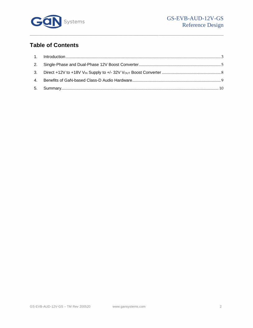
1. Introduction
GaN Systems introduced a combination amplifier and companion SMPS audio evaluation kit with much excitement and positive market response. The kit, pictured below, includes:
AUDIO AMPLIFIER Complete 2 Channel Class-D Amplifier
• Multi-Audio Signal Inputs • Bridge-Tied Load Output • On-Board Power Management
High-Performance Audio • 200W/Ch (8Ω), 300W/Ch (4Ω) • > 108dB SNR & Dynamic Range • < 0.01% THD+N (8Ω, 1W) • +/- 0.5dB Freq. Response (8Ω)
High-Performance Output • 96% Efficiency • Reduced thermals
COMPANION SMPS Complete Audio LLC SMPS
• Universal AC Line Input • Easy Integration w/GaN Amplifier • Common-Mode AC Filter
High-Performance Audio • 400W Continuous, 550W Peak • +/-32VDC Dual-Rail Output
High-Performance Output • No heatsinking, no cooling • High efficiency, 40% loss decrease
• EMI/EMC friendly
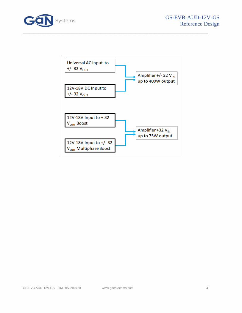
Interest from designers in the 12V markets requested designs suitable for their applications. As a result, this document provides a summary of the information to design amplifiers for 12V input systems. The schematics and bill-of-material details are available by contacting GaN Systems. The diagram below provides a visual description of the incremental capabilities of using GaN transistors in 12V audio systems.
GS-EVB-AUD-12V-GS
Reference Design
_____________________________________________________________________________________________________________________
GS-EVB-AUD-12V-GS – TM Rev 200720 www.gansystems.com 4
GS-EVB-AUD-12V-GS
Reference Design
_____________________________________________________________________________________________________________________
GS-EVB-AUD-12V-GS – TM Rev 200720 www.gansystems.com 5
2. Single-Phase and Dual-Phase 12V Boost Converter
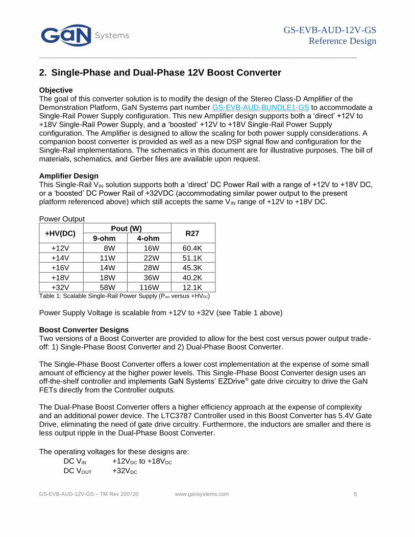
Objective The goal of this converter solution is to modify the design of the Stereo Class-D Amplifier of the Demonstration Platform, GaN Systems part number GS-EVB-AUD-BUNDLE1-GS to accommodate a Single-Rail Power Supply configuration. This new Amplifier design supports both a ‘direct’ +12V to +18V Single-Rail Power Supply, and a ‘boosted’ +12V to +18V Single-Rail Power Supply configuration. The Amplifier is designed to allow the scaling for both power supply considerations. A companion boost converter is provided as well as a new DSP signal flow and configuration for the Single-Rail implementations. The schematics in this document are for illustrative purposes. The bill of materials, schematics, and Gerber files are available upon request. Amplifier Design This Single-Rail VIN solution supports both a ‘direct’ DC Power Rail with a range of +12V to +18V DC, or a ‘boosted’ DC Power Rail of +32VDC (accommodating similar power output to the present platform referenced above) which still accepts the same VIN range of +12V to +18V DC. Power Output
+HV(DC) Pout (W)
R27 9-ohm 4-ohm
+12V 8W 16W 60.4K
+14V 11W 22W 51.1K
+16V 14W 28W 45.3K
+18V 18W 36W 40.2K
+32V 58W 116W 12.1K Table 1: Scalable Single-Rail Power Supply (Pout versus +HVDC)
Power Supply Voltage is scalable from +12V to +32V (see Table 1 above) Boost Converter Designs Two versions of a Boost Converter are provided to allow for the best cost versus power output trade-off: 1) Single-Phase Boost Converter and 2) Dual-Phase Boost Converter. The Single-Phase Boost Converter offers a lower cost implementation at the expense of some small amount of efficiency at the higher power levels. This Single-Phase Boost Converter design uses an off-the-shelf controller and implements GaN Systems’ EZDrive® gate drive circuitry to drive the GaN FETs directly from the Controller outputs. The Dual-Phase Boost Converter offers a higher efficiency approach at the expense of complexity and an additional power device. The LTC3787 Controller used in this Boost Converter has 5.4V Gate Drive, eliminating the need of gate drive circuitry. Furthermore, the inductors are smaller and there is less output ripple in the Dual-Phase Boost Converter.
The operating voltages for these designs are:
DC VIN +12VDC to +18VDC
DC VOUT +32VDC

GS-EVB-AUD-12V-GS
Reference Design
_____________________________________________________________________________________________________________________
GS-EVB-AUD-12V-GS – TM Rev 200720 www.gansystems.com 6
1-PH Boost Schematic
2-PH Boost Schematic
GS-EVB-AUD-12V-GS
Reference Design
_____________________________________________________________________________________________________________________
GS-EVB-AUD-12V-GS – TM Rev 200720 www.gansystems.com 7
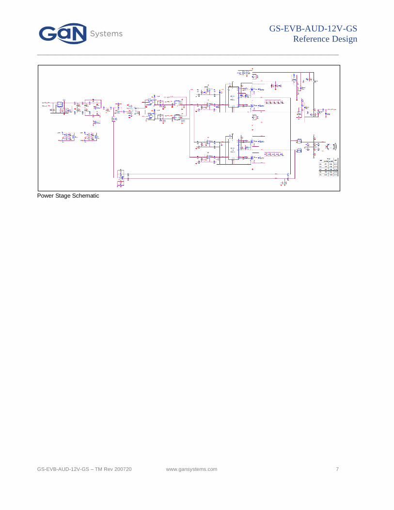
Power Stage Schematic
GS-EVB-AUD-12V-GS
Reference Design
_____________________________________________________________________________________________________________________
GS-EVB-AUD-12V-GS – TM Rev 200720 www.gansystems.com 8
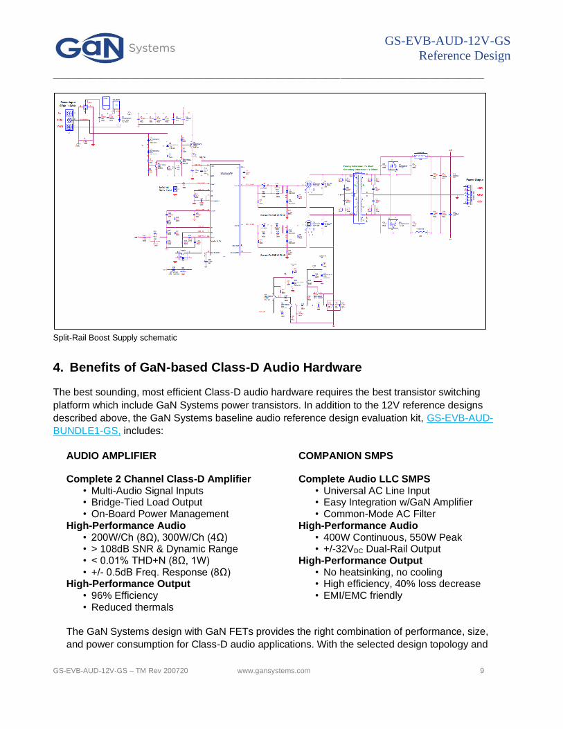
3. Direct +12V to +18V VIN Supply to +/- 32V VOUT Boost Converter
Design Objective
Based upon interest for 12V systems, we have also modified the design of the GaN Systems SMPS Boost Converters described above to accommodate a Split-Rail Boost Converter Power Supply that is compatible with the present BTL Class-D Amplifier Demonstration Platform, GS-EVB-AUD-BUNDLE1-GS. The new SMPS design supports a ‘direct’ +12V to +18V VIN supply.
Split-Rail Boost Converter Design This Boost Converter design was selected to allow for the best cost versus power output trade-off, while maintaining the desired audio performance – both measured performance and sonic performance. The Split-Rail, Bipolar Boost Converter design offers a low-cost, scalable implementation that is appropriate for any Automotive, Marine, battery-operated system, or other application. In this design, the Boost Converter uses GaN Systems’ GS61008P as used in the companion BTL Class-D Amplifier Demonstration Platform. This Bipolar Boost Converter design uses the SG2525AP Controller and implements GaN Systems EZDrive gate drive circuitry to drive the GaN FETs directly from the Controller outputs. The Bipolar Boost Converter also includes a ‘Remote’ Power-On capability that is required for most Automotive and Marine applications. The DC Input Voltage can remain connected and the Boost Converter can be engaged by simply applying a low-level +12V signal to the “REM” Input terminal. When used with a Class-D Amplifier, an ‘External Sync Input’ is provided to assure that the system-level clocks are all synchronized, thus avoiding any additional noise and distortion that might be caused by ‘clock drift’ on either of the two system components.
The operating voltages for these designs are:
DC VIN +12V to +18V DC DC VOUT +/- 32VDC
GS-EVB-AUD-12V-GS
Reference Design
_____________________________________________________________________________________________________________________
GS-EVB-AUD-12V-GS – TM Rev 200720 www.gansystems.com 9
Split-Rail Boost Supply schematic
4. Benefits of GaN-based Class-D Audio Hardware
The best sounding, most efficient Class-D audio hardware requires the best transistor switching
platform which include GaN Systems power transistors. In addition to the 12V reference designs
described above, the GaN Systems baseline audio reference design evaluation kit, GS-EVB-AUD-
BUNDLE1-GS, includes:
AUDIO AMPLIFIER Complete 2 Channel Class-D Amplifier
• Multi-Audio Signal Inputs • Bridge-Tied Load Output • On-Board Power Management
High-Performance Audio • 200W/Ch (8Ω), 300W/Ch (4Ω) • > 108dB SNR & Dynamic Range • < 0.01% THD+N (8Ω, 1W) • +/- 0.5dB Freq. Response (8Ω)
High-Performance Output • 96% Efficiency • Reduced thermals
COMPANION SMPS Complete Audio LLC SMPS
• Universal AC Line Input • Easy Integration w/GaN Amplifier • Common-Mode AC Filter
High-Performance Audio • 400W Continuous, 550W Peak • +/-32VDC Dual-Rail Output
High-Performance Output • No heatsinking, no cooling • High efficiency, 40% loss decrease • EMI/EMC friendly
The GaN Systems design with GaN FETs provides the right combination of performance, size,
and power consumption for Class-D audio applications. With the selected design topology and
GS-EVB-AUD-12V-GS
Reference Design
_____________________________________________________________________________________________________________________
GS-EVB-AUD-12V-GS – TM Rev 200720 www.gansystems.com 10
resulting thermal and sonic performance, the design is scalable in many ways. Derivative
designs for this evaluation kit include: increasing power by using a heatsink on the GaN
Systems top-side cooled devices or tying the two outputs together, or reducing power by going
to a half bridge without BTL or a single-rail design.
5. Summary
The enclosed overviews of the 12V reference designs provide a head start for designers
targeting high-quality and high-power Class D audio output. Audio quality has become an
important part of nearly every interaction people have today. No longer is good sound only
affordable for the audiophiles, expensive cars, or elaborate home sound systems. GaN devices
provide the performance, size, and cost benefits to allow everyone to enjoy Class-D audio
sound.
Contact GaN Systems for details on these designs. Source files for the schematics and bill-of-
material files are available.
GaN Systems home page: www.gansystems.com
Local contact: https://gansystems.com/where-to-buy/
Reference designs and evaluation kits: https://gansystems.com/design-center/evaluation-boards/
GS-EVB-AUD-12V-GS
Reference Design
_____________________________________________________________________________________________________________________
GS-EVB-AUD-12V-GS – TM Rev 200720 www.gansystems.com 11
Reference Design Important Notice
GaN Systems Inc. (GaN Systems) provides the enclosed reference design under the following AS IS conditions:
This reference design is intended for use for ENGINEERING DEVELOPMENT, DEMONSTRATION, AND/ OR
EVALUATION PURPOSES ONLY and is not considered by GaN Systems to be the design of a finished end-product
fit for general consumer use. As such, the reference design provided is not intended to be complete in terms of
required design, marketing, and/or manufacturing-related protective considerations, including but not limited to
product safety and environmental measures typically found in end products that incorporate such semiconductor
components or circuit boards. This reference design does not fall within the scope of the European Union directives
regarding electromagnetic compatibility, restricted substances (RoHS), recycling (WEEE), FCC, CE or UL, and
therefore may not meet the technical requirements of these directives, or other related regulations.
No License is granted under any patent right or other intellectual property right of GaN Systems whatsoever. GaN
Systems assumes no liability for applications assistance, customer product design, software performance, or
infringement of patents or any other intellectual property rights of any kind.
.
www.gansystems.com Important Notice – Unless expressly approved in writing by an authorized representative of GaN Systems, GaN Systems components are not
designed, authorized, or warranted for use in lifesaving, life sustaining, military, aircraft, or space applications, nor in products or systems where
failure or malfunction may result in personal injury, death, or property or environmental damage. The information given in th is document shall
not in any event be regarded as a guarantee of performance. GaN Systems hereby disclaims any or all warranties and liabilitie s of any kind,
including but not limited to warranties of non-infringement of intellectual property rights. All other brand and product names are trademarks or
registered trademarks of their respective owners. Information provided herein is intended as a guide only and is subject to change without notice.
The information contained herein or any use of such information does not grant, explicitly, or implicitly, to any party any patent rights, licenses,
or any other intellectual property rights. General Sales and Terms Conditions apply.
© 2009-2020 GaN Systems Inc. All rights reserved.