Photoemission study of sulfur and oxygen adsorption on GaN( 0 0 0 1
Upload
khangminh22Category
view
0download
0
inside News Review, News Analysis, Features, Research Review, and much more...Free Weekly E News round up go to: www.compoundsemiconductor.net
ECOC: Highlighting the progress in photonic ICs
Green light for the industry’s problem LED
LEDs: GaN-on-silicon finds its true calling
Empowering electronics with PowerAmerica
Single-wafer processing refines SiC production
GaN on insulatorBoosting HEMT blocking voltages
Volume 25 Issue 8 NOVEMBER / DECEMBER 2019 @compoundsemi www.compoundsemiconductor.net
Front Cover CS v4RS.indd 1Front Cover CS v4RS.indd 1 21/11/2019 14:4821/11/2019 14:48

Best performance for next generation SiC power electronics to address global mega trends
AIX G5 WW C Electric vehicles: on board chargers, power inverters Infrastructure: charging stations Renewables: solar and wind Industrial: motor drives, power supplies Power distribution: HVDC
Discover our SiC epi production batch tool with single wafer performance
Aixtron AIX G5 WW C System Ad v5.indd 1 12/08/2019 11:31

ViewpointBy Dr Richard Stevenson, Editor
COPYRIGHT COMPOUND SEMICONDUCTOR l NOVEMBER / DECEMBER 2019 l WWW.COMPOUNDSEMICONDUCTOR.NET 3
Compound Semiconductor is published eight times a year on a controlled circulation basis. Non-qualifying individuals can subscribe at: £105.00/e158 pa (UK & Europe), £138.00 pa (air mail), $198 pa (USA). Cover price £4.50. All information herein is believed to be correct at time of going to press. The publisher does not accept responsibility for any errors and omissions. The views expressed in this publication are not necessarily those of the publisher. Every effort has been made to obtain copyright permission for the material contained in this publication. Angel Business Communications Ltd will be happy to acknowledge any copyright oversights in a subsequent issue of the publication. Angel Business Communications Ltd © Copyright 2019. All rights reserved. Contents may not be reproduced in whole or part without the written consent of the publishers. The paper used within this magazine is produced by chain of custody certifi ed manufacturers, guaranteeing sustainable sourcing.US mailing information: Compound Semiconductor, ISSN 1096-598X, is published 8 times a year, Jan/Feb, March, April/May, June, July, August/September, October, November/ December by Angel Business Communications Ltd, Unit 6, Bow Court, Fletchworth Gate, Burnsall Rd, Coventry CV5 6SP. UK. The 2019 US annual subscription price is $198. Airfreight and mailing in the USA by agent named Air Business Ltd, c/o WN Shipping USA, 156-15, 146th Avenue, 2nd Floor, Jamaica, NY 11434, USA. Periodicals postage paid at Jamaica NY 11431. US Postmaster: Send address changes to Compound Semiconductor, Air Business Ltd, c/o WN Shipping USA, 156-15, 146th Avenue, 2nd Floor, Jamaica, NY 11434, USA. Printed by: The Manson Group. ISSN 1096-598X (Print) ISSN 2042-7328 (Online) © Copyright 2019.
We strive for accuracy in all we publish; readers and contributors are encouraged to contact us if they recognise an error or omission. Once a magazine edition is published [online, in print or both], we do not update previously published articles to align old company names, branding, marketing efforts, taglines, mission statements or other promotional verbiage, images, or logos to newly created or updated names, images, typographic renderings, logos (or similar) when such references/images were accurately stated, rendered or displayed at the time of the original publication. When companies change their names or the images/text used to represent the company, we invite organizations to provide Angel Business Communications with a news release detailing their new business objectives and/or other changes that could impact how customers/prospects might recognise the company, contact the organisation, or engage with them for future commercial enterprise.
The Professional
Publishers Association
Member
Editor Richard Stevenson [email protected] +44 (0)1291 629640Contributing Editor Rebecca Pool [email protected] Editor Christine Evans-Pughe [email protected] Sales Executive Jessica Harrison [email protected] +44 (0)2476 718970USA Representatives Brun Media
Tom Brun [email protected] +001 724 539-2404 Janice Jenkins [email protected] +001 724-929-3550Publisher Jackie Cannon [email protected] +44 (0)1923 690205Director of Logistics Sharon Cowley [email protected] +44 (0)1923 690200Design & Production Manager Mitch Gaynor [email protected] +44 (0)1923 690214
Circulation Director Jan Smoothy [email protected] +44 (0)1923 690200Chief Executive Offi cer Stephen Whitehurst [email protected] +44 (0)2476 718970
Directors Bill Dunlop Uprichard – EC, Stephen Whitehurst – CEO, Jan Smoothy – CFO, Jackie Cannon, Scott Adams, Sharon Cowley, Sukhi Bhadal
Published by Angel Business Communications Ltd, Unit 6, Bow Court, Fletchworth Gate, Burnsall Road, Coventry CV5 6SP, UK. T: +44 (0)2476 718 970 E: [email protected]
IT IS FASCINATING to see what happens when an incumbent technology is threaten by a rival with far more promise. One would expect the established technology to lose the battle. However, often the incumbent fi ghts back, delivering a substantial improvement in the bang-per-buck.
This has certainly happened in the solar industry. Concentrating photovoltaics has much promise, but as of today, it has made minimal impact. At the time when this industry threatened to take off, silicon solar cell manufacturers in China were slashing their prices – a move that many didn’t see coming – and the fl edgling CPV industry fell apart.
Another technology with much promise is the GaN-on-silicon LED. At the start of this decade Bridgelux championed it as the solution for bringing solid-state lighting to the masses. Manufacturing costs for LEDs would plummet, thanks to the switch to larger substrates, and the processing of material in under-utilised, fully depreciated 200 mm silicon lines.
But the GaN-on-silicon LED never took the market by storm. Instead, thanks to some very attractive subsidies and a substantial reduction in the price of sapphire, it has been the LED chipmakers in China that have fl ooded the market with far cheaper devices.
This has left those with GaN-on-silicon technology scratching their heads, trying to fi nd a new market for their devices.
And Plessey, which I visited this autumn, thinks it has the answer: microLEDs for displays (see p. 18 for
details).
Plessey is in a great position to exploit this technology. It has
a well-equipped silicon line, and thanks to the technology it acquired from CamGaN, it can put really
fl at wafers through its fab.
Fighting for a share of the microLED display market are many makers of GaN-on-
sapphire LEDs. They are trying to form displays by the picking and placing of microLED chiplets.
According to Plessey, it has important advantages over these rivals: the performance of the GaN-on-silicon LED pulls ahead as the device get smaller; and its monolithic approach is better for shrinking LEDs and making displays. With Plessey signing deals, looking to make a big splash at CES, and improving its technology at great pace, it looks like the GaN-on-silicon LED is fi nally destined for signifi cant success.
Although this technology didn’t displace the incumbent in the market it fi rst targeted, it appears to have found its niche.
Displacing the incumbent
ViewPoint v3RS 4MG.indd 3ViewPoint v3RS 4MG.indd 3 25/11/2019 15:1925/11/2019 15:19
4 WWW.COMPOUNDSEMICONDUCTOR.NET l NOVEMBER / DECEMBER 2019 l COPYRIGHT COMPOUND SEMICONDUCTOR
VOLUME 25 ISSUE 8 NOVEMBER / DECEMBER 2019 2019
CONTENTS
18 LEDs: GaN-on-silicon finds its calling Processing GaN-on-silicon epiwafers through a dedicated silicon line offers a very attractive approach to making microLED displays
26 ECOC offers a snapshot of PIC progress At ECOC many big names, including Intel, Infinera and Hewlett Packard Enterprise, unveiled their latest plans for their PICs
30 Single-wafer processing streamlines SiC production Replacing batch lapping and polishing with a single-wafer grind and polish enables scalability in SiC substrate production while improving consistency, increasing yield and lowering the manufacturing cost
36 Empowering power electronics with PowerAmerica PowerAmerica targets the primary obstacles to widespread adoption of wide bandgap power electronics: high costs, concerns with reliability and ruggedness, and a lack of expertise in the workforce
54 Better etching enhances selective area doping for vertical GaN power devices Multi-step etching slashes the leakage current in regrown GaN p-n junctions for selective area doping
44 COVER STORY Insulating interlayer boosts the breakdown voltage HEMTs exceed the breakdown limit imposed by the epilayer when an insulator is inserted between GaN and silicon.
By Singapore-MIT Alliance for Research and Technology, Nanyang Technological University and Massachusetts Institute of Technology
Contents v4.indd 4Contents v4.indd 4 25/11/2019 15:2725/11/2019 15:27

COPYRIGHT COMPOUND SEMICONDUCTOR l NOVEMBER / DECEMBER 2019 l WWW.COMPOUNDSEMICONDUCTOR.NET 5
news06 ZF and Cree partner on automotive SiC power devices
07 Transphorm milestone for multi-kilowatt applications
08 mPower nets $2.5 million for DragonSCALE solar tech
09 SiC is the future for car power electronics?
10 Odyssey acquires wafer manufacturing facility
news analysis12 Cree to set up SiC corridor Why Cree has shifted SiC wafer expansion plans from North Carolina to New York state
14 Green light for the industry’s problem LED With its cubic GaN epitaxy, Kubos Semiconductors is intent on delivering a process for the mass manufacture of green LEDs soon
research review59 LEDs: A deeper understanding of V-pits The introduction of V-pits shifts radiative recombination within the active region
60 HEMTs: Broadening transconductance Forming nanowires in the gate opening of a HEMT increases the linearity of amplification
61 Building better semi-polar substrates Inserting interlayers and reducing the growth pressure yields better semi-polar GaN
1408
12 18
30 36
Contents v4.indd 5Contents v4.indd 5 25/11/2019 15:2725/11/2019 15:27

6 WWW.COMPOUNDSEMICONDUCTOR.NET l NOVEMBER / DECEMBER 2019 l COPYRIGHT COMPOUND SEMICONDUCTOR
news reviewsZF and Cree partner on automotive SiC power devicesAUTOMOTIVE SUPPLER ZF Friedrichshafen and Cree have announced a strategic partnership to create highly efficient SiC-based electric drivelines.
With this partnership, ZF and Cree are intensifying their existing cooperation. “We’re delighted that we’re building on our cooperation with Cree using their Wolfspeed SiC technology and are absolutely convinced that combining our strengths will further improve efficiency and competitive edge for our components and systems,” says Jörg Grotendorst, Head of the ZF E-Mobility Division.
The future use of SiC-based power semiconductors will increase the range for electric vehicles in contrast to today’s standard silicon technology. Due to high battery costs, the efficient electric drive represents an enormous growth potential for the foreseeable future. In particular, SiC technology in conjunction with the 800 V vehicle electrical system voltage makes a significant contribution to further increasing efficiency.
“Partnering with a tier-one leading global automotive supplier like ZF for the use of SiC-based power inverters in next
generation electric vehicles is indicative of the integral role SiC plays in extending the capabilities of EVs everywhere,” said Gregg Lowe, CEO of Cree.
Electrified drivelines are making vast contributions to achieving worldwide emission targets and making mobility more sustainable. Cree’s technology will initially be used to fulfill orders that ZF has already received for SiC-based electric drives from several leading global automakers. Through the
partnership, ZF expects to make SiC electric drivelines available to the market by 2022.
Since January 2016, ZF has bundled its electromobility activities in the E-Mobility Division headquartered in Schweinfurt, Germany. More than 9,000 employees work in this division, spread across various locations around the world.
Cree has recently announced SiC capacity expansion with a mega materials factory in Durham, North Carolina and the world’s largest SiC device manufacturing facility in New York. The company offers SiC and GaN power and RF (radio frequency) solutions through its Wolfspeed business unit.
SCIENTISTS at the Fraunhofer Institute for Applied Solid State Physics IAF have achieved what was previously considered impossible: they are the first in the world to manufacture AlScN via MOCVD. They say this is a decisive step towards developing power electronics based on AlScN transistors for industrial applications.
Transistors based on AlScN are promising for industrial applications such as data transfer, satellite communication, radar systems or autonomous driving, especially since current devices based on silicon are reaching their physical limit in these applications.
One reason for this is the size of silicon devices, which cannot be reduced any more according to the current state of research. If the ever-increasing amounts of data had to be processed with the current silicon technology, the server rooms would occupy such a large area that it would be economically and ecologically unsustainable.
HEMTs surpass the possibilities of silicon devices by far. The key to the success of HEMT structures lies in the materials they are based on. AlScN has exceptional properties, allowing higher carrier concentrations than other materials. In the future, significantly more powerful and efficient HEMTs will be realised based on AlScN.
The production of AlScN involves fundamental challenges. The state-of-the-art production process grows AlScN layers via sputtering. Unfortunately, the quality of these layers is insufficient for electronic applications such as LEDs and high-power transistors.
An alternative method is to produce AlScN via MBE. With this process, high amounts of scandium can be incorporated in the compound. The quality is also sufficient for the production of microelectronic devices. However, the procedure is very complex and the productivity too low for industrial scale productions.
Fraunhofer makes first AlScN wafer using MOCVD
News CS v8MG.indd 6News CS v8MG.indd 6 25/11/2019 15:2225/11/2019 15:22

COPYRIGHT COMPOUND SEMICONDUCTOR l NOVEMBER / DECEMBER 2019 l WWW.COMPOUNDSEMICONDUCTOR.NET 7
news review sTransphorm, a company that makes hi-rel and JEDEC- and AEC-Q101 qualified 650 V GaN semiconductors, has announced that it has shipped more than 500,00 high-voltage GaN FETs. The company hit this milestone as customers continue to adopt its high quality-high reliability GaN platform.
Customers in the broad industrial, infrastructure and IT, and PC gaming markets have publicly announced in-production devices built with Transphorm’s GaN technology. They illustrate the rising confidence in GaN solutions that are projected to be an attractive market.
Industry analyst firm IHS Markit Technology, now a part of Informa Tech, forecasts the total GaN power discrete, module, and system IC revenues to reach $1.2 billion by 2028. Approximately $750 million of those revenues – almost two-thirds of the total market – will be driven by high voltage GaN solutions.
“We came to market with the most robust, two-chip normally-off device at a time when the industry was more familiar with single-chip normally-off Silicon MOSFETs,” said Primit Parikh, co-founder
and COO, Transphorm. “As proven by our public momentum and also that of other reputable manufacturers like Power Integrations in the consumer adapter space, the two-chip normally-off GaN solution is the most practical high-voltage GaN FET design today. In fact, it’s this design that enables Transphorm’s GaN to deliver high performance with strong robustness, which has led to more than 5 billion hours of field reliability data to date.”
Transphorm says the adoption success is driven largely by the quality and reliability of its products. This is backed by the company’s normally-off GaN platform, strong control of its epitaxial process, and manufacturing capability – which is well-positioned to meet the volume and quality requirements of various cross-industry markets from consumer adapters to automotive.
“Following our success in the core higher power markets targeted by GaN, we’re also working with customers in fast growing markets that are underserved by silicon, such as consumer adapters and set-top boxes,” said Philip Zuk, VP of worldwide technical marketing and North American sales, Transphorm. “Consider
that the majority of products we’ve shipped to date were targeted for higher power applications. Those 500,000-plus 650 V FETs equate to more than 4 million lower power (sub 100 W) FETs, demonstrating our volume production capabilities.”
A year ago, Transphorm released the first complete set of validation data for high voltage GaN power semiconductors. Today, the company formally released its latest field reliability data. With more than five billion hours in the field, Transphorm’s GaN technology currently has a FIT rate less than 2.0 at below 19.8 ppm per year.
DEPOSITION equipment firm Aixtron has announced that it has provided an AIX G5 WW C system to EpiWorld International for the further development of next generation SiC epitaxial wafers mainly used for the manufacturing of power devices for automotive applications.
The shipment and installation of Aixtron’s high-volume manufacturing system to EpiWorld’s cleanroom facilities in Xiamen, China, has been conducted in the third quarter of 2019.
The AIX G5 WW C MOCVD tool is based on Aixtron’s fully-automated Planetary Reactor platform, which is designed for high batch capacity and high throughput.
The system offers flexible 6-inch or 4-inch configurations with the design aiming at squeezing production costs to a minimum,
while maintaining excellent production quality, according to Aixtron.
EpiWorld seeks to further expand its production capacity to meet the increasing demand by customers. The company has already completed production lines for 4-inch and 6-inch SiC epitaxial wafers for making 600 V, 1,200V and 1,700 V power devices.
“In recent years, we have been qualified as a leading supplier of SiC epitaxy wafers by device manufacturers in the automotive and various other sectors. Therefore, we have a strong footprint in one of the most challenging industries. We had so far served over 100 customers around the world. With this new addition, our annual capacity will be increased to 60,000 wafers in 2019,” says Gan Feng, general manager of EpiWorld.
“Our recently completed phase I expansion of an 18,000 m2 new facility is designed to provide manufacturing space for an annual capacity of up to 400,000 wafers. As we and our customers have high quality standards, we rely on industry leaders such as Aixtron and their proven system technology to meet these requirements appropriately. We are looking forward to launch the high-volume production of our SiC epitaxial wafers with the AIX G5 WW C”, he added
Felix Grawert, Aixtron’s president comments: “We are delighted to cooperate with one of the leading epitaxy foundries to accelerate the further commercialisation of SiC. SiC will support the development of numerous high-end power electronics applications, meaning that we are paving the way for megatrends such as e-mobility or renewable energy.”
EpiWorld chooses new Aixtron tool for SiC production
Transphorm milestone for multi-kilowatt applications
News CS v8MG.indd 7News CS v8MG.indd 7 25/11/2019 15:2225/11/2019 15:22

8 WWW.COMPOUNDSEMICONDUCTOR.NET l NOVEMBER / DECEMBER 2019 l COPYRIGHT COMPOUND SEMICONDUCTOR
news reviews
INFINEON TECHNOLOGIES AG has broadened its CoolGaN series with two new devices, the CoolGaN 400V for audio systems and the CoolGaN 600V for low-power SMPS and telecom rectifiers.
The 400V audio device (IGT40R070D1 E8220) is tailored for premium HiFi audio systems where end users demand every detail of their high resolution sound tracks. These have been conventionally addressed by bulky linear or tube amplifiers.The switch enables smoother switching and more linear class D output stage by offering low/linear Coss, zero Q rr, and normally-off switch. Ideal class D audio amplifiers offers zero percent distortion and 100 percent efficiency. What impairs the linearity and power loss is highly dependent on switching characteristics of the switching device.
Infineon says its CoolGaN breaks through the technology barrier by introducing zero reverse recovery charge in the body diode and very small, linear input and output capacitances. The resulting benefit to the end users is more natural and wider soundstage audio experience.
To further simplify the design, Infineon pairs the CoolGaN 400 V device in an HSOF-8-3 (TO-leadless) package with a popular class D controller (IRS20957STRPBF) in an evaluation board.With the CoolGaN 400 V switch as class D output stage, audio designers are able to deliver excellent listening experience to their prospective audio fans.
The CoolGaN 600V industrial-grade device (IGLD60R190D1) enables
performance and cost optimisation for low- and mid-power applications, such as in the area of low-power SMPS and telecom rectifiers.
Infineon’s CoolGaN 600 V portfolio is now also extended with a new 190 mΩ, industrial-grade HEMT. This product was developed to fit any consumer and industrial application on an optimised cost with the aim to lower the technology entry barrier. Easy design-in is supported with a standardised DFN 8x8 packaging and the matching driver ICs from the GaN EiceDRIVER series.
The CoolGaN 400 V (IGT40R070D1 E8220) and the new CoolGaN 600 V (IGLD60R190D1) devices can be ordered now. The evaluation board EVAL_AUDAMP24 will be available for order in February, 2020.
SOLAR CELL TECHNOLOGY startup, mPower Technology, has raised $2.5 million in Series A funding from sector investors, including Santa Fe-based Sun Mountain Capital. The capital builds upon R&D investment by Sandia National Laboratories and will be used to commercialise mPower’s GaAs solar cell technology, DragonSCALEs, in the aerospace market.
mPower’s DragonSCALEs are made up of individually interconnected cells of highly efficient silicon that can be meshed into any shape or form. They are lightweight, flexible, resilient and extremely reliable, overcoming the low-voltage limitations of today’s rigid solar cells. The combined advantages of DragonSCALEs enable a wide new range of solar power design possibilities for multiple applications and markets. The company thinks they are ideal for the aerospace market, offering reduced weight and stowage volume, increased radiation recovery, and dramatically lower cost as compared to existing GaAs-based solutions.
“We’ve made a great deal of progress in 2019 with our partners in the aerospace market. This investment is
a direct reflection of the promise of this technology and the confidence our investors have in our ability to execute our business plan in the near future,” said Kevin Hell, president and CEO, mPower Technology.
“With its disruptive cost and performance advantages, our groundbreaking technology is incredibly well positioned to be the solar power solution of choice for the next era of aerospace applications, particularly the large emerging market for satellite constellations.”
Drawn by the significant opportunities in the aerospace market initially, but also
by the expanded market opportunity for applications such as remote power, IoT and terrestrial rooftops, investors believe mPower’s technology overcomes critical limitations of existing solar cell technology.
“This technology is going to drive the next adoption wave of solar power,” said Lee Rand, Partner, Sun Mountain Capital. “We’ve already seen the advantages that mPower can deliver in the aerospace market and believe that this is just the start of adoption across many industries.”
“The team’s solid leadership and vision for growth make this a compelling investment.”
mPower nets $2.5 million for DragonSCALE solar tech
Infineon expands CoolGaN portfolio with two new devices
News CS v8MG.indd 8News CS v8MG.indd 8 25/11/2019 15:2225/11/2019 15:22

COPYRIGHT COMPOUND SEMICONDUCTOR l NOVEMBER / DECEMBER 2019 l WWW.COMPOUNDSEMICONDUCTOR.NET 9
news review sBOSCH, the only automotive supplier that manufactures semiconductors, says the future of all its power electronics will be based on SiC. And this will be key to the wider adoption of hybrid and electric vehicles.
Using SiC power electronics, for instance, Bosch says that motorists can drive 6 percent further on a single battery charge. In this way, Bosch is addressing one of the stumbling blocks for potential buyers of electric cars: nearly one in two consumers (42 percent) decide against buying an electric vehicle because they are afraid the battery will run out while they are on the road.
In Germany, this anxiety is even more prevalent, affecting 69 percent of consumers, acording to Consors Finanz Automobile Barometer 2019. Alternatively, car manufacturers can make the battery smaller for a given range. This reduces the cost of an electric car’s most expensive component, which in turn reduces the vehicle’s price.
SiC technology also offers further potential savings down the line: the much lower heat losses of the chips, combined with their ability to work at much higher operating temperatures, mean that manufacturers can cut back on the expensive cooling of the powertrain components. That has a positive impact on electric vehicles’ weight and cost.
“Thanks to our deep understanding of systems in e-mobility, the benefi ts of SiC technology fl ow directly into the development of components and systems,” said Harald Kroeger, member of the Bosch board of management
In 2018, the value of semiconductor chips in an average car was around €337. While this amount is growing by 1 to 2 percent annually for applications not relating to infotainment, connectivity, automation, and electrifi cation, on average an electric vehicle has additional semiconductor chips worth €410 on board. Experts predict that this fi gure will increase again by around €910 as a result of automated driving. This makes the automotive market one of the drivers of growth in the semiconductor sector. Furthermore, key applications of the internet of things, such as artifi cial intelligence, cyber security, smart cities, edge computing, smart homes, and connected industry, will drive future growth in the domain.
With its semiconductor factories in Reutlingen and Dresden, Bosch is well prepared for these developments: “Our semiconductor know-how helps us not only to develop new automotive functions and IoT applications but also to continuously improve the chips themselves,” Kroeger says.
In June 2018, Bosch laid the cornerstone for a state-of-the-art semiconductor factory in Dresden. Its manufacturing operations
will use wafers with a diameter of 300 mm. Currently, Bosch makes 150- and 200 mm technology in Reutlingen, where it will also manufacture the new SiC chips. But it says the wafer fabs in Reutlingen and Dresden complement each other. “
Semiconductors are a core component of all electrical systems. They are also turning data into a coveted raw material of the future. As they are becoming increasingly important in our fi elds of activity, we want to continuously expand our manufacturing operations,” Kroeger says.
In its wafer fab in Dresden, Bosch is investing around a billion euros – the largest single investment in the company’s history. In the factory, facilities are currently being installed in the clean room areas. The fi rst associates are due to start work in the spring of 2020.
SiC is the future for car power electronics?
Advanced Compound Semiconductor Foundry Services
Advanced III-V semiconductor solutions for optoelectronics
application in the biotechnology, telecommunications,
energy, industrial, and defense industries.
MasimoSemiconductor.com | 603-595-8900 semiconductor
M O C V D • Fa b r i c at i o n • Te s t i n g
P H O T O D E T E C T O R S
L E D S
S O L A R C E L L S
V C S E L S
T H E R M O P H O T O V O LT A I C C E L L S
L A S E R P O W E R C O N V E R T E R S
FT_337A, Ad, Compound Semiconductor Publication, Masimo Semiconductor, 189x79mm, v3.indd 1 5/10/16 4:42 PM
News CS v8MG.indd 9News CS v8MG.indd 9 25/11/2019 15:2225/11/2019 15:22
10 WWW.COMPOUNDSEMICONDUCTOR.NET l NOVEMBER / DECEMBER 2019 l COPYRIGHT COMPOUND SEMICONDUCTOR
news reviews
CREE has announced a partnership to jointly expand the rollout of SiC in the rapidly-growing high-power semiconductor market. The agreement incorporates the use of Cree’s Wolfspeed SiC-based semiconductors into ABB’s product portfolio, enabling Cree to broaden its customer base while accelerating ABB’s entry into the fast-expanding EV sector.
Cree’s products will be included as part of ABB’s power semiconductor product portfolio, across power grids, train and traction, industrial and e-mobility sectors.
Specifically, Cree’s SiC devices will be assembled into ABB power modules.
“Cree is committed to leading the global semiconductor market’s transition to more energy efficient, higher performing SiC-based solutions. ABB has a longstanding heritage as the world market leader in industrial power electrification solutions, so expanding our work with them will help increase the adoption of transformative and eco-friendly alternatives in the power and automotive sectors,” said Cree CEO Gregg Lowe.
“Together, this partnership delivers Wolfspeed SiC into new markets, such as power grids and high-speed trains for the continued advancement of the power, traction, industrial and EV markets.”“The partnership with Cree supports ABB’s strategy in developing energy-efficient SiC semiconductors in the automotive and industrial sectors,” said Rainer Käsmaier, managing director of semiconductors at ABB’s Power Grids business. “It emphasises ABB’s commitment to continuous technological innovation to shape the future of a smarter and greener society.”
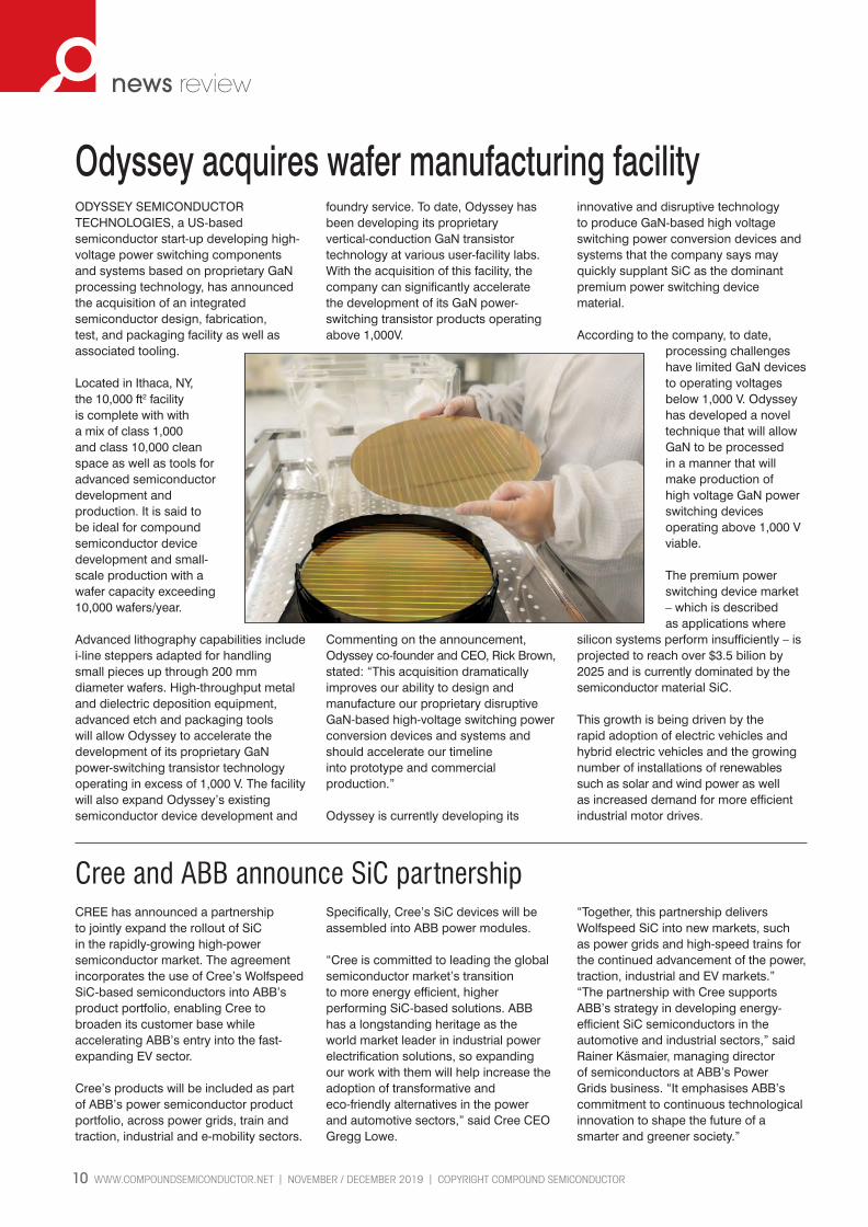
ODYSSEY SEMICONDUCTOR TECHNOLOGIES, a US-based semiconductor start-up developing high-voltage power switching components and systems based on proprietary GaN processing technology, has announced the acquisition of an integrated semiconductor design, fabrication, test, and packaging facility as well as associated tooling.
Located in Ithaca, NY, the 10,000 ft2 facility is complete with with a mix of class 1,000 and class 10,000 clean space as well as tools for advanced semiconductor development and production. It is said to be ideal for compound semiconductor device development and small-scale production with a wafer capacity exceeding 10,000 wafers/year.
Advanced lithography capabilities include i-line steppers adapted for handling small pieces up through 200 mm diameter wafers. High-throughput metal and dielectric deposition equipment, advanced etch and packaging tools will allow Odyssey to accelerate the development of its proprietary GaN power-switching transistor technology operating in excess of 1,000 V. The facility will also expand Odyssey’s existing semiconductor device development and
foundry service. To date, Odyssey has been developing its proprietary vertical-conduction GaN transistor technology at various user-facility labs. With the acquisition of this facility, the company can significantly accelerate the development of its GaN power-switching transistor products operating above 1,000V.
Commenting on the announcement, Odyssey co-founder and CEO, Rick Brown, stated: “This acquisition dramatically improves our ability to design and manufacture our proprietary disruptive GaN-based high-voltage switching power conversion devices and systems and should accelerate our timeline into prototype and commercial production.”
Odyssey is currently developing its
innovative and disruptive technology to produce GaN-based high voltage switching power conversion devices and systems that the company says may quickly supplant SiC as the dominant premium power switching device material.
According to the company, to date, processing challenges have limited GaN devices to operating voltages below 1,000 V. Odyssey has developed a novel technique that will allow GaN to be processed in a manner that will make production of high voltage GaN power switching devices operating above 1,000 V viable.
The premium power switching device market – which is described as applications where
silicon systems perform insufficiently – is projected to reach over $3.5 bilion by 2025 and is currently dominated by the semiconductor material SiC.
This growth is being driven by the rapid adoption of electric vehicles and hybrid electric vehicles and the growing number of installations of renewables such as solar and wind power as well as increased demand for more efficient industrial motor drives.
Cree and ABB announce SiC partnership
Odyssey acquires wafer manufacturing facility
News CS v8MG.indd 10News CS v8MG.indd 10 25/11/2019 15:2225/11/2019 15:22

Wireless
The global leader in wafer outsourcing
www.iqep.com
OfferingtheIndustry’sBroadestProductPor6olio
World leading technology
Complete materials range
MOCVD, MBE & CVD platformsAdvanced substrates
Multiple, manufacturing sites (Europe, Asia, USA)
Advanced R&D facilities
Photonics Infrared
PowerCMOS++Solar
Enabling advanced technologies
Untitled-2 1Untitled-2 1 19/11/2019 15:1019/11/2019 15:10

12 WWW.COMPOUNDSEMICONDUCTOR.NET l NOVEMBER / DECEMBER 2019 l COPYRIGHT COMPOUND SEMICONDUCTOR
news analysis
Cree to set up SiC corridorWhy Cree has shifted SiC wafer expansion plans from North Carolina to New York state, reports Rebecca Pool
AS CREE FORGES AHEAD with its $1 billion SiC capacity expansion, company chief executive, Gregg Lowe, recently revealed a detour from the original plan.
Following a mighty $500 million grant from the state of New York, Cree will now build a new automotive-qualified 200 mm power and RF wafer fabrication plant in Marcy, New York.
The company had set out to convert an existing facility into such a fab, in Durham, North Carolina. But as Lowe points out: “We got this tremendous offer from New York state which has allowed us to get a substantially bigger fab for substantially less money.”
According to Lowe, Cree was to spend some $450 million on retrofitting an existing structure at Durham to expand wafer capacity by thirty times. However, the company will now invest around $170 million in building a new facility with nearly forty times more capacity.
Crystal growth and materials expansion will continue at Durham, to the tune of $500 million. And as Lowe says: “[The New York state investment] is a pretty good deal for us.”
“We’re creating this East silicon carbide corridor from New York to North Carolina and we reckon this is going to be very powerful,” he adds. “Customers see us continuing to invest in silicon carbide capacity and expansion, and everyone is super-excited.”
The new facility in Marcy, New York, is expected to bring in more than 600 new jobs by the end of this decade. Meanwhile the expansion of SiC crystal growth and epitaxy at Durham, North Carolina, will see a shift from lower-paid operator positions to higher-paid technician posts.
“We have partnered with local colleges in Durham to develop our own workforce, so our operators will be taking the necessary courses and associated degrees ready for this transition,” says Lowe. “Also, up-state New York has a great collection of universities that are deep into materials and electronic engineering; having a highly qualified workforce is going to be key to get this really moving.”
Right now, the site in New York is ready for development while materials capacity expansion is already taking place in North Carolina. Come 2022, and with materials production in place, Cree expects to ramp 150 mm wafer production at New York and then transition to 200 mm wafer sizes around two years later.
The timings coincide with Cree’s recent contract with US-based automotive propulsion system developer, Delphi Technologies. Here, the company is to manufacture SiC MOSFETs for use in Delphi’s 800 V inverters, with production scheduled to ramp during 2022. “These inverters are for a global, European [car] manufacturer, and our increases in capacity will
Proposed 200 mm power and RF wafer fabrication facility, known as the “North Fab,” was to be built in Durham (pictured), but will now reside at a new location in New York state.
News Analysis v4RS 6MG.indd 12News Analysis v4RS 6MG.indd 12 25/11/2019 15:2325/11/2019 15:23

COPYRIGHT COMPOUND SEMICONDUCTOR l NOVEMBER / DECEMBER 2019 l WWW.COMPOUNDSEMICONDUCTOR.NET 13
news analysis
work nicely with the ramp of this product,” says Lowe. “We’re quite certain that come this time our silicon carbide wafer fab will be the largest on the planet.”
Importantly, the Cree chief executive also reckons industry SiC capacity constraints are easing. He highlights how Cree is steadily increasing SiC crystal growth capacity every week while also increasing epitaxy capability. “I also think the customer shift on electric vehicles from silicon to silicon carbide has really happened too,” he adds. “Our customers are leaning very heavily towards silicon carbide right now.”
China changesBut right now, how is Cree weathering ongoing US-China tensions? Earlier this year, the US Bureau of Industry and Security added Huawei to its ‘Entity List’, banning the beleaguered China-based business from buying components from US companies, such as Cree.
According to Lowe, Cree’s LEDs business is “still bouncing around a bit” which hasn’t been helped by trade friction and the economic situation in China. But, as he highlights: “The enthusiasm for silicon carbide power devices as well as electric vehicles and solar power systems will be the growth engine for Cree going forwards.”
And while demand for electric vehicles has softened in China, following cuts in the nation’s generous government subsidies, Lowe is unfazed, pointing out how subsidies are now aimed at cars with a relatively large driving range.
“The short-term has put a pause on the growth rate of the Chinese car market and car manufacturers are adjusting to these subsidy changes,” he says. “But silicon carbide enables cars to go further with the same battery-size so in the long-term this is good for us.”
News Analysis v4RS 6MG.indd 13News Analysis v4RS 6MG.indd 13 25/11/2019 15:2325/11/2019 15:23

14 WWW.COMPOUNDSEMICONDUCTOR.NET l NOVEMBER / DECEMBER 2019 l COPYRIGHT COMPOUND SEMICONDUCTOR
news analysis
Green light for the industry’s problem LEDWith its cubic GaN epitaxy, Kubos Semiconductors is intent on delivering a process for the mass manufacture of green LEDs soon, reports Rebecca Pool
THE UK’S KUBOS SEMICONDUCTORS and the Compound Semiconductor Centre have joined forces to solve the LED industry’s notorious ‘green gap’ problem.
As revealed in October this year, the partners are working together to commercialise cubic GaN epitaxy for the manufacture of high efficiency green and amber LEDs.
The move comes at a time when green LED efficiency figures significantly trail those of blue LEDs, despite industry players’ efforts worldwide to close the so-called green gap.
“Closing the green gap is a long-standing issue that has been a perennial challenge for LED manufacturers and hasn’t been solved yet,” says Kubos CEO, Caroline O’Brien. “But we’ll soon be coming to market with a solution that is commercially viable, and we expect this will be received extremely well.”
“The green LED is our main commercialisation catalyst and we’ve made good progress here, so aim to start this commercialisation process next year,” she adds.
To date, hexagonal GaN crystals have been widely used to fabricate blue LEDs, but achieving efficient operation in the green is a problem. Large polarization fields in the active region of these longer-wavelength structures reduce radiative recombination rates and limit LED efficiency.
But Kubos could have an answer. The company’s process is based on growing cubic GaN on 3C (cubic) SiC on silicon substrates. Unlike hexagonal GaN, cubic GaN is electric-field free, removing polarisation issues and opening the door to the design of efficient LEDs.
The epitaxy process for 3C SiC on silicon was pioneered by Warwick University spin-out, Anvil Semiconductors. Anvil has carefully guarded its IP, but around eight years ago, it started honing a process to grow 3C SiC on silicon wafers for SiC power devices, overcoming the associated mismatches in the different materials’ lattice parameters and thermal expansion coefficients.
With device-quality layers in hand, the company partnered with Cambridge University some five years ago to grow cubic GaN on the cubic SiC on silicion templates. Success ensued, the partners produced
News Analysis v4RS 6MG.indd 14News Analysis v4RS 6MG.indd 14 25/11/2019 15:2325/11/2019 15:23
COPYRIGHT COMPOUND SEMICONDUCTOR l NOVEMBER / DECEMBER 2019 l WWW.COMPOUNDSEMICONDUCTOR.NET 15
news analysis
the world’s first 150 mm wafer with 100 percent cubic GaN grown on it, and Kubos was launched with an exclusive licence to commercialise this IP and deliver efficient green and amber LEDs.
Crucially, the recent Kubos-CSC partnership is set to accelerate Kubos’ technical development. CSC – a joint venture between IQE, a manufacturer of semiconductor epiwafer products, and Cardiff University – provides commercial access to industry standard epitaxy tools, providing clear routes to commercialisation.
“Growing cubic gallium nitride on the cubic silicon carbide on silicon offers a scalable platform that delivers high quality cubic gallium nitride layers,” says Rob Harper, CSC.
“Importantly, we have multiple MOCVD tool platforms which enable cost effective development to be performed on smaller diameters before scaling to the larger 200 millimetre wafers.”
“The availability of an Aixtron G5+ reactor means the [Kubos] process could be commercialised on up to 200 mm substrates,” he adds. “Demonstration of Kubos technology on industry standard MOCVD tools that are globally available facilitates scale-up and therefore reduces time to market.”
According to O’Brien, Kubos has already demonstrated that cubic GaN can be grown on 150 millimetre 3C SiC on silicon wafers, and asserts that as 200 millimetre SiC on silicon wafers become available the cubic GaN growth can also be scaled.“There are no limitations to scaling this to 200 millimetre wafers or even larger wafer sizes,” she says. “We really have been working to ensure scalability so that the technology is compatible with large volume manufacturing and is commercially viable.”
Cost-wise, neither O’Brien or Harper see any stumbling blocks. O’Brien believes that so far there is nothing to suggest that an LED manufacturer couldn’t adopt the process in a cost efficient and highly manufacturable way.
As Harper says: “The fact that this can be scaled to 200 millimetre wafers offers further cost reductions beyond 150 millimetre wafers.”
Production could be performed on multi-wafer MOCVD platforms, such as the Aixtron G5+, invoving process batches of 5 x 200 mm wafers or 8 x 150 mm wafers simultaneously, which could provide a significantly lower wafer cost than single wafer tools.
“Once the technology is in place we can expect further cost reduction driven by economies of scale and optimisation of operational efficiencies,” says Harper.
Reaching marketKey applications include microLEDs for display markets as well as automotive and conventional LED lighting markets. With this in mind, Kubos and partners are working on raising the efficiencies of the green LEDs that will be fabricated via its process.
As O’Brien points out, back in 2017, the US Department of Energy set an ambitious Internal Quantum Efficiency (IQE) target of 54 percent, so this is the company’s eventual target. “Right now the efficiencies of many green LED devices are still significantly below this so improving IQE is the focus of our development right now and while the DoE target is a way to go, we have that in our sights,” she says.
At the same time, work on process optimisation and yield engineering is also underway. The key goal for the partners is to fit the process to into a tier 1 manufacturing line, and as such, they plan to license the technology to large LED companies over the next two to three years.
As O’Brien adds: “We’re starting customer engagement next year, and LED manufacturing is a very established process so I would be disappointed if this isn’t in the market within this time-frame.”
News Analysis v4RS 6MG.indd 15News Analysis v4RS 6MG.indd 15 25/11/2019 15:2325/11/2019 15:23

Connecting, informing and inspiring the compound semiconductor industry
MOMENTUM BUILDS AS SPEAKER AND SPONSOR LINEUP EXPANDS FURTHER
THE TENTH EDITION of CS INTERNATIONAL is set to be even bigger and better with more industry leading speakers and sponsors from across the global compound semiconductor industry confirming participation with 5 months to spare.
Returning to the Sheraton Airport Hotel in Brussels on 31 March – 1 April 2020, CS International will continue to deliver in bringing together the major players from the compound semiconductor industry from across the supply chain for two-days of technical tracks and exhibit opportunities.
With an attendance in 2019 of 700 senior level delegates including representatives from Sony, ROHM Semiconductor, WIN Semiconductors and IHS Markit among many others, the event was our largest yet. Those attending can also spend time at the exhibition hall, supported by over 60 companies detailing the latest advances in
materials, equipment and software; and play their part in two awards ceremonies, which acknowledge the most important breakthroughs within these industries.
Consisting of the co-located Photonic Integrated Circuits International, and Sensor Solutions International, plus a single exhibition area, delegates can dip in and out of every session to put together their own tailor-made programme by selecting from over 125 talks, delivered by leaders of the most innovative global companies of today. With a strong synergy between the three conferences, attendees and exhibitors are fully exposed to the relevant supply chains as well as customer and supplier bases.
The CS International Conference continues to grow in scale and stature year on year and is now firmly established as the must-attend conference for the compound semiconductor industry.
5 New Themes for 2020:Satisfying demand for more dataHow are we supporting the roll-out of 5G? And how can we speed other data links?
Seeking new opportunities for LEDs and lasersWhat’s needed to unlock the microLED market? And what does the future hold for the VCSEL?
Ramping volumes in the power electronics sectorHow will the supply chain fulfil the ever-growing demand for SiC? And what will be GaN’s first killer application?
Enhancing the automobileWhy is GaN power electronics poised for success? How will higher-performance lasers make our roads safer?
Taking wide bandgap devices to their ultimate limitsHow will GaN-on-diamond grow its volumes? Is the market ready to receive gallium oxide?
31 MARCH - 1 APRIL 2020 BRUSSELS, BELGIUM
CS 2020 DPS Ad v9.indd 26CS 2020 DPS Ad v9.indd 26 12/11/2019 09:1012/11/2019 09:10

3 Conferences, 2 Days, 1 Ticket
Speakers confirmed to date include:AIXTRON, Attolight, Bruker, ClassOne, DISCO Europe, EpiGaN, Evatec, EV Group, ExaGaN, Ferrotec, FLOSFIA, IHS Markit, Infineon, KLA, Laytec, Nanotronics, Nanowin, Panasonic, Plessey Semiconductors, QROMIS, Revasum, RFHIC USA, Sony Corporation, Stanley Electric, Strategy Analytics, United Monolithic Semiconductors, Veeco, Wolfspeed, Yole Développement
Book your place NOW!www.csinternational.net/register to secure your place
It’s set to be another sellout
PLATINUM SPONSORS
GOLD SPONSORS
CONFERENCE APP SPONSORPORTFOLIO SPONSOR PROGRAMME GUIDE
WIFI SPONSORTHEME SPONSORS EVENING RECEPTION
BADGE HOLDERPRE-EVENT OPENING RECEPTION
CS 2020 DPS Ad v9.indd 27CS 2020 DPS Ad v9.indd 27 12/11/2019 09:1012/11/2019 09:10

18 WWW.COMPOUNDSEMICONDUCTOR.NET l NOVEMBER / DECEMBER 2019 l COPYRIGHT COMPOUND SEMICONDUCTOR
industry LEDs
LEDs: GaN-on-silicon finds its callingProcessing GaN-on-silicon epiwafers through a dedicated silicon line offers a very attractive approach to making microLED displays
BY RICHARD STEVENSON
The GaN-on-silicon LED has always attracted much attention. It grabbed the headlines at the start of this decade when Bridgelux billed the technology as the one to slash the cost of LED lighting. Manufacturing costs for LED chips would plummet, thanks to a switch to cheaper, larger wafers, and the opportunity to process devices in underutilised, fully depreciated 200 mm silicon lines. But instead, with the help of subsidies and a significant fall in the price of the sapphire substrate, it has been the companies from
Plessey v3RS 4MG.indd 18Plessey v3RS 4MG.indd 18 25/11/2019 15:2125/11/2019 15:21

COPYRIGHT COMPOUND SEMICONDUCTOR l NOVEMBER / DECEMBER 2019 l WWW.COMPOUNDSEMICONDUCTOR.NET 19
industry LEDs
China that have flooded the market, by slashing the cost of conventional chips.
It’s not just Bridgelux that has suffered from this unexpected twist. Hopes have also been dashed at the UK firm Plessey. Back in 2012, it acquired GaN-on-silicon technology from CamGaN, a spin-off of the University of Cambridge. After establishing the process at its site in Plymouth, it spent several years trying to turn a profit in the LED lighting market. Efforts focused on finding a niche where it could make an impact. Products were launched for spotlights, for circadian lighting and for horticulture, but none of these ventures realised significant success.
So does this mean that the GaN-on-silicon LED is never going to succeed? Absolutely not. All that’s needed is to find an applications that will really benefit from this form of LED. And under the current
leadership, including President Michael Lee, who joined Plessey in 2017 and leads business and corporate development, the company is doing just that. It has identified displays, made from microLEDs, as a fantastic fit for this technology, and it is now focused entirely on this lucrative sector.
For this class of application, the GaN-on-silicon LED has a critical advantage over its more common, sapphire based cousin: as the size of the emitter reduces, its performance pulls ahead. That’s because the light extraction is higher, and there is a reduction in droop, the mysterious malady behind the decline in efficiency as the current is cranked up.
Additional merits of the GaN-on-silicon LED are an efficiency that is very high, even when the device is driven with very little power; and an emission profile that can be tailored to create a better light emitter by shaping the chip.
Producing high-quality LEDs for displays is a far tougher assignment than making chips for lighting. To bridge this gap, Plessey has devoted several years to refining its production process. Efforts have not just been directed at optimising the light extraction for far smaller LEDs, but have extended to reducing wafer bow, increasing wavelength uniformity, and driving down defect densities.
A very low bow is a pre-requisite for running the GaN-on-silicon epiwafers through Plessey’s silicon line, which includes wafer bonding, lithography and stepper tools. Engineers working at this site inherited a great starting position, as CamGaN’s technology focused on minimising bow. But to make microLED displays, Plessey’s engineers have had to take flatness to a new level. According to Lee, this improvement increased the yield associated with the lithography, stepper and wafer-bonding processes.
Wavelength uniformity is another important criteria, due to the eye’s great sensitivity to changes in colour that can compromise the performance of a display. “Even the wavelength uniformity across the die is critical,” says Lee. By improving the process over the last year or so, wavelength uniformity across a wafer has been reduced to 10 ± 3 nm.
Display technologies also require incredibly low defect densities. Even when a particle as small as a micron comes onto the surface of a wafer during processing, it can wipe out several pixels in a display with a very
Plessey GaN-on-silicon microLED technology is being used for assisted reality displays. Opportunities for this technology include googles that allow the swimmer to track their time without having to look up at a clock on the wall.
Plessey v3RS 4MG.indd 19Plessey v3RS 4MG.indd 19 25/11/2019 15:2125/11/2019 15:21

20 WWW.COMPOUNDSEMICONDUCTOR.NET l NOVEMBER / DECEMBER 2019 l COPYRIGHT COMPOUND SEMICONDUCTOR
industry LEDs
small pitch. That wreaks havoc, because the eye is extremely sensitive to dead pixels.
To drive down defect levels, Plessey has taken delivery of the latest tooling that supports much lower defect levels, together with specifi c handling measures.
Assisted realit yWith an improved production process in place, the team at Plessey is now working with companies to produce a range of assisted-reality products that contain an information display designed to work close to the eye. These are battery-driven products, operating for many, many hours, thanks to the very high effi ciency of the microLEDs. Shipments are already underway, with sales expected to peak within a few years.
One example of these assisted-reality products is a scuba diving mask that incorporates a dive computer. “Another one is a sky-diving mask, so you know altitude, rate of descent and GPS, which is critical when you are sky-diving,” says Lee, who adds that assisted reality could also feature in motorbike helmets, so the driver no longer needs to look down at the dashboard; in swimming googles that provide a lap clock; and in gun scopes, offering range-fi nding capability and details of wind speed.
Such opportunities are very lucrative for all parties involved. For example, according to Lee, companies are coming out with products that allow them to increase the price tag for a gun scope from $500 to $1500.
All these assisted-reality displays feature symbolic content, such as arrows and numbers, rather than
individually addressable pixels. In some products, one colour is used for all content, but in other designs, different colours are used for different segments.
Right now, many companies are keen to get into these markets with new products. To help them in this
quest, Plessey is offering turnkey displays that emit in the red, green and blue and don’t
require customisation.
“The fi rst thing they want, if they’re a larger company that has deeper pockets, is a custom version of that,” says Lee. Plessey meets this need by
tailoring the colours used in the display, as well as the shapes
of the emitting areas and the brightness. Turning down the latter is essential in products
for night applications.
To drive further success, Plessey will launch a development kit at the upcoming Consumer Electronics Show. Known currently as Direct Drive, it features a display with dimensions below 5 mm by 5 mm, a driver that allows die to be driven at up to 2 A, a processor, and an ultra-small rechargeable battery. Symbolic content in the displays is fully customisable, using monochrome colour segments with pixel features that can be as small as 2 μm.
Production processesProduction of these assisted-reality displays begins by loading 150 mm silicon <111> substrates into an Aixtron Crius II MOCVD reactor. To create the LED structure, a recipe with 137 steps is used to deposit a stack of GaN-based layers. The growth of GaN on silicon is challenging, as thermal and lattice mismatches between the materials can cause epiwafer bow. To prevent this from happening, the engineers use slightly thicker substrates and a complex buffer technology.
The only signifi cant downside of the GaN-on-silicon LED architecture is that the substrate threatens to absorb the light that is emitted from the active region, dragging down effi ciency. To prevent this from happening, engineers at Plessey deposit a mirror on top of the epistructure before bonding this side to a handle wafer and removing the original silicon substrate. This procedure boosts output, as light can no longer disappear into the substrate. Instead, radiation heading in this direction is refl ected back into the chip, where its chances of exiting the chip are high, thanks to the texturing of the top surface.
To defi ne the symbolic content, the engineers use photolithography and etching. After this, they remove the handle wafer and apply electrical contacts to the LEDs to complete the production of these units for assisted reality displays.
individually addressable pixels. In some products, one colour is used for all content, but in other designs, different colours are used for different segments.
Right now, many companies are keen to get into these markets with new products. To help them in this
quest, Plessey is offering turnkey displays that emit in the red, green and blue and don’t
require customisation.
tailoring the colours used in the display, as well as the shapes
of the emitting areas and the brightness. Turning down the latter is essential in products
for night applications.
To drive further success, Plessey will launch a development kit at the upcoming Consumer Electronics Show. Known currently as Direct Drive,
Plessey is producing direct-drive displays for many customers. They feature symbolic content, defi ned by etching into GaN-on-silicon epiwafers.
Plessey v3RS 4MG.indd 20Plessey v3RS 4MG.indd 20 25/11/2019 15:2125/11/2019 15:21

COPYRIGHT COMPOUND SEMICONDUCTOR l NOVEMBER / DECEMBER 2019 l WWW.COMPOUNDSEMICONDUCTOR.NET 21
industry LEDs
Plessey initially made just blue LEDs with this process. Thanks to refinement, external quantum efficiency of these 455 nm emitters is now as high as 25 percent, for a device with a 4 μm diameter. Note that when dimensions reduce, this figure falls because the periphery, where no emission takes place, becomes more significant.
One option for producing red LEDs is to crank up the indium content in the quantum wells. But efficiency plummets, due to strain-induced dislocations. So, rather than producing native red emitters, Plessey’s engineers produce sources that emit in this spectral range by coating blue LEDs with red-emitting quantum dots.
Plessey could adopt a similar approach for making its green LEDs. But it doesn’t, because there is a very low efficiency associated with the emission of green-emitting quantum dots that are pumped with a blue source. Switching to phosphors doesn’t help, as it addresses one problem while introducing another. The issue is that phosphor particles are much bigger than the pixels – and if they are ground down, this sacrifices their efficiency.
To avoid all these issues, Plessey’s engineers make native green LEDs. Their efficiency is not yet as high as that for their blue siblings – the external quantum efficiency is around 17 percent – but thanks to the far higher sensitivity of the eye in this spectral domain, they have a higher figure for cd m-2, the more important metric for displays.
Augmented realityManufacturing vast arrays of tiny LEDs is the critical step in the production of Plessey’s second generation of products, which will go into augmented reality headsets that provide a fully immersive experience. Lee argues that GaN-on-silicon is the ideal technology for this type of application because its efficiency lengthens battery life while enabling high brightness, so headsets can be used outdoors when the sun is out.
One of the capabilities of this technology is that it will allow the image from the smartphone to be brought to the headset. “This is a massive, growing market,” says Lee.
Many companies are working with Plessey to develop
Production of displays involves chemical-mechanical polishing of GaN-on-silicon epiwafers. To reduce the chances of particle contamination, Perspex sheeting is used over the tool.
Plessey v3RS 4MG.indd 21Plessey v3RS 4MG.indd 21 25/11/2019 15:2225/11/2019 15:22

22 WWW.COMPOUNDSEMICONDUCTOR.NET l NOVEMBER / DECEMBER 2019 l COPYRIGHT COMPOUND SEMICONDUCTOR
industry LEDs
their own headset technology. Those partners incur a one-time cost to cover the expenses associated with the research, design, development and testing of a new product.
To demonstrate its prowess, Plessey recently demonstrated two displays. This May, at SID Display Week, it claimed to have produced the world’s first bonded and fully addressable GaN-on-silicon high-definition active-matrix microLED display. It has a 0.7-inch diagonal and features 1920 by 1080 pixels with dimensions of 6 μm, separated with an 8 μm pitch. The second display, unveiled this September, is even smaller – sporting a definition of 2k by 2k, it has a 2.5 μm pixel pitch.
Production of the displays begins with the growth of LED epistructures on 200 mm substrates, using an Aixtron G5+. Unlike the Crius II, this is a planetary reactor, so it offers greater uniformity and, importantly, lower defectivity levels – despite the shift from 150 mm to 200 mm wafers, there is no reduction in wavelength uniformity across the diameter.
During the processing of the wafer, which involves several lithography and etching steps, LEDs and
mesas are defined in the structure. The latter contains blocking material, so that each LED is electrically and optically isolated from its neighbours.
The next step is to attach each of the processed epiwafers to a backplane. As a full high-definition display contains 1920 by 1080 pixels, 2 million individual electrical bonds are created during this process.
Plessey has found it challenging to find good suppliers of backplanes. The primary market for those companies – often design houses that outsource production – is providing backplanes to makers of liquid crystal on silicon displays. These are voltage driven, while displays for microLEDs need to be current driven.
One company addressing the need for current-driven backplanes is Jasper Display, which produces processed 200 mm wafers with its patented eSP70 silicon technology. Partnering with Jasper enabled Plessey to produce the 0.7-inch diagonal display it unveiled this May. The backplane provides 10-bit single colour control of each pixel.
More recently, Plessey announced a partnership with Compound Photonics, which will provide silicon backplanes for smart glasses. By the middle of next year, samples should be available that have a 0.26-inch diagonal full high-definition resolution, and a driver display that accepts the industry standard MIPI input. As the display industry continues to evolve, backplane manufactures will shift to 300 mm silicon wafers and a smaller CMOS process. A reduction in the size of the CMOS process is beneficial, as it can restrict the size of the LED pixels. For example, for a 2.5 μm pixel, the maximum size for the CMOS process is 70 nm.
Plessey is well-positioned to prepare for this eventual transition, because its Crius II reactors can be used to grow 300 mm epiwafers. And when it eventually makes the move to this larger size, cost savings should follow, because the migration will trim the proportion of the wafer that is wasted.
Today, the pixelated, high-definition displays that Plessey has developed are monochrome, emitting in either the blue or the green. Obviously, that’s not what the market wants – it wants full-colour displays.
Rivals are pursuing this goal with pick and place methods. This involves producing three sets of wafers – one with red microLEDs, another with green microLEDs and a third with blue microLEDs – and transferring individual microLED chiplets onto a backplane to form RGB pixels. Efforts are focused on massively parallel techniques to speed the process. However, there are many challenges associated with positioning every microLED in the right place.
In May 2019, Plessey unveiled a microLED display featuring an array of 1920×1080 current-driven monochrome pixels on a pitch of 8 μm. Each display requires more than two million individual electrical bonds to connect the microLED pixels to the controlling backplane.
Plessey v3RS 4MG.indd 22Plessey v3RS 4MG.indd 22 25/11/2019 15:2225/11/2019 15:22

COPYRIGHT COMPOUND SEMICONDUCTOR l NOVEMBER / DECEMBER 2019 l WWW.COMPOUNDSEMICONDUCTOR.NET 23
industry LEDs
Lee and his colleague are advocating a monolithic approach, so that placement and alignment are controlled by lithography. This technology has a great track record, having enabled the tremendous scaling of the silicon transistor, in accordance with Moore’s law.
One of Plessey’s solutions is to form three separate microLED displays: one blue, another green, and a third red. To produce a colour image, the output of these three is combined with a form of prism. The image that results has a flux density of 5 W cm-2, a figure fifty times that produced by a TV. Note that an advantage of this approach over having red, green and blue pixels side-by-side is that for the same size microLED, the image has a higher resolution.
There is no doubt that the positioning of red, green and blue pixels on the same back plane is a neater solution. Plessey has started working towards this. In October it announced that it is capable of producing blue and green pixels on the same wafer, by growing one LED structure on top of another. However, adding native red microLEDs will not be easy.
Can they be caught?Plessey is clearly in a great position right now, with a novel, powerful technology that is wooing many customers. But is there a danger that in a few years’ time, the company will be losing sales to rivals with either lower overheads, a better approach, or copycat technology?
Lee think’s not. He is certainly not worried about companies trying to flout Plessey’s intellectual property and reverse engineer the process. That’s because doing so is nigh on impossible. Even what appears to be a relatively simple task of transferring a well-established process from an Aixtron Crius II to a G5+ reactor has taken Plessey’s experienced team of engineers substantial time and effort.
Another massive barrier to competing is the cost of the infrastructure. It’s not just the investment required to purchase an Aixtron G5+. There is also the need to put together a dedicated silicon line, containing steppers, etching tools and a suite of characterisation equipment.
Last, but by no means least, Lee believes that Plessey has a first-mover advantage over any competitor that tries to replicate its technology. “We are in every deal,” says Lee.
Optimism is abounding at Plessey, and the next few years will be a very exciting time for the company. It is looking to sign more deals, make a big splash at CES 2020 and develop processes to produce even smaller pixels. In addition, it is strengthening its workforce. “We want to hire another fifty people by June 2020,” says Lee. Plessey anticipates appointing process engineers, development engineers, and those in leadership and management roles.
All these efforts promise to provide the GaN-on-silicon LED with its first ever taste of significant commercial success. While it may have appeared to have been the best option for bringing LED lighting to the masses, it’s now clear that its best chance is to drive widespread adoption of microLED displays.
In NOVEMBER / DECEMBER 2019 2019, Plessey revealed that it has developed a technology to form green and blue pixels on the same wafer, by growing one LED structure on top of another.
As the display industry continues to evolve, backplane manufactures will shift to 300 mm silicon wafers, and a smaller CMOS process. A reduction in the size of the CMOS process is beneficial, as it can restrict the size of the LED pixels. For example, for a 2.5 μm pixel, the maximum size for the CMOS process is 70 nm
Plessey v3RS 4MG.indd 23Plessey v3RS 4MG.indd 23 25/11/2019 15:2225/11/2019 15:22

IN ITS FIFTH YEAR, PIC International continues to grow in scale and stature year on year and is now firmly established as the must-attend conference for the PIC industry. Returning to Brussels on 31st March – 1st April 2020, the event brings together the key players from the integrated photonics industry from across the supply chain for two-days of technical tracks and exhibit opportunities.
PIC International is part of the AngelTech series of events, which has produced for close to a decade, a portfolio of insightful, informative and highly valued chip-level conferences.
Attracting more than 700 delegates, consisting of co-located Compound Semiconductor International, and Sensor Solutions International, plus a single exhibition area, delegates can dip in and out of every session to put together their own tailor-made programme by selecting from over 125+ invited talks, delivered by leaders of the most innovative global companies of today.
With a strong synergy between the three conferences, attendees and exhibitors are fully exposed to the relevant supply chains as well as customer and supplier bases.
5 New Themes for 2020:PICs Today - Datacom, Sensing & LiDARDatacom remains today’s largest PIC opportunity. We will explore progress in PICs for data switching / transmission along with the potential for PICs in emerging sensing applications including LiDAR, digital imaging, fibre optic sensors and bio-photonics.
PIC Manufacturing - TAP, Co-Packaging & FabAs early generations of PICs are moving into commercial applications the need for automated test, assembly and packaging (TAP) is paramount to ensure long-term reliability. Opportunities for co-packaging hold promise while foundry consolidation and applications beyond datacom have implications for substrate suppliers, EDA/EPDA and many others across the supply chain.
PIC Technology - Solutions, Analysis & ResearchThe rapidly evolving nature of photonic integration, silicon photonics (SiP), optical computing and automotive SoCs tied to PICs offers new manufacturing opportunities. We will explore programmable PICs, the coherent vs. incoherent debate, quantum encryption and the latest integration/hybridization approaches for light sources and other PIC devices.
PIC ROI - Quality Metrics & ScalabilityScalability is a key manufacturing interest as pilot lines set the stage for volume manufacturing. What metrics can best be applied to design and manufacturing as the industry pivots to higher production levels? Is a total quality management (TQM) approach vital to long-term vitality? We’ll explore TAP within a quality matrix and how today’s systems can be readied for long-term scalability and margin growth.
PICs Vision - Evolution and RevolutionAs PICs move from 100G to 400G, the future will require 800/1600G devices - can we set the stage today for a smooth transition? We will explore leading pathways to a PIC-enabled future and what needs to be initiated in the short-term to satisfy long-term requirements. What role might quantum technologies play to increase performance, reduce power consumption and improve quality?
Connecting, informing and inspiring the global integrated photonics industry
MOMENTUM BUILDS AS SPEAKER AND SPONSOR LINEUP EXPANDS FURTHER
31 MARCH - 1 APRIL 2020 BRUSSELS, BELGIUM
PIC 2020 DPS Ad v8.indd 46PIC 2020 DPS Ad v8.indd 46 12/11/2019 11:2312/11/2019 11:23

Speakers confirmed to date include:Aeponyx, AIM Photonics, Aristotle University of Thessaloniki, Broadex Technologies, CEA-Leti, CORNERSTONE, CORNING, Elenion Technologies, EPIC, ePIXfab/Aarhus University, ficonTEC, Fraunhofer HHI, Hewlett Packard Enterprise, IBM, II-VI Incorporated, Infinera, Juniper Networks, LIGENTEC, Luceda Photonics, Luminous Computing, Lumerical Solutions, Luxtera, Multiphoton Optics, Nanoscribe, ON Semiconductor, Physik Instrumente, POET Technologies, Samsung Advanced Institute of Technology, SiLC Technologies, SMART Photonics, Strategy Analytics, Synopsys, VLC Photonics, vario-optics ag, VPIphotonics, Yole Développement
Book your place NOW!www.picinternational.net/register to secure your place
It’s set to be another sellout
3 Conferences, 2 Days, 1 Ticket
LANYARD SPONSOR
DELEGATE BAG SPONSOR
CONFERENCE SUPPORTERS
NETWORKING RECEPTION SPONSOR
PLATINUM SPONSORS
CORNERSTONE
GOLD SPONSORS
PIC 2020 DPS Ad v8.indd 47PIC 2020 DPS Ad v8.indd 47 12/11/2019 11:2312/11/2019 11:23

26 WWW.COMPOUNDSEMICONDUCTOR.NET l NOVEMBER / DECEMBER 2019 l COPYRIGHT COMPOUND SEMICONDUCTOR
conference report ECOC
ECOC offers a snapshot of PIC progress
At ECOC many big names, including Intel, Infinera and Hewlett Packard Enterprise, unveiled their latest plans for their PICs.
RICHARD STEVENSON REPORTS
MOST OF US take our mobile phones for granted. We are so used to having them by our side that we easily overlook the phenomenal computational power they provide. This prowess stems from the tremendous miniaturisation of the transistors on the integrated circuit. By keeping pace with Moore’s law, today’s ICs pack billions of nanoscale transistors into a single chip that’s no bigger than a fingernail.
Lagging far behind, in terms of miniaturisation, is the optical equivalent, the photonic integrated circuit (PIC). That’s partly because this type of device is not so easy to scale, as optical features cannot plunge into the sub-wavelength domain. However, progress is also impaired by a far greater number of devices on the chip – the circuits contain lasers, amplifiers, modulators, gratings, and diodes, linked by
optical waveguides. And last but by no means least, the rate of improvement is hampered by a lack of a consensus on the right material system for the circuit. While there is no question that silicon is the best choice for the all-electronic IC, there are several candidates for the PIC, including silicon architectures with either SiO2 or SiN waveguides, and all-InP solutions.
Championing many of the different options were a number of speakers at the 45th European Conference on Optical Communications, held at the Royal Dublin Society, Ireland. At this meeting, presenters made their case for the right mix of materials for a particular application in several well-attended sessions, including three on Sunday, before the conference was in full swing.
ECOC_v3RS 4MG.indd 26ECOC_v3RS 4MG.indd 26 25/11/2019 15:2525/11/2019 15:25

COPYRIGHT COMPOUND SEMICONDUCTOR l NOVEMBER / DECEMBER 2019 l WWW.COMPOUNDSEMICONDUCTOR.NET 27
conference report ECOC
Infinera extols InPWithout doubt, the darling of the InP PIC industry is Infinera, the Californian-headquartered vertically integrated manufacturer of optical transmission systems made with its own chips. This company launched its first product back in 2004, and over the intervening years its annual revenue has climbed to now net nearly $1 billion per annum. Speaking on behalf of the company at the Integrated Photonics Workshop, held on Sunday morning, Vice-President Mehrdad Ziari extolled the virtues of PICs that are based entirely on InP. He argued that this material is best-placed to increase capacity: it allows modulation schemes that transmit much data, such as 64 QAM; it enables 100 Gbaud; and it promises 1 Tbit/s per wavelength. One of the benefits of integration, argued Ziari, is that it offers a good route to increasing the number of channels – Infinera has had 10-channel PICs in production for several years.
Ziari went on to highlight other virtues of an all-InP PIC. These chips require a light source, and according to Ziari, one of the merits of the monolithic approach is “native gain”, as InP is the ideal material for making the laser. Working with InP also enables devices to deliver low-noise, along with a high efficiency that reduces cooling requirements. What’s more, according to Ziari, InP can deliver economic benefits. He argued that Infinera has put together an InP line that produces consistent yields, high-quality chips, and has the ability to offer scalable, future-proof production.
Infinera has recently developed its fourth generation of technology, detailed in a talk given by Ziari’s colleague Stefan Wolf, a Senior Test Development Engineer at Infinera. Speaking during a technical session devoted to transmitters and photodiodes, Wolf explained that on the transmitter side of Infinera’s latest PIC, there is a new addition, a widely tunable laser with a range of 50 nm.
This is claimed to be a best-in-class laser, in terms of its bandwidth. For every laser on the chip, there are two modulators – one for each polarisation – and two semiconductor optical amplifiers. On the receiver side, the tunable laser acts as the local oscillator. For each of these lasers there are eight high-speed photodiodes.
Another significant departure from previous generations of technology is the use of a flip-chip
technology for electrical connections, rather than wirebonds. Flip-chip bonding is providing more than 1000 connections between an Infinera InP chip and an application-specific IC that is made from SiGe and acts as a modulator driver and a transimpedance amplifier. Production of this IC is based on a 180 nm SiGe BiCMOS process, capable of producing transistors with a cut of frequency of more than 230 GHz, and a maximum oscillation frequency in excess of 270 GHz. According to Wolf, these high values contribute to the high linearity and low noise of the amplifier.
Infinera’s fourth generation technology has enabled 100 GBaud, 32 QAM transmission over 500 km of fibre. The Q-factor associated with this is 6dB. “There is plenty of margin for error correction,” said Wolf, indicating that transmission at 800 Gbit/s is feasible.
Outsourcing InP productionOptions for companies and research groups that wish to outsource the production of their InP PICs include the open access foundry Smart Photonics of
Eindhoven, The Netherlands. This company has a strong heritage, as it
produces its InP PICs at a site previously owned by Philips and JDSU Uniphase. Since its
founding in 2012, the workforce at Smart Photonics has mushroomed from four staff to more than 70.
Speaking on behalf of the company during a special event on Sunday that focused on the challenges and solutions associated with PIC Manufacturing, Smart Photonics’ CTO Luc Augustin offered an insight into what his firm can offer its customers. To support the development of the PIC, it has developed a dedicated process design kit. This can be used to evaluate designs that incorporate the company’s lasers – DFB and DBR designs with outputs in excess of 10 mW, and tuning ranges that can be more than 60 nm – and
Intel has ramped the production of its silicon photonics 100G transceivers, and expects to now produce 2 million per year.
ECOC_v3RS 4MG.indd 27ECOC_v3RS 4MG.indd 27 25/11/2019 15:2525/11/2019 15:25

28 WWW.COMPOUNDSEMICONDUCTOR.NET l NOVEMBER / DECEMBER 2019 l COPYRIGHT COMPOUND SEMICONDUCTOR
conference report ECOC
other photonic components that an operate at more than 25 GHz.
To aid development of designs, Smart Photonics has been offering multi-project wafers since 2013. Runs start every quarter, providing customers with regular opportunities to modify and advance their chip architecture.
The perfect size? Another company piquing the interest of delegates at ECOC was the fabless manufacturer of chipsets, Rockley Photonics. It uses a combination of silicon photonics and III-Vs in its products. Company’s co-founder and VP R&D Silicon Photonics, Aaron Zilkie, described this combination of materials as “the best of both worlds”, during a talk he gave at the Integrated Photonics Workshop.
What distinguishes Rockley Photonics from its peers is the size of the features in its chipsets. It pursues what it describes as a multi-micron waveguide platform.
Working at this larger length scale, sensitivity to width variation is claimed to plummet by a factor of 60. Additional merits are: much smaller variations in the key characteristics of the filters; an increase in yield; simplification of the fibre-attach process; and a very high degree of light confinement, enabling the use of very tight bends.
Rockley’s efforts include the development of a 400 Gbit/s transceiver PIC. Its manufacture requires the use of three different foundries. Laser and modulator die are produced on a III-V line, so benefit from being made with a III-V process. A CMOS process makes the electronics, and the silicon photonic structures are produced at a different foundry.
Supercomputing solutionOne opportunity for integrated photonics is to ‘green’ supercomputers. Sales of these power-hungry machines are growing a rate of about 9 percent per year, thanks to huge support from governments all over the world. Dominating this market is Hewlett Packard Enterprise, with a 35 percent share – a figure that is set to climb even higher when it acquires Cray next year.
During an Industry Focus session entitled Photonics integration and digital silicon photonics Di Lang, a Senior Research Scientist at HP, outlined how PICs can come to the aid supercomputers. These machines are undergoing a change in architecture, with a shift from process-centric computing to one that is memory-driven, allowing advances that do not rely on maintaining the march of Moore’s law. The new architecture needs low cost, small form-factor links. Liang and co-workers have been investigating the best solution for many years, and have considered both external lasers, including VCSELs, and the addition of InP-based lasers and InGaAs photodetectors onto a silicon chip.
Due to power constraints, the team at HP is pursuing quantum dots lasers for its PICs. HP is working with Innolume to produce these lasers, which produce a comb-like spectrum, and combine a high gain with stability at elevated temperatures.
Intel’s milestonesA more well-known market for the PIC is in the data centre, where it can help to prevent a bottleneck in connectivity. This is the market Intel is targeting. After a decade of development, it is now enjoying significant sales of 100 G transceiver silicon photonic products.
Robert Blum, who leads strategic marketing and business development at Intel, told delegates attending the Integrated Photonics Workshop that the company had now shipped 2 million 100G transceivers since the launch of the first product in 2016. Thanks to a ramp in production, Intel is now manufacturing 2 million of these per year. The portfolio is also set to grow, with a planned ramp of 200G and 400G products throughout next year.
Infinera builds networking equipment that features its own photonic integrated circuits, made from InP.
ECOC_v3RS 4MG.indd 28ECOC_v3RS 4MG.indd 28 25/11/2019 15:2525/11/2019 15:25

COPYRIGHT COMPOUND SEMICONDUCTOR l NOVEMBER / DECEMBER 2019 l WWW.COMPOUNDSEMICONDUCTOR.NET 29
conference report ECOC
Production of these PICs involves the bonding of InP-based chips, containing a quantum well stack, to a handle wafer, before they are then attached to a 300 mm silicon wafer. No critical alignment is needed, and the laser cavity is formed on the silicon wafer in a manner that ensures 90 percent coupling between the laser and the silicon photonic waveguides.
Speaking at the market focus session, Blum’s colleague Thomas Liljeberg, who has the role of General Manager of Photonic Integration within the Silicon Photonics Products Division at Intel, said that the approach that’s adopted allows standard wafer testing. “Photonics looks more like silicon,” said Liljeberg, who explained that the process aids production, as it only proceeds with known good die.
In the technical session on silicon photonics and hybrid integration, more details on the performance of Intel’s lasers were given by another company spokesperson, Yuliya Akulova, who is Director of R&D within the Silicon Photonics Products Division. She revealed that the 1310 nm lasers on the chip can deliver more than 25 mW at room-temperature, and more than 15 mW at a substrate temperature of 120 °C. “Performance characteristics are exceptionally good.”
These laser have been put through extensive reliability testing. Sampling of 30 devices revealed no degradation over nearly three years.
Engineers at Intel have also produced devices with four channels, operating at 1270 nm, 1290 nm, 1310 nm and 1330 nm. They can be used to produce a 400 Gbit/s chip, also featuring four Mach-Zehnder modulators and four spot-size converters.
Akulova explained that Mach-Zehnder modulators have pros and cons. They are robust, but their relatively large size hampers the production of compact photonic chips. For that reason, the team is investing the potential of ring-modulators in its designs.
Just siliconIf the laser is not put on the chip, the PIC can be made from just silicon. Offering a foundry service for this is Advanced Micro Foundry – it is a spin-off of the Institute of Microelectronics, part of Singapore’s Agency for Science, Technology and Research.
Speaking on behalf of Advanced Micro Foundry, Patrick Lo Guo Qiang explained that the company has a capacity to process 9,000 8-inch wafers per year with a 0.13 μm CMOS technology. The facility runs round the clock, 7 days a week, employs 160 staff, and has a combination of class 10 and class 100 areas. Material combinations offered include SOI, SiN-SOI and SiN. The foundry also has capabilities associated with producing through-silicon vias, bumping and bonding.
The wide variety of PIC presentations at ECOC highlight the great diversity of this technology. This is something of a double-edged sword: it allows the most suitable technology to target a particular application, but it hampers efforts at standardisation.
The silicon industry has taken a very different approach, and it will be interesting to see whether the PIC industry ever heads down a similar path. In the short-term, that’s surely unlikely – but look further ahead, and one never knows.
ECOC 2019 was held at the Royal Dublin Society, a campus with venues used regularly for exhibitions, concerts and sporting events
ECOC_v3RS 4MG.indd 29ECOC_v3RS 4MG.indd 29 25/11/2019 15:2525/11/2019 15:25

30 WWW.COMPOUNDSEMICONDUCTOR.NET l NOVEMBER / DECEMBER 2019 l COPYRIGHT COMPOUND SEMICONDUCTOR
industry processing
Single-wafer processing streamlines
SiC productionReplacing batch lapping and polishing with a single-wafer grind and polish enables scalability in SiC substrate production while improving consistency, increasing yield and lowering the manufacturing cost
BY ROBERT RHOADES FROM REVASUM
SiC IS RENOWNED FOR being difficult to grow and process. Falling just below diamond on the Mohs hardness scale, it is chemically inert to all but the most aggressive etchants. Such traits make SiC a challenging material to produce. However, it is well worth the effort, because this wide bandgap semiconductor can make great devices. Following several decades of development, commercial SiC diodes and transistors are combining high voltages with high powers and high frequencies to outperform those made from silicon by a substantial margin. Sales are now rising fast, with demand outpacing supply, as devices are deployed in the automotive, IoT, power regulation, and 5G markets (see box “The primary opportunities for SiC devices” for details).
Growth in just one of these market segments will justify the expansion of SiC wafer production capacity over the next five to ten years. So, when ramping demand from all these sectors is taken into account, one can see that there is a tremendous opportunity for makers of SiC material.
The leading supplier of SiC substrates, US firm Cree, recently announced plans to increase its production by a factor of 30 over the next few years. Others are Figure 1.
A typical batch processing sequence requires six process tools: a lapper, diamond polisher, stock polisher, fine polisher, standalone cleaner and a wafer sorter.
sure to follow suit and announce their own plans soon. However, for all these companies, cranking up SiC substrate production cannot be done by simply flicking a switch. Ramping capacity is constrained by the time taken to build and qualify furnaces – even for experienced teams, this can take a year or more to bring on line. For companies just getting into SiC production, the time that this will take will surely be much longer, given that the growth conditions necessary to achieve the best quality single-crystal SiC – such as the optimum times, temperatures, and flow rates – are trade secrets. When all these factors and difficulties are accounted for, some sources estimate that demand will exceed capacity to at least 2030.
Given the high level of demand for SiC substrates, to ensure that this industry has as much success as possible, it is essential to manufacture these wafers in the most efficient manner. Traditionally, they have been produced with batch processes, but there is an alternative, offering better consistency, higher yields, and a lower cost of manufacturing: single-wafer processing. At Revasum of San Luis Obispo, we are pioneering the production of equipment that is dedicated to this approach.
Reavsum v3RS 4MG.indd 30Reavsum v3RS 4MG.indd 30 25/11/2019 15:2025/11/2019 15:20

COPYRIGHT COMPOUND SEMICONDUCTOR l NOVEMBER / DECEMBER 2019 l WWW.COMPOUNDSEMICONDUCTOR.NET 31
industry processing
Batch processesThe historical, batch-based process for making SiC wafers, illustrated in Figure 1, begins by growing a boule and sawing or slicing it into individual wafers. They are then loaded into a batch lapping system to remove slicing damage, reduce thickness, and make the top and bottom surfaces parallel. After manual unloading and cleaning, wafers are measured and sorted into groups by thickness, generally using a large sorting system.
The sorting process is necessary to match thicknesses within a batch as tightly as possible, because it enables the use of a reasonably uniform pressure distribution during the batch polish process. If sorting were not undertaken, the batch polish process would remove more material from thicker wafers, and less material from thinner wafers. For the latter, some of the damage could remain, requiring them to be reworked.
After sorting, a batch polish takes place, using a diamond abrasive to remove lapping damage and provide a lower surface roughness. This is referred to as a diamond polish. Wafers are then unloaded and cleaned once more before going to a different batch polisher for the stock polish step, using a different pad and slurry.
Following the stock polish, wafers are unloaded, cleaned, and reloaded into yet another batch
polisher – with a different pad and slurry – for the fi nal step polish, which removes only a small amount of material, typically less than 0.5 μm. The purpose is to realise the fi nal surface fi nish required for epigrowth.
In the stock and fi nal polish steps, the total amount of material that’s typically removed varies from 1.5 μm to 3.0 μm. The exact value is governed by the diamond size used in the previous step.
Following this, wafers are unloaded manually one more time, and taken to a cleaning system, where they are measured and inspected. This determines which wafers need to be reworked. Due to wide variations within each batch, it is not uncommon for a signifi cant
reasonably uniform pressure distribution during the batch polish process. If sorting were not undertaken, the batch
Reavsum v3RS 4MG.indd 31Reavsum v3RS 4MG.indd 31 25/11/2019 15:2025/11/2019 15:20
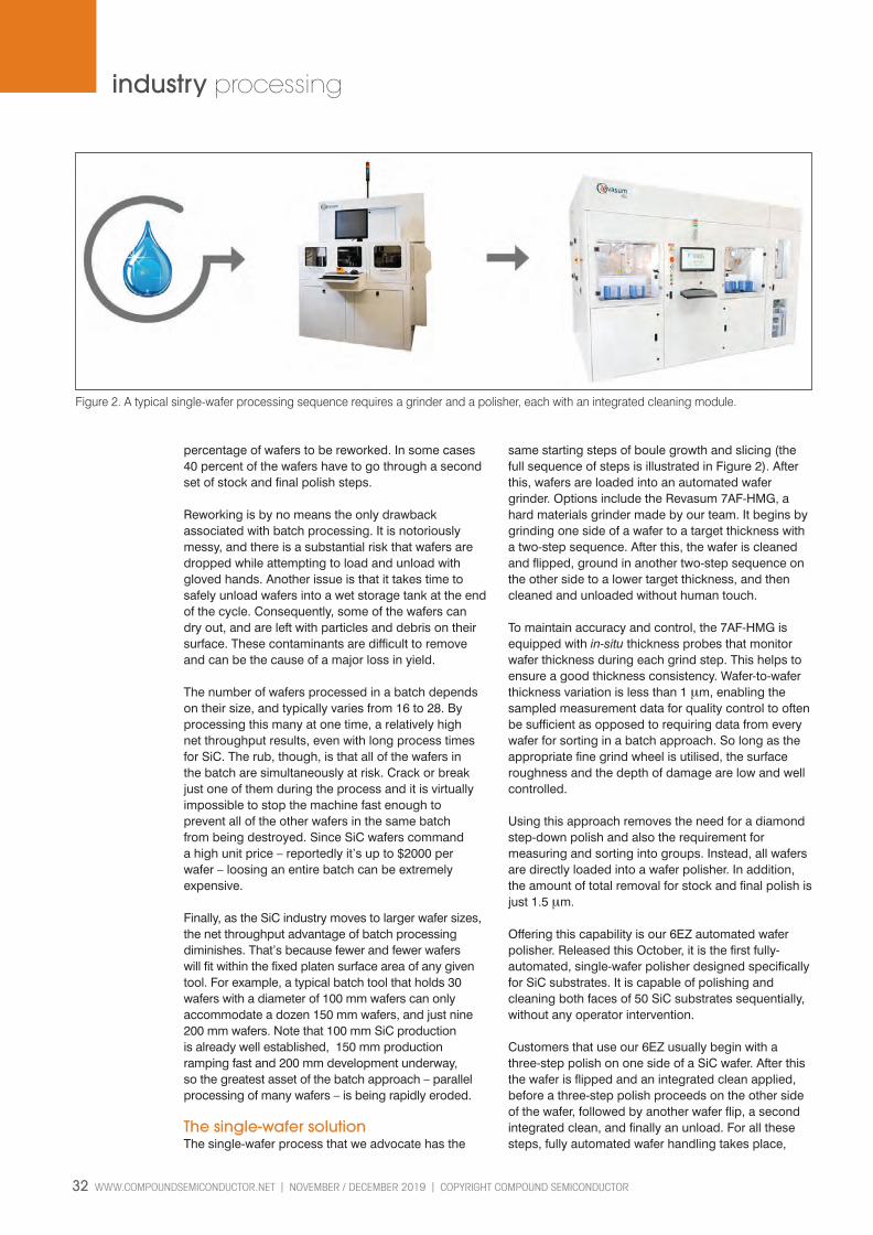
32 WWW.COMPOUNDSEMICONDUCTOR.NET l NOVEMBER / DECEMBER 2019 l COPYRIGHT COMPOUND SEMICONDUCTOR
industry processing
percentage of wafers to be reworked. In some cases 40 percent of the wafers have to go through a second set of stock and final polish steps.
Reworking is by no means the only drawback associated with batch processing. It is notoriously messy, and there is a substantial risk that wafers are dropped while attempting to load and unload with gloved hands. Another issue is that it takes time to safely unload wafers into a wet storage tank at the end of the cycle. Consequently, some of the wafers can dry out, and are left with particles and debris on their surface. These contaminants are difficult to remove and can be the cause of a major loss in yield.
The number of wafers processed in a batch depends on their size, and typically varies from 16 to 28. By processing this many at one time, a relatively high net throughput results, even with long process times for SiC. The rub, though, is that all of the wafers in the batch are simultaneously at risk. Crack or break just one of them during the process and it is virtually impossible to stop the machine fast enough to prevent all of the other wafers in the same batch from being destroyed. Since SiC wafers command a high unit price – reportedly it’s up to $2000 per wafer – loosing an entire batch can be extremely expensive.
Finally, as the SiC industry moves to larger wafer sizes, the net throughput advantage of batch processing diminishes. That’s because fewer and fewer wafers will fit within the fixed platen surface area of any given tool. For example, a typical batch tool that holds 30 wafers with a diameter of 100 mm wafers can only accommodate a dozen 150 mm wafers, and just nine 200 mm wafers. Note that 100 mm SiC production is already well established, 150 mm production ramping fast and 200 mm development underway, so the greatest asset of the batch approach – parallel processing of many wafers – is being rapidly eroded.
The single-wafer solutionThe single-wafer process that we advocate has the
same starting steps of boule growth and slicing (the full sequence of steps is illustrated in Figure 2). After this, wafers are loaded into an automated wafer grinder. Options include the Revasum 7AF-HMG, a hard materials grinder made by our team. It begins by grinding one side of a wafer to a target thickness with a two-step sequence. After this, the wafer is cleaned and flipped, ground in another two-step sequence on the other side to a lower target thickness, and then cleaned and unloaded without human touch.
To maintain accuracy and control, the 7AF-HMG is equipped with in-situ thickness probes that monitor wafer thickness during each grind step. This helps to ensure a good thickness consistency. Wafer-to-wafer thickness variation is less than 1 μm, enabling the sampled measurement data for quality control to often be sufficient as opposed to requiring data from every wafer for sorting in a batch approach. So long as the appropriate fine grind wheel is utilised, the surface roughness and the depth of damage are low and well controlled.
Using this approach removes the need for a diamond step-down polish and also the requirement for measuring and sorting into groups. Instead, all wafers are directly loaded into a wafer polisher. In addition, the amount of total removal for stock and final polish is just 1.5 μm.
Offering this capability is our 6EZ automated wafer polisher. Released this October, it is the first fully-automated, single-wafer polisher designed specifically for SiC substrates. It is capable of polishing and cleaning both faces of 50 SiC substrates sequentially, without any operator intervention.
Customers that use our 6EZ usually begin with a three-step polish on one side of a SiC wafer. After this the wafer is flipped and an integrated clean applied, before a three-step polish proceeds on the other side of the wafer, followed by another wafer flip, a second integrated clean, and finally an unload. For all these steps, fully automated wafer handling takes place,
Figure 2. A typical single-wafer processing sequence requires a grinder and a polisher, each with an integrated cleaning module.
Reavsum v3RS 4MG.indd 32Reavsum v3RS 4MG.indd 32 25/11/2019 15:2025/11/2019 15:20

COPYRIGHT COMPOUND SEMICONDUCTOR l NOVEMBER / DECEMBER 2019 l WWW.COMPOUNDSEMICONDUCTOR.NET 33
industry processing
along with single-wafer control. An overhead diagram of the 6EZ, illustrating where the various steps take place, is shown in Figure 3.
The first significant advantage of single-wafer processing is that it reduces the total number of tools in the process sequence. Benefits that result include a simplification of procedures, and a reduction in the total floor space required for any given production level. Rather than requiring six process tools for batch processing of SiC – a lapper, diamond polisher, stock polisher, fine polisher, separate cleaner, and a wafer sorter – all that’s needed is a grinder and a three-step polisher, each having integrated cleans.
What’s more, there is no longer a need for a wafer sorter. That’s partly because the grind process is very consistent. It is also a result of independent control of the polish steps for each wafer, reducing sensitivity to differences in wafer thickness. Yet another advantage is that it may be possible to use fewer metrology tools, as there is no longer the need to measure every wafer at multiple steps just so they can be sorted.
A second strength of single-wafer processing is that it can slash the number of labour hours needed to support any given production volume. There are many reasons behind this: there are fewer operations in the overall process sequence, the manual loading and unloading for each batch tool is eliminated, there is no longer the need to sort wafers into different batches, and there is less need for in-line data measurements.
The third set of advantages relate to consistency and control. By their very nature, fully automated single-wafer tools are designed to provide each wafer with the same process conditions. No longer are there concerns that wafers within a batch are having an
Figure 3. An overhead shot of Revasum’s 6EZ, the first fully-automated, single-wafer polisher designed specifically for SiC substrates.
A second strength of single-wafer processing is that it can
slash the number of labour hours needed to support any given production volume. There are
many reasons behind this: there are fewer operations in the overall
process sequence, the manual loading and unloading for each
batch tool is eliminated, there is no longer the need to sort
wafers into different batches, and there is less need for in-line data
measurements
Reavsum v3RS 4MG.indd 33Reavsum v3RS 4MG.indd 33 25/11/2019 15:2025/11/2019 15:20

34 WWW.COMPOUNDSEMICONDUCTOR.NET l NOVEMBER / DECEMBER 2019 l COPYRIGHT COMPOUND SEMICONDUCTOR
industry processing
impact on one another. Using well designed control systems and feedback mechanisms, it is possible to ensure that the physical conditions are the same from run to run.
In our case, this is realised by carefully considering every possible impact that our tools have on the process, from the grind wheel feed rates and speeds on the 7AF-HMG to the polish downforce and table speeds on the 6EZ. Fabs that invest in our tools can be confident that every wafer is individually processed with the same recipe settings and experiences the same process conditions. This results in higher productivity (less rework) of higher quality wafers.
On top of these three key advantages, there is another that is easy to overlook. With single-wafer processing, there is much merit in scaling to larger wafers, the direction the industry is heading. Since wafers are processed one at a time, the net throughput is essentially independent of wafer size. In sharp contrast, with batch processing net throughput is tied to the number of wafers per batch, and this is a strong function of wafer size. Batch processes that are efficient and cost effective with 100 mm wafers are less efficient and more costly as the size of the wafer increases.
The final, and possibly most important advantage of single-wafer processing is that it produces a higher yield. With each wafer processed individually, excellent consistency is maintained wafer after wafer, day after day. So long as grind and polish processes are optimised properly, the in-line process yields should average well over 95 percent, maximising productivity and driving down costs. Of course, many other factors beyond grind and polish will contribute to overall yield, but the goal, at each unit process, is always to maximize yield, while minimising the risk of broken wafers.
With demand for SiC strong, and widely expected to grow over the next decade and beyond, there needs to be a massive ramp in SiC capacity alongside improvements in the wafer manufacturing processes that will increase yield and lower cost. One great opportunity for improvement is the transition from batch lapping and polishing to single-wafer grind and polish. The new generation of tools currently coming to market, such as those released by our team, offer scalability to 200 mm wafer sizes alongside greater consistency, higher yields, and a lower cost of manufacturing.
ONE OF THE MOST SIGNIFICANT drivers behind the increasing demand for SiC devices is the rising production of electric vehicles. Over the next ten years, nearly all major car manufacturers are planning to shift a significant portion of their production from vehicles with internal combustion engines to those that run on electricity. Sales of electric vehicles are projected to grow from a current level of $2-3 billion to roughly $16 billion by 2030. One of the gating items for this growth is the availability of SiC components for the power conversion modules.
The second broad segment that is driving demand for SiC is power devices and voltage regulation. This sector includes discrete power devices and power regulation modules, serving everything from computer data storage farms to systems for the efficient harvesting of alternative energy sources, such as solar grids and wind turbines. For many of these applications, SiC is selected primarily for its power efficiency, which stems more from the low-loss properties of this semiconductor, rather than its high-voltage capability. Compared to silicon-based voltage regulating power supplies for data storage systems, those made from SiC
components are about 30 percent more efficient. This leads to two simultaneous savings: less electrical power required to run the system; and the SiC chips generate less heat, trimming the load on the air conditioning system that cools the room.
The third major market where SiC is destined to make an impact is 5G mobile communications equipment. Here, devices will be used to satisfy power and high-frequency demands. One of the drawbacks of moving to the higher operating frequencies of 5G networks is that signals suffer from stronger attenuation in the atmosphere. To address this, there will be more base stations spaced more closely together – now they typically cover only one city block. These base stations will have to handle more signals and more data packets than ever before, so they will have to operate at higher power levels. Due to these requirements, SiC is being designed into the power regulation and driver circuits. While the majority of the RF signals generated at 5G base stations will come from GaN HEMTs, due to a lack of native substrates, these devices are grown on SiC, creating yet another growing market for this substrate.
The primary opportunities for SiC devices
Figure 4. Rate graph (showing goal of 10 μm/hr)
Reavsum v3RS 4MG.indd 34Reavsum v3RS 4MG.indd 34 25/11/2019 15:2025/11/2019 15:20

If you have answered yes to any of the questions above, then CS International 2020 is the perfect event for you. Here are but a few reasons why you must consider sponsorship.
Reasons to sponsor1. Access and network with the top strategists within the compound semiconductor industry Celebrating its tenth anniversary, CS International 2020 will allow you to engage with 450+ key senior decision makers from the major companies across the compound semiconductor industry in one dedicated exhibition hall, including over 30 international experts, who will speak at the conference.
2. Raise brand and company awareness We have an intensive and multi-faceted marketing program available and already underway, which includes email marketing, social media, conference partners, direct mail and live events in addition to promotion in the prestigious Compound Semiconductor print and digital magazine. Coupled with the marketing program, the support of our highly esteemed Conference association and media partners ensure your company, product and service will achieve maximum visibility within the compound semiconductor industry for the next 7 months.
3. Thought leadership and credibility Aligning with the premier compound semiconductor conference will give you a great opportunity to be positioned as a thought leader in the industry. Engage in debate, share insights and expertise on industry challenges with your peers.
4. ROI and long-term partnerships Many of our sponsors repeatedly support the event year on year, demonstrating how the industry trusts the CS International brand as the leading information and networking resource to deliver the best programme and ROI. Unparalleled networking opportunities enable you to both build existing and generate new relationships and demonstrate ROI by aligning with the conference brand.
5. Accessibility We have opportunities to suit all budgets.
6. Post-event exposure Even when the event is over, you will be included in off-season conference promotional activities, plus the CS print and digital magazine as well as the weekly email newsletter.
7. Expand your audience CS International is part of AngelTech, a brand which uniquely delivers insightful, engaging and high- valued conferences that have tremendous synergy between audiences. The current line-up, attracting more than 700 delegates, consists of co-located Compound Semiconductor (CS) International, Photonic Integrated Circuits (PIC) International, and Sensor Solutions International (SSI). Delegates can choose between which sessions they want to participate in and the single exhibition hall layout enables exposure to 3 different but related audience.
Why should you choose to sponsor with CS International?31 MARCH - 1 APRIL 2020 BRUSSELS, BELGIUM
Are you looking to accelerate your growth and reach the major players in the compound semiconductor industry?
Do you want to educate, influence and network with the industry?
Contact: [email protected] to discuss opportunities with the CS International Conference and Exhibition team or by calling +44 (0)2476 718 970 today.
90% of exhibition space is taken at CS International
Make sure you book soon!
CS 2020 Why Should You Ad v2.indd 1CS 2020 Why Should You Ad v2.indd 1 11/11/2019 12:5311/11/2019 12:53

36 WWW.COMPOUNDSEMICONDUCTOR.NET l NOVEMBER / DECEMBER 2019 l COPYRIGHT COMPOUND SEMICONDUCTOR
industry power electronics
Empowering power electronics with
PowerAmericaPowerAmerica targets the primary obstacles to widespread adoption of wide bandgap power electronics: high costs, concerns with reliability and ruggedness, and a lack of expertise in the workforce
BY VICTOR VELIADIS FROM POWERAMERICA
THERE ARE SEVERAL REASONS behind silicon’s dominance of the power electronics market. Silicon is renowned for its excellent starting material quality, its ease of processing, the opportunity for low-cost mass production, and proven reliability. However, despite significant progress, silicon devices are now approaching their operational limits. They are held back by their relatively low bandgap and low critical electric field, traits that result in high conduction and switching losses and a substandard high-temperature performance.
To address these shortcomings, much effort is being directed at increasing the competitiveness of
commercial SiC and GaN power devices. Transistors and diodes made with these wider bandgap semiconductors have superior material properties, enabling the production of highly efficient power devices with a smaller form factor and reduced cooling requirements.
Helping to exploit the potential for energy saving and technological innovation are several initiatives promoting the adoption of these wide bandgap power devices. In the US, a number of government programmes have already played a major role in supporting early work to develop advanced crystal growth of SiC and GaN, wafer fabrication and device processing technologies. As far back as the late 1980s, organizations such as the Air Force Research Laboratory, the Army Research Laboratory, the Office of Naval Research, the Missile Defense Agency, and the Defense Advanced Research Projects Agency provided hundreds of millions of dollars to fund what has been decades of work at universities, industry, and government laboratories. Efforts initially focused on developing critical enabling technologies such as high-quality substrates and epitaxy; and unit process steps such as ion-implantation, implant activation and gate oxidation. Success ensured a domestic source for the US Department of Defense Wide Bandgap systems.
More recently, the Advanced Manufacturing Office of the US Department of Energy and North Carolina State University have formed PowerAmerica, a National
Left: Many of the students trained in hands-on PowerAmerica projects will go on to staff Universities or enter the industrial workforce. This will accelerate wide bandgap technology innovation.
Power America v6RS 7MG.indd 36Power America v6RS 7MG.indd 36 25/11/2019 15:2125/11/2019 15:21

COPYRIGHT COMPOUND SEMICONDUCTOR l NOVEMBER / DECEMBER 2019 l WWW.COMPOUNDSEMICONDUCTOR.NET 37
industry power electronics
Network for Manufacturing Innovation Institute. This initiative, which commenced in 2015 and has a five-year budget of $150 million, is directed at improving cost-effective, large-scale production of wide bandgap power electronics. Efforts are aimed at addressing manufacturing gaps in wide bandgap power technology. Success will enable high-tech job creation, technological innovation, and a hike in the energy efficiency associated with many different applications.
Overcoming barriers to adoptionToday there is no question that wide bandgap devices are well beyond the stage of proof-of-concept. For example, it’s been nearly two decades since Infineon launched the world’s first commercial SiC Schottky diode. However, commercial progress has been slow, primarily due to three factors. One is that costs are far higher than those for mass-produced silicon, chiefly because manufacturing volumes are low and the dedicated foundries used for GaN and SiC production are not fully loaded. A second significant issue is that there are ruggedness and long-term reliability concerns. And the third issue is that the workforce lacks expertise in integrating wide bandgap technologies into systems – like many industries, the power electronics industry is traditionally slow to change and adapt to new technologies.
To tackle all these three issues, PowerAmerica is running over 35 industrial, university, and national laboratory projects annually. Projects are scheduled to complete their scope of work in a single year. This
programme of activities will enable US leadership in wide bandgap power electronics manufacturing, work force development, job creation, and energy savings.
Within this, my role as Executive Director and CTO of PowerAmerica is to strategically select these projects. This is a position that I have held since 2016, following 21 years in the semiconductor industry, where I undertook various roles involving wide bandgap devices. I have been active in SiC, with tasks that include the design, fabrication and testing of 1-12 kV SiC static induction transistors, JFETs, MOSFETs, thyristors, junction barrier Schottky diodes and PiN diodes. I have also helped to develop 150 mm GaN-on-silicon wafers for advanced radar systems, and taken responsibility for the financial and operations management of a commercial foundry. My approach for catalysing the manufacturing of low-cost SiC and GaN power electronics is outlined in Figure 1.
Cutting costsThe efforts of PowerAmerica are taking place against a backdrop of falling prices for wide bandgap power devices. During the last eight years, prices of commercially available SiC MOSFETs have plummeted by about 80 percent, thanks to a combination of an increase in manufacturing volume, technological innovation, and an a move to larger-area wafers – 150 mm is now the common diameter. However, the prices of wide bandgap devices are still about three-to-four times higher than those of similarly rated components made from silicon.
Figure 1. PowerAmerica funds projects in areas that synergistically culminate in large-scale wide bandgap power electronics adoption (green boxes). The red boxes represent key technology areas that are presently outside the Department of Energy PowerAmerica mission.
Power America v6RS 7MG.indd 37Power America v6RS 7MG.indd 37 25/11/2019 15:2125/11/2019 15:21

38 WWW.COMPOUNDSEMICONDUCTOR.NET l NOVEMBER / DECEMBER 2019 l COPYRIGHT COMPOUND SEMICONDUCTOR
industry power electronics
One way to trim costs is to exploit economies of scale. This can be accomplished by repurposing 150 mm and 200 mm silicon foundries. If these foundries have not kept pace with the channel length reductions of the last two decades, this opportunity may have great appeal. That’s because it allows the lines to manufacture legacy silicon parts while ramping up SiC fabrication, which requires relatively modest 0.5 μm design rules. Although investment will be needed to support fabrication steps that are unique to the production of wide bandgap devices, such as high-temperature implantation and annealing, contact formation, and backside processing, a capital investment of $12 million to $15 million should be sufficient.
Taking this approach lowers both material and process costs, so long as the foundry is loaded close to capacity with silicon and SiC wafers running on the same line – and that standard, high-yield SiC process blocks are offered for the majority of SiC fabrication, to ensure mass production. Note that today the latter
is challenging, as SiC ‘device’ companies tend to compete on design as well as process integration, an area where many hold extensive IP portfolios.
Pioneering this approach is the collaboration between PowerAmerica and X-FAB, which is a facility that has 150 mm SiC wafers fully integrated within a high-volume, automotive-qualified silicon foundry. In X-FAB’s lines, processing is dominated by fixed overhead costs, with the economy of scale of silicon fabrication brought to SiC manufacturing, slashing costs. Members of PowerAmerica that are fabricating at X-FAB include ABB, GeneSiC, Microchip, Monolith, UnitedSiC, Global Power, Sonrisa, The State University of New York, and North Carolina State University. In addition, several other companies are fabricating at X-FAB including many from Europe and Asia.
Costs should continue to fall with the introduction of 200 mm wafers. Thanks to this, it should be possible to produce devices for a cost that is just 50 percent more than it is for silicon, so long as the
Figure 2. Strategic PowerAmerica 2018-2019 budget period projects synergistically accelerate commercialization of wide bandgap power electronics. New member projects are shown in blue font.
Power America v6RS 7MG.indd 38Power America v6RS 7MG.indd 38 25/11/2019 15:2125/11/2019 15:21

COPYRIGHT COMPOUND SEMICONDUCTOR l NOVEMBER / DECEMBER 2019 l WWW.COMPOUNDSEMICONDUCTOR.NET 39
industry power electronics
right approach is adopted in the foundry. Note that device cost is only one element of the system’s bill of materials, and that the move to wide bandgap devices reduces the demands on other components, opening the door to the production of systems that are smaller, lighter and cheaper to make.
After wide bandgap chips are produced they need to be packaged and put into modules. There are no volume manufacturing efforts in these two critical tasks in the US, because, since as far back as 1970s, semiconductor assembly and packaging has been off-shored. Complicating matters, if a GaN or a SiC chip is housed in a standard silicon module, it will fail to reach its full potential.
But it’s not all doom and gloom. The reality is that wide bandgap devices offer a unique opportunity for industrial growth, because they require modules with reduced parasitic inductance, a lower thermal impedance, higher-voltage isolation, and a higher-temperature capability. To usher in this era, PowerAmerica is funding the development of wide bandgap modules that will excel on all these fronts. They will feature specialised layouts that minimise parasitics; they will utilise new base-plate materials that will lower thermal impedance and allow for double-sided cooling; they will feature a low inductance; and they will employ new potting compounds for higher-temperature operation.
Ruggedness and reliabilityThe second criterion for ensuring widespread adoption, as well as improved performance, is to produce wide bandgap devices that are more reliable and rugged. Reliability can increase through improvements in material quality and fabrication. Many makers of SiC and GaN devices are now releasing their reliability data. Results indicate that performance is rivalling that of silicon. There is also a move towards greater rigour, with several industry-led semiconductor engineering trade organisations and standardisation bodies working towards the establishment of standards for these classes of power device.
Increasing the ruggedness of a power device is not easy. In practice, it requires careful consideration of design trade-offs. Ultimately, power electronics engineers have to define safe-operating-area requirements for particular applications. The chances of commercial success are much higher if the ruggedness of the wide bandgap device mimics that of silicon, since this holds the key to quick adoption.
Numerous device reliability and qualification projects have been funded by PowerAmerica (see Figure 2 for a list of projects carried out in the 2018-2019 budget period). This has led to several product releases in the marketplace. Device ruggedness projects have identified failure mechanisms and safe operating areas, and elucidated design trade-offs for optimising resistance for given ruggedness requirements.
Another important initiative by PowerAmerica is the funding of the establishment of an honest broker ruggedness/reliability testing centre. The work that is done there builds ‘independent’ confidence for the suitability of wide bandgap devices in power electronics systems.
The applications projects that are supported by PowerAmerica are highlighting the compelling advantages of SiC and GaN devices in power electronics systems, including a trimming of the weight of the unit, a reduction in its volume, a higher efficiency, and a reduced bill of materials. There has also been a great deal of technological innovation, including new circuit topologies, novel gate drivers for faster switching and protection, and printed circuit board layouts that minimise inductance and eliminate ringing. These advances help to build the value proposition provided by wide bandgap electronics in the likes of laptop adapters, photovoltaic inverters, uninterruptible power systems, data centres, electric vehicle fast chargers and on-board chargers, solid-state circuit breakers, microgrid power conditioning systems, medium-voltage variable speed drives, traction inverters, and auxiliary power converters. Thanks to these successes, those in upper management are left in no doubt of the competitive advantages of wide bandgap technology. This can unlock internal funding, leading to further development.
Educating the workforceA highly skilled workforce is the third essential ingredient to creating a substantial demand for wide bandgap devices. To realise this, during the first four years of the PowerAmerica initiative, more than $24 million of funding was used to support
PowerAmerica applications projects, like Fast EV charger, highlight the competitive advantages of SiC and GaN devices in power electronics systems spurring further development and growth.
Power America v6RS 7MG.indd 39Power America v6RS 7MG.indd 39 25/11/2019 15:2125/11/2019 15:21

40 WWW.COMPOUNDSEMICONDUCTOR.NET l NOVEMBER / DECEMBER 2019 l COPYRIGHT COMPOUND SEMICONDUCTOR
industry power electronics
63 hands-on University projects. This has equipped over 300 students with real-world wide bandgap power electronics experience.
During the next few years, these efforts will start to bear much fruit. Some of these students will enter the industrial workforce and help to accelerate the insertion of wide bandgap technologies into products. For those making that transition, entering the workforce has been aided by the university-industry collaborative nature of these projects. There have been ample internship opportunities, with PowerAmerica university-affiliated students spending time at ABB, John Deere, GE, Lockheed Martin, Raytheon, Eaton, Schneider Electric, XFAB, UnitedSiC, and GeneSiC. In addition, there has been a steady flow of qualified personnel taking up highly specialised wide bandgap employment positions.
Other students involved in PowerAmerica will become faculty members at universities. This is also beneficial to the future of SiC and GaN, as it will help to train a new generation of students, and create a snowball effect in wide bandgap education.
To train the existing workforce, every year PowerAmerica organizes an industry-driven short course on wide bandgap semiconductors. Taught by experts from across the United States, it lasts two-and-a-half days. It is typically offered to sold-out audiences in the fall of each year. The programme is designed to provide diverse applied training, filling
industry knowledge gaps, with content formulated by evaluating data from industry-wide polls asking the critical question: What training is needed to catalyse your wide bandgap growth and is not available in present educational settings? The content for this course continues to evolve, with improvements driven by attendee feedback.
Additional educational initiatives run by PowerAmerica include free, available-to-all monthly technical webinars, delivered by member experts. There are also: wide bandgap lectures, being added to power electronics courses across all 18 member universities; and tutorials offered at the winter and summer PowerAmerica member meetings, which provide an informal setting for learning and networking. Finally, to educate participants and promote the PowerAmerica wide bandgap ecosystem, I have recently delivered numerous, well-attended tutorials at mainstream trade conferences. They include the Applied Power Electronics Conference and Exposition, the International Symposium on Power Semiconductor Devices, both the International Conference on Silicon Carbide and Related Materials and its European counterpart, the Workshop on Wide Bandgap Power Devices and Applications, and the Energy Conversion Congress and Exposition. At all these gatherings there has been a recent surge in interest in wide bandgap devices.
PowerAmerica is clearly playing an important role in addressing the three key barriers to widespread
Member-only PowerAmerica meetings provide opportunities for networking and partnerships. They also allow members to deliver a collective, amplified voice on issues that affect the wide bandgap industry, influencing its direction and shaping its growth.
Power America v6RS 7MG.indd 40Power America v6RS 7MG.indd 40 25/11/2019 15:2125/11/2019 15:21

1000STANDARDS& COUNTINGSEMI
Industry counts on SEMI standards.SEMI is the global industry association serving the product design and manufacturing chain for the electronics industry.
Check out our new standards on SMT & PCB Manufacturing Equipment Communication, Panel Level Packaging & Energetic Materials at:
www.semi.org/collaborate/standards
Untitled-1 1Untitled-1 1 20/11/2019 10:2020/11/2019 10:20

42 WWW.COMPOUNDSEMICONDUCTOR.NET l NOVEMBER / DECEMBER 2019 l COPYRIGHT COMPOUND SEMICONDUCTOR
industry power electronics
THERE ARE COMPELLING INCENTIVES for membership in PowerAmerica, a 49-member institute that includes those from all areas of the GaN and SiC supply chain. One of the benefits is assistance with device design and cost-effective manufacturing in high-volume foundries. To bolster confidence in the use of SiC and GaN devices and modules in power electronics applications, support is given to ‘honest broker’ third party reliability/ruggedness evaluation centres.
Another initiative of PowerAmerica has been the establishment of a device/module bank to increase the availability and timely accessibility of long lead-time, pre-production engineering samples for power application development. By turning to the device bank, just a few days are needed for members to procure long lead-time engineering samples. That’s a great asset, as it speeds members’ development of next-generation products, while producing valuable user performance feedback that can guide manufacturer device optimisation.One of the strengths of PowerAmerica is that it has the reach and depth to connect companies and practitioners across the wide bandgap supply chain. It provides its members with unparalleled opportunities to effortlessly make connections, create partnerships, advance technology innovation,
grow their business, and build their brand. Members have complimentary access to online members-only business and technical content – including market research and presentations – and this provides powerful context and data for making sound technical and business decisions. By participating in regularly held member-only meetings, individual companies are able to deliver a collective, amplified voice on issues that affect the wide bandgap industry. This influences its direction and shapes its growth.
The work of PowerAmerica also includes the running of member-initiated, pre-competitive projects. These are selected by members and financed with membership funds. Working on projects of common interest and sharing generated IP is a cost-effective way to spur technological innovation and overcome barriers limiting industry growth.
Finally, there are PowerAmerica education and workforce benefits for the members. They include access to industry tailored short courses at reduced cost, specialised tutorials, opportunities for internships and talent recruitment, and interaction with experts across the wide bandgap supply chain.
PowerAmerica is a 49 Strong, member driven institute active in all areas of the power wide bandgap supply chain
PowerAmerica: The benefits of membership
commercialisation of wide bandgap power electronics: the high cost, the concerns over reliability, and the lack of expertise in systems integration of these devices. Thanks to the funding of building-block projects in device and foundry, reliability and modules, and commercial applications that synergistically culminate in large-scale wide bandgap adoption, sales
of SiC and GaN devices are sure to climb over the next decade and beyond. Victor Veliadis is greatly indebted to his team, and the Department of Energy Technical Manager Dr. Allen Hefner for his valuable technical contributions and generous support.
Power America v6RS 7MG.indd 42Power America v6RS 7MG.indd 42 25/11/2019 15:2125/11/2019 15:21

If you have answered yes to any of the questions above, then PIC International 2020 is the perfect event for you. Here are but a few reasons why you must consider sponsorship.
Reasons to sponsor1. Access and network with the leading players across the global photonic integrated circuits industry Going from strength-to strength, PIC International 2020 will allow you to engage with 400+ leading senior decision makers from the major companies across the integrated photonics industry in one dedicated exhibition hall, including over 30 international experts, who will speak at the conference.
2. Raise brand and company awareness We have an intensive and multi-faceted marketing program available and already underway, which includes email marketing, social media, conference partners, direct mail and live events in addition to promotion in the PIC Magazine digital portfolio Coupled with the marketing program, the support of our highly esteemed Conference association and media partners ensure your company, product and service will achieve maximum visibility within the industry for the next 7 months.
3. Thought leadership and credibility Aligning with the leading global photonic circuits industry conference will give you a great opportunity to be positioned as a thought leader in the industry. Engage in debate, share insights and expertise on industry challenges with your peers.
4. ROI and long-term partnerships Many of our sponsors repeatedly support the event year on year, demonstrating how the industry trusts the PIC International brand as the leading information and networking resource to deliver the best programme and ROI. Unparalleled networking opportunities enable you to both build existing and generate new relationships and demonstrate ROI by aligning with the conference brand.
5. Accessibility We have opportunities to suit all budgets.
6. Post-event exposure Even when the event is over, you will be included in off-season conference promotional activities, plus the PIC digital portfolio as well as the fortnightly email newsletter.
7. Expand your audience PIC International is part of AngelTech, a brand which uniquely delivers insightful, engaging and high- valued conferences that have tremendous synergy between audiences. The current line-up, attracting more than 700 delegates, consists of co-located Compound Semiconductor (CS) International, Photonic Integrated Circuits (PIC) International, and Sensor Solutions International (SSI). Delegates can choose between which sessions they want to participate in and the single exhibition hall layout enables exposure to 3 different but related audiences
Contact: [email protected] to discuss opportunities with the PIC International Conference and Exhibition team or by calling +44 (0)2476 718 970 today.
Why should you choose to sponsor with PIC International?31 MARCH - 1 APRIL 2020 BRUSSELS, BELGIUM
Are you looking to accelerate your growth and reach the major players in the integrated photonic circuits industry?
Do you want to educate, influence and network with the industry?
90% of exhibition space is taken at PIC International
Make sure you book soon!
PIC 2020 Why Should You Ad v4.indd 1PIC 2020 Why Should You Ad v4.indd 1 11/11/2019 12:5311/11/2019 12:53

44 WWW.COMPOUNDSEMICONDUCTOR.NET l NOVEMBER / DECEMBER 2019 l COPYRIGHT COMPOUND SEMICONDUCTOR
cover story
Insulating interlayer boosts the breakdown voltageHEMTs exceed the breakdown limit imposed by the epilayer when an insulator is inserted between GaN and silicon
BY ZHIHONG LIU, HANLIN XIE AND KWANG HONG LEE FROM SINGAPORE-MIT ALLIANCE FOR RESEARCH AND TECHNOLOGY, CHUAN SENG TAN AND GEOK ING NG FROM NANYANG TECHNOLOGICAL UNIVERSITY, AND EUGENE FITZGERALD FROM MASSACHUSETTS INSTITUTE OF TECHNOLOGY
GaN HAS MANY GREAT ATTRIBUTES, including a wide bandgap, a substantial critical electric field, and a high density for its polarization-induced two-dimensional electron gas. It is these qualities that are behind the high performance of the GaN HEMT. This transistor outperforms rivals made from silicon, and enables the construction of power converters that combine a low power loss with a high power conversion efficiency and a high operation frequency.
To make GaN power diodes and transistors even more competitive with their silicon-based counterparts, the cost of these products must fall. One promising option is to manufacture these devices from 200 mm GaN-on-silicon wafers, as this enables a low substrate cost and high-volume production at mature silicon foundries. Much progress has been made on this front, including some commercial production of these wide bandgap HEMTs from 200 mm GaN-on-silicon epiwafers.
However, with this technology, there are concerns related to the breakdown voltage of the transistor. HEMTs, like other lateral power devices, have a breakdown voltage that increases with its gate-to-drain distance. Drawing on this, a team from Panasonic Corporation has realised a breakdown voltage of just over 10 kV, using a gate-to-drain distance of 125 μm. However, the substrate for this record-breaking feat is not silicon, but sapphire. It’s a good choice – as would be SiC – because it allows the widening of the gate-to-drain distance to boost the blocking voltage. That’s not the case with silicon, due to vertical breakdown
in the GaN epilayer, leading to a leakage current flowing through the conductive silicon substrate (see Figure 1). For this compromised material combination, the maximum achievable breakdown voltage is governed by the GaN epilayer thickness. To try and increase the breakdown voltage of the GaN-on-silicon HEMT, much effort has been directed at improving the growth techniques, to enable a thicker GaN buffer on the silicon substrate. Accomplishing this is far from easy, due to the severe issues of wafer crack, bow and even breakage. All stem from the large lattice mismatch and the large thermal expansion coefficient discrepancy between the silicon substrate and GaN epilayers. These differences have a tremendous impact on large-size wafers, such as those with a 200 mm diameter. For this size wafer, until recently the breakdown voltage of the GaN HEMT has been restricted to below 1900 V, with the best results coming from strutures with a 4.5 μm GaN epilayer thickness.
Several technologies have been developed to try and overcome this limitation. At MIT, Tomas Palacios’ team have transferred the GaN HEMT epilayers from the silicon substrate to glass, in an attempt to increase the breakdown voltage of the lateral device. This paid dividends, increasing breakdown from around 600 V to 1.5 kV, and offering experimental proof that the silicon substrate is the root cause of the breakdown voltage saturation in HEMTs with a gate-to-drain distance that’s beyond a certain value. However, the switch to glass is not a great solution – it has a poor
GaN on SOI v3RS 6MG.indd 44GaN on SOI v3RS 6MG.indd 44 25/11/2019 15:2425/11/2019 15:24

COPYRIGHT COMPOUND SEMICONDUCTOR l NOVEMBER / DECEMBER 2019 l WWW.COMPOUNDSEMICONDUCTOR.NET 45
cover story
GaN on SOI v3RS 6MG.indd 45GaN on SOI v3RS 6MG.indd 45 25/11/2019 15:2425/11/2019 15:24

46 WWW.COMPOUNDSEMICONDUCTOR.NET l NOVEMBER / DECEMBER 2019 l COPYRIGHT COMPOUND SEMICONDUCTOR
cover story
thermal conductivity, and it is not compatible with silicon CMOS foundries.
Other groups have enjoyed some success by locally removing the silicon substrate. It’s an idea that has been proposed by Puneet Srivastava at co-workers from imec, and pursued by Farid Medjoub’s group at IEMN that have realised breakdown voltages of 3 kV.
Again, there is a price to pay for this triumph. In this case, substrate removal leads to mechanical stability issues, both for large-area power devices and for large-size GaN-on-silicon wafers. In addition, thermal spreading is compromised, with the loss of part of the silicon substrate limiting the paths of heat spreading, leading to an increase in thermal resistance.
To avoid issues associated with either the use of glass or with substrate removal, our team from the Singapore-MIT Research and Technology Alliance, Nanyang Technology University and Massachusetts Institute of Technology is pioneering a different approach – the use of a GaN-on-insulator (GNOI)-on-silicon structure (see Figure 2). Unveiled at the VLSI Symposium 2019, our novel architecture avoids the need for thick GaN epilayers by using wafer-bonding to insert an additional insulator between the silicon substrate and the device layers.
Our approach holds many advantages. Using large silicon wafers, we can process our material in silicon foundries; we can remove the original transition layer that is hampered by numerous dislocations and poor thermal conductivity, thereby improving device reliability and heat dissipation; and after high temperature GaN growth, we can replace the original, fragile silicon substrate with a new one with good hardness – this reduces the probability that a wafer breaks as it passes through the line, leading to higher yield.
Inserting the insulator Fabrication of our novel HEMTs begins by preparing a 200 mm GaN-on-silicon (111) wafer and a silicon handling substrate. SiO2 is deposited on the front side of both of them, followed by densification of this oxide, before chemical mechanical polishing reduces surface roughness. After this, the surfaces are cleaned, treated with plasma activation, and bonded together. Subsequent high-temperature annealing strengthens this bond.
To enable insertion of the insulator, the original silicon (111) substrate for the growth of the GaN epilayers is removed. This exposes the back side of the GaN epilayers – in our case, the N-polar side – so that it can be bonded to a new p-silicon (100) substrate. Similar to the first bonding process, after SiO2 deposition, densification, chemical-mechanical polishing and surface activation, the GaN-on-silicon handling wafer and the new p-silicon (100) wafer are bonded together. Finally, the silicon handling substrate and the bonding material are removed, to expose the
Figure 1. After the GaN epilayers are vertically broken down in a conventional GaN-on-silicon HEMT, current flows through the conductive silicon substrate.
Figure 2. GaN-on-insulator (GNOI)-on-silicon wafers can break through the limit of breakdown voltage caused by GaN epilayer vertical breakdown. This is accomplished by adding an insulating layer between the GaN epilayers and the silicon substrate to enhance the vertical breakdown voltage.
Figure 3. (a) Infrared transmission image of the prepared GNOI wafer. There are no obvious bubbles formed; (b) scanning electron microscopy image of the cross-section of the GNOI wafer.
GaN on SOI v3RS 6MG.indd 46GaN on SOI v3RS 6MG.indd 46 25/11/2019 15:2425/11/2019 15:24

COPYRIGHT COMPOUND SEMICONDUCTOR l NOVEMBER / DECEMBER 2019 l WWW.COMPOUNDSEMICONDUCTOR.NET 47
cover story
GaN front surface (Ga-polar) and realise a GNOI-on-silicon wafer (see Figure 2). We have scrutinised the material quality of our heterogeneous structure within a variety of techniques. Infrared transmission images of our 200 mm GNOI-on-silicon wafer reveal that there are no visible bubbles at the bonding interface (see Figure 3 (a)), and scanning electron microscopy shows that there are clear interfaces between the GaN, SiO2 and silicon.
According to Hall measurements, the density and mobility of the two-dimensional electron gas are 8.7 x 1012 cm-2 and 1930 cm2 V-1s-1, respectively. Comparing these values to those for GaN-on-silicon structures shows that our processes for producing our GaNOI-on-silicon wafers do not impact the electrical characteristics of the GaN heterostructure.
Evaluating performanceTo see if our GNOI architecture can fulfil its promise, we have fabricated GaN HEMTs from a small piece of a 200 mm GaNOI-on-silicon wafer (see Figure 4 for a diagram of our GaN HEMT structure). These transistors have been formed using a standard fabrication process flow for GaN HEMTs. After device isolation, realized through a mesa plasma etch, we
create ohmic contacts from a Ti/Al/Ni/Au metal stack that is annealed at 775 °C. Measurements reveal that the ohmic contact resistance is 0.5-0.7 Ω-mm. Fabrication of these transistors is completed with the construction of Schottky gate contacts, formed by Ni/Au metallization and post-gate-annealing at 400 °C for 10 min under nitrogen gas. Note that no field plates are used in these devices. To benchmark them, we have also made GaN HEMTs from a piece of 200 mm GaN-on-silicon wafer, using an identical process.
Measurements using the well-known FATFET technology have uncovered the 2DEG drift mobility in both forms of HEMT. The insertion of the insulator has no noticeable impact, with mobilities for both types of transistor in the range 1900-2100 cm2 V-1s-1.
Figure 4. A fabricated HEMT on a GNOI-on-silicon wafer.
Figure 5. (a) Output (Id-Vd) and (b) transfer (Id-Vg) characteristics of a HEMT on a GaN-on-silicon substrate with Lgs/Lg/Lgd=2/2/14 μm; (c) Output (Id-Vd) and (d) transfer (Id-Vg) characteristics of a HEMT on GNOI-on-silicon substrate with Lgs/Lg/Lgd=2/2/14 μm.
Figure 6. Vertical leakage current versus the voltage biased on an ohmic contact pad on GNOI-on-silicon and GaN-on-silicon wafers with substrate grounded.
We have also measured the DC characteristics ofboth types of HEMT, considering devices with a gate-to-source separation of 2 μm, a gate length of 2 μm, and a gate-to-drain distance of 14 μm. Plots shown in Figure 5 reveal that for the GNOI-on-silicon device, the maximum drain current is 508 mA/mm, the on-resistance is 8.8 Ω mm, the maximum transconductance peaks at 140 mS/mm, and the threshold voltage is -2.85 V. For the GaN-on-silicon variant, values are only slight different – the figures are 576 mA/mm, 11.0 Ω mm,147 mS/mm, and -2.37 V.
GaN on SOI v3RS 6MG.indd 47GaN on SOI v3RS 6MG.indd 47 25/11/2019 15:2425/11/2019 15:24
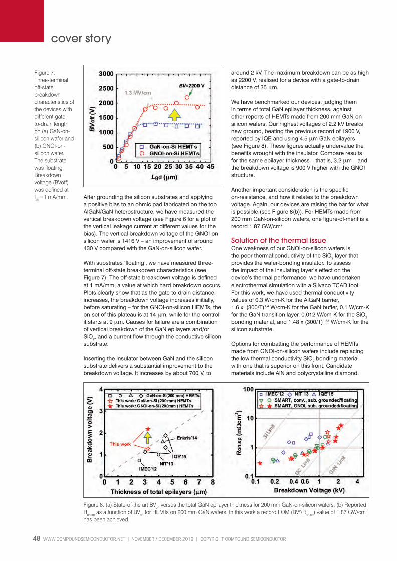
48 WWW.COMPOUNDSEMICONDUCTOR.NET l NOVEMBER / DECEMBER 2019 l COPYRIGHT COMPOUND SEMICONDUCTOR
cover story
After grounding the silicon substrates and applying a positive bias to an ohmic pad fabricated on the top AlGaN/GaN heterostructure, we have measured the vertical breakdown voltage (see Figure 6 for a plot of the vertical leakage current at different values for the bias). The vertical breakdown voltage of the GNOI-on-silicon wafer is 1416 V – an improvement of around 430 V compared with the GaN-on-silicon wafer.
With substrates ‘floating’, we have measured three-terminal off-state breakdown characteristics (see Figure 7). The off-state breakdown voltage is defined at 1 mA/mm, a value at which hard breakdown occurs. Plots clearly show that as the gate-to-drain distance increases, the breakdown voltage increases initially, before saturating – for the GNOI-on-silicon HEMTs, the on-set of this plateau is at 14 μm, while for the control it starts at 9 μm. Causes for failure are a combination of vertical breakdown of the GaN epilayers and/or SiO2, and a current flow through the conductive silicon substrate.
Inserting the insulator between GaN and the silicon substrate delivers a substantial improvement to the breakdown voltage. It increases by about 700 V, to
around 2 kV. The maximum breakdown can be as high as 2200 V, realised for a device with a gate-to-drain distance of 35 μm.
We have benchmarked our devices, judging them in terms of total GaN epilayer thickness, against other reports of HEMTs made from 200 mm GaN-on-silicon wafers. Our highest voltages of 2.2 kV breaks new ground, beating the previous record of 1900 V, reported by IQE and using 4.5 μm GaN epilayers (see Figure 8). These figures actually undervalue the benefits wrought with the insulator. Compare results for the same epilayer thickness – that is, 3.2 μm – and the breakdown voltage is 900 V higher with the GNOI structure.
Another important consideration is the specific on-resistance, and how it relates to the breakdown voltage. Again, our devices are raising the bar for what is possible (see Figure 8(b)). For HEMTs made from 200 mm GaN-on-silicon wafers, one figure-of-merit is a record 1.87 GW/cm2.
Solution of the thermal issueOne weakness of our GNOI-on-silicon wafers is the poor thermal conductivity of the SiO2 layer that provides the wafer-bonding insulator. To assess the impact of the insulating layer’s effect on the device’s thermal performance, we have undertaken electrothermal simulation with a Silvaco TCAD tool. For this work, we have used thermal conductivity values of 0.3 W/cm-K for the AlGaN barrier, 1.6 x (300/T)1.4 W/cm-K for the GaN buffer, 0.1 W/cm-K for the GaN transition layer, 0.012 W/cm-K for the SiO2 bonding material, and 1.48 x (300/T)1.65 W/cm-K for the silicon substrate.
Options for combatting the performance of HEMTs made from GNOI-on-silicon wafers include replacing the low thermal conductivity SiO2 bonding material with one that is superior on this front. Candidate materials include AlN and polycrystalline diamond.
Figure 7. Three-terminal off-state breakdown characteristics of the devices with different gate-to-drain length on (a) GaN-on-silicon wafer and (b) GNOI-on-silicon wafer. The substrate was floating. Breakdown voltage (BVoff) was defined at Ids=1 mA/mm.
Figure 8. (a) State-of-the art BVoff versus the total GaN epilayer thickness for 200 mm GaN-on-silicon wafers. (b) Reported Ron,sp as a function of BVoff for HEMTs on 200 mm GaN wafers. In this work a record FOM (BV2/Ron,sp) value of 1.87 GW/cm2 has been achieved.
GaN on SOI v3RS 6MG.indd 48GaN on SOI v3RS 6MG.indd 48 25/11/2019 15:2425/11/2019 15:24

If you have answered yes to any of the questions above, then SSI International 2020 is the perfect event for you. Here are but a few reasons why you must consider sponsorship.
Reasons to sponsor1. Access and network with the leading players across the global sensors industry Going from strength-to strength, the fourth edition of SSI International 2020 will allow you to engage with 300+ senior decision makers from the major companies along the entire value chain of the sensors industry in one dedicated exhibition hall, including over 30 international experts, who will speak at the conference.
2. Raise brand and company awareness We have an intensive and multi-faceted marketing program available and already underway, which includes email marketing, social media, conference partners, direct mail and live events in addition to promotion in the SSI Magazine digital portfolio Coupled with the marketing program, the support of our highly esteemed Conference association and media partners ensure your company, product and service will achieve maximum visibility within the industry for the next 7 months.
3. Thought leadership and credibility Aligning with the leading global sensors industry conference will give you a great opportunity to be positioned as a thought leader in the industry. Engage in debate, share insights and expertise on industry challenges with your peers.
4. ROI and long-term partnerships Many of our sponsors repeatedly support the event year on year, demonstrating how the industry trusts the SSI International brand as the leading information and networking resource to deliver the best programme and ROI. Unparalleled networking opportunities enable you to both build existing and generate new relationships and demonstrate ROI by aligning with the conference brand.
5. Accessibility We have opportunities to suit all budgets.
6. Post-event exposure Even when the event is over, you will be included in off-season conference promotional activities, plus the SSI digital portfolio as well as the fortnightly email newsletter.
7. Expand your audience SSI International is part of AngelTech, a brand which uniquely delivers insightful, engaging and high- valued conferences that have tremendous synergy between audiences. The current line-up, attracting more than 700 delegates, consists of co-located Compound Semiconductor (CS) International, Photonic Integrated Circuits (PIC) International, and Sensor Solutions International (SSI). Delegates can choose between which sessions they want to participate in and the single exhibition hall layout enables exposure to 3 different but related audiences
Contact: [email protected] to discuss opportunities with the SSI International Conference and Exhibition team or by calling +44 (0)2476 718 970 today.
Sponsorship opportunities are limited.
Connecting, informing and inspiring the global sensors industry
Why should you choose to sponsor with SSI International?
Are you looking to accelerate your growth and reach the major players in the global sensors industry?
Do you want to educate, influence and network with the industry?
31 MARCH - 1 APRIL 2020BRUSSELS, BELGIUM
SSI 2020 Why Should You Ad v4.indd 1SSI 2020 Why Should You Ad v4.indd 1 11/11/2019 12:5711/11/2019 12:57

50 WWW.COMPOUNDSEMICONDUCTOR.NET l NOVEMBER / DECEMBER 2019 l COPYRIGHT COMPOUND SEMICONDUCTOR
cover story
Further readingZ. Liu et al. Proc. of VLSI tech., 2019 B. Lu et al. IEEE Electron. Dev. Lett. 31 951 (2010) E. A. Fitzgerald et al. ECS Trans. 75 31 (2016)Y. Zhang et al. IEEE Tran. Electron Dev. 60 2224(2013)
To evaluate the benefits of these materials, we have carried out simulations, using values of 1.13 W/cm-K for the thermal conductivity of 700 nm AlN, and 2.3 W/cm-K for 700 nm of polycrystalline diamond. According to the calculations, the addition of either AlN bonding material or polycrystalline diamond bonding material trims the thermal resistance of the device from 45 °C(W/mm) to 29 °C(W/mm).
Superior thermal management holds the key to higher powers. If the channel temperature must be no more than 150 °C, the allowable power increases from 3.9 W/mm for the GNOI-on-silicon wafer with SiO2 bonding material to 5.3 W/mm with AlN bonding material and 5.4 W/mm with polycrystalline diamond bonding material. This is a significant improvement, indicating that the thermal issue created by the SiO2 bonding material can be addressed with either AlN or poly-crystalline diamond.
In short, it is clear that introducing new materials to the GaN-on-silicon HEMTs improves ther performance of this transistor. Inserting SiO2 propels the breakdown voltage to a new high, and increases other figures-of-merit; and the addition of bonding materials with a higher thermal conductivity than SiO2 prevents any compromise to thermal management. This shows that more powerful HEMTs that can keep their cool are within our grasp.
Submit your Lab & Fab article
www.compoundsemiconductor.net
Research is the foundation for the growth of the compound semiconductor industry.
If you want to highlight the important breakthroughs that you make, submit your latest research stories to: [email protected] It is imperative that Compound Semiconductor remains a timely resource for this industry, so we are only interested in highlighting very recent work reported in academic papers.
Therefore, please only consider writing a short piece highlighting your work if you have a journal paper that has been accepted and about to appear in press, or a paper that has been published within the last month.
GaN on SOI v3RS 6MG.indd 50GaN on SOI v3RS 6MG.indd 50 25/11/2019 15:2425/11/2019 15:24

“Now offering Germanium Reclaim”
A D VA N C E D PA C K A G I N G • S E M I C O N D U C T O R • O P T O E L E C T R O N I C S • P H O T O N I C S • T H E T H I N F I L M P O W E R H O U S E
FAST TRACK YOUR THIN FILM PROCESS DEVELOPMENT AT EVATEC’S NEW “ECL”For more information about Evatec thin film production tools visit www.evatecnet.com To find out more about our new “ECL” Laboratory and its capabilities contact us at [email protected]
1Sample tracking
software
>150Deposition
Sources
>20Measurement
techniques
Clean room qualitydown to
T: +41 81 403 80 00 | E: [email protected] | www.evatecnet.com
Untitled-3 1Untitled-3 1 19/11/2019 15:2019/11/2019 15:20

Connecting, informing and inspiring the global sensors industry
IN ITS FOURTH YEAR (preceded by IoT International and HighEnd Sensors International), Sensor Solutions International – one of the leading events for the global sensors industry returns to Brussels in 2020 - bringing together the key players from the industry from across the supply chain for two-days of technical tracks and exhibit opportunities.
SSI International is part of the AngelTech series of events, which has produced for close to a decade, a portfolio of insightful, informative and highly valued chip-level conferences. Attracting more than 700 delegates, consisting of co-located Photonic Integrated Circuits International, and Compound Semiconductor International, plus a
single exhibition area, delegates can dip in and out of every session to put together their own tailor-made programme by selecting from over 125+ invited talks, delivered by leaders of the most innovative global companies of today.
With a strong synergy between the three conferences, attendees and exhibitors are fully exposed to the relevant supply chains as well as customer and supplier bases.
SSI International continues to grow in scale and stature year on year and is firmly established as one of the must-attend conferences for the sensors industry. 2020 is set to be even bigger and better!
3 Conferences, 2 Days, 1 Ticket
Book your place NOW!www.sensorsinternational.net/register
to secure your place It’s set to be another sellout
31 MARCH - 1 APRIL 2020 BRUSSELS, BELGIUM
ANTICIPATION BUILDS AS SENSOR SOLUTIONS INTERNATIONAL OFFERS ITS STRONGEST
SPEAKER LINE UP YET
SSI 2020 DPS Ad v11.indd 26SSI 2020 DPS Ad v11.indd 26 11/11/2019 13:0111/11/2019 13:01

5 New Themes for 2020:Autonomous Transport & Delivery: LiDAR / Sonics / Digital CamerasAutonomous transport and delivery industries present some of the greatest opportunities for advanced sensors including those employed in LiDAR, Radar, ultrasonic and digital imaging systems. We will explore key sensors and sensor-critical systems that will enable these advances while considering the role of essential related technologies such as AI and edge data processing and much more!.
Healthcare & Wellness: Wearables / Portables / Fixed Diagnostics We will explore sensors and SoCs for healthcare, AI’s role, and the need for secure data processing to monitor, diagnose, and treat a wide range of medical conditions. We will also delve into steps needed to increase confi dence regarding the medical effi cacy of next-generation healthcare devices..
Edge Data Analytics: AI / Machine Learning / Big DataWe will dive into the growth in edge networking devices and network protocols (such as OPC UA and MQTT) and ways these are evolving to enable completely new analytical capabilities. We will also explore how sensing devices as well as analytical/AI software can be rethought to help manufacturers utilize their data for improved profi tability and market reach.
Harsh Environments: Space / Aviation & Aerospace / Subsurface & Extreme Heavy IndustryWe will explore the challenges of manufacturing sensors that withstand harsh environmental conditions along with key issues tied to powering devices and securely collecting data from sensors deployed in harsh environments. We will also explore the expanding need for sensors and sensor fusion approaches specifi cally for use in harsh environments as well as the special challenges in designing for space, aviation and aerospace applications.
Simulation and Automation: Industry 4.0 & IIoT / Automation & Autonomy / Smart City We will delve into how simulation and automation providers are integrating new sensors and SoCs into testbeds for enhanced performance and illustrate how sensor and data fusion, machine learning and AI can enhance simulator performance while extending the benefi ts of automation into nondigitized sectors.
Speakers confi rmed to date include:AEye, Artilux, Aryballe Technologies, Blickfeld, Bosch, Broadcom, EPIC, fi conTEC, Henkel, IHS Markit, Ilika Technologies, imec, IQE, Leddartech, Lightricity, Lumotive, Onscale, Outsight, Renovo Auto Sensuron, STMicroelectronics, Tarilian Laser Technologies, Vision Markets, Yole Développement
PROGRAM SPONSORWI-FI SPONSORCONFERENCE APP SPONSOR
NETWORKING RECEPTION SPONSOR OPENING RECEPTION SPONSOR
PLATINUM SPONSORS
SSI 2020 DPS Ad v11.indd 27SSI 2020 DPS Ad v11.indd 27 11/11/2019 13:0111/11/2019 13:01

54 WWW.COMPOUNDSEMICONDUCTOR.NET l NOVEMBER / DECEMBER 2019 l COPYRIGHT COMPOUND SEMICONDUCTOR
technology processing
Better etching enhances selective area doping for vertical GaN power devicesMulti-step etching slashes the leakage current in regrown GaN p-n junctions for selective area doping.
BY HOUQIANG FU, KAI FU AND YUJI ZHAO FROM ARIZONA STATE UNIVERSITY
GaN IS A VERY ATTRACTIVE material for making power electronics. It has a bandgap that is three times wider than the incumbent, silicon, and a critical electric field that is more than ten times higher. Thanks to these attributes, devices made from GaN can realise higher breakdown voltages when they have the same thickness as those made from silicon, or a similar breakdown voltage with less material.
Additional strengths of GaN devices are a low on-resistance and a high switching speed, merits that are reflected in outstanding values for various figures-of-merit (see table 1).
However, these excellent material properties are of no practical benefit unless they are harnessed in electronic devices that excel on many fronts, and lead to efficiency gains in the likes of the power grid, electric vehicles, renewables, data centres, wireless charging, and consumer electronics.
Building great GaN devices is far from trivial, with success hinging on the use of the best geometry. Early development focused on lateral GaN power devices, such as HEMTs, grown on foreign substrates. With this architecture, breakdown voltages are held laterally, and currents flow laterally. That’s not ideal. Part of the problem is that there are issues associated with surface states that can lead to performance degradation, and also result in reproducibility and reliability concerns. In addition, the heat that is generated concentrates in a very narrow region, causing device temperature to rise; and the higher breakdown voltages require a larger chip area, an impediment to scalability.
To tackle these issues, our research team at Arizona State University has been developing high-performance vertical GaN power devices on bulk GaN substrates. One merit of this architecture is that it employs homoepitaxial growth, significantly reducing the density of defects, which can deteriorate breakdown voltages and increase leakage currents.
What’s more, the vertical device geometry offers: higher voltages and forward currents, without
Table 1. Material properties and power electronics figures-of-merit (FOMs) for silicon, SiC and GaN. Eg: bandgap; ε: permittivity; µ: mobility; K: thermal conductivity; Vsat: saturation velocity; EC: critical electric field; BFOM: Baliga’s FOM; BHFFOM: Baliga’s high frequency FOM; JFOM: Johnson’s FOM. The FOMs of silicon are normalised to 1 to ease comparison.
ASU v6RS 7MG.indd 54ASU v6RS 7MG.indd 54 25/11/2019 15:2525/11/2019 15:25

COPYRIGHT COMPOUND SEMICONDUCTOR l NOVEMBER / DECEMBER 2019 l WWW.COMPOUNDSEMICONDUCTOR.NET 55
technology processing
sacrificing chip area; better scalability and heat dissipation; and freedom from the effects of surface states.
This approach may raise a few eyebrows, given the high cost of GaN substrates. However, volumes have been steadily growing over the years, large size substrates with diameters of up to 6 inch are starting to emerge, and the substrate price is expected to continue to decrease, due to further expansion of both the power electronic market and that for GaN optoelectronic devices, such as laser diodes.
Vertical GaN power devices can be divided into four regions: the buffer layer, the drift layer, the channel layer and the edge-termination region (see Figure 1). We have strategies for improving each of these, leading to a boost in device performance. For the channel layer we are pursuing selective-area doping, an ongoing hot topic. Doping challengesSelective-area doping remains a huge hurdle for realising the full potential of GaN power electronics. The purpose of this form of doping is to create laterally patterned p-n junctions (see Figure 2(a)). This type of junction is needed for the fabrication of various GaN power devices, including: junction barrier Schottky diodes or merged p-n/Schottky diodes (see Figure 2(b)); and vertical junction FETs (see Figure 2(c)). These structures have been produced in silicon and SiC by ion-implantation, but not in GaN.
There are two reasons why it is very challenging to realise ion-implantation in GaN, especially for the production of p-type material. One issue is related to the subsequent thermal annealing process, needed to activate implanted atoms and recover crystal damage caused by ion-bombardment. To anneal, often the temperature has to exceed 1200 °C, but GaN begins to decompose at only 900 °C.
The second concern relates to the success of approaches to overcome this decomposition. To alleviate GaN decomposition at high temperatures, researchers have turned to capping layers such as AlN, multi-cycle rapid thermal annealing, and ultra-high pressure, but in all cases the conductivity of the implanted p-GaN is still very low – and judged from the perspective of power devices, it is far from satisfactory.
To overcome this particular hurdle, we have developed a re-growth method that realises selectively doped p-n junctions. With our approach, we can produce high conductivity p-GaN without having to worry about high annealing temperatures and associated GaN decomposition. This process currently remains one of the most important and promising methods for selective-area doping.
Figure 1. A cross-sectional diagram of the simplified structure of vertical GaN power devices on heavily doped bulk GaN substrates. ET indicates edge terminations
Figure 2. a) schematics of selectively doped p-n junctions. (b) JBS diodes or MPS diodes. (c) VJFETs.
ASU v6RS 7MG.indd 55ASU v6RS 7MG.indd 55 25/11/2019 15:2525/11/2019 15:25

56 WWW.COMPOUNDSEMICONDUCTOR.NET l NOVEMBER / DECEMBER 2019 l COPYRIGHT COMPOUND SEMICONDUCTOR
technology processing
When we undertake our regrowth process, it is essential to ensure that the subsequent devices are not impaired by large reverse leakage currents, which can limit the ultimate breakdown voltage and increase power conversion losses in power electronics. Our research has uncovered two contributors to large leakage currents: surface contaminations at the regrowth interface, caused by impurities such as silicon, oxygen and carbon, all identified by secondary ion mass spectrometry; and etching damage, often caused by inductively coupled plasma etching, which is a widely used dry etching technique during GaN device fabrication.
To obtain selectively doped p-n junctions (as shown in Figure 2(a)), we could selectively remove part of n-GaN by inductively coupled plasma etching. This step would form trenches for subsequent p-GaN regrowth. However, this process would complicate experiments and analysis, because when two interfaces are exposed there is the possibility that leakage currents will flow in two directions. What’s more, this approach is time-consuming.
To avoid these complications and speed turnaround, we begin by making planar regrown p-n junctions (see Figure 3). These junctions, regrown by MOCVD, have provided us with a test vehicle for obtaining fundamental knowledge on regrowth, such as the impact of inductively coupled plasma etching and surface treatments.
Figure 3. The growth and fabrication process of regrown p-n junctions formed by MOCVD. The structure is homoepitaxially grown on (0001) bulk GaN substrates. It is formed by the growth of an n+-GaN buffer layer and an unintentionally doped (UID) GaN drift layer, before undertaking ICP dry etching and surface treatments, followed by the regrowth of a thin insertion layer and p-GaN. Diode fabrication includes the deposition of metal stacks for anodes and cathodes, mesa isolation and edge termination.
Figure 4. Reverse current-voltage characteristics of (a) non-etched and (b) etched samples with and without surface treatments. The non-etched sample was not subject to ICP plasma etching before regrowth. The etched sample was subject to ICP plasma etching, using a power of 70 W. Etching proceeds at around 200-300 nm/min, a reasonable rate for most device fabrication processes. A high etching power results in stronger ion-bombardment and more severe etching damage.
ASU v6RS 7MG.indd 56ASU v6RS 7MG.indd 56 25/11/2019 15:2525/11/2019 15:25

COPYRIGHT COMPOUND SEMICONDUCTOR l NOVEMBER / DECEMBER 2019 l WWW.COMPOUNDSEMICONDUCTOR.NET 57
technology processing
Evaluating etching damageFor our first set of experiments, we co-load two samples into the MOCVD reactor and regrow without any surface treatment. With this approach, we compared a non-etched sample and one etched with an inductively coupled plasma etching power of 70 W. Both samples suffer from large reverse leakage currents, highlighting the need to properly treat the surface prior to regrowth.
To realise this, we adopt a combination of UV-ozone and acid surface treatments. The former utilises powerful oxygen radicals to oxidize the surfaces and organic residue contaminants. The beauty of this treatment is that it is purely chemical, and thus free from plasma discharging. Note that with inductively coupled plasma etching, ion-bombardment takes place that can lead to charging damage and deterioration of the device’s electrical characteristics. After the UV-ozone treatment, both samples are immersed in hydrofluoric acid and hydrochloric acid to remove oxidised materials and future clean the surface.
Electrical measurements reveal a massive reduction in the reverse leakage current in the non-etched sample. But that’s not the case in the etched sample (see Figure 4). Our hypothesis for explaining this stark difference is that in the etched sample, etching damage is so severe that it cannot be repaired by surface treatments.
To put this theory to the test, we have carried out another set of experiments involving a lower etching power. This is reduced to just 5 W, a condition that slows the etching rate. We compare the reverse leakage currents in an as-grown sample with three samples that are first subjected to the aforementioned surface treatments. Two samples are etched with a power of 5 W, with an insertion layer thickness of 25 nm and 50 nm, respectively, and a third is etched at 70 W.
Results indicate that slow etching dramatically reduces the reverse leakage currents, and that an insertion layer helps to move the junction away from the regrowth interface, further reducing the reverse leakage current (see Figure 5). For the etched sample with an inductively coupled plasma etching power of 5 W and a 50 nm insertion layer, the reverse leakage current is lower than that in the non-etched sample and similar to the as-grown sample. The key conclusion from this experiment is that the combination of slow etching and proper surface treatments is very effective for regrowth.
Our findings prompt this question: What really drives the difference in reverse leakage currents between these samples? To find out, we have taken a closer look at the regrowth interface.
One of its characteristics that can have a significant impact on the regrowth interface, and ultimately reverse leakage currents, is the charge density. Our
measurements show that the higher the interface surface density, the larger the leakage current (see Figure 6). The as-grown sample has a low, constant charge distribution, on the order of 1016 cm−3, while the regrown sample has a peak charge density at the regrowth interface in the range 1017-1021 cm−3. Measurements also show that a reduction in the etching power lowers the charge density at the regrowth interface, and trims the leakage current.
It is not surprising that a high density of surface charges has profound physical consequences. These charges will create a large electric field at the regrowth interface, and help carriers to tunnel through the potential barrier in the p-n junction and make a significant contribution to the leakage current.
Figure 5. Reverse current-voltage characteristics of the non-etched sample and different etched samples. The power indicates the ICP etching power, and the thickness indicates the insertion layer thickness. An etching power of 5 W corresponds to an etching rate of around 20 nm/min.
Figure 6. Charge density at the regrowth interface (histogram) and leakage current (line-shape) at −600 V for the five samples measured in Figure 5. The charge density is extracted from capacitance-voltage measurements.
ASU v6RS 7MG.indd 57ASU v6RS 7MG.indd 57 25/11/2019 15:2525/11/2019 15:25

58 WWW.COMPOUNDSEMICONDUCTOR.NET l NOVEMBER / DECEMBER 2019 l COPYRIGHT COMPOUND SEMICONDUCTOR
technology processing
Further readingK. Fu et al. Appl. Phys. Lett. 113 233502 (2018)K. Fu et al. IEEE Electron Device Lett. 40 1728 (2019)H. Fu et al. Appl. Phys. Express 11 111003 (2018)H. Fu et al. IEEE Electron Device Lett. 39 1018 (2018)H. Liu et al. Appl. Phys. Lett. 114 082102 (2019)
Multi-step etchingAlthough slow etching delivers the best results, it’s not always practical. It can be very time-consuming, a significant impediment for some device structures with deep trenches and mesas.
To address this concern, we have evaluated multi-step etching, decreasing the ICP power from 70 W to 35 W, and then down to 5 W and finally 2 W. The four-step etching process pays dividends, producing samples with significantly reduced reverse leakage currents and the highest breakdown voltage – it can be over 1.2 kV (see Figure 7(a)).
Another benefit of this multi-step etching process is that it produces a good regrowth surface. We have
compared two etched samples, both subject to a 70 W etching power. Subsequent slow etching steps, using multi-step etching, produce significant improvements in surface quality. We postulate that during multi-step etching, slow etching probably plays a role in recovering the plasma etching damage caused by previous high-power etching steps. In other words, slow etching is more like healing than etching.
Before we can herald multi-step etching as a great success, we need to make sure that it doesn’t degrade the forward characteristics of regrown p-n junctions. Our measurements are encouraging. Samples exhibits excellent forward rectifying behaviours, with an on-off ratio of around 1010 and an on-resistance of 0.8 mΩ cm2. The ideality factor, which can be used to evaluate the performance of a p-n junction, is also promising. Its value is around 2.0, a figure that compares favourably with previously reported values for regrown p-n junctions, and is close to that of our as-grown samples – they are in the range 1.5-1.8.
Baliga’s figure-of-merit provides another opportunity for us to benchmark our regrown p-n diodes. For these devices, it is 2.0 GW cm-2. That’s very close to the SiC limit, and even comparable to some values reported for as-grown p-n diodes. Given that this work is still in its infancy, we are very encouraged by this result. We anticipate improvements in inductively coupled plasma etching, surface treatments and device fabrications, spurring the performance of GaN regrown p-n junctions towards the GaN limit.
In short, our results show that it is possible to produce high performance regrown p-n junctions via epitaxial regrowth. Our next step is to apply the obtained fundamental knowledge on regrowth to selective area doping. When progress follows, it will make a significant contribution to improving the performance of advanced GaN power electronics, and helping this class of device to create a greener planet.
Figure 7. (a) Reverse current-voltage characteristics of the non-etched sample, the sample with the single-step etching, and the sample with the multi-step etching. All samples are subject to the aforementioned surface treatments. (b) Forward current-voltage characteristics and ideality of the sample with the multi-step etching.
Figure 8. Benchmark plot of on-resistance versus breakdown voltage for reported as-grown and regrown GaN-on-GaN p-n diodes.
ASU v6RS 7MG.indd 58ASU v6RS 7MG.indd 58 25/11/2019 15:2525/11/2019 15:25

COPYRIGHT COMPOUND SEMICONDUCTOR l NOVEMBER / DECEMBER 2019 l WWW.COMPOUNDSEMICONDUCTOR.NET 59
research review
ReferenceD. Kang et al. Appl. Phys. Express 12 102016 (2019)
LEDs: A deeper understanding of V-pitsThe introduction of V-pits shifts radiative recombination within the active region
ONE OPTION for increasing the efficiency of the LED is to introduce V-pits into the quantum wells.
What impact this has on carrier dynamics within the device is not fully understood, so to shed more light on this matter, a partnership between researchers from Korea, Japan and Germany has been studying hole transport within these structures.
“Our findings show that for quantum wells with V-pits, current is not injected through the first quantum well, but the lower quantum wells near the n-cladding side,” says team spokesman Tae-Yeon Seong from Korea University. “This is a highly important finding, by which efficient LEDs can be designed.”
According to him, this work shows that by optimising the size of the V-pits, as well as the thickness and the doping of the layers in the active region, it is possible to reduce hole resistance and increase LED efficiency.
To investigate the impact of V-pits on hole transport, Seong and co-workers have produced a portfolio of blue-emitting LEDs. All were produced using MOCVD, and began with the growth of a 30 nm-thick nucleation layer, a 3 μm-thick undoped layer of GaN, a silicon doped n-type layer of GaN that is 2 μm-thick, and a ten pair InGaN/GaN strained superlattice. On this the team added an active region with either five or nine 3 nm-thick quantum wells, a 30 nm-thick Al0.18Ga0.82N electron-blocking layer, and a 60 nm-thick magnesium-doped layer.
For the LEDs with the V-pits, the researchers included a second electron-blocking layer, formed from a superlattice with nine alternating layers of 3 nm-thick of Al0.18Ga0.82N and GaN, both doped with magnesium. They grew this structure on a 20 nm-thick layer of magnesium-doped GaN.
Note that another difference between the two types of LEDs is that the devices with the V-pits have quantum barriers 11 nm-thick, while those that don’t have quantum barriers 4 nm-thick.
To generate the V-pits, the team set the reactor temperature to 800 °C and grew a 220 nm-thick layer of GaN on top of the n-type GaN. This condition produced V-pits with a size that maximised LED light output.
The team used scanning tunnelling electron microscopy to investigate the V-pits. This technique revealed a density of 2 x 108 cm-2, with pits accounting for nearly 8 percent of the total quantum well area in the c-plane.
To investigate the origin of the light emission in the LEDs, some wells were formed with a different bandgap. This was accomplished by reducing the growth temperature by 6 °C.
When measuring the emission from the LEDs that have wider wells near the n-type cladding, the team found that only the LEDs without V-pits produced a pair of electroluminescence peaks. They concluded that in devices without V-pits, recombination is predominantly through the top quantum wells on the p-cladding side; while for LEDs with V-pits, radiative recombination does not occur in the top quantum wells. Further study showed that in LEDs with V-pits, the majority of radiative recombination occurs at the quantum-wells near the n-cladding side.
Seong and co-workers have an explanation for this difference in the location of light extraction. They argue that in LEDs without V-pits, most of the holes crowd at the top of the quantum wells, due to their low mobility and the piezoelectric barrier (see Figure (a)). When V-pits are introduced, holes can be efficiently injected through their sidewalls and into the LEDs (see Figure (b)). This occurs through a lowering of the piezoelectric barrier and the sidewalls, and is aided by the thicker quantum barrier.
After holes are injected into the device, they are uniformly distributed across all the lateral multi-quantum wells. As the mobility for electrons is higher than that for holes, efficient recombination takes place in the wells that are nearer the n-cladding side.
The team now plans to apply these findings to the development of green microLEDs for display applications.
The introduction of V-pits produces a dramatic change in hole transport.
Research Review v4RS 5MG.indd 59Research Review v4RS 5MG.indd 59 25/11/2019 15:2025/11/2019 15:20
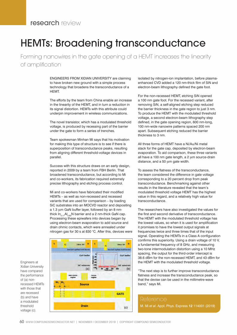
60 WWW.COMPOUNDSEMICONDUCTOR.NET l NOVEMBER / DECEMBER 2019 l COPYRIGHT COMPOUND SEMICONDUCTOR
research review
ReferenceM. Mi et al. Appl. Phys. Express 12 114001 (2019)
HEMTs: Broadening transconductanceForming nanowires in the gate opening of a HEMT increases the linearity of amplification
ENGINEERS FROM XIDIAN UNIVERSITY are claiming to have broken new ground with a simple process technology that broadens the transconductance of a HEMT.
The efforts by the team from China enable an increase in the linearity of the HEMT, and in turn a reduction in its signal distortion. HEMTs with this attribute could underpin improvement in wireless communications.
The novel transistor, which has a modulated threshold voltage, is produced by recessing part of the barrier under the gate to form a series of trenches.
Team spokesman Minhan Mi says that his motivation for making this type of structure is to see if there is superposition of transconductance peaks, resulting from aligning different threshold-voltage devices in parallel.
Success with this structure draws on an early design, reported in 2009 by a team from FBH Berlin. That broadened transconductance, but according to Mi and co-workers, its fabrication required extremely precise lithography and etching process control.
Mi and co-workers have fabricated their modified HEMTs – as well as non-recessed and recessed variants that are used for comparison – by loading SiC substrates into an MOCVD reactor and depositing a 1.3 μm GaN buffer layer, followed by an 8 nm-thick In0.17Al0.83N barrier and a 2 nm-thick GaN cap. Processing these epiwafers into devices began by using electron-beam evaporation to add source and drain ohmic contacts, which were annealed under nitrogen gas for 30 s at 830 °C. After this, devices were
isolated by nitrogen-ion implantation, before plasma-enhanced CVD added a 120 nm-thick film of SiN and electron-beam lithography defined the gate foot.
For the non-recessed HEMT, etching SiN opened a 100 nm gate foot. For the recessed variant, after removing SiN, a self-aligned etching step reduced the barrier thickness in the gate region to just 3 nm. To produce the HEMT with the modulated threshold voltage, a second electron-beam lithography step defined, in the gate opening region, 600 nm-long, 100 nm-wide nanowire patterns spaced 200 nm apart. Subsequent etching reduced the barrier thickness to 3 nm.
All three forms of HEMT have a Ni/Au/Ni metal stack for the gate cap, deposited by electron-beam evaporation. To aid comparison, these three variants all have a 100 nm gate length, a 2 μm source-drain distance, and a 50 μm gate width.
To assess the flatness of the transconductance, the team considered the difference in gate voltage corresponding to a 20 percent drop from peak transconductance. Benchmarking against other results in the literature revealed that the team’s modulated threshold voltage HEMT has the highest value in this regard, and a relatively high value for transconductance.
The researchers have also investigated the values for the first and second derivative of transconductance. The HEMT with the modulated threshold voltage has the lowest values, so when it is used for amplification it promises to have the lowest output signals at frequencies twice and three times that of the input signal. Operating the HEMTs in a Class A configuration confirms this superiority. Using a drain voltage of 10 V, a fundamental frequency of 8 GHz, and measuring two-tone intermodulation distortion using a 10 MHz spacing, the output for the third-order intercept is 38.6 dBm for the non-recessed HEMT, and 43 dBm for the HEMT with the modulated threshold voltage.
“The next step is to further improve transconductance flatness and increase the transconductance peak, so that the devise can be used in the millimetre-wave band,” says Mi.
Engineers at Xidian University have compared the performance of (a) non-recessed HEMTs with those that are recessed (b) and have a modulated threshold voltage (c).
Research Review v4RS 5MG.indd 60Research Review v4RS 5MG.indd 60 25/11/2019 15:2025/11/2019 15:20

COPYRIGHT COMPOUND SEMICONDUCTOR l NOVEMBER / DECEMBER 2019 l WWW.COMPOUNDSEMICONDUCTOR.NET 61
research review
ReferenceK. Xin et al. Appl. Phys. Express 12 115501 (2019)
Building better semi-polar substratesInserting interlayers and reducing the growth pressure yields better semi-polar GaN
SEMI-POLAR PLANES have much promise for producing green and yellow emitters. That’s because they can enable high levels of indium incorporation; and they can reduce the strength of internal electric fields, leading to an increase in the likelihood of radiative recombination.
Progress of semi-polar LEDs and lasers is pegged back by the lack of an affordable, high-quality substrate. But there is now much hope, thanks to a collaboration between researchers at Hefei University of Technology, China, the University of Birmingham, UK, and Chinese company Anhui San’an Optoelectronics.
Using a three-stage growth process that involves the addition of a very thin SiN interlayer, this team has produced, on m-plane sapphire, a film of semi-polar (1122) that has a defect density that is comparable to GaN layers grown on c-plane sapphire. The crystallinity of the team’s semi-polar GaN is high, according to X-ray diffraction, and quantum wells grown on this foundation have a far stronger photoluminescence signal than a control, grown on semi-polar GaN by a standard method.
The team’s work forms part of a much wider effort at developing semi-polar GaN on m-plane sapphire. Many other groups are pursuing approaches that are based on epitaxial layer over-growth, an approach that significantly reduces the density of threading dislocations and Basal stacking faults in the GaN, but requires deposition of two GaN layers and intervening ex-situ processing steps. According to the team, this inefficient approach leads to a relatively high cost for production.
The team from China and the UK advocate a more efficient, cheaper, in-situ approach, involving a SiN interlayer. They are by no means alone in using this approach – other groups have developed two-stage growth processes, which includes the growth of three-dimensional GaN islands from the nano-sized pores in the SiN interlayer. Two-dimensional growth follows, extending laterally to realise full coalescence.
Up until now this type of approach has produced a far higher defect density than that based on epitaxial layer over-growth. But this has now changed, thanks to the three-stage process pioneered by the China-UK team.
These researchers begin by loading 4-inch m-plane sapphire substrates into a Veeco K465i MOCVD reactor. The susceptor is heated up to 1100 °C, before substrates are exposed for 10 minutes to a mixture of ammonia and nitrogen to ensure that the (1013) phase
of GaN is suppressed, and pure (1122) semi-polar GaN is formed. After this, a 50 nm-thick film of AlN is grown at 60 Torr.
The team has used this AlN film as a basis for producing a portfolio of structures (see figure). The low-pressure (LP) growth is carried out at 100 Torr, while high-pressure (HP) growth proceeds at 300 Torr. Note that the difference between samples D, E and F is the thickness of the interlayer: the deposition time is 3 minutes for sample D, 5 minutes for E and 7 minutes for F. X-ray diffraction measurements indicate that increasing the deposition time improves the degree of crystallinity in the semi-polar GaN, while reducing its anisotropic features. These benefits stem from reduced propagation of extended defects, due to a combination of increased coverage of the interlayer; and from a slowdown in the coalescence rate during the two-dimensional growth process.
Scrutinising sample F with transmission electron microscopy revealed a reduction in the density of threading dislocations. The density of these imperfections fell through a lowering of the growth pressure, and decreased again at the interlayer, which causes the dislocations to bend and annihilate. The dislocation density in sample F is estimated to be 7 x 108 cm-2, which is two orders of magnitude lower than that for sample A.
The quality of semi-polar GaN improves by inserting a SiN interlayer and switching from high-pressure to low-pressure growth.
Research Review v4RS 5MG.indd 61Research Review v4RS 5MG.indd 61 25/11/2019 15:2025/11/2019 15:20

62 WWW.COMPOUNDSEMICONDUCTOR.NET l NOVEMBER / DECEMBER 2019 l COPYRIGHT COMPOUND SEMICONDUCTOR
green pages directory
To promote your Products and Services contact: Adam [email protected]: +44 (0) 2476 71897
Corporate Partners Green Pages 20112019 NEW.indd 62Corporate Partners Green Pages 20112019 NEW.indd 62 20/11/2019 10:5920/11/2019 10:59

COPYRIGHT COMPOUND SEMICONDUCTOR l NOVEMBER / DECEMBER 2019 l WWW.COMPOUNDSEMICONDUCTOR.NET 63
green pages directory
To promote your Products and Services contact: Adam [email protected]: +44 (0) 2476 71897
Showcase your presence to the global CS industry for 12 months
COMPOUND SEMICONDUCTOR MAGAZINE is the primary information resource for professionals working with compound semiconductor materials and devices.
Each issue of the magazine is distributed in print and digitally to over 60,000 professionals worldwide. With the largest and most diverse global audience of qualified buyers served by any compound semiconductor focused magazine, secure a corporate partnership and buyers guide entry and receive 12 months of promotion and exposure to the compound semiconductor industry across the magazine portfolio including: 12 months of promotion in eight issues of the print and digital versions of Compound Semiconductor featuring your company logo and company details 12 months of promotion and exposure on the Compound Semiconductor website www.compoundsemiconductor.net featuring a Buyers Guide entry and hyperlinked company logo Sponsorship of one e-news alerts sent out to over 60,000 industry professionals with text and a standard web banner.
To find out more, contact: Adam Richardson, Marketing Manager E: [email protected] T: +44 (0)2476 718970
Corporate Partners Green Pages 20112019 NEW.indd 63Corporate Partners Green Pages 20112019 NEW.indd 63 20/11/2019 10:5920/11/2019 10:59

© 2018 Ferrotec (USA) Corporation. All rights reserved. Temescal is a registered trademark and Auratus is a trademark of Ferrotec (USA) Corporation.
Our conic-shaped chambers are taking over in compound
semiconductor production facilities as the world’s leading
manufacturers adopt our Auratus™ enhanced line of
Temescal electron beam deposition systems. We vaporize
metals more eciently. We deliver uniformity. We return
unmatched savings. The results are overwhelming.
With a line of tools optimized for a range of production
environments, whether 150mm or 200mm, small-batch
or high-volume, this invasion could be coming your way.
Find out more before you take us to your leader.
Contact Ferrotec at 1-925-371-4170 or visit
temescal.ferrotec.com/auratus-invasion.
There is no alien invasionIt’s just our Auratus line of Temescal Systems
UEFC-490025 Wafers (150mm)
UEFC-5700 42 Wafers (150mm) 18 Wafers (200mm)
UEFC-610025 Wafers (200mm)
C
M
Y
CM
MY
CY
CMY
K
Ferrotec Auratus Spaceship ad 052218 copy.pdf 1 5/22/18 3:36 PM
Untitled-1 1 23/05/2018 09:22
Copyright © 2022 FDOKUMEN