Topological Control: Systematic control of topological insulator Dirac fermion density on the...
14
arXiv:0907.3089v1 [cond-mat.mes-hall] 17 Jul 2009 APS/123-QED Systematic control of surface Dirac fermion density on topological insulator Bi 2 Te 3 Y. Xia, 1 D. Qian, 1, 2 D. Hsieh, 1 R. Shankar, 1 H. Lin, 3 A. Bansil, 3 A.V. Fedorov, 4 D. Grauer, 5 Y. S. Hor, 5 R. J. Cava, 5 and M. Z. Hasan 1, 6, 7 1 Joseph Henry Laboratories of Physics, Department of Physics, Princeton University, Princeton, NJ 08544, USA 2 Department of Physics, Shanghai Jiao Tong University, Shanghai 200030, China 3 Department of Physics, Northeastern University, Boston, MA 4 Advanced Light Source, Lawrence Berkeley National Laboratory, University of California, Berkeley, CA 94305, USA 5 Department of Chemistry, Princeton University, Princeton, NJ 08544, USA 6 Princeton Center for Complex Materials, Princeton University, Princeton, NJ 08544, USA 7 Princeton Institute for the Science and Technology of Materials, Princeton University, Princeton, NJ 08544, USA (Dated: July 17, 2009) 1
-
Upload
independent -
Category
Documents
-
view
0 -
download
0
Transcript of Topological Control: Systematic control of topological insulator Dirac fermion density on the...
arX
iv:0
907.
3089
v1 [
cond
-mat
.mes
-hal
l] 1
7 Ju
l 200
9APS/123-QED
Systematic control of surface Dirac fermion density on topological
insulator Bi2Te3
Y. Xia,1 D. Qian,1, 2 D. Hsieh,1 R. Shankar,1 H. Lin,3 A. Bansil,3 A.V.
Fedorov,4 D. Grauer,5 Y. S. Hor,5 R. J. Cava,5 and M. Z. Hasan1, 6, 7
1Joseph Henry Laboratories of Physics, Department of Physics,
Princeton University, Princeton, NJ 08544, USA
2Department of Physics, Shanghai Jiao Tong University, Shanghai 200030, China
3Department of Physics, Northeastern University, Boston, MA
4Advanced Light Source, Lawrence Berkeley National Laboratory,
University of California, Berkeley, CA 94305, USA
5Department of Chemistry, Princeton University, Princeton, NJ 08544, USA
6Princeton Center for Complex Materials,
Princeton University, Princeton, NJ 08544, USA
7Princeton Institute for the Science and Technology of Materials,
Princeton University, Princeton, NJ 08544, USA
(Dated: July 17, 2009)
1
Abstract
Three dimensional (3D) topological insulators are quantum materials with a spin-orbit induced
bulk insulating gap that exhibit quantum-Hall-like phenomena in the absence of applied magnetic
fields. They feature surface states that are topologically protected against scattering by time re-
versal symmetry. The proposed applications of topological insulators in device geometries rely
on the ability to tune the chemical potential on their surfaces in the vicinity of the Dirac node.
Here, we demonstrate a suite of surface control methods based on a combination of photo-doping
and molecular-doping to systematically tune the Dirac fermion density on the topological (111)
surface of Bi2Te3. Their efficacy is demonstrated via direct electronic structure topology measure-
ments using high resolution angle-resolved photoemission spectroscopy. These results open up new
opportunities for probing topological behavior of Dirac electrons in Bi2Te3. At least one of the
methods demonstrated here can be successfully applied to other topological insulators such as the
bulk-insulating-Bi1−xSbx, Sb2Te3 and Bi2Se3 which will be shown elsewhere. More importantly,
our methods of topological surface state manipulation demonstrated here are highly suitable for
future spectroscopic studies of topological phenomena which will complement the transport results
gained from the traditional electrical gating techniques.
2
Recently, there has been a surge of research interest in the newly discovered class of 3D
time reversal invariant topological insulators [1, 2, 3, 4, 5, 6] both from the fundamental
physics and potential application viewpoints. Such systems have been proposed to exhibit
many exotic quantum phenomena [7, 8, 9] that can be realized in condensed-matter table-
top settings. Three dimensional topological insulator phases with gapless topological edge
states have been observed in Bi1−xSbx [10, 12], Bi2Se3 [11] and Bi2Te3 [13, 14, 15]. Topo-
logical order (the physically observable quantity that uniquely characterizes the new state,
and in some sense comes closest to an ”order parameter” of the state in the absence of the
spontaneously broken symmetry unlike that in a superconductor) in a topological insulator
cannot be determined without spin-texture or Berry’s phase imaging measurements. Using
spin-resolved methods, Hsieh et.al. measured the Berry’s phase texture of the Bi1−xSbx and
Bi2Te3 classes of material [12, 14], confirming the Fu-Kane-Mele type Z2 topological order
[4, 5, 6] in these materials. In the momentum space, the pairs of time-reversal invariant
edge states can be described as massless Dirac fermions inside the bulk band-gap. A strong
topological insulator (STI) is the one characterized by having an odd number pair of such
states, which are topologically protected against backscattering. The STI phase is a topo-
logically distinct novel phase of matter and cannot be adiabatically reduced to the quantum
spin Hall phase proposed in the strongly spin-orbit coupled two dimensional electron gases
[16]. It is the surface dynamics and control of topological Dirac fermions in the Bi2Te3 class
that we focus in this paper.
While the density of state at the Fermi level (DOS(EF ))in a conventional quantum Hall
system (QHE in 2DEG) can be tuned via an external magnetic field, this method cannot
be applied to the STIs for a magnetic field breaks time reversal symmetry and the topolog-
ical protection is thus lost. Furthermore, chemical techniques such as the bulk doping to
reach the Dirac point are undesirable as they introduce extra carriers which either turn the
bulk into a semi-metal or an alloy or increase the residual conductivity beyond the surface
conduction limit. None of these conditions are desirable for a functional topological insu-
lator. Here, we demonstrate a suite of surface doping methods which can tune the carrier
density on the surfaces of the topological insulator system Bi2Te3 in a time-reversal invari-
ant way. Using angle-resolved photoemission spectroscopy, we demonstrate the capability
of electronic structure engineering of the Bi2Te3 surface with alkali atom (potassium, K)
deposition, molecular adsorption and photo-doping without breaking the time reversal or
3
the Z2 invariance. We show that the chemical potential can be systematically tuned to shift
the surface Dirac point downwards in energy. Moreover, we report that the effect of NO2
molecular adsorption can be further manipulated by photon-assisted stimulation, thereby
controlling the surface carrier density in the opposite directions. These methods of tuning
carrier densities on the surface of a topological insulator open up new research avenues for
spintronic and quantum computing applications where the control of the density of Dirac
fermions on the surfaces is critical to observe many spin-orbit or spintronic quantum effects.
More importantly, our methods of topological surface state manipulation, highly suitable for
spectroscopic studies, demonstrated here will complement the traditional electrical gating
techniques.
Single crystal of Bi2Te3 was grown by melting stoichiometric mixtures of high purity
elemental Bi (99.999%) and Te (99.999%) in a vacuum sealed 4 mm inner diameter quartz
tube at 800 ◦C. The sample was then cooled over a period of two days to 550 ◦C, and then
annealed at that temperature for 5 days. A single crystal with lowest residual conductivity
characterized via transport methods was obtained. Single crystals could be easily cleaved
along the basal plane. The crystal was confirmed to be single phase and identified as
having the rhombohedral crystal structure by X-ray powder diffractometry using a Bruker
D8 diffractometer with Cu Kα radiation and a graphite diffracted beam monochromator.
High-resolution ARPES measurements were then performed using 30 to 55eV photons
at Beamline 12.0.1 of the Advanced Light Source in Lawrence Berkeley National Labora-
tory. The energy and momentum resolution were typically 15meV and 1.5% of the surface
Brillouin Zone (BZ) respectively using a Scienta analyzer. The in-plane crystal orientation
was determined by Laue x-ray diffraction prior to inserting into the ultra-high vacuum mea-
surement chamber. The samples were cleaved in situ at 10K under pressures of less than
2× 10⁻¹¹ torr, resulting in shiny flat surfaces. NO2 molecular doping of the Bi2Te3 surface
was achieved via controlled exposures to NO2 gas (Matheson, 99.5%), after the surface was
allowed to relax for 1 hour after cleavage [14]. The adsorption effects were studied under
static flow mode: exposing the sample to the gas for a certain time then taking data after the
chamber was pumped down to the base pressure. The sample temperature was maintained
at 10K during exposure to NO2. For K deposition, a heated K evaporation source was used
operating at 5.5A. We also present band calculations for the Bi2Te3(111) surface with param-
eters optimized based on experimental data, which were performed with the LAPW method
4
0 1x10⁴ 2x10⁴-0.1 0.0 0.1
-0.6
-0.3
0.0
-0.1 0.0 0.1-0.1 0.0 0.1
(d) (e) (f)
(g)
Bi Te2 3+δ 1 min. K Dep. 2 min. K Dep.
E(e
V)
B
Momentum (Å )k-1 Intensity (a. u.)
Δ
E(e
V)
B
0.4
0.0
-0.4
-0.8GK M
G
M
K
0.0
-0.1
-0.2
(a)
(b) (c)
G
Theoretical Calculation
Diracpoint
Bi Te2 3
Theo.
Experiment
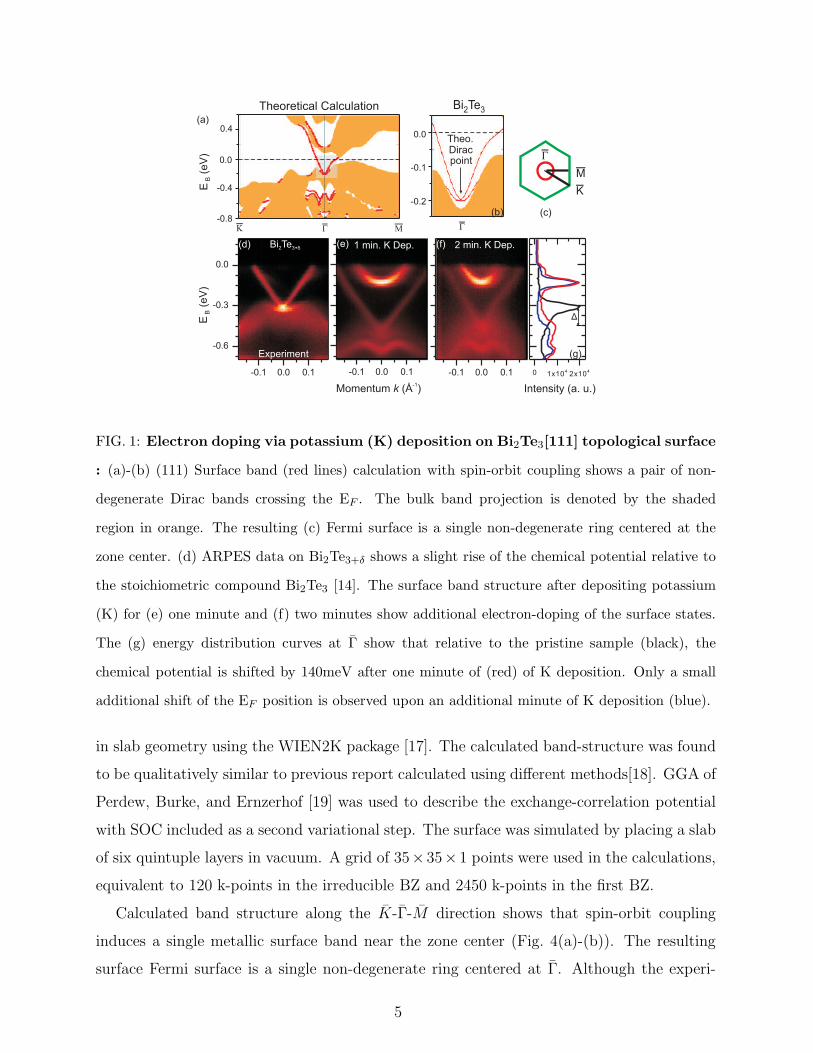
FIG. 1: Electron doping via potassium (K) deposition on Bi2Te3[111] topological surface
: (a)-(b) (111) Surface band (red lines) calculation with spin-orbit coupling shows a pair of non-
degenerate Dirac bands crossing the EF . The bulk band projection is denoted by the shaded
region in orange. The resulting (c) Fermi surface is a single non-degenerate ring centered at the
zone center. (d) ARPES data on Bi2Te3+δ shows a slight rise of the chemical potential relative to
the stoichiometric compound Bi2Te3 [14]. The surface band structure after depositing potassium
(K) for (e) one minute and (f) two minutes show additional electron-doping of the surface states.
The (g) energy distribution curves at Γ̄ show that relative to the pristine sample (black), the
chemical potential is shifted by 140meV after one minute of (red) of K deposition. Only a small
additional shift of the EF position is observed upon an additional minute of K deposition (blue).
in slab geometry using the WIEN2K package [17]. The calculated band-structure was found
to be qualitatively similar to previous report calculated using different methods[18]. GGA of
Perdew, Burke, and Ernzerhof [19] was used to describe the exchange-correlation potential
with SOC included as a second variational step. The surface was simulated by placing a slab
of six quintuple layers in vacuum. A grid of 35×35×1 points were used in the calculations,
equivalent to 120 k-points in the irreducible BZ and 2450 k-points in the first BZ.
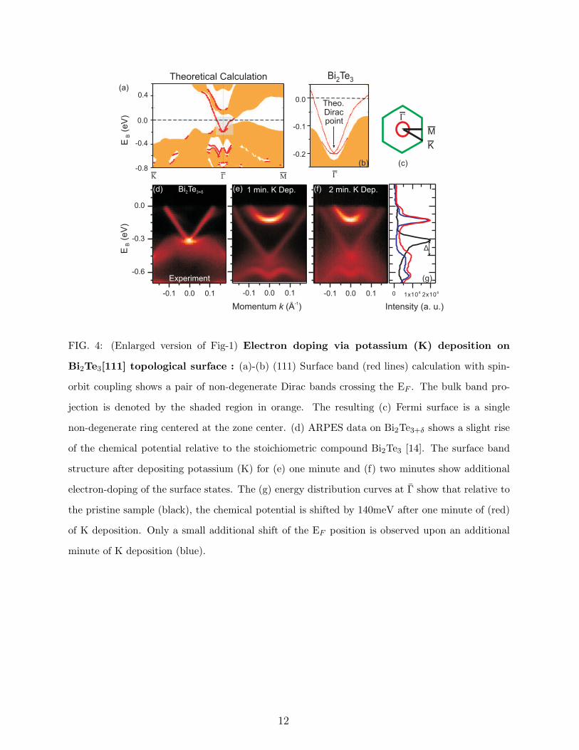
Calculated band structure along the K̄-Γ̄-M̄ direction shows that spin-orbit coupling
induces a single metallic surface band near the zone center (Fig. 4(a)-(b)). The resulting
surface Fermi surface is a single non-degenerate ring centered at Γ̄. Although the experi-
5
mental results are in qualitative agreement with calculations and the chemical potential lies
in the gap only intersecting the surface states (Fig.1), the observed differences could result
from the fact that all Bi2Te3 samples have a relaxed cleaved surface [13, 14]. Because of
details of the surface relaxation (thus band bending) of Bi2Te3 has no simple correlation with
the bulk carrier concentration (insulating or not) of our samples it is not possible to find
a unique fingerprint of the bulk insulating state by just studying the surface Fermi surface
shape. We have experimentally determined that in the presence of relaxation, slightly excess
Te atoms added in the bulk can electron dope the surface (Figure 1(d)). These effects taken
together may account for some of the differences between calculated band structure and the
experimental data.
In Figure 4(e)) we present ARPES data taken at 30eV after potassium (K) is deposited
onto the sample for approximately one minute. The material becomes strongly electron
doped, with the bottom of the ”V” (Dirac band) band rigidly shifted by approximately
140meV. The Fermi velocity of the Dirac band is unchanged with doping. In addition, we
observe an inner resonant-state (due to surface band bending) feature that appears to be
the bottom of a pair of spin-split parabolic bands shifted from each other in k-space. These
bands are reminiscent of those observed in the SS of Au(111) and Sb(111) at Γ̄. Assuming
that each K atom donates one electron, Luttinger count theorem suggests that the change
of the electron pocket size corresponds to 7% of a K monolayer deposited onto the sample
surface. Additional K doping (Fig. 4(f)) has little effect on moving the chemical potential.
The signal from the Dirac point however attenuates due to the increasing escape depth of
the photoelectrons (Fig. 4(g)). Nevertheless, no gap is observed as a result of deposition,
confirming that time-reversal symmetry is preserved suggesting the non-magnetic character
of the valence state of K sticking onto the surface.
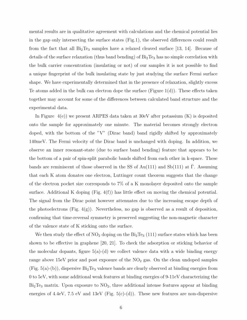
We then study the effect of NO2 doping on the Bi2Te3 (111) surface states which has been
shown to be effective in graphene [20, 21]. To check the adsorption or sticking behavior of
the molecular dopants, figure 5(a)-(d) we collect valence data with a wide binding energy
range above 15eV prior and post exposure of the NO2 gas. On the clean undoped samples
(Fig. 5(a)-(b)), dispersive Bi2Te3 valence bands are clearly observed at binding energies from
0 to 5eV, with some additional weak features at binding energies of 9-11eV characterizing the
Bi2Te3 matrix. Upon exposure to NO2, three additional intense features appear at binding
energies of 4.4eV, 7.5 eV and 13eV (Fig. 5(c)-(d)). These new features are non-dispersive
6
-15 -10 -5 0 -0.1 0.0 0.1
-0.1
0.0
0.1
-0.1
0.0
0.1
k(Å
-1)
k(Å
-1)
Inte
nsit
y
(arb
. u
nit
)In
ten
sit
y(a
rb.
un
it)
Binding Energy (eV)
(a)
(b)
(c)
(d)
Before NO absorption2
After NO absorption2
NO2
-0.1 0.0 0.1-0.1 0.0 0.1
-0.4
-0.2
0.0
-0.4
-0.2
0.0
Bin
din
g E
nerg
y (e
V)
Momentum (Å )k-1
(e) 0L (f) 0.15L (g) 0.3L
(h) 0.6L (i) 1L (j) 1.5L
(k)
Bi Te2 3
NO O
NO O
NO O
Mo
lecu
lar
Do
pin
g
(e)
(g)
(j)
Bi Te2 3 Chemical Potential Tuning via Surface Doping
μ
G
E
k
Bi Te2 3
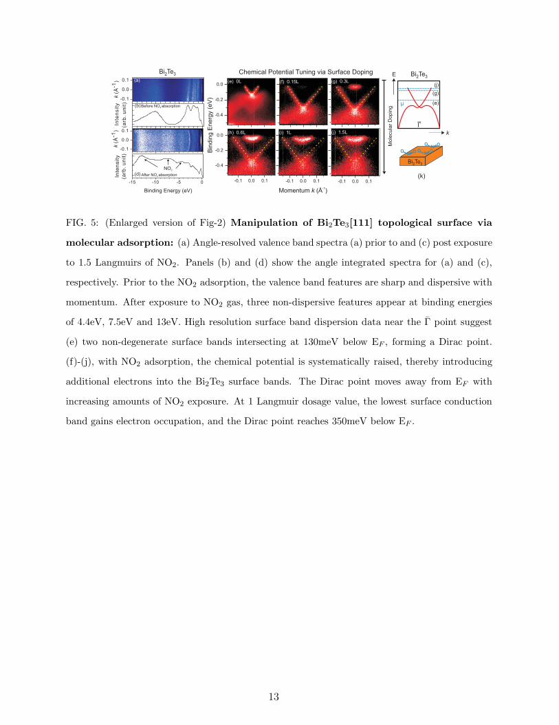
FIG. 2: Manipulation of Bi2Te3[111] topological surface via molecular adsorption: (a)
Angle-resolved valence band spectra (a) prior to and (c) post exposure to 1.5 Langmuirs of NO2.
Panels (b) and (d) show the angle integrated spectra for (a) and (c), respectively. Prior to the NO2
adsorption, the valence band features are sharp and dispersive with momentum. After exposure to
NO2 gas, three non-dispersive features appear at binding energies of 4.4eV, 7.5eV and 13eV. High
resolution surface band dispersion data near the Γ̄ point suggest (e) two non-degenerate surface
bands intersecting at 130meV below EF , forming a Dirac point. (f)-(j), with NO2 adsorption, the
chemical potential is systematically raised, thereby introducing additional electrons into the Bi2Te3
surface bands. The Dirac point moves away from EF with increasing amounts of NO2 exposure.
At 1 Langmuir dosage value, the lowest surface conduction band gains electron occupation, and
the Dirac point reaches 350meV below EF .
and independent of the choice of incident photon energy, which suggest that they are due
to the adsorbed distributed molecules on the sample surface. Core level signals at similar
binding energies are known to appear upon depositing NO2 on carbon-based materials [21].
These results confirm the sticking or adsorption of NO2 on Bi2Te3 (111) surface.
The surface band dispersions near Γ̄ with varying NO2 dosages are shown in Fig. 5(e)-
(j). After equal intervals of data collection time, one finds two significant changes in the
photoemission spectra. Firstly, due to an increasing surface roughness, the measured spectra
after NO2 exposure are not as sharp as that from a clean surface. The total emission
intensity is reduced, as the photoelectron escape depth is increased. Secondly, after NO2
adsorption, the electron pocket around Γ̄ grows significantly larger as the chemical potential
gradually shifts away from the surface Dirac point. After a NO2 exposure of 0.15 Langmuir
(0.15L) (Fig. 5(f)), the chemical potential is raised by approximately 170meV. The surface
conduction bands gain partial occupation, introducing a weak resonant state feature near
7
EF . The pure surface band velocity is unchanged after NO2 exposure. However, the surface
Dirac point (degenerate Kramer’s point) is rigidly shifted downwards to 300meV below
EF . Increasing amounts of NO2 doping increase the electron carrier density on the Bi2Te3
surface. Eventually, after an exposure of 1L of NO2(Fig. 5(i)), the surface Dirac point reaches
350meV below EF . Inside the non-degenerate Dirac cone, a pair of spin-split parabolic
bands from the previously unoccupied surface conduction band is also observed at around
60meV. Additional exposures deteriorates the sample significantly. While the position of the
Dirac point becomes difficult to locate, judging from the size of the lowest energy electron
pocket the shift of the Fermi level is minimal with further dosages. This observation is in
direct contrast with that observed in graphene [21], where electrons are transferred from the
graphene layer to the NO2 molecules.
We then estimate the amount of charge carrier transfer as a result of NO2 deposition by
applying the Luttinger count theorem. Relaxing the sample for 1 hour after cleavage, the
charge concentration (figure 5(e)) is approximately 0.00335 electrons per unit cell. After
exposure to 1L of NO2 gas (Fig. 5(i)), the surface becomes strongly electron doped and
approximately 0.039 electrons are transferred to the surface. The mechanism behind this
charge transfer is presently unclear which makes it difficult to precisely estimate the amount
of NO2 molecules that actually dopes the surface. Nevertheless, it is clear that a systematic
tuning of the chemical potential is possible with K doping.
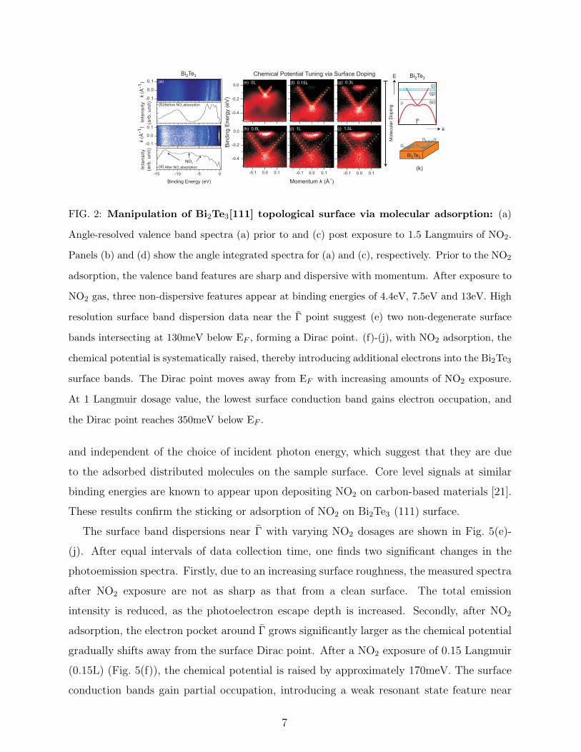
We have further investigated the effect of photo-induced changes on the surface of Bi2Te3.
In our experiment, we find that the effect of NO2 adsorption is unstable against photon
exposure. This result suggests that photo-induced doping could be an additional way with
which to tune the electron-doped surface states on Bi2Te3(111). We present the photon-
induced evolution of the surface band structure data in Fig. 6. To reduce the uncertainties
due to photon-related effects, each spectrum was collected within 1 minute after opening
the photon shutter. Fig. 6(a) presents the surface band dispersion after the sample was first
exposed to 0.3L of NO2. The resulting Dirac point is at about 330meV below EF . With
photon exposure the chemical potential gradually shifts upwards. After a dosage of 1×10¹⁵
photons 30eV, the Dirac point is shifted to approximately 250meV below EF . Successive
exposures continue to shift the chemical potential. After a total dosage of approximately
8×10¹⁵ photons per mm2, the chemical potential is found to be stabilized as the Dirac
point reaches 130meV, the energy location prior to the NO2 exposure. The photon-induced
8
-0.1 0.0 0.1-0.1 0.0 0.1-0.4
-0.2
0.0
-0.1 0.0 0.1
E(e
V)
B
Momentum (Å )k-1
Photo-assisted manipulation of Dirac Carrier Density
-0.1 0.0 0.1 -0.1 0.0 0.1 -0.1 0.0 0.1
-0.15 0.0 0.15
BiTe/SeNO2
1x10¹³ 2x10¹³ 1x10¹⁴ 3x10¹⁴ 6x10¹⁴(g) (i)(h) (j) (k)
(m)
(a) (b) (e)(c) (d) (f)
BTe
i 23
0.0
-0.2
-0.4-0.15 0.0 0.15 -0.15 0.0 0.15 -0.15 0.0 0.15 -0.15 0.0 0.15 -0.15 0.0 0.15
(l)0.1L NO2
0.3L NO2 1x10¹⁵ 3x10¹⁵ 8x10155x1015 7x10¹⁵
μ
E
k
6x10¹⁴
Photons
G
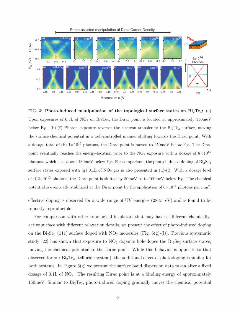
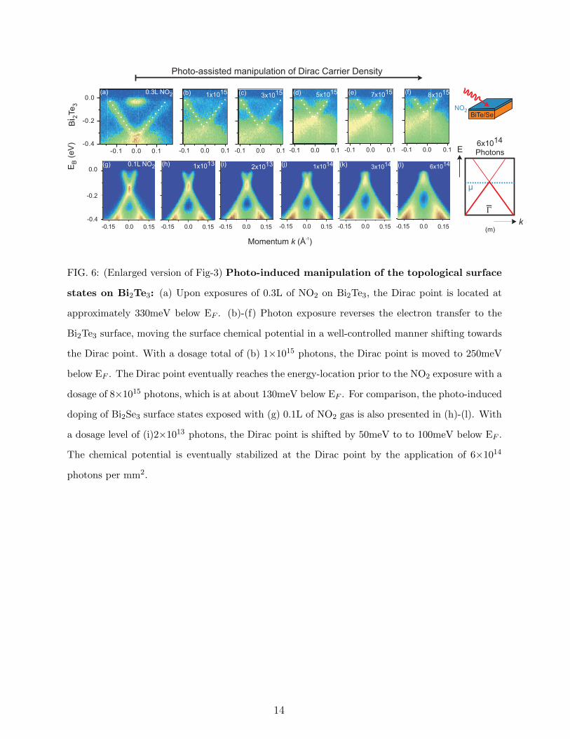
FIG. 3: Photo-induced manipulation of the topological surface states on Bi2Te3: (a)
Upon exposures of 0.3L of NO2 on Bi2Te3, the Dirac point is located at approximately 330meV
below EF . (b)-(f) Photon exposure reverses the electron transfer to the Bi2Te3 surface, moving
the surface chemical potential in a well-controlled manner shifting towards the Dirac point. With
a dosage total of (b) 1×10¹⁵ photons, the Dirac point is moved to 250meV below EF . The Dirac
point eventually reaches the energy-location prior to the NO2 exposure with a dosage of 8×10¹⁵
photons, which is at about 130meV below EF . For comparison, the photo-induced doping of Bi2Se3
surface states exposed with (g) 0.1L of NO2 gas is also presented in (h)-(l). With a dosage level
of (i)2×10¹³ photons, the Dirac point is shifted by 50meV to to 100meV below EF . The chemical
potential is eventually stabilized at the Dirac point by the application of 6×10¹⁴ photons per mm2.
effective doping is observed for a wide range of UV energies (28-55 eV) and is found to be
robustly reproducible.
For comparison with other topological insulators that may have a different chemically-
active surface with different relaxation details, we present the effect of photo-induced doping
on the Bi2Se3 (111) surface doped with NO2 molecules (Fig. 6(g)-(l)). Previous systematic
study [22] has shown that exposure to NO2 dopants hole-dopes the Bi2Se3 surface states,
moving the chemical potential to the Dirac point. While this behavior is opposite to that
observed for our Bi2Te3 (telluride system), the additional effect of photodoping is similar for
both systems. In Figure 6(g) we present the surface band dispersion data taken after a fixed
dosage of 0.1L of NO2. The resulting Dirac point is at a binding energy of approximately
150meV. Similar to Bi2Te3, photo-induced doping gradually moves the chemical potential
9
downwards. A dosage of 2×10¹³ photons at 30eV shifts the Dirac point by 50meV, while a
total dosage of 6×10¹⁴ photons shifts the Dirac point to the Fermi level (Fig. 6(l)). While
the effect of photo-induced doping in Bi2Te3 could be attributed to photo-stimulated des-
orption, the detailed mechanism in Bi2Se3 is still under investigation by us. Nevertheless,
we have demonstrated that photon-induced hole doping can be a controllable mechanism to
manipulate the topological spin-polarized surface bands, systematically driving the chemical
potential to the Dirac point via photon flux.
In summary, using high resolution ARPES, we have demonstrated for the first time a
suite of methods to controllably manipulate the topological edge states of the topological
insulator Bi2Te3 on its (111)-surface without breaking time reversal symmetry. Our sys-
tematic data (Fig.1-3) directly show that both potassium (K) and NO2 electron-dopes the
topologically ordered surface over a wide doping-range. Additionally, we showed that the ef-
fect of the dosage can be reversed by controlling exposure to photon-flux. We further showed
that photodoping has a similar effect on Bi2Se3, which can be used to place the chemical
potential to the much desired Dirac point. Our work opens up many new possibilities for
future utility of topological insulators in spintronic and quantum computing research. More
importantly, our methods of topological surface state manipulation are highly suitable for
spectroscopic studies than the traditional electrical gating based techniques thus open up
new spectroscopic investigation opportunities of topological quantum phenomena.
NOTE ADDED: Some of the methods and their combinations demonstrated here can
be successfully applied to other topological insulators such as the bulk-insulating-Bi1−xSbx,
Sb2Te3 and Bi2Se3 by carefully considering their unique material-specific surface chemistry
and the nature of the surface relaxation which will be shown elsewhere [22].
[1] J. E. Moore, ”Topological Insulators: The Next Generation” Nature Phys. 5, 378 (2009).
[2] S.-C. Zhang, ”Topological States of Quantum Matter” Physics 1, 6 (2008).
[3] C. L. Kane, ”An insulator with a twist” Nature Phys. 4, 348 (2008).
[4] L. Fu, C.L. Kane and E.J. Mele, Phys. Rev. Lett. 98, 106803 (2007).
[5] J.E. Moore and L. Balents, Phys. Rev. B 75, 121306(R) (2007).
[6] L. Fu and C. L. Kane, Phys. Rev. B 76, 045302 (2007).
10
[7] X.-L. Qi, T. L. Hughes and S.-C. Zhang, Phys. Rev. B 78, 195424 (2008).
[8] L. Fu and C.L. Kane, Phys. Rev. Lett. 102, 216403 (2008).
[9] B. Seradjeh, J. E. Moore and M. Franz, arXiv:0902.1147 (2009).
[10] D. Hsieh, D. Qian, L. Wray, et al., Nature 452, 970 (2008).
[11] Y. Xia, D. Qian, D. Hsieh, et al., Nature Phys. 5, 398 (2009).
[12] D. Hsieh, Y. Xia, L. Wray et al., Science 323, 919 (2009).
[13] H.-J. Noh, H. Koh, S.J. Oh et al., Europhys. Lett. 81, 57006 (2008).
[14] D. Hsieh, Y. Xia, D. Qian, et al., arXiv:0904.1260 (2009).
[15] Y.L. Chen, J. G. Analytis, J. H. Chu et al., arXiv:0904.1829 (2009).
[16] B. A. Bernevig, T. L. Hughes, S. C. Zhang, Science 314, 1757 (2006);
[17] P. Blaha et al., computer code WIEN2K (Vienna University of Technology, Vienna, (2001).
[18] H. Zhang, C.-X. Liu, X.-L. Qi, X. Dai et al., Nature Phys. 5, 438 (2009).
[19] J. P. Perdew, K. Burke and M. Ernzerhof, Phys. Rev. Lett. 77, 3865 (1996).
[20] T. Ohta, A. Bostwick, T. Seyller et al., Science 313, 951 (2006).
[21] S.Y. Zhou et al., Phys. Rev. Lett. 101, 086402 (2008).
[22] D. Qian, D. Hsieh, Y. Xia et.al., (surface doping measurements, 2008).
Some preliminary surface-doping data and methods were presented at the
KITP conferences : (http://online.itp.ucsb.edu/online/lowdim09/hasan/) and
(http://online.itp.ucsb.edu/online/qspinhall m08/hasan/) (2008).
11
0 1x10⁴ 2x10⁴-0.1 0.0 0.1
-0.6
-0.3
0.0
-0.1 0.0 0.1-0.1 0.0 0.1
(d) (e) (f)
(g)
Bi Te2 3+δ 1 min. K Dep. 2 min. K Dep.
E(e
V)
B
Momentum (Å )k-1 Intensity (a. u.)
Δ
E(e
V)
B
0.4
0.0
-0.4
-0.8GK M
G
M
K
0.0
-0.1
-0.2
(a)
(b) (c)
G
Theoretical Calculation
Diracpoint
Bi Te2 3
Theo.
Experiment
FIG. 4: (Enlarged version of Fig-1) Electron doping via potassium (K) deposition on
Bi2Te3[111] topological surface : (a)-(b) (111) Surface band (red lines) calculation with spin-
orbit coupling shows a pair of non-degenerate Dirac bands crossing the EF . The bulk band pro-
jection is denoted by the shaded region in orange. The resulting (c) Fermi surface is a single
non-degenerate ring centered at the zone center. (d) ARPES data on Bi2Te3+δ shows a slight rise
of the chemical potential relative to the stoichiometric compound Bi2Te3 [14]. The surface band
structure after depositing potassium (K) for (e) one minute and (f) two minutes show additional
electron-doping of the surface states. The (g) energy distribution curves at Γ̄ show that relative to
the pristine sample (black), the chemical potential is shifted by 140meV after one minute of (red)
of K deposition. Only a small additional shift of the EF position is observed upon an additional
minute of K deposition (blue).
12
-15 -10 -5 0 -0.1 0.0 0.1
-0.1
0.0
0.1
-0.1
0.0
0.1
k(Å
-1)
k(Å
-1)
Inte
nsit
y
(arb
. u
nit
)In
ten
sit
y(a
rb.
un
it)
Binding Energy (eV)
(a)
(b)
(c)
(d)
Before NO absorption2
After NO absorption2
NO2
-0.1 0.0 0.1-0.1 0.0 0.1
-0.4
-0.2
0.0
-0.4
-0.2
0.0
Bin
din
g E
nerg
y (e
V)
Momentum (Å )k-1
(e) 0L (f) 0.15L (g) 0.3L
(h) 0.6L (i) 1L (j) 1.5L
(k)
Bi Te2 3
NO O
NO O
NO O
Mo
lecu
lar
Do
pin
g
(e)
(g)
(j)
Bi Te2 3 Chemical Potential Tuning via Surface Doping
μ
G
E
k
Bi Te2 3
FIG. 5: (Enlarged version of Fig-2) Manipulation of Bi2Te3[111] topological surface via
molecular adsorption: (a) Angle-resolved valence band spectra (a) prior to and (c) post exposure
to 1.5 Langmuirs of NO2. Panels (b) and (d) show the angle integrated spectra for (a) and (c),
respectively. Prior to the NO2 adsorption, the valence band features are sharp and dispersive with
momentum. After exposure to NO2 gas, three non-dispersive features appear at binding energies
of 4.4eV, 7.5eV and 13eV. High resolution surface band dispersion data near the Γ̄ point suggest
(e) two non-degenerate surface bands intersecting at 130meV below EF , forming a Dirac point.
(f)-(j), with NO2 adsorption, the chemical potential is systematically raised, thereby introducing
additional electrons into the Bi2Te3 surface bands. The Dirac point moves away from EF with
increasing amounts of NO2 exposure. At 1 Langmuir dosage value, the lowest surface conduction
band gains electron occupation, and the Dirac point reaches 350meV below EF .
13
-0.1 0.0 0.1-0.1 0.0 0.1-0.4
-0.2
0.0
-0.1 0.0 0.1
E(e
V)
B
Momentum (Å )k-1
Photo-assisted manipulation of Dirac Carrier Density
-0.1 0.0 0.1 -0.1 0.0 0.1 -0.1 0.0 0.1
-0.15 0.0 0.15
BiTe/SeNO2
1x10¹³ 2x10¹³ 1x10¹⁴ 3x10¹⁴ 6x10¹⁴(g) (i)(h) (j) (k)
(m)
(a) (b) (e)(c) (d) (f)
BTe
i 23
0.0
-0.2
-0.4-0.15 0.0 0.15 -0.15 0.0 0.15 -0.15 0.0 0.15 -0.15 0.0 0.15 -0.15 0.0 0.15
(l)0.1L NO2
0.3L NO2 1x10¹⁵ 3x10¹⁵ 8x10155x1015 7x10¹⁵
μ
E
k
6x10¹⁴
Photons
G
FIG. 6: (Enlarged version of Fig-3) Photo-induced manipulation of the topological surface
states on Bi2Te3: (a) Upon exposures of 0.3L of NO2 on Bi2Te3, the Dirac point is located at
approximately 330meV below EF . (b)-(f) Photon exposure reverses the electron transfer to the
Bi2Te3 surface, moving the surface chemical potential in a well-controlled manner shifting towards
the Dirac point. With a dosage total of (b) 1×10¹⁵ photons, the Dirac point is moved to 250meV
below EF . The Dirac point eventually reaches the energy-location prior to the NO2 exposure with a
dosage of 8×10¹⁵ photons, which is at about 130meV below EF . For comparison, the photo-induced
doping of Bi2Se3 surface states exposed with (g) 0.1L of NO2 gas is also presented in (h)-(l). With
a dosage level of (i)2×10¹³ photons, the Dirac point is shifted by 50meV to to 100meV below EF .
The chemical potential is eventually stabilized at the Dirac point by the application of 6×10¹⁴
photons per mm2.
14