Electrical Performances of AlInN/GaN HEMTs. A Comparison with AlGaN/GaN HEMTs with similar...
10
Electrical Performances of AlInN/GaN HEMTs. A Comparison with AlGaN/GaN HEMTs with similar technological process O. Jardel, G. Callet, J. Dufraisse, M. Piazza, N. Sarazin, E. Chartier, M. Oualli, R. Aubry, T. Reveyrand, J.-C. Jacquet, M.A. Di Forte Poisson, E. Morvan, S. Piotrowicz, S.L. Delage Published in International Journal of Microwave and Wireless Technologies, Volume 3, Issue 3, June 2011, pp.301 - 309. DOI: 10.1017/S1759078711000419 This paper is a postprint of a paper submitted to and accepted for publication in International Journal of Microwave and Wireless Technologies and is subject to Cambridge University Press Copyright. http://journals.cambridge.org/action/displayJournal?jid=MRF
-
Upload
independent -
Category
Documents
-
view
1 -
download
0
Transcript of Electrical Performances of AlInN/GaN HEMTs. A Comparison with AlGaN/GaN HEMTs with similar...

Electrical Performances of AlInN/GaN HEMTs. A Comparison with AlGaN/GaN HEMTs with
similar technological process
O. Jardel, G. Callet, J. Dufraisse, M. Piazza, N. Sarazin, E. Chartier, M. Oualli, R. Aubry, T. Reveyrand, J.-C. Jacquet, M.A. Di Forte Poisson, E. Morvan,
S. Piotrowicz, S.L. Delage
Published inInternational Journal of Microwave and Wireless Technologies, Volume 3,
Issue 3, June 2011, pp.301 309.
DOI: 10.1017/S1759078711000419
This paper is a postprint of a paper submitted to and accepted for publication in
International Journal of Microwave and Wireless Technologies and is subject to
Cambridge University Press Copyright.
http://journals.cambridge.org/action/displayJournal?jid=MRF
research paper
Electrical performances of AlInN/GaNHEMTs. A comparison with AlGaN/GaNHEMTs with similar technological process
olivier jardel1
, guillaume callet1,2
, je’re’my dufraisse1,2
, michele piazza1,2
,
nicolas sarazin1
, eric chartier1
, mourad oualli1
, raphae¤l aubry1
, tibault reveyrand2
,
jean-claude jacquet1
, marie-antoinette di forte poisson1
, erwan morvan1
,
ste’phane piotrowicz1
and sylvain l. delage1
A study of the electrical performances of AlInN/GaN High Electron Mobility Transistors (HEMTs) on SiC substrates is pre-sented in this paper. Four different wafers with different technological and epitaxial processes were characterized. Thanksto intensive characterizations as pulsed-IV, [S]-parameters, and load-pull measurements from S to Ku bands, it is demon-strated here that AlInN/GaN HEMTs show excellent power performances and constitute a particularly interesting alternativeto AlGaN/GaN HEMTs, especially for high-frequency applications beyond the X band. The measured transistors with 250 nmgate lengths from different wafers delivered in continuous wave (cw): 10.8 W/mm with 60% associated power added efficiency(PAE) at 3,5 GHz, 6.6 W/mm with 39% associated PAE at 10.24 GHz, and 4.2 W/mm with 43% associated PAE at 18 GHz.
Keywords: AlGaN/GaN HEMT, AlInN/GaN HEMT, Power devices, Power characterizations
Received 14 October 2010; Revised 25 February 2011; first published online 21 April 2011
I . I N T R O D U C T I O N
Following the idea of Kuzmik in 2001 [1], AlInN/GaNHEMTs for high-frequency power applications have becomethe new research topic in several laboratories, substitutinglittle by little the work on AlGaN/GaN HEMTs, which arenow in industrialization phase in several companies. Somepublications showing very impressive power performancesat microwave frequencies have been recently edited [2–5],despite the fledging maturity of the processes.
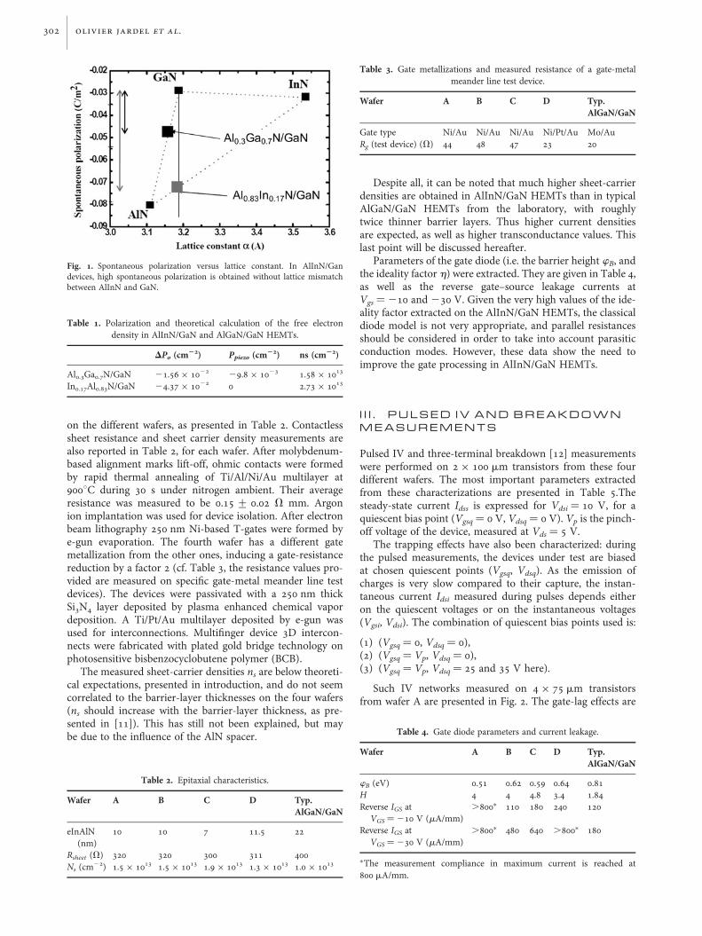
Why such interest in AlInN/GaN devices? As can be seenin Fig. 1 representing the spontaneous polarization versusthe lattice constant, AlInN/GaN HEMTs have two mainadvantages over AlGaN/GaN HEMTs: (1) the chargeinduced by the spontaneous polarization is almost threetimes higher, allowing higher current densities. Some calcu-lations from the equations proposed in [6] are given inTable 1. They show that electron densities as high as 2.73 ×10¹³ can be reached in lattice matched AlInN/GaN devices.(2) As Al0.83In0.17N and GaN are lattice matched, there areno mechanical constraints in the epitaxial structures. Thesemechanical constraints are harmful to the reliability of the
devices and are also supposed to be at the origin of trappingcenters in transistors [7–9].
In this paper we present the latest results obtained atAlcatel-Thales III–V Lab, and particularly large-signalmeasurement results, showing the strong potential of thisnew technology, and confirming the theoretical expectations[1]. This study was done on several wafers with different pro-cesses or epitaxial growth characteristics. The impact of suchdifferences in the processes is studied here by monitoringseveral electrical parameters, thanks to different characteriz-ation tools like pulsed-IV and [S]-parameters. Even if thelink between physical and electrical parameters is neverobvious and direct, this study gives some trends and allowus to draw some interesting conclusions, showing the advan-tages of this new technology as well as the points to improve.
I I . E P I T A X I A L G R O W T H A N DD E V I C E P R O C E S S I N G
Four wafers have been characterized, named A, B, C, and D.On all these wafers, epitaxial layers were grown on SiC sub-strate by low pressure metal organic chemical vapour depo-sition (LP-MOCVD) using a 2-in. single wafer reactor. Theheterostructures consist in a 1.7 mm insulating GaN bufferlayer, a 1 nm thick AlN spacer layer (to enhance electronmobility [10]) and an undoped AlInN layer with approxi-mately 18% of indium content (i.e. lattice matched with theGaN buffer). Different thicknesses of this layer were grown
Corresponding author:O. JardelEmail: [email protected]
1Alcatel-Thales III-V Lab, route de Nozay, 91460 Marcoussis Cedex, France. Phone:+ 33 1 30 77 68 642XLIM – CNRS 123, Avenue Albert Thomas, 87060 Limoges Cedex, France
301
International Journal of Microwave and Wireless Technologies, 2011, 3(3), 301–309. # Cambridge University Press and the European Microwave Association, 2011doi:10.1017/S1759078711000419
on the different wafers, as presented in Table 2. Contactlesssheet resistance and sheet carrier density measurements arealso reported in Table 2, for each wafer. After molybdenum-based alignment marks lift-off, ohmic contacts were formedby rapid thermal annealing of Ti/Al/Ni/Au multilayer at9008C during 30 s under nitrogen ambient. Their averageresistance was measured to be 0.15 + 0.02 V mm. Argonion implantation was used for device isolation. After electronbeam lithography 250 nm Ni-based T-gates were formed bye-gun evaporation. The fourth wafer has a different gatemetallization from the other ones, inducing a gate-resistancereduction by a factor 2 (cf. Table 3, the resistance values pro-vided are measured on specific gate-metal meander line testdevices). The devices were passivated with a 250 nm thickSi3N4 layer deposited by plasma enhanced chemical vapordeposition. A Ti/Pt/Au multilayer deposited by e-gun wasused for interconnections. Multifinger device 3D intercon-nects were fabricated with plated gold bridge technology onphotosensitive bisbenzocyclobutene polymer (BCB).
The measured sheet-carrier densities ns are below theoreti-cal expectations, presented in introduction, and do not seemcorrelated to the barrier-layer thicknesses on the four wafers(ns should increase with the barrier-layer thickness, as pre-sented in [11]). This has still not been explained, but maybe due to the influence of the AlN spacer.
Despite all, it can be noted that much higher sheet-carrierdensities are obtained in AlInN/GaN HEMTs than in typicalAlGaN/GaN HEMTs from the laboratory, with roughlytwice thinner barrier layers. Thus higher current densitiesare expected, as well as higher transconductance values. Thislast point will be discussed hereafter.
Parameters of the gate diode (i.e. the barrier height wB, andthe ideality factor h) were extracted. They are given in Table 4,as well as the reverse gate–source leakage currents atVgs ¼ 210 and 230 V. Given the very high values of the ide-ality factor extracted on the AlInN/GaN HEMTs, the classicaldiode model is not very appropriate, and parallel resistancesshould be considered in order to take into account parasiticconduction modes. However, these data show the need toimprove the gate processing in AlInN/GaN HEMTs.
I I I . P U L S E D I V A N D B R E A K D O W NM E A S U R E M E N T S
Pulsed IV and three-terminal breakdown [12] measurementswere performed on 2 × 100 mm transistors from these fourdifferent wafers. The most important parameters extractedfrom these characterizations are presented in Table 5.Thesteady-state current Idss is expressed for Vdsi ¼ 10 V, for aquiescent bias point (Vgsq ¼ 0 V, Vdsq ¼ 0 V). Vp is the pinch-off voltage of the device, measured at Vds ¼ 5 V.
The trapping effects have also been characterized: duringthe pulsed measurements, the devices under test are biasedat chosen quiescent points (Vgsq, Vdsq). As the emission ofcharges is very slow compared to their capture, the instan-taneous current Idsi measured during pulses depends eitheron the quiescent voltages or on the instantaneous voltages(Vgsi, Vdsi). The combination of quiescent bias points used is:
(1) (Vgsq ¼ 0, Vdsq ¼ 0),(2) (Vgsq ¼ Vp, Vdsq ¼ 0),(3) (Vgsq ¼ Vp, Vdsq ¼ 25 and 35 V here).
Such IV networks measured on 4 × 75 mm transistorsfrom wafer A are presented in Fig. 2. The gate-lag effects are
Table 3. Gate metallizations and measured resistance of a gate-metalmeander line test device.
Wafer A B C D Typ.AlGaN/GaN
Gate type Ni/Au Ni/Au Ni/Au Ni/Pt/Au Mo/AuRg (test device) (V) 44 48 47 23 20
Table 4. Gate diode parameters and current leakage.
Wafer A B C D Typ.AlGaN/GaN
wB (eV) 0.51 0.62 0.59 0.64 0.81H 4 4 4.8 3.4 1.84Reverse IGS at
VGS ¼210 V (mA/mm).800∗ 110 180 240 120
Reverse IGS atVGS ¼230 V (mA/mm)
.800∗ 480 640 .800∗ 180
∗The measurement compliance in maximum current is reached at800 mA/mm.
Fig. 1. Spontaneous polarization versus lattice constant. In AlInN/Gandevices, high spontaneous polarization is obtained without lattice mismatchbetween AlInN and GaN.
Table 1. Polarization and theoretical calculation of the free electrondensity in AlInN/GaN and AlGaN/GaN HEMTs.
DPo (cm22) Ppiezo (cm22) ns (cm22)
Al0.3Ga0.7N/GaN 21.56 × 10²² 29.8 × 10²³ 1.58 × 10¹³
In0.17Al0.83N/GaN 24.37 × 10²² 0 2.73 × 10¹³
Table 2. Epitaxial characteristics.
Wafer A B C D Typ.AlGaN/GaN
eInAlN(nm)
10 10 7 11.5 22
Rsheet (V) 320 320 300 311 400Ns (cm22) 1.5 × 10¹³ 1.5 × 10¹³ 1.9 × 10¹³ 1.3 × 10¹³ 1.0 × 10¹³
302 olivier jardel et al.

quantified by comparing (1) and (2), and the drain-lag effectsby comparing (2) and (3). In order to obtain a meaningfulquantification of the lag effects, they are expressed in termsof potential power degradation, as detailed in [13]: the achiev-able power is calculated, thanks to the formulation giving thetheoretical output power in class A.
The steady-state current is higher than 1.2 A/mm in all thefour wafers, whereas it is around 1 A/mm for AlGaN/GaNHEMTs processed in the laboratory. This is in accordancewith the higher sheet-carrier densities in AlInN/GaNHEMTs, as presented at Table 2. The lag effects differ fromwafer to wafer, but the gate-lag effects are negligible in all thewafers. The drain-lag effects induce a power dispersion esti-mated between 9 and 19% at Vdsq ¼ 25 V (a typical voltagefor applications using 0.25 mm gate devices). The high levelof current associated with the limited lag effects cause thateven when the traps are stressed at such drain voltage, thecurrent remains higher than 1 A/mm and the knee voltage aslow as 5 V. Then, an estimation of the output power in classA power calculated from the theoretical formulation (Pout ¼
(1/8)ImaxVmax) give a result of around 6 W/mm at Vds¼ 25 V.In return, the breakdown voltages are lower than in
AlGaN/GaN HEMTs, for which they are around 100–110 V.This can be explained by the higher density of electrons inthe channel of AlInN/GaN HEMTs, inducing higher electricfield in the gate–drain area at a given bias. However, exceptedfor the wafer A, the measured breakdown voltages are higherthan 65 V, hence allowing nominal bias voltages at 25 V oreven 30 V in power applications.
I V . S M A L L - S I G N A LM E A S U R E M E N T S
[S]-parameters have been measured at Vds ¼ 15 V, Ids ¼
200 mA/mm, in order to obtain the frequency performances.They are presented in Table 6 for 8 × 75 mm devices with0.25 mm gates. The MSG/MAG transition frequency waslower than 20 GHz on the first three wafers, preventingtheir use in Ku band applications. It reaches 22.5 GHz inthe last one, thanks to the strong diminution of the gate resist-ance when a Pt diffusion barrier layer is used in the gate metal-lization (cf. Table 3).
Small-signal models have been extracted from thesemeasurements in order to evaluate the correlation betweenthe fabrication aspects and the electrical performances.Some parameters of these models are presented in Table 7.The gate resistance values extracted confirm the interest ofthe Ni/Pt/Au gate metallization, Rg being almost divided bytwo in the wafer D compared to the wafers A, B, and C.This decrease of the gate resistance allows having perform-ances comparable with classical AlGaN/GaN HEMTs pro-cessed in the lab, in terms of MSG/MAG transitionfrequency. In particular, the MSG/MAG transition ofdevices from wafer D is 7 to 4 GHz higher than the one oftransistors from wafer A, B, or C. It is even 1 GHz higherthan in AlGaN/GaN devices. Such improvement in the gateprocess is very important, allowing the use of 8 × 75 ×0.25 mm devices for power amplification at 20 GHz.
A) Correlation between physical andelectrical parametersHowever, there is no clear correlation between the values ofthe capacitance Cgs and the barrier layer thickness, whichwas expected to diminish with its increase. This is the casefor Cgd, but not in a proportional manner.
Table 5. Parameters extracted from pulsed IV measurements.
Wafer A B C D Typ.AlGaN/GaN
Idss (mA/mm) 1.2 1.2 1.28 1.22 1.05Vp (V) 22.65 22.8 22.7 23.8 25.5Gate-lag (%) 4 6 3 0 11Drain-lag at
Vds ¼ 25 V (%)9 12 19 17 20
Drain-lag atVds ¼ 35 V (%)
15 22 29 23 27
Vbk (V) ≈45∗ ≈83 ≈70 .65∗ ≈105
∗The breakdown voltages on wafers A and D could not be well estimateddue to current leakage, which alters the measurement results.
Fig. 2. Pulsed IV measurements of a 4 × 75 mm AlInN/GaN transistor,at different quiescent bias points: (Vgsq ¼ 0, Vdsq ¼ 0) in black,(Vgsq ¼ ¼Vp ¼ 25, Vdsq ¼ 0) in dark gray, and (Vgsq ¼ 25 V, Vdsq ¼ 25 V)in light gray. Under both gate-lag- and drain-lag-related trap stress, thecurrent keeps higher than 1 A/mm, at a knee voltage of around 5 V.
Table 6. Small-signal measurements results.
Wafer A B C D Typ.AlGaN/GaN
MSG/MAGtrans.(GHz)
15.5 18 16 22.5 21.5
Max gain at10 GHz(dB)
13.8(MSG)
13.2(MSG)
14.1(MSG)
12.7(MSG)
13.4 (MSG)
Max gain at20 GHz(dB)
7.8(MAG)
8.3(MAG)
8 (MAG) 10.1(MSG)
10.6 (MSG)
Table 7. Main equivalent small-signal model parameters.
Wafer A B C D Typ.AlGaN/GaN
Rg (V) 2 1.8 2 1.05 1.05Cgs (pF/mm) 1.88 1.842 1.473 1.56 1.03Cgd (pF/mm) 0.151 0.172 0.293 0.193 0.13Gm (S/mm) 0.373 0.482 0.467 0.415 0.18Gd (S/mm) 0.015 0.015 0.019 0.017 0.0082Cds (S/mm) 0.192 0.348 0.368 0.193 0.27
electrical performances of aliN
n/gAn hemts 303

Even if the correlation between the barrier layer thicknessand the intrinsic capacitances Cgs and Cgd remains quiteunclear, there is a clear difference compared to the typicalvalues of AlGaN/GaN HEMTs. A factor 1.45–1.8 is obtainedapproximately for Cgs and 1.2–2.2 for Cgd. The inversephenomenon is remarkable for gm and gd, which are moreor less twice lower in AlGaN/GaN HEMTs. This is totally cor-related to the barrier layer thickness, which is approximatelytwice in AlGaN/GaN HEMTs. Calculations with first-orderapproximations show it very well, as detailed hereafter.
The capacitance Cgs can be expressed as
Cgs =∂Q∂Vgs
= ∂qnsZLGeff
∂Vgs, (1)
where Q represents the total charge under the gate, ns the sheetcarrier density, Z the total gate width, and LGeff the effectivegate length.
Moreover, the drain current can be expressed as
ID = qnsnsatZ, (2)
where vsat is the saturation velocity of the electrons in thechannel.
And the transconductance as
gm = ∂Ids
∂Vgs. (3)
Then, it is possible, by combining equations (1)–(3), toexpress Cgs versus the transconductance, as
Cgs = gmLGeff
nsat. (4)
Moreover,
gm = Idss
Vp, (5)
where Vp represents the pinch-off voltage, and can beexpressed as:
Vp = EDEPeAlInN = qns
1AlInNeAlInN , (6)
where eAlInN represents the barrier layer thickness, and 1AlInN
the barrier layer dielectric permittivity.Then, (5) and (6) can be rewritten as
gm = nsatZ1AlInN
eAlInN(7)
and (3) and (7) as
Cgs =1AlInN ZLGeff
eAlInN. (8)
Equations (7) and (8) show that both gm and Cgs are inver-sely proportional to the barrier layer thickness (the planarcapacitor formulation can be recognized in equation (8)).This explains the differences of these parameters by a factor
of around 2 between AlGaN/GaN HEMTs and AlInN/GaNHEMTs, the barrier layer in the latter being approximatelytwice thinner than in AlGaN/GaN HEMTs.
What is the impact of the gm, Cgs, and Cgd variations?Figure 3 shows measurements of two similar 8 × 75 ×0.25 mm transistors, one in AlInN/GaN and one in AlGaN/GaN: the marked points at 10 GHz show that the input impe-dances are very similar. The AlInN/GaN device shows aninput reflection coefficient |Gin| ¼ 0.81, while the value forthe AlGaN/GaN device is |Gin| ¼ 0.83. The differences inphases are due to access lines with different lengths. As a con-clusion, although Cgs and gm vary by a factor of 2 and 1
2,respectively, with respect to AlGaN/GaN HEMTs, this doesnot seem to have impact on the input impedance of thedevices.
B) Frequency performances versus gatedevelopment and lengthFigure 4 shows the values of the MSG/MAG transition fre-quency versus the total gate width of transistors from thewafer B (with Ni/Au high resistive gates) with different topol-ogies, from 2 × 50 to 12 × 140 mm. These graphs are useful topower amplifier designers in order to help them in choosingthe best topology for an application at a given frequency. Itcan be seen here that 8 × 75 mm devices (with a total develop-ment of 600 mm) can be used for applications at 18 GHz. Theoutput power of such devices has to be evaluated thanks toload-pull measurements. This will be presented in a latersection.
However, these graphs also show that the transistors whichwould be apt for power applications at frequencies higher than25 GHz have a relatively small total gate development (2 ×50 mm or 2 × 75 mm), hence limiting the absolute outputpower in amplifiers. As recapped before, the improvement
Fig. 3. Input impedance of two transistors with the same topology (8 × 75 ×0.25 mm), in AlInN/GaN and AlGaN/GaN. Despite the strong differences ofCgs and gm, the input impedances are very similar over the (0.5–40 GHz)band. The differences in the phase were due to different access lines betweenthe devices.
304 olivier jardel et al.
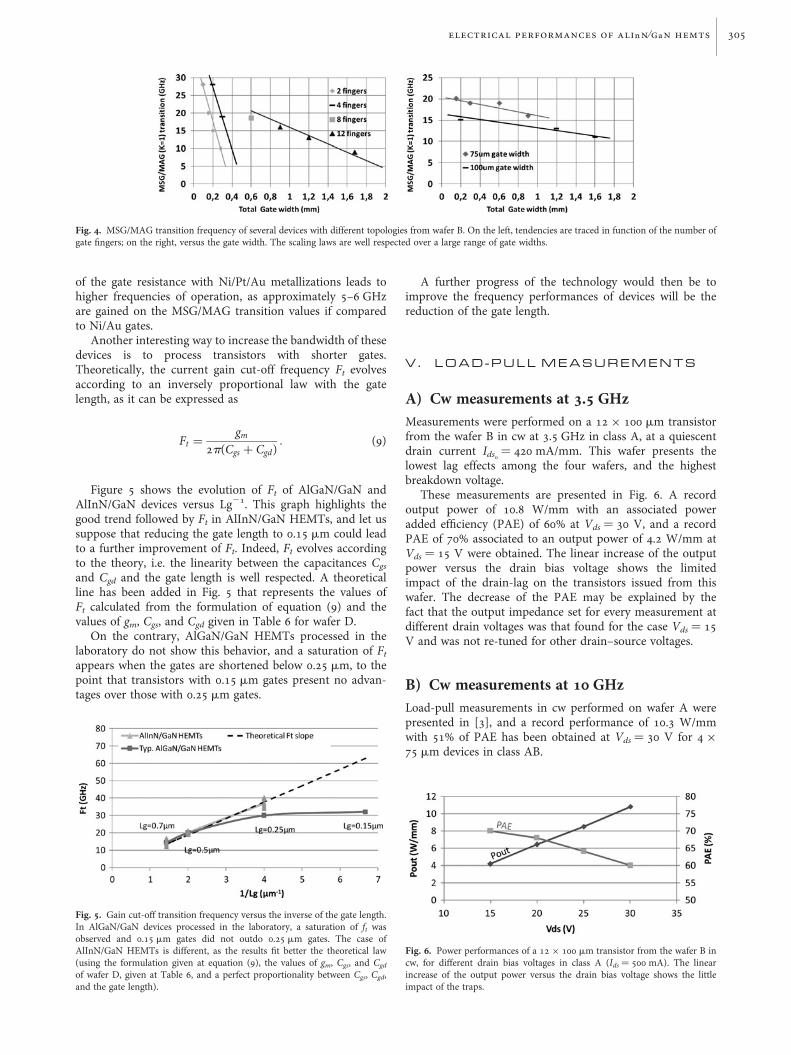
of the gate resistance with Ni/Pt/Au metallizations leads tohigher frequencies of operation, as approximately 5–6 GHzare gained on the MSG/MAG transition values if comparedto Ni/Au gates.
Another interesting way to increase the bandwidth of thesedevices is to process transistors with shorter gates.Theoretically, the current gain cut-off frequency Ft evolvesaccording to an inversely proportional law with the gatelength, as it can be expressed as
Ft =gm
2p(Cgs + Cgd). (9)
Figure 5 shows the evolution of Ft of AlGaN/GaN andAlInN/GaN devices versus Lg21. This graph highlights thegood trend followed by Ft in AlInN/GaN HEMTs, and let ussuppose that reducing the gate length to 0.15 mm could leadto a further improvement of Ft. Indeed, Ft evolves accordingto the theory, i.e. the linearity between the capacitances Cgs
and Cgd and the gate length is well respected. A theoreticalline has been added in Fig. 5 that represents the values ofFt calculated from the formulation of equation (9) and thevalues of gm, Cgs, and Cgd given in Table 6 for wafer D.
On the contrary, AlGaN/GaN HEMTs processed in thelaboratory do not show this behavior, and a saturation of Ft
appears when the gates are shortened below 0.25 mm, to thepoint that transistors with 0.15 mm gates present no advan-tages over those with 0.25 mm gates.
A further progress of the technology would then be toimprove the frequency performances of devices will be thereduction of the gate length.
V . L O A D - P U L L M E A S U R E M E N T S
A) Cw measurements at 3.5 GHzMeasurements were performed on a 12 × 100 mm transistorfrom the wafer B in cw at 3.5 GHz in class A, at a quiescentdrain current Ids0
¼ 420 mA/mm. This wafer presents thelowest lag effects among the four wafers, and the highestbreakdown voltage.
These measurements are presented in Fig. 6. A recordoutput power of 10.8 W/mm with an associated poweradded efficiency (PAE) of 60% at Vds ¼ 30 V, and a recordPAE of 70% associated to an output power of 4.2 W/mm atVds ¼ 15 V were obtained. The linear increase of the outputpower versus the drain bias voltage shows the limitedimpact of the drain-lag on the transistors issued from thiswafer. The decrease of the PAE may be explained by thefact that the output impedance set for every measurement atdifferent drain voltages was that found for the case Vds ¼ 15V and was not re-tuned for other drain–source voltages.
B) Cw measurements at 10 GHzLoad-pull measurements in cw performed on wafer A werepresented in [3], and a record performance of 10.3 W/mmwith 51% of PAE has been obtained at Vds ¼ 30 V for 4 ×75 mm devices in class AB.
Fig. 4. MSG/MAG transition frequency of several devices with different topologies from wafer B. On the left, tendencies are traced in function of the number ofgate fingers; on the right, versus the gate width. The scaling laws are well respected over a large range of gate widths.
Fig. 6. Power performances of a 12 × 100 mm transistor from the wafer B incw, for different drain bias voltages in class A (Ids ¼ 500 mA). The linearincrease of the output power versus the drain bias voltage shows the littleimpact of the traps.
Fig. 5. Gain cut-off transition frequency versus the inverse of the gate length.In AlGaN/GaN devices processed in the laboratory, a saturation of ft wasobserved and 0.15 mm gates did not outdo 0.25 mm gates. The case ofAlInN/GaN HEMTs is different, as the results fit better the theoretical law(using the formulation given at equation (9), the values of gm, Cgs, and Cgd
of wafer D, given at Table 6, and a perfect proportionality between Cgs, Cgd,and the gate length).
electrical performances of aliN
n/gAn hemts 305

New measurements were carried out on 8 × 75 mm tran-sistors from the wafer D at 10.24 GHz in cw, at Ids0
¼
300 mA/mm, and at Vds ¼ 15, 20, 25, and 30 V (Fig. 7).For each bias voltage, the load impedance was optimized inorder to maximize the output power. The maximum powerobtained is 3.5 W/mm with a PAE of 51% at Vds ¼ 15 Vand 6.6 W/mm with a PAE of 39% at Vds ¼ 30 V. Thedevices showed almost no ageing at Vds ¼ 15, 20, and 25 Vduring the whole measurement campaign. The weak impactof the trapping effects can be attested by the limited decreaseof the mean drain current in function of the input powerbefore the gain compression, as explained in [14]. Moreover,it has to be underlined that despite the fact that the technologyis still under development, we noted a very high reproducibil-ity of the measurements performed on several devices of thewafer.
Measurements realized on wafer D has been recapitulatedand plotted in Fig. 8. The results presented here are comparedthose of the existing bibliography published at 10 GHz, fromIII–V Lab and other labs since the last 4 years, to ourknowledge.
It is interesting to notice the good results obtained, andparticularly the constant increasing of performances in spiteof the maturity of the technology. As for the results presentedin this paper, one can notice lower performances than thosepublished in [3]. This limitation is due to a deliberate restric-tion imposed on the gain compression level, in order to evalu-ate the devices for power amplifiers perspectives (i.e. keeping aconsequent power gain at compression).
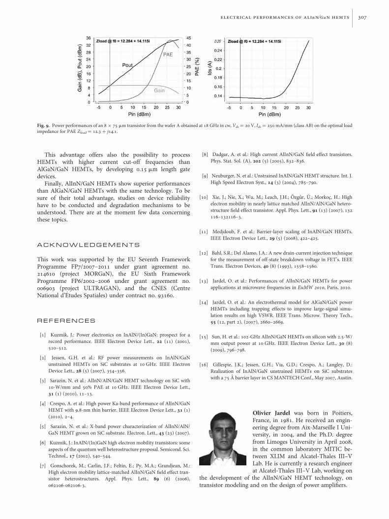
C) Cw measurements at 18 GHzLoad-pull measurements were also carried out at 18 GHz incw on 8 × 75 mm transistors from the wafer A. Even if themax gain performances prevent the use of such devices atthis frequency on this wafer, the goal was to evaluate thepotentialities of the technology at high frequency. The per-formances obtained for the optimal load impedance for PAEare presented in Fig. 9. Indeed, it can be noted that thepower gain at the maximum of PAE is equal to 6.5 dB,which needs to be improved. The reduction of the gate resist-ance (with new Ni/Pt/Au gate metallizations) will improvethis gain, as well as the reduction of the gate length. Despiteall, an output power of 34.1 dBm (2.5 W) was obtained,which corresponds to 4.2 W/mm, with a PAE of 43%. Thisrelatively high value of PAE, as well as the negligible decreaseof the mean drain current, shows indirectly the low level ofdrain-lag of these devices.
V I . C O N C L U S I O N
An overview of the potentialities of the AlInN/GaN-basedHEMTs processed at Alcatel-Thales III–V Lab has been pre-sented here. Despite the fledgling maturity of the technology,the measured devices exhibit excellent power performances,even in Ku band, despite the poor gain in this case. Highlevels of PAE are obtained thanks to very limited trappingeffects, which seem to be one of the main advantages of theAlInN/GaN compared to the AlGaN/GaN technology.
Fig. 7. Power performances of an 8 × 75 mm transistor from the wafer D in cw, for different drain bias voltages (15, 20, 25, and 30 V) in class AB, (Ids ¼ 300 mA/mm) at 10.24 GHz.
Fig. 8. Inventory of published results at the frequency of 10 GHz,performances are plotted in PAE versus output power for all the labratoriesregistered, number in brackets refers to the publication as reference.
306 olivier jardel et al.
This advantage offers also the possibility to processHEMTs with higher current cut-off frequencies thanAlGaN/GaN HEMTs, by developing 0.15 mm length gatedevices.
Finally, AlInN/GaN HEMTs show superior performancesthan AlGaN/GaN HEMTs with the same technology. To besure of their total advantage, studies on device reliabilityhave to be conducted and degradation mechanisms to beunderstood. There are at the moment few data concerningthese topics.
A C K N O W L E D G E M E N T S
This work was supported by the EU Seventh FrameworkProgramme FP7/2007–2011 under grant agreement no.214610 (project MORGaN), the EU Sixth FrameworkProgramme FP6/2002–2006 under grant agreement no.006903 (project ULTRAGAN), and the CNES (CentreNational d’Etudes Spatiales) under contract no. 93160.
R E F E R E N C E S
[1] Kuzmik, J.: Power electronics on InAlN/(In)GaN: prospect for arecord performance. IEEE Electron Device Lett., 22 (11) (2001),510–512.
[2] Jessen, G.H. et al.: RF power measurements on InAlN/GaNunstrained HEMTs on SiC substrates at 10 GHz. IEEE ElectronDevice Lett., 28 (5) (2007), 354–356.
[3] Sarazin, N. et al.: AlInN/AlN/GaN HEMT technology on SiC with10-W/mm and 50% PAE at 10 GHz. IEEE Electron Device Lett.,31 (1) (2010), 11–13.
[4] Crespo, A. et al.: High power Ka-band performance of AlInN/GaNHEMT with 9.8-nm thin barrier. IEEE Electron Device Lett., 31 (1)(2010), 2–4.
[5] Sarazin, N. et al.: X-band power characterization of AlInN/AlN/GaN HEMT grown on SiC substrate. Electron. Lett., 43 (23) (2007).
[6] Kuzmik, J.: InAlN/(In)GaN high electron mobility transistors: someaspects of the quantum well heterostructure proposal. Semicond. Sci.Technol., 17 (2002), 540–544.
[7] Gonschorek, M.; Carlin, J.F.; Feltin, E.; Py, M.A.; Grandjean, M.:High electron mobility lattice-matched AlInN/GaN field effect tran-sistor heterostructures. Appl. Phys. Lett., 89 (6) (2006),062106-062106-3.
[8] Dadgar, A. et al.: High current AlInN/GaN field effect transistors.Phys. Stat. Sol. (A), 202 (5) (2005), 832–836.
[9] Neuburger, N. et al.: Unstrained InAlN/GaN HEMT structure. Int. J.High Speed Electron Syst., 14 (3) (2004), 785–790.
[10] Xie, J.; Nie, X.; Wu, M.; Leach, J.H.; Ozgur, U.; Morkoc, H.: Highelectron mobility in nearly lattice matched AlInN/AlN/GaN hetero-structure field effect transistor. Appl. Phys. Lett., 91 (13) (2007), 132116–132116–3.
[11] Medjdoub, F. et al.: Barrier-layer scaling of InAlN/GaN HEMTs.IEEE Electron Device Lett., 29 (5) (2008), 422–425.
[12] Bahl, S.R.; Del Alamo, J.A.: A new drain-current injection techniquefor the measurement of off-state breakdown voltage in FET’s. IEEETrans. Electron Devices, 40 (8) (1993), 1558–1560.
[13] Jardel, O. et al.: Performances of AlInN/GaN HEMTs for powerapplications at microwave frequencies in EuMW 2010, Paris, 2010.
[14] Jardel, O. et al.: An electrothermal model for AlGaN/GaN powerHEMTs including trapping effects to improve large-signal simu-lation results on high VSWR. IEEE Trans. Microw. Theory Tech.,55 (12, part 2), (2007), 2660–2669.
[15] Sun, H. et al.: 102-GHz AlInN/GaN HEMTs on silicon with 2.5-W/mm output power at 10 GHz. IEEE Electron Device Lett., 30 (8)(2009), 796–798.
[16] Gillespie, J.K.; Jessen, G.H.; Via, G.D.; Crespo, A.; Langley, D.:Realization of InAlN/GaN unstrained HEMTs on SiC substrateswith a 75 A barrier layer in CS MANTECH Conf., May 2007, Austin.
Olivier Jardel was born in Poitiers,France, in 1981. He received an engin-eering degree from Aix-Marseille I Uni-versity, in 2004, and the Ph.D. degreefrom Limoges University in April 2008,in the common laboratory MITIC be-tween XLIM and Alcatel-Thales III–VLab. He is currently a research engineerat Alcatel-Thales III–V Lab, working on
the development of the AlInN/GaN HEMT technology, ontransistor modeling and on the design of power amplifiers.
Fig. 9. Power performances of an 8 × 75 mm transistor from the wafer A obtained at 18 GHz in cw, Vds ¼ 20 V, Ids ¼ 250 mA/mm (class AB) on the optimal loadimpedance for PAE Zload ¼ 12.3 + j14.1.
electrical performances of aliN
n/gAn hemts 307

Guillaume Callet was born in Arles,France, in 1983. He obtained an engin-eering degree from ENSEA (Ecole Na-tionale Suprieure d’Electronique et deses Applications) in 2008 and is cur-rently working toward a Ph.D. degreefrom Limoges University, in thecommon laboratory between Xlim andAlcatel-Thales III–V Lab, MITIC. He
works on the development of AlInN/GaN technology, particu-larly on the modeling of power devices.
Jeremy Dufraisse was born in France1985. He received the French diplomaof engineer from Supelec and the mas-ter’s degree in electronics from the Uni-versity of Paris XI in 2009. He iscurrently a Ph.D. student working ondeveloping new designs using AlGaN/GaN technology at Alcatel-Thales III–V Lab.
Michele Piazza was born in Pordenone,Italy, in 1981. He graduated in electronicengineering at the University Of Padova(Italy) in 2008 with a thesis on reliabilitytesting of AlGaN/GaN HEMTs grownon hybrid substrates. He is currently aresearch engineer at Alcatel-Thales III–V Lab and registered as Ph.D. studentat X-LIM, France. He works on GaN
HEMTs reliability within the Thales MicroelectronicsGroup. His main interests are the characterization andreliability testing of Schottky diode in GaN based semiconduc-tor devices.
Nicolas Sarazin was born in France in1977. He Joined the Thales Research &Technology Center in 2004 and gradu-ated his Ph.D. degree in microwaveand micro technology from the Univer-sity of Lille in 2007. He is involved inAlGaN/GaN device processing and,during the last few years, has focusedon AlInN based high electron mobilitytransistors.
Eric Chartier received the M.Sc degreein physics from Ecole Superieure dePhysique et Chimie de PARIS (ESPCI),Paris, France, in 1979. Since 1981, hehas been at Thales Research and Tech-nology Laboratory and has worked fordeveloping transistor on amorphousthen III–V semiconductors. His researchinterest includes microwaves measure-
ments of transistors and MMICs.
Mourad Oualli was born in France in1982. He was graduated from the EcolePolytechnique and the Ecole Superieured’Electricite (Supelec) in 2007. He thenjoined the Alcatel-Thales III–V Lab asa research engineer in the developmentof the AlGaN/GaN and AlInN/GaNHEMT technologies. He especially con-tributes to the improvement of
reliability aspects by studying parasitic effects.
Raphael Aubry was born in France in1973. He received the material engineer-ing degree from ECAM Rennes in 1999,the physics master research degree fromRennes University in 2000 and Ph.D.degree from Lille University in 2004.His Ph.D. work subject was on the ther-mal management of the power micro-wave devices. He joined the THALES
research center and has been working on the developmentof the power AlGaN/GaN HEMT technology for radar andspace applications. He is currently at Alcatel-Thales III–Vlab, a joint research group on III–V opto-microwave devicesand power semiconductors, in charge of technology and ther-mal management on component based on Gallium Nitridematerial.
Tibault Reveyrand was born in Paris,France. He received a Ph.D. degreefrom Universite de Limoges, Limoges,France, in 2002. From 2002 to 2004, hewas post-doctoral scientist with theCentre National d’Etudes Spatiales(CNES) (French Space Agency). In2005, he became a contractual engineerwith the Centre National de la Re-
cherche Scientifique (CNRS), XLIM, Limoges, France. Hismain research interests include the characterization and mod-eling of RF and microwave nonlinear components.
Jean-Claude Jacquet received theengineering degree from the EcoleSuperieure d’Optique, Orsay, France, in1990. He subsequently joined the Cen-tral Research Laboratory of Thales, as aresearch staff member, where he was in-volved with spintronic devices. He fo-cused his efforts on the giantmagnetoresistive effect and found a
new physical effect called the magnetorefractive effect. Since1999, he has been involved with GaInP HBT and GaNHEMT microwave power devices. He is currently in chargeof thermal management and of the physical modeling aspectson GaN HEMT at Alcatel-Thales III–V Lab.
308 olivier jardel et al.
Marie-Antoinette Di-Forte Poissonobtained her Ph.D. in 1978 and joinedthe Central Research Laboratory ofThomson-CSF. She has been involvedin the MOVPE growth, characterizationand device applications of a variety ofIII–V compounds. Her past achieve-ments include: the growth of highpower 94 GHz InP Gunn diodes, the
first realization of a linear array of a thousand pin photodiodesat 1.72 mm for the SPOT IV satellite, 980 nm high power laserdiodes, GaInP/GaAs based HBT epitaxial structures for highpower S band and X band amplifiers. Currently, Dr Di-FortePoisson manages the team responsible for the “EpitaxialGrowth of Wide Band-gap Materials”. She is a program com-mittee member of the MO-VPE EUROPEAN WORSHOPand the MOVPE international conference.
Erwan Morvan graduated in materialphysics and semiconductor devices atNational Institute for Applied Science(INSA) in Lyon (France). He was aPh.D. student at National Center forMicroelectronics in Barcelona (CNM)from 1995 to 1999. He worked in thefield of device and technology simu-lation. He developed an ion implan-
tation simulator for Silicon Carbide (SiC) crystal. Heobtained the Ph.D. degree in electronics from INSA Lyon in1999. In 2000, he joined the Corporate Laboratory of Thom-son CSF (LCR), now called Thales Research and Technology(TRT). He was involved in SiC MESFET design, technology,
and characterization as a research engineer from 2000 to2003. He is now involved in AlGaN/GaN and AlInN/GaNdevice technology research and development.
Stephane Piotrowicz was born inFrance 1971. He received a Ph.D.degree in electronics from the Universityof Lille in 1999. He joined the Thales Re-search Center and worked on the designof hybrid and MMIC power amplifierson the InGaP/GaAs HBT technologyfor radar and space applications. He cur-rently works on the development of
AlGaN/GaN technology at Alcatel-Thales III–V Lab. He isin charge of hybrid and MMIC demonstrators for T/R mod-ules as power switches, power amplifiers and low noiseamplifiers.
Sylvain Delage obtained his Ph.D. fromUniversity Paris VII in 1985 for his workcarried out at CNET-Meylan on thedemonstration of monolithic Si/CoSi2/Si metal base transistor grown by mol-ecular beam epitaxy. Afterwards he wasfor 2 years with IBM T.J. Watson Re-search Center as research staffmember, where he did participate to
the first demonstration of Si/SiGe HBT, which later on hasbeen developed and manufactured worldwide by major semi-conductor companies.
electrical performances of aliN
n/gAn hemts 309