High Lateral Breakdown Voltage in Thin Channel AlGaN/GaN ...
9
HAL Id: hal-02344992 https://hal.archives-ouvertes.fr/hal-02344992 Submitted on 3 Dec 2020 HAL is a multi-disciplinary open access archive for the deposit and dissemination of sci- entific research documents, whether they are pub- lished or not. The documents may come from teaching and research institutions in France or abroad, or from public or private research centers. L’archive ouverte pluridisciplinaire HAL, est destinée au dépôt et à la diffusion de documents scientifiques de niveau recherche, publiés ou non, émanant des établissements d’enseignement et de recherche français ou étrangers, des laboratoires publics ou privés. High Lateral Breakdown Voltage in Thin Channel AlGaN/GaN High Electron Mobility Transistors on AlN/Sapphire Templates Idriss Abid, Riad Kabouche, Catherine Bougerol, Julien Pernot, Cédric Masante, Rémi Comyn, Yvon Cordier, F Medjdoub To cite this version: Idriss Abid, Riad Kabouche, Catherine Bougerol, Julien Pernot, Cédric Masante, et al.. High Lateral Breakdown Voltage in Thin Channel AlGaN/GaN High Electron Mobility Transistors on AlN/Sapphire Templates. Micromachines, MDPI, 2019, 10 (10), pp.690. 10.3390/mi10100690. hal- 02344992
-
Upload
khangminh22 -
Category
Documents
-
view
0 -
download
0
Transcript of High Lateral Breakdown Voltage in Thin Channel AlGaN/GaN ...
HAL Id: hal-02344992https://hal.archives-ouvertes.fr/hal-02344992
Submitted on 3 Dec 2020
HAL is a multi-disciplinary open accessarchive for the deposit and dissemination of sci-entific research documents, whether they are pub-lished or not. The documents may come fromteaching and research institutions in France orabroad, or from public or private research centers.
L’archive ouverte pluridisciplinaire HAL, estdestinée au dépôt et à la diffusion de documentsscientifiques de niveau recherche, publiés ou non,émanant des établissements d’enseignement et derecherche français ou étrangers, des laboratoirespublics ou privés.
High Lateral Breakdown Voltage in Thin ChannelAlGaN/GaN High Electron Mobility Transistors on
AlN/Sapphire TemplatesIdriss Abid, Riad Kabouche, Catherine Bougerol, Julien Pernot, Cédric
Masante, Rémi Comyn, Yvon Cordier, F Medjdoub
To cite this version:Idriss Abid, Riad Kabouche, Catherine Bougerol, Julien Pernot, Cédric Masante, et al.. HighLateral Breakdown Voltage in Thin Channel AlGaN/GaN High Electron Mobility Transistors onAlN/Sapphire Templates. Micromachines, MDPI, 2019, 10 (10), pp.690. 10.3390/mi10100690. hal-02344992
micromachines
Article
High Lateral Breakdown Voltage in Thin ChannelAlGaN/GaN High Electron Mobility Transistors onAlN/Sapphire Templates
Idriss Abid 1,*, Riad Kabouche 1, Catherine Bougerol 2, Julien Pernot 2, Cedric Masante 2,Remi Comyn 3, Yvon Cordier 3 and Farid Medjdoub 1,*
1 IEMN (Institute of Electronics, Microelectronics and Nanotechnology), Avenue Poincaré,59650 Villeneuve d’Ascq, France; [email protected]
2 CNRS-Institut Néel, University Grenoble-Alpes, 38000 Grenoble, France; [email protected] (C.B.);[email protected] (J.P.); [email protected] (C.M.)
3 CNRS-CRHEA, University Côte d’Azur, rue Bernard Grégory, 06560 Valbonne, France;[email protected] (R.C.); [email protected] (Y.C.)
* Correspondence: [email protected] (I.A.); [email protected] (F.M.);Tel.: +33-320-19-7840 (F.M.)
Received: 15 September 2019; Accepted: 11 October 2019; Published: 12 October 2019
Abstract: In this paper, we present the fabrication and Direct Current/high voltage characterizations ofAlN-based thin and thick channel AlGaN/GaN heterostructures that are regrown by molecular beamepitaxy on AlN/sapphire. A very high lateral breakdown voltage above 10 kV was observed on thethin channel structure for large contact distances. Also, the buffer assessment revealed a remarkablebreakdown field of 5 MV/cm for short contact distances, which is far beyond the theoretical limit ofthe GaN-based material system. The potential interest of the thin channel configuration in AlN-basedhigh electron mobility transistors is confirmed by the much lower breakdown field that is obtained onthe thick channel structure. Furthermore, fabricated transistors are fully functional on both structureswith low leakage current, low on-resistance, and reduced temperature dependence as measured upto 300 C. This is attributed to the ultra-wide bandgap AlN buffer, which is extremely promising forhigh power, high temperature future applications.
Keywords: GaN; high-electron-mobility transistor (HEMT); ultra-wide band gap
1. Introduction
AlGaN/GaN high-electron-mobility transistors (HEMTs) is a promising device for high-powerand high-voltage electronic applications [1–9]. GaN-based HEMTs are already commercially availablefor up to 650 V applications. However, they are currently restricted to below 1 kV mainly because ofthe total buffer thickness limitation with low bow and high crystal quality on large wafer diameters.SiC is another attractive wide bandgap for higher voltage but still has limited impact for the momentbecause of cost issues. In order to address the dynamic medium and high voltage markets beyond1200 V while benefiting from low on-resistances, low leakage current, and low switching losses in acost-effective way, a novel breakthrough in power electronics performance requires a new generationof materials. In this frame, the so-called ultra-wide-bandgap (UWBG) [10–13] materials such as AlN(6.2 eV), which have energy bandgaps that are larger than SiC and GaN, are very promising in enablingthe next leap forward in power electronics. An AlN-based material system has a unique advantage dueto its prominent spontaneous and piezoelectric polarization effects, but also its flexibility in insertingappropriate heterojunctions, thus dramatically broadening the device’s design space. Furthermore,AlN material represents the ideal back barrier for high voltage HEMT applications due to its large
Micromachines 2019, 10, 690; doi:10.3390/mi10100690 www.mdpi.com/journal/micromachines

Micromachines 2019, 10, 690 2 of 8
electrical breakdown field combined with a high thermal conductivity [14–17]. In turn, the AlN buffercan potentially not only increase the electron confinement in a transistor channel, but can also help toboost the breakdown voltage (BV), owing to its wider bandgap, while benefiting from an enhancedthermal dissipation as compared to GaN-based devices [18–20]. In this paper, we experimentallyexplore two AlGaN/GaN HEMT structures using a sub-10 nm thin and 240 nm thick GaN channel thatis grown on AlN/sapphire templates.
2. Material Description and Device Fabrication
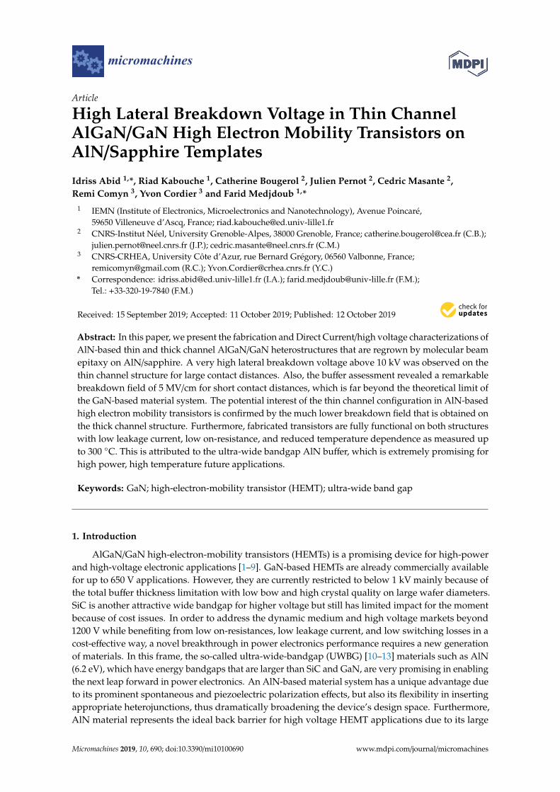
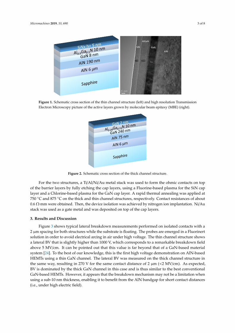
Figure 1 shows a schematic cross section of the AlN-based heterostructures grown by ammoniamolecular beam epitaxy (MBE). The first structure, referred to as the thin channel structure, includes a190 nm AlN buffer that was regrown on a 6 µm thick AlN-on-sapphire commercial template followedby a 8 nm thin GaN channel, a 10 nm AlGaN barrier layer with a high aluminum content (90%), and a5 nm in-situ SiN cap layer. The growths were performed in a Riber Compact 21T MBE system that wasequipped with 80 cc crucible effusion cells that were designed to supply a uniform flux of group IIIelements on 50 mm wafers [21]. After outgassing under high vacuum at 500 C, the AlN-on-sapphiretemplates were annealed under NH3 (flow rate 200 sccm) at 850 C prior to the growth of AlN bufferusing the same conditions at a growth rate of 100 nm/h. Then, the temperature was reduced to780 C in order to grow the rest of the structure, starting with the GaN channel. Based on previouscalibration samples, the growth rates of GaN and AlN were then adjusted to produce AlGaN barrierswith the desired Al content. While the structure with a 240 nm GaN channel and 29% Al barrierwas capped with a thin GaN layer in quite a standard procedure, which produced high performanceRadio Frequency HEMTs on silicon [22], the structure with 90% Al barrier was capped with a 5 nmSiN layer in-situ grown at 700 C using a silicon sublimation source (SUSI) from MBE Komponenten(Weil der Stadt, Germany). The crystal quality of AlN was assessed by X-ray diffraction (XRD) usingomega scans. Rocking curves around the symmetric (002) reflections are mainly sensitive to screwtype threading dislocations and asymmetric (101) reflections are sensitive to any type of threadingdislocations, edge, mixed, and screw type. The full widths at half maximum (FWHM) of AlN (002)and AlN (101) reflection peaks were estimated below 350 arcsec and 500 arcsec, respectively, for bothsamples, indicating a mean threading dislocation density in the range of fewer than 108/cm2. On theother hand, the signal of GaN reflections were too weak for the correct determination of (002) and (302)peak widths for the 8 nm channel, whereas they were evaluated at 450 arcsec and 1940 arcsec for the240 nm GaN layer, indicating a mean threading dislocation density in the range of fewer than 109/cm2.Interestingly, such values are in a similar range as 1,7 µm thick GaN layers were developed to producehigh performance HEMTs on silicon [22,23]. The 2DEG properties that were obtained by the Hall Effectmeasurements show a sheet carrier density of 1.9 × 1013 cm−2 and an electron mobility of 340 cm2/V·s.The rather low mobility can be attributed to the thin channel and/or the high Al content into the barrierlayer, which can still be optimized, with large room for improvement. A high resolution TransmissionElectron Microscopy picture of the active layers is also shown in Figure 1. Sharp interfaces and highmaterial quality are observed. The second structure (Figure 2), which was grown on a similar template,consists of a 240 nm thick GaN channel, a 10 nm AlGaN barrier (29% Al), and is capped with a 2 nmGaN layer. The 2DEG properties show a charge density of 1.1 × 1013 cm−2 and a higher electronmobility of 1500 cm2/V·s.
Micromachines 2019, 10, 690 3 of 8Micromachines 2019, 10, x 3 of 8
Figure 1. Schematic cross section of the thin channel structure (left) and high resolution Transmission Electron Microscopy picture of the active layers grown by molecular beam epitaxy (MBE) (right).
Figure 2. Schematic cross section of the thick channel structure.
For the two structures, a Ti/Al/Ni/Au metal stack was used to form the ohmic contacts on top of the barrier layers by fully etching the cap layers, using a Fluorine-based plasma for the SiN cap layer and a Chlorine-based plasma for the GaN cap layer. A rapid thermal annealing was applied at 750 °C and 875 °C on the thick and thin channel structures, respectively. Contact resistances of about 0.6 Ω·mm were obtained. Then, the device isolation was achieved by nitrogen ion implantation. Ni/Au stack was used as a gate metal and was deposited on top of the cap layers.
3. Results and Discussion
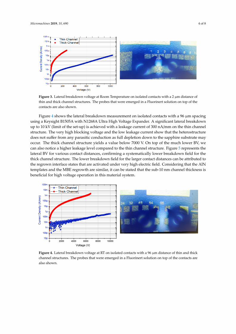
Figure 3 shows typical lateral breakdown measurements performed on isolated contacts with a 2 µm spacing for both structures while the substrate is floating. The probes are emerged in a Fluorinert solution in order to avoid electrical arcing in air under high voltage. The thin channel structure shows a lateral BV that is slightly higher than 1000 V, which corresponds to a remarkable breakdown field above 5 MV/cm. It can be pointed out that this value is far beyond that of a GaN-based material system [24]. To the best of our knowledge, this is the first high voltage demonstration on AlN-based HEMTs using a thin GaN channel. The lateral BV was measured on the thick channel structure in the same way, resulting in 270 V for the same contact distance of 2 µm (<2 MV/cm). As expected, BV is dominated by the thick GaN channel in this case and is thus similar to the best conventional GaN-based HEMTs. However, it appears that the breakdown mechanism may not be a limitation when using a sub-10 nm thickness, enabling it to benefit from the AlN bandgap for short contact distances (i.e., under high electric field).
Figure 1. Schematic cross section of the thin channel structure (left) and high resolution TransmissionElectron Microscopy picture of the active layers grown by molecular beam epitaxy (MBE) (right).
Micromachines 2019, 10, x 3 of 8
Figure 1. Schematic cross section of the thin channel structure (left) and high resolution Transmission Electron Microscopy picture of the active layers grown by molecular beam epitaxy (MBE) (right).
Figure 2. Schematic cross section of the thick channel structure.
For the two structures, a Ti/Al/Ni/Au metal stack was used to form the ohmic contacts on top of the barrier layers by fully etching the cap layers, using a Fluorine-based plasma for the SiN cap layer and a Chlorine-based plasma for the GaN cap layer. A rapid thermal annealing was applied at 750 °C and 875 °C on the thick and thin channel structures, respectively. Contact resistances of about 0.6 Ω·mm were obtained. Then, the device isolation was achieved by nitrogen ion implantation. Ni/Au stack was used as a gate metal and was deposited on top of the cap layers.
3. Results and Discussion
Figure 3 shows typical lateral breakdown measurements performed on isolated contacts with a 2 µm spacing for both structures while the substrate is floating. The probes are emerged in a Fluorinert solution in order to avoid electrical arcing in air under high voltage. The thin channel structure shows a lateral BV that is slightly higher than 1000 V, which corresponds to a remarkable breakdown field above 5 MV/cm. It can be pointed out that this value is far beyond that of a GaN-based material system [24]. To the best of our knowledge, this is the first high voltage demonstration on AlN-based HEMTs using a thin GaN channel. The lateral BV was measured on the thick channel structure in the same way, resulting in 270 V for the same contact distance of 2 µm (<2 MV/cm). As expected, BV is dominated by the thick GaN channel in this case and is thus similar to the best conventional GaN-based HEMTs. However, it appears that the breakdown mechanism may not be a limitation when using a sub-10 nm thickness, enabling it to benefit from the AlN bandgap for short contact distances (i.e., under high electric field).
Figure 2. Schematic cross section of the thick channel structure.
For the two structures, a Ti/Al/Ni/Au metal stack was used to form the ohmic contacts on topof the barrier layers by fully etching the cap layers, using a Fluorine-based plasma for the SiN caplayer and a Chlorine-based plasma for the GaN cap layer. A rapid thermal annealing was applied at750 C and 875 C on the thick and thin channel structures, respectively. Contact resistances of about0.6 Ω·mm were obtained. Then, the device isolation was achieved by nitrogen ion implantation. Ni/Austack was used as a gate metal and was deposited on top of the cap layers.
3. Results and Discussion
Figure 3 shows typical lateral breakdown measurements performed on isolated contacts with a2 µm spacing for both structures while the substrate is floating. The probes are emerged in a Fluorinertsolution in order to avoid electrical arcing in air under high voltage. The thin channel structure showsa lateral BV that is slightly higher than 1000 V, which corresponds to a remarkable breakdown fieldabove 5 MV/cm. It can be pointed out that this value is far beyond that of a GaN-based materialsystem [24]. To the best of our knowledge, this is the first high voltage demonstration on AlN-basedHEMTs using a thin GaN channel. The lateral BV was measured on the thick channel structure inthe same way, resulting in 270 V for the same contact distance of 2 µm (<2 MV/cm). As expected,BV is dominated by the thick GaN channel in this case and is thus similar to the best conventionalGaN-based HEMTs. However, it appears that the breakdown mechanism may not be a limitation whenusing a sub-10 nm thickness, enabling it to benefit from the AlN bandgap for short contact distances(i.e., under high electric field).
Micromachines 2019, 10, 690 4 of 8Micromachines 2019, 10, x 4 of 8
Figure 3. Lateral breakdown voltage at Room Temperature on isolated contacts with a 2 µm distance of thin and thick channel structures. The probes that were emerged in a Fluorinert solution on top of the contacts are also shown.
Figure 4 shows the lateral breakdown measurement on isolated contacts with a 96 µm spacing using a Keysight B1505A with N1268A Ultra High Voltage Expander. A significant lateral breakdown up to 10 kV (limit of the set-up) is achieved with a leakage current of 300 nA/mm on the thin channel structure. The very high blocking voltage and the low leakage current show that the heterostructure does not suffer from any parasitic conduction as full depletion down to the sapphire substrate may occur. The thick channel structure yields a value below 7000 V. On top of the much lower BV, we can also notice a higher leakage level compared to the thin channel structure. Figure 5 represents the lateral BV for various contact distances, confirming a systematically lower breakdown field for the thick channel structure. The lower breakdown field for the larger contact distances can be attributed to the regrown interface states that are activated under very high electric field. Considering that the AlN templates and the MBE regrowth are similar, it can be stated that the sub-10 nm channel thickness is beneficial for high voltage operation in this material system.
Figure 4. Lateral breakdown voltage at RT on isolated contacts with a 96 µm distance of thin and thick channel structures. The probes that were emerged in a Fluorinert solution on top of the contacts are also shown.
Figure 3. Lateral breakdown voltage at Room Temperature on isolated contacts with a 2 µm distance ofthin and thick channel structures. The probes that were emerged in a Fluorinert solution on top of thecontacts are also shown.
Figure 4 shows the lateral breakdown measurement on isolated contacts with a 96 µm spacingusing a Keysight B1505A with N1268A Ultra High Voltage Expander. A significant lateral breakdownup to 10 kV (limit of the set-up) is achieved with a leakage current of 300 nA/mm on the thin channelstructure. The very high blocking voltage and the low leakage current show that the heterostructuredoes not suffer from any parasitic conduction as full depletion down to the sapphire substrate mayoccur. The thick channel structure yields a value below 7000 V. On top of the much lower BV, wecan also notice a higher leakage level compared to the thin channel structure. Figure 5 represents thelateral BV for various contact distances, confirming a systematically lower breakdown field for thethick channel structure. The lower breakdown field for the larger contact distances can be attributed tothe regrown interface states that are activated under very high electric field. Considering that the AlNtemplates and the MBE regrowth are similar, it can be stated that the sub-10 nm channel thickness isbeneficial for high voltage operation in this material system.
Micromachines 2019, 10, x 4 of 8
Figure 3. Lateral breakdown voltage at Room Temperature on isolated contacts with a 2 µm distance of thin and thick channel structures. The probes that were emerged in a Fluorinert solution on top of the contacts are also shown.
Figure 4 shows the lateral breakdown measurement on isolated contacts with a 96 µm spacing using a Keysight B1505A with N1268A Ultra High Voltage Expander. A significant lateral breakdown up to 10 kV (limit of the set-up) is achieved with a leakage current of 300 nA/mm on the thin channel structure. The very high blocking voltage and the low leakage current show that the heterostructure does not suffer from any parasitic conduction as full depletion down to the sapphire substrate may occur. The thick channel structure yields a value below 7000 V. On top of the much lower BV, we can also notice a higher leakage level compared to the thin channel structure. Figure 5 represents the lateral BV for various contact distances, confirming a systematically lower breakdown field for the thick channel structure. The lower breakdown field for the larger contact distances can be attributed to the regrown interface states that are activated under very high electric field. Considering that the AlN templates and the MBE regrowth are similar, it can be stated that the sub-10 nm channel thickness is beneficial for high voltage operation in this material system.
Figure 4. Lateral breakdown voltage at RT on isolated contacts with a 96 µm distance of thin and thick channel structures. The probes that were emerged in a Fluorinert solution on top of the contacts are also shown.
Figure 4. Lateral breakdown voltage at RT on isolated contacts with a 96 µm distance of thin and thickchannel structures. The probes that were emerged in a Fluorinert solution on top of the contacts arealso shown.

Micromachines 2019, 10, 690 5 of 8Micromachines 2019, 10, x 5 of 8
Figure 5. Lateral breakdown voltage at RT on isolated contacts with a 96 µm distance of thin and thick channel structures. The probes that were in a Fluorinert solution on top of the contacts are also shown.
DC characteristics of both structures show fully functional devices, as seen in Figure 6 for both structures. For the thin channel structure, the off-state leakage current at VDS = 4 V is around 200 nA/mm and the static on-resistance RON scales are expected with the gate-drain distance to reach values below 15 mΩ·cm2 for a 5 µm distance. However, despite fully functional transistors with low leakage current and low on-resistance, a rather limited BV on transistors of about 600 V was measured, which is attributed to the non-optimized SiN passivation layer. On the other hand, in agreement with the buffer characteristics, more than two orders of magnitude higher off-state leakage current is observed on thick channel transistors.
Figure 6. Transfer characteristics (left) for thin and thick channel structures and output characteristics (right) of the thin channel structure at RT.
Figure 7 depicts the transfer characteristics at various temperatures for the thin and thick channel structures at VDS = 10 V. A low variation of the off-state leakage current and the threshold voltage (VTH) is observed up to 300 °C even though the thick channel structure delivers a higher leakage current level. It can be stressed that at such a high temperature, AlGaN/GaN HEMTs using standard (Al)GaN-based buffer layers generally show VTH shift and especially significant leakage current increase due to a higher charge conductivity within the buffer layers. Therefore, it appears that the use of AlN material as a buffer may enable it to push the temperature limitation of GaN-based transistors. Furthermore, as expected, the on-state current density drops with the temperature increase due to the decrease of the electron mobility, which is induced by increasing phonon scattering [25]. However, the current density degradation is lower in the case of the thin channel. This indicates that the channel temperature for the thin channel devices is lower under the same bias
Figure 5. Lateral breakdown voltage at RT on isolated contacts with a 96 µm distance of thin and thickchannel structures. The probes that were in a Fluorinert solution on top of the contacts are also shown.
DC characteristics of both structures show fully functional devices, as seen in Figure 6 for bothstructures. For the thin channel structure, the off-state leakage current at VDS = 4 V is around 200 nA/mmand the static on-resistance RON scales are expected with the gate-drain distance to reach values below15 mΩ·cm2 for a 5 µm distance. However, despite fully functional transistors with low leakage currentand low on-resistance, a rather limited BV on transistors of about 600 V was measured, which isattributed to the non-optimized SiN passivation layer. On the other hand, in agreement with the buffercharacteristics, more than two orders of magnitude higher off-state leakage current is observed onthick channel transistors.
Micromachines 2019, 10, x 5 of 8
Figure 5. Lateral breakdown voltage at RT on isolated contacts with a 96 µm distance of thin and thick channel structures. The probes that were in a Fluorinert solution on top of the contacts are also shown.
DC characteristics of both structures show fully functional devices, as seen in Figure 6 for both structures. For the thin channel structure, the off-state leakage current at VDS = 4 V is around 200 nA/mm and the static on-resistance RON scales are expected with the gate-drain distance to reach values below 15 mΩ·cm2 for a 5 µm distance. However, despite fully functional transistors with low leakage current and low on-resistance, a rather limited BV on transistors of about 600 V was measured, which is attributed to the non-optimized SiN passivation layer. On the other hand, in agreement with the buffer characteristics, more than two orders of magnitude higher off-state leakage current is observed on thick channel transistors.
Figure 6. Transfer characteristics (left) for thin and thick channel structures and output characteristics (right) of the thin channel structure at RT.
Figure 7 depicts the transfer characteristics at various temperatures for the thin and thick channel structures at VDS = 10 V. A low variation of the off-state leakage current and the threshold voltage (VTH) is observed up to 300 °C even though the thick channel structure delivers a higher leakage current level. It can be stressed that at such a high temperature, AlGaN/GaN HEMTs using standard (Al)GaN-based buffer layers generally show VTH shift and especially significant leakage current increase due to a higher charge conductivity within the buffer layers. Therefore, it appears that the use of AlN material as a buffer may enable it to push the temperature limitation of GaN-based transistors. Furthermore, as expected, the on-state current density drops with the temperature increase due to the decrease of the electron mobility, which is induced by increasing phonon scattering [25]. However, the current density degradation is lower in the case of the thin channel. This indicates that the channel temperature for the thin channel devices is lower under the same bias
Figure 6. Transfer characteristics (left) for thin and thick channel structures and output characteristics(right) of the thin channel structure at RT.
Figure 7 depicts the transfer characteristics at various temperatures for the thin and thick channelstructures at VDS = 10 V. A low variation of the off-state leakage current and the threshold voltage (VTH)is observed up to 300 C even though the thick channel structure delivers a higher leakage current level.It can be stressed that at such a high temperature, AlGaN/GaN HEMTs using standard (Al)GaN-basedbuffer layers generally show VTH shift and especially significant leakage current increase due to ahigher charge conductivity within the buffer layers. Therefore, it appears that the use of AlN materialas a buffer may enable it to push the temperature limitation of GaN-based transistors. Furthermore, asexpected, the on-state current density drops with the temperature increase due to the decrease of theelectron mobility, which is induced by increasing phonon scattering [25]. However, the current densitydegradation is lower in the case of the thin channel. This indicates that the channel temperature forthe thin channel devices is lower under the same bias conditions. This effect is probably due to the

Micromachines 2019, 10, 690 6 of 8
lower dislocation density at the GaN/AlN interface in the case of the thin layer, in turn reflecting thebenefit of the high AlN thermal conductivity [26,27]. Further experiments such as Infrared/Ramanthermography would be needed in order to fully confirm the thermal stability improvement.
Micromachines 2019, 10, x 6 of 8
conditions. This effect is probably due to the lower dislocation density at the GaN/AlN interface in the case of the thin layer, in turn reflecting the benefit of the high AlN thermal conductivity [26,27]. Further experiments such as Infrared/Raman thermography would be needed in order to fully confirm the thermal stability improvement.
Figure 7. Transfer characteristics at VDS = +10 V as a function of temperature (from 150 °C to 300 °C) of the thin channel structure (left) and the thick channel structure (right).
4. Conclusions
This work presents the fabrication and characterization of thin and thick channel AlGaN/GaN HEMTs grown on AlN/sapphire templates. Lateral buffer breakdown voltage assessment of the thin channel reveals a remarkable breakdown field of 5 MV/cm for short contact distances, which is far beyond the theoretical limits of a GaN-based material system. Furthermore, fabricated transistors are fully functional with low leakage current and low on-resistance. The use of a sub-10 nm ultrathin GaN channel may not be a limiting factor for the breakdown mechanism of transistors. Temperature measurements up to 300 °C show that the AlN buffer enables increased temperature stability of GaN-based transistors. When combined with a thin channel, the related transistors may deliver lower channel temperatures as compared to devices with thicker channels. Proper passivation and associated processing will allow us to take advantage of the properties offered by AlN-based devices, providing both low resistances and high voltages well above 1 kV.
Author Contributions: Device design, fabrication and characterization, I.A., R.K. and F.M., TEM images, C.B., Temperature measurements, J.P., C.M., R.C., Growth, Y.C., Writing-Original Draft Preparation, all co-authors.
Funding: This work is supported by the French RENATECH network and the French National grant ANR-17-CE05-00131 within the project called BREAKUP and ANR-11-LABX-0014 representing GaNeX: the “Investissements d’Avenir”.
Conflicts of Interest: The authors declare no conflict of interest.
References
1. Saito, W. Reliability of GaN-HEMTs for high-voltage switching applications. In Proceedings of the International Reliability Physics Symposium, Monterey, CA, USA, 10–14 April 2011.
2. Dogmus, E.; Zegaoui, M.; Medjdoub, F. GaN-on-silicon high-electron-mobility transistor technology with ultra-low leakage up to 3000 V using local substrate removal and AlN ultra-wide bandgap. Appl. Phys. Express 2018, 11, 034102.
3. Mishra, U.K.; Parikh, P.; Wu, Y.F. AlGaN/GaN HEMTs: An overview of device operation and applications. Proc. IEEE 2002, 90, 1022–1031.
Figure 7. Transfer characteristics at VDS = +10 V as a function of temperature (from 150 C to 300 C)of the thin channel structure (left) and the thick channel structure (right).
4. Conclusions
This work presents the fabrication and characterization of thin and thick channel AlGaN/GaNHEMTs grown on AlN/sapphire templates. Lateral buffer breakdown voltage assessment of the thinchannel reveals a remarkable breakdown field of 5 MV/cm for short contact distances, which is farbeyond the theoretical limits of a GaN-based material system. Furthermore, fabricated transistors arefully functional with low leakage current and low on-resistance. The use of a sub-10 nm ultrathinGaN channel may not be a limiting factor for the breakdown mechanism of transistors. Temperaturemeasurements up to 300 C show that the AlN buffer enables increased temperature stability ofGaN-based transistors. When combined with a thin channel, the related transistors may deliver lowerchannel temperatures as compared to devices with thicker channels. Proper passivation and associatedprocessing will allow us to take advantage of the properties offered by AlN-based devices, providingboth low resistances and high voltages well above 1 kV.
Author Contributions: Device design, fabrication and characterization, I.A., R.K. and F.M., TEM images, C.B.,Temperature measurements, J.P., C.M., R.C., Growth, Y.C., Writing-Original Draft Preparation, all co-authors.
Funding: This work is supported by the French RENATECH network and the French National grantANR-17-CE05-00131 within the project called BREAKUP and ANR-11-LABX-0014 representing GaNeX: the“Investissements d’Avenir”.
Conflicts of Interest: The authors declare no conflict of interest.
References
1. Saito, W. Reliability of GaN-HEMTs for high-voltage switching applications. In Proceedings of theInternational Reliability Physics Symposium, Monterey, CA, USA, 10–14 April 2011.
2. Dogmus, E.; Zegaoui, M.; Medjdoub, F. GaN-on-silicon high-electron-mobility transistor technology withultra-low leakage up to 3000 V using local substrate removal and AlN ultra-wide bandgap. Appl. Phys.Express 2018, 11, 034102. [CrossRef]
3. Mishra, U.K.; Parikh, P.; Wu, Y.F. AlGaN/GaN HEMTs: An overview of device operation and applications.Proc. IEEE 2002, 90, 1022–1031. [CrossRef]
4. Roccaforte, F.; Greco, G.; Fiorenza, P.; Iucolano, F. An Overview of Normally-Off GaN-Based High ElectronMobility Transistors. Materials 2019, 12, 1599. [CrossRef] [PubMed]

Micromachines 2019, 10, 690 7 of 8
5. Baliga, B.J. Gallium nitride devices for power electronic applications. Semicond. Sci. Technol. 2013, 28, 074011.[CrossRef]
6. Pavlidis, G.; Kim, S.H.; Abid, I.; Zegaoui, M.; Medjdoub, F.; Graham, S. The Effects of AlN and Copper BackSide Deposition on the Performance of Etched Back GaN/Si HEMTs. IEEE Electron Device Lett. 2019, 40,1060–1063. [CrossRef]
7. Ikeda, N.; Niiyama, Y.; Kambayashi, H.; Sato, Y.; Nomura, T.; Kato, S.; Yoshida, S. GaN Power Transistors onSi Substrates for Switching Applications. Proc. IEEE 2010, 98, 1151–1161. [CrossRef]
8. Kambayashi, H.; Satoh, Y.; Ootomo, S.; Kokawa, T.; Nomura, T.; Kato, S.; Chow, T.S. Over 100 A operationnormally-off AlGaN/GaN hybrid MOS-HFET on Si substrate with high-breakdown voltage. Solid-StateElectron. 2010, 54, 660–664. [CrossRef]
9. Herbecq, N.; Roch-Jeune, I.; Rolland, N.; Visalli, D.; Derluyn, J.; Degroote, S.; Germain, M.; Medjdoub, F.1900 V, 1.6 mΩ cm2 AlN/GaN-on-Si power devices realized by local substrate removal. Appl. Phys. Express2014, 7, 034103. [CrossRef]
10. Tsao, J.Y.; Chowdhury, S.; Hollis, M.A.; Jena, D.; Johnson, N.M.; Jones, K.A.; Kaplar, R.J.; Rajan, S.; Van deWalle, C.G.; Bellotti, E.; et al. Ultrawide-Bandgap Semiconductors: Research Opportunities and Challenges.Adv. Electron. Mater. 2018, 1, 1600501. [CrossRef]
11. Kaplar, R.J.; Allerman, A.A.; Armstrong, A.M.; Crawford, M.H.; Dickerson, J.R.; Fischer, A.J.; Baca, A.G.;Douglas, E.A. Review-Ultra-Wide-Bandgap AlGaN Power Electronic Devices. ECS J. Solid State Sci. Technol.2017, 6, Q3061. [CrossRef]
12. Razzak, T.; Xue, H.; Xia, Z.; Hwang, S.; Khan, A.; Lu, W.; Rajan, S. Ultra-wide band gap materials for highfrequency applications. In Proceedings of the IEEE MTT-S International Microwave Workshop Series onAdvanced Materials and Processes for RF and THz Applications (IMWS-AMP), Ann Arbor, MI, USA, 16–18July 2018.
13. Anderson, T.J.; Hite, J.K.; Ren, F. Ultra-Wide Bandgap Materials and Device. ECS J. Solid State Sci. Technol.2017, 6, Y1. [CrossRef]
14. Shealy, J.R.; Kaper, V.; Tilak, V.; Prunty, T.; Smart, J.A.; Green, B.; Eastman, L.F. An AlGaN/GaNhigh-electron-mobility transistor with an AlN sub-buffer layer. J. Phys. Condens. Matter 2002, 14, 3499.[CrossRef]
15. Yafune, N.; Hashimoto, S.; Akita, K.; Yamamoto, Y.; Tokuda, H.; Kuzuhara, M. AlN/AlGaN HEMTs on AlNsubstrate for stable high-temperature operation. Electron. Lett. 2014, 50, 211–212. [CrossRef]
16. Wu, Y.F.; Kapolnek, D.; Ibbetson, J.P.; Parikh, P.; Keller, B.P.; Mishra, U.K. Very-high power density AlGaN/GaNHEMTs. IEEE Trans. Electron Devices 2001, 48, 586–590.
17. Kinoshita, T.; Nagashima, T.; Obata, T.; Takashima, S.; Yamamoto, R.; Togashi, R.; Kumagai, Y.; Schlesser, R.;Collazo, R.; Koukitu, A.; et al. Fabrication of vertical Schottky barrier diodes on n-type freestanding AlNsubstrates grown by hydride vapor phase epitaxy. Appl. Phys. Exp. 2015, 8, 061003. [CrossRef]
18. Cahill, D.G. Analysis of heat flow in layered structures for time-domain thermoreflectance. Rev. Sci. Instrum.2004, 75, 5119–5122. [CrossRef]
19. Choi, S.R.; Kim, D.; Choa, S.H.; Lee, S.H.; Kim, J.K. Thermal Conductivity of AlN and SiC Thin Films. Int. J.Thermophys. 2006, 27, 896–905. [CrossRef]
20. Strite, S.; Morkoç, H. GaN, AlN, and InN: A review. J. Vac. Sci. Technol. B 1992, 10, 1237. [CrossRef]21. Cordier, Y.; Pruvost, F.; Semond, F.; Massies, J.; Leroux, M.; Lorenzini, P.; Chaix, C. Quality and uniformity
assessment of AlGaN/GaN Quantum Wells and HEMT heterostructures grown by molecular beam epitaxywith ammonia source. Phys. Stat. Sol. C 2006, 3, 2325–2328. [CrossRef]
22. Cordier, Y. Al(Ga)N/GaN high electron mobility transistors on silicon. Phys. Status Solidi A 2015, 212,1049–1058. [CrossRef]
23. Baron, N.; Cordier, Y.; Chenot, S.; Vennéguès, P.; Tottereau, O.; Leroux, M.; Semond, F.; Massies, J. The criticalrole of growth temperature on the structural and electrical properties of AlGaN/GaN high electron mobilitytransistor heterostructures grown on Si (111). J. Appl. Phys. 2009, 105, 033701. [CrossRef]
24. Rowena, I.B.; Selvaraj, S.L.; Egawa, T. Buffer thickness contribution to suppress vertical leakage current withhigh breakdown field (2.3 MV/cm) for GaN on Si. IEEE Electron Device Lett. 2011, 32, 1534–1536. [CrossRef]
25. Khan, M.N.; Ahmed, U.F.; Ahmed, M.M.; Rehman, S. An improved model to assess temperature-dependentDC characteristics of submicron GaN HEMTs. J. Comput. Electron. 2018, 17, 653–662. [CrossRef]
Micromachines 2019, 10, 690 8 of 8
26. Razeeb, K.M.; Dalton, E.; Cross, G.L.; Robinson, A.J. Present and future thermal interface materials forelectronic devices. Int. Mater. Rev. 2017, 63, 1–21. [CrossRef]
27. Cho, J.; Bozorg-Grayeli, E.; Altman, D.H.; Asheghi, M.; Goodson, K.E. Low Thermal Resistances at GaN–SiCInterfaces for HEMT Technology. IEEE Trans. Electron Devices Lett. 2012, 33, 378–380. [CrossRef]
© 2019 by the authors. Licensee MDPI, Basel, Switzerland. This article is an open accessarticle distributed under the terms and conditions of the Creative Commons Attribution(CC BY) license (http://creativecommons.org/licenses/by/4.0/).