Breakdown behavior of GaAs/AlGaAs HBT's
8
IEEE TRANSACTIONS ON ELECTRON DEVICES, VOL. 36. NO. IO, OCTOBER 1989 2165 Breakdown Behavior of GaAs/AlGaAs HBT's Abstract-Avalanche breakdown behavior at the collector junction of the GaAs/AIGaAs heterojunction bipolar transistor (HBT) has been studied. Junction breakdown characteristics displaying hard break- down, soft breakdown, and negative resistance breakdown behavior were observed and are interpreted by analysis of localized micro- plasma effects, uniform microplasma-free behavior, and associated current gain measurements. Light emission from the collector-base junction of the GaAs/AIGaAs HBT was observed and was used to in- vestigate breakdown uniformity. Using a simple punchthrough break- down model, the theoretical breakdown curves at different collector doping concentrations and thicknesses were computed and found to be in agreement with maximum breakdown voltages measured from de- vices displaying the most uniform junction breakdown. I. INTRODUCTION N recent years, GaAs /AlGaAs heterojunction bipolar I transistors (HBT's) have attracted considerable interest due to their high-speed performance and high current- handling capability. Encouraged by the potential micro- wave and digital applications of the GaAs/AlGaAs HBT, researchers have extensively investigated this device with respect to current gain [l], [2], and high-frequency per- formance [3], [4], suggesting various modifications in de- vice structures [5], [6] and fabrication processes [7]-[ l l]. In association with the experimental studies, researchers have also pursued modeling and simulation work [ 121- [ 151 to investigate various device parameter tradeoff con- siderations and to determine the limitations of the GaAs/AlGaAs HBT. Many exciting results have been re- ported, including super current gains h, = 12 500 [2], cutoff frequencies = 105 GHz [4], propagation delay times of 1.9 ps/gate in ECL ring oscillators [16], and continuous-wave output powers of 0.4 W at 10 GHz with 7-dB power gain in microwave power HBT's [ 171. The realization of good microwave transistor perfor- mance requires the development of optimum dc transistor performance, which can generally be satisfied indepen- dently of high-frequency requirements. Of primary im- portance is the construction of good p-n junctions, e.g., the p-n junctions must exhibit uniform microplasma-free hard breakdown behavior. Reverse-bias breakdown is a Manuscript received January 17, 1989; revised April 10, 1989. This work was supported by the Air Force Office of Scientific Research, the Strategic Defense Initiative Office through the Office of Naval Research under Contract N00014-86-05 13, and the National Science Foundation un- der Contract ECS-88-22406. J. J. Chen, J.-I. Chyi, and H. Morkog are with the Materials Research Laboratory, University of Illinois at Urbana-Champaign, Urbana, IL 61801. G. Gao is on leave with the Materials Research Laboratory, University of Illinois at Urbana-Champaign, Urbana, IL 61801. He is with the Reli- ability Physics Laboratory, Beijing Polytechnic University, Beijing, China. IEEE Log Number 8930061. significant limiting factor of the microwave power output of GaAs /AlGaAs HBT's; the device breakdown voltage is also an important figure of merit. Despite extensive in- vestigation of the GaAs / AlGaAs HBT, however, reports on its breakdown behavior have been limited. Under- standing the collector junction breakdown phenomenon and the breakdown mechanism is very important for de- signing, fabricating, and operating HBT's at microwave and millimeter frequencies. Collector junction behavior is governed by the choice of doping concentration, thickness, and junction geome- try and size. Optimal HBT design requires tradeoff be- tween these various parameters. Reducing collector dop- ing and increasing collector thickness can lead to high breakdown voltages, but cutoff frequencies and current- handling capabilities are thereby degraded. Alternatively, high collector doping and thin collector layers yield low breakdown voltages and large junction capacitances, which degrade maximum oscillation frequencies. Thus , selection of optimum collector doping and thickness should be tailored to the specified reverse voltage re- quired. This paper presents experimental results on the break- down behavior of GaAs/AlGaAs HBT's. The observa- tion of various breakdown characteristics is presented along with a report of light emission from avalanche breakdown in the reverse-biased GaAs collector-base junction. Some factors affecting the breakdown behavior are analyzed including dependence upon collector doping concentration and layer thicknesses. 11. GROWTH AND FABRICATION The HBT's studied in the present investigation were grown by molecular-beam epitaxy on Si-doped (100)-ori- ented GaAs substrates. A 0.5-1 .O-pm-thick n+-GaAs col- lector contact layer, doped 10" cmP3with Si, was grown first. The n-GaAs collector layer was then grown with variable thicknesses and doping concentrations. (The thickness and doping parameters of the various layers are identified with their corresponding collector-base break- down voltage in Table I.) The pf-GaAs base layer of the investigated structures was 0.1-0.3 pm thick, doped 10l8- lOI9 cmP3 with Be. Grading to A1,Gal -,As (x = 0.15- 0.3), a 0.15-0.2-pm-thick emitter was grown, doped 2 X 10'' to 5 x lo'* cm-3 with Si. Finally, a heavily doped 0.1-0.4-pm-thick n+-GaAs emitter cap layer was grown. After epitaxial growth, self-aligned HBT's with differ- ent device dimensions were fabricated by standard wet 0018-9383/89/1000-2165$01 .OO O 1989 IEEE
-
Upload
independent -
Category
Documents
-
view
3 -
download
0
Transcript of Breakdown behavior of GaAs/AlGaAs HBT's

IEEE TRANSACTIONS ON ELECTRON DEVICES, VOL. 36. NO. IO, OCTOBER 1989 2165
Breakdown Behavior of GaAs/AlGaAs HBT's
Abstract-Avalanche breakdown behavior at the collector junction of the GaAs/AIGaAs heterojunction bipolar transistor (HBT) has been studied. Junction breakdown characteristics displaying hard break- down, soft breakdown, and negative resistance breakdown behavior were observed and are interpreted by analysis of localized micro- plasma effects, uniform microplasma-free behavior, and associated current gain measurements. Light emission from the collector-base junction of the GaAs/AIGaAs HBT was observed and was used to in- vestigate breakdown uniformity. Using a simple punchthrough break- down model, the theoretical breakdown curves at different collector doping concentrations and thicknesses were computed and found to be in agreement with maximum breakdown voltages measured from de- vices displaying the most uniform junction breakdown.
I. INTRODUCTION N recent years, GaAs /AlGaAs heterojunction bipolar I transistors (HBT's) have attracted considerable interest
due to their high-speed performance and high current- handling capability. Encouraged by the potential micro- wave and digital applications of the GaAs/AlGaAs HBT, researchers have extensively investigated this device with respect to current gain [l] , [2], and high-frequency per- formance [3], [4], suggesting various modifications in de- vice structures [5], [6] and fabrication processes [7]-[ l l ] . In association with the experimental studies, researchers have also pursued modeling and simulation work [ 121- [ 151 to investigate various device parameter tradeoff con- siderations and to determine the limitations of the GaAs/AlGaAs HBT. Many exciting results have been re- ported, including super current gains h , = 12 500 [2], cutoff frequencies = 105 GHz [4], propagation delay times of 1.9 ps/gate in ECL ring oscillators [16], and continuous-wave output powers of 0.4 W at 10 GHz with 7-dB power gain in microwave power HBT's [ 171.
The realization of good microwave transistor perfor- mance requires the development of optimum dc transistor performance, which can generally be satisfied indepen- dently of high-frequency requirements. Of primary im- portance is the construction of good p-n junctions, e.g., the p-n junctions must exhibit uniform microplasma-free hard breakdown behavior. Reverse-bias breakdown is a
Manuscript received January 17, 1989; revised April 10, 1989. This work was supported by the Air Force Office of Scientific Research, the Strategic Defense Initiative Office through the Office of Naval Research under Contract N00014-86-05 13, and the National Science Foundation un- der Contract ECS-88-22406.
J . J. Chen, J.-I. Chyi, and H. Morkog are with the Materials Research Laboratory, University of Illinois at Urbana-Champaign, Urbana, IL 61801.
G. Gao is on leave with the Materials Research Laboratory, University of Illinois at Urbana-Champaign, Urbana, IL 61801. He is with the Reli- ability Physics Laboratory, Beijing Polytechnic University, Beijing, China.
IEEE Log Number 8930061.
significant limiting factor of the microwave power output of GaAs /AlGaAs HBT's; the device breakdown voltage is also an important figure of merit. Despite extensive in- vestigation of the GaAs / AlGaAs HBT, however, reports on its breakdown behavior have been limited. Under- standing the collector junction breakdown phenomenon and the breakdown mechanism is very important for de- signing, fabricating, and operating HBT's at microwave and millimeter frequencies.
Collector junction behavior is governed by the choice of doping concentration, thickness, and junction geome- try and size. Optimal HBT design requires tradeoff be- tween these various parameters. Reducing collector dop- ing and increasing collector thickness can lead to high breakdown voltages, but cutoff frequencies and current- handling capabilities are thereby degraded. Alternatively, high collector doping and thin collector layers yield low breakdown voltages and large junction capacitances, which degrade maximum oscillation frequencies. Thus , selection of optimum collector doping and thickness should be tailored to the specified reverse voltage re- quired.
This paper presents experimental results on the break- down behavior of GaAs/AlGaAs HBT's. The observa- tion of various breakdown characteristics is presented along with a report of light emission from avalanche breakdown in the reverse-biased GaAs collector-base junction. Some factors affecting the breakdown behavior are analyzed including dependence upon collector doping concentration and layer thicknesses.
11. GROWTH AND FABRICATION The HBT's studied in the present investigation were
grown by molecular-beam epitaxy on Si-doped (100)-ori- ented GaAs substrates. A 0.5-1 .O-pm-thick n+-GaAs col- lector contact layer, doped 10" cmP3 with Si, was grown first. The n-GaAs collector layer was then grown with variable thicknesses and doping concentrations. (The thickness and doping parameters of the various layers are identified with their corresponding collector-base break- down voltage in Table I.) The pf-GaAs base layer of the investigated structures was 0.1-0.3 pm thick, doped 10l8- l O I 9 cmP3 with Be. Grading to A1,Gal -,As (x = 0.15- 0.3), a 0.15-0.2-pm-thick emitter was grown, doped 2 X 10'' to 5 x lo'* cm-3 with Si. Finally, a heavily doped 0.1-0.4-pm-thick n+-GaAs emitter cap layer was grown.
After epitaxial growth, self-aligned HBT's with differ- ent device dimensions were fabricated by standard wet
0018-9383/89/1000-2165$01 .OO O 1989 IEEE
2166 IEEE TRANSACTIONS ON ELECTRON DEVICES, VOL. 36, NO. IO, OCTOBER 1989
TABLE I COLLECTOR-BASE BREAKDOWN VOLTAGES
Layer Collector Base Average Maximum Calculated # Thickness Doping Thidtness Doping BVcso BVcso BVceo
(pm) (cm-9 (pm) (cm-3) (Volts) (Volts) (Volts)
1 0.3 7x10” 0.3 7x10“ 5.5 6.3 2 0.3 5 ~ 1 0 ’ ~ 0.1 1x10¹⁹ 5.2 6.7 6.8 3 0.3 2x101’ 0.15 2x10” 7.8 10.7 8.0 4 0.3 5 ~ 1 0 ’ ~ 0.2 2 ~ 1 0 ’ ~ 8.2 9.4 13.7 5 0.4 5 ~ 1 0 ’ ~ 0.2 2 ~ 1 0 ’ ~ 13.5 16.2 16.8 6 0.5 5x10L6 0.1 3 ~ 1 0 ’ ~ 15.6 16.3 20.2 7 0.8 2 ~ 1 0 ’ ~ 0.15 1 ~ 1 0 ~ ~ 25.0 26.0 31.0
Emitter
I 0.2jm p+GaAs I ~
0.4pm n-GaAs Collector
l.Ojrm n+GaAs
n+GaAs Substrate
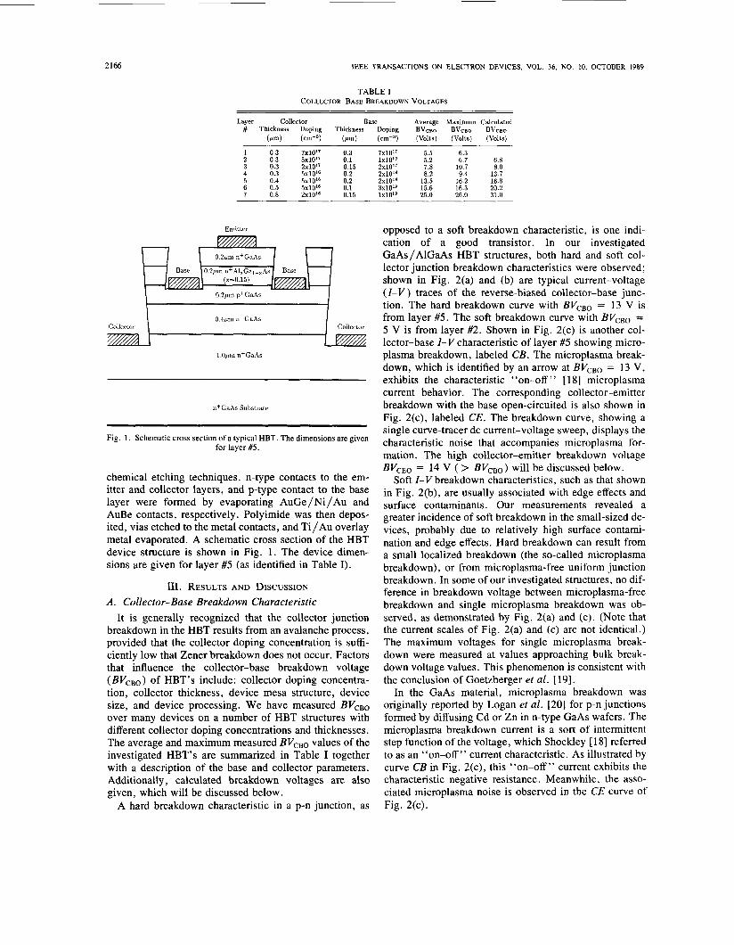
Fig. 1 . Schematic cross section of a typical HBT. The dimensions are given for layer #5.
chemical etching techniques. n-type contacts to the em- itter and collector layers, and p-type contact to the base layer were formed by evaporating AuGe/Ni/Au and AuBe contacts, respectively. Polyimide was then depos- ited, vias etched to the metal contacts, and Ti/Au overlay metal evaporated. A schematic cross section of the HBT device structure is shown in Fig. 1. The device dimen- sions are given for layer #5 (as identified in Table I).
111. RESULTS AND DISCUSSION A. Collector-Base Breakdown Characteristic
It is generally recognized that the collector junction breakdown in the HBT results from an avalanche process, provided that the collector doping concentration is suffi- ciently low that Zener breakdown does not occur. Factors that influence the collector-base breakdown voltage ( B V C B O ) of HBT’s include: collector doping concentra- tion, collector thickness, device mesa structure, device size, and device processing. We have measured B V C B O
over many devices on a number of HBT structures with different collector doping concentrations and thicknesses. The average and maximum measured BVcBo values of the investigated HBT’s are summarized in Table I together with a description of the base and collector parameters. Additionally, calculated breakdown voltages are also given, which will be discussed below.
A hard breakdown characteristic in a p-n junction, as
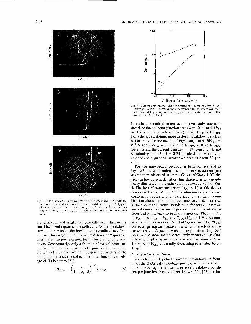
opposed to a soft breakdown Characteristic, is one indi- cation of a good transistor. In our investigated GaAs/AlGaAs HBT structures, both hard and soft col- lector junction breakdown characteristics were observed; shown in Fig. 2(a) and (b) are typical current-voltage ( I - V ) traces of the reverse-biased collector-base junc- tion. The hard breakdown curve with BVC-0 = 13 V is from layer #5. The soft breakdown curve with B V C B O = 5 V is from layer #2. Shown in Fig. 2(c) is another col- lector-base I-V characteristic of layer #5 showing micro- plasma breakdown, labeled CB. The microplasma break- down, which is identified by an arrow at BVcB0 = 13 V, exhibits the characteristic “on-off ” [ 181 microplasma current behavior. The corresponding collector-emitter breakdown with the base open-circuited is also shown in Fig. 2(c), labeled CE. The breakdown curve, showing a single curve-tracer dc current-voltage sweep, displays the characteristic noise that accompanies microplasma for- mation. The high collector-emitter breakdown voltage B V c E O = 14 V ( > B V C B O ) will be discussed below.
Soft I-V breakdown characteristics, such as that shown in Fig. 2(b), are usually associated with edge effects and surface contaminants. Our measurements revealed a greater incidence of soft breakdown in the small-sized de- vices, probably due to relatively high surface contami- nation and edge effects. Hard breakdown can result from a small localized breakdown (the so-called microplasma breakdown), or from microplasma-free uniform junction breakdown. In some of our investigated structures, no dif- ference in breakdown voltage between microplasma-free breakdown and single microplasma breakdown was ob- served, as demonstrated by Fig. 2(a) and (c). (Note that the current scales of Fig. 2(a) and (c) are not identical.) The maximum voltages for single microplasma break- down were measured at values approaching bulk break- down voltage values. This phenomenon is consistent with the conclusion of Goetzberger et a l . [19].
In the GaAs material, microplasma breakdown was originally reported by Logan et a l . [20] for p-n junctions formed by diffusing Cd or Zn in n-type GaAs wafers. The microplasma breakdown current is a sort of intermittent step function of the voltage, which Shockley [ 181 referred to as an “on-off” current characteristic. As illustrated by curve CB in Fig. 2(c), this “on-off ” current exhibits the characteristic negative resistance. Meanwhile, the asso- ciated microplasma noise is observed in the CE curve of Fig. 2(c).

2167
The results of Goe ticms suggest that rri
EBT.
The avd n fa be approximated by
ransistors, avalanche
2168 IEEE TRANSACTIONS ON ELECTRON DEVICES, VOL. 36, NO. IO, OCTOBER 1989
Fig. 3. I-V characteristics for collector-emitter breakdown ( CE ) with the base open-circuited and collector-base breakdown (CB): (a) Typical Characteristic, BV,,, ( = 6 V ) < BV,,,,. (b) Low-gain ( h , < 1 ) char- acteristic, BV,,, > BV,,,. ic) Characteristic of (b) at high current (high gain).
multiplication and breakdown generally occur first over a small localized region of the collector. As the breakdown current is increased, the breakdown is confined to a lim- ited area for single microplasma breakdown or “spreads” over the entire junction area for uniform junction break- down. Consequently, only a fraction of the collector cur- rent is multiplied by the avalanche process. Defining 6 as the ratio of area over which multiplication occurs to the total junction area, the collector-emitter breakdown volt- age of ( 1) becomes [2 11
1 / ! I
BvCEO = ( + hFE *) BvCBO. ( 5 1
0.1 1- 0.1 1 .o 10 1
Collector Currerit (mA) 0
Fig. 4. Current gain versus collector current for (curve a ) layer #4 and (curve b) layer #3. Curves a and B correspond to the breakdown char- acteristics of Fig. 2(a), and Fig. 2(b) and (c), respectively. Notice that hF,- < 1 fort, < 1 mA.
If avalanche multiplication occurs over only one-hun- dredth of the collector junction area ( 6 = and if hFE = 10 (current gain at low current), then BV,,, = BVcBO. For a device exhibiting more uniform breakdown, such as is illustrated for the device of Figs. 3(a) and 4, BVCBO = 8.3 V and BVCEO = 6.0 V give BVcEo = 0.72 BVcBo. Determining the current gain h, = 10 from Fig. 4, and substituting into ( 5 ) , 6 = 0.34 is calculated, which cor- responds to a junction breakdown area of about 30 per- cent.
For the unexpected breakdown behavior realized in layer #3, the explanation lies in the serious current gain degradation observed in these GaAs /AlGaAs HBT de- vices at low current densities: this characteristic is graph- ically illustrated in the gain versus current curve b of Fig. 4. The loss of transistor action (hFE < 1 ) in this device is observed for IC < 1 mA: this situation arises from re- combination at the emitter-base junction, surface recom- bination about the emitter-base junction, and/or serious surface leakage currents. In this case, the breakdown volt- age relation of ( 5 ) is no longer valid as the transistor is described by the back-to-back p-n junctions: BVcEo = V c ~
sistor action occurs ( A F E > 1) at higher currents, BVCEO decreases giving the negative resistance characteristic dis- cussed above. Agreeing with our explanation, Fig. 3(c) does indeed show the collector-emitter breakdown char- acteristic displaying negative resistance behavior at I , - 1 mA, with VCEo eventually decreasing to a value below
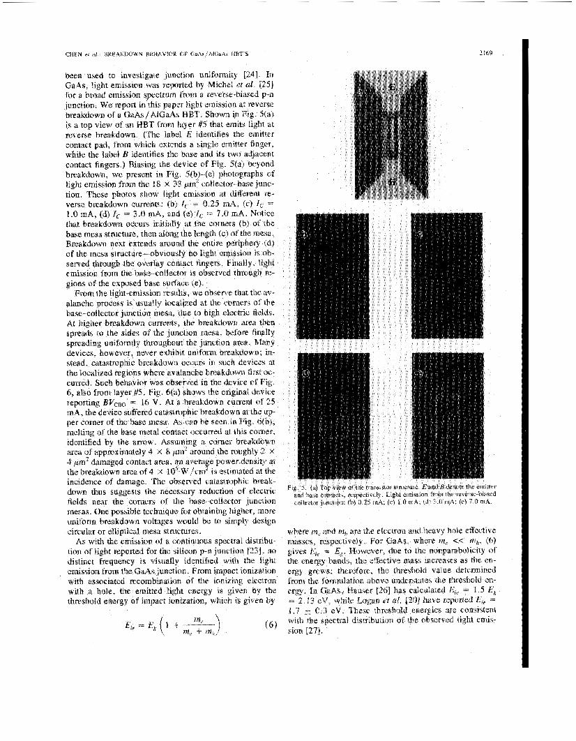
C. Light-Emission Study As with silicon bipolar transistors, breakdown uniform-
ity of the GaAs collector-base junction is of considerable importance. Light emission at reverse breakdown of sili- con p-n junctions has long been known [22], [23] and has
+ VBE = BVcBO + Vp,, > BVCBO ( VB, = 1 V ) . AS tran-
vCBO.
2170 IEEE TRANSACTIONS ON ELECTRON DEVICES, VOL. 36, NO. IO. OCTOBER 1989
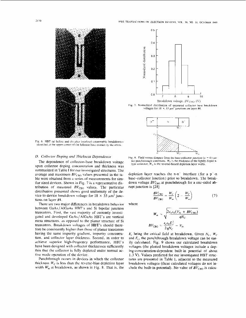
Fig. 6 . HBT (a) before and (b) after localized catastrophic breakdown- identified at the upper corner of the leftmost base contact by the arrow.
D. Collector Doping und Thickness Dependence The dependence of collector-base breakdown voltage
upon collector doping concentration and thickness was summarized in Table I for our investigated structures. The average and maximum BVcBo values presented in the ta- ble were obtained from a series of measurements for sim- ilar sized devices. Shown in Fig. 7 is a representative dis- tribution of measured BVcBo values. The particular distribution presented shows good uniformity of the de- vice-to-device breakdown voltage for 18 X 33 pm2 junc- tions on layer #4.
There are two major differences in breakdown behavior between GaAs/AlGaAs HBT’s and Si bipolar junction transistors. First, the vast majority of currently investi- gated and developed GaAs/AlGaAs HBT’s are vertical mesa structures, as opposed to the planar structure of Si transistors. Breakdown voltages of HBT’s should there- fore be consistently higher than those of planar transistors having the same impurity gradient, impurity concentra- tion, and collector layer thickness. Second, in order to achieve superior high-frequency performance, HBT’s have been designed with collector thicknesses sufficiently thin that the collector is fully depleted under normal ac- tive mode operation of the device.
Punchthrough occurs in devices in which the collector thickness Wc is less than the reverse-bias depletion layer width W,,, at breakdown, as shown in Fig. 8 . That is, the
7 8 9 1 0
Breakdown voltage, BVcoo (V)
voltages for 18 X 33 pm2 junctions on layer #4. Fig. 7. Normalized distribution of measured collector-base breakdown
Fig. 8. Field versus distance from the base-collectorjunction ( x = 0 ) un- der punchthrough conditions. W , is the thickness of the lightly doped n- type collector; W,n is the reverse-biased depletion layer width.
depletion layer reaches the n-n+ interface (for a p+-n base-collector junction) prior to breakdown. The break- down voltage BVkBo at punchthrough for a one-sided ab- rupt junction is [28]
(7)
where
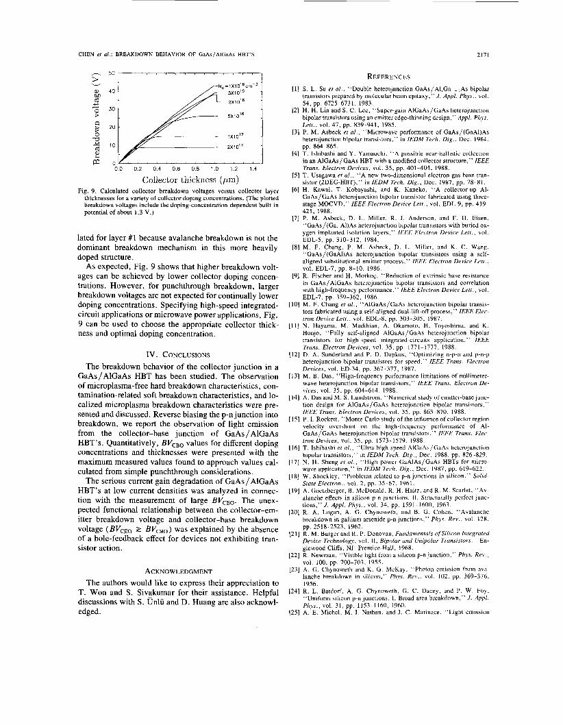
E, being the critical field at breakdown. Given N,, Wc and E,, the punchthrough breakdown voltage can be eas- ily calculated. Fig. 9 shows our calculated breakdown voltages (the plotted breakdown voltages include a dop- ing-concentration-dependent built-in potential of about 1 .3 V). Values predicted for our investigated HBT struc- tures are presented in Table I, adjacent to the measured breakdown voltages (these calculated voltages do not in- clude the built-in potential). No value of BvCBo is calcu-
CHEN er al . : BREAKDOWN BEHAVIOR OF GaAs/AIGaAs HBT’S 2171
40
30
20
10
0 0.0 0.2 0.4 0.6 0.8 1.0 1.2 1.4
Collector thickness (,urn) Fig. 9 . Calculated collector breakdown voltages versus collector layer
thicknesses for a variety of collector doping concentrations. (The plotted breakdown voltages include the doping-concentration-dependent built-in potential of about 1.3 V.)
lated for layer #1 because avalanche breakdown is not the dominant breakdown mechanism in this more heavily doped structure.
As expected, Fig. 9 shows that higher breakdown volt- ages can be achieved by lower collector doping concen- trations. However, for punchthrough breakdown, larger breakdown voltages are not expected for continually lower doping concentrations. Specifying high-speed integrated- circuit applications or microwave power applications, Fig. 9 can be used to choose the appropriate collector thick- ness and optimal doping concentration.
IV. CONCLUSIONS The breakdown behavior of the collector junction in a
GaAs/AlGaAs HBT has been studied. The observation of microplasma-free hard breakdown characteristics, con- tamination-related soft breakdown characteristics, and lo- calized microplasma breakdown characteristics were pre- sented and discussed. Reverse biasing the p-n junction into breakdown, we report the observation of light emission from the collector-base junction of GaAs /AlGaAs HBT’s. Quantitatively, WcB0 values for different doping concentrations and thicknesses were presented with the maximum measured values found to approach values cal- culated from simple punchthrough considerations.
The serious current gain degradation of GaAs / AlGaAs HBT’s at low current densities was analyzed in connec- tion with the measurement of large BVcEO. The unex- pected functional relationship between the collector-em- itter breakdown voltage and collector-base breakdown voltage (BVcEO 2 BVcBo) was explained by the absence of a hole-feedback effect for devices not exhibiting tran- sistor action.
ACKNOWLEDGMENT The authors would like to express their appreciation to
T. Won and S. Sivakumar for their assistance. Helpful discussions with S. Unlu and D. Huang are also acknowl- edged.
REFERENCES [ I ] S . L. Su et a l . . “Double heterojunction GaAs/AI,Ga, -,As bipolar
transistors prepared by molecular beam epitaxy,” J . Appl. Phys., vol.
[2] H. H. Lin and S. C. Lee, “Super-gain AIGaAs/GaAs heterojunction bipolar transistors using an emitter edge-thinning design,” Appl. Phys. Lett., vol. 47, pp. 839-941, 1985.
[3] P. M. Asbeck et a l . , “Microwave performance of GaAs/(GaAl)As heterojunction bipolar transistors,” in IEDM Tech. D i g . , Dec. 1984,
[4] T. Ishibashi and Y. Yamauchi, “A possible near-ballistic collection in an AIGaAs/GaAs HBT with a modified collector structure,” IEEE Trans. Electron Devices, vol. 35, pp. 401-404, 1988.
[5] T. Usagawa et a l . , “A new two-dimensional electron gas base tran- sistor (2DEG-HBT),” in IEDM Tech. Dig. , Dec. 1987, pp. 78-81.
[6] H. Kawai, T. Kobayashi, and K. Kaneko, “A collector-up Al- GaAs/GaAs heterojunction bipolar transistor fabricated using three- stage MOCVD,” IEEE Electron Device Lett., vol. EDL-9, pp. 419- 421, 1988.
[7] P. M. Asbeck, D. L. Miller, R. J. Anderson, and F. H. Eisen, “GaAs/(Ga, A1)As heterojunction bipolar transistors with buried ox- ygen implanted isolation layers,” IEEE Electron Device Lett., vol. EDL-5, pp. 310-312, 1984.
[8] M. F. Chang, P. M. Asbeck, D. L. Miller, and K. C . Wang, “GaAs/(GaAI)As heterojunction bipolar transistors using a self- aligned substitutional emitter process,” IEEE Electron Device Lett. ,
[9] R. Fischer and H. Morkoq, “Reduction of extrinsic base resistance in GaAs/ AlGaAs heterojunction bipolar transistors and correlation with high-frequency performance,” IEEE Electron Device Lett., vol.
[IO] M. F . Chang et a l . , “AIGaAs/GaAs heterojunction bipolar transis- tors fabricated using a self-aligned dual-lift-off process,” IEEE Elec- tron Device Lett . , vol. EDL-8, pp. 303-305, 1987.
[ l l ] N. Hayama, M. Madihian, A. Okamoto, H. Toyoshima, and K. Honjo, “Fully self-aligned AlGaAs /GaAs heterojunction bipolar transistors for high-speed integrated-circuits application,” IEEE Trans. Electron Devices, vol. 35, pp. 1771-1777, 1988.
[I21 D. A. Sunderland and P. D. Dapkus. “Optimizing n-p-n and p-n-p heterojunction bipolar transistors for speed, ” IEEE Trans. Electron Devices, vol. ED-34, pp. 367-377, 1987.
(131 M. B. Das, “High-frequency performance limitations of millimeter- wave heterojunction bipolar transistors,” IEEE Trans. Electron De- vices, vol. 35, pp. 604-614, 1988.
[14] A. Das and M. S . Lundstrom, “Numerical study of emitter-base junc- tion design for AIGaAs/GaAs heterojunction bipolar transistors,” IEEE Trans. Electron Devices, vol. 35, pp. 863-870, 1988.
151 P. I. Rockett, “Monte Carlo study of the influence of collector region velocity overshoot on the high-frequency performance of Al- GaAs/GaAs heterojunction bipolar transistors,” IEEE Trans. Elec- tron Devices, vol. 35, pp. 1573-1579, 1988.
161 T. Ishibashi et a l . , “Ultra-high speed AIGaAs/GaAs heterojunction bipolar transistors,” in IEDM Tech. Dig . , Dec. 1988, pp. 826-829.
171 N. H. Sheng et a l . , “High power GaAlAs/GaAs HBTs for micro- wave application,” in IEDM Tech. Dig. , Dec. 1987, pp. 619-622.
[I81 W. Shockley, “Problems related to p-n junctions in silicon,’’ Solid- State Electron., vol. 2, pp. 35-67, 1961.
[I91 A. Goetzberger. B. McDonald, R. H. Haitz, and R. M. Scarlet, “Av- alanche effects in silicon p-n junctions. 11. Stnrcturally perfect junc- t ions,”J. Appl. Phys., vol. 34, pp. 1591-1600, 1963.
[20] R. A. Logan, A. G. Chynoweth, and B. G. Cohen, “Avalanche breakdown in gallium arsenide p-n junctions,” Phys. Rev., vol. 128,
[21] R. M. Burger and R. P. Donovan, Fundamentals of Silicon Integrated Device Technology, vol. 11, Bipolar and Unipolar Transistors. En- glewood Cliffs, NJ: Prentice-Hall, 1968.
[22] R. Newman, “Visible light from a silicon p-n junction,” Phys. Rev., vol. 100, pp. 700-703, 1955.
[23] A. G. Chynoweth and K . G. McKay, “Photon emission from ava- lanche breakdown in silicon,” Phys. Rev., vol. 102, pp. 369-376, 1956.
[24] R. L. Batdorf, A. G. Chynoweth, G. C. Dacey, and P. W. Foy, “Uniform silicon p-n junctions. I. Broad area breakdown,” J . Appl.
[25] A. E. Michel, M. I . Nathan, and J . C. Marinace, “Light emission
54, pp. 6725-6731, 1983.
pp. 864-865.
vol. EDL-7, pp. 8-10, 1986.
EDL-7, pp. 359-362, 1986.
pp. 2518-2523, 1962.
Phys., vol. 31, pp. 1153-1160, 1960.
2172 IEEF. TRANSACTIONS ON ELECTRON DEVICES. VOL. 36, NO. IO, OCTOBER 1989
from reverse biased GaAs and InP p-n junctions.” J . Appl. Phys . , vol. 35, pp. 3543-3547. 1964. J . R. Hauser, “Threshold energy for avalanche multiplication in semiconductors,” J . Appl. Phys.. vol. 37. pp. 507-509. 1966. J . Chen et a l . , “Photon emission from avalanche breakdown in the collector junction of GaAs/AlGaAs HBT’s,” Appl. Phys. Lett., vol. 55, pp. 374-376, 1989. S . M. Sze, Seiniconductor Device Physics and Technology. New York: Wiley. 1985.
*
James J . Chen (S‘87) received the B.A. degree in physics from the University o f California, Berkeley, in 1985 and the M.S.E.E. degree from the University of Illinois at Urbana-Champaign in 1987. He is currently working toward the Ph.D. degree in electrical engineering at the University of Illinois. His research interests include the fab- rication, characterization and modeling of semi- conductor devices.
Electronics, a council member of the Reliability Research Society of the Chinese Electrotechnical Institute, and a Fellow of the Beijing Scientist and Engineer Association. He is listed in Who’s Who of Chinese Contem- porary Inventors and Who k Who of Chinese Sc ien t imfrom the Ancient to the Con tempo r(i ry
* Jen-Inn Chyi was born in Taiwan, Republic of China, in 1959. He received the B.S . and M.S. degrees in electrical engineering from National Tsing-Hua University, Hsinchu, Taiwan, in 1982 and 1984, respectively. He is currently working toward the Ph.D. degree in electrical engineering at the University of Illinois at Urbana-Cham- paign.
From 1982 to 1984, he was a Research Assis- tant at National Tsing-Hua University, where he worked on MOCVD. His current research inter-
ests are in the areas of MBE growth, fabrication. and characterization of 111-V compound semiconductor devices.
Mr. Chyi is a member of Phi Tau Phi. * *
Guang-bo Gao (SM’86) was born in Shenyang. China. on January 5. 1941. He graduated from the Department of Radio and Electronics Science, Tsinghua University, Beijing. in 1965, specialir- ing in semiconductor devices and physics.
In 1965. he joined Beijing Polytechnic Univer- sity. He is currently a Professor in the Department of Radio and Electronics and the Director of the Reliability Physics Laboratory at Beijing Poly- technic University. Since 1970. he has been work- ing on reliability physics, microwave power tran-
sistors, thermal and electrical models of semiconductor devices. thermal failure and thermal design studies of power devices. ohmic contact and metallization electromigration, and heterojunction device physics. He has authored or coauthored over 40 research articles and a research book en- titled Reliuhility Physics ofSemiconducror Devices. Since July of 1988, he has worked with Prof. H. Morkoq as a Visiting Scientist at the University of Illinois at Urbana-Champaign.
Mr. Gao was twice awarded the National Invention Prize of the P.R.C. in 1983 and 1984. and nine times the Science and Technology Prize of Beijing and the Ministry of Electronic Industry from 1979 to 1987. for contributions to power semiconductor devices and reliability ph) sics. He received four best paper awards from the Beijing Science and Technology Committee and the R & QC Society of the Chinese Institute of Electronics in 1980 and 1986-1988. He was awarded the title of Distinguished Na- tional Scientist of P.R.C. in 1986. He is the deputy director of the Reli- ability Physics Group of the R & QC Society of the Chinese Institute of
Hadis Morkoc (S’72-M’76-SM’79-F’87) re- ceived the B S E E. and M S E E degrees from the Istanbul Technicdl University, Turkey, in 1968 dnd 1969, respectively He began his Ph D stud ies at Michigan State University in 1971 and later transferred to Cornel1 University where he re- ceived the Ph D degree in electrical engineering in 1975 His dissertation topic dealt with liquid phase epitaxy of GaAs FET’s
He was employed at Varian Associates, Palo Alto, CA, trom 1976 to 1978, where he was heav-
i ly involved in various novel FET structure5 He has held visiting positions at AT&T Bell Ldboratorm (1978-1979), and the Calitomia Institute of Technology and Jet Propulsion Laboratory (1987-1988) Since 1978, he ha\ been with the University of Illinois pursuing research in heterostructure devices dnd material5 He has authored, coauthored, or edited one book (pending). 9 book chapters and proceedings, some 500 technical journal articles. 100 conference papers, dnd 40 technical reports
Dr Morkoq is d Fellow of the American Association for the Advance- ment of Science, d Fellow of the American Physical Society, a member of the Materid1 Research Society. a member of the Optical Society of Amer- icd, d lite member of Sigma Xi. a member of Eta Kdppa Nu, and a life member of Phi Kdppa Phi He is listed in who'^ Who in the Midwest, Attierican Men wid Wonien in Science, Who’s Who i n Engineering, and Interiiutiorial M m of Ac hiel emeiit. He received Electronics Letters Best Paper Awdrd in 1978 for his work on InGaAsP FET’s