Cisco Aironet 1550 Series Outdoor Mesh Access Point Power ...
Upload
khangminh22Category
view
1download
0
ErAs:In(Al)GaAs photoconductors for
1550 nm-based Terahertz time domain
spectroscopy systems
Vom Fachbereich Elektrotechnik und Informationstechnikder Technischen Universitat Darmstadt
zur Erlangung des akademischen Grades einesDoktor-Ingenieurs (Dr.-Ing.)
genehmigte
Dissertation
von
M.Sc.
Uttam Nandi
Referent: Prof. Dr. Sascha PreuKorreferent: Prof. Dr. Clara Saraceno
Tag der Einreichung: 16 Marz, 2021Tag der mundlichen Prufung: 30 Juli, 2021
D17Darmstadt 2021

Nandi, Uttam: ErAs:In(Al)GaAs photoconductors for 1550 nm-based Terahertz timedomain spectroscopy systemsDarmstadt, Technische Universitat Darmstadt,Jahr der Veroffentlichung der Dissertation auf TUprints: 2021URN: urn:nbn:de:tuda-tuprints-194070URL: https://tuprints.ulb.tu-darmstadt.de/id/eprint/19407Tag der Einreichung: 16.03.2021Tag der mundlichen Prufung: 30.07.2021Veroffentlicht unter CC BY-NC-ND 4.0 Internationalhttps://creativecommons.org/licenses/by-nc-nd/4.0/
2

Abstract
ErAs:In(Al)GaAs photoconductors have proven to be outstanding devices for pho-tonic terahertz (0.1 THz-10 THz) generation and detection. These superlatticesare composed of ErAs, InGaAs and InAlAs layers, grown by Molecular Beam Epi-taxy. This thesis presents the so far most detailed material characterization of thesephotoconductor materials followed by an investigation of THz performance. Thevariation of the material properties as a function of the ErAs concentration andthe superlattice structure is discussed for both emitter and receiver materials. In-frared spectroscopy shows an absorption coefficient in the range of 4700-6600 cm−1
at 1550 nm, with shallow absorption edges towards longer wavelengths caused byabsorption by ErAs precipitates. The carrier lifetime of the material was obtainedusing differential transmission measurements. The carrier dynamics also featured abias-dependent bi-exponential decay, which has been described by a proposed theo-retical modelling. Hall measurements show that samples with only 0.8 monolayers(ML) of compensation-doped ErAs precipitates (p-delta-doped at 5×1013 cm−2) withInAlAs spacer layer featured a carrier concentration of 3.6±0.4×1012 cm−3 which isalmost reaching the intrinsic carrier concentration of InGaAs. The IV characteristicsfeatured a resistance in the range of ∼10-20 MΩ and high breakdown field strengthsbeyond 100 kV/cm, corresponding to >500 V for a 50 µm electrode gap. With ahigher ErAs concentration of 1.6 ML (2.4 ML) the resistance decreases by a factorof ∼40 (120) for an otherwise identical superlattice structure. We further propose atheoretical model for the calculation of the excess current generated due to heatingand for estimation of the photocurrent from the total illuminated current.
The THz performance has been investigated for all dedicated source materialstructures. TDS measurements and emitted THz power proves that In(Al)GaAswith 0.8 ML ErAs precipitates is suitable for fabricating high performance THzdevices. THz characterization shows that ErAs:InGaAs receivers are suitable fordetecting high average THz power of ∼14 mW with current responsivity in the rangeof 110±25 µA/
√W , yet showing slight saturation. Investigation on the antenna
performance showed that low frequency optimized 200 µm H-dipole antennas emitsthe maximum THz signal. Similarly, 50 µm H-dipole antennas used as receiversshowed a higher THz peak-peak signal with enhancement of the low frequencyspectrum, whereas for 25 µm H-dipole receivers the spectrum was enhanced uniformly.These measurements were in line with the simulated radiation resistance of theantenna structures. The maximum THz peak-peak signal obtained was 1580 nAcorresponding to approx. 113 dB peak dynamic range using source and receiverantenna combinations optimized around 0.2-1 THz where the peak of the spectrumoccurs. Bandwidth-optimized antenna structures feature a bandwidth of 6.5 THz. A
i

Abstract
maximum THz power of 472±35 µW was emitted by low frequency optimized 200 µmH-dipole antenna using p-compensated 0.8 ML ErAs In(Al)GaAs photoconductormaterial. We finally make a comparison between the emitted THz signal for antennaemitter (AE) and large are emitter (LAE), operated under low laser power (45 mW).Antenna-coupled emitters enhance the overall emitted THz signal, with a maximumof 2.42-fold increase in the THz peak-peak signal corresponding to 12 dB higherdynamic range using 200 µm H-dipole antenna. A theoretical modelling had alsobeen developed which supports these measured results.
ii

Kurzfassung
ErAs:In(Al)GaAs Photoleiter lassen sich hervorragend zur Erzeugung und Detektionvon Terahertz-Strahlung (0,1 THz-10 THz) mittels Laser nutzen. Diese Ubergitter-strukturen bestehen aus ErAs, InGaAs und InAlAs Schichten, die durch Moleku-larstrahlepitaxie gewachsen wurden. Wir zeigen die bislang detaillierteste Material-charakterisierung dieser Photoleitermaterialien, gefolgt von einer Untersuchung derTHz-Performanz. Die Variation der Materialeigenschaften als Funktion der ErAsKonzentration und der Ubergitterstruktur wird sowohl fur Emitter- als auch furEmpfangermaterialien diskutiert. Infrarotspektroskopie zeigt einen Absorptionsko-effizienten im Bereich von 4700-6600 cm−1 bei 1550 nm mit flachen Auslaufern zulangeren Wellenlangen, die durch Absorption der ErAs Partikel verursacht werden.Die Ladungstragerlebensdauer des Materials wurde unter Verwendung von differen-tiellen Transmissionsmessungen ermittelt. Die Ladungstragerdynamik zeigte einenvorspannungsabhangigen biexponentiellen Abfall, der durch ein theoretisches Modellbeschrieben wurde. Hallmessungen zeigen, dass Proben mit nur 0,8 Monolagen (ML)aus p-typ kompensierten ErAs Schichten (p-Delta-dotiert bei 5×1013 cm−2) mitInAlAs-Abstandsschicht eine Ladungstragerkonzentration von 3,6±0,4×1012 cm−3
aufwiesen und damit fast die intrinsische Ladungstragerkonzentration von InGaAserreichten. Die IV-Charakterisierung zeigte einen Widerstand im Bereich von ∼10-20 MΩ und hohe Durchbruchfeldstarken uber 100 kV/cm, entsprechend >500 Vbei einem Elektrodenabstand von 50 µm. Bei einer hoheren ErAs Konzentrationvon 1,6 ML(2,4 ML) nimmt der Widerstand fur eine ansonsten identische Uber-gitterstruktur um den Faktor ∼40 (120) ab. Wir schlagen ferner ein theoretischesModell zur Berechnung des durch Erwarmung erzeugten zusatzlichen Stromes undzur Abschatzung des Anteils an Photostrom vor.
Die emittierte THz Leistung wurde fur alle designierten Quell-Materialstrukturenuntersucht. TDS Messungen und emittierte THz Leistung beweisen, dass In(Al)GaAsmit 0,8 ML ErAs zur Herstellung von Hochleistungs-THz-Bauelementen geeignet ist.Die THz Charakterisierung der Empfanger zeigt, dass ErAs:InGaAs Photoleiter fureine sehr hohe durchschnittliche THz Leistung von ∼14 mW mit einer Stromempfind-lichkeit im Bereich von 110±25 µA/
√W geeignet sind. Bei diesen Leistungspegeln tritt
eine geringfugige Sattigung von etwa 35% auf. Untersuchungen zur Antennenstrukturergaben, dass ein niederfrequenzoptimierter 200 µm H-Dipol die THz-Spitzenleistungmaximiert. In ahnlicher Weise zeigten 50 µm H-Dipole, die als Empfanger verwendetwurden, ein hoheres THz p-p Signal mit Verbesserung des Niederfrequenzspektrums,wahrend 25 µm H-Dipol Empfanger das Spektrum gleichmaßig verstarkten. DieseMessungen stimmten mit dem simulierten Strahlungswiderstand uber die Frequenzder Antennenstrukturen uberein. Unter Verwendung der geeigneten Antennenkom-
iii

Abstract
bination betrug das maximal erhaltene THz p-p Signal 1580 nA, was ca. 113 dBDynamikbereich entspricht, wahrend bandbreitenoptimierte Antennenstrukturen eineBandbreite von 6,5 THz aufweisen. Eine maximale THz-Leistung von 472±35 µWwurde von einem niederfrequenzoptimierten 200 µm H-Dipol unter Verwendung vonp-kompensiertem 0,8 ML ErAs In(Al)GaAs-Photoleitermaterial emittiert. Die Arbeitschließt mit einem Vergleich zwischen dem emittierten THz Signal fur Antennene-mitter (AE) und großflachige Emitter (large area emitter, LAE), welche mit einemfasergekoppelten Anschluss mit niedriger Laserleistung (45 mW) betrieben werden,ab. Antennengekoppelte Emitter verbessern das insgesamt emittierte THz Signal umeinen Faktor von 2,42, was einem 12 dB hoheren Dynamikbereich unter Verwendungeines 200 µm H-Dipols entspricht. Es wurde auch ein theoretisches Modell entwickelt,welches diese Messergebnisse bekraftigt.
iv

Contents
Abstract i
1. Introduction 11.1. Terahertz Overview . . . . . . . . . . . . . . . . . . . . . . . . . . . . . . 11.2. Overview of THz Sources and Detectors . . . . . . . . . . . . . . . . . . 3
1.2.1. THz Sources . . . . . . . . . . . . . . . . . . . . . . . . . . . . . . 31.2.2. THz Detectors . . . . . . . . . . . . . . . . . . . . . . . . . . . . . 6
1.3. Motivation . . . . . . . . . . . . . . . . . . . . . . . . . . . . . . . . . . . . 81.4. Objective and Thesis Outline . . . . . . . . . . . . . . . . . . . . . . . . 9
2. Photoconductor Theory and Concepts 112.1. Principle of Photomixing . . . . . . . . . . . . . . . . . . . . . . . . . . . 11
2.1.1. Continuous Wave Operation . . . . . . . . . . . . . . . . . . . . 112.1.2. Pulsed Operation . . . . . . . . . . . . . . . . . . . . . . . . . . . 13
2.2. Lifetime and RC roll-off . . . . . . . . . . . . . . . . . . . . . . . . . . . . 182.3. THz Pulse Detection using Photoconductors . . . . . . . . . . . . . . . 202.4. Material Properties and Theory . . . . . . . . . . . . . . . . . . . . . . . 232.5. State-of-the-Art Photoconductor Materials . . . . . . . . . . . . . . . . 29
2.5.1. ErAs:GaAs . . . . . . . . . . . . . . . . . . . . . . . . . . . . . . . 302.5.2. LTG InGaAs/InAlAs Superlattice . . . . . . . . . . . . . . . . . 312.5.3. Ion-Implanted and Heavy Metal-Doped InGaAs . . . . . . . . . 322.5.4. ErAs:InAlAs/InGaAs Superlattice . . . . . . . . . . . . . . . . . 33
3. Antenna Theory and Design 373.1. Impedance Matching for Photoconductive Antennas . . . . . . . . . . . 373.2. Emitter Configurations for Pulsed Operation . . . . . . . . . . . . . . . 38
3.2.1. Large Area Emitter (LAE) . . . . . . . . . . . . . . . . . . . . . 393.2.2. Antenna Emitter (AE) . . . . . . . . . . . . . . . . . . . . . . . . 403.2.3. LAE vs. AE . . . . . . . . . . . . . . . . . . . . . . . . . . . . . . 42
3.3. Pulsed Antenna Design and Simulations . . . . . . . . . . . . . . . . . . 453.3.1. Topology for Antenna Simulations . . . . . . . . . . . . . . . . . 453.3.2. Surface Current Distribution . . . . . . . . . . . . . . . . . . . . 453.3.3. Low Frequency Antenna Resonance . . . . . . . . . . . . . . . . 463.3.4. Parameter Optimization for Antenna . . . . . . . . . . . . . . . 473.3.5. Farfield Radiation Pattern . . . . . . . . . . . . . . . . . . . . . . 49
4. ErAs:In(Al)GaAs Material Characterization 534.1. Material Design and Growth . . . . . . . . . . . . . . . . . . . . . . . . . 53
v

Contents
4.2. Hall Measurements . . . . . . . . . . . . . . . . . . . . . . . . . . . . . . . 564.3. Infrared Absorption Characterization . . . . . . . . . . . . . . . . . . . . 574.4. Lifetime Measurements . . . . . . . . . . . . . . . . . . . . . . . . . . . . 60
4.4.1. Bias Dependence . . . . . . . . . . . . . . . . . . . . . . . . . . . . 634.4.2. Power Dependence . . . . . . . . . . . . . . . . . . . . . . . . . . 66
5. Device Fabrication and DC Characterization 695.1. Device Fabrication Process . . . . . . . . . . . . . . . . . . . . . . . . . . 69
5.1.1. Antenna Deposition . . . . . . . . . . . . . . . . . . . . . . . . . . 695.1.2. Mesa Etching . . . . . . . . . . . . . . . . . . . . . . . . . . . . . . 705.1.3. Anti-Reflection Coating Deposition . . . . . . . . . . . . . . . . 71
5.2. DC Characterization . . . . . . . . . . . . . . . . . . . . . . . . . . . . . . 715.2.1. IV Characteristics - Dark and Illuminated . . . . . . . . . . . . 725.2.2. Breakdown Field Properties . . . . . . . . . . . . . . . . . . . . . 77
5.3. Device Packaging . . . . . . . . . . . . . . . . . . . . . . . . . . . . . . . . 79
6. Measured THz Performance 816.1. TDS Measurement Setup . . . . . . . . . . . . . . . . . . . . . . . . . . . 816.2. Determination of the optimum operation conditions . . . . . . . . . . . 82
6.2.1. Emitter signal vs. laser power . . . . . . . . . . . . . . . . . . . . 836.2.2. Emitter signal vs. bias voltage . . . . . . . . . . . . . . . . . . . 846.2.3. Receiver Noise . . . . . . . . . . . . . . . . . . . . . . . . . . . . . 866.2.4. Performance of ErAs:InGaAs Receivers at high THz power . . 87
6.3. THz performance: Time Domain Spectroscopy . . . . . . . . . . . . . . 906.3.1. Material Dependence . . . . . . . . . . . . . . . . . . . . . . . . . 916.3.2. Antenna Structure Dependence . . . . . . . . . . . . . . . . . . . 946.3.3. ErAs:In(Al)GaAs vs. other Novel Materials . . . . . . . . . . . 100
6.4. THz performance: Emitted THz Power . . . . . . . . . . . . . . . . . . . 1026.4.1. Material Dependence . . . . . . . . . . . . . . . . . . . . . . . . . 1026.4.2. Antenna Structure Dependence . . . . . . . . . . . . . . . . . . . 1036.4.3. Laser power Dependence . . . . . . . . . . . . . . . . . . . . . . . 103
6.5. LAE vs. AE: Measured results . . . . . . . . . . . . . . . . . . . . . . . . 105
7. Summary and Outlook 1097.1. Summary and Conclusion . . . . . . . . . . . . . . . . . . . . . . . . . . . 1097.2. Outlook . . . . . . . . . . . . . . . . . . . . . . . . . . . . . . . . . . . . . 111
A. Appendix 113A.1. Antenna Theory . . . . . . . . . . . . . . . . . . . . . . . . . . . . . . . . 113
B. Acronyms 115
Bibliography 117
vi

1. Introduction
1.1. Terahertz Overview
Terahertz (THz) electromagnetic radiation lies in the frequency (wavelength) rangebetween 0.1-10 THz (3 mm - 30µm) [1]. Earlier such electromagnetic (EM) waveswere also referred to as sub-millimeter or far-infrared radiation. Fig.1.1 shows thepictorial representation of the EM spectrum with THz waves which lies in betweenmicrowaves and infrared radiation. Long established methods of generating THzradiation are the extension of high frequency cut-off of electronic sources or decreasethe low frequency limit of optical sources, but also a combination of both such asphotomixing. Historically, a gap around 1 THz remained where no concept couldprovide large power levels. This gap was termed the ”THz gap”. Research anddevelopment in the past few decades have helped to develop efficient THz sourcesand receivers which drastically has reduced this gap. This has opened up possibilitiesto use THz in various industrial applications which includes turnkey systems, workkits, process monitoring and analytical apparatus [2, 3].
Historically, astronomic research fostered development of THz technology as theTHz range is filled with astrophysical information due to its several unique features[4]. Firstly, the cosmic background black-body temperature of TB = 2.725K has itsspectral density peaks in the THz range [u(λ)dλ at 281.91 GHz]. Second, many stellargases feature resonances in the THz frequency range making it ideal for spectroscopicmeasurements to analyze the origins of the universe. THz is also going to play animportant role for communication in 5G and beyond. The fundamental limitationof bandwidth and data-rate in 5G can be addressed by THz wireless communicationwhich can provide data rate in the terabits-per-second regime. Fraunhofer HeinrichHertz Institute (HHI) also launched a project ‘‘TERRANOVA’’ which envisionslinking the optical fiber system to the wireless links above 270 GHz [5]. Also forimplementing concepts like internet of things [6], autonomous driving [7] etc. wherehigh data rates and bandwidth is a must wireless THz technology will play animportant role. Imaging is another important field where THz is making its mark.Due to its shorter wavelength as compared to microwaves better resolution in imagingcan be obtained [8]. Additionally, many optically opaque materials like cloths, plastic,paints etc are transparent to THz radiation. All the above features combined giveTHz the advantage of detecting buried defects such as air bubbles in low densitystructures or inspecting large scale integrated circuits [9, 10]. THz imaging has beenimplemented for food inspection where conventional X-ray systems have difficultiesin identifying low-density contaminants [11–13]. Also due to the non-ionizing natureof THz radiation (photon energy ∼ 0.4 - 41 meV) and high image resolution THz
1

1. Introduction
103 106 109 1012 1015 1018 1021
f (Hz)
microwaves visible x-rays raysTHz
electronics sources optical sources
1010 1011 10121013 1014
f (Hz)
λ (mm)
Figure 1.1.: Depiction of the position of Terahertz (THz) in the Electromagnetic(EM) Spectrum.
is becoming increasingly popular for security applications [14] to detect concealedweapons and non-metallic threats. The absorption peaks of polar molecules in the THzrange can further be used for non-destructive detection of illicit drugs and explosiveslike RDX [15, 16]. Fundamental research on biological effects of THz interaction ontissues, cells and bio-molecules have helped to advance THz applications in the field ofmedicine [17–19]. THz waves feature many observable bio-molecular characteristicsat low-energy vibrations modes and dynamical fingerprinting of macro-moleculeslike proteins and RNA [20, 21]. Such aforementioned properties of THz are beingexploited to investigate the possibilities of detecting cancer cells [22], blood cells,micro organisms [23] etc. In fact there have already been clinical trials of THz imagingto detect cancer cells using nanoparticles to improve the contrast between healthyand cancerous cells [24]. Other technologies like CMOS based THz breath gas sensorshave been reported in ref. [25, 26] which can be used for analysing blood sugar basedon breath composition and assessment of asthma-related problems.
Many of the THz applications mentioned above are implemented using TimeDomain Spectroscopy System (TDS) systems. TDS systems are very populardue to its multi-functional usage such as gas identification, imaging, thicknessmeasurements, material characterization etc. Most of the polar molecules featurerotational resonances in the THz range. These rotational spectra show distinctcharacteristic peaks in the frequency domain which represent fingerprints of the polarmolecule and can be identified using TDS measurements [27–29]. More advanced THzabsorption spectroscopy techniques are capable of identifying chemical compositioneven upto sub-ppm range [25]. Short THz pulse used in THz TDS systems along withcomplex data extracting algorithms [30–33] are being used for accurate estimationof material parameters such as thickness, refractive index, absorption coefficientsetc [34, 35]. For example, highly accurate thickness measurements of multi-layerautomotive paints with 10 µm precision have been developed using a generalized
2

1.2. Overview of THz Sources and Detectors
Rouard’s method [36]. Due to such multipurpose use of THz TDS systems there hasbeen a constant effort to improve these systems.
1.2. Overview of THz Sources and Detectors
There have always been constant efforts for realising better quality THz sources anddetectors both from the electronic and optical domain. In this section, an overviewof the state-of-the-art THz devices which are suitable for room-temperature table-top operations is presented. We also present the advantages of photoconductorsin comparison to other room-temperature table-top devices. Few of these THzemitters and receivers have also been used to characterize the ErAs:In(Al)GaAsphotoconductor devices.
1.2.1. THz Sources
For electronics sources there has always been an ongoing effort to push its highfrequency limit to emit high power THz signal [37]. A common method to increasethe RF signal to THz is the use of multiplier chains [38]. Most frequently, thenon-linear IV-characteristics of Schottky diodes is used to generate harmonics ofthe input frequency [39]. In most cases, the Schottky diodes are implemented in amicrostrip line architecture , coupled to hollow metal waveguides. These table top,room temperature operated devices can produce 3 µW of power at 1.7 THz andhave even reached an operation frequency as high as 3.2 THz [40, 41]. Engineeringof semiconductor materials to have a negative differential resistance (NDR)over a certain voltage range have also been implemented to generate THz signal. Forexample, resonance tunneling diode (RTD) are capable of emitting frequenciesabove 1 THz with power level of 7-10 µW [42–44]. Other NDR device such as Gunndiodes [45] and IMPATT diodes [46] have also shown high performance below0.5 THz. While very powerful, all the aforementioned electronic concepts feature afairly limited tuning range, typically not more than 10-50% of the center frequency.
One of the commonly used optical methods for generating THz radiation isfrequency conversion in a χ(2)-active non linear crystal. Such crystals are non-centro-symmetric, showing second order susceptibility χ(2) at high NIR power, leadingto a quadratic dependence of the polarization of the lattice as
Pc(t) = εo (χ(1)E(t) + χ(2)E(t)2 + χ(3)E(t)3 + ...) (1.1)
The quadratic term is responsible for the mixing of the two incoming NIR signals.This method of generating THz signal is also known as optical rectification (OR)where the lattice of the crystal oscillates with the difference frequency of the two NIRsignals, which in turn generates the THz signal [47–51]. However, conversion efficiencyof OR is very low (∼ 0.1%). This can be understood by the Manley-Rowe criterionwhich states that only one THz photon can be generated by two mixing NIR photons.Also a high power density of the laser signal (∼ W/cm2) is required to generate
3

1. Introduction
an adequate THz signal due to the low value of χ(2) coefficient of such crystals.This makes CW operations challenging as it requires phase matching between theTHz and the NIR signal over a long interaction length of the crystal. Therefore CWoperations are implemented with NIR pulse in the range of 10’s of ns at the cost ofthe spectral purity of THz signal. OR method for generating pulsed THz signal isconvenient as it requires only a single pulsed NIR laser. When laser light falls intonon-linear crystals photon-phonon polaritons interaction generates an idler wave atνI = νP − νTHz which mixes with the pump beam in a successive χ(2) process andthereby generating THz signal [52–54]. For such method of THz generation phase
matching conditionÐ→k THz =
Ð→k P −
Ð→k I needs to be fulfilled. Techniques like the tilted
pulse front method in Lithium Niobate (LiNO3) with a high χ(2) coefficient in therange of 25.2pm/V have shown to produce very high THz power [55–57]. Non-linearcrystals require 10’s of Watts of laser power to generate adequate THz power. Also,only a fraction of the laser power is converted into THz and the remaining needs to bedumped using an appropriate system layout. Hence, implementing non-linear crystalsto built compact, plug and play sources for industrial applications is challenging. Ina recent publication, a trapezoidally shaped Lithium Niobate crystal has been usedto generate the highest recorded average THz power of 66 mW using pulse front tiltof 63o and more than 100 W NIR laser power [57]. A similar system has also beenused to determine the saturation characteristic of our photoconductive receiver. Thedetails of it will be discussed in chapter 6.
Recently a new class of THz emitters, spintronic THz emitters (STE), havebeen developed by utilizing elementary spintronic operations [58]. When femtosecondlaser pulse is absorbed by a bi-layer of non-magnetic-ferro-magnetic (NM-FM)material spin polarized electrons are generated in the FM layer. Excited electronsdiffuse from the FM layer to the NM layer where spin orbit coupling converts thespin current (js) to charge current (jc). This process known as inverse spin halleffect (ISHE). Such charge current is a source of broadband THz radiation (see Fig.1.2.a) [59–61]. The generated charge current (jc) is related with the spin current (js)according to
Ð→j c = γs
Ð→j s ×Ð→σ s (1.2)
where γs is the spin hall angle which is material specific and σs is the spin polarizationvector [62, 63]. T. Seiffert et al demonstrated a trilayer structure with improvedlaser-THz conversion efficiency as compared to previous bilayer structures [60]. Thistri-layer structure consisted of Pt∣Co40Fe40B20 ∣W (NM∣FM∣NM). The STE structurewas optimized by decreasing the thickness of the metal layers (increase depositedlaser energy), varying the FM composition (maximize js) and changing the locationand material of the NM (maximize js to jc conversion efficiency). Operating thisdevice using 800 nm laser with 2.5 nJ pulse energy (10 fs pulse duration, repetitionrate of 80 MHz) the entire THz band up to 30 THz was covered [60]. It is noteworthyto mention that STE sources outperform non-linear sources like GaP in terms ofconversion efficiency, cost of fabrication and bandwidth. However, these sourcesstill require high laser power for its operation (∼200 mW up to several W-level),
4

1.2. Overview of THz Sources and Detectors
Figure 1.2.: Spintronic THz Emitter. a) Schematic diagram of THz generation in abi-layer Ferro-magnetic(FM)/non-magnetic(NM) layer structure throughInverse Spin Hall Effect (ISHE). b) Optimized tri-layer structure NM-FM-NM where the NM layer has opposite spin hall angle for maximizingthe THz output. Reprinted with permission from AIP Publishing, [64]© 2019.
making fiber-coupled table-top operation challenging. Hence, further optimizationof these STE can be done by depositing antenna structures to improve the far-fieldoutcoupling of the THz signal. In ref.[64] we show that optimization by antennastructures yields higher bandwidth or dynamic range (DNR). In this paper a fiber-coupled 1550 nm laser pulse with 45 mW power exciting a H-dipole structure resultedin a 2.4 fold increase in the THz peak-peak signal as compared to an unstructuredlayer (large area emitter (LAE)) as usually used in the state-of-the-art, correspondingto 12 dB increase of its DNR. The details of this comparison between antenna-coupledemitters (AE) and LAE will be discussed in chapter 6.
A combination of optics and electronics methods results in photonic concepts suchas photomixing. Photomixers have proven to be a remarkable source, producingTHz signals with high conversion efficiency [65, 66]. While in non-linear crystals, theTHz radiation results from small displacements at a fraction of the lattice constant,the displacement currents in photomixers result from macroscopic charge separationof photogenerated electron-hole pairs with displacements in the range of tens tohundreds of nm. Semiconductor materials having a direct bandgap lower than thephoton energy (hυ) of the laser light are used to generate electron-hole pairs. Theseelectron-hole are then accelerated to the respective electrode using an external biasvoltage or a built-in voltage. The acceleration of the carriers follows the envelope ofthe absorbed laser light which generates THz signal from these devices. Integratedantennas or the Hertzian dipole originating from charge separation radiate the THzbeam. As compared to OR in non-linear crystal which is limited by the Manley-Rowe limit, photomixers are capable of generating more than one THz photon perelectron-hole pair due to the applied DC bias which provides additional energy to thecarriers. Hence photomixers have a high conversion efficiency ( >0.3 % [67]) and canbe operated using significantly less laser power (< 40 mW). These features have made
5

1. Introduction
photomixers into a compact fiber-coupled THz source. Pin diodes are one suchpowerful CW THz source consisting of an intrinsic layer sandwiched between n andp layers. A strong internal built-in electric field is thus created in this intrinsic layerwhich helps to accelerate the electron-hole pairs generated from the absorption oflaser light [68]. Advanced pin diodes design such as uni-travelling carrier (UTC)diodes where only the high mobility electrons are accelerated through the transportlayer are able to generate powers up to 2.6 µW at 1.04 THz [69–71]. Another advancedtechnique of growing pin diodes includes growing superlattice structure of n-i-pn-i-pin order to decouple the RC and transit-time roll-off. As several p-i-n structures arestacked on top of each other the overall capacitance is reduced leading to the decreasein its RC roll-off. The transit time of the device is lowered by reducing the thicknessof the transport layers in each p-i-n structure of the superlattice [72–74]. More than100 µW power at 100 GHz has been reported by n-i-pn-i-p superlattice structures witha broadband design, not optimized for this frequency [75, 76]. Photoconductorsare yet another photomixing concept capable of generating very broadband THzsignals. These sources can be designed for generating both CW and pulsed THzradiation. CW operations using photoconductors are capable of producing morethan 3.5 THz bandwidth [77]. However, the generated THz power level for CWphotoconductors is much lower as compared to pin diodes (∼ 10 µW) below 1 THz.For pulsed operation, 6.5 THz bandwidth with more than 450 µW emitted THzpower have been demonstrated [67, 78]. As photoconductors are broadband andprovide a compact fiber-coupled solution it is a preferable source for implementing inTDS systems. A detailed theory and operation principle of photoconductor deviceswill be discussed in chapter 2.
1.2.2. THz Detectors
THz detectors can be broadly classified into two categories - direct detector(detects THz power) and mixer (detects THz field). The most commonly used directdetectors are based on thermal expansion such as Golay cells, and pyroelectricdetectors. A Golay cell is a pneumatic THz detector where gas expansion due toTHz power absorption displaces a membrane. Even though these detectors have aslow response time (∼ 30 − 50 ms), they are very broadband with a fairly frequency-independent response, typically covering the whole THz range and beyond with anoise equivalent power (NEP) of 77pW/
√Hz [79, 80]. Pyroelectric detectors are also
thermal detectors made of a piezoelectric crystal. These crystals have a temperature-dependent permanent electric polarization, causing a current due to charge separationupon temperature change [81–83]. A broadband pyroelectric detector has beendeveloped by the national metrology institute of Germany, Physikalisch-TechnischeBundesanstalt (PTB), consisting of pyroelectric polyvinylidene fluoride (PVDF) foilcoated with ultra-thin layer of metal oxide on both side of the foil [81, 82]. Thesemetal oxide layers serve two purposes: it helps to absorb the THz radiation in thefoil and also acts as electrodes to detect the generated current with bond-wireson each layer. By optimizing the thickness of the layers a sheet resistance half of
6
1.2. Overview of THz Sources and Detectors
that of vacuum impedance is obtained. Through such configuration 50% of the THzpower is absorbed, 25% transmitted and 25% reflected. The detector features a flatresponse over a wide range of frequencies (100 GHz - 5 THz) and calibrated byPTB. They feature a NEP of 200 nW/
√Hz. The emitted THz power for various
photoconductors material and antenna designs have been characterized using a PTBcalibrated pyroelectric detector which will be discussed in chapter 6.
Electronic devices such as Schottky diodes are also an appealing solution forTHz detection due to the high speed (∼GHz) and high sensitivity few pW/
√Hz
[84–86]. The working principle is based on rectification employing non-linear IVcharacteristics of the device. Schottky detectors can be operated both as a directdetector or mixer response depending on fabricated design. Despite the fact thatthese receivers have the best performance at the lower end of the THz spectrum [87],high end Schottky receivers have been developed which can operate at more than 5THz [88]. Rectifying Field Effect Transistors (FET) are compact, work at roomtemperature and a competitive electronic receiver [89–91]. GaAs-based FETs canoffer a high detection speed of ∼ 5 ps, hence suitable for high speed operations [92].FET based on SiGe technology is very sensitive with NEP of 47 pW/
√Hz at 0.7
THz [93]. However, all the above mentioned detectors are direct detectors that arenot useful for TDS systems.
A commonly employed Optical method for THz detection is Electro-OpticalSampling (EOS) using non-linear crystals. χ(2) active crystals feature a THz-field-dependent birefringence, resulting in a THz-induced phase difference of optical waveswith polarization parallel and perpendicular to the main crystal axis. This phasedifference is subsequently read out by a polarizing beam splitter and a set of balancedphotodiodes. EOS benefits from the fact that it can be used for both CW and pulseTHz detection and has a sub-picosecond temporal resolution [94]. Many advancedtechniques such as introducing Brewster windows which increase the ellipticity ofthe probe beam have been implemented to improve the performance of EOS [95, 96].However, realising a compact EOS receiver capable of plug-and-play operations isdifficult. Photoconductors are an attractive solution for THz detection for bothpulsed and CW systems. These receivers are compact, require very less opticalpower (∼ 15 − 20 mW) and are suitable for table top operations. Photoconductorreceivers have been designed to have a life-time below 0.5 ps and hence are suitablesub-picosecond range operations. A theoretical model for the NEP of photoconductivereceivers and its validation with experimental results have been done recently inref.[97], where a very low NEP of 1.8 fW/Hz for 188 GHz have been reported at roomtemperature under CW operation. Photoconductor receivers being a field detector isable to obtain the spectral information of the signal. More details of the detectionmechanism of photoconductors are discussed in chapter 2.
7

1. Introduction
1.3. Motivation
Photoconductors are operational with 10’s of mW laser power enabling compact,fiber-coupled solutions, operated with likewise compact and stable 1550 nm fiberlaser systems suitable for industrial applications [3]. In fact, most of the THz TDSsystems which are being developed for catering to industrial needs are employingbroadband photoconductive plug-and-play devices. For instance, THz TDS systemsare being investigated as a replacement for established technologies like X-rays orultrasound for inline monitoring of the extrusion process in the plastic industry witha global production of more than 250 million tons per year [98]. For automotive andaircraft industry where high quality multi-layer coating is required, photoconductortransceiver-based non-destructive TDS systems are being employed to monitorcoating quality and thickness for speeding up the coating process [36, 99–101]. Ithas been predicted that the thickness measurement market is going to reach morethan 500 million dollars in the coming years [102]. Even for other industries likepharmaceuticals [103] and petrochemicals [104], THz TDS-based systems have thepotential of making a significant impact. Such industrial applications demand TDS-based systems to have high speeds (≪ 1 sec per trace). This imposes two requirementson TDS-based systems: i) optical system with a fast moving time delay and high dataacquisition rate, ii) transmitter-receiver pair which is able to provide a high DNR. Forthe first, TDS systems based on electronically controlled optical sampling (ECOPS)and asynchronous sampling optical systems (ASOPS) are capable of very high speeddata acquisition (1600 pulse/sec) [105]. The second requires the development of high-end photoconductors through material engineering and antenna designs. Hence theneed for implementing systems capable of meeting demands from emerging industrialapplications has surged the scientific community to invest in the development ofhigh-end photoconductive transmitters and receivers.
This thesis focuses on the development ErAs:In(Al)GaAs photoconductors for1550 nm operated TDS systems. Semi-metallic ErAs forms self-aligned nano-clusterswithin the In(Al)GaAs matrix which acts as trap centers for charge carriers. ErAsprecipitate containing InGa(Al)As photoconductors have been demonstrated by A. C.Grossard et al. in UCSB in the early 2000’s [106, 107]. As compared to other materialslike LTG-InGaAs and ion-implanted InGaAs, a superlattice structure with localizedErAs preserves the high resistivity and mobility of the InGaAs material. Earlieranalysis of these material properties using temperature-dependent Hall measurements,X-ray diffraction and transmission electron microscopy have shown sheet resistanceas high as 37000 Ω/◻ and mobilities in the range of 1500-5700 cm2/Vs [106, 108, 109].Additionally, investigation of the carrier dynamics of ErAs:In(Al)GaAs material asa function of the superlattice period and ErAs doping concentration have shownto produce sub-picosecond lifetime of carriers [110–113]. Hence ErAs:In(Al)GaAsphotoconductor devices have a great potential for producing high end and high speedTDS systems designed for industrial applications and quality control in productionlines.
8

1.4. Objective and Thesis Outline
1.4. Objective and Thesis Outline
The objectives of this thesis are to optimize the ErAs:In(Al)GaAs layer structure,characterise the grown materials, design suitable antenna structures using CSTsimulations, and finally fabricate and investigate the THz performance for bothphotoconductive sources and receivers. Material structure optimization includesvarying the superlattice structure, namely thickness of InAlAs/InGaAs layers andconcentration and position of ErAs precipitates. Hall measurements and differentialtransmission (DT) measurements were used to determine the material properties.A theoretical modelling of the ultra-fast carrier dynamics of the material and itsdependence on the applied electric field and laser power has been developed. Thetheoretical model helps to understand the carrier dynamics and its dependence onthe material superlattice structure, providing a useful tool for designing high qualityphotoconductor materials. CST microwave studio used for designing on-wafer antennastructures suitable for pulsed operations provided insight for a better understandingof the radiation mechanism. The THz performance of the fabricated photoconductorsis investigated using time domain spectroscopy (TDS) setup and power measurementsusing a pyroelectric detector. The final goal of achieving high-end photoconductordevices capable of producing state-of-the-art bandwidth, DNR and emitted THzpower has been accomplished.
Chapter 2 presents the theory for the generation and detection mechanism ofTHz in a photoconductor including its RC and lifetime roll-off. We discuss thetheory of the material properties associated with a photoconductor, namely mobility,resistivity and carrier lifetime. Finally, a literature review of the various materialengineering techniques for growing 1550 nm based photoconductor materials is done.
Chapter 3 deals with antenna theory and simulations. The two emitter config-urations, antenna emitters (AE) and large area emitters (LAE), are described indetail. A theoretical modeling in order to compare the emitted THz power for AEand LAE is developed. Design and simulations of the antenna structures for pulsedTHz generation and detection are also presented.
Chapter 4 presents the structure of various grown ErAs:In(Al)GaAs samples,followed by its characterization. Material characterization was performed using Hallmeasurements (carrier concentration, mobility and resistivity), infrared spectrometry(IR absorption characteristics) and differential transmission measurements (carrierdynamics and lifetime). A theoretical modelling of the observed carrier dynamics asa function of applied electric field and pump power is also presented in this chapter.
The device fabrication process is discussed in Chapter 5. IV characterization,bias dependent resistance and the breakdown field characteristics are also discussed.Further, a theoretical model to estimate the actual photocurrent from the observedilluminated current is presented. Additionally, packaging techniques for the photo-conductor devices are presented.
In Chapter 6, the THz performance for the different emitter and receiver materialsare investigated. We present the saturation characteristics of both the emitter andreceiver materials. A comparison of the different antenna structures employed for
9

1. Introduction
emitters and receivers is done. Finally, we analyze the emitted THz signal for AEand LAE and compare it with the theoretical prediction.
In Chapter 7 summary of the work done, conclusion and possible future work ispresented.
10

2. Photoconductor Theory andConcepts
In this chapter, a detailed theory of the working principle of photoconductors(emission and detection) are presented. We also discuss material properties associatedwith photoconductors, namely, mobility, breakdown field properties and carrierlifetime. Further, various material engineering techniques for growing 1550 nm basedphotoconductors and a comparison between different photoconductor materials willbe presented.
2.1. Principle of Photomixing
Photoconductors are semiconductor devices with a direct band-gap. These devicesare operated with lasers and are based on the principle of photomixing. When laserlight with energy more than that of the band-gap of the semiconductor falls on suchdevices it creates photo-generated electron-hole pairs. A bias voltage applied onelectrodes of the device separates the carriers to create a displacement current. Suchcurrent oscillates with the envelope of the absorbed laser light, giving rise to THzsignal. The mathematical expressions for the THz generation through photomixingare given in the following sections.
2.1.1. Continuous Wave Operation
CW THz signal are generated using two CW lasers having a lasing frequency ofυL = υ0±υTHz/2. The photon energy of these lasers should be more than the band-gapenergy of the photoconductor material, ie. hυL > EG, where h is Planck’s constantand EG is the bandgap energy of the material. The two laser signals are heterodynedusing a fiber coupler before they are fed into the photoconductor with an opticalfield of
Ð→E (t) =
Ð→E 1(t) +
Ð→E 2(t) =
Ð→E 1,0e
i(ωL+ωTHz/2)t +Ð→E 2,0e
i(ωL−ωTHz/2)t−iφ (2.1)
where ωL = 2πυL and φ is the relative phase between the two laser signals. Theoptical intensity of the signal absorbed by the photoconductor is given by
IL(t) ∼ ∣Ð→E (t)∣
2= ∣Ð→E 1,0∣
2+ ∣Ð→E 2,0∣
2+ 2 ∣
Ð→E 1,0 ⋅
Ð→E 2,0∣ cos(ωTHzt + φ) (2.2)
11

2. Photoconductor Theory and Concepts
+ time
time
Ele
ctri
c fi
led
Pow
er
L + THz/2a) b)
c)L - THz/2
THz
Figure 2.1.: Photomixing process where two laser signals with frequency υL =υ0 ± υTHz/2 are heterodyned and fed into a photomixing device togenerate a current with a THz frequency component.
Eq. 2.2 can be rewritten in terms of the laser power as
PL(t) = P1 + P2 + 2√P1P2 cos(β) ⋅ cos(ωTHzt + φ) (2.3)
where β is the angle between the polarizations of the electric fields. Fig. 2.1.(a-c)illustrates the photomixing process for CW operation. For an ideal photoconductorwhere all the laser signal is absorbed and there are no losses the generated photocurrentwill be
IPhid = ePL(t)hυL
= e(P1 + P2)hυL
+ 2e√P1P2
hυLcos(β) ⋅ cos(ωTHzt + φ) (2.4)
where the photocurrent consists of a DC term of IidDC = e(P1 + P2)/(hυL) and anAC term with amplitude of IidTHz = 2e
√P1P2 cos(β)/(hυL). In order to maximize the
THz output IidTHz needs to be maximized, yielding P1 = P2 = Ptot/2 and β = 0. Thisimplies that the laser signals have identical power and polarization. Implementingthese conditions in Eq.2.4 leads to
IidPh = Iid[1 + cos(ωTHzt + φ)] (2.5)
where Iid = ePtot/(hυL) = IidTHz = IidDC .
The emitted THz E-field is proportional to the derivative of the generated pho-tocurrent as ETHz(t) ∼ ∂IPh(t)/∂t. This generated THz signal is radiated by feedingthe photocurrent to an antenna with a radiation resistance of RA. The emitted THzpower is
P idTHz =1
2RA (IidTHz)
2 = 1
2RA (ePtot
hυL)2
(2.6)
12

2.1. Principle of Photomixing
When taking into consideration the reflection and the absorption coefficient of thematerial an efficiency factor needs to be added to Eq. 2.5 as
ηext = (1 −R) ⋅ [1 − exp(−αdi)] (2.7)
where R is the power reflection coefficient and α is the absorption coefficient anddi is the thickness of the active material. This will result in a total photocurrent ofIPh = ηextIidPh. Other factors like RC roll-off and lifetime-time roll-off further decreasethe emitted THz power which is explained in the coming sections. It is to be notedthat for generating a tunable CW THz signal the beat frequency (υTHz) of the twolaser signals can be varied comparatively easily by tuning one or both of the lasers.
2.1.2. Pulsed Operation
The concept of CW operation can be extended to the pulsed operation where insteadof mixing of two laser frequencies several laser frequencies are mixed to form a laserpulse denoted by
Ð→E (t) =
n
∑j
Ð→E j expi(ωjt+φj) (2.8)
where ωj = 2πυj are the frequency components each of which is associated withE-field Ej . These frequency components are equally spaced in the spectral domainwith a spacing of υj − υj−1 = Rp, where Rp is the repetition rate of the laser. If thephases φj have a fixed relationship , ideally a linear one (i.e. φj −φj+1 = const), laserpulses will result. The technique used to achieve such fixed-phase relationship is calledmode-locking. Using mode-locking, an extremely short laser pulse in the range offemtoseconds can be achieved. In most table-top lasers, the repetition rate may drift,smearing out the sharp lines at ωj in Eq. 2.8. Further, the field strengths, Ej oftenshow a Gaussian distribution, yielding a temporal shape that is well approximated
E(t) = A(t) exp(iωLt) (2.9)
A(t) is the complex envelope of the pulse and ωL is the central frequency ofthe laser pulse. For a linear phase relationship in Eq. 2.8, the pulse is Fouriertransform-limited with an envelope of
A(t) = Ao exp(−t2/τ2) (2.10)
where τ =√
2/(πσ) with the spectral 1/e2 width of the pulse, σ. The intensity ofthe Gaussian pulse is I(t) = ∣E(t)∣2 which yields
IL(t) = I0 exp(−2t2/τ2) (2.11)
13

2. Photoconductor Theory and Concepts
where I0 ∼ ∣A0∣2 is the peak value of intensity. The Gaussian intensity has a 1/e2
width of τ and a FWHM of√
2 ln 2τ . The spectral components of the pulse describedby the Fourier transform of Eq. 2.9
V (υ) = ∫ E(t) exp(−i2πυt)dt = ∣V (υ)∣ exp[iψ(υ)] (2.12)
where SI(υ) = ∣V (υ)∣2 is the spectral intensity and ψ(υ) is the spectral phase. Fora Gaussian pulse the spectral intensity is given by
SI(υ) = ∣V (υ)∣2 ∝ exp[−2π2τ2(υ − υL)2] (2.13)
with a spectral width of σ =√
2/(πτ) as mentioned in conjunction with Eq. 2.10.The laser pulse in the time domain, its Fourier transform and the intensity of thepulse is illustrated in Fig. 2.2. Since the photocurrent is IPh(t) ∝ PL(t) we canexpress the ideal generated photocurrent using Eq. 2.4 and 2.11 as
IidPh(t) = ePL(t)hυL
= Ipko exp(−2t2/τ2) (2.14)
where Ipko is the peak photocurrent. From Eq. 2.14 we can conclude that for an
ideal case the carriers can respond to the envelope of the laser pulse and hencethe generated photocurrent will have a Gaussian shape. The Fourier transform ofGaussian pulse in Eq. 2.14 is also Gaussian with the center frequency at ν = 0. Theideal photocurrent needs to be multiplied with Eq. 2.7 to take into considerationreflection, losses and imperfect absorption in the material. Further, the intrinsicresponse of the photoconductor material and losses from RC roll-off has not beenconsidered in the above equations. A convolution approach for THz generation whichaccounts for the material response is presented in the next section [114].
Convolution approach for photoconductors
The convolution approach presented here is a revision based on the derivation inref. [114]. The generated photocurrent due to the short laser pulse excitation in aphotoconductor is radiated by feeding this current to an antenna structure or simplyradiating it as a small Hertzian dipole originating directly from the photo-generatedcharges. The derivation here is done for Hertzian dipole and later extended for anyantenna structure. The emitted E-field from a Hertzian dipole is given as [114]
Ð→E THz(Ð→r , t) = 1
4πε0εrc2exp(ikr) sin(θ)
r⋅ ∂
2
∂t2∫V
Ð→p (Ð→ρ , t)d3ρ (2.15)
where εr is the relative dielectric constant, Ð→p (Ð→ρ , t) = n(Ð→ρ , t)Ð→x (Ð→ρ , t) is the dipolemoment density having carrier density n(Ð→ρ , t) and dipole length ofÐ→x (Ð→ρ , t).Ð→p (Ð→ρ , t)is integrated over the illuminated volume V and θ is the angle between the dipolemoment and the direction of observation Ð→r . The derivation of the dipole moment
14

2.1. Principle of Photomixing
time
time
0
Wavefunction
ReE(t)Envelope
|A(t)|
Spectral Intensity
SI()
Intensity
I(t)
laser repetition rate
Fourier Transform
Figure 2.2.: Temporal a) and spectral b) representation of a femtosecond laser pulse.c) The time domain intensity profile for the femtosecond pulse can bedetected by an ideal photoconductor.
density give rise to current density, ∂Ð→p (Ð→ρ , t)/∂t = Ð→j (Ð→ρ , t). Taking the Fouriertransform of Eq. 2.15 leads to
Ð→E THz(Ð→r ,ω) = exp(ikr)sin(θ)
4πε0εrc2riω∫
V
Ð→j (Ð→r ,ω)dV (2.16)
The total emitted THz power from the Hertzian dipole can be calculated as
PTHz(ω) = ∫1
2ε0εrc ∣
Ð→E THz(Ð→r ,ω)∣
2d2r = 1
12πε0εrc3ω2 ∣Ð→S (ω)∣
2(2.17)
with source termÐ→S (ω) = ∫V
Ð→j (Ð→r ,ω)dV = I(ω)
Ð→lD being the dipole current hav-
ing length lD. The emitted THz power in Eq. 2.17 can be rewritten as PTHz =12R
HA (ω)I2(ω). By comparison with Eq. 2.17 the radiation resistance of a Hertzian
dipole is calculated as RHA = l2Dω2/(6πε0εrc3) = (789√εr)(lD/λ)2 Ω , in agreement
with the textbook expression [115]. We next find the source termÐ→S (ω) in order to
calculate the E-field and the emitted THz power. The photocurrent carrier densityÐ→j (Ð→ρ , t, t′) at time t, generated at time t′ for a carrier concentration of n(Ð→ρ , t, t′)having velocity of Ð→v P (Ð→ρ , t, t′) can be expressed as
∂Ð→j (Ð→ρ , t, t′) = eÐ→v P (Ð→ρ , t, t′)∂n(Ð→ρ , t, t′) (2.18)
where Ð→ρ is the position of generation. Photoconductors have a low carrier lifetimewhich influence the carrier concentration yielding n(Ð→ρ , t, t′) = n0(Ð→ρ , t, t′) exp(−(t −
15

2. Photoconductor Theory and Concepts
t′)/τrec), where τrec is the recombination lifetime of the material. n0(Ð→ρ , t, t′) isdependent on the laser intensity IL(Ð→ρ , t′) = IL(x, y, t′) exp(−αz) which is given by
∂n0(Ð→ρ , t′)/∂t′ = αIL(Ð→ρ , t′)/(hυL) (2.19)
where α is the absorption coefficient of the material. Using Eq. 2.18 and 2.19 thesource term can be written as
S(t) = ∫V∫
t−t′=τtr(Ð→ρ )
t−t′=0vP (Ð→ρ , t, t′) exp(− t − t
′
τrec)αeIL(
Ð→ρ , t′)hυL
dt′dV (2.20)
where τtr is the transit time of the carriers to reach the respective electrode whichis generated at the position Ð→ρ . Since the applied bias field becomes weaker and thecarrier density decreases with increase in depth of the active region, the contributionof the carrier to the generated photocurrent decrease with depth. For simplicitywe consider photocurrent generation only close to the surface. The active region isconsidered to be uniformly illuminated by the laser pulse so that the intensity is afunction of the depth, IL(t) = IL(t) exp(−αz). Applying these approximations Eq.2.20 is converted to
S(t) = ∫Vα exp(−αz) e
hυL∫
τtr(x)
0IL(t − τ)vP (Ð→ρ , τ) exp(−τ/τrec)dτdV (2.21)
where τ = t − t′ is the time elapsed from the time of generation of the carriers.Taking into consideration the transit time dependence on the position of generationof the carriers the material response function can be written using step function
h(τ) = 1
wG∫
wG
0[θ(τ) − θ(τ − τtr(x))]vp(τ) exp(−τ/τrec)dx (2.22)
where wG is the illuminated gap of the active region and θ(τ) is Heaviside step func-tion. Comparing Eq. 2.21 with Eq. 2.22 shows that the source term is a convolutionof the laser power and the response function of the semiconductor
S(t) = e
hυL∫
∞
−∞Pabs(t − τ) × h(τ)dτ (2.23)
The Fourier transform of Eq. 2.23 is the product of the laser pulse and the responsefunction
S(ω) = ePabs(ω)hυL
H(ω) (2.24)
where H(ω) is the Fourier transform of the response function h(t). This showsthat the source term can be written as a product of the material response and the
16

2.1. Principle of Photomixing
spectrum of the optical pulse. Eq. 2.24 can be used to calculate the radiated E-fieldof the THz signal using Eq. 2.16, which gives
ETHz(Ð→r ,ω) = exp(ikr) sin(θ)4πε0εrc2r
iωePabs(ω)hυL
H(ω) (2.25)
The emitted THz power as a function of frequency can be expressed by substitutingEq. 2.24 in Eq. 2.17 yielding
PTHz(ω) =1
2rHA (ω) ∣H(ω)∣2 ∣ePabs(ω)
hυL∣2
(2.26)
where rHA (ω) = ω2/(6πε0εrc3) = RHA /l2D is the radiation resistance of a Hertziandipole normalized to its length square. The term ePabs(ω)/(hυL) = Iid(ω) is theideal photocurrent spectrum generated by the photoconductor. For pulse THz signalEq. 2.26 is actually the energy spectral density (Wiener–Khinchin theorem), and isalso used to represent the signal in frequency domain for TDS systems. So far allthe derivations to calculate the emitted THz power have been done for a Hertziandipole. If an antenna structure is used to emit the THz power the Hertzian dipoleradiation resistance (RHA (ω)) needs to be simply replaced with the impedance of theantenna structure, ZA(ω). In Eq. 2.26 the influence of radiation resistance, intrinsicresponse and laser spectrum on the emitted THz power can be seen separately whichcan be used for better antenna design and material engineering.
Eq. 2.26 is a very general expression. Depending on H(ω) the emitted THz powercan be calculated for any technologically important device structures like low lifetimematerials, semi-insulating devices and devices supporting ballistic transport. Inorder to approximate spectral density in Eq. 2.26 for photoconductors we make thefollowing assumptions: a) the devices have a low carrier lifetime (carrier dynamicsdominated by trapping), hence τtr is neglected as most of the carriers will be trappedbefore it can reach the electrodes. b) The photoconductor electrodes are several µmapart so the carrier velocity can be approximated as saturated without any velocityovershoot, v(τ) = vsat. For simplicity, we assume no spatial dependence and theactive region is uniformly illuminated by the laser. Considering these assumptionsthe intrinsic material response in Eq. 2.22 for a photoconductor becomes
h(τ) = θ(τ)vsat exp(−τ/τrec) (2.27)
The Fourier transform of the material response yields
H(ω) = vsatτrec1 + iωτrec
(2.28)
Replacing this value of H(ω) in Eq. 2.26 yields PTHz(ω) as
PTHz(ω) =(ωvsatτrec)2
12πε0εrc31
1 + (ωτrec)2∣ePabs(ω)
hυL∣2
(2.29)
17

2. Photoconductor Theory and Concepts
0 1.0 2.0 3.0 4.0 5.0 6.0 7.0 8.0 9.0
Norm
aliz
ed P
TH
z(
)
0.1
0.3
0.5
0.7
0.9
frequency (THz)
0.8
0.6
0.4
0.2
0
10.0
1.0
rec = 0.5 ps
rec = 5 ps
Figure 2.3.: Normalized PTHz(ω) according to Eq. 2.30 for photoconductor materialswith different lifetimes- 0.5 ps and 5 ps. The laser power was estimatedto have a Gaussian shape (Eq. 2.14) with a e−2 width of 6 THz, corre-sponding to 90 fs pulse width (interferometric autocorrelation) in timedomain.
The photo-generated carriers are separated using an external bias voltage appliedon the electrodes with gap wG. The readout external current is decreased due to thephotoconductive gain, g = τrec/τtr = lD/wG where lD = vsatτrec. Replacing τrec = gτtrand using equation wG = τtrvsat, Eq. 2.29 can be reformulated as
PTHz(ω) =1
2
(ωwG)2
6πε0εrc31
1 + (ωτrec)2I2ext(ω) (2.30)
where Iext(ω) = gIid(ω).
2.2. Lifetime and RC roll-off
As the devices are not ideal several loss factors which are responsible for reducing theoverall emitted THz power. Losses due to reflection and the absorption coefficientcan be expressed with Eq. 2.7. The absorption efficiency can be used to calculate theabsorbed laser power in Eq. 2.29 yielding Pabs(ω) = ηextPL(ω). Further two roll-offfactors also decrease the emitted THz power which is discussed in the sections below.
Lifetime Roll-off
A fast operational and broadband photoconductors requires a short carrier lifetimeof the material. However, this comes at the cost of loss introduced by scattering
18

2.2. Lifetime and RC roll-off
and trapping of the generated electron-hole pair. The magnitude of photoconductormaterial response in Eq. 2.28 is
∣H(ω)∣ = vsatτrec√1 + (ωτrec)2
(2.31)
This equation can be rewritten as ∣H(ω)∣ = lD√ηT , where lD is the Hertzian dipole
length defined as lD = vsatτrec and ηT = (1+ (ωτrec)2)−1 is the life-time roll-off arisingfrom the material intrinsic properties. Using Eq. 2.31 for the emitted THz power ofa Hertzian dipole can be expressed as PTHz(ω) = 1
2RHA ηT I
2ext(ω). If an antenna is
attached then the radiation resistance of the Hertzian dipole needs to be replacedwith the antenna radiation resistance (RA) to calculate the emitted THz power. Theeffect of lifetime roll-off is shown by the emitted THz spectrum in Fig. 2.3 usingEq. 2.30. For a carrier lifetime of 5 ps the lower frequencies components are enhancedwith its peak at 250 GHz. With a decrease in the carrier lifetime the energy spectrumis shifted towards higher frequencies (0.5 ps spectrum peaks at 1.0 THz). For highTHz frequencies ω >> 1/τrec the lifetime roll-off is independent of the recombinationlifetime of carriers, τrec. In this case the power level is proportional only to saturationvelocity and the absorbed laser power, ETHz(ω) ∼ vsatPabs(ω). Fig. 2.3 shows thateven long lifetime material can be used to generate THz signal with more enhancedlower frequency components.
RC Roll-off
So far equivalent circuit of the photoconductor and impedance matching to antennahas not been taken into consideration. The photoconductor features capacitance CPbetween the electrodes which are parallel to the radiating element. The opticallygenerated photoconductivity GP is parallel to the antenna radiation resistance RA.Not all the energy in the antenna is radiated and part of it is stored due to theadditional susceptance BA of the antenna. A resistance serial to the photocurrentsource is also prevalent due to the contact resistance of the semiconductor-metalcontact. However, this resistance is very small and hence can be neglected. Consideringall the above mentioned parasitic the emitted THz power in Eq. 2.30 is modified to
PTHz(ω) =1
2
GA(ω)[GA(ω) +GP ]2 + [ωCP +BA(ω)]2
ηT I2ext(ω) (2.32)
where GA + iBA(ω) = YA(ω) = Z−1A (ω) is the admittance and GA = R−1
A is theconductance of the antenna. An equivalent circuit diagram for the photoconductoris presented in Fig. 2.4.
In most cases, the photoconductive admittance GP ≪ GA, and hence can beneglected. Further, a Hertzian dipole BA is very small. Using these assumptions Eq.2.32 reduces to
PTHz(ω) =1
2RA(ω)
1
1 + [ωCPRA(ω)]2ηT I
2ext(ω) (2.33)
19

2. Photoconductor Theory and Concepts
Figure 2.4.: Equivalent circuit diagram for a photoconductor consisting of antennaadmittance YA(ω) = GA + iBA(ω), photoconductive capacitance CP andphotoconductive conductance GP .
Here ηRC = (1+[ωCRA(ω)]2)−1 is the RC roll off the photoconductor. For Hertziandipole ηRC ∼ 1 and hence Eq. 2.30 for emitted power is valid. But for antennastructures BA needs to be taken into consideration and Eq. 2.32 needs to be used.It may be further needed to include series resistance and shunt capacitance on thecircuit layout.
The overall emitted THz power is therefore affected by the absorption efficiencyof the laser, lifetime roll-off and RC roll-off yielding
PTHz(ω) =1
2RA(ω)η2extηRC(ω)ηT (ω)I2ext(ω) (2.34)
2.3. THz Pulse Detection using Photoconductors
The THz pulse detection theory presented in this section is a revision of ref. [116].Photoconductors detectors are widely used for detecting THz signal due to its applica-tions in spectroscopy and imaging. In contrast to thermal detectors photoconductorsare field detectors that can be used to detect THz pulses through TDS measurements.In TDS system laser signal is focused on the active region to generate electron-holepairs making the device highly conductive. This allows for the easy flow of currentthrough the receiver. Suitable antenna structures are employed to receive the THzsignal which generates a bias field between the electrodes. The low resistance dueto laser irradiation and the bias due to the received THz signal creates a currentwhich is readout by external electronics. The generated current depends mainly onthe conductivity of the material. Depending on the material properties two modes ofoperation of the photoconductive detector are possible i) direct sampling mode andii) integrating mode [116].Direct sampling detection takes place in semiconductor materials which exhibit
a very low carrier lifetime, τc ≪ 1 ps. In such low-lifetime material, the generatedcarriers are trapped very quickly which manifests into a spike in the conductivityof the material. In an ideal case this can be considered as a delta function thatgenerates current for only the point of THz transient that overlaps temporally with
20

2.3. THz Pulse Detection using Photoconductors
the laser pulse, as shown in Fig. 2.5.a). The THz wave can be reconstructed bychanging the temporal overlap between the THz wave and the laser pulse. Thedetected photocurrent at a transient overlap τ is
I(τ)∝ ETHz(t = τ) (2.35)
with the assumption that the duration of spike in the conductivity of the materialis much lower than the transient features of the THz pulse.
Integrating detection is associated with photoconductor materials with a verylong lifetime of the carriers, τc > 1 ps. Due to such high lifetime of the material thephoto generated carriers remains long after its generation and the detected current isa convolution of the transient THz electric field and the conductivity of the material(σ(t) ), which is expressed as [116–118]
I(τ)∝ ∫+∞
−∞ETHz(t)σ(t − τ)dt (2.36)
The actual THz E-filed ETHz(t) can be obtained using deconvolution of Eq. 2.36.This requires only the time resolved conductivity σ(t) of the photoconductor materialfor correction of the detected current I(τ). One of the methods to determine thetime resolved conductivity of the material is using optical pump terahertz probespectroscopy method which has been described in detail in chapter 4. The timeresolved conductivity of the material is assumed to have a mono-exponential decayand can be represented by
σ(t) = σ0e−t/τrec (2.37)
where σ0 is the peak conductivity exactly after excitation and τrec is the carrierlifetime of the material. The mobility µ and the carrier concentration n of thematerial is related with conductivity as σ(t) = eµ(t)n(t). This mobility is assumedto be time-independent µ(t) = µ0 and can be calculated using σ0 and the initialphotocarrier density.
We can further consider the two limiting cases of the conductivity: a) τrec ≪1 ps.In such case Eq. 2.36 can be approximated to Eq. 2.35 for the direct sampling. b)τrec ≫ 1 ps, where the conductivity of the sample can be approximated as a stepfunction and Eq. 2.36 is converted to I(τ)∝ ∫
∞
τ ETHz(t)dt. For such case the THzsignal ETHz can be recovered simply by differentiating the received current I(τ) withrespect to τ . This gives an impression that a low lifetime material is not necessary forimplementing a photoconductor detector. However, for such high life-time materialwe integrate over noise when the sample is still conductive, decreasing the overallsignal-to-noise ratio. In an actual scenario, it could be a combination of both, forexample, ‘‘direct sampling mode” at 200 GHz but in the ‘‘integrating mode” at2 THz and above.
Since the temporal current I(τ) and the time resolved photoconductivity of thematerial is known, numerical methods can be used to extract the transient THz fieldETHz. However such methods are numerically exhaustive and an approximate but
21

2. Photoconductor Theory and Concepts
Figure 2.5.: Current response for a THz pulse having a transient overlap with laserpulse at τ for a) low lifetime material (τc << 1 ps) and b) material havinga high lifetime (τc << 1 ps). Adapted from Ref. [116]
fast deconvolution method has been used for extracting ETHz [116]. The expressionof I(τ) in Eq. 2.36 can be rewritten as
I(τ) = β ∫+∞
−∞ETHz(t)Φ(t − τ)dt (2.38)
where β is a constant dependent on the Fresnel transmission coefficient, wavelengthof the laser beam and laser power [116]. Φ(t) is the normalized time dependentconductivity which can be expressed as Φ(t) = θ(t)e−t/τrec , where θ(t) is a stepfunction. Taking the Fourier transform of Eq. 2.38 yields
I(ω) = βETHz(ω)Φ(ω) (2.39)
The time domain THz field ETHz can be calculated by taking the inverse Fouriertransform of Eq. 2.39
ETHz(t) = (1/β)F−1 [ I(ω)Φ(ω)
] = (1/β)F−1 [I(ω) ( 1
τc+ iω)] (2.40)
where F−1 is the inverse Fourier transform operator and we have replaced Φ(ω)with its inverse Fourier transform.
22

2.4. Material Properties and Theory
This deconvolution is a useful tool for extracting the received THz field ETHzonly by knowing the recombination lifetime of the carriers τrec. It is a fast andconvenient spectral response correction expression and can be used for all kinds ofphotoconductor materials.
2.4. Material Properties and Theory
The properties of the semiconductor material depend on the atoms and their latticearrangement. For example, Silicon and Gallium Arsenide have similar lattice structure(Si: Diamond and GaAs: Zinc Blende) but features indirect and direct bandgap,respectively. For semiconductor material properties are modified using materialengineering which includes doping, growing super-lattice structures, or creatinghetero-junctions in order to cater to a specific application. In this section, we discusssome basic material properties pertaining to device operation. Such properties includedrift, mobility, resistivity, high field properties and carrier lifetime of materials. Theseproperties are very essential in defining the quality of the grown photoconductormaterials.
Drift and Mobility
The movement of carriers due to an electric field is called drift and its correspondingvelocity at steady state is called drift velocity, vd. For THz, the saturation or driftvelocity only plays a minor role. The vast majority of the process happens on timescales, where the charge transport has not yet reached equilibrium. However, mobilityis a good measure for how well the transport takes place. High mobility sampleswill usually produce quite higher powers than low mobility samples under the sameoperation conditions, but it does not scale directly with mobility.
At low electric fields, the drift velocity is directly proportional to the electric fieldstrength with the proportionality constant defined as the mobility of the material
vd = µEbias (2.41)
where Ebias is the electric field strength and µ is the mobility of the material.For non-polar materials the mobility is significantly dependent upon the acousticphonons and ionized impurities due to scattering of the carriers. The acoustic phononsinfluence in the mobility is given by [119]
µl ∝1
(m∗c )5/2T 3/2
(2.42)
here m∗c is the conductivity effective mass. Eq. 2.42 shows that the mobility of
the material will decrease with the increase of m∗c and temperature. The ionized
impurities affect the mobility as [120]
µi ∝T 3/2
NI(m∗c )1/2
(2.43)
23

2. Photoconductor Theory and Concepts
where NI is the ionized impurity density of the material. The mobility is inverselydependent on NI and m∗
c . However, in contrast to Eq. 2.42 the mobility is predictedto increase with temperature rise due to the ionized impurity effect. Combining boththese effects the effective mobility of the material is given by
µ = ( 1
µl+ 1
µi)−1
(2.44)
For low impurity materials phonon scattering is dominant and the mobility decreasewith the increase in temperature as predicted in Eq. 2.42. For a constant temperatureat high impurity the mobility decrease with an increase in impurity concentration aspredicted in Eq. 2.43. In addition, there are other mechanisms that affect the actualmobility.
Since the mobility of a semiconductor is dependent on the scattering of the carriers,it can also be defined by the mean free time τm or the mean free path λm as
µ = qτmm∗
= qλm√3kTm∗
(2.45)
where the mean free path can be defined as λm = vthτm and vth is the thermalvelocity. Multiple scattering mechanisms will have different mean free paths and theeffective τm will be given by
1
τm= 1
τm1+ 1
τm2+ ... (2.46)
Eq. 2.46 is equivalent to Eq. 2.44. For photoconductors the prominent scatteringmechanism includes i) intrinsic scattering which can be intra-valley (acoustic phonons)or inter-valley scattering in which electrons are scattered from the vicinity of onevalley minimum to another valley minimum involving high energetic phonons, opticalphonons ii) scattering due to dopants and impurities iii) alloy scattering for InGaAsmaterial due to the random position of the In and Ga in the lattice. Our designedIn(Al)GaAs photoconductor contains ErAs traps causing additional scattering. iv) thecarrier lifetime of the material is another scattering time and will have a contributionto the scattering mechanism provided it is comparable to other scattering timevalues.
Resistivity / Conductivity
Photoconductors, in particular photoconductive sources require high dark resistiv-ity (or likewise, low conductivity) in order to minimize dark currents at a givenapplied DC bias which, in turn, minimizes Joule heat generated by dark currents.Photoconductive receivers further show less current noise when featuring a highresistance. The resistivity of a material is dependent on carrier concentration andmobility according to
σ = 1
ρ= q(µnn + µpp) (2.47)
24

2.4. Material Properties and Theory
Here σ is the conductivity and ρ is the resistivity of the material. The carrierconcentrations of electrons and holes are n and p respectively. µn (µp) is the mobilityof electrons (holes). Using conductivity the drift current density under an appliedfield can be calculated by
J = σEbias = q(µnn + µpp)Ebias (2.48)
For a n−type semiconductor where n >> p the resistivity is reduced to ρ = 1/(qµnn).Generally speaking, the resistivity of semiconductor material decreases with theincrease in the dopant concentration (for both n − type and p − type doping). Also,the mobility of the material features similar behavior as a function of the impurityconcentration. Hence from Eq. 2.47 we can conclude that the increase in the carrierconcentration due to an increase in dopant plays a dominant role in comparison tomobility. In case where the bias is applied to the opposite facets of a cuboid theresistance (R) of a device can be simply calculated using its resistivity using equation
R = ρ lA
(2.49)
where l is the length between the electrodes and A is the cross-section area of thesemiconductor material.
High Field Properties
We will show the IV characterization of ErAs:In(Al)GaAs photoconductors in chap-ter 5 where high electric field strengths beyond several 10 kV/cm are applied. Thesebias field strengths go well beyond the low field range, where Eq. 2.41 becomes invalid.In this section, we present an insight into the effect of carriers in a moderate and highelectric field. At sufficiently high fields nonlinearities in the mobility are observedwhich finally leads to velocity saturation. At even higher field strength breakdownof the photoconductor material will be observed. We first discuss nonlinearities andsaturation of mobility.
In the presence of an electric field the electrons gain energy and lose it to phonons.At moderate electric field the most common loss mechanism is low energy acousticphonons. In such case the electrons possess more energy and acquire a temperatureTe which is more than the lattice temperature T . The equation relating these twotemperatures and the acquired drift velocity are [121]
TeT
= 1
2
⎡⎢⎢⎢⎢⎢⎣1 +
¿ÁÁÀ1 + 3π
8(µ0Ebias
cs)2⎤⎥⎥⎥⎥⎥⎦
(2.50)
vd = µ0Ebias
√T
Te, (2.51)
where µ0 is the low field mobility and cs is the velocity of sound. At moderate fieldstrength the linear relation of vd and Ebias starts to deviate by a factor of
√T /Te.
25

2. Photoconductor Theory and Concepts
At even higher field strength the electrons start to interact with optical phonons andsaturation of vd is observed. This is given by
vs =√
8Ep
3πm0(2.52)
where Ep is the optical phonon energy. The complete dependence of vd as a functionof the applied electric field Ebias can be given by an empirical formula [122]
vd =µ0Ebias
[1 + (µ0Ebias/vs)C2]1/C2
(2.53)
where C2 is a constant with a value close to two for electrons and one for holeand is temperature dependent.
On increasing the electric-field further a final breakdown of the device will beobserved. The breakdown field strength of a material depends on several factorsincluding bandgap of the material, lattice structure and thermal conductivity, wherethe bandgap of the material plays a dominant role. An empirical formulae relatingthe breakdown field strength to the bandgap of a direct gap material is given by[123]
EB[V /cm] = 1.73 × 10⁵(UG)2.5 (2.54)
where, UG is the bandgap of the material in electron volts (eV). For photoconductorthe breakdown of the device can be either thermal or electrical. The breakdown fieldstrength of our grown ErAs:In(Al)GaAs material is demonstrated in chapter 5. Aninsight into the possible breakdown mechanism (thermal/electrical) based on the IVcharacteristics is also presented.
Carrier Lifetime
A semiconductor material is in thermal equilibrium satisfying the condition pn = n2i .For a photoconductor this equilibrium state is perturbed (pn > n2i ) by the absorptionof laser light leading to recombination to restore the systems equilibrium state. Twotypes of recombination processes are possible. A direct band-to-band electron-holerecombination or recombination through trap centers.
For photoconductor materials with trap centers, the combination process occursthrough electron capture and hole capture in the trap centers. These trap centershave a density of state Nt and energy Et which lies within the bandgap. The nettransition rate is given by Shockley-Read-Hall statistics [124] as
R =σnσpvthNt(pn − n2i )
σn [n + ni exp (Et−Ei
kT)] + σp [p + ni exp (Ei−Et
kT)]
(2.55)
where σn and σp are the capture cross-section of electrons and holes respectivelyand Ei is the intrinsic Fermi energy. R is maximized for the case where Et = Ei,
26

2.4. Material Properties and Theory
indicating that traps that lie near the mid-gap acts as effective recombination centers.Considering mid-gap traps Eq. 2.55 reduces to
R =σnσpvthNt(pn − n2i )σn(n + ni) + σp(p + ni)
(2.56)
Considering a n-type material for a low-level injection Eq. 2.56 becomes
R =σnσpvthNt((pno +∆p)n − n2i )
σnn∼ σpvthNt∆p ≡
∆p
τp(2.57)
where τp is the lifetime of holes for n-type material
τp =1
σpvthNt(2.58)
Similarly it is possible to define time of electrons for p-type material which isdefined as τn = 1/(σnvthNt). It can be observed from 2.58 that the lifetime is inverselyproportional to the density of traps (Nt) for recombination due to traps.
For the case of high-level injection the excess carriers (∆n = ∆p) is in the range ofor higher than the majority carrier concentration. In this case, the carrier lifetimefor materials with traps as the major contributor for carrier recombination can bederived using Eq. 2.56, which is
τn = τp =σn + σp
σnσpvthNt(2.59)
Comparing Eq. 2.58 and 2.59 the lifetime for high-level injection is higher thanthe previous low-level injection for materials with trap centers.
Further, the above equations are formulated considering that there are surplus trapcenters as compared to the generated carriers, which is not universal and dependson the photoconductor material and illuminated laser power. We next present atheoretical description for photoconductor materials, considering the finite trapcenters, which is a revision of ref. [125]. The carrier dynamics can be described as acombination of two processes. Firstly, the electrons excited to the conduction bandget trapped in the mid band-gap trap centers. Next, these trapped electrons areneutralized by holes in the valence band. Such carrier dynamic processes can bedescribed using equations [125, 126]:
dn
dt= − n
τn(1 − nT
N0T
) (2.60)
dnTdt
= n
τn(1 − nT
N0T
) − nTτp
(2.61)
where nT and N0T are the number of occupied traps and total number of trap
centers, respectively. Depending on N0T and the initial amount of excited carrier
(n(t)∣t=0 = nex) the recombination process can be estimated to be in three different
27

2. Photoconductor Theory and Concepts
regimes- i) unsaturated regime ii) partial trap filling iii) saturated regime. Wedescribe each of these limiting cases separately and derive the time dependent carrierconcentration.
i) Unsaturated Regime
In case where the excited carrier concentration is much smaller than the availabletrap centers (nex ≪ N0
T ), the occupancy of the trap centers have no effect on thecarrier dynamics. Eq. 2.61 can be neglected and Eq. 2.60 and is modified to
dn
dt= − n
τn(2.62)
The solution to this equation is a mono-exponential function given by
n(t) = nex exp(−t/τn) (2.63)
The lifetime of the material in this case is τn with an initial carrier concentrationof nex.
ii) Partial Trap Filling
In case the excited carrier concentration (nex) is smaller but in the same range asthat of the available traps centers N0
T , the available traps at a given instant of timewill affect the overall carrier dynamics given by
dn
dt= − n
τn(1 − nT
N0T
) (2.64)
dnTdt
= n
τn(1 − nT
N0T
) (2.65)
In this case, we neglect the neutralization of the trap centers by low mobility holesas τp >> τn. We will also present the carrier life-time measurements in chapter 4which will verify this claim. The analytical solution to the above equation is
n(t) =N0T (nex/N0
T − 1)1 −N0
T /nex exp(−(nex/N0T − 1)t/τn)
(2.66)
Considering the partial trap filling condition 0 < nex/N0T < 1, the above equation
can be further approximated to
N(t) ≈ nex(1 − nex/N0T ) exp(−(1 − nex/N0
T )t/τn)≈ nex exp(−(1 − nex/N0
T )t/τn)(2.67)
This is also a mono-exponential decrease in the carrier concentration with a carrierlife-time given by
τpt ≡ τn (1 − nexN0T
)−1
(2.68)
28

2.5. State-of-the-Art Photoconductor Materials
The above function shows that the carrier life-time is modified by the ratio ofnex/N0
T .
iii) Saturated Regime
In the saturated regime, the number of excited carriers is much higher than theavailable trap centers (nex >> N0
T ). As τp >> τn, the trap centers will always beoccupied (nT /N0
T ≈ 1) and the carrier lifetime will be solely determined by therecombination process of the trapped electrons with the holes. The carrier dynamicsequation is hence modified to
dnTdt
= −nTτp
(2.69)
The solution to this equation is given by
nT (t) = N0T exp(−t/τp) (2.70)
This is also a mono-exponential function with an initial carrier equal to the trapcenters and a life-time of hole trapping time.
In chapter 4 we will present the differential transmission (DT) measurements forour ErAs:In(Al)GaAs samples and implement the aforementioned theory to estimatethe life-time of the samples.
2.5. State-of-the-Art Photoconductor Materials
Having described the critical material properties for a photoconductor in the previoussection we now give a qualitative estimate of various properties required for asuperior photoconductor material. Finally, we discuss the various material engineeringconcepts implemented till date to fabricate high quality photoconductor devices.
The photoconductive material requires to fulfill several material properties forefficient terahertz generation[78]:
• An absorption coefficient (>5000 cm−1) to generate high currents at considerablylow laser powers
• A high dark resistivity (>500 Ω cm). Otherwise, the application of the DC biaswill lead to a large current flow that finally thermally destroys the semiconduc-tor.
• A high carrier mobility (>400 cm2/Vs) allows using of less DC bias to generatea certain AC current.
• For emitters, a large breakdown field strength (>100 kV/cm) enables theapplication of large DC bias in order to generate high currents at a comparativelylow laser power of table-top (fiber-coupled) lasers.
29

2. Photoconductor Theory and Concepts
• A low carrier lifetime (< 1 ps) allows for recovery of the highly resistive stateafter optical illumination and enables the device to follow the fast terahertzmodulation. This is particularly relevant for receivers and continuous-waveoperation, not so much for pulsed sources, though helpful to shift the spectralemission peak to frequencies beyond 1 THz.
These features are difficult to fulfill at the same time as they partially competewith each other. Defect engineering is the answer to the aforementioned requirements.For 800 nm operation which is based on GaAs material engineering to produce highquality photoconductor devices is less challenging. Even semi-insulating (SI)-GaAshas demonstrated to produce THz signals despite space charge limitations. Lowtemperature grown (LTG)-GaAs with a growth temperature around 200oC usingmolecular beam epitaxy (MBE) features two to three times higher breakdown fieldstrength as compared to SI-GaAs, a low lifetime as low as 100 fs [127, 128] andmay feature a dark resistance in the GΩ/square range. For CW operation 1.8 mWat 250 GHz have been demonstrated using LTG-GaAs [129]. Another promisingmaterial engineering approach for 800 nm operation is ErAs:GaAs superlattice.ErAs forms nano-islands (∼ 2 nm) [130, 131] on GaAs which are grown to formmono-layers (ML) between GaAs to create a superlattice structure. In contrast toLTG-GaAs, ErAs:GaAs is normally grown at 535-580 oC which is slightly lower thanthe standard GaAs growth temperature [132, 133]. The lifetime of ErAs:GaAs canbe controlled by the superlattice period length and can vary between 100-300 fs fora high quality grown material [134–136]. Although the resistivity of LTG-GaAs isorders of magnitude higher than ErAs:GaAs, it is enough to produce devices with highquality performance. These materials have been used for CW operations which couldcover up to 2 THz bandwidth and emit 12 µW peak output power at 90 GHz [137].In terms of performance both LTG-GaAs and ErAs:GaAs are competitive for 800 nmoperations. Other techniques such as plasmonic enhanced GaAs photoconductorshave also shown to produce very high THz power [138, 139].
Material engineering for 1550 nm telecom wavelength is much more challengingas compared to 800 nm. For InGaAs material it is difficult to create deep trapswhile maintaining a high resistivity and mobility of the material. LTG-InGaAsfeatures n-type conductivity with very low resistivity (∼ 50-100 Ωcm) as compared toLTG-GaAs. 1550 nm devices operate at about two times lower bandgap as comparedto 800 nm. This leads to a decrease in the breakdown field strength of the device. Theempirical formulae in Eq. 2.54 show that EB for InGaAs devices is approximately5 times lower than for GaAs devices. However, there has been constant researchin developing high quality materials for 1550 nm wavelength operations due to theavailability of cheaper laser systems and optical components. In the following sections,we discuss several material engineering concepts for 1550 nm operation.
2.5.1. ErAs:GaAs
A promising alternative for InGaAs is GaAs by introducing mid bandgap statesthrough impurity defects. One such technique includes ErAs alloying of GaAs which
30

2.5. State-of-the-Art Photoconductor Materials
showed promising results for 1550 nm operations. Such ErAs features a Fermi energyslightly above the bandgap center of GaAs. When gallium, arsenic and erbiumatom are simultaneously injected at high densities the Er atoms incorporate intoGaAs to form ErAs trap bands and absorb 1550 nm radiation through extrinsicphotoconductivity.
MBE has so far proved to be the most suitable method of fabrication of ErAs:GaAsphotoconductor material. It has been demonstrated that uniform doping of Er canbe utilized to vary the absorption peak between 0.6-1.0 eV (2.2-1.4 µm) by changingthe ErAs volume fraction [140, 141] in GaAs lattice. The absorption coefficient ofthese ErAs:GaAs materials has been measured to be >7000 cm−1. The mobility ofthese materials is >1000 cm2/Vs which is higher (∼ 3-10 times) than LTG-GaAs [142,143]. In Ref. [144] homogeneous 1% Er-bearing GaAs have been used to generateTHz average power as high as 100 µW using a square spiral antenna. Homogeneouslydoped 4% Er (∼ 8.8 × 1020 cm−3) with a growth temperature of 600 oC featuredexcellent material properties: dark bulk resistivity- 6.8×10³ Ωcm and dark hallmobility- 2.35×103 cm2/Vs [145]. This material was used in combination with squarespiral antennas to achieve 117 µW THz power using 64 mW laser power with aconversion efficiency of 0.18% [146]. The bias voltage used was 145 V (10 µm gap)which is much lower than the breakdown field strength of ErAs:GaAs devices (150-400 kV/cm) [137, 147]. Although ErAs:GaAs offers a spectral width (FWHM) ofabout 360 nm, the centre of the absorption peak lies at 1550 nm wavelength onlybelow 2% Er concentration thereby constraining growth optimization parameters[140, 141].
2.5.2. LTG InGaAs/InAlAs Superlattice
Initial attempts of using InGaAs for 1550 nm operations were done by growingLTG InGaAs using MBE [148]. When InGaAs is grown below 200 oC, excess As isincorporated in the InGaAs lattice which replaces the Ga atoms to form antisitedefects (AsGa), leading to the formation of donor levels in the material. In contrastto the antisite defects of LTG-GaAs which lie close to the bandgap centre, AsGadefects in InGaAs lie close to the conduction band edge with an activation energyof 30-40 meV. Consequently, LTG-InGaAs have a low dark resistance making itchallenging to achieve high THz signal using these materials. A system composed ofLTG-InGaAs with mobility of 120 cm2/Vs and resistivity of 700 Ωcm has been usedto achieve 3 THz bandwidth and 55 dB DNR [149, 150]. To increase the resistivityof LTG-InGaAs material periodic layers of high bandgap material InAlAs are addedwhich helps to trap the residual carriers. Such layers also increase the breakdown fieldstrength of the material allowing sources to have a higher bias voltage. AdditionalBe-doping of the material is done to compensate for the n-doping introduced due tothe As antisite defects which further increases the resistivity of the material. LTG(130 oC) Be:In(Al)GaAs superlattice structure feature sub-picosecond lifetime (280 fsat 4×1018 cm−3 Be-doping) with mobility and resistivity in the range of 335 cm2/Vsand 339 Ωcm, respectively [151–153].
31

2. Photoconductor Theory and Concepts
Further enhancement of material properties can be obtained by separating thephotoconductive region and the trapping region. This can be done by utilizing thespecial characteristic of MBE growth of InAlAs. When the growth temperature isbetween Tg= 300-500 oC the growth of InAlAs shows an alloy clustering effect withInAs and AlAs like composite structures which have a cluster size of few nanometers.The maximum clustering density occurs at Tg= 400 oC. The activation energy of suchcluster defects is in the range of 0.6-0.7 eV which leads to semi-isolating InAlAs layers.Hence relatively pure InGaAs layer can be grown adjacent to InAlAs layer havingcluster traps to form a superlattice structure. These materials with mobility in therange of 1500-3000 cm2/Vs and resistivity as high as 2500 Ωcm have demonstratedto have a six-fold increase in the THz conversion efficiency as compared to uniformlyBe-doped LTG-InGaAs/InAlAs superlattice [154, 155].
Another effective approach in achieving material with high mobility and resis-tivity while maintaining a low carrier lifeitme is localized doping of Be in LTGInGaAs/InAlAs superlattice structure. In this method the Be doped InAlAs layerstap the electrons through the ionized arsenic antisites while the high mobility of thecarrier in the generation layer (InGaAs) is maintained. In Ref. [156] such locallydoped (14 nm) InGaAs- (16 nm) InAlAs superlattice structure for THz detectionhave been presented. For an optimized Be concentration of 2.5 × 1019cm−3 thismaterial had a mobility 340 cm2/Vs and resistivity of 498 Ωcm with a significantlylow carrier lifetime of 290 fs. As compared to a homogeneous Be doping, localized Bedoped detectors featured a noise floor reduction by a factor of four with only 25%decrease in the THz amplitude. In the frequency domain this corresponded to morethan 10 dB increase in the DNR at higher THz frequencies.
2.5.3. Ion-Implanted and Heavy Metal-Doped InGaAs
Implantation of ions into intrinsic grown InGaAs has been used for a long time inorder to reduce the lifetime of the material [157]. Ions accelerated to MeV energybombard the InGaAs lattice with a dose ranging from 1×10¹² to 1×1016 cm−2. This isusually followed by annealing of the sample at temperature between 400-800 oC whichpartially restores the lattice structure. Such process creates defects by replacingexisting atoms in the lattice (substitutional defect) or occupies interstitial sites(interstitial defect). Several atoms have shown to produce favourable ion-implantationlike Br [158, 159], Fe [160–162], Au [163] and others. In Ref. [158] Br ion-implantedInGaAs featuring 200 fs carrier lifetime, mobility of 490 cm2/Vs and resistivity of3 Ωcm was used to generate THz pulses with around 3 THz bandwidth. The majorconcern of ion-implanted material is its low resistivity (∼1-5 Ωcm ) due to the damagein the lattice structure caused by ion bombardment. The reduction of dark resistivityincreases the noise current and degrades the overall signal-to-noise ratio of the signal.
An alternative approach is adding defects during growth. Promising results for ion-doping have been achieved using Fe as deep traps [164, 165]. Transition metals likeFe exhibit unique features both in electrical and optical domain due to their partiallyfilled d-orbital. It has been observed that in sphalerite-like crystals such as GaAs and
32
2.5. State-of-the-Art Photoconductor Materials
InGaAs Fe-doping features a substitutional defect. The substitution takes place inthe cation lattice site which is In or Ga for InGaAs lattice. As III-V semiconductoris trivalent, substitution of neutral Fe leads to Fe3+, acting as an acceptor withionization energy of 0.39-0.40 eV above the valance band maxima of InGaAs. WhenFe3+ accepts an electron it changes its oxidation state to Fe2+. These are the only twooxidation states which have been reported for Fe-doped InGaAs. Fe:InGaAs grownthrough metal-organic chemical vapor deposition (MOCVD) having a resistivity of2.2 ×10 3 Ωcm featured close to 3 THz bandwidth [165, 166]. In the recent pastFe:InGaAs grown at 350-400 oC using MBE had shown excellent material properties[125]: Optimized Fe-doping concentration of 5 ×10 19cm−3 featured a resistivity of 2kΩcm, carrier lifetime of 0.3 ps and mobility of 900 cm2/Vcm. This was suitable asa photoconductive source where a bias field of 60 kV/cm produced 75±5 µW THzpower with no damage to the device. THz receivers fabricated using this materialwere capable of detecting 6 THz bandwidth with 95 dB DNR (90 fs laser pulse,average: 1000 pulse) using a source of the same material. An alternative receivermaterial with 2×1019 cm−3 Fe-doping concentration had also been presented in thispaper where 100 dB DNR (90 fs laser pulse, average: 1000 pulse) could be achievedwith only 5 mW laser power and better high frequency performance.
Inspired by the state-of-the-art results achieved by Fe-doping of InGaAs, anothertransition element Rhodium (Rh) has been used as an alternative to Fe-doping whichalso showed excellent material properties [167]. Similar to Fe, Rh has a deep midgap acceptor level at Ec-0.38 eV for InGaAs. For an optimized Rh concentrationof 7.9×1019 cm−3 the InGaAs material had a resistivity of 3189 Ωcm, mobility of1010 cm2/Vs and a very short carrier lifetime of 220 fs. Using this Rh:InGaAsmaterial as detector in combination with InGaAs-InAlAs superlattice source a DNRof 105 dB with 6.5 THz bandwidth was achieved (90 fs laser pulse, average: 1000pulse). Recently, receiver-emitter pair from Rh:InGaAs material featured 111 dBDNR with 6.5 THz bandwidth (90 fs laser pulse, average: 2000 pulse) [168].
2.5.4. ErAs:InAlAs/InGaAs Superlattice
The superior material quality of ErAs:GaAs-based materials for 800 nm operation haddrawn the attention to investigate ErAs:InGaAs for 1550 nm operation. ErAs traps lieclose to or even above the conduction band edge of InGaAs which introduces n-typedoping making the material conductive. Hence, an additional p-doping, typically ofBe or C, is hence required to compensate the excess electrons and increase the overallresistance of the material [113]. Despite these challenges ErAs have several advantages:a) growth temperature of ErAs SL structure is close to the growth temperature ofintrinsic InGaAs. b) ErAs acts as efficient trap centers, and only a low concentrationof ErAs (0.4-2.4 ML) is required in the SL structure. This helps to maintain thepurity of the material. c) these materials have an overall high absorption coefficient(4500-7500cm−1), and feature absorption even beyond the absorption band edge ofInGaAs through extrinsic photoconductivity (discussed in detail in chapter 4). Thematerial properties of InGaAs as a function of ErAs concentration (in terms of mono-
33
2. Photoconductor Theory and Concepts
layers (ML)) have been studied in ref. [106]. An increase of the ErAs concentrationleads to a decrease of the Fermi level from ∼0.01 eV above the conduction band edgeto ∼0.2 eV below the conduction band edge which helps to decrease its conductivityat the cost of mobility of the material. The mobility of the materials reported in thispaper was also high and was in the range of 4000 cm2/Vs for 1.2 ML ErAs layerthickness. The carrier lifetime of the InGaAs material is also a function of ErAs andBe doping concentration and the superlattice period. In ref. [111] a carrier lifetime of400 fs for 0.8 ML with 5×1019 cm−3 Be-doping having mobility of 906 cm2/Vs wasreported. However, the resistivity of ErAs:InGaAs grown in a superlattice structureis in the range of 100-400 Ωcm with a low breakdown field strength (100 kV/cm)[107, 108]. Hence, additional high bandgap InAlAs layers are incorporated to increasethe overall resistivity and the breakdown field strength of the material [110]. Tomaintain the purity of the InGaAs layer ErAs traps are sandwiched between theInAlAs layers (or between InAlAs-InGaAs interface) where the electrons need totunnel through before it reaches the trap centers [113]. This increases the overalllifetime of the carriers. Hence it is necessary to keep the thickness of the InAlAssmall typically in the range of 1.5-2.5 nm. The thickness of InGaAs and InAlAs is acompromise between low lifetime, high resistance and absorption of the material. Anoptimised ErAs enhanced InGaAs-InAlAs superlattice structure has been presentedin ref. [169] with resistivity of 670 Ωcm, mobility of 1100 cm2/Vs and a carrier lifetimeof 1.2 ps. This material operated with 100 fs 1550 nm laser system produced 4 THzbandwidth with close to 50 dB DNR using a lock-in detection (1 sec time constant).The obtained result was very promising which encouraged further development ofErAs:In(Al)GaAs material to produce high end photoconductor devices.
In this work ErAs:In(Al)GaAs have been optimised separately for photoconductivesource and receiver. One of the most suitable optimized sources featured a resistivityof 3850 Ωcm, mobility of 450 cm2/Vs and a lifetime of 2.5 ps. For receivers where ashort carrier lifetime is necessary the SL structure was grown without InAlAs layer,and featured a resistivity of 240 Ωcm, mobility of 775 cm2/Vs and a carrier lifetimeof 0.39 ps. We will discuss more in detail the various grown ErAs:In(Al)GaAs SLstructures, its Hall measurements, infrared spectroscopy and differential transmissionmeasurements will be presented in chapter 4. For now, a summary of the materialproperties for state-of-the-art 1500 nm operable photoconductors is listed in Table2.1.
34

2.5. State-of-the-Art Photoconductor Materials
Table 2.1.: Summary of the electrical properties and carrier dynamics of the state-of-the-art photoconductor materials suitable for 1550 nm operation todate. The parameters nd, ρ, µ and τrec are the doping concentration,resistivity, mobility, and carrier lifetime, respectively. The materials inthe list are homogeneously doped Er:GaAs [146], InGaAs/InAlAs su-perlattice [155] denoted as SL, LTG homogeneously Beryllium dopedBe:InGaAs/Be:InAlAs [153] superlattice denoted as LTG-Be:SL, LTGlocally Beryllium doped InGaAs/Be:InAlAs superlattice [156] denotedas LTG-Be:SL(Lo), homogeneously Iron doped Fe:InGaAs [125], ho-mogeneously Rhodium doped Rh:InGaAs [167], localized ErAs alloyingInGaAs/ErAs:InAlAs superlattice denoted as ErAs:SL(Lo) [67, 78] andErAs:InGaAs superlattice [67, 78]
Material Tx/Rx nd ρ µ τrec
(1019cm−3) (Ωcm) (cm2/Vs) (ps)
Er:GaAs Tx 88 6800 2350 1.7
SL Tx no doping 2500 2700 40
LTG-Be:SL Rx 0.4 339 335 0.28
LTG-Be:SL(Lo) Rx 2.5 498 340 0.29
Fe:InGaAs Tx,Rx 5 2000 900 0.3
Rh:InGaAs Tx,Rx 7.9 3189 1010 0.2
ErAs:SL(Lo) Tx 0.8 ML 3850 450 2.5
ErAs:InGaAs Rx 0.8 ML 240 775 0.39
35


3. Antenna Theory and Design
In this chapter, we discuss the impedance matching criteria for photoconductiveantennas. Further theoretical comparison between large area emitter (LAE) and an-tenna emitter (AE) is presented. We present an insight into the radiation mechanismof slotline (H-dipole) antennas. Finally, CST microwave studio has been employedto examine the performance of slotline and H-dipole antennas.
3.1. Impedance Matching for PhotoconductiveAntennas
For a conventional antenna, the maximum power is radiated by complex conjugatematching of the antenna impedance. However, in the case of photoconductive antennawhere the photoconductor resistance features optical pump dependence, conjugatematching may not necessarily be the optimum matching condition. In this section,we put forward concepts to understand optimum photoconductive antenna matchingconditions in detail, which is a revision from ref. [170].
The temporal carrier dynamics in a photoconductive material features an expo-nential decay as discussed in the previous chapter. The carrier dynamics can also berepresented as a summation over all contributing frequency components representedas [170, 171]
n(t) = ( ατrechυLwgwe
)×
⎡⎢⎢⎢⎣Popt(0) +
Popt(ω1) sin(ω1t + φ(ω1))√1 + ω2
1τ2rec
+Popt(ω2) sin(ω2t + φ(ω2))√
1 + ω22τ
2rec
+ ...⎤⎥⎥⎥⎦
(3.1)
where, α is the absorption coefficient and wg and we are the gap and the width ofthe active region. Popt(ωi) is the frequency component of the envelope of the opticalpump at an angular frequency ωi. When the laser pump uniformly illuminates theactive region, the carrier concentration n(t) can be used to calculate the conductanceas GP = q(µe + µn)n(t)we/(wgα). The generated photocurrent can be determinedusing IP = q(ve + vh)n(t)we/α which gives [170]
IP (ω) =qτrec(ve + vh)
hνwg
1√1 + ω2τ2rec
Popt(ω)
= Ubias√1 + ω2τ2rec
GP (ω)(3.2)
37

3. Antenna Theory and Design
where Ubias is the applied voltage. Eq. 3.2 demonstrates that the generated pho-tocurrent (IP ) features a linear dependence on the illuminated laser power as well ason GP .
The radiated THz power emitted by the photoconductor can be calculated fromits equivalent circuit presented in Fig.2.4. For pulse operation with large gap size(wg ∼ 10 − 30 µm), the photoconductor capacitance CP is negligible. Also assuming anegligible reactance of the antenna (GP +GA ≫ BA) the emitted THz power will begiven by
Prad(ω) =1
2
U2bias
(1 + ω2τ2rec)GA(ω) [
GP (ω)GA(ω) +GP (ω)
]2
(3.3)
Eq. 3.3 shows that the maximum THz power will be emitted when GA = GP ,i.e. conjugate matching. For pulse operation with 10’s of MHz repetition rate, a40 mW average laser power will lead to an instantaneous illuminated resistance of1/GP = RP = 10-100 Ω. As the antenna resistance lies in the same range a conjugatematching to maximize THz power is feasible.
Next, we consider the second scenario where the laser inhomogeneously illuminatesthe active region. In such cases the total photoconductor conductance is not linearlyproportional to the optical pump power and will be given by 1/GP = 1/GillP +1/GdarkP ,where GillP = [qτrec(µe + µhPopt)]/(hνLd2ill). The total emitted THz power will nowbe determined using the first relation in Eq. 3.2 which becomes
Prad(ω) =1
2[qτrec(ve + vh)
hνLdill]2 P 2
opt(ω)(1 + ω2τ2rec)
GA(ω)(GA(ω) +GP (ω))2
(3.4)
where dill is the part of the gap illuminated by the laser power. The emitted THzpower features a quadratic dependence on the pump laser power. As GA ≫ GP ,the optimum antenna resistance that maximizes the THz output will be a veryhigh radiation resistance of the photoconductive antenna. This is contrary to thewell-known impedance conjugate matching criteria.
In conclusion for pulse operation where the pump power homogeneously illuminatesthe active region, a conjugate impedance matching will maximize the emitted THzpower. However, for cases where the pump power is very less or non-homogeneousillumination, leading to a high RP , the emitted THz power is directly proportionalto the radiation resistance of the photoconductive antenna RA.
3.2. Emitter Configurations for Pulsed Operation
Broadly speaking, two classes of emitter configurations have been implemented tilldate for generating wide bandwidth pulsed THz signal. These include high laserpower operated large area emitter (LAE) and relatively low laser power operated(10-50 mW) antenna emitters (slotline and H-dipole). In the following subsection, webriefly give an insight into the two emitter layouts and present a comparison of theemitted THz power.
38

3.2. Emitter Configurations for Pulsed Operation
3.2.1. Large Area Emitter (LAE)
The LAE concept presented in this section is a revision of ref. [65]. When a laserpump is used to optically excite a photoconductor, such that the metal structuressolely serve the purpose of electrodes, the emitted THz field arises by elementaryHertzian dipole. Such layout is termed as large area emitter (LAE).
When the area of illumination of LAE is relatively small (lx, ly < λTHz/5), thespatial phase shift of the generated THz signal can be neglected and the emittedTHz power can be calculated by using the Hertzian dipole E-field in Eq. A.5 giving
P = 1
2
Z0ω2l2d
6πneffc2I2o (3.5)
here Zo ≈ 377Ω, Io is the total current generated by the LAE, neff is the effectiverefractive index of the antenna substrate, c is the speed of light in the medium andld is the effective dipole length. Eq. 3.5 can be rewritten as P = RHa I2o /2 where theradiation resistance of the Hertzian dipole is
RHa =Z0ω
2l2d6πneffc2
= 789 neff ⋅ (ldλ0
)2
Ω, (3.6)
with the free-space THz wavelength λ0 and neff =√
(n2InP + 1)/2 ≈ 2.5 for anantenna at an InP-air interface.
In case the beam spot size is larger than the emitted THz wavelength the spatialphase modulation needs to be taken into consideration [65]. For calculating theemitted THz power and its angular distribution we consider the laser beam profilewith a Gaussian distribution
IL(t,ρ) =PL(t)πρ2o
exp[−(ρ/ρo)2] (3.7)
where, ρ is the radial coordinates. The intensity also features a depth dependence asIL(t,ρ, z) = IL(t,ρ) exp(−αz), where α is the absorption coefficient. The absorptionlength ∆z is < 2 µm which is much smaller than ρo and THz wavelength.
The surface current generated by implementing bias lines oriented along the y-direction yields only an x-component of jx,s = eN (2D)(t,ρ)vv(t), which also featuresa similar profile as the laser intensity. It can be expressed as
jx,s(t,ρ) = eNo(t)v(t)exp[−(ρ/ρo)2]
πρ2o= js,o(t) exp[−(ρ/ρo)2] (3.8)
No is the total number of generated carriers that depends on the incoming lasersignal PL. The surface current can be used to calculate the emitted E-field according[65], yielding
Ð→E (t,Ð→r ) = −ZnTHz
4πco∫ R ×
⎡⎢⎢⎢⎢⎣R ×
∂Ð→j x,s(t,ρ′)∂t
⎤⎥⎥⎥⎥⎦
exp(ikTHz ∣Ð→R ∣)
∣Ð→R ∣
d2ρ′ (3.9)
39

3. Antenna Theory and Design
where the unit vector R =Ð→r −Ð→ρ ′
∣Ð→r −Ð→ρ ′∣and Z = (1/neff)
√µoµr/εo is the wave impedance.
Using the far field approximation Ð→r −Ð→ρ ′ ≈Ð→r and introducing polar coordinates forÐ→r we get [65]
∣Ð→E (t,Ð→r )∣ = ZnTHz
4πrco∣D(t)∣
√1 − sin2(θ) cos2(φ) exp(−
ρ2ok2THz sin2(θ)
4) (3.10)
D(t) is the ρ independent source term given by the time derivative of the integral
in Eq. 3.8, D(t) = ∂/∂t ∫ js,x(t,ρ′)d2ρ′ = ∂/∂t(eN(t)vx(t)). Using the above E-field
we can calculate the pointing vector, ∣Ð→S THz(Ð→r )∣ = (1/Z) ∣
Ð→E (Ð→r )∣
2, and the total
radiated THz power by integrating over the hemisphere into the substrate with anapproximate solution as
PTHz(ρo/λTHz) ≈ PLAQDTHz
1
1 + [b (ρo/λ)]2= PLAQDTHz
1
1 + (ω/ωP )2(3.11)
where b = 4π/√
6 for ρo ≫ λTHz and ωP = 2πco/(bnTHzρo) is the characteristicsfrequency. At frequencies above ωρ the emission process starts to differ substantially
from a point-like Hertzian dipole-like pattern. PLAQDTHz is the power emitted by thelarge area quasi dipole and is given by
PLAQDTHz = 1
2
Zn2THz6πc2o
∣D(t)∣2 (3.12)
here D(t) can be seen as the second derivative of the dipole moment and formallycorresponds to the power emitted by the Hertzian dipole.
Eq. 3.11 shows that for a fixed laser power PL the emitted THz power features a1/ρ2o dependence, indicating a smaller spot size is a better emitter. However, largerareas allow for larger laser powers and, thus, larger currents I. Assuming constantlaser intensity which is thermally and electrically tolerable by the device, an increasein spot radius allows for a quadratic increase of laser power and, hence the THz powerincreases by PTHz(ρo/λTHz) ∼ ρ4o ∼ P 2
L. Even if the radiation resistance decreases asρ−2 in the limit of a LAE (ρo/λTHz ≫ b−1 ≈ 0.2), the total THz power still increasesquadratically with the spot size giving PTHz(ρo/λTHz) ∼ ρ2o ∼ PL. Hence, a quadraticdependence on PL can be observed for the emitted THz power for smaller spot sizeand linear dependence for large spot size. We note, however, in case that the deviceis thermally limited by heat removal through the substrate [172], the maximum laserpower increases only as PL ∼
√A ∼ ρ. In this case, the THz power will saturate with
increasing spot size.
3.2.2. Antenna Emitter (AE)
Photoconductive antenna emitters consist of a relatively small active region thatis operated using a tightly focused laser beam, acting as a feed for the antenna
40

3.2. Emitter Configurations for Pulsed Operation
structure. An additional hyper-hemispherical Silicon lens is further used for efficientout-coupling of the generated THz field. In contrast to the low radiation resistance(Ra) of LAE (< 1 Ω), AEs typically feature Ra in the range of 20-200 Ω. For CWoperation the commonly used broadband antennas include bow-tie, spiral and log-periodic antennas [77]. But for pulsed operation spiral and log-periodic antennasfeature dispersion of the THz pulse as reported in ref. [173]. Bow-tie [174] andcomplementary square spiral antennas [146] are less dispersive and can be usedto enhance low frequency radiation of the THz pulse to achieve an overall largeDNR. The most frequently used antenna types employed for THz pulse generationare H-dipole and slotline antennas [78, 167] as they feature very little dispersion,maintaining a short pulse duration. Its simple design and non-dispersive broadbandperformance provide an attractive solution for THz pulse generation and they havebeen employed as the antenna choice in this thesis.
The emitted radiation from these on-substrate slotline and H-dipole antenna arebased on resonant dipole and leaky wave mechanisms depending on the antennastructures [175–178]. For cases where the dipole length of the antenna is appropriatefor resonance the wave is predominantly radiated as a resonant dipole. Whereas,when the slot is much smaller than the wavelength of the radiating signal, leaky wavemodes are the dominant mode of radiation. Such leaky wave mode is associated withdistributed radiation predominantly into the denser medium. The radiation occursas the wave propagates through the slot which can be observed as an exponentialattenuation in the direction of propagation [175]. In ref. [179] the real part of thepropagation constant associated with such leaky wave radiation has been estimatedas the average propagation constant of the two dielectric media in contact with theslot which gives
β =√
(k21 + k22) /2 (3.13)
where k1 and k2 are the propagation constant of the rarer and denser medium,respectively. The angle of radiation γLW of the leaky wave is associated with thereal part of the propagation constant and is given by [175]
γLW = cos−1 (β/k2) (3.14)
This angle is linked with the fact that the phase velocity of the wave is essentiallydetermined by the free space. Hence, in order to fulfill the continuity equation of thetangential field component at the air-dielectric interface the wave in the dielectricneeds to propagate in leaky wave angle, γLW . From Eq. 3.14 the maximum leakywave angle for the increase in the dielectric constant can be estimated to be 45o. Aschematic of the leaky wave radiation in a slotine (H-dipole) antenna is shown inFig. 3.1. c).
As the excitation port is in the center of the slot and the leaky wave propagatesoutward at an angle γLW , two intensity maxima symmetrically placed on either sideof the E-plane at an angle γLW can be observed [175]. The imaginary part of thepropagation constant (αLW ) is associated with the radiation of the wave. Theoretical
41

3. Antenna Theory and Design
a)
Slotline AntennaH-Dipole Antenna
b) c)
LWLW
z
y
substrate
air
x
y
x
y
Leaky-wave radiation
la
100 m
0
wa
wa
100 m
0
Figure 3.1.: Micrographs of two fabricated antenna-coupled devices as seen fromthe right-hand side in panel (a) H-dipole (la = 200 µm and gap size ofwa= 10 µm) (left) and (b) slotline (right) antenna (wa= 25 µm). Theantennas consist of gold (yellow) with the active material in its center(grayish brown). Reprinted with permission from AIP Publishing, [64]© 2019. c) Schematic diagram of a leaky wave radiation. (Adopted fromref. [64])
modelling in ref.[175] shows that with a decrease in the wavelength αLW increases,indicating higher radiation when the slot is wider.
In the upcoming sections, we will further present the port impedance and far-fieldpattern for H-dipole and slotline antennas employing numerical simulations usingCST.
3.2.3. LAE vs. AE
We next present a comparative study of LAE and AE and estimate the ratio ofthe THz power emitted using telecom compatible fiber-coupled laser for these twoarchitectures [64]. For dimensions much smaller than the wavelength, the radiationmechanism is well described by the Hertzian dipole with a harmonically oscillatingdipole moment of µeiωt. The emitted power is described by Eq. 3.5. The dipolecurrent in Eq. 3.5 is Io = iωµ/ld where the dipole length ld is the linear extent of jcalong the flow direction of jc, that is, ld ∼ 2ρ which is the diameter of the spot size(see Fig. 3.2).
The power emitted by a Hertzian dipole expressed in terms of its radiationresistance RHa in Eq. 3.6 is much more general than a description by the dipolemoment for two reasons: First, the expression in terms of current and resistance ismore convenient and can be incorporated in circuits to calculate the overall radiationefficiency of the system. Eq. 3.6 can be generalized, also including the reactance ofthe antenna. Second, the radiation resistance can be calculated or simulated for anyradiating structure, such as antennas that are large compared to the wavelength oreven arrays. In this section, we apply these techniques to (i) a LAE illuminated witha laser spot of radius ρ, and (ii) a lumped-element active device with dimensionsmuch smaller than the wavelength, connected to an antenna.
Using Eq. 3.6 and Eq. 3.11 the radiation resistance of the LAE described in the
42

3.2. Emitter Configurations for Pulsed Operation
Figure 3.2.: Schematic diagram of (a) current distribution in an LAE configurationwith spot size of 2ρ and (b) current distribution (spot size- 2ρ) with an-tenna structure attached to the active region. Reprinted with permissionfrom AIP Publishing, [64] © 2019.
previous section can be expressed as
RLAEa = RHa .1
1 + ω2/ω2ρ
(3.15)
Generally, the maximum THz power is finally limited by available laser power. Fortelecom laser systems the maximum fiber-coupled power is in the range of 50-100 mW,which is only sufficient to drive areas with a diameter in the range of 10-30 µm. Alarger spot size will decrease the overall radiation resistance (RLAEa ) of the device.Higher powers would also result in considerable dispersion within the optical fiberand thus broaden the optical pulse, degrading the THz spectral width. For suchconsiderably low laser powers, antennas are beneficial, where antenna attached to aHertzian dipole extends its dipole length to the length of the antenna. This is becausethe Hertzian dipole current induces a displacement current in the antenna which issubsequently radiated (Fig. 3.2).
As an example, a full wavelength dipole on a semiconductor-air interface featuresa radiation resistance of 200Ω/neff ≈ 77Ω which may be orders of magnitude largerthan the radiation resistance of a Hertzian dipole. However, the current has to be fedinto the antenna. For a photoconductive device, only a fraction of the current reachesthe antenna. This fraction is termed gain, g = ld/wa which we assume to be smallerthan one (Fig. 3.2). The width of the gap between the antenna arms, wa ≥ 10 µm,where the active material is situated has to be large enough to accommodate thelaser spot. The total generated THz power for an antenna-emitter (AE) will become
PAE = 1
2Rag
2I2 (3.16)
where I = IidPh = ePL(t)/(hνL). The benefit of the AE as compared to the LAEcan be estimated by calculating the ratio of emitted THz power using Eq. 3.15 and
43

3. Antenna Theory and Design
Eq. 3.16 which gives
B = PAEPLAE
= Ra789Ω ⋅ neff
⋅ (1 + ω2
ω2ρ
) ⋅ (2πc0ωwa
)2
. (3.17)
Here we consider the case of a resonant antenna, whose reactive component is zero.For the case of a small laser-spot radius in the range 5 − 10 µm, the first term canbe omitted for the THz frequency range (<10 THz) as ωρ > 20 THz . Comparing afull-wavelength dipole with a gap of 10 µm to an LAE with a laser-spot diameter of10 µm yields at 1 THz (600 GHz) a B value of 36 (103), that is, the antenna emitteris 36 times (103 times) more powerful than the LAE. For a better understandingof this scaling, we briefly discuss the case of an electrically short dipole where theantenna length is la ≪ λ. In this case, we can express the radiation resistance ofthe antenna, Ra also by a Hertzian dipole approximation, where the dipole lengthbecomes equal to the antenna length (ld = la). By substitution of the Hertzian dipoleradiation resistance of 3.6 in 3.17, we get
B = PAEPLAE
= (1 + ω2
ω2ρ
) ⋅ ( lawa
)2
. (3.18)
As la ≪ wa, B ≪ 1, which depicts the significance of antenna structures.
Finally, the reactive part of the antenna may further reduce the current actuallyfed into the antenna. Fig. 2.4 shows the equivalent-circuit diagram which includesphotoconductive resistance Rs, the radiation resistance Ra and the antenna reactanceXa. The emitted THz power reduces by a factor of
ηcirc =(Rs)2
(Rs +Ra)2 +X2a
, (3.19)
thus reducing the benefit to Bηcirc, where we assumed that the reactance of theLAE is negligible.
We note that the model so far does not consider differences in the radiation patternof large-area and antenna-coupled devices, which in turn may lead to differencesin THz beam propagation and, consequently, affect the coupling efficiency to thereceiver. We will later show in chapter 6, different alignments of the setup also leadto quite different results. Further, the radiation resistance is an integral quantitythat does not describe the amount of power coupled to the substrate side towardsthe detector as opposed to the air side.
The propagation and coupling efficiency, ηprop(ω) requires extensive simulations.The total benefit becomes
Btot = Bηcirc(ω)ηprop(ω), (3.20)
In the framework of this thesis, we approximated ηprop(ω) by integrating thesimulated radiation pattern towards the substrate within an angle of 40, butneglecting interference effects of the field-detecting receiver.
44

3.3. Pulsed Antenna Design and Simulations
The radiation resistance of the antenna structures can be estimated throughnumerical simulation and can be employed to calculate the ratio of the emitted THzpower as in Eq. 3.17. In the next section, we present the simulation results for slotlineand H-dipole antennas. Later in chapter 6, we present a comparison of the emittedTHz signal for LAE and AE, and verify the measurements with the developed theoryin this section.
3.3. Pulsed Antenna Design and Simulations
Designing appropriate antenna structures is crucial for obtaining THz signals withhigh power and bandwidth. In this thesis, we have employed CST simulation softwareto design antenna structures for pulsed operation, mainly H-dipole and slotlineantennas. The main results obtained are presented in the following sections.
3.3.1. Topology for Antenna Simulations
The antenna structures are deposited over the active material (∼1.5 µm). Belowthe active material lies the semi-insulating InP substrate (∼500 µm) followed by a6.1 mm thick hyper-hemispherical silicon lens for efficient out-coupling of the signal.Simulating the entire large structure with the silicon lens is not feasible as the systemwill require high computational capabilities and memory. We instead use a techniqueused in ref. [180, 181] for performing the antenna simulations. The antenna is placedover the air-substrate interface using the ‘‘open add space’’ boundary condition inCST. For all the other surfaces the ‘‘open’’ boundary condition is used which absorbsthe EM radiation, replicating the infinite continuity of the material in all directions.In Fig. 3.3 the topology of the antenna structure employed for the simulation can beseen. The thickness of the substrate (air) is at least one wavelength for all frequenciesof interest.
The ‘‘lumped element’’ port has been used for excitation of the on substrateH-dipole (slotline) antenna structures. For accurate results, the port dimensionshould be at least five times smaller than the effective wavelength. As the antennaperformance is investigated over a broad frequency range (0.1-4.5 THz), this criterionis not fulfilled at higher frequencies (>1.5 THz). However, using the ‘‘distributed’’option for lumped port, the simulated results at higher frequencies are in line withtheoretically expected results.
3.3.2. Surface Current Distribution
The surface current distribution is a measure of the propagation of EM wavesthrough the antenna structure. These current distributions can be used to calculatethe emitted THz field according to Eq. A.3. Fig. 3.3 shows the surface currents for a200 µm H-dipole antenna for several operating frequencies (0.5-4.5 THz). At lowerfrequencies (0.5 THz) where the wavelength is larger than the dimension between thestrips the surface current propagates to a high extent through the strip (≈2.3 mm at
45

3. Antenna Theory and Design
0.5 THz 1.0 THz
4.0 THz2.0 THz
a) b)
c) d)
x
y
x
y
x
y
x
y
Figure 3.3.: Simulated surface current distribution for 200 µm H-dipole antenna fordifferent frequencies- a) 0.5 THz, b) 1.0 THz, c) 2.0 THz d) 4 THz. Thelength of the strips is 2.3 mm which includes the pads of length 300 µmeach. These plots have been simulated using CST microwave studio.
0.5 THz), indicating its leaky-wave behaviour (in y-axis). As the frequency increasesthe extent to which the surface current propagates through the strip decreases. For4 THz it can be observed that the surface current lies only on the 200 µm verticalelectrodes without propagation into the strip. This indicates at higher frequenciesthe vertical electrode is predominantly responsible for the leaky wave radiation (inx-axis). For 25 µm slotline the waves travel to a greater extent through the strip ascompared to the 200 µm H-dipole (plots not shown). The simulated surface currentsare in line with the theoretical prediction in section. 3.2.2, where a higher αLW(attenuation associated with radiation) is predicted at higher frequencies.
3.3.3. Low Frequency Antenna Resonance
We first investigate the response of H-dipole (slotline) antenna at lower frequencies(<0.5 THz) as it features sharp resonance due to the finite length of the strip. Fig. 3.4.a)shows the port impedance of 200 µm H-dipole antenna for two cases: finite (2.3 mm)and infinite strip length. The non-radiative lower frequencies which reach the end ofthe slot are reflected creating a standing wave with sharp resonance peaks. Theseresonance peaks are approximately 50 GHz apart with an effective wavelength equalto the length of the strip. Such resonance features dissimilar propagation constant tothat of the leaky wave modes. This leads to the dispersion of the emitted THz pulseand appears as an unwanted time-harmonic oscillation following the THz pulse. A
46

3.3. Pulsed Antenna Design and Simulations
0 0.1 0.2 0.3 0.4-200
-100
0
100
200
300
400
500
-400
-200
0
200
400
600
800
1000
frequency (THz)frequency (THz)
imp
ed
an
ce
()
imp
ed
an
ce
()
a) b)
0.5 0 0.1 0.2 0.3 0.4 0.5
-600
infinite Strip
finite Strip
1.9 mm Strip
2.3 mm Strip
Figure 3.4.: The simulated port impedance of 200 µm H-dipole with different striplengths. Comparison of port impedance of H-dipole having a) finite andinfinite strip length, b) two different strip lengths. The solid lines andthe dashed lines are the port resistance and reactance, respectively.
possible solution to deal with such unwanted low-frequency oscillation is to designemitter and receiver antennas with different strip lengths such that the resonancepeaks are different. An example of such a solution is shown in Fig. 3.4.b). In thisthesis, we have used different shapes of antenna pads for emitters and receiverswhich too changes the effective length of the strip. This ensures that the emittedlow-frequency components from the emitter are not imaged well to the receiver.
3.3.4. Parameter Optimization for Antenna
We next investigate the antenna port impedance (ideally radiation resistance Ra) bysweeping critical dimensions of the antenna structure. For an accurate understandingof how each dimension affects the impedance of the antenna, we consider the case ofinfinite length of the strip which featured no standing wave resonance.
Changing the thickness of the strip (wst) shows a marginal effect on the resistanceat lower frequencies and remains unchanged otherwise (Fig. 3.5.a)). For a 25 µmslotline low thickness of the strip shows marginally less resistance above 0.5 THzwhich finally converges at 2 THz. For the fabricated antennas the width of thestrip was 10 µm. Another critical dimension is the width of the electrode (wel).Fig. 3.5.b) shows that for most of the frequency range the resistance increases withthe decrease in the electrode width. This gives the impression that electrodes withsmaller widths will feature better THz performance. However, the resistance of theactive material will decrease with a decrease in electrode width at a constant laserpower, consequently generating less THz current. Hence, for optimum electrodewidth the resistance of the active material should be taken into consideration. Forfiber-coupled system (15-40 mW) electrode width of 25 µm and 10 µm showedoptimum results for emitters and receivers, respectively (discussed later in chapter6).
47

3. Antenna Theory and Design
imped
ance (
)
0 0.5 1.0 1.5 2.0 2.5 3.0 3.5 4.0 4.5
-20
0
20
40
60
80
100
wst =infinite
wst =10 m
wst =50 m
imped
ance (
)
-100
0
100
200
300
wel = 50 m
wel = 10 m
wel = 25 m
wel
frequency (THz)
250
150
50
-50
-150
wst
a)
b)
Figure 3.5.: Comparison of the port impedance of antenna structures using paramet-ric sweep of different dimensions. The gap between the electrodes of theantennas are wa=25 µm. The solid lines and the dashed lines are theport resistance and reactance, respectively. Port impedance as a functionof a) thickness of strip, wst (la= 25 µm), (port dimension: wa ×wa µm).b) width of electrode, wel (la = 200µm, wst=10 µm), (port dimension:wa×10 µm).
Fig. 3.5.a) shows the impedance for H-dipoles (slotline) with different lengths la,potentially suitable as emitter (wa= 25 µm, wst= 10 µm, wel= 25 µm). The travellingwave characteristics coupled with the resonance behaviour for the H-dipole antennacan be observed from its antenna impedance. The 200 µm (50 µm) H-dipole featuresits first resonance at 200 GHz (1.0 THz) and has a periodicity of 0.5 THz (2 THz).At higher frequencies, the reactance is close to zero for all antennas indicating thereis negligible power stored in the near field at higher frequencies. The maximumRa=170 Ω at 200 GHz (resonance peak) is featured by the 200 µm H-dipole. For a25 µm slotline the radiation is predominantly radiated as travelling wave featuring aflat Ra without a sharp resonance peak. The resistance is 60 Ω at lower frequenciesand increases gradually to approx. 90 Ω. It has marginally higher radiation resistancebeyond 1.5 THz which finally converges to the resistance of H-dipole antennas. Onecan also observe a slightly lower port impedance for 200 µm H-dipole when comparing
48

3.3. Pulsed Antenna Design and Simulations
imped
ance (
)
-100
-50
0
50
100
150
200
0 0.5 1.0 1.5 2.0 2.5 3.0 3.5 4.0 4.5
frequency (THz)
a)
lawa100 m H-dipole
25 m H-dipole
50 m H-dipole
imped
ance (
)
-150
-100
0
50
100
150
200
b) 250
-50
200 m H-dipole
25 m slotline
50 m H-dipolelawa
Figure 3.6.: Simulated antenna impedance for H-dipole (slotline) antennas. Portdimension: wa ×wa µm. The solid lines and the dashed lines are the portresistance and reactance, respectively. Comparison of H-dipole (slotine)antennas with different la implemented as a) emitters (wa= 25 µm,wst= 10 µm, wel= 25 µm), b) receivers (wa= 10 µm, wst= 10 µm, wel=10 µm).
to Fig. 3.5.b) due to its smaller port dimension (25×10 µm).
The potential receiver antenna structures (wa= 10 µm, wst= 10 µm, wel= 10 µm)with varying lengths la are shown in Fig. 3.5.b). The 25 µm H-dipole features abroader resonance with its peak Ra=130 Ω at 1.7 THz hence, suitable for broadbandapplications. As the length of the H-dipole increases the resonance peak becomessharper and shifts towards lower frequencies: resonance peak for la= 50 µm (100 µm)is at 0.4 THz (0.8 THz) with Ra=165 Ω (210 Ω). The periodicity of such resonanceare 1 THz (2 THz) for la= 50 µm (100 µm). At higher frequencies the Ra for allantenna structures converges to approx. 60 Ω with negligible reactance.
3.3.5. Farfield Radiation Pattern
Finally, we investigated the far-field radiation pattern for the antenna structures.Fig. 3.7 and Fig. 3.8 presents the far-field radiation pattern of 200 µm H-dipole
49

3. Antenna Theory and Design
0.5 THz
2.0 THz 4.0 THz
1.0 THz
Phix
y
Theta
z
Phix
y
Theta
z
Phix
y
z
Theta
Phix
y
z
Theta
a) b)
c)d)
Figure 3.7.: Far-field radiation pattern of 200 µm H-dipole for various frequencies-a) 0.5 THz, b) 1.0 THz, c) 2.0 THz, d) 4.0 THz. These plots have beensimulated using CST microwave studio
and 25 µm slotline respectively. For low frequencies, where the wavelength is muchhigher than the gap between the strip, the wave travels through the gap and radiatesout as leaky wave as described in section 3.2.2. For 0.5 THz the angle of maximumdirectivity can be observed at a leaky wave angle γLW = 30o. At 1 THz a combinationof leaky wave radiation due to the strip (yz-plane) and radiation due to the 200 µmelectrodes (xz-plane) can be observed (Fig. 3.7). For 25 µm slotline the leaky-waveradiation in the y-axis can be observed even at higher frequencies (∼1 THz) (Fig. 3.8).On further increase in frequency (2 THz) the radiation is predominantly from the200 µm electrodes with directivity of 8.3 dBi in the plane perpendicular to the slot(xz-plane). For very high frequencies (4 THz and above) where the wavelength isequivalent or smaller than the electrode gap the radiation gradually becomes moreand more uniform and directive (11.1 dBi). In summary, the far-field radiationpattern comes from leaky wave modes on the strips at lower frequencies and transitsto radiation which comes predominately from the electrodes. The radiation patternfeatures a greater extent of leaky wave behaviour for smaller gap between the strip.
50

3.3. Pulsed Antenna Design and Simulations
0.5 THz
2.0 THz 4.0 THz
1.0 THz
a) b)
c)d)
yy
yy
Phi
Phi
PhiPhix
x
x
x
z
z
z
z
Figure 3.8.: Far-field radiation pattern of 25 µm slotline antenna for variousfrequencies- a) 0.5 THz, b) 1.0 THz, c) 2.0 THz, d) 4.0 THz. These plotshave been simulated using CST microwave studio
It is worth mentioning that an additional silicon lens is employed to collimate theradiated beam from the antennas. Although properties such as port impedance andsurface current distribution of the antenna will have negligible effect, the far-fieldradiation pattern will be modified due to the silicon lens. However, for antennacharacterization, the far-field radiation without the silicon lens can be studied. Theeffect on the far-field pattern in the presence of a hemispherical dielectric lens hasbeen discussed in ref. [182, 183] and is beyond the realms of this thesis.
51


4. ErAs:In(Al)GaAs MaterialCharacterization
This chapter presents a detailed material characterization of several grown super-lattice (SL) structures of ErAs:InGaAs/InAlAs. We discuss Hall measurements,infrared (IR) absorption characteristics, and carrier lifetime of the materials. Aninsight into the dependence of the material properties on several growth parameterssuch as doping concentration and SL structure is also discussed. A theoreticalmodeling and detailed analysis of the influence of bias and laser power on the carrierdynamics for the grown materials is done.
4.1. Material Design and Growth
The ErAs:In(Al)GaAs photoconductors are grown by MBE at standard growthtemperatures of InGaAs (490C), lattice-matched to InP. ErAs precipitates self-alignby growing a thin layer, corresponding to 0.8-2.4 monolayers of ErAs, on top of
Table 4.1.: Material structure of the grown ErAs:InGaAs samples. The samplesare denoted by letters indicating the number of InAlAs layers in thesuperlattice structure (A - 2 InAsAs layers, B - 1 InAlAs layer and C -no InAlAs layer) followed by a sample number.
Sample Layer Structure
A1 90×(InGaAs∣C:InAlAs∣ δC-0.8 ML ErAs∣∣C:InAlAs)
A2 90×(InGaAs∣C:InAlAs∣ δC-1.6 ML ErAs∣∣C:InAlAs)
A3 90×(InGaAs∣C:InAlAs∣ δC-2.4 ML ErAs∣∣C:InAlAs)
B1 90×(InGaAs∣δC-1.6 ML ErAs∣∣C:InAlAs)
B2 70×(InGaAs∣δBe-0.8 ML ErAs∣∣Be:InAlAs)
C1 100×(InGaAs∣δC-0.8 ML ErAs∣)
C2 100×(InGaAs∣δBe-0.8 ML ErAs∣)
53

4. ErAs:In(Al)GaAs Material Characterization
Figure 4.1.: Material structure of the different grown samples. a) sample sequenceA consists of InGaAs (L = 15 nm) and x mono-layers (ML) ErAs,sandwiched between two InAlAs layers (m =1.5 nm) (A1: x = 0.8, A2:x = 1.6, A3: x = 2.4). b) sample sequence B consists of InGaAs (L=15 nm), a single InAlAs layer of thickness m and x ML ErAs (B1: m=2 nm, x = 1.6 and B2: m = 2.5 nm, x = 0.8). c) sample sequenceC consists of InGaAs ( L = 10 nm) with 0.8 ML ErAs that is deltap-doped with Be and C for C1 and C2, respectively. The substrate ishighly resistive Fe:InP with 500 µm thickness. An optional buffer layerof InAlAs is grown on top of the substrate with thickness in the range of50-300 µm. Reprinted with permission from American Vacuum Society,[184] © 2020.
InGaAs [111]. Due to a mismatch of the lattice structure (Zinc blende for InGaAsand rocksalt for ErAs), ErAs does not wet the InGaAs surface and clusters toform semi-metallic precipitates with a Fermi energy close to the conduction bandedge of InGaAs [106]. P-type co-doping with Beryllium or Carbon shifts the Fermienergy close to the bandgap center in order to enable efficient carrier trappingand high resistance. Table 4.1 shows a series of ErAs:In(Al)GaAs photoconductorsemployed for THz generation and detection. Fig. 4.1 depicts the layer structure ofthe investigated ErAs:InGaAs/InAlAs SL.
Mainly three different SL structures have been grown: SL consisting of (a) ErAsprecipitates sandwiched between two InAlAs layers (denoted as A), (b) one InAlAslayer (denoted as B) and (c) no InAlAs layer (denoted as C). The incorporation ofa higher bandgap InAlAs layer in the SL serves several purposes. It increases theresistivity and the breakdown field strength of the material. Additional p-doping of
54

4.1. Material Design and Growth
5×1018cm−3 (Be or C) was incorporated to the InAlAs layers for all samples (exceptB1 (1.3×1019cm−3 C-doping)) to compensate the n-type conductivity of ErAs [110,113]. P-doping compensation for samples B2 and C2 was implemented using Be,whereas for all other samples C-dopant has been used. A drawback of InAlAs barriersis that it increases the overall carrier lifetime of the material [113] as the electronsneed to tunnel through the InAlAs barrier to reach the traps. Hence, for the receivermaterials- C1 and C2 this layer was omitted. The localized ErAs nano-islands act astrap centers for the electrons reducing the carrier lifetime of the material. LocalizedErAs precipitates allow to use otherwise unmodified, undoped InGaAs layers withhigh mobility and absorption coefficient. The A-structures feature different ErAsML concentrations (0.8-2.4 ML) at a constant p-type delta doping concentration of5×1013 cm−2 allowing for the study of changes in material properties as a functionof the ErAs ML concentration. The details of the material structure such as thelayer thickness and ML concentration are summarized in the caption of Fig. 4.1.The substrate is a 500 µm semi-insulating Fe:InP a with resistivity in the range of
Figure 4.2.: Band diagram of the various grown ErAs:In(Al)GaAs materials indicat-ing electron-hole pair generation and its trapping at ErAs trap sites. a)samples sequence A, b) sample sequence B and c) sample sequence C.
55

4. ErAs:In(Al)GaAs Material Characterization
Table 4.2.: Hall measurements of ErAs:In(Al)GaAs photoconductor materials grownusing MBE for 1550 nm operation. The parameters ρ, µ, ns and nc are theresistivity, mobility, sheet carrier concentration and carrier concentration,respectively. Reprinted with permission from American Vacuum Society,[184] © 2020.
Sample ρ µ ns nc carr. type
(Ω cm) (cm2/Vs) (cm−2) (cm−3)
A1 3900±400 450±40 5.85±0.5 ×10⁸ 3.60±0.4 ×10¹² N
A2 60±7 800±70 2.05±0.3 ×10¹⁰ 1.25±0.2 ×10¹⁴ N
A3 15±3 300±25 2.50±0.2 ×10¹¹ 1.50±0.2 ×10¹⁵ N
B1 100±10 890±80 1.15 ±0.2×10¹⁰ 7.05±0.8 ×10¹³ N
B2 4700±500 190±20 8.65±0.9 ×10⁸ 8.60±0.9 ×10¹² N
C1 290±30 775±70 3.45±0.3 ×10⁹ 3.40±0.3 ×10¹³ N
C2 60±6 2080±200 6.55±0.6 ×10⁹ 5.30±0.5 ×10¹³ N
∼ 107 Ωcm [185], several orders of magnitude higher than the active material. Thehigh resistivity is due to iron (Fe) doping which acts as a deep acceptor close to themid-gap region which compensates for the residual shallow donors. An additionalInAlAs buffer layer between the Fe:InP substrate and the active material is grownfor all samples (Fig. 4.1).
The band diagram of the different material sequences - A, B and C are shownin Fig. 4.2. The diagram clearly depicts the higher bandgap of InAlAs (1.46 eV) ascompared to InGaAs (0.74 eV). At the region of the ErAs ML the conduction bandbecomes close to the fermi-level due to the n-doping effect of ErAs. The generationand trapping of electron-hole pairs are also depicted in the diagram.
4.2. Hall Measurements
The Hall measurement results for all samples are presented in Table 4.2. All samplesare n-type conductive with a carrier concentration, nc, in the range of 1012−1015 cm−3.Sample A1 and B2 with 0.8 ML ErAs concentration show the lowest carrier concen-tration of nc ∼ 3.6×1012 cm−3 and 8.6×1012 cm−3, respectively, almost reaching theintrinsic carrier concentration of InGaAs of ni = 6.3×1011 cm−3. A higher ErAs contentof 1.6 ML (2.4 ML) for sample A2 (A3) leads to approx. two (three) orders of magni-tude increase in the electron concentration in the conduction band (∼ 1.3×1014 cm−3
56

4.3. Infrared Absorption Characterization
(A2) and ∼ 1.5×1015 cm−3 (A3)). The resistivity of the samples follows a similarbehavior featuring high values for A1 (∼3.9 kΩcm) and B2 (∼4.7 kΩcm), however,the measurement error of such highly resistive samples is large. We later presentthe IV characteristics of the samples in chapter 5 which shows that A1 features ahigher resistance. These IV measurements feature a more accurate measurement ofthe actual resistivity of the samples. Unlike the resistivity and carrier concentrationthe mobility of the samples does not feature a specific trend. Samples C1 and C2which are receiver materials show reasonably high mobility (>750cm2/Vs) as seen inTable. 4.2.
4.3. Infrared Absorption Characterization
IR spectroscopy of the structures was performed using a commercial spectrometerfrom Agilent Technologies (Cary7000). The sample was placed at an incidence angleof 6C. The signal is received using two receivers at an angle of 12C (reflectionmeasurement) and 180C (transmission measurement) with respect to the incidentsignal. The coherence length of the source was greater than 2 µm, and showedFabry-Perot interference pattern caused by the photoconductive film, however, notby the substrate. The reflection measurements of the Fabry-Perot interference havebeen used to estimate the refractive index, n, of the active region employing the freespectral range (FSR) ∆υ = c0/(2n × d), where c0 is the speed of light and d is thethickness of the active material that was measured using a Dektak profilometer afterlocally removing the photoconductive layer. Fig. 4.3 shows the refractive index ofthe samples as a function of wavelength. The measurements presented here have anapproximate variance of ±0.15. The high refractive index of sample B1 at 2000 nmis probably due to marginal error in thickness measurement of the sample. Atwavelength greater than 1700 nm the calculated refractive index of the active regionis similar to intrinsic InGaAs (n ∼3.4) which is expected. At lower wavelength, thecalculated refractive index value is much higher due to the presence of the bandgapand absorption (Kramers Kroenig relations) [186].
The IR spectroscopy measurements have also been used to calculate the absorptioncoefficient, α(λ), of the samples. As the substrates are much thicker than thecoherence length of the spectrometer light, there is no interference. Therefore, incontrast to the addition of fields, the incoherent sum of powers needs to be calculated.The (multiple) reflections within the sample sum up incoherently for both transmissionand reflection data. The very minor reflection at the InGaAs/InP interface wasneglected. Using these assumptions the total power reflection coefficient (R(λ)) canbe calculated as
R(λ) = R1 + T1e−α(λ)dR2T1e−α(λ)d + T1e−α(λ)dR2R1e
−2α(λ)dT1e−α(λ)d + ...,
= R1 + T 21R2e
−2α(λ)d ( 1
1 −R1R2e−2α(λ)d)
(4.1)
57

4. ErAs:In(Al)GaAs Material Characterization
Similarly, the total power transmission coefficient (T (λ)) is
T (λ) = T1e−α(λ)dT2 + T1e−α(λ)dR2R1T2e−2α(λ)d + T1e−α(λ)dR2R1e
−2α(λ)d
R2R1T2e−2α(λ)d + ...,
= T1T2e−α(λ)d (1
1 −R1R2e−2α(λ)d)
(4.2)
here Ri = (1−ni
1+ni)2
and Ti = 1 − Ri (i = 1, 2). Ri and Ti are the power reflection
coefficient and power transmission coefficient, with subscript denoting air-activematerial interface (i=1, nInGaAs ≈ 3.4) and air-substrate interface (i=2, nInP ≈ 3.1).The measured non-absorbed fraction of the light, X(λ) = T (λ)+R(λ) (Eq. 4.1 +Eq. 4.2), allows one to calculate the absorption coefficient, α(λ), by solving thequadratic equation in Ab
(T 21R2 +X(λ)R1R2 −R2
1R2)A2b + (T1T2)Ab + (R1 −X(λ)) = 0, (4.3)
where Ab = e−α(λ)d. The calculated absorption coefficient vs. wavelength for thesamples is shown in Fig.4.4. All samples feature a shallow absorption edge (decrease inα(λ) < 10 times) occurring at wavelengths longer than 1600 nm, however, the materialis not becoming completely transparent as opposed to a reference InP wafer. Afterthe absorption edge, there is even a gradual increase in α(λ) at longer wavelengthsfor all the samples. Fig.4.4 a) shows that sample structure series A with increasing Ercontent (0.8 ML, 1.6 ML and 2.4 ML for A1, A2 and A3, respectively), features largerabsorption at the long-wavelength end the larger the Er content. This allows us toconclude that the absorption below the bandgap arises from the ErAs nano-islands
1000 1200 1400 1600 1800 2000 2200
re
fra
ctive
in
de
x (
n)
3.1
wavelength (nm)
3.3
3.5
3.7
3.9
4.1
4.3
4.5
4.7
A1
B2 C1
A2 B1
A3
Figure 4.3.: Refractive index (n) of the various samples calculated from the freespectral range (FSR) of reflection measurement using spectrometer.Reprinted with permission from American Vacuum Society, [184] ©2020.
58

4.3. Infrared Absorption Characterization
a)
b)
(
cm
-1)
c)
1100 1300 1500 1700 1900 2100 2300 2500
103
104
103
104
wavelength (nm)
103
104
A1 B2 C1
A2
B1
A3
A1 A2 A3
A1 B2 C1
(
cm
-1)
(
cm
-1)
Figure 4.4.: Absorption coefficient (α) obtained by IR spectrometric measurements. a)Comparison of absorption coefficient as a function of the ErAs monolayers(ML) (A1: 0.8 ML, A2: 1.6 ML and A3: 2.4 ML). b) Comparison ofabsorption coefficient as a function of the superlattice structure with0.8 ML ErAs (A1: two InAlAs layers, B2: one InAlAs layer, and C1: noInAlAs layer). c) absorption coefficients of all samples. Reprinted withpermission from American Vacuum Society, [184] © 2020.
59

4. ErAs:In(Al)GaAs Material Characterization
in the In(Al)GaAs SL structure. This may enable employment of ErAs:InGaAs alsofor operation with lasers emitting at wavelengths beyond 1600 nm. Such absorptionof wavelength below the band-gap energy is likely due to the photoionization of ErAsnanoparticles occurring via resonant, bound-to-continuum electron transition fromErAs miniband to Γ-valley in InGaAs, similar to in Ref. [141]. In order to validatethe calculated absorption coefficient, a reference measurement using only the InPsubstrate had been employed. Analysis proved that the substrate had no influenceon the absorption coefficient for the wavelength range of interest.
A comparison of α(λ) for different SL structure maintaining a constant ErAsof 0.8 ML is presented in Fig.4.4.b). Similar to sample series A, below 1600 nm,the absorption coefficients are very similar, yet with sample C1 being slightly moreabsorptive (6500 cm−1 at 1550 nm). This is due to the absence of InAlAs layers thatcause an increase of the effective bandgap due to quantization effects. Introducing anInAlAs layer of 2.5 nm thickness (B2) in the SL decreases the absorption coefficientslightly (5900 cm−1 at 1550 nm). With increase in the InAlAs layer thickness (atotal of 3 nm for A1) further decrease the absorption coefficient in α(λ) is observed(4700 cm−1 at 1550 nm). Fig.4.4.c) shows the absorption coefficient of all the grownsamples. From the IR spectroscopy measurements, we conclude that absorption edgeis sharper with lower absorption coefficient, α(λ), at wavelengths longer than thatcorresponding to the bandgap, for samples with thicker InAlAs barriers and lessErAs. For the operational laser wavelength of 1550 nm the absorption coefficient ofall the samples is in the range of 4700-6500 cm−1.
4.4. Lifetime Measurements
The carrier dynamics of the samples were determined using differential transmission(DT) measurements. Fig. 4.5 shows the schematic of the DT setup. A 1550 nmfiber-coupled based laser system with 90 fs pulse width and 100 MHz repetition ratewas utilized for these measurements. The setup consisted of a pump and probe beamrealised by splitting the laser beam (>90% pump and <10% probe) by an IR polarizer.The laser was focused into the active region of the device using a lens with 4 cmfocal length featuring a spot size of approx. 25±10µm. The DT probe power wasreceived using a commercially available photo-diode (Model - S132C) with a veryhigh resolution of 1 nanoWatt (nW). A delay stage for the probe beam allows for atime-domain scan to acquire the lifetime of the samples.
Fig. 4.6 shows the carrier lifetime for the grown samples. The samples are pumpedwith a power of 26 mW which saturates the absorption as discussed earlier insection 2.4. This claim will be verified later in the lifetime dependence on laser powersubsection. The step size between the sampling points was 66.67 fs, with each pointaveraged over 50 data samples. The dependence of the lifetime on parameters likeErAs doping concentration and SL structure is investigated. Fig. 4.6.a) shows thelifetime for structure series A with varying ErAs ML, otherwise identical structure.With the increase in the ErAs trap centers the lifetime of the sample decrease (A1:
60

4.4. Lifetime Measurements
Figure 4.5.: Schematic diagram of the differential transmission (DT) measurementsetup indicating both the pump and probe beams focused into thephotoconductor sample.
2.53±0.15 ps (0.8 ML), A2: 2.27±0.15 ps (1.6 ML) and A3: 1.81±0.3 ps (2.4 ML)).This is consistent with theoretical prediction and earlier reported results [111]. Thelifetime of 2.53±0.15 ps presented is higher than earlier reported lifetime for sampleA1 (1.85 ps) [67]. The longer lifetime value determined here may have several origins.First of all, there may be slight variations of the material on the wafer, particularlyclose to the wafer edge. Secondly, the carrier lifetime also shows a laser powerdependence. The laser spot size will also affect the laser intensity deposited intothe sample. Further studies of the power and bias dependence, are presented in thefollowing subsection.
The lifetime dependence on the SL structure (thickness and position of InAlAslayers) is shown in Fig.4.6.b). C1 without any InAlAs layer featured a low carrierlifetime of 0.38±0.02 ps. Introducing InAlAs drastically increases the lifetime of thesamples. For the same ErAs conc. (0.8 ML) the lifetime of the material increase to2.23±0.15 ps (one InAlAs layer of 2.5 nm thickness) and 2.53±0.15 ps (two InAlAslayers of 3.0 nm thickness) for B1 and A1, respectively. This is about 6-7 timeshigher than the lifetime of C1, indicating the high influence of tunneling on thelifetime of the material. For samples containing InAlAs layers the shortest lifetimeof 1.57±0.15 ps was achieved for sample B1 (one InAlAs layer and 1.6 ML ErAs).Sample C1 and C2 with Carbon (C) and Beryllium (Be) doping, but otherwiseidentical structures, have identical carrier lifetime. The lifetime measurements alsoshow a small peak at approx. 3 ps which is due to internal reflection inside thesubstrate.
61

4. ErAs:In(Al)GaAs Material Characterization
time (ps)
0 0.5 1.0 6.01.5 2.0 2.5 3.0 3.5 4.0 4.5 5.0 5.5
B2 : 2.23±0.15 psC1 : 0.38±0.02 ps
B1 : 1.57±0.20 ps
C2 : 0.38±0.02 ps
A1 : 2.53±0.15 psA2 : 2.27±0.15 psA3 : 1.81±0.30 ps
A1 : 2.53±0.15 psB2 : 2.23±0.15 psC1 : 0.38±0.02 ps
-0.1
0
0.1
0.2
0.3
0.4
0.5
0.6
0.7
0.8
0.9
1.0
0
0.1
0.2
0.3
0.4
0.5
0.6
0.7
0.8
0.9
1.0
0
0.1
0.2
0.3
0.4
0.5
0.6
0.7
0.8
0.9
1.0a)
b)
c)
Norm
aliz
ed
TN
orm
aliz
ed
TN
orm
aliz
ed
T
A1 : 2.53±0.15 psA2 : 2.27±0.15 psA3 : 1.81±0.30 ps
Figure 4.6.: Carrier dynamics obtained by differential transmission measurements.a) Comparison of carrier lifetime as a function of the ErAs ML. b)Comparison of carrier lifetime as a function of the superlattice structurewith 0.8 ML ErAs (A1: two InAlAs layers, B2: one InAlAs layer, andC1: no InAlAs layer). c) carrier lifetime of all samples. The pump andprobe power used were 26 mW and 1 mW respectively. The calculatedlifetimes using a mono-exponential curve fitting for the materials areshown in the inset of the plots.
62

4.4. Lifetime Measurements
4.4.1. Bias Dependence
The carrier dynamics of the material can be categorized into three regimes. a)Unsaturated regime with an excess of trap centers where τn is the lifetime of theelectrons to occupy the trap centers, b) an intermediate partial trap filling regimeand c) saturation regime with all trap centers occupied, where the lifetime of thematerial is determined by the time required for a hole to neutralize a trap centre, τp.The details of the three regimes are discussed in chapter 2 (section 2.4). Applicationof bias to the ErAs:In(Al)GaAs photoconductive material will influence the carrierdynamics of the material. Such bias may also influence the regime of operation. Inthis section, we will discuss such bias influence in detail.
In actual measurements, it can be observed that the carrier dynamics feature aninitial fast decay followed by a more gradual decay of the excited carriers. This isdue to the availability of all trap centers (N0
T ) just after initial excitation whichmanifests to the unsaturated regime with carrier lifetime of τn. Depending on thenumber of excited carriers the system could then transit to partial trap filling (τpt)or saturated regime (τp). The carrier dynamics for such materials can be expressedas a bi-exponential decay given by [125, 126]
n(t) = an exp(− t
τn) + ah exp(− t
τh) (4.4)
where n(t) is the normalized carrier concentration (n(0)=1, n(t→ ∞) = 0), andτh = τpt or τp depending on the initial carrier concentration. The coefficients an andah quantify the contribution of the corresponding exponential decay term, satisfyingan,ah ∈ [0, 1] and an + ah = 1.
For a lifetime in the range of 0.4-2.5 ps the drift of carriers due to external fieldis in the range of 50-200 nm. This is negligible as compared to the laser spot size(10-40 µm), hence, the carrier dynamics will have a negligible effect due to the driftof electrons towards the electrodes. However, for In(Al)GaAs SL with localized ErAstraps separated by ≈16 nm, bias will permit additional carriers generated in theInGaAs layers to reach ErAs trap centers in the time scale of 100 fs. Further, theprobability of tunneling for the carriers, i.e. the transmission probability throughthe high barrier InAlAs layer is given by [187],
Tt ∝ exp⎛⎝−2
√2m∗(U0 −Ek)
h2W
⎞⎠
(4.5)
where U0 is the barrier potential energy with a barrier width of W and energy ofthe carrier Ek. The applied bias will drop in two regions: a) first a part of the biaswill drop at the InGaAs layer, where the charges are and thus accelerate the charges,b) the rest of the bias will drop at the InAlAs barrier and reduce the tunnel barrierheight U0, which should be a more prominent effect due to much higher resistance ofInAlAs layers. For sample sequence C that consists only of InGaAs layers the biasdrop increases the energy of the carriers as
√Ek ∝ µEbias, thereby increasing the
probability of the carriers reaching the trap centers. The influence of bias can be
63

4. ErAs:In(Al)GaAs Material Characterization
time (ps)
0 0.5 1.0 6.01.5 2.0 2.5 3.0 3.5 4.0 4.5 5.0 5.5-0.1
0
0.1
0.2
0.3
0.4
0.5
0.6
0.7
0.8
0.9
1.0
Norm
aliz
ed
T
1.0
5.0
9.0
13.0
17.0
21.0
25.0
DT
(W
)
0 kV/cm 20 kV/cm
40 kV/cm 60 kV/cm 80 kV/cm
0 kV/cm 20 kV/cm
40 kV/cm 60 kV/cm 80 kV/cm
1.0
0.1
0.5
0.50.30.1
T
a)
b)
0 20 40 60 80
5
15
30
field (kV/cm)
Pe
ak D
T (
µW
)
Figure 4.7.: Carrier dynamics for sample A1 using differential transmission (DT)method with 26 mW pump power. a) DT of probe power as a functionof the electric field applied to the device, Inset: Peak transmitted probepower vs Applied electric field b) Normalized ∆T (dotted lines) withbi-exponential curve fitting (dashed lines). Inset: carrier dynamics (∆T)up to 0.5 ps time window.
incorporated by considering an overall increase in the availability of the trap centersas γb. For the In(Al)GaAs photoconductor with localized ErAs traps, the fraction ofthe excited carriers in the unsaturated regime an (Eq. 4.4) is directly proportional toγb. We can express this relation as
an ∝ γb ∝ (µEbiasL
)Tt (4.6)
here L/(2µEbias) is the average time required for the carriers to reach the vicinityof the trap centers, where L is InGaAs layer thickness. Tt is the tunneling probabilitydefined in Eq. 4.5. For sample series C Tt = 1 as there is no InAlAs layers. Afterthe initial bias assisted trapping the carrier will reach either saturated or partialtrap regime. In the case of partial trap regime the remaining excited carriers andtrap centers can be expressed as ahnex and ahN
0T respectively. Due to the additional
64

4.4. Lifetime Measurements
external bias, the carrier lifetime in the partial trap filling in Eq. 2.68 will be modifiedto
τpt = τn (1 − nexteN0
T
)−1
(4.7)
where te is a factor representing the overall increase in the trapping efficiency dueto the application of external bias.
The bias dependence carrier dynamics were obtained with a step size of 33.34 fs andeach point averaged over 50 points. Fig. 4.7 shows the pump-probe measurementsfor sample A1 for electric field strength varying from 0 to 80 kV/cm (25 µm gapsize). The pump power was 26 mW which generates a density of excited carriersof nex = 2.5 × 1018 cm−3 (spot size ≈20µm). The carriers were probed with 1 mWlaser power. On application of bias, the peak DT probe power decreases from 25 µW(0 kV/cm) to 10 µW (80 kV/cm) (Fig. 4.7.a)), indicating a higher absorption dueto the increased probability of tunneling of the carriers to the trap centers. Thenormalized DT probe power is shown in Fig. 4.7.b) with an inset showing carrierdynamics for initial 0.5 ps. These measurements were fitted using Eq. 4.4 to extract thelifetimes (τn, τh) and its coefficients (an, ah). The curve fitting values for 26 mW areshown in Table. 4.4. The extracted initial electron trapping time is τn = 0.12±0.04 psand τh = 2.5 ± 0.3 ps. As there is no decrease in τh with increasing bias it can bepredicted that the carriers reach the saturated regime after initial fast trapping for26 mW pump power (nex ≫ N0
T ). We can further compare the coefficients an andah. For no external bias applied the coefficients ah = 0.876 and an = 0.129 indicating<13% of the nex are trapped in the unsaturated regime. With increasing bias thepercentage of nex trapped in the unsaturated regime increases, with a maximum of
time (ps)
0 0.5 1.0 6.01.5 2.0 2.5 3.0 3.5 4.0 4.5 5.0 5.5-0.1
0
0.1
0.2
0.3
0.4
0.5
0.6
0.7
0.8
0.9
1.0
No
rma
lize
d
T
1.0
0.2
0.6
0.50.30.1
T
0 kV/cm
10 kV/cm
20 kV/cm
33 kV/cm
Figure 4.8.: Normalized DT (∆T) for sample B1 (dotted lines) with bi-exponentialcurve fitting (dashed lines) for 26 mW pump power. Inset: carrier dy-namics (∆T) up to 0.5 ps time window.
65

4. ErAs:In(Al)GaAs Material Characterization
Table 4.3.: Bi-exponential fitting (an e−t/τn+ ah e−t/τh) for sample B1. Parametersan, τn, ah and τh are fitted to the carrier lifetime of the device with26 mW probe power for increasing bias field strength.
E-Field ah τh (ps) an τn (ps)
0 kV/cm 0.969±0.04 1.73±0.02 0.032±0.04 0.02±0.01
10 kV/cm 0.829±0.10 1.43±0.10 0.164±0.02 0.02±0.01
20 kV/cm 0.530±0.15 1.40±0.40 0.387±0.15 0.28±0.10
33 kV/cm 0.445±0.20 1.31±0.60 0.576±0.15 0.15±0.06
73% at 80 kV/cm bias field.
Next, we investigated the carrier dynamics for sample B1 with 1.6 ML ErAstraps (one InAlAs layer in SL) using 26 mW pump laser power. Fig.4.8 shows thecarrier lifetime for bias field ranging from 0-33 kV/cm. Due to the low breakdownfield strength of B1 (40-60 kV/cm) higher bias could not be applied. The curvefitting values are shown in Table. 4.3. The extracted electron trapping time for B1 isτn = 0.11±0.05 ps, which is similar to A1. At 0 kV/cm the coefficients ah = 0.969 andan = 0.032 which indicates <4% of the carrier are trapped in the unsaturated regime.This increases to 57% at 33 kV/cm bias. The longer lifetime τh features a slightdependence on the bias, however, as the standard deviation is high it is not possibleto make a conclusive argument. The approximate longer lifetime τh = 1.46 ± 0.25.
4.4.2. Power Dependence
We finally make a comparison of the carrier dynamics for different laser power usingsample A1. Fig.4.9.a) compares the carrier lifetime for 6 mW and 26 mW pump power.For 0 kV/cm bias the lifetime features marginal difference when the laser power isreduced from 26 mW to 6 mW. However, under bias operation the lifetime featuresa steeper decay for 6 mW pump power. Parameters extracted from bi-exponentialcurve fitting for 6 mW and 26 mW pump power are shown in Table. 4.4. Examiningparameters an and ah at 0 kV/cm reveals that these values are similar for 6 mW and26 mW. However, at higher electric field the percentage of carrier decaying by theshorter lifetime τn is higher for 6 mW. For example, at 80 kV/cm an = 0.833 and 0.737for 6 mW and 26 mW, respectively. This is expected as there is a four-fold decreasein the excited carrier concentration. As discussed earlier for 26 mW laser power nosignificant change in τh is observed with increase in bias, implying a saturated regime(τh = τp). For 6 mW it can be observed that external bias decreases τh, indicatingthat the carriers are around the partial trap filling regime (τh = τpt). Using Eq. 4.7and τh at 0 kV/cm for 6 mW, the concentration of available trap centers N0
T isestimated to be 6.1 × 1017 cm−3 (nex = 5.7 × 1017 cm−3, te = 1). Further, using N0
T
we can estimate factor te under bias application. te ≈ 1.5 at 80 kV/cm, indicating a1.5 fold increase in the trapping efficiency due to applied field.
66

4.4. Lifetime Measurements
a)
b)
time (ps)
0 0.5 1.0 6.01.5 2.0 2.5 3.0 3.5 4.0 4.5 5.0 5.5-0.1
0
0.1
0.2
0.3
0.4
0.5
0.6
0.7
0.8
0.9
1.0
No
rma
lize
d
T
0
0.1
0.2
0.3
0.4
0.5
0.6
0.7
0.8
0.9
1.0
No
rma
lize
d
T
0 kV/cm 20 kV/cm
40 kV/cm 60 kV/cm 80 kV/cm
0 kV/cm 20 kV/cm
40 kV/cm 60 kV/cm 80 kV/cm
1.0
0.1
0.5
0.50.30.1
T
Figure 4.9.: Carrier dynamics of sample A1 for different pump power- 6 mW and26 mW. a) comparison of normalized ∆T measurements for differentpump power as a function of the bias voltage. Dashed line- 6 mW andsolid line- 26 mW. Inset: carrier dynamics (∆T) up to 0.5 ps time window.b) normalized ∆T (dotted lines) with bi-exponential curve fitting (dashedlines) for 6 mW pump power.
In conclusion, the bias dependent measurements show that the fraction of thecarriers trapped by fast recombination τn increases at a higher bias. For sample A1with 26 mW laser power an increases from 13% at 0 kV/cm to 87% at 80 kV/cm. Bydecreasing the pump power to 6 mW a steeper decay is observed, due to the higherfraction of carriers decaying with τn. A similar trend can also be seen for sample B1,with 57% carriers recombined with carrier lifetime τn at 33 kV/cm.
67

4. ErAs:In(Al)GaAs Material Characterization
Table 4.4.: Bi-exponential fitting (ane−t/τn+ ahe
−t/τh) for sample A1. Parametersan, τn, ah and τh are fitted to the carrier lifetime for 6 mW and 26 mWpump power, with increasing electric field strength.
E-Field 6 mW
[kV/cm] ah τh (ps) an τn (ps)
0 0.838±0.06 2.28±0.10 0.164±0.06 0.02±0.01
20 0.646±0.03 1.55±0.30 0.325±0.02 0.08±0.04
40 0.426±0.07 1.67±0.20 0.500±0.11 0.13±0.02
60 0.233±0.03 1.53±0.05 0.718±0.07 0.08±0.01
80 0.125±0.01 1.40±0.10 0.833±0.08 0.09±0.02
26 mW
0 0.876±0.04 2.36±0.20 0.129±0.10 0.03±0.01
20 0.665±0.01 2.53±0.10 0.281±0.05 0.24±0.02
40 0.300±0.02 3.18±0.30 0.558±0.03 0.16±0.01
60 0.287±0.01 2.96±0.60 0.686±0.05 0.10±0.01
80 0.293±0.02 2.32±0.20 0.737±0.10 0.08±0.03
68

5. Device Fabrication and DCCharacterization
The grown photoconductor wafers need to be cleaved into appropriate size followedby several processing steps. In this chapter we discuss the processes involved inthe fabrication ErAs:In(Al)GaAs device. We then present the DC characterizationof these devices. The dark and illuminated current as a function of bias voltageand the breakdown field strength for different materials are studied using proposedtheoretical modelling. For convenient handling, the devices need further packaging.Simple and compact packaging techniques are presented at the end of this chapter.
5.1. Device Fabrication Process
Fabrication of the device involves three steps. Firstly deposition of the antennastructures and the contact pads for biasing the device. This is followed by etching toremove the unwanted active material and finally a deposition of the anti-reflectioncoating (ARC) for better coupling of the laser light into the device. In the followingsections, we describe each of the three processing steps in detail.
5.1.1. Antenna Deposition
The samples are initially cleaved to have a size of 8 mm × 7 mm with its major axisaligned to the longer side. Photo-lithography of the sample is then performed to createthe antenna structures which involves using AZ 5214E image reversal photoresistand MIF 726 developer. The image reversal property of the resist is achieved by post
Figure 5.1.: Schematic diagram of the antenna deposition process. a) AZ 5214EIR photoresist having 1.5 µm thickness. b) photo-lithography processto form antenna structures and DC contact pads followed by metaldeposition (20nm Ti/ 180nm Au) through metal evaporation process. c)lift-off process to get rid of the excess gold from the sample.
69

5. Device Fabrication and DC Characterization
Figure 5.2.: Schematic diagram of mesa etching process. a) AZ 1518 HS positivephotoresist having ∼1.6 µm thickness. b) photo-lithography process toform shapes over the antenna structures. c) antenna structures withmesa after mesa etching and photoresist removal.
baking the sample at 120 oC for 1 min and then a post UV exposure of 5 times theinitial exposure time. Before the metal deposition process, the samples are dipped inhydrochloric acid for 10 sec to get rid of the oxide which forms at the surface. Thishelps to give a better ohmic contact between the wafer and the metal. The antennaand the contact pads are then fabricated by depositing 180 nm gold (Au) in theevaporating chamber. Additional 20 nm Titanium (Ti) is deposited below the goldlayer to have good contact with the InGaAs material. Finally, lift-off of the metalis done by dipping the samples in acetone to get rid of the unwanted metals. Theminimum reliable dimension using such contact lithography process is approximately1 µm. Fig. 5.1 shows the antenna deposition process - photo-lithography, metalevaporation and lift-off. An additional annealing process needs to be done afterthe metal deposition in order to have a better contact between the metal and thesemiconductor. Such annealing process reduces the interface trap density and createsa good contact on the atomic scale between the metal and semiconductor. Theannealing was performed at an annealing temperature of 425 oC for 30 sec. Afterannealing the IV-characteristics of the devices are measured to make sure that thecontact is ohmic.
5.1.2. Mesa Etching
The antenna deposition process is followed by mesa etching. In this step, the activeInGaAs layer is removed by wet etched process from the entire sample exceptbetween the electrodes and under the antenna and pads. This process ensures that theresistance is high with a minimum dark current. A high dark current will drasticallyreduce the signal-to-noise ratio of the THz signal. The mesa etching process involvesan initial photo-lithography step using AZ 1518 HS positive photoresist and MIF 726developer. The printed structure after photo-lithography is shown in Fig. 5.2.b). Thisis followed by hard baking of the photoresist at 110 oC for 15 minutes. Hard bakingmakes the residual solvent present in the resist evaporate and stabilize the printedstructure and improves the bonding of the resist to the material. The etching agentconsists of hydrogen peroxide (H2O2), sulphuric acid (H2SO4) and water mixed inappropriate proportion. This chemical agent etches In(Al)GaAs at an etch rate of
70

5.2. DC Characterization
Figure 5.3.: Schematic diagram for anti-reflection coating (ARC) deposition. a)Silicon Nitride (Si3N4) deposition using PECVD machine followed byAZ 1518 HS positive photoresist layer. b) photo-lithography processto create printed structures above the antenna and Si3N4. c) ARClayer deposited above the mesa by dry etching of Si3N4 using carbontetrafluoride (CF4) as etching agent.
approximately 14.5 nm/sec. The exact etching rate is determined by pre and postthickness measurements of the sample during the etching process. The total thicknessof the active region (mesa) is in the range of 1.3-1.7 µm. The device structure aftermesa etching and photoresist removal is shown in Fig. 5.2.c).
5.1.3. Anti-Reflection Coating Deposition
After mesa etching, the final step involves the deposition of anti-refection coating(ARC) above the active region. Such ARC layer serves several purposes: i) helps inbetter absorption of the incoming infrared signal in the active region by minimizingreflection, ii) protects the device from external damage. The ARC consists of Sili-con Nitride (Si3N4) deposited using plasma enhanced chemical vapour deposition(PECVD) machine. The Si3N4 deposition rate is approx. 13.5 nm/min. After Si3N4
deposition photo-lithography process is done using AZ 1581 HS photoresist to formrequired shapes over the mesa structure. This is followed by the final etching of theSi3N4 in a plasma etching machine using carbon tetra-fluoride (CF4) as the etchingagent. Alternative etching agent sulphur hexafluoride (SF6) can also be used to etchSi3N4. The etching takes place through a chemical reaction between the Si3N4 andreactive gases generated by the plasma with an etching rate of around 330 nm/min.After etching of Si3N4 the photoresist is removed by dipping the sample into acetone.Fig. 5.3 shows the schematic of the ARC layer deposition process.
5.2. DC Characterization
Next, we present both dark and illuminated IV characteristics of structures that arepotentially well suited for implementation in emitters. These include samples A1, A2,A3 and B2. Since these samples have the same p-doping concentrations and similarsuperlattice structure, the IV characteristics are predominantly influenced by theML concentration of ErAs and the thickness of the InAlAs layer (B2 vs A-series).The details of the samples have been presented in the previous chapter 4. Such IV
71

5. Device Fabrication and DC Characterization
Figure 5.4.: Final fabricated test structures for determining the dark and illuminatedIV-characteristics and the breakdown field strength of various materials.Gap Size - a) 25×25, b) 35×35, c) 50×50
characteristics are a direct measure of the quality of the fabricated devices. A highquality device features i) dark IV curves which are predominantly linear ensuringan ohmic contact, ii) low dark current which reduces the overall noise of the device,iii) high photocurrent which enables the generation of high THz power with highconversion efficiency, and iv) high breakdown field strength (dark/illuminated).
5.2.1. IV Characteristics - Dark and Illuminated
The test structures consisted of three different electrode gap sizes of 25 µm, 35 µmand 50 µm in a square geometry with two identical copies of each kind as shownin Fig. 5.4. One set of these was used to determine dark current and dark breakdownfield strength. The second set was used to record illuminated IV characteristicsimplementing 42 mW average laser power at 1550 nm using a pulsed laser systemwith ∼90 fs pulse width and 100 MHz repetition rate [78]. All samples were destroyedduring operation in order to determine the point of breakdown. In order to emulaterealistic operation conditions, we have waited at each bias till the current stabilizedin order to take into account increased dark and illuminated currents due to heatingup of the sample.
The dark and illuminated current as a function of the applied bias voltage forthe 4 potential materials as emitters is presented in Fig. 5.5. Due to the squareshape of the biased area, the currents are almost identical for all investigated gapsizes at low and intermediate biases, proving high reproducibility. The two mostsuitable samples for emitters with low dark current (high dark resistance) are A1and B2 with 0.8 ML ErAs. This is similar to the previously achieved results where0.8 ML ErAs with 5×1013 cm−2 Be compensation featured high quality material [108,111, 112]. Comparing Fig. 5.5 a) and d) one can observe that A1 sample with ErAssandwiched between the two InAlAs layers has less dark current (∼8.6 µA at 100 V)as compared to B2 (∼18 µA at 100 V) with one InAlAs layer in the superlattice
72

5.2. DC Characterization
0 50 100 150 200 250 300 350 400 450 500 550 650600
0
50
100
150
200
250
300
350
400
450
500
550
600
curr
ent (
A)
0 20 40 60 80 100 120 140 160 180 200
0
100
200
300
400
500
600
700
800
900
1000
0 10 20 30 40 50 60 70 80voltage (V)
voltage (V)
0
200
400
600
800
1000
1200
1400
1600
1800
2000
2200
2400
0 50 100 150 200 250 300 350 400 450 500 550 600
0
50
100
150
200
250
300
350
400
450
500
a)
b)
c)
d)
25 X 25 m - dark current , photo current
35 X 35 m - dark current , photo current
50 X 50 m - dark current , photo current
sample - A1
sample - A2
sample - A3
sample - B2
voltage (V)
voltage (V)
curr
ent (
A)
curr
ent (
A)
curr
ent (
A)
Figure 5.5.: IV Curves for various samples (A1, A2, A3 and B2) as transmittermaterials. The test structures had square geometry with different size -25µm (red), 35µm (blue) and 50µm (black). The dark current is repre-sented by solid lines and photocurrent by dashed lines. Reprinted withpermission from American Vacuum Society, [184] © 2020.
73

5. Device Fabrication and DC Characterization
structure. The lower dark current is due to two reasons: i) the requirement oftunnelling of charges into the recombination centers through InAlAs from either sidein structure A1 whereas in B2 the absorbing InGaAs layer touches on one side theErAs recombination centers. ii) the two InAlAs layers are 0.5 nm thicker than thesingle InAlAs layer of sample B2. InAlAs features a large bandgap (1.46 eV), thusorders of magnitude lower intrinsic carrier density and the Fermi level of the ErAsinclusions is close to the bandgap center.
The current under illumination, Iill with 42 mW for sample A1 and B2 at 100 V(25 µm electrode spacing) were 162 µA (27.5 times higher than Idark) and 316 µA (17.8times higher than Idark), respectively. All four structures withstood at least 450 µAfor all gap sizes without thermal failure or electrical breakdown under illumination.For all samples an exponential increase in the dark current (including illuminatedcurrent for samples A2 and A3) at high bias voltage is observed. This is in associationwith the exponential dependence of the resistance of the semiconductor as a functiontemperature. Samples A2 and A3 with twice and three times higher Er content butotherwise identical sample structure as A1 show 30 times (130 µA at 40 V) and110 times (460 µA at 40 V) higher dark current respectively, pointing out partialcharge compensation by p-doping. These measurements are in good agreement withthe lower resistance found in the Hall measurements in chapter 4. The illuminatedcurrent is also considerably larger than that of structure A1 with 260 µA and ∼600-850 µA at 40 V for structures A2 and A3, respectively. This gives the impressionthat the photocurrent, Iph = Iill − Idark, of samples A2 and A3 were larger than thoseof samples A1 and B2. However, the large current flow under illumination, combinedwith high bias, considerably heats up the samples. The measured dark currents aretherefore not representative and cannot be used to calculate the photocurrent, Iph.
Theoretical Modeling for Photocurrent Estimation
In order to estimate the photocurrent (Iph) from the recorded total illuminated current(Iill), we present a theoretical model to calculate the photocurrent considering thetemperature rise of the sample. The excess current due to heating of the material isproportional to the amount of thermal carriers in the conduction (valence) band. Asthe samples are all n-type the mass action law dictates that the hole concentrationin the sample is much smaller than the electron concentration. We thus simplify thesubsequent calculations by restricting to electrons in the conduction band only. Theelectron density is given by
n = Nc exp(− EakBT
) , (5.1)
where kB is the Boltzmann constant, Nc = 2.1 × 1017 cm−3 is the effective densityof states in the conduction band and Ea ≈ Ec−EF is the activation energy. Using thecarrier concentration obtained from the Hall measurements in chapter 4 (Table 4.2)at 300 K and Eq. 5.1 an activation energy of 0.271 eV (A1), 0.192 eV (A2), 0.127 eV
74

5.2. DC Characterization
(A3) and 0.266 eV (B2) is obtained. We can further calculate the increase in darkcurrent when subject to heat using Eq.
Id(T ) = I300Kd ( TT0
)3/2
exp(−Eak
( 1
T− 1
T0)) , (5.2)
where Id(T ) is the excess dark current under laser illumination and T0 = 300 Kis the initial temperature under dark condition where I300Kd is measured. Here weneglect that the Fermi energy, as well as the bandgap energy, are a weak function oftemperature. We note that I300Kd is approximately the dark current shown in Fig.5.5 as without laser signal, the only heat source is Joule heat. Further, the total darkcurrent can be orders of magnitude less, so is the heat deposition. The temperatureof the active area under illumination can be estimated by calculating the thermalload of the device by
PH = PL + IillUDC , (5.3)
where PL = 42 mW is the average laser power and the second term is Joule heat.Iill is current under illumination that can be obtained from Fig. 5.5. The maximumthermal load given by heat conduction out of a hot disk on a heat sink (the InPsubstrate) is given by [172]
PH = λ∆T√πA, (5.4)
where λ = 0.68W/(cm K) is the heat conductivity of the InP substrate and A isthe cross-section of the illuminated active region, where we assume homogeneousillumination with a temperature rise of an average temperature of ∆T for simplicity.For samples with 25 µm gaps, considering a focal spot size of the laser in the rangeof 25-20µm, we estimate a temperature rise of the active structure at the maximumbiases where currents started increasing superlinearly of ∆TA1 = 62 − 77 K at 270 V,∆TA2 = 37− 46 K at 86 V, ∆TA3 = 39− 48 K at 45 V, and ∆TB2 = 41− 51 K at 145 V.One can observe the rise in temperature for all samples is almost the same except A1.Substituting these Values into Eq. 5.2, the excess dark current Id(T0 +∆T ) and thephotocurrent, Iph = Iill − Id(T0 +∆T ) can be calculated. The values are summarizedin table 5.1.
Table 5.1 shows that the actual photocurrent for various structures. One can seethat the actual photocurrent of A1 and B2 are superior to structures A2 and A3,indicating that samples A1 and B2 will be best suited for sources. The calculatedphotocurrents (IPh) are 86±5% (A1), 12.6±9.4% (A2), 11±7% (A3) and 79±4% (B2)of the illuminated current (Iill). We will in the next chapter evaluate the performanceof the emitters and compare its results with the theoretically calculated values. Wenote that the values in table 5.1 underestimate the excess dark current as we assumeda large laser spot size of the order of 20-25 µm which may not be the case in theexperiment. The diffraction-limited spot size -if the sample is mounted perfectly inthe center of the focal spot- can be as low as 10 µm for the used optics. However,the samples are usually a bit defocused. The actual spot size can also show some
75

5. Device Fabrication and DC Characterization
Table 5.1.: The calculated range of temperature increase (∆T ), excess dark current(Id(T )) and photo current (IPh) for various emitter samples with 25 µmgap and operated at maximum bias. The laser spot size was consideredto be 22.5±2.5 µm. Reprinted with permission from American VacuumSociety, [184] © 2020.
Samples ∆T Id(T ) IPh
(oC) (µA) (µA)
A1 (270V) 69±8 108±22 349±22
A2 (86 V) 41±5 565±61 82±61
A3 (45 V) 43±5 1215±100 153±100
B2 (145 V) 46±5 100±16 367±16
variation for each measurement leading to some change in the illuminated IV curves.In chapter 6 we will show that the photocurrent and the emitted THz pulse dependon the alignment of the laser spot on the active material.
Fig. 5.6 plots the dark resistance as a function of the applied voltage for teststructures with dimensions of 35 × 35 µm. Structure A1 with 0.8 ML ErAs exhibits thehighest resistance. As opposed to an ideal resistor, the resistance increases from 6 MΩto 25 MΩ with the increasing bias voltage. Several factors could lead to such an effect.These include non-linearities in mobility at high bias field strength (section. 2.4) andsaturation of drift velocity of the material (intrinsic InGaAs ∼4 kV/cm). However, asub-linear increase in the photocurrent and linear increase in the emitted THz p-psignal with bias voltage as reported in ref. [78] indicates that material parameterslike mobility and drift velocity may show some laser power dependence. Anotherpossible reason could be that the application of bias to the material drasticallyreduces the lifetime as the carriers are more efficiently and faster drifted to the ErAstraps (see section. 4.4), which reduces the overall current. Further investigation istherefore required. Such increase in the dark resistance with superlinear increase inthe photocurrent is beneficial as it enhances the overall performance of the emitter.After a four-fold increase in the device resistance with bias, a decrease in the resistanceis observed (> 400 V) due to the onset of break down. Finally, current runaway andbreak down leads to the demise of the device. A similar trend in the resistance canbe observed for B2 and A2. For B2 with a single InAlAs barrier the resistance isapprox. 5 times lower than that of A1 (1 MΩ at low bias voltage and ∼7 MΩ at350 V). In sample A2 the resistance further drops by 25-30 times (0.25-0.4 MΩ) ascompared to A1. The resistance of A3 is monotonously falling with increased biasdue to the high currents finally causing failure.
76

5.2. DC Characterization
0 50 100 150 200 250 300 350 400 450 50010
4
105
106
107
108
resis
tan
ce
()
voltage (V)
A1
A2
A3
B2
Figure 5.6.: The dark resistance of the transmitter samples (A1, A2, A3 and B2) asa function of the applied voltage. The dimension of the test structuresis 35µm × 35µm. Reprinted with permission from American VacuumSociety, [184] © 2020.
5.2.2. Breakdown Field Properties
All samples feature a higher dark breakdown field strength than the illuminated onefor all gap sizes as seen in Fig. 5.5. Materials A1 and B2 feature a high breakdownfield strength of 153 kV/cm and 138 kV/cm, respectively, for 25 µm gap and decreasewith increase in gap size, shown in Fig. 5.7. As the thermal load of these samples islow under dark conditions, A1 and B2 break down electrically. For higher ErAs MLconcentrations the breakdown field strengths decrease drastically: 56 kV/cm and21 kV/cm for samples A2 and A3, respectively, for 25 µm gap. This is about 2.7 (A2)and 7.3 (A3) times lower than that of A1. For samples A2 and A3 which show anexponential increase of current at the high biases and also for illuminated conditionfor A1 and B2 (Fig. 5.5) either thermal break down occurs by current runawaydue to excessive intrinsic carrier generation at high temperatures or electrical breakdown. For the illuminated case, empirical data in ref. [188] suggest thermal breakdown for LT-GaAs-based samples occurring at a temperature rise of about 120 K.We expect similar values for InGaAs on InP as the thermal conductivity of InP(λ = 0.68 W/cmK) is slightly higher than that of GaAs (λ = 0.55 W/cmK), however,the thermal conductance of the thin InGaAs layer is about 12 times worse.
The 25 µm samples were destroyed at biases above 270 V (A1), 86 V (A2),45 V (A3), and 145 V (B2) respectively. The estimated temperature rise assuminghomogeneous illumination is summarized in table 5.1. For 35-50 µm gap size similarvalues in temperature rise are obtained. These temperatures are about a factor of2-3 smaller than the empirical value of 120 K despite the samples were destroyed.This may have two causes: i) the devices were thermally destroyed due to non-homogeneous illumination causing much higher local temperatures or ii) devices
77

5. Device Fabrication and DC Characterization
A1
A2
A3
B2
20 25 30 35 40 45 50 55
bre
ak d
ow
n fie
ld (
kV
/cm
)
gap size (μm)
0
20
40
60
80
100
120
140
160
Figure 5.7.: Breakdown field strength (dark) of the transmitter samples (A1, A2, A3and B2) as a function of the gap size of the test structures. Reprintedwith permission from American Vacuum Society, [184] © 2020.
broke electrically down caused by charging up of the structures due to chargeseparation and trapping at high optical fluence combined with high bias, which canlocally exceed the breakdown field strength [1].
For case i) the approximately Gaussian shape with an optical spot size that issmaller than the area of the devices leads to a non-homogeneous distribution of theoptical power. Thus, the center of the optical spot may get too hot causing thermalfailure. However, non-homogeneous illumination is indeed advantageous to a certaindegree. Poorly illuminated areas of the gap between the electrodes remain fairlyresistive, the resistance is solely reduced by charge carriers drifting into these regionsfrom adjacent illuminated regions and a manageable temperature rise that remainslower than in the optical spot. Such high resistance is in series to low resistiveilluminated areas which function as a current limiter, preventing the early breakdown of the sample.
For case ii) separation of optically generated charges by the applied bias leadsto an excess of holes close to the negative electrode and an excess of electrons atthe positive electrode. Such charge clouds screen the externally applied bias, leadingto an inhomogeneous potential landscape with the majority of the potential dropin the vicinity of the electrodes, while the center of the gap experiences a lowerfield. The effect is intensified by charge trapping in the low lifetime material astrapped charges hardly find an opposite charged for recombination to neutralize thetrap. This leads to early break down as the local field strength in the vicinity ofthe electrodes may exceed the breakdown field strength. Excessive charge trapping,however, is mitigated if a large dark current flows through the sample in addition tothe photocurrent, however the thermal load increases. The interplay of both thermaland electrical breakdown is most likely the cause of the demise of the samples.
The breakdown field strengths are summarized in Fig. 5.7 for all investigated
78

5.3. Device Packaging
electrode gaps. Ideally, if the field between the electrodes was uniform the breakdownfield strength of the device should be independent of the gap size. However, as theelectrodes are deposited on top of the active material it causes non-uniformities inthe E-field which is dependent on the gap size. The breakdown field strength ishigher for smaller gap sizes. For smaller gaps, the field is less uniform along thegrowth direction. The trend in the breakdown field strength for sample A1 in Fig.5.7 also confirms the earlier reported breakdown field strength of 170±40 kV/cm fora 10 µm gap [78].
From the IV characteristics, we conclude that samples A1 and B2 are best suitedas sources as they show the highest breakdown field strengths at considerably largephotocurrents. In the next section, we will show that they indeed outperform theother samples as THz sources.
5.3. Device Packaging
The final step of device fabrication process involves the packaging of the devices.Packaging of the device serves the following purpose- i) device protection, ii) conve-nient handling of the device, and iii) prevent noise catch up from external sources.The device should consist of an electrical connection for applying bias (currentreadout) for emitter (receiver). It should also facilitate the coupling of the infraredsignal into the active region. The photoconductors are normally operated by placingthe sample on a hyper-hemispherical silicon lens which allows for better outcoupling(incoupling) of the THz signal from (into) the device [189]. Our design employedhyper-hemispherical silicon lens of 5 mm radius. The thickness of the lens was 6.1 mmwhich was slightly higher than the required optimum thickness for the grown wafer(Fe:InP substrate thickness of ∼ 500 µm). Two kinds of packages of the device have
Figure 5.8.: Front view (left) and back view (right) of a semi-package of a receiverwith protection circuit and co-axial output port. This package wasdesigned earlier in Ref. [77]
79

5. Device Fabrication and DC Characterization
Figure 5.9.: Front view (left) and back view (right) of fully packaged transmitterwith SAM connector for applying bias voltage and fiber collimator forcoupling laser signal. This package was designed earlier in Ref. [97].Adapted form Ref. [67].
been used for the samples: semi-packaged (Fig. 5.8) and full package (Fig. 5.9).
Semi Package
The semi-package consists of a square slab of 3.5 cm× 3.5 cm× 10 mm with astructure to hold the silicon lens with the device. The package also consists ofadditional structures for coaxial cable and a top lid. The device is fixed to the siliconlens using UV glue and is connected to the external circuit with conductive epoxy.For receivers where high bias voltage is not applied additional RC protection circuitis added to prevent the damage of device due to voltage spikes. Fig. 5.8 showsa semi-packaged device with protection circuit. For operating such semi-packagedevice an external focusing lens is required to focus the laser light into the activeregion. This is accomplished using a highly precise 3-D stage with µm level precision.Although for such package additional alignment of the laser spot to the active regionis required, it provides more degree of freedom for optimization of the THz setup.
Full Package
A fully packaged device is shown in Fig. 5.9. It consists of an APC-fiber for laser inputand a SMA connector for applying voltage (current readout) for emitter (receiver).The package has a cylindrical shape with 5 cm length and 6 cm diameter as its outerdimensions. The device is fixed to the silicon lens with UV glue and to externalcircuit using conductive epoxy similar to semi-packaged devices. The package furtherconsists of a fiber collimator and focusing lens with 7 mm focal length to couple thelaser signal into the device. The alignment of the laser into the active region is donewith µm precise 3-D stage and the optimum alignment is fixed using epoxy. Thesepackages are compact and are used as a plug-and-play device [67].
80

6. Measured THz Performance
In this chapter we characterize the THz performance of the fabricated ErAs:In(Al)-GaAs photoconductors employing THz time-domain spectroscopy (TDS) systemsand THz power measurements using a pyroelectric detector. TDS measurements fordifferent materials and antenna structures are compared. We further present theemitted THz power as a function of the emitter materials, antenna structures andoperating laser power. Finally, a comparison between large area emitter (LAE) andantenna emitter (AE) is done and verified with proposed theoretical modelling.
6.1. TDS Measurement Setup
The time-domain spectroscopy (TDS) systems that were used for photoconductorcharacterization use a pulsed laser system with a pulse width of 90 fs, a repetitionrate of 100 MHz at 1560 nm center wavelength. A schematic diagram of the TDSsetup is shown in Fig. 6.1. Lenses with a focal length of 7-15 cm and a high numericalaperture (NA∼ 0.35-0.5) focus the laser signal (diameter ∼ 10 − 35 µm) into theactive region of the photoconductive devices. A precision 3D stage with micrometeraccuracy assists in aligning the laser beam. The incident laser power modulates
fiber coupled laser output
output current to trans- impedance amplifier
silicon lens
focusing lens
THz pulse
Rx
Tx delay stage
femto - second laser pulse
power splitter
Figure 6.1.: A schematic diagram of a telecom wavelength coupled TDS systememploying photoconductor devices. The laser signal is guided to thedevices using fiber, fiber collimator and focusing lens. The THz pathwas aligned with parabolic mirrors. Reprinted by permission from CCC:Springer, JIMT [78], © 2018.
81

6. Measured THz Performance
the carrier concentration of the material on the time scale of the laser pulse width(∼100’s of fs). A DC bias applied to the illuminated photoconductors generates a DCcurrent in the range of 100’s of micro-ampere (µA). However, the actual receivedTHz current is in the nanoampere (nA) range which is the integral of the transientlaser pulse laser as discussed in chapter 2. The generated THz signal is radiatedusing suitable emitting structures (LAE and AE). In this thesis, we confined ourinvestigation to AE which are suitable for tens of mW powered fiber-coupled systemswith the exception of a section comparing AE and LAE under low power operations.Parabolic mirrors (∼2 inches) image the emitted THz signal onto the receiver. Thedevices are mounted on a hyper-spherical lens (diameter 10 mm, hyper-hemisphericoffset 6.1 mm) for efficient out-coupling (in-coupling) of the THz signal. On thereceiver side, the incoming THz signal is converted to a DC current (chapter 2)which is amplified by a trans-impedance amplifier with a gain of ∼ 107V/A before thesignal is read out by a lock-in amplifier or ADC. For lock-in detection, an additionalmodulation of the incoming THz signal is required using a chopping wheel or a DCbias modulation. In this thesis, we have averaged a number of N THz pulse traces inorder to reduce the overall system noise.
The results presented in this thesis were taken using two different commerciallyavailable telecom fiber-compatible (1550 nm) TDS systems- i) a Menlo TDS Systemand ii) a TeraFlash Pro System from Toptica. Both systems delivered laser pulseswith ≈90 fs pulse width at 100 MHz repetition rate. The Menlo TDS system consistedof fiber-coupled ports at transmitter and receiver with ≈45 mW and ≈16 mW laserpower, respectively. It also features an additional free space port with 350 mWlaser power. The more recent TeraFlash pro system from Toptica was designed tohave fiber-coupled ports with ≈15 mW laser power at both transmitter and receiver.For characterizing the ErAs:InGaAs receivers we have also employed a tailor-made1030nm operated TDS system using a non-linear crystal driven by 100 W averagepower laser as a high power THz source.
6.2. Determination of the optimum operationconditions
The performance of a TDS setup is dependent on several factors like the photocon-ductor material, employed antenna structures, and the pulse width of the laser signal.Such system needs to be optimized which includes operating the photoconductoremitter at optimum laser power and bias voltage, THz path alignment to maximizedTHz pulse p-p signal (bandwidth), and operating the receiver at optimum laserpower. Additionally, photoconductor-based systems receive a maximum 100’s of µWTHz power corresponding to 100’s of nA p-p THz current. Such low currents aresusceptible to noise and hence proper shielding of the receiver is essential. Othernoise sources include discretization errors of the ADC card, delay stage inaccuracy,and laser noise. In this section we determine the saturation characteristics of i) pho-toconductive sources vs. laser power and bias, and ii) receiver with probe laser power
82

6.2. Determination of the optimum operation conditions
cu
rre
nt
(nA
)D
NR
(d
B)
laser power (mW)
a)
b)
25 V
75 V
100 V
25 V
75 V
100 V
0 10 20 30 40 50 60 70 80 90 100 110 120 130 140
35
45
55
65
75
0
50
100
150
Figure 6.2.: Saturation characteristics of the emitted THz p-p signal and the peakDNR as a function of laser pump power for sample A1. The receivermaterial used B1 operated with an average laser power of 16 mW. Forboth emitter and receiver 25 µm slotline antenna was used. The timetraces were averaged over 100 samples. (Menlo TDS system was used).Reprinted by permission from CCC: Springer, JIMT [78], © 2018.
and incoming THz power.
We investigate the saturation characteristics for the most promising emitter (A1)and receiver (C2), determined through material characterization and DC measure-ments. The superior quality of these materials will be verified by TDS and powermeasurements in the later sections. As the actual operating laser power is low(∼15 mW), photoconductive devices from all materials operate below saturation.
6.2.1. Emitter signal vs. laser power
In Fig. 6.2 the saturation curves for emitted p-p THz signal and the correspondingpeak DNR as a function of the pump laser power is plotted for sample A1 using a25 µm slotline antenna. The free space laser port (≈350 mW) from the Menlo systemwas employed for characterizing the emitter. One can observe that the p-p THzsignal increases linearly with the laser power which is in line with the theoreticalprediction in chapter 2. Finally, a gradual saturation is reached where there is nofurther increase in the p-p THz signal. The saturation regime appears at higherlaser power levels for higher DC bias. Higher bias restores sufficient field for efficientcarrier separation within the device, overcoming bias field screening effects [66].
83

6. Measured THz Performance
0 20 40 60 80 100 120 140 160 180 2000 20 40 60 80 100 120 140 160 180 200
voltage (V)voltage (V)
curr
ent (
A)
p-p
puls
e a
mplit
ude (
nA
)
a) b)
0
50
100
150
200
250
300
350
400
450
0
50
100
150
200
250
THz pulse (a1)
THz pulse (a2)
dark current
photo current (a1)
photo current (a2)
Figure 6.3.: a) Photocurrent as a function of the bias voltage for two differentalignment of the laser spot into the active region. b) The correspondingp-p THz signal as a function of the bias voltage. The Menlo system wasemployed (laser power- 42 mW at emitter and 16 mW at receiver).
For instance, for 25 V and 100 V bias voltage one can observe saturation of theemitter at 25 mW and 50 mW, respectively. Additionally, theoretical prediction byEq. 5.3 and 5.4 shows that for 100 V bias and uniform illumination the device cantolerate >150 mW laser power, therefore, no damage to the device is observed evenat 130 mW.
6.2.2. Emitter signal vs. bias voltage
The emitted THz signal as a function of the bias voltage is influenced by the alignmentof the laser spot into the active region, shown in Fig. 6.3. In alignment 1 (a1) wherethe photocurrent is maximized for lower bias, the emitted THz p-p signal featuressaturation at high bias voltage. Whereas in alignment 2 (a2) a linear increase in theTHz p-p signal with bias is observed. One can also observe that a1 and a2 have equalp-p THz pulse at 140 V. However, the illuminated current at 140 V for a2 is higherindicating a higher dark current generated due to heating (detailed in chapter 4).For InGaAs the drift velocity at saturation for electron and holes are in the range of2.5-2.7×107cm/sec (for 5 kV/cm) and 4.5-6×106cm/sec (for 60 kV/cm) respectively[190]. The saturation field for holes is more than an order magnitude higher thanthat of electrons. Hence the optimum generation point of the electron-hole pair, tomaximize the total generated photo-current, will depend on the field strength.
Despite alignment (a2) starts with a lower p-p amplitude, the absence of saturationat high bias fields leads to a larger maximum p-p amplitude. Therefore, we have optedin all subsequent THz measurements for an alignment optimized for high bias, similarto alignment a2, offering the highest THz p-p signals. In Fig. 6.4.a) and b) we showTDS measurements employing both the Menlo system and TeraFlash Toptica system,respectively. The plot represents the THz p-p signal and its corresponding maximumDNR averaged over 100 traces (10 micro-sec equivalent time constant). The DNR is
84

6.2. Determination of the optimum operation conditions
0 20 40 60 80 100 120 140 160
voltage (V)180 200
50
65
55
60
75
45
70
DN
R (
dB
)
100
400
200
300
600
0
500
p-p
TH
z p
uls
e (
nA
)
55
70
60
66
80
50
75
DN
R (
dB
)
85
90
0 20 40 60 80 100 120 140 160
voltage (V)180 200
100
400
200
300
600
0
500
p-p
TH
z p
uls
e (
nA
)
700
800a) b)
Figure 6.4.: Peak-peak THz signal as a function of the bias voltage (right y-axis)and its corresponding DNR (left y-axis) for A1 using 25 µm slotline.Signal averaged over 100 traces. a) Menlo system was employed (laserpower- 42 mW at emitter and 16 mW at receiver). The data are fittedusing Eq. 6.2 yelding B = 2.0×10³V −2 and U3dB = 128V . Reprinted bypermission from CCC: Springer, JIMT [78], © 2018. b) TeraFlash ProSystem employed. (15 mW laser power at emitter and receiver).
determined by comparing the signal strength (i.e., power spectral density) to theaverage (noise) level at high frequencies. For the Menlo System although the p-pTHz signal increase linearly with bias, a saturation of the DNR of the system can beobserved. This can be modeled assuming a saturation characteristic of
PTHz(UDC) =AU2
DC
1 + (UDC/U3dB)2+ PN , (6.1)
where PN is the noise floor, A is an ideality factor, and U3dB is the 3 dB saturationvoltage. The DNR = 10log(PTHz/PN ) will show a saturation behavior according to
DNR(UDC) ∼ log (BU2
DC
1 + (UDC/U3dB)2+ 1) , (6.2)
with B = A/PN . The fit shown in Fig. 6.4.a) yields a 3-dB DC bias of U3dB = 128 V ,with little DNR improvement above 130 V (corresponding to 52 kV/cm bias field).Saturation of the DNR despite a linearly increasing signal strength indicates thatthe DNR of this system is not limited anymore by the (thermal) noise floor of theimplemented photoconductive receiver but possibly rather by excess noise due todiscretization errors of the ADC card, stage accuracy, noise pick-up, or by lasernoise. The latter influences the noise floor of the system twofold: first, laser noise atthe source is transformed into noise of the THz field strength. Second, the receivermixes a copy of the (noisy) laser pulse with the received (noisy) THz pulse. Thecombination of both effects causes a superlinear increase of the THz noise floor withlaser noise.
85

6. Measured THz Performance
For the TeraFlash system the increase in the DNR is sublinear with no distinctsaturation point (Fig. 6.4.b)). One can observe that at 20 V DNR of both the systemsare similar (≈60 dB) for 100 averages. However, at higher bias field the TeraFlashsystem features 90 dB DNR as compared to 74 dB DNR from Menlo system. Thiscomparison validates the fact that apart from the photoconductor device the overallTDS results obtained depend upon the aforementioned factors.
6.2.3. Receiver Noise
Fig. 6.5.a) shows the noise floor of the receiver using the TeraFlash Pro system. Onecan observe a marginal difference between the system noise without receiver connected(rms noise ≈ 0.017 nA) and the dark noise of receiver C1 (rms noise ≈ 0.022 nA).When operated with laser power (15 mW) the rms noise increases to ≈0.068 nA,much higher than the dark noise. The dark resistance of material C1 was 1.8±0.1 MΩwhich is 2-3 times higher than the illuminated resistance, hence such an increasein noise floor is expected. In Fig. 6.5.b) the illuminated noise for the two receivermaterials C1 and C2 is compared. The rms noise of C2 was higher (∼ 0.162 nA)due to its relatively low resistance (Rdark ≈0.9±0.1 MΩ and Rill ≈0.4±0.1 MΩ) ascompared to sample C1. The Menlo system featured a 4 times higher illuminatednoise (not shown in plot), indicating larger noise from discretization error, stageaccuracy, or trans-impedance amplifier. The receiver noise increases with laser powerand the optimum probe power can be determined by maximizing the received signalto noise ratio. We next show in receiver characterization (C2) 6.2.4 and determinethe optimum probe power as a function of the receiving THz power.
0 5 10 15 20 25 30 35 40
time (ps)time (ps)
curr
ent (n
A)
curr
ent (n
A)
a) b)
-0.6
-0.4
-0.2
0
0.2
0.4
0.6
system noisedark noise illuminated noise
C2
C1
0 5 10 15 20 25 30 35 40
-0.6
-0.4
-0.2
0
0.2
0.4
0.6
Figure 6.5.: Single shot transient noise at the receiver using 25 µm H-dipole with10 µm gap. a) system noise (black) without receiver connected (rms noise∼ 0.0165 nA), dark noise (red) without laser (rms noise ∼ 0.0221 nA)and illuminated noise (blue) with 15 mW laser for sample C1 (rms noise∼ 0.068 nA). b) comparison of noise floor for sample C1 (rms noise ∼0.068 nA). and C2 (rms noise ∼ 0.1615 nA). (TeraFlash Pro from Topticaused).
86

6.2. Determination of the optimum operation conditions
Figure 6.6.: TDS system using non-linear crystal (0.6% MgO:LiNb3) as high powerTHz source. The trapezoidal crystal is illuminated with a tilted pulsefront of 63o using a dielectric grating. An ErAs:InGaAs receiver (C1)with 100 µm H-dipole with 10 µm gap was used to receive high powerTHz pulse.
6.2.4. Performance of ErAs:InGaAs Receivers at high THz power
In this section, we characterize low-noise ErAs:InGaAs receivers under pulsed oper-ation with a record-high average power few-cycle THz source capable of reaching>10 mW of average THz power [191].
The TDS system is driven by a mode-locked Yb-doped thin-disk oscillator capableof delivering up to 120 W of average power at 1030 nm [191, 193], and emittingpulses with a duration of 520 fs, at a repetition rate 13.3 MHz. The high-powerfew-cycle THz source used to test the receiver is based on optical rectification usingthe tilted-pulse front method in a trapezoidal shaped Lithium Niobate (LiNbO3)crystal. The schematic of the measurement setup is illustrated in Fig. 6.6. It consistsof a dielectric grating (1600 lines/mm) and aspherical lens to obtain a pulse tilt of 63o
to have phase matching between the THz and the IR wavefronts. Using this system,F. Meyer et al. recently demonstrated a THz power of up to 66 mW, which is thehighest reported so far for a laser-driven THz source [191]. However, we have onlyused up to 14 mW, but much higher powers are available for future investigation.For guiding the THz wave from the source to the receiver two parabolic mirrors offocal length of 5 cm and 10 cm are used, respectively. The photoconductive receiver
87

6. Measured THz Performance
100 W THz Power
7.8 mW THz Power
3 mW THz Power
0 1 2 3 4 5 6 7
laser power (mW)
TH
z p
-p c
urr
ent (
A)
1
2
3
4
5
0
6
7
8
9
10
11
Figure 6.7.: Peak–Peak received THz current as a function of the probe laser powerusing ErAs:InGaAs receiver (C2). These plots are shown by varyingincoming THz power - 100 µW, 3 mW and 7.8 mW. © 2020 IEEE,reprinted from [192].
is attached to an H-dipole antenna with a length of 100 µm and a 10 µm gap. Asshown in chapter 3 this antenna is tailored to operation around 1 THz, matchedto the expected spectrum of the laser pulse. This offers a higher DNR at lowerfrequencies at the cost of lower bandwidth [64] that is of the order of 1.5 THz for a520 fs pulse. As in previous experiments, a 6.1mm hyper-hemispheric high resistivityfloat zone silicon lens with a diameter of 10 mm assists in coupling the THz wavethrough the substrate-side of the photoconductor. The data were acquired with ahigh resolution 10 bits oscilloscope with a sampling rate of 125 kSamples/sec. Thedelay stage consists of a sinusoidal shaker featuring a 4 mm travel range with 15 Hzrepetition rate.
Fig. 6.7 shows the detected THz p-p current by the receiver as a function of theprobe laser power. For 100 µW THz power the receiver features a linear increase inthe THz p-p signal upto ∼2 mW laser power. This corresponds to approx. 15 mWfor a 100 MHz laser system. A similar laser power was used to operate the receiversfor material and antenna characterization in the upcoming sections. At high THzpower (> 3 mW) the detected current increases sublinearly with increased probe laserpower, yet showing some minor saturation above 3-4 mW of laser power. Since wecharacterize the receiver at high THz power, we used a laser probe power of 4 mWwith a 7 mm focal length lens resulting in a spot size of 10±3 µm.
The emitted THz power from the LiNbO3 crystal was measured as a function of thepump NIR power using a commercially available power detector (Ophir 3A-P-THzThermopile). Fig. 6.8 shows the transient THz pulse in a time window of approx.20 ps. One can observe that the pulse shape remains unchanged with a maximumpeak-peak THz current of 10.1 µA at 14 mW THz power. Fig. 6.9 shows the measuredpeak-peak current of the receiver as a function of the received THz power (left y-axis).
88

6.2. Determination of the optimum operation conditions
0 5 10 15 20
0
-2
-4
4
2
6
-6
time (ps)
rece
ive
d c
urr
en
t (
A)
TH
z P
ow
er
(mW
)
0
1
2
3
4
5
6
7
8
9
10
11
12
13
Figure 6.8.: Received transient THz pulse for varying incoming THz power. Thepulse had been averaged over 75 traces (≈ 6 sec.) with a time window of20 ps. © 2020 IEEE, reprinted from [192].
The detected current was in the range of several µA, which is close to 2 orders ofmagnitude higher than the receiver currents of conventional 1550 nm TDS systemsusing photoconductive sources driven by few 10’s of mW of laser power (THz powerlevels typically < 200 µW) [78]. We note that the actual received power by thephotoconductive antenna is 30% less due to the in-coupling losses through the siliconlens. The preliminary spectrum features a DNR of approx. 90 dB averaged over 75pulse traces (≈6 sec) (not shown in plot). However, such DNR is in the same rangeas the TDS system employing photoconductive emitters (THz power in the rangeof 100’s of µW). As demonstrated earlier in section 6.2.2 the DNR of the systemis dependent on stage accuracy shaker, and laser fluctuation noise. A particularbottleneck is the discretization error of the 10 bit ADC of the oscilloscope. Hencefurther investigation on improving these parameters is required. In order to examinethe performance of the receiver, we study the received THz current as a function ofthe THz power. The linearity of the receiver was investigated by fitting the detectedTHz current vs. THz power by
ITHz = a × [(PTHz − b)]d + c (6.3)
An ideal, non-saturated receiver shows d=0.5 while a is the current responsivity.Fig. 6.9. shows an almost perfectly matched fit with d=0.42, a = 3.19 µA/W0.42,b =27 µW and c= 0.28 µA. As d is slightly smaller than 0.5, there is some slightsaturation. The large values of b =27 µW c= 0.28 µA are only due to the offset ofthe power meter and the current noise level of the oscilloscope and post-detectionelectronics, respectively, and are not related to the noise floor of the photoconductor.Fig. 6.9. also shows the current (field) responsivity of the receiver which is in therange of 85–135 µA/
√W (right y-axis). The responsivity at the highest received
THz power (≈ 14 mW) is approx. 63% of the maximum responsivity and it remainsrelatively constant as we go to high THz power (> 6 mW THz power). This is
89

6. Measured THz Performance
0 2 4 6 8 10 12 14
THz Power (mW)
TH
z p
-p c
urr
ent (
A)
Responsiv
ity (
A/W
0.5)
80
90
100
110
120
130
140
2
4
5
8
10
0
12
Responsivity
Measured p-p THz Current
Curve Fitting - × (PTHz - b)d + câ
Figure 6.9.: Peak–Peak THz current as a function of the received THz power (lefty-axis). Fit of the received current according to the text with d =0.42, a= 3.19µA/W0.42, b =27µW and c= 0.28 µA. Responsivity of the receiveras a function of the received THz power (right y-axis). © 2020 IEEE,reprinted from [192].
remarkable considering the extreme THz power of 14 mW. In the next section, weshow that similar detectors offer dynamic ranges beyond 100 dB at THz power levelsbelow 200 µW, pointing out an extreme linearity range of photoconductive receivers.The highest power received with photoconductors at 1030 nm in the literature is150 µW using a Be-doped InGaAs/InAlAs multilayer photoconductive structure[194]. Hence we can conclude that ErAs:InGaAs receivers can be used to detect highTHz power with negligible saturation indicating that high dynamic range systems(>120 dB) are within reach.
6.3. THz performance: Time Domain Spectroscopy
In this section, we present the TDS results for different materials tested as emitterand receiver. We also show a comparative study of the received transient THz signaland power spectrum based on antenna structures. A comparison of ErAs:In(Al)GaAsdevices with an available, state-of-the-art commercial photoconductor is presentedat the end of this section. All measurements were taken with the TeraFlash Prosystem from Toptica (≈90 fs pulse width, 100 MHz repetition rate). The systemprovided a laser power of 15 mW for operating both the emitter and receiver. Emittersamples were mounted on a tailor-made holder which facilitates the probing of thedevice using needles. Parabolic mirrors were employed to guide the THz signal tothe receivers. This is beneficial as there are no absorption losses leading to betterhigh-frequency performance. Since such setup is prone to external noise pickup thereceivers were semi-packaged (see chapter 5). Measurements were taken for a timewindow of 70 ps (thereof 30 ps shown in plots) and the TD signal was averaged over
90

6.3. THz performance: Time Domain Spectroscopy
1000 traces (≈1 min). The delay stage consists of a voice coil with a data acquisitionspeed of 15.7 traces/sec (70 ps transient window). For calculating the FFT thetransient signal is windowed and zero-padded to reach a frequency resolution of 1GHz. The power spectrum presented in this section is normalized to the noise floor,which has been estimated by averaging the spectrum between 8.5-10 THz.
6.3.1. Material Dependence
Emitter Materials
Fig. 6.10 shows the TDS results obtained from the 4 different materials tested asemitters: A1, A2, A3. and B2. These materials have been compared based on twocriteria: i) keeping a constant DC current for all samples and ii) operating the devicewith a high bias voltage (which features a linear increase in Iill, and operating devicebelow breakdown field strength determined by IV measurements in chapter 5). Fig.6.10.a) shows THz TDS results for all four materials using a 25 µm slotline antennaand a DC photocurrent of Iill ∼ 200± 20 µA. The receiver was a 25 µm H-dipole with5 µm gap. One can observe that the maximum p-p THz signal of 930 nA is obtainedfor A1 followed by sample B2 with 700 nA p-p signal. For sample A2 with 1.6 MLErAs traps the p-p THz signal is reduced significantly (220 nA). Finally, for sampleA3 (2.4 ML ErAs) that features a strong n-type background doping the emittedTHz signal is negligible (35 nA). The FFT of these time-domain pulses featured amaximum DNR of 100 dB for sample A1 and 73 dB for sample A3.
Fig. 6.10.b) compares the different emitter materials by operating the device undera high bias voltage. The antenna used was 200 µm H-dipole with 25 µm gap foremitter and 25 µm H-dipole with 10 µm gap as receiver. Unlike the previous casewhere the p-p signal for A1 was much higher than B2, one can observe that sampleB2 has a p-p signal of 730 nA which is marginally less as compared to samples A1(790 nA). This is because both these samples have been operated at 200 V withB2 featuring higher illuminated current (173 µA) as compared to sample A1 (143µA). The performance of A2 is significantly enhanced (490 nA p-p THz pulse) whenoperated under high bias voltage (Iill(80 V) ≈ 313 µA) in comparison to the fixedcurrent operation. A flip in the THz pulse can also be seen for sample A1 whichis due to the 180o phase shift while imaging the THz signal into the receiver. Thepower spectrum of the signal shows a maximum DNR of ≈108 dB with a bandwidthof 6.5 THz for samples A1 and B2. One can also notice from the spectrum a slightlybetter performance above 4.5 THz for sample B2, which is due to its lower lifetime.
Estimated photocurrent for emitters and verification: The performance ofthe emitters in terms of the photocurrent Iph, predicted using the theoretical modeldeveloped in chapter 5, can also be related to the received THz pulse in Fig. 6.10. Theincrease in the temperature of the material can be estimated using Eq. 5.3 and 5.4.For sample A1 the temperature increase for a laser power of 15 mW is approx. 35 Kwhere we assumed a close to the diffraction-limited spot size of ∼13±3µm eligible for
91

6. Measured THz Performance
A1
A2
A3
B2
A1
A2
A3
B2
A1
A2
A3
B2
A1
A2
A3
B2
10
40
20
30
60
80
0
50
70
90
100
110a)
0 5 10 15 20 25 30
100
0
-100
-200
200
300
0 1 2 3 4 5 6 7 8
time (ps)
curr
ent (n
A)
frequency (THz)
DN
R (
dB
)
400
500
-300
-400
-500
10
40
20
30
60
80
0
50
70
90
100
110
0 5 10 15 20 25 30
200
0
-600
-400
-200
400
600
0 1 2 3 4 5 6 7 8
time (ps)
curr
ent (n
A)
frequency (THz)
DN
R (
dB
)
b)
Figure 6.10.: TDS measurements for different emitter materials (A1, A2, A3 andB2) operated using 15 mW laser power. a) transient signal and itscorresponding power spectrum using 25 µm slotline as emitter and25 µm H-dipole with 5 µm gap as receiver (Rx material- C1). Iill ∼200±20 µA was kept constant for all emitters with operational voltage ofA1: 200V, A2: 50V, A3: 20V and B2: 140V. Reprinted with permissionfrom American Vacuum Society, [184] © 2020. b) TD signal and itscorresponding power spectrum using 200 µm H-dipole with 25 µmgap as emitter and 25 µm H-dipole with 10 µm gap as receiver (Rxmaterial- C2). Emitters operated under optimum voltage, A1: 200V(Iill ∼143µA), A2: 80V (Iill ∼313µA), A3: 40V (Iill ∼780µA) and B2:200V (Iill ∼173µA). The signal averaged over 1000 traces (≈ 1 min).(TeraFlash Pro System used)
92

6.3. THz performance: Time Domain Spectroscopy
the lower laser power in use. First we estimate the photocurrent for the constantcurrent operation (Iill ∼ 200± 20 µA) shown in Fig. 6.10.a). The photocurrent Iph forsample A1 is estimated to be ∼157 µA using Eq. 5.2 and Iill mentioned in caption ofFig. 6.10.a). Since Iph ∝ ETHz, the photocurrent can be estimated from the p-p THzpulse. The calculated photocurrent Iph for the samples are ∼40µA (A2), ∼7µA (A3)and ∼120µA (B2). These are approx. 85% (A1), 18% (A2), 3% (A3) and 63% (B2)of the total illuminated current, Iill.
Similarly, the photocurrent Iph for sample A1 for high bias operation is estimatedto be 117 µA using Eq. 5.2 and Iill = 143µA (caption of Fig. 6.10.b)). Using thetransient p-p THz pulse Iph for samples have been estimated to be 70 µA (A2), 10 µAand 107 µA. The fraction of the photocurrent from the total illuminated current Iphare 82% (A1), 22% (A2), 1.5% (A3) and 62% (B2) of the total illuminated current,Iill.
With minor variations, the fraction of the Iph for both measurements (constantIill and high bias) are in the same range as those calculated from Table 5.1, namely86 ± 5% (A1), 12.6± 9.4% (A2) and 11 ± 7% (A3) and 79 ± 4% (B2). Hence thetheoretical model for calculating the actual photocurrent Iph presented in chapter 5is in good agreement with the measured results. The deviations are due to strongdependence on the actual laser spot size which can just be estimated as well as theneglected influence of the carrier lifetime that differs for all samples.
Receiver Materials
As shown earlier in chapter 4 samples C1 and C2 with no InAlAs layers featuringa carrier lifetime of 0.39±0.04 ps and mobility >750 cm2/Vs are suitable materialsfor receivers. An alternative material B1 (one InAlAs in the superlattice structure),which featured high mobility (890 cm2/Vs) with resistivity similar to that of C1 andC2 was also tested as a receiver material. However, as shown in Fig. 4.6 the carrierlifetime of sample B1 was much higher (1.5±0.06 ps). Fig. 6.11 shows the transientpulse and its FFT for the 3 different receiver samples. One can observe that theperformance of samples C2 and C1 is better, with a p-p THz amplitude of 590 nAand 510 nA, respectively, as compared to sample B1 (230 nA p-p THz amplitude). Inthe frequency domain, this corresponds to a >95 dB DNR with > 6.0 THz bandwidthfor samples C2 and C1. For sample B1 the spectrum reaches 90 dB DNR with 4.5THz bandwidth. The long lifetime of the B1 material accounts for a decrease in itsperformance at higher frequencies. The performance of sample C2 with Be-dopantis marginally better than C-doped C1 material. This is contrary to earlier reportedresults in Ref. [113] where carbon doping showed a lower lifetime of the material dueto its ability to localize the doping to nanoparticles. However, there are several otherfactors which could affect the performance of the device from clean room fabricationprocess to alignment of the TDS setup. Hence, with such marginal difference in theTHz p-p signal, a conclusion that Be-dopant is superior to C-dopant needs furtherverification.
93

6. Measured THz Performance
B1
C1
C2
B1
C1
C2
10
40
20
30
60
80
0
50
70
90
100
110a) b)
0 5 10 15 20 25 30
100
0
-300
-200
-100
200
300
0 1 2 3 4 5 6 7 8
time (ps)
cu
rre
nt
(nA
)
frequency (THz)
DN
R (
dB
)
-400
Figure 6.11.: TDS measurements for receiver materials B1, C1 and C2. a) transientsignal and b) corresponding power spectrum. The emitter materialwas A1. Measurements were taken using 25 µm gap slotine antennaas emitter and 25 µm H-dipole antenna with 10 µm gap as receiver.The emitter was biased at 200 V illuminated with 15 mW laser power(Iill ∼ 170 µA). The signals were averaged over 1000 traces (≈ 1 min).(TeraFlash Pro System used)
6.3.2. Antenna Structure Dependence
Apart from the material the antenna structure plays a crucial role in the achievableTDS signal. As mentioned earlier in chapter 3 H-dipole and slotline antennas are bestsuited for pulsed THz generation [173]. These antennas can be optimized for lowerfrequencies to emit high THz power and achieve an overall higher DNR. Likewise,high frequency optimization will increase the bandwidth of the THz signal [64]. Thefollowing subsections present the TDS results for several combinations of emitter andreceiver antennas. These include 3 different 25 µm gap emitter antennas (200 µmH-dipole, 50 µm H-dipole and 25 µm slotline antenna) and 4 receiver antennas (50 µmH-dipole with 5 µm gap, 50 µm H-dipole with 10 µm gap, 25 µm H-dipole with 5 µmgap and 25 µm H-dipole with 10 µm gap). The antenna characterization was carriedout employing materials with one of the best performances- A1 as emitter and C1 asreceiver.
Emitter Antenna
In Fig. 6.12 and Fig. 6.13 TDS measurements show the results for different emitterantennas using 25 µm H-dipole and 50 µm H-dipole receivers respectively. These plotsdepict that the 200 µm H-dipole antenna, which is optimised for lower frequencies,has the maximum p-p THz signal that is 1.5±0.3 times higher than 25 µm slotlineantenna. This corresponds to 5±1 dB higher peak DNR in the THz spectrum. 200 µmand 50 µm H-dipole antennas feature a similar peak DNR. However, due to the flatspectrum of 200 µm H-dipole at lower frequencies the p-p THz signal is marginallyhigher. Further, comparing the plots in Fig. 6.14 for a specific emitter antenna shows
94

6.3. THz performance: Time Domain Spectroscopy
10
40
20
30
60
80
0
50
70
90
100
110
0 1 2 3 4 5 6 7 8
frequency (THz)
DN
R (
dB
)
120
0 5 10 15 20 25 30
400
0
-800
-400
800
1000
time (ps)
curr
en
t (n
A)
-600
-200
200
600
10
40
20
30
60
80
0
50
70
90
100
110
0 1 2 3 4 5 6 7 8
frequency (THz)
DN
R (
dB
)
120
a)
0 5 10 15 20 25 30
400
0
-800
-400
800
1000
cu
rre
nt
(nA
)
-600
-200
200
600
time (ps)
b)
200 m H-dipole [25 m gap] 50 m H-dipole [25 m gap] 25 m slotline
25 m H-dipole [10 m gap] 25 m H-dipole [10 m gap]
25 m H-dipole [05 m gap] 25 m H-dipole [05 m gap]
Figure 6.12.: TDS measurements showing the transient signal and correspondingspectrum for 3 different emitter antennas bias at 200 V with a gapsize of 25 µm each: 200 µm H-dipole (Iill ∼ 140±5), 50 µm H-dipole(Iill ∼ 145±5) and 25 µm slotline antenna (Iill ∼ 175±5). The receiverswere 25 µm H-dipoles with gap size of a) 5 µm b) 10 µm. The emittermaterial was A1 and receiver material was C1. The signal is averagedover 1000 traces (≈ 1 min). (TeraFlash Pro system used)
that the time domain THz pulse shape is similar, indicating that the shape of theTHz pulse is predominantly influenced by the emitter antenna. In contrary, thereceiving antenna influences the spectral shape of the signal (Fig. 6.12 and Fig. 6.13).
These measurements are in line with the simulated antenna resistance (Ra) inFig. 3.5. A simulated high Ra up to 1 THz with a maximum at 250 GHz (Ra ∼160 Ω)for 200 µm H-dipole antenna is also shown in the measured results. For 25 µm slotlinethe simulated Ra ∼60 Ω at 250 GHz corresponds to 4-4.5 dB lower power level than200 µm H-dipole. However, the DNR difference observed in the spectrum is muchhigher (7-8 dB). This is due to the high extent of travelling wave propagation in the25 µm slotline, where low frequency components radiated far from the center of thesilicon lens are unable to couple out and image to the receiver. This will be furtherconfirmed by the comparison of LAE with 25 µm slotline in the last section.
95

6. Measured THz Performance
10
40
20
30
60
80
0
50
70
90
100
110
0 1 2 3 4 5 6 7 8
frequency (THz)
DN
R (
dB
)
120
0 5 10 15 20 25 30
400
0
-800
-400
800
1000
time (ps)
curr
en
t (n
A)
-600
-200
200
600
10
40
20
30
60
80
0
50
70
90
100
110
0 1 2 3 4 5 6 7 8
frequency (THz)
DN
R (
dB
)
120
a)
0 5 10 15 20 25 30
400
0
-800
-400
800
1000
cu
rre
nt
(nA
)
-600
-200
200
600
time (ps)
b)
200 m H-dipole [25 m gap] 50 m H-dipole [25 m gap] 25 m slotline
50 m H-dipole [10 m gap] 50 m H-dipole [10 m gap]
50 m H-dipole [05 m gap] 50 m H-dipole [05 m gap]
Figure 6.13.: TDS measurements showing the transient signal and correspondingspectrum for 3 different emitter antennas bias at 200 V a gap size of25 µm each: 200 µm H-dipole (Iill ∼ 140±5), 50 µm H-dipole (Iill ∼145±5) and 25 µm slotline antenna (Iill ∼ 175±5). The receivers were50 µm H-dipole with gap size of a) 5 µm b) 10 µm. The emitter materialwas A1 and receiver material was C1. The signal is averaged over 1000traces (≈ 1 min). (TeraFlash Pro system used)
Receiver Antenna
Fig. 6.14 shows the received TDS results (transient THz pulse and power spectrum)for the 4 different receiver antennas. Fig. 6.14.a), b) and c) corresponds to emitterantennas 25 µm slotline, 50 µm H-dipole and 200 µm H-dipole respectively. The gapbetween the electrode has a significant contribution to the received THz signal. A5 µm gap features approx. 1.3±0.1 (1.7±0.2) times higher p-p THz signal as comparedto 10 µm gap for 50 µm (25 µm) H-dipole antenna. This is because the E-field inthe gap is given by ETHz = UTHz/wa, with an ideal field enhancement by a factor oftwo for same antenna structures with half the gap size. In frequency domain, 5 µmgap gives 3±1 (5±1) dB higher DNR for 50 µm (25 µm) H-dipole antenna.
However, receiver antennas with 5 µm gap feature a marginally lower DNR at
96

6.3. THz performance: Time Domain Spectroscopy
10
40
20
30
60
80
0
50
70
90
100
110
c)
0 5 10 15 20 25 30
400
0
-800
-400
800
1000
0 1 2 3 4 5 6 7 8
time (ps)
cu
rre
nt
(nA
)
frequency (THz)
DN
R (
dB
)
-600
-200
200
600
10
40
20
30
60
80
0
50
70
90
100
110
0 1 2 3 4 5 6 7 8
frequency (THz)
DN
R (
dB
)
120
0 5 10 15 20 25 30
400
0
-800
-400
800
1000
time (ps)
cu
rre
nt (n
A)
-600
-200
200
600
10
40
20
30
60
80
0
50
70
90
100
110
0 1 2 3 4 5 6 7 8
frequency (THz)
DN
R (
dB
)
120
a)
0 5 10 15 20 25 30
400
0
-800
-400
800
1000
cu
rre
nt
(nA
)
-600
-200
200
600
time (ps)
b)
50 m H-dipole [10 m gap]
50 m H-dipole [5 m gap]
25 m H-dipole [10 m gap]
25 m H-dipole [5 m gap]
25 m slotline 25 m slotline
50 m H-dipole [25 m gap] 50 m H-dipole [25 m gap]
200 m H-dipole [25 m gap]200 m H-dipole [25 m gap]
120
Figure 6.14.: TDS measurements showing the transient signal and correspondingspectrum for 4 different H-dipole receiver antennas having length of25 or 50 µm with gap size of 5 or 10 µm a) emitter with 25 µm slotineantenna (200 V- Iill ∼ 170±10 µA). b) emitter with 50 µm H-dipoleantenna with 25 µm gap (200 V- Iill ∼ 150±10 µA). c) emitter with200 µm H-dipole antenna with 25 µm gap (200 V- Iill ∼ 140±5 µA).Emitter material was A1 and the receiver material was C1. The signalis averaged over 1000 traces (≈ 1 min). (TeraFlash Pro system used)
97

6. Measured THz Performance
higher frequencies due to its greater RC roll-off. Detailed analysis of the spectrumalso shows that the water absorption lines are not accurate above 5.0 THz for5 µm gap receiver antennas. This is more distinctly visible when comparing plots a)and b) in Fig.6.12 and Fig.6.13. Such inaccuracy in the absorption lines at higherfrequencies may originate from stage inaccuracies and subsequent corrections by postdetection processing of the received signal, or clipping of the signal. However, moreinvestigation needs to be done before coming to a conclusive argument. Also, it canbe observed in Fig.6.13.b) that a combination of 50 µm H-dipole emitter and 50 µmH-dipole with 10 µm gap receiver shows a lower THz signal at frequencies >5 THz.However, this is due to imperfect alignment, which if rectified will show performancesimilar to other 10 µm gap antenna.
50 µm H-dipole features a higher p-p THz signal compared to 25 µm H-dipoles.This is in line with the simulated results in Fig. 3.6.b) where longer dipole hadsharper resonance at lower frequencies. The maximum THz p-p signal achieved by50 µm H-dipole (5 µm gap) is 2.7±0.3 times higher than the p-p signal with the25 µm H-dipole (10 µm gap). For the power spectrum, this corresponds to approx.7.5-9.5 dB increase in the DNR. The spectrum of the THz pulse is predominantlyinfluenced by the receiver antennas. Fig.6.12 and Fig.6.13 further shows that thepower spectrum for 25 µm receivers decreases monotonically with a constant roll-off.However, in the case of 50 µm receiver the spectrum can be described to have roughly2 roll-off factors which merge at 1.8 THz. This can be attributed to the spectralsensitivity of the system defined by the laser pulse duration and receiver responsewhich features high Ra below 1.2 THz for 50 µm H-dipole (see Fig. 3.6.b)).
The bandwidth optimized antenna combination of 200 µm H-dipole emitter and25 µm H-dipole (10 µm gap) receiver had 104 dB peak DNR with > 6 THz bandwidth[Fig. 6.12.b)]. Replacing the receiver with 50 µm H-dipole (10 µm gap) the peakDNR increases further to 110 dB [Fig. 6.13.b)]. The maximum p-p signal is achievedusing a combination of 200 µm H-dipole antenna as emitter and 50 µm H-dipole with5 µm gap as receiver. This combination delivered the largest p-p signal of 1590 nAin the time domain with ≈80 dB single-shot DNR (not shown in plot). However,for 1000 averages (≈1 min) the absence of water lines beyond 5.5 THz disguises theactual noise floor and may lead to an incorrect extraction of the DNR. This behaviormay point towards saturation of the post detection electronics that is limited to peakcurrents of 1000 nA or inaccuracy in sampling of the pulse. By comparison with thespectral shape and DNR from the second best result in Fig. 6.12. b) we can stillclaim that the 113 dB peak DNR shown by the system is in the range of the actualDNR after averaging.
The summary of the results obtained using a different combination of emitter-receiver pairs is given in Table. 6.1.
98

6.3. THz performance: Time Domain Spectroscopy
Table 6.1.: Summary of the measured peak DNR and bandwidth obtained fromvarious emitter-receiver antenna pairs. The dimensions of the antennasare defined as la: length between the strip and wa: gap between theelectrodes. Emitters operated at 200 V (80 kV/cm) and THz pulseaveraged over 1000 (∼1 min) time traces.
emitter receiver p-p THz peak DNR bandwidth
(la,25)(µm) (la,wa)(µm) (nA) (dB) (THz)
200 (25,10) 544±10 104±3 6.5±0.2
200 (25,05) 932±19 108±6 5.5±1.0
200 (50,10) 1085±20 110±3 6.5±0.2
200 (50,05) 1587±32 113±10 5.5±1.0
50 (25,10) 548±12 103±3 6.5±0.2
50 (25,05) 885±16 107±6 5.5±1.0
50 (50,10) 1041±20 109±3 6.0±0.5
50 (50,05) 1465±28 113±6 5.5±1.0
25 (25,10) 402±8 98±3 6.5±0.2
25 (25,05) 797±18 104±6 5.5±1.0
25 (50,10) 820±16 106±3 6.5±0.2
25 (50,05) 894±16 109±6 5.5±1.0
99

6. Measured THz Performance
6.3.3. ErAs:In(Al)GaAs vs. other Novel Materials
In this section, we present a comparison of ErAs:In(Al)GaAs photoconductor withother photoconductor devices for 1550 nm operation from the literature. Table. 6.2shows the attained bandwidth and DNR for the different material systems. A maxi-mum of 110 dB DNR with 6.5 THz bandwidth has been achieved using ErAs:In(Al)-GaAs photoconductors. For fiber-coupled, table-top systems with >6 THz bandwidthwith 1000 time trace average (∼1 min), the results obtained are better or competitivethan all the other material systems.
Fig. 6.15 compares ErAs:In(Al)GaAs photoconductors with commercially availableFe-doped InGaAs photoconductors. The commercial photoconductor features a p-pTHz signal of 700 nA with a peak DNR of 101 dB at 1 THz by operating the emitterat 100 V bias. Based on the results from the previous subsection, we compare thecommercial emitter-receiver pair to ErAs:In(Al)GaAs pairs with antennas optimizedfor a) frequency coverage (Fig. 6.15.a)) and b) peak DNR (Fig. 6.15.b)). Thebandwidth optimized pair employs 50 µm H-dipole as emitter and a 25 µm H-dipole with 10 µm gap as receiver antenna. A p-p signal of 700 nA (identical to thecommercial device) and a maximum DNR of 105 dB at 500 GHz is achieved usingthis antenna pair. For the power spectrum, one can observe a better performance forthis antenna combination below 1 THz and comparable performance above 2 THz.
The DNR optimized TDS system employs 200 µm H-dipole emitter and 50 µmH-dipole receiver with 5 µm gap. Using this antenna combination the THz p-p timedomain signal is ≈2.3 times larger. The corresponding spectrum shows even 12 dBgreater DNR. The peak DNR of our devices is at 500 GHz whereas commercial deviceoffers a maximum DNR at 1 THz, which is due to the lower lifetime of Fe:InGaAsphotoconductor which shifts the spectrum peak to a higher frequency as shownearlier in Fig. 2.3. The operating voltage for the ErAs:In(Al)GaAs emitters was 200V which is higher than that used in the commercial emitter (100 V). In chapter 5we had demonstrated that these devices are capable of operating at very high field
Table 6.2.: Comparison of ErAs:In(Al)GaAs photoconductor [*this work] with othernovel photoconductor material systems. The obtained bandwidth andDNR for each material system are shown including essential systemspecifications- laser pulse width, laser power and total number of THzpulse traces averaged.
material pulse width laser power DNR bandwidth No.
(fs) Tx∣Rx(mW) (dB) (THz) of traces
Fe:InGaAs [125] 90 20 ∣ 20 95 6 1000
plasmonic [195] 190 - ∣ 10 122 3.6 1000
Rh:InGaAs [168] 90 28 ∣ 20 111 6.5 2000
ErAs:In(Al)GaAs* 90 15 ∣ 15 110 6.5 1000
100

6.4. THz performance: Emitted THz Power
strength without showing saturation or breakdown. For a 25 µm gap electrode 200 V(80 kV/cm) is much below the breakdown threshold. Another key aspect is that theemitted THz signal for our ErAs:In(Al)GaAs emitters show no saturation even at42 mW laser power and high bias voltage, as illustrated in Fig. 6.2. The TeraFlashTDS system provided ≈15 mW of laser power for operating the devices. Hence, thereis further scope for improvements by operating the device at higher laser power.
b)
10
40
20
30
60
80
0
50
70
90
100
110
0 1 2 3 4 5 6 7 8
frequency (THz)
DN
R (
dB
)
120
0 5 10 15 20 25 30
400
0
-800
-400
800
1000
time (ps)
curr
ent (n
A)
-600
-200
200
600
10
40
20
30
60
80
0
50
70
90
100
110
0 1 2 3 4 5 6 7 8
frequency (THz)
DN
R (
dB
)
120
0 5 10 15 20 25 30
400
0
-800
-400
800
1000
curr
ent (n
A)
-600
-200
200
600
time (ps)
a)
Commercial Photoconductor ErAs:In(Al)GaAs Photoconductor
frequency optimized frequency optimized
DNR optimizedDNR optimized
Figure 6.15.: TDS measurements comparing ErAs:In(Al)GaAs photoconductor pairto a commercial photoconductor pair. a) bandwidth-optimized TDSsystem. Emitter: 50 µm H-dipole antenna with 25 µm gap (Bias: 200V, Iill ∼ 210 µA, material B2), receiver: 25µm H-dipole antenna with10 µm gap (material C2). b) power spectrum-optimized TDS system.Emitter: 200 µm H-dipole antenna with 25 µm gap (Bias: 200 V, Iill ∼140 µA, material A1), receiver: 50µm H-dipole antenna with 5 µmgap (material C1). The signal is averaged over 1000 traces (≈ 1 min).(TeraFlash Pro system used)
101

6. Measured THz Performance
6.4. THz performance: Emitted THz Power
The dependence of the emitted THz power as a function of the bias voltage andlaser power are recorded with a pyroelectric detector calibrated by the PhysikalischTechnische Bundesanstalt (PTB)(THZ 10 HS) [82]. The sensitivity of the receiverwas 67.7 V/W at a modulation frequency of 23 Hz with a tolerance of ±5 V/W.The measurement setup was similar to the previously used TDS setup with 2-inchfocal length parabolic mirrors, where the photoconductive receiver was replaced withpyroelectric detector. Care was taken to remove any 1550 nm light entering the THzsetup by adding a Styrofoam beam block with calibrated THz loss. A chopper wheelwas used to modulate the THz signal (23 Hz modulation frequency) to measure theTHz power.
6.4.1. Material Dependence
The emitted THz power as a function of the bias voltage for samples A1, A2, A3,and B2 are shown in Fig. 6.16. The antenna which had generated the highest THzpeak-peak pulse, 200 µm H-dipole, was used for the comparison. The TeraFlashsystem with 15 mW laser power drove the emitters. The THz power was recorded bygradually increasing the bias voltage, up to a safe operational voltage (moderatelylower than the breakdown voltage) estimated from Fig.5.5. A maximum THz powerof 145 µW has been recorded for sample A1 with 200 V bias voltage. The performanceof B2 is similar, however at voltage > 160 V saturation of the device is observed. Theemitter fabricated from material A2 features a maximum of 60 µW THz power at amaximum permissible bias of 90 V. The THz power emitted by A3 is comparativelysmall (<5 µW) even at 50 V bias. The emitted power is in conformity with the p-p
20 40
voltage (V)
TH
z p
ow
er
(W
)
15
30
45
60
75
0
90
105
120
135
150
60 80 100 120 140 160 180 200
B2
A2
A1
A3
Figure 6.16.: Emitted THz power for 15 mW laser power (TeraFlash pro System) asa function of the bias voltage for the materials tested as emitters: A1,A2, A3 and B2. The emitter antenna employed was a 200 µm H-dipolewith 25 µm active region.
102

6.4. THz performance: Emitted THz Power
105
75
0
30
135
150
15
60
90
120
45
20 40
105
75
0
30
135
150T
Hz p
ow
er
(W
)
15
60
90
120
voltage (V)
a)
45
60 80 100 120 140 160 180 200
b)
TH
z p
ow
er
(W
)
40 60 80 100 120 140 160 180 200
200 m H-dipole
50 m H-dipole
25 m slotline
Sample A1 Sample B2
voltage (V)
200 m H-dipole
50 m H-dipole
25 m slotline
Figure 6.17.: Emitted THz power for 15 mW laser power (TeraFlash Pro) as afunction of the bias voltage for different antenna structures with 25 µmgap: 200 µm H-dipole, 50 µm H-dipole and 25 µm slotline. a) materialA1, b) material B2.
THz pulse demonstrated for various materials in Fig. 6.10- A1 and B2 with identicalp-p THz pulse have similar THz power, whereas A2 with approx. 1.6 times lowerp-p THz pulse features 2.6 times lower THz power.
6.4.2. Antenna Structure Dependence
The emitted THz power for the three different emitter antennas (200 µm H-dipole,50 µm H-dipole and 25 µm slotline) is shown in Fig. 6.17. The low frequencyoptimized 200 µm H-dipole emits the highest THz power of 145 µW at 200 V for A1(Fig. 6.17.a)). With the decrease in the dipole length (50 µm H-dipole) the emittedTHz power reduces to 83 µW at 200 V. However, the p-p transient THz pulse fromthe TDS measurements (Fig. 6.12 and Fig. 6.13) show only a marginal difference for200 µm and 50 µm H-dipole antennas. This can be explained considering the responseof the receiver antennas which are optimized to have broadband performance, henceunable to efficiently couple low frequency components (<0.3 THz). The pyroelectricdetector features a window of 10 mm diameter suitable for capturing all frequencycomponents. The emitted THz power of sample B2 saturates at high bias voltage(Fig. 6.17.b)). This could possibly be due to different material properties of A1 andB2 such as absorption coefficient, mobility, etc.
6.4.3. Laser power Dependence
Fig. 6.18 shows a comparison of the emitted THz power as a function of the laserpower for sample A1. Fig. 6.18.a) and c) depicts the bias-dependent THz powerfor three different laser powers employing 25 µm slotline and 200 µm H-dipole,respectively. For low laser power the emitted THz power is sub-quadratic with biasand also can show saturation at high bias field (Fig. 6.18 at 15 mW ). With a
103
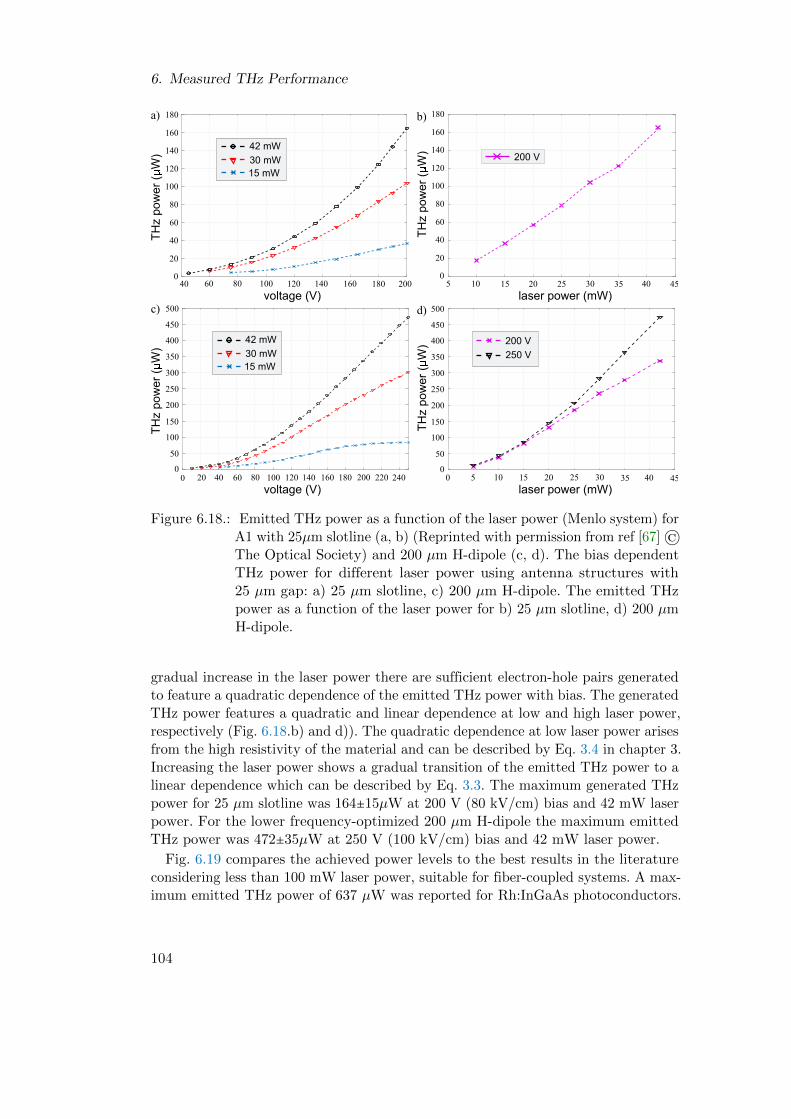
6. Measured THz Performance
0 5 10 15 20 25 30 35 40
laser power (mW)0 20 40
350
250
0
100
450
500
TH
z p
ow
er
(W
)
50
200
300
400
voltage (V)
c)
150
350
250
0
100
450
500
50
200
300
400
150
4560 80 100 120 140 160 180 200 220 240
42 mW
30 mW
15 mW
200 V
250 V
d)
TH
zp
ow
er
(W
)
5 10 15 20 25 30 35 40
laser power (mW)40 60 80
140
100
40
180
TH
z p
ow
er
(W
)
20
80
120
160
voltage (V)
a)
60
45100 120 140 160 180 200
b)
TH
z p
ow
er
(W
)
42 mW
30 mW
15 mW
200 V
0
140
100
40
180
20
80
120
160
60
0
Figure 6.18.: Emitted THz power as a function of the laser power (Menlo system) forA1 with 25µm slotline (a, b) (Reprinted with permission from ref [67] ©The Optical Society) and 200 µm H-dipole (c, d). The bias dependentTHz power for different laser power using antenna structures with25 µm gap: a) 25 µm slotline, c) 200 µm H-dipole. The emitted THzpower as a function of the laser power for b) 25 µm slotline, d) 200 µmH-dipole.
gradual increase in the laser power there are sufficient electron-hole pairs generatedto feature a quadratic dependence of the emitted THz power with bias. The generatedTHz power features a quadratic and linear dependence at low and high laser power,respectively (Fig. 6.18.b) and d)). The quadratic dependence at low laser power arisesfrom the high resistivity of the material and can be described by Eq. 3.4 in chapter 3.Increasing the laser power shows a gradual transition of the emitted THz power to alinear dependence which can be described by Eq. 3.3. The maximum generated THzpower for 25 µm slotline was 164±15µW at 200 V (80 kV/cm) bias and 42 mW laserpower. For the lower frequency-optimized 200 µm H-dipole the maximum emittedTHz power was 472±35µW at 250 V (100 kV/cm) bias and 42 mW laser power.
Fig. 6.19 compares the achieved power levels to the best results in the literatureconsidering less than 100 mW laser power, suitable for fiber-coupled systems. A max-imum emitted THz power of 637 µW was reported for Rh:InGaAs photoconductors.
104

6.5. LAE vs. AE: Measured results
20 50
laser power (mW)
TH
z p
ow
er
(W
)
100
80
300
30 40 60 70 90 100
200
400
500
600
700
0
ErAs:InGaAs, (a)
ErAs:InGaAs, (b)
Rh:InGaAs
Fe:InGaAs
Er:GaAs
InGaAs/InAlAs
Figure 6.19.: Maximum emitted THz power and corresponding laser power for differ-ent material systems. ErAs:In(Al)GaAs [67], Er:GaAs [146], Rh:InGaAs[168], Fe:InGaAs [168], and InGaAs/InAlAs superlattice [82].
Using ErAs:In(Al)GaAs material a maximum averaged THz power of 472 µW hasbeen demonstrated.
6.5. LAE vs. AE: Measured results
The major goal of this section is to study and compare the output signal of antenna-coupled emitters (AE) to that of large area emitters (LAE) driven by low laser power(45 mW) using fiber coupled ports. For simplicity, the LAEs are implemented on aspintronic THz emitter (STE) material that does not require any structuring. Antenna-coupled STE were deposited on the STE using photo-lithography, evaporation andlift-off techniques. The LAE is compared to two different AE namely, 200 µm H-dipole with a gap of 10 µm and a 25 µm slotline. Ref. [64] discusses the details ofthe STE and antenna deposition process. The Menlo TDS system was used to takethe measurements (a center wavelength of 1560 nm, a pulse duration of 90 fs, anda repetition rate of 100 MHz). ErAs:InGaAs photoconductor (material C2) with a25 µm H-dipole with 5 µm gap was used as the receiver. Fiber-coupled laser pulsesat an average power of 45 mW (16 mW) drove the STE (receiver). The laser wastightly focused with an estimated spot size of 10±5 µm. As mentioned in chapter3 for low laser power with no thermal limitations such tight focusing is the mostsuitable configuration for LAE. For outcoupling of the THz signal the STE wasplaced on a 6.1 mm thickness hyper-spherical silicon lens with a 10 mm diametersimilar to that of photoconductor devices.
Fig. 6.20 shows the central result of this section: the THz signals as obtainedfrom an LAE STE and two antenna-coupled devices under otherwise identicalexperimental conditions using the fiber-coupled laser signals. The time-domainsignals are displayed in Fig. 6.20.a). While the peak-to-peak signal from the LAE
105

6. Measured THz Performance
Unstructured Emitter
25 m Slotline
a)
b)time (ps)
TH
z p
uls
e (
mV
)
70
50
30
100
-10
-30
-50
-70
-900 5 10 15 20 25
200 m H-Dipole Antenna, a1
25 m Slotline AntennaUnstructured Emitter
c)
70
60
50
40
30
20
10
0
70
60
50
40
30
20
10
0
-10
frequency (THz)0 0.5 1.51 2 2.5 3 3.5 4 4.5 5 5.5 6
157 mV
65 mV
DN
R (
dB
)D
NR
(d
B)
12 dB Unstructured Emitter
200 m H-dipole, a1
200 m H-dipole, a2
Figure 6.20.: Performance of antenna-coupled STEs. (a) Time-domain signals asobtained from a LAE STE (LAE) and the devices coupled to a 25 µmslotline and a 200 µm-wide H-dipole antenna. Waveforms are offsethorizontally for clarity. b) Power spectrum of the 200 µm H-dipole-antenna-based STE (PAE) vs the LAE STE (PAE). Two differentalignments have been used: a1 is optimized for low frequencies [alsoshown in panel (a)], a2 for frequencies above 2 THz. c) As panel b), butfor the 25 µm slotline antenna [Menlo system used]. Reprinted withpermission from AIP Publishing, [64] © 2019.
106

6.5. LAE vs. AE: Measured results
1 2 3 4
frequency (THz)
1.5 2.5 3.50.5
10
20
30
0
po
we
r ra
tio
(d
B)
-10
10
20
30
0
1 2 3 4
frequency (THz)
po
we
r ra
tio
(d
B)
1.5 2.5 3.50.5
-30
-20
-10
measured
theory
measured, a1
measured, a2
theory
a) b)
Figure 6.21.: Ratio of the emitted THz power (PAE/PLAE) for antenna emitter(AE) and LAE emitter (LAE) as obtained from the experiment andfrom our modeling based on Eq. 3.17 and Eq. 3.20. a) 200µm H-dipoleantenna, b) 25µm slotline antenna. Reprinted with permission fromAIP Publishing, [64] © 2019.
STE is 65 mV, significantly enhanced peak-to-peak signals are observed for theantenna-coupled devices, with a maximum of 157 mV using the 200 µm H-dipoleantenna with 10 µm gap. Therefore, this antenna enhances the emitted THz powerby a factor of 2.422 ≈ 5.86 as compared to the LAE.
Fig. 6.20.b) and c) show the power spectra of the LAE emitter (PLAE) comparedto those of the antenna-coupled devices (PAE). The LAE shows a DNR of 53 dBwith 4.5 THz bandwidth. The 200 µm H-dipole achieves a maximum DNR of 65 dBwhich is 12 dB greater than the DNR of the LAE with the same bandwidth of about4.5 THz (Fig. 6.20.b)). To achieve a similar DNR with the LAE, about 4 times higherlaser power would be required, i.e. about 180 mW, which is hardly achievable withinfibers while preserving a pulse duration of 90 fs.
The differences in the spectral characteristics of the H-dipole as compared to theLAE can be rationalized based on the frequency-dependent radiation impedanceZa = Ra+ iXa of the antenna described earlier in chapter 3. 200 µm H-dipole antennawith a resonance behaviour along with travelling wave characteristics features ahigh Ra with negligible Xa at lower frequencies. Hence, a much higher signal isobserved as compared to LAE. The slotline does not feature a strong resonancebehaviour, however, its travelling wave characteristics are still higher as comparedto the Hertzian dipole emission of LAE.
For comparison of the measured spectra to theory in chapter 3 (Eq. 3.17), Fig. 6.21depicts the ratio PAE/PLAE vs frequency, that is, the power spectrum of the antenna-coupled STEs normalized by that of the LAE STE in Fig. 6.20.b) and c). Thetheoretical results based on Eq. 3.17 and simulated radiation impedances of theantennas from chapter 5 are shown as well. The model also accounts for the far-field radiation patterns of the various emitter structures. For the H-dipole (Fig.
107

6. Measured THz Performance
6.21.a)), we find excellent agreement between experiment and theory, both in termsof frequency dependence and absolute values, even though the silicon lens andpropagation from the source to the receiver were not simulated. Non-ideal THzpropagation and coupling to the receiver antenna (e.g. due to different alignment)noticeably change the spectrum, as is shown for an alignment emphasizing low (a1 inFig. 6.21.a)) and high frequency components (a2). The spectral differences betweenthe two alignments are larger than the deviation from the theoretical model. Forthe slotline antenna (Fig. 6.21.b)), above 1 THz, the theoretical model excellentlyagrees with the experimental findings. However, the simulation does not as wellreproduce the propagation of frequency components below 1 THz. This is due to thehigh extent of propagation of the lower frequency components through the slot owingto its travelling wave characteristics. As the low frequencies components are radiatedaway from the center of the silicon lens outcoupling becomes challenging due to totalinternal reflection. For the same reason the expected DNR difference between 200 µmH-dipole and 25 µm slotline was found to be higher than theoretically expected insection 6.3.2.
We show an excellent reproducibility of the spectral characteristics of antenna-coupled and LAE devices. Hence, the emission process of these emitters is wellunderstood which helps us to employ the appropriate emitter type (LAE/AE) basedon the operation conditions.
108

7. Summary and Outlook
7.1. Summary and Conclusion
We have fabricated ErAs:In(Al)GaAs photoconductors using MBE at the standardgrowth temperature of InGaAs (490o C). The concentration of the localized ErAstraps has been varied in the range of 0.8-2.4 ML with a constant p-doping of5×1018 cm−3 for the InAlAs layers. Three different kinds of SL structures have beengrown, namely: A (ErAs deposited in between InAlAs layers), B (ErAs deposited inbetween the InGaAs and InAlAs layers) and C (no InAlAs layers).
The ErAs:In(Al)GaAs photoconductor materials were characterized in detail, in-cluding IR absorption measurements, Hall measurements, pump-probe measurementsand IV characteristics. Finally, the THz performance of the fabricated photoconduc-tors attached to optimized antenna structures has been investigated.
The absorption coefficient, α, calculated from IR spectroscopic data shows ashallow absorption edge with non-zero absorption below the bandgap (of the orderof 600-4000 cm−1) due to absorption through mid bandgap states provided by theErAs precipitates. An increase in ErAs concentration or decrease in the thickness ofthe InAlAs layers leads to a higher absorption coefficient at wavelengths >1700 nm.The absorption coefficients at 1550 nm for all investigated samples are in the rangeof 4700-6600 cm−1, well suitable for operation at this wavelength.
Hall measurements show that the materials feature an n-type conductivity withmore than two orders of magnitude increase in the carrier concentration for an increaseof the ErAs deposition from 0.8 ML to 2.4 ML for otherwise identical SL structures.Likewise, the materials with 0.8 ML ErAs featured the highest resistivity (material A1and B2) with more than two orders decrease in resistivity with increasing ErAs ML.Material sequence C suitable for receivers featured high mobility of >750 cm2/Vs.
Pump-probe measurements were used to determine the carrier dynamics of thegrown samples. With the increase in the ErAs concentration (0.8-2.4 ML) other-wise identical structure (sequence A) the carrier lifetime of the material decreases.The lifetime is also dependent on the material structure. The shortest lifetime ofτrec=0.38±0.02 ps is featured by material sequence C without any InAlAs layer.Introducing high bandgap InAlAs layers requires additional tunneling of the carrierto reach the ErAs traps, thereby increasing the lifetime to >1.5 ps. We have furtherinvestigated the bias-dependent carrier dynamics (i.e. under operational condition).It has been observed that the carriers feature a bi-exponential decay with an initialbias-assisted fast trapping (τn), followed by a more gradual decay (τh). At 0 kV/cmbias the percentage of carriers decaying by fast trapping is in the range of 5-15%and increases to 85-95% at 80 kV/cm bias voltage.
109

7. Summary and Outlook
Four different samples have been investigated as terahertz emitters. A theoreticalmodel has been developed to estimate the actual photocurrent from the total illu-minated current, taking the heating of the samples into account. Using this modelthe estimated fraction of the photocurrent (IPh) from the illuminated current (Iill)were 86±5% (A1), 12.6±9.4% (A2), 11±7% (A3) and 79±4% (B2), respectively. Thesevalues were in good agreement with the estimated photocurrent using the measuredTDS pulse for the materials. DC measurements were also used to estimate theresistance and breakdown field strength of the materials. Samples containing 0.8 MLErAs per SL period feature high dark resistance of several MΩ per square at biases ofthe order of 200 V. An increase of the ErAs concentration causes orders of magnitudedecrease of the resistance. For 1.6 ML ErAs, the resistance decreases by a factorof ≈40, and for 2.4 ML ErAs the resistance decreases by a factor of ≈120. Sampleswith 0.8 ML ErAs feature a high breakdown field strength of 150±10 kV/cm and140±10 kV/cm respectively (A1 and B2 with 25 µm electrode gaps) with decreasingbreakdown field strength for larger gaps.
Investigation on the THz performance shows that materials A1 and B2 with 0.8 MLErAs are the best suited as emitters, results which were in line with the materialcharacterization. Using 200 µm H-dipole antenna and high bias material A1 and B2featured approx. 760±30 nA p-p THz current, followed by A2 with 490 nA p-p THzcurrent (33% decrease in THz signal) and A3 with < 10% of THz signal as comparedto A1. In the spectral domain A1 and B2 featured 108 dB DNR. The emitted THzpower for the aforementioned setup was 145 µW (A1), 120 µW (B3), 45 µW (A2)and < 5 µW (A3). A saturation of the emitted THz power is also observed for B2.
TDS measurements showed that the best receiver materials were C1 and C2.Material B1 featuring a longer lifetime shows a lower p-p THz signal and DNR.We have also characterized ErAs:InGaAs receivers using a LiNbO3 crystal-basedpulsed THz source operated at 1030 nm. The maximum responsivity of the receiveris 135 µA/
√W with no drastic change in responsivity even at a very high THz power
of 14 mW (∼ 85 µA/√W ). Hence, ErAs:InGaAs receivers in combination with high
power THz sources like LiNbO3 crystals are expected to achieve record-breakingdynamic ranges systems.
H-dipole and slotline antennas were implemented for both emission and detection ofthe THz pulses. CST microwave studio was used to determine the optimum antennastructures for emitter and receiver. Simulations indicate that leaky waves are themeans of THz radiation for slotline antennas. H-dipole antennas featured a resonancebehaviour in addition to its leaky wave modes offering a high radiation resistanceRa. The antenna measurements presented were for the best possible combination ofemitter material A1 and receiver material C1. Three different emitter antennas havebeen investigated in detail in this thesis, namely, i) 200 µm and ii) 50 µm H-dipolewith 25 µm gap and iii) 25 µm slotline antenna. The maximum p-p THz current andDNR were obtained by 200 µm H-dipole. For receivers four different antennas havebeen tested, 25 µm H-dipole with i) 5 µm and ii) 10 µm gap, and 50 µm H-dipole withiii) 5 µm and iv) 10 µm gap. The 50 µm H-dipoles feature a higher p-p THz signaland DNR as compared to 25 µm H-dipoles. These measurements were in agreement
110
7.2. Outlook
with the radiation resistance (Ra) trends obtained from simulations. The maximump-p THz signal (1580 nA) and DNR (113 dB) was obtained using a combination of200 µm H-dipole as emitter and 50 µm H-dipole (5 µm gap) as receiver, optimizedfor the frequency range between 0.5-1 THz where the spectral maximum of the TDSsystem occurs for all investigated antenna structures. A maximum bandwidth of6.5 THz had been obtained for 10 µm gap receivers.
The emitted THz power for the different emitter antennas was also compared. Thelow frequency-optimized 200 µm H-dipole emitted the maximum THz power, while thebandwidth optimized slotline featured the minimum THz power. Further, the emittedTHz power as a function of the pump laser power has also been investigated. Forlow laser power (<10 mW) the emitted THz power features a quadratic dependence.Above 10 mW, the emitted THz power shows a linear relation with laser power. Amaximum THz power of 472±35 µW was obtained with the 200 µm H-dipole at250 V bias and 42 mW laser power.
We finally compared the performance of AE and LAE operated with relativelylow laser power (45 mW) using the fiber-coupled port of the TDS system. Thesecomparisons were done using spintronic THz emitters as source material whereimplementation of LAE is convenient. All AE led to a significant increase of the THzoutput as compared to LAE, when operated with 45 mW laser power. A maximumamplitude increase of 2.42 of the peak-to-peak THz time-domain signal was obtainedusing the 200 µm H-dipole antenna, corresponding to an increase of the peak DNRby 12 dB. A comparison of the ratio of emitted THz power (PAE/PLAE) obtainedthrough measurements are in good agreement with theoretically predicted results.
7.2. Outlook
Only a limited number of ErAs:In(Al)GaAs samples could be investigated during thisthesis. There is still plenty of room for improvement in future work. For example,decreasing the InAlAs layer (< 2.5 nm) for emitter while maintaining the highresistivity of the material can assist the emission of high THz frequencies due to alower carrier lifetime of the material. For receivers very thin InAlAs layers withoutmuch impact on its carrier lifetime could reduce the overall noise of the receivers.A p-doping concentration of 5×1018cm−3 (Be or C) was optimum for 0.8 ML ErAsconcentration. Hence, it is worth growing material with higher p-doping concentration(Be or C) for 1.6-2.4 ML ErAs traps and investigating its THz performance. Weexpect that the lifetime reduces below that of 0.8 ML once appropriate compensation-doping is realized as more trap states are available. Also, the saturated laser powershould increase.
This thesis mainly focused on antenna-coupled photoconductive devices. Anothertopic of research interest is designing suitable LAE photoconductive structurescapable of emitting > 1 mW THz power.
Further research on the bias-dependent lifetime of the ErAs:In(Al)GaAs materialcould open up new applications. For example, the reduction of the transmitted probe
111

7. Summary and Outlook
power with bias (see Fig. 4.7.a)) has the potential to develop into a THz detector forhigh powers (i.e. THz biases) or a sensor application.
112

A. Appendix
A.1. Antenna Theory
The conventional method to determine the E-field radiated from an antenna is by
introducing magnetic vector potential (Ð→A) and electric vector potential (
Ð→F ). These
terms can be used to solve Maxwell’s equation for a source located in a homogeneous
space. Without giving the detailed proof, the E-field resulting fromÐ→A and
Ð→F is
calculated to be [115]
Ð→E (Ð→r ) = −jω
Ð→A (Ð→r ) − j 1
ωµε∇ (∇ ⋅
Ð→A (Ð→r )) − 1
ε∇×
Ð→F (Ð→r ) (A.1)
Ð→A and
Ð→F are the solutions of the Helmholtz equations which are given by
∇2Ð→A (Ð→r ) + k2Ð→A (Ð→r ) = −µ
Ð→J (Ð→r ′)
∇2Ð→F (Ð→r ) + k2Ð→F (Ð→r ) = −ε
Ð→M (Ð→r ′)
(A.2)
whereÐ→J (Ð→r ′) and
Ð→M (Ð→r ′) are the electric and magnetic surface current distri-
bution. Hence, the emitted E-field from a source can be determined if the surfacecurrent distribution of the system is known. Similarly, it is also possible to calculate
the H-field emitted from the source. It is also worth mentioning thatÐ→M (Ð→r ′) is a
fictitious current and are employed to reduce the numerical complexities of manyproblems.
The calculation of the E-field from Eq. A.1 is complex as we initially require
to determine the vector potentialsÐ→A and
Ð→F . A vector integral form of Eq. A.1
independent ofÐ→A and
Ð→F can also be written which is [115]
Ð→E J (Ð→r ) = Ck∬
S′[ηÐ→J (Ð→r ′)CN1 − (η
Ð→J (Ð→r ′) ⋅ R)RCN2]
1
Re−jkRdS
′
(A.3)
Ð→EM (Ð→r ) = Ck∬
S′(Ð→M (Ð→r ′) × R)CN
1
Re−jkRdS
′
(A.4)
where Ck = − jk4π , CN = 1+ 1jkR , CN1 = 1+ 1
jkR −1
(kR)2, CN2 = 1+ 3
jkR −3
(kR)2and the
position vectorÐ→R = (Ð→r −Ð→r ′) with R unit vector.
Ð→E J (Ð→r ) and
Ð→EM (Ð→r ) are the E-
field due to electric and magnetic surface currents respectively. The term exp(-jkR)/Ris the greens function for the Helmholtz Eq. in free space. The total E-field will be
113

A. Appendix
given by the superposition of the two fields i.eÐ→E (Ð→r ) =
Ð→E J (Ð→r )+
Ð→EM (Ð→r ). Similarly,
we can derive the Eq. forÐ→H (Ð→r ). The above general equations can be implemented
to determine the fields from incremental current sources. For a incremental electriccurrent (Hertzian dipole) under far-field conditions the E-field can be calculatedusing Eq. A.3 which is
Ð→E id(Ð→r ) = CkηIold[ld − (ld ⋅ r)r]
1
re−jkr (A.5)
whereÐ→l is the length of the current source and η =
√µo/εo is the impedance
of free space. These sources play an important role in antenna analysis as it canbe used to build bigger sources by superposition of incremental sources. Severalother techniques such as imaging and method of moments [196] are used to analyzeantenna structures, however, these are beyond the scope of this thesis.
114

B. Acronyms
χ susceptibility
ν frequency
js spin current
jc charge current
γs spin hall angle
σs spin polarization vector
ε permittivity
εr relative permittivity
µ mobility
vd drift velocity
vsat saturation velocity
ηT lifetime roll-off
ηRC RC roll-off
σ conductivity
ρ resistivity
τrec carrier lifetime
Ra radiation resistance
ωP characteristics frequency
α absorption coefficient
γLW leaky-wave angle
115

B. Acronyms
THz Terahertz
EM Electromagnetic
TDS Time Domain Spectroscopy
CW Continuous Wave
CMOS Complementary Metal-Oxide-Semiconductor
BWO Backward Wave Oscillator
NDR Negative Differential Resistance
RTD Resonance Tunneling Diode
NIR Near Infrared
QCL Quantum Cascade Laser
OR Optical Rectification
AE Antenna Emitter
LAE Large Area Emitter
UTC uni-travelling carrier
STE Spintronic Terahertz Emitter
NM non-magnetic
FM ferro-magnetic
ISHE inverse spin hall effect
DNR dynamic range
FET field effect transistor
EOS electro optical sampling
SI semi insulating
LTG low temperature grown
DT differential transmission
MBE molecular beam epitaxy
FWHM full width half maximum
116

Bibliography
[1] G. Carpintero et al. Semiconductor Terahertz Technology: Devices and sys-tems at room temperature operation. John Wiley & Sons, 2015.
[2] T. Hochrein. ‘‘Markets, availability, notice, and technical performance ofterahertz systems: Historic development, present, and trends’’. In: Journal ofInfrared, Millimeter, and Terahertz Waves 36.3 (2015), pp. 235–254.
[3] M. Naftaly, N. Vieweg, and A. Deninger. ‘‘Industrial Applications of TerahertzSensing: State of Play’’. In: Sensors 19.19 (2019), p. 4203.
[4] R. Blundell et al. ‘‘Prospects for terahertz radio astronomy from NorthernChile’’. In: Thirteenth International Symposium on Space Terahertz Technol-ogy. Vol. 159. 2002.
[5] A. A. Boulogeorgos et al. ‘‘Wireless terahertz system architectures for networksbeyond 5G’’. In: arXiv preprint arXiv:1810.12260 (2018).
[6] P. P. Ray. ‘‘A survey on Internet of Things architectures’’. In: Journal of KingSaud University-Computer and Information Sciences 30.3 (2018), pp. 291–319.
[7] H. Caesar et al. ‘‘Nuscenes: A multimodal dataset for autonomous driving’’.In: arXiv preprint arXiv:1903.11027 (2019).
[8] D. M. Mittleman. ‘‘Twenty years of terahertz imaging’’. In: Optics Express26.8 (2018), pp. 9417–9431.
[9] D. M. Mittleman, R. H. Jacobsen, and M. C. Nuss. ‘‘T-ray imaging’’. In: IEEEJournal of selected topics in Quantum Electronics 2.3 (1996), pp. 679–692.
[10] K. Kawase. ‘‘Terahertz imaging for drug detection and large-scale integratedcircuit inspection’’. In: Optics and Photonics News 15.10 (2004), pp. 34–39.
[11] Y. Lee et al. ‘‘Detection of foreign bodies in foods using continuous waveterahertz imaging’’. In: Journal of food protection 75.1 (2012), pp. 179–183.
[12] G. Ok et al. ‘‘High-speed terahertz imaging toward food quality inspection’’.In: Applied Optics 53.7 (2014), pp. 1406–1412.
[13] G. Ok et al. ‘‘Large-scan-area sub-terahertz imaging system for nondestructivefood quality inspection’’. In: Food Control 96 (2019), pp. 383–389.
[14] T. May et al. ‘‘Safe VISITOR: visible, infrared, and terahertz object recognitionfor security screening application’’. In: Passive Millimeter-Wave ImagingTechnology XII. Vol. 7309. International Society for Optics and Photonics.2009, 73090E.
117

Bibliography
[15] K. Kawase et al. ‘‘Non-destructive terahertz imaging of illicit drugs usingspectral fingerprints’’. In: Optics Express 11.20 (2003), pp. 2549–2554.
[16] J. Liu et al. ‘‘Identification of high explosive RDX using terahertz imagingand spectral fingerprints’’. In: Journal of Physics: Conference Series. Vol. 680.1. IOP Publishing. 2016, p. 012030.
[17] V. I. Fedorov. ‘‘New Trend in Terahertz Medicine’’. In: Frontiers in Optics.Optical Society of America. 2016, JTh2A–125.
[18] R. H. Giles et al. ‘‘Applications of terahertz frequency technologies in biology’’.In: 2017 42nd International Conference on Infrared, Millimeter, and TerahertzWaves (IRMMW-THz). IEEE. 2017, pp. 1–2.
[19] L. Yu et al. ‘‘The medical application of terahertz technology in non-invasivedetection of cells and tissues: opportunities and challenges’’. In: RSC Advances9.17 (2019), pp. 9354–9363.
[20] Y. Deng et al. ‘‘Terahertz Light Fingerprints Biomolecular Dynamics’’. In:CLEO: Science and Innovations. Optical Society of America. 2018, SW3D–5.
[21] K. A. Niessen et al. ‘‘Protein and RNA dynamical fingerprinting’’. In: NatureCommunications 10.1 (2019), pp. 1–10.
[22] P. C. Ashworth et al. ‘‘Terahertz pulsed spectroscopy of freshly excised humanbreast cancer’’. In: Optics Express 17.15 (2009), pp. 12444–12454.
[23] T. Globus et al. ‘‘Highly resolved sub-terahertz vibrational spectroscopy ofbiological macromolecules and cells’’. In: IEEE Sensors Journal 13.1 (2012),pp. 72–79.
[24] H. Cheon, H. Yang, and J. Son. ‘‘Toward clinical cancer imaging usingterahertz spectroscopy’’. In: IEEE Journal of Selected Topics in QuantumElectronics 23.4 (2017), pp. 1–9.
[25] N. Rothbart et al. ‘‘Analysis of human breath by millimeter-wave/terahertzspectroscopy’’. In: Sensors 19.12 (2019), p. 2719.
[26] A. M. Fosnight, B. L. Moran, and I. R. Medvedev. ‘‘Chemical analysis ofexhaled human breath using a terahertz spectroscopic approach’’. In: AppliedPhysics Letters 103.13 (2013), p. 133703.
[27] B. Han et al. ‘‘A sensitive and selective terahertz sensor for the fingerprintdetection of lactose’’. In: Talanta 192 (2019), pp. 1–5.
[28] A. Tekawade et al. ‘‘Towards Industrial THz Wave Electronic Gas Sensingand Spectroscopy’’. In: 2019 44th International Conference on Infrared,Millimeter, and Terahertz Waves (IRMMW-THz). IEEE. 2019, pp. 1–2.
[29] A. S. Pine et al. ‘‘A Terahertz Photomixing Spectrometer: Application toSO2 Self Broadening’’. In: Journal of Molecular Spectroscopy 175.1 (1996),pp. 37–47.
118

Bibliography
[30] I. Pupeza, R. Wilk, and M. Koch. ‘‘Highly accurate optical material parameterdetermination with THz time-domain spectroscopy’’. In: Optics Express 15.7(2007), pp. 4335–4350.
[31] T. D Dorney, R. G Baraniuk, and D. M. Mittleman. ‘‘Material parameterestimation with terahertz time-domain spectroscopy’’. In: JOSA A 18.7 (2001),pp. 1562–1571.
[32] A. Taschin et al. ‘‘THz time-domain spectroscopic investigations of thin films’’.In: Measurement 118 (2018), pp. 282–288.
[33] W. Withayachumnankul and M. Naftaly. ‘‘Fundamentals of measurementin terahertz time-domain spectroscopy’’. In: Journal of Infrared, Millimeter,and Terahertz Waves 35.8 (2014), pp. 610–637.
[34] P. Mousavi et al. ‘‘Simultaneous composition and thickness measurement ofpaper using terahertz time-domain spectroscopy’’. In: Applied Optics 48.33(2009), pp. 6541–6546.
[35] D. Zimdars and J. S. White. ‘‘Terahertz reflection imaging for package andpersonnel inspection’’. In: Terahertz for Military and Security Applications II.Vol. 5411. International Society for Optics and Photonics. 2004, pp. 78–83.
[36] S. Krimi et al. ‘‘Highly accurate thickness measurement of multi-layeredautomotive paints using terahertz technology’’. In: Applied Physics Letters109.2 (2016), p. 021105.
[37] A. Glagolewa-Arkadiewa. ‘‘Short electromagnetic waves of wavelength up to82 microns’’. In: Nature 113.2844 (1924), pp. 640–640.
[38] J. V. Siles et al. ‘‘A new generation of room-temperature frequency-multipliedsources with up to 10× higher output power in the 160-GHz-1.6-THz range’’.In: IEEE Transactions on Terahertz Science and Technology 8.6 (2018),pp. 596–604.
[39] I. Mehdi et al. ‘‘THz diode technology: status, prospects, and applications’’.In: Proceedings of the IEEE 105.6 (2017), pp. 990–1007.
[40] A. Maestrini et al. ‘‘A 1.7-1.9 THz local oscillator source’’. In: IEEE Microwaveand Wireless Components Letters 14.6 (2004), pp. 253–255.
[41] B. T. Bulcha et al. ‘‘Design and characterization of 1.8-3.2 THz Schottky-based harmonic mixers’’. In: IEEE Transactions on Terahertz Science andTechnology 6.5 (2016), pp. 737–746.
[42] M. Feiginov et al. ‘‘Resonant-tunnelling-diode oscillators operating at frequen-cies above 1.1 THz’’. In: Applied Physics Letters 99.23 (2011), p. 233506.
[43] T. Maekawa et al. ‘‘Oscillation up to 1.92 THz in resonant tunneling diode byreduced conduction loss’’. In: Applied Physics Express 9.2 (2016), p. 024101.
119
Bibliography
[44] R. Izumi, S. Suzuki, and M. Asada. ‘‘1.98 THz resonant-tunneling-diodeoscillator with reduced conduction loss by thick antenna electrode’’. In: 201742nd International Conference on Infrared, Millimeter, and Terahertz Waves(IRMMW-THz). IEEE. 2017, pp. 1–2.
[45] A. Khalid et al. ‘‘Terahertz oscillations in an In0.53Ga0.47As submicron planarGunn diode’’. In: Journal of Applied Physics 115.11 (2014), p. 114502.
[46] M. Mukherjee et al. ‘‘An opto-sensitive InP based Impatt diode for applica-tion in Terahertz regime’’. In: 2007 International Workshop on Physics ofSemiconductor Devices. IEEE. 2007, pp. 392–395.
[47] F. Zernike Jr and P. R. Berman. ‘‘Generation of far infrared as a differencefrequency’’. In: Physical Review Letters 15.26 (1965), p. 999.
[48] T. Tanabe et al. ‘‘Frequency-tunable high-power terahertz wave generationfrom GaP’’. In: Journal of Applied Physics 93.8 (2003), pp. 4610–4615.
[49] D. Creeden et al. ‘‘Compact fiber-pumped terahertz source based on differencefrequency mixing in ZGP’’. In: IEEE Journal of Selected Topics in QuantumElectronics 13.3 (2007), pp. 732–737.
[50] F. Meyer et al. ‘‘Milliwatt-class broadband THz source driven by a 112 W,sub-100 fs thin-disk laser’’. In: Optics Express 27.21 (2019), pp. 30340–30349.
[51] F. Meyer et al. ‘‘Optical rectification of a 100 W average power mode-lockedthin-disk oscillator’’. In: Optics Letters 43.24 (2018), pp. 5909–5912.
[52] Y. J. Ding. ‘‘High-power tunable terahertz sources based on parametricprocesses and applications’’. In: IEEE Journal of selected topics in QuantumElectronics 13.3 (2007), pp. 705–720.
[53] J. Kawase K.and Shikata, K. Imai, and H. Ito. ‘‘Transform-limited, narrow-linewidth, terahertz-wave parametric generator’’. In: Applied Physics Letters78.19 (2001), pp. 2819–2821.
[54] K. Kawase, J. Shikata, and H. Ito. ‘‘Terahertz wave parametric source’’. In:Journal of Physics D: Applied Physics 35.3 (2002), R1.
[55] I. Shoji et al. ‘‘Absolute scale of second-order nonlinear-optical coefficients’’.In: JOSA B 14.9 (1997), pp. 2268–2294.
[56] H. A. Hafez et al. ‘‘Intense terahertz radiation and their applications’’. In:Journal of Optics 18.9 (2016), p. 093004.
[57] F. Meyer et al. ‘‘Single-cycle, MHz-repetition rate THz source with 66 mW ofaverage power’’. In: arXiv preprint arXiv:2002.00222 (2020).
[58] J. E. Hirsch. ‘‘Spin hall effect’’. In: Physical Review Letters 83.9 (1999),p. 1834.
[59] T. Kampfrath et al. ‘‘Terahertz spin current pulses controlled by magneticheterostructures’’. In: Nature Nanotechnology 8.4 (2013), p. 256.
120

Bibliography
[60] T. Seifert et al. ‘‘Efficient metallic spintronic emitters of ultrabroadbandterahertz radiation’’. In: Nature Photonics 10.7 (2016), pp. 483–488.
[61] G. Torosyan et al. ‘‘Optimized spintronic terahertz emitters based on epitaxialgrown Fe/Pt layer structures’’. In: Scientific Reports 8.1 (2018), p. 1311.
[62] E. Saitoh et al. ‘‘Conversion of spin current into charge current at roomtemperature: Inverse spin-Hall effect’’. In: Applied Physics Letters 88.18(2006), p. 182509.
[63] H. Y. Inoue et al. ‘‘Detection of pure inverse spin-Hall effect induced by spinpumping at various excitation’’. In: Journal of Applied Physics 102.8 (2007),p. 083915.
[64] U. Nandi et al. ‘‘Antenna-coupled spintronic terahertz emitters driven bya 1550 nm femtosecond laser oscillator’’. In: Applied Physics Letters 115.2(2019), p. 022405.
[65] S. Preu et al. ‘‘Tunable, continuous-wave terahertz photomixer sources andapplications’’. In: Journal of Applied Physics 109.6 (2011), p. 4.
[66] R. Safian, G. Ghazi, and N. Mohammadian. ‘‘Review of photomixingcontinuous-wave terahertz systems and current application trends in ter-ahertz domain’’. In: Optical Engineering 58.11 (2019), p. 110901.
[67] U. Nandi et al. ‘‘ErAs:In(Al)GaAs photoconductor-based time domain systemwith 4.5 THz single shot bandwidth and emitted terahertz power of 164 µW’’.In: Optics letters 45.10 (2020), pp. 2812–2815.
[68] B. Sartorius et al. ‘‘Continuous wave terahertz systems exploiting 1.5 µmtelecom technologies’’. In: Optics Express 17.17 (2009), pp. 15001–15007.
[69] H. Ito et al. ‘‘Continuous THz-wave generation using antenna-integrated uni-travelling-carrier photodiodes’’. In: Semiconductor Science and Technology20.7 (2005), S191.
[70] A. Geizutis et al. ‘‘Growth and characterization of UTC photo-diodes con-taining GaAs1−xBix absorber layer’’. In: Solid-state Electronics 99 (2014),pp. 101–103.
[71] P. Latzel et al. ‘‘High efficiency UTC photodiodes as photonic emitters for300 GHz high spectral efficiency wireless communications’’. In: 2017 11thEuropean Conference on Antennas and Propagation (EUCAP). IEEE. 2017,pp. 1639–1641.
[72] F. H. Renner et al. ‘‘The nipnip-THz-emitter: photomixing based on ballistictransport’’. In: AIP Conference Proceedings. Vol. 772. 1. American Instituteof Physics. 2005, pp. 1220–1221.
[73] S. Preu et al. ‘‘InGaAs nipnip superlattice THz emitters’’. In: Optical TerahertzScience and Technology. Optical Society of America. 2007, WB6.
121

Bibliography
[74] S. Preu et al. ‘‘Efficient terahertz emission from ballistic transport enhancedn-i-p-n-i-p superlattice photomixers’’. In: Applied Physics Letters 90.21 (2007),p. 212115.
[75] S. Nellen et al. ‘‘Experimental Comparison of UTC-and PIN-Photodiodes forContinuous-Wave Terahertz Generation’’. In: Journal of Infrared, Millimeter,and Terahertz Waves (2019), pp. 1–12.
[76] S. Nellen et al. ‘‘Continuous wave terahertz generation from photodiode-basedemitters with up to 200 µW terahertz power’’. In: 2018 43rd InternationalConference on Infrared, Millimeter, and Terahertz Waves (IRMMW-THz).IEEE. 2018, pp. 1–2.
[77] A. D. J. Fernandez Olvera et al. ‘‘Continuous-wave 1550 nm operated terahertzsystem using ErAs:In(Al)GaAs photo-conductors with 52 dB dynamic rangeat 1 THz’’. In: Optics Express 25.23 (2017), pp. 29492–29500.
[78] U. Nandi et al. ‘‘1550-nm driven ErAs:In(Al)GaAs photoconductor-basedterahertz time domain system with 6.5 THz bandwidth’’. In: Journal ofInfrared, Millimeter, and Terahertz Waves 39.4 (2018), pp. 340–348.
[79] P. S. Stefanova et al. ‘‘Polymer-based micro-golay cells for THz detection’’. In:2016 41st International Conference on Infrared, Millimeter, and Terahertzwaves (IRMMW-THz). IEEE. 2016, pp. 1–2.
[80] V. Desmaris et al. ‘‘Design, simulations and optimization of micromachinedGolay-cell based THz sensors operating at room temperature’’. In: ProcediaChemistry 1.1 (2009), pp. 1175–1178.
[81] R. Muller et al. ‘‘Characterization of a large-area pyroelectric detector from300 GHz to 30 THz’’. In: Journal of Infrared, Millimeter, and TerahertzWaves 36.7 (2015), pp. 654–661.
[82] B. Globisch et al. ‘‘Absolute terahertz power measurement of a time-domainspectroscopy system’’. In: Optics Letters 40.15 (2015), pp. 3544–3547.
[83] Z. Liu et al. ‘‘High performance Terahertz Absorption of Nanostructured NiCrFilm for a pyroelectric detector’’. In: 2019 44th International Conferenceon Infrared, Millimeter, and Terahertz Waves (IRMMW-THz). IEEE. 2019,pp. 1–2.
[84] O. Cojocari et al. ‘‘European Schottky-Diode Based Receiver Technology’’. In:2019 44th International Conference on Infrared, Millimeter, and TerahertzWaves (IRMMW-THz). IEEE. 2019, pp. 1–2.
[85] A. Maestrini et al. ‘‘Terahertz Schottky Mixers for Atmospheric and PlanetarySciences’’. In: 2019 44th International Conference on Infrared, Millimeter,and Terahertz Waves (IRMMW-THz). IEEE. 2019, pp. 1–2.
[86] E. Schlecht et al. ‘‘Schottky diode based 1.2 THz receivers operating atroom-temperature and below for planetary atmospheric sounding’’. In: IEEETransactions on Terahertz Science and Technology 4.6 (2014), pp. 661–669.
122

Bibliography
[87] P. J. Sobis et al. ‘‘A broadband, low noise, integrated 340 GHz Schottkydiode receiver’’. In: IEEE Microwave and Wireless Components Letters 22.7(2012), pp. 366–368.
[88] H. Hubers. ‘‘Terahertz heterodyne receivers’’. In: IEEE journal of selectedtopics in Quantum Electronics 14.2 (2008), pp. 378–391.
[89] S. Regensburger. ‘‘Large-area and lumped element field-effect transistors forpicosecond-scale detection in the Terahertz band and beyond’’. PhD thesis.Technische Universitat, 2019.
[90] S. Preu et al. ‘‘An improved model for non-resonant terahertz detection infield-effect transistors’’. In: Journal of Applied Physics 111.2 (2012), p. 024502.
[91] S. Regensburger et al. ‘‘Broadband Terahertz Detection With Zero-Bias Field-Effect Transistors Between 100 GHz and 11.8 THz With a Noise EquivalentPower of 250 pW/
√Hz at 0.6 THz’’. In: IEEE Transactions on Terahertz
Science and Technology 8.4 (2018), pp. 465–471.
[92] S. Regensburger et al. ‘‘Picosecond-scale terahertz pulse characterization withfield-effect transistors’’. In: IEEE Transactions on Terahertz Science andTechnology 9.3 (2019), pp. 262–271.
[93] J. Grzyb and U. Pfeiffer. ‘‘THz direct detector and heterodyne receiver arraysin silicon nanoscale technologies’’. In: Journal of Infrared, Millimeter, andTerahertz Waves 36.10 (2015), pp. 998–1032.
[94] Q. Wu and X. C. Zhang. ‘‘Free-space electro-optic sampling of terahertzbeams’’. In: Applied Physics Letters 67.24 (1995), pp. 3523–3525.
[95] S. Ahmed, J. Savolainen, and P. Hamm. ‘‘Detectivity enhancement in THzelectrooptical sampling’’. In: Review of Scientific Instruments 85.1 (2014),p. 013114.
[96] C. Szwaj et al. ‘‘High sensitivity photonic time-stretch electro-optic sampling ofterahertz pulses’’. In: Review of Scientific Instruments 87.10 (2016), p. 103111.
[97] A. D. J. Fernandez Olvera et al. ‘‘International system of units (SI) traceablenoise-equivalent power and responsivity characterization of continuous waveErAs:InGaAs photoconductive terahertz detectors’’. In: Photonics. Vol. 6. 1.Multidisciplinary Digital Publishing Institute. 2019, p. 15.
[98] For more information, visit the Inoex website. 2020. url: https://www.inoex.de/en/home/ (visited on 04/20/2020).
[99] B. Globisch et al. ‘‘Fiber-coupled transceiver for terahertz reflection measure-ments with a 4.5 THz bandwidth’’. In: Optics Letters 41.22 (2016), pp. 5262–5265.
[100] R. B. Kohlhaas et al. ‘‘Fiber Coupled Transceiver with 6.5 THz Bandwidth forTerahertz Time-Domain Spectroscopy in Reflection Geometry’’. In: Sensors20.9 (2020), p. 2616.
123

Bibliography
[101] J. White et al. ‘‘Time-domain terahertz mapping of thickness and degradationof aircraft turbine blade thermal barrier coatings’’. In: Conference on Lasersand Electro-Optics. Optical Society of America. 2008, CThN7.
[102] For more information, visit the Fischer website. 2020. url: https://www.helmut-fischer.de/ (visited on 04/20/2020).
[103] Y. Shen. ‘‘Terahertz pulsed spectroscopy and imaging for pharmaceuticalapplications: a review’’. In: International journal of Pharmaceutics 417.1-2(2011), pp. 48–60.
[104] F. M. Al-Douseri, Y. Chen, and X. C. Zhang. ‘‘THz wave sensing for petroleumindustrial applications’’. In: International journal of Infrared and MillimeterWaves 27.4 (2006), pp. 481–503.
[105] M. Yahyapour et al. ‘‘Fastest thickness measurements with a terahertz time-domain system based on electronically controlled optical sampling’’. In: Ap-plied Sciences 9.7 (2019), p. 1283.
[106] D. C. Driscoll et al. ‘‘Electronic structure and conduction in a metal-semiconductor digital composite: ErAs:InGaAs’’. In: Applied Physics Letters78.12 (2001), pp. 1703–1705.
[107] M. Sukhotin et al. ‘‘Photomixing and photoconductor measurements onErAs/InGaAs at 1.55 µm’’. In: Applied Physics Letters 82.18 (2003), pp. 3116–3118.
[108] F. Ospald et al. ‘‘1.55 µm ultrafast photoconductive switches based onErAs:InGaAs’’. In: Applied Physics Letters 92.13 (2008), p. 131117.
[109] A. Schwagmann et al. ‘‘Terahertz emission characteristics of ErAs:InGaAs-based photoconductive antennas excited at 1.55 µm’’. In: Applied PhysicsLetters 96.14 (2010), p. 141108.
[110] M. Sukhotin et al. ‘‘Picosecond photocarrier-lifetime in ErAs:InGaAs at 1.55µm’’. In: Applied Physics Letters 83.19 (2003), pp. 3921–3923.
[111] D. C. Driscoll et al. ‘‘Ultrafast photoresponse at 1.55 µm in InGaAs withembedded semimetallic ErAs nanoparticles’’. In: Applied Physics Letters 86.5(2005), p. 051908.
[112] A. K. Azad et al. ‘‘Carrier dynamics in InGaAs with embedded ErAs nanois-lands’’. In: Applied Physics Letters 93.12 (2008), p. 121108.
[113] J. Y. Suen et al. ‘‘Measurement and modeling of ErAs:In0.53Ga0.47As nanocom-posite photoconductivity for THz generation at 1.55 µm pump wavelength’’.In: Journal of Applied Physics 116.1 (2014), p. 013703.
[114] S. Preu. ‘‘A unified derivation of the terahertz spectra generated by photo-conductors and diodes’’. In: Journal of Infrared, Millimeter, and TerahertzWaves 35.12 (2014), pp. 998–1010.
[115] P. Kildal. Foundations of antenna engineering: a unified approach for line-of-sight and multipath. Artech House, 2015.
124

Bibliography
[116] E. Castro-Camus et al. ‘‘Photoconductive response correction for detectors ofterahertz radiation’’. In: Journal of Applied Physics 104.5 (2008), p. 053113.
[117] M. Ashida. ‘‘Ultra-broadband terahertz wave detection using photoconductiveantenna’’. In: Japanese Journal of Applied Physics 47.10S (2008), p. 8221.
[118] S. Kono, M. Tani, and K. Sakai. ‘‘Ultrabroadband photoconductive detection:Comparison with free-space electro-optic sampling’’. In: Applied PhysicsLetters 79.7 (2001), pp. 898–900.
[119] J. Bardeen and W. Shockley. ‘‘Deformation potentials and mobilities innon-polar crystals’’. In: Physical Review 80.1 (1950), p. 72.
[120] E. Conwell and V. F. Weisskopf. ‘‘Theory of impurity scattering in semicon-ductors’’. In: Physical Review 77.3 (1950), p. 388.
[121] J. L. Moll. Physics of semiconductors. McGraw-Hill, 1964.
[122] D. M. Caughey and R. E. Thomas. ‘‘Carrier mobilities in silicon empiricallyrelated to doping and field’’. In: Proceedings of the IEEE 55.12 (1967),pp. 2192–2193.
[123] J. L. Hudgins et al. ‘‘An assessment of wide bandgap semiconductors forpower devices’’. In: IEEE Transactions on Power Electronics 18.3 (2003),pp. 907–914.
[124] C. Sah, R. N. Noyce, and W. Shockley. ‘‘Carrier generation and recombinationin pn junctions and pn junction characteristics’’. In: Proceedings of the IRE45.9 (1957), pp. 1228–1243.
[125] B. Globisch et al. ‘‘Iron doped InGaAs: Competitive THz emitters and de-tectors fabricated from the same photoconductor’’. In: Journal of AppliedPhysics 121.5 (2017), p. 053102.
[126] B. Globisch et al. ‘‘Carrier dynamics in Beryllium doped low-temperature-grown InGaAs/InAlAs’’. In: Applied Physics Letters 104.17 (2014), p. 172103.
[127] I. S. Gregory et al. ‘‘High resistivity annealed low-temperature GaAs with100 fs lifetimes’’. In: Applied Physics Letters 83.20 (2003), pp. 4199–4201.
[128] E. R. Brown, F. W. Smith, and K. A. McIntosh. ‘‘Coherent millimeter-wave generation by heterodyne conversion in low-temperature-grown GaAsphotoconductors’’. In: Journal of Applied Physics 73.3 (1993), pp. 1480–1484.
[129] E. Peytavit et al. ‘‘CW source based on photomixing with output powerreaching 1.8 mW at 250 GHz’’. In: IEEE Electron Device Letters 34.10(2013), pp. 1277–1279.
[130] C. Kadow et al. ‘‘Growth and microstructure of self-assembled ErAs islandsin GaAs’’. In: Journal of Vacuum Science & Technology B: Microelectronicsand Nanometer Structures Processing, Measurement, and Phenomena 18.4(2000), pp. 2197–2203.
125

Bibliography
[131] Y. Zhang et al. ‘‘Kinetically controlled dewetting of thin GaAs cap from anErAs/GaAs nanoparticle composite layer’’. In: Journal of Vacuum Science &Technology B, Nanotechnology and Microelectronics: Materials, Processing,Measurement, and Phenomena 36.4 (2018), p. 041801.
[132] C. Kadow et al. ‘‘Self-assembled ErAs islands in GaAs for THz applications’’.In: Physica E: Low-dimensional Systems and Nanostructures 7.1-2 (2000),pp. 97–100.
[133] C. Kadow et al. ‘‘Growth-temperature dependence of the microstructure ofErAs islands in GaAs’’. In: Journal of Vacuum Science & Technology B:Microelectronics and Nanometer Structures Processing, Measurement, andPhenomena 21.1 (2003), pp. 29–32.
[134] C. Kadow et al. ‘‘Self-assembled ErAs islands in GaAs: Growth and subpicosec-ond carrier dynamics’’. In: Applied Physics Letters 75.22 (1999), pp. 3548–3550.
[135] M. Griebel et al. ‘‘Tunable subpicosecond optoelectronic transduction insuperlattices of self-assembled ErAs nanoislands’’. In: Nature Materials 2.2(2003), pp. 122–126.
[136] R. P. Prasankumar et al. ‘‘Carrier dynamics in self-assembled ErAs nanoislandsembedded in GaAs measured by optical-pump terahertz-probe spectroscopy’’.In: Applied Physics Letters 86.20 (2005), p. 201107.
[137] J. E. Bjarnason et al. ‘‘ErAs:GaAs photomixer with two-decade tunabilityand 12 µW peak output power’’. In: Applied Physics Letters 85.18 (2004),pp. 3983–3985.
[138] N. T. Yardimci et al. ‘‘A high-power broadband terahertz source enabled bythree-dimensional light confinement in a plasmonic nanocavity’’. In: ScientificReports 7.1 (2017), pp. 1–8.
[139] S. Yang et al. ‘‘7.5% optical-to-terahertz conversion efficiency offered by pho-toconductive emitters with three-dimensional plasmonic contact electrodes’’.In: IEEE Transactions on Terahertz Science and Technology 4.5 (2014),pp. 575–581.
[140] M. A. Scarpulla et al. ‘‘Near-infrared absorption and semimetal-semiconductortransition in 2 nm ErAs nanoparticles embedded in GaAs and AlAs’’. In:Applied Physics Letters 92.17 (2008), p. 173116.
[141] E. R. Brown et al. ‘‘Model for ultrafast extrinsic photoconductivity in Er-doped GaAs’’. In: 2016 41st International Conference on Infrared, Millimeter,and Terahertz waves (IRMMW-THz). IEEE. 2016, pp. 1–2.
[142] A. Mingardi, W. D. Zhang, and E. R. Brown. ‘‘THz performance of 1550-nm-driven photoconductive switches made from GaAs:Er with ErAs quantumdots’’. In: 2017 IEEE National Aerospace and Electronics Conference (NAE-CON). IEEE. 2017, pp. 332–334.
126

Bibliography
[143] W. D. Zhang et al. ‘‘Ultrafast photoconductive devices based upon GaAs:ErAsnanoparticle composite driven at 1550 nm’’. In: Ultrafast Bandgap Photonics II.Vol. 10193. International Society for Optics and Photonics. 2017, p. 1019308.
[144] J. R. Middendorf and E. R. Brown. ‘‘THz generation using extrinsic pho-toconductivity at 1550 nm’’. In: Optics Express 20.15 (2012), pp. 16504–16509.
[145] E. R. Brown et al. ‘‘Abrupt dependence of ultrafast extrinsic photoconduc-tivity on Er fraction in GaAs:Er’’. In: Applied Physics Letters 111.3 (2017),p. 031104.
[146] A. Mingardi et al. ‘‘High power generation of THz from 1550-nm photocon-ductive emitters’’. In: Optics Express 26.11 (2018), pp. 14472–14478.
[147] E. R. Brown. ‘‘THz generation by photomixing in ultrafast photoconduc-tors’’. In: Terahertz Sensing Technology: Volume 1: Electronic Devices andAdvanced Systems Technology. World Scientific, 2003, pp. 147–195.
[148] R. A. Metzger et al. ‘‘Structural and electrical properties of low temperatureGaInAs’’. In: Journal of Vacuum Science & Technology B: Microelectronicsand Nanometer Structures Processing, Measurement, and Phenomena 11.3(1993), pp. 798–801.
[149] A. Takazato et al. ‘‘Detection of terahertz waves using low-temperature-grownInGaAs with 1.56 µm pulse excitation’’. In: Applied Physics Letters 90.10(2007), p. 101119.
[150] A. Takazato et al. ‘‘Terahertz wave emission and detection using photocon-ductive antennas made on low-temperature-grown InGaAs with 1.56 µm pulseexcitation’’. In: Applied Physics Letters 91.1 (2007), p. 011102.
[151] B. Sartorius et al. ‘‘All-fiber terahertz time-domain spectrometer operating at1.5 µm telecom wavelengths’’. In: Optics Express 16.13 (2008), pp. 9565–9570.
[152] H. Roehle et al. ‘‘Next generation 1.5 µm terahertz antennas: mesa-structuringof InGaAs/InAlAs photoconductive layers’’. In: Optics Express 18.3 (2010),pp. 2296–2301.
[153] R. J. B. Dietz et al. ‘‘Influence and adjustment of carrier lifetimes in In-GaAs/InAlAs photoconductive pulsed terahertz detectors: 6 THz bandwidthand 90 dB dynamic range’’. In: Optics Express 22.16 (2014), pp. 19411–19422.
[154] R. J. B. Dietz et al. ‘‘THz generation at 1.55 µm excitation: six-fold increasein THz conversion efficiency by separated photoconductive and trappingregions’’. In: Optics Express 19.27 (2011), pp. 25911–25917.
[155] R. J. B. Dietz et al. ‘‘64 µW pulsed terahertz emission from growth opti-mized InGaAs/InAlAs heterostructures with separated photoconductive andtrapping regions’’. In: Applied Physics Letters 103.6 (2013), p. 061103.
127

Bibliography
[156] R. B. Kohlhaas et al. ‘‘Improving the dynamic range of InGaAs-based THzdetectors by localized beryllium doping: up to 70 dB at 3 THz’’. In: OpticsLetters 43.21 (2018), pp. 5423–5426.
[157] J. Mangeney. ‘‘THz photoconductive antennas made from ion-bombardedsemiconductors’’. In: Journal of Infrared, Millimeter, and Terahertz Waves33.4 (2012), pp. 455–473.
[158] N. Chimot et al. ‘‘Terahertz radiation from heavy-ion-irradiatedIn0.53Ga0.47As photoconductive antenna excited at 1.55 µm’’. In: AppliedPhysics Letters 87.19 (2005), p. 193510.
[159] J. C. Delagnes et al. ‘‘High photocarrier mobility in ultrafast ion-irradiatedIn0.53Ga0.47As for terahertz applications’’. In: Journal of Physics D: AppliedPhysics 42.19 (2009), p. 195103.
[160] C. Carmody et al. ‘‘Ion-implanted In0.53Ga0.47As for ultrafast optoelectronicapplications’’. In: Applied Physics Letters 82.22 (2003), pp. 3913–3915.
[161] M. Suzuki and M. Tonouchi. ‘‘Fe-implanted InGaAs terahertz emitters for1.56 µm wavelength excitation’’. In: Applied Physics Letters 86.5 (2005),p. 051104.
[162] M. Suzuki and M. Tonouchi. ‘‘Fe-implanted InGaAs photoconductive terahertzdetectors triggered by 1.56 µm femtosecond optical pulses’’. In: Applied PhysicsLetters 86.16 (2005), p. 163504.
[163] BC Tousley et al. ‘‘Femtosecond Optical Response of Low TemperatureGrown In0.53Ga0.47As’’. In: Ultrafast Electronics and Optoelectronics. OpticalSociety of America. 1993, p. D6.
[164] M. Guezo et al. ‘‘Ultrashort, nonlinear, optical time response of Fe-dopedInGaAs/InP multiple quantum wells in 1.55-µm range’’. In: Applied PhysicsLetters 82.11 (2003), pp. 1670–1672.
[165] C. D. Wood et al. ‘‘Terahertz emission from metal-organic chemical vapordeposition grown Fe:InGaAs using 830 nm to 1.55 µm excitation’’. In: AppliedPhysics Letters 96.19 (2010), p. 194104.
[166] O. Hatem et al. ‘‘Terahertz-frequency photoconductive detectors fabricatedfrom metal-organic chemical vapor deposition-grown Fe-doped InGaAs’’. In:Applied Physics Letters 98.12 (2011), p. 121107.
[167] R. B. Kohlhaas et al. ‘‘Photoconductive terahertz detectors with 105 dB peakdynamic range made of rhodium doped InGaAs’’. In: Applied Physics Letters114.22 (2019), p. 221103.
[168] R. B. Kohlhaas et al. ‘‘637 µW emitted terahertz power from photoconductiveantennas based on rhodium doped InGaAs’’. In: Applied Physics Letters117.13 (2020), p. 131105.
[169] S. Preu et al. ‘‘1550 nm ErAs:In(Al)GaAs large area photoconductive emitters’’.In: Applied Physics Letters 101.10 (2012), p. 101105.
128

Bibliography
[170] C. W. Berry and M. Jarrahi. ‘‘Principles of impedance matching in photocon-ductive antennas’’. In: Journal of Infrared, Millimeter, and Terahertz Waves33.12 (2012), pp. 1182–1189.
[171] E. R. Brown, F. W. Smith, and K. A. McIntosh. ‘‘Coherent millimeter-wave generation by heterodyne conversion in low-temperature-grown GaAsphotoconductors’’. In: Journal of Applied Physics 73.3 (1993), pp. 1480–1484.
[172] P. Hui and H. S. Tan. ‘‘Temperature distributions in a heat dissipation systemusing a cylindrical diamond heat spreader on a copper heat sink’’. In: Journalof Applied Physics 75.2 (1994), pp. 748–757.
[173] A. D. J. Fernandez Olvera et al. ‘‘Dispersive properties of self-complementarylog-periodic antennas in pulsed THz systems’’. In: 2017 42nd InternationalConference on Infrared, Millimeter, and Terahertz Waves (IRMMW-THz).IEEE. 2017, pp. 1–2.
[174] C. W. Berry et al. ‘‘Significant performance enhancement in photoconductiveterahertz optoelectronics by incorporating plasmonic contact electrodes’’. In:Nature Communications 4.1 (2013), pp. 1–10.
[175] A. Neto. ‘‘UWB, non dispersive radiation from the planarly fed leaky lensantenna—Part 1: Theory and design’’. In: IEEE Transactions on Antennasand Propagation 58.7 (2010), pp. 2238–2247.
[176] S. Bruni et al. ‘‘Problem-matched basis functions for microstrip coupledslot arrays based on transmission line Green’s functions (TLGF)’’. In: IEEETransactions on Antennas and Propagation 53.11 (2005), pp. 3556–3567.
[177] A. Neto and S. Maci. ‘‘Green’s function for an infinite slot printed betweentwo homogeneous dielectrics. I. Magnetic currents’’. In: IEEE Transactionson Antennas and Propagation 51.7 (2003), pp. 1572–1581.
[178] S. Maci and A. Neto. ‘‘Green’s function of an infinite slot printed betweentwo homogeneous dielectrics-Part II: Uniform asymptotic solution’’. In: IEEETransactions on Antennas and Propagation 52.3 (2004), pp. 666–676.
[179] A. Neto et al. ‘‘The leaky lens: A broad-band fixed-beam leaky-wave antenna’’.In: IEEE Transactions on Antennas and Propagation 53.10 (2005), pp. 3240–3246.
[180] N. Llombart and A. Neto. ‘‘THz time-domain sensing: The antenna dispersionproblem and a possible solution’’. In: IEEE Transactions on Terahertz Scienceand Technology 2.4 (2012), pp. 416–423.
[181] A. Garufo et al. ‘‘Norton equivalent circuit for pulsed photoconductiveantennas-Part I: Theoretical model’’. In: IEEE Transactions on Antennasand Propagation 66.4 (2018), pp. 1635–1645.
[182] S. Chen and P. Hsu. ‘‘A Simplified Method to Calculate Far-Field Patternsof Extended Hemispherical Dielectric Lens’’. In: 2007 Asia-Pacific MicrowaveConference. IEEE. 2007, pp. 1–4.
129

Bibliography
[183] A. Garufo, N. Llombart, and A. Neto. ‘‘Radiation of logarithmic spiral an-tennas in the presence of dense dielectric lenses’’. In: IEEE Transactions onAntennas and Propagation 64.10 (2016), pp. 4168–4177.
[184] U. Nandi et al. ‘‘Material properties and performance of ErAs:In(Al)GaAsphotoconductors for 1550 nm laser operation’’. In: Journal of Vacuum Science& Technology A: Vacuum, Surfaces, and Films 39.2 (2021), p. 023407.
[185] O. Mizuno and H. Watanabe. ‘‘Semi-insulating properties of Fe-doped InP’’.In: Electronics Letters 11.5 (1975), pp. 118–119.
[186] J. Mistrik et al. ‘‘Optical properties of electronic materials: fundamentalsand characterization’’. In: Springer Handbook of Electronic and PhotonicMaterials. Springer, 2017, pp. 1–1.
[187] W. F. Brinkman, R. C. Dynes, and J. M. Rowell. ‘‘Tunneling conductance ofasymmetrical barriers’’. In: Journal of Applied Physics 41.5 (1970), pp. 1915–1921.
[188] S. Verghese, K. A. McIntosh, and E. R. Brown. ‘‘Optical and terahertz powerlimits in the low-temperature-grown GaAs photomixers’’. In: Applied PhysicsLetters 71.19 (1997), pp. 2743–2745.
[189] D. F. Filipovic, S. S. Gearhart, and G. M. Rebeiz. ‘‘Double-slot antennason extended hemispherical and elliptical silicon dielectric lenses’’. In: IEEETransactions on Microwave Theory and Techniques 41.10 (1993), pp. 1738–1749.
[190] P. Hill et al. ‘‘Measurement of hole velocity in n-type InGaAs’’. In: AppliedPhysics Letters 50.18 (1987), pp. 1260–1262.
[191] T. Meyer F.and Vogel, S. Ahmed, and C. J. Saraceno. ‘‘Single-cycle, MHzrepetition rate THz source with 66 mW of average power’’. In: Optics Letters45.9 (2020), pp. 2494–2497.
[192] U. Nandi et al. ‘‘Performance of a 1030 nm driven ErAs:InGaAs photocon-ductive receiver at high THz average power’’. In: 2020 45th InternationalConference on Infrared, Millimeter, and Terahertz Waves (IRMMW-THz).IEEE. 2020.
[193] C. J. Saraceno. ‘‘Mode-locked thin-disk lasers and their potential applicationfor high-power terahertz generation’’. In: Journal of Optics 20.4 (2018),p. 044010.
[194] R. J. B. Dietz et al. ‘‘Low temperature grown Be-doped InGaAs/InAlAsphotoconductive antennas excited at 1030 nm’’. In: Journal of Infrared,Millimeter, and Terahertz Waves 34.3-4 (2013), pp. 231–237.
[195] P. K. Lu, D. Turan, and M. Jarrahi. ‘‘High-sensitivity telecommunication-compatible photoconductive terahertz detection through carrier transit timereduction’’. In: Optics Express 28.18 (2020), pp. 26324–26335.
130

Bibliography
[196] W. Wang et al. ‘‘Differential evolution algorithm and method of moments forthe design of low-RCS antenna’’. In: IEEE Antennas and Wireless PropagationLetters 9 (2010), pp. 295–298.
131


Curriculum Vitae
Personal Details
Name Uttam Nandi
Date of birth 20 December, 1990
Nationality Indian
Education
2010 -- 2014 B-Tech: Electronics and Communication EngineeringIndian Institute of Technology, Guwahati (IITG)
2014 -- 2016 Msc: Wireless, Photonics and Space EngineeringChalmers University of Technology, Sweden
2017-- 2021 DoctorateTechnische Universitat Darmstadt, Germany
Honours and Awards
2014 IPOET Scholarship Awarded by Chalmers University ofTechnology
Employment
2017 -- 2021 Technische Universitat DarmstadtResearch assistant at the Department of Department ofElectrical Engineering and Information Technology
133


List of Publications
Journal Publications
• U. Nandi, J. C. Norman, A. C. Gossard, H. Lu, and S. Preu. ‘‘1550 nm drivenErAs:In(Al)GaAs photoconductor-based terahertz time domain system with6.5 THz bandwidth’’. Journal of Infrared, Millimeter, and Terahertz Waves39.4 (2018), pp. 340-348.
• U. Nandi, M. S. Abdelaziz, S. Jaiswal, G. Jakob, O. Gueckstock, S. M. Rouze-gar, T. S. Seifert, M. Klaui, T. Kampfrath, and S. Preu. ‘‘Antenna-coupledspintronic terahertz emitters driven by a 1550 nm femtosecond laser oscillator.’’Applied Physics Letters 115.2 (2019), pp. 022405.
• U. Nandi, K. Dutzi, A. Deninger, H. Lu, J. Norman, A. C. Gossard, N. Vieweg,and S. Preu. ‘‘ErAs:In(Al)GaAs photoconductor-based time domain systemwith 4.5 THz single shot bandwidth and emitted terahertz power of 164 µW.”Optics Letters 45.10 (2020): pp. 2812-2815.
• U. Nandi, M. Mohammadi, H. Lu, J. Norman, A. C. Gossard, L. Alff, andS. Preu. ‘‘Material properties and performance of ErAs:In(Al)GaAs photocon-ductors for 1550 nm laser operation.” Journal of Vacuum Science & TechnologyA: Vacuum, Surfaces, and Films 39.2 (2021): pp. 023407.
Conference Publications
• U. Nandi, F. R. Faridi, A. D. J. Fernandez Olvera, J. Norman, H. Lu, A. C. Gos-sard, and S. Preu. ‘‘High Dynamic Range THz Systems using ErAs: In (Al)GaAs Photoconductors.” In 2019 IEEE MTT-S International Microwave Work-shop Series on Advanced Materials and Processes for RF and THz Applications(IMWS-AMP), IEEE (2019), pp. 115-117.
• U. Nandi, M. S. Abdelaziz, S. Jaiswal, G. Jakob, O. Gueckstock, S. M. Rouzegar,T. S. Seifert, M. Klaui, T. Kampfrath, and S. Preu. ‘‘Effect of DC ElectricField on the Emitted THz Signal of Antenna-Coupled Spintronic Emitters.”In 2019 44th International Conference on Infrared, Millimeter, and TerahertzWaves (IRMMW-THz), IEEE (2019), pp. 1-2.
• U. Nandi, T. Vogel, S. Mansourzadeh, M. Hoffmann, J. C. Norman, H. Lu,A. C. Gossard, C. J. Saraceno, and S. Preu. ‘‘Performance of a 1030 nm driven
135

Bibliography
ErAs:InGaAs photoconductive receiver at high THz average power.” In 202045th International Conference on Infrared, Millimeter, and Terahertz Waves(IRMMW-THz), IEEE (2020).
Workshop Contributions
• U. Nandi, J. C. Norman, A. C. Gossard, H. Lu, and S. Preu ‘‘Large BandwidthTDS System using ErAs:InGaAs photoconductor with highest recorded resis-tivity and breakdown voltage.” In 2018 International Workshop on TerahertzTechnology and Applications, Kaiserslautern, March (2018).
• U. Nandi, M. S. Abdelaziz, T. S. Seifert, S. Jaiswal, M. Klaui, T. Kampfrath,and S. Preu. ‘‘Spintronic Large Area THz Source at 1550 nm Laser Excitation.”In 2019 French German THz Conference, Kaiserslautern, (FGTC2019) April(2019).
Supervised Thesises
• Felix Schmidt-Brand, ‘‘Large area photoconductive terahertz emitters for1550 nm and 1030 nm excitation.” Master thesis, August-November 2017.
• Mohammed Sayed Abdel Aziz, ‘‘Spintronic Terahertz Emitters.” Master thesis,February-August 2018.
• Adrian Minwegen, ‘‘Electron lifetime measurement at photoconductors with1550 nm.” Master thesis, October 2018- January 2019.
• Moritz Scheer, ‘‘Investigation of carrier dynamics in In(Al)GaAs photoconduc-tor materials.” Bachelor thesis, February-July 2021
136

Erklarungen laut Promotionsordnung
§ 8 Abs. 1 lit. c PromOIch versichere hiermit, dass die elektronische Version meiner Dissertation mit der
schriftlichen Version ubereinstimmt.
§ 8 Abs. 1 lit. d PromOZu einem vorherigen Zeitpunkt noch keine Promotion versucht wurde. In diesem
Fall sind nahere Angaben uber Zeitpunkt, Hochschule, Dissertationsthema undErgebnis dieses Versuchs mitzuteilen.
§ 9 Abs. 1 PromODie vorliegende Dissertation selbststandig und nur unter Verwendung der angegebe-
nen Quellen verfasst wurde.
§ 9 Abs. 2 PromODie Arbeit hat bisher noch nicht zu Prufungszwecken gedient.
Darmstadt, 12. Marz 2021
137


Acknowledgement
Firstly, I would like to thank my supervisor Prof. Dr. Sascha Preu for his guidancethroughout the journey of my Ph.D. He had always managed to find out time fromhis busy schedule to give excellent suggestions, correct my writings and help me onbuilding the theoretical aspects of my work. I also appreciate his efforts to help mein the lab during my initial Ph.D. days. I clearly remember him detecting the groundloop problem in the TIA and finally finding the THz pulse. I was very fortunate tobe under his guidance.
This research has been done in collaboration with several groups. I would liketo thank Peter Kießlich and Andreas Semrad who helped in maintaining the clean-room and fabricating several holders and packages in the workshop. My deepestacknowledgment to Prof. Dr. A. C. Gossard and Dr. Justin Norman from MaterialsDepartment from University of California, Santa Barbara for growing the photocon-ductor materials. I would also like to thank Prof. Dr. Hong Lu from University ofNanjing University, China for doing the Hall Measurements of our grown photocon-ductor materials. Further, I would like to thank Mahdad Mohammadi and Prof. Dr.Lambert Alff from the Material Science Department of TU-Darmstadt for helpingus with the IR absorption measurements for the photoconductor materials. I amthankful to Katja Dutzi, Dr. Anselm Deninger, and Dr. Nico Vieweg from Topticafor their collaboration in measuring TDS performance of our device. I would also liketo thank Prof. Dr. Clara Saraceno, Tim Vogel, and Samira Mansourzadeh from RuhrUniversitat Bochum for collaborating with us for characterizing our photoconductivereceivers. Last but not least I would like to acknowledge Prof. Dr. Tobias Kampfrathand Dr. Tom Seifert from Fritz Haber Institute of the Max Planck Society, Berlinfor collaborating and providing us Spintronic Devices.
It is often said you normally learn a lot from your peers during your Ph.D., andit is definitely true. I would like to thank my senior Ph.D. students Stefan andMario for their works in calibrating processes in the cleanroom and Terahertz lab.Prior programming of the Newport Port delay stage and other DC characterizationprograms was really useful. Thank you Julian for always being there to help withthe CVD machine and taking out the screw which I had accidentally dropped intoCVD machine motor. I am grateful to Anuar for teaching me the art of fabricatingphotoconductors in the cleanroom and the craft of building THz setup. His patienceto explain me the same things several times is also acknowledged. The knowledgeenhancement scientific discussions we had in our office on a regular basis reallyhelped me in the better understanding of concepts and progress with my work. Iwould also remember all the outside-work deep philosophical discussions we hadtogether. He has been a dear friend to me and the best office mate I could ever
139

Bibliography
have. Thank you Fahd Bhai for all the wonderful experience I had with you, cookingtogether in the weekends, for being the storyteller, cracking ‘‘hi-fi’’ jokes, and alsobearing with me even when I intruded into your personal space- ‘‘Ar e Fahd BhaiFahd Bhai Fahd Bhi Rae’’. Also thank you for making the ThorLabs PowerMeterprogram work. Thank you Amlan for bearing with me and also helping me with manycomputer and programming-related stuff. The camera you brought was the mostuseful thing for me and I take back my statement ‘‘I don’t think it’s worth’’. All thetrips we made together during the Ph.D. wouldn’t have been possible without you.Benedikt thank you for helping me to connect the Swiss THz Camera. Rahul yourdrinking of white wine in the Beer Garden and jogging with you will be remembered.Irene, I will remember your highly energetic discussions in the kitchen during lunchtime and the ‘‘Plaka Paneer’’ I have to give is still due. Mojdeh thank you for yourkind gestures, the food you shared with me during lunch, and walk back home fromuniversity sometimes. All the best to my successor Romina, a quick learner with vastknowledge about different stuff ranging from animals to Anime. Ahid, thank you forgiving me the position of ‘‘Referee’’ in the football matches you people played eventhough I was the spectator. Thank you Alaa for informing me about how to submitmy thesis and letting me hold your kids.
Finally, I would like to thank my parents for supporting me in all aspects of mylife. Without their emotional and financial support, it would have not have beenpossible to reach where I am now. My dad has been and will always be a source ofinspiration in my life.
140
Copyright © 2022 FDOKUMEN