Optical and Mechanical Characterization of InAs/GaAs ...
162
Rochester Institute of Technology Rochester Institute of Technology RIT Scholar Works RIT Scholar Works Theses 1-2012 Optical and Mechanical Characterization of InAs/GaAs Quantum Optical and Mechanical Characterization of InAs/GaAs Quantum Dot Solar Cells Dot Solar Cells Christopher G. Bailey Follow this and additional works at: https://scholarworks.rit.edu/theses Recommended Citation Recommended Citation Bailey, Christopher G., "Optical and Mechanical Characterization of InAs/GaAs Quantum Dot Solar Cells" (2012). Thesis. Rochester Institute of Technology. Accessed from This Dissertation is brought to you for free and open access by RIT Scholar Works. It has been accepted for inclusion in Theses by an authorized administrator of RIT Scholar Works. For more information, please contact [email protected].
-
Upload
khangminh22 -
Category
Documents
-
view
4 -
download
0
Transcript of Optical and Mechanical Characterization of InAs/GaAs ...

Rochester Institute of Technology Rochester Institute of Technology
RIT Scholar Works RIT Scholar Works
Theses
1-2012
Optical and Mechanical Characterization of InAs/GaAs Quantum Optical and Mechanical Characterization of InAs/GaAs Quantum
Dot Solar Cells Dot Solar Cells
Christopher G. Bailey
Follow this and additional works at: https://scholarworks.rit.edu/theses
Recommended Citation Recommended Citation Bailey, Christopher G., "Optical and Mechanical Characterization of InAs/GaAs Quantum Dot Solar Cells" (2012). Thesis. Rochester Institute of Technology. Accessed from
This Dissertation is brought to you for free and open access by RIT Scholar Works. It has been accepted for inclusion in Theses by an authorized administrator of RIT Scholar Works. For more information, please contact [email protected].

OPTICAL AND MECHANICAL CHARACTERIZATION OF InAs/GaAs QUANTUM DOT SOLAR CELLS
by
CHRISTOPHER G. BAILEY
A DISSERTATION
Submitted in partial fulfillment of the requirements For the degree of Doctor of Philosophy
in Microsystems Engineering
at the Rochester Institute of Technology
January, 2012
Author: ______________________________________________________
Microsystems Engineering Program Certified by: ______________________________________________________
Ryne P. Raffaelle, Ph.D. Co-advisor, Vice President of Research
Certified by: ______________________________________________________
Seth M. Hubbard, Ph.D. Co-advisor, Assistant Professor, Department of Physics
Approved by: ______________________________________________________
Bruce W. Smith, Ph.D. Director of Microsystems Engineering Program
Certified by: ______________________________________________________
Harvey J. Palmer, Ph.D. Dean, Kate Gleason College of Engineering

ii
NOTICE OF COPYRIGHT
© 2011
Christopher G. Bailey
REPRODUCTION PERMISSION STATEMENT
Permission Granted
TITLE:
“Optical And Mechanical Characterization of InAs/GaAs Quantum Dot Solar Cells”
I, Christopher G. Bailey, hereby grant permission to the Wallace Library of the Rochester Institute of Technology to reproduce my dissertation in whole or in part. Any reproduction will not be for commercial use or profit. Signature of Author: Date:

iii
OPTICAL AND MECHANICAL CHARACTERIZATION OF InAs/GaAs QUANTUM DOT SOLAR CELLS
By
Christopher George Bailey
Submitted by Christopher George Bailey in partial fulfillment of the requirements for the degree of Doctor of Philosophy in Microsystems Engineering and accepted on behalf of the Rochester Institute of Technology by the dissertation committee. We, the undersigned members of the Faculty of the Rochester Institute of Technology, certify that we have advised and/or supervised the candidate on the work described in this dissertation. We further certify that we have reviewed the dissertation manuscript and approve it in partial fulfillment of the requirements of the degree of Doctor of Philosophy in Microsystems Engineering. Dr. Seth M. Hubbard ____________________________________ (Dissertation Advisor) Dr. Ryne P. Raffaelle ____________________________________ (Committee Chair & Dissertation Advisor) Dr. Sean L. Rommel ____________________________________ Dr. Alan D. Raisanen ____________________________________ Dr. Donald F. Figer ____________________________________ Dr. Bruce W. Smith ____________________________________ (Director, Microsystems Engineering) Dr. Harvey J. Palmer ____________________________________
MICROSYSTEMS ENGINEERING PROGRAM ROCHESTER INSTITUTE OF TECHNOLOGY

iv
To my grandmother Katherine Kramer for her passion, wisdom and strength which she showed me during the precious years we spent together. Her encouragement lives on in
everything I do.

v
Abstract
Kate Gleason College of Engineering Rochester Institute of Technology
Degree Doctor of Philosophy Program Microsystems Engineering
Name of Candidate Christopher G. Bailey Title Optical and mechanical characterization of inas/gaas quantum dot solar cells State of the art triple junction solar cells have achieved in excess of 43% efficiency. In order to extend this beyond a multijunction-only design, novel approaches to photon conversion must be sought and realized. Two novel mechanisms, bandgap engineering and absorption from an intermediate state within a semiconductor bandgap show promise in this regard. A single promising approach to both of these novel mechanisms is to exploit the unique properties of nanostructured materials to extend the absorption spectrum for the ultimate improvement of solar energy conversion efficiency. In this work, it is proposed to utilize InAs quantum dot (QD) nanostructures embedded in a GaAs p-i-n solar cell device to investigate the effects of these unique properties. Theoretical and experimental approaches will be used in tandem to explore these types of devices with special attention given to mechanical issues and optical processes inherent in this type of device. In this work, typical optical, mechanical and photovoltaic experiments for these devices will be demonstrated. The techniques and analysis used here can lead to the advancement of the use nanostructures in solar cells as well as many other types of optoelectronic devices. As a result, an improved method of strain balancing (SB) three-dimensional layers is developed and implemented in QD solar cells. Along with this improved technique, a reduced InAs coverage value was found to ultimately improve the device absolute power conversion efficiency by 0.5%.
Abstract Approval: Committee Chair ___________________________
Program Director ___________________________
Dean KGCOE ___________________________

vi
Acknowledgements My Advisors: I would like to thank Dr. Seth M. Hubbard for his monumental contribution to my doctoral education. His undying dedication to me and his other students, unequaled approachability and optimism, and his patience and eagerness to listen to students’ ideas provided a working environment that encouraged innovation, hard work and a desire to investigate my own hypotheses. And also, being a good friend. I would also like to thank Dr. Ryne P. Raffaelle for his inspiration, motivation and the opportunities provided by him both directly and indirectly. His enthusiastic direction and leadership gave me confidence during stressful times. In one instance, during the approach to a particular deadline, he arrived in the cleanroom in full ‘bunny suit’ on a Saturday and ‘advised’ me, “Put me to work, Chris!” I would also like to thank:
• My committee: Dr. Sean Rommel, Dr. Alan Raisanen, Dr. Donald Figer. • My parents for their unconditional support and understanding through the years. • My sister, Jessica, for always being available for a late night phone call. • Dr. Cory Cress, for inspirational discussions and thought experiments, some of which turned real. • Dr. Brian Landi for encouraging me to write my first paper. • Dr. David Forbes, for countless discussions on epitaxy and timeless humor. • Stephen J. Polly, Esq. for his eagerness to help and learn and discuss (at Macgregor’s). • Zachary Bittner for his eager morning attitude and keeping me on my toes (good morning, sir). • The Hubbard Project Group: Chelsea Mackos, Chris Kerestes, Michael Slocum, Adam Po∇,
Wyatt Strong, Yushuai Dai. • Ryan Aguinaldo & Matthew Lomb for their simulations and discussions. • The SMFL Team: John, Dave, Bruce and Rich. • Dave Scheiman for aid in measurements, car problems & helpful life lessons. • Dr. Andersen for intense and enlightening physics discussions. • Dr. Stefan Preble for being a good and understanding professor. • Dr. Vinnie Gupta for being an eager and helpful tutor to the world of XRD. • Sharon Stevens for being superhuman in her understanding of the system. • Stephanie Klenk for helping me through all the paperwork things I didn’t understand. • Elaine Van Patten for keeping the workplace lively and eventful. • Roberta DiLeo for learning the Microsystems ropes with me. • Dr. Annick Anctil for having more confidence in me than I had. • Derek Schmitt and Melissa Monahan for their understanding of my work hours. • The PV branch at the NASA Glenn Research Center for keeping my time in Cleveland eventful.
Especially Mike, Barb, Jay, Eric and Anna. • The Trifonopoulos family, Johnny, Helen and George for their family-away-from-home attitude
towards me during my time in Cleveland. • Last, but not least, my girlfriend, Elizabeth Trifon, for her constant support, and understanding
nature.

vii
Table of Contents
ABSTRACT ................................................................................................................................................... V
ACKNOWLEDGEMENTS ......................................................................................................................... V
TABLE OF CONTENTS .......................................................................................................................... VII
LIST OF FIGURES ..................................................................................................................................... IX
LIST OF TABLES .................................................................................................................................... XIV
1. INTRODUCTION ................................................................................................................................ 1
1.1. APPROACHES TO HIGH EFFICIENCY ................................................................................................ 1 1.2. EFFICIENCY IN PHOTOVOLTAIC DEVICES ....................................................................................... 4
1.2.1. Detailed Balance Development ................................................................................................ 4 1.2.2. Inclusion in Triple Junction Devices ....................................................................................... 6
1.3. EPITAXIAL QDS IN PV ................................................................................................................... 8 1.4. ORGANIZATION OF THESIS ........................................................................................................... 11
2. QD EMBEDDED PHOTOVOLTAIC DEVICES ........................................................................... 14
2.1. HIGH EFFICIENCY PHOTOVOLTAICS ............................................................................................ 14 2.1.1. Group III-V Devices. .............................................................................................................. 14 2.1.2. PV Bandgap Tuning with Nanostructures. ............................................................................ 18
2.2. PHOTOVOLTAIC OPERATION AND TESTING ................................................................................. 19 2.2.1. The p/n junction ..................................................................................................................... 19 2.2.2. The illuminated p/n junction .................................................................................................. 23 2.2.3. Devices Under Test ................................................................................................................ 26
2.3. DEVICE DESIGN ........................................................................................................................... 31 2.3.1. The p/i/n junction ................................................................................................................... 32 2.3.2. Growth and Fabrication ........................................................................................................ 33
2.4. GROWTH OF QDS ........................................................................................................................ 39 2.4.1. Strain in Epitaxial Layers ...................................................................................................... 39 2.4.2. Stranski Krastinow Growth Mode ......................................................................................... 41 2.4.3. QD Nucleation and Ostwald Ripening .................................................................................. 44 2.4.4. Experimental QD Test Structures .......................................................................................... 45 2.4.5. QD superlattices .................................................................................................................... 46
2.5. CONCLUSION ............................................................................................................................... 47
3. STRAIN BALANCING QD SUPERLATTICES ............................................................................ 49
3.1. INTRODUCTION ............................................................................................................................ 49 3.2. STRAIN BALANCING IN QW SOLAR CELLS ................................................................................... 52 3.3. STRAIN BALANCING IN QDS ........................................................................................................ 53
3.3.1. Test structures ........................................................................................................................ 54 3.3.2. Three Dimensional Modification ........................................................................................... 65 3.3.3. Other balancing materials ..................................................................................................... 69
3.4. SOLAR CELL RESULTS ................................................................................................................. 72 3.5. CONCLUSION ............................................................................................................................... 78
4. OPTIMUM QD GROWTH CONDITIONS .................................................................................... 81

viii
4.1. INTRODUCTION ............................................................................................................................ 81 4.2. INAS COVERAGE .......................................................................................................................... 82
4.2.1. Atomic Force Microscopy ...................................................................................................... 84 4.2.2. Photoluminescence and High Resolution X-Ray Diffraction ................................................. 88
4.3. SOLAR CELL RESULTS ................................................................................................................. 92 4.3.1. Further Device Characterization ........................................................................................... 98
4.4. CONCLUSION ............................................................................................................................. 102
5. PHOTON AND CARRIER MANAGEMENT .............................................................................. 104
5.1. SOLAR CELLS UNDER CONCENTRATION ..................................................................................... 104 5.1.1. Concentration Measurements .............................................................................................. 106
5.2. TEMPERATURE DEPENDENCE OF QD CELLS .............................................................................. 109 5.3. ACTIVATION ENERGY ................................................................................................................ 116 5.4. INTERMEDIATE BAND SOLAR CELL ........................................................................................... 123
5.4.1. Requirements ........................................................................................................................ 123 5.4.2. Determination of WF Overlap ............................................................................................. 124
5.5. CONCLUSION ............................................................................................................................. 129
6. CONCLUSION & FUTURE WORK ............................................................................................. 131
APPENDIX A: STRAIN BALANCE DEVELOPMENT ....................................................................... 136
APPENDIX B: GLOSSARY OF ABBREVIATIONS ............................................................................ 137
REFERENCES ........................................................................................................................................... 139

ix
List of Figures
Figure 1.1. Pictorial table of various type of nanostructures. The additional dimensionality of confinement is represented in the second column by geometrical conditions and in the third column by the carrier distribution in the confined states. ........ 3
Figure 1.2. The detailed balance model applied to a triple junction solar cell with a fixed Ge bottom cell highlighting the current state of the art lattice-matched triple junction and the potential efficiency gains of lowering the middle bandgap of such a device (left). The effect of the lowering of this bandgap can be seen here represented by the adjustment of the absorption edge with respect to the incident AM0 spectrum (right). ............................ 8
Figure 1.3. Graphical representation of the dependence of the de Broglie Wavelength on the effective mass ratio with reported values of various important semiconductor materials. ........................................................................................................................... 11
Figure 2.1. Generalized E-k diagram for semiconductor materials highlighting the Γ-point of the Brillouin Zone. For direct bandgap semiconductors, the lowest of the band minima at this point in k-space. Indirect bandgaps exhibit lowest transition band minima away from this point. .................................................................................................................. 15
Figure 2.2. Left: Bandgap vs. Lattice constant chart used by III-V compound semiconductor crystal growers and designers [41] (copyright pending). Solid dots represent available latticed-matched binaries/ternaries. Right: Standard materials for a monolithically grown triple junction stack. ...................................................................... 17
Figure 2.3. The three regions of a p-n junction and the electronic band structure at equilibrium. ....................................................................................................................... 21
Figure 2.4. The three regions of a p-n junction and the electronic band structure under applied bias. ...................................................................................................................... 22
Figure 2.5. The ASTM standard AM0 spectrum overlaid with the AM0 filtered simulated spectrum generated by the TS Space Systems solar simulator at RIT. ............................. 26
Figure 2.6. Light J-V curve indicating important extractable solar cell parameters from data. ................................................................................................................................... 27
Figure 2.7. Spectral resolution of current generation in SJ GaAs solar cell overlaid on the AM0 solar spectrum. ......................................................................................................... 31

x
Figure 2.8. Image of the MOCVD reactor at the NASA Glenn Research Center. ........... 34
Figure 2.9. Cross section of GaAs single junction solar cell embedded with QDs. ......... 36
Figure 2.10. Illustration of tetragonal distortion and its two and three dimensional representations. ................................................................................................................. 40
Figure 2.11. Visualization of the different growth modes based on lattice match and surface energy parameters. ................................................................................................ 42
Figure 2.12. A plot of the Leonard equation with an indication of the onset of QD nucleation. ......................................................................................................................... 44
Figure 2.13. A 2 x 2 µm atomic force microscopy image of 2.17 ML of InAs QDs grown on GaAs substrate. ............................................................................................................ 46
Figure 3.1. Left: TEM image of 5 layers of QDs with no strain balancing describing size non-uniformity in the growth direction. Middle: TEM image of propagating defects into the emitter region above QD-embedded i-region. Right: J-V characteristics of baseline and unstrain-balanced QD-embedded solar cells. ............................................................. 51
Figure 3.2. Left: HRXRD scans of three QD superlattice samples with varying the strain balancing condition. Right: Cross-sectional TEM image of strain balanced 5x QD test sample. .............................................................................................................................. 56
Figure 3.3. Results of HRXRD simulation of 10-layer test structure illustrating the effects of varying the thickness of the GaP strain balancing layer. .............................................. 58
Figure 3.4. Plot showing the amount of out-of-plane strain in both experimental and simulated samples as a function of GaP layer thickness. The line is provided as a guide for the eye. ........................................................................................................................ 60
Figure 3.5. Left: IV curves of solar cells grown with and without quantum dots including a comparison of strain compensation layer thicknesses. Right: Log scale external quantum efficiency of the same samples giving spectral resolution to current losses. ..... 60
Figure 3.6. Three strain balancing methods plotted along with the data from high-resolution x-ray diffraction. .............................................................................................. 63
Figure 3.7. The effects of balancing layer thickness on the overall strain throughout a single repeat unit of the QD superlattice structure used in these devices. ........................ 64
xi
Figure 3.8. Illustration of the modified zero stress method for strain compensation of quantum dot arrays. ........................................................................................................... 66
Figure 3.9. Left: HRXRD ω/2θ scans revealing the out of plane strain in the superlattice of the samples. Right: the extracted in-plane strain plotted with various strain balancing theories [66]. ..................................................................................................................... 68
Figure 3.10. Left: Photoluminescence spectra for each of the five samples with varying GaP thickness. Right: shows the single integrated values for each of the five samples [66]. ................................................................................................................................... 69
Figure 3.11. Cartoon depiction of the energy band diagram and layer structure of a varied As composition strain balancing layer. ............................................................................. 71
Figure 3.12. Calculation of necessary thickness of strain balancing layer for different As compositions. .................................................................................................................... 72
Figure 3.13. Left: Light J-V measurement of standard strain balanced 10-layer QD solar cell and modified GaAsP strain balancing layer. Right: EQE measurement of the same two samples. ...................................................................................................................... 73
Figure 3.14. Left: I-V curves for 1cm2 solar cell devices with increasing number of QD layers. Right: external quantum efficiency spectra for QD embedded p-i-n devices with varying number of QD layers. .......................................................................................... 75
Figure 3.15. Left: Hovel model of EQE indicating degradation due to a decrease in carrier lifetimes. Right: a zoom in of Figure 3.14 (left) showing the detail of the sub-GaAs bandgap current increase. .................................................................................................. 77
Figure 4.1. Atomic force microscopy images of surface of test samples with varying InAs coverage. QDs appear in a two mode distribution. Increasing QD size and density track roughly with coverage value. Images read left to right: (θ = 1.82, 2.17 and 2.31 ML) .... 85
Figure 4.2. Histograms of QD diameter and height obtained from AFM images for QD test structures with varying InAs coverage values. ........................................................... 87
Figure 4.3. Low temperature PL measurements of QD test structures with varying InAs coverage values. ................................................................................................................ 89
Figure 4.4. HRXRD measurements of QD test structures with varying InAs coverage values. ............................................................................................................................... 90

xii
Figure 4.5. Light J-V measurements showing 10X QD solar cell with only 50 mV loss in open circuit voltage. .......................................................................................................... 93
Figure 4.6. Left: EQE measurements of baseline, standard QD solar cell and QD solar cell with reduced InAs coverage value. Right: EQE and electroluminescence data for both QD solar cells. ........................................................................................................... 95
Figure 4.7. Light J-V measurements of baseline and QD solar cells with increasing number of QD layers. ........................................................................................................ 96
Figure 4.8. Left: External quantum efficiency measurements for the three QD and the baseline/control GaAs p-i-n solar cell devices, indicating no significant degradation in the bulk GaAs absorption wavelengths and a consistent increase in sub-GaAs bandedge EQE values with increasing numbers of QD layers. Right: External quantum efficiency measurements for the three QD and the baseline/control GaAs p-i-n solar cell devices, indicating no significant degradation in the bulk GaAs absorption wavelengths and a consistent increase in sub-GaAs bandedge EQE values with increasing numbers of QD layers. ................................................................................................................................ 98
Figure 4.9. Left: Electroluminescence measurements for the three QD solar cell devices, indicating a strong increase in WL-states with increased QD layer numbers. Right: A breakdown of the spectral region of the EL indicating where majority of emission is coming from. ................................................................................................................... 100
Figure 4.10. HRXRD measurement of series of solar cells with increasing numbers of QD layers. ....................................................................................................................... 101
Figure 4.11. Left: Short circuit current tracking with QD layer number. This plot shows the improvement of slope of the improved QD growth scheme. Right: Open-circuit voltage tracking with QD layer number indicating the maintenance of minimized open-circuit voltage losses to 40 layers of QDs. ...................................................................... 102
Figure 5.1. Efficiency (left) and Fill Factor (right) as a function of solar concentration factor for multiple series resistance values. .................................................................... 105
Figure 5.2. Image taken of the monorail-guided sample vacuum-chuck allowing one-dimensional translation towards and away from the flash bulb (back of blue box). ...... 107
Figure 5.3. Measurements of Voc (left), Efficiency (upper right) and concentration (bottom right) as a function of concentration for baseline, 5x, 10x, 20x QD solar cells. 108

xiii
Figure 5.4. Temperature dependent EQE bandage of baseline, 20x and 40x QDSC devices. ............................................................................................................................ 111
Figure 5.5. Extracted peak energies from EQE of 20x and 40x QDSC plotted with the bandgap vs. temperature relationship. ............................................................................ 112
Figure 5.6. Integrated sub-bandgap spectral responsivity versus temperature for 20x and 40x QDSC. ...................................................................................................................... 113
Figure 5.7. Left: Electroluminescence spectra of 5x QD solar cell as a function of temperature. Right: GaAs bulk peak value decreases with increasing energy while resolvable sub-GaAs band gap peaks appear less sensitive to temperature. ................... 115
Figure 5.8. Carriers injected into state n by either photo- or electroluminescence can be trapped at state m and can either recombine or get promoted back to state n. ................ 118
Figure 5.9. Left: Temperature dependent photoluminescence spectra of 10x QD test structure. Right: Integrated PL intensity of the sample with the lowest InAs coverage value. Three separate fits indicate three states that carriers are being extracted from. ... 120
Figure 5.10. Extracted activation energy data for QD test structures with varying InAs coverage values. .............................................................................................................. 121
Figure 5.11. Left: Temperature dependent electroluminescence measurements for both GaP and GaAsP type strain balancing layers. Right: Integrated EL intensity versus temperature used to extract activation energies and recombination ratios. .................... 122
Figure 5.12. Operational band diagram for the intermediate band solar cell incorporating 3 distinct bands, providing 3 distinct absorption pathways. ........................................... 123
Figure 5.13. Left: Lorentzian-deconvolved and fit electroluminescence spectrum of 5x QD sample with 21ML barrier thickness. Right: Peak energies extracted and plotted as function of barrier thickness. .......................................................................................... 126
Figure 5.14. Normalized peak intensity values as a function of forward injected current density. ............................................................................................................................ 127
Figure 5.15. Left: Normalized photoluminescence spectra; Middle: extracted peak energies from data shown in at left; Right: HRXRD of 5 thickest barrier samples. ....... 128

xiv
List of Tables
Table 2.1. Electron mobility and densities of states for important semiconductors. ........ 16
Table 2.2. Intrinsic carrier concentration and saturation current densities for important photovoltaic semiconductors. ........................................................................................... 25
Table 3.1. Table of solar cell parameters from light J-V curve in Figure 3.13 (left). ....... 74
Table 3.2. Table of solar cell parameters from light J-V curve in Figure 3.14 (left). ....... 76
Table 3.3. Integrated Jsc above 890 nm for the EQE curves in Figure 3.15. .................... 78
Table 4.1. Statistical data extracted from AFM images in Figure 4.1 and binned by “small” and “large.” .......................................................................................................... 86
Table 4.2. Extracted periodicity and strain values from HRXRD shown in Figure 4.4. .. 91
Table 4.3. Solar cell device parameters extracted from AM0 light J-V measurements shown in Figure 4.7........................................................................................................... 97
Table 5.1. Extracted Varshni parameters Eg(0) and α for 20x and 40x QD samples using EQE spectra and 5x QD sample using EL spectra, extracted from Figure 5.5 and Figure 5.7 (left). .......................................................................................................................... 116

1
1. Introduction 1.1. Approaches to high efficiency
For the last decade, the energy production community in the developed world has
made renewable energy sources a major focus for research. Annual funding for the
National Renewable Energy Laboratory (NREL) has doubled in the past five years. Solar
energy is of particular interest for the renewable resources, as it has roughly 3000 times
the earth’s energy requirements with any given time interval [1]. The solar private sector
has strongly responded to this interest and availability, with a five hundred-fold increase
in production output from 46 MW in 1990, to 23.5 GW in 2010 [2].
An important factor driving this interest is the photovoltaic (PV) device
efficiency. If PV manufacturers can increase the efficiencies of a devices while
maintaining the production cost, the reduction of the $/Watt metric can be obtained.
NREL’s 2010 Solar Technology Market Report [3] estimates current (2008) production
costs at $4US/Watt. The Solar American Initiative has given research awards to those
proposing technologies reducing this number further (target $1US/Watt by 2017, with a
50/50 focus on cell and module development) [4]. Developing novel technologies to meet
these targets is currently driving many photovoltaic research efforts.
Of the pathways to higher efficiency, the multi-junction approach is one of the
most successful. Since 1993, all of the efficiency world records have been achieved using
this technology under concentrated sunlight. Multijunction cells are able to achieve such
high efficiencies because of their ability to divide the absorption of the solar spectrum
among multiple materials which are highly efficient for specific wavelength ranges,

2
minimizing thermalization and non-absorption losses. Standard lattice-matched triple
junction solar cells consist of InGaP (1.85 eV/675 nm) and GaAs (1.42 eV/875 nm)
monolithically grown on a Ge (0.67 eV/1850 nm) substrate. The lattice matched
condition provides the ability for low-defect epitaxial layers. However, non-optimal
bandgaps result from this constraint. For a three-junction device, the bottom junction is
optimized to near 1 eV, but no substrate material exists which is lattice matched to GaAs
at this value. The Inverted Metamorphic (IMM) solar cells enabled this condition to be
circumvented. In this revolutionary device, the lattice-matched InGaP and InGaP/GaAs
subcells were grown first, followed by a 9-step graded buffer stepping to a lattice
constant representing a 2.2% lattice mismatch arriving at a 1 eV InGaAs bottom subcell
[5]. This resulted in 1-sun 31.1% efficiency (1% absolute below world record) despite not
being optimized for concentration measurements.
Other photovoltaic technologies have included unique single junction designs
such as hot carrier devices [6, 7], multiple exciton generation [8, 9]. Other novel
technologies take advantage of quantum wells and dots to aid in the mitigation of
thermalization and non-absorption losses [10]. It is relatively well understood that
quantum confinement can be used to absorb photons below the bandgap of a bulk
semiconductor photovoltaic device. Quantum wells (QW), and more recently, quantum
dots (QD) have been used to improve short circuit current densities [11, 12]. An increase
in density of states is desirable for increased capacity for photon-separated carriers.
Reduction in dimensionality to quantum mechanical length scales leads to further
descretization of states as well as an increase in their density. A 2D dimensional material,
or a quantum well (in which the ratio of one length scale to the other two approaches

3
zero) exhibits a step-function-like density of states. Further dimensional confinement, as
in quantum wire (1D) or quantum dot (0D) structures, adds additional discretization and
increases the density of available states. The dimensionality of confinement follows an
inverse relationship, with the zero dimensional QD structures exhibiting 3D confinement.
Figure 1.1 shows the various levels of dimensionality, geometry and carrier distribution,
N(E).
Figure 1.1. Pictorial table of various type of nanostructures. The additional dimensionality of confinement is represented in the second column by geometrical conditions and in the third column by the carrier distribution in the confined states.
Including quantum dot structures in the active region of a solar cell can give a
number of significant advantages. The availability of states below the bandgap extends
the absorption range of a single junction. Additionally, the improved density of states
with high geometrical confinement provided by QDs can drastically enhance the
absorption coefficient. Finally, the size dependence of the energy levels provides the
ability to vary absorption edges of an absorber. This last trait can provide not only an
advantage in single material photovoltaic devices, but can add an additional variable to
the design of current-matching devices such as multijunction solar cells which typically

4
middle junction limited [13]. Although the multijunction solar cell is a major, outstanding
motivation for this work, the focus will be primarily the investigation of the properties of
InAs/GaAs QD system for the enhancement and improvement of solar cell parameters of
single junction GaAs devices.
1.2. Efficiency in photovoltaic devices
1.2.1. Detailed Balance Development
Prior to discussing the ways in which nanostructures such as QDs can enhance
efficiencies of single or multijunction devices, it is important to establish how PV
efficiency is evaluated. In an adiabatic system in which the sun is both a sink and a
source at Ts = 5760K and the cell is the same at Tc = 300K, the fundamental
thermodynamic ‘Carnot’ efficiency can be calculated at ~95%. With the inclusion of
entropy gain via a second sink (non-adiabatic system), this efficiency drops to 93.3% for
these temperatures (Landsberg model [14]). Both of these methods consider perfect
absorbers with no thermalization or absorption losses included. These two losses are very
present in real devices and must be considered.
The efficiency calculation developed by Shockley and Queisser uses a ‘detailed
balance’ model in which both losses are included [15]. This is calculated by including the
addition of bandgap (Eg) of a single semiconductor material, and the associated
absorption conditions that hν > Eg are absorbed, but energy of value hν - Eg is lost and all
energy from photons of hν < Eg are lost via non-absorption (transmission). It is shown
that the chemical potential of the material can be substituted for Eg [16].
5
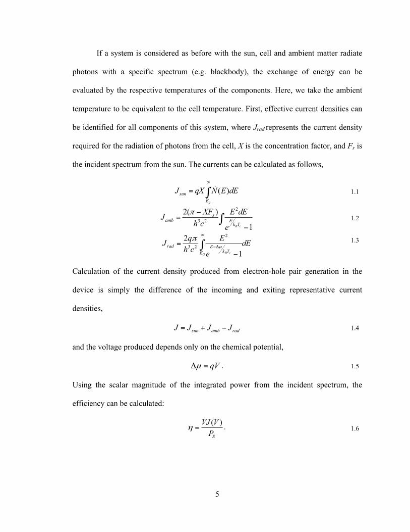
If a system is considered as before with the sun, cell and ambient matter radiate
photons with a specific spectrum (e.g. blackbody), the exchange of energy can be
evaluated by the respective temperatures of the components. Here, we take the ambient
temperature to be equivalent to the cell temperature. First, effective current densities can
be identified for all components of this system, where Jrad represents the current density
required for the radiation of photons from the cell, X is the concentration factor, and Fs is
the incident spectrum from the sun. The currents can be calculated as follows,
∫∞
=gE
sun dEENqXJ )(! 1.1
∫−
−=
1
)(2 2
23cBTk
Es
amb
e
dEEchXFJ π
1.2
dEe
EchqJ
G cBE TkErad ∫
∞
Δ−
−=
1
2 2
23 µ
π 1.3
Calculation of the current density produced from electron-hole pair generation in the
device is simply the difference of the incoming and exiting representative current
densities,
radambsun JJJJ −+= 1.4
and the voltage produced depends only on the chemical potential,
qV=Δµ . 1.5
Using the scalar magnitude of the integrated power from the incident spectrum, the
efficiency can be calculated:
SPVVJ )(
=η . 1.6

6
It is important to mention that loss due to material properties and its quality such as
diffusion length, mobility, and non-radiative recombination are neglected in this
calculation.
The versatility of this approach can be seen with the repetition of this calculation
for multiple spectra. For an Air Mass Zero (AM0) spectrum (the incident solar spectrum
from just beyond the absorbing portion of the troposphere), the limiting efficiency is 31%
at a bandgap of 1.3 eV. For an AM1.5 spectrum (the incident solar spectrum taking an
average of daily shift of the air mass absorption coefficient, which changes as the secant
of the angle between the sun and the horizon), limiting efficiency rises to 33% at a
bandgap of 1.4 eV. This calculation is a fundamental application of a thermodynamic
balance between a source and an absorber and is a commonly used limit when evaluating
effectiveness of new material systems and novel PV devices such as nanostructured solar
cells.
1.2.2. Inclusion in Triple Junction Devices
Photovoltaic devices have reached experimental efficiencies beyond this,
typically using the multijunction approach. Beyond the lattice-matched condition
specified in section 1.1, another limiting constraint is applied to multijunction cells. Since
each junction generates current, and the subjunctions are connected in series, it follows
that although the voltages add, the currents are equivalent. They are therefore restricted to
the current density generated by the subjunction which contributes the least. This current-
matching condition creates a limit to the efficiency of the entire device. In traditional
lattice matched triple junctions, the middle junction generates the least amount of current
of the three, causing it to be the limiting junction.
7
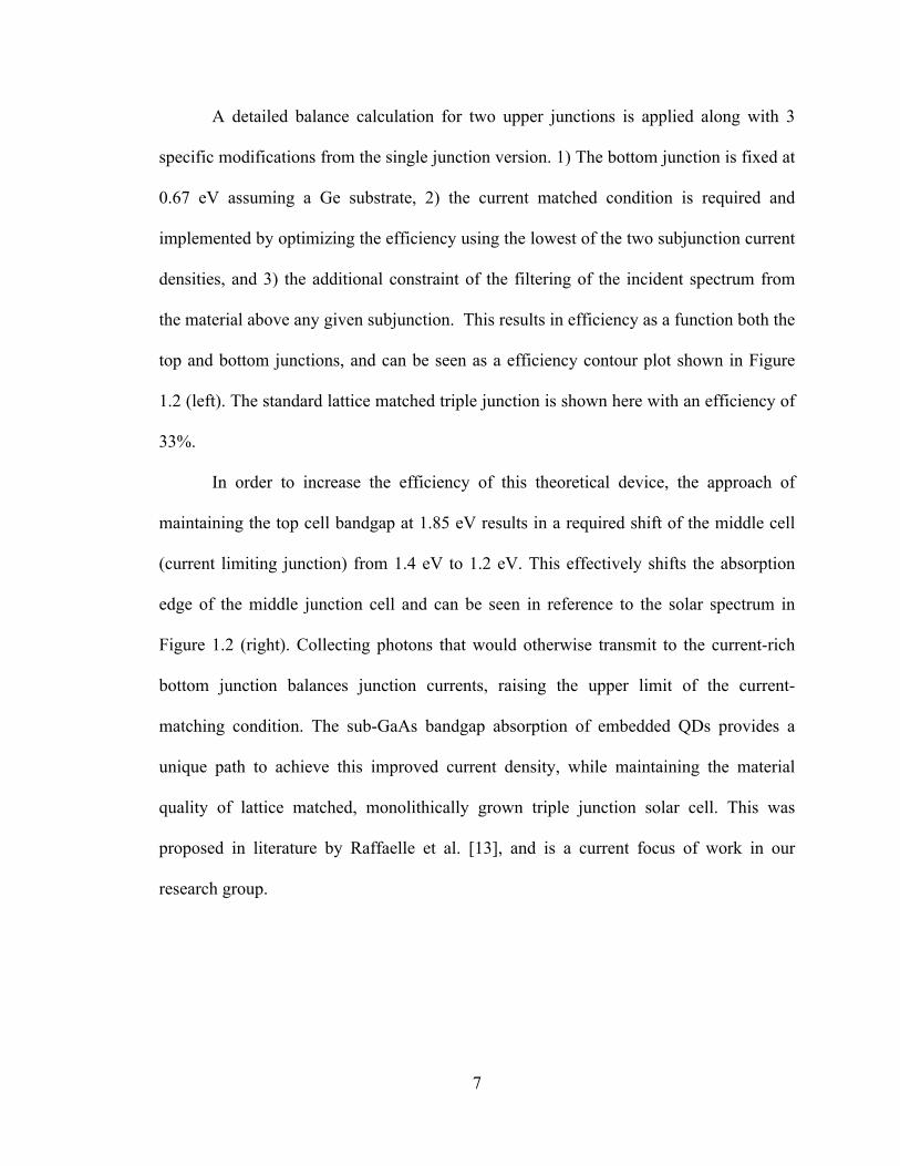
A detailed balance calculation for two upper junctions is applied along with 3
specific modifications from the single junction version. 1) The bottom junction is fixed at
0.67 eV assuming a Ge substrate, 2) the current matched condition is required and
implemented by optimizing the efficiency using the lowest of the two subjunction current
densities, and 3) the additional constraint of the filtering of the incident spectrum from
the material above any given subjunction. This results in efficiency as a function both the
top and bottom junctions, and can be seen as a efficiency contour plot shown in Figure
1.2 (left). The standard lattice matched triple junction is shown here with an efficiency of
33%.
In order to increase the efficiency of this theoretical device, the approach of
maintaining the top cell bandgap at 1.85 eV results in a required shift of the middle cell
(current limiting junction) from 1.4 eV to 1.2 eV. This effectively shifts the absorption
edge of the middle junction cell and can be seen in reference to the solar spectrum in
Figure 1.2 (right). Collecting photons that would otherwise transmit to the current-rich
bottom junction balances junction currents, raising the upper limit of the current-
matching condition. The sub-GaAs bandgap absorption of embedded QDs provides a
unique path to achieve this improved current density, while maintaining the material
quality of lattice matched, monolithically grown triple junction solar cell. This was
proposed in literature by Raffaelle et al. [13], and is a current focus of work in our
research group.

8
Figure 1.2. The detailed balance model applied to a triple junction solar cell with a fixed Ge bottom cell highlighting the current state of the art lattice-matched triple junction and the potential efficiency gains of lowering the middle bandgap of such a device (left). The effect of the lowering of this bandgap can be seen here represented by the adjustment of the absorption edge with respect to the incident AM0 spectrum (right).
1.3. Epitaxial QDs in PV
III-V materials lattice matched to GaAs exist only with bandgaps of higher
energy. In order to reduce the middle junction (GaAs) bandgap using nanostructures, the
lattice constant must depart from, and be larger than that of GaAs. This lattice mismatch
is a requirement for the growth of QDs, as will be discussed in section 2.2. Layer by layer
growth of lattice matched and slightly lattice mismatched material, is generally known as
Frank van der Merwe growth mode, and considerable thicknesses of high quality material
can be grown given a fixed substrate lattice constant. As the material lattice constant
further departs from the substrate value, the surface energy increases, until a critical
thickness is reached where defects may form [17]. This highly defective mode of growth
is called Vollmer-Webber mode and is typically avoided for optoelectronic devices. At
relatively low lattice mismatch (nominally 2-10%), a third mode of growth can be
observed. First observed by Stranski and Krastinow [18], self assembled islands nucleate
and grow indicating a compromise in the competition between cohesive and adhesive

9
forces. These islands can be maintained defect free with minimal relaxation and leave
behind a characteristic 2D layer called the wetting layer (WL).
The defect-free epitaxial growth of these self-assembled, coherently strained
islands was first shown to give strong luminescence properties in 1985 [19].
Subsequently, studies of using this Stranski-Krastinow (SK) growth mode for
optoelectronic devices began emerging such as lasers [20, 21] and infrared (IR) detectors
[22, 23]. At the same time, quantum well solar cells began to emerge based on a concept
introduced in 1990 [24]. The enhancement of device performance due to the inclusion of
QDs in solar cells was proposed for the first time [25] in pursuit of the Intermediate Band
Solar Cell (IBSC) [26], and light IV measurements of epitaxial QD solar cells were first
shown experimentally in 2005 [27]. The IBSC is of a secondary motivation for this work.
QDs are the primary method of implementation of this proposed device type and will be
discussed in detail in Chapter 5. The InAs/GaAs system was used here since it was, and
still is, currently the most widely studied of the III-V QD material systems for
optoelectronic purposes.
Despite the vast implementation of the InAs QD system in a GaAs matrix for
optoelectronic device applications, there are other systems exploring QD arrays in
optoelectronic devices. The binary elemental nature of InAs makes it relatively simple to
grow, having single group III and V elements. A common departure from the InAs QD
on GaAs is the addition of Ga, making an InGaAs ternary QD on GaAs substrates for
infrared detectors [28]. Other binary QD molecules have been explored in the GaAs
matrix such as GaSb [29]. Non-GaAs-based quantum dot systems have also been studied,

10
such as InSb on InAs [30] and InAs on InP [31, 32] for goal of improving optoelectronic
devices.
The choice of InAs on GaAs is relatively straightforward. In addition to being the
most widely studied III-V QD material system, the motivation for both single junction
GaAs, and Ge-lattice matched multijunction solar cells make it simple to implement in
existing solar cell device technology. The confinement requirement of a material of lower
bandgap than GaAs (Eg = 1.4 eV) is met with InAs (Eg = 0.36 eV). The lattice mismatch
of 7.2% (aGaAs = 5.65 Å, and aInAs = 6.05 Å), makes it an ideal candidate for the SK
growth mode without the added variable of a ternary III-V alloy.
InAs has the additional property of having a relatively early onset for the effects
of quantum confinement making it an attractive choice for bandgap tuning methodology.
Using the de Broglie Wavelength (λdb) for the determination of the onset of quantum
confinement effects, the comparison of various semiconductor materials can be made.
Figure 1.3 shows λdb for various III-V materials and Si as a function of their effective
mass. The relation is defined:
kTmdb *2 2!πλ = 1.7
where ħ is the reduced Planck’s constant, k is Boltzmann’s constant, T is temperature in
Kelvin and m* is the electron effective mass. InSb (m* = 0.014m0) exhibits quantum
effects at near 40 nm. This very high λdb value allows for tuning of energy bands at
feasible layer thicknesses. The value for InAs (m* = 0.023m0) is slightly smaller at 29
nm. Si and GaP have particularly high effective masses due to their electron band
curvature and result in quite low wavelengths requiring extremely thin layers for
confinement effects to be exploited.

11
Figure 1.3. Graphical representation of the dependence of the de Broglie Wavelength on the effective mass ratio with reported values of various important semiconductor materials.
The InAs/GaAs QDs form on the order of 20-30 nm/3-6 nm in diameter/height.
Both dimensions fall below the λdb value, making their confinement effects easily tunable
with QD size. This is seen throughout literature, with QD/barrier conduction band offsets
in the range of meV [33, 34] resulting in conduction to valance band transition energies
near 1.1-1.2 eV [35, 36].
1.4. Organization of thesis
The work included in this thesis involves the electrical, mechanical, and optical
properties of strain-balanced InAs/GaAs QD superlattices and their inclusion in the i-
region of p-i-n devices. After investigating the InAs coverage in test structures [37],
devices were grown using the optimal coverage value of InAs, and losses in Voc were
found to be similar to existing devices in literature but with improved absolute voltage
values for both QD and baseline structures [38]. QD embedded devices were
subsequently grown and fabricated with higher numbers of repeat layers and improved

12
short circuit current, along with minimal degradation in open circuit voltage led to, for
the first time, the improvement of absolute device efficiency in these devices by 0.5%.
The purpose of Chapter 1 is to give the reader an exposure to the general
motivation behind the inclusion of nanostructures, in particular QDs, in photovoltaic
devices. Briefly addressing the key features of this type of device, the reader is
introduced to the major topics which will be scientifically explored throughout the
remainder of the document.
Chapter 2 discusses photovoltaic devices and their physics both in general and
under illuminated conditions. Also included is the outline of the growth and fabrication
details performed at the NASA Glenn Research Center and Rochester Institute of
Technology. The chapter concludes with testing and preliminary results of our devices.
Chapter 3 is an overview of the strain balancing of the InAs/GaAs superlattices and the
use of GaP and GaAsP as strain balancing layers in discussed. An optimal thickness
evaluation is derived to arrive at the proper growth conditions and results are shown for
both test and solar cell devices.
Chapter 4 outlines the theory and work performed involving evolution of QD
growth within in the chamber, how it can be controlled, and how these methods can be
used to obtain an optimal coverage of InAs for these types of solar cells. Test structures
and devices are evaluated and ultimately, when many layers are grown, the improvement
in Jsc is shown to be able to outweigh loss in Voc resulting in improved efficiency.
Chapter 5 encompasses the effects of temperature on these types of devices. The
quenching of photoluminesence at high temperature, studies of bandgap and confined
state variations vs. temperature, comparisons of these under both photon and

13
electron/hole pair injection and activation energy extract are discussed topics. Particular
focus is put on the operation of the intermediate band solar cell concept as these
techniques can be of use when evaluating the performance of these devices under this
motivation.
Chapters 2 – 5 all include suggested next steps for the current state of the work.
Chapter 6 concludes the major results of the thesis and provides a recap of the next step
sections in order to provide a path forward for the research in light of current and state of
the art literature and findings.

14
2. QD Embedded Photovoltaic Devices
2.1. High Efficiency Photovoltaics
Currently the world record solar cell is 43.5% by Solar Junction which included
dilute nitride in the bottom junction [39]. Drawbacks to III-Vs include toxicity of material
source, high growth cost, high substrate cost, and low to medium throughput device
growth. Because of these, manufacturability can be limited further driving up cost. Often,
niche markets like power conversion in space, in which manufacturing costs are dwarfed
by costs of rocket propulsion fuel, opt for these types of high specific power devices.
Companies like Solar Junction are evaluating and producing concentrator modules for
terrestrial use of III-V materials. Besides Solar Junction, Emcore and Azur Space, are
also currently pursuing this path taking advantage of the reduction in cell material
provided by concentrator technology to offset the high cost of III-V materials.
2.1.1. Group III-V Devices.
Semiconductor group III (Ga, In, Al) and V (As, P, Sb) elements are used for
some of the highest efficiency solar cells produced today. Their high absorption
coefficients, high electron mobilities, and layer-by-layer epitaxial growth capabilities
provide attractive properties for high performance electronic and optoelectronic devices.
With the additional benefit of single-chamber, multiple-material growth capability,
spectrum-spanning III-V multijunction technology becomes a feasible pathway to very
high efficiencies.
Most III-V binary and ternary compounds feature a direct bandgap, i.e. aligned
minimum and maximum band transitions at the gamma point in an E-k diagram. Figure

15
2.1 shows a generalization of semiconductor band structure near this point. Indirect
bandgap semiconductors, like Si and Ge require a phonon interaction event. This trait
results in a weak absorption coefficient. For direct bandgap semiconductors, separated
electron hole pairs can populate bands without the aid of phonons (see Figure 2.1, Δk),
making them ideal candidates for devices like lasers and photodetectors. With strong
absorption coefficients, solar cells made from these materials can be kept thin as opposed
to semiconductors like silicon and germanium.
Figure 2.1. Generalized E-k diagram for semiconductor materials highlighting the Γ-point of the Brillouin Zone. For direct bandgap semiconductors, the lowest of the band minima at this point in k-space. Indirect bandgaps exhibit lowest transition band minima away from this point.
Additionally, the conduction band densities of states of III-V materials are
typically lower for direct bandgap semiconductors due to orbital symmetry [40]. Table
2.1 shows these values for Si, InP and GaAs at room temperature and equivalent doping

16
values. The electron mobility of both InP and GaAs are excellent compared to Si, making
them ideal for high frequency devices such as HEMTs and Lasers.
Table 2.1. Electron mobility and densities of states for important semiconductors.
Semiconductor Type
Conduction Band Density of States Electron Mobility
(1/cm3) (cm2/V-s)
Silicon Indirect 3.2e19 1400
InP Direct 5.4e17 5400
GaAs Direct 4.7e17 8500
The increase in mobility provided by the reduced scattering from lower densities
of states in these III-V devices leads to improved diffusion lengths. The following
equation combines the definition of the diffusion length, L, with the Einstein relation:
pnpnpnpnpn qkTDL ,,,,, τµτ =≡ 2.1
where D is the diffusion coefficient, and τ is the lifetime of the p- or n-type material.
Lifetimes especially in minority carrier devices like solar cells.
High electron mobilities and high absorption coefficients are generally
characteristic of most III-V materials allowing these excellent electronic and
optoelectronic properties to be taken advantage of for high efficiency solar cells such as
multiple junction cells. Most multijunction solar cells are connected monolithically in
series. Because of this, lattice constants of the materials forming the separate junctions
must be lattice matched. This material constraint severely restricts the binary compounds
that can be grown on any given substrate (GaAs, a = 5.6533Å or InP, a = 5.8687Å, or
Germanium, a = 5.658Å). More significant to the solar cell designer, this material

17
constraint restricts the composition of any ternary material grown subsequently. A visual
aid to any compound semiconductor grower is the bandgap vs. lattice constant chart, also
known as the “crystal growers’ chart.” Figure 2.2 shows a version of this chart for the
group III-V semiconductor materials. The lines represent a path (ternary material)
between any two binary materials varying the composition. With this useful aid, it is
easily seen that any vertical line drawn through the page represents a line of varying
bandgap but of constant lattice parameter. With a few exceptions, solar cells are typically
grown smallest bandgap first since transmission through larger bandgaps closer to the cell
surface can be collected by a subsequent sub-junction. The point at which such a vertical
line crosses a ternary line, the material can be grown upon the substrate below it with no
internal stress or strain. Germanium’s low bandgap and relatively closely matched lattice
parameter, is widely used for multiple junction solar cells.
Figure 2.2. Left: Bandgap vs. Lattice constant chart used by III-V compound semiconductor crystal growers and designers [41] (copyright pending). Solid dots represent available latticed-matched binaries/ternaries. Right: Standard materials for a monolithically grown triple junction stack.
Desired
Desired
Desired Ge
InGaP

18
A detailed balance calculation reveals that given the option of three junctions,
with Ge (Eg = 0.67eV) fixed as the bottom junction, the middle and top junction
bandgaps are optimized to be 1.21 and 1.86eV, respectively [13]. Lattice matched InGaP
(In content = 49%) gives about this value for the top bandgap, but no lattice matched
material exists at the 1.21eV bandgap point. The calculation above suggests that under a
one sun AM0 spectrum, a triple junction cell with these bandgaps will give a conversion
efficiency of 47% [13]. Therefore tuning of this middle junction to better fit the spectrum
is paramount for the space power community. The inclusion of nanostructures is
proposed in this work as a method to achieve this.
2.1.2. PV Bandgap Tuning with Nanostructures.
The use of layers of quantum confined material inside a solar cell was been
suggested, as mentioned earlier, by Barnham and Duggan [24] and realized by Barnham
and others [11, 42, 43]. The ability to tune the bandgap can be implemented here to attain
the lower bandgap need of the middle junction (1.21eV). With the GaAs (Eg = 1.42eV)
embedded with InAs QDs (typical ground state absorption 1.0-1.1eV [35]), an “average”
bandgap can be estimated to have values much closer to this preferred energy. ‘Bandgap
tuning’ has the potential use as a tool to achieve bandgaps otherwise inaccessible.
The pursuit of the IBSC is a more specific, focused use of quantum confined
material within a solar cell. This concept, proposed by Marti and Luque, hypothesizes
that intermediate level states or ‘minibands’ provided by wavefunction coupling between
embedded nanostructures provide photon absorption capability from both valence to
intermediate and intermediate to conduction bands [26]. This functionality reduces

19
transmission loss much like a multijunction cell and gives a detailed balance efficiency
value of 63% with an optimized energy transitions. Their result corresponds to a total
host bandgap of 1.93eV, with the intermediate band at 1.23eV from the valence band.
Their theory has very specific assumptions, most of which are quite unrealistic at this
technology juncture, such as a concentration value of 46,000 suns, no non-radiative
recombination, and infinite carrier mobilities [26]. Quantum well structures would
otherwise be useful for this concept except that the isolation requirement of the
intermediate band can only be ideally satisfied by a band with zero-dimensional density
of states [44]. For this reason, this concept has drawn much attention to solar cells
embedded with QDs as the most viable means of realizing such a device [45]. It is these
two potential solar technologies that motivate the work done here.
2.2. Photovoltaic Operation and Testing
Photons striking a uniformly doped single material semiconductor generate
electrons and holes, which relax back to their equilibrium state. Solar cells make use of
this photovoltaic effect in which device asymmetry is used to collect the separated charge
prior to relaxation. The asymmetry is provided by reversing the doping polarity within a
bulk semiconductor material, producing a p/n or n/p junction. Virtually all solar cells
operate using this type of asymmetry making the physics of the p/n junction fundamental
to the understanding of photovoltaic device operation.
2.2.1. The p/n junction
A metallurgical junction is formed in a material when a semiconductor with
excess acceptors (p-type) meets an interface with a material with excess donors (n-type).

20
A depletion region forms at this interface creating a natural intrinsic layer between the
extrinsic (doped) layers. Evaluation of this i-region can be followed by a standard
electrostatics treatment of device material, doping levels and thicknesses. Using
Poisson’s equation:
2.2
we can convert the doping profile into an electrostatic potential (φ), where N is the
concentration of the respective dopant. By integrating the profile of this potential, we can
arrive at the built-in voltage (Vbi). In the case of an abrupt junction device,
2.3
and these values are typically 1.2-1.5 for GaAs and 0.8 to 1.1 for Si (depending on
doping level) [46]. Vbi can be an important metric in solar cells, as it is directly
proportional to the open circuit voltage of a device and is shown in Figure 2.3, below.
Ultimately, depletion width can be calculated from this value. As it may be desirable for
improved absorption and collection purposes, an i-region maybe artificially inserted into
an abrupt junction design to enhance device performance.
To this point we have discussed the statics of p/n junctions, yet the
electrodynamics of these devices reveal the fundamental operation of photovoltaic action.
In order to examine the influence of generated electron hole pairs, the existing currents in
a p/n junction will be briefly discussed first. Currents in the junction, under no
illumination, are dominated by both drift and diffusion components based on location
within the junction. In the i-region, there is a strong electric field present due to the
( )+− −+−=∇ DA NNpnEq
002φ
⎟⎟⎠
⎞⎜⎜⎝
⎛= 2ln
i
DAbi n
NNqkTV

21
missing excess carriers, inducing drift as the dominating current flow mechanism. In the
quasi-neutral regions, diffusion is predominant. These regions are depicted for a device at
equilibrium in Figure 2.3. The energy of the conduction, valence and Fermi level are
shown as Ec, Ev and Ef, respectively.
Figure 2.3. The three regions of a p-n junction and the electronic band structure at equilibrium.
At equilibrium, these competing currents can be evaluated algebraically with the
total current relationship:
pneq JJJ += 2.4
nqDnEqJJJ nndiffusionndriftnn ∇+=+= µ|| 2.5
pqDpEqJJJ ppdiffusionpdriftpp ∇−=+= µ|| . 2.6
In equations 2.5 and 2.6, the components of the current are separated with the first term
resulting from the drift associated with the electric field, E, and the mobility and carrier
populations. The second term describes the current purely associated with the spatial non-
uniformity of carrier populations and results in the current contribution from diffusion
action.
Under applied bias, a term describing the current from the space charge region
becomes significant and an exponential relationship with the applied voltage which is

22
derived from the Fermi-Dirac statistics of a semiconductor. The differences in band
structure under applied bias can be seen in Figure 2.4. The energy offset in either band is
now reduced by the applied voltage. The diffusion of excess majority carriers increases
significantly outweighs the drift component which has been further reduced from the
decrease in electric field. The correct application of ohmic contacts, this current can be
extracted as a function of voltage applied, resulting in a J-V relationship.
Figure 2.4. The three regions of a p-n junction and the electronic band structure under applied bias.
Additionally, in high-quality, direct bandgap semiconductors, radiative
recombination currents (also exponentially dependent on voltage) can become significant.
These conditions result in a current-voltage relationship as follows:
⎟⎠⎞
⎜⎝⎛ −+⎟
⎠⎞
⎜⎝⎛ −+⎟
⎠⎞
⎜⎝⎛ −= 111 0|
20|0|
kTqV
radkT
qV
scrkT
qV
diffdark eJeJeJJ 2.7
⎟⎟⎠
⎞⎜⎜⎝
⎛+=
pd
p
na
nidiff LN
DLNDqnJ 2
0| 2.8
( )pn
pniscr
wwqnJ
ττ
+=0| . 2.9

23
where Jdark is the total current in the device as a function of voltage, Jdiff and Jscr envelope
the diffusion and drift components discussed above and Jrad is the radiative
recombination portion (which can have significance in high quality materials with direct
bandgaps). This is a form of the diode equation. Of note here in equation 2.7 is that the
voltage dependencies differ by the denominator in the exponential, termed the ideality
(n). For both diffusion and radiatively limited devices, this value tends toward n = 1, and
in the case of poor material quality and/or low injection operation, the effects of
recombination in trap states in the space charge region dominate the dark current and this
ideality approaches n = 2. The interaction of a semiconductor with light adds another
term to this equation which will be discussed in the next section.
2.2.2. The illuminated p/n junction
Under illumination, generation and recombination have affects the carrier
populations in the material and alters these equations. Generation of carriers from
incident photons provide additional terms in the equations used to derive equation(s) 2.7
through 2.9. These sum to a value of light-induced current called the short circuit current
density, Jsc:
( ) ( ) ( ) ( )[ ]∫∫∞∞
−−−==00
dEEjEjEjdEEjJ scrpnscsc 2.10
The individual light-generated current terms are energy dependent and can be
calculated from the incident spectrum, bs, reflectance, R, and the absorption coefficient,
α. This relationship is shown here for the example of jn(E):
( ) ( ) ( )( ) ( )xEsn eEREqbEj α−−= 1 2.11

24
This relationship is used for all regions of the device, and x is representative of the
current contribution of the particular region of the device. Here, the dependence of
semiconductor material can be evaluated. The absorption coefficient is dependent on the
density of states and can be approximated as:
( ) ( ) 210 gEEE −=αα 2.12
Clearly, at E equal to Eg, the absorption coefficient drops to zero, and at E < Eg, is
undefined, representing transmission of light through a material at wavelengths higher
than that of the absorption edge. The inclusion of nanostructures in devices potentially
extends this absorption range and can therefore have a direct positive effect on the short
circuit current density.
This short circuit current density is voltage independent and is added as a term in
the diode equation that is constant with respect to voltage:
sckT
qV
radkT
qV
scrkT
qV
diff JeJeJeJVJ −⎟⎠⎞
⎜⎝⎛+⎟
⎠⎞
⎜⎝⎛+⎟
⎠⎞
⎜⎝⎛= 0|
20|0|)( 2.13
This is the light-based diode equation and is competitive in nature with the other dark
currents in the device and offsets the diode curve at all values of V, by the Jsc value. The
point on the diode curve described by equation 2.13 where the dark current terms exactly
cancel the light generated current is known as the open circuit voltage. At this point the
diffusion and radiative terms are dominant, and the Jscr term can be neglected. Setting the
By this definition, setting the J(V) term to zero, plugging in Voc for the voltage, and
rearranging this simplified equation gives:
⎟⎟⎠
⎞⎜⎜⎝
⎛+= 1ln
0JJ
qnkTV sc
oc 2.14

25
in which case, the J0 factor is dominant dark current value at short circuit current, called
the saturation current, and is described by equation 2.8. This parameter has a strong
influence on the open circuit voltage and is an important metric in determining material
quality of a solar cell. It is strongly and moderately dependent on the intrinsic carrier
concentration, ni, and the diffusion coefficient, D of the material. Table 2.2 shows these
values in diffusion limited device regime for important photovoltaic semiconductors at
typical doping levels.
Table 2.2. Intrinsic carrier concentration and saturation current densities for important photovoltaic semiconductors.
Semiconductor ni
Dn Dn J0
(1/cm3) (1/cm2-s) (A/cm2)
Silicon 1.0 x 10¹⁰ 36 12 1.2 x 10⁻¹²
InP 1.3 x 10⁷ 130 5 6.2 x 10⁻¹⁸
GaAs 2.1 x 10⁶ 200 10 2.3 x 10⁻¹⁹
Typical open circuit voltage values generally track with these with Voc|GaAs >
Voc|InP > Voc|Si. This correlates with the dependence of ni on Eg: gEi en −∝2 . Because of the
dependence of the saturation current on material quality, evident through its dependence
on the diffusion coefficient, keeping material quality high directly improves the open
circuit voltage values of photovoltaic devices.
The open circuit voltage and short circuit current are important extractable
parameters that can be obtained from a light-IV measurement, as discussed in the next
section. They, along with the fill factor, ultimately determine a solar cell efficiency, as we
will see in the next section.

26
2.2.3. Devices Under Test
Testing state of the art solar cells requires equipment that allows comparison of
results to those in the research community. Efficiency is calculated from illuminated
current density (J) vs. voltage (V) measurements (light J-V curve). Precise control of the
space solar spectrum is obtained using NASA certified calibration solar cells along with
an air mass zero (AM0) filter. The terrestrial solar spectrum is calibrated using NREL
certified solar cells under an air mass 1.5 (AM1.5) filter. A TS Space Systems Class A
solar simulator along with a Newport single source xenon lamp were used to generate the
spectrum. Figure 2.5 shows the close-matched nature of this simulator at RIT along with
the ASTM AM0 spectrum. Spikes in the visible wavelength region are due to the
spectrum lines typical of a xenon bulb.
Figure 2.5. The ASTM standard AM0 spectrum overlaid with the AM0 filtered simulated spectrum generated by the TS Space Systems solar simulator at RIT.
With the provided simulation of the spectrum under AM0 conditions, a light J-V
curve obtained from one of our GaAs baseline cells is shown in Figure 2.6. The diode

27
behavior of these p-i-n solar cells, provide the J-V behavior shown in the red dashed
curve.
Figure 2.6. Light J-V curve indicating important extractable solar cell parameters from data.
A typical illuminated measurement lies in the fourth quadrant, but is commonly
mirrored into quadrant one for ease of display. In this plot, it is easy to see the parameters
that are of importance in solar power production. The blue dot indicates the short circuit
current density (0 V) under this specific illumination condition. The point at which the
current is zero (or where the light-generated current is equal to the forward bias-induced
current) is the open circuit voltage and indicated with a green dot in Figure 2.6. The
product of any current density value with its corresponding voltage value, give the
particular power density at that given point on J-V curve. The location at which this
product is maximized is denoted as the maximum power point, and is labeled on the plot

28
in orange. The power generated here divided by the power of the incident spectrum gives
the device efficiency. Equation 2.15 shows this quotient and its constituents,
inc
ocsc
incinc PVJFF
PVJ
PP
=== maxmaxmaxη 2.15
where Jmax and Vmax are the current density and voltage values at the maximum power
point. Also from this curve, we can obtain the device fill factor (FF), which collects
losses from shunt and series resistance in a single ratio. Graphically, it is the ratio of the
shaded box and the bigger box (defined by Jsc and Voc). In equation 2.16, we have,
ocscocsc VJVJ
VJPFF maxmaxmax == 2.16
The fill factor is a single, quantitative metric describing the departure from an ideal diode
by losses such as series and shunt resistance. Series resistance becomes significant when
there is internal voltage reduction throughout a device. The most significant loss in FF,
for high-quality solar cell materials, is ohmic contact resistance, Rs. The diode equation is
altered by including both series and shunt resistance, Rsh, as follows.
( )( )
scsh
sktJARVq
JRJARVeJVJ
s
−+
+⎟⎠⎞
⎜⎝⎛ −=
+
10 2.17
From this, it is clear that shunt (series) resistance must be maximized (minimized) to
obtain a minimized 2nd term, or ratio, in this equation. At any given voltage, the size of
this ratio will determine the squareness of the diode, and can be represented by the fill
factor.
Current generation in a junction (or multiple junctions) can be experimentally
spectrally resolved by obtaining characteristic spectral responsivity (SR) measurements.
Spectral responsivity is a measure of a photo-electrical conversion as a function of the

29
spectral wavelength and is very sensitive to the material quality. Taking equation 2.10 and
dividing out the spectrum, we get:
( ) ( )( )( )Ej
EREqbESR sc
s −=
11)( 2.18
where jsc(E)is the integrand of equation 2.10. This integrand, jsc, is a sum of the current
contributions from different regions of the solar cell. In this way, a reduction in the SR
can be directly associated with a loss in a particular region’s diffusion length. This can be
useful in determining the identification of losses within a p-i-n junction.
The technique allows calibrated incoming monochromatic light to be absorbed
and converted by the cell, while a wavelength-specific short circuit current is measured.
This SR measurement can then be converted to an external quantum efficiency value
(EQE) which is also spectrally resolved, but is independent of the photon energy. This
can be calculated from the SR using equation 2.19:
( )( )1240eV nm SREQE
λ
∗= 2.19
where λ is the specific wavelength of the given SR data point. Quantum efficiency is a
well known optoelectronic metric and is used for LEDs and photodetectors. A plot of the
experimental external quantum efficiency for a single junction GaAs solar cell is shown
in Figure 2.7. This was taken using an Optronics Laboratories 750 series
spectroradiometer equipped with an internal lock-in amplifier at 167 Hz. Here, we can
see the peak is about 71% at 700nm. If this cell was a perfect absorber, it would give
100% at all wavelengths. Much of the light hitting the solar cell is reflected (almost 30%
averaged over the wavelength) and light at energies lower than the electronic bandgap is

30
transmitted. If these are taken into account, the plot gives internal quantum efficiency
(IQE) and is much closer to 100%. This can be seen in the following equation:
( )( ) ( )ETER
EEQEEIQE−−
=1
)( 2.20
where T(E) is the transmission of light as a function of photon energy.
Also of note here is the semiconductor’s absorption bandedge. The bandgap of
GaAs is 1.42eV at 300K. This is equivalent to energies of photons with wavelengths of
about 880nm and below. This is shown here as the EQE quickly drops to 0% at or near
this wavelength value. This can be seen in equation 2.20 as a transmission of unity at
these wavelengths. Photons with energy less than the bandgap will not be absorbed by the
material, and therefore the smaller the bandgap, the more current the junction will
generate. However, since voltage is highly dependent on the bandgap of the material as
well, a smaller bandgap will results in a lower voltage. This tradeoff has been outlined in
Chapter 1 using the detailed balance calculation. It is in this manner that QDs show the
potential of lowering the bandgap to gather more of the sun’s emitted photons, without
sacrificing the higher voltages of the host bandgap.

31
Figure 2.7. Spectral resolution of current generation in SJ GaAs solar cell overlaid on the AM0 solar spectrum. Throughout the next four chapters, the work completed will be shown in order to
provide preliminary details on how these devices can be improved upon with the ultimate
goal of improving solar cell efficiency, while also further characterizing the phenomenon
of in the insertion of low dimensional, quantum confined structures into optoelectronic
devices with the specific focus on photovoltaic energy conversion.
2.3. Device Design
The design of a solar cell layer structure the layer structure of a solar cell, of the
utmost importance can be the layer doping and thicknesses. Higher doping will widen the
chemical potential, improving the open circuit voltage, while also decreasing diffusion
length and mobility due to scattering effects. Layer thickness follows a similar
optimization, with the necessity to be thick enough for maximum absorption, but
remaining on the order of the diffusion length to avoid recombination of minority carriers

32
prior to reaching the junction. The absorption of photons decays exponentially into the
cell based on the Beer-Lambert law:
xeII α−= 0 2.21
where α is the absorption coefficient of the material. This leads to the same exponential
dependence of carriers generated throughout the material. Therefore, it is necessary to
place the physical junction (i.e. point of highest electric field) near the approximate
halfway point of this generation function. Additionally, since the majority of the carriers
are generated near the surface, a highly doped emitter layer (quasi-neutral region closest
to the incident photon flux) to ensure efficient minority carrier collection. These two
constraints lead to designs with much thinner emitters (100-700 nm) than base (quasi-
neutral region physically beneath the emitter and i-region) layers (few microns). In this
section, we will outline the basic device design used at RIT in more detail and
subsequently discuss the modifications necessary to incorporate nanostructured
superlattices.
2.3.1. The p/i/n junction
The p-i-n junction is often used in III-V solar cells (and particularly in amorphous
Si) as it is simple to grow epitaxially (as opposed to diffusion-created junctions often
used in crystalline Si). An extended i-region is advantageous for the exploitation of an
higher absorption volume of low-doped, higher lifetime material. The extended electric
field increases the ratio of drift-driven to diffusion-driven carriers. This is especially
important in minority carrier devices in which carriers photogenerated in quasi-neutral
regions have a likelihood of not reaching the junction. Since devices used for this work
make use of QD-embedded superlattices placed in the high-electric field region, it is also

33
convenient to have a comparable i-region thickness for comparable nanostructure-
excluded control, or baseline cells. An outline of the layer structure for the basic GaAs
cell is included in this section.
2.3.2. Growth and Fabrication
The materials used in this work are predominantly lattice-matched to GaAs. This
is the clear choice for the investigation of GaAs-lattice-matched triple junction devices
and therefore results from this work can easily transfer to that system. as that is the
cheapest III-V substrate, and in-depth studies of the InAs/GaAs QD material system
requires a GaAs host. The single junction solar cells used for these studies are comprised
of the following layers grown on the n-type substrate (in order of growth):
1. 250 nm n-type Si doped GaAs epitaxial seed layer
2. 50 nm n-type Si doped 1 x 1018 cm-3 InGaP “window” layer used for blocking
minority carrier holes from diffusing to the n-type contact layer
3. 2000 nm n-type Si doped 1 x 1017 cm-3 GaAs base layer
4. 100 nm unintentionally doped n-type 5 x 1015 cm-3 GaAs i-region layer
5. 500 nm p-type Zn doped 1 x 1018 cm-3 GaAs emitter layer
6. 50 nm p-type Zn doped 2 x 1018 cm-3 InGaP “window” layer used to reduce front
surface recombination
7. 160 nm p-type C doped 2 x 1020 cm-3 GaAs contact layer
All layers are grown in a Veeco 3 x 2” rotating disk metal chemical vapor
deposition (MOCVD) reactor shown in Figure 2.8. Precursor metal-organic alkyl gases
used for the epitaxial layers include Trimethylgallium (TMGa), Trimethylindium (TMIn)

34
for the group III elements, and precursor hydrides used include Arsine (AsH3) and
Phosphine (PH3), for the group V elements. N-type dopant sources used are
Diethyltelluride (DETe) and Disilane (Si2H6). P-type dopant sources used are Diethylzinc
(DEZn) and Carbon Tetrachloride (CCl4). Temperatures for most GaAs and InGaP layer
ranged between 575 and 675C. Chamber pressures are typically held at 60 Torr for
standard bulk growth. Typical growth rates under these conditions vary from 1-2 µm/hr
depending on material. For bulk GaAs and InGaP layers, the V/III ratio was 58,
maintaining the AsH3 overpressure necessary to prevent the formation of group III metal
islands.
Figure 2.8. Image of the MOCVD reactor at the NASA Glenn Research Center.
Figure 2.9 shows the layer structure described above, with the addition of
multiple-layer QD superlattice in place of the 100nm intrinsic layer. The embedded QD
superlattice layer structure consists from five to one hundred repeat units of the following
5 layers in growth order:
1. InAs wetting layer and QD array
2. Low temperature GaAs capping layer
3. High temperature GaAs spacer layer
4. GaP strain balancing layer

35
5. High temperature GaAs spacer
Epitaxial QD arrays are grown by the Stranski-Krastinow (SK) growth method elaborated
on in a later section. Typical growth temperatures for this growth mechanism are 100-
200°C lower than is required for the growth of high quality GaAs bulk and spacer layers.
Growth temperatures are raised to 575°C for the remaining GaAs and GaP layers to avoid
low-quality defective 2D layers typical of low temperature growth. To prevent InAs from
evaporating during this rise in temperature, a thin (2.1 nm) GaAs layer is deposited
before the temperature increase. The GaAs (4.6 nm), GaP (1 nm, nominal) and
subsequent GaAs (4.6 nm) layers are all grown at the higher temperature before returning
to 490°C for the beginning of the next repeat unit (InAs). This sequence is repeated for
the desired number of repeat units, each of which results in approximately 14 nm of
material. For reference, this results in i-region thicknesses of 140 nm for a 10-layer repeat
unit structure, and 560 nm for a 40-layer QD superlattice. The GaP and high temperature
GaAs spacer thicknesses are varied for particular studies which will be addressed in
subsequent chapters.
The procedure for growth of solar cells embedded with these superlattices, are
varied only after the base layer (GaAs) is completed. After the desired superlattice is
complete, 33 nm of unintentionally doped GaAs is grown at 620°C. The doped emitter
layer then continues the sequence identical to a solar cell without a superlattice-
embedded i-region. For test structures grown for this study were grown with the same
250 nm epitaxial seed layer, followed by the superlattice discussed above. A 33 nm GaAs
cap layer is then deposited for quantum mechanical barrier isolation of the multiple
quantum dot layers. A layer of InAs wetting layer and QDs is then grown on the surface

36
as the final layer for surface characterization using Atomic Force Microscopy (AFM).
Growth and optical, electrical and mechanical characterization of these arrays and their
superlattices are deeply investigated in further sections and chapters.
Figure 2.9. Cross section of GaAs single junction solar cell embedded with QDs.
This is then followed by the typical metallization contact layer as in step 6 of the
GaAs cell. Quantum dot embedded solar cells are grown in the intrinsic region of the
GaAs junction, replacing step 3 in the growth steps (and as depicted in Figure 2.9).
Standard solar cell fabrication processing is used to make epitaxially grown layers
into actual power producing solar cells. The device is contacted on both the top and
bottom of the device, with metallization systems that accommodate both p-type and n-
type GaAs. P-type GaAs allows for ohmic contacting to metals with lower work
functions, such as eutectics of Au-Zn, Ag-In, Ag-Zn and In-Zn [47]. In this work, the Au-
Back Contact
GaAs Substrate
GaAs buffer
InGaP Window
GaAs Base
GaAs EmitterWindowContact

37
Zn alloy is used. A final layer of thick, current-carrying Au is the deposited. Au is chosen
for its low reactivity and high conductivity. Zn has a fairly low melting temperature
lending itself well to thermal evaporation systems. For n-type ohmic contacts, the Au-Ge
alloy is used. This alloy is chosen since, for p-on-n devices, the n-type doped side of the
device is a 300 nm thick substrate. Ge has a very high diffusion coefficient in GaAs, but
can afford to be used here since there is low chance of the Ge atoms to puncture the
physical junction, preventing carrier shunt pathways. Other potential n-type metallization
layers include Au-Si, Au-Te and also Ag-In [47]. All metallization is performed with
thermal evaporation equipment, and alloys are sequentially deposited during the same
low pressure (< 10-6 torr) chamber evacuation.
An annealing step is then used for the diffusion of the metal/alloy into the
semiconductor lattice. This was optimized by testing various temperatures and
minimizing the contact resistance using a standard semiconductor TLM method. P-type
metallization was found to give the best results at 406°C and n-type metallization was
optimized at 372°C. For this reason, typically the p-type anneal is performed prior to the
n-type anneal.
Lift-off photolithography is used for patterning of the current distribution grid.
The non-photoactive lift-off resist, LOR-10A is used in two spin-cast (3000 rpm)/bake
steps of 1 um thickness each. The bake temperature used was 180°C, for 6 minutes. A
photoactive resist layer is then deposited. MicroChem Microposit S1813 is spin-cast at
3000 rpm and baked
The photoactive resist is exposed through a patterned, chrome coated
photolithography mask. The mask includes seven 1 x 1 cm2 cells designed for 1 sun

38
illumination. Also included are three 1 x 0.5 cm2 concentrator-designed grid cells, two
quantum efficiency pads, transmission line model (TLM) measurement pads A
broadband/g-line ultraviolet light source was calibrated to 10 mW/cm2 irradiance. A 12.5
second exposure provides an energy density (dose) of 125 mJ/cm2. A photoresist
development step is then performed using MicroChem Microposit MF CD26 developer
solution, after a Hexa-Methyl Disilizane (HMDS) surfactant surface preparation. After a
two minute developer immersion (approximately 1 minute for the photoactive layer, and
1 minute for the development of the LOR resist), the wafers are rinsed with de-ionized
water, and dried with a nitrogen jet. After the image is transferred into the photoresist
pattern, An overhang sidewall profile remains due to the isotropic dissolution of the LOR
resist. Thermally deposited metallization is then applied. To realize the grid structure and
remove the underlying resist, a strong polar solvent, N-methyl Pyrrolidinone is used
(Nano Remover PG by Microchem) for the removal of all photoresist, lifting off the
metal of the negative image of the mask, leaving only the desired pattern. The annealing
step is then performed described above.
For the isolation of the cells and a wet-chemical mesa isolation step is then used
to define (physically and electrically) the dimensions of the cell. A simpler
photolithographic process is used for masking the etchant. For this process,
approximately 1 µm of S1813 photoresist is deposited after an HMDS surface
preparation. A 60 second exposure is used under the same dose as above, followed by a
1 min bake at 115°C and a 2 minute develop in MF CD-26 developer agent.
Common etches for III-V materials make use of acids such as HCl, H3PO4, and
H2SO4. These are typically combined with an oxidizer such as H2O2 and can be diluted in
39
H2O. For this work, a mixture of H3PO4, H2O2, and water (in a ratio of 3:4:1) is used for
the etching of (100) oriented GaAs layers. The phosphoric acid is particularly suited for
binaries ending in -As group V elements. It is an aggressive GaAs etch with etch rate of
0.16 µm/s. The hydrogen peroxide oxidizes the semiconductor, upon which the acid
dissolves the oxide. The anisotropic nature of the phosphoric acid mixture results in the
slowest etch rate in the {100} plane family [47]. For a (100) surface, this etch results in a
90° sidewall. HCl is commonly used for P-ending group V compounds. For the InGaP
layers, this was used without dilution, providing an etch rate of 0.3 µm/s.
All photolithography, liftoff resist dissolution, and wet chemical etches were
performed in a class 1000 cleanroom at RIT. When possible, experimental QD solar cells
are fabricated in tandem with SJ GaAs control cells, or “baselines.”
2.4. Growth of QDs
2.4.1. Strain in Epitaxial Layers
The deposition of epitaxially grown material by either Molecular Beam Epitaxy
(MBE) or MOCVD is controlled on the atomic level and very abrupt interfaces between
layered materials can be realized [48]. One of the essential mechanical properties of these
heterostructured materials is the lattice constant, a0. This value, in an unstrained
environment is a result of the delicate competition between ionic and covalent force
interaction in compound semiconductors between, for instance, the binary atoms (Ga, As)
in GaAs. This energy minimization results in this natural atomic distance, a0. As a layer
of a material is deposited by either of these techniques, the lattice constant of the
substrate is replicated by the newly deposited layer, regardless of its own lattice

40
parameter. This property is called coherent growth and a layer with the same lattice
parameter as the underlying material is called lattice-matched.
When a material is lattice-mismatched, or the deposited material has a lattice
parameter slightly larger, or smaller than the underlying material, a phenomenon called
tetragonal distortion occurs depicted in Figure 2.10 (left). When atoms of one lattice
parameter (a0), are forced to a different value (a||), the minimum energy formation of the
unit cell is altered, and the lattice parameter in the growth direction (a⊥) shifts to
accommodate. This is shown in this figure for both materials with both smaller and larger
lattice constants than the substrate material beneath, resulting in material in tension and
compression, respectively, in the in-plane direction. Assuming zero relaxation of the
lattice, this geometry persists through the extent of the layer thickness.
Figure 2.10. Illustration of tetragonal distortion and its two and three dimensional representations.

41
Tetragonal distortion directly affects the out-of-plane lattice parameter as well. As
a material with a larger a0,layer than the substrate a0,subs, the former assumes the value of
the latter, becoming a|| = a0,subs. The result is that a⊥ > a0,layer > a|| in this case, following
the elastic theory of solid body mechanics and taking into account the stiffness
coefficients of materials. The equation describing this relationship can be seen in
equation 2.22 where n is Poisson’s ratio, described by 2.23 [49]. This results in the third
equation shown 2.24, where the stiffness coefficients are now seen, represented by Cij.
( ) ||||0 121 aaaa +⎟
⎠
⎞⎜⎝
⎛−
+−=⊥ νν 2.22
1211
12
CCC+
=ν 2.23
( ) ||11
12||0
21 aCCaaa +⎟⎟
⎠
⎞⎜⎜⎝
⎛+−=⊥ . 2.24
For quantum wells, this calculation is specifically important for strain balancing, a
technique which uses layers of material with lattice parameters which alternate values
higher and lower than the substrate value. This is outlined further in section 3.2. For
quantum dot arrays, tetragonal distortion subsists, but an additional mechanism becomes
prevalent at higher lattice-mismatch values.
2.4.2. Stranski Krastinow Growth Mode
For use in quantum confined devices, quantum dots must have the following
characteristics: (a) the material must have a lower bandgap than the host, and (b) the
material must have a larger lattice constant than the host. The first consideration affects
the confinement and therefore the design of the absorption band (always red-shifted from
the host). The second requirement results from the lattice mismatch necessary for the

42
special growth conditions that lead to QD formation. The first to observe this growth
condition were Ivan Stranski and Lyubomir Krastinow in 1937 [50] who gave it their
namesake.
Epitaxial growth modes for lattice-mismatched layers are typically categorized in
three groups. Purely layer by layer growth often occurs at low lattice mismatch values
(approximately 2% or less), and is called Frank van der Merwe mode. Vollmer-Weber
(VW) mode refers to a relatively high strain energy differential (due to high lattice-
mismatch) resulting in large, defective island formation. This is the most undesirable
growth mode for optoelectronic devices, as its energy minimization is a result of the
formation of lattice dislocations. If a material has a lattice mismatch of approximately
between 2% and 10% [51], it is energetically favorable for small, coherently strained,
defect-free islands to form instead of a continuous layer. This is known as the SK growth
mode, and is an alternative to defect-generating relaxation occurring in the VW mode.
These three modes are depicted in Figure 2.11 with their associated lattice-mismatch
ranges.
Figure 2.11. Visualization of the different growth modes based on lattice match and surface energy parameters.

43
These ranges are typically more approximations since the physical mechanisms take into
account the strain-related surface energy (γ) relationships. The following equation relates
the layer surface energy, γ2, the substrate surface energy, γ1 and the interface energy, γ12.
Two dimensional layer formation (Frank van der Merwe mode) occurs when the substrate
layer energy is greater than the sum of the interface and layer surface energies (equation
2.25). VW mode occurs when this sum is the larger quantity, but is typical of layers with
higher interface energy, in which the substrate surface energy does not play as large a
role. The layer surface energy, γ2, increases with layer thickness, θ. SK mode occurs
when equation 2.25 is satisfied during initial deposition, but gradually approaches and
finally surpasses the inequality represented by equation 2.26. This is typical of layers
exhibiting slight lattice-mismatches, but high thickness-dependent layer surface energies
[17].
The two dimensional transition occurs when the left and right side of equation
2.25 or 2.26 are equal, and SK growth mode continues. This transition correlates with the
system’s critical thickness, θc. This value for the InAs/GaAs system is typically near 1.5
ML [17]. Beyond this thickness, quantum dots begin to nucleate. The density becomes
then becomes highly dependent on further increased layer thickness illustrated in Figure
2.12. Shown in this figure are the effects of coverage value on QD nucleation and density
with the critical thickness of 2D to 3D transition identified. QDs are typically spherical
1122 γγγ <+ van der Merwe 2.25
1122 γγγ >+ SK & VW 2.26
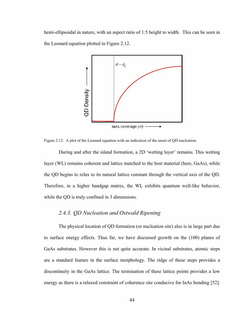
44
hemi-ellipsoidal in nature, with an aspect ratio of 1:5 height to width. This can be seen in
the Leonard equation plotted in Figure 2.12.
Figure 2.12. A plot of the Leonard equation with an indication of the onset of QD nucleation.
During and after the island formation, a 2D ‘wetting layer’ remains. This wetting
layer (WL) remains coherent and lattice matched to the host material (here, GaAs), while
the QD begins to relax to its natural lattice constant through the vertical axis of the QD.
Therefore, in a higher bandgap matrix, the WL exhibits quantum well-like behavior,
while the QD is truly confined in 3 dimensions.
2.4.3. QD Nucleation and Ostwald Ripening
The physical location of QD formation (or nucleation site) also is in large part due
to surface energy effects. Thus far, we have discussed growth on the (100) planes of
GaAs substrates. However this is not quite accurate. In vicinal substrates, atomic steps
are a standard feature in the surface morphology. The ridge of these steps provides a
discontinuity in the GaAs lattice. The termination of these lattice points provides a low
energy as there is a relaxed constraint of coherence site conducive for InAs bonding [52].

45
This is evident in two cases. Preferential alignment of QD formation along terrace step
edges has been observed [53]. This can be observed in Figure 2.13. Secondly is the degree
of which miscut plays a role in the nucleation of these sites. As the terrace step edges
created by this vicinal nature are increased, with increasing miscut angle, the QD density
increases [53].
A secondary growth mechanism can occur subsequent to coherent island
formation. Ostwald ripening, or the maturation of large, coalesced QDs begin to form at
higher coverage values. This process becomes energetically favorable when the surface
of the coherent QDs provides a new energy minimization site for other existing QDs. At
growth temperatures, the In and As adatoms are mobile enough to allow for surface
translation. The coalesced QDs are much larger (up to 25/100 nm in height/diameter)
[54]. The interfacial nature of multiple QD coalescence provides a phase difference in
morphology in which lattice dislocations can occur. This formation is detrimental to
optoelectronic device operation due to high non-radiative recombination occurrences that
may be present at these dislocations, and avoidance of this growth regime is desirable.
This topic is addressed extensively in chapter 4.
2.4.4. Experimental QD Test Structures
Test structures were grown with QDs uncapped, and atomic force microscopy
(AFM) was used to reveal size, density and shape of the QDs. Figure 2.13 shows an
example of an AFM image of these nanostructures on the surface of GaAs. From these
images, we obtain QD sizes of between 25-45 nm diameter and 5-10 nm height values.
Shape is generally hemi-spherical and QD density was found to be 5 x 1010 cm2. It should
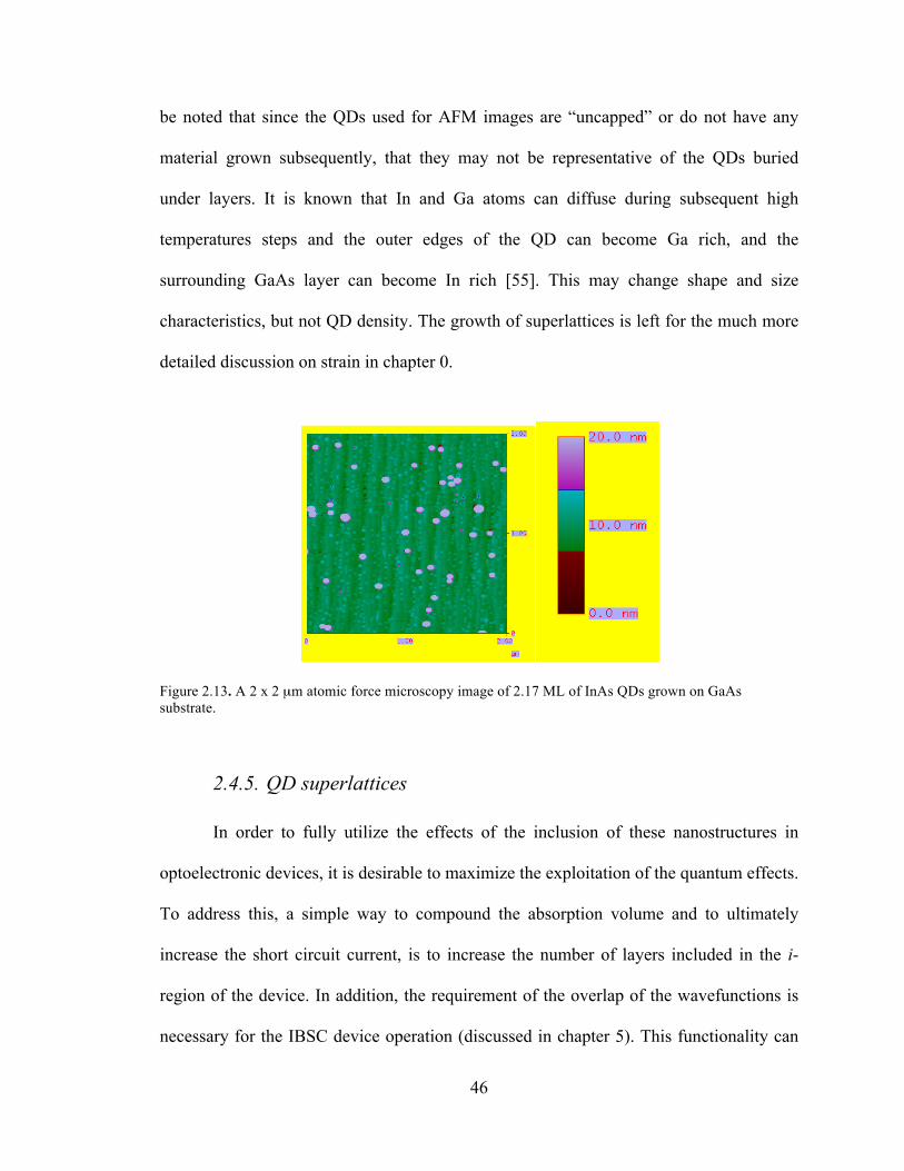
46
be noted that since the QDs used for AFM images are “uncapped” or do not have any
material grown subsequently, that they may not be representative of the QDs buried
under layers. It is known that In and Ga atoms can diffuse during subsequent high
temperatures steps and the outer edges of the QD can become Ga rich, and the
surrounding GaAs layer can become In rich [55]. This may change shape and size
characteristics, but not QD density. The growth of superlattices is left for the much more
detailed discussion on strain in chapter 0.
Figure 2.13. A 2 x 2 µm atomic force microscopy image of 2.17 ML of InAs QDs grown on GaAs substrate.
2.4.5. QD superlattices
In order to fully utilize the effects of the inclusion of these nanostructures in
optoelectronic devices, it is desirable to maximize the exploitation of the quantum effects.
To address this, a simple way to compound the absorption volume and to ultimately
increase the short circuit current, is to increase the number of layers included in the i-
region of the device. In addition, the requirement of the overlap of the wavefunctions is
necessary for the IBSC device operation (discussed in chapter 5). This functionality can

47
be obtained only by including multiple wells or dots separated by an energetic barrier. It
is for this reason that stacking the arrays of quantum dots is of critical importance. Strain
balancing in these systems becomes essential to the material quality as well, but will be
left for chapter 0. More importantly here, is the consideration of absorption depth as the
layer numbers increase.
The absorption coefficient (α) can be defined with the simple form of the Beer-
Lambert law (equation 2.21) can be used to determine the loss of intensity through a
medium, or the absorptivity (I/I0) [56]. This can be implemented using the absorption
coefficient of a quantum dot or well. Therefore absorptivity increases with amount of
material. In multiple quantum structures, layers are inherently thin and therefore
increasing the number of layers is the primary method of increasing the absorption
volume. Similar to emission-based devices, an increase in volume of the confined or
tuned absorbing media improves sensitivity in the case of a detector, [57, 58]. Similarly,
in photovoltaic devices, whether pursuing an IBSC or a bandgap tuning approach, an
increase in the absorbing media, as will be discussed, improves short circuit current
density and ultimately device performance.
2.5. Conclusion
In this chapter the origin of photovoltaic action has been established. The current
III-V technology is introduced and discussed. The current methods of splitting the solar
spectrum using the variation in bandgaps are outlined and an alternative was introduced
using nanostructured photovoltaics. The operation of a solar cell and the physics of these
devices were outlined. The regions of a solar cell were evaluated and their contributions
to device operation explained.

48
The InAs/GaAs QD system was identified for its use in these devices with
benefits including high-profile literature exposure and broad knowledge base, and the
compatibility with existing GaAs technology. Device fabrication steps were outlined and
the importance of the specifics used here was justified. Device testing was introduced and
will be valuable for the understanding of subsequent chapters. Device design was
explained in the light of the inclusion of nanostructures in the intrinsic region. Epitaxial
MOCVD growth of both semiconductor layers and QDs was described in detail and the
mechanisms of SK growth were clarified. Application of these in superlattices was
introduced and the need for this structure was explained with a focus on increasing the
number of layers included.

49
3. Strain Balancing QD Superlattices 3.1. Introduction
It is well known that heterostructure materials with mismatched lattice constants
will grow ‘pseudomorphically’ until a relatively predictable thickness. This thickness,
known as the ‘critical thickness’ was first evaluated by Matthews and Blakeslee [59].
Their analysis began with a force balance between the force exerted by the misfit strain
(involving the Poisson’s ratio, the shear modulus and the angle between multilayer
interface and slip plane), and the force resulting from the tension line of the dislocation
[59]. This force balance may exhibit an inequality, in which either dislocations form or
lattice coherence is observed. This development lead to the first derivation of the
following transcendental equation for the determination of the critical thickness, hc, of a
strained layer grown on a theoretically infinitely thick substrate [60]:
3.1
where a is the lattice constant of the strained layer, κ is the structural coefficient, ν is
Poisson’s ratio, and f is the mismatch factor defined by Δa/a. The structural coefficient is
simply an integer (1, 2 or 4) based on whether the structure is a superlattice, single QW,
or single strained layer, respectively. It is clear from this equation that at higher mismatch
factors, hc is reduced. Using this method, critical thickness for pure InAs on GaAs is hc <
1 nm, for GaP it is hc ≈ 10 nm. Although a superlattice is used here, the factor of κ = 1 for
this structure is not quite accurate since this is a strain balanced superlattice. As we will
discuss further in the following sections, a method of stain-balancing is used to grow
⎟⎟⎠
⎞⎜⎜⎝
⎛+
+
−= 12ln
125.01
2 ah
fah c
c νν
πκ

50
layers much thicker than the resulting critical thickness without this technique, since the
overall system mismatch factor decreases. In QW systems, correct stain balancing can
theoretically provide the ability to grow superlattices infinitely thick, since overall
mismatch results in a net factor of zero. Because of the three-dimensional nature of the
strain field, this is thought not to be possible with QD array-based superlattices.
In order to understand why stain balancing is necessary, it is important to first
understand the conditions that are present when strain balancing is not used. Initial
quantum dot solar cells grown without strain balancing, it was apparent that there was
significant degradation in cell material. TEM imaging of a test structures indicated
undesirable material qualities, showing inhomogeneous QD geometry, and threading
dislocations, leading to reduced lifetimes in both the intrinsic and emitter regions. Shown
in Figure 3.1 (left), is a 5 layer QD superlattice which has not been strain balanced. The
original QD size is not maintained in the growth direction. As each additional layer is
grown, the GaAs capping layer is stretched to the relaxed InAs lattice constant and
slowly relaxes back to its lattice constant before the next QD is grown. If the GaAs does
not fully relax, then the next layer of QDs will not be as mismatched as the first QD,
resulting in a wider, more pancake like structure. With each additional layer, this trend
continues approaching a more QW-like superlattice. This effect can be seen with
different materials systems, since if the lattice mismatch factor is larger, the interfacial
strain energy (γ12) will be higher, which causes greater self-accumulation of InAs,
directly affecting aspect ratio [61].
Point defects originating in the superlattice material, or i-region in a device, can
propagate as threading dislocations, in the material grown subsequently, in this case, the

51
solar cell emitter, see Figure 3.1 (middle). These defects cause unwanted recombination
in both the space charge (SCR) and the quasi-neutral regions of the device. These
problems become very obvious when looking at the illuminated forward J-V
characteristics (Figure 3.1, right). Recombination in the high defect density emitter can
reduce the amount of carriers that will complete the path to the metalized contacts. This
manifests itself in the reduced current shown in Figure 3.1 (right) for the 5 layer QD p-i-n
device when compared to the baseline with no QDs. Recombination in the SCR, places
device operation in the ideality of n = 2 region of a traditional diode curve. This
domination of the SCR term in equation 2.13 is due to the lifetime reduction shown in the
denominator of equation 2.9, significantly increasing the device reverse saturation
current, J0. As per equation 2.14, we see how this increase can degrade the open circuit
voltage of the device, and is also apparent in Figure 3.1 (right) by the loss of about
500mV with the addition of QD layers (red curve). This corresponds to an increase of
eight orders of magnitude in the J0 value resulting from a shift in the domination in terms
of equation 2.13.
Figure 3.1. Left: TEM image of 5 layers of QDs with no strain balancing describing size non-uniformity in the growth direction. Middle: TEM image of propagating defects into the emitter region above QD-embedded i-region. Right: J-V characteristics of baseline and unstrain-balanced QD-embedded solar cells.

52
The defects in shown in Figure 3.1 are typical in lattice mismatched material. The
strain associated with this lattice mismatch is principally undesirable for optoelectronic
device operation. However, if the strain can be controlled and minimized, it is possible to
use lattice mismatched material in devices. Examples of this include strained multiple
quantum well lasers [62], step-graded buffer pseudo substrates [63], as well as high
efficiency solar cells,
3.2. Strain balancing in QW solar cells
Balancing the strain in these complex structures can be simple in the case of a
quantum well. Since deposition with near-atomic precision can be achieved, balancing
this strain is necessary. Well known theories of strain balancing have been thoroughly
studied, and quick calculations can be used to determine, given both the strained layer
layers [64].
Following a specific formula (Ekins-Daukes compares 3 different formulas [64]),
for quantum wells, it is simple to determine the thickness of the GaP layer that will
correctly compensate for strain in the originally strained layer. The simplest of these,
namely the average lattice method (ALM) [64], was used originally to compare our
samples with and those without strain compensation. In this method, the thickness/lattice
constant product is used to determine the appropriate strain balanced condition. If tsl is
the thickness of the originally strained layer, and tb is the to-be-determined strain
balancing layer, then,
⎟⎟⎠
⎞⎜⎜⎝
⎛
−−
=b
slslb aa
aatt0
0 3.2
b)

53
The thickness weighted method includes the thickness as a weighting, assuming that a
thickness-lattice constant product is more influential to strain balancing than purely the
lattice constant alone and is described by:
⎟⎟⎠
⎞⎜⎜⎝
⎛
−−
=b
sl
sl
bslb aa
aaaatt
0
0 3.3
And finally, the zero stress method includes the stiffness coefficients of each material.
The values of these are different enough between semiconductors such that the inclusion
of them into the strain balancing calculation is necessary, and is shown in equation 3.4:
⎟⎟⎠
⎞⎜⎜⎝
⎛
−−
=bbb
slslsl
sl
bslb AaAa
AaAaaatt
0
02
2
3.4
where:
ii C
CCCA ⎟⎟⎠
⎞⎜⎜⎝
⎛−+=
11
212
12112
3.5
where asl and ab are the lattice constant values of the strained layer and the balancing
layer, respectively.
3.3. Strain Balancing in QDs
For quantum dot material, there is less of a layer and more of a non-continuous
array of islands. Therefore, this strain balancing can be more complex, as the strain fields
are now in three dimensions, instead of nominally one. The material choices for strain
balancing are limited to those with lattice constants less than that of the host material, in
this case GaAs (a0 = 5.6533Å). Referring again to the crystal grower’s chart (Figure 2.2),
we see III-V materials that can be utilized for this purpose as having a higher bandgap

54
than the InAs QD structures as well as the GaAs host and spacer layers. The materials
available from the OMVPE reactor at NASA GRC, including trimethylgallium (TMGa),
trimethylindium (TMIn), trimethylaluminum (TMAl) (as group III precursors) and arsine
(AsH3) and phosphine (PH3) (for group V precursors) were used for alkyl and hydride
sources, can be used for growing most binary and ternary compounds.
Although ternary materials can be and often are used for device design and
managing strain, binary compounds are used when possible, due to their ease of growth.
The single binary III-V compound with a shorter inter-atomic distance than GaAs is GaP.
This material is also convenient for the purpose of keeping the layer thin, aiding in both
carrier transport and miniband formation, which requires a high degree of proximity for
the confined states. The lattice constant of GaP is aGaP = 5.45Å resulting in a lattice
mismatch with GaAs of ~3.6%. When GaP is grown directly on a layer of GaAs, its
lattice constant is stretched in the parallel-to-wafer-surface direction, hitherto referred to
as the parallel direction. Biaxial stress in a single unit cell of GaP grown on GaAs causes
the lattice constant in the perpendicular-to-wafer-surface direction to decrease, as
described by the material property Poisson’s ratio, ν (typically in the range of 0.3-0.35
for semiconductors). This general mechanism is outlined extensively in section 2.4.1 and
can be visualized in Figure 2.10.
3.3.1. Test structures
Using the basic balancing equation (3.2), early test structure and solar cell
samples were grown with varying strain compensation thicknesses near the optimal
thickness (14Å) for 2.15 ML of InAs. Test structures with these varying thicknesses were

55
used to perform high resolution x-ray diffractometry (HRXRD) in order to determine the
amount of residual out-of-plane strain present.
High Resolution XRD is an extremely sensitive tool used to determine structural
aspects of single-crystal materials. In these materials, slight changes in lattice constant
due to strain can give specific intensity signatures with respect to diffraction angles (θ
and 2θ) which are often not reliably detectable with standard XRD techniques. This is
specifically of interest when working with lattice mismatched materials, as the residual
strain can determine the material quality of subsequently grown epitaxial layers. Small
slit sizes are coupled with high x-ray intensities to provide extremely detailed XRD
signatures for materials capable of quantitative characterization of material strain (shift in
lattice constant in space) and other helpful information like layer thickness and interface
quality.
Classical XRD theory begins with the Laue condition that, when satisfied,
particular angles produce intensely diffracted x-ray reemission. This was simplified by
Bragg with his equation describing the angle at which these re-emitted x-rays
constructively interfere. The Bragg equation (equation 3.6) states that for n planes of a
particular material with a plane spacing of d, a diffraction angle exists, θ, at which an
intense peak in intensity can be detected, and at theoretically all other angles, no x-rays
will be detected.
θλ sin2dn = 3.6
Implicit differentiation along with the replacement of the plane spacing with the
lattice constant, a, allows the evaluation of the strain, Δa/a as a function of the Bragg
angle, and the separation of the Bragg angle and “layer” peak associated with the lattice

56
constant of the strained layer (equation 3.7). In the case of a superlattice grown
epitaxially on a pre-existing semiconductor surface, the average out-of-plane lattice
constant of the entire superlattice is interchangeable with the lattice constant of a single
layer. In equation 3.7, this can be also quantified as the lattice mismatch between the
layers.
To evaluate the effects of designed lattice mismatch, three samples were grown
with no GaP, 14Å (5.1ML), 18Å (6.6ML) in order to investigate no strain balancing,
calculated value of correct balancing, and a sufficiently over strain-balanced condition.
Figure 3.2 shows the [004] HRXRD scans of these three samples. The [004] plane allows
for a symmetric HRXRD scan, providing out-of-plane lattice constants for the three
samples in a single scan. The peaks centered at zero arc-seconds (denoted as the Bragg
peak) indicate the high intensity of diffracted rays
Figure 3.2. Left: HRXRD scans of three QD superlattice samples with varying the strain balancing condition. Right: Cross-sectional TEM image of strain balanced 5x QD test sample. from the substrate (GaAs), where the peaks to the left (labeled InAs) indicate the
superlattice (-1) peak and the superlattice (0) peak, (SL(0)) shows up to the right of the
Bragg peak. The difference between the SL(0) peak and the Bragg peak is an indication

57
of the amount of out-of-plane strain that remains in the sample. The fractional lattice
mismatch can be determined by,
tansl baa
θ θΔ
= Δ 3.7
where θb is the measured Bragg angle, and Δθsl is the difference in radians between the
Bragg peak and SL(0).
As seen in Figure 3.2 (left), the sample with 14Å of GaP shows a SL(0) buried in
the Bragg peak indicating very little out-of-plane strain (400ppm), while the 18Å GaP
sample was calculated to have about 5000ppm. Figure 3.2 (right) shows a TEM image of
a strain balanced stack of 5 layers of QD structures. Here, it is shown that the QD
structures align vertically and are uniform in size from layer to layer (comparing to
Figure 3.1, left). Clearly, the addition of GaP is instrumental in balancing the strain in the
sample which is essential to minimizing defects (avoiding devices like that shown in
Figure 3.1, right).
As stated in chapter 0, maximizing the absorbing volume of nanostructures is of
much interest to general quantum optoelectronic devices. 400ppm in a five layer structure
is sufficiently low for optoelectronic device performance [64]. However, increasing the
number of layers of these structures brings the potential for a higher accuracy of strain
balancing. To further illuminate the optimal balancing point, simulated HRXRD was
performed using the LEPTOS DIFFRACplus software (provided by the Bruker Discovery
D8 tool package). This simulation uses a genetic algorithm method to fully solve the
Laue equations for the exiting x-ray spectrum. The actual experimental conditions of x-
ray diffraction are used along with given layer thicknesses and material (included is a
library of material properties such as x-ray susceptibility, lattice constant etc.). Keeping

58
all other layers constant, and assuming an InAs layer thickness (QW) of 2nm, the GaP
thickness was varied from 0.1nm to 1.5nm in steps of 0.2nm. Figure 3.3 illustrates the
results from this simulation. The peak labeled SL(0) is the 0th order superlattice peak and
its offset indicates magnitude and sign of strain in the layers. For the 1.5nm through the
0.9nm curves, the SL(0) peak lies to the right of the Bragg peak, indicating a respectively
decreasing magnitude of tensile strain (+). From 0.1nm to 0.5nm, the SL(0) peak lies to
the left of the Bragg peak, indicating a respectively decreasing magnitude of compressive
strain (-). At 0.7nm of GaP, the peak is buried under the Bragg (GaAs) peak indicating it
is the layer stack closest to being strain balanced.
Figure 3.3. Results of HRXRD simulation of 10-layer test structure illustrating the effects of varying the thickness of the GaP strain balancing layer.
Extracting the out-of-plane strain value using equation 3.7 from both experimental
and simulated data and plotting these together (Figure 3.4), the trends become obvious.
First, as expected, there is a positive slope in both sets of data, as thinner GaP thicknesses

59
will inherently result in a more compressive superlattice. GaP is strained to a lattice
constant larger than natural, so with a thicker layer, a larger volume of the superlattice is
comprised of GaP material, resulting in a more tensile layer stack. Second, there is a shift
in the “0” intercept, or the strain-neutral condition between the data and the simulation.
This shift is non-negligible and is due largely to the fact the simulation assumed no
relaxation (coherently strained condition. This no relaxation condition is not the case with
most materials, and therefore more GaP (in this case) is needed to make up for loss due to
relaxation. Also, the simulation is of quantum wells, not three dimensional structures
which were estimated to be only 1nm continuous layer for the simulation. The 2D-3D
assumption can give drastically under-estimated thicknesses of required GaP since the
QDs (~5-6nm) are roughly an order of magnitude thicker than the 2D wetting layer. This
second point motivates the need to a more comprehensive solution to the strain balanced
condition when considering 3D islands such as QDs, and provides the ground work for
modifications discussed in section 3.3.2.

60
Figure 3.4. Plot showing the amount of out-of-plane strain in both experimental and simulated samples as a function of GaP layer thickness. The line is provided as a guide for the eye.
With preliminary conclusive evidence of the efficacy of strain balancing, it was
clear that solar cell testing could provide further device-related information for samples
without and with strain balancing layer thickness, as well as the variation of this
thickness. A series of 5x QD solar cells were grown along with a baseline GaAs p-i-n
solar cell. Of the 3 solar cells with QDs, one had no strain compensation, one with 14Å
and one with 18Å of GaP inserted between each layer of QDs as the SB layer. Figure 3.5
(left) indicates the results of this series of devices. The black curve indicates the baseline
GaAs sample giving typical values of about 23.5mA/cm2, 1.042V, and an efficiency of
15%. The cell with 5 layers of quantum dots and no strain compensation has severe losses
in both current density and voltage when compared to the baseline.
Figure 3.5. Left: IV curves of solar cells grown with and without quantum dots including a comparison of strain compensation layer thicknesses. Right: Log scale external quantum efficiency of the same samples giving spectral resolution to current losses. Minority carrier devices such as solar cells are inherently very sensitive to
minority carrier diffusion length which increases as a function of dislocation density.

61
Therefore, devices with a high defect density, will cause a high number of carriers that
recombine before they cross the junction and will not contribute to the current. In this
case, material grown after the QD region cab be a source of these defects. Emitter
degradation can be as a spectral responsivity loss in the entire visible region (above
GaAs-bandgap) as in Figure 3.5 (right). The open-circuit voltage is also affected with a
value at about 0.5V or half the expected GaAs voltage. Although this can attributed to a
logarithmic loss in short-circuit current, the most likely cause of the voltage drop in all of
these samples (referencing the baseline), is a significant increase in the dark current
density as described by equation 2.14. Although dark current measurements were not
taken for these cells, high dark saturation currents (J0) typically stem from a poor (high)
non-radiative recombination caused by the high defect density associated with no strain
balancing. Here, a fill factor loss is observed indicating internal series resistance
originating from the decreased mobility of the emitter layer due to defects. Defects due to
the QD layers have had a negative effect on each solar cell parameter, when compared to
the baseline. Upon the insertion of GaP strain compensation layers, improvement in each
parameter is observed. The short-circuit current is virtually restored to the baseline value
indicating severe recombination has been avoided. Some voltage reduction is still
observed, which can be attributed to the remaining unavoidable defects in the intrinsic
region due to the inhomogeneous strain present. The fill factor improves to almost that of
the baseline indicating a higher quality emitter material. It is clear that not only do the SB
layers improve material quality, but including them in QD solar cells drastically improves
devices performance.

62
Careful investigation into the atomistic mechanisms of the superlattice can reveal
further details regarding the perfectly strained condition. Equation 3.2 is a very basic,
lattice constant/thickness average that can be rearranged from the Matthews and
Blakeslee formulation [59]. Two further formulations have been proposed to Ekins-
Daukes in his paper on the strain balancing of QW solar cell [64]. As previously
discussed, the thickness-weighted method (equation 3.3) weights the product of the
lattice constant and the thickness for the determination of the balanced condition. The
second alternate method is known as the zero stress method (ZSM) [64], which applies
the continuum elasticity theory (CET) of mechanics [65] and is shown in equation 3.4. In
this theory, the stiffness coefficients as well as lattice constants and thicknesses are inputs
and the in-plane stress is minimized in order to ensure that no shearing occurs at any
lattice plane.
Plotting these three relationships illustrates the differences in their determination
of the condition with zero strain in the out of plane direction. Figure 3.6 shows these
relationships plotted with the HRXRD-determined strain values as a function of GaP
layer thickness. There is a relatively small difference between the determined optimal
thickness using the average lattice and the thickness weighted methods. The zero stress
method, however, shows quite a reduction in the thickness required from the strain
compensation layer to obtain the minimally strained condition. In comparison, samples
were grown with 3.5, 4.5, 6.4 and 7.5 ML of GaP, and the HRXRD data follows quite
well with the first two theories. This is contrary to the anticipated result since the zero
stress method is accepted as the most accurate theory as it takes into account the elastic
coefficients of the materials and the other two do not. The only explanation was that the

63
data was coming from a 3-D, discontinuous medium (quantum dots) and the theories
represent the balancing of two dimensional layers.
Figure 3.6. Three strain balancing methods plotted along with the data from high-resolution x-ray diffraction.
Looking at a cross section of the layer structure as the simplified cartoon shown in
Figure 3.7, we can see the strain (represented by the lattice constant ratio here), is very
sensitive to the layer thicknesses. In the middle diagram, the blue line represents the
relative value of this ratio. When InAs is placed on top of the GaAs, the GaAs stretches
in the horizontal direction, so the ratio gets higher than 1. Initially, what is known as the
wetting layer is considered, “coherently strained,” and maintains the GaAs lattice
constant. Above this point, as the QD grows, its lattice constant increases until it is fully
relaxed at the top of the QD, represented by the top of the yellow layer. The GaAs grown
above the InAs at this point begins coherently strained to the InAs, but relaxes slightly
back towards its natural lattice constant, reducing the ratio. GaP has a lower lattice
constant that GaAs, so it naturally moves the ratio back towards 1, and a final GaAs

64
theoretically relaxes back to its own lattice constant. This is ideally how using GaP for
strain balancing should work. One can see by looking at the left (under balanced) or the
right (over balanced), how too little or too much GaP can immediately alter the strain
energy in the stack. Since these diagrams only represent a single repeat unit of a much
higher order superlattice, a layer of InAs will inevitably be grown on top of the last layer
of GaAs. In the left or the right case, the behavior of this secondary InAs layer will
behave differently than the first (shown). And the difference will propagate up through
the superlattice. If this difference is small, the effects may not compound significantly
enough in only 5 layers, but may still be present and could not show up until 10 or more
layers are grown. It is this added constraint that indicates the criticality of getting this
layer thickness correct.
Figure 3.7. The effects of balancing layer thickness on the overall strain throughout a single repeat unit of the QD superlattice structure used in these devices.

65
Combining the critical nature of the layer thickness sensitivity with the 3D nature
of the QD layers, clearly a more accurate method is needed for the design of QD
superlattices. As shown with the material characterization, as well as electrical device
characterization, structural and optical degradation of QD-embedded devices can be
problematic. Fundamentally, an optimal strain balancing layer would be one in which
there were different thicknesses above each individual quantum dot as opposed to above
areas with no QDs. This, of course would require the growth of QDs with the balancing
material, which is impossible due its lattice constant ratio to GaAs being less than 1.
3.3.2. Three Dimensional Modification
Proposed here is a new method making use of both the most accurate zero stress
method, but also taking into account the three dimensional nature of the QD layer. This
method uses the thickness calculated from the ZSM above a QD and also the thickness
calculated from the ZSM above the wetting layer only. These two values are then
weighted by the QD density. This is illustrated for visual aid in Figure 3.8.

66
Figure 3.8. Illustration of the modified zero stress method for strain compensation of quantum dot arrays.
Here, the yellow material denotes material that requires balancing, and the blue material
indicates the GaP (or other material) that is used for balancing. Since first two
thicknesses t2,WL and t2,QD can be calculated, a 3D t2 can be then estimated by weighting
the effects of the wetting layer and the QDs by their respective areal densities. The
equation describing this weighting is shown here:
( )2 1, 1,1QD WLt t tρσ ρσ= + − 3.8
In this relationship, ρ is the two dimensional density of QDs and σ is the areal footprint
of a single QD. Thickness subscripts denote the known (estimated) QD/WL thickness (1)
and the GaP thickness (2). The value t2 was determined for this system to be a GaP
thickness of 3.9ML. A series of 10x QD test structures were then grown centered on this
expected value by varying the GaP thickness (3.1ML – 5.0ML). These structures were
t2 = ?
t2,WL = calculated
t1,WL = known t1,QD = known
t2,QD = calculated

67
not solar cells and therefore were only tested for their mechanical properties (HRXRD)
and their optical properties (photoluminescence).
Figure 3.9 (left) shows the results from the x-ray measurements. As before, the 0th
order superlattice peak does show up offset from the Bragg peak in most samples. But, as
seen in the simulation (Figure 3.7), there is a point at which the 0th order superlattice peak
passes through the GaAs Bragg peak (adjusted to 0 arcseconds). This offset is used as
before to calculate the out of plane strain, and then using a formulation of Poisson’s ratio
[64], the in-plane strain were determined. These five data points can be seen in Figure 3.9
(right) plotted with the three other theoretical relationships and the modified zero stress
method described by Figure 3.8. The general trend of all of these theories show that with
increasing thickness of GaP, the in-plane strain becomes increasingly negative, indicating
a more tensile case. This stands to reason, as the GaP is naturally in tension on a GaAs
substrate. Clearly, a value between 4.2 and 4.7ML for the thickness of this layer in this
system would result in an in-plane strain-neutral condition. Although the thickness
predicted by the modified method (green curve in Figure 3.9, right) of 3.9ML does not
fall in this range, it does follow the experimental results much more closely than the
unmodified zero stress method (purple curve).

68
Figure 3.9. Left: HRXRD ω/2θ scans revealing the out of plane strain in the superlattice of the samples. Right: the extracted in-plane strain plotted with various strain balancing theories [66].
In order to investigate the effects of proper (or improper) strain balancing on the
optical quality of these arrays, the samples were then subject to experimental optical
testing. Photoluminescence (PL) is a method in which the optical quality of a material
can be evaluated. Typically, electron-hole pairs are separated due to incoming optical
excitation, and their radiative recombination processes can be observed by detecting
emitted photons. In the event that recombination occurs non-radiatively, the emitting
spectrum is reduced, as radiative events are lost to non-radiative events. This
measurement is highly sensitive to material quality since an increased defect density can
be correlated to a reduction in radiative recombination directly observable by PL.
Here, the five samples were excited by a 514nm Argon Ion laser, with a beam
flux of 0.477 W/m2, and their spectra were recorded using an Ocean Optics NIR512
cooled InGaAs array spectroradiometer. Since QD size varies spatially on the wafer, PL
measurements were taken on the same locations on all samples (± 2mm). The results of
these measurements are shown in Figure 3.10 (left). The curves’ peak values maximize at

69
the 4.2ML sample, with the 4.7ML sample very similar. More importantly, the integrated
PL intensities (shown in Figure 3.10, right), clearly indicate that the sample with 4.2ML
has the highest number of radiative recombination events. This correlates to the highest
optical material quality of all of the five grown samples. Both mechanical and optical
experimental outcomes have been shown to support the modified theory. It is therefore
proposed that this theory is applicable to any material system being utilized for strain
balanced QD arrays.
Figure 3.10. Left: Photoluminescence spectra for each of the five samples with varying GaP thickness. Right: shows the single integrated values for each of the five samples [66].
3.3.3. Other balancing materials In this work, GaP was chosen as for the strain balancing layer first because of the
tensile lattice constant it provides in reference to GaAs. Additionally, the availability of
this compound with the given precursors and its simplicity of growth as a binary material
made it the ideal candidate. Strain balancing of QD arrays for superlattices has been

70
achieved successfully using other materials such as GaNAs [67], GaAsP [68], as well as a
unique double-GaP layer shown by Laghumavarapu [12]. Of these methods, GaAsP is the
most promising alternative to GaP. The degree of growth complexity increases due to the
ternary nature of this compound, with the addition that ternaries with composition trade
off in the group V element can be especially difficult due to sensitivity of composition to
both thermodynamic and kinetic growth processes [48]. However, because these layers
are being grown between layers of GaAs, it may be advantages to use GaAsP for this
purpose, as the AsH3 precursor does not need to be removed and replaced during growth
of these very thin layers. An additional benefit of using GaAsP is that the addition of the
As element allows for a reduction in bandgap (GaP = 2.24 eV, GaAs0.2P0.8 = 2.1 eV),
which, in the barrier material, may assist transport through the intrinsic region and
remove some necessity to tunnel through pure GaP. Unfortunately, the reduced lattice
constant associated with the inclusion of As in the alloy, requires a thicker layer for
appropriate strain balancing. This can be detrimental to carriers that are required to
tunnel, thought this effect is competitive in nature with the lowered barrier height. Since
the lattice mismatch of GaP is 3.6%, this layer is kept on the order of single monolayers.
A result of the need for thicker balancing layers with the addition of As is that more
thickness control is available and uncertainty in the thickness can be minimized, and
more accurate balancing may be obtained.
This complex set of advantages and disadvantages can be visualized in Figure
3.11. Here, a depiction of the energy band diagram (not to scale) is shown as a function
of As content (0, 10 and 20%). Here we can see the reduction in barrier height impeding
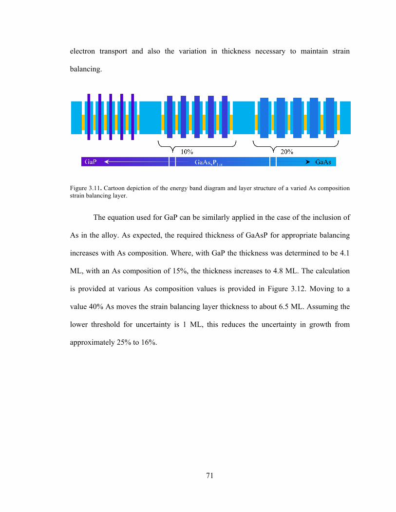
71
electron transport and also the variation in thickness necessary to maintain strain
balancing.
Figure 3.11. Cartoon depiction of the energy band diagram and layer structure of a varied As composition strain balancing layer.
The equation used for GaP can be similarly applied in the case of the inclusion of
As in the alloy. As expected, the required thickness of GaAsP for appropriate balancing
increases with As composition. Where, with GaP the thickness was determined to be 4.1
ML, with an As composition of 15%, the thickness increases to 4.8 ML. The calculation
is provided at various As composition values is provided in Figure 3.12. Moving to a
value 40% As moves the strain balancing layer thickness to about 6.5 ML. Assuming the
lower threshold for uncertainty is 1 ML, this reduces the uncertainty in growth from
approximately 25% to 16%.

72
Figure 3.12. Calculation of necessary thickness of strain balancing layer for different As compositions.
3.4. Solar Cell results
Strain balancing techniques derived from this work have been shown to prove to
improve both optical and mechanical properties of otherwise highly defective quantum
dot superlattices. These improved strain balancing techniques should therefore improve
solar cell device parameters, such as Voc, since material quality and the
photoluminescence intensities have been shown to improve, as shown in Figure 3.10.
Previously, the open circuit voltage values gave just over 1 V for the baseline GaAs cell,
while QD-embedded devices shown near 150 mV degradation. Devices were fabricated
using both and optimized GaP thickness as well as the GaAsP alloy (at 15% As). Shown
in Figure 3.13 (left) are the light J-V data for these two devices. The GaP-balanced
devices showed improved Voc values of 0.89 V and the GaAsP sample gave 0.95 V.
Furthermore, the inclusion of GaAsP may be responsible for the further enhanced Voc

73
value. In the latter case, the balancing layer may be more accurate due to improved
growth rate accuracy associated with the thicker layer. This improvement can lead to
further reduction in i-region recombination losses. The improved Voc values, similar short
circuit current densities and fill factors lead to an increase in solar cell efficiency from
11.7% to 13.3%
The material quality in the layers grown above the intrinsic layer (predominantly
the emitter) has also shown evidence of improvement. Figure 3.13 (right) shows the
external quantum efficiency of the same two devices. The low wavelength bulk EQE
(indicative of high energy photons absorbed at the top of the cell) increases slightly for
the device with GaAsP balancing layer. The inset in this figure shows that although there
are differences in the current generated by the QD layers and this can be potentially
associated with reduced tunneling thickness in the GaP-based superlattice.
Figure 3.13. Left: Light J-V measurement of standard strain balanced 10-layer QD solar cell and modified GaAsP strain balancing layer. Right: EQE measurement of the same two samples.
It is beneficial for many types of QD-embedded devices to expand upon the limit
of number of these layers. Even with the correct strain balancing conditions, there may be

74
a limit to this number, due to the inhomogeneous strain inherent in a three dimensional
array such as we have here. Once a more accurate generalized theory for strain balancing
the arrays was characterized, the implementation of increased numbers of layers could be
confidently investigated. Two solar cells were subsequently grown, one with forty and
one with sixty layers of strain balanced QD arrays. These were fabricated into
photovoltaic devices and complete PV characterization was performed. Table 3.1 gives
the raw extracted parameters from Figure 3.13 (left).
Table 3.1. Table of solar cell parameters from light J-V curve in Figure 3.13 (left).
QDSC Strain Balancing Material
Jsc Voc FF η
(mA/cm2) (V) (%) (%)
GaP 24.4 0.89 73 11.7
GaAsP 24.6 0.95 77 13.3
Figure 3.14 (left), shows the inverted AM0 illuminated J-V curves for a baseline
sample and three QD embedded devices with 10, 40 and 60 layers of QDs. The baseline
sample exhibits the typical solar cell parameters for a GaAs p-i-n cell of 1.04V, 24.1
mA/cm2 and relatively high fill factor (FF) (83%). With 10 and 40 QD layers, the fill
factor immediate drops (78%, 76%) due to small defects in the emitter region causing a
decreased mobility and higher series resistance through the complex intrinsic region. The
current is enhanced 24.9mA/cm2 and 26mA/cm2, respectively, with drops in voltage to
0.96 and 0.88V, respectively. This observed drop in voltage is most likely due to the
increased dark current due to recombination in the i-region of these samples when
compared with the low defect i-region of the baseline. Table 3.2 shows the solar cell
parameters extracted from these curves.

75
When 60 layers of QDs are implemented, although there is a similar voltage loss
compared with the 40x, the current does not continue this upward trend, and a significant
shunting characteristic appears. This is due to the existence of defect pathways between
the doped quasi neutral regions not present in the 10 and 40 layer devices. It is possible
that in the 60 layer device, the superlattice critical thickness has been reached and
significant relaxation has occurred, providing the propagation of threading dislocations
often seen in highly strained semiconductor layers. The loss in current can be investigated
by spectrally resolving the current generation in the devices. Figure 3.14 (right) shows
these data as external quantum efficiency. It is apparent that although there is a
continuous upward trend in the sub-GaAs bandgap “knee” with increasing layers of QDs,
the loss in the visible wavelengths is significant (2 mA/cm2, estimated extrapolation from
10x) in the 60x QD sample when compared to the others.
Figure 3.14. Left: I-V curves for 1cm2 solar cell devices with increasing number of QD layers. Right: external quantum efficiency spectra for QD embedded p-i-n devices with varying number of QD layers.

76
To verify that the loss from the 60x is originating from material degradation, a
model of the external quantum efficiency was created to simulate the effects of an emitter
with decreasing carrier lifetime values. This model, (demonstrated by Nelson [69]), sums
the current densities in all regions of the solar cell as a function of incoming photon
wavelength. It takes into account current generation terms which can be obtained using
the absorption coefficient and the incident spectrum, solving the continuity equation and
Poisson’s equation and arrives at a modified version of the current density equation
shown in chapter 0.
Figure 3.15 (left) shows the effects of a decreasing emitter lifetime alongside the
effects a decreasing lifetime in all device regions. This isolates the effects originating
specifically from the emitter and illustrates the specific decrease in EQE from a
decreased emitter carrier lifetime of only a few orders of magnitude. Adjusting lifetime
values in this model and fitting to the data, evidence is conclusive that the material grown
after the 60 layers of QDs has a significantly reduced carrier lifetime (11 ps) when
compared to the samples with the control cell and the 10 and 40 layer structures (~1 ns).
This suggests that somewhere between 40 and 60 layers, the QDs are reaching a critical
limit as a superlattice since subsequently grown material appears degraded. This fact
Table 3.2. Table of solar cell parameters from light J-V curve in Figure 3.14 (left).
Jsc
Voc FF η
(mA/cm2) (V) (%) (%)
Control 24.1 1.04 83 14.7
10x 24.9 0.96 78 13.6
40x 26.0 0.88 76 12.2
60x 25.0 0.88 69 11.3

77
confirms the above suggestion that relaxation is occurring at this number of layers and
indicates a need for a more accurate method of strain compensation than that which was
proposed here. Another possibility explored in the next chapter, is that QD structural
characteristics are playing a role in the material quality in subsequently grown material.
The strain balancing theory proposed here may work to a certain limit, but the balancing
may become exceedingly sensitive with more and more QD layers.
Figure 3.15. Left: Hovel model of EQE indicating degradation due to a decrease in carrier lifetimes. Right: a zoom in of Figure 3.14 (left) showing the detail of the sub-GaAs bandgap current increase. This drawback does not seem to significantly affect the absorption and collection
of carriers below the GaAs bandgap. Figure 3.15 (right) shows the systematic increase
seen if focusing more closely on the wavelengths absorbed by the QD layers. The 60-
layer QD sample, although degraded in the visible, shows an EQE value of ~28% above
890nm. Integrating under these curves and convolving with the solar spectrum, it is
possible to extract the current generated by the device at specific wavelengths. A
comparison of these values is shown in Figure 4.11 (left). Table 3.3 tabulates these values
indicating the systematic increase provided by the inclusion of the QD layers.
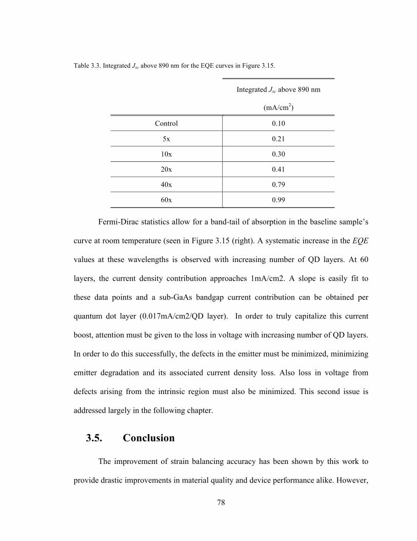
78
Fermi-Dirac statistics allow for a band-tail of absorption in the baseline sample’s
curve at room temperature (seen in Figure 3.15 (right). A systematic increase in the EQE
values at these wavelengths is observed with increasing number of QD layers. At 60
layers, the current density contribution approaches 1mA/cm2. A slope is easily fit to
these data points and a sub-GaAs bandgap current contribution can be obtained per
quantum dot layer (0.017mA/cm2/QD layer). In order to truly capitalize this current
boost, attention must be given to the loss in voltage with increasing number of QD layers.
In order to do this successfully, the defects in the emitter must be minimized, minimizing
emitter degradation and its associated current density loss. Also loss in voltage from
defects arising from the intrinsic region must also be minimized. This second issue is
addressed largely in the following chapter.
3.5. Conclusion
The improvement of strain balancing accuracy has been shown by this work to
provide drastic improvements in material quality and device performance alike. However,
Table 3.3. Integrated Jsc above 890 nm for the EQE curves in Figure 3.15.
Integrated Jsc above 890 nm
(mA/cm2)
Control 0.10
5x 0.21
10x 0.30
20x 0.41
40x 0.79
60x 0.99

79
there are potential points of improvement that can be pursued within this subtopic. One of
the advantages of using a weighted strain balancing thickness determination method is
that it better approximates the necessary stress minimization necessary to avoid material
defects. This is the first time an application of this method has been applied to any
quantum dot system, and has proven very successful at device improvement. Its
application to other type of quantum dot devices should also be considered with such
success in solar cells.
However, this approximation is merely one of a first-order. Second order
calculations can be made which take into account the inhomogeneous strain in the
material within the superlattice layers. Again, just above the QD, the material is assumed
to be in tension owing to the partial relaxation of the InAs at the top of the QD. Above a
purely wetting layer location, the opposite effect may be seen, since this layer is still
psuedomorphicly strained to GaAs. These two regions themselves may interact and there
may be further deleterious effects un-accounted for in this approximation. A full,
atomistic calculation such as those provided by other authors may be possible to better
calculate an energy minimization for this system [55, 70].
Other materials for balancing layers may also be evaluated. A relatively simple
study would be to continue the use of GaAsP with increasing As content. A series of
samples stepping through this value of composition may be able to shed light on the
effects of this thicker/lower barrier height material. InGaP may be another potential
material choice as it avoids the group V composition variation undertaken by growing
GaAsP. Further materials characterization may also be available for atomic lattice
constant variation throughout the QD/balancing layer superlattice. High resolution TEM

80
is becoming more commonplace and is used to evaluate localized lattice constants in
today’s QD arrays [71].
In order to make successfully operating devices that can be applied to both the
progress of bandgap-engineered solar cells and the intermediate band solar cell, it is
important to solve the problems outlined at the end of the last section. The ultimate goal
of all of these techniques would be to provide a pathway to growing a very high number
of QD layers (100+) consistently and without degradation to the emitter (current loss) or
the i-region material quality (voltage loss).

81
4. Optimum QD growth conditions 4.1. Introduction
Until this point, the focus of this body of work has been primarily on a single
layer of the superlattice, namely the strain balancing layer. Although it has been shown
that this layer is of high importance for proper device operation, it became a natural step
within this thesis work to investigate the other layers of the repeat unit. The GaAs spacer
layers haves some requirements such as being kept relatively thin for adherence to the
intermediate band approach (see section 5.4). The InAs layers, however, have the highest
degree of variability based on growth conditions because they are grown within the
kinetically-driven growth regime (low temperatures, 495°C). Additionally, in these layers
are those which give the device improved current densities, result in the scientific need to
evaluate their formation mechanisms, structural characteristics, and ultimately their
growth conditions.
Within these growth conditions are a number of variables which have been
relatively widely studied for the InAs/GaAs system. Some of the most significant growth
conditions which affect QD nucleation and arrangement are as follows:
• Temperature
• V/III Ratio
• Chamber Pressure
• Injector Flow Rate
• InAs Coverage Value
Temperature effects on QD growth have been studied since their growth began. More
recently, studies have been performed under the lens of photovoltaic device incorporation

82
by Hubbard [72]. It was found that a growth temperature of 495°C give the strongest PL
signal. This was in part due to the lack of surface energy provided at low temperatures
limiting In adatom surface diffusion leading to disorganized, polydispersed QD sizes. At
higher temperatures, In desorption can occur, also resulting in lower QD densities. This
study, among others for MBE [73] and MOCVD [74] show that V/III ratio can affect dot
densities. Reduction in V/III ratio also led to drastically improved spatial uniformity [72].
A ten-fold increased in grow rate was found to slightly improve QD density (from 49-
57%) [73]. Although chamber pressure and alkyl injector flow rate are very important to
QD growth, they are not discussed here, as their conditions vary between MOCVD
reactors and are difficult to conclude upon for the scientific community.
One of the most critical parameters for QD growth is the coverage value. Beyond the
critical thickness of 3D island formation (θc), there is a period which only small, coherent
QDs form. It is these that are of interest for these devices as they exhibit the highest
optical quality and most uniform size. Beyond this point, Oswalt ripening occurs,
forming large, incoherent, optically inactive islands begin forming, due to the
coalescence of the smaller, mobile InAs structures [75]. This results in point defects at
the site of nucleation, which can cause second order defects in subsequently grown
material, such as threading dislocations. In order to avoid these latter conditions, the InAs
coverage value was studied in an attempt to optimize this parameter in the frame of the
photovoltaic devices used here.
4.2. InAs coverage
The QD formation includes both the physical islands, as well as the wetting layer.
This two-aspect layer system imparts a difficulty on the definition of a thickness value. It

83
is for this reason that a ‘coverage value,’ θ, is defined and accepted among growers of the
S-K mode. It is a value that represents an effective thickness of a layer based on growth
rate (0.26 monolayers (ML) per second) and time, and is therefore reported in units of
length. This was calculated by depositing a thick InAs layer, and using a scanning
electron microscope measurement to determine average height of pyramidal islands.
For the InAs/GaAs QD system, it is well understood that there is a narrow range
of InAs coverage (1.7 – 2.5 ML) in which acceptable optical performance can be
achieved [76]. The samples grown here fall within this range at θ = 1.82, 2.10, 2.17, 2.24,
3.31 ML, calculated by growth rate and time. To investigate the structural and optical
results of varying the InAs coverage, low temperature PL as well as both AFM images
and HRXRD was performed.
With any superlattice structure involving layers with different lattice constants, it
is important to quantitatively characterize the strain in the samples. It has been shown
previously that the strain balancing layer (GaP) can be reasonably tuned using a 1st order
calculation of the appropriate strain compensation layer thickness section 3.3. This
method is employed here, but despite QD dimensional changes, the GaP layer thickness
is maintained throughout the structure. This choice was made so that the only
experimental variable was the InAs dot size. Dot diameters did not change enough to
justify an increased QD footprint. Although QD densities did increase for the larger dots,
the decrease in the smaller dots accounts for some of this increase. As will be shown, QD
height is the most significantly varied geometrical dimension for the small QDs. Altering
the GaP thickness from previous studies would have also altered the tunneling
probabilities of the transition states investigated here and was therefore avoided.
84
4.2.1. Atomic Force Microscopy
From visual inspection of the AFM images, there exists a bi-modal distribution in
the QD size. The smaller sized QDs, on the order of 3-5 nm thick, and 25-35 nm in
diameter are coherent, unrelaxed, defect free, islands of InAs. The larger islands in the
images are almost an order of magnitude in size difference with heights of 20-25 nm and
diameters ranging from 65 to 105 nm. These islands are a combination of coalesced
smaller islands and additional InAs which adsorbs after relaxation, as the lattice constant
that exists and these surfaces is energetically favorable to unsettled InAs. Consequently,
they have phase interfaces and relaxation locations resulting in point defects acting as
recombination centers and are considered optically inactive [75]. These centers can cause
severe loss in open circuit voltage in quantum dot embedded solar cells. Threading
dislocations arising from these point defects can propagate into the emitter, and as
discussed in chapter 3, can then cause short circuit current density losses in these cells. It
is therefore these large QDs that that are undesirable for these devices as well as any
optoelectronic device which take advantage of quantum confinement via quantum dots.
Figure 4.1 shows the AFM images of the 1.82, 2.17 and 2.31 ML InAs coverage
values. Smaller QDs align themselves with the step edges discussed in chapter 2. It is less
clear whether this is occurring with the larger QDs. Interestingly, the smaller dots
decrease in density with increased Θ. This is largely due to the increase in density of the
larger mode of QDs. The smaller dots range from 3.6 x 1010 cm-2 to 2.0 x 1010 cm-2 as the
coverage value increases. Larger dot densities range from 1.5x108 cm-2 to 1.21x109 cm-2
indicating the favorability of InAs to form larger islands with increased availability of In
and As atoms.

85
Figure 4.1. Atomic force microscopy images of surface of test samples with varying InAs coverage. QDs appear in a two mode distribution. Increasing QD size and density track roughly with coverage value. Images read left to right: (θ = 1.82, 2.17 and 2.31 ML) QD diameters do not show any particular trend in size ranging from 20 to 45 nm
for the small mode, and 65 to 125 for the larger QDs. QD heights however, did show an
interesting trend. The small QDs increased in height with increasing coverage values,
from 3.65nm, 4.20nm to 5.54 nm. The larger QD size did not show any significant trend.
These results indicate that increasing InAs coverage leads to increasing small dot heights
and increasing large dot densities. Table 4.1 outlines these statistics obtained from
analysis of the AFM images using the software provided by the Dimension AFM, DI
Nanoscope Image. Five line scans were taken for each image independently for both
small and large QDs. 2 x 2 cm2 images (not shown) were used, in order to reduce
uncertainty associated with anomalies in a 1 x 1 cm2 image, to count the number of
quantum dots by hand.

86
Table 4.1. Statistical data extracted from AFM images in Figure 4.1 and binned by “small” and “large.”
A separate statistical image analysis program, Scanning Probe Image Processor,
uses a height flooding method to recognize entities in data set containing x and y
coordinates and associated height values. This is used to gather the height and diameter
data from the AFM images for histograms which are plotted in Figure 4.2 for the first
three coverage value samples. These three samples give us the finest detail of the five for
information pertaining to the mechanics before and after the onset of the large quantum
dot formation. It is immediately apparent that in the sample with the lowest InAs
coverage value, 1.82 ML, there appears to be a very tight distribution of both height and
(to a lesser degree) diameter peaking at roughly 2 nm and 15 nm, respectively. Height
values shift by roughly 1.5 nm between the two software programs used, and is assumed
to be a result of an incorrect offset made by the SPIP program, and the DI Nanoscope
Image software is used as a baseline.
As the InAs increases in coverage value, and we approach and pass the onset (or
critical thickness) of the large, incoherent QD formation, these QD counts begin to
appear more significantly. In the sample with 2.17 ML a second, distinct peak in the data

87
begins to occur. In the 2.10 ML sample it is clear that the small-dot peak has shifted in
height by about 0.75 nm. This is due to an accumulation of InAs at the top of the QD.
The average QD height returns to a value of 1.5 nm as the secondary, large-dot peak
begins to form indicating that InAs has migrated to the larger QDs from the top of the
small QDs. These larger-dot peaks can be estimated to be at an average of 12 and 55 nm
for the height and diameter, respectively. This evolution of the larger, optically inactive
islands (coalesced QDs) becomes very apparent.
It is also of note from Table 4.1 that the small QD density decreases with
increasing coverage value. This indicates that the InAs used to form the larger QDs
consists not only of atoms that have been relocated from the top of QDs, but also of entire
small QDs. This supports the fact that small QDs are coalescing. The fact that the large
QD density increases with increased coverage value also corroborates this mechanical
process.
Figure 4.2. Histograms of QD diameter and height obtained from AFM images for QD test structures with varying InAs coverage values.

88
It is clear from these data that a reduced InAs coverage value is a pathway to
avoiding large, defective quantum dots. Both a reduction in large dot density is observed
with decreasing InAs coverage, and in particular for the 1.82 ML coverage value, a
negligible density of QDs is found. This pathway is of interest for pursuing
optoelectronic devices that use these structures as it is a simple, quantifiable method of
improving physical material properties of these structures. Subsequent sections of this
chapter address other characterization techniques with these samples.
4.2.2. Photoluminescence and High Resolution X-Ray Diffraction
One of the most significant measurement of the optical quality on these types of
test structures is photoluminescence, as it is a direct measurement of the radiative
recombination of carriers in the confined states. After a carrier excitation event such as a
photon separated electron-hole pair occurs, it is subject to an array of possible paths
including both non-radiative and radiative recombination, thermal excitation (out of the
confined state), tunneling (into another confined state), and other recombination
processes such as Auger. When performed at low temperature, photoluminescence
measurements can provide very high detail due to suppressed of the thermal excitation
process, thereby increasing the carrier available for all other processes, including
radiative recombination and can increase the radiative lifetime in the confined states.
Increased carrier lifetime in the QD states allow for very high emission efficiency.
Shown in Figure 4.3, are the PL spectra at 80 K as a function of InAs coverage value.
The larger the QD heights, the deeper the QD state is expected to be, and this is the case
here. The smallest θ value gives the shallowest state, and therefore the highest emission
energy. This effect systematically red-shifts with increasing coverage, indicating a slight

89
increase in energy state. This is a shift from 1.22 to 1.18 eV (40 meV difference). More
interestingly, however is the shift in the full-width at half-maximum (FWHM). This is
indicative of inhomogeneous broadening associated with the natural distribution of QDs.
These curves show broadening with increasing coverage value indicating an increase in
the distribution in the QD size which corresponds to the increased volume of the InAs
producing a larger variation in QD height.
Figure 4.3. Low temperature PL measurements of QD test structures with varying InAs coverage values.
High resolution x-ray diffraction is used to study the strain in these samples.
Figure 4.4 shows symmetric 2θ/ω scans in the [004] plane for each of the five test
structures and provide insight into the structural integrity of these test samples. The 0th
order superlattice peak, labeled SL(0), can be seen just to the left of the GaAs Bragg peak
indicating slight compressive residual strain in the layer structure.

90
Figure 4.4. HRXRD measurements of QD test structures with varying InAs coverage values.
The strain and periodicity are extracted as discussed in chapter 3 and can be seen
in Table 4.2. This strain value gradually moves more negatively in 2θ value with
increasing coverage value. This is clearly due to the increasing compressive strain
associated with the larger volume of InAs. As the larger quantum dots begin to form, the
GaP strain balancing become insufficient for proper balancing. No significant trend in
periodicity is seen for the samples between 1.82 and 2.17ML InAs, ranging from 19.4 to
20.2nm. The 2.31ML InAs sample, however decreases below this range at 18.9nm. This
suggests that there is some relaxation in the superlattice, and as the average lattice
constant shifts to larger values, the lattice mismatch is smaller than the previous four
samples. This results in an altered SK growth mode. This claim would be better
supported with the measurement of asymmetric XRD scans as these can provide in-plane
lattice constant shifts. Pendellosung fringes can be seen clearly in all three samples of
lower InAs coverage. These disappear in the 2.31ML sample, indicating a loss in
interface quality characteristic of layer relaxation. Also interesting is the much broader
GaAs Bragg peak associated with the 2.31ML sample. This indicates diffraction from a

91
tensile layer, most likely the 33nm spacer GaAs layer. This layer might be in tension
since the relaxation of the SL below it now has a larger lattice constant. The range of
samples tested here illustrates that the InAs coverage value plays a role in strain
balancing in the superlattice, and at a critical thickness can cause significant layer
degradation. The lowest value of Θc gives not only the lowest bi-modal spread, but also
the least strained superlattice.
Table 4.2. Extracted periodicity and strain values from HRXRD shown in Figure 4.4.
No significant shift in periodicity of the superlattice repeat unit was found with
coverage value, as it is thought that the increased volume of InAs on the surface
manifests primarily in QD height increases, and increased density of larger, incoherent
QDs. The table below shows the periodicities calculated from the x-ray in Figure 4.4.
Also shown is the calculated strain values, which for does not change much for the
coverage values between 2.1 and 2.31 ML. These data can be compared in Table 4.2.
This is most likely due to the onset of the larger QD islands sometime after 1.8 ML of
growth, as confirmed by the AFM images in section 4.2.1. The strain is minimized in the
sample with 1.8 ML indicating that the GaP thickness designed uniquely for these smaller

92
sizes QDs is accurate, but departs from ideal upon the onset of the larger, undesirable
islands.
4.3. Solar Cell Results The results thus far in this section showed that with coverage of 1.8 ML of InAs,
smaller, more uniform coverage of QDs can be realized. They show improved PL
FWHM (or narrowing inhomogeneous broadening), they can be better designed for strain
balancing, and the large, optically inactive islands are reduced to a relatively insignificant
density. It is therefore of interest to move to explore slightly smaller InAs coverage
values in order to approach more uniform distribution and improve radiative
recombination characteristics in these devices in the pursuit of the improvement of solar
cell device parameters.
Figure 4.5 shows the 1 sun AM0 illuminated J-V curves for the baseline GaAs p-
i-n and the 10x QD GaP strain balanced solar cells with the lower InAs coverage value.
The baseline sample exhibited characteristics typical of GaAs single junction solar cells
with a Jsc of 22.6 mA/cm2. In the QD embedded sample, Jsc was enhanced to 23.1
mA/cm2, giving a 2.2% increase in short circuit current over the baseline solar cell
current. This increase is larger than typical of QD enhanced solar cells, shown to give
increases as high as 0.025 mA/cm2/QD layer calculated by the slope of Jsc plotted versus
QD layer number in Hubbard, et al. [77] and can be seen here in Figure 4.11. This may be
due to small differences in measurement of the bulk GaAs absorption wavelength region.
The open circuit voltage for the standard control GaAs cell was typical of a high quality
GaAs solar cell with a value of 1.041 V. The ten layer QD sample showed slight
degradation of this voltage value, with a loss of about 47 mV. The source of this

93
improved voltage value compared to that of the control is due to an improvement in the
strain balancing by the significant suppression of the density of the secondary, larger
coalesced QD mode using a reduced InAs coverage. This Voc value, 0.994 V is the
highest InAs/GaAs-based QD solar cell voltage to date. The fill factor variation was
insignificant between the two samples, and the efficiencies are comparable at 13.8 and
13.5% for the control and QD solar cell, respectively with negligible different in fill
factors (~81%).
Figure 4.5. Light J-V measurements showing 10X QD solar cell with only 50 mV loss in open circuit voltage. Spectrally resolving the short circuit current density can be evaluated using
spectral responsivity measurements and then converted to external quantum efficiency
(EQE). Figure 4.6 (left) shows the comparison of this data for the two samples shown in
Figure 4.5, with the addition of the solar cell with 2.1 ML InAs to show how the spectral
sensitivity has changed below the GaAs bandedge. Peak bulk EQE values are equivalent
for all samples near 73%. Typical measured reflectivity values for these samples were
~30% [56] giving an internal quantum efficiency near unity. The sub-GaAs bandgap (>
880 nm) absorption is clearly enhanced for all InAs QD devices indicating the source of

94
the improved Jsc. The numerical integration of the spectral responsivity and the AM0
spectrum (data vectors) was used to calculate the expected short circuit current values
and deviated from the illuminated light J-V measurements by 7-12%. In addition, this
calculation was performed specifically for the sub-GaAs absorption portion of the
spectrum (> 880 nm), and was found to be relatively constant across all 3 QDSC samples,
varying by only 4%. Slight differences in the bulk wavelength EQE offset any influence
of the absorption above 880 nm on the differences in the Jsc values of the QD enhanced
devices.
In Figure 4.6 (right), the sub-GaAs bandedge EQE is scaled (semi-logarithmic) to
highlight the fine structure and compared with the electroluminescence (EL) spectra
(linear). EL was measured using an injection current density of 200 mA/cm2. All three
EQE spectra show absorption features near 940, 985 and 1035 nm. The 2.1 ML sample
shows weaker absorption at the 940 nm peak. This near band-edge peak is typically
associated with the QW-like wetting layer (WL) [36]. It is also apparent that emission
seen in the EL spectra, correlate well with the slope changes of the EQE absorption
peaks. These peaks appear at 950, 995 and 1050 nm, indicating a Stokes’ shift of 10-15
nm (12-20 meV). This shift is inherent in confined structures and represents the
difference in energy observed by absorption and emission. The reciprocal nature of
absorption and emission differ only by collection and injection efficiencies in the case of
EQE and EL measurement. The domination of radiative recombination (seen in the EL
spectra) in the deeper infrared (IR) states (1050 nm) of the 2.1 ML sample is thought to
be due to an increase in volume of QDs (from height increase). The reduced collection
efficiency of the deeper IR QD states is due to the larger conduction band offset of these
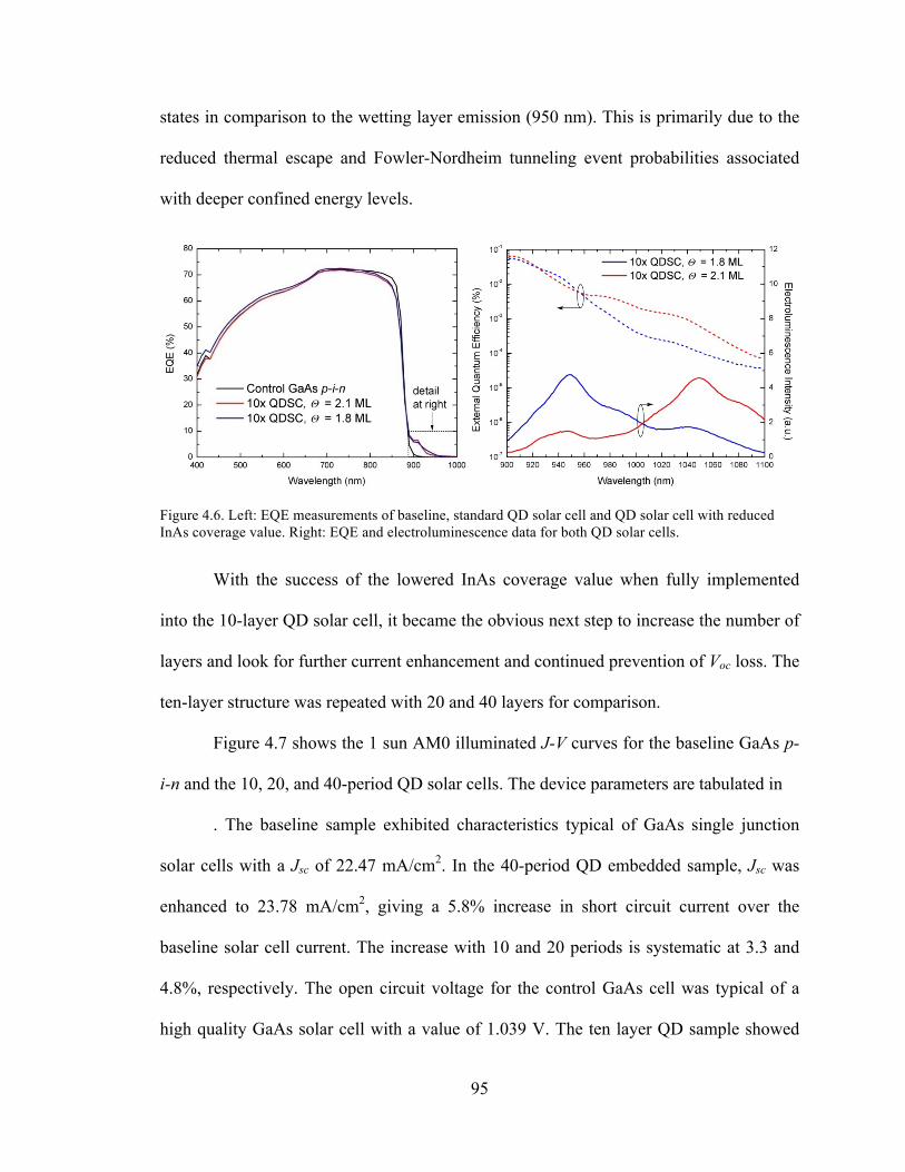
95
states in comparison to the wetting layer emission (950 nm). This is primarily due to the
reduced thermal escape and Fowler-Nordheim tunneling event probabilities associated
with deeper confined energy levels.
Figure 4.6. Left: EQE measurements of baseline, standard QD solar cell and QD solar cell with reduced InAs coverage value. Right: EQE and electroluminescence data for both QD solar cells.
With the success of the lowered InAs coverage value when fully implemented
into the 10-layer QD solar cell, it became the obvious next step to increase the number of
layers and look for further current enhancement and continued prevention of Voc loss. The
ten-layer structure was repeated with 20 and 40 layers for comparison.
Figure 4.7 shows the 1 sun AM0 illuminated J-V curves for the baseline GaAs p-
i-n and the 10, 20, and 40-period QD solar cells. The device parameters are tabulated in
. The baseline sample exhibited characteristics typical of GaAs single junction
solar cells with a Jsc of 22.47 mA/cm2. In the 40-period QD embedded sample, Jsc was
enhanced to 23.78 mA/cm2, giving a 5.8% increase in short circuit current over the
baseline solar cell current. The increase with 10 and 20 periods is systematic at 3.3 and
4.8%, respectively. The open circuit voltage for the control GaAs cell was typical of a
high quality GaAs solar cell with a value of 1.039 V. The ten layer QD sample showed

96
slight degradation of this voltage value, with a loss of about 42 mV. The source of the
improved voltage value compared to that of the control is due to an improvement in the
strain balancing by the significant suppression of the density of the secondary, larger
coalesced QD mode using the reduced InAs coverage [38].
Figure 4.7. Light J-V measurements of baseline and QD solar cells with increasing number of QD layers.
The 20-period device showed a significantly degraded voltage value. The cross-
wafer standard deviation for this sample was 36 mV and a reduced fill factor was
observed, indicating a potential variation in wet isolation etch-depth and poor
metallization contacting adhesion. The 40-period QD cell exhibited a voltage of 0.990 V,
comparable to that of the 10-layer cell. The improved current and fill factor for this
device resulted in an efficiency value of 14.3%. This is a relative efficiency improvement
of 3.6% over the control cell, or an absolute efficiency improvement of 0.5%. The fill
factor variation is not insignificant between the 40-layer and the control cells, but
represents only 2.7% relative efficiency improvement contribution from the fill factor.
This indicated that the 40-layer structure would still exhibit enhanced efficiency with an

97
identical fill factor as the control cell.
Table 4.3. Solar cell device parameters extracted from AM0 light J-V measurements shown in Figure 4.7.
Figure 4.8 (left) shows the external quantum efficiency (EQE) from this
measurement as a function of number of QD layers (10-40x) and the control device. The
response typical of a GaAs solar cell is exhibited with a bandedge near 875 nm for all
four samples. Solar cells with layers of QDs exhibited relatively equivalent response in
the visible wavelength region (400-875 nm). This indicates good material quality
throughout the devices, signifying emitter degradation does not occur as seen previously
in cells with high numbers of layers at higher coverage values [78]. With increased
numbers of stacked layers, the sensitivity of strain balancing may be reduced with the use
of 1.8 ML compared to 2.1 ML coverage of previous QD solar cells. Therefore emitter
degradation seen previously may be mitigated with improved InAs coverage values and is
not seen here. The absorption observed beyond 875 nm is due to the inclusion of InAs
QD and wetting layer (WL) and is not present in the control cell. The relative increase in
absorption and collection occurring at these wavelengths with greater numbers of QD
layers can also be seen here.

98
This increase is highlighted in Figure 4.8 (right). This shows, in finer detail, the
EQE of these cells beyond 880 nm. The peak values (~915 nm) range from 6 to 22%
EQE. Using an integration with the AM0 spectrum, the contribution from the 40-period
QD cell approaches 0.9 mA/cm2. This leads to an approximate increase of 0.55% EQE
per QD layer observed at this peak value. The suppressed responsivity peaks above 940
nm, is due to the poor extraction efficiency associated with absorbing states of this depth
(100-180 meV below the conduction band (ΔE)), as opposed to the collection-dominating
near-bandedge state at 910 nm (ΔE = 45 meV). This is further confirmed by
electroluminescence measurements.
Figure 4.8. Left: External quantum efficiency measurements for the three QD and the baseline/control GaAs p-i-n solar cell devices, indicating no significant degradation in the bulk GaAs absorption wavelengths and a consistent increase in sub-GaAs bandedge EQE values with increasing numbers of QD layers. Right: External quantum efficiency measurements for the three QD and the baseline/control GaAs p-i-n solar cell devices, indicating no significant degradation in the bulk GaAs absorption wavelengths and a consistent increase in sub-GaAs bandedge EQE values with increasing numbers of QD layers.
4.3.1. Further Device Characterization
Electroluminescence (EL) was measured identically for the three QD samples,
using an injection current of 100 mA/cm2 and is shown in Figure 4.9 (left). Spectra

99
detection was performed using an Ocean Optics NIR512 InGaAs infrared photodetector
and all samples were measured under equivalent optical distances. All three QD-
embedded samples show a weak GaAs bandedge emission, indicating high QD injection
efficiency. The 10- and 20-period samples exhibit a strong WL-like state near 940 nm,
and a deeper QD emission region between 1000 and 1100 nm. The 40-period cell,
however, exhibits a much stronger increase in the WL-like state, and degraded intensity
in the QD emission regions when compared with the lower-QD number structures. This
anomaly was thought to be explainable by a natural loss in strain at higher period
numbers, removing the Stranksi-Krastinow mismatch requirement for dot formation, and
did not contribute significantly to the devices results. However, HRXRD measurements
(Figure 4.10) indicated insignificant shifts in out-of-plane superlattice strain values with
204, 485, and -32 ppm, for the 10-, 20-, and 40-period structures, respectively, indicating
general structural integrity throughout the superlattice. Integrated EL curves (Figure 4.9,
right) showed a systematic, linear increase in intensity with values of 1.0 x 10⁶, 1.4 x 10⁶,
2.2 x 10⁶ a.u., for the 10-, 20-, and 40-period structures, respectively. This signifies
equivalent overall device injection and emission efficiencies for all three QD embedded
samples.

100
Figure 4.9. Left: Electroluminescence measurements for the three QD solar cell devices, indicating a strong increase in WL-states with increased QD layer numbers. Right: A breakdown of the spectral region of the EL indicating where majority of emission is coming from.
In order to further investigate the voltage loss associated with the 20x layer and to
see if any other structural anomalies were present in these devices, HRXRD was
performed on all three samples. Figure 4.10 indicates that the three samples are relatively
lattice matched with the largest strain (20X sample) being 485 ppm (tensile). Also the
periodicity did not change much with the values being 13.1 nm +/- 1 nm. These results
are not convincing for a structure reason behind the loss in voltage for the 20 layer
device. This indicates that the sample potentially had a fabrication problem and should be
repeated for more accurate evaluation of the nature of this loss.

101
Figure 4.10. HRXRD measurement of series of solar cells with increasing numbers of QD layers.
Despite the 20-layer result, the high open circuit voltage (comparable with a
standard GaAs solar cell), and improved short current density, of these QD enhanced
GaAs solar cells is a promising result, as it represents a clear path forward using QD
bandgap engineering for efficiency enhancement of III-V solar cells.
The continuation of adding more QD layers to the devices is one of the key
factors in improving device performance. When arranged on the same plots, the trends in
open circuit voltage and short circuit current shed light on the true potential of these
devices. In Figure 4.11, these values are plotted. The voltage loss associated with the
original growth type (Θ = 2.1 ML) systematically dropped to 150 mV lower than the
GaAs cell. It appears to exhibit a saturation point with diminishing reduction in voltage
with additional layers. It was shown, however, that at 60 layers, the loss in current due to
emitter degradation began to become significant such that any advantage of voltage
saturation with increased QD layers was eliminated [78]. With the improved QD epitaxy
recipe, the minimization of the large, coalesced QD has resulted in only 50 mV reduction

102
from the control cell. In 9(b), the tracking of short circuit current with increased QD
number can be shown to have slight improvement with the reduced Θ. Using the original
recipe, a short circuit current gain was 0.017 mA/cm2/QD layer [79]. Overlaid in this
figure, are the short circuit current values from this study. There is a modest increase in
the per-QD-layer metric to that of 0.020 mA/cm2/QD layer. If emitter degradation and
voltage loss mechanisms continues to be suppressed, higher number of QD layered-
devices may be able to show further enhancements in efficiency and is the current focus
of this research group.
Figure 4.11. Left: Short circuit current tracking with QD layer number. This plot shows the improvement of slope of the improved QD growth scheme. Right: Open-circuit voltage tracking with QD layer number indicating the maintenance of minimized open-circuit voltage losses to 40 layers of QDs.
4.4. Conclusion
Although there exist other methods in literature to limit the density of, and
ultimately, eliminate large QDs, reducing the InAs coverage value is a simple and
effective method which shows definitive improvement in material quality of both the
superlattice region and the subsequently grown material. It would also be beneficial for
103
any optoelectronic device to remove these defective, coalesced QDs arising from Oswalt
ripening, as they are detrimental to device performance and not optically active.
Reducing the coverage value has been shown here to not only improve the
material quality, but the usage of the improved material has shown to improve solar cell
device parameters. This includes both the avoidance of current density losses in QD
embedded solar cells, as well as an improvement in open circuit voltage by over 100 mV.
This has provided the first efficiency improvement in QD-embedded solar cells with an
increase of 0.5% absolute efficiency.
104
5. Photon and Carrier Management
The physics of the operation of standard solar cells involve two major functions,
absorption and collection. From the beginning of photovoltaic device research, efforts
have focused on both of these functions for a wide variety of materials. For this reason, it
is important to consider these functions when investigating nanostructured solar cells as
well. This chapter will focus on a number these aspects with respect to incident photon
intensity (concentration), introduce a third function in addition to absorption and
collection specific to nanostructured solar cells, and evaluate these processes as they
affect the intermediate band solar cell.
5.1. Solar cells under concentration
One of the most simplistic concepts in improving the efficiency of a particular
solar cell, is by increasing the intensity of the incoming photon flux. It is well known that
efficiency increases logarithmically with light intensity. Additionally, high injection
conditions can potentially fill traps generate by defects and can therefore be a useful
measurement to investigate this particular effect in QD solar cells [80].
A number of arguments lead to the potential improvement of efficiency using
quantum dots in solar cells tested and operated under concentrated sunlight. Because QD
solar cells have the ability to improve the short circuit current at one sun, it is logical to
assume that this trend will continue linearly with concentration, therefore the efficiency
should remain constant with increasing current from higher solar intensity. However,
voltage improves on a scale of the natural log of the concentration as well. Under this
assumption, efficiency should (and does) improve under concentrated sunlight for both a

105
baseline and a QD-embedded solar cell. The voltage for a QD cell, however, is much
lower at one sun than the baseline, thus having higher capability of regaining low
voltages due to trap filling. With this theory, quantum dot and baseline cells were grown
and tested under concentration. Other important potential benefits include lower
temperature dependence of QD solar cells has been previously shown.
Series resistance becomes a large limiting factor as sunlight is concentrated and
currents increase (due to I2R power losses). The PC1D solar cell simulator program was
used in Figure 5.1 to determine the effects of series resistance on fill factor and efficiency
as a function of concentration. At a reasonable series resistance value of 0.43 ohms
(shown in Figure 5.1, left), the efficiency maximizes at about 8 suns. This is not ideal as
current high efficiency cells are typically tested between 250-450 suns. This gave insight
into the necessary grid metallization improvements that may be necessary for full device
testing under concentration.
Figure 5.1. Efficiency (left) and Fill Factor (right) as a function of solar concentration factor for multiple series resistance values.

106
5.1.1. Concentration Measurements
Devices were fabricated as previously discussed with 5, 10 and 20 layers of QDs
in the i-region, along with a baseline cell. Cells were tested at the NASA Glenn Research
Center using a Large Area Pulsed Solar Simulator (LAPSS). This simulator used a
variable-distance mount with fixed tungsten flash bulb. The wafer was placed on a chuck
mounted on a monorail in the back of the room and a flash bulb was used to calibrate the
system to 4 suns shown in Figure 5.2. Calibration is performed by mounting sample at
the largest available distance and adjusting bulb current to AM1.5D one sun short-circuit
current density. The devices were moved progressively closer (distance d) to the flash
bulb increasing the effective solar concentration, proportional to 1/d2.
Typically, concentration value is calculated using the short circuit current density,
as it scales linearly with concentration as shown in equation 5.1.
( ) ( )1scsc CJCJ = 5.1
However, this can hide Jsc-related anomalies such as superlinearity of this relationship
due to Auger recombination. Two-photon absorption processes are also expected to
follow a superlinear relationship. Therefore a more sophisticated and accurate method is
employed here for evaluation of concentration. A view factor is calculated to determine
concentration value in an effort to independently characterize short-circuit current as a
function of concentration [81]. This method calculates the fraction of the photon-flux
exiting the bulb which is entering the surface of the solar cell. Below is the equation (5.2)
describing the formulation:
'cos'cos12 dAs
dAA
F ∫ ∫=φφ
π 5.2

107
in which A is the area of the cell, A’ is the area of the arc lamp, s is the distance between
the cell and the source, and φ and φ’ are the angles the edges of the cells make to the
point source, which are calculated using the distance and cell dimensions. In this manner,
all four solar cell parameters can be assumed independent of concentration during the
measurement.
Figure 5.2. Image taken of the monorail-guided sample vacuum-chuck allowing one-dimensional translation towards and away from the flash bulb (back of blue box).
Preliminary results of this data are promising. Although the Voc in Figure 5.3 (left)
did not show significant improvement in slope when plotted logarithmically for the QD
cells versus the baseline, improvements were seen in the efficiency due to the
maintenance of the fill factor at higher concentrations. Peak efficiency increases with QD
layer number shown in Figure 5.3 (upper right). Fill factor was observed to peak near
100-200X while efficiency peaked near 400X for most cells. This was consistent with our
concentrator cell grid design. The QD enhanced cell gave near 18% power efficiency at
400X. This represented a ~1% absolute efficiency improvement compared to the baseline
(6% relative improvement). Under concentrated sunlight, the reduced (longer
wavelength) effective bandgap of the QD enhanced solar cell leads to direct improvement

108
in cell efficiency, since the optimal bandgap shifts to lower energy values with an
increase in concentrated sunlight. The enhanced efficiency of the QD cells were a result
of the enhanced Jsc combined with minimal Voc loss.
Figure 5.3. Measurements of Voc (left), Efficiency (upper right) and concentration (bottom right) as a function of concentration for baseline, 5x, 10x, 20x QD solar cells.
In addition, the open circuit voltage versus concentration was fit to the following
relation derived from the diode equation:
5.3
where n is the diode ideality factor. As seen in Figure 5.3 (left), all cells shows a good fit
to this relation with an extracted ideality near 1.4. This number is indicative of cells
operating between the Shockley Reid Hall (SRH) recombination in both the quasi-neutral
and depletion regions. The fact that the ideality deviates slightly from 1 may indicate a
slightly higher perimeter area recombination related to processing [82]. However, all
cells show similar ideality and should be equivalent for comparison purposes.
( ) ( ) ( )CqkTnVCV ococ ln1 +=

109
5.2. Temperature Dependence of QD Cells
The scope of this thesis focuses on the subset of III-V materials which include
nanostructured materials for spectrum enhancing and intermediate band effects. For these
types of devices, attention must also be given to an additional function besides absorption
and collection. Carrier extraction from confined states is a limiting factor of the
enhancement these devices can provide. Temperature dependent spectroscopy can be
used on devices and test structures including sub-bandgap-absorbing nanostructures.
Additionally, since most applications using concentrated sunlight expose the cells
to temperatures much greater than room temperature. Therefore solar cells being
evaluated for their operation under concentrated sunlight, it is necessary that temperature-
dependent characteristics of the devices are investigated. As seen in previous sections,
spectral responsivity measurements can enhance our understanding of the absorption and
collection properties of these devices. Here, it was used to evaluate the effects of
temperature on the absorption properties of both the bulk and the nanostructure
absorption wavelengths.
In Figure 5.4, the temperature dependence of the spectral responsivity of a single
junction GaAs cell (a), a single junction GaAs cell with 20 layers (b) and 40 layers (c) of
QD is shown. Measurements were made using a Janis cryogenic probestation and
cryostat tool coupled with a nitrogen dewar and connected with a Lakeshore Instruments
temperature controller. The monochromatic light source was provided by an Optronics
Laboratories 750 series spectroradiometer and was directed through the quartz window of
the cryostat probestation. Temperature ranged from roughly liquid nitrogen temperature
to 410K. As temperature increases, semiconductor band gap decreases. For photovoltaic

110
devices, this relationship results in an increase in current generation as more of the
incoming spectral flux can be absorbed. The absorption bandedge in wavelength space
thus moves outward with increasing temperature. All samples clearly showed this effect.
In both QD devices, sub-GaAs band gap absorption and collection is observed. At low
temperatures, carrier have less available phonon interaction, causing the effective lifetime
of minority carriers to decrease. This effect is the suspected cause of decreasing EQE at
lower temperatures in the low wavelength GaAs bulk absorption region. This effect is
more pronounced in the 40x QD embedded device. This is expected to occur for all
samples at much lower temperatures less than 100K [83], but an early onset may be
occurring due to a reduction in minority carrier lifetime in material with more defects,
and higher recombination rates may be present. EQE value slightly increases for the
identifiable sub GaAs band gap peaks. At these wavelengths, absorption is from wetting
layer states 40-100 meV below the GaAs conduction band edge [84]. Qualitatively, these
peaks exhibit a similar blue shift with decreasing temperature as that of the bandedge.
This suggests that the electron and hole-to-conduction band offsets of the WL state are
relatively insensitive to temperature. This QD temperature-dependence is indicative of
conduction and valence band offset following a similar temperature-dependence of the
absorption energies in comparison with the bulk host bandgap.

111
Figure 5.4. Temperature dependent EQE bandage of baseline, 20x and 40x QDSC devices.
A fitting routine was used to de-convolve the spectral responsivity of the three
apparent QD peaks and the bulk bandedge for each temperature. Upon fitting an
absorption edge function to the host GaAs bandedge, the remaining spectra were fit using
three overlapping Lorentzian functions. A Lorentzian distribution was used for this fit in
accordance with the distribution of transition energy values present in confined states
associated with both the conduction and valence bands. This can be seen for
electroluminescence data as an example in Figure 5.13. Since the band offset is relatively
temperature insensitive, as temperature increases, the peak responsivity energies of the
InAs nanostructures decreases in a trend similar to the expected bandgap versus
temperature relationship for GaAs shown in the dotted line in Figure 5.5. This indicates
that the bandgap widening affecting the confined states from lattice expansion or
contraction, are relatively insignificant in comparison to the confinement effects on these
states.

112
Figure 5.5. Extracted peak energies from EQE of 20x and 40x QDSC plotted with the bandgap vs. temperature relationship.
Also of importance is the temperature dependence of the absorption coefficient
which can be directly related to the spectral responsivity through the following
relationship:
( ) ( )0
1 1SR q E R E dEEα
∞
⎡ ⎤= −⎣ ⎦∫ 5.4
Here, α(E) is the energy dependent absorption coefficient and R(E) is the surface
reflectivity of the device. Numerical integration of the Lorentzian fits was performed to
determine the relative absorption coefficient (spectral responsivity, assuming collection is
constant) of the nanostructures as a function of temperature. Figure 5.6 shows the
integrated spectral responsivity values as a function of temperature. Here, it is apparent
that there is no significant trend with temperature, indicating any increase in apparent
absorption intensity shown in Figure 5.4, is merely due to the proximity of the sub-
bandgap transition to the bulk bandedge artificially enhancing the QD responsivity
through convolution of Fermi-Dirac bandtail states in the bulk. This is a relatively
encouraging result, as enhancing the temperature insensitivity of solar cells may be
beneficial to those operating under concentration.
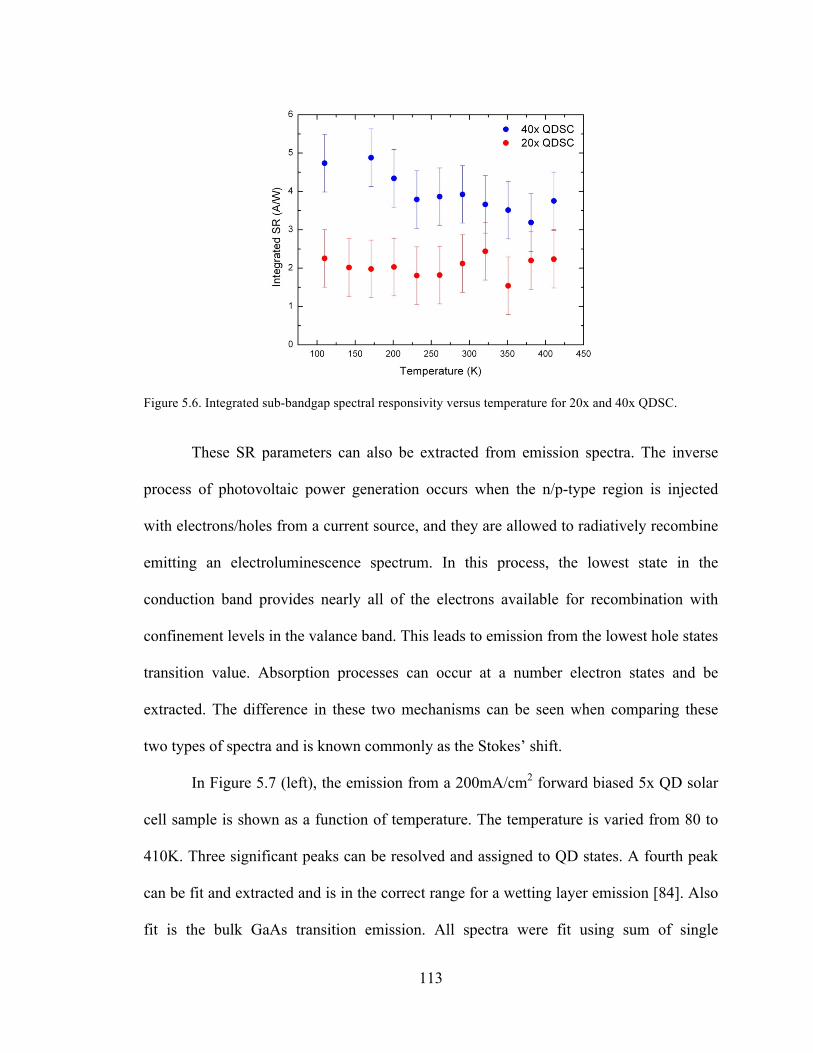
113
Figure 5.6. Integrated sub-bandgap spectral responsivity versus temperature for 20x and 40x QDSC.
These SR parameters can also be extracted from emission spectra. The inverse
process of photovoltaic power generation occurs when the n/p-type region is injected
with electrons/holes from a current source, and they are allowed to radiatively recombine
emitting an electroluminescence spectrum. In this process, the lowest state in the
conduction band provides nearly all of the electrons available for recombination with
confinement levels in the valance band. This leads to emission from the lowest hole states
transition value. Absorption processes can occur at a number electron states and be
extracted. The difference in these two mechanisms can be seen when comparing these
two types of spectra and is known commonly as the Stokes’ shift.
In Figure 5.7 (left), the emission from a 200mA/cm2 forward biased 5x QD solar
cell sample is shown as a function of temperature. The temperature is varied from 80 to
410K. Three significant peaks can be resolved and assigned to QD states. A fourth peak
can be fit and extracted and is in the correct range for a wetting layer emission [84]. Also
fit is the bulk GaAs transition emission. All spectra were fit using sum of single

114
Lorenztian functions for each apparent transition. A general trend can be seen of
increasing emission intensity with decreasing temperature. This is due to the same
quenching effect of photocurrent allowing an increase in the available carriers for
radiative recombination [34, 85, 86]. All five of these peaks’ peak energy value is plotted
in Figure 5.7 (right) and are fit to the Varshni equation. This is an empirically derived
equation with parameters α and β, which are material dependent. The peak energy value
for the GaAs bulk peak fits well with the Varshni equation for GaAs (Eg(0) = 1.519 eV, α
= 5.41 x 10⁻⁴ eV/K, β = 204 K). The other four peaks were fit allowing both Eg(0) and α
to float. β is assumed to be insignificantly different from bulk GaAs. These peak values
are reported and discussed in Table 5.1, below. Included are also the extracted peak
values from the spectral responsivity measurements shown in Figure 5.5 for comparison.
Qualitatively, it is observed that there is a relatively insensitive temperature
dependence of the QD states. This has been observed elsewhere and is likely attributed to
the excitonic nature of the highly confined nanostructures [87]. The emission WL state
appears to be much less temperature sensitive than its absorption counterpart. This
indicates the possibility of a temperature dependence of the Stokes’ shift seen elsewhere
in QW embedded devices [88, 89].

115
Figure 5.7. Left: Electroluminescence spectra of 5x QD solar cell as a function of temperature. Right: GaAs bulk peak value decreases with increasing energy while resolvable sub-GaAs band gap peaks appear less sensitive to temperature. These trends are much more apparent in Table 5.1. Using the extracted Eg(0)
value, the conduction band offset tracks well with temperature for both the 20x and 40x
QD samples. By holding β constant and equivalent to GaAs, the α value is allowed to be
a fitting parameter. Despite this allowance, very little variation in this value is seen when
comparing these WL states to the GaAs bulk. InAs bulk values are very different (Eg(0) =
0.415eV, α = 2.73x10⁻⁴, β = 83K) indicating the strength of the temperature dependence
of the WL states’ relation to that of the bulk material. The emission-derived parameters
are much different. The α values are much lower departure of the emission indicating a
different temperature dependent nature of these two mechanisms.

116
Table 5.1. Extracted Varshni parameters Eg(0) and α for 20x and 40x QD samples using EQE spectra and 5x QD sample using EL spectra, extracted from Figure 5.5 and Figure 5.7 (left).
Absorption fits (SR data) Emission fits (EL data)
20x QD 40x QD 5x QD
Parameter WL1 WL2 WL3 WL1 WL2 WL3 WL QD1 QD2 QD3
Eg(0) (eV) 1.50 1.47 1.45 1.49 1.47 1.44 1.35 1.18 1.22 1.25
α (10-4eV/K) 5.51 5.22 5.63 5.55 5.32 5.42 1.54 2.26 1.85 2.80
Because of their empirically derived origin, the Varshni parameters are in
widespread use and are much more valuable as a comparison tool rather than bearing a
meaningful physical significance [90]. The difference in extracted Eg(0) value indicates a
very stable slope indicative of the temperature stability seen qualitatively. Interestingly,
the wetting layer emission parameters has much different Eg(0) and α values than its
absorption process counterpart. This supports the potential for the temperature dependent
Stokes’ shift mentioned earlier.
5.3. Activation Energy
To investigate the nature of the competitive mechanisms involved in carrier
escape and recombination in quantum confined structures, a number of studies have been
performed on quantum well devices in which photoluminescence (PL) is performed as a
function of temperature [34, 91, 92]. In these studies, an Arrhenius function was fit to the
integrated PL signal to determine an activation energy for carrier escape into continuum.

117
Using this measurement along with the analysis of the emission spectrum both as a
function of temperature, extracting information regarding the carrier dynamics of the
quantum confined layers can be done. These experiments are performed using the InAs
coverage variation samples from Chapter 4, in order to evaluate the effects of the size and
density changes have on the activation energies.
In a GaAs matrix, InAs QD structures exhibit confined states below the energy
value of the conduction band. Simplifying to a two-state system, the change in carrier
population with respect to time (the rate) includes trapping by the QD, U, and anti-
trapping to the barrier, Uβ. Injected carriers, P, add to the upper state carrier population
n. Recombination of carriers from the lower state, m, to the valance band consist of
radiative, R and non-radiative, R’. Figure 5.8 illustrates this concept showing all
processes that interact with state n and m. Processes that involve electron recombination
from m with holes associated with the valance band do not directly affect population of n,
but do subtract from that of state m. These recombination events can be seen when they
are radiative resulting in the spectra obtained by photoluminescence. Since Uβ follows
the exponential function [93], (β ~ e-E/kT), the population of m will be largely affected by
temperature. This population can be probed using techniques like PL, and as the
temperature is changed, variations in this population can be monitored.

118
Figure 5.8. Carriers injected into state n by either photo- or electroluminescence can be trapped at state m and can either recombine or get promoted back to state n.
From this process diagram, we can write the following rate equations. For state n,
we have:
5.5
And for state m, we have:
5.6
In state m, it is clear that there is competition between the thermally promoted carrier and
those that recombine to emit luminescence. From this it is possible to obtain the
activation energy, Ea, as well as a radiative to non-radiative recombination ratio which
will be discussed further.
In an EQE measurement, both the photon generation of electron hole pairs, as
well as the collection of them, at their respective potential, are evaluated without
distinction between them. In order to isolate these two processes, it is important to
optically characterize these devices. Photoluminescence measurements allow this, as it is
an isolated measurement of the radiative recombination.

119
For the quantitative investigation of the carrier dynamics, further rearrangement
of the rate equations mentioned above, must be made. Solving for the emission intensity
I, or Rm, in the variables used, we get:
5.7
Where the ratio R’/R is of importance as an extractable parameter representing the ratio
of non-radiative to radiative recombination. Also appearing here is the energy obtained
from the β expression. This term, now denoted as Ea, is representative of the activation
energy in an Arrhenius relationship. In QWs and QD systems, this often represents the
energy barrier seen by a trapped carrier, and is closely related to the difference in energy
from the top of the barrier conduction band to the energy state of the carrier. Literature
often refers to a simpler 3-parameter equation for the fitting of the integrated intensity
variation with temperature. Plotted in Figure 5.9 (left), the data for the 1.82ML InAs
coverage sample mentioned in chapter 4 is shown. The fit in Figure 5.9 (right) is using
the 3-parameter simplification by the equation shown here:
0( )1 aE kT
II TAe−
=+
5.8
where A is the non-radiative to radiative ratio discussed earlier. I0 is the amplitude of the
intensity and can be divided to the left hand side for normalization.

120
Figure 5.9. Left: Temperature dependent photoluminescence spectra of 10x QD test structure. Right: Integrated PL intensity of the sample with the lowest InAs coverage value. Three separate fits indicate three states that carriers are being extracted from.
Figure 5.10 is plotted with the zero value being equated to the conduction band
continuum and the values of Ea are plotted below successively. The most obvious feature
in Figure 5.10 is that the top most, or closest to the conduction band state decreases with
increasing InAs coverage. This correlates with quantum mechanical theory and the state
value corresponds with accepted literature value range of the WL state (1.25-1.35 eV)
[94]. The two states below suggest QD states at values of roughly 200 and 400meV
below the conduction band. These values appear to be relatively insensitive to the varying
InAs coverage. In the near-conduction band state, however, this is not true. The effects on
the emission of this WL state may indicate that radiative recombination lost to non-
radiative recombination in the large, defective QDs is coming primarily from the wetting
layers. This is reasonable since the small QDs (and their electrons) are physically
separated from the large QDs. This is not so with the wetting layer, as it is a continuous
layer. The ratio A, not shown, stays relatively constant for the QD states, but shows a
significant shift upwards with increasing Θ in the wetting layer. This indicates that the
sample with the lowest number of larger quantum dots and lowest InAs coverage has the

121
most efficient radiative recombination of all of the samples. This fact also corroborates
the data in Figure 5.10, as the wetting layer showed an increase in non-radiative
recombination.
Figure 5.10. Extracted activation energy data for QD test structures with varying InAs coverage values.
With the improvement of optical quality and the reduction in non-radiative
recombination, quantum efficiency can be improved and higher current values may be
available for collection from the QD structures. A further contribution will enhance the
benefits of these structures to the over solar energy conversion efficiency. The improved
accuracy of the strain compensation associated with a monodisperse QD distribution may
also improve the ability to increase the number of these layers available for i-region
insertion. This would increase the absorption cross section of the lower-bandgap material,
contributing further to the current.
Similar EL measurements were performed on the GaAs and GaAsP strain
balancing solar cells discussed in section 3.4. Temperatures were varied from 80K to
295K. Figure 5.11 (left) shows this data and the extraction of activation energies can be
seen in Figure 5.11 (right). Two activation energies were extracted for each of these

122
devices. Relatively little difference in activation energies were seen which is consistent
with the assumption that the additional thickness added for GaAsP is negligible, or offset
by the reduction in barrier height. The non-radiative to radiative recombination ratios do
differ by an order of approximately 3X for the GaP sample indicating a possible increase
in non-radiative recombination associated with the decreased accuracy with strain
balancing in this sample.
Figure 5.11. Left: Temperature dependent electroluminescence measurements for both GaP and GaAsP type strain balancing layers. Right: Integrated EL intensity versus temperature used to extract activation energies and recombination ratios. These results further stress the importance of both the InAs coverage value and
the sensitivity of strain balancing. At higher InAs coverage, the non-radiative
recombination was found to be subtracting from carriers in the WL states, which are key
to the current enhancement in these devices. With the improved accuracy of GaAsP strain
balancing, the non-radiative recombination ratio drops when compared to the GaP
sample. Further characterization of both temperature and voltage would be a desirable
next step to more deeply reveal carrier dynamics in these devices.

123
5.4. Intermediate Band Solar Cell
In 1997, Luque and Marti release their seminal paper entitled, “Increasing the
Efficiency of Ideal Solar Cells by Photon Induced Transitions at Intermediate Levels”
[26]. In this paper, they introduce the intermediate band solar cell. They derive, using a
detailed balance approach, a theoretical efficiency value of a solar cell embedded with an
impurity level. They assume transitions not only from the valence band (VB) to the
conduction band (CB), but also from the VB to the “Intermediate Band” (IB) and from
the IB to the CB. Figure 5.12 outlines the primary photon absorption bands. These
transitions can be modeled similarly to the multi-quantum well system due to the sub-
baseline-bandgap absorption condition. Their efficiency prediction yields a 63.1% solar
cell. At this finding, the novel PV community began seeing increased efforts towards this
thrust since the most efficient cell at the time was just below the Shockley-Queisser limit
[15] of 31%.
Figure 5.12. Operational band diagram for the intermediate band solar cell incorporating 3 distinct bands, providing 3 distinct absorption pathways.
5.4.1. Requirements

124
The pursuit of the intermediate band solar cell is a more specific, focused use of
quantum confined material within a solar cell. This concept’s full potential uses very
specific assumptions, such as a concentration value of 46,000 suns, no non-radiative
recombination, and infinite carrier mobilities [26]. This is meant to be an upper limit
calculation, so these are reasonable, but estimates using more practical numbers approach
the upper 40%. Also, the thermal isolation between transitions is restricted, as only two
supplied photons are the means of operation. One constraint that is realizable is the
calculated energy band values for the individual transitions. Their 63% result corresponds
to a total host bandgap of 1.93eV, with the intermediate band at 1.23eV from the valence
band. Quantum well structures would otherwise be useful for this concept except that the
isolation requirement of the intermediate band can only be ideally satisfied by a band
with zero-dimensional density of states (Figure 1.1). For this reason, this concept has
drawn much attention to solar cells embedded with QDs as the most viable means of
realizing such a device [45]. It is these two potential solar technologies that motivate the
work done here.
5.4.2. Determination of WF Overlap
In the design of the intermediate band solar cell, it is proposed that there exists the
formation of “minibands” within the bandgap of the host embedded with QDs. These are
seen in Figure 5.12 as the intermediate band. With thin energy barriers between confined
structures, the individual wave functions may overlap significantly enough to widen the
energy level to an individual band [44]. Previously, QDs were modeled as QWs in a
GaAs matrix, using Silvaco ATLAS device simulator to approximate the wavenumber as

125
a function of depth through a 1D superlattice [95]. This substitution was justified for
modeling the quantum dot samples in this study because of their high aspect ratio (6 x 25
nm, height x diameter). Thus, the energy of a single quantum dot will be dominated by
confinement along the growth direction. It was found that with a barrier thickness of 35
ML, there was no significant wavefunction overlap from well to well. This was defined
as a system with eigenvalues above 10-6 cm-1/2 [95]. However, the samples modeled here,
with the thinner barriers exhibited significant overlap, O(10cm-1/2).
To fully realize these results, epitaxially grown p-i-n devices with two sets of QD
superlattices (5x and 10x repeat layers) embedded in the i-region were designed with
varying barrier thicknesses above and below the wavefunction threshold mentioned
above. Electroluminescence measurements were taken and analyzed. The peak energies
of these samples are compared and trends extracted. Figure 5.13 (left) shows the EL
spectra for the 21ML barrier thickness and the de-convolution of the spectrum into fitted
Lorentzian functions in order to more accurately extract peak energies. The full-width
half-max (FWHM) values are 45-70meV per state. Figure 5.13 (right) shows the
transition energy values of the fitted electroluminescence functions for all six samples.
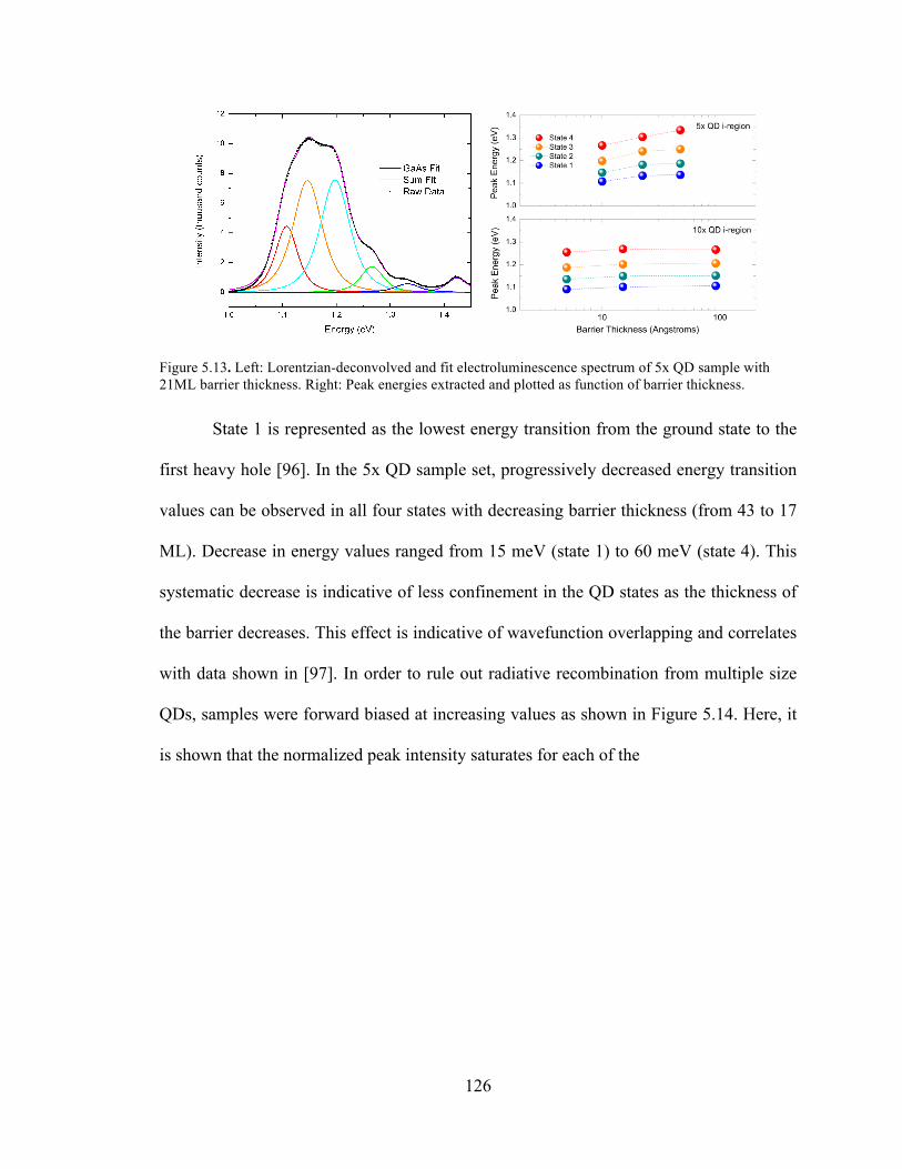
126
Figure 5.13. Left: Lorentzian-deconvolved and fit electroluminescence spectrum of 5x QD sample with 21ML barrier thickness. Right: Peak energies extracted and plotted as function of barrier thickness.
State 1 is represented as the lowest energy transition from the ground state to the
first heavy hole [96]. In the 5x QD sample set, progressively decreased energy transition
values can be observed in all four states with decreasing barrier thickness (from 43 to 17
ML). Decrease in energy values ranged from 15 meV (state 1) to 60 meV (state 4). This
systematic decrease is indicative of less confinement in the QD states as the thickness of
the barrier decreases. This effect is indicative of wavefunction overlapping and correlates
with data shown in [97]. In order to rule out radiative recombination from multiple size
QDs, samples were forward biased at increasing values as shown in Figure 5.14. Here, it
is shown that the normalized peak intensity saturates for each of the

127
Figure 5.14. Normalized peak intensity values as a function of forward injected current density. states. It is apparent that a single state saturates only after that of the state of lower
energy. If the EL-contributing QD size distribution was poly-modal, saturation would not
be energy dependent. This systematic saturation can then be assigned to a single QD size.
This is confirmed by AFMs shown previously, where the small, optically active QDs are
mono-modal in nature, with only inhomogeneous broadening as the geometrical
variation.
Further characterization involved a more detailed investigation of the barrier
widths using test structures grown at some smaller thicknesses (0.8, 1, 1.2, 1.4, 3, 4, 8, 25
nm) and spreading over a larger range. Figure 5.15 (left) shows the normalized
photoluminescence spectra of these samples. Extracting the peak values from these data
revealed two separate trends (Figure 5.15, middle). Shown here are the peak energy
values as a function of barrier thickness. The trend shown in the three largest thickness
samples, is decreasing energy values as the barrier thins. This can be assigned to
miniband thinning and has been discussed in literature [98].

128
Figure 5.15. Left: Normalized photoluminescence spectra; Middle: extracted peak energies from data shown in at left; Right: HRXRD of 5 thickest barrier samples.
The trend shown with the samples with much thinner layers is increasing as the
barrier thins. This counters the convention of the three thickest layer samples. There is a
reasonable explanation for this, since as these layers become on the order of the QD
height (or thinner), there is very little GaAs material to allow for relaxation resulting in
large amounts of inhomogeneous strain. In support of this explanation, Figure 5.15 (right)
shows the high resolution x-ray diffraction data ([004] 2θ scan) for the five thickest
barrier samples. As seen in both the 25 and 8nm samples, the superlattice peaks are very
intense indicating high material quality. Strain was relatively minimized, as no deviation
from the Bragg peak is noticed in the superlattice peaks. This indicates that the samples
are all well strain balanced. This is a reasonable conclusion since the only layer changing
thickness here is GaAs. Samples with thinner barriers showed degradation in this aspect,
as their SL peaks have decreased in intensity, and FWHM has broadened. This effect is
especially significant in the 1nm sample. Data for even thinner samples was not taken as
the superlattice peak spacing was beyond a reasonable scan range. These samples are
assumed to have followed this trend as the 1nm sample was already roughly an order of
magnitude smaller than QD heights.

129
5.5. Conclusion
As mentioned, QD layer number should be increased and further concentration
measurements can be taken to observe the effects of more quantum dot layers on the
various solar cell parameters at high concentration values. Short circuit current as a
function of concentration is of particular interest because of the expected behavior of a
baseline cell and that of a potential intermediate band solar cell. In the intermediate band
case, there may be the ability for a two photon absorption process. This manifests in a
short circuit current on the square of the concentration. This will typically be very small
in magnitude when compared with one-photon processes and therefore has not been
observed with low quantum dot number stacks and at lower concentrations. However, if
this affect is taking place, it will be more observable at higher QD layer numbers and
higher concentration values. Particular attention will be paid to these concepts with future
experiments.
Further studies regarding the temperature dependence can be made as well. More
recent activation-energy related data has shown an independence of the absorption energy
as a function of temperature, contradictory to Figure 5.6 involving the spectral
responsivity. This indicates the potential for a temperature dependence of the Stokes’
shift and will be investigated in detail using all means of spectroscopy. This has been
shown in the literature for quantum well structures [99, 100].
Delta doping QDs has also been accepted as a large requirement of the IB solar
cell. The theory being that the intermediate band itself needs to be half filled providing
necessary carriers for absorption from IB to CB and VB to IB. One method of testing the
efficacy of actual devices with delta doped QDs is to use samples with and without delta

130
doping and perform photoluminescence experiments at energies lower than the bulk
bandgap of GaAs (1.42eV at room temperature). This can be done by using a 980nm
HeNe laser (1.26eV). Also, increasing the delta doping value (equivalent to approximate
number of carriers per QD), can be used in this experiment to observe the onset of a
threshold, above which delta doping may become an effective method for this half-filled
condition.
Additionally, further characterization of the tunneling process can be used to
evaluate the alternative escape mechanisms to better approximate the probability of the
2nd photon effect as a carrier pathway. To vary the tunneling effects, biasing the solar
cells may be possible during the EQE measurement itself. By using a negative or
reversed bias, the band structure will bend systematically, and sub-gap EQE can be
monitored for any changes as a function of bias. Increasing carrier extraction under
further reverse bias can give a dependence of extraction based on tunneling. By
normalizing this to the current value at zero bias, one could theoretically extract a ratio of
carriers removed purely by tunneling. This, coupled with an increase in extraction under
IR light biasing, may be able to give ratios of the effectiveness of all three escape
mechanisms.

131
6. Conclusion & Future Work
This body of work has described in extensive detail the materials science and
device physics of InAs QD-embedded superlattice-based p-i-n GaAs solar cells. We have
seen the importance of strain balancing in light of its effects on structural and optical
metrics, as well as its effects on photovoltaic device performance. A large focus of this
work also investigated the nature of the role of QDs themselves on material quality and
device parameters. An in depth study of optical spectroscopy as well as mechanical
stress/strain relations was used to more deeply probe the mechanisms causing
performance degradation, and ultimately used to mitigate some of these inherent
problems.
Paths forward are outlined here for each of the subtopic chapters in this document.
The future work can be divided into two categories. First, the QD arrays can be
evaluated from a design standpoint. This not to be confused with the topics covered in
chapter 4, as that focuses on the optimal growth conditions. The questions to be
answered here are:
• What is the highest achievable QD densities and ranges of sizes to
maximize absorption?
• Is there a limitation to this density maximum based on limitations of strain
balancing?
• Is there a QD size that best fits the needs of the spectral tuning
motivation? IBSC motivation?
• Can we improve the control of the QD growth nucleation?

132
To begin answering these questions, we can make rough calculations, but also
implement experimental pathways. For instance it has been shown that QD densities
saturate near 1x1011 cm-2 [17]. An experimental thrust may be necessary here to
determine if our current growth conditions will allow this density. The second point may
be much more difficult to answer. Clearly there is a dependence of strain balancing on
QD density (see section 3.3), but does the surface become too dense with islands that the
heterogeneous nature of the strain vectors in the material above the QD become too great
to mitigate with a two-dimensional layer? A series of samples (p/n junctions) could be
grown here with intentionally varying QD densities, their correct strain balancing layers,
and TEM and Electron Beam Induced Current (EBIC) measurements could be made to
evaluate defect density.
Nucleation site improvement can be investigated by possibly changing the offcut
of the substrate which provides a variation in terrace density. Preliminary results have
already been investigated elsewhere in our research group [53, 101]. Further
investigation may involve the use of surfactants in the growth chamber such as Sb.
Although difficult to implement in a manufacturing environment, investigations on nano-
patterning would be of good scientific value for QD nucleation enhancement as well.
This has been done elsewhere [102, 103].
The dependence of energy levels on the QD size ensures that tweaking the dot
size allows for a direct control of the absorption edge. Further evaluation of this effect
can be obtained by combining a detailed balance calculation with a realistic confined-
state calculation such as k*p method. This could yield an optimal QD size to target. A
more atomistic, energy-minimization-based model may prove to be a viable second order

133
strain balancing calculation for improving the superlattice structure. Other materials
should continue to be evaluated for this balancing layer also, such as GaAsP, evaluated
here.
From the cell design standpoint, it will be necessary to gain further advantages
with these devices with proper cell design and comparisons to equivalent baseline/control
cells. Increasing QD densities and improving the control over nucleation sites would also
be valuable. Growth conditions in the InAs layers has proven to be a very sensitive
variable in the device performance, and chamber conditions need to be critically assessed
with respect to the mitigation of large, optically inactive QDs. Unique spectroscopic
measurements may also become very valuable for the evaluation of the IBSC including
voltage biased and IR-light biased EQE measurements. Maximizing absorption,
absorption volume, and carrier extraction while minimizing material defects in the
superlattice and emitter will be the most important efforts to keep focus on as the
research continues.
Other ideas for the advancement of these devices include answering the following
questions:
• How can we increase absorption per QD layer?
• How can we increase QD density?
• How can we continue to increase number of layers without loss in electric field?
• How can we increase extraction efficiency of QD-generated e-h pairs?
• How can we improve uniformity of QDs to minimize FWHM?
• How can we further reduce i-region recombination?

134
Some of the answers to these questions lie in calculations. Detailed absorption coefficient
formulation can be used to optimize absorption by evaluating the variation in QD
morphology prior to implementing it on the reactor. For instance, if absorption coefficient
increases with a change in diameter or height theoretically, this can then be a hypothesis
going into an experiment.
Ultimately, many of these questions must be answered via experimentation.
Changes in chamber pressure have shown to improve dot densities and variation of the
injector flows inside the reactor has shown the ability to increase spatial uniformity
across wafer [104]. Varying the doping levels in the extrinsic regions of the devices may
provide enhanced electric field across the junction. In 1993, Paxman performed this
experiment with QW solar cells and found that superlattices placed at ¼ and ¾ of the
depth of the i-region improved dark current densities in the devices [105]. A similar
variation of QD array location within the intrinsic region may also be an approach to
maximize the existing electric field.
The improvement of extraction efficiency can be looked at using the tradeoff
between the benefits of deep QD states (enhanced spectrum absorption) and the
drawbacks (higher thermal energy necessary for extraction) can also be evaluated
experimentally. Alternatively, limiting the band offset to only the valence band allows the
intensely rich states in this band to provide a ‘ladder’ effect for an enhanced thermal
pathway out to the continuum. This would require choosing materials with iso-
conduction band properties and may indicate another use of the Sb source mentioned in
the previous section. Since the QD layer itself is the most valuable knob to turn in the
spectrum enhancing mechanism of this device type, it will be of great value to these cells

135
to pursue a meticulous study of the QD growth parameters, with this chapter merely
scratching the surface.
Secondly, from a general device design standpoint, the device layer structure may
show room for improvement. As the number of QD layers increases, the intensity of the
electric field provided by the i-region begins to diminish. It may be necessary to increase
the emitter and base doping such that the electric field is maintained high. A series of
varied doping solar cells could be grown to evaluate the significance of this effect.
Another important point to begin to evaluate, as it has been lacking in the solar cells
grown to date, is to evaluate the effect of pure i-region thickness on the device
parameters. This could include growing a series of baseline cells at varying thickness
and monitor the short-circuit current, and the ideality factors, as these are the most
sensitive to this region of the device. Additionally, it would be an effective test to change
the intrinsic region in our “standard baseline” to one which reflects an equivalent i-region
thickness of our QD-embedded samples. This will further remove asymmetry in
experimental evaluations.
By the methods and efforts contained herein, absolute solar cell device efficiency
was improved by one half of a percent which can be a significant finding in the
photovoltaic field. Although much work is left in inclusion of these nanostructures into
real, manufactured devices such as state of the art multijunction III-V cells and also for
the realization of an operational intermediate band solar cell, the advancements made
here provide a step forward in the direction of these goals to reach fruition. Bandgap
engineering can be a viable endeavor in the field of photovoltaic devices.

136
Appendix A: Strain balance development Included in this appendix is a detailed development of the application of the continuum elasticity theorem to the strain balancing of a superlattice of two layers which alternate between compressive and tensile about a substrate lattice constant. In a layer with a cubic lattice psuedomorphically strained to a substrate or thick layer, the energy density is a function of the strained layer’s stiffness coefficients (Cij) and the directional components of the strain (εij):
( ) ( )yyxxxxzzzzyyzzyyxx CCU εεεεεεεεε +++++= 1222212
2 (1)
where the strain, is defined as εij = [(a0 – a1)/ a1]ij for a particular direction, x, y and z. Since εxx and εyy are equal as they are strained to the material beneath, and εzz is defined as νεxx, where ν is the ratio of -2C12/C11, this can be reduced to:
⎥⎦
⎤⎢⎣
⎡−+=
11
212
12112 2
CCCCU ε (1)
with ε = εxx = εyy. Then, taking a thickness weighted average of the energy density for a stack of layers, and substituting A for the factor in the brackets above, we obtain:
21
22221
211
tttAtAUave +
+=
εε (1)
This equation can be minimized by taking dU/de and setting equal to zero. Using the definition of εij, this minimization of energy density results in a ratio of thicknesses of alternating lattice constants about a0:
21220
212
0221
2211
1
2
aaAaaAaaAaaA
tt
−−
= (1)
Assuming t1 = strained layer (in this case InAs) and t2 = balancing layer, in this case GaP. It is then the calculation of t2 that is used for the weighted method described in section 3.2.

137
Appendix B: Glossary of Abbreviations Included in this appendix is a listing of common abbreviations used in this thesis. AFM – Atomic Force Microscopy. Feature height and surface roughness characterization technique which makes use of a highly sensitive cantilever/stylus mechanism. Used in this work for QD diameter, height and distribution density evaluation. AMx – Air Mass number (x) used to describe a particular solar spectrum. AM0 is used for solar spectrum used in space, and AM1.5 is used for terrestrial spectra. The air mass number is the daily average of the secant of the angle the sun makes with the horizon. The average is taken using a time weighted average of this value throughout the day. BSF – Back Surface Field, Layer typically included beneath base layer of a solar cell with slightly higher doping CET – Continuum Elasticity Theory/Theorem utilized in [68] for the minimization of stress in a superlattice. Called Zero Stress Method (ZSM) in [64]. EL – Electroluminescence. A spectroscopic measurement in which photons emitted from a semiconductor are detected and plotted versus wavelength or energy. It is a very sensitive measurement used to determine energy levels of radiative recombination events and can provide information about radiative lifetime. It is performed by forward biasing a metal-contacted p/n junction and detection is performed using emission from the surface of the material. EQE – External Quantum Efficiency. This is a measurement of the efficiency of conversion of photons to electron-hole pairs as a function of wavelength. It is a very useful measurement for solar cells as it can indicate performance of the device as a function of doping region. HRXRD – High Resolution X-Ray Diffraction. This is form of x-ray diffraction in which very small slits are used to guide x-rays into low defect density materials such as single crystal semiconductors. This is a highly sensitive measurement and tool that can be used to extract mechanical and material parameters such as lattice constant, in- and out-of-plane strain, superlattice periodicity, interface quality and alloy composition. ML – Monolayer. This refers to a material-dependent unit of thickness equal to half of the material’s lattice constant. MOCVD – Metalorganic Chemical Vapor Deposition (also called OMVPE).

138
QD – Quantum Dot. Typically defined as a three dimensionally confined, zero-dimensional structure with dimensions on the order of or below the Bohr Radius of a material, whose properties are governed by quantum mechanics. QW – Quantum Well. Defined as a one dimensionally confined, two dimensional material (or layer) with dimensions on the order of or below the Bohr Radius of a material, whose properties are governed by quantum mechanics. PL – Photoluminescence. Similar to electroluminescence, this is a spectroscopic measurement in which photons emitted from a semiconductor are detected and plotted versus wavelength or energy. It is a very sensitive measurement used to determine energy levels of radiative recombination events and can provide information about radiative lifetime. It is performed by probing a test structure or device using a laser at a wavelength whose energy is larger than the detection energy range, and detection is performed using emission from the surface of the material. WL – Wetting Layer. This layer is an extremely thin (on the order of a ML that forms during QD growth and is left “behind” after QD nucleation is complete.

139
References [1] A. Zervos, C. Lins, and J. Muth, "Re-thinking 2050: A 100% Renewable Energy
Vision for the European Union," Brussels, Belgium2010.
[2] A. Jager-Waldau, "PV Status Report 2011: Research, Solar Cell Production and Market Implementation of Photovoltaics," Institute for Energy, Renewable Energy Unit, Via Enrico Fermi 2749; TP 450 I - 21027 Ispra (VA), Italia, Luxembourg2011.
[3] G. G. a. W. Doeztel, Introduction to Microsystems Technology: A Guide for Students. Chichester, England: J. Wiley & Sons, 2008.
[4] "$1/W Photovoltaic Systems," U. S. D. o. Energy, Ed., ed: Advanced Research Projects Agency - Energy, 2009.
[5] M. W. Wanlass, S. P. Ahrenkiel, R. K. Ahrenkiel, D. S. Albin, J. J. Carapella, A. Duda, J. F. Geisz, S. Kurtz, T. Moriarty, R. J. Wehrer, and B. Wernsman, "Lattice-mismatched approaches for high-performance, III-V photovoltaic energy converters," in 31st Photovoltaic Specialists Conference, Orlando, FL, 2005, pp. 530-535.
[6] A. J. Nozik, "Spectroscopy and hot electron relaxation dynamics in semiconductor quantum wells and quantum dots," Annul. Rev. Phys. Chem., vol. 52, pp. 193-231, 2001.
[7] R. D. Schaller and V. I. Klimov, "High efficiency carrier multiplication in PbSe nanocrystals: Implications for solar energy conversion," Phys. Rev. Lett., vol. 92, 2004.
[8] R. J. Ellingson, M. C. Beard, J. C. Johnson, P. Yu, O. I. Micic, A. J. Nozik, A. Shabaev, and A. L. Efros, "Highly efficient multiple exciton generation in colloidal PbSe and PbS quantum dots," Nano Lett., vol. 5, pp. 865-871, 2005.
[9] A. J. Nozik, "Exciton multiplication and relaxation dynamics in quantum dots: Applications to ultrahigh-efficiency solar photon conversion," Inorg. Chem., vol. 44, pp. 6893-6899, 2005.
[10] S. M. Hubbard, C. D. Cress, C. G. Bailey, R. P. Raffaelle, S. G. Bailey, and D. M. Wilt, "Effect of strain compensation on quantum dot enhanced GaAs solar cells " Appl. Phys. Lett., vol. 92, 2008.
[11] K. W. J. Barnham, B. Braun, J. Nelson, M. Paxman, C. Button, J. S. Roberts, and C. T. Foxon, "Short-circuit current and energy efficiency enhancement in low-dimensional structure photovoltaic device.," Appl. Phys. Lett., vol. 59, pp. 135-137, 1991.

140
[12] R. B. Laghumavarapu, M. El-Emawy, N. Nuntawong, A. Moscho, L. F. Lester, and D. L. Huffaker, "Improved device performance of InAs/GaAs quantum dot solar cells with GaP strain compensation layers," Appl. Phys. Lett., vol. 91, 2007.
[13] R. P. Raffaelle, S. Sinharoy, J. D. Andersen, D. M. Wilt, and S. G. Bailey, "Multi-junction solar cell spectral tuning with quantum dots," in World Conference on Photovoltaic Energy Conversion, Waikoloa, Hawaii, 2006, pp. 162-166.
[14] P. T. Landsberg and G. Tonge, "Thermodynamic energy conversion efficiencies," Journal of Applied Physics, vol. 51, 1980.
[15] W. Shockley and H. J. Queisser, "Detailed balance limit of efficiency of p-n junction solar cells," J. Appl. Phys., vol. 32, pp. 510-519, 1961.
[16] G. L. Araujo and A. Marti, "Absolute limiting efficiencies for photovoltaic energy conversion," Sol. Ener. Mat. and Sol. Cel., vol. 33, 1994.
[17] D. Bimberg, M. Grundmann, and N. N. Ledentsov, Quantum Dot Heterostructures. New York: John Wiley & Sons, 1999.
[18] I. N. Stranski and L. Krastinow, in Proceedings of the Meeting of the Academy of Sciences, Vienna, Austria, 1937, p. 797.
[19] L. Goldstein, F. Glas, J. Y. Marzin, M. N. Charasse, and G. L. Roux, "Growth by molecular beam epitaxy and characterization of InAs/GaAs strained-‐layer superlattices," Appl. Phys. Lett., vol. 47, 1985.
[20] N. Kristaeder, N. N. Ledentsov, M. Grundmann, D. Bimberg, V. M. Ustinov, S. S. Ruvinov, M. V. Maximov, P. S. Kop'ev, Z. I. Alferov, U. Richter, P. Werner, U. Gosele, and J. Heidenreich, "Low threshold, large T0 injection laser emission from (InGa)As quantum dots," Elec. Lett., vol. 30, 1994.
[21] R. Mirin, A. Gossard, and J. Bowers, "Room temperature lasing from InGaAs quantum dots," Elec. Lett., vol. 32, 1996.
[22] K. W. Berryman, S. A. Lyon, and M. Segev, "Mid-infrared photoconductivity in InAs quantum dots," Appl. Phys. Lett., vol. 70, 1997.
[23] J. Phillips, K. Kamath, and P. Bhattacharya, "Far-infrared photoconductivity in self organized InAs quantum dots," Appl. Phys. Lett., vol. 72, 1998.
[24] K. W. J. Barnham and G. Duggan, "A new approach to high-efficiency multi-band-gap solar cells," J. Appl. Phys., vol. 67, pp. 3490-3493, 1990.
[25] A. Marti, L. Cuadra, and A. Luque, "Quantum dot intermediate band solar cell," in 28th Photovoltaic Specialists Conference, Anchorage, AL, 2000.

141
[26] A. Luque and A. Marti, "Increasing the efficiency of ideal solar cells by photon induced transitions at intermediate levels," Phys. Rev. Lett., vol. 78, pp. 5014-5017, 1997.
[27] A. G. Norman, M. C. Hanna, P. Dippo, D. H. Levi, R. C. Reedy, J. S. Ward, and M. M. Al-Jassim, "InGaAs/GaAs QD Superlattices: MOVPE Growth, Structural and Optical Characterization, and Application in Intermediate-Band Solar Cells," in 31st Photovoltaic Specialists Conference, Lake Buena Vista, FL, 2005.
[28] S. Chakrabarti, S. Adhikary, N. Halder, Y. Aytac, and A. G. U. Perera, "High-performance, long-wave (~10.2 um) InGaAs/GaAs quantum dot infrared
photodetector with quaternary In0.21Al0.21Ga0.58As capping," Appl. Phys. Lett., vol. 99, 2011.
[29] S. I. Molina, A. M. Beltran, T. Ben, P. L. Galindo, E. Guerrero, A. G. Taboada, J. M. Ripalda, and M. F. Chisholm, "High resolution electron microscopy of GaAs capped GaSb nanostructures," Appl. Phys. Lett., vol. 94, 2009.
[30] Y. V. Terent'ev, O. G. Lyublinskaya, A. A. Toropov, B. Y. Meltser, A. N. Semenov, V. A. Solov'ev, and S. V. Ivanov, "Anomalous spin splitting of electrons in type-II InSb quantum dots in InAs," Semiconductors, vol. 43, 2009.
[31] D. Kim, W. Sheng, P. J. Poole, D. Dalacu, J. Lefebvre, J. Lapointe, M. E. Reimer, G. C. Aers, and R. L. Williams, "Tuning the exciton g factor in single InAs/InP quantum dots," Phys. Rev. B, vol. 79, 2009.
[32] J. McCaffrey, M. Robertson, P. Poole, Z. Wasilewski, B. Riel, R. WIlliams, and S. Fafard, "Structural Characterization of InAs/GaAs and InAs/InP Quantum Dots by Transmission Electron Microscopy," in Materials Research Society Symposium, 2010, pp. J851-J8510.
[33] A. Alemu, J. A. H. Coaquira, and A. Freundlich, "Dependence of device performance on carrier escape sequence in multi-quantum-well p-i-n solar cells," J. Appl. Phys., vol. 99, p. 4506, 2006.
[34] J. R. Botha and A. W. R. Leitch, "Temperature dependence of the photoluminescence properties and band gap energy of InxGa1–xAs/GaAs quantum wells," Journal of Electronic Materials, vol. 29, 2000.
[35] C. G. Bailey, S. M. Hubbard, D. V. Forbes, R. F. Aguinaldo, C. D. Cress, S. J. Polly, and R. P. Raffaelle, "Effect of barrier thickness on strain balanced InAs/GaAs QD solar cells," in 34th Photovoltaic Specialist Conference, Philadelphia, PA, 2009.
[36] D. Guimard, R. Morihara, D. Bordel, K. Tanabe, Y. Wakayama, M. Nishioka, and Y. Arakawa, "Fabrication of InAs/GaAs quantum dot solar cells with enhanced

142
photocurrent and without degradation of open circuit voltage," Appl. Phys. Lett., vol. 96, 2010.
[37] C. G. Bailey, S. J. Polly, J. Okvath, D. V. Forbes, C. D. Cress, S. M. Hubbard, and R. P. Raffaelle, "Temperature dependent photoluminescence spectroscopy of InAs/GaAs solar cells," in 35th Photovoltaic Specialists Conference, Honolulu, HI, 2010.
[38] C. G. Bailey, D. V. Forbes, R. P. Raffaelle, and S. M. Hubbard, "Near 1V open circuit voltage InAs/GaAs quantum dot solar cells," Appl. Phys. Lett., vol. 98, 2011.
[39] M. Wiemer, V. Sabnis, and H. Yuen, "43.5% efficient lattice matched solar cells," in High and Low Concentrator Systems for Solar Electric Applications VI, San Diego, California, USA 2011, p. 810804.
[40] J. Singh, Physics of semiconductors and their heterostructures: McGraw-Hill, 1993.
[41] E. F. Schubert, Light Emitting Diodes: Cambridge University Press, 2006.
[42] K. W. J. Barnham, I. Ballard, J. Barnes, J. Connolly, P. Griffin, B. Kluftinger, J. Nelson, E. Tsui, and A. Zachariou, "Quantum well solar cells," Appl. Surf. Sci., vol. 113/114, pp. 722-733, 1997.
[43] N. J. Ekins-Daukes, K. W. J. Barnham, J. P. Connolly, J. S. Roberts, J. C. Clark, G. Hill, and M. Mazzer, "Strain-balanced GaAsP/InGaAs quantum well solar cells," Appl. Phys. Lett., vol. 75, pp. 4195-4197, 1999.
[44] A. Luque and A. Marti, "The intermediate band solar cell: Progress towards the realization of an attractive concept," Advanced Materials, vol. 22, pp. 160-174, 2010.
[45] A. Luque, P. G. Linares, E. Antolin, E. Canovas, C. D. Farmer, C. R. Stanley, and A. Marti, "Multiple levels in intermediate band solar cells," Appl. Phys. Lett., vol. 96, 2010.
[46] S. M. Sze, Physics of Semiconductor Devices. New York: Wiley-Interscience, 1981.
[47] R. Williams, Modern GaAs processing techniques. Norwood, MA: Artech House, 1990.
[48] G. B. Stringfellow, Organometallic vapor-phase epitaxy: theory and practice: Academic Press, 1989.
[49] S. Adachi, Properties of Semiconductor Alloys: Group-IV, III-V and II-VI Semiconductors: Wiley, 2009.

143
[50] I. N. Stranski and L. Krastinow, in Proceedings of the Meeting of the Academy of Sciences in Vienna, 1937, p. 797.
[51] R. V. Kukta and L. B. Freund, "Minimium energy configuration of epitaxial material clusters on a lattice-mismatched substrate," J. Mech. & Phys. Solids, vol. 45, 1997.
[52] V. P. Evtikhiev, A. M. Boiko, I. V. Kudryashov, A. K. Kryganovskii, R. A. Suris, A. N. Titkov, and V. E. Tokranov, "Control of density, size and size uniformity of MBE-grown InAs quantum dots by means of substrate misorientation," Semicon. Sci. and Tech,, vol. 17, pp. 545-550, 2002.
[53] C. R. Mackos, D. V. Forbes, S. J. Polly, A. Podell, Y. Dai, C. G. Bailey, and S. M. Hubbard, "GaAs Substrate Misorientation and the Effect on InAs Quantum Dot Critical Thickness," in 37th IEEE Photovoltaic Specialists Conference, Seattle, WA, 2011.
[54] J. Kim, C. Yang, U. Sim, G.-D. Lee, J. Park, Y. Lee, and E. Yoon, "Growth mechanism of highly uniform InAs/GaAs quantum dot with periodic arsine interruption by metalorganic chemical vapor deposition," J. Appl. Phys., vol. 110, 2011.
[55] M. Yang, S. J. Xu, and J. Wang, "Influence of capping layer and atomic interdiffusion on the strain distribution in single and double self-assembled InAs/GaAs quantum dots," Appl. Phys. Lett., vol. 92, p. 3112, 2008.
[56] J. Nelson, The physics of solar cells. London: Imperial College Press, 2003.
[57] B. S. Passmore, J.Wu, E. A. D. Jr., O. Manasreh, P. M. Lytvyn, V. P. Kunets, and G. J. Salamo, "Multi-color photoresponse based on interband and intersubband transitions in InAs and InGaAs quantum dot photodetectors," in Fall meeting of the Materials Research Society, Boston, MA, 2008.
[58] S. Tsao, H. Lim, H. Seo, W. Zhang, and M. Razeghi, "InP-based quantum dot infrared photodetectors with high quantum efficiency and high-temperature imaging," IEEE Sensors Journal, vol. 8, pp. 936-941, 2008.
[59] J. W. Matthews and A. E. Blakeslee, "Defects in epitaxial multilayers," J. Crystal Growth, vol. 27, pp. 118-125, 1974.
[60] P. S. Zory, Ed., Quantum Well Lasers. San Diego: Academic Press, 1993, p.^pp. Pages.
[61] F. Liu, S. E. Davenport, H. M. Evans, and M. G. Lagally, "Self-Organization of 3D coherent island size and shape in multilayer heteroepitaxial films," Phys. Rev. Lett., vol. 82, 1999.

144
[62] H. Hamada, R. Hiroyama, S. Honda, M. Shono, K. Yodoshi, and T. Yamaguchi, "AlGaInP strained multiple-quantum-well visible laser diodes (λL⩽630 nm band) with a multiquantum barrier grown on misoriented substrates," Journ. of Quan. Elec., vol. 29, 1993.
[63] L. Diehl, S. Mentese, H. Sigg, E. MÜller, D. GrÜtzmacher, U. Gennser, I. Sagnes, T. Fromherz, J. Stangl, T. Rochl, G. Bauer, Y. Campidelli, O. Kermarrec, D. Bensahel, and J. Faist, "Strain Compensated Si/Sige Quantum Cascade Emitters Grown On Sige Pseudosubstrates," Chemistry and Materials Science, vol. 93, pp. 325-330, 2003.
[64] N. J. Ekins-Daukes, "Strain-balanced criteria for multiple quantum well structures and its signiture in X-ray rocking curves," Crystal Growth & Design, vol. 2, pp. 287-292, 2002.
[65] V. Popescu, G. Bester, M. C. Hanna, A. G. Norman, and A. Zunger, "Theoretical and experimental examination of the intermediate-band concept for strain-balanced (In,Ga)As/Ga(As,P) quantum dot solar cells," Phys. Rev. B, vol. 78, p. 5321, 2008.
[66] C. G. Bailey, S. M. Hubbard, D. V. Forbes, and R. P. Raffaelle, "Evaluation of strain balancing layer thickness for InAs/GaAs quantum dot arrays using high resolution x-ray diffraction and photoluminescence," Appl. Phys. Lett., vol. 95, p. 3110, 2009.
[67] Y. Okada, R. Oshima, and A. Takata, "Characteristics of InAs/GaNAs strain-compensated quantum dot solar cell," J. Appl. Phys., vol. 106, 2009.
[68] V. Popescu, G. Bester, M. C. Hanna, A. G. Norman, and A. Zunger, "Theoretical and experimental examination of the intermediate-band concept for strain-balanced (In,Ga)As/Ga(As,P) quantum dot solar cells," Phys. Rev. B, vol. 78, 2008.
[69] J. Nelson, The physics of solar cells. London: Imperial College Press, 2003.
[70] S. Tomic, A. G. Sunderland, and I. J. Bush, "Parallel multi-band k·p code for electronic structure of zinc blend semiconductor quantum dots," J. of Mat.Chem., 2006.
[71] S. Kret, P. Ruterana, A. Rosenauer, and D. Gerthsen, "Extracting Quantitative Information from High Resolution Electron Microscopy," Physica Status Solidi B, vol. 227, 2001.
[72] S. M. Hubbard, D. Wilt, S. Bailey, D. Byrnes, and R. Raffaelle, "OMVPE grown InAs quantum dots for application in nanostructured photovoltaics," in World Conference on Photovoltaic Energy Conversion, Waikoloa, HI 2006, pp. 118-121.

145
[73] G. S. Solomon, J. A. Trezza, and J. S. Harris, "Effects of monolayer coverage, flux ratio, and growth rate on the island density of InAs islands on GaAs," Appl. Phys. Lett., vol. 66, 1995.
[74] F. Heinrichsdorff, A. Krost, M. Grundmann, D. Bimberg, F. Bertram, J. Christen, A. Kosogov, and P. Werner, "Self organization phenomena of InGaAs/GaAs quantum dots grown by metalorganic chemical vapour deposition," Journal of Crystal Growth, vol. 170, 1997.
[75] T. S. Yeoh, C. P. Liu, R. B. Swint, A. E. Huber, S. D. Roh, C. Y. Woo, K. E. Lee, and J. J. Coleman, "Epitaxy of InAs quantum dots on self-organized two-dimensional InAs
islands by atmospheric pressure metalorganic chemical vapor deposition," Appl. Phys. Lett., vol. 79, 2001.
[76] P. Frigeri, L. Nasi, M. Prezioso, L. Seravalli, G. Trevisi, E. Gombia, R. Mosca, F. Germini, C. Bocchi, and S. Franchi, "Effects of the quantum dot ripening in high-coverage InAs/GaAs nanostructures," J. Appl. Phys., vol. 102, 2007.
[77] S. M. Hubbard, C. G. Bailey, S. J. Polly, C. D. Cress, J. D. Andersen, D. V. Forbes, and R. P. Raffaelle, "Nanostructured photovoltaics for space power," J. Nano. Photon., vol. 3, 2009.
[78] S. M. Hubbard, C. Plourde, Z. Bittner, C. G. Bailey, M. Harris, T. Bald, M. Bennett, D. V. Forbes, and R. P. Raffaelle, "InAs quantum dot enhancement of GaAs solar cells," in Photovoltaic Specialists Conference, Honolulu, HI, 2010, pp. 001217-001222.
[79] R. P. Raffaelle, C. G. Bailey, S. M. Hubbard, S. J. Polly, and D. V. Forbes, "Quantum Dot Spectral Tuning of Multijunction III-V Solar Cells " in Fall Meeting of the MRS, Boston, MA, 2008.
[80] S. M. Hubbard, C. G. Bailey, R. Aguinaldo, S. J. Polly, D. V. Forbes, and R. P. Raffaelle, "Characterization of quantum dot enhanced solar cells for concentrator photovoltaics," in 34th Photovoltaic Specialists Conference, Philadelphia, PA, 2009.
[81] D. Scheiman, B. L. Sater, D. Chubb, and P. Jenkins, "Measurement and Characterization of Concentrator Solar Cells," in 3rd World Conference on Photovoltaic Energy Conversion, Osaka, Japan, 2003, pp. 885-888.
[82] S. J. Polly, M. L. Harris, Z. Bittner, C. R. Plourde, C. G. Bailey, D. V. Forbes, and S. M. Hubbard, "Effect of cell size on GaAs concentrators with InAs quantum dots," in 35th Photovoltaic Specialists Conference, Honolulu, HI, 2010, pp. 2057-2061.
146
[83] J. Barnes, E. Tsui, and K. Barnham, "Steady state photocurrent and photoluminescence from single quantum wells as a function of temperature and bias," J. Appl. Phys., vol. 81, 1997.
[84] G. Rowland, T. Hosea, S. Malik, D. Childs, and R. Murray, "A photomodulated reflectance study of InAs/GaAs self-assembled quantum dots," Appl. Phys. Lett., vol. 73, 1998.
[85] Y. T. Dai, J. C. Fan, Y. F. Chen, R. M. Lin, S. C. Lee, and H. H. Lin, "Temperature dependence of photoluminescence spectra in InAs/GaAs quantum dot superlattices with large thicknesses," J. Appl. Phys., vol. 82, pp. 4489-4492, 1997.
[86] L. Kong, Z. C. Feng, Z. Wu, and W. Lu, "Temperature depedent and time-resolved photoluminescence stuides of InAs self-assembled quantum dots with InGaAs strain reducing layer structure," Journal of Applied Physics, vol. 106, 2009.
[87] O. Kojima, H. Nakatani, T. Kita, O. Wada, and K. Akahane, "Temperature dependence of photoluminescence characteristics of excitons in stacked quantum dots and quantum dot chains," J. Appl. Phys., vol. 107, 2010.
[88] C. Sasaki, H. Naito, M. Iwata, H. Kudo, Y. Yamada, T. Taguchi, T. Jyouichi, H. Okagawa, K. Tadatomo, and H. Tanaka, "Temperature dependence of Stokes shift in InxGa1-xN epitaxial layers," J. Appl. Phys., vol. 93, 2003.
[89] D. Hang, M. Chou, M. Hsieh, and M. Heuken, "Temperature dependence of the Stokes shift in tensile InGaN/GaN MQWs with advanced buffer layers," Journal of Korean Physical Society, vol. 53, pp. 1584-1588, 2008.
[90] I. Vainshtein, A. Zatsepin, and V. Kortov, "Applicability of the empirical Varshni relation for the temperature dependence of the width of the band gap," Phys. Sol. State, vol. 41, pp. 905-908, 1999.
[91] A. Alemu, L. Bhusal, and A. Freundlich, "Improved performance due to fast electronic escape in MQW p-i-n solar cells," in 31st Photovoltaic Specialists Conference, Lake Beuna Vista, FL, 2005.
[92] J. S. Hwang, M. F. Chen, K. I. Lin, C. N. Tsai, W. C. Hwang, W. Y. Chou, H. H. Lin, and M. C. Chen, "Study of Self-Organized InAs/GaAs Quantum Dots by Photoluminescence and Photoreflectance," Jpn. J. Appl. Phys. , vol. 42, 2003.
[93] S. Martini, A. A. Quivy, A. Tabata, and J. R. Leite, "Influence of the temperature and excitation power on the optical properties of InGaAs/GaAs quantum wells grown on vicinal GaAs(001) surfaces," J. Appl. Phys., vol. 90, 2001.

147
[94] J. Gardner, E. Albers, C. G. Bailey, S. M. Hubbard, and R. P. Raffaelle, "Advanced techniques for the characterization of quantum dot enhanced solar cells," in Photovoltaic Specialists Conference, Philadelphia, PA, 2009.
[95] R. F. Aguinaldo, "Modeling solutions and simulations for advanced III-V photovoltaics based on nanostructures," M.S. Thesis, , Rochester Institute of Technology, Rochester, NY, 2008.
[96] J. G. J. Adams, J. S. Roberts, G. Hill, N. J. Ekins-Daukes, and K. W. J. Barnham, in 34th Photovoltaic Specialists Conference, Philadelphia, PA, 2009.
[97] N. N. Ledentsov, V. A. Shchukin, M. Grundmann, N. Kirstaedter, J. Boehrer, O. Schmidt, D. Bimberg, V. M. Ustinov, A. Y. Egorov, A. E. Zhukov, P. S. Kop'ev, S. V. Zaitsev, N. Y. Gordeev, Z. I. Alferov, A. I. Borovkov, A. O. Kosogov, S. S. Ruvimov, P. Werner, U. Goesele, and J. Heydenreich, "Direct formation of vertically coupled quantum dots in Stranski-Krastinow growth," Phys. Rev. B, vol. 54, pp. 8743-8750, 1996.
[98] S. Tomic, T. S. Jones, and N. M. Harrison, "Absorption characteristics of a quantum dot array induced intermediate band: Implications for solar cell design," Appl. Phys. Lett., vol. 93, 2008.
[99] D. R. Hang, M. M. C. Chou, M. H. Hsieh, and M. Heuken, "Temperature dependence of the Stokes shift in tensile InGaN/GaN MQWs with advanced buffer layers," Journal of the Korean Physical Society, vol. 53, pp. 1584-1588, 2008.
[100] C. Sasaki, H. Naito, M. Iwata, H. Kudo, Y. Yamada, T. Taguchi, T. Jyouichi, H. Okagawa, K. Tadatomo, and H. Tanaka, "Temperature dependence of Stokes shift in InxGa1-xN epitaxial layers," J. Appl. Phys., vol. 93, pp. 1642-1646, 2003.
[101] D. V. Forbes, C. G. Bailey, S. J. Polly, C. R. Plourde, S. M. Hubbard, and R. P. Raffaelle, "Substrate Orientation Effects on QD-Strain Compensated GaAs Solar Cells," in IEEE Photovoltaic Specialists Conference, Honolulu, HI, 2010.
[102] J. Kim, M. Kawabe, and N. Koguchi, "Ordering of high-quality InAs quantum dots on defect-free nanoholes," Appl. Phys. Lett., vol. 88, 2006.
[103] J. Martın-Sanchez, Y. Gonzalez, L. Gonzalez, M. Tello, R. Garcıa, D. Granados, J. M. Garcıa, and F. Briones, "Ordered InAs quantumdots on pre-patterned GaAs (001) by local oxidation nanolithography," Journal of Crystal Growth, vol. 284, 2005.