GaAs MESFET photodetectors for imaging arrays
338
r-l- \o "- GaAs MtrSFET Photodetectors for Imaging Arrays by Derek Abbott, B.Sc. (Hons.) Thesis submitted for the degree of Doctor of Philosophy The lJniversity of Adelaide Adelaide, South Australia Centre for Gallium Arsenide VLSI Technology Department of Electrical and Electronic Engineering Faculty of Engineering December 1995
-
Upload
khangminh22 -
Category
Documents
-
view
7 -
download
0
Transcript of GaAs MESFET photodetectors for imaging arrays

r-l- \o "-
GaAs MtrSFET Photodetectors forImaging Arrays
by
Derek Abbott, B.Sc. (Hons.)
Thesis submitted for the degree of
Doctor of Philosophy
The lJniversity of AdelaideAdelaide, South Australia
Centre for Gallium Arsenide VLSI Technology
Department of Electrical and Electronic EngineeringFaculty of Engineering
December 1995


Contents
Abstract
Declaration
Preface
Acknowledgement
Resume
Publications
List of Figures
List of Tables
Glossary
1 Introduction
1.1 Aims and Significance
1.1.1 Long Term Aim .
1.I.2 Immediate Aim of this Work .
r.2
1.2.2 Pixel Array
1.3 Research Philosophy
I.4 Field of this Research .
vilt
X
xi
xiii
xviii
xix
xxi
xxvii
xxix
1.1.3 State of the Art and Present Knowledge in the Area of GaAs Arrays
7.L.4 Signiflcance of GaAs
Overview of XY Array Strategy
I.2.I Photocollection Modes
1
2
2
2
3
IJ
6
6
7
8
10

1.5 Achievements from this Research
1.6 GaAs Background and Future Vision
1.7 Summary and Chapter Overview
2 GaAs versus Silicon
Introduction
History
2.2.1 Gallium
2.2.2 Arsenic
2.2.3 Gallium Arsenide
Competing Technologies
2.3.I Diamond
2.3.2 Silicon Carbide (SiC) .
2.3.3 Gallium Nitride (GaN)
2.3.4 PolymerElectronics
2.3.5 Porous Silicon
2.3.6 Silicon-on-Insulator (SOI)
2.3.7 Silicon-Germanium (SiGe) Heterostructures
The Semi-insulating (SI) GaAs Substrate
GaAs Characteristics
2.5.I Bandgap
2.5.2 Speed
2.5.3 Radiation Hardness
2.5.4 Dark Current
2.5.5 Absorption Coefficients
2.5.6 AtmosphericBands
2.5.7 Quantum Efficiency Formulae
2.5.8 Quantum Efficiency & Responsivity .
ii
2.r
2.2
2.3
2.4
2.5

2.5.9 Spatial Degradation by Diffusion
2.6 Summary
3 MESFET Photodetection
3.1 GaAs MESFET Optical Model
3.1.1 Background
3.I.2 Photoresponse Model
3.2 GaAs MESFET Photoresponse Measurements
3.2.7 Monochromator Measurements
3.2.2 Laser Flood Measurements .
3.2.3 Focussed Laser Measurements
3.2.3.1 Two Dimensional Laser Scan Set Up
3.2.3.2 Two Dimensional Scan Results
3.2.3.3 Discussion
3.2.3.4 Experimental Refinement
3.3 Summary
4 Noise
4.I Introduction
4.2 A Brief Early History of Noise
4.3 A New Derivation of the Thermal Noise Formula
4.3.1 Overview of Methods in the Literature
4.3.2 The Lumped Model
4.3.3 The Windowed Fourier Transform (WFT)
4.3.4 The Thermal Noise Formula
4.4 The Classical Energy Catastrophe
4.5 The Quantum Enelgy Catastrophe
4.6 The Steak Grilling Debate
58
60
67
68
68
69
73
73
78
81
86
86
90
94
94
103
i04
104
109
109
110
110
TT4
118
1i8
119
nl

4.7 Quantum Cut-Off Experimental Status
4.8 MacDonald's Objection .
4.9 The Case of Limiting R & C . . .
4.10 kTC Noise
4.11 Power in a Matched Load
4.12 Distributed RC
4.13 The Capacitor Paradox
4.14 Forward's Photoamplifier
4.15 Measurement of Noise
4.16 Thermal Noise in MOSFETs .
4.17 Flicker Noise in MOSFETs .
4.18 Thermal Noise in MtrSFETs
4.19 Flicker Noise in MESFETs
4.20 Shot Noise in MESFETs
4.21 Noise Analysis of Imager Output Circuit
4.2I.1 Silicon output circuit
4.2I.2 GaAs output circuit
4.22 Summary
5 Imagers
5.1 Introduction
5.2 Pixel Design
5.2.1 Illumination Modes
5.2.2 Photocollection Modes
5.2.3 Channel to Substrate Mode
5.2.4 Gate to Channel Mode
5.2.5 Pixel Active Area
5.2.6 Pixel Design
iv
720
t22
122
125
t26
. r27
. t29
129
130
134
134
135
. 136
. 136
. 137
i40
t42
153
t54
. 154
154
154
156
158
159
139
159

5.3
5.4
5.5
5.6
Array Organisation
Address Circuitry
5.4.I Case 1: The Capacitively Bootstrapped Shift Register
5.4.2 Case 2: Conventional D Flip-Flop Shift Register
5.4.3 Case 3: Edge Triggered D Flip-Flop Shift Register .
5.4.4 Register Comparison
Column-to-video line multiplexer
Summary
r62
166
169
17r
174
174
176
. t77
181
r82
183
186
189
190
191
t92
193
194
. r94
. 198
20r
207
208
208
6 Design Methodology
6.1 Introduction
6.1.1 Technology
6.1.2
6.1.3
6.7.4
Parasitic Oscillations
Layout Approaches
6.1.3.1 Symbolic mask level layout
6.1.3.2 Practical constraints
6.1.3.3 CAD tools
6.1.3.4 Modelling of gallium arsenide circuits
6.1.3.5 Interface to fabrication .
Performance Study
6.1.4.1 Adders .
6.1.4.2 Multipliers
184
6.2 Summary
7 Visions & Applications
7.1 Introduction
7.2 Case 1: Aerospace paradigm
7.2.I Image Processing 208

7.3
7.4
7.2.Ll Imageregistration
7.2.I.2 Image enhancement
7.2.2 Polynomial Evaluator .
7.2.2.I Behavioural Model
7.2.2.2 Algorithmic Solution
7.2.2.3 Functional Specification
7.2.2.4 Structural Description (Floor PIan)
7.2.2.5 Symbolic Physical Description .
7.2.2.6 PhysicalLayout
Case 2: The Mobile Multimedia Paradigm
7.3.1 Complementary Gallium Arsenide
7.3.2 Objectives
7.3.3 Current State-of-the-Art
7.3.4 Sub-systems
7.3.4.1 High-density high-speed RAM
7.3.4.2 Image compression
7.3.4.3 Modulo Multiplier for Data Encryption/Decryption
7.3.4.4 Solid-state imager
7.3.4.5 RF/digital interface
Case 3: The Motion Detector Paradigm
7.4.1 Introduction
7.4.2 Comparison with other approaches
7.4.3 Motion Detector Chip
7.4.4 Range Estimation
7.4.4.1 Gallium Arsenide Implementation .
Case 4: The Spatial Light Modulator paradigm
7.5.I Significance
vi
. 209
. 209
. 22t
. 222
. 223
. 224
. 225
. 225
. 228
. 235
. 236
.'l t F7. L¿I
. 237
. 237
. 239
. 239
. 240
. 240
. 24r
. 242
. 243
. 247
. 248
. 253
. 255
. 257
. 259
f .i)

7.6
7.7
7.5.1.1 FLC/Si Technology .
7.5.1.2 GaAs Technology .
7.5.1.3 Devices
7.5.I.4 Optical Neural Network
Techniques and Methods
7.6.1 FLC/Si Devices
7.6.2 LED/GaAs and FLC/GaAs Devices
7.6.3 Smart Pixel Circuitry
7.6.4 SLM and ONN Testing
Summary
. 259
. 260
. 26r
. 263
. 264
. 264
. 266
. 266
. 266
. 267
277
283
. 284
. 285
289
. 290
. 29r
296
299
. 300
. 301
303
I Conclusions and Recommendations
A Finite Difference Method
4.1 FDM Voltage Potential Solution
4.2 FDM Electric Field Solution
B Quantum Efficiency
B.1 Quantum Efficiency in a Semi-Infinite Slab
8.2 Quantum Efficiency in a Finite Slab .
C Heat Equations
D Complex fntegration
D.1 General Complex Integral for Capacitor Problem
D.2 Noise Analysis of 2-Stage RC Ladder
E Polynomial Equations
vll

ABSTRACT
Is it possible for an XY addressable imaging array to be realised in standard or near-standard gallium arsenide digital IC technology? This was the original question at theheart of this work. The motivation was the ability to embed such an imager with digitalGaAs processing on one IC chip. Integration of an imager with a processor offers thepromise of smart sensors that exploit the excellent power-delay product of GaAs, usefulfor mobile applications - where, for instance, image compression may need to take placein real-time on the same chip. Compact mobile systems of the future can also exploit themixed digital/RF capability of GaAs.
Measurements of the photoresponse of GaAs MESFtrTs are used to understand the pho-todetection mechanisms to aid future study and design. A significant new internal gaineffect, in planar MEStrETs has been discovered which we call the "photovoltaic self-biasing edge-effect." The edge-effect can be exploited to attain up to a factor of tenimprovement in photosensitivity. In order to project further the advantages of GaAs andfully understand the challenges, the key differences in device physics between silicon andGaAs are critically examined.
Theoretical quantum efficiency calculations are carried out and compared against the pho-toresponse measurements. A new result is obtained showing that the quantum efficiencyin a finite slab (which models an epitaxial layer) is equal to the quantum efficiency ina semi-infinite slab (which models a bulk substrate) plus a simple add,itiue second orderterm.
A new optical technique for extracting semi-insulating (SI) substrate parameters, includ-ing the carrier diffusion length, is demonstrated showing diffusion lengths of an order ofmagnitude lower than in silicon. This is significant for improved spatial resolution in highdefinition television (HDTV) imagers. From the perspective of silicon device physics thisis a surprising result, but is explained in terms of the deep levels in the GaAs SI substrate.
Various new pixel schemes and layouts are presented for the realisation of a GaAs XYaddressable imaging array. A number of shift register designs for readout of the imager are
VìII

analysed, simulated and compared for the first time. Detailed calculations for optimisingthe noise performance of imager readout circuitry are developed and this is based on a
detailed review of a number of conumdrums and surprises in noise theory.
Future visions and novel applications of the imager are carefully considered. A reviewof various image enhancement, image compression and image registration schemes are
presented for possible future integration with the imager. Potential applications in mo-bile multimedia communications, artificial insect vision and spatial light modulators arereviewed.
The edge-effect discovery is shown to be particularly suited to producing increased pho-tosensitivity in a smart sensor array based on insect vision.
In conclusion, a number of important new principles have been uncovered by this researchleading to the potential realisation of a simple GaAs XY addressable imager that canbe integrated with digital GaAs processing circuitry. This enables the 'smart sensor'paradigm to shift from silicon and reap the advantages of GaAs.
IX

DECLARATION
This work contains no material which has been accepted for the award of any other degreeor diploma in any university or other tertiary institution and, to the best of the author'sknowledge and belief, contains no material previously published or written by anotherperson, except where due acknowledgement has been made in the text.
The author gives consent to this copy, when deposited in the University Library, beingavailable for loan or photocopying.
Derek Abbott
X

PREFACE
This work has an interesting history behind it giving rise to a thesis with a number ofsignificant perspectives that are highlighted as follows.
Firstly, like many engineers today, the author originally came from a firmly entrencheclsilicon background, via working many years in industry, and thus originally approachedthe field of gallium arsenide with extreme skepticism. A change in belief took place,as concrete experimental results from this research gradually verified that GaAs is anexcellent medium for imaging systems.
The initial research questions and challenges concerning a GaAs implementation are thustackled and presented from the point of view of a 'silicon mind.' Interesting discoveriesand surprises concerning GaAs device physics are viewed from a silicon perspective.
This work faced the interesting challenge that technology was not static over the durationof this research. The status quo was constantly changing throughout this research period.Due to the many unknowns in GaAs device physics, unknowns in substrate behaviourand immaturity of the technology, only a few years ago, the idea of a GaAs XY arrayimager was quite a courageous one. The known 'facts' at the time dictated that suchan imager would not outperform silicon. However, the adopted attitude has been "whatdo we need to change to make it work?" The next question was "why should we expendthe effort to do this?" The initial motivation was a vision that a simple GaAs XY arraycould be integrated with high speed image processing circuitry on the one chip, makingmaking an ideal solution for mobile multimedia applications. This in itself was also arather bold vision as mobile multimedia, in the telecommunications community then, wasto our knowledge not spoken of and easy to contest based on the near-term foreseeabletechnology then.
Today, the unclerstanding of the GaAs substrate has greatly improved, the maturity ofthe technology can support large VLSI designs, the research described in this work shows'surprisingly' (from the silicon mindset) good prospects for GaAs XY arrays based bothon theoretical analysis and actual experimental results. Furthermore, telecommunications
XÌ

technology has matured to the point where concepts such as BISDN microcell networksare now within foreseeable reach and therefore the eventual realisation of a communica-tions infrastructure required to support mobile multimedia is no longer a dream but nowinevitable.
The philosophy employed in writing this thesis has been to communicate in a clear andnon-obfuscating manner' As part of creating a clear presentation some special attentionhas been made to the history, vision and motivation that the work is built on. Fbr cìearunderstanding the "*hy" is as important as the ..how."
In any pioneering research program, the meandering path is seldom straight. More oftenthan not other discoveries are made along tangent paths, that can turn out to be morevaluable than the original goals. This is the nature of true research. Therefbre a numberof these 'side alleys' have been carefulìy woven into the main fabric of this thesis - withhopefully minimal disturbance to the logical flow. The famous engineer Thévenin wassurprised when he was told, just before his death, that his theorem had been acceptedworldwide' some 43 years after he posed it in 1883. For this reason nothing has beenprejudged.
Alexander Graham Bell once said t.Leave the beaten track occasionally and diveinto the woods. You will be certain to find something you have never seenbefore." This has been one of the principles underlying this work.
xil

ACKNOWLEDGEMENTS
I walmly thank my parenls for tlteil visiou ald sacrifice in ploviding an eclucation fo¡me. Also for the strong work ethic, they taught me by their example. They did not havethe money to buy toys, so as a baby I was given old electrical plugs to play with. Thisearly contact with electrical devices must have worked on my subconscious to bring meto this point today. Electricity was actually -y worst physics subject at high school, so
the plugs must be thanked for at least having a delayed effect on shaping my future.
I thank Dr. Percy Baxter and Dr. Denis Scotter for employing me at the GtrC HirstResearch Centre, UK, which set me on the path of interest in electronic devices. Theyalso awarded me a Bursary to help pay my way for obtaining my flrst degree. I would notbe here today without their foresight.
At Hirst, David Burt was my mentor and generously guided me through many semicon-ductor principles. Ray Bell taught me the basics of electronics, how to use instrumentsand even how to solder. I thank them both for their patience and generosity. An im-portant milestone, was at about the age of 19 when I asked the 'silly' question: "*hydo electric field lines stop existing outside a depletion region?" Stephen Lovatt providedthe answer: "because field ìines begin and end on f,red charges." The realisation of thissimple fact, helped -y undersbanding of device physics to suddenly blossom. I thankStephen for providing the vital catalyst.
My mentors at Loughborough University, during undergladuate days, were Dr. MikeBrown and Nick Phillips. Mike Brown taught me how to look at solid state physics insimple ways and Nick Phillips sparked my curiosity in unsolved noise theory. These seeds,lhat were then implanted in my mind, have now grown ancl founcl expression within thisthesis. Without their inspiration, this work would not be the same.
Moving to the present, I heartily ihank my supervisors Prof. Kamran Eshr-aghian andAssociate Prof. Bruce Davis for their guidance, patience and belief in me. Prof. Eshraghianhas taught me so much through his tileless energy, loyalty and vision. He has been therock upon which this work has been built, in terms of raising funding, springboarding
xtll

ideas and never prejudging a 'wild' idea. His belief in me and in the vision of the project,callied us thlough the early days when I could not see that far ahead. His boundlessenthusiasm, deep belief in people & teamwork, willingness to encourage risks & takingthem, devotion to long term thinking, ability to engineer & redefine reality, commitmentto high expectations along with readiness, virtue and vision have been marks of his trueleadership. Prof. Davis also has generously given of himself and has guided me throughmany mathematical concepts and has been an inspirational springboard for discussion ofnoise concepts.
There are many people that I must thank of their input into this work. Due to theobvious breadth of this thesis in contrast to my limited time & capabilities something hashad to 'give.' Consequently, I kept myself totally 'software dumb' throughout this work.lVlichael Liebelt, Andrew Beaumont-Smith and Ali Moini have been extremely patientand generous by rescuing me from many software problems. The scan software for theLaser Prober turned out to be particularly tricky and although I originally wrote most ofthe code, Andrew must get the credit for making it work properly.
Dr. Don Griffin and Michael Needle must be thanked for the early work they did ingetting the Laser Prober made up. A special thanks goes to Dr. Tony Pugatschew of theUniversity of South Australia for arranging the laser unit to work through the microscopeoptics of the prober. Stephen Guest, Ian Linke and all the guys from the workshop dida marvellous job of constructing the antivibration table, for the prober, out of a granitegravestone, steel tubing and industrial vibration isolators. Thanks also to Geoff Pook formaking up numerous PCB test heads for all my samples.
The Physics Department also generously lent me their monochrometer equipment for ayear.
A special thanks is due to Dr. Eithne McCabe, Oxford University (now at Trinity, Dublin),for her support and encouragement with some of the early laser based measurements. Shewas the first of a long line of international visitors to witness the 'photovoltaic self-biasingedge-effect,' uncovered by this work.
I warmly thank Dr. Jerry Hallmark and Dr. Jon Abrokwah, of Motorola, for recentlyhosting me in Arizona and answering all my questions about their CGaAs HIGFETs. Iwould also like to thank Dr. Tim Coe, of Vitesse Semiconductor Corporation, for hostingme in Camarillo, California and also answering my questions.
Prof' Antonio Nuñez, Prof. Roberto Sarmiento and Dr. Jose Lopez have hosted me nanytimes at the Ilniversity of Las Palmas, Spain their hospitality has been selfless andIavish. They have been a delight to work and collaborate with. Much of the creclit for
XIV

Chapter 6 must be given to their team. I cannot praise them too highly.
Dr. Bruce Odekirk of Triquint Semiconductor genelously spent a lot of his time unlockingsome of the mysteries of the semi-insulating substrate for me. Much credìt is owed tohim for this very tricky area. Discussions with Prof. Doug S. McGregor, University ofMichigan, Ann Arbor, and Prof. Robert B. Darling, University of Washington, Seattle,on this vexing subject have also been tlemendously influential and helpful.
Dr. Bobby Yu of the University of Reading, UK, receives my deepest thanks for flyingout to meet me both in Adelaide and Paris and has provided much of the inspiration forthe Spatial Light Modulator (SLM) paradigm in Chapter 7.
Our Head of Department, Dr. Tony Parker must be thanked for his marvellous support,finding lab space and releasing me from teaching duties on many occasions for me toengage in international conferences and collaboration.
Dr. Neil Burgess has been a great springboard for discussions on the mobile multimediaconcept and he has generously pointed me to some useful references on encryption anclcompression for which his inspiration must be given credit.
The assistance of Sam Mosel with the polynomial evaluator and Mrs. L. Gu with thebackground work on image processing & use of KHOROS is gratefully acknowledged.Much credit is due to their tireless help.
The following figures were put together by the following people and appeared in jointpublications with myself: (1) Figs. 1.2 and 1.3, Andrew Beaumont-Smith, (2) Fig. 3.3,Song Cui (3) trigs. 7.27,7.30 and 2.31, Dr. André yakovleff and (a) Figs. 7.34, 7.3band 7.36, Ali Moini.
The photographs in Figs. 4.1 and 4.2 are by courtesy of AT&T Archives. Dr. Bob Anholt,of Gateway Modeling, Minnesota, kindly ran G-PISCES-28 for me, to produce Fig. 3.16.Clive Fuller kindìy took the photograph in Fig. 3.12.
The section on insect vision would not be possible without the ingenuity and energy of thewhole 'Bugeye'team: Aìi Moini, Dr. André Yakovleff, Andrew Blanksby, Richard Beare,Ook Kim, Gyudong Kim, Thong Nguyen, Dr. Abdesselam Bouzer.doum, Prof. AdrianHorridge, Prof. Bob Bogner and Prof. Wonchan Kim.
Thanks are due to Dr'. Murray W. Hamilton, University of Adelaide; Prof. B. L. HLr,
University of Maryland; Prof. Laszlo B. Kiss, JATE, Hungary; Dr. Roger H. Koch, IBVIWatson Research Center; Prof. Matt Mclrvin, Harvard University; Prof. Tony Siegman,Stanford Univelsity for helpful discussions on ZPF.
XV

A special thanks is due to Prof. Paul C. W. Davies, University of Adelaide, and Prof. Wal-ter T. Grandy, Jr., University of Wyoming, who as leading experts in the field, kindlychecked through my section on ZPF.
Also thanks is due to Dr. Andrew Mehnert, of Queensland Univelsity of Technology, forchecking through this thesis and filtering out my errors.
Assistance with historical references from Hugh H. Wigg, Adelaide; Claudia Bruning,Fachhochschule Hamburg Fachbereich Bibliothek und Information; Dr. Jan W. Nienhuys,Eindhoven University of Technology; Prof. Gary A. Zimmerman) Antioch University,Seattle; Prof. Arthur van Rheenen, University of Minnesota, and Prof. Chapin C. Cutler,Stanford University is gratefully acknowledged.
Thanks is due to Ninette Ellis, Walter Foid and Chris Holshuysen for translation of papersfrom Dutch and German.
A special thanks to my wife, Stevie, for translating a number of papers from French. Iwarmly thank my wife, children and family for their support and coping with my longhours day & night away in the lab or grafted to a computer terminal. The tr-ue credit forthis work belongs to them - and this work is dedicated to them.
A final thanks to mv friends over the years for their support and encouragement. Ihave been particularly influenced by Peter & Helen McKenna, Bill & Brioney Smart, Bill& Jane Francis and especially Lyndon & Jenny Dolling who have taught me to alwayschallenge the prevailing paradigm and to think without limits.
The initial funding for this work came from the Sir Ross & Sir Keith Smith I Foundationand credit is due to Prof. Sam Luxton who encouraged us to apply for this funding. Fur-ther funding then came from the Australian Research Council (ARC) and the AustralianDepartment of Education Employment & Training (DEtrT) Targeted Instit,tional Links(TIL) program (in conjunction with Seoul National University, Korea) and the AustralianAsean Educational Cooperative Program (AAECp).
lSir Ross & Sir Keith Smith were famous Australian aviators of the 1930s and the aerospace applicationoverview in Chapter 7 is in t,heir honour. An anecdote about Sir Ross & Sir Keith Smi[h can be foundin Dale Carnegie's cÌassic book on interpersonal relations.
XVI

Typesetting: This thesis has been generated using [ATgXsoftware and graphical output is displayedusing MATLAB. Processed images are via KHOROS. Numerous different drawing packages were used as
departmental standards kept changing regularising the postscript format generated from these differentsources was a nightmare and was achieved with difficulty.
Spelling: The Bngìish speìling convenbion has been adopted, except for the words "programme" and"analogue" have been replaced by their American equivalents "program" and "analog." Where more thanone spelling variant is allowed in English such as "biassing" or "biasing" and "infra-red" or "infrared,',the option with the fewesl characters has been adopted.
Quotations: At the beginning of each chapter, various quotes are displayecl. The quotes are a mixtureof pro and con. Contrary quotes are provided to reflecb on the paradigm-shift in thinking. Some aretongue-in-cheek.
Transistors: Unless otherwise stated all, GaAs MESFBT analysis, experimental results and discussionapply only to n-channel and non-self-aligned transistors on an SI GaAs:BL2 substrate with no p-bufferlayer.
Mathematics: All mathematical results in this thesis have been carefully double checked using the
MAPLE symbolic math editor. In some cases where this was not readily possible, MAPLE was used
to numerically solve an equation and this was cross-checked for a number of specific examples with the
by-hand analytical solution.
XVII

RESUME
Derek Abbott obtained his B.Sc. (HONS) in physics at Loughborough University ofTechnologY,UK, and completed his PhD thesis in Electrical & Electronic Engineering atthe University of Adelaide. He worked for a number of years at the GEC Hirst ResearchCentre, London, on infrared and visible image sensors - requiring discipline in VLSIdesign, optoelectronics, device physics, semiconductor noise, fabrication and testing. Hehas worked with both novel and standard technoìogies including nMOS, CMOS, CCD,SOS, GaAs and vacuum microeìectronics (ie. fleld emission devices). Since his arrival inAustralia, he worked for Austek Microsystems, Technology Park, and has been associatedwith the University of Adelaide since 1987 and is a Lecturer within the Departmentof Electrical Electronic Engineering. He has been an invited speaker at a number ofinternational institutions and has appeared on national radio and television. He is afounder member of the Centre for Gallium Arsenide VLSI Technology, Adelaide, institutedin 1987. He has been consuliant to various industry and defence organisations. His currentresearch interests are in the areas of VLSI, GaAs, photodetectors, biologically inspiredsensors) device physics and noise. His most recent contribution is the discovery of a newphotovoltaic self-biasing internal gain effect within planar GaAs MESFETs. He is oninternational committees of both the SPItr, USA and UPoN, Hungary. He was an invitedkeynote speaker at the SPIE conference in Phiìadephia, 1995, and is an invited speakerfor Unsolved Problems in Noise (UPoN '96) in Hungary. He has been invited to speak ata number of international institutions including: EPFL, Lausanne; University of Geneva;MIT, Cambridge; Los Alamos National Research Labs (LANL), New Mexico; Motorola,Tempe, Arizona; Seoul National University and the University of Las Palmas, Spain.
XVIII

PUBLICATIONS
o "Gallium Arsenide MESFET Imager," World Intellectual Property Organisation, Inter-national Bureau, Patent wo 93/07649,1b April 1993. (with Eshraghian.)
o "Photovoltaic Gate Biasing Edge Effect in GaAs MESFETs," Electronics Letters, IEE,vol. 27, no.2r, oct. 1991, pp. 1900-1991, (with Eshraghian, cui & Mccabe).
o"Derivation of the thermal noise formula using window limited Fourier transforms,"IEEE Trans Ed., vol.39, no. 1, Feb. 19g6, pp. 1-13.
o "An Introduction to Gallium Arsenide Devices ," Proceedings of the Australian Interna-tional Electronics Technology Conference, Adelaide, oct. 1g8g, pp. 19-37.
o "Towards Ultra High Speed Systems ," Electronics 'g0, Oct. 1g90, pp. lg3-202. (withA. Nunez.)
o "Conception of a Robot Eye Using a New Technology," ANZAAS, Microfilm, Universityof Sydney, Oct. 1991.
o "Ultra high speed gallium arsenide systems: design methodology, CAD tools and archi-tectures," Microelectronics Conf., Melbourne, June 1991, pp. 85-90.
o "An analog implementation of early visual processing in insects," International Sym-posiurn on VLSI Technology, Systems, and Applications, Taipei, pp.2g3-2g2, May 12-14,1993. (With Moini et al.)
o "An implementation of smart visual micro-sensor based upon insect vision," Proc. lLthAust. Micro. Conf., 5-8 oct 1993, Gold Coast, eueensland, pp. rzg-r}4. (withX.T. Nguyen et al.)
o "The stair-step tracking algorithm for velocity estimation," Proc. 1st Austratia €j NZConf . on Intelligent [nfo. Sys., I-3 Dec lgg3, Perth, pp. 4I2-4L6. (\,Vith Moini et at.)
o "A new VLSI smart sensor for collision avoidance inspired by insect vision," Proc. SPIE,vol.2344, 2-4 Nov 1994, Boston, pp. 105-11b.
XIX


List of Figures
Photonics versus electronics. The scope of this research is indicated in theshaded region.
Optical interconnects. .
1.1
r.2
1.3 Partitioning of high speed systems
2.I Victor Moritz Goldschmidt
Number of published GaAs papers on the INSPEC data base. only thekeywords 'GaAs' and 'gallium arsenide' were searched for.
Understanding the meaning of 'semi-insulator.'
Carrier concentration plots, electric field lines and band bending diagramsfor a silicon pn junction an a GaAs hi-lo n/SI junction.
Channel/substrate hi-lo junction field solved by FDM using the 4-level deepdonor compensation model due to George ef ø/.
Channel/substrate hi-lo junction field solved by FDM using the 2-level deepdonor compensation model due to McGregor et al. .
Energy Band Structures of GaAs v. Si
Lambert's Law of Absorption for GaAs. Solid line: À : 0.4 pm. Dashedline: ) :0.6 ¡^rm. Chained line: À : 0.8 /-¿m.
GaAs Absorption Length Dependence on Wavelength
GaAs v. Si Absorption Length Comparison
MTF due to diffusion. A comparison of the traditional formula due to Seib(dashed line) and the formula due to Barbe (solid line). .
Planck's law
2.2
2.3
2.4
2.5
2.6
2.7
2.8
2.9
2.r0
2.tr
2.r2
10
13
t4
.r,7LI
28
36
38
39
39
4T
44
45
46
51
52
XXI

2.r3
2.t4
2.15
2.t6
2.17
2.r8
Measured absorption length against wavelength for silicon.
Measured absorption length against wavelength for GaAs.
Internal quantum efficiency v. wavelength \
weighted responsivity versus wavelength for silicon. Solid line, w :0.5 ¡;m. Dashed Iine, W :2 p.m. Chained Iine, W :5 p,rn
Weighted responsivity versus wavelength for GaAs
Theoretical MTF versus spatial frequency. Diffusion-only curves are: Si
bulk, 550 nm (chained line); Si epi, 800 nm (dotted line); Si bulk, 800 nm(dashed line). Geometrical-only curve is for a Tf20 aperture to pitch ratioand the GaAs case matches this curve (solid line). .
3.1 Equivalent circuit of MEStrtrT showing photoresponsive elements
3.2 Voltage across channel/substrate barrier against laser modulation fre-quency. The vertical dashed lines show the approximated time constantpositions.
3.3 Drain current versus laser modulation frequency. Three curves representthree separate devices.
3.4 Wavelength response using xenon source monochromatorV¿":0.6 V. Dual curve represents the looping effect.
Vn":-0.8 V,
3.5 I-V Characteristic variation using xenon source monochromator, Vr":-0.8 V, '*.':700 nm, 'f ':300 nm, 'o':0 nm (dark). Dual curves representthe looping effect. There is no looping in the dark condition.
3.6 Transfer characteristic variation using xenon source monochromatorV¿":0.6 V, '{':700 nm,'*':400 nm,'0':200 nm.
3.7 Transfer characteristic variation using laser flood. V¿":0.6 V, ,-l-':815 nm@ 3 mW,'*':632 nm @ 0.95 mw,'o':0 nm (dark)
3.8 Transistor length scan with focussed laser, 628 nm @ 0.125 rrW,2 ¡,r,rt,diameter spot size. I MCI series gate resistor. vr":-0 .8 y, v¿":0. 6v.
3.9 Transistor width scan with focussed laser, 678 nm @ 0.12b mW,2 ¡,trndiameter spot size. 1 Mf¿ series gate resistor. Vr":-0.8 v, v¿":Q.g !.Transistor edge corlesponds to 20 ¡lm on the x-axis.
54
56
53
55
57
59
lC)
70
74
75
II
79
80
82
XXII
83

3.10 Transistor wiclth scan with focussed laser, 6zg nm @ 0.125 mw,2 ¡rm diam-eter spot size. No series gate resistor. Vn":_0.g V, V¿,:0.6 V. Transistoredge corresponds to 20 ¡tm on the x-axis. g4
Response against gate series resistor. 6zg nm @ 0.125 mw,2 pm diam-eter laser spot size. I Mf-¿ series gate resistor. vn":-0.g v, v¿"-0.5 v,'o':transistor edge,'*':transistor middle.
Laser Prober with Computerised X-y platform
3'13 MESFET drain current response to 2-D laser scan, max. current 3.2 mANo gate resistor.
3.14 MtrSFET drain current response to 2-D laser scan, max. current 29 mAWith 10 Mf-¿ gate resistor.
3.11
3.r2
3.15
3.16
3.t7
3.18
3.19
3.20
85
87
88
89
Laser spot positions for high & low gain drain current response. gg
3-D Electric field plot using G-PISCES-2B with Spicer's uDM. Left half isfield under the gate overhang. Right half is field under the schottky gate. . g1
convergence of schottky gate, MIS gate and channel/substrate field linesat the transistor edge. conceptual drawing with exaggerated features. gz
Quantum efficiency versus gate resistor. solid line: internal quantum effi-ciency (T:1) from first order theory. Dashed line: measured (low gain).Chained line: measured (high gain). gB
MtrsFET drain c'rrent response to 2-D laser scan, max. current 2g mA.With 10 M0 gate resistor. 3-D plot. Performed on antivibration table. 95
MESFET drain current response to 2-D laser scan, max. current 2g mA.With 10 Mf) gate resistor. Contour plot. Performed on antivibration table. 96
4,I
4.2
4.3
4.4
4.5
4.6
4.7
Bert Johnson
Harry Nyquist
Lumped Circuit Model.
The window function
Quantum equipartition energy
Noise in distributed RC line. .
Two stage RC ladder a source of an unsolved paradox
xxiii
106
107
111
113
r2l
128
129

4.8
4.9
4.10
4.11
4.r2
5.1
5.2
5.3
5.4
5.5
5.6
5.7
5.8
5.9
5.10
5.11
5.r2
5.13
Amplifierconfiguration. .. . .180
Opamp noise sources . . 131
Imageroutputcircuitconfiguration. .....13gImageroutputcircuitnoise(silicon). .....140Imageroutputcircuitnoise(GaAs)... ....I42
Fingered rransistor Dual-Gate Pixel conceptual Layout . . 160
PixelEquivalentCircuit ....161Layoutof 3by3pixels. .....163Layout of 3 by 3 pixels, with antiblooming structure. . . . . 164
Arrayorganisation. ...167Array organisation with antiblooming structure. . . . 16g
Shift register with bootstrapped stages . . . . 169
Conventional D flip-flop shift register stage . . ITIConventional D flip-flop shift register layout segment . . . . I7Z
Conventional D flip-flop shift register simulation. Top trace demonstratesnon-overlapping clocks, second trace is the serial input and subsequentparalleloutputsfollow. .. ..123trdgetriggeredDflip-flopshiftregisterstage .....I74Edge triggered D flip-flop shift register layout segment . . . IT5
Column-to-video line switching: equivalent circuit . . ITT
6.1 DCFL logic gates
6.2 SDCFL logic gates
6.3 DCFL inverter circuit
6.4 SDCFL inverter circuit
6.5 Photograph qualitatively showing parasitic oscillations in I-V chalacteris-tic. Arbitrary axes. Notice region of negative resistance.
6.6 Layout styles: nMOS-type stick approach
. 184
..184
. 185
185
186
XXIV
187

6.7
6.8
6.9
6.10
6.11
6.r2
6.13
6.r4
6.15
6.16
6.r7
6.18
Layout styles (a) Ring Notation using dual bus pair, (b) Ring Notationusing single bus pair
Ring Notation showing topology of circuit
Ring Notation for 2-Input NoR gate, (a) initial representation, (b) aftersimplification
Translation from Ring Notation into Mask layout for a D-Latch
Gallium arsenide design process using CAD tools
1-bit Ripple carry layout (a) nMoS type stick and (b) Ring Notation
Floorplan of the GaAs implementation of carry look-ahead expressions
Area vs. delay of Ripple Carry and Carry Look-Ahead adders
Block diagram of Binary carry look-ahead adders
Comparison of different adders
Computational density of parallel multipliers
Shift register bit-slice (a) diagram, (b) simulation
7.1 Edge enhancement/thresholding edge detection system
7.2 A satellite image of Adelaide (band7).
7.3 The result of edge detection from Roberts operator.
7.4 The result of edge detection from Prewitt operator.
7.5 The result of edge detection from Sobel operator.
7.6 The result of a median filter.
188
188
189
189
r92
195
197
197
198
199
200
20r
2t0
2r3
274
2t5
216
219
220
222
224
225
226
226
226
t.(
7.8
7.9
7.10
7.r1
7.r2
The result of sobel operator applied on the median filtered image.
SDCFL design example.
Block diagram of bit-serial algorithmic solution
PE cell structural layout.
Generation of half-carry result.
Generation of sum result.
7.13 Generation of carry result
XXV

7.14
7.r5
7.16
7.17
7.18
7.r9
7.20
7.2r
7.22
7.23
7.24
7.25
7.26
7.27
7.28
7.29
7.30
7.3r
7.32
7.33
7.34
7.35
7.36
Register logical representation. .
Diplexor logical representation.
Adder floor plan block diagram.
Adder cell ring notation.
Register cell ring notation.
Diplexor cell ring notation.
PE cell structural block diagram.
Polynomial evaluator cell.
Adder and simulation.
Register and simulation.
Block diagram of bit-serial algorithmic solution with PE cell structurallayout below.
System block diagram for basic mobile video device. Unshaded areas arestandard tasks. Shaded areas need to be particularly addressed by CGaAssolutions.
Insect vision concept compared to conventional CCD camera.
Coding of templates
Template table.
Example template output pattern. X-axis represents bearing - each sampleis 1o. Y-axis represents time - each sample is 20 ms.
Extraction of angular velocity from a template pattern.
Looming pattern.
Calculation for range
Theoretical MTF versus spatial frequency. Diffusion-only curves are forspecific optical wavelengths. Geometrical-only curve is for the acttal T f 20
aperture to pitch ratio used.
A Smart Pixel Architecture
A FLCiSi or FLC/GaAs Smart Pixel
A LED/GaAs Smart Pixel
227
227
228
229
230
230
230
23r
232
233
234
238
244
250
250
25r
252
252
254
256
262
265
265
XXVI

8.1 Internal quantum efficiency versus absorption length
8.2 Internal quantum efficiency versus absorption length
C.1 Cylindrical coordinate system
. 292
293
296
XXVII

XXVIII

List of Tables
Historical evolution of GaAs - a brief chronology
Properties of Si, GaAs, SiC, GaN and Diamond.
Absorption coefficients
GaAs v. Si Responsivity.
History of fluctuation research - a brief early chronology
Thermal noise over infinite bandwidth for different cases of limiting R andC.
2.L
2.2
2.3
2.4
4.t
4.2
6.1
6.2
6.3
6.4
6.5
7,7
7.2
.29
.30
.43
.58
. 108
. r25
. t75
. 190
. 196
. 196
. 198
. 199
. 246
. 253
5.1 Performance comparison of shift registers. Notice Case t has no powersupplies as it is powered via the clocks.
Gallium Arsenide Symbolic Representation and Notations
Parameters of several ripple carry adders.
Parameters of the carry look-ahead adders.
Parameters of the binary carry look-ahead adders.
Parameters of several adders.
Some possible insect vision technology application areas
Evolution of 'Bugeye' Insect Vision Chip
XXIX

ADCATMBISDNCCDCDSCGaAsCHFÐTCIDCMTCWDCFLDCTDDStrSDÐL2FDMFLCFPNHBTHDTVHEMTHIGFETIM3PCIPNITBITKITOIQBLANLWIRMBSFETMTFMWIRNBDNNOBICONNPAEQERAMSIS/DS/NSOISRAMUDMWFTZPEZPF
GLOSSARY
Analog-to-digital converterAsynchronous transfer modeBroadband ISDNCharge coupled deviceCorrelated double samplingComplementary GaAsComplementary high mobility GaAs FET (=CGaAs FBT)Charge injection deviceCadmium mercury tellurideContinuous wave (unmodulated laser)Direct coupled FET logicDiscrete cosine transformDelayed double samplingÐlectrost atic D amage/ Discharge"Electron level 2" - a deep donorFinite difference methodFerroelectric liquid crystalFixed pattern noiseHeterojuntion bipolar transistorHigh definition televisionHigh electron mobility transistorHigh mobility insulating gate FETInteractive mobile multimedia personal communicatorInteractive personal navigationInteractive telebankingInteractive time keepingIndium tin oxideInternal quantum efficiencyLocal area networkLong wave infraredMetal semiconductor FETModulation transfer functionMedium wave infraredNoise electron densityNeural networkOptoelectronic integrated circuitOptical neural networkPower added efficiencyQuantum efficiencyRandom access memorySemi-insulatingSource or drainSignal-to-noise ratioSiiicon on insulatorStatic random access memoryUnified defect modelWindowed Fourier transformZero point energyZero point fluctuations
XXX

Chapter 1
Introduction
"Research is tlte process of going up alleys to see if they are blind."Marston Bates (L906-1974)AMERICAN ZOOLOGIST
"Human knowledge is personal ønd responsible, an unending ad,uentureat the edge of uncertainty."Jacob Bronowski (rsOB-L9T )POLISH.BRITISH MATHEMATICIAN AND POET
1

1.1 Airns and Significance
1.1.1 Long Term Aim
The overall aim is to create a significant advance in the area of solid-state imaging via theresearch of an image sensor than can be ultimately integrated with high-speed galliumarsenide (GaAs) processing circuitry on a common substrate chip. This combination willfacilitate a new generation of compact smart sensors) useful in mobile applications fordetecting and transmitting full visual images. Spin-off application in the area of highdefinition television (HDTV) is also promising due to the larger absorption coefÊcients inGaAs leading to improved spatial resolution. The intention is for a GaAs image sensor, tobe fabricated in a standard or near-standard GaAs digital IC process, enabling potentialintegration with a higher speed GaAs image preprocessor. This new paradigm offers theadvantage of a preprocessor that can quickly access the image sensor in serial or parallel toefficiently perform low-level early uision tasks. The high-level vision tasks, if required, ffiaybe then carried out in real-time on a simpler host processor. The superior speed-powerperformance of GaAs over silicon and the excellent ongoing progress in GaAs fabricationmaturity make GaAs a favourable choice for mobile applications where superior speed-power product is essential. Also the potential mixed digital/RF capability of GaAs, suchas in the emerging CGaAstM technology, is ideal for compact wireless mobile systems. Thespeed performance and other well known characteristics of GaAs are ideal for applicationswhere harsh environment and increasing need for processing speed place high demands.
L.L.z Immediate Aim of this Work
Due to very large throughput rates and vast amounts of data necessary for real timeperformance, there is an increasing demand for higher speed and lower power consumptionin digital image and signal processors. This means that the choice of algorithms, andindeed that of the architecture to match the technology, becomes a crucial task in therealisation of such systems for real time applications.
Within the scope of the research to develop an imaging system for mobile applicationsit became obvious that many interrelated tasks had to be pursued in order to addressnumerous questions in relation to Ultra High Speed systems. The issues that requiredcareful consideration included, the identification of suitable technology for Very Highand Ultra High speed image processing, front end processing including the photodetectorcharacteristics, architectural mapping and the design methodology.
2

Having identified gallium arsenide as a suitable contender, the complexities associatedwith this emerging technology became a focus for much of the initial research program.As the result of this investigation, an original apploach to design methodology and hencearchitecture, referred to as the'Ring Notation,'has been developed [Eshraghian g1].
The performance of GaAs optical sensors is already proven by our previous investi-gations [Abbott 91] and the work of others [Darling 93, Lange g4, Lin 93, Hibbs 91,Kozlowski 92], therefore one of the remaining major tasks in the clevelopment of a GaAsimage sensor is to determine the various factors which affect the optical gain mechanismsin a GaAs MtrSFET. Thus, the need to accurately model, the behaviour of the MES-FET transistor for implementation within the image sensor became the first major taskpursued. It may be noted that considerable controversy in the literature exists over thenature of GaAs MESFET optical gain. As a result of our investigation, a consistent modelwas developed that overcame the difficulties raised by other researchers engaged in thecontroversy [Adibi 89].
This model is used to resolve apparent contradictions, between different results publishedin the literature, by observing that each of the reported effects come into play by varyingdegree depending on the wavelength of light used and hence penetration depth achievecl.The results have been instrumental in providing a better understanding towards reali-sation of both on-chip and off-chip optical interconnects. Furthermore, in the course ofour research, we uncovered an important effect that we have termed the "Edge Effect."This discovery may well have significant influence upon the pixel design of future imagingsystems.
The research program for the gallium arsenide (GaAs) solid-state image sensor has beensuccessful. The characteristics of the GaAs MESFtrT have been carefully investigatedand we have demonstrated that the excellent characteristics enable its utilisation as thephotosensitive element in an XY array imager, with particular advantages f'or mobileapplications.
1.1-.3 State of the Art and Present Knowledge in the Area ofGaAs Arrays
An XY array image sensor is simply an array of transistors that is exposed to light andthat can be addressed and read out in a similar manner to a memory ar.chitecture. Theterms 'XY image sensor,' 'MOS imager,' and 'mosaic array' have all been used in theliterature to describe essentially the same thing. The charge injection device (CID) alsoconsists of an array of transistors, however this term is only tLsed fol those devices with
3
a specific patented read out technique championed by General Electric.
Presently the silicon CCD technology dominates the image sensor field. However, becauseCCDs require a complex esoteric process, they are not suitable for integration on a simplestandard IC process. In the past, many workers, eg. [Dyck 68, Arnold 21, Kioke g0],
developed simpler silicon XY array image sensors that are more suitable for integrationon a standald IC process. These devices were popular in the early days of the hand-heldvideo camera.
However, CCDs have now displaced XY arrays in the video camera market and conse-quently the XY array has been receiving little attention. Nevertheless, there are somerecent studies in the literature with silicon XY arrays. A group at Edinburgh have inte-grated an XY array to create a smart sensor allowing simple low-level preprocessing func-tions such as adaptive thresholding and correlation/convolution - this scenario has beenused with success for applications such as biometric verification [Mavor 92, Vellacott 94].A group at AT&T have recognised the importance of the XY array for multimedia appli-cations [Dickinson 95].
For mobile applications, such as in aerospace, where there is a greater demand for speed-power performance) our unique proposal is a paradigm-shift from silicon to GaAs. Theinherently larger output node capacitance on silicon XY arrays, as compared with CCDs,gives rise to higher kTC noise which is a limiting feature, of the old paradigm. Conse-quently, the lower line and parasitic capacitances in GaAs mean that this technology isbetter suited to the XY array approach. Over the past decade there has been extensiveresearch on the use of a simple GaAs MESFET as an optical detector. This activity isdue to the MtrSFET's superior noise performance over, say, the pin diode and more sobecause the MESFET can be simply integrated on a stand.ard IC process thus providingan ideal optical port for an OEIC, eg. [Hibbs 91]. Now that GaAs has considerably ma-tured, over the last 5 years, there is renewed activity in GaAs for X-ray detectors withapplications in medicine, astronomy etc. GaAs has proven advantageous in this area dueto low thermal leakage current [McGregor g2, Beaumont 93, Bencivelli 95] and greatertolerance to permanent radiation damage. Work in the area of GaAs CCDs is ongoing,but is still immature due to the complex CCD process [Liu 80, Sahai 83, Kosel 85]. ThisCCD work has no bearing on our research other than highlighting the value of GaAs as anoptical detector and also demonstrating that the Schottky gates can serve as convenientin-house antiblooming lines. This is not possible with MOS gates, in traditional opticalimagers, due to the insulating oxide. The antiblooming facility, with Schottky gates, canbe exploited in the proposed XY array.
In conclusion, on the international scene, there has been considerable interest in single
4

GaAs detectors and their optical performance is proven, with a number of advantages.Our novel proposal recognises the advantage of producing an array of such devices to forman imager in the optical spectrum.
GaAs is now at a level of maturity where chips with as many as 1.44 million transistorshave been successfully built - this highlights the rapidly increasing advance in yield andat full maturity there is no fundamental reason why GaAs yield should not, in fact, ex-ceed that of silicon (due to the fewer mask layers). Other supporting evidence towardsa successful outcome is the fact that photodetector arrays, different in nature from ourproposal, but nevertheless highlighting the ability of GaAs have been successfully fabri-cated' Examples are neural photodetector arrays [Darling 93, Lange 94, Lin 93], OEICarray connectors [Hibbs 91] and hybrid infrared arrays [Kozlowski 92].
I.L.4 Significance of GaAs
This work investigates fundamental GaAs principles that will ultimately enable an ad-vance in the area of smart sensors) especially for mobile applications. Important spin-off areas include remote sensing, industrial robotic vision, forensic image restoration,aerospace vehicle guidance and control, mobile videophones, air surveillance and map-ping and possibly HDTV. Significant future branch off areas of this proposed technologymay include infrared (via hybrid techniques) and X-ray imaging which opens up vast ap-plication areas in medicine, astronomy etc. The economic benefit and social impact in allthese areas is clearly not insignificant.
The key reason for developing the imager in a standard GaAs IC process, is the facilityto euentually integrate this sensoT' with a digital GaAs preprocessor for low-leuel uisionú¿sks such as thresholding, contrast enhancement, edge detection etc. and/or data com-pression/encryption for remote communication. The advantage of a GaAs preprocessoris to meet the demands for ever increasing speed-power performance. Improved speed-
power together with the increased compactness from the circuit integration suits well foradvanced mobile applications.
In addition, there are numerous interesting side benefits to an imager in GaAs. Tosummarise, firstly, we have already discussed the reported low thermal leakage current
[McGregor 92, Bencivelli g5], lower line and parasitic capacitances better suited to the XYarray approach, natural antiblooming provided by Schottky gates and greater tolerance topermanent radiation damage. In comparison to CMOS, it is well known that bhe benefitsagainsl ladiation incluced phenomena include: (a) no latchup (b) no gate oxide charging(c) no field inversion (d) shorter carrier lifetimes.
5

Secondly, further side benefits from using GaAs are: (a) simple manufacture (hence yieldwill be excellent when full maturity is achieved); (b) at visible wavelengths the absorptionlength in GaAs is less than one micron this implies an up to factor ten improvementover silicon - also the visible absorption curve is favourably centred about the channeldepth; (c) this implies better photocollection hence quantum efficiency - in CMOS usefulphotocollection is zero below the epitaxial layer (bulk substrates are not normally useddue to pixel crosstalk); (d) in our imager the n* on semi-insulator (SI) is a high-lowjunction and collects majority carriers - hence there is no Modulation Transfer Function(MTF) degradation due to diffusion - plotting from the well known equations showsthat, if we assume the geometrical MTF curve for GaAs, this is typically better than thediffusion MTF of epitaxial silicon, especially at longer wavelengths - this is useful for highdefinition applications.
This work does not rely on the immediate realisation of any one of these side benefits- however, their significance lies in their potential impact on wider application areas.Future research will answer the question of exactly how large the anticipated side benefitsare in reality.
L.2 Overview of XY Array Strategy
L.2.L Photocollection Modes
All present-day silicon 2-D imagers are designed around a photovoltaic collection tech-nique. Not only does the photovoltaic approach lend itself to the architecture of theimager, but the details of the physics reveals a lower generation noise. Also a furtherreduction in the effect of noise is achieved, over photoconductive devices, as photovoltaicdevices intrinsically perform a capacitive temporal integration of the signal - thus im-proving the signal-to-noise ratio. S/N can be increased in photoconductive devices, byincreasing their size - ie. effectively introducing a spatial integration. However any sig-nificant increase in area would render a 2-D imager array inordinately large. Thereforeit is this fact that photoconductive devices are in the spatial domain, whereas photo-voltaic devices are in the temporal domain, that leads to the fundamental reason why thephotovoltaic approach is favoured for 2-D arrays, in the interest of a high S/N per arearatio.
Having chosen that the imager must be designed around the optimisalion of photovoltaicmechanisms, we need to decide on which MESFET depletion region should be utilised.Making the correct choice is crucial as the photovoltaic mechanism r.elies on the electric
6

field, supported by a depletion region, to separate electron-hole pairs and thus collectcharge. The following depletion regions are available in the MtrSFtrT: (1) surface depletionregion, (2) S/D to substrate depletion region, (3) gate depletion region and (a) channel tosubstrate depletion region. The surface depletion region can be immediately disregardecl,as it is not a 2-terminal structure and therefore charge readout would be impossible. S/Dor channel to substrate depletion regions and gate depletion regions are both viable. Eventhough there is a long RC time constant associated with the S/D and channel cases, atTV rates this mode is still viable. However, a design based around the gate depletionregion offers antiblooming possibilities.
Selection of this photocollection mode immediately suggests two useful constraints for thepixel design. Firstly, the pixel must include a dual-gate MESFET - one gate is to beshielded from the light and acts as a switch to enable/disable readout, and the other isused for photocollection. Secondly, as the gate material is opaque, the detector gate is tobe designed with a 'fingered' structure to maximise the amount of depletion region thatis exposed to generated photocharge.l The use of a fingered transistor will act as a simple'proving ground' to demonstrate the working concept of the imager with a standardunaltered digital GaAs IC process. Although the design relies solely on the gate depletionregion, it is anticipated that the channel/substrate region may have an advantageous sideeffect - namely, stray electrons in this region will be swept into the channel. This effectwill lead to improved Modulation Transfer Function (MTF) characteristics.
L.2.2 Pixel Array
In later sections it will be seen that this work experimentally verifies samples of fingeredMESFtrTs as the basis for a detector pixel. However, The effect of transistor fingerspacing on the collection efficiency of the GaAs device, needs to be fully quantified anclfurther investigated experimentally. As the gates are opaque, the finger wiclth will bekept to a minimum. A series of test structures with various finger spacings would bethe best way to maximise the quantum efficiency - future research can also investigatetransparent gates such as thinned gold or ITO [Sahai 83]. Hence, at this initial researchphase, optimising fill factor will not be an immediate issue. The lesearch challenge ofsurface leakage currents will be combated, if necessary, using annular. st,ructures.
The array organisation required to read out the pixels will follow the stanclard techniquesused for silicon XY array imagers. Basically, one shift register addresses a series of paths
lAlthough the gate is opaque, photocollection can still take place as the depletion region laterallyprotrudes from under the gate. With an optimised structure this scheme can be surprisingly effective.
I

that control the pixel enable/disable gates. A second shift register is used to address ananalogue multiplexer that converts the parallel data into a serial stream. A, charge sensingapproach will be adopted, for readout, where charge is transferred from pixel to data lineand from data line to output bus by a process of capacitive charge sharing. This is a wellunderstood and proven technique used in silicon XY imaging arrays.
Silicon imagers have been known to adopt either the technique of uoltage sensing orcharge sensing for image readout. Voltage sensing entails detecting a voltage at eachpixel and charge sensing reads out the charge from each pixel. Basically, charge sensingis the superior technique because: (1) each pixel does not need to be explicitly reset, as
the action of charge readout is the reset, (2) one capacitor is used for charge-to-voltageconversion, at the output, rather than one at every pixel, therefore fixed pattern noiseis reduced and (3) charge-to-voltage conversion occurs at the final output and not ateach pixel node, therefore pixel circuitry and hence space is reduced. Recent reports,for silicon arrays, have described an 'active pixel' technique [Dickinson 9b] using voltagesensing at each pixel and an alternative approach that implements the sensing at everypixel column [Mavor 92, Vellacott 94]. Both approaches are fundamentally limited bythe degree of matching between active circuits and the area consumed by the additionalcircuitry that would eliminate a realistic HDTV implementation.
The only real advantage with voltage sensing is the increased signal-to-noise ratio due tothe small pixel capacitance used for charge to voltage conversion. In the charge sensingcase' a lower signal-to-noise ratio results from the fact that the charge-to-voltage conver-sion capacitance is unavoidably larger (inherently due to the architecture of the array)and is required to ensure efficient charge transfer to the output bus. It is this very prob-lem that work such as [Mavor 92, Vellacott 94] and [Dickinson 9b] seeks to address. GaAshas the advantage that the lower metal track capacitances improve the S/N and thereforecharge sensing lends itself to this technology. Hence the use of GaAs is an alternativesolution to [Mavor 92, Vellacott 94] and [Dickinson g5], promising superior performanceand space saving.
1.3 Research Philosophy
This work initially raised a number research questions which we highlight as follows.
If the GaAs imager is realised, where are the areas of innovation and originalityin performing this research?
Our near-term goal is to fabricate the worlds first GaAs XY array imager in order to
8

characterise it and investigate the research challenges that include fixed-pattern-noise,surface leakage, etc. and definitively answer a number of fascinating research questionssuch as "is the MTF really good enough for HDTV?" or "how well does the antibloomingperform?" and how the results compare with theory. We know that this pilot chip willnot outperform silicon in terms of fill-factor and defect density, but these are not theimmediate issue, are not fundamental and will gradually improve with technology. Ourimmediate concern is whether the hypotheses connected with the short absorption lengthscan be verified within an actual working imager and how well our circuit techniques canovercome the challenge of small signal swings.
Given the usual read-out times for imagers, is not the speed of GaAs madesuperfluous?
No. One future option is a low speed imager integrated with high speed image processingcircuitry to produce a compact "smart" sensor and/or RF circuitry for wireless com-munications. Another option is for the imager itself to go to higher speeds for non-TVapplication. (eg. machine target tracking).
What are the advantages of using GaAs?
(1) A GaAs image sensor can be integrated with high speed GaAs image processingcircuitry implying future increased compactness and reliability, (2) improved speed-powerproduct, (3) simple manufacture, fewer mask layers than CMOS, hence improaed, defectdensity when full maturity is reached, (4) natural antiblooming provided by Schottkygates and hence ultimately more compact pixels, (5) good spatial resolution from shallowabsorption depths; hence no need for epi-on-high doped layer approach implying improued,q'ua'ntum efficiency, (6) possible further sensitivity increase via our internal gain edge-effect discovery [Abbott 91], (7) higher temperature tolerance from larger bandgap, (8)lower dark current as evidenced by published results [McGregor 92], (g) greater radiationtolerance to permanent danage, (10) no latchup.
What are the research challenges?
(1) Fixed pattern noise - this will be addressed by CDS/DDS techniques, (2) surface leak-age current - addressed by using annular structures, (3) threshold voltage drops makingswitch designs difficult - we have a number of published approaches within our designmethodology to carry out (4) non-optimum fill factor - a demonstrator chip can be madeto work by slightly increasing the lighting level to prove the concept - transparent gatesare then perfectly possible for the future.
What are the future research questions to answer once the chip is fabricated?
o

(1) What is the smallest pixel pitch possible, measure the MTF curve and is this suitablefor HDTV? (2) What is the fastest and ìowest operation speed and the power consump-tion? (3) What is the best finger spacing? (a) Is the edge-effect usable? (b) Based on themeasured kTC noise on the output, project what would be the largest array size possible?(6) Can the concept be proved with a demonstration with at least producing a crudeimage? (7) What light levels can the antiblooming withstand? (8) What is the measuredresponsivity?
L.4 Field of this Research
The merging of optical with electronic functions is a rapidly growing field and terms suchas 'electrooptics,' 'optoelectronics,' 'quantum electronics,' 'quantum optics' and ,lightwave technology'have been somewhat elastic as these paradigms have been in a formativestage. However, a consensus is beginning to emerge and it seems clear that 'photonics'and'electronics'are now regarded as parallel terms, see Fig. 1.1, where electronics dealswith the control of charge flow and photonics with the control of photons.
Photon¡csControl of photons
Electron¡csControl ol eleclrons
L¡ghtwave technology
Ouantum electron¡cs Elãarooptics Optoelectron¡cs
Figure 1.1: Photonics versus electronics. The scope of this research is indicated inthe shaded region.
Electrooptics is a term for essentially optical devices where electrical effects have a role,for example as in the laser. On the other hand, optoelectronics refers to systems that areessentially electronic in nature but where light is involved, for example LCDs ancl imagingarrays.
The term quantum electronics is used where light interacts with matter and therefore, to
Ouantum opl¡cs
Optics
r0

some extent, is a subset of the above terms. Quantum optics refers to the study of lightitself, such as in its quantum and coherence properties. Lightwave technology is used todescribe devices used in optical communications and optical signal processing.
Hence, it becomes clear that imaging arrays, the subject of this thesis, is in the fieldwhere quantum electronics, optoelectronics and electronics overlap this is indicated bythe shaded area in Fig. i.1.2
1.5 Achievements from this Research
Considerable amount of work was conducted in the area of optical modelling of GaAsMESFETs to determine the advantages and feasibility of the proposed imager. Thismodelling has created a firm foundation to enable a first pass design of the imager pixel.The pixel is a transistor with a floating drain exposed to light. The concept and op-eration of the pixel follows identical well known principles proven in current silicon XYarray technology. A notable difference is the presence of a special fingered gate over thephotosensitive drain. The depletion regions around the fingers provide increased photo-collection volume. Also during optical overload (blooming), the over charge will send thefingers into forward bias. By connecting all the fingers to a constant voltage source (withgood current sink capability)) a momentary path to sink the excess charge is created untilreverse bias is reestablished.
Significant progress has also been made by our discovery of a photovoltaic gate biasingedge effect [Abbott 91, Abbott 93]. Here we reported, that under certain gate biasingconditions, dramatic peaks in drain photocurrent gain are observed where the gate over-laps the transistor edges. We have successfully secured a patent fAbbott 93] detailing a
unique imager design where we utilised this gain effect to create an increased sensitivity.
1.6 GaAs Background and Future Vision
The rapidly emerging area of High Speed and Ultra High Speed processing that underpinsthe transformation of much of the ideas into working systems necessitates for evolutionarychanges in both the technology and the strategy that would facilitate the ability forphysical mapping of such systems. The systems that are mostly affected, and indeed in
2Note that Fig. 1.1 is not rigorously correct, but is a useful starting point fo¡ discussion. Full rigour isnot appropriate as the terms are somewhat elastic and exact representation would probably be impossibleon a 2-dimensional diagram. The beauty of Fig. 1.1 lies in a mature acceptance of ambiguity.
1i

the next decade or so would require an ever increasing processing power include real timesignal processors and image processors) computer vision, telecommunications, biomedicalsystems and personaì super computers, just to name a few.
Since the invention of the transistor in 1947, and the development of the very first inte-grated circuit at the beginning of 1960, there has been four generation of ICs. Now, we arebeginning to witness the emergence of the fifth generation of ICs that are characterisedby complexities in excess of 1.8 million devices on a single chip. Over the past severalyears, CMOS technology has become the dominant fabrication process for relatively highperformance and cost effective VLSI circuits and systems. For example, today's micro-processors are able to handle some 80-100 million operations per second, but the circuitrythat manages communications with other processors and in particular with the memory,is just too slow to keep up with this data rate.
Paralleling the developments in CMOS technology some evolving technological changesare also beginning to take place in the area of BiCMOS where some of the advantages ofthe Bipolar transistor are being utilised as CMOS speed enhancer. Main advantages ofBipolar technology over MOS, are greater current drive per unit area, low delay sensitivityto load variation (make excellent line drivers, and decoders for memory elements and faston-chip cache), better device matching, low sensitivity to process variation and linearperformance (sense amplifiers and current mirrors).
Although progress in both silicon processing and technology has been somewhat remark-able during the last decade, we are still confronted with the speed/power limitations ofthe technology that are becoming apparent in fast digital systems and subsequently havebrought about the need for development of other technologies such as gallium arsenide.
Gallium arsenide is rather a different material to silicon. For the same power consump-tion, GaAs is about half an order of magnitude faster than emitter-coupled logic (ECL),the fastest of the silicon family. The speed advantage is primarily the result of galliumarsenide's high electron mobility and the semi-insulating substrate. Other advantages ofgallium arsenide over silicon include its higher temperature tolerance, radiation hard.nessand optoelectronic properties. The last point permits efficient integration of electronic andoptical devices, on the GaAs IC, and is somewhat critical for Ultra High Speed systemsof the future. Gallium arsenide has a direct bandgap. This means that energy level tran-sitions take place with momentum conservation, allowing photon emission. Thus, GaAsis both a good emitter, as well as a good receiver of light. This creates new opportunitiestowards on-chip integrated optical communications. Optical interconnect can either takethe form of optical fibres or thin film paths (eg. aluminium oxicle) integratecl on the chipcarrier as illustrated in Figure 1.2. Another form is the free-space interconnect where
12

focussed or unfocused light is broadcast over an area. This can be utilised to supply a
high speed global clock to a VLSI circuit without the usual routing complexity. Here anopaque masking layer would be used to shield parts of the chip fi'om unwanted light.
CrossoverBranch
0ptical lnterconnects
Silicon VLSI
Circuit
Siliæn Carrier
Figure 1.2: Optical interconnects
One possibility is to utilise gallium arsenide technology for front-end processor sections ofhigh-speed single stream processors for digital data (eg. 1-2 Gigasamples/second), usuallygenerated by way of very wideband image sensor, detectors or the like. This fast datastream can subsequently be subdivided into lower rate parallel streams suitable for pro-cessing in silicon CMOS/BiCMOS subsystems at lower frequencies. Figure 1.3 illustratessuch a concept and highlights the critical paths for communications.
The necessity for high clock rates in the 'front end' processors is compounded since it isvery likely that 10-20 microcycles of the processor may be required to preprocess eachincoming data sample. This means an input data rate of 108 bytes/second might demanda system clock rate of 2GHz. By mixing GaAs and Silicon CMOS/BiCMOS technologies,it becomes possible to exploit high system clock rates together with all the importantreduction in power dissipation in a number of systems, including high bandwidth imageand signal processors in particular in aerospace applications.
In order to take the advantages that can be gained by combining GaAs/BiCMOS/CMOSas the base for Ultra High Speed High performance imaging VLSI systems referred to as
the 'unified technology', attention is also directed towards charactelisation, optimisation
-
13

Output Fibre
ElectricâllnputYOutputs
lntegrated Laser
Multiplexer/Dêmultiplexer
lnput F¡bre
lnt€gratedDetector
Ampl¡fier
Copp€r HêatSink
Error Detection andData Correction
Ceramlc Substrate
Figure 1.3: Partitioning of high speed systems
14

as well as development of a design methodology for GaAs/BiCMOS/CMOS as the basetechnology for Ultra High Speed VLSI systems. The uniqueness of the approach pro-vides the possibility to exploit high system clock rates in a number of systems includingtelecommunication, vision systems, and high bandwidth signal and image processing ap-plications. The significance of this research is that it could provide the design communitythe all-important design methodology for the design of High Speed and Ultra High Speecl,High Performance VLSI systems. In order to facilitate rapid progress and to create thefoundation for future work towards algorithm transformation and mapping of Ultra HighSpeed, high performance imaging systems, initially two areas of research namely GaAssensor development and some aspect of architectural issues associated with the imageprocessing have been pursued within the scope of this program.
I.7 Summary and Chapter Overview
In this introductory chapter we have outlined the immediate and future aims of this work.We have highlighted the research challenges that will be addressed in later chapters, as
well as those for future work. We have introduced the paradigm of a smart image sensorbased on the gallium arsenide technology and have discussed the rationale and anticipatedbenefits. Future application areas have been briefly described - however the concept ofof an interactive multimedia mobile communicator (IM3C) or mobile videophone andimaging for aerospace are the main, though not exclusive, motivational forces for thiswork.
In Ch. 2 we first take a look at the GaAs technology. In order to understand whywe selected GaAs, for this work, its history and comparison with other technologies isreviewed. It is shown that most competing technologies except for silicon are eitherinappropriate or too immature. Hence Ch. 2 is mainly devoted to a comparison withsilicon in terms of mainly optical and substrate properties. Electrical circuit propertiesare well documented in the literature and are not repeated here except in brief summary.
Having accepted GaAs as the choice of technology for this work, Ch. 3 looks at theissues of photodetection in GaAs MESFETs. Detailed photoresponse measurements aredescribed and a new photovoltaic 'edge-effect' is reported, giving an enhancement inphotosensitivity. The results of Ch. 3 suggest two possible approaches for detectors:
o Active pixel. An active pixel exploits the internal gain of the GaAs MESFETto produce enhanced photosensitivity. Although promising, it is argued that thisapproach is not suitable for the imager array) as gain variations lead to fixed pattern
15
noise (fpn). However, Ch. 7 proposes that active pixels can be exploited in motiondetectors, where only coarse thresholded optical data is required.
¡ Passive pixel. A passive pixel simply uses the drain junction of the MESFET as aphotodetector. The MESFET itself is used as a switch to read out the photocol-lected charge at the d¡ain node. Due to the simplicity and better uniformity of thisapproach, it is adopted for the imager design proposed in Ch. 5. A further possibleembellishment is described where fingers of Schottky metal contacts are laid overthe photosensitive drain a¡ea to act as antiblooming lines.
Having suggested these useful design constraints for the imager pixel, based on photode-tector measurements in Ch. 3, Ch. 4 investigates noise issues in order to understand thedesign constraints of the imager's output circuit.
As the area of noise is somewhat obscure and poorly understood in the literature, Ch. 4begins with an original survey of the history and areas of common misunderstanding innoise theory. This sets the framework for then discussing noise in the imager outputcircuit. Original theory and results in the area of noise are also presented in Ch. 4although this is not all directly relevant to the imager design, it is included as the resultsare startling and were part of the meandering path of this research. This is the nature oftrue research and the reader is asked to indulge in a tangent for several pages of Ch. 4.
Given pixel design constraints, from Ch. 3, and output circuit design constraints, fromCh. 4, an overall outline of a possible initial proof-of-concept imager design using a passivepixel approach is finally given in Ch. 5.
Having the proposed imager design scheme, Ch. 6 then proceeds to describe the earlywork carried out to define a suitable design methodology to realise VLSI circuits onGaAs. Using this methodology allows the efficient realisation of image processing circuitsthat can then be integrated with the imager array, thus making way for the smart imagerparadigm in GaAs.
Ch. 7 then uses this methodology to present a case study of an actual GaAs design of apolynomial evaluator that can be used as part of a real-time image post-processor, withthe imager at the front-end, for applications such as in aerospace. Ch. 7 then proceedsto survey other possible image enhancement functions for future GaAs realisation, as
an illustration of the type of processing of the imager's output that can be performedin real-time for the next generation of aerospace or IM3C smart sensors. Finally, analternative type of vision system application is described: a motion detector based aninsect vision for collision avoidance - this new concept uses coarse thresholcled data andthus is an ideal application for exploiting the active pixel approach identifiecl in Ch. 3.
16

In this way, Ch. 7 uses a two-pronged approach - it not only illustrates the vision ofthe smart imager paradigm, but also illustrates a possible exploitation for the promisingactive pixel mechanisms, uncovered by this work,, within an alternative smart motiondetector paradigm.
The branching of this work into these two equally significant apploaches, was not foreseenat the outset of this work, but became apparent as the research evolved. Although thebranching into the motion detector paradigm represents a departure from the originalaims, it was a natural consequence from following through the interesting results fromthis work.
t7

1 8

Bibtiography
i9

[Abbott 91]
[Abbott 92]
[Abbott e3]
lAdibi 8el
[Arnold 71]
[Beaumont 93]
[Bencivelli 95]
[Darlins 93]
[Dickinson 95]
[Dyck 68]
D. Abbott, S. Cui, K. Eshraghian and E. McCabe, ,,photovoltaic
gate biasing edge effect in GaAs MESFETs," Electronics Letters,vol.27, no. 21, pp. 1900-1902, Oct. 19g1.
D. Abbott and K. Eshraghian, "Imaging system for aerospace vehi-cle," GaAs Centre Report, vol. GAAS g2-0I, IggZ.
D. Abbott and K. Eshraghian, "Gallium arsenide MtrSFET im-ager," World Intellectual Property organisation, International Bu-reau,Geneva, Patent \MO 93/OZB4B, lb Apr. 1gg3.
A. Adibi and K. Eshraghian, "A generalised model for GaAs MES-FET photodetectors," IEE Proc. G, Circuits, Deuices ü Systems,vol. 136, Part-G, no. 7, pp. 337-343, Dec. 1989.
E. Arnold et al, "Yideo signals and switching transients in capacitor-photodiode and capacitor-phototransistor image sensors," IEEETrans. Elec. Deu., vol. 18, no. 11, pp. 1003-1010, Nov. 1921.
s.P. Beaumont et øi, "GaAs solid state detectors for physics at theLHC," IEEE Trans. Nuc. Sci., vol. 40, no. 4, 1gg3.
w. Becivelli et al, "some new results on semi-insulating GaAs de-tectors for low energy X-rays," Nuc. Inst. Methods phys. Res. A,Elsevier, vol. 355, pp. 425-427, 1ggb.
R. B' Darling and w. T. Dietze, "Implementation of multiplica-tive lateral inhibition in a GaAs sensory neural-network photode-tector array," IEEE J. Quantunt Elec., vol. 2g, no.2, pp. 645-654,Feb. 1993.
A. Dickinson, B. Ackland, tr. Eid and D. Inglis, ,,standard CMOSactive pixel image sensors for multimedia applications," AduancedVLil Conference, Chapel Hill, March 28, lgg5.
R.H. Dyck and G.P. weckler, "Integrated arrays of silicon photode-tectors for image sensing," IEEE Trans. Elec. Dea., vol. 15, no. 4,pp. 196-201, April 1968.
K. Eshraghian, R. Sarmiento, P.P. Carballo, and A. Nuñez, ,,Speed-
area optimization for DCFL and sDCFL class of logic using ringnotation," Microprocessing and Microprogramming, vol. 32, pp. Z5-
82, 1991.
[Eshraghian 91]
20

[Hibbs 91]
[Kioke 80]
[Kosel 85]
IKozlowski 92]
[Lange 94]
[Lin e3]
[Liu 80]
[Mavor 92]
[McGregor 92]
IMoini 93]
M. Hibbs-Brenner et al, "Design, fabrication and performance ofan integrated optoelectronic cellular array," sPIE oprical Enhance-ments to Computing Technology, vol.1568, pp. 10-20, 19g1.
N. Kioke et al, "MOS area sensor: Part 1,"
Trans. Elec. Deu., vol. 27, no.8, pp. 1676-1687, 1980.
iI IEEE
P.B' Kosel et al, "configurations for high speed gallium arsenidecharge-coupled device imagers," Optical Engineerinq, vol. 24, ro. I,pp. 176-182, 1985.
L.J. Kozlowski and R.E. Kezer, "2 x 64 GaAs readout for IR FpAapplication," SPIE Infrared Readout Electronics, vol. 1684, pp. 181-
138, 1992.
E. Lange, Y. Nitta and K. Kyuma, "Optical Neural Chips," IEEEMicro, vol. 14, no. 6, pp.29-41, Igg4.
S. Lin, A. Grot, J. Luo and D. Psaltis, "GaAs optoelectronic neuronarrays," Applied Optics, vol. 32, no. 8, pp. 1275-1289, lgg3.
Y.Z. Lui, I. Deyhimy, R.J. Anderson, R.A. Milano, M.J. Cohen,J.S. Harris and L.R. Tomasetta, "A backside-illuminate imagingAlGaAs/GaAs charge-coupled device," Appt. Phys. Lett., vol. BZ,no. 9 pp. 803-807, 1980.
J. Mavor, "Compact image processors em loying analogue MOStechniques," IEEE APCCAS 92, Sydney, pp. 1-9, 8-i1 Dec. 19g2.
D. S. McGregor et al, "Development of bulk GaAs radiation detec-tors," IEEE Nuc. Sci., vol. 39, no. 5, pp. 1226-1236, October 1gg2.
A. Moini, K. Eshraghian, D. Abbott et al, "An analog implementa-tion of early visual processing in insects," Internatíonal Symposiumon VLSI Technology, Systerns, and Applications, Taipei, pp.283-287,May 12-14, 1993.
R. Sahai et al, "GaAs CCDs with transpar-ent (lTO) gates for imag-ing and optical signal processing," IEEE Electron Deuice Lett., uol. y',
no. 12,463-464, 1983.
[Sahai 83]
2t

ISensiper 93] M. sensiper et al, "Modulation transfer function testing of detec-tor arrays using narrow-band laser speckle," opticat Engineering,vol. 32, no.2, pp. 395-400, 1993.
[Vellacott 94] O. Vellacott, "CMOS in camera," IEE Reuiew, pp. 1ll-114, May1994.
22

Chapter 2
GaAs versus Silicon
"AIl great truths begin as blasphernies."George Bernard Shaw (1S5G-1950)IRISH COMIC DRAMATIST AND LITERARY CRITIC
"This is the essence of science: ask an impertinent question, and, youare on the way to a pertinent ansu)er."Jacob Bronowski (1908-1924)POLISH-BRITISH MATHEMATICIAN AND POET
"The great tragedy of science - the slaying of a beautiful hypothesis byan ugly fact."Thomas Henry Huxley (faZS-f895)BRITISH BIOLOGIST
23

2.L Introduction
The purpose of this chapter is to examine the history of GaAs and its competing tech-nologies, in order to illustrate the importance of the chosen technology. Given that siliconemerges as the main contender, we proceed to critically examine the unusual substrateand optical properties of GaAs, as compared to silicon, to understand and demonstratethe anticipated advantages of GaAs.
2.2 History
As part of the understanding of our choice of the GaAs technology and gauging its levelof maturity for the proposed work, we shall briefly review its historical development.
2.2.L Gallium
Gallium is a soft white silver metal found throughout the earth's crust and can be ex-tracted from ores such as bauxite, coal and sphalerite. It has a low melting point (29.78"C)and can melt with the warmth of a hand. Consequently, its first application was in hightemperature thermometers. Other applications have been in low melting solders, arclamps, batteries and vanadium-gallium superconductors. Gallium is one of the few met-als that expands as it freezes.
On the 27th of August 1875, between 3 and 4 am in the morning (!), " French chemist bythe name of Paul Émile Lecoq de Boisbaudran (1838 -lgl2) discovered gallium by isolatingit from zinc biende ore found in the Pyrenees. With a spectroscopic analysis he confirmedthat he indeed had a new element and Lecoq identified this with Mendeleyev's predictionof the existence of 'eka-aluminium.' I Lecoq made a significant discovery by showing thatgallium : eka-aluminium, as this was the first of Mendeleyev's predictions of the periodictable to be verified-
There is some debate as to where the name 'gallium' comes from. According to someauthorities it derives from the Latin Gatlia meaning Gaul (France) and hence Lecoqnamed it in honour of his country. Other sources claim that it derives from the Latingallus meaning a 'cock' and hence was named after Lecoq himself. The educated guess ofthis author is that Lecoq made a deliberat e double entendret
r Eka is Sanskrit for 'one.'
24

2.2.2 Arsenic
Arsenic compounds have a long history going back into antiquity. The main compounclsare orpiment (As253) or 'yellow arsenic,' arsenolite (Asa06) or 'white arsenic,' arsenopyrite(FeAsS) and realgar (AsS). The pure metallic form of arsenic (As) is called'grey arsenic'and comes in the form of a flaky grey brittle metalloid. The name 'arsenic' was thoughtto come from the Greek apoeuLKoç meaning 'male' - as the Greeks believecl metals hacl
different sex. However, the latest authorities now say it comes from the Arabic az-zarnllcmeaning 'orpiment' - a compound of arsenic used as a yellow/gold pigment. In turn,az-zarnilc comes from the Persian word zar, meaning ,gold.'
The first documented description of orpiment and realgar is due to Aristotle (384-323BC)- A neoplatonist by the name of Olympiodorus of Alexandria (73. ante b50 AD) isthe first to document white arsenic. The German alchemist and Dominican philosopherAlbertus Magnus (c. 1206-1280) was the first to actually document metallic arsenic andits discovery is usually attributed to him. An anonymous Spanish alchemist, using thepen name Geber (fl. I4th cent. AD), discovered that white arsenic can be obtained byburning realgar.
The Swedish chemist Georg Brandt (1694-1763) showed the connection between whiteand metallic arsenic in 1733 and was the first to examine metallic arsenic in detail. Hewas one of the first chemists to oppose alchemy.
Arsenic has had many uses: orpiment was used as a yellow pigment called "King's Yellow"and, mixed with quicklime, was used as a depilatory called "rusma" in the East. Arsenicwas used as a hardening agent in the process of making lead shot, is used in rat poisonsand in insecticides.
2.2.3 Gallium Arsenide
Gallium Arsenide was first grown and chemically characterised in 1926 by Victor MoritzGoldschmidt, Fig.2.1. However it was not until the early 1960s that researchers firstattempted to make devices with GaAs, see Table2.I. In ig65 Carver Mead producedthe first GaAs FET [Mead 66]. The GaAs FET began to find its first applications in themicrowave area. The 1970s saw the first small scale integrated circuits but reliability waspoor. The 1980s produced accessible and reliable GaAs foundries enabling realisationof large scale integration. By the late 1980s the scale of integlation was sufficient forthe contemplation of complex digital processing in GaAs. The early 19g0s saw the firsttrue VLSI GaAs designs. The present day quality and performance of GaAs has largely
25

displaced the preconceptions about GaAs reliability, though some stigma from the 1g7Os
still remains. Today applications abound and we see GaAs in >90% of all mobile phones,in satellite commtrnication systems, optical fibre transceivers, ATM switching in telecom-munication systems and in high speed digital signal processing, to name a few. The mainarea where there has been a weakness is in the GaAs CPU research programs in thisarea lead by SUN and CRAY, for example, have all collapsed. The key problem is the gateleakage current in the MBSFET, making large CPU memory in GaAs difficult to realise.This may now change as the emerging CGaAsrM technology, using low leakage HIGFETs,begins to prove itself. The rate of growth in GaAs research has gathered considerablemomentum and this is illustrated in Fig. 2.2, which shows a remarkable increase in thenumber of GaAs publications. Whilst the number of publications is not an ideal measureof the health of the GaAs industry, it does reflect the increasing effort going into research.The recent drop in publications (1993 & 1994), was probably caused by military détenteand the latest increase in growth (1995) is most likely due to the rapid penetration ofGaAs into communications systems.
2.3 Cornpeting Technologies
Before we begin to discuss the special characteristics of GaAs over silicon, which make itparticularly suited for the proposed imager, we briefly review some of the major competingtechnologies other than silicon, in order to highlight the importance of GaAs as thetechnology base for this work.
2.3.1 Diamond
There has been much interest in the idea of producing integrated circuits on diamondsubstrates. The characteristics of diamond appear to offer high power, high frequencyand high temperature operation surpassing that of GaAs and silicon. However, diamondhas a number of limiting problems, the worst being that only p-type crystals can be grown.Furthermore, [Colìins 92] has identified a number of errors in the literature showing over-optimistic theoretical predictions for diamond. Another fundamental problem is thatthe p-dopant (boron) in diamond has a rather high activation energy (360 eV) at roomtemperature - this means that only 1,-5% oT the dopant is activated and thus the draincurrent is drastically low (in the order of nA) at room temperature. It shoLrld also benoted that the diamond technology is extremely immature, with only single transistorsfabricated to date and with material that is still extremely difficult to grow rvith device
26

Figure 2.1: Victor Moritz Goldschmiclt (b. Zurich 27thJan. L,S8S. d. Oslo, Norway20th Mar. 1947) was the only son of the distinguished physical chernist HeinrichJacob Goldschmidt, who held professolshìps at Arnsterdan, Ilcidelbelg, and Oslo.His mother was Amelie Kohne. In 1926, he rvas the filst tci glorv a,nci repolt onthe chemical properties of gallìum arsenide, as pa,r't of a systeniaLic stucly of manygallium compouttds. Although he ha,cl no irrkling of how ¡iallirLrn arscnìde rnightbe someday useful, the impact on engineering has been profouuri lith applicationsin integrateci circuits, solar cells, superlatticcs, c¡uanturn ele<:t lonic rler.ices, lightemitting diodes attcl laser diodes. Of Jewish pir"rent¿ì.ge he lclt {ol Norrl'a.y in 1901
ancl obtained Nolwegian citizenship in 1905. IIe rnatriculatecl iLr tlrc same year attlie Uuivelsit.y of Christiania. In 19[ [ lre obtaiuer-l his Ptr.D <lcgrce, ancl irL tg14 he
became a professot'of crystallography, minelalog,.l. anil geolog.r'. f.çcr in t]r,: nriddleof his owu absc.'t'biug rvork lte rvas alw¿rvs giacl to answr]r qrrrrstions arrcL give his
opiniorr. His Iecttrres were excell.ent a,ncl clc-ar'. ILr his.jrrrlgc'rrrclil r.rt'¡rc:r'sons aucl
situations he rvor¡ ld oltett exaggera,tc, ancl lLis Lr:;rcl,iorLs \vcrír 5()rir,ririr,r:; r'ioLerLl ¿r.ncl
seetrtittg[y chilclish. Rut fol his fliencls his glr.l:r.L r¡Lrälitì,'s r.rvr]isiriì'lorr'r,rri ever.y'thing
else. As a Jerv. lie sttffelecl servr:rerl.y at the lLa,rLrls ,-rl tlrt' \azìs. \¡,;ìs ;r rl.stcrL triice.artd in Octoirttt [!)'[2 rvas sent to a corì(:cnf re,l iorL i;rrrL1.r. tlri' rvli,,il oi lris ¡rroitelt.ybcins confist'¿rto<1. IIc c¿llliccl a capsrrlr.r c¡l irvrlr.o( I'rrtri, lcì<! iì,r r j,, ;rs t lrc firraL
cvasiotr ol op¡rlcssiott. ^\ rLttivclsity t:ollc¿rgLrc irr Oslo o¡rr,.' asli,'rl (ìoi,isr lrnlitl t [ol a
sittti[al ciì[)su[c. llo letplic'tl . '"1'his ¡roisorr is fìrr' ¡rrofì,,; j(,t¡ i)f t lrr,iri:ir,, onl',. \irrr. ¿rs
;t ¡rtofìrssot ot ur-,'lr¡ltics. rvill lrar<' t() usc tirc rr,¡r,,."
)

8000
7000
6000
5000
4000
3000
2000
1000
o(t(ú-o(ú(úoot.rJo-Øzcoaoo-(úÈan
(dCIoo-oEfz
Number of GaAs Papers Published Each year
1 970 1 975 1 980Year
1 985 1990 '1995
Figure 2.2: Number of published GaAs papers on the INSpEC data base. onlythe keywords 'GaAs'and 'gallium arsenide, were searched for.
28

Narne
Albertus MagnusJons Jacob BerzeliusPaul Émile Lecoq de BoisbaudranJ. CzochralskiVictor Moritz GoldschmidtJulius LilienfeldVereinigte Chemische FabrikenOskar HeilCetralab, Div. of Globe-UnionSosnowski, Starkiewicz & SimpsonBardeen, Brattain & ShockleyG.K. Teal & J.B. LittleR.S. Ohl & W. ShockleyG.W.A. DummerG.K.Teal & E. BuehlerN.H. FletcherStanislas TesznerJ.A. HoerniJ.S. KilbyVarious companiesLoor, Christensen, Kleimock
& Theu¡erH. NelsonJ.W. AllenS.R. Holstein & F.P. HeimanN. HolouyakR.N. Hall et alM.I. Nathan & G. LaslerVariousCarver A. MeadVariousBell LabsA. Yaniv et alVittesse SemiconductorUniversity of Adelaide
Origin Milestone Date
GermanySwedenFrancePolandNorwayGermanyGermanyGermanyUSAUKUSAUSAUSAUKUSAUSAFr-PolUSAUSAUSAUSA
Isolated pure arsenicIsolated pure siliconIsolated pure galliumInvents CZ crystal growth methodFirst to grow & characterise GaAsFiles patent for copper sulphide FETFirst commercial galliumFiles patent for FETFirst thick film circuitMBÐ growth inventedGermanium point contact transistorGermanium bipolar junction transistorSemiconductor ion implantationIC concept first describedSilicon junction transistorInterdigitated transistorFirst commercial germanium FETPlanar processFirst IC patentBirth of linear ICsEpitaxial growth
LPE growth of GaAsConcept of semi-insulatorFirst MOS ICFirst practical GaAsP LEDSemiconductor laserFirst GaAs pn junctionBirth of TTLFirst GaAs FETBirth of CMOSDBeam lithographyFirst GaAs OEICFirst semi-custom GaAs VLSI ICFirst full custom GaAs VLSI IC
c. 1 250r82418751917192619301932193519411947194819481949I 95219521954195819591959i9601960
UKUSAUSAUSAUSAUSAUSAUSAUSAUSAUSAAustralia
196 r196019621 96219621962196319651968r974197819901991
Table 2.1: Historical evolution of GaAs - a brief chronology.
quality
2.3.2 Silicon Carbide (SiC)
SiC can occur in many polytype forms and over a 180 different polytypes have beenidentified. Polytype 6H is the most stable and has been the most studied. However,although less is known about polytype 4H, it has recently emerged as the favourecl formof SiC - giving increased mobilities over 6H? by a factor of two, as shown in Tab. 2.2.
Due to the good thermal conductivity, wide bandgap and large beakdown field, thiswide bandgap semiconductor (WBS) material is targeted for power applications. ForVLSI digital applications the mobility of Si and GaAs, still appear to be superior (see
Tal>.2.2). SiC has only recentìy become commercially available to difficulty in fincling a
suitable Srowth technique. This together with its immaturity means that starting material
29

Si GaAs SiC-6H SiC-4H GaN DiarnondCrystal structure
Lattice constant (Ä.)
Cost in 1995 ($/sq inch)
Bnergy gap (eV)
Melting point ("C)
Thermal conductivityat 300 K (Wcm-tX-r¡
Breakdown field (kV/cm)
Relative permittivity
Effective electron mass
Effective hole mass
Refractive index
Electron mobilityat 300 K (cm2/Vs)
Hole mobilityat 300 K (cm2/Vs)
Saturation velocity(cm/sec)
diamond
5.43
2.8
I.T2Indirect
t4r2
1.31
300
11.9
0.92m"(lon6j tuditral )
0.I9m"( ! ransverse )
0.49m"(heavy hole)0.I6m"
(lisht hole)
3.42
1450
500
zincblende
5.65
21,
1.42Direct
I 238
0.46
400
13.1
0.067m"
0.50ræ,(heavy hole)0.076m"(lighr hole)
.) ..)
8500
400
wurtzite
4.36
2200
2.86Indirect
2800
4.3
>1000
9.7
1.5m"(longit udinal )
0.25m"(transverse)
1.0m"
2.55
500
wurtzite
4.36
>2200
Dq
Indirect
2800
4.3
> 1000
9.7
1000
cubic
4.51
200
3.4Direct
1500
1.3
3500
8.9
0.2m"
0.8rn"(heavy hole)
o ct
800
diamond
.).i) ¡
2000
5.6Indirect
4000
20
5000
5.5
N/A
250 500 100(?) 500
lx 107 lx 107 2xr07 2x10⁷ 1.5 x 10² 2x10⁷
Table 2.2:, Properties of Si, GaAs, SiC, GaN and Diamond
prices are high and material quality is generally poor [Lande 96]
2.3.3 Gallium Nitride (caN)
GaN is another example of an intensiveìy studied WBS material. Parameters are shownin Tab. 2.2, though it should be noted that there is considerable uncertainty regardingGaN electronic transport parameters. A suitable substrate for expitaxial growth does notpresently exist and an alternative substrate must be used. Sapphire starting substratesare generally used, however lattice and thermal matching with GaN are poor [Trew g5].
Latest work involves growing GaN on SiC substrates. This technology is still in the phase
30

of fundamental materials research and thus is too immature for consideration
2.3.4 Polymer Electronics
Polymer electronics offers many exciting possibilities. LEDs, transistors, displays, de-tectors, integrated circuits can all be achieved with the promise of mechanically flexiblecircuits, by using doped polymers. Therefore, it is conceivable that a future televisionmay be simply a thin flexible A4 sheet, which is portable and can be used in the bath!Polymers offer many advantages including better contrast displays, the ability to form newhetereostructures and the opportunity to design new materials with different bandgapsand electron affinities. In polymers, there are no dangling bonds at interfaces and thushigh vacuum systems are not required for fabrication. Fabrication is further simplifiedin that spin coating replaces epitaxial growth. Apart from being an extremely imma-ture technology, the disadvantages thus far include extremely low mobility and detectorquantum efficiencies in the order ol l% [May 9b].
2.3.5 Porous Silicon
Conventional bulk silicon has an indirect bandgap and therefore fundamentally cannotcompete with the ability of GaAs to emit light and therefore promise full OEIC technology.However, porous silicon can emit light and, although this property is not fully understood,the possible threat is that this may enable silicon to compete with GaAs in the OEICarena. However porous silicon is still very immature: stable operation for thousands ofhours of operation, without degradation in quantum efficiency has not yet been achieved.Also modulation speeds in the hundreds of MHz range have not yet been attained. Mono-lithic ICs in porous silicon have not been achieved and progress is far off [Buda g4]. GaAshas already achieved monolithic circuits, integrated with both detectors and laser diodes.
2.3.6 Silicon-on-Insulator (SOI)
The main insulation techniques that are used in this technology are sapphire, SIMOX(Separation by IMplanted OXygen), DI (polysilicon handle Dielectric Isolation) or BE-SOI (Bond and Etchback SOI). Sapphire tends to have the a poorer quality semiconduc-tor/insulator interface and DI suffers from large wafer warping > 100 ¡;m. Thus SIMOXhas been the traditionally favoured choice. However as SIMOX suffers from defect den-sities as high as 104-10s defects/cm2, the newly emerging BtrSOI technology appears to
31
be overtaking with only i0-100 defects/cm2 but is immature and unproven in the arenaof thin film SOI. For comparison traditional bulk silicon contains 1-b defects l. r.
SOI shows promise in high-speed VLSI. There is high resistance to punchthrough, dueto the insulating substrate. Low capacitive coupling between the inversion channel andthe underlying film reduces the vertical electric field, with a consequent enhancementin mobility and an increase in drain saturation current, as compared to the equivalentbulk CMOS transistor. The major advantage of SOI, due to the insulating substrate, isradiation hardness.
However, a problem that emerges is the floating body effect which gives rise to a kinkin the I-V characteristics of the transistor. This kink effect induces unwanted transientsand can be reduced at the expense of lower breakdown voltage, increased lateral bipolarsnapback effects and negative slope resistance effects.
If the silicon film thickness is reduced, so that it becomes fully depleted, the kink effectis eliminated. However, the drain depth'is thereby reduced, giving rise to an increase inimpact ionisation leading to reduced drain breakdown voltage. This places a prematurelimit on scaling. Holes from the impact ionisation also exacerbate the lateral bipolarsnapback effect.
Also the thin film on insulator has thermal management problems in terms of reliability,ESD protection and local heating effects which cause a drop in mobility giving rise tonegative slope resistance effects on the I-V characteristic.
Due to these various problems, SOI ICs have found only niche application areas whereradiation hardness is of prime importance such as in SRAMs for satellites. Furthermorethis technology would be unsuitable for the proposed imager as the trend is towards siliconthicknesses around 0.1 pm [Groeseneken 90], which would severely limit the depletionregion volume for photocollection.
2.3.7 Silicon-Germanium (Sice) Heterostructures
There has been considerable recent activity with SiGe technology and much speculationabout whether it will soon displace GaAs.
Advances in conventional CMOS, over the years, have been based around device scaling.As submicron dimensions have been approached, further scaling of CMOS has becomeincreasingly complex and fundamental limits will soon emerge. The significance of SiGeis that it is compatible with conventional silicon processing and offers improved materialproperties, so that continued advancement can be sustained.
32

Given that there are many alternative emergent technologies, other than SiGe, the ques-tion is 'why is SiGe presented in the literature as the main contender?' If we examine someof the main emergent technologies in Table 2.2 we see that in terms of cost and mobility,GaAs is clearly in the lead. SiGe becomes a closer competitor by virtue of the fact thatcosts are supposedly low, as it can be produced in existing silicon fabrication lines. AlsoSiGe attracts higher levels of R&D investment, as it rides on silicon funding sources. Un-fortunately, it is difficult to enter a SiGe column in Table 2.2 - this is partly due to the factthat SiGe parameters will vary with mole fraction and particular heterostructure architec-ture, but is mainly because the open literature appears fairly silent for room temperatureparameters. However, wherever sparse data is available, GaAs still remains superior. Forinstance, the effective electron mass of Ge6.25Si6.7s:0.264m" [Sun 95] is 4 times heavierthan in GaAs. Although, p-channel devices show higher mobility (around 1000 cm2/Vs
[Sadek 95]), peak electron mobility in n-channel devices (3000 crrrz f Y s [Sadek 95]) is stillbelow that of GaAs.
There are two kinds of SiGe starting material: Typ" I is a strained layer of SiGe on a
silicon substrate and Type rr is a strained layer of silicon on SiGe.
As SiGe is a binary alloy, whereas III-V heterostructures employ ternary alloys, there isless control over tuning the lattice constant. 2 This, together with the 4% lattice mis-match between Si and Ge, means that SiGe is restricted to particular critical strainedlayer thicknesses depending on the mole fraction. It turns out for SiGe FET devices thatthe strained layer must be extremely thin (5-15 nm) and that it is susceptible to disloca-tions if processing temperatures go above 600"C. The trend is towards lower fabricationtemperatures, but at the present state-of-the-art this means that yield is currently poor.Also limiting the thermal budget during processing often results in poorer oxide quality,incomplete dopant activation and poor passivation reflow resulting in reliability problems.Furthermore, field oxide growth and field implant activation requires higher temperaturesand consequently SiGe is restricted to a mesa process [Konig 94] - this makes it difficultfor SiGe to compete with planar processes for achieving VLSI densities.
Carrier transport takes place at the Si/SiGe heterointerface, however as gate voltageis increased parasitic conduction at the Si/SiO2 interface becomes a problem in MOSdevices.
Unfortunately, due to a fundamentally small conduction band offset in Type I devices, onlyp-channel MOS devices can be achieved. On the other hand, complementary MOS deviceswould be possible in Type II materials, however these suffer more from dislocations. There
2There have been recent attempts at attaining better controì by adcling carbon to obtain the SiGeCternary combination. This may be successful, but work has only just started.
33

are no successful reports of fabrication of Typ" II MOS devices. Furthermore Type II isconsidered too complex for future mass production purposes [Voinigescu g3].
With Schottky gate devices, both Typ" I & II complementary devices are possibìe, howeverit turns out that the Schottky barrier height for the p-channel device is too low, resultingin high gate leakage current.
In summary, there are a number of unsolved problems preventing fully complementarySiGe technology. The technology is immature and it is suited to low temperature process-ing (600"C max.) that has not arrived yet as state-of-the-art. To put the maturity of SiGeinto perspective: the first SiGe FET was reported in 1985 [Pearsal 8b], whereas the firstGaAs FET was documented in 1966 [Mead 66] - hence SiGe has a maturity lag of uptoabout 20 years! By contrast, complementary GaAs has now been reported with VLSIpacking densities [Bernhardt 95] and densities of a million gates per chip are expected bythe end of 1996.
Complementary MOS SiGe faces fundamental problems, however the complementarySchottky gate SiGe problem may be solved in the near future. In any case, the com-plementary GaAs (CGaAsrM ) HIGFtrT has emerged and has advantages over both MOSand Schottky SiGe. As the CGaAst' HIGFtrT has a serni-insulating gate, it has a lowerleakage current than Schottky SiGe devices and does not trap charge, as does the oxidein an MOS structure. Therefore the HIGFtrT has greater tolerance to radiation and hotelectrons than the SiGe MOS device.
Furthermore, SiGe cannot compete with the GaAs semi-insulating substrate for reduc-ing parasitic capacitances.3 SiGe cannot presently compete with the OEIC capability ofGaAs. In addition, the power added efficiency (PAE) and noise performance of microwaveSiGe FETs cannot compete with GaAs. This means that GaAs is also the choice for mixeddigital/RF mobile applications where compactness and hence a monolithic realisation be-comes important, such as in the realisation of the single chip radio transceiver. Althoughit is often argued from an economics point of view that there is no market for the addedexpense of such a single-chip solution, the shift towards the mobile multimedia paradigmwill make strict demands on compactness and thus the mixed digital/RF/optical capabil-ity of GaAs becomes even more attractive.
Another important factor with GaAs, that is often overlooked, is its inherent simplicity:no wells, no substrate ties, no latchup and over ten fewer masking layers than in BiCMOS.Conventional GaAs fabrication, such as through Vittesse, is now cheaper than BiCMOS.CGaAsru also has over ten fewer masking layers than BiCMOS and a key feature is that
3sice/sol is an option, but this would inherit t,he problems of both SiGe and sol
34

n and p-channel devices differ by only two implant steps.
SiGe HBT devices are the only SiGe devices showing signs of near-term success. How-ever, GaAs MESFET power amplifiers show greater linearity and greater power-addedefficiency. The SiGe HBT is essentially a performance enhancement of existing bipolartechnology with all its attendant strengths and weaknesses. Also present SiGe technologiestend to be non-planar and use mesa isolation, to avoid the higher temperatures involvecl.Proposals to create a new BiCMOS comprising conventional CMOS with SiGe HBTs,will be faced with initially lower yields, greater complexity, greater number of maskinglayers and expense. As SiGe struggles to close the large gap in maturity against GaAs,facing all the economic and technical challenges described, GaAs in the meanwhile willhave progressed further into the future.
2.4 The Semi-insulatirg (SI) GaAs Substrate
The word 'semi-insulator' is a somewhat confusing misnomer as it suggests an interme-diate material between 'insulator' and 'semiconductor'on the horizontal axis of Fig. 2.3.The term is actually intended to describ e a semiconductor with a reduced level of con-ductivity, but not as low as that of an insulator. A better term would be 'compensatedsemiconductor' as the reduced conductivity is a result of arranging a balance betweenshallow and deep levels called'compensation.' In contrast to this a'doped'semicon-ductor has increased conductivity due to a deliberate excess of donors or acceptors. So,
in both cases, we have a semiconductor and the conductivity is a function of impurityn'¿o,nagenxent, as shown on the vertical axis of Fig. 2.3.
So a semi-insulator is in fact a semiconductor with low conductivity, due to a processcalled compensation and is not a function of bandgap as the name erroneously suggests.
However, we shall continue to use the term 'semi-insulator' or 'SI' due to its widespreaduse and acceptance. The term should be understood in terms of kuel of conductivityrather than type of material in terms of bandgap.
There are two common forms of SI GaAs, namely GaAs:Cr and GaAs:8L2. GaAs:Cr isreferred to as intentionally doped SI GaAs because chromium (Cr) impurities are deliber-ately introduced to compensate unavoidable silicon shallow donors in the substrate. Bycontrast, GaAs:EL2 is referred to as unintentionally dopedsl GaAs as EL2 is a deep donorthat already exists in the substrate, ie. is not externally introduced. ÐL2 is a native deepdonor that compensates the unavoidable carbon shallow acceptors (101s /cm3) founcl inmost wafers produced by present-day growth techniques.
35

/- I /= /= / /= /= /= /= ., donor
E"
/////////n-type semiconductor
I doped
// /// ///0.5 - l.5eVw"'/////////
///// //// E"
+
lncreaslngconductivity
conductor
5-8eV
impuritymanagement
Eu
Ec
insulator
+bandgap
management
semiconductor
compensated
E"EL2 (deeo donor)
Eu carborì (sliallow ácceptor¡
'semi-insulator'
Figure 2.3: Understanding the meaning of ,semi-insulator.,
36

Modern GaAs wafer technologies now almost exclusively use GaAs:trL2 substrates andGaAs:Cr is largely outmoded. The reason for the fall in favour of the GaAs:Cr substratewas one of lack of controllability in that Cr was not thermally stable and hence out-cìiffuseclduring processing.
BL2 has the property of increasing in concentration with increasing arsenic (As) con-centration. Hence modern SI GaAs is grown slightly As rich to produce enough EL2to compensate the carbon acceptors - this can result in SI wafers that are very slightlyn-type.a Deep levels such as EL2 have a high activation energy and hence do not fullyionise at room temperature. The carrier concentration (10s /.-t) in GaAs:EL2 is there-fore extremely small. This results in typical SI substrate resistivities around 108 f)/cm,in contrast to around 1 Cl/cm for typical CMOS substrates.
What is EL2? There has been a lot of controversy on the nature of F,L2,, however it isnow accepted that EL2 is an As antisite defect. The controversy now centres around thesmaller detail of whether it is an isolated defect or is associated with an interstitial oranother vacancy.
During wafer production, trLz is formed at 900'C, then quenched at 1200"C and thenreformed at 800-900"C. This increases the wafer resistivity presumably because otherdefects are not reformed. It is strangely paradoxical that a defect such as EL2 is a ,mixed
blessing' and is harnessed to provide the useful semi-insulating property. Similarly, oxygenimpurities in GaAs are a 'mixed blessing' in that they are essential in the process ofgettering to produce a denuded zone.
There is much consternation in the literature about the terminology used when discussingELz- EL2 itself is not compensated - it is simply a deep donor and because of its depthinto the energy band, it will not contribute electrons to the conduction band under normalconditions . ELz is also not a trap; it is a deep donor. Some fraction of EL2 will be ionisedby the excess shallow acceptor population - this is the compensation mechanism men-tioned above. The ionised trL2 (called EL2+) does act as a trap, and is the primary trapof interest in most of the parasitic effects in GaAs, such as backgating, drain current lag,frequency dispersion of output conductance etc. Manufacturers are constantly improvingthe extrinsic defect populations while maintaining a slight excess of acceptors. The trendis now to reduce the EL2 concentration, although the ELz+ concentration goes downwith (l/" - ¡/d). Whether or not the reductions in ¡/", ¡/d and consequently EL2* nowbeing achieved do provide the expected improvements in trap related problems should be
aIt has been reported that sometimes SI wafers can turn out slightly p-type possibly due to carbonacceptors being fully ionised, whereas EL2 donors are not fully ionised, at room temperature. Unlessstated othetwise, this work refers only to our test samples which have slightly n-type bulk substrates.
qJt)l

known in the near future.
Anothel sottrce of confusion ìn the semi-insulating (SI) substrate is the nature of thedepletion region. Referring to the concentration plot of electrons across an n/SI hi-lojunction, Fig.2.4, we see that the concentration in the bulk is lower than in the depletionregion! Thele is no consensus in terminology: some workers call the the whole of the bulk'depleted'whereas some prefer to call the region of band bending the'depletion region.'Strictly speaking the former is more correct, however the later is more useful as we tendto think of a depletion layer as that region which supports an electric field. Therefore,throughout this work, we shall use the term 'depletion region' as signifying the area of ajunction that supports an electric field, corresponding to the band bending region. Afterall 'depletedness' is relative and we see in trig. 2.4 that the n concentration curve is verysimilar to that in silicon, except that in silicon the presence of the p region distracts usfrom thinking that there is an apparent paradox.
Silicon GaAs
1017 n
108
n p
Ec
E,Ev
Figure 2.4: Carriet concenttation plots, electric field ünes and band bending dia-grams for a silicon pn junction an a GaAs hi-lo n/SI junction.
Fig' 2.4 highlights another important feature of GaAs: the Fermi level is permanentlypinned 0.6-0.7 eV below the conduction band, due to the effect of surface states. There-fore the surface ca,nnot be inverted. This explains why all GaAs MESFETs are depletiondevices and do not enhance an inversion layer as for MOSFET channels. A GaAs ,en-
n p
EceV
+
E"
38

hancement' device is therefore a misnomer - it gets its 'normally-off' characteristic bymaking the channel thin so that it is pinched-off by the built-in Schottky gate depletionregion.
x tos Elætric Fl6td vs O6pth
o5 'I 5D€plh ¡n sem¡conductor (mekês) xlO-
Figure 2.5: Channel/substrate hi-lo junction field solved by FDM using the 4-leveldeep donor compensation model due to George eú ø/.
Eloclric F¡eld vs O€pth
35
05 1 15 2 25 3 35 1Doplh in sem¡@ndrctor (mstræ)
EС!.9u
õü¡
!,9L.e
ú
25
to'
e2s¿
4.5to'
Figure 2.6: Channel/substrate hi-lo junction field solved by FDM using the 2-leveldeep donor compensation model due to McGregor el ø/.
The difference in depletion layer thickness between the GaAs ancl silicon junctions inFig. 2.4 has not been indicated as this depends on specific factors such as doping andbias. However at zero bias we can typically expect a depletion thickness around 0.3-0.5pm for silicon and 0.5-2.0 pm for GaAs. The larger spread of values in GaAs is due to the
39

number of different models available. For instance, if we use a 4-level model [George 89]using deep donor compensation we can obtain the field plot given in Fig. 2.5 and a 2-Ievel model [McGregor 92] gives the plot in Fig. 2.6 showing a shorter penetration offield and hence indicating a thinner depletion region. These plots were obtained using anumerical finite difference method (FDM) detailed in Appendix A. Although analyticalsolutions were possible, this FDM solution sets the groundwork for researching morecomplex models in the future. A complete analysis of all the models is beyond the scopeof this present work. The unified defect model (UDM) [Spicer 85] is regarded as the state-of-the-art model and we use this in later chapters as embodied within the commercialG-PISCES-28 software package.
2.5 GaAs Characteristics
Various key concepts such as bandgap, dark current, absorption coefficients etc. are con-sidered and their impact on the feasibility and application areas of a GaAs imager arediscussed.
2.5.L Bandgap
Gallium Arsenide has a direct bandgap, whereas silicon has an ind,irect bandgap. Thismeans that energy level transitions in silicon, as shown in Fig. 2.7, takeplace with momen-tum change - whereas energy level transitions, in GaAs, can take place with momentumconservation, allowing photon emission.
In a direct band gap semiconductor like GaAs, radiative recombination is efficient becauseenergy and momentum are conserved in the transition. In silicon, however, electronsand hoìes do not have the same momentum. Radiative recombination can only takeplace if a third particle, such as a phonon, participates in the process. This means thatlight emission is a million times less likely in indirect bandgap semiconductors. Notethat radiative recombination takes place on a nanosecond timescale in GaAs and on amillisecond timescale in silicon. Because, electrons and holes take so long to convertto photons in silicon, competing recombination mechanisms involving defects take over.Hence only a small fraction of the electrons and holes recombine to produce light. Thequantum efficiency for conversion to light, in silicon, is typically 0.0001%.
Therefore GaAs is a good emitter of light, as well as a good receiver - whereas silicon can-not efficiently emit light. The ramification of this is that our study of the GaAs MESFET
40

O)Loctu
as an imager element could well produce spin-offs in the area of optical communicationsbetween GaAs circuits. This is particularly important as there is the possibility of in-tegrated optical wave guides on the GaAs substrate, forming compact ultra-high speecl
interconnects between circuit modules. This optical communications potential is relevantfor future high-speed electronic systems.
ConductionBand
Eg
Crystal Momentum
Figure 2.7: Energy Band Structures of GaAs v. Si
Notice the valence band shape in Fig. 2.7 for both GaAs and silicon is almost the same.
This explains why the hole mobilities in both GaAs and silicon, as indicated in Table 2.2,are very similar. This has held back the development of a 'CMOS' style process for GaAs
however, this has at last emerged using pseudomorphic HIGFETs, where hole mobilitiesare successfully increased by lattice strain techniques.
2.5.2 Speed
At first sight the speed advantage of GaAs appears to be irrelevant, as imagers generallyoperate in the MHz range. However, the significant point is that the speed of galliumarsenide is required by the complex image processing algorithms that are becoming more
ConductionBand
Valence Band
+++ ++
Silicon
Eg
GaAs
Valence Band
+++
+
4t
prevalent in vision systems. Furthermore, a gallium arsenide imager will offer the possi-bility of integration with the GaAs processing circuitry hence reducing cost, weight andincreasing interconnect reliability. Alternatively, a high-speed imager, itself, could berealised for non-TV rate applications, such as in high-speed machine target tracking.
2.5.3 Radiation Hardness
The assertion that a good detector of light, such as a gallium arsenide imager, is alsoa good radiation hard circuit, appears at first sight paradoxical. However there is noparadox when we clarify the meaning of 'radiation hardness'. We mean a tolerance againstpermanent damage caused by radiation, brought about by the fact that a MESFET doesnot contain a sensitive gate oxide - but tolerance to transient radiation effects is onlymarginally better than silicon.s
This tolerance to permanent radiation damage is particularly important for the reliabilityof aerospace systems that do not have the protection against radiation offered by theEarth's atmosphere. The use of gallium arsenide circuits potentially offers the promise oflighter aerospace vehicles via the reduction or even elimination of metallic anti-radiationcladding necessary for present-day circuits.
2.5.4 Dark Current
Dark current refers to unwanted current present in the imager, caused by thermally excitedcarriers jumping a potential barrier - ie. the MESFET Schottky barrier, in our case. Darkcurrent manifests itself by adding spatial noise and blemishes to the final image. For aSchottky barrier device, the dark current is given in Af crrr2, by the following equation:
I : A*T2e-Óø/kr
- where, A* is the effectiue Richardson emission constant (Alcm2lK2) neglecting theeffects of optical phonon scattering and quantum mechanical reflections, T is the temper-ature (K), k is Boltzmann's constant and /6 is the Schottky barrier height.
The barrier height is approximately 0.8 eV, for both the proposed GaAs MESFtrT imagerand a typical n-Si Schottky barrier such as PtSi, so there is no apparent advantage.
sNote that new developments have recently shown a dramatic improvement in transient radiationhardness for GaAs. This has been achieved by using an LT GaAs buffer layer. The low temperature (LT)buffer layer exhibits extremely short carrier lifet,imes in the 200-1000 fs range.
42

However, the advantage of GaAs is in the lower A* at 8 Alcrn2lK2, as opposed to 110
Af cm2fK2 in silicon, for electrons.
This means that the dark current in a GaAs imager could be about 10 times lower thanin a similar silicon imager. However, in practice some of this gain may be lost dueto higher defect densities in GaAs, giving rise to increased dark current. Nevertheless,superior dark current characteristics are presently obtainable and this is evidenced by thesuccessful realisation of room temperature GaAs X-ray detectors, whereas silicon X-raydetectors require cooling [Beaumont 93, Bencivelli 95, McGregor 92, Sumner g2].
In conclusion, we have indicated that GaAs can exceed silicon in terms of dark currentperformance and that this may increase further as the technology progressively matures.This is relevant for aerospace applications at low light levels (eg. star tracking), wherethe long integration times required cause the image to saturate with dark current. This is
overcome in silicon devices, by cooling (eg. to 77K) and thus GaAs offers the potential ofmore convenient operating temperatures. Obviously the removal of a cooler reduces thecost, weight and volume of the imaging system.
2.5.5 Absorption Coefficients
An analysis that compares the optical absorption coefficients of GaAs and silicon, showsthat GaAs is optically the superior material for use in photodetection and imaging.
The governing equation for the penetration of light into the material is given by Lambert'slaw of absorption (also known as Bouguer's or Beer's law),
O(r) : Qo€-o'
- where a is called the absorption coefficient. Comparison of the absorption coefficientsof GaAs and silicon against wavelength (l), clearly highlights the superiority of GaAs.
t lon ts
^tF,m GaAs a-t(ttr.rr Si a-'i pm
0 40 b0 8
000
012082
0.12.0
12.0
Table 2.3: Absorption coefficients
43

The absorption length or penetration is given by s-t. So for instance, the percentage oflight absorbed within two absorption lengths, ie. 2a-r, is 100(l -.-r):g6To. Lambert'sIaw is glaphically illustrated in Fig. 2.8 for GaAs.
Theoretícal Lambert-Beer-Bouguer plots for Different wavelengths1
0.9
^0.8Eo.U'
E o.ztocão.oIË 0.sloo0.4xftrE 0.3oEn o.2
0.1
00 05 1 1.5 2 2.5
Penetration (um)3 3.5 4
Figure 2.8: Lambert's Law of Absorption for GaAs. solid line: À = 0.4 pm.Dashed üne: À = 0.6 pm. Chained line: À : 0.8 /_¿m.
To understand what this means, from Table 2.3 we deduce that, at À : 0.6 ¡tm,86% isabsorbed within 0.4 p,m for GaAs & within 4 lt^for Si.
Yet again we see a key GaAs parameter with an order of magnitude improvement oversilicon. The implication is that GaAs is a more efficient photocollector as most of the lightis detected near the surface, where transistor action collects the photocharge. Improvedspatial resolution is expected, as a result, and fewer wasted carriers imply improvedquantum efficiency and hence greater responsivity.
The absorption length dependence on wavelength, in GaAs, is displayed in Fig. 2.g. Thepositions of the cut-off wavelengths in GaAs and Si, are inclicated showing that GaAs iscloser to the peak response of the human eye and is better placed with respect to the visible
I
I
iI
I
iI
II
I
. . .t.I
I
44

E-ì-co,cocoo-oU)-o
10 -3
10 -2
10-1
100
10 1
102
103
104
105
106
GaAlAs He-Ne 3-5pm MWIR8-12pm LWIR
Extension to 1.Spm by. Traps. lnternal photoemission
Visible Near lR
Peak Eye
+1.spmGaAs Si
0.3 0.4 0.5 0.6 0.7 0.8 0.9 1.0 1.1 1.2Wavelength (pm)
Figure 2.9: GaAs Absorption Length Dependence on Wavelength
45

10 -3
10-2
1o -1
100
10 1
102
103
104
10 5
106
BlueI
RedVisible Gate Depletion
RegionlI
-j<cnannel+DepletionI RegiontSubstrate
aAs
Si
EJJ.
co)c(I)Jcoo-l-oU)-o
II
Peak Eye GaAs Si
0.3 0.4 0.5 0.6 0.7 0.8 0.9 1.0 1.1 1.2Wavelength (pm)
Figure 2.10: GaAs v. Si Absorption Length Comparison
46

spectrum. Indeed, at 5.5 ¡-rm, the peak eye response, the absorption length for GaAs isprecisely in the channel region - whereas for silicon, absorption at this wavelength) occurswell into the substrate where many carriers recombine and thus are thus not collected.
The relative positions of GaAlAs and red He-Ne lasers are indicated on the curve showingthat GaAlAs is suited to investigations at channel-substrate interface depths, whereas redHe-Ne lends itself for observing substrate effects.
Irig. 2.9, clearly shows that neither GaAs nor silicon can intrinsically achieve sensitivityin the standard 3-5pm MWIR or 8-12¡.rm LWIR infrared bands.
Howevet' a GaAs imager can be extended to operate in the Near IR waveband, as indicatedin Fig. 2.9. The introduction of states in the forbidden gap, introduced intentionallyby impurities such as chromium, provide 'stepping stones' for electrons to traverse thebandgap via excitation from these lower energy wavelengths. This technique is well knownin silicon infrared imagers, where the impurity used is typically indium. Such imagers arecalled ertrinsic detectors.
As indicated, an alternative scheme to achieve Near IR sensitivity, is to utilise the internalphotoernission effect. Internal photoemission occurs when the incident light frees electronsfrom the su¡face of the gate metal, which are then collected if they have enough energyto jump the gate Schottky barrier. Now, the Schottky barrier height for a MESFET isabout 0.8 eV, whereas the GaAs and Si bandgaps are 1.4 eV and 1.1 eV, respectively- therefore less energy is required for an electron to jump the Schottky barrier than toj,tmp a bandgap. Thus internal photoemission provides sensitivity to longer wavelengthsof lower energy, namely in the Near IR band.
Commercial Si imagers, using internal photoemission, are available on the market - trans-lating this scheme over to GaAs is beyond the scope of this work, but would make a finebasis for useful future proposals.
Fig. 2.10 highlights the superiority of GaAs over Si, for visible band detection, showingclearly that in GaAs the entire visible spectrum is absorbed close to where transistoraction occurs, whereas for silicon the longer visible wavelengths are absorbed well intothe substrate. Electrons that are generated by this absorption, in the silicon substrate,either recombine (and are therefore wasted) or diffuse to the channel region causing anunfortunate degradation in spatial resolution.
Note that size and position of the channel/substrate depletion region, in Fig.2.l0, isfor a GaAs MESFET. For a typical silicon MOSFET, the depletion region will be a littlesmaller - this further highlights the superiority of the GaAs MESFtrT fo' photodetection.
47

2.5.6 Atrnospheric Bands
Examination of the transmission of different wavelengths through the Earth's atmospherereveals that some infrared wavelengths are blocked by the presence of water, COr, aerosolsetc. The Near IR band has a large transmission widow centled at 1.4 ¡;m and is thereforea potentially useful band. This is important in the area of astronomy, where clouds ofcosmic dust tend to have strong emission in this band. This underscores the usefulnessof future proposals for Near IR detectors.
Other useful and very popular infrared transmission windows are the standard 3-5 ¡;mMedium Wave IR (MWIR) and 8-12 p.m Long Wave IR (LWIR) bands. Present-daysilicon imagers achieve MWIR capability via reducing the PtSi Schottky barrier heightby using p-Si instead of n-Si substrates. There is scope for investigation of p-GaAsSchottky barrier imagers, in future proposals changing the MEStrET process would bean additional challenge and expense.
Silicon can achieve LWIR performance via the use of IrSi Schottky barriers - unfortu-nately, a major drawback is the requirement to cool to 50 K. Therefore there is scopefor future studies to investigate more exotic GaAs Schottky contacts, that perhaps donot require such stringent cooling - this, of course, implies the expense of GaAs processchanges.
Another technique employed, to exploit the MWIR and LWIR atmospheric windows, isthe hybridisation of materials such as InSb or CMT on top of silicon circuitry. Thereis potential for applying this scheme to GaAs, with an advantage over GaAs Schottkybarrier imagers, in terms of quantum efficiency - though this improvement would haveto be weighed against the increased complexity, expense and uniformity degradation ofthe hybrid approach. At this early stage it is difficult to predict which direction futureproposals should take, in this regard, but by judging from the recent surge in PtSi detec-tors, it would seem commercially wise to try to steer future GaAs proposals towards thecheaper monolithic Schottky barrier approach - rather than the complex hybrid approach.
2.5.7 Quantum Efficiency Formulae
Before we can compate the quantum efficiencies of GaAs and silicon imagers we must firstcarefully discuss a few esoteric subtleties.
Firstly, it should be noted that minority carriers in silicon substrates have diffusion lengthsmuch larger than the pixel size. Hence, in order to reduce pixel crosstalk, silicon imagersare all exclusively fabricated on epitaxial substrates. The substrate under the epi-layer
48

is heavily doped so that stray carriers quickly recombine and do not find their way toneighbouring pixels. Unfortunately, the quantum efficiency is thereby reduced, as a largenumber of carriers are forced to recombine in this way.
Due to the unusual hi-lo junction6 (n+/SI) situation present in the GaAs imager, it isthe majoriúy carriers that are being collected - hence a bulk substrate is appropriate fora GaAs imager. Therefore, for our GaAs case, it is appropriate to use the formula forquantum efficiency that approximates the bulk substrate to a semi-infinite slab giving(see Appendix B).
Tbutk:"())(l - ,","*= ). (2.t)\ /\ rraL"By contrast, in a typical silicon imager it is the minority carriers that are collected ancl
there is a quantum efficiency degradation due to minority carriers recombining before theyare collected. As this situation does not occur in our GaAs scenario, we may simulatethis by setting the minority carrier diffusion length Lo : 0 in trqn. 2.I. 7
For the epitaxial silicon case, the semi-infinite slab assumption of Eqn. 2.1 is no longervalid as the epi-layer is thin and of the order of h : L5-25 ¡rm. In Appendix B, we showthat if we consider a finite slab, the appropriate quantum efficiency formula for epi is
repi:"(r)(1 -#- aLo¿-aW e-h/L" - e-hoa2L2"-l sinh(hlL") (2.2)
If we let
n- : T( \\?Loe-ow e-h/L" - e-ho' ' a2 LZ - 1 sinh(hl L,)
we see the remarkable result that r¡"e;: \butk _ T+, where r7a is the quantum efficiency ofthe highly doped substrate beneath the epitaxial layer. Notice that this formula assumesthat recombination in the highly-doped substrate is instantaneous - this approximation is
accurate for most practical cases. The ability to separat e \epi into two clearly identifiableterms is significant, as the modulation transfer function (MTF) can then also be separatedand the two terms can be analysed separately in a physically rneaningful way.
6Note that our samples do not have a p-buffer layer and that the SI substrate is slightly n-type andhence we have a hi-lo junction situation.
TThis equation should not, be confused with the expressions for quantum efficiency that wilt be de-veloped in a following chapter on the 'edge effect' which considers the collection of holes by the gate,producing a gate photocurrent. We are now considering the more general case of electron collectionproducing channel photocurrent
49

Both Eqn. 2.2 and the realisation that it can be sepalated into two physicallyidentifiableterms is an original contribution and has not been reported in the literature. The quantumefficiency formulae are generally poorly presented and ill-conceived in the literature. Forinstance, the latest attempt at aformulafor \"p;, which can befound in [Theuwissen gb], isclearly dimensionally incorrect, does not have separable terms and under some conditionsproduces values greater than unity! Note that our expression (Eqn. 2.2) has all theexpected features. Each term is dimensionless - ie. each argument is a ratio of two lengthsor an absorption coefficient times a length. This is an important feature which is missingin erroneous attempts found in the literature. Also for å -t oo our expression reduces tothe semi-infinite case. Our function is also well-behaved in that quantum efficiency goes
down for increasing absorption length, as expected, and goes up for increasing diffusionlength. Another important feature is that, by inspection, Eqn. 2.2 always stays belowunity.
There is also some confusion in the literature over Eqn. 2.1. Our equation agrees withthe derivation in the seminal work of [Seib 74] and with a fair body of literature. How-ever, there is an erroneous formula due to [Barbe 75] that appears to have insidiouslypropagated, unchallenged, into some of the literature, such as [McCaughan 79]. Barbe'sexpression is in terms of MTF and therefore we plot the MTF expressions for both Barbeand Seib in fig. 2.11, showing that Barbe's expression is clearly too optimistic.
2.5.8 Quantum Efficiency & Responsivity
Using Eqns. 2.1 and 2.2 we can now analyse the quantum efficiency and hence the respon-sivity in both the silicon and GaAs devices - these formulae were used to plot Fig. 2.15.
At the red end of the spectrum, ie. 8 ¡;m, we find that the GaAs device has about twicethe quantum efficiency of a comparable silicon device. Initially, this advantage will be lostdue to the opaque gates in GaAs, but the potential is there for future investigation intotransparent ITO gates. In our present device, the effect of transistor finger spacing onthe quantum efficiency of the GaAs device, needs to be quantified and can be investigatedexperimentally. A series of test structures with various spacings would enable furthermaximisation of the quantum efficiency.
Responsivity is related to the quantum efficiency by,
n^: !,Ìn.c
For all wavelengths, the total is,
50
A/w

6.0.
MTF in a Semi-lnfinite Slab
0.99
98
0.97
0.96
0.95
0.94
0.93
0.92
0.91
0.90 0.1 0.2 0.3 0.4 0.5 0.6 0.7 0.8 0.9 1
Normalised Spatial Frequency (no units)
Figure 2.11: MTF due to diffusion. A comparison of the traditional formula due
to Seib (dashed line) and the formula due to Barbe (solid line).
c:toccoC)cltroat,c(út-Lo(It5Eo
I
IIII
ìtI,|
II
I
II
I
51

where, by Planck, radiated power,
where this curve is illustrated in Fig. 2.12
w/-'
Planck Law
5.5 6 6.5Wavelength (m)
x 10123
52
5
ÊñE
àooc(d.=()xÌ!c
.(dÞ(!tE(ú
t)oo-(t)
2
0.5
4 4.5 5 7 7.5 I-7x 10 '
Figure 2.12: Planck's law curve, W¡. Area under curve for visible wavelengthrange is 5.31 x 10⁵ W/m2. Total area under the curve for all wavelengths, given byStefan's Law, is 46 x 105 W l^r.
For reference, a silicon MOS CCD, has typically, A = 50 mA/W (3000 K tungsten source).We expect to exceed this with the GaAs imager and values are predicted as follows.
Irigs. 2.13 k 2-14 show measured absorption lengths for silicon and gallium arsenide. Fromthese curves the predicted quantum efficiencies are plotted in Fig. 2.15.
52

a
boÉoJÉoBØ-o
Absorption Length v. Wavelength (Silicon)103
102
l0r
100
10-r
l0-2
l0-3200 300 400 500 600 700
V/avelength (nm)
800 900 1000
Figure 2.13: Measured absorption length against wavelength for siücon
53
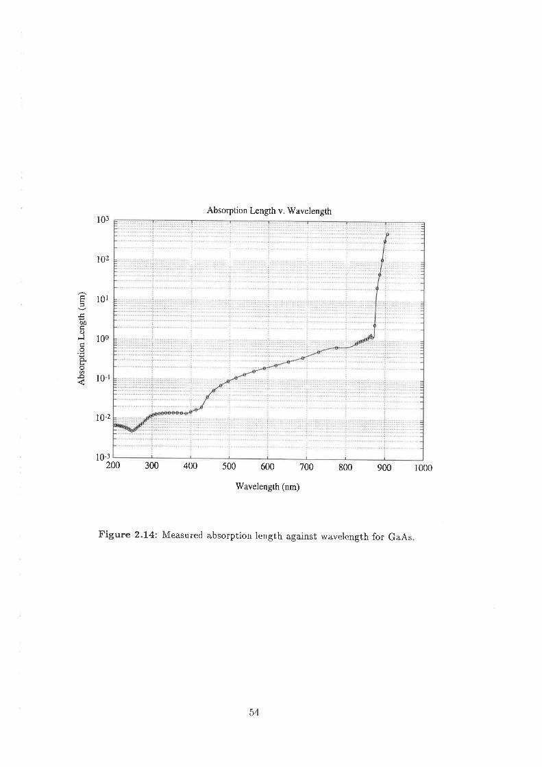
E
-qboç(.)tloo.t<oØ
-o
I 00
0-
10-2
Absorption Length v. Wavelength103
102
l0r
l0-3200 300 400 500 600 700
Wavelength (nm)
800 900 1000
Figure 2.14: Measured absorption length against wavelength for GaAs
I
54

0.9
0.8
9 o.tcfo90.6oc.3 o.suJE 0.4fc(tlo u.ó
o.2
0.1
4 4.5 5
Quantum Etficiency (Si & GaAs)
5.5 6 6.5Wavelength (m)
7 7.5 I0
-7x10
Figure 2.15: Internal quantum efficiency versus wavelength. Dashed lines, siliconw=5, 2 and 0.5 ¡rm. solid lines, GaAs w=2, 1 or 0.1 pm. euantum efficiencyincreases with depletion width !l/. Transmission coefficient is set at unity.
55

The superior quantum efficiency of GaAs over silicon, as seen in Fig. 2.15, is due to theshallower absorption lengths and majority carrier collection process in the GaAs imager.In silicon imagers' minority carriers are collected and so there is a degradation in quan-tum efficiencY due to recombination processes. For the purpose of comparison, we haveassumed a transmission coefficient of unity - this simplification does not nake a differenceto our conclusions. In Fig. 2.r5, a depletion region width of w: 0.1 /¿m correspondsto that under the gate. The improved quantum efficiency curves with w : r-2 rtm,simulate the expected effect of the substrate/channel depletion region working togetherwith the gate depletion region. As the imager is a low-frequency device, we expect thesubstrate/channel depletion region to take pa't in the collection process, leading to anexcellent quantum efficiency.
From the quantum efficiency curves we can now apply Planck's law to calculate theresponsivities' Fig' 2'16 k 2.17 show the weighted responsivities for silicon and galliumarsenide.
Responsivity-Excitance product v. Wavelength (Silicon)x 10122
1
.8
Ê!rEì;1ttcoo-U'occoEp
.4
.2
'30.0
=
1.8
'1.6
o.2
0
o.4
4 4.5 5 5.5 6 6.5Wavelength (m)
7.5 8x 10 '
7
Figure 2.16: weighted responsivity versus waverength for silicon0.5 pm. Dashed line, W = 2 pm. Chained line, W : 5 pm
//
56
Solid line, I/:

X 012 Responsivity-Excitance Product v. Wavelength (GaAs)
5 5.s 6 6.5Wavelength (m)
7
2
1
1
1
0
0
EñE3.àU'coo-U'o(rÞc)E.9(¡)
=
.b
.4
.2
1.8
0.2
0
.8
.6
o4
454 7.5 I_ax10'
Figure 2.17: Weighted responsivity versus wavelength for GaAs. Solid line, W=0.1¡rm. Chained line, W=1 ,¿m. Dotted line, W=2 pm.
Total responsivity, over the visible spectrum, is determined by evaluating the areas underthe curves in Figs. 2.16 k 2.I7 and then dividing by the total area under the Planck'sLaw curve : 46 x 105 W/m2 (see Fig. 2.I2). A typical tungsten light source can besimulated by inserting a temperature of 3000 K into the Planck equations and the resultingresponsivities are displayed in Table 2.4.
The results for silicon, are a little larger compared to 50 mA/W for a typical silicon XYarray imager with W : 5 /-¿m. This is because we have omitted the effect of the trans-mission coefficient and furthermore we have assumed a fixed depletion width. In realitythe depletion width diminishes as photocharge collects - however the comparison betweenGaAs and silicon is still valid if we make the simplification of a fixed depletion width. Ta-ble 2.4 shows that for GaAs operating with just the gate depletion region, W : 0.I ltm,the responsivity is inferior. However, if we include the channel/substrate region, withW :2 ¡zm, the responsivity in GaAs is about 20To larger than in silicon. Furthelmore, ifwe take into accottnt that the channel/substrate region has a fixed potential across it, in
57
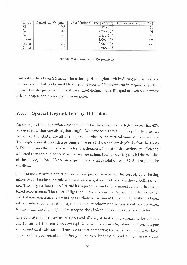
Iype Depletion W t pm Area U Curve (W Itnt Responsivity mA/WSiSiSiGaAsGaAsGaAs
0.52.05.00.11.02.0
2.37 x 1052.95 x 1052.81x 10s1.00x 10s2.95x 10s3.25 x 105
51566122647l
Table 2.4: GaAs v. Si Responsivity.
contrast to the silicon XY array where the depletion region shrinks during photocollection,we can expect that GaAs would have upto a factor of 5 improvement in responsivity. Thismeans that the proposed 'fingered gate' pixel design, may still equal or even out-performsilicon, despite the presence of opaque gates.
2.5.9 Spatial Degradation by Diffusion
According to the Lambertian exponential law for the absorption of light, we see that 68%is absorbed within one absorption length. We have seen that the absorption lengths, forvisible light in GaAs, are all of comparable order to the vertical transistor dimensions.The implication of photocharge being collected at these shallow depths is that the GaAsMESF ET is an efficient photocollector. Furthermore, if most of the carriers are efficientlycollected then the number of stray carriers spreading, thereby causing spatial degradationof the image, is low. Hence we expect the spatial resolution of a GaAs imager to beexcellent.
The channel/substrate depletion region is expected to assist in this regard, by deflectingminority carriers into the substrate and sweeping stray electrons into the collecting chan-nel. The magnitude of this effect and its importance can be determined by monochromatorbased experiments. The effect of light indirectly altering the depletion width, via photo-assisted emission from substrate traps or photo-ionisation of traps, would need to be takeninto consideration. In a later chapter, actual monochromator measurements are presentedto show that the channel/substrate region does indeed act as a good photocollector.
The quantitative comparison of GaAs and silicon, at first sight, appears to be difficultdue to the fact that our GaAs example is on a bulk substrate, whereas silicon imagersare on epitaxial substrates. Hence we are not comparing like with like. A thin epi-layergives rise to a poor quantum efficiency but an excellent spatial resolution, whereas a bulk
58

substrate gives an improved quantum efficiency at the expense of spatial resolution. Sohow can we make a fair comparison that takes into account this trade-off? The answer isto compare GaAs with silicon, not in terms quantum efficiency or raw spatial resolutionper' sel but in terms of a special figure of merit known as the modulation transfer function(MTF). An ideal MTF has the value of unity and it has the behaviour that if eitherquantum efficiency or spatial resolution decreases, then MTF also decreases below unity.The definition of MTF is simply [Seib Ta]
MTF T*rl
where 17¡ is given by the same formula as the quantum efficiency, 4, but with each Lo termsubstituted by fi + lZ"tt¡2 and k is the spatial frequency.
Modulation Transfer Function (MTF)1
0.8
o.4
0.30 10 15 20 25
Spatial Frequency (cycles/mm)30 35 40
Figure 2.18: Theoretical MTF versus spatial frequency. Diffusion-only curves are:Si bulk, 550 nm (chained line); Si epi, 800 nm (dotred line); Si bulk, 800 nm (dashedline). Geometrical-only curve is for a 7 f 20 aperture to pitch ratio and the GaAscase matches this curve (solid line).
This is plotted in Fig. 2.18, rvhere the importance of epi rather than bulk substrates for
0.9
6=^ac -.,fog
TLl- 0.6
0.5
5
59

silicon is demonstrated. Although the diffusion curve for a wavelength of 5b0 nm in bulkis acceptable, the MTF for 800 nm is severely degraded in bulk compared to epi. Thegeometrical-only curve is obtained from the usual sinc function expression and representsthe ideal case in a,bsence of diffusion effects. Due to the hi-lo n+/SI junction majoritycarriers are collected, hence the diffusion term vanishes and our GaAs case corresponds tothe ideal geometrical curve. This result is attractive for HDTV detector array applications,where high pixel densities are more susceptible to crosstalk by diffusion.
2.6 Surnmary
We have given a brief account of the history of gallium arsenide showing that it hasbuilt up considerable momentum, giving rise to applications in many areas of high-speedcommunications and mobile communications. Digital applications also abound but havebeen slower to progress due to the problems with realising large memories in GaAs.This situation promises to vastly improve as the rapidly emerging CGaAs"' technologymatures. A brief comparison between GaAs and other possible competing technologiessuch as diamond, SOI and SiGe showed that GaAs is the best choice for the XY arrayapproach due its greater maturity, lower complexity and presence of the semi-insulatingsubstrate. For the interactive mobile multimedia communicator paradigm, GaAs is thebest choice due to its capability for mixed digital/Rtr/optical designs.
In comparing the characteristics of GaAs and silicon, we have indicated that GaAs showspromise for X-ray detector arrays, near infrared arrays (by investigating internal photoe-mission), HDTV arrays, MWIR and LWIR arrays (by investigating new Schottky mate-rials or via hybridisation with CMT) and arrays for aerosp ace k astronomy, as well as
optical arrays for mobile communications. We have shown that GaAs outperforms siliconin a number of significant areas.
In the analysis of quantum efficiency, we have disputed the equation for quantum effi-ciency in a frontside illuminated finite slab given in recent literature. From first principleswe derive the correct equation, which has not been previously reported. This originalcontribution is significant as the equation can be separated into two physically mean-ingful terms. This new perspective will be useful for simplifying MTF analysis in episubstrates. Furthermore, we have disputed the MTF equation in bulk due to Barbe andhave confirmed, from firsl principles, the validity of Seib's bulk equation.
We have shown that due to the superior absorption coefficients in GaAs, improved quan-tum efficiency is expected. Furthermore for a hi-lo n/SI junction in GaAs, majority
60

carriers are collected and this leads to improved spatial resolution. This advantage ispresented in the form of MTF plots, showing superior overall MTF of GaAs over silicon.
Having made the case for GaAs as the choice technology, for this work, in the next chapterwe now proceed to perform actual optical measurements to study the photoresponse ofthe GaAs MBSFET for optimisation of the pixels for the imaging array.
61

62

Bibliography
63

[Barbe 75] D.F. Barbe, "Imaging devices using the charge-coupled concept,"Proc. IEEE, vol.63, pp. 38-67, Jan. 1g7b.
IBeaurnont 93] s.P. Beaumont et a/, "GaAs solid state detectors for physics at theLHC," IEEE Trans. Nuc. Sci., vol. 40, no. 4, 1g93.
IBencivelli 95] w. Becivelli et al, "some new results on semi-insulating GaAs de-tectors for low energy X-rays," Nuc. Inst. Methods phys. Res. A,Elsevier, vol. 355, pp.425-427, 1995.
[Bernhardt 95] B. Bernhardt eú al, "Complementary GaAs (CGaAs"M ): A highperformance BiCMOS alternative," IEEE GaAs IC Symposium, SanDiego, pp. 18-21, 29 Oct.-l Nov. 1995.
[Buda 9a] F. Buda and J. Kohanoff, "Porous silicon: a silicon structure withnew optical properties," Prog. Quant. Electr., vol. 18, pp.20I-226,1994.
[Collins 92] A.T. collins, "Diamond electronic devices - can they outperformsilicon or GaAs?" Materials Science and Eng., vol. 811, pp. 257-263, tggz.
IGeorge 89] P. George et al., "Modelling the substrate depletion region for GaAsFETs fabricated on semi-insulating substrates," Solid-State Elec-tronics, vol. 32, no.2, pp. 16b-168, 1989.
[Groeseneken 90] G. Groeseneken eú ø( "Temperature dependence of threshold voltagein thin-film SOI MOSFETs," IEEE Electron Deu. Lett., vol. 11,no. 8, pp. 329-331, 1990.
IKonig 9a] U. Konig, "Challenges for a Si/Ge heterodevice technology,,, Micro-electronic Engineerinq, vol. 28, pp. 3-13, 1994.
[Lande 96] s. Lande, "The status of silicon carbide and related materiar s," Iil-Vs Reuiew, vol. 9, no. 1, pp. b8-62, 1996.
[May e5] P. May, "Polymer electronics - fact or fantasy?" phy-sics World,pp. 52-57, March 1995.
c.A. Mead, "schottky barrier gate field effect t,r'ansistor,"Proc. IEEE Lett., pp. 307-308, Feb. 1966.
[Mead 66]
64

[McCaughan 79]
[McGregor 92]
[Pearsal 85]
[Sadek 95]
[Seib 7a]
[Spicer 85]
[Sumner 92]
[Sun 95]
[Theuwissen 95]
[Trew 95]
[Voinigescu 93]
D.V. McCaughan and B.R. Holeman, Chapter 5, pp. 241-ZgS, foundin Charge-Coupled Deuices and Systerns, Eds. M.J. Howes ancl
D.V. Morgan, Wiley, 1979.
D. s. McGregor eú ø/, "Development of bulk GaAs radiation detec-tors," IEEE Nuc. Sci., vol.39, No.5, pp. 1226-1236, October 1g92.
T.P. Pearsal et al, "Ge,si1-, Modulation-Doped p-channel Feilcl Ef-fect Transistors," Proc. lst Int. Symp. Silicon MBE, ElectrochemicalSociety, Pennington, N.J., pp. 400-405, 198b.
A. Sadek and K. Ismail, "Si/SiGe CMOS possibilities,', Solid-StateElectronics, vol. 38, no. 9, pp. 1731-1734, 1995.
D.H. seib, "carrier diffusion degradation of modulation transferfunction in charge coupled imagers," IEEE Trans. E. D., vol. ED-21, no. 3, pp. 270-217, 1974.
W.E. Spice and S.J. Eglash, "Fundamental studies of interfaces: theunified defect model and its application to GaAs integrated circuits,"VLil Electronics Mlcrostructure Science, vol. 10, pp. 79-112, i985.
T.J. Sumner et al, "GaAs revisited as a room temperature X-raydetector," Nuc. Inst. Methods Phys. Res. A, Elsevier, vol. 822,pp. 514-517, 1992.
G. Sun, L. Friedman and R.A. Soref, "Intersubband lasing lifetimesof SiGe/Si and GaAs/AlGaAs multiple quantum well structures,"Appl. Phys. Lett., vol. 66, no.25, pp. 3425-3427,1995"
A.J.P Theuwissen, Solid-State Imaging with Charge-Coupled De-aices, Kluwer, 1995, p. 135.
R. J. Trew and M. W. Shin, "High frequency, high temperature field-effect transistors fabricated from wide band gap semiconductors,"Int. Journ of High Speed Elec., vol. 6, no. 1, pp.2II-236, lggb.
S. Voinigescu et al, "Emerging SiGe technology - a review," ElectronTechnology, vol. 26, no. 4, pp. 25-64, Igg3.
65

66

Chapter 3
MESFET Photodetection
"Frequently, I haue beer¿ aslced if an erperiment I haue planned is pure orapplied research; to me it is more important to know if the erperiment willyield new and probably enduring lenowledge about nature. If it is liketyto yield such knowledge, it 'is, in my opinion, good fundamental research;and this is much n'Lore important than whether the motiuation is purelyesthetic satisfaction on the part of the erperirnenter on the one hand orthe improuement of the stability of a high-power transistor on the other."'William Shockley (1910-19Ss)AMERICAN CO.INVENTOR OF THE TRANSISTOR
"When one conl,es down to particular instances, eueryth,i,ng becomes n'Lorecomplicated."Albert Camus (1913-1960)FRENCH NOVELIST AND PLAYWRIGHT
67

3.1 GaAs MESFET Optical Model
3.1 . 1 Background
F¡om the outset we realised the importance of determining the various optical gain mech-anisms in a GaAs MtrSFtrT in order to accurately predict transistor behaviour for im-plementation within an image sensor. It was noted that considerable controversy, in theliterature, existed over the nature of GaAs MESFBT optical gain. As a result of ourinvestigation, a consistent model was developed [Adibi 89] that overcame the difficultiesraised by other researchers engaged in the controversy.
The approach pursued in this research was to model the overall optical gain of a MESFtrTin terms of four unified effects:
(1) A photovoltaic effect in the gate-source and gate-drain depletion regions
(2) A photoconductive effect in the channel, with associated recirculation gain
(3) A photovoltaic effect in the channel-substrate depletion region
(4) A photovoltaic effect via photo-assisted carrier emission from substrate traps
This model is used to resolve apparent contradictions, between different results publishedin the ìiterature, by observing that each of these effects come into play, by varying degrees,depending on the wavelength of light used and hence penetration depth achieved.
Apparent discrepancies are reconciled by side effects such as the blocking of the electronrecirculation effect caused by pulsing the light in coincidence with the depletion layerrecovery time. Another effect not taken into account by other researchers is the sidewaysdiffusion of carriers into unilluminated regions - this effect is further used to reconcilepreviously unexplained discrepancies.
Two proposed primary mechanisms are reported in the literature:
o classical photoconductivity effect [Gammel 7g, osterwalder 79, Gammel g0]
o Classical photovoltaic effect
However the photovoltaic mechanism manifests via two reported secondary effects:
o Depletion modulation of channel (intrinsic) [Graffeuil 79, Edwards 80, Wieder g0,Sun 81, Chaturvedi 83, Umeda 85, Umeda g6]
68

o Depletion modulation of channel (extlinsic) [Sugeta 80]
Various combinations of the above effects are also reported [Pan 78, Flesner 82, Forrest 82,
Noad 82]. The controversy centres around the lack of consensus amongst various re-
searchers as to which combination of these mechanisms actually takes place in the GaAsMESFET. Developing a correct description of the optical mechanisms, in the GaAs MBS-FET, is considered important for design optimisation of an imager based on an 'activepixel' that exploits the gain mechanisms of the transistor.
The key experimental techniques to investigate the photoresponse characteristics involveMBSFtrT illumination by:
o Unfocussed laser flood
o Scanned focussed laser
o Modulated laser (focussed & unfocussed)
o Monochromator
Firstly, we shall describe our model lAdibi 89] and then the experiments and results willbe detailed in a later section.
3.L.2 Photoresponse Model
The GaAs MESFET can be implemented as the photoresponsive element in the XYimager either passively or actively. The passive case requires the MESFET to behave as
a simple switch and only the source terminal is illuminated so as to act as a photodiode.In the active case the whole MESFET is illuminated to take advantage of the resultinginternal photogain mechanisms. The advantage of passive illumination is that it is easy
to implement. Active illumination offers better sensitivity and is more of a challenge toimplement, particularly due to the controversy surrounding the origin of these internalphotogain mechanisms.
In order to design an imager utilising active illumination, the first step was to produce a
generalised model that adequately explained the photoresponse mechanisms in the MtrS-FET so that reproducible design calculations could be made. In summary, the model isencapsulated in the equivalent circuit shown in Fig.3.1. The photoresponsive elementsof the equivalent circuit are as follows:
69

^Ipd
DG
S
^Ct
b
Figure 3-1: Bquivalent circuit of MESFET showing photoresponsive elements
Cb
rss
SI.JB
+
t + + +
Rg rd"
R
+ +
rb
70

o Photoconductive response in the channel is modelled by 1"¿
o Photovoltaic response takes place in the parts of the gate depletion region thatprotrude out from under the gate. This protrusion is larger on the side of the gatetowards the drain than on the side towards the source. Response in these two regionsis thus separately modelled by lea and 1p".
o Photovoltaic response in the channel/substrate depletion region is modelled Ity Io.
o Photo-assisted carrier generation from substrate traps is modelled bv 1r.
¡ Modulation of the channel/substrate depletion region changes the drain current andthis is modelled lty g'*r"u. Modulation of the gate depletion region also changes thedrain current and is modelled by g^un".
Due to electrons recirculating through the channel, until a photogenerated hole is recom-bined, there is an associated gain B that must be applied to I"¡. When the hole transittime, f¿, is comparable to the minority carrier (hole) lifetime, r, the photoconductivecurrent gain becomes,
for,
t¡xr
where l" is the electron transit time. When l¿ is small compared to r the gain obviouslybecomes,
13
'ùe
uh
tnK.r
where u" and uh are electron and hole velocities respectively. In our case r N 20 ns andtn:0.4 ns, for Vd* :0.6 V u'ith a 3.2¡tm drain/source separation. The frrst expressionincorrectly gives B = 1000, for our case, but the second expression holds with p x 20.
Referring to Fig. 3.1, Cs" and Cna can be modelled by the standard relation,
cn:cn,lt-þl-*'
ß:''t.
for
7t
ubi

1
tand the Schottky dynamic resistances,rs" k rad) can be found from suitable curve tracer
where,
Ms
measurements.
Under reverse bias the gate reverse saturation current 1r=10-tt A, and for gate photocur-tent Irn ) 1, w" can say that 1, : Ips.However, under forward bias,
In:1"þ# _ r)-Irn
and the gate open circuit voltage can be found by putting In : 0,
Terminating the gate with a resistor, Rn,to ground will cause a current
v":'kr tn(r + þ)q
I,:Hhl+?)to flow. This can be tested by experiment and we expect the relation to be more accuratefor shorter wavelengths. By varying ,Rn and 1rn, this could be used as a technique toextract n and Io.
Substrate parameters can be evaluated by modulating the laser beam and sweepingthrough frequency. The frequency response will drop off at approximate positions corre-sponding to 16 - 2trR6C6 and r¿ :2tr(ra + rùCt. The first time constant is due to thechannel/substrate interface and the second is due to traps. Also r?6 : rallrt, where 16 isthe channel/substrate barrier interface resistance and r¿ is the equivalent resistance dueto traps. To determine the substrate transconductance, gl is given by,
xd"
Usb
we stimulate the traps with a suitably long wavelength (À > g00nm) and then
g^
rtlt,"b: jrc,
By applying a voltage Vo, to the substrate, with no incident light, we can adjust Vo, Lo
obtain the same i¿" achieved with the laser; then,
72

Using manufacturer's data C¿ and rss can be calculated. Vo, and ûr are known drivenvariables. id", rt, Tö and usò are measured. Thus there remains five equations and fiveunknowns rb, rt, Cr, I, and gl. A spread of values against a can be graphed to determineboth experimental error and model limits.
For wavelengths that stimulate both substrate traps and the channel/substrate region,the full solution is given by,
roI,(;;àa) -l 1616(#*+t)Usó :|+(jaC6rb+1)(Fär+1)
The time constants are given by the quadratic roots of the reduced denominator, whichare somewhat complex but can be approximated by rt : 2r RaCt and r¿ : 2r(rt I r¡)C¡.Fig. 3.2 shows the frequency response for this case, indicative of a dual pole and singlezero system - the dashed line at the lowerfrequency gives 1/r¿ and at the higher frequencygives 1/16. To illustrate the form of the curve, dummy values ol Co: 20 fF, Cr : 1 pF,r¿ : l0k0 t rt : 100 kf-¿, 1¡ : 50 ¡;A and It : 20 ¡rA have been inserted. In practice, u"6
is a difficult quantity to measure; however changes in u"6 modulate the channel thicknessand hence drain current. Therefore the time constants are evaluated from a plot of draincurrent versus laser modulation frequency. It should be noted that a roll-off in u"6 increasesthe channel thickness and hence drain current. Parameter extraction from this curve is
more complex than the long wavelength case, as the two poles can influence each other.The advantage of using a longer wavelength is that the circuit reduces to a simpler onepole system. In the two pole case the top plateau is given by u¡ : rt(It * 16), the lowerplateau by u6 x r?616 and the zero position by r" :Figure 3.3 shows the measured drain current against laser modulation frequency. Thethree curves are for three separate devices, giving an indication of the spread in values.From this graph we deduce that the time constant due to substrate traps, rr : 0.1- I ms.
3.2 GaAs MESFET Photoresponse Measurements
3.2.L Monochromator Measurements
The photoresponse of a MESFET at different depths, within the device, can be 'probed'
73

Substrate barrier voltage v. frequency (Theory)
o
-o
1
o.9
o.8
o.'7
o.6
o.5
o.4
o.3
o.2
o.1
l04 105 106 lo7 1O8
Modulation frequency (Hz)
lolo l0lr10e
Figure 3.2: Voltage across channel/substrate barrier against laser modulation fre-quency. The vertical dashed lines show the approximated time constant positions.
74

tt€
25
20
15
10
Drain Current v. Modulation Freqency
lo3 t04
f (Hz)
5
oloo 10r t02 105 106 107 l08
Figure 3.3: Drain curtent versus laser modulation frequency. Three curves repre-sent three separate devices.
#l:H
- -# - - - - | - ----- - --+----- +
+ {!:
75

(1)
Hc)ctkâ
2
1.9
1.8
r.7
r.6
1.5
t.4
1.3
1.2
1.1
I100 200
Wavelength Response
300 400 500
Wavelength (nrn)
600 7o0 800o
Figure 3.4: Wavelength response using xenon source onochromator. vr":-g.g v,V¿":0.6 V. Dual curve represents the looping effect.
76

I-V Characteristic Variation with Wavelength2
EÉc)tr
C)
c,Hâ
1.8
r.6
t-4
1.2
o.8
o.6
o.4
o.2
1
o o.l o.2 0.3 o.4 0.5 0.6
Drain Voltage (V)o.7 0.8 0.9 I
Figure 3.5: I-V Characteristic variation using xenon source monochromator, Vn,=-0.8 v, '*':700 nm, 'f '-300 nm, 'o':0 nm (dark). Dual curves represent the roopingefect. There is no looping in the dark condition.
tt

by using a variable wavelength source. The objective is to separate the gate responsefrom the channel/substrate response, so as to establish their lelative importance.
To this end we used a Bausch & Lomb monochromator with a xenon source ancl a1200 groove/mm grating. Fig. 3.4 shows the drain current response to wavelength. Thetwo curves represent the upper and lower portions of the hysteresis loop. An interestingobservation is that the loop increases in width for longer wavelengths. Fig. 3.b shows thelooping in the I-V characteristic - notice there is no looping in the dark conditìon. Theloop is widest at about 700 nm - however, on the contrary, with a 0.125 mW laser at678 nm no looping is observed. This appears to suggest that both power and wavelengthhave an effect on the hysteresis. Further work would need to be carried out to conclusivelytie in these observations with the accepted trap theory; however, as it does not appearimmediately relevant to the imager design, further analysis is deferred for the future.
The conclusions drawn from Fig. 3.4 are:
o The sharp increase at 450 nm corresponds to light penetrating the gate depletionregion. Below this wavelength, surface state recombination would be dominant.
o Between 600 nm and 700 nm the curve does not roll off. This is significant as
these wavelengths correspond to the channel/substrate depletion region. Hence thechannel/substrate depletion region is just as efficient a photocharge collector as thegate depletion region. This is only true for low frequency operation due to the largetime constant associated with the channel/substrate interface.
The last observation is most important as we now expect the low frequency imager toefficiently collect photocharge generated from the whole visible spectrum ie. the quantumefficiency should be excellent.
Fig. 3'6 shows only a small perturbation in the transfer characteristic with wavelength.This is advantageous as the transistors, in the imager, should not have greatly varyingbias points with incoming light.
3.2.2 Laser Flood Measurements
In order to explore the effect of laser illumination, transfer characteristics are plotted inFig. 3.7 with the whole MESFET region exposed to unfocussed laser light. The pertur-bation of the transfer characteristics is larger in Fig. 3.7 than Fig. 3.6, due to the higherpowered laser sources' The lasers appear to create a shift in the transfer curve, equivalent
78

Transfer Characteristic Variation with Wavelength
ll
(1:¡k
OGIkâ
40
35
30
25
20
15
lo
5
oo o.1 0-2 0.3 o.4 0.5 0.6
Gate VoltaCe (-V)o.7 0.8 0.9 I
Figure 3.6: Transfer characteristic variation using xenon source monochromatorV¿":0.6 V, t+'=700 nm, t+t-400 nm, tot:200 nm.
79

Transfer Characteristic Variation with Laser Flood40
35
30
25
20
15
10
É
C;)tsc)Écrtkâ
5
oo o.1 0.2 0.3 o.4 0.5 0.6
Gate VoltaCe (-V)o.7 0.8 0.9
Figure 3.7: Transfer characteristic variation using laser flood. v¿"=0.6 v,'*'=815 nm @ 3 mW, '*'=632 nm @ 0.g5 mw,,o'=0 nm (dark).
80

to increasing the gate voltage by around 0.1 V. This could potentially be modellecl by a
contraction of the gate depletion region.
3.2.3 Focussed Laser Measurements
A new effect, in planar GaAs MESFETs, whereby a sharp increase in optical gain at thetransistor edges occurs, is reported for the first time. This gain effect only manifests whena large resistor is inserted in series with the gate, to produce the conditions for photovoltaicgate biasing. The mechanism for increased gain, at the edges, is suggested to be dueto carrier photogeneration in the substrate that is subsequently collected by the gate.Application in the area of X-Y addressable transistor array imagers, motion detectors,optical neural nets, GaAs X-ray detectors etc. is possible, for increasing photosensitivity.
Photoresponse of GaAs MESFETs has received much attention due to potential applica-tion in high speed optoelectronic communications, OEICs and optical tuning of microwavedevices. Various optical gain mechanisms have been reported, including photovoltaic gatebiasing. This effect occurs when the gate photocurrent follows through an external seriesgate resistor, Rn, thus increasing the gate voltage and hence drain current. To produce asignificant increase in drain current, a large -r?, introduces a large RC time constant whichtypically causes the response to roll off in the 10-100 MHz range. Consequently, as mostresearchers have concentrated on high speed applications, photovoltaic gate biasing hasbeen regarded as being of limited merit [Darling 87] and has not received full attention.However, as the data rate of a typical imager is less than 10 MHz, photovoltaic gatebiasing can potentially be used to increase the sensitivity of such devices. Furthermore,we discovered that the sensitivity is increased in the region where a gate overhangs thetransistor edge. This new knowledge can help to maximise the benefits of this effect toimaging devices.
This new edge effect was discovered when a GaAs MESFBT was scanned with a focussedlaser spot' The planar MESFETs used have a fingered structure with b gates, tr :0.8 ¡;m and overall W : 400 ¡rm. The channel (depth, d : 0.1 ¡rm and doping, ¡úd :I.2xl0r7 .m-3) is situated on a semi-insulating (SI) GaAs:EL2 substrate, with no bufferlayer. The source-gate and drain-gate separations are both 1.3 ¡-rm.
Fig. 3.8 shows a length scan across a transistor with 5 fingers. As the gate length, 0.8 ¡rm,is smaller than the laser spot diameter, 2 p^, the peaks of the curve correspond to whenthe spot exactly straddles the gate. A 1 Mf^¿ resistor is included, in series with the gate,to produce an extrinsic gain effect by photovoltaic self-biasing. This gain was deliberateìyintroduced to accentuate the peaks and troughs. It is notable that the gain al a trough is
81

8
6Éc)ts
C)
dHâ 4
2
T2
10
o
Length Scan - R:l MOhm
20 25 30
Laser Spot Position (urn)
5o lo 15 35 40 45 50
Figure 3.8: Transistor length scan with focussed laser, 67g nm @ 0.125 mw, 2 pmdiameter spot size. 1 M0 series gate resistor. Vr":-0.8 V, V¿"-Q. g!.
82

at best 2, whereas the gain at a peak is at best 5, ie. the gain is more than doubled whenthe laser spot straddles the gate. This indicates that maximum sensitivity is obtained byilluminating the gate edges.
Width Scan - R:l MOhm
to 20
50
45
40
35
30
25
20
l5
10
À
6)krC)Ékâ
5
oo 30 40
Laser Spot Position (urn)
50 60 70
Figure 3.9: Transistor width scan with focussed laser,6z8 nm @ 0.L25mw,2 ¡.r.m
diameter spot size. 1 MO series gate resistor. Vn":-0.8 V, V¿"=Q.g V. Transistoredge corresponds to 20 p,m on the x-axis.
Fig. 3.9 was obtained by scanning the laser across the transistor width and highlights asignificant gain effect. From a gain of about 3, the gain dramatically increases to over 20,at the transistor edge. This is a new effect that has not been reported in the literature,by other workers. We have patented a novel imager design that utilises this new effect
[Abbott 91] to create an increased sensitivity.
An important result from Fig. 3.9, for the imager design, is that the left hand side of thecurve decays rapidly over a distance 5 pm, as the spot moves away from the transistoredge and onto the substrate. This decay distance is much smalle¡ than the anticipatedimager pixel size (40 pm sq) and is an excellent feature requiled fol an imager with lowpixel crosstalk and goocl spatial resolution.
With reference to Fig.3.10, we see that the gain drops off at the edge, in the absence of
83

2.5
1.5
o.5
o
3
2
'Width Scan - R=O Ohm
30 40
Laser Spot Position (um)
4ÈÉ(1)
HC)
qâ
o lo 20 50 60 70
Figure 3.10: Transistor width scan with focussed laser, 6zg nm @ 0.L25 mw ,2 p,mdiameter spot size. No series gate resistor. Vr"=-0.8 V, V¿"-0.6 V. Transistor edgecorresponds to 20 pm on the x-axis.
84

the series resistor. This demonstrates the photoductive component of the photoresponse,showing that it is small. The fact that roll-off commences a few microns before the edgeis reached could possibly be explained by tapering of the channel.
Photovoltaic Self-B iasing
o loo 20,0,
50
45
40
35
30
z5
20
l5
10
çÉ()ts(JÉc!kÊ
5
o 300 400 500 600 7c,0,
Series Gate Resistor (kohm)
800 900 looo
Figure 3.11: Response against gate series resistor. 628 nm @ 0.125 mw,2 pmdiameter laser spot size. 1Mo series gate resistor. Vn"=-0.8 V, V¿"=Q.g \,r,
'ot:transistor edge,'*':transistor middle.
Fig. 3.11 shows the photovoltaic self-biasing (or 'gate biasing') effect, as a function of seriesresistance. The higher curve, corresponding to the transistor edge, begins to plateau athigher resistances, as the gate approaches the forward bias regime. The edge clearlyproduces a higher gain for all resistor values. Due to the large series resistor required toproduce a significant gain, high frequency operation is not possible and so photovoltaicgate biasing has not received much attention in the literature.
However, photovoltaic gate biasing is of interest in a low frequency GaAs X-Y addressabletransistor array for solid-state imaging. The pixels in such an imager can be configuredto optimise the edge gain mechanism, thereby increasing the sensitivity of the device.With careful development, a GaAs imager utilising a conventional planar MESFET tech-nology may potentially offer increased radiation hardness, reduced dark current and the
85

convenience of integration with high speed GaAs image processing cells.
We have discovered a new finding that the optical gain sharply increases where the gatecrosses the transistor edge. This only occurs with a series gate resistor inserted, to producethe conditions for photovoltaic gate biasing. This finding suggests that carriers generatedin the substrate, beyond the transistor boundary, are able to be collected by the gatedepletion region. This edge effect is observed in a planar GaAs MtrSFtrT and is quitedifferent to the edge gain effect observed in mesa GaAs MBSFET structures [Flesner 82,Rouger 85].
We proposed a generalised model for the photoresponse of a GaAs MESFET [Adibi 89]which considered a photovoltaic (PV) effect in the gate depletion region, a photocon-ductive (PC) effect in the channel and two main substrate effects (trapping by defectcentres and substrate/channel depletion region collection). In order to explain the ob-served effects, in our present case, we are able to invoke the gate depletion region andsubstrate/channel depletion region parts of the model.
To explore the edge effect further, we set up a computerised measurement system toproduce a complete 2 dimensional scan of the whole transistor region.
3.2.3.L Two Dimensional Laser Scan Set Up
The planar MBSFETs used have a fingered structure with 5 gates, tr : 0.8 ¡rm andoverali w : 400 ¡;m. The channel (depth, d : 0.1 ¡,rm and doping, N¿ :1.2x 1012 cm-3)is situated on a semi-insulating (SI) GaAs:EL2 substrate, with no buffer layer. Thesource-gate and drain-gate separations are both 1.3 ¡^lm.
The device was mounted on a computerised X-Y platform, shown in Fig. 3.12, and illumi-nated by a 2 ¡;m diameter CW laser spot with a wavelength of 678 nm. The laser powerincident on the device was measured to be 1.4 pW. The X-Y platform was controlled tomove the device through a 2-D raster sequence and the drain current was automaticallylogged so that a 3-D plot of the transistor response was generated.
3.2.3.2 Two Dimensional Scan Results
Example 3-D plots of transistor drain current response to laser illumination are shownin Figs' 3.13 & 3.14. For comparison, the case for no series gate resistor is shown inFig' 3'13. Peak drain current is in the central region of the transistor, and the draincurrent rolls off towards the periphely of the transistor, as classically expected. However,with a 10 MC¿ resistor in series with the gate, Fig.3.13 shows dramatic drain current
86

iltjllllltrïjllr ffi
Figure 3.12: l.aser'[)rober rvith (,oirrlrrrri r,iisr,r[ \ \'f]i;rilìrlur
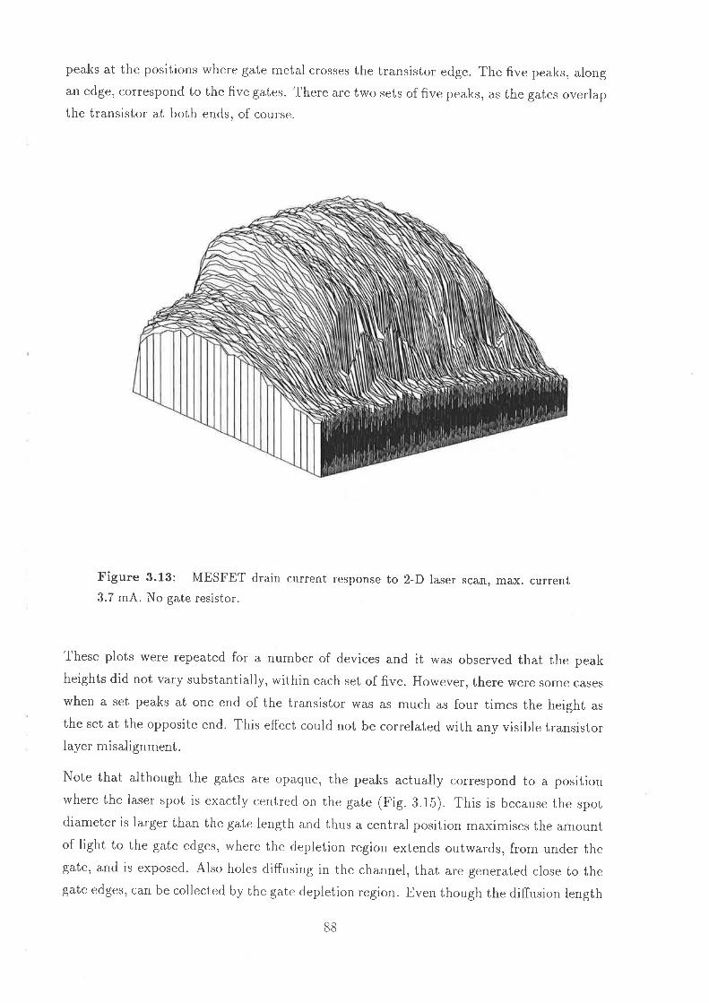
peaks at the positions where gate metal crosses the tlansistor edge. The five peaks, alongan edge, correspond to the five gates. There are two sets of five peaks, as the gates overlapthe transistor at both ends, of course.
Figure 3.13: MESFET drain current response to 2-D laser scan, max. cullent3.7 mA. No gate resistor.
These plots were repeated for a number of devices and it was observed that the peakheights did not vary substantialìy, within each set of five. However, there were some cases
when a set peaks at one end of the transistor was as much as four times the height as
the set at the opposite end. This effect could not be correlated with any visible transistorlayer misalignment.
Note that although the gates are opaque, the peaks actually correspond to a positionwhere the ìaser spot is exactly centred on the gate (Fig. 3.15). This is because the spotdiameter is larger than the gate length and thus a central position maximises the amountof light to the gate edges, where the depletion region extends outwards, from under thegate, and is exposed. Also holes diffusing in the channel, that are generated close to thegate edges, can be collected by the gate depletion region. Even though the diffusion length
88

Figure 3.14: MESFBT drain current response to 2-D laser scan, max. current29 mA. With 10 MQ gate resistor.
MIS gateextens¡on
Hlgh gain--laserposltlon
Schottky barr¡er MIS gateextension
F¡ngered gates
Figure 3.15: Laser spot positions for high & low gain drain current response.
Source
Draln .¿ Low galn laser position
Source
Hlgh gain laser posltlon\Draln
Source
Draln
89

of holes in the channel is 1.8 ¡rm, holes that are far from the gate are more likely to becollected by the channel/substrate depletion region because the channel depth d(1.8 ¡rm- therefore there is a very narrow capture angle for gate collection.
3.2.3.3 Discussion
We established that the peak drain current could be accounted for by an increase in gatephotocurrent, as measured by an electrometer. Fig. 3.18 shows gate photocurrent versusAn, when the laser spot is centrally placed on the gate, for a position at the transistoredge (high gain) and towards the middle of the transistor (low gain). The theoreticalcurve is found by following the front illumination case of Seib [Seib 74], to evaluate thequantum efficiency, ry. However, in a GaAs MESFBT, the boundary conditions changeand the equations are now solved with hole concentration p - 0 at the substrate/channelinterface (A: d), instead of at y: oo. This results in,
q:T(^)A,{1 - exp(-aW¿) - A+ B - C} (3 1)
where
" _ t t - exp{-(d -w¿)(a + *)}dLo 1-exp{-_2Wà}
1 - exp {-(d - Wa)(o - )Ì1-exp{ d-
and after some manipulation, this elegantly reduces to,
n:r(^)A.{l -#-#tr:ffi#} (32)
which is identical to the finite slab equation given in Appendix B. tro is the hole diffusionlength in the channel and a is the absorption coefficient at the wavelength of interest. Ifwe assume that the depletion region extension from under the gate is W¿ and approximatethat light is only captured in these regions, as a first order estimate, then the dimensionlessgeometryfactor, Ao:2 x 1.83 xw¿f r. The depletion region width, w¿,is given by thestandard relation for a Schottky barrier,
w¿: e#tv; - v, - \¡+ (3 3)qtv¿ - q
where, the built-in voltage, V¡ :0.85 V. If the external bias applied to .R, is _0.g V,then the gate voltage, Vs: -0.8 + IsLs. By knowing the incident laser power, po, the
90

gate photocurrent is obtained from,
rn : (fr)ro, (8.4)
The theoretical curve for 4, in Fig. 3.18, is obtained via an iterative solution of the aboveequations with the transmission coefficient set at T :1, for simplicity. This is lowerthan the measured curve because our first order approximation has neglected sidewaysdiffusion of holes into the gate. Another possibility is local heating effects, caused by thelaser, have not been taken into account - however we have shown in Appendix C that thiseffect is negligible. Future work could consider a full three dimensional solution to thediffusion equation. We consider the following hypotheses in order to explain the increase
in gate photocurrent that produces the sharp increase in drain current at the transistoredges:
HYPOTHESIS 1: Gate metal thinning over the edge. Possibly the gate metal thinsat the edge, enough to become partially transparent, thereby letting in more light. Thishypothesis is easy to reject, as such thinning would effectively increase the area factor Ao
by 30% at most - this can only modulate the drain current by 2-3 mA at the most. Weneed an effect that is ten times that order.
c field G-PISCES.2B1
d85
,4
Eoog
q,ir-- o
0
o.o6o.42
o.781.14
Depth (pm) 1. 50o .o 2.O 4.O 6.0 8.o 10.0
Lateral Distance (/m)Figure 3.16: 3-D Electric field plot using G-PISCES-2B with Spicer's UDM. Lefthalf is field under the gate overhang. Right half is field under the Schottky gate.
HYPOTHESIS 2z Electric freld at edge. It is conceivable that the abrupt junction atthe transistor edge is causing a region of high electric field that results in a higher currentflowing through the gate. Figure 3.16 a 3-D electric field plot generated by G-PISCES-28,that uses Spicer's unified defect model. The left half of the plot represents electric field
il
91

under the gate metal that overhangs the transistor and extends over Si3N4. The righthalf of the plot represents the field under gate Schottky contact. At the intelface or edgebetween the two, the field is clearly well-behaved. Therefore we reject this hypothesis.
HYPOTHESIS 3: Contiguous depletion regions. From Figure 3.16, it can be seen thatthe depletion region that supports an electric field under the MIS gate overhang is con-tiguous with the gate depletion region. It is also quite obvious that the channel/substratedepletion region must also connect here at the transistor edge. Therefore the large volumeof depletion region, just outside the transistor edge, at the meeting point of the gate, MISand channel/substrate depletion regions greatly increases the photocollection capacity.Photocharge generated in this region can flow into the gate, via connecting field lines,giving rise to an increased gate photocurrent. A conceptual diagram of how the field linespossibly flow is shown in Fig. 3.17. In the last chapter we established that the chan-nel/substrate depletion region is of the order of 2 p,m and thus the resulting collectionvolume is large enough to explain the observed effect. Consequently this becomes ourworking hypothesis.
Figure 3.17: Convergence of Schottky gate, MIS gate and channel/substrate fieldlines at the transistor edge. Conceptual drawing with exaggerated features.
According to our working hypothesis, the high gain curve in Fig. 3.18 can be explained
S¡ N3 4
Gate T|/PUAU
mi-insulator
92

if there are holes generated in the substrate, outside the transistor, being collected bythe gate. Therefore we postulate the existence of a depletion region in the substratethat has connecting electric field lines with the edge of the gate depletion region. Thisnew depletion region is assumed to be formed under the MIS structure, where the gate
extends over Si3Na, outside the transistor. The channel/substrate depletion region mustalso connect at the edge and, given a depth of about 2 p^, we estimate that the depletionregion would need to protrude from under the MIS electrode by about 0.2 ¡tm to accountfor the high gain curve in Fig. 3.18.
In conclusion, we have reported a new optical edge gain effect in planar GaAs MESFETs,useful in low frequency applications, such as in an X-Y array imager. Photocollectionunder the MIS gate extension, outside the transistor, is suggested to explain the gain
effect. Future models for the photoresponse in planar GaAs MESFBTs, that attempt togeneralise all operating conditions, must take into account this new effect.
o.t4
o.t2
o.l
o.o8
o.06
o.04
o.o2
ol05 106 lo7
Series Gate Resistor (Ohm)
Figure 3.18: Quantum effi.ciency versus gate resistor. Solid line: internal quantumefficiency (T=1) from first order theory. Dashed Line: measured (low gain). Chained
line: measured (high gain).
>r(-)(t)Or--(L¡
rÐE
G'
a
lo8
o
ì
Go
o
-ox- tx- ó
93

3.2.3.4 Experimental Refinement
It can be seen that in Fig.3.13, the peaks are not uniform and one peak appears to be'smeared.' It was not known, at the time, whether the non-uniformity was fundamentalto the edge effect or whether it was an artifact of the measurements. In an effort tofurther refine the experiment, to reduce the vibrational disturbance that was the likelycause of the smeared peak, we designed an antivibrational table. The table compriseda heavy marble top supported by a steel frame. The steel tubing, of the frame, wasfilled with glass beads to improve damping. The complete four-legged structure restedfour separate industrial vibration isolator mounts. Each mount had an effective Hooke'sLaw spring constant of about 106 kg/m and the total supported mass was 387 kg. Thisresults in a resonant frequency of the order of 100 Hz which is safely out of the 10-20 Hzregion that is typical for building vibrations. For a rigorous analysis the torsional andshear resonant frequencies should also be evaluated - but this is a complex mechanicalengineering problem beyond the scope of this work. However, it turned out the thetable design was sufficient to produce the perfect result shown in Fig. 3.1g. Notice thatFig. 3.13 and Fig.3.19 are scans of the very same device. Not only has the smearedpeak disappeared, but the peaks are now perfectly uniform. Hence, we can conclude thatthe peak non-uniformity in Fig. 3.13 was due to mechanic¿l disturbance of the sampleunder test and thus is merely an artifact. FiS. 3.20 is a contour plot of the same data inFig. 3.19. The contour plot clearly shows the integrity of the mechanical scanning, withno visible smearing of data.
3.3 Surnmary
In this chapter we have examined a number of issues surrounding photodetection withGaAs MtrSFETs. We have reviewed the controversy surrounding the modelling of theactive MtrSFtrT photodetector and have presented Adibi's model in some detail. For thefirst time' we successfully measure the substrate time constant parameter in the Adibimodel. We were unable to extract Adibi's channel/substrate time constant parameter, asfuture work must employ a laser with a higher modulation frequency than that presentlyavailable. We also discussed that by using a variable wavelength laser, in the future, anumber of useful substrate parameters can be elegantly extracted using the Adibi model.
Another original contribution is that, with monochrometer and laser based measurements,we have established that the I-V hysteresis in MESFETs is effected by both the powerand wavelength of incoming light.
94

30
25
ãÈ20Ic8rsfO
Ë'oÕ
5
0150
60100
2010
Y (um) 00X (um)
Figure 3.19: MESFET drain current response to 2-D laser scan, max. current29 mA. With 10 Mfl gate resistor. 3-D plot. Performed on antivibration table.
5040
3050
95

100
90
80
70
60
E3so
40
30
20
10
10 15 20 25 30X (um)
35 40 45 50
Figure 3.20: MESFET drain current response to 2-D laser scan, max. current29 mA' With 10 MO gate resistor. Contour plot. Performed on antivibration table.
5
I
9o
ÞÕ?
1
0
a? -¡I é
ôô
--9ô
Oo oo
0IÒo <)
<> €a
4Õ
o
oa-
o"a
96

Some confusion exists over the nature of fields and depletion regions in semi-insulatingsubstrates - however, we have clearly demonstrated, with a monochrometer, that pho-
tocollection in the channel/substrate depletion region does indeed take place. This is
expected to enhance the performance of the proposed imager.
Another important original contribution is that we have discovered a new internal gain
effect in GaAs MESFETs. As well as having implications for increasing the sensitivityof photodetectors we have exploited the gain effect to estimate that the carrier diffusionlength in the semi-insulating substrate is less than 10 ¡rm - the realisation of this fact isimportant for good spatial resolution in high definition television (HDTV) sensors.
We have discussed a number of hypotheses as to the origin of the internal gain edge-effectand the picture that emerges is that, where the gate crosses the edge of the transistor,there is a convergence of electric field lines from (a) the gate depletion region, (b) the MISgate overhang depletion region and (c) the channel/substrate depletion region, giving riseto a larger photocollection volume. This results in a larger photocurrent that flows intothe gate. To manifest this effect in a useful manner, a gate resistor is required so thatthe increased gate current modulates the drain current. This is the first time a detailedpicture of the depletion region structure at the transistor edges has emerged. Future workmay determine if this depletion region model, at the edge, explains any purely electricalparasitic effects in the GaAs MESFET.
The observation that there is some variation in the edge-effect from transistor to transistorand the discussion of the complicated active photoresponse of the MESFET immediatelysuggests an important design constraint for the imager: the photoresponsive element, inthe first instance, should be a simple diode structure. Utilising a full active MESFtrTphotodetector will present unwanted non-uniformities and thus fixed-pattern-noise (fpn)in the final imager. However, utilisation of the edge-effect would be appropriate in simplemotion detectors where the signals are thresholded and thus pixel uniformity is not crucial
- this possibility will be discussed in the penultimate chapter as part of our future vision.
Before we consider the design of an imager, in the light of this study on photodetectors, inthe next chapter we turn to the important issue of understanding noise in the MESFETand how this will also impact on the imager design.
97

98

Bibliography
99

[Abbott e1] D. Abbott, "Gallium Arsenide MESFET Imager," prov. patent,PK8660, Aug. 1991.
A. Adibi and K. Eshraghian, "Generalised moder for.GaAs MESFETphotodetectors," IEE Proc.., vol. 186, pt. G, no. 6, pp. 337_348,1989.
G.J. chaturvedi, R.K. Purohit and B.L. sharma, "optical Effect onGaAs MESFtrTs," Infrared Phys., vol. 23, no. 2, pp 6b-6g, 1gg3.
R.B. Darling and J.P. uyemura, "optical gain and large-signalcharacteristics of illuminated GaAs MESFETs," IEEE J. euan-tum Elec., vol. QE-23, no. 7, pp. 1160-1171, 19g7. (refer p. 1167,para. 2)
w.D. Edwards, "Two and rhree Terminal Galrium Arsenide FETOptical Detectors," IEEE EIec. Dev. Lett., vol. EDL-I, no. g,
pp. 149-150, 1980.
w'D. Edwards and R.F. Haythornwaite, "Laser and Electron beamScanning of GaAs FETs," Microelectron. Reliab., vol. 22, no. 4,pp 735-746, 1982.
L.D. Flesner, N.M. Davis and H.H. wieder, "High speed Repsonseof a GaAs Metal-Semiconductor Field-Effect Transistor to ElectronBeam Excitation," J. Appl. Phys., vol. 53, no. b, pp 3gZ3_3gZT,7982.
J.R. Forrest, F.P. Richards and A. perichon, "The Microwave MES-FET Optical Detector," IEDM, pp 529-b32,IggZ.
J.C. Gammel and J.M. Ballantyne, *The OpFET: a New High-Speed Optical Detector," Proc. IEDM, pp 120-128, 1g7g.
J.c. Gammel and J.M. Ballantyne, "comments on 'High Speed pho-toresponse Mechanism of a GaAs-MESFET i,, Jup. J. Appl. phys.,vol. 19, no. 5, pp L273-27b, 1980.
P. George, P-K. Ko and c. Hu, "Modelling the substrate deple-tion region for GaAs PETs fabricated on semi-insulating substrates,"Solid-State Electronic.s, vol. 82, no. 2, pp.16b-16g, lggg.
[Adibi 8e]
[Chaturvedi 83]
[Darling 87]
[Edwards 80]
[Edwards 82]
[Flesner 82]
[Forrest 82]
[Gammel 78]
[Gammel 80]
IGeorge 89]
100

[Graffeuil 79] J. Graffeuil, P. Rossel and H. Martinot, "Light-InducedGaAs FETs," Electronics Letters, vol. 15, pp 439-440, 1g ùilt1
[Long 90] S.I. Long and S.E. Butner, "Gallium Arsenide Digital IntegratedCircuit Design," McGraw-Hill, 1990.
[Noad 82] J.P. Noad, E.H. Hara, R.H. Hum and R.I. MacDonald, "FET Pho-
todetectors: A Combined Study Using Optical and Electron-BeamStimulation," IEEE Trans. 8.D., vol. ED-2g, no. 11, pp l7g2-I797,1982.
IOsterwalder 79] J.M. Osterwalder and B.J. Rickett, "GaAs MESFET Demodulates
Gigabit Signal Rates from GaAlAs Injection laser," Prcc. IEEE,vol. 67, no. 6, pp 966-968, 1979.
[Pan 78] J.J. Pan, "GaAs MtrSFET for High Speed Detection," SPIE,vol. 150, pp 175-184, 1978.
[Rouger 85] J-M. Rouger, R. Perichon, S. Mottet and J.R. Forrest, "Etude ducomportment du transistor a effect de champ au GaAs sous injectionoptique quasi ponctuelle," Ann. Telecommun.l40, no. 3-4, pp. 88-
97, 1985 (in French).
[Seib 7a] D.H. Seib, "Carrier diffusion degradation of modulation transferfunction in charge coupled imagers," IEEE Trans. E. D., vol. ED-21, no. 3, pp. 210-217,1974.
[Sugeta 80] T. Sugeta and Y. Mizushima, "High Speed Photoresponse Mech-anism of a GaAs-MESFET," Jap. J. Appl. Phys., vol. 1g, no. l,pp L27-29, 1980.
ts in
[Sun 81] H.J. Sun, R.J. Gutmann and J.M. Borrego, "Photoeffects inCommon-Source and Common Drain Microwave GaAs MESFET Os-
cillators," Solid State Elec.,vol.24, no. 10, pp 935-940, 1981.
T. Umeda and Y. Cho, "Effect of Incident Light Illumina-tion Shape on Responsivity of GaAs MtrSFET Photodetector,"Jap. J. App. Phys., vol. 24, no.5, pp L367-369, 198b.
T. Umeda and Y. Cho, "High-Speed GaAs Photodetectors UsingGaAs MBSFET," EIec. Comm. Jap., Part 2,vol.6g, no. l, pp 83-
90, 1986.
[Umeda 85]
IUmeda 86]
101
[Wieder 80] H.H. wieder, N.M. Davis and L.D. Flesner, "Electron BeamModulation of GaAs Metal-Semiconductor Field-Effect Transistors,"Appl. Phys. Lett., vol. 87, no. 10, pp g43-94b, 19g0.
t02

Chapter 4
Noise
"The paradorical ch,aracter of truth is in its objectiue uncertainty."Søren Kierkegaard (1818-1855)DANISH FOUNDER OF EXISTENTIALIST PHILOSOPHY
'Nothing in nature is randonù..... A thi,ng appears random only throughthe incompleteness of our knowledge."Benedict de Spinoza (1632-L6TT)DUTCH PHILOSOPHER
"There is no absolute knowledge.... aII information is imperfect. Wehaue to treat i,t with humility."Jacob Bronowski ( 1908- fg7 4)POLISH-BRITISH MATHEMATICIAN AND POET
The important thing in science is not so much to obtain new facts asto discoaer new ways of thinking about them."William Henry Bragg (1862-L942)BRITISH SOLID-STATE PHYSICIST
"La chose importante, c'est lø théorie, qui, est mind-blowing. Et si j'airaison, ma théorie ua produire un crises en world thinking et, øaec luck,un Prir Nobel."Miles Kington (1941- )BRITISH EXPONENT OF FRANGLAIS
103
4.L Introduction
ln order to optimise the design of the imager output circuitry a carefuì noise analysisof the output is necessary. Given that noise is generally a poorly understood area andthe literature tends to be obscute, we discuss a number of general issues, paradoxes andmisconceptions with thermal noise. This then sets the framework for full noise analysisof the imager.
Firstly, this chapter takes a detour to present historical background and then discussa new derivation of the thermal noise formula. This leads to discussion of a number ofinteresting paradoxes & misunderstandings surrounding this formula. We then describe anexperimental set-up for measuring noise that will be required for future work to measureand characterise noise in the imager. Initial thermal noise tests on the equipment areshown to give results that challenge accepted theory. Analysis of this problem makes useof the new thermal noise derivation presented here.
This backbround work finally allows a discussion, with greater clarity, of noise problemsin the design of the imager output circuit and makes comparisons with silicon.
4.2 A Brief Early History of Noise
Thermal noise caused by electrons jostled within a cond.uctor's lattice is an electricalanalogy of Brownian motion. The random motion of particles in a fluid is named afterR. Brown in recognition of his work in 1827 [Brown 28]. Inspired by discoveries follow-ing a historic voyage to Australia [King 27],he was led to closely examine the structureof pollen under a microscope, where upon he became intrigued by their random motionin a fluid. Brown was not the first to see such motion, in fact, many had before suchas W. F. Gleichen, J. T. Needham, G-L. Leclerc, A-T. Brogniart and L. Spallanzani[Brown 28, Brown 29], except that their ability for correct interpretation was cloudedmidst the ongoing debate on vitalism and spontaneous generation. Brown opened thedoor for research in microscopic fluctuations, by being the first to perform a major sys-tematic experimental analysis convincingly demonstrating that the motion was not dueto bubbles, release of matter, interaction between the particles themselves or organisms.It is interesting to note, however, that J. Ingen-Housz in 1284 [Ingenhousz 84] and thenJ' Bywater in 1819 [Bywater 19] independently came to the conclusion that the mo-tion exists for inorganic particles, before Brown. For the next half a century a numberof scientists including H. V. Regnault, L. C. Wiener [Wiener 63], Cantoni & Oehl andS. Enxer fExner 67] debated the cause of the fluctuations, on whether it was heat, light,
104

or electrical forces. Finally, in 1877, R. J. Delsaulx for the first time suggested impactof liquid molecules on the particles [Delsaulx 77]. Evidence to support this hypothesis
came gradually. The work of L-G. Gouy [Gouy 88] showed the motion slowed down inmore viscous fluids and he made the further step of ascribing fluctuations to thermal
motion of the fluid molecules. F. M. Exner, in 1900, established that the activity de-
creased with increasing particle size and decreasing temperature [Bxner 00]. About this
time M. R. Smoluchowski began theoretical work on the subject and published papers
in the 1904-06 period. A. Einstein independently wrote a number of famous theoreti-
cal papers in 1905-07. The first theoretical discussion of electrons as Brownian particles
[de Hass-Lorentz 13] came as early as 1912, by G. L. de Haas-Lorentz, t which inspired
G. A. Ising, in 1925, to fully explain the problem of galvanometer fluctuations [Ising 26]
observed by Moll & Burger [Moll 25]. With J. J. Thomson's discovery of the electron, in1897, and P. K. L. Drude's classical model of electrical conduction in terms of an electron
gas in an atomic lattice, both well established by this stage, the accumulated knowledge
was ripe for the understanding of electrical noise.
J. B. Johnson (Fig. 4.1), drawing inspiration from W. Schottky's work [Schottky 18] of1918, began during 1925 to characterise the thermal noise in various conductors via avacuum tube amplifier, and published in 1927-28 his well-known formula [Johnson 28] forvoltage noise, which is equivalent to Binstein's fluctuation formula for Brownian motionof charge. Johnson discussed his results with H. Nyquist (Fig. a.2) who, about a monthIater, managed to produce a remarkably compact theoretical derivation based on thethermodynamics of a transmission line [Nyquist 28].
Because of the equivalence of Johnson's formula with the earlier theory (see also
[Blum 73]), some authors prefer to use the neutral term thermal noise, whereas some
prefer Johnson noise or Johnson-Nyquist noise to prevent the confusion between electri-cal thermal noise and temperature fl"uctuations. Similarly W. S. Jevons in 1878 attemptedto coin the phrase pedesis (Gk. 'jump') [Jevons 78] as a neutral expression for Brownianmotion; however, tradition prevailed. For a brief chronology see Table. 4.1.
lShe was the eldesb daughter olthe physicist H. A. Lorentz, married his assistant W. J. de Haas and
has the distinction of being lhe first woman in noise theory. In his 1912 series of lectures, H. A. Lorentzexpounded her work within a stalistical thermodynamics framework [Lorentz 16] .
105

Figure 4.1: John [[ìrik] Bertrand Jo]Lnson (ne.lohan Elik Bertranrl) rr.'as 5r¡Lin the Carl Johan parish ol Goteborg, Srverleu. ou October'2ncl, L88Z;rLrcl ¡[r.istencd October 7th, 1887. tlis birth certifrcate only lecolrLs his ¡rother \rL.,.rLst¿r
tVlattlilcla Johansdotter (b. 1866) anci his stLlnaure clcrlives lrom his assumecl f¿rrlLc¡
Call Beltrand Johansson. IIe enrigratecl to the USA in 1904 ancl:rttentit'rl yaler
at tlre san-re time as N.yquist, producin3; a tlresis r:ntitlercl "'['r¡tal [o¡¿isatio¡ uJ'Slou,ILr:ctrons" in 1917. .Io[rnson tvas a pioneer in thr-,strrr[1'oI cathocle la-1,t¡¡e.s ¿rLLcl
slttdiecl tlte c¿ruses of noise in vacrrunr tubers in thc t!)25 :J0 per.ioc[, w.oIkirLg ¿rr lJ0ll'IblepltoLre [,abolatories until 1952. IIe then joinerl f he Ir]rlisou [ìesear.ch f,alrorrrro¡r.tLntil ltis retitement in tg69. He leceivecl ¿r Lruurbcl o['arvar<-ls anc[ nrr:riiLls :rrr,] lr¡'lcloveI iJ0 ¡lateuls. Johrtsort [reca,tne a [iS citizcn in [9iJ8, rvas a Ilc¡rLr llIicau i¡r<l [,r.r,s
ll.t'ttlriaLl . [[is intelests inclLrclecl o¡rela. plarrt lift'arrrl rvoorIrvork. Ile nrar.r.ii,rj ('l;rril[,ottis¿r (]ort8elt (rl. t96t)in l!)Lf) ;rntl [ìutlL \'[:rri¡,S,rvli'l s¡¡¡ ill¡11 rlr.n in l1)ii i iì,, lii,;[irsI rrr¿trlia.ge [tr-'ha,tl til'o sorrs. []cltr'¿rrrtl ('on{('r ir rc[ .\i¡rr \\'illì¿nrr llr,r.t .]r,irí\()rltlirr<l at t, lrt, agc ol S:l irr Ola,rrqr:. \.1. on \r¡roiìiÌ)r.r .)irlr lf),0. l,,it,,iit tt( ttjt;\-,t)t,,l l'(; l' .-lt't'lt,it:t:s.
I t)"

Figure '1.2: fiatry Nyquist (né Harry Theodor N.yqvist) rvas boLu in the parishrll Stola Kil irt 1[te c.ottnt-y of Vartnl¿uirl . Sw'edeu. Februar'1, 7, 188g, t|re son of L¿r.r's
'loLrsson N.ycivir;t (b. 1S,17) anci I(atrina llliksclotter (b. 1857). The¡c rvere seven chil-cl len altogetlier': Illin Teresia, Astricl, Sehna, Harr.y l'heoclor, .\rnelie, Olga tr{ariaiLncl -\xel; nolÌe ol rvhotn u'ere christened. Ilarr-l.emigratecl to the tlsi\ in Lg0l arL<l ,
;ittcnding Yale, lris 1917 thesis was on the St¿irk e[[er;l. ancl tLrerelor.e he rvotLld lL¿¡.vcr
[reett ¿lrva.Le o['t,he ,,vork of IL A. Lorentz; horvever, no historian has r.et establisftecl iflivc¡rList krlerv of Lot'r:rttz's L9l2 rvolk [[,olentz L6] o¡ t[re statistical t¡er.rrrocl.'.'.arLrit:so['rtoiser. N.yclrrisl, beqan rvorking rvilh the:\-f,(;'f (lompan:¡ c.tf]ti a,rrrI rve¡1 riu loPror[ttcc' [38 pate'nts iLr l.hc ¿¡"r'ea, clf teIc¡lhonr: arLcl te.levisiou l.L¿insuLissic¡Lr. as u erLl a:;
r:ollccting rttilttv liotlotLt's ¿urd arva,r'cls. llr: arlir-ecl at [ris clelir.atio. of't,[rc tlrer..ta,Lttoise lot'tlttt[¿r itt ¿tltottt, a tttclnllt af'tel c[iscrrssions ri ith Johusou. Ilc is aìso r.r.r.cl it.r[l ith t, lrtr Nvt¡rris1 rìiirglarrt. lol rlcfìrring :if al,ler r',rnrlit,lous irr rroqatir.t' ieerllr;rr l. sr-lr,urs. lrnrl l.lrr')i.r,,¡rrisl s;irrrllliLLg t,lri'orr. irr ttiqileL corrrirrrnrir:iLtiorLs. il:rr.rr,\rt1rri.rrrlts ttttit¡rttl itr lltirt lrt'w'¿Ls Ilurror]s ¡.i a Llicolr-tlic:i¿rrr ;¡r(l \'(,t \\it.; iì [)r,rlilì r.it]!'r,tìt()r..l{r' l'i'li|r:rl iir i9¡ t. rlLr.,rtr:;lL corrtirìl¡('(l ¿Ìs ;r ( ()n:irLt;rrri. ¡n,l tli¡rl rrt rlr¡' ;rq¡ ¡f Si e¡r
.\lrlil ttlr. lÍ)l'(;. lllulirrqcrr. 'l'r'xirs. ['l¡t,1,, ¡tr tnti--,t¡i¡t: | !'i: I l¡¡ ltì¡.r.;.

Name
Sacharias JansenHans LipperheyAntoni van LeeuwenhoekWiüam DerhamGeorges Louis Leclerc
(Comte de Buffon)John Turberville NeedhamWilhelm F.
von Gleichen-RusworrnLazzano SpallanzarriJan lrrgen-HouszJohn BywaterRobert BrownHemi Victor Regnau-lt(Ludwig) Christian WienerCantoni & OehlSigrnund Exner(Rene) Joseph DelsaulxWiì-Iim Stanley JevonsCarI Wilhelm von NageliWilliam Miller OrdLouis-Georges Gouy(Richard) Meade BacheJoseph John ThompsonPau-l Kæl Ludwig DrudeFelix Muia ExnerLouis Jean Baptiste
Alphonse BachelierJem Baptiste PeminMarim Rit.ter
von Smolan SmoluchowskiAìbert Einst,einGeertruida Luberta
de Haas-LorentzHendrik Antoon LorentzWalter Schot,tkyMoll & BurgerGustav Adolf Ising(Johr) Bert(rmd) JohnsonHarry (Theodor) NyquistNorberi Wiener
Background
Optician, Coin forgerySpectacle makerAnatomy, MicroscopyBishop, PhysicianNatu¡alist
b.-d. Origin Observation
I 588-c.1631c.1570-1 6197632-17231657-1735I 707- I 788
1713-1 78177L7-L7a3
L729-77991730-1799
c.L774-L8%I 773-1858r810-1878182È1896
DutchDutchDutchEnglishFrench
Eng-BelGerma¡r
pe
Observed the motion before BrownObserved the motion before Brown
Observed the motion before BrownObserved inorga.nic particle motion
Motion more rapid if viscosity loweredMotion peßists after a week in darknessDiscovered the electronElectron gas model of conductionMotion increases $'ith ¿emperatureAnalyzed fluctuations in Paris stock exchangefirst to apply theory to Brownian motion
Began systematic experiments.First systematic theory began
Began publishing famous theoretical papersFirst to discuss electrical noise
and first, woman in noise theoryStatistical thermodynarnics frameworkClassic paper on electrical noiseAmplifi ed galvanometer fluctuatio¡sCorrectly explained galvmometer noiseBegan work on circuit noiseTrmsmission line based derivationBegan mathematical formalism
Date
<1609<1609
1713
Natr:ralist, ClergymanNatu¡alist
Naturalist, Jesuit,Physics, MedicineOptician, Philos.BotanyPhysics, ChernistryMath., Physics, Philos.PhysicsMedicine, Physiol.Math., Physics, PriestLogic, EconomicsBotarry, MicroscopyAnatomyGeneral Physics, OpticsPhysicsPhysicsPhysicsMeteorolog¡rMathemat,ics
PhysicsPhysics
PhysiaPhysics
PhysicsPhysicsPhysicsPhysicsPhysical electronicsComrns. EngineeringMathematics
184ô1926r828-18911835-1882181 7-1891184319021854-1926
c.1830-19071856-1940186319061876-19301870-1946
ItalianDut-EngEnglishScottishFrenchGermanItalia¡rGerma¡rBelgianEnglishSwissEnglishFrenchUSAEnglishGermarrGermu¡French
1784181974271858186318651867L877r87878791879188818941897190019001900
7870-19427872-7917
1879-1955I 885-1973
185L19281886-1976
1 883- r 9601 887- I 970I 889- 1 976I 894- I 964
FrenchPolish
Ger-USADutch
DutchGermanDutchSwedishSwd-USASwd-USAUSA
19001900
19051912
191 219181 925192679257927I 928
Table 4.1: History of fluctuation research - a brief early chronology
108

4.3 A New Derivation of the Thermal Noise For-mula
A simple theoretical derivation for obtaining the Johnson thermal noise formula usingwindow limited Fourier transforms is presented in detail for the first time, utilising thewell known energy theorems. In the literature, a diverse range of alternative methodsalready exist and the pedagogical value of the Fourier transform approach is that itillustrates useful mathematical principles, taught at the undergraduate level, naturallyhighlighting a number of physical assumptions that are not always clearly dealt with.
As we shall see, this new transform technique for noise analysis clearly reveals the originof the coefficient in the thermal noise formula. This will become useful when we laterdiscuss our noise measurement apparatus for the imager - after careful calibration of thesystem we find surprising new evidence to challenge conventional theory. The simplicityof this transform technique also may lead to future application in analysing various noiseproblems in photodetector and imaging systems.
4.3.I Overview of Methods in the Literature
The three most common methods found in the pedagogical literature for the derivation ofJohnson's formula are (a) Nyquist's original proof [Nyquist 28] considering a transmissionline in thermal equilibrium [Buckingham 83, Kittel 58, Lawson 50, Robinson 74, King 66,Beck 76, Bell 60], (b) a sharply tuned LCR circuit in thermal equilibrium [Wannier 66],and (c) the autocorrelation function technique [Beck 76, Bendat 58, Davenport 58].
Other techniques concentrate on starting from individual particle motion include the(a) Langevin equation approach considering particle mobilities and possible use of theWiener-Khintchine theorem [Buckingham 83, Kittel 5S], (b) kinetic theory derivation us-
ing the simple Drude model picture of conduction in metals in terms of a classical elec-
tron gas [Lawson 50, Freeman 58], (c) extension of this approach considering the modernFermi-Dirac gas model of electron conduction [Dekker 91], and (d) a further generalised
statistical proof independent of whether particles are classical or quantum [Robinson 74].
This remarkable diversity of proofs allows the pedagogue to draw upon whichever suits theparticular course materiaì at hand. However, none of the cited references present a proofin terms of Fourier transforms, making use of the well known energy theorerns. The notionthat the eneÌgy in a stationary random process is infinite is partially responsible for thisomission. As pointed out by [Buckingham 83, King 66] the use of Fourier transforms is
109

nevertheless permissible as the power is finite, however they do not pursue the matter anyfurther. Therefore, for the first time, we shall detail a proof using the Fourier transformenergy theorems by considering them in terms of power.
Nyquist's original derivation has been criticised as it only considers TEM modes and partof the proof involves shorting out the resistors leaving an unansrvvered question of upsetthermal equilibrium. The proof can be modified to overcome such objections [Blum 73,Beck 76], at the expense of brevity. A further pedagogical objection is that the Nyquistproof and the tuned LCR proof explicitly say very little about the statistical assumptionsof the noise process; a list of further objections is given by [Moullin 38]. The presentalternatives are either lengthy Lévy-Khintchine-Paley-Wiener type formalisms or kinetictheory. Thus our aim is for a simple'engineering proof' based on Fourier transforms.
Section 4'3.2 introduces the lumped circuit model, section 4.3.3 discusses windowedFourier transform concepts, section 4.3.4 derives Johnson's formula and the followingsections review a number of the conundrums, debates and anomalies surrounding thermalnoise that are generally not clearly discussed in the literature.
4.3.2 The Lumped Model
Consider a resistor in parallel with a capacitor. Any segment, d,r, of this circuit loopconsists of some continuous conducting medium, that has some finite resistance, eg. theresistor material, the metal wires or the capacitor dielectric. The electrons in these mate-rials will experience random velocity fluctuations, due to thermal energy in the material.This Brownian-like motion of charge, leads to a voltage fluctuation across each segmentof the circuit. In a given instant of time, the sum of this ensemble of fluctuations formsa net voltage en.
Assumption 1: This circuit is modeled in Fig. 4.3, by a random voltage generator e^(t),a pure capacitor C, a lumped resistor ,R and resistance free wires. Note that the capacitoris pure, so there is space between the plates, and therefore we expect the thermal noiseformula to be independent of C.
4.3.3 The Windowed Fourier Tbansform (WFT)
By definition the Foulier transform I^(r) of the fluctuating current i,(l) through thecircuit, as shown in Fig. 4.3, is given by
110
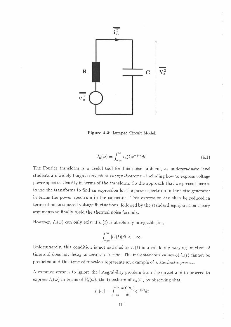
-l;
I
CR
I
e3
V.r2
Figure 4.3: Lumped Circuit Model
r^(,): I:i^(t)e-i-tdt. (4.1)
The Fourier transform is a useful tool for this noise problem, as undergraduate levelstudents are widely taught convenient energy theorems - including how to express voltagepower spectral density in terms of the transform. So the approach that we present here isto use the transforms to find an expression for the power spectrum in the noise generatorin terms the power spectrum in the capacitor. This expression can then be reduced interms of mean squared voltage fluctuations, followed by the standard equipartition theoryarguments to finally yield the thermal noise formula.
However, I"(r) can only exist if i"(ú) is absolutely integrable, ie.,
[* ¡,çt¡¡aú < +-.J -tn
Unfortunately, this condition is not satisfied as i,(ú) is a randomly varying function oftimeanddoesnotdecaytozeroasl--+too. Theinstantaneousvalues of i.Q) cannotbepredicted and this type of function represents an example of a stochastic process.
A common error is to ignore the integrability problem from the outset and to proceed toexpress I"(.) in terms ol V"(,'t), the transform of u.(t), by observing that
I^(.): [* d(c") "-¡''dtJ_* dt
111

an then integrating bv parts
I,(r) : clune-r-'lt= - Il*t- ¡rt)une-i't dt
which yields the 'correct' result
h(r): juCV"(a)
by making a second mistake in assuming that V"(r) exists and the square bracket residualvanishes at the limits, which is clearly unfounded as the limiting values are unknown. Atthis point disapproval can be expressed, and the concept of windowing the function canbe introduced. In practice, the random process can only be observed for a finite windowof time 1' so a dimensionless time window 2 function W(t,r) is defined in Fig. 4.4 and,provided a large r is chosen to minimise statistical sampling error, the windowed versionof equation 4.1 becomes
I,(,.t,r): l:i,(t.,r)e-i.tdt. (4.2)
As the measured voltage u, is only known over the observation time r, it is tempting todefine the windowed current as,
i,(t, r) : filC r,lt)W (t, r)1.
Assumption 2: The stochastic process is independent of where the origin ol W(t,r) isplaced on the time axis. This condition is referred to as stationarity and is reasonable inview of the observed nature of thermal noise.
This useful property means tha| 4.2 is invariant to the positioning of W(t,r). Althoughthe presence of W tn 4.2 solves the integrability problem, it introduces the artifact ofspectrum leakage. The leakage occurs essentially because the transform of W, ttself,contains a continuous range of non-zero frequency components. This can be ignored as
we will eventually be considering just the limiting case as r -+ c!c. Another potentialproblem is that the differential term appears to create a discontinuity artifact at theedges of the window, however by substitution into 4.2 one finds that it eventually cancels,as follows
2Some texts, such as [Buckingham 83], replace a random variable ø(l) by a 'gated' random variable17(l)which is zero outside the time window ?. A Fourier transform is then performed on x7(t). Although,as we show, this does eventtrally lead to the co¡rect result, the impticit window is introduced withoutdiscussion and lhe student is justified in questioning what becomes of any edge discontinuity eflects. Forthis reason we introdrtce art explicil window function W(t,r) as a 'book keeping' device to track andnronilor the arlifact.
112

w
-fl2 d2
Figure 4.4: The window function
rn(,,,) : I:fiV u^r)"-i,t dt (4.3)
by expanding the differential we obtain,
I,(u,r) : t l* ffr"-,"d,t + c l:#,"e-i.t¿,
I,(a,r) : CIu,W¿-i'']1i
c[* (¿,w I- J_,ot"\ * "-t't - juW"-t-tldt
+ c I* urn"-,"¿¿
where the residual now legitimately vanishes, and the superfluous differential windowterms cancel, again giving the 'correct result,
integrating the left hand integral by parts,
I,(u,r): juCV^(u,r)
Although this attempt has greater merit, as the integrals are now legitimate, it can beargued that the invoked definition of windowed current was somewhat ad, hoc. Notice
r13

as r --+ æ, in(t,r) does not tend to i"(t) due to delta functions at the extremities.The artificial introduction of these spikes, from the outset, fortuitously cancels with thedifferential window term during the integration by parts, thereby producing the 'correct'result. Again disapproval must be expressed and the preferred method now follows.
Consider a windowed version of e,(l) as
e*(t,r) : e"(t)W(t,r)
We now define the signals u,(t,r) and i,,(ú,r) as the responses of the circuit to e^(t,r).Noticethis timethat as 1 --+ oo, u,(t,r) --. u^(t) and i,,(ú,") * i,(f). We havein(t,r):ddt
I^(u,r): lC u"(t, r))e-t't dt
and integrating by parts,
I^(u, r) : C [u*(t,, I e- i't]!i + j rC t: u.(t,r)e-i't dt
which reduces to
I.(r,r) : ju:CV"(r,r) (4.4)
Although this result is trivial, it was important to show that there were no windowartifact problems. General discussion of window problems can be found ìn [Papoulis 84]and [Dym72]. As #:0lr=*"" it can be shown for the general case that
{#a*-Uù^W(.,')is a windowed or time-limited Fourier pair
4.3.4 The Thermal Noise Formula
We now proceed to use the eqn. 4.4 result to find the power spectrum in the capacitor andthen produce the celebrated Johnson formula. Consider the voltages around the loop, inFig. 4.3, by Kirchhoff
u"(l) * i"(t)R: e,(t)
thusu*(C T )t
/oo dJ-- ¿,
rt4

and viewed from the window W(t,r) this becomes
u"(t,r) * i,(t,r)R: e,(t,r)
Notice that by definition, e,(t,r) does not contain any delta function terms and thereforei"(t,r) and u,,(ú, r) must also be free of spikes. This can simply be demonstrated byreductio ad absurdum: if i^(t,r) contained a delta function pair, due to windowing, thenu^(t,r) would need an identical pair of opposing sign to balance the above equation. Butthis would be impossible as i"(t,r) would then contain the second derivative and thereasoning continues inductively ad inf,nitum.
Now taking Fourier transforms we have
V"(r,r) + I^(u,r)R: E,(u,r)
substituting in eqn. 4.4 gives
w En(4.5)I * juRC
multiplying by complex conjugates
lE"l'lwl' I I (uRC)z (4.6)
n theBy conservation of energy, the total energy in the time domain must equal that ifrequency domain, therefore
This is known as the energy theorem or Plancherel's theorem (a special case of Parseval'stheorem). Each side of the equation represents total energg and therefore lE,l2 representsthe energy density with units of V2sfHz. Due to the Hermitian property of the Fouriertransform, lB"l2 is always even therefore, we can write the one-sided form
Il*"\a, r)d,t : * I"* zll,(t, r)12 du.
By definition of temporal average
lgå("3),
e2"t: (t, r)dt: I2tr t: lE,(r,r)l2du.
li- lT+æ T t:
k'")
115
e2^(t,lat

therefore
(",.) : ]Æ+ ¡o* ,lE"(?,,)l' a,
where ø! ;" called the sample spectrurn or period,ogran't. It is permissible to movethe lim"roo inside the integral provided the ensemble average is performed first[Buckingham 83, p. 32]. Thus,
4:+l-{;*Y\^As we have a random process, the limit would be indeterminate had the ensemble averagenot been performed first.
Assumption 3: The process is ergodic, so temporal and ensemble averages are equiva-lent, ie. lim"*oo ("',), :4. Thrs,
\"'"11
2tr l"*
1
I + (wfuC)'zdu
da
,. 2lÛ,l'f+æ T
(4.7)
therefore
(4 8)
(4 e)
lim7+æ
By definition, the one-sided power spectral density of e, is, S(ø) : lim"*oo 2
we can rewrite eqn. 4.7 as
and substituting in eqn. 4.6
("r^):+1,*s(u)da.Assumption 4: The noise spectrum is white, therefore S(a,,) : ,S,, a constant.
For a practical measuring instrument bandwidth of Ac..r, eqn. 4.g becomes
("r.): ls,or.z1f
Using identical arguments for the capacitor voltage, u,, we have
(,'*):+ l,* {i* Y}^
("'") I"
cuo
1
2"cUO
2"1
da
I -t (uRC)'z
[arctan(øRC)]f : I ,q^ o2r"o zRC2r RC
116

Putting this into eqn. 4.9, to eliminate S,, gives
("',):?t(r',)oor- (4.10)1f
Assumption 5: The system is in equilibrium with its surroundings.
According to equipartition theory, a general dynamical system in thermal equilibriumhas on average a potential energy of kTl2 for each degree of freedom. One short handmethod for counting up the degrees of freedom in a linear system is to count the number ofindependent quadratic variables in the energy expression [Reif 67]. By inspection of 4.10,we see that our system takes up energy as |C (ul) and therefore has one degree of freedom,hence
itpZt:Tr, (4 11)
Assumption 6: Let us assume the system is classical (ie. no quantum effects) so thatthe Maxwell-Boltzmam lcT term holds.
Substituting 4'11 into 4.10 finally yields Johnson's formulafor open circuit noise voltage
þ7t ?nr nn,7f
4kT RLr.
U?\:4kTLf ',"sc/ - R.
which is the familiar current form fo. the Johnson noise formula
(4.t2)
(4.13)
This unassuming equation is a source of a number of interesting conundrums and muchconsternation. One common question is "where does the coefficient of 4 really come from?That is, what is its physical significance?" This can now be quite easily traced from theabove analysis, where the f clearly comes the one-sided integral of the arctan function.Hence it is purely a 'geometrical' quantity. If the integral is modified by substituting thecapacitor with a more complex network, the number of degrees of freedom of the systemchanges to always maintain the ubiquitous 4.
If the capacitor is replaced by an inductor I, the analysis can be repeated in thecurrent domain and the generated short circuit noise current can be shown to be(i?,): ?*(i'?")L,t, where (il) is the observed noise current. The system now takes upenergy as |L(i,"| : tkT, therefore
1t7
(4.t4)

Complete analysis and detailed discussion of the behaviour of 4.13 and 4.14 at limitingvalues of the main variables is lacking in the pedagogical literature, so we proceed for thefirst time to examine, in detail, the main problem areas in the following sections.
4.4 The Classical Bnergy Catastrophe
The most obvious problem with 4.13 is that it classically predicts infinite energy as / --+
oo. This is analogous to the black-body radiation problem where the Rayleigh-Jean,s lawsuffers from the so-called ultraviolet catastrophe - the divergent curve having infinite areaover all frequencies. Anticipating this, Nyquist [Nyquist 28] in 1928 suggested replacingkZ with the one-dimensional form of Planck's law
hrehflkT _ 1
which reduces to lcT as / --+ 0 and rolls off for hf > kT. So far so good, however thisquantum term predicts zero energy aI T : 0 which is a violation of the UncertaintyPrinciple. As we shall see the solution to this creates a further conundrum.
4.5 The Quanturrt Energy Catastrophe
During I97I-12, Planck's'second theory'produced the following modification to the quan-tum term [Kuhn 78]
ùH=*ry:å/corh (#)The extra hf f 2 terrn is called the zero-point energy (ZPE) and in this case, at ? : 0,the Uncertainty Principle is not violated. This creates a further conundrum in that hf 12is infinite when integrated over all frequencies, which is an apparent return to the typeof 'catastrophe' problem we saw in the classical case. One can only assume that Nyquistaccordingly did not suggest this form and probably would have been aware of Planck'sown misgivings concerning the experimental objectivity of hf 12. The inclusion of hf l2 instandard noise texts only became popular after 1951 following the classic work of Callen&Welton[Callen51] thatproduced thehf 12 ZPEtermasanaturalconsequenceof theirgeneralised treatment of noise in irreversible systems using perturbation theory.
The solutìon to the catastrophe problem is that hf 12, in fact, turns out to be the groyndstateof a quantum mechanical oscillator. If n is the quantum number, which is a positive
118
integer, then the allowed energy states for a quantum oscillator are (n + )nf and thusthe ground state is given when n :0. As there is no lower energy state than the groundstate, there is no energy level transition available to release the ZPE. Therefore it can beargued that hf 12 should be dropped before integration of the quantum expression. Thisprocedure is an example of renormalisation, which basically redefines the zero of energy.Renormalisation is a significant area of quantum field theory and is usually presented ina more formal manner. The problem of renormalisation is an open question in the theoryof gravitation where there is the apparent catastrophe of total energy becoming infinite.For most laboratory measurements there is no catastrophe as we are only interested inenergy differences.
The fact that the ground state energy, which we call ZPE, cannot be released means thattexts that quote the Callen & Welton hf 12 term as an observable noise component arenot strictly correct. However, by coincidence it turns out that the mean square of the zeropoint fluctuation (ZPF) also has the form hf l2 fLouisell 73]. The mean square does notvanish with renormalisation, of course, and this ensures the Uncertainty Principle survivesrenormalisation. The mean square fluctuation is a detectable quantity and represents themagnitude of the ZPF.
Each mode contribules hf 12 towards the mean square fluctuation and, for an infinitenumber of frequencies, the magnitude is infinite. It is considered that this infinity is notfundamental, since the measurement conditions have not been specified. It can be shown
[Louisell 73] that for any finite observation bandwidth and volume of space the magnitudeof the fluctuations of a quantum field is finite - if either the bandwidth is infinite or themeasurement is evaluated at a point in space then the fluctuations become infinite.
4.6 The Steak Grilling Debate
In 1982, Grau & Kleen expressed the view that hf l2 is both unextractable and unobserv-able, adding their memorable rejoinder in the Solid-State Electronicsjournal that hf 12 isnot "available for grilling steaks" [Grau 82]. Uncannily, about the same time Koch, VanHarlingen & Clarke (KVC) published noise measurements in superconductors reportingto have observed ZPF [Koch 81]. Over the next 3-4 years a number of independent su-perconductor papers folìowed, all nonchalantly quoting the KVC interpretation of ZPF as
standard. In reply, Kleen (1987) essentially restated his case pointing out an unanswereclquestion in the superconductor measurements [Kleen 87]. As far as we are aware therehas been no published KVC leply.
119

The orthodox position, is that the effects of ZPF are observable such as in the Casimireffect [Itzykson 80]. ZPF also has an orthodox status in explaining the observations ofMullikan [Mullikan 24], Lamb [Welton 48] and the nature of liquid helium [Adkins Tb]. Onthe other hand, consensus is not total as the school of Kleen has some support eg. [Beck 76,p. 173] and [Kiss 88], the commonly supposed link between spontaneous emission and ZpFhas been criticised [Siegman 64] and the overall understanding of ZPF is also questionedas expressed, for example, in the following quote [Grandy 70]:
"The obvious question, then, is whether the zero-point energy and the vacuumfluctuations are one and the same thing. If they are, why is it that the formercan be eliminated from the theory? The answer is not yet clear, and a deepersignificance has yet to be discovered. Therefore, we will adopt the view that thezero-point energies are to be formally removed from the theory...., and all physicaleffects of the type.... discussed are to be ascribed to quantum fluctuations of thevacuum.... It must be admitted that the vacuum is not completely understood,neither physically nor philosophicatly. Whether or not the vacuum fluctuationsare intimately related to the (unobservable) zero-point energy remains an openquestion.tt
where the expression "vacuum fluctuations" is an alternative term for ZPF. The view thatZPF cannot give rise to a detectable noise power itself, but can indirectly modulate orinduce a detectable noise power has been recently expounded [Senitzky 93].
As for grilling steaks, the debate still sizzles but has shifted away from electrical noisetheory. Controversial attempts to harness ZPE are underway using the concept of sys-tem self-organisation [King 91] and presupposing the idea that the ground state is notthe actual source of energy but is a 'pipeline' into some universal background source
[Puthoff 89]' In an enterprising decade where there have been controversial attempts toconsider superluminal velocity [Giakos 91] and quantum information theory (promisingtwo bits of information from one physical bit [Bennett 92] and a form of teleportationfBennett 93]), there is no doubt that ZPE research will thrive. It remains to be seen whatconcrete results are produced and, if any, what the implications are to noise theory. Untilfurther evidence, the quantum zero-field should be regarded as a conservative field as faras the extraction of energy is concerned.
4.7 Quanturn Cut-Off Experimental Status
Fig. 4-7 shows a theoretical plot of the quantum term for different temperatures. Thehf 12 Lerm is plotted to illustrate that at normal working frequencies and temperatures it
t20

is vanishingly small, so for these conditions it can be neglected regardless of the status ofdebate. It can be seen from the Fig. 4.7 plot that experimental verification of the quantumcut-off point for electrical noise is rather difficult due to the Tera Hertz frequencies. Ifthe temperature is reduced, to reduce the cut-off frequency, we see that the maximumenergy of the curves falls, thus making noise detection more difficult. In 1981, van derZiel fvan derZiel81] proposed to make measurements in this region, at 100 GHz usingHanbury-Brown Twiss circuits; unfortunately, this research effort was never completed.The only curves we have today, for electrical noise, appear to be those of the type ofKVC, which show no cut-off due to ZPF becoming significant. Therefore, as far as weare aware, there are no measurements that directly demonstrate the quantum cut-off forelectrical thermal noise, to this day. Although the cut-off region, for electrical noise, hasso far been obscured by ZPF it may become possible in the future to view at least partof this region, without violation of the Uncertainty Principle, if somehow the concept ofsqueezed states can be successfully employed for the electrical case (eg. [Baseia 93]).
Quantum Equipartition Energyl0-20
l0-2t
lo-22
l0-23
lo-24
10-25
l0-26
lo-27
l0-28
lo-2e
l0-30100 103 106 10e 1012
Frequency (Hz)
l0l5 l0 t8 l02l
Figure 4.5: Quantum equipartition energy versus frequency for 300K, 77K and,4K.The line represents the hf l2 term plotted separately.
(.)
=o
òoot¡l
r2l

4.8 MacDonald's Objection
In 1962, MacDonald raised an interesting objection [MacDonald 62] concerning the quan-tum term. He correctly demonstrated that for hf > kT the time-dependence charac-teristic of a reuer.siåle system is exhibited. For å/(fr? he showed that the system isirreuersible as expected. Given that an electrical resistor is regarded as a dissipative ir-reversible system, a transition to a reversible regime lor hf > kT caused MacDonald todoubt the validity of the quantum term altogether.
The transition to the reversible regime can be simply thought of as taking place becauseat high frequencies, hf ) kT, ie. for time intervals less than hlkT, the period is tooshort to achieve thermal equilibrium. As noise is a manifestation of a dissipative systemmaintaining thermal equilibrium, if the intervals are too short, then the dissipative processmust roll off at these higher frequencies. This is precisely what is predicted by the quantumterm.
Dissipation can be thought of as a process that eventually brings classical particles, ina closed system, to rest. This situation is not permissible for quantum particles as itwould be a violation of the Uncertainty Principle. Dissipation does not play a role inmicroscopic description of quantum particles. It is a macroscopic concept whose relationto the quantum microscopic description is purely a statistical one in the classical limit.The 'sleight of hand' that turns non-dissipative equations of motion, into dissipativeones in the classical limit is hidden within the equation boundary conditions. For amore mathematical discussion see [Ullersma 66]. From the modern viewpoint, quantumBrownian motion (QBM) is now a major discipline area [Grabert 88] and MacDonald'sobjection is therefore clearly out-moded.
4.9 The Case of Limiting R & C
Remembering that the Johnson expression for (el) is the case for an open circuitresistor,we now systematically illustrate, for the first time, how to examine the output voltage,current and charge fluctuation. ((rl), (ifl) and (qfl)) for the various limiting cases of R &C - the results are summarised in Table 4.2.
The case of finite R €j C and f --+ oo
The voltage noise detected across the capacitor is simply
r22

4kT Rdr kT(4.15)I+(2rfRC)2 C
which normally causes some surprise as the kT lC term is independent of -R which isthe source of the noise! This is easily explained by observing that as ,R increases, thecorresponding increase in noise is exactly cancelled by a decrease in circuit bandwidthx IlR. The circuit current noise is given by
þ") : l"
zi t* ØkT I R)(ztr f RC)2 dfJo@:æ
{-;*r}:*u{'*rq:Y
)
and this divergent result is a consequence of classical theory breakdown
The case of f,nite f, R €j C
Por a finite frequency band A/, taken from zero, the voltage noise becomes
(r"")2kTfi arcran(zr\f RC)kT 4kT RLfc (B^lB.)'
by expanding arctan f.or B*Þ8", where the measurement bandwidth B^ : (tr l2)L,f andthe circuit bandwidth B.: Il(4RC). This remarkable result is the difference between thefamiliar kf lC noise and the open circuit noise divided by the square of the ratio of thebandwidths. The analogous expression for the current noise can be shown to be
t;z\ - 4kTLf (- / B. \2\ kT\,í)æ R' (t*(r;))-eøwhich goes to infinity for / r oo, as expected for the classical theory. The solutionsusing the quantum term for finite -R and C involve tedious integrals and are not thatinstructive; for such a treatment refer to ref. [Pyati 93].
Open circuit capacitor: fi"nite C, R ----¡ oo, .f - -Using the well-known delta function approximation of the form
6(ar\:!li-f t Ì\ / 'rf 11Ø l1 + a2r2 )
limRræ
we observe that
123

by applying the delta function identity 6(aæ):6(r)la. Therefore
(,í)1"=-:;l:+nrffar:T (4 16)
where the integral limits are taken between too as á(/) is centered about the / : 0 axis.The factor of Il2 is introduced as we are dealing with frequencies in the positive domain- this is justified as the function is symmetrical about the / : 0 axis. This surprisingresult of kTlC has to be interpreted in terms of a dc voltage across the capacitor, becauseas -R --+ oo the circuit bandwidth--+ 0. Therefore, the classical formulation predicts thatan ensemble of capacitors will, on average, display a dc voltage of {k'I|C across theirterminals. The source of the dc voltage can be thought of as the voltage that is sampledby the capacitor at the moment the finite resistor is removed. Note that substitution ofthe quantum term into the above integral also produces the same result.
This explanation in terms of a dc voltage is much more satisfactory than that ofref. [Pyati 93] which considers it as a time varying noise voltage and consequently proposeshighly ingenious ways of making a pure capacitor dissipative! This is clearly unnecessaryas any dissipative proposal for the capacitor can be modeled by an equivalent resistor.
Short circuit capacitor: finite C , R --+ 0, / --+ oo
As -R --+ 0, all the integrals, classical and quantum, trivially go to zero - this is expectedas rB is the source of the noise.
Open circuit resistor: fi,nite R, C -- 0, / --+ oo
For the classical case (ul) --+ oo as expected due to breakdown of the theory. Theintegrals for þ2") and (ql) trivially tend to zero. This is expected as there is no circuitloop for current to flow. The quantum case for the open circuit resistor, where I isthe mathematical Samma function and ( is the Weierstrass zeta function, now becomes
[Rhyshik 63]
þ'^): I"4RhrdÍ
ehÍ/kT _ | (+) f (2x(2))
4Rh
2RþrkT)2
which implies that the open circuit thermal noise voltage across a I MQ resistor, at roomtemperature, viewed with an instrument of infinite input impedance ancl infinite band-width (or at least )fr?lh:6250 GHz) with no parasitic capacitance present is 0.41 V.-"!
3h
124

This is rather large, but fortunately these ideal conditions are unrealisable in practice. Italso assumes that the result is directly observable and not swamped by hf l2 quantumnoise.
Short circuit resistor: finite R, C --. æ, f -+ oo
For the classical case, the voltage integral goes to zero whereas current and charge go toinfinity. Zeto voltage is expected as the terminals are shorted and infinite current in theloop is a breakdown of the classical theory. For the quantum case for current we have
(i,,):1"*#ffi:ffi{,,T,which is finite as expected. However, the quantum integral for charge turns out to bedivergent, giving infinite charge. Notice we now have a random walk type non-stationaryprocess. The infinite result may be seen, not as a breakdown in the classical or quantumtheory, but due to the artificial construct of theoretical infinite capacitance. An infinitecapacitor can be thought of as an infinite store of charge - this never occurs in practicewhich is another way of saying that there is no such thing as a perfect short circuit. Noticethat in the limit as C --+ oo, the capacitor becomes simultaneously an infinite store ofcharge anci a perfect short. This can be resolved by thinkin g of C --+ oo as being modeledby an ideal voltage source.
Classical QuantumU U 2,2 2
---+
,R --+ ooC ---+ ooC -+0
Open Cap.Shorted Res.Open Res.
ä (¿") 00 #(trkT)2
krc Goo0
2R (trkT)2 0
Table 4.2: Thermal noise over infinite bandwidth for different cases of limiting Rand C
4.LO kTC Noise
A subtle source of confusion is that equations 4.15 and 4.16 appear identical - howeverthey are fundamentally different. Equation 4.15 is the ac thermal noise of a resistor over a
E@"0
oo
kTC (dcoo0
0oo0
)
125

measurement bandwidth greater than the circuit bandwidth, when loaded by a capacitorC. Whereas 4.16 is the average value of the dc voltage sampled,by C, when the resistorsupplying the thermal noise is removed. These are two fundamentally different quantitiesthat coincidentally have the same numerical value.
Multiplication of eqn. 4.16 by C' gives the well known result (qfl) : krC used foranalysing noise on switched capacitor circuits. For example, a 1 pF capacitor will sample64 ¡'t'Yr*" across its terminals or in terms of electron number this is 400 rms electrons.
In practice the noise on a switched capacitor, when the transistor is'on,'is given by 4.15and the circuit bandwidth is large - but doesn't exceed the quantum cut-off for realistic-RC values. When the transistor is 'off,' the average voltage sampled by the capacitoris given by 4.16 and the circuit bandwidth is very small. As the ofi-resistance of atransistor is finite the circuit bandwidth will be small but non-zero. Hence, the voltageon the capacitor will not be perfectly dc, but will be slowly varying. However, in mostreal applications the switching time of the capacitor is much shorter than the ,RC timeconstant, hence the sampled voltage appears as a steady dc level over the switching period.
4.LL Power in a Matched Load
If a resistor -t? develops an open circuit noise voltage of 4kT RA,.f , the power delivered toan equal load resistor is
P : (i'z,)R: **o: I : kr^f .l'zttyz 4RThis causes some surprise as P appears to be independent of -8, which is the source! Tounderstand this, let us consider an arbitrary load .B¿, so the power now becomes
P : 4kT RLf RL-' (Rr Rt¡z'
So we see that for small r?, the noise term is small and therefore the delivered power pis small; whereas for large -R the potential divider term becomes small, so the deliveredpower is still small. Maximum power transfer occurs when #. :0, which trivially yieldsR : Rt' - hence there is balance achieved between noise generation and the potentialdivider effect.
This analysis can, of course, be reproduced by considering a resistor -B in parallel with acurrent noise source of akTLf lR. A common student error is to mechanically proceedthe analysis with the power, P : (i'?^)Rr-, as before. This, of course, leads to the wrongresult. For the case of a current source we must put p : (ur,) lRL, giving
r26

P
which is the same result as before
þ1) \i2") R2 RLRr (R + Rr)24kT Lf R, Rr
R (R + RL)2
AkrR.Lf , Rt" (R+ Rù2
Another curious feature of the P : kT L,/ formula is that it appears to imply that forlarge observation times the power transfer tends to zero, whereas for small times thepower transfer increases. This is simply explained by noting that the application of thethermal noise formula presumes that both resistors are in thermal equilibrium. Hence forlong observation times we expect the net power transfer to be zero; otherwise a resistorwould heat up and escape thermal equilibrium. However for a small'snapshot' of time, as
the fluctuations in each resistor are uncorrelated, there must be an instantaneous transferof power. The momentary transfers of power back and forth between the resistors, on
average, add to zero. This also explains why energy cannot be harnessed from the thermalnoise in a resistor, cf. Brillouin's Rectifier Paradox fBrillouin 50], Penfield's Motor Para-dox [Penfield 66], Feynman's Rachet Paradox [Feynman 63], Panse's Radiation Paradox
[Browne 93] and Bogner's Microwave Isolator Paradox [Bogner 94]. Analogous argumentsare used by some authors [Buckingham 83] to assert that energy cannot be extracted fromZPF, however this has been disputed [Puthoff 90]. The apparent infinite power as thesnapshot of time approaches zero is, of course, due to breakdown of the classical kT term.
4.L2 Distributed RC
Until this point, our analysis has only considered a lumped circuit model. In a givenpractical case, a resistor may have some distributed parasitic capacitance and thus it is
instructive to analyze the noise in a distributed RC line. From standard transmission linetheory, the impedance looking into an RC line with the other end shorted is
RjrCZ- tanh JuRC
The voltage noise seen across the open circuit terminals is found by simply inserting ft(Z)into the Johnson noise formula [Davenport 58, Starr 53]. Therefore
(r'") 4krnØ)Lr
127

4kTLr R sinh rffifP * sin uff¡pg1/4ifÃe cosh ßi-fRC f cos JTn:TRC
which reduces to 4kTRA,,/ for small /, as expected. This is plotted in Fig.4.6 with thesimple RC case for comparison, showing that at low frequencies they are equal, but athigh frequencies the simple RC curve rolls off faster. The quantum curve is included toshow that there is a physical limit to the slow roll-off in the distributed case. Finally,the case for a transmission line with a matched,load is also plotted to clearly show thatthis option does zoú model a discrete resistor with distributed parasitic capacitance. Thecurious phenomenon of the noise increasing, for low frequencies, in the matched load case,is a manifestation of noise in the load (which is physically unrealisable in this case) andnot an anomaly in the line.
Thermal Noise in a Distributed RC Linel0-13
l0- l4
l0- l5
l0-16
l0-r7
l0-18
l0-20
l0-2r
lo'22
lo-23
l0-le
N
(\
(l)
z
l0r 104 l0? l0ro l0r3 1016 lote lo22 lo25 1028
Frequency (Hz)
Figure 4.6: Noise in distributed RC line. Chained line: short circuit load. Solidline: matched load. Dashed line: short circuit load with planck term. À:1 Mfl,c=1 pF. All curves plateau at 1.66x10⁻¹⁴ vh" f\z, except for the matched loadcase that increases due to noise in the load. For reference, the simple lumped RCcase is shown as a dotted line.
r28

4.L3 The Capacitor Paradox
For the first time, we present an unsolved paradox in a simple two stage RC ladder(Fig. a.7). In Appendix D, we solve the relevant complex integral for the circuit showingthat correlation between the two capacitor noise voltages is zero, ie. u1u2 :0. However,we also show that if R2 --+ 0 or ,R1 -) oo then u1u2 suddenly becomes non zero! Thisstrange dilemma is unsolved and may highlight a limitation in the circuit noise theoryformalism. If the capacitors are replaced by inductors, it may be that the problem has
similar parallels to Penfield's motor paradox [Penfield 66].
I %
vt
Æ
ct vz cz
Figure 4.7: Two stage RC ladder - a source of an unsolved paradox.
4.L4 Forward's Photoamplifier
A standard passive resistor in a photodiode circuit introduces thermal noise a can hencelimit the signal to noise ratio. A room-temperature active resistor has been devised
[Forward 82] that can maintain the same resistance, giving rise to the same photovoltage.However, the active resistor generates thermal noise as if it were at cryogenic temperature.This remarkable result may have applications in future areas of this work on GaAs pho-todetectors. The ability to maintain an equivalent resistance and yet reduce the thermalnoise below the theoretical limit appears to be in violation of the fluctuation-dissipationtheorem and the laws of thermodynamics. This apparent paradox can be explained whenwe consider the fact that the active resistor is powered and therefore there is an erternalenergY source feeding the system - this preserves the thermodynamical laws.
t29

4.L5 Measurement of Noise
Measurement of noise is important both for the determination of noise parameters for theimager design and final performance testing of fabricated devices. A simple set up wasdevised to investigate some of the potential challenges. The amplifier configuration inFig. 4.8 was connected to an HP36654. In order to characterise the system, we set out tomeasure the thermal noise in -Bo for a range of values. The output noise of the amplifieris given by,
R
Figure 4.8: Amplifier configuration for noise measurement. Rris the device undertest (variable). ,R" : 1K and À¡ : 6.8M. Opamp voltage noise sources are uncorre-lated but equal in magnitude at:az-L} ny f rcot-H2 Opamp current noise sourcesare uncorrelated but equal in magnitude it=iz-0.01pA,f rcot_Hz.
ul : u]+u2"( R¡+u3(
R *4"
Rf
1v2
ft
t) ¡'+4n',+Q( ), +r?(Rt !¿;R"¡, +;i4(t&¡R¡lR"
R",
R" R"
where ur2 is equal to ulin magnitude but uncorrelated and zf is equal to z! but uncorrelated.The terms in this expression are plotted in Fig. 4.9. Notice that only the data points inthe central straight portion of the output noise curve are a valid measure of noise in .Ro.This is because in this region the noise in R, dominates all the other sources.
Back calculating from the valid data points we find that the coefficient '4'from the thermalnoise formula comes to 3.710.3. This result is curious as it appears to predict noise levels
356
+
130

NIñat,E
c).ü,oz.
100Thermal noise in a resistor
o-t0
10-1s100 102 1o4 106
Res¡stance (Ohm)108
Figure 4.9: Operational amplifier noise sources. Solid line: total noise on output.Dashed lines: opamp voltage nåise (upp"r trace), resistor under test noise (middletrace), opamp current noise (lower trace). Fine dotted line: input resistor noise.
Coarse dotted lìne: spectrum analyser noise floor. Chained line: feedback resistornoise. Vertical dashes: actual measured data points - height of dashes representerror bars.
10-
1
'too
L
131

/ess than theory. It is tempting to dismiss this by pointing out that the result does includethe value of 4 if the error is taken into consideration. However, only a small componentof this error is experimental error, as such - it mostly represents the intlinsic variance ofthe noise taken over many rms averages. Hence the fact that the mean (3.2) is lower than4, is something that must be critically examined in case we have discovered somethingfundamental. Let us now critically evaluate all the variable factors.
Repeatability: we found that the experiment could be repeated many times, on differentdays, with different circuit boards, different resistors and yet the mean thermal noisecoefficient was always lower than 4 and about 3.7. It is interesting to note that in theseminal work on measuring thermal noise [Johnson 28] a mean of 3.7 was also obtained!However in 1928 this low value was ignored as it lay within experimental error.
Window Function: \,ve operated the fFT spectrum analyser with a Hanning windowwhich is theoretically the optimum for noise measurements and should introduce an errorno more than 1%.
Component Values: the resistor values in the circuit and those under test were allmeasured rather than relying on colour coding. The maximum error for a Fluke meterreading is I%. This was checked against several meters.
Fbequency Response: the gain of the operational amplifier was not calculated from theresistor values, but instead was obtained from the frequency response of the operationalamplifier which was measured with a swept sinewave. The response was flat over themeasured noise band (100-300H2). Maximum error introduced is 2%.
Temperature: the maximum error in temperature reading for insertion into the thermalnoise formula is 1%.
Overdrive: if the amplified peak-to-peak noise is so large that it overdrives the opera-tional amplifier into a non-linear region, the gain can drop thereby producing apparentlylower noise readings. This was not the case as the noise was viewed simultaneously on anoscilloscope and a spectrum analyser - no sign of clipping was observed on the time traceand no unusual frequencies were observed in the frequency domain.
Batteries: the amplifier was powered by batteries to reduce extraneous noise. Thebattery voltage level was checked before each experiment.
Averages: the HP3665A was automatically logged by a PC running under LABVIEW.This enabled us to efficiently take 400 ensemble rms averages of the traces ancl 400 tem-poral rms averages of each trace (skipping multiples of 50 Hz). Thus each data point wasobtaine.l from 160,000 rms averages!
r32

Automation: preliminary hand measurements were taken to check there were no arti-facts introduced by the automated logging procedure.
Parasitic Resistance: the resistors under test were individually soldered into positionand the resulting total resistance was rechecked. There was no significant extra resistanceintroduced from these connections.
Open Circuit Formula: the formula 4kT RL./ strictly gives the open circuil noise
voltage across the resistor under test. The input capacitance of the amplifier is a few pFand therefore a possible objection is that we should use the closed circuit form, with loadcapacitance,2þ+ arctan(2zrA f RC), and that this could be the source of error. However,for small arguments arctan(r) : r and the formula reduces to the open circuit form. Inorder to obtain an error of about 7.5% it would be necessary for A > 400 Mf^¿ - this is
clearly not the case for our data points. The .R values we have used produce an error as
littleaslxl0-5%.
Test Jig: the test jig was in a screened box with a star earth to the box. Screened BNCcable was used to feed the output to the spectrum analyser. Screening ensures that nopickup overdrives the amplifier, perhaps paradoxically producing lower noise readings.
Analyser: the calibration of the spectrum analyser was carefully checked by feeding ina known long pseudo-random bit sequence. The maximum error foun d was 2%.
Given the above obvious effects have been discounted we are now left with three possibìe
hypotheses.
HYPOTHESIS 1: Correlation of errors. If all the possible error sources 'colluded'together to produce a lower noise value, their magnitude may just be enough to producea low noise coefficient of 3.7. However, it is highly unlikely that so many uncorrelatedevents can synergise given that the experiment was done many times on different days,with different tempetatures, different resistors, different amplifiers and cross checked withtwo different spectrum analysers! We reject this hypothesis.
HYPOTHESIS 2¿ Boltzmann's constant is reduced At first sight this bold hypothesisdoesn't seem too absurd. We must question why Boltzmann's constant (k) is not perhapsa little lower for an electron gas. After all, the particles are negatively charged and are
repulsive, hence we might expect a different gas behaviour. However, we must rejectthis hypothesis - from the equipartition theorem we see that k is simply a constant ofproportionality between the energy of a particle system and its temperature. Hence, theactual value of fr arises from the way we conventionally define temperature and can thtishave nothing to do with whether the gas particles are charged or not.
133
HYPOTHESIS 3: Coruelations between electrons. As the electrons form a gas ofnegatively charged particles, and interact with negative repulsion, it is conceivable thatthis interaction results in a small amount of correlation which results in a slightly lowernoise value than theory. As we have no evidence to dispute this idea and that it is notentirely absurd given that space charge smoothing is a well known effect that reduc es shotnoise below theory, we shall adopt this as our working hypothesis for future work.
4.16 Thermal Noise in MOSFETs
The thermal noise in the channel of a MOSFET can be referred back to the gate. Thisgate referred voltage noise is given by,
?)'n8 KTB3g^ (4.r7)
there the factor of t only has a weak bias dependence and the formula is accurate forthe saturation region. The thermal noise in the channel has a second.ary effect in thatit produces random fluctuations in voltage along the channel which, in turn, modulatesthe depletion layer encroaching on the width of the channel. Via capacitive coupling, thisfluctuation is modelled by a gate noise current,
e, : 2kr Bu2c3
3 s^ (4'18)
where Cn is the gate capacitance. Although ul and zl fundamentally arise from the samethermal noise source, they are uncorrelated! The solution to this conundrum is due to thetime constant associated with the capacitive coupling causing a phase shift between thetwo random waveforms. Detailed analysis shows that the square of the modulus of thecorrelation is only 0.16 and hence for most design applications we take the correlation aszeÍo.
4.LT Flicker Noise in MOSFETs
1// noise results from a process (or set of processes) characterised by a continuous dis-tribution of time constants over a very wide range. Two competing models that describethis process are well known:
(1) Mcwhorter's carrier densitv or number fluctuation model
134
(2) Hooge's mobility fluctuation model.
These models are invoked, either separately or in a unified form, to explain the variety of1// noise data in the literature. The number fluctuations model assumes that carriers inthe conduction or valence bands communicate with the fast surface states, at the Si-SiO2interface, through a Shockley-Read-Hall (SRH) process. The carriers then tunnel into orout of traps, located further in the oxide, whose energies lie in the semiconductor bandgap.Noise is caused by carrier density fluctuations in the channel due to this random trappingof the free carriers. The second model assumes that mobility fluctuations are bought aboutby phonon scattering and interactions with interface charges. Various electron-interfacecharge interactions are reported:
(a) Coulomb scattering
(b) Scattering inhomogeneous surface potential due to non-uniform fixed interface charges
(c) Hopping between localised states in the interface.
It is clear that in both models surface states are instrumental in the I I f noise mechanism.This means that the 7l f noise performance of a MOSFET is dependent on factors such as
crystal orientation, hydrogen annealing, implantation and processing temperatures thataffect the Si-SiO2 interface.
For any given transistor the noise spectrum can be approximated by the following well-known expression,
u] aBwLC" (4.1e)
where u] is the gate referred flicker noise, W k L are the effective channel width andlength, C, is the gate oxide capacitance per unit area, û is the constant of proportionalityand 7 defines the power law. Since W LCo, the active gate capacitance, is merely thefactor that couples charge fluctuations in the channel with corresponding fluctuations inthe gate voltage, this means that o and 7 are the constants that essentially characterise1// noise in any device. Note that o increases with the number of fast surface statesat the Si-SiO2 interface and the exponent 7 is a measure of the uniformity of the timeconstant distribution. Typically 1 is in the region of 1.
4.L8 Thermal Noise in MESFETs
The formulae for thermal noise in MtrSFETs are given by [Danneville g4]
tlr
135

and
-- _ 4kTBu2C2n
e^ Ø'21)
which appear similar to those for MOSFETs, except that the bias dependent coefficientsare slightly different. Again the correlation between the two is small and therefore forworst-case analysis we shall treat them as totally uncorrelated.
4.Lg Flicker Noise in MtrSFETs
Due to the absence of an oxide interface in MtrSFETs, flicker noise is considerably lower.Flicker noise in this case is attributed to carrier density fluctuation in the channel duegeneration and recombination or trapping. The formula is given by [Graffeuil 82]
O ZKTBn 9^
(4.20)
(4.22)a.Vrz B
2aN¿W L r1
uÍ-
where Vo is the pinchoff voltage, a is the channel depth, ÄI¿ is the channel doping and o"is the flicker noise constant.
4.2O Shot Noise in MESFETs
Although MESFETs have the advantage of low flicker noise, the presence of gate leakagegives rise to shot noise not present in MOSFETs.
The origin of shot noise is generally attributed to the quantised nature of electric charge.The name 'shot' comes from the analogy of irregular impact of lead shot on a surface.It is not true that shot noise is present in all electrical currents. The flow of currentthrough a resistor does not contain shot noise. Similarly freely falling lead shot has littleopportunity to interact.
The analogy with lead shot is not totally adequate. In the movement of charged particles,large scale electrostatic interactions between individual current carriers smooth out theflow, given enough time for thermal equilibrium.
136

Shot noise is generated when current carriers cross a barrier, and in this sense is a non-equilibrium form of noise. Shot noise is encountered in solid-state devices, whenever a
net current flows across a potential barrier such as the depletion layer of a junction. Forthe MESFET the formula is given by
i2":ZeInB (4.23)
where e is the charge on the electron and 1, is the gate leakage current.
4.2r Noise Analysis of Irnager output circuitThe preceding sections have created a framework for now discussing the noise in theoutput circuit of the XY array imager. Noise is usually poorly presented in the literatureand thus our careful discussion of kTC noise and noise in transistors, in particular, willbe used in the following analysis.
The output circuit of an XY array imager consists simply of the gate of a source followerconnected to the output bus (called the video line), shown in Fig.4.10. As signal chargeis dumped on the video line, the resulting voltage variation is detected by the sourcefollower. A second transistor is used to then reset the video line to a base dc voltage,thereby discharging the line in preparation for the next signal charge dump.
In order to achieve the best dynamic range) it is necessary to optimise the size of the sourcefollower. As it turns out, this is a non-trivial problem due to a number of conflicting designtrade-offs. The traditional rule of thumb, for silicon XY arrays, has been to set the widthof the source follower such that the gate capacitance Cn equals the video line capacitanceC". We shall show that this can give a workable result but is in fact not optimum.
Noise analysis can take place in the voltage, current or charge domain. Each domain isequally valid, and is selected on the basis of whichever results in the simplest analysis. Inthe case of an imager output circuit it is usually more convenient to operate in the chargedomain. It is then conventional to divide the noise charge by the charge on the electron e,
to produce a dimensionless result called the rms electron number or simply rms electronsor noise electron density (NED). In our case we shall plot all graphs in terms of squared,
rms electro?¿s so that uncorrelated sources can be directly added. Another conveniencewe shall adopt is to use expressions lor gate referred noise for the source follower, so thatall sources of noise are compared 'as seen' from the video line.
The following conditions, in some cases contradictory, are required for optimum circuit
t37

V¿¿ResetTransistor
Vreset
V¿¿
FromMult¡plexer
Video Line
ccg
SourceFollower
Output,Æ
load
Figure 4.10: Imager output circuit configuration.
performance,
Reset transistorz (a) WIL to meet speed requirement (b) smatl W L to minimise channelcharge and hence feedthrough spikes (sometimes called partition noise)
Source follower: (a) W I L to meet speed requirement (b) large W L for low gate referred1// noise (c) large WIL fot low thermal noise voltage
Output node capacitance (C,¡Cn)r (u) large node capacitance for low capacitor resetnoise (fr?/C) voltage (b) large node capacitance for low reset pulse feedthrough voltage(c) small node capacitance for large signal voltage swing.
These trade-offs turn a mere 3 component circuit into a surprisingly difficult optimisationproblem that is too complex to solve analytically without some judicious simplifications.
Assumptions & simplifications:
(a) ignore the source follower gain reduction effect on input capacitance as this will affectsignal and capacitor noise equally
(b) leave the reset transistor out of the optimisation - preset W L to the smallest areathat still meets speed requirement
(c) use the maximum (worst case) value of source follower gate capacitance; ie. ignore anydepletion layer capacitance in series with the gate
138

(d) neglect bias effects on flicker and thermal noise
(e) the thermal noise formulae, that incorporat es g^., assumes saturation
(f) kf lC is strictly the rms value of the noise sampled by the capacitor - this sampleis a dc voltage - but as the instantaneous value is different for each time sample, we treatit as an ac noise source and add it in quadrature in the usual way
(g) *" neglect any correlation between gate referred voltage thermal noise and gate currentthermal noise, thus producing a worst case result
(h) we ignore any electrostatic effects between charge carriers producing any correlation(worst case)
(i) we assume the noise contribution of an off-chip preamplifier referred back to the sourcefollower input is negligible.
4.2L.1 Silicon output circuit
The charge-normalised noise formulae in terms of rms electron number are
Thermal noise,
-, _ gkrg c2 ,8 kr B (W LC.)2 .''t-5 g*e-5 g* ", ;
Capacitor reset noise,O KTCní: ---.
Flicker noise,
n'JaB 7C2
WLC, f e2
where C : Cu+W LC" and g^ : 2Y pC.(Vn"-V). Inserting typical values: (Vn"-V) : zY, L:3¡lm, oxide capacitance Co:860¡rF/m2, bandwidth B: 2MHz and mobility/ : 650 x 10-a m/V2s we obtain the curves in Fig. 4.1i. A video line capacitance Cu : 4
pF was estimated assuming a 128 by !28 size array of 40 ¡rm pitch. A worst case û : lQ-23Joules was inserted.
The curves in Fig.4.11 show the magnitude of the noise contributions as a function ofsource follower width. The dominant curve is the flicker noise at the bottom end of usefulvideo bandwidth ,f : 50 Hz. The minimum flicker noise at the high end of the bandwidthis also shown and lies below the kTC noise. In practice, low frequency flicker noise andkTC noise are significantly reduced using correlated double sampling (CDS) [Barbe T5]
or delayed double sampling (DDS) [Obho 88], therefore only the thermal noise curve
139

needs to be considered. This curve actually has a very shallow saddle point (minima) atI4l : 1000 ¡;m, however as the curve varies very slowly we can choose W : 400 ¡;m withan insignificant increase in noise. The traditional rule of thumb (extolled by [Burt gb], forexample), suggests to match Cn with C,, giving a large overestimate at W : 1600 pm. Interms of noise this is a workable result but is wasteful in terms of power and real estate.
lnput Referred Noise Electrons v. Source Follower Width (Silicon)10o
C\T
É-1anCoo(t) .õlat
E.Ø1c,o()
_9uJ1q).9oz.ôl(l)oE:{z.rÞ(l)(úfo-1
U)
o"
o8
07
o6
o"
o4
o3
102 o o.2 0.4 0.6 0.8 1
Width W (m)1.2 1.4 1.6 1.8 2
_2x 10 -
Figure 4.11: Imager output circuit noise sources - silicon. Solid line: thermalnoise. Chained ltne: kTC noise. Dotted lines: maximum & minimum flicker noise(frequency dependent).
4.2I.2 GaAs output circuit
The charge-normalised noise formulae in terms of rms electron number are
Thermal noise,---; krg c2 , ^kTB (W LC")2n!-A--t2-- \''- .
9* ez grn e2 '
C KTCtt" - ---i-
Capacitor reset noise,
140

Flicker noise,
)1j2
Ja"Vr2 B
2aN¿W LC 2
n
Shot noise,
fr2"2IsBeu2
where C : Cu + WC. and g^ : 2W PQ + lyd")tanh(2|¿")(Vn" - Vr). Inserting typicalvalues: (Vn" - V) : 0.5 V, gate capacitance Co : 1.3 nF/m, bandwidth B : 2 MHz,channel doping
^,L : 1.2 x 10²³ m-3, channel depth a : 0.L pm, pinchoff voltage V, :
-0.5 V and beta þ : 200 AlY2lm we obtain the curves in Fig. 4.12. A video linecapacitancl C, :0.5 pF was estimated assuming a 128 by 128 size array of 40 ¡lm pitch.A worst case dimensionless ûc : 5 x 10⁻⁴ was inserted.
A notable feature of Fig. 4.I2 is that the flicker noise curv" (,f : 50 Hz) is two orders ofmagnitude lower than in silicon - this is due to the absence of a gate insulator. The numberof thermal and kTC noise electrons are also lower than in silicon - this is mainly due to thelower line capacitance in GaAs, leading to a potentially wider dynamic range. However,one set back is that the dominant curve is the MESFET gate shot noise. Unfortunatelyit is impossible to remove shot noise by correlated double sampling. This means thatthe circuit cannot be optimised for this MESFET technology. Hence to realise a proof-of-concept imager, in the short term, two options are available: (a) use off-chip outputcircuitry or (b) used ammonium sulphide, (NH4)2S, anealed MESFETs.3 Option (a) mayadd 1-2 pF of parasitic package and board capacitance to the output node of the imager,however the total output node capacitance will still be less than in silicon. In option(b), anealing with ammonium sulphide is reported as reducing gate leakage currents by 3orders of magnitude [Cooper 93] - this would reduce the shot noise of a minimum sizedtransistor down to the level of thermal noise in the silicon case. To achieve this comparableperformance to silicon, a multiple stage output would be required; ie. a minimum sizedtransistor for low shot noise, followed by a larger transistor to drive the required load.
In the longer term, two emerging GaAs technologies are promising: the HIGFET and theanisotype FET. The HIGFET [Abrokwah 94] uses a semi-insulating AlGaAs layer in thegate to reduce leakage currents - the middle shot noise curve in Fig. 4.12 represents thiscase. It can be seen that the optimum trade-off between shot and thermal noise for thiscase occurs when W :5 p,m.
The anisotype FET [Abrokwah 93] uses a graded semiconductor InGaAs/GaAs layer inthe gate, producing yet a further improvement in gate leakage - the shot noise for this
3However, there maybe a question over the stability of sulphide treatments
r4l

case is tlre lowest dashed curve in Fig. 4.I2. The optimum trade-off between thermal andshot noise is now at W : 400 ¡;m and the noise level is an order of magnitude lower thanin the optimum silicon case.
lnput Referred Noise Electrons v. Source Follower Width (GaAs)
100o o.2 o.4 o.6 o.a 1
x 1o-3Width W (m)
Figure 4.12: Imager output circuit noise sources - GaAs. Solid ljne: thermalnoise. Chained hne: lcTC noise. Dotted üne: maximum flicker noise. Dashed lines:shot noise (upper curve, MESFBT, Is = 2 x 10-84/m; middle curve, HIGFET,Is : L0-r2Ã/m; lower curve, anisotype FET, Ie : 2 x 10⁻¹sA/m.)
4.22 Sumrnary
A brief history of the events leading up to the discovery of thermal noise has been covered,with some biographical information on Johnson & Nyquist, as these details have notbeen readily accessible in the pedagogical texts or encyclopaedias and in some cases aremisleading or incorrect.
We have presented, for the first time, a simple 'engineering proof' of the thermal noiseformula, based on Fourier transfo¡ms, that avoids lengthy kinetic theory or Wiener for-malisms and illustrates the physical assumptions more clearly than the Nyquist proof.
oo
Q'¡ 1
<J)cEro_go)Ø1E;5l(Jo)t1o)
../)o7toq)
€o1:'z.Þ¡(l)l(ú5ctØ1
o"
o8
07
o6
o"
o4
o3
02
o1
142

This proof has enabled us to clearly verify and trace the physical origin of the thermalnoise coefficient '4.' We have set up and described an automated noise measurement sys-tem, necessary for noise parameter extraction for future optimisation of imager clesigns
and for performance testing. However, detailed calibration of the system has revealecl amean value of the thermal noise coeffi cient 7 .5To lower than theory. This is the first timethat below theory thermal noise has been claimed. The best working hypothesis is oneof electrostatic interactions, causing some correlated behaviour between carriers, therebyreducing the noise.
We made a detour by discussing, in detail, the thermal noise formula at high frequencies.In the Tera Hertz region, acheivable by GaAs quantum well tunnel diodes, we show thereis uncertainty and debate in the literature surrounding role of ZPF in observable noise.This unsolved problem will become more important as the technology at these frequenciesmatures. However, we have made a conceptual advance in that we have clearly identifiedthat the idea that quantum mechanics satisfactorily resolves the catastrophe problem isa misconception. We state that the classical catastrophe is merely replaced by a differentcatastrophe. For the first time, we call this the quanturn catastrophe. Such problems withquantum mechanics are known, but our original contribution is to clearly state and namethis paradigm that is traditionally obfuscated in the literature.
We have also surveyed a number of other debates, misconceptions, conundrums and sur-prises regarding thermal noise that traditionally cause consternation. In particular wehave disputed Pyati's assumption that kTC noise on an open circuited capacitor is time-varying and we have shown it to be a dc voltage. This has enabled us to correctly considerthe noise analysis of the output circuit of the imager.
In regards to the output circuit in a silicon imager we have disproved the traditionalconception that the optimum output transistor size is chosen when its gate capacitanceequals the video line capacitance. In the case of GaAs, we have shown that althougha two orders of magnitude reduction in flicker noise is possible, the gate leakage shotnoise becomes dominant. One solution is to use an off-chip MOSFET amplifier, wherenoise performance is still predicted to be improved over a silicon imager - this solutiondefeats the objective of an imager that is totally monolithic, however serves as an initialproof-of-concept option. Another solution is to use a GaAs process that has been tailoredfor RAMs by ammonium sulphide annealing, for example, resulting in lower gate leakage.Comparable noise performance to silicon is expected by this approach.
Finally a longer term solution is to use a newly emerging GaAs technology that uses verylow leakage anisotype FETs. With this approach we predict up to an order of magnitudeimprovement in total noise performance over silicon.
143

Fol an initial proof-of-concept, the solution of using an external amplifier seems the bestsolution. Consequently in the next chapter, we shall examine the imager design in termsof the pixels and address circuitry only and not the output circuit.
r44

Bibliography
145

[Abrokwah 93]
[Abrokwah 94]
[Adkins 75]
[Barbe 75]
[Baseia 93]
[Beck 76]
[Bell 60]
[Bendat 58]
[Bennett 92]
[Bennett 93]
[Blum 73]
[Bogner 94]
J.K. Abrokwah, "Anisotype-gate self-aligned p-channel heterostruc-ture field effect transistors r" IEEE Trans. Elec. Deu., vol. 40, no. 2,pp. 278-284, 1993.
J.K. Abrokwah, "A manufacturable high-speed low-power compre-mentary GaAs process," Int. conf. solid state Deuices and Materi-als, pp. 592-594, Yokohama, Ang. 2J-26,, Igg4.
C. J. Adkins, Equilibrium Thermodynamics, McGraw-Hill, lg7S,p.202.
D.F. Barbe, "Imaging devices using the charge-coupled concept,"Proc. IEEE, vol. 63, pp. 38-67, Jan. 192b.
B. Baseia and A. L. De Brito, "Quantum noise reduction in anelectrical circuit having a time dependent parameter ," physica A,vol. 197, pp. 364-370, 1993.
A. H. W. Beck, Statistical Mechanics, Fluctuations and, Noise, Ed-ward Arnold, 1976.
D. A. Bell, Electrical Noise, Van Nostrand, 1960.
J- s. Bendat, Principles and Applications of Random Noise Theory,Wiley, 1958.
c. Bennett and s. wiesner, "communication via one-particleand 2-particle operators on Einstein-Poldolsky-Rosen states,"Phys. Rea. Lett., vol. 6g, no. 20, pp. 2881-2884, 1992.
c. Bennett et. al.r "Teleporting an unknown quantum state via dualclassical and Einstein-Podolsky-Rosen channels," phys. Rea. Lett.,vol. 70, no. 13 pp. 1895-1899, 1993.
A- Blum, "Ein Beitrag ^tr Begründung der Former für das wider-standsrauschen," Arch. Elek. [Jber., vol. 27, no. b, pp.20g-212,1973.
Private communication, Prof. R. E. Bogner, 1g94. consider.a 2-port'black box' with a resistor across the input port and another resistoracross the output port. If a ferrite microwave isolator is the contentsof the box then thermal noise from one resistor apparently heats upthe other resistor.
146

[Brillouin 50] L. Brillouin, "can the rectifier become a the.modynamical demon?"Phys. Reu., vol. 78, p. 627-628, 1950.
[Brown 28] R. Brown, "A brief account of microscopical observations made inthe months of June, July & August, 1827, on the particles con-tained in the pollen of plants; and on the general existence of activemolecules in organic & inorganic bodies," Philosophical Maqazine,vol. 4, no. 21, pp. 161-173, 1828.
[Brown 29] R. Brown, "Additional remarks on active molecules," PhilosophicalMagazine, vol. 6, no. 33, pp. 161-166, 1829.
[Browne 93] K. M. Browne, "Focused radiation, the second law of thermodynam-ics and temperature measurements," Engineering Optics, vol. 6,no. 2, pp. 127-130, 1993.
[Buckingham 83] M. J. Buckingharn, Noise in Electronic Deaices €l Systems. Wiley,1983
[Burt 95]
[Bywater 19]
[Callen 51]
[Cooper 93]
[Danneville 94]
[Davenport 58]
D. J. Burt, "Extending the performance limits of CCD image sen-
sors," GEC Journal of Research, vol. 12, no.3, pp. 130-140, lggb.
J. Bywater, Physiological Fragments: to Which are Added Supple-mentary obseruations, to shew that vital Energies are of the sameNature, and Both Deriued frorn Solar Light, R. Hunter, London,1824, pp. I27-I28. (First published in 1819.)
H. B. callen and r. A. welton, "Irreversibility and and generalizednoise," Phys. Reu.,vol.83, no. 1, pp. 34-40, 1951.
J.A. Cooper, "Recent advances in GaAs daynamic RAMs," Aduancesin Electronics and Electron Physics, vol. 86, pp. 1-Tg, 1gg3.
F. Danneville eú a/, "Microscopic noise modeling and macroscopicnoise mode\s," IEEE Trans. Elec. Deu., vol. 41, no. b, May 1gg4.
W. B. Davenport & W. L. Root, An Introduction to the Theory ofRandom Signals €! Noise, McGraw-Hill, lgb8, pp. 183-188.
A. J. Dekker, H. Hickman & T. M. Chen, "A tutorial approach tothermal noise in metaìs," Arn. J. Phys., vol. 5g, no. 7, pp. 609-614,July 1991.
[Dekker 91]
147

IDelsaulx 77]
IDym72]
IExner 00]
[Exner 67]
fFeynman 63]
[Forward 82]
[Freeman 58]
[Giakos 91]
[Gouy 88]
[Grabert 88]
[Graffeuil 82]
[Grandy 70]
J. Delsaulx, "Thermo-dynamic origin of the Brownian motion," TåeMonthly Microscopical Journal, vol. 18, pp. I-7, l8TT.
H. Dym & H. P. McKean, Fourier Series and [ntegrals, AcademicPress, 7972, pp. l2I-732.
F. M. Exner, "Notiz zu Brown's Molecularbewegung,', Ann. d. phys.,
vol. 2, no. 8, p. 843-847, 1900.
S. Exner, "Untersuchungen über Brown's Molecularbewegung,"Sitzungsber ichte der I(aiserlichen Academie der wissenschaften,vol. 56, pp. 116-123, 1867.
R. P. Feynman, R. B. Leighton & M. Sands, The Feynman Lectureson Physics, Addison-Wesley, 1963, vol. I, ch. 46 pp. 1-4.
R.L. Forward, "Reducing noise in photoamplifier circuits with lownoise artificial resistors," ./. Appl. Phys., vol. 53, no. 5, pp. 3865-3371, May 1982.
J. J. Freeman, Principles of Noise, Wiley, 1gb8, pp. 107-119.
G. C. Giakos and T. K. Ishii, "Rapid pulsed microwave propagation,"IEEE Microwaue ü Guided Waue Letters, vol. 1, no. 12, pp. JT4-375, 1991.
Gouy, "Note sur le mouvement brownien," J. de Phys., vol. Z, no.2,p.561-564, 1888.
H. Grabert, P. Schramm and G-L. Ingold, ,,Quantum Brownian mo-tion," Phys. Rep., vol.168, no. 3, pp. 11b-202, 1988.
J. Graffeuil et al, "Low frequency noise physical analysis for theimprovement of the spectral purity of GaAs FETs osciilators," solid-State Elec., vol. 26, no.5, pp. J6T-J64, IgB2.
W. T. Grandy, Introduction to Electrodynarnic.s, Academic press,
1970, p. 143 U p.252.
G. Grau and W. Kleen, "Comments on zero point energy, quan-tum noise and spontaneous emission noise," solid-state Electronics,vol.25, no. 8, pp.749-751, 1982.
[Grau 82]
148

IIngenhousz 84]
[Ising 26]
[Itzykson 80]
[Jevons 78]
[Johnson 28]
[Kins 27]
[Kins 66]
[King el]
[Kiss 88]
[Kittel 5s]
[Kleen 87]
[Koch 81]
J. Ingenhorsz, vermischte schriften physisch, rnedicinischen inhalts,Wappler, Vienna, 1784, vol. 2,, pp. f?3-1^26.
G. A. Ising, "A natural limit for the sensibility of galvanometers,"Phil. Mag., vol. 51, pp. 827-834, 1926.
C. Itzykson and J-8. Zuber, Quantum Fietd Theory, McGraw-Hill,1980, pp. 138-142.
W. S. Jevons, "Movement of microscopic particles suspended in liq-uids," Quart. J. Sci., vol. 15, pp. 170-171, 1828.
J. B. Johnson, "Thermal agitation of electricity in conductors,"Physical Reuiew, vol. 32, pp. 97-109, 1928.
P. P. King, Narrat'iae of a Suruey of the Intertropical and WesternCoasts of Australia Performed Between the Years |BIS and 1BLZ,
John Murray, vol. 2, appendix B, pp. b34-565, 1822, (abbreviatedtitle: "King's voyages to Australia.")
R. King, Electrical Noise, Chapman & Hall, 1966.
M. B. King, "Tapping the zero-point energy as an energy source,,'26th Proc. IECE, vol. 4, pp. 364-369, lggl.
L. B. Kiss, "To the Problem of Zero-Point Energy and ThermalNoise," Solid, State Cornmunications, vol. 62, no. T, pp. T4g-75I,1988.
C. Kittel, Elementary Statistical Physics, Wiley, ig58, pp. 14I-146.
W. J. Kleen, "Thermal radiation, thermal noise and zero point en-
ergy," Solid-State Electronics, vol. 80, no. 12, pp.lB03-1304, lg8Z.
R. H. Koch, D. J. Van Harlingen and J. Clarke, "Observatiorr of zero-point fluctuations in a resistively shunted Josephson tunnel junc-tion," Phys. Reu. Lett., vol. 47,, no. 17, pp. 1216-i219, 1981.
T. S. Kuhn, Black-Body Theory and the Quantum Discontinuity1894- 1 I 12, Oxford, 1978.
J. L. Lawson & G. E. Uhlenbeck, Threshold Signals, McGraw-Hill,1950, pp. 64-71.
[Kuhn 78]
ILawson 50]
149

[Lorentz 16] H. A. Lorentz, Les Théories Statistiques en Thermodynamique- conférences Faites au collège de France en Nouen¿bre 1g1g,B. G. Teubner, 1916.
flouisell 73] w. H. Louisell, Quanturn statistical Properties of Radiation, wrley,1973, p. 235 k p.257.
[MacDonald 62] D. K. c. MacDonald, "on Brownian movement and irreversibility,"Physica, vol. 28, pp. 409-416, 1962.
W. J. H. Moll and H. C. Burger, "The sensitivity of a galvanometerand its amplification," Phil. Mog., vol. 51, pp. 626-631, 1925.
[Moll 25]
IMoullin 38] E. B. Moullin, Spontaneous Fluctuations of Voltage, Oxford, 193g,p.39.
[Mullikan 24] R. S. Mullikan, "The band spectrum of boron monoxide,,, Nature,vol. 114, pp. 349-350,7924.
[Nyquist 28] H. Nyquist, "Thermal agitation of electric charge in conductors,"Physical Reuiew, vol. 32, pp. 110-113, 1928.
M. obho and s. Yamamoto, "Integral delayed and differential noisesuppresion method for CCD cameïa," ICCE, pp. b8-5g, Chicago,June 8-10, 1988.
[obho 88]
[Other 95] A. N. other, "Test to see if anyone reads this thesis in detail," Buried,in the Noise, vol. 10, pp. 1-100, 199b.
A. Papoulis, Probability, Random variables and stochastic pro-cesses) McGraw-Hill, 1984, pp. 4gl-4g2.
P. Penfield, "Unresolved paradox in circuit theory,', proc. IEEE,vol. 54, no. 9, pp. 1200-1201, 1966.
H. B. Puthoff, "source of vacuum electromagnetic zero-point en-€rgy," Phys. Reu. A, vol. 40, no. g, pp. 48bZ-4862, 1989.
H. tr. Puthoff, "The energetic vacuum: implications for energy re-search," Spec. Sci. and Tech., vol. L3, no. 4, pp.24T-257, 1gg0.
v. P. Pyati, "An exact expression for the noise voltage across aresistor shunted by a capacitor," IEEE Trans. circ. syst., vol. FTA-39, no. 12, pp. 1027-1029, Dec. 1992.
[Papoulis 84]
[Penfield 66]
[Puthotr 89]
[Puthoff 90]
[Pyati 93]
150

[Reif 67]
[Rhyshik 63]
[Robinson 74]
[Schottky 18]
[Senitzky 93]
[Siegman 64]
[Starr 53]
IUllersma 66]
F. Reif, Statistical Physics, McGraw-Hill, 1967, p.248.
I. M. Ryshik & I. S. Gradstein, Summen-, Produkt- und Integral-Tafeln, Veb Deutscher Verlag Der Wissenschaften, 1g63, p. i4g.
F. N. H. Robinson, Noise €! fl,uctuations, CIarcndon, 1974.
W. Schottky, "Über spontane Stromschwankungen in verschiedenenElectrizitätsleitern," Ann. Phys., vol. 57, pp. b41-567, 1918.
I. R. Senitzky, "Detection of quantum noise," Physical Reuiew A,vol. 48, no. 8, pp.4629-4638, 1993.
A. E. Siegman, Microwaue Solid-State Masers, McGraw-Hill, 1966,
p.210.
A. T. Starr, Radio and Radar Technique, Pitman, 1953, pp. 552-553.
P. Ullersma, "An exactly solvable model for Brownian motion,"Physica, vol. 32, pp. 27-96, i966.
G. H. Wannier, Statistical Physics, Wiley, 1966.[Wannier 66]
[Welton 48] T. A. Welton, "Some quantum observable effects of the quantummechanical fluctuations of the electromagnetic field," Phys. Rea.,vol.74, no. 9, p. 1157-1167, 1948.
[Wiener 63] C. Wiener, "Erklärung des atomistischen Wesens des tropfbar-flüssigen Körperzustandes, und Bestätigung desselben durch die so-
genannten Molecularbewegungen," Ann. Phys. Chem., vol. 118,p. 79-94, 1863.
[de Hass-Lorentz 13] G. L. de Haas-Lorentz, Die brownsche bewegung und, einige aer-wandte erscheinungen, Brarnschweig, F. Vieweg und Sohn, 1913.
(In German. The Dutch original was published in lgl2.)
[van der Ziel 81] A. van der Ziel, "Quantum noise at high frequencies and low temper-atures," Sixth Int. Conf. Noise Phys. Syt., pp.364-368, April 6-10,1981.
r51

r52

Chapter 5
TIrnagers
"An idea'is putting the truth in checlc-n'Late."José Ortega y Gasset (L883-L955)SPANISH PHILOSOPHER AND AUTHOR
"It doesn't matter how new an idea is:what matters is how new it becomes.ttElias Canetti (1905- )BULGARIAN-AUSTRIAN NOVELIST AND PLAYWRIGHT
"Manlcind always sets itself only such problems as it can sohte."Karl Marx (1818-1883)GERMAN SOCIOLOGIST, ECONOMIST AND POLITICAL THEORIST
r53

5.1 Introduction
Ch. 4 demonstrated how future work can lead to a low noise on-chip output circuit, butin the present scope of this work shot noise was found to be too high. We therefore limitthe study of the imager design, in this chapter, to only the pixels and readout registers.For initial proof-of-concept, a standard off-chip amplifier must be used. Ch. 3 concludedthat the passive pixel approach is the most appropriate for the initial imager design andthis is now elaborated in this chapter.
5.2 Pixel Design
5.2.L Illumination Modes
There are three possible illumination modes for the MESFET,
o Backside
¡ Thin gold or ITO gates
o Fingered transistor
Backside illumination requires substrate thinning to -100 ¡lm and is a major complicationand reliability hazard, for GaAs. Transparent gates (eg. thin gold or ITO) are attractivebut require expensive process changes.
Our preferred mode is to select an approach that requires no process changes. Thereduced sensitive area introduced by opaque gates is offset by the increased responsivity,as discussed in Ch. 2.
5.2.2 Photocollection Modes
All present-day silicon 2-D imagers are designed around a photovoltaic collection tech-nique. Not only does the photovoltaic approach lend itself to the architecture of theimager, but the details of the physics reveals a lower generation noise. Also a furtherreduction in the effect of noise is achieved, over photoconductive devices, as photovoltaicdevices intrinsically perform a capacitive temporal integration of the signal - thus im-proving the signal-to-noise ratio.
r54

S/N can be increased in photoconductive devices, by increasing their size_ ie. effectivelyintroducing a spatial integration. However any significant increase in area would rendera 2-D imager array inordinately large.
Therefore it is this fact that photoconductive devices are in the spatial domain, whereasphotovoltaic devices are in the temporal domain, that leads to the fundamental reasonwhy the photovoltaic approach is favoured for 2-D arrays, in the interest of a high S/Nper area ratio.
Having chosen that the imager must be designed around the optimisation of photovoltaicmechanisms, we need to decide on which MESFBT depletion region should be utilised.Making the correct choice is crucial as the photovoltaic mechanism relies on the electricfield, supported by a depletion region, to separate electron-hole pairs and thus collectcharge.
The following depletion regions are available in the MESFET:
o Surface depletion region
o S/D to substrate depletion region
o Gate depletion region
o Channel to substrate depletion region.
The surface depletion region can be immediately disregarded, as it is not a 2-terminalstructure and therefore charge readout would be impossible. The source/drain to sub-strate or channel to substrate depletion regions may be used - however, in a followingsubsection, we show that the series resistance due to the substrate introduces a large.RC time constant. Fortunately, it turns out that the time constant does not introduce aproblem as standard TV rates are quite slow anyhow.
The gate depletion, as will be shown, has a much shorter ,RC time constant and thereforewould become important in fast applications such as machine target tracking. However,use of the gate has the short-term disadvantage that it is opaque and, in any case, hasa much smaller photocollection volume. In its favour, the fact that the gate forms a
Schottky diode provides a means for antibloomrng.
Selection of the gate photocollection mode, to enable antiblooming, immediately suggests
two useful constraints for commencement of one of the pixel designs. Firstly, the pixelmust include a dual-gate MESFET - one gate is to be shielded from the light and acts as
a switch to enable/disable readout, and the other is used for photocollection. Secondly, as
155

the gate material is opaque, the detector gate is to be designed with a 'fingered' structureto maximise the amount of depletion region 1 that is exposed to generated photocharge.The area between gate fingers will contain source-to-substrate depletion region and willthus significantly add to the overall photocollection volume.
It is intended that the use of a fingered transistor will act as a simple 'proving ground' todemonstrate the working concept of the imager. Future proposals will address the conceptof using transparent gates. Gates can be made transparent either by choice of materialor by sufficient thinning.
It is anticipated that the channel/substrate region, under each gate finger, will have anadvantageous side effect - namely, stray electrons in this region will be swept into thechannel. This photocollection mechanism was established in Ch. 3 by monochrometerexperiments.
5.2.3 Channel to Substrate Mode
In order to calculate the effect due to |he RC time constant associated with the chan-nel/substrate mode. We must firstly calculate the associated depletion region width. Thedepletion region width, W , is given by,
eoeV;qN
- where V; i" the built-in voltage. Many researchers, in the past, have been guilty ofcalculating 76¿ using the standard formula used in silicon. This is incorrect because the SIGaAs substrate is, in fact n-type, which forms a hi-lojunction with the n-type channel -whereas the standard silicon formulation assumes a standard pn junction. Furthermore,the traditional formula does not take into account the peculiar nature of the SI substratewith its various compensated deep and shallow levels. A good approximation is the four-level model of George et al [George 89] given by solving Poisson's equation, based onFermi-Dirac statistics,
W
where
o : (l/"a - ¡/", - N¿o)s¿¿""p(#)lEven though the gate is opaque, the depletion region laterally protrudes from under the gate and is
thereby exposed.
156

0: N"¿* N¿¿- N"o - N¿o+ (¡/"¿ - N,")g¿og¿¿exp (Eo"r:Eoo)kr '/
l : (tú"¿ f t/¿¿ - N"o)s¿o.*p a+#)
Approximate values in the above expression are,
Es:L'42 eY
l/":2.8x101ecm-3
ly'"¿:1.2x1017cm-3
Ndo :1016cm-3 @ 0.75 eV
ly'"¿ : 1915"--3 @ 1.35 eV
lú"o : 1914"--3 @ 0.05 eV
N¿¿ - 1914"--3 @ 0.65 eV
As o comes out negative, the rule is to then take the negative sign in the quadratic
solution. Assuming no deep level degeneracy, gd¿:g¿o:I, we obtain, the built-in voltage
V¿:0.59 V and thus the depletion region width W : I.8 prn.
For a 20 p,rn2 area,C : ffx25 fF and taking,R > 100 Mf), using,
-1J: tnRC
results in a maximum pixel frequency rate of, f <64 kHz.
Actual pixel rates must be lower than this limit. Therefore this mode of operation is
appropriate for standard TV rates, which requires imager data rates of the order of MHz
and hence pixel rates < 1 kHz. This conclusion equally holds for the source/drain tosubstrate mode - as the source/drain doping concentration is an order of magnitude
greater than that of the channel.
We will now retrospectively compare the above formulation of V6; with the following
traditional formulae:
Vo : Vr.f l¡91Q n¡"
pn Junction
r57

Hi-lo Junction
Vo': q r'f I-* Iq
where ly'+ and ly'- are the two n-type doping concentrations across the hi-lo junctions -and, 1ú+ is the larger of the two.
For a typical silicon MOSFET,
No :1916 .--s
N.¿,:101e cm-3
n¿ : I.45 x 1010 cm-3
therefore W:0.34 pm (pn) or W:0.15 pm (hi-lo)
For a typical GaAs MESFET,
N",ó : 2.5 x 10la cm-3
N,h : I.2 x l0rz cm-3
(N¿,o¡n - 1018 c--t)
Di:1.79 x 106 cm-3
upon substituting the above, once again weobtain, W:2.5 pm (pn), which is clearly anoverestimate; similarly + W:I.9 p^ (hi-lo).
This clearly illustrates that the incorrect use of the pn formulation on SI GaAs MESFETsresults in an ouerestimate of the depletion region width. Furthermore, for rough ord.er-of-magnitude calculations, it would appear that the simple hi-lo formula, is adequate forGaAs MESFETs - and the more complex 4-level compensation model can be used formore precise modelling.
Comparing these calculations with a typical silicon MOSFET, confirms that the built-insi junction depletion regions are typically smaller than in GaAs.
5.2.4 Gate to Channel Mode
The calculation of the gate depletion region width is much simpler as it only requires thestandard formula for a Schottky diode. This yields, V6¿ =0.8b V, thus W :0.I ¡zm andC:100 fF for 10 ¡rm sq.
Using ¡ : j¿ and A=100 k0,
r58
+ f = 16 MHz.
Thus photocollection in the gate/channel depletion region mode can lead to GaAs imagersthat operate significantly faster than at normal TV rates. This is useful for applicationssuch as machine target tracking.
5.2.5 Pixel Active Area
The size that each detector pixel must be designed to, depends on the pixel storagecapacity required to produce a detectable signal current.
The signal current is related to the pixel capacitance by,
1 fV^o,I": ' I C¿vT J"
As C is voltage dependent, we substitute in the standard capacitance formula for a Schot-tky barrier diode, and rearranging the relation yields:
Typical values are,
V^o, :2-5 Vr :0.4 ps (for 128 by 128 imager at TV rates)
1"=300 nA (common in present CCDs)
resulting in an active pixel area of -10 É¿m by 10 ¡rm, therefore a die size of -3-5mm sqis quite feasible for 128 by 128 pixels.
In conclusion, both the pixel size and overall die size are elegant and achievable.
5.2.6 Pixel Design
The pixel conceptual layout is shown in Fig. 5.1, for the fingered case. The salient featuresare as follows:
o The address line enables/disables pixel readout
o This switch is shielded frorn light by the data line metal
159

ReadoutTransistor
MESFET Active Area
MetallBias Line(Antiblooming)
\
FingeredDiode
MetalllData line
Figure 5.1: Fingered rransistor Dual-Gate pixel conceptual Layout
160

o The fingered layout optimises the amount of gate depletion volume presented to gener-
ated photocharge (optimum finger number and spacings are still to be determined)
o The layout can step-&-repeat to form an array (there is scope for making the layoutmore efficient in this regard)
o The fingered gates are connected to a bias line that can be be utilised to control bloom-i.tg - this useful feature is made possible by the fact that the gate is a Schottkydiode ( in MOS silicon arrays, the MIS structure does not allow this facility)
o The drawn contact between Metal II and Active Area, in reality would be done in twostages, using Metal I.
Address Line
ReadoutTransistor
Data Linehv
FingeredDiode
Figure 5.2: Pixel Equivalent Circuit
The proposed pixel layout can be modelled by the equivalent circuit shown in Fig. 5.2.
In the fingered case, the diode represents the Schottky gate diode in parallel with thechannel/substrate diode. The operation is as follows:
(f ) The address line is pulsed to turn on the readout transistor
(2) Accumulated photocharge, in the diode, is dumped onto the data line by capacitivecharge shaling
(3) When readout is complete the diode settles to the data bus voltage minus a thresholddrop and the readout transistor is then turned off
161

(a) The diode is now in a reversed biased state
(5) Photons incident on the diode generate electron-hole pairs in the underlying GaAs
(6) trlectron-hole pairs are separated by the field, supported by the depletion region.Electrons are swept up and accumulate on the diode's self-capacitance, causing thedepletion region to contract
(7) The sequence repeats from (1).
Note that when photocharge collects this is called the integration period and it is thendumped in the readout period. The integration period is much longer than the readoutperiod - so the effect of incident light during the readout period is negligible. Also as
photocollection is much more efficient, than in silicon, the problem of photocharge findingits way to the depletion region of the readout gate is greatly reduced. This is yet anotherexample of the inherent superiority of the GaAs array.
trig. 5.3 shows the actual layout of 3 by 3 pixels. Each pixel consists of one transistor withan enlarged unconnected source terminal. This source terminal acts as the photosensitivesource/substrate diode. The gate of the transistor is shielded from the light by a layer ofsecond level metal.
An alternative layout is shown in Fig. 5.4, where the source has a number of Schottkymetal fingers over its surface. As well as increasing the depletion volume for photocollec-tion, these Schottky fingers provide antiblooming protection in that they provided a pathfor the forward bias current. This elegant mechanism is, of course, not possible in MOSimagers. The spacing of the fingers is unimportant for the first prototype, but can beoptimised in the future by including a test structure with a number of spacing options.
Of the two alternative designs, we recommend the second option for fabrication. Thisoption can reduce to the first case by appropriately biasing the Schottky fingers andaccounting for the reduced fill factor. In this way, the fingered design will provide infor-mation on both approaches. It will also provide some preliminary information on utilisingthe edge gain effect, if a large resistor is placed in series with the common connection tothe Schottky fingers.
5.3 Array Organisation
The array organisation required to read out 128 by 128 pixels will follow the standardtechniques used for silicon XY array imagers. Basically, one shift register addresses a
r62

=
Figure 5.3: Layout of 3 by 3 pixels.
163

Ittlt
ilttlr
ll]tItllt
I¡
Ittlt
ill
Figure 5.4: Layout of 3 by 3 pixels, with antiblooming structure
r64

series of paths that control the pixel enable/disable gates.
A second shift register is used to address a multiplexer that converts the parallel datainto a serial stream.
If a charge sensing approach is adopted, for readout, charge is transferred from pixel todata line and from data line to output bus by a process of capacitive charge sharing. Thisis a well understood and proven technique used in silicon XY imaging arrays.
Silicon imagers have been known to adopt either the techniqre of aoltage sensing or chargesensing for image readout. Voltage sensing entails detecting a voltage at each pixel andcharge sensing reads out the charge from each pixel. Basically, charge sensing is thesuperior technique because:
o each pixel does not need to be explicitly reset (the action of charge readout is the reset)
o one capacitor is used for charge-to-voltage conversion, at the output, rather than oneat every pixel, therefore fixed pattern noise is reduced
o charge-to-voltage conversion occurs at the final output and not at each pixel node,therefore pixel circuitry and hence space is reduced.
The only real advantage with voltage sensing is the increased signal-to-noise ratio due tothe small pixel capacitance used for charge-to-voltage conversion. In the charge sensingcase, a lower signal-to-noise ratio results from the fact that the charge-to-voltage conver-sion capacitance is unavoidably larger - inherently due to the architecture of the arrayand is required to ensure efficient charge transfer to the output bus. However, becauseof the space saving & uniformity advantages, charge sensing has predominated in siliconXY imagers and careful design overcomes any S/N problems.
GaAs has the advantage that the lower metal track capacitances improve the S/N andtherefore charge sensing lends itself to this technology.
Although we expect an improved S/N, with GaAs, there is the question of increasedfixed-pattern-noise (fpn) over silicon imagers. This may be due to transistor to transistorthreshold variations. However, rapid advances are being made in GaAs processing andsuch variations are expected to continually decline as the technology matures.
Another potential problem area is that of threshold voltage drops due to MBSFETs inseries. The pixel and multiplexer switches are effectively in series, but this problem canbe solved by
(a) capacitive bootstrapping techniques
165

(b) choosing a suitably high pixel reset voltage
(c) using depletion mode switches
(d) moving to CGaAs (ie. with GaAs HIGFETs).
Method (a) is fraught with problems due to gate leakage currents discharging the boot-strap capacitors - this technique would work in CGaAs but would then be redundant!In the case of (b), we have a viable option - due to the architecture of the array, thisvoltage never 'sees' a gate that would create a dangerous forward bias situation. Method(c) would work, but at the expense of increased power dissipation. Case (d) would give usproper complementary pass gates with no threshold drops and thus is the ideal solutionfor future work. In the short term, (b) therefore remains the best immediate option -in practice the optimum reset voltage would be determined by varying it until the bestpicture is obtained on a TV monitor.
A schematic of the standard structure of an XY array, utilising the charge sensing ap-proach is shown in Fig. 5.5. Fig. 5.6 shows how this structure is modified when theschottky fingers are employed to provide the antiblooming facility.
5.4 Address Circuitry
Having discussed the pixei array in detail, we now examine how these pixels are add¡essed.We saw in Figs. 5.5 & 5'6 that a 'row select register' is required enable each pixel and a'column select register'is required to enable readout via enabling analog parallel-in/serial-out multiplexer. The two select registers can be of the same design.
The two options for select register archtecture are (1) a shift register or (2) a decoder.Shift registers are the usually favoured option in silicon XY arrays because pitch-matchingis easier and the resulting pin-count is smaller. The ostensible advantage of decoders is'random' access of the XY array for 'homing in' on a moving object, for target trackingpurposes - however to the author's knowledge there are no successful reports of this inthe literature. One obvious problem with non-sequential addressing is that non-sequentialswitching transients that feed through onto the output signal, by capacitive coupling,become more difficult to suppress - ìeading to increased fixed pattern noise (fpn). On theother hand, the synchronous switching transients caused by a shift register can be greatlyreduced by a well-known charge integration technique [Ohba 80]. For this reason we willselect the shift register approach. In the following subsections we look at 3 shift registercase studies.
166

Column Select Register
Analogue Multiplexer
c)(t)boc.)ú()C)o)
ct)Èoú
T T
TransistorSwitch
VideoOutput
Data
Address
Line
Line
Source/SubDiode
Figure 5.5: Array organisation
167
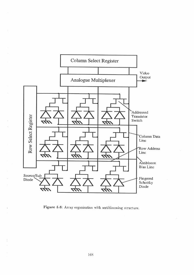
Column Select Register
Analogue Multiplexer
c.)(t)Þo(.)ú()c)o)
V)Èoú,
T T
VideoOutput
sedTransistorSwitch
Line
Line
Data
Address
Source/SubDiode
bloomBias Line
FingeredSchottkyDiode
Figure 5.6: Array organisation with antiblooming structure.
168

5.4.L case 1: The capacitively Bootstrapped shift Register
trig. 5.7 shows an original GaAs shift register with a 2-phase low power dynamic design.Each stage is non-inverting and consists of only 4 non-ratioed enhancement minimum sizecl
MtrSFETs! An MIM capacitor provides bootstrapping action to overcome the thresholdvoltage drop problem for MESFtrT pass transistors. We shall refer to this new logic famiìyas 'non-ratioed bootstrapped logic' (NRBL).
This register was devised and selected because of it's compact design and its ability tofunction with non-overlapping clocks. Non-overlapping clocks are a prerequisite of thesynchronous clock transient cancellation scheme [Ohba 80], required to minimise fpn.Notice that the design in Fig. 5.7 also has no dc power busses! The register is entirelydriven by the 2-phase clocks, leading to no static power dissipation and hence a low powerdesign.
oljlpuls:
S€rlal UP
ctk 1
ctk2
Shfü alemnt:
o/P
R6ssl
Pass
D¡schargo
I ctk f ctk2I
Figure õ.7: Shift register with bootstrapped stages
With reference to Fig. 5.7, the circuit operation is as follows. The drain of each enabletransistor is pulsed every c1k 1 period. The output of each shift element remains lorvuntil a high is enabled by the previous stage. When a high appears at the gate of anenable transistor, the output is charged up by the clock pulse. This pulse does not get
I
n
f-cp
169

cut off at a threshold voltag" (V) below the clock amplitude (V"r) due to the action ofthe bootstrap capacitor Ct. C6 pulls up the gate of the enable transistor by Vtoot, holdingit at V,¡¡ i Voot, where
Voot:ffi**and Co is the stray capacitance to ground at the input of each stage. As the outputis charged up to a full Vt*, Vt* - V appears at the gates of the reset transistor andthe following enable transistor via the pass transistor. When C1k 1 starts going low theoutput drops. lVhen the output is2V below V.¡¡,,thereset transistor turns on and resetsthe bootstrap capacitor. This causes the enable transistor to turn off when the outputis at this level. When the next clock phase comes on (ctt 2) the discharge transistorturns on and completes the discharge of the output. (Ar the gate of the pass transistor isnow at a lower potential than its source, the bootstap capacitor of the next stage is notdischarged.) The same cycle repeats for the next stage and so on. The functions of eachof the transistors are summarised as follows,
o Enable transistor: Connects clock to output when enabled by the previous stage
o Reseú ftansistor: Resets bootstrap capacitor
o Pass ttansistor: (a) passes initial current to charge up bootstrap capacitor of nextstage, (b) when output discharges, it turns off so that the bootstrap capcitor of thenext stage does not discharge, (c) provides a threshold voltage drop so that the resettransistor is kept hard off until the output potentil drops.
o Discharge transistor: As the enable transistor turns off before the output settles,the discharge transistor provides the output with a conduction path to ground inthe alternate clock cycle.
As can be seen in Fig. 5.7, extra transistors are reqired at the input and output endsof the shift register. These are required, respectivel¡ to clock the serial input pulse inand to discharge the last bootstrap capacitor, which would otherwise remain permanentlycharged. A significant advantage of this type of register, is that the output scan pulseshave exactly the same amplitude and width as the clock pulses, giving a considerabledegree of external control over the operation of the Xy array.
The power dissipated by the shift registers is due to the charging and discharging of thecapacitance that each stage drives, C¿. As only one stage is active at any one time, the
170
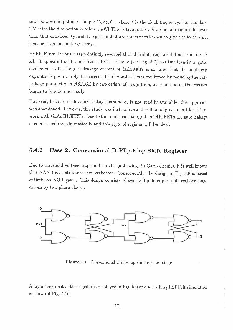
total power dissipation is simply CtV,'u,f - where / is the clock frequency. For standardTV rates the dissipation is below 1 pW! This is favourably 5-6 orders of magnitude lowerthan that of ratioed-type shift registers that are sometimes known to give rise to thermalheating problems in large arrays.
HSPICE simulations disappointingly revealed that this shift register did not function atall. It appears that because each shift in node (see Fig. 5.7) has two transistor gates
connected to it, the gate leakage current of MESFETs is so large that the bootstrapcapacitor is prematurely discharged. This hypothesis was confirmed by reducing the gateleakage parameter in HSPICE by two orders of magnitude, at which point the registerbegan to function normally.
However, because such a low leakage parameter is not readily available, this approachwas abandoned. However, this study was instructive and will be of great merit for futurework with GaAs HIGFETs. Due to the semi-insulating gate of HIGFETs the gate leakagecurrent is reduced dramatically and this style of register will be ideal.
5.4.2 Case 2: Conventional D Flip-Flop Shift Register
Due to threshold voltage drops and small signal swings in GaAs circuits, it is well knownthat NAND gate structures are verbotten. Consequently, the design in Fig. 5.8 is basedentirely on NOR gates. This design consists of two D flip-flops per shift register stagedriven by two-phase clocks.
D
ctk 1
o
Figure 5.8: Conventional D flip-flop shift register stage
A layout segment of the register is displayed in Fig. 5.9 and a working HSPICE simulationis shown if Fig. 5.i0.
ctk 2
17I

Figure 5.9: conventional D flip-flop shift register layout segment
172
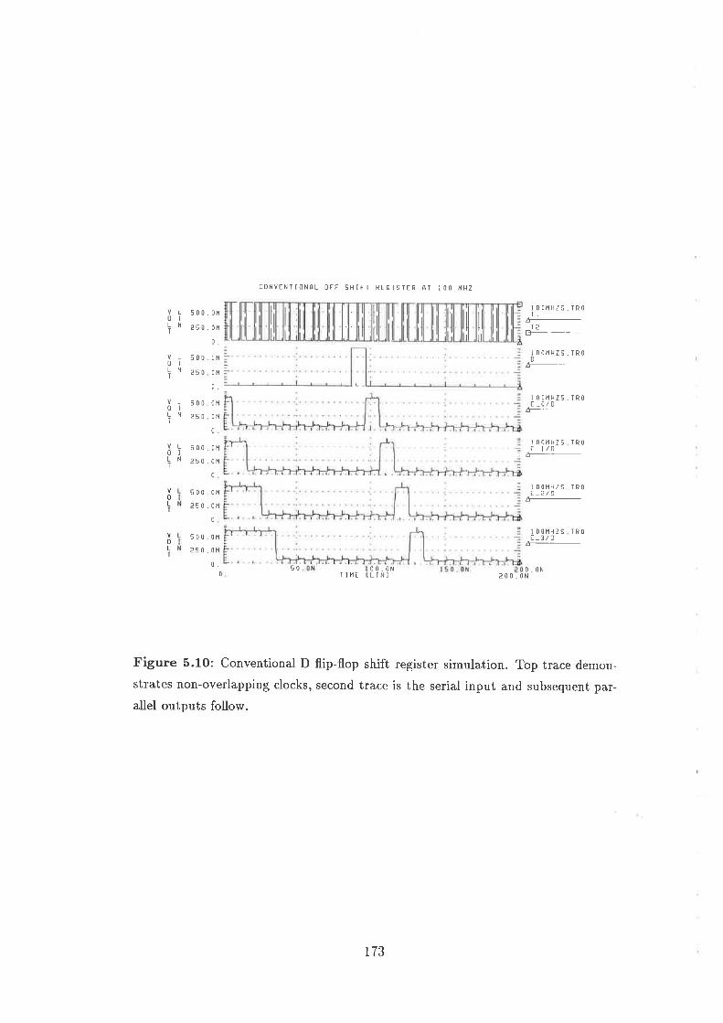
I
I I lill, ill0tLNT
OILNT
VL0tLNf
VLOILNI
500_0M
250.0r4
0.
500,0¡,r
25 0 0r,!
0,
500 0M
250 0fr
0
500,0M250.0r{
0
500.0r.r
250.0H0
500 0t1
250.0H
0,0
CONVENTIONAL OFF SHIFI REGISTER AT IO() MHZ
50
t00r1HZs.TR0TLÂ-I2
t00¡1Hzs.TR0DÁ-
0LT
0LT
:Â--
I Ot)MHZS TR()E_0,/0ß--
t 00t1Hzs TR0E_t/o
100¡tHzs TR0t_2/oÈ-
I O()MHZS TR()t_3/oL-
0 0 , 0NLIN)TIME0.0N
200 _ 0N
Figure 5.10: Conventional D flip-flop shift register simulation. Top trace demon-strates non-overlapping clocks, second trace is the serial input and subsequent par-allel outputs follow.
173

5-4-3 case 3: Edge Tbiggered D Flip-Flop shift Register
Although Case 2 was found to work adequately, a NOR gate implementation using edgetriggered flip-flops was investigated, in search of a more area efficient design. Fig. b.11shows that only a single flip-flop is required per register stage, whereas two flip-flopswere required in Fig. 5.8, thus yielding an area saving. As will be shown later, anotheradvantage is a dramatic power saving. Fig.5.12 shows an example layout segment. Al-though Case 3 has a number of merits over Case 2, the main drawback of this approachwas that the edge triggered design did not function with non-overlapping clocks. Conse-quently, Case 3 was abandoned, but is presented here as an example of a real 'dead-end'encountered, that may be useful in other digital applications.
ctk 1
ctk 2o
D
Figure 5.11: Edge triggered D flip-flop shift register stage
5.4.4 Register Comparison
Table 5.1 suminarises the performance differences between our three case studies andcompares them with three other designs available in the literature - Toshiba [Kikaura 88],OKI [Mori 88] and CMA [Sarmiento 92]. The first point to note is that the max. speedfigures for our designs our irrelevant due to the low speed TV rates in our application. Ourdesigns are therefore optimised for power and area, whereas the designs from the literatureare clearly optimised for speed. Nevertheless the power per clock frequency (mW/MHz)is favourably low compared to the examples from the literature. Although our Case 1
and Case 3 have been abandoned for the present work, they may have valid applicationin other contexts. Case 3 has been rejected as it does not operate with non-overlappingclocks- The problem of Case 1 not working, due to gate leakage current, can be solved by
174

Figure 5.12: Edge triggered D flip-flop shift register layout segment
ase ase aMax. speed (G 0.5
144501
DCFL
0.88360
1
DCFL
2.480294
2SLCF
r.220557
1
DCF'L/SBFL
0.00472
r.21 1000
1
DCFL
Area/stag. (p^,)No. of pwr suppliesLogic type
mW/MHz 0.01?
0.00320
22000 (!)
NRBL
Transistors S
small4
0.00324
0.000915
Table 5'1: Performance comparison of shift registers. Notice Case I has no powersupplies as it is powered via the clocks
175
a move to the GaAs HIGFtrT technology. In the present context, Case 2 is recommendedas being functional and of adequate performance for a proof-of-concept imager. Futurework, however, should address HIGFET technology as it becomes increasingly available.
5.5 Column-to-video line multiplexer
The multipexer comprises a row of simple transistor switches, that connect the columnlines, in turn, to the video line. The switching sequence is controlled by the vertical shiftregsiter that is connected in parallel with the multiplexer. In design, the layout of theindividual switches is optimised to (a) minimise scan pulse feedthrough onto the video lineand (b) minimise the switch on-resistance. These requirements are considered in turn:
a Feedthrough
Feedthrough results from gate charge (Qn) being drawn from and dumped on the videoline as the multiplexer transistors turn on and off. Variations in this charge, A,Qn, giverise to fpn and this can be expressed as,
LQ s : A,Cn(Vt* - U - V") + Cn(LI%,o - LU).
Thus, fpn can be reduced by minimising the clock amplitude V.¡¡ and,maximising the videoIine bias I/, in operation - where I{ is the threshold voltage. Minimum sized transistorscan be used to minimise the gate capacitance Cn.
(b) On-resistance
The transistor switches have to be minimum sized to satisfy requirement (a). Conse-quently, this results in an on-resistance of -R : 2 kfl. The limit that the resultant r?C,time constant imposes on the signal read out time (f,) must be calculated. The differentialequation that describes the equivalent circuit in Fig. 5.13 is,
drv *Í r -L 1 _ 1 .,.
dt2'tcuï'C"Rn C.RrdVVdt C"C.RR¿
0
With appropriate boundary conditions, a solution can be approximated [Kioke 80] byputting C" > C. giving,
RC"R.;C"
to: RC,ln{(1 - ?)(t - ))
where 4 is the fraction of signal charge read out in úo seconds. Taking C. :5 pF andÆ¿ :500 Q, T : 99To and Cu:50 pF as severest estimates gives úo:100 ns. This impliesthat all column lines can be favourably read out in less than a standard line time.
176

RR
Mux transistoron-resistancec c
Head amplifierinput resistance
c vColumncapacitance
Video linecapacitance
Figure 5.13: Column-to-video line switching: equivalent circuit
5.6 Summary
In this chapter we have defined a suitable imager array architecture. A passiue pixelapproach has been analysed showing that the internal photodiod e RC time constants(even on semi-insulating GaAs) are fortunately fast enough for operation at standardTV rates. Two possible pixel layouts were proposed: (1) simply the diode formed bya transistors' source-to-substrate junction and (2) as before but with 'fingers' of gatecontact across the surface of the diode - the fingers serve as antiblooming lines but at theexpense of pixel fill-factor. The realisation that method ( 1) can operate on an SI substrateis an original contribution and so is the structure of (2) which conceptually reduces to asource-substrate diode in parallel with a gate diode. Either of these two pixel designs canbe simply stepped into a 128 by 128 array for realisation of a working imager.
A number of approaches for array addressing and readout were discussed and rejected.Because of problems with gate leakage currents and the system requirement for non-overlapping clocks, the D flip-flop shift register design is recommended. Over an orderof magnitude saving in power is demonstrated by an edge-triggered shift register design
- although shown unsuitable for the imager, this result will be useful for future digitalprocessingf blocks.
An new GaAs logic family which we call NRBL was proposed, for the first time, but thissuffered from MESFET gate leakage currents. Future use in HIGFET circuits is highlyrecommended.
Finally multiplexer switches, for column-to-video line parallel/serial readout, were anal-ysed. It was deemed that single minimum size transistors gave the lowest feedthrough
177

noise and were sufficiently fast for TV rates.
Having cleated a tailored design for the imager, in the next chapter we turn to examininga GaAs design methodology for general digital circuits - for future integration of digitalplocessing elements with the imager.
178

Bibliography
t79

[George 89]
[Kikaura 88]
[Kioke 80]
[Mori 88]
[Ohba s0]
[Sarmiento 92]
P. George et al., "Modelling the substrate depletion region for. Ga,As
FtrTs fabricated on semi-insulating substrates," Solid-State Elec-tronics, vol. 32, no.2, pp. 165-168, 1989.
Y. Kikaura et al, "A.2 Gb/s GaAs i28-bit shift register using stan-dard cells with 0.5 um WNx gate MESFETs," IEEE GaAs IC Sym-posium, Nashville, Nov. 6-9, 1988, pp. IZT-IJ}.
N. Kioke, *MOS area sensor: Part I," IEEE Trans., ED, vol. ED-27,, no. 8, 1980.
H. Mori et al, "A. I.2 GHz high-speed 256-bit shift register LSI,,'IEEE GaAs IC Sytmposium, Nashville, Nov. 6-g, 1988, pp. 13b-139.
S. Ohba et al, *MOS area sensor:
vol. ED-27, no. 8, 1980.
Part II," IEEE Trans., ED,
R. Sarmiento et al, "High speed primitives of hardware acceleratorsfor DSP in GaAs technology," IEE Proc. G,vol.1Bg, no. 2, lgg2,pp. 205-216.
180

Chapter 6
Design Methodology
"There is nothing rnore difficult to talce in hand, n'ùore peri,lous to conduct,or rnore uncerta'in in its I'trccess, than to talce the lead in the introductionof a new order of things."Niccolò Machiavelli (1469-L527)ITALIAN WRITER AND STATESMAN
181

6.1 Introduction
Advances in the development of digital GaAs integrated circuits have progressed to thepoint that designers of signal and data processors can discern the system applications forwhich GaAs is best suited. Basic computation primitives in DSP and image processingsystems are usually adders, multipliers and delay elements. In this chapter we presentthe results of a systematic study conducted to evaluate the influence of layout and de-sign methodologies, both conventional and innovative ones, on the performance of digitalcomputation primitives.
There is increasing demand for higher speed and lower power consumption in digitalsignal and image processors, due to very large throughput rates and vast amounts ofdata necessary for real time performance. It would appear that much could be gainedby implementing both the image and signal processing algorithms with high speed digitalgallium arsenide.
The choice of architecture, and indeed the choice of algorithm, is crucial to the perfor-manceof the signal processing systems [Gilbert 87]. The architectureis influenced by thewell known design criteria for VLSI and in the case of gallium arsenide these criteria aremore stringent. The designs for arithmetic and logic units in signal and data processorshave to be reexamined in view of the strengths and constraints of GaAs devices.
CMOS-VLSI implementations of fixed precision and floating point arithmetic usually haveemployed as many logic gates as necessary to construct the function, because there is notmajor cost penalty for the use of large number of gates; however there are constraintsimposed on the speed of this gates. Conversely, GaAs gates are much faster but moreexpensive at the current levels of complexity.
These tradeoffs favour single and well structured arithmetic implementations. This simplyimplies that the design must be highly regular with simple data and control paths, andlocal or minimum interconnections. It may also be possible to recast some arithmeticalgorithms, which are recursive in nature, into iterative implementations, re-using gatesagain and again to execute a more simple arithmetic function.
Pipelining of arithmetic structures to increase throughput should be exploited wheneverpossible, since the addition of perhaps only 10-20% additional gates in the form of pipelin-ing registers can enhance throughput for GaAs logic families, which can support the higherclock rates.
The design methodology for each class of logic together with the layout approach becomescritical as clock speed increases. The problem manifests itself in the form of signal skew
r82

where there is a delay between arrival times of a given signal at two different destinations,and crosstalk which manifests as noise on buses.
Since basic computational primitives in DSP and image processing systems are usuallyadders, multipliers and delay elements, in this segment of research we have explored theinfluence of layout and design methodology on the performance of these modules forDCFL (Direct Coupled FET Logic) and SDCFL (Source-follower Direct Coupled FETLogic) classes of logic.
6.1.1 Technology
Gallium arsenide circuits built using DCFL logic implement the set of func-tions {NOR,NOT}, whereas SDCFL implements the augmented set {NOR,NOR-oR,NoT,NoT-oRÌ. The output from two SDCFL buffer stages (shown inFigs. 6.2b, 6.2d) be connected to produce a wired-OR function.
From a layout point of view, DCFL is the most compact GaAs logic and most suited tohigh performance VLSI systems. This class of logic uses depletion type and enhancementFtrTs in much the same manner as they are used in traditional nMOS Silicon technologywhere the ratio rule, which determine the device size, applies (Fig. 6.3).
One disadvantage, however, is the limited output voltage swing, which is due to limitedbarrier height of the Schottky diode gate and results in small noise margins (less than100 mV). DCFL gates have also a weak load drive capability which influence the gatedelay as fan-in, and fan-out, ate increased. A further point that needs to be taken intoconsideration is the switching point of a DCFL gate which has a negative temperaturecoefficient which varies in the range -0.4 to -0.6 mV/C.
In order to overcome the complexities with small noise-margins, fan-out limitations, andthe ability to compensate for temperature variations, the SDCFL structure, which issimply DCFL gate followed by a source follower (Fig. 6.a), is considered as the basicprimitive for realisation of computational subcircuits. SDCFL is fully compatible withDCFL.
Since the threshold voltage increases at the same time as channel conductance (these aretwo parameters that dictate the temperature behaviour) by "tuning" the process it ispossible to compensate the net effect of temperature on drain current and realise SDCFLstructures which have good tolerance to temperature variations.
A negative power supply (-%") for the pulldown of the buffer stage ensures that whenthe buffer tr-MESFET transistor is off the output low level can be made more negative
183

vdd
vin
gnd
r{
vdd
V ln5
gnd
*{l+vln2
vddl
vin ¡lgnd
vdd I
NoR oôte I nverter
Figure 6.1: DCFL logic gatesvü2
vin ¡l
Vss
lnverter input slæ Buffer stæe
v&2
Vin t+l þvin2
vintll--vinz
qnd Vss
NoR oste_innut stdE OR oô1e bulfer slaopFigure 6.2: SDCFL logi¿ gates
so that the following DCFL logic gate is fully off. Furthermore it provides for isolation oflogic GND path from those of the buffer.
6.L.2 Parasitic Oscillations
Parasitic oscillations in GaAs MESFETs are not clearly discussed in the literature andthus we shall briefly describe this effect. It is the early study of this effect that inspiredthe development of the "Ring Notation" Iayout style that we shall introduce in the nextsection.
During early studies, it was found that if a curve tracer was used to plot the I-V char-
184

Q1DFET
out
lñj In¡
Figure 6.3: DCFL inverter circuit
v¿o
B3
EFET
out
ln B¿DFET
Figure 6.4: SDCFL inverter circuit
acteristics of a GaAs MESFET attached by conventional connectors, disastrous resultsoccurred. An example photograph of the curve tracer screen is shown in Fig. 6.5, where itcan be seen that there is a region with negative slope. This indicates negative resistanceand hence indicates that oscillations are taking place. This is a good example of what istermed parasitic oscillations in GaAs MESFETs. The low nodal capacitances of the MtrS-FET are of the order that a resonant circuit is formed with the parasitic capacitances andinductances of the conventional wire connectors. This in conjunction with the drain-gatecapacitance providing feedback and high gain, inevitably produces an unwanted oscillator.This is not a problem particular to gallium arsenide, but is inherent for usually any veryhigh speed device.
Hence, care must be taken to keep connections extremely short, using carefully terminatedtransmission lines on printed boards. For transistor measurements, this is not always
possible if the test jig is, say, on a mechanical scanning device. Sometimes conventionalwire connectors cannot be avoided. The solution is to package the transistor with [he(grounded) source pin between the drain and gate pins. This serves to reduce the drain-
3ET
oET EF
BlOF ET
82EF ET
185

I
Figure 6.5: Photograph qualitatively showing parasitic oscillations in I-V charac-teristic. Arbitrary axes. Notice region of negative resistance.
gate feedback capacitance. A chip capacitor placed between drain and source can also beused to ensure any resonant oscillations are decoupled and not fed back to the gate. Thisis appropriate for dc measurements but for ac measurements the use of a chip capacitoris not possible. In this case the transistor must be continuously monitored by a spectrumanalvser for oscillations and the resonance can be detuned by moving the orientation ofthe connecting wires by trial and error. This is not good practice, but is used when thereis no alternative, and is reported eg. [Golio 90], with successful results.
It was the realisation that drain can be screened from the gate by the source connec-tion, giving better results, that inspired the development of *Ring Notation.,, The keyelement of Ring Notation is that address busses (gates) are screened from V¿¿ powerbusses (drains) by ground busses (sources). This has the effect of reducing clrain-gatecapacitances throughout the whole VLSI layout and desirably increasing the ctrain-sourcecapacitance (ie. decoupting)' As we shall see in the following sections, another aclvan-tage is that more compact layouts can be achieved this way - which also res.lts in lorverpropagation delay.
6.1.3 Layout Approaches
'['her large banclwiclth requirement of high speecl signals (- 3 GHz) procluces the f.ollorvingproblerrrs
rE6

o crosstalk from high speed signal lines is increased
o inductive spikes due to current transients cause spurious noise voltages on busses
o reflection from unmatched impedances on long interconnects degrade rise times
o distortions occur due to transmission line effects
These problems can be reduced or minimised through layout considerations
Figure 6.6: Layout styles: nMOS-type stick approach
As the basis of layout, two alternative styles have been used in this study. The first methodis the conventional approach used by Silicon designers where *Voo bus is located at thetop with the GND bus being located in the bottom of the layout. The circuit is thenplaced in-between these two rails (Fig. 6.6).
In order to reduce coupling between the fast signal lines and the power bus and further-more to optimise the interconnections between circuits, a second approach, referred toas Ring Notation [Eshraghian 96], is adopted for comparisons. In "Ring" approach theGND bus is placed between the circuit and the +VDD bus as illustrated in Fig. 6.7(a).A second option for layout which uses "Ring" convention, and which provides for betterpacking density, is also illustrated (b).
In the "Ring Notation" as shown in Fig. 6.8(a), the dotted line (GREEN) represents theE-MESFET while the solid line (YELLOW) represents the D-MESFET. The approach isvery much in-line with the colour coding used to differentiate between different layers inSilicon technology. Another rule which is implicit is that (GREEN) and (YELLOW) areconnected only through either Metal 1 or Metal 2 (BLUE). Thus representation of thisconnection can be removed from layout at this level of abstraction (Fig. 6.8(b)).
In this class of logic, due to degradation of performance, we restrict ourselves to parallelbranches in the input path, ie. NOR gates only, then representation of NOR gates can
vdd
G.o
187

VDO
CtO
crû
VDO
c*o
Gl.O
vtD
(a ) (b)
Figure 6.7: Layout styles (a) Ring Notation using dual bus pair, (b) Ring Notationusing single bus pair
+VddG}ID
oVddct¡D
ln
(ô) (b)
Figure 6.8: Ring Notation showing topology of circuit
further be simplified by eliminating the parallel branches of the input paths. Fig. 6.9shows the process.
Translation from Ring to symbolic and hence to mask is rather straight forward. Whatbecomes important in the Ring Notation, as an intermediate method of describing alayout, is that signal paths can be highlighted and the interconnect strategy formulated,before translation into a layout commences. Using this methodology complex structurescan readily be mapped. One such case is the D-type latch where the structure is realisedby reflection of half the logic gate about the x-axis (Fig. 6.10).
Once a design has been drawn in ring notation, interconnect paths may be optimisedto create electrical symmetry and so minimise signal skew between critical paths. Thisis particularly important in the distribution of clock signals across a chip. An electricalequivalence in the form of a data flow diagram shows connectivity between cells or gates.A weight on each link describes its delay characteristic as a function of geometric length,width' adjacency (coupling), fan-in and fan-out. Geometric symmetry does not neces-
188

.YddGl¡D
.YddGND
(a) (b)
Figure 6.9: Ring Notation for 2-Input NoR gate, (a) initiat representation, (b)after simplification
c
vddGNO
D
.K
õ
q0
CK
o
ola) LoBrc di¿grânú
vddGNO
(c) Rrog ootatroo
(b) trmroe
(d) layou!Mask layout for a D-Latch
sarily imply electrical symmetry but by adjusting the aspect ratio of the layout, someoptimisations may be possible.
6.1.3.1 Symbolic mask level layout
The gallium arsenide process layers are very complex, and inhibit the visualisation of allthe mask levels used in the actual fabrication process. An approach has been developedin which both layer and topology information may be simply represented to the designer.Mask layers derived from the foundry specification are abstracted to a manageable num-ber of layout levels to hide unnecessary layer complexity. Colour coding and symbolicrepresentation greatly assist in interpreting gallium arsenide circuits, while allowing theVLSI designer to concentrate on more fundamental aspects of UHS VLSI design such as
routing and optimisation of interconnection paths. The colour scheme, layer names andCIF codes adopted for gallium arsenide are shown in Table 6.1.
c(
riM)v6
Figure 6.10: Translation from Ring Notation into
DAIA CLOCK On On+l0
0I1 l-
0I0I
0
0
I1
189

Layer Colour Symbolic CIF Code Comments
Diffusion *Shallown-
nplus
n*mask
MetallMetal2Contact
VialSymcap
Overglass
GreenRed
Yellow
Orange
BluePurpleBlackGrey
BrownCyan
ImplantE-transistor
nf implant
n*
MetallMetal2Contact
VialMIM
GDGP
GI
GJ
GMGNGCGVGYGG
active area, outside is substratecreates the shallown- channelfor the enhancement device
outside yellow, nf implant takesplace, for MESFET's only
inside, n* implant takes place,for diodes only
first level interconnectsecond level metal interconnect
diffusion to metall contactmetall to metal2 connection
inside is MIM capacitor
Table 6.1: Gallium Arsenide Symbolic Representation and Notations
* This layer is an implant region, but the terrn d,iffusion has been used, to be consistentwith nMOS and CMOS notation that many silicon d,esigners are familiar with.
Design rules are described on a Lambda-based grid while fine detail (micron-based rules)is embedded within the predefined objects and is hidden from the designer.
6.1.3.2 Practical constraints
The gallium arsenide lattice structure exhibits different conductance in different planes.To ensure a uniform transconductance between devices, it is required that all MESFETgates be laid out in the horizontal direction. Design rules dictate the minimum size andspacing of the geometric features in a layout to ensure a reasonable yield will be obtained.A trade off exists between performance and yield for a given chip size. The trend istowards the use of minimum design rules to maximise speed at the expense of yield. Evenwith this trend, the integration level of gallium arsenide is generally lower than silicontechnologies, typically around 3000 devices per square millimetre as opposed to a 0.g¡rm CMOS process with up to 8000 devices per square millimetre. The ratio of pull-upto pull-down device width is determined by maximising the noise margins, whereas theactual width is determined by gate delay.
Logic family implementation constraints which must be met to ensure successful highspeed operation of the circuit include fan-in and fan-out. The fan-in of a gate should be
190

limited to 3, and is preferably 2 since the output high level of the input stage is degradedas fan-in is increased. The fan-out of a gate, which is characterised in terms of the numberof driven gate capacitances and the total interconnect capacitance, is limited to 2 and theinterconnect lengths which contribute parasitic capacity must be minimised.
Most gallium arsenide processes contain either two or three layer metal interconnect. Theupper metal layers have lower parasitic and coupling capacitances due to the dielectricstructure and the wire pitch. These layers are therefore preferred for signals where signalskew is to be minimised. Coupling between power supply busses and fast interconnectson any metal layer can be minimised by the use of additional ground wires.
Separate power busses for buffers and logic gates reduce the noise induced by switchingtransients.
6.1.3.3 CAD tools
The gallium arsenide VLSI design suite provides a complete design environment. It in-cludes graphical layout of full custom chips using a library of predefined objects, designrule checking, network and parameter extraction and provides an interface to both func-tional and analogue circuit simulators. The design process is shown in Fig. 6.11 IISD 83].It consists of the following software tools:
PLAN a graphics editor for VLSI design for which technology files and a predefined ob-jects library have been written for gallium arsenide implementing the design method-ology presented in section 3.2.
CHtrCK a fast corner based design rule checker. The abstracted design rules are derivedfrom the foundry rules and are used to verify circuit topology.
SEE a general purpose geometric display tool which shows a fully instantiated circuiton a variety of plotting devices.
GAASNET a gallium arsenide network extractor and circuit verification tool which ex-tracts devices and circuit parameters from the CIF level description. Emphasiswas placed on the accuracy of circuit extraction so that tightly toleranced de-
signs could be realised. An interface is provided to various circuit simulators such
as PSPICE [Microsim 90], SPICE [Quarles 89] and functional simulators such as
THOR [Standford 86].
Technology independence allorvs multiple foundries and processes to be targeted
191

co¡ætPt
Figure 6.11: Gallium arsenide design process using CAD tools
6.1.3.4 Modelling of gallium arsenide circuits
Accurate modelling of gallium arsenide devices is critical in determining if a circuit willwork. In very high speed and ultra high speed systems, logic circuits respond to repet-itive signals and pulses that have periods similar to their propagation delay times. Themodelling of these circuits may be done in two parts:
o device modelling of MESFET's, resistors and schottky diodes
o interconnect modelling
Device models have been well characterised. The models employed are the Curtice[Curtice 80] and Statz models [Statz 87] combined with subthreshold models [Chang g7,
Conger 88] to model MESFET operation in all regions [Chen 90]. Inaccurate noise mar-gins may be obtained if leakage current in the subthreshold region is not considered as itdegrades the output voltage swing. The parameters for the models are obtained by mea-surement at the frequencies of interest (typically 1 GHz) due to the non-linear frequencybehaviour of MESFET's.
Interconnect modelling for gallium arsenide is not well characterised due to the impedancebeing a non-linear function of:
o distance to ground plane
. overcrossing capacitance of metal of different layers
CHECK OAASNEI
DæU¡lENIAIION
r92

o coplanar fringing capacitance
o geometry
The series resistance of an interconnect is around a5 mf-l/¿lm for 2 p^ wide first layermetal. Therefore the impedance of an interconnect is mostly made up of capacitance tothe ground plane and adjacent interconnects.
The rise time of a signal emerging from a gate is around 50 ps, if we choose an upperbound of 10 GHz for the bandwidth requirement and the velocity of propagation of asignal is 110 pllr,lps, the wavelength is then 11 mm. For a transmission line approach tobe appropriate, the length of the line needs to be at least a quarter wavelength long, 2.7bmm. The use of transmission line or stripline models is only required for interconnectlengths which approach this figure. Most interconnects are much less than 2.75 mmlong. It should also be noted that stripline models are not likety to be appropriate sincethe substrate thickness to the ground plane (- 600 ¡rm) is two orders of magnitudelarger than the line width. Short interconnects (( 2.75 mm) are modelled simply as alumped capacitance which represents the total distributed capacitance of an interconnect.The GHz frequencies dictate that some longer signal paths cannot be treated simply as
lumped elements but as a transmission line terminated by a capacitance (mostly the gate-source capacitance of an enhancement MESFET.) We can model long interconnects as
unterminated transmission lines which have a reflection coefficient of unity at the end ofthe line. The length of the line must be constrained by:
lensth u,*ï*
where r,¿"" is the rise time of a signal and r.pa is the propagation delay per unit lengthalong the line. The velocit1 V) of a signal along an interconnect is 110 ¡rm/ps. If weinclude a factor of five (r,i,":50 ps, rpd: IlV, :1/110 pm/ps), we have a rule that thelength of an interconnect is less than 550 ¡.1m.
The output impedance of a gate is high compared to the characteristic impedance of theinterconnect [Long 90] (modelled as a transmission line). Therefore a returning signalwill not cause ringing as the reflection coefficient at the source for this signal is much less
than 0.5. This justifies the use of a lumped capacitance model.
6.1.3.5 Interface to fabrication
Interface to the gallium arsenide foundry is through a mask level conversion programwhich produces foundry mask layers from the simplified designers layout.
193

The designer mask layers are a subset of the foundry mask layers which may be translatedat the CIF level by the following operations:
o direct mapping
o bloat factor
o mask inversion
o logical operation of several mask layers
An example is the isolation damage layer between active regions which electr.ically isolatedevices by damaging the surrounding semi-insulating substrate. This layer is derivedfrom the inverted diffusion layer with a 'bloat factor' to account for lateral diffusion ofthe implant during processing.
6.L.4 Performance Study
Using the approaches shown in Fig. 6.6 and Fig. 6.7, a set of 8 bit and 16 bit addersand 8 bit multipliers were designed and their performance compared. Although severaloptions were available to compare the performance of the different circuits and layouts,the approach that was adopted for the basis of our initial comparison defined a Figure ofMerit or a performance indicator (Pn,a) in terms of number of gates ly', maximum clockingfrequency of the circuit, and utilisation area, given by:
D. _ Nsot"r* f*o,n-- Ar"o
where Nsaks is the number of gates and f^o, is the maximum clock frequency. This givesus a measure of computational density as gate-GHzf mm2.
6.1.4.1 Adders
GaAs/Silicon differences (transistor count per chip as well as gate fanin and fanout) affectthe choice of adders in a number of ways. Traditionally, the full carry look-ahead adder hasbeen preferred for high speed applications, and ripple -carry adders have been discountedfor all but the shortest word length.
Further evaluation of the adders show that the fastest adder in Silicon is not necessarilythe fastest in GaAs technology (because of the fastest Si adder is based on high fanin anclfanout capability, and GaAs technology is intolerant to high fanin and fanout).
194

Several adder architectures are available for GaAs technologies, ranging from high-speed,large area Binary-Carry-Lookahead adder to the low-speed, small area ripple carry adder.Other architectures having speed and resource requirements between these two extremesinclude Carry Look-Ahead and Carry-Select adders. Several versions of each architecturehave been designed. In turn, each logic alternative has been implemented with differentlayout styles (Figs. 6.6 and 6.7). The aim is to study the different architectures as wellas the layout techniques best suited for GaAs logic families.
Ripple Carry Adders
Table 6.2 summarises HSPICE simulations results of several ripple carry adders. Theripple carry adders have been designed with exclusive OR gates, taking advantage of theNOR-OR structure easily implementable in SDCFL. The adders have been optimised forlow power and area consumption (VLSI applications). The results show that.the RingNotation methodology (FiS. 6.12(b)) produces circuits with higher speed that the nMOStype stick methodology (FiS. 6.12(a)), mainly because of the shortest interconnectionlength of the path. The Ring layout using single bus pair produces circuits with less area,
but slightly slower than Ring layout using dual bus pair.
b
Figure 6.12: 1-bit Ripple Carry layout (a) nMoS type stick and (b) Ring Notation
From designers point of view, Ring Notation methodology is easier to implement than thenMOS type stick approach, allowing easy approach to structured design. Furthermore, itis well suited for symbolic layout.
Carry Look-ahead Adders
The limited fanin and fanout of GaAs gates affects both the area that is needed and theadder delay incurred. Single gates with high fanin and fanout must be implemented as a
series of gates with low fanin and fanout, which increases transistor count. Because delayis highly dependent on load capacitance, high fanout devices have a relatively large delay.
@EÉl
195

S leNo. ofbits
Delay(t.)
Power(-w)
Area(--')
Pind.
8 3.8 83 u.133 269n 16 7.7 169 0.264 133
u 8 3.6 83 0.1 75 216u 16 7.4 169 0.389 95
'Ring' single bus 8 3.7 83 u.150 245'Ring' single bus 77 7.5 r69 0.299 r21
LayoutStyle
No. ofbits
.Delay(t')
Power(-w)
Area(-mt)
P¿nd
US 9 '2.9 80 0.2L1 33716 4.9 r40 0.3tt8 204
e S 9 2.5 80 0.210 392'Rìng' single bus t6 4.7 I20 u.363 302
Table 6.2: Parameters of several ripple carry adders
Table 6.3: Parameters of the carry look-ahead adders
In a tree built in a random fashion this dependence may cause the delay through lrt levelsof high fanout gates to exceed the delay through I/ + t levels of low fanout gates.
The carry expression in a Carry Look-Ahead adder is:
C¿: G¡ * P¡G;-1* P¿P¿-:G;-z t.....+ P;P¿_t.....poCo
Where G¿ : X;YaP¿ : X¿* X. The GaAs implementation of this expression bring abouta critical path with no less gates than a Ripple Carry adder. A suitable implementationusing GaAs is to incorporate n + | cell serially. The carry expression will be divided intwo terms: C a¿ and Có¿. The first one will be fan-out loads between the inputs X¿ and yand their complements l/X; and ,À/{ each cell does the terms generation in an alternatingway with either input type. Fig. 6.18 shows the floorplan for a b bits adder.
Table 6.3 shows the results of the GaAs implementation of the carry look-ahead expres-sions' In this case the single bus layout is faster than the double bus pair since theinter-cell communications are dominant in the critical path. A broad comparison betweenthis adder implementation and the Ripple Carry one, as shown in Fig.6.l4, illustratesthat the former is best suited for GaAs. The Ripple Carry adder implemented with onlytwo-input gates remains too slow, as in the Silicon implementation, and with high are
196

oobo
olql
co¡-t. cell A
%Do
cell B
cu¡-tNql Nbl
cell C
c¡¡ -roz b2
cell B cu¡-tNo3 No3
cell Co, co -r
cell D
02b2
NLrn
N5o
NSr
NSz
NS¡
N5o
NCout
q3
b3
o1
b,
o5
bs
Figure 6.13: Floorplan of the GaAs implementation of carry look-ahead expressions
factore
- Qtple Côrry
...... Ctr'1 loot-rtÞad
õE
tE
3
o oó o I o rõ o.2 0.26 o.3 o 36 O.aArea (mm2)
Figure 6.14: Area vs. delay of Ripple Carry and Carry Look-Ahead adders
Binary Carry Look-ahead Adders
The Binary Carry Look-ahead, sometimes called Brent & Kung adder, is based on thecarry generation (G;) and carry propagation (P,) functions [Brent 83]. The main advan-tages of this adder implementation when used in GaAs technology is that it uses onlytwo-point gates and the fan-out is extremely low. Fig. 6.15 represents the block diagramof an 8-bit Brent & Kung adder. The gp cells generate the G¿ and P¿ functions and theout cells provides the add operation. The carry generation block is a tree with two celltypes: the processors (proca and procb)and the inverter-bufer cell (intera and interb).
Table 6.3 shows the results of the HSPICE simulations for the adder. As expected thedouble bus pair is slightly faster than single bus pair realisations, although with higherarea utilisation factor.
The difference in transistor count limits the complexity of any adder that is going to beimplemented as part of a processor. Fig. 6.16 shows the relationship between the number
r97

9P BLOCK
øoc0 Þroca præ0 p.ocö
procb procb
pr ocô
pro<a procà DrO(ô
SIÀ,t BLOCK
sr s? S¡l 55 56
Figure 6.15: Block diagram of Binary carry look-ahead adders
LayoutStyle
No. ofbits
Delay(nr)
Power(*w)
Area(m-')
P;nd
'Ring'dual bus 8 1.3 92 0.466 5I0l6 1.7 278 L.T42 382
US 8 r.4 92 0.434 5U7'Ring'single bui i6 1.8 218 1.078 381
Table 6.4: Parameters of the binary carry look-ahead adders
of bits and the B factor, where
B _ no.bits(delay * area)
Although the Brent & Kung adder is the fastest of the approaches pursued, the area maybe too high for GaAs VLSI implementations. Therefore it is necessary to further optimisethe Brent & Kung layout (ie. not using a celr concatenation).
6.1.4.2 Multipliers
Similar tradeoffs occur in the design of multipliers and other arithmetic and DSp subsys-tems' A variety of architectures are suitable for GaAs designs. The speed advantage ofGaAs gives fast multipliers using straight forward parallel architectures. It is possible toimplement inherently faster architectures.
On the other hand, bit-serial architectures present two keys advantages: Firstly, bit serialnetworks are easily routed on-chip without the problems of bit-serial busing. Secondly,all signals entering and leaving the chip do so via single pins.
198

- Rþoþ côrry
- c6rÌ, bot-6heôd
--... tent&Kung
{ rl¡roe. ol ons 16
Figure 6.16: Compari,sqn of different adders
Table 6.5: Parameters of several adders.
We have implemented two kind of parallel multiplier architectures: Booth and Baugh andWooley; a serial multiplier and a serial/parallel multiplier.
Parallel multipliers
Table 6.5 shows the results of the 8*8 bit parallel multipliers designed. Booth multiplierhave been designed with different adder types for the final sum stage. Using a Brent andKung adder it can multiply two 8-bit operated in 5.4 ns. Then, use of fast adders to formthe final sum eliminates many delays.
A comparison of this realisation with the GaAs Booth multiplier implementation in[Singh 90] shows the latter has a delay of 3.2 ns, with a power consumption of 510 mW andarea occupation of 2.18 mm2. The computed P;n¿ for it is 101 gate-GEzf mmz. Our designdemands less than a half power and area. The Baugh-Wooley algorithm is for multiplica-tion of signed operands. It is inherently faster and power hungry than Booth algorithm.Fig. 6.17 represent the computational density of the parallel multipliers designed. Thedata obtained from reference [Singh 90] has been added for comparison purposes.
Serial and serial/parallel multiplier
30
?8
?6
24
22
?0
l8l6f{12
t0
I5
4
ß
LayoutStvle
Delay(t r)
Power(mw)
Area(--')
P;n¿
Booth/RC 7.4 255 t.542 95Booth/CLA 6.4 252 r.550 116Booth/B&K 5.4 2.67 I.EzU rzb
tsaugh/Wooley 5.3 279 1.970 111
199

r{0
r20
r00
80
60
10
20
0
Ðco
E No. of blts 6
Figure 6.17: Computational density of parallel multipliers
On a broad comparison between bit-serial and bit-parallel operators assuming a commonclock rate, we expect the serial part to process one word every N clock ticks comparedwith one clock tick in the parallel part, but to contain only l/Nth of the hardware (onefull adder cell opposed to NH in the case of an adder). Gi.ven a common clock rate andtechnology base for both implementations we would expect them to be broadly equivalentin terms of an area-time measure. The condition of a common clock rate may not holdhowever, since tight bit-level pipelining of the serial system should permit a shorter clockperiod than for the (non pipelined) parallel system, whose clock period must reflect anallowance for carry propagation in the multiply and add elements. This would be reflectedin a reduction of the chip devoted to the arithmetic processes in the bit serial part.
However, the GaAs implementation of serial multipliers have a significant problem theshift register must be implemented with static logic, with an area consumption by bitsimilar to a full adder. Whereas a parallel multiplier needs about N*N full adders, aserial multiplier needs two N-bit shift registers (parallel-in serial-out), a full adder withlatch and a 2N shift register (serial-in parallel-out). This means about 3N+2 equivalentfull adders.
The serial multiplier designed runs at 1 GHz clock rate, producing a delay of 64 ns, witha power consumption lesser than 100 mW. In order to avoid glitches in the circuit theshift register with parallel inputs switching at 1 GHz has been designed with electricallyequivalent path as shown in Fig. 6.i8.
In order to decrease the processing time a serial/parallel multiplier could be used. Thearea consumption of such an 8x8-bit multiplier is 0.92 mm2 and the delay incurred is 16ns.
820
200

Lôtch
o o
oo
r.rt rr ri..t.ll.¡rar rrt..,t
SrtSI
sf
EN
0t
5r. t
õi
s77 s,
ct (
Figure 6.18: Shift register bit-slice (a) diagram, (b) simulation
6.2 Summary
A detailed discussion of parasitic oscillations is lacking in the literature. A careful dis-cussion of the cause of this effect, leading to the realisation that optimal bus layout isachieved when ground busses are interposed between address and power busses was pre-sented as an important original contribution. It is this key paradigm-shift from the oldnMOS bus style, that lead to the systemised "Ring Notation" developed by Eshraghian.
The early work described in this chapter can now be greatly improved upon, as new GaAsprocesses have recently emerged such as CGaAstt and HGaAs IV, promising greaterspeeds and much lower power dissipation. Also since this work was carried out, a 'modi-fied Ring Notation' approach has been developed that uses vertically stacked transistorswith shared source/drains [Cui 95]. This produces upto a factor of 2 saving in area. Nev-ertheless, the early work, presented here, was a stepping stone which established that theRing Notation layout methodology was capable of saving area and reducing propagationdelay.
In the next chapter we now proceed to apply this methodology in a case study designof a polynomial evaluator. This evaluator is an example of a useful circuit that canbe integrated with the image sensor to achieve our aim for a GaAs smart sensor withhigh-speed processing.
20r

202

Bibliography
203

[Brent 83]
[Chen 90]
[Conger 88]
[Cui e5]
[Curtice 80]
[Eshraghian 96]
[Gilbert 87]
[Golio 90]
lrsD s8l
[Lons 90]
[Microsim 90]
IQuarles 89]
[Rouger 85]
R-P. Brent and H.T. Kung, "A Regular Layout for parallel Adders,"IEEE Trans. Computers, vol. 16, no. 72, pp.41_5g, 1gg3.
Y.D. chen and A. Beaumont-smith, "Evaluation of gallium arsenidesubthreshold MBSFtrT models," Technicar Report GAAS-\T-4, TheUniversity of Adelaide, November 19g0.
J. conger, A. Peczalski, and M.s. shur, "subthreshold currentin GaAs MESFET's," IEEE Electron Device Lett., vol. g, no. 3,Mar. 1988.
s. cui et al, "A 32-bit GaAs IEEE floating point multiplier usingtrailing-ls rounding algoritm," Proc. IEEE Etec. Tech. Directions2000, Adelaide, Australia, pp.246-252, May ZJ-25, Igg5.
w'R. curtice, "A MESFET Model for use in the Design of GaAsIntegrated circuits," IEEE Transactions on Microwave Theory andTechniques, vol. MTT-28, pp 448-4b6, 19g0.
K. Eshraghian, "Fundamentals of ultra High speed systems: Gal-lium Arsenide vLSI Technology," prentice-Hall, to be published1996.
B.K. Gilbert and G.w. Pan, "The apprication of Gallium ArsenideIntegrated Circuit Technology to the Design and Fabrication of Fu-ture Generation Digital Signal Processors: problems and promises,"Proc. IEEE, vol. 76, no. 7, pp. 816-834, Igg7.
J.M. Golio, "Frequency-dependent electrical charateristics of GaAsMESFETs," IEEE Trans. ED, vol. BZ, no. 5,, p. I2I7ff, 1gg0.
Integrated Silicon Design, "Phase 1 VLSI design suite user manual,"version 4.2 edition, June 1g88.
s.I. Long and s.E. Butner, "Gallium Arsenide Digital IntegratedCircuit Design," McGraw-Hill, 1990.
MicroSim Corporation, "PSPICE reference manual," 1gg0.
T. Quarles, *SPICE3 user's manual," lggg.
J-M. Rouger, R. Perichon, s. Mottet and J.R. Forrest, "Etude ducomportment du transistor a effect de champ au GaAs sous injection
204

fSingh e0]
optique quasi ponctuelle," Ann. Telecommun.r 40, no. 3-4, pp. 88-
97, 1985 (in French).
H.P. Singh, R.A. Burrier and R.A. Sadler, "A 6.5-ns GaAs 20*20-b Parallel Multiplier with 67-ps Gate Delay," IEEE J. Solid-StateCircuits, vol. 25, no. 5, pp. L226-7231, 1990.
VLSI-CAD group, *THOR tutorial," Stanford University, 1986.
H. Statz, P. Newman, I.W. Smith, R.A. Pucel, and H.A. Haus,
"GaAs FET Device and Circuit Simulation in SPICE," IEEE Ttans-actions on Electron Devices, ED-34, pp. 160-169, 1987.
C.T.M. Chang, T. Vrotsos, M.T. FrizzelI, and R. Carrol, "A Sub-threshold Current Model for GaAs MESFETs," IEEE Electron De-vice Lett., vol. EDL-8, pp. 69-72, Feb. 1987.
[Standford 86]
[Statz 87]
[Chang 87]
205

206

Chapter 7
Visions k Applications
"Where there is no u'ision, the people perish."Proverbs 29:18 (KJV)
"Imagination is n1,ore important than lenowledge."Albert Einstein (1879-1955)GERMAN-AMERICAN PHYSICIST
"[Worse than blindness i,s]...sight without uision."Helen Keller (1880-1968)BLIND AND DEAF EDUCATOR/AUTHOR
"The staternent of the cause is incomplete, unless in sonl,e shape or otherwe introduce all the conditions."John Stuart Mill (L806-1-873)BRITISH UTILITARIANIST PHILOSOPHER
"When I po'int don't look at my finger! Look at where I point!"Warren Sturgis McCulloch (1898-192i_)AMERICAN PILLAR OF CYBERNETICS
"Well informed people lcnow it is irnpossible to transmi,t the aoice ouerwires, and that were 'it possible to do so, the thing would be of no practi-cal ualue."Editorial, Boston Post (1865)
207

7.L Introduction
In this chapter we now bring together the work of the previous chapters, by overviewing4 key application areas for the GaAs imager concept deveioped. The four applicationparadigms discussed are:
o Aetospace - the radiation hard properties of the image sensor make it ideal foraerospace
o Mobile Multimedia- the abitity to integrate low-power digital, optical and RF func-tions in GaAs makes the image sensor ideal for portable wireless video applications
o Insect Vision - the edge-effect discovery lends itself to a GaAs motion detector, basedon insect vision principles, where coarsely thresholded data is merely required
o Spatial Light Modulator - a number of favourable optical and mechanical propertiesof GaAs make the image sensor highly suitable as the front end of an opticallyaddressable spatial light modulator (OASLM).
Notice that these are all direct applications of the image sensor, except for the ,insect
vision'example which is more about utilising the edge-effect discovery.
7.2 Case 1: Aerospace paradigm
7.2.t Image Processing
Before we go on to utilise the design methodology, developed in the last chapter, torealise an example high speed digital image post-processing function for the-imager, wemust firstly identify image processing tasks that could be usefully integrated with theimager. Three important areas are,
o Image registration
o Image enhancement
o Image classification
Image classification areas' such as texture classification, image identification etc. are highlyuseful in aerospace imaging systems, for example. However, these are high level functionsthat are beyond the scope of this study. We shall limit discussion to the low level functions.
208

7.2.1.L Image registration
Image registration is the aligning of two images of the same scene from different per-spectives. The change in perspective may be caused, for example, by movement of an
aerospace vehicle or by virtue of two imaging systems mounted on different positions onthe same craft. One image sensor may be infrared and the other may operate in the visibleband, and so the two images may have different pixel resolutions - this is also regardedas an image registration problem.
Image registration is performed via a process of image warping, which simply meanstransforming an image from one coordinate system to another. A traditional example ofwarping is the cartographer's transformation of a globe map into a flat coordinate system.This class of processing can be performed by a polynomial evaluator, though, does notneed to be performed on board the craft in real-time.
Howevet, for smart aerospace vehicles of the future, where real-time registration wouldbe required, for example, during the link-up between two vehicles, a high speed GaAspolynomial evaluator would be desirable. Furthermore, for irregular shaped objects, suchas other aerospace craft, the same polynomial evaluator can be used to find the centre ofmass of the object, as an origin or reference point for registration.
In section 7.2.2 we will proceed to design a polynomial evaluator architecture as a case
study of a digital element that could be possibly integrated with the imager. It will alsoillustrate the design methodology principles developed in the last chapter.
7.2.t.2 Image enhancement
In practice) many enhancement operations such as contrast enhancement, fixed-pattern-noise correction etc. are carried out at the video pre-processing stage. An importantimage post-processing enhancement technique is edge detection, which we will survey insome detail.
Definition An edge in an image is a boundary or contour at which a significant changeoccurs in some physical aspect of an image, such as the surface reflectance, illumination, orthe distances of the visible surfaces from the viewer. Changes in physical aspects manifestthemselves in a variety of ways, including changes in intensity, colour, and texture. Inmost cases, intensity changes are considered.
Edee Detection Algorithms
Detecting edges is very useful in a number of contexts. For example, in a typical image
209

understanding task such as object identification, an essential step is to segment an imageinto different regions corresponding to different objects in the scene. Edge detection isoften the first step in image segmentation. There are two basic approaches to imageedge detection: the enhancement/thresholding method and the edge fitting method. Inthe former, discontinuities in an image attribute are enhanced or accentuated by somespatial operators' If the enhanced discontinuity is sufficiently large, or greater than somethreshold level, an edge is deemed present. The edge fitting approach involves fitting ofan ideal edge replica, a two-dimensional ramp or step function, to the image over someregion. If the fit is close, an edge is judged present.
Enhancement/threshol ding edge detectors
The enhancement/thresholding edge detection method is described in Fig. 7.1.
z
z Eaoa
x
N xrJ
Figure 7.1: Edge enhancement/thresholding edge detection system
In this method, the discrete image array f U, j) is spatially processed by a set of ly' linearoperators of masks Hn(i,j) to produce a set of gradient functions.
e*þ,¡¡: f (i,j)8 H*(i,i)
where Q denotes two-dimensional spatial convolution. Next, at each pixel, the gradientfunctions are combined by a linear or nonlinear point operator O to create an edgeenhanced array
A(i, i) : C[ø*1;, ¡;1
Typical forms of the point operator include the root mean square (rms), magnitude, andmaximum. The enhanced array A(i,j) provides a measure of the edge discontinuity at
SpatialOperatorHt(i, i)
PointOperator
o(*)Spatial
OperatorHN(i,i)
ThresholdDecision
210

the center of the gradient mask. An edge decision is formed on the basis of the amplitudeof A(i,j) with the respect to a threshold (t). If
A(i, i) > t
an edge is assumed present, and ifA(i, j) < t
no edge is indicated. The edge decision is usually recorded as a binary edge map E(i,j)where a one value indicates an edge and a zero value, no edge. There are two types ofspatial edge enhancement operators: the differential and the template matching operators.
A. Differential Operators
It is well known that the first derivative or the second derivative represents the change
of a function. Therefore, possible edge points can be determined by looking for the localextrema of f'(r,y) or by looking for a zero crossing of f,,(x,y).For a two dimensional function, the first derivative is as following:
vf@,ù:UP;,+Uffî,For a 2-D sequence f (i,,7), the first partial derivatives can be replaced by some form ofdifference. For example, 0 f (æ,y) I 0" may be replaced by
lfu+r,j)- ru-r,j)lSome operators based on this idea are the Roberts, Prewitt and Sobel operators. Theirmathematical expressions and mask forms are presented in the following.
Roberts
It is a 2 x 2 pixel mask in which
n(i.,¡¡ : f(i,i + r¡ - fU+ t,r)
sz(i,¡¡:fU+I,j +1) - lU,j)
*:l?-å I
-10
H2
2rl
?l

Prewitt
It is a 3 X 3 pixel operator where
nþ,¡¡
ez(i, ¡¡
Sobel
It is also a 3 X 3 pixel operator where
n(i,¡¡
Tz(i, ¡¡
fU + r,j - L) + fU+ 1,r) + fU* 1,r * 1)
-lu -r,j - r) - f(i _ r,j) _ ru _ 1,j + 1)
ru -r,i +r) + ru,i + r; + ru + 1,i + 1)
-ru-r,j-L)_ru,j _1) _ rþ+r,j_r)
HL
H21
01
101101101
1
01
1
01
20,
fU + r,j - r) +zf(i+ 1,r) + fU+ 1,j + 1)
-ru - r,j - r) -zf(i- l,j) _ ru_ 1,j + 1)
ru -r,i + 1) +2f (i,i + 1) + r(i + 1,i + 1)
-f(i - r,j - r) - 2ru,j _ L) _ r(i+ 1,j _ 1)
H1 it-1 0
-20-1 0
1
01
H2
2t2
it

These operators usually utilise an rms nonlinearity to procluce ¿ìn edge enhanced array
A(i, i) : br(t, ¡¡1' + [s2(i,, j))2
A magnitude point nonlinearity yielding
A(i,, j) : ls{i, j)l + lsr(i, j)lis often used for computational simplicity.
Some results of these operators applied on a satellite image ale give here. Fig. 7.2 is asatellite image (band7) of Adelaide. Figs. 7.3, 7.4 and 7.5 show the results of Roberts.Prewitt and Sobel operators using the rms point operator applied to the original imagerespectively. By comparison, it is clear that the Sobel operatol is the best one among
Figure 7.2: A, satelLite image of Adelaide (bancl7)
these operators
Tlrere is another clifferential operator based on the second clerii'ative f"(x,y). ie. thc.
Laplacian operator. It has three variations ancl their rnathematical explessions ancl cor'-
responcling mask folms are given below.
v'zru.J) : .f(i +l,r) * Í'(r,i +l) +./(i - l..l)+.f (i,J - L) -,.t.f (i, i)
')t.)-L)

Figure 7.3: The result of edge detection from Roberts operator
21,t

Figure 7.4: The result of edge detection from Prewitt operator
2l,r

Figure 7.5: The result of edge detection from Sobel operator
216

v'ru, i) f(i + 1,j) + r(i,j + r) + /(¿ - t,j)+f(i,j - 1) - 8ru,j) + rþ+ 1,j - 1)
+/(i + r,,j +1) + /(r - r,j+ r) + rþ -1,j - 1)
11 111u:11 -8 r IIr r 1l
v'lU,i) 2r(i + r,j) * 2ru,j + r) + 2lu - r,j)+2ru,j - r) - 4ru,j) - ru+ 1,j - 1)
-ru+r,i+1)-/(i-r,i +1) - ru- 1,i-1)
H_I22-4L2
B. Template matching Operators
The template matching operators are a set of masks representing discrete approximationsto ideal edges of various orientations. Two of eight possible compass orientations are givenbelow for the compass gradient operator.
Mask fIr11r-211
Mask f12
-1-2
1
With these operators, the enhancement is formed as the maximum of the gradient arrays
Thus
A(i,i): marlsk(i, j)lThe edge orientation 0(i, j) corresponds to the compass direction of the largest gradientNo results are shown here because the algorithm is currently not available.
Edee fittine edge detectors
This method uses a local feature model to represent the grey scale distributions and uses
parameters of the model as the edge measurements. One of the simplest and oldest method
10-4 1
10
1
21
1
1
1
li1
1
1
217

was to assume that in each neighbourhood of the image the underlying gray tone intensityfunction / takes the parametric form of a polynomial in the row and column coordinatesand that the sampling producing the digital image function is a regular equal interval gridsampling of the square plane which is the domain of /. Thus, in each neighbourhood /takes the form
f (r, r) : a1 ! a,2r I asc + aqr' j a5rc t aø.'
lazrs ! asrzc* asrc2 * anc3
The problem here is to calculate the coefficients (or parameters) from the sampling data ofthe image. Using the least-square fitting method, they can be obtained from the followingequations.
o, : D'D" P^(T-'-')G(''')D¿ D¡ P:(i, j)
Where P"(r,c) isasetof orthogonalpolynomialfunctionsand G(r,c)istheimagedatain this neighbourhood. After the coefficients are obtained, the gradient and the secondderivative at any point can be easily calcuiated from the polynomial function. The gra-dient and the second derivative can be used as the edge measure.
Another commonly used model is to use a set of basis functions (eg. cos d, sin g) to ap-proximate a step edge. If the fitted model is close to the local data distribution, a stepedge is judged present and its strength can be measured from the coefficients of the basisfunctions. One of the advantages of the edge fitting method is that it can discriminateweak edges from the rapid fluctuating noise, if the model used is close enough to an idealedge.
It is difficult to compare the performance of these operators and it depends on the appli-cation cases' whether they are differential, template or Laplacians. After these operatorshave been applied, more information about the local connectivity and threshold valueshould normally be added to reduce the random points (noise). The size of the operatorsalso plays an important role in reducing noise and detecting fine details. The larger theoperator size, more random noisy points are eliminated, but more details about edges arealso lost' Therefore, some noise reducing algorithms should usually be used before apply-ing edge detection operators. Lowpass filtering and median filtering are two examples forreducing noise.
Median Filter Median filtering is a nonlinear process useful in reducing impulsive, orsalt-and-pepper noise. It is also useful in preserving edges while reducing random noise.In a median filter, a window slides along the image, and the median intensity value of thepixels within the window becomes the output intensity of the pixel being processed. Forexample, suppose the pixel values within a window are 5, 6, b5, 10, and 15, and the pixel
218

being processed has a value of 55. The output of the median filter at the current pixellocation is 10, which is the median of the five values.
Fig. 7.6 shows the result of a 3x3 median filter applied on the oliginal image.
Figure 7.6: The result of a median filter.
Fig. 7.7 shows the result of Sobel operator applied on the median filteled image. FromFig. 7.7, it can be seen that most random points have disappeared, while some imagedetails have also been lost. This is the disadvantage of most noise reducing op,e¡ators.
Summary Sevelal edge detecting operators have been reviewed and their results on a
satellite image ha,ve been shown. Also some noise reducing algorithms have been men-tioned. Accorcling to their mathematical expressions, it is not clifficult to implementthem through hardware, especially using GaAs because of its high plocessing speecL. Theprocessing speed of such ICs rvoulcl be much fasier than the conventional software implementation, thelefore the era of processing huge amount of data in leal tìme is irrcleecl a
reality.
219

Figure 7.7: The result of sobel operator applied on the median filtered image.
220

7.2.2 Polynomial Evaluator
In order to implement the 'registration' image processing function, discussed in Sec-
tion 7.2.1.1, a polynomial evaluator was identified as a useful processing element. Thisstructure would also have applications in edge detection for fitting corrected grey levelsto the image. This section deals with the design of an architecture for a polynomial eval-uator, as an example of a digital processing function that could be integrated with theimage sensor within the aerospace application paradigm. Furthermore, it serves as a case
study of an implementation of the design methodology developed in the last chapter.
The polynomial evaluator (PE) described hereafter is an example of a type of processingunit that performs a reasonably complex function whilst still being fundamentally a simplearchitectural element. Although the implementation decided upon for this particularapplication is by no means the only one applicable nor is it the fastest, it works and does
so reliably, and with minimal chip area.
An important part of the design methodology in specific relation to this architecturalentity is the need for a two-way design to take place simultaneously. Top-down designis necessary to allow the behavioural description to be realised correctly, and bottom-updesign is needed to ensure that the algorithm chosen to implement the unit is such thatit is easily realisable in Gallium Arsenide, and is consistent with the accepted designprinciples and limitations of this technology.
The technology that has been decided upon for the implementation of this functionalelement is Source-Follower Direct-Coupled FET Logic, or SDCFL. The reason that thisparticular technology has been chosen is the favourable physical characteristics that itdisplays, namely high noise-margins, good temperature stability, and also good fan-outcapabilities. The power dissipation and switching delays are comparable to and alsocompatible with that of ordinary DCFL systems, so the advantages mentioned above arepaid for only in chip area, since SDCFL systems generally require more transistors (forexample, a DCFL inverter had only 2 devices, whilst an SDCFL inverter has 4). The drivevoltages of SDCFL (and DCFL) are considerably lower than that of the usual silicon VLSIimplementations, drain voltage connections (VDD) are generally about 1.4V, and sourcevoltages (VSS) generally -0.2V.
In the design of the polynomial evaluator using GaAs SDCFL, as the logic family, the'Ring Notation,' which considerably simplifies the 'pen-and-paper' stage of the devicelayout, was adopted. Fig. 7.8 an example of the notation being used in this exercise.
Since it is generally implicit to which power rails the different devices connect to, thenotation is simplified further and a single 'power' rail is shown in later ring notation
22r

Circuit
vm
v"
GND
-Ys
RingNotation
-Ys
x
SymbolicNotation GND
-Vs
a
Figure 7.8: SDCFL design example
diagrams. It is assumed that the correct connections are made, without explicit statementsto that effect.
7.2.2.L Behavioural Model
The behaviour of the PE is very simple to describe, it consists of supplying a set of coeffi-cients an¡an-7¡.'.'¡0,o of an arbitrary order polynomial, and a step size, h, and proceedingwith an execution cycle to obtain the next data point. The general representation of anarbitrary order polynomial is given by,
V@) : anrn I an_rt'-t + ..... ! a1r ! as
Such an execution cycle is repeated until no more data is required from the polynomial,at which time new coefficients and step size is loaded and the process is simply repeated.
222

7.2.2.2 Algorithmic Solution
In keeping with the methodology discussed in the introduction, it is at this point where
a certain component of bottom-up design is necessary.
It is required that the algorithm chosen can be mapped into a GaAs layout.
By examining the form of the polynomial, it is possible to transform it into a form inwhich the only operation necessary for the evaluation of any point on the curve from theinitial starting point is found by the simple application of an recursive addition process onthe individual bits of both the initial point and a set of coefficients. The decompositionof the algorithm, into the recursive structure, is detailed in Appendix E.
Commencing with the general form of a polynomial,
a@) : anrn * an-Lrn-r + ..... j a1r ! as
Then from Appendix E, the new, bit-serial form of the polynomial is described by
a@¡+t): a@¿) * fu(r¿)
dr(r¿+r) : dt(x¿) * d2(r;)
dr(*;+t) : dz(x¿) -l ds(r¿)
d^-t(*;+t): d,n-t(rn) + d"(*n)
dn(r¿+r) : d"(*n)
where
ri+7: t¿ * h
and
hn-t(" - j)t
also
d¡(,n) : hd,¡_r("n) + Tr,_r(r¿) + * ,ro" ,tI' ,jrdtl,ù (x;),do : y
It should be noted that the manipulations required to convert an arbitrary polynomialinto the form that is required by this algorithm are not trivial. This means the coefficientsrequired by the hardware may take some time to calculate.
d¡(*n*r) : d¡(r¿) + hd¡(r¿) * T ii,ø,1+ . + a"-i) çro¡
223

It may be necessary to have coefficients pre-computed for a number of common poly-nomials and starting values, and approximations may be made using interpolations forvalues that are required that do not coincide exactly with any stored set of coefficients.It is likely that for evaluations of polynomials requiring a large number of points from thesame polynomial, significant speed increases in the evaluation would be obtained if thecoefficients were calculated at run-time, since the time spent on this calculation wouldbe offset by the large number of interpolations necessary if the 'approximate from storedvalues' method was used.
7.2.2.3 Functional Specification
The algorithm described in the previous section requires an iterative addition process, asshown in Fig. 7.9. The required functional blocks to realise the algorithm are adders andregisters. The adders perform the calculations and the registers initially store coefficients,and then store intermediate values as the block is clocked in its execution cycle.
ci 1)i ci
Co
d1
d(rÞ1) d(rr2)
Co Co
Figure 7.9: Block diagram of bit-seriar algorithmic solution
with reference to Fig. 7.9 the notation being implemented is as follows:
d(" - /) : coefficient (n - j), all except d(n) change as execution cycle is run.
d(" - j)i : Initial coefficient (" - j),loaded at start-up.
y1 : Initial evaluation point.
C; : Carry in
Co : Carry out.
The coefficients d(" - j)i,d(n) must be loaded initially into the system. This can beachieved by the inclusion of a2 way multiplexor (diplexor), so that when coefficients arebeing loaded into the system, the adders are by-passed and no execution cycles take place.
224

With the addition of this requirement, the system now has two states: Load, and Execute.An extra 1-bit signal may be used to realise this control.
7.2.2.4 Structural Description (Floor Plan)
A single PE cell consists of the three functional elements, an adder, a register and a
diplexor. These elements may be connected as shown in Fig. 7.10 to form the PB cell forthe polynomial evaluator.
The approach is illustrated by Fig. 7.10, which lends itself readily to replication. A singlePE cell may be replicated both vertically to increase the bit size of the results, andhorizontally to increase the order of polynomial.
c(¡,¡) LDI
Cell (i,j)A(i+1,j)
B(i,i)
C(ij+1)
Figure 7.10: PE cell structural layout
7.2.2.6 Symbolic Physical Description
At this point a decision had to be made about the implementation of the functionalelements, ie. the adder, the register and the diplexor.
The Adder
It was decided that for the sake of simplicity, initially a simple ripple-through carryadder would be sufficient to realise the function required without overly increasing thecomplexity of the cell.
The adder can be described by three logic equations, ie. the half-carry (11¡), the sum(^9¡), and the carry (C¿). Since the technology that has been decided upon for theimplementation of the PE is SDCFL GaAs, it is necessary to manipulate the equation(using DeMorgan's Laws) into a form which contains only inverters and NOR gates. The
A(i,i)+
MUX
Rs(¡,i)
225

OR gate in SDCFL is of the 'wired-OR' form, and hence can only be used between NORgates and inverters, ie. two OR gates in series cannot be used. Following is the logicequations for the three required results and their transformed equivalents.
Half-Carry: H¡ :fiBn * A¡4 : A*4 +Àrqr
AK
BK
Sum: S¡ : H*4 +fiCr:ncr + Hã
c(k-1)
Figure 7.11: Generation of ha,lf-carry result.
HK
HK
SK
Carry: C*: ArB* * H¡C¡:ffi* +m
Figure 7.12: Generation of sum result.
ck
AK
BK
1)
HK
Figure 7.18: Generation of carry result
rigs' 7'1r,7'12 and 7.13 illustrate the logical transformation of the three expressions.
226

The Register
The register, shown in Fig. 7.14, was by necessity an edge triggered device, since the dataat the inputs would be changing while the data at the output was still needed for the nextPE cell to the right, and transparent latches cannot realise this property without placingconstraints on the clocking system. A negative edge-triggered 'D' type latch was used inthe layout.
Figure 7.14: Register logical representation
The Diplexor
The logic equation that describes the diplexor is given by
Z:IoLD+IúD
The diplexor, shown in Fig. 7.15, was the simplest element in the cell and was realisedusing two SDCFL 'NOR'gates with their outputs in a 'Wired-OR' configuration.
D
ok
LD
LD./
lo
l1
z
Figure 7.15: Diplexor logical representation
The PE Cell
The PE cell in its entirety consists of the adder, diplexor and latch connected in such away so that the input to the latch is selectable between the A input to the adder, and
227

the S output of the adder. Hence the overall result of which is that depending on thestate of the control input, LD, either a) the system passes constant values through thelatches (latch input : AoT adder), ie. loading data coefficients, or b) the system executesan evaluation cycle and produces a result (latch input : S of adder). Since the outputof the diplexor is the complement of the selected input, it is necessary to connect thediplexor output to the D/ input of the latch in order to have the correct value latched.The D input of the latch is connected to the output of the NOR gate adjacent to the D Iinput. This allows the latch to be operated without the normally required complementaryinput. The Q output of the latch is connected to the B input of the adder, to realise thefeedback path and hence the recursive property of the cell.
7.2.2.6 Physical Layout
Each single PE cell contained the three functional elements, the adder, the D-latch andthe diplexor. The adder cell was initially designed using the abbreviated ring notation.The initial design entailed 3 vertical rows of devices. This was not considered optimum,since a lot of area appeared to be wasted at the edges of the design. The floor planfinally arrived at for the final implementation is shown in Fig. 2.16. It encompasses allthe necessary design criteria, including placement of the input and output signals so thatthe PE cell may be assembled with minimum length routing paths between sub-circuits.
c(k-1)
HK
AK
sk
BK
ck
Figure 7.16: Adder floor plan block diagram
+l +l¡11
N-+ N-+
.FN N-+
l--+ .<-l
N--+ <_N
228

Following the generation of the block diagram, ring representation was developed for allthe sub-circuits. The Ring Notation diagrams for the three functional elements are shownin Figs. 7.17,7.I8 k 7.19.
In the above diagram, the thick horizontal lines represent the power and ground buses.
All the buses have GND, VDD and VSS rails, Bus (1) also contains LD and LDf signal,bus (2) has the Clk signal for the register, and bus (3) has the feed-forward by-pass pathfor the A¡ signal through the adder, and the feedback path for the Q output to the B¿
input through the register.
c(k-1)
SK
AK BK
Figure 7.17: Adder cell ring notation.
In the layout, the adder occupied 5 rows of gates. This was fortunate due to the fact thatthe diplexor occupied one row, and the D-latch 4 rows. This allowed the Adder to be
placed on the left of the cell, with the diplexor and the latch placed vertically (relative toeach other) to the right of the adder. The full cell arrangement is illustrated by Fig. 7.20.
Since this placement of devices occupies 5 horizontal rows, it was not possible to stackthese cells vertically, because two rows share a single set of power and ground buses.
Therefore it is required that an even number of rows of devices be present in order toreplicate any block vertically. Hence it was necessary to layout another PE cell below thefirst, and an anti-symmetric arrangement with respect to the power and ground buses.
This arrangement occupied now a total of 10 rows.
In the 2 PE cell aÌrangement, the clock (clk) and control signals (LD and LDI), as well
ck
229

DI
o
ctk
AK
a/
td
i0
D
Figure 7.18: Register cell ring notation.
z
Figure 7.19: Diplexor cell ring notation
c(k-1)
Figure 7.20: PE cell structural block diagram.
td/¡1
o
o
Ø
@
ck
T SK
DI
Diplex
BK
G-+ I Reg
230

as the feed-forward A signal (to the input of the cliplexor), and the feedback Ç signal (tothe B of the adder), are separated from the VSS ancl VDD rails. This is due to the highlevel of crosstalk and capacitive effecls which introduce noise into the supply rails when
there are fast switching transients on signal lines nearby.
trig. 7.21 illustrates the layout of the completed 5th order polynomial evaluator havingan 8-bit wide data path.
Figure 7.2L: Polynomial evaluator cell
The unit rvill only load coefficient clata when the circuit connected to the input buffer has
data available, and sirr-rilarly the unit will only clock an execution cycle when the circuit
23r

connected to the output has indicated that it is ready to receive data. The LogicWorks"Mcircuit diagram of the adder, register unit and the PE cell, together with correspondingsimulation results are shown in Figs. 7.22, T.2J and 7.24.
qk-1)
AK SK
HK
BK
ck
AK
BK
c(k-1)HK
SK
ck
Figure 7.22: Adder and simulation.
The power dissipation of the device presents somewhat of a problem: The measurementsof the current flow in the 24I cell indicate that power dissipation for the double cell isof the order of 16.5 mW, for a clock speed of 250 MHz (4 ns between clocks). Since thecell dimensions are approximately 900 À by 700 l, with a feature size (À) of 0.4 mm,this equates to approximately 0.1 mm2. With some simple extrapolation, it is clear thatthe dissipation of an arbitrary size PE cell is approximately 165 mW/mm2. This isgenerally considered to be too high for use in GaAs, where the accepted limit for chipsis approximately 100-120 mW/mm2. The solution to the problem is to arrange thatthe layout have sufficient spacing between the individual cells in order to reduce thisdissipation f area figure.
The propagation delay of each cell in a horizontal manner is approximately 2.g ns. Inthe vertical direction, it is necessary to examine the propagation delay of the carry signal
I r-r
232

D
cko/
o
EY
Figure 7.23: Register and simulation
through each cell. Since during each evaluation cycle data is only moved from one cellto its immediate right neighbour, the horizontal delay is independent of the polynomialorder. The vertical delay, however, is a different matter. The carry signal must propagatethrough the entire bit-depth of the array and allow the adder output data to settle in themost significant bit before any clocking of the MSB row can take place. It does not appearadvantageous to clock the lesser significant bits before the entire arrays adder output isstable.
D
DI
ctkoo/
The estimation of the delay time can now be made. Using the data obtained from theadder simulation plot, the carry signal delay is in the worst case 1200 ps. Therefore we
must wait (" - 1) times this long (for n bits deep array), plus the horizontal delay. As thebit depth increases, the horizontal delay contributes relatively less to the overall delay.Note that this is only the theoretical minimum clock delay for an evaluation cycle, and
a data load cycle will have considerably less delay involved, since no carries are required,and furthermore the adder is by-passed resulting in a very fast load cycle (compared tothe execution cycle). The delay (for the execution cycle) is therefore estimated to be
741200 ps (carry prop. delay) : 8.4 ns + 142800 ps (PE cell prop. delay) : 11.2 ns,
giving a theoretical clock speed of 90 MHz.
Although this figure could be construed as being fairly slow for a technology such as
GaAs, the most serious problem occurring here is the time complexity of the array being
233

uy
qk-1)
AK
o
a
ck
AK
LDLryctkoo/D
cvSK
O(qk-r)
Figure 7.24:layout below.
Block diagram of bit-serial algorithmic solution with pE cell structurar
tv
234

proportional to the bit-depth of the implementation. If this dependency could be removed,or at least reduced, significant savings could be made in the propagation delays of thearray. One possible method of realising this would be to substitute the present ripple-through carry adder with a device such as a 4-bit carry lookahead adder. This wouldsignificantly reduce the time taken for the carry to propagate vertically through the array,and hence improve the overall performance of the circuit.
7.3 Case 2: The Mobile Multirnedia Paradig-
Having explored some possibilities for the image sensor within the aerospace vision systeinsparadigm, we now review an application within a personal communication systems (PCS)paradigm.
Personal communication systems of the future will augment the mobile phone conceptto include multimedia services such as: digitised speech, data, e-mail, paging, fax, GPS,still image compression, compressed/slow scan video and eventually real-time video. Themany potential applications for this technology include use of mobile telecommunicationsin areas such as telemedicine, offi.ce teleworking, interactive telebanking, teleshopping,teleconferencing, personal communication/navigation, tele-education and interactive timekeeping (ITK)1 In summary the key visions, of this Author, that will drive this technologyalongside video capture are:
o Interactive Telebanking (ITB): the IMsPC will replace all types of bank card. Onentering a PIN number into the phone, shopping transactions can automaticallyhappen and the user's final bank balance can be checked on the phone's display
c Interactive Time IGeping (ITI{): the time will be displayed in the corner of screen
of the IM3PC. This time display will automatically change for daylight saving and
during interstate travel. For international travel, time will automatically speed upor even go backwards! When making an international call, the time in that regionwill be displayed
o Interactive Personal Navigation (IPN): when a 'locate' button is depressed on thephone, the nearest street name that you are located to will be displayed. This
llnteractive time will fastforward or reverse automatically during international travel. Time willautomatically change for daylight saving, leap years, crossing interstate time zone boundaries etc. Localtime for any overseas location can be retrieved by simply entering the area and country codes - alladjustments for local time zones etc. will be automatic. Even information as to whether there is acurrent public holiday in that time zone can be displayed.
235

essentially becomes a smart hand-held global positioning system (Gps).
This range of services, together with interactive video, will lead to the development ofinteractive mobile multimedia personal communicators (IM3PCs) that require the inte-gration of many sub-systems including real-time image and signal processors, computervision, RF communications links, and high-speed networks. These systems demand veryhigh speed processing, small physical size and low power consumption and in the nextfive years demand for such a combination of processor attributes will increase.
This will ultimately be a fully public system that is suited to operate in a microcell networkenvironment with a fib¡e optic backbone. As an achievable intermediate step towards thisvision, we hypothesise that IM3PCs will first operate within a wireless local area network(LAN) office environment with a localised degree of mobility in mobile teleworking andteleconferencing applications. Given this first step, an enormous opportunity exists forcompanies that can exploit underlying microelectronics technology to provide IM3pCs at aprice acceptable to the business community. In particular, the following sub-systems mustform part of any IM3PC and their integration represents the major hurdle to realisationof IM3PC technology:
o high-speed high-density RAM;
. very high-speed video compressor;
o very high-speed modulo multiplier encrypt/decrypt circuit;
o solid-state imager (this work);
o integrated RF/digital circuitry for wireless communication.
To facilitate hardware realisation and integration of these system elements, advances inboth technology and implementation are required.
7.3.L Complementary Gallium Arsenide
Motorola have developed a complementary gallium arsenide integrated circuit manufac-turing process (CGaAsT'M ) that provides both n-type and p-type pseudo-morphic highelectron mobility transistors with a semi-insulating gate (HIGFtrTs). Hole mobility inHIGFETs has been found to be very much higher than in MESFETs [Bernhardt 95],enabling CMOS-like gates to be built from dual networks of n-type and p-type transis-tors that have power dissipations two orders of magnitude lower than gates built from
236

MESFETs. Consequently, CGaAsrM overcomes the major difficulty associated with usinggallium arsenide to fabricate integrated circuits - namely, its static power dissipation -permitting the integration of millions of very high-speed HIGFETs onto one chip, offeringsystem performances equivalent to CMOS for lower power dissipation or superior systemperformances for the same power dissipation.
7.3.2 Objectives
Initially, the primary objective would be to develop the critical sub-systems for a futureIM3PC capable of operating in a wireless LAN environment using CGaAsrt VLSI tech-nology in every case to demonstrate the flexibility and truly integrating nature of thattechnology. The critical sub-systems are listed above but it is worth noting that somestandard parts are also required such as phase-locked loops, digital-to-analog converters,codecs, etc. A secondary objective would be to investigate the applicability of the RingNotation layout style, developed at the University of Adelaide, to CGaAsrM integratedcircuits and to ascertain a set of rules that determine which logic family (or families)should be used in which design in order to derive a rapid, easy-to-use, reliable designstyle for CGaAstt .
7.3.3 Current State-of-the-Art
Internationally, many researchers have proposed and realised desk top multimedia appli-cations; such as in [Ackland 95], [Beadle 93] and [Lin 95]. Mobile or wireless multimediahas been considered, such as in [Meng 95] and [Moura 96], proposing various algorithmsfor efficiently processing the data. However, there is little work that is specifically ad-
dressing the hardware issue of a compact and low power hand-held IM3PC device - thisis due to speed-power limitations in the current VLSI technology. Now with CGaAsrM as
the emergent leading technology, that promises to cater for this niche, there is a windowof opportunity for unique research in this area.
7.3.4 Sub-systems
We now finally proceed to briefly review some of the basic building blocks for the system.
237

Audlo Out(speaker, D/A) MUX Audio ln
codec,
LCD Display
Figure 7.25: System block diagram for basic mobile video device. Unshaded areasare standard tasks. Shaded areas need to be particularly addressed by CGaAssolutions.
238

7.3.4.L High-density high-speed RAM
High performance memory structures are required to implement data compression al-gorithms - eg. transpose memory. Also, cryptographic processing requires scratch-padmemory for partial results storage, and each frame captured by the imager will require a
frame buffer. GaAs VLSI has long suffered from the high gate leakage current exhibitedby MESFETs, so that GaAs RAM cells have been typically static in design. lVe havedeveloped a 3-transistor dynamic RAM cell design, suitable for MESFET technology, thatis smaller and less power-hungry than the static RAM cell [McGeever 95]. This cell designcan be implemented in CGaAsrM in a small (1kb) RAM to optimise its performance andthen larger RAMs can be built, selected for the above uses.
7.3.4.2 Image compression
Compressed video is critical to the development of multimedia applications, because thestorage requirements and associated transmission times for uncompressed images (stillor video) are prohibitive. Image compression methods reduce the amount of data thatneeds to be transmitted and stored and in recent years, there has been significant progress
towards the development of image compression standards:
o CCITT H.26I for tele-conferencing
o ISO JPEG for high quality still image storage and retrieval
o ISO MPEG I for interactive video playback
o ISO MPEG II for entertainment quality video distribution
All of these standards employ transform coding based on the Discrete Cosine Transform(DCT) to remove spatial redundancy in the image data. The DCT is the most demandingpart of the video encoding/decoding process in terms of the number of arithmetic opera-tions required [Ackland 9a]. Hence, the implementation in CGaAsrt of a DCT processor
is required. Motion Compensation or Interpolation techniques need not be considered,because in the applications intended, there will be little variation between succeedingframes, so that only Frame Differencing need be employed to further reduce the amountof transmitted data. Our preliminary experiments indicate that using frame differenc-ing only (and dispensing with interpolation and motion estimation) greatly reduces thecomplexity of video compression circuits for only a 3% increase in the compressed imagedata size [Wagnitz 95]. The design and fabrication of a l-D DCT processor in CGaAstt
239

to establish performance consttaints, and then the design a full 2-D DCT processor withassociated transpose memory, is suggested for future work.
7.3.4.3 Modulo Multiplier for Data Encryption/Decryption
Global digital communications networks are growing at an exponential rate to facilitatethe electronic transfer of data in areas as diverse as entertainment, business, law, gov-ernment, personal communication, and banking, to name but a few. Data transmittedover these networks will often be of a sensitive nature and hence security of transmitteddata is becoming increasingly important. Data encryption is employed to provide securityand authentification of data: transmitted data must not be intercepted and decipheredby anyone unauthorised to do so; data to be transmitted must be ,,signed,, so that fakereceived messages may not be invented by a receiver nor real sent messages disowned bya sender. Since its invention in 1978, RSA coding has been widely accepted as the bestmeans of implementing public-key coding systems. For example, the Australian Standardfor Electronic Data Transfer, 4S2s095.5.3 specifies RSA. It will be more widely used stillin virtually all forms of secure data transmission now that the U.S. Gove¡nment has ac-cepted that RSA provides a means for electronically "signing" a document for electronictransmission.
Existing work has shown that radix-64 ("6 bits at a time") modulo exponentiation min-imises the number of multiplications to perform an exponentiation of any length an¿ useof Montgomery's modulo multiplication algorithm fMontgomery 85j enables long wordlength (512 bit) modulo multiplication rates in excess of 10 MHz to be achieved. (W"are currently investigating a modification of Montgomery's algorithm to facilitate modulosquaring of long word length numbers, which is also needed in RSA processing.) Combi-nation of these two techniques will lead to 512-bit processing on CGaAstM in excess of 1
Mb/s, in comparison with a silicon-based processing rate of 64 kb/s [Kornerup 93].
7.3.4.4 Solid-state imager
Image capture is the vital ingredient in the development of IM3PC devices. Considerableresearch and developmental work has already been directed towards realisation of a GaAsimage sensor' herein, using a standard digitat GaAs IC process, thus enabling integrationwith a high speed GaAs image preprocessor. The key reason for developing the sensorusing a digital GaAs IC process is the facility to integrate this sensor with a digital GaAspreprocessor for low-level vision tasks such as thresholding, contrast enhancement, edgedetection etc. and/or data compression for remote communication. The advantage of a
240

GaAs preprocessor is to meet the demands for ever increasing speed-power performance.Improved speed-power together with the increased compactness from the circuit inte-gration suits advanced mobile applications well with their demand for minimised power
consumption.
Our work on GaAs solid-state imagers to date includes extensive laser-based optical char-
acterisation of GaAs detectors, extensive design and simulation studies of imager read-outcircuitry, theoretical modelling of photo-detector characteristics and full noise analysis ofimager output amplifier circuitry. This work uncovered the superiority of GaAs over Si
especially with regard to spatial resolution, photo-collection efficiency, and anti-bloomingcapability. However, conventional GaAs MESFETs displayed disappointing levels of shotnoise in the imager output circuit. This problem is totally solved by the move to CGaAsrM
which uses a semi-insulating gate that dramatically reduces the gate leakage current and
hence shot noise levels. We estimated, in Ch. 4 that CGaAsrM is ultimately expected toproduce an factor of 10 improvement in overall noise performance over Si.
The results of our research on imagers in GaAs apply equally to CGaAsrM because all theanticipated benefits still hold for CGaAsrM However CGaAstt has the added advan-tage that proper pass gates are realisable, thus solving the problem of threshold voltagedrops across analog switches. The semi-insulating gate also permits use of capacitivebootstrapped circuit techniques in the address circuitry, if desired, to provide variablepulse height control (this may be useful in the early stages of optimising the imager's per-
formance). Finally it should be noted that Motorola's CGaAsrM process is truly planar,with no gate recess etching, thus providing the perfect medium for imager design work.
For future work, a small 32 x32 pixel test imager will be designed and fabricated to provideexperimental data to optimise the final design of the imager. A second larger imager (128
x 128 pixels) will then be designed and integrated with an output amplifier and analog-to-digital conversion module together with a frame buffer to demonstrate CGaAs'M capacityfor integrating optical and digital circuitry on one substrate. The imager size of 128 x128 pixels was chosen because that image size is deemed to be suitable for most IM3PCapplications.
7.3.4.6 RF/digital interface
CGaAstt also offers the prospect of integrating RF and digital circuits onto one chip - a
degree of integration not readily achieved in silicon technology. This represents a majorstep forward in IM3PC technology because the number of chips needed ìn a communicatorare reduced if some RF and digital functions are placed on the same IC. Most power
241

consumption in an IC is due to the i/o pads, which house relatively high power paddrivers. If there are fewer chips in a system, there will be fewer pads and consequently alower power demand. Such a reduction in power requirements is vital to IM3pC technologybecause it leads to longer battery life, as well as increased reliability and a reduction insize and weight.
Direct digital down conversion using under-sampled analog-to-digital converters removesall the IF circuitry found in a conventional superheterodyne receiver. None have beenrealised in silicon to date because sample-and-hold circuits with a sufficiently quick switch-ing rate may not be realised in CMOS owing to the inadequate /¿ of currently availableMOSFETs (silicon MOSFETs would need a channel length of < 0.25 pm to be accept-able [Sheng 94]). The HIGFETs found in 0.75pm CGaAsrM circuits have an f¿ of.20 GHz,,comfortably exceeding that required for direct RF down conversion using an under sam-pled ADC.
The overall system characteristics, such as receiver/transmitter antenna requirements, RFcoding and modulation schemes, analogue to digital performance requirements and thedigital signal processing architecture will first be defined, as a future task. The designof a patch antenna for reception and transmission using a microstrip structure will becarried out' An analogue-to-digital converter specifically tailored for the transmittedsignal coding and modulation schemes will then be efiected. A high level simulation ofthe digital signal processing used to reconstitute the modulating signal waveform will needto be be carried out to confirm acceptable system performance before detailed design ofthe CGaAsrM circuits.
7 -4 case 3: The Motion Detector paradigm
In this section we describe a novel motion detector, useful for robotic collision avoidance,inspired by the physiology of insect vision. A proof-of-concept in CMOS is reviewed firstand then we discuss the advantages of a future GaAs implementation. As the VLSI im-plementation of insect vision only requires coarsely thresholded data, this creates an idealapplication for the 'photovoltaic self-biasing edge-efiect' that we uncovered in Chapter 3.Use of the 'edge-effect' would enable the realisation of a motion detector with up to afactor of 10 increase photosensitivity.
242

7.4.t Introduction
An analog VLSI implementation of a smart microsensor that mimics the early visualprocessing stage in insects is described with an emphasis on the overall concept and thefront-end detection. The system employs the'smart sensor' paradigm in that the detectorsand processing circuitry are integrated on the one chip. The integrated circuit is composed
of sixty channels of photodetectors and parallel processing elements. The photodetectioncircuitry includes p-well junction diodes on a 2p,m CMOS process and a logarithmiccompression to increase the dynamic range of the system. The future possibility of galliumarsenide implementation is discussed. The processing elements behind each photodetectorcontain a low frequency differentiator where subthreshold design methods have been used.
The completed IC is ideal for motion detection, particularly collision avoidance tasks, as itessentially detects time-to-impact, speed & bearing of an object. The Horridge TemplateModel [Horridge 91a] for insect vision has been directly mapped into VLSI and thereforethe IC truly exploits the beauty of nature in that the insect eye is so compact with parallelprocessing, enabling compact motion detection without the computational overhead ofintensive imaging, full image extraction and interpretation. This world-first has excitingapplications in the areas of automobile anti-collision, IVHS, autonomous robot guidance,aids for the blind, continuous process monitoring/web inspection and automated welding,for example.
The Intelligent Vehicle Highway System (IVHS) is essentially a marriage between an
electronic highway management system and cars with smart sensors, instrumentation &communication devices, to reduce traffic congestion and increase safety. In a number ofcountries, IVHS programs have built up considerable momentum and there are now anumber of Australian initiatives [Longfoot 91]. The social benefits of this vision are welldocumented [Stafford 90] and include reduced traffic congestion, fuel consumption, roadaccidents and more efficient travel.
The developed insect vision sensor has a number of possible automotive applications, as
shown in Table 7.1, and can either be used stand-alone or can be integrated as part of afuture IVHS system. The sensor is essentially a smart motion detector, based on opticalflow, and in an IVHS environment would be expected to feedback hazard informationsuch a frequency of blind-spot hits, white line crossing hits, poor braking distance'hitsetc., to the central control hub, for identification of high-risk zones.
Conventional imaging devices and associated image processing have yielded only limitedsuccess in mobile real-time applications, due to the vast amounts of visual data and bulkof required processing hardware.
243

For collision avoidance tasks, where full imaging is unnecessary, simple motion detectionof object boundaries offers an efficient solution. A world-first single-chip 4.5mm x 4.6mmdevice, based on insect vision principles, has been developed [Moini 98, yakovleff 93,Bouzerdoum 93] in a 2 ¡lm p-well CMOS process, that simply outputs the range, bearingand velocity of a detected object. The processing power of a commercial microcontrolleris then sufficient for making decisions based only on such simple variables.
The chip accepts a real-time optical image and indicates the motion of edges in the visualfield' From the outputs of the chip, we can infer the bearing, range, and speed of objectsin the visual environment.
The advantage of a smart-sensor that can mimic insect vision is that the image processingis simplified and can be integrated on the detector chip, creating a compact device ideal formobile applications. In addition, insects operate with no iris action or focusing adjustmentrequired - this is also a feature of the developed sensor - leading to a truly solid-state visionsystem' Such simplicity is an important factor for high-volume automotive applications.
CÇD (hmer¡
ÇÇD SJsæm
r Çompler image processing ofl a s€Fsrst€ hæt, com.putcr.
r Âll ¡Ícton elerne ats (pireb) arc pruceseed.
r Bully aad expeosive.
r ljses conlEat¡onal camera kæ.
lns€ct,Vbior¡ SvstÆm
fnræt-\'iriol Cìlp ¡ l,le¡surcs raage, bcaring, and speed ofobjects.
¡ Simple on.chip prcceæing intrgrattd with det¡ctors.
¡ Tr¡cls cdgcs ofobjcctr ooly-
r Comp¡ct and chrop (10-20(Ã' cæt of ÇÇD sysrtm)
r Det¿ctor hove logarithmic response, eo no irisnecded-
r Cylindrical gradient indrx lens used - no focussingneeded.
Figure 7.26: Insect vision concept compared to conventional ccD camera
The concept and advantage of the system, in comparison to a conventional CCD camerais illustrated in Fig. 7.26, the compactness of insect vision being because it:
Eort lrragrProc¡r¿ol
244

o Detects movement by optical flow
o Does not 'see'full image, just moving edges - hence small & compact
o No variable focusing needed
¡ No iris action needed.
The 'intelligence' part of the insect vision is independent of the technology used. So itcan never be displaced or become obsolete as new technologies are discovered - in fact itcan be used with any front-end technology:
o Optical (with silicon or gallium arsenide)
o Infrared (for night vision)
o Millimetre wave (excellent for poor weather conditions)
o Direct output from an electrical instrument ("g. ECG, echocardiogram, etc.)
Finally, a major advantage is that insect vision is multifunctional. In other words, on acar for instance, the very same chip design can do all the functions of braking distance,lane tracking, blind spot detection etc. Other competing non-insect detectors tend to befunction specific and perform only one task.
The system is based on the use of optical flow to detect and locate obstacles. The opticalflow information is derived via simple special purpose parallel processing combined withcodified templates [Horridge 91a, Horridge 91b]. The system exploits this concept toproduce a compact real-time motion & proximity detector.
Insects, compared to humans, possess a relatively simple visual system, yet are capableof performing complex visual tasks. The photoreceptors in the retina, sample the visualfield and perform adaptation using a gain control mechanism for efficient operation invarying light conditions. The role of the large monopolar cells, the main output cells
of the lamina, is coding of contrast to enable vision with large variation in backgroundintensity.
Conventional robotics systems often utilise measurements such as range and velocity whichrequire further interpretation in order to determine a course of action. In contrast, in-sect vision provides readily interpreted visual information, or 'percepts,' which are repre-sented qualitatively ("g. obstacles are 'close,' 'moving fast,' or 'looming') instead of being
245

Area p c lon scrl
Automotive Blind spot detectorpresence o
jects in blind-spot using optical flow tech-ues
Braking distance warninglme TM ls ac v uslng
le's formula for ob ectsSln cluìse con-
trol or swerving monitor under manual con-White line tracking
Driver's head monitor n uencles ver
Automatic parking
ure, a VCI ag wlremotely activate central locking, theft alarmsystem and auto parking sequence - sensorswill collision
Auto road sign readingslgns are wt a coalse
code,' this may become a viable low-costt
n crletc. are sent to IVHS control hub - hit his-to ams will then iden hazardous zones
IVHS sensors
Physically handicapped Blindness aid onw ng st I grves su
feedbackal n warn
vacuumrun au
Domestic Auto vacuum cleaner
Smart ironmovemen IS , lron grves warnrng
if it is motionless for too long, to prevent
Securrty ovemen lc securl
Electronic petau v can
stroy unwanted pests - no mess, no chemicalsand solarIndustrial utonomous ro For hazardous areas or environments
Automated welding vlslon ls I ue ln
Process control t lnuous process monl we lnspec-
Medical Vital function monitoront tors wa op
techAutonomous slave
Table 7.1: some possible insect vision technology application areas
246

expressed in terms of precise metric measurements. This implies that the approach to de-
signing the control structure of an insect vision based system should difer from traditionalcomputational schemes, where sensing and control are clearly distinct.
In fact, it appears that in some biological species, sensors and motor control are di-rectly linked, at least at a low level, as exemplified by the insect's optomotor response
[Reichardt 61]. For instance, the response observedin a numberof insect species is gener-
ally in a different direction from that of the detected pattern motion lLazzari g0, Borst g3],
while guard bees seem to control a stable "hovering" position by responding to the smallpositional changes of a fixated pattern [Kelber 93]. Moreover, psychophysical evidencesuggests that primates may extract heading direction and depth information simultane-ously [Perrone 94].
Finally, many species, including humans, make use of the rate of expansion of an objectrelative to the visual receptor to estimate the time-to-impact. Mathematically, the time-to-impact is a function of the ratio of the angle subtended at the receptor by an object,to the rate of increase of that angle. Experimental studies (eg. [Reagan 78, Reagan 93])suggest that channels of the visual pathways are sensitive to this 'looming' effect. Con-sidering that neither the receptor's motion nor the distance between the observer and theobject are known, the result is quite remarkable, as it can be utilised directly by colli-sion avoidance mechanisms. However, it should be pointed out that it is unclear if thecollision avoidance mechanism is itself triggered by the time-to-impact having decreasedto a particular value. In fact, experimental studies on locusts show that the insect mayalter its flight path when an obstacle subtends more than ten degrees of the field of view,apparently irrespective of the time-to-impact [Robertson 93].
7.4.2 Comparison with other approaches
The single-chip insect vision IC, for detecting motion, via realisation of the Horridgetemplate model [Horridge 91a], is a world-first [Moini 93, Yakovleff 93, Bouzerdoum 93].
The use of insect vision principles enables a compact smart-sensor with the processingon the same chip as the detector array. Other workers have implemented other insectvision processing tasks, such as lateral inhibition [Darling 93], but these do not pertainto motion.
The work of John Tanner and Carver Mead at Caltech on the correlating optical mo-tion detector [Tanner 84] in 1984, was inspirational and has led to several VLSI imple-mentations of other motion detection algorithms. Unfortunately, most implementationswere based on the gradient scheme [Tanner 86, Moore 91] and the Marr and Hildreth
247

zero-crossing detector [Bair 91], which are computationally intensive and inherently noisesensitive; both models are concerned with an accurate estimation of the velocity, which inturn requires an accurate estimate of the spatial and temporal derivatives of the intensityfunction. The result is that all the implementations were sensitive to light intensity; asthe light intensity dropped the estimate of the velocity deteriorated quickly.
In regard to detectors on automobiles, other workers have gone from the solution of multi-ple CCD cameras [Mitsubishi] to discrete infrared detectors [Stuckman 89, Hyland]. TheCCD camera approach is complex in that it extracts too much information for relativelysimple tasks, such as lane sensing, which then has to be interpreted by extensive imagerecognition post-processing. On the other hand, the complexity problem is solved by themove towards simple discrete infrared detectors, for blind spot detection. However, asthe principle is to coarsely detect hot car engines, this technology cannot be used for, say,white line sensing. Furthermore, high risk blind spot hazards of non-engine-hot objectssuch as pedal bikes must be identified from background clutter.
Our proposed insect vision motion detector is balanced between these two extreme ends.It is much more compact than the CCD approach and yet more visually discriminatingthan the discrete infrared approach, therefore represents the ideal automotive solution.2 It also has the potential to perform multiple tasks such as lane sensing, blind spotdetection and braking distance warning. For future research programs an infrared versionof insect vision will be the next logical step, for poor driver visibility due to harsh weatherconditions.
Microwave blind spot detectors are active systems requiring both transmitter and receiver,whereas insect vision is purely passive and therefore saves the need for a transmitterdevice' Millimetre wave passive detectors have been demonstrated [Lam g2], and theantennae are small enough to integrate on a GaAs insect vision chip. The drawbackis the requirement for expensive g0 GHz technology and therefore is not an immediatecommercial possibility. However, this option and realisation of this device is a logical stepfor a future research phase to improve harsh weather performance.
7.4.3 Motion Detector Chip
The developed chip contains a l-D linear array of 60 photodetectors. Upon this founda-tion' the next stage will be to build a 2-D array chip. Several 2-D array chips can then
2For instance, as the insect vision chip is based on optical flou it can distinguish between the falsealarm case of a parked car or a car passing in the opposite direction from the genuine case of a carapproaching from the rear into the blind spot regio
248
be assembled to form a 180' or 360o near-omnidirectional sensor, for example. A possiblescenario would be six chips in a hexagonal ring.
The design is a "smart" micro-sensor which accepts a time-varying pattern of stimuìi andindicates the bearing, range, and speed of objects in the visual environment, ie. a sensorwhich identifies the 3-D arrangement of objects in space from motion rather than 3-Dforms of the objects themselves from shading (which requires coding of relative intensities).Specifically the system is based on the use of optical flow to detect and locate obstacles.The optical flow information is derived via simple special purpose parallel processingcombined wit templates [Horridge gla]. The system exploits this concept toproduce a compact real-time motion & proximity detector.
Insects, compared to humans, possess a relatively simple visual system, yet are capable ofperforming complex visual tasks. The insect visual system has a highly parallel structure- the visual ganglia in the optic lobes are organised into columns and strata. The laminais the first optic ganglion and and contains a large number of identical parallel channels
The photoreceptors in the retina sample the visual field and perform adaptation using a
gain control mechanism for efficient operation in varying light conditions. The role of thelarge monopolar cells, the main output cells of the lamina, is coding of contrast to enablevision with large variation in background intensity.
The IC realisation is a linear array of 60 photodetectors with 60 channels of parallel analogdifferentiators. Processing at each node mimics the parallel structure of the insect visualsystem and provides improved edge discrimination in varying light conditions.
The light is focused onto the surface by a gradient index (GRIN) lens, with a visual angleof 72o- The lens has a 1.8 mm diameter and has been chosen due to it's flat surface thatcan be simply glued to the chip. The spacing between each of the 60 photodetectors hasbeen designed so that each channel corresponds to a 1o angle, thus giving a total visualangle of 60".
Photocurrent from the each detector is transformed into a voltage using a subthresholdcircuit technique, thus providing a logarithmic response. This form of automatic gaincontrol provides a wide dynamic range? as insects do not use a butky iris mechanism.
The signal voltage is then buffered, time differentiated and thresholded to digitally 2-bitencode the detected light variations. These detected contrast changes are then multiplexedin pairs, from adjacent channels, together with the previous sample time states of thesame pair, to form a Horridge template. The way Horridge templates are formed isillustrated in Fig. 7.27, where (f ) indicates an increasing contrast change, (J) indicatesa decreasing contrast change and (-) indicates no change at each photodetector - these
249

states are determined from one temporal sample to another. The temporal sampling timeis adjustable, but is typically 10-20 ms.
light focusedfrom above
(position at b)
-
edetectors
response before to
response at to
response at tl
temporalmotion templates
Figure 7.27: Coding of templates
-,riJ
Figure 7.28: Template table
Interpretation of the template is then found by a lookup table, see Table 2.2g, storedin RAM and the outputs are then stored in an intermediate RAM. The template codesthemselves provide information on object direction, whereas the orientation of a groupof templates on a spatio-temporal plane provides information on angular velocity and
+++++++
changetemplate
J
JJ J J
ñ t ü* ü+ ô ôt ô tr ü
<- + + +
* '> <:
t* -> -> <- <-
ü+ <! ->
+ <- ->
++ <- <- + '>
ô + +
+* '> <-
{ <_ +
250

bearing. Each location in the template table is labelled with an arbitrary ascii character(otzs+SaZSgABcDEFc . . ) and a typical output from the chip is shown in Fig. 7.29 -where a '.' indicates no motion detected. Fig. 7.29 shows the motion due to two objects
- where one object clearly changes direction twice.
: : : : : . : : : : : : : : . : : . : : : : : iaEilËååååi:ifllf?; : | : : : : . :.. . . .,...?ÀÀAÀEFFF6F002. . .,,... C4., 4, . ., ...?.À¡¡ÀÀ00000000020. . .. . ., ..?a84. . 4. . . . .
. : . :iülÈÈà3È3!:1?1: . : : : : : : :. : : : : : : : : ;EFåå. :å: : : : :
Figure 7.29: Example template output pattern. X-axis represents bearing - each
sample is 1o. Y-axis represents time - each sample is 20 ms.
Angular velocity is given by the inverse of the gradient of the output template pattern,Figure 7.30 and angular direction can be inferred from the fact that each horizontallocation corresponds to 1o of visual angle.
Looming objects can be detected by exploiting the fact that moving edges are of identicalpolarity. For instance, if the object is dark with respect to the background, the motiontemplates detected to the left and right would indicate bright-to-dark changes in contrast.Fig. 7.31 shows an example of a looming picture - the angular velocity of the edge on theright hand side is, on average, slower than the edge on the right.
The detection of looming illustrates one example of interpreting velocity measurements bytaking into account the polarity information conveyed by the templates. In general, if an
object's contrast with respect to the background is reasonably constant, and if the objectis wide enough or close enough to the sensor, relative motion should elicit the detectionof at least two edges.
Table 7.2 indicates the chronological development and future vision for our insect visionchip dubbed the 'bugeye.' Bugeye I of 1992 vintage was the first design for proof-of-
concept and it contained both analog and digital circuitry. The signal was differentiatedfor detecting changes in contrast. It successfully operated with bearing, velocity and time-to-impact being successfully extracted from the template output. However, the drawbackwas that it only worked under DC light sources. The Bugeye II redesign produced a chip
25t

angular position
o.E
0
I
v¡sual fieldcgnter 59
172?172917291730173117321 733't774r 735I 736'l?371 738I 7391740174117421743174417451?46174717481749r 75017511752I 75317541 755I 756175?1 758I 759I 760
,r)r,
5D4.....52.7A3
cF835DTBA3
..,......50008AA8........500F8A3....
..............500D8M3.....500027AAAA3...
500Dt8A3...... 500 FBA3. . .. . .5DFt8F3.
.CFFFF4..7EFFH...
..........74AE6002.,......7.Ft602..........7A8F502.........744E60E2.........74EF602.0....,.....
......cFF62,........
......50F83.........
.......5008A3.......
. . . . . . , . . 50 F8A3. . . . .
Figure 7.30: Extraction of angurar velocity from a template pattern
Figure 7.31: Looming pattern.
IOOT100€100910101011lot21013LOL410151016LOLT101A70L91020LO27LOZ2Ior¿3LO24loÆ
252

with improved dynamic range and contained a multiplicative noise cancellation circuit(MNC) [Moini 95]. The digital sections of the chip were discarded in favour of an external
microcontroller. The MNC circuit allowed the chip to successfully operate under AClighting conditions. The principle of MNC is to simply divide the signal in each channel
by the spatial average over a number of channels. The circuit is designed so the averages
over 3, 5 or 7 channels can be externally selected. As the detected signal luminance I is
simply a function of the reflectance of an object p times the illuminance of the incidentlight E, division by the spatial average cancels the E terms (containing the unwantedAC noise component), resulting in a simple ratio of reflectances or contrast ratio. Thishas three benefits: (1) reduction in the effect of the 50 Hz or 60 Hz hum from AC lightsources, (2) " data compression due a simple contrast ratio figure producing numbers
close to unity and (3) and edge enhancement due to a reduction in spatial average near
the edges.
The latest Bugeye III design contains a truly 2 dimensional array of detectors. AGC occurs
at every node by virtue of logarithmic compression due to subthreshold detector circuits,however contrast change detection is carried out by only one row of differentiators. Thisis achieved by clocking signal out of the device as in conventional 2D arrays.
Bugeye IV will be an array of a larger size and perhaps exploit the qualities BiCMOS,being an analog device. Bugeye V will be a proof-of-concept in GaAs. This can be ina conventional E/D MESFET process or in the newly emerging complimentary CGaAsprocess.
Version Size 'I-echnology YearBugeye IBugeye IIBugeye IIIBugeye IVBugeye V
64 by 1264by264 by 3264 by 6464 by 64
Z¡rm UM05I.2prn CMOS0.8¡;m CMOSBiCMOSGaAs or CGaAs
L99219941996r9971998
Table 7.2: Bvolution of 'Bugeye' Insect Vision Chip
7.4.4 Range Estimation
From Figure 7.4.4, it can be seen that d = / and R# : sin d, where r? is the lange
the detectors are moving at a velocity V, the angular velocity is given by,
' d,0 d0dr Vsinïu- - d.dt- R
ôÉÐLt) <l
As

this formula was first considered in the context of aircraft navigation by Whiteside andSamuel [Whiteside 70].
Object
Detectors
Figure 7.32: Calculation for range
In the context of in-lane traffic, however, the range of a looming object is the relevantquantity for braking distance warning. In this case the ïange is given by,
^ V V sin20-R : j-sin 0 cos? :002
where 7 is the velocity of the detectors, d is half the angle subtended by the car in frontand d is the apparent angular velocity of it's rear wing tip. This formula assumes that thecar ahead is stationary - if it is moving, it's velocity must also be known to calculate therange' This must be calculated by some other means or alternatively if relatiue velocityis considered, then 'time-to-impact' I can be calculated instead which is also a usefulquantity,
sin2020
d is simply given by the inverse of the slope of the template pattern. As each templatecorresponds to a visual angle of 1o, then d is simply half the number of template channelssubtended by the object. Notice for small d, the formula reduces to ú : 010 which is themore usual form of Hoyle's formula used in the context of looming astronomical bodies[Hoyle 57].
R
óVdx
Rdeo
254

7.4.4.1 Gallium Arsenide Implementation
The excellent progress and maturity of the Gallium Arsenide technology has lead to thedevelopment of high-speed systems, with as many as I.44 million GaAs transistors per
chip, suitable for working in harsh environments. Therefore, one of the next goals is tocreate a significant advance in the area of solid-state vision systems via the research ofa high-speed Gallium Arsenide (GaAs) version of the chip. We propose a GaAs sensor)
to be fabricated in a standard or near-standard GaAs digital IC process. The superiorpower-delay performance of GaAs over silicon and the excellent ongoing progress in GaAsfabrication maturity make GaAs a favourable choice [Moini 93, Darling 93]. The shortabsorption lengths and short carrier diffusion lengths in GaAs enable high sensitivitywhilst maintaining low detector crosstalk and improved performance during optical over-load (blooming).
Presently, the chosen 2¡;m CMOS process contains p-wells on an n-epi layer. The p-
well/n-epi junction was chosen for the photodetection, rather than the n+/p-well junction,because of greater quantum efficiency (QE) due to the greater depth of epi over well. Thechoice of a n-substrate process, over a p-substrate, was not critical for photodetection as
the minority carrier diffusion lengths are much greater than the epi depth, in each case.
The choice of epi over bulk is essential due to improved modulation transfer function(MTF), which implies a greater ability to detect higher spatial frequency detail. Thisis illustrated in Figurc7.4.4.1, where although the diffusion curve for 550 nm in bulk isacceptable, the MTF for 800 nm is severely degraded in bulk compared to epi. Althoughthe diffusion curves are obtained from the well known function of quantum efficiency, theexpression for Qtr in epi [Abbott 91] or Appendix B can be readily generalised for QE in afinite slab. The geometrical-only curve is obtained from the usual sinc function expressionand represents the ideal case in absence of diffusion effects - we speculate that this couldbe achieved in GaAs where the hi-lo n+/SI junction collects majority carriers, hence any
diffusion terms vanish. Using the usual Planck's Law curve formulation we estimate theresponsivity of our p-well/n-epi junction to be 53 mA/W, whereas for the GaAs case we
obtain 71 mA/W. Therefore, in practice, for a scene illumination in the range 10-3 to 102
W l^', we expect a signal current from hundreds of femtoamps to tens of nanoamps, forour silicon element and slightly higher results for GaAs. For future work, GaAs may be
promising for cases where demands are made on increasing the processing speed, rvhilstmaintaining low power for mobile applications as a by-product we would expect an
improved MTF and lesponsivity.
The advantages of using gallium arsenide include
255

I
0.9
0.8
o7
0.6
Modulation Transfer Funcrion (MTF)
t0 l5
o
rF¿
05
o4
0.3
o.2
0.1
05 20 25 30 4035
Spatial Frequency (cycleVmm)
Figure 7.33: Theoretical MTF versus spatial frequency. Diffusion-only curvesare for speciflc optical wavelengths. Geometrical-only curve is for the actual T f 20aperture to pitch ratio used.
o GaAs has high speed for low power dissipation and is the choice technology formobile communications, mobile global positioning systems (GPS) etc. - hence aGaAs insect vision chip will integrate well with this technology.
o GaAs high speed is also useful for digital circuitry that may be useful to integrateon the same chip, such as a high-speed customised Hough transform engine.
¡ GaAs chips actually have fewer manufacturing steps (about half) than silicon CMOSchips - hence at full maturity will be more reliable, have better yield and may evenbe cheaper.
o In GaAs, light is absorbed ten times closer to the surface, than in silicon. Therefore,light is more efficiently detected. Also if there is too much light overload (called'blooming') thls is better controlled in GaAs.
o The surface structure of GaAs is more suited for sandwiching together with animportant infrared sensitive material called Cadmium Mercury Telluricle (CMT).This will enable insect eyes to see in the dark.
o We discovered for the first time that GaAs transistors are around 10 times moresensitive to light at the edges [Abbott 91]. This is called the photovoltaic self-biasingedge-effect. This will enable insect eyes that work in very poor light conclitions.
-
geometrical only- - p-welUn-bulk,550 nm
p-welUn-epi, 80O nm- - - - p-welUn-bulk, 800 nm
256

o GaAs is the choice material for the integration of millimeter wave microantennastructures [Parfitt 92]. This has two exciting possibilities: (1) mm wave antennas
can replace the photodetectors to produce excellent performance in poor weather,
(2) for an automobile, or any system, that uses multiple insect vision chips, wireless
interchip communication can take place.
A world-first VLSI 4.5mm x 4.6mm CMOS integrated circuit has been developed thatmimics the compact and yet powerful visual capabilities of an insect. The chip contains a
linear array of 60 photodetectors. Future work will be to extend the present concept to a2-D array and to also exploit the many advantages of a gallium arsenide implementation.The entomologist Thomas Eisner [Naumanng4] said "Bugs are not going to inherit theearth - they own it now. So we might as well make our peace with the landlord." To thiswe can add that there is still much to be learned from the landlord.
7.5 Case 4: The Spatial Light Modulator Paradigm
A spatial light modulator (SLM) is essentially an image processor that outputs the datadirectly onto an integrated liquid crystal (LC) or a LED array display. The SLM can
be either electrically addressed (EASLM) or optically addressed (OASLM). The GaAsimager we have developed provides an ideal optical input device for an OASLM and thisaspect will be reviewed in this section.
There are many exciting applications of SLMs in combination with neural network (NN)and optical neural network (ONN) techniques. The driving vision includes:
c Image recognition systems in vehicles/aircraft: detection of motion, shape, direc-
tion etc. (road signs, moving objects, targets etc.); chip-level processing plus NNtechniques; fast (sub millisecond), compact, robust, and not computing intensive.
Its simplest form would be one smart pixel device: photodetectors do the detection,in-plane VLSI interconnects and circuits do the NN processing, and LC modulatorsoutput a low resolution feature-extracted image. A more complex form would be tohave an ONN implemented by microlenses and holograms.
o Civilian security sysúems.' face, fingerprint, signature recognition; security camera
(motion detection, speed, shape etc.); picture, image scrambling; compact, portable,low-cost, NN intelligent. For face and motion recognition etc, the smart pixel circuitand interconnects will do the processing, and LC modulators output some meaning-ful pattern. Again, this can be abutted to an ONN. For picture scrambling, output
257

of any template can be represented by an LC modulator, for example, then digitallyencoded for transmission.
o Production line inspection: number, size, fault and other error detection; from ICvisual inspection to food packaging; low-cost, flexible. The output highìights theedge of a faulty object.
o Personal Communications - multimedia: picture, face recording and transmis-sion; hand-held electronic drawing pad, head-mount display etc; powerful in-formation throughputs (10 Gbits/sec) - compact & portable; image compres_sion/decompression done in smart pixels (this is HOT). A small personal commsunit may consist of image detectors, NN interconnects plus circuits this is wherecompression can be implemented. Again, an ONN can be added to do more complexoperations such as object extraction - ie. recognise a circle and transmit a coupleof bits instead of a whole chain of pixels. The idea is, to intelligently extract usefulinformation for transmission. A very fast EASLM is needed.
o Netwotk Communications - optical/optoelectronic: high bandwidth, fast opticalswitch; intelligent packet switching (ATM packet formatted into an optical page);optical switching is imminent, and devices are badly needed.
o Parallel Computing: extension processor unit to fit into computers (mainframe, pCetc); implement NN, to obtain parallel and intelligent processing; can be digital oranalog; hardware image de/compression.
o General Purpose Machine - ¡\I¡\r machine - not a conventional compr:úer: has NNarchitecture throughout, highly interconnected; basic processors being smart pixels,which can have specialised functions; fast GaAs technology, micro-optics, laserdiodearrays etc. A completely new beast. Picture the brain. We can build specialistmodules of smart pixels plus ONN, and they carry out specialist tasks. Smartpixels are the neural cells. Each module implements some NN model, and it neednot be big or complex.
o Virtual Reality: an EASLM can be driven by computer generated holographic datato realise 3D motion pictures.
o Electtically Reconfrgurable Hologram: an EASLM can be used lo generate recon-figurable holographic interconnects and/or ONNs or to create an optical anaolg ofan EPLD.
o Optical Memory: an OASLIVI can be used for reading from/writing to solid-stateoptical memory storage.
258

Due to the vastness of this area it would be advantageoLrs to investigate and implementferroelectric liquid crysbal (FLC) on silicon (Si) ancl Gallium Arsenide (GaAs) VLSI tech-
nologies for smart pixels. FLC and GaAs are emerging technologies which show tremen-
dous promise towards future two/three dimensional optoelectronic devices and systems.
Smart pixels offer excellent prospects for integrating optics and microelectronics, whereby
parallelism, connectivity, complexity and functionality can be exploited to their full po-
tential.
In order to demonstrate the advantages and feasibility of the technologies, a spatial lightmodulator (SLM) for vision applications, can be built, containing smart pixels which per-
form local electronic processing and can be interconnected by optics. Vision systems are
good applications to demonstrate complexity issues and processing abilities. An optical
neural network (ONN) can be studied using the SLM. An ONN can implement high-level
functionalities to complement the front-end processing in the smart pixel, highlightingthe complexity achievable by the integration of optics with electronics. The overall ar-
chitecture is one that does not rely on conventional software or interface, but is entirelycontained in the VLSl-optics hardware.
7.5.L Significance
7.6.L.L FLC/Si Technology
Integration of FLC on Si VLSI has opened up possibilities of various two-dimensionalelectrooptic devices which are suitable for systems demanding high performances. Fast
svzitclring tìmes (up to 10 ps) and high spatial bandwidths (up to 320x240 pixels in I cm2)
are obtainable. It is therefore possible to achieve information throughputs on the order of
Gbits per second per cm2. This is likely to break new grounds in realising systems rvhich
demand complex interconnections operating at very high speeds. Such systems will frnd
applications in advanced computing, machine intelligence and communications. Assembly
of FLC/Si devices has been a major challenge. High quality devices require careful control
of positioning, FLC material alignment, component flatness, uniformity etc. in a clean
roorn environment. However, once the assembly processes have been developed, it willbe easily incorporated in standard Si CMOS or BiCMOS processes. The introductionof smart pixel structures will create a new set of challenges. Uniformity in optical and
electrical properties becomes clitical, but may also be relaxed if implemented in a suitablesystem such as neural network.
259

7.5.1.2 GaAs Technology
GaAs offers two significant possibilities: an LED/GaAs or FLC/GaAs. The a,clvantages ofGaAs are numerous. Firstly the larger absorption coefficient in GaAs leads to improvedoptical addressing characteristics [Moini g3]. Secondly, FLC technology is sensitive tosurface planarity and wafer warp as little as I p^ - GaAs offers excellent planarity due tothe absence of field oxide steps and a warp of less than 0.5 ¡rm has been achieved. In silicon,for typical devices, the warp is greater than 1 pm leading to critical non-uniformities in theFLC layer. GaAs also offers the potential to move away from LC technology altogether asLED arrays can be monolithically integrated [Grot 94]. With the emergence of low-powercomplementary GaAs (CGaAs), already available with VLSI maturity, the traditionalproblems with power dissipation are no longer of concern. Other advantages of GaAsinclude no latchup, fewer masking layers (simpler) and existing techniques for through-substrate-vias (this has implications for future 3-D mounted SLMs).
GaAs has a number of advantages with respect to the smart pixel concept. F irstly inorder to enable optical input, a 2D image sensor must be vertically stacked with parallelconnections to the display device using, for example, flip-chip techniques. Fortunately,the GaAs crystal has excellent crystal properties enabling etching of through-substrate-vias with relative ease and this is a known technique in GaAs MMICs that use verticalconnections to a backside groundplane. Smart pixel functions can be embedded either inthe sensor or display device or both.
Another feature of GaAs is that wafer warp across a chip is superior to silicon and(l[Lm' Silicon has the disadvantage that a warp 7I pm degrades the performance of theFLC display, creating a deleterious dispersion in phase across the area of the device. Thedigital GaAs process is also intrinsically more planar than CMOS ("g. no field oxide) andtherefore variations in FLC thickness are further reduced.
Due to the improved power-delay product of GaAs over silicon, either throughput ratecan be increased or, for the same speed, power dissipation is reduced. 'fhis becomesimportant for stacked devices as greater care over thermal management is required.
For non-coherent applications, an alternative to an PLC output device is the use of VCSELarrays' GaAs offers the unique advantage of smart VCStrLs as emitting diodes andprocessing at each pixel can be integrated in GaAs. This has been successfully achievedby other workers' This approach has the advantage that it removes the need for anexternal light source and contrast is improved.
For the 2D sensor array, GaAs has the advantage that absorption lengths are l0 timesshallower in GaAs over silicon, leading to great spatial resolution ancl greater photocol-
260

Iection efficiency and better control over blooming. Extremely short substrate carrier
diffusion lengths in GaAs (<L0 pm) also lead to greatly improved spatial resolution -minority carrier diffusion lengths in standard CMOS can be as gleater than 200 ¡;m.
Due to the intrinsic simplicity of GaAs, there are no problems with latchup, no substrate
ties, no well ties etc., thus allowing more real estate for smart functions at each pixelnode and the through-substrate-vias. Also GaAs has over ten fewer masking layers than
standard CMOS and with the current push towards 6" GaAs wafers GaAs is becoming
extremely cost competitive with CMOS - for research batches where a number of design
iterations are mandatory, GaAs has a better turn around time and cost savings can be
made via fewer mask layers.
A key future research task would be to evaluate a number of logic family approaches
with respect to smart pixels. Normally, Direct Coupled FET Logic (DCFL) would be
used because of its better power-delay characteristics. However, with DCFL low noise
margins (approx. 130 mV) are the main drawback. This is due to the barrier height ofthe MESFET Schottky diode, which limits the output voltage swing. Other problems
are the large sensitivity of gate delay and noise margin with fan-in, fan-out and load
capacitances as well as the poor temperature stability of the basic gates. These facts have
spurred an interest in other circuital solutions that increase the logic swing or alleviatestrict process requirenents altogether. One of these solutions, named Pseudo CurreñtMode Logic (PCML), is based on current mirrors and allows a significant enhancement
of noise margin (around 350 mV) and low sensitivity with fan-in. Super-Buffered FETLogic (SBFL) is used when fan-out, and load capacitance impose stringent conditions. Forthose parts of the system where extremely high speed is a requirement, Source-Coupled
fET Logic (SCFL) is the solution, although its use should be limitecl because of its highpower dissipation as compared with the others. This leads to the development of a merged
logic where different logic families are mixed depending on the requirements of the whole
system in order to get full benefit of each circuital solution.
7.5.1.3 Devices
There has been considerable demand in two-dimensional devices exhibiting electroopticeffects. These devices are important for any future systems to capitalise on the parallelism
and connectivity in optics. The ability of electronics to drive and to process compensates
for the difficulties in manipulating optical signals. It is therefore advantageous to com-
bine optics for connectivity, rvith electronics for processing. Spatial light modulators show
promise to meet this demancl. Current electrically addressed SLMs, however, suffer the
26r

electrical bottleneck of matrix-addressing. Liquid Crystal Light Valves, being opticallyaddressed, are free fi'om this bottleneck, but their functionality is limited. It is thereforedesirable to have pixels which receive and moclulate light in parallel, and provide electronicfunctionalities which are flexible to design. This calls for a new device design paradigm:Smart Pixels. A smart pixel generally consists of an optically detector, an optical mod-ulato¡ and a coupling circuit. In this way, the smart pixel allows input and output tobe in parallel, and is capable of local processing which is also in parallel. This type ofsmart pixel architecture is illustrated in Fig. 7.34. The nature of the local processing is
OpticalInput
OpticalOutput
Electronic lnterconnætt¡om Neighbour(s)
ReadLight
Global Conlrol
IntercoDnætto Ncighbour(s)
Figure 7.34: A, Smart Pixel Architecture
significant. Each smart pixel is an individual processing unit, and hence both parallel andasynchronous in nature' If each smart pixel performs complex processing tasks, then theresult is an array of asynchronous parallel processors. However, as indicated by neuralnetworks, these individual units need not be complex, and yet high level operations canbe performed when the units are interconnected to form a network. This is the approachto be adopted in this project. The smart pixel will perform low-level processing such asedge, texture and motion detection, noise reduction, light level adaptation etc. To com-plement this, an optical neural network implemented with these smart pixels will thenperform high-level functionalities such as image recognition and transformation. Visionsystems will be considered in this project, for they are good applications to demonstratecomplexity and processing ability.
Smart pixels research has emerged rapidly in the past few years. Constrained as well asencouraged by the present VLSI technologies, devices are being demonstrated using Siliconrelated technologies (FLC/Si, deformable mirrors etc.) and GaAs based technologies(multiple quantum well modulators, Self Electrooptic Effect Devices and monolithic LEDsetc')' Most GaAs based demonstrators suffel from problems involving power dissipation,limited transistor circuits and low contrast ratios. However, the GaAs fabrication process
Modulalor/Træsmitter
262

offers advantages such as high speeds, simpler steps, metal layels with higher flatness
and good absorption of light in the visible spectrum. On the other hand, although FLC
response times are relatively long, Silicon offers excellent circuit variety and range of
components. Since this research group has expertise in both technology streams this
project therefore provides a good platform to explore ihe possibilities available. It is
conceivable, for instance, that the GaAs process is able to provide flatter reflective surfaces
for FLC devices because of the absence of field oxide steps. It also allows higher modulator
fill factor by having up to five metal layers. Integrating LEDs in the GaAs environment is
another possibility. In the longer term, this investigation will enable this research group
to evaluate three-dimensional optoelectronic devices. These may be in the form of a
multi-chip module, which may allow chips to be bonded back-to-back so that the detector
and the modulator are on opposite sides of the device. It is also possible to reduce the
topographical undulation by building a stack of chips. These are not set as immediate
options in this project, but have attractive possibilities for further advancement from the
demonstrator SLM.
7.6.L.4 Optical Neural Network
Parallelism and Connectivity
Optics offers parallelism and high connectivity. These are the signatures of a sophisticated
neural network. It has been established that optical signal processing has clear advantages
over digital signal processing techniques in terms of speed and bandwidths. Optical corre-
lators and neural networks have been demonstrated to a certain degree, but the electronic
bottleneck and cumbersome off-line control remain apparent. It is clear that any system
which includes electronic interface and software calculations detracts from the advantages
in using optics. Therefore there is a need to find new architectures which preserve the
parallelism and connectivity throughout the entire operation. This project proposes such
a system architecture. The system to be investigated consists of an optical neural network
(ONN) which is realised by Fourier optics in free-space. The dendrites and axons and
their interconnections are defined by lenses and holograms. Neural network models such
as Hopfield and various types of associative memories can then implemented. Armed withthis ONN, the system therefore has the ability to perform difficult and abstract functions
including recognition, association and other forms of high-level operations. Moreover, the
ONN obtains the input information directly from the front-end smart pixels SLM. This
is made possible by virtue of the smart pixel, which not only is able to detect images, butis also able to transmit/modulate light to reach the ONN. This whole operation again
exhibits parallelism, and can be massively interconnected.
263

Partitioning of F\rnctionality
Partitioning of functionality amongst layers or networks of neurons is important, anclclearly evident in many biological nervous systems. Individual neurons can be specialisedin certain operations (delay, differentiation, thresholding etc.), whilst interconnections canalso be specialised or arranged in certain fashions (nearest neighbour interconnects, intraor inter-layer interconnects etc). Combinations of these enable various functionalitieswhich can be simple, localised and low-level, or complex, extensive and high-level. Inthe proposed system, partitioning is achieved by assigning low-level functionalities tothe smart pixels. These smart pixels will perform spatial or temporal differentiation orother localised operations. This is expected to significantly reduce the complexity andaccuracy required of the ONN to subsequently process the information. The ONN thenperforms high-level functions such as recognition, association and transformation whichrequire extensive connectivity. Hence the system architecture is efficient in engineeringterms, and can be robust and flexible in application. There is an apparent mapping of ihisarchitecture to biological vision systems. The retina carries out optical detection, performslocalised averaging, adapts to the light intensity, finds edges, responds to motion, sendsoff signals to the brain etc. These functions are reasonably local to the retina,s cells,and can be implemented by VLSI circuitry. This is what the proposed SLM will bedesigned to do. Moreover, the brain anaìyses the transmitted information and attemptsto recall memories, associate, recognise, manipulate, reiterate or discard the information.Some of these functions can be realised by the proposed ONN. It is hence clear that theoverall concept is an autonomous vision architecture. This architecture does not relyon any external interface or software, but is entirely contained and self-sufficient in theVLSI-optics regime.
7.6 Techniques and Methods
7.6.L FLC/Si Devices
Many properties of FLC/Si are advantageous for smart pixels devices. Switching speedscan be as fast as 10 ¡-rs. Contrast ratios are generally over 100:1. Most FLC materialsshow binary switching and are bistable [Wilkinson g4, Collings 8g]. More advanced mate-rials can be used to show analogue response in their Smectic A phase [Walba 93, yu 9bb].These analogue materials are much sought after in applications like neural networks andfast display techniques, but are difficult to control and to maintain stability and temper-ature insensitivity. Both types of FLC materials will be considered in this project. The
264

opelation principles of FLC are different from more commonly used nematic LCs, and
indeed the FLC's response is 100 times faster. The FLC molecules orientate themselves ac-
colding to the electric fieid present. The optic axis, due to the refractive index anisotropy,
rotates with the molecules. The transmitted light's polarisation is therefore also rotated,
and the effect is a rotatable halfwave plate. This gives rise to a change of phase in the
light. This can be directly employed as phase modulation, or analysed by a polariser to
give amplitude modulation. In a FLC/Si SLM (see Fig. 7.35) [Wilkinson 94, Collings 89],
a thin film of FLC is placed between the Si backplane and a front glass electrode coated
with ITO. A modulator metal pad is built on the backplane to act as a mirror. Voltages
are then applied to this mirror to create an electric field across the FLC. This voltage can
be determined by a digitaì driver if a binary operation is desired. Analogue circuitry can
also be built to drive the mirror, which can act as a capacitive memory.
Glass
ITO CoatingFLC Thin FilmModulator/Transmitter
Figure 7.35: A FLC/Si or FLC/GaAs Smart Pixel
OpticalInput
OpticalOutput
GaAsDetector GaAs
LED
Figure 7.36: A LED/GaAs Smart Pixel
Si or GaAs Substrate
LocalCircuitry
Local Circuitry
GaAs Substrate
265

7.6.2 tED/GaAs and FLC/GaAs Devices
The maturity of GaAs is such that low-power complementary GaAs (CGaAs) ìs nowa reality with VLSI integration levels. Transistor counts of a million transistors/chipare expected by the end of 1996. GaAs offers a more planar surface for the realisa-tion of an FLC pixel, fast processing, no-latchup, greater absorption coefficient and sim-pler processing. State-of-the-art GaAs processing is now cheaper than BiCMOS. A fur-ther possibility is the monolithic integration of LED arrays, Fig. 7.36, which has beenachieved [Kehrli 94, Grot 94] and offers a possibly more robust alternative to FLC andsimpler óptical systems. The power of each LED need not be high (100 nW is sufficient) -Ref. [Kehrli 94] showed 90 ¡rW and a dissipation of 20 mW. The main research challengewith GaAs will be designing circuits tolerant to the small noise margins resulting fromsmall signal swings.
7.6.3 Smart Pixel Circuitry
The minimum circuitry in a smart pixel is one that is sufficient to read the optical inputand to drive the modulator or transmitter. This can be as few as 3 transistors in CMOS.Basic functionalities of a neuron have been attempted in two previous devices [Yu g5a,
Yu 95b]. The smart pixel is ideal for performing low-level vision processing. An adaptivedetector circuit can be built to enable a wide dynamic range [Moini 93]. Delay amongstneighbouring pixels can also be implemented. Spatial differentiation can be obtained bysimple differentiators to enable edge detection or noise filtering. Simple buffers can alsobe built to provide short memory to connecting weights to realise cellular networks. Todetermine the circuit functionalities, detailed analysis and modelling will be carried out.This will include simulations of local and extensive neural networks, taking into accountthe role of partitioning between the SLM smart pixels and the oNN.
7.6.4 SLM and ONN Testing
In order to carry out electrical and optical testing of the SLM device, strategic test struc-tures are needed to yield a comprehensive performance assessment. Preliminary opticalsystems are needed to characterise the optical performance and examine the feasibility fora full scale ONN. Realising an ONN is technically difficult, and addressing/interrogatingsmart pixels is not a trivial task. Certain ONNs (perceptron, Kohonen and Hopfield)have been investigated yielding useful results [Yu 95c, Yu g6, Collings g2, Collings 95].The ONN we envisage will be simple. For a basic implementation, replication of the in-
266

put is obtained by use of holograms, and weight multiplication is achieved by amplitudemodulation using an optical mask. Summation is performed either using the intrinsicintegration of photons by photodiodes or phototransistors, or using lenses to control fo-
cusing. These different stages and components, to be used with the smart pixel SLM,
need further investigation.
7.7 Summary
This chapter has ambitiously reviewed four main applications for this work. In the
aerospace arena we reviewed a number of image processing functions to illustrate the
kinds of processing that might be needed for future integration with the imager. We then
focussed on the function of image registration' and discussed a design for an polynomial
evaluator that could be used for this task. Although future work is required to develop
an exact implementation, the polynomial evaluator provided a case study for the 'ringnotation' design methodology outlined in the last chapter.
In the personal communication systems (PCS) arena we discussed some of the system
level requirements such as compression, storage and encryption that would be required
for a mobile phone augmented with interactive video using the GaAs imager. We defined
a number of original paradigms, coining the terms: interactive telebanking (ITB), interac-
tive personal navigation (IPN) and interactive time keeping (ITK). Often simply naminga paradigm is an important contribution that spurs further technological development.
In the motion detector arena, for collision avoidance tasks, we identified an architecture
suitable for exploiting the 'edge-effect' gain mechanism uncovered in Chapter 3 to produce
motion detectors with significantly increased photosensitivity. Even small variations in the
edge-effect would not be tolerable for conventional imaging, because of fixed-pattern-noise(fp"). However, in the motion detector, based on insect vision, only coarsely thresholded
data is required - thus making an ideal vehicle for demonstrating the advantages of the
edge-effect.
In the spatial light modulator (SLM) and smart pixels arena we demonstrated that the
optoelectronic and mechanical properties (warp etc.) of the GaAs imager were ideal, folthe purposes of an optically addressed device. A rich selection of exciting SLM paradigms
were defined and we showed that this opens up vast areas for future research.
The potential future research directions for the GaAs imager need not be limited to these
4 areas. Other areas that we have not even begun to discuss include HTDV sensors (due
to the small diffusion length in GaAs), infrared arrays (either by hybrid techniques or
267

investigatilìg rlew Schottky gate materials), X-ray detectol arr¿ì.ys, particle clctectors eLc.'flrc possibilities are staggering. These areas ancl the four, cliscussed in this chapter., willbc .eco.rnrercle<l lor lubure wo.k in the next (concluding) chapter.
:l(i\

Bibliography
269

[Abbott 91]
[Abbott 93]
[Abbott ea]
[Abbott 95]
[Ackland 94]
[Ackland 95]
[Bair 91]
[Beadle 93]
[Bernhardt 85]
D. Abbott, s. cui, K. Eshraghian & tr. Mccabe, "photovoltaic gatebiasing edge effect in GaAs MtrsFETs ," Electronics Letters, vol.2T,no" 21, pp. 1900-1902, Oct. 1991.
D. Abbott k K. Eshraghian, "Gallium arsenide MESFET im-ager," world Intellectual Property organisation, International Bu-reau, Geneva, Patent WO gB/0T648, 1b Apr. 1g93.
D. Abbott, A. Moini, A. Yakovleff, X.T. Nguyen, A. Blanksby,G. Kim, A. Bouzerdoum, R.E. Bogner & K. Eshraghian, ,,A newvLSI smart sensor for collision avoidance inspired by insect vision,,,Proc. SPIE, Boston, vol. 254{ pp. 105-115, Nov. 2_4, lgg4.
D. Abbott, A. Yakovleff, A. Moini, X.T. Nguyen, A. Blanksby,R. Beare, A. Beaumont-Smith, G. Kim, A. Bouzerdoum,R.E. Bogner and K. Eshraghain, "Biologicaily inspired obstacreavoidance - a technology independent paradigm," proc. spIE,Philadelphia, vol. 2591-, pp. 2-I2.
B. Ackland, "The role of VLSI in multimedia," IEEE Journal ofSolid-State Circuits, vol. 2g, no. 4, pp. 3g1_Bgg, 1gg4.
B. Ackland, "VLSI for multimedia applications," proc. lsth Aus-tralian Microelectronics conference, Aderaide, pp. 23-33, Jury 16-1g,1995.
w. Bair and c. Koch, "Real-time motion detection using an ana-log vLSI zero-crossing chip," visual Information processing: FromNeurons to Chips, Proc. SpIE, vol. L4Zg, pp. 59_65, lg9l.
H.w.P' Beadle, "Multimedia communications and applications,,,J. Electrical €j Electronics Engineering, Australia - IE Aust. g IREEAust., vol. 13, no. 3, pp. 181-190, 1gg3.
B' Bernhardt, et al., "complementary GaAs (cGaAs): A high per-formance BicMos alternative," IEEE GaAs IC sympo.sizm, SanDiego, pp. 18-21, lgg5.
A' Borst, M' Egelhaaf and H.s. seung "Two-dimensionar MotionPerception in Flies"' Neural computation,vor. S, pp. g56-g6g, 1gg3.
[Borst 93]
270

[Bouzeldoum 93] A. Bouzerdoum, R. E. Bogner, K. Eshraghian, A. Moini, A. Yakovleff& X. T. Nguyen, "A VLSI front-end visual processor based on insect
vision," Sensorg Stratagems: From Liaing Eyes to Seeing Machines,
Canberra, 7-11 Feb. 1993.
[Bouzerdoum 94] A. Bouzerdoum, A. Moini, A. Yakovleff, X. T. Nguyen, R. E. Bogner,
K. Eshraghian, "A smart visual micro-sensor," Proc. IEEEInt. Conf. on Systems, Man and Cgbernetics,2-5 Oct. 1994.
[Collings 89] N. Collings, W.A. Crossland, P.J. Ayliffe, D.G.Vass and I. Under-wood, "Bvolutionary development of advanced liquid crystal lightmodulators," Applied Optics, vol. 28, no. 22, pp. 47 40-4747, 1989.
ICollings 92] N. Collings, R. Sumi, K.J. Weible, B. Acklin and W. Xue, "The use ofoptical hardware to find good solutions of the Travelling Salesman
Problem," SPIE Optical Computing 92, vol. 1806, pp. 637-641,
1992.
ICollings 95] N. Collings, A.R. Purzand and R. Völkel, "Construction of a pro-
grammable multiplier analogue neural network using space invariantinterconnects," SPIE, vol. 2565, pp. 40-47, 1995.
[Darling 93] R. B. Darling and W. T. Dietze, "Implementation of multiplica-tive lateral inhibition in a GaAs sensory neural-network photode-tector array," IEEE J. Quantum Elec., vol. 29, no.2,, pp. 645-654,
Feb. 1993.
[Grot 9a] A.C. Grot and D. Psaltis, "Large Scale integration of LEDs and
GaAs circuits fabricated through MOSIS," Tech. Digest, OpticalComputing 94, MA2 l3-4, 1994.
[Horridge 91a] G. A. Horridge, "Ratios of template responses as the basis of semivi-sion," Phil. Trans. Roy. Soc. London 8,vol.331, pp. 189-197, 1991.
IHorridge 91b] G. A. Horridge, "The compromise between seeing spatial layout and
making visual discriminations," Current Science, vol. 60, no. 12,
pp. 686-693, June 1991.
[Hoyle 57] F. Hoyle, The Black Cloud, p. 20, Hinemann, 1957.
W. Hyland, "Sideminder: advanced blind spot monitoring," Auto-Sense, (company brochure), Denver, Colorado, USA.
IHyland]
27r

IKehrli 9a]
[Kelber 93]
IKornerup 93]
[Lam 92]
fLazzari 90)
U. Kehrli, D. Leipold, K. Thelen, H.p. Schweizer, p. Seitz andB.D. Patterson, "Monolithically Integrated optoelectr.onic smartPixels," Tech. Digest, Optical Computing g4t, MCIIIZ_1g, 1gg4.
A. Kelber and J. zeiI "A, robust procedure for visual stabilisation ofhovering flight position in guard bees of rrigona (Tetragonisca) an-gustala (Apidae, Meliponinae)," Journal of cornparatiue physiorogyA, vol.167, pp. 569-527, 1gg3.
P. Kornerup, "High-radix modular multiplication for cryptosys-tems," Proc. 1lth IEEE sy-p. computer Arithmetic, windsor,Canada, June 1993.
w. Lam et al, "Millimeter-wave imaging using preamplified diode de-tector," IEEE Microwaue Guided Waae Lett., vol. 2, No. 7, pp.2T6_277, Jul. 1992.
c- Lazzari and D. varju "visual lateral fixation and tracking in thehaematophagous bug Triatorna Infestans," Journar of comparatiuePhysiology A, vol. 167, pp. 527-b81, 1990.
H-D Lin, "Handling multimedia information with VLSI," IEEE cir-cuits €j Deuices, pp. 2b-31, July 1gg5.
J. E. Longfoot, "Australian initiatives and responses to IVHS," pz-ture Transportation Technology conference, portrand, oR, USA,SAE Technical Paper Series, pp. 61-66, Aug 5-2, 1991.
M.K. McGeever et al, "A l4kbit three transistor GaAs DRAM foran ATM switch," Proc. 1Sth Australian Microelectronics conference,Adelaide, pp. 169-174, July 16-19, 1995.
T.H. Meng et al, "Portable video-on-demand in wireless communi-cation," Proc. IEEE, vol. 88, no. 4, pp. 65g_6g0, lggb.
"Mitsubishi HSR rrr," Mitsubishi Motors corporation, (companybrochure), Tokyo, Japan.
A. Moini, K. Eshraghian, D. Abbott et al,,,A.n analog impìementa_tion of early visual processing in insect s," [nternational symposiurnon VLSI Technology, Systems, and Applications, Taipei, pp.2g3_2g1,May I2-I4, 1993.
[Lin e5]
[Longfoot 91]
[McGeever 95]
[Meng 95]
IMitsubishi]
[Moini 93]
272

[Moini 95] A. Moini, et al, "Mtltiplicative Noise Cancellation (MNC) in AnalogVLSI Vision Sensors," IEEE Proc. Elec. Tech. Directions to the Year
2000, Adelaide, Australia, pp. 253-257,May 23-25, 1995.
[Montgomery 85] P.L. Montgomery, "Modular multiplication without trial divisìon,"Mathematics of Computation, vol. 44) pp. 519-521, 1985.
fMoore 91] A. Moore and C. Koch, "A multiplication based analog motion detec-
tion chip," Visual Information Processing: From Neurons to Chips,
Proc. SPIE, vol. L473, pp. 66-75, 1991.
[Moura 96] J.M.F. Moura et al, "Yideo over wireless," ItrEE Personal Commu-nications, pp. 44-54, Feb. 1996.
[Naumanng4] I. D. Naumann, Systematic and applied entomolocy, Melbourne IJni-versity Press, 1994.
[Nguyen 93a] X. T. Nguyen, A. Bouzerdoum, R.E. Bogner, K. Eshraghian, D. Ab-bott, A. Moini, "The stair-step tracking algorithm for velocity esti-
mation," ANZIIS-/3, Perth, pp. 412-416, 1 3 Dec., 1994.
[Nguyen 93b] X. T. Nguyen, K. trshraghian, A" Moini, A. Bouzerdoum, A. Yakovl-eff, D. Abbott, R. E. Bogner, "An implementation of a smart visualmicro-sensor based upon insect vision," 12th Australian Microelec-tronics Conference, Queensland, pp. 129-734,5-8 Oct., 1993.
[Nguyen 94a] X. T. Nguyen, A. Yakovleff, A. Moini, K. Eshraghian, A. Bouzer-
doum, R. tr. Bogner, "VLSI architecture of a low computationalload processor for a visual system based on insect vision," European
design ü test conf., pp. 85-89, 1994.
[Nguyen 94b] X. T. Nguyen, A. Bouzerdoum, A.Yakovleff, A. Moini, R. E. Bogner,
K. Eshraghian, "VLSI robotic micro-sensor: range-finder from self
motion," IEEE Proc. mechatronics and machine uision in practice,
Toowoomba, pp. 78-83, 13-15 Sep., 1994.
A. J. Parfitt, D. W. Griffin, P. H. Cole, "On the modelling of metaÌ
strip antennas contiguous with the edge of electrically thick finitesize dielectric substrates," IEEE Trans. Antennas and Propagation,vol. 40, no. 2, Feb. 1992.
[Parfitt 92]
273

IPerrone 94]
[Reagan 78]
[Reagan 93]
[Reichardt 6i]
[Robertson 93]
[Sheng 9a]
[Stafford 90]
[Stuckman 89]
[Tanner 84]
fTanner 86]
J.A. Perrone and L.s. Stone, "A Model of self-Motion Estima_tion within Primate Extrastriate visual cortex," vision Research,vol. 34, no.2l, pp.2gl7-2938, 1994.
D. Regan and K.I. Beverley, "Looming Detectors in the Human vi-sual Pathway," Vision Research, vol. 1g, no. 4, pp.4\5_421, 1g?g.
D. Regan and S.J. Hamstra "Dissociation of Discrimination Thresh-olds for Time to contact and for Rate of Angular Expansion ,,, visionResearch, vol. 33, no. 4, pp. 447-462, 1gg3.
w. Reichardt "Autocorrelation, a principle for the Evaluation ofsensory Information by the central Nervous system," in sensorycommunication, walter A. Rosenblith Ed., MIT press and JohnWiley & Sons (New York, London), pp. 803_317, 1961.
R.M. Robertson and A.G. Johnson "collision Avoidance of FlyingLocusts: steering Torques and Behaviour," Journar of ErperimentarBiology, vol. 183, pp 3b-60, 1g93.
s. sheng el ø/, "A monolithic cMoS radio system for widebandCDMA communications," proc. Wireless 'gy', Calgary, Canada, June1994.
F. P. stafford, "social benefits of IVHS systems," sAE Transactions,vol. 99, no. 6, pp. 137g-1384, lgg0.
B. E. stuckman et al, "A solid state infrared device for detectingthe presence of car in a driver's blind spot," proc. s2nd MidwestSymposium on Circuits and Systems, parl2, pp. 11g5_1lgg, 1ggg.
J. Tanner and c. Mead, "A correlating optical motion detector,,,Pro. Conference on Aduanced Research in VLSI, M.I.T., pp.5T_64,1984.
J' Tanner and c. Mead, "An integrated analog optical motion sen-sor," In: VLSI Signal Processing II,pp.Sg_76,ItrEtr press, 19g6.
D' wagnitz, "compressing images in rear time on chip," uniaersityof Adelaide: Internal Report, Igg5.
[Wagnitz 95]
274

[Walba 93]
[Whiteside 70]
[Wilkinson 94]
[Yakovleff 93]
[Yakovleff 94]
[Yakovleff 95]
[Yu 95a]
[Yu e5b]
D.M. Walba, D.J. Dyer, R. Shao, N.A. Clark, R.T.Vohra, K. More,
W.N. Thurmes and M.D. Ward, "High performance electroclinic ma-
terials," Ferroelectrics, vol. 148, pp. 435-442, 1993.
T. C. D. Whiteside and G. D. Samuel, "Blur zole," Nature, vol.225,pp.94-95, Jan. 1970.
T.D. Wilkinson, W.A. Crossland, S.T. Warr, T.C.B. Yu, A.B. Davey
and R.J. Mears, "New applications for ferroelectric liquid crystals,"
Liquid Crystals Today, vol. 4, no. 3, pp. 1-6, 1994.
A. Yakovleff, A. Moini, A. Bouzerdoum, X. T. Nguyen, R. E. Bogner
& K. Eshraghian, "A micro-sensor based on insect vision," submittedto the Conference on Computer Architectures for Machine Percep-
tion (CAMP'9?),New Orleans, USA, 15-lT Dec. 1993.
A. Yakovleff, X. T. Nguyen, A. Bouzerdoum, A. Moini, R. E. Bogner,
K. Eshraghian, "Dual-purpose interpretation of sensory informa-
tion," Proc. IEEE Int. Conf . Robotics and Automation, San Diego,
vol.2, pp. 1635-1640, 8-13 May, 1994.
A. Yakovleff, D. Abbott, X.T. Nguyen & K. Eshraghian, "Obstacleavoidance and motion-induced navigation r" Proc. Comp. Arch. forMachine Perception (CAMP'?í), Como, Italy, pp. 384-393, 18-20
Sep. 1995.
T.C.B. Yu and R.J. Mears, A.B. Davey, W.A. Crossland,
M.W.G. Snook, N. Collings and N. Birch, "Design of smart spatial
light modulators for neural networks," Journal of Optical lvfemory
and Neural Networks, vol. 4, no. 3, i995.
T.C.B. Yu and R.J. Mears, A.B. Davey, W.A. Crossland,
M.W.G. Snook, N. Collings and M. Birch, "Analogue optoelectronic
implementation of a neural network with in-situ learning." Proceed-
ings of 1995 IEEE Int. Conf. on Neural Networks, Perth, 1995.
T.C.B. Yu and N. Collings, "Optical neural systems using a smart
pixel array device," Int'ernal Report of IMT, Uniuersity of Neuchâ.tel
(#395 DA 11/95), re95.
[Yu 95c]
275

[Yu e6] T.c.B. Yu and N. collings, "optical Neural systems with sASLMl:Initial Demonstrations," submitted to opticar computinq 1996,Sendai, 1996.
276

Chapter 8
Conclusions and Recommendations
"For th'is, indeed, is the true source of our ignorance the fact that ourlrnowledge can only be finite, while our ignorance must necessarily be in-fi,nite."Karl Popper (1920- )AUSTRIAN-BRITISH PHILOSOPHER OF SCIENCE
"Stupidity consists in wanting to coTne to a conclusion."Elemire Zolla (1926- )ITALIAN PHILOSOPHER AND ESSAYIST
"I neuer lcnow what I say until I hear the response to ,it.',Norbert Wiener (1s94-1964)AMERICAN MATHEMATICIAN AND FATHER OF CYBERNETICS
"The future infl,uences the present as much as the past."FYiedrich Nietzsche (L844-1900)GERMAN PHILOSOPHER AND SCHOLAR
277

Aftel dismissing a number of alternative technologies to silicon, we began by essentiallycomparing GaAs to silicon' GaAs was shown to be superior in a number of respects,thus underpinning our choice of investigating GaAs for an imager array. Initially, wesaw the two most important characteristics of GaAs were that absorption coefficientswere an older of magnitude shorter (leading to improved photocollection and bloomingcontrol) and that the power-delay product is increasingly becoming smaller, particularlywith the emergence of CGaAsr. Small power-delay product is ideal for the vision ofintegrating high speed digital processing with the imager. Further to this we underscoredthe maturity of GaAs within its historical context and, for the first time, carefully clarifieda number of difficult areas of consternation that are traditionally caused by obfuscationin the literature (eg. the GaAs semi-insulating substrate, hi-lo junctions on SI, physics ofdepletion regions on SI etc.).
Next we proceeded with an original examination of the Adibi model for photodetectionin MESFETs. For the first time we extracted one of Adibi's substrate time constantparameters, using a modulated laser beam. The second substrate parameter requiresfuture investigation with new equipment that can modulate the laser at higher frequencies(possibly several tens of MHz).
With monochrometer based measurements we established that surface recombination didnot significantly affect the detection of wavelengths of interest. Also because of lack ofknowledge of the physics of depletion regions in SI substrates, there was initial cause toquestion the photocollection capability of the channel/substrate depletion region. Forthe first time, we experimentally demonstrated, based on monochrometer measurements,that photocollection in this region did indeed take place. This is a desirable effect leadingto a more efficient detector and, furthermore, it confirmed our theoretical discussion ofdepletion regions in SI substrates in this regard.
With a scanned focussed laser beam, we then discovered, for the first time, what we havenamed 'the photovoltaic self-biasing edge-effect.' This new effect is significant because,for applications not sensitive to fixed-pattern-noise (such as in coarse motion detectors), itpromises up to a factor of ten increase in photosensitivity. The current working hypothesisfor the explanation of this effect, of increased photogain at the transistor edges, is anincrease in depletion region volume at the edges where (1) the gate depletion region (2)the channel/substrate depletion region and (3) the MIS gate overhang depletion region allconverge. This is bhe first time that the convergence of these three depletion regions hasbeen discussed or suggested and is consistent with the observation that the effect did not
rPower-delay product in CGaAs is presently around 0.1 ¡.tWlM1zf gate,whereas CMOS is about 4-5times higher
278

occur in mesa MtrSFETs or in MESFETs with a p-buffer layer. Future work is required todemonstrate if this convergence produces any purely electrical parasitic effects. Also theeffect of isolation implant-to-transistor spacing on the edge-effect, needs to be quantified.Future measurements with MESFETs from more vendors and with self-aligned MBSFETswould also be valuable.
Another significant observation was that the decay of the photogain curve from the peak(at the transistor edge) to the substrate region was very short. From this decay lengthwe were able to deduce to that the carrier diffusion length in SI GaAs is ( 10 ¡rm. Thisshort diffusion length is quite remarkable given that in silicon we typically get lengths1-2 orders of magnitude higher. The combination of deep levels and the indirect GaAsbandgap leads to a much shorter carrier diffusion length than in silicon. The realisationof this fact is significant as it strongly points to GaAs as the ideal medium for HDTVimage sensors, where good spatial resolution becomes of prime importance.
In the analysis of quantum efficiency in GaAs detectors, a significant side issue emerged.We found that the formulae for the quantum efficiency in a finite slab of material, givenin the literature, are incorrect 2. For the first time, we present the correct derivation andthis can be found in Appendix B.
The next a,rea of investigation was to examine issue of noise in the output circuit of theimager. As the whole topic of noise is poorly presented and obfuscated in the literaturewe firstly created a framework of basic theory and discussed a number of conundrums,paradoxes and difficulties that arise with noise theory. A number of original contributionswere developed - as they are tangential to this work the interested reader is referred tothe summary at the end of Chapter 4. With regards to the analysis of noise of the imageroutput circuit, we rejected the common misconception amongst imager designers thatthe gate capacitance of the output source follower should be tailored to equal the videoline capacitance. Our improved analysis showed that the source follower could in fact bemade much smaller with no degradation in noise performance. Specifically, with regardto GaAs design, our analysis unfortunately showed that MtrSFET gate leakage currentlead to disastrous levels of shot noise. Our immediate recommendation is for an initialproof-of-concept GaAs MtrSFET imager to be fabricated without an output circuit andan off-chip output amplifier is to be used. Future work based on CGaAs HIGFETs willenable complete integration of the output circuit. Furthermore we showed that a futuremove to anisotype GaAs FETs is expected to produce a factor of 10 overall improvementin noise performance over silicon.
2Also lve showed that some of the literature was incorrect for the QE formula in a semi-infinite slab
279

In considering the pixel design of the imager, we chose simple non-active pixels (ie. simpletwo terminal photodiode structures, rather than th¡ee terminal structures with internalgain) in order to minimise fixed-pattern-noise and other complex unknowns. An analysisof the various AC time constants for the various photocollecting depletion regions, showedthat the semi-insulating substrate was fine for standard TV frequencies. Two types ofpixel were eventually proposed (1) a pixel based on the source to substrate junction ofa transistor (2) a similar pixel but with a gate diode in parallel. The second optionhas the advantage that a fingered gate diode can act as an antiblooming line, but itunfortunately reduces the pixel fill-factor. The relative performance of both approachesmust be experimentally determined by future work, by realising the two different imagers.
For the column-to-video line analog parallel/serial multiplexer, single minimum sizecl tran-sistors were found to be adequate in terms of speed performance and optimum in terms ofminimised clock feedthrough spikes onto the video line. In terms of address circuitry forcolumn and row select functions, a D flip-flop shift register was shown to have the requiredperformance and in particular it operated with non-overlapping clocks. Non-overlappingclocks are a prerequisite of synchronous clock transient cancellation schemes. ln thisregard a design based on an edge-triggered flip-flop was rejected, as it could not workwith non-overlapping clocks. However its mW/MHz rating was an order of magnitudelower and it took up less area and is thus a recommended approach for any future digi-tal processing blocks that may requìre registers. Another approach based on an originalnon-ratioed bootstrapped logic (NRBL) was also rejected - unfortunately this register didnot work due to MESFET gate leakage currents prematurely discharging the bootstrapcapacitances. However as the power and area consumption is potentially very small forNRBL' this new approach is highly recommended for future work with HIGPETs (wheregate leakage is dramatically reduced).
Having completed the analysis of the imager design, we then looked at the developmentof a design methodology for general digital processing blocks that could potentially beintegrated with the imager. Beginning with an original discussion of parasitic oscillationsin MESFETs we showed how this lead to a preferred bus layout style, which then leadto Eshraghian's systemised'ring notation' which is basicaìly a GaAs analog of the nMOS'sticks' style. Various simulations then showed how this style lead to reduced area con-sumption and delay' Although this work is now largely obsolete as it has been snpercededby 'modified ring notation' and 'unified ring notation' that offer even more efÊcient lay-outs, it nevertheless was part of the logical development path of this work and showedpromise for ring notation in the early stages of our research.
All the work is finally crystalised in the penultimate chapter, where we examined four
280

potential application areas for the imager work. In the area of aerospace we reviewed anumber of image processing algorithms and then developed a polynomial evaluator forthe function of image registration.' Although future work is required to fully optimisethe architecture further and develop the interface details to enable 'image registration,'the polynomial evaluator nevertheless served as an important case study clearly showingthe application of the 'ring notation' design methodology.
The imager was also shown to be ideal for mobile video capture for personal communica-tion systems (PCS) of the future. In this paradigm high speed compression, ìtorage andencryption functions may be integrated with the imager. The HIGFET CGaAs technologywas deemed necessary to obtain the best practical power-delay product.
A motion detector, based on insect vision principles, was reviewed and is ideal for demon-strating the 'photovoltaic self-biasing edge-effect.' The motion detector is ideal for colli-sion avoidance tasks and uses merely coarsely thresholded data - thus is not sensitive tofixed-pattern noise. For this reason the 'edge-effect' is ideally demonstrated on this device,potentially giving rise to a motion detector with a factor of 10 increase in photosensitivity.
Finally the area of spatial light modulators (SLMs) was considered. For optically address-able SLMs (OASLMs), the optical and mechanical properties of the GaAs imager wereshown to be ideal.
Future work need not be restricted to developing these four areas. The GaAs imager mayprove advantageous in the areas of HDTV sensors, infrared detectors, X-ray detectors,particle detectors etc. - the possibilities are endless. This work has only scratched thesurface in comparison with the opportunities it has laid open for future research withwhich to redefine reality.
281

282

Appendix A
Finite Difference Method
"I do not belieue in mathernatics."Albert Einstein (1879-L955)GERMAN-AMERICAN PHYSICIST
283

4.1 FDM Voltage Potential Solution
The one dimensional form of Poisson's equation is given by,
azv p
ðr2 €(A.1)
(A.2)
(A.4)
(A.5)
(A 6)
(A 7)
Consider a solution divided into small increments å. A Taylor expansion of V(z) gives,
v("+h)-v(r)+hy+yllòr 2 ôr2
(A 3)
where eqn' 4.2 is the forward difference equation and eqn. ,{.3 is the reverse differenceequation. Adding these two together gives,
and,
rearranglng,
v(,-h)-v(r)-hy+fq\ðr 2 ôr2
V(r -t h) + V(r - h) :2V(r) + h2
a2v V(r*h)+V(r-h)-2V
a2vð12
(")0x2
and substituting this into eqn. 4.1 gives,
h2
V(, + h) - 2v@) + V(r- å) : -4IcThe can be re-expressed in the following notation:
V,-t-2V.+W-t:-Ph'e
A system of linear equations can be formed by substituting in various values of n. providedthat the initial, 7s, and frnal, Vn, boundary conditions are known, the equations can besolved using matrices. Matrix operations can be very conveniently performed using thecommercial MATLAB software. The matrix equation can be written as,
284

2 1 002r0.)_L
0
ó1
-2I
00
C -VoCC
V1V2Vz
I00
1
0
V"-zV"-t
CC -V"
(A 8)
(A.e)
(A 11)
(A 13)
2 01
-2
ph2
ó0 0
1
0
where,
A Taylor expansion of E(r) gives,
and,
E(r*h)-E(r)*oH
E(*-h)-E(r)-^#
E(r -r h) - E(r - h) : ro{
AE:E(r-rh)-E(r-h)0r 2h
Ce
and the above matrices of the form [A][7] : ÍCl can be solved for [I/] in MATLAB with[r/] : [A]-'[B]
4.2 FDM Electric Field Solution
Given that ffi - -E we can substitute this into Poisson's equation giving,
aEp(A.10)ôx e
(A.12)
where eqn. 4.11 is the forward difference equation and eqn. 4.12 is the reverse differenceequation. Subtracting these two equations gives,
rearranSlng,
285
(A 14)

and substituting this into eqn. 4.10 gives,
E(r -t h) - E(r - h) : -2Ph
The can be re-expressed in the following notation:
En+t - E 2ph
c(A.15)
(A.16)
(A.1e)
n-l - e
A system of linear equations can be formed by substituting in various values of n. providedthat the initial, Es, and fr,nal, En, boundary conditions are known, the equations can besolved using matrices. The matrix equation can be written as,
(A.17)0
00 100-1 0100 -1 000
01001-1 0
00
ErE2E3
C-EoCC
C0 0 C_E^
where,
t-_
e(A.1s)
and the above matrices of the form [,4][ø] : [C] can be solved for [V] in MATLAB withlÐl: [A]-t[B]. However, leading diagonal of [A] is all zeros which becomes problematicfor finding the inverse of [A].
To get around this problem, the solution is to substitute A.l0 into into the forwarddifference equation 4.11, giving,
00
-1 Er_zEn-t
E(r -r h) - E(r) : Ph€.
or
phE,+t - En€.
which leads to a system of equations with the following matrix representation,
286
(A.20)

10-1 1
0000I
0
001
-10
00
00I
E1EzE.s
En_En_
00
:
00
1
0
1
(A.21)
(A.22)
1 2
1
where,
n-Phe
and the solution is given bV [E] : [A]-t[C]. The original contribution is to clearly presentthe problem of the zero leading diagonal, as this is not clearly described in the literature.
287

288

Appendix B
Quantum Efficiency
"It is n'ùore importønt to haue beauty in one's equations than to haue themfit erperiment."Paul A.M. Dirac (1902-1934)BRITISH QUANTUM PHYSICIST AND CO-INVENTOR OF FERMI-DIRAC STAISTICS
"God gaae us the integers. AII the rest is n't,an's utorlc."Leopold Kronecker (1823-1s91)GERMAN MATHEMATICIAN
289

B-1 Quantum trfficiency in a semi-rnfinite slab
Considel a semi-infinite slab of semiconductor material. Let the surface be at r : 0and the backside be at tr : oo. The continuity equation balance for generation andrecombination under steady-state is:
(B 1)
where D is the diffusion constant, n is the minority carrie¡ concentration in the undepletedregion, ¡ is minority carrier lifetime and G the electron-hole pair generation rate. Weshall use n to denote either n or p type carriers as this analysis is independent of whetherelectrons or holes are the minority carriers, so long as the correct coefficient values forholes or electrons are used in any particular instance. The generation rate G is given by,
G : Qae-o' (B 2)
where lÞ is the incident photon flux per unit area and a is the absorption coefficient.Combining the above equations with the expression for minority carrier diffusion length,Lo : l/Dr, we get,
d2n n
-DV2n*2:GT
1 Qae-o' (B 3)dr2 L2 Do
Using the solution of the form,
n: Ae-o' * Be-f; * Cef; (B 4)
we assert boundary conditions at the depletion edge r - W, n : 0 and at the slabbackside r : oo, n:0, yielding
B : -Ae(à,-")w, C:0
The steady state carrier flux is given by,
t : Io* Gdr -r off l,=*
which becomes
290
(B 5)

"r:Õ(1 -""w)-DAae
and by substituting in the expressions for A and B,
-aw DBLo
W€Lo
hence, internal quantum efficiency which is given by, rl : -I/(Þ, becomes,
J:Õ(1 -"o*)*aLoÞe"_wIlaL"
8.2 Quantum Efficiency in a Finite Slab
Consider a slab of semiconductor material, with finite thickness, å. For mathematicalconvenience, let the surface be at r - -W, the depletion region edge be aT, r -- 0 and thebackside be at r - h - W . We can rewrite the continuity equation, in the last section, as
d2n n 16o,"-a(r-lw) (8.7)D
(8.6)
n: Ae-o" * Be-t * Ceù (8.8)
we assert boundary conditions at the depletion edge r :0,n:0 and at the slab backsider:h-W,n--0.,yielding
dr2 LZ
Again, using the solution of the form.
The steady state carrier flux is given by,
,: loro(r- "-,*)+nffb=o
DB DCJ: Q(l - ""') - DAa
which becomes
291
Lo Lo
(B e)

IQE for Finite Slab Thickness for Lo=7SO um
08
o7cf,oc
c.o.9ulElõfoõ
c
o.9
0
0.5
o.4
0.3
o.2
0.1
0r234 67 I I 10Absorption Length (microns)
Figure E}.1: Internal quantum efficiency versus absorption length
and by substituting in the expressions for A, B and C, after some manipulation, usingq : J lQ, we get,
- 1 e-oW aLo¿-oW e-h/L" - e-hoT:t- |+"h-ã4--¡"h6øJ- (B'10)
This equation shows that the quantum efficiency equals that of the semi-infinite caseplus a (negative) second order term. It is quite remarkable and elegant that these twoterms can be separately identified. Both this expression and the realisation that the semi-infinite case plus a second order term yields the finite slab case is an original contribution,and appears nowhere in the literature. Note that this expression has all the expectedfeatures. Each term is dimensionless - ie. each argument is a ratio of two lengths or anabsorption coefficient times a length. This is an important feature that is missing in someerroneous attempts found in the literature. AIso for å -- oo the expression reduces to thesemi-infinite case.
The function is also well-behaved in that internal quantum efficiency (leE) goes down, asexpected, for increasing absorption length, Fig.B.1, and goes up for increasing diffusionlength, Fig' B.2. Another important feature is that, by inspection, IeE always staysbelow unity - this is illustrated for specific examples in the graphs.
)a)

IQE for Fìnite Slab Thickness lor Absorption Length=1 um0.65
o.6
0.55
0.5
0.45
0.4
c-oc
c,o.9UEfc6foEEoc
123 456Diffusion Length (m¡crons)
7 I 9 10
Figure 8.2: Internal quantum efficiency versus absorption length.
293

294

Appendix C
Heat Equations
"As far as the laws of mathematics refer to reality they are not certain,a,nd as far as they are certain they do not refer to reality."Albert Einstein (1879-1955)GERMAN-AMERICAN PHYSICIST
"The miracle of the appropriateness of the lønguage of mathematics forthe formulation of the laws of physics is a wonderful gift which we neaercan understand nor deserue."Eugene Paul'Wigner (1902- )HUNGARIAN-AMERICAN PHYSICIST
295

T=constant
,:Alo
boundary
e-"'rdrd0dz
insulated9=0
a f
Air
b
GaAs
h
z
'" lo
Figure c.1: cylindrical coordinate system. ø=radius of laser beam. b:waferradius. h=wafer thickness.
The objective is to calculate the steady-state local temperature increase when a focussedlaser beam of radius a impinges on a GaAs wafer of radius ó and thickness å. We assumethe mass surrounding the locally heated region acts as a good enough heat sink so thatboundary conditions at r : ó and z : h are at constant temperature. We assume thatthere is negligible heat loss by the top surface to the air and so ôTf ôz:0 at z:0.The heat generation per unit volume is not constant but varies with z as, g(z) x e-o, -where o is the absorption coefficient. If ,4 is the constant of proportionality, then it isrelated to the incident power P by integrating over the volume of the cylinder,
h
t,d
which gives,
(c.1)
- a2rP:Aï(' _"-"h)
but as e-oh < 1 the heat generation per unit volume can now be written as
296
(c 2)

(c 3)
Due to the temperature dependence of thermal conductivity on temperature given by theempirical expression k(T) : 54.4 x I03T-t'2 W/mK we will invoke Kirchhoff's transfor-mation. We must solve,
v . [k(?)vr] + g(") :0 (c 4)
and the dependent variable can be transformed by using the following substitution
g(r) : t"-'"a"T
tr - [' kg')" Jr" lc"dT,
v W(T#vul + ee): o
u : îl,, * c l.(kr)l cos(k,z)
where k.: k(7.). To implement the substitution we can rewrite C.4 as
(c.5)
(c 6)
(c.7)
(c.8)
(c.e)
(c.10)
and from C.5
au kQ)aT ko
therefore the master equation becomes
lc.V2U*g:0
The solution is best found by conversion to cylindrical coordinates:
where the coefficient C is given in terms of modified Bessel functions
/- _ s l{o(kb)I{ka) - Is(kb)I{{ka)L-k2
-"("-T)
and the coefficients kn are given by
lcn
297
h(c.11)

and the coefficients gn are given by
2 a2 ,lcne"h(_ 1¡n+t I.9": ho4 lû*t--e- * ol. (C.12)
Finally temperature is obtained by invoking the Kirchhoff transformation and then com-puted using a MATLAB program. For example with P : 0.25 mW, a laser spot of radiusa : I þfr, à wafer thickness of h, : 150 ¡rm, a chip size of b : I cm and an absorptioncoefficient of 0.3 x 10⁵ m-r, the resulting local temperatureincrease comes to 100.C! Thisis rather large. Also it took MATLAB over 24 hrs run time to compute this! However, itshould be noted the result is somewhat extreme as reflections have not been consideredand heat is assumed to be all generated within the cylinder. Given that our main resultsare obtained with a laser power of P : 1.4 ¡,r,W, we can safely assume, therefore, thatthere are no significant heating effects. Another factor leading to insignificant heating, isthat the laser is automatically scanned across the surface of the chip, whereas the abovecalculations are for steady-state. The original contribution is that this analysis considersnon-constant heat generation. In conclusion, we have established that laser heating ef-fects can be ignored when considering mechanisms to explain the photovoltaic self-biasingedge-effect in GaAs MESFETs, provided the laser power is in the order of micro Watts.
298

Appendix D
Complex Integration
"The scientif"c rnind does not so much prouide the right answer as theright questions."Claude Lévi-Strauss (1908- )FRENCH SOCIAL ANTHROPOLOGIST
"Calculus is the art of numbering and mea,suring eractly a thing whoseeristence cønnot be conce'iued."François Marie Arouet de Voltaire (f 00+-1-7TB)FRENCH AUTHOR
299

D.l General cornplex rntegral for capacitor prob-lem
We need to solve the integral of the general form:
I: T
2nj [:: (óo -l- ór s -f b2s2)(bo - órs * b2s2)
aslals*azs2ds (D 1)
Let ós * órs * bzsz : óz(s - ,r)(, - sz), so by factorising the denominator and taking acontour integral we have,
t:f-[2rj lc b2r(s - s1)(s-s2)(s*s1)(s1rr) ds (D 2)as!a1s*azs2
Taking the sum of the residues,
I- a2s1s2(s1 - "r) - as(s1 - s2(D.3)2s1s2(s1 - sz)(sr * s2)bl
and using s1s2 : bsf b2 with sr * sz : -hlbz, finally gives
,_aobz-azbo2bobú2 (D 4)
This result is quite fascinating as the a1 term has totally dropped out giving a purely realresult. This can be explained because a1s is an od,d,function of s.
Another curious matter is that because of the conjugation on the denominator of theoriginal integral, the Cauchy-Riemann equations are not satisfied. However, the methodof residuals happens to nevertheless work because the integral is essentially real giventhat the ø1 term drops out. As a precaution) we integrated the real part of the integralthe long hand way and found that it did indeed reduce to the same result provided bythe method of residues' Due to the great length of this procedure, this was accomplishedusing the MAPLE math editor software.
The fact that the method of residues is found to work on a non-analytic integral, is notdiscussed in the complex analysis literature. Hence this discovery and discussion is anoriginal contribution to complex analysis. There is scope for future work to formallydefine a class of such integrals.
)
300

D.2 Noise Analysis of 2-Stage RC Ladder
From nodal analysis of the circuit we find that,
e1(1 tsC2R2)-ezsCz&t"1 - 1 + úCrRr + C2R2 + C2Rt) + s2CrC2Rrh
e1je2(I*sCr,Rr)ur: . (D.6/
Using et:2lcTR1 and ez:2kTR2 and multiplying by complex conjugates, gives us thespectral densities,
c, _.tt^ry1 A1l1 + sCzRzl2 * R2lsC2R1l2
11 + s(CrRt I CzRz + C2Rr) j s2C1C2R1R2l2
and
but if Rz ---+ 0,
therefore,
If r?1 --+ oo,
(D.5)
(D 7)
(D 8)
sn: znr - Rt!L-l-"C'4')-- "c'Rlfu'(t - t?'n')11 + s(c1u1+ c2R2 + c2lt) iad4Ããfr (D'e)
These spectral densities are norff integrated using the general solution given in the lastsection. This yields the noise voltages in Volts squared per Hertz, and the integrals simplyreduce to
KTCt
lkr'u3 : ---^-. uruc : U'Cz
,Srr : zkr Rt * Rzlr * sCtRtl2l1 + s(CrRt * C2R2 + C2Rt) ! s2CyC2R1R2l2
c _c _cl zkTïr., ll-r22-r21 - @
c¡kTUí:Uí:UtU2:,-(Ct + C')
u2t
e zkr R2c3 c, zkr R2c? n _zkr RzCtcz.r1r-@¡r22:@,J12:w,
301

therefore,
KTU1'l)n : CtlCz
kTClu]Cr(Ct ¡ Cz)'
302

Appendix E
Polynomial Equations
"I am ill at these numbers: I haue not art to reclcon my groans."Hamlet (act II, scene 2)
303

The general form of a polynomial is as folìows
Aþ) : únrn I an-1rn-r + ... + a1r ! us
This may be re-written in the nested form like so:
v(r) : ((...("", I a^-1)r + o,-r)...)...)r I ao
In this form, in order to evaluate points on the general curve, n multiplications and n ad-ditions are necessary. The multiply operation is the most important of these to consider,since multipliers in general occupy an area (of the chosen substrate, be it Si or GaAs)proportional to the product of the bit sizes of the operand.s. The representation of thepolynomial is to be decomposed and transformed into a form which is equivalent to theoriginal form of the polynomial, but is more suitable for a recursive algorithm to evaluate.
Beginning with the general form of the polynomial, as before
aþ) : anrn i ûn-rtn-r + ... + o,1:L J as (tr 1)
This may be expressed in the Taylor series form:
v@o + h) : y(rs) + h,!(rs) + Çt;@"1+ ... + firØ){,o) (tr 2)
where
ro : some value of r for which the derivatives y, ür...,y(.) exist,
h:r- :xo
and
z : the point at which evaluation of y is required
Equation E.2 may be re-written as
304

(B 4)
This polynomial may be reduced to a recursive set options by iteration of this process, ie
y(ro+ h): y(rs) 1- d1(rs)
where:
Equation E.6 corresponds to
dt(ro+ å) : dt(*o) * d2(rs)
This process rnay be continued until the frrst derivative ls zero
The polynorrrial may then be re-written in the new form, ie
y(ro + h) : y(xs) + dr (ro)
dt(ro + h) : dr(*o) I d2(rs)
dr(*o+ å) : dr(ro)* d:(16)
dn-t(ro+ å) : d"-t(ro) + d"(ro)
d.(ro+h):d"(*o)
where, in bhe most general terms
d,,(*o) : hi1@ù + \røa+ ... + ffirt'-')(,.)
d,(*o+ å) : d,r(,o) + hdt ('o) + t¿,@o)+... + ffirt'-')('o)
,tr(*o) -- hdr(ro) + t¿r@o)+ ... + ffirt'-')("0)
(E.3)
(8.5)
(E.6)
(tr.7)
d¡(*o + h) -- d¡(rs) + t a¡çrol + Ç;,ç,0) * ... - #ila\"-ù çro¡
and
305
(tr 8)

h2d¡(*o) - hd.¡-r(ro) + d¡a(rs) -fLn-.t*l, 'o ,(n-i+l\ | \ t+
1" -' * t ¡ dì'-i ' '' (to), do : a (8.9)2
Ifry::xg!h,
then given that
d¡(ro),i : I, I,n,y(rs),it becomes possible to calculate exactly
y(rt),d¡(rr), j : t,I,n.
Hence, any point at an integral number of å away from z may be evaluated by the followingrecurslon:
v(r¡+t) : y(ri) -t fi(r¡)dr(r;+r) : dír¡) -f d2(r¡)
dr(r;+t) : dz(rò -f fu(r¡)
d,-r(r;+t) = dn-t(*o) + d.(*¡)
d.(*¡+r) : d,(*o)
where
ri+t: r¿ * h
The system of equations above are significant because they require no multiplications.There is a trade-off though, since the initial conditions expressed in E.g are required tobe calculated.
If z6 : 0, the problem is significantly reduced, because only the highest order derivativets non-zero) le
d¡(*o): ffiaji,,+,)1ro¡ (E.10)
this system may be calculated quickly or possible stored for retrieval when required
306