Atomic delocalisation as a microscopic origin of two-level defects in Josephson junctions
JOURNAL OF APPLIED PHYSICS VOLUME 90, NUMBER 7 1 OCTOBER 2001
Phase-locking Josephson junctions arraysM. Cirilloa)
Dipartimento di Fisica and Unita` INFM, Universitadi Roma ‘‘Tor Vergata’’, I-00133 Roma, Italy
G. RotoliDipartimento di Energetica and Unita` INFM, Universitadi L’Aquila, I-67040 L’Aquila, Italy
F. Mueller, J. Niemeyer, and R. PoepelPhysikalisch-Technische Bundesanstalt, Bundesallee 100, D-38116 Braunschweig, Germany
~Received 23 October 2000; accepted for publication 17 July 2001!
We demonstrate that a large area Josephson junction oscillating in the fluxon oscillator mode can besynchronized to other large junctions and simultaneously pump, by emitted radiation, a small areajunction. We study the synchronization of the oscillations of the long junctions as a function ofrelevant experimental parameters such as bias current and stripline coupling characteristics.Experimental results obtained on coupled series arrays of Josephson junctions designed on the basisof our calculations are presented. We have fabricated coupled arrays containing each up to 1500junctions in order to estimate the usefulness of our calculations for voltage standard devices.© 2001 American Institute of Physics.@DOI: 10.1063/1.1402662#
nceac
gind
ngionfel
denne,
m
amson-ys
fudtetic
rib
ubr
an
cil-k-lsomedtheon-
o
-nit
atinedns.hetaltionsthearch
itsachemnset. 1
odeical
I. INTRODUCTION
The reliable fabrication technology of Josephson jutions based on all refractory materials has allowed the rization of several successful integrated superconductingcuits and devices. A limit has been established, usinmultiwasher device, for the sensitivity of dc-superconductquantum interference devices1 and reliable voltage standardevices are nowadays used for calibrations up to 10 V.2 Afully integrated receiver system is presently beideveloped:3 this device includes a long Josephson junct~LJJ! biased on Fiske and Eck steps4 as a pumping device othe superconductor–insulator–superconductor mixerment.
Along with the success achieved in superconductingvices, the well established fabrication process has opeperspectives in the study of the physics of complex tunjunction-based systems such as multistacked junctions5–7
large planar arrays,8 macroscopic evidence of quantulevels,9 and complex bidimensional dynamics.10
Recently, interesting phenomena concerning the dynics of two-dimensional arrays based on trilayer Josephjunctions have been reported.8 These experiments have cofirmed that the problem of the coherence of nonlinear stems is intriguing, stimulating, and potentially very usefor applications. Indeed, several publications were devotethe study of phase-locking phenomena in Josephson sysin the past two decades; beside the interest for the pracrealization of Josephson voltage standards,11 work was alsodevoted to the study of the locking between planar distuted oscillators.12–16
In the present article, we investigate by numerical simlations and experiments phase-locking phenomena in hyJosephson junctions systems; the systems investigatedhybrid in the sense that they contain both long junctions
a!Electronic mail: [email protected]
3570021-8979/2001/90(7)/3570/8/$18.00
Downloaded 11 Oct 2001 to 193.204.140.45. Redistribution subject to A
-l-ir-a
g
e-
-edl
-n
-ltomsal
-
-idared
small area Josephson junctions~SJJ!. We investigate theranges of stability of the phase-locking between a LJJ oslator and a small junction and the possibility of phase locing an array of LJJ oscillators to an array of SJJ; we areport on experiments that have been thought and perforon the basis of our calculations. We recall here thatphysical dimensions of Josephson tunnel junctions are csidered ‘‘long’’ or ‘‘short’’ depending on their size relative tthe penetration depthl j5AF0/2pIL where F052.07310215 Wb is the flux quantum;I andL represent, respectively, the supercurrent density and inductance per ulength of the junctions.
In Sec. II, we describe the capacitive coupling modelthe basis of our simulations and present the results obtafor the long Josephson oscillators coupled to small junctioIn Sec. III, we show the numerical results obtained for tcoupling of two arrays; in Sec. IV, we present experimendata that have been obtained on real Josephson juncarrays. In Sec. V, we conclude the article by discussingpossible impact of our results on voltage standard reseand superconducting electronics.
II. THE MODEL
The model that we intend to investigate consists insimplest form of two long Josephson junctions coupled eat one end to a small area junction which is the systshown in Fig. 1. Before analyzing the full circuit equatiofor this model, we will go through two preliminary steps. Lus consider first the circuit equations obtained from Figconsidering only one LJJ coupled via the capacitorC1 to theSJJ above it and neglect the rest of the circuit: shorting n1 with 2 and node 3 with 4 as shown by the dashed vertlines. The Kirchoff laws give
C1~ vs2 vL!5Js , ~1!
0 © 2001 American Institute of Physics
IP license or copyright, see http://ojps.aip.org/japo/japcr.jsp

nglle
nt
hejuth
nh-
n
idart wy-
a
JJ
aadoflis
a
hans,
ofthe
nt–ing
m-
nempa-
ontu-
reeris-ele
p
stthe
arcu
tionthe
tepare
3571J. Appl. Phys., Vol. 90, No. 7, 1 October 2001 Cirillo et al.
C1~ vL2 vs!5JL , ~2!
whereC1 is the coupling capacitor between small and lojunctions;vs andvL are, respectively, the voltages of smaand long junction~at the end points labeled 1 and 2 in thFig. 1!. Js and JL are currents from Josephson elemewhich can be written as:
Js52Csvs2Gsvs2I s sinws1I sb , ~3!
JL52C~Dx/2!vL2G~Dx/2!vL2I~Dx/2!sinwL
1I b~Dx/2!1F0
2pL
]2wL
]x2~Dx/2!, ~4!
where,Cs ,Gs , and I s are, respectively, the capacitance, tconductance, and Josephson supercurrent of the smalltion, while C andG are, respectively, the capacitance andconductance per unit length. FinallyDx is the length of thelast element of long junction andI s
b andI b are, respectively,the bias current of small junction and bias current per ulength of long junction~normalized to the maximum Josepson supercurrent!. In this article, we will often setg[I s
b fortypographic convenience.
The system of differential Eqs.~1!–~4! has been inte-grated, after discretizing the long Josephson junction inNsections, by a Bulirsh–Stoer routine. We chose for the lojunction a normalized lengthl 53 with N560 sections. Wetested that the results were not dependent uponN makingruns with different values ofN. We note that, for simplicity,we assumed the bias current was uniformly distributed insthe long junctions. However, as far as fluxon oscillationsconcerned, for the lengths and the loss parameter, thawill consider, there is not much difference in the fluxon dnamics between overlap~uniform! or inline ~boundary! biascurrent injection. Thus, the internal dynamics of the LJJ waccounted for by an equation similar to Eq.~4! with theleft-hand side set to zero. At the uncoupled ends of the Lwe imposed open circuit boundary conditions.
In the first set of simulations in which we only coupledsingle long junction to a single small junction, this latter ha normalized lengthl s50.05 corresponding to one sectionlong junction model. Current densities are assumed equathe long and small junction and in all simulations the timenormalized to the plasma frequencyv j5A2pI/F0C. In or-der to avoid pumping of the small junction below its plasm
FIG. 1. The capacitively coupled Josephson junctions systems investigare shown. The dashed lines indicate shorting paths generating subcithat we analyzed before considering the whole system.
Downloaded 11 Oct 2001 to 193.204.140.45. Redistribution subject to A
s
nc-e
it
g
eee
s
s,
in
frequency, its capacitance was chosen slightly larger tthat of a unit section of the long junction. For both junctionwe fixed a loss parametera5 1/Abc 5GsAF0/2pCsI s
50.025.The results of the integrations were analyzed in terms
voltage and phase versus time plots, but we believe thatclearest way to display the results is the plot of the currevoltage characteristics of the junctions. The basic couplscheme described by the system of Eqs.~1!–~4! was inves-tigated in Ref. 17 and it was found that the relevant paraeter for the capacitive loading is the normalized quantityz5C1 /Cl j . In Fig. 2~a!, we show the result of an integratioobtained from fixing all the parameters of the coupled systas described in the previous paragraph and the couplingrameterz50.008. Under these conditions, the single fluxshuttling oscillations in the long junction generated a ‘‘naral’’ oscillation frequency which gave rise to a voltageVs
>2 and very stable zero-field steps~ZFS!12,13in the current–voltage characteristics. In Fig. 2~a!, we report part of thecurrent–voltage characteristic of the ‘‘small’’ junction whewe can see Shapiro steps in the current–voltage characttics obtained for a dc bias point of the long junction moddetermined byI b50.25. The phase locking between thjunctions is very stable and the first Shapiro steps~whichcross the zero current axis! have an amplitude which goes uto 15% of the Josephson critical current.
In Fig. 2~b!, we show the obtained amplitude of the firShapiro step of the small junction obtained sweeping
tedits
FIG. 2. ~a! Current–voltage characteristics of a point Josephson juncpumped by the power emitted by a long Josephson junction biased onfirst ZFS and~b! dependence of the amplitude of the first Shapiro sshown in~a! upon the coupling parameter are shown. Different symbolsrelative to distinct bias points.
IP license or copyright, see http://ojps.aip.org/japo/japcr.jsp

enret
maxf tiateoiicigw
u-ilrt
eathheidic
a
-
thoucarestunthitthuaoar
alre
as
io
Jo-25%e ofc-using
JJaseofofrstthepingisithwe-ceingig.
. 1twoThe
byh-he
3572 J. Appl. Phys., Vol. 90, No. 7, 1 October 2001 Cirillo et al.
coupling parameter from zero up to 0.016 for three differvalues of the dc bias current of the long junction which arespectively 0.15, 0.3, and 0.45 for circles, squares, andangles; all the other parameters were like in Fig. 2~a!. Figure2~a! shows that for the higher values of the coupling paraeter, the amplitude of the step goes up to 30% of the mmum Josephson supercurrent and that the amplitude ostep is not critically dependent upon the value of the bcurrent in the long junction. This configuration and such samplitudes would be enough to provide a stable dc bias pon the Shapiro step for voltage standard oriented appltions. Note that the points on the zero-voltage axis in F2~a! represent the Josephson current that in this casedepressed of 10% of its maximum value.
III. COUPLED ARRAYS
We analyze now the circuit shown in Fig. 1 in two sitations more complex than that reported in Sec. II. We wfirst consider the circuit obtained removing the vertical shoing path~dashed line shorting node 3 to 4 in Fig. 1! in theLJJs series connection and shorting nodes 2 and 5 by mof the path indicated by the horizontal dashed line: thus,two long junctions are coupled to the small junction on tleft-hand side while the small junction on the right-hand sis shorted out. Successively, we will consider the dynamof the whole circuit~removing all the shorting paths!. In thefirst case investigated here, two coupled long junctionspumping by means of the capacitorsC1 and C2 a singlesmall junction and the equations that we integrate are:
C1~ vL12 vs!1C3~ vL12 v2!5JL1 , ~5!
C3~ vL22 vL1!1C2~ vL22 vs!5JL2 , ~6!
C1~ vs2 vL1!1C2~ vs2 vL2!5Js . ~7!
Here again,Js , JL1 , andJL2 are currents from Josephson elements that can be written as in Eqs.~3! and~4! andC3
is the coupling capacitor between two long junctions. Insimulations, we have neglected the effect of the inductconnecting the two long junctions: the effect of these indtors, from the point of view of the modeling, is to provideseries dc connection between the junctions. At high fquency, in practical experimental situations, we have emated that the values of the inductances connecting the jtions are so high that most of the rf current goes throughcapacitor. We started the integration in the two LJJs winitial data generating single flux-quanta oscillations in bothe junctions with an arbitrary position. The same bias crent was feeding both junctions; this biasing condition cmodel a series dc bias which, as we shall see, is a gapproximation of the experimental conditions that wegoing to model.
The results obtained by coupling two LJJs with normized lengths different of 3% to a single small junction ashown in Fig. 3~a!; the numerical integration in this case wobtained for the same set of parameters of Fig. 2~a! with thecoupling between the long junctions determined byz50.075 and identical coupling between each long junctand the small one, i.e.,C15C2 ~and z50.008). Here, as
Downloaded 11 Oct 2001 to 193.204.140.45. Redistribution subject to A
t,
ri-
-i-hespnta-.as
l-
nse
es
re
ers-
-i-c-e
h
r-node
-
n
before, the points on the zero-voltage axis represent thesephson current that was depressed in this case of aboutof its maximum value. We can see that, for the same valuthe coupling parameter~between the long and the short juntion! the amplitude of the step is larger than in the previocase in which a single long junction is acting as a pumpelement.
Although a part of the radiation emitted by a single Lis injected in the other long junction and provides the phlocking of the oscillations, there is an evident increasepower feeding the small junction that we estimate to bethe order of 66% at the fundamental frequency of the fiShapiro step. Thus, we conclude that the amplitude offirst phase-locked Shapiro step can be increased by pumthe small junction with two synchronized long junctions. Itworth noting that the phase locking of the two LJJs wdifferent lengths produces a single frequency output:verified this condition within the limits of the numerical uncertainty. In Fig. 3~b!, we show in this case the dependenof the amplitude of the first Shapiro step upon the couplparameter: the value of the bias current of the LJJs for F3~b! wasI b50.25.
Let us consider now the whole system shown in Figconsisting of two series-connected small junctions andseries-connected long junctions coupled by capacitors.equations that we have integrated in this case are:
C3~ vL12 vL2!1C1~ vL12 vs1!5JL1 , ~8!
FIG. 3. ~a! Current–voltage characteristic of one small junction pumpedtwo long junctions and~b! dependence of the current amplitude of the higest Shapiro step in~a! upon the coupling parameter, for a fixed value of tbias currentg50.3.
IP license or copyright, see http://ojps.aip.org/japo/japcr.jsp

n
iostefu.zencs,rshae
dw
pirorethth
athv;igaJic
nsve
o alyons
pre-thein-witha-ci-for
on
bneio
,
rstree
3573J. Appl. Phys., Vol. 90, No. 7, 1 October 2001 Cirillo et al.
C3~ vL22 vL1!1C2~ vL22 vs2!5JL2 , ~9!
C1~ vs12 vL1!5Js1 , ~10!
C2~ vs22 vL2!5Js2 . ~11!
Here, as in the system of Eqs.~5!–~7!, we have ne-glected the effect of the inductors connecting the two lojunctions and the two small junctions;Js1 ,Js2 , JL1 , andJL2
can be written as in Eqs.~3! and~4!. In Fig. 4, as a result ofthe series connection the voltages of the small area junctare summed up and therefore we see two zero crossingwhich correspond to the Shapiro step appearing at thedamental frequency of the pumping process. Even for Figthe coupling between the long junctions was characteriby z50.075 and the coupling between long and small jutions by C15C2 ~and z50.008). As in the previous casethe voltage output was ‘‘monochromatic’’ within the erroimposed by the numerical integration routine, meaning tthe two zero-crossing Shapiro steps of Fig. 4 can be viewas two steps of a single junction. Here, we have imposedifference of 3% between the normalized length of the tlong junctions.
In Fig. 5, instead we show the dependence of Shasteps at the fundamental pumping frequency upon the cpling parameter between long and short junctions for thpercentages of difference in length of the junctions: infigure squares and full circles show the different height ofShapiro steps at the fundamental frequency in the two smjunctions. The value of the coupling parameter betweenlong junctions increases from a to c. In particular, we haz50.025,z50.075, andz50.15 respectively, for a, b, and cthe results of Figs. 4 and 5 are quite similar to those of F3 meaning that the simultaneous rf biasing of the two smjunctions is very stable and a stable phase locking to the Lsignal is generated. We also performed simulations in whslightly different parameters for the two small junctiowhich did not modify significantly the features that we hadescribed so far.
FIG. 4. Current–voltage characteristic of two small junctions pumpedtwo coupled long junctions is shown. In order to simulate a series contion of the two small junctions we summed to the voltage of one junct~empty circles! the values obtained from the other~full circles! during thesame simulation run. Note that this process generates superpositionnumerical error, in the current interval0.02,g,0.08 forV52.
Downloaded 11 Oct 2001 to 193.204.140.45. Redistribution subject to A
g
nsps
n-4,d-
tda
o
ou-eeellee
.llJsh
IV. EXPERIMENTS
A system composed by one LJJ coupled capacitively tsingle SJJ~111 case! has already been experimentalinvestigated;17 measurements on real Josephson junctiwere also reported for the~211! system, in which two LJJsoscillators are coupled to one SJJ.18 In both cases, goodagreement was found between experimental data and thedictions of the theoretical analysis and simulations; in~211! case in particular, the experiments confirmed ancrease of the detected radiation when pumping the SJJtwo coherent oscillators, just like we found in the simultions. However, both in Refs. 17 and 18, the coupling capator was obtained adding extra layers to the ones requiredthe growth of the junctions; the extension of that fabricati
yc-n
the
FIG. 5. ~a!,~b!, and ~c! show the dependence of the amplitude of the fitwo Shapiro steps shown in Fig. 4 upon the coupling parameter for thvalues of percentage length difference between the long junctions.
IP license or copyright, see http://ojps.aip.org/japo/japcr.jsp
nbe
othnclaheofnontho.uple
heinncc
st
din
n
slpo
soereareao
yer
cu-s isthe
allsNb
xi-ack,
Nbect-ThefF
ghend.ds
gea
, byachethece/
r,
-gers.375
--
r
lldr-o
ngndar
bys
re
3574 J. Appl. Phys., Vol. 90, No. 7, 1 October 2001 Cirillo et al.
technique~and coupling concept! to large coupled arrays, aimportant practical counterpart of our work, would noteasy.
The main problem with the experimental realizationlarge coupled arrays employing as a basic building blocksystem studied in the previous section is topological. Siwe wanted to keep the configuration of our final layout pnar and the fabrication of the circuit compatible with texisting Nb–Al/AlO–Nb trilayer technologies, the designthe system closer to our theoretical modeling wasstraightforward. As far as the coupling between the lojunctions is concerned, we know that having two ends oflong junctions facing each other may provide by itself a gocapacitive connection, very effective for phase locking12
The topological constraint arises because we must cocapacitively two series arrays which should be decoupfrom the dc point of view without adding extra layers to ttrilayer junction fabrication technology. However, sinceseries connection of junctions we can have only two jutions on the same trilayer island, the basic LJJ building bloof our experimental system will be close to the one invegated numerically, i.e., two coupled long junctions.
The samples that we produced were obtained accorto a standard PTB Nb trilayer processing.2 The junctions hada critical current density of 1400 A/cm2 and a Josephsopenetration depthl j510 mm. Also, we recall that in thistechnology, the specific capacitance of the tunnel junctionCs53 mF/cm2. In Fig. 6~a!, we show a detail of the finaproduct of the fabrication process: in the photograph the
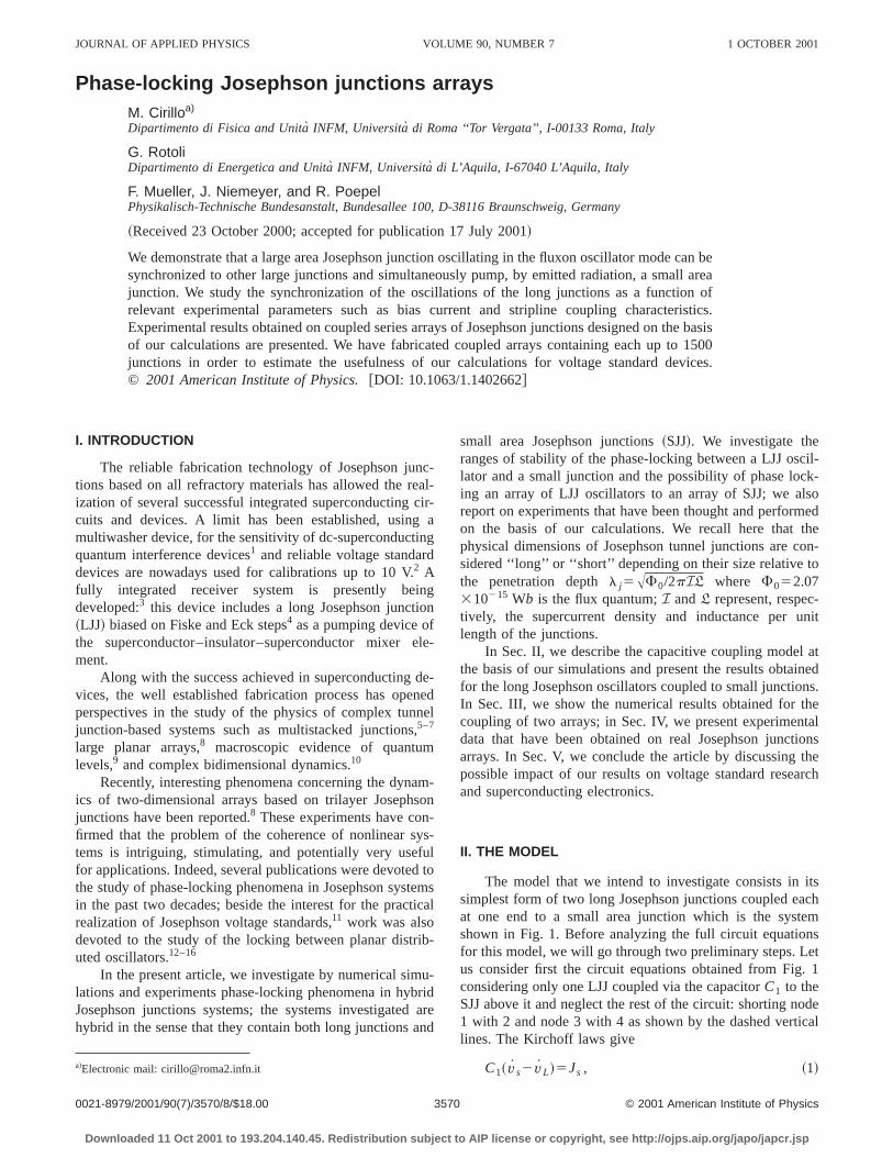
FIG. 6. ~a! A photograph of the circuit that we have fabricated showibasic building blocks similar to that of Fig. 1, i.e., two long junctions atwo small junctions is shown. The trilayer island where the junctionslocated can be clearly identified by the rectangular areas delimitedrougher lines;~b! a sketch of the meander line nesting of the two arra~each meander line represents the path of a series array!. The line by the sideindicates the length of the unitary cell of our interdigital capacitor structu
Downloaded 11 Oct 2001 to 193.204.140.45. Redistribution subject to A
fee-
tged
led
-ki-
g
is
-
sition of long and short junctions is clearly visible. We alindicate the Nb contacts connecting the islands whcouples of long junctions and couples of short junctionslocated. The photo of Fig. 6~a! represents a few sections oflarge array whose basic ’’units’’ are just two LJJs and twSJJs, just like in our 212 system simulations. It is worthnoting that we sputtered on the back of the Si wafer a laof Nb with the intention of using it as a groundplane.
The coupling~and the values of the parameterz) be-tween two long junctions on the same Nb island was callated assuming that the capacitance connecting the LJJdue to the gap in the striplines. Since the gap separatingtwo top electrodes of the long junctions is relatively sm~there is only a 10mm distance between the top electrode!,we estimate, using the typical junction parameters oftrilayer technology and the matrix inversion method,19 a C0
>26 fF and therefore a coupling factorz50.045. We notethat, due to the fact that the trilayer is grown over an odized Si substrate which has a groundplane on the bthere exists also a capacitive coupling between the baseislands due to the capacitor formed between the top conning electrode, the Si substrate, and the ground plane.capacitance of this element, however, is of the order of 0.1which givesz>1024; thus, the coupling between the lonjunctions on different islands is negligible with respect to tcontribution calculated for the junctions on the same islaHowever, even if it is small, a coupling between the islancontaining each two junctions exists.
In order to couple capacitively the two arrays of lonand small junctions, we adopted the following strategy. Wfabricated two arrays of junctions that each formedmeander-like line: the two meanders formed, respectivelythe series arrays of long and small junctions arrays fit eother as shown in Fig. 6~b!. In these conditions, we assumthat an interdigital capacitive coupling exists betweentwo series arrays and that for this coupling the capacitanunit length is regulated by the equation20
Cul5S e r11
W DL@~n23!A11A2#pF/ in, ~12!
wheren is the number of fingers of the interdigital capacitoL their length in inches,W the total length of the capacitor ininches, andA1 andA2 two variables depending on the thickness of the substrate and on the spacing between the finIn our case, the dielectric layer is represented by the 0.mm thick Si substrate~for Si, we assumee r511.4 at 4.2K!,21 the length of the fingers isL52.2 mm and their spacing is of the order of 20mm. Thus, the coupling is characterized by a capacitance/unit length given byCul
5(12.4/W)L@(n23)0.110.23#pF/in. This equation is ex-pected to hold only if the substrate thicknessT.(W/n)whereW is the total length of the interdigital structure: in oucase, sinceT50.375 mm, if the length of a unit cell is of theorder of 64 mm ~to form a unit cell we need a minimanumber three fingers!, this condition can be expected to hoeven if n53. The capacitance of the unit cell of our intedigital structure20 has been evaluated in our case with tw
ey
.
IP license or copyright, see http://ojps.aip.org/japo/japcr.jsp

asf
-tw
tetathito
thc
triceTharu
ea
hiy
ear
aomfo
oc-
troshd
orfs
in
,torra
-oa
,edch
Zthbn
ter
the
edtllelthe. 7;entretiveis
nt
taled
iesthe
isys
l. The
3575J. Appl. Phys., Vol. 90, No. 7, 1 October 2001 Cirillo et al.
coupled arrays constituted each of 64 junctions. In this cwe get for W564 mm and n53 a coupling capacitor o0.24 pF.
It is worth noting that in our interdigital capacitive modeling we evaluate the overall capacitance coupling theports ~which are the long and short junction array!. Sinceradiation is distributed all over the stripline of one port~theradiation emitted from the long junctions!, we assume thaeach small junction of the ‘‘detector’’ port will receive thamount of radiation coupled capacitively by the interdigistructure. At the same time, however, each basic cell oflong junction array shall be loaded by the same capac~see the circuit model shown in Fig. 1 of Ref. 19! because allthe junctions of the two arrays are faced parallel toground; more precisely, we have all the junctions capatances in series to ground with the capacitance of the slines. We neglect the effect of the junctions capacitansince these are much larger than that of the striplines.basic limit of our assumptions is the fact that our fingers‘‘empty,’’ however, considering the frequencies at which osamples are operating~only up to 90 GHz! and that theempty slot in our fingers are only few microns wide, wthink that the interdigital capacitive coupling described isfirst rough but reasonable approximation. In terms of tmodeling, the problem of loading the basic unit of the arracan be reduced to the~212! junction system analyzed in thsimulations because all the long junctions of the arrayloaded parallel to the interdigital capacitor.
The experimental results that we obtained with therays were consistent with the predictions of this model. Frthe model, we can expect that the coupling will be betterarrays having an increasing number of fingers~n!. We cancalculate that forn53, the coupling parameter between twadjacent fingers~i.e., between one double row of long juntions and one double row of small junctions! is z50.15which takes us in a region17 where the reflection of fluxons athe ends of the long junctions and the coupling of electmagnetic radiation to other junctions is just below a threold value for absorption. This would be a very privilegeregion in terms of transferring power from a fluxon oscillatto other junctions17 and we would expect, within the limits oour modeling, radiation-coupling effects. Naturally, increaing the number of fingers we expect more radiation becoupled.
We fabricated several samples and show in Figs. 7and 9, typical results. Figure 7 shows oscillator on oscillaoff current–voltage characteristics of a 64 junctions SJJ acoupled to an array of 64 LJJs~a unit cell in terms of ourinterdigital capacitor modeling!. In order to obtain the emission of radiation, we biased the LJJ array with a current600 mA at a voltage of 32 mV. For this sample, the physicextended dimension of the long junctions was 50mm and theZFS appeared at asymptotic voltages, in each junction334 mV; thus, at the voltage of 32 mV, we were biasroughly on the 96th ZFS of the long junctions array whimakes sense because we had two and sometimes threefor a single junction. We note, however, that in this case,observed suppression of the Josephson current was of a40%. This result is consistent with the numerical simulatio
Downloaded 11 Oct 2001 to 193.204.140.45. Redistribution subject to A
e,
o
ler
ei-p-se
er
ss
e
r-
r
--
-g
8,ry
fl
of
FSeouts
because in the experiments we have a coupling paramez50.15 which is larger than thatz50.008 value of the simu-lations which allowed a maximum 25% suppression ofJosephson current.
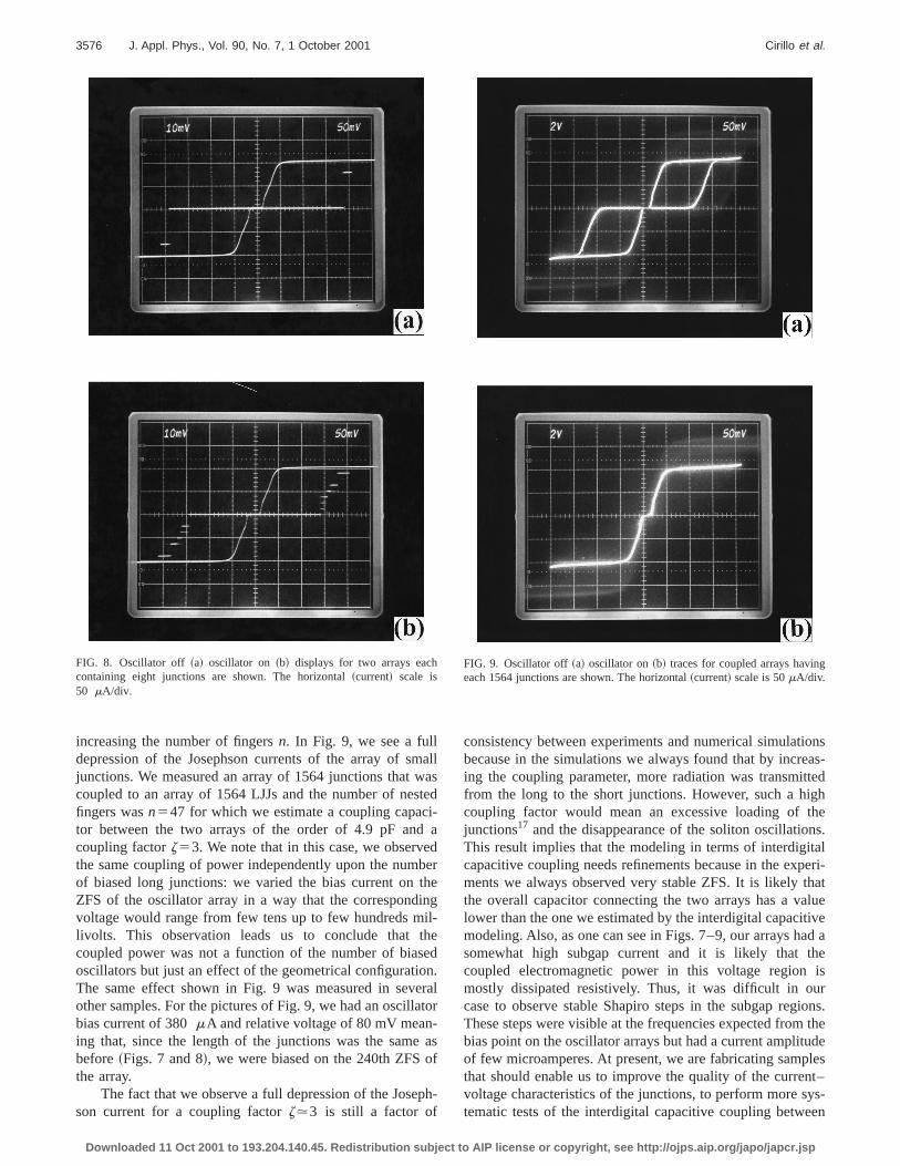
A result similar to that shown in Fig. 7 was also obtain~see Fig. 8!, coupling only eight oscillator junctions to eighdetector junctions which were just placed along two paralines. In this case, the length of the long junctions andasymptotic voltages of the ZFSs were the same as for Figthe bias point of the oscillator array was defined by a currof 600 mA and a voltage of 4.5 mV and therefore we webiased on the 13th ZFS of the array. We see that the relasuppression of the critical currents of the detector arraynow of the order of 25%, a result that is not very differefrom the previous one. As one can expect,19,20 the couplingprovided between the arrays of a unit cell of our interdigicapacitor is of the same order of magnitude of that providby the coupling of the two microstrips formed by the serarrays. The situation is very different when we increasenumber of fingers.
In Fig. 9, we show evidence that our coupling schemevery effective in transferring power between the two arra
FIG. 7. Oscillators off~a! oscillator on~b! curves for an array of 64 smalarea junctions coupled to an array of 64 large area junctions are shownhorizontal~current! scale is 50mA/div.
IP license or copyright, see http://ojps.aip.org/japo/japcr.jsp
mwasti-
edbthinil
the
onerat-
of
p
ionsas-tedighthens.alperi-hatlue
tivead aheis
urions.the
udelest–
ys-en
g
3576 J. Appl. Phys., Vol. 90, No. 7, 1 October 2001 Cirillo et al.
increasing the number of fingersn. In Fig. 9, we see a fulldepression of the Josephson currents of the array of sjunctions. We measured an array of 1564 junctions thatcoupled to an array of 1564 LJJs and the number of nefingers wasn547 for which we estimate a coupling capactor between the two arrays of the order of 4.9 pF andcoupling factorz53. We note that in this case, we observthe same coupling of power independently upon the numof biased long junctions: we varied the bias current onZFS of the oscillator array in a way that the correspondvoltage would range from few tens up to few hundreds mlivolts. This observation leads us to conclude thatcoupled power was not a function of the number of biasoscillators but just an effect of the geometrical configuratiThe same effect shown in Fig. 9 was measured in sevother samples. For the pictures of Fig. 9, we had an oscillbias current of 380mA and relative voltage of 80 mV meaning that, since the length of the junctions was the samebefore~Figs. 7 and 8!, we were biased on the 240th ZFSthe array.
The fact that we observe a full depression of the Joseson current for a coupling factorz.3 is still a factor of
FIG. 8. Oscillator off ~a! oscillator on ~b! displays for two arrays eachcontaining eight junctions are shown. The horizontal~current! scale is50 mA/div.
Downloaded 11 Oct 2001 to 193.204.140.45. Redistribution subject to A
alls
ed
a
ereg-ed.alor
as
h-
consistency between experiments and numerical simulatbecause in the simulations we always found that by increing the coupling parameter, more radiation was transmitfrom the long to the short junctions. However, such a hcoupling factor would mean an excessive loading ofjunctions17 and the disappearance of the soliton oscillatioThis result implies that the modeling in terms of interdigitcapacitive coupling needs refinements because in the exments we always observed very stable ZFS. It is likely tthe overall capacitor connecting the two arrays has a valower than the one we estimated by the interdigital capacimodeling. Also, as one can see in Figs. 7–9, our arrays hsomewhat high subgap current and it is likely that tcoupled electromagnetic power in this voltage regionmostly dissipated resistively. Thus, it was difficult in ocase to observe stable Shapiro steps in the subgap regThese steps were visible at the frequencies expected frombias point on the oscillator arrays but had a current amplitof few microamperes. At present, we are fabricating sampthat should enable us to improve the quality of the currenvoltage characteristics of the junctions, to perform more stematic tests of the interdigital capacitive coupling betwe
FIG. 9. Oscillator off~a! oscillator on~b! traces for coupled arrays havineach 1564 junctions are shown. The horizontal~current! scale is 50mA/div.
IP license or copyright, see http://ojps.aip.org/japo/japcr.jsp

ra
inaro
baw
hthfoi
gathdgib
ctoatste
th
lVt
danleistuomrd
herutras-ur
-
oe-dardouldc-
thead-h on
tt.
W.ond.
o,
,
G.
en,
ev. B
ett.
kos,
. F.
A
3577J. Appl. Phys., Vol. 90, No. 7, 1 October 2001 Cirillo et al.
the arrays, and to obtain convincing evidence of the ovecoherence of the large number of oscillators.
V. CONCLUSIONS
We have shown numerically that a complicated nonlear system represented by a coupled array of two longtwo short Josephson exhibits remarkable phase-locking perties. The simulations have shown that the power emittedthe large junctions can be used both to synchronize themto pump small area junctions. From the numerical results,have also seen that the coherent oscillation gives rise toincrease of the emitted radiation, a phenomenon thatbeen observed even in the experiments. The stability ofphase locking in the numerical simulations investigatedpractical ranges of disuniformities between the junctionssuch that applications of our results in the field of metroloand millimeter-wave electronics can be considered. We hreported experimental evidence that the effect found insimulations due to a capacitive coupling can be observearrays shaped in a meander line and nested in an interdiway. The experiments have shown that radiation cantransmitted from one large oscillator array to a large detearray without affecting the stability of the oscillators and ththe coupled electromagnetic power is not dependent onbias voltage of the oscillators. In these arrays, the babuilding block is just represented by the system investigain the simulations
Our coupling scheme required, in terms of space, fortwo arrays each having 1564 junctions, less than 2 mm2 ~ex-cluding the contact pads!. This number of junctions is typicafor a 1 V standard array chip. Also, the extension to 10chips can be easily predicted to occupy less space thanfinline antenna of the samples nowadays used for stanmaintenance; therefore frequency stabilizer circuits acounters could easily be integrated along with the couparrays. The details of these circuits, which are importantsues of our research at present, shall be dealt with in a fuarticle. The major advantage of our coupling scheme frthe point of view of the rf biasing of large voltage standaarrays~both classical and programmable! is the fact that theelectromagnetic power is distributed uniformly all over tjunctions. Indeed, any oscillator~semiconductor-based osuperconductor-based! whose power is coupled at the inpof a finline antenna would not solve the problem of thediative losses~and subsequent nonuniformity of power ditribution! along the arrays. This characteristic might turn oto be especially useful for the SINIS voltage standatechnology22 for which a relatively low amount of micro
Downloaded 11 Oct 2001 to 193.204.140.45. Redistribution subject to A
ll
-ndp-y
ndeanasersyveeintaler
theicd
e
herddd-re
-
td
wave power is required: it would not be very difficult tsubstitute our small junctions array with a SINIS one. Bsides these encouraging perspectives for voltage stanpurposes, we believe that our radiation transfer scheme clend itself to other applications in superconducting eletronics.
ACKNOWLEDGMENTS
This work was partially supported by the MURST~Italy!through a COFIN98 project. The article is dedicated tomemory of our colleague Ralf Poepel whose premature fing represented a hardly recoverable loss for the researcvoltage standard devices.
1P. Carelli, M. G. Castellano, G. Torrioli, and R. Leoni, Appl. Phys. Le72, 115 ~1998!.
2J. Kohlman, F. Mueller, P. Gutman, R. Poepel, L. Grimm, F.-Duehnschede, W. Meier, and J. Niemeyer, IEEE Trans. Appl. Superc7, 3411~1997!.
3T. Nakamura, K. Enpuku, F. Irie, and Y. Yoshida, J. Appl. Phys.54, 3302~1983!; V. P. Koshelets, A. V. Shchukin, S. V. Shitov, and L. V. FilippenkIEEE Trans. Appl. Supercond.3, 2524 ~1993!; S. V. Shitov, V. P.Koshelets, A. B. Ermakov, L. V. Filippenko, A. M. Barishev, W. Luingeand Jian-Rong Gao, IEEE Trans. Appl. Supercond.9, 3773~1999!.
4M. Cirillo, N. Grønbech-Jensen, M. R. Samuelsen, M. Salerno, andVerona Rinati, Phys. Rev. B58, 12377~1998!.
5S. Sakai, A. V. Ustinov, H. Kohlstedt, A. Petraglia, and N. F. PedersPhys. Rev. B50, 12905~1994!.
6N. Grønbech-Jensen, J. A. Blackburn, and M. R. Samuelsen, Phys. R53, 12364~1996!.
7N. F. Pedersen and S. Sakai, Phys. Rev. B58, 2820~1998!.8P. A. Booi and S. P. Benz, Appl. Phys. Lett.68, 3799~1996!; P. Barbara,A. B. Cawthorne, S. V. Shitov, and C. J. Lobb, Phys. Rev. Lett.82, 1963~1999!.
9P. Silvestrini, V. G. Palmieri, B. Ruggiero, and M. Russo, Phys. Rev. L79, 3046~1997!.
10C. Nappi, R. Cristiano, and M. P. Listiskii, Phys. Rev. B58, 11685~1998!.11R. L. Kautz, Rep. Prog. Phys.59, 935 ~1996!.12M. Cirillo and F. L. Lloyd, J. Appl. Phys.61, 2581~1987!.13R. Monaco, S. Pagano, and G. Costabile, Phys. Lett. A131, 122 ~1988!.14G. Reinisch, J. C. Fernandez, N. Flytzanis, M. Taki, and S. Pnevmati
Phys. Rev. B38, 11284~1988!.15G. Rotoli, G. Costabile, and R. D. Parmentier, Phys. Rev. B41, 1958
~1990!.16G. Filatrella, G. Rotoli, N. Grønbech-Jensen, R. D. Parmentier, and N
Pedersen, J. Appl. Phys.72, 3179~1992!.17M. Cirillo, A. R. Bishop, P. S. Lomdahl, and S. Pace, J. Appl. Phys.66,
1772 ~1989!.18M. Cirillo, I. Modena, F. Santucci, P. Carelli, and R. Leoni, Phys. Lett.
167, 175 ~1992!.19K. C. Gupta, R. Garg, and I. J. Bahl,Microstrip Lines and Slotlines
~Artech House, Boston, 1979!.20G. D. Alley, IEEE Trans. Microwave Theory Tech.18, 1028~1970!; Y. M.
Zhang, D. Winkler, and T. Claeson, Appl. Phys. Lett.62, 3195~1993!.21H. H. Li, J. Phys. Chem. Ref. Data9, 561 ~1980!.22H. Schulze, R. Behr, F. Mueller, and J. Niemeyer, Appl. Phys. Lett.73,
996 ~1998!.
IP license or copyright, see http://ojps.aip.org/japo/japcr.jsp
Copyright © 2022 FDOKUMEN