Electrodeposition of Bi films on H covered n- GaAs(111)B ...
41
1 Electrodeposition of Bi films on H covered n- GaAs(111)B substrates Alicia Prados and Rocío Ranchal Dpto. Física de Materiales, Universidad Complutense de Madrid. Ciudad Universitaria s/n, Madrid 28040, Spain *Corresponding author: [email protected] Phone: (+34) 91 394 5012; Fax: (+34) 91 394 4547
-
Upload
khangminh22 -
Category
Documents
-
view
0 -
download
0
Transcript of Electrodeposition of Bi films on H covered n- GaAs(111)B ...
1
Electrodeposition of Bi films on H covered n-
GaAs(111)B substrates
Alicia Prados and Rocío Ranchal
Dpto. Física de Materiales, Universidad Complutense de Madrid. Ciudad Universitaria s/n,
Madrid 28040, Spain
*Corresponding author: [email protected] Phone: (+34) 91 394 5012;
Fax: (+34) 91 394 4547
2
Abstract
We have investigated how the presence of an adsorbed hydrogen layer affects the
nucleation and properties of Bi layers grown by dc electrodeposition at different
overpotentials on n-GaAs(111)B substrates with a carrier concentration of 1.3 ·1017 cm-3 in
darkness and at 300 K. The kinetics of Bi(III) ions reduction is controlled by the overpotential
but also negatively affected by the adsorbed hydrogen layer, as deduced from the
deconvolution of the current density transients recorded during the nucleation of the films.
The surface morphology and the structural properties of the Bi films are correlated with the
nucleation process and therefore, influenced by both the overpotential and the adsorbed
hydrogen layer. At low overpotentials, porous and rough Bi films with a low crystal quality
are obtained due to the low rate of proton and Bi(III) ion reduction. As the overpotentials
raises, the rate of these reactions increase leading to flatter and more compact Bi films with a
higher crystal quality. The electrical properties of the Bi/n-GaAs interface depend on the
interfacial states whose origin is again the combined effect of the adsorbed hydrogen layer
and growth overpotential.
Keywords
Bismuth; n-GaAs; Electrodeposition; Nucleation; Thermionic Emission.
3
1. Introduction
Bismuth (Bi) is a semimetal with interesting electronic properties at the nanoscale [1, 2,
3, 4, 5]. In a thin film configuration, Bi can be used in the development of new spintronic
devices that take advantage of its surface states which are strongly spin-polarized via Rashba
effect [6, 7]. In fact, a large spin to charge conversion induced by spin−orbit coupling in a
Bi/Ag Rashba interface has been very recently observed [8]. Consequently, in order to
investigate the possibility of implementing Bi in new applications, it is compulsory to deeply
investigate the growth of Bi thin films.
Among the different growth techniques, electrodeposition appears as the most suitable
to grow Bi since it is a fast procedure to obtain high quality layers on different substrates ( [9]
and references therein). Also important to remark, it is a cost-effective growth method
compatible with patterning and transferable to industry. In order to implement Bi in electronic
devices, semiconductors like GaAs can be very versatile for several reasons. Tunnel [10, 11]
or rectifying [12] Schottky barriers can be obtained by varying the substrate doping level,
leading to different mechanisms for electron transport through the interface, thermionic-field
emission or thermionic emission, respectively. Moreover, modifying the substrate surface
orientation it is possible to synthesize Bi thin films with different crystalline textures and
interfacial electrical properties [10]. Therefore, a wide range of devices could be fabricated
starting from just one material and growth technique. However, one of the main drawbacks of
the electrodeposition of Bi onto n-GaAs is the presence of a blocking layer of adsorbed
hydrogen (Hads) at the substrate surface. This blocking layer results from the interaction
between the n-GaAs surface states and the protons (H+) of the electrolyte. Although it might
protect the n-GaAs surface from oxidation, it will hinder the nucleation of Bi(III) ions
avoiding the growth of compact and high quality Bi thin films [13]. To solve this problem, we
designed a procedure that desorbs the Hads layer before performing the growth of the Bi layer,
4
so high-quality films can be obtained [14, 10, 11]. Nevertheless, this protocol involves the
dissolution of an initial Bi deposit and, therefore, it can only be used with highly-doped
semiconducting substrates with a carrier concentration higher than 2·1017 cm-3. For n-GaAs
substrates with a lower carrier concentration, that we will call from now on “lower-doped n-
GaAs”, we investigated other protocols based on the electrodeposition of Bi under
illumination conditions [14] since photogenerated holes remove the Hads layer [15]. However,
this cannot be used because illumination also produces the photocorrosion of the n-GaAs
surface [16, 17, 18]. Considering the experimental results reported so far, we can only
conclude that the electrodeposition of Bi thin films on lower-doped n-GaAs substrates has to
be performed in the presence of the Hads layer and therefore, it is necessary to explore the
optimum growth conditions to achieve high quality Bi thin films.
We showed the strong impact that the growth overpotential has on the properties of Bi
layers electrodeposited at constant potential on Hads-free highly doped n-GaAs(111)B
substrates [11, 9]. We reported that the morphological, structural and interfacial electrical
properties are clearly correlated with the nucleation process which is in turn correlated with
the energy band diagram of the semiconductor-electrolyte interface (SEI). Here, it is not
possible to remove the Hads layer, so the effect of the growth overpotential on the nucleation
of the Bi films is affected by the presence of this layer. Consequently, the goal of the present
work is double: i) to study in detail the combined effect of the growth overpotential and the
Hads layer on the nucleation and properties of Bi films electrodeposited at dc potentials on
Hads-covered lower-doped n-GaAs(111)B substrates, and ii) to find the optimal conditions to
achieve high quality Bi thin films on these substrates. We have also analyzed the effect of the
growth mode (static or dynamic) on the properties of the Bi layer.
5
2. Experimental
Electrochemical experiments have been carried out using a stable water-based
electrolyte containing 1 mM Bi2O3 (bismuth oxide) as the Bi(III) cation source and 1 M
HClO4 (perchloric acid) as supporting electrolyte. Solutions were prepared with analytical
grade chemicals and deionized water in order to avoid free ions. Bismuth oxide was first
added to perchloric acid in a volumetric flask, and then, the solution was made to the mark
with deionized water. The pH of the solution (approximately 0.1) was not necessary to be
further adjusted. Working electrodes were Si doped n-type GaAs(111)B wafers, supplied by
Semiconductor Wafer Inc., with a carrier concentration of n = 1.3 × 1017 cm-3. Ohmic contacts
were made on the back of the wafers by thermal evaporation of 80 nm of AuGe (2% Ge) and
250 nm of Au, followed by an annealing at 380 oC in forming gas for 90 s. The total surface
area exposed to the electrolyte was 0.15 cm2 in all cases. Prior to each experiment, substrates
were degreased and then etched to remove GaAs native oxide under darkness conditions.
First, substrates are dipped in a solution of HCl (10% vol.) for 2 min to remove arsenic and
gallium oxides [19]. Then, substrates are rinsed in deionized water for 2 min to remove Ga-
Clx species since they are soluble in water [20]. Finally, substrates are immersed in 1 M
HClO4 (supporting electrolyte) for 2 min to remove possible Cl- ions remaining in the solution
or adsorbed at the substrate surface. Then, the substrate surface is protected from air with a
drop of 1M HClO4 (supporting electrolyte) when transferred to the Bi(III) solution, where
substrates remained 2 min to reach a stable open-circuit potential (OCP). In this condition, the
substrate surface is oxide-free with about one monolayer coverage of elementary As that
interacts with the protons in the solution (As-H) [21], creating a layer of adsorbed hydrogen
[13]. Electrochemical experiments were controlled by a PalmSens EmStat3+Blue potentiostat
and carried out in a three-electrode cell with a platinum mesh as counter electrode and a
Ag/AgCl (3 M NaCl) reference electrode supplied by BASi (Eeq = 0.196 V vs. SHE). In this
6
study, all potentials are referred to this electrode. All electrochemical experiments were
performed without agitation, at 300 K and in darkness. After deposition, films were rinsed in
deionized water and dried with N2.
Surface characterization was done by means of a Nanoscope Atomic Force Microscope
(AFM) with a Si tip, working in tapping mode and operating in air. The surface roughness has
been characterized by the root mean square (rms) obtained from the images analyzed with
WSxM 5.0 software and Nanoscope 5.31r1 software. Structural characterization of the Bi
layers was done by X-Ray Diffraction (XRD) using a Philips X’Pert PRO system equipped
with a Cu target (λΚα = 1.54 nm) and a four-circle goniometer. All films were measured in a
symmetric Bragg-Brentano configuration (θ −2θ scan) to determine the preferred orientation
of the films. To avoid substrate reflections, an offset of 0.5o was introduced between the
incidence and the diffracted direction (ω = θ − θoffset). The crystallographic uniformity of the
Bi layers has been analyzed by means of ω-rocking curves and ϕ-scans (azimuthal scans). The
full width at half maximum (FWHM) of these curves is twice the average tilt and twist of Bi
grains with respect the GaAs substrate, respectively. In order to extract the FWHM values
with their corresponding errors, the ω-rocking curves have been fitted to a pseudovoigt
function and the φ-scans to a Gaussian function. The values obtained for the FWHM have
been corroborated with the software X’Pert Data Viewer provided by PANalytical B. V.
Finally, the Bi/GaAs interface was characterized electrically by means of current
density-voltage (j-V) curves. Several diodes with 230 µm and 250 µm of diameter were
fabricated in the Bi films by standard optical lithography followed by photochemical etching.
Afterward, an electrical contact made by 20 nm Cr/300 nm Au was evaporated on the top of
the Bi diodes to protect them. I-V measurements were carried out at 290 K in a Janis probe
station (model CCR10-1) with a Hewlett Packard 4145 semiconductor parameter analyzer.
7
All diodes show a good reproducibility for the measured curves. At least 10 diodes have been
measured in each sample, giving standard errors below 6%.
3. Results
4.1. Electrochemical characterization
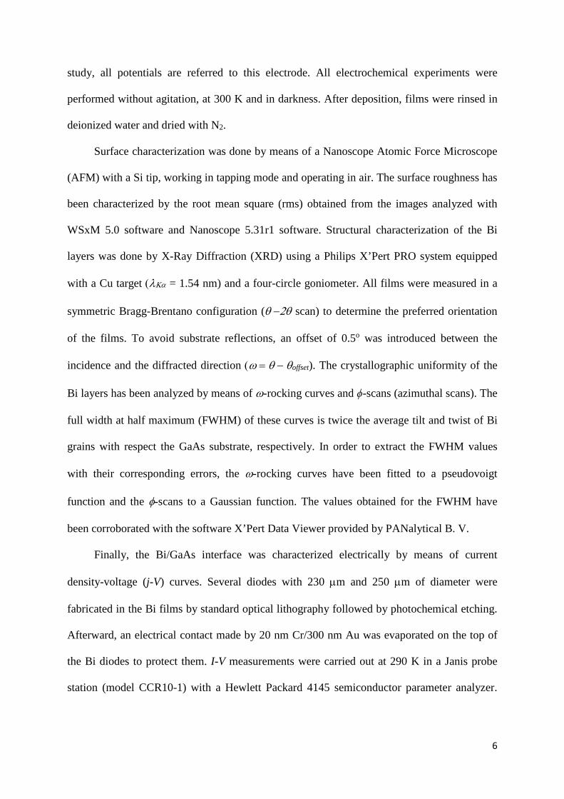
Figure 1 shows a cyclic voltammetry (CV) performed at 10 mV/s on an n-GaAs
substrate immersed in the Bi(III) solution. The CV comprises two scans and starts at the OCP
≈ 70 mV, goes first toward the cathodic, then to the anodic stage and finishes at the initial
OCP. In the first scan we can observe a cathodic peak with an onset potential (defined as the
intersection of the rising current of the cathodic peak with respect to its baseline) around -200
mV, whereas the second scan presents a reduction peak with a different shape and a more
positive onset potential (≈ -100 mV). Taking into account our previous work, these two peaks
consist of the superposition of those assigned to Bi(III) ion and H+ reduction on the n-GaAs
surface [13, 10, 9]. Despite the reduction peaks, no anodic peak is observed in the CV, i.e., the
metallic Bi cannot be oxidized into Bi(III) ions during the anodic stage (inset Figure 1).
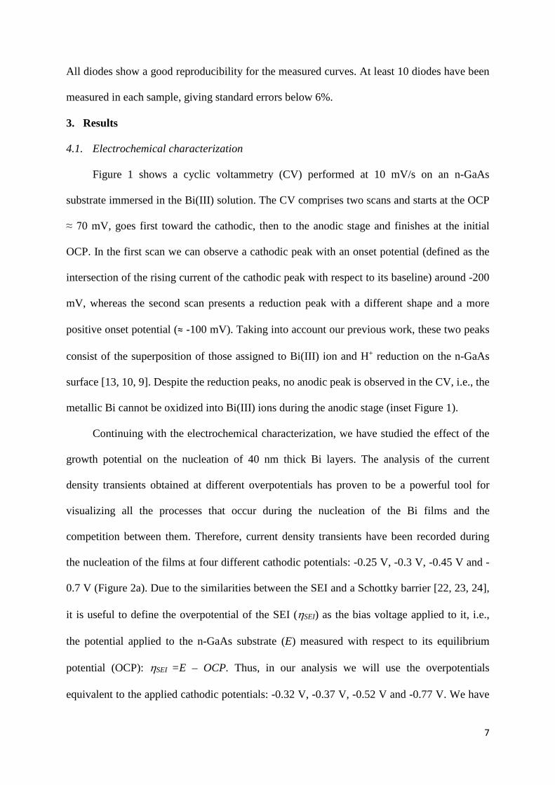
Continuing with the electrochemical characterization, we have studied the effect of the
growth potential on the nucleation of 40 nm thick Bi layers. The analysis of the current
density transients obtained at different overpotentials has proven to be a powerful tool for
visualizing all the processes that occur during the nucleation of the Bi films and the
competition between them. Therefore, current density transients have been recorded during
the nucleation of the films at four different cathodic potentials: -0.25 V, -0.3 V, -0.45 V and -
0.7 V (Figure 2a). Due to the similarities between the SEI and a Schottky barrier [22, 23, 24],
it is useful to define the overpotential of the SEI (ηSEI) as the bias voltage applied to it, i.e.,
the potential applied to the n-GaAs substrate (E) measured with respect to its equilibrium
potential (OCP): ηSEI =E – OCP. Thus, in our analysis we will use the overpotentials
equivalent to the applied cathodic potentials: -0.32 V, -0.37 V, -0.52 V and -0.77 V. We have
8
analyzed the current density transients by a procedure developed by Palomar-Pardavé et al.
[25] that allows the deconvolution of the current density, j(t), into its individual contributions,
ji (with i = SEI, des, ads, PR and 3D), each one assigned to a different process. This
procedure consists in a nonlinear fit of the experimental j(t) to a theoretical nucleation model,
using the Marquardt−Levenberg algorithm. For cathodic reactions, where the current density
is negative, the absolute value of j(t) should be used. We have elaborated a theoretical
nucleation model based on several processes that occur in the SEI when it is biased, and that
accurately describes the experimental nucleation curves for the electrodeposition of Bi on n-
GaAs substrates [9]:
[a] Charging of the SEI capacitance considering it as a series RC circuit [24]:
𝑗𝑗𝑆𝑆𝑆𝑆𝑆𝑆(𝑡𝑡) = 𝑄𝑄𝑆𝑆𝑆𝑆𝑆𝑆𝜏𝜏𝑆𝑆𝑆𝑆𝑆𝑆
∙ 𝑒𝑒𝑒𝑒𝑒𝑒 �− 𝑡𝑡𝜏𝜏𝑆𝑆𝑆𝑆𝑆𝑆
� (1)
[b] Desorption of OH- and ClO4- anions:
𝑗𝑗𝑑𝑑𝑑𝑑𝑑𝑑(𝑡𝑡) = 𝑄𝑄𝑑𝑑𝑑𝑑𝑑𝑑𝜏𝜏𝑑𝑑𝑑𝑑𝑑𝑑
∙ 𝑒𝑒𝑒𝑒𝑒𝑒 �− 𝑡𝑡𝜏𝜏𝑑𝑑𝑑𝑑𝑑𝑑
�
(2)
[c] Adsorption of H+ via surface states on available surface sites present at the GaAs
electrode [14]:
𝑗𝑗𝑎𝑎𝑑𝑑𝑑𝑑(𝑡𝑡) = 𝑄𝑄𝑎𝑎𝑑𝑑𝑑𝑑𝜏𝜏𝑎𝑎𝑑𝑑𝑑𝑑
∙ 𝑒𝑒𝑒𝑒𝑒𝑒 �− 𝑡𝑡𝜏𝜏𝑎𝑎𝑑𝑑𝑑𝑑
�
(3)
The parameters QSEI, Qdes and Qads represent the electrical charge involved in each
process, and τSEI, τdes and τads represent their time constants [26].
[d] Reduction of H+ on the GaAs surface:
𝑗𝑗𝑃𝑃𝑃𝑃 = 𝑧𝑧𝑃𝑃𝑃𝑃 ∙ 𝐹𝐹 ∙ 𝑘𝑘𝑃𝑃𝑃𝑃 (4)
where zPR is the number of electrons involved in the reduction reaction; F is Faraday’s
constant; and kPR is the rate constant of the reaction [27]. This expression takes into
account the two steps involved in the hydrogen evolution reaction, which follows the
Volmer-Heyrovsky route on GaAs surfaces in acidic aqueous solutions [28].
9
[e] Reduction of Bi(III) ions into metallic Bi following a 3D nucleation controlled by
diffusion, and delayed by an induction time, t0, associated with the initial current decay
[29]. This process can be described by the following expression:
𝑗𝑗3𝐷𝐷(𝑡𝑡) = 𝑃𝑃4 ∙ (𝑡𝑡 − 𝑡𝑡0)−1 2⁄ ∙ 𝜃𝜃(𝑡𝑡 − 𝑡𝑡0) (5)
where θ(t) is the n-GaAs surface area covered by the diffusion zones of Bi nuclei [30].
𝜃𝜃(𝑡𝑡) = 1 − 𝑒𝑒𝑒𝑒𝑒𝑒 �−𝑃𝑃2 ∙ �(𝑡𝑡 − 𝑡𝑡0) − (1−𝑑𝑑𝑒𝑒𝑒𝑒[−𝐴𝐴∙(𝑡𝑡−𝑡𝑡0)])𝐴𝐴
�� (6)
and
𝑃𝑃2 = 𝑁𝑁0 ∙ 𝜋𝜋 ∙ 𝐷𝐷 ∙ �8𝜋𝜋∙𝑐𝑐0∙𝑀𝑀𝜌𝜌
�1 2⁄
(7)
𝑃𝑃4 = �𝑧𝑧∙𝐹𝐹∙𝐷𝐷1 2⁄ ∙𝑐𝑐0
𝜋𝜋1 2⁄ � (8)
where A, D and co are the nucleation frequency per active site, the diffusion coefficient,
and the concentration in the bulk of the electrolyte of Bi(III) ions, respectively; M and
ρ are the molar mass and the density of metallic Bi; and No is the saturation density of
nucleation active sites on the GaAs surface. To fulfill the requirement of dimensional
homogeneity, co should be introduced in mol·cm−3 and ρ in g·cm−3.
The nucleation process is divided into two regimes delimited by the induction time, t0
[9]. During the first regime the SEI is rearranged due to the modification of the potential from
the OCP to the growth potential. When the second regime starts, the Bi(III) ion reduction (j3D)
begins and the GaAs surface is progressively covered by metallic Bi. This new process alters
H+ reduction (jPR) since the two reactions occur via conduction band electrons [31, 28].
However, H+ adsorption (jads) can run in parallel to Bi(III) ion reduction because they take
place at different surface sites and through different electronic states [26, 32]. Therefore, our
nucleation model is described by the following equations:
𝑗𝑗(𝑡𝑡) = 𝑗𝑗𝑆𝑆𝑆𝑆𝑆𝑆(𝑡𝑡) + 𝑗𝑗𝑑𝑑𝑑𝑑𝑑𝑑(𝑡𝑡) + 𝑗𝑗𝑎𝑎𝑑𝑑𝑑𝑑(𝑡𝑡) + 𝑗𝑗𝑃𝑃𝑃𝑃 𝑡𝑡 ≤ 𝑡𝑡0 (9)
𝑗𝑗(𝑡𝑡) = 𝑗𝑗𝑎𝑎𝑑𝑑𝑑𝑑(𝑡𝑡) + 𝑗𝑗𝑃𝑃𝑃𝑃 ∙ [1 − 𝜃𝜃(𝑡𝑡)] + 𝑗𝑗3𝐷𝐷(𝑡𝑡) 𝑡𝑡 > 𝑡𝑡0 (10)
10
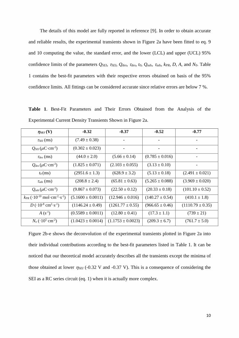
The details of this model are fully reported in reference [9]. In order to obtain accurate
and reliable results, the experimental transients shown in Figure 2a have been fitted to eq. 9
and 10 computing the value, the standard error, and the lower (LCL) and upper (UCL) 95%
confidence limits of the parameters QSEI, τSEI, Qdes, τdes, t0, Qads, τads, kPR, D, A, and N0. Table
1 contains the best-fit parameters with their respective errors obtained on basis of the 95%
confidence limits. All fittings can be considered accurate since relative errors are below 7 %.
Table 1. Best-Fit Parameters and Their Errors Obtained from the Analysis of the
Experimental Current Density Transients Shown in Figure 2a.
ηSEI (V) -0.32 -0.37 -0.52 -0.77
τSEI (ms) (7.49 ± 0.38) - - -
QSEI (µC·cm-2) (0.302 ± 0.023) - - -
τdes (ms) (44.0 ± 2.0) (5.66 ± 0.14) (0.785 ± 0.016) -
Qdes (µC·cm-2) (1.825 ± 0.071) (2.103 ± 0.055) (3.13 ± 0.10) -
t0 (ms) (2951.6 ± 1.3) (628.9 ± 3.2) (5.13 ± 0.18) (2.491 ± 0.021)
τads (ms) (208.8 ± 2.4) (65.81 ± 0.63) (5.265 ± 0.088) (3.969 ± 0.020)
Qads (µC·cm-2) (9.867 ± 0.073) (22.50 ± 0.12) (20.33 ± 0.18) (101.10 ± 0.52)
kPR (·10-10 mol·cm-2·s-1) (5.1600 ± 0.0011) (12.946 ± 0.016) (140.27 ± 0.54) (410.1 ± 1.8)
D (·10-8 cm2·s-1) (1146.24 ± 0.49) (1261.77 ± 0.55) (966.65 ± 0.46) (1110.79 ± 0.35)
A (s-1) (0.5589 ± 0.0011) (12.80 ± 0.41) (17.3 ± 1.1) (739 ± 21)
No (·105 cm-2) (1.0423 ± 0.0014) (1.1753 ± 0.0023) (209.3 ± 6.7) (761.7 ± 5.0)
Figure 2b-e shows the deconvolution of the experimental transients plotted in Figure 2a into
their individual contributions according to the best-fit parameters listed in Table 1. It can be
noticed that our theoretical model accurately describes all the transients except the minima of
those obtained at lower ηSEI (-0.32 V and -0.37 V). This is a consequence of considering the
SEI as a RC series circuit (eq. 1) when it is actually more complex.
11
4.2. Morphological and structural characterization
Figures 3a-e show AFM images obtained in each Bi film whereas Figure 3.f exhibits the
evolution of the films rms with the overpotential. In all cases, the rms of the films is higher
than that obtained for Bi films grown on Hads-free highly doped n-GaAs substrates [11], and
decreases with ηSEI. At low overpotentials (ηSEI = -0.32 V and -0.37 V), porous Bi layers with
rounded islands and a rms of around 9-10 nm are obtained (Figure 3a-b and f). For ηSEI = -
0.52 V and -0.77 V, the Bi films are more compact and present a higher coalescence and a
lower rms (Figure 3c-d and f). At ηSEI = -0.77 V there is also a change of surface morphology,
with the appearance of bigger round-shaped isolated islands. Since it is not possible to avoid
the effect of the Hads layer on the dc electrodeposition (static growth) on lower-doped n-GaAs
substrates, we have explored the possibility of growing a Bi film in a dynamic mode, by
performing consecutive CV scans. In order to obtain a 40 nm-Bi thick film, it is necessary to
carry out 5 scans similar to those shown in Figure 1b. The Bi film grown in the dynamic mode
(Figure 3e) presents a morphology similar to the film grown at ηSEI = -0.52 V (Figure 3c),
although the latter is more compact and has a slightly lower rms (Figure 3f).
Figure 4 show the XRD diffraction patterns obtained in each Bi film. All the layers
exhibit a (012) texture assigned to the rhombohedral structure of metallic Bi ( mR3 , 166). This
crystal texture is correlated with the substrate surface orientation and is independent of the
growth overpotential, in agreement with previous work [10, 11]We have not found traces of
oxides or secondary compounds.
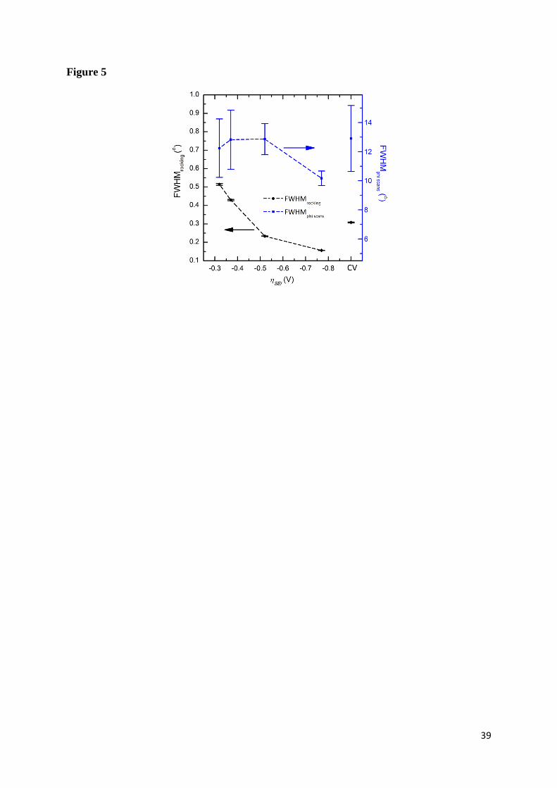
Figure 5 show the FWHM obtained from the ω-rocking curves and the ϕ-scans. The ω-
rocking curves give information about the out-of-plane crystal uniformity, and their FWHM is
considered twice the average tilt of the Bi grains with respect to the GaAs surface. These
scans have been performed around the Bi(024) Bragg reflection instead of the Bi(012)
because the GaAs(111) reflection interferes with the latter, whereas the GaAs(222) reflection
12
does not interfere with the Bi(024). The ϕ-scans give information about the in-plane crystal
uniformity, and their FWHM is considered twice the average twist of the Bi grains with
respect to the GaAs surface. These scans are performed around the strongest asymmetric-
Bragg reflections, i.e., reflections that are not related to the layer texture. In this case of
Bi(012) films grown on GaAs(111)B, we have chosen the Bi(110) reflection, which has a 3-
fold symmetry. However, the azimuthal scans show 12 reflections, which indicates that Bi
grains are distributed in four possible orientations with respect to GaAs(111)B planes. From
the data in Figure 5 we can infer that all the Bi layers show a lower crystal quality than those
grown on Hads-free highly doped n-GaAs substrates [11]. The out-of plane crystal quality is
enhanced with ηSEI whereas the in-plane crystal quality is less sensitive to the growth
overpotential taking into account the error bars. Similarly to the morphology, the film grown
in the dynamic mode exhibits an out-of-plane quality between that of the films grown at ηSEI
= -0.37 V and -0.52 V.
4.3. Electrical characterization of the interface
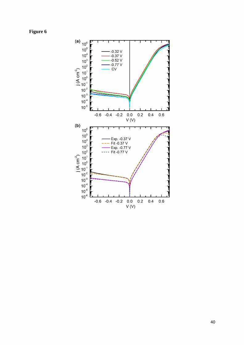
Figure 6a shows j-V curves measured in each Bi film. In all cases, the reverse current
density is 6 orders of magnitude lower than the forward current density, indicating a good
rectifying behaviour, i.e., there is no significant electron tunneling through the barrier.
Consequently, the j-V curves should be analyzed on the basis of Thermionic Emission (TE)
theory [33]. Then, the current that flows through the Schottky barrier is described by:
𝑗𝑗 = 𝐴𝐴∗∗𝑇𝑇2 ∙ 𝑒𝑒𝑒𝑒𝑒𝑒 �− 𝑞𝑞𝜙𝜙𝐵𝐵𝑘𝑘𝐵𝐵𝑇𝑇
� ∙ �−1 + 𝑒𝑒𝑒𝑒𝑒𝑒 �𝑞𝑞𝑉𝑉𝐷𝐷𝑘𝑘𝐵𝐵𝑇𝑇
��
(11)
where A** is the modified Richardson constant, T is the temperature, q is the
elementary charge, φb is the potential barrier height, kB is Boltzmann constant and VD is the
potential across the Schottky barrier. The modification of Richardson constant, A*, into A**=
fp · fq · A* takes into account the probability of an electron reaching the metal without being
backscattered (fp) and the quantum-mechanical transmission (fq) [33]. The optimal value for
13
GaAs substrates is A** = 3 · 104 A m-2 K-2, which has been experimentally evidenced [34]. VD
can be extracted from the applied bias, V, by modeling the system like a Schottky diode in
series with a resistor of resistance R. This R represents the effect of the bulk of the
semiconductor, the electrical contacts, and the probes used to perform the measurements.
Consequently:
𝑉𝑉𝐷𝐷 = (𝑉𝑉 − 𝑗𝑗 ∙ 𝑆𝑆 ∙ 𝑅𝑅) (12)
where S is the area of the diode. In order to obtain a good fit it is necessary to suppose
the existence of interfacial states at the Bi/n-GaAs interface [33]. It is usually considered that
these states, with a density DSS, are located at an interfacial layer of thickness d. Since the
XRD measurements do not show traces of oxides or other compounds, these interfacial states
must be related to metal-induced gap states (MIGS) or to interfacial defects that act as charge
traps. Although the principal native defect that exerts a strong influence on the electrical
properties of GaAs Schottky barriers is the AsGa antisite [35], additional interfacial defects
could be introduced by the mismatch between the Bi layer and the GaAs surface (Figure 5).
Due to the presence of these interfacial states, the barrier height presents a dependence on the
applied field, i.e., on the applied bias:
𝜙𝜙𝑏𝑏 = 𝜙𝜙𝑏𝑏0 + 𝜙𝜙12− �𝜙𝜙1 ∙ �𝜙𝜙𝑏𝑏0 + 𝜙𝜙1
4− 𝑉𝑉𝐷𝐷 −
𝑆𝑆𝐶𝐶−𝑆𝑆𝐹𝐹𝑞𝑞
− 𝑘𝑘𝐵𝐵𝑇𝑇𝑞𝑞�� (13)
where 0bφ is the zero-bias barrier height, φ1 is a parameter related to the characteristics of
the interfacial states layer, Ec is the energy of the bottom of the conduction band (CB) and EF
is the Fermi energy level. Considering the bulk carrier concentration of our substrates (n = 1.3
× 1017 cm-3) and using the Nilsson approximation [36]:
𝐸𝐸𝐶𝐶 − 𝐸𝐸𝐹𝐹 = −𝑘𝑘𝐵𝐵𝑇𝑇 ·
⎩⎨
⎧𝑙𝑙𝑙𝑙(𝑢𝑢)1−𝑢𝑢2
+�34√𝜋𝜋∙𝑢𝑢�
23
1+�0.24+1.08∙�34√𝜋𝜋∙𝑢𝑢�23�−2
⎭⎬
⎫ (14)
where the parameter u is defined as:

14
( )CN
nFu == η21
(15)
Taking into account Nc (= 4.7·1017 cm-3) the effective density of states for electrons in
the CB in GaAs at 290 K [37] and F1/2(η) the Fermi-Dirac integral [36], we obtain a value of
EC - EF ≈ 26 meV. The parameter φ1 is:
s
qnε
αφ2
12
= (16)
where εs is the semiconductor dynamic electrical permittivity, which is 10.89·ε0 for
GaAs [38], being ε0 the vacuum permittivity. The parameter α is related to the characteristics
of the layer containing the interfacial states:
ssi
s
qdDd
+=
εεα (17)
Since this layer is not related to the formation of a new phase, we have considered its
electrical permittivity as εi = ε0. The zero-bias barrier height is also related to the interfacial
states through the Bardeen model [33]:
𝑞𝑞𝜙𝜙𝑏𝑏0 = 𝛾𝛾 ∙ 𝑞𝑞(𝜙𝜙𝑚𝑚 − 𝜒𝜒) + (1 − 𝛾𝛾) ∙ �𝐸𝐸𝑔𝑔 − 𝜙𝜙0� (18)
where φm is the metal work function (4.35 V for Bi) [37], χ is the semiconductor
electron affinity (4.07 V for GaAs) [37], Eg is the semiconductor band gap (1.42 eV for GaAs)
[37] and φ0 is the neutral energy level for the interfacial states (0.5 eV for GaAs) [39, 33, 40].
The parameter γ is also related to the characteristics of the layer containing the interfacial
states [33]:
ssi
i
qdD+=
εεγ (19)
All j-V curves have been analyzed by a nonlinear fit of the experimental data to eq. 11
using the Marquardt–Levenberg algorithm, with R, Dss and d as free parameters. Their
uncertainties have been provided by the fitting on basis of the 95% confidence limits. The

15
fitting has been limited from 0.45 V to -0.3 V because at higher bias there are additional
effects such as local heating [41]. Figure 6b shows two experimental j-V curves with their
respective fittings. Table 2 lists the weighted average values of R, d and DSS obtained for each
Bi film. The errors have been calculated taking into account the errors provided by the
weighted average and the standard deviation. From d and DSS, the zero-bias barrier height, 0bφ ,
has been obtained according to eq. 18 and 19 and its error has been calculated by propagation
of uncertainties [42]. All these values can be considered accurate since their relative errors are
lower than 6%, except for R which has relative errors up to 30%.
Table 2. Resistance (R), Interfacial Layer Width (d), Density of Interfacial States (DSS) and
Zero-Bias Barrier Height (𝑞𝑞𝜙𝜙𝑏𝑏0) Values with their Respective Uncertainties obtained by j-V
Curves Performed in the Bi Films.
ηSEI (V) R (Ω) d (nm) DSS (·1016 eV-1 m-2) 𝒒𝒒𝝓𝝓𝒃𝒃𝟎𝟎 (eV)
-0.32 4.75 ± 0.68 4.06 ± 0.12 8.410 ± 0.098 0.8307 ± 0.0027
-0.37 5.2 ± 1.5 4.06 ± 0.25 7.01 ± 0.25 0.8158 ± 0.0071
-0.52 4.8 ± 0.8 3.79 ± 0.11 8.51 ± 0.23 0.8263 ± 0.0034
-0.77 9.25 ± 0.91 3.802 ± 0.050 9.406 ± 0.047 0.8343 ± 0.0012
CV 21.3 ± 4.7 3.85 ± 0.14 9.32 ± 0.11 0.8346 ± 0.0033
4. Discussion
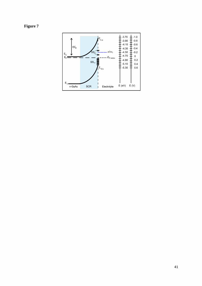
4.1. Energy band diagram of the SEI
As we already reported, the electrochemical properties of a SEI are closely related to its
energy band diagram [9]. Therefore, it is useful to show briefly the principal characteristics of
this diagram. Although a SEI can be a complex structure, it is possible to establish some
analogies with a Schottky barrier where the metal role is played by the Bi(III) electrolyte and
the interfacial states are the surface states at the n-GaAs electrode (Figure 7) [22, 23, 24]. The

16
position of the CB edge at the SEI can be derived from the experimental flat band potential
[9]. Taking into account the flat band potentials of n-GaAs electrodes reported in several
articles [43, 44, 32, 21, 45, 18], we have calculated the average value of the CB edge:
EC,s = (-3.737 ± 0.020) eV (20)
The uncertainty has been considered as the standard deviation of the average due to the
different reported values. In the same way we have calculated the valence band (VB) edge:
EV,s = EC,s - Eg = (-5.157 ± 0.020) eV (21)
The surface states of the GaAs are formed by a surface band of intrinsic states (SSint)
located near the VB and related to surface dangling bonds [46], and some discrete extrinsic
states (SSext) associated to surface defects. [40] According to the Advanced Unified Defect
Model (AUDM) the most relevant SSext in GaAs are antisites [35]. The AsGa antisite (an As
atom surrounded by four As atoms) is a double donor whose energy levels are located at both
0.5 + EV,s, and 0.75 eV + EV,s. The GaAs antisite (a Ga atom surrounded by four Ga atoms) is a
double acceptor that provides two energy levels between the lower level of the AsGa antisite
and EV,s. These native defects have a great importance in GaAs Schottky barriers since they
are related to the pinning of the Fermi level (EF). [40] The position of the EF at the SEI in
equilibrium conditions can be obtained from the OCP. In our case, OCP ≈ 0.07 V vs
Ag/AgCl, which is equivalent to -4.77 eV with respect to the vacuum level [22]. The position
of the EF approximately coincides with the energy of the highest occupied level of SSint,
measured by photocapacitance spectroscopy (E1 = EC,s − 0.98 eV) [47]. This indicates that
surface dangling bonds are filled, i.e., saturated by adsorbed species, which is the reason for
the absence of surface reconstructions in liquid media [46]. Depending on the type of
adsorbed ion at the surface, the OCP can slightly vary from 70 mV (adsorbed protons) to 100
mV (adsorbed anions) due to the different effect that each type of ion produces on the surface

17
dipole [10]. At OCP conditions, i.e., in equilibrium, the energy bands of the n-GaAs electrode
bend upwards, leading to a contact potential (Vbi):
𝑞𝑞𝑉𝑉𝑏𝑏𝑏𝑏 = 𝐸𝐸𝐶𝐶,𝑑𝑑 − 𝐸𝐸𝐶𝐶 = �𝐸𝐸𝐶𝐶,𝑑𝑑 − 𝐸𝐸𝐹𝐹� + (𝐸𝐸𝐹𝐹 − 𝐸𝐸𝐶𝐶) ≈ 0.94 𝑒𝑒𝑉𝑉 (22)
where and EC - EF is obtained from eq. 14. Associated to Vbi, a space charge region
(SCR) of width w is formed in the near-surface region of the n-GaAs electrode:
𝑤𝑤 = �� 2𝜀𝜀𝑑𝑑𝑞𝑞∙𝑁𝑁𝐷𝐷
+� ∙ �𝑉𝑉𝑏𝑏𝑏𝑏 + 𝜂𝜂𝑆𝑆𝑆𝑆𝑆𝑆 −𝑘𝑘𝐵𝐵𝑇𝑇𝑞𝑞� (23)
where ND+ is the concentration of the ionized donors (equal to the bulk electron
concentration, n). At OCP conditions (ηSEI = 0 V), w = 100 nm. This SCR contains a certain
positive charge assigned to the ionized donors that electrically interact with the electrolyte,
affecting the structure of the electrical double layer. As abovementioned, the Bi(III)
electrolyte plays the role of the metal in a Schottky barrier although composed of several
energy levels instead of one. These energy levels, one per redox couple, present a Gaussian
distribution due to the effect of the water molecules surrounding the ions [22]. When EF lies
above one of these energy levels, electrons can be transferred from the substrate to the
electrolyte promoting the reduction reaction [22, 23].
4.2. Analysis of the CV and the current-density transients
When translated to the energy band diagram (Figure 7), the CVs shown in Figure 1
consist in moving EF upwards (cathodic stage or forward bias) and then, downwards (anodic
stage or reverse bias) with respect to its equilibrium position (OCP or zero bias). When the EF
surpasses the energy level of a redox couple a reduction peak is obtained. The reduction peak
of the first scan has an onset potential similar to H+ reduction potential (𝐸𝐸𝐻𝐻+/𝐻𝐻2 ≈ −0.196 𝑉𝑉)
although Bi(III) ions reduction is activated at more positive potentials [48]. This results from
the presence of the blocking Hads layer on the n-GaAs surface [13]. Due to the absence of free
surface sites, Bi(III) ions cannot get reduced on the n-GaAs surface until H+ reduction is
activated since this reaction frees surface sites [13, 10, 15]:
18
𝐻𝐻+ + 𝐻𝐻𝑎𝑎𝑑𝑑𝑑𝑑 + 𝑒𝑒− → 𝐻𝐻2(𝑔𝑔) (24)
Therefore, when using an Hads-covered n-GaAs electrode, the reduction of Bi(III) ions
can only occur simultaneously with H+ reduction, which is activated below ≈ -200 mV, i.e., -
4.5 eV in the energy scale (Figure 7). The absence of anodic peaks in the CVs is a
consequence of the wide SCR provided by the low doping level of the n-GaAs substrate (eq.
23), which avoids the necessary electron tunneling from the electrolyte to the substrate for the
anodic reaction to occur. This has two consequences: i) in the second scan of the CV Bi(III)
ions get reduced on an n-GaAs surface partially covered by metallic Bi, which gives a
reduction peak with a different shape and a different onset potential (≈ -100 mV), ii) it is not
possible to perform the scan route described in reference [14] to obtain an Hads-free n-GaAs
surface on lower-doped substrates. As a result of the second point, the electrodeposition of the
Bi layers is affected by the presence of the Hads layer regardless of the ηSEI.
The analysis of the current-density transients obtained during the nucleation of the Bi
films (Figure 2) has proven to be a powerful tool to gain insight into this combined effect.
When a negative ηSEI is applied EF moves upwards (Figure 7), modifying w (eq. 23) and the
positive charge contained in the SCR. In order to maintain the electrical neutrality, the SEI is
reorganized during the first stage of the transients (eq. 9). The charging of the SEI (jSEI, red
dashed line in Figure 2.b) is only detected at ηSEI = -0.32 V because of the used step time (tstep
= 1 ms). The time constant (τSEI) and the charge (QSEI) involved in this process are similar to
those obtained for a low overpotential (ηSEI = -0.25 V) in our previous work [9]. Anion
desorption (jdes, blue dashed line in Figure 2.b-c) is significantly lower than that observed in
Hads-free n-GaAs substrates for similar ηSEI [9] indicating that the Hads occupies an important
percentage of the electrode surface. The amount of desorbed anions (Qdes) increases with ηSEI
due to the decrease of w and, therefore, the decrease of the positive charge associated with it.
The time constant, τdes, decreases with the overpotential up to ηSEI = -0.52 V when the
19
desorption process becomes undetectable. The time required for the reorganization of the SEI
is given by t0, which is always higher than τSEI and τdes. As well as these time constants, t0
rapidly decreases with ηSEI as the SEI reorganization becomes faster (Table 1).
The dependence of H+ adsorption (jads, green dashed line in Figure 2.b-e) with ηSEI is
different from what it is observed on a Hads-free n-GaAs surface [9] indicating that this
process is influenced by the presence of the Hads layer. Although Qads increases with ηSEI
(Table 1), it is always lower than the charge associated with the formation of one monolayer
of Hads, qm = 232 µC·cm−2, reflecting that the n-GaAs surface is already covered by Hads. In
addition, the relation between Qdes and Qads indicates that H+ gets adsorbed on the surface
sites that become free after anions are desorbed. In fact, Qdes is always lower than Qads
because of the bigger size of anions with respect to H+. At ηSEI = -0.37 V there is an abrupt
increase of Qads related to the coincidence of EF with the AsGa antisite upper level, when new
SS become accessible (Figure 1.a). Although τads always decreases with ηSEI (Table 1), it is
lower than t0 at low overpotentials (ηSEI = -0.32 V and -0.37 V), but similar or higher at high
overpotentials (ηSEI = -0.52 V and -0.77 V). This is a consequence derived from the
progressively enhancement of Bi(III) ion reduction (j3D, orange line in Figure 2b-e), which
delays H + adsorption at high ηSEI.
Protons reduction (jPR, light blue dashed line in Figure 2b-e) is present in all transients
and takes place even during the reorganization of the SEI due to the presence of Hads on the n-
GaAs surface. This process continues until all the n-GaAs surface is covered by metallic Bi,
because Bi does not favor protons reduction [49]. From the comparison of kPR obtained in this
work with respect to a previous work where Hads-free highly doped n-GaAs substrates were
used [9], we can obtain two main conclusions. First, kPR is lower in lower-doped substrates
because the lower surface electron concentration decreases the reaction rates [22]. Second, the
20
increase of kPR with ηSEI is more significant in Hads-covered substrates because the presence of
Hads favors this reaction [32].
After the SEI is reorganized, Bi(III) ion reduction starts and the second range of the
transients begins (eq. 10). The diffusion coefficient of Bi(III) ions, D, is not affected by the
Hads layer and has values between 1.6 to 2.6 · 10-5 cm-2 s-1, which are in the same magnitude
of those found in the literature [50, 51, 52, 9]. Both the saturation density of nucleation sites,
N0, and the nucleation rate, A, are enhanced with ηSEI but do not show a clear dependence
with it, i.e., the Hads layer affects the two parameters. At low overpotentials (ηSEI = -0.32 V
and -0.37 V), N0 is small due to the blockade of the surface sites produced by the Hads layer
and the slow rate of H+ reduction (Table 1). N0 increases with ηSEI in all the studied range due
to the enhancement of kPR. A also increases with ηSEI but does not follow the exponential
tendency reported in other work [53, 54, 55] or the dependency described by Sebastián et al.
based on the classical theory of electrocrystallization [56]. At ηSEI = -0.37 V the value of A is
higher than expected due to the coincidence of EF with the AsGa antisite upper level which
raises Bi(III) ion reduction. Taking into account the data obtained with the analysis of the
current density transients we can conclude that the principal SSext that influences on the
electrochemical properties of an n-GaAs electrode is the upper level of the AsGa antisite defect
(0.75 eV + EV,s). This result is in agreement with the recent work of M. Enache et al. [57]
where they show that the principal group of electronic states at n-type GaAs electrodes is
located at 0.7 eV below the bottom of the CB.
4.3. Properties of the Bi layers
All the studied films have a surface morphology (Figure 3a-e) in agreement with a 3D
nucleation as expected from the analysis of the current density transients (Figure 2b-e). At
low overpotentials (ηSEI = -0.32 V and -0.37 V), the blocking effect of the Hads layer on Bi(III)
ions reduction is significant due to the low kPR and A (Table 1), leading to porous Bi layers
21
with a high rms (Figure 3a-b and f). It should be noticed that a more regular surface, with
islands of similar sizes, is obtained at ηSEI = -0.37 V as a result of the higher A (Table 1). For
ηSEI = -0.52 V and -0.77 V, H+ and Bi(III) ions reduction are enhanced leading to more
compact Bi films with a higher coalescence and a lower rms (Figure 3c-d and f). The
appearance of bigger round-shaped isolated islands at ηSEI = -0.77 V can be related to the
onset of water reduction (also considered as hydrogen evolution at high overpotentials) [9],
reaction that alters the hydrodynamic conditions [58, 59]. Other authors have observed that
this reaction has a clear impact on the surface morphology of electrodeposited films [60, 59].
Moreover, in the areas surrounding where the H2 bubbles were formed, the composition of
alloys [61] and the nanowires length [62] are altered. Due to the low overpotential of water
reduction at a potential of E = -0.7 V, this reaction is undetectable in the deconvolution of the
current-density transient shown in Figure 2e. In all cases the rms is higher than that obtained
for Bi films grown on Hads-free highly doped n-GaAs substrates [11], which is a result of the
lower kPR and A produced by the combination of the lower surface electron concentration and
the presence of the Hads layer. The morphology of the Bi film grown in the dynamic mode
(Figure 3e) can be explained taking into account that the deposition rate in this growth is not
constant but increases with the overpotential. Therefore, the most part of the Bi film is
deposited at high ηSEI and, consequently, the morphology is similar to that obtained for Bi
films grown at high dc potentials. However, since the CV starts at the OCP, the nucleation of
the film occurs at low ηSEI which is responsible for the higher porosity of this film with
respect to the film grown at ηSEI = -0.52 V (Figure 3c).
From the data in Figure 5 we can infer that the out-of plane crystal quality is mainly
influenced by the overpotential and is enhanced progressively with ηSEI. At low ηSEI the
presence of the Hads layer combined with a low kPR and a low A inhibits a good match
between the Bi grains and the n-GaAs surface, leading to high crystal tilts (high FWHM/2).
22
As ηSEI increases, Bi(III) ion and H+ reduction are enhanced leading to a better lattice match,
i.e., lower tilts (lower FWHM/2). Nevertheless, the in-plane crystal quality remains constant
through all the overpotentials, being only slightly enhanced at ηSEI = -0.77 V. Therefore, the
in-plane crystal quality is mainly affected by the Hads layer. Similarly to the morphology, the
film grown in the dynamic mode exhibits both an out-of-plane and in-plane quality between
the films grown at ηSEI = -0.37 V and -0.52 V because the nucleation takes place at low ηSEI
but the main part of the film is deposited at high ηSEI. All the Bi layers show a lower crystal
quality than those grown on Hads-free highly doped n-GaAs substrates [11]. Similarly to the
morphology, this results from the lower values of kPR and A produced by the Hads layer and
the lower surface electron concentration.
All Bi/n-GaAs interfaces behave like Schottky barriers with a good rectifying
behaviour. The values obtained for 𝑞𝑞𝜙𝜙𝑏𝑏0 are in good agreement with those found in the
literature for n-GaAs Schottky barriers obtained by electrodeposition [31, 12, 63]. The
dependence of 𝑞𝑞𝜙𝜙𝑏𝑏0 with ηSEI is similar to that obtained for Bi films electrodeposited on Hads-
free highly doped n-GaAs substrates [11]. Therefore, a similar explanation can be given.
According to the MIGS model and the AUDM, the Fermi level at a Bi/n-GaAs Schottky
barrier should be pinned at 0.5 eV above the VB [33, 40], which gives a 𝑞𝑞𝜙𝜙𝑏𝑏0 = 0.92 𝑒𝑒𝑉𝑉.
However, when MIGS are inhibited or the AsGa/GaAs antisites ratio is modified, EF can be
pinned at 0.75 eV above the VB, leading to a 𝑞𝑞𝜙𝜙𝑏𝑏0 = 0.67 𝑒𝑒𝑉𝑉 . This can happen when
additional defects are created, for example, by the mismatch between the Bi layer and the n-
GaAs surface or by the oxidation of the interface when the films are porous. Consequently,
when the crystal quality of the Bi films is enhanced with ηSEI (Figure 5) the barrier height
tends toward 𝑞𝑞𝜙𝜙𝑏𝑏0 = 0.92 eV (Table 2). However, at ηSEI = -0.32 V the barrier height
increases despite its lower crystal quality because the porosity of the film allows the oxidation

23
of the interface when exposed to the air. Consequently, this interfacial oxide layer could
incorporate new interfacial states that can store additional charge at the interface.
5. Conclusions
The main goal of this work has been to clarify the effect of the Hads layer on the dc
electrodeposition of Bi films at different overpotentials on lower-doped n-GaAs electrodes.
We have also investigated its influence on the Bi properties. The effect of the Hads layer on the
nucleation of the Bi films can be elucidated from the deconvolution of the current density
transients, especially from the behaviour of H+ adsorption, H+ reduction and Bi (III) ion
reduction with ηSEI. In Hads-covered n-GaAs substrates, Bi(III) ion reduction is always
concurrent with H+ reduction and consequently, the kinetics of the former is influenced by the
kinetics of the latter. Bi films surface morphology is correlated with the nucleation process,
principally through kPR and A. As these two parameters are enhanced with ηSEI, flatter and
more compact films are obtained when it increases. The in-plane crystal quality seems to
depend just on the Hads layer whereas the overpotential has an impact on the out-of-plane
crystal quality. The electrical properties of the Bi/n-GaAs interface depend on the density of
interfacial states, which are correlated with the crystal quality and the surface morphology of
the Bi films. Comparing to Bi films grown on Hads-free highly doped n-GaAs surface, we can
conclude that both the low carrier density of the substrate and the presence of the Hads layer
lead to Bi films more porous and rough, with a lower crystal quality and lower Schottky
barriers.
Acknowledgements
This work has been financially supported by the Spanish Ministry of Economy and
Competitiveness (MINECO/FEDER) [project MAT2015-66888-C3-3-R]; Santander and
Universidad Complutense de Madrid [project PR26/16-3B-2]. We would like to acknowledge
24
the postdoctoral fellowship granted by Comunidad de Madrid and the European Union
[PEJD-2016/IND-2233]. We also acknowledge the use of facilities of Instituto de Sistemas
Optoelectrónicos y Microtecnología (ISOM).
25
REFERENCES
[1] T. Hirahara, K. Miyamoto, A. Kimura, Y. Niinuma, G. Bihlmayer, E. V. Chulkov, T.
Nagao, I. Matsuda, S. Qiao, K. Shimada, H. Namatame, M. Taniguchi, S. Hasegawa,
Origin of the surface-state band-splitting in ultrathin Bi films: from Rasbha effect to a
parity effect, New J. Phys. 10 (2008) 083038. DOI: 10.1088/1367-2630/10/8/083038.
[2] M. Wada, S. Murakami, F. Freimuth, G. Bihlmayer, Localized edge states in two-
dimensional topological insulators: ultrathin Bi films, Phys. Rev. B 83 (2011)
121310(R). DOI: 10.1103/PhysRevB.83.121310.
[3] F. Y. Yang, K. Liu, K. Hong, D. H. Reich, P. C. Searson, C. L. Chien, Y. Leprince-
Wang, K. Yu-Zhang, K. Han, Shubnikov-de Haas oscillations in electrodeposited
single-crystal bismuth films, Phys. Rev. B 61 (2000) 6631-6636. DOI:
10.1103/PhysRevB.61.6631.
[4] C. A. Hoffman, J. R. Meyer, F. J. Bartoli, A. D. Venere, X. J. Yi, C. L. Hou, H. C.
Wang, J. B. Ketterson, G. K. Wong, Semimetal-to-semiconductor transition in bismuth
thin, Phys. Rev. B 48 (1993) 11431. DOI: 10.1103/PhysRevB.48.11431.
[5] S. Sangiao, J. M. Michalik, L. Casado, M. C. Martínez-Velarte, L. Morellón, M. R.
Ibarra, J. M. De Teresa, Conductance steps in electromigrated Bi nanoconstrictions,
Phys. Chem. Chem. Phys. 15 (2013) 5132. DOI:
10.1039/C3CP44133D.
[6] T. Hirahara, K. Miyamoto, I. Matsuda, T. Kadono, A. Kimura, T. Nagao, G. Bihlmayer,
E. V. Chulkov, S. Qiao, K. Shimada, H. Namatame, M. Taniguchi, S. Hasegawa, Direct
observation of spin splitting in bismuth surface states, Phys. Rev. B 76 (2007) 153305.
DOI: 10.1103/PhysRevB.76.153305.
[7] A. V. Khvalkovskiy, V. Cros, D. Apalkov, V. Nikitin, M. Krounbi, K. A. Zvezdin, A.
Anane, J. Grollier, A. Fert, Matching domain wall configuration and spin-orbit torques
26
for efficient domain-wall motion, Phys. Rev. B 87 (2013) 020402(R). DOI:
10.1103/PhysRevB.87.020402.
[8] J. C. Rojas Sánchez, L. Vila, G. Desfonds, S. Gambarelli, J. P. Attane, J. M. De Teresa,
C. Magén, A. Fert, Spin-to-charge conversion using Rashba coupling at the interface
between non-magnetic materials, Nat. Commun. 4 (2013) 2944. DOI:
10.1038/ncomms3944.
[9] A. Prados, R. Ranchal, Electrodeposition of Bi thin films on n-GaAs(111)B. I.
Correlation between the overpotential and the nucleation process, J. Phys.Chem. C 122
(2018) 8874. DOI: 10.1021/acs.jpcc.8b01838.
[10] A. Prados, L. Pérez, A. Guzmán, R. Ranchal, Mixed effects of the atomic arrangement
and surface chemistry on the electrodeposition of Bi thin films on n-GaAs substrates, J.
Phys. Chem. C 120 (2016) 28295. DOI: 10.1021/acs.jpcc.6b09144.
[11] A. Prados, R. Ranchal, Electrodeposition of Bi thin films on n-GaAs(111)B. II.
Correlation between the nucleation process and the structural and electrical properties,
J. Phys. Chem. C 122 (2018) 8886. DOI: 10.1021/acs.jpcc.7b12263.
[12] Z. L. Bao, K. L. Kavanagh, Epitaxial Bi/GaAs diodes via electrodeposition, J. Vac. Sci.
Technol. B 24 (2006) 2138. DOI: 10.1116/1.2218874.
[13] A. Prados, R. Ranchal, L. Pérez, Blocking effect in the electrodeposition of Bi on n-
GaAs in acidic electrolytes, 143 (2014) 23. DOI: 10.1016/j.electacta.2014.07.137.
[14] A. Prados, R. Ranchal, L. Pérez, Strategies to unblock the n-GaAs surface when
electrodepositing Bi from acidic solutions, Electrochim. Acta 174 (2015) 264. DOI:
10.1016/j.electacta.2015.05.188.
[15] B. H. Erné, F. Ozanam, J. -N. Chazalviel, The mechanism of hydrogen gas evolution on
GaAs cathodes elucidated by in situ snfrared spectroscopy, J. Phys. Chem. B 103 (1999)
2948. DOI: 10.1021/jp984765t.
27
[16] H. Gerischer, Electrochemical behaviour of semiconductors under illumination, J.
Electrochem. Soc. 113 (1966) 1174. DOI: 10.1149/1.2423779.
[17] J. Li, L. M. Peter, Surface recombination at semiconductor electordes. Part IV., J.
Electroanal. Chem. 199 (1986) 1. DOI: 10.1016/0022-0728(86)87038-3.
[18] Y. Huang, J. Luo, D. G. Ivey, Comparative study of GaAs corrosion in H2SO4 and
NH3H2O solutions by electrochemical methods and surface analysis, Mater. Chem.
Phys. 93 (2005) 429. DOI: 10.1016/j.matchemphys.2005.03.049.
[19] T. Mayer, M. Lebedev, R. Hunger, W. Jaegermann, Elementary processes at
semiconductor/electrolyte interfaces: perspectives and limits of electron spectroscopy,
Appl. Surf. Sci. 252 (2005) 31. DOI: 10.1016/j.apsusc.2005.01.110.
[20] M. V. Lebedev, T. Masuda, K. Uosaki, Charge transport at the interface of n-GaAs
(100) with an aqueous HCl solution: electrochemical impedance spectroscopy study,
Semicond. 46 (2012) 471. DOI: 10.1134/S1063782612040136.
[21] B. H. Erné, F. Ozanam, J. -N. Chazalviel, Dynamics of hydrogen adsorption on GaAs
electrodes, Phys. Rev. Lett. 80 (1998) 4337. DOI: 10.1103/PhysRevLett.80.4337.
[22] R. Memming, Semiconductor electrochemistry, Wiley-VCH , Darmstadt, 2001.
[23] N. Sato, Electrochemistry at metal and semiconductor electrodes, Elsevier Science B.V.,
Amsterdam, 1998.
[24] G. Oskam, P. M. Hoffmann, A. Natarajan, P. C. Searson, Semiconductor/electrolyte
boundaries, in: J. G. Webster, Wiley Encyclopedia of electrical and electronics
engineering, John Wiley and Sons, 2007. DOI: 10.1002/047134608X.W3225.pub2.
[25] M. Palomar-Pardavé, M. Miranda-Hernández, I. González, N. Batina, Detailed
characterization of potentiostatic current transients with 2D-2D and 2D-3D nucleation
transitions, Surf. Sci. 399 (1998) 80. DOI: 10.1016/S0039-6028(97)00813-3.
28
[26] M. H. Hölzle, U. Retter, D. M. Kolb, The kinetics of structural changes in Cu adlayers
on Au(111), J. Electroanal. Chem. 371 (1994) 101. DOI: 10.1016/0022-0728(93)03235-
H.
[27] M. Palomar-Pardavé, B. Scharifker, E. Arce, M. Romero-Romo, Nucleation and
diffusion-controlled growth of electroactive centers. Reduction of protons during cobalt
electrodeposition, Electrochim. Acta 50 (2005) 4736. DOI:
10.1016/j.electacta.2005.03.004.
[28] B. H. Erné, M. Stchakovsky, F. Ozanam, J.-N. Chazalviel, Surface composition of n-
GaAs cathodes during hydrogen evolution characterized by in situ ultraviolet-visible
ellipsometry and in situ infrared spectroscopy, J. Electrochem. Soc. 145 (1998) 447.
DOI: 10.1149/1.1838283.
[29] P. M. Rigano, C. Mayer, T. Chierchie, Electrochemical nucleation and growth of copper
on polycriystalline palladium, J. Electroanal. Chem. Interfacial Electrochem. 248 (1988)
219. DOI: 10.1016/0022-0728(88)85163-5.
[30] B. R. Scharifker, J. Mostany, M. Palomar-Pardavé, I. González, On the theory of the
potentiostatic current transient for diffusion-controlled three-dimensional
electrocrystallization processes, J. Electrochem. Soc. 146 (1999) 1005. DOI:
10.1149/1.1391713.
[31] P. M. Vereecken, P. C. Searson, Electrochemical deposition of Bi on GaAs (100), J.
Electrochem. Soc. 148 (2001) C733. DOI: 10.1149/1.1406493.
[32] I. Uhlendorf, R. Reineke-Koch, R. Memming, Analysis of the hydrogen formation at
GaAs electrodes by impedance spectroscopy investigations, Ber. Bunsenges. Phys.
Chem. 99 (1995) 1082. DOI: 10.1002/bbpc.199500038.
[33] E. H. Rhoderick, Metal-semiconductor contacts, IEE Proceedings I - Solid-State and
Electron Devices 129 (1982) 1. DOI: 10.1049/ip-i-1.1982.0001.
29
[34] Y. A. Goldberg, E. A. Posse, B. V. Tsarenkov, Mechanism of flow of direct current in
GaAs surface-barrier structures, Sov. Phys. Semicond. 9 (1975) 337.
[35] W. E. Spicer, Z. Liliental‐Weber, E. Weber, N. Newman, T. Kendelewicz, R. Cao, C.
McCants, P. Mahowald, K. Miyano, I. Lindau, The advanced unified defect model for
Schottky barrier formation, J. Vac. Sci. Tec. B 6 (1988) 1245. DOI: 10.1116/1.584244.
[36] J. S. Blakemore, Approximation for Fermi-Dirac Integrals, especially the function
F_1/2(η) used to describe electron density in a semiconductor, Solid-State Electron. 25
(1982) 1067. DOI: 10.1016/0038-1101(82)90143-5.
[37] S. M. Sze, Physics of Semiconductor Devices, John Wiley & Sons, Inc., New York,
1981.
[38] V. L. Rideout, C. R. Crowell, Effects of image force and tunneling on current transport
in metal-semiconductor (Schottky barrier) contacts, Solid-State Electron. 13 (1970) 993.
DOI: 10.1016/0038-1101(70)90097-3.
[39] A. M. Cowley, S. M. Sze, Surface states and barrier height of metal semiconductor
Systems, J. Appl. Phys. 36 (1965) 3212. DOI: 10.1063/1.1702952.
[40] W. Mönch, Electronic structure of metal-semiconductor contacts, Springer, Dordrecht,
1990.
[41] R. Stratton, Volt-current characteristics for tunneling through insulating films, J. Phys.
Chem. Sol. 23 (1962) 1177. DOI: 10.1016/0022-3697(62)90165-8.
[42] J. R. Taylor, An introduction to error analysis. The study of uncertainties in physical
measurements, University Science Books, Sausalito (CA - USA), 1997.
[43] K. Rajeshwar, T. Mraz, The n-GaAs/electrolyte interface: evidence for specificity in
lattice ion-electrolyte interactions, dependence of interfacial potential drops on crystal
plane orientation to the electrolyte and implications for solar energy conversion, J. Phys.
Chem. 87 (1983) 742. DOI: 10.1021/j100228a010.
30
[44] P. Allongue, E. Souteyrand, L. Allemand, Metal electrodeposition on semiconductors.
Part III: Description of charge transfer for the formation of Schottky diodes, J.
Electroanal. Chem. 362 (1993) 89. DOI: 10.1016/0022-0728(93)80009-7.
[45] L. M. Depestel, K. Strubbe, Influence of the crystal orientation on the electrochemical
behaviour of n-GaAs in Au(I)-containing solutions, Phys. Chem. Chem. Phys. 5 (2003)
2881. DOI: 10.1039/B302243A.
[46] H. Lüth, Surface and interfaces of solid materials, Springer, Berlin, 1995. DOI
10.1007/978-3-662-03132-2.
[47] P. Allongue, Steady state photocapacitance study of semiconductor/electrolyte junctions
II. Surface state distribution and charge transfer mechanisms, Ber. Bunsenges. Phys.
Chern. 92 (1988) 895. DOI: 10.1002/bbpc.198800217.
[48] M. S. Antelman, The encyclopedia of chemical electrode potentials (1st ed.), Plenum
Press, New York, 1982. DOl: 10.1007/978-1-4613-3374-6.
[49] S. Trassati, Work function, electronegativity, and electrochemical behaviour of metals.
III. Electrolytic hydrogen evolution in acid solutions, Electroanal. Chem. Interf.
Electrochem. 39 (1972) 163. DOI: 10.1016/S0022-0728(72)80485-6.
[50] S. H. Cadle, S. Bruckenstein, Ring-disk electrode study of the reduction of bismuth on
platinum, Anal. Chem. 44 (1972) 1993. DOI: 10.1021/ac60320a011.
[51] P. M. Vereecken, K. Rodbell, C. Ji, P. C. Searson, Electrodeposition of bismuth thin
films on n-GaAs (110), Appl. Phys. Lett. 86 (2005) 121916. DOI: 10.1063/1.1886248g.
[52] M. A. Elmorsi, K. Jüttner, Electrolytic deposition of bismuth on CdS(0001) single-
crystal surfaces, Electrochim. Acta 31 (1986) 211. DOI: 10.1016/0013-4686(86)87110-
9.
[53] M. Palomar-Pardavé, J. Aldana-González, L. E. Botello, E. M. Arce-Estrada, M. T.
Ramírezz-Silva, J. Mostany, M. Romero-Romo, Influence of temperature on the
31
thermodynamics and kinetics of cobalt electrochemical nucleation and growth,
Electrochim. Acta 241 (2017) 162. DOI: 10.1016/j.electacta.2017.04.126.
[54] E. Barrera, M. Palomar-Pardavé, N. Batina, I. González, Formation mechanisms and
characterization of black and white cobalt electrodeposition onto stainless steel, J.
Electrochem. Soc. 147 (2000) 1787. DOI: 10.1149/1.1393435.
[55] M. Aguilar-Sánchez, M. Palomar-Pardavé, M. Romero-Romo, M. T. Ramírez-Silva, E.
Barrera, B. R. Scharifker, Electrochemical nucleation and growth of black and white
chromium deposits onto stainless steel surfaces, J. Electroanal. Chem. 647 (2010) 128.
DOI: 10.1016/j.jelechem.2010.06.012.
[56] P. Sebastián, L. E. Botello, E. Vallés, E. Gómez, M. Palomar-Pardavé, B. R. Scharifker,
J. Mostany, Three-dimensional nucleation with diffusion controlled growth: A
comparative study of electrochemical phase formation fromaqueous and deep eutectic
solvents, J. Electroanal. Chem. 793 (2017) 119. DOI: 10.1016/j.elechem.2016.12.014.
[57] M. Enache, C. Negrila, M. Anastasescu, G. Dobrescu, M. F. Lazarescu, V. Lazarescu,
Surface states- and field-effects at GaAs(100) electrodes in sodium dodecyl sulfate acid
solution, J. Electrochem. Soc. 165 (2018) H3008. DOI: 10.1149/2.0031804jes.
[58] L. J. J. Janssen, J. Hoogland, The effect of electrolytically evolved gas bubbles on the
thickness of the diffusion layer, Electrochim. Acta 15 (1970) 1013. DOI: 10.1016/0013-
4686(73)85016-9.
[59] N. D. Nikolić, K. I. Popov, L. J. Pavlović, M. G. Pavlović, The effect of hydrogen
codeposition on the morphology of copper electrodeposits. I. The concept of effective
overpotential, J. Electroanal. Chem. 588 (2006) 88. DOI:
10.1016/j.jelechem.2005.12.006.
[60] H.-C. Shin, J. Dong, M. Liu, Nanoporous structures prepared by an electrochemical
deposition process, Adv. Mater. 15 (2003) 1610. DOI: 10.1002/adma.200305160.
32
[61] K. Msellak, J. -P. Chopart, O. Jbara, O. Aaboubi, J.Amblard, Magnetic field effects on
Ni–Fe alloys codeposition, J. Magn. Magn Mater. 281 (2004) 295. DOI:
10.1016/j.jmmm.2004.04.118
[62] A. Llavona, L. Pérez, M. Sánchez, V. de Manuel, Enhancement of anomalous
codeposition in the synthesis of Fe–Ni alloys in nanopores, Electrochim. Acta 106
(2013) 392. DOI: 10.1016/j.electacta.2013.05.116.
[63] A. De Vrieze, K. Strubbe, W. P. Gomes, S. Forment, R. L. Van Meirhaeghe,
Electrochemical formation and properties of n-GaAs/Au and n-GaAs/Ag Schottky
barriers: Influence of surface composition upon the barrier height., Phys. Chem. Chem.
Phys. 3 (2001) 5297. DOI: 10.1039/b104887m.

33
FIGURES CAPTIONS
Figure 1. Cyclic voltammetry scans performed on a lower-doped n-GaAs(111)B substrate
into the Bi(III) solution at 10 mV/s.
Figure 2. (a) Current density transients recorded during the nucleation of the Bi layers
electrodeposited on lower-doped n-GaAs(111)B substrates at different overpotentials.
Individual contributions obtained from the deconvolution of the transient recorded at a ηSEI of
(b) -0.32 V, (c) -0.37 V, (d) -0.52 V, and (e) -0.77 V. Insets: enlargement of the initial current
density decay.
Figure 3. AFM images and representative depth profiles shown below each image measured
on the Bi thin films (40 nm) grown on lower-doped n-GaAs(111)B substrates at a ηSEI of (a) -
0.32 V, (b) -0.37 V, (c) -0.52 V, (d) -0.77 V, and (e) performing several CV scans.
Figure 4. Bragg−Brentano XRD patterns of the Bi films grown on lower-doped n-
GaAs(111)B substrates at different ηSEI (static mode) and performing CV scans (dynamic
mode). The dashed lines indicate the position of Bi reflections (ICDD card 00-044-1246) that
matches with an observed peak. Peaks marked with * correspond to GaAs(333) reflections.
Figure 5. FWHM of ω-rocking and φ-scans measured in the Bi films.
Figure 6. (a) Experimental j-V curves measured in the Bi films. (b) Experimental j-V curves
measured in the films grown at ηSEI = -0.37 V and -0.77 V with their corrresponding fittings.
Figure 7. Energy band diagram at OCP conditions of a SEI formed by an n-GaAs substrate (n
= 1.3 · 1017 cm-3) immersed in the Bi(III) solution.
34
FIGURES
Graphical Abstract

35
Figure 1

36
Figure 2
37
Figure 3

38
Figure 4
39
Figure 5
40
Figure 6
41
Figure 7