Synthesis, contact printing, and device characterization of Ni-catalyzed, crystalline InAs nanowires
21
1 Synthesis, Contact Printing, and Device Characterization of Ni- Catalyzed, Crystalline InAs Nanowires Alexandra C. Ford 1,2 , Johnny C. Ho 1,2 , Zhiyong Fan 1,2 , Onur Ergen 1 , Virginia Altoe 3 , Shaul Aloni 3 , Haleh Razavi 1 , Ali Javey 1,2, * 1. Department of Electrical Engineering and Computer Sciences, University of California at Berkeley, Berkeley, CA 94720. 2. Materials Sciences Division, Lawrence Berkeley National Laboratory, Berkeley, CA 94720 3. Molecular Foundry, Lawrence Berkeley National Laboratory, Berkeley, CA 94720 * Author to whom correspondence should be addressed. Electronic mail: [email protected] ASTRACT - InAs nanowires have been actively explored as the channel material for high performance transistors owing to their high electron mobility and ease of ohmic metal contact formation. The catalytic growth of non-epitaxial InAs nanowires, however, has often relied on the use of Au colloids which is non-CMOS compatible. Here, we demonstrate the successful synthesis of high yield of crystalline InAs nanowires with high yield and tunable diameters by using Ni nanoparticles as the catalyst material on amorphous SiO 2 substrates. The nanowires show superb electrical properties with field-effect electron mobility ~2,700 cm 2 /Vs and I ON /I OFF >10 3 . The uniformity and purity of the grown InAs nanowires are further demonstrated by large- scale assembly of parallel arrays of nanowires on substrates via the contact printing process that enables high performance, “printable” transistors, capable of delivering 5-10 mA ON currents (~400 nanowires).
-
Upload
independent -
Category
Documents
-
view
0 -
download
0
Transcript of Synthesis, contact printing, and device characterization of Ni-catalyzed, crystalline InAs nanowires

1
Synthesis, Contact Printing, and Device Characterization of Ni-
Catalyzed, Crystalline InAs Nanowires
Alexandra C. Ford1,2
, Johnny C. Ho1,2
, Zhiyong Fan1,2
, Onur Ergen1, Virginia Altoe
3, Shaul
Aloni3, Haleh Razavi
1, Ali Javey
1,2,*
1. Department of Electrical Engineering and Computer Sciences, University of California at
Berkeley, Berkeley, CA 94720.
2. Materials Sciences Division, Lawrence Berkeley National Laboratory, Berkeley, CA 94720
3. Molecular Foundry, Lawrence Berkeley National Laboratory, Berkeley, CA 94720
* Author to whom correspondence should be addressed.
Electronic mail: [email protected]
ASTRACT - InAs nanowires have been actively explored as the channel material for high
performance transistors owing to their high electron mobility and ease of ohmic metal contact
formation. The catalytic growth of non-epitaxial InAs nanowires, however, has often relied on
the use of Au colloids which is non-CMOS compatible. Here, we demonstrate the successful
synthesis of high yield of crystalline InAs nanowires with high yield and tunable diameters by
using Ni nanoparticles as the catalyst material on amorphous SiO2 substrates. The nanowires
show superb electrical properties with field-effect electron mobility ~2,700 cm2/Vs and ION/IOFF
>103. The uniformity and purity of the grown InAs nanowires are further demonstrated by large-
scale assembly of parallel arrays of nanowires on substrates via the contact printing process that
enables high performance, “printable” transistors, capable of delivering 5-10 mA ON currents
(~400 nanowires).

2
The ability to control the size, structure, composition and morphology of semiconductor
nanowires (NWs) makes them ideal one-dimensional building blocks for potential applications in
high performance nanoelectronics and large-area, flexible electronics.1-7
Uniquely, nanowires
can be readily assembled on various substrates using low temperature processing conditions,
therefore, making them compatible with CMOS processing while avoiding the lattice mismatch
and single-crystalline growth challenges often encountered for epitaxial, planar thin films.8-11
As
a result, hybrid electronics4 consisting of “top-down” Si CMOS and “bottom-up” nanomaterials
may be envisioned for enabling advanced functionalities. In particular, InAs nanowires have
been widely explored as the channel material for high performance transistors owing to (i) their
high electron mobility (µn), and (ii) the ability to readily form near-ohmic, transparent metal
source/drain contacts due to their small band gap and the intrinsic surface charge accumulation
layer.2,12-15
Additionally, InAs has a large bulk exciton Bohr radius (~34 nm) which is on the
order of the radial size of nanowires, resulting in 1-D quantum confinement of the carriers with
potentially interesting carrier transport characteristics.16
The reported synthesis of non-epitaxial, semiconductor nanowires often involves the
vapor-liquid-solid (VLS) or vapor-solid-solid (VSS) mechanisms, where a metal nanoparticle
(NP) catalyzes the growth. Currently, InAs NWs grown on amorphous substrates have all
utilized Au NPs as the catalyst material.12-15,17
Au, however, is a non-ideal material for
electronics and is incompatible with conventional Si CMOS technology because of its well-
known role as a deep-level trap in Si, resulting in severe degradation of CMOS properties. This
presents a challenge for potential integration of InAs NWs with Si CMOS for hybrid electronics.
Furthermore, the exact magnitude of Au incorporation and its role on the electrical properties of
InAs NWs is still not known. While there has been multiple reports of growing InAs NWs

3
epitaxially on crystalline Si and InAs substrates without the use of metal NPs,18-19
such
approaches are not compatible with certain applications, for instance for those utilizing roll or
contact printing of NWs that require high yield growth on amorphous substrates (i.e., glass
rollers).8-9
Therefore, there is a need to explore alternative catalyst materials for VLS/VSS
growth of high purity, crystalline InAs NWs for high performance, CMOS-compatible, and yet
printable electronics. To address this challenge, here, we demonstrate the successful synthesis of
crystalline, high-mobility InAs nanowires by using Ni NPs with tunable diameters. These grown
nanowires are then successfully transferred to receiver substrates in highly regular arrays by the
contact printing process and configured as the channel material for high performance transistors.
Ni nanoclusters used for InAs nanowire growth were obtained by thermal annealing (800-
900ºC) of thin Ni films (thermally evaporated) on Si/SiO2 (50 nm thermally grown) substrates in
a hydrogen environment. Due to the finite mobility and diffusion of the Ni atoms on SiO2
surfaces at elevated temperatures, NPs are formed upon aggregation and bonding of the atoms
via metal-metal interactions. The NP diameters can be readily tuned by the corresponding thin
film thickness and the annealing conditions. Figure 1 shows the atomic force microcopy (AFM)
images and corresponding particle diameter distributions of Ni particles formed by the thermal
annealing of 0.5 nm (Fig. 1a and b), 1.5 nm (Fig. 1c and d), and 3 nm (Fig. 1e and f) Ni films at
850 ºC for 10 min. The NP diameters obtained from AFM and scanning electron microscopy
(SEM) for the 0.5, 1.5, and 3 nm films are 10±2, 14±3, and 26±5 nm, respectively. The diameter
variation as a percent of the mean for all three particle sizes is ~20%. This is remarkably good
considering the simplicity of this method, and that the variation for commercially available
colloidal Au NPs used to grow nanowires of similar diameter (20-40 nm) is ~10%.

4
The NPs attained from thin film annealing were used as catalytic seeds for the growth of
InAs nanowires. After the thermal annealing process, the sample temperature was reduced to
470-550ºC, and InAs NWs were then grown for ~1 hr by vaporization of InAs solid source
(source temperature 720ºC). The growth furnace consisted of two independently controlled
temperature zones, one for the solid source and the other for the sample, similar to the previously
reported Au-catalyzed InAs NW growth set up.13
Hydrogen (150 s.c.c.m.) was used as the carrier
gas for the delivery of the thermally vaporized solid InAs source. The pressure was maintained
constant at ~1 torr. The NWs were grown chemically intrinsic without any intentional doping.
SEM images of Ni-catalyzed InAs NWs grown from different particle diameters are shown in
Fig. 2. From the SEM images, it is evident that the grown NWs are relatively straight with low
structural defect density. Furthermore, Ni NPs can be clearly observed at the tip of most
nanowires (Fig. 2), which is a distinct characteristic of the tip-based, VLS/VSS growth
mechanism. The NW diameter shows a direct correlation with the catalytic NP diameter.
Nanowire diameters of 23±6, 26±8, and 38±9 nm were obtained for 10, 14, and 26 nm NPs,
respectively. The variation as a percent of the mean for the grown nanowires is 25-32% which is
slightly larger than that of the NP distribution. The optimal sample temperature is found to
depend on the NP diameter. For the 10, 14, and 26 nm NPs, sample temperatures of 475, 500,
and 520ºC were found to yield the highest density of NWs, respectively (Table 1). The higher
growth temperature for larger particles is expected as the larger particles have higher eutectic
temperatures. Notably, while relatively high NW growth yields are observed at the optimal
temperatures for both 10 and 14 nm NPs (5-50 NW/µm2), significantly lower yield is observed
for the 26 nm NPs (~1 NW/µm2). This diameter dependence growth yield can be explained by
the higher activation energy and higher InAs source delivery rate required for the successful

5
nucleation and therefore growth of larger diameter nanowires. The successful catalytic growth of
InAs NWs from Ni NPs arises from the phase properties and the eutectic temperature of the Ni-
In-As system. However, the phase diagrams for Ni-In-As have not been well-studied, either
experimentally or theoretically. Given the interest in nanowire growth by the vapor-liquid-solid
process, this is certainly an area that needs further attention and future exploration. We note that
our growth temperatures using Ni and Au NPs of similar diameter are approximately the same
(Table 1), suggesting similar eutectic temperatures for the Au-In-As and Ni-In-As systems at this
scale.
The structure of the InAs NWs was studied by transmission electron microscopy (TEM).
Low and high resolution TEM images confirm the crystallinity and low defect density of the
NWs as well as the presence of 2-3 nm thick amorphous surface layer. This layer thickness is
consistent with the typical native oxide present on the surface of bulk InAs. Most of the NWs
have diameters ranging from ~20-40 nm. The diameters are uniform along the nanowire and no
“tapering” is observed, confirming the lack of uncontrolled over-coating during the growth
process. Figure 3 shows typical HRTEM images of InAs NWs grown at 475 oC. No dominant
growth axis was observed. Several NWs studied by TEM grew in the [211] direction, with one
such NW shown in Figure 3a. NW growth along the [210] direction (Figure 3b) was also
observed. Figure 3c shows a NW grown ~7o off the [111] direction. Data obtained from
standardless x-ray EDS elemental analysis gave In/As ratios ranging from 1.2 to 1.5, suggesting
the composition of the NWs is close to the expected stoichiometry.
To characterize the electrical properties of the Ni-catalyzed InAs NWs, field-effect
transistors (FETs) were fabricated (Fig. 4a) by using Ni (~50 nm) source/drain (S/D) metal
contacts in a common back gated geometry (50 nm thermal oxide as gate dielectric, and heavily

6
B doped Si substrate as the gate). The electrical properties of a representative FET consisting of
an individual InAs NW as the channel material with diameter (i.e., channel width) d~25 nm (NW
diameter ~29 NW with ~2 nm native oxide shell) and a channel length of L~9.9µm are show in
Fig. 4b-c. The transistor shows a minimal hysteresis (Fig 4b) with an ON current ION~12 µA at
VDS = 3V and VGS=5V, corresponding to a current density of ~0.5 mA/µm as normalized with the
nanowire diameter. Notably, the ON current for this long channel device is comparable to that of
the state-of-the-art Si MOSFETs (ION~1 mA/µm), even though the channel length is over two
orders of magnitude larger. The device also exhibits a respectable ION/IOFF>103 (Fig 4b, inset) at
VDS=0.5V. The low-bias (low VDS, linear-triode region), ON-state conductance of this nanowire
as normalized by the channel length is GON~60 µS.µm. Notably, the NW transistors exhibit a
uniform response in terms of both ON and OFF state conductance with GON=40-120 µS.µm and
GON/GOFF>102 for over 100 measured devices (d=20-30 nm and L=2-10 µm).
The high ON current and conductance of the InAs NWs arise from their high electron
mobility, and demonstrates the utility of these synthetic materials for high performance
electronics. The field-effect mobility of the nanowires was estimated from the transfer
characteristics and is depicted in Fig. 4d as a function of the back-gate voltage VGS. The mobility
was deduced from the low-bias (low VDS) transconductance, dIDS/dVGS of the device by using the
standard square-law model,
DSoxGS
DS
nVC
L
dV
dI 12
where Cox is the gate capacitance. The capacitance Cox = 0.52 fF was
obtained from modeling using the finite element analysis software Finite Element Method
Magnetics. From the square law model, a peak electron mobility of µn~2,700 cm2/Vs is obtained.
Notably, this electron mobility estimation presents the lower boundary limit as no correction was
taken into account, for example, for possible contact resistance. Our Ni-catalyzed InAs NW

7
mobility is comparable to the previously reported Au-catalyzed NWs.2,12-15
Further enhancement
of the mobility may be achieved in the future by the passivation of the NW surfaces with large
band-gap InP shell as previously demonstrated in ref. 13.
To further investigate the electrical properties and uniformity of the Ni-catalyzed InAs
nanowires, we utilized the contact printing approach8 to controllably transfer and assemble
parallel arrays of NWs on Si/SiO2 substrates over large areas with an average pitch of ~0.5 µm.
Poly-L-lysine (0.1%w/v in H2O, Sigma-Aldrich) was applied to the receiver substrate prior to the
printing process to enhance the nanowire-substrate chemical interactions and yield a higher
nanowire density. Octane:mineral oil (2:1 v/v) was used as a lubricant for the printing process to
reduce uncontrollable nanowire-nanowire friction and therefore, enable controlled transfer of
aligned nanowires. Following nanowire printing, FETs were fabricated based on the printed InAs
NW arrays by using Ni (~50 nm) source/drain (S/D) metal contacts in a common back gated
geometry (50 nm thermal oxide as gate dielectric). Figure 5a shows an SEM image and device
schematic of a printed InAs NW device. The electrical properties of a representative FET
consisting of an array of printed InAs NWs (width~200 µm and channel length~3 µm) are shown
in Figures 5b and c. The transistor delivers an ON current of ~6 mA at VDS = 3V, which
corresponds to ~15 µA per nanowire (~400 NWs bridging S/D) with ION/IOFF ~100. The parallel-
array NW FETs demonstrate the feasibility of using a printing technology for attaining high
performance devices with potentially high switching speeds. Notably, since during the printing
process, all synthesized materials are transferred from the growth substrate to the receiver
substrate, the results attest the high purity and uniformity of the InAs nanowires grown by using
Ni NPs. In future, the nanowire device performance can be readily enhanced through channel
length scaling and integration of high-κ dielectrics in a top gate configuration.13,20-22

8
In conclusion, a method to grow crystalline, high-mobility InAs nanowires on amorphous
substrates by the VLS/VSS process (non-epitaxial) with the use of Ni catalyst has been
demonstraed. Ni NPs are found to serve as efficient catalytic materials for InAs NW growth.
Importantly, the chemical composition of the wires grown using this method is close to the
expected stoichiometry, therefore, enabling high performance nanowire devices with electron
mobility ~2,700 cm2/Vs and ION/IOFF>10
3. The high yield and purity of the grown InAs
nanowires enable for the successful and aligned transfer of NWs from the growth substrate to the
receiver substrate by the contact printing process. The ability to grow high mobility, crystalline,
CMOS-compatible, and printable InAs NWs may have important implications for future
integration of InAs NWs for various electronic applications.
Experimental Section
Thermal evaporation was carried out using 99.995% pure Ni pellets (Kurt J. Lesker) under a
vacuum of ~8x10⁻⁷
torr. AFM used to image the Ni catalysts after annealing was performed
using a Digital Instruments Dimension 3100. SEM and TEM were performed on the InAs
nanowires using a Gemini Leo 1550 and JEOL 2100-F 200 kV, respectively. The InAs nanowire
FET devices were fabricated by drop-casting the InAs nanowires suspended in ethanol onto p-
type Si substrates with a 50 nm gate oxide. Photolithography was used to define the source and
drain regions and Ni was thermally evaporated to form the source and drain contacts. Details of
the printing process for fabrication of the InAs NW array FETs have been previously described.8
Acknowledgements. This work was financially supported by MARCO/MSD Focus Center
Research Program, Intel Corporation, Lawrence Berkeley National Laboratory, and an Intel

9
Graduate Fellowship (J.C.H.). All fabrication was performed in the UC Berkeley Microlab
facility. TEM imaging was performed at the Molecular Foundry, Lawrence Berkeley National
Laboratory, which is supported by the Office of Science, Office of Basic Energy Sciences, U.S.
Department of Energy, under Contract No. DE-AC02-05CH11231.

10
Table 1. InAs NW growth yield studies at various sample temperatures for annealed Ni films of
various thicknesses and commercially available Au colloids. High density corresponds to >5
NW/µm2 while low density corresponds to ~1 NW/µm
2.

11
Figure Captions
Figure 1. AFM images and NP diameter distribution histograms for Ni particles resulting from
the thermal anneal of (a,b) ~0.5 nm, (c,d) ~1.5 nm, and (e,f) ~3 nm Ni films at 850 ºC for 10
min. All AFM images show an area of 1 µm x 1 µm. Particle diameter average and standard
deviation are shown in the upper right corners of the histograms.
Figure 2. SEM images and nanowire diameter distribution histograms for InAs nanowires
grown using Ni catalyst particles produced by the thermal anneal of (a,b) 0.5 nm, (c,d) 1.5 nm,
and (e,f) 3 nm Ni films. SEM image insets clearly show the Ni catalyst tips at the ends of the
nanowires, depicting the tip-based growth mechanism. Nanowire diameter average and standard
deviation are shown in the upper right corners of the histograms.
Figure 3. HRTEM images of typical InAs NWs grown using Ni catalyst NPs. (a) Growth axis
along the [211] direction, (b) growth axis along the [210] direction, and (c) growth axis 7o off the
[111] direction.
Figure 4. (a) A SEM image and a schematic of a back-gated InAs nanowire FET with Ni S/D
metal contacts. (b) Linear scale, transfer characteristics of a representative Ni-catalyzed InAs
FET with d~29 nm (~25 nm InAs core with ~2 nm thick native oxide shell) and L~9.9 for VDS =
0.1, 0.3, and 0.5 V. Both forward and backward gate voltage sweep directions are shown,
exhibiting a minimal hysteresis. The inset shows the log scale IDS-VGS curve for VDS = 0.5 V. (c)
Output characteristics of the same nanowire device at various VGS. (d) Electron mobility vs. VGS
estimated from the transfer characteristic at VDS = 0.1 V using the square-law model. The black

12
dotted line shows the actual data with a peak mobility of ~3000 cm2/Vs and the solid red line
shows the smoothed values (peak mobility ~2700 cm2/Vs). All electrical measurements were
conducted in vacuum in order to minimize the hysteresis and noise due to the ambient
environment.
Figure 5. Contact printed NW devices. (a) An SEM image and a device schematic of a back-
gated FET fabricated on a printed, parallel array of InAs nanowires. (b) Linear scale, transfer
characteristics of a representative FET with W~200 µm (~400 NWs bridging S/D) and L~3 µm at
VDS = 0.1, 0.3, and 0.5 V. The inset shows the log scale IDS-VGS curve for VDS = 0.3 V. (c)
Output characteristics of the same device at various VGS.
13
References
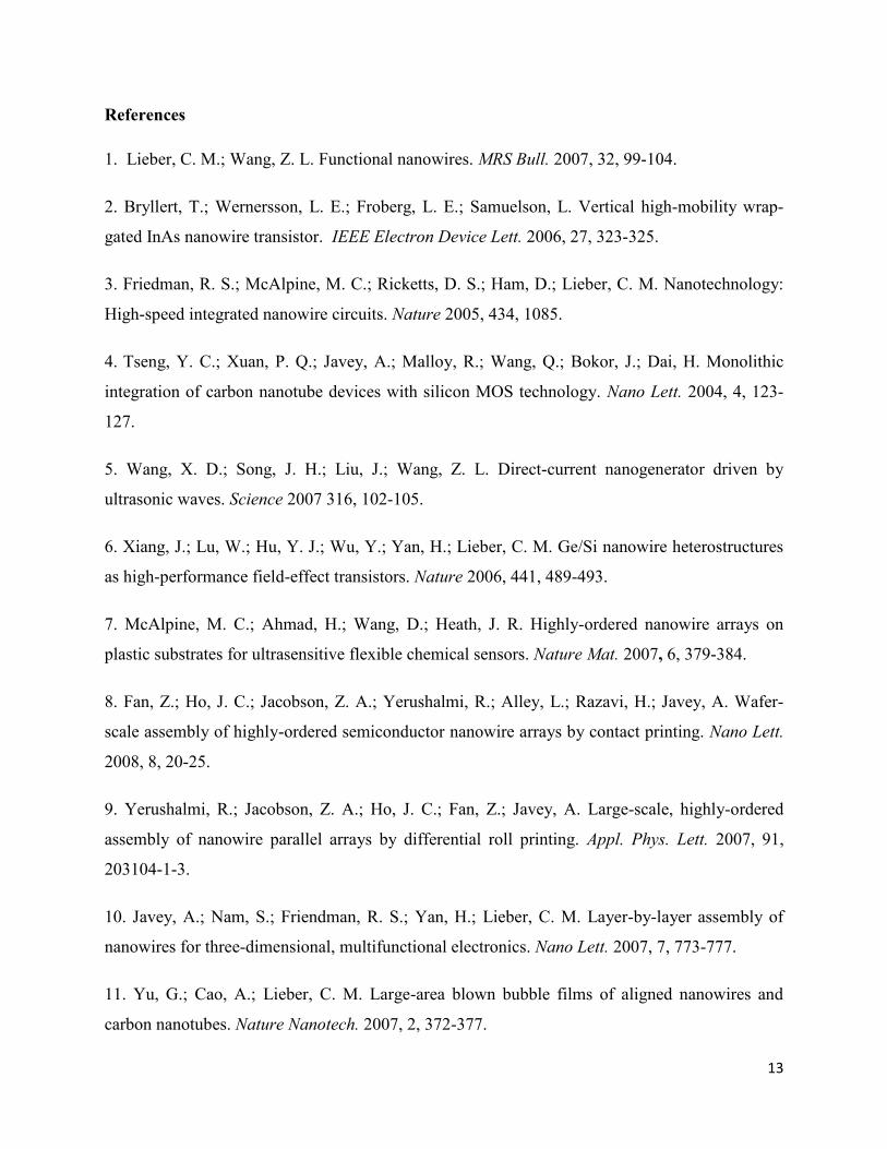
1. Lieber, C. M.; Wang, Z. L. Functional nanowires. MRS Bull. 2007, 32, 99-104.
2. Bryllert, T.; Wernersson, L. E.; Froberg, L. E.; Samuelson, L. Vertical high-mobility wrap-
gated InAs nanowire transistor. IEEE Electron Device Lett. 2006, 27, 323-325.
3. Friedman, R. S.; McAlpine, M. C.; Ricketts, D. S.; Ham, D.; Lieber, C. M. Nanotechnology:
High-speed integrated nanowire circuits. Nature 2005, 434, 1085.
4. Tseng, Y. C.; Xuan, P. Q.; Javey, A.; Malloy, R.; Wang, Q.; Bokor, J.; Dai, H. Monolithic
integration of carbon nanotube devices with silicon MOS technology. Nano Lett. 2004, 4, 123-
127.
5. Wang, X. D.; Song, J. H.; Liu, J.; Wang, Z. L. Direct-current nanogenerator driven by
ultrasonic waves. Science 2007 316, 102-105.
6. Xiang, J.; Lu, W.; Hu, Y. J.; Wu, Y.; Yan, H.; Lieber, C. M. Ge/Si nanowire heterostructures
as high-performance field-effect transistors. Nature 2006, 441, 489-493.
7. McAlpine, M. C.; Ahmad, H.; Wang, D.; Heath, J. R. Highly-ordered nanowire arrays on
plastic substrates for ultrasensitive flexible chemical sensors. Nature Mat. 2007, 6, 379-384.
8. Fan, Z.; Ho, J. C.; Jacobson, Z. A.; Yerushalmi, R.; Alley, L.; Razavi, H.; Javey, A. Wafer-
scale assembly of highly-ordered semiconductor nanowire arrays by contact printing. Nano Lett.
2008, 8, 20-25.
9. Yerushalmi, R.; Jacobson, Z. A.; Ho, J. C.; Fan, Z.; Javey, A. Large-scale, highly-ordered
assembly of nanowire parallel arrays by differential roll printing. Appl. Phys. Lett. 2007, 91,
203104-1-3.
10. Javey, A.; Nam, S.; Friendman, R. S.; Yan, H.; Lieber, C. M. Layer-by-layer assembly of
nanowires for three-dimensional, multifunctional electronics. Nano Lett. 2007, 7, 773-777.
11. Yu, G.; Cao, A.; Lieber, C. M. Large-area blown bubble films of aligned nanowires and
carbon nanotubes. Nature Nanotech. 2007, 2, 372-377.

14
12. Lind, E.; Persson, A. I.; Samuelson, L.; Wernersson, L. E. Improved subthreshold slope in an
InAs nanowire heterostructure field-effect transistor. Nano Lett. 2006, 6, 1842-1846.
13. Jiang, X.; Xiong, Q.; Nam, S.; Qian, F.; Li, Y.; Lieber, C. M. InAs/InP radial nanowire
heterostructures as high electron mobility devices. Nano Lett. 2007, 7, 3214-3218.
14. Dayeh, S. A.; Yu, E. T.; Wang, D. InAs nanowire growth on SiO2 substrates: nucleation,
evolution, and role of Au nanoparticles. J. Phys. Chem. C 2007, 111, 13331-13336.
15. Dayeh, S. A.; Aplin, D. P. R.; Zhou, X.; Yu, P. K. L.; Yu, E. T.; Wang, D. High electron
mobility InAs nanowire field-effect transistors. Small 2007, 3, 326-332.
16. Bleszynski, A.C.; Zwanenburg, F. A.; Westervelt, R. M.; Roest, A. L.; Bakkers, E. P. A. M.;
Kouwenhoven, L. P. Scanned probe imaging of quantum dots inside InAs nanowires. Nano Lett.
2007, 7, 2559-2562.
17. Park, H. D.; Gaillot, A. C.; Prokes, S. M.; Cammarata, R. C. Observation of size-dependent
liquidus depression in the growth of InAs nanowires. J. Crystal Growth 2006, 296, 159-164.
18. Park, H. D.; Prokes, S. M.; Twigg, M. E.; Cammarata, R. C.; Gaillot, A.-C. Si-assisted
growth of InAs nanowires. Appl. Phys. Lett. 2006, 89, 223125-1-3.
19. Mandl, B.; Stangl, J.; Mårtensson, T.; Mikkelsen, A.; Eriksson, J.; Karlsson, L. S.; Bauer, G.;
Samuelson, L.; Seifert, W. Au-free epitaxial growth of InAs nanowires. Nano Lett. 2006, 6,
1817-1821.
20. Javey, A.; Guo, J.; Farmer, D. B.; Wang, Q.; Yenilmez, E.; Gordon, R. G.; Lundstrom, M.;
Dai, H. Self-aligned ballistic molecular transistors and electrically parallel nanotube arrays. Nano
Lett. 2004, 4, 1319-1322.
21. Javey, A.; Kim, H.; Brink, M.; Wang, Q.; Ural, A.; Guo, J.; McIntyre, P.; McEuen, P.;
Lundstrom, M.; Dai, H. High- dielectrics for advanced carbon-nanotube transistors and logic
gates. Nature Mat. 2002, 1, 241-246.

15
22. Wang, D.; Wang, Q.; Javey, A.; Tu, R.; Dai, H.; Kim, H.; Krishnamohan, T.; McIntyre, P.;
Saraswat, K. Germanium nanowire field-effect transistor with SiO2 and high- HfO2 gate
dielectrics. Appl. Phys. Lett. 2003, 83, 2432-2434.

16
30
20
10
0
Nu
mb
er
of P
art
icle
s
2219161310Particle Diameter (nm)
30
20
10
0
Nu
mb
er
of P
art
icle
s
4236302418Particle Diameter (nm)
40
30
20
10
0
Nu
mb
er
of P
art
icle
s
131197Particle Diameter (nm)
Figure 1
a)
c)
e)
f)
d)
b) 9.7±1.7 19.3%
13.6±2.8 20.4%
26.5±5.4 20.3%

17
25
20
15
10
5
0
Nu
mb
er
of
Na
no
wir
es
605040302010Nanowire Diameter (nm)
25
20
15
10
5
0
Nu
mb
er
of
Na
no
wir
es
70605040302010Nanowire Diameter (nm)
25
20
15
10
5
0
Nu
mb
er
of N
an
ow
ire
s
4540353025201510Nanowire Diameter (nm)
Figure 2
a)
e)
c)
23.2±6 26.1%
26.2±8.3 31.8%
37.6±9.1 24.1%
b)
d)
f)

18
Figure 3

19
3500
3000
2500
2000
1500
1000
500
0
Mobili
ty (
cm
2/V
s)
-4 -2 0 2 4VGS (V)
15
12
9
6
3
0
ID
S (
3210VDS (V)
5 V
4 V
3 V
2 V
1 V
0 V
4
3
2
1
0
ID
S (
-4 -2 0 2 4VGS (V)
0.1 V
0.3 V
0.5 V
10-10
10-9
10-8
10-7
10-6
10-5
I DS (
A)
-4 -2 0 2 4VGS (V)
Figure 4
a)
c)
b)
d)
d~29 nm
L~9.9 µm
d~29 nm
L~9.9 µm

20
7
6
5
4
3
2
1
0
ID
S (
mA
)
3210VDS (V)
-10 V
-6 V
-2 V
2 V
10 V
1.4
1.2
1.0
0.8
0.6
0.4
0.2
0.0
ID
S (
mA
)
-10 -5 0 5 10VGS (V)
0.1 V
0.3 V
0.5 V
10-5
10-4
10-3
I DS (
A)
-10 -5 0 5 10VGS (V)
Figure 5
c)
b)
a)

21
Table of Contents
Ni nanoparticles are shown to serve as an efficient catalyst for high yield growth of high mobility
InAs nanowires on amorphous SiO2 substrates. The grown nanowires can be readily printed as
parallel arrays on substrates and configured as high performance transistors.
NW
printing growth
Ni nanoparticles InAs nanowires Parallel Array Nanowire FETs