Heterotwin Zn3P2 superlattice nanowires - RSC Publishing
8
rsc.li/nanoscale As featured in: Showcasing research from the Laboratory of Semiconductor Materials led by Prof. Fontcuberta i Morral, Institute of Materials, Ecole Polytechnique Fédérale de Lausanne, Switzerland. Heterotwin Zn 3P 2 superlattice nanowires: the role of indium insertion in the superlattice formation mechanism and their optical properties Zinc phosphide nanowires were long thought to form twin superlattices in the same way as III–V materials. Herein, they are instead shown to form heterotwin superlattices through the inclusion of an indium-rich monolayer to facilitate crystal rotation. Furthermore, their structure and influence on the functional properties are investigated, and a new model for twin superlattice formation mechanism based on the material's non-polar nature is proposed. Registered charity number: 207890 See Anna Fontcuberta i Morral et al., Nanoscale, 2020, 12, 22534. Nanoscale rsc.li/nanoscale ISSN 2040-3372 PAPER Zhenyu Zhang, Hongjiu Su et al. Green chemical mechanical polishing of sapphire wafers using a novel slurry Volume 12 Number 44 28 November 2020 Pages 22351-22828
-
Upload
khangminh22 -
Category
Documents
-
view
0 -
download
0
Transcript of Heterotwin Zn3P2 superlattice nanowires - RSC Publishing

rsc.li/nanoscale
As featured in: Showcasing research from the Laboratory of Semiconductor Materials led by Prof. Fontcuberta i Morral, Institute of Materials, Ecole Polytechnique Fédérale de Lausanne, Switzerland.
Heterotwin Zn 3 P 2 superlattice nanowires: the role of indium insertion in the superlattice formation mechanism and their optical properties
Zinc phosphide nanowires were long thought to form twin superlattices in the same way as III–V materials. Herein, they are instead shown to form heterotwin superlattices through the inclusion of an indium-rich monolayer to facilitate crystal rotation. Furthermore, their structure and infl uence on the functional properties are investigated, and a new model for twin superlattice formation mechanism based on the material's non-polar nature is proposed.
Registered charity number: 207890
See Anna Fontcuberta i Morral et al. , Nanoscale , 2020, 12 , 22534.
Nanoscalersc.li/nanoscale
ISSN 2040-3372
PAPER Zhenyu Zhang, Hongjiu Su et al. Green chemical mechanical polishing of sapphire wafers using a novel slurry
Volume 12Number 4428 November 2020Pages 22351-22828
Nanoscale
PAPER
Cite this: Nanoscale, 2020, 12, 22534
Received 8th August 2020,Accepted 24th September 2020
DOI: 10.1039/d0nr05852a
rsc.li/nanoscale
Heterotwin Zn3P2 superlattice nanowires: the roleof indium insertion in the superlattice formationmechanism and their optical properties†
Simon Escobar Steinvall, ‡a Lea Ghisalberti,‡a Reza R. Zamani, ‡b
Nicolas Tappy,a Fredrik S. Hage, c,d Elias Z. Stutz, a Mahdi Zamani, a
Rajrupa Paul, a Jean-Baptiste Leran,a Quentin M. Ramasse, c,e
W. Craig Carter a,f and Anna Fontcuberta i Morral *a,g
Zinc phosphide (Zn3P2) nanowires constitute prospective building blocks for next generation solar cells
due to the combination of suitable optoelectronic properties and an abundance of the constituting
elements in the Earth’s crust. The generation of periodic superstructures along the nanowire axis could
provide an additional mechanism to tune their functional properties. Here we present the vapour–liquid–
solid growth of zinc phosphide superlattices driven by periodic heterotwins. This uncommon planar
defect involves the exchange of Zn by In at the twinning boundary. We find that the zigzag superlattice
formation is driven by reduction of the total surface energy of the liquid droplet. The chemical variation
across the heterotwin does not affect the homogeneity of the optical properties, as measured by catho-
doluminescence. The basic understanding provided here brings new propsects on the use of II–V semi-
conductors in nanowire technology.
Introduction
Filamentary crystals, also known as nanowires, have providedadditional design freedom in the elaboration of materials withdesirable properties.1–4 This arises from the possibility of engin-eering the crystal phase and material composition, and for thepossibility of expanding the structure in three dimensions.3,5,6
Among the design opportunities, the composition or structureof nanowires can be arranged periodically in the form ofsuperlattices.6–9 The periodicity of the superstructure modulatesboth the electronic and phonon (vibrational) states, depending
on the magnitude of the period.10–13 Semiconductor superlat-tices find applications in the optoelectronic and thermoelectricarena.14–17 In thin films, the materials combinations are mostlyrestrained due to lattice-mismatch and thermal expansion con-ditions. Superlattice nanowire structures circumvent these limit-ations, and have been achieved by modulating the composition,crystal phase, and crystal orientation through rotational twins.5–8
Twin superlattices (TSLs) in semiconductors were predictedby Ikonic et al. in 1993.18 More recently, they wereimplemented in nanowire form, first in Al2O3 and ZnSe, andsubsequently in InP.19–21 These TSLs have been obtainedmainly by the vapour–liquid–solid (VLS) method in which ananoscale liquid droplet preferentially collects the growth pre-cursors.22 In addition to a periodic arrangement of twins,these nanowire superlattices adopt a characteristic zigzag mor-phology with alternating (111)A/B facets in the case of zincblende nanowires.7,8 According to Algra et al., twin formationis determined by energy minimisation involving the stability ofthe droplet and the surface energy of the facets as a functionof their polarity -(111) a or B-.8
Zinc phosphide, Zn3P2, has recently attracted attention as acompound semiconductor made of elements that are abun-dant in the Earth’s crust with optoelectronic propertiessuitable for photovoltaic applications.23–28 Zn3P2 has beenobtained both in the form of bulk crystals,29,30 thin films,25,26,31
and nanostructures.9,24,32–34 Zinc phosphide based solar cells
†Electronic supplementary information (ESI) available. See DOI: 10.1039/d0nr05852a‡Equal contrubutions.
aLaboratory of Semiconductor Materials, Institute of Materials École Polytechnique
Fédérale de Lausanne, 1015 Lausanne, SwitzerlandbCentre Interdisciplinaire de Microscopie Électronique, École Polytechnique Fédérale
de Lausanne, 1015 Lausanne, SwitzerlandcSuperSTEM Laboratory, SciTech Daresbury Campus, Keckwick Lane, Warrington
WA4AD, UKdDepartment of Materials, University of Oxford, Oxford, OX1 3PH, UKeSchool of Chemical and Process Engineering and School of Physics and Astronomy,
University of Leeds, Leeds LS2 9JT, UKfDepartment of Materials Science and Engineering, Massachusetts Institute of
Technology, Cambridge, Massachusetts 02139, USAgInstitute of Physics, École Polytechnique Fédérale de Lausanne, 1015 Lausanne,
Switzerland. E-mail: [email protected]
22534 | Nanoscale, 2020, 12, 22534–22540 This journal is © The Royal Society of Chemistry 2020
Ope
n A
cces
s A
rtic
le. P
ublis
hed
on 2
2 O
ctob
er 2
020.
Dow
nloa
ded
on 1
/12/
2022
9:2
8:09
PM
. T
his
artic
le is
lice
nsed
und
er a
Cre
ativ
e C
omm
ons
Attr
ibut
ion-
Non
Com
mer
cial
3.0
Unp
orte
d L
icen
ce.
View Article OnlineView Journal | View Issue
with an efficiency of up to 6% have been eported.30 This valueis still well below the theoretical limit (>30%), illustrating theimprovement potential of this material.35,36
The synthesis of Zn3P2 nanowires can follow the VLSand the vapour–solid mechanisms, with In, Sn, and Au ascatalysts.9,24,32–34,37,38 Zn3P2 nanowires adopt various mor-phologies depending on the fabrication method and/or growthconditions, including a zigzag superlattice.9,24,32–34 In contrastwith III–V compound semiconductors, Zn3P2 exhibits a centro-symmetric tetragonal structure, and thus also non-polar facetsand main crystal symmetry directions.29 Consequently, all sidefacets of Zn3P2 zigzag nanowires are always Zn-terminated.27,33
This means that the mechanism through which Zn3P2 obtainsa zigzag morphology is inconsistent with the model proposedbased on III–Vs.8
In this paper we reveal the nature of the defects leading tothe zigzag structure using aberration-corrected and analyticalscanning transmission electron microscopy (STEM). Inaddition, we explain the formation mechanisms based onsimulations of the surface energetics of the droplet as a func-tion of the nanowire cross-section. Finally, we outline the con-sequences of this periodic structure for the optical functional-ity through cathodoluminescence spectroscopy (CL).
Experimental
The Zn3P2 nanowires were epitaxially grown in a VeecoGENxplor molecular beam epitaxy (MBE) system on InP (100)substrates. They were grown through In catalysed VLS, with theIn originating from the substrate.24 The analysed samples weregrown at a manipulator temperature of 250 °C and a V/II ratioof 1.15 or 1.45 for four hours, with additional details on thegrowth in ref. 24. The nanowires were transferred to copperTEM grids with holey carbon by scraping the grid on thegrowth substrate for TEM studies, and were used as grown forCL studies.
Scanning electron microscopy (SEM) images were acquiredusing a Zeiss Merlin FE-SEM equipped with a Gemini column.The operating conditions were an acceleration voltage of 3 kVand a beam current of 100 pA. An in-lens secondary electrondetector was used for the imaging.
Droplet simulations were performed using the SurfaceEvolver software,39 which computes minimised surface energyby optimising shapes given constraints and wetting angles. Weimplement the interfacial energy of the liquid–solid interfaceby means of the Young’s equation with a contact angle of 43°when the triple line is unconstrained. The vertical axis inFig. 2c is the total energy divided by L2, with L being theaverage length of the sides, and the difference between thesolid–liquid and the solid surface tensions. The average lengthof the side remains constant with a value of 1.57. Regardingthe geometrical constraint, the triple line is not pinned to theedge, but is left free to move inside the polygon. To build thepolygon, centred at the origin, we define an equation for eachside of the hexagon through the lat and shrink parameters,
illustrated in the ESI.† While the lat parameter is fixed at 0.55and defines the apothem of the reference hexagon, the shrinkparameter is variable controlling the shape of the constraintsince it represents the normal between the facet centroid andthe selected facet. By varying the shrink parameter from −0.25to 0.25, we can reproduce the evolution of the nanowire cross-section from left oriented triangle to right oriented triangle(HT1 & HT2), passing through the hexagonal geometry atshrink equal to 0. To compare the effect of the volume we per-formed the simulations for three different droplet volumes:0.125, 0.225, and 0.325 with dimensions of L3.
Aberration-corrected bright-field/high-angle annular dark-field (BF/HAADF) STEM images and electron energy loss spec-troscopy (EELS) maps were collected on a STEM-dedicatedNion microscope (US100MC) operating at 60 kV. The NionUltraSTEM 100MC HERMES is equipped with a C5 Nion probecorrector (full correction up to 6-fold astigmatism C5, 6) and aUHV Gatan Enfinium ERS spectrometer optimised for highenergy resolution with high-stability electronics. The micro-scope is equipped with a cold-field emission gun (C-FEG),having an energy spread of 0.35 eV. The beam convergencesemi-angle was 31.5 mrad and the EEL spectrometer entranceaperture semi-angle was 44 mrad. Image detector angles were0–14 mrad (BF) and 100–230 mrad (HAADF). To minimise con-tamination, the specimens were baked prior to insertion at130 °C in vacuum (∼10−6 Torr), and the microscope column ismaintained at ultrahigh vacuum (UHV). The denoising ofSTEM-EELS datasets was done using the MSA plugin forGatan’s Digital Micrograph suite, commercially available fromHREM research.40 Example spectra are shown in the ESI,† andthe 443 eV and 1020 eV peaks were used for EEL mapping ofIn and Zn, respectively. Further imaging was also performed ina FEI Titan Themis 60–300 kV TEM operating at 200 or 300 kV.The machine is equipped with a field emission gun (X-FEG), amonochromators, two aberration correctors (one pre-specimenprobe-corrector, and one post-specimen image corrector), anda Fischione HAADF detector. The collection angles are typically85–200 mrad for HAADF-STEM images. The BF and HAADFimages were denoised using radial a Weiner filter. Viewingdirection illustrations were created in Mathematica.
An Attolight Rosa setup equipped with an Andor Newton920 Si-CCD was used for CL measurements. It was operated atroom temperature with an acceleration voltage of 3 kV, a beamcurrent of <1 nA, and an exposure time of 50 ms per pixel. Thenanowires were mounted on a stage with 20° tilt. Denoising ofthe hyperspectral maps was done through principal-com-ponent analysis (PCA) using the Hyperspy Software.41 Peakfitting was done after data treatment based on the approachdescribed in ref. 42.
Results and discussionElectron microscopy
Fig. 1a shows a representative secondary electron SEM images ofa typical zigzag Zn3P2 nanowire. These nanowires grow perpen-
Nanoscale Paper
This journal is © The Royal Society of Chemistry 2020 Nanoscale, 2020, 12, 22534–22540 | 22535
Ope
n A
cces
s A
rtic
le. P
ublis
hed
on 2
2 O
ctob
er 2
020.
Dow
nloa
ded
on 1
/12/
2022
9:2
8:09
PM
. T
his
artic
le is
lice
nsed
und
er a
Cre
ativ
e C
omm
ons
Attr
ibut
ion-
Non
Com
mer
cial
3.0
Unp
orte
d L
icen
ce.
View Article Online
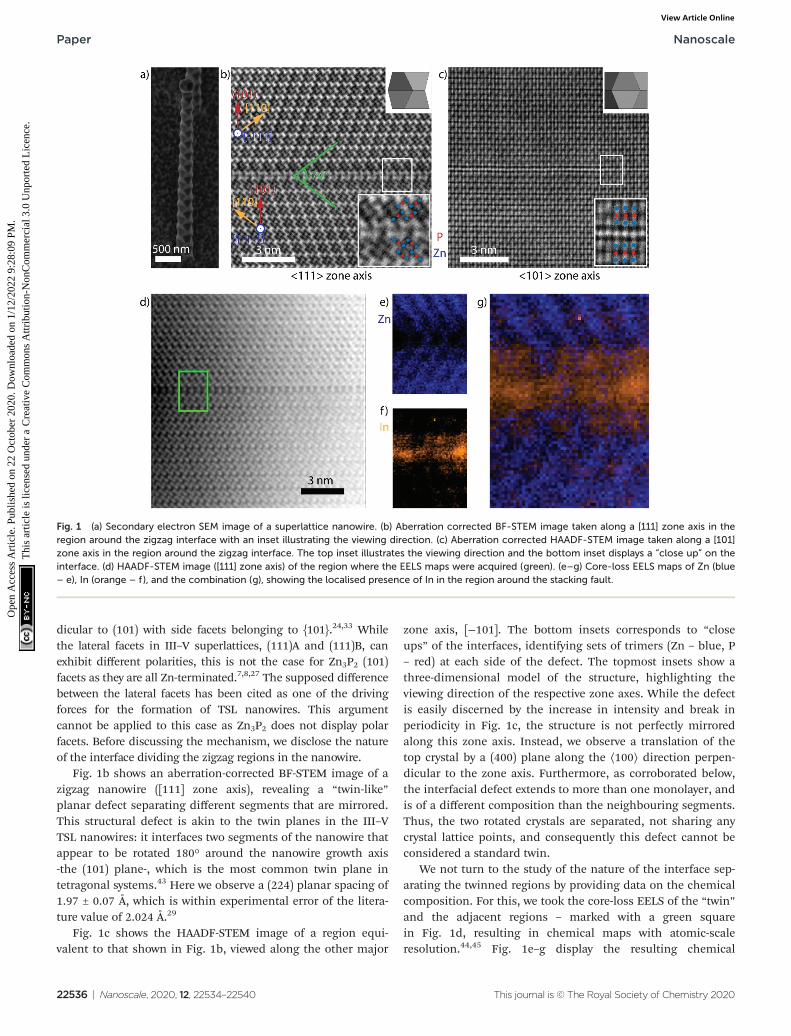
dicular to (101) with side facets belonging to {101}.24,33 Whilethe lateral facets in III–V superlattices, (111)A and (111)B, canexhibit different polarities, this is not the case for Zn3P2 (101)facets as they are all Zn-terminated.7,8,27 The supposed differencebetween the lateral facets has been cited as one of the drivingforces for the formation of TSL nanowires. This argumentcannot be applied to this case as Zn3P2 does not display polarfacets. Before discussing the mechanism, we disclose the natureof the interface dividing the zigzag regions in the nanowire.
Fig. 1b shows an aberration-corrected BF-STEM image of azigzag nanowire ([111] zone axis), revealing a “twin-like”planar defect separating different segments that are mirrored.This structural defect is akin to the twin planes in the III–VTSL nanowires: it interfaces two segments of the nanowire thatappear to be rotated 180° around the nanowire growth axis-the (101) plane-, which is the most common twin plane intetragonal systems.43 Here we observe a (224) planar spacing of1.97 ± 0.07 Å, which is within experimental error of the litera-ture value of 2.024 Å.29
Fig. 1c shows the HAADF-STEM image of a region equi-valent to that shown in Fig. 1b, viewed along the other major
zone axis, [−101]. The bottom insets corresponds to “closeups” of the interfaces, identifying sets of trimers (Zn – blue, P– red) at each side of the defect. The topmost insets show athree-dimensional model of the structure, highlighting theviewing direction of the respective zone axes. While the defectis easily discerned by the increase in intensity and break inperiodicity in Fig. 1c, the structure is not perfectly mirroredalong this zone axis. Instead, we observe a translation of thetop crystal by a (400) plane along the ⟨100⟩ direction perpen-dicular to the zone axis. Furthermore, as corroborated below,the interfacial defect extends to more than one monolayer, andis of a different composition than the neighbouring segments.Thus, the two rotated crystals are separated, not sharing anycrystal lattice points, and consequently this defect cannot beconsidered a standard twin.
We not turn to the study of the nature of the interface sep-arating the twinned regions by providing data on the chemicalcomposition. For this, we took the core-loss EELS of the “twin”and the adjacent regions – marked with a green squarein Fig. 1d, resulting in chemical maps with atomic-scaleresolution.44,45 Fig. 1e–g display the resulting chemical
Fig. 1 (a) Secondary electron SEM image of a superlattice nanowire. (b) Aberration corrected BF-STEM image taken along a [111] zone axis in theregion around the zigzag interface with an inset illustrating the viewing direction. (c) Aberration corrected HAADF-STEM image taken along a [101]zone axis in the region around the zigzag interface. The top inset illustrates the viewing direction and the bottom inset displays a “close up” on theinterface. (d) HAADF-STEM image ([111] zone axis) of the region where the EELS maps were acquired (green). (e–g) Core-loss EELS maps of Zn (blue– e), In (orange – f ), and the combination (g), showing the localised presence of In in the region around the stacking fault.
Paper Nanoscale
22536 | Nanoscale, 2020, 12, 22534–22540 This journal is © The Royal Society of Chemistry 2020
Ope
n A
cces
s A
rtic
le. P
ublis
hed
on 2
2 O
ctob
er 2
020.
Dow
nloa
ded
on 1
/12/
2022
9:2
8:09
PM
. T
his
artic
le is
lice
nsed
und
er a
Cre
ativ
e C
omm
ons
Attr
ibut
ion-
Non
Com
mer
cial
3.0
Unp
orte
d L
icen
ce.
View Article Online
mapping of Zn (blue – e), In (orange – f ), and combined (g). Pmapping did not provide the same resolution, and a constantsignal was observed throughout. The maps reveal the presenceof In at the interface and the neighbouring layers,accompanied by a drop in the Zn content. The presence of Inis consistent with the intensity analysis in the HAADF-STEMimages, especially from the [−101] direction (Fig. 1c). Theinterface there appears slightly brighter than the rest,suggesting the presence of a heavier element, i.e. In. Given thechemical inhomogeneity across the boundary, the defectshould rather be identified as a heterotwin.46 The In originatesfrom the droplet that drives the VLS growth,24 which was incontact with the twin region during formation.
The utilisation of a chemical heterogeneity at the bound-aries or planar defects have been reported in Al/TiN compo-sites and in doped II–VI compounds such as ZnO. In the caseof Al, N-terminated TiN lowers the formation energy of twins,and they provide significantly improved mechanicalproperties.46,47 In ZnO, trivalent metals such as Al, Fe, Ga, orIn have shown to precipitate at the interface of inversiondomain boundaries.48 The presence of trivalent metals in II–VIdefects modifies the bonding coordination from four in atetrahedral fashion to eight in an octahedral one, causing thepolarity inversion.49–52 However, in the case considered herethe defect cannot be classified as an inversion domain bound-ary as there is no polarity inversion associated with it. In thefollowing section we discuss the mechanism by which Zn3P2forms a zigzag structure via a heterotwin.
Zigzag mechanism
To investigate the driving forces prompting the regular inser-tion of heterotwins, we analysed the heterotwin periodicityalong the nanowire length, x (nm), and as a function of W, anapproximation of the cross-sectional apothem. The trend wasobserved in multiple nanowires, while the equation is basedon the high-resolution TEM image shown in Fig. S3.† Similarto III–V TSL nanowires, the heterotwin periodicity in Zn3P2nanowires depends on their diameter.7,53 The zigzag mor-phology results in the width being a periodic function with anamplitude with linear decay:
W xð Þ ¼ W0 �W0 �W0
22
� x
tanπ
2:02
0B@
1CA 1þ 1
3cos
2πxh0e�2�10�5x
� �
ð1Þwhere W0 is the initial width and h0 is the distance betweenthe initial segment separation. eqn (1) shows that the hetero-twin interdistance reduces with the reduction of the nanowirediameter, in agreement with studies on non-tapered superlat-tice ZnSe and GaAs nanowires.20,53 In particular, the termπ/2.02 corresponds to 89°, i.e. the measured tapering anglecharacterising the reduction of the nanowire’s diameter. Theorigin of the tapering is explored in detail in ref. 24.
Regarding possible explanations for the heterotwin for-mation mechanism, previous studies argued that twins in a
zigzag structure form to minimise the nanowire surfaceenergy.8,54 The argument is reasonable for compound semi-conductor nanowires exhibiting facets with different polaritiesand thus different surface energies. However, Zn3P2 is notpolar. The basic structural unit consists of symmetric Zn–P–Zntrimers, instead of asymmetric cation–anion dumbbells suchas In–P in InP, and its centrosymmetric crystal structure.29,48,55
Thus, all facets in the zigzag structure are equivalent.27 Thismeans we cannot reasonably attribute the instigation of theZn3P2 twinning process to nanowire surface energy minimis-ation alone. As discussed below, deformation of the liquiddroplet during growth provides a more compelling argument.
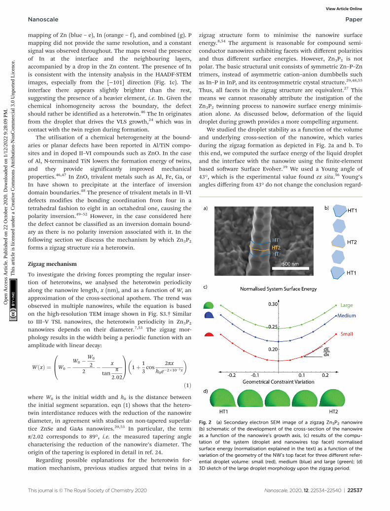
We studied the droplet stability as a function of the volumeand underlying cross-section of the nanowire, which variesduring the zigzag formation as depicted in Fig. 2a and b. Tothis end, we computed the surface energy of the liquid dropletand the interface with the nanowire using the finite-elementbased software Surface Evolver.39 We used a Young angle of43°, which is the experimental value found ex situ.56 Young’sangles differing from 43° do not change the conclusion regard-
Fig. 2 (a) Secondary electron SEM image of a zigzag Zn3P2 nanowire(b) schematic of the development of the cross-section of the nanowireas a function of the nanowire’s growth axis, (c) results of the compu-tation of the system (droplet and nanowires top facet) normalisedsurface energy (normalisation explained in the text) as a function of thevariation of the geometry of the NW’s top facet for three different refer-ential droplet volume: small (red), medium (blue) and large (green); (d)3D sketch of the large droplet morphology upon the zigzag period.
Nanoscale Paper
This journal is © The Royal Society of Chemistry 2020 Nanoscale, 2020, 12, 22534–22540 | 22537
Ope
n A
cces
s A
rtic
le. P
ublis
hed
on 2
2 O
ctob
er 2
020.
Dow
nloa
ded
on 1
/12/
2022
9:2
8:09
PM
. T
his
artic
le is
lice
nsed
und
er a
Cre
ativ
e C
omm
ons
Attr
ibut
ion-
Non
Com
mer
cial
3.0
Unp
orte
d L
icen
ce.
View Article Online

ing alternating stability, the only modify the threshold for het-erotwin formation.
Fig. 2c illustrates the evolution of the surface energy of thedroplet plus the liquid–solid interface during one zigzag cycle.We include the curves for three relative values of dropletvolumes, which all follow a similar trend. The total surfaceenergy has been normalised by the average length of the sides,constant throughout all simulations, by the surface energy of afloating sphere with an identical volume, and by the surfacetension of the liquid–vapour interface. Due to the pinning ofthe liquid at the edge of the faceted nanowires, an increase inthe liquid volume results in the increase of the apparentcontact angle.56 The normalised surface energy increases withthe liquid volume due to the expansion and deformation ofthe liquid surface at the edges. The lowest normalised surfaceenergy corresponds to the configuration with hexagonal nano-wire cross-section, where the droplet is the least deformed.The normalised surface energy increases parabolically (to asecond order approximation) with the modification of theliquid–solid interface area. The slope of the curve increaseswith the droplet deformation. A representative display of thepredicted droplet shape during the zigzag process is shown inFig. 2d. It shows that the deformation is larger at the cornersof the cross-section. In addition, the local and overall defor-mations are the largest when the cross-section is the closest toa triangular shape. This increasing deformation with the devi-ation from a hexagonal cross-section explains the increase inthe normalised surface energy.
The introduction of a heterotwin constitutes a mechanismto stop the increase in surface energy during the nanowireelongation caused by the droplet’s deformation.53,57 As theenergy required to form a heterotwin (EHT) is fixed, there is acritical geometry of the nanowire’s cross-section after which itis energetically favourable to insert a heterotwin rather than tocontinue increasing the total normalised surface energy. Theprobability of creating a heterotwin along the nanowire axis,P(x), should thus increase with the normalised surface energyof the system, γ(x), as:
P xð Þ � γ xð ÞEHTA xð Þ
After formation of a heterotwin, the normalised surfaceenergy decreases with nanowire elongation due to the changein the facet orientation and return towards a hexagonal crosssection.
Optical properties
Previous studies on Zn3P2 indicate that it exhibits a directbandgap at ∼1.5 eV, which is close to the ideal bandgap forthe highest efficiency of single junction solar cells.58 In ourrecent work, we demonstrated that zigzag Zn3P2 nanowiresluminesce at 1.43 eV at cryogenic temperatures, which is rela-tively close to the expected value of the bandgap.24 We haveobserved that in Zn3P2 nanowires with a square cross-section,luminescence can vary with the relative stoichiometry betweenthe Zn and P.24 Given the composition variation at the hetero-
twin in the zigzag nanowires, the question arises of whetherthe optical properties vary at these points. To ascertain theirpotential influence, we performed CL on zigzag nanowires atroom temperature. The experimental conditions were chosenas to decrease the diffusion length and allow for higher spatialresolution measurements compared to previous studies.
Fig. 3a shows a panchromatic map of the CL emission. Weobserve a ∼10% variation in the emission intensity aroundedges and on the outward facet orientation compared to thatof the inward orientation of the zigzag structure. We attributethis fluctuation to the variations in electron-beam excitation asa function of the morphology (see ESI† for more details).Detailed spectra along one oscillation of the zigzag mor-phology indicated by the arrow in Fig. 3a are shown in Fig. 3b.We observe to main peaks centred around 869 and 950 nm(1.43 eV and 1.30 eV, respectively), which correspond to sub-bandgap emission, potentially caused by the incorporation ofindium in the bulk.59 First principle simulations should beperformed to confirm this hypothesis. We also distinguish athird weaker peak centred around 748 nm (1.66 eV). This peakcould correspond to emission from the Γ2 transition 260 meVabove the bandgap, available due to the high energy excitationof CL.58,60 The spectra along and on each side of the hetero-twin are qualitatively extremely similar. The similarity of thespectra along the zigzag structure could be due to the carrierdiffusion length being larger than the excitation volume.58 Thespectra intensity tends to decrease down the nanowire axis. Weattribute this to optical wave-guiding effects. The channellingof CL signal between optical modes of a nanowire dependsstrongly on the excitation position.61 In the measurement geo-metry used here, and with the restricted collection angle of theCL setup, the signal can be collected only when emitted fromthe top of the wire and for a restricted range of angles. Thiswould explain the peak intensity variations on a λ/2 spatialscale as observed in Fig. 3. One would require angle-resolvedCL experiments to confirm this.
Fig. 3 (a) High-resolution panchromatic CL intensity map of a zigzagnanowire with the white arrow indicating the linescan of the extractedspectra in (b), of which the second and fourth from the top wereextracted from regions on top of the heterotwin.
Paper Nanoscale
22538 | Nanoscale, 2020, 12, 22534–22540 This journal is © The Royal Society of Chemistry 2020
Ope
n A
cces
s A
rtic
le. P
ublis
hed
on 2
2 O
ctob
er 2
020.
Dow
nloa
ded
on 1
/12/
2022
9:2
8:09
PM
. T
his
artic
le is
lice
nsed
und
er a
Cre
ativ
e C
omm
ons
Attr
ibut
ion-
Non
Com
mer
cial
3.0
Unp
orte
d L
icen
ce.
View Article Online

Conclusions
In conclusion, we have demonstrated that the Zn3P2 super-lattice nanowires do not form through regular twinning, asobserved in their III–V analogue. Instead, an In-rich heterotwinis formed, as shown through EELS mapping and aberration-corrected STEM imaging, which facilitates the rotation of thecrystal structure between segments through the inset of a sep-arate material. Furthermore, we developed a model to explainthe onset of heterotwin formation. Based on the non-polarnature of Zn3P2 we could tie the model solely to the constraintsposed by the droplet shape as a function of the nanowirecross-section. Characterisation of the emission through roomtemperature CL shows no effect of the heterotwins on the func-tional properties.
Conflicts of interest
There are no conflicts to declare.
Acknowledgements
S. E. S., E. S., M. Z., R. P., J. L., and A. F. i M. were supported bythe SNSF Consolidator grant BSCGI0-157705. N. T. and A. F. i M.were supported by SNSF grant 20B2-1 17668. L. G., W. C. C.,and A. F. i M. were supported by SNSF via project200021_169908 and SCR0222237. R. R. Z. was supported byEPFL-CIME. F. S. H., Q. M. R., and the SuperSTEM Laboratory,the U. K. National Research Facility for Advanced ElectronMicroscopy, were supported by the Engineering and PhysicalSciences Research Council (EPSRC).
Notes and references
1 J. Arbiol, M. de la Mata, M. Eickhoff and A. F. i Morral,Mater. Today, 2013, 16, 213–219.
2 P. C. McIntyre and A. Fontcuberta i Morral, Mater. TodayNano, 2020, 9, 100058.
3 K. A. Dick, K. Deppert, M. W. Larsson, T. Mårtensson,W. Seifert, L. R. Wallenberg and L. Samuelson, Nat. Mater.,2004, 3, 380–384.
4 L. Güniat, P. Caroff and A. Fontcuberta i Morral, Chem.Rev., 2019, 119, 8958–8971.
5 M. S. Gudiksen, L. J. Lauhon, J. Wang, D. C. Smith andC. M. Lieber, Nature, 2002, 415, 617–620.
6 K. A. Dick, C. Thelander, L. Samuelson and P. Caroff, NanoLett., 2010, 10, 3494–3499.
7 P. Caroff, K. A. Dick, J. Johansson, M. E. Messing,K. Deppert and L. Samuelson, Nat. Nanotechnol., 2009, 4,50–55.
8 R. E. Algra, M. A. Verheijen, M. T. Borgstrom, L.-F. Feiner,G. Immink, W. J. P. van Enckevort, E. Vlieg andE. P. A. M. Bakkers, Nature, 2008, 456, 369–372.
9 G. Shen, P.-C. Chen, Y. Bando, D. Golberg and C. Zhou,J. Phys. Chem. C, 2008, 112, 16405–16410.
10 D. Spirkoska, J. Arbiol, A. Gustafsson, S. Conesa-Boj,F. Glas, I. Zardo, M. Heigoldt, M. H. Gass, A. L. Bleloch,S. Estrade, M. Kaniber, J. Rossler, F. Peiro, J. R. Morante,G. Abstreiter, L. Samuelson and A. Fontcuberta i Morral,Phys. Rev. B: Condens. Matter Mater. Phys., 2009, 80, 245325.
11 M. De Luca, C. Fasolato, M. A. Verheijen, Y. Ren,M. Y. Swinkels, S. Kölling, E. P. A. M. Bakkers, R. Rurali,X. Cartoixà and I. Zardo, Nano Lett., 2019, 19, 4702–4711.
12 Z. Ikonic, G. P. Srivastava and J. C. Inkson, Phys. Rev. B:Condens. Matter Mater. Phys., 1995, 52, 14078–14085.
13 Z. Ikonic, G. P. Srivastava and J. C. Inkson, Phys. Rev. B:Condens. Matter Mater. Phys., 1993, 48, 17181–17193.
14 M. Y. Swinkels and I. Zardo, J. Phys. D, 2018, 51, 353001.15 N. Guan, X. Dai, A. V. Babichev, F. H. Julien and
M. Tchernycheva, Chem. Sci., 2017, 8, 7904–7911.16 P. Krogstrup, H. I. Jørgensen, M. Heiss, O. Demichel,
J. V. Holm, M. Aagesen, J. Nygard and A. Fontcuberta iMorral, Nat. Photonics, 2013, 7, 306–310.
17 S. A. Mann, R. R. Grote, R. M. Osgood Jr., A. Alu andE. C. Garneet, ACS Nano, 2016, 10, 8620–8631.
18 Z. Ikonic, G. P. Srivastava and J. C. Inkson, Solid StateCommun., 1993, 86, 799–802.
19 X.-S. Fang, C.-H. Ye, L.-D. Zhang and T. Xie, Adv. Mater.,2005, 17, 1661–1665.
20 Q. Li, X. Gong, C. Wang, J. Wang, K. Ip and S. Hark, Adv.Mater., 2004, 16, 1436–1440.
21 G. Shen, Y. Bando, B. Liu, C. Tang and D. Golberg, J. Phys.Chem. B, 2006, 110, 20129–20132.
22 R. Wagner and W. Ellis, Appl. Phys. Lett., 1964, 4, 89–90.23 R. Katsube and Y. Nose, J. Solid State Chem., 2019, 280,
120983.24 S. Escobar Steinvall, N. Tappy, M. Ghasemi, R. R. Zamani,
T. LaGrange, E. Z. Stutz, J.-B. Leran, M. Zamani, R. Pauland A. Fontcuberta i Morral, Nanoscale Horiz., 2020, 5,274–282.
25 J. P. Bosco, G. M. Kimball, N. S. Lewis and H. A. Atwater,J. Cryst. Growth, 2013, 363, 205–210.
26 R. Paul, N. Humblot, S. Escobar Steinvall, E. Z. Stutz,S. S. Joglekar, J.-B. Leran, M. Zamani, C. Cayron, R. Logé,A. G. del Aguila, Q. Xiong and A. Fontcuberta i Morral,Cryst. Growth Des., 2020, 20, 3816–3825.
27 N. Y. Dzade, Phys. Chem. Chem. Phys., 2020, 22, 1444–1456.28 M. Y. Swinkels, A. Campo, D. Vakulov, W. Kim, L. Gagliano,
S. Escobar Steinvall, H. Detz, M. De Luca, A. Lugstein,E. P. A. M. Bakkers, A. Fontcuberta i Morral and I. Zardo,Phys. Rev. Appl., 2020, 14, 024045.
29 M. V. Stackelberg and R. Paulus, Z. Phys. Chem., 1935, 28,427–460.
30 M. Bhushan and A. Catalano, Appl. Phys. Lett., 1981, 38,39–41.
31 T. Suda, K. Kakishita, H. Sato and K. Sasaki, Appl. Phys.Lett., 1996, 69, 2426–2428.
32 H. S. Im, K. Park, D. M. Jang, C. S. Jung, J. Park, S. J. Yooand J.-G. Kim, Nano Lett., 2015, 15, 990–997.
Nanoscale Paper
This journal is © The Royal Society of Chemistry 2020 Nanoscale, 2020, 12, 22534–22540 | 22539
Ope
n A
cces
s A
rtic
le. P
ublis
hed
on 2
2 O
ctob
er 2
020.
Dow
nloa
ded
on 1
/12/
2022
9:2
8:09
PM
. T
his
artic
le is
lice
nsed
und
er a
Cre
ativ
e C
omm
ons
Attr
ibut
ion-
Non
Com
mer
cial
3.0
Unp
orte
d L
icen
ce.
View Article Online

33 H. S. Kim, Y. Myung, Y. J. Cho, D. M. Jang, C. S. Jung,J. Park and J.-P. Ahn, Nano Lett., 2010, 10, 1682–1691.
34 S. B. Choi, M. S. Song and Y. Kim, J. Phys. Chem. C, 2019,123, 4597–4604.
35 W. Shockley and H. J. Queisser, J. Appl. Phys., 1961, 32,510–519.
36 S. Rühle, Sol. Energy, 2016, 130, 139–147.37 R. Yang, Y.-L. Chueh, J. R. Morber, R. Snyder, L.-J. Chou
and Z. L. Wang, Nano Lett., 2007, 7, 269–275.38 G. Lombardi, F. de Oliveira, M. Teodoro and A. Chiquito,
Appl. Phys. Lett., 2018, 112, 193103.39 K. A. Brakke, Exp. Math., 1992, 1, 141–165.40 MSA for Digital Micrograph, HREM Research, https://www.
hremresearch.com/Eng/plugin/MSAEng.html.41 F. de la Peña, T. Ostasevicius, V. Tonaas Fauske, P. Burdet,
P. Jokubauskas, M. Nord, M. Sarahan, E. Prestat,D. N. Johnstone, J. Taillon, J. Caron, T. Furnival,K. E. MacArthur, A. Eljarrat, S. Mazzucco, V. Migunov,T. Aarholt, M. Walls, F. Winkler, G. Donval, B. Martineau,A. Garmannslund, L.-F. Zagonel and I. Iyengar, Microsc.Microanal., 2017, 23(S1), 214–215.
42 J. Mooney and P. Kambhampati, J. Phys. Chem. Lett., 2014,5, 3497–3497.
43 C. Klein, B. Dutrow, J. D. Dana and C. Klein, Manual ofmineral science, Wiley New York, 2002.
44 R. R. Zamani, F. S. Hage, S. Lehmann, Q. M. Ramasse andK. A. Dick, Nano Lett., 2018, 18, 1557–1563.
45 J. A. Mundy, Q. Mao, C. M. Brooks, D. G. Schlom andD. A. Muller, Appl. Phys. Lett., 2012, 101, 042907.
46 D. Bhattacharyya, X.-Y. Liu, A. Genc, H. L. Fraser,R. G. Hoagland and A. Misra, Appl. Phys. Lett., 2010, 96,093113.
47 D. Bhattacharyya, N. A. Mara, P. Dickerson, R. G. Hoaglandand A. Misra, Acta Mater., 2011, 59, 3804–3816.
48 R. R. Zamani and J. Arbiol, Nanotechnology, 2019, 30,262001.
49 A. P. Goldstein, S. C. Andrews, R. F. Berger,V. R. Radmilovic, J. B. Neaton and P. Yang, ACS Nano, 2013,7, 10747–10751.
50 J. Hoemke, E. Tochigi, T. Tohei, H. Yoshida, N. Shibata,Y. Ikuhara and Y. Sakka, J. Am. Ceram. Soc., 2018, 101,2616–2626.
51 J. Hoemke, E. Tochigi, T. Tohei, H. Yoshida, N. Shibata,Y. Ikuhara and Y. Sakka, J. Am. Ceram. Soc., 2017, 100,4252–4262.
52 H. Schmid, E. Okunishi, T. Oikawa and W. Mader, Micron,2012, 43, 49–56.
53 T. Burgess, S. Breuer, P. Caroff, J. Wong-Leung, Q. Gao,H. Hoe Tan and C. Jagadish, ACS Nano, 2013, 7, 8105–8114.
54 N. Isik Goktas, A. Sokolovskii, V. G. Dubrovskii andR. R. LaPierre, Nano Lett., 2020, 20, 3344–3351.
55 M. de la Mata, R. R. Zamani, S. Martí-Sánchez, M. Eickhoff,Q. Xiong, A. Fontcuberta i Morral, P. Caroff and J. Arbiol,Nano Lett., 2019, 19, 3396–3408.
56 L. Ghisalberti, H. Potts, M. Friedl, M. Zamani, L. Güniat,G. Tütüncüoglu, W. C. Carter and A. F. i Morral,Nanotechnology, 2019, 30, 285604.
57 F. M. Ross, J. Tersoff and M. C. Reuter, Phys. Rev. Lett.,2005, 95, 146104.
58 G. M. Kimball, A. M. Mueller, N. S. Lewis andH. A. Atwater, Appl. Phys. Lett., 2009, 95, 112103.
59 R. Katsube, H. Hayashi, A. Nagaoka, K. Yoshino, Y. Noseand Y. Shirai, Jpn. J. Appl. Phys., 2016, 55, 041201.
60 J. Andrzejewski and J. Misiewicz, Phys. Status Solidi B, 2001,227, 515–540.
61 B. J. M. Brenny, D. R. Abujetas, D. van Dam, J. A. Sánchez-Gil, J. G. Rivas and A. Polman, ACS Photonics, 2016, 3, 677–684.
Paper Nanoscale
22540 | Nanoscale, 2020, 12, 22534–22540 This journal is © The Royal Society of Chemistry 2020
Ope
n A
cces
s A
rtic
le. P
ublis
hed
on 2
2 O
ctob
er 2
020.
Dow
nloa
ded
on 1
/12/
2022
9:2
8:09
PM
. T
his
artic
le is
lice
nsed
und
er a
Cre
ativ
e C
omm
ons
Attr
ibut
ion-
Non
Com
mer
cial
3.0
Unp
orte
d L
icen
ce.
View Article Online