Metal Fabrication by Additive Manufacturing Using Laser and Electron Beam Melting Technologies
Upload
independentCategory
view
1download
0
arX
iv:c
ond-
mat
/030
7600
v1 [
cond
-mat
.mes
-hal
l] 2
4 Ju
l 200
3
Fabrication of metal nanowires
D. Natelson
Dept. of Physics & Astronomy and Electrical & Computer Engineering
Rice University
Houston, TX 77005
This review article discusses and compares various techniques for fabricating metal nanowires.We begin by defining what we mean by a nanowire, and why such nanostructures are of scientificand technological interest. We then present different fabrication methodologies, describing in somedetail the advantages of each. “Top-down” techniques discussed include: electron beam lithography;scanned probe lithography; step-edge and molecular beam epitaxy templating; and nanotube tem-plating. “Bottom-up” methodologies covered include: electrodeposition into etched porous media;direct chemical synthesis; step-edge decoration; and strain-mediated self-assembly. We conclude bysummarizing our observations and briefly discuss the future of metal nanowire fabrication.
PACS numbers:
I. INTRODUCTION
Colloquially, a wire is a metallic structure extendedin one (longitudinal) direction and strongly confined inthe other two (transverse) directions. A fundamental at-tribute of such a two-terminal device is electrical conti-nuity, i.e. the ability to transport charge along its lengthunder a longitudinal potential bias. There is much sci-entific and technological interest in fabricating and un-derstanding metal wires with transverse dimensions ap-proaching the nanometer scale. We call such structuresnanowires, and this article reviews a number of tech-niques for the fabrication of these objects.
For our purposes a metal nanowire has transverse di-mensions (w, t) substantially below 100 nm, an aspectratio significantly greater than one (L >> w, t), and iscomposed of a material that is metallic in the bulk (e.g.gold, copper, nickel). This definition is deliberately con-structed to exclude from discussion some other structuresknown colloquially as nanowires: e.g., nanoscale metalpoint contacts[1, 2]; extended semiconductor crystals[3]and heterostructures (so-called “quantum wires”)[4, 5];and molecules used as two-terminal conductors [6, 7].
It is useful to compare the sizes of nanowires with someof the physically significant length scales in metals. Thesecomparisons emphasize the difference between nanowiresand the other elongated structures mentioned above, andalso show why the sub-100 nm transverse scale is inter-esting.
The Fermi wavelength, λF, is one relevant length scale.In typical bulk metals the Fermi wavelength associatedwith the conduction electron Bloch waves is on the or-der of 0.1 nm. This short wavelength is due to the highspatial density of electrons. Since λF << w, t exceptfor wires of atomic cross-section, most nanowires un-der discussion have many conducting channels, and arewell-described by three dimensional Fermi Liquid The-ory. More exotic physics (e.g. Luttinger liquid proper-ties) only becomes relevant in extremely narrow struc-tures, when w, t → λF. Note that in contrast, λF in
doped semiconductor nanowires may be on the order oftens of nanometers.
Another closely related quantity is the screeninglength, Lsc, the scale over which electrostatic impuritiesare screened by the conduction electrons. This is on thesame order as λF. As transverse wire dimensions arereduced, an increasing fraction of the metal atoms arewithin Lsc of the wire surface.
Other relevant sizes are ℓ, the electronic mean freepath for elastic scattering, and ℓtot, the mean free pathfor either inelastic or elastic scattering. A “good” metalhas ℓ/λF >> 1; that is, electronic partial waves propa-gate many wavelengths between scattering events. Sincemetal nanowires are often nanocrystalline, elastic scat-tering in such structures is strongly influenced by grainboundary scattering. Similarly, if the transverse dimen-sions of the wire are sufficiently small (ℓ ∼ w, t) thenboundary scattering can also strongly influence nanowireconduction properties. This limit is certainly achievableat low temperatures for “clean” metals.
Related to the inelastic mean free path is the coher-ence length, Lφ. Consider introducing an electron in asingle-particle eigenstate of the wire, and then allowingthe electron to propagate while undergoing interactionswith other dynamic degrees of freedom (e.g. phonons,photons, magnetic impurities, other electrons). Lφ is thedistance traversed before the phase of the electron partialwave becomes poorly defined through interactions withthe environment. Quantum interference corrections toelectronic conduction (often referred to as “mesoscopic”phenomena[8, 9]) are typically relevant on this lengthscale. Because of the temperature dependence of pro-cesses involving those dynamic degrees of freedom, Lφ
often varies strongly with T , tending toward larger val-ues at lower temperatures. In a metal like silver at 1 K,Lφ ∼ 1 µm.
Once Lφ > w, t, the wire is one-dimensional with re-spect to quantum phase coherence. One important prop-erty of such one-dimensional structures is that the motionof a single impurity or defect will then affect the conduct-
2
ing properties of the entire wire. Every trajectory thatbrings an electron from one end of the wire to the otherwill have to pass through the same coherent volume asthe defect in question. Similarly, suppose some chargeddefect adjacent to the nanowire changes its state. Classi-cally this should only affect electron trajectories passingwithin Lsc of the nanowire surface; however, because ofquantum coherence and mixing of transverse channels, alltrajectories passing within Lφ must now be considered.
As wire transverse dimensions are reduced, quantumcorrections to conduction become relevant at higher tem-peratures. In the limit of atomic-scale metal contacts,quantum effects dominate electronic transport even atroom temperature[1]. In some of the smallest nanowiresconsidered in this article, conductance fluctuation noisefrom quantum interference and scatterer motion[10, 11]is clearly detectable at temperatures above that of liquidnitrogen[12].
Finally, one more useful quantity is the thermal lengthLT =
√
~D/kBT in diffusive wires and ~vF/kBT in bal-listic wires, where vF is the Fermi velocity. Considerstarting out two electrons near the Fermi surface withenergies differing by kBT , but beginning on the same tra-jectory. The length LT is the distance that the electronswould typically travel before their partial waves are outof step due to their slightly different energies. This scalealso determines the thermal smearing of the conductancefluctuation noise described above.
Metal nanowires with transverse dimensions well be-low 100 nm are of scientific interest because this sizerange spans the lengths mentioned above. Surface scat-tering effects, changes in screening, and the increasedimportance of quantum corrections to the conductanceare all topics of research that may be addressed throughnovel nanowire samples. Moreover, metals with sub-stantial electronic correlation effects such as ferromag-netism and superconductivity possess additional lengthscales (e.g. domain wall thickness, superconducting co-herence length) that further complicate wire properties.Nanowires are ideal tools for the study of such physics.
With the continued trend toward further technologi-cal miniaturization, nanowires are likely to be industri-ally relevant as well. Already the physical gate lengthfor transistors is predicted to be as small as 25 nm by2007[13]. With the possibility of electronic devices basedon individual molecules being seriously explored, fabri-cation of metal nanostructures on comparable scales is atopic of much interest.
As has been pointed out by other authors[14], fabrica-tion processes at these length scales fall into three broadcategories: lithographic processes (Sec. II) involve pat-tern definition through a drawing step; while templating
approaches (Sec. III) use alternative means to produce ananodetailed template and replicate some feature of thattemplate in metal; and finally chemical synthesis and self-
assembly may be employed without any patterning stepat all. We begin by considering lithographic techniques.
II. LITHOGRAPHIC TECHNIQUES
Lithographic techniques for nanowire fabrication maybe divided into two classes: additive and subtractivemethods. In many additive techniques some form of re-
sist is applied to the entire substrate; the resist is thenmodified in a pattern definition step, turning the resistlayer into a stencil, with resist material removed to ex-pose the underlying substrate. Metallization then occurs,in which the entire resist layer is coated with a metalfilm of thickness t, usually by evaporation or sputter-ing. The final step is liftoff, in which the remaining resistis removed by chemical means, leaving behind metal onthe substrate only where the resist had been patterned.Alternately, resist-free techniques may be employed, inwhich the metal is “drawn” directly onto the substrate.
Subtractive techniques begin by metallizing the entiresubstrate with the desired wire material. Some formof resist may then be applied and patterned, with re-sist remaining where the wire is desired to be formed.Unwanted metal is then removed by physical etchingor chemical means. Any remaining resist is then liftedoff chemically. Again, there are also resist-free ap-proaches that locally remove the excess metal to form thenanowires. For nanowire fabrication, subtractive litho-graphic approaches are less common than additive ones.
A. Photolithography
We only briefly consider photolithography because ofits size limitations. For more complete discussions ofthis extremely wide-spread technique, see Refs. [15, 16].In this technique chemical changes in a resist materialare photoactivated, with some sort of optical mask usedto spatially define the regions of photochemical activity.Optics between the mask and the substrate are used tofurther reduce mask feature sizes when exposing the re-sist.
An intrinsic limitation of this technique is the diffrac-tion limit of the wavelength of light involved. Cur-rent industrial practice typically uses 248 nm light, andthrough clever mask designs and specially tailored poly-meric resists[17], feature sizes below 100 nm are possible.Further reductions are achievable, but there are enor-mous engineering challenges involved, since wavelengthsin the deep ultraviolet (DUV) and x-ray require signifi-cant changes in the optical elements used in patterning.Extensions of projection photolithography to the 10 nmtransverse size scale seem unlikely to occur, except per-haps through scanning near-field methods[18, 19]. Wedo not consider nanowire production by photolithogra-phy further.

3
B. Electron-beam lithography
One of the most flexible and widely used techniquesfor producing narrow metal nanowires is electron beamlithography (EBL). We consider this method in some de-tail, and certain steps (e.g. metallization) are of generalconcern to the other techniques that we discuss.
1. Patterning
In EBL, a resist of some type (often polymeric) is ap-plied to the substrate, and a focused beam of high energy(typically > 30 kV) electrons is scanned over the surface,tracing out the desired pattern. The beam hits the re-sist and locally ionizes the constituent atoms, breakingchemical bonds and producing a cloud of secondary elec-trons, many of which are also sufficiently energetic to dofurther damage to the resist.
In “positive” polymer resists, exposed polymers arebroken down into smaller units, typically with enhancedsolubility in some developer solution when compared tothe original material[15, 16]. Development removes theexposed resist, with the remaining material comprisinga stencil for further processing. “Negative” resists areless common; in these materials the electron beam lo-cally crosslinks the polymer, so that development re-moves the unexposed resist. Positive resists nearly al-ways have superior resolution for isolated features suchas single nanowires, in part because of some techniquesdescribed below. Thus we confine the remainder of ourEBL discussion to positive resists.
Polymethylmethacrylate (PMMA) is the most com-monly employed positive e-beam resist; different molec-ular weights of polymer (typically 495 kDaltons and 950kDaltons) and different concentrations of polymer in car-rier solvent (typically anisol or chlorobenzene) are used totailor the resist’s exposure and viscosity properties. Theresist is commonly spun onto a planar substrate whichis then baked for some time. The bake is at a tempera-ture high enough to drive off the carrier solvent yet lowenough to avoid crosslinking or decomposing the polymer(say 160C for 2 hours).
Nanowire production with a positive resist requirespattern definition in the resist, development that pre-serves that pattern, and a successful metallization andliftoff step. Each of these steps contains subtleties thatdetermine the size limits of EBL-produced nanowires.
Electron wavelength is usually not an issue, since sub-Angstrom wavelengths are achievable with beam volt-ages in excess of a few kV. Similarly, electron beam spotsize is generally not a limiting factor; electron optics canproduce electron beams with atomic resolution[20]. Theexposed area of resist is primarily limited by the sizeof the secondary electron cloud, which is usually muchlarger than the impinging beam size. All other thingsbeing equal, higher column voltages tend to produce nar-rower exposed patterns for two reasons: lower beam tran-
FIG. 1: (a) Cross-section of ideal resist exposure, showingresultant development and metallization. The larger expo-sure near the substrate in the top image is due to secondaryelectrons produced in the substrate. (b) An example of anarray of interdigitated Al nanowires made by e-beam lithog-raphy and liftoff processing. Image courtesy R.L. Willett, BellLabs.
sit time to the sample minimizes relative jitter betweenthe gun and the sample; and higher incident electronmomentum produces a secondary cloud farther into thesubstrate, with fewer secondary exposures within the re-sist. A similar secondary distribution in the resist maybe achieved by using extremely thin samples to reducethe total secondary yield[21].
Figure 1a illustrates an ideal resist exposure profilefor liftoff metallization. When developed, this exposureprofile should leave a clean resist overhang for liftoff,as shown. Other approaches for obtaining such a pro-file include double-layer resist schemes, with the lowerlayer possessing a higher sensitivity[22, 23], and usingan extremely thin metal film as a top layer to pro-duce a large downward secondary yield[24]. More exoticschemes include inorganic resists such as CaF2[25] andself-assembled monolayer (SAM) resists[26].
It is challenging to convert even an ideal resist ex-posure profile into a completed nanowire at deep-sub-100 nm scales. Beam jitter must be extremely well-

4
controlled to avoid edge roughness. The developmentprocess also plays a crucial role. Significant complica-tions arise in the development process, including: thetransport of developer into and out of the exposed resist;the strong intermolecular forces between developmentproducts and unexposed resist at sub-10 nm scales; andresist swelling[27, 28]. These difficulties are enhanced asthe aspect ratio of the resist exposure profile is increased,so that thinner resist layers are generally used for higherresolution lithography.
An alternative approach is to make do with larger fea-ture sizes in the original resist pattern, and use subse-quent steps to reduce the linewidth. For example, byapplying SAM coatings to parallel metal leads, the gapbetween the leads can be reduced by precise amounts;subsequently evaporated metal can then form nanowireswith widths ∼12 nm, significantly narrower than the orig-inal pattern linewidth[29].
2. Metallization
Finally, as we shall see again in other fabrication tech-niques, the detailed choice of metallization material andmethod can strongly affect final nanowire morphology.Evaporation (thermal or electron beam) and sputteringare common metal deposition methods. The stickingand diffusion properties of the metal on the substrateare crucial to forming uniform and continuous metalfilms, let alone nanowires. For example, on clean, room-temperature GaAs, pure Au is highly mobile, adheringbetter to itself than to the substrate. As a result, a Aufilm nominally a few nm thick tends to break up intodiscrete grains rather than to form a continuous layer ofuniform thickness.
One metallization approach that has been successfulin a number of nanowire fabrication methods is to min-imize the grain size of the metal. For example, alloysof Au and Pd are known to have reasonably good ad-hesion qualities and grain sizes on the nm scale[30, 31].The ultimate limit of small grains is an amorphous metal.Quench condensation by evaporation onto extremely coldsubstrates can produce continuous and films of a numberof metals at few-monolayer coverages [32, 33, 34]. An-other approach is to use “naturally” amorphous metals,such as MoGe alloys[35]. Even with atomic lateral defi-nition of a pattern, the narrowest nanowires possible aredetermined by the surface physics of the metal and anymetal-substrate interface.
To summarize: EBL is a very flexible nanofabricationtechnique capable, under the best circumstances, of sub-10 nm linewidths on a variety of substrates. With moretypical conditions, nanowires with widths on the orderof 20-40 nm may be produced fairly routinely. Edgeroughness is a significant issue, and even with ideal liftofflateral definition is influenced by the patterning beamitself, the development process, and the morphology ofthe metal. A major advantage of the technique is that
nanowires may be positioned in a variety of configura-tions and directions on the substrate. Furthermore, EBLrequires no exotic contraints on sample treatment (e.g.ultra-high vacuum (UHV) conditions). However, thelack of atomic-level lateral definition in the resist pat-tern makes extension of EBL well into the sub-10 nmwidth regime exceedingly challenging.
C. Scanned probe lithography - additive
Lithographic techniques using scanned probes[36, 37]have also been employed to create sub-100 nm widenanowires, though no scanned probe lithography (SPL)approach has yet attained the wide-spead popularity ofEBL. Scanned probes (e.g. atomic force microscopy(AFM) and scanning tunneling microscopy (STM)[38])are natural candidates for adaptation to fabrication tech-niques, since the probe tip interacts with the substrateon a very local scale. A number of results have been re-ported in which AFM and STM have been used to modifya substrate electrochemically (see Refs. [39, 40] and ref-erences therein). However, we restrict our discussion tomethods that result in nanowires as defined in Section I.
1. AFM methods
AFM-based lithography techniques used for nanowirecreation use three main approaches for pattern defini-tion: direct drawing of metal onto a substrate; mechan-ical modification of a resist layer followed by evapora-tion and liftoff; or electrochemical modification of a resistlayer followed by evaporation and liftoff.
Using an AFM tip in contact mode to draw various or-ganic molecule “inks” directly onto a substrate is a tech-nique known as “dip-pen nanolithography” [41]. Thismethod uses the adsorbed layer of water on the AFM tipunder ambient conditions to “wick” ink directly to thecontact point between tip and substrate. An approachsimilar in spirit has been demonstrated[42] to produceAu nanowires 4 nm wide, 1 nm thick with lengths of sev-eral microns. The substrate is (111) Si that has beenheated in vacuum to remove the native oxide and triggerthe 7 × 7 surface reconstruction. At room temperatureunder UHV, an AFM tip coated by e-beam evaporationwith Au is then drawn across the Si surface in contactmode. Gold atoms have sufficient surface diffusivity atroom temperature that a gold wire is left behind on theSi surface where the tip had been in contact. While thistechnique is quite interesting, it must be performed un-der UHV conditions, and should only work with metalshaving high atomic diffusivities.
Mechanical deformation of resist by an AFM tip typ-ically leads to a resist profile that is not conducive toliftoff processing (see Fig. 2). With a trough-shaped in-dentation, subsequently evaporated metal tends to clingstrongly to the resist sidewalls, making a clean liftoff

5
(a) (c)
(b) (d) Ti
Ge
FIG. 2: Resist profiles associated with different AFM lithogra-phy schemes. (a) mechanical deformation, single layer resist.Note the raised edges around the trough, caused by “plow-ing”; (b) bilayer resist, as in Ref. [43]; (c) plasma-assistedmultilayer approach, as in Ref. [44]; (d) a simpler multilayermethod, as in Ref. [45].
problematic. One approach to dealing with this issueis that of Ref. [43]. Rather than “plowing” through asingle layer of resist, the authors employ a bilayer resistscheme, using a lower layer composed of PMMA-MAA(methacrylic scid) copolymer with a considerably highersolubility than the top layer of PMMA. The cantilever tipplows through the upper layer, exposing the more solublebase layer for removal. The result is an undercut resistprofile that allows good liftoff. The thick resist bilayer isalso useful for producing wires that cross substrate topog-raphy. The authors produced 40-50 nm thick and widenanowires extending over 50 nm-thick predefined contactpads.
Another way to mitigate the resist profile issue is de-scribed in Ref. [44]. A 200-300 nm thick layer of PMMA-MAA copolymer is spun onto the substrate, baked, andthen coated by thermal evaporation with a 5-15 nm thickgermanium layer. This Ge layer will eventually act as asuspended mask. The substrate is then coated with a15-20 nm thick polyimide layer and baked at 60 C todrive off residual solvent. This polyimide is mechan-ically furrowed by a Si AFM cantilever, exposing theGe layer under the polyimide. By reactive ion etching(RIE), the exposed Ge is removed, revealing the under-lying PMMA-MAA; subsequent RIE in an O2 plasmaetches the PMMA-MAA vertically down to the substrate,and laterally to some extent. The suspended Ge layernow acts as a properly undercut mask for metallizationand subsequent liftoff. Wires as narrow as 40 nm weremade with this process.
A slightly simpler approach is described in Ref. [45].An ultrathin (3 nm) Ti layer is evaporated on top of abaked PMMA resist layer. The AFM tip mechanicallyremoves the Ti by abrasion as the cantilever is drawnacross the surface in the desired pattern. The PMMAexposed by Ti removal is then etched by oxygen RIE toform an undercut resist pattern.
These mechanical-deformation-based AFM methods
succeed as flexible approaches, capable of producingnanowires substantially below 100 nm in width on avariety of substrates. In terms of ultimate wire size,however, their capabilities appear to differ insignificantlyfrom those of EBL. While AFMs may have atomic resolu-tion in imaging[46] because of the extremely short-rangenature of the hard-core part of the tip-surface interaction,no convenient method currently exists to use that reso-lution in a patterning mode. Mechanical surface modi-fication tends instead to affect a region at least as largeas the radius of curvature of a typical AFM tip, on theorder of 10-20 nm.
Both conducting AFM tips and STM tips have beenused as local sources of electrons to modify a resist layerchemically, in a proximal probe form of EBL. Examplesof conducting AFM or STM to expose a resist layer in-clude Refs. [47, 48, 49, 50]. This approach runs into sim-ilar limitations as standard EBL, described in Sec. II B.Despite extremely local tip-resist interactions, the ac-tual wire widths seen in the best liftoff-processed sam-ples remain near 50 nm. The need to sink current fromthe tip into the substrate at comparatively low voltagesmeans that this method tends to work best on conduct-ing substrates. Furthermore, since tip voltages in thismethod cannot approach those used in high resolutionEBL, achieving a resist profile favorable for liftoff is chal-lenging. Similarly, the thinner resist layers best-suitedfor this method also tend to be those least suited to met-allization and liftoff.
2. STM methods
One additional scanned probe approach that does seemcapable of producing nanowires with exceedingly nar-row cross-sections uses UHV STM on a conducting sil-icon substrate. The patterning process[51] begins witha doped (100) Si wafer in UHV that has had its nativeoxide removed by heating to 1250 C for 1 minute. Thesurface is then exposed at 650 C to atomic hydrogenobtained by cracking a dose of molecular hydrogen witha 1500 C filament. The hydrogen passivates the siliconsurface, forming a uniform monohydride layer that willact as a resist.
The STM tip is then biased negatively with respectto the sample by several volts[51, 53, 54] and cur-rent doses on the order of 100-1000 µC/cm are usedto strip the hydrogen away through electron-stimulateddesorption[55, 56]. The depassivated Si surface is nowavailable for metallization. Metal nanostructures havebeen produced with this approach using chemical vapordeposition [53, 54] as well as physical vapor deposition[52,57]. In the former, the chemistry that deposits the metalcan only occur on the depassivated Si sites. In the lat-ter case Co was deposited at sub-monolayer coverage,and annealing allowed the Co to migrate to the unpassi-vated Si sites and possibly form metallic silicides. Cobaltnanowires as narrow as 3 nm were reported, though no

6
FIG. 3: An STM image of a cobalt nanowire 3 nm wide ona Si surface, produced by selective depassivation and surfacedecoration in UHV. Figure reproduced with permission fromRef. [52], copyright 1999, American Institute of Physics.
transport data has been presented on such structures; seeFig. 3.
The STM depassivation technique is the only SPL ap-proach thus far that can approach true atomic resolutionin structure definition. The restrictions on the method,however, are quite severe: UHV working conditions, a Sisubstrate that conducts well enough for STM, and carefulcontrol of the metallization process.
D. Scanned probe lithography - subtractive
STM[58] and conducting AFM[59, 60, 61, 62] have alsobeen employed in subtractive approaches to nanowire fab-rication. The resulting devices often do not met our defi-nition of “nanowire” due to their small length. We brieflydescribe the method of Ref. [59] here, since that workspecifically addresses devices that satisfy the aspect ra-tio criterion of Sec. I.
A substrate of interest, in this case an oxidized Siwafer, is coated with a metal layer, 7 nm of Ti, patternedby photolithography. To eventually make a narrow wire,one starts with a wider (micron-scale) structure betweenlarger pads; this allows wire conductance to be moni-tored in real time as fabrication procedes. A conductingAFM tip is then brought into contact with the metalsurface under ambient conditions (in air, 40% relativehumidity, 300 K). When the tip is negatively biased by∼10-12 V with respect to the Ti layer, an electrochemicalreaction[58] takes place due to the adsorbed water at the
tip-metal junction. The Ti layer immediately in contactwith the tip is converted into TiO2, with a sheet resis-tance greater than 1 TΩ. Using the computer to sweepout particular paths, a Ti film originally 2 µm wide wasselectively oxidized, leaving an unoxidized wire 15 nmwide, 7 nm thick, and 500 nm long with a resistance ofapproximately 100 kΩ. Wires with nominal widths asnarrow as 3 nm are reported in this work. Variationsof this approach have been used on chromium[60] andaluminum[61].
As pointed out in Ref. [59], inferring wire transversedimensions produced in this technique from resistancemeasurements is nontrivial. In the smallest structures ac-tual conducting cross-section does not scale linearly withapparent wire width. Reasons for this include the in-trinsic roughness of the wire edges due to granularity ofthe metal, and swelling of the anodized material becauseof lattice mismatch between the metal and its oxide. Infact, metallic conduction is observed even in structuresso narrow that oxide swelling has eliminated any AFM-image signature of unoxidized material. Feedback controlof anodization using the in-situ measured wire conduc-tance allows the electrical properties of resulting devicesto be precisely controlled, but geometrical measurementsof the wires are not readily performed when widths fallbelow 10 nm.
E. Lithographic methods: summary
Some general observations are possible. First, theprime advantage of lithographic approaches is the flex-ibility in nanowire geometry that is then possible. Bydefinition lithographic methods are capable of producingnanowires of nearly any shape that may be “drawn”. Sec-ond, resist-based techniques face fundamental limitationsdue to the development process and the need for a resistprofile that will generate clean liftoff. Third, while probeslike AFM and STM are capable of extremely local exam-ination of the properties of substrates, employing thesegeneralized tools for precise lateral definition of nanowirestructures is nontrivial. SPL often requires special sub-strates, metals, UHV conditions, or some combination ofthe three. Finally, even with atomically precise lateraldefinition of a hole in resist (such as STM-depassivatedSi), the ultimate limits of nanowire size are set by thesurface science of the constituent metal itself, and of themetal-substrate interface.
III. TEMPLATING
Templating has also proven extremely useful for thefabrication of nanowires. While a lithographic techniqueemploys some kind of drawing to define the pattern, tem-plating instead utilizes nanoscale surface relief to providedefinition to the metal structure. The keys to nanoscalewire construction then become finding a suitable tem-

7
plate and controlling metal morphology. Below we dis-cuss a number of templating approaches.
A. Step-edge lithography
One templating approach that has proven quite suc-cessful and innovative is “step-edge lithography”[30](SEL), as illustrated in Fig. 4. On a suitable substratesuch as a glass slide, an initial patterning step is used todefine an edge; for example, photolithography and liftoffprocessing may be used to define a large chromium padon the substrate. The sample is now placed in an ionmill, and a beam of Ar ions is directed to impinge atnormal incidence on the substrate. Because of the differ-ential etch rate between the substrate and the chromium,the area covered by the chromium becomes a mesa, whilethe exposed substrate surface is sputtered away by theion beam. The chromium is then removed with a stan-dard wet etch. This has now produced surface relief onthe substrate (a crisp step at the edge of the mesa) witha critical dimension (the step height) determined by theion etch time.
Next, metal is deposited at normal incidence onto thesubstrate. As with all such metallization steps, to achievetransverse wire dimensions on the few-nm scale requiresthe metal to have nm-scale grains or be amorphous. AAuPd alloy was first used to demonstrate this technique.
Now the metal-coated substrate is placed back in theion mill, with the ion beam this time incident on the sam-ple at a substantial angle (∼ 45) from the normal. Theion mill then sputters away the exposed metal on top ofthe mesa as well as that on the remainder of the sub-strate, with the exception of one place: The step at themesa edge geometrically protects the metal right next tothe step from the etching effects of the ion beam. Theideal end result is a nanowire of triangular cross-sectionrunning the length of the mesa edge. Again, the criticalwire dimensions have been determined by metal deposi-tion (thickness) and template geometry (width via theetch angle). Contacts to larger pads may then be madevia additional lithography steps or other means.
This method has been employed to make 10 nm-scalenanowires from a variety of materials, including normalmetals[63, 64, 65], superconductors[66], and ferromag-netic metals[67]. Nanowires made with the step-edge ap-proach may be hundreds of microns long. A limitationis that, because of the shadowing involved, the lateraldefinition of the wire is only as good as the collimationof the incident ion beam. Similarly, by necessity the ionbeam damages the exposed wire surface. Furthermore,the edge roughness of the original step is set by the initiallithography and chrome metallization processes. Finally,this technique works best if the ion etch rate of the de-posited metal is on the order of or faster than that of thesubstrate.
A clear advantage of this technique is its ability toreach extremely small lateral length scales while preserv-
FIG. 4: Step-edge lithography templated fabrication method.The image shows a resulting AuPd wire (scale bar = 100 nm).Figure reproduced with permission from [31], copyright 1980American Physical Society.
ing a large aspect ratio. The tradeoff when compared toEBL or SPL is one of flexibility; step-edge lithographyis very good for achieving linear nanowires in isolation,rather than for producing multiple nanowires intersectingat arbitrary angles.
B. MBE-defined templates
A recent innovation in nanowire fabrication with anumber of similarities to the step-edge technique is de-scribed in Refs. [12, 68]. However, rather than relyingon lithographic and ion etch processes to provide lateraldefinition to the nanowires, the authors take advantageof the remarkable thickness resolution possible in molec-ular beam epitaxy (MBE). In the GaAs/AlGaAs systemmonolayer thickness control of MBE growth is typical.This MBE templating approach is shown in Fig. 5.
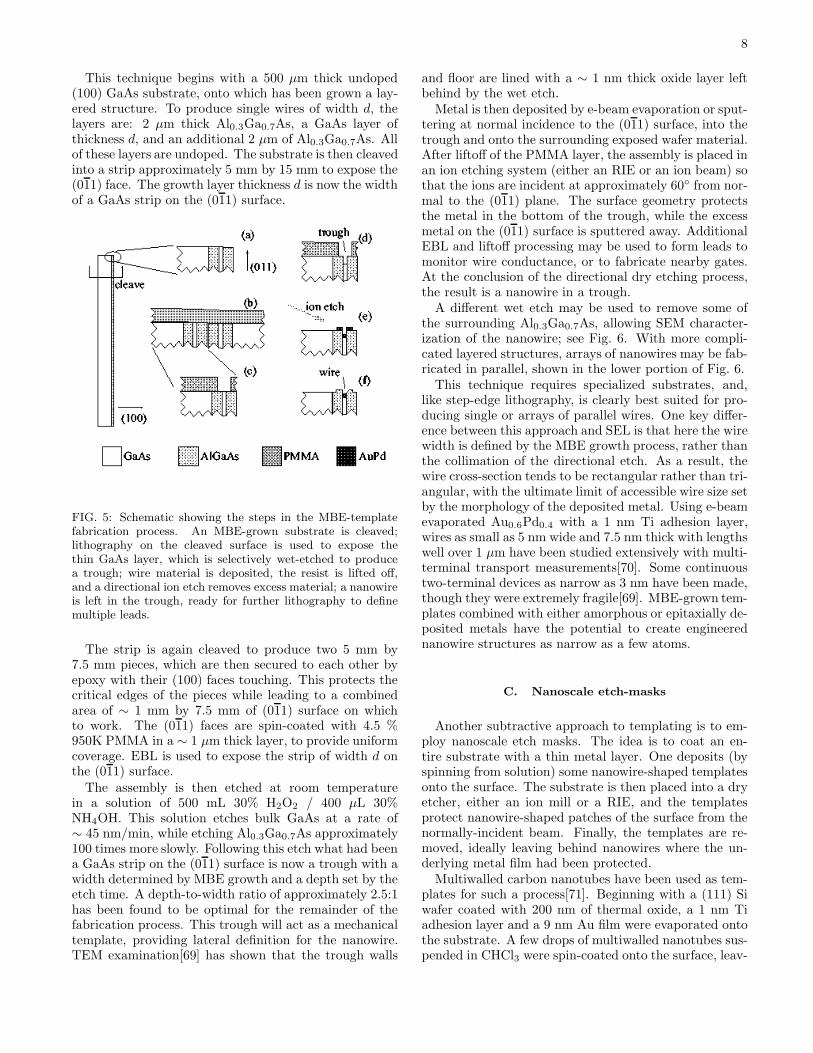
8
This technique begins with a 500 µm thick undoped(100) GaAs substrate, onto which has been grown a lay-ered structure. To produce single wires of width d, thelayers are: 2 µm thick Al0.3Ga0.7As, a GaAs layer ofthickness d, and an additional 2 µm of Al0.3Ga0.7As. Allof these layers are undoped. The substrate is then cleavedinto a strip approximately 5 mm by 15 mm to expose the(011) face. The growth layer thickness d is now the widthof a GaAs strip on the (011) surface.
FIG. 5: Schematic showing the steps in the MBE-templatefabrication process. An MBE-grown substrate is cleaved;lithography on the cleaved surface is used to expose thethin GaAs layer, which is selectively wet-etched to producea trough; wire material is deposited, the resist is lifted off,and a directional ion etch removes excess material; a nanowireis left in the trough, ready for further lithography to definemultiple leads.
The strip is again cleaved to produce two 5 mm by7.5 mm pieces, which are then secured to each other byepoxy with their (100) faces touching. This protects thecritical edges of the pieces while leading to a combinedarea of ∼ 1 mm by 7.5 mm of (011) surface on whichto work. The (011) faces are spin-coated with 4.5 %950K PMMA in a ∼ 1 µm thick layer, to provide uniformcoverage. EBL is used to expose the strip of width d onthe (011) surface.
The assembly is then etched at room temperaturein a solution of 500 mL 30% H2O2 / 400 µL 30%NH4OH. This solution etches bulk GaAs at a rate of∼ 45 nm/min, while etching Al0.3Ga0.7As approximately100 times more slowly. Following this etch what had beena GaAs strip on the (011) surface is now a trough with awidth determined by MBE growth and a depth set by theetch time. A depth-to-width ratio of approximately 2.5:1has been found to be optimal for the remainder of thefabrication process. This trough will act as a mechanicaltemplate, providing lateral definition for the nanowire.TEM examination[69] has shown that the trough walls
and floor are lined with a ∼ 1 nm thick oxide layer leftbehind by the wet etch.
Metal is then deposited by e-beam evaporation or sput-tering at normal incidence to the (011) surface, into thetrough and onto the surrounding exposed wafer material.After liftoff of the PMMA layer, the assembly is placed inan ion etching system (either an RIE or an ion beam) sothat the ions are incident at approximately 60 from nor-mal to the (011) plane. The surface geometry protectsthe metal in the bottom of the trough, while the excessmetal on the (011) surface is sputtered away. AdditionalEBL and liftoff processing may be used to form leads tomonitor wire conductance, or to fabricate nearby gates.At the conclusion of the directional dry etching process,the result is a nanowire in a trough.
A different wet etch may be used to remove some ofthe surrounding Al0.3Ga0.7As, allowing SEM character-ization of the nanowire; see Fig. 6. With more compli-cated layered structures, arrays of nanowires may be fab-ricated in parallel, shown in the lower portion of Fig. 6.
This technique requires specialized substrates, and,like step-edge lithography, is clearly best suited for pro-ducing single or arrays of parallel wires. One key differ-ence between this approach and SEL is that here the wirewidth is defined by the MBE growth process, rather thanthe collimation of the directional etch. As a result, thewire cross-section tends to be rectangular rather than tri-angular, with the ultimate limit of accessible wire size setby the morphology of the deposited metal. Using e-beamevaporated Au0.6Pd0.4 with a 1 nm Ti adhesion layer,wires as small as 5 nm wide and 7.5 nm thick with lengthswell over 1 µm have been studied extensively with multi-terminal transport measurements[70]. Some continuoustwo-terminal devices as narrow as 3 nm have been made,though they were extremely fragile[69]. MBE-grown tem-plates combined with either amorphous or epitaxially de-posited metals have the potential to create engineerednanowire structures as narrow as a few atoms.
C. Nanoscale etch-masks
Another subtractive approach to templating is to em-ploy nanoscale etch masks. The idea is to coat an en-tire substrate with a thin metal layer. One deposits (byspinning from solution) some nanowire-shaped templatesonto the surface. The substrate is then placed into a dryetcher, either an ion mill or a RIE, and the templatesprotect nanowire-shaped patches of the surface from thenormally-incident beam. Finally, the templates are re-moved, ideally leaving behind nanowires where the un-derlying metal film had been protected.
Multiwalled carbon nanotubes have been used as tem-plates for such a process[71]. Beginning with a (111) Siwafer coated with 200 nm of thermal oxide, a 1 nm Tiadhesion layer and a 9 nm Au film were evaporated ontothe substrate. A few drops of multiwalled nanotubes sus-pended in CHCl3 were spin-coated onto the surface, leav-

9
FIG. 6: Upper image: a 20 nm wide AuPd wire (indicatedby arrows) made with the MBE templating process, span-ning several EBL-fabricated Au leads. Surface etching of theGaAs/AlGaAs substrate has been performed to aid in imag-ing. Lower image: an array of parallel nanowires made withthe same technique. The largest wires are 50 nm wide, whilethe narrowest are 7.5 nm wide. Scale bar = 100 nm.
ing behind isolated nanotubes as the solvent evaporated.The substrate was then placed in the path of a 300 Vbeam of Ar+ ions at normal incidence for 1 minute, longenough to mill away the metal film and ∼ 1 nm of SiO2
from uncovered portions of the surface. The nanotubesof various diameters act as etch masks, allowing isolatedTi/Au wires as narrow as 12 nm to be produced. Theremaining nanotubes could be removed by AFM manip-ulation, though one suspects that exposure to an oxygenplasma or ozone environment might be more effective atspeedily ridding large areas of any carbon residue.
A variation on this approach[72] addresses two diffi-culties in the above technique: the dispersity of multi-walled nanotube sizes and the difficulty of removing car-bon residue. Rather than carbon nanotubes, the tem-
plates are chemically modified V2O5 fibers. Unlike fibersproduced in pure water, these are hydrolyzed in a di-lute solution of N-methylforamide, resulting in transversefiber dimensions of 6-10 nm × 15-20 nm, with lengths onthe micron scale. These authors use a 1 nm Ti / 6 nmAuPd film for enhanced metal uniformity from the smallAuPd grain size, and an Ar ion beam (200 V) to providethe directional etch. The V2O5 fibers consistently leadto fairly monodisperse 15 nm-wide nanowires whereeverthe fibers protect the film from the etch. Residual V2O5
is removed by soaking the substrate in a dilute acid so-lution.
A more involved example of this approach[73] inter-poses an additional step. Starting with a CdTe substratecoated with a Bi film (the desired wire material; the un-usual substrate facilitates MBE growth of high quality Bifilms), a layer of PMMA is spun on and baked. The mask-ing in this case is provided by chemically self-assembledchains of Ag nanocrystals. The chains are ∼ 40 nm in di-ameter, with micron-scale lengths. These structures[74]are transferred from solution as a Langmuir-Schaefferfilm onto the PMMA-coated substrates that are thenflood-exposed with a dose of 50 µC/cm2 of 700 V elec-trons. This is sufficiently energetic to expose the PMMAbut not to penetrate the Ag nanocrystals. The nanocrys-tals act as a shadow mask for e-beam exposure rahterthan as a direct etch mask. After the exposed resist isremoved by development in MIBK:IPA solution, the sub-strate is etched with BCl3 in a RIE etcher. The BCL3
attacks the exposed Bi, leaving Bi nanowires behind. Re-moval of the remaining PMMA and Ag nanocrystals isnot discussed.
A final example of this approach[75] uses biopolymericmaterials as etch masks. Microtubules with diameterssmaller than 40 nm and lengths of tens of microns wereused to shadow regions of Ti/Au film on an oxidized Siwafer. Biopolymer templates open up the possibility ofusing biologically inspired pattern formation mechanismsto engineer complicated mask structures.
The advantage of approaches like these is that the tem-plates may be fabricated by chemical means, often withhigh reliability and uniformity on the nm scale. The fi-delity with which this uniformity is transferred to the fi-nal structures is then limited by the etching techniqueand the morphology of the initial metal film. A fur-ther complication is the positioning of the templates; themethods described here form wires whereever the tem-plates happen to land, rather than in predetermined lo-cations.
D. Suspended nanotubes
One may also consider templating approaches that areadditive rather than subtractive. Here a template is usedas a mechanical scaffold upon which wire material is de-posited. Using suspended carbon nanotubes in this wayhas allowed the creation of amorphous MoGe nanowires

10
with widths from a few nm up to ∼ 20 nm[76].For this technique to produce nanowires suited for
conductance studies, the nanotube must be suspendedover the substrate so that it is electrically isolated,except at end points. One method of achieving thisconfiguration[77] begins with a Si wafer coated with 1 µmof SiO2 and a further 60 nm of Si3N4 film. EBL and RIEare used to open a ∼100 nm wide slit in the nitride witha narrower constriction where the measuring electrodeswill be. An HF treatment etches the exposed SiO2 andundercuts the Si3N4. The result is a trough with twocantilevered Si3N4 protrusions at the location of the orig-inal constriction. Through a shadow mask, metal is de-posited to coat these protrusions, forming two measuringelectrodes spaced very closely, with the HF etch under-cut preventing the two electrodes from shorting together.Electrostatic trapping is then used to “capture” a singlenanotube from solution to bridge the electrodes.
FIG. 7: Nanowires made using suspended single-walled car-bon nanotubes as templates for deposition. Tubes were coatedwith 2 nm Ti and 5 nm of the designated metal. Figure repro-duced with permission from [78]. Copyright 2000, AmericanInstitute of Physics.
An alternative approach[78] uses chemical vapor de-position to grow nanotubes directly from patternedcatalyst-coated islands on a Si wafer[79]. The directgrowth method is easier to use for longer nanotubes thanelectrostatic trapping.
As we have seen in all other techniques, in the limitof an atomically precise template the quality of narrownanowires can be limited by the morphology of the con-stituent metal. That is again true for this approach.
Zhang et al.[78, 80] have studied the metal-nanotube in-terface by preparing a series of nanowires from Au, Pd,Fe, Al, and Pb both with and without a 1-2 nm Ti bufferlayer. Metals deposited on top of the Ti adhesion layerare much more uniform, leading to continuous nanowiresat coverages of ∼5 nm of the working metal (see Fig. 7).They postulate that the electronic structure of Ti makesit particularly well-suited to forming thin, uniform coat-ings on the graphite-like surface of the nanotubes.
Suspended templates such as these are versatile and en-able the formation of extremely narrow structures. Withelectrostatic trapping or patterned catalyst deposition,the nanowire position may be engineered rather than de-termined by chance. UHV conditions are not necessaryfor this approach. However, the need to electrically iso-late the templates from the substrates limits the geo-metric flexibility of the technique. Measurements withmore than two electrodes in contact with the wire arealso challenging in this configuration.
E. Electrodeposition into channels
Electrochemical approaches have also been used veryeffectively to produce nanowires using additive templat-ing. To constrain the growth of electrochemically de-posited metal, a three-dimensional template (i.e. a chan-nel with transverse dimensions close to the desired finalwire size) is most commonly required.
An ideal template would be a long pore, ideally ofuniform cross-section, through an electrochemically in-ert membrane. A recent review of membrane-based tem-plating of nanoscale materials may be found in Ref. [81].One approach[82], borrowing from a nuclear physics tech-nique of particle detection, is to create such pores bychemically etching membranes that have been exposedto an energetic ion flux from a radioactive source[83].The MeV-scale ions pass through thin films of mica orpolycarbonate, leaving behind a chemically-altered track.Mica tracks are etched by HF, while polycarbonate mem-branes may be etched by a mixture of NaOH and methylalcohol. Pore sizes below 100 nm are routine, and di-ameters below 10 nm have been reported[84]. Polycar-bonate membranes may also be purchased commercially(e.g. Nuclepore Corp. or Poretics Corp.). Pore densityis determined by the integrated ion dose and may be ashigh as 109 cm−2, while diameter uniformity is set by thedetails of the etch process[85].
An alternative membrane material is anodically etchedporous alumina. This may be produced electrochemicallyfrom a thin aluminum membrane[86]; such membranesmay purchased commercially, albeit with a limited rangeof pore sizes, from, e.g., Whatman Lab. Division. Poredensities can be as high as 1011 cm−2, with diametersas small as a few nm[81], and alumina’s chemical stabil-ity allows great diversity in the types of materials thatmay be deposited[87]. Another template alternative isnanochannel glass[88, 89], in which pores are reduced

11
(a) (b)
(c) (d)
FIG. 8: Nanowires by electrodeposition into a porous tem-plate. (a) a nanoporous membrane; (b) a seed layer of metalsputtered or evaporated onto one side of the membrane; (c)electrodeposition in progress - metal composition may be var-ied by appropriately changing the deposition solution; (d)completed nanowires still in template.
from microscopic to nanoscale dimensions by drawing ofthe glass template.
Chemical self-assembly has also been employedto create templates for electrodeposition. Diblockcopolymers[90] are composed of two polymer componentsthat, under appropriate temperature and surface con-ditions, phase separate into self-organized regions con-taining the different polymers. Because of the chemi-cal distinctiveness of the regions, with suitable process-ing such self-assembled structures may be used to createtemplates for nanowire deposition. For example[91], adiblock copolymer composed of PMMA and polystyrene(PS) dissolved in toluene may be spin-coated onto a con-ducting substrate. By application of an electric field nor-mal to the substrate surface, the self-organization pro-duces a 0.5 µm-thick, hexagonally close-packed array ofPMMA rods 14 nm in diameter embedded in a PS ma-trix. Exposure to DUV radiation degrades the PMMAand crosslinks the PS, so that subsequent development inacetic acid leaves behind a dense array of pores in a PSfilm for use as a template. Pore density and parallelismis similar to that in alumina films, while not requiringstrong acids or bases for processing.
Figure 8 illustrates the steps in the templating pro-cess. An initial metal layer is deposited by evaporationor sputtering onto one side of the membrane. The mem-brane is then placed in an appropriate solution and thedesired metal is electrochemically deposited, using theinitial metallization as a seed. Note that wires with longi-tudinally varying chemical composition may be grown bychanging the deposition solution during the growth pro-cess. Precise multilayers are possible and may be com-bined with chemical functionalization for self-assemblyexperiments[92] or diagnostic sensing[93]. Similarly, bydepositing alternating layers of ferromagnetic and normalmetals, wires that exhibit longitudinal giant magnetore-
sistance (GMR) have been made[94, 95]. It should alsobe noted that templates such as these may be filled bymethods other than electrodeposition, such as high pres-sure injection of molten metal into the pores (see [96] andreferences therein).
Following deposition the membrane may be dissolvedwith an appropriate solvent, allowing access to individ-ual nanowires. Alternately, for sparse arrays made usinglow-porosity membranes, lithography on the upper mem-brane surface may allow two-terminal contacting of smallnumbers of nanowires[84, 97].
Attractive features of this templating approach in-clude: the ability to make large numbers of wires inparallel; the ability for those wires to be substantiallynarrower than 100 nm with a small dispersity in wirediameter; and applicability to a large number of mate-rial systems, including noble metals, ferromagnetic ma-terials, semimetals, etc. Wire diameter is limited by thetemplate, particularly the longitudinal uniformity of poresize[85], and the morphology of the electrodeposited ma-terial. It is possible to form single crystal nanowires withappropriate materials and conditions; for example, seeRefs. [98, 99]. A complication of this method is thatarranging individual wires in precise configurations forstudy is quite challenging.
F. Other templated deposition
Cleaved heterostructures can be another example of anunconventional template. A heavily doped well layer inan MBE-grown III-V heterostructure on the edge of acleaved can be used as the active electrode for depositionwafer[100]. While the quantum well itself is defined withatomic precision, as discussed above in Sec. III B, depo-sition in this approach is not capable of producing wireswith comparable definition. The growth of depositedmetal is not constrained laterally, so that the resultingnanowires produced from a 4 nm-wide quantum well aregranular and have widths ∼20 nm.
Chemically synthesized template structures may alsobe employed as scaffolds for nanowire deposition. Honget al.[101] synthesize arrays of organic nanotubes fromcalix[4]hydroxyquinones (CHQs). The pores in these ar-rays are 0.6 nm × 0.6 nm and are lined with OH groupsand π-conjugated faces. The hydrophilic OH groups al-low silver ions in aqueous solution to be intercalated intothe pores and reduced out of solution, where they aggre-gate to form 0.4 nm diameter crystalline Ag nanowires upto microns in length. This approach produces large num-bers of extremely narrow, straight nanowires without theneed for UHV or high temperature processing. Formingmetallic contacts to the resulting structures, however, isextremely challenging[102].
Individual molecules may also be used as templatesfor chemical metallization. For example, DNA moleculesmay be functionalized to form connections between litho-graphically defined Au electrodes[103]. A chemical pro-

12
cedure exploiting ion exchange is used to seed silver clus-ters along the DNA. Chemical reduction of additionalAg from solution then leads to the formation of a granu-lar wire spanning the electrodes. While this method cantake advantage of existing tools for manipulating DNA,the quality of the resulting wires is not well-controlled atpresent.
IV. CHEMISTRY AND SELF-ASSEMBLY
Direct chemical synthesis and other self-assembly tech-niques have also demonstrated nanowire formation. Wehave already discussed templated chemical synthesis,which relies on a template to confine the reactants andshape the metallic reaction products. Direct chemi-cal synthesis instead takes advantage of some inherentanisotropy in reaction materials or kinetics to produceextended structures. Other forms of self-assembly uti-lize anisotropic energetics (e.g. strain energy from latticemismatch) to guide nanowire formation.
A. Chemical approaches
Direct chemical synthesis of nanowires can be difficultto generalize to large numbers of metals because of theneed for precise control of anisotropy in growth, and alack of suitable reaction chemistries. A full explanationof chemical approaches is beyond the scope of this article.Instead we very briefly state some essential features ofthe methods and provide some references in this rapidlydeveloping field.
Synthesizing elongated structures in either the solu-tion (for example, [104]) or the gas phase[105] often in-volves clever use of seed or catalytic particles. Parti-cle size can directly influence the diameter of the result-ing nanowire. One example of catalytic growth that hasbeen very successfully applied to semiconductor materi-als (though not yet to metals) is described in Ref. [105].The growth mechanism is called the vapor-liquid-solid(VLS) technique[106, 107]. A catalytic liquid nanoclus-ter is made from a material that can form a liquid alloywith the desired nanowire material. Such a cluster, whichdefines the diameter of the nanowire, is then placed inan environment supersaturated with reactant, and servesas a nucleation site for crystallization. One-dimensionalgrowth then occurs, with the liquid nanocluster servingas one end of the resulting nanowire.
An alternative method of chemically producing elon-gated structures from nanoparticles[104] uses surfactantsto coat the seed. By using multiple surfactants, thecrystallographic direction of growth of crystalline ma-terial from solution onto the seed may be controlled.This method has been used to produce single crystal Conanorods with diameters below 15 nm, though to datetheir lengths have been limited to ∼ 100 nm.
Other chemical means may be used to encouragegrowth anisotropy. For example, by reducing silver out ofsolution onto 4 nm seed particles in the presence of a mi-cellar template[108], microns-long Ag nanowires ∼12 nmin diameter may be formed.
Some metals possess crystallographic structures thatnaturally tend toward anisotropic growth when synthe-sized from solution. Examples include selenium[109]and alloys of selenium and tellurium[110]. These sub-stances tend to have helical crystal structures that favor1d growth. Single crystal selenium nanowires 10 nm indiameter microns in length have been produced from so-lution.
Chemical methods sometimes succeed in producingnanowire structures even when there is no clear mech-anism for growth anisotropy. Silver nanowires pro-duced from solution with AgBr seeds[111] and zinc“nanobelts”[112] from ZnS and graphite powder heatedin flowing Ar are two examples.
FIG. 9: SEM image of chemically synthesized Zn “nanobelts”.The growth mechanism that produces these anisotropicnanowire structures is not yet known. Figure reproduced withpermission from [112], copyright 2001 Royal Society of Chem-istry.
Development of chemical methods for nanowire synthe-sis are in an early stage, and have already produced somespectacular results. As with templating approaches, forstudy of electrical transport properties, the nanowiresproduced chemically must then be separated and ma-nipulated onto leads. If suitable reaction pathways andgrowth mechanisms may be found and utilized for morematerials of interest, chemical synthesis may play a ma-jor role in future nanowire studies.
B. Self-assembly
Finally, self-assembly techniques may be employed,particularly to form ordered arrays of nanowires from

13
certain materials on specific substrates. One might imag-ine that the large configurational entropy associated withplacing adsorbate atoms on a substrate would make spon-taneous formation of nanowire structures unlikely. Ener-getic considerations can make organized patterns favor-able, however. This section only touches on the richnessof this subject, focusing on recent examples exlicitly deal-ing with metal nanowires.
One common means of ensuring linear structures is“step-edge decoration.” Here one considers a substratethat is a vicinal surface, where the surface normal devi-ates very slightly from a high symmetry crystalline di-rection. As a result, for clean surfaces (usually annealedat high temperatures in UHV), the substrate has a seriesof parallel atomic terrace steps that are roughly linear,with the density of steps increasing with the degree of“mis-cut”. Nanowire material is then deposited at sub-monolayer coverages. With appropriate choices of sub-strate, nanowire material, and deposition/annealing con-ditions, deposited metal migrates via surface diffusionuntil being trapped up against step edges.
Step edge growth has been employed by a number ofinvestigators (for example, Refs. [113, 114, 115, 116]) inrecent years. The resulting wires are often difficult tocharacterize electronically. The wires are usually onlyone or two atomic layers thick perpendicular to the sub-strate; further, when metal wires are formed at stepson the surface of another metal, isolating the conductingproperties of the wires from the substrate may not bepossible.
One interesting variation that evades these difficultiesis that of Zach et al.[117]. Using electrochemistry theauthors deposit molybdenum oxide at step edges on acleaved graphite substrate. By exposing the substrateto hydrogen at 500 C for an hour, the oxide is reducedto form metallic Mo wires. The wire adhesion to thegraphite is sufficiently poor that the wires may be trans-ferred to the surface of a polymer film cast on top of thegraphite substrate.
An alternative approach to nanowire fabrication thathas received much recent attention is self-assembly as-sisted by differential strain between a deposited metaland the underlying substrate lattice. As in the step dec-oration method, energetic considerations in certain ma-terial systems may be sufficient to overwhelm the entropygain that would result from non-straight wires. Latticemismatch strain has been employed extensively in epi-taxially grown semiconductor structures in recent years(see Ref. [119]).
Simple lattice mismatch is not sufficient to producewire structures[120, 121]; isotropic lattice mismatch re-sults in islands rather than nanowire formation. Sub-stantial growth anisotropy requires the wire material tohave minimal lattice mismatch along the wire directionand large mismatch along the transverse direction. Thisself-assembly technique requires epitaxially smooth andclean substrate surfaces, UHV growth conditions, andcareful material selection to achieve the required lattice
FIG. 10: STM image of self-assembled ErSi2 nanowires onthe Si (001) surface. The nanowires are less than 5 nm wideand are microns in length. Figure reproduced with permissionfrom [118], copyright 2001 Elsevier Science.
conditions.
Rare earths have been observed to form long metallicsilicide nanowires on Si (001) surfaces[118, 120, 122, 123].A typical growth process[120] begins with a flat Si (001)substrate in UHV. Submonolayer coverages of Er are thenevaporated onto the substrate. Erbium forms a ther-modynamically stable silicide, ErSi2, with a hexagonalcrystal structure. The silicide grows so that the lowestlattice mismatch (-1.3%) occurs along the [1120] direc-tion of the ErSi2 and the (110) direction of the Si. Thisdirection is the long axis of the wires. The transverse di-rection ([0001] for the ErSi2; (110) for the Si) has a muchlarger (6.5%) lattice mismatch; as a result wire growthin that direction is strongly disfavored. The result afterannealing is a large number of metallic nanowires a fewnm in width, one or two atomic layers in thickness, andmicrons in length. See Fig. 10.
As with direct chemical synthesis, self-assembly tech-niques for producing nanowires are relatively immature,but show signs of great promise for certain classes of ma-terials. The requirements for UHV conditions and ex-tremely careful surface preparation are stringent, how-ever. Research on more robust, fault-tolerant, and engi-neerable self-assembly mechanisms is sure to be an activefield for some time.

14
V. CONCLUSIONS
Metal nanowires are important both as componentsof future technologies and as tools for examining funda-mental science in metals at the nm scale. It is clear fromthe above that tremendous progress has been made inthe last twenty years on techniques for fabricating suchstructures. Nanowires with transverse dimensions below20 nm present a particular challenge.
The techniques presented here have advantages anddisadvantages that make them well-suited to certaintasks. Summarizing the main points:
• Nanowires are only as well-defined as the metalmaterial that constitutes them. For physically de-posited metals small grain sizes aid in the formationof narrow structures, and the surface physics of themetal-substrate interface is critical in determiningwire morphology.
• Lithographic processes possess tremendous flexibil-ity, but tend to be slow. Lateral definition at ex-tremely small scales is very challenging, and trueatomic resolution from scanned probe methods re-quires UHV conditions and special substrate prepa-ration.
• Templating approaches have been very successful.Subtractive methods produce small numbers of ex-tremely narrow wires at very well-defined locations,given engineered (step-edge, MBE-defined) tem-plates.
• Additive templating using porous membranes toconstrain electrochemical metal growth producesvery large numbers of nanowires. Addressing in-dividual wires or arraying them on a substrate isnontrivial, however. Other structures for templat-ing (chemical scaffolds, nanotubes) are also promis-ing.
• Direct chemical synthesis of metal nanowires ispromising in its infancy. Encouraging results existin a small number of material systems, and muchremains to be learned about growth mechanismsand generalizability of techniques.
• Self-assembly is also a nascent approach. Here, too,the restrictions of particular material systems andprocessing conditions present challenges that needto be more fully investigated.
Nanowires promise to be a fruitful area of physics,materials science, and chemistry research for the fore-seeable future. Advances in nanoscale characterizationtechniques and computational approaches to materialsshould ensure much continued progress in this excitingarena.
DN wishes to acknowledge and thank his nanowire col-laborators (R.L. Willett, L.N. Pfeiffer, K.W. West) andsupport from the DOE (DE-FG03-01ER45946) and theRobert A. Welch Foundation.
[1] van Ruitenbeek, J. M. 2000, in K.-H. Meiwes-Broer(Ed.), Metal Clusters on Surfaces: Structure, QuantumProperties, Physical Chemistry, Springer-Verlag, Berlin.
[2] Yanson, A. I., Bollinger, G. R., van den Brom, H. E.,Agrait, N., and van Ruitenbeek, J. M. 1998, Nature,395, 783.
[3] Cui, Y., Lauhon, L. J., Gudiksen, M. S., Wang, J. F.,and Lieber, C. M. 2001, Appl. Phys. Lett., 78, 2214.
[4] Pfeiffer, L. N., Stormer, H. L., Baldwin, K. W., West,K. W., Goni, A. R., Pinczuk, A., Ashoori, R. C., Dig-nam, M. M., and Wegscheider, W. 1993, J. Cryst.Growth, 127, 849.
[5] Liang, C. T., Simmons, M. Y., Smith, C. G., Ritchie,D. A., and Pepper, M. 1999, Appl. Phys. Lett., 75, 2975.
[6] Tans, S. J., Devoret, M. H., Dai, H. J., Thess, A., Smal-ley, R. E., Geerligs, L. J., and Dekker, C. 1997, Nature,386, 474.
[7] Tour, J. M. 2000, Acc. Chem. Res., 33, 791.[8] Datta, S. 1995, Electronic transport in mesoscopic sys-
tems, Cambridge Studies in Semiconductor Physics andMicroelectronic Engineering 3, Cambridge University,New York.
[9] Imry, Y. 1997, Introduction to Mesoscopic Physics,Mesoscopic Physics and Nanotechnology, Oxford Uni-versity, New York.
[10] Feng, S. 1991, in B. L. Altshuler, P. A. Lee, and R. A.Webb (Eds.), Mesoscopic phenomena in solids, Elsevier,Amsterdam, 107.
[11] Giordano, N. 1991, in B. L. Altshuler, P. A. Lee, andR. A. Webb (Eds.), Mesoscopic phenomena in solids,Elsevier, Amsterdam, 131.
[12] Natelson, D., Willett, R. L., West, K. W., and Pfeiffer,L. N. 2000, Sol. State Comm., 115, 269.
[13] 2001, International Technology Roadmap for Semicon-ductors, http://public.itrs.net.
[14] Xia, Y., Rogers, J. A., Paul, K. E., and Whitesides,G. M. 1999, Chem. Rev., 99, 1823.
[15] Moreau, W. M. 1988, Plenum, New York.[16] Wong, A. K. 2002, SPIE Press, Bellingham, Washing-
ton.[17] Reichmanis, E., Nalamasu, O., and Houlihan, F. M.
2001, Macromol. Symp., 175, 185.[18] Betzig, E. and Trautman, J. K. 1992, Science, 257, 189.[19] Kuwahara, M., Nakano, T., Tominaga, J., Lee, M. B.,
and Atoda, N. 2000, Microelect. Eng., 53, 535.[20] Krivanek, O. L., Dellby, N., and Lupini, A. R. 1999,
Ultramicroscopy, 78, 1.[21] Smith, H. I. and Craighead, H. G. 1990, Physics Today,
43, 24.[22] Grobman, W. D., Luhn, H. E., Donohue, T. P., Speth,

15
A. J., Wilson, A., Hatzakis, M., and Chang, T. H. P.1979, IEEE J. Sol. State Circuits, SC-14, 282.
[23] Rooks, M. J., Wind, S., McEuen, P., and Prober, D. E.1987, J. Vac. Sci. Tech. B, 5, 318.
[24] Sharifi, F. 1996, Proc. of the Symp. on High Speed III-VElect. for Wireless Appl., 316.
[25] Harrison, T. R., Mankiewich, P. M., and Dayem, A. H.1982, Appl. Phys. Lett., 41, 1102.
[26] Tiberio, R. C., Craighead, H. G., Lercel, M., Lau, T.,Sheen, C. W., and Allara, D. L. 1993, Appl. Phys. Lett.,62, 476.
[27] Chen, W. and Ahmed, H. 1993, Appl. Phys. Lett., 62,1499.
[28] Yasin, S., Hasko, D. G., and Ahmed, H. 2001, Appl.Phys. Lett., 78, 2760.
[29] Hatzor, A. and Weiss, P. S. 2001, Science, 291, 1019.[30] Prober, D. E., Feuer, M. D., and Giordano, N. 1980,
Appl. Phys. Lett., 37, 94.[31] Giordano, N. 1980, Phys. Rev. B, 22, 5635.[32] Dynes, R. C., Garno, J. P., and Rowell, J. M. 1978,
Phys. Rev. Lett., 40, 479.[33] Herzog, A. V., Xiong, P., Sharifi, F., and Dynes, R. C.
1996, Phys. Rev. Lett., 76, 668.[34] Butko, V. Y., Ditusa, J. F., and Adams, P. W. 2000,
Phys. Rev. Lett., 84, 1543.[35] Graybeal, J. M. and Beasley, M. R. 1984, Phys. Rev. B,
29, 4167.[36] Quate, C. F. 1997, Surf. Sci., 386, 259.[37] Soh, H. T., Guarioni, K. W., and Quate, C. F. 2001,
Kluwer Academic, New York.[38] Bai, C. 2000, Springer-Verlag, New York.[39] Abadal, G., Perez-Murano, F., Barniol, N., and
Aymerich, X. 1998, Appl. Phys. A, 66, S791.[40] Avouris, P., Martel, R., Hertel, T., and Sandstrom, R.
1998, Appl. Phys. A, 66, S659.[41] Piner, R. D., Zhu, J., Xu, F., Hong, S. H., and Mirkin,
C. A. 1999, Science, 283, 661.[42] Ramsperger, U., Uchihashi, T., and Nejoh, H. 2001,
Appl. Phys. Lett., 78, 85.[43] Sohn, L. L. and Willett, R. L. 1995, Appl. Phys. Lett.,
67, 1552.[44] Bouchiat, V. and Esteve, D. 1996, Appl. Phys. Lett.,
69, 3098.[45] Hu, S., Hamidi, A., Altmeyer, S., Koster, T., Spangen-
berg, B., and Kurz, H. 1998, J. Vac. Sci. Tech. B, 16,2822.
[46] Sugawara, Y., Ohta, M., Ueyama, H., and Morita, S.1995, Science, 270, 1646.
[47] Majumdar, A., Oden, P. I., Carrejo, J. P., Nagahara,L. A., Graham, J. J., and Alexander, L. 1992, Appl.Phys. Lett., 61, 2293.
[48] Kim, J., Lee, H., Shin, Y., and Park, S. 1998, J. KoreanPhys. Soc., 33, S84.
[49] Davidsson, P., Lindell, A., Makela, T., Paalanen, M.,and Pekola, J. 1999, Micro. Eng., 45, 1.
[50] Dubois, E. and Bubbendorff, J. L. 1999, Sol. StateElect., 43, 1085.
[51] Lyding, J. W., Shen, T. C., Hubacek, J. S., J. R. Tucker,J., and Abeln, G. C. 1994, Appl. Phys. Lett., 64, 2010.
[52] Palasantzas, G., Ilge, B., Nijs, J. D., and Geerligs, L. J.1999, J. Appl. Phys., 85, 1907.
[53] Masu, K. and Tsubouchi, M. 1994, J. Vac. Sci. Tech. B,12, 3270.
[54] Adams, D. P., Mayer, T. M., and Swartzentruber, B. S.
1996, Appl. Phys. Lett., 68, 2210.[55] Becker, R. S., Higashi, G. S., Chabal, Y. J., and Becker,
A. J. 1990, Phys. Rev. Lett., 65, 1917.[56] Bolland, J. J. 1990, Phys. Rev. Lett., 65, 3325.[57] Palasantzas, G., Ilge, B., Rogge, S., and Geerlings, L. J.
1999, Microelect. Eng., 46, 133.[58] Sugimura, H., Uchida, T., Kitamura, N., and Masuhara,
H. 1993, Jap. Journ. Appl. Phys. 2, 32, L553.[59] Snow, E. S. and Campbell, P. M. 1995, Science, 270,
1639.[60] Wang, D. W., Tsau, L. M., Wang, K. L., and Chow, P.
1995, Appl. Phys. Lett., 67, 1295.[61] Snow, E. S., Park, D., and Campbell, P. M. 1996, Appl.
Phys. Lett., 69, 269.[62] Held, R., Heinzel, T., Studerus, P., and Ensslin, K.
1998, Physica E, 2, 748.[63] Giordano, N., Gilson, W., and Prober, D. E. 1979, Phys.
Rev. Lett., 43, 725.[64] Flanders, D. C. and White, A. E. 1981, J. Vac. Sci.
Tech., 19, 892.[65] White, A. E., Tinkham, M., Skocpol, W. J., and Flan-
ders, D. C. 1982, Phys. Rev. Lett., 48, 1752.[66] Giordano, N. and Schuler, E. R. 1989, Phys. Rev. Lett.,
63, 2417.[67] Hong, K. M. and Giordano, N. 1995, J. Mag. Mag. Mat.,
151, 396.[68] Natelson, D., Willett, R. L., West, K. W., and Pfeiffer,
L. N. 2000, Appl. Phys. Lett., 77, 1991.[69] Werder, D., Natelson, D., Willett, R. L., Pfeiffer, L. N.,
and West, K. W. 2001, unpublished.[70] Natelson, D., Willett, R. L., West, K. W., and Pfeiffer,
L. N. 2001, Phys. Rev. Lett., 86, 1821.[71] Yun, W. S., Kim, J., Park, K. H., Ha, J. S., Ko, Y. J.,
Park, K., Kim, S. K., Doh, Y. J., Lee, H. J., Salvetat,J. P., and Forro, L. 2000, J. Vac. Sci. Tech. A, 18, 1329.
[72] Sordan, R., Burghard, M., and Kem, K. 2001, Appl.Phys. Lett., 79, 2073.
[73] Choi, S. H., Wang, K. L., Leung, M. S., Stupian, G. W.,Presser, N., Morgan, B. A., Robertson, R. E., Abraham,M., King, E. E., Tueling, M. B., Chung, S. W., Heath,J. R., Cho, S. L., and Ketterson, J. B. 2000, J. Vac. Sci.Tech. A, 18, 1326.
[74] Heath, J. R., Knobler, C. M., and Leff, D. V. 1997, J.Phys. Chem. B, 101, 189.
[75] Fritzsche, W., Bohm, K. J., Unger, E., and Kohler, J. M.1999, Appl. Phys. Lett., 75, 2854.
[76] Bezryadin, A., Lau, C. N., and Tinkham, M. 2000, Na-ture, 404, 971.
[77] Bezryadin, A., Dekker, C., and Schmid, G. 1997, Appl.Phys. Lett., 71, 1273.
[78] Zhang, Y. and Dai, H. 2000, Appl. Phys. Lett., 77, 3015.[79] Kong, J., Soh, H. T., Cassell, A. M., Quate, C. F., and
Dai, H. 1998, Nature, 395, 878.[80] Zhang, Y., Frankln, N. W., Chen, R. J., and Dai, H.
2000, Chem. Phys. Lett., 31, 35.[81] Martin, C. R. 1994, Science, 266, 1961.[82] Possin, G. E. 1971, Physica, 55, 339.[83] Fleischer, R. L., Prince, P. B., and Walker, R. M. 1975,
Univ. of California Press, Berkeley.[84] Williams, W. D. and Giordano, N. 1984, Rev. Sci. Instr.,
55, 410.[85] Schonenberger, C., van der Zaande, B. M. I., Fokkink,
L. G. J., Henny, M., Schmid, C., Kruger, M., Bachtold,A., Huber, R., Birk, H., and Staufer, U. 1997, J. Phys.

16
Chem. B, 101, 5497.[86] Despic, A. and Parkhutik, V. P. 1989, in J. O. Bockris,
R. E. White, and B. E. Conway (Eds.), Modern Aspectsof Electrochemistry, volume 26, Plenum, NY, Ch. 6.
[87] Routkevitch, D., Tager, A. A., Haruyama, J., Al-mawlawi, D., Moskovits, M., and Xu, J. M. 1996, IEEETrans. Elect. Dev., 43, 1646.
[88] Tonucci, R. J., Justus, B. L., Campillo, A. J., and Ford,C. E. 1992, Science, 258, 783.
[89] Nguyen, P. P., Pearson, D. H., tonucci, R. J., and Bab-cock, K. 1998, J. Electrochem. Soc., 145, 247.
[90] Fasolka, M. J. and Mayes, A. M. 2001, Ann. Rev. Mat.Res., 31, 323.
[91] Thurn-Albrecht, T., Schotter, J., Kastle, C. A., Em-ley, N., Shibauchi, T., Krusin-Elbaum, L., Guarini, K.,Black, C. T., Tuominen, M., and Russell, T. P. 2000,Science, 290, 2126.
[92] Martin, B. R., Dermody, D. J., Reiss, B. D., Fang,M. M., Lyon, L. A., Natan, M. J., and Mallouk, T. E.1999, Adv. Mat., 11, 1021.
[93] Nicewarner-Pena, S. R., Freeman, R. G., Reiss, B. D.,He, L., Pena, D. J., Walton, I. D., Cromer, R., Keating,C. D., and Natan, M. J. 2001, Science, 294, 137.
[94] Piraux, L., George, J. M., Despres, J. F., Leroy, C.,Ferain, E., Legras, R., Ounadjela, K., and Fert, A. 1994,Appl. Phys. Lett., 65, 2484.
[95] Liu, K., Nagodawithana, K., Searson, P. C., and Chien,C. L. 1995, Phys. Rev. B, 51, 7381.
[96] Zhang, Z. B., Sun, X. Z., Dresselhaus, M. S., Ying, J. Y.,and Heremans, J. P. 1998, Appl. Phys. Lett., 73, 1589.
[97] Bachtold, A., Terrier, C., Kruger, M., Henny, M., Hoss,T., Strunk, C., Huber, R., Birk, H., Staufer, U., andSchonenberger, C. 1998, Micro. Eng., 42, 571.
[98] Yi, G. and Schwarzacher, W. 1999, Appl. Phys. Lett.,74, 1746.
[99] Gao, T., Meng, G. W., Zhang, J., Wang, Y. W., Liang,C. H., Fan, J. C., and Zhang, L. D. 2001, Appl. Phys.A, 73, 251.
[100] Fasol, G. and Runge, K. 1997, Appl. Phys. Lett., 70,2467.
[101] Hong, B. H., Bae, S. C., Lee, C. W., Jeong, S., and Kim,K. S. 2001, Science, 294, 348.
[102] Kim, K. S. 2002, private communication.[103] Braun, E., Eichen, Y., Sivan, U., and Ben-Yoseph, G.
1998, Nature, 391, 775.[104] Puntes, V. F., Krishnan, K. M., and Alivisatos, A. P.
2001, Science, 291, 2115.[105] Hu, J. T., Odom, T. W., and Lieber, C. M. 1999, Acc.
Chem. Res., 32, 435.[106] Wagner, R. S. and Ellis, W. C. 1964, Appl. Phys. Lett.,
4, 89.[107] Wagner, R. S. 1970, in A. P. Levitt (Ed.), Whisker Tech-
nology, Wiley, New York.[108] Jana, N. R., Gearheart, L., and Murphy, C. J. 2001,
Chem. Comm., 7, 617.[109] Gates, B., Yin, Y., and Xia, Y. 2000, J. Am. Chem.
Soc., 122, 12582.[110] Mayers, B., Gates, B., Yin, Y., and Xia, Y. 2001, Adv.
Mat., 13, 1380.[111] Liu, S., Yue, J., and Gedanken, A. 2001, Adv. Mat., 13,
656.[112] Wang, Y., Zhang, L., Meng, G., Liang, C., Wang, G.,
and Sun, S. 2001, Chem. Commun., 2632.[113] Jung, T., Schlittler, R., Gimzewski, J. K., and Himpsel,
F. J. 1995, Appl. Phys. A, 61, 467.[114] Himpsel, F. J., Jung, T., and Ortega, J. E. 1997, Surf.
Rev. Lett., 4, 371.[115] Batzill, M., Sarstedt, M., and Snowdon, K. J. 1998,
Nanotechnology, 9, 20.[116] Dekoster, J., Degroote, B., Pattyn, H., Lagouche, G.,
Vantomme, A., and Degroote, S. 1999, Appl. Phys.Lett., 75, 938.
[117] Zach, M. P., Ng, K. H., and Penner, R. M. 2000, Science,290, 2120.
[118] Chen, Y., Ohlberg, D. A. A., and Williams, R. S. 2001,Mat. Sci. Eng. B, 87, 222.
[119] Petroff, P. M., Lorke, A., and Imamoglu, A. 2001, Phys.Today, 54, 46.
[120] Chen, Y., Ohlberg, D. A. A., Medeiros-Ribeiro, G.,Chang, Y. A., and Williams, R. S. 2000, Appl. Phys.Lett., 76, 4004.
[121] Petroff, P. M. and DenBaars, S. P. 1994, Superlatt. Mi-crostr., 15, 15.
[122] Preinesberger, C., Vandre, S., Kalka, T., and Dahne-Prietsch, M. 1998, J. Phys. D, 31, L43.
[123] Nogami, J., Liu, B. Z., Katkov, M. V., Ohbuchi, C., andBirge, N. O. 2001, Phys. Rev. B, 63, 233305.
Copyright © 2022 FDOKUMEN