Electrical properties of single CdTe nanowires
7
444 Electrical properties of single CdTe nanowires Elena Matei 1 , Camelia Florica 1 , Andreea Costas 1 , María Eugenia Toimil-Molares 2 and Ionut Enculescu *1 Full Research Paper Open Access Address: 1 National Institute for Materials Physics, Magurele, Ilfov, Romania, 77125 and 2 GSI, Planckstraße 1, 64291 Darmstadt, Germany Email: Ionut Enculescu * - [email protected] * Corresponding author Keywords: CdTe; electrodeposition; nanowires; transport properties Beilstein J. Nanotechnol. 2015, 6, 444–450. doi:10.3762/bjnano.6.45 Received: 17 September 2014 Accepted: 16 December 2014 Published: 12 February 2015 This article is part of the Thematic Series "Self-assembly of nanostructures and nanomaterials". Guest Editor: I. Berbezier © 2015 Matei et al; licensee Beilstein-Institut. License and terms: see end of document. Abstract Ion track, nanoporous membranes were employed as templates for the preparation of CdTe nanowires. For this purpose, electro- chemical deposition from a bath containing Cd and Te ions was employed. This process leads to high aspect ratio CdTe nanowires, which were harvested and placed on a substrate with lithographically patterned, interdigitated electrodes. Focused ion beam- induced metallization was used to produce individual nanowires with electrical contacts and electrical measurements were performed on these individual nanowires. The influence of a bottom gate was investigated and it was found that surface passivation leads to improved transport properties. 444 Introduction Nanowires, which are quasi one-dimensional structures, are considered an extremely important class of nanostructures, regarded as highly effective building blocks for future elec- tronic devices [1-4]. In addition to their specific dimensions and high aspect ratio (which enable ultraminiaturization, due to the high surface-to-volume ratio), nanowires provide increased functionality for electronic devices which contain them [5-7]. There are numerous ways to fabricate nanowires, with methods ranging from simple and straightforward wet chemistry approaches, to complex multistep approaches that were devel- oped over the past two decades. The main goal in all experi- ments involving such nanostructure preparation is to control both the morphological properties and the structural and compo- sitional characteristics, in order to control the functionality of the nanowires. It is also important that the fabrication method leads to reproducible results and is highly scalable, thus increasing the efficiency of the preparation step. The template approach is a method which enables the fabrica- tion of nanowires with excellent reproducibility and a narrow distribution of the geometrical characteristics [8-13]. The
Transcript of Electrical properties of single CdTe nanowires

444
Electrical properties of single CdTe nanowiresElena Matei1, Camelia Florica1, Andreea Costas1, María Eugenia Toimil-Molares2
and Ionut Enculescu*1
Full Research Paper Open Access
Address:1National Institute for Materials Physics, Magurele, Ilfov, Romania,77125 and 2GSI, Planckstraße 1, 64291 Darmstadt, Germany
Email:Ionut Enculescu* - [email protected]
* Corresponding author
Keywords:CdTe; electrodeposition; nanowires; transport properties
Beilstein J. Nanotechnol. 2015, 6, 444–450.doi:10.3762/bjnano.6.45
Received: 17 September 2014Accepted: 16 December 2014Published: 12 February 2015
This article is part of the Thematic Series "Self-assembly ofnanostructures and nanomaterials".
Guest Editor: I. Berbezier
© 2015 Matei et al; licensee Beilstein-Institut.License and terms: see end of document.
AbstractIon track, nanoporous membranes were employed as templates for the preparation of CdTe nanowires. For this purpose, electro-
chemical deposition from a bath containing Cd and Te ions was employed. This process leads to high aspect ratio CdTe nanowires,
which were harvested and placed on a substrate with lithographically patterned, interdigitated electrodes. Focused ion beam-
induced metallization was used to produce individual nanowires with electrical contacts and electrical measurements were
performed on these individual nanowires. The influence of a bottom gate was investigated and it was found that surface passivation
leads to improved transport properties.
444
IntroductionNanowires, which are quasi one-dimensional structures, are
considered an extremely important class of nanostructures,
regarded as highly effective building blocks for future elec-
tronic devices [1-4]. In addition to their specific dimensions and
high aspect ratio (which enable ultraminiaturization, due to the
high surface-to-volume ratio), nanowires provide increased
functionality for electronic devices which contain them [5-7].
There are numerous ways to fabricate nanowires, with methods
ranging from simple and straightforward wet chemistry
approaches, to complex multistep approaches that were devel-
oped over the past two decades. The main goal in all experi-
ments involving such nanostructure preparation is to control
both the morphological properties and the structural and compo-
sitional characteristics, in order to control the functionality of
the nanowires. It is also important that the fabrication method
leads to reproducible results and is highly scalable, thus
increasing the efficiency of the preparation step.
The template approach is a method which enables the fabrica-
tion of nanowires with excellent reproducibility and a narrow
distribution of the geometrical characteristics [8-13]. The

Beilstein J. Nanotechnol. 2015, 6, 444–450.
445
method typically makes use of a nanoporous membrane as a
template along with a method for filling its pores. As templates,
most used are polymer ion track membranes, anodic alumina
and diblock copolymer templates, while the filling methods
range from electrochemical or electroless deposition, to atomic
layer deposition or molten metal injection.
The nanoporous polymer ion track membranes are obtained by
polymer foil irradiation with swift heavy ions and further chem-
ical etching of the ion tracks [13]. This method allows for
control of pore density by taking into account that each ion
leaves a single, cylindrical track and pore size throughout the
etching process. These parameters are usually chosen in
connection with the desired final nanowire size and quantity.
Electrochemical deposition is a well-established method of
plating conductive substrates with a specific metal or alloy.
During the last decades, semiconductor electrodeposition
became more and more attractive, as it may represent a viable
alternative to more expensive fabrication methods [14-16].
CdTe electroplating is an excellent example of semiconductor
electrodeposition for both film and nanostructure fabrication
[14]. By employing a bath containing both cadmium and
telluride, their controlled reduction at the working electrode
leads to the formation of a high quality, stoichiometric, com-
pound semiconductor.
In this work, a template approach for fabricating CdTe
nanowires by electrodeposition inside ion track polycarbonate
nanoporous membranes was employed. It was recently proved
that one can easily control the characteristic of the nanowires
prepared in this way by controlling the electrodeposition over-
potential [15]. However, the number of reports dealing with the
electrical properties of individual CdTe nanowires are very few.
In the present report, in addition to basic characterization
regarding morphology, structure and composition determin-
ation, the nanowires were connected with electrical contacts by
means of a combination of lithography and focused ion beam-
induced metallization (FIBIM). The electrical properties were
determined for individual nanowires prepared under different
conditions. Further, the effect of a bottom gate on the charge
carriers transported through the nanowire channel was exam-
ined. It was also found that (similar to other cases of semicon-
ductor nanowires) the surface passivation leads to an improve-
ment in the electrical properties [16,17].
Results and DiscussionElectrochemical deposition of CdTe is a process that has been
studied over several decades, and is one of the first reports of an
electrodeposited semiconductor. The mechanism leading to the
formation of the stoichiometric compound was thermodynami-
cally explained based on the free energy corresponding to the
compound formation reaction. In the case of this particular
compound, this free energy opens up the possibility to obtain
the stoichiometric composition for a rather wide range of elec-
trode potentials and the ability to tune the bath composition
over a rather wide range. Practically, the electrodeposition of
multicomponent materials (either alloys or compounds) is
related to the differences in reduction potentials for each
component. In order to reach the desired composition, the depo-
sition conditions must be adjusted in order to reach the desired
reaction rate for each component. The procedure typically
involves a deposition bath containing a high ratio of the element
that is reduced at more electronegative values to the element
that is reduced at less electronegative values. For the electrode-
position of CdTe, a bath containing CdSO4 as a source of Cd
ions and TeO2 as a source of Te ions was employed at a ratio of
100 (considering that Cd is reduced at a far more negative elec-
trode potential than Te). Consequently, the electrochemical
polarization curves show a plateau in current over a range
covering approximately 300 mV.
Electrodeposition inside nanoporous membranes has several
particularities, which are a consequence of the fact that the
process takes place in a restricted geometry ([13] gives a
detailed description of the process). In this regard, the diffusion
of ions through the nanopores is different from typical diffu-
sion in an open bath when plating on a typical two-dimensional
electrode. As a consequence, the current versus time curve
shows a strong current increase when the pore is completely
filled and during switching from deposition inside the nanopore
to deposition on the surface. This effect was used to determine
the time necessary for complete filling whereby the process can
be stopped earlier. The nanowires growing from caps on the
surface (indicating complete pore filling) are more difficult to
harvest and contact, and therefore, the deposition process
should be stopped before cap formation.
The deposition was performed in membranes with 108 and
109 pores/cm2 and different pore diameters. In order to charac-
terize the nanowires, the template membrane was dissolved by
immersing the template containing the nanowires in chloroform
and the process was repeated at least 5 times. The process was
started with p.a.-grade chloroform and for the last two washing
steps, semiconductor-grade chloroform was used. Thorough
washing is important for precise electrical characterization since
template remnants can influence the characteristics of the
metal–semiconductor interface.
In Figure 1 one can observe SEM images of such arrays of
nanowires prepared at different electrode potentials, shown after
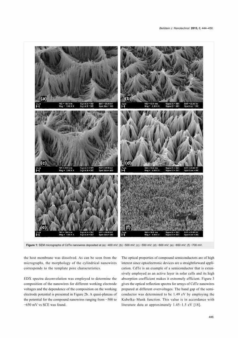
Beilstein J. Nanotechnol. 2015, 6, 444–450.
446
Figure 1: SEM micrographs of CdTe nanowires deposited at (a) −400 mV; (b) −500 mV; (c) −550 mV; (d) −600 mV; (e) −650 mV; (f) −700 mV.
the host membrane was dissolved. As can be seen from the
micrographs, the morphology of the cylindrical nanowires
corresponds to the template pore characteristics.
EDX spectra deconvolution was employed to determine the
composition of the nanowires for different working electrode
voltages and the dependence of the composition on the working
electrode potential is presented in Figure 2b. A quasi-plateau of
the potential for the compound nanowires ranging from −500 to
−650 mV vs SCE was found.
The optical properties of compound semiconductors are of high
interest since optoelectronic devices are a straightforward appli-
cation. CdTe is an example of a semiconductor that is exten-
sively employed as an active layer in solar cells and its high
absorption coefficient makes it extremely efficient. Figure 3
gives the optical reflection spectra for arrays of CdTe nanowires
prepared at different overvoltages. The band gap of the semi-
conductor was determined to be 1.49 eV by employing the
Kubelka–Munk function. This value is in accordance with
literature data at approximately 1.45–1.5 eV [18].

Beilstein J. Nanotechnol. 2015, 6, 444–450.
447
Figure 2: (a) EDX spectra for a series of samples prepared at different electrode potentials; (b) Cd content versus working electrode potential.
Figure 3: (a) Spectral reflectance curve and (b) Kubelka–Munk representation for band gap determination of CdTe deposited at −500 mV.
The nanowires were further harvested in chloroform by ultra-
sonication. Taking into account the brittleness of the semicon-
ducting nanostructure, the ultrasonication step was performed
for only a few seconds. Further, a droplet of nanowire suspen-
sion was placed on Si/SiO2 substrates on which interdigitated
Ti/Au electrodes were patterned by photolithography (Figure 4).
FIBIM is a direct patterning method employed for the design of
metallic nanostructures. The method is based on the interaction
of an ion beam with the surface-adsorbed, metal–organic mole-
cules corresponding to the working gas. The decomposition
leads to a patterned metallic layer with precisely tailored geom-
etry. In our case, a platinum pattern was formed in order to
connect the CdTe nanowires to the photolithographically
designed, interdigitated contact (Figure 4b). The drawback of
this method is that the metal deposited in this way has a lower
conductivity as compared to other deposition methods. This is a
direct result of the approach and is due to the presence of
carbon in the metal layer. This carbon is a residue due to the
organic component of the precursor gas.
Further electrical measurements revealed a slightly nonlinear
current–voltage characteristic. When a voltage was applied to
the silicon substrate, this gate potential influenced the current
through the nanowire.
For ZnO it was previously reported [17,19] that a thin layer of
polymer covering the nanowire drastically improved the trans-
port properties. This was tested in this work and to our knowl-
edge, only one previous paper dealt with the electrical transport
of individual nanowires [20]. No observation of passivation
effects on CdTe nanowires was previously reported. We also

Beilstein J. Nanotechnol. 2015, 6, 444–450.
448
Figure 4: (a) The system of electrodes produced by lithography for contacting the nanowire; (b) an image of an individual nanowire contacted byFIBIM to the larger lithographically prepared electrodes.
Figure 5: (a) Current–voltage characteristics for a CdTe nanowire contacted by FIBIM; (b) Current–voltage characteristics for a CdTe nanowirecontacted by FIBIM after PMMA passivation.
observed a similar behavior for CdTe, as would be expected for
objects with similar geometries. In Figure 5 current–voltage
characteristics are presented for a nanowire contacted by this
approach before and after poly(methyl methacrylate) (PMMA)
passivation.
A difference of almost an order of magnitude between the
sample before and after PMMA covering was observed. This
increase in current observed when adding the polymer layer has
a potential source: the passivation of surface states, which may
be responsible for a decrease in the number of the free charge
carriers available in the nanowire.
ConclusionCdTe nanowires were prepared by electrochemical deposition
inside ion track, nanoporous membranes. Substrates with inter-
digitated electrodes were fabricated by employing a photo-
lithographic approach. After the growth of the nanowires, they
were placed onto the substrate and FIBIM was employed to
make contacts between the nanowire and the electrodes. The
contacts were not pure platinum, but rather a mixture of
platinum and carbon, which was the residual phase from the
organic component of the gaseous precursor used.
The electrical characteristics were measured and nonlinear I–V
characteristics were observed. A strong increase in current was
measured when the nanowire was covered with a thin polymer
layer. One possible explanation for this phenomenon is that the
surface states, which are extremely important for high surface-
to-volume ratios, were passivated through the process.
CdTe is an important semiconductor for optoelectronics and this
approach to CdTe nanowire fabrication gives the opportunity to
measure electrical properties of individual nanostructures and to

Beilstein J. Nanotechnol. 2015, 6, 444–450.
449
better understand them in correlation with the preparation
methods.
ExperimentalPolycarbonate foils of 30 μm thickness were irradiated with
swift heavy ions from the linear accelerator UNILAC at the
Gesellschaft für Schwerionenforschung (GSI). The ions (Au,
Pb or U) were accelerated at a specific kinetic energy of
11.4 MeV/nucleon. When passing through the polymer foil,
each ion leaves a cylindrical defect track as a consequence of its
interaction with the target. Further, these tracks were chemi-
cally etched, leading to the formation of cylindrical pores. An
aqueous solution of 5 M NaOH and 10 vol % methanol was
employed for the etching process at a temperature of 50 °C. The
etching rate was 2 μm/h, at three minutes of etching, resulting in
cylindrical pores of approximately 100 nm diameter.
On one face of the membrane, a thin (50 nm) gold electrode is
deposited by means of DC sputtering. This is further strength-
ened by the electrodeposition of a thick (10 μm) copper film.
This membrane was then inserted into an electrochemical cell,
with the uncovered side facing the electrolyte.
A potentiostat (Parstat 2272) was employed for controlling the
deposition process in a three-electrode setup. The reference
electrode was a commercial, saturated calomel electrode and the
counter electrode was a 4 cm2 platinum foil. A double-walled
glass beaker was employed as an electrochemical cell, and a
deposition temperature of 80 °C was maintained by means of an
external water circulator.
The deposition bath contained CdSO4 and TeO2 as the sources
of the two ions. The pH was adjusted to 2 using sulfuric acid
and sodium hydroxide. Higher pHs led to tellurium oxide
precipitation.
After nanowire growth, the membrane was dissolved with chlo-
roform leaving the nanowires exposed. The arrays of nanowires
fabricated in this manner were investigated by means of scan-
ning electron microscopy, energy dispersive X-ray analysis and
optical spectroscopy.
Further, the wires were harvested by ultrasonication into a
suspension in chloroform. A droplet of nanowire suspension in
semiconductor-grade chloroform was placed on a n++ Si/SiO2
substrate with patterned, interdigitated contracts. These were
obtained by photolithography and sequential deposition of
20 nm of Ti and 200 nm Au. A dual-beam, FIB/FEG machine
was employed to connect the individual nanowire with the
existing interdigitated contacts. During this FIBIM process, a
metal–organic gas containing platinum was injected through a
nozzle close to the surface of the sample and decomposed in a
precise pattern determined by the Ga ion beam. The result is a
stripe of a mixture of Pt–C–Ga with the desired geometry deter-
mined by the ion beam scanning pattern.
A probe station was employed for performing the electrical
characterization of individual nanowires. In order to investigate
the effect of a gate on the transport through the nanowire, a
third electrical contact was made to the n++ Si substrate. A com-
parison of the transport properties of the nanowires with and
without a passivated thin layer of PMMA was performed. This
polymer passivation layer was deposited onto the wire by
means of spin coating.
AcknowledgementsThe authors acknowledge the financial support of the Romanian
Government through UEFISCDI contract 24/2013. Andreea
Costas was supported by the strategic grant POSDRU/159/1.5/
S/137750, “Project Doctoral and Postdoctoral programs support
for increased competitiveness in Exact Sciences research”,
which is cofinanced by the European Social Foundation within
the Sectorial Operational Program Human Resources Develop-
ment 2007–2013.
References1. Li, D.; Xia, Y. Adv. Mater. 2004, 16, 1151–1170.
doi:10.1002/adma.2004007192. Huang, M. H.; Mao, S.; Feick, H.; Yan, H.; Wu, Y.; Kind, H.; Weber, E.;
Russo, R.; Yang, P. Science 2001, 292, 1897–1899.doi:10.1126/science.1060367
3. Morales, A. M.; Lieber, C. M. Science 1998, 279, 208–211.doi:10.1126/science.279.5348.208
4. Lu, W.; Lieber, C. M. Nat. Mater. 2007, 6, 841–850.doi:10.1038/nmat2028
5. Cui, Y.; Wei, Q.; Park, H.; Lieber, C. M. Science 2001, 293,1289–1292. doi:10.1126/science.1062711
6. Yan, H.; Choe, H. S.; Nam, S.; Hu, Y.; Das, S.; Klemic, J. F.;Ellenbogen, J. C.; Lieber, C. M. Nature 2011, 470, 240–244.doi:10.1038/nature09749
7. Rogers, J. A.; Lagally, M. G.; Nuzzo, R. G. Nature 2011, 477, 45–53.doi:10.1038/nature10381
8. Martin, C. R. Science 1994, 266, 1961–1966.doi:10.1126/science.266.5193.1961
9. Liang, H.-W.; Liu, S.; Yu, S.-H. Adv. Mater. 2010, 22, 3925–3937.doi:10.1002/adma.200904391
10. Kline, T. R.; Tian, M.; Wang, J.; Sen, A.; Chan, M. W. H.; Mallouk, T. E.Inorg. Chem. 2006, 45, 7555–7565. doi:10.1021/ic0601384
11. Li, L.; Pan, S.; Dou, X.; Zhu, Y.; Huang, X.; Yang, Y.; Li, G.; Zhang, L.J. Phys. Chem. C 2007, 111, 7288–7291. doi:10.1021/jp0711242
12. Matei, E.; Enculescu, I.; Toimil-Molares, M. E.; Leca, A.; Ghica, C.;Kuncser, V. J. Nanopart. Res. 2013, 15, 1863.doi:10.1007/s11051-013-1863-3
13. Toimil-Molares, M. E. Beilstein J. Nanotechnol. 2012, 3, 860–883.doi:10.3762/bjnano.3.97

Beilstein J. Nanotechnol. 2015, 6, 444–450.
450
14. Lincot, D. Thin Solid Films 2005, 487, 40–48.doi:10.1016/j.tsf.2005.01.032
15. Matei, E.; Ion, L.; Antohe, S.; Neumann, R.; Enculescu, I.Nanotechnology 2010, 21, 105202.doi:10.1088/0957-4484/21/10/105202
16. Jeong, S. S.; Mittiga, A.; Salza, E.; Masci, A.; Passerini, S.Electrochim. Acta 2008, 53, 2226–2231.doi:10.1016/j.electacta.2007.09.030
17. Hong, W.-K.; Song, S.; Hwang, D.-K.; Kwon, S.-S.; Jo, G.; Park, S.-J.;Lee, T. Appl. Surf. Sci. 2008, 254, 7559–7564.doi:10.1016/j.apsusc.2008.01.070
18. Sarkar, S.; Pal, S.; Sarkar, P. J. Mater. Chem. 2012, 22, 10716–10724.doi:10.1039/c2jm16810c
19. Florica, C.; Matei, E.; Costas, A.; Toimil Molares, M. E.; Enculescu, I.Electrochim. Acta 2014, 137, 290–297.doi:10.1016/j.electacta.2014.05.124
20. Kum, M. C.; Yoo, B. Y.; Rheem, Y. W.; Bozhilov, K. N.; Chen, W.;Mulchandani, A.; Myung, N. V. Nanotechnology 2008, 19, 325711.doi:10.1088/0957-4484/19/32/325711
License and TermsThis is an Open Access article under the terms of the
Creative Commons Attribution License
(http://creativecommons.org/licenses/by/2.0), which
permits unrestricted use, distribution, and reproduction in
any medium, provided the original work is properly cited.
The license is subject to the Beilstein Journal of
Nanotechnology terms and conditions:
(http://www.beilstein-journals.org/bjnano)
The definitive version of this article is the electronic one
which can be found at:
doi:10.3762/bjnano.6.45