Surface-structure-regulated cell-membrane penetration by monolayer-protected nanoparticles
Upload
khangminh22Category
view
0download
0


MONOLAYER FUNCTIONALIZATION OF
SILICON MICRO AND NANOWIRES:
TOWARDS SOLAR‐TO‐FUEL AND SENSING DEVICES
Janneke Veerbeek

Members of the committee:
Chairman: prof. dr. ir. J.W.M. Hilgenkamp University of Twente
Promotor: prof. dr. ir. J. Huskens University of Twente
Members: prof. dr. J.G.E. Gardeniers University of Twente
prof. dr. S. Hecht Humboldt‐Universität zu Berlin
prof. dr. S.J.G. Lemay University of Twente
prof. dr. G. Mul University of Twente
prof. dr. J.N.H. Reek University of Amsterdam
The research described in this thesis was performed within the laboratories of the
Molecular NanoFabrication (MnF) group, the MESA+ Institute for Nanotechnology, and
the Department of Science and Technology (TNW) of the University of Twente (UT). This
research was supported by the Netherlands Organization for Scientific Research (NWO,
MESA+ School for Nanotechnology, grant 022.003.001).
Monolayer functionalization of silicon micro and nanowires: towards solar‐to‐fuel and
sensing devices
Copyright © 2017 Janneke Veerbeek
PhD thesis, University of Twente, Enschede, the Netherlands
ISBN: 978‐90‐365‐4308‐8
DOI: 10.3990/1.9789036543088
Cover art: Janneke Veerbeek
Printed by: Gildeprint

MONOLAYER FUNCTIONALIZATION OF
SILICON MICRO AND NANOWIRES:
TOWARDS SOLAR‐TO‐FUEL AND SENSING DEVICES
PROEFSCHRIFT
ter verkrijging van
de graad van doctor aan de Universiteit Twente,
op gezag van de rector magnificus,
prof. dr. T.T.M. Palstra,
volgens besluit van het College voor Promoties
in het openbaar te verdedigen
op vrijdag 12 mei 2017 om 14:45 uur
door
Janneke Veerbeek
geboren op 28 februari 1990
te Noordoostpolder, Nederland

Dit proefschrift is goedgekeurd door:
Promotor: prof. dr. ir. J. Huskens

v
Table of contents Chapter 1 General introduction .......................................................................................... 1
1.1 Introduction ...................................................................................................... 1
1.2 Scope and outline of the thesis ........................................................................ 2
1.3 References ........................................................................................................ 4
Chapter 2 Applications of monolayer‐functionalized H‐terminated silicon surfaces: a
review .................................................................................................................................. 7
2.1 Introduction ...................................................................................................... 8
2.2 Methods ............................................................................................................ 8
2.3 Surface passivation ......................................................................................... 11
2.4 Electronics ....................................................................................................... 14
2.5 Doping ............................................................................................................. 17
2.6 Optics .............................................................................................................. 23
2.7 Biomedical devices .......................................................................................... 26
2.8 Sensors ............................................................................................................ 29
2.9 Conclusions and outlook ................................................................................. 34
2.10 References ...................................................................................................... 35
Chapter 3 Molecular monolayers for electrical passivation and functionalization of silicon‐
based solar energy devices ............................................................................................... 43
3.1 Introduction .................................................................................................... 44
3.2 Results and discussion .................................................................................... 45
3.2.1 Monolayer passivation ............................................................................... 45
3.2.2 Dual passivation and functionalization ...................................................... 51
3.3 Conclusions ..................................................................................................... 53
3.4 Acknowledgments .......................................................................................... 54
3.5 Experimental section ...................................................................................... 54
3.5.1 Materials ..................................................................................................... 54
3.5.2 Methods ..................................................................................................... 55
3.5.3 Equipment .................................................................................................. 57
3.6 References ...................................................................................................... 58
Chapter 4 Highly doped silicon nanowires by monolayer doping ..................................... 61
4.1 Introduction .................................................................................................... 62
4.2 Results and discussion .................................................................................... 63
4.2.1 Nanowire synthesis .................................................................................... 64

vi
4.2.2 Monolayer doping ....................................................................................... 66
4.2.3 Monolayer contact doping .......................................................................... 68
4.2.4 Monolayer doping with an external capping layer ..................................... 70
4.3 Conclusions ...................................................................................................... 71
4.4 Acknowledgments ........................................................................................... 72
4.5 Experimental section ....................................................................................... 72
4.5.1 Materials ..................................................................................................... 72
4.5.2 Methods ...................................................................................................... 73
4.5.3 Equipment ................................................................................................... 75
4.6 References ....................................................................................................... 76
Chapter 5 Maskless spatioselective functionalization of silicon nanowires ....................... 79
5.1 Introduction ..................................................................................................... 80
5.2 Results and discussion ..................................................................................... 81
5.2.1 First MACE step and monolayer formation ................................................ 83
5.2.2 Second MACE step and monolayer formation ........................................... 85
5.2.3 Secondary functionalization ........................................................................ 87
5.3 Conclusions and outlook ................................................................................. 90
5.4 Acknowledgments ........................................................................................... 91
5.5 Experimental section ....................................................................................... 91
5.5.1 Materials ..................................................................................................... 91
5.5.2 Methods ...................................................................................................... 92
5.5.3 Equipment ................................................................................................... 93
5.6 References ....................................................................................................... 94
Chapter 6 Selective silicon nanowire functionalization: towards early cancer DNA
detection ............................................................................................................................ 97
6.1 Introduction ..................................................................................................... 98
6.2 Results and discussion ..................................................................................... 99
6.2.1 Material‐selective monolayer formation .................................................. 100
6.2.2 PNA‐DNA hybridization ............................................................................. 105
6.3 Conclusions and outlook ............................................................................... 109
6.4 Acknowledgments ......................................................................................... 111
6.5 Experimental section ..................................................................................... 111
6.5.1 Materials ................................................................................................... 111
6.5.2 Methods .................................................................................................... 112
6.5.3 Equipment ................................................................................................. 114
6.6 References ..................................................................................................... 115

vii
Chapter 7 Electrochemistry of redox‐active guest molecules at β‐cyclodextrin‐
functionalized silicon electrodes ..................................................................................... 117
7.1 Introduction .................................................................................................. 118
7.2 Results and discussion .................................................................................. 119
7.2.1 Monolayer formation ............................................................................... 120
7.2.2 Guest immobilization ............................................................................... 121
7.3 Conclusions ................................................................................................... 126
7.4 Acknowledgments ........................................................................................ 126
7.5 Experimental section .................................................................................... 126
7.5.1 Materials ................................................................................................... 126
7.5.2 Methods ................................................................................................... 127
7.5.3 Equipment ................................................................................................ 129
7.6 References .................................................................................................... 130
Chapter 8 Covalent and noncovalent immobilization of hydrogen evolution catalysts on
gold and silicon electrodes .............................................................................................. 133
8.1 Introduction .................................................................................................. 134
8.2 Results and discussion .................................................................................. 135
8.2.1 Covalently bound hydrogenase mimic ..................................................... 137
8.2.2 Supramolecularly bound hydrogenase mimic ......................................... 138
8.2.3 Redox activity and catalysis ...................................................................... 143
8.3 Conclusions and outlook ............................................................................... 147
8.4 Acknowledgments ........................................................................................ 149
8.5 Experimental section .................................................................................... 149
8.5.1 Materials ................................................................................................... 149
8.5.2 Methods ................................................................................................... 150
8.5.3 Equipment ................................................................................................ 153
8.6 References .................................................................................................... 155
Summary ......................................................................................................................... 157
Samenvatting .................................................................................................................. 159
Acknowledgments ........................................................................................................... 163
About the author ............................................................................................................. 165
List of publications ..................................................................................................... 165

viii

1
1
Chapter 1
General introduction
1.1 Introduction Silicon (Si) is an earth‐abundant material that is commonly used for electronic and energy
applications owing to the ease of fabricating silicon micro and nanostructures, the large
availability of doping methods, and its attractive semiconductor properties.1 Silicon
nanostructures and micro/nanowire arrays are of high interest because of their one‐
dimensional architecture and unique optical, electronic, mechanical, and thermal
properties.2‐4
Surface chemistry is a feasible way to tune the functionality of silicon structures towards
a specific device, for example by coupling photocatalysts onto the surface for hydrogen
production5,6 or to make an analyte‐specific sensor.7,8 Several routes have been
investigated for self‐assembled monolayer formation on silicon substrates, i.e., the
covalent coupling of a single layer of (in)organic molecules.9‐11 The most commonly used
chemistry includes the use of silane derivatives, which bind to Si‐OH groups at the
surface.12 These silane‐based monolayers are, however, susceptible to hydrolysis.13
Moreover, in several applications of silicon‐based substrates, the presence of silicon
oxide leads to lower quality or nonfunctioning devices. These applications require the
removal of the, often electrically insulating, silicon oxide between the silicon surface and
the monolayer, thus precluding the more conventional silane‐based chemistry.
Oxide‐free monolayers can be formed by several routes, of which the two main routes
include hydrosilylation14‐16 and chlorination/alkylation.17,18 In this thesis, we focus on the
hydrosilylation route because of the possibility to couple versatile molecules in a one‐
step reaction and the relatively mild reaction conditions needed. By this method,
molecules with terminal unsaturated carbon‐carbon bonds, i.e., 1‐alkenes or 1‐alkynes,
are coupled onto hydrogen‐terminated silicon, and Si‐C bonds are directly obtained.
H‐terminated silicon is created by removing the native oxide layer, which is mostly
achieved by wet chemistry with an aqueous hydrogen fluoride (HF) solution.
One of the application areas that benefit from oxide‐free monolayers include solar‐to‐
fuel devices. Because of the world’s increasing energy demand, the simultaneous

Chapter 1
2
1
depletion of fossil fuels and the climate change induced by increased CO2 emissions, more
(versatile) sustainable energy sources are desperately needed. Although silicon solar cells
can be used to harvest sunlight for sustainable electricity production, the intermittent
presence of sunlight does not allow for a steady power output. Therefore, the production
of solar fuels using sunlight has great potential19,20 and can lead to hydrogen after water
splitting21,22 or to carbon‐based fuels, such as CO, CH4, or CH3OH, from CO2 reduction.23
To obtain the most efficient, integrated solar‐to‐fuel device, both an efficient solar cell
and catalysts coupled to the surface are required. Here, oxide‐free functionalization is
advantageous because of an improved electrical contact between the monolayer/catalyst
and the substrate, and a higher resistance against oxidation in aqueous environments
and air.24 Next, structuring of silicon solar cells leads to a higher surface area for capturing
more sunlight and a higher loading capacity of catalyst.25,26 Inevitably,
micro/nanostructuring also increases the amount of dangling bonds at the surface, which
lowers the output of the solar cell due to undesired recombination sites for electron‐hole
pairs.27 A passivation layer, which could also consist of molecular monolayers,28 can be
used to remove the dangling bonds and boost the solar cell output.29,30
Sensing devices also profit by the formation of self‐assembled monolayers without silicon
oxide. Chemical sensing devices convert the recognition process between a receptor and
an analyte into an analytical signal, which can be monitored by, e.g., a variation in
fluorescence,31 optical32 or electrical33 properties, or a change in mass.34 Signal
transduction from/to the substrate is better for Si‐C monolayers compared to silane‐
based monolayers, which improves the sensor’s sensitivity.35 In biosensing applications,
an additional driver for oxide‐free functionalization includes the enhanced stability in
aqueous environments, as Si‐O bonds can easily hydrolyze.13 Next to a higher sensitivity
and stability, the monolayers can also be used to enhance the selectivity of the sensor,
i.e., to respond to a specific analyte only.7,8
1.2 Scope and outline of the thesis The research described in this thesis aims at the formation of molecular monolayers on
H‐terminated silicon micro and nanowires for solar‐to‐fuel devices (Chapters 3, 4, 5, and
8) and sensing devices (Chapters 6 and 7). For solar‐to‐fuel devices, monolayers are
studied for passivation, doping, spatioselective functionalization, and catalyst
immobilization. For sensing devices, monolayers are investigated to increase the
selectivity and sensitivity of a sensor.
Chapter 2 provides a literature overview of the applications of monolayer‐functionalized
H‐terminated silicon surfaces. The different techniques to create Si‐C, Si‐N, Si‐O‐C, and
Si‐S bonds in an oxide‐free way are surveyed, of which the most frequently used
techniques include hydrosilylation and chlorination/alkylation. The applications of these

General introduction
3
1
surfaces are reviewed, as subdivided into the areas of surface passivation, electronics,
doping, optics, biomedical devices, and sensors.
In Chapter 3, molecular monolayers are used for electrical passivation and simultaneous
functionalization of silicon solar cells. Planar and micropillar‐based silicon solar cells with
planar and radial p‐n junctions are fabricated, respectively, and subsequently
functionalized with 1‐alkynes by hydrosilylation. The passivation effect is characterized
by J‐V measurements, whereas coupling of a model catalyst is studied by fluorescence
microscopy.
In Chapter 4, the fabrication and doping of silicon nanowires is described. Silicon
nanowires are fabricated by metal‐assisted chemical etching (MACE), after which three
different monolayer doping techniques are used to dope the nanowires. The influence of
the porosity of the nanowires on the total doping dose is investigated.
In Chapter 5, a method for the spatioselective functionalization of silicon nanowires is
tested without the use of a masking material. The designed process is based on
alternating steps of MACE to create (parts of) silicon nanowires and hydrosilylation to
form Si‐C monolayers on the exposed silicon parts. Secondary functionalization by click
chemistry with azide‐functionalized model compounds is tested. The different process
parameters that influence the success rate of the selective functionalization process are
discussed.
In Chapter 6, selective functionalization of silicon nanowires is tested on a sensor for
cancer DNA detection. Absence of a monolayer on the inactive silicon oxide surroundings
would prevent loss of analyte and thus increase the sensitivity of the sensor.
Hydrosilylation is used to form a 1,8‐nonadiyne monolayer, after which the selectivity is
imaged by click chemistry with dummy molecules. Moreover, the headgroup of the
1,8‐nonadiyne monolayer is functionalized with different PNA probes to test PNA‐DNA
hybridization.
In Chapter 7, the electronic coupling between a β‐cyclodextrin monolayer and a silicon
substrate is studied using redox‐active guest molecules. Hydrosilylation is applied to form
monolayers of an alkyne‐functionalized β‐cyclodextrin molecule, after which host‐guest
complexes are formed with a ferrocene‐containing trivalent guest. The characteristic
ferrocene redox signal is monitored by electrochemistry on differently doped silicon
substrates.
In Chapter 8, covalent and noncovalent immobilization of hydrogen evolution catalysts is
reported. Hydrosilylation is used to covalently couple an alkyne‐functionalized catalyst

Chapter 1
4
1
onto H‐terminated silicon substrates. Next, β‐cyclodextrin monolayers on gold and silicon
surfaces are employed to immobilize a guest‐functionalized catalyst in a supramolecular
way. Electrochemistry is used to characterize the redox properties and catalytic activity
of the catalyst after immobilization.
1.3 References 1. R. Elbersen, W. Vijselaar, R.M. Tiggelaar, H. Gardeniers and J. Huskens, Adv. Mater., 2015, 27,
6781‐6796.
2. N.P. Dasgupta, J.W. Sun, C. Liu, S. Brittman, S.C. Andrews, J. Lim, H.W. Gao, R.X. Yan and P.D.
Yang, Adv. Mater., 2014, 26, 2137‐2184.
3. Y.L. Wang, T.Y. Wang, P.M. Da, M. Xu, H. Wu and G.F. Zheng, Adv. Mater., 2013, 25, 5177‐
5195.
4. K.Q. Peng, X. Wang, L. Li, Y. Hu and S.T. Lee, Nano Today, 2013, 8, 75‐97.
5. I. Oh, J. Kye and S. Hwang, Nano Lett., 2012, 12, 298‐302.
6. S.Y. Reece, J.A. Hamel, K. Sung, T.D. Jarvi, A.J. Esswein, J.J.H. Pijpers and D.G. Nocera, Science,
2011, 334, 645‐648.
7. L. Basabe‐Desmonts, J. Beld, R.S. Zimmerman, J. Hernando, P. Mela, M.F. Garcia‐Parajo, N.F.
van Hulst, A. van den Berg, D.N. Reinhoudt and M. Crego‐Calama, J. Am. Chem. Soc., 2004,
126, 7293‐7299.
8. M.D. Yilmaz, S.H. Hsu, D.N. Reinhoudt, A.H. Velders and J. Huskens, Angew. Chem., Int. Ed.,
2010, 49, 5938‐5941.
9. J.J. Gooding and S. Ciampi, Chem. Soc. Rev., 2011, 40, 2704‐2718.
10. A. Ulman, Chem. Rev., 1996, 96, 1533‐1554.
11. G. Collins and J.D. Holmes, J. Mater. Chem., 2011, 21, 11052‐11069.
12. S. Onclin, B.J. Ravoo and D.N. Reinhoudt, Angew. Chem., Int. Ed., 2005, 44, 6282‐6304.
13. M.J. Sweetman, F.J. Harding, S.D. Graney and N.H. Voelcker, Appl. Surf. Sci., 2011, 257, 6768‐
6774.
14. J.M. Buriak, Chem. Commun., 1999, 1051‐1060.
15. N. Shirahata, A. Hozumi and T. Yonezawa, Chem. Rec., 2005, 5, 145‐159.
16. S. Ciampi, J.B. Harper and J.J. Gooding, Chem. Soc. Rev., 2010, 39, 2158‐2183.
17. M.Y. Bashouti, K. Sardashti, S.W. Schmitt, M. Pietsch, J. Ristein, H. Haick and S.H. Christiansen,
Prog. Surf. Sci., 2013, 88, 39‐60.
18. K.T. Wong and N.S. Lewis, Acc. Chem. Res., 2014, 47, 3037‐3044.
19. M.G. Walter, E.L. Warren, J.R. McKone, S.W. Boettcher, Q.X. Mi, E.A. Santori and N.S. Lewis,
Chem. Rev., 2010, 110, 6446‐6473.
20. K. Sun, S. Shen, Y. Liang, P.E. Burrows, S.S. Mao and D. Wang, Chem. Rev., 2014, 114, 8662‐
8719.
21. P.P. Edwards, V.L. Kuznetsov, W.I.F. David and N.P. Brandon, Energy Policy, 2008, 36, 4356‐
4362.
22. J. Nowotny, C.C. Sorrell, L.R. Sheppard and T. Bak, Int. J. Hydrogen Energy, 2005, 30, 521‐544.
23. W.G. Tu, Y. Zhou and Z.G. Zou, Adv. Mater., 2014, 26, 4607‐4626.
24. M.Y. Bashouti, J. Ristein, H. Haick and S. Christiansen, Hybrid Mater., 2014, 1, 2‐14.

General introduction
5
1
25. R. Elbersen, W. Vijselaar, R.M. Tiggelaar, H. Gardeniers and J. Huskens, Adv. Energy Mater.,
2016, 6, 1501728.
26. M.D. Kelzenberg, S.W. Boettcher, J.A. Petykiewicz, D.B. Turner‐Evans, M.C. Putnam, E.L.
Warren, J.M. Spurgeon, R.M. Briggs, N.S. Lewis and H.A. Atwater, Nat. Mater., 2010, 9, 239‐
244.
27. M.V. Fernandez‐Serra, C. Adessi and X. Blase, Nano Lett., 2006, 6, 2674‐2678.
28. F. Zhang, D. Liu, Y. Zhang, H. Wei, T. Song and B. Sun, ACS Appl. Mater. Interfaces, 2013, 5,
4678‐4684.
29. A.G. Aberle, Prog. Photovoltaics, 2000, 8, 473‐487.
30. A.D. Mallorquí, E. Alarcón‐Lladó, I.C. Mundet, A. Kiani, B. Demaurex, S. De Wolf, A. Menzel, M.
Zacharias and A. Fontcuberta i Morral, Nano Res., 2015, 8, 673‐681.
31. E. Biavardi, M. Favazza, A. Motta, I.L. Fragala, C. Massera, L. Prodi, M. Montalti, M. Melegari,
G.G. Condorelli and E. Dalcanale, J. Am. Chem. Soc., 2009, 131, 7447‐7455.
32. L. De Stefano, L. Rotiroti, I. Rea, L. Moretti, G. Di Francia, E. Massera, A. Lamberti, P. Arcari, C.
Sanges and I. Rendina, J. Opt. A: Pure Appl. Opt., 2006, 8, S540‐S544.
33. H. Haick, P.T. Hurley, A.I. Hochbaum, P. Yang and N.S. Lewis, J. Am. Chem. Soc., 2006, 128,
8990‐8991.
34. V.I. Boiadjiev, G.M. Brown, L.A. Pinnaduwage, G. Goretzki, P.V. Bonnesen and T. Thundat,
Langmuir, 2005, 21, 1139‐1142.
35. Y.L. Bunimovich, Y.S. Shin, W.S. Yeo, M. Amori, G. Kwong and J.R. Heath, J. Am. Chem. Soc.,
2006, 128, 16323‐16331.

6

7
2
Chapter 2
Applications of monolayer‐functionalized
H‐terminated silicon surfaces: a review
Silicon is an attractive semiconductor material for wide‐ranging applications, from
electronics and sensing to solar cells. Functionalization of H‐terminated silicon surfaces
with molecular monolayers can be used to tune the properties of the material towards a
desired application. Several applications require the removal of the, often insulating,
silicon oxide between the silicon surface and a monolayer, thus precluding the more
conventional silane‐based chemistry. This chapter surveys the applications of monolayer‐
functionalized silicon surfaces starting from H‐terminated silicon. The oxide‐free routes
available for Si‐C, Si‐N, Si‐O‐C, and Si‐S bond formation are described, of which the most
commonly used techniques include hydrosilylation and a chlorination/alkylation route
onto H‐terminated silicon. Applications are subdivided into the areas of surface
passivation, electronics, doping, optics, biomedical devices, and sensors. Overall, these
methods provide great prospects for the development of stabilized silicon
micro/nanosystems with engineered functionalities.
Part of this chapter has been published as: J. Veerbeek and J. Huskens, Small Methods,
2017, 1, 1700072.

Chapter 2
8
2
2.1 Introduction Silicon is a commonly used material due to its earth abundance, the availability of
fabrication methods and its semiconductor properties. Self‐assembled monolayer
formation of (in)organic molecules is a feasible way to tune the functionality of the
desired substrate towards a specific device.1,2 In several fabrication processes of silicon‐
based devices, the presence of silicon oxide leads to lower quality or nonfunctioning
devices. For example, in electronic applications, silicon oxide acts as an insulating layer
and should thus be avoided when electrical contact is required. In this chapter, we review
the applications of silicon surfaces, i.e., planar substrates, nanowires, and nanoparticles,
which require the use of oxide‐free functionalization.
Since the formation of Si‐C alkyl monolayers originally reported by Linford and Chidsey,3
many more routes have been developed. An overview of the routes towards covalent
oxide‐free formation of molecular monolayers on silicon is given in Section 2.2. This is
followed by an overview of the reported applications (Sections 2.3‐2.8) in surface
passivation, electronics, doping, optics, biomedical devices, and sensors. For each
application area, the drivers for oxide‐free functionalization are highlighted, of which the
main reasons include stability in aqueous environment and air,4 and the avoidance of an
insulating layer.
2.2 Methods The routes towards covalent, oxide‐free functionalization of silicon are summarized only
briefly here, since numerous reviews exist on these methods.5‐12 All routes start from
H‐terminated Si and continue with direct or indirect coupling of the desired monolayer
(Scheme 2.1). H‐terminated Si is formed by removing the native oxide layer, which is
mostly achieved by wet chemistry, although exposure to molecular hydrogen under
ultrahigh vacuum is possible as well.6,13 In the case of Si(111) surfaces, immersion in a
40% aqueous ammonium fluoride (NH4F) solution results in Si monohydride sites. For
Si(100), an aqueous 1% hydrogen fluoride (HF) solution is usually used for Si‐H formation,
which predominantly results in Si dihydride sites, but also monohydride and trihydride
sites are formed because of the different crystal lattice compared to Si(111).5,6

Applications of monolayer‐functionalized H‐terminated silicon surfaces: a review
9
2
Scheme 2.1. Schematic overview of methods for oxide‐free monolayer formation on H‐terminated
silicon.

Chapter 2
10
2
After Si‐H formation (Scheme 2.1a), different routes have been reported for monolayer
formation (Scheme 2.1b‐i). All of these reactions should be performed under water‐free
and oxygen‐free conditions in order to avoid the regrowth of silicon oxide before Si‐R
bonds are formed. One of the main functionalization routes onto Si‐H is hydrosilylation,
in which unsaturated carbon‐carbon bonds, i.e., 1‐alkenes or 1‐alkynes, are grafted onto
H‐terminated Si, and Si‐C bonds are thus directly obtained (Scheme 2.1b).5,6,14 For
1‐alkenes Si‐C‐C‐R bonds are obtained, whereas 1‐alkynes result in Si‐C=C‐R on Si(111)
and Si‐C‐C‐R on Si(100) due to twofold coupling to the Si dihydride sites.5,6 The
hydrosilylation reaction can be performed under heat (thermal hydrosilylation)15,16 or
light (photochemical hydrosilylation)17,18 or even in the dark,19,20 in diluted21 or pure
1‐alkene/1‐alkyne solutions,15,16 optionally in the presence of a Lewis acid catalyst, such
as C2H5AlCl2. This hydrosilylation route is advantageous due to the direct coupling of
versatile molecules and can be performed under mild conditions. Another variant applies
an electrical potential to couple 1‐alkenes or 1‐alkynes to the surface, which is called
anodic electrografting when a positive bias is applied and cathodic electrografting when
using a negative bias (Scheme 2.1d).22‐24 The hydrosilylation reaction can also be applied
to bind aldehyde or alcohol molecules onto Si‐H directly, which results in Si‐O‐C linkages
(Scheme 2.1c).5,25
The other main technique towards oxide‐free functionalization includes a
chlorination/alkylation route (Scheme 2.1g‐i), in which H‐terminated Si is first converted
into Si‐Cl using PCl5 or chlorine gas. This monolayer subsequently reacts with an alkyl
Grignard reagent (RMgX, with X = Cl, Br, or H) or an alkyl lithium reagent (RLi) to result in
Si‐C bonds and MgClX or LiX as a byproduct (Scheme 2.1g).26,27 This reaction can also
proceed through Si‐Br or Si‐I or even directly,6,28 but a Si‐Cl monolayer is the most
commonly used intermediate.5 The advantage of this route is its ability to use short
molecules, for example to make monolayers of single methyl groups. In this case, every
Si‐H site is reacted and thus the surface is fully passivated.6 The route can also be used to
create Si‐N bonds by the reaction of ammonia13,29 or other primary amines (R‐NH2) onto
Si‐Cl, where the amino group reacts with two Si‐Cl groups and thus forms, at most, a half‐
packed monolayer (Scheme 2.1h).5,30,31 Reacting a primary alcohol (ROH) onto Si‐Cl
results in a Si‐O‐C bonded monolayer (Scheme 2.1i).5,32
Another option for Si‐C bond formation includes the reduction of diazonium salts
(N2+‐phenyl‐R, with R = Br, NO2, COOH, CN, or CnH2n+1), either by applying a potential or
spontaneously, which gives an aryl radical that binds to the surface along with N2 as a
byproduct (Scheme 2.1e).33,34 Alkylphosphonic acids have rarely been used for Si‐O‐P
bond formation.35 Si‐S bond formation has been investigated in a few reports by reacting
thiols (R‐SH) onto Si‐H,36 which has recently been expanded to the use of disulfide,
diselenide, and ditelluride reagents for Si‐S, Si‐Se, and Si‐Te bond formation, respectively

Applications of monolayer‐functionalized H‐terminated silicon surfaces: a review
11
2
(Scheme 2.1f).37,38 Also, direct Si‐Ir bond formation has been reported.39 Despite all these
recent reports on Si‐Se/Te/Ir, no applications have been reported yet.
2.3 Surface passivation When the presence of silicon oxide is undesired, the removal of silicon oxide is easily
carried out by immersion in NH4F or HF, but the resulting H‐terminated surface is not
stable in air. To prevent the regrowth of the native oxide, oxide‐free monolayers can be
used to passivate the surface. Passivation effects can be divided into two subtypes, i.e.,
chemical and electrical passivation. Chemical passivation includes resistance against
oxidation, whereas electrical passivation implies the reduced surface recombination of
charge carriers, which is reflected by lower surface recombination velocities and longer
charge carrier lifetimes.
The chemical passivation effect is mostly studied by prolonged exposure to air or water.
For saturated alkyl chains on silicon nanowires, the highest resistance against oxidation
(>300 h in air) was observed for the shortest (C1) monolayers due to their high surface
coverage.40,41 Assad et al. functionalized silicon nanowires by the chlorination/alkylation
route to obtain methyl (‐CH3), propenyl (‐CH=CH‐CH3), or propynyl (‐C≡C‐CH3)
monolayers in almost full coverage.42 X‐ray photoelectron spectroscopy (XPS) showed
that the propenyl monolayers were the most resistant to oxidation during exposure to
ambient air (Figure 2.1). For these samples, the oxidation started after ~100 h, increased
to 0.15 monolayer of oxide after ~150 h, and was then stable until ~700 h. This higher
stability, compared to the methyl and propynyl monolayers, was attributed to the
favorable π‐π interactions between the molecules. Ciampi et al. studied the chemical
passivation effect of 1,8‐nonadiyne monolayers in aqueous environments.43 After ~200
cycles of cyclic voltammetry in an aqueous solution, no oxidation could be detected by
XPS (<0.07 SiOx monolayer). Again, the π‐π interactions between the alkyne head
moieties resulted in a stabilizing factor, which was disrupted when diluting the monolayer
with 1‐heptyne molecules. Different headgroups than methyl could be used as well. For
example, fluorinated 1‐hexadecyne‐derived monolayers on silicon nanowires showed a
proper chemical passivation effect, since the contact angle hardly changed during
exposure to acidic (pH 3) or basic solutions (pH 11) for 1 week.44 Next to the beneficial
passivation effect observed for unsaturated end groups, these moieties allow for
secondary functionalization. Depending on the desired application, catalysts, redox‐
active moieties, or biomolecules can be coupled onto the surface.42,43,45

Chapter 2
12
2
Figure 2.1. Ratio of the SiO2 to Si2p peak areas from XPS for silicon nanowires with different
monolayers, exposed to air for prolonged periods. Reproduced with permission.42 Copyright 2008,
American Chemical Society.
The electrical passivation effect is often confirmed by a high minority charge carrier
lifetime and a low surface recombination rate.46 Also in this case, a high surface coverage
is beneficial, as shown by a surface recombination velocity <30 cm/s for methyl
monolayers compared to <60 cm/s for other linear alkyl chains and <80 cm/s for bulky
alkyl groups.47,48 Alderman et al. used Kelvin probe measurements to study the electrical
passivation of several monolayers, from methyl to butyl, made by the
chlorination/alkylation route.49 On Si‐H and Si‐Cl surfaces, the minority carrier
recombination lifetime was extremely low as expected (<10 µs), which is equal to a
surface recombination velocity of >2700 cm/s. A better electrical passivation, i.e., a
higher minority charge carrier lifetime (200‐250 µs), was observed for methyl, butyl, and
tert‐butyl monolayers due to a higher surface coverage and a lower number of surface
states. The recombination lifetime was measured during storage in air (Figure 2.2) and
decreased to about 50 µs after 600 h. After 500 days, the values decreased to 10‐15 µs.
Figure 2.2. The recombination lifetime of minority charge carriers for monolayer‐functionalized
silicon substrates during exposure to air. Reproduced with permission.49 Copyright 2013, The Royal
Society of Chemistry.

Applications of monolayer‐functionalized H‐terminated silicon surfaces: a review
13
2
The reaction route does influence the effectiveness of passivation effects, which is mainly
reflected by differences in surface coverage.50‐52 Yaffe et al. reacted 1‐alcohols onto Si‐H,
which led to Si‐O‐CH2‐R bonds by heating at 80 °C (nucleophilic substitution) or
Si‐CH(OH)‐R by UV irradiation (radical chain reaction).53 The nucleophilic substitution
reaction resulted in a better electrical passivation, as observed by less surface band
bending and an extended lifetime of minority carriers. In contrast, the reaction mediated
by UV light gave more densely packed monolayers and thus showed a higher chemical
passivation effect. This trade‐off could be balanced by reacting the 1‐alcohols at room
temperature under UV irradiation. Comparably, Webb et al. compared monolayers made
by chlorination/alkylation, Lewis acid catalysis, or anodization of CH3MgI.54 The
chlorination/alkylation route showed the best passivation properties of this series, with
surface recombination velocities of <200 cm/s after 24 h air exposure. On the other hand,
the Lewis acid‐based route resulted in surfaces with high recombination values
(>1200 cm/s), which oxidized as quickly as Si‐H surfaces. The anodization route gave
stable but high recombination rates (460 cm/s), but also suffered from extensive
oxidation in air.
Passivation layers are attractive for use in solar applications, for example.55,56 Solar cells
are often 3D structured to improve the absorption of light, but the concomitant increase
in surface area also introduces more dangling bonds at the surface. These surface defects
create undesired recombination sites for electron‐hole pairs, which lowers the solar cell
output.57 Applying a monolayer as electrical passivation layer reduces this negative effect
of dangling bonds. Zhang et al. investigated the use of oxide‐free monolayers to
electrically passivate a silicon/polymer hybrid solar cell.58 A methyl/allyl monolayer was
created on a silicon nanowire array, after which a poly(3,4‐ethylenedioxythiophene)/
poly(styrenesulfonate) (PEDOT:PSS) film was deposited to function as a Schottky diode.
The total power conversion efficiency was equal to 9.4%, 9.7%, and 10.2% when using
allyl, methyl, or methyl/allyl monolayers, respectively. This trend originated from an
increasing surface coverage, since any uncovered Si‐H sites act as a recombination center.
This was also reflected by a trend in the density of trap states for the three different
monolayers (Figure 2.3). Accordingly, the charge carrier lifetime increased from 17 to 25
and 29 µs for allyl, methyl, and methyl/allyl monolayers, respectively. For solar‐to‐fuel
applications, the use of a passivation layer can be combined with catalyst immobilization.
For example, a nickel bisdiphosphine‐based hydrogenase mimic was immobilized as a
hydrogen evolution catalyst onto an oxide‐free amine‐terminated monolayer on silicon
substrates.59

Chapter 2
14
2
Figure 2.3. Number of density trap states (N) versus the open circuit potential (Voc) of silicon
nanowires/PEDOT:PSS devices with different passivation monolayers. Reproduced with
permission.58 Copyright 2013, American Chemical Society.
At the same time, chemical passivation is required to avoid oxidation of solar cells in air
or photoelectrochemical cells in, mostly acidic or alkaline, aqueous environments.
Bashouti et al. exposed both silicon nanowire arrays and planar silicon substrates
functionalized with a methyl monolayer to air for 45 days and found a higher oxidation
resistance for the silicon nanowire arrays.56 This difference was at least a factor of two
and was attributed to stronger Si‐C bonds on the nanowire samples. Shen et al. studied
methyl‐terminated silicon nanowire arrays as an electrode in a photoelectrochemical
cell.60 When using these cells in an ionic liquid as the electrolyte, only a little surface
oxidation was observed. The stability in water was, however, very poor due to corrosion
of the silicon surface within 4 h.
2.4 Electronics The miniaturizing trend in electronic devices puts stringent requirements on the
fabrication of silicon‐based devices. Molecular monolayers are suitable for adding
functionalities at these small scales. Oxide‐free layers are often strictly necessary, since
silicon oxide functions as an insulating layer and thus prevents the transfer of charges
from/to the surface. Silicon substrate doping and electrical sensors are discussed
separately in Sections 2.5 and 2.8, respectively.
Extensive literature is available on the coupling of electroactive moieties onto oxide‐free
silicon substrates, as reviewed recently.61 Such moieties can have two stable redox states,
such as ferrocene62,63 and quinones,64 or more than two redox states, such as metal‐
complexed porphyrins,62,65 tetrathiafulvalene (TTF),66,67 and fullerene (C60).68 These
systems are commonly used as model systems to investigate the charge transfer at
surfaces, for example to study the influence of the linker length.62,63 Ferrocene is
frequently studied because of its proper electrochemical characteristics, such as fast
electron transfer, low oxidation potential, and stability of both the neutral ferrocene and

Applications of monolayer‐functionalized H‐terminated silicon surfaces: a review
15
2
oxidized ferrocenium cation species.61 Nonetheless, molecules with multiple electron
transfer processes are also gaining more interest because of their potential for high
storage memory devices and more sophisticated logic gates.
Molecular monolayers are commonly used in metal‐semiconductor junctions, in order to
saturate the dangling bonds and avoid direct contact between the metal and
semiconductor, for example as a gate insulator.69,70 This results in a metal‐insulator‐
semiconductor (MIS) structure, where a drop of Hg is often used as a metal contact on
top of the monolayer, and the current across the monolayer is measured. The monolayers
can be based onto either majority carriers (metal‐semiconductor junctions) or minority
carriers (behaving like p‐n junctions).71 The MIS junctions that are used for doping
applications are described in Section 2.5, whereas the other reports are treated in this
section.
Changes in the monolayer, e.g., variations in the surface bond,72,73 the terminating
group,74‐77 or molecular length,70,77 are of large influence on MIS junctions. In general, the
junction characteristics improve at higher monolayer quality, which depends on the
packing density, the coverage, and the number of defects of the monolayer.78 Changing
the monolayer headgroup from ‐Br to ‐OH strengthened the interactions between the
terminal groups, which increased the packing density of the monolayer.74 This led to a
better ideality factor for the ‐OH monolayer, which equaled to 1.30, whereas 1.85 and
1.50 were found for ‐Br and ‐CH3 terminated monolayers, respectively. The lower ideality
factor indicates a more homogeneous junction. Faber et al. studied MIS junctions based
on several alkyl lengths.70 The J‐V data were characteristic of Schottky diodes and showed
the insulating properties of the molecular monolayers (Figure 2.4). For example, the C16
monolayer (1.78 ± 0.02 nm) was thinner than the SiO2 insulator (1.99 ± 0.06 nm) but
showed lower currents and thus better insulating properties. The current density could
be tuned by changing the length of the 1‐alkene used, since the insulating properties
increased for longer alkyl lengths. This corresponds to an exponential increase in series
resistance from 0.49 Ω∙cm2 for C10 layers to 22.84 Ω∙cm2 for C22 alkyl chains.
Figure 2.4. J‐V characteristics for several alkyl monolayers on p‐type Si, including Si‐H and SiO2 as
references. Reproduced with permission.70 Copyright 2005, Wiley‐VCH.

Chapter 2
16
2
Redox‐active molecules are investigated for application in memory devices, where
oxidation results in charge storage in the monolayer and reduction erases the stored
charge. The molecules used should thus be redox‐active, easily switchable, and stable for
numerous switching cycles. Porphyrin‐based molecules, for example, do fulfill these
requirements, as they are stable at high temperature (400 °C) for ~1 h under inert
atmosphere.79 Moreover, 1012 switching cycles can be performed without degradation.
Also ferrocene has been studied for storage devices in which the two redox states
constitute two memory states.61 The potential to oxidize ferrocene is <1.0 V, which allows
charge storage with low power consumption. The surface coverage of ferrocene
monolayers typically equals 2‐5 × 10‐10 mol/cm2, which allows relatively high charge
densities (20‐50 µC/cm2) compared to Si/SiO2 capacitors conventionally used in dynamic
random access memory devices (5‐10 µC/cm2).80
Fabre et al. studied micropatterned ferrocene‐functionalized areas as light‐activated
memory cells with capacitance performance.80 Si‐H substrates were functionalized with
an acid fluoride‐terminated monolayer by thermal hydrosilylation, after which an amine‐
functionalized ferrocene derivative was microcontact printed onto this monolayer. In this
way, square patterns of 5 × 5 µm2 with ferrocene molecules were created, and the areas
in between were backfilled using butylamine. Under white light illumination, these
monolayers showed a maximum capacitance of 120‐140 µF/cm2 at 50 Hz, which is a
significant improvement compared to maximally tens of µF/cm2 for conventional devices.
The electrodes could be switched between the ON and OFF states by light illumination
(Figure 2.5), and only a 10% decrease in capacitance density was observed after 1000
ON/OFF cycles. The devices based on 5 × 5 µm2 patterns performed better than those
with 10 × 10 or 20 × 20 µm2 regions, which is beneficial for miniaturization.81 Li et al.
extended the use of ferrocene for memory devices by adding porphyrin moieties.82
Because of the separated potentials of these two molecules, the mixed monolayers could
be used as a four‐state memory element.
Figure 2.5. Capacitance density of micropatterned ferrocene‐terminated silicon surfaces measured
at 50 Hz at different applied potentials, under white light illumination (ON state) or in the dark
(OFF). Reproduced with permission.80 Copyright 2013, Wiley‐VCH.
Applications of monolayer‐functionalized H‐terminated silicon surfaces: a review
17
2
Redox‐terminated surfaces can also be used for binary logic gates when using the
electrical voltage as an input function. Then, a high capacitance density is desired, which
should remain constant over many ON/OFF switching cycles. An AND gate was
constructed for a ferrocene‐terminated monolayer based on a light‐induced switch in
capacitance, where the two inputs consisted of the illumination level and the applied
potential.80 The output signal was based on the capacitance measured at 50 Hz, which
could be set at “0” when the capacitance was <2 µF/cm2 and at “1” when the capacitance
was >80 µF/cm2. Output “1” was only achieved when both the surface was illuminated
and the potential was set at the required value (0.06 V, close to the formal potential of
the ferrocene/ferrocenium redox couple). All the other combinations yielded an output
signal “0”, as required for an AND gate.
2.5 Doping Silicon devices often require doping, i.e., the addition of foreign atoms into the silicon
lattice to create an excess of holes (p‐type) or electrons (n‐type), to modulate its electrical
properties or create a p‐n junction. The majority of doping methods is based on volume
doping, such as ion implantation or chemical vapor deposition. Downscaling of devices,
however, requires lower amounts of dopant atoms. Oxide‐free monolayers are perfectly
suitable for this purpose, in a process called monolayer doping (MLD, Figure 2.6), as has
been reviewed recently.83,84 In the MLD process, a monolayer of dopant‐rich molecules is
assembled onto the surface by thermal hydrosilylation (Si‐C bonds), after which a capping
layer (silicon oxide) is added to prevent loss of the organic monolayer during heating. A
short heating step, i.e., rapid thermal annealing (RTA), breaks up the molecular structure
and diffuses the dopants into the silicon substrate. After removal of the capping layer, a
shallow junction (<100 nm) is achieved without causing crystal damage. MLD results in
uniform junctions, since it is based on the self‐limiting monolayer formation. This process
has been pioneered by Ho et al., who studied p‐type and n‐type doping by monolayer
formation of allylboronic acid pinacol ester and diethyl 1‐propylphosphonate,
respectively.85 After RTA for 5 s at 900‐1050 °C, secondary ion mass spectrometry (SIMS)
measurements showed a junction depth of <50 nm and surface concentrations of
~5 × 10²⁰ atoms/cm3 and ~1 × 10²² atoms/cm3 for boron and phosphorus, respectively.
The use of an oxide‐free monolayer is needed to make the dopant diffusion more
efficient.85

Chapter 2
18
2
Figure 2.6. Schematic representation of the monolayer doping (MLD) process on silicon substrates.
Reproduced with permission.85 Copyright 2008, Nature Publishing Group.
The MLD method allows tunability of the doping concentration and doping dose tailored
to the desired device. The junction depth can be regulated by the RTA step and
temperature, which results in shallow junctions even down to ultrashallow sub‐5 nm
junctions.86 The total doping dose can be tuned downwards by the use of a bulkier
precursor85 or by mixing in alkene molecules without dopant atoms.87 The latter
technique tuned the surface concentrations from 2 × 10¹⁹ atoms/cm3 for 100% dopant
molecules (boron and phosphorus) down to 4 × 10¹⁸ atoms/cm3 (boron) and
2 × 10¹⁸ atoms/cm3 (phosphorus) for 0.1% dopant adsorbates, i.e., a variation over one
order of magnitude. Conversely, the total amount of doping can be regulated upwards
by the use of dopant‐rich molecules, for example using carborane molecules that have
10 boron atoms per molecule, which resulted in surface concentrations of
~5 × 10¹⁹ atoms/cm3.88 The MLD method has been expanded to the use of arsenic atoms
as n‐type dopants using triallylarsine,89 methylarsenic acid,90 or arsenic azide by click
chemistry.91 Recently, the use of nitrogen‐containing precursor molecules has also been
reported,92 since nitrogen atoms have a lower thermal diffusion coefficient than
phosphorus or boron. This allows for a more accurate annealing process as longer
annealing times, i.e., 1050 °C for 2 min, can be used while still obtaining shallow junctions
(<50 nm). From the in‐diffused atoms, however, only 0.5% was electrically active, which
makes this route unacceptable for device applications. Alternatively, alkylphosphonic
acids can be used for n‐type doping, which form monolayers through a Si‐O‐P bond.35
These bonds are stable up to high temperatures, so the need for a capping layer is
avoided. Alkyl chains were released at 500 °C, i.e., before the dopant diffusion occurs,
which avoids any carbon contamination.
The MLD process is compatible with 3D nanostructure doping, which makes MLD suitable
for doping electronic devices, for example, fin field‐effect transistors (FinFETs).93,94 For

Applications of monolayer‐functionalized H‐terminated silicon surfaces: a review
19
2
example, Ho et al. applied MLD to dope Si nanowires, of which a two‐terminal device was
constructed.85 The doping of the nanowires lowered their resistance at 1 V from ~100 GΩ
for undoped nanowires to ~2 MΩ for nanowires doped by n‐type MLD. The MLD process
was also found to be suitable for fabricating FETs from Si‐on‐insulator substrates.
Photolithography was used to make heavily doped p‐type Si regions underneath the
Si‐metal source/drain contacts only, whereas the channel remained intrinsically doped.
This changed the FET performance from a ~0.1 µA source‐drain current at 0.5 V for a
device with undoped contacts to more than 1.0 µA for a doped device.85 If local
functionalization is required on a smaller scale, nanoimprint lithography can be used to
perform MLD at a nanoscale resolution.95 This makes MLD a technique that is compatible
with the downscaling trend in semiconductor industry.
As another example of device fabrication, O’Connell et al. fabricated Si nanowires with a
diameter from 20 to 1000 nm, which were doped with arsenic atoms by MLD.89 Even the
20 nm devices showed a proper current conduction, which indicates that the MLD
process can be applied to small feature sizes as well. The resistivity of the nanowires was
decreased by five orders of magnitude for nanowires with a width >40 nm and by seven
orders of magnitude for smaller nanowires.
A variation of the MLD process includes monolayer contact doping (MLCD, Figure 2.7), in
which the dopant‐containing monolayer is formed on an external substrate. This dummy
substrate is brought into contact with the target substrate, after which the stack of
substrates is annealed. The formation of a monolayer and a capping layer on the target
substrate is avoided by this strategy, which can thus be used when the target substrate
is not compatible with HF etching, which is usually required to remove the native oxide
and the capping layer. Hazut et al. first employed this technique using phosphine oxide
monolayers on intrinsic dummy substrates with native oxide.96 In a nanowire device,
n‐type doped nanowires were obtained by MLCD, which resulted in a highly uniform
dopant distribution along the nanowire length (Figure 2.7). The starting intrinsic
nanowires performed as an inactive source‐drain channel with a resistance of ~20 GΩ at
2 V, which was lowered to ~20 kΩ after MLCD. MLCD was thus confirmed to be a
successful alternative to MLD. The technique was also used to create parallel p‐i‐n
junctions inside nanowires.97 Here, Hazut et al. applied MLCD to undoped nanowires by
sandwiching the nanowires between two dummy substrates, including one boron‐
containing (phenylboronic acid) and one phosphorus‐containing (tetraethyl
methylenediphosphonate) donor substrate. The junction formation was confirmed by
scanning tunneling microscopy measurements in combination with scanning tunneling
spectroscopy.

Chapter 2
20
2
Figure 2.7. Schematic representation of the monolayer contact doping (MLCD) process on silicon
nanowires. Reproduced with permission.96 Copyright 2012, American Chemical Society.
Whereas the applications of MLD and MLCD described above focused on electronic
devices, Puglisi et al. have used MLD for Si nanowire‐based solar cells.98 Here, doping can
be used to create p‐n junctions for solar light‐induced charge separation. Vertical Si
nanowire arrays with a nanowire diameter of <70 nm and a length of about 500 nm were
grown by metal‐catalyzed chemical vapor deposition. After removal of the gold catalyst,
the H‐terminated Si nanowires were dip‐coated in a solution of diethyl
1‐propylphosphonate. Thermal annealing at 900 or 950 °C for 500 s led to a phosphorus
concentration of 1019 atoms/cm3 and doping of the entire nanowires. The substrates
were measured as solar cells, of which a rectifying junction behavior was observed as
expected. Electrical characterization showed an increase in the fill factor from 10 to 35%
for the MLD solar cells compared to planar control samples treated equally, although the
open‐circuit voltage decreased from 0.42 to 0.27 V. The solar cell performance can be
increased even further when using 3D micropillars/nanowires with a radial p‐n junction,
since the larger surface‐to‐volume ratio and larger junction area enhance the efficiency.
The use of MLD to create radial junctions was also reported in solar cells based on
nanohole arrays,99,100 where the doping was also found to be conformal in the vertical
direction.

Applications of monolayer‐functionalized H‐terminated silicon surfaces: a review
21
2
Surface transfer doping has been used to obtain p‐n junction behavior without physically
implementing foreign atoms into the silicon lattice. In this technique, the coupling of
molecules onto the surface is used to tune the electrical properties of silicon, so that the
charge transfer between the semiconductor surface and the monolayer can be used to
locally manipulate the silicon conductivity.101,102 The changes depend on the electron‐
donating ability, work function, and/or dipole moment of the grafted molecules.103 To
study this effect, Zhang et al. coupled an azobenzene‐containing molecule to a silicon
surface by hydrosilylation, after which the dipole moment of the azobenzene moiety was
changed by switching between UV (to create the cis configuration) and visible light (to
create the trans state) illumination.104 This changed the electrical properties of the silicon
surface, as the conductivity was higher when the molecules were in the trans state.
Whereas surface transfer doping is already effective for adsorbed molecules,105 covalent
monolayer formation is beneficial for allowing close contact between the dopants and
the substrate and for avoiding dopant removal. When the adsorbate molecules are
electron‐withdrawing, the surface behaves as a p‐type semiconductor, whereas electron‐
donating molecules result in n‐type conductivity. For example, the binding of terpyridine
molecules onto silicon nanowires resulted in a shift of the Fermi level towards the
conduction band, which is similar to n‐type doping.106
The field of surface transfer doping on silicon is still in its infancy, especially regarding the
study of possible applications. Since surface transfer doping is compatible with 3D
nanostructures, a few reports are available on the use of molecular monolayers on
FETs.106‐108 For example, He et al. used electrografting to create monolayers that
influenced the conducting properties (drain current and threshold voltage) of the channel
region of metal‐oxide‐semiconductor FETs (MOSFETs).109 Molecules with different
electron‐donating abilities were used, i.e., N2+‐phenyl‐X with X = N(CH3)2, NH2, NO2, or a
Mo6 oxide cluster (Figure 2.8a). These molecules were grafted onto H‐terminated silicon
by exposing the sample to a 0.5 mM solution of the diazonium salts, resulting in aryl‐
silicon bonds (Figure 2.8b). For the electron donating molecules 1‐3, molecular grafting
led to a lower drain current with the highest decrease for molecule 1 and a more negative
threshold voltage. The opposite effect was observed when grafting electron‐withdrawing
molecule 4. The channel conductance was reduced by grafting 1‐3 and increased by 4,
which scaled directly with the relative electron‐donating abilities of the molecules.
Similarly, Bashouti et al. modulated n‐type Si nanowires in FETs by monolayers with
1,3‐dioxan‐2‐ethyl, butyl, allyl, and propylalcohol moieties by the chlorination/alkylation
route.107 Here, the channel conductance showed a trend in the order Si‐propylalcohol <
Si‐SiO2 < Si‐allyl < Si‐butyl < Si‐1,3‐dioxan‐2‐ethyl, which was correlated to a decreasing
change in work function.

Chapter 2
22
2
Figure 2.8. a) Chemical structures of the diazonium salts used for electrografting on the channel of
a MOSFET. b) The mechanism of the electrografting reaction onto H‐terminated Si. Reproduced
with permission.109 Copyright 2006, American Chemical Society.
Similar to surface transfer doping, metal‐insulator‐semiconductor (MIS) junctions can
result in inversion of the doping carriers, i.e., the carrier type that is dominant at the
surface is opposite from the bulk carrier type.71 The inverted region then behaves like a
p‐n junction.110 This is reflected in asymmetric J‐V characteristics with semiconductor‐
limited transport at reverse bias up to low forward bias and monolayer thickness‐
dependent transport at high forward bias. Har‐Lavan et al. studied the electrical
properties of hydroquinone/1‐alcohol monolayers on Si‐H, which led to a surface with
Si‐O‐C bonds, of which 95% were methoxy and 5% were hydroquinone groups.69 After
contacting the surface by Hg, the junction behavior was measured to be close to the
Schottky‐Mott model, which represents ideal metal‐semiconductor junctions. The
molecular surface dipole could be changed by 400 mV by changing the length of the alkyl
molecules, which resulted in a near‐ideal effective electron affinity. The shortest alcohol,
i.e., methanol, resulted in the largest surface dipole. The silicon n+ substrate was then
inverted, so that the monolayer region behaved like p+ type semiconductor and the
substrate could be measured as a photovoltaic device (Figure 2.9). The open‐circuit
voltage, i.e., the cross section at the x‐axis, shifted towards higher values for substrates
with higher substrate doping concentrations (Figure 2.9a).

Applications of monolayer‐functionalized H‐terminated silicon surfaces: a review
23
2
Figure 2.9. a) J‐V measurements for n‐Si(100) substrates with different doping concentrations, with
a hydroquinone/methanol monolayer on top, measured under 561 nm illumination and for
comparison adjusted to Jph = 10 mW/cm2. b) Cartoon of the metal‐insulator‐semiconductor
junction. Reproduced with permission.69 Copyright 2012, AIP Publishing.
2.6 Optics For optical or optoelectronic applications, silicon is used in either its porous111 or
nanoparticle112 form, since both possess bright photoluminescence properties at room
temperature. These light emission properties can be beneficial for displays, sensing
devices, or solar cells. Both silicon configurations, however, suffer from instability and
loss of photoluminescence by oxidation.113,114 For planar porous silicon, oxide‐free
monolayers of 1‐alkenes, nonconjugated dienes, and aldehydes are the most suited, since
monolayers of 1‐alkynes or conjugated molecules tend to quench the photoluminescence
to large extents.115 The reaction route is also of importance, since the use of alkyllithium
reagents does result in Si‐alkyl and Si‐Li surface species, of which the latter is easily
hydrolyzed by water and thus results in surface oxidation and a reduced
photoluminescence.116,117 Similarly, the reaction of 1‐alcohols onto Si nanoparticles first
quenches the photoluminescence almost completely, which can then be slightly
recovered until 10‐50% of the original intensity by a heating step.118 Choi et al. studied
the influence of different monolayer formation routes on the electrochemiluminescence
properties, i.e., luminescence by bias‐induced charge injection from a hole/electron
source, of porous silicon substrates.119 When comparing cathodic/anodic electrografting
and Lewis acid‐based hydrosilylation, anodic electrografting yielded the brightest
emission, but this intensity was only half the value of unfunctionalized Si‐H surfaces. The
emission lifetime was, however, twice as long for the functionalized samples and could
be recovered by 10 s application of a cathodic bias.
On porous silicon substrates, ethyl undecylenate,120 1,7‐octadiene,115 octyl aldehydes,115
and 1‐dodecene,121 amongst others, have been shown to passivate the surface and
preserve the photoluminescence properties. Stewart et al. have further explored the

Chapter 2
24
2
stability of these photoluminescent surfaces.122 To make a distinction between
functionalized and unfunctionalized regions, they functionalized porous silicon with
1‐alkenes/1‐alkynes by local light‐promoted hydrosilylation through a photomask. In
three steps, different regions of the substrate were functionalized with monolayers of
1‐decene, styrene, and 1,5‐cyclooctadiene as patterned in their corresponding names
(Figure 2.10a). After 15 s immersion in a boiling KOH solution (pH 12), which would
normally dissolve micrometer‐thick porous silicon layers, UV light irradiation revealed
that the patterned areas were still photoluminescent (Figure 2.10b). The untreated
background areas were dark and had lost their photoluminescence. Thus, the monolayers
stabilized the photoluminescent properties, even when subjected to severe etching
conditions by hydroxide ions. This effect appeared to depend on the nature of the
monolayer, since the photoluminescence intensity was still at its original value with a
monolayer of 1‐dodecene, whereas the intensity dropped to ~34% when adding an
aliphatic alkenyl group (a monolayer of 1‐octyne) or was even completely quenched by a
monolayer of conjugated molecules, such as phenylacetylene (Figure 2.10c).
Figure 2.10. a,b) A porous silicon substrate locally functionalized with 1‐decene, styrene, and
1,5‐cyclooctadiene, as imaged under UV (365 nm) illumination after a) monolayer formation and
b) immersion in a boiling pH 12 KOH solution. c) The photoluminescence spectra of several
monolayers on porous silicon, in order of decreasing intensity: Si‐H (‒ ‒), dodecyl (― ―), phenethyl
(‐ ‐ ‐), octenyl (‒‒‒), styrenyl (∙∙∙∙∙). Reproduced with permission.122 Copyright 2001, American
Chemical Society.
Luminescent silicon nanoparticles (3‐6 nm) also need surface passivation to prevent
oxidation and loss of photoluminescence properties.113 Although silane monolayers have
been investigated for this purpose,113,123 oxide‐free monolayers are more suited for
surface passivation, especially when aqueous environments are needed. For example, Li
et al. applied the thermal hydrosilylation technique to stabilize the photoluminescence
properties of silicon quantum dots.113 After nanoparticle fabrication, etching in a
HF/HNO3 solution was used to downsize the particles. Although these particles already
showed bright visible photoluminescence, the stability was significantly increased when
adding a 1‐octadecene or undecylenic acid monolayer onto the Si‐H surface. These
monolayers prevented oxidation of the surface, particle agglomeration, and a blueshift

Applications of monolayer‐functionalized H‐terminated silicon surfaces: a review
25
2
of the photoluminescence (Figure 2.11). The 1‐octadecene‐treated nanoparticles did not
show a change in photoluminescence intensity and peak position after 60 days storage in
air, whereas the untreated samples showed a decrease in intensity (factor ~24) and a
blueshift in peak position within 12 days. This stabilization was attributed to the
passivation of the surface, since any surface oxidation was observed by a blueshift.
Correspondingly, nanoparticles with a monolayer of undecylenic acid were less stable
than those functionalized with 1‐octadecene, since the undecylenic acid monolayer was
less densely packed.
Figure 2.11. Silicon nanoparticles with or without a 1‐octadecene monolayer under ambient
illumination (left two pictures) or UV illumination (right two pictures). Reproduced with
permission.113 Copyright 2004, American Chemical Society.
Next to the packing density of the monolayer, the presence of a π‐electron system also
influences the luminescence properties of the silicon nanoparticles.124,125 The use of
π‐conjugated monolayers, e.g., styrene or 1‐vinyl naphthalene, not only stabilizes the
luminescence properties but also increases the radiation rate compared to 1‐decene
monolayers. This is opposite to the effect described above for porous silicon substrates,
where any conjugated monolayer quenches the photoluminescence. Rosso‐Vasic et al.
studied the influence of the monolayer length on the luminescence properties.126 They
synthesized monodisperse silicon nanoparticles (1.57 ± 0.21 nm) functionalized with alkyl
monolayers by immersing the nanoparticles in a degassed alkene solution with H2PtCl6 as
a catalyst. Infrared spectroscopy and X‐ray photoelectron spectroscopy showed no
surface oxidation for alkyl monolayers longer than twelve carbon atoms. The surface
coverage was about 50%, which is close to the value observed for planar substrates. The
fluorescence quantum yield increased for monolayers of longer alkyl chains, i.e., from
13% for 1‐decene to 23% for 1‐hexadecene monolayers.
If an optical device is made from a nonporous silicon substrate, monolayers can be used
to add luminescent properties by the immobilization of metal complexes. For example, a
nickel(II)‐based complex was grafted onto Si‐H by thermal hydrosilylation, which was
confirmed by scanning near‐field optical microscopy.127 As another option, a multiple‐

Chapter 2
26
2
step reaction is often used to prevent degradation of the metal complexes during the
hydrosilylation reaction, for example for lanthanide complexes. Since the optical
properties of these complexes are highly influenced by the geometry of the molecules, a
europium(III) complex was coupled indirectly to an N‐hydroxysuccinimide (NHS)
monolayer by nucleophilic substitution by Condorelli et al.128 This multistep process
preserved the luminescent properties of the complex.
2.7 Biomedical devices For biological applications, a device is required to be stable in biological fluids or aqueous
environments. Si‐C linkages are perfectly suited for this purpose, as opposed to silane‐
based monolayers, for example, of which the Si‐O bonds are susceptible to hydrolysis.129
Porous silicon degrades in aqueous environments into nontoxic silicic acid within hours
to months, depending on its porosity.129 The degradation can be advantageous in the
case of drug delivery applications, for example, but is undesired for longer term
applications. Canham et al. studied the use of oxide‐free monolayers to stabilize porous
silicon under in vivo conditions, in this case human blood plasma.130 A Lewis acid‐based
hydrosilylation route was used to bind 1‐dodecyne onto porous silicon, which was then
subjected to physiological conditions for several weeks. Whereas the porous film of Si‐H
control samples was already dissolved within 70 h, the monolayer‐functionalized samples
hardly changed upon 4 weeks of immersion in simulated body fluid. The oxygen detected
along the depth of the sample was just slightly higher for a monolayer sample after 4
weeks under physiological conditions compared to a monolayer sample that had been
stored in air for 6 weeks. In addition, Böcking et al. reported the influence of the
monolayer coverage on the stability of the porous silicon and its secondary
functionalities.131 As expected, the higher the surface coverage of the 10‐undecenoic acid
monolayer, the slower the oxidation and thus dissolution of silicon in aqueous
environments. For the samples with the highest monolayer coverage, however, the
majority of the carboxylic acid moieties was not available anymore for secondary
functionalization by 1‐ethyl‐3‐(3‐dimethylaminopropyl)carbodiimide (EDC)/NHS coupling
with a tripeptide. This difference was attributed to steric hindrance of the densely packed
headgroups. An optimum was found in an intermediate level of alkylation, which showed
both a low amount of oxidation and a high functionalization yield.
The immobilization of biomolecules has been a topic of wide interest, e.g., for sensor
applications (as described in Section 2.8) or cell studies. Monolayer formation of
biomolecules has to be carried out by a mild functionalization technique to avoid
deterioration of these mostly labile molecules. For direct coupling onto Si‐H, the mild
photochemical route is commonly used, for example to make monolayers of
carbohydrates132‐134 or NHS‐biotin combinations.135 Alternatively, an indirect route can
be used to first establish a densely packed monolayer, onto which the bulkier

Applications of monolayer‐functionalized H‐terminated silicon surfaces: a review
27
2
biomolecules are reacted by, for example, click chemistry,136 thiol‐ene chemistry,137 or
EDC/NHS coupling.138 The latter methods have led to the immobilization of DNA,138‐142
peptides,143 biotin‐avidin sequences,144‐146 antibodies,147 or other proteins.129,148,149 The
desired application then determines the functionality to be used. For example, Qin et al.
created an alkyne‐functionalized monolayer, protected with a trimethylgermanyl group,
which could be reacted subsequently with azide‐containing mannose molecules in order
to capture E. coli bacteria.136 The same platform was used to bind azide‐functionalized
biotin or mannose onto the surface, which was backfilled with oligo(ethylene glycol)
moieties to prevent nonspecific adsorption (Figure 2.12). Protein immobilization was
achieved by specific biotin‐avidin and mannose‐concanavalin A interactions, respectively.
The higher the amount of oligo(ethylene glycol) units, the lower the fluorescence
intensity of the immobilized proteins, as expected. The optical properties of porous
silicon or silicon nanoparticles can also be used for biological applications. The stabilizing
effect of the oxide‐free monolayer on the photoluminescence (Section 2.6) is then
combined with the monolayer’s opportunities for secondary functionalization. For
example, amino‐modified oligonucleotides150 or biotin/streptavidin151 were coupled onto
monolayers with an NHS ester in order to enable the use of Si nanoparticles in biological
applications, where both solubility and stability in aqueous environments are required.
Figure 2.12. Schematic overview a trimethylgermanyl‐protected alkyne monolayer with subsequent
click chemistry of (left) azide‐functionalized biotin for interactions with avidin, and (right) azide‐
functionalized mannose for interactions with concanavalin A. Both substrates were backfilled with
azide‐containing oligo(ethylene glycol) moieties and measured using fluorescence microscopy.
Reproduced with permission.136 Copyright 2010, American Chemical Society.
Apart from the targeted attachment of (bio)molecules or (bio)compounds described
above, antifouling properties could be desired as well. Antifouling is mostly achieved by
monolayers that contain oligo(ethylene glycol) moieties.129,152‐155 Sweetman et al. studied
the antifouling properties of Si‐C‐bound monolayers on porous silicon.129 Thermal
hydrosilylation was used to bind two alkenes, which were identical apart from a
tri(ethylene glycol) group. The oligo(ethylene glycol) group exhibited low‐fouling
properties towards bovine serum albumin (BSA) but not towards fibronectin (Figure 2.13,

Chapter 2
28
2
“adsorbed BSA” or “adsorbed fibronectin”). As a comparison, the fluorescence intensity
of covalently bound proteins was added as well, which was consequently higher than that
of the adsorbed proteins. They expected the oligo(ethylene glycol) moiety to be too short
to prevent adsorption of the bulkier fibronectin, which contains two dimer subunits of
250 kDa compared to 66 kDa for BSA. Flavel et al. observed that the small protein
lysozyme (15 kDa) tended to penetrate into the poly(ethylene glycol) monolayer, which
made the antifouling properties less effective in repelling this small protein.152 Kilian et
al. showed that hexa(ethylene glycol) groups not only lead to antifouling properties but
also to a higher stability.153 Surfaces functionalized with 10‐undecylenic acid only
withstood exposure to blood plasma at 37 °C (physiological conditions) for less than 50 h,
whereas the samples with hexa(ethylene glycol) had not changed after 72 h.
Figure 2.13. Relative fluorescence intensities of adsorbed or covalently bound proteins, i.e.,
fluorescently labeled BSA or fibronectin, on an alkyl monolayer (“4”), an alkyl monolayer with
tri(ethylene glycol) (“5”), or unfunctionalized porous silicon (“ox. pSi”). Reproduced with
permission.129 Copyright 2011, Elsevier.
Porous silicon is an attractive platform for drug release applications, because of the
tunability of its pore size and volume, its large surface area, its biodegradability, and its
biocompatibility.156,157 Oxide‐free monolayer functionalization of these surfaces can be of
added value, mainly because of the stabilizing effect on porous silicon, as described
earlier in this section, and thus a more controlled drug release rate.157 The drug can be
loaded into the pores of porous silicon158‐160 or covalently bound to the substrate.156,161
As an example of the first type, Anglin et al. created monolayers of 1‐dodecene on porous
silicon substrates and studied the release of the steroid dexamethasone by a change in
optical reflectivity.158 The 1‐dodecene monolayer prevented, however, loading of the
steroid molecules into the pores due to steric hindrance. This was solved by pore
widening in the porous silicon preparation step. Release of the steroid was tested in a
phosphate‐buffered saline solution and turned out to be more controlled for the
1‐dodecene‐functionalized samples (Figure 2.14). About 90% of the drug was released
over 3 days for the modified samples, whereas the unmodified substrates were already
dissolved within 3 h. Alternatively, the drug can be covalently bound to the silicon surface

Applications of monolayer‐functionalized H‐terminated silicon surfaces: a review
29
2
in order to control the release by bond breaking. Wu et al. attached the anticancer drug
doxorubicin covalently to mesoporous silicon microparticles by a linker of 10‐undecenoic
acid.161 The release was then triggered by oxidation of the Si‐Si substrate bonds in water,
leading to slow release of the drug. This process was accelerated by adding peroxynitrite
as oxidizing species. Similarly, the controlled release was studied for the covalently bound
drug daunorubicin,156 which is used to treat a specific ocular disease or as an anticancer
drug. By degradation of the porous silicon substrate, the drug was released in a linear
fashion over 30 days, which is longer than can be obtained by injection of the pure drug.
Figure 2.14. Percentage of dexamethasone released as a function of time as measured by UV
absorbance in solution. The circles and squares represent unmodified (H‐terminated) and modified
(1‐dodecene) samples, respectively. The open and solid shapes denote duplicate batches for
comparison. Reproduced with permission.158 Copyright 2004, American Chemical Society.
2.8 Sensors For chemical sensing applications, an analytical signal is generated as a consequence of
the recognition process between the receptor and the analyte. For this purpose, Si‐C
linkages are beneficial because of the improved signal transfer to the substrate. In
biosensing applications, the Si‐C linkages improve the stability in biological fluids or
aqueous environments (see Section 2.7). Sensing devices can be based on a variation in
fluorescence, optical, or electrical properties, or a mass change, of which several
examples are listed in this section.
Sensors based on supramolecular chemistry are advantageous because of the inherent
reversibility of noncovalent interactions, which allows a repeated use of the sensor. For
example, Condorelli et al. have studied monolayers of quinoxaline cavitands to detect
aromatic compounds in the vapor phase, for example in a benzene detection device.162
The quinoxaline cavitand possessed four decenyl groups which were bound by
photochemical hydrosilylation, because the chance of retaining the molecular

Chapter 2
30
2
recognition properties were the highest for this mild functionalization method. Because
of the bulkiness of the cavitand molecules, 1‐octene was added to the reactant solution
(mole fraction 0.8) in order to fully cover the Si‐H sites and thus prevent surface oxidation
(Figure 2.15a). The sensing properties were tested using α,α,α‐trichlorotoluene (TCT), the
chlorine moieties of which were used for detection by XPS. When the functionalized
silicon surfaces were exposed to TCT vapor, XPS indeed confirmed complexation of about
80% of the host molecules, which did not occur for control samples with an inactive
methylene‐bridged cavitand. The molecular recognition was selective towards aromatic
compounds, as tested by a mixture of TCT and bromo‐containing linear and cyclic alkanes
(Figure 2.15b). The host‐guest interactions were reversible by heating up to 80 °C for
15 min (Figure 2.15c), and the receptors could be reused thereafter. Similarly, Biavardi et
al. covalently bound a tetraphosphonate cavitand onto Si‐H, which is able to complex
positively charged ions, such as ammonium and pyridinium salts, or neutral molecules,
such as alcohols.163 The recognition of ammonium and pyridinium salts was confirmed
using XPS and fluorescence spectroscopy. The complexation was reversible by using a
base.
Figure 2.15. Molecular recognition steps as measured by XPS, including a) the quinoxaline cavitand‐
functionalized silicon surface, b) competition between chlorine‐tagged aromatic compounds and
bromine‐tagged linear and cyclic alkanes in the vapor phase, and c) decomplexation of the host‐
guest complex by heating. Reproduced with permission.162 Copyright 2010, The Royal Society of
Chemistry.

Applications of monolayer‐functionalized H‐terminated silicon surfaces: a review
31
2
Another type of sensors is based on a change in optical properties, e.g., optical reflectivity
changes after DNA hybridization164 or protein‐protein interactions.165 Trojan et al. used
the photoluminescence of porous silicon (see Section 2.6) to build a sensor device.166,167
They attached alkene‐functionalized β‐cyclodextrin molecules with different spacer
lengths (C4, C7, C11) onto H‐terminated porous silicon. The photoluminescence signal of
the porous silicon substrate without functionalization was quenched for several
concentrations of analytes in the vapor phase (Figure 2.16a). When using a cyclodextrin‐
functionalized substrate, however, the photoluminescence changed depending on the
analyte concentration and the complexation strength (Figure 2.16b). The strongest
recognition was observed for aromatic molecules, for which the photoluminescence was
even enhanced for low analyte concentrations. These guests fit most optimally into the
cyclodextrin host molecules and could thus not penetrate into the porous silicon matrix
to quench the photoluminescence. The highest photoluminescence enhancement was
observed for molecules with a C7 spacer. For a shorter spacer length (C4), the packing
density of the cyclodextrin molecules was lower, while for a longer spacer (C11) the
electron transfer was less efficient. Although the stability of the monolayer‐containing
substrates was significantly higher, the limit of detection was increased by one or two
orders of magnitude.
Figure 2.16. Relative photoluminescence intensities for a porous silicon substrate a) as prepared
and b) with a β‐cyclodextrin monolayer, with different analyte concentrations in the vapor phase.
Reproduced with permission.166 Copyright 2007, Springer.
Zhu et al. investigated the use of porous silicon rugate filters, i.e., one‐dimensional
photonic crystals, as an optical sensor, which detects changes in the refractive index upon
a reaction occurring inside the pores.168 The porous silicon substrate was functionalized
with a monolayer of 1,8‐nonadiyne by hydrosilylation. To be able to detect any changes,
the pores were functionalized locally, i.e., only a part of freestanding alkyne moieties was
reacted further by copper‐catalyzed click‐chemistry while selectively blocking the other
areas with a titanium mask. The reflectivity spectra of the differently functionalized
regions showed a redshift from 702.1 (alkyne moieties) to 720.5 nm (tetra(ethylene

Chapter 2
32
2
glycol) moieties). After mask removal, a second click chemistry reaction functionalized
the initially masked 1,8‐nonadiyne monolayer thus resulting in a chemical pattern.
Functionalization with a tetra(ethylene glycol) chain with a hydroxyl moiety was
successful and could potentially be used for biomolecule immobilization. This sensing
platform has been used to detect cell adhesion169 and protease activity, which is a marker
of immune response.170,171
Assad et al. built a sensing device based on a silicon nanowire FET that responds to
analyte binding by changing conductivity.172 Any oxide layer lowered the response of the
FET sensors, probably due to charge trapping.173 Therefore, Si‐C bonds were formed on
the silicon nanowires by binding alkyl groups by the chlorination/alkylation route. This
device could detect polar and apolar compounds in the gas phase down to concentrations
of 40 ppb. The apolar analyte molecules were adsorbed between the alkyl chains of the
monolayer, which resulted in a conformational change of the monolayer and thus a
change in conductivity of the silicon nanowire. For polar gas‐phase molecules, the sensor
response was higher and depended on the dipole moment of the analyte. When using an
array of several monolayers, the device could discriminate between simulated vapors of
“healthy” and “cancerous” breaths, which is a step towards an electronic nose for cancer
diagnosis.
FETs are also commonly used for biosensing applications, mostly for DNA detection.
Bunimovich et al. compared monolayers of amine‐terminated silane and amine‐
terminated alkyl molecules, onto which single‐stranded DNA was electrostatically
adsorbed.174 For this research, physiological conditions were mimicked by a 0.165 M
electrolyte solution, which promotes hybridization. On the other hand, the Debye
screening length is lowered to about 1 nm in this medium, which requires the
hybridization to occur close to the surface in order to be detected. Nonetheless,
hybridization could be detected by a decrease of the resistance of the silicon nanowires.
The devices based on oxide‐free Si‐C layers showed better FET characteristics and an
increased sensitivity by one order of magnitude from 1 nM to <0.1 nM (Figure 2.17).
Another way to improve the sensitivity based on Si‐C175 or Si‐N176 bonds was explored by
Masood et al. They created nanowire biosensors with selective functionalization of the
nanowires only, in order to avoid the loss of analyte, and thus sensitivity, at the
nondetected regions. Oxide‐free functionalization was used to create amine‐terminated
monolayers at the silicon nanowire regions, onto which biotin groups were coupled,
whereas the surrounding silicon oxide was not functionalized. Streptavidin‐functionalized
gold nanoparticles could then be selectively bound onto the silicon nanowire regions.
Alternatively, selectively functionalized sensor areas can be achieved by immersion in a
silane/alkene mixture,177 or by applying a potential on silicon wires to locally activate a
hydroquinone monolayer.178 This oxidized benzoquinone form was then able to react

Applications of monolayer‐functionalized H‐terminated silicon surfaces: a review
33
2
with a biotin‐functionalized cyclopentadiene in a Diels‐Alder reaction, after which
streptavidin molecules could only react onto the wired areas.
Figure 2.17. Real‐time sensing of different concentrations of complementary DNA in 0.165 M
electrolyte by silicon nanowires, functionalized with a) an amine‐terminated silane on SiO2 and b)
amine‐terminated alkyl molecules on Si‐H. The black line in (a) represents exposure of the silicon
nanowire sensor to 100 nM noncomplementary DNA. Reproduced with permission.174 Copyright
2006, American Chemical Society.
Other electrical sensors are based on electrochemistry179 or impedance
measurements,180‐182 e.g., for the detection of DNA hybridization181,182 or antigen‐
antibody interactions.179,180 As an example, Wei et al. reported the coupling of a single‐
strand DNA sequence to a Si‐C alkyl carboxylic acid monolayer for a DNA sensor based on
impedance measurements, which avoids the use of an auxiliary redox couple or
fluorescent labelling.182 A solution with 10 µM complementary oligo DNA strands resulted
in a real‐time change in the capacitance, which was not observed for noncomplementary
strands (Figure 2.18a). When starting from a substrate already saturated with
complementary DNA, no signal change was observed as expected (Figure 2.18b).
Dehybridization with a mixture of formamide and SDS at 60 °C for 10 min recovered the
chip, which could then be reused (Figure 2.18c). This sensor was further optimized by the
use of a hairpin strand as probe on the surface, since any hybridization would then open
the hairpin structure and result in a higher sensitivity.183

Chapter 2
34
2
Figure 2.18. Real‐time capacitance monitoring upon addition of (non)complementary DNA strands
at an electrode modified with single‐strand DNA a) as prepared, b) pre‐hybridized with its
complementary strand, and c) dehybridized for repeated use. Reproduced with permission.182
Copyright 2003, Elsevier.
Based on mass adsorption properties, Boiadjiev et al. built a cantilever‐based sensor for
Cr(VI) detection, which is relevant because the chromate anion (CrO42‐) is toxic to animals
and humans.184 They created a monolayer of a quaternary ammonium salt on Si‐H by
photochemical hydrosilylation, which kept its affinity for chromate ions after
functionalization. When an aqueous solution of 10‐9‐10‐4 M chromate was passed over
the microcantilever, deflection of the cantilever was detected upon adsorption of the
ions onto the monolayer.
2.9 Conclusions and outlook Oxide‐free monolayer functionalization of silicon surfaces is a highly attractive method
for the formation of stable, oxidation resistant monolayers. As a consequence, the
amount of applications reported has rapidly expanded during the last two decades, as
here subdivided into the fields of surface passivation, electronics, doping, optics,
biomedical devices, and sensors. A wide range of molecules can be coupled to oxide‐free
molecules by the different routes available, including mild routes to avoid damage to
labile molecules. Most of these routes lead to Si‐C bonds, but Si‐N, Si‐O‐C, and Si‐S have
been frequently reported as well. The monolayer headgroup can involve the desired
functional moiety or a reactive group available for secondary functionalization. Any
functional bulky molecules are mostly reacted on the surface by the latter multi‐step
procedure. These routes result in silicon surfaces that are either modulated at the silicon‐
molecule bond and/or obtain a new functionality due to the addition of a specific
chemical group. Owing to this versatility, the number of applications is expected to keep

Applications of monolayer‐functionalized H‐terminated silicon surfaces: a review
35
2
increasing, especially in the area of silicon micro/nanostructures where molecular
monolayers go beyond the limits of conventional fabrication and functionalization
techniques.
2.10 References 1. J.J. Gooding and S. Ciampi, Chem. Soc. Rev., 2011, 40, 2704‐2718.
2. A. Ulman, Chem. Rev., 1996, 96, 1533‐1554.
3. M.R. Linford and C.E.D. Chidsey, J. Am. Chem. Soc., 1993, 115, 12631‐12632.
4. N.S. Bhairamadgi, S.P. Pujari, F.G. Trovela, A. Debrassi, A.A. Khamis, J.M. Alonso, A.A. Al
Zahrani, T. Wennekes, H.A. Al‐Turaif, C. van Rijn, Y.A. Alhamed and H. Zuilhof, Langmuir, 2014,
30, 5829‐5839.
5. N. Shirahata, A. Hozumi and T. Yonezawa, Chem. Rec., 2005, 5, 145‐159.
6. S. Ciampi, J.B. Harper and J.J. Gooding, Chem. Soc. Rev., 2010, 39, 2158‐2183.
7. J.M. Buriak, Chem. Commun., 1999, 1051‐1060.
8. J.M. Buriak, Chem. Rev., 2002, 102, 1271‐1308.
9. D.D.M. Wayner and R.A. Wolkow, J. Chem. Soc., Perkin Trans. 2, 2002, 23‐34.
10. G. Collins and J.D. Holmes, J. Mater. Chem., 2011, 21, 11052‐11069.
11. R. Boukherroub, Curr. Opin. Solid State Mater. Sci., 2005, 9, 66‐72.
12. P. Thissen, O. Seitz and Y.J. Chabal, Prog. Surf. Sci., 2012, 87, 272‐290.
13. K.A. Perrine and A.V. Teplyakov, Chem. Soc. Rev., 2010, 39, 3256‐3274.
14. A.B. Sieval, R. Linke, H. Zuilhof and E.J.R. Sudholter, Adv. Mater., 2000, 12, 1457‐1460.
15. A.B. Sieval, A.L. Demirel, J.W.M. Nissink, M.R. Linford, J.H. van der Maas, W.H. de Jeu, H. Zuilhof
and E.J.R. Sudholter, Langmuir, 1998, 14, 1759‐1768.
16. A.B. Sieval, R. Opitz, H.P.A. Maas, M.G. Schoeman, G. Meijer, F.J. Vergeldt, H. Zuilhof and E.J.R.
Sudholter, Langmuir, 2000, 16, 10359‐10368.
17. Q.Y. Sun, L.C.P.M. de Smet, B. van Lagen, M. Giesbers, P.C. Thune, J. van Engelenburg, F.A. de
Wolf, H. Zuilhof and E.J.R. Sudholter, J. Am. Chem. Soc., 2005, 127, 2514‐2523.
18. R.L. Cicero, M.R. Linford and C.E.D. Chidsey, Langmuir, 2000, 16, 5688‐5695.
19. S. Ciampi, E. Luais, M. James, M.H. Choudhury, N.A. Darwish and J.J. Gooding, Phys. Chem.
Chem. Phys., 2014, 16, 8003‐8011.
20. L. Scheres, A. Arafat and H. Zuilhof, Langmuir, 2007, 23, 8343‐8346.
21. A.B. Sieval, V. Vleeming, H. Zuilhof and E.J.R. Sudholter, Langmuir, 1999, 15, 8288‐8291.
22. E.G. Robins, M.P. Stewart and J.M. Buriak, Chem. Commun., 1999, 2479‐2480.
23. D. Belanger and J. Pinson, Chem. Soc. Rev., 2011, 40, 3995‐4048.
24. D.K. Aswal, S.P. Koiry, B. Jousselme, S.K. Gupta, S. Palacin and J.V. Yakhmi, Phys. E, 2009, 41,
325‐344.
25. G. Cleland, B.R. Horrocks and A. Houlton, J. Chem. Soc., Faraday Trans., 1995, 91, 4001‐4003.
26. M.Y. Bashouti, K. Sardashti, S.W. Schmitt, M. Pietsch, J. Ristein, H. Haick and S.H. Christiansen,
Prog. Surf. Sci., 2013, 88, 39‐60.
27. K.T. Wong and N.S. Lewis, Acc. Chem. Res., 2014, 47, 3037‐3044.
28. R. Boukherroub, S. Morin, F. Bensebaa and D.D.M. Wayner, Langmuir, 1999, 15, 3831‐3835.
29. T.P. Chopra, R.C. Longo, K. Cho and Y.J. Chabal, Surf. Sci., 2016, 650, 285‐294.
30. W.F. Bergerson, J.A. Mulder, R.P. Hsung and X.Y. Zhu, J. Am. Chem. Soc., 1999, 121, 454‐455.

Chapter 2
36
2
31. F.Y. Tian and A.V. Teplyakov, Langmuir, 2013, 29, 13‐28.
32. X.Y. Zhu, V. Boiadjiev, J.A. Mulder, R.P. Hsung and R.C. Major, Langmuir, 2000, 16, 6766‐6772.
33. M.P. Stewart, F. Maya, D.V. Kosynkin, S.M. Dirk, J.J. Stapleton, C.L. McGuiness, D.L. Allara and
J.M. Tour, J. Am. Chem. Soc., 2004, 126, 370‐378.
34. P. Allongue, C.H. de Villeneuve, J. Pinson, F. Ozanam, J.N. Chazalviel and X. Wallart,
Electrochim. Acta, 1998, 43, 2791‐2798.
35. R.C. Longo, K. Cho, W.G. Schmidt, Y.J. Chabal and P. Thissen, Adv. Funct. Mater., 2013, 23,
3471‐3477.
36. L.H. Yu, N. Gergel‐Hackett, C.D. Zangmeister, C.A. Hacker, C.A. Richter and J.G. Kushmerick, J.
Phys.: Condens. Matter, 2008, 20, 374114.
37. J.M. Buriak and M.D.H. Sikder, J. Am. Chem. Soc., 2015, 137, 9730‐9738.
38. M.J. Hu, F.L. Liu and J.M. Buriak, ACS Appl. Mater. Interfaces, 2016, 8, 11091‐11099.
39. G. Shambat, A. Deberardinis, B. Chen, P. Reinke, B.J. Venton, L. Pu, J. Tour and J. Bean, Appl.
Surf. Sci., 2009, 255, 8533‐8538.
40. M.Y. Bashouti, T. Stelzner, A. Berger, S. Christiansen and H. Haick, J. Phys. Chem. C, 2008, 112,
19168‐19172.
41. M.Y. Bashouti, T. Stelzner, S. Christiansen and H. Haick, J. Phys. Chem. C, 2009, 113, 14823‐
14828.
42. O. Assad, S.R. Puniredd, T. Stelzner, S. Christiansen and H. Haick, J. Am. Chem. Soc., 2008, 130,
17670‐17671.
43. S. Ciampi, P.K. Eggers, G. Le Saux, M. James, J.B. Harper and J.J. Gooding, Langmuir, 2009, 25,
2530‐2539.
44. Q. Nguyen Minh, S.P. Pujari, B. Wang, Z. Wang, H. Haick, H. Zuilhof and C.J.M. van Rijn, Appl.
Surf. Sci., 2016, 387, 1202‐1210.
45. K.E. Plass, X.L. Liu, B.S. Brunschwig and N.S. Lewis, Chem. Mater., 2008, 20, 2228‐2233.
46. A.B. Sieval, C.L. Huisman, A. Schonecker, F.M. Schuurmans, A.S.H. van der Heide, A. Goossens,
W.C. Sinke, H. Zuilhof and E.J.R. Sudholter, J. Phys. Chem. B, 2003, 107, 6846‐6852.
47. E.J. Nemanick, P.T. Hurley, L.J. Webb, D.W. Knapp, D.J. Michalak, B.S. Brunschwig and N.S.
Lewis, J. Phys. Chem. B, 2006, 110, 14770‐14778.
48. E.J. Nemanick, P.T. Hurley, B.S. Brunschwig and N.S. Lewis, J. Phys. Chem. B, 2006, 110, 14800‐
14808.
49. N. Alderman, L. Danos, M.C. Grossel and T. Markvart, RSC Adv., 2013, 3, 20125‐20131.
50. C.J. Barrelet, D.B. Robinson, J. Cheng, T.P. Hunt, C.F. Quate and C.E.D. Chidsey, Langmuir, 2001,
17, 3460‐3465.
51. R. Boukherroub, S. Morin, D.D.M. Wayner, F. Bensebaa, G.I. Sproule, J.M. Baribeau and D.J.
Lockwood, Chem. Mater., 2001, 13, 2002‐2011.
52. C.A. Hacker, K.A. Anderson, L.J. Richter and C.A. Richter, Langmuir, 2005, 21, 882‐889.
53. O. Yaffe, T. Ely, R. Har‐Lavan, D.A. Egger, S. Johnston, H. Cohen, L. Kronik, A. Vilan and D. Cahen,
J. Phys. Chem. C, 2013, 117, 22351‐22361.
54. L.J. Webb and N.S. Lewis, J. Phys. Chem. B, 2003, 107, 5404‐5412.
55. A.G. Aberle, Prog. Photovoltaics, 2000, 8, 473‐487.
56. M.Y. Bashouti, J. Ristein, H. Haick and S. Christiansen, Hybrid Mater., 2014, 1, 2‐14.
57. M.V. Fernandez‐Serra, C. Adessi and X. Blase, Nano Lett., 2006, 6, 2674‐2678.
58. F. Zhang, D. Liu, Y. Zhang, H. Wei, T. Song and B. Sun, ACS Appl. Mater. Interfaces, 2013, 5,
4678‐4684.

Applications of monolayer‐functionalized H‐terminated silicon surfaces: a review
37
2
59. G.F. Moore and I.D. Sharp, J. Phys. Chem. Lett., 2013, 4, 568‐572.
60. X.J. Shen, B.Q. Sun, F. Yan, J. Zhao, F.T. Zhang, S.D. Wang, X.L. Zhu and S. Lee, ACS Nano, 2010,
4, 5869‐5876.
61. B. Fabre, Chem. Rev., 2016, 116, 4808‐4849.
62. K. Huang, F. Duclairoir, T. Pro, J. Buckley, G. Marchand, E. Martinez, J.‐C. Marchon, B. De Salvo,
G. Delapierre and F. Vinet, ChemPhysChem, 2009, 10, 963‐971.
63. A.G. Marrani, F. Cattaruzza, F. Decker, R. Zanoni, M. Cossi and M.F. Iozzi, J. Nanosci.
Nanotechnol., 2010, 10, 2901‐2907.
64. Y. Yang, S. Ciampi, M.H. Choudhury and J.J. Gooding, J. Phys. Chem. C, 2016, 120, 2874‐2882.
65. H. Liu, F. Duclairoir, B. Fleury, L. Dubois, Y. Chenavier and J.C. Marchon, Dalton Trans., 2009,
3793‐3799.
66. G. Yzambart, B. Fabre, F. Camerel, T. Roisnel and D. Lorcy, J. Phys. Chem. C, 2012, 116, 12093‐
12102.
67. G. Yzambart, B. Fabre and D. Lorcy, Langmuir, 2012, 28, 3453‐3459.
68. W.J. Feng and B. Miller, Langmuir, 1999, 15, 3152‐3156.
69. R. Har‐Lavan, O. Yaffe, P. Joshi, R. Kazaz, H. Cohen and D. Cahen, AIP Adv., 2012, 2, 012164.
70. E.J. Faber, L.C.P.M. de Smet, W. Olthuis, H. Zuilhof, E.J.R. Sudholter, P. Bergveld and A. van den
Berg, ChemPhysChem, 2005, 6, 2153‐2166.
71. A. Vilan, O. Yaffe, A. Biller, A. Salomon, A. Kahn and D. Cahen, Adv. Mater., 2010, 22, 140‐159.
72. F. Thieblemont, O. Seitz, A. Vilan, H. Cohen, E. Salomon, A. Kahn and D. Cahen, Adv. Mater.,
2008, 20, 3931‐3936.
73. Y.J. Liu and H.Z. Yu, J. Phys. Chem. B, 2003, 107, 7803‐7811.
74. Y.S. Cohen, A. Vilan, I. Ron and D. Cahen, J. Phys. Chem. C, 2009, 113, 6174‐6181.
75. T. Böcking, A. Salomon, D. Cahen and J.J. Gooding, Langmuir, 2007, 23, 3236‐3241.
76. H. Asanuma, E.M. Bishop and H.Z. Yu, Electrochim. Acta, 2007, 52, 2913‐2919.
77. S.P. Pujari, E. van Andel, O. Yaffe, D. Cahen, T. Weidner, C.J.M. van Rijn and H. Zuilhof,
Langmuir, 2013, 29, 570‐580.
78. O. Seitz, T. Böcking, A. Salomon, J.J. Gooding and D. Cahen, Langmuir, 2006, 22, 6915‐6922.
79. Z.M. Liu, A.A. Yasseri, J.S. Lindsey and D.F. Bocian, Science, 2003, 302, 1543‐1545.
80. B. Fabre, Y. Li, L. Scheres, S.P. Pujari and H. Zuilhof, Angew. Chem., Int. Ed., 2013, 52, 12024‐
12027.
81. B. Fabre, S.P. Pujari, L. Scheres and H. Zuilhof, Langmuir, 2014, 30, 7235‐7243.
82. Q.L. Li, G. Mathur, S. Gowda, S. Surthi, Q. Zhao, L.H. Yu, J.S. Lindsey, D.F. Bocian and V. Misra,
Adv. Mater., 2004, 16, 133‐137.
83. L. Ye, M.P. de Jong, T. Kudernac, W.G. van der Wiel and J. Huskens, Mater. Sci. Semicond.
Process., 2017, 62, 128‐134.
84. J. O’Connell, S. Biswas, R. Duffy and J.D. Holmes, Nanotechnology, 2016, 27, 342002.
85. J.C. Ho, R. Yerushalmi, Z.A. Jacobson, Z. Fan, R.L. Alley and A. Javey, Nat. Mater., 2008, 7, 62‐
67.
86. J.C. Ho, R. Yerushalmi, G. Smith, P. Majhi, J. Bennett, J. Halim, V.N. Faifer and A. Javey, Nano
Lett., 2009, 9, 725‐730.
87. L. Ye, S.P. Pujari, H. Zuilhof, T. Kudernac, M.P. de Jong, W.G. van der Wiel and J. Huskens, ACS
Appl. Mater. Interfaces, 2015, 7, 3231‐3236.
88. L. Ye, A. Gonzalez‐Campo, R. Nunez, M.P. de Jong, T. Kudernac, W.G. van der Wiel and J.
Huskens, ACS Appl. Mater. Interfaces, 2015, 7, 27357‐27361.

Chapter 2
38
2
89. J. O'Connell, G.A. Verni, A. Gangnaik, M. Shayesteh, B. Long, Y.M. Georgiev, N. Petkov, G.P.
McGlacken, M.A. Morris, R. Duffy and J.D. Holmes, ACS Appl. Mater. Interfaces, 2015, 7, 15514‐
15521.
90. R.C. Longo, E.C. Mattson, A. Vega, W. Cabrera, K. Cho, Y.J. Chabal and P. Thissen, Chem. Mater.,
2016, 28, 1975‐1979.
91. J. O’Connell, G. Collins, G.P. McGlacken, R. Duffy and J.D. Holmes, ACS Appl. Mater. Interfaces,
2016, 8, 4101‐4108.
92. B. Guan, H. Siampour, Z. Fan, S. Wang, X.Y. Kong, A. Mesli, J. Zhang and Y.P. Dan, Sci. Rep.,
2015, 5, 12641.
93. I. Ok, K.W. Ang, C. Hobbs, R.H. Baek, C.Y. Kang, J. Snow, P. Nunan, S. Nadahara, P.D. Kirsch and
R. Jammy, in 12th International Workshop on Junction Technology, Shanghai, 2012, 29‐34.
94. M.P.V. Kumar, C.Y. Hu, K.H. Kao, Y.J. Lee and T.S. Chao, IEEE Trans. Electron Devices, 2015,
3541‐3546.
95. W.P. Voorthuijzen, M.D. Yilmaz, W.J.M. Naber, J. Huskens and W.G. van der Wiel, Adv. Mater.,
2011, 23, 1346‐1350.
96. O. Hazut, A. Agarwala, I. Amit, T. Subramani, S. Zaidiner, Y. Rosenwaks and R. Yerushalmi, ACS
Nano, 2012, 6, 10311‐10318.
97. O. Hazut, B.C. Huang, A. Pantzer, I. Amit, Y. Rosenwaks, A. Kohn, C.S. Chang, Y.P. Chiu and R.
Yerushalmi, ACS Nano, 2014, 8, 8357‐8362.
98. R.A. Puglisi, C. Garozzo, C. Bongiorno, S. Di Franco, M. Italia, G. Mannino, S. Scalese and A. La
Magna, Sol. Energy Mater. Sol. Cells, 2015, 132, 118‐122.
99. C. Garozzo, F. Giannazzo, M. Italia, A. La Magna, V. Privitera and R.A. Puglisi, Mater. Sci. Eng.,
B, 2013, 178, 686‐690.
100. C. Garozzo, C. Bongiorno, S. Di Franco, M. Italia, A. La Magna, S. Scalese, P.M. Sberna and R.A.
Puglisi, Phys. Status Solidi A, 2013, 210, 1564‐1570.
101. W. Chen, D.C. Qi, X.Y. Gao and A.T.S. Wee, Prog. Surf. Sci., 2009, 84, 279‐321.
102. J. Ristein, Science, 2006, 313, 1057‐1058.
103. T. He, H.J. Ding, N. Peor, M. Lu, D.A. Corley, B. Chen, Y. Ofir, Y.L. Gao, S. Yitzchaik and J.M. Tour,
J. Am. Chem. Soc., 2008, 130, 1699‐1710.
104. X.Y. Zhang, Y.Q. Wen, Y.F. Li, G. Li, S.X. Du, H.M. Guo, L.M. Yang, L. Jiang, H.J. Gao and Y. Song,
J. Phys. Chem. C, 2008, 112, 8288‐8293.
105. A. Miranda‐Duran, X. Cartoixa, M.C. Irisson and R. Rurali, Nano Lett., 2010, 10, 3590‐3595.
106. R. Haight, L. Sekaric, A. Afzali and D. Newns, Nano Lett., 2009, 9, 3165‐3170.
107. M.Y. Bashouti, R.T. Tung and H. Haick, Small, 2009, 5, 2761‐2769.
108. C. Suspene, R. Barattin, C. Celle, A. Carella and J.P. Simonato, J. Phys. Chem. C, 2010, 114, 3924‐
3931.
109. T. He, J.L. He, M. Lu, B. Chen, H. Pang, W.F. Reus, W.M. Nolte, D.P. Nackashi, P.D. Franzon and
J.M. Tour, J. Am. Chem. Soc., 2006, 128, 14537‐14541.
110. R. Har‐Lavan, I. Ron, F. Thieblemont and D. Cahen, Appl. Phys. Lett., 2009, 94, 043308.
111. B. Hamilton, Semicond. Sci. Technol., 1995, 10, 1187‐1207.
112. G. Belomoin, J. Therrien, A. Smith, S. Rao, R. Twesten, S. Chaieb, M.H. Nayfeh, L. Wagner and
L. Mitas, Appl. Phys. Lett., 2002, 80, 841‐843.
113. X.G. Li, Y.Q. He and M.T. Swihart, Langmuir, 2004, 20, 4720‐4727.
114. M. Miyano, T. Nakanishi, S. Wada, Y. Kitagawa, A. Kawashima, K. Fushimi, Y. Morisaki, Y. Chujo
and Y. Hasegawa, J. Photopolym. Sci. Technol., 2015, 28, 255‐260.

Applications of monolayer‐functionalized H‐terminated silicon surfaces: a review
39
2
115. R. Boukherroub, S. Morin, D.D.M. Wayner and D.J. Lockwood, Phys. Status Solidi A, 2000, 182,
117‐121.
116. J.H. Song and M.J. Sailor, Inorg. Chem., 1999, 38, 1498‐1503.
117. J.H. Song and M.J. Sailor, J. Am. Chem. Soc., 1998, 120, 2376‐2381.
118. B. Sweryda‐Krawiec, T. Cassagneau and J.H. Fendler, J. Phys. Chem. B, 1999, 103, 9524‐9529.
119. H.C. Choi and J.M. Buriak, Chem. Mater., 2000, 12, 2151‐2156.
120. R. Boukherroub, D.D.M. Wayner, G.I. Sproule, D.J. Lockwood and L.T. Canham, Nano Lett.,
2001, 1, 713‐717.
121. M.P. Stewart and J.M. Buriak, Angew. Chem., Int. Ed., 1998, 37, 3257‐3260.
122. M.P. Stewart and J.M. Buriak, J. Am. Chem. Soc., 2001, 123, 7821‐7830.
123. J. Zou, R.K. Baldwin, K.A. Pettigrew and S.M. Kauzlarich, Nano Lett., 2004, 4, 1181‐1186.
124. M. Miyano, S. Endo, H. Takenouchi, S. Nakamura, Y. Iwabuti, O. Shiino, T. Nakanishi and Y.
Hasegawa, J. Phys. Chem. C, 2014, 118, 19778‐19784.
125. M. Miyano, Y. Kitagawa, S. Wada, A. Kawashima, A. Nakajima, T. Nakanishi, J. Ishioka, T.
Shibayama, S. Watanabe and Y. Hasegawa, Photochem. Photobiol. Sci., 2016, 15, 99‐104.
126. M. Rosso‐Vasic, E. Spruijt, B. van Lagen, L. De Cola and H. Zuilhof, Small, 2008, 4, 1835‐1841.
127. S. Di Bella, G.G. Condorelli, A. Motta, A. Ustione and A. Cricenti, Langmuir, 2006, 22, 7952‐
7955.
128. G.G. Condorelli, C. Tudisco, A. Motta, A. Di Mauro, F. Lupo, A. Gulino and I.L. Fragala, Eur. J.
Inorg. Chem., 2010, 4121‐4129.
129. M.J. Sweetman, F.J. Harding, S.D. Graney and N.H. Voelcker, Appl. Surf. Sci., 2011, 257, 6768‐
6774.
130. L.T. Canham, C.L. Reeves, J.P. Newey, M.R. Houlton, T.I. Cox, J.M. Buriak and M.P. Stewart,
Adv. Mater., 1999, 11, 1505‐1507.
131. T. Böcking, K.A. Kilian, K. Gaus and J.J. Gooding, Adv. Funct. Mater., 2008, 18, 3827‐3833.
132. L.C.P.M. de Smet, G.A. Stork, G.H.F. Hurenkamp, Q.Y. Sun, H. Topal, P.J.E. Vronen, A.B. Sieval,
A. Wright, G.M. Visser, H. Zuilhof and E.J.R. Sudholter, J. Am. Chem. Soc., 2003, 125, 13916‐
13917.
133. L.C.P.M. de Smet, A.V. Pukin, Q.‐Y. Sun, B.J. Eves, G.P. Lopinski, G.M. Visser, H. Zuilhof and
E.J.R. Sudhölter, Appl. Surf. Sci., 2005, 252, 24‐30.
134. N. Shirahata, T. Yonezawa, Y. Miura, K. Kobayashi and K. Koumoto, Langmuir, 2003, 19, 9107‐
9109.
135. M. Yang, R.L.M. Teeuwen, M. Giesbers, J. Baggerman, A. Arafat, F.A. de Wolf, J.C.M. van Hest
and H. Zuilhof, Langmuir, 2008, 24, 7931‐7938.
136. G.T. Qin, C. Santos, W. Zhang, Y. Li, A. Kumar, U.J. Erasquin, K. Liu, P. Muradov, B.W. Trautner
and C.Z. Cai, J. Am. Chem. Soc., 2010, 132, 16432‐16441.
137. M.A. Caipa Campos, J.M.J. Paulusse and H. Zuilhof, Chem. Commun., 2010, 46, 5512‐5514.
138. L. Ruizendaal, S.P. Pujari, V. Gevaerts, J.M.J. Paulusse and H. Zuilhof, Chem. ‐ Asian J., 2011, 6,
2776‐2786.
139. T. Strother, W. Cai, X.S. Zhao, R.J. Hamers and L.M. Smith, J. Am. Chem. Soc., 2000, 122, 1205‐
1209.
140. A.R. Pike, L.H. Lie, R.A. Eagling, L.C. Ryder, S.N. Patole, B.A. Connolly, B.R. Horrocks and A.
Houlton, Angew. Chem., Int. Ed., 2002, 41, 615‐617.
141. F. Cattaruzza, A. Cricenti, A. Flamini, M. Girasole, G. Longo, T. Prosperi, G. Andreano, L. Cellai
and E. Chirivino, Nucleic Acids Res., 2006, 34, e32.

Chapter 2
40
2
142. L. Scheres, J. ter Maat, M. Giesbers and H. Zuilhof, Small, 2010, 6, 642‐650.
143. B. Guan, S. Ciampi, G. Le Saux, K. Gaus, P.J. Reece and J.J. Gooding, Langmuir, 2011, 27, 328‐
334.
144. M. Rosso, M. Giesbers, K. Schroen and H. Zuilhof, Langmuir, 2010, 26, 866‐872.
145. B.S. Flavel, A.J. Gross, D.J. Garrett, V. Nock and A.J. Downard, ACS Appl. Mater. Interfaces,
2010, 2, 1184‐1190.
146. J. Choi, N.S. Wang and V. Reipa, Bioconjugate Chem., 2008, 19, 680‐685.
147. W. Liao, F. Wei, M.X. Qian and X.S. Zhao, Sens. Actuators, B, 2004, 101, 361‐367.
148. Z.R. Scheibal, W. Xu, J.F. Audiffred, J.E. Henry and J.C. Flake, Electrochem. Solid‐State Lett.,
2008, 11, K81‐K84.
149. D.J. Guo, S.J. Xiao, B. Xia, Shuai‐Wei, J. Pei, Y. Pan, X.Z. You, Z.Z. Gu and Z.H. Lu, J. Phys. Chem.
B, 2005, 109, 20620‐20628.
150. L. Wang, V. Reipa and J. Blasic, Bioconjugate Chem., 2004, 15, 409‐412.
151. B.R. Hart, S.E. Letant, S.R. Kane, M.Z. Hadi, S.J. Shields and J.G. Reynolds, Chem. Commun.,
2003, 322‐323.
152. B.S. Flavel, M. Jasieniak, L. Velleman, S. Ciampi, E. Luais, J.R. Peterson, H.J. Griesser, J.G.
Shapter and J.J. Gooding, Langmuir, 2013, 29, 8355‐8362.
153. K.A. Kilian, T. Böcking, S. Ilyas, K. Gaus, W. Jessup, M. Gal and J.J. Gooding, Adv. Funct. Mater.,
2007, 17, 2884‐2890.
154. C.M. Yam, J.M. Lopez‐Romero, J.H. Gu and C.Z. Cai, Chem. Commun., 2004, 2510‐2511.
155. C.C.A. Ng, S. Ciampi, J.B. Harper and J.J. Gooding, Surf. Sci., 2010, 604, 1388‐1394.
156. E.C. Wu, J.S. Andrew, L.Y. Cheng, W.R. Freeman, L. Pearson and M.J. Sailor, Biomaterials, 2011,
32, 1957‐1966.
157. K.L. Jarvis, T.J. Barnes and C.A. Prestidge, Adv. Colloid Interface Sci., 2012, 175, 25‐38.
158. E.J. Anglin, M.P. Schwartz, V.P. Ng, L.A. Perelman and M.J. Sailor, Langmuir, 2004, 20, 11264‐
11269.
159. M. Kovalainen, J. Monkare, E. Makila, J. Salonen, V.P. Lehto, K.H. Herzig and K. Jarvinen, Pharm.
Res., 2012, 29, 837‐846.
160. J.S. Park, J.M. Kinsella, D.D. Jandial, S.B. Howell and M.J. Sailor, Small, 2011, 7, 2061‐2069.
161. E.C. Wu, J.H. Park, J. Park, E. Segal, F. Cunin and M.J. Sailor, ACS Nano, 2008, 2, 2401‐2409.
162. G.G. Condorelli, A. Motta, M. Favazza, E. Gurrieri, P. Betti and E. Dalcanale, Chem. Commun.,
2010, 46, 288‐290.
163. E. Biavardi, M. Favazza, A. Motta, I.L. Fragala, C. Massera, L. Prodi, M. Montalti, M. Melegari,
G.G. Condorelli and E. Dalcanale, J. Am. Chem. Soc., 2009, 131, 7447‐7455.
164. L. De Stefano, L. Rotiroti, I. Rea, L. Moretti, G. Di Francia, E. Massera, A. Lamberti, P. Arcari, C.
Sanges and I. Rendina, J. Opt. A: Pure Appl. Opt., 2006, 8, S540‐S544.
165. L. De Stefano, M. Rossi, M. Staiano, G. Mamone, A. Parracino, L. Rotiroti, I. Rendina, M. Rossi
and S. D'Auria, J. Proteome Res., 2006, 5, 1241‐1245.
166. T. Trojan, J. Jindrich, V. Vrkoslav, I. Jelinek and J. Dian, J. Inclusion Phenom. Macrocyclic Chem.,
2007, 57, 343‐348.
167. V. Vrkoslav, I. Jelinek, T. Trojan, J. Jindrich and J. Dian, Phys. E, 2007, 38, 200‐204.
168. Y. Zhu, B. Gupta, B. Guan, S. Ciampi, P.J. Reece and J.J. Gooding, ACS Appl. Mater. Interfaces,
2013, 5, 6514‐6521.
169. K.A. Kilian, T. Böcking, K. Gaus and J.J. Gooding, Angew. Chem., Int. Ed., 2008, 47, 2697‐2699.
170. M.M. Orosco, C. Pacholski, G.M. Miskelly and M.J. Sailor, Adv. Mater., 2006, 18, 1393‐1396.

Applications of monolayer‐functionalized H‐terminated silicon surfaces: a review
41
2
171. K.A. Kilian, T. Boecking, K. Gaus, M. Gal and J.J. Gooding, ACS Nano, 2007, 1, 355‐361.
172. O. Assad and H. Haick, IEEE Int. Symp. Ind. Electron., 2008, 2040‐2044.
173. H. Haick, P.T. Hurley, A.I. Hochbaum, P. Yang and N.S. Lewis, J. Am. Chem. Soc., 2006, 128,
8990‐8991.
174. Y.L. Bunimovich, Y.S. Shin, W.S. Yeo, M. Amori, G. Kwong and J.R. Heath, J. Am. Chem. Soc.,
2006, 128, 16323‐16331.
175. M.N. Masood, S. Chen, E.T. Carlen and A. van den Berg, ACS Appl. Mater. Interfaces, 2010, 2,
3422‐3428.
176. M.N. Masood, E.T. Carlen and A. van den Berg, Appl. Surf. Sci., 2015, 337, 105‐110.
177. O. Seitz, P.G. Fernandes, G.A. Mahmud, H.C. Wen, H.J. Stiegler, R.A. Chapman, E.M. Vogel and
Y.J. Chabal, Langmuir, 2011, 27, 7337‐7340.
178. Y.L. Bunimovich, G.L. Ge, K.C. Beverly, R.S. Ries, L. Hood and J.R. Heath, Langmuir, 2004, 20,
10630‐10638.
179. G.Z. Liu, M.N. Paddon‐Row and J.J. Gooding, Chem. Commun., 2008, 3870‐3872.
180. W.S. Yang, J.E. Butler, J.N. Russell and R.J. Hamers, Analyst, 2007, 132, 296‐306.
181. W. Cai, J.R. Peck, D.W. van der Weide and R.J. Hamers, Biosens. Bioelectron., 2004, 19, 1013‐
1019.
182. F. Wei, B. Sun, Y. Guo and X.S. Zhao, Biosens. Bioelectron., 2003, 18, 1157‐1163.
183. F. Wei, B. Sun, W. Liao, J.H. Ouyang and X.S. Zhao, Biosens. Bioelectron., 2003, 18, 1149‐1155.
184. V.I. Boiadjiev, G.M. Brown, L.A. Pinnaduwage, G. Goretzki, P.V. Bonnesen and T. Thundat,
Langmuir, 2005, 21, 1139‐1142.

42

43
3
Chapter 3
Molecular monolayers for electrical passivation and
functionalization of silicon‐based solar energy devices
Silicon‐based solar fuel devices require passivation for optimal performance yet at the
same time need functionalization with (photo)catalysts for efficient solar fuel production.
Here, we use molecular monolayers to enable electrical passivation and simultaneous
functionalization of silicon‐based solar cells. Organic monolayers were coupled to silicon
surfaces by hydrosilylation in order to avoid an insulating silicon oxide layer at the surface.
Monolayers of 1‐tetradecyne were shown to passivate silicon micropillar‐based solar cells
with radial junctions, by which the efficiency increased from 8.7% to 9.9% for n+/p
junctions and from 7.8% to 8.8% for p+/n junctions. This electrical passivation of the
surface, most likely by removal of dangling bonds, is reflected in a higher shunt resistance
in the J‐V measurements. Monolayers of 1,8‐nonadiyne were still reactive for click
chemistry with a model catalyst, thus enabling simultaneous passivation and future
catalyst coupling.
Part of this chapter has been published as: J. Veerbeek, N.J. Firet, W. Vijselaar, R.
Elbersen, J.G.E. Gardeniers and J. Huskens, ACS Appl. Mater. Interfaces, 2017, 9, 413‐421.

Chapter 3
44
3
3.1 Introduction Silicon solar cells have gained increasing attention for electricity production, due to
silicon’s ease of fabrication, wide availability, and charge separation by using a p/n
junction.1‐3 Because of the intermittent presence of sunlight, however, a steady power
output is not feasible by photovoltaic cells only. Therefore, it is much more attractive to
use sunlight to produce solar fuels, in which solar energy can be stored until needed.4,5
Examples of solar fuels include hydrogen from water splitting6,7 or carbon‐based fuels,
such as CO, CH4, or CH3OH, from combining water splitting and CO2.8 One of the
envisioned solar‐to‐fuel devices consists of a tandem configuration, containing two
semiconductors assembled with a membrane in between and catalysts on each side to
assist water splitting.9,10 In this way, the solar cell converts sunlight into power, the
catalysts use this power output to split water, and the evolved gases are kept separate
by the membrane. To obtain the most efficient, integrated solar‐to‐fuel device, both an
efficient solar cell and catalysts coupled to the surface are required. We focus here on
devices that use silicon as one of the semiconductors, primarily for the hydrogen
production side.
Structuring of silicon solar cells can increase the solar cell output by a higher surface area
for light absorption and less reflection, e.g., using micropyramids or nano/micropillars
with radial junctions.11‐13 Nano/microstructuring increases the surface area but inevitably
also the amount of dangling bonds at the surface. This constitutes undesired
recombination sites for electron‐hole pairs, thus lowering the output of the solar cell. The
negative effect of dangling bonds can be suppressed by applying an electrical passivation
layer,14‐16 e.g., an inorganic layer of silicon oxide, silicon nitride, or aluminum oxide.11,16‐19
A solar‐to‐fuel device requires catalyst functionalization and passivation at the same time.
For catalyst coupling to silicon, numerous literature examples have shown hydrogen
production.10,18,20‐22 In such an architecture, combining passivation and catalyst coupling
can only be obtained in two steps, i.e., first catalyst deposition and then selectively
applying a passivation layer by a bottom‐up method that does not overgrow the catalyst23
or vice versa.18 Molecular monolayers, however, offer the solution to fulfill both surface
passivation and subsequent catalyst coupling. Monolayer‐forming adsorbates can be
bound to silicon by direct Si‐C bonds in order to avoid the presence of silicon oxide as
insulating layer and function as an electrical passivation layer.24‐28 A few articles have
reported the combination of passivation and secondary functionalization,29‐31 but to our
knowledge, this method has not been applied to silicon solar cells yet.
Here, we use organic molecular monolayers for electrical passivation and simultaneous
functionalization of silicon solar cells. Covalent monolayer coupling has been achieved by
hydrosilylation, which is a one‐step reaction in which molecules with unsaturated carbon‐

Monolayers for electrical passivation and functionalization of solar energy devices
45
3
carbon end groups are coupled to hydrogen‐terminated silicon.32,33 1‐Tetradecyne has
been used to study the passivation effect on silicon solar cells by J‐V measurements
(Section 3.2.1). Silicon solar cells have been fabricated with planar junctions in 2D
substrates and radial junctions in 3D micropillars in order to assess the effect of Si
microstructuring on the passivation effect. To test the versatility of this platform, the
passivation effect was investigated on both n+/p and p+/n junctions. A monolayer of the
dialkyne 1,8‐nonadiyne has been studied to demonstrate that the passivation layers are
still available for further functionalization (Section 3.2.2). As a proof of concept, a
fluorescent dye has been coupled as model catalyst by the well‐developed click
chemistry.34
3.2 Results and discussion Silicon solar cells with a junction were fabricated in 2D substrates and 3D micropillars
(4 µm diameter, 6 µm pitch, about 40 µm length, Figure 3.1). Planar and pillared Si
substrates were doped to create planar and radial junctions, respectively, according to a
procedure reported before.35 Both n+/p junctions (defined as p‐type base with
phosphorus doping) and p+/n junctions (n‐type base wafers doped with boron) were
created, with a junction depth of approximately 1 µm.
Figure 3.1. Cross‐sectional high‐resolution scanning electron microscopy (HR‐SEM) image of a
silicon micropillar array.
3.2.1 Monolayer passivation In order to passivate the surface, monolayers were coupled to the solar cell substrates by
a thermal hydrosilylation method in which chemical compounds with unsaturated end
groups are grafted onto oxide‐free silicon (Scheme 3.1).32,36 To that purpose, the silicon
substrates were immersed in an aqueous 1% hydrofluoric acid (HF) solution to remove
the native oxide layer and create a hydrogen‐terminated surface. An alkyne‐terminated
molecule, i.e., 1‐tetradecyne with a methyl end group, was coupled to hydrogen‐

Chapter 3
46
3
terminated silicon to create a Si‐C bound monolayer. This molecule was chosen because
of its hydrophobic nature, enabling easy proof of monolayer presence by contact angle
measurements.
Scheme 3.1. Schematic representation of monolayer coupling to planar and radial junctions at
planar and pillared Si substrates, respectively, by hydrosilylation. Aluminum contacts are created in
order to assess the solar cell properties of the substrates.
The contact angle of hydrogen‐terminated silicon was 42‐44° (Table 3.1) and increased
upon hydrosilylation with 1‐tetradecyne to ~108° for n+/p junctions and ~95‐98° for p+/n
junctions, as measured on the planar substrates or planar regions next to the pillar arrays.
These values are characteristic for hydrophobic surfaces, thus indicating that the
monolayer coupling was successful. The large difference in contact angle between n+ and
p+ surfaces has been reported before for a visible light‐induced hydrosilylation reaction37
and was attributed to the formation of more electron‐hole pairs in n+ substrates, which
speeds up the radical chain mechanism. The control samples without a monolayer were
processed through all steps, but their hydrosilylation step was mimicked with solvent
only. For these control samples, the contact angle was ~91‐94° for n+/p junctions and
~84‐87° for p+/n junctions, which is inexplicably higher than the values of the hydrogen‐
terminated samples.
Table 3.1. Static water contact angle values before and after monolayer formation.
1% HF Control 1‐Tetradecyne 1,8‐Nonadiyne
n+/p planar 42.3° ± 0.8 94.1° ± 1.1 108.0° ± 2.6 76.0° ± 2.3
n+/p radial 91.4° ± 0.5 108.5° ± 0.4
p+/n planar 43.6° ± 2.3 87.1° ± 2.7 98.0° ± 0.5 82.6° ± 2.0
p+/n radial 84.8° ± 2.3 95.4° ± 0.8

Monolayers for electrical passivation and functionalization of solar energy devices
47
3
Attenuated total reflection infrared spectroscopy (ATR‐IR) spectra of dummy substrates,
functionalized simultaneously with the solar cell samples, confirmed the presence of a
1‐tetradecyne monolayer by disappearance of the Si‐Hx stretching modes at 2112 cm‐1
and the appearance of CH3, CH2 (antisymmetric), and CH2 (symmetric) peaks at 2961,
2922, and 2853 cm‐1, respectively (Figure 3.2). As expected, no peaks appeared in the
spectra of the control samples, thus indicating that no monolayer was formed on these
bare samples.
Figure 3.2. ATR‐IR spectra of silicon substrates without functionalization (control) and
functionalized with 1‐tetradecyne or 1,8‐nonadiyne, all referenced to an H‐terminated silicon
sample.
In order to characterize the substrates as solar cells, Ohmic contacts of an
aluminum/silicon alloy (99/1%) were sputtered at the front and back side. The presence
of a monolayer at the interface between the solar cell interface and the metal contact
suppressed the conductance significantly, probably due to a poor contact between the
aluminum and the silicon (data not shown). Therefore, to fabricate an Ohmic contact at
the front side of the samples, the active solar cell area (0.5 × 0.5 cm2) was first protected
by photoresist masking. The 1‐tetradecyne monolayer was then selectively removed
outside the active solar cell areas by oxygen plasma, followed by removal of the resist.
The thin silicon oxide layer induced by the oxygen plasma treatment was removed in
1% HF. The monolayers on the active solar cell areas were still intact after this treatment,
as indicated by the high hydrophobicity on the planar junctions. Hereafter,
aluminum/silicon alloy was sputtered outside the active/functionalized solar cell areas
and on the back side of the samples.

Chapter 3
48
3
J‐V measurements were performed to investigate the effect of the monolayers on the
solar cell performance. The efficiency (η) of a solar cell can be calculated by Equation (1):
(1)
where Voc is the open‐circuit voltage, Jsc is the short‐circuit current density, FF is the fill
factor, and Pin is the input power (100 mW/cm2, AM 1.5G). An ideal solar cell would show
rectangular J‐V behavior, with Voc, Jsc, and FF as high as possible. FF mainly depends on
two resistances, i.e., the shunt resistance (Rsh) and the series resistance (Rs). Rsh is equal
to the inverse slope of the J‐V curve at Jsc, which becomes higher when there are less
leaking pathways for the current, as is achieved by more effective surface passivation.38,39
Rs equals the inverse slope of the J‐V curve at Voc and reflects the resistance in the
materials through which the current passes, and Rs should be as low as possible.
J‐V measurements were performed on both planar and micropillar array samples with
n+/p and p+/n junctions (Figure 3.3). The overall performance of planar n+/p (Figure 3.3a,
Table 3.2) and p+/n junctions (Figure 3.3c, Table 3.3) did not change significantly after
functionalization with a 1‐tetradecyne monolayer. Internally, however, Rsh increased by
15% and 4%, respectively, thus indicating the expected positive effect of surface
passivation. The J‐V response for micropillar arrays with radial n+/p (Figure 3.3b, Table
3.2) and p+/n junctions (Figure 3.3d, Table 3.3) improved significantly. Adding a
monolayer enhanced all characteristic parameters, so that the efficiency increased from
8.7 to 9.9% for n+/p junctions and from 7.8% to 8.8% for p+/n junctions. Notably, Rsh
increased from 0.21 to 0.32 kΩ∙cm2 (57% increase) for n+/p junctions and from 0.91 to
1.6 kΩ∙cm2 (74% increase) for p+/n junctions, thus confirming surface passivation by the
monolayer. The improved efficiencies mainly originate from these differences in Rsh,
whereas the Voc and Jsc values changed only slightly, which shows that this passivation
method results in an intrinsic change in material properties.

Monolayers for electrical passivation and functionalization of solar energy devices
49
3
Figure 3.3. J‐V measurements of Si samples with a) planar and b) radial n+/p junctions (p‐type base
wafer) and c) planar and d) radial p+/n junctions (n‐type base wafer) with and without a
1‐tetradecyne monolayer. The shaded areas indicate the 1σ‐range around the average (at least four
samples were analyzed for each configuration).
Table 3.2. J‐V characteristics of n+/p planar and radial junctions with and without a 1‐tetradecyne
monolayer.
* Rs should be as low as possible, so a lower value is shown as positive difference
Planar n+/p junctions Radial n+/p junctions
Control 1‐Tetradecyne ± Control 1‐Tetradecyne ±
Rs (Ω∙cm2) 1.5 ± 0.1 1.5 ± 0.1 ‐2%* 1.6 ± 0.1 1.5 ± 0.1 9%*
Rsh (kΩ∙cm2) 0.61 ± 0.59 0.69 ± 0.02 15% 0.21 ± 0.03 0.32 ± 0.08 57%
Voc (V) 0.47 ± 0.01 0.47 ± 0.01 ‐1% 0.43 ± 0.01 0.45 ± 0.01 4%
Jsc (mA/cm2) 26.9 ± 0.8 27.4 ± 1.1 2% 32.7 ± 1.2 33.5 ± 1.5 2%
FF (%) 71 ± 4 70 ± 2 ‐1% 62 ± 8 66 ± 4 7%
η (%) 9.0 ± 0.4 9.0 ± 0.6 0% 8.7 ± 1.0 9.9 ± 1.1 14%

Chapter 3
50
3
Table 3.3. J‐V characteristics of p+/n planar and radial junctions with and without a 1‐tetradecyne
monolayer.
* Rs should be as low as possible, so a lower value is shown as positive difference
The passivation effect can also be derived from plotting the local ideality factor versus
the potential (Figure 3.4), as extracted from the J‐V behavior in the dark. The local ideality
factor is expected to decrease when the number of defect sites is lowered upon applying
a passivation layer.19,40,41 This effect was indeed observed for n+/p junctions, where the
local ideality factor decreased for both planar and micropillar array samples with a
1‐tetradecyne monolayer compared to unfunctionalized samples. For p+/n junctions, no
difference in local ideality factor was observed, but the more pronounced differences in
Rsh already confirmed the passivation effect on these junctions.
Figure 3.4. The local ideality factor for Si samples with a) planar and b) radial n+/p junctions (p‐type
base wafer) and c) planar and d) radial p+/n junctions (n‐type base wafer) with and without a
1‐tetradecyne or 1,8‐nonadiyne monolayer.
Planar p+/n junctions Radial p+/n junctions
Control 1‐Tetradecyne ± Control 1‐Tetradecyne ±
Rs (Ω∙cm2) 2.2 ± 0.1 2.3 ± 0.1 ‐2%* 1.9 ± 0.3 1.5 ± 0.1 27%*
Rsh (kΩ∙cm2) 1.39 ± 0.22 1.45 ± 0.16 4% 0.91 ± 0.11 1.58 ± 0.13 74%
Voc (V) 0.45 ± 0.01 0.45 ± 0.01 ‐1% 0.45 ± 0.01 0.45 ± 0.01 0%
Jsc (mA/cm2) 17.6 ± 0.3 17.3 ± 0.6 ‐2% 25.6 ± 2.6 26.4 ± 1.0 3%
FF (%) 74 ± 3 74 ± 1 0% 67 ± 6 73 ± 1 9%
η (%) 5.9 ± 0.3 5.7 ± 0.3 ‐3% 7.8 ± 1.5 8.8 ± 0.4 12%

Monolayers for electrical passivation and functionalization of solar energy devices
51
3
The passivation effect is most clearly visible on the micropillared solar cells, which can be
explained by the difference in absolute surface area compared to a planar solar cell. With
the micropillar layout used the total surface area has increased by a factor of ~17. As
stated above, dangling bonds at the silicon surface provide undesired recombination sites
for electron‐hole pairs, which can be suppressed by coupling a molecular monolayer onto
the surface. The micropillar solar cells contain more dangling bonds due to both their 3D
structuring and the introduction of scallops during the pillar fabrication.11,42 This makes
the effect of a molecular passivation layer more pronounced, thus emphasizing the need
for passivation even more.
3.2.2 Dual passivation and functionalization To allow both passivation and functionalization, an adsorbate with two functional groups,
at the head and tail of the molecule, is required. A suitable choice is the dialkyne
1,8‐nonadiyne, where one alkyne group can be coupled to the solar cell by hydrosilylation
and the other alkyne group can be functionalized subsequently with an azide‐containing
molecule using the well‐studied copper‐catalyzed click chemistry34 or thiol‐yne
chemistry.43
Because we expected a very similar passivation effect of 1,8‐nonadiyne compared to
1‐tetradecyne, the electrical passivation effect of 1,8‐nonadiyne was tested only on
planar silicon solar cells. The hydrosilylation reaction was carried out in pure
1,8‐nonadiyne in order to suppress back bending of the second alkyne group towards the
hydrogen‐terminated silicon surface. The contact angle of 1,8‐nonadiyne‐terminated
surfaces was 76.0° and 82.6° for n+/p and p+/n planar junctions, respectively (Table 3.1).
The latter value is similar to the literature, where 82° was reported for a 1,8‐nonadiyne
monolayer on p+ silicon.44 ATR‐IR further evidenced the monolayer formation by the
disappearance of Si‐Hx stretching modes at 2110 cm‐1 and the appearance of C≡CH, CH2
(antisymmetric), and CH2 (symmetric) peaks at 3310, 2934, and 2858 cm‐1, respectively
(Figure 3.2), similar to spectra reported in the literature.43
After aluminum/silicon contact formation, J‐V measurements on the planar junctions did
not show a significant difference of the efficiencies (Figure 3.5, Table 3.4). Looking at the
individual parameters, however, Rsh was improved, which indicates a passivated surface.
The largest increase was observed for n+/p junctions (Figure 3.5a), similarly as described
above for 1‐tetradecyne. The values of Rsh for the 1,8‐nonadiyne‐functionalized samples
were higher than those obtained with 1‐tetradecyne, indicating a better electrical
passivation effect. This trend was also observed by a decrease of the local ideality factor
(Figure 3.4), which was for planar n+/p junctions even close to ideal diode behavior, as
featured by a local ideality factor below 2 under forward bias.40

Chapter 3
52
3
Figure 3.5. J‐V measurements of planar a) n+/p junctions (p‐type base wafer) and b) p+/n junctions
(n‐type base wafer) with and without a 1,8‐nonadiyne monolayer. The shaded areas indicate the
1σ‐range around the average (at least four samples were analyzed for each configuration).
Table 3.4. J‐V characteristics of planar n+/p and p+/n junctions with and without a 1,8‐nonadiyne
monolayer.
* Rs should be as low as possible, so a lower value is shown as positive difference
As a proof of concept to confirm that the alkyne headgroup is still available for further
functionalization, click chemistry was performed with an azide‐functionalized dye as a
model catalyst (Figure 3.6a). Microcontact printing was used to provide contrast with the
background signal in fluorescence microscopy. A planar silicon substrate was successfully
functionalized with azide‐fluor 488 (Figure 3.6b, c). A line pattern is observed with a
periodicity equal to that of the stamp used. X‐ray photoelectron spectroscopy (XPS) of
the monolayer after click chemistry showed the presence of the triazole moiety by two
characteristic bands at 400 and 402 eV in the N1s region (Figure 3.6d). Any physisorbed
azide species would have appeared at 405 eV,34 which was not observed in this spectrum
(data not shown). Further evidence for the formation of the dye monolayer is the
appearance of a peak at 288 eV in the C1s spectrum owing to the introduction of carbonyl
groups (Figure 3.6e).
Planar n+/p junctions Planar p+/n junctions
Control 1,8‐Nonadiyne ± Control 1,8‐Nonadiyne ±
Rs (Ω∙cm2) 1.5 ± 0.1 1.5 ± 0.1 4%* 2.2 ± 0.1 2.3 ± 0.1 ‐6%*
Rsh (kΩ∙cm2) 0.61 ± 0.59 1.74 ± 0.01 188% 1.39 ± 0.22 1.65 ± 0.14 19%
Voc (V) 0.47 ± 0.01 0.47 ± 0.01 ‐1% 0.45 ± 0.01 0.45 ± 0.01 ‐1%
Jsc (mA/cm2) 26.9 ± 0.8 27.2 ± 0.7 1% 17.6 ± 0.3 16.7 ± 0.8 ‐5%
FF (%) 71 ± 4 73 ± 1 3% 74 ± 3 74 ± 1 1%
η (%) 9.0 ± 0.4 9.3 ± 0.2 3% 5.9 ± 0.3 5.5 ± 0.3 ‐5%

Monolayers for electrical passivation and functionalization of solar energy devices
53
3
Figure 3.6. a) Schematic representation of 1,8‐nonadiyne coupling to silicon by hydrosilylation and
subsequent click chemistry with an azide‐functionalized dye. b) Fluorescence microscopy image
after microcontact printing, exposure time 10 s, brightness and contrast increased by 30%. c)
Fluorescence intensity profile of the original image of (b). d,e) XPS spectra of d) the N1s region and
e) the C1s region after microcontact printing, including deconvoluted signals.
3.3 Conclusions In summary, we have shown the electrical passivation of silicon solar cells using molecular
monolayers of 1‐tetradecyne and 1,8‐nonadiyne. The passivation effect was particularly
observed by a substantial increase of the shunt resistance, which increased by 57% and
74% for n+/p and p+/n micropillar solar cells, respectively, when adding a monolayer of
1‐tetradecyne. The molecular monolayers suppressed dangling bonds at the silicon
surface, thus preventing recombination at those sites. This passivation effect was less
pronounced in the case of planar junctions, because of their lower surface area and thus
lower number of dangling bonds. Nevertheless, an increasing trend in shunt resistance

Chapter 3
54
3
was observed from control samples towards samples with monolayers of 1‐tetradecyne
and 1,8‐nonadiyne. The latter monolayer was still available for further functionalization,
as shown by coupling to a model catalyst. Since the length of the 1,8‐nonadiyne is less
than 1 nm, we expect still a decent electrical contact between silicon and any catalyst
bound on top of the monolayer, as indicated by the use of alkyl monolayers to prepare
molecular junctions45,46 and the successful detection of redox‐active groups on silicon
bridged through alkyl monolayers.47,48 In the same manner, it should therefore be
possible to functionalize silicon solar cells with an azide‐functionalized photocatalyst
towards a solar‐to‐fuel device. The resistance of the monolayer could be lowered by the
use of conjugated molecules as passivation and functionalization layer.49,50
3.4 Acknowledgments Nienke Firet is gratefully acknowledged for her work during the initial experiments, for
her help, and for fruitful discussions. Wouter Vijselaar and Rick Elbersen are gratefully
acknowledged for the fabrication of the (micropillar) solar cells and for fruitful
discussions. Wouter is also kindly thanked for supplying the numerical model to fit the
J‐V measurements. Carlo Nicosia is gratefully acknowledged for the synthesis of TBTA.
3.5 Experimental section
3.5.1 Materials Silicon wafers (<100>‐oriented, 100 mm diameter, single side polished) were obtained
from Okmetic (Finland) as p‐type (boron, resistivity 5‐10 Ω∙cm, thickness 525 µm) or
n‐type (phosphorus, 1‐10 Ω∙cm, 375 µm). For infrared spectroscopy, double side polished
p‐type silicon wafers were used with parameters equal to the single side polished p‐type
wafers. Mesitylene (>98%, Sigma‐Aldrich) and 1,8‐nonadiyne (98%, Sigma‐Aldrich) were
dried over molecular sieves (0.3 nm). Dichloromethane (99.7%, Actu‐All) was dried over
anhydrous magnesium sulphate (Merck). Acetone (VLSI, BASF), acetonitrile (ACS grade,
CH3CN, Merck), azide‐fluor 488 (>90%, Sigma‐Aldrich), buffered hydrogen fluoride (VLSI,
BHF, 7:1, Technic France), ethanol (absolute, VWR), ethylenediaminetetraacetic acid
disodium salt dihydrate (>99%, EDTA, Sigma‐Aldrich), hydrofluoric acid 1% (aqueous,
VLSI, Technic France), phosphate‐buffered saline powder (pH 7.4, results in 10 mM PBS
with 0.138 M NaCl, Sigma‐Aldrich), photoresist AZ9260 (Merck Microchemicals),
photoresist OiR 906‐12 (Fujifilm), 2‐propanol (VLSI, BASF), resist developer OPD 4262
(Fujifilm), 1‐tetradecyne (>97%, Sigma‐Aldrich), tetrakis‐(acetonitrile)copper(I)
hexafluorophosphate (Cu(I)(CH3CN)4PF6, Sigma‐Aldrich), and Tween‐20 (Aldrich) were
used as received. Tris‐(benzyltriazolylmethyl)amine (TBTA) was synthesized according to
a procedure from the literature.51 Hexane was obtained from a solvent purification
system (MB SPS‐800). Milli‐Q water with a resistivity >18 MΩ∙cm was obtained from a

Monolayers for electrical passivation and functionalization of solar energy devices
55
3
Milli‐Q Integral water purification system (Merck Millipore). Glassware used for the
hydrosilylation reactions was dried overnight at 120 °C.
3.5.2 Methods Fabrication of silicon micropillars. Silicon micropillars were fabricated as reported before35
but without the use of silicon dioxide as a hard mask (Scheme 3.2). In short, cleaned
silicon substrates were covered with a 100 nm thick silicon‐rich silicon nitride layer (SiRN)
using low‐pressure chemical vapor deposition (LPCVD). The SiRN layer was removed from
the front side using reactive ion etching, leaving a protective SiRN layer at the back side.
After cleaning, a photoresist layer (OiR 906‐12) on the front side was patterned by
standard photolithography, resulting in 0.5 × 0.5 cm2 hexagonal arrays of dots (diameter
4 μm, spacing 2 μm, packing density 35%) for each 2 × 2 cm2 sample. This resist layer
functioned as a mask during deep reactive ion etching of silicon using the Bosch process.
This process resulted in micropillars with a length of approximately 40 µm, which were
cleaned by an O2/CF4 plasma before further processing.
Scheme 3.2. Schematic fabrication process with a) micropillar fabrication using deep reactive ion
etching, b) radial junction formation by dopant deposition and in‐diffusion, followed by silicon
nitride removal, c) organic monolayer coupling by hydrosilylation, d) photoresist coverage and
photolithography, and e) monolayer removal outside the active solar cell areas and Ohmic contact
formation at the front and back sides.
Junction fabrication. Planar silicon substrates and the silicon micropillars fabricated as
described above were doped as reported before.35 Doping was performed on freshly
cleaned substrates by depositing a dopant containing oxide layer, followed by a thermal
drive‐in step to diffuse the dopant into the silicon. In the case of n+/p junctions, p‐type
substrates were covered with a phosphorus oxide layer by LPCVD. Thermal diffusion was
performed at 1050 °C for 15 min under nitrogen flow. Opposite p+/n junctions were
created by doping n‐type substrates with boron by solid‐source dotation (SSD). A boron

Chapter 3
56
3
oxide (B2O5) layer was grown from boron nitride source wafers and simultaneously
diffused into the silicon at 1050 °C for 15 min. After removal of the remaining B2O5 layer
by 10 min immersion in BHF, the wafers were further oxidized at 800 °C for 30 min to
remove the Si‐B bonds. The back side of these wafers was doped with phosphorus
(similarly as described above) to create n+ Si, which was needed to create Ohmic contacts
later on. In all cases, the SiRN protection layer was removed, and the samples were
cleaned before further processing.
Monolayer coupling. To couple the alkyne‐terminated molecules to the silicon substrates,
first a hydrogen‐terminated surface was created by 2 min immersion in an aqueous
1% HF solution. Subsequently, the wafers were transferred into a full‐wafer setup,
equipped with a capillary as a nitrogen inlet and a reflux condenser, which was flushed
with nitrogen for 10 min. The adsorbate solution (80 mL), consisting of a 5% v/v solution
of 1‐tetradecyne in mesitylene or pure 1,8‐nonadiyne, was added to the setup via a
septum after degassing the solution by four freeze‐pump‐thaw cycles. The control
samples were processed through the same steps as the samples with a monolayer, but
the reaction step was performed in pure mesitylene, i.e., in the absence of adsorbate.
The hydrosilylation reactions were performed overnight under continuous nitrogen flow
at 180 °C for 1‐tetradecyne, 170 °C for 1,8‐nonadiyne, and 180 °C for the control samples
in pure mesitylene. The wafers were cleaned by immersion in hexane, rinsing with
ethanol, 10 min ultrasonication in dichloromethane to remove any physisorbed material,
and subsequently dried in a stream of nitrogen. The functionalized samples were sealed
in a nitrogen glovebox and stored under nitrogen prior to characterization.
The monolayer was removed outside the active solar cell areas in order to make a proper
Ohmic contact. Therefore, the active areas were first protected with photoresist. The
planar junctions were protected by spin coating photoresist (OiR 906‐12, 6000 rpm, 30 s)
on top of the monolayer. The resist layer was baked at 95 °C for 90 s, patterned using
standard photolithography (3 s UV exposure), and immersed in resist developer
(OPD 4262, 45 s). The micropillar arrays were protected by spin coating photoresist
(AZ9260, 1000 rpm, 30 s) in between the pillars, overnight drying in a desiccator at
1 × 10‐3 mbar, photolithography (3 cycles of 10 s UV exposure and 10 s delay), and resist
development (OPD 4262, 7 min). In all cases, the wafers were exposed to oxygen plasma
(Tepla 300E, 0.25 mbar, 300 W) for 2 min to remove the monolayer from the nonactive
areas. On the planar junctions, the solar cell area was marked before resist removal in
order to align the Ohmic contacts later on. The resist was removed by 15 min
ultrasonication in acetone. Afterwards, the samples were rinsed with 2‐propanol and
dried under nitrogen.

Monolayers for electrical passivation and functionalization of solar energy devices
57
3
Click chemistry by microcontact printing. Poly(dimethylsiloxane) (PDMS) stamps were
prepared by casting the precursor and curing agent (Sylgard 184, Dow Corning) at a 10:1
volume ratio onto a silicon master. Air bubbles were removed by vacuum for 30 min, and
the stamps were cured overnight at 60 °C. Before microcontact printing, the cut stamps
(10 μm lines and 5 μm spacing) were oxidized by oxygen plasma (power tuned to 40 mA)
for 30 s. The stamps were inked with 75 μL of azide‐fluor 488 solution (2 mM in CH3CN)
and 25 µL of catalyst solution (2 mM Cu(I)(CH3CN)4PF6 and 2 mM TBTA in CH3CN/ethanol,
ratio 2:1 v/v) for 4 min. After drying in a stream of nitrogen, the stamp was brought into
conformal contact with a planar substrate (functionalized with a monolayer of
1,8‐nonadiyne) for 2 h. Subsequently, the printed substrate was rinsed with acetonitrile
and ethanol, and sonicated in PBS with 0.05% v/v Tween‐20 for 1 min. After rinsing with
a 0.05% w/v EDTA solution in water to remove any copper traces, the substrate was dried
under nitrogen.
Ohmic contact formation. Ohmic contacts were made in order to study the electrical
properties of the formed junctions by recording J‐V curves. Native oxide was removed
from the wafers by a 1% HF dip, followed by sputtering a 1 µm thick layer of
aluminum/silicon alloy (99/1% Al/Si, Oxford PL400, 500 W, 8:24 min) at the front side and
500 nm at the back side. At the front side, the active solar cell areas were protected by a
stainless steel mask. The wafers were diced into single solar cells with 0.5 × 0.5 cm2 active
area and surrounding aluminum up to 2 × 2 cm2.
3.5.3 Equipment Contact angle measurements. Static contact angles were measured with Milli‐Q water
droplets on a Krüss G10 Contact Angle Measuring Instrument equipped with a CCD
camera. Contact angle values were determined automatically by a drop shape analysis
software. Contact angles were measured immediately after the hydrosilylation. At least
three drops were measured and averaged. On the micropillar arrays, the contact angle
was measured on the planar regions next to the pillars.
Attenuated total reflection infrared spectroscopy. Infrared spectra were measured on
double side polished silicon wafer pieces treated similarly to the solar cell samples.
Spectra were collected with a Bruker spectrometer (Vertex 70v) equipped with an
attenuated total reflection accessory (L = 15 mm) and MCT detector. The spectra were
recorded with a resolution of 4 cm‐1 and 1024 scans. Each spectrum was referenced to a
hydrogen‐terminated silicon sample. A spline baseline correction was applied.
J‐V measurements. Samples were positioned perpendicular to a 300 W xenon arc light
source with a filter. The position of the samples with respect to the lamp was calibrated
to 1 sun intensity (AM 1.5G). J‐V curves were recorded with a VersaSTAT 4 potentiostat

Chapter 3
58
3
from ‐0.7 to 0.7 V at 0.2 V/s. For each setting at least four different samples were
measured and averaged. The current densities were normalized to the sample area,
instead of the actual surface area of the pillars. The series and shunt resistances were
determined by linearly fitting the inverse slope of the average graph at the x‐axis
(‐10 < J < 10 mA/cm2) and y‐axis (‐0.15 < V < 0.15 V), respectively. The minimum and
maximum series and shunt resistance were acquired by fitting the average
graph ± standard deviation, after which the standard deviation of the resistances was
determined by one‐fourth of the range.
The local ideality factor was extracted from the dark J‐V measurements by determining
the slope of the ln(J) versus potential plot for each potential value according to Equation
(2) and then averaging the local ideality factor over five points. The relation between
current density (in the dark) and potential is given by the Shockley diode equation:
ln ln (2)
where J is the current density, J0 is the dark saturation current density, q is the absolute
value of electron charge, n is the ideality factor, k is the Boltzmann constant, T is the
absolute temperature, and V is the potential.
High‐resolution scanning electron microscopy. HR‐SEM images of cross sections of
micropillar arrays were obtained with a FEI Sirion HR‐SEM with a through‐the‐lens
detector (TLD), operated at an acceleration voltage of 10 kV.
Fluorescence microscopy. Fluorescence microscopy images were acquired in air on an
Olympus inverted research microscope IX71 equipped with a mercury burner U‐RFL‐T as
light source and a digital Olympus DP70 camera. Blue excitation (λex = 490‐510 nm) and
green emission (λem = 520‐550 nm) were filtered using a Chroma filter cube. Intensity
profiles were obtained by averaging the images from three different places at the surface.
X‐ray photoelectron spectroscopy. XPS measurements were performed on a Physical
Electronics Quantera SXM setup equipped with an Al Kα X‐ray source (1486.6 eV). A
detector angle of 45° was used, and collected spectra were calibrated on the C1s peak at
284.8 eV.
3.6 References 1. M.D. Kelzenberg, D.B. Turner‐Evans, M.C. Putnam, S.W. Boettcher, R.M. Briggs, J.Y. Baek, N.S.
Lewis and H.A. Atwater, Energy Environ. Sci., 2011, 4, 866‐871.
2. E. Garnett and P.D. Yang, Nano Lett., 2010, 10, 1082‐1087.
3. T. Saga, NPG Asia Mater., 2010, 2, 96‐102.

Monolayers for electrical passivation and functionalization of solar energy devices
59
3
4. M.G. Walter, E.L. Warren, J.R. McKone, S.W. Boettcher, Q.X. Mi, E.A. Santori and N.S. Lewis,
Chem. Rev., 2010, 110, 6446‐6473.
5. K. Sun, S. Shen, Y. Liang, P.E. Burrows, S.S. Mao and D. Wang, Chem. Rev., 2014, 114, 8662‐
8719.
6. P.P. Edwards, V.L. Kuznetsov, W.I.F. David and N.P. Brandon, Energy Policy, 2008, 36, 4356‐
4362.
7. J. Nowotny, C.C. Sorrell, L.R. Sheppard and T. Bak, Int. J. Hydrogen Energy, 2005, 30, 521‐544.
8. W.G. Tu, Y. Zhou and Z.G. Zou, Adv. Mater., 2014, 26, 4607‐4626.
9. J.M. Spurgeon, M.G. Walter, J.F. Zhou, P.A. Kohl and N.S. Lewis, Energy Environ. Sci., 2011, 4,
1772‐1780.
10. Y.D. Hou, B.L. Abrams, P.C.K. Vesborg, M.E. Bjorketun, K. Herbst, L. Bech, A.M. Setti, C.D.
Damsgaard, T. Pedersen, O. Hansen, J. Rossmeisl, S. Dahl, J.K. Norskov and I. Chorkendorff,
Nat. Mater., 2011, 10, 434‐438.
11. R. Elbersen, W. Vijselaar, R.M. Tiggelaar, H. Gardeniers and J. Huskens, Adv. Energy Mater.,
2016, 6, 1501728.
12. Y.L. Li, Q. Chen, D.Y. He and J.S. Li, Nano Energy, 2014, 7, 10‐24.
13. M.D. Kelzenberg, S.W. Boettcher, J.A. Petykiewicz, D.B. Turner‐Evans, M.C. Putnam, E.L.
Warren, J.M. Spurgeon, R.M. Briggs, N.S. Lewis and H.A. Atwater, Nat. Mater., 2010, 9, 239‐
244.
14. M.V. Fernandez‐Serra, C. Adessi and X. Blase, Nano Lett., 2006, 6, 2674‐2678.
15. A.G. Aberle, Prog. Photovoltaics, 2000, 8, 473‐487.
16. A.D. Mallorquí, E. Alarcón‐Lladó, I.C. Mundet, A. Kiani, B. Demaurex, S. De Wolf, A. Menzel, M.
Zacharias and A. Fontcuberta i Morral, Nano Res., 2015, 8, 673‐681.
17. M.Z. Rahman, Renewable Sustainable Energy Rev., 2014, 30, 734‐742.
18. Y.Q. Qu, L. Liao, R. Cheng, Y. Wang, Y.C. Lin, Y. Huang and X.F. Duan, Nano Lett., 2010, 10,
1941‐1949.
19. W. Vijselaar, R. Elbersen, R.M. Tiggelaar, H. Gardeniers and J. Huskens, Adv. Energy Mater.,
2016, 1601497.
20. I. Oh, J. Kye and S. Hwang, Nano Lett., 2012, 12, 298‐302.
21. S.Y. Reece, J.A. Hamel, K. Sung, T.D. Jarvi, A.J. Esswein, J.J.H. Pijpers and D.G. Nocera, Science,
2011, 334, 645‐648.
22. E.L. Warren, J.R. McKone, H.A. Atwater, H.B. Gray and N.S. Lewis, Energy Environ. Sci., 2012,
5, 9653‐9661.
23. N.A. Ray, R.P. Van Duyne and P.C. Stair, J. Phys. Chem. C, 2012, 116, 7748‐7756.
24. E.J. Nemanick, P.T. Hurley, L.J. Webb, D.W. Knapp, D.J. Michalak, B.S. Brunschwig and N.S.
Lewis, J. Phys. Chem. B, 2006, 110, 14770‐14778.
25. L.E. O'Leary, E. Johansson, B.S. Brunschwig and N.S. Lewis, J. Phys. Chem. B, 2010, 114, 14298‐
14302.
26. A.B. Sieval, C.L. Huisman, A. Schonecker, F.M. Schuurmans, A.S.H. van der Heide, A. Goossens,
W.C. Sinke, H. Zuilhof and E.J.R. Sudholter, J. Phys. Chem. B, 2003, 107, 6846‐6852.
27. M.Y. Bashouti, J. Ristein, H. Haick and S. Christiansen, Hybrid Mater., 2014, 1, 2‐14.
28. F. Zhang, D. Liu, Y. Zhang, H. Wei, T. Song and B. Sun, ACS Appl. Mater. Interfaces, 2013, 5,
4678‐4684.
29. O. Assad, S.R. Puniredd, T. Stelzner, S. Christiansen and H. Haick, J. Am. Chem. Soc., 2008, 130,
17670‐17671.

Chapter 3
60
3
30. S. Ciampi, P.K. Eggers, G. Le Saux, M. James, J.B. Harper and J.J. Gooding, Langmuir, 2009, 25,
2530‐2539.
31. K.E. Plass, X.L. Liu, B.S. Brunschwig and N.S. Lewis, Chem. Mater., 2008, 20, 2228‐2233.
32. A.B. Sieval, R. Linke, H. Zuilhof and E.J.R. Sudholter, Adv. Mater., 2000, 12, 1457‐1460.
33. J.M. Buriak, Chem. Commun., 1999, 1051‐1060.
34. S. Ciampi, T. Böcking, K.A. Kilian, M. James, J.B. Harper and J.J. Gooding, Langmuir, 2007, 23,
9320‐9329.
35. R. Elbersen, R.M. Tiggelaar, A. Milbrat, G. Mul, H. Gardeniers and J. Huskens, Adv. Energy
Mater., 2015, 5, 1401745.
36. L. Scheres, M. Giesbers and H. Zuilhof, Langmuir, 2010, 26, 10924‐10929.
37. Q.Y. Sun, L.C.P.M. de Smet, B. van Lagen, M. Giesbers, P.C. Thune, J. van Engelenburg, F.A. de
Wolf, H. Zuilhof and E.J.R. Sudholter, J. Am. Chem. Soc., 2005, 127, 2514‐2523.
38. D. Zielke, J.H. Petermann, F. Werner, B. Veith, R. Brendel and J. Schmidt, Phys. Status Solidi
RRL, 2011, 5, 298‐300.
39. S. Banerjee and W.A. Anderson, Appl. Phys. Lett., 1986, 49, 38‐40.
40. O. Breitenstein, J. Bauer, A. Lotnyk and J.M. Wagner, Superlattices Microstruct., 2009, 45, 182‐
189.
41. P.R. Pudasaini, D. Elam and A.A. Ayon, J. Phys. D: Appl. Phys., 2013, 46, 235104.
42. H.V. Jansen, M.J. de Boer, S. Unnikrishnan, M.C. Louwerse and M.C. Elwenspoek, J. Micromech.
Microeng., 2009, 19, 033001.
43. N.S. Bhairamadgi, S. Gangarapu, M.A. Caipa Campos, J.M.J. Paulusse, C.J.M. van Rijn and H.
Zuilhof, Langmuir, 2013, 29, 4535‐4542.
44. M. James, T.A. Darwish, S. Ciampi, S.O. Sylvester, Z.M. Zhang, A. Ng, J.J. Gooding and T.L.
Hanley, Soft Matter, 2011, 7, 5309‐5318.
45. A. Salomon, T. Böcking, J. Gooding and D. Cahen, Nano Lett., 2006, 6, 2873‐2876.
46. A. Vilan, O. Yaffe, A. Biller, A. Salomon, A. Kahn and D. Cahen, Adv. Mater., 2010, 22, 140‐159.
47. A.G. Marrani, F. Cattaruzza, F. Decker, R. Zanoni, M. Cossi and M.F. Iozzi, J. Nanosci.
Nanotechnol., 2010, 10, 2901‐2907.
48. B. Fabre, Chem. Rev., 2016, 116, 4808‐4849.
49. D.J. Wold, R. Haag, M.A. Rampi and C.D. Frisbie, J. Phys. Chem. B, 2002, 106, 2813‐2816.
50. H.L. Yip, S.K. Hau, N.S. Baek, H. Ma and A.K.Y. Jen, Adv. Mater., 2008, 20, 2376‐2382.
51. T.R. Chan, R. Hilgraf, K.B. Sharpless and V.V. Fokin, Org. Lett., 2004, 6, 2853‐2855.

61
4
Chapter 4
Highly doped silicon nanowires by monolayer doping
Controlling the doping concentration of silicon nanostructures is challenging. Here, we
investigated three different monolayer doping techniques to obtain silicon nanowires
with a high doping dose. These routes were based on conventional monolayer doping,
starting from covalently bound dopant‐containing molecules, or on monolayer contact
doping, in which a source substrate coated with a monolayer of a carborane silane was
the dopant source. As a third route, both techniques were combined to retain the
benefits of conformal monolayer formation and the use of an external capping layer.
These routes were used for doping fragile porous nanowires fabricated by metal‐assisted
chemical etching. The porosity was used to tune the total doping dose inside the
nanowires, as measured by X‐ray photoelectron spectroscopy and secondary ion mass
spectrometry measurements. The higher the porosity, the higher the surface that was
available for dopant‐containing molecules, which in turn led to a higher doping dose.
Slightly porous nanowires could be doped by all three routes, which resulted in highly
doped nanowires with (projected areal) doping doses of 1014‐1015 boron atoms/cm2
compared to 1012 atoms/cm2 for a nonporous planar sample. Highly porous nanowires
were not compatible with the conventional monolayer doping technique, but monolayer
contact doping and the combined route resulted for these highly porous nanowires in
tremendously high doping doses up to 1017 boron atoms/cm2.
Part of this chapter has been published as: J. Veerbeek, L. Ye, W. Vijselaar, T. Kudernac,
W.G. van der Wiel and J. Huskens, Nanoscale, 2017, 9, 2836‐2844.

Chapter 4
62
4
4.1 Introduction Silicon is an earth‐abundant material that is commonly used for electronic and energy
applications owing to its ease of structuring,1 versatile options for surface chemistry,2 and
the large availability of doping methods.1 Silicon nanowire (Si NW) arrays are of high
interest in sensing, photovoltaic, and electronic applications because of their one‐
dimensional architecture and unique electrical, optical, and mechanical properties, and
the availability of simple fabrication methods.3‐5 These properties depend on the silicon
doping level,6 thus achieving control over the doping dose is crucial for Si NW‐based
device fabrication.
Many different techniques exist to fabricate Si NWs, such as vapor‐liquid‐solid (VLS)
growth,7,8 dry etching processes,9,10 and metal‐assisted chemical etching (MACE).11,12
MACE has attracted attention during the last decade because it is a relatively inexpensive
and simple approach. In the two‐step method, a silicon wafer is covered with a metal film,
mostly silver or gold, that promotes wet etching down into silicon when exposed to a
HF/H2O2 solution. The position of the nanowires can be defined using lithography,13‐15 the
diameter is determined by the gaps in the patterned metal film, and the length can be
tuned by the etching time.
While many techniques are available to dope silicon, adding dopants to Si NWs is
challenging. Most doping techniques that are applied to flat Si are destructive or not
compatible with nonplanar structures. In situ doping is possible by VLS but suffers from
inhomogeneous dopant distribution along the nanowire length.16 Doping Si NWs
fabricated by MACE is even more challenging since these nanowires are partly porous,
depending on the H2O2 concentration of the MACE solution and the doping concentration
of the base wafer used.17‐20 The techniques that have been used to dope MACE
nanowires, i.e., chemical vapor deposition21‐23 and spin‐on dopants,24‐26 lack uniformity
and/or tunability of the doping dose. Epitaxial growth overcomes these problems but is
only applicable to smooth nanowire surfaces.9 MACE applied to a Si wafer with a planar
p‐n junction does result in doped Si NWs,27‐29 but does not allow for radial and shallow
junction formation, nor does it give independent control over the doping dose and NW
length as the initial doping should match the targeted NW length.
Monolayer doping (MLD) is suitable for creating high‐quality, shallow junctions in
silicon.30,31 It provides inherently uniform doping, also on 3D structures, since the initial
formation of the self‐assembled monolayer leads to a self‐limiting coverage. The doping
dose can be tuned downwards using mixed MLD32 or upwards using dopant‐rich
molecules.33 Furthermore, ex situ doping is possible by monolayer contact doping
(MLCD), in which the target substrate is doped by a source substrate that is functionalized
with a monolayer of dopant molecules.34,35 MLD techniques have been used to dope Si

Highly doped silicon nanowires by monolayer doping
63
4
NWs completely (MLD,30,36 MLCD34) or with a parallel junction (MLCD35), but, to our
knowledge, the doping of MACE nanowires using MLD techniques has not yet been
investigated.
Here, we report the use of three monolayer doping approaches, i.e., MLD (Section 4.2.2),
MLCD (Section 4.2.3), and a combined method (Section 4.2.4), on Si NWs created by
MACE. The influence of porosity on the final doping dose of the Si NWs is investigated.
Wafers with different base doping concentrations were used to create NW arrays with
different porosities (Section 4.2.1), as imaged by high‐resolution scanning electron
microscopy (HR‐SEM). The coverage of dopant‐containing molecules on these NWs is
studied by contact angle measurements and X‐ray photoelectron spectroscopy (XPS).
Secondary ion mass spectrometry (SIMS) is used to determine the total doping dose after
in‐diffusion into the silicon lattice.
4.2 Results and discussion Three different monolayer doping processes were tested on MACE‐fabricated nanowires
(Scheme 4.1). The first route employs the normal MLD process (Scheme 4.1a), which
involves coupling of a monolayer of boron dopant‐containing molecules to oxide‐free,
H‐terminated silicon by hydrosilylation.37,38 A silicon oxide capping layer is deposited to
prevent the release of the molecules during the subsequent heating step. Rapid thermal
annealing (RTA) ensures diffusion of the dopant atoms into the underlying silicon. The
capping layer is removed in an aqueous buffered hydrogen fluoride (BHF) solution.
Porous silicon NWs, however, are possibly incompatible with the oxide removal step,
since BHF etches porous silicon. Therefore, MLCD (Scheme 4.1b) was tested, as it avoids
capping layer formation and removal. This route uses a source substrate functionalized
with boron dopant molecules, which is brought into contact with the silicon nanowire
target substrate. RTA ensures boron in‐diffusion into silicon. The use of a carborane silane
molecule, which contains 10 boron atoms per molecule, can lead to higher doping
levels.33
Because it is unknown whether the dopant is distributed conformally along the length of
the nanowires in the MLCD process (Scheme 4.1b), a combination of MLD and MLCD was
also tried (Scheme 4.1c). In this process, a monolayer is formed on the H‐terminated
nanowire surface by hydrosilylation as is done in the normal MLD process, followed by
capping using a dummy wafer. While porous silicon is etched by BHF, it is compatible with
the short 1% HF dip required for the hydrosilylation reaction.39,40 Instead of capping the
monolayer on the target substrate using silicon oxide which would require HF etching, a
dummy substrate with silicon oxide is placed on top of the nanowire substrate as is
normally done in MLCD. In this way, the benefits of direct and conformal monolayer
formation on the target and the use of an external capping substrate are combined.

Chapter 4
64
4 Scheme 4.1. Schematic illustration of the three different monolayer doping processes tested on
MACE‐fabricated silicon nanowire substrates, including a) MLD, b) MLCD, and c) MLD with external
capping layer (RTA = rapid thermal annealing).
4.2.1 Nanowire synthesis Nanowires were fabricated by nanolithography, i.e., either nanoimprint lithography or
nanosphere lithography, and subsequent MACE.13,18,41 Most samples were created using
nanosphere lithography (Scheme 4.2), where a close‐packed array of polystyrene (PS)
spheres was formed on a cleaned silicon substrate (Figure 4.1a). The diameter of the
spheres was 447 nm in the dried state, which was decreased to about 280 nm by oxygen
reactive ion etching (Figure 4.1b). Subsequently, a 40 nm silver layer was sputtered on
top (Figure 4.1c), and lift‐off of the polystyrene spheres was achieved in
dichloromethane, resulting in a silver layer with gaps (Figure 4.1d). Exposing the substrate
to an aqueous HF/H2O2 solution caused wet etching of the silicon substrate underneath
the silver layer. After etching of the resulting wires to the desired length, the silver layer
was removed in HNO3 to yield clean silicon nanowire arrays.

Highly doped silicon nanowires by monolayer doping
65
4
Scheme 4.2. Schematic illustration of the fabrication of Si NWs by combining nanosphere
lithography and MACE.
Figure 4.1. Top‐view HR‐SEM images of samples resulting from nanosphere lithography, including
a) close‐packed array formation of polystyrene spheres, b) diameter decrease by oxygen reactive‐
ion etching, c) silver sputtering on top, and d) lift‐off of polystyrene spheres.
The nanowires were prepared from p‐type (5‐10 Ω∙cm), n‐type (1‐10 Ω∙cm), and
n++ (0.0012‐0.0015 Ω∙cm) silicon substrates. The fabrication process was equal for the
different base wafers, but the etching rate was higher for the n++ samples. All wires were
tuned to be about 300 nm in diameter and 1 µm in length (Figure 4.2). HR‐SEM images
showed a low porosity at the top of the p‐type and n‐type samples. In contrast, the

Chapter 4
66
4
n++ samples were highly porous including a porous layer in the underlying Si substrate of
1.8 µm underneath the nanowires, with a pore size of a few to 10 nm.
Figure 4.2. Cross‐sectional HR‐SEM images of cleaned Si NWs from a) p‐type, b) n‐type, and c)
n++ substrates (inset: zoom‐in with pores shown as dark spots).
4.2.2 Monolayer doping The usual MLD process (Scheme 4.1a) was tested on these nanowires. Boron dopant
molecules (allylboronic acid pinacol ester) were coupled covalently to hydrogen‐
terminated Si NWs created upon a short HF dip. Contact angle measurements on an
intrinsic dummy substrate, functionalized simultaneously with the nanowire samples,
indicated monolayer formation by a value of 73.6° ± 0.9 comparable to a value reported
before.32 XPS showed successful monolayer coupling on p‐type and n++ nanowires, as
evidenced by the presence of boron (Table 4.1). The amount of boron on the highly
porous n++ nanowires is significantly higher than on the p‐type nanowires and on a planar
intrinsic silicon substrate measured before.32 This is in correspondence with the high
porosity detected in HR‐SEM, resulting in a larger monolayer coverage for the
n++ samples. The B/C ratio approaches the theoretical value of 0.11 (C9H17O2B) on the
n++ nanowires. The lower value for the p‐type nanowires is probably due to adventitious
carbon, as observed before on a planar sample.32
Table 4.1. Relative boron and carbon concentrations from XPS measurements on surfaces modified
with monolayers of allylboronic acid pinacol ester.
Sample B (%) C (%) B/C
p nanowires 0.68 ± 0.32 25.5 ± 0.8 0.027 ± 0.013
n++ nanowires 3.92 ± 0.56* 40.2 ± 0.8 0.098 ± 0.014
i planar32 1.09 ± 0.10 34.1 ± 2.0 0.032 ± 0.003
* p < 0.01 compared to either p nanowires or i planar (Student’s t‐test, n = 4)
To test the influence of the amount of the dopant on junction formation, the boron
dopants were diffused into silicon by depositing a SiO2 capping layer followed by RTA.
MLD was successfully applied to the p‐ and n‐type nanowires. HR‐SEM images showed no
change in shape before and after MLD (Figure 4.3a, b). In contrast, the highly porous
n++ nanowires were etched away in this process (Figure 4.3c). This appeared to be caused

Highly doped silicon nanowires by monolayer doping
67
4
by the BHF step, as tested on an undoped n++ control sample with nanowires (data not
shown). Consequently, the normal MLD process cannot be performed on n++ nanowires.
Figure 4.3. a, b) Cross‐sectional and c) top‐view HR‐SEM images of Si NWs after MLD on a) p‐type,
b) n‐type, and c) n++ substrates.
SIMS (Figure 4.4, Table 4.2) was used to measure the amount of boron after MLD on
p‐ and n‐type nanowires. The peak concentrations were about 1019 atoms/cm3, which are
comparable to the values reported before for boron‐doped planar samples.32 The total
boron dose, per projected surface area, was determined from the area under the
concentration vs. depth graph (Figure 4.4) and amounted to 7.3 × 10¹⁴ atoms/cm2 for
p‐type nanowires, 1.6 × 10¹⁴ atoms/cm2 for n‐type nanowires, and 2.9 × 10¹² atoms/cm2
for a planar intrinsic sample. The total boron dose for the nanowire samples is thus two
orders of magnitude higher than for the planar sample. It should be noted that the base
concentration of the p‐type nanowires is ~1015 atoms/cm3 (i.e., 1011 atoms/cm2 for 1 μm
depth) and thus does not contribute significantly to the total amount of boron. No
conclusions can be drawn about the distribution of boron atoms along the nanowire
length, since the voids in between the nanowires result in random surface
bombardments during the SIMS measurements.
Figure 4.4. SIMS depth profiles of boron dopant atoms in p‐type nanowires, n‐type nanowires, and
an intrinsic planar sample after MLD.

Chapter 4
68
4
Table 4.2. Overview of total boron doses in atoms/cm2 as determined by SIMS.
Sample MLD (a) MLCD (b)* MLD & MLCD (c)
i planar 2.9 × 10¹² 4.4 × 10¹³, ref. 42
p nanowires 7.3 × 10¹⁴ 5.9 × 10¹⁵ 1.9 × 10¹⁵
n nanowires 1.6 × 10¹⁴
n++ nanowires N/A** 8.1 × 10¹⁵ 1.4 × 10¹⁷
* Carborane molecules used with 10 boron atoms/molecule
** The n++ nanowires were not compatible with the MLD process
The observed two orders higher doping dose for the nanowires is larger than would have
been expected for smooth, nonporous nanowires. The theoretical total surface area of
the nanowire samples is just 6.5 times higher than that of a planar surface (based on
nanowires with a diameter of 300 nm, a length of 1 µm, and a pitch of 447 nm). Surface
roughness and a noncylindrical nanowire shape do increase the total surface area, while
packing defects could slightly decrease the amount of nanowires present. In any case, the
increase in total doping dose from planar to nanowire samples cannot be explained solely
by the geometry.
We hypothesize that the porosity induced by MACE, even in lowly doped base wafers,
offers a larger area for the covalent attachment of molecules in the MLD step and for
in‐diffusion during RTA, both of which enhance the total doping dose. Whereas most
literature reports conclude that base wafers with a low doping concentration (1‐10 Ω∙cm)
lead to solid nanowires,19,20 Geyer et al.18 have concluded that MACE always results in a
porous silicon layer. The thickness of this porous layer depends on the doping
concentration of the base wafer. For doping levels lower than 1018 atoms/cm3
(>0.02 Ω∙cm), a porous layer of about 100 nm was observed using transmission electron
microscopy. Base wafers with more than 1018 atoms/cm3 led to a porous silicon layer of
several micrometers. Since we are using base wafers with a low doping concentration,
the p‐ and n‐type nanowires are expected to be porous with pores too small to be
detected in HR‐SEM. We therefore attribute the higher doping dose of the p‐ and n‐type
nanowires to the porosity of the NWs. We note that the enhanced uptake and binding of
the boron adsorbate after monolayer formation is not (p‐type wires) or less (n++ wires)
visible by XPS (see Table 4.1), which is attributed to the surface sensitivity of XPS of only
a few nm which obscures dopants present deeper inside the NWs.
4.2.3 Monolayer contact doping As stated above, highly porous n++ nanowires were not compatible with the BHF step of
the MLD process. Therefore, MLCD was tested, in which a source substrate with a dopant‐
containing monolayer is brought into contact with the target substrate (Scheme 4.1b).
Here, we used a carborane silane as the monolayer on a silicon oxide source substrate,

Highly doped silicon nanowires by monolayer doping
69
4
thus making use of the easier formation of silane layers compared to hydrosilylation and
an oxide layer underneath that suppresses diffusion into the source substrate.42 Both
p‐type and n++ nanowires were used as target samples. After the RTA step, HR‐SEM
images (Figure 4.5a) showed that the p‐type nanowires were still intact. However, in the
case of the n++ nanowires, the piranha cleaning (for removal of carbon residuals) and
1% HF dip (for native oxide removal) resulted in bundling of the nanowires and cracking
of the porous layer underneath (Figure 4.5b), and this sample was therefore not further
studied. Instead, performing only the RTA step, without the preceding cleaning and oxide
removal steps, did not damage the n++ nanowires (Figure 4.5c).
Figure 4.5. Cross‐sectional HR‐SEM images of Si NWs after MLCD on a) p‐type, b) n++, and c)
noncleaned n++ substrates.
The (projected) areal doping dose of these samples amounted to 5.9 × 10¹⁵ atoms/cm2
for the p‐type nanowires and 8.1 × 10¹⁵ atoms/cm2 for the n++ nanowires, as determined
by SIMS (Figure 4.6, Table 4.2). These values are again two orders of magnitude higher
than the value of 4.4 × 10¹³ atoms/cm2 reported for an intrinsic planar sample.42 The
source substrate contained a carborane silane, which contains 10 boron atoms per
molecule, i.e., for equal coverages the doping dose is expected to be 10 times higher than
for the MLD process, as has also been confirmed on flat surfaces.33 The p‐type nanowires
show an 8 times higher doping dose than the MLD samples, which is, within the
experimental error, as expected. The doping dose of the n++ nanowires (shown in Figure
4.5c) was even higher, even though the native oxide layer was not removed on
beforehand. This means that MLCD can even be applied onto highly porous nanowires,
without damaging their structure.

Chapter 4
70
4
Figure 4.6. SIMS depth profiles of boron dopant atoms in n++ and p‐type nanowires after MLCD.
Since the SIMS analysis does not confirm whether the dopants were electrically
active,43,44 the sheet resistance of the n++ nanowire arrays was measured. The sheet
resistance equaled to 78 Ω/□, whereas 2 × 10³ Ω/□ was found before for a planar intrinsic
sample.32 This confirms the enhanced doping concentration of the porous nanowires. The
sheet resistance can be converted into the doping peak concentration, however, the
actual junction depth of these porous nanowires is unknown. When assuming a junction
depth of 100 nm, a doping peak concentration of 1020 atoms/cm3 was obtained, which
matches well with the concentrations observed in SIMS (Figure 4.6) and thus indicates
that the dopants are predominantly electrically active. Since this sample showed one of
the highest doping doses in the SIMS measurements, it is assumed that the implemented
dopants are also electrically active in the other samples.
4.2.4 Monolayer doping with an external capping layer To combine the advantages of MLD in conformal monolayer formation on the nanowires
directly and of MLCD in supplying an external capping layer that avoids further wet
etching steps on the target sample, a combination of MLD and MLCD was tested (Scheme
4.1c). The dopant‐containing monolayer was coupled to the nanowires, but the oxide
capping layer was applied as a dummy substrate. After RTA, HR‐SEM images (Figure 4.7)
showed that both p and n++ nanowires were still intact. The n++ nanowires showed blobs
on top, which could be SiO2 residuals as judged from the SEM contrast.
Figure 4.7. Cross‐sectional HR‐SEM images of Si NWs after MLD with an external capping
layer on a) p‐type and b) n++ substrates.

Highly doped silicon nanowires by monolayer doping
71
4
The (projected) areal doping dose was determined to be 1.9 × 10¹⁵ atoms/cm2 for the
p‐type base nanowires and 1.4 × 10¹⁷ atoms/cm2 for the n++ nanowires (Figure 4.8, Table
4.2). The doping dose of the p‐type nanowires is even higher than that of the p‐type wires
doped by MLD or MLCD (when correcting for the difference in boron loading in the
dopant molecules). These results indicate that the combined route can also successfully
dope nanowires. The n++ nanowires showed a tremendously high doping dose, which is
even higher than the n++ nanowires treated by MLCD. For the n++ nanowires doped by the
combined MLD/MLCD route, the sheet resistance was measured to be 102 Ω/□ (approx.
1020 atoms/cm3 for a junction depth of 100 nm), which shows that the main part of the
dopants was electrically active. These data confirm the idea that the porosity leads to a
larger monolayer coverage and thus a higher doping dose. The bottleneck of the capping
layer removal can be overcome in this combined MLD/MLCD process by placing a dummy
substrate with an oxide layer on top of the nanowires.
Figure 4.8. SIMS depth profiles of boron dopant atoms in n++ and p‐type nanowires after MLD with
an external capping layer.
4.3 Conclusions Overall, high doping doses were obtained in Si NWs by making use of their porosity. MACE
led to slightly porous and highly porous nanostructures, depending on the doping
concentration of the base wafers. The porosity provided a higher surface area accessible
for doping by monolayers of dopant‐rich molecules. In the case of slightly porous (p or n)
nanowires, three different monolayer doping techniques (MLD, MLCD, and a combined
method) were successfully applied. This resulted in highly doped p‐ and n‐type nanowires
with (projected) areal doping doses of about 1014‐1015 atoms/cm2, which is much higher
than for a nonporous planar reference sample (1012 atoms/cm2). Highly porous
nanowires were not compatible with the capping layer used in MLD because the
necessary oxide removal step after RTA damages the NWs. Two alternative techniques
were found to be suitable, i.e., MLCD and MLD with an external capping layer. Especially

Chapter 4
72
4
the latter, combining the conformal monolayer formation of MLD with the advantage of
an external capping layer of MLCD, led to an extraordinarily high doping dose of
1017 atoms/cm2. All in all, the results show that monolayer doping techniques are
perfectly suited to create arrays of highly doped Si NWs, which is beneficial for solar‐to‐
fuel devices, for example. A higher doping concentration of the base wafer leads to a
higher porosity in the nanowires and thus boosts the doping dose even further. Even
more control on the doping dose could be achieved by varying the annealing temperature
and time.
4.4 Acknowledgments Liang Ye is gratefully acknowledged for the monolayer doping of all samples, for his help,
and for fruitful discussions. Arántzazu González‐Campo and Rosario Núñez (Institut de
Ciència de Materials de Barcelona, Spain) are gratefully acknowledged for supplying the
silane‐functionalized carborane compound. Wei Zhu is gratefully acknowledged for his
help with the polystyrene beads monolayer formation. Roald Tiggelaar (Mesoscale
Chemical Systems group, University of Twente) is kindly thanked for supplying the
n++ wafer. Wouter Vijselaar is gratefully acknowledged for performing the sheet
resistance measurements.
4.5 Experimental section
4.5.1 Materials Silicon wafers (<100>‐oriented, 100 mm diameter) were obtained from Okmetic (Finland)
as p‐type (boron doped, resistivity 5‐10 Ω∙cm, ~1015 doping atoms/cm3, thickness
525 µm, single side polished), n‐type (phosphorus, 1‐10 Ω∙cm, ~1015 doping atoms/cm3,
375 µm, single side polished), n++ (phosphorus, 0.0012‐0.0015 Ω∙cm,
~1019 doping atoms/cm3, 380 µm, double side polished), or from Topsil as an intrinsic
wafer (phosphorus, 104‐105 Ω∙cm, ~1011 doping atoms/cm3, 515‐535 µm, single side
polished). Chemicals were used as received unless stated otherwise. Polystyrene (PS)
spheres of 500 nm diameter functionalized with carboxyl groups were obtained from
Polysciences. Allylboronic acid pinacol ester (97%), mesitylene (>98%), poly(methyl
methacrylate) (PMMA, Mw = 350 kDa), and sodium dodecyl sulfate (SDS, >99%) were
obtained from Sigma‐Aldrich. Acetone (pure) and ethanol (absolute) were purchased
from VWR, anisole (99%) from Acros, dichloromethane (99.7%) from Actu‐All and
1H,1H,2H,2H‐perfluorodecyltrichlorosilane (PFDTS, 97%) from ABCR. Hydrofluoric acid
(VLSI, HF, 50%), sulfuric acid (VLSI, H2SO4, 96%), hydrochloric acid (VLSI, HCl, 36%),
hydrogen peroxide (VLSIn, H2O2, 31%), and nitric acid (VLSI, HNO3, 69%) were obtained
from BASF. Buffered hydrogen fluoride (VLSI, BOE 7:1) and 1% aqueous hydrofluoric acid
(VLSI, HF) were ordered from Technic France. Toluene was obtained from a solvent
purification system (MB SPS‐800). A silane‐functionalized carborane compound,

Highly doped silicon nanowires by monolayer doping
73
4
1‐triethoxysilyl‐2‐methyl‐carborane, was prepared according to the literature.45,46 Milli‐Q
water with a resistivity >18 MΩ∙cm was obtained from a Milli‐Q Integral water purification
system (Merck Millipore). Glassware used for the monolayer reactions was dried for at
least 3 h at 120 °C.
4.5.2 Methods Fabrication of Si NWs by nanoimprint lithography. Si NWs were fabricated by combining
nanolithography and MACE. Specifically, nanoimprint lithography (p‐type, MLD route)
and nanosphere lithography (other samples) were used. For the nanoimprint lithography
step, a silicon mold containing a square array of holes with 200 nm diameter, 200 nm
spacing, and 300 nm depth was obtained from Eulitha (Switzerland). Before use, the mold
was cleaned with piranha solution (96% H2SO4 and 31% H2O2 mixed at 3:1 v/v) for 30 min,
rinsed with water and dried carefully in a stream of nitrogen. An antisticking layer of
PFDTS was applied by overnight gas‐phase deposition in a desiccator followed by 30 min
baking at 120 °C. Sonication in acetone for 10 min was used to remove any polymerized
residuals.
As a target substrate, a layer of PMMA was spin coated (6 wt% 350 kDa PMMA in anisole,
500 rpm for 5 s, 3000 rpm for 30 s) on a piranha‐cleaned silicon substrate (p‐type).
Nanoimprint lithography was performed by bringing the mold and substrate into contact
at 10 bar pressure using a hand‐press (Specac) at 180 °C for 5 min. The residual layer was
removed by reactive ion etching using a custom‐built etching machine (10 mTorr,
20 sccm O2, 20 W, 100 s).
Fabrication of Si NWs by nanosphere lithography. For the nanosphere lithography step
(Scheme 4.2), close‐packed arrays of PS spheres were created at the water/air interface
and transferred onto a submerged silicon substrate according to a procedure adapted
from the literature.47,48 More specifically, silicon wafers (p, n, or n++) were diced into
2 × 2 cm2 pieces, which were rinsed with ethanol and sonicated in acetone for 10 min to
remove the particles generated during dicing. A 0.65% w/v solution of 500 nm PS spheres
in 1:1 water:ethanol was sonicated for several hours to make a uniform suspension.
Oxygen plasma (SPI Plasma Prep II, 40 mA, 10 min) was used to turn the silicon substrates
hydrophilic, as well as a glass Petri dish and a small microscope glass slide. With the glass
slide in the middle of the Petri dish, water was added until the level was just above the
glass slide without wetting the top of the glass slide. The PS solution (120 µL) was
dispersed onto the glass slide in order to spread the spheres from the glass slide to the
water/air interface. The water level was increased slowly, and 50 µL of an aqueous
2% w/v SDS solution was added as the surfactant. Opposite to the side where the PS
spheres started to cluster, the glass slide was carefully removed from the solution and
replaced by a silicon substrate. The silicon substrate was moved underneath the PS

Chapter 4
74
4
spheres, after which the water level was carefully decreased by removing all water. The
rest of the solution evaporated over time, resulting in well‐ordered hexagonally packed
PS arrays reflecting blue light when seen under an angle. The diameter of the PS spheres
deposited on a Si substrate was reduced by reactive ion etching using a custom‐built
etching machine (10 mTorr, 20 sccm O2, 20 W, 2.5 min).
Metal‐assisted chemical etching. For the MACE process,13,18,41 a silver layer of 40 nm was
sputtered on top of a lithography‐patterned Si substrate using a custom‐built sputtering
system. Lift‐off of the PMMA features was achieved by 60 min sonication in acetone,
whereas lift‐off of the PS spheres was achieved by 90 min immersion and 5 min
sonication in dichloromethane. Exposing the substrates to an aqueous solution of 4.9 M
HF/0.2 M H2O2 for 8 min (p‐type, used for MLCD and MLD with an external capping layer)
or 4 min (n++, used for MLCD and MLD with an external capping layer) resulted in silicon
nanowire arrays. The samples doped by MLD were etched with slightly different
solutions, namely 5.8 M HF/0.1 M H2O2 for 2 min (p‐type) or 4.9 M HF/0.1 M H2O2 for
3 min (n‐type). After rinsing with water, the silver layer was removed by 2 min immersion
in an aqueous HNO3 solution (69% HNO3 diluted with deionized water in a 1:1 ratio)
followed by rinsing with water. RCA2 cleaning (36% HCl, 31% H2O2, and deionized water
mixed at 1:1:5 v/v/v) for 15 min at 70 °C was used to remove any metal residuals. Piranha
cleaning for 15 min was used to clean the samples before doping. The nanowire
fabrication and monolayer doping were performed without storage in between to avoid
deterioration of the NW surface.
Monolayer doping. MLD was performed by a procedure reported before.32 A 5% v/v
solution of allylboronic acid pinacol ester in mesitylene was degassed by three
freeze‐pump‐thaw cycles. A cleaned silicon nanowire substrate was immersed in a 1% HF
solution for 1 min to remove the native silicon oxide and to create a hydrogen‐terminated
silicon surface. After rinsing in Milli‐Q water and drying in a nitrogen stream, the silicon
substrate was immersed in the degassed solution inside a nitrogen glovebox. A round‐
bottom flask, equipped with a capillary as a nitrogen inlet and a reflux condenser, was
heated to 180 °C in an oil bath overnight under a low continuous nitrogen flow.
Afterwards the samples were rinsed with ethanol, acetone, and Milli‐Q water. Samples
were sonicated in acetone for 2 min (50% power, 80 kHz) to remove any physisorbed
material and subsequently dried in a stream of nitrogen.
Following monolayer formation, a SiO2 capping layer was sputtered onto the samples
using a custom‐built sputtering system. A layer thickness of 100 nm was used for planar
substrates, whereas 300 nm was sputtered onto nanowire substrates to fill up the voids.
Backfilling with 1 sccm of oxygen ensured the formation of stoichiometric SiO2 layers.
Annealing (Solaris 150 rapid thermal annealing system) was performed by a temperature

Highly doped silicon nanowires by monolayer doping
75
4
ramp‐up at 75 °C/s to 1000 °C, holding at 1000 °C for 6 s, and a temperature ramp‐down
at 125 °C/s to 400 °C. The capping layer was stripped by immersing the substrates in an
aqueous buffered HF solution for 10 min. The samples were cleaned by a piranha solution
for 15 min, followed by immersion in a 1% HF solution for 1 min.
Monolayer contact doping. MLCD was performed as described before.42 To prepare a
dopant source substrate, 100 nm of thermal SiO2 (1100 °C for 45 min) was grown on a
cleaned p‐type silicon substrate to avoid doping losses into the source substrate. After
acetone sonication for 10 min and piranha cleaning for 30 min, the silane‐functionalized
carborane molecule was coupled covalently to the oxide layer. A 1% v/v solution of the
carborane silane in toluene was transported into a nitrogen glovebox, where the SiO2
substrate was immersed in the solution in a closed flask. The setup was kept in a
fumehood with a balloon filled with dry nitrogen to avoid moisture in the reaction
solution. After overnight reaction at room temperature, the source substrate was rinsed
with ethanol, acetone, and Milli‐Q water. Sonication in acetone for 10 min was used to
remove any physisorbed material.
Si NWs on a Si substrate prepared by the MACE process described above were subjected
to 20 s immersion in 1% HF, after which they were used as the target substrate in MLCD.
The target substrate, with the source substrate on top, was annealed under the same
conditions as described for the MLD process. The samples were cleaned by immersing in
a piranha solution for 15 min, followed by a 1% HF dip for 1 min.
Monolayer doping with an external capping layer. This route starts with the covalent
coupling of an allylboronic acid pinacol ester monolayer on the nanowire‐coated
substrate, as described above for the normal MLD technique. The capping layer was not
formed on the nanowire substrate but on a dummy substrate (100 nm of thermal SiO2 on
p‐type silicon). This external capping layer avoids the use of HF etching on the target
substrate, which is used in MLD to remove the capping layer. The annealing and cleaning
were equal to the MLCD procedure described above.
4.5.3 Equipment High‐resolution scanning electron microscopy. HR‐SEM images of cross sections of the
nanowire arrays were obtained with a FEI Sirion HR‐SEM with a through‐the‐lens detector
(TLD) or a Zeiss Merlin HR‐SEM system with an InLens or HE‐SE2 detector, operated at
typical acceleration voltages of 10‐15 kV and 1.4 kV, respectively.
Contact angle measurements. Static contact angles were measured with Milli‐Q water
on a Krüss G10 Contact Angle Measuring Instrument equipped with a CCD camera and
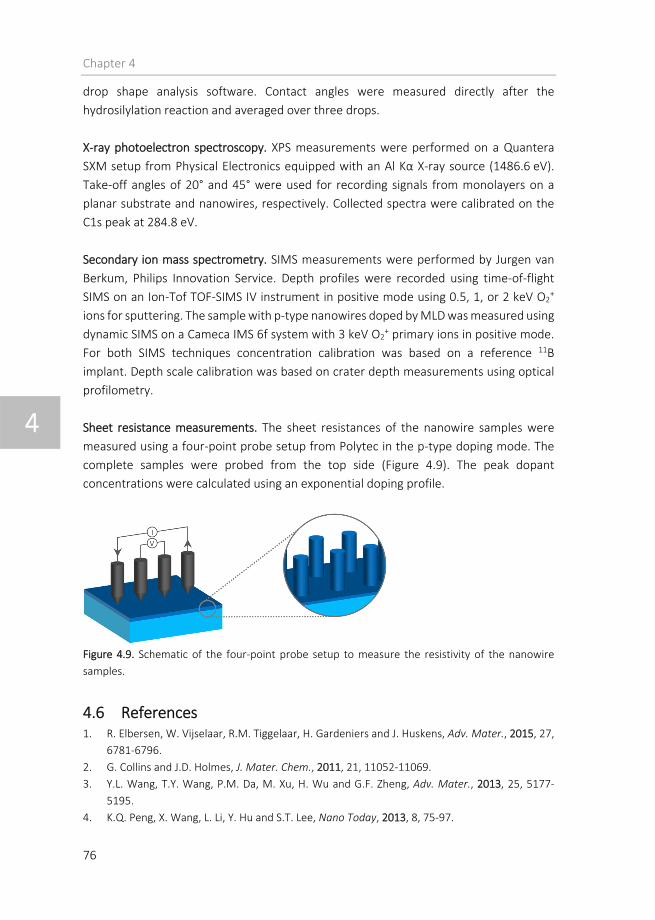
Chapter 4
76
4
drop shape analysis software. Contact angles were measured directly after the
hydrosilylation reaction and averaged over three drops.
X‐ray photoelectron spectroscopy. XPS measurements were performed on a Quantera
SXM setup from Physical Electronics equipped with an Al Kα X‐ray source (1486.6 eV).
Take‐off angles of 20° and 45° were used for recording signals from monolayers on a
planar substrate and nanowires, respectively. Collected spectra were calibrated on the
C1s peak at 284.8 eV.
Secondary ion mass spectrometry. SIMS measurements were performed by Jurgen van
Berkum, Philips Innovation Service. Depth profiles were recorded using time‐of‐flight
SIMS on an Ion‐Tof TOF‐SIMS IV instrument in positive mode using 0.5, 1, or 2 keV O2+
ions for sputtering. The sample with p‐type nanowires doped by MLD was measured using
dynamic SIMS on a Cameca IMS 6f system with 3 keV O2+ primary ions in positive mode.
For both SIMS techniques concentration calibration was based on a reference 11B
implant. Depth scale calibration was based on crater depth measurements using optical
profilometry.
Sheet resistance measurements. The sheet resistances of the nanowire samples were
measured using a four‐point probe setup from Polytec in the p‐type doping mode. The
complete samples were probed from the top side (Figure 4.9). The peak dopant
concentrations were calculated using an exponential doping profile.
Figure 4.9. Schematic of the four‐point probe setup to measure the resistivity of the nanowire
samples.
4.6 References 1. R. Elbersen, W. Vijselaar, R.M. Tiggelaar, H. Gardeniers and J. Huskens, Adv. Mater., 2015, 27,
6781‐6796.
2. G. Collins and J.D. Holmes, J. Mater. Chem., 2011, 21, 11052‐11069.
3. Y.L. Wang, T.Y. Wang, P.M. Da, M. Xu, H. Wu and G.F. Zheng, Adv. Mater., 2013, 25, 5177‐
5195.
4. K.Q. Peng, X. Wang, L. Li, Y. Hu and S.T. Lee, Nano Today, 2013, 8, 75‐97.

Highly doped silicon nanowires by monolayer doping
77
4
5. N.P. Dasgupta, J.W. Sun, C. Liu, S. Brittman, S.C. Andrews, J. Lim, H.W. Gao, R.X. Yan and P.D.
Yang, Adv. Mater., 2014, 26, 2137‐2184.
6. N. Nafie, M.A. Lachiheb, M. Ben Rabha, W. Dimassi and M. Bouaicha, Phys. E, 2014, 56, 427‐
430.
7. H.J. Yang, F.W. Yuan and H.Y. Tuan, Chem. Commun., 2010, 46, 6105‐6107.
8. L. Yu, B. O’Donnell, M. Foldyna and P. Roca i Cabarrocas, Nanotechnology, 2012, 23, 194011.
9. J. Yoo, S.A. Dayeh, W. Tang and S.T. Picraux, Appl. Phys. Lett., 2013, 102, 093113.
10. E. Garnett and P.D. Yang, Nano Lett., 2010, 10, 1082‐1087.
11. W.K. To, C.H. Tsang, H.H. Li and Z.F. Huang, Nano Lett., 2011, 11, 5252‐5258.
12. Z.P. Huang, N. Geyer, P. Werner, J. de Boor and U. Gosele, Adv. Mater., 2011, 23, 285‐308.
13. Z.P. Huang, H. Fang and J. Zhu, Adv. Mater., 2007, 19, 744‐748.
14. X. Wang, K.Q. Peng, X.L. Wu and S.T. Lee, Electrochem. Commun., 2010, 12, 509‐512.
15. J. de Boor, N. Geyer, J.V. Wittemann, U. Gosele and V. Schmidt, Nanotechnology, 2010, 21,
095302.
16. E. Koren, Y. Rosenwaks, J.E. Allen, E.R. Hemesath and L.J. Lauhon, Appl. Phys. Lett., 2009, 95,
092105.
17. Y.Q. Qu, H.L. Zhou and X.F. Duan, Nanoscale, 2011, 3, 4060‐4068.
18. N. Geyer, B. Fuhrmann, Z.P. Huang, J. de Boor, H.S. Leipner and P. Werner, J. Phys. Chem. C,
2012, 116, 13446‐13451.
19. C. Chiappini, X.W. Liu, J.R. Fakhoury and M. Ferrari, Adv. Funct. Mater., 2010, 20, 2231‐2239.
20. X. Zhong, Y.Q. Qu, Y.C. Lin, L. Liao and X.F. Duan, ACS Appl. Mater. Interfaces, 2011, 3, 261‐
270.
21. E.C. Garnett and P.D. Yang, J. Am. Chem. Soc., 2008, 130, 9224‐9225.
22. G. Dong, F. Liu, J. Liu, H. Zhang and M. Zhu, Nanoscale Res. Lett., 2013, 8, 1‐17.
23. K.Q. Peng, Y. Xu, Y. Wu, Y.J. Yan, S.T. Lee and J. Zhu, Small, 2005, 1, 1062‐1067.
24. H.D. Um, J.Y. Jung, H.S. Seo, K.T. Park, S.W. Jee, S.A. Moiz and J.H. Lee, Jpn. J. Appl. Phys., 2010,
49, 04DN02.
25. J.S. Sadhu, H.X. Tian, T. Spila, J. Kim, B. Azeredo, P. Ferreira and S. Sinha, Nanotechnology,
2014, 25, 375701.
26. X. Wang, K.L. Pey, C.H. Yip, E.A. Fitzgerald and D.A. Antoniadis, J. Appl. Phys., 2010, 108,
124303.
27. H. Lee, J. Hong, S. Lee, S.D. Kim, Y.W. Kim and T. Lee, Appl. Surf. Sci., 2013, 274, 79‐84.
28. K.Q. Peng, Z.P. Huang and J. Zhu, Adv. Mater., 2004, 16, 73‐76.
29. S. Lee, J.H. Koo, J. Seo, S.‐D. Kim, K.H. Lee, S. Im, Y.‐W. Kim and T. Lee, J. Nanopart. Res., 2012,
14, 1‐10.
30. J.C. Ho, R. Yerushalmi, Z.A. Jacobson, Z. Fan, R.L. Alley and A. Javey, Nat. Mater., 2008, 7, 62‐
67.
31. J.C. Ho, R. Yerushalmi, G. Smith, P. Majhi, J. Bennett, J. Halim, V.N. Faifer and A. Javey, Nano
Lett., 2009, 9, 725‐730.
32. L. Ye, S.P. Pujari, H. Zuilhof, T. Kudernac, M.P. de Jong, W.G. van der Wiel and J. Huskens, ACS
Appl. Mater. Interfaces, 2015, 7, 3231‐3236.
33. L. Ye, A. Gonzalez‐Campo, R. Nunez, M.P. de Jong, T. Kudernac, W.G. van der Wiel and J.
Huskens, ACS Appl. Mater. Interfaces, 2015, 7, 27357‐27361.
34. O. Hazut, A. Agarwala, I. Amit, T. Subramani, S. Zaidiner, Y. Rosenwaks and R. Yerushalmi, ACS
Nano, 2012, 6, 10311‐10318.

Chapter 4
78
4
35. O. Hazut, B.C. Huang, A. Pantzer, I. Amit, Y. Rosenwaks, A. Kohn, C.S. Chang, Y.P. Chiu and R.
Yerushalmi, ACS Nano, 2014, 8, 8357‐8362.
36. R.A. Puglisi, C. Garozzo, C. Bongiorno, S. Di Franco, M. Italia, G. Mannino, S. Scalese and A. La
Magna, Sol. Energy Mater. Sol. Cells, 2015, 132, 118‐122.
37. A.B. Sieval, R. Linke, H. Zuilhof and E.J.R. Sudholter, Adv. Mater., 2000, 12, 1457‐1460.
38. J.M. Buriak, Chem. Commun., 1999, 1051‐1060.
39. Y. Zhu, B. Gupta, B. Guan, S. Ciampi, P.J. Reece and J.J. Gooding, ACS Appl. Mater. Interfaces,
2013, 5, 6514‐6521.
40. N.H. Maniya, S.R. Patel and Z.V.P. Murthy, Mater. Res. Bull., 2014, 57, 6‐12.
41. K. Peng, M. Zhang, A. Lu, N.‐B. Wong, R. Zhang and S.‐T. Lee, Appl. Phys. Lett., 2007, 90,
163123.
42. L. Ye, A. González‐Campo, T. Kudernac, R. Nuñez, M.P. de Jong, W.G. van der Wiel and J.
Huskens, Langmuir, 2017, in press, DOI: 10.1021/acs.langmuir.7b00157.
43. V. Schmidt, J.V. Wittemann, S. Senz and U. Gosele, Adv. Mater., 2009, 21, 2681‐2702.
44. K.K. Lew, L. Pan, T.E. Bogart, S.M. Dilts, E.C. Dickey, J.M. Redwing, Y.F. Wang, M. Cabassi, T.S.
Mayer and S.W. Novak, Appl. Phys. Lett., 2004, 85, 3101‐3103.
45. A. Gonzalez‐Campo, E.J. Juarez‐Perez, C. Vinas, B. Boury, R. Sillanpaa, R. Kivekas and R. Nunez,
Macromolecules, 2008, 41, 8458‐8466.
46. A. Gonzalez‐Campo, B. Boury, F. Teixidor and R. Nunez, Chem. Mater., 2006, 18, 4344‐4353.
47. G.S. Hong, C. Li and L.M. Qi, Adv. Funct. Mater., 2010, 20, 3774‐3783.
48. C. Li, G. Hong, P. Wang, D. Yu and L. Qi, Chem. Mater., 2009, 21, 891‐897.

79
5
Chapter 5
Maskless spatioselective functionalization
of silicon nanowires
Spatioselective functionalization of silicon nanowires was achieved without the use of a
masking material. The designed process is based on a combination of metal‐assisted
chemical etching (MACE) to fabricate silicon nanowires and the use of hydrosilylation to
form molecular monolayers. After MACE, a monolayer of 1‐undecene, 1‐tetradecyne, or
1,8‐nonadiyne was formed on the exposed silicon nanowire surfaces. A second MACE
step was expected to elongate the nanowires, so that the freshly exposed silicon surface
could be functionalized using click chemistry in a subsequent functionalization step,
resulting in visualization of the different segments. When monolayers of 1‐undecene or
1‐tetradecyne were formed on the upper segment, however, the second MACE step did
not extend the nanowires. In contrast, nanowires functionalized with 1,8‐nonadiyne
could be elongated in the second MACE step at an approximately 8 times slower etching
rate. The elongation resulted in a contrast difference in high‐resolution scanning electron
microscopy (HR‐SEM) images, which indicated the formation of nanowires that were
covered with a monolayer only at the top parts. Secondary functionalization of the
monolayer with an azide‐functionalized dye by click chemistry was possible, but
fluorescence imaging did not allow distinction between the two segments. Instead, click
chemistry with azide‐functionalized nanoparticles was successfully used to functionalize
the nanowires. The spatioselective presence of 1,8‐nonadiyne gave a threefold higher
particle density on the upper segment functionalized with 1,8‐nonadiyne than on the
lower segment without monolayer. These results indicate the successful spatioselective
functionalization of silicon nanowires fabricated by MACE.

Chapter 5
80
5
5.1 Introduction Silicon nanostructures and nano/microwire arrays are attractive because of their optical,
electronic, electrochemical, mechanical, and thermal properties.1 To tune these
nanostructures towards a specific application, surface functionalization can offer
versatility and specificity, for example, to couple photocatalysts onto the surface for
hydrogen production.2,3 Whereas surface functionalization is mostly applied onto the
entire surface of a Si micro/nanostructure, spatioselective functionalization of 3D
nanostructures, i.e., the functionalization of parts of the structure, is useful when several
functionalities should be combined.4 For example, oxidation and reduction reactions can
be performed on two different ends of a nanowire when these are site‐specifically
functionalized with the respective catalysts.5,6
Spatioselective functionalization of 3D nanostructures can be achieved by prohibiting
access of functionalization agents to specific areas of the structures, i.e., by protecting
specific segments with a masking material, such as a polymer (resist),6‐10 a metal,11
nanoparticles (NPs),12 or a membrane.13‐15 These techniques, however, always require
extra steps, such as the addition of the masking material, the removal of the masking
material from the sites that should not be blocked and finally the mask removal after
functionalization. Very few studies provide processes that avoid such multiple
masking/unmasking steps. For example, Milbrat et al. have developed a method for the
spatioselective functionalization of silicon microwires with axial p‐n junctions.16 The
charges directed by the junction, either in the dark or under illumination, were used to
electrochemically deposit silver or platinum NPs in a spatially selective manner. This
method, however, is applicable to metals in general but not to organic molecules. The
use of molecular monolayers would offer versatility, for example, by secondary
functionalization enabled by the chosen end moieties.17‐19
Here, we aim for the spatioselective functionalization of silicon nanowires with molecular
monolayers without the use of a masking material. We have designed a process (Scheme
5.1) based on metal‐assisted chemical etching (MACE) as the nanowire fabrication
method, in which a metal film (silver or gold) with patterned gaps is etched into the
underlying silicon substrate upon immersion in a HF/H2O2 solution.20‐23 The diameter of
the resulting nanowires is determined by the pattern in the metal film, whereas the
length is determined by the etching time. Spatioselective functionalization was tested by
two MACE steps with monolayer formation after the first step and functionalization of
the top or bottom section of the nanowire after the second MACE step. The first MACE
step is used to etch nanowires until a certain length, after which a monolayer is formed
on the exposed silicon surface. A second MACE step is expected to elongate the
nanowires and thus expose an unfunctionalized part of the silicon nanowires, which could
then be functionalized differently in the final functionalization step.

Maskless spatioselective functionalization of silicon nanowires
81
5
Scheme 5.1. Schematic illustration of the spatioselective functionalization process.
Monolayer formation has been achieved by hydrosilylation of alkenes or alkynes, i.e., by
linking terminally unsaturated carbon‐carbon bonds onto H‐terminated Si surfaces.24,25
This technique results in direct Si‐C bond formation and avoids the presence of silicon
oxide in between the substrate and the monolayer. If silicon oxide would be present, the
second MACE step would etch away the silicon oxide on the first part including the
monolayer. Specifically, 1‐undecene or 1‐tetradecyne were chosen as (methyl‐
terminated) dummy molecules, and the dialkyne 1,8‐nonadiyne, which can potentially be
reacted further by click chemistry with azide‐functionalized model catalysts, as a
functional adsorbate. We here compare the different process parameters that influence
the success rate of the selectively functionalized nanowire fabrication process.
5.2 Results and discussion Two routes were envisaged towards the spatioselective functionalization of silicon
nanowires (Scheme 5.2). Both routes are based on the same order of steps: i) MACE,
ii) monolayer formation, iii) MACE, iv) functionalization. The first route (Scheme 5.2a) was
designed using monolayer formation with a dummy molecule on the upper part, i.e., an
alkene/alkyne (1‐undecene or 1‐tetradecyne, Scheme 5.3) with a nonreactive methyl end
moiety. As a requirement, these monolayers should survive the second MACE step. After
the second MACE step, monolayer formation with a dialkyne (1,8‐nonadiyne, Scheme
5.3) could be employed, which then selectively forms on the lower part since the upper
segment is already covered by a monolayer of 1‐undecene or 1‐tetradecyne. To visualize
the difference between the two segments, the 1,8‐nonadiyne monolayer could be
functionalized further by copper‐catalyzed click chemistry17 (Scheme 5.3) with an azide‐
functionalized dye (characterized by fluorescence microscopy) or azide‐functionalized
gold NPs (characterized by HR‐SEM). The second route (Scheme 5.2b) involves the
formation of a 1,8‐nonadiyne monolayer after the first MACE step. After the second
MACE step to elongate the nanowires, the lower segment remains unfunctionalized and
click chemistry onto the exposed alkyne moieties attached to the upper nanowire
segments could be used to visualize the spatial selectivity.

Chapter 5
82
5
Scheme 5.2. Schematic illustration of the two different routes tested for the spatioselective
functionalization of MACE‐fabricated silicon nanowires: a) MACE|1‐undecene/1‐tetradecyne|
MACE|1,8‐nonadiyne|click chemistry and b) MACE|1,8‐nonadiyne|MACE|click chemistry).
1% HF
1 min, RT
native oxide
water, 16 h, RTSi
5NN
N
N3 , Cu(I)
.
Si
5 5
Si
H H
Si
O
NH2
NH2+
O
‐O
ONH
O
N3
3
1‐undecenemesitylene
16 h, 180°Cor 420 nm
1,8‐nonadiyne
16 h, 420 nm
1‐tetradecynemesitylene
16 h, 420 nm
Si
7 7
Si
10 10 5NN
N
water, 16 h, RT
N3 , Cu(I)
.
Au
Si
5NN
N
5NN
N
Scheme 5.3. Schematic representation of monolayer coupling to Si‐H nanowires by hydrosilylation
with alkenes or alkynes and subsequent click chemistry of an azide‐functionalized dye or azide‐
functionalized gold NPs onto the alkyne end groups of 1,8‐nonadiyne.

Maskless spatioselective functionalization of silicon nanowires
83
5
5.2.1 First MACE step and monolayer formation Silicon nanowires were created by combining nanosphere lithography and MACE.26,27
Nanosphere lithography (Scheme 5.4) was used to form a close‐packed array of
polystyrene spheres on a cleaned p‐type silicon substrate. The diameter of the spheres
was decreased from 447 nm (dried state) to about 280 nm by oxygen reactive ion etching.
After sputtering a metal film (silver or gold) on top, lift‐off of the polystyrene spheres
resulted in a metal film with patterned openings. Exposure of these metal‐coated
samples to an aqueous solution of HF/H2O2 ensured wet etching of the silicon substrate
underneath the metal layer. Immersion for 7 min (Ag) or 15 min (Au) resulted in
nanowires with a length of about 2.1 and 1.0‐1.1 µm, and a diameter of 390 and 260 nm,
respectively, as shown by HR‐SEM imaging (Figure 5.1a, c, e).
Scheme 5.4. Schematic illustration of the patterned metal film formation by nanosphere
lithography.
Figure 5.1. Cross‐sectional HR‐SEM images of silicon nanowires using a‐b) a Ag or c‐f) a Au film,
imaged a,c,e) after the first MACE step and b,d,f) after the second MACE step on samples with
photochemically formed monolayers of a‐d) 1‐undecene or e,f) 1,8‐nonadiyne (insets: control
samples without monolayer formation).

Chapter 5
84
5
Monolayer formation was achieved by thermal or photochemical hydrosilylation (Scheme
5.3).24,25 This oxide‐free monolayer formation technique significantly increases the
chance that the monolayer stays intact during the second MACE step, since HF, present
in the MACE solution, quickly removes silicon oxide. Monolayer formation was first tested
by the thermal hydrosilylation method, since this generally results in higher quality
monolayers than the photochemical route. The temperature used for this reaction
(180 °C for 1‐undecene in mesitylene), however, resulted in agglomeration of the gold
film (Figure 5.2). The photochemical route was therefore used by reaction under
illumination of 420 nm light, which did not affect the metal films.
Figure 5.2. Top‐view HR‐SEM images of a Au film after thermal hydrosilylation (180 °C) imaged a)
within and b) outside the nanowires region.
The photochemical hydrosilylation technique (Scheme 5.3) was used to form monolayers
onto the exposed silicon nanowire surfaces after the first MACE step. On one half of the
sample with nanowires, an H‐terminated silicon surface was created by short immersion
in an aqueous 1% HF solution. Subsequently, a monolayer of 1‐undecene, 1‐tetradecyne,
or 1,8‐nonadiyne with Si‐C bonds was formed under illumination with a 420 nm LED.
Whereas the hydrosilylation of 1‐undecene and 1‐tetradecyne was performed in a 5% v/v
solution in mesitylene, 1,8‐nonadiyne was used in its pure form to suppress back bending
of the second alkyne group towards the hydrogen‐terminated silicon surface. Cleaning
was performed without ultrasonication in order to avoid damage to the metal film. The
other half of the sample was used as a control, on which the second MACE step was
tested without preceding monolayer formation. For the first route (Scheme 5.2a),
presence of the monolayer was indicated by a contact angle of 130.7° ± 2.1 (1‐undecene)
or 132.6° ± 2.2 (1‐tetradecyne) on top of the nanowires, confirming the combined effect
of nanostructuring and the presence of the hydrophobic monolayer. Nanowires with a
monolayer of 1,8‐nonadiyne (Scheme 5.2b) were less hydrophobic due to their alkyne
end moieties, as shown by a contact angle of 112.1° ± 3.6. The nanowires without
monolayer showed a contact angle of 40.4° ± 3.5, 70.7° ± 6.5, or 89.0° ± 7.2, indicative of
(varying degrees of) regrowth of native silicon oxide.
Images after the first and second MACE steps indicated a preference for using a gold film
over a silver film, since i) a gold film gave more homogeneously etched samples (Figure

Maskless spatioselective functionalization of silicon nanowires
85
5
5.1) and ii) the silver film was sometimes dissolved and redeposited on the lower segment
of the nanowires, after which the bottom of the nanowires got etched until they broke
off (data not shown). The etch rate, however, was lower for samples with a gold film
compared to a silver film. This is a disadvantage since the second MACE step, and thus
the exposure of the monolayer on the upper segment to the MACE solution, has to be
longer.
5.2.2 Second MACE step and monolayer formation Upon the second MACE step, the nanowires with a monolayer of 1‐undecene (Scheme
5.2a) were unexpectedly not elongated after 15 min (Ag) or 45 min (Au) of MACE (Figure
5.1b, d). HR‐SEM images showed that the unfunctionalized nanowires increased in length
to 3.7 (Ag) and 4.8 µm (Au), while the nanowires functionalized with 1‐undecene
remained 2.1 and 1.0 µm, respectively (Figure 5.1b, d). The same effect was observed for
silicon nanowires functionalized with 1‐tetradecyne (data not shown).
Although these data already indicated a clear effect of the presence of a monolayer on
the etching behavior, contact angle measurements could not be used to verify whether
the monolayers on the nanowires survived the second MACE step, since the top of the
nanowires got roughened and resulted in contact angles of 130.8° ± 2.0 and 138.8° ± 0.5
for the functionalized (1‐tetradecyne) and unfunctionalized samples, respectively. As a
control, therefore, a planar substrate with a monolayer of 1‐tetradecyne was immersed
in the MACE solution for 10, 20, and 40 min, after which the contact angle was measured
(Figure 5.3, left axis). The contact angle decreased due to exposure to the etching
solution, thus indicating that the monolayer had deteriorated. These values were
converted into the fraction of monolayer that was still intact (assuming a full monolayer
at t = 0) and the fraction of Si‐H formed (contact angle 78° for a fully H‐terminated
surface) using Cassie’s law (Figure 5.3, right axis). This indicates that about 44% of the
monolayer was still intact after 40 min exposure to the MACE solution, whereas a second
MACE step of 45 min had not lengthened the nanowires yet. A longer second MACE step
would induce even more damage to the monolayer, if it would be possible to elongate
the nanowires at all. More importantly, when viewing the process envisaged in Scheme
5.2a, the incomplete monolayer at the upper segment would be back‐filled with
1,8‐nonadiyne molecules in the second functionalization step. Spatioselective
functionalization can thus not be achieved by this route, since 1,8‐nonadiyne would be
present on both segments.

Chapter 5
86
5
Figure 5.3. Contact angle measurements (black squares, left axis) of a 1‐tetradecyne monolayer on
a p(100) planar sample measured after the reaction and after exposure to the MACE solution, and
the monolayer fraction (blue circles, right axis) that is still intact as determined by Cassie’s law.
For the other route, with 1,8‐nonadiyne on the upper segment and an unfunctionalized
lower segment (Scheme 5.2b), the second MACE step was tested as well. Only samples
with a gold film were tested for this adsorbate for the reasons mentioned above.
Additionally, it was observed that a silver film could be destroyed by contact with
1,8‐nonadiyne (Figure 5.4). Contrary to the results with 1‐undecene/1‐tetradecyne, a
second MACE step of 30 min after 1,8‐nonadiyne attachment resulted in an increase of
the length of the nanowires of 200‐300 nm, from 1.1 µm to 1.3‐1.4 µm (Figure 5.1f). The
unfunctionalized control samples were elongated up to 3.0 µm, which shows that the
presence of the monolayer has a retarding effect (of approximately a factor 8) on the
second MACE step. The effect of 30 min exposure of the 1,8‐nonadiyne monolayer to the
MACE solution could not be tested by contact angle measurements as described above
for 1‐tetradecyne (Figure 5.3), since the contact angle of a full monolayer of
1,8‐nonadiyne on a planar sample (82°) was too close to that of a deteriorated monolayer
(Si‐H, 78°). This made a proper determination of the fraction of intact monolayer
impossible.
Figure 5.4. Top‐view HR‐SEM image of a Ag film after overnight immersion in 1,8‐nonadiyne.

Maskless spatioselective functionalization of silicon nanowires
87
5
The HR‐SEM data do not clarify what causes the retardation or complete inhibition of the
second MACE step. The difference in etching between the 1,8‐nonadiyne and
1‐undecene/1‐tetradecyne samples seems to originate from the monolayer formation
step, since the unfunctionalized control samples were etched as expected. The main
differences between the two routes (Scheme 5.2) include the adsorbates (1,8‐nonadiyne
versus 1‐undecene/1‐tetradecyne) and the solvents (none versus mesitylene). Two main
explanations are hypothesized: i) the MACE solution is not able to enter the voids when
a hydrophobic monolayer is present and ii) a contamination at the metal/silicon interface
is preventing the second MACE step. To the first point, the more hydrophilic the
nanowires are, the higher the chance that the aqueous MACE solution enters the voids
to continue etching. As shown by contact angle measurements, the monolayers of
1‐undecene and 1‐tetradecyne were more hydrophobic than those of 1,8‐nonadiyne and
could thus prevent the MACE solution from reaching the metal film at the bottom of the
voids. To the second point, if something would be present on the metal/silicon interface,
the second MACE step could be delayed or prohibited. A layer on top of the metal film,
instead, does not prohibit MACE,22 i.e., only the interface between the metal film and the
underlying silicon substrate is of importance. After the first MACE step, porous silicon is
formed underneath the metal film,22 which could theoretically be filled up with reagents
or solvents (from the reaction or cleaning steps). This would, however, not explain why
the samples with 1,8‐nonadiyne could be etched further in the second MACE step.
Control experiments were performed by overnight immersion of silicon samples with a
gold‐patterned film after lift‐off, i.e., before the first MACE step, in mesitylene,
1‐undecene, or 1,8‐nonadiyne. The first MACE step was successful for all of these
samples, although the etch rate was lower than for samples without immersion.
Preliminary tests on immersion of silicon nanowires in mesitylene and a subsequent
second MACE step, did not conclusively show whether the nanowires could be elongated
or not. Further research is thus required to verify whether these hypotheses are correct.
5.2.3 Secondary functionalization In the second route (Scheme 5.2b), the copper‐catalyzed click reaction17,28 was used to
investigate whether the 1,8‐nonadiyne monolayer was still present after the second
MACE step and spatioselective functionalization could be achieved. In this reaction, an
azide‐functionalized molecule or particle is coupled onto the alkyne end moiety of the
1,8‐nonadiyne monolayer using Cu(I) as the catalyst (Scheme 5.3). Either an azide‐
functionalized dye was chosen for detection by fluorescence microscopy, or azide‐
functionalized gold NPs to allow detection by high‐resolution scanning electron
microscopy. A Cu(I) stabilizing ligand (TBTA) was used to increase the rate of the click
chemistry within the voids between the nanowires.29

Chapter 5
88
5
After functionalization with azide‐fluor 488, the nanowires were scraped off the surface
and immobilized onto a microscope glass slide. As a disadvantage, this induced a high
background fluorescence and showed irregularly shaped fluorescent objects, probably
due to residuals of the gold film used for MACE. Nonetheless, fluorescence microscopy
showed needle‐shaped objects that are most likely the functionalized nanowires based
on their size (Figure 5.5). Comparison of the length of the wires in the fluorescence and
brightfield images indicates, however, that the resolution of these images is too low to
conclude whether the 200‐300 nm bottom segments had remained unfunctionalized.
Confocal microscopy did not solve this resolution issue. A longer second MACE step would
be needed to increase the contrast between the two segments but could also damage
the 1,8‐nonadiyne monolayer on the upper segment and thus was not pursued further
here.
Figure 5.5. Microscopy images after click chemistry with an azide‐functionalized dye onto silicon
nanowires (Au film) functionalized with a monolayer of 1,8‐nonadiyne on the upper segment (left:
fluorescence microscopy image, 200 ms exposure time, brightness increased by 30%, right:
brightfield image, 5 ms exposure time).
To circumvent the practical issues associated with fluorescent dye functionalization and
imaging, click chemistry with azide‐functionalized gold NPs (10 nm diameter) was tested.
In this way, the nanowires did not have to be transferred to a microscope slide, since
HR‐SEM imaging of sample cross sections was sufficient, and a higher resolution could be
obtained. After click chemistry, HR‐SEM images showed a clear contrast between the
upper functionalized segment and the lower unfunctionalized segment (Figure 5.6a). This
contrast was also visible when imaging before click chemistry (Figure 5.1f) but was more
clearly visible in the higher resolution image of Figure 5.6a. Since the contrast was not
visible on the control samples, it is assumed that this indicates the presence of a
1,8‐nonadiyne monolayer on the upper segment. A carbon‐containing layer is known to
give a darker contrast in SEM images compared to the, most likely, silicon oxide‐
containing lower segment which is much brighter. The height of the lower segment in the
HR‐SEM image (Figure 5.6a) corresponds well with the nanowire length increase
observed for the second MACE step, as discussed above.

Maskless spatioselective functionalization of silicon nanowires
89
5
Figure 5.6. a,b) Cross‐sectional HR‐SEM images of silicon nanowires (Au film) after click chemistry
with azide‐functionalized gold NPs on a) nanowires functionalized with a 1,8‐nonadiyne monolayer
on the upper segment and b) the corresponding ESB image. c) The particle count along the
nanowire length (bin size 50 nm). d) The number of bins from (c) sorted on particle density for the
two segments. e,f) Cross‐sectional HR‐SEM images after click chemistry with azide‐functionalized
gold NPs on nanowires fully functionalized with a monolayer of e) 1‐undecene and f) 1,8‐nonadiyne.
After click chemistry, the azide‐functionalized gold NPs should be present on the upper
segment only. An energy‐selective backscatter (ESB) detector was used to reflect
compositional variations on the sample based on atomic number, which showed NPs over
the entire nanowire length (Figure 5.6b). Nonetheless, particle counting along the
nanowire length (Figure 5.6c) clearly showed more NPs on the segment above the
contrasting line. Quantitatively, the average particle densities, as calculated from the SEM
images, were 136 ± 70 NPs/µm2 on the 1,8‐nonadiyne functionalized upper segment
(0‐0.8 µm) and 45 ± 27 NPs/µm2 on the unfunctionalized lower segment (1.0‐1.3 µm),
where the gradual transition in contrast between 0.8 and 1.0 µm was not taken into
account. The threefold difference between the two segments (p < 0.01, Student’s t‐test)

Chapter 5
90
5
is also reflected in Figure 5.6d, where the upper segment shows higher particle densities
than the lower segment. Nonspecific adsorption of the gold NPs was also observed on
control samples with a monolayer of 1‐undecene on the full nanowires (Figure 5.6e,
81 ± 15 NPs/µm2), but the average particle density was much lower than on the same
nanowires with 1,8‐nonadiyne (Figure 5.6f, 212 ± 17 NPs/µm2). Although the NPs were
inhomogeneously distributed along the nanowires that were fully functionalized with
1,8‐nonadiyne, particles were clearly observed at the lower part of these nanowires. The
much lower amount of particles present at the lower part of the nanowires shown in
Figure 5.6b should thus be due to the absence of a 1,8‐nonadiyne monolayer. Overall, on
nanowires fabricated by the 1,8‐nonadiyne route (Scheme 5.2b) the differences in
contrast and in the amount of NPs present on the two segments clearly indicate
successful spatioselective functionalization.
5.3 Conclusions and outlook In summary, the spatioselective functionalization of silicon nanowires was tested using
consecutively: i) MACE, ii) monolayer formation, iii) MACE, iv) functionalization by click
chemistry. Nanowires were successfully fabricated and subsequently functionalized with
1‐alkenes/alkynes by hydrosilylation. When the top segment, exposed after the first
MACE step, was covered with a monolayer of 1‐undecene or 1‐tetradecyne, the second
MACE step inexplicably did not elongate the nanowires. In contrast, nanowires
functionalized with 1,8‐nonadiyne could be lengthened from 1.1 µm to 1.3‐1.4 µm. A
contrast difference observed in HR‐SEM images of the 1,8‐nonadiyne‐functionalized
nanowires indicated the formation of the 1,8‐nonadiyne monolayer only on the top
section of the nanowires. Click chemistry with an azide‐functionalized dye was possible,
but presence of the dye only on the top section could not be verified. The reaction with
azide‐functionalized nanoparticles, however, confirmed the successful secondary
functionalization and showed a higher particle density on the upper segment. These
results indicate that spatioselective functionalization of silicon nanowires by MACE is
possible.
Further research could elucidate why/when the second MACE step does (not) work. To
conclude whether the hydrophobicity of the monolayer is the origin, testing the second
MACE step on nanowires functionalized with a hydrophilic alkyne, for example with a
carboxylic acid end group,30,31 could be useful. Alternatively, it might help to add a
surfactant, e.g., ethanol32 or sodium dodecyl sulfate, to lower the interfacial tension.
Next, the influence of the metal/silicon interface could be studied further, i.e., whether
something present at this interface is prohibiting the second MACE step. For example,
the role of mesitylene as a solvent can be eliminated by monolayer formation in pure
1‐undecene/1‐tetradecyne or in a solution of 1,8‐nonadiyne in mesitylene. Considering
the specific click chemistry reaction used, the nonspecific adsorption of the azide‐

Maskless spatioselective functionalization of silicon nanowires
91
5
functionalized gold NPs on the segment without 1,8‐nonadiyne should be lowered, for
example using a poly(ethylene glycol) antifouling monolayer.
The spatioselective formation of a 1,8‐nonadiyne monolayer was shown here by a
contrast difference in the HR‐SEM images, and azide‐functionalized nanoparticles were
successfully used to functionalize the nanowires further. The compounds used here,
however, are just an example for the applicability of this process. End group of the alkyne‐
containing molecules used in the monolayer formation can be chosen as desired, and the
subsequent secondary functionalization can be tuned accordingly. The fabrication
method also offers versatility, since i) the height of each segment could be tuned,
depending on the application, for instance different amounts of catalysts based on their
respective catalytic activities, ii) more than two segments could be made by adding more
MACE/functionalization cycles. Thus, this fabrication method offers a relatively simple
solution for the creation of spatioselectively functionalized nanowires without the use of
a masking material.
5.4 Acknowledgments Carlo Nicosia is gratefully acknowledged for the synthesis of TBTA. Wei Zhu is gratefully
acknowledged for his help with the polystyrene beads monolayer formation.
5.5 Experimental section
5.5.1 Materials Silicon wafers (<100>‐oriented, 100 mm diameter, single side polished) were obtained
from Okmetic (Finland) as p‐type (boron, resistivity 5‐10 Ω∙cm, thickness 525 µm).
Polystyrene spheres of 500 nm diameter functionalized with carboxyl groups were
obtained from Polysciences. Azide‐functionalized gold NPs of 10 nm diameter were
obtained from NanoCS, with a particle concentration of 0.5 mg/mL in water (based on
gold salt, 2.8 × 10¹³ particles/mL), a size distribution <15% and a poly(ethylene glycol)
linker between the NPs and the azide groups. Mesitylene (>98%, Sigma‐Aldrich) and
1,8‐nonadiyne (98%, Sigma‐Aldrich) were dried over molecular sieves (0.3 nm).
Dichloromethane (99.7%, Actu‐All) was dried over anhydrous magnesium sulphate
(Merck). Acetone (pure, VWR), L‐ascorbic acid (>99%, Sigma‐Aldrich), azide‐fluor 488
(>90%, Sigma‐Aldrich), copper(II) sulfate pentahydrate (99.995% metals basis,
Cu(II)SO4.5H2O, Sigma‐Aldrich), ethanol (absolute, VWR), hydrofluoric acid 1% (aqueous,
VLSI, 1% HF, Technic France), hydrofluoric acid 50% (aqueous, VLSI, 50% HF, BASF),
hydrogen peroxide (VLSIn, H2O2, 31%, BASF), sodium dodecyl sulfate (SDS, >99%, Sigma‐
Aldrich), 1‐tetradecyne (>97%, Sigma‐Aldrich), and 1‐undecene (97%, Sigma‐Aldrich)
were used as received. Tris‐(benzyltriazolylmethyl)amine (TBTA) was synthesized
according to a procedure from the literature.33 Hexane was obtained from a solvent

Chapter 5
92
5
purification system (MB SPS‐800). Milli‐Q water with a resistivity >18 MΩ∙cm was
obtained from a Milli‐Q Integral water purification system (Merck Millipore). Glassware
used for the hydrosilylation reactions was dried overnight at 120 °C.
5.5.2 Methods Fabrication of silicon nanowires. Silicon nanowires were fabricated by combining
nanosphere lithography (Scheme 5.4) and MACE. A close‐packed array of 500 nm
polystyrene (PS) spheres was formed at the water/air interface and transferred onto a
silicon substrate according to a procedure adapted from the literature.34,35 Specifically,
small 2x2 cm2 samples were diced from silicon wafers (p‐type), which were rinsed with
ethanol and sonicated in acetone for 10 min to remove particles generated during dicing.
A 0.65% w/v solution of 500 nm PS spheres in 1:1 water:ethanol was sonicated for several
hours to make a uniform suspension. The silicon samples, a glass Petri dish, and a small
microscope glass slide were turned hydrophilic by oxygen plasma (SPI Plasma Prep II,
40 mA, 10 min). The glass slide was put in the middle of the Petri dish, after which water
was added until the level was just above the glass slide without wetting the top of the
glass slide. The PS solution (120 µL) was dispersed onto the glass slide in order to diffuse
the spheres from the glass slide to the water/air interface. After slowly increasing the
water level, 50 µL of an aqueous 2% w/v SDS solution was added as surfactant. Opposite
to the side where the PS spheres started to cluster, the glass slide was carefully removed
from the solution, and a silicon substrate was submerged. The silicon substrate was
moved underneath the PS spheres, and the water level was carefully lowered by
removing all water. The rest of the solution evaporated over time, resulting in well‐
ordered hexagonally packed PS arrays reflecting blue light when seen under an angle.
The diameter of the PS spheres was reduced by reactive ion etching using a custom‐built
etching machine (10 mTorr, 20 sccm O2, 20 W, 2.5 min). Then, a silver layer of 40 nm
(100 W, 1.0 min) or a gold layer of 30 nm (200 W, 45 s) was sputtered on top using a
custom‐built sputtering system. Lift‐off of the PS spheres was achieved by 90 min
immersion and 5 min sonication in dichloromethane. For the MACE step,22,26,27 the
substrates were immersed in an aqueous solution of 5.8 M HF/0.1 M H2O2 (50% HF,
31% H2O2, and water mixed at 20/0.9/79.1 v/v%) for 7 min (Ag) or 15 min (Au) to obtain
silicon nanowire arrays. The samples were rinsed with water and dried under nitrogen.
The samples were cut into two halves to use one half as a control without monolayer
formation. After monolayer formation on the other half, the second MACE step was
performed on both halves in the same MACE solution for 15 min (Ag) and 30 or 45 min
(Au).
Monolayer formation. Monolayers of 1‐undecene, 1‐tetradecyne, or 1,8‐nonadiyne were
formed by hydrosilylation (Scheme 5.3). The adsorbate solution (3‐6 mL), consisting of a

Maskless spatioselective functionalization of silicon nanowires
93
5
5% v/v solution of 1‐undecene in mesitylene, a 5% v/v solution of 1‐tetradecyne in
mesitylene or pure 1,8‐nonadiyne, was degassed by four freeze‐pump‐thaw cycles for
the hydrosilylation reaction. After MACE and HR‐SEM imaging, a hydrogen‐terminated
surface was reactivated on the p‐type silicon nanowires by 1 min immersion in an
aqueous 1% HF solution, to remove the native oxide grown during HR‐SEM imaging. The
substrates were then immediately immersed in the degassed adsorbate solution inside a
nitrogen glovebox. The reaction flask was equipped with a capillary as a nitrogen inlet and
a reflux condenser. The hydrosilylation reactions were performed overnight under
continuous nitrogen flow at 180 °C (for 1‐undecene) for the thermal route and under
illumination of a 420 nm LED (130 mW) at a 1 cm distance for the photochemical route
(for 1‐undecene, 1‐tetradecyne, or 1,8‐nonadiyne). The nanowires were cleaned by
immersion in hexane, rinsed with ethanol and dichloromethane, and subsequently dried
in a stream of nitrogen. The samples were not sonicated in order to keep the metal film
intact.
Click chemistry. Copper‐catalyzed azide‐alkyne cycloaddition (click chemistry, Scheme
5.3) was used to couple the fluorescent dye azide‐fluor 488 or azide‐functionalized gold
NPs onto a 1,8‐nonadiyne monolayer. Silicon nanowires were overnight incubated with
60 µL of the azide solution (2 mM azide‐fluor 488 in water, or azide‐functionalized gold
NPs as received) and 60 µL of the catalyst solution (1.5 mM Cu(II)SO4.5H2O, 1.5 mM TBTA,
60 mM L‐ascorbic acid in ethanol/water, ratio 5:2 v/v) in a silicone isolator (Electron
Microscopy Sciences). A glass slide on top was used to avoid solvent evaporation.
Afterwards, the samples were sequentially rinsed with water, ethanol, water, ethanol,
immersed in acetone to remove the glue of the isolator, sonicated in ethanol for 1 min
and dried in a stream of nitrogen.
5.5.3 Equipment Contact angle measurements. Static contact angles were measured with Milli‐Q water on
a Krüss G10 Contact Angle Measuring Instrument equipped with a CCD camera and drop
shape analysis software. Contact angles were measured directly after the hydrosilylation
reaction and averaged over three drops.
High‐resolution scanning electron microscopy. HR‐SEM images of cross sections of the
nanowire arrays were obtained with a FEI Sirion HR‐SEM with a through‐the‐lens detector
(TLD) or a Zeiss Merlin HR‐SEM system with an InLens or ESB detector, operated at typical
acceleration voltages of 10‐15 kV and 1.6 kV, respectively. Fresh cuts were made to assess
the cross sections after each step.
Fluorescence microscopy. Silicon nanowires functionalized with azide‐functionalized dye
were removed from the surface using a scalpel and immersed in a small volume of

Chapter 5
94
5
ethanol. The solution was pipetted onto a microscope glass slide, after which the ethanol
was evaporated to confine the nanowires onto the glass slide. Fluorescence microscopy
images were acquired in air on an Olympus inverted research microscope IX71 equipped
with a mercury burner U‐RFL‐T as light source and a digital Olympus DP70 camera. Blue
excitation (λex = 490‐510 nm) and green emission (λem = 520‐550 nm) were filtered using
a Chroma filter cube.
5.6 References 1. N.P. Dasgupta, J.W. Sun, C. Liu, S. Brittman, S.C. Andrews, J. Lim, H.W. Gao, R.X. Yan and P.D.
Yang, Adv. Mater., 2014, 26, 2137‐2184.
2. I. Oh, J. Kye and S. Hwang, Nano Lett., 2012, 12, 298‐302.
3. S.Y. Reece, J.A. Hamel, K. Sung, T.D. Jarvi, A.J. Esswein, J.J.H. Pijpers and D.G. Nocera, Science,
2011, 334, 645‐648.
4. A. Walther and A.H.E. Müller, Chem. Rev., 2013, 113, 5194‐5261.
5. Y.Q. Qu, L. Liao, R. Cheng, Y. Wang, Y.C. Lin, Y. Huang and X.F. Duan, Nano Lett., 2010, 10,
1941‐1949.
6. Y.Q. Qu, T. Xue, X. Zhong, Y.C. Lin, L. Liao, J.N. Choi and X.F. Duan, Adv. Funct. Mater., 2010,
20, 3005‐3011.
7. T.E. McKnight, C. Peeraphatdit, S.W. Jones, J.D. Fowlkes, B.L. Fletcher, K.L. Klein, A.V.
Melechko, M.J. Doktycz and M.L. Simpson, Chem. Mater., 2006, 18, 3203‐3211.
8. X.Y. Ling, I.Y. Phang, C. Acikgoz, M.D. Yilmaz, M.A. Hempenius, G.J. Vancso and J. Huskens,
Angew. Chem., Int. Ed., 2009, 48, 7677‐7682.
9. I. Park, Z.Y. Li, A.P. Pisano and R.S. Williams, Nano Lett., 2007, 7, 3106‐3111.
10. C. Liu, J.Y. Tang, H.M. Chen, B. Liu and P.D. Yang, Nano Lett., 2013, 13, 2989‐2992.
11. J.S. Yu, J.Y. Kim, S. Lee, J.K.N. Mbindyo, B.R. Martin and T.E. Mallouk, Chem. Commun., 2000,
2445‐2446.
12. A.M. Yake, C.E. Snyder and D. Velegol, Langmuir, 2007, 23, 9069‐9075.
13. Z. Wang and M. Brust, Nanoscale Res. Lett., 2007, 2, 34‐39.
14. C.T. Sousa, D.C. Leitao, J. Ventura, P.B. Tavares and J.P. Araujo, Nanoscale Res. Lett., 2012, 7,
168.
15. K. Skinner, C. Dwyer and S. Washburn, Nano Lett., 2006, 6, 2758‐2762.
16. A. Milbrat, R. Elbersen, R. Kas, R.M. Tiggelaar, H. Gardeniers, G. Mul and J. Huskens, Adv.
Mater., 2016, 28, 1400‐1405.
17. Y. Li and C.Z. Cai, Chem. ‐ Asian J., 2011, 6, 2592‐2605.
18. N. Herzer, C. Haensch, S. Hoeppener and U.S. Schubert, Langmuir, 2010, 26, 8358‐8365.
19. M.D. Yilmaz and J. Huskens, Soft Matter, 2012, 8, 11768‐11780.
20. Z.P. Huang, N. Geyer, P. Werner, J. de Boor and U. Gosele, Adv. Mater., 2011, 23, 285‐308.
21. Y.Q. Qu, H.L. Zhou and X.F. Duan, Nanoscale, 2011, 3, 4060‐4068.
22. N. Geyer, B. Fuhrmann, Z.P. Huang, J. de Boor, H.S. Leipner and P. Werner, J. Phys. Chem. C,
2012, 116, 13446‐13451.
23. X. Zhong, Y.Q. Qu, Y.C. Lin, L. Liao and X.F. Duan, ACS Appl. Mater. Interfaces, 2011, 3, 261‐
270.
24. S. Ciampi, J.B. Harper and J.J. Gooding, Chem. Soc. Rev., 2010, 39, 2158‐2183.

Maskless spatioselective functionalization of silicon nanowires
95
5
25. J.M. Buriak, Chem. Commun., 1999, 1051‐1060.
26. Z.P. Huang, H. Fang and J. Zhu, Adv. Mater., 2007, 19, 744‐748.
27. K. Peng, M. Zhang, A. Lu, N.‐B. Wong, R. Zhang and S.‐T. Lee, Appl. Phys. Lett., 2007, 90,
163123.
28. S. Ciampi, T. Böcking, K.A. Kilian, M. James, J.B. Harper and J.J. Gooding, Langmuir, 2007, 23,
9320‐9329.
29. S. Ciampi, T. Böcking, K.A. Kilian, J.B. Harper and J.J. Gooding, Langmuir, 2008, 24, 5888‐5892.
30. R. Boukherroub, J.T.C. Wojtyk, D.D.M. Wayner and D.J. Lockwood, J. Electrochem. Soc., 2002,
149, H59‐H63.
31. F. Cattaruzza, A. Cricenti, A. Flamini, M. Girasole, G. Longo, A. Mezzi and T. Prosperi, J. Mater.
Chem., 2004, 14, 1461‐1468.
32. K. Balasundaram, J.S. Sadhu, J.C. Shin, B. Azeredo, D. Chanda, M. Malik, K. Hsu, J.A. Rogers, P.
Ferreira, S. Sinha and X.L. Li, Nanotechnology, 2012, 23, 305304.
33. T.R. Chan, R. Hilgraf, K.B. Sharpless and V.V. Fokin, Org. Lett., 2004, 6, 2853‐2855.
34. G.S. Hong, C. Li and L.M. Qi, Adv. Funct. Mater., 2010, 20, 3774‐3783.
35. C. Li, G. Hong, P. Wang, D. Yu and L. Qi, Chem. Mater., 2009, 21, 891‐897.

96

97
6
Chapter 6
Selective silicon nanowire functionalization:
towards early cancer DNA detection
Silicon nanowire chips can function as sensors for cancer DNA detection, whereby
selective functionalization of the silicon sensing areas over the surrounding silicon oxide
would prevent loss of analyte and thus increase the sensitivity. The thermal
hydrosilylation of unsaturated carbon‐carbon bonds onto H‐terminated silicon has been
studied here to selectively functionalize the silicon nanowires with a monolayer of
1,8‐nonadiyne. The silicon oxide areas, however, appeared to be functionalized as well.
The selectivity towards the Si‐H regions was increased by introducing an extra HF
treatment after the 1,8‐nonadiyne monolayer formation. This step (partly) removed the
monolayer from the silicon oxide regions, whereas the Si‐C bonds at the Si areas
remained intact. The alkyne headgroups of immobilized 1,8‐nonadiyne were
functionalized with PNA probes by coupling azido‐PNA and thiol‐PNA by click chemistry
and thiol‐yne chemistry, respectively. Although both functionalization routes were
successful, hybridization could only be detected on the samples with thiol‐PNA. No
fluorescence was observed when introducing dye‐labelled noncomplementary DNA,
which indicates specific DNA hybridization. These results open up the possibilities for
creating silicon nanowire‐based sensors for binding tumor DNA in both a specific way and
with a higher sensitivity.

Chapter 6
98
6
6.1 Introduction Early diagnostics of diseases, in particular cancer, is receiving increasing attention as early
detection promises a higher cure rate and/or longer survival periods.1 Detecting tumor
DNA is preferably noninvasive, for example based on blood2 or urine samples.3 As a
sensor, lab‐on‐a‐chip configurations are attractive since analysis outside the hospital is
possible, for example at the general practitioner or even at home as a do‐it‐yourself
test.4,5 Ideally, the DNA detection is highly specific, i.e., for cancer DNA only, in particular
for a well‐recognized marker sequence, and highly sensitive, i.e., detecting the cancer
DNA at low concentrations, also in the presence of a lot of other background DNA.
Surface chemistry can be used to specifically capture tumor DNA.6,7 For this purpose, a
specific DNA or peptide nucleic acid (PNA) oligo can be attached as a probe sequence to
the surface, which consists of the complementary strand for the disease‐specific DNA
sequence. PNA is an artificially synthesized polymer that functions as a mimic for DNA
and contains a neutral peptide‐like backbone instead of a negatively charged deoxyribose
phosphate backbone.8 The spacing between the nucleotides is equal for DNA and PNA,
which makes PNA‐DNA hybridization possible. For sensing purposes, PNA is preferred as
a probe since i) PNA‐DNA interactions are stronger than DNA‐DNA interactions due to the
absence of electrostatic repulsion and ii) PNA‐DNA interactions often show a better
selectivity.9 The absence of charge repulsion also prevents inhibition of DNA approach to
the sensing surface, which then enables a higher sensitivity.
Sensors to detect PNA‐DNA hybridization rely on signal transduction based on surface
plasmon resonance10 or electrical measurements,11‐14 for example, and are frequently
based on silicon nanowires on a chip. In the literature, hydrosilylation chemistry, in which
unsaturated carbon‐carbon bonds are coupled onto oxide‐free silicon surfaces, is
commonly used for fabricating silicon sensors for DNA detection.11‐15 Hydrosilylation is
advantageous because the resulting Si‐C bonds are stable in aqueous environment, and
the absence of an insulating silicon oxide layer improves the electrical contact with the
underlying substrate and thus the sensitivity of the sensor as well.14 Nonetheless, any
adsorption of analyte DNA outside the sensor area, either specific or nonspecific, would
result in a loss of sensitivity. Therefore, the sensitivity of a DNA sensor device can be
enormously increased when the probe is only bound at the sensing areas. Here, we focus
on chips with silicon nanowires surrounded by silicon oxide,16 of which the silicon regions
should be functionalized selectively with the probe DNA or PNA. Hydrosilylation could
potentially be used to selectively functionalize the silicon nanowires over the silicon oxide
surroundings, as has been suggested in the literature.15,17,18 This material‐selective
functionalization has, however, not yet been studied in detail.

Selective silicon nanowire functionalization: towards early cancer DNA detection
99
6
Here, we study the selective functionalization of the sensing area of a chip, i.e., its silicon
nanowires, whereas the surrounding silicon oxide should not be functionalized.
Specifically, the dialkyne 1,8‐nonadiyne is coupled to H‐terminated silicon in order to
achieve material‐selective functionalization. Whereas most examples from literature are
based on photochemical hydrosilylation, i.e., coupling under illumination by light, we
have used thermal hydrosilylation since this technique generally yields monolayers with
a higher coverage.19 The freestanding alkyne group of the 1,8‐nonadiyne monolayer can
then be functionalized with azide or thiol moieties by copper‐catalyzed click chemistry20,21
and thiol‐yne chemistry,22,23 respectively. First, the specific functionalization of silicon
nanowires on a chip is tested by click chemistry with dummy molecules, i.e., with an
azide‐functionalized dye and with azide‐functionalized nanoparticles to enable
characterization by fluorescence microscopy and high‐resolution scanning electron
microscopy (HR‐SEM), respectively (Section 6.2.1). Thereafter, azido‐PNA or thiol‐PNA is
coupled onto the 1,8‐nonadiyne monolayer as a proof of concept for a biosensor.
PNA‐DNA hybridization with cancer DNA is investigated using fluorescence microscopy
and quartz crystal microbalance (QCM) measurements (Section 6.2.2).
6.2 Results and discussion The chip designed for early cancer diagnostics is based on silicon nanowires as sensing
areas surrounded by inactive silicon oxide (SiOx), as reported before (Scheme 6.1).16 A
sensor consists of two silicon nanowires with a triangular cross section, bridging two
contact pads. A substrate contained several sensors with the same design and different
nanowire lengths. For proof of principle tests, chips with silicon‐rich silicon nitride contact
pads instead of metal contacts were used,16 which did not allow for electrical
characterization. Instead, fluorescence microscopy, HR‐SEM, and QCM were used to
verify the selective functionalization routes. In the nanowire fabrication process, two
rectangular areas of silicon oxide, next to the silicon nanowires, are slightly etched
(Scheme 6.1). The composition of these areas is similar to the surrounding silicon oxide,
but the difference in thickness can be seen as a contrast in the microscopy images.
Scheme 6.1. Schematic illustration of the chips with silicon nanowires.

Chapter 6
100
6
The process to functionalize the silicon nanowires specifically with probe PNA, while not
functionalizing the silicon oxide areas, is shown in Scheme 6.2. First, 4 min immersion in
an aqueous solution of 1% hydrofluoric acid (HF) leads to removal of the thin oxide layer
from the silicon nanowires. The surroundings, including the rectangular areas around the
nanowires, consist of a thick (>120 nm) silicon oxide layer, which is only marginally
removed by the HF dip. Nonetheless, the treatment needs to be controlled well to avoid
underetching, and thereby potential removal, of the Si nanowires. Subsequent
monolayer formation with 1,8‐nonadiyne only applies onto the H‐terminated silicon
nanowires. Functionalized PNA can be coupled thereafter onto the alkyne headgroup by
click chemistry with azido‐PNA24,25 or thiol‐yne chemistry with thiol‐PNA.26,27 Introducing
complementary DNA (cDNA) onto this chip should result in specific and spatioselective
binding onto the probe‐functionalized nanowires. Since cDNA only adsorbs onto the
sensing areas of the chip, tumor DNA detection should thereby be possible with a higher
sensitivity.
Scheme 6.2. Schematic illustration of the material‐selective monolayer formation and subsequent
probe PNA modification onto H‐terminated silicon nanowires surrounded by silicon oxide.
6.2.1 Material‐selective monolayer formation Selective monolayer formation at the silicon nanowires was tested using click chemistry
with dummy compounds (Scheme 6.3). As stated above, a monolayer of 1,8‐nonadiyne is
first formed onto H‐terminated silicon nanowires. Click chemistry with an azide‐
functionalized dye or azide‐functionalized gold nanoparticles (NPs) was used to allow
characterization by fluorescence microscopy and HR‐SEM, respectively, in order to probe
the success and the selectivity of the preceding monolayer formation step.

Selective silicon nanowire functionalization: towards early cancer DNA detection
101
6
Scheme 6.3. a) Schematic illustration and b) reaction scheme of the click chemistry routes tested
at silicon nanowires functionalized with a 1,8‐nonadiyne monolayer.
To properly discriminate between monolayer formation at the Si and SiOx regions, first
tests were performed on patterns larger than the nanowires on chip (150 nm diameter).
Using photolithography, patterns of silicon oxide dots were created with a diameter of
100 µm and a thickness of 160 nm, surrounded by Si‐H due to silicon oxide removal on
these resist‐free areas (Scheme 6.4). Immediately afterwards, a monolayer of
1,8‐nonadiyne was formed on the patterned substrate as described in Chapter 3, i.e., by
thermal hydrosilylation (160 °C) of the pure 1,8‐nonadiyne. After click chemistry with an
azide‐functionalized dye, fluorescence imaging was expected to show nonfluorescent
silicon oxide dots, surrounded by fluorescent silicon. Figure 6.1a showed, however, the
inverted pattern with a higher intensity at the dots compared to the surrounding silicon.
This observation does not necessarily mean that the coverage of the dye is higher at the
dots, as silicon is known to heavily quench fluorescence signals.28
Scheme 6.4. Schematic illustration of the formation of silicon oxide dots surrounded by
H‐terminated silicon and subsequent material‐selective monolayer formation (BHF = buffered
hydrogen fluoride).

Chapter 6
102
6
Figure 6.1. Fluorescence microscopy images (exposure time 1 s) of SiO2/Si patterns functionalized
with a) 1,8‐nonadiyne and azide‐functionalized dye, b) the same sequence as (a) with an extra BHF
dip (10 s) after the 1,8‐nonadiyne monolayer formation, and c) a control sample without
1,8‐nonadiyne.
X‐ray photoelectron spectroscopy (XPS) was chosen as a more detailed characterization
method on the selective monolayer formation, as element scans could distinguish
between unbound azide groups and triazole moieties after click chemistry. XPS elemental
mapping showed more O atoms at the dots, as expected due to the SiO2 composition
(Figure 6.2a). The expected contrast in C and N was, however, hardly distinguishable. This
cannot be due to physisorption of the dye, as a control sample without a 1,8‐nonadiyne
monolayer did not show any fluorescence (Figure 6.1c) nor N atoms (Figure 6.2c) by
fluorescence microscopy and XPS, respectively. We therefore attribute these
observations to, here undesired, 1,8‐nonadiyne monolayer formation at the SiO2 dots.
This nonselective functionalization of oxidized and unoxidized silicon by hydrosilylation
has been observed before in the literature.29 This was supported by a change in the
contact angle of a planar SiO2 substrate from hydrophilic (<20°) after a 1% HF dip to
77.8° ± 1.2 after the 1,8‐nonadiyne reaction, which is comparable to a 1,8‐nonadiyne
monolayer on Si‐H (Section 6.2.2, vide infra). In the literature a 2 min 2% HF dip was
sufficient to remove the monolayer from the oxidized regions.29 Here, a buffered
hydrogen fluoride (BHF) dip for 10 s lowered the contact angle to <20°, which indicates
removal of any undesired monolayer at the silicon oxide parts. The Si‐C bound monolayer
should withstand this treatment, as observed in Chapter 5 where comparable HF
concentrations were used.

Selective silicon nanowire functionalization: towards early cancer DNA detection
103
6
Figure 6.2. Elemental mapping of the C1s, N1s, O1s, and Si2p regions on the SiO2/Si patterned
substrates of a) Figure 6.1a, b) Figure 6.1b, and c) Figure 6.1c.
When an extra BHF dip was performed between the 1,8‐nonadiyne monolayer formation
and the click chemistry step on a patterned sample, an even higher fluorescence intensity
was observed at the dots (Figure 6.1b). Nonetheless, the XPS elemental mapping showed
more C and Si at the areas outside the dots (Figure 6.2b), as expected from the selective
presence of a 1,8‐nonadiyne monolayer. The difference in composition was also reflected
by the Si2p element spectra, in which oxidized Si was observed at the dots (Figure 6.3a)
and mainly unoxidized Si outside the dots (Figure 6.3b). For the N1s signal, however,
hardly a difference could be detected between the Si and SiO2 regions in the mappings
(Figure 6.2b). The element spectra recorded at (Figure 6.3c) and outside (Figure 6.3d) the
dots showed the presence of N atoms at both areas. The highest intensity was observed
at the Si areas, as expected. The presence of N atoms at the SiO2 dots still denotes
physisorption of dye or undesired 1,8‐nonadiyne monolayer formation (and subsequent
click chemistry) at these regions, even though the BHF dip should have removed the
monolayer selectively. The deconvoluted spectra showed two bands at 399 and 402 eV
in the N1s region for both areas (Figure 6.3c, d), which are characteristic for the formation
of a triazole moiety. Any physisorbed azide‐containing compound would have appeared
at 405 eV,21 which was not observed in these spectra. All these observations denote
undesired 1,8‐nonadiyne monolayer formation at the SiO2 dots, although in a lesser
extent than the desired monolayer formation at the Si areas.

Chapter 6
104
6
Figure 6.3. XPS spectra of the SiO2/Si patterned substrates of Figure 6.1b, including a) the Si2p
region at the SiO2 dots, b) the Si2p region at the surrounding Si, c) the N1s region at the SiO2 dots,
and d) the N1s region at the surrounding Si.
The monolayer formation process was transferred onto chips with silicon nanowires
surrounded by silicon oxide. After 1,8‐nonadiyne monolayer formation, click chemistry
was performed with an azide‐functionalized dye or 10 nm azide‐functionalized Au NPs.
Both fluorescence microscopy (Figure 6.4a, d) and HR‐SEM images (Figure 6.4e, f) showed
successful functionalization of the silicon nanowires, as indicated by a bright fluorescence
and dots with a bright contrast in the HR‐SEM images, respectively. A control sample
without 1,8‐nonadiyne was only slightly fluorescent after click chemistry (Figure 6.4c, d),
although no fluorescent signal was expected at all. For the HR‐SEM image, an energy‐
selective backscatter (ESB) detector was used to display compositional variations on the
sample based on atomic number (Figure 6.4f). Whereas these HR‐SEM images do seem
to show specific functionalization, the background fluorescence observed at the oxidized
areas in Figure 6.4a could denote nonspecific physisorption and/or undesired
1,8‐nonadiyne monolayer formation, as observed above for the SiO2 dots pattern. The
higher background fluorescence in the rectangular areas around the silicon nanowires is
expected to be due to a higher surface roughness, which could lead to a higher monolayer
coverage. An extra BHF dip between the 1,8‐nonadiyne monolayer formation and the

Selective silicon nanowire functionalization: towards early cancer DNA detection
105
6
click chemistry step resulted in a lower fluorescence signal of the SiOx background and
showed more defined presence of the dye at the nanowires only (Figure 6.4b, d). Thus,
material‐selective functionalization at the nanowires seems to be possible, although
removal of 1,8‐nonadiyne from the silicon oxide areas is a necessary step.
Figure 6.4. Selective functionalization of silicon nanowires on chips with a 1,8‐nonadiyne monolayer
characterized by a‐d) fluorescence microscopy after click chemistry with an azide‐functionalized
dye (exposure time 2 s), and e‐f) HR‐SEM imaging after click chemistry with azide‐functionalized Au
NPs. The fluorescence microscopy images include a) a chip treated with 1,8‐nonadiyne and azide‐
functionalized dye, b) a chip treated additionally with a 10 s BHF dip after the 1,8‐nonadiyne
monolayer formation, c) a control sample without 1,8‐nonadiyne, and d) the corresponding
fluorescence intensity profiles. The HR‐SEM images include e) an InLens zoom‐in image of a silicon
nanowire and f) the corresponding ESB image to show a contrast in elements.
6.2.2 PNA‐DNA hybridization In order to use the chips for cancer DNA detection, surface chemistry can be used to
provide specific hybridization. Tests on PNA‐DNA hybridization were first performed on
planar silicon substrates. A monolayer of 1,8‐nonadiyne was formed on H‐terminated Si
as sketched above (Scheme 6.3b). Subsequently, two functionalization routes were used
to couple PNA probes onto the freestanding alkyne moiety, i.e., click chemistry with
azido‐PNA (Scheme 6.5a) and thiol‐yne chemistry with thiol‐PNA (Scheme 6.5b). In the
latter reaction, potentially two thiol groups can bind to one alkyne headgroup.23

Chapter 6
106
6
Scheme 6.5. Reaction schemes of a) click chemistry with azido‐PNA and b) thiol‐yne chemistry with
thiol‐PNA onto a 1,8‐nonadiyne monolayer, followed by hybridization with complementary DNA.
Click chemistry was performed as described in Section 6.2.1 and resulted in a change of
the contact angle from 78.3° ± 2.2 for a 1,8‐nonadiyne monolayer to 50.1° ± 1.4 after
azido‐PNA coupling. This lowering in contact angle indicates azido‐PNA coupling to the
surface, as the increased hydrophilicity is expected from the polar structural groups.30
Thiol‐yne chemistry was performed by exposing the 1,8‐nonadiyne monolayer to a
solution of thiol‐PNA in phosphate‐buffered saline (PBS) under illumination with a 365 nm
light source. The thiol‐PNA‐functionalized surface changed the contact angle from
87.6° ± 1.1 after 1,8‐nonadiyne to 46.5° ± 3.2 after thiol‐PNA, again indicating a
hydrophilic surface and thus proper functionalization. XPS measurements confirmed the
coupling of PNA for both routes by the atomic percentages of N and S, which elements
are absent in the 1,8‐nonadiyne monolayer, but increase to 16% N after click chemistry
(each azido‐PNA molecule contains 94 N atoms) and 0.26% S after thiol‐yne chemistry
(each thiol‐PNA molecule contains 1 S atom). Thus, azido‐PNA and thiol‐PNA have been
successfully coupled onto 1,8‐nonadiyne monolayers.
Hybridization tests (Scheme 6.5) were performed at micrometer‐sized lines of azido‐PNA
and thiol‐PNA to be able to visualize hybridization with dye‐labeled cDNA by a contrast in
the fluorescence signal. On a fully formed 1,8‐nonadiyne monolayer, lines of PNA were
created by microcontact printing. Azido‐PNA was microcontact printed using
Cu(I)(CH3CN)4PF6 and TBTA as stabilizing ligand,31 as opposed to the use of a Cu(II) salt
with ascorbic acid for the click chemistry reactions described above. Seen the different

Selective silicon nanowire functionalization: towards early cancer DNA detection
107
6
procedure, XPS was used again to verify whether the azido‐PNA coupling was successful.
On a separate sample, an atomic percentage of 12% N was observed after microcontact
printing, which indicates a successful coupling. The yield of the click reaction is
comparable to the Cu(II) reaction described above (16% N) when taking into account the
maximum coverage of 2/3 due to the spacing of the microcontact printing stamp (10 µm
diameter, 5 µm spacing) and the use of a different azido‐PNA sequence. For microcontact
printing of the thiol‐yne reaction,22 the stamp with lines (5 µm diameter, 3 µm spacing)
was inked with a thiol‐PNA solution in PBS, equal to the samples that were fully immersed.
As a difference, the substrate was illuminated through the stamp. After microcontact
printing, hybridization with a fluorescently labeled cDNA (dye‐cDNA, rhodamine) did not
result in the expected fluorescent pattern for the substrate with azido‐PNA (Figure 6.5a,
c). For the samples functionalized with thiol‐PNA, however, fluorescent lines were
observed after hybridization (Figure 6.5b, c).
Figure 6.5. a,b) Fluorescence microscopy images (brightness increased by 20%, contrast increased
by 40%, exposure time 20 s) after hybridization with dye‐cDNA on silicon substrates with a
1,8‐nonadiyne monolayer functionalized by microcontact printing of a) azido‐PNA and b) thiol‐PNA.
c) The corresponding fluorescence intensity profiles of the original images. d) QCM‐D
measurements on silicon sensors with azido‐PNA or thiol‐PNA attached to a 1,8‐nonadiyne
monolayer, showing the fifth resonance frequency overtone (Δf5) when adding a 3 µM cDNA
(azido‐PNA) or 2 µM cDNA (thiol‐PNA) solution in buffer; the vertical dashed line indicates the time
at which the flow of cDNA was started.

Chapter 6
108
6
The hybridization step was quantified further using quartz crystal microbalance with
dissipation monitoring (QCM‐D), where a decrease in resonance frequency reflects an
increase in mass at the surface. The frequency was monitored while flowing cDNA over
PNA‐functionalized QCM sensors (Figure 6.5d). These measurements supported the
observations of the fluorescence microscopy images. No hybridization was observed for
the azido‐PNA surface, whereas the thiol‐PNA‐functionalized QCM sensor showed a
decrease of the resonance frequency upon addition of a 2 µM cDNA solution. This reflects
successful PNA‐DNA hybridization for the thiol‐PNA substrates. As a rough estimation,
the Sauerbrey equation was used to convert the observed frequency change (3.4 Hz) into
a mass change, giving an adsorbed mass of about 12 ng/cm2. In the best case, i.e.,
assuming no water adsorption, this mass change corresponds to a cDNA coverage of
about 10‐12 mol/cm2, which is comparable to values reported before in the literature for
PNA/DNA hybridization at surfaces.10,32 Considering the azido‐PNA substrates, the reason
for the absence of hybridization is unknown, as the presence of azido‐PNA was confirmed
by XPS. Two different azido‐PNA sequences were tested, including a sequence similar to
the thiol‐PNA oligonucleotide, which was expected to be successful seen the positive
microcontact printing and QCM‐D results. Backfilling of the 1,8‐nonadiyne monolayer
with azide‐functionalized tetra(ethylene glycol) as antifouling layer did not improve the
results either.
The successful hybridization on thiol‐PNA samples described above was transferred onto
silicon nanowire chips. After applying the same functionalization route to couple
thiol‐PNA onto a 1,8‐nonadiyne monolayer, hybridization with dye‐functionalized DNA
was characterized using fluorescence microscopy. This resulted in a clear fluorescence
signal after immersion in a dye‐cDNA solution (Figure 6.6a, d), as observed in Figure 6.4a.
When adding a dye‐functionalized noncomplementary DNA (dye‐ncDNA) onto the PNA
monolayer, no fluorescence could be detected (Figure 6.6b, d), which indicates that the
PNA‐DNA interactions are specific. A control sample without 1,8‐nonadiyne monolayer
did not show fluorescence either after immersion in dye‐cDNA (Figure 6.6c, d), which
indicates that there is no physisorption of dye‐cDNA in the absence of PNA.
Consequently, the fluorescence observed in Figure 6.6a, in particular in the SiOx areas, is
likely due to the, here undesired, presence of a 1,8‐nonadiyne monolayer with PNA at
the surrounding silicon oxide.

Selective silicon nanowire functionalization: towards early cancer DNA detection
109
6
Figure 6.6. a‐c) Fluorescence microscopy images of silicon nanowires on chips functionalized with
a 1,8‐nonadiyne monolayer and thiol‐PNA, after adding a) dye‐cDNA, b) dye‐ncDNA, and c) a control
sample without 1,8‐nonadiyne, immersed in dye‐cDNA. The exposure time is 50 ms for the main
images and 2 s for the insets. d) The corresponding fluorescence intensity profiles of the main
images, where the profiles of (b) and (c) are located at zero intensity.
6.3 Conclusions and outlook In summary, selective functionalization of silicon nanowire sensors with probe PNA
appeared impossible in a direct way. Hydrosilylation of 1,8‐nonadiyne led to a covalently
bound monolayer at both the Si‐H and the SiOx regions, as shown by fluorescence
microscopy and XPS after click chemistry with an azide‐functionalized dye. An extra BHF
dip after 1,8‐nonadiyne monolayer formation was used to partly remove the monolayer
from the oxidized regions. This seemed to result in successful local functionalization at
the silicon nanowires only, although the BHF treatment only resulted in a minor contrast
between the Si and SiO2 regions for surfaces patterned at a larger scale. The reason for
this apparent difference between the substrates is still unknown. Thus, selective
functionalization of silicon over silicon oxide seems to be possible when using an extra
(B)HF treatment, but this step requires more optimization to increase the selectivity.
Monolayers of 1,8‐nonadiyne functionalized with probe PNA were used to test the
hybridization with complementary DNA (cDNA) at the surface. Azido‐PNA and thiol‐PNA
were successfully coupled onto the 1,8‐nonadiyne monolayer, as confirmed by contact
angle and XPS measurements. For unknown reasons, no hybridization could be detected

Chapter 6
110
6
on the samples with azido‐PNA. Nonetheless, successful hybridization of cDNA onto the
substrates with thiol‐PNA was confirmed by fluorescence microscopy and QCM‐D
measurements. On chips, hybridization was only observed when using cDNA and not for
the noncomplementary variant, which indicates specificity towards a disease‐specific
DNA sequence. More tests would be required to verify whether single mismatch DNA
does not lead to hybridization either, as this could comprise the difference between
healthy and unhealthy DNA. Next, PNA/DNA hybridization has to be tested on chips with
selective monolayer formation, i.e., with a (B)HF dip after 1,8‐nonadiyne monolayer
formation, as applied in Section 6.2.1.
To increase the selectivity of the 1,8‐nonadiyne monolayer formation on silicon, the
surrounding silicon oxide could first be functionalized with a silane‐functionalized
antifouling compound, for example poly(ethylene glycol) silane. This reaction should not
occur at the Si‐H regions, so that the second step could be used to backfill the Si‐H
regions. The creation of Si‐H is then the most crucial step, since the HF dip should occur
before the silane formation and the Si‐H moieties should remain for a prolonged period
of time. Alternatively, a one‐step reaction could be performed with a mixture of silane‐
based and alkyne‐based molecules, which preferably graft onto the oxidized and
unoxidized regions, respectively.17 In addition, the thermal hydrosilylation route could be
replaced by the photochemical version. Mischki et al. observed no difference in contact
angle when reacting Si‐H and oxidized silicon with 1‐decene under thermal conditions
(102° for both areas), whereas the photochemical route showed a contact angle of 91° at
the Si‐H regions and 59° at the oxidized areas.29 Alternatively, the reaction could be
performed in the dark, since the oxidized areas then showed an even lower contact angle
(33°), whereas 1‐alkynes could still react onto Si‐H with relatively high yield.33
Next, the chip design could be used to increase the selectivity of the monolayer
formation. One approach applies a potential at the nanowires to locally activate a
homogeneously formed monolayer. In this way, a hydroquinone monolayer at silicon
nanowires can be oxidized locally, for example, after which the next functionalization step
is only applicable to these oxidized molecules.34 Another approach applies a bias onto the
silicon nanowires to locally remove a protective polymer from the surface, which is called
nanoscale Joule heating.35,36
All in all, these suggestions can be used for a more in‐depth research on the selective
1,8‐nonadiyne monolayer formation at the silicon nanowires. A proof of principle was
shown for PNA/DNA hybridization after thiol‐PNA coupling, which is required to further
develop the silicon nanowire sensor. Herein, the Si‐C bound monolayer is beneficial to
increase the specificity by using a specific marker sequence and to improve the sensitivity
by avoiding an insulating silicon oxide layer. Further research is needed to validate

Selective silicon nanowire functionalization: towards early cancer DNA detection
111
6
whether the tumor DNA can be detected at concentrations low enough for early
diagnostics and whether the tumor DNA can be detected in physiological solutions, i.e.,
in the presence of a lot of other background DNA.
6.4 Acknowledgments The BIOS group (University of Twente) is kindly thanked for supplying the chips with
silicon nanowires. From this group, Rik Rurup is gratefully acknowledged for fruitful
discussions, proofreading of the manuscript, and his help with the hybridization
experiments and general biology‐related questions. Raymond Steen is gratefully
acknowledged for performing the initial experiments on selective functionalization.
Songyue Chen and Jan van Nieuwkasteele are acknowledged for sharing their experience
on the chip design. Roberto Corradini and co‐workers (Department of Chemistry,
University of Parma) are gratefully acknowledged for the synthesis of the azido‐PNA and
thiol‐PNA. Roberto Ricciardi is kindly thanked for his help with the QCM‐D experiments
and sharing his experience on the PNA/DNA hybridization. Wouter Vijselaar is gratefully
acknowledged for growing the silicon oxide layer used for the patterned substrates. Carlo
Nicosia is thanked for the synthesis of TBTA.
6.5 Experimental section
6.5.1 Materials Boron‐doped p‐type silicon wafers (<100>‐oriented, 100 mm diameter, single side
polished, resistivity 5‐10 Ω∙cm, thickness 525 µm) were obtained from Okmetic (Finland).
Chips with silicon nanowires were fabricated as reported before16 and consisted of two
silicon nanowires with a triangular cross section, bridging two silicon‐rich silicon nitride
contact pads surrounded by silicon oxide. Chips without metal contacts were used, which
did not allow for electrical characterization. Silicon‐coated QCM sensors QSX‐Si,
consisting of gold electrodes with 200 nm sputtered, polycrystalline silicon (resonance
frequency of 5 MHz), were obtained from LOT‐QuantumDesign GmbH.
Acetone (pure, VWR), acetonitrile (ACS grade, CH3CN, Merck), L‐ascorbic acid (>99%,
Sigma‐Aldrich), azide‐fluor 488 (>90%, Sigma‐Aldrich), buffered hydrogen fluoride (VLSI,
BHF, 7:1, Technic France), copper(II) sulfate pentahydrate (99.995% metals basis,
Cu(II)SO4.5H2O, Sigma‐Aldrich), dimethyl sulfoxide (anhydrous, >99.9%, DMSO, Sigma‐
Aldrich), ethanol (absolute, VWR), ethylenediaminetetraacetic acid disodium salt
dihydrate (>99%, EDTA, Sigma‐Aldrich), hydrofluoric acid 1% (aqueous, VLSI, Technic
France), hydrogen peroxide (33%, H2O2, VWR), O‐(2‐azidoethyl)‐O’‐methyl‐triethylene
glycol (azido‐TEG, >90%, Sigma‐Aldrich), phosphate‐buffered saline powder (pH 7.4,
results in 10 mM PBS with 0.138 M NaCl, Sigma‐Aldrich), photoresist OiR 906‐12 or OiR
907‐17 (Fujifilm), resist developer OPD 4262 (Fujifilm), sodium chloride (>99.5%, NaCl,

Chapter 6
112
6
Sigma‐Aldrich), sodium citrate monobasic (>99%, Sigma‐Aldrich), sodium dodecyl sulfate
(SDS, >99%, Sigma‐Aldrich), sulfuric acid (95%, H2SO4, VWR), tetrakis(acetonitrile)‐
copper(I) hexafluorophosphate (Cu(I)(CH3CN)4PF6, Sigma‐Aldrich), tris(2‐
carboxyethyl)phosphine hydrochloride (TCEP, Sigma‐Aldrich), and Tween‐20 (Aldrich)
were used as received. SSC buffer 20× consisted of 3 M sodium chloride and 0.3 M
sodium citrate at pH 7.0 in water. Tris‐(benzyltriazolylmethyl)amine (TBTA) was
synthesized according to a procedure from the literature.37 Hexane was obtained from a
solvent purification system (MB SPS‐800). Milli‐Q water with a resistivity >18 MΩ∙cm was
obtained from a Milli‐Q Integral water purification system (Merck Millipore). Glassware
used for the hydrosilylation reaction was dried overnight at 120 °C. The dialkyne
1,8‐nonadiyne (98%, Sigma‐Aldrich) was dried over molecular sieves (0.3 nm).
Dichloromethane (99.7%, Actu‐All) was dried over anhydrous magnesium sulphate
(Merck). Azide‐functionalized gold NPs of 10 nm diameter were obtained from NanoCS,
with a particle concentration of 0.5 mg/mL in water (based on gold salt, 2.8 × 10¹³
particles/mL), a size distribution <15%, and a poly(ethylene glycol) linker between the
NPs and the azide groups.
The PNA sequences were synthesized by solid phase methodologies as reported before10
and included X‐R‐R‐GCA GCG CGT TGG CAC‐Gly‐NH2 as azido‐PNA1 (297 µM in water,
X = 2‐azide‐acetic acid, R = [2‐(2‐aminoethoxy)ethoxy]acetic acid, azide group at the
N terminus (5’), probe for bladder cancer), X‐R‐R‐CTA CGC CAC CAG CT‐NH2 as azido‐PNA2
(272 µM in water, azide group at the N terminus (5’), wild type of probe for colon cancer),
and SPDP‐PEG4‐CTA CGC CAC CAG CT‐NH2 for (protected) thiol‐PNA (369 µM in water,
SPDP = N‐succinimidyl 3‐(2‐pyridyldithio)propionate, PEG = poly(ethylene glycol), thiol
group at the N terminus (5’), wild type of probe for colon cancer). The thiol‐PNA was
deprotected by adding 1 mM TCEP in PBS. The used (n)cDNA sequences were obtained
from Eurofins Genomics and included 5’‐GCG TGC CAA CGC GCT GCG CAT‐3’ (100 µM in
water) as cDNA for azido‐PNA1 and 5’‐AGC TGG TGG CGT AG‐3’ (100 µM in water) as
cDNA for azido‐PNA2 and thiol‐PNA. The latter cDNA was obtained both with and without
fluorescent rhodamine at its 5’ end. As dye‐ncDNA, the sequence
5’‐CTA CGC CAC CAG CT‐3’ was obtained with a rhodamine dye at the 5’ end.
6.5.2 Methods Silicon oxide patterning. To make a pattern of silicon oxide dots, first a 160 nm thick SiO2
layer was grown by wet oxidation on a cleaned silicon p(100) wafer. A photoresist layer
was spin coated on the front side (OiR 906‐12, 6000 rpm, 30 s), baked at 95 °C for 90 s,
patterned using standard photolithography (3 s UV exposure), immersed in resist
developer (OPD 4262, 45 s), and baked at 120 °C for 10 min. This resulted in a hexagonal
array of resist dots with both a diameter and spacing of 100 µm, which was used as a
mask to etch away the surrounding silicon oxide layer by 135 s immersion in an aqueous

Selective silicon nanowire functionalization: towards early cancer DNA detection
113
6
BHF solution. After resist removal by acetone rinsing, the resulting substrate contained
silicon oxide dots surrounded by H‐terminated silicon. Without extra 1% HF dip, a
1,8‐nonadiyne monolayer was formed following the procedure described below.
Monolayer formation of 1,8‐nonadiyne. To form a 1,8‐nonadiyne monolayer on silicon
substrates by hydrosilylation (Scheme 6.3b), the pure 1,8‐nonadiyne solution was first
degassed by four freeze‐pump‐thaw cycles. The silicon substrates, i.e., planar silicon
pieces or silicon nanowires on chip, were cleaned by 5 min ultrasonication in acetone and
for the chips an additional 25 min piranha cleaning (95% H2SO4 and 33% H2O2 mixed at
3:1 v/v). A hydrogen‐terminated surface was created by 2 min and 4 min exposure to an
aqueous 1% HF solution to remove the native oxide, respectively. After rinsing in Milli‐Q
water and drying in a nitrogen stream, the substrates were immersed in the degassed
1,8‐nonadiyne solution inside a nitrogen glovebox. A round‐bottom reaction flask was
equipped with a capillary as a nitrogen inlet and a reflux condenser. The hydrosilylation
reaction was performed overnight under a low continuous nitrogen flow at 160 °C.
Afterwards the samples were cleaned by immersion in hexane, rinsing with
dichloromethane, rinsing with ethanol, 5 min ultrasonication in dichloromethane to
remove any physisorbed material, and subsequently dried in a stream of nitrogen.
Click chemistry with azide‐functionalized dye, Au NPs, PNA, or TEG. Copper‐catalyzed
azide‐alkyne cycloaddition (click chemistry, Scheme 6.3b, Scheme 6.5a) was used to
couple the fluorescent dye azide‐fluor 488, azide‐functionalized gold NPs, azide‐
functionalized PNA1, or azide‐functionalized TEG onto a 1,8‐nonadiyne monolayer. The
substrate was overnight incubated with 25 µL of the azide solution (2 mM azide‐fluor 488
in water, azide‐functionalized gold NPs as received, 297 µM azido‐PNA1 in water, 2 mM
azide‐TEG in water) and 25 µL of the catalyst solution (2 mM Cu(II)SO4.5H2O, 80 mM
L‐ascorbic acid in water (for the azide‐dye, azido‐PNA1, and azide‐TEG click chemistry) or
in DMSO (for the azide‐NPs)) in a silicone isolator (Electron Microscopy Sciences). A glass
slide on top was used to avoid solvent evaporation. Afterwards, the samples were
sequentially rinsed with water, ethanol, immersed in acetone to remove the glue of the
isolator, and sonicated in PBS with 0.05% v/v Tween‐20 for 2 min (azido‐PNA1) or 5 min
(azide‐dye, azide‐Au NPs, and azide‐TEG). After rinsing with a 0.05% w/v EDTA solution in
water to remove any copper traces, the substrate was dried under nitrogen.
Thiol‐yne chemistry with thiol‐PNA. Thiol‐yne chemistry (Scheme 6.5b) was used to couple
thiol‐PNA onto a 1,8‐nonadiyne monolayer. The substrate was covered with a 10 µM
solution of thiol‐PNA in PBS. The reaction was performed for 1 h under illumination by a
365 nm light source (4 W) at a 0.5 cm distance. Subsequently, the sample was sonicated
in PBS for 1 min, rinsed with water, and dried under nitrogen.

Chapter 6
114
6
Microcontact printing of azido‐PNA or thiol‐PNA. Poly(dimethylsiloxane) (PDMS) stamps
were prepared by casting the precursor poly(dimethylsiloxane) and curing agent (Sylgard
184, Dow Corning) at 10:1 volume ratio onto a silicon master. Air bubbles were removed
by vacuum for 30 min, and the stamps were cured overnight at 60 °C. Before
microcontact printing, the cut stamps (10 µm lines and 5 µm spacing for azido‐PNA2, and
5 µm lines and 3 μm spacing for thiol‐PNA) were oxidized by oxygen plasma (power tuned
at 40 mA) for 30 s. The stamp for click chemistry was inked with 75 μL of azido‐PNA2
(272 µM in water) and 25 µL of catalyst solution (2 mM Cu(I)(CH3CN)4PF6 and 2 mM TBTA
in CH3CN/ethanol, ratio 2:1 v/v) for 4 min. After drying in a stream of nitrogen, the stamp
was brought into conformal contact with the substrate for 2 h. Subsequently, the printed
substrate was rinsed with ethanol and water, and dried under nitrogen. For the thiol‐yne
reaction, the stamp was inked with 40 µL of thiol‐PNA (25 µM in PBS) for 4 min. After
drying the stamp under nitrogen, the stamp was brought into conformal contact with the
substrate for 75 min under UV illumination (365 nm (4 W) at a 0.5 cm distance).
Afterwards, the substrate was rinsed with PBS and water, and dried in a stream of
nitrogen.
PNA‐DNA hybridization. Hybridization with dye‐(n)cDNA was performed by covering the
PNA‐monolayer‐containing sample with a 2 µM solution of dye‐(n)cDNA in buffer (5× SSC,
optionally with 0.2% w/v SDS). The reaction was performed for 2 h at room temperature
under aluminum foil. Afterwards, the samples were sonicated in PBS with 0.05% v/v
Tween‐20 for 2 min, rinsed with water, and dried in a stream of nitrogen.
6.5.3 Equipment Contact angle measurements. Static contact angles were measured with Milli‐Q water on
a Krüss G10 Contact Angle Measuring Instrument equipped with a CCD camera. Contact
angle values were determined automatically by a drop shape analysis software. Contact
angles were measured directly after the reaction and averaged over at least three drops.
Fluorescence microscopy. Fluorescence microscopy images were recorded in air on an
Olympus inverted research microscope IX71 equipped with a mercury burner U‐RFL‐T as
light source and a digital Olympus DP70 camera. To image the fluorescence of the
azide‐fluor 488 dye, blue excitation (490 ≤ λex ≤ 510 nm) and green emission
(520 ≤ λem ≤ 550 nm) were filtered using a Chroma filter cube. For the rhodamine‐labeled
DNA sequences, green excitation (510 ≤ λex ≤ 550 nm) and red emission (λem ≥ 590 nm)
were filtered using an Olympus filter cube. Intensity profiles were obtained by a
rectangular average over a part of the surface.
X‐ray photoelectron spectroscopy. XPS measurements were performed on a Quantera
SXM setup from Physical Electronics equipped with an Al Kα X‐ray source (1486.6 eV). A

Selective silicon nanowire functionalization: towards early cancer DNA detection
115
6
take‐off angle of 45° was used, and collected spectra were calibrated on the C1s peak at
284.8 eV.
High‐resolution scanning electron microscopy. HR‐SEM images of nanowires on a chip
were obtained with a Zeiss Merlin HR‐SEM system with an InLens or ESB detector,
operated at a typical acceleration voltages of 1.4 kV.
Quartz crystal microbalance with dissipation monitoring. QCM‐D sensograms were
recorded using a Q‐Sense E4 module (Biolin Scientific) with two peristaltic pumps. Silicon‐
coated QCM sensors were cleaned by 5 min immersion in a piranha solution (95% H2SO4
and 33% H2O2 mixed at 3:1 v/v) and 5 min ultrasonication in acetone. To expose only the
active sensor area to 1% HF, the remaining areas of the silicon QCM sensors were first
protected by photoresist. The active area at the top side of the sensor was covered with
a small suction cup, after which photoresist OiR 907‐17 was spin coated three times
(1000 rpm, 30 s). After baking for 10 min at 120 °C, the entire back side was covered with
photoresist using the same spin coating parameters. After a 3 min 1% HF dip, the resist
was removed by acetone rinsing, and the substrates were immediately modified with a
monolayer of 1,8‐nonadiyne and azido‐PNA1 or thiol‐PNA as described above.
Afterwards, QCM‐D measurements were started by sequentially recording a baseline in
Milli‐Q water and buffer (PBS for azido‐PNA1 and 5× SSC with 0.2% w/v SDS for thiol‐PNA)
until stable. Hybridization was tested with 3 µM cDNA (azido‐PNA1) or 2 µM cDNA
(thiol‐PNA) solutions in the same buffer. The flow rate was set at 100 µL/min, and the
temperature was kept at 22 °C. The sensograms were treated with a linear baseline
correction to correct for a drift in the signal.
6.6 References 1. S. Lee, H. Huang and M. Zelen, Stat. Methods Med. Res., 2004, 13, 443‐456.
2. M.G. Best, N. Sol, I. Kooi, J. Tannous, B.A. Westerman, F. Rustenburg, P. Schellen, H.
Verschueren, E. Post, J. Koster, B. Ylstra, N. Ameziane, J. Dorsman, E.F. Smit, H.M. Verheul, D.P.
Noske, J.C. Reijneveld, R.J.A. Nilsson, B.A. Tannous, P. Wesseling and T. Wurdinger, Cancer Cell,
2015, 28, 666‐676.
3. J.H. Appel, H. Ren, M.L.Y. Sin, J.C. Liao and J. Chae, Analyst, 2016, 141, 652‐660.
4. M. Mir, A. Homs and J. Samitier, Electrophoresis, 2009, 30, 3386‐3397.
5. J.G.E. Gardeniers and A. van den Berg, Anal. Bioanal. Chem., 2004, 378, 1700‐1703.
6. L. Scheres, J. ter Maat, M. Giesbers and H. Zuilhof, Small, 2010, 6, 642‐650.
7. A. Calabretta, D. Wasserberg, G.A. Posthuma‐Trumpie, V. Subramaniam, A. van Amerongen,
R. Corradini, T. Tedeschi, S. Sforza, D.N. Reinhoudt, R. Marchelli, J. Huskens and P. Jonkheijm,
Langmuir, 2011, 27, 1536‐1542.
8. P.E. Nielsen and M. Egholm, Curr. Issues Mol. Biol., 1999, 1, 89‐104.
9. F.P. Schwarz, S. Robinson and J.M. Butler, Nucleic Acids Res., 1999, 27, 4792‐4800.
10. H. Park, A. Germini, S. Sforza, R. Corradini, R. Marchelli and W. Knoll, Biointerphases, 2007, 2,
80‐88.

Chapter 6
116
6
11. W. Cai, J.R. Peck, D.W. van der Weide and R.J. Hamers, Biosens. Bioelectron., 2004, 19, 1013‐
1019.
12. F. Wei, B. Sun, Y. Guo and X.S. Zhao, Biosens. Bioelectron., 2003, 18, 1157‐1163.
13. P. Michaels, M.T. Alam, S. Ciampi, W. Rouesnel, S.G. Parker, M.H. Choudhury and J.J. Gooding,
Chem. Commun., 2014, 50, 7878‐7880.
14. Y.L. Bunimovich, Y.S. Shin, W.S. Yeo, M. Amori, G. Kwong and J.R. Heath, J. Am. Chem. Soc.,
2006, 128, 16323‐16331.
15. G.J. Zhang, J.H. Chua, R.E. Chee, A. Agarwal, S.M. Wong, K.D. Buddharaju and N.
Balasubramanian, Biosens. Bioelectron., 2008, 23, 1701‐1707.
16. S.Y. Chen, J.G. Bomer, W.G. van der Wiel, E.T. Carlen and A. van den Berg, ACS Nano, 2009, 3,
3485‐3492.
17. O. Seitz, P.G. Fernandes, G.A. Mahmud, H.C. Wen, H.J. Stiegler, R.A. Chapman, E.M. Vogel and
Y.J. Chabal, Langmuir, 2011, 27, 7337‐7340.
18. M.N. Masood, S. Chen, E.T. Carlen and A. van den Berg, ACS Appl. Mater. Interfaces, 2010, 2,
3422‐3428.
19. Q.Y. Sun, L.C.P.M. de Smet, B. van Lagen, M. Giesbers, P.C. Thune, J. van Engelenburg, F.A. de
Wolf, H. Zuilhof and E.J.R. Sudholter, J. Am. Chem. Soc., 2005, 127, 2514‐2523.
20. Y. Li and C.Z. Cai, Chem. ‐ Asian J., 2011, 6, 2592‐2605.
21. S. Ciampi, T. Böcking, K.A. Kilian, M. James, J.B. Harper and J.J. Gooding, Langmuir, 2007, 23,
9320‐9329.
22. C. Wendeln, S. Rinnen, C. Schulz, H.F. Arlinghaus and B.J. Ravoo, Langmuir, 2010, 26, 15966‐
15971.
23. N.S. Bhairamadgi, S. Gangarapu, M.A. Caipa Campos, J.M.J. Paulusse, C.J.M. van Rijn and H.
Zuilhof, Langmuir, 2013, 29, 4535‐4542.
24. N.K. Devaraj, G.P. Miller, W. Ebina, B. Kakaradov, J.P. Collman, E.T. Kool and C.E.D. Chidsey, J.
Am. Chem. Soc., 2005, 127, 8600‐8601.
25. S.Y. Lim, W.‐y. Chung, H.K. Lee, M.S. Park and H.G. Park, Biochem. Biophys. Res. Commun.,
2008, 376, 633‐636.
26. J. Escorihuela, M.J. Banuls, R. Puchades and A. Maquieira, J. Mater. Chem. B, 2014, 2, 8510‐
8517.
27. D. Meziane, A. Barras, A. Kromka, J. Houdkova, R. Boukherroub and S. Szunerits, Anal. Chem.,
2012, 84, 194‐200.
28. L. Danos, R. Greef and T. Markvart, Thin Solid Films, 2008, 516, 7251‐7255.
29. T.K. Mischki, R.L. Donkers, B.J. Eves, G.P. Lopinski and D.D.M. Wayner, Langmuir, 2006, 22,
8359‐8365.
30. A. Cattani‐Scholz, D. Pedone, M. Dubey, S. Neppl, B. Nickel, P. Feulner, J. Schwartz, G.
Abstreiter and M. Tornow, ACS Nano, 2008, 2, 1653‐1660.
31. C. Nicosia, J. Cabanas‐Danés, P. Jonkheijm and J. Huskens, ChemBioChem, 2012, 13, 778‐782.
32. E.G. Hvastkovs and D.A. Buttry, Langmuir, 2009, 25, 3839‐3844.
33. L. Scheres, A. Arafat and H. Zuilhof, Langmuir, 2007, 23, 8343‐8346.
34. Y.L. Bunimovich, G.L. Ge, K.C. Beverly, R.S. Ries, L. Hood and J.R. Heath, Langmuir, 2004, 20,
10630‐10638.
35. I. Park, Z.Y. Li, A.P. Pisano and R.S. Williams, Nano Lett., 2007, 7, 3106‐3111.
36. H.H. Liu, T.H. Lin and J.T. Sheu, ACS Appl. Mater. Interfaces, 2013, 5, 10048‐10053.
37. T.R. Chan, R. Hilgraf, K.B. Sharpless and V.V. Fokin, Org. Lett., 2004, 6, 2853‐2855.

117
7
Chapter 7
Electrochemistry of redox‐active guest molecules at
β‐cyclodextrin‐functionalized silicon electrodes
Functionalization of silicon‐based sensing devices with self‐assembled receptor
monolayers offers flexibility and specificity towards the requested analyte as well as the
possibility of sensor reuse. As electrical sensor performance is determined by electron
transfer, we functionalized H‐terminated silicon substrates with β‐cyclodextrin (β‐CD)
molecules to investigate the electronic coupling between these host monolayers and the
substrate. A trivalent (one ferrocene and two adamantyl moieties), redox‐active guest
was bound to the β‐CD surface with a coverage of about 10‐11 mol/cm2 and an overall
binding constant of 1.5 × 10⁹ M‐1. This packing density of the host monolayers on silicon
is lower than that for similar β‐CD monolayers on gold. The monolayers were comparable
on lowly doped p‐type and highly doped p++ substrates regarding their packing density
and the extent of oxide formation. Nonetheless, the electron transfer was more favorable
on p++ substrates, as shown by the lower values of the peak splitting and peak widths in
the cyclic voltammograms. These results show that the electron transfer rate on the host
monolayers is not only determined by the composition of the monolayer, but also by the
doping level of the substrate.
Part of this chapter has been published as: J. Veerbeek, A. Méndez‐Ardoy and J. Huskens,
ChemElectroChem, 2017, in press, DOI: 10.1002/celc.201600872.

Chapter 7
118
7
7.1 Introduction Silicon substrates are of high interest for the fabrication of electronic devices, for example
for sensing,1 data storage,2 and energy conversion.1 Placing functional groups onto the
surface, for example by self‐assembled monolayers, enables more flexibility and
specificity towards an application, for instance to make an analyte‐specific sensor.3‐5
These devices, however, rely on direct charge transfer from/to the silicon substrate,
which makes studies on these electron transfer processes essential. Typical monolayer
parameters that influence the electron transfer include the way of surface coupling, the
length and conductivity of the molecules used, and the packing of the monolayer.
When choosing molecules for self‐assembled monolayers on sensing devices,
supramolecular chemistry is attractive because of its modularity and reversibility.6,7
Specifically, cyclodextrin (CD) host molecules can be used for self‐assembled monolayer
formation by coupling to the surface.8‐10 CD molecules, which are cyclic oligosaccharides
consisting of 6 (α), 7 (β), or 8 (γ) α‐D‐glucopyranose units, can be functionalized on their
primary rim with substrate‐coupling moieties, mostly performed in a multipodant way to
increase monolayer stability. Monolayers of β‐CD have been applied, mostly for sensing
purposes, on gold,11‐18 glass,19‐21 and silicon,22 for example.
For a silicon‐based sensing device, oxide‐free functionalization is required because any
silicon oxide would function as an insulating layer and prevent charge transfer from/to
the surface.23 Hydrosilylation is a suitable technique to functionalize silicon in an oxide‐
free way, since unsaturated carbon‐carbon bonds are coupled to H‐terminated silicon,
resulting in a direct Si‐C coupling.24,25 A few examples have been reported in which
alkene‐functionalized β‐CD molecules have been grafted onto Si‐H by a photochemical
hydrosilylation method.22,26,27 These monolayers enabled measuring host‐guest
interactions by impedance spectroscopy22 or by a photoluminescence response,26,27
which confirmed the applicability of β‐CD host monolayers on silicon in sensing
applications. These examples are based on electron transfer, which means that the
sensor performance depends on the electronic coupling between the host‐guest
complexes and the substrate. The electron transfer processes between these β‐CD host
monolayers and the silicon substrate have, however, not been studied in detail.
Here, we use a redox‐active guest to study the electronic coupling of a β‐CD host
monolayer on silicon substrates. A new heptapodant alkyne‐functionalized β‐CD
molecule has been synthesized as the host molecule, since alkynes have been reported
to result in better monolayers than alkenes.28,29 Monolayers of this β‐CD derivative have
been formed by a hydrosilylation reaction. Host‐guest complexes were formed with a
ferrocene‐containing trivalent guest, since ferrocene‐based guests have a characteristic
redox signal.11,17,18 Electrochemistry was used to evaluate the properties of the electrical

Electrochemistry at β‐cyclodextrin‐functionalized silicon electrodes
119
7
contact between the host layer and the underlying surface, as well as the influence of the
doping concentration of the silicon substrates, i.e., lowly doped p‐type (Si(p)) and highly
doped p‐type (Si(p++)). Additionally, the electrochemical measurements were used to
quantify the packing density of the host monolayer.
7.2 Results and discussion Scheme 7.1a shows the monolayer formation on silicon substrates with heptaalkyne‐
functionalized β‐CD host 1 and its subsequent host‐guest chemistry with the bis‐
adamantyl ferrocene guest 2. To avoid any insulating silicon oxide between the β‐CD
monolayer and the substrate, functionalization of the Si surface with β‐CD host molecules
was achieved by hydrosilylation, by which unsaturated carbon‐carbon bonds are coupled
covalently to H‐terminated silicon.24,25 The heptaalkyne‐functionalized β‐CD molecule 1
(Scheme 7.1b) was synthesized by coupling 10‐undecynoic acid to heptaamino‐
functionalized β‐CD. This resulted in complete substitution of all seven amino groups as
confirmed by electrospray ionization mass spectrometry (ESI‐MS). Formation of the
desired product was further supported by elemental analysis and proton and carbon
nuclear magnetic resonance (NMR) spectroscopy (see Figure 7.5 in the Experimental
section).
Scheme 7.1. a) Schematic procedure of silicon surface functionalization by covalent coupling of 1
to H‐terminated Si, followed by host‐guest chemistry with 2. b) Chemical structures of heptaalkyne‐
functionalized β‐CD 1 and bis‐adamantyl ferrocene guest 2.

Chapter 7
120
7
7.2.1 Monolayer formation To make monolayers of 1 on Si (Si‐1), the native oxide layer of Si was first removed from
lowly doped (p‐type) or highly doped (p++) Si(100) substrates by short immersion in
1% aqueous hydrofluoric acid (HF). To enable electrochemistry at a later stage, an
aluminum/silicon alloy was sputtered as Ohmic contact at the back side. The substrates
were directly immersed in a 4 mM solution of 1 in THF/DMF/mesitylene at 60 °C for 16 h.
The resulting monolayer was characterized by contact angle measurements, showing
85.1° ± 1.9 and 84.2° ± 3.3 for p‐type and p++ silicon, respectively. These values are higher
than expected for the hydrophilic rim of the host cavity, as (advancing) contact angle
values of 55° and 49° have been reported for β‐CD monolayers on gold30 and glass,8
respectively. Attenuated total reflection infrared spectroscopy (ATR‐IR) spectra of
dummy substrates, functionalized simultaneously with the electrochemistry samples,
confirmed the formation of Si‐1 by the appearance of O‐H/N‐H stretch vibrations in the
3600‐3200 cm‐1 range, C‐H stretches at 2968, 2937, 2857 cm‐1 and the disappearance of
Si‐Hx stretches around 2108 cm‐1 (Figure 7.1). Furthermore, no C≡CH stretch vibra on
was visible at 3300 cm‐1, thus indicating that the alkyne groups had fully reacted onto the
surface.
Figure 7.1. ATR‐IR spectra of silicon substrates functionalized with 1 (β‐CD, Si‐1) and 2 (β‐CD with
guest 2, Si‐1∙2) referenced to an H‐terminated silicon sample. The FT‐IR spectrum of pure 2 is added
for comparison.
X‐ray photoelectron spectroscopy (XPS) provided further evidence for successful Si‐1
monolayer formation (Figure 7.2). The C1s core levels (Figure 7.2a, c) could be
deconvoluted and fitted to three peaks at 288.3, 286.5, and 284.8 eV for p‐type Si and
288.5, 286.5, and 284.8 eV for p++ Si, which correspond to the C=O, C‐O/C‐N, and C‐C
moieties, respectively.31 The C=O peaks amounted to 6.7% (p‐type) and 6.1% (p++) of the
total C signal. These values match well with the expected value of 5.9%. It was not
possible to determine the number of alkyne groups bound to the surface, since the signals

Electrochemistry at β‐cyclodextrin‐functionalized silicon electrodes
121
7
for neither the Si‐C=C moiety (283.5 eV32) nor the C‐C≡C moiety (286.2 eV32) could be
clearly deconvoluted in the C1s region. The atomic concentration ratios of C:N equaled
to 35 for both p and p++ Si, which is higher than the stoichiometric value of 17, probably
due to some adventitious carbon contaminants. The Si2p core spectrum (Figure 7.2b, d)
shows that the surface (after storage under nitrogen for two days before measuring) was
partly converted into SiO2, seen from the signals at 102.5 eV (p‐type, 14%) or 102.4 eV
(p++, 13%). This could be explained by i) the bulkiness of the heptaalkyne‐functionalized
β‐CD molecules, resulting in a less densely packed monolayer, and/or ii) the covalent
nature of the binding of the heptapodant host molecules, which lowers the lateral
mobility compared to monolayer formation on gold. Any Si‐O‐C moieties would have
been visible in the XPS spectra at lower binding energies, thus indicating that the β‐CD
molecules were covalently coupled by Si‐C bonds, indicating that SiO2 only occurred at
the nonreacted sites.
Figure 7.2. XPS spectra of Si‐1 on a,b) p‐type and c,d) p++ silicon, showing a,c) the C1s region and
b,d) the Si2p region including deconvoluted signals.
7.2.2 Guest immobilization To study host‐guest chemistry on Si‐1, trivalent guest 2 (Scheme 7.1b) was used as
designed before,11 consisting of two tetra(ethylene glycol) spacers with adamantyl
moieties for stable anchoring onto β‐CD surfaces and an electroactive ferrocene moiety

Chapter 7
122
7
linked through a benzene ring. Guest immobilization was achieved by immersion in a
10 µM solution of 2, resulting in silicon surfaces with covalently bound β‐CD and
supramolecularly bound ferrocene guest (Si‐1∙2). The concentration of 10 µM is expected
to lead to practically saturated, divalently bound 2 on the surface of Si‐1.11 The contact
angle of these surfaces was 83.7° ± 2.0 and 79.5° ± 1.2 for p‐type and p++ silicon,
respectively, which is slightly more hydrophilic than the Si‐1 host surfaces. ATR‐IR (Figure
7.1) showed a clear increase in the C‐H stretch signals. XPS of Si‐1∙2 surfaces further
confirmed guest immobilization by the presence of Fe (data not shown).
Electrochemical experiments were used to study the electronic coupling between the
guest 2 and the Si‐1 surface and the density of β‐CD groups on the surface. After guest
immobilization, cyclic voltammograms were measured without guest or β‐CD in solution
(Figure 7.3a, d). The ferrocene redox activity is clearly visible, with a half‐wave potential
(E1/2) of 0.523 and 0.528 V vs. Ag/AgCl for p and p++ silicon, respectively, which is
comparable to previous measurements on gold.11 Cyclic voltammetry showed that the
host‐guest binding was reversible, since the ferrocene peaks disappeared upon
competition with an aqueous 10 mM β‐CD solution (Figure 7.3c, f). The peak current
increased linearly with the scan rate (Figure 7.3b, e), which confirms that the redox
activity originates from a surface‐confined species instead of a diffusion‐controlled
reaction.33 The slope of these graphs can be used to calculate the surface coverage of the
guest molecules by Equation (1):
4 (1)
where ip is the peak current, n is the number of electrons transferred in the redox event,
F is the Faraday constant, R is the gas constant, T is the temperature, A is the electrode
area, Γ0 is the surface coverage, and v is the scan rate. Using the graph of the anodic peak
current versus the scan rate, guest surface coverages of 1.2 × 10‐11 mol/cm2 and
1.1 × 10‐11 mol/cm2 were found for p and p++ substrates, respectively. Assuming divalent
guest binding as reported before,11 the host coverages equaled to 2.4 × 10‐11 mol/cm2
and 2.2 × 10‐11 mol/cm2, respectively. The packing density of β‐CD monolayers on silicon
has not been reported before, but alkyl‐functionalized β‐CD molecules on gold showed a
host coverage of 5.9 × 10‐11 mol/cm2 determined by the same method.11 It can be
concluded that the β‐CD monolayers on silicon showed about half of the packing densities
compared to the highly packed monolayers on gold. This is in line with the XPS data that
showed the presence of SiO2.

Electrochemistry at β‐cyclodextrin‐functionalized silicon electrodes
123
7
Figure 7.3. Electrochemical characterization of Si‐1∙2 on a‐c) p‐type and d‐f) p++ substrates.
a,d) Cyclic voltammetry at 0.1, 0.2, 0.4, 0.6, 0.8 and 1.0 V/s in an aqueous solution of 1 M NaClO4.
b,e) The corresponding graphs reporting the dependence of the anodic (closed dots) and cathodic
(open dots) peak current densities on scan rate. c,f) Cyclic voltammograms at 1 V/s before (solid
line) and after (dotted line) competition with a 10 mM β‐CD solution in water.
Whereas the host‐guest chemistry described so far was comparable for p and p++ Si, the
electron transfer properties slightly differed. The peak splitting at 0.1 V/s was 52 mV for
p‐type Si and 18 mV for p++ Si, of which the latter value is the closest to the expected
value of 0 mV for an ideal surface‐confined electron transfer process. The peak separation
increased for higher scan rates, e.g., to 286 mV for p‐type Si and 136 mV for p++ Si at 1 V/s,
which indicates that the electron transfer gets kinetically limited and shifts from
reversible to quasi‐reversible. This effect was confirmed by unequal peak currents for the
anodic and cathodic reactions. Irreversible electron transfer (peak splitting >200 mV34)
was observed upward of 0.8 V/s for p‐type Si and 2 V/s for p++ Si. This behavior could be
due to the linkers in the host and guest molecules used, which place the ferrocene moiety
relatively far from the Si surface and thus retard the electron transfer.11 Alternatively, the
electron transfer could be retarded by the presence of SiO2 due to the non‐close‐packed
β‐CD monolayer.
Full width at half maximum (FWHM) values of the cyclic voltammetry peaks were
determined to be 98 and 91 mV (anodic peak, 0.1 V/s) for p and p++ substrates,
respectively. These values are just slightly larger than or equal to the theoretical value of
91 mV.35 Nonetheless, the FWHM values were not independent of the scan rate as they
should be, since the values at 1.0 V/s increased to 130 (p‐type) and 118 mV (p++ Si). The
peak splitting and FWHM values of silicon p++ substrates were comparable to monolayers
of heptathioether β‐CD with the same guest on gold substrates.11 Also for this monolayer,
the alkyl chains place the host cavity relatively far from the substrate, which is further

Chapter 7
124
7
enhanced by the linker in the guest molecule. Therefore, the retarded electron transfer
in the Si‐1∙2 system is taken as a sign of the occurrence of an insulating alkyl layer
between the host cavity and the surface.
In short, the host monolayers on p and p++ substrates were chemically equivalent, as both
surfaces showed similar coverages and SiO2 percentages. Nonetheless, the electron
transfer properties were more favorable for the p++ substrates, as seen from the lower
peak splitting and peak widths. Thus, the electron transfer rate is not only limited by the
thickness and coupling of the β‐CD monolayer but is also determined by the doping level
of the substrate. The better electrochemical response on the p++ substrates is expected
to originate from their higher conductivity, which enables a better charge transfer from
the host‐guest complexes to the substrate.
To further investigate the host‐guest chemistry, the effect of the variation of the guest
concentration was monitored by electrochemistry, as performed on p++ Si‐1 by measuring
the coverage of guest 2 by cyclic voltammetry with guest 2 in solution. Starting from a
bare host surface and with guest molecules in an aqueous solution complexed with free
β‐CD, an equilibrium should favor the binding of the guest to the β‐CD monolayer. The
surface coverage was determined for several guest concentrations ranging from 0.1 to
8.0 µM in the presence of 1 mM β‐CD as competitor and 1 M NaClO4 as electrolyte. Figure
7.4a shows that the shape of a plot of surface coverage vs. guest 2 concentration is
comparable to an SPR adsorption isotherm on gold surfaces with a β‐CD monolayer.36
Each of the data series shows a linear scan rate dependence (Figure 7.4b), which indicates
that the major part measured is surface‐confined, even though there is guest present in
solution. The increase of the intercepts with the y‐axis >0 at higher concentrations
indicates, however, a minor contribution of solution species for these series. Fitting with
a combined diffusion‐controlled and surface‐confined model to determine the surface
coverage33 did not yield a better fit, thus we found the diffusion part negligible. As
another control, the 8.0 µM guest solution was also measured on top of a bare Si
substrate, which instead gave a linear dependence on the square root of the scan rate
(Figure 7.4c). The peak splitting was smaller when measuring this diffusion‐controlled
species on a bare Si substrate compared to the surface‐confined species on a Si‐1
substrate (Figure 7.4d), which made a clear distinction between diffusion‐controlled and
surface‐confined peaks possible. Consequently, the redox‐active species as measured in
Figure 7.4a and b were assumed to be surface‐confined.

Electrochemistry at β‐cyclodextrin‐functionalized silicon electrodes
125
7
Figure 7.4. a) Titration of guest 2 in an aqueous 1 mM β‐CD solution with 1 M NaClO4 on Si(p++)‐1,
where each surface coverage was determined by cyclic voltammetry at different scan rates and the
solid line is a fit to a thermodynamic multivalent model. b) The corresponding graphs on scan rate
dependence of the anodic peak current density for each surface coverage determination (the data
point at 0.1 V/s for 0.1 µM guest was omitted because the peak current was too low to be
determined). c) The linear dependence of the peak current density versus the square root of the
scan rate for cyclic voltammetry of 8.0 µM guest 2 in solution on a bare silicon substrate. d) Cyclic
voltammetry at 1 V/s with 8.0 µM of guest 2 in solution (1 mM β‐CD and 1 M NaClO4 in water) on
p++ Si functionalized with 1 (solid line, peak positions 0.260 and 0.705 V) and bare p++ Si (dotted
line, peak positions 0.453 and 0.589 V).
The host‐guest interactions were further quantified by fitting the data using a
thermodynamic model for multivalent host‐guest interactions on a surface in the
presence of a competing guest in solution.11,37 The fitting was performed using Ki,s and
the maximum surface coverage as variables and Ki,l = 4.6 × 10⁴ M‐1, Ceff = 0.2 M, and
[β‐CDl] = 1 mM as fixed parameters.36 Assuming divalent guest binding through both
adamantyl moieties as reported before for the same guest,11 the fitting resulted in
Ki,s = 8.6 × 10⁴ M‐1 and a maximum guest coverage of 1.1 × 10‐11 mol/cm2, i.e., an overall
observed binding constant (Kobs = Ki,s2 × Ceff) of 1.5 × 10⁹ M‐1. The Ki,s value is slightly lower
than observed before for β‐CD monolayers on gold with another divalent adamantane
guest (1.6 × 10⁵ M‐1),36 which could be due to the lower packing density observed. The
saturation guest coverage is comparable to the guest‐incubated samples described above
without host or guest molecules in solution (1 × 10‐11 mol/cm2).

Chapter 7
126
7
7.3 Conclusions Overall, we have studied host‐guest chemistry on silicon p and p++ surfaces functionalized
with monolayers of β‐CD. Supramolecular interactions with a trivalent ferrocene‐
functionalized guest were shown to be reversible by competition with free β‐CD in
solution. The host coverages were equal to 2 × 10‐11 mol/cm2, which indicated that the
β‐CD monolayers on silicon have a coverage of about half of the values reported for
comparable β‐CD monolayers on gold. This could be explained by the bulkiness of the
heptaalkyne‐functionalized β‐CD molecules and/or the covalent nature of the binding of
the heptapodant host molecules, which prohibits the lateral mobility during monolayer
formation. A titration was performed at varying concentrations of guest while also using
free β‐cyclodextrin in solution as a competitor, by monitoring the cyclic voltammetry
signal. These results showed an overall observed binding constant of the guest on a
β‐cyclodextrin‐functionalized silicon p++ substrate of 1.5 × 10⁹ M‐1. The electron transfer
between the host‐guest complex and the substrate was more kinetically limited at p‐type
substrates than on p++ surfaces, as indicated by a larger peak splitting in the cyclic
voltammograms and larger peak widths. Even though the insulating alkyl layer between
the β‐CD and the silicon substrates is expected to retard the electron transfer, the
monolayers were chemically equivalent on both substrate types and could not explain
the differences observed in cyclic voltammetry. The doping level of the substrate thus
also influenced the electrochemical response on the host layer. The electrochemical
response could be measured better on the p++ substrates, which indicates that these
substrates are the preferred candidates for silicon‐based sensors over lowly doped p‐type
silicon. Further research is required to elucidate the stability of the electrodes in aqueous
environments, as prolonged cyclic voltammetry could lead to wave broadening and
electrode oxidation, for example.38‐40 The electrochemical response and stability may be
improved further by backfilling the host monolayer with spectator molecules, which
avoids oxidation of the surface after β‐CD monolayer formation.41
7.4 Acknowledgments Alejandro Méndez‐Ardoy is gratefully acknowledged for the syntheses of heptaalkyne‐
functionalized β‐CD 1 and ferrocene‐containing trivalent guest 2.
7.5 Experimental section
7.5.1 Materials Silicon wafers (<100>‐oriented, 100 mm diameter, single side polished) were obtained
from Okmetic (Finland) as p‐type (boron, resistivity 5‐10 Ω∙cm) or p++ (boron,
0.010‐0.025 Ω∙cm). For infrared spectroscopy, double‐sided p‐type silicon wafers were
used with parameters equal to the single side polished p‐type wafers. Reagents and

Electrochemistry at β‐cyclodextrin‐functionalized silicon electrodes
127
7
solvents were obtained from commercial sources and used without further purification
unless stated otherwise. Mesitylene (>98%), dichloromethane (99.7%), and
N,N‐dimethylformamide (DMF, 99.8%) were dried over molecular sieves (0.3 nm).
Tetrahydrofuran (THF) was obtained from a solvent purification system (MB SPS‐800).
The trivalent guest 2 was synthesized as described before.11 Milli‐Q water with a
resistivity >18 MΩ∙cm was obtained from a Milli‐Q Integral water purification system
(Merck Millipore). Glassware used for the hydrosilylation reactions was dried overnight
at 120 °C.
7.5.2 Methods Synthesis of heptakis‐6‐deoxy‐6‐(undec‐10‐ynamido)cyclomaltoheptaose 1. Heptakis(6‐
amino‐6‐deoxy)cyclomaltoheptaose was prepared following the procedure of Ashton et
al.42 and further purified by repeated precipitation of the aqueous solution of the
hydrochloride by adding aqueous solution of ammonium hydroxide (30%) until reaching
the pH 9‐10. The precipitate was then filtered off, washed with water, methanol, and
diethyl ether and dried in vacuum. A solution of 10‐undecynoic acid (339 mg, 1.89 mmol,
1 eq) and 1‐hydroxybenzotriazole (287 mg, 2.08 mmol, 1.1 eq) in dry DMF (13 mL) was
cooled down to 0 oC, and N,N′‐dicyclohexylcarbodiimide (385 mg, 1.89 mmol, 1 eq) was
added. The mixture was stirred under argon for 1 h at 0 oC and 1 h at room temperature.
A slurry of heptakis(6‐amino‐6‐deoxy)cyclomaltoheptaose (300 mg, 0.27 mmol) and
N‐ethylmorpholine (0.2 mL, 1.89 mmol, 1 eq) in DMF (13 mL) was added, and the
reaction mixture was stirred for 3 days. DMF was evaporated to about 10 mL and added
to 80 mL water to form a suspension. The solid was filtered off and washed with water
(3 × 10 mL) and diethyl ether (3 × 10 mL). The solid was purified by silica gel column
chromatography eluting with 9:1 → 5:1 dichloromethane‐methanol to give compound 1
as an off‐white syrup. Yield 108 mg (18%). Rf = 0.42 (5:1 dichloromethane‐methanol). 1H NMR (400 MHz, methanol‐d4, Figure 7.5) δ 8.26 (t, 7 H, JNH,CH = 5.3 Hz, NH), 4.97 (d, 7
H, J1,2 = 3.5 Hz, H‐1), 3.98 (bd, 7 H, J6a,6b = 12.6 Hz, H‐6a), 3.86 (t, 7 H, J2,3 = J3,4 = 9.2 Hz, H‐
3), 3.86 (m, 7 H, H‐5), 3.54 (dd, 7 H, H‐2), 3.46 (m, 7 H, H‐6b), 3.32 (t, 7 H, J4,5 = 9.3 Hz, H‐
4), 2.31 (t, 14 H, 3JH,H = 7.3 Hz, CH2CO), 2.21 (m, 21 H, ≡CH, CH2C≡CH), 1.66 (bs, 14 H,
COCH2CH2), 1.52 (q, 14 H, 3JH,H = 6.6 Hz, CH2CH2C≡CH), 1.5‐1.3 (m, 56 H, COCH2CH2(CH2)4). 13C NMR (100.3 MHz, methanol‐d4, Figure 7.5) δ 176.3 (CO), 104.0 (C‐1), 85.5 (C‐4), 85.1
(C≡CH), 74.5, 74.2, 72.4 (C‐5, C‐2, C‐3), 70.0 (C≡CH), 41.3 (C‐6), 37.1 (COCH2), 30.4‐29.7
(COCH2CH2(CH2)5), 27.2 (COCH2CH2), 19.1 (CH2C≡CH). ESI‐MS m/z calculated 1139.91,
found 1139.50 [M+2H]2+ and calculated 2278.81, found 2278.34 [M+H]+. Anal. calcd. for
C119H189N7O35 ∙ 2 H2O C 61.77, H 8.41, N 4.24, found C 61.84, H 8.01, N 3.80.

Chapter 7
128
7 Figure 7.5. a) 1H and b) 13C NMR spectra of 1 (measured at 400 and 100.3 MHz, respectively, in
methanol‐d4). Numbered signals correspond to the cyclodextrin ring.
CD monolayer formation on silicon. A 4 mM solution of heptaalkyne‐functionalized β‐CD
1 in THF/DMF/mesitylene (0.3/0.8/3.0 mL) was degassed by four freeze‐pump‐thaw
cycles. Silicon p and p++ substrates were diced into pieces of 2 × 2 cm2 and sonicated in
acetone for 10 min to remove particles generated during dicing. Native oxide was
removed from p and p++ silicon substrates by immersion in 1% aqueous HF for 2 min to
result in an H‐terminated surface. The back side was sputtered with a 1 µm
aluminum/silicon layer (99/1% Al/Si, Oxford PL400, 7 kW) as Ohmic contact for
electrochemistry. Afterwards, the substrates were immediately immersed in the

Electrochemistry at β‐cyclodextrin‐functionalized silicon electrodes
129
7
degassed solution of 1 inside a nitrogen glovebox. The reaction flask was equipped with
a capillary as a nitrogen inlet and a reflux condenser. The hydrosilylation reaction was
performed overnight under continuous nitrogen flow at 60 °C. The wafers were cleaned
by 2 min ultrasonication in dichloromethane, rinsing with ethanol, rinsing with Milli‐Q
water, and subsequently dried in a stream of nitrogen.
Guest immobilization. A 10 µM guest solution was made by first dissolving guest 2 in
methanol, followed by dilution with water to obtain a solution with 1% v/v methanol.
Host‐functionalized surfaces were incubated with guest molecules by 15 min immersion
in this solution. The surfaces were rinsed with Milli‐Q water, 2 mL of 1 mM aqueous β‐CD
solution, and Milli‐Q water, and dried in a stream of nitrogen. Competition experiments
were performed by 2 × 15 min immersion in a 10 mM aqueous β‐CD solution.
7.5.3 Equipment Characterization after synthesis. 1H and 13C NMR were recorded at 400 and 100.6 MHz,
respectively. 2D COSY and HMQC experiments were used to assist the NMR peak
assignments. Fourier transform infrared (FT‐IR) spectroscopy was performed on a Nicolet
6700 FT‐IR instrument (4 cm‐1 resolution, 128 scans). Thin‐layer chromatography was
carried out on aluminum sheets, with visualization by UV light and by charring with
10% H2SO4. Column chromatography was carried out on silica gel (230‐400 mesh). ESI‐MS
spectra were obtained for samples dissolved in dichloromethane‐methanol at low μM
concentrations.
Contact angle measurements. Static contact angles were measured with Milli‐Q water on
a Krüss G10 Contact Angle Measuring Instrument equipped with a CCD camera. Contact
angle values were determined automatically by a drop shape analysis software. Contact
angles were measured directly after the hydrosilylation reaction or guest immobilization
and shown as an average of four drops.
Attenuated total reflection infrared spectroscopy. ATR‐IR spectra were measured on
double side polished silicon wafer pieces treated equally to the electrochemistry samples
but lacking the aluminum/silicon contact. Spectra were collected with a Bruker
spectrometer (Vertex 70v) equipped with an attenuated total reflection accessory
(L = 15 mm) and MCT detector. The spectra were recorded with a resolution of 4 cm‐1
and 1024 scans and treated with a spline baseline correction. Each spectrum was
referenced to a hydrogen‐terminated silicon sample.
X‐ray photoelectron spectroscopy. XPS measurements were performed on a Quantera
SXM setup from Physical Electronics equipped with an Al Kα X‐ray source (1486.6 eV). A

Chapter 7
130
7
detector angle of 45° was used, and collected spectra were calibrated on the C1s peak at
284.8 eV.
Electrochemistry. Electrochemical measurements were performed on a CH Instruments
bipotentiostat 760D. Measurements were performed in a custom‐built glass
electrochemical cell with a platinum disk as counter electrode, a red rod reference
electrode (Ag/AgCl, saturated KCl solution, Radiometer Analytical), and the functionalized
silicon p or p++ substrates as working electrode (0.44 cm2). Cyclic voltammograms were
recorded in 1 M sodium perchlorate monohydrate (NaClO4) in water at scan rates of 0.1,
0.2, 0.4, 0.6, 0.8, 1.0 V/s. Three cycles were recorded, of which the last is shown in the
graphs. An electrochemical titration of guest 2 were performed by measuring cyclic
voltammetry on host‐functionalized surfaces with on top aqueous solutions with 1 mM
β‐CD, 1 M NaClO4 and different concentrations of guest 2 (0.1, 0.5, 1, 2, 4, 6, 8 µM). To
prepare the guest solutions, a stock solution with 15 µM guest was sonicated for 30 min
to dissolve the guest in water with 1 mM β‐CD and 1 M NaClO4, which was then mixed in
different ratios with the guest‐free solution. The surface coverage was determined for
each guest concentration by measuring at scan rates of 0.1, 0.2, 0.4, 0.6, 0.8, 1.0 V/s. For
all measurements, peak currents were determined by Gaussian fitting (using linear
baseline correction) in the CHI760D software. The voltammetric data were recorded with
an accuracy of 10 µA and 5 mV.
7.6 References 1. Y.L. Wang, T.Y. Wang, P.M. Da, M. Xu, H. Wu and G.F. Zheng, Adv. Mater., 2013, 25, 5177‐
5195.
2. B. Fabre, Y. Li, L. Scheres, S.P. Pujari and H. Zuilhof, Angew. Chem., Int. Ed., 2013, 52, 12024‐
12027.
3. M.N. Masood, S. Chen, E.T. Carlen and A. van den Berg, ACS Appl. Mater. Interfaces, 2010, 2,
3422‐3428.
4. L. Basabe‐Desmonts, J. Beld, R.S. Zimmerman, J. Hernando, P. Mela, M.F. Garcia‐Parajo, N.F.
van Hulst, A. van den Berg, D.N. Reinhoudt and M. Crego‐Calama, J. Am. Chem. Soc., 2004,
126, 7293‐7299.
5. M.D. Yilmaz, S.H. Hsu, D.N. Reinhoudt, A.H. Velders and J. Huskens, Angew. Chem., Int. Ed.,
2010, 49, 5938‐5941.
6. C.A. Nijhuis, B.J. Ravoo, J. Huskens and D.N. Reinhoudt, Coord. Chem. Rev., 2007, 251, 1761‐
1780.
7. C.Z. Zhu and L. Fang, Curr. Org. Chem., 2014, 18, 1957‐1964.
8. S. Onclin, A. Mulder, J. Huskens, B.J. Ravoo and D.N. Reinhoudt, Langmuir, 2004, 20, 5460‐
5466.
9. A. Méndez‐Ardoy, T. Steentjes, T. Kudemac and J. Huskens, Langmuir, 2014, 30, 3467‐3476.
10. M.W.J. Beulen, J. Bügler, B. Lammerink, F.A.J. Geurts, E.M.E.F. Biemond, K.G.C. van Leerdam,
F.C.J.M. van Veggel, J.F.J. Engbersen and D.N. Reinhoudt, Langmuir, 1998, 14, 6424‐6429.

Electrochemistry at β‐cyclodextrin‐functionalized silicon electrodes
131
7
11. A. Méndez‐Ardoy, T. Steentjes, B.A. Boukamp, P. Jonkheijm, T. Kudernac and J. Huskens,
Langmuir, 2016, in press, DOI: 10.1021/acs.langmuir.6b03860.
12. M.W.J. Beulen, J. Bugler, M.R. de Jong, B. Lammerink, J. Huskens, H. Schonherr, G.J. Vancso,
B.A. Boukamp, H. Wieder, A. Offenhauser, W. Knoll, F.C.J.M. van Veggel and D.N. Reinhoudt,
Chem. Eur. J., 2000, 6, 1176‐1183.
13. V. Kolivoška, R. Sokolová, J. Kocábová, C. Loukou, J.‐M. Mallet and M. Hromadová, Monatsh.
Chem., 2016, 147, 45‐51.
14. L.T. Yang, A. Gomez‐Casado, J.F. Young, H.D. Nguyen, J. Cabanas‐Danes, J. Huskens, L.
Brunsveld and P. Jonkheijm, J. Am. Chem. Soc., 2012, 134, 19199‐19206.
15. Z.X. Zhang, J.A. Wang, X.L. Wang, Y. Wang and X.R. Yang, Talanta, 2010, 82, 483‐487.
16. C. Quintana, C.S.H. Domínguez, E. Blanco, P. Hernández and L. Hernández, Microchim. Acta,
2010, 171, 41‐47.
17. X.Y. Ling, D.N. Reinhoudt and J. Huskens, Chem. Mater., 2008, 20, 3574‐3578.
18. C.A. Nijhuis, J. Huskens and D.N. Reinhoudt, J. Am. Chem. Soc., 2004, 126, 12266‐12267.
19. M.J.W. Ludden, J.K. Sinha, G. Wittstock, D.N. Reinhoudt and J. Huskens, Org. Biomol. Chem.,
2008, 6, 1553‐1557.
20. C.A. Nijhuis, J.K. Sinha, G. Wittstock, J. Huskens, B.J. Ravoo and D.N. Reinhoudt, Langmuir,
2006, 22, 9770‐9775.
21. L. Chen, L. Tian, L. Liu, X. Tian, W. Song, H. Xu and X. Wang, Sens. Actuators, B, 2005, 110, 271‐
278.
22. C. Lagrost, G. Alcaraz, J.F. Bergamini, B. Fabre and I. Serbanescu, Chem. Commun., 2007, 1050‐
1052.
23. B. Fabre, Chem. Rev., 2016, 116, 4808‐4849.
24. A.B. Sieval, R. Linke, H. Zuilhof and E.J.R. Sudholter, Adv. Mater., 2000, 12, 1457‐1460.
25. J.M. Buriak, Chem. Commun., 1999, 1051‐1060.
26. V. Vrkoslav, I. Jelinek, T. Trojan, J. Jindrich and J. Dian, Phys. E, 2007, 38, 200‐204.
27. T. Trojan, J. Jindrich, V. Vrkoslav, I. Jelinek and J. Dian, J. Inclusion Phenom. Macrocyclic Chem.,
2007, 57, 343‐348.
28. L. Scheres, M. Giesbers and H. Zuilhof, Langmuir, 2010, 26, 10924‐10929.
29. A. Ng, S. Ciampi, M. James, J.B. Harper and J.J. Gooding, Langmuir, 2009, 25, 13934‐13941.
30. M.R. de Jong, J. Huskens and D.N. Reinhoudt, Chem. Eur. J., 2001, 7, 4164‐4170.
31. S. Ciampi, M. James, P. Michaels and J.J. Gooding, Langmuir, 2011, 27, 6940‐6949.
32. N.S. Bhairamadgi, S. Gangarapu, M.A. Caipa Campos, J.M.J. Paulusse, C.J.M. van Rijn and H.
Zuilhof, Langmuir, 2013, 29, 4535‐4542.
33. N. Husken, M. Gebala, F. La Mantia, W. Schuhmann and N. Metzler‐Nolte, Chem. Eur. J., 2011,
17, 9678‐9690.
34. E. Laviron, J. Electroanal. Chem. Interfacial Electrochem., 1979, 101, 19‐28.
35. A.J. Bard and L.R. Faulkner, Electrochemical methods. Fundamentals and Applications, 2nd ed.,
Wiley, 2001, p. 591.
36. A. Mulder, T. Auletta, A. Sartori, S. Del Ciotto, A. Casnati, R. Ungaro, J. Huskens and D.N.
Reinhoudt, J. Am. Chem. Soc., 2004, 126, 6627‐6636.
37. J. Huskens, A. Mulder, T. Auletta, C.A. Nijhuis, M.J.W. Ludden and D.N. Reinhoudt, J. Am. Chem.
Soc., 2004, 126, 6784‐6797.
38. R. Zanoni, F. Cattaruzza, C. Coluzza, E.A. Dalchiele, F. Decker, G. Di Santo, A. Flamini, L. Funari
and A.G. Marrani, Surf. Sci., 2005, 575, 260‐272.

Chapter 7
132
7
39. F. Decker, F. Cattaruzza, C. Coluzza, A. Flamini, A.G. Marrani, R. Zanoni and E.A. Dalchiele, J.
Phys. Chem. B, 2006, 110, 7374‐7379.
40. V.R. Goncales, Y.F. Wu, B. Gupta, S.G. Parker, Y. Yang, S. Ciampi, R. Tilley and J.J. Gooding, J.
Phys. Chem. C, 2016, 120, 15941‐15948.
41. G.G. Condorelli, A. Motta, M. Favazza, E. Gurrieri, P. Betti and E. Dalcanale, Chem. Commun.,
2010, 46, 288‐290.
42. P.R. Ashton, R. Königer, J.F. Stoddart, D. Alker and V.D. Harding, J. Org. Chem., 1996, 61, 903‐
908.

133
8
Chapter 8
Covalent and noncovalent immobilization of hydrogen
evolution catalysts on gold and silicon electrodes
Solar‐to‐fuel devices require the immobilization of hydrogen and oxygen evolution
catalysts. We have investigated two routes to achieve immobilization of a molecular
catalyst with a [FeFe]hydrogenase mimic as the active headgroup for hydrogen evolution.
First, covalent attachment was tested by hydrosilylation of an alkyne‐functionalized
hydrogenase mimic onto H‐terminated silicon surfaces. Second, supramolecular host‐
guest interactions were used to achieve immobilization of a guest‐functionalized catalyst
onto β‐CD monolayers on gold and silicon substrates. The supramolecular catalyst was
synthesized with three adamantyl moieties for strong anchoring to the substrate. For
both routes, catalyst immobilization was confirmed by infrared spectroscopy and X‐ray
photoelectron spectroscopy, which showed the characteristic C≡O stretch vibrations and
N, S, and Fe atoms of the hydrogenase mimic, respectively. Ellipsometry showed that the
covalently bound catalyst formed multilayers on the surface. Surface plasmon resonance
spectroscopy was used to assess the binding affinity of the supramolecular catalyst, which
indicated that the host‐guest interactions are effectively divalent. Preliminary
electrochemistry experiments indicated some reduction activity of both catalysts, but
more research is needed to verify whether the hydrogenase mimics are still catalytically
active after immobilization.

Chapter 8
134
8
8.1 Introduction Solar‐to‐fuel devices, i.e., devices that convert water or CO2 into an energy carrier using
sunlight, have gained increasing attention due to the world’s need for more sustainable
energy sources.1‐3 These photoelectrochemical devices are often designed as a tandem
setup, in which two semiconductors are assembled in series, and in which the two
electrodes have a membrane in between, and catalysts are immobilized on either side to
assist water splitting.4,5 One of the steps required in device fabrication is the
immobilization of a catalyst onto the surface on an electrode.
The most feasible route to bind a catalyst to a surface depends on the nature of the
catalyst, i.e., whether it is in a particle form or as a molecular catalyst. Molecular catalysts
are attractive because of their high reactivity and selective catalysis.6 These, mostly
transition metal‐based, complexes have been immobilized for hydrogen evolution,5,7‐10
or CO2 reduction,6 for example. Here, we focus on a hydrogenase mimic as a molecular
hydrogen evolution catalyst. Hydrogenases are naturally occurring enzymes that are able
to reversibly reduce protons to molecular hydrogen with a rate and overpotential similar
to platinum, which is the best inorganic catalyst known to date.11 Iron‐iron hydrogenases
([FeFe]hydrogenase) are the most efficient of this class of enzymes, which makes it
fruitful to mimic these enzymes synthetically.11‐13 The ideal mimic has not been found yet,
as in most cases the synthetic catalyst operates at a high overpotential and/or shows a
low production rate.14 Moreover, many mimics are poorly soluble in water, whereas
water is highly desirable as the proton source.15 One of the main mimics used involves a
[FeFe] core to which six carbonyl ligands are bound and a benzenedithiolate bridge to
form a Fe2S2 cluster.
Catalyst coupling can be obtained covalently, i.e., by covalent monolayer formation, or
noncovalently, i.e., by supramolecular host‐guest interactions. Covalent bond formation
leads to irreversible fixation of molecules, which avoids undesired catalyst desorption. To
allow electronic coupling between the catalyst and the substrate, an insulating layer of
silicon oxide should be avoided. For this purpose, hydrosilylation is a proper method,
which is a one‐step reaction in which molecules with unsaturated carbon‐carbon end
groups are coupled to hydrogen‐terminated silicon.16,17 In this way, electrochemical
measurements on, for example, ferrocene‐containing monolayers have been
reported.18‐20 On the other hand, noncovalent interactions offer modularity and
tunability.21,22 Specifically, β‐cyclodextrin (β‐CD) is a suitable host molecule for the
formation of self‐assembled monolayers with molecular recognition properties. These
cyclic cavities can be used to form stable monolayers on several substrates, including
gold,23,24 glass,25 and silicon,26 due to their heptapodant nature. In Chapter 7 we have
shown that electronic coupling between a redox‐active guest and β‐CD monolayers on
silicon is possible, which makes these platforms also applicable for catalyst

Covalent and noncovalent immobilization of hydrogen evolution catalysts
135
8
immobilization. Strong host‐guest interactions can be obtained using guest molecules
with adamantyl moieties.25,27 Based on the valency of the guest, the strength of the host‐
guest interactions can be tuned.28,29 When employing competition with free host
molecules in solution, the catalyst could be removed and reloaded at will.
Here, we study the immobilization of a hydrogenase mimic as a molecular hydrogen
evolution catalyst by two routes, i.e., both covalently by hydrosilylation and
noncovalently on host monolayers of β‐CD. As a substrate, silicon was used because it is
a suitable semiconductor for the hydrogen production side of a solar‐to‐fuel device. Gold
substrates were tested as well, because of its possible use in solar‐to‐fuel devices, for
example as gold nanoparticles on a semiconductor device.30 The [FeFe]hydrogenase
mimic for covalent binding was functionalized with an alkyne moiety to allow
hydrosilylation onto H‐terminated silicon. The supramolecular catalyst was designed with
a tris‐adamantyl moiety, since such trivalent interactions would enable strong
immobilization on a β‐CD surface. For both routes, the immobilization was characterized
using contact angle measurements, infrared spectroscopy, and X‐ray photoelectron
spectroscopy (XPS). Electrochemistry was used to characterize the redox properties and
catalytic activity of the catalyst.
8.2 Results and discussion A schematic procedure for monolayer formation, either by covalent or noncovalent
binding of a hydrogenase mimic, is shown in Scheme 8.1. The alkyne‐functionalized
hydrogenase mimic 1 was coupled directly onto H‐terminated silicon by hydrosilylation
(Si‐1, Scheme 8.1a).16,17 β‐CD monolayers on gold were formed, as reported before, using
heptaiodo‐functionalized β‐CD 2 (Au‐2, Scheme 8.1b).23 Silicon substrates were
functionalized as described in Chapter 7, i.e., by hydrosilylation of heptaalkyne‐
functionalized β‐CD 3 onto H‐terminated silicon (Si‐3, Scheme 8.1c). Tris‐adamantyl
hydrogenase mimic 5 (Scheme 8.1d) consisted of three tetra(ethylene glycol) spacers
with adamantyl moieties for stable anchoring and water solubility and a redox active
hydrogenase mimic moiety linked through a benzene ring. Bis‐adamantyl ferrocene guest
4, as also used in Chapter 7, was used as a model compound to probe the stability of the
host‐guest monolayers in the potential range where guest 5 was redox active.

Chapter 8
136
8
Scheme 8.1. a) Schematic procedure of silicon surface functionalization by covalent coupling of 1
onto H‐terminated Si. b) Schematic procedure of gold surface functionalization by monolayer
formation of 2, followed by host‐guest binding of 5. c) Schematic procedure of silicon surface
functionalization by covalent coupling of 3 onto H‐terminated Si, followed by host‐guest binding of
5. d) Chemical structures of alkyne‐functionalized hydrogenase mimic 1, heptaiodo‐functionalized
β‐CD 2, heptaalkyne‐functionalized β‐CD 3, bis‐adamantyl ferrocene guest 4, and tris‐adamantyl
hydrogenase mimic 5.

Covalent and noncovalent immobilization of hydrogen evolution catalysts
137
8
8.2.1 Covalently bound hydrogenase mimic The alkyne‐functionalized hydrogenase mimic 1 (Scheme 8.1d) was synthesized by
coupling Fe2(µ‐mcbdt)(CO)6 (mcbdt = 1‐monocarboxylbenzene‐2,3‐dithiolate)31 to
propargylamine. 1H nuclear magnetic resonance (NMR) spectroscopy confirmed the
coupling, although some impurities were present in the 0.5‐2 ppm region as well (see
Figure 8.9 in the Experimental Section). Fourier transform infrared spectroscopy (FT‐IR)
showed the presence of the characteristic C≡O stretch vibra ons at 2080, 2043, and
2001 cm‐1 (Figure 8.1), similar to spectra reported in the literature.12,32 This compound
was coupled onto H‐terminated Si by a hydrosilylation reaction (Scheme 8.1a). The native
oxide layer was removed from lowly doped (p‐type) or highly doped (p++) Si substrates by
short immersion in 1% aqueous hydrofluoric acid (HF). After sputtering an
aluminum/silicon alloy as Ohmic contact at the back side, the substrates were immersed
in a 2 mM solution of 1 in toluene overnight at 80 °C. This resulted in static water contact
angles that varied from batch to batch. Values in the range of 78‐99° and 67‐97° were
found for Si(p)‐1 and Si(p++)‐1 substrates (4 batches), respectively. The standard
deviations within samples were about 3°, which is relatively high and indicates an
inhomogeneous surface functionalization. Nonetheless, attenuated total reflection
infrared spectroscopy (ATR‐IR, Figure 8.1) confirmed Si‐1 formation by the presence of
the C≡O stretches in the 2080‐2000 cm‐1 region, which indicates that the catalyst is still
intact after immobilization. The formation of Si‐1 was also confirmed by the appearance
of C‐H stretches at 2962 and 2930 cm‐1. The broad peak at 3294 cm‐1, which is hardly
visible in the spectrum of pure 1, probably originates from the N‐H stretch of the
secondary amide group. The C≡CH stretch vibra on would also appear in this region for
any unreacted or physisorbed molecules of 1 but should result in a sharper peak.
Moreover, any physisorbed molecules are expected to be removed by ultrasonication in
toluene, dichloromethane, and acetonitrile.
Figure 8.1. ATR‐IR spectra of a silicon substrate functionalized with 1 (Si(p)‐1) referenced to an
H‐terminated silicon sample. The FT‐IR spectrum of pure 1 is added for comparison.

Chapter 8
138
8
XPS of Si‐1 surfaces showed the presence of N, S, and Fe atoms (Table 8.1). This indicates,
together with the C≡O stretches observed by ATR‐IR, that the molecules were
immobilized on the silicon substrates. For retaining the catalytic activity, intactness of the
Fe2S2 center is of importance. The N:S:Fe ratios equaled to 1:1.5:2.8 and 1:2.0:3.0 for
Si(p)‐1 and Si(p++)‐1, respectively, which slightly deviated from the expected ratio of 1:2:2
based on the molecular structure of 1. This deviation could be explained by overlap of
the S2p and Si2s peaks, which required indirect quantification of the S contents and
resulted in an error of the atomic percentage of S. The deviating ratio was also observed
in the XPS spectrum of physisorbed molecules of 1 on Si (Table 8.1, ratio 1:1.3:1.0), which
indicates an XPS sensitivity issue rather than damage to the immobilized molecules. Thus,
we conclude that the Si‐1 surfaces have been formed successfully and that the molecules
seemed to be intact after immobilization.
Table 8.1. Relative atomic percentages from XPS measurements on Si‐1 surfaces or with 1
physisorbed on Si(p).
Sample Si (%) C (%) O (%) N (%) S (%) Fe (%)
Si(p)‐1 9.0 ± 0.5 49.9 ± 0.2 25.2 ± 0.6 2.6 ± 0.5 3.9 ± 0.3 7.2 ± 0.2
Si(p++)‐1 5.8 ± 0.6 53.0 ± 0.5 25.2 ± 0.5 2.7 ± 0.3 5.4 ± 0.1 8.0 ± 0.3
1 on Si(p) 8.1 ± 0.4 68.1 ± 0.6 17.2 ± 0.4 2.0 ± 0.2 2.6 ± 0.5 2.0 ± 0.1
The N, S, and Fe atoms were present in relatively high amounts, whereas the amount of
silicon detected was rather low (<10%) compared to XPS spectra of other monolayers on
Si. This could denote multilayer formation. This hypothesis was confirmed by ellipsometry
measurements, since Si‐1 substrates showed layer thicknesses of 7.1‐9.6 nm, whereas
~1 nm was expected. Multilayer formation could have occurred by repetitive alkyne
addition,33 although this has not been observed for hydrosilylation of other 1‐alkynes
onto Si‐H (including the heptapodant β‐CD derivative described below), and steric
hindrance is expected to impede the approach of additional molecules of 1 towards the
Si‐C bond.
8.2.2 Supramolecularly bound hydrogenase mimic β‐CD monolayers were formed on cleaned gold substrates by overnight immersion in a
solution of heptaiodo‐functionalized β‐CD (Scheme 8.1b).23 To create Si‐3 monolayers
(Scheme 8.1c), p and p++ silicon substrates with an aluminum/silicon alloy as Ohmic
contact at the back side were used. On these substrates, β‐CD monolayers were obtained
by immersing Si‐H substrates in a 4 mM solution of 3 in THF/DMF/mesitylene overnight
at 60 °C (see Chapter 7). Static water contact angle measurements showed values of
31.2° ± 1.7, 77.2° ± 0.9, and 72.2° ± 3.2 for Au‐2, Si(p)‐3, and Si(p++)‐3, respectively. The
value for the gold substrate was lower than expected, since an (advancing) contact angle
of 45° was reported before for the same monolayers.23 The values on silicon were

Covalent and noncovalent immobilization of hydrogen evolution catalysts
139
8
comparable to those reported in Chapter 7. Infrared reflection‐absorption spectroscopy
(IRRAS) of Au‐2 samples (Figure 8.2) did not reveal any peaks in the range of 3700‐
1900 cm‐1, which is similar to the data reported before.23 ATR‐IR of silicon dummy
substrates displayed a similar spectrum as shown in Figure 7.1. The formation of Si‐3 was
confirmed by the appearance of O‐H/N‐H stretch vibrations in the 3600‐3200 cm‐1 range,
C‐H stretches at 2962, 2918, 2853 cm‐1, and the disappearance of Si‐Hx stretches around
2112 cm‐1 (Figure 8.2). The absence of any C≡CH stretch vibra on at 3300 cm‐1 indicated
that the alkyne groups had fully reacted onto the surface.
Figure 8.2. IR spectra of gold (IRRAS) and silicon (ATR‐IR) substrates functionalized with β‐CD (Au‐2
and Si(p)‐3) and with host‐guest complexes of guest 5 (Au‐2∙5, Si(p)‐3∙5). The spectra on silicon
samples are referenced to an H‐terminated silicon sample. The FT‐IR spectrum of pure 5 is added
for comparison.
Hydrogenase mimics such as guest 5 show electron transfer around ‐1.0 V vs. Ag/AgCl,
where the exact potential depends on the specific [FeFe] complex and (the pH of) the
solvent used.15,34‐36 The stability of the host‐guest monolayers was tested under these
strongly reducing conditions, which could possibly be destructive for the β‐CD monolayer
and/or the β‐CD/adamantane interactions. Stability tests were performed using bis‐
adamantyl ferrocene guest 4 as a model compound. The guest surface coverage was
determined from the cyclic voltammograms at different scan rates, as described in
Chapter 7. These guest coverages equaled to 1.9 × 10‐11 mol/cm2 and 1.4 × 10‐11 mol/cm2
for Au‐2∙4 and Si‐3∙4 monolayers, respectively. Assuming divalent guest binding as
reported before,37 the host coverages equaled to 3.8 × 10‐11 mol/cm2 and 2.8 × 10‐11
mol/cm2, respectively. These are somewhat lower than reported before for equal or
comparable β‐CD monolayers, i.e., 5.4 × 10‐11 mol/cm2 for Au‐2∙4 monolayers and
5.9 × 10‐11 mol/cm2 for alkyl‐functionalized β‐CD molecules on gold, respectively.37

Chapter 8
140
8
The stability of Au‐2∙4 and Si‐3∙4 monolayers was electrochemically characterized by
measuring the guest coverage of 4 after taking several cyclic voltammetry (CV) cycles in
the potential range down to ‐1.1 V vs. Ag/AgCl. For Au‐2∙4 substrates, four cycles
performed at 1 V/s in the potential range 0.0 to ‐1.1 V vs. Ag/AgCl led to only a slight
decrease of the guest coverage from 1.9 × 10‐11 mol/cm2 to 1.8 × 10‐11 mol/cm2. CV over
a more positive potential range including the redox potential of the ferrocene moiety (0.8
to ‐1.1 V vs. Ag/AgCl), did decrease the surface coverage further to 7.7 × 10‐12 mol/cm2
after four additional cycles (about 40% of the original coverage remaining) and to
nondetectable amounts after another ten cycles. Incubation with a fresh guest (4)
solution replenished the surface coverage to 8.4 × 10‐12 mol/cm2 (about 44% of the
original amount), which indicates that there were still host molecules on the surface
available for host‐guest interactions. The stability was better on Si(p++)‐3∙4 substrates,
where the guest coverage decreased from 1.4 × 10‐11 mol/cm2 to 8.9 × 10‐12 mol/cm2
(64%) after ten cycles from 0 to ‐1.1 V vs. Ag/AgCl and then to 6.9 × 10‐12 mol/cm2 (50%)
after ten additional cycles from 0.8 to ‐1.1 V vs. Ag/AgCl. On the silicon substrates, a lower
loss in surface coverage was thus observed compared to the gold substrates. These
experiments showed that the host‐guest monolayers on both Au and Si were relatively
stable in the potential window needed (0.0 to ‐1.1 V vs. Ag/AgCl), and the use of β‐CD
monolayers as a platform to immobilize the hydrogenase mimic 5 should thus be feasible.
As a supramolecular guest molecule, tris‐adamantyl hydrogenase mimic 5 (Scheme 8.1d)
was synthesized by coupling Fe2(µ‐mcbdt)(CO)631 to a trivalent adamantane guest with
an amino headgroup.29 Formation of the desired product was confirmed by mass
spectrometry and 1H NMR spectroscopy (see Figure 8.10 in the Experimental Section).
Upon coupling of the starting compounds, the 1H NMR spectrum showed a shift of the
aromatic protons from the aniline ring from 6.32 ppm to 7.05 ppm, which indicates
successful coupling. Next, the glycol chains were still bound to the aniline group, as
confirmed by the signal of the aliphatic protons next to the aniline at 4.15‐3.99 ppm
versus 3.81 ppm for the leg in the free alcohol form. Infrared spectroscopy showed the
presence of the characteristic C≡O stretch vibrations at 2073, 2031, and 2000 cm‐1 (Figure
8.2), similar to the spectrum shown for 1 (Figure 8.1).
To immobilize the tris‐adamantyl hydrogenase mimic 5 on Au‐2 and Si‐3, the β‐CD
monolayers were immersed in an aqueous solution of 10 µM guest 5 with 0.5% v/v
methanol and 1 mM β‐CD to enhance the solubility. The resulting immobilized host‐guest
complexes showed contact angle values of 59.9° ± 0.8, 70.3° ± 1.2, and 61.7° ± 0.7 for
Au‐2∙5, Si(p)‐3∙5, and Si(p++)‐3∙5, respectively. These values are closer to each other than
observed for the Au‐2 and Si‐3 host monolayers, as expected for monolayers of the same
guest molecule. IRRAS and ATR‐IR (Figure 8.2) clearly showed the presence of the C≡O
stretches in the 2080‐2000 cm‐1 region for Au‐2∙5 and Si‐3∙5 monolayers, respectively,

Covalent and noncovalent immobilization of hydrogen evolution catalysts
141
8
which indicates that the guest molecules were still intact after immobilization. Guest
immobilization was further supported by the appearance of C‐H stretches at 2918 and
2857 cm‐1 for the Au‐2∙5 monolayer.
XPS of Au‐2∙5 and Si‐3∙5 monolayers was used to quantify the amounts of immobilized
guest. The XPS spectra (Table 8.2) showed the presence of Fe atoms on all substrates,
which indicates catalyst immobilization. For the Si substrates, attenuation of the Si signal
and an increase of the C signal were observed, which denote an increase in layer
thickness, i.e., adsorption of guest molecules. The I/Fe ratio on Au‐2∙5 substrates was
used to obtain a rough estimate of the surface coverage, when assuming divalent
interactions (vide infra) and not taking into account the differences in signal attenuation.
This ratio equaled to 6.2 compared to the maximum value of 7.0, which indicated a
relatively high percentage of occupied host molecules. On the Si(p) substrate no S atoms
were detectable. This is in contradiction with the detected presence of Fe in the XPS
spectra and of the C≡O bonds observed in the ATR‐IR spectra of other p‐type Si
substrates, which indicate that the S atoms should be present as the bridge between
Fe/C≡O and the substrate. Moreover, S atoms were detected at the Si(p++)‐3∙5 substrate,
which suggests that the absence of S atoms at the Si(p) substrate is a measurement
artefact.
Table 8.2. Relative atomic percentages from XPS measurements on surfaces modified with
monolayers of β‐CD and subsequently adsorbed guest 5.
Sample Substrate Monolayer
Au or Si (%) I (%) C (%) O (%) N (%) S (%) Fe (%)
Au‐2∙5 22.3 ± 0.6 1.3 ± 0.1 53.2 ± 1.5 20.9 ± 1.0 1.42 ± 0.57 0.72 ± 0.20 0.21 ± 0.18
Si(p)‐3 49.1 ± 2.0 28.5 ± 2.2 21.6 ± 0.5 0.82 ± 0.36
Si(p)‐3∙5 35.9 ± 1.3 38.3 ± 1.6 24.8 ± 0.7 0.88 ± 0.15 0.00 ± 0.00 0.16 ± 0.13
Si(p++)‐3 48.8 ± 1.1 28.4 ± 1.3 22.0 ± 0.6 0.80 ± 0.13
Si(p++)‐3∙5 31.4 ± 0.4 45.3 ± 0.3 21.6 ± 0.2 1.04 ± 0.35 0.19 ± 0.22 0.72 ± 0.14
Similar to the XPS results of Si‐1 substrates (Section 8.2.1), the relative atomic
percentages for N:S:Fe deviated from the theoretically expected ratio. The N:S:Fe ratio
was expected to be 1:2:2 based on the molecular structure of guest molecule 5, but a
value of 7:3.6:1 was observed experimentally for the Au‐2∙5 monolayers. The N signal of
Si(p++)‐3∙5 involved contributions from both host 3 and guest 5, which impeded an
accurate determination of the N contribution of the guest molecule 5. The S:Fe ratio of
this Si substrate equaled to 1:3.8, in contrast to the expected 1:1 ratio. Alternatively, the
outer moieties of the hydrogenase mimic, i.e., the Fe/C≡O groups, could be used to verify
the intactness of the guest molecules, since a ratio of 1:3 is expected. The C≡O moiety
was, however, not clearly distinguishable in the XPS C1s element spectra (data not
shown). Its binding energy was expected at around 288.4 eV in the C1s element

Chapter 8
142
8
spectrum,38,39 which overlaps with the C=O binding energy of the heptaalkyne‐
functionalized β‐CD 3 on Si and of adventitious CO2. On Au‐2∙5 a C≡O:Fe ratio of 13:1 was
found, compared to the theoretical ratio of 3:1, which indicates that the amount of Fe
measured is lower than expected and/or the deconvoluted signal also contained a
contribution of adventitious CO2. In short, sensitivity issues precluded any conclusions
about the intactness of the guest molecules, but the immobilization seemed to be
successful.
The affinity of the host‐guest interactions was assessed by surface plasmon resonance
(SPR) on a Au‐2 monolayer. An SPR titration was performed with increasing
concentrations of guest 5 in aqueous solutions in the presence of 1 mM β‐CD and
0.5% v/v methanol. Figure 8.3 shows a titration curve similar to the binding of a divalent
guest reported before,27 which can be fitted using a thermodynamic model for
multivalent host‐guest interactions on a surface in the presence of a competing host in
solution.40 As fitting parameters, the solution affinity for β‐CD and adamantane in
solution, Ki,l = 4.6 × 10⁴ M‐1, the effective concentration, Ceff = 0.2 M, and the
concentration of the competing β‐CD, [β‐CDl] = 1 mM, were used to fit the binding affinity
of a single β‐CD/adamantane interaction at the surface, Ki,s, as well as the maximum SPR
angle change (Δθmax) in a least squares minimization routine.27 The guest was assumed to
bind trivalently, as reported before for guests with the same tris‐adamantyl moiety.28,29
This did, however, only result in proper fitting with either Ki,s = 5 × 10³ M‐1 or
Ceff < 10 mM. The lower affinity for adamantyl groups at the surface compared to binding
in solution is unlikely because of the comparability to host‐guest monolayers used earlier
with comparable guest molecules. A lower Ceff could be due to a host monolayer with low
packing density. The best fitting was obtained when assuming effective divalent binding,
which resulted in Ki,s = 3.3 × 10⁴ M‐1 and Δθmax = 0.390°. This value for the individual host‐
guest interaction at the surface is in line with the values observed before. Therefore we
conclude that guest 5 binds in a divalent fashion. This is, however, not in line with the
binding of tris‐adamantyl guests described before.28,29 Theoretically upside down binding
of the guest is possible, since inclusion of the [FeFe] core into β‐CD has been reported in
the literature.36 This is, however, not expected to play a role here since the
β‐CD/adamantane interactions are much stronger. Most likely the currently used
heptaiodo‐functionalized β‐CD monolayer contained an average spacing that permits
divalent but prohibits trivalent binding. The β‐CD monolayers used before for trivalent
guest binding were made using heptathioether‐functionalized β‐CD on gold. These
monolayers showed a higher packing density than the Au‐2 monolayer used here, i.e.,
5.9 × 10‐11 mol/cm2 versus 3.8 × 10‐11 mol/cm2, as discussed above using Au‐2∙4
monolayers. The lower packing density is expected to result in the observed divalent
binding.

Covalent and noncovalent immobilization of hydrogen evolution catalysts
143
8
Figure 8.3. SPR titration of guest 5 on a Au‐2 substrate in the presence of 1 mM β‐CD, where the
solid line is a fit to a thermodynamic multivalent model.
8.2.3 Redox activity and catalysis Electrochemistry of supramolecular guest 5 in solution indicated that the hydrogenase
mimic was still redox active after synthesis (Figure 8.4). The catalyst was dissolved in an
aqueous solution with 10 mM β‐CD, which showed an electrochemical response in cyclic
voltammograms at pH 4.0 (Figure 8.4a). The observed reduction peaks could originate
from either catalyst or proton reduction.34 CV of a solution without 5 did not show peaks
in this region, which confirmed that the observed peaks originate from the hydrogenase
mimic 5. Differential pulse voltammetry (DPV), a more accurate technique than CV, was
used to reveal more peaks, including the small peak around ‐0.85 V observed in Figure
8.4a. In DPV (Figure 8.4b), the first reduction peak was observed at ‐0.85 V vs. AgCl,
‐0.93 V, ‐0.97 V, and ‐0.99 V at pH 4.0, 6.0, 7.4, and 8.0, respectively. The shift in the
electrochemical activity when measuring at different pHs indicates that the
electrochemistry is coupled to a protonation step.13 A plot of the peak potential versus
pH gave a slope of ‐35 mV, which is close to the theoretical value of ‐30 mV (‐2.3RT/2F)
for a two‐electron process. This indicates that the transfer of one proton is coupled to
the transfer of two electrons, as has been observed before for other hydrogenase
mimics.13,15 The increase in current at more negative potentials could be a sign of catalytic
proton reduction, of which both the onset potential and the height of the current are
(highly) pH dependent. The large (negative) current increase observed in Figure 8.4a
might also be due to proton reduction, with an onset potential around ‐1.0 V vs. Ag/AgCl
at pH 4.0. Proton reduction occurs at milder potentials when the pH is lower and vice
versa, so for this reaction it is advantageous to test the system at lower pH.

Chapter 8
144
8
Figure 8.4. Electrochemistry of <10 µM 5 in an aqueous 100 mM NaxHyPO4 buffer with 10 mM β‐CD
using a) CV at pH 4.0 (2 V/s), compared to the solution without 5, where the inset shows a zoom‐in
at the ‐0.7 to ‐1.4 V region and b) DPV at different pHs.
Subsequently, electrochemistry was used to study the redox activity of the immobilized
hydrogenase mimics. Specifically, CV was applied to the functionalized gold and silicon
electrodes in an aqueous solution at pH 7.0. At this pH, reduction of a solution with
catalyst 5 could be detected by DPV at around ‐0.9/‐1.0 V vs. Ag/AgCl (Figure 8.4b). For
the covalently bound hydrogenase mimic, however, CV of Si(p)‐1 did not reveal any
obvious difference between functionalized and unfunctionalized substrates (Figure 8.5a).
Nonetheless, for p++ substrates the very first scans showed a (negative) increase in
current for Si(p++)‐1 compared to a bare p++ substrate (Figure 8.5b), with a small peak
around ‐0.95 V vs. Ag/AgCl as expected. This peak disappeared after a few cycles, which
indicates desorption or destruction of the redox‐active molecules. This is supported by a
decrease in contact angle from >75° after hydrosilylation to <40° after electrochemistry
and a decrease in layer thickness from >7 nm to <3.5 nm, as measured by ellipsometry.
These results were not reproducible, since other cyclic voltammograms did not show a
difference in peaks between Si‐1 and bare Si substrates. Also illumination (420 nm LED)
did not elucidate other reduction events, whereas illumination has been used for light‐
assisted reduction on p‐type Si.34 Hypothetically the multilayer of 1 (Section 8.2.1) could
be too thick to be measured by electrochemistry or the catalyst could have been
deactivated during the hydrosilylation reaction.

Covalent and noncovalent immobilization of hydrogen evolution catalysts
145
8
Figure 8.5. First cyclic voltammograms at 0.1 V/s in an aqueous phosphate‐buffered saline (PBS)
solution of pH 7.0 at bare Si and Si‐1 substrates measured in the dark for a) p‐type and b) p++ Si.
Similarly, electrochemistry was employed to detect reduction of the supramolecularly
immobilized hydrogenase mimic 5 on β‐CD monolayers. CV of Au‐2∙5 and Si‐3∙5
substrates at pH 7.0 did, however, not show peaks at around ‐0.9/‐1.0 vs. Ag/AgCl, i.e.,
no electrochemical response of the catalyst could be detected (Figure 8.6). Au‐2 and bare
Si p++ substrates did show some redox peaks in the potential range measured (0.0 to
‐1.1 V vs. Ag/AgCl), which could be due to, for example, reactions of the substrate with
water, reactions of the electrolyte, or adsorption/readsorption of the heptaiodo legs of
the β‐CD derivative on gold. These peaks were not assigned to a specific redox event,
since any catalytic activity of the guest should have been confirmed by a difference
between the graphs with and without guest. The other conditions tested included a wider
potential range (down to ‐1.5 V vs. Ag/AgCl), p‐type instead of p++ Si substrates, higher
scan rates (up to 5 V/s), pH 6.0, DPV instead of CV, and illumination of the Si samples
(420 nm LED), but none of these revealed any reduction event.
Figure 8.6. Cyclic voltammetry at 1.0 V/s in an aqueous phosphate‐buffered saline (PBS) solution of
pH 7.0 at a) Au‐2 and Au‐2∙5 substrates and b) bare Si(p++) and Si(p++)‐3∙5 substrates, measured in
the dark.

Chapter 8
146
8
Another method to study the catalytic activity involves the addition of an acid to induce
proton reduction in an organic solvent.12,41,42 On surfaces with the covalently bound
hydrogenase mimic (Si‐1), cyclic voltammetry was performed in acetonitrile with 0.1 M
tetrabutylammonium hexafluorophosphate (TBAPF6) as electrolyte, 1 mM ferrocene‐
methanol as internal standard, and 0, 1, 2, 3, or 4 mM acetic acid, under illumination with
a 420 nm LED. On Si(p)‐1 this resulted in a clear reduction for 1 and 2 mM acetic acid,
whereas a control on bare Si(p) did not show these peaks (Figure 8.7). The peak current
roughly doubled when switching from 1 to 2 mM acetic acid, which corresponds to
observations reported before where the peak intensity increased linearly with the
amount of acid added.41,42 These results indicate that the catalyst at the surface is still
catalytically active. For higher acetic acid concentrations (3 and 4 mM), however, the
cyclic voltammograms were equal to those of 0 mM acetic acid or bare Si(p). The catalyst
seemed to be deactivated or removed from the surface. Rapid inactivation has been
observed before for a comparable catalyst complex,8 which was attributed to elimination
of the carbonyl ligands from the [FeFe] center. Hypothetically, a milder light source could
be used to avoid catalyst destruction,43 but experiments with a 617 nm LED did not show
any catalytic activity (data not shown). The preliminary results with the 420 nm LED
source were not reproducible either, so more research is needed to elucidate the exact
catalytic activity of Si‐1 substrates.
Figure 8.7. Cyclic voltammetry at 0.1 V/s in acetonitrile with 0.1 M TBAPF6 with 0, 1, 2, 3, and 4 mM
acetic acid at Si(p)‐1, measured under 420 nm illumination. The cyclic voltammogram of the 4 mM
acetic acid solution at bare Si(p) is added for comparison.
The tests with acetic acid in acetonitrile, as described above for Si‐1 substrates, could not
be performed on the supramolecularly immobilized hydrogenase mimics (5), since the
β‐CD monolayers are not compatible with organic solvents. Instead, proton reduction on
Au‐2∙5 and Si‐3∙5 substrates was tested in aqueous solutions at low pH, since proton
reduction occurs at milder potentials when the pH is lower and vice versa (Figure 8.4b).

Covalent and noncovalent immobilization of hydrogen evolution catalysts
147
8
Therefore, CV in solutions of pH 3.0 and 4.0 was tested until ‐2.0 V vs. Ag/AgCl, even
though the stability of the monolayers was tested neither for these pHs nor in this
potential range. At pH 4.0, the onset potential of catalysis was observed around ‐1.0 V vs.
Ag/AgCl for the catalyst in solution (Figure 8.4). The onset of the background reaction of
the Au‐2 substrates without guest was, however, at a more positive potential than ‐1.0 V
vs. Ag/AgCl, as shown in Figure 8.8a for pH 3.0. The other conditions tested, i.e., pH 4.0
and 6.0, and DPV instead of CV, showed the same results, which made it impossible to
visualize any difference between the Au‐2 and Au‐2∙5 substrates. Because of the high
overpotential needed for the catalyst, the gold substrates started proton reduction at an
earlier stage than the catalyst. For silicon substrates, however, the background reaction
tended to start at more negative potentials. The best result obtained for these substrates
showed a steeper decrease in current for the Si(p++)‐3∙5 substrates with catalyst, including
a tiny peak at ‐1.32 V vs. Ag/AgCl with a peak current density of about 3 µA/cm2 (Figure
8.8b). The crossing of the anodic and cathodic signal could denote an electrochemically
induced reaction at the surface.44,45 This preliminary result might indicate catalyst activity
but was not reproducible and disappeared after two cycles. All other conditions tested,
i.e., p‐type instead of p++ Si substrates, pH 4.0 and 6.0, DPV instead of CV, higher scan
rates (up to 5 V/s), and illumination of the Si samples (420 nm or 617 nm LED) showed
graphs with similar shapes for bare Si or Si‐3∙5. The current density sometimes differed
between the two substrates, but this was randomly in favor of either of the two
substrates instead of a consistently higher current for the Si‐3∙5 samples as expected.
Nonetheless, the silicon substrates seem to be preferred over gold substrates since the
overpotential of the bare substrate was higher than that of the catalyst.
Figure 8.8. Cyclic voltammetry at 0.2 V/s in an aqueous 100 mM NaxHyPO4 buffer of pH 3.0 at a) Au‐
2 and Au‐2∙5 substrates and b) bare Si(p++) and Si(p++)‐3∙5 substrates, measured in the dark.
8.3 Conclusions and outlook All in all, a [FeFe]hydrogenase mimic has been immobilized as proton reduction catalyst
by two routes, i.e., either covalently on silicon substrates or by host‐guest interactions at

Chapter 8
148
8
β‐CD monolayers on gold and silicon substrates. For both routes, the characteristic C≡O
stretch vibrations of the hydrogenase mimic headgroup and the presence of N, S, and Fe
was confirmed by infrared spectroscopy and XPS, respectively. The covalently bound
hydrogenase mimic appeared to form multilayers instead of a monolayer, as shown by
ellipsometry measurements. The supramolecular hydrogenase mimic was synthesized
with a tris‐adamantyl moiety to ensure strong anchoring. A non‐close‐packed β‐CD
monolayer resulted, however, in divalent host‐guest interactions according to SPR on
gold substrates.
Electrochemistry was employed to test the catalytic properties of the immobilized
catalyst. Only preliminary results have shown catalyst or proton reduction at the gold and
silicon surfaces. The covalently bound hydrogenase mimic showed reduction on p++ Si at
a potential as expected from measurements in solution. This peak, however, disappeared
after a few cycles, which denotes desorption or destruction of the catalyst. For the
supramolecularly bound hydrogenase mimic, no reduction could be detected at all.
Proton reduction was tested with acetic acid solutions on the covalently bound catalyst.
This resulted on p‐type Si in a clear reduction signal when using 1 and 2 mM acetic acid
solutions. For higher acetic acid concentrations, no reduction was observed anymore,
which indicates catalyst deactivation or removal from the surface. When testing proton
reduction on β‐CD monolayers, a large background signal was observed from the bare
substrates. Silicon substrates seemed to be the most suitable for this purpose, where a
preliminary result showed a small catalytic peak and a steeper decrease in current
compared to a bare substrate. Thus, immobilization of the catalyst was successful on both
gold and silicon substrates, but further research is needed to confirm its catalytic activity.
To elucidate whether the catalyst still contained its catalytic function after immobilization
on gold substrates, SPR and CV could potentially be combined.46 This joint technique
would visualize the direct relation between a change in electrochemical response and
immobilization/desorption of the (supramolecular) catalyst. For both immobilization
routes, the amount of hydrogen produced while applying a constant potential could be
detected by gas chromatography (GC), for example, although the background signal from
reduction of protons at the substrate should then be minimized as much as possible.
Theoretically, a hydrogen production rate of 75 µL/(cm2∙h) could be achieved, when
assuming a maximum catalyst coverage of 1.7 × 10‐11 mol/cm2 (based on the
supramolecular route) and a turnover frequency (TOF) of 100 s‐1, which is fairly
underestimated for a worst case scenario.9 Using a 5 mL argon carrier gas flow, this would
result in about 250 ppm H2 which is far above the detection limit of GC. If needed, a 3D
topography could be added to the Si surfaces, for example in the form of silicon
nano/micropillars, to increase the amount of catalyst per sample area and thus achieve a
higher H2 production.

Covalent and noncovalent immobilization of hydrogen evolution catalysts
149
8
Alternatively, the systems could be designed differently, for example by adapting the
catalyst towards one with a lower overpotential. Considering the substrates used, the
silicon electrodes seemed to be the most suitable, since the gold substrates interfered
with a large background signal. The latter might be solved by using an electrode of
mercury and gold (gold amalgam) instead, for which the overpotential should be higher
whereas monolayer formation should still be possible.47
The two catalyst immobilization routes have their own advantages and disadvantages.
Whereas covalent immobilization results in a higher catalyst loading at the surface due
to multilayer formation, the molecules have to withstand the harsh conditions of the
hydrosilylation reaction. The supramolecular catalyst binding is weaker due to the
divalent interactions, which could induce guest desorption over time. The host‐guest
interactions could, however, also be used to reload the β‐CD monolayer with new catalyst
when desired, i.e., by incubation with a fresh guest solution after desorption of the aged
guest by competition with free β‐CD in solution.27 This would make both the covalent and
noncovalent immobilization routes suitable for the production of a solar‐to‐fuel device.
8.4 Acknowledgments This work is the result of a joint research project with the University of Amsterdam
(Homogeneous, Supramolecular and Bio‐inspired Catalysis group, prof. J.N.H. Reek). René
Becker (UvA) is gratefully acknowledged for the synthesis of the alkyne‐functionalized
hydrogenase mimic 1, the initial electrochemistry experiments on Si‐1 substrates,
proofreading of the manuscript, and for fruitful discussions. Richard Egberink and
Alejandro Méndez‐Ardoy are kindly thanked for the synthesis of the heptaiodo‐
functionalized β‐CD compound 2. Alejandro Méndez‐Ardoy is also gratefully
acknowledged for the syntheses of heptaalkyne‐functionalized β‐CD compound 3 and bis‐
adamantyl ferrocene guest 4. Esther Schippers (UvA) and Riccardo Zaffaroni (UvA) are
gratefully acknowledged for the synthesis of tris‐adamantyl hydrogenase mimic 5, fruitful
discussions on the electrochemistry experiments, and proofreading of the manuscript.
Esther Schippers is also thanked for the characterization and electrochemistry
experiments of 5 in solution.
8.5 Experimental section
8.5.1 Materials Glass‐supported gold substrates (2.54 cm diameter, 2 nm Ti adhesion layer, 50 nm Au for
SPR or 200 nm Au for electrochemistry and IRRAS) were obtained from Ssens (Enschede,
the Netherlands). Silicon wafers (<100>‐oriented, 100 mm diameter, single side polished)
were obtained from Okmetic (Finland) as p‐type (boron, resistivity 5‐10 Ω∙cm) or p++

Chapter 8
150
8
(boron, 0.010‐0.025 Ω∙cm). For ATR‐IR, double side polished p‐type silicon wafers were
used with parameters equal to the single side polished p‐type wafers. Reagents and
solvents were obtained from commercial sources and used without further purification
unless stated otherwise. Dichloromethane used for the synthesis of 1 was distilled over
CaH2 before use. 1‐[Bis(dimethylamino)methylene]‐1H‐1,2,3‐triazolo[4,5‐b]pyridinium 3‐
oxide hexafluorophosphate (HATU) was obtained from GenScript. The solvents used for
the synthesis of 5 (triethylamine, tetrahydrofuran (THF), and acetonitrile) were freshly
distilled. Heptakis(2,3‐di‐O‐acetyl‐6‐deoxy‐6‐iodo)‐cyclomaltoheptaose (2, heptaiodo‐
functionalized β‐CD)48 and the trivalent ferrocene‐containing guest 437 were synthesized
according to literature procedures. Heptakis‐6‐deoxy‐6‐(undec‐10‐ynamido)cyclomalto‐
heptaose (3, heptaalkyne‐functionalized β‐CD) was synthesized as described in
Chapter 7. Milli‐Q water with a resistivity >18 MΩ∙cm was obtained from a Milli‐Q Integral
water purification system (Merck Millipore). Glassware used for the hydrosilylation
reactions was dried overnight at 120 °C.
8.5.2 Methods Synthesis of alkyne‐functionalized hydrogenase mimic 1. The synthesis of 1 was carried
out under a nitrogen atmosphere using general Schlenk techniques. Fe2(μ‐mcbdt)(CO)6
(mcbdt = 1‐monocarboxylbenzene‐2,3‐dithiolate) was synthesized according to a
procedure from the literature,31 where it was isolated as an uncharacterized side‐
product. To a 50 mL Schlenk flask was added Fe2(μ‐mcbdt)(CO)6 (93 mg, 0.2 mmol),
N,N′‐diisopropylcarbodiimide (35 µL, 1.1 eq) and propargylamine (1.1 eq) in
dichloromethane (10 mL). The solution was stirred for 30 min at room temperature,
preadsorbed on silica and purified by column chromatography in air using nondegassed
solvents (1% methanol in dichloromethane). The desired product eluted as an orange
band, and the product after solvent removal was stored in the dark at 4 °C until use. 1H NMR (400 MHz, dichloromethane‐d2, Figure 8.9) δ 7.27 (dd, J = 7.5, 1.2 Hz, 1H), 6.99
(dd, J = 7.8, 1.2 Hz, 1H), 6.74 (t, J = 7.7 Hz, 1H), 6.36 (bs, 1H), 4.18 (dd, J = 5.4, 2.6 Hz, 2H),
2.33 (t, J = 2.6 Hz, 1H). IR νCO 2080, 2043, 2001 cm‐1.

Covalent and noncovalent immobilization of hydrogen evolution catalysts
151
8
Figure 8.9. 1H NMR spectrum of 1 (measured at 400 MHz in dichloromethane‐d2).
Synthesis of tris‐adamantyl hydrogenase mimic 5. Fe2(μ‐mcbdt)(CO)631 and 3,4,5‐tris[2‐(2‐
{2‐[2‐(adamantan‐1‐yloxy)ethoxy]ethoxy}ethoxy)‐ethoxy]phenylamine (a trivalent
adamantane guest with amino headgroup, Ad3‐NH2)29 were synthesized according to
literature procedures. A solution of Fe2(μ‐mcbdt)(CO)6 (21 mg, 0.045 mmol), Ad3‐NH2
(40 mg, 0.04 mmol), HATU (22 mg, 0.052 mmol), and triethylamine (34 µL, 0.2 mmol) in
5 mL 2:3 acetonitrile/THF was stirred under argon atmosphere at 50 °C. The reaction was
followed with thin‐layer chromatography (eluent: 5% triethylamine in ethyl acetate
(EtOAc)). After 30 min the reaction mixture was diluted with 60 mL EtOAc and washed
with solutions of 1 M HCl (3 × 20 mL), saturated NaHCO3 (3 × 20 mL), and saturated NaCl.
Subsequently, the organic layer was dried on MgSO4 and the volatiles were evaporated
using a rotary evaporator. Column chromatography (5‐10% triethylamine in EtOAc)
afforded 5 as an orange oil (9 mg, 0.006 mmol, 15% yield), which was stored in the dark
at 4 °C until use. 1H NMR (400 MHz, acetonitrile‐d3, Figure 8.10) δ 8.59 (s, 1H), 7.33 (d,
J = 7.6 Hz, 1H), 7.05 (s, 2H), 6.99 (d, J = 7.9 Hz, 1H), 6.82 (t, J = 7.7 Hz, 1H), 4.15‐3.99 (m,
6H), 3.82‐3.75 (m, 4H), 3.73‐3.69 (m, 2H), 3.68‐3.36 (m, 36H), 2.11‐2.06 (m, 9H),
1.73‐1.66 (m, 18H), 1.65‐1.58 (m, 18H). IR νCO 2073, 2031, 2000 cm‐1. Mass spectrometry
CSI+ (m/z) calculated 1540.47 [M+Na]+, found 1540.47.

Chapter 8
152
8
Figure 8.10. 1H NMR spectrum of 5 (measured at 400 MHz in acetonitrile‐d3).
Hydrosilylation of 1 on silicon. The hydrosilylation of 1 onto Si‐H, including the preparation
and cleaning steps, was performed in the dark using aluminum foil. The reactant solution,
a 2 mM solution of alkyne‐functionalized hydrogenase mimic 1 in toluene, was degassed
by four freeze‐pump‐thaw cycles. More than 10 mL solution was used to avoid solvent
evaporation overnight. Silicon p and p++ substrates were diced into pieces of 2 × 2 cm2
and sonicated in acetone for 10 min to remove particles generated during dicing. A
hydrogen‐terminated surface was created by 2 min immersion in an aqueous 1% HF
solution. For electrochemistry, an Ohmic contact was created at the back side by
sputtering a 1 µm aluminum/silicon layer (99/1% Al/Si, Oxford PL400, 7 kW). Afterwards,
the substrates were immediately transferred into a nitrogen glovebox and immersed in
the degassed solution of 1. The reaction flask was equipped with a capillary as a nitrogen
inlet and a reflux condenser. The hydrosilylation reaction was performed overnight under
continuous nitrogen flow at 80 °C. Afterwards, the wafers were cleaned by
ultrasonication for 2 min in consecutively toluene, dichloromethane, and acetonitrile,
and subsequently dried in a stream of nitrogen. The samples were characterized
immediately or stored in the dark under nitrogen until use.
β‐CD monolayer formation on gold. Monolayers of heptaiodo‐functionalized β‐CD were
formed on gold as reported before.23 In short, substrates with gold (200 nm for
electrochemistry, 50 nm for SPR) were cleaned by 10 min oxygen plasma (SPI Plasma
Prep II, 40 mA) and 20 min immersion in ethanol. Monolayers were formed by overnight
immersion in a 0.1 mM solution of heptaiodo‐functionalized β‐CD in THF:methanol (ratio
4:1 v/v) at room temperature under an argon atmosphere. The substrates were cleaned
by rinsing with THF/methanol, ethanol, and Milli‐Q water, and dried using a stream of
nitrogen.

Covalent and noncovalent immobilization of hydrogen evolution catalysts
153
8
β‐CD monolayer formation on silicon. Monolayers of Si‐3 were prepared as described in
Chapter 7.
Guest immobilization. For guest 4, a 10 µM solution was made by first dissolving the guest
in methanol, followed by dilution with water to obtain a solution with 1% v/v methanol.
A 10 µM solution of guest 5 was prepared similarly but was diluted with an aqueous β‐CD
solution to obtain a solution with 0.5% v/v methanol and 1 mM β‐CD. The solutions of
guest 5 were protected from light and used within a few hours to avoid deterioration of
the compound. Guest immobilization of both guests was achieved by immersing the host‐
functionalized surfaces in the guest‐containing solution for 10 min. The surfaces were
rinsed with Milli‐Q water, 2 mL of 1 mM aqueous β‐CD solution, and Milli‐Q water, and
dried in a stream of nitrogen. The samples were characterized immediately or stored in
the dark under nitrogen until use.
8.5.3 Equipment Characterization after synthesis. 1H NMR spectroscopy was measured on a Bruker AV400
spectrometer. FT‐IR spectroscopy was performed on a Nicolet 6700 FT‐IR (4 cm‐1
resolution, 128 scans). A high resolution mass spectrum of 5 was recorded on a JEOL JMS‐
T100LP AccuTOF LC mass spectrometer using cold spray ionization (CSI).
Contact angle measurements. Static contact angles were measured with Milli‐Q water on
a Krüss G10 Contact Angle Measuring Instrument equipped with a CCD camera and drop
shape analysis software. Contact angles were measured directly after the monolayer
formation or guest immobilization and averaged over four drops.
Attenuated total reflection infrared spectroscopy. ATR‐IR spectra were measured on
double side polished silicon wafer pieces treated similarly to the electrochemistry
samples but lacking the aluminum/silicon contact. Spectra were collected with a Bruker
spectrometer (Vertex 70v) equipped with an attenuated total reflection accessory
(L = 15 mm) and MCT detector. The spectra were recorded with a resolution of 4 cm‐1
and 1024 scans and treated with a spline baseline correction. Each spectrum was
referenced to a hydrogen‐terminated silicon sample.
Infrared reflection‐absorption spectroscopy. IRRAS measurements of functionalized
substrates (200 nm Au) were performed on a Nicolet 6700 FT‐IR with a TOM optical
module (Thermo Scientific) equipped with a photoelastic modulator (PEM, Hinds
Instruments). Spectra were recorded with the p‐polarized light incidence at 81° relative
to the surface normal, with the PEM wavenumber set to 2900 cm−1. The spectra were
recorded with a resolution of 4 cm‐1 and 128 scans.

Chapter 8
154
8
X‐ray photoelectron spectroscopy. XPS measurements were performed on a Quantera
SXM setup from Physical Electronics equipped with an Al Kα X‐ray source (1486.6 eV). A
detector angle of 45° was used, and collected spectra were calibrated on the C1s peak at
284.8 eV. The atomic percentage of S was determined by multiplying the ratio between
the S2s and C1s peak by the determined atomic percentage of C, since the S2p peak
overlapped with the Si2s shake‐up peak and could thus not be quantified directly. The
XPS spectrum of physisorbed molecules of 1 was recorded on a Si sample onto which a
2 mM solution of 1 in toluene was added, and the toluene was evaporated in a few hours.
Ellipsometry. Layer thicknesses on silicon substrates were measured using a Woollam
M‐2000UI ellipsometer. The ellipsometric spectra were obtained at an angle of 75° and
fitted with a Cauchy layer with a refractive index of 1.46.
Surface plasmon resonance spectroscopy. SPR measurements were conducted on
substrates (50 nm gold) functionalized with a β‐CD host monolayer using a two‐channel
vibrating mirror angle scan setup from Resonant Probes GmbH. Light from a 10 mW HeNe
laser (λ = 632.8 nm) is directed onto a prism surface by a vibrating mirror. The gold
substrate with the monolayer was optically matched to a high index prism using an index
matching oil (Cargille, series B, nD25 = 1.700 ± 0.002). A Teflon cell was placed on the
monolayer with an O‐ring to avoid leakage. A syringe pump was used to flow guest
solutions with different concentrations (0.1, 0.5, 1, 2, 4, 6, and 10 µM) over the β‐CD‐
functionalized surface with a continuous flow of 100 µL/min. The angle change was
obtained when no further enhancement in angle was observed, after which a higher
guest concentration was added. All guest solutions were prepared in an aqueous solution
of 1 mM β‐CD and 0.5% v/v methanol, which was also used to record the baseline.
Electrochemistry. Electrochemical measurements were performed on a CH Instruments
bipotentiostat 760D. All solutions used for electrochemical measurements were
deaerated by bubbling with nitrogen for at least 10 min. The electrochemistry
experiments with guest 5 in solution were performed with a hanging mercury drop
electrode as working electrode, a platinum wire as counter electrode, and an aqueous
Ag/AgCl reference electrode (3 M KCl). For DPV measurements, a modulation amplitude
of 25 mV was used. Electrochemical measurements on surfaces were performed in a
custom‐built glass electrochemical cell with a platinum disk as counter electrode, and the
functionalized gold or silicon substrates as working electrode (0.44 cm2). As a reference
electrode, a red rod electrode was used in aqueous solutions (Ag/AgCl, saturated KCl
solution, Radiometer Analytical) or 1 mM ferrocenemethanol as internal standard in
acetonitrile solutions. A Faradaic cage was used to shield influences from the
environment. For the stability tests with guest 4, the guest surface coverage was
determined by recording cyclic voltammograms in aqueous solutions of 1 M sodium

Covalent and noncovalent immobilization of hydrogen evolution catalysts
155
8
perchlorate monohydrate (NaClO4) at scan rates of 0.2, 1.0, 2.0, and 5.0 V/s for Au
substrates and 0.1, 0.2, 0.5, 1.0, and 2.0 V/s for Si substrates. The cycles at more negative
potential ranges were performed at 1 V/s. The peak currents were determined by
Gaussian fitting (using linear baseline correction) in the CHI760D software. For the CV
measurements of guest 5 in solution, the first scan is shown in the graphs. For the CV
measurements on surfaces with 1 or with guest 5, two or three cycles were recorded, of
which the last is shown in the graphs. DPV measurements on surfaces were performed
with an increasing potential of 2 mV, an amplitude of 40 mV and a pulse width of 0.1 s.
8.6 References 1. I. Ganesh, Renewable Sustainable Energy Rev., 2015, 44, 904‐932.
2. K. Sun, S. Shen, Y. Liang, P.E. Burrows, S.S. Mao and D. Wang, Chem. Rev., 2014, 114, 8662‐
8719.
3. J. Nowotny, C.C. Sorrell, L.R. Sheppard and T. Bak, Int. J. Hydrogen Energy, 2005, 30, 521‐544.
4. J.M. Spurgeon, M.G. Walter, J.F. Zhou, P.A. Kohl and N.S. Lewis, Energy Environ. Sci., 2011, 4,
1772‐1780.
5. Y.D. Hou, B.L. Abrams, P.C.K. Vesborg, M.E. Bjorketun, K. Herbst, L. Bech, A.M. Setti, C.D.
Damsgaard, T. Pedersen, O. Hansen, J. Rossmeisl, S. Dahl, J.K. Norskov and I. Chorkendorff,
Nat. Mater., 2011, 10, 434‐438.
6. M.E. Louis, T.G. Fenton, J. Rondeau, T. Jin and G.H. Li, Comments Inorg. Chem., 2016, 36, 38‐
60.
7. J. Seo, R.T. Pekarek and M.J. Rose, Chem. Commun., 2015, 51, 13264‐13267.
8. A. Le Goff, V. Artero, R. Metayé, F. Moggia, B. Jousselme, M. Razavet, P.D. Tran, S. Palacin and
M. Fontecave, Int. J. Hydrogen Energy, 2010, 35, 10790‐10796.
9. P. Rodriguez‐Macia, A. Dutta, W. Lubitz, W.J. Shaw and O. Rudiger, Angew. Chem., Int. Ed.,
2015, 54, 12303‐12307.
10. N.M. Muresan, J. Willkomm, D. Mersch, Y. Vaynzof and E. Reisner, Angew. Chem., Int. Ed.,
2012, 51, 12749‐12753.
11. R. Becker, S. Amirjalayer, P. Li, S. Woutersen and J.N. Reek, Sci. Adv., 2016, 2, e1501014.
12. G.A.N. Felton, A.K. Vannucci, J. Chen, L.T. Lockett, N. Okumura, B.J. Petro, U.I. Zakai, D.H.
Evans, R.S. Glass and D.L. Lichtenberger, J. Am. Chem. Soc., 2007, 129, 12521‐12530.
13. F. Quentel, G. Passard and F. Gloaguen, Chem. Eur. J., 2012, 18, 13473‐13479.
14. J.C. Fontecilla‐Camps, A. Volbeda, C. Cavazza and Y. Nicolet, Chem. Rev., 2007, 107, 4273‐4303.
15. F. Quentel, G. Passard and F. Gloaguen, Energy Environ. Sci., 2012, 5, 7757‐7761.
16. A.B. Sieval, R. Linke, H. Zuilhof and E.J.R. Sudholter, Adv. Mater., 2000, 12, 1457‐1460.
17. J.M. Buriak, Chem. Commun., 1999, 1051‐1060.
18. R. Zanoni, M. Cossi, M.F. Iozzi, F. Cattaruzza, E.A. Dalchiele, F. Decker, A.G. Marrani and M.
Valori, Superlattices Microstruct., 2008, 44, 542‐549.
19. A.G. Marrani, F. Cattaruzza, F. Decker, R. Zanoni, M. Cossi and M.F. Iozzi, J. Nanosci.
Nanotechnol., 2010, 10, 2901‐2907.
20. V. Aiello, N. Joo, J. Buckley, G. Nonglaton, F. Duclairoir, L. Dubois, J.C. Marchon, M. Gely, N.
Chevalier and B. De Salvo, Surf. Sci., 2013, 612, 57‐62.

Chapter 8
156
8
21. C.A. Nijhuis, B.J. Ravoo, J. Huskens and D.N. Reinhoudt, Coord. Chem. Rev., 2007, 251, 1761‐
1780.
22. C.Z. Zhu and L. Fang, Curr. Org. Chem., 2014, 18, 1957‐1964.
23. A. Méndez‐Ardoy, T. Steentjes, T. Kudemac and J. Huskens, Langmuir, 2014, 30, 3467‐3476.
24. M.W.J. Beulen, J. Bügler, B. Lammerink, F.A.J. Geurts, E.M.E.F. Biemond, K.G.C. van Leerdam,
F.C.J.M. van Veggel, J.F.J. Engbersen and D.N. Reinhoudt, Langmuir, 1998, 14, 6424‐6429.
25. S. Onclin, A. Mulder, J. Huskens, B.J. Ravoo and D.N. Reinhoudt, Langmuir, 2004, 20, 5460‐
5466.
26. C. Lagrost, G. Alcaraz, J.F. Bergamini, B. Fabre and I. Serbanescu, Chem. Commun., 2007, 1050‐
1052.
27. A. Mulder, T. Auletta, A. Sartori, S. Del Ciotto, A. Casnati, R. Ungaro, J. Huskens and D.N.
Reinhoudt, J. Am. Chem. Soc., 2004, 126, 6627‐6636.
28. A. Perl, A. Gomez‐Casado, D. Thompson, H.H. Dam, P. Jonkheijm, D.N. Reinhoudt and J.
Huskens, Nat. Chem., 2011, 3, 317‐322.
29. A. Gomez‐Casado, H.H. Dam, M.D. Yilmaz, D. Florea, P. Jonkheijm and J. Huskens, J. Am. Chem.
Soc., 2011, 133, 10849‐10857.
30. X. Wang, K.Q. Peng, Y. Hu, F.Q. Zhang, B. Hu, L. Li, M. Wang, X.M. Meng and S.T. Lee, Nano
Lett., 2014, 14, 18‐23.
31. S. Pullen, H.H. Fei, A. Orthaber, S.M. Cohen and S. Ott, J. Am. Chem. Soc., 2013, 135, 16997‐
17003.
32. B.R. Garrett, A. Awad, M. He, K.A. Click, C.B. Durr, J.C. Gallucci, C.M. Hadad and Y. Wu,
Polyhedron, 2016, 103, Part A, 21‐27.
33. J. Navarro‐Ruiz, A. Rimola and M. Sodupe, J. Phys. Chem. C, 2013, 117, 15130‐15138.
34. B. Kumar, M. Beyler, C.P. Kubiak and S. Ott, Chem. Eur. J., 2012, 18, 1295‐1298.
35. C. Tard and C.J. Pickett, Chem. Rev., 2009, 109, 2245‐2274.
36. M.L. Singleton, J.H. Reibenspies and M.Y. Darensbourg, J. Am. Chem. Soc., 2010, 132, 8870‐
8871.
37. A. Méndez‐Ardoy, T. Steentjes, B.A. Boukamp, P. Jonkheijm, T. Kudernac and J. Huskens,
Langmuir, 2016, in press, DOI: 10.1021/acs.langmuir.6b03860.
38. M. Mahon, K.W. Wulser and M.A. Langell, Langmuir, 1991, 7, 486‐492.
39. S. Moussa, G. Atkinson and M.S. El‐Shall, J. Nanopart. Res., 2013, 15, 1470.
40. J. Huskens, A. Mulder, T. Auletta, C.A. Nijhuis, M.J.W. Ludden and D.N. Reinhoudt, J. Am. Chem.
Soc., 2004, 126, 6784‐6797.
41. J. Sanabria‐Chinchilla, A. Javier, D. Crouthers, J.H. Baricuatro, M.Y. Darensbourg and M.P.
Soriaga, Electrocatalysis, 2014, 5, 5‐7.
42. Y. Na, M. Wang, K. Jin, R. Zhang and L. Sun, J. Organomet. Chem., 2006, 691, 5045‐5051.
43. L. Bertini, C. Greco, P. Fantucci and L. De Gioia, Int. J. Quantum Chem., 2014, 114, 851‐861.
44. C. Amatore, J. Pinson, J.M. Saveant and A. Thiebault, J. Electroanal. Chem., 1980, 107, 59‐74.
45. M.A. Fox and R. Akaba, J. Am. Chem. Soc., 1983, 105, 3460‐3463.
46. C.A. Nijhuis, F. Yu, W. Knoll, J. Huskens and D.N. Reinhoudt, Langmuir, 2005, 21, 7866‐7876.
47. B. Yosypchuk and V. Mareček, J. Electroanal. Chem., 2011, 653, 7‐13.
48. P.R. Ashton, R. Königer, J.F. Stoddart, D. Alker and V.D. Harding, J. Org. Chem., 1996, 61, 903‐
908.

157
Summary
Silicon is an attractive semiconductor material for wide‐ranging applications, especially
when taking advantage of the larger surface area of silicon micro and nanowires. Surface
functionalization with self‐assembled monolayers of (in)organic molecules can be
employed to tune the functionality of a substrate towards a desired application.
Specifically, solar‐to‐fuel and sensing devices highly benefit from the use of oxide‐free
monolayers, since any silicon oxide layer functions as an insulating layer and retards
electrical contact with the substrate. For this purpose, hydrosilylation can be used to
couple terminal unsaturated carbon‐carbon bonds, i.e., 1‐alkenes or 1‐alkynes, onto
H‐terminated Si which leads to direct Si‐C bond formation. The research described in this
thesis aims at the formation of molecular monolayers on H‐terminated silicon micro and
nanowires for solar‐to‐fuel and sensing devices.
In the first part of this thesis (Chapters 3‐4), oxide‐free monolayers have been applied
onto silicon micro and nanowires for solar‐to‐fuel devices. Chapter 3 has reported the
use of molecular monolayers for simultaneous passivation and catalyst coupling. A
1‐tetradecyne monolayer functioned as an electrical passivation layer, which increased
the efficiency of micropillar‐based solar cells. At the same time, secondary
functionalization was demonstrated with a model catalyst by copper‐catalyzed click
chemistry onto a 1,8‐nonadiyne monolayer, which could be used in the future for
(photo)catalyst coupling for efficient solar fuel production. In Chapter 4, nanowires have
been fabricated by metal‐assisted chemical etching (MACE) to benefit from an even
larger surface area compared to microwires. After fabrication, highly doped nanowires
were created by three different monolayer doping techniques, where the total doping
dose inside the nanowires could be tuned by changing the porosity of the nanowires.
The second part of this thesis (Chapters 5‐6) has described the selective functionalization
of silicon nanowires. Chapter 5 has discussed the spatioselective functionalization of
silicon nanowires without the use of a masking material, based on alternating steps of
MACE and monolayer formation. This resulted in nanowires with a 1,8‐nonadiyne
monolayer on the upper segments only, as seen by a contrast difference in scanning
electron microscopy images. Secondary functionalization with azide‐functionalized
nanoparticles confirmed this observation by a threefold higher particle density on the top
segments compared to the lower segments without a monolayer. In Chapter 6,
material‐selective functionalization of silicon nanowire sensors was targeted to prevent
loss of analyte and increase the sensor’s sensitivity. However, hydrosilylation resulted in

Summary
158
nonselective functionalization, which required the use of an extra wet etching step to
remove the monolayer from the oxidized areas. This increased the selectivity towards
functionalization of the silicon nanowires, which were then functionalized with probe
PNA for tumor DNA detection.
In the third part of this thesis (Chapters 7‐8), electrochemistry on oxide‐free monolayers
has been tested. Chapter 7 has described the electron transfer of redox‐active guest
molecules at silicon electrodes with β‐cyclodextrin host molecules. Whereas the packing
density and extent of oxide formation were comparable for monolayers on lowly doped
p‐type and highly doped p++ substrates, the electron transfer was more favorable on
p++ substrates. This indicated that the electrochemical response on the host layer is not
only determined by the composition of the monolayer but also by the doping level of the
substrate. This proof of principle was further explored in Chapter 8, in which hydrogen
evolution catalysts were immobilized on silicon and gold electrodes. Hydrosilylation was
used to couple an alkyne‐functionalized catalyst covalently onto H‐terminated silicon.
Alternatively, β‐cyclodextrin host monolayers were used to immobilize a guest‐
functionalized catalyst on gold and silicon electrodes by supramolecular interactions.
Whereas catalyst immobilization was confirmed for both routes, preliminary results only
hinted at reduction events for both catalysts, and more research is needed to verify their
catalytic activity after immobilization.
In summary, the results described in this thesis demonstrate the versatility of molecular
monolayers on H‐terminated silicon structures. When applying a monolayer by
hydrosilylation, the absence of an insulating oxide layer allows electrical contact between
the functionalized headgroup of the monolayer and the substrate. This enables the
fabrication of solar‐to‐fuel devices, in which molecular monolayers ensure electrical
passivation of the surface, a controllable doping concentration, covalent or noncovalent
immobilization of catalysts, and spatioselective functionalization to couple different
catalysts onto the same device. For sensing devices, oxide‐free monolayers establish a
higher stability of the sensor owing to the direct Si‐C bonds, a higher sensitivity due to
the selective functionalization of the sensing area only, and a higher specificity when
using supramolecular chemistry to make an analyte‐specific sensor. These findings offer
new perspectives for the development of stabilized silicon micro/nanosystems with
engineered functionalities.

159
Samenvatting
Silicium is een aantrekkelijk halfgeleidermateriaal voor uiteenlopende toepassingen,
vooral wanneer gebruikgemaakt wordt van het grotere oppervlak van siliciummicro‐ en
‐nanodraden. Oppervlaktefunctionalisatie met zelf‐assemblerende monolagen van
(an)organische moleculen kan gebruikt worden om de functionaliteit van een substraat
af te stemmen op een gewenste toepassing. Vooral zonlicht‐naar‐brandstof‐apparaten
en sensoren profiteren sterk van het gebruik van oxidevrije monolagen, aangezien een
siliciumoxidelaag functioneert als een isolator en daardoor het elektrisch contact met het
substraat belemmert. Hydrosilylering kan gebruikt worden om eindstandig onverzadigde
koolstof‐koolstofverbindingen, d.w.z. 1‐alkenen of 1‐alkynen, aan H‐getermineerd
silicium te binden, hetgeen leidt tot Si‐C‐bindingen. Het onderzoek beschreven in dit
proefschrift heeft als doel om moleculaire monolagen te maken op H‐getermineerde
siliciummicro‐ en ‐nanodraden voor zonlicht‐naar‐brandstof‐apparaten en sensoren.
In het eerste deel van dit proefschrift (Hoofdstukken 3‐4) zijn oxidevrije monolagen
toegepast op siliciummicro‐ en ‐nanodraden voor zonlicht‐naar‐brandstof‐apparaten. In
Hoofdstuk 3 is het gebruik van moleculaire monolagen voor gelijktijdige passivatie en
katalysatorkoppeling beschreven. Een monolaag van 1‐tetradecyn is gebruikt als een
elektrische passivatielaag, waardoor de efficiëntie van een micropilaar‐gebaseerde
zonnecel verhoogd kon worden. Tegelijkertijd is een vervolgfunctionalisatiestap
aangetoond met een modelkatalysator via kopergekatalyseerde klikchemie op een
1,8‐nonadiyn‐monolaag, wat in de toekomst gebruikt kan worden voor het koppelen van
een (foto)katalysator voor de efficiënte productie van zonnebrandstoffen. In Hoofdstuk
4 zijn nanodraden van silicium gemaakt via metaalondersteund chemisch etsen
(‘metal‐assisted chemical etching’, MACE) om zo te profiteren van een nog groter
oppervlak in vergelijking met microdraden. Na de fabricage zijn hooggedoteerde
nanodraden gemaakt met behulp van drie verschillende monolaag‐doteringstechnieken,
waarbij de totale doteringsdosis in de nanodraden gecontroleerd kon worden door de
porositeit van de nanodraden te variëren.
In het tweede deel van dit proefschrift (Hoofdstukken 5‐6) is de selectieve functionalisatie
van siliciumnanodraden beschreven. Hoofdstuk 5 behandelt de selectieve
functionalisatie van siliciumnanodraden zonder het gebruik van een maskerend
materiaal, gebaseerd op afwisselende stappen van MACE en monolaagvorming. Dit
resulteerde in nanodraden met een 1,8‐nonadiyn‐monolaag op alleen de bovenste

Samenvatting
160
segmenten, zoals blijkt uit een contrastverschil in de rasterelektronenmicroscoop‐
plaatjes. Een vervolgfunctionalisatiestap met azide‐gefunctionaliseerde nanodeeltjes
bevestigde deze observatie met een drie keer hogere deeltjesdichtheid op de bovenste
segmenten in vergelijking met de onderste segmenten zonder monolaag. In Hoofdstuk 6
is materiaalselectieve functionalisatie van siliciumnanodraadsensoren bekeken om het
verlies van analyt te voorkomen en zo de gevoeligheid van de sensor te verhogen.
Hydrosilylering resulteerde echter in niet‐selectieve functionalisatie, waardoor het
gebruik van een extra, natte‐etsstap nodig was om de monolaag te verwijderen van de
geoxideerde gebieden. Deze extra stap verhoogde de selectiviteit voor functionalisatie
van de siliciumnanodraden zonder het omliggende siliciumoxide te functionaliseren. De
nanodraden zijn daarna gefunctionaliseerd met probe‐PNA voor de detectie van
tumor‐DNA.
In het derde deel van dit proefschrift (Hoofdstukken 7‐8) is elektrochemie op oxidevrije
monolagen getest. Hoofdstuk 7 beschrijft de elektronoverdracht van redoxactieve
gastmoleculen op siliciumelektrodes met β‐cyclodextrine‐gastheermoleculen. De
pakkingsdichtheid en de hoeveelheid oxidevorming waren vergelijkbaar voor monolagen
op laaggedoteerde p‐type en hooggedoteerde p++ substraten, maar de elektron‐
overdracht was gunstiger op p++ substraten. Hiermee is aangetoond dat de
elektrochemische respons op de gastheermonolaag niet alleen wordt bepaald door de
samenstelling van de monolaag, maar ook door het doteringsniveau van het substraat.
Dit principe is verder onderzocht in Hoofdstuk 8, waarin katalysatoren voor
waterstofproductie zijn geïmmobiliseerd op silicium‐ en goudelektrodes. Hydrosilylering
is gebruikt om een alkyngefunctionaliseerde katalysator covalent te binden op
H‐getermineerd silicium. Daarnaast zijn β‐cyclodextrine‐gastheermonolagen gebruikt om
een gastgefunctionaliseerde katalysator op goud‐ en siliciumelektrodes te immobiliseren
door middel van supramoleculaire interacties. Hoewel immobilisatie van de katalysator is
bevestigd voor beide routes, lieten de voorlopige resultaten alleen sporadisch reductieve
activiteit zien voor beide katalysatoren. Meer onderzoek is nodig om de katalytische
activiteit te verifiëren na immobilisatie.
Samenvattend, de in dit proefschrift beschreven resultaten tonen de veelzijdigheid aan
van moleculaire monolagen op H‐getermineerde siliciumstructuren. Wanneer een
monolaag wordt aangebracht via hydrosilylering, dan zorgt de afwezigheid van een
isolerende oxidelaag ervoor dat elektrisch contract tussen de functionele eindgroep van
de monolaag en het substraat mogelijk is. Dit zorgt er op zijn beurt voor dat de fabricage
van zonlicht‐naar‐brandstof‐apparaten mogelijk wordt, waarbij moleculaire monolagen
de volgende functies kunnen verzorgen: elektrische passivatie van het oppervlak, een
controleerbare doteringsconcentratie, covalente of niet‐covalente immobilisatie van
katalysatoren en selectieve functionalisatie om verschillende katalysatoren op hetzelfde

Samenvatting
161
apparaat te binden. Voor sensoren kunnen oxidevrije monolagen zorgen voor een hogere
stabiliteit van de sensor vanwege directe Si‐C‐bindingen, een hogere gevoeligheid door
de selectieve functionalisatie van alleen het sensorgebied en een hogere specificiteit
wanneer supramoleculaire chemie wordt gebruikt om een analyt‐specifieke sensor te
maken. Deze bevindingen bieden nieuwe perspectieven voor de ontwikkeling van
gestabiliseerde siliciummicro‐ en ‐nanosystemen met ontworpen functionaliteiten.

162

163
Acknowledgments
Although I have always said that I would never become a doctor (physician), I will
hopefully receive my doctor’s title soon. As I could not have done that on my own, I am
grateful to finish this thesis with an acknowledgments section. This is the section that, I
admit, I always read first when I receive a thesis. In addition to the acknowledgments that
were already listed per chapter, there are many people that I would like to thank for their
contribution to my PhD period.
Om meteen te beginnen met de belangrijkste: Jurriaan, ik wil jou van harte bedanken als
mijn promotor. Ik weet nog hoe verbaasd ik in het begin was dat ‘een professor’ smileys
in zijn e‐mails zette. Daar kijk ik inmiddels niet meer van op, maar je blijft me positief
verrassen met jouw kijk op de wetenschap, je managementkwaliteiten en nieuwe ideeën.
Ook als ik dacht dat ik alle opties had geprobeerd, kwam jij met een nieuw idee uit
onverwachte hoek. Ik waardeer het erg dat je me de vrijheid hebt gegeven om mijn eigen
keuzes te maken. Bedankt voor al je advies, snelle nakijkwerk en je bewonderens‐
waardige eigenschap om altijd klaar te staan voor je PhD studenten!
Other inspiration sources, fruitful discussions, and new ideas came from the subgroup
meetings we had, both within and outside MnF. Therefore I like to thank all members of
the electronics and solar meetings, the assembly meetings, the MnF/BNT colloquium, the
TBSC group, and the Nanopil team for their input. In het bijzonder wil ik Wouter graag
bedanken voor alle brainstormsessies, hulp in de cleanroom, het zijn van een vraagbaak
en de (tevergeefse) volhardendheid voor het aanbieden van thee in de ochtend. Ook
hartelijk dank voor het doorlezen van mijn proefschrift en de nuttige opmerkingen die
daaruit voortgekomen zijn. Rick, bedankt voor het wegwijs maken in de cleanroom en het
fabriceren van zonnecellen op aanvraag. Ik ben blij dat de dreiging om te stoppen met
het zonnecelproject heeft geholpen. Alexander, although our joint project was ‘high risk,
no gain’, we had a lot of fun in the lab. Thank you for sharing your knowledge on
electrochemistry, band levels, and p‐n junctions.
Nienke, bedankt voor jouw inzet in je uitdagende masterproject onder begeleiding van
Rick en mij. Jouw enthousiaste en goed doordachte manier van werken heeft de basis
gelegd voor Hoofdstuk 3. Liang, thank you for being not only a nice fumehood mate but
also a good collaborator for the project that resulted in Chapter 4. Rik, dankzij jou is mijn
biologiekennis weer flink bijgespijkerd binnen het Nanopil project. Bedankt dat we
regelmatig konden sparren over de rare resultaten met PNA/DNA hybridisatie (Hoofdstuk
6). Alejandro, thank you for synthesizing several compounds, which led to the results

Acknowledgments
164
described in Chapters 7 and 8. Esther, Riccardo, and René, thank you for our joint project
on hydrogen evolution catalysts (Chapter 8) and the fruitful brainstorm meeting in
Amsterdam. René, bedankt voor je optimisme en altijd enthousiaste mailtjes.
Voor de karakterisatie van samples wil ik graag Jurgen (SIMS), Gerard (XPS), Mark (SEM),
Henk (FIB) en Frans (FIB) bedanken. Clemens, hartelijk dank voor je hulp bij de zoektocht
naar een IR accessoire en je ondersteuning bij de ATR‐IR metingen en de
fluorescentiemicroscoop. I would like to thank Robert and Sun‐Young for their help with
the J‐V measurement set‐up at the PCS group. Raquel, Gülistan, and Milou, thank you for
helping me with confocal microscopy.
Binnen MnF wil ik graag Nicole en Izabel bedanken voor alle hulp bij organisatorische
zaken, papierwerk en conferenties. Marcel, Richard, Regine en Bianca, hartelijk dank voor
jullie hulp in het dagelijkse lableven. Marcel, bedankt voor je inventieve ideeën over
reactieopstellingen, en Richard, bedankt voor je hulp bij mijn vraagstukken over
organische chemie. Daarnaast wil ik graag de hele cleanroomstaf bedanken voor alle
ondersteuning en het onderhouden van de cleanroom. Tibor, thank you for proofreading
my thesis. I also thank the committee members for reviewing my thesis and being present
at my defense.
I would like to thank the entire MnF/BNT group for the nice atmosphere during the last
5.5 years. To avoid an extremely long list of names (and to avoid forgetting someone), I
will not mention everybody by name. Thanks to everyone, including the cleaning staff,
who gave me a good start of the day with a cheerful “good morning”, even when it was
not yet 8 o’clock. Mirande, bedankt voor je vrolijke telefoontjes als de broodjes bezorgd
waren. Thanks to all the lab mates of lab 1 for keeping up a good spirit. De Nederlandse
koffiegroep wil ik bedanken als proefpersonen voor de baksels van het weekend.
Daarnaast wil ik graag mijn paranimfen, Milou en Rianne, bedanken voor alle hulp bij de
laatste loodjes van mijn promotie en het afronden van mijn proefschrift. Maar eigenlijk is
dat alleen de kers op de taart en wil ik jullie nog meer bedanken voor alle tijd
daaromheen, inclusief alle lachmomenten tijdens de pauzes, in het lab en daarbuiten!
Last but not least, wil ik graag mijn ouders, Gerard, Astrid, familie en vrienden bedanken
voor hun steun, vertrouwen en interesse in mijn onderzoek. Ik hoop dat dit boekje een
klein beetje antwoord geeft op de vraag “wat doe je nou eigenlijk?”.
– If ‘Plan A’ didn’t work, the alphabet has 25 more letters –
(Anonymous)
Enschede, April 2017

165
About the author
Janneke Veerbeek was born in Noordoostpolder,
the Netherlands, on February 28th, 1990. She
studied Chemical Engineering at the University of
Twente in Enschede, the Netherlands, where she
received her BSc degree in July 2010. Her bachelor
thesis was entitled ‘Titania nanowires: towards
hydrogen production’ and was performed in the
Inorganic Materials Science research group under
the supervision of prof. dr. ir. André ten Elshof.
In July 2012, she received her MSc degree in Chemical Engineering, with Molecules &
Materials as a specialization track. Her internship, entitled ‘One‐step synthesis of loaded
non‐porous silica particles’, was performed at the Ytkemiska Institutet, Stockholm,
Sweden, under the supervision of dr. Emiel Speets. Her master thesis, entitled
‘Electrochemically controlled gradients: towards directed motion of molecules’, was
carried out in the Molecular NanoFabrication group of prof. dr. ir. Jurriaan Huskens.
Since September 2012, she has been working as a PhD candidate at the Molecular
NanoFabrication group under the supervision of prof. dr. ir. Jurriaan Huskens. The results
of this research are described in this thesis.
List of publications 1. Maskless spatioselective functionalization of silicon nanowires, in preparation.
2. Selective silicon nanowire functionalization: towards early cancer DNA detection, in
preparation.
3. J. Veerbeek, A. Méndez‐Ardoy and J. Huskens, Electrochemistry of redox‐active guest
molecules at β‐cyclodextrin‐functionalized silicon electrodes, ChemElectroChem,
2017, in press, DOI: 10.1002/celc.201600872.
4. J. Veerbeek and J. Huskens, Applications of monolayer‐functionalized H‐terminated
silicon surfaces: a review, Small Methods, 2017, 1, 1700072.

About the author
166
5. J. Veerbeek,* L. Ye,* W. Vijselaar, T. Kudernac, W.G. van der Wiel and J. Huskens,
Highly doped silicon nanowires by monolayer doping, Nanoscale, 2017, 9, 2836‐
2844. (*equal authorship).
6. J. Veerbeek, N.J. Firet, W. Vijselaar, R. Elbersen, J.G.E. Gardeniers and J. Huskens,
Molecular monolayers for electrical passivation and functionalization of
silicon‐based solar energy devices, ACS Appl. Mater. Interfaces, 2017, 9, 413‐421.
7. S.O. Krabbenborg, J. Veerbeek and J. Huskens, Spatially controlled out‐of‐equilibrium
host‐guest system under electrochemical control, Chem. Eur. J., 2015, 21, 9638‐
9644.
8. A.W. Maijenburg, J. Veerbeek, R. de Putter, S.A. Veldhuis, M.G.C. Zoontjes, G. Mul,
J.M. Montero‐Moreno, K. Nielsch, H. Schafer, M. Steinhart and J.E. ten Elshof,
Electrochemical synthesis of coaxial TiO2‐Ag nanowires and their application in
photocatalytic water splitting, J. Mater. Chem. A, 2014, 2, 2648‐2656.
9. J. Veerbeek, D.N. Reinhoudt and J. Huskens, Layer‐by‐layer assembly using
host‐guest interactions, in Multilayer thin films: sequential assembly of
nanocomposite materials, second edition, G. Decher, J.B. Schlenoff, Eds., Wiley‐VCH
Verlag GmbH & Co. KGaA (ISBN 978‐3‐527‐31648‐9), 2012, Chapter 5, 83‐97.
10. J. Veerbeek, Op zoek naar de olifant: over de grenzen van modellen, in Voorbij het
eind ● Over de grenzen van de wetenschap, H. Procee, Ed., University of Twente
Honours Programma Press (ISBN 978‐90‐365‐2986‐0), 2010, 214‐230.
Copyright © 2022 FDOKUMEN