Homoepitaxial n-core: p-shell gallium nitride nanowires: HVPE overgrowth on MBE nanowires
8
Homoepitaxial n-core: p-shell gallium nitride nanowires: HVPE overgrowth on MBE nanowires This article has been downloaded from IOPscience. Please scroll down to see the full text article. 2011 Nanotechnology 22 465703 (http://iopscience.iop.org/0957-4484/22/46/465703) Download details: IP Address: 129.6.196.30 The article was downloaded on 31/10/2011 at 16:21 Please note that terms and conditions apply. View the table of contents for this issue, or go to the journal homepage for more Home Search Collections Journals About Contact us My IOPscience
Transcript of Homoepitaxial n-core: p-shell gallium nitride nanowires: HVPE overgrowth on MBE nanowires

Homoepitaxial n-core: p-shell gallium nitride nanowires: HVPE overgrowth on MBE nanowires
This article has been downloaded from IOPscience. Please scroll down to see the full text article.
2011 Nanotechnology 22 465703
(http://iopscience.iop.org/0957-4484/22/46/465703)
Download details:IP Address: 129.6.196.30The article was downloaded on 31/10/2011 at 16:21
Please note that terms and conditions apply.
View the table of contents for this issue, or go to the journal homepage for more
Home Search Collections Journals About Contact us My IOPscience

IOP PUBLISHING NANOTECHNOLOGY
Nanotechnology 22 (2011) 465703 (7pp) doi:10.1088/0957-4484/22/46/465703
Homoepitaxial n-core: p-shell galliumnitride nanowires: HVPE overgrowth onMBE nanowiresAric Sanders1, Paul Blanchard1, Kris Bertness1,Matthew Brubaker1, Christopher Dodson1, Todd Harvey1,Andrew Herrero1, Devin Rourke1, John Schlager1,Norman Sanford1, Ann N Chiaramonti2, Albert Davydov2,Abhishek Motayed2 and Denis Tsvetkov2
1 National Institute of Standards and Technology, Physical Measurement Laboratory,325 Broadway, Boulder, CO 80305, USA2 National Institute of Standards and Technology, Material Measurement Laboratory,100 Bureau Drive, Gaithersburg, MD 20899, USA
E-mail: [email protected]
Received 29 June 2011, in final form 23 September 2011Published 25 October 2011Online at stacks.iop.org/Nano/22/465703
AbstractWe present the homoepitaxial growth of p-type, magnesium doped gallium nitride shells by useof halide vapor phase epitaxy (HVPE) on n-type gallium nitride nanowires grown byplasma-assisted molecular beam epitaxy (MBE). Scanning electron microscopy shows cleardopant contrast between the core and shell of the nanowire. The growth of magnesium dopednanowire shells shows little or no effect on the lattice parameters of the underlying nanowires,as measured by x-ray diffraction (XRD). Photoluminescence measurements of the nanowiresshow the appearance of sub-bandgap features in the blue and the ultraviolet, indicating thepresence of acceptors. Finally, electrical measurements confirm the presence of electricallyactive holes in the nanowires.
(Some figures in this article are in colour only in the electronic version)
1. Introduction
Nanowire growth of the III–V semiconductors, in particularthe III-nitrides, has exploded in the last decade due tothe prospect of solving longstanding growth issues in thesematerial systems. Nanowires offer the ability to grow high-quality single crystals of AlN, InN, and GaN at predeterminedlocations and sizes [1–3]. This growth is independent of latticemismatches of the underlying substrate. In particular, the strainand resulting high defect density that plagues film growth isalmost non-existent in nanowire growth. In addition, the abilityto control morphology and composition to an almost arbitrarydegree has been demonstrated repeatedly [4]. These factorsmake nanowires grown from GaN and its related alloys verypromising for high-efficiency single nanowire light emittingdiodes (LEDs). Single nanowire LEDs could lead to an arrayof new integrated technologies including but not limited to
near-field scanning optical microscopy (NSOM) sources, lightsources for Si microelectronics, and low-power microfluidic-based water purification systems. To accomplish the highest-efficiency single nanowire emitters, a complex array ofdevice and material engineering issues must be simultaneouslyaddressed. Catalyzed growth of GaN nanowires is popularfor the flexibility it provides; however, catalyst contaminationor carbon incorporation from organometallic precursors stillmay limit the quality of GaN nanowires. In particular, themost promising growth techniques, such as organometallicvapor phase epitaxy and hot-wall chemical vapor deposition,show sub-gap photoluminescence (PL) [2], and high intrinsiccarrier concentrations [5]. To overcome these difficulties, weuse nitrogen plasma-assisted molecular beam epitaxy (MBE).The slow growth rate allows for superb control over axialdoping profiles and wire composition [6]. Additionally,the quality of material has been shown to be excellent by
0957-4484/11/465703+07$33.00 © 2011 IOP Publishing Ltd Printed in the UK & the USA1

Nanotechnology 22 (2011) 465703 A Sanders et al
many researchers [6–9]. However, the radial incorporation ofmagnesium while simultaneously optimizing wire morphologyhas yet to be realized for MBE growth. This is because ofthe small latitude in process parameters to attain adequateMg incorporation via MBE. To overcome this limitation,while taking advantage of the high material quality of theMBE growth method, it is important to investigate two-stage growths. In particular, use of MBE nanowires asa strain-free low defect density scaffold for other growthmethods is promising. A popular choice of growth methodsfor commercial thin-film GaN is halide vapor phase epitaxy(HVPE). HVPE provides high growth rates and reproduciblep-doped layers. We present the growth of a Mg:GaN shell byuse of HVPE on n-type nanowires grown by use of plasma-assisted MBE.
2. Growth
The c-axis, catalyst-free nanowire cores were grown by useof plasma-assisted MBE [10]. Wires were grown on Si(111)substrates that were prepared by HF etch (10% HF:H20) andoxide desorption steps at 750 ◦C for 15 min and then 850 ◦Cfor 10 min. After this pretreatment, a thin (<1 nm) aluminumwetting layer was deposited at 700 ◦C. Next, an AlN bufferlayer approximately 75 nm thick was grown by use of a solidsource Al effusion cell, and a radio frequency nitrogen plasmasource at a substrate temperature of 630 ◦C. Finally, wireswere grown at temperatures between 800 and 850 ◦C, underhigh nitrogen flux conditions, to a length of 5–15 μm, withdiameters ranging from 50 to 500 nm. In addition to nanowires,as-grown material includes a shorter ‘matrix’ layer of highlyfaceted material surrounding the nanowire roots. This matrixlayer frequently includes a high density of basal stackingfaults [10]. Five growths of such GaN wires were used forthis study: three growths of undoped nanowires with room-temperature n-type carrier concentrations of 1015–1016 cm−3(B992, B822, B738) and two growths of intentionally silicondoped wires with carrier concentrations of 1017–1018 cm−3(B982, C023). Carrier concentrations were measured bycorrelating nanowire resistance with nanowire dimensions andmodulating the depleted region of nanowires made into two-terminal electrical devices [11, 12] by use of ultraviolet lightexposure. After growth of the nanowires, the p-type GaNshells were deposited on a piece of as-grown MBE nanowirematerial in an HVPE reactor. HVPE was chosen for its provenability to grow high carrier concentration p-type material andthe lack of any hydrocarbon precursors. The HVPE reactor isof standard design with HCl being flowed over molten Ga tocreate GaCl that is delivered to the substrate by use of nitrogenas a carrier gas [13]. The source of reactive nitrogen for thegrowth of GaN was NH3 at flow rates of ∼2000 sccm. Typicalgrowth temperatures were 900–1000 ◦C, causing the wires toquickly grow, at ∼200 nm min−1, in diameter with typicalgrowth periods of 3 min or less and the thickness of coatingsranging from 50 to 600 nm, for total coated wire diametersof 100 nm–1 μm. Thin-film samples grown under similarconditions show atomic magnesium doping concentrations
Figure 1. SIMS of a reference film. SIMS shows a concentration ofMg atoms of 4× 1019 cm−3 (red curve, left axis), for 1.42× 10⁸ Gacounts s−1 (blue curve, right axis) for a film grown under equivalentconditions to the nanowire growths. The growth time of the film wasslightly longer to provide more material for characterization (totalthickness of Mg doped GaN was ∼1 μm).
of 4 × 1019 cm−3 as determined by secondary ion massspectrometry (SIMS); see figure 1.
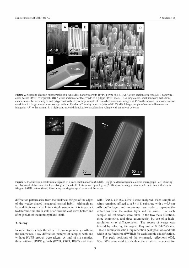
After growth, the wires are inspected for changes inmorphology in a field-emission scanning electron microscope(FESEM). Secondary electron imaging reveals a clear contrastbetween the core and shell in all of the unintentionally dopednanowires; see figure 2. This contrast is consistent withdoping contrast seen in Si [14]. It appears strongest for lowacceleration voltages and in-lens type detectors, indicatingthat the information regarding dopant concentration is carriedby the secondary electrons generated by the primary beamand not by the high-energy back-scattered electrons. Thistechnique reveals inhomogeneity in the dopant distributionof the resulting core–shell nanowire structure. First, coresare not always concentric with the shells (approximately 30%in a representative sample of 85 wires). Second, the shellsare of varying thickness, with the range of shell thicknessesfor a representative sample being 50–200 nm. And finally,we observe apparent growth anisotropy for the c-face of thenanowires, or the HVPE overgrowth appears thinner on thec-plane. Since this technique is sensitive to electric fieldsgenerated by dopant distributions, the relative ratio of howmuch of this is caused by a differential growth rate betweenthe m-plane and c-plane and how much is caused by dopantdiffusion in the overgrowth process is still unknown.
In contrast to FESEM, transmission electron micrographsshow no dopant-based contrast in either bright-field orconventional dark-field imaging. Figure 3 shows transmissionelectron micrographs of a wire from a growth that showed cleardopant contrast in FESEM images. In addition to the lack ofdopant contrast, the TEMmicrographs show a lack of extendeddefects. The dark-field image formed by imaging with the(2 1̄ 0) diffraction spot also shows no cracking or large defectswith lattice distortions with components in the g direction. Theselected area electron diffraction (SAED) image (inset on topleft), together with the corresponding images indicate that thewire has no crystallographic twinning [15] driven by HVPE re-growth; we believe that the small satellite spots present in the
2
Nanotechnology 22 (2011) 465703 A Sanders et al
Figure 2. Scanning electron micrographs of n-type MBE nanowires with HVPE p-type shells. (A) A cross section of n-type MBE nanowirecores before HVPE overgrowth. (B) A cross section after the growth of a p-type HVPE shell. (C) A single core–shell nanowire that showsclear contrast between n-type and p-type materials. (D) A large sample of core–shell nanowires imaged at 45◦ to the normal, in a low-contrastcondition, i.e. large acceleration voltage with an Everhart–Thornley detector (bias +100 V). (E) A large sample of core–shell nanowiresimaged at 45◦ to the normal, in a high-contrast condition, i.e. low acceleration voltage with an in-lens detector.
Figure 3. Transmission electron micrograph of a core–shell nanowire (GN84). Bright-field transmission electron micrograph (left) showingno observable defects and thickness fringes. Dark-field electron micrograph g = (2 1̄ 0), also showing no observable defects and thicknessfringes. SAED pattern (inset) illustrating the single-crystal nature of the wires.
diffraction pattern arise from the thickness fringes of the edgesof the wedge-shaped hexagonal-crystal habit. Although nolarge defects were visible in a single nanowire, it is importantto determine the strain state of an ensemble of wires before andafter growth of the homoepitaxial shell.
3. X-ray
In order to establish the effect of homoepitaxial growth onthe nanowires, x-ray diffraction patterns of samples with andwithout HVPE growth were taken. A total of six samples,three without HVPE growth (B738, C023, B982) and three
with (GN84, GN169, GN97) were analyzed. Each sample ofwires remained affixed to a Si(111) substrate with a ∼75 nmAlN buffer layer, and no attempt was made to separate thereflections from the matrix layer and the wires. For eachsample, six reflections were taken in the two-theta direction,three symmetric, and three asymmetric, by use of a high-resolution x-ray diffractometer. The source of x-rays wasfiltered by selecting the copper Kα1 line at 0.154 0595 nm.Table 1 summarizes the x-ray reflection peak positions and fullwidth at half maxima (FWHM) for each sample and reflection.
The peak positions of the symmetric reflections (002,004, 006) were used to calculate the c lattice parameter for
3

Nanotechnology 22 (2011) 465703 A Sanders et al
Table 1. 2θ–ω diffractions of gallium nitride nanowires. X-ray reflections of nanowires before and after HVPE overgrowth used incalculating lattice parameters. The reported 2θ is the restricted range centroid, taking the weighted average of the values between halfmaximum points, along with the full width at half maximum (FWHM). For a given sample, all of the symmetric reflections are used tocalculate an average c lattice parameter. This c lattice parameter is used with the asymmetric reflections to calculate the average a latticeparameter.
Symmetric diffractions
002 004 006
Description Sample 2θ angle (deg) FWHM (deg) 2θ angle (deg) FWHM (deg) 2θ angle (deg) FWHM (deg)
Wires B738 34.575 0.029 72.928 0.067 126.125 0.196HVPE on B738 wires GN84 34.574 0.042 72.926 0.092 126.126 0.256Repeat of GN84 GN84b 34.570 0.042 72.920 0.093 126.117 0.252
Wires C023 34.570 0.014 72.919 0.035 126.099 0.120HVPE on C023 wires GN169 34.564 0.025 72.914 0.039 126.095 0.120
Wires B982 34.572 0.015 72.925 0.037 126.115 0.130HVPE on B982 wires GN97 34.571 0.020 72.924 0.044 126.114 0.140
Asymmetric diffractions
104 105 204
Description Sample 2θ angle (deg) FWHM (deg) 2θ angle (deg) FWHM (deg) 2θ angle (deg) FWHM (deg)
Wires B738 82.065 0.342 105.032 0.257 109.173 0.460HVPE on B738 wires GN84 82.046 0.109 105.023 0.219 109.145 0.204Repeat of GN84 GN84b 82.051 0.116 105.029 0.219 109.151 0.206
Wires C023 82.049 0.086 105.011 0.103 109.166 0.139HVPE on C023 wires GN169 82.050 0.062 105.015 0.094 109.183 0.099
Wires B982 82.065 0.071 105.030 0.103 109.198 0.127HVPE on B982 wires GN97 82.062 0.082 105.026 0.117 109.187 0.148
each sample. The average of these measurements yielded avalue of c lattice parameter that was used with the asymmetricreflections (104, 105, 204) to calculate the a lattice parameter.This method is explained in detail in [16]. Each peak positionwas determined by finding the weighted average of the pointsfrom half maximum to half maximum, i.e. a restricted rangecentroid. In order to track the stability of x-ray measurements,one as-grown specimen had reflections taken by separateusers after a long period (∼5 months), these reflections arereported as GN87 and GN87b. This repeated experimentplaces a reasonable estimate on all errors associated withsample misalignment, long-term environmental changes suchas humidity, temperature, and general operator differencesof at most ±6 × 10⁻⁵ (120 ppm) fractionally and typically±3× 10⁻⁵ (60 ppm). These errors are similar to the fractionalerrors assigned by use of the internal variation of the latticeparameters calculated for each reflection. Since each 2θ–ωscan of a reflection constitutes a separate measurement of the clattice, it is reasonable to expect that the error in the mean valueof the lattice parameters will be representative of the precisionof the measurement. With this in mind, the errors in the latticeparameters are assigned by taking the 95% confidence intervalfor the mean of c lattice values, to a maximum fractionalaccuracy of 120 ppm, and then repeating this for the a latticevalues calculated from the mean c lattice for each sample.The average c lattice parameter for all of the samples in thisstudy is between 0.518 53 and 0.518 43 nm, and the a latticeparameters are between 0.3188 and 0.3192 nm. Although thex-ray reflections were the result of both the matrix and thenanowires, the measured lattice parameters agree very wellwith measurements of the strain-free values of GaN found in
the literature. To illustrate this point, a range of strain-freeGaN lattice parameters found in the literature is represented bya gray box in figure 4. The box is formed by [17] and [18],forming a range of values in which most reported valuesfor strain-free lattice parameters are included; a summary ofmany of the values appears in [16]. In addition, figure 4illustrates that the addition of the HVPE p-type material doesnot affect the average lattice parameter of the nanowires. Thisis consistent with bulk homoepitaxy [17] that shows no changein lattice parameters regardless of Mg doping, within theresolution of our experiment.
4. Photoluminescence
AlthoughMg incorporation had no measurable effect on latticeparameters, the presence of an acceptor in single nanowiresis evident in PL spectra. PL of single nanowires removedfrom the growth substrate were measured in a continuousflow helium cryostat, by use of a HeCd laser as an excitationsource. To prepare samples for PL measurements at 5 K, alarge number of wires were released from the growth substrateby ultrasonic agitation in isopropanol to produce a suspension.This suspension was dried on a fused-silica substrate with aphotolithographically defined, indexed metal grid to aid in theidentification and location of individual wires. UV emissionfrom the HeCd laser (325 nm) was focused onto the samplethrough a fused-silica window in the cryostat. The resultant PLspectra were obtained with a scanning 0.5 m monochromatorthat collected and dispersed the luminescence onto an UV-sensitive photomultiplier tube. The PL collected is a weighted
4

Nanotechnology 22 (2011) 465703 A Sanders et al
Figure 4. GaN nanowire lattice parameters measured by XRD.Lattice parameters undergo no significant change before and afterHVPE growth of p-type shells. The gray region represents literaturevalues for strain-free GaN. The x-ray reflections used in determiningthe lattice constants and their errors are presented in table 1.
sum of GaN perpendicular to the incidence of the beam to adepth of approximately 80 nm [19]. Any variation in thicknessof the nanowire, or film coating the nanowire, will serveto generate an average spectrum. The PL spectra of MBEnanowire cores have distinct band-edge emission due to thedonor bound A-exciton (D0XA) at 3.472 eV. Occasionally,this peak will be displaced by up to ∼15 meV due to straininduced by the differential thermal contraction between theGaN and the substrate [20]. For the nanowire cores itis common to observe up to four phonon replicas of theemission from exciton transitions in the spectra, which arespaced at regular intervals determined by the longitudinaloptical (LO) phonon energy (∼92 meV). Single nanowireshave no significant yellow emission or any other significantsub-bandgap emission. In contrast, once the HVPE shell isgrown there are at least two recognizable sub-bandgap features.
At 5 K, these features occur roughly at 2.9 and 3.25 eVand can be seen in figure 5, for two coated nanowire growthruns. These features are broad and occur typically in spectralregions and can be associated with various acceptors. The blueluminescence (BL) band has been observed in unintentionallydoped, Zn, and Mg doped GaN grown by HVPE, and weuse the notation found in [21]. Since we have intentionallyintroduced Mg, and have analyzed thin films grown in similarconditions using SIMS, we believe that the BL band is causedby Mg incorporated into the overgrowth of GaN on thenanowire. In addition, although the ultraviolet luminescence(UVL) band occurs close to the same spectral position as the2 LO phonon replica of the exciton transitions, we believethe vastly increased magnitude and the broadening of featuresat approximately 3.25 eV represent the incorporation of Mg.The difference in shape for the overcoated wires labeled GN84and GN97 occurs most likely because of a difference inconcentration of Mg. Others have reported that at a certaindoping level the peaks of the UVL band broaden, redshift,and transform into a single unstructured band peaking at about3.2 eV [21].
5. Electrical characterization
The electrical resistivity and carrier polarity of the core–shell nanowires were determined by two-terminal electricalmeasurements. Nanowires were first released from theirgrowth substrates by ultrasonic agitation in isopropanol. Thewire suspension was then deposited on fused-silica substratesand metallic leads were patterned and deposited by useof standard lift-off photolithographic techniques. A largenumber of electrode pairs are patterned and a small fractionresult in single nanowire devices; several different contactingmetals and annealing schemes were tested. Comparing thecurrent that flows through unintentionally doped nanowiresbefore and after HVPE growth, it is clear that the HVPEfilm is conductive. All HVPE overgrown wire growthswere conductive regardless of their initial resistivity. Forexample, wires from the B992 growth have an estimated carrierconcentration of ∼1015 cm−3 and are completely depleted atroom temperature. Measurements of 25 devices with singlewires clearly bridging electrode pairs, and 50 nm Ni/292 nm
Figure 5. PL at 5 K of single wires from the growths B982 and B738 for both n-type single nanowires and core–shell n–p nanowires. In bothcases an increase of sub-bandgap spectral content indicates the presence of an acceptor. At 5 K, two donor–acceptor pair (DAP) transitions areapparent in core–shell nanowires, but not in MBE nanowire cores. These transitions are referred to as BL and UVL, to correspond to the bulkequivalents reported in [21].
5

Nanotechnology 22 (2011) 465703 A Sanders et al
Figure 6. Electrical measurements. (A) A typical core–shell device micrograph with Ni/Au contacts. The core nanowires are B992 and arecompletely depleted at room temperature. There has been no attempt in this device to contact the core selectively. A typical current–voltagecurve of a comparable device is shown directly below. Non-ohmic device characteristics are typical in core–shell devices for both n-type andp-type contact metallization schemes. (B) Minority carrier injection from the metallic contacts. In the case of n-type nanowire cores (top)holes are injected, causing electroluminescence to appear next to the positively biased lead, whereas in the case of core–shell nanowirescontacted only on the shell (bottom), electrons are injected, causing electroluminescence near the negatively biased lead.
Au contacts, unannealed, show virtually no conduction, andcurrent–voltage curves in all instances have currents less than10−10 A at 1 V, a system noise floor for fast characterization.In contrast, after the HVPE growth, a sample with the samecontact metallization, shows the wires are conductive, havinga typical current of 10−6 A at 1 V. Of 17 devices measured,each clearly having a single wire between the electrode pairs,16 had currents at 1 V that ranged between 10−5 and 10−10 A.The inhomogeneity in the shell dimensions no doubt plays arole in the large distribution of currents at 1 V. The current–voltage characteristics of devices are predominately nonlinear,having a barrier associated with the contact, a typical devicemicrograph and a typical current–voltage curve is shown infigure 6(A).
This is true regardless of the contact metallization,whether it is 20 nm Ti/200 nm Al or 50 nm Ni/292 nm Au, andgenerally nanowire contacts worsen under contact annealing.In contrast, contacts to n-nanowires with annealed Ti/Alcontacts are normally linear and of low resistance [11]. Thisis qualitatively consistent with the increase in contact barrierassociated with p-doping; however, it is not conclusive. Thischange in contact quality was observed for all of the HVPEovercoated growth runs. For certain devices that can toleratehigh applied voltages >25 V and have currents that exceed10−7 A at 25 V, mild electroluminescence from single wires isobserved. The visible part of this electroluminescence is dimand requires camera integration times of 10–20 s to capture; seefigure 6(B). Wires with p-type material tend to emit light closeto the negatively biased lead, whereas n-type wires, with nop-type material, emit close to the positively biased lead. Thistype of polarity dependent light emission is seen when minoritycarriers are extracted from the metallic leads and injected intosemiconductors [22]. It should be noted that minority carriersinjected from the metal contacts can either directly tunnel intothe semiconductor or have sufficient kinetic energy to impact
ionize lattice atoms, creating a minority carrier population witha small fraction that recombines radiatively. We do not observea significant increase in current for biases greater than thatat which the luminescence is observed, suggesting that theavalanche generation of carriers is not dominating the currentcharacteristics. The polarity of this effect indicates that thereare electrically active holes in the p-type material.
6. Conclusion
In conclusion, using n-type nanowires grown by MBE anda p-type cladding grown by HVPE, we have demonstratedthe growth of homoepitaxial n-core:p-shell nanowires. Thesewires have clear signatures of dopant contrast in scanningelectron micrographs, no apparent defects in electrondiffraction patterns and TEM images, and a clear PLsignature related to an acceptor in the HVPE shell. Inaddition, no change in lattice parameter is observed for largeensembles of nanowires as measured by x-ray diffractionindicating homoepitaxial growth. Finally, active holes in thecoated wires are observed through minority carrier tunnelingelectroluminescence.
Acknowledgments
We would like to acknowledge Dr Manuel Romero for manyuseful discussions and data regarding cathode-luminescence insimilar structures. This is a contribution of an agency of theUS government and is not subject to copyright.
References
[1] Hersee S, Sun X and Wang X 2006 The controlled growth ofGaN nanowires Nano Lett. 6 1808–11
6
Nanotechnology 22 (2011) 465703 A Sanders et al
[2] Ishizawa S, Sekiguchi H, Kikuchi A and Kishino K 2007Selective growth of GaN nanocolumns by Al thin layer onsubstrate Phys. Status Solidi b 244 1815–9
[3] Bertness K A, Sanders A W, Rourke D M, Harvey T E,Roshko A, Schlager J B and Sanford N A 2010 Controllednucleation of GaN nanowires grown with molecular beamepitaxy Adv. Funct. Mater. 20 2911–5
[4] Qian F, Gradecjak S, Li Y, Wen C-Y and Lieber C 2005Core/multishell nanowire heterostructures as multicolor,high-efficiency light-emitting diodes Nano Lett. 5 2287–91
[5] Stern E et al 2005 Electrical characterization of single GaNnanowires Nanotechnology 16 2941–53
[6] Calleja E et al 2007 Growth, morphology, and structuralproperties of group-III-nitride nanocolumns and nanodisksPhys. Status Solidi b 244 2816–37
[7] Tchernycheva M et al 2007 Growth of GaN free-standingnanowires by plasma-assisted molecular beam epitaxy:structural and optical characterization Nanotechnology18 385306
[8] Guo W, Zheng M, Banerjee A and Bhattacharya P 2010Catalyst-free InGaN/GaN nanowire light emitting diodesgrown on (001) silicon by molecular beam epitaxy NanoLett. 10 3355–9
[9] Calarco R and Marso M 2007 GaN an InN nanowires grown byMBE: a comparison Appl. Phys. A 87 499–503
[10] Bertness K, Roshko A, Mansfield L, Harvey T andSanford N 2007 Nucleation conditions for catalyst-free GaNnanowires J. Cryst. Growth 300 94–9
[11] Mansfield L, Bertness K, Blanchard P, Harvey T,Sanders A and Sanford N 2009 GaN nanowire carrierconcentration calculated from light and dark resistancemeasurements J. Electron. Mater. 38 495–504
[12] Sanford N, Blanchard P, Bertness K, Mansfield L, Schlager J,Sanders A, Roshko A, Burton B and George S 2010Steady-state and transient photoconductivity in c-axis GaN
nanowires grown by nitrogen-plasma-assisted molecularbeam epitaxy J. Appl. Phys. 107 034318
[13] Ambacher O 1998 Growth and applications of groupIII-nitrides J. Phys. D: Appl. Phys. 31 2652–710
[14] El-Gomati M, Zacjgout F, Jayacody H, Tear S andWilson K 2005 Why is it possible to detect doped regions ofsemiconductors in low voltage SEM: a review and updateSurf. Interface Anal. 37 907–11
[15] Wiliams D and Carter C 2009 Transmission ElectronMicroscopy: A Textbook for Materials Science 2nd edn(Berlin: Springer)
[16] Moram M and Vickers M 2009 X-ray diffraction of III-nitridesRep. Prog. Phys. 72 036502
[17] Porowski S 1998 Bulk and homoepitaxial GaN-growth andcharacterisation J. Cryst. Growth 190 153–8
[18] Leszcznski M, Grzegory I, Teisseyre H, Suski T, Bockowski M,Jun J, Branowski J M, Poroski S and Major J 1995 Latticeconstants, thermal expansion and compressibility of galliumnitride J. Phys. D: Appl. Phys. 28 A149
[19] Muth J, Lee J, Shmagin I, Kolbas R, Casey H, Keller B,Mishra U and DenBaars S 1997 Absorbtion coefficient,energy gap, exciton binding energy, and recombinationlifetime of GaN obtained from transmission experimentsAppl. Phys. Lett. 71 2572–4
[20] Schlager J, Bertness K, Blanchard P, Robins L, Roshko A andSanford N 2008 Steady-state and time-resolvedphotoluminescence from relaxed and strained GaNnanowires grown by catalyst-free molecular-beam epitaxyJ. Appl. Phys. 103 124309
[21] Reshchikov M and Morkoc H 2005 Luminescence properties ofdefects in GaN J. Appl. Phys. 97 061301
[22] Zimmler M, Bao J, Shalish I, Yi W, Yoon J,Narayanamurti N and Capasso F 2007 Electroluminescencefrom single nanowires by tunnel injection: an experimentalstudy Nanotechnology 18 235205
7