Transparent conducting films from NbSe3 nanowires
6
Transparent conducting films from NbSe 3 nanowires This article has been downloaded from IOPscience. Please scroll down to see the full text article. 2011 Nanotechnology 22 285202 (http://iopscience.iop.org/0957-4484/22/28/285202) Download details: IP Address: 134.226.252.155 The article was downloaded on 01/06/2011 at 14:30 Please note that terms and conditions apply. View the table of contents for this issue, or go to the journal homepage for more Home Search Collections Journals About Contact us My IOPscience
Transcript of Transparent conducting films from NbSe3 nanowires

Transparent conducting films from NbSe3 nanowires
This article has been downloaded from IOPscience. Please scroll down to see the full text article.
2011 Nanotechnology 22 285202
(http://iopscience.iop.org/0957-4484/22/28/285202)
Download details:
IP Address: 134.226.252.155
The article was downloaded on 01/06/2011 at 14:30
Please note that terms and conditions apply.
View the table of contents for this issue, or go to the journal homepage for more
Home Search Collections Journals About Contact us My IOPscience
IOP PUBLISHING NANOTECHNOLOGY
Nanotechnology 22 (2011) 285202 (5pp) doi:10.1088/0957-4484/22/28/285202
Transparent conducting films from NbSe3nanowiresSukanta De1, Conor S Boland1, Paul J King1, Sophie Sorel1,Mustafa Lotya1, U Patel2, Z L Xiao2 and Jonathan N Coleman1
1 School of Physics and CRANN, Trinity College Dublin, Dublin 2, Ireland2 Department of Physics, Northern Illinois University, DeKalb, IL 60115, USA
E-mail: [email protected]
Received 7 March 2011, in final form 6 May 2011Published 31 May 2011Online at stacks.iop.org/Nano/22/285202
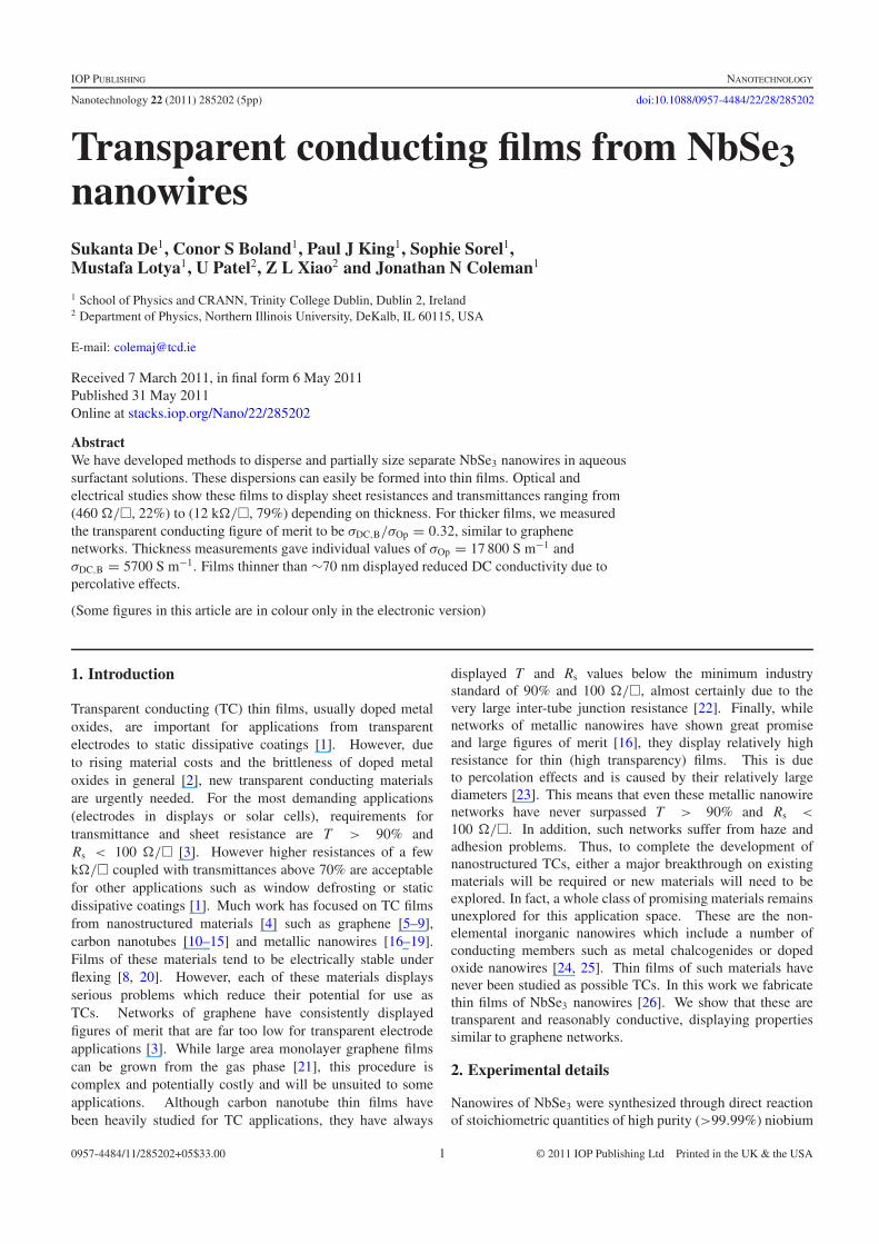
AbstractWe have developed methods to disperse and partially size separate NbSe3 nanowires in aqueoussurfactant solutions. These dispersions can easily be formed into thin films. Optical andelectrical studies show these films to display sheet resistances and transmittances ranging from(460 �/�, 22%) to (12 k�/�, 79%) depending on thickness. For thicker films, we measuredthe transparent conducting figure of merit to be σDC,B/σOp = 0.32, similar to graphenenetworks. Thickness measurements gave individual values of σOp = 17 800 S m−1 andσDC,B = 5700 S m−1. Films thinner than ∼70 nm displayed reduced DC conductivity due topercolative effects.
(Some figures in this article are in colour only in the electronic version)
1. Introduction
Transparent conducting (TC) thin films, usually doped metaloxides, are important for applications from transparentelectrodes to static dissipative coatings [1]. However, dueto rising material costs and the brittleness of doped metaloxides in general [2], new transparent conducting materialsare urgently needed. For the most demanding applications(electrodes in displays or solar cells), requirements fortransmittance and sheet resistance are T > 90% andRs < 100 �/� [3]. However higher resistances of a fewk�/� coupled with transmittances above 70% are acceptablefor other applications such as window defrosting or staticdissipative coatings [1]. Much work has focused on TC filmsfrom nanostructured materials [4] such as graphene [5–9],carbon nanotubes [10–15] and metallic nanowires [16–19].Films of these materials tend to be electrically stable underflexing [8, 20]. However, each of these materials displaysserious problems which reduce their potential for use asTCs. Networks of graphene have consistently displayedfigures of merit that are far too low for transparent electrodeapplications [3]. While large area monolayer graphene filmscan be grown from the gas phase [21], this procedure iscomplex and potentially costly and will be unsuited to someapplications. Although carbon nanotube thin films havebeen heavily studied for TC applications, they have always
displayed T and Rs values below the minimum industrystandard of 90% and 100 �/�, almost certainly due to thevery large inter-tube junction resistance [22]. Finally, whilenetworks of metallic nanowires have shown great promiseand large figures of merit [16], they display relatively highresistance for thin (high transparency) films. This is dueto percolation effects and is caused by their relatively largediameters [23]. This means that even these metallic nanowirenetworks have never surpassed T > 90% and Rs <
100 �/�. In addition, such networks suffer from haze andadhesion problems. Thus, to complete the development ofnanostructured TCs, either a major breakthrough on existingmaterials will be required or new materials will need to beexplored. In fact, a whole class of promising materials remainsunexplored for this application space. These are the non-elemental inorganic nanowires which include a number ofconducting members such as metal chalcogenides or dopedoxide nanowires [24, 25]. Thin films of such materials havenever been studied as possible TCs. In this work we fabricatethin films of NbSe3 nanowires [26]. We show that these aretransparent and reasonably conductive, displaying propertiessimilar to graphene networks.
2. Experimental details
Nanowires of NbSe3 were synthesized through direct reactionof stoichiometric quantities of high purity (>99.99%) niobium
0957-4484/11/285202+05$33.00 © 2011 IOP Publishing Ltd Printed in the UK & the USA1
Nanotechnology 22 (2011) 285202 S De et al
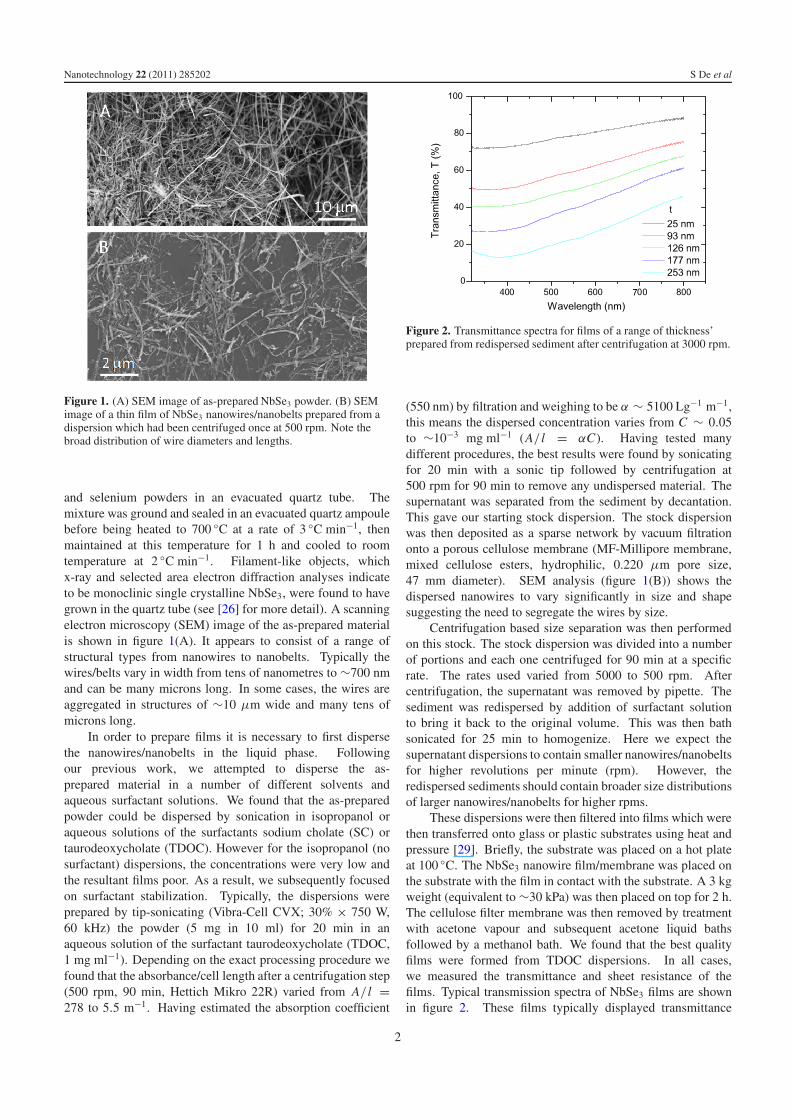
Figure 1. (A) SEM image of as-prepared NbSe3 powder. (B) SEMimage of a thin film of NbSe3 nanowires/nanobelts prepared from adispersion which had been centrifuged once at 500 rpm. Note thebroad distribution of wire diameters and lengths.
and selenium powders in an evacuated quartz tube. Themixture was ground and sealed in an evacuated quartz ampoulebefore being heated to 700 ◦C at a rate of 3 ◦C min−1, thenmaintained at this temperature for 1 h and cooled to roomtemperature at 2 ◦C min−1. Filament-like objects, whichx-ray and selected area electron diffraction analyses indicateto be monoclinic single crystalline NbSe3, were found to havegrown in the quartz tube (see [26] for more detail). A scanningelectron microscopy (SEM) image of the as-prepared materialis shown in figure 1(A). It appears to consist of a range ofstructural types from nanowires to nanobelts. Typically thewires/belts vary in width from tens of nanometres to ∼700 nmand can be many microns long. In some cases, the wires areaggregated in structures of ∼10 μm wide and many tens ofmicrons long.
In order to prepare films it is necessary to first dispersethe nanowires/nanobelts in the liquid phase. Followingour previous work, we attempted to disperse the as-prepared material in a number of different solvents andaqueous surfactant solutions. We found that the as-preparedpowder could be dispersed by sonication in isopropanol oraqueous solutions of the surfactants sodium cholate (SC) ortaurodeoxycholate (TDOC). However for the isopropanol (nosurfactant) dispersions, the concentrations were very low andthe resultant films poor. As a result, we subsequently focusedon surfactant stabilization. Typically, the dispersions wereprepared by tip-sonicating (Vibra-Cell CVX; 30% × 750 W,60 kHz) the powder (5 mg in 10 ml) for 20 min in anaqueous solution of the surfactant taurodeoxycholate (TDOC,1 mg ml−1). Depending on the exact processing procedure wefound that the absorbance/cell length after a centrifugation step(500 rpm, 90 min, Hettich Mikro 22R) varied from A/ l =278 to 5.5 m−1. Having estimated the absorption coefficient
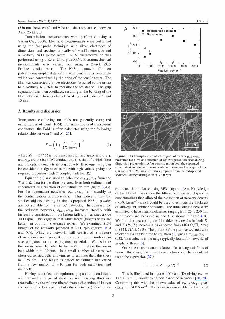
Figure 2. Transmittance spectra for films of a range of thickness’prepared from redispersed sediment after centrifugation at 3000 rpm.
(550 nm) by filtration and weighing to be α ∼ 5100 Lg−1 m−1,this means the dispersed concentration varies from C ∼ 0.05to ∼10−3 mg ml−1 (A/ l = αC). Having tested manydifferent procedures, the best results were found by sonicatingfor 20 min with a sonic tip followed by centrifugation at500 rpm for 90 min to remove any undispersed material. Thesupernatant was separated from the sediment by decantation.This gave our starting stock dispersion. The stock dispersionwas then deposited as a sparse network by vacuum filtrationonto a porous cellulose membrane (MF-Millipore membrane,mixed cellulose esters, hydrophilic, 0.220 μm pore size,47 mm diameter). SEM analysis (figure 1(B)) shows thedispersed nanowires to vary significantly in size and shapesuggesting the need to segregate the wires by size.
Centrifugation based size separation was then performedon this stock. The stock dispersion was divided into a numberof portions and each one centrifuged for 90 min at a specificrate. The rates used varied from 5000 to 500 rpm. Aftercentrifugation, the supernatant was removed by pipette. Thesediment was redispersed by addition of surfactant solutionto bring it back to the original volume. This was then bathsonicated for 25 min to homogenize. Here we expect thesupernatant dispersions to contain smaller nanowires/nanobeltsfor higher revolutions per minute (rpm). However, theredispersed sediments should contain broader size distributionsof larger nanowires/nanobelts for higher rpms.
These dispersions were then filtered into films which werethen transferred onto glass or plastic substrates using heat andpressure [29]. Briefly, the substrate was placed on a hot plateat 100 ◦C. The NbSe3 nanowire film/membrane was placed onthe substrate with the film in contact with the substrate. A 3 kgweight (equivalent to ∼30 kPa) was then placed on top for 2 h.The cellulose filter membrane was then removed by treatmentwith acetone vapour and subsequent acetone liquid bathsfollowed by a methanol bath. We found that the best qualityfilms were formed from TDOC dispersions. In all cases,we measured the transmittance and sheet resistance of thefilms. Typical transmission spectra of NbSe3 films are shownin figure 2. These films typically displayed transmittance
2
Nanotechnology 22 (2011) 285202 S De et al
(550 nm) between 60 and 95% and sheet resistances between3 and 25 k�/�.
Transmission measurements were performed using aVarian Cary 6000i. Electrical measurements were performedusing the four-probe technique with silver electrodes ofdimensions and spacings typically of ∼ millimetre size anda Keithley 2400 source metre. SEM characterization wasperformed using a Zeiss Ultra plus SEM. Electromechanicalmeasurements were carried out using a Zwick Z0.5Proline tensile tester. The NbSe3 nanowire film onpolyethyleneterephthalate (PET) was bent into a semicirclewhich was constrained by the grips of the tensile tester. Thefilm was connected via two electrodes (attached to the grips)to a Keithley KE 2601 to measure the resistance. The gripseparation was then oscillated, resulting in the bending of thefilm between extremes characterized by bend radii of 5 and15 mm.
3. Results and discussion
Transparent conducting materials are generally comparedusing figures of merit (FoM). For nanostructured transparentconductors, the FoM is often calculated using the followingrelationship between T and Rs [27]:
T =(
1 + Z0
2Rs
σOp
σDC,B
)−2
(1)
where Z0 = 377 � is the impedance of free space and σDC,B
and σOp are the bulk DC conductivity (i.e. that of a thick film)and the optical conductivity respectively. Here σDC,B/σOp canbe considered a figure of merit with high values giving therequired properties (high T coupled with low Rs).
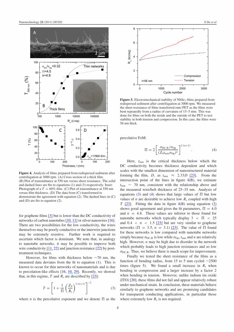
Equation (1) was used to calculate σDC,B/σOp from theT and Rs data for the films prepared from both sediment andsupernatant as a function of centrifugation rpm (figure 3(A)).For the supernatant networks, σDC,B/σOp falls steadily asthe centrifugation rate increases. This indicates that thesmaller objects existing in the as-prepared NbSe3 powderare not suitable for use in TC networks. In contrast, forthe sediment networks, σDC,B/σOp increases steadily withincreasing centrifugation rate before falling off at rates above3000 rpm. This suggests that while larger (longer) wires arebetter, an optimum size-range exists. We examined SEMimages of the networks prepared at 3000 rpm (figures 3(B)and (C)). While the networks still consist of a mixtureof nanowires and nanobelts, they appear more uniform insize compared to the as-prepared material. We estimatethe mean wire diameter to be ∼35 nm while the meanbelt width is ∼130 nm. In a small number of cases, weobserved twisted belts allowing us to estimate their thicknessas ∼25 nm. The length is harder to estimate but variedfrom a few micron to >10 μm for both nanowires andnanobelts.
Having identified the optimum preparation conditions,we prepared a range of networks with varying thickness(controlled by the volume filtered from a dispersion of knownconcentration). For a particularly thick network (∼3 μm), we
Figure 3. A) Transparent conductor figure of merit, σDC,B/σOp,measured for films as a function of centrifugation rate used duringdispersion preparation. After centrifugation both the separatedsupernatant and the redispersed sediment were used to prepare films.(B) and (C) SEM images of films prepared from the redispersedsediment after centrifugation at 3000 rpm.
estimated the thickness using SEM (figure 4(A)). Knowledgeof the filtered mass (from the filtered volume and dispersionconcentration) then allowed the estimation of network density(∼340 kg m−3) which could be used to estimate the thicknessof subsequent, thinner networks. The films studied here wereestimated to have mean thicknesses ranging from 25 to 250 nm.In all cases, we measured Rs and T as shown in figure 4(B).We find that decreasing the film thickness results in both Rs
and T (Rs, T ) increasing as expected from (460 �/�, 22%)to (12 k �/�, 79%). The portion of the graph associated withthicker films can be fitted to equation (1), giving σDC,B/σOp =0.32. This value is in the range typically found for networks ofgraphene flakes [3].
Once the transmittance is known for a range of films ofknown thickness, the optical conductivity can be calculatedusing the expression [27]:
T = (1 + Z0σOpt/2)−2. (2)
This is illustrated in figures 4(C) and (D) giving σOp =17 800 S m−1, similar to carbon nanotube networks [10, 28].Combining this with the known value of σDC,B/σOp, givesσDC,B = 5700 S m−1. This value is comparable to that found
3
Nanotechnology 22 (2011) 285202 S De et al
Figure 4. Analysis of films prepared from redispersed sediment aftercentrifugation at 3000 rpm. (A) Cross section of a thick film.(B) Plot of transmittance at 550 nm versus sheet resistance. The solidand dashed lines are fits to equations (1) and (3) respectively. Inset:Photograph of a T = 60% film. (C) Plot of transmittance at 550 nmversus film thickness. (D) The data from (C) transformed todemonstrate the agreement with equation (2). The dashed lines in (C)and (D) are fits to equation (2).
for graphene films [3] but is lower than the DC conductivity ofnetworks of carbon nanotubes [10, 11] or silver nanowires [16].There are two possibilities for the low conductivity, the wiresthemselves may be poorly conductive or the interwire junctionsmay be extremely resistive. Further work is required toascertain which factor is dominant. We note that, in analogyto nanotube networks, it may be possible to improve bothwire conductivity [11, 22] and junction resistance [22] by post-treatment techniques.
However, for films with thickness below ∼70 nm, themeasured data deviates from the fit to equation (1). This isknown to occur for thin networks of nanomaterials and is dueto percolation-like effects [16, 10, 29]. Recently, we showedthat, in this regime, T and Rs are described by [23]:
T =[
1 + 1
�
(Z0
Rs
)1/(n+1)]−2
(3)
where n is the percolative exponent and we denote � as the
Figure 5. Electromechanical stability of NbSe3 films prepared fromredispersed sediment after centrifugation at 3000 rpm. We measuredthe sheet resistance of films transferred onto PET as the films werebent repeatedly from a radius of curvature of 15–5 mm. This wasdone for films on both the inside and the outside of the PET to teststability in both tension and compression. In this case, the films were56 nm thick.
percolative FoM:
� = 2
[σDC,B/σOp
(Z0tminσOp)n
]1/(n+1)
. (4)
Here, tmin is the critical thickness below which theDC conductivity becomes thickness dependent and whichscales with the smallest dimension of nanostructured materialforming the film, D, as tmin ≈ 2.33D [23]. From theintersection point of the lines in figure 4(B), we estimatetmin ∼ 70 nm, consistent with the relationship above andthe measured wire/belt thickness of 25–35 nm. Analysis ofequations (3) and (4) shows that large values of � but lowvalues of n are desirable to achieve low Rs coupled with highT [23]. Fitting the data in figure 4(B) using equation (3)shows good agreement and gives the fit parameters, � = 4.0and n = 4.8. These values are inferior to those found fornanotube networks which typically display 3 < � < 25and 0.4 < n < 1.5 [23] but are very similar to graphenenetworks (� = 3.5, n = 3.1) [23]. The value of � foundfor these networks is low compared with nanotube networkssimply because σDC,B is low while σOp, tmin and n are relativelyhigh. However, n may be high due to disorder in the networkwhich probably leads to high junction resistances and so lowσDC,B. Thus, we believe there is much scope for improvement.
Finally we tested the sheet resistance of the films as afunction of bending radius, from 15 to 5 mm cycled ∼2500times (figure 5). We found a small increase in Rs whenbending in compression and a larger increase by a factor 2when bending in tension. However, unlike indium tin oxide(ITO) [20], these films did not fail and appear relatively robustunder mechanical strain. In conclusion, these materials behavesimilarly to graphene networks and are promising candidatesfor transparent conducting applications, in particular thosewhere extremely low Rs is not required.
4

Nanotechnology 22 (2011) 285202 S De et al
Acknowledgments
We acknowledge the Science Foundation Ireland fundedcollaboration (SFI grant 03/CE3/M406s1) between TrinityCollege Dublin and Hewlett Packard which has allowed thiswork to take place. JNC is also supported by an SFI PI award.The work on nanowire fabrication was supported by the USDepartment of Energy (DOE) Grant DE-FG02-06ER46334.
References
[1] Gordon R G 2000 Criteria for choosing transparent conductorsMRS Bull. 25 52
[2] Chen Z, Cotterell B and Wang W 2002 The fracture of brittlethin films on compliant substrates in flexible displays Eng.Fract. Mech. 69 597–603
[3] De S and Coleman J N 2010 Are there fundamental limitationson the sheet resistance and transmittance of thin graphenefilms? ACS Nano 4 2713–20
[4] Hecht D S, Hu L B and Irvin G 2011 Emerging transparentelectrodes based on thin films of carbon nanotubes,graphene, and metallic nanostructures Adv. Mater. 231482–513
[5] Becerril H A, Mao J, Liu Z, Stoltenberg R M, Bao Z andChen Y 2008 Evaluation of solution-processed reducedgraphene oxide films as transparent conductors ACS Nano2 463–70
[6] Biswas S and Drzal L T 2008 A novel approach to create ahighly ordered monolayer film of graphene nanosheets at theliquida ’liquid interface Nano Lett. 9 167–72
[7] Blake P et al 2008 Graphene-based liquid crystal device NanoLett. 8 1704–8
[8] De S, King P J, Lotya M, O’Neill A, Doherty E M,Hernandez Y, Duesberg G S and Coleman J N 2009Flexible, transparent, conducting films of randomly stackedgraphene from surfactant-stabilized, oxide-free graphenedispersions Small 6 458
[9] Wang X, Zhi L and Mullen K 2007 Transparent, conductivegraphene electrodes for dye-sensitized solar cells Nano Lett.8 323–7
[10] Doherty E M, De S, Lyons P E, Shmeliov A, Nirmalraj P N,Scardaci V, Joimel J, Blau W J, Boland J J and Coleman J N2009 The spatial uniformity and electromechanical stabilityof transparent, conductive films of single walled nanotubesCarbon 47 2466–73
[11] Geng H Z, Kim K K, So K P,Lee Y S, Chang Y and Lee Y H 2007 Effect of acidtreatment on carbon nanotube-based flexible transparentconducting films J. Am. Chem. Soc. 129 7758
[12] Hu L, Hecht D S and Gruner G 2004 Percolation in transparentand conducting carbon nanotube networks Nano Lett.4 2513–7
[13] Scardaci V, Coull R and Coleman J N 2010 Very thintransparent, conductive carbon nanotube films on flexiblesubstrates Appl. Phys. Lett. 97 023114
[14] Wu Z C et al 2004 Transparent, conductive carbon nanotubefilms Science 305 1273–6
[15] Hecht D S, Heintz A M, Lee R, Hu L B, Moore B, Cucksey Cand Risser S 2011 High conductivity transparent carbonnanotube films deposited from superacid Nanotechnology22 075201
[16] De S, Higgins T, Lyons P E, Doherty E M, Nirmalraj P N,Blau W J, Boland J J and Coleman J N 2009 Silver nanowirenetworks as flexible, transparent, conducting films:extremely high DC to optical conductivity ratios ACS Nano3 1767–74
[17] Hu L B, Kim H S, Lee J Y, Peumans P and Cui Y 2010Scalable coating and properties of transparent, flexible,silver nanowire electrodes ACS Nano 4 2955–63
[18] Lee J Y, Connor S T, Cui Y and Peumans P 2008Solution-processed metal nanowire mesh transparentelectrodes Nano Lett. 8 689–92
[19] Wu H, Hu L B, Rowell M W, Kong D S, Cha J J,McDonough J R, Zhu J, Yang Y A, McGehee M D andCui Y 2010 Electrospun metal nanofiber webs ashigh-performance transparent electrode Nano Lett.10 4242–8
[20] De S et al 2009 Transparent, flexible, and highly conductivethin films based on polymer–nanotube composites ACSNano 3 714–20
[21] Bae S et al 2010 Roll-to-roll production of 30 inch graphenefilms for transparent electrodes Nat. Nanotechnol. 5 574–8
[22] Nirmalraj P N, Lyons P E, De S, Coleman J N and Boland J J2009 Electrical connectivity in single-walled carbonnanotube networks Nano Lett. 9 3890–5
[23] De S, King P J, Lyons P E, Khan U and Coleman J N 2010 Sizeeffects and the problem with percolation in nanostructuredtransparent conductors ACS Nano 4 7064–72
[24] Wu X C, Tao Y R, Ke X K, Zhu J M and Hong J M 2004Catalytic synthesis of long NbS2 nanowire strands Mater.Res. Bull. 39 901–8
[25] Wan Q, Dattoli E N, Fung W Y, Guo W, Chen Y B, Pan X Qand Lu W 2006 High-performance transparent conductingoxide nanowires Nano Lett. 6 2909–15
[26] Hor Y S, Xiao Z L, Welp U, Ito Y, Mitchell J F, Cook R E,Kwok W K and Crabtree G W 2005 Nanowires andnanoribbons of charge–density-wave conductor NbSe3 NanoLett. 5 397–401
[27] Dressel M and Gruner G 2002 Electrodynamics of Solids:Optical Properties of Electrons in Matter (Cambridge:Cambridge University Press)
[28] Ruzicka B, Degiorgi L, Gaal R, Thien-Nga L, Bacsa R,Salvetat J P and Forro L 2000 Optical and dc conductivitystudy of potassium-doped single-walled carbon nanotubefilms Phys. Rev. B 61 R2468–71
[29] King P J, Khan U, Lotya M, De S and Coleman J N 2010Improvement of transparent conducting nanotube films byaddition of small quantities of graphene ACS Nano4 4238–46
5