Exploiting memory customization in FPGA for 3D stencil computations
Upload
independentCategory
view
0download
0
Metallic nanowires by full wafer stencil lithography
O. Vazquez-Mena, G. Villanueva, V. Savu, K. Sidler, M.A.F. van den Boogaart, J. Brugger
Microsystems Laboratory, Ecole Polytechnique Federale de Lausanne (EPFL), 1015 Lausanne, Switzerland
[email protected], [email protected]
Abstract
Aluminum and gold nanowires were fabricated using 100 mm stencil wafers containing nanoslits
fabricated with a focused ion beam. The stencils were aligned and the nanowires deposited on a
substrate with predefined electrical pads. The morphology and resistivity of the wires were studied.
Nanowires down to 70-nm wide and 5 µm long have been achieved showing a resistivity of 10 µΩcm
for Al and 5 µΩcm for Au and maximum current density of ~108 A/cm2. This proves the capability of
stencil lithography for the fabrication of metallic nanowires on a full wafer scale.
Keywords: Stencil lithography, metallic nanowires, resistivity,
1

An important objective in nanotechnology is the development of alternative nanopatterning methods
and the fabrication of novel nanoscale structures and materials. Among such structures, nanowires
(NWs) have shown potential and applications in a broad range of fields such as electronics1,2, magnetic
memories3, thermoelectric4,5, nano-mechanical6, optoelectronic7 and bio-sensing devices8-10 due to their
physical properties and surface to volume ratio. In particular, metallic nanowires can be applied for
interconnects, magnetic memories based on spin-polarized current3 and biosensors9. To fabricate NWs,
the two approaches used are the chemical synthesis (bottom-up) and the nanopatterning methods (top-
down).1 The common techniques for top-down nanopatterning are Electron Beam Lithography (EBL)11,
Focused Ion Beam (FIB)12, Deep-UV Lithography (DUV)13 and Nanoimprint Lithography (NIL).14,15
EBL and FIB have a very high resolution (<10 nm) but they are serial techniques, limiting their
throughput. DUV is a well established parallel technique developed for silicon based technologies with
high throughput and largely used in semiconductor industry, but it relies on complex equipment and
processing rules. NIL is a parallel patterning technique with high throughput and resolution (~10 nm)
that requires embossing a resist layer with a stamp. Since EBL, DUV and NIL are resist-based
techniques, they require resist coating, chemical solvents, heat treatments, energy radiation or pressure
embossing (NIL) on the substrate; this limits their application on substrates with high topography,
fragile or with materials that can be damaged by energy radiation or pressure. An alternative method for
nanopatterning is Stencil Lithography (SL). SL is a shadow masking technique, illustrated in Figure 1a,
that only requires to put a stencil onto a substrate for direct and parallel pattering by deposition16,
etching17 or implantation18 of the substrate through the stencil apertures without any resist processing.
Compared to the previous techniques, SL has a lower resolution and the patterning area is limited by the
size and stability of the membranes; nevertheless, SL has been used to pattern metallic dots <50 nm in
diameter with chip size stencils16,19 and areas up to 1x3 mm2 have been patterned with 300 nm metallic
dots.20 Since SL does not require any resist processing, it has the advantage of reducing the number of
steps required for patterning and allowing the patterning of a broad range of substrates compared to
resist-based techniques. For instance, SL has been used to deposit metals,20 fullerenes,21 organic
2

conductive molecules,22 complex oxides23 and magnetic alloys24 and to pattern different substrates such
as self-assembled monolayers (SAMs),25 organic layers26, polymer substrates,27 CMOS devices,28
cantilevers and non-planar substrates.20 Another important advantage of SL is that the stencils can be
reused many times.19,26,29,30 In particular stencils containing nanoapertures have been used up to 12
times for Al depositions without showing any degradation or damage on the membranes.29 The
fabrication of stencils with silicon nitride membranes is based on conventional silicon microfabrication
techniques. Once the stencil has been fabricated, it makes the patterning of metals simpler than using
resist-based methods such as lift-off or metal etching. In Table 1 we compare the steps required for
metal patterning using a stencil, lift-off and etching.
Table 1. Comparison of steps required for metal patterning
Stencil Lift-Off Etching
Metal deposition
Resist Coating Resist Coating
Alignment of stencil on substrate
Alignment and Exposure
through Mask (EBL,
DUV,UV)
Alignment and Exposure through
Mask(EBL, DUV,UV)
Resist Development
Resist Development
Metal deposition
Metal Deposition Metal etching
Resist Lift-Off Resist removal
3

Figure 1. Fabrication of nanowires by stencil lithography. (a) Schematics showing the principle of SL
for NW deposition. The stencil is put and aligned on top of a substrate. Then an evaporated material
passes through the stencil apertures forming NWs onto a pre-patterned substrate without any resist,
etching or lift-off processing. (b) Stencil membrane made of low stress silicon nitride (LS SiN)
containing a nanoslit in between two side micrometric apertures. The membrane is reinforced using
corrugations (see Supporting Information, Figure SI 1 and 2). (c) Aluminum structure deposited through
a stencil. It consists of a NW in between two side micrometric structures corresponding to the aperture
in the stencil. This structure is deposited in between predefined contacts to allow electrical
measurements.
4

In this letter we present the parallel fabrication of metallic NWs on full wafer scale (100 mm
diameter) using stencil lithography. In this work we have analyzed the dimensions, the electrical
resistivity and the maximal current density before breaking of the nanowires. The stencils used for this
work are made of thin reinforced membranes containing <100 nm wide nanoslits fabricated by focused
ion beam (FIB) milling. These stencils have been used to deposit Al and Au NWs with nominal
thicknesses of 60 nm and 45 nm respectively and widths in the range from 65 nm to 175 nm on
substrates containing predefined electrical contact pads. The width and thickness of the deposited NWs
were analyzed in order to study the pattern transfer from the apertures on the stencil to the deposited
structures. This study revealed a size enlargement with respect to the stencil aperture, a thickness
reduction compared to the nominal deposited thickness and a polycrystalline structure of the NWs. The
NWs show an ohmic behavior, with an electrical resistivity higher than bulk values and a maximal
current density in the order of 108 A/cm2.
The stencils fabricated for this work contain corrugated membranes with nanoslits patterned by FIB
milling and distributed across the entire wafer.31,32 The membranes are made of 100 nm thick low stress
silicon nitride (LS SiN) with dimensions of 100 µm in width and 1 mm in length. This membrane
thickness is required in order to pattern sub-100 nm apertures; however, membranes with such thickness
are fragile to physical stress and may suffer deformations and ruptures.19,33 To increase their stability,
the fabricated membranes are corrugated instead of being planar. The corrugations have a hexagonal
ring geometry shown in Figure 1b. These corrugations give more stability to the membrane by
increasing its moment of inertia.31,33 The stencil apertures are shown in Figure 1b. They consist of two
side micrometric apertures (~5 x 3 µm2) defined by UV lithography (0.8 µm resolution) with a nanoslit
in between them fabricated by FIB milling. The width of the nanoslits is defined by the FIB whereas
the length corresponds to the distance between the two side micrometric apertures. The stencils also
contain alignment apertures that should match with their corresponding alignment marks on the
substrate. Two stencils were fabricated, one for Al deposition and the other for Au deposition. The
stencil used for Al deposition contains nanoslits with lengths L=1, 2 and 5 µm and the one for Au
5
deposition has nanoslits with L=0.8, 1.6 and 4.6 µm. In both cases the nanoslits have widths (WSt) from
50 to 140 nm. (Stencil fabrication process, corrugations and a full wafer stencil are shown in the
Supporting Information, Figures SI 1 and SI 2)
Al and Au NWs were deposited on substrates with a 200 nm thick silicon oxide layer, predefined
electrical contact pads and alignment marks. In the substrate for the deposition of Al NWs, the contacts
pads and the alignment marks were made of a film of Pt(45nm)/Ti(5nm). On the substrate for Au NWs
they were made of Au(40 nm)/Ti(5 nm). These structures were prepared by UV lithography, metal
deposition and lift-off process. To deposit the NWs, the stencils were aligned and clamped with their
respective substrate using a standard bond aligner system (Suss MA6/BA6). Then the stencil and
substrate clamped for Al deposition were mounted into an evaporator for the deposition of 60 nm thick
Al by e-beam evaporation. The same process was used for the stencil and substrate for Au, depositing
45 nm thick Au by e-beam evaporation as well. In both cases, the depositions were done at room
temperature without any temperature controller, base pressure of 10-6 mbar and a deposition rate of 0.4
nm/s. The distance from the source to the substrate was 1 m and the material source ~1 cm in diameter.
The deposited structures consist of two side micrometric structures (to facilitate electrical contact) with
a NW in between, corresponding to the apertures in the stencil membranes as illustrated in Figure 1c.
The NWs are deposited in between the predefined electrical contact pads to allow electrical
measurements. Due to the curvature of the stencil and the substrate, there is a gap between them during
the metal deposition. For full wafer stencils and substrates 100 mm in diameter, the size of the gap
varies between 10 and 20 µm across the stencil-substrate interface (measured from focal distances with
an optical microscope). This limits the resolution compared to chip-size (~1 cm) stencil deposition
where there is a reduced and more uniform gap size (~1 µm) between stencil and substrate.
6
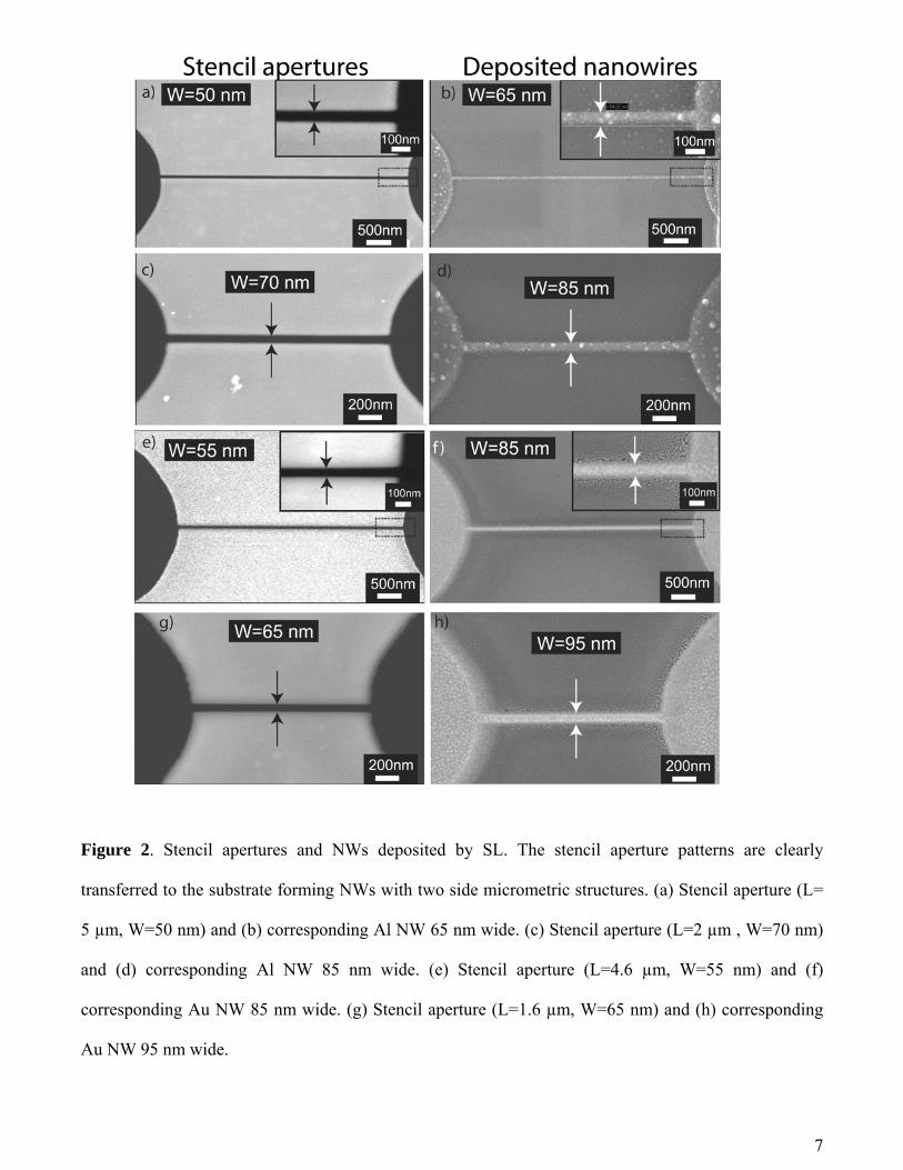
Figure 2. Stencil apertures and NWs deposited by SL. The stencil aperture patterns are clearly
transferred to the substrate forming NWs with two side micrometric structures. (a) Stencil aperture (L=
5 µm, W=50 nm) and (b) corresponding Al NW 65 nm wide. (c) Stencil aperture (L=2 µm , W=70 nm)
and (d) corresponding Al NW 85 nm wide. (e) Stencil aperture (L=4.6 µm, W=55 nm) and (f)
corresponding Au NW 85 nm wide. (g) Stencil aperture (L=1.6 µm, W=65 nm) and (h) corresponding
Au NW 95 nm wide.
7

Figure 2 illustrates deposited Al and Au NWs with their corresponding stencil apertures. The NWs
were aligned with a lateral precision of ~1 µm. The length of the NWs corresponds to the length of the
nanoslits in the stencils. For the Al NWs the width (WNW) ranges from 65 to 160 nm and for the Au
NWs WNW ranges from 80 nm to 175 nm as measured by scanning electron microscopy (SEM). In both
cases, Au and Al, the pattern in the stencil aperture is clearly transferred as a metallic NW on the
substrate. The NWs were analyzed by SEM and Atomic-Force Microscopy (AFM) and compared with
their respective stencil apertures in order to study the pattern transfer from the stencil apertures to the
deposited structures.34 This analysis revealed that the NWs are wider than the nanoslits by a few tens of
nanometers. The thickness of the NWs is also affected by the width of the stencil apertures; below a
critical size of stencil apertures, the thickness of the NWs decreases. The AFM and SEM analysis also
show that the NWs have a polycrystalline structure.
In Figure 3a the width of the NWs (WNW) is plotted as a function of the stencil aperture width (WSt),
showing a linear trend for both Al and Au NWs. After fitting the data to a linear function we obtain
WAl-NW=1.03WSt+11.81 nm for Al and WAu-NW=1.11WSt+26.77 nm for Au. From these expressions and
for this size range, we can make a simple model of the width of NWs deposited by stencil lithography
fixing the slope of WNW vs. WSt to 1: WNW=WSt+SE, where SE is the size enlargement of the NWs with
respect to the stencil apertures. For Al NWs SE=15.00±3.93 nm and for Au NWs SE=35.86±5.93 nm.
The analysis by Tapping Mode AFM shows that the thickness of the NWs (tNW) depends on the width of
the stencil apertures. Figure 3b shows the AFM image of an Al NW (same as in Figure 2b) from where
we have extracted cross sections through one of the micrometric side structures (CS-CT) and through
the NW (CS-NW). The cross sections are shown in Figure 3c. This clearly shows that the micrometric
side structure has the expected nominal thickness tn-Al=60 nm, defined from the Al deposition, whereas
the NW thickness is only 30 nm. This behavior is observed also for Au NWs (Supporting Information,
Figure SI 3). In Figure 3e we have plotted tNW as a function of the aperture width WSt. For WSt~130 nm,
the NWs have the nominal thickness of tn-Al=60 nm for Al and tn-Au=45 nm for Au. However, for
8
WSt<130 nm the thickness of the deposited structures decreases. For the narrowest apertures of WSt~50
nm, the deposited Al and Au NWs have a thickness close to half of the nominal value (20 nm for Au
and 30 nm for Al). In the case of the Au NWs the reduction follows a linear trend, whereas in the case
of Al NWs the values are more dispersed but still the reducing trend is clear. The SEM and AFM
images also revealed a polycrystalline structure for both Al and Au NWs. From the SEM images we
estimate a grain size in the 20-30 nm range for both Al and Au NWs without any observable
dependence on their width or thickness. The RMS roughness of the Al NWs is 1.8 nm whereas for Au is
0.52 nm (grain size and roughness shown in the Supporting Information, Figure SI 4). The blurring of
the structures is observed in Figure 3d, forming a thin layer of material <5 nm and some isolated grains
around the nanowire. The same behavior has been observed for Au NWs (see Supporting Information,
Figure SI 4c). This blurred zone is extended ~100-200 nm on each side of the NWs. The blurring is a
consequence of the existence of a gap between the stencil and substrate as reported previously on
structures deposited by stencil lithography.16,33,35-37
9

Figure 3. (a) Width of Al and Au NWs (WNW) distributed on the full wafer as a function of the width of
the nanoslits in the stencils (WSt). The Al NWs are wider than the stencil slits by WNW-WSt=15±4 nm,
whereas the Au NWs by 35±5 nm. (b) Tapping Mode AFM image of an Al NW showing two cross
section paths. CS-CT goes across one of the side micrometric structures and CS-NW goes across the
NW. (c) Cross section profiles of CS-CT and CS-NW in c) showing the difference in thickness between
the micrometric structure and the NW (CS-CT: 60 nm, CS-NW: 30 nm). (d) Zoom into the NW with
10
WNW=65 nm. The arrows show the blurring surrounding the NW. This blurred part is <5 nm thick and
also has isolated grains. (e) NW thickness tNW as a function of stencil aperture width WSt. The values of
tN-Al=60 nm and tN-Au=45 nm refer to the nominal deposited thickness of Al and Au respectively. The
thickness of the NWs is reduced from the nominal thickness for WSt<130 nm.
In order to extract the resistivity of the nanowires, electrical DC measurements at room temperature
(~293 K) were performed using a probe station and a HP parameter analyzer. The resistance of the
nanowires was measured keeping the electrical current below 100 µA to prevent wire breakdown. In
Figure 4 the current vs voltage (I-V) curves for three Al NWs and three Au NWs are shown (measured
NWs shown in the Supporting Information, Figure SI 5). The measurements show the characteristic
linear behavior for metallic structures. In a few NWs we applied larger current levels and we observed
an ohmic behavior up to ~500 µA and for larger currents the NWs eventually broke down as shown in
Figure 6. The resistance R of the NWs increases as the width is decreased, as expected from the
resistance of a conductor R=ρL/A (Eq 1) where ρ corresponds to the resistivity of the material and A is
the cross section area. The measured resistance consist of the resistance from the NWs plus the contact
resistance from the predefined contact pads (RMeasured=RNW+RContact). The contact resistance was
estimated by the linear fitting of the RMeasured vs A-1 relation (RMeasured=αA-1+β), and identifying αA-1 as
the nanowire resistance and β as the contact resistance. For the Al NWs, we have estimated a contact
resistance from the Pt/Ti predefined contact pads of 70±7 Ω and for the Au NW pads a contact
resistance of 20±5 Ω from the Au/Ti pads. This contact resistance was subtracted for each measured
resistance to obtain the resistance from the NWs. In Figure 5 the resistance of the Al and Au NWs
distributed on the full wafer is plotted as a function of A-1 for different lengths. The cross section area
(A) was calculated from the width and thickness measured from SEM and AFM images respectively.
As observed in Figure 5, the resistance of the NWs increases as A is reduced and the slope of the curves
is proportional to the length of the wire as expected from Eq 1. To extract the resistivity of the NWs, we
have used the slope of R vs. A-1 from Figure 5, dR/dA-1=ρL, since the length of the NWs is known.
Taking the average from the slopes of the different lengths of NWs, the resistivity found for Al is ρAl-
11

NW=10.5±1.09 µΩcm and for Au ρAu-NW=5.16±0.2 µΩcm. As a reference, we also deposited test films of
Al and Au during the same evaporation as the NWs (tAu=45 nm and tAl=60 nm). The resistivity of these
test films was ρAl-t=60nm=8 µΩcm and ρAu-t=45nm=4.2 µΩcm. The behavior of the NWs was explored at
higher voltages (voltage ramp rate of 200 mV/sec, steps of 20 mV). A non-linear behavior was observed
for current densities J>5x10⁷ A/cm2. Above this value the NWs show an increase in resistivity until
they breakdown. We measured 6 Au NWs obtaining an average maximal current density of
Jmax=1.76±0.45 x10⁸ A/cm2 and 3 Al NWs with Jmax=1.12±0.18 x10⁸ A/cm2. Figure 6 illustrates the
case of an Al and a Au NW. For the Au NW (100 nm wide), the maximal current density (Jmax) before
breaking yields 1.5x10⁸ A/cm2. For the Al NW (65 nm wide), it breaks down at Jmax=1.1x10⁸ A/cm2.
The failure normally occurred in the middle of the NWs, where they probably reach the highest
temperature.
Figure 4. Current vs Voltage curves. Top: I-V curves for Al NWs with L=2 µm and widths of 120, 90
and 70 nm. The NWs show an ohmic behavior and their corresponding resistances are 115 Ω, 125 Ω
and 160 Ω respectively. These values include the contact resistance (~70 Ω). Bottom: I-V curves for Au
12
NWs with L=1.6 µm and widths of 115, 100 and 85 nm wide showing also an ohmic behavior. Their
respective resistances are 45 Ω, 55 Ω and 70 Ω. These values include the contact resistance (~20 Ω). In
both cases, Au and Al, the resistance increases as the width of the NWs decreases. (Measured NWs
shown in the Supporting Information, Figure SI 5).
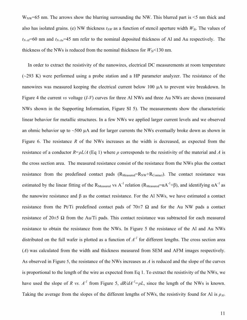
Figure 5. Resistance of Al (top) and Au (down) NWs distributed on the full wafer as a function of the
inverse of the area cross section (A-1) for different wire lengths. The resistance increases as the area
cross section decreases. The slope of the curves is also proportional to the length of the NWs.
Resistivities for Al: L=5 µm, ρ=11 µΩcm; L=2 µm, ρ=9.27 µΩcm; L=1 µm, ρ=11.3 µΩcm. Resistivities
for Au: L=4.6 µm, ρ=5.43 µΩcm; L=1.6 µm, ρ=5.02 µΩcm; L= 0.6 µm, ρ=5.03 µΩcm.
13
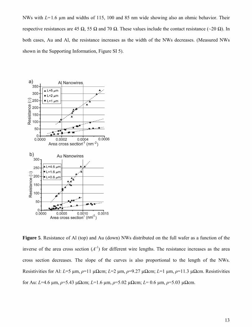
Figure 6. I vs V for Au and Al nanowires at large voltages (voltage ramp rate of 200 mV/sec) a) The
measured Au NW has dimensions WNW=100 nm, t=30 nm and L=1.6 µm. The Au NW starts to show a
non-linear behavior at a current density of J=7x10⁷ A/cm2 (I=2 mA) and it breaks down at a current
density of Jmax=1.5x10⁸ A/cm2 as observed from the drastic current drop at I=4.5 mA and V=0.8 V. In
the case of Al, the dimensions of the NW are WNW=65 nm, t= 28 nm and L= 2 µm. The non-linear
behavior starts at a J=5x10⁷ A/cm2 (I= 1 mA) and the breakdown of the wires is at Jmax= 1x10⁸ A/cm2 as
the current drastically drops at I=2 mA and V= 1.3 V. b) and c) Images of the Al and Au NWs after
breakdown
The resolution of stencil lithography is limited due to the inherent gap between stencil and substrate
during deposition. This gap produces two effects: first, the material coming from the source to the
substrate is deposited not only under the stencil aperture but also underneath the membrane as
illustrated in Figure 7; and second, once the material lands on the surface, due to surface diffusion, the
14
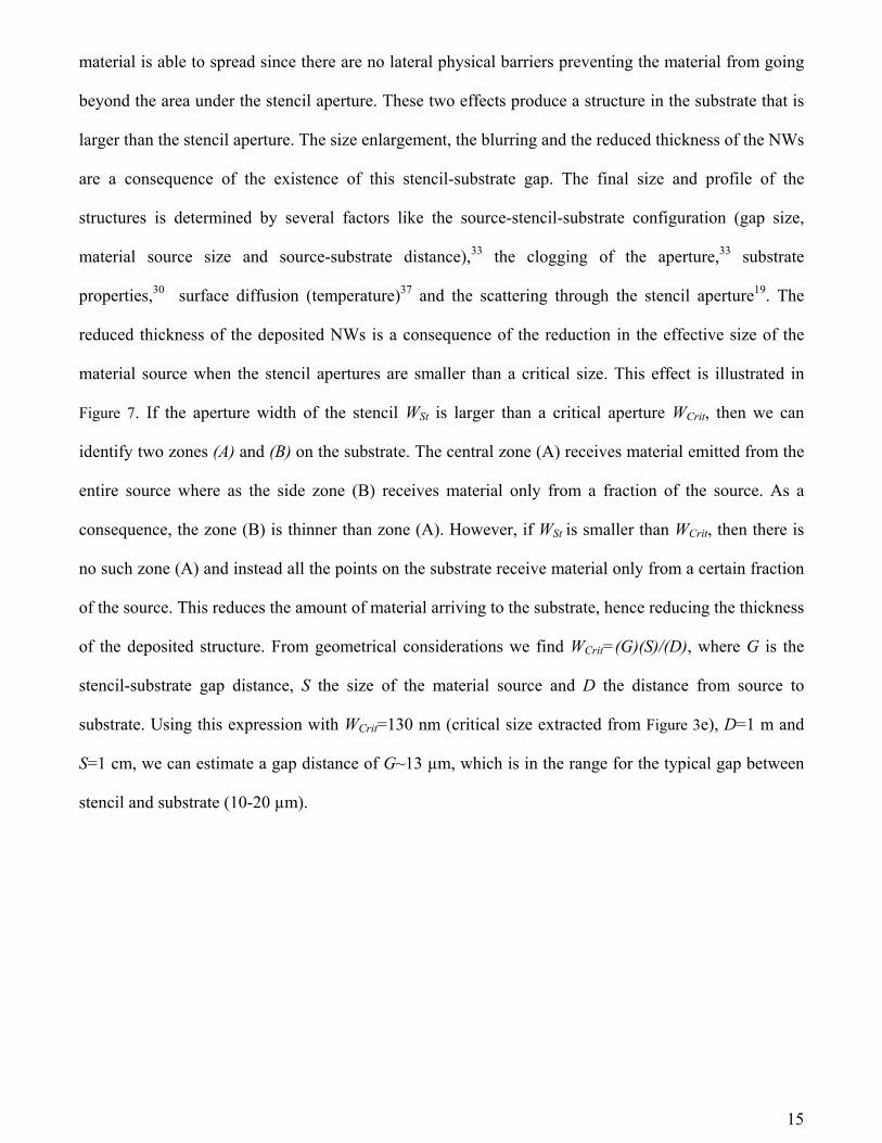
material is able to spread since there are no lateral physical barriers preventing the material from going
beyond the area under the stencil aperture. These two effects produce a structure in the substrate that is
larger than the stencil aperture. The size enlargement, the blurring and the reduced thickness of the NWs
are a consequence of the existence of this stencil-substrate gap. The final size and profile of the
structures is determined by several factors like the source-stencil-substrate configuration (gap size,
material source size and source-substrate distance),33 the clogging of the aperture,33 substrate
properties,30 surface diffusion (temperature)37 and the scattering through the stencil aperture19. The
reduced thickness of the deposited NWs is a consequence of the reduction in the effective size of the
material source when the stencil apertures are smaller than a critical size. This effect is illustrated in
Figure 7. If the aperture width of the stencil WSt is larger than a critical aperture WCrit, then we can
identify two zones (A) and (B) on the substrate. The central zone (A) receives material emitted from the
entire source where as the side zone (B) receives material only from a fraction of the source. As a
consequence, the zone (B) is thinner than zone (A). However, if WSt is smaller than WCrit, then there is
no such zone (A) and instead all the points on the substrate receive material only from a certain fraction
of the source. This reduces the amount of material arriving to the substrate, hence reducing the thickness
of the deposited structure. From geometrical considerations we find WCrit=(G)(S)/(D), where G is the
stencil-substrate gap distance, S the size of the material source and D the distance from source to
substrate. Using this expression with WCrit=130 nm (critical size extracted from Figure 3e), D=1 m and
S=1 cm, we can estimate a gap distance of G~13 µm, which is in the range for the typical gap between
stencil and substrate (10-20 µm).
15
Figure 7. Stencil aperture and effective source size. (a) For aperture widths WSt larger than a critical
width Wcrit, there is a zone (A) on the substrate under the aperture that receives material from the entire
source and there is a side zone (B) that receives material only from a fraction of the source so it is
thinner than zone (A). (b) For aperture widths WSt smaller than a critical aperture Wcrit, then there is not
such a zone (A) on the substrate receiving material from the entire source. All the points on the
substrate receive material only from a fraction of the source, reducing the source effective size. As
consequence, the structures are thinner since there is less material arriving to the substrate. From
geometrical considerations Wcrit=GS/D. (Image is not in scale and surface diffusion of material is not
illustrated)
The measured room-temperature resistivity of the NWs (ρAl-NW=10.5 µΩcm and ρAu-NW=5.16 µΩcm) is
larger than the reported bulk resistivity of Al and Au (ρAl-bulk=2.65 µΩcm and ρAu-bulk=2.21 µΩcm @ 293
K).38 It is known that the conductivity of metallic films and wires decreases when the size scales are
comparable to or smaller than the electron mean free path (Al~15 nm and Au~40 nm at room
temperature39) due mainly to two phenomena, 1) scattering at the surfaces40,41 and 2) scattering at grain
16
boundaries of conduction electrons.42 The effect of these factors on the electrical resistivity depends on
the degree of specularity of the scattering at the surface and on the electron reflectivity at the grain
boundaries of the nanowires. Comparing the resistivity of the NWs with the resistivity of the test thin
films and with the resistivity of the bulk, we found that for Al the NWs resistivity is only 1.3 times
larger than the Al test film (t=60 nm) resistivity but 3.9 times larger than Al bulk value. In the case of
Au NWs we found that ρAu-NW is 1.22 times larger than ρAu-t=45nm but 2.3 times larger than ρAu-bulk.
Similar results have been obtained previously by Durkan et al 43 for Au NW (ρAu=6 µΩcm) and by
Mayadas for Al thin films (ρAl=9.5 µΩcm).44 Given that the resistivities of the NWs are very close to the
film values compared to the bulk values, we can infer that the thickness of the NWs (Al:30-60 nm and
Au: 45-20) is the main factor increasing the resistivity of the NWs with respect to bulk values either by
surface or grain boundary scattering. However, it is interesting that in the size range of the NWs studied,
we did not observe a dependence of the resistivity on the cross section area (width or thickness) as
expected from size reduction of the NWs. This was also observed by Durkan et al for Au wires that
were not annealed as in our case.43,45 If this dependence exists, it might be too small to be detected in
our experimental conditions and dimensions. In our NWs we did not observe a change in grain size with
the width or thickness of the NWs either. Given that the electrical resistivity and the grain size do not
change with the size of the structures, this could be an indication that the resistivity of our NWs is
dominated by grain boundary scattering. This is also supported by the fact that the grain sizes were
smaller than the size of the NWs. Previous works reported that for thin films and NWs fabricated with
templates or lift-off, the grain size was roughly equal to the structure dimensions.43,46,47 In our case we
did not observe such relation and this could be related to the way structures are deposited in SL.
Compared to lift-off or template growth, during SL the material lands freely on the surface without any
lateral barrier restricting the spreading of the material or the growth of the structure. This probably
affects the geometry and grain structure of the deposited NWs and this would have an impact on the
electrical resistivity. We also observed that the increase in resistivity of NWs and films compared to
bulk values is larger for Al than for Au. This behavior could be due to a larger surface roughness and a
17
larger reflection at grain boundary scattering for Al than for Au. The difference in the growth, shape
and grain structure of NWs fabricated by SL compare to lift-off or template methods may offer new
information on the effect of the size and grain structure on the electrical conductivity of nanostructures.
(See Supporting Information, Figure SI 6, for a comparison of the resistivity of the NWs with Au and Al
thin films and Table SI 1 and 2, for estimations of the resistivity of the NWs due to surface and the grain
boundary scattering)
In conclusion, we have demonstrated the fabrication of metallic nanowires <100 nm on a full wafer
scale by stencil lithography without any resist processing. The nanowires are wider than the stencil
apertures by tens of nanometers and the thickness decreases as the width of the stencil apertures
decreases. The NWs fabricated by SL show an ohmic behavior, a higher than bulk resistivity and
maximum current density in the order of 108 A/cm2. This opens an alternative to fabricate NWs in other
in substrates that are not compatible with resist-based lithography. Since the NWs fabricated by SL do
not use any template, resist or etching during their deposition, they can offer new properties and insight
into the deposition and properties of metallic nanostructures.
Acknowledgment. This effort is sponsored by the Swiss Federal Office for Science and Education
(OFES) in the framework of the EC-funded FP6 project NaPa (NMP4-CT-2003-500120), the Swiss
National Science Foundation (Project IC-Nano, 200021-112291/1) and the EPFL-STI Seed Funding.
The authors are very grateful to the EPFL Centre of Micro-Nano-Technology (CMI) and its staff,
especially to Dr. Philippe Langlet and Guy Clerk for their effort implementing stencil lithography at
CMI. We are also grateful to Dr. Chan Woo Park and our colleagues at the Microsystems Laboratory for
their very valuable support and help.
Supporting Information Available. 100 mm diameter stencil wafers, stencil fabrication, corrugated
membranes; Au NWs thickness reduction; grain structure and roughness of NWs; Al and Au NWs from
I/V curves in Figure 2; Al and Au thin film resistivity; and an estimation of electrical resistivity of NWs
18
due to surface and grain boundary scattering. This material is available free of charge at via the Internet
at http://pubs.acs.org
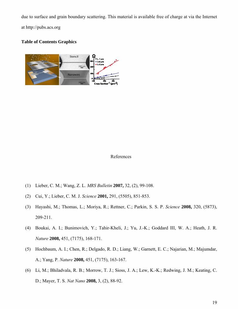
Table of Contents Graphics
References
(1) Lieber, C. M.; Wang, Z. L. MRS Bulletin 2007, 32, (2), 99-108.
(2) Cui, Y.; Lieber, C. M. J. Science 2001, 291, (5505), 851-853.
(3) Hayashi, M.; Thomas, L.; Moriya, R.; Rettner, C.; Parkin, S. S. P. Science 2008, 320, (5873),
209-211.
(4) Boukai, A. I.; Bunimovich, Y.; Tahir-Kheli, J.; Yu, J.-K.; Goddard III, W. A.; Heath, J. R.
Nature 2008, 451, (7175), 168-171.
(5) Hochbaum, A. I.; Chen, R.; Delgado, R. D.; Liang, W.; Garnett, E. C.; Najarian, M.; Majumdar,
A.; Yang, P. Nature 2008, 451, (7175), 163-167.
(6) Li, M.; Bhiladvala, R. B.; Morrow, T. J.; Sioss, J. A.; Lew, K.-K.; Redwing, J. M.; Keating, C.
D.; Mayer, T. S. Nat Nano 2008, 3, (2), 88-92.
19
(7) Wang, J.; Gudiksen, M. S.; Duan, X.; Cui, Y.; Lieber, C. M. Science 2001, 293, (5534), 1455-
1457.
(8) Wanekaya, A.; Chen, W.; Myung, N.; Mulchandani, A. Electroanalysis 2006, 18, (6), 533-550.
(9) Aravamudhan, S.; Kumar, A.; Mohapatra, S.; Bhansali, S. Biosensors and Bioelectronics 2007,
22, (9-10), 2289-2294.
(10) Huang, S.; Chen, Y. Nano Lett. 2008.
(11) McCord, M. A.; Rooks, M. J., Electron Beam Lithography. In SPIE Handbook of
Microlithography, Micromachining and Microfabrication Rai-Choudhury, P., Ed. SPIE: 1997;
Vol. 2.
(12) Reyntjens, S.; Puers, R. Journal of Micromechanics and Microengineering 2001, (4), 287.
(13) Silverman, P. J. Intel Technology Journal 2002, 06, (2), 55-61.
(14) Chou, S. Y.; Krauss, P. R.; Renstrom, P. J. Science 1996, 272, (5258), 85-87.
(15) Chou, S., Y.; Krauss, P., R.; Zhang, W.; Gou, L.; Zhuang, L. In Sub-10 nm imprint lithography
and applications, 1997; AVS: 1997; pp 2897-2904.
(16) Deshmukh, M. M.; Ralph, D. C.; Thomas, M.; Silcox, J. Applied Physics Letters 1999, 75, (11),
1631-1633.
(17) Villanueva, G.; Vazquez-Mena, O.; van den Boogaart, M. A. F.; Sidler, K.; Pataky, K.; Savu, V.;
Brugger, J. Microelectronic Engineering 2008, 85, (5-6), 1010-1014.
(18) Dumas, C.; Grisolia, J.; Ressier, L.; Arbouet, A.; Paillard, V.; Ben Assayag, G.; Claverie, A.;
van den Boogaart, M. A. F.; Brugger, J. physica status solidi (a) 2007, 204, (2), 487-491.
(19) Yan, X. M.; Contreras, A. M.; Koebel, M. M.; Liddle, J. A.; Somorjai, G. A. Nano Lett. 2005, 5,
(6), 1129-1134.
(20) Brugger, J.; Berenschot, J. W.; Kuiper, S.; Nijdam, W.; Otter, B.; Elwenspoek, M.
Microelectronic Engineering 2000, 53, (1-4), 403-405.
(21) Schlittler, R. R.; Seo, J. W.; Gimzewski, J. K.; Durkan, C.; Saifullah, M. S. M.; Welland, M. E.
Science 2001, 292, (5519), 1136-1139.
20
(22) Lee, J. W.; Ju, B. K.; Jang, J.; Yoon, Y. S.; Kim, J. K. Journal of Materials Science 2007, 42,
(3), 1026-1030.
(23) Cojocaru, C.-V.; Harnagea, C.; Rosei, F.; Pignolet, A.; van den Boogaart, M. A. F.; Brugger, J.
Applied Physics Letters 2005, 86, (18), 183107.
(24) Rodriguez, A. F.; Heyderman, L. J.; Nolting, F.; Hoffmann, A.; Pearson, J. E.; Doeswijk, L. M.;
Boogaart, M. A. F. v. d.; Brugger, J. Applied Physics Letters 2006, 89, (14), 142508.
(25) Speets, E. A.; Riele, P. T.; van den Boogaart, M. A. F.; Doeswijk, L. M.; Ravoo, B. J.; Rijnders,
G.; Brugger, J.; Reinhoudt, D. N.; Blank, D. H. A. Advanced Functional Materials 2006, 16,
(10), 1337-1342.
(26) Zhou, Y. X.; Johnson, A. T.; Hone, J.; Smith, W. F. Nano Lett. 2003, 3, (10), 1371-1374.
(27) Sidler, K.; Vazquez-Mena, O.; Savu, V.; Villanueva, G.; van den Boogaart, M. A. F.; Brugger, J.
Microelectronic Engineering 2008, 85, (5-6), 1108-1111.
(28) Arcamone, J.; van den Boogaart, M. A. F.; Serra-Graells, F.; Hansen, S.; Brugger, J.; Torres, F.;
Abadal, G.; Barniol, N.; Perez-Murano, F. 2006 International Electron Devices Meeting, Vols 1
and 2 2006, 250-253.
(29) Vázquez-Mena, O.; Villanueva, G.; van den Boogaart, M. A. F.; Savu, V.; Brugger, J.
Microelectronic Engineering 2008, 85, (5-6), 1237-1240.
(30) Tun, T. N.; Lwin, M.; Kim, A. H. H.; Chandrasekhar, A. N.; Joachim, C. Nanotechnology
2007, 18, (33), 335301.
(31) van den Boogaart, M. A. F.; Lishchynska, M.; Doeswijk, L. M.; Greer, J. C.; Brugger, J. Sensors
and Actuators A: Physical 2006, 130-131, 568-574.
(32) Kim, G. M.; van den Boogaart, M. A. F.; Brugger, J. Microelectronic Engineering 2003, 67-68,
609-614.
(33) Lishchynska, M.; Bourenkov, V.; van den Boogaart, M. A. F.; Doeswijk, L.; Brugger, J.; Greer,
J. C. Microelectronic Engineering 2007, 84, (1), 42-53.
21
22
(34) Horcas, I.; Fernandez, R.; Gomez-Rodriguez, J. M.; Colchero, J.; Gomez-Herrero, J.; Baro, A.
M. Review of Scientific Instruments 2007, 78, (1), 013705.
(35) Egger, S.; Ilie, A.; Fu, Y.; Chongsathien, J.; Kang, D.-J.; Welland, M. E. Nano Lett. 2005, 5, (1),
15-20.
(36) Kohler, J.; Albrecht, M.; Musil, C. R.; Bucher, E. Physica E: Low-dimensional Systems and
Nanostructures 1999, 4, (3), 196-200.
(37) Racz, Z.; Seabaugh, A. Journal of Vacuum Science & Technology B: Microelectronics and
Nanometer Structures 2007, 25, (3), 857-861.
(38) Lide, D., CRC Handbook of Chemistry and Physics. 87th
ed.; CRC Press: 2006.
(39) Ashcroft, N. W.; N. D. Mermin, Solid State Physics. Saunders College Publishing, U.S.A.: 1976.
(40) Fuchs, K. Proceedings of the Cambridge Philosophical Society 1938, 34, 100-108.
(41) Sondheimer, E. H. Advances in Physics 1952, 1, (1), 1 - 42.
(42) Mayadas, A. F.; Shatzkes, M. Physical Review B 1970, 1, (4), 1382-1389.
(43) Durkan, C.; Welland, M. E. Physical Review B 2000, 61, (20), 14215-14218.
(44) Mayadas, A. F. Journal of Applied Physics 1968, 39, (9), 4241-4245.
(45) Durkan, C.; Schneider, M. A.; Welland, M. E. Journal of Applied Physics 1999, 86, (3), 1280-
1286.
(46) Mayadas, A. F.; Feder, R.; Rosenberg, R. Journal of Vacuum Science and Technology 1969, 6,
(4), 690-693.
(47) Steinhögl, W.; Schindler, G.; Steinlesberger, G.; Engelhardt, M. Physical Review B 2002, 66,
(7), 075414.
Copyright © 2022 FDOKUMEN