Five-point stencil CNN for solving reaction-diffusion equations
Upload
khangminh22Category
view
1download
0
FROM ONE ENGINEER TO ANOTHER® 1
Indium Corporation Tech Paper
From One Engineer To Another® 1
Meeting Future Stencil Printing Challenges with Ultrafine Powder Solder PastesAuthored by: Ed Briggs, Indium Corporation
ED BRIGGS
Ed Briggs, Senior Technical Support Engineer, Indium Corporation, is an SMTA-certified engineer and has earned a Six Sigma Green Belt Certification from Dartmouth College for demonstrated proficiency in developing and executing design experiments to support continuous process improvement.
Email: [email protected] Full biography: www.indium.com/biographies
Form No. 98954 R0
AbstractThe explosive growth of personal electronic devices, such as mobile phones, tablets, and personal music devices, has driven the need for smaller and smaller active and passive electrical components. Not long ago, 0201 passives were seen as the ultimate in miniaturization, but now we have 01005 passives with rumors of even smaller sizes not far behind. For active components, array packages with 0.4mm pitch are virtually a requirement for enabling the many features in modern portable electronic devices. To meet the challenge of stencil printing smaller stencil apertures, there is an increased interest in using finer particle-sized solder pastes to improve transfer efficiency. The smaller particle size results in a large surface area-to-volume ratio that challenges the solder paste’s flux to effectively perform its fluxing and oxidation protection action. The potential resulting surface oxidation can lead to voiding, graping, head-in-pillow, and other defects.
The combination of higher lead-free process temperatures, smaller print deposits, and temperature restraints on electrical components have created several challenges. Two in particular include obtaining consistent volume in the printed solder paste deposit and minimizing the oxidation of the solder powder in the small deposit during reflow. Solder pastes comprised of finer particle solder powders may help with stencil printing, but the increased surface oxide associated with finer powders may also reduce the reflow process window. The focus of this paper is to provide a statistical comparison of the transfer efficiency of different solder powder particle sizes, specifically types 3, 4, 5, and 6, and to visually observe post reflow results in both optimal and harsh conditions.
IntroductionBack to the basics, or the fundamentals, is a term often heard in relation to sports teams when they lose sight of the basic foundations of playing the game. In the SMT process, this may not necessarily be due to losing sight of the basic
fundamentals, but because the “game” itself continues to evolve. As the trend toward miniaturization continues, a process that was successful in the past may suddenly present unacceptable results due to the decreasing size of the stencil apertures required to print
Indium Corporation Tech Paper
From One Engineer To Another® 2
ultrafine solder paste deposits. In an earlier paper titled “Process Guidelines to Ensure Optimal SMT Electronics Assembly,” Edward Briggs and Ron Lasky, SMTAI Toronto, May 2012, discussed solder paste storage and handling; process setup, including the importance of gasketing and registration; solder paste attributes; reflow processes; newer SMT technologies; and the data collection methods for characterizing the stencil printing process to meet this evolution. The focus of this paper is to single out one of those considerations—powder particle size (powder types) and its affect on the stencil printing process. In order to focus on particle sizes, many variables as possible were eliminated and the data analyzed using solder paste inspection equipment. A physical observation will also be made of the reflowed results. Finer powder particles can mean an increase in surface oxide and create challenges for reflow.
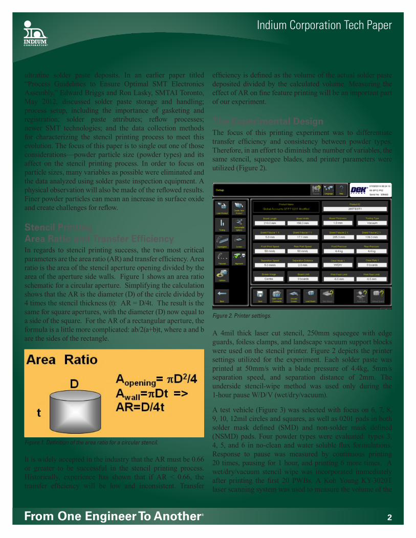
Stencil Printing Area Ratio and Transfer EfficiencyIn regards to stencil printing success, the two most critical parameters are the area ratio (AR) and transfer efficiency. Area ratio is the area of the stencil aperture opening divided by the area of the aperture side walls. Figure 1 shows an area ratio schematic for a circular aperture. Simplifying the calculation shows that the AR is the diameter (D) of the circle divided by 4 times the stencil thickness (t): AR = D/4t. The result is the same for square apertures, with the diameter (D) now equal to a side of the square. For the AR of a rectangular aperture, the formula is a little more complicated: ab/2(a+b)t, where a and b are the sides of the rectangle.
It is widely accepted in the industry that the AR must be 0.66 or greater to be successful in the stencil printing process. Historically, experience has shown that if AR < 0.66, the transfer efficiency will be low and inconsistent. Transfer
efficiency is defined as the volume of the actual solder paste deposited divided by the calculated volume. Measuring the effect of AR on fine feature printing will be an important part of our experiment.
The Experimental DesignThe focus of this printing experiment was to differentiate transfer efficiency and consistency between powder types. Therefore, in an effort to diminish the number of variables, the same stencil, squeegee blades, and printer parameters were utilized (Figure 2).
A 4mil thick laser cut stencil, 250mm squeegee with edge guards, foiless clamps, and landscape vacuum support blocks were used on the stencil printer. Figure 2 depicts the printer settings utilized for the experiment. Each solder paste was printed at 50mm/s with a blade pressure of 4.4kg, 5mm/s separation speed, and separation distance of 2mm. The underside stencil-wipe method was used only during the 1-hour pause W/D/V (wet/dry/vacuum).
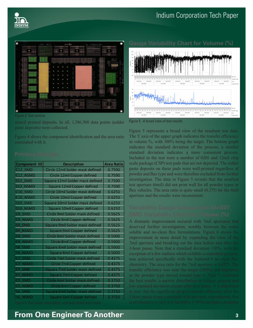
A test vehicle (Figure 3) was selected with focus on 6, 7, 8, 9, 10, 12mil circles and squares, as well as 0201 pads in both solder mask defined (SMD) and non-solder mask defined (NSMD) pads. Four powder types were evaluated: types 3, 4, 5, and 6 in no-clean and water soluble flux formulations. Response to pause was measured by continuous printing 20 times, pausing for 1 hour, and printing 6 more times. A wet/dry/vacuum stencil wipe was incorporated immediately after printing the first 20 PWBs. A Koh Young KY-3020T laser scanning system was used to measure the volume of the
Figure 1. Definition of the area ratio for a circular stencil.
Figure 2. Printer settings.
Indium Corporation Tech Paper
From One Engineer To Another® 3
stencil printed deposits. In all, 1,386,500 data points (solder paste deposits) were collected.
Figure 4 shows the component identification and the area ratio associated with it.
Printing Results
Gauge Variability Chart for Volume (%)
Figure 5 represents a broad view of the resultant test data. The Y axis of the upper graph indicates the transfer efficiency in volume %, with 100% being the target. The bottom graph indicates the standard deviation of the process; a smaller standard deviation indicates a more consistent process. Included in the test were a number of 0201 and 12mil chip scale package (CSP) test pads that are not depicted. The solder paste deposits on these pads were well-printed regardless of powder and flux type and were therefore excluded from further investigation. The data in Figure 5 reveals that the smallest test aperture (6mil) did not print well for all powder types or flux vehicles. The area ratio is quite small (0.375) for the 6mil aperture and the results were inconsistent.
Variability Gauge Component ID=S07_SMD Variability Chart for Volume (%)A dramatic improvement occured with 7mil apertures that deserved further investigation, notably between the water soluble and no-clean flux formulations. Figure 6 shows the improvement in more detail by expanding the view of the 7mil aperture and breaking out the data before and after the 1-hour pause. Note that a standard deviation <10%, with the exception of a few outliers which exhibits a controlled process, was achieved specifically with the Indium8.9 no-clean flux chemistry. The area ratio for the 7mil aperture is 0.4375. The transfer efficiency was near the target (100%) and improved as the powder type moved toward type 6. Type 5 exhibited the best results: a narrow distribution in volume percent and low standard deviation except after first pause. It is important to note that the significant drop in transfer efficiency after the 1-hour pause is not consistent with previous experiments; this is attributed to a very low humidity (<10%) and had a dramatic Figure 4. Pad labels, description, and associated area ratios.
Figure 3. Test vehicle.Figure 5. A broad view of test results.
Indium Corporation Tech Paper
From One Engineer To Another® 4
affect on the first print after sitting on the stencil for one hour, for all solder pastes tested.
Looking at the first chart in Figure 7, it can be seen that the mean transfer efficiency favors the no-clean flux. The water soluble flux in the Indium6.4 solder paste was more erratic, giving more insufficient, as well as excessive, solder paste deposits.
The second chart reveals that most of this inconsistency occurs with the 6mil aperture. This result is consistent with previous experience. The rosin/resin bases found in most no-clean fluxes increase the material’s tacky properties (adhesive and cohesive attractions) of the solder pastes. When releasing from the stencil aperture, adhesion of the solder paste to the PCB pad helps pull the paste from the stencil aperture as the PCB is lowered from the stencil. This is especially true for the smaller pads, as there is very little surface area for the paste deposit to “cling” to. The cohesive forces or attraction of the flux-coated powder particles to one another are also increased. These cohesive forces help the paste release from the stencil walls and retain shape of the stencil aperture after printing.
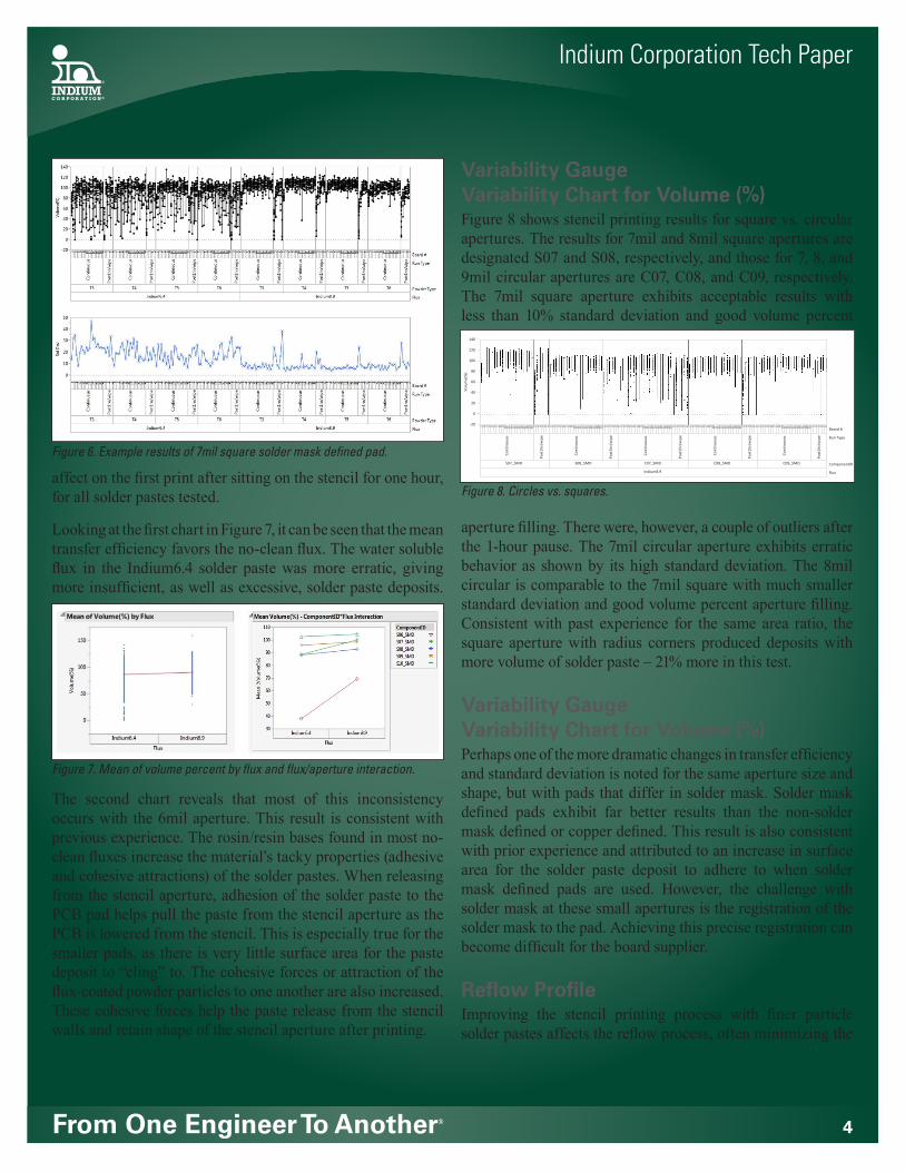
Variability Gauge Variability Chart for Volume (%)Figure 8 shows stencil printing results for square vs. circular apertures. The results for 7mil and 8mil square apertures are designated S07 and S08, respectively, and those for 7, 8, and 9mil circular apertures are C07, C08, and C09, respectively. The 7mil square aperture exhibits acceptable results with less than 10% standard deviation and good volume percent
aperture filling. There were, however, a couple of outliers after the 1-hour pause. The 7mil circular aperture exhibits erratic behavior as shown by its high standard deviation. The 8mil circular is comparable to the 7mil square with much smaller standard deviation and good volume percent aperture filling. Consistent with past experience for the same area ratio, the square aperture with radius corners produced deposits with more volume of solder paste – 21% more in this test.
Variability Gauge Variability Chart for Volume (%)Perhaps one of the more dramatic changes in transfer efficiency and standard deviation is noted for the same aperture size and shape, but with pads that differ in solder mask. Solder mask defined pads exhibit far better results than the non-solder mask defined or copper defined. This result is also consistent with prior experience and attributed to an increase in surface area for the solder paste deposit to adhere to when solder mask defined pads are used. However, the challenge with solder mask at these small apertures is the registration of the solder mask to the pad. Achieving this precise registration can become difficult for the board supplier.
Reflow ProfileImproving the stencil printing process with finer particle solder pastes affects the reflow process, often minimizing the
Figure 8. Circles vs. squares.
Figure 6. Example results of 7mil square solder mask defined pad.
Figure 7. Mean of volume percent by flux and flux/aperture interaction.
Indium Corporation Tech Paper
From One Engineer To Another® 5
reflow process window for acceptable results. As the particle size decreases, the total surface area for the same volume of solder paste increases. This increase in total surface area also means an increase in total surface oxide and increases the demand on the flux to remove them.
The demand on the flux is further challenged as the reason for selecting a finer particle solder paste to print into a smaller stencil aperture, resulting in a smaller paste deposit. Figure 10 illustrates the relationship of increased surface area to available flux as the paste deposit decreases. Note that the ratio of flux available to the surface area decreases as aperture width decreases. This situation will result in less available flux to protect against surface oxidation when aperture widths are small.
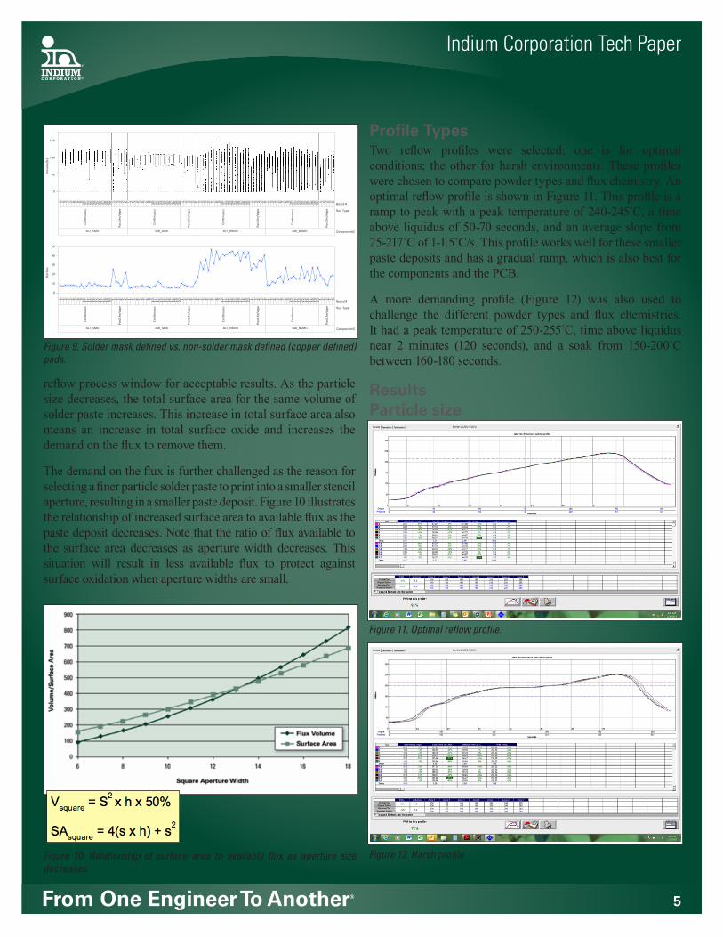
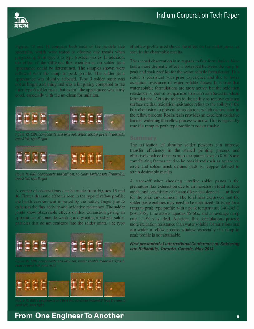
Profile TypesTwo reflow profiles were selected: one is for optimal conditions; the other for harsh environments. These profiles were chosen to compare powder types and flux chemistry. An optimal reflow profile is shown in Figure 11. This profile is a ramp to peak with a peak temperature of 240-245˚C, a time above liquidus of 50-70 seconds, and an average slope from 25-217˚C of 1-1.5˚C/s. This profile works well for these smaller paste deposits and has a gradual ramp, which is also best for the components and the PCB.
A more demanding profile (Figure 12) was also used to challenge the different powder types and flux chemistries. It had a peak temperature of 250-255˚C, time above liquidus near 2 minutes (120 seconds), and a soak from 150-200˚C between 160-180 seconds.
Results Particle size
Figure 9. Solder mask defined vs. non-solder mask defined (copper defined) pads.
Figure 10. Relationship of surface area to available flux as aperture size decreases.
Figure 11. Optimal reflow profile.
Figure 12. Harsh profile.
Indium Corporation Tech Paper
From One Engineer To Another® 6
Figures 13 and 14 compare both ends of the particle size spectrum, which were tested to observe any trends when progressing from type 3 to type 6 solder pastes. In addition, the effect of the different flux chemistries on solder joint appearance could be determined. The samples shown were reflowed with the ramp to peak profile. The solder joint appearance was slightly affected. Type 3 solder paste was not as bright and shiny and was a bit grainy compared to the finer type 6 solder paste, but overall the appearance was fairly good, especially with the no-clean formulation.
A couple of observations can be made from Figures 15 and 16. First, a dramatic effect is seen in the type of reflow profile; the harsh environment imposed by the hotter, longer profile exhausts the flux activity and oxidative resistance. The solder joints show observable effects of flux exhaustion giving an appearance of some de-wetting and graping (oxidized solder particles that do not coalesce into the solder joint). The type
of reflow profile used shows the effect on the solder joints, as seen in the observable results.
The second observation is in regards to flux formulation. Note that a more dramatic effect is observed between the ramp to peak and soak profiles for the water soluble formulation. This result is consistent with prior experience and due to lower oxidation resistance of water soluble fluxes. It is true that water soluble formulations are more active, but the oxidation resistance is poor in comparison to rosin/resin based no-clean formulations. Activity refers to the ability to remove existing surface oxides; oxidation resistance refers to the ability of the flux chemistry to prevent re-oxidation, which occurs later in the reflow process. Rosin/resin provides an excellent oxidative barrier, widening the reflow process window. This is especially true if a ramp to peak type profile is not attainable.
SummaryThe utilization of ultrafine solder powders can improve transfer efficiency in the stencil printing process and effectively reduce the area ratio acceptance level to 0.50. Some contributing factors need to be considered such as square vs. circle and solder mask defined pads vs. copper defined to attain desireable results.
A trade-off when choosing ultrafine solder pastes is the premature flux exhaustion due to an increase in total surface oxide, and sensitivity of the smaller paste deposit — utilized for the oven environment. The total heat excursion that the solder paste endures may need to be optimized. Striving for a ramp to peak type profile with a peak temperature 240-245˚C (SAC305), time above liquidus 45-60s, and an average ramp rate 1-1.5˚C/s is ideal. No-clean flux formulations provide more oxidation resistance than water soluble formulations and can widen a reflow process window, especially if a ramp to peak profile is not attainable.
First presented at International Conference on Soldering and Reliability, Toronto, Canada, May 2014.
Figure 13. 0201 components and 6mil dot, water soluble paste (Indium6.4): type 3 left, type 6 right.
Figure 14. 0201 components and 6mil dot, no-clean solder paste (Indium8.9): type 3 left, type 6 right.
Figure 15. 0201 components and 6mil dot, water soluble Indium6.4 Type 6: ramp to peak left, soak right.
Figure 16. 0201 components and 6mil dot, no-clean Indium8.9 Type 6: ramp to peak left, soak right.
Copyright © 2022 FDOKUMEN