Optimization and Performance Modeling of Stencil Computations on Modern Microprocessors
Upload
independentCategory
view
4download
0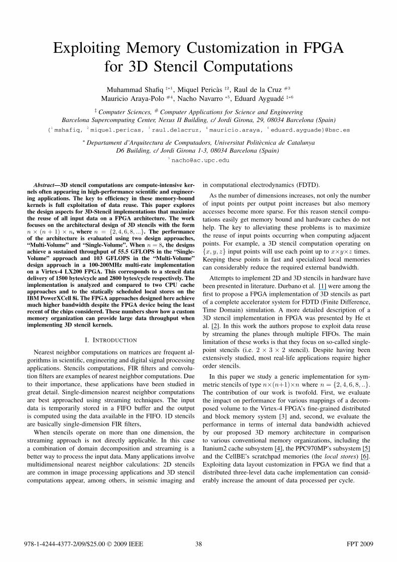
Exploiting Memory Customization in FPGAfor 3D Stencil ComputationsMuhammad Shafiq ‡∗1, Miquel Pericas ‡2, Raul de la Cruz #3
Mauricio Araya-Polo #4, Nacho Navarro ∗5, Eduard Ayguade ‡∗6
‡ Computer Sciences, # Computer Applications for Science and EngineeringBarcelona Supercomputing Center, Nexus II Building, c/ Jordi Girona, 29, 08034 Barcelona (Spain)
∗ Departament d’Arquitectura de Computadors, Universitat Politecnica de CatalunyaD6 Building, c/ Jordi Girona 1-3, 08034 Barcelona (Spain)
Abstract—3D stencil computations are compute-intensive ker-nels often appearing in high-performance scientific and engineer-ing applications. The key to efficiency in these memory-boundkernels is full exploitation of data reuse. This paper exploresthe design aspects for 3D-Stencil implementations that maximizethe reuse of all input data on a FPGA architecture. The workfocuses on the architectural design of 3D stencils with the formn × (n + 1) × n, where n = {2, 4, 6, 8, ...}. The performanceof the architecture is evaluated using two design approaches,“Multi-Volume” and “Single-Volume”. When n = 8, the designsachieve a sustained throughput of 55.5 GFLOPS in the “Single-Volume” approach and 103 GFLOPS in the “Multi-Volume”design approach in a 100-200MHz multi-rate implementationon a Virtex-4 LX200 FPGA. This corresponds to a stencil datadelivery of 1500 bytes/cycle and 2800 bytes/cycle respectively. Theimplementation is analyzed and compared to two CPU cacheapproaches and to the statically scheduled local stores on theIBM PowerXCell 8i. The FPGA approaches designed here achievemuch higher bandwidth despite the FPGA device being the leastrecent of the chips considered. These numbers show how a custommemory organization can provide large data throughput whenimplementing 3D stencil kernels.
I. INTRODUCTION
Nearest neighbor computations on matrices are frequent al-gorithms in scientific, engineering and digital signal processingapplications. Stencils computations, FIR filters and convolu-tion filters are examples of nearest neighbor computations. Dueto their importance, these applications have been studied ingreat detail. Single-dimension nearest neighbor computationsare best approached using streaming techniques. The inputdata is temporarily stored in a FIFO buffer and the outputis computed using the data available in the FIFO. 1D stencilsare basically single-dimension FIR filters,
When stencils operate on more than one dimension, thestreaming approach is not directly applicable. In this casea combination of domain decomposition and streaming is abetter way to process the input data. Many applications involvemultidimensional nearest neighbor calculations: 2D stencilsare common in image processing applications and 3D stencilcomputations appear, among others, in seismic imaging and
in computational electrodynamics (FDTD).
As the number of dimensions increases, not only the numberof input points per output point increases but also memoryaccesses become more sparse. For this reason stencil compu-tations easily get memory bound and hardware caches do nothelp. The key to alleviating these problems is to maximizethe reuse of input points occurring when computing adjacentpoints. For example, a 3D stencil computation operating on{x, y, z} input points will use each point up to x×y×z times.Keeping these points in fast and specialized local memoriescan considerably reduce the required external bandwidth.
Attempts to implement 2D and 3D stencils in hardware havebeen presented in literature. Durbano et al. [1] were among thefirst to propose a FPGA implementation of 3D stencils as partof a complete accelerator system for FDTD (Finite Difference,Time Domain) simulation. A more detailed description of a3D stencil implementation in FPGA was presented by He etal. [2]. In this work the authors propose to exploit data reuseby streaming the planes through multiple FIFOs. The mainlimitation of these works is that they focus on so-called single-point stencils (i.e. 2 × 3 × 2 stencil). Despite having beenextensively studied, most real-life applications require higherorder stencils.
In this paper we study a generic implementation for sym-metric stencils of type n×(n+1)×n where n = {2, 4, 6, 8, ..}.The contribution of our work is twofold. First, we evaluatethe impact on performance for various mappings of a decom-posed volume to the Virtex-4 FPGA’s fine-grained distributedand block memory system [3] and, second, we evaluate theperformance in terms of internal data bandwidth achievedby our proposed 3D memory architecture in comparisonto various conventional memory organizations, including theItanium2 cache subsystem [4], the PPC970MP’s subsystem [5]and the CellBE’s scratchpad memories (the local stores) [6].Exploiting data layout customization in FPGA we find that adistributed three-level data cache implementation can consid-erably increase the amount of data processed per cycle.
{1 mshafiq, 2 miquel.pericas, 3 raul.delacruz, 4 mauricio.araya, 6 eduard.ayguade}@bsc.es
978-1-4244-4377-2/09/$25.00 © 2009 IEEE FPT 200938
II. 3D STENCIL COMPUTATIONS
Stencils are used in numerous scientific applications like,computational fluid dynamics, geometric modeling, electro-magnetics, diffusion and image processing. These applicationsare often implemented using iterative finite-difference tech-niques that sweep over a 2D or 3D grid, while performingcomputations called stencil on the nearest neighbors of thecurrent point in the grid. In a stencil operation, each point in amultidimensional grid is updated with weighted contributionsfrom a subset of its neighbors in both time and space.
In a 3D stencil, each point’s computation needs to accessdata from the three axis of a volume as shown in Figure 1.Therefore, the 3D stencil computation increases the complex-ity not only by increasing 3 times the number of computationsbut also due to the sparse data access pattern arising from avolume linearly laid out in memory.
Fig. 1. 3D stencil inscribed in dataset along with its memory access pattern(a), and 8-point stencil diagram (b).
In this paper we focus on two design approaches for 3D-Stencil computation cores to compute symmetric stencils withdimensions {n × (n + 1) × n} with n: 2, 4, 6, 8,... In ourexperiments we evaluate up to n = 8. Our first approachis based on a “Multi-Volume” design which intends to usemaximum possible number of modules for the same stencilalthough by compromising the base volume size. Variousbase volume sizes, as shown in Table I, have been used forperformance evaluation. The base volume sizes used in the“Single-Volume” approach are shown in Table II. Out of the336 18Kb BRAM blocks present in the Virtex-4 LX200, 320blocks were reserved for storing volume data. The rest ofBRAM blocks were used to meet the internal requirements(e.g. FIFOs) of the design.
In both cases the base volume sizes (Xdim, Zdim and Ydim)as shown in the corresponding tables represent the {x, z}dimensions while the third dimension {y} can be streamed intothe core for any number of planes (n + 1 −→∞). In order toevaluate performance overheads for different decompositionsin these cases, we have used a main input volume withdimensions 4096×2048×8192. This volume has been selectedto keep it evenly decomposable for most of the cases in Tables
Decomp. #ID A:2× 3× 2 B:4× 5× 4 C:6× 7× 6 D:8× 9× 8
1 32× 256 32× 256 16× 256 16× 2562 16× 512 16× 512 8× 512 NA3 8× 1024 8× 1024 NA NA4 4× 2048 NA NA NABRAM 276 276 256 320BLOCKS
TABLE IDIMENSIONS (XDIM,ZDIM,YDIM=∞) FOR VARIOUS VOLUME
DECOMPOSITIONS AND THEIR BLOCKRAM CONSUMPTION IN THEMULTI-VOLUME DESIGN APPROACH. TOTAL DATA MODULES: 3 (FOR
N=2), 2 (FOR N=4,6,8). NA = NO MORE DECOMPOSITIONS POSSIBLE FORTHIS STENCIL.
Decomp. #ID E:2× 3× 2 F:4× 5× 4 G:6× 7× 6 H:8× 9× 8
1 160× 256 96× 256 64× 256 48× 2562 40× 1024 32× 768 32× 512 24× 5123 20× 2048 16× 1536 16× 1024 16× 7684 10× 4096 6× 4096 8× 2048 12× 1024BRAM 320 306 296 300BLOCKS
TABLE IIDIMENSIONS (XDIM,ZDIM,YDIM=∞) FOR VARIOUS VOLUME
DECOMPOSITIONS AND THEIR BLOCKRAM CONSUMPTION IN THESINGLE-VOLUME DESIGN APPROACH. TOTAL DATA MODULES: 1
I and II.On the other hand, in order to compare the performance with
other implementations (Itanium2, PowerPC970 and Cell/B.E.),we have used stencil for n=8 and the input volume is takenfrom an implementation of a reverse-time migration kernel [7]which makes intensive use of the same stencil (8× 9× 8) tosolve the partial differential wave equation.
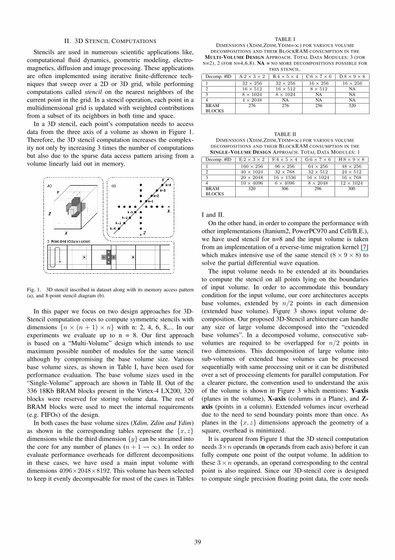
The input volume needs to be extended at its boundariesto compute the stencil on all points lying on the boundariesof input volume. In order to accommodate this boundarycondition for the input volume, our core architectures acceptsbase volumes, extended by n/2 points in each dimension(extended base volume). Figure 3 shows input volume de-composition. Our proposed 3D-Stencil architecture can handleany size of large volume decomposed into the “extendedbase volumes”. In a decomposed volume, consecutive sub-volumes are required to be overlapped for n/2 points intwo dimensions. This decomposition of large volume intosub-volumes of extended base volumes can be processedsequentially with same processing unit or it can be distributedover a set of processing elements for parallel computation. Fora clearer picture, the convention used to understand the axisof the volume is shown in Figure 3 which mentions: Y-axis(planes in the volume), X-axis (columns in a Plane), and Z-axis (points in a column). Extended volumes incur overheaddue to the need to send boundary points more than once. Asplanes in the {x, z} dimensions approach the geometry of asquare, overhead is minimized.
It is apparent from Figure 1 that the 3D stencil computationneeds 3×n operands (n operands from each axis) before it canfully compute one point of the output volume. In addition tothese 3×n operands, an operand corresponding to the centralpoint is also required. Since our 3D-stencil core is designedto compute single precision floating point data, the core needs
39

(3×n+1)×4 bytes for each computed point. Besides this largedata requirement, it needs 3×n/2+1 multiplications and 3×naddition operations for computing one output point.
Since stencil computations sweep on consecutive neighbor-ing points in all directions, with a specific arrangement anextensive data reuse is possible. In our case, an exclusivelyaccessible arrangement of data for n + 1 consecutive planescorresponding to Y-axis makes it feasible to get all operandsneeded from Y-axis and as well as for other two axis. Thus,an architecture with specialized data layout can be designedwhich makes available all required operands from X-axis andZ-axis by utilizing previously fetched data from Y-axis tocompute a single point. Such architecture can sustain theavailability of all input operands to compute a point justby fetching only one new operand from Y-axis rather thanfetching {3 × n + 1} operands from three axis. This meansthat the architecture for specialized data layout would givea (3 × n + 1)-fold increase in data bandwidth at the inputof Back-End compared to the input bandwidth of the dataFront End. However, the practically achievable external–to–core bandwidth normally remains one of the major factorsthat limit the scaling of the core architecture.
III. 3D MEMORY ORGANIZATIONS FOR STENCILCOMPUTATIONS IN RECONFIGURABLE LOGIC
In this section we present a generalized data engine foralgorithms based on 3D stencils. The 3D-Stencil core designsare based on three main modules: the Front-End, the Back-End and the Controller. The architecture of every modulecan be scaled according to the available external–to–coredata bandwidth and on-chip resources of FPGA device. Ourconfiguration of the core is based on Virtex-4 FPGA deviceXC4VLX200-10. The FPGA is present in an SGI RASCRC100 board part of an SGI Altix 4700. In this configurationthe FPGAs can achieve a maximum external data bandwidthof 3.2GBytes/Sec/Direction when using streaming DMA. TheFPGA designs have been developed in Verilog. Xilinx ISEversion 9.2 has been used to generate the hardware implemen-tations. A simplified view of the core environment is shown inFigure 2. Next we will elaborate on the structure and workingprinciples of each module in the 3D-Stencil core.
A. Front-End (Data-Engine)
The Role of Front-End in 3D stencil core can be seenas a specialized data cache backing an arithmetic logicunit. The Front-End can consist of multiple Data Engines(“Multi-Volume Design” approach) or of a single Data Engine(“Single-Volume” approach).
The Data Engine is a basic building block of the Front-End. It consists of multiple sub-modules. These sub-modulesinclude an external memory interface (Streaming DMA inour case), three levels of internal memory hierarchy, circularwrite control and circular read control for each level ofmemory. Along with management of three memory levels, thearchitecture offers independent reads and writes at each level.This capability is achieved by using dual ported block RAMs.
HostSystem
Front-End (100Mhz)
Back-End (200Mhz)
CONTROLLER
Multi-Rate Interface
FIFO(Sub Volume-2)
FIFO(Sub-Volume-1)
FIFO(Sub Volume-3)
FIFO(Sub-Volume-1 )
Data Engine
2
Data Engine
(1)
Data Engine
3
Compute Engine
2
ComputeEngine
3
FIFO(Sub-Volume-3 )
FIFO(Sub-Volume-2 )
Data Flow
Compute Engine
(1)
Fig. 2. 3D-Stencil Core and Interfaces
In other words, the Data-Engine, besides Streaming interface,consists of a specialized 3D memory layout and 3D writeand read control corresponding to the three dimensions of theinput volume. The Data-Engine’s internal structure, consistingof three memory layers (Y-layer, X-Layer and Z-Layer), isshown in Figure 4. To exactly understand the functionalityof Data-Engine, it is important to correctly understand thepattern of data required to compute output points as describedin section II.
Extendedx-axis
y-ax
is∞
Ext
end
ed
z-a
xis
Plane (Y+3)
Plane (Y+2)
Plane (Y+1)
Plane (Yth)
Column in a Plane
Point in a Column
Partitioned Volume
Extended Base Volume
Planes, Columns & points
x-axis Z-a
xis
Fig. 3. Extended base volume, Partitioned volume and Axis convention
In Figure 4, next to the “STREAM Read Controller” we cansee the first layer of memory, representing Planes correspond-ing to the Y-axis of the volume (therefore named Y-layer). Thisfirst layer in the Data-Engine’s memory hierarchy consists of256bit×Xdim sized n+2 dual ported block RAM. Here thevalue “Xdim” corresponds to the dimensions (Xdim, Zdim,Ydim) given in Tables I and II. The architecture keeps oneextra plane thus the total number of planes managed is n+2.This additional (n+2)th plane is used for exclusively writingthe data using both of its ports and at the same time it is
40

possible to read all the other n+1 planes from their two ports.This means that at any time one plane would be working ina dual write address mode for both of its ports and all otherplanes would be in a dual read address mode at the same time.Our architecture logically splits each plane in two halves asshown in Figure 4. The two address pointers Pr0 (plane readpointer for lower half) and Pr1 (plane read pointer for upperhalf). This technique of exploiting both ports of BRAM forreading effectively doubles the throughput of the Data-Engineat the cost of maintaining one extra plane inside FPGA usingfew more BRAMs.
All n+1 planes in Y-Layer are sequentially writable at thetime in turn when a plane’s status becomes n+2. Other n+1planes are possible to read in parallel. This means that onewrite to Y-layer is of 256bit×2 where factor 2 corresponds todual port write. A read from this layer is possible for 256bit×2 × (n + 1) where again factor 2 represents the dual portread. The read side inherits a minimum latency of one clockcycle. The second layer of memory is labeled as Column andcorresponds to X-axis of input volume (named X-Layer) Thislayer has exactly the same features as that of Y-layer exceptthat its size is 256bit×Zdim×n + 2 where Zdim correspondsto the dimensions given in Tables I and II. Both X-layer andY-layer memories are created by using internal Block RAMsof the FPGA. The third memory layer corresponds to Z-axis(Z-layer) and it is based on FPGA distributed RAM. Its totalsize is 1536bits.
B. Working Principle of the Data-Engine
At host interface, input and output volume(s) are streamedinto FIFOs of the 3D-Stencil core. In order to synchronize theoperation of the Data-Engine(s) with stalls in the input/outputstream, each FIFO maintains an upper bound and lower boundto activate and stall all the data management sequences of theEngine. The Compute-Engines in Back-End, however, alwayscontinues working if any data is available in its pipelines.
As soon as a FIFO crosses the upper bound limit, the cor-responding Data-Engine starts working. The Stream InterfaceController prefetches this data from the extended base volumeinto the Y-layer. As soon as last plane (Y+ n/2+1) in Y-layerstarts to fill, an overlapped prefetch operation is started jointlyby the circular read controller (Planes) and circular writecontroller (Column) to fill the X-layer from the Yth plane.The prefetch sequence is ended by the circular write controller(Points) after filling the Z-layer by fetching data from theXth column. The prefetch operation is instantly followed bysimultaneous reading of X,Y,Z-operands (see Xopr, Yopr, Zoprin Figure 4) and by forwarding these operands to the Back-Endthrough a multi-rate interface (Figure 2).
The prefetch operation is required at the start of everyextended base volume. After prefetch phase, computations areoverlapped with data fetched from the FIFO’s to Y-layer, Ythplane to X-layer and Xth column to Z-layer. If the FIFOs toucha lower bound, the Data-Engine stalls until the upper bound isagain reached. Writing and reading each layer continues in around circle at its both ends. The circular write is quite simple.
Compute – Engine (s)
Circular Write Controller (Columns)
Y-1 Y Y+1 Y+n/2+1
CPopr ( 32bit x 16) Zopr ( nx32bit x 16)
STREAM Read Controller
STREAMIN
Circular Read Controller (Planes) Yopr ( nx32bit x 16)
Circular Read Controller (Columns) Xopr ( nx32bit x 16)
Circular Write/Read Controller (Points)
Circular Write Controller (Planes)
Registers
Y-Layern+2 Planes
X-Layern+2 Columns
NextPlane
PreviousPlane
Y-n/2
X-1 X X+1 X+n/2+1Next
ColumnPreviousColumn
X-n/2
Z-Layern+16 Points
Pr1
Pr0
Cr1
Cr0
Fig. 4. Architecture of Data-Engine : Implementing three memory levels(Y-Layer, X-Layer, Z-Layer). “Pr0/Cr0” and “Pr1/Cr1“ are the plane/Columnread pointers for lower and upper halves respectively at Y-Layer and X-Layer
For example, when finishing writing to Y+n/2+1 plane the twowriting pointers for lower and upper half of the plane are takento the Y-n/2 plane. On write completion to Y-n/2 the pointersare taken to Y-n/2+1 and so on. The same processes are validfor the other two layers. On the reading side, these layersare accessed such that all planes, all columns and all pointscorresponding to the three layers are read simultaneously inthe same clock cycle. As soon as any layer is read to its top,all pointers to its units (plane or column) are shifted by one.For example in the case of the X-layer, the two read pointersfor the X+n/2 column will become X+n/2-1 and the pointersfor the X-n/2 will become X+n/2+1 and so on. It is same forthe Y-layer but a little different in Z-layer, where data, ratherthan pointers, is shifted.
The prefetching phase ends while starting a write to the lastplane (Y+n/2+1). After this prefetch phase, writing to a layeris automatically followed by the read cycles because writeoperations, which now are overlapping computations, are stillcontinued to fill up to the last plane. This phase differenceis important for correct data read otherwise an over-write ofdata is possible after an arbitrary time even due to a minormismatch in read and write rate. This difference in write andread rate is possible because of some regular stalls on theread side. These stalls occur at plane and column boundaries.Data from central (Yth) plane is forwarded to X-layer but assoon as this plane has finished sending data to X-Layer, theplane pointer is shifted by one, i.e. Y+1 plane is now Ythplane therefore it is necessary that all data present in X-layermust be fetched from the new layer. The same case is truefor the Xth column to the Z-layer. Therefore a latency of n×Zdim/(256×2) cycles occurs after each shift of read pointersin the Y-layer and a latency of n/2 cycles occurs at each shift
41

P0, P1P2, P3
P4, P5P6, P7P22, P23Cp, C12
FIFO
ComputedPoint
C0C1C2C3C11
P20, P21
C10
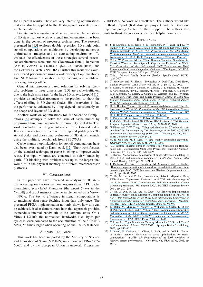
Fig. 5. Architecture of Compute-Engine in the Back-End for n=8 stenciltype. C(0) to C(12) are the constant coefficient multipliers of the stencil. P0to p23 and Cp are the input data operands coming from Front-Engine
of read pointers to the X-layer.The Data-Engine uses between 75% to 95% of the Block
RAMs and from 14% to 63% slices on Virtex-4 LX200device, depending on the design approach used, stencil sizeand selected decomposition dimensions.
C. Back-End (Compute-Engine)
This module of the 3D-Stencil core also scales based on thedesign approach (Multi-Volume or Single-Volume) used forthe Front-End therefore the Back-End is normally based onmultiple instantiations of a Compute-Engine. Each Compute-Engine outputs values at the rate of 1 result/cycle
The Compute-Engine works at 200MHz (Figure 2) whichis twice the operating frequency of Data-Engine. As shown inFigure 4, the Data-Engine can arrange operands (Yopr, Xopr,Zopr, CP) for computing 16 points in parallel. These operandsare forwarded to the Compute-Engines in the Back-End. Amulti-rate data interface takes care of transacting the data(operands and results) between the Front-End and Back-Endin a correct way. The computation requirement of 16 pointsper cycle, posed by the Data-Engine needs a Back-End with 8Compute-Engines working in parallel at twice the rate of theFront-End.
Each of the Compute-Engine in Back-End takes 3× n + 1variable operands mentioned as “Pn and Cp” correspondingto “Yopr, Xopr, Zopr and CPopr”. It also takes a numberof constant coefficients mentioned as “Cn”. Each Compute-Engine implements a binary tree for computing output asshown in Figure 5. A small FIFO is also implemented toaccommodate the latency for the odd operand before it isadded in the binary tree. A summary of sustained performancefor the FPGA implementation of the 3D memory organizationwith 8× 9× 8 stencil is shown in table III.
D. Control-Engine
This module is responsible for synchronizing the data flowin whole architecture. It takes care of synchronizing the HostInterface, the Data-Engine and the Compute-Engines. As men-tioned in subsection III-A, the 3D data layout is forced to stallat certain positions during the execution, therefore the Back-End is responsible of managing the effects of these stalls. TheControl-Engine, in fact, integrates all stalls to a single majorstall at plane boundaries so that Stream Interface Controllercan transfer data to the upper bound of input FIFO(s).
E. Performance
Figure 6 shows the internal data throughput of the differentstencil implementations as a function of the number of planesin Y -direction. As can be seen, a small number of frames hasa large impact on performance. Among the “Multi-VolumeDesign” implementations, D1 achieves the highest throughputat 280 GB/s. Among the ”Single-Volume” designs the bestconfiguration is H4, which obtains 150 GBytes / second. Thefigure also shows the ratios between internal and externalbandwidths. In this figure, higher bars indicate better usageof external bandwidth (i.e., less overhead due to extendedvolumes).
Table IV presents an evaluation of the efficiency (measuredas throughput per slice) of the different stencil approaches. Thenumbers are for the best performing volume decomposition.As expected Single-Volume designs are somewhat more effi-cient than the Multi-Volume designs (6%-14%). The differenceincreases with higher order stencils.
IV. 3D STENCIL IMPLEMENTATIONS AND ANALYSIS
A. Homogeneous Processors: Itanium2 and PowerPC970
The two main problems for the implementation of stencilson homogeneous processors are the access pattern and thelow computation/access ratio. In the following paragraphs, wefocus on the access problem.
As can be seen from Figure 1 the direction Z is the onlyconsecutive in memory, then accesses to memory for the otherdirections are very expensive, in terms of L2/L3 cache misses.This forces us to be careful with the way the data is placedand accessed.
One of the main approaches when trying to diminish thememory access cost is to apply blocking [8], [9]. The goal ofthis technique is to fill the cache levels in order to maximizethe locality of the data being accessed, hence diminishing thenecessity of accessing slower memory levels for getting thedata. In practical terms, the blocking technique divides thedataset in blocks that fit the memory hierarchies. The evaluatedprocessors and their cache hierarchies are summarized intable V.
Table III shows that the blocking technique is useful toovercome the stencil problems. The performance improvementobtained after conducting a large design space exploration ofdifferent blocking dimensions is around 40%.
B. IBM PowerXCell 8i
The Cell/B.E. is a multi-core chip composed of a general64-bit PowerPC Architecture processor core (PPE) and 8SPEs (SIMD processors) that have a small 256KB scratch-pad memory called local store (LS). A high speed bus (EIB,Element Interconnect Bus) is shared among all components,allowing all of them to directly access main memory throughthe Memory Interface Controller (MIC).
Due to the size of the 3D data to be processed it is necessaryto split the data for parallel processing. This splitting (or block-ing) has to respect LS size and optimize the bandwidth. Figure7 shows how the data space is divided and scattered among
42

PowerPC970MP Itanium2 Montecito PowerXCell 8i Virtex-4 LX200 (D1 implementation)GFLOPS 0.81 (naive) 0.5 (naive) 59.4 (blocking) 103 (blocking)
1.14 (blocking) 0.69 (blocking)Output Points / Second 30.8× 10⁶ 18.6× 10⁶ 1605× 106 2783× 106
Operation Frequency 2.3 GHZ 1.6 GHz 3.2 GHz 100 MHz (Data)200 MHz (Compute)
Stencil Data Throughput 3.08 GB/s 1.86 GB/s 160.5 GB/s 278 GB/sNormalized Data Throughput 1.34 bytes/cycle 1.16 bytes/cycle 50.2 bytes/cycle 2783 bytes/cycle
TABLE IIIPERFORMANCE VALUES FOR ALL ARCHITECTURES WHEN COMPUTING THE 8X9X8 STENCIL. NATIVE COMPILERS (XLC,ICC) HAVE BEEN USED AT -O3
OPTIMIZATION LEVEL. INTERNAL BW REFERS TO THE BANDWIDTH OBSERVED BY THE 3D STENCIL ALGORITHM
0
5e+10
1e+11
1.5e+11
2e+11
2.5e+11
3e+11
0 500 1000 1500 2000
Da
ta E
ng
ine
Ba
nd
wid
th (
Ste
ncil
Typ
es n
=2
,4,6
,8)
Number Of Frames Processed
Data Engine Bandwidth (Multi-Volume Design)
A1(64x256)A2(32x512)
A3(16x1024)
A4(4x4096)B1(32x256)B2(16x512)
B3(8x1024)C1(16x256)C2(8x512)
D1(16x256)
0
2e+10
4e+10
6e+10
8e+10
1e+11
1.2e+11
1.4e+11
1.6e+11
0 500 1000 1500 2000D
ata
En
gin
e B
an
dw
idth
(S
ten
cil
Typ
es n
=2
,4,6
,8)
Number Of Frames Processed
Data Engine Bandwidth (Single-Volume Design)
E1:160x256E2:40x1024E3:20x2048E4:10x4096
F1:96x256F2:32x768
F3:16x1536F4:6x4096
G1:64x256G2:32x512
G3:16x1024G4:8x2048
H1:48x256H2:24x512H3:16x768
H4:12x1024
(a) 3D-Stencil Core Internal Data Bandwidth (b) 3D-Stencil Core Internal Data Bandwidth(Multi-Volume Design) (Single-Volume Design)
0
2
4
6
8
10
12
14
16
18
A (2x3x2) B (4x5x4) C (6x7x6) D (8x9x8)
Ratio
Core Internal BW / External Required BW
Dim-1Dim-2Dim-3Dim-4
0
5
10
15
20
25
E (2x3x2) F (4x5x4) G (6x7x6) H (8x9x8)
Ratio
Core Internal BW / External Required BW
Dim-1Dim-2Dim-3Dim-4
(c) Ratio: Internal BW / External BW (d) Ratio: Internal BW / External BW(Multi-Volume Design) (Single-Volume Design)
Fig. 6. Internal Bandwidths for different number of planes and Ratios between Internal and External Bandwidths for Multi-Volume andSingle-Volume design approaches using the dimensions laid out in Tables I and II.
the SPEs. Notice that the 3D space is blocked in X direction,then each sub-block given to one SPE to be processed. Ydirection is again traversed by a streaming of {x, z} planes.In this architecture the memory management is programmerduty. In order to achieve efficient scheduling of data transfersto/from the main memory and the LS, we use double-bufferingtechnique, as explained in [10]. Computation time and memorytransfer time are almost completely overlapped.
Another main concern to get the most benefit from Cell/B.E.is to use SIMD code. Considering the number of SIMD
Fig. 7. Data accessing and vectorization pattern.
43

Multi-Volume (3, 2, 2, 2) Single-Volume (1, 1, 1, 1)A:2× 3× 2 B:4× 5× 4 C:6× 7× 6 D:8× 9× 8 E:2× 3× 2 F:4× 5× 4 G:6× 7× 6 H:8× 9× 8
V4LX200 Slices (%) 40569 (46%) 39666 (45%) 52310 (59%) 64922 (73%) 12632 (14%) 18942 (21%) 25264 (28%) 31570 (35%)Throughput per Slice 3.2410 4.031 4.1889 4.2119 3.4934 4.2835 4.6444 4.8142
(MB/s)/slice
TABLE IVSLICE COUNTS AND THROUGHPUT PER SLICE FOR MULTI-VOLUME AND SINGLE-VOLUME APPROACH. THE SELECTED DOMAIN DECOMPOSITION
(TABLES I AND II) IS THE ONE DELIVERING THE HIGHEST THROUGHPUT (FIGURE 6)
PowerPC970MP Itanium2 Montecito PowerXCell 8i Virtex-4 LX200Num. cores 2 2 8 1Frequency (GHz) 2.3 1.6 3.2 <500MHzPeak (Single Precision GFlop/s) 36.8 25.6 204.8 NAL2-D p/core (KB) 1024 256 512 (PPE) 756 (Block RAM)
256 (SPE)L3-D (MB) NA 8 NA NAYear of Introduction 2005 2006 2008 2005
TABLE VPROCESSOR TECHNICAL SPECS. PEAK GFLOPS ARE OBTAINED CONSIDERING SIMD EXTENSIONS
registers in Cell/B.E. it is possible to optimize the code in orderto compute up to 20 points of data field simultaneously, whichleads to high performance gain. Also, instruction reorderingvia software pipelining and software prefetching was heavilyemployed to remove stalls, thus achieving a balanced pipelineschedule. Table III shows that the average performance isabout 30% of the theoretical peak performance.
C. Performance Comparison with proposed FPGA Design
Throughput data for the different processors has been col-lected in Table III. The table makes it evident that a big gapexists between dynamic cache hierarchies and statically sched-uled accelerators. There are about two orders of magnitudedifference between conventional processors and the consideredaccelerators. For the case of the 8×9×8 stencil, the impressiveinternal bandwidth of the FPGA (2783 bytes per cycle) allowsit even to outperform PowerXCell 8i processor despite the factthat local storage is clocked more then 30 times faster (3.2GHzvs 100MHz). Also interesting is the fact that the Virtex-4LX200 is actually the oldest of all hardware analyzed. Weexpect to see considerable gain when using more recent Virtex-5 or Virtex-6 hardware, thanks to increased storage capacityand higher internal bandwidth.
It is however important to note that, despite the efficientdata reuse which reduces the external bandwidth, at suchhigh rates, external bandwidth will also need to be veryfast. For the V4LX200 implementation, 22.24 GB/s (11.12GB/s in each direction) are required to operate without stalls.High performance hardware needs to be developed in orderto provide such bandwidths. For example, our developmentsystem (SGI Altix 4700) provides only 3.2GB/s per direction,which is only about one fourth of the required bandwidth.
V. RELATED WORK
Given the importance for scientific and engineering appli-cations, much research has been conducted on the implemen-tation of stencils.
FPGA implementations of the 2D/3D stencil problem arisemainly in the context of FDTD (Finite-Difference Time-Domain) and seismic imaging. In [11] Brown evaluates ef-ficient implementations of 2D finite-difference modeling. Forevaluation Brown compared FPGA, quad-core and Cell ma-chines. The work focuses on 2D stencils computations. Thepresented FPGA design is too undetailed to understand thearchitectural innovations.
Durbano et al. [12], [1] have done comprehensive researchin accelerating the FDTD problem. In [1] they introduced acomplete hardware accelerator that connects to a PC host viathe PCI bus. The accelerator features local SDRAM to supportproblem sizes of up to 8 GB. The system is based on anFPGA and it is mentioned that local BRAMs are used for databuffering, but details of the implementation are scarce. Onlyinternal bandwidth numbers are provided (a 27GB/s bandwidthnumber is given). As with most other research this work islimited by focusing only on single-point stencils.
He et al. [13], [2], [14] have proposed hardware implemen-tations and optimizations for the 3D stencils occurring in theFDTD simulation and seismic imaging problems. In [2] anarchitecture for 2D and 3D single-point stencils is described.The authors propose to exploit locality by sending the differentcolumns (2D case) or planes (3D case) through a set oflinked FIFOs. Processing begins when all input data points areavailable, thus startup latency is somewhat reduced comparedto our scheme. However, sending the data through the FIFOscan be quite inefficient. If their scheme is extended to a8 × 9 × 8 stencil as used by RTM (reverse time migration)and a throughput of 4 results per cycle is desired, 144 bytesof data would need to be moved among BRAMs every cycle.An approach which does not move data around is likelymore efficient. In [14], He et al. improve their work in [2]by introducing two optimization into the compute datapath:reducing the number of bits of the FDTD coefficients andimplementation of a new floating point summation unit thatperforms rounding and normalization only once instead of
44
for all partial results. These are very interesting optimizationsthat can also be applied to the floating-point variants of ourimplementations.
Despite much interesting work in hardware implementationsof 3D stencils, most work on stencil implementations has beendone in the context of processor architectures. The researchpresented in [15] explores double- precision 3D single-pointstencil computations on multicores by developing numerousoptimization strategies and an auto-tuning environment. Toevaluate the effectiveness of these strategies several proces-sor architectures were studied: Clovertown (Intel), Barcelona(AMD), Victoria Falls (Sun), a QS22 Cell Blade (IBM), andthe GeForce GTX280 (NVIDIA). Further this work also exam-ines stencil performance using a wide variety of optimizations,like NUMA-aware allocation, array padding and multilevelblocking, among others.
General microprocessor based solutions for solving scien-tific problems in three dimensions (3D) are cache-inefficientdue to the high miss-rates for the large 3D arrays. Leopold [16]provides an analytical treatment to the problem to show theeffects of tiling in 3D Stencil Codes. His observation is thatthe performance enhanced by tiling depends considerably onthe shape and layout of 3D data.
Another work on optimizations for 3D Scientific Compu-tations [8] attempts to solve the issue of cache misses byproposing tiling based approach for reusability of D data. Thiswork concludes that tiling is not needed for 2D stencil codes.It also presents transformations for tiling and padding for 3Dstencil codes and does some evaluation on 3D stencil kernelsusing the multigrid benchmark from SPEC/NAS.
Cache memory optimizations for stencil computations havealso been investigated by Kamil et al. [17]. Their work focuseson the standard technique of cache blocking to improve cachereuse. The input volumes are converted to sub-volumes bypartial 3D blocking with problem sizes up to the largest thatwould fit in the physical memory of different microprocessorplatforms.
VI. CONCLUSIONS
In this paper we have presented an analysis of 3D sten-cils operating on various memory organizations: CPU cachehierarchies, ScratchPad Memories (the Local Stores in theCellBE) and a 3D memory scheme implemented on a Virtex-4 FPGA. The key to efficiency in stencil computations isto maximize data reuse fetching input data only once. Thepresented FPGA implementation not only shows how this canbe achieved, it also demonstrates how this approach providestremendous internal bandwidth to the compute units. On aVirtex-4 LX200, the normalized bandwidth (i.e., bytes percycle) is, even compared to the accumulation of the 8 CellBESPEs, 56 times larger when operating on the 8×9×8 stencil.
ACKNOWLEDGEMENTS
This work has been supported by the Ministry of Scienceand Innovation of Spain (MICINN) under contract TIN–2007–60625 and by the European Union Framework Programme
7 HiPEAC2 Network of Excellence. The authors would liketo thank Repsol (Kaleidoscope project) and the BarcelonaSupercomputing Center for their support. The authors alsowish to thank the reviewers for their helpful comments.
REFERENCES
[1] J. P. Durbano, F. E. Ortiz, J. R. Humphrey, P. F. Curt, and D. W.Prather, “FPGA-Based Acceleration of the 3D Finite-Difference Time-Domain Method,” in FCCM ’04: Proceedings of the 12th AnnualIEEE Symposium on Field-Programmable Custom Computing Machines.Washington, DC, USA: IEEE Computer Society, 2004, pp. 156–163.
[2] C. He, W. Zhao, and M. Lu, “Time Domain Numerical Simulation forTransient Waves on Reconfigurable Coprocessor Platform,” in FCCM’05: Proceedings of the 13th Annual IEEE Symposium on Field-Programmable Custom Computing Machines. Washington, DC, USA:IEEE Computer Society, 2005, pp. 127–136.
[3] Xilinx, “Virtex-4 Family Overview (Product Specification),” DS112-v3.0, 2007.
[4] C. McNairy and R. Bhatia, “Montecito: A Dual-Core, Dual-ThreadItanium Processor,” IEEE Micro, vol. 25, no. 2, pp. 10–20, 2005.
[5] E. Cohen, N. Rohrer, P. Sandon, M. Canada, C. Lichtenau, M. Ringler,P. Kartschoke, R. Floyd, J. Heaslip, M. Ross, T. Pflueger, R. Hilgendorf,P. McCormick, G. Salem, J. Connor, S. Geissler, and D. Thygesen,“A 64B CPU Pair: Dual- and Single-Processor Chips,” in Solid-StateCircuits Conference, 2006. ISSCC 2006. Digest of Technical Papers.IEEE International, Feb. 2006, pp. 333–342.
[6] H. P. Hofstee, “Power Efficient Processor Architecture and The CellProcessor,” in HPCA ’05: Proceedings of the 11th International Sympo-sium on High-Performance Computer Architecture. Washington, DC,USA: IEEE Computer Society, 2005, pp. 258–262.
[7] F. Ortigosa, M. A. Polo, F. Rubio, M. Hanzich, R. de la Cruz, andJ. M. Cela, “Evaluation of 3D RTM on HPC Platforms,” SEG TechnicalProgram Expanded Abstracts, vol. 27, pp. 2879–2883, 2008.
[8] G. Rivera and C.-W. Tseng, “Tiling optimizations for 3D scientific com-putations,” in Supercomputing ’00: Proceedings of the 2000 ACM/IEEEconference on Supercomputing (CDROM). Washington, DC, USA:IEEE Computer Society, 2000, p. 32.
[9] M. E. Wolf and M. S. Lam, “A data locality optimizing algorithm,”SIGPLAN Not., vol. 26, no. 6, pp. 30–44, 1991.
[10] “3D Seismic Imaging Through Reverse-Time Migration on Homoge-neous and Heterogeneous Multi-Core Processors,” Scientific Program-ming, vol. 17 (1-2), pp. 185–198, 2009.
[11] S. Brown, “Performance comparison of finite-difference modeling onCell,, FPGA and multi-core computers,” in SEG/San Antonio 2007Annual Meeting, 2007, pp. 2110–2114.
[12] J. Durbano, F. Ortiz, J. Humphrey, M. Mirotznik, and D. Prather,“Hardware implementation of a three-dimensional finite-difference time-domain algorithm,” IEEE Antennas and Wireless Propagation Letters,vol. 2, pp. 54–57, 2003.
[13] C. He, M. Lu, and C. Sun, “Accelerating Seismic Migration UsingFPGA-Based Coprocessor Platform,” in FCCM ’04: Proceedings ofthe 12th Annual IEEE Symposium on Field-Programmable CustomComputing Machines. Washington, DC, USA: IEEE Computer Society,2004, pp. 207–216.
[14] C. He, G. Qin, M. Lu, and W. Zhao, “An Efficient Implementationof High-Accuracy Finite Difference Computing Engine on FPGAs,” inASAP ’06: Proceedings of the IEEE 17th International Conference onApplication-specific Systems, Architectures and Processors. Washing-ton, DC, USA: IEEE Computer Society, 2006, pp. 95–98.
[15] K. Datta, M. Murphy, V. Volkov, S. Williams, J. Carter, L. Oliker,D. Patterson, J. Shalf, and K. Yelick, “Stencil computation optimizationand auto-tuning on state-of-the-art multicore architectures,” in SC ’08:Proceedings of the 2008 ACM/IEEE conference on Supercomputing.Piscataway, NJ, USA: IEEE Press, 2008, pp. 1–12.
[16] C. Leopold, “Tight Bounds on Capacity Misses for 3D Stencil Codes,”in Computational Science ICCS 2002. Springer Berlin / Heidelberg,2002, pp. 843–852.
[17] S. Kamil, P. Husbands, L. Oliker, J. Shalf, and K. Yelick, “Impactof modern memory subsystems on cache optimizations for stencilcomputations,” in MSP ’05: Proceedings of the 2005 workshop onMemory system performance. New York, NY, USA: ACM, 2005, pp.36–43.
45
Copyright © 2022 FDOKUMEN