Intensive optimization of masks and sources for 22nm lithography
15
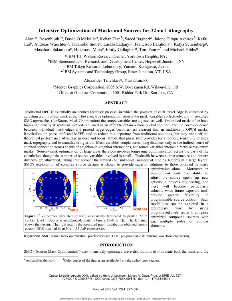
1 Figure 1 † - Complex pixelated source 3 , successfully fabricated to print a 22nm contact level. (Source is unpolarized; mask is binary [T=0 or 1]). The left map shows the design. The right map is the measured pupil distribution obtained from a custom DOE installed in an NA=1.35 ArF exposure tool. Intensive Optimization of Masks and Sources for 22nm Lithography Alan E. Rosenbluth * a , David O Melville a , Kehan Tian b , Saeed Bagheri b , Jaione Tirapu Azpiroz b , Kafai Lai b , Andreas Waechter a , Tadanobu Inoue c , Laszlo Ladanyi a , Francisco Barahona a , Katya Scheinberg a , Masaharu Sakamoto c , Hidemasa Muta c , Emily Gallagher d , Tom Faure d , and Michael Hibbs d a IBM T.J. Watson Research Center, Yorktown Heights, NY; b IBM Semiconductor Research and Development Center, Hopewell Junction, NY c IBM Tokyo Research Laboratory, Yamato, Kanagawa, Japan; d IBM Systems and Technology Group, Essex Junction, VT, USA Alexander Tritchkov e , Yuri Granik f , e Mentor Graphics Corporation, 8005 S.W. Boeckman Rd, Wilsonville, OR; f Mentor Graphics Corporation, 1001 Ridder Park Dr., San Jose, CA ABSTRACT Traditional OPC is essentially an iterated feedback process, in which the position of each target edge is corrected by adjusting a controlling mask edge. However, true optimization adjusts the mask variables collectively, and in so-called SMO approaches (for Source Mask Optimization) the source variables are adjusted as well. Optimized masks often have high edge density if synthesis methods are used in an effort to obtain a more global solution, and the correspondence between individual mask edges and printed target edges becomes less clearcut than in traditionally OPC'd masks. Restrictions on phase shift and MEEF tend to reduce this departure from traditional solutions, but they trade off the theoretical performance advantage in dose and focus latitude that phase shift provides for a reduced sensitivity to thick mask topography and to manufacturing error. Mask variables couple across long distances only in the indirect sense of stitched connection across chains of neighbor-to-neighbor interactions, but source variables interact directly across entire masks. Source+mask optimization of large areas therefore involves long-range communication across the parts of the calculation, though the number of source variables involved is small. Tradeoffs between source structure and pattern diversity are illustrated, taking into account the limited (but unknown) number of binding features in a large layout. SMO's exploitation of complex source designs is shown to provide superior solutions to those obtained by mask optimization alone. Moreover, in development work the ability to adjust the source opens up new options in process engineering, and these will become particularly valuable when future exposure tools provide greater flexibility in programmable source control. Such capabilities can be explored in a preliminary way by using programmed multi-scans to compose optimized compound sources with e.g. multiple poles or annular elements. Keywords: SMO, source mask optimization, pixelated source, DOE, programmable illuminator, wavefront engineering. INTRODUCTION SMO ("Source Mask Optimization") uses intensively optimized wave distributions to illuminate both the mask and the * [email protected] † Color copies of the figures are available from the author upon request. Optical Microlithography XXII, edited by Harry J. Levinson, Mircea V. Dusa, Proc. of SPIE Vol. 7274, 727409 · © 2009 SPIE · CCC code: 0277-786X/09/$18 · doi: 10.1117/12.814844 Proc. of SPIE Vol. 7274 727409-1 Downloaded from SPIE Digital Library on 18 Apr 2011 to 129.34.20.23. Terms of Use: http://spiedl.org/terms
-
Upload
independent -
Category
Documents
-
view
0 -
download
0
Transcript of Intensive optimization of masks and sources for 22nm lithography
120
100
80
60
40
20
0.0
00
07
0.6
0.5
0.4
0.0
0.2
0.I
0.5
Co
-0.5
-1
1
no
0.9
0.9
0.7
0.0
0.5
0.4
0.2
0.2
0.1
Scanner20 40 00 50Sigmax
100 120
SMO-0.5 0
Sigmax0.5 1
Figure 1† - Complex pixelated source3, successfully fabricated to print a 22nm contact level. (Source is unpolarized; mask is binary [T=0 or 1]). The left map shows the design. The right map is the measured pupil distribution obtained from a custom DOE installed in an NA=1.35 ArF exposure tool.
Intensive Optimization of Masks and Sources for 22nm Lithography Alan E. Rosenbluth*a, David O Melvillea, Kehan Tianb, Saeed Bagherib, Jaione Tirapu Azpirozb, Kafai Laib, Andreas Waechtera, Tadanobu Inouec, Laszlo Ladanyia, Francisco Barahonaa, Katya Scheinberga,
Masaharu Sakamotoc, Hidemasa Mutac, Emily Gallagherd, Tom Faured, and Michael Hibbsd aIBM T.J. Watson Research Center, Yorktown Heights, NY;
bIBM Semiconductor Research and Development Center, Hopewell Junction, NY cIBM Tokyo Research Laboratory, Yamato, Kanagawa, Japan;
dIBM Systems and Technology Group, Essex Junction, VT, USA
Alexander Tritchkove, Yuri Granik f, eMentor Graphics Corporation, 8005 S.W. Boeckman Rd, Wilsonville, OR;
f Mentor Graphics Corporation, 1001 Ridder Park Dr., San Jose, CA
ABSTRACT
Traditional OPC is essentially an iterated feedback process, in which the position of each target edge is corrected by adjusting a controlling mask edge. However, true optimization adjusts the mask variables collectively, and in so-called SMO approaches (for Source Mask Optimization) the source variables are adjusted as well. Optimized masks often have high edge density if synthesis methods are used in an effort to obtain a more global solution, and the correspondence between individual mask edges and printed target edges becomes less clearcut than in traditionally OPC'd masks. Restrictions on phase shift and MEEF tend to reduce this departure from traditional solutions, but they trade off the theoretical performance advantage in dose and focus latitude that phase shift provides for a reduced sensitivity to thick mask topography and to manufacturing error. Mask variables couple across long distances only in the indirect sense of stitched connection across chains of neighbor-to-neighbor interactions, but source variables interact directly across entire masks. Source+mask optimization of large areas therefore involves long-range communication across the parts of the calculation, though the number of source variables involved is small. Tradeoffs between source structure and pattern diversity are illustrated, taking into account the limited (but unknown) number of binding features in a large layout. SMO's exploitation of complex source designs is shown to provide superior solutions to those obtained by mask
optimization alone. Moreover, in development work the ability to adjust the source opens up new options in process engineering, and these will become particularly valuable when future exposure tools provide greater flexibility in programmable source control. Such capabilities can be explored in a preliminary way by using programmed multi-scans to compose optimized compound sources with e.g. multiple poles or annular elements.
Keywords: SMO, source mask optimization, pixelated source, DOE, programmable illuminator, wavefront engineering.
INTRODUCTION SMO ("Source Mask Optimization") uses intensively optimized wave distributions to illuminate both the mask and the *[email protected] †Color copies of the figures are available from the author upon request.
Optical Microlithography XXII, edited by Harry J. Levinson, Mircea V. Dusa, Proc. of SPIE Vol. 7274,727409 · © 2009 SPIE · CCC code: 0277-786X/09/$18 · doi: 10.1117/12.814844
Proc. of SPIE Vol. 7274 727409-1
Downloaded from SPIE Digital Library on 18 Apr 2011 to 129.34.20.23. Terms of Use: http://spiedl.org/terms
C),
' JO
OIJ
rOO
rtU
oQ
"r)(
) O
Q)!
'()JO
(°"
O°-
ciO
o,oo
"cc7
OiO
0n0O
0oO
fl.o0
)o4-
Q00
)O
OQ
''O"C
)O
oQo°
"OrQ
.0f
l000
000C
)Jo
000"
0 co
Co
Or,
oOoQ
000O
-'(O
Q C
OO
.) C
00
0.3
0OO
O'CD C) C) C. C) - ,r
- -
0c cpc?OQ0000000000000
oD00000000000000oo 0o%
. 0000000 %%
000o000o0O000C0 0 COC 0 0
0000000o0000000000Do 00 00 00000000000000000 cCcc,tc,c,o
0.01 1
wafer during lithographic exposures, and was proposed in ref.4 as a means for exploiting all available degrees of freedom in the bandlimited exposure process. Such an approach becomes attractive as resolution improvements of the classical kind become harder to obtain. SMO optimization is nonlinear and non-convex (particularly when phase shift and pattern decomposition are considered), and the ref.4 algorithm seeks to address these difficulties by employing both global optimization methods (for sequential optimization of mask and source), as well as local joint optimization of mask and source variables together to more efficiently account for interactions between the two. In broad terms, the SMO algorithms used in the present work address the problems of optimizing mask and source using the basic approaches of refs.5 and 6, respectively. Our joint optimization step is discussed in general terms below.
Methods to optimize masks and sources have been developed by many groups. Hsu et al.7 discuss the advantages provided by joint mask+source optimization over (purely) sequential mask,source optimization. [Our algorithm combines both approaches because: a) global search methods are more easily devised when the mask and source synthesis problems are addressed separately, and b) local optimization of mask and source variables together accounts more efficiently for their interaction, while also allowing the use of less idealized constraints and objective in obtaining the final output solution.] The ref.7 group has published a number of other papers on SMO during the last several years; for example refs.8,9. Other forms of SMO are considered in ref.10, and ref.11. The literature on the separate steps of mask optimization and source optimization is today quite extensive1,4-7,9,10,12-23. In particular, ref.1 discusses a quadratic method of mask synthesis broadly similar to that of refs.4 and 5, and a pixel-based mask-only optimization method that is used in some of the experiments below.
The fundamental goal of SMO is to determine the optimum set of image forming waves that can propagate within the finite NA of the projection lens. Though our SMO methodology employs standard optimization algorithms, its objectives and heuristics are largely grounded in physical optics, in that they center on the bandlimited image formation process. On the other hand, lithographic image formation is also constrained by a broad set of manufacturability requirements, of which the most critical pertain to the manufacturability of the mask polygons that must diffract the optimal set of imaging waves into the lens. It is natural to formulate these manufacturability restrictions as shape processing constraints, but as such they have a fundamentally different character from the optical processes that govern image formation. Managing this dichotomy is a key element in designing an efficient SMO algorithm, as we discuss in Section I.
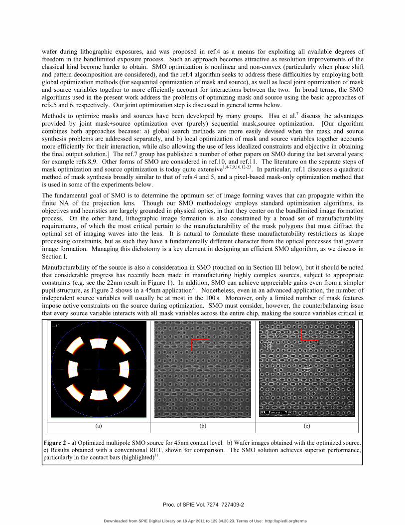
Manufacturability of the source is also a consideration in SMO (touched on in Section III below), but it should be noted that considerable progress has recently been made in manufacturing highly complex sources, subject to appropriate constraints (e.g. see the 22nm result in Figure 1). In addition, SMO can achieve appreciable gains even from a simpler pupil structure, as Figure 2 shows in a 45nm application31. Nonetheless, even in an advanced application, the number of independent source variables will usually be at most in the 100's. Moreover, only a limited number of mask features impose active constraints on the source during optimization. SMO must consider, however, the counterbalancing issue that every source variable interacts with all mask variables across the entire chip, making the source variables critical in
(a) (b) (c)
Figure 2 - a) Optimized multipole SMO source for 45nm contact level. b) Wafer images obtained with the optimized source. c) Results obtained with a conventional RET, shown for comparison. The SMO solution achieves superior performance, particularly in the contact bars (highlighted)31.
Proc. of SPIE Vol. 7274 727409-2
Downloaded from SPIE Digital Library on 18 Apr 2011 to 129.34.20.23. Terms of Use: http://spiedl.org/terms

a. b.
c.
Mask change thatshifts position
Bias change in mask
MEEF is edgepositionchange dueto mask bias
Figure 3 - a) The MEEF metric is a ratio which can be calculated as the intensity change from a differential mask bias, divided by the image slope. b) Image slope is the change in intensity from a differential change in position, which may be taken as a change in mask position instead of wafer position. A change in mask position is equivalent to the change in mask transmission shown in the sketch. c) Local mask bias is also equivalent to a change in mask transmission, but unlike b the perturbations from bias have the same sign at all edges. Implication is that adjacent narrowly spaced mask edges contribute additively where mask bias is concerned, but have partly canceling contributions to image slope. MEEF is the ratio of these effects, so its control becomes important at high feature densities.
successfully scaling SMO to larger areas. The implications of this are discussed in Section II. A standard requirement in most inequality-constrained optimization methods is that the active constraints be efficiently identified. In SMO the mask solutions will depend on the source solution (and vice-versa), but in general we can expect the familiar drivers in lithographic process development to be well represented in the active constraint set (e.g. such patterns as forbidden pitches and critical features), although with a non-convex problem we must employ intensive optimization in order to avoid overlooking a small number of unexpectedly critical features in a large layout that would cause the solution to be invalid.
Mask resolution vs. lens resolution in lithographic optimization The optimization methods considered here employ both mask and source variables, but in most cases we find it convenient to depart from standard representations of these variables as e.g. mask-shape edge positions, or the pole dimensional settings of conventional sources. Since the fundamental resolution bottleneck is that of the lens (the resist resolution and the scaled mask resolution being somewhat finer), it is natural to regard the problem as one of imaging within the constraints of a finite bandlimit. Images can be optimized for lithographic purposes using ED-window24,25 or PV band26 metrics, and in the constant-threshold (CTR) approximation these metrics are simple functions of the intensities generated by image-forming waves that interfere within the bandlimit. The resolution limit imposed by the finite NA of the exposure tool is automatically encoded in the bandlimit of the collection pupil, and a key aspect of lithographic optimization problems is to find the optimal set of image forming waves that can propagate within the illumination and collection pupils, optionally including deployment across multiple exposures. Wavefront variables are continuously adjustable and mutually unconstrained within an optical beam, making them quite convenient for optimization, and the bandlimit imposed by the lens pupil allows the variable count to be efficiently matched to the available degrees of freedom in the system. The optical optimization may involve multiple exposures, which for pure SMO clips may be understood as the superposition of multiple sets of unknown partially coherent waves within a single image.
However, this algorithmically convenient formulation presumes the practical availability of arbitrarily specified imaging solutions within the lens bandlimit, and it is also important that the mask shapes which generate these optimal images
obey the constraints imposed by the mask fabrication process. This "wavefront engineering" problem becomes harder at 22nm, where the feature sizes required on the mask become challenging despite the 4X reduction ratio. To achieve full control of the imaging wavefront, the resolution advantage of the mask-writer must be able to compensate for the restriction of the mask to only two or three allowed transmission values. In addition, phase-shifted polarities may in practice be excluded for reasons of manufacturability, limiting the wavefront solutions that can be produced. The mask-process resolution must also be able to accommodate the feature biases that are needed to optimally compensate mask topography effects (so-called EMF effects).
On the other hand, it proves possible to employ lithographic metrics in the wavefront engineering objective when the
Proc. of SPIE Vol. 7274 727409-3
Downloaded from SPIE Digital Library on 18 Apr 2011 to 129.34.20.23. Terms of Use: http://spiedl.org/terms

PPP
Figure 5 – Optimized example source31 (unpolarized) for 22nm via patterns, e.g. laid out with different pitches P in the staggered configuration shown.
4.1X Reduction in MEEF
With MEEF
Control
No MEEF
Control
Figure 4 - Example of the significant effect that optimization against MEEF can have in 22nm SMO solutions. Phase mask designs are from a 0.1μm2 SRAM cell at PC level, where the rectangles print dark and the surround is bright.
ref.4 method is used, i.e. to allow lithographic trade-offs during wavefront engineering in order to ensure mask manufacturability. If optimization of the (relatively sparse and less densely constrained) optical variables is initially used to both fix the source, and to establish a target/starting image, the subsequent wavefront engineering step then resembles the kind of problem that is now usually referred to as "inverse lithography". The methods of e.g. refs.1 and 4 show how such problems can be solved without restriction to a preconceived topology for the mask features.
It should also be noted that the ability provided by SMO to fully and directly control the wave distribution illuminating the wafer (and mask) has applications beyond
those of maximizing classical lithographic metrics. Examples are the formation of complex 3D structures in stacked resist layers of different (designed) sensitivities27, and the formation of complex image modulating structures (etched hologram, or CEL-like), and their subsequent illumination by complex designed wavefronts (in a disjoint exposure regime, e.g. using resists of strongly different sensitivities) to achieve true superresolution28 (because the second-stage images contain sum-harmonic spatial frequencies that have been upshifted beyond the lens bandlimit).
In summary, the lithographic process intertwines problems of wave imaging and mask shape restriction whose character would be fairly generic if encountered in their usual distinct domains. This remains true even if resist and EMF effects are separated from the fundamental imaging step by treating them as perturbations. Algorithms for lithographic optimization are thus complicated by the different formulations that are appropriate for characterizing the resolution limitations of the lens and the mask-writing process.
Source variables couple mask variables across the entire mask, but are few in number Another important algorithmic consideration for SMO is that each source variable interacts with all mask variables within the optimization field. Source+mask optimization of large chip areas therefore involves long-range communication across the parts of the calculation, and (as is usual in modern lithography) this computation is already highly compute-intensive even before SMO comes into play, due to the enormous number of variables involved (and to the nonlinearity of optical imaging calculations). To keep the problem tractable it then becomes important to consider the optimal complexity of the source as a function of gating constraints and features. Optimization of the source alone can be accomplished using linear programming methods6, whose scaling is fairly benign. The source variable count (degrees of freedom) can exceed those present in the mask when the optimized area is e.g. of SRAM scale, though the details depend on the specific form used for the source elements. Gridded source pupils (sometimes referred to as pixelated sources, though we also use that term more generally) have advantages that persist even when large areas are being optimized, in which case the number of mask degrees of freedom greatly exceeds those available in the source. These points are discussed further in section III.
Proc. of SPIE Vol. 7274 727409-4
Downloaded from SPIE Digital Library on 18 Apr 2011 to 129.34.20.23. Terms of Use: http://spiedl.org/terms
P=133nm P=136nmP=130nm P=149nm
P=163nm P=198nmP=184nm P=212nm
P=233nm P=269nmP=255nm P=283nm
P=297nm P=396nmP=354nmP=325nm
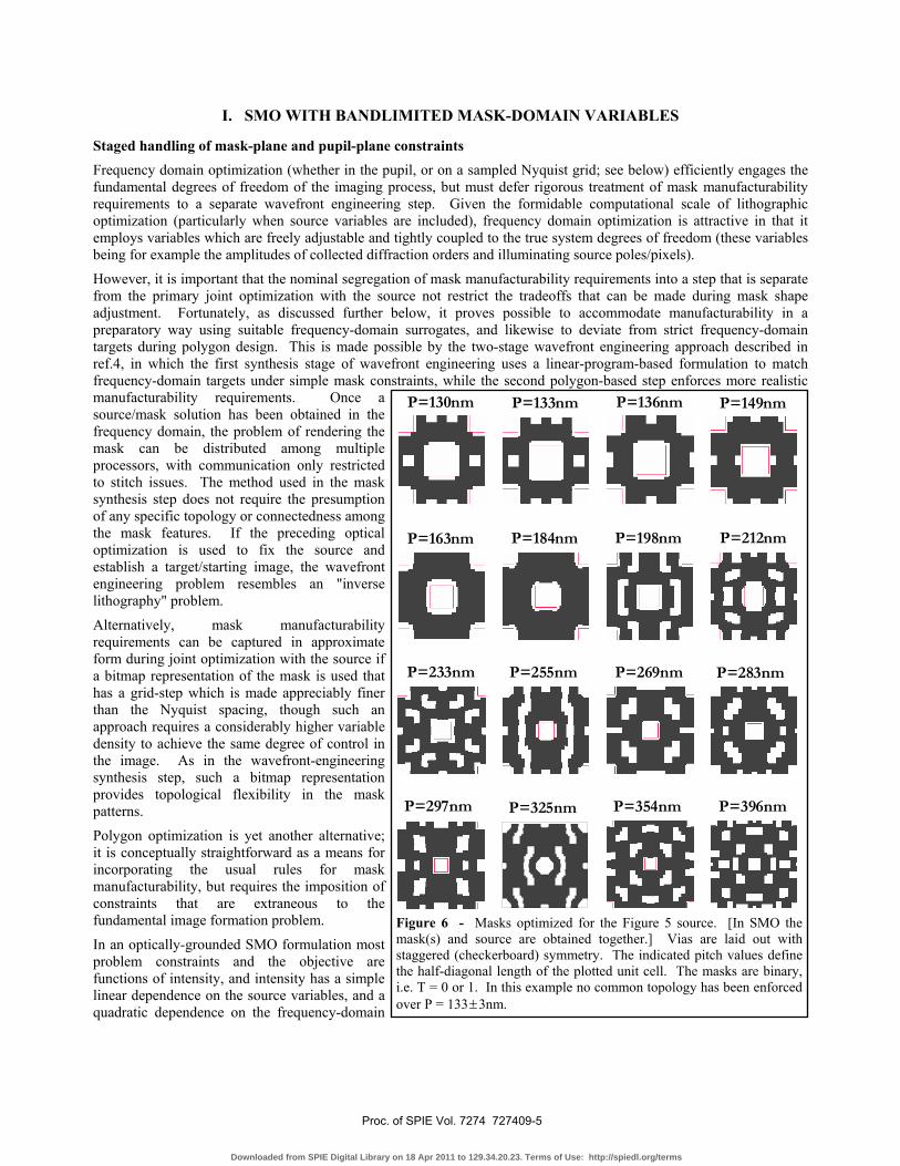
Figure 6 - Masks optimized for the Figure 5 source. [In SMO the mask(s) and source are obtained together.] Vias are laid out with staggered (checkerboard) symmetry. The indicated pitch values define the half-diagonal length of the plotted unit cell. The masks are binary, i.e. T = 0 or 1. In this example no common topology has been enforced over P = 133 ± 3nm.
I. SMO WITH BANDLIMITED MASK-DOMAIN VARIABLES
Staged handling of mask-plane and pupil-plane constraints Frequency domain optimization (whether in the pupil, or on a sampled Nyquist grid; see below) efficiently engages the fundamental degrees of freedom of the imaging process, but must defer rigorous treatment of mask manufacturability requirements to a separate wavefront engineering step. Given the formidable computational scale of lithographic optimization (particularly when source variables are included), frequency domain optimization is attractive in that it employs variables which are freely adjustable and tightly coupled to the true system degrees of freedom (these variables being for example the amplitudes of collected diffraction orders and illuminating source poles/pixels).
However, it is important that the nominal segregation of mask manufacturability requirements into a step that is separate from the primary joint optimization with the source not restrict the tradeoffs that can be made during mask shape adjustment. Fortunately, as discussed further below, it proves possible to accommodate manufacturability in a preparatory way using suitable frequency-domain surrogates, and likewise to deviate from strict frequency-domain targets during polygon design. This is made possible by the two-stage wavefront engineering approach described in ref.4, in which the first synthesis stage of wavefront engineering uses a linear-program-based formulation to match frequency-domain targets under simple mask constraints, while the second polygon-based step enforces more realistic manufacturability requirements. Once a source/mask solution has been obtained in the frequency domain, the problem of rendering the mask can be distributed among multiple processors, with communication only restricted to stitch issues. The method used in the mask synthesis step does not require the presumption of any specific topology or connectedness among the mask features. If the preceding optical optimization is used to fix the source and establish a target/starting image, the wavefront engineering problem resembles an "inverse lithography" problem.
Alternatively, mask manufacturability requirements can be captured in approximate form during joint optimization with the source if a bitmap representation of the mask is used that has a grid-step which is made appreciably finer than the Nyquist spacing, though such an approach requires a considerably higher variable density to achieve the same degree of control in the image. As in the wavefront-engineering synthesis step, such a bitmap representation provides topological flexibility in the mask patterns.
Polygon optimization is yet another alternative; it is conceptually straightforward as a means for incorporating the usual rules for mask manufacturability, but requires the imposition of constraints that are extraneous to the fundamental image formation problem.
In an optically-grounded SMO formulation most problem constraints and the objective are functions of intensity, and intensity has a simple linear dependence on the source variables, and a quadratic dependence on the frequency-domain
Proc. of SPIE Vol. 7274 727409-5
Downloaded from SPIE Digital Library on 18 Apr 2011 to 129.34.20.23. Terms of Use: http://spiedl.org/terms

P396nmP269nm P354nmP325nmP283nm P297nm
P255nmP233nmP198nm P212nm
P184nmP163nmP149nmP130nm P136nmP133nm
P396nmP396nmP269nmP269nm P354nmP354nmP325nmP283nmP283nm P297nmP297nm
P255nmP255nmP233nmP233nmP198nmP198nm P212nmP212nm
P184nmP184nmP163nmP163nmP149nmP149nmP130nm P136nmP136nmP133nm
Figure 7 - Standard mask solutions for the via patterns of Figure 6, designed for the advanced conventional source shown (soft quasar).
mask variables (cubic overall). Simultaneous (joint) optimization of mask and source variables is thus efficiently handled using mask variables in the frequency domain. As discussed in previous publications4-6, we can within certain approximations and heuristics find global solutions over restricted areas to the problems of optimizing the mask for fixed source, and the source for fixed mask, with these steps being alternated with joint local optimization of the mask and source variables together. As noted above, multiple exposures can be handled within such a formulation.
In lithography it is customary to apply periodic boundary conditions to the computational field of view, in which case the optimization problem can use discrete variables (e.g. the amplitudes of the diffraction orders) to represent the mask. According to the Nyquist theorem, these values are entirely determined from a discretely gridded sampling of their Fourier transform, making the discrete transform a suitable alternative representation. Note that this transform does not represent the mask transmission, but rather the filtered transmission, with the filter kernel being given by the extended lens impulse response (e.g. an Airy disk with bandlimit NA[1+σ]). There is a simple invertible mapping between the paired Fourier variables in the object and pupil planes - In contrast, the domain of polygonal mask apertures is governed by intricate dimensional restrictions and discrete transmission choices.
Heuristic incorporation of mask requirements during bandlimited pupil-domain optimization It should be noted that a strict division between the spatial-frequency and mask domains need not be enforced. For example, though polygon content has no explicit meaning when frequency domain variables are used, it turns out to be possible during frequency-domain optimization to provide suitable preparatory control over polygon-specific mask fabrication issues like sensitivity to mask error, and restricted mask transmission options (most commonly to amplitude transmissions of 0 or 1 only). The resulting frequency domain solution likewise provides a suitable starting point if readjustments to the target image are allowed for the purpose of more exactly accounting for mask manufacturability requirements.
A technical discussion of our methods to optimize against mask error is beyond the scope of this paper; ref.6 discusses it in the context of source optimization. However, we note here that sensitivity to mask error can be addressed by adding constraints on the so-called MEEF ratio (see below) to the optimization problem, and show below that MEEF control becomes an important consideration at k1 factors of current interest, particularly for advanced masks that contain highly optimized structure. The underlying basis for this trend is essentially a matter of edge density, as can be understood from the simple analytic argument given below; see also the simulation-based examination of this question by Xiao et al.11.
In general we expect mask error to include a random component; however this stochastic contribution will tend to be moderated in its effect by partial cancellation of the random errors contributed by different edges. Unfortunately, masks often suffer from a systematic error of the opposite kind, in which all features in some local region of the mask (typically extending well beyond the optical interaction radius) are consistently biased in unison (either larger or smaller), thus giving rise to a collective impact on local wafer CDs that can be particularly severe, and making sensitivity to local mask-bias particularly useful as a determinative MEEF metric. Such bias effects are often well controlled in their average, meaning that both of the bias extremes allowed by the mask spatial-uniformity tolerance may occur somewhere on a given plate.
Proc. of SPIE Vol. 7274 727409-6
Downloaded from SPIE Digital Library on 18 Apr 2011 to 129.34.20.23. Terms of Use: http://spiedl.org/terms

-
-
P396nm
P163nm
P136nmP133nmP130nm P149nm
P184nm
P198nm P212nmP212nm
P233nm P255nmP233nm P255nm P325nm
Figure 8 - Programmed source obtained by superposing three standard installed source options using three scans of the mask. The associated mask designs that SMO provides along with this source are also shown.
It is therefore appropriate to define MEEF as the absolute value of the change in printed edge position per unit of local mask bias, and in fact this definition has now become widely used. We will next discuss a key aspect of MEEF behavior, namely that MEEF can be understood the ratio of the differential intensity impact from a uniform rim of excess material on feature boundaries, divided by the differential impact of equal and opposite signed contributions along the sides of features, with both factors having a very similar form. We will then show that this has important implications for advanced mask design at 22nm. Figure 3 presents an intuitive explanation of the result, which we now explain. For purposes of discussion we will refer to the particular feature at which MEEF is being evaluated as "Edge 0", assumed vertically oriented for simplicity, with the exact evaluation position being denoted Vertical
Edge 0xr , or VE0xr for short. Since
MEEF is a differential quantity, the bias-induced shift in printed edge position will be given by the ratio of the intensity error induced by an incremental unit of local mask bias, divided by the image slope along the direction perpendicular to the printed edge (Figure 3a). Since image slope is the derivative of intensity with respect to image position, it can equivalently be regarded as a derivative with respect to the conjugate mask position, since only the absolute value is of interest here. In physical terms, image slope can then be understood as the differential change in intensity caused by the particular differential change in mask transmission profile that is induced by an infinitesimal translation of the mask (Figure 3b). Image slope
can thus be understood as resulting from interactions between perturbed mask feature edges and the nominal mask. Moreover, these translational perturbations have a qualitatively similar form to the perturbations which produce an intensity change when the mask is differentially biased (Figure 3c), in that both involve the differential impact of delta-functions that trace feature edges. However, in the case of image slope these delta-functions are signed, and have opposite signs at opposite edges. Thus, if VE0xr lies on, for example, the left edge of a feature, the translational delta-function contributions from the left edges of other features will have positive sign, while those on the right edges will be negative. In addition, only vertical edges contribute to image slope (when the reference edge 0 is vertical), while edges of all orientations contribute intensity when the mask is biased. Other things being equal, this tends to make MEEF higher in 2D patterns. It also explains the observation by Xiao et al.11 that the inevitable corner rounding in written mask features tends to reduce MEEF. This occurs because corner rounding will tend to reduce the intensity impact of bias in mask features by shrinking their perimeter length. Note that the largest contributions to MEEF from these delta-function perturbations at mask edges (whether from a bias or translational change) will be from edges in immediate proximity to Edge 0 (with the strongest contribution occurring along Edge 0 itself). In the classical lithography regime where all mask features are well-resolved, we could in lowest order ignore all edges except Edge 0,
Proc. of SPIE Vol. 7274 727409-7
Downloaded from SPIE Digital Library on 18 Apr 2011 to 129.34.20.23. Terms of Use: http://spiedl.org/terms

5
10
15
20
25
30
35
100 150 200 250 300 350 400Staggered Pitch (nm)
CD
max
-CD
min
(nm
) Conventional
SMO Multi-scan
SMO Gridded
Figure 9 - Dimensional variations (due to fluctuations in dose, focus, and local mask bias) are considerably smaller with the SMO solutions given above for the Figure 5 problem than with the conventional solution. (See earlier figures [and ref.31] for further details.)
because mask features in the classical regime are appreciably larger than the lens resolution. Thus, in the case of comfortably resolved features, the differential edge contribution from either bias or translation will be approximately the same (i.e. primarily that of a delta-function along Edge 0 only), implying that in a classical imaging regime we will have MEEF ≅ 1.
However, in an intensively optimized mask for low-k1 lithography there may be many feature edges falling within roughly one resolution-length of Edge 0, due both to the small size of the printed features, and to the use of masks that are highly decorated with assist-like
features, serifs, hammerheads, etc. Other things being equal, this increased edge density will tend to increase the intensity impact of mask bias (Figure 3c). In addition, the contribution of adjacent edges to the intensity change from a translational shift (i.e. that rescales by image slope, Figure 3b) will tend to alternate in sign (e.g. between the left and right edges of successive features), and since the spacing between adjacent decorating edges may become smaller than the lens resolution, the resulting cancellation of amplitude contributions can potentially become appreciable. The MEEF ratio thus tends to be doubly impacted at high edge density, other things being equal. Note, however, that the lens impulse response or SOCS kernels will include lobes of negative amplitude outside the central peak, and thus that the contributions from bias or translation are not inexorably monotonic functions of edge density. Nonetheless, an increase in mask edge density beyond the reciprocal of the lens resolution would typically drive up MEEF, making it important to take MEEF into account during the optimization of low k1 masks, an observation made in ref.11. Figure 4 shows an example.
II. SMO AT LARGER SCALES Collective optimization versus feature-by-feature proximity compensation Traditional OPC is essentially a feedback process, in which the printed position of each target edge is corrected for optical proximity effects by adjusting the position of a controlling mask edge, with collective effects only accounted for in an implicit way. This paradigm has generally carried over into exposure methods that involve multiple masks (which will be a central element of RET design for 22nm). However, true optimization adjusts the mask edge positions (or other mask variables) collectively, usually for a collectively defined objective function, such as process window, that involves multiple focal planes. In low-k1 regimes where the optical proximity effect at each point also operates collectively across multiple mask variables, a stronger solution is obtained when intensive synthesis methods are used, as we will illustrate below. However, today's OPC is already highly compute-intensive, even before bringing full optimization to bear. Advanced algorithmic schemes for implementation on high performance computing systems are therefore essential to the implementation of SMO at large scale. Intensive optimization often produces masks with high edge density, and the correspondence between individual mask edges and target edges in the printed pattern is less clearcut than in traditionally OPC'd masks. Restrictions on phase shift and MEEF, introduced to improve mask manufacturability, tend to reduce this departure from traditional solutions, in terms of mask complexity but also in terms of performance advantage.
Proc. of SPIE Vol. 7274 727409-8
Downloaded from SPIE Digital Library on 18 Apr 2011 to 129.34.20.23. Terms of Use: http://spiedl.org/terms

133nm ± 3nm + 149nm 163nm + 184nm 198nm 212nm
+ 233nm + 255nm + 325nm
+ 396nm NOTE:
These simulations are based only on the frequency - domain optimization stages of SMO.
Figure 10 - Sources from SMO solutions that are intensively optimized over increasingly large subsets of the pitch spectrum31. The source solution does not converge to a single solution, because the optimum is determined by the active constraints in the set of included pitches. It is necessary that the SMO algorithm consider all active constraints in the layout, but this set will typically be small compared to the total number of patterns. (The optimization settings here are very slightly different from those in the more detailed ref.31 discussion.)
Long-range coupling of source variables The exploratory SMO studies of refs.4,6 considered cells of DRAM or SRAM scale, and the number of degrees of freedom in the source exceeded the number of degrees of freedom in the mask field. This remains broadly true even with the relatively coarse poles used in conventional multiple-pole sources (e.g. "windmills" or "soft quasar"; see also section III), since the relatively small number of poles employed in such sources is optimally chosen from a considerably larger set of installed options. However, for most 22nm applications the number of degrees of freedom available in the mask will vastly exceed those available in the source. Nonetheless, IC patterns are far from random, and may be designed under ground rules that exploit the availability of intensive optimization. The tradeoffs between optimal source structure and pattern diversity (and thus design regularity) are discussed in the next section. At the exterior boundaries of fields that are processed as contiguous frequency-domain blocks, it is possible to stitch polygons in the mode of conventional OPC, once wavefront engineering is completed in the interior. (Of course, it is necessary that this interior SMO operation ensure compatible assist topology.) Broadly speaking, the coupling of mask variables across the entire chip is then broken at frame boundaries, and polygon shape compatibility within each frame is delegated to independent wavefront engineering steps. A remaining cross-coupling across the entire mask is potentially entailed by the source variables, and their joint optimization can more efficiently be handled in the frequency domain at near-Nyquist mask sampling. The scale and scaling of this step becomes a key factor in the overall efficiency of the SMO algorithm.
III. IMPACT OF SOURCE VARIABLES IN SMO Source representations Our SMO algorithm assumes an enumerated set of source options, approximately sampling continuous source adjustments as necessary. The intensity contribution to the source from each such element/option is an unknown source
variable to be optimized. The advantage of such a representation is that the image intensity contributed by a source element of specified pupil shape will be a linear function of the element's intensity in the pupil.
For many problems this makes it natural to design advanced sources by subdividing the source pupil into elements (essentially pixels) that map out all addressable pupil regions, and to represent the solution as a weighted superposition of these pixels, with the weights being the optimized parameters. Moreover, it is shown in ref.6 that complex lithographic metrics like process window can be optimized globally with such a source representation, by means of a linear programming formulation. A natural approach is to define the source element boundaries using intersecting gridlines. Alternatively, when optimizing repetitive structures like memory arrays, it is
Proc. of SPIE Vol. 7274 727409-9
Downloaded from SPIE Digital Library on 18 Apr 2011 to 129.34.20.23. Terms of Use: http://spiedl.org/terms

25
25
45 65 55
Cli p count
too 125 145
flu (c)
theoretically more appropriate to define the element boundaries using the intersecting collection frontiers of the various diffraction orders (subdivided or merged as necessary to roughly enforce a desirable pixel size) - This is the so-called archel representation4,6,29,30,31. It should be noted that these collection boundaries serve to mark off pixels whose pupil regions inject unfavorable diffraction orders into the image, as well as delineating pixels that form part of the optimum solution. As a result, the optimized source shapes for feature sets that include critical small cells will ideally conform to complex archel boundaries (see ref.6 for futher discussion of this point), rather than the more straghtforward polar-gridded boundaries of conventional source designs.
These periodicity considerations continue to apply broadly when the source elements are defined by a simple rectilinear gridding of the pupil. Moreover, it can also be shown that practical manufacturing limitations can sucessfully be represented in our optimization framework, making fabrication of advanced pixelated sources a practical proposition, as we discuss in a companion paper3. Pixelated sources can be implemented with custom diffractive optical elements23, though at the cost of an additional custom optical artifact for printing each level (the first such artifact being the mask). However, an illumination pattern contains vastly fewer degrees of freedom than does a mask - Development work in maskless lithography then encourages consideration of a potentially more transformative means for rendering custom illumination patterns, namely by means of a Programmable Illuminator (PI)14.
Computational Scaling Technology
Source Mask Optimization | 2009 SPIE Advanced Lithography
Active Constraint Patterns Are Desired Candidates for Full SMOExample: Source optimization (SO) on clips from 22nm (low) metal level.– SO is rerun each time optimization set is augmented by a new sample clip (buffered
1μm2 area, randomly selected), until 128μm2 has been covered.• Clip #1 is from
memory array.
Only 34 of 128 clips contribute active constraints to final source solution forentire set.
Difference between intermediate source solutions and final source is plotted at right.
– Only a small set of clips contribute binding constraintsto evolving source.
• Lower inserts showsample binding clips. Upper inserts showresulting source impact.
13 29 48 89 124
128
k1
128
k1
1
SS
%S
S
Figure 11 - Source evolution as optimization is rerun using successively more clips in the optimization set. Optimization set is drawn from a 2025μm2 random logic clip (with memory array), in a 22nm metal level. The final set includes 128 clips (each 1μm x 1μm, plus buffer). The vertical axis plots the normalized difference (summed absolute values) between the solution for the final set and the solutions for earlier partial populations; the horizontal plots the number of clips in the optimization set. The majority of clips have no impact on the solution when added to the set. The lower inserts show some of the exceptions; the impact of these strongly active clips on the pixelated source solution can be seen in the upper inserts.
Proc. of SPIE Vol. 7274 727409-10
Downloaded from SPIE Digital Library on 18 Apr 2011 to 129.34.20.23. Terms of Use: http://spiedl.org/terms

B BEE I
E J : m I
BEE B E
D
S
D
Dci
b
o(J:
D(i
at
A
-'k0.
D(1
MEEF MEEF MEEF MEEF MEEF MEEF MEEF
SOURCE MASK 7.50nm 4.33 7.40nm 4.00 9.00nm 3.50 8.30nm 3.50 10.70nm 3.20 10.40nm 3.30 5.60nm 3.90
MASK OPT ONLY F F 13.80nm 4.30 9.50nm 3.50 8.60nm 3.00 5.10nm 3.80 4.40nm 3.20
HYBRID 6.60nm 4.21 7.30nm 4.60 9.40nm 3.80 8.60nm 3.70 10.60nm 3.00 11.70nm 3.60 9.80nm 3.80
PVBPVB
F F
PVB PVB PVB PVB PVBPitch = 184nm Pitch = 297nm Pitch = 396nmPitch = 130nm Pitch = 136nm Pitch = 149nm Pitch = 163nm
Figure 12 - Comparison of full SMO to strategies in which the final mask patterns are not optimized jointly with the source variables. Row 1 (SOURCE MASK): Full SMO, where mask is optimized together with source. Row 2 (MASK OPT ONLY): Mask is optimized using a pixel-based method (ref.1) with the source a standard Quasar solution (fixed). Row 3 (HYBRID): The source is obtained from the row 1 full SMO solution, but the SMO mask patterns are discarded; instead the mask is optimized (under the fixed SMO source) using the pixel-based method of row 2. "PVB" refers to the worst-case total dimensional spread under certain extreme combinations of dose, focus, and mask bias errors. MEEF is the sensitivity to mask bias error. "F" designates an unresolved pattern.
Full SMO
Hybrid
P = 184nm P = 297nm P = 398nm
Figure 13 - Sample masks in the Figure 12 experiment. All masks use a common source (SMO-derived), but in the "hybrid" approach a fast pixel-based optimization method1 is used to derive the masks.
Programmable illuminators As noted above, complex lithographic metrics like process windows can be optimized globally using a source representation in which the source pupil is divided into elements (essentially pixels) that map out all addressable pupil regions, with the solution being represented as a weighted superposition of these pixels, and with the weights being the optimized parameters. Pixel variables in an archel representation are field-size dependent; however hardware engineering in a programmable illuminator is more naturally represented for simulation purposes by a fixed rectilinear grid of pixels whose intensities are independently adjustable within a range. To remain effectively incoherent a light
source must have finite etendue, which in turn will limit source resolution; however with current Diffractive Optical Element (DOE) technology it is already possible to design sources on a grid that is considerably finer than the pole sizes used in standard sources, as we show in ref.3; see also ref.23. In a companion paper31 we provide a direct illustration of the performance advantage that an optimized pixelated source provides compared with optimization of a less advanced multipole source. Figure 1 shows an example which illustrates that SMO can accommodate a pupil addressability that is somewhat finer than pupil resolution, in that SMO can consider source pixels which overlap6.
Figure 5 shows the result of optimizing a pixelated source to print checkerboard arrays of vias (see insert) across a wide pitch range; additional details are given in ref.31. Figure 6 shows a through-pitch sampling of SMO mask cells that are designed to print via arrays with the Figure 5 source. The assist structure of these patterns is somewhat non-intuitive, as may be seen by comparison with the conventionally designed mask solutions shown in Figure 7, though the overall
topology is less exotic than is encountered in SMO-designed phase masks.
It should be noted that current exposure tools already provide a limited form of illumination programmability, in that source optimization solutions can be realized as a selection from installed DOEs of a standard kind. For experimental purposes these programmed sources can optionally include composite sources comprising a multi-scan superposition of separate installed shapes, with adjustable relative dose contributions. (A few advanced conventional
Proc. of SPIE Vol. 7274 727409-11
Downloaded from SPIE Digital Library on 18 Apr 2011 to 129.34.20.23. Terms of Use: http://spiedl.org/terms

000)
(H
o
)00010
)C
)OO
Oç
I
flftftfl
ftftftft
[rr[
Ooo
)0
)0o0C
01)
C
)00Oi'
a
C
a a
sources already fall into an equivalent multipole category as far as the total source shape is concerned, e.g. "windmills" and "soft quasars".) Since the image contributions from each source scan combine incoherently, they can be regarded as contributions from independent pixels6. Such solutions do not require the fabrication of new DOEs, and they can be instantly readjusted and then accurately characterized, as would be the case for a more advanced full-fledged programmable illuminator. Of course, such conventional source elements are limited in the sophistication of the pupil structure they can provide, and in the multi-scan case they suffer from a throughout loss and/or potential resist degradation due to the need for multiple-pass exposures with distinct DOEs, whose total count must be limited to a practical value by the optimization algorithm. Nonetheless, they serve as a useful experimental vehicle until such time as full-fledged programmable illumination becomes available. Figure 8 shows such a multi-scan source for the Figure 5 via level, along with associated through-pitch mask designs for the checkerboard layout examples. For comparison, Figure 7 shows a more conventional advanced source solution for this level, along with mask designs obtained by applying standard assist placement rules. Figure 9 compares the calculated performance of these different solutions for the 22nm via level example. The error metric is the spread in via diameter in the face of fluctuations in dose, focus, and local mask bias. (See ref.31 for details.) The Figure 5 gridded-pixel source provides substantially tighter dimensional control than the Figure 7 conventional solution, and the Figure 8 multi-scan source also does quite well, though it gains some relative advantage from use of polarization. (While designed source polarization is not considered in the gridded solution shown here, our source design methods are entirely compatible with polarized pixels, and the pixel polarizations can in principle even be optimized during SMO6.) It should be noted that although global search methods may only be applicable to subsets of the full set of chip patterns (since SMO optimization is strongly compute-intensive), it is not necessary that the solution obtained for different clip collections converge rapidly to a single invariant solution. (See for example Figure 10.31) Rather, it is necessary that the
TMASimulation
Source to Correct EMFTMA-Designed Mask (as fabricated)
EMFSimulation
Source for TMA Mask
Figure 14 - Programmed source adjustment to achieve small process adjustments, using current exposure tool technology. In the example shown here, the contact-level source on the left was used to design the SRAM mask pattern shown at top row center, using the thin mask approximation. The mask is shown with the as-written feature shapes, rather than the Manhattan shapes of the thin-mask design. The bottom left image shows that EMF effects (simulated here with full angular dependence in the illumination2) have degraded the resolution of the semi-isolated contact. In development work a programmable illuminator (here approximated using a re-optimized multiscan composite of installed DOE's) can restore the resolution without requiring procurement of a new mask, but with some performance compromises in other patterns. This is illustrated in the right column. Figure 15 shows the improved performance that could be obtained with a more advanced programmable illuminator.
Proc. of SPIE Vol. 7274 727409-12
Downloaded from SPIE Digital Library on 18 Apr 2011 to 129.34.20.23. Terms of Use: http://spiedl.org/terms

oao4)
a)O
oO:
)O0Qa
1)000
TMASimulation
Source to Correct EMFTMA-Designed Mask (written)
EMFSimulation
Source for TMA Mask
Figure 15 - The right column shows the result of carrying out the small process adjustments of Figure 14 using source adjustments that are provided by an advanced programmable illuminator. The process degradation entailed by restricting the re-optimization to only the source variables (fixed mask) is reduced when the programmable illuminator has fine pupil resolution, as may be seen by comparison with Figure 14.
algorithm ensure good performance from each particular optimized source when verified on a broad set of patterns that may be far larger than the particular clip set over which global optimization methods are applied. Both calibration and verification sets would usually include generic patterns, e.g. through-pitch.
A key requirement (common to virtually all nonlinear optimization problems) is that the SMO algorithm accurately identify all mask features in the large layout which impose active (i.e. binding) constraints. As discussed in ref.31, this set is likely to contain such familiar driving features as forbidden pitches and critical features; however the mutual dependence of the optimized mask and source solutions on one another make exact identification of the binding features a nontrivial problem. Figure 10 provides clear indication of the presence of strongly active constraints as more and more pitch patterns are added to the optimized set, in a modest-scale experiment where full frequency-domain optimization is applied to the patterns. As the optimization is rerun with each newly added pitch, the source impact is most often found to be fairly small; however some pitches are seen to be more strongly binding in the solution. Figure 11 shows that very similar behavior arises in a larger-scale experiment, here involving source-only optimization.
It thus becomes interesting to assess the performance impact from optimizing the source against a pre-selected approximation to the active set. Figure 12 and Figure 13 illustrate the effect of employing a mask-only optimization step in a simplified experiment along these lines.
Process tweaks to adjust printed patterns are fairly common in current lithographic practice (e.g. dose adjustments), and programmable illumination makes many more degrees of freedom available for such adjustments. This enables, for example, a small empirical counter-bias to be imposed on a certain feature or feature-type that does not (or no longer does) print at the desired CD, as we have discussed elsewhere6,32. Of course, given the limited number of degrees of freedom in the source, it is necessary that the mask provide sufficiently tight CDs from a large majority of feature types that the uncorrectable set of deviations induced by source re-adjustment represents a desirable tradeoff for the correction achieved in the problematic feature, as would be the case when a reasonably successful mask and process is being fine-tuned. Figure 14 and Figure 15 illustrate this for a mask in which SMO with optimized SRAM mask patterns has given rise to somewhat narrowed and elongated mask features for printing semi-isolated contacts. This mask example was designed in the thin-mask approximation, and as a result the more isolated SRAM contact is seen to suffer a relative intensity loss when the EMF boundary layers33 are taken into account, due to the high-aspect-ratio mask shape that such
Proc. of SPIE Vol. 7274 727409-13
Downloaded from SPIE Digital Library on 18 Apr 2011 to 129.34.20.23. Terms of Use: http://spiedl.org/terms

contacts receive in the SMO solution (i.e. due to their increased boundary/area ratio). Naturally this causes poor printing if left uncorrected, as shown in Figure 14. However, by reoptimizing the source using current exposure tool technology (i.e. an optimized multiscan solution), we can achieve a compensating intensity increase in the semi-isolated contact (right side of Figure 14). Moreover, Figure 15 shows that future advanced programmable illuminators will allow such adjustments to be made with appreciably fewer compromises in the performance of less critical features.
CONCLUSIONS Source mask optimization (SMO) provides improved imaging when recent improvements in source fabrication technology are exploited. Fully programmable illumination control at high pupil resolution will open up new avenues in process engineering, if guided by suitable optimization methods. Though inclusion of the source variables makes intensive lithographic optimization more challenging computationally, this challenge can be mitigated by exploiting the bandlimit imposed by the illumination and collection pupils, and by exploiting special characteristics of the source variables, such as their limited count relative to the number of mask variables, and the limited size of the active constraint set that binds them. A simple heuristic example along these lines is to apply a pure mask optimization step to patterns lying outside a critical set of clips that receive full SMO. More generally, identification of the active constraint set can be handled as a standard feature of constrained optimization problems, and advanced optimization methods can therefore be brought to bear. We have also shown that flexible and efficient handling of mask topology and manufacturability requirements is critical to designing a strong SMO algorithm, and in particular that it is important to consider MEEF control during image optimization and wavefront engineering steps for 22nm.
ACKNOWLEDGEMENTS The authors gratefully acknowledge the many contributions of our colleagues on the SMO development project recently announced by IBM and Mentor Graphics Corporation34. We also thank our Zeiss and ASML colleagues for successfully fabricating the advanced sources discussed above.
REFERENCES [1] Y. Granik, “Fast pixel-based mask optimization for inverse lithography,” JM3 5, no.4 (2006): p. 043002. [2] J. Tirapu-Azpiroz, G.W. Burr, A.E. Rosenbluth, and M.S. Hibbs, “Massively-Parallel FDTD Simulations to Address Mask Electromagnetic Effects in Hyper-NA Immersion Lithography,” in Optical Microlithography XXI (San Jose: 2008). [3] K. Lai, A.E. Rosenbluth, S. Bagheri, J. Hoffnagle, K. Tian, D. Melville, J. Tirapu-Azpiroz, M. Fahkry, Y. Kim, S. Halle, G. McIntyre, G.W. Burr, M. Burkhardt, D. Corliss, D. Flagello, J. Zimmermann, F. Rohmund, F. Hartun, R. Carsten, M. Manuel, R. Kazinczi, A. Engelen, and C. Cebulla, “Experimental Result and Simulation Analysis for the Use of Customized Illumination from Source Mask Optimization for 22nm Logic Lithography Process,” in Optical Microlithography XXII (SPIE, 2009). [4] A.E. Rosenbluth, S. Bukofsky, C. Fonseca, M. Hibbs, K. Lai, A. Molless, R.N. Singh, and A.K.K. Wong, “Optimum Mask and Source Patterns to Print a Given Shape,” JM3 1, no.1 (2002): p. 13. [5] A.E. Rosenbluth, D. Melville, K. Tian, K. Lai, N. Seong, D. Pfeiffer, and M. Colburn, “Global optimization of masks, including film stack design to restore TM contrast in high NA TCC's,” in SPIE v.6520 - Optical Microlithography XX, ed. Donis G. Flagello (2007), p. 65200P. [6] A.E. Rosenbluth and N. Seong, “Global Optimization of the Illumination Distribution to Maximize Integrated Process Window,” SPIE v.6154 Optical Microlithography XIX (2006): p. 61540H. [7] S. Hsu, L. Chen, Z. Li, S. Park, K. Gronlund, H.-Y. Liu, N. Callan, R. Socha, and S. Hansen, “An innovative Source-Mask co-Optimization (SMO) method for extending low k1 imaging,” in Lithography Asia 2008, ed. Alek C. Chen, Burn Lin, and Anthony Yen (SPIE, 2008), p. 714010. [8] R. Socha, M. Eurlings, F. Nowak, and J. Finders, “Illumination optimization of periodic patterns for maximum process window,” Microelectronic Engineering 61-62 (2002): p. 57. [9] R. Socha, X. Shi, and D. LeHoty, “Simultaneous Source Mask Optimization (SMO),” SPIE v.5853 - Photomask and Next-Generation Lithography Mask Technology XII (2005): p. 180. [10] T. Fuhner and A. Erdmann, “Improved mask and source representations for automatic optimization of lithographic process conditions using a genetic algorithm,” in SPIE v.5754 - Optical Microlithography XVIII, ed. Bruce W. Smith (2004), p. 415.
Proc. of SPIE Vol. 7274 727409-14
Downloaded from SPIE Digital Library on 18 Apr 2011 to 129.34.20.23. Terms of Use: http://spiedl.org/terms

[11] G. Xiao, T. Cecil, L. Pang, B. Gleason, and J. McCarty, “Source Optimization and Mask Design to Minimize MEEF in Low k1 Lithography,” in SPIE v.7028 - Photomask and Next-Generation Lithography Mask Technology XV, ed. Toshiyuki Horiuchi (2008), p. 70280T. [12] Y. Liu and A. Zakhor, “Optimal binary image design based on the branch and bound algorithm,” in 1990 International Conference on Acoustics, Speech and Signal Processing (Albuquerque, NM: IEEE, 1990), p. 1877. [13] T.-S. Gau, R.-G. Liu, C.-K. Chen, C.-M. Lai, F.-J. Liang, and C.C. Hsia, “The Customized Illumination Aperture Filter for Low k1 Photolithography Process,” SPIE v.4000 - Optical Microlithography XIII (2000): p. 271. [14] J. Gortych and A.E. Rosenbluth, "Method and system for optimizing illumination in an optical photolithography projection imaging system," US Patent 5,680,588 (1997). [15] Y. Granik, “Solving inverse problems of optical microlithography,” SPIE v.5754 - Optical Microlithography XVIII (2005): p. 506. [16] M. Hsu, D.V.D. Broeke, T. Laidig, K.E. Wampler, U. Hollerbach, R. Socha, J.F. Chen, S. Hsu, and X. Shi, “Model-based scattering bars implementation for 65nm and 45nm nodes using IML technology,” SPIE Vol. 5853, Photomask and Next-Generation Lithography Mask Technology XII SPIE v.5853 (2005): p. 659. [17] H.-C. Kim, D.-S. Nam, C. Hwang, Y.S. Kang, S.-G. Woo, H.-K. Cho, and W.-S. Han, “Layer-specific illumination optimization by Monte Carlo method,” SPIE v.5040 - Optical Microlithography XVI (2003): p. 244. [18] A. Poonawala and P. Milanfar, “OPC and PSM design using inverse lithography: a nonlinear optimization approach,” in SPIE v.6154 - Optical Microlithography XIX, ed. Donis G. Flagello (2006), p. 61543H. [19] Y. Liu and A. Zachor, “Binary and phase-shifting image design for optical lithography,” SPIE v.1463 (1991): p. 382. [20] D.S. Abrams and L. Pang, “Fast inverse lithography technology,” SPIE v.6154 Optical Microlithography XIX 6154 (2006): p. 61541J. [21] R.J. Socha, D.J.V.D. Broeke, S.D. Hsu, J.F. Chen, T.L. Laidig, N.P. Corcoran, U. Hollerbach, K.E. Wampler, X. Shi, and W.E. Conley, “Contact hole reticle optimization by using interference mapping lithography (IML),” in SPIE v.5446 - Photomask and Next-Generation Lithography Mask Technology XI, ed. Hiroyoshi Tanabe (2004), p. 516. [22] A.E. Rosenbluth, "Printing a Mask with Maximum Possible Process Window Through Adjustment of the Source Distribution," US Patent 7,057,709 (2006). [23] Y. Granik, F.M. Schellenberg, J.T.A. Carriere, and M.D. Himel, “Manufacturable source mask optimization,” Microlithography World November (2008). [24] B.J. Lin, “Optical Methods for Fine Line Lithography,” in Fine Line Lithography, ed. R. Newman (New York: North Holland, 1980). [25] A.E. Rosenbluth, D.S. Goodman, and B.J. Lin, “A Critical Examination of Sub-Micron Optical Lithography Using Simulated Projection Images,” J. Vac. Sci. Technol. B 1, no.4 (1983): p. 1190. [26] J.A. Torres and C.N. Berglund, “Integrated circuit DFM framework for deep sub-wavelength processes,” in Design and Process Integration for Microelectronic Manufacturing III, ed. Lars W. Liebmann (SPIE, 2005), p. 39. [27] D.O.S. Melville, A.E. Rosenbluth, and K. Tian, “Source Optimization for 3D Lithography,” in Optical Microlithography XXII (SPIE, 2009). [28] G. Feijoo, J. Tirapu-Azpiroz, A.E. Rosenbluth, A. Oberai, K. Tian, D.O.S. Melville, J. Mohan, D. Gil, and K. Lai, “Two Stage Holographic Lithography,” in Optical Microlithography XXII (SPIE, 2009). [29] Y. Granik, “Source optimization for image fidelity and throughput,” JM3 3, no.4 (2004): p. 509. [30] M. Burkhardt, A. Yen, C. Progler, and G. Wells, “Illuminator design for the printing of regular contact patterns,” Microelectronic Engineering 41-42 (1998): p. 91. [31] K. Tian, A. Krasnoperova, D. Melville, A.E. Rosenbluth, J. Tirapu-Azpiroz, K. Lai, S. Bagheri, C.-C. Chen, and B. Morgenfeld, “Benefits and Trade-Offs of Global Source Optimization in Optical Lithography,” in Optical Microlithography XXII (SPIE, 2009). [32] A.E. Rosenbluth, S.J. Bukofsky, M.S. Hibbs, and A.K. Wong, "System and method for printing semiconductor patterns using an optimized illumination and reticle," US Patent 6,563,566 (2003). [33] J. Tirapu-Azpiroz and E. Yablonovitch, “Incorporating mask topography edge diffraction in photolithography simulations,” J. Opt. Soc. Am. A 23, no.4 (2006): p. 821. [34] IBM Develops Computational Scaling Solution for Next Generation "22nm" Semiconductors, http://www-03.ibm.com/press/us/en/pressrelease/25147.wss.
Proc. of SPIE Vol. 7274 727409-15
Downloaded from SPIE Digital Library on 18 Apr 2011 to 129.34.20.23. Terms of Use: http://spiedl.org/terms