Design for Manufacturability in Advanced Lithography ... - CORE
154
Graduate eses and Dissertations Iowa State University Capstones, eses and Dissertations 2016 Design for Manufacturability in Advanced Lithography Technologies Yixiao Ding Iowa State University Follow this and additional works at: hps://lib.dr.iastate.edu/etd Part of the Computer Engineering Commons is Dissertation is brought to you for free and open access by the Iowa State University Capstones, eses and Dissertations at Iowa State University Digital Repository. It has been accepted for inclusion in Graduate eses and Dissertations by an authorized administrator of Iowa State University Digital Repository. For more information, please contact [email protected]. Recommended Citation Ding, Yixiao, "Design for Manufacturability in Advanced Lithography Technologies" (2016). Graduate eses and Dissertations. 15901. hps://lib.dr.iastate.edu/etd/15901
-
Upload
khangminh22 -
Category
Documents
-
view
2 -
download
0
Transcript of Design for Manufacturability in Advanced Lithography ... - CORE

Graduate Theses and Dissertations Iowa State University Capstones, Theses andDissertations
2016
Design for Manufacturability in AdvancedLithography TechnologiesYixiao DingIowa State University
Follow this and additional works at: https://lib.dr.iastate.edu/etd
Part of the Computer Engineering Commons
This Dissertation is brought to you for free and open access by the Iowa State University Capstones, Theses and Dissertations at Iowa State UniversityDigital Repository. It has been accepted for inclusion in Graduate Theses and Dissertations by an authorized administrator of Iowa State UniversityDigital Repository. For more information, please contact [email protected].
Recommended CitationDing, Yixiao, "Design for Manufacturability in Advanced Lithography Technologies" (2016). Graduate Theses and Dissertations. 15901.https://lib.dr.iastate.edu/etd/15901

Design for manufacturability in advanced lithography technologies
by
Yixiao Ding
A dissertation submitted to the graduate faculty
in partial fulfillment of the requirements for the degree of
DOCTOR OF PHILOSOPHY
Major: Computer Engineering
Program of Study Committee:
Chris Chu, Major Professor
Akhilesh Tyagi
Fernandez-Baca
Phillip Jones
Randall Geiger
Iowa State University
Ames, Iowa
2016
Copyright c© Yixiao Ding, 2016. All rights reserved.

ii
DEDICATION
To my parents and Zhou Fang
iii
TABLE OF CONTENTS
LIST OF TABLES . . . . . . . . . . . . . . . . . . . . . . . . . . . . . . . . . . . . vii
LIST OF FIGURES . . . . . . . . . . . . . . . . . . . . . . . . . . . . . . . . . . . ix
ACKNOWLEDGEMENTS . . . . . . . . . . . . . . . . . . . . . . . . . . . . . . . xiv
ABSTRACT . . . . . . . . . . . . . . . . . . . . . . . . . . . . . . . . . . . . . . . . xv
CHAPTER 1. INTRODUCTION . . . . . . . . . . . . . . . . . . . . . . . . . . 1
1.1 Background . . . . . . . . . . . . . . . . . . . . . . . . . . . . . . . . . . . . . . 1
1.2 Photolithography system . . . . . . . . . . . . . . . . . . . . . . . . . . . . . . . 1
1.3 Advanced lithography technologies . . . . . . . . . . . . . . . . . . . . . . . . . 2
1.4 Overview of this dissertation . . . . . . . . . . . . . . . . . . . . . . . . . . . . 5
CHAPTER 2. THROUGHPUT OPTIMIZATION FOR SADP AND E-BEAM
BASED MANUFACTURING OF 1D LAYOUT . . . . . . . . . . . . . . . . 8
2.1 Introduction . . . . . . . . . . . . . . . . . . . . . . . . . . . . . . . . . . . . . . 8
2.2 Problem description . . . . . . . . . . . . . . . . . . . . . . . . . . . . . . . . . 10
2.2.1 Overview of SADP and E-beam process . . . . . . . . . . . . . . . . . . 10
2.2.2 Problem formulation . . . . . . . . . . . . . . . . . . . . . . . . . . . . . 12
2.3 Proposed solution . . . . . . . . . . . . . . . . . . . . . . . . . . . . . . . . . . . 13
2.3.1 ILP formulation for trimming by end cutting approach . . . . . . . . . . 14
2.3.2 ILP formulation for trimming by gap removal approach . . . . . . . . . 17
2.4 Experimental results . . . . . . . . . . . . . . . . . . . . . . . . . . . . . . . . . 20
2.4.1 Comparison with Yuelin Du et al. (2012)’s ILP formulation . . . . . . . 21
2.4.2 Comparison of ILPs for two trimming approaches . . . . . . . . . . . . . 22
2.5 Conclusion . . . . . . . . . . . . . . . . . . . . . . . . . . . . . . . . . . . . . . 24

iv
CHAPTER 3. AN EFFICIENT SHIFT INVARIANT RASTERIZATION
ALGORITHM FOR ALL-ANGLE MASK PATTERNS IN ILT . . . . . . . 26
3.1 Introduction . . . . . . . . . . . . . . . . . . . . . . . . . . . . . . . . . . . . . . 26
3.2 Problem description . . . . . . . . . . . . . . . . . . . . . . . . . . . . . . . . . 29
3.2.1 Overview of traditional rasterization approach . . . . . . . . . . . . . . 29
3.2.2 Problem formulation . . . . . . . . . . . . . . . . . . . . . . . . . . . . . 30
3.3 Algorithm . . . . . . . . . . . . . . . . . . . . . . . . . . . . . . . . . . . . . . . 31
3.3.1 Algorithm overview . . . . . . . . . . . . . . . . . . . . . . . . . . . . . 31
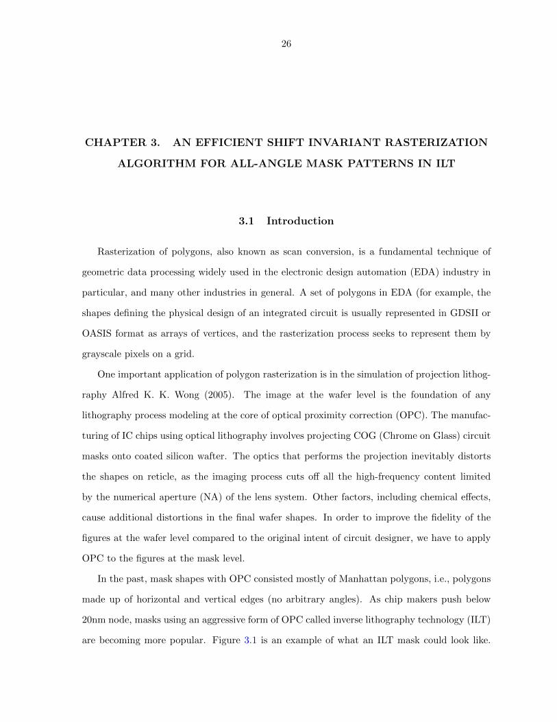
3.3.2 Definitions of small and large pixel . . . . . . . . . . . . . . . . . . . . . 32
3.3.3 Key observation . . . . . . . . . . . . . . . . . . . . . . . . . . . . . . . 32
3.3.4 LUT approach for non-exception large pixels . . . . . . . . . . . . . . . 33
3.3.5 Technique to handle exception large pixels . . . . . . . . . . . . . . . . . 34
3.3.6 Cost of lookup table . . . . . . . . . . . . . . . . . . . . . . . . . . . . . 37
3.3.7 Technique to obtain clipping configuration . . . . . . . . . . . . . . . . . 38
3.4 Experimental results . . . . . . . . . . . . . . . . . . . . . . . . . . . . . . . . . 38
3.4.1 Performance of our proposed algorithm . . . . . . . . . . . . . . . . . . 39
3.4.2 Compared with other rasterization approaches . . . . . . . . . . . . . . 40
3.4.3 Evaluation of shift-invariance property . . . . . . . . . . . . . . . . . . . 41
3.5 Conclusion . . . . . . . . . . . . . . . . . . . . . . . . . . . . . . . . . . . . . . 42
CHAPTER 4. SELF-ALIGNED DOUBLE PATTERNING LITHOGRAPHY
AWARE DETAILED ROUTING WITH COLOR PRE-ASSIGNMENT . . 44
4.1 Introduction . . . . . . . . . . . . . . . . . . . . . . . . . . . . . . . . . . . . . . 44
4.2 Preliminaries . . . . . . . . . . . . . . . . . . . . . . . . . . . . . . . . . . . . . 48
4.2.1 Core and cut/trim mask design rules . . . . . . . . . . . . . . . . . . . . 49
4.2.2 Overlay error . . . . . . . . . . . . . . . . . . . . . . . . . . . . . . . . . 49
4.2.3 Non-preferred turns . . . . . . . . . . . . . . . . . . . . . . . . . . . . . 50
4.2.4 Prohibited line-ends . . . . . . . . . . . . . . . . . . . . . . . . . . . . . 52
4.3 Problem formulation . . . . . . . . . . . . . . . . . . . . . . . . . . . . . . . . . 53
4.4 Proposed solution . . . . . . . . . . . . . . . . . . . . . . . . . . . . . . . . . . . 53

v
4.4.1 Overall flow . . . . . . . . . . . . . . . . . . . . . . . . . . . . . . . . . . 53
4.4.2 Color pre-assignment . . . . . . . . . . . . . . . . . . . . . . . . . . . . . 54
4.4.3 Graph model . . . . . . . . . . . . . . . . . . . . . . . . . . . . . . . . . 58
4.4.4 Overall routing scheme . . . . . . . . . . . . . . . . . . . . . . . . . . . . 62
4.5 Experimental results . . . . . . . . . . . . . . . . . . . . . . . . . . . . . . . . . 68
4.5.1 Compare with Seong-I Lei et al. (2014) . . . . . . . . . . . . . . . . . . 69
4.5.2 Compare with Iou-Jen Liu et al. (2014) . . . . . . . . . . . . . . . . . . 70
4.5.3 Compare with Xiaoqing Xu et al. (2015a) . . . . . . . . . . . . . . . . . 72
4.5.4 Demonstrate effectiveness of RNR heuristic . . . . . . . . . . . . . . . . 74
4.5.5 Demonstrate the solution quality and convergence of our routing scheme 76
4.5.6 Demonstrate effectiveness of color pre-assignment approach . . . . . . . 77
4.6 Conclusion . . . . . . . . . . . . . . . . . . . . . . . . . . . . . . . . . . . . . . 78
CHAPTER 5. SELF-ALIGNED DOUBLE PATTERNING-AWARE DETAILED
ROUTING WITH DOUBLE VIA INSERTION AND VIA MANUFAC-
TURABILITY CONSIDERATION . . . . . . . . . . . . . . . . . . . . . . . . 79
5.1 Introduction . . . . . . . . . . . . . . . . . . . . . . . . . . . . . . . . . . . . . . 79
5.2 Preliminaries . . . . . . . . . . . . . . . . . . . . . . . . . . . . . . . . . . . . . 84
5.2.1 Problem formulation . . . . . . . . . . . . . . . . . . . . . . . . . . . . . 84
5.2.2 Color pre-assignment approach . . . . . . . . . . . . . . . . . . . . . . . 84
5.2.3 Double via insertion feasibility . . . . . . . . . . . . . . . . . . . . . . . 85
5.2.4 Forbidden via pattern . . . . . . . . . . . . . . . . . . . . . . . . . . . . 87
5.3 Proposed solution . . . . . . . . . . . . . . . . . . . . . . . . . . . . . . . . . . . 89
5.3.1 Overall flow . . . . . . . . . . . . . . . . . . . . . . . . . . . . . . . . . . 89
5.3.2 Single net routing considering DVI and via layer TPL . . . . . . . . . . 90
5.3.3 Via layer TPL violation removal based rip-up and reroute . . . . . . . . 94
5.3.4 3-colorability check of decomposition graph . . . . . . . . . . . . . . . . 95
5.3.5 TPL-aware double via insertion . . . . . . . . . . . . . . . . . . . . . . . 96
5.4 Experimental results . . . . . . . . . . . . . . . . . . . . . . . . . . . . . . . . . 101
5.4.1 SADP-aware detailed routing considering DVI and via layer TPL . . . 101

vi
5.4.2 TPL-aware DVI . . . . . . . . . . . . . . . . . . . . . . . . . . . . . . . 105
5.5 Conclusion . . . . . . . . . . . . . . . . . . . . . . . . . . . . . . . . . . . . . . 106
CHAPTER 6. PIN ACCESSIBILITY-DRIVEN DETAILED PLACEMENT
REFINEMENT . . . . . . . . . . . . . . . . . . . . . . . . . . . . . . . . . . . . 107
6.1 Introduction . . . . . . . . . . . . . . . . . . . . . . . . . . . . . . . . . . . . . . 107
6.2 Preliminaries . . . . . . . . . . . . . . . . . . . . . . . . . . . . . . . . . . . . . 111
6.2.1 Assumptions . . . . . . . . . . . . . . . . . . . . . . . . . . . . . . . . . 111
6.2.2 Pin access region . . . . . . . . . . . . . . . . . . . . . . . . . . . . . . . 112
6.2.3 Pin access penalty . . . . . . . . . . . . . . . . . . . . . . . . . . . . . . 113
6.3 Problem formulation . . . . . . . . . . . . . . . . . . . . . . . . . . . . . . . . . 116
6.4 Proposed solution . . . . . . . . . . . . . . . . . . . . . . . . . . . . . . . . . . . 117
6.4.1 Framework . . . . . . . . . . . . . . . . . . . . . . . . . . . . . . . . . . 117
6.4.2 Refinement phase 1 . . . . . . . . . . . . . . . . . . . . . . . . . . . . . . 118
6.4.3 Refinement phase 2 . . . . . . . . . . . . . . . . . . . . . . . . . . . . . . 119
6.5 Experimental results . . . . . . . . . . . . . . . . . . . . . . . . . . . . . . . . . 121
6.6 Conclusion . . . . . . . . . . . . . . . . . . . . . . . . . . . . . . . . . . . . . . 125
CHAPTER 7. CONCLUSIONS AND FUTURE WORKS . . . . . . . . . . . 126
BIBLIOGRAPHY . . . . . . . . . . . . . . . . . . . . . . . . . . . . . . . . . . . . 129

vii
LIST OF TABLES
Table 2.1 Comparison withs ILP formulation . . . . . . . . . . . . . . . . . . . . 21
Table 2.2 Comparison of two trimming approaches on small-scale benchmarks . . 22
Table 2.3 Comparison of two trimming approaches on large-scale benchmarks . . 23
Table 3.1 Performance of our proposed algorithm . . . . . . . . . . . . . . . . . . 39
Table 3.2 Handling exception large pixels (ELP) . . . . . . . . . . . . . . . . . . 40
Table 3.3 Runtime comparison with other rasterization approaches . . . . . . . . 41
Table 3.4 CD error variations caused by rotation . . . . . . . . . . . . . . . . . . 42
Table 4.1 Statistics of benchmarks from Seong-I Lei et al. (2014) . . . . . . . . . 69
Table 4.2 Statistics of benchmarks from Iou-Jen Liu et al. (2014) . . . . . . . . . 69
Table 4.3 Statistics of benchmarks from Xiaoqing Xu et al. (2015a) . . . . . . . . 70
Table 4.4 Parameter values in the experiments . . . . . . . . . . . . . . . . . . . 70
Table 4.5 Compare with Seong-I Lei et al. (2014) . . . . . . . . . . . . . . . . . . 71
Table 4.6 Compare with Iou-Jen Liu et al. (2014) . . . . . . . . . . . . . . . . . . 73
Table 4.7 Compare with Xiaoqing Xu et al. (2015a) . . . . . . . . . . . . . . . . 75
Table 4.8 Demonstrate effectiveness of proposed RNR heuristic . . . . . . . . . . 76
Table 4.9 Demonstrate of color pre-assignment approach . . . . . . . . . . . . . . 77
Table 5.1 Parameter values in the experiments . . . . . . . . . . . . . . . . . . . 101
Table 5.2 SIM type SADP-aware detailed routing . . . . . . . . . . . . . . . . . . 102
Table 5.3 SID type SADP-aware detailed routing . . . . . . . . . . . . . . . . . . 103
Table 5.4 TPL-aware DVI for SIM type SADP-aware detailed routing . . . . . . 105
Table 5.5 TPL-aware DVI for SID type SADP-aware detailed routing . . . . . . 105

viii
Table 6.1 Statistics of benchmarks . . . . . . . . . . . . . . . . . . . . . . . . . . 121
Table 6.2 Comparison between the given placement and the placements after re-
finement . . . . . . . . . . . . . . . . . . . . . . . . . . . . . . . . . . . 122
Table 6.3 Comparison of the detailed routing results for the given and the refined
placements. . . . . . . . . . . . . . . . . . . . . . . . . . . . . . . . . . 123

ix
LIST OF FIGURES
Figure 1.1 Schematic diagram of conventional photolithography system . . . . . . 2
Figure 1.2 Lithography technology node roadmap . . . . . . . . . . . . . . . . . . 3
Figure 1.3 Layout manufacturing by LELE. (a) Target layout. (b) Features with
the same color represent a group of features processed at once. (c) Side
view of schematic LELE process (not drawn to scale). . . . . . . . . . 4
Figure 1.4 Both top-down and side views of schematic SIM type SADP process in
layout manufacturing (not drawn to scale). . . . . . . . . . . . . . . . . 5
Figure 1.5 Our contributions of DFM in their corresponding design stages. . . . . 6
Figure 2.1 SADP process in two steps: dense line generation and trimming. (a)
target layout pattern. (b) dense line generation. (c) trimming by gap
removal. (d) trimming by end cutting. . . . . . . . . . . . . . . . . . . 9
Figure 2.2 Three options to eliminate the violations of trim mask constraints. (a) A
simple 1D target layout. (b) Violation in trimming by end cutting. (c)
Merge two cuts. (d) Separate two cuts by line-end extension. (e) Print
one cut by e-beam shot. (f) Violation in trimming by gap removal. (g)
Merging two patterns. (h) Separate two patterns by line-end extension.
(i) Print one pattern by e-beam shot. . . . . . . . . . . . . . . . . . . . 11

x
Figure 2.3 End cutting approach performs better than gap removal approach for
M2 layout manufacturing. (a) Target layout on M2. (b) End cutting re-
quires less line-end extension to separate conflicting patterns. (c) Gap
removal requires more line-end extension to separate conflicting pat-
terns. (d) If wire extension exceeds the limit, one more e-beam shot is
required. . . . . . . . . . . . . . . . . . . . . . . . . . . . . . . . . . . . 24
Figure 3.1 An example of an ILT mask . . . . . . . . . . . . . . . . . . . . . . . . 27
Figure 3.2 Traditional rasterization approach. (a) A mask pattern laying on a
small-pixel grid. (b) Bitmap generation by scan conversion. (c) A
grayscale image in small pixels. (d) Grayscale values of large pixels. . . 30
Figure 3.3 The overall algorithm flow . . . . . . . . . . . . . . . . . . . . . . . . . 31
Figure 3.4 Small and large pixels. . . . . . . . . . . . . . . . . . . . . . . . . . . . 32
Figure 3.5 Non-exception and exception large pixels . . . . . . . . . . . . . . . . . 33
Figure 3.6 A large pixel convolution. (a) Given a large pixel with identified clip-
ping configuration. (b) Bitmap generation based on small pixel. (c)
Convolution based on small pixels. (d) Grayscale values of large pixels. 34
Figure 3.7 Exception large pixel convolution. (a) An exception large pixel and its
bitmap Bexp. (b) The corresponding non-exception large pixel and its
bitmap Bnon−exp. (c) Two bitmaps difference Bdiff . . . . . . . . . . . 35
Figure 3.8 A bad choice of corresponding non-exception large. (a) The same ex-
ception large pixel and its bitmap Bexp with Figure 3.7(a). (b) An bad
choice of corresponding non-exception large pixel and its bitmap. (c)
Bdiff with more non-zero entries. . . . . . . . . . . . . . . . . . . . . . 36
Figure 3.9 Fast heuristic to find correspondong non-exception large pixel. (a) The
same exception large pixel and its bitmap Bexp with Figure 3.7(a). (b)
A corresponding non-exception large pixel with diversity degree√
1014 .
(c) A corresponding non-exception large pixel with diversity degree√
21374 . 37
xi
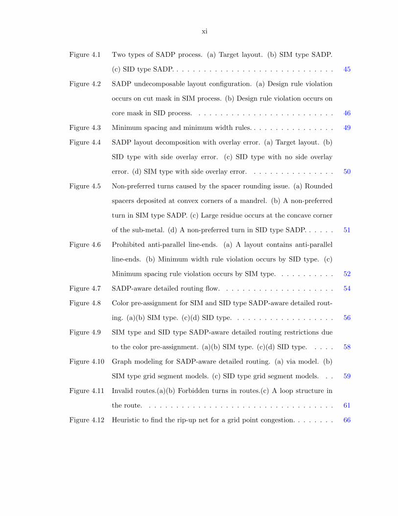
Figure 4.1 Two types of SADP process. (a) Target layout. (b) SIM type SADP.
(c) SID type SADP. . . . . . . . . . . . . . . . . . . . . . . . . . . . . . 45
Figure 4.2 SADP undecomposable layout configuration. (a) Design rule violation
occurs on cut mask in SIM process. (b) Design rule violation occurs on
core mask in SID process. . . . . . . . . . . . . . . . . . . . . . . . . . 46
Figure 4.3 Minimum spacing and minimum width rules. . . . . . . . . . . . . . . . 49
Figure 4.4 SADP layout decomposition with overlay error. (a) Target layout. (b)
SID type with side overlay error. (c) SID type with no side overlay
error. (d) SIM type with side overlay error. . . . . . . . . . . . . . . . 50
Figure 4.5 Non-preferred turns caused by the spacer rounding issue. (a) Rounded
spacers deposited at convex corners of a mandrel. (b) A non-preferred
turn in SIM type SADP. (c) Large residue occurs at the concave corner
of the sub-metal. (d) A non-preferred turn in SID type SADP. . . . . . 51
Figure 4.6 Prohibited anti-parallel line-ends. (a) A layout contains anti-parallel
line-ends. (b) Minimum width rule violation occurs by SID type. (c)
Minimum spacing rule violation occurs by SIM type. . . . . . . . . . . 52
Figure 4.7 SADP-aware detailed routing flow. . . . . . . . . . . . . . . . . . . . . 54
Figure 4.8 Color pre-assignment for SIM and SID type SADP-aware detailed rout-
ing. (a)(b) SIM type. (c)(d) SID type. . . . . . . . . . . . . . . . . . . 56
Figure 4.9 SIM type and SID type SADP-aware detailed routing restrictions due
to the color pre-assignment. (a)(b) SIM type. (c)(d) SID type. . . . . 58
Figure 4.10 Graph modeling for SADP-aware detailed routing. (a) via model. (b)
SIM type grid segment models. (c) SID type grid segment models. . . 59
Figure 4.11 Invalid routes.(a)(b) Forbidden turns in routes.(c) A loop structure in
the route. . . . . . . . . . . . . . . . . . . . . . . . . . . . . . . . . . . 61
Figure 4.12 Heuristic to find the rip-up net for a grid point congestion. . . . . . . . 66

xii
Figure 4.13 (a) Prohibited line-end region. (b) Prohibited anti-parallel line-ends
cause cut mask design rule violation by SIM type SADP lithography.
(c) Line end extension is performed. (d) No design rule violation by
SIM type SADP lithography. . . . . . . . . . . . . . . . . . . . . . . . . 67
Figure 4.14 The solution quality and convergence of our SADP-aware detailed rout-
ing with different parameter settings. . . . . . . . . . . . . . . . . . . . 76
Figure 5.1 Layout decomposition. (a) Target layout. (b) TPL layout decomposi-
tion. (c) SIM type SADP with cut approach layout decomposition. (d)
SID type SADP with trim approach layout decomposition. . . . . . . . 81
Figure 5.2 (a) Same-color via pitch. (b) A via pattern forms a TPL violation in
SADP-aware detailed routing solution. . . . . . . . . . . . . . . . . . . 81
Figure 5.3 (a) Detailed routing without DVI consideration. (b) Detailed routing
considering DVI. . . . . . . . . . . . . . . . . . . . . . . . . . . . . . . 84
Figure 5.4 Color pre-assignment for SADP-aware detailed routing. (a) SIM type
SADP. (b) SID type SADP. . . . . . . . . . . . . . . . . . . . . . . . . 86
Figure 5.5 Double via insertion. (a) Each single via has four DVICs. (b) The DVIC
d is infeasible. . . . . . . . . . . . . . . . . . . . . . . . . . . . . . . . . 87
Figure 5.6 (a)(b) DVI feasibility in SIM type SADP-aware detailed routing. (c)(d)
DVI feasibility in SID type SADP-aware detailed routing. . . . . . . . 88
Figure 5.7 Via patterns in 3x3 subregion and its decomposition graph. (a) A via
pattern with 5 vias which is not an FVP. (b) An FVP with 5 vias, in
which one via is uncolorable. (c) A via pattern with 4 vias which is not
an FVP. (d) An FVP with 4 vias, in which one via is uncolorable. . . . 89
Figure 5.8 Overall flow. . . . . . . . . . . . . . . . . . . . . . . . . . . . . . . . . . 90
Figure 5.9 An example to illustrate how cost assignment scheme works for single
net routing (colored routing grid is not shown for clarity). (a) viau
of neti has three feasible DVICs. (b) Block-DVIC via locations. (c)
Along-metal via locations. (d) Conflict-DVIC via locations. . . . . . . 91

xiii
Figure 5.10 Examples of how vias are blocked in via layer TPL violation removal
based R&R. . . . . . . . . . . . . . . . . . . . . . . . . . . . . . . . . . 95
Figure 5.11 Post-routing DVI. (a) Two adjacent single vias. (b) A TPL violation
occurs after DVI. (c) TPL-aware DVI. . . . . . . . . . . . . . . . . . . 96
Figure 5.12 TPL-aware DVI. (a) Four single via, and via v has three feasible DVICs.
(b) An FVP occurs when a redundant via is inserted at a. (b) An FVP
occurs when a redundant via is inserted at c. (c) No FVP occurs when
a redundant via is inserted at d. . . . . . . . . . . . . . . . . . . . . . . 100
Figure 6.1 Detailed routing around pins in a standard cell. (a) A standard cell
with three pins. (b) Pin C cannot be accessed because all its tapping
points are blocked. (c) A wise choice of tapping points makes all pins
accessible. . . . . . . . . . . . . . . . . . . . . . . . . . . . . . . . . . . 108
Figure 6.2 Enhance pin accessibility in DR. (a) Pin access becomes harder within
area with high pin density. (b) Pin E cannot be accessed even with a
careful choice of tapping points. . . . . . . . . . . . . . . . . . . . . . . 109
Figure 6.3 Three approaches to enhance pin accessibility in DP (a) Cell shifting.
(b) Cell flipping. (c) Adjacent cell swap. . . . . . . . . . . . . . . . . . 109
Figure 6.4 The minimum center-to-center spacing rule in via design rules. . . . . . 111
Figure 6.5 A PAR is defined for each pin-to-pin connection of each pin. Connection
AB is a same-row connection while connection CD is a different-row
connection. . . . . . . . . . . . . . . . . . . . . . . . . . . . . . . . . . 112
Figure 6.6 Penalty function fw(dist) for (a) same-row connection. (b) different-row
connection. . . . . . . . . . . . . . . . . . . . . . . . . . . . . . . . . . 114
Figure 6.7 PAP in four scenarios. (a) 1st scenario. (b) 2nd scenario. (c) 3rd
scenario. (d) 4th scenario. . . . . . . . . . . . . . . . . . . . . . . . . . 115
Figure 6.8 Our framework . . . . . . . . . . . . . . . . . . . . . . . . . . . . . . . 117

xiv
ACKNOWLEDGEMENTS
Firstly, I am heartily thankful to my adviser, Professor Chris C.-N. Chu. He is a wise leader
and guides me to pursue meaningful research. He is a experienced mentor and helps me to
solve challenging problems. He is also a dear friend and encourages me to overcome various
difficulties. It has been a great honor and pleasure to be your student.
Secondly, my sincere thanks go to Prof. Wai-Kei Mak. He is a great mentor and gives me
numerous insights and suggestions to my research.
Thirdly, I am really thankful to my committee members, including Prof. Akhilesh Tyagi,
Prof. David Fernandez-Baca, Prof. Phillip Jones, and Prof. Randall Geiger. Thanks for
making technical comments on my research and dissertation, and pointing out future research
directions. In addition, I would like to give my special thanks to Professor David Fernandez-
Baca. You lead me to a fun world of algorithm.
Besides, I really appreciate Dr. Charles Alpert, Dr. Zhuo Li, Dr. Mehmet Yildiz, Dr.
Wen-Hao Liu in Cadence Design Systems. They are helpful teammates and teachers during
my internship. Furthermore, I also thanks Dr. Min Pan in Synopsys Inc. He is a responsible
and supportive supervisor during my internship.
I am lucky to have been working with the colleagues at Prof. Chris C.-N. Chu’s group:
Dr. Tao Lin, Dr. Gang Wu, and Ankur Sharma. It has been a great pleasure to working
with you. In addition, I would like to thank Guolei Yang and Xiaoqing Xu for all the inspiring
discussions.
Last but not least, I am deeply thankful to my parents. Without your support and care, I
cannot start and complete my Ph.D. study.

xv
ABSTRACT
As the technology nodes keep shrinking following Moore’s law, lithography becomes increas-
ingly critical to the fabrication of integrated circuits. The 193nm ArF immersion lithography
(193i) has been a common technique for manufacturing integrated circuits. However, the 193i
with single exposure has finally reached its printability limit at the 28nm technology node.
To keep the pace of Moore’s law, design for manufacturability (DFM) is demonstrated to be
effective and cost-efficient. The concept of DFM is to modify the design of integrated circuits
in order to make them more manufacturable. Tremendous efforts have been made for DFM in
advanced lithography technologies. In general, the progress can be summarized in four direc-
tions. (1) Advanced lithography process by novel patterning techniques and next-generation
lithography; (2) High performance lithography simulation approach in mask synthesis; (3)
Physical design (PD) methodology with lithography manufacturability awareness; (4) Robust
design flow integrating emerging PD challenges. Accordingly, we propose our research topics
in those directions. (1) Throughput optimization for self-aligned double patterning (SADP)
and e-beam lithography based manufacturing of 1D layout; (2) Design of efficient rasterization
algorithm for mask patterns in inverse lithography technology (ILT); (3) SADP-aware detailed
routing; (4) SADP-aware detailed routing with consideration of double via insertion and via
manufacturability; (5) Pin accessibility driven detailed placement refinement.
In our first research work, we investigate throughput optimization of 1D layout manufac-
turing. SADP is a mature lithography technique to print 1D gridded layout for advanced
technologies. However, in 16nm technology node, trim mask pattern in SADP lithography
process may not be printable using 193i along within a single exposure. A viable solution is to
complement SADP with e-beam lithography. To order to increase the throughput of 1D lay-
out manufacturing, we consider the problem of e-beam shot minimization subject to bounded
line-end extension constraints. Two different approaches of utilizing the trim mask and e-beam

xvi
to print a 1D layout are considered. The first approach is trimming by end cutting, in which
trim mask and e-beam are used to chop up parallel lines at required locations by small fixed
rectangles. The second approach is trimming by gap removal, in which trim mask and e-beam
are used to rid of all unnecessary portions. We propose elegant integer linear program for-
mulations for both approaches. Experimental results show that both integer linear program
formulations can be solved efficiently and have a major speedup compared with previous related
work. Furthermore, the pros and cons of the two approaches for manufacturing 1D layout are
discussed.
In our second research work, we focus on a critical problem of lithography simulation in
the design of ILT mask. To reduce the complexity of modern lithography simulation, a widely
used approach is to first rasterize the ILT mask before it is inputted to the simulation tool.
Accordingly, we propose a high performance rasterization algorithm. The algorithm is based
on a pre-computed look-up table. Every pixel in the rasterized image is firstly identified its
category: exception or non-exception. Then convolution for every pixel can be performed by
a single or multiple look-up table queries depending on its category. In addition, the proposed
algorithm has shift invariant property and can be applied for all-angle mask patterns in ILT.
Experimental results demonstrate that our approach can speedup conventional rasterization
process by almost 500x while maintaining small variations in critical dimension.
In our third research work, we concentrate on SADP-aware detailed routing. SADP is
a promising manufacturing option for sub-22nm technology nodes due to its good overlay
control. To ensure layout is manufacturable by SADP, it is necessary to consider it during
layout configuration, e.g., detailed routing stage. However, SADP process is not intuitive in
terms of mask design, and considering it during detailed routing stage is even more challenging.
We investigate both of two popular types of SADP: spacer-is-dielectric and spacer-is-metal.
Different from previous works, we apply the color pre-assignment idea and propose an elegant
graph model which captures both routing and SADP manufacturing cost. They greatly simplify
the problem to maintain SADP design rules during detailed routing. A negotiated congestion
based rip-up and reroute scheme is applied to achieve good routability while maintaining SADP
design rules. Our approach can be extended to consider other multiple patterning lithography

xvii
during detailed routing, e.g., self-aligned quadruple patterning targeted at sub-10nm technology
nodes. Compared with state-of-the-art academic SADP-aware detailed routers, we offer routing
solution with better quality of result.
In our fourth research work, we extend our SADP-aware detailed routing to consider other
manufacturing issues. Both SADP and triple patterning lithography (TPL) are potential layout
manufacturing techniques in 10nm technology node. While metal layers can be printed by
SADP, via layer manufacturing requires TPL. Previous works on SADP-aware detailed routing
do not automatically guarantee via layer are manufacturable by TPL. We extend our SADP-
aware detailed routing to consider TPL manufacturability of via layer. Double via insertion is an
effective method to improve yield and reliability in integrated circuits manufacturing. We also
consider it in our SADP-aware detailed routing to further improve insertion rate. A problem of
TPL-aware double via insertion in the post routing stage is proposed. It is solved by both integer
linear programming and high-performance heuristic. Experimental results demonstrate that
our SADP-aware detailed routing can ensure via layer are TPL manufacturable and improve
double via insertion rate.
In our last research work, we target at the enhancement of pin access. The significant
increased number of routing design rules in advanced technologies has made pin access an
emerging difficultly in detailed routing. Resolving pin access in detailed routing may be too
late due to the fix pin locations. Thus, we consider pin access in earlier design stage, i.e.,
detailed placement stage, when perturbation of cell placement is allowed. A cost function is
proposed to model pin access for each pin-to-pin connection in detailed routing. A two-phase
detailed placement refinement is performed to improve pin access, and refinement techniques
are limited to cell flipping, same-row adjacent cell swap and cell shifting. The problem is
solved by dynamic programming and linear programming. Experimental results demonstrate
that the proposed detailed placement refinement improve pin access and reduce the number of
unroutable nets in detailed routing significantly.

1
CHAPTER 1. INTRODUCTION
1.1 Background
The technology node has been scaling down year by year following Moore’s law. It shrinks
from 180nm in late 1990s to 14nm designs today. To keep up with the Moore’s law, semicon-
ductor industry has been trying to make the feature size of very large scale integrated circuit
(VLSI) smaller. However, the conventional 193nm ArF immersion lithography (193i) with sin-
gle exposure reaches its resolution limit at 28nm technology node. To overcome such bottleneck,
a variety of innovations and tremendous efforts to optimize design and manufacturability are
required. In such context, a set of techniques are developed to modify the design of integrate
circuits (IC) in order to make them more manufacturable, i.e., to improve throughput, yield,
and reliability. This is the birth of the concept of design for manufacturability (DFM). It is
proven to be an effective and cost-efficient approach to solve those joint challenges and optimize
the trade-off between design and manufacturability. In this dissertation, we will demonstrate
our research works contributed to the DFM field.
1.2 Photolithography system
As illustrate in Figure 1.1, a conventional photolithography system consists of five major
components: light source, optical system, mask, projection system, and silicon wafer. The
high intensity light source is used to transferred geometric patterns from the mask to the
light-sensitive chemical called photoresist on the silicon wafer The minimum feature size that
a photolithography system can print is computed approximately as follows.
CD = k1 ×λ
NA

2
where CD is the minimum feature size (also known as critical dimension), k1 is a process-
related coefficient, λ is the wavelength of light source, and NA is the numerical aperture of
the projection system as seen from the silicon wafer. Based on above equation, the ability
to print a small feature onto the wafer clearly is limited by k1, NA, and λ. k1 typically is
equal to 0.4 for production, and can be reduced to 0.25 with intensive resolution enhancement
techniques (RET), such as optical proximity correction (OPC) Alfred Kwok-Kit Wong (2001)
NA can be increased to 1.35 by immersion lithography (IL), where water replaces usual air gap
between projection system and silicon wafer Yayi Wei and David Back (2007). State-of-the-art
photolithography systems use deep ultraviolet (DUV) light from excimer laser with wavelength
of 193nm. Therefore, current photolithography systems are reaching their printability limit at
28nm technology node after continuous advance of Moore’s law.
Figure 1.1 Schematic diagram of conventional photolithography system
1.3 Advanced lithography technologies
As shown in Figure 1.2, simply relying on RET to print IC designs at the sub-28nm is far
from enough. As a result, various advanced lithography technologies are developed to keep the
continuation of Moore’s law. In this dissertation, we concentrate on two categories of advanced

3
lithography technologies. In the first category, 193i is still used but novel patterning techniques,
e.g., multiple patterning, are applied in photolithography to enhance resolution limit. In the
second category, a range of lithography techniques are developed to replace the conventional
photolithography in integrated circuit (IC) manufacturing. We refer to them as next-generation
lithography (NGL).
Figure 1.2 Lithography technology node roadmap
Multiple patterning lithography (MPL) is considered the most viable solution to the emerg-
ing technology nodes. The premise is that the conventional lithography with a single exposure
cannot provide sufficiently small feature size. Hence more exposure-etch steps are applied in the
lithography process to achieve higher feature density. To realize such process, all the features in
the original layout are divided into several groups. Each group may be processed conventionally
by a mask through one exposure-etch step. By interleaving the features produced in all steps,
the feature density in final layout can be increased. Thus, the feature size in the final layout
which is previously limited by the conventional lithography with a single exposure can be fur-
ther split. Depending on the number of exposure-etch steps, MPL has several forms including
double patterning lithography (DPL), triple patterning lithography (TPL), and even quadruple
patterning lithography (QPL). The earliest and simplest form of DPL is litho-etch-litho-etch
(LELE). Figure 1.3 is an example of layout manufacturing by LELE Paul Zimmerman (2009).

4
Figure 1.3 Layout manufacturing by LELE. (a) Target layout. (b) Features with the same
color represent a group of features processed at once. (c) Side view of schematic
LELE process (not drawn to scale).
In the chip manufacturing industry, LELE is extensively applied on the 22nm technology node
designs. Meanwhile, TPL and QPL are been developed and tested for manufacturing 10nm
technology node designs and sub-10nm technology node designs, respectively. A major concern
of MPL is the mask alignment error between separate steps, which is also called overlay error.
This is the main reason that the practical resolution limit of MPL is significant larger than the
theoretical one. Consequently, self-align multiple patterning (SAMP) is developed to overcome
MPL’s disadvantage. Among various forms of SAMP, self-aligned double patterning (SADP)
is one of the potential candidate techniques for 10nm technology nodes. There are two major
types of SADP, one is spacer-is-metal (SIM) and the other one is spacer-is-dielectric (SID).
Figure 1.4 shows an example of layout manufacturing by SIM type SADP.
With increasing number of exposure-etch steps, the costs of MPL increase dramatically
including additional mask synthesis cost and extra turnaround time, etc. This motivates a
continued search for a NGL that can achieve required feature size with a single exposure. The
candidates for NGL include electron-beam lithography (EBL), extreme ultraviolet lithography

5
Figure 1.4 Both top-down and side views of schematic SIM type SADP process in layout
manufacturing (not drawn to scale).
(EUV), directed self-assembly (DSA), etc. EBL is one of the most important techniques in
nanofabrication. It involves the exposure by a focused beam of electrons to directly draw
custom shapes onto a wafer covered with an electron-sensitive film called a resist. EBL uses
electrons instead of photons to expose a resist, which has a much smaller wavelength. Thus,
it has much higher intrinsic resolution down to sub-10nm. In addition, electron beam can be
focused onto wafer directly without a mask and controlled so that it only exposes intended
area. As a maskless lithography, EBL can save the mask manufacturing cost. However, EBL
suffers from low throughput capability and expensive cost of operation and implementation.
Hence, its usage is limited to low-volume production. For example, EBL can be complemented
to MPL in layout manufacturing at 16nm technology node.
1.4 Overview of this dissertation
In this dissertation, we will demonstrate our research works contributed to the DFM in
advanced lithography technologies. Figure 1.5 presents each of our contributions in its corre-
sponding stage of IC design flow. Note that not all stages of IC design flows are shown in the
Figure. The rest of dissertation is organized as follows.
In Chapter 2, we investigate the throughput optimization of 1D layout manufacturing. We
focus on the manufacturing approach of SADP with complementary EBL. To increase the

6
Figure 1.5 Our contributions of DFM in their corresponding design stages.
throughput of 1D layout manufacturing, we consider the problem of e-beam shot minimization
subject to bounded line-end extension constraints. Two different approaches of utilizing the
trim mask and e-beam to print a 1D layout are considered. One is trimming by end cutting
and the other is trimming by gap removal. We propose elegant ILP formulations for both
approaches.
In Chapter 3, we focus on the performance improvement of rasterization algorithm, which is
widely used in lithography simulation during the design of inverse lithography technology (ILT)
masks. We propose an efficient rasterization algorithm based on a pre-computed look-up table.
Every pixel in the rasterized image is firstly identified its category: exception or non-exception.
Then convolution for every pixel can be performed by a single or multiple look-up table queries
depending on its category. In addition, the proposed algorithm has shift invariant property
and can be applied for all-angle mask patterns in ILT.
In Chapter 4, we concentrate on the challenging problem of SAPD-aware detailed routing.
We consider both SIM and SID types of SADP. We adopt the idea of color pre-assignment to

7
resolve the difficulty of maintaining SADP design rules in detailed routing. We propose an
elegant graph model which captures both routing and SADP manufacturing cost. A negoti-
ated congestion based rip-up and reroute scheme is applied to achieve good routability while
maintaining SADP design rules.
In Chapter 5, we extend both SIM and SID types SADP-aware detailed routing to consider
other manufacturing issues. Specifically, via layer manufacturing by TPL is considered in
SADP-aware detailed routing. We ensure that via layer patterns are TPL manufacturable while
metal layer patterns are compliant to SADP. Furthermore, we consider double via insertion
(DVI) in SADP-aware detailed routing to improve insertion rate. The problem of TPL-aware
DVI in the post routing stage is formulated. Both optimal integer linear programming and
high-performance heuristic approaches are proposed to solve the problem.
In Chapter 6, we look into pin access issue in detailed placement stage. A cost function is
proposed to model pin access for each pin-to-pin connection in detailed routing. Based on the
cost function, we propose a two-phase detailed placement refinement to improve pin access. In
the first phase, cell flipping and same-row adjacent cell swap are applied to refine the placement.
The problem is solved by dynamic programming. In the second phase, cell shifting is applied
and the problem is solved by linear programming.
We will summarize and conclude this dissertation in Chapter 7.

8
CHAPTER 2. THROUGHPUT OPTIMIZATION FOR SADP AND
E-BEAM BASED MANUFACTURING OF 1D LAYOUT
2.1 Introduction
The IC industry has been moving towards highly regular 1D gridded designs for advanced
nodes Christopher Bencher et al. (2009); Clair Webb (2008); Michael C. Smayling et al. (2008);
Michael C. Smayling (2013). The use of 1D patterns and a simplified set of gridded design
rules simplify both design and fabrication compared to conventional 2D layout style. It has
been shown to result in better yield, smaller area, and better uniformity Michael C. Smayling
et al. (2008).
Self-aligned double patterning (SADP) is an excellent option for 1D gridded design manufac-
turing Hongbo Zhang et al. (2011). While lithoetch-litho-etch type double patterning requires
high overlay accuracy in the exposure equipment, SADP can fabricate fine unidirectional line
patterns without any overlay error easily. In the first step of SADP, uniform dense lines of the
intended pitch are formed as illustrated in Figure 2.1(b). Then, the portions not on the design
can be removed by a trim mask in the second step as shown in Figure 2.1(c). We will refer to
this approach as trimming by gap removal.
On the other hand, Yuelin Du et al. (2012) proposed another possibility of trimming the
layout for 1D gridded design at sub-20nm process node. Instead of totally removing the un-
wanted portions after fabricating the unidirectional line patterns, one may use small fixed size
rectangular cuts (48nm by 32nm for 16nm process node) to chop up the parallel tracks into
real and dummy wires as shown in Figure 2.1(d). We will refer to this approach as trimming
by end cutting.

9
Figure 2.1 SADP process in two steps: dense line generation and trimming. (a) target layout
pattern. (b) dense line generation. (c) trimming by gap removal. (d) trimming by
end cutting.
However, at sub-20nm process node, the trim mask may not be printable using 193nm
immersion (193i) lithography alone. For the gap removal approach, some unwanted portions
may become too small or too close to each other and violate the design rules of the trim mask.
For the end cutting approach, the cuts may be too close to each other that forbidden patterns
may be formed and cannot be printed by 193i.
As a solution, it is possible to apply the trim mask to rid of most of the unwanted portions
/ print most of the cuts and then apply e-beam lithography to remove the remaining unwanted
portions / print the remaining cuts. This is an example of complementary or hybrid lithography
Steven Steen et al. (2006); David K. Lam et al. (2011); Hideaki Komami et al. (2012). In this
chapter, we assume variable-shaped beam (VSB) method H. C. Pfeiffer (1978) is used in e-beam
lithography.
Yuelin Du et al. (2012) considered the end cutting approach for trimming and formulated a
cut redistribution problem to maximize the number of cuts printed by 193i lithography while not

10
violating any rule of forbidden patterns. Hence, the number of e-beam cuts can be minimized
and the manufacturing throughput will be increased. However, there are two shortcomings
in their work. First, their problem formulation assumes that line end extension is allowed as
long as the logic connections are not changed when performing cut redistribution. Thus, the
length of the wire segments may be greatly increased. This is not desirable in practice since
significant line end extension will affect the circuit performance. Second, the proposed ILP-
based cut redistribution algorithm in Yuelin Du et al. (2012) was very time consuming. The
CPU time of their optimal ILP for small layouts was up to 9 hours. For larger layouts, they
proposed a faster iterative non-optimal version but still required hours of CPU time.
In this work, we investigate the printing of 1D layout with complementary SADP / e-
beam lithography. We solve two problems of e-beam shot minimization, one for trimming by
end cutting and another for trimming by gap removal, underline end extension constraint on
individual wires to limit performance impact. For trimming by end cutting, we propose a fast
optimal ILP based solution which is on average more than 1000 times faster than that in Yuelin
Du et al. (2012). For trimming by gap removal, we give an optimal ILP based solution which
is also very efficient in practice and can reduce the e-beam shot count by about 41.38% on
average compared to trimming by end cutting based on layout benchmarks for M1 layer.
The rest of the chapter is organized as follows. Section 2 firstly provides an overview of
SADP and e-beam process. Then, it gives formal problem definitions for both trimming by end
cutting and trimming by gap remova. In Section 3, we give elegant ILP formulations for both
of the problems. Section 4 presents our experimental results. Finally, Section 5 concludes this
chapter.
2.2 Problem description
2.2.1 Overview of SADP and E-beam process
The traditional SADP has two major steps. The first step is dense line generation. Suppose
the intended 1D layout pitch is p. 1D tracks with pitch 2p will firstly be fabricated. Printing
at two times of the intended pitch is relatively easy to handle with 193i technology. By etching

11
Figure 2.2 Three options to eliminate the violations of trim mask constraints. (a) A simple
1D target layout. (b) Violation in trimming by end cutting. (c) Merge two cuts.
(d) Separate two cuts by line-end extension. (e) Print one cut by e-beam shot. (f)
Violation in trimming by gap removal. (g) Merging two patterns. (h) Separate
two patterns by line-end extension. (i) Print one pattern by e-beam shot.
all the film material on the horizontal surface of 1D tracks and the original 1D tracks, a spacer
which is a film layer deposited on the sidewall of 1D tracks is formed. Since there are two
spacers for each track, the line density is doubled and pitch is halved.
The second step is trim mask application. In order to achieve the intended circuit pattern
and functionality, some portions of the metal lines need to be trimmed away with the help of
a trim mask. In practice, the trim mask can be designed by two different approaches. One
is to use fixed size rectangular cuts to chop up the parallel lines at required positions such
that the unwanted portions are separated from real wires. As a result, the trim mask contains
those small rectangular cuts. We call this approach trimming by end cutting. The other one
is to directly remove unwanted portions of wires. As a result, the trim mask contains patterns
covering those unwanted portions. We refer to those unwanted portions as gaps and call this
approach trimming by gap removal.

12
In SADP, the trim mask is printed by 193i lithography. The patterns on the trim mask must
satisfy minimum spacing and minimum width constraints. However at sub-20nm process node,
for both trimming approaches, it is very likely that some trimming patterns would violate the
trim mask constraints. In that case, the violations must be eliminated by some combinations
of line end extension and e-beam lithography.
For both trimming approaches, three options to eliminate the violations are illustrated by
the printing of the simple 1D layout in Figure 2.1(a). For trimming by end cutting, lets focus on
cuts 1 and 2 in Figure 2.1(b). Suppose they are too close to each other such that the minimum
spacing constraint is violated. To resolve the violation, one option is to merge the two cuts
into a single one as shown in Figure 2.1(c). Note that the line ends need to be extended to
align the cuts vertically. Another option, as shown in Figure 2.1(d), is to separate the two cuts
from each other by extending the line ends. The third option is to use 193i to print cut 1 and
e-beam to print cut 2 as shown in Figure 2.1(e). Now consider trimming by gap removal. As
shown in Figure 2.1(f), the two patterns covering the gaps are too close to each other. Similar
to above, we have three options to resolve it. The first option is to merge the two patterns
as in Figure 2.1(g), as long as the abutting part satisfies the minimum width constraint. The
second option, as shown in Figure 2.1(h), is to separate the two patterns from each other by
extending the line ends. The third option is to print one of the patterns by e-beam as shown
in Figure 2.1(i).
However, due to the throughput impact of e-beam shot count, we want to minimize the
number of e-beam shots used. Meanwhile, significant amount of wire extension may affect
circuit timing. In particular, some wires may be on the critical paths of the design for which
wire extension is not even allowed. Consequently, we introduce a line end extension constraint
for each wire which limits the allowed length of wire extension. We also want to minimize the
total length of wire extension while satisfying line end constraints of all the wires.
2.2.2 Problem formulation
Given a 1D layout, we would like to use complementary lithography with SADP and e-beam
to print it. For each wire, a maximum allowed extension length is given. The problem is to

13
minimize a weighted sum of the number of e-beam shots and the total line end extension length
subject to layout constraints on trim mask and line end extension constraints on individual
wires. Based on the two different approaches of trim mask design, we can formulate two
different problems for complementary SADP / e-beam lithography of 1D layout.
2.2.2.1 Trimming by end cutting
To trim a 1D layout by end cutting, each wire is delineated by two small rectangular cuts
on its two ends. The problem is basically to redistribute the cuts in order to eliminate all
forbidden patterns while minimizing the required number of e-beam shots and total line end
extension length. Yuelin Du et al. (2012) has considered a similar problem. Different from
their work, we are adding line end extension constraints to the problem as a way to control the
impact on performance.
2.2.2.2 Trimming by gap removal
Given a 1D layout, a gap is defined by the ends of the two wires on its left and right sides.
For gap removal trimming approach, the problem is to determine the cut required for each gap
to remove all or part of it so that the cut patterns are printable while the required number of
e-beam shots and total line end extension length are minimized.
Compared with trimming by end cutting, trimming by gap removal intuitively has its
advantages. In order to get rid of an unwanted portion, end cutting uses two small cuts
to separate it from real wires. However, gap removal directly removes the unwanted portions
with one cut. The number of cuts required to define the wires is relatively smaller. Thus
the number of e-beam shots required is potentially smaller. We confirm this intuition in the
experimental results section.
2.3 Proposed solution
We propose an elegant ILP formulation for each of the problems. Experimental results
demonstrate that ILP solver can solve the ILPs in a very efficient manner.
14
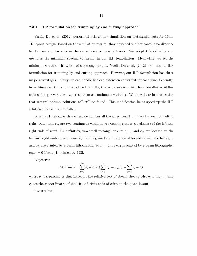
2.3.1 ILP formulation for trimming by end cutting approach
Yuelin Du et al. (2012) performed lithography simulation on rectangular cuts for 16nm
1D layout design. Based on the simulation results, they obtained the horizontal safe distance
for two rectangular cuts in the same track or nearby tracks. We adopt this criterion and
use it as the minimum spacing constraint in our ILP formulation. Meanwhile, we set the
minimum width as the width of a rectangular cut. Yuelin Du et al. (2012) proposed an ILP
formulation for trimming by end cutting approach. However, our ILP formulation has three
major advantages. Firstly, we can handle line end extension constraint for each wire. Secondly,
fewer binary variables are introduced. Finally, instead of representing the x-coordinates of line
ends as integer variables, we treat them as continuous variables. We show later in this section
that integral optimal solutions will still be found. This modification helps speed up the ILP
solution process dramatically.
Given a 1D layout with n wires, we number all the wires from 1 to n row by row from left to
right. x2i−1 and x2i are two continuous variables representing the x-coordinates of the left and
right ends of wirei. By definition, two small rectangular cuts c2i−1 and c2i are located on the
left and right ends of each wire. e2i1 and e2i are two binary variables indicating whether c2i−1
and c2i are printed by e-beam lithography. e2i−1 = 1 if c2i−1 is printed by e-beam lithography;
e2i−1 = 0 if c2i−1 is printed by 193i.
Objective:
Minimize2n∑i=1
ei + α× (n∑i=1
x2i − x2i−1 −n∑i=1
ri − li)
where α is a parameter that indicates the relative cost of ebeam shot to wire extension, li and
ri are the x-coordinates of the left and right ends of wirei in the given layout.
Constraints:

15
C1. Constraints for line-end extension
x2i ≥ ri 1 ≤ i ≤ n
x2i − x2i−1 ≤ ri − li + δi 1 ≤ i ≤ n
x2i−1 ≤ li 1 ≤ i ≤ n
x2i−1 ≥ LL 1 ≤ i ≤ n
x2i ≤ RR 1 ≤ i ≤ n
where δi is the allowed wire extension for each wirei, LL and RR are the x-coordinates of the
left and right boundaries in the given layout.
C2. Constraints for gap between wires
For any gapk between wirei and wirei+1 in the given layout, ri and li + 1 are the x-
coordinates of its left and right ends. We denote it as gapk[ri, li+1]. Two small rectangular
cuts c2i and c2i+1 locate on the left and right ends of gapk, respectively. m2i2i+1 is a binary
variable indicating whether c2i and c2i+1 overlap or abut. m2i2i+1 = 0 if c2i and c2i+1 do not
overlap or abut. In this case, c2i and c2i+1 should be separated horizontally by at least the
minimum spacing. Otherwise, one of two cuts should be printed by e-beam. m2i2i+1 = 1 if c2i
and c2i+1 overlap or abut, which means the two cuts merge into a single cut. Hence, we have
the following constraints.
x2i+1 − x2i +B × e2i+1 +B × e2i +B ×m2i2i+1 ≥ mins
x2i+1 − x2i −B × (1−m2i2i+1) ≤ 2×minw
x2i+1 − x2i ≥ minw
where B is a very big constant, mins is the minimum cut spacing, and minw is the minimum
cut width.
C3. Constraint for non-overlapping gaps
Given gapp[ri, li+ 1] and gapq[rj , lj+1], distpq = max(ri, rj)min(li+1, lj+1) is defined as the
horizontal distance for them. We say gapp[ri, li+1] and gapq[rj , lj+1] are non-overlapping in the
horizontal direction if distpq ≥ 0. If 0 ≤ distpq < mins, a forbidden pattern occurs. There are
three available options to resolve a forbidden pattern: (1) merging a pair of rectangular cuts by
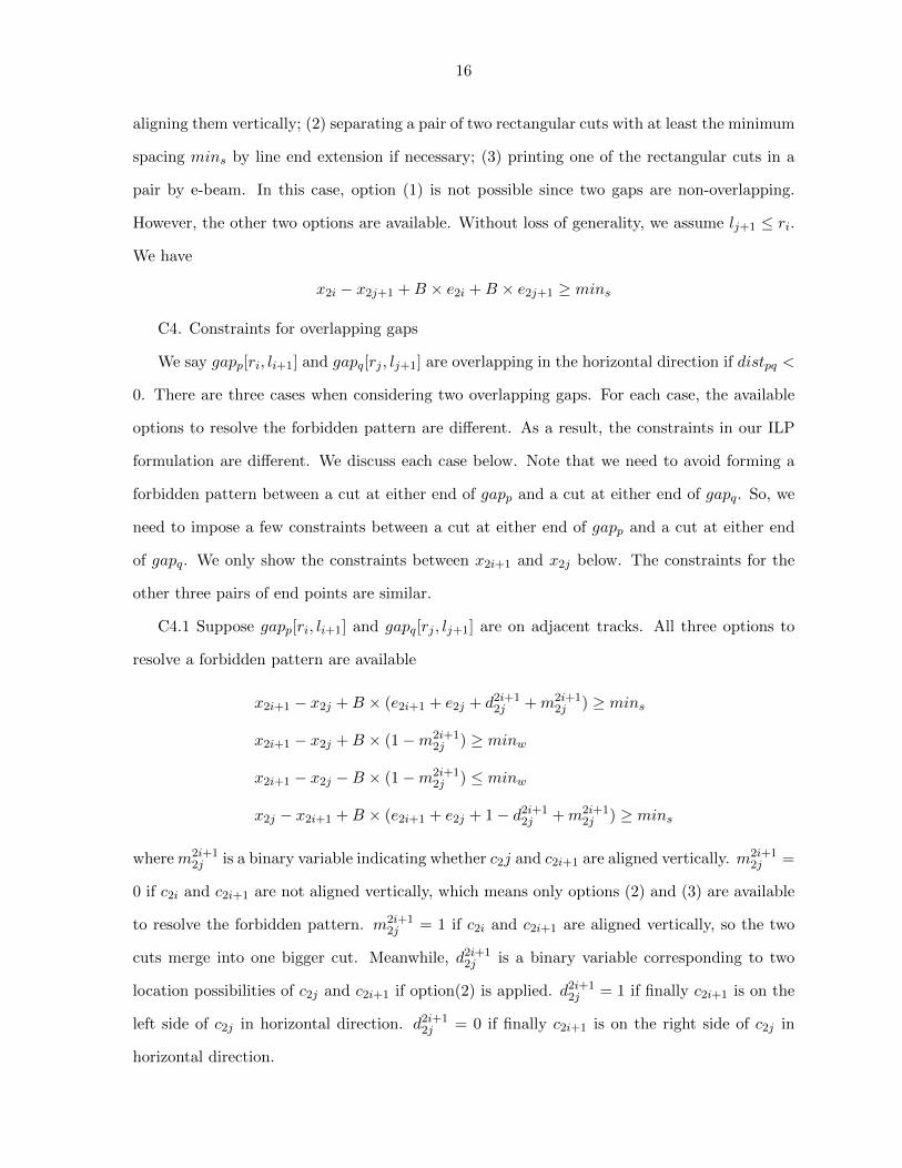
16
aligning them vertically; (2) separating a pair of two rectangular cuts with at least the minimum
spacing mins by line end extension if necessary; (3) printing one of the rectangular cuts in a
pair by e-beam. In this case, option (1) is not possible since two gaps are non-overlapping.
However, the other two options are available. Without loss of generality, we assume lj+1 ≤ ri.
We have
x2i − x2j+1 +B × e2i +B × e2j+1 ≥ mins
C4. Constraints for overlapping gaps
We say gapp[ri, li+1] and gapq[rj , lj+1] are overlapping in the horizontal direction if distpq <
0. There are three cases when considering two overlapping gaps. For each case, the available
options to resolve the forbidden pattern are different. As a result, the constraints in our ILP
formulation are different. We discuss each case below. Note that we need to avoid forming a
forbidden pattern between a cut at either end of gapp and a cut at either end of gapq. So, we
need to impose a few constraints between a cut at either end of gapp and a cut at either end
of gapq. We only show the constraints between x2i+1 and x2j below. The constraints for the
other three pairs of end points are similar.
C4.1 Suppose gapp[ri, li+1] and gapq[rj , lj+1] are on adjacent tracks. All three options to
resolve a forbidden pattern are available
x2i+1 − x2j +B × (e2i+1 + e2j + d2i+12j +m2i+1
2j ) ≥ mins
x2i+1 − x2j +B × (1−m2i+12j ) ≥ minw
x2i+1 − x2j −B × (1−m2i+12j ) ≤ minw
x2j − x2i+1 +B × (e2i+1 + e2j + 1− d2i+12j +m2i+1
2j ) ≥ mins
wherem2i+12j is a binary variable indicating whether c2j and c2i+1 are aligned vertically. m2i+1
2j =
0 if c2i and c2i+1 are not aligned vertically, which means only options (2) and (3) are available
to resolve the forbidden pattern. m2i+12j = 1 if c2i and c2i+1 are aligned vertically, so the two
cuts merge into one bigger cut. Meanwhile, d2i+12j is a binary variable corresponding to two
location possibilities of c2j and c2i+1 if option(2) is applied. d2i+12j = 1 if finally c2i+1 is on the
left side of c2j in horizontal direction. d2i+12j = 0 if finally c2i+1 is on the right side of c2j in
horizontal direction.

17
C4.2 Suppose gapp[ri, li+1] and gapq[rj , lj+1] are on nonadjacent tracks and for each track
in between there does not always exist a gap such that all these gaps together with gapp and
gapq are mutually overlapped. In this case, the option (1) is not possible. This is because the
merging of two rectangular cuts will intersect with wire segment on some track in between.
x2i+1 − x2j +B × (e2i+1 + e2j) +B × d2i+12j ≥ mins
x2j − x2i+1 +B × (e2i+1 + e2j) +B × (1− d2i+12j ) ≥ mins
C4.3 Suppose gapp[ri, li+1] and gapq[rj , lj+1] are on nonadjacent tracks and for each track
in between there always exists a gap such that all these gaps together with gapp and gapq are
mutually overlapped. In this case, the option (1) is possible only when there is a rectangular
cut from each track in between also aligns with them vertically. Without loss of generality, we
assume gapp and gapq are on non-adjacent tracks with only one track in between and there
exists gaps[rk, lk+1] from this track such that gapp, gapq and gaps are mutually overlapped.
x2i+1 − x2j +B × (e2i+1 + e2j + d2i+12j +m2i+1
2j ) ≥ mins
x2i+1 − x2j +B × (1−m2i+12j ) ≥ minw
x2i+1 − x2j −B × (1−m2i+12j ) ≥ minw
x2k+1 − x2j +B × (1−m2i+12j ) ≥ minw
x2k+1 − x2j −B × (1−m2i+12j ) ≥ minw
x2j − x2i+1 +B × (e2i+1 + e2j + 1d2i+12j +m2i+1
2j ) ≥ mins
2.3.2 ILP formulation for trimming by gap removal approach
Objective:
Minimize
m∑i=1
ei + α× (
m∑i=1
x2i−1 − x2i −n∑k=1
rk − lk)
where m and n are the total number of gaps and wires in the given layout respectively, ei is a
binary variable indicates whether the gapi is printed by e-beam lithography, α is a parameter
indicates relative cost of e-beam shot to wire extension, x2i1 and x2i are x-coordinates for left
and right ends of gapi, lk and rk are x-coordinates of left and right ends of wirek in the given
layout.

18
Constraints:
C1. Constraints for line end extension
x2k ≤ lk 1 ≤ k ≤ m
x2k+1 − x2k ≤ rk − lk + δk 1 ≤ k ≤ m
x2k+1 ≥ rk 1 ≤ k ≤ m
x2k+1 ≤ RR 1 ≤ k ≤ m
x2k ≥ LL 1 ≤ k ≤ m
C2. Constraint for gap ends
Given a gapi, we have
x2i − x2i1 +B × ei ≥ minw
where minw is minimum width.
C3. Constraint for non-overlapping gaps or overlapping gaps with overlapping length less
than minimum width
Given two gaps, suppose gapi is between wirep and wirep+1, gapj is between wireq and
wireq+1. Then we have a similar definition of distij for gapi[rp, lp+1] and gapj[rq, lq+1] as
in 3.1.C3 If 0 < distij < mins or minw < distij ≤ 0, gapi[rp, lp+1] and gapj[rq, lq+1] form a
forbidden pattern. There are three available options to resolve a forbidden pattern: (1) merging
two patterns with at least minimum width of abutting part; (2) separating two patterns with
at least minimum spacing by line end extension if necessary; (3) printing one of two patterns
by e-beam. In this case, the option (1) is not possible since either two gaps are non-overlapping
or merging two gaps violates minimum width constraint. However, the other two options are
available. Without loss of generality, we assume lq+1 < rp. We have
x2i1 − x2j +B × ei +B × ej ≥ mins
C4. Constraints for overlapping gaps with overlapping length equal or larger than minimum
width

19
C4.1 Suppose gapi[rp, lp+1] and gapj [rq, lq+1] are on adjacent tracks. In this case, all three
options are available to resolve a forbidden pattern. Hence, we have following constraints.
x2j − x2i1 +B × ei +B × ej +B × (1−mji ) ≥ minw
x2i1 − x2j +B × (ei + ej +mji ) +B × dji ≥ mins
x2i − x2j1 +B × ei +B × ej +B × (1−mji ) ≥ minw
x2j1 − x2i +B × (ei + ej +mji ) +B × (1− dji ) ≥ mins
where mji is a binary variable indicating whether gapi and gapj merge into one pattern. mji = 0
if gapi and gapj do not merge, which means only options (2) and (3) are available to resolve
the forbidden pattern. mji = 1 if gapi and gapj merge into one pattern and the abutting part
should satisfy minimumwidth constraint. Meanwhile, dji is a binary variable corresponding to
two location possibilities of gapi and gapj if option (2) is applied. dji = 0 if finally gapi is on
the right side of gapj in the horizontal direction. dji = 1 if finally gapi is on the left side of
gapj in horizontal direction.
C4.2 Suppose gapi[rp, lp+1] and gapj [rq, lq+1] are on nonadjacent tracks and for each track
in between there does not always exist a gap such that all these gaps together with gapi and
gapj are mutually overlapped. In this case, option (1) is not possible. This is because there is
a wire segment on some track in between which separates gapi[rp, lp+1] and gapj [rq, lq+1] apart.
Hence, we have following constraints.
x2i1x2j +B × ei +B × ej +B × dji ≥ mins
x2j1x2i +B × ei +B × ej +B × (1− dji ) ≥ mins
Note that the wires of a 1D gridded design are supposed to end at discrete locations.
Although we are using continuous variables to represent the x-coordinates of the line ends,
both of our ILP formulations are optimal. We will prove it below.

20
Lemma 2.3.1. There always exists integral optimal solutions for our ILP formulations.
Proof. For our ILP formulations, all the parameters in the constraints are integers. If we fix
the binary variables in our ILPs, all the constraints are of the form:
A ≤ x ≤ B
C ≤ x− x′ ≤ D
where A, B, C, and D are some integer constants. So the vertices of the polytopes formed by
these constraints must be integral. This implies that there exist integral optimal solutions for
our ILP formulations.
A Simplex method based solver will always return the integral optimal solution as Simplex
method moves from one vertex of the feasible set to an adjacent vertex during the search for
the optimal solution. If some other methods are used to solve the ILPs, the optimal solution
returned may not be integral. In that case, the optimal integral solution can be found by
running one step of Simplex method to move to a vertex
2.4 Experimental results
We run all experiments on a machine with an Intel Core i5 2.66GHz CPU (which has two
cores) and 4GB of memory. We use Gurobi 5.6.0 linux64 to solve our ILP formulations. Note
that Gurobi uses primal and dual simplex algorithms to solve LPs. It always returns integral
solutions for all benchmarks. We generated a set of benchmarks based on the benchmarks
provided by Yuelin Du et al. (2012). As we consider line end extension constraints in our
problem formulations, we randomly generate allowed wire extension value for each wire in the
benchmarks. The benchmarks are based on 16 nm 1D standard cell design. In 1D standard cell
design, standard cells of the same height are placed along the cell tracks in the layout. The cell
tracks are isolated from one another by the power/ground rails. As a result, each benchmark
corresponds to one cell track. In the 1D cell library used, wire tracks on Poly and Metal 1 are
perpendicular to the cell tracks. The height of each standard cell is 14 grids, which means there

21
Table 2.1 Comparison withs ILP formulation
M1 layer Yuelin Du et al. (2012)’s ILP Our ILP (by end cutting)
#tracks #e-beam CPU(s) #e-beam CPU(s)
50 14 64.76 14 0.53
100 24 185.34 24 2.18
150 36 301.29 36 4.00
200 48 589.13 48 4.47
250 59 20141.16 59 4.03
300 69 22097.32 69 17.41
Nor. 1.00 1113.56 1.00 1.00
are 14 locations along the Poly / Metal 1 wire direction to place the cuts. The wire tracks on
Metal 2 are parallel to the cell tracks. In Section 4.1, we first use 6 small benchmarks for Metal
1 (with 50 to 300 wire tracks) to compare the ILP formulation of Yuelin Du et al. (2012) with
ours. In Section 4.2, our ILP formulations for the two trimming approaches are compared. In
addition to the small benchmarks, 8 larger benchmarks (4 for Metal 1 with 1000 to 8000 wire
tracks and 4 for Metal 2 with width of 1000 to 8000 tracks) are used. Section 4.3 discusses the
pros and cons of the two trimming approaches for manufacturing of 1D layout.
2.4.1 Comparison with Yuelin Du et al. (2012)’s ILP formulation
In this subsection, we try to compare the performance of Yuelin Du et al. (2012)s ILP
formulation with our ILP formulation for end cutting trimming approach. Because the ILP
formulation in Yuelin Du et al. (2012) does not consider line end extension constraints, we
modify their ILP formulation and add line end extension constraints to it. Moreover, the ILP
formulation in Yuelin Du et al. (2012) does not consider the overlapping of e-beam shots. If
two e-beam shots completely overlap, their ILP will still count them as two shots even though
a single shot is enough to print them. In other words, their ILP may overestimate the required
shot count. For the sake of comparison, we disable the consideration of overlapping e-beam
shots in our ILP formulation here. (We enable this feature of our ILP in all other experiments.)
In Table 2.1, we can see that our ILP formulation dramatically reduces the runtime by more
than 1000× while obtaining optimal solutions. We believe using continuous instead of discrete

22
Table 2.2 Comparison of two trimming approaches
on small-scale benchmarks
M1 layer End cutting approach Gap removal approach
#tracks #e-beam Wire ext. CPU(s) #e-beam Wire ext. CPU(s)
50 14 53 0.09 8 40 0.02
100 24 106 2.37 14 64 0.04
150 36 236 4.08 22 91 0.06
200 48 244 0.04 30 133 0.34
250 59 324 4.02 38 166 0.22
300 69 403 4.88 46 211 0.93
Nor. 1.63 1.88 26.34 1.00 1.00 1.00
variables for the line end coordinates is one of the major reasons that our ILP is much faster
than Yuelin Du et al. (2012)s. We cannot report the comparison based on bigger benchmarks
here as the ILP in Yuelin Du et al. (2012) is too slow to handle them.
2.4.2 Comparison of ILPs for two trimming approaches
In this subsection, we compare the ILP formulations for the two trimming approaches of
manufacturing 1D layout. We first test them on the same small benchmarks used in Section
4.1. From Table 2.2, we can see that the ILPs for both approaches can be solved efficiently.
The gap removal approach is even faster. In addition, the required number of e-beam shots
and total length of wire extension are both less for gap removal approach.
Then we test the two ILPs on the larger benchmarks for both M1 and M2 layers. The
results are reported in Table 2.3. For M1 layer, the gap removal approach still get a much faster
runtime, fewer e-beam shots and less wire extension compared with end cutting approach. For
the benchmarks for M2 layer, it is very interesting to see that end cutting approach generates
much better solution than gap removal approach. It can print the M2 layouts without using
any e-beam shot and the wire extension is also less than that of gap removal approach.
As pointed out by Yuelin Du et al. (2012), wires on the M2 layer are used to connect
different standard cells. Thus both wires and gaps in M2 layer are much longer than those in
M1 layer. Figure 2.3(a) shows a part of M2 layout pattern. So when the end cutting approach

23
is applied to M2 layer, the rectangular cuts are relatively few and are sparsely distributed. In
other words, forbidden patterns in a given layout may be few and can usually be resolved easily
by line end extension as shown in Figure 2.3(b).
Table 2.3 Comparison of two trimming approaches
on large-scale benchmarks
M1 layer End cutting approach Gap removal approach
#tracks #e-beam Wire ext. CPU(s) #e-beam Wire ext. CPU(s)
1000 266 1560 1144.65 148 624 1.35
2000 515 3123 623.99 286 1248 5.09
4000 1026 6447 1866.07 564 2701 16.73
8000 2157 12924 12975.00 1166 5373 90.65
Nor. 1.82 2.45 306.29 1.00 1.00 1.00
M2 layer End cutting approach Gap removal approach
width #e-beam Wire ext. CPU(s) #e-beam Wire ext. CPU(s)
1000 0 63 0.33 8 172 0.30
2000 0 115 0.62 12 216 0.06
4000 0 218 1.19 564 426 0.10
8000 0 473 4.18 56 918 0.56
Nor. 0.00 0.49 7.70 1.00 1.00 1.00
However, for gap removal approach, longer gaps mean longer trim patterns. It is much
easier for forbidden patterns to occur and it may take excessive line end extension to separate
the conflicting patterns as shown in Figure 2.3(c). If the wire extension required is beyond
the allowed value, one e-beam shots is needed to resolve the forbidden patterns as shown in
Figure 2.3(d).
Based on the characteristics of M1 and M2 layer, the two approaches shows their pros and
cons for manufacturing of 1D layout. For M1 layer, the line end distribution is dense and gap
range is small compared with M2 layer, gap removal approach potentially can fabricate the
layout with fewer e-beam shots and less wire extension. The ILP for gap removal approach
can also be solved very efficiently. However, because the trim mask of gap removal approach
is general shape instead of small fixed rectangles for end cutting approach, the cost of making
the trim mask is probably higher Hongbo Zhang et al. (2011). Overall, the gap removal should
still be the better approach for M1 layer. For M2 layer, the line end distribution is sparse and

24
Figure 2.3 End cutting approach performs better than gap removal approach for M2 layout
manufacturing. (a) Target layout on M2. (b) End cutting requires less line-end
extension to separate conflicting patterns. (c) Gap removal requires more line-end
extension to separate conflicting patterns. (d) If wire extension exceeds the limit,
one more e-beam shot is required.
gap range is big, end cutting approach potentially can fabricate the layout with zero e-beam
shot. Thus, the e-beam lithography process is totally eliminated for M2 fabrication, which
tremendously saves the fabrication cost. The ILP for end cutting approach can also be solved
very efficiently. Hence end cutting is the better approach for M2 layer.
2.5 Conclusion
In this chapter, in order to increase the throughput of printing a 1D layout, we consider
the problem of e-beam shot count and line end extension minimization subject to bounded
line end extension constraints. Two different approaches of utilizing the trim mask and e-
beam to print a layout are considered. The first approach which is called trimming by end
cutting is under the assumption that the trim mask and e-beam are used to cut unnecessary
portions from real wires. The second approach which trimming by gap removal is under the
assumption that the trim mask and e-beam are used to rid of all unnecessary portions. We
proposed elegant ILP formulations for both approaches. Experimental results show that both
ILP formulations can be solved very efficiently. Meanwhile, the optimal solutions obtained by
our ILP formulations demonstrate that gap removal approach is suitable for manufacturing of
M1 layer and end cutting approach is suitable for manufacturing of M2 layer. For future work,

25
we want to combine these two approaches and consider them simultaneously for manufacturing
of 1D layout. Due to the larger solution space, we expect that we can obtain better solution
than either one of the two approaches.
26
CHAPTER 3. AN EFFICIENT SHIFT INVARIANT RASTERIZATION
ALGORITHM FOR ALL-ANGLE MASK PATTERNS IN ILT
3.1 Introduction
Rasterization of polygons, also known as scan conversion, is a fundamental technique of
geometric data processing widely used in the electronic design automation (EDA) industry in
particular, and many other industries in general. A set of polygons in EDA (for example, the
shapes defining the physical design of an integrated circuit is usually represented in GDSII or
OASIS format as arrays of vertices, and the rasterization process seeks to represent them by
grayscale pixels on a grid.
One important application of polygon rasterization is in the simulation of projection lithog-
raphy Alfred K. K. Wong (2005). The image at the wafer level is the foundation of any
lithography process modeling at the core of optical proximity correction (OPC). The manufac-
turing of IC chips using optical lithography involves projecting COG (Chrome on Glass) circuit
masks onto coated silicon wafter. The optics that performs the projection inevitably distorts
the shapes on reticle, as the imaging process cuts off all the high-frequency content limited
by the numerical aperture (NA) of the lens system. Other factors, including chemical effects,
cause additional distortions in the final wafer shapes. In order to improve the fidelity of the
figures at the wafer level compared to the original intent of circuit designer, we have to apply
OPC to the figures at the mask level.
In the past, mask shapes with OPC consisted mostly of Manhattan polygons, i.e., polygons
made up of horizontal and vertical edges (no arbitrary angles). As chip makers push below
20nm node, masks using an aggressive form of OPC called inverse lithography technology (ILT)
are becoming more popular. Figure 3.1 is an example of what an ILT mask could look like.

27
Figure 3.1 An example of an ILT mask
Note that the shapes contain many curved features, and almost none of the edges are aligned to
a multiple of 45 degrees. In principle, the lithography simulation can take any polygon figures
as input directly. But when the figures are getting more numerous and more complex, as in
the case of ILT masks, taking rasterized mask as input becomes more efficient than the direct
method Yong Liu et al. (2005).
In order to preserve the fidelity of the original mask polygons, the size of fill pixels in the
rasterized representation should be very small (say 1nm × 1nm). In other words, the ideal
rasterization procedure should be undertaken on a grid of very small fill pixels. On the other
hand, lithography simulation takes the rasterized image as input to generate wafer image.
In order to keep the input data volume and runtime reasonable for lithography simulation, we
would like to use larger(i.e., fewer) pixels to present the rasterized image. In practice, a suitable
pixel size for lithography simulation is on the order of 10nm, and the size of image could be
around 1024× 1024 pixels.
The challenge of using large pixels in rasterization is that the result should preserve shift-
invariance, which means that changes in the position of input polygons relative to the pixel

28
sampling grid should cause very minimal variations in the corresponding output data. This
property is critical in chip manufacturing. For example, in the core of a memory chip, an arrayed
pattern of bitcells repeats itself millions or even billions of times, and the wafer image for each
repeated cell must be as consistent as possible. If the mask representation shows any significant
asymmetry or distortion, the resulting distortions on the wafer will likely be amplified due to
the mask error enhancement factor (MEEF) effect at advanced nodes. A common approach
for preserving shift-invariance is to preprocess the input mask patterns with an anti-aliasing
filter before rasterization in large pixel level. Anti-aliasing removes the frequencies in the input
polygons that are too high to be accurately captured at the sampling rate of rasterization, so
that they do not appear in the samples improperly at a lower frequency (a phenomenon called
aliasing). The software challenge is how to perform filtering and rasterization on a large amount
of all-angle polygon data very quickly, while preserving accuracy of lithography simulation.
Traditional EDA rasterization tools deal with large volume of data of mostly Manhattan
geometry, and very small percentage of 45-degree-angled polygons. There are established tech-
niques to handle rectangular figures efficiently and accurately, and they have been extended
to handle figures with 45/135 degree edges, and even figures with a limited set of predefined
angles (e.g., 22.5 degrees). Michael L. Rieger et al. (2009) is the state-of-the-art of Manhattan
rasterization by look-up tables. For non-Manhattan patterns, John F. Hughes et al. (2013) ex-
plains an area-coverage technique and a significant refinement by cone-filter anti-aliasing, which
are not based on look-up tables. Unfortunately, there is no published technique that handles
truly all-angle figures with a known performance on par with the best rectangle-processing al-
gorithms. To the best of our knowledge, there is also no mature technology to handle all-angle
polygon rasterization in industry.
In this chapter, we propose to solve the problem of all-angle polygon rasterization with a
lookup table-based approach. In this approach the convolution for a majority of the large pixels
can be done in a single lookup table query. The experimental results demonstrate that our
proposed algorithm can speed up rasterization by several orders of magnitude over conventional
methods. Meanwhile, the time for pre-computing the lookup table and the memory for storing
it can be kept within reasonable limits.

29
The remainder of the chapter is organized as follows. In Section 2, we present a description
of the problem and overview of our proposed algorithm. In Section 3, we describe our proposed
algorithm in detail. In Section 4, we show our experimental results. Finally, Section 5 is the
conclusion of this chapter.
3.2 Problem description
3.2.1 Overview of traditional rasterization approach
Rasterization is the task of taking an image described in a vector graphics format (shapes)
and converting it into a raster image (pixels) for output. Given mask patterns which have been
applied OPC, we want to represent them on a pixel grid. In order to preserve the fidelity of
the original patterns during the rasterization process, we ideally should use a grid of very small
fill pixels. We denote such small fill pixels as small pixels. Figure 3.2(a) shows an all-angle
mask pattern (triangle) and a small pixel grid. Then, a scan conversion algorithm Marc Levoy
(2008) is applied upon the mask patterns to obtain a bitmap on the small pixel grid. It is shown
in Figure 3.2(b). Even though we can take this bitmap directly as the input to lithography
simulation, it is enormous and undesirable. In order to preserve shift invariance, the bitmap
should goes through a convolution process under a properly-designed anti-alising filter. Since
the convolution process is undertaken on the small pixel level, the output image is represented
in grayscale on a grid of small pixel. As shown in the Figure 3.2(c), the grayscale value for each
small pixel is represented by its color lightness. To reduce the computation load of lithography
simulation, we would like to increase the size of pixel for the output image while keeping certain
degree of resolution. We denote pixels with increased size for the output image as large pixels.
The grayscale value of large pixel is computed by averaging out the grayscale values of all small
pixels contained inside. Figure 3.2(d) shows the grayscale values of large pixels. This grayscale
image is a shift-invariance preserving representation of the original mask in Figure 3.2(a) and
is the input to lithography simulation tools.
There is a problem associated with the traditional rasterization approach. In order to
preserve the fidelity of input mask patterns, the convolution process is undertaken on the

30
Figure 3.2 Traditional rasterization approach. (a) A mask pattern laying on a small-pixel
grid. (b) Bitmap generation by scan conversion. (c) A grayscale image in small
pixels. (d) Grayscale values of large pixels.
small pixel level. Besides, the filter used in the convolution process can be large for industrial
applications. Even though the traditional rasterization approach is ideal, it is expensive in
term of runtime and memory usage. In this chapter, we solve this problem by applying the
idea of lookup table. By taking advantage of a pre-computed lookup table, the whole filtering
and rasterization process can be undertaken on the large pixel level without loss of accuracy.
Meanwhile, the patterns within one large pixel can be handled with just one lookup table query.
This dramatically speeds up the rasterization process.
3.2.2 Problem formulation
Given a set of all-angle polygon patterns represented by arrays of vertices and the size
of large pixels according to the requirement of the lithography simulation, the problem is to
convert the polygon patterns into a grayscale image at the large pixel level. The result should
preserve shift-invariance, which means translation of input data causes very small difference in
output data. The objective is to process large amount of these kinds of data very quickly but
still accurately.

31
Figure 3.3 The overall algorithm flow
3.3 Algorithm
3.3.1 Algorithm overview
The algorithm overview is shown in Figure 3.3. The program takes a GDSII file as input.
Firstly, a small pixel grid is constructed for input polygon patterns on a specific layer. Mean-
while, assume the size of large pixels is a multiple of the size of small pixels. Then, clipping
configurations of input polygon patterns to each large pixel are captured. Based on clip-
ping configuration, each large pixel is identified which categories it belongs to: non-exception
or exception. Non-exception refers to the large pixel which is only cut through by at most
one polygon edge and the rest of large pixels are exception. The pre-computed and stored
grayscale results in the lookup table can be taken advantage for convolution process. If it is a
non-exception large pixel, only one lookup table query is required for convolution process. If
it is an exception large pixel, multiple lookup table queries are required. A heuristic method
is applied here in order to speed up this process. After completion of convolution for all large
32
Figure 3.4 Small and large pixels.
pixels, the program outputs a grayscale image.
3.3.2 Definitions of small and large pixel
In order to preserve fidelity of mask patterns, the fill pixels in rasterization process should
be very small. We define such a small fill pixel as a small pixel. In practice, 1nm× 1nm small
pixels are small enough to capturing fine fragments of mask patterns. However, if we directly
take the grayscale image which is represented by small pixels to the lithography simulation,
the input data volume is prohibitive. Thus, we would like to use increased size of pixels to
represent the grayscale image. We define the pixel with increased size as a large pixel. In
practice, 10nm× 10nm large pixel is a appropriate choice such that we can keep a reasonable
data volume while having enough resolution for grayscale image. The Figure 3.4 shows the
small pixel with size of 1nm× 1nm and the large pixel with size of 10nm× 10nm.
3.3.3 Key observation
With appropriately chosen size of large pixel, we have a key observation for a given polygon
under the large pixel grid: a majority of large pixels are only cut through by zero or one polygon
edge. We define those large pixels as non-exception large pixels. For the rest of large pixels,
we define them as exception large pixels. Thus, by acquiring clipping configuration of input
polygon patterns to each large pixel, we can identify whether it belongs to non-exception large
pixel or exception large pixel. As shown in Figure 3.5, the top-right large pixel is an exception

33
Figure 3.5 Non-exception and exception large pixels
large pixel which containing a polygon corner, and the large pixel below it is a non-exception
large pixel which is only cut through by a polygon edge. In general case, unless the given set of
polygons have many extremely thin or tiny parts, the number of exception large pixels is O(n)
where n is the total number of vertices for given set of polygons.
3.3.4 LUT approach for non-exception large pixels
For each large pixel with certain clipping configuration, we apply the traditional rasteri-
zation approach. Figure 3.6 illustrates the whole process. Given a large pixel with clipping
configuration shown in Figure 3.6(a), its bitmap will be firstly computed based on small pixel
grid which is shown in Figure 3.6(b). Then, the bitmap will go through convolution process
under a pre-design filter. The result is shown in Fig. 6(c). After that, grayscale value of
each small pixel projects back to the corresponding large pixel. Finally, grayscale results are
generated based on large pixels which is shown in Figure 3.6(d). Note that the convolution
process is conducted on the small pixel level and the size of filter can be very large for industrial
applications. Besides, some large pixels with same clipping configuration will probably appear
multiply times, thus the computation of grayscale result for each time are repeated. As a result,
even though this procedure is ideal, it is relatively expensive in term of runtime and memory
usage.

34
Figure 3.6 A large pixel convolution. (a) Given a large pixel with identified clipping config-
uration. (b) Bitmap generation based on small pixel. (c) Convolution based on
small pixels. (d) Grayscale values of large pixels.
However, if we pre-compute and store the grayscale results in the look-up table for all dif-
ferent clipping configurations of non-exception large pixels, time spent on computing grayscale
results is saved. The total runtime will decrease dramatically since non-exception large pixels
account for a majority of large pixels. Fortunately, the number of all different clipping con-
figurations for non-exception large pixel is limited with given sizes of large and small pixel.
Suppose the size of large pixel is n× n small pixel. If the non-exception large pixel is only cut
through by one polygon edge, two out of four boundary edges of square pixel will intersect with
the polygon edge. For each boundary edge, there are n different locations for a intersection
point. Provided that either side of polygon edge could be within the polygon interior, the total
number of clipping configurations for non-exception large pixel is 12n2. If considering the sym-
metric property of all the clipping configuration, the total number can be further reduced to
6n2. For industrial applications, we usually have small pixel with size of 1nm× 1nm and large
pixel with size of 10nm × 10nm. Consequently, the number of entries used to store grayscale
results for non-exception large pixels in the lookup table is 600.
3.3.5 Technique to handle exception large pixels
For each non-exception large pixel, we can easily obtain its grayscale results from lookup
table. Next, we propose our technique to deal with exception large pixels. As shown in
Figure 3.7, exception large pixels could have various clipping configurations, such as containing
a polygon corner or cut through by two polygon edges. Even though exception large pixels
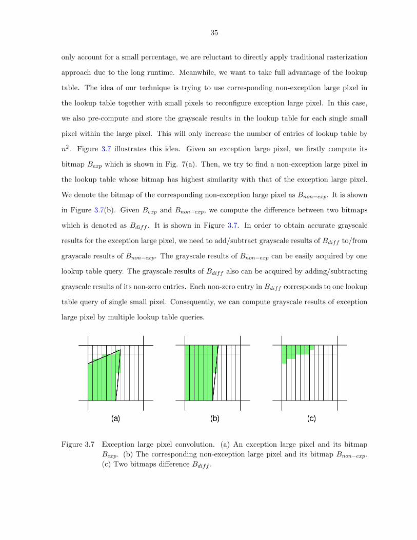
35
only account for a small percentage, we are reluctant to directly apply traditional rasterization
approach due to the long runtime. Meanwhile, we want to take full advantage of the lookup
table. The idea of our technique is trying to use corresponding non-exception large pixel in
the lookup table together with small pixels to reconfigure exception large pixel. In this case,
we also pre-compute and store the grayscale results in the lookup table for each single small
pixel within the large pixel. This will only increase the number of entries of lookup table by
n2. Figure 3.7 illustrates this idea. Given an exception large pixel, we firstly compute its
bitmap Bexp which is shown in Fig. 7(a). Then, we try to find a non-exception large pixel in
the lookup table whose bitmap has highest similarity with that of the exception large pixel.
We denote the bitmap of the corresponding non-exception large pixel as Bnon−exp. It is shown
in Figure 3.7(b). Given Bexp and Bnon−exp, we compute the difference between two bitmaps
which is denoted as Bdiff . It is shown in Figure 3.7. In order to obtain accurate grayscale
results for the exception large pixel, we need to add/subtract grayscale results of Bdiff to/from
grayscale results of Bnon−exp. The grayscale results of Bnon−exp can be easily acquired by one
lookup table query. The grayscale results of Bdiff also can be acquired by adding/subtracting
grayscale results of its non-zero entries. Each non-zero entry in Bdiff corresponds to one lookup
table query of single small pixel. Consequently, we can compute grayscale results of exception
large pixel by multiple lookup table queries.
Figure 3.7 Exception large pixel convolution. (a) An exception large pixel and its bitmap
Bexp. (b) The corresponding non-exception large pixel and its bitmap Bnon−exp.
(c) Two bitmaps difference Bdiff .

36
The number of non-zero entries in Bdiff determines the number of lookup table queries
in order to accurately compute grayscale results of the exception large pixel. Meanwhile, the
number of non-zero entries in Bdiff is greatly affected by the choice of corresponding non-
exception large pixel. Figure 3.8 illustrates the importance of good choice of corresponding
non-exception large pixel. Given an exception large pixel in Figure 3.8 , if we choose the
corresponding non-exception large pixel in Figure 3.8 (b), the Bdiff in Figure 3.8 has relatively
more number of non-zero entries than that in Figure 3.7(c). Each one of non-zero entries
in Bdiff requires one lookup table query and an operation of adding/subtracting grayscale
results to/from grayscale results of corresponding non-exception large pixel. We can see an
inappropriate choice of non-exception large pixel will cause unnecessary lookup table queries
and computational time. Therefore, the current problem is how to find corresponding non-
exception large pixel for given exception large pixel which results in as few non-zero entires in
Bdiff as possible. We propose a smart heuristic for this problem.
Figure 3.8 A bad choice of corresponding non-exception large. (a) The same exception large
pixel and its bitmap Bexp with Figure 3.7(a). (b) An bad choice of corresponding
non-exception large pixel and its bitmap. (c) Bdiff with more non-zero entries.
For each clipping configuration of non-exception large pixel stored in the lookup table, we
quadrisect its bitmap and record number of non-zero entries for each quadrant. We denote the
four records as N1 , N2 , N3 , and N4 . Thus, four records are associated with each entry in the
lookup table. Given an exception large pixel, we also quadrisect its bitmap and calculate N ′1,
N ′2, N′3, and N ′4 for each quadrant. We define the diversitydegree between the given exception

37
large pixel and non-exception large pixel stored in the lookup table as
√∑4i=1 (Ni−N ′i)
2
4 . The
corresponding non-exception large pixel can be obtained by finding a entry in the lookup table
whose has minimum diversity degree. Figure 3.9 gives an example. Consider an exception
largepixel in Figure 3.9(a), the non-exception large pixel in Figure 3.9(b) which has diversity
degree of√
1014 is a better choice than the nonexception large pixel in Figure 3.9(c) which has
diversity degree of√
21374 .
Figure 3.9 Fast heuristic to find correspondong non-exception large pixel. (a) The same ex-
ception large pixel and its bitmap Bexp with Figure 3.7(a). (b) A corresponding
non-exception large pixel with diversity degree√
1014 . (c) A corresponding non-ex-
ception large pixel with diversity degree√
21374 .
3.3.6 Cost of lookup table
As we have mentioned above, the number of entries for non-exception large pixel in lookup
table is 6n2 with additional n2 number of entry for single small pixels. We also pre-compute
and store grayscale results of a large pixel in the lookup table for the case which is entirely
within polygon interior. In sum, the total number of lookup table entries is 7n2 + 1. The size

38
of lookup table can be kept within a reasonable manner and the time spent on building lookup
table is due before start of program. Once the program starts, only one lookup table query is
needed for each non-exception large pixel and each large pixel which is entirely within polygon
interior. For exception large pixel, one lookup table query of corresponding non-exception large
pixel and several lookup table queries of single small pixel are needed. In practice, the number
of lookup table queries of single small pixel is small due to the proposed heuristic.
3.3.7 Technique to obtain clipping configuration
In order to correctly identify each large pixel as non-exception large pixel or exception
large pixel, we should firstly obtain clipping configuration of each large pixel with given set of
polygons. This is actually the problem of polygon clipping where large pixel is the clipping
window and given set of polygons are the clipping polygons. We adopt WeilerAtherton clip-
ping algorithm John F. Hughes et al. (2013); Kevin Weiler and Peter Atherton (1977) in our
implementation to solve this problem. The Weiler-Atherton algorithm is capable of clipping a
concave polygon with interior holes to the boundaries of another concave polygon, also with
interior holes. The polygon to be clipped is called the subject polygon and the clipping region
is called the clip polygon. The algorithm has four major steps: (1)Determine the intersections
of the subject and clip polygons; (2)Process non-intersecting polygon borders; (3)Create two
intersection vertex lists; (4)Perform the actual clipping.
3.4 Experimental results
We implement our algorithm in the C/C++ programming language. We run all experiments
on a machine with an Intel Core i5 2.66GHz CPU and 4GB of memory. All ten benchmarks
are provided by Synopsys, Inc. in the format of GDSII. Except for the first benchmark, the
dimensions of all other nine benchmarks are approximately 10m × 10m. The size of small
pixel is defined as 1nm × 1nm and the size of large pixel is defined as 10nm × 10nm. The
size of 2D filter that we are using during the convolution process is 500nm × 500nm. In
Section 4.1, the performance of our proposed algorithm is demonstrated. In Section 4.2, our
proposed algorithm is compared with the other two rasterization approaches. One is small pixel

39
approach, the other is area coverage approach. In Section 4.3, the property of shift invariance
of our proposed approach is evaluated.
Table 3.1 Performance of our proposed algorithm
Benchmarks Non-exp. Pct. (%) Clipping CPU (s) Convolution CPU (s) Total CPU (s)
GDSII#1 99.55 0.12 2.26 2.38
GDSII#2 98.74 26.31 171.81 198.12
GDSII#3 95.09 25.63 189.22 214.85
GDSII#4 97.49 25.75 213.26 239.01
GDSII#5 97.50 27.89 232.05 259.94
GDSII#6 97.54 31.97 239.40 271.37
GDSII#7 97.61 44.24 270.46 314.70
GDSII#8 97.39 46.41 278.22 324.63
GDSII#9 97.49 25.44 210.90 236.34
GDSII#10 99.55 28.24 222.01 250.25
Ave. 97.35 28.20 202.96 231.16
3.4.1 Performance of our proposed algorithm
Before the start of the program, we firstly build up the lookup table. The time spent
on building lookup table is 607.1s which is reasonable. Table 3.1 shows the performance of
our proposed algorithm. Column 2 shows percentages of non-exception large pixel among all
large pixels in the output image. For all the benchmarks, the percentages are more than 95%
and on average 97.35% which confirms the key observation in our algorithm. The runtime of
our proposed algorithm consists of two parts: one is capturing clipping configuration of input
polygon patterns to each large pixel and the other is convolution process for all large pixels in
the output grayscale image. Column 3 shows the runtime of the first part and column 4 shows
the runtime of the second part. Column 5 shows the total runtime of our proposed algorithm.
We can see that the convolution process takes most of algorithm runtime. Traditional 2D
convolution operation requires 4 levels of nested loops to go through every pixel of the image
and every element of the filter matrix. It is usually slow unless one uses small filter. Bigger
filters can be applied with much faster runtime, if one uses the Fast Fourier Transform (FFT).
Thus, the ideal approach is firstly to use FFT to handle large pixels which are not cut by polygon
boundary. Then, using LUT to take care of large pixels which are cut by polygon boundary

40
and refine in spatial domain the image generated by FFT. However, we do not implement FFT
since it is not the focus of this chapter.
For each exception large pixel in the output grayscale image, the convolution process re-
quires multiple lookup table queries. Table 3.2 demonstrate experimental results of handling
exception large pixels. Column 1 shows the number of exception large pixels in output image
for each benchmark. Due to the proposed heuristics, the number of lookup table queries for
each exception large pixel stays within a reasonable number, which is on average 10.67 as shown
in Column 2. Thus, handling all the exception large pixels does not take too long, which is on
average 14.07s.
Table 3.2 Handling exception large pixels (ELP)
Benchmarks #ELP Ave. LUT queries CPU (s)
GDSII#1 48 5.77 0.22
GDSII#2 3400 5.39 6.99
GDSII#3 7396 5.30 15.02
GDSII#4 3796 16.62 18.40
GDSII#5 3793 15.77 19.23
GDSII#6 3789 13.44 16.90
GDSII#7 3798 11.59 14.20
GDSII#8 4154 10.47 13.81
GDSII#9 3799 17.02 18.49
GDSII#10 7395 5.29 17.47
Ave. 4136.8 10.67 14.07
3.4.2 Compared with other rasterization approaches
In this subsection, we compare our approach with the other two rasterization approaches,
which do not apply the idea of lookup table. One is small pixel approach, the other is area cov-
erage approach. For the small pixel approach, both the scan conversion and convolution process
are undertaken in the small pixel level. The grayscale result of each large pixel in the output
image is obtained by averaging out all the small pixels contained inside. For this approach,
the runtime is expected to be extremely high. Thus, we modified each GDSII benchmark in
Table 3.1 and generated smaller scale testcase to perform experiments for this part. For the
area coverage approach, the grayscale value for each large pixel is directly determined by the

41
percentage of area covered by the input polygons. Thus, the runtime is expected to be very
fast. As shown in Table 3.3, compared with small pixel approach, our algorithm on average
has almost 500× speedup. Besides, our proposed algorithm does not do any approximation
for the whole process. Thus, the grayscale value of each large pixel in the output image is
exactly the same as that computed by the traditional rasterization approach. The area cover-
age approach has even faster runtime. However, since no anti-alising filter is applied for area
coverage approach. The shift invariance property can be damaged. We will show this in the
next subsection.
Table 3.3 Runtime comparison with other rasteriza-
tion approaches
Testcases Traditonal Area-cover Ours
testcase#1 240.19 0.11 0.22
testcase#2 614.29 0.35 0.60
testcase#3 244.04 0.30 0.52
testcase#4 239.75 0.32 0.51
testcase#5 307.76 0.34 0.55
testcase#6 307.44 0.43 0.65
testcase#7 321.06 0.62 0.90
testcase#8 283.58 0.73 1.14
testcase#9 255.40 0.30 0.53
testcase#10 238.30 0.26 0.51
Ave. 4136.8 0.37 0.51
Nor. 497.84 0.73 1.00
3.4.3 Evaluation of shift-invariance property
As we have already mentioned before, shift-invariance is a critical factor which should be
considered during the rasterization process. We evaluate the quality of shift-invariance by
analyzing variation of critical dimension (CD) error due to rotation of input polygons. In
order to demonstrate our proposed algorithm has a good quality of shift-invariance, we also
compare with both small pixel and area coverage approaches. For the small pixel approach,
the convolution process is undertaken in the small pixel level and the output grayscale image
is also based on small pixels. The CD error variation is expected to be very small when the

42
input polygons are rotated. Thus, this approach provides the baseline CD error variation for
us to evaluate the other two approaches. However, its runtime and memory usage is prohibited
in practice. For the area coverage approach, the grayscale value for each large pixel is directly
calculated by the percentage of area covered by the input polygons. No antialising filter is
applied. Thus, the CD error variation is probably very large. All the eight benchmarks are
provided by Synopsys, Inc. and each consists of an array of aligned rectangles rotated by a
different degree. The width of each rectangle is 79nm and height is 167nm. “Ave. wcde”/“Ave.
hcde” is the average CD error in width/height over all the input rectangles. “SD” is the standard
deviation of “Ave. wcde” or “Ave. hcde” over all eight benchmarks. As shown in Table 3.4,
compared with small pixel approach, our approach has a little bit more CD error variation
when rectangles are rotated. Meanwhile, the area coverage approach has much more variation
on CD error when the rotations occur. This demonstrates that our proposed algorithm has
good quality of shift-invariance.
Table 3.4 CD error variations caused by rotation
Unit (nm) Small-pixel approach Area-cover approach Ours
Benchmarks Rotation (◦) Ave. wcde Ave. hcde Ave. wcde Ave. hcde Ave. wcde Ave. hcde
Benchmark#1 0 0.191 0.6068 6.6339 1.6699 0.0536 0.5179
Benchmark#2 1 0.4606 0.4456 6.6399 1.6699 0.0536 0.5179
Benchmark#3 3 1.3556 2.5336 7.5850 2.9584 1.3039 3.6488
Benchmark#4 10 2.1633 2.7311 7.5064 2.8858 1.7591 2.9286
Benchmark#5 30 2.7658 0.4926 8.5512 2.6745 2.3684 1.8378
Benchmark#6 45 5.0739 2.0091 11.6156 3.9560 5.9772 2.0257
Benchmark#7 89 0.9059 0.6035 7.3052 1.8888 0.8238 1.7438
Benchmark#8 90 0.2106 0.5667 6.6389 1.6699 0.0706 0.5705
SD 2.2645 1.5576 7.9904 2.5907 2.4339 2.1044
Nor. SD 1.00 1.00 3.53 1.66 1.07 1.35
3.5 Conclusion
In this chapter, we propose an efficient rasterization algorithm for all-angle polygons. The
algorithm is based on a pre-computed lookup table. By taking advantage of lookup table,
the whole rasterization process can be undertaken on the large pixel level without loss of any
accuracy. Meanwhile, for a majority of large pixels, the patterns within them can be handled
with only one lookup table query. Experimental results show that our proposed algorithm

43
can speed up by almost 500× compared with accurate small pixel approach. Meanwhile, our
proposed algorithm demonstrates a good quality of shift-invariance property. In the future
work, we want to explore the application of FFT in the convolution process and further speed
up the whole rasterization process.

44
CHAPTER 4. SELF-ALIGNED DOUBLE PATTERNING
LITHOGRAPHY AWARE DETAILED ROUTING WITH COLOR
PRE-ASSIGNMENT
4.1 Introduction
As the technology nodes scale down to 22nm and beyond, double patterning lithography
(DPL) has been considered as a practical solution for layout manufacturing. There are two
major types of DPL: litho-etch-litho-etch (LELE) and self-aligned double patterning (SADP).
In LELE lithography, layout patterns are firstly decomposed into two halves and each half of
patterns is assigned into a mask. Then, a process of exposure and etch is applied on each mask
for layout manufacturing. In the decomposition step, adjacent patterns with space less than
manufacturing limit are assigned into different masks. Thus, design rule violations are avoided
and smaller chip features are obtained. However, LELE requires accurate alignment on the
second mask exposure. Otherwise, the overlay error will cause yield loss.
Compared with LELE, SADP has less stringent overlay requirements. Thus, it is a promis-
ing technique to further push beyond the alignment constrained resolution limit of LELE.
Two popular types of process are developed for SADP Yongchan Ban et al. (2011a). One is
spacer-is-metal (SIM) in which the spacers directly define metal patterns. The other one is
spacer-is-dielectric (SID) in which spacers ultimately define trenches. Both types of SADP
utilize two masks: a core mask to make mandrel patterns and a cut/trim mask to get final
layout patterns. Figure 4.1 shows an example of target layout manufactured by two different
SADP processes. In SIM type SADP as shown in Figure 4.1(b), the spacer is firstly deposited
around the pre-featured mandrel patterns. Since the spacer itself becomes the metal pattern,
the cut mask is used to cut off unwanted portions of patterns formed by spacer. Thus, the

45
Figure 4.1 Two types of SADP process. (a) Target layout. (b) SIM type SADP. (c) SID type
SADP.
regions covered by spacer but not covered by cut mask patterns produce the final layout. In
addition, since the width of spacer is constant, it is difficult to vary the line-width of metal
patterns by SIM type SADP Yongchan Ban et al. (2011a). In SID type SADP as shown in
Figure 4.1(c), after the similar spacer deposition, the mandrels are removed and sub-metals
are deposited at both original mandrels locations and space between spacers. Then, the trim
mask is used to include target layout patterns. Since the spacer is just dielectric, the regions
not covered by spacer but covered by trim mask form the final patterns. In this chapter, we
assume the SIM type SADP applies cut mask, and SID type SADP uses trim mask for layout
manufacturing. Note that our work can be potentially extended to handle some other SADP
variants, e.g., trim-based SIM type SADP and cut-based SID type SADP.
The LELE layout decomposition problem can be modeled as a two-coloring problem with
stitch minimization Kun Yuan et al. (2009a); Yue Xu and Chris Chu (2009). Two patterns
are assigned with different colors if they have a conflict. A pattern may be split into two

46
Figure 4.2 SADP undecomposable layout configuration. (a) Design rule violation occurs on
cut mask in SIM process. (b) Design rule violation occurs on core mask in SID
process.
parts to resolve a conflict but results in a stitch. Then layout patterns with the same color
are assigned into the same mask. Similar to LELE, SADP also requires a decomposition of
the layout into core mask and cut/trim mask. However, SADP layout decomposition is more
challenging since the resulting mandrel mask and cut/trim mask look significantly different
from the target layout. A layout configuration without considering SADP layout decomposition
will probably make the layout not manufacturable by SADP. As shown in Figure 4.2(a), after
layout decomposition, the two adjacent cut mask patterns are too close and cause design
rule violation. Thus, the target layout is not manufacturable by SIM type SADP. Similarly, a
design rule violation occurs on the core mask after layout decomposition in Figure 4.2(b). Thus,
the target layout cannot be manufactured by SID type SADP. In order to avoid these SADP
unmanufacturable patterns, it is necessary to consider SADP layout decomposition in the earlier
design stage, especially in detailed routing. This will greatly improve the decomposability of
layout patterns during manufacturing time.
Seong-I Lei et al. (2014) proposed an LELE-aware detailed routing algorithm which applied
a color pre-assignment idea. Each track in the routing grid is firstly assigned with a fixed color,
then maze routing is performed on the grid. In this way, the mask assignment is known at
the moment once a net is routed. Hence, the presence of stitches is foreknown during detailed

47
routing and can be easily minimized. Besides, the way that the colors are pre-assigned enables
the detailed router to generate only decomposable layout. We extend the idea of color pre-
assignment to our SADP-aware detailed routing. Yongchan Ban et al. (2011b); Hongbo Zhang
et al. (2011); Zigang Xiao et al. (2012) presented the SADP layout decomposition of arbitrary
2D patterns in post routing stage. However, the design flexibility is restricted in this stage and
some layout patterns may be naturally undecomposable. Previous works on SADP-aware de-
tailed routing only focus on SID type SADP Jhih-Rong Gao and David Z. Pan (2012); Chikaaki
Kodama et al. (2013); Yuelin Du et al. (2013b); Iou-Jen Liu et al. (2014); Xiaoqing Xu et al.
(2015a). To the best of our knowledge, there is no previous work considering SIM type SADP
during detailed routing stage. Jhih-Rong Gao and David Z. Pan (2012) solved routing and
layout decomposition problems simultaneously based on the correct-by-construction approach.
However, the final routability and layout decomposability heavily depend on the net ordering.
Chikaaki Kodama et al. (2013) performed routing on a grid structure where grid nodes are
alternately colored by two colors or uncolored for SADP. However, their approach is unreal-
istic because it requires that every pin of each net must fall on the same colored grid nodes,
otherwise it cannot route the net. Yuelin Du et al. (2013b) proposed an expanded routing
graph model. Each point in the routing grid is split into four vertices in the routing graph, and
further split into eight vertices to consider prohibited line-ends. The high complexity of routing
graph will slow down the runtime and increase memory load of detailed router. In addition,
how to handle via in the graph model is not mentioned. Iou-Jen Liu et al. (2014) maintained a
overlay constraint graph during routing which is expensive. Meanwhile, the side overlay error
cannot be avoided in the experimental results. Xiaoqing Xu et al. (2015a) mainly focused on
SADP-aware pin access for standard cell instead of SADP-aware detailed routing. Color pre-
assignment is the key idea and major innovation for our SADP-aware detailed routing. Some
primitive forms of color pre-assignment idea are proposed and applied in Gerard Luk-Pat et al.
(2013); Xiaoqing Xu et al. (2014, 2015b); Yuelin Du et al. (2013b). Gerard Luk-Pat et al.
(2013) proposed a feature assignment method for SID type SADP layout decomposition of
line-space array. They treated lines as main mandrel features alternately while remaining lines
as sub-metals. Xiaoqing Xu et al. (2014, 2015b) applied the similar idea on their SADP-aware

48
pin access for purely unidirectional patterns. Yuelin Du et al. (2013b) assigned routing tracks
as main mandrel tracks and sub-metal tracks alternatively before detailed routing.
The contributions of this chapter are summarized in the followings.
• This is the first work to systematically consider SIM type SADP lithography during
detailed routing stage.
• We extend the idea of color pre-assignment to both SIM and SID types SADP-aware
detailed routing. The idea greatly simplifies the problem to maintain SADP design rules
in detailed routing.
• The novel graph models are proposed for both SIM and SID type SADP-aware detailed
routing. They effectively capture both routing and SADP manufacturing cost.
• We offer the strong routing results in terms of wirelength, routability, and runtime. Fur-
thermore, in the final routing solution, no side overlay error is guaranteed for SADP
layout manufacturing.
The rest of the chapter is organized as follows. Section 2 provides some preliminary in-
formation, especially the SADP design rules considered in the chapter. Section 3 presents
our problem formulation. Section 4 explains our proposed solution to the problem in details.
Section 5 demonstrates our experimental results. Finally, Section 6 concludes the chapter.
4.2 Preliminaries
As mentioned in the previous section, it is hard to print metal lines with mixed-width by
SIM type SADP lithography. However, it is possible to manufacture patterns with mixed width
by SID type SADP lithography. Since the focus of the SID type SADP-aware detailed routing
in this chapter is how to apply our key idea of color pre-assignment, we will not further consider
mixed-width wires. Thus, we assume that all the metal patterns in the layout are regular with
same fixed width. To successfully manufacture the layout by SADP lithography, SADP design
rules should be maintained. In this section, we will discuss the SADP design rules considered
in this chapter and the incurred routing constraints in detailed routing.

49
4.2.1 Core and cut/trim mask design rules
As mentioned before, core mask is used to make mandrel patterns in both types of SADP.
A secondary mask, a cut mask in SIM process and a trim mask in SID process, is used to form
the target layout patterns. Due to the optical resolution limits, several design rules should
be enforced in the design of core and cut/trim masks. In this chapter, we consider minimum
spacing and minimum width rules as shown in Figure 4.3. The minimum spacing rule requires
any two adjacent patterns on the mask should be separated with distance at least minimum
spacing value. We define Sc and Ss as the minimum spacing values for core and secondary
masks. The minimum width rule specifies the minimum width for every pattern on the mask.
Wc and Ws denote minimum width values for core and secondary masks.
Figure 4.3 Minimum spacing and minimum width rules.
4.2.2 Overlay error
The major advantage of SADP over LELE is the better overlay control. However, mis-
alignment of secondary mask sometimes could still cause overlay error, which results in pattern
distortions. Iou-Jen Liu et al. (2014) defines a side overlay error as an overlay error occurs at
a section of the side boundary of a layout pattern and tip overlay error as an overlay error
occur at the line end of a layout pattern. Iou-Jen Liu et al. (2014) also points out tip over-
lays are considered as non-critical overlays which can be ignored while side overlays should be
minimized to reduce yield loss. Figure 4.4(b)(c) show two methods of SID type SADP layout
decomposition for target layout in Figure 4.4(a). For the method in Figure 4.4(b), the pattern
B will be generated with a side overlay error at upper boundary and a tip overlay error at the
right line end. However, if side boundaries of pattern B are all surrounded by spacers as shown
in Figure 4.4(c), no side overlay error will occur in SADP layout manufacturing. Hence, an ad-
ditional mandrel pattern is placed at the upper side of pattern B to provide spacer protection.

50
Figure 4.4 SADP layout decomposition with overlay error. (a) Target layout. (b) SID type
with side overlay error. (c) SID type with no side overlay error. (d) SIM type with
side overlay error.
We refer to the additional mandrel pattern as an assist mandrel. To obtain zero side overlay
error in SID type SADP process, we require that all the patterns formed from sub-metals have
spacer protection in layout decomposition. Figure 4.4(d) shows the SIM type SADP layout
decomposition for the same target layout. The pattern A will be generated with a side overlay
error at its right side boundary. Therefore, we require the cut mask patterns not to overlap
with side boundaries of spacers which used to form target layout patterns. In this way, zero
side overlay error can be achieved for SIM type SADP layout manufacturing.
4.2.3 Non-preferred turns
Gerard Luk-Pat et al. (2013) observes the corner rounding of the spacer deposition around
mandrel line ends in the simulations of the mandrel contours. Yuelin Du et al. (2013a) further
observers that spacers get rounded at convex corners of mandrels while staying sharp at concave
mandrel corners. Figure 4.5(a) shows the rounding issue of spacers. As a result, additional
constraints need to be considered for layout manufacturing. In SIM type SADP, if an L shape
layout pattern is formed from the rounded spacer at a convex mandrel corner, yield loss will
increase. Therefore, whenever L shape layout patterns are formed, we prefer using spacers

51
deposited around concave corners of mandrels. In the case shown in Figure 4.5(b), pattern B
is preferred over pattern A by SIM type SADP. In SID type SADP, when an L-shape layout
pattern is defined by sub-metal, large residue will occur at its concave corner due to the spacer
rounding at the convex corner of the assist mandrel. As a result, the pattern is manufactured
with distortion by SID type SADP. In order to obtain the clean layout patterns, we prefer to
use mandrel patterns to directly define L-shape layout patterns in SID type SADP lithography.
Figure 4.5(c) shows the layout decomposition for two L-shape layout patterns manufactured
by SID type SADP. As shown in Figure 4.5(d), pattern A is preferred over pattern B by SID
type SADP. Yuelin Du et al. (2013b) also identified this manufacturing challenge and called
it sm-jogs minimization. In this chapter, we refer to L-shape layout patterns manufactured
by rounded spacer in SIM process or sub-metal in SID process as non-preferred turns. The
number of non-preferred turns should be minimized in detailed routing.
Figure 4.5 Non-preferred turns caused by the spacer rounding issue. (a) Rounded spacers
deposited at convex corners of a mandrel. (b) A non-preferred turn in SIM type
SADP. (c) Large residue occurs at the concave corner of the sub-metal. (d) A
non-preferred turn in SID type SADP.

52
4.2.4 Prohibited line-ends
The prohibited line-ends refer to a particular line-ends configuration in the layout pattern
which is prohibited during detailed routing due to the manufacturing challenge. Yuelin Du et al.
(2013b) identified the “anti-parallel line-ends”, in which two layout patterns are on adjacent
tracks and form a pair of line ends in opposite direction. Figure 4.6(a) shows a layout pattern
containing an anti-parallel line-ends. In the SID type SADP layout decomposition shown in
Figure 4.6(b), the minimum width rule is violated when two trim mask patterns are merged.
Thus, the anti-parallel line-ends should be prohibited in SID type SADP-aware detailed routing.
The anti-parallel line-ends in Figure 4.6(a) should also be prohibited in SIM type SADP-aware
detailed routing. This is due to the violation of minimum spacing rule on cut mask patterns,
which is shown in Figure 4.6(c). Therefore, the anti-parallel line-ends should either have enough
horizontal overlapping length leno or enough horizontal separation distance dists. leno = Ws
and diss = Ss for SID type, while leno = Ss and dists = Ws for SIM type.
Figure 4.6 Prohibited anti-parallel line-ends. (a) A layout contains anti-parallel line-ends.
(b) Minimum width rule violation occurs by SID type. (c) Minimum spacing rule
violation occurs by SIM type.
Besides, the line-ends configuration in Figure 4.2(b) should be prohibited in SID type SADP-
aware detailed routing due to the minimum spacing rule violation on core mask. We refer to
this line-ends configuration as anti line-ends. Furthermore, the line-ends configuration in Fig-
ure 4.4(d) should be prohibited in SIM type SADP-aware detailed routing due to the intolerable
side overlay error during manufacturing.

53
4.3 Problem formulation
We assume that there is a preferred routing direction for each layer and the other direction
perpendicular to the preferred routing direction is defined as non-preferred routing direction of
the layer. We do not completely disable but strongly discourage routing in the non-preferred
routing direction. We refer to the above problem as the restricted detailed routing problem.
In addition, we assume all the multi-pin nets from netlist have been decomposed into 2-pin
nets and each pin has several candidate locations. With such assumption and design rules
mentioned in Section 2, we formulate the SADP lithography aware detailed routing problem.
Given a netlist, a multi-layer routing grid, a set of blockages, and design rules, restricted
detailed routing with simultaneous pin location determination for all the nets is performed.
The final routing patterns should be compliant to design rules of either SIM or SID type SADP
lithography in layout manufacturing. The objective is to achieve 100% routability and to ensure
zero side overlay error in SADP layout decomposition. Besides, design rule violations, total
wirelength, the number of vias, and non-preferred turns should be minimized
4.4 Proposed solution
4.4.1 Overall flow
The overall flow of our SADP-aware detailed routing is shown in Figure 4.7. Assuming a
netlist, a routing grid, a set of blockages, and design rules are given. The routing of each net
should be along the grid lines. We firstly perform color pre-assignment on the routing grid,
then we build a routing graph based on our proposed graph model. After that, we perform
independent routing iterations. During this phase, we route all the nets almost independently
in each iteration to minimize the negative impact of net ordering. Several heuristics are applied
here in order to obtain better solution in fewer number of iterations. This phase will terminate
if the congestion of the current iteration is no better than the previous one. Next, we treat
the output of independent routing iterations as the initial routing solution for the negotiated
congestion based rip-up and reroute (RNR) phase. The RND iterations will continue until
there is no congestion in the routing solution or it reaches the pre-set maximum number of
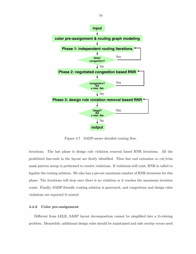
54
Figure 4.7 SADP-aware detailed routing flow.
iterations. The last phase is design rule violation removal based RNR iterations. All the
prohibited line-ends in the layout are firstly identified. Then line end extension or cut/trim
mask pattern merge is performed to resolve violations. If violations still exist, RNR is called to
legalize the routing solution. We also has a pre-set maximum number of RNR iterations for this
phase. The iterations will stop once there is no violation or it reaches the maximum iteration
count. Finally, SADP-friendly routing solution is generated, and congestions and design rules
violations are reported if existed.
4.4.2 Color pre-assignment
Different from LELE, SADP layout decomposition cannot be simplified into a 2-coloring
problem. Meanwhile, additional design rules should be maintained and side overlay errors need

55
to be avoided during layout decomposition. Those make the consideration of SADP lithography
in detailed routing an even more complicated problem. In this situation, we adopt the idea
of color pre-assignment to simplify the problem. Before detailed routing, the routing grid
is assigned colors to determine where mandrel patterns and cut/trim mask patterns can be
formed. With such restriction, the layout decomposition is known at the moment when a net is
routed. In this way, SADP design rule violations and side overlay errors can be easily avoided
during detailed routing. In this subsection, we will explain how we pre-assign colors over the
routing grid. Since the color pre-assignment is performed on each layer individually, it can be
applied to a multi-layer routing grid with different pitch sizes for each layer. Note that the
way we do color pre-assignment and the resulting routing restrictions for SIM and SID types
SADP-aware detailed routing are different, which will be described as follows.
4.4.2.1 SIM type
On each layer, we define a panel as the area between two adjacent horizontal (vertical) grid
lines. We pre-assign colors to the panels alternately in both horizontal and vertical directions.
Figure 4.8(a) shows the colored routing grid prepared for SIM type SADP-aware detailed
routing. The colored panels specify where the mandrel patterns may be formed. Meanwhile,
mandrel pattern is required to be aligned in the middle of colored panel which is shown in
Figure 4.8(b). Suppose the pitch size of routing tracks p is given. To align the metal patterns
along the routing tracks, we assume wm + wsp = p where wm is the width of mandrel, and
wsp is the width of spacer. Meanwhile, wm ≥ Wc is required to maintain the minimum width
rule. If we require that the pitch size of colored panels, which is 2p, is larger than or equal to
Sc +wm, the minimum spacing rule of core mask is also maintained. Since similar lithography
processes are implemented for both core and cut mask pattern fabrication, we assume Sc ≈ Ss
and Wc ≈Ws. To have better side overlay control, we require wc = p where wc is the width of
cut mask. The cut mask patterns are aligned along the routing tracks and Figure 4.8(b) shows
four possible locations of cut mask patterns A, B, C, and D. For the pair of patterns A and
pattern B, their pitch size is 2p, thus the design rules are maintained. Under the condition of
no prohibited anti-parallel line-ends in the layout pattern, the pair of B and C are separated

56
Figure 4.8 Color pre-assignment for SIM and SID type SADP-aware detailed routing. (a)(b)
SIM type. (c)(d) SID type.
with enough spacing, while the pair of C and D can merge. With color pre-assignment and
above assumption, the SADP layout decomposition becomes straightforward and SADP design
rule are easy to maintain.
4.4.2.2 SID type
Different from SIM type, we pre-assign color to routing tracks alternately in both horizontal
and vertical directions. Figure 4.8(c) shows the routing grid with color pre-assignment which
prepares for SID type SADP-aware detailed routing. The mandrel patterns are required to
be formed only along red tracks and should be aligned in the center, which is shown in Fig-
ure 4.8(d). Thus, the routing layout patterns along red tracks are made directly from mandrels,

57
while patterns along black tracks are made from sub-metals. With similar geometric assump-
tion for SIM type, the design rules of core mask and trim mask can be maintained. Fig. 8(d)
shows four possible locations of trim mask patterns A, B, C, and D. Under the condition of
no prohibited anti-parallel line-ends and anti line-ends in the layout, any pair of trim mask
patterns can be either separated with enough spacing or merged.
4.4.2.3 Routing restrictions
The color pre-assignment restricts where mandrel patterns can be formed for both SIM and
SID types SADP layout decomposition. Under such restrictions, some routing patterns are
not manufacturable due to the design rule violations, thus should be forbidden during detailed
routing. Figure 4.9(a) shows three L-shape routing patterns A, B, and C, Figure 4.9(b) shows
their corresponding SIM type SADP layout decomposition. A is a non-preferred turn due to
the spacer rounding issue at a convex mandrel corner. B is formed from spacer deposited at a
concave mandrel corner, thus can be manufactured without any degradation. We refer to it as a
preferred turn. The layout decomposition for C cannot avoid design rule violations. As shown
in Figure 4.9(b), both core and cut mask violate the minimum spacing rule. Hence, we refer
to the L-shape pattern C as a forbidden turn, and should be strictly avoided during detailed
routing. Figure 4.9(c)(d) show the same L-shape routing patterns and their corresponding SID
type SADP layout decomposition. A is directly defined by mandrel which is free from spacing
rounding issue. We refer to it as a preferred turn. B is a non-preferred turn since it is formed
from sub-metal. The mandrel and trim mask patterns cannot even be designed for C under
the restrictions of color pre-assignment. There, the pattern C is referred as a forbidden turn
during detailed routing.
From the examples above, it is observed that how a routing pattern turns at the grid point
determines its manufacturability. We have a forbidden turn which cannot be manufactured,
and a preferred turn and a non-preferred turn which can be manufactured without degradation
and with degradation, respectively. In the next subsection, we will introduce the graph model
used in detailed routing which captures manufacturability of routing patterns exactly.

58
Figure 4.9 SIM type and SID type SADP-aware detailed routing restrictions due to the color
pre-assignment. (a)(b) SIM type. (c)(d) SID type.
4.4.3 Graph model
In this section, we introduce our graph model which captures both routing cost and manu-
facturability of routing pattern in detailed routing. In addition, the graph model complexity is
linear with the size of routing grid in which the constant factor can be kept small in practice.
The graph models for SIM and SID type SADP-aware detailed routing are slightly different
which will be described separately as follows.

59
Figure 4.10 Graph modeling for SADP-aware detailed routing. (a) via model. (b) SIM type
grid segment models. (c) SID type grid segment models.
4.4.3.1 SIM type
Suppose we are given a multi-layer routing grid with color pre-assignment and a preferred
routing direction for each layer. We construct our routing graph G by viewing each grid segment
or via as a vertex. An edge exists between two vertices if they are directly connected in the
routing grid. A cost is associated with each edge to indicate the cost of traveling from the
vertex in one end to the vertex in the other end. The construction of G is described below
by considering graph models for pin, via, and grid segment separately. Figure 4.10 shows the
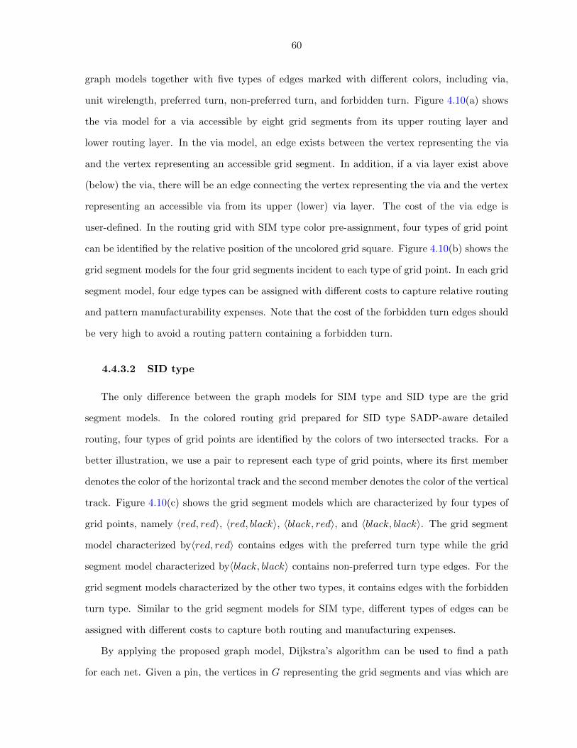
60
graph models together with five types of edges marked with different colors, including via,
unit wirelength, preferred turn, non-preferred turn, and forbidden turn. Figure 4.10(a) shows
the via model for a via accessible by eight grid segments from its upper routing layer and
lower routing layer. In the via model, an edge exists between the vertex representing the via
and the vertex representing an accessible grid segment. In addition, if a via layer exist above
(below) the via, there will be an edge connecting the vertex representing the via and the vertex
representing an accessible via from its upper (lower) via layer. The cost of the via edge is
user-defined. In the routing grid with SIM type color pre-assignment, four types of grid point
can be identified by the relative position of the uncolored grid square. Figure 4.10(b) shows the
grid segment models for the four grid segments incident to each type of grid point. In each grid
segment model, four edge types can be assigned with different costs to capture relative routing
and pattern manufacturability expenses. Note that the cost of the forbidden turn edges should
be very high to avoid a routing pattern containing a forbidden turn.
4.4.3.2 SID type
The only difference between the graph models for SIM type and SID type are the grid
segment models. In the colored routing grid prepared for SID type SADP-aware detailed
routing, four types of grid points are identified by the colors of two intersected tracks. For a
better illustration, we use a pair to represent each type of grid points, where its first member
denotes the color of the horizontal track and the second member denotes the color of the vertical
track. Figure 4.10(c) shows the grid segment models which are characterized by four types of
grid points, namely 〈red, red〉, 〈red, black〉, 〈black, red〉, and 〈black, black〉. The grid segment
model characterized by〈red, red〉 contains edges with the preferred turn type while the grid
segment model characterized by〈black, black〉 contains non-preferred turn type edges. For the
grid segment models characterized by the other two types, it contains edges with the forbidden
turn type. Similar to the grid segment models for SIM type, different types of edges can be
assigned with different costs to capture both routing and manufacturing expenses.
By applying the proposed graph model, Dijkstra’s algorithm can be used to find a path
for each net. Given a pin, the vertices in G representing the grid segments and vias which are

61
Figure 4.11 Invalid routes.(a)(b) Forbidden turns in routes.(c) A loop structure in the route.
accessible to it are treated as source/sink nodes. However, the path computed by Dijkstra’s
algorithm may not be a valid route in the routing grid. Figure 4.11 shows three cases of invalid
routes. As shown in Figure 4.11(a), to avoid the path segment A which contains a forbidden
turn edge, Dijkstra’s algorithm will choose a path with the path segment B instead. The reason
is that the cost of a unit wirelength edge together with a non-preferred turn edge is less than
that of a forbidden turn edge. However, the corresponding route in the routing grid is not valid
since it contains a forbidden turn. Similar issue occurs in Figure 4.11(b). Thus, we resolve those
issues by modifying Dijkstra’s algorithm which is shown in Algorithm 1. Whenever we perform
relaxation procedure on an edge (u, v) to update the minimum cost for vertex u, we check
whether vertex presenting u’s predecessor is connected to vertex v in G. If so, the relaxation
is abandoned. In addition, the path computed by the modified Dijkstra’s algorithm might
contains a loop as shown in Figure 4.11(c). Thus, once a loop structure is found in a routing
path, we increase the cost to use the routing resources along the loop. Then, we rip-up and
reroute the net by the modified Dijkstra’s algorithm until no loop is found in the path. In this
way, every path in the routing solution is ensured to be a valid route in the routing grid.
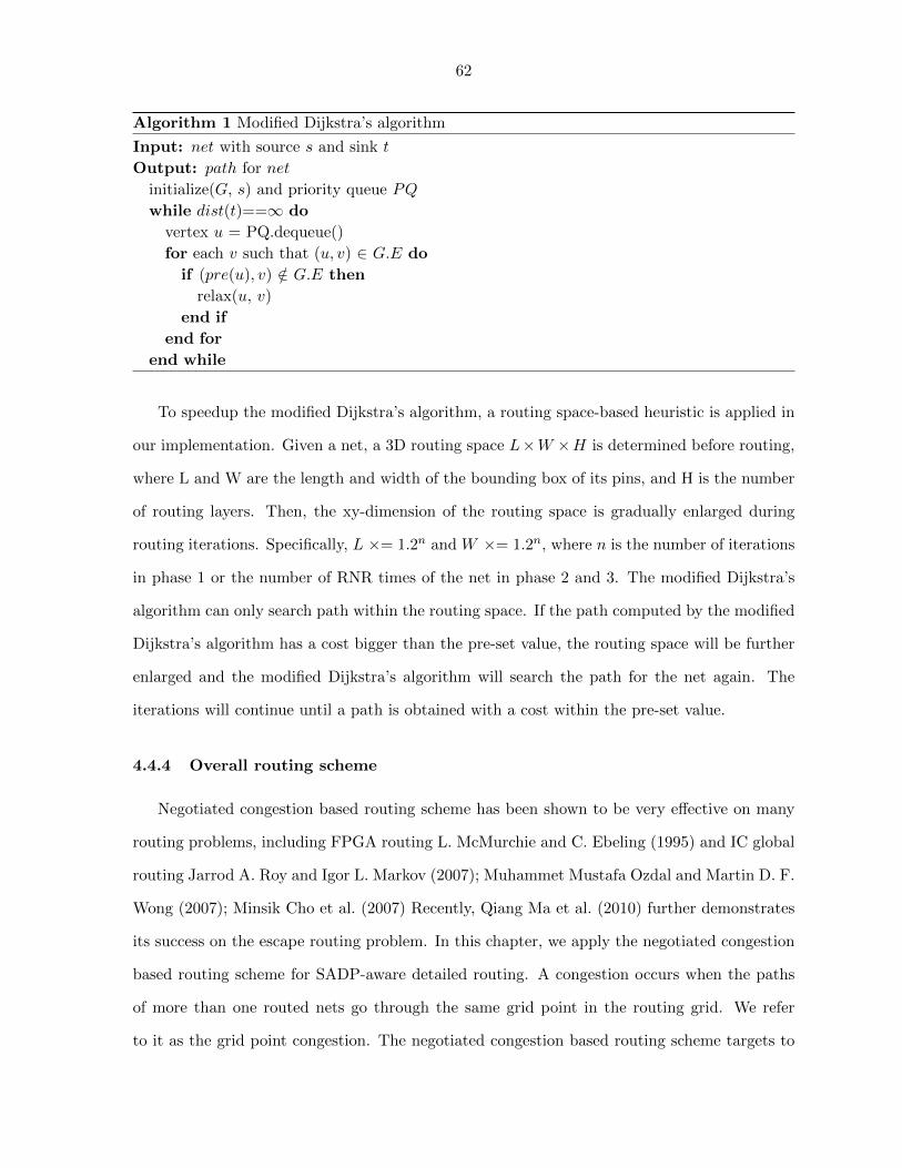
62
Algorithm 1 Modified Dijkstra’s algorithm
Input: net with source s and sink t
Output: path for net
initialize(G, s) and priority queue PQ
while dist(t)==∞ do
vertex u = PQ.dequeue()
for each v such that (u, v) ∈ G.E do
if (pre(u), v) /∈ G.E then
relax(u, v)
end if
end for
end while
To speedup the modified Dijkstra’s algorithm, a routing space-based heuristic is applied in
our implementation. Given a net, a 3D routing space L×W ×H is determined before routing,
where L and W are the length and width of the bounding box of its pins, and H is the number
of routing layers. Then, the xy-dimension of the routing space is gradually enlarged during
routing iterations. Specifically, L ×= 1.2n and W ×= 1.2n, where n is the number of iterations
in phase 1 or the number of RNR times of the net in phase 2 and 3. The modified Dijkstra’s
algorithm can only search path within the routing space. If the path computed by the modified
Dijkstra’s algorithm has a cost bigger than the pre-set value, the routing space will be further
enlarged and the modified Dijkstra’s algorithm will search the path for the net again. The
iterations will continue until a path is obtained with a cost within the pre-set value.
4.4.4 Overall routing scheme
Negotiated congestion based routing scheme has been shown to be very effective on many
routing problems, including FPGA routing L. McMurchie and C. Ebeling (1995) and IC global
routing Jarrod A. Roy and Igor L. Markov (2007); Muhammet Mustafa Ozdal and Martin D. F.
Wong (2007); Minsik Cho et al. (2007) Recently, Qiang Ma et al. (2010) further demonstrates
its success on the escape routing problem. In this chapter, we apply the negotiated congestion
based routing scheme for SADP-aware detailed routing. A congestion occurs when the paths
of more than one routed nets go through the same grid point in the routing grid. We refer
to it as the grid point congestion. The negotiated congestion based routing scheme targets to

63
resolve all grid point congestions to obtain a congestion free routing solution. Every time a
net is routed, if its path causes any grid point congestions with the previously routed nets, we
increase the cost to use the routing resources corresponding to the grid point congestion. Thus,
the net with more alternative routes tends to detour from the congested routing resources in the
RNR. In this way, the grid point congestion can be potentially resolved. One major advantage
of negotiated congestion based routing scheme is that the route of each net is never committed
as final routing solution until the entire flow terminates. Nets causing congestions or design
rule violations will be ripped-up and rerouted. All the nets will negotiate with each other for
using the routing resources to find their own routes. This is the reason our routing scheme does
not depend on a particular net ordering. To realize such scheme, we incorporate the other two
cost components into our graph model.
Coste = BCe + UCe +HCie
UCe = α× Usage(p)
HCie = HCi−1e + β ×Overflow(p)
Coste is the total cost of an edge e in G. BCe denotes the base cost of e, which is determined
by the edge type. p is a grid point in the routing grid shared by two grid segments/vias
corresponding to the two vertices of e. UCe is the usage cost indicating occupation of routing
resources. It is updated after a net is routed or ripped-up and equal to the weighted current
usage at p. HCie is the history cost after iteration i indicating historical congestion information.
It is updated once a grid point congestion is detected at p and can be computed by accumulating
HCi−1e with weighted overflow at p.
As shown in Algorithm 2, our SADP-aware detailed routing has three major phases. The
first phase is independent routing iterations. In this phase, the routing of each net does not
consider the already routed nets, i.e., no additional penalty will be charged to use the routing
resources occupied by routed nets when finding a path for a net. We refer to such routing as
independent routing. In each iteration, we route all the nets from the netlist by independent
routing. The reason for independent routing is to minimize the negative effect of net ordering

64
Algorithm 2 SADP-aware detailed routing
Input: netlist, a routing graph, and SADP design rules
Output: SADP friendly detailed routing solution
Phase 1: independent routing iterations
block routing resources occupied by all the pins from netlist
while fewer grid point congestions do
for each neti in netlist do
unblock routing resources occupied by pins of netithe modified Dijkstra’s algorithm finds pathi for netiblock routing resources occupied by pins of netiupdate UC for pathi (α is extremely small)
end for
update HC for all grid point congestions
remove all UC in the G
end while
Phase 2: negotiated congestion based RNR iterations
update UC for all the paths in netlist
build a queue Q containing all grid point congestions
while !isEmpty(Q) && #iter. ≤ max. #iter. do
a grid point congestion c = Q.dequeue()
chose rip-up net netj which causes the c
update UC after removing pathj of netjthe modified Dijkstra’s algorithm finds path′j for netjupdate UC for path′jif reroute of netj causes a grid point congestion c′ then
update HC for the c′
Q.enqueue(c′)
end if
end while
Phase 3: design rule violation based RNR iterations
build a priority queue PQ containing all prohibited line-ends violations
block vias within prohibited line-ends regions
while !isEmpty(PQ) && #iter. ≤ max. #iter. do
violation = PQ.dequeue()
if violation is prohibited anti-parallel line-ends && line-end extension is allowed then
do line-end extension
else
rip-up and reroute
if reroute causes a grid point congestion c then
PQ.enqueue(c)
end if
end if
end while

65
in sequential routing. A couple of heuristics are applied here to obtain a better routing solution
in fewer number of iterations, which are explained as follows.
• In a valid detailed routing solution, the path of every net should not go through pins
of any other nets. Thus, before the start of independent routing iterations, we block
the routing resources occupied by all pins of netlist. Every time we route a net, we
firstly unblock routing resources occupied by the pins of the net, then modified Dijkstra’s
algorithm is applied to find a path. After that, we re-block routing resources occupied
by the pins of the net and prepare for the routing of the next net. In this way, potential
routing congestions will be avoided.
• As shown in Algorithm 1, every net is routed by performing the modified Dijkstra’s
algorithm from source to sink nodes. It is possible that multiple optimal solutions exist
for a net. Thus, choosing one optimal solution which causes fewest number of grid point
congestions with previously already routed nets will probably reduce total number of grid
point congestions in the end of iteration. Therefore, every time after we route a net, we
will update usage cost for the path of the net. The value of α used to calculate usage
cost is set extremely small such that multiple optimal solutions can be differentiated.
By applying this heuristic, the routing of each net is not totally independent from the
previously routed nets. However, the value of α is so small, the usage cost update will
never make the original non-optimal solutions optimal.
After all the nets from the netlist are routed in one iteration, we update the history cost
for all grid point congestions so that the congested routing resources are more expensive to use
in the next iteration. This phase will terminate if the grid point congestion count of current
iteration is more than that of the last iteration.
The next phase is negotiated congestion based RNR iterations. The target of this phase is
to eliminate all the grid point congestions by RNR. Initially, a queue Q is built and it includes
all the identified grid point congestions. At each iteration, one grid point congestion is popped
up from Q, then a rip-up net causing this grid point congestion is chosen. After that, a reroute
aiming to avoid grid point congestion in the new path is performed for the rip-up net. As

66
Figure 4.12 Heuristic to find the rip-up net for a grid point congestion.
a result, the grid point congestion will probably be resolved over iterations, and a detailed
routing solution without any congestion could be obtained. In practice, we find that the choice
of rip-up net is critical to the effectiveness of RNR. Thus, we develop a heuristic to find a better
rip-up net. As shown in Figure 4.12, the paths of three routed nets m, l, and n all go through
the grid point A, thus a grid point congestion is detected and targeted to be resolved. Suppose
the costs of paths for net l, m, and n are cm, cl, and cn, respectively. We firstly do a trial
reroute to obtain the costs of new paths for nets m, l, and n, which are c′m, c′l, and c′n. We
define ∆reroute = c′i − ci, where i = {m, l, n}. Then, we chose the net with smallest ∆reroute
as the rip-up net. The heuristic greatly helps us to obtain a congestion free routing solution
with fewer number of RNR iterations. Given the rip-up net, the modified Dijkstra’s algorithm
is performed to compute the new path for it and usage cost is updated due to the RNR. In
the case of the new path obtained in the reroute could not avoid grid point congestion, we will
update history cost for the grid point congestion, and push it to Q for later fix. This phase will
continue until PQ is empty or current iteration count reaches the pre-set maximum iteration
count. A congestion is reported if it exists.
The last phase is design rule violation based RNR iterations. The target of this phase
is to resolve all prohibited line-ends while ensuring a congestion free routing solution. Given
a metal pattern, we define a prohibited line-ends region for its line ends which is shown in
Figure 4.13(a). Other metal patterns within this region are checked if they form a prohibited
line-ends with it. Thus, time complexity of identifying all the prohibited line-ends in the
layout pattern is O(n), where n is number of metal lines in the layout. Then, a priority queue
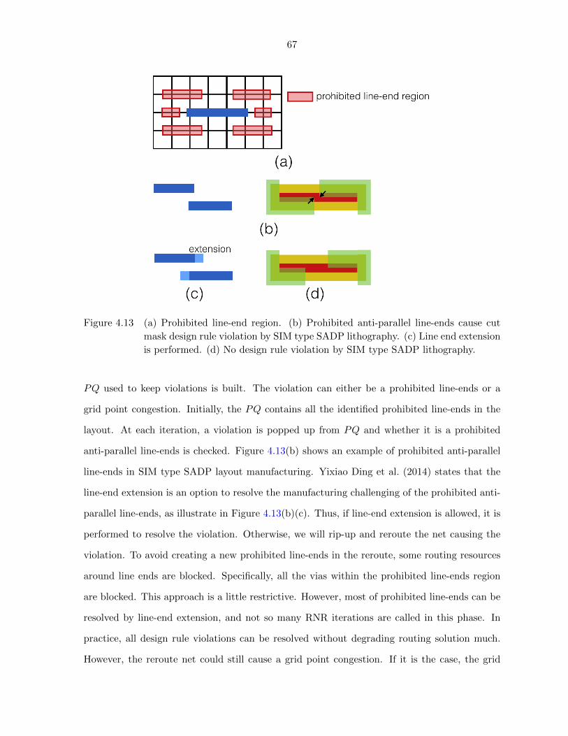
67
Figure 4.13 (a) Prohibited line-end region. (b) Prohibited anti-parallel line-ends cause cut
mask design rule violation by SIM type SADP lithography. (c) Line end extension
is performed. (d) No design rule violation by SIM type SADP lithography.
PQ used to keep violations is built. The violation can either be a prohibited line-ends or a
grid point congestion. Initially, the PQ contains all the identified prohibited line-ends in the
layout. At each iteration, a violation is popped up from PQ and whether it is a prohibited
anti-parallel line-ends is checked. Figure 4.13(b) shows an example of prohibited anti-parallel
line-ends in SIM type SADP layout manufacturing. Yixiao Ding et al. (2014) states that the
line-end extension is an option to resolve the manufacturing challenging of the prohibited anti-
parallel line-ends, as illustrate in Figure 4.13(b)(c). Thus, if line-end extension is allowed, it is
performed to resolve the violation. Otherwise, we will rip-up and reroute the net causing the
violation. To avoid creating a new prohibited line-ends in the reroute, some routing resources
around line ends are blocked. Specifically, all the vias within the prohibited line-ends region
are blocked. This approach is a little restrictive. However, most of prohibited line-ends can be
resolved by line-end extension, and not so many RNR iterations are called in this phase. In
practice, all design rule violations can be resolved without degrading routing solution much.
However, the reroute net could still cause a grid point congestion. If it is the case, the grid

68
point congestion is pushed to PQ. To maintain a congestion free routing solution, the violation
with the type of grid point congestion has higher priority in PQ than that of prohibited line-
ends. This phase will continue until PQ is empty or current iteration count reaches the pre-set
maximum iteration count. Finally, detailed routing solution compliant to SADP design rules
is generated. Congestions or design rule violations will be reported if they exist.
4.5 Experimental results
Our SADP-aware detailed routing is implemented by C++ programming language and with
an option to choose either SIM or SID type SADP lithography. We run all the experiments
on a machine with a 2.4 GHz Intel Core i5 CPU and 8 GB memory. We compare with three
previous works Seong-I Lei et al. (2014), Iou-Jen Liu et al. (2014), and Xiaoqing Xu et al.
(2015a). Seong-I Lei et al. (2014) is LELE-aware detailed routing also applying the idea of
color pre-assignment. Iou-Jen Liu et al. (2014) is the SID type SADP-aware detailed routing
using cut process instead of trim process. Xiaoqing Xu et al. (2015a) is the latest work on SID
type SADP-aware detailed routing. The benchmark suite used in each comparison is provided
by the authors of each chapter. The statistics of each benchmark, including the number of nets
and size of routing grid are listed in Table 4.1, Table 4.2, and Table 4.3 respectively. In our
experiments, we set the p = 48nm, wm = wsp = 24nm, Sc = 72nm, and Ss = 64nm. Note
that the parameters, including edge cost in the G and α and β values, are always kept the
same values in the experiments for each benchmark suite. Table 5.4 lists all the parameter
values used in each set of experiments. and the results are listed in Table 4.5, Table 4.6,
and Table 4.7. Furthermore, we perform another three sets of experiments. Firstly, we show
the effectiveness of our proposed RNR heuristic, and experimental results are in Table 4.8.
Secondly, we investigate the solution quality and convergence of SADP-aware detailed routing
under different parameter settings, which is shown in Figure 4.14. Finally, we analyze the
advantages of our color pre-assignment approach, and experimental results are in Table 4.9.

69
Table 4.1 Statistics of benchmarks from Seong-I Lei et al. (2014)
Benchmark C1 C2 C3 C4 T1 T2 T3 T4
#Nets 1500 10000 1927 2400 869 1036 1763 3017
Grid size 100 × 100 300 × 300 400 × 400 400 × 400 500 × 500 600 × 600 800 × 800 1000 × 1000
Table 4.2 Statistics of benchmarks from Iou-Jen Liu et al. (2014)
Benchmark Test1 Test2 Test3 Test4 Test5 Test6 Test7 Test8 Test9 Test10
#Nets 1000 1800 4000 8000 12000 1000 1800 4000 8000 12000
Grid size 240 × 240 340 × 340 400 × 400 600 × 600 900 × 900 240 × 240 340 × 340 400 × 400 600 × 600 900 × 900
4.5.1 Compare with Seong-I Lei et al. (2014)
The motivation to compare our algorithm with Seong-I Lei et al. (2014) is that both of the
works adopt the idea of color pre-assignment for detailed routing. In Seong-I Lei et al. (2014),
each routing track is assigned with one of the two colors and adjacent tracks in horizontal (or
vertical) direction are assigned with different colors. The idea greatly reduces coloring conflicts
in LELE layout decomposition. However, there are several intrinsic differences between LELE
and SADP. Firstly, LELE allows using stitches to resolve conflicts in layout decomposition
where SADP does not. Secondly, LELE has a major disadvantage that it has worse overlay
control due to the easy misalignment of two masks. Finally, SADP targets at 10nm technology
node while LELE targets at 16/14nm technology node. Thus, more design rules need to be
considered in SADP-aware detailed routing. For example, we need to consider the non-preferred
turn minimization which will restrict solution space of detailed routing. The prohibited line-
ends is not allowed in the routing solution which will further restrict detailed routing. Each
benchmark has four routing layers. In benchmarks C1-C4, each pin only covers one grid point
while each pin might cover several grid points (usually 2-5 grid points) in benchmarks T1-T4.
Table 4.5 shows the performance between Seong-I Lei et al. (2014) and our algorithm, where
“#S” reports the number of stitches, and “#NPT” gives the number of non-preferred jogs.
Compared with Seong-I Lei et al. (2014), our approach for both SIM and SID type SADP
lithography can generate detailed routing solution with almost same quality in terms of total
wirelength and via count. The non-preferred turn count can be minimized by our algorithm
to a very small number. Seong-I Lei et al. (2014) uses a 3GHz Linux machine with 64 GB

70
Table 4.3 Statistics of benchmarks from Xiaoqing Xu et al. (2015a)
Benchmark ecc efc ctl alu div top
#Nets 1671 2219 2706 3108 5813 22201
Grid size 436 × 446 406 × 421 496 × 503 406 × 408 636 × 646 1176 × 1179
Table 4.4 Parameter values in the experiments
Parameters Via unit WL Preferred turn Non-preferred turn Forbidden turn α β
Section V.A 4 1 16 20 INT MAX/8 4 1
Section V.B 12 1 1 1 INT MAX/8 4 2
Sections V.C, V.D, and V.E 4 1 INT MAX/8 INT MAX/8 INT MAX/8 4 8
memory. Given the different machine speeds, our algorithm is estimated more than 3X faster.
4.5.2 Compare with Iou-Jen Liu et al. (2014)
Iou-Jen Liu et al. (2014) is the overlay-aware detailed routing for SID type SADP lithog-
raphy using cut process. Iou-Jen Liu et al. (2014) claims the cut process has higher design
flexibility over trim process. However, it inevitably introduces side overlay error whenever a
cut pattern overlaps with a section of a feature side boundary. In contrast, SIM type SADP
does not introduce any side overlay since all features are formed by spacers. Moreover, we
ensure all the features’ side boundaries are protected by spacer in our SID type SADP layout
decomposition. Table 4.6 compares the performance of our algorithm and Iou-Jen Liu et al.
(2014), where “VPN” denotes via count per net, and “OLL” reports the total side overlay
length. In benchmarks Test1-Test5, the locations of the source and sink pins of each two-pin
net are fixed while the source and sink pins of every two-pin net have multiple candidate lo-
cations in Test6 - Test10. There are three routing layers from M1 to M3 in each benchmark,
and each layer does not have a preferred routing direction. Iou-Jen Liu et al. (2014) performs
the detailed routing in all routing layers, but most of the wires are routed on M1. This is the
reason why they have such small “VPN” in the detailed routing solution as shown in Table VI.
For a fair comparison, we remove the penalty for routing in non-preferred routing direction and
disable the non-preferred turn minimization in our SADP-aware detailed routing. Compared
with Iou-Jen Liu et al. (2014), our detailed routing for SIM and SID type SADP lithography
both reduce total wirelength by 21%. Iou-Jen Liu et al. (2014) tries to complete detailed rout-

71
Tab
le4.
5C
omp
are
wit
hS
eon
g-I
Lei
etal
.(2
014)
Seo
ng-
IL
eiet
al.
(201
4)SIM
typ
eSA
DP
-aw
are
det
aile
dro
uti
ng
SID
typ
eSA
DP
-aw
are
det
aile
dro
uti
ng
Ben
chm
ark
WL
#V
ias
#S
%R
out.
CP
U(s
)W
L#
Via
s#
NP
T%
Rou
t.C
PU
(s)
WL
#V
ias
#N
PT
%R
out.
CP
U(s
)
C1
905
43900
010
011
9196
4568
110
02
9202
4544
210
01
C2
6032
523
036
010
060
6103
924
906
210
010
6101
924
728
410
010
C3
6434
740
840
100
4264
415
4108
010
022
6441
741
060
100
24
C4
6433
151
240
100
4264
401
5142
010
017
6441
551
540
100
22
T1
9914
620
920
100
122
9898
420
020
100
7998
989
2000
010
070
T2
12842
9248
00
100
819
1282
5023
520
100
113
1282
5123
620
100
107
T3
21503
5406
00
100
539
2146
9739
360
100
174
2146
8839
400
100
178
T4
19471
6630
60
100
159
1939
4061
440
100
105
1939
4861
400
100
112
Ave
rage
10442
2.9
6385
.30
100.
022
4.3
1043
65.3
6644
.80.
410
0.0
65.3
1043
66.1
6621
.80.
810
0.0
65.5
Nor
mal
ized
1.00
1.0
01.
001.
001.
001.
041.
000.
291.
001.
041.
000.2
9

72
ing using a single layer, thus “VPN” is very small in the experimental results. The “VPN” in
our routing solution is slightly larger than that in Iou-Jen Liu et al. (2014). However, the value
is actually small enough, and on average 0.08 in SIM type and 0.12 in SID type. Furthermore,
our algorithm achieves 100% routability while Iou-Jen Liu et al. (2014) cannot route all the
nets successfully for all the benchmarks. It shall be noted that the total wirelength and “VPN”
for Iou-Jen Liu et al. (2014) will increase if 100% routability could be achieved. Finally, al-
though Iou-Jen Liu et al. (2014) tries to minimize the amount of side overlay error, they cannot
completely eliminate it. On average 2.2% of total wirelength (462.8 over 20731.7) is generated
with side overlay error. On the other hand, our approach produces no side overlay error at all.
This greatly improves the yield and reduces circuit performance variability. Since it is a joint
work with TSMC, Iou-Jen Liu et al. (2014) is not able to release the binary. Thus, we have to
compare the runtime of two algorithms on different machines. Iou-Jen Liu et al. (2014) uses
a 2.93 GHz Linux work station with 48GB memory. Given the different machine speeds, our
algorithm is estimated more than 2X faster. Iou-Jen Liu et al. (2014) maintains a constraint
graph during detailed routing to minimize overlay error and resolve design rule violation. One
of the major reasons that we can have such speedup is that we totally avoid it due to the color
pre-assignment approach.
4.5.3 Compare with Xiaoqing Xu et al. (2015a)
Xiaoqing Xu et al. (2015a) is the most recently published SID type SADP-aware detailed
routing. Table 4.7 are the experimental results of the comparison. All the benchmarks have
three layers, where M1 is not allowed for routing. Xiaoqing Xu et al. (2015a) performed
the unidirectional routing, and routing direction for M2 and M3 are horizontal and vertical,
respectively. In addition, Xiaoqing Xu et al. (2015a) considers the via rule in which no two
vias can be inserted within certain spacing. To have a fair comparison, we also disallow routing
on M1 and routing not in routing direction on M2 and M3. Since our SADP-aware detailed
routing only considers different-net via rule which requires no two vias from different nets can
be inserted within certain spacing. Thus, we ask the author of Xiaoqing Xu et al. (2015a) to
disable the via rule and generate experimental results. Meanwhile, we disable the different-

73
Tab
le4.
6C
omp
are
wit
hIo
u-J
enL
iuet
al.
(201
4)
Iou-J
enL
iuet
al.
(201
4)S
IMty
pe
SA
DP
-aw
are
det
ailed
rou
ting
SID
typ
eS
AD
P-a
ware
det
ailed
rou
ting
Ben
chm
ark
WL
VP
NO
LL
%R
out.
CP
U(s
)W
LV
PN
OL
L%
Rou
t.C
PU
(s)
WL
VP
NO
LL
%R
out.
CP
U(s
)
Tes
t146
100.
0310
495
.30.
441
86
0.12
0100
1.0
392
60.
340
100
0.5
Tes
t273
180.
0213
496
.71.
660
41
0.12
0100
1.8
588
90.
140
100
1.7
Tes
t312
115
0.02
268
97.2
6.0
8650
0.13
0100
2.7
843
80.
190
100
2.9
Tes
t426
745
0.02
503
97.4
23.1
20210
0.1
40
100
8.7
196
56
0.18
010
06.
8
Tes
t540
204
0.01
424
98.3
56.2
29598
0.0
50
100
23.5
289
24
0.11
010
015.
8
Tes
t651
980.
0620
996
.10.
338
91
0.05
0100
1.5
386
80.
040
100
0.7
Tes
t791
080.
0426
096
.91.
265
80
0.02
0100
1.7
658
40.
030
100
1.9
Tes
t817
397
0.03
642
95.6
5.4
13569
0.0
60
100
3.6
137
17
0.08
010
04.
9
Tes
t933
589
0.03
104
096
.224
.533
931
0.0
50
100
12.9
355
34
0.08
010
019.
2
Tes
t10
5105
10.
02104
497
.854
.837
301
0.0
10
100
17.2
373
36
0.03
010
017.
3
Ave
rage
2073
1.7
0.03
462.
896
.817
.416
385
.70.0
80
100.0
7.5
1638
7.2
0.12
010
0.0
7.2
Nor
mal
ized
1.00
1.0
01.
001.
000.
793.
951.
030.
430.
794.5
61.0
30.4
1

74
net via rule to generate experimental results. Furthermore, we ensure the way to measure
wirelength and via count are same with Xiaoqing Xu et al. (2015a). Both Xiaoqing Xu et al.
(2015a) and our algorithm can generate routing solution with no side overlay error in SADP
layout decomposition. Thus, we do not show OLL in Table VII. Compared with Xiaoqing
Xu et al. (2015a), both of our SIM type and SID type SADP-aware detailed routing reduce
total wirelength by 23%. Both of our SIM and SID type SADP-aware detailed routing reduce
via count by 10% comparing with Xiaoqing Xu et al. (2015a). Furthermore, we can achieve
100% routability for all the benchmarks while Xiaoqing Xu et al. (2015a) fails to route all
the nets in each benchmark. These unroutable nets will further enlarge the difference of total
wirelength and via count between our algorithm and Xiaoqing Xu et al. (2015a). Xiaoqing Xu
et al. (2015a) uses a Linux machine with 3.4GHz Intel(R) Core and 32GB memory to generate
experimental results. Given the different machine speeds, our algorithm is estimated more than
4X faster.
4.5.4 Demonstrate effectiveness of RNR heuristic
In this subsection, we will demonstrate the effectiveness of our proposed heuristic for choos-
ing the rip-up net during RNR iterations. We choose our SIM type SADP-aware detailed
routing on benchmarks from Xiaoqing Xu et al. (2015a) as the baseline. To compare with it,
we disable the heuristic and always randomly choose the rip-up net during RNR iterations.
Table 4.8 shows the comparison results, where “#C” reports the number of grid point conges-
tions, and “#DRV” gives the number of design rule violations in the layout. As shown in the
Table 4.8, compared with the baseline, the routability is reduced by more than 1% without
proposed heuristic. Congestions can not be resolved for all the benchmarks, and design rule
violations may occur in the layout. Meanwhile, the total wirelength and via count also increase.
This is because a bad choice of rip-up net is more likely to have more detour in the reroute.
Thus, quality of routing solution is degraded. However, our proposed heuristic has almost 20%
runtime overhead.

75
Tab
le4.
7C
omp
are
wit
hX
iaoqin
gX
uet
al.
(201
5a)
Xia
oqin
gX
uet
al.
(201
5a)
SIM
typ
eS
AD
P-a
war
ed
etai
led
rou
ting
SID
typ
eS
AD
P-a
war
ed
etai
led
rou
ting
Ben
chm
ark
WL
#V
ias
%R
out.
CP
U(s
)W
L#
Via
s%
Rou
t.C
PU
(s)
WL
#V
ias
%R
out.
CP
U(s
)
ecc
4597
564
4196.
4121
.635
090
5490
100
9.1
3504
454
9210
09.
9
efc
5745
885
1694.
0536
.746
477
7973
100
13.8
4646
379
7210
013
.9
ctl
7186
910
616
95.2
736
.557
739
9445
100
15.4
5769
094
4510
018
.1
alu
7456
811
525
94.1
848
.357
236
1040
210
014
.957
265
1040
410
015
.4
div
155
602
229
6794.
5199
.512
1983
2078
710
040
.112
2087
2078
910
039
.3
top
506
072
821
3294.
5466
4.5
3795
3973
999
100
121.
238
0008
7399
210
011
4.9
Ave
rage
151
924.
0236
99.5
94.8
151.
211
6344
.021
349.
310
0.0
35.8
1164
26.2
2134
9.0
100.
035
.3
Nor
mal
ized
1.0
01.
001.0
01.
000.
770.
901.
060.
240.
770.
901.
060.
23

76
Table 4.8 Demonstrate effectiveness of proposed RNR heuristic
With RNR heuristic Without RNR heuristic
Benchmark WL #Vias %Rout. CPU(s) WL #Vias %Rout. #C #DRV CPU(s)
ecc 35090 5490 100 9.1 35094 5528 99.28 11 0 9.8
efc 46477 7973 100 13.8 46625 8042 98.02 36 1 10.9
ctl 57739 9445 100 15.4 57870 9554 99.22 13 0 14.8
alu 57236 10402 100 14.9 57441 10604 98.94 33 0 11.6
div 121983 20787 100 40.1 122468 21136 98.66 46 0 32.4
top 379539 73999 100 121.2 381468 75434 98.59 193 7 94.7
Average 116344.0 21349.3 100.0 35.8 116827.7 21716.3 0.99 55.3 1.3 29.0
Normalized 1.00 1.00 1.00 1.00 1.00 1.02 0.99 0.81
Figure 4.14 The solution quality and convergence of our SADP-aware detailed routing with
different parameter settings.
4.5.5 Demonstrate the solution quality and convergence of our routing scheme
In this subsection, we will demonstrate the solution quality and convergence of our SADP-
aware detailed routing under different parameter settings. Several user-defined parameters
are used in our SADP-aware detailed routers, which are shown in Table 5.4. Based on our
observation on all the experiments above, the unit wirelength cost value has little effect on the
routing solution. Thus, we keep its value as one in all the experiments. Meanwhile, increasing
(decreasing) via cost will reduce (raise) via count within a certain range in the routing solution.
To investigate the impact of α and β, we choose benchmark “div” in Table 4.7 and run our
SADP-aware detailed routing with different values. Note that different from the experiments
in Section V.C, we enable our different-net via rule. We use a pair (α, β) to denote the values
of α and β in a run. Fig. 14 are four plots showing solution quality and convergence of our
SIM type SADP-aware detailed routing, include total wirelength, via count, total number of
RNR iterations, and CPU time. Each point in the plots is a run with different α and β values.

77
Since all the runs can achieve 100% routability, we do not show the routability plot here.
Generally speaking, if the α and β are set smaller values, our SADP-aware detailed routing
can achieve little better solution quality in terms of wirelength and via count. However, more
RNR iterations are needed in order to achieve 100% routability, and total runtime increases
accordingly. Note that the impact of α and β on solution quality is actually small. The run
with maximum wirelength is only about 0.5% more than the run with minimum wirelength.
At the same time, the run with maximum via count is only about 1.8% more than the run with
minimum via count. Consequently, the solution quality of our SADP-aware detailed routing
has little dependence on the setting of α and β values.
Table 4.9 Demonstrate of color pre-assignment approach
Pure DR w/o color pre-assignment SADP-aware DR w/ color pre-assignment
Benchmark WL #Vias %Rout. CPU(s) WL #Vias %Rout. CPU(s)
ecc 35549 5033 100 8.6 35853 5061 100 11.9
efc 46022 7828 100 13.4 46654 7883 100 17.0
ctl 57153 9260 100 14.3 57875 9323 100 18.4
alu 56958 10039 100 14.8 57888 10167 100 20.4
div 120890 20509 100 39.8 122660 20742 100 41.63
top 378970 70058 100 112.3 385368 70947 100 153.0
Average 115923.6 20454.5 100 33.9 117716.3 20687.1 100.0 43.76
Normalized 1.00 1.00 1.00 1.00 1.02 1.01 1.00 1.28
4.5.6 Demonstrate effectiveness of color pre-assignment approach
Color pre-assignment is the key idea and innovation of our SADP-aware detailed routing. To
demonstrate its effectiveness, we choose the pure detailed routing without color pre-assignment
as a baseline. In the baseline, we only run our routing scheme with phase 1 and 2, and report
wirelength, via count, routability, and runtime. We compare our SADP-aware detailed routing
with the baseline on benchmark suite from Xiaoqing Xu et al. (2015a). The experimental results
are in Table 4.9. Compared with the baseline, SADP-aware detailed routing has 2% wirelength
increase, 1%via count increase, and 28% runtime increase. Consequently, color pre-assignment
approach helps us to achieve SADP decomposable routing solution without much overhead.

78
4.6 Conclusion
In this chapter, we propose a detailed routing algorithm for both SIM and SID type SADP
lithography. We apply the color pre-assignment approach which greatly simplifies the SADP
layout decomposition of routing pattern. The proposed graph model helps avoiding the design
rule violation in detailed routing. Compared with other state-of-the-art SADP-aware detailed
routing algorithms, we generate stronger experimental results in terms of total wirelength,
routability, and runtime. Moreover, no side overlay error is ensured in our detailed routing
solution for SADP layout manufacturing. This gives us an evidence that color pre-assignment
is a highly effective approach to consider SADP lithography during detailed routing. For the
future works, we have several directions. Firstly, this work assumes the SIM type SADP using
cut process while SID type SADP using trim process. However, our work can be potentially
extended to trim-based SIM type SADP and cut-based SID type SADP. Generally, the mask
patterns in cut process are absolutely complement of mask patterns in trim process. Thus,
several modifications should be made. For example, the definition of each prohibited line-ends
configuration, and the way to identify the type of the edge in the graph model. Secondly,
our SADP-aware detailed routing can be potentially speedup by parallelization, especially the
independent routing iterations. Thirdly, our SADP-aware detailed routing can be potentially
extended to non-uniform track structure. However, some modifications should be made. For
example, the via model should be changed to handle the misalignment of routing tracks from
different layers. Furthermore, we can consider mixed-width wires in our SID type SADP
detailed routing, which will make our work more realistic to industrial designs. Finally, we
want to further extend our color pre-assignment approach to detailed routing for self-aligned
quadruple patterning (SAQP) lithography targeted at sub-10nm design.

79
CHAPTER 5. SELF-ALIGNED DOUBLE PATTERNING-AWARE
DETAILED ROUTING WITH DOUBLE VIA INSERTION AND VIA
MANUFACTURABILITY CONSIDERATION
5.1 Introduction
Due to the various delays and setbacks, the next-generation lithography (NGL), e.g, extreme
ultraviolet (EUV) and electron beam lithography (EBL), is not ready for volume production.
Multiple patterning lithography (MPL) has emerged as a key solution for layout manufacturing
in advanced technology nodes. The two main choices for 10nm technology node are triple pat-
terning lithography (TPL) and self-aligned double patterning (SADP). TPL is involved with
three exposure-etch steps, and a mask is used for patterning in each step. This process flow
is known as litho-etch-litho-etch-litho-etch (LELELE). Layout decomposition assigns layout
patterns into three masks to resolve conflicts, and patterns assigned to the same masks are pro-
cessed at once. It is a crucial design step which determines whether layout is manufacturable
by TPL. The TPL layout decomposition can be transformed into a 3-coloring problem which
is NP-complete. Christopher Cork et al. (2008); Bei Yu et al. (2011); Shao-Yun Fang et al.
(2012); Kuang Jian and Evangeline F. Y. Young (2013) are major works on TPL layout decom-
position. The Figure 5.1(b) shows an example of TPL layout decomposition for target layout
in Figure 5.1(a). The layout patterns are assigned with three colors (orange, green, and blue),
and patterns with the same color are in the same mask. Different from TPL, only two masks
are used in SADP to produce the final layout patterns: a core mask and a cut/trim mask. In
SADP, the mandrel patterns are firstly formed by a core mask. Then, spacers are deposited
around mandrels. By utilizing the cut/trim mask, we can obtain the target layout patterns.
Two popular types of processes are developed for SADP Yongchan Ban et al. (2011a). One is

80
Spacer-Is-Metal (SIM) in which the spacers directly define layout patterns. The other one is
Spacer-Is-Dielectric (SID) in which spacers ultimately define trenches between layout patterns.
SADP layout decomposition generates both core and cut/trim masks to form the target layout
while maintaining mask design rules, e.g., minimum spacing and minimum width constraints.
Hongbo Zhang et al. (2011); Yongchan Ban et al. (2011b); Zigang Xiao et al. (2012); Shao-Yun
Fang et al. (2015) are selected works on SADP layout decomposition. Based on how the second
mask is utilized, we have either cut or trim approach in SADP process. In the cut approach,
patterns defined on the cut mask are not included in the final layout patterns. In the trim
approach, region not covered by the trim mask patterns are not included in the final layout
patterns. In this paper, we focus on the SIM type SADP with cut approach and SID type
SADP with trim approach. Note that our approach can be easily adapted to other SADP
variants, e.g., SIM type SADP with trim approach. Figure 5.1(b)(c) show SIM type and SID
type SADP layout decomposition for the target layout in Figure 5.1(a), respectively.
Compared with TPL, SADP has a couple of advantages. Firstly, SADP uses one fewer mask,
which results in less manufacturing cost. Secondly, LELELE based TPL has misalignment error
among the three exposure-etch steps. In contrast, SADP has a self-alignment property and less
stringent overlay accuracy. It is popularly in production use for unidirectional dense patterns
with good pitch control Yongchan Ban et al. (2011b). However, to print two adjacent via
patterns in 10nm technology node, we note that TPL is required. It is because the minimum
width and minimum spacing constraints of the cut/trim mask in SADP prohibit printing two
tiny features so close to each other. Thus, to manufacture layout in 10nm technology node, we
assume to use SADP to print metal layer patterns and TPL to print via layer patterns in this
paper.
The same-color via pitch is defined as the minimum center-to-center distance of a pair of
via patterns from the same via layer that can be assigned to the same mask in TPL layout
decomposition. By applying SADP on metal layers and TPL on via layers in layout manufac-
turing, the same-color via pitch is slightly larger than two times of routing track pitch size Lars
Liebmann et al. (2014). As shown in Figure 5.2(a), suppose a via from a routed net is inserted
in the center of the grid. The same-color via is a via location where a via can be inserted, and

81
Figure 5.1 Layout decomposition. (a) Target layout. (b) TPL layout decomposition. (c) SIM
type SADP with cut approach layout decomposition. (d) SID type SADP with
trim approach layout decomposition.
Figure 5.2 (a) Same-color via pitch. (b) A via pattern forms a TPL violation in SADP-aware
detailed routing solution.
assigned with the same color with existing via in TPL layout decomposition. On the contrary,
a different color should be assigned to the via if it is inserted at the different-color via. We
observe that SADP-aware detailed routing, which targets to ensure SADP decomposable metal
layers, does not automatically guarantee via layers are TPL decomposable. Figure 5.2(b) shows
an example of SADP-aware detailed routing solution which contains a TPL violation on the
via layer between metal 2 and metal 3. Therefore, in 10nm technology node, it is necessary for
SADP-aware detailed routing to consider the TPL decomposability of via layers.
With the shrinking size of technology nodes, the yield and reliability of integrated circuits
(ICs) are more sensitive to process variation. Due to various reasons, e.g., cut misalignment,

82
eletromigration, and thermal stress, vias may fail partially or completely Kuang-Yao Lee and
Ting-Chi Wang (2006). A partial failed via will increase contact resistance and the parasitic
capacitance which may induce timing problem. A complete failed via will leave an open net,
and affect circuit functionality. It is identified as one of the major factors to cause chip failure
and yield lossPuneet Gupta and Evanthia Papadopoulou (2010). Double via insertion (DVI),
which inserts a redundant via adjacent to a single via, is an effective means to increase yield and
improve reliability. We call the single via that cannot have a redundant via without violating
design rules a dead via. DVI in post-routing stage is limited by the inherent dead vias in the
layout after detailed routing. To effectively reduce the dead via count, considering DVI during
detailed routing stage is shown very helpful by previous works. In Figure 5.3(a), a redundant
via is inserted for via b while via a is a dead via in post-routing DVI. On the contrary, if
the detailed routing considers DVI as shown in Figure 5.3(b), all three vias can be protected
by redundant vias. However, with the restriction of SADP design rules on metal layers and
TPL design rules on via layers, considering DVI in detailed routing becomes an even more
challenging problem. In this work, we investigate the SADP-aware detailed routing problem
that simultaneously considers both DIV and via layer manufacturability in 10nm technology
node.
Selected works on SADP-aware detailed routing are Jhih-Rong Gao and David Z. Pan
(2012); Yuelin Du et al. (2013b); Iou-Jen Liu et al. (2014); Xiaoqing Xu et al. (2014); Yixiao
Ding et al. (2015); Xiaoqing Xu et al. (2015a); Yixiao Ding et al. (2016b). However, all these
previous works ignore via layer manufacturability in 10nm technology node. Xiaoqing Xu et al.
(2015a) considers a via spacing rule, in which several via positions around an inserted via are
forbidden. However, the via spacing rule does not ensure via layer patterns are compliant
to design rules of a specific lithography technology. DVI in post-routing stage is studied by
Kuang-Yao Lee and Ting-Chi Wang (2006); Kuang-Yao Lee et al. (2008, 2009b); Cheok-Kei
Lei et al. (2009); Kuang-Yao Lee et al. (2009a); Shing-Tung Lin et al. (2011). However, in
this stage only a slight layout modification is allowed, this methodology will restrict the DVI
feasibility of some vias. Thus, considering DIV in detailed routing is proposed in Gang Xu
et al. (2005); Huang-Yu Chen et al. (2006); Kun Yuan et al. (2009b); Chih-Ta Lin et al. (2010).

83
Gang Xu et al. (2005) formulates the problem as a multi-constrained shortest path problem
solved by a Lagrangian relaxation technique. The approach has high time complexity, which
limits the feasible problem size to be within hundreds of nets. In addition, the hard constraint
which controls the dead via count in each net greatly reduces the routability. Chih-Ta Lin
et al. (2010); Huang-Yu Chen et al. (2006) considers DVI within a gridless routing model while
grid based detailed routing is applied in our paper. Kun Yuan et al. (2009b) considers DVI
both in double patterning lithography (DPL)-aware detailed routing and in post-routing stages.
The DPL-aware detailed routing targets at 32/22nm technology nodes. Moreover, the exact
function to compute each cost introduced to consider DVI in detailed routing is not given.
Finally, the modification on coloring solution of existing layout is disabled during post-routing
DVI. It greatly restricts flexibility of DVI, and potentially increases dead via count.
In this paper, we study both SIM and SID type SADP-aware detailed routing considering
DVI and via layer manufacturability by TPL. Our major contributions are summarized as
follows:
• This is the first work to consider DVI in both SIM and SID types SADP-aware detailed
routing.
• This is the first work to consider via layer manufacturability by TPL in detailed routing.
Each via layer in our routing solution is ensured to be TPL decomposable.
• This is the first work to consider TPL design rules when performing DVI in post-routing
stage. With the inserted redundant vias in post-routing DVI, each via layer is still TPL
decomposable.
• The experimental results demonstrate the effectiveness and efficiency of our algorithm.
Furthermore, the overheads of considering both DVI and via layer manufacturability in
detailed routing is kept minimal.
The rest of the paper is organized as follows. Section 2 presents our problem formulation
and some preliminaries. The overall flow and details of our proposed solution are presented in
Section 3. Section 4 shows the experimental results, and finally Section 5 concludes the paper.

84
Figure 5.3 (a) Detailed routing without DVI consideration. (b) Detailed routing considering
DVI.
5.2 Preliminaries
5.2.1 Problem formulation
We assume that there is a preferred routing direction on each routing layer and the other
direction perpendicular to the preferred routing direction is defined as the non-preferred routing
direction. We strongly discourage instead of completely disable routing in the non-preferred
routing direction. We refer to this routing behavior as the restricted detailed routing. The
following is the formal problem definition.
Given a placed netlist, a multi-layer routing grid, and a set of design rules, we perform
restricted detailed routing to generate a legal routing solution. The objective is to minimize
the total wirelength and via count while achieving 100% routability. Meanwhile, the dead via
count should be minimized in post-routing DVI. The constraints are that metal layer patterns
are compliant to SADP design rules, and via layers are TPL decomposable.
5.2.2 Color pre-assignment approach
SADP-aware detailed routing is a challenging problem due to the non-intuitive SADP layout
decomposition. As shown in Fig. 1(c)(d), the two mask patterns used to form the final layout
have only minor similarities with the target layout patterns. Meanwhile, additional design
rules, e.g., overlap error minimization Iou-Jen Liu et al. (2014), should be considered. The

85
idea of color pre-assignment is applied in Yixiao Ding et al. (2015) to simplify the problem
of maintaining SIM type SADP design rules in detailed routing. This approach is extended
to handle SID type SADP-aware detailed routing Yixiao Ding et al. (2016b). In this paper,
we adopt this approach for our SADP-aware detailed routing. Before the detailed routing,
the multi-layer routing grid is assigned with colors. On each metal layer, a panel is defined
as the area between two adjacent horizontal (vertical) grid lines. In the SIM type SADP, we
pre-assign colors (grey and white) to the panels alternately in both horizontal and vertical
directions as shown in Figure 4.8(a). In the SID type SADP, routing tracks are assigned
with colors (black and grey) alternately in both horizontal and vertical directions as shown in
Figure 4.8(b). The colored routing grid determines where mandrel and cut/trim mask patterns
may form. In this way, the SADP layout decomposition is known at the moment when a net is
routed. Hence, the occurrence of a design rule violation is foreknown in detailed routing and
can be easily minimized. However, color pre-assignment also imposes additional constraints
on detailed routing. Yixiao Ding et al. (2016b) defines a preferred turn, a non-preferred turn,
and a forbidden turn according to the cost of layout manufacturing by SADP. Each type of
turn can be identified based on the location of the turning point and the turning direction. As
shown in both Figure 4.8(a)(b), turn a is a preferred turn, turns b and c are forbidden turns,
and turn d is a non-preferred turn. A forbidden turn is an L-shape metal layer pattern not
allowed in detailed routing due to the design rule violation in SADP layout manufacturing.
Thus, the forbidden turn should be strictly avoided in order to guarantee SADP decomposable
metal layers.
5.2.3 Double via insertion feasibility
Double via insertion is to add a redundant via beside a single via on the same via layer
without a design rule violation. Given a single via, we assume a redundant via can be inserted
at one of the four locations beside it. Figure 5.5(a) shows a partial layout of SIM type SADP-
aware detailed routing containing a single via v which connects layout patterns from metal 2
and metal 3. Four locations a, b, c, and d on the same via layer of via v are candidate locations
to insert a redundant via. We define these four candidate locations as DVI candidates (DVICs)

86
Figure 5.4 Color pre-assignment for SADP-aware detailed routing. (a) SIM type SADP. (b)
SID type SADP.
of via v. To connect to the inserted redundant via, the two metal patterns connected by v
need to extend to a DVIC location as shown in Figure 5.5(b). This short connection together
with the original metal pattern may form an L-shape pattern. This L-shape pattern needs to
be examined under the constraints of our SADP-aware detailed routing. In Figure 5.5(b), the
L-shape pattern on metal 3 is a forbidden turn. Thus, the DVIC d is not feasible for double via
insertion. For the same reason, DVIC c is also not feasible due to the occurrence of a forbidden
turn on metal 2. Furthermore, DVIC b is not feasible since the space is occupied by a metal
layer pattern from another routed net. In this case, only DVIC a is feasible.
From above example, the DVI feasibility of a single via is affected by our SADP-aware
detailed routing constraints. Without considering the case that the DVIC is occupied by the
layout pattern from a different routed net, the DVI feasibility of a single via is determined
by two factors. One is the type of grid point where the single via locates in the colored grid,
and the other is how the two metal patterns connected by the single via are oriented. Hence,
given a single via from a routed net, it is easy to identify all its feasible and infeasible DVICs.
Figure 5.6(a)(b) shows two examples of DVI feasibility of a single via in SIM type SADP-aware
detailed routing. Note that the single via in Figure 5.6(b) is a stacked via which connects

87
Figure 5.5 Double via insertion. (a) Each single via has four DVICs. (b) The DVIC d is
infeasible.
two layout patterns from metal 2 and metal 4. The two single vias are located at the same
type of grid point in the colored grid Yixiao Ding et al. (2016b). However, the orientation
of two metal patterns connected by the single via in Figure 5.6(a) is different from that in
Figure 5.6(b). Thus, the DVI feasibility of two single vias is not the same. Figure 5.6(c)(d)
shows two examples of DVI feasibility of a single via in SID type SADP-aware detailed routing.
Different from the previous examples, the orientations of two metal patterns connected by the
single via in Figure 5.6(c)(d) are the same. However, the types of grid points where the two
single vias locates in the colored grid are different Yixiao Ding et al. (2016b). As a result, the
feasibility of the two single vias is different.
5.2.4 Forbidden via pattern
The via layer TPL layout decomposition can be transformed to a 3-coloring problem on
the decomposition graph Bei Yu et al. (2011). The graph is constructed by viewing each via
pattern as a vertex. An edge exists between two vertices if the two via patterns are within same-
color via pitch. However, maintaining a decomposition graph in detailed routing is expensive
in terms of runtime and memory usage. Moreover, 3-coloring problem is NP-complete, and
ensuring the decomposition graph is always 3-colorable in routing is difficult. Alternatively, we
propose to examine each subregion of size 3 × 3 on each layer of routing grid and extract the
via pattern within it. Then, determining if the via pattern is 3-colorable can be done in O(1)

88
Figure 5.6 (a)(b) DVI feasibility in SIM type SADP-aware detailed routing. (c)(d) DVI fea-
sibility in SID type SADP-aware detailed routing.
time. If the via patterns in any 3 × 3 subregions in the routing grid are 3-colorable, then the
decomposition graph is highly likely to be 3-colorable. Figure 5.7 shows several examples of the
via pattern within a 3 × 3 subregion and its corresponding colored decomposition graph. We
define a forbidden via pattern as a via pattern within a 3×3 subregion which is not 3-colorable.
For simplicity, we refer to it as the FVP. An FVP can be identified by the via count and how
vias are distributed within 3× 3 subregion as follows:
1. Via patterns with 6 or more vias are all FVPs.
2. For via patterns with via count equal to 5, unless 4 of 5 the vias are on four corners of
the 3 × 3 subregion, they are FVPs. Figure 5.7(a) shows an non-FVP with 5 vias and
Figure 5.7(b) shows an FVP with 5 vias.
3. For via patterns with via count equal to 4, unless 2 of 4 the vias are on diagonally opposite
corners of the 3 × 3 subregion, they are FVPs. Figure 5.7(c) shows an non-FVP with 4
vias and Figure 5.7(d) shows an FVP with 4 vias.
4. Via patterns with 3 or fewer vias are not FVPs.

89
Figure 5.7 Via patterns in 3x3 subregion and its decomposition graph. (a) A via pattern
with 5 vias which is not an FVP. (b) An FVP with 5 vias, in which one via is
uncolorable. (c) A via pattern with 4 vias which is not an FVP. (d) An FVP with
4 vias, in which one via is uncolorable.
5.3 Proposed solution
5.3.1 Overall flow
The overall flow is shown in Figure 5.8. The inputs are a placed netlist, a multi-layer routing
grid, and a set of design rules. The routing graph modeling, independent routing iterations, and
negotiated congestion based rip-up and reroute (R&R) are explained with details in Yixiao Ding
et al. (2016b). To consider DVI and via layer manufacturability by TPL in detailed routing,
we develop a cost assignment scheme. The scheme assigns costs to the routing graph after
routing of each net. The major advantage of this approach is the overheads of those additional
considerations in detailed routing can be minimized. Thus, the SADP-aware detailed routing
can keep high performance as before. Then, we propose a via layer TPL violation removal based
R&R to eliminate all FVPs on the via layers. After that, a decomposition graph is constructed
based on via layer patterns, and a fast 3-colorability check is performed. If not 3-colorable, the
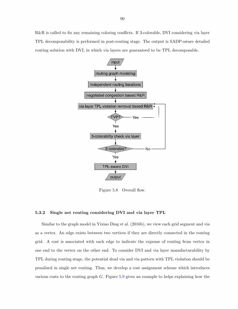
90
R&R is called to fix any remaining coloring conflicts. If 3-colorable, DVI considering via layer
TPL decomposability is performed in post-routing stage. The output is SADP-aware detailed
routing solution with DVI, in which via layers are guaranteed to be TPL decomposable.
Figure 5.8 Overall flow.
5.3.2 Single net routing considering DVI and via layer TPL
Similar to the graph model in Yixiao Ding et al. (2016b), we view each grid segment and via
as a vertex. An edge exists between two vertices if they are directly connected in the routing
grid. A cost is associated with each edge to indicate the expense of routing from vertex in
one end to the vertex on the other end. To consider DVI and via layer manufacturability by
TPL during routing stage, the potential dead via and via pattern with TPL violation should be
penalized in single net routing. Thus, we develop a cost assignment scheme which introduces
various costs to the routing graph G. Figure 5.9 gives an example to helps explaining how the

91
Figure 5.9 An example to illustrate how cost assignment scheme works for single net routing
(colored routing grid is not shown for clarity). (a) viau of neti has three feasi-
ble DVICs. (b) Block-DVIC via locations. (c) Along-metal via locations. (d)
Conflict-DVIC via locations.
cost assignment scheme works. Algorithm 1 is the pseudocode describing how costs are added
to the G after routing of each net.
During sequential routing, the routing of a new net may affect the DVI feasibility of the vias
in already routed nets. Meanwhile, the already routed nets may also affect the DVI feasibility
of the vias in the net to be routed. We observe that the bi-directional effect is not symmetric,
which will be analyzed as follows. Suppose viau of a routed neti connects metal lines on metal
2 and metal 3, and it has three feasible DVICs as shown in Figure 5.9(a). netj is the new
net to be routed. We firstly look into how routing of a new net affects the routed nets in
terms of DVI feasibility. Given a single via in a routed net, block-DVIC via locations are
defined as the its feasible DVICs. As shown in Figure 5.9(b), the block-DVIC via locations
of viau are marked by orange empty-fill squares. As long as netj is routed across/through
the block-DVIC via locations, the feasible DVIC count of viau is reduced. The chance that
viau will have a redundant via in the post-routing DVI becomes lower. To penalize routing

92
netj across/through block-DVIC via locations, a penalty cost is added to the G after routing
of neti. The penalty cost can be computed by α# of feasible DVICs of viau
, which we refer to it as
block-DVIC cost (BDC). In this way, routing resources used for DVI by the via with smaller
feasible DVIC count are assigned with higher costs, and vias from routed nets can be prevented
from becoming dead vias.
Now, we look into how routed nets affect the net to be routed in terms of DVI feasibility.
There are two scenarios which are shown in Figure 5.9(c)(d). We define the via locations along
the metal patterns in the routed net as along-metal via locations, which are marked by blue
empty-fill squares in Figure 5.9(c). If the netj is routed with a viav at any along-metal via
location, the feasible DVIC of viav may be reduced since the space is occupied by the metal
pattern. To penalize routing netj using vias at along-metal locations, a penalty cost is added
to the G after routing of neti. The penalty cost is referred as along-metal cost (AMC), which
is a constant. In the other scenario, if netj is routed with a viav such that the viav’s DVIC
shares the same via location with a feasible DVIC of viau. We say these two DVICs are in
conflict. In addition, the fewer number of feasible DVICs of viau, the more chance that viau
or viav becomes a dead via due to the conflicting DVIC. We define the via location like viav as
a conflict-DVIC via location which is marked by green empty-fill square in Figure 5.9(d). To
prevent vias becoming dead vias due to conflicting DVIC in post-routing DVI, a penalty cost is
added to the G after routing of neti. The penalty cost is computed by β# of feasible DVICs of viau
,
which we refer to it as conflict-DVIC cost (CDC). In summary, the cost assignment introduce
three new kinds of costs to consider DVI in detailed routing, namely BDC, AMC, and CDC.
In this way, the DVI feasibility of vias in both routed nets and the new net to be routed can
be protected.
To avoid TPL violation on via layer, the cost assignment scheme also introduces another
penalty cost. Given a via in a routed net, a penalty cost is assigned to each of its different-color
via locations, which is shown in Figure 5.2(a). For each different-color via location, we find
all existing vias that are within same-color via pitch with it, and refer to them as coloring
conflicts. The penalty cost can be computed by γ× (# of coloring conflicts), which we refer to
it as TPL cost (TPLC).

93
Algorithm 3 Cost assignment scheme.
for each viau of routed neti do
for each viak at feasible DVIC location of viau dofind vertexk in G represents viak;
for each vertexm adjacent to vertexk in G do
for each edge e incident to vertexm docost(e)+ = α
(# of feasibleDV ICs of viau);
end
end
end
for each viak at conflict-DVI via location of viau dofind vertexk in G represents viak;
for each edge e incident to vertexk do
cost(e)+ = β(# of feasibleDV ICs of viau)
;
end
end
for each viak at different-color via location of viau dofind vertexk in G represents viak;
for each edge e incident to vertexk docost(e)+ = γ ×# of coloring conflicts of viak
end
end
end
for each viak at along-metal via location of neti dofind vertexk in G represents viak;
for each edge e incident to vertexk docost(e) += AMC;
end
end

94
5.3.3 Via layer TPL violation removal based rip-up and reroute
To ensure via layers are TPL decomposable is a hard constraint for our SADP-aware detailed
routing. The cost assignment scheme only discourages the occurrence of a TPL violation on
via layers by adding TPLC to G. Thus, we introduce a new phase to our SADP-aware detailed
routing flow: via layer TPL violation removal based R&R. Its pseudocode is presented in
Algorithm 2. Similar to the negotiated congestion based R&R in Yixiao Ding et al. (2016b),
a base cost (BC), a usage cost (UC), and a history cost (HC) are applied to G. As mentioned
before, maintaining a 3-colorable decomposition graph during R&R is expensive and difficult.
Alternatively, we target to remove TPL violation on via layers by eliminating all FVPs through
R&R iterations. The major advantage of this approach is detecting all the FVPs on via layers
is O(n), where n is the size of routing grid. In addition, updating the detected FVPs after a
R&R iteration is O(m), where m is the total number of vias in the rip-up and reroute net.
Algorithm 4 Via Layer TPL violation removal based R&R.
initialize a priority queue (PQ) and push all FVPs;
block via locations that will potentially generate FVP;
while !PQ.emptry() doviolation = PQ.pop();
choose rip-up net N to resolve violation;
update UC, BDC, AMC, CDC, and TPLC after removing N ;
update blocked via locations after removing N ;
the modified Dijkstra’s algorithm reroutes N;
update UC, BDC, AMC, CDC, and TPLC after rerouting N ;
update blocked via locations after rerouting N ;
if reroute creates congestion thenupdate HC for congested routing resource;
PQ.push(congestion);
else if reroute creates FVP thenupdate HC for vias in that FVP;
PQ.push(FVP);
end
Several techniques are applied in order to obtain a faster convergence of R&R iterations in
this phase. Firstly, we use a priority queue to keep both congestion violations and FVPs in line 1
of Algorithm 2. The associated priority of a congestion violation is higher than that of an FVP.

95
Hence, R&R is always targeted to resolve congestion violations first if they exist. Secondly, in
the beginning of R&R iterations, some via locations are blocked in line 2 of Algorithm 2 to
prevent reroute from creating FVPs. The blocked via locations are updated in lines 7 and 10
after a R&R iteration. Figure 5.10 shows several examples of how via locations are blocked.
Given a 3 × 3 subregion, for each unused via location, if an FVP is created after inserting a
via at that location, then it should be blocked. Even with blocked via locations, the reroute
could still create an FVP if multiple vias are inserted within a 3 × 3 subregion. In this case,
the HC of all the edges incident to each via in the newly created FVP are increased as shown
in line 15. Hence, the vias in FVPs grow more expensive to use and FVPs can be potentially
eliminated through R&R iterations.
Figure 5.10 Examples of how vias are blocked in via layer TPL violation removal based R&R.
5.3.4 3-colorability check of decomposition graph
The target of via layer TPL violation removal based R&R is eliminate all the FVPs on
via layers. However, even if all FVPs are successfully eliminated, there is a small chance that
the decomposition graph is still not 3-colorable. Thus, after via layer TPL violation removal
based R&R, a decomposition graph is constructed for via layers. Then, we perform a fast
3-colorability check of decomposition graph. A greedy based Welsh-Powell algorithm D. J. A.
Welsh and M. B. Powell (1967) is applied for the check. If it is 3-colorable, our SADP-aware
detailed routing exits. If not, R&R is called to fix the coloring conflict. We note that this

96
case did not happen in our experiments in Section 4. This demonstrates that our FVP-based
heuristic is good enough to remove all TPL violations on via layers in practice.
5.3.5 TPL-aware double via insertion
Our SADP-aware detailed routing is optimized for DVI, and via layers are TPL decompos-
able. In post-routing stage, DVI is performed and a large number of redundant vias will be
inserted on via layers. The inserted redundant vias together with original vias in the routing
solution will potentially cause TPL violations. Figure 5.11 shows an example of post-routing
DVI for two adjacent single vias v1 and v2 on a via layer. Each single via has three feasible
DVICs. In Figure 5.11(b), two redundant vias are inserted at a1 and a2 for the two single
vias. The four-via pattern is not 3-colorable in TPL layout decomposition, and a TPL viola-
tion occurs. Thus, it is necessary to consider TPL decomposability of via layers even in the
post-routing DVI. Figure 5.11(c) is another method of DVI with TPL awareness. Each of the
single vias is inserted with a redundant via, and the four-via pattern is 3-colorable. We refer to
post-routing DVI with consideration of via layer TPL decomposability as the TPL-aware DVI
problem. The formal problem statement is as follows.
Given a SADP-aware detailed routing solution with TPL decomposable via layers, and a
set of design rules, we perform double via insertion without modifying routing solution. The
objective is to maximize the total number of inserted redundant vias. The constraint are that via
layers are still TPL decomposable and metal layers are still SADP decomposable after double
via insertion.
Figure 5.11 Post-routing DVI. (a) Two adjacent single vias. (b) A TPL violation occurs after
DVI. (c) TPL-aware DVI.

97
The post-routing DVI problem can be reduced into the maximum independent set problem,
which is NP-complete Kuang-Yao Lee and Ting-Chi Wang (2006). To further consider via
layer TPL decomposability and metal layer SADP decomposability in DVI makes the TPL-
aware DVI a more challenging problem. To accurately evaluate the effectiveness of our DVI
consideration in SADP-aware detailed routing, an integer linear program (ILP) is formulated
for the TPL-aware DVI problem. By solving the ILP optimally, we can fairly compare the dead
via count in our SADP-aware detailed routing with and without DVI consideration. The ILP
formulation is presented as follows.
For each feasible DV ICj of viai, a binary variable Dij indicates whether a redundant via is
inserted at DV ICj for viai. Dij = 1 if a redundant via is inserted. For each viai, three binary
variables oVi, gVi, and bVi indicate its TPL color (orange, green, or blue) in 3-coloring. oVi = 1,
gVi = 0, and bVi = 0 if viai’s TPL color is orange. oVi = 0, gVi = 1, and bVi = 0 if viai’s
TPL color is green. oVi = 0, gVi = 0, and bVi = 1 if viai’s TPL color is blue. Another binary
variable uVi is introduced in case it is uncolorable. uVi = 1 if viai is uncolorable in 3-coloring.
For each feasible DV ICj of viai, a redundant via is introduced if Dij = 1. Similarly, three
binary variables oDij , gDij , bDij are introduced to indicate the redundant via’s TPL color in
3-coloring. B is an extremely big constant. The mathematic formulation is shown as follows.
Objective:
maximizen∑i=1
m∑j=1
Dij −B ×n∑i=1
uVi
where m is the number of feasible DVICs of viai, and n is total number of single vias in the
routing solution.
Constraints:
C1: For each viai,m∑j=1
Dij ≤ 1
C2: If DV ICij and DV ICi′j′ are in conflict,
Dij +Di′j′ ≤ 1
C3: For each viai,
oVi + gVi + bVi + uVi = 1

98
C4: For each DV ICj of viai,
oDi + gDi + bDi −B × (Dij − 1) ≥ 1
oDi + gDi + bDi +B × (Dij − 1) ≤ 1
C5: If viai and viai′ are within same-color via pitch,
oVi + oVi′ ≤ 1
gVi + gVi′ ≤ 1
bVi + bVi′ ≤ 1
C6: If viai and DV ICj′ of viai′ are within same-color via pitch,
oVi + oDi′j′ +B × (Di′j′ − 1) ≤ 1
gVi + gDi′j′ +B × (Di′j′ − 1) ≤ 1
bVi + bDi′j′ +B × (Di′j′ − 1) ≤ 1
C7: If DV ICj of viai and DV ICj′ of viai′ are within same-color via pitch,
oDij + oDi′j′ +B × (Dij +Di′j′ − 2) ≤ 1
gDij + gDi′j′ +B × (Dij +Di′j′ − 2) ≤ 1
bDij + bDi′j′ +B × (Dij +Di′j′ − 2) ≤ 1
C8: For each DV ICj of each viai,
Dij , oDi, gDi, bDi ∈ {0, 1}
oVi, gVi, bVi, uVi ∈ {0, 1}
As mentioned above, the major purpose of ILP formulation is to fairly evaluate the DVI
consideration in our SADP-aware detailed routing. Solving the ILP may be time consuming
when the problem size is big. This solution to the post-routing TPL-aware DVI problem is not
realistic in practice. Alternatively, we propose a fast heuristic for TPL-aware DVI problem,
which is shown in Algorithm 3. Note that the time complexity of the algorithm is O(nlogn)
where n is number of feasible DVICs.

99
Algorithm 5 Fast heuristic for TPL-aware DVI
initialize a priority queue (PQ);
for each feasible DV ICj of viai dosetDP(DV ICj);
PQ.push(DV ICj);
end
while !PQ.empty() doDVIC = PQ.top();
if !DVIC.isValid() thenPQ.pop();
else
if DVIC.DP!=computeDP(DV IC) thensetDP(DV IC);
PQ.pop();
PQ.push(DVIC);
elseinsert a redundant via at DVIC;
PQ.pop();
end
end
end
Two critical issues need to be tackled in the design of TPL-aware DVI heuristic. The first
issue is how to choose a feasible DVIC to insert a redundant via, i.e., DVI ordering. For each
feasible DV ICj of each single viai, a DVI penalty (DP) is defined to determine the priority to
insert a redundant via at it in the DVI process. The bigger DP of a feasible DVIC, the lower
priority to insert a redundant via at the DVIC.
DPDV ICj = δ ×# of feasible DV ICs of viai
+ λ×# of conflicting DV ICs with DV ICj
+ µ×# of killed DV ICs by DV ICj
As shown in above equation, the DP computation consists of three parts. δ, λ, and µ are three
parameters to control the weight of three parts. The first part is the number of feasible DVICs
of viai. It is more likely for single vias with fewer feasible DVICs to become dead vias. Hence,
we would like to insert redundant vias with higher priority for those single vias. The second

100
part is the number of conflicting DVICs with DV ICj . To insert a redundant via at a DVIC
with more conflicting DVICs will leave less chance of DVI for other single vias. Thus, we charge
a bigger penalty on a feasible DVIC with more conflicting DVICs. The last part is how many
feasible DVICs will be killed if a redundant via is inserted at DV ICj . We say a feasible DVIC
is killed if the redundant via at it form an FVP with existing vias. As shown in lines 2-5 of
Algorithm 3, we compute DP for each feasible DV ICj of each viai, and push it into PQ. The
top element in PQ is the feasible DVIC with smallest DP. Note that the DP of each feasible
DV ICj in the PQ is constantly updated in the DVI process, which is shown in lines 11-14 of
Algorithm 3.
Figure 5.12 TPL-aware DVI. (a) Four single via, and via v has three feasible DVICs. (b) An
FVP occurs when a redundant via is inserted at a. (b) An FVP occurs when
a redundant via is inserted at c. (c) No FVP occurs when a redundant via is
inserted at d.
The second issue is how to ensure via layer TPL decomposability during DVI. We again
apply the idea of FVP to maintain the constraint. Specifically, we do not allow inserting a
redundant via at a feasible DVIC if it creates an FVP. Figure 5.12 shows an example of DVI
for v among four single vias. The single via v has three feasible DVCs, namely a, c, and d. If
a redundant via is inserted at a, an FVP is created as shown in Figure 5.12(b). Similarly, an
FVP is created if a redundant via is inserted at c in Figure 5.12(c). The only valid choice is
DVI at d which does not create any FVPs. Thus, every time before we insert a redundant via
at a feasible DVIC, a validity check is perform as shown in line 8 of Algorithm 3. This check
can be easily done in O(1). Specifically, for each feasible DV ICj of single viai, three conditions
are checked. It is valid if and only if three conditions are all false. The three conditions are list
as follows.

101
• a redundant via is already inserted at one of DV ICj ’s conflicting DVICs.
• a redundant via is already inserted at a feasible DVIC of viai, which is not DV ICj .
• an FVP is created if a redundant via is inserted at DV ICj .
5.4 Experimental results
We implemented our proposed algorithm in C++ programming language. We run all the
experiments on a machine with a 2.4 GHz Intel Core i5 CPU and 8 GB memory. Gurobi 6.5
is called to solve the ILPs. Benchmarks from Xiaoqing Xu et al. (2015a) are used to generate
experimental results. Each circuit contains three routing layers metal 1, metal 2, and metal
3. Metal 1 is not allowed for routing, and the preferred routing direction for metal 2 and
metal 3 are horizontal and vertical, respectively. Other benchmarks statistics, including the
number of nets and grid sizes, are listed in Xiaoqing Xu et al. (2015a). In the first subsection,
we demonstrate the consideration of DVI and via layer TPL decomposability in both SIM and
SID types SADP-aware detailed routing. In the second subsection, we compare the performance
of ILP and heuristic solutions to TPL-aware DVI problem. Note that all parameters are kept
the same for all the experiments in this section. The values of all the parameters are listed in
Table 5.4.
Table 5.1 Parameter values in the experiments
Cost assignment scheme TPL-aware DVI
parameter α AMC β γ δ λ µ
value 8 1 4 4 1 1 1
5.4.1 SADP-aware detailed routing considering DVI and via layer TPL
In this subsection, we demonstrate our consideration of DVI and via layer TPL decom-
posability in both SIM and SID types SADP-aware detailed routing. For each type of SADP
process, we run four sets of experiments, including SADP-aware detailed routing, SADP-aware
detailed routing considering DVI, SADP-aware detailed routing considering via layer TPL

102
Tab
le5.
2S
IMty
pe
SA
DP
-aw
are
det
aile
dro
uti
ng
SIM
typ
eSA
DP
-aw
are
routi
ng
Con
sider
DV
IC
onsi
der
via
laye
rT
PL
Consi
der
DV
I&
via
laye
rT
PL
CK
TW
L#
Via
sC
PU
(s)
#D
V#
UV
WL
#V
ias
CP
U(s
)#
DV
#U
VW
L#
Via
sC
PU
(s)
#D
V#
UV
WL
#V
ias
CP
U(s
)#
DV
#U
V
ecc
354
23
496
915
.6291
24355
1249
8218
.816
323
3578
249
6519
.7132
0358
37
5027
22.9
105
0
efc
458
56
770
730
.2880
104
460
8578
4233
.161
164
4705
978
1941
.0440
0472
17
7965
41.2
357
0
ctl
569
02
913
231
.5663
63572
4492
2835
.641
236
5759
191
7237
.5305
0579
08
9289
46.2
240
0
alu
569
86
10053
38.
5122
711
3576
3310
312
36.6
858
5158
724
1025
250
.8600
0591
03
1048
651
.4481
0
div
1202
67
2015
386
.123
0227
212
1489
2055
310
3.3
1775
139
1232
9520
377
150.
6113
30
124
024
20800
157.3
883
0
top
3791
14
7018
5261
.190
6831
738
2784
7148
928
2.1
5932
161
3930
3071
459
377.
5419
90
394
752
72878
367.2
3461
0
Ave
.11
5758.
020
366
.577.
2024
05.1
148
.811
6791
.120
734.
384
.96
1625
.179
.011
9246
.820
674.
011
2.90
1134
.80
119
806.8
21074.
1114.4
1921.1
0
Nor
.1.
001.
001.0
01.
001.
001.
011.
021.
100.
680.
531.
031.
021.
460.
47
1.0
31.0
31.
480.
38
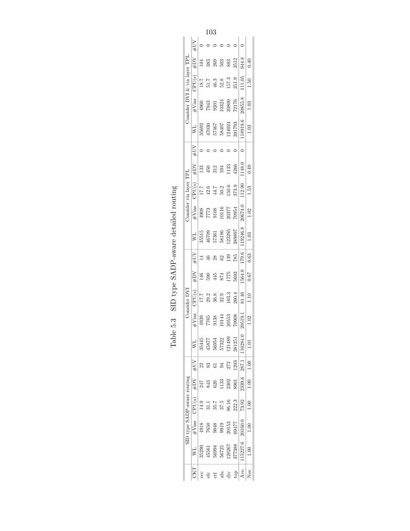
103
Tab
le5.
3S
IDty
pe
SA
DP
-aw
are
det
aile
dro
uti
ng
SID
typ
eSA
DP
-aw
are
routi
ng
Con
sider
DV
IC
onsi
der
via
laye
rT
PL
Consi
der
DV
I&
via
laye
rT
PL
CK
TW
L#
Via
sC
PU
(s)
#D
V#
UV
WL
#V
ias
CP
U(s
)#
DV
#U
VW
L#
Via
sC
PU
(s)
#D
V#
UV
WL
#V
ias
CP
U(s
)#
DV
#U
V
ecc
352
90
491
814
.9247
22354
4549
3917
.714
614
3551
549
0817
.7133
0356
92
4960
18.7
104
0
efc
455
61
765
031
.1843
83458
7777
6529
.259
046
4670
977
7342
.6450
0470
30
7943
51.7
383
0
ctl
569
94
904
835
.7626
61569
5491
3836
.844
528
5736
191
0844
.7312
0574
67
9201
46.3
269
0
alu
567
25
991
937
.511
3394
573
2210
144
32.9
874
6258
186
1011
650
.2594
0584
07
1032
452
.8503
0
div
1202
67
2015
386.
1623
0227
212
1489
2055
310
3.3
1775
139
1232
9520
377
150.
6113
30
124
024
20800
157.3
883
0
top
3773
88
6947
7222
.389
01120
338
1251
7090
826
0.4
5693
785
3898
9770
954
373.
9426
60
391
793
72176
351.9
3512
0
Ave
.11
5227.
620
160
.073.
9223
39.6
287
.111
6284
.020
519.
181
.46
1564
.017
9.6
1192
46.8
2067
4.0
112.
90
1148
.00
118
919.6
20855.
8111.0
5944.8
0
Nor
.1.
001.
001.0
01.
001.
001.
011.
021.
100.
670.
631.
031.
021.
530.
49
1.0
31.0
31.
500.
40

104
decomposability, and SADP-aware detailed routing consider both DVI and via layer TPL de-
composability. For a fair and accurate comparison, the post-routing TPL-aware DVI problem
is solved by the ILP approach. The Table 5.2 and Table 5.3 shows the experimental results of
considering DVI and via layer TPL decomposability in SIM and SID types SADP-aware de-
tailed routing, respectively. “CPU” is the detailed routing runtime, “#DV” denotes dead via
count and “#UV” denotes the number of uncolorable vias in via layer TPL layout decomposi-
tion. Both “#DV” and “#UV” are reported from post-routing TPL-aware DVI ILP solution.
Note that the routability for all benchmarks in four sets of experiments is 100%, thus we do
not list it due to the limited table width.
As shown in the first two sets of experiments in Table 5.2, without considering via TPL
manufacturability, there are numerous uncolorable vias in TPL-aware DVI ILP solution. It
indicates that TPL violations exist on via layers in SADP-aware detailed routing solution.
Compared with the baseline, SADP-aware detailed routing considering DVI can reduce dead
via count by 32%. With the consideration of via layer TPL decomposability in SADP-aware
detailed routing, no uncolorable via is reported. Thus, via layers are TPL decomposable after
post-routing DVI. Note that the consideration of via layer TPL decomposability indirectly
helps to reduce dead via count since vias are more spread out. Hence, more space is left for
DVI in post-routing stage. Finally, the SADP-aware detailed routing considering both DVI and
via layer TPL decomposability can simultaneously reduce dead via count by 62% and ensure
the via layers are TPL decomposable. The overheads are only 3% increase on wirelength and
via count, respectively. With more routing constraints, runtime increases by 48% due to more
R&R iterations.
As shown in Table 5.3, the consideration of DVI in SADP-aware detailed routing can reduce
dead via count by 33%. Furthermore, with the consideration of via layer TPL decomposability,
via layers are ensured to be TPL decomposable after post-routing DVI. Finally, the SID type
SADP-aware detailed routing considering both DVI and via layer TPL decomposability can
simultaneously reduce dead via count by 60% and ensure the via layers are TPL decomposable.
The overheads of wirelength and via count are 3% increase, respectively. In addition, total
detailed routing runtime is increased by 50%.

105
Table 5.4 TPL-aware DVI for SIM type SAD-
P-aware detailed routing
ILP Heuristic
#DV #UV CPU (s) #DV #UV CPU (s)
ecc 105 0 1505.0 113 0 1.0
efc 357 0 1332.7 389 0 1.4
ctl 240 0 3275.0 257 0 1.9
alu 481 0 2868.3 533 0 1.8
div 883 0 1505.0 979 0 3.9
top 3461 0 5075.0 3740 0 13.1
Ave. 921.1 0 2593.52 1001.8 0 3.89
Nor. 0.92 667.57 1.00 1.00
Table 5.5 TPL-aware DVI for SID type SAD-
P-aware detailed routing
ILP Heuristic
#DV #UV CPU (s) #DV #UV CPU (s)
ecc 104 0 20.4 111 0 0.9
efc 383 0 323.4 418 0 1.3
ctl 269 0 175.1 294 0 1.6
alu 503 0 1292.0 559 0 1.7
div 898 0 2930.1 1008 0 4.7
top 3512 0 6509.9 3917 0 12.2
Ave. 944.8 0 1875.21 1051.1 0 3.77
Nor. 0.90 497.40 1.00 1.00
5.4.2 TPL-aware DVI
In this subsection, we compare the performance of our proposed ILP and heuristic solutions
to TPL-aware DVI problem. We generate routing solutions by both SIM and SID types SADP-
aware detailed routing with consideration of DVI and via layer TPL decomposability. Based
on each routing solution, the post-routing TPL-aware DVI is solved by both ILP and heuristic
approaches. For heuristic approach, we do 3-coloring of via layer patterns after DVI by Welsh-
Powell algorithm D. J. A. Welsh and M. B. Powell (1967). Table 5.4 and Table 5.5 show
experimental results of TPL-aware DVI for SIM and SID type SADP-aware detailed routing,
respectively. In Table 5.4, compared with ILP approach, our proposed heuristic has more than
600× speedup. Meanwhile, no uncolorable via is reported. It further demonstrates that via

106
layer TPL decomposability can be ensured in DVI by prohibiting FVPs. Finally, our heuristic
only has about 8% more dead vias than that of ILP approach. In Table 5.5, compared with
ILP approach, our proposed heuristic has almost 500× speedup, no uncolorable via, and about
10% more dead vias.
5.5 Conclusion
In this paper, we consider DVI and via layer manufacturability by TPL in both SIM and
SID types SADP-aware detailed routing. A cost assignment scheme is integrated into our
SADP-aware detailed routing framework to consider DVI and via layer TPL decomposability.
In addition, a via layer TPL violation based rip-up and reroute is applied to ensure via layers
are TPL decomposable. In the post-routing stage, we tackle the TPL-aware DVI problem,
and propose both ILP and high-performance heuristic solutions. The experimental results
demonstrate that the consideration of DVI and via layer TPL manufacturability is effective
and efficient with minimal overheads.

107
CHAPTER 6. PIN ACCESSIBILITY-DRIVEN DETAILED
PLACEMENT REFINEMENT
6.1 Introduction
With increasing number of design rules in advanced technology nodes, detailed routing (DR)
is becoming more and more difficult. Pin access is one of the most critical problems Xiang Qiu
and Malgorzata Marek-Sadowska (2012); Meng-Kai Hsu et al. (2014). To alleviate pin access
difficulty, the choice of tapping point is important during DR. Figure 6.1 shows the pin access
issue for a standard cell containing three pins a, b, and c. Each pin has several tapping points
for via insertion to connect to a metal 2 wire segment. Suppose pins a, b, and c belong to nets
A, B, and C respectively, and DR is performed in the order of A−B − C. In Fig. 1(b), after
routing nets A and B, all tapping points of pin c are blocked by other routes. There is no way
to connect pin c to a metal 2 wire segment, which leads to a pin access failure. With a wise
choice of tapping points as shown in Fig. 1(c), all three pins can be accessed in DR.
However, choosing tapping points wisely during DR is not always sufficient due to the fixed
cell placement. In the area with high pin density, pin access maybe still impossible even with
a careful choice of tapping points. As shown in Figure 6.2(a), the standard cell SCa is placed
abutting to the left boundary of standard cell SCb. Thus, pins are very close to each other,
especially for pins D and E, which potentially increase pin access difficulty. Figure 6.2(b)
shows DR around the two standard cells. Both of pin E’s tapping points are blocked by metal
2 wire segments, which used to access pin D and pin E. As a result, pin access for pin E is
not possible.
To further improve pin accessibility, we propose a refinement stage after the detailed place-
ment (DP) stage, in which small perturbation of a given DP is allowed. shows the three possible

108
Figure 6.1 Detailed routing around pins in a standard cell. (a) A standard cell with three
pins. (b) Pin C cannot be accessed because all its tapping points are blocked. (c)
A wise choice of tapping points makes all pins accessible.
options of refining the placement to improve pin access. In Figure 6.3(a), cell SCb shifts to
the right to make some space between SCa and SCb. Then, a via can be inserted at the top
tapping point of pin D, and there is enough space to form a metal 2 wire segment from the
tapping point. By utilizing both metal 2 and metal 3 wire segments, pin access for pin D is
not the bottleneck in DR anymore. In Figure 6.3(b), cell SCb is flipped, and all pins can be
easily accessed during DR. Finally, in Figure 6.3(c), two cells are swapped, and pins are better
distributed with more space in between than in Figure 6.2(a). Thus, pin access becomes easier
and DR can be completed with less efforts. From the examples above, we observe pin access can
be effectively improved by cell shifting, cell flipping, and adjacent cell swap. Thus, we propose
a detailed placement refinement stage which directly targets at pin accessibility enhancement
using these three approaches.

109
Figure 6.2 Enhance pin accessibility in DR. (a) Pin access becomes harder within area with
high pin density. (b) Pin E cannot be accessed even with a careful choice of tapping
points.
Figure 6.3 Three approaches to enhance pin accessibility in DP (a) Cell shifting. (b) Cell
flipping. (c) Adjacent cell swap.
Pin access is considered in DR stage Xiaoqing Xu et al. (2014, 2015b,a, 2016); Tim Nieberg
(2011); Muhammet Ozdal (2009). Xiaoqing Xu et al. (2014, 2015b,a, 2016) proposed stan-
dard cell-level pin access planning under SADP lithography constraints. Tim Nieberg (2011)
addressed offgrid or gridless pin access while Muhammet Ozdal (2009) tackled escape routing

110
for a dense pin cluster. Pin access is also considered in the global routing (GR) stage in the
form of local routing congestion estimation Charles J. Alpert et al. (2013); Zhongdong Qi et al.
(2014); Yaoguang Wei et al. (2012). However, they only took into account pin information,
e.g., pin count, pin shape, and pin’s Steiner tree length, which fails to capture the real pin
access scenario during DR. Furthermore, in both GR and DR stages, cell placement cannot be
changed and all pin locations are fixed. Even with the proposed techniques in above works, pin
access may still be impossible which leads to failed connection. To overcome such limitation,
detailed routing is considered during placement. The recent placement contest Vladimir Yutsis
et al. (2014) demonstrates that physical data, like pin geometries, is important, and needs to be
considered in placement to improve routability in DR. Furthermore, routing congestion is con-
sidered during DP Yanheng Zhang and Chris Chu (2009); Wen-Hao Liu et al. (2013); Taraneh
Taghavi et al. (2010). The models to estimate congestion in Yanheng Zhang and Chris Chu
(2009); Wen-Hao Liu et al. (2013) are very rough, especially for local routing congestion, and
pin access problem is not directly touched. Taraneh Taghavi et al. (2010) included pin infor-
mation in the cost function to guide detailed placement. However, the pin information are not
enough to model pin access in DR accurately.
Our major contributions are summarized as follows:
• It is the first work to directly consider pin access issue in detailed placement stage.
• We propose an accurate model to capture the pin access scenario during detailed routing.
A cost function is used to guide the detailed placement refinement.
• The placement refinement operations are limited to cell flipping, adjacent cell swap, and
cell shifting. Meanwhile, the proposed solution is dynamic programing and linear pro-
graming based. Thus, our DP refinement ensures a fast runtime without a big perturba-
tion of the given legalized placement.
• The experimental results demonstrate that the total cell displacement of our DP re-
finement is kept in control. By applying the DP refinement, unroutable nets can be
significantly reduced in DR without much overheads of total wirelength, via count, and
runtime.

111
The rest of the chapter is organized as follows. Section 2 presents some preliminaries.
Section 3 is the problem formulation. The overall flow and details of our proposed solution
are presented in Section 4. Section 5 shows ours experimental results, and finally Section 6
concludes the chapter.
6.2 Preliminaries
6.2.1 Assumptions
In the following, we present our DP refinement approach under a few assumptions. Note
that our approach is general and is not limited to these assumptions. It can be easily extended
to handle different assumptions.
Figure 6.4 The minimum center-to-center spacing rule in via design rules.
In typical designs, the majority of pins occur on metal 1 layer, where the available routing
resources are extremely limited. Meanwhile, 1D gridded design has become the mainstream in
advanced technology nodes Yixiao Ding et al. (2014). Each metal layer has a routing direction,
either horizontal or vertical. Without loss of generality, we assume metal 1 layer is not allowed
for routing, metal 2 has horizontal routing direction, metal 3 has vertical routing direction,
and so on. We also assume each pin in the cell is either a rectangle strip or a rectilinear shape
spanning one or more metal 2 tracks. A tapping point (TP) is defined as the overlap of a metal

112
2 track and the pin shape, where a via can be inserted to connect the pin to a metal 2 wire
segment.
In 1D gridded design, changing the routing direction means switching to another metal layer
and via insertion among the layers. Thus, maintaining via design rules in DR is critical to both
routing solution quality and layout manufacturing. For example, the minimum center-to-center
via spacing is one of the major via design rules Jason Cong et al. (2000). In this chapter, the
minimum center-to-center via spacing is assumed to be more than one routing pitch, and it is
enforced for every via layer. As shown in Figure 6.4, an via is inserted on the via layer between
metal 1 and metal 2. Thus, the four via locations on the same via layer represented by purple
empty squares are forbidden. Note that the assumed via design rules can be easily extended to
other complex via design rules, e.g., multiple patterning constraints on via layer pattern Yixiao
Ding et al. (2016a).
6.2.2 Pin access region
Figure 6.5 A PAR is defined for each pin-to-pin connection of each pin. Connection AB is a
same-row connection while connection CD is a different-row connection.
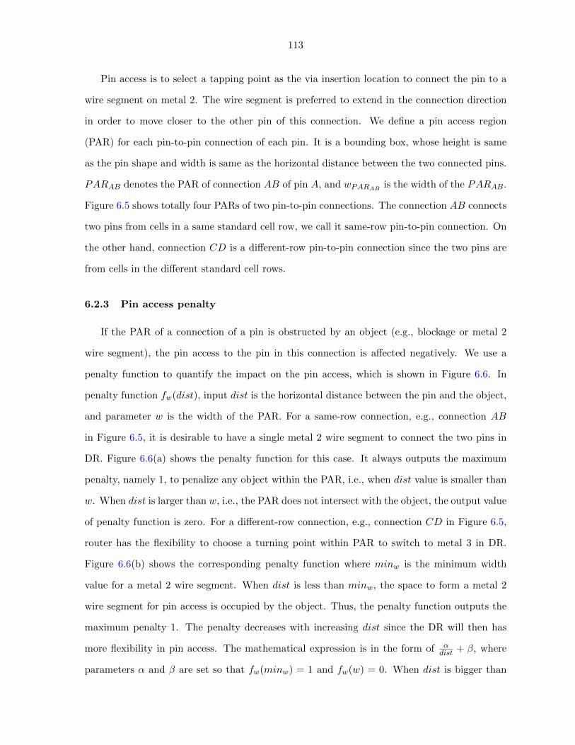
113
Pin access is to select a tapping point as the via insertion location to connect the pin to a
wire segment on metal 2. The wire segment is preferred to extend in the connection direction
in order to move closer to the other pin of this connection. We define a pin access region
(PAR) for each pin-to-pin connection of each pin. It is a bounding box, whose height is same
as the pin shape and width is same as the horizontal distance between the two connected pins.
PARAB denotes the PAR of connection AB of pin A, and wPARABis the width of the PARAB.
Figure 6.5 shows totally four PARs of two pin-to-pin connections. The connection AB connects
two pins from cells in a same standard cell row, we call it same-row pin-to-pin connection. On
the other hand, connection CD is a different-row pin-to-pin connection since the two pins are
from cells in the different standard cell rows.
6.2.3 Pin access penalty
If the PAR of a connection of a pin is obstructed by an object (e.g., blockage or metal 2
wire segment), the pin access to the pin in this connection is affected negatively. We use a
penalty function to quantify the impact on the pin access, which is shown in Figure 6.6. In
penalty function fw(dist), input dist is the horizontal distance between the pin and the object,
and parameter w is the width of the PAR. For a same-row connection, e.g., connection AB
in Figure 6.5, it is desirable to have a single metal 2 wire segment to connect the two pins in
DR. Figure 6.6(a) shows the penalty function for this case. It always outputs the maximum
penalty, namely 1, to penalize any object within the PAR, i.e., when dist value is smaller than
w. When dist is larger than w, i.e., the PAR does not intersect with the object, the output value
of penalty function is zero. For a different-row connection, e.g., connection CD in Figure 6.5,
router has the flexibility to choose a turning point within PAR to switch to metal 3 in DR.
Figure 6.6(b) shows the corresponding penalty function where minw is the minimum width
value for a metal 2 wire segment. When dist is less than minw, the space to form a metal 2
wire segment for pin access is occupied by the object. Thus, the penalty function outputs the
maximum penalty 1. The penalty decreases with increasing dist since the DR will then has
more flexibility in pin access. The mathematical expression is in the form of αdist + β, where
parameters α and β are set so that fw(minw) = 1 and fw(w) = 0. When dist is bigger than

114
Figure 6.6 Penalty function fw(dist) for (a) same-row connection. (b) different-row connec-
tion.
w, the PAR is not occupied by the object, so the output penalty is zero.
Given a connection of a pin, the pin access penalty (PAP) is a cost imposed on the connection
to reflect the impact of an object on the pin access in the connection. The computation of PAP
depends on the type of object and how the PAR of the connection intersects with the object.
As shown in Figure 6.7, there are totally four scenarios. Let’s firstly consider the simplest
scenario which is shown in Fig. 7(a). The PARAA′ of a connection AA′ of pin A is intersected
with a metal 2 blockage B. We say that connection AA′ is in conflict with blockage B. distAB
denotes the horizontal distance between pin A and blockage B. A conflict tapping point (CTP)
is a TP on a metal 2 track which is obstructed by the blockage B. #CTPAA′.B denotes the
number of CTPs of pin A when connection AA′ is in conflict with blockage B. In Fig. 7(a),
#CTPAA′.B = 2, and they are highlighted with red color. In the first scenario, the pin access to
pin A becomes harder since the routing resources used for pin access are occupied by blockage
B. PAPBAA′ is the PAP cost imposed on connection AA′ to model the increase in the hardness
of the pin access.
PAPBAA′ =#CTPAA′.B
#TPA× fwPARAA′
(distAB)
PAPBAA′ = 0 if pin access to pin A in the connection AA′ is completely free from the impact of
blockage B. PAPBAA′ = 1 if the pin access is impossible through all pin A’s TPs. The PAPBAA′
consists of two components. One is the probability of the occupied routing resource will actually

115
affect pin access, which is#CTPAA′.B
#TPA. The other is the penalty function to determine the
negative impact on pin access, which is fwPARAA′(distAB). The penalty function used in the
computation of PAPBAA′ depends on whether connection AA′ is a same-row connection or a
different-row connection as described earlier.
Figure 6.7 PAP in four scenarios. (a) 1st scenario. (b) 2nd scenario. (c) 3rd scenario. (d)
4th scenario.
In other scenarios, the PAP cost is imposed on the connection AA′ when its PAR intersects
with the PAR of another connection. As shown in Figure 6.7(b)(c)(d), there are three kinds of
intersection which lead to the other three scenarios. Suppose the PARAA′ of connection AA′
of pin A is intersected with the PAR of connection BB′ of pin B. We say that connection AA′
is in conflict with the connection BB′. The second scenario is when the connection directions
of pin A and pin B are right and pin A is on the left side of pin B, or connection direction
of pin A and pin B are left and pin A is on the right side of pin B. The third scenario is
when the connection directions of pin A and pin B are different. The fourth scenario is when
the connection directions of pin A and pin B are right and pin A is on the right side of pin
B, or connection directions of pin A and pin B are left and pin A is on the left side of pin
B. PAPBB′
AA′ is the PAP cost imposed on connection AA′ due to conflicting connection BB′.
116
PAPBB′
AA′ for the three scenarios are shown as follows.
PAPBB′
AA′ =#CTPAA′.BB′
#TPA ×#TPBfwPARAA′
(distAB)
PAPBB′
AA′ =#CTPAA′.BB′
#TPA ×#TPBfwPARAA′
(wPARAA′
wPARAA′ + wPARBB′distAB)
PAPBB′
AA′ =#CTPAA′.BB′
#TPA ×#TPBfwPARBB′
(distAB)
Similar to PAPBAA′ , PAPBB′AA′ is a product of a probability term and a penalty function The
penalty function used in the computation also depends on the type of connection AA′.
The PAP function computes the PAP cost imposed on a connection due to a conflicting
blockage or connection. For each connection AA′, we can compute its total PAP cost PAPAA′
imposed by all conflicting blockages and connections as follows.
PAPAA′ =∑
block∈CBPAP blockAA′ +
∑conn∈CC
PAP connAA′
where CB is the set of conflicting blockages with AA′ and CC is the set of conflicting connec-
tions with AA′. Furthermore, we define CPAPc for each cell c as the total PAP cost imposed
on all the connections of all the pins in c.
CPAPc =∑
A∈Pinc
∑AA′∈ConnA
PAPAA′
where ConnA denotes all the connections of pin A and Pinc denotes all the pins in c. CPAPc
reflects the pin accessibility for all the connections of all the pins in the cell c. It can be used
to evaluate if the cell placement is good in terms of pin access. We are trying to refine the cell
placement to improve pin access for all the connections. Thus, we define total cell pin access
penalty (TCPAP) as the total PAP cost computed for all the connections in the placement.
TCPAP =∑
c∈All CellsCPAPc
6.3 Problem formulation
The TCPAP can be used to evaluate the pin accessibility of a detailed placement. Our
proposed DP refinement is targeted to improve pin access by minimizing the TCPAP. Below is
our formal problem statement.
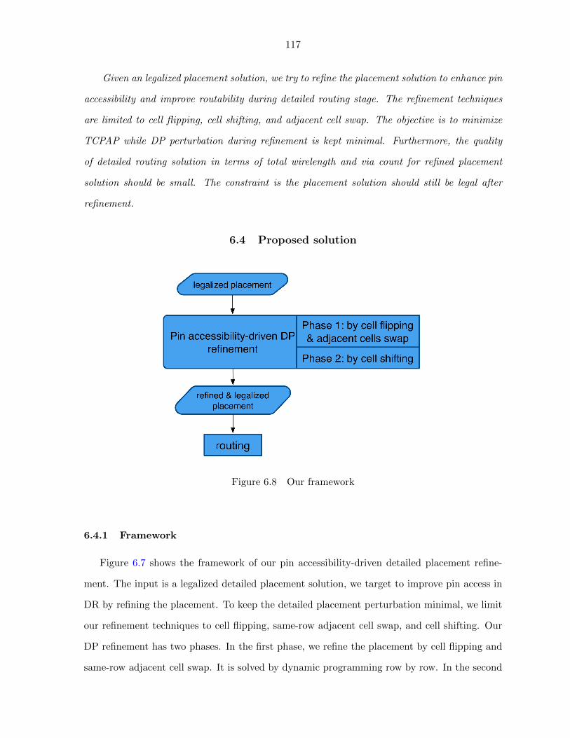
117
Given an legalized placement solution, we try to refine the placement solution to enhance pin
accessibility and improve routability during detailed routing stage. The refinement techniques
are limited to cell flipping, cell shifting, and adjacent cell swap. The objective is to minimize
TCPAP while DP perturbation during refinement is kept minimal. Furthermore, the quality
of detailed routing solution in terms of total wirelength and via count for refined placement
solution should be small. The constraint is the placement solution should still be legal after
refinement.
6.4 Proposed solution
Figure 6.8 Our framework
6.4.1 Framework
Figure 6.7 shows the framework of our pin accessibility-driven detailed placement refine-
ment. The input is a legalized detailed placement solution, we target to improve pin access in
DR by refining the placement. To keep the detailed placement perturbation minimal, we limit
our refinement techniques to cell flipping, same-row adjacent cell swap, and cell shifting. Our
DP refinement has two phases. In the first phase, we refine the placement by cell flipping and
same-row adjacent cell swap. It is solved by dynamic programming row by row. In the second

118
phase, we further refine placement by cell shifting. It is solved by linear programming. The
output is the refined and legalized placement. It is ready for routing, and expected to have
better pin access in DR.
6.4.2 Refinement phase 1
In this phase, we try to refine an initial placement by cell flipping and adjacent cell swap
to minimize TCPAP. We make an assumption in the computation of PAPAA′ for a connection
AA′ of pin A from cell c as follows.
PAPAA′ ≈∑
block∈CBPAP blockAA′ +
∑conn∈CC′
PAP connAA′
where CB is the set of the conflicting blockages with AA′, and CC ′ is the set of conflict-
ing connections with AA′ and they contain a pin in cell c or a pin in a cell adjacent to c.
Based on the above assumption, we can solve the problem by dynamic programming row
by row. For each row, the dynamic programming helps to find the optimal cell placement
to minimize∑
c∈CrowCPAPc where Crow denotes all cells in the row. Given TCPAP =∑
row∈All Rows∑
c∈CrowCPAPc, TCPAP can be minimized. Given a placement row with n
placed cells, we denote the cells as c1 to cn according to their order in the original row place-
ment. We use ci′ to denote the flipped version of ci. We use dynamic programming to compute
the optimal refined prefix placement of length p for p = 1, 2, ..., n where refinement by cell
flipping and adjacent cell swap is allowed. Let solqp (solq′p ) denote the optimal refined prefix
placement of length p where the cell in the p-th position is cq (c′q). Since we allow cell flipping
and adjacent cell swap, the cell in the p-th position of a refined placement is either cp, c′p, cp−1,
c(p−1)′ , cp+1, or c(p+1)′ . Let TPAP qp (TPAP q′
p ) denote the total CPAP for solqp (solq′p ). Let
∆TPAPci denote the change of TPAP value after adding ci at the end of solqp to construct
solip+1. Observe that the computation of TPAP for a prefix placement of length k+ 1 requires
TPAP kk , TPAP k′
k , TPAP k−1k , TPAP(k−1)′k , TPAP k+1
k , and TPAP(k+1)′
k . Thus, six kinds of
solution need to be kept during dynamic programming, including solkk , solk′k , solk−1k , sol
(k−1)′k ,
solk+1k , and sol
(k+1)′
k . The followings are the base cases and recursive formula of our dynamic
program.

119
Base cases:
{ TPAP 11 , TPAP
1′1 , TPAP
21 , TPAP
2′1 }
where each case is obtained by computing TPAP value for the cell sequence of the initial
solution sol11, sol1′
1 , sol21, and sol2′
1 .
Recursive formula:
TPAP kk = min{TPAP k−1k−1 + ∆TPAPck , TPAP(k−1)′k−1 + ∆TPAPck , TPAP
k−2k−1 + ∆TPAPck , TPAP
(k−2)′k−1 + ∆TPAPck}
TPAP k′
k = min{TPAP k−1k−1 + ∆TPAPck′ , TPAP(k−1)′k−1 + ∆TPAPck′ , TPAP
k−2k−1 + ∆TPAPck′ , TPAP
(k−2)′k−1 + ∆TPAPck′}
TPAP k−1k = min{TPAP kk−1 + ∆TPAPck−1, TPAP k
′k−1 + ∆TPAPck−1
, TPAP kk−1 + ∆TPAPck−1, TPAP k
′k−1 + ∆TPAPck−1
}
TPAP(k−1)′k = min{TPAP kk−1 + ∆TPAPc(k−1)′ , TPAP
k′k−1 + ∆TPAPc(k−1)′ , TPAP
kk−1 + ∆TPAPc(k−1)′ , TPAP
k′k−1 + ∆TPAPc(k−1)′}
TPAP k+1k = min{TPAP k−1k−1 + ∆TPAPck+1
, TPAP(k−1)′k−1 + ∆TPAPck+1
, TPAP k−2k−1 + ∆TPAPck+1, TPAP
(k−2)′k−1 + ∆TPAPck+1
}
TPAP(k+1)′
k = min{TPAP k−1k−1 + ∆TPAPc(k+1)′ , TPAP(k−1)′k−1 + ∆TPAPc(k+1)′ , TPAP
k−2k−1 + ∆TPAPc(k+1)′ , TPAP
(k−2)′k−1 + ∆TPAPc(k+1)′}
Finally, the minimum∑
c∈CrowCPAPc can be obtained by identifying min {TPAPnn , TPAPn
′n ,
TPAPn−1n , TPAP(n−1)′n }. Meanwhile, the refined cell placement for the given row of cells can
be obtained from corresponding solution kept in dynamic programming.
6.4.3 Refinement phase 2
In this phase, we try to further refine the placement by cell shifting. As mentioned before,
cell shifting helps to re-distribute the space between the cells, which will potentially improve
pin access in DR. We continue to use the proposed PAP function to guide the refinement to
further improve pin access. However, we need to keep the cell displacement in control to avoid
big perturbation of the given legalized placement. We solve this problem by formulating a
linear program (LP). Given the refined placement after phase 1, we label all the cells in the
i-th row from left to right as cellij . For cellij , let Lij denote the x coordinate of its bottom
left corner, and Wij denote its width. Furthermore, we label the m-th pin in cellij as pijm,
and n-th connection of pinijm as cijmn. In addition, let LL and RR be the x coordinates
of the left and right boundaries of the placement region, respectively. We use a continuous
variable δij to represent the shift amount for cellij . To avoid a big amount of shift, we set
∆S as the threshold to control the maximum shift distance for every cell. For each connection
cijmn during cell shifting, the width wijmn of its PAR changes. Suppose bk and ci′j′m′n′ are

120
some blockage and connection which are in conflict with cijmn. Let distkijm denote the distance
between the pijm and bk. Let disti′j′m′ijm denote the distance between pijm and pi′j′m′. Both
distkijm and disti′j′m′ijm also change. Other parameters in the PAP function remains unchanged.
Thus, we can re-write the PAP function as a function of w and dist as follows.
PAP bkcijm(distkijm + δs, wijmn + δs)
PAPci′j′m′n′cijm (disti′j′m′ijm + δs, wijmn + δs)
Function PAP bkcijm computes the penalty cost imposed by a conflicting blockage, and function
PAPci′j′m′n′cijm computes the penalty cost imposed by a conflicting connection. δs denotes the
changes of dist and w when cij shifts. δs = δij in function PAP bkcijm , and δs = δij − δi′j′ in
function PAPci′j′m′n′cijm . However, the PAP function is non-linear when cijm is a different-row
connection. To formulate the problem as a LP, we use linear approximation to approximate
the new penalty cost computed by the PAP function after cell shifting. The linear functions of
δs used to approximate the PAP function for connection cijmn during cell shifting is shown as
follows.
LF bkcijmn(δs) = α× δs + β
where α =∂PAP
bkcijm
∂δs|δs=0 and β = PAP bkcijm |δs=0
LFci′j′m′n′cijmn (δs) = α′ × δs + β′
where α′ =∂PAP
ci′j′m′n′cijm
∂δs|δs=0 and β′ = PAP
ci′j′m′n′cijm |δs=0. The δs is controlled by ∆S which
is usually small in practice (several routing pitches). The approximation is usually accurate
enough to be used to compute PAP during cell shifting. Thus , we can approximate TCPAP
by a linear function∑
cijmn∈C (∑
bk∈BijmnLF bkcijmn
+∑
ci′j′m′n′∈Ci′j′m′n′LF
ci′j′m′n′cijmn ) where Bijmn is a
set of blockages in conflict with cijmn, Ci′j′m′n′ is a set of connections in conflict with cijmn,
and C denotes all the connections of all the pins in all the cells in the placement. Below is LP
formulation for refinement phase 2.
Objective:
Min∑
cijmn∈C (∑
bk∈BijmnLF bkcijmn
+∑
ci′j′m′n′∈Ci′j′m′n′LF
ci′j′m′n′cijmn )

121
Constraints:
C1: For the leftmost cell ci1 in rowi,
Li0 + δi1 >= LL
C2: For the rightmost cell ciN in rowi,
LiN + δiN +WiN <= RR , where N the number of cells in rowi
C3: For two adjacent cells cij and ci(j+1) in rowi,
Lij + δij +Wij <= Li(j+1) + δi(j+1)
C4: For each cij ,
δij <= ∆S and δij >= −∆S
C1 (C2) ensures that the leftmost (rightmost) cell in each row is not shifted out of left (right)
boundary. The C3 ensures that no two adjacent cells from same row are overlapped after cell
shifting. Finally, C4 makes sure each cell cannot shift more than the pre-set threshold.
6.5 Experimental results
Table 6.1 Statistics of benchmarks
Benchmark ecc efc ctl alu div top
#Cells 1302 1197 1715 1802 3260 12576
#Connections 1615 2872 3308 3261 5847 18618
ave. #TPs 3.02 3.21 3.39 3.28 3.27 3.03
We implemented our pin accessibility-driven detailed placement refinement by C++ pro-
gramming language. All experiments are performed on a machine with 2.4 GHz Intel Core
i5 and 8GB memory. Gurobi 6.0.5 is called to solve the LP in refinement phase 2. As men-
tioned before, this is the first work to directly consider pin access in DP stage. We derive our
benchmarks based on the netlist and placement information that the authors of Xiaoqing Xu
et al. (2015a) used to construct their detailed routing benchmarks. Every net with n pins is
decomposed into n − 1 pin-to-pin connections. In a few standard cells, we found that some

122
Tab
le6.
2C
omp
aris
onb
etw
een
the
give
np
lace
men
tan
dth
ep
lace
men
tsaf
ter
refi
nem
ent
Giv
enpla
cem
ent
Aft
erre
finem
ent
phas
e1
Aft
erre
finem
ent
phas
e1&
2
Ben
chm
ark
TC
PA
PT
CP
AP
Ave.
Dis
p.
#F
Cs
(pct
%)
CP
U(s
)T
CP
AP
Ave
.D
isp.
CP
U(s
)
ecc
2469.
41210
8.51
5.65
500
(38.
40)
4.25
2070
.43
7.40
5.01
efc
3926.
39347
2.32
5.20
438
(36.
59)
5.66
3419
.43
7.04
6.56
ctl
3327.
58291
2.31
5.33
557
(32.
48)
6.04
2874
.78
7.18
7.00
alu
3409.
91284
8.64
3.59
549
(30.
47)
5.55
2849
.36
5.14
5.80
div
7044.
60665
9.68
5.40
1059
(32.
48)
11.1
361
19.2
16.
9912
.48
top
18909
.70
1532
36.8
05.
0838
92(3
0.95
)39
.68
1482
3.90
6.61
41.9
6
Ave
.65
14.
60553
9.71
5.04
1165
.83
(33.
56)
12.0
553
59.5
26.
7313
.14
Nor
.1.0
00.
851.
001.
000.
821.
331.
09

123
Tab
le6.3
Com
pari
son
ofth
ed
etai
led
rou
tin
gre
sult
sfo
rth
egi
ven
and
the
refi
ned
pla
cem
ents
.
Giv
enpla
cem
ent
Pla
cem
ent
afte
rre
finem
ent
phas
e1
Pla
cem
ent
afte
rre
finem
ent
phas
e1&
2
Ben
chm
ark
WL
#V
ias
#U
Ns
CP
U(s
)W
L#
Via
s#
UN
sC
PU
(s)
WL
#V
ias
#U
Ns
CP
U(s
)
ecc
10401
610
710
158
109.
6711
3015
1104
112
016
3.09
1187
17
113
0584
123
.99
efc
850
30
11446
162
106.
2695
256
1171
910
287
.09
1013
14
118
5292
84.
17
ctl
11174
612
936
139
109.
3912
1619
1350
110
413
4.08
1279
86
136
6889
98.
58
alu
921
17
12807
177
91.4
796
823
1285
414
110
7.31
1030
84
133
18150
149.
16
div
18006
123
865
258
261.
1219
9196
2457
321
825
1.41
2096
48
250
56202
360.
94
top
80897
873
058
899
1181
.68
8558
5674
521
743
1220
.30
8925
90
761
71588
1314.
92
Ave
.230
324
.67
24137
.00
298.
8330
9.93
2469
60.8
324
701.
5023
8.00
327.
2125
889.
83
252
28.
33200
.83
355.
29
Nor
.1.
001.
001.
001.
001.
071.
020.
801.
061.1
21.0
50.
67
1.1
5

124
pins from metal 1 have only a single TP, and the distance between these TPs is less than the
required assumed minimum center-to-center via spacing. Thus, pin access is impossible for
these pins due to the constraint of via design rules. Thus, we elongate these pins to increase
their TP counts. The Table 6.1 shows the statistics for each benchmark, including cell count,
the number of pin-to-pin connections, and average TP count of all the pins.
Table 6.2 shows the results of our pin accessibility-driven detailed placement refinement.
TCPAP is computed for the given legalized placement, placement after refinement phase 1,
and placement after refinement phase 1&2 respectively. Compared with the given placement,
the refinement phase 1 can reduce TCPAP by 15% on average over all the benchmarks. In
refinement phase 2, we set ∆S to 3 × p in the LP formulation. It can further reduce the
TCPAP by another 3%. One of the objectives for our DP refinement is to keep the change
of the given placement small. To measure the difference between refined placement and given
placement, we also report the average cell displacement and the flipped cell count, which are
represented as “Ave. Disp.” and “#FCs” in Table 6.2 . The average cell displacement is
defined as
∑ci∈C
|xi−x′i||C|×p , where C denotes all the cells in the given placement, x′i denotes ci’s x
coordinate in the given placement, xi is ci’s x coordinate after refinement, and p is the pitch size
of metal 1 vertical tracks. In phase 1, the cell displacement is due to adjacent cell swap, and on
average cells are displaced from their original location by 5.04 metal 1 pitch size. Meanwhile,
on average 33.56% of all the cells are flipped after refinement phase 1. After refinement phase
1&2, on average, cells are displaced from the original placement by 6.73 metal 1 pitch size..
As shown in Table 6.2, our DP refinement is very fast and takes only 13.14 seconds on average
over all the benchmarks.
Next we will demonstrate that our pin accessibility-driven DP refinement really improves
pin access and reduces unroutable nets in DR. Table 6.3 compares the detailed routing solution
for the given placement, the placement after refinement phase 1, and the placement after
refinement phase 1&2. The state-or-the-art SID-type SADP-aware detailed router from Yixiao
Ding et al. (2016b) is applied to route each placement. There are totally four layers, where
metal 1 layer is not allowed for routing, metal 2 and metal 4 has horizontal routing direction,
metal 3 has vertical routing direction. We report in Table 6.3 total wirelength, via count,

125
the number of unroutable nets (#UNs), and runtime. Compared with the routing for the
given placement, the number of unroutable nets can be reduced by 20% on average in DR
for placement with refinement phase 1. Meanwhile, the wirelength, via count, and runtime
are increased by 7%, 2%, and 6%, respectively. Note that part of the increase is due to the
increase in number of routable nets in DR for placement with refinement phase 1. With our
DP refinement phase 1&2, the number of unroutable nets can be reduced by 33% on average in
DR. The wirelength, via count, and runtime are increased by 12%, 5%, and 15%, respectively.
In conclusion, the TCPAP used to evaluate the pin accessibility in DP stage is accurate. Our
dynamic programming and linear programming based refinement techniques can effectively
improve pin access and reduce the number of unroutable nets in DR.
6.6 Conclusion
In this chapter, we propose a detailed placement refinement stage after detailed placement.
It directly targets to improve pin accessibility during detailed routing stage. One of the future
works is to extend our pin accessibility-driven detailed placement refinement to handle standard
cells with different row heights for wider industrial applications.

126
CHAPTER 7. CONCLUSIONS AND FUTURE WORKS
In this dissertation, we have proposed a set of algorithms/methodologies to resolve issues
in modern design for manufacturing problems with advanced lithography. Our major contri-
butions include:
In Chapter 2, we investigate the throughput optimization of 1D layout manufacturing by
SADP and complementary EBL. To order to increase the throughput of 1D layout manufactur-
ing, we consider the problem of e-beam shot minimization subject to bounded line-end extension
constraints. Two approaches of utilizing trim mask in SADP process are explored: trimming
by end cutting and trimming by gap removal. An elegant ILP formulation is proposed for each
approach. Experimental results demonstrate that our ILP formulations have more than 1000×
speedup compared with previous works. Furthermore, pros and cons of two approaches for 1D
layout manufacturing are discussed.
In Chapter 3, we tackle a critical problem in lithography simulation in the design of mask for
inverse lithography technology. We propose an efficient rasterization algorithm which converts
an all-angle polygon to a grayscale image. The algorithm is based on a pre-computed look-up
table, and convolution of each pixel in the output image can be done by a single or multiple look-
up table queries. Furthermore, the algorithm has a shift-invariant property. The experimental
results demonstrate that our algorithm has more 500× speedup over conventional rasterization
approach on industrial benchmarks. Meanwhile, the small variation on critical dimension errors
during rotation of input polygon proves the shift-invariant property of our proposed algorithm.
In Chapter 4, we systematically study the self-aligned double patterning (SADP) lithogra-
phy aware detailed routing problem. We apply the idea of color pre-assignment and propose an
elegant graph model to capture both routing and SADP manufacturing costs. Our approach
greatly simplifies the problem to consider SADP in detailed routing stage. A negotiated conges-

127
tion based rip-up and reroute scheme is applied to improve routability while maintaining SADP
design rules. Our work can be easily extend to consider self-aligned quadruple patterning in
detailed routing which targets at sub-10nm technology nodes. In the experiments, we compare
with the other three state-of-art academic SADP-aware detailed routers. We offer routing with
the best quality of result and fastest runtime.
In Chapter 5, we further investigate both SIM and SID types SADP-aware detailed routing
to consider other manufacturing issues in advanced technologies. Specifically, we consider via
layer manufacturability in 10nm technology node which is ignored in previous works. We ensure
via layer pattern is compliant to triple patterning lithography (TPL) design rules. Meanwhile,
we consider double via insertion in SADP-aware detailed routing to further improve insertion
rate. Finally, we formulate a problem of TPL-aware double via insertion in post-routing stage.
Both integer linear programming and heuristic approaches are proposed to solve the problem.
The via layer pattern is ensured to be TPL manufacturable after double via insertion. The
experimental results demonstrate that our SADP-aware detailed routing can ensure via layer
pattern are TPL manufacturable and improve double via insertion rate with minimal overheads.
The proposed heuristic approach to solve the TPL-aware DVI can achieve near optimal solution
with significant runtime speedup.
In Chapter 6, we target at pin access in detailed routing which is an emerging problem in
advance technologies. We propose a detailed placement refinement stage to improve pin access
in later detailed routing stage. To respect detailed placement solution, we limit our refinement
techniques to cell flipping, adjacent cell swap, and cell shifting. A cost function is presented
to model the pin access scenarios in detailed routing. Based on the cost function, we refine
detailed placement to improve pin access in two phases. In the first phase, cell flipping and
cell swap are allowed. We solve the problem by dynamic programming for each row of cells
optimally. In the second phase, only cell shifting is allowed and the problem is formulated
as linear program. In the experiments, detailed routing is performed on detailed placement
with our refinement. Compared with the case without refinement, pin access is improve and
unroutable nets is reduced by more than 33%.

128
With our investigation in the field of design for manufacturability (DFM), we can see the
design optimization is critical for chip manufacturing in advanced lithography technologies.
With more emerging challenges along the road of Moore’s law, we can expect more research
progress in DFM. Based on our current research, we still have a lot of directions to make more
contributions to DFM. Here we list a couple of directions in our future works.
• In the research work of SADP-aware detailed routing, we plan to extend our works to have
broader industrial applications. Firstly, we consider spacer-is-metal (SIM) type SADP
with cut process and spacer-is-dielectric (SID) type SADP with trim process. Potentially,
our SADP-aware detailed routing can also handle SIM type with trim process and SID
type with cut process. Secondly, we assume all the metal patterns have the same width
in detailed routing. The SID type SADP is capable to manufacture mixed-width metal
wires, which is popular among industrial designs in advanced technologies. Finally, we
want to investigate how the idea of color pre-assignment can be applied to non-uniform
track structure.
• In the research of detailed placement refinement, several options are available to further
improve our work. Firstly, we want to extend our refinement to handle multi-row height
standard cells, which is gaining popularity in the industrial designs. Secondly, pin access
model could be further enhanced to capture pin access scenarios in detailed routing more
accurately. Finally, more design rules, e.g., via rules, can be considered to further improve
pin access in our detailed placement refinement.

129
BIBLIOGRAPHY
Bei Yu, Kun Yuan, Boyang Zhang, Duo Ding, and David Z. Pan (2011). Layout decomposition
for triple patterning lithography. In Proceedings of ICCAD.
Charles J. Alpert, Zhuo Li, Chin Ngai Sze, and Yaoguang Wei (2013). Consideration of local
routing and pin access during VLSI global routing. US Patent 8,418,113.
Cheok-Kei Lei, Po-Yi Chiang, and Yu-Min Lee (2009). Post-routing redundant via insertion
with wire spreading capability. In Proceedings of ASPDAC.
Chih-Ta Lin, Yen-Hung Lin, Guan-Chan Su, and Yih-Lang Li (2010). Dead via minimization
by simultaneous routing and redundant via insertion. In Proceedings of ASPDAC.
Chikaaki Kodama, Hirotaka Ichikawa, Koichi Nakayama, Toshiya Kotani, Shigeki Nojima,
Shoji Mimotogi, Shinji Miyamoto, and Atsushi Takahashi (2013). Self-aligned double and
quadruple patterning-aware grid routing with hotspots control. In Proceedings of ASPDAC.
Christopher Cork, Jean-Christophe Madre, and Levi Barnes (2008). Comparison of triple-
patterning decomposition algorithm using aperiodic tiling patterns. In Proceedings of SPIE.
D. J. A. Welsh and M. B. Powell (1967). An upper bound for the chromatic number of a graph
and its application to timetabling problems. The Computer Journal, 10:85–86.
Gang Xu, Li-Da Huang, David Z. Pan, and Martin D. F. Wong (2005). Redundant-via enhanced
maze routing for yield improvement. In Proceedings of ASPDAC.
Gerard Luk-Pat, Ben Painter, Alex Miloslavsky, Peter De Bisschop, Adam Beacham, and
Kevin Lucas (2013). Avoiding wafer-print artifacts in spacer is dielectric (SID) patterning.
In Proceedings of SPIE.

130
Hongbo Zhang, Yuelin Du, Martin D. F. Wong, and Rasit Topaloglu (2011). Self-aligned double
patterning decomposition for overlay minimization and hot spot detection. In Proceedings of
DAC.
Huang-Yu Chen, Mei-Fang Chiang, Yao-Wen Chang, Lumdo Chen, and Brian Han (2006).
Full-chip routing considering double-via insertion. In Proceedings of DAC.
Iou-Jen Liu, Shao-Yun Fang, and Yao-Wen Chang (2014). Overlay-aware detailed routing for
self-aligned double patterning lithography using the cut process. In Proceedings of DAC.
Jarrod A. Roy and Igor L. Markov (2007). High-performance routing at the nanometer scale.
In Proceedings of ICCAD.
Jason Cong, Jie Fang, and Kei-Yong Khoo (2000). Via design rule consideration in multilayer
maze routing algorithms. ACM Transactions on Design Automation of Electronic Systems.
Jhih-Rong Gao and David Z. Pan (2012). Flexible self-aligned double patterning aware detailed
routing with prescribed layout planning. In Proceedings of ISPD.
Kuang Jian and Evangeline F. Y. Young (2013). An efficient layout decomposition approach
for triple patterning lithography. In Proceedings of DAC.
Kuang-Yao Lee, Cheng-Kok Koh, Ting-Chi Wang, and Kai-Yuan Chao (2008). Optimal post-
routing redundant via insertion. In Proceedings of ISPD.
Kuang-Yao Lee, Shing-Tung Lin, and Ting-Chi Wang (2009a). Post-routing redundant via
insertion and line end extension with via density consideration. In Proceedings of ISPD.
Kuang-Yao Lee, Shing-Tung Lin, and Ting-Chi Wang (2009b). Redundant via insertion with
wire bending. In Proceedings of ISPD.
Kuang-Yao Lee and Ting-Chi Wang (2006). Post-routing redundant via insertion for
yield/reliability improvement. In Proceedings of ASPDAC.
Kun Yuan, Jae-Seok Yang, and David Z. Pan (2009a). Double patterning layout decomposition
for simultaneous conflict and stitch minimization. In Proceedings of ISPD.
131
Kun Yuan, Katrina Lu, and David. Z. Pan (2009b). Double patterning lithography friendly
detailed routing with redundant via consideration. In Proceedings of DAC.
Lars Liebmann, Vassilios Gerousis, Paul Gutwin, Mike Zhang, Geng Han, and Brian Cline
(2014). Demonstrating production quality multiple exposure patterning aware routing for
the 10nm node. In Proceedings of SPIE.
L. McMurchie and C. Ebeling (1995). Pathfinder: A negotiation-based performance-driven
router for fpgas. In Proceedings of ISFPGA.
Meng-Kai Hsu , Nitesh Katta, Homer Yen-Hung Lin, Keny Tzu-Hen Lin, King Ho Tam, and
Ken Chung-Hsing Wang (2014). Design and manufacturing process co-optimization in nano-
technology. In Proceedings of ICCAD.
Minsik Cho, Katrina Lu, Kun Yuan, and David Z. Pan (2007). Boxrouter 2.0: architecture and
implementation of a hybrid and robust global router. In Proceedings of ICCAD.
Muhammet Mustafa Ozdal and Martin D. F. Wong (2007). Archer: a history-driven global
routing algorithm. In Proceedings of ICCAD.
Muhammet Ozdal (2009). Detailed-routing algorithms for dense pin clusters in integrated
circuits. IEEE Transactions on Computer-Aided Design of Integrated Circuits and Systems.
Puneet Gupta and Evanthia Papadopoulou (2010). Yield analysis and optimization. In The
Handbook of Algorithms for VLSI Physical Design Automation. CRC Press.
Qiang Ma, Tan Yan, and Martin D. F. Wong (2010). A negotiated congestion based router for
simultaneous escape routing. In Proceedings of ISQED.
Marc Levoy (2008). Rasterization algorithms. http://graphics.stanford.edu/courses/
cs248-08/scan/scan1.html.
Alfred K. K. Wong (2005). Optical imaging in projection microlithography. SPIE Press.
Alfred Kwok-Kit Wong (2001). Resolution enhancement techniques in optical lithography.
SPIE Press.

132
Christopher Bencher, Huixiong Dai, and Yongmei Chen (2009). Gridded design rule scaling:
taking the CPU toward the 16nm node. In Proceedings of SPIE.
Clair Webb (2008). Intel 45nm CMOS technology. Intel Technology Journal.
David K. Lam, Enden D. Liu, Michael C. Smayling, and Ted Prescop (2011). E-beam to
complement optical lithography for 1D layouts. In Proceedings of SPIE.
H. C. Pfeiffer (1978). Variable spot shaping for electron-beam lithography. Journal of Vacuum
Science and Technology.
Hideaki Komami, Kenji Abe, Keita Bunya, Hideaki Isobe, Masahiro Takizawa, Masaki
Kurokawa, Akio Yamada, Hietami Yaegashi, Kenichi Oyama, and Shohei Yamauchi (2012).
Complementary patterning demonstration with e-beam direct writer and spacer dp process
of 11nm node. In Proceedings of SPIE.
Hongbo Zhang, Yuelin Du, Martin D. F. Wong, and Kai-Yuan Chao (2011). Mask cost reduction
with circuit performance consideration for self-aligned double patterning. In Proceedings of
ASP-DAC.
John F. Hughes, James D. Foley, Steven K. Feiner, and Andries van Dam (2013). Computer
graphics: principles and practice (3rd ed.). Addison-Wesley Professional, Boston, MA, USA.
Kevin Weiler and Peter Atherton (1977). Hidden surface removal using polygon area sorting.
In Proceedings of Computer graphics.
Michael C. Smayling (2013). 1D design style implications for mask making and CEBL. In
Proceedings of SPIE.
Michael C. Smayling, Hua-yu Liu, and Lynn Cai (2008). Low-k1 logic design using gridded
design rules. In Proceedings of SPIE.
Michael L. Rieger, Micheal Cranford, and John P. Stirniman (2009). Flash-based anti-aliasing
techniques for high-accuracy high efficiency mask synthesis. US Patent 7,617,478.

133
Paul Zimmerman (2009). Double patterning lithography: double the trouble or double the fun?
SPIE Newsroom.
Steven Steen, Sharee J. McNab, Lidija Sekaric, Inna Babich, Jyotica Patel, Jim Bucchignano,
Michael Rooks, David M. Fried, Anna W. Topol, Jim R. Brancaccio, Roy Yu, John M. Her-
genrother, James P. Doyle, Ron Nunes, Raman G. Viswanathan, Sampath Purushothaman,
and Mary Beth Rothwell (2006). Hybrid lithography: The marriage between optical and
e-beam lithography. a method to study process integration and device performance for ad-
vanced device nodes. Microelectronic Engineering.
Yayi Wei and David Back (2007). 193nm immersion lithography: Status and challenges. SPIE
Newsroom.
Yong Liu, Dan Abrams, Linyong Pang, and Andrew Moore (2005). Inverse lithography tech-
nology principles in practice: unintuitive patterns. In Proceedings of SPIE.
Yuelin Du, Hongbo Zhang, Martin D. F. Wong, and Kai-Yuan Chao (2012). Hybrid lithog-
raphy optimization with e-beam and immersion processes for 16nm 1d gridded design. In
Proceedings of ASP-DAC.
Seong-I Lei, Chris Chu, and Wai-Kei Mak (2014). Double patterning-aware detailed routing
with mask usage balancing. In Proceedings of ISQED.
Shao-Yun Fang, Yao-Wen Chang, and Wei-Yu Chen (2012). An novel layout decomposition
algorithm for triple patterning lithography. In Proceedings of DAC.
Shao-Yun Fang, Yi-Shu Tai, and Yao-Wen Chang (2015). Layout decomposition for spacer-is-
metal (SIM) self-aligned double patterning. In Proceedings of ADP-DAC.
Shing-Tung Lin, Kuang-Yao Lee, Ting-Chi Wang, Cheng-Kok Koh, and Kai-Yuan Chao (2011).
Simultaneous redundant via insertion and line end extension for yield optimization. In Pro-
ceedings of ASPDAC.

134
Taraneh Taghavi, Charles Alpert, Andrew Huber, Zhuo Li, Gi-Joon Nam, and Shyam Ramji
(2010). New placement prediction and mitigation techniques for local routing congestion. In
Proceedings of ICCAD.
Tim Nieberg (2011). Gridless pin access in detailed routing. In Proceedings of DAC.
Vladimir Yutsis, Ismail S. Bustany, David Chinnery, Joseph R. Shinnerl, and Wen-Hao Liu
(2014). ISPD 2014 benchmarks with sub-45nm technology rules for detailed-routing-driven
placement. In Proceedings of ISPD.
Wen-Hao Liu, Cheng-Kok Koh, and Yih-Lang Li (2013). Optimization of placement solutions
for routability. In Proceedings of DAC.
Xiang Qiu and Malgorzata Marek-Sadowska (2012). Can pin access limit the footprint scaling.
In Proceedings of DAC.
Xiaoqing Xu, Bei Yu, Jhih-Rong Gao, Che-Lun Hsu, and David Z. Pan (2015a). PARR: Pin
access planning and regular routing for self-aligned double patterning. In Proceedings of
DAC.
Xiaoqing Xu, Bei Yu, Jhih-Rong Gao, Che-Lun Hsu, and David Z. Pan (2016). PARR: Pin
access planning and regular routing for self-aligned double patterning. ACM Transactions
on Design Automation of Electronic Systems.
Xiaoqing Xu, Brian Cline, Greg Yeric, Bei Yu, and David Pan (2014). Self-aligned double
patterning aware pin access and standard cell layout co-optimization. In Proceedings of
ISPD.
Xiaoqing Xu, Brian Cline, Greg Yeric, Bei Yu, and David Pan (2015b). Self-aligned dou-
ble patterning aware pin access and standard cell layout co-optimization. IEEE Trans.
Computer-Aided Design Integrated Circuits Systems.
Yanheng Zhang and Chris Chu (2009). CROP: Fast and effective congestion refinement of
placement. In Proceedings of ICCAD.
135
Yaoguang Wei, Cliff Sze, Natarajan Viswanathan, Zhuo Li, Charles J. Alpert, Lakshmi Reddy,
Andrew D. Huber, Gustavo E. Tellez, Douglas Keller, and Sachin S. Sapatnekar (2012).
GLARE: Global and local wiring aware routability evaluation. In Proceedings of DAC.
Yixiao Ding, Chris Chu, and Wai-Kei Mak (2014). Throughput optimization for SADP and
e-beam based manufacturing of 1D layout. In Proceedings of DAC.
Yixiao Ding, Chris Chu, and Wai-Kei Mak (2015). Detailed routing for spacer-is-metal type
self-aligned double/quadruple patterning lithography. In Proceedings of DAC.
Yixiao Ding, Chris Chu, and Wai-Kei Mak (2016a). Self-aligned double patterning-aware
detailed routing with double via insertion and via manufacturability consideration. In Pro-
ceedings of DAC.
Yixiao Ding, Chris Chu, and Wai-Kei Mak (2016b). Self-aligned double patterning lithography
aware detailed-routing with color pre-assignment. IEEE Transactions on Computer-Aided
Design of Integrated Circuits and Systems.
Yongchan Ban, Alex Miloslavsky, Kevin Lucas, Soo-Han Choi, Chul-Hong Park, and David Z.
Pan (2011a). Layout decomposition of self-aligned double patterning for 2D random logic
patterning. In Proceedings of SPIE.
Yongchan Ban, Kevin Lucas, and David Z. Pan (2011b). Flexible 2D layout decomposition
framework for spacer-type double pattering lithography. In Proceedings of DAC.
Yuelin Du, Hua Song, James Shiely, and Martin D. F. Wong (2013a). Improved spacer-is-
dielectric (SID) decomposition with model based verification. In Proceedings of SPIE.
Yuelin Du, Qiang Ma, Hua Song, James Shiely, Gerard Luk-Pat, Alexander Miloslavsky, and
Martin D. F. Wong (2013b). Spacer-is-dielectric-compliant detailed routing for self-aligned
double patterning lithography. In Proceedings of DAC.
Yue Xu and Chris Chu (2009). GREMA: Graph reduction based efficient mask assignment for
double patterning technology. In Proceedings of ICCAD.

136
Zhongdong Qi, Yici Cai, and Qiang Zhou (2014). Accurate prediction of detailed routing
congestion using supervised data learning. In Proceedings of ICCAD.
Zigang Xiao, Yuelin Du, Hongbo Zhang, and Martin D. F. Wong (2012). A polynomial time
exact algorithm for self-aligned double patterning layout decomposition. In Proceedings of
ISPD.