Checking design conformance and optimizing manufacturability using automated double patterning...
8
Checking design conformance and optimizing manufacturability using automated Double Patterning decomposition. Chris Cork 1 , Brian Ward 2 , Levi Barnes 3 , Ben Painter 3 , Kevin Lucas 2 , Gerry Luk-Pat 4 , Vincent Wiaux 5 , Staf Verhaegen 5 , Mireille Maenhoudt 5 1 Synopsys SARL 12, Rue Lavoisier, 38330 Montbonnot, France 2 Synopsys Inc 1301, South Mopac Expressway, Austin, TX 78746 USA 3 Synopsys Technology Park, 2025 NW Cornelius Pass Rd., Hillsboro, OR 97124 4 Synopsys Inc, 700 East Middlefield Rd., Mountain View CA 94043 5 IMEC Kapeldreef 75, B-3001 Leuven, Belgium ABSTRACT Delays in equipment availability for both Extreme UV and High index immersion have led to a growing interest in double patterning as a suitable solution for the 22nm logic node. Double patterning involves decomposing a layout into two masking layers that are printed and etched separately so as to provide the intrinsic manufacturability of a previous lithography node with the pitch reduction of a more aggressive node. Most 2D designs cannot be blindly shrunk to run automatically on a double patterning process and so a set of guidelines for how to layout for this type of flow is needed by designers. While certain classes of layout can be clearly identified and avoided based on short range interactions, compliance issues can also extend over large areas of the design and are hard to recognize. This means certain design practices should be implemented to provide suitable breaks or performed with layout tools that are double patterning compliance aware. The most striking set of compliance errors result in layout on one of the masks that is at the minimum design space rather than the relaxed space intended. Another equally important class of compliance errors is that related to marginal printability, be it poor wafer overlap and/or poor process window (depth of focus, dose latitude, MEEF, overlay). When decomposing a layout the tool is often presented with multiple options for where to cut the design thereby defining an area of overlap between the different printed layers. While these overlap areas can have markedly different topologies (for instance the overlap may occur on a straight edge or at a right angled corner), quantifying the quality of a given overlap ensures that more robust decomposition solutions can be chosen over less robust solutions. Layouts which cannot be decomposed or which can only be decomposed with poor manufacturability need to be highlighted to the designer, ideally with indications on how best to resolve this issue. This paper uses an internally developed automated double pattern decomposition tool to investigate design compliance and describes a number of classes of non-conforming layout. Tool results then provide help to the designer to achieve robust design compliant layout. INTRODUCTION Double Patterning adds new challenges to design compliance beyond those seen for alt-PSM. A true design solution, which is both decomposition and lithographically aware is essential. Blind shrinks of existing single layer arbitrary 2D layouts will invariably require intervention to be double patterning compliant. Underlying decomposition algorithms as well as multiple parameter values will dictate the final decomposed mask split. A single set of design rules is unlikely for all double patterning schemes. This paper explores the challenges faced in providing a double patterning compliant layout by analyzing decomposition results on typical design layouts. Design for Manufacturability through Design-Process Integration II, edited by Vivek K. Singh, Michael L. Rieger, Proc. of SPIE Vol. 6925, 69251Q, (2008) · 0277-786X/08/$18 · doi: 10.1117/12.774647 Proc. of SPIE Vol. 6925 69251Q-1 2008 SPIE Digital Library -- Subscriber Archive Copy
-
Upload
independent -
Category
Documents
-
view
2 -
download
0
Transcript of Checking design conformance and optimizing manufacturability using automated double patterning...
Checking design conformance and optimizing manufacturability using automated Double Patterning
decomposition.
Chris Cork1, Brian Ward2, Levi Barnes3, Ben Painter3, Kevin Lucas2, Gerry Luk-Pat4, Vincent Wiaux5, Staf Verhaegen5, Mireille Maenhoudt5
1Synopsys SARL 12, Rue Lavoisier, 38330 Montbonnot, France
2Synopsys Inc 1301, South Mopac Expressway, Austin, TX 78746 USA 3Synopsys Technology Park, 2025 NW Cornelius Pass Rd., Hillsboro, OR 97124
4Synopsys Inc, 700 East Middlefield Rd., Mountain View CA 94043 5IMEC Kapeldreef 75, B-3001 Leuven, Belgium
ABSTRACT
Delays in equipment availability for both Extreme UV and High index immersion have led to a growing interest in double patterning as a suitable solution for the 22nm logic node. Double patterning involves decomposing a layout into two masking layers that are printed and etched separately so as to provide the intrinsic manufacturability of a previous lithography node with the pitch reduction of a more aggressive node. Most 2D designs cannot be blindly shrunk to run automatically on a double patterning process and so a set of guidelines for how to layout for this type of flow is needed by designers. While certain classes of layout can be clearly identified and avoided based on short range interactions, compliance issues can also extend over large areas of the design and are hard to recognize. This means certain design practices should be implemented to provide suitable breaks or performed with layout tools that are double patterning compliance aware. The most striking set of compliance errors result in layout on one of the masks that is at the minimum design space rather than the relaxed space intended. Another equally important class of compliance errors is that related to marginal printability, be it poor wafer overlap and/or poor process window (depth of focus, dose latitude, MEEF, overlay). When decomposing a layout the tool is often presented with multiple options for where to cut the design thereby defining an area of overlap between the different printed layers. While these overlap areas can have markedly different topologies (for instance the overlap may occur on a straight edge or at a right angled corner), quantifying the quality of a given overlap ensures that more robust decomposition solutions can be chosen over less robust solutions. Layouts which cannot be decomposed or which can only be decomposed with poor manufacturability need to be highlighted to the designer, ideally with indications on how best to resolve this issue. This paper uses an internally developed automated double pattern decomposition tool to investigate design compliance and describes a number of classes of non-conforming layout. Tool results then provide help to the designer to achieve robust design compliant layout.
INTRODUCTION Double Patterning adds new challenges to design compliance beyond those seen for alt-PSM. A true design solution, which is both decomposition and lithographically aware is essential. Blind shrinks of existing single layer arbitrary 2D layouts will invariably require intervention to be double patterning compliant. Underlying decomposition algorithms as well as multiple parameter values will dictate the final decomposed mask split. A single set of design rules is unlikely for all double patterning schemes. This paper explores the challenges faced in providing a double patterning compliant layout by analyzing decomposition results on typical design layouts.
Design for Manufacturability through Design-Process Integration II, edited by Vivek K. Singh, Michael L. Rieger, Proc. of SPIE Vol. 6925, 69251Q, (2008) · 0277-786X/08/$18 · doi: 10.1117/12.774647
Proc. of SPIE Vol. 6925 69251Q-12008 SPIE Digital Library -- Subscriber Archive Copy

DOUBLE PATTERNING DECOMPOSITION ENGINE REQUIREMENTS
As double patterning decomposition is an unbounded problem, i.e. information from many parts the chip may be needed to make be done correctly; decomposition must be part of any Mask tape-out flow. It must provide a streamlined & scalable for fast TAT. To give verification compliant solutions any splitting must try to optimize manufacturability. Similarly a double patterning engine needs to be integrated within the design framework. Here it should give hints on how to best turn an non-compliant layout into a compliant one. As much simulation work may be done in finding a suitable layout that same layout must be generated independent of rotation or reflection of the layout. Furthermore the mask tape out decomposition must be the same as the DFM one, requiring either the same tools or suitable protocols. This is illustrated by Fig. 1
COMPLIANCE ISSUES IN LAYOUT A set of double patterning design rules, however incomplete can help speed designers to a compliant design faster. A similar decomposition for alternating Phase Shift Masks has been used in production for several years, with several well-known, short-range non-compliant layout. In fact each of these has a corresponding double patterning non-compliant layout, whereby the phase shifters in alt-PSM are mapped onto polygons for double patterning. Two example analogous non-compliant layouts are shown in Fig. 2
Fig. 2 – Analogous compliance issues for double pattering and alt-PSM layouts. Both examples could be considered as odd cycles.
While the alt-PSM analogies are suitable for a set of short range topologies, double patterning can image layouts not amenable to alt-PSM. The most striking of these is the contact layer. While odd-cycles are
Litho Verification
Automated Design
Integrated DPT engine
Hints
Mask Tape-out DPT engine
OPC/RET
Design Compliance Mask Tape-out
Fracture
0 p
U n d e te rm in e d
M a s k 1 M a s k 2
U n d e te rm in e d
0 p
p
U n d e te rm in e d
A lt-P S M D o u b le P a tte rn in g
V io la t io n s
0 p
U n d e te rm in e d
M a s k 1 M a s k 2
U n d e te rm in e d
0 p
p
U n d e te rm in e d
A lt-P S M D o u b le P a tte rn in g
V io la t io n s
Proc. of SPIE Vol. 6925 69251Q-2

• •• ••
•• •••••• •• •• ••••• •• •• • • •• •
known in alt-PSM as a non-compliant layout, contacts can more easily form odd cycles due to their restricted size in 2 dimensions. Furthermore, these odd cycles could more easily extend for long distances. Fig. 3 shows a particularly complicated layout, with multiple interacting odd cycles. This layout can be colored with three different patterning layers, i.e. if a triple patterning process was available. Other such layout may require even more than three colors. If double patterning of contacts provides too severe a design rule restriction in light also of potential improvements of double patterning also a poly and metal 1, then triple patterning may present a viable solution.
Fig. 3 Example of contact layout made up of multiple interacting odd cycles. Such layouts require at least three patterning layers to be printed correctly.
Longer range odd cycles in line-space layouts are less likely due to the possibility of splitting a design polygon between different printing layers. This requires suitable cut lines in the polygon providing sufficient overlap. If other neighboring shapes are placed consistently so as to prevent any cutting locations, such as minimum space parallel tracks; then odd cycles can traverse large distances.
Fig. 4 – Geometrically equivalent odd-cycles, the latter’s inability to split at any point is due to the proximity of neighboring tracks.
Whatever the cause of a coloring compliance error is, this information needs to be made available in the most suitable format for the design compliance hinting engine. Two methods for doing this are illustrated in Fig. 5. Firstly a best attempt coloring with a two coloring engine, that also returns error markers – such as minimum space violations. This would allow the hinting engine to suggest moving the violating edges further apart. Another approach is to color with the minimum number of suitable colors. Polygons being colored in layers 3 or above could be considered, for instance, for routing on another metal layer.
Fig. 5 Non-compliance reporting by: 1) Two coloring and marking violation and 2) Coloring with minimum number of colors.
5
5
5
77
5
7
5 7 5
7
54
5
454
5
4
53
3
3
33 3
33
3
3
33
3
3
3
33 3
3
3 3
33
4 3
33
3
3
3
3
3
5
5
5
77
5
7
5 7 5
7
54
5
454
5
4
53
3
3
33 3
33
3
3
33
3
3
3
33 3
3
3 3
33
4 3
33
3
3
3
3
3
5
5
5
77
5
7
5 7 5
7
54
5
454
5
4
53
3
3
33 3
33
3
3
33
3
3
3
33 3
3
3 3
33
4 3
33
3
3
3
3
3
1
2
3 4
2
11
1
3
11
1
2
3 4
2
11
1
3
11
3
Track pairsprevent polygon splitting
Track pairsprevent polygon splitting
Proc. of SPIE Vol. 6925 69251Q-3

DESIGN SHRINKS AMENABLE WITH DOUBLE PATTERNING
The reason for the current interest in double patterning is that designs can be printed at a smaller design node than that achievable with resolution afforded by single imaging. Logic layers typically have significant 2D information and so are likely to be more severely constrained by double patterning design restrictions. They typically shrink half-pitch by 70% with each generation. With a single node shrink, the design constraints may be tolerable enough to avoid drastic re-layout. See Fig. 6.
Fig. 6 – 70% Linear Shrink
The requirement for memory devices scaling is most aggressive for the memory bit cells. As these are
often created from simple line/space patterns they can potentially benefit from a two-node shrink of 50% linear dimensions. If the design is amenable to this in two mutually perpendicular directions then potentially the bit cell can be reduced to 25% of its original size. Memory cells however need to be wired to coarser more random geometries such as those in row and column decoders. The fan-out between memory array and these devices is what effectively limit the shrink-ability with double patterning as shown in Fig. 7.
Fig. 7 – 50% Linear shrink on memory fan-out.
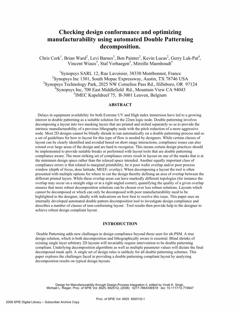
Contact array density can be doubled by alternating masking layers using double-diamond type decomposition. Based simply on geometrical considerations a density reduction down to 43% is possible if x and y design pitches are allowed to be different and a hexagonal-close packing structure is applied (see Fig. 8).
Proc. of SPIE Vol. 6925 69251Q-4
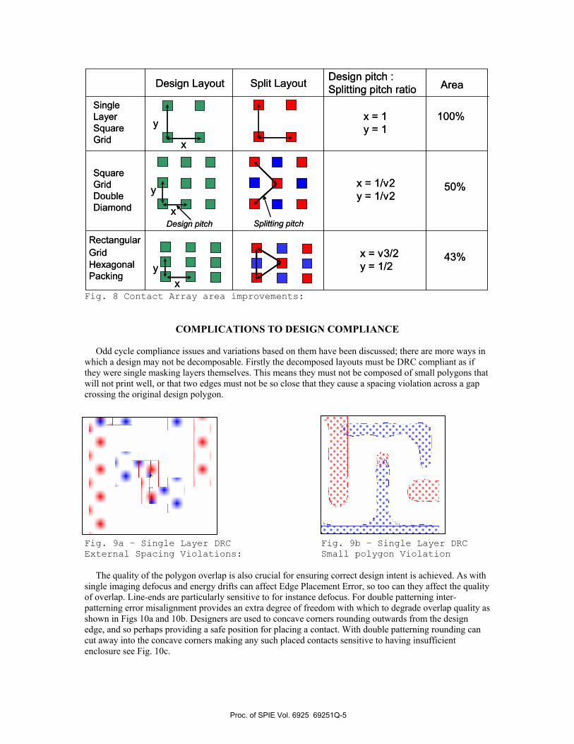
Fig. 8 Contact Array area improvements:
COMPLICATIONS TO DESIGN COMPLIANCE Odd cycle compliance issues and variations based on them have been discussed; there are more ways in
which a design may not be decomposable. Firstly the decomposed layouts must be DRC compliant as if they were single masking layers themselves. This means they must not be composed of small polygons that will not print well, or that two edges must not be so close that they cause a spacing violation across a gap crossing the original design polygon.
Fig. 9a – Single Layer DRC Fig. 9b – Single Layer DRC External Spacing Violations: Small polygon Violation The quality of the polygon overlap is also crucial for ensuring correct design intent is achieved. As with
single imaging defocus and energy drifts can affect Edge Placement Error, so too can they affect the quality of overlap. Line-ends are particularly sensitive to for instance defocus. For double patterning inter-patterning error misalignment provides an extra degree of freedom with which to degrade overlap quality as shown in Figs 10a and 10b. Designers are used to concave corners rounding outwards from the design edge, and so perhaps providing a safe position for placing a contact. With double patterning rounding can cut away into the concave corners making any such placed contacts sensitive to having insufficient enclosure see Fig. 10c.
Area
50%
Design Layout Split Layout Design pitch : Splitting pitch ratio
x = 1/v2y = 1/v2
SquareGrid ?Double Diamond x
y
xy
x = v3/2y = 1/2
43%Rectangular Grid ?HexagonalPacking
Splitting pitchDesign pitch
y
x
x = 1y = 1
100%SingleLayer Square Grid
Area
50%
Design Layout Split Layout Design pitch : Splitting pitch ratio
x = 1/v2y = 1/v2
SquareGrid ?Double Diamond x
y
xy
x = v3/2y = 1/2
43%Rectangular Grid ?HexagonalPacking
Splitting pitchDesign pitch
y
x
x = 1y = 1
100%SingleLayer Square Grid
Proc. of SPIE Vol. 6925 69251Q-5

UU
If the case of two perpendicular line-ends overlapping (Fig. 10b) is deemed unacceptable, due to its sensitivity to line-end pullback on defocus, then a variety of complex design rules can result. One such is the case of 4 facing comb structures which are compliant with odd numbers of teeth but non-compliant with an even number of teeth (see Fig. 11).
Fig. 11 – Odd-Even compliance issue based on acceptable overlap.
Symmetry can be another constraint on decomposition; certain layouts see Fig. 12 can only be decomposed symmetrically if a minimum-width feature is defined by both masks – thereby degrading its dimensional control. Some layouts cannot be compliant with all constraints simultaneously. Fig. 12 – Symmetry requirements may conflict with other constraints such as minimum width features defined with a single mask.
Fig. 10 Critical overlap structures
Not compliant
Proc. of SPIE Vol. 6925 69251Q-6

A DESIGN FRAMEWORK TO SPEED TIME TO COMPLIANCE The final constraint considered here are hot-spots. These are already well known to single patterning and are layouts that defy a good OPC correction, leading to poor edge placement error or excessive line-end pullback. The new twist with double patterning is that these hotspot layouts are more likely and much less predictable. Fig. 13 shows the one case where the design layout consists of line-ends facing only edges. The decomposed layout, however, consists of multiple interacting line-ends. MRCF enforcement applied during OPC correction limits the extent to which line-ends and hammerhead segments can extend. The angular arrangement between line-ends is somewhat irregular and arbitrary, so that simple DRC checks may not be able to efficiently detect and avoid these layout configurations in advance.
Fig. 13 – Layout sensitive to poor OPC correction after double patterning decomposition.
Such single patterning hotspots consisting of multiply interacting line-ends are rare. However double patterning tends to increase the number of line-ends and the short range-order seen with single patterning breaks down when considering next nearest-neighbor interactions. If these next-nearest neighbors could be placed so that their interactions become more predictable, then suitable DRC like checks could identify and warn earlier in the design stage. These layouts styles: glassy, single and poly-crystalline and described in Fig. 14.
Fig. 14 – Material Science analogies for Double Patterning friendly
layouts styles
• Only short range order: • Minimum width and space.• Next neighbor interactions essentially random.• Clean decomposition unlikely.
Glass Like
• Infinite long range order:• Tracks only allowed on grid.• Next neighbor interactions now more predictable.• Dense packing may leave no room to achieve compliance.
• Multiple small areas of on-grid layout separated by large spaces.• Space for design tool to relieve compliance issues.• Avoids long range odd cycles
Coherence
Distance
Single CrystalCoherence
Distance
Coherence
Distance
Polycrystalline
• Only short range order: • Minimum width and space.• Next neighbor interactions essentially random.• Clean decomposition unlikely.
Glass Like
• Infinite long range order:• Tracks only allowed on grid.• Next neighbor interactions now more predictable.• Dense packing may leave no room to achieve compliance.
• Multiple small areas of on-grid layout separated by large spaces.• Space for design tool to relieve compliance issues.• Avoids long range odd cycles
Coherence
Distance
Single CrystalCoherence
Distance
Single CrystalCoherence
Distance
Coherence
Distance
Coherence
Distance
Polycrystalline
Proc. of SPIE Vol. 6925 69251Q-7

CONCLUSION
Ensuring design compliance is a key requirement for enabling double patterning in production. While compliance issues are analogous to those for alt-PSM, several new modes for compliance failure have been identified. Double patterning provides opportunities for significant area density improvement but also more ways to fail. Robust designs require integrated checking with a double patterning decomposition engine and suitable model based verification methodology. A conservative design framework such as “polycrystalline” layout grid with appropriate short-range design rules, will help designers speed time to a compliant design.
REFERENCES
[1] Liebmann, L. “Layout optimization at the pinnacle of optical lithography.” Proc. SPIE Vol. 5042, (2003) [2] Drapeau, M. “Patterning Design Split Implementation and Validation for the 32nm Node.” Proc. SPIE Vol. 6521, (2007) [3] Bailey, G. “Double Patterning EDA solutions for 32nm HP and beyond.” Proc of SPIE Vol 6521, (2007) [4] Liebmann, L. “DFM lessons learnt from alt-PSM design.” Proc SPIE Vol. 6925, (2008)
Proc. of SPIE Vol. 6925 69251Q-8