Specific features in the ferroelectric properties of Sr 0.75 Ba 0.25 Nb 2 O 6 crystals
Upload
independentCategory
view
5download
0
Advances in Excimer Laser Technology forSub-0.25- m Lithography
PALASH DAS AND RICHARD L. SANDSTROM
Invited Paper
There are several lasers that can provide high-power radiationat deep-UV wavelengths. The only laser that has been successfullyused in semiconductor manufacturing as a source for lithography isthe excimer laser. Excimer lasers provide direct deep-UV light, arescalable in energy and power, and are capable of operating withnarrow spectral widths. Also, by providing three wavelengths at248, 193, and 157 nm, excimer lasers span three generations. Theyhave large beams and a low degree of coherence. Their physics andchemistry are well understood. Thanks to major technical develop-ments, these lasers have kept up with the ever-tightening specifica-tions of the lithography industry. We will discuss what these spec-ifications are and the advances that have been made in laser tech-nology to meet these. We will also identify any possible future lim-itation in this technology. The success behind the microelectronicsexplosion is attributed to many factors. The excimer laser is one ofthem.
Keywords—ArF lasers, excimer lasers, F2 lasers, KrF lasers,lithography.
I. INTRODUCTION—LASERS INMICROLITHOGRAPHY
Microlithography is a manufacturing process for highlyprecise microscopic two-dimensional (2-D) patterns in aphotosensitive resist material. These patterns are replicasof a master pattern on a mask. The mask is illuminatedby a light source and then imaged on a wafer, coated withphotoresist, by a lens. At the end of the lithographic process,the resist is used to create a useful structure in the devicethat is being built such as trenches on silicon wafer or ametal network on silicon. These structures then form thefoundation for memory and processor ICs that go intocomputers, cellular phones, PDAs, and games, to name afew—everything that makes our lives more productive andfun.
Traditional light source for lithography has been theHg–Xe Arc lamp. Its i line and g line are used for lithog-
Manuscript received October 15, 2001; revised June 15, 2002.The authors are with Cymer, Inc., San Diego, CA 92127 USA (e-mail:
[email protected]; [email protected]).Digital Object Identifier 10.1109/JPROC.2002.803665
raphy below 256 MB DRAM. Its emission centered on248 nm has also been used, but available power at thiswavelength is very low. On the other hand, excimer lasers,such as the KrF at 248 nm, the ArF at 193 nm, and the Flaser at 157 nm, are sources of high-power radiation. Theyhave relatively narrow spectrum as compared to Hg–Xelamps, that is, they are considered to be high brightnesssources. They provide direct tunable high-power output atthe deep UV (DUV) without complex wavelength conver-sion schemes, as is the case with solid-state lasers. Theirphysics permit efficient spectral narrowing limited only bythe quality of the narrowing optics. They can be scaled inpower and repetition rate. Table 1 summarizes what wasrequired, what they have evolved to, and what we mightexpect over the next few years from excimer lasers forlithography. Based on what the authors have experiencedthis past decade, we believe that excimer lasers will meetthe lithography requirements for 16-Gb DRAM and 10-GHzmicroprocessors in the next ten years!
Solid-state lasers are other possible light sources. One ex-ample is alexandrite lasers at 248 nm and the other is diode-pumped, frequency multiplied solid-state laser at 248 and193 nm. One apparent advantage they have over excimerlasers is that the factory does not have to deal with Fgases.However, considering the early start by excimer lasers andthe ever-increasing power requirements, it is just too latefor solid-state lasers to be viable light sources for advancedlithography.
II. EXCIMER LASERS AND THELITHOGRAPHY PROCESS
A. Wafer Exposure
The wafer exposure process involves the following sys-tems: laser, optics to illuminate a mask, the mask itself, pro-jection lens to image the mask on a wafer, a wafer-posi-tioning system to position a chip on the wafer to the imageof the mask, and the wafer itself. The reader is referred totwo excellent textbooks ([4] and [6]) for an in-depth descrip-
0018-9219/02$17.00 © 2002 IEEE
PROCEEDINGS OF THE IEEE, VOL. 90, NO. 10, OCTOBER 2002 1637

Table IExcimer Laser Requirements
tion about lithography and all the technologies that supportthis field. The web sites of the three key lithography tool-makers–ASML, Canon, and Nikon—also contain excellentinformation about steppers and scanners.
The mask defines the pattern that is projected onto thechip (technically, the structure on the wafer is a die that be-comes a chip when the die is saved up and packaged). Thesubstrate of the mask is about 150 mm150 mm 6 mmfused silica blank on which the circuit pattern is deposited.The deposited material is usually chromium. Fused silica hasgood transmission at 248 and 193 nm. The presence of OHgroups in fused silica severely limits 157-nm transmission.However, recently, the fused silica transmission at 157 nmwas increased to nearly 80% by reducing its OH content anddoping it with fluorine [1]. Now, it appears that fused silicamasks could be used for all three excimer laser wavelengths.
The projection lens is a large compound lens made up ofover 20 simple elements mounted in a rigid barrel. The largenumbers of elements are required to correct optical aberra-tions to better than over the exposure field. The lensproduces the optical image of the mask, reduced by a factorof 4. A silicon wafer is exposed to this image, which is cap-tured by the layer of photoresists. The image is eventually de-veloped to leave the resist pattern on silicon. The lens at theKrF wavelength is not chromatically corrected as it is madeof entirely one material: fused silica. The natural linewidth
of the laser ( 300 pm) is too broad for the image qualityrequirements, hence the narrow spectral width requirementsfrom the excimer laser. Thus, for a lens of , thefull-width at half-maximum (FWHM) requirement is about0.8 pm. At 193 nm, the projections lens requires some colorcorrection. Otherwise, the laser linewidth requirements aremuch lower than what is practically possible. Thus, a combi-nation of fused silica and CaFis used with a great increasein lens costs. The situation for Fis still open, but very likelythe material would be CaFand a catadioptric lens would beused instead of the refractive lens for KrF and ArF. There-fore, line narrowing may not be required for F.
B. Stepper and Scanner
The wafer positioning system is probably the most precisemechanical system in existence. It positions the wafer, either200 or 300 mm in diameter, under the lens to a precisionof better than 20 nm. The motion of the wafer positioningsystem coupled with the exposure technique determines twoclasses of lithography systems—stepper and scanner.
The stepper system exposes one chip at a time, as shownin Fig. 1 The light source exposes the full mask that containsthe chip information and the lens images the mask on to thechip. The exposure field of the lens matches the chip size, sois about 28 to 30 mm in diameter. The number of pulses the
1638 PROCEEDINGS OF THE IEEE, VOL. 90, NO. 10, OCTOBER 2002

Fig. 1. Exposure of a wafer with a stepper and a scanner.
Fig. 2. Operation of an excimer laser with a stepper or a scanner.
laser fires on each chip is equal to the total energy requiredto expose the resist. After each chip, the wafer positioningsystem steps the wafer to next chip.
A scanner exposes the chip by “painting” a slit over thewafer (Fig. 1). After a chip is exposed, the wafer is steppedto the next chip and the exposure is repeated. This is doneby scanning the mask and the wafer through the slit whilethe lens remains stationary. Slit height and width then deter-mine the field size requirements of the lens. The slit height ismatched to the smaller dimension of the chip (25 mm) andthe slit width is between 7–8 mm. Since only a smaller partof the chip is imaged, a smaller part of the lens is utilized.Therefore, the part of the lens with the least aberrations andbest imaging is used. The process of scanning the chip in-creases the overall field size cost-effectively. As the require-ments for lenses have tightened over the last five years [2],all lithography equipment manufacturers have now switchedto scanner technology for their advanced tools despite theadded mechanical complexity of scanning a wafer and maskduring exposure.
The scan and step of a scanner and expose-and-step op-eration of a stepper impacts the operation of the laser. Ex-cimer lasers operate in burst mode, meaning that they ex-pose for few hundred pulses, and then wait for a longer pe-riod during wafer exchange (Fig. 2). Continuous operationis the preferred operating method of an excimer laser muchlike a lamp. Continuous operation permits stabilization of all
laser-operating conditions, such as gas temperature and pres-sure. Based on the exposure conditions shown in Fig. 2, con-tinuos operation implies a 50% waste of pulses. Laser manu-facturers now live with burst mode operation despite the pres-ence of significant transients in energy and beam pointingat the start of a burst. Fortunately, these transients are pre-dictable and the laser’s control software corrects for thesetransients [3]. Once the laser’s controller learns the transientbehavior of the laser, as seen in Fig. 3, the subsequent wafersare exposed correctly. In practice, the laser’s software learnsabout the transient behavior prior to exposing wafers.
III. A DVANCES IN EXCIMER LASERSSPECIFICATIONS FOR
LITHOGRAPHY
A. Introduction and History
The first excimer lasers for lithography exposure toolswere introduced more than a decade ago. But it was only in1997 that Hg i-line light sources at 365 nm were replacedwith excimer lasers in volume manufacturing of semicon-ductor devices. The transition from Hg lamp light sourcetechnology to excimer technology is clearly illustratedin Fig. 4. As one can see, this Hg-to-excimer transitionwas driven by the need to make sub–0.25-m features insemiconductor devices. Based on Rayleigh’s criterion, onewould think that the introduction of shorter wavelengthsshould have occurred much earlier, either in 1993 or 1995.
DAS AND SANDSTROM: ADVANCES IN EXCIMER LASER TECHNOLOGY FOR SUB-0.25-m LITHOGRAPHY 1639

Fig. 3. Transients in energy during burst mode operation of an excimer laser for a stepper orscanner. The software learns the energy transients and, by the fourth burst, corrects for the transients.The software remembers these transient effects during subsequent exposures. The transients changewhen the operating conditions change, such as a time interval between bursts.
Fig. 4. The evolution of feature size on a wafer and the lightsources used to achieve the feature size. The information has beengathered from numerous sources.
Rayleigh’s criterion states that the resolution of an imaginglens with a numerical aperture is affected by thewavelength given in
(1)
where is the dimensionless process-factor. The largerthe process -factor, the easier it is to produce the chip, butat the expense of the resolution of the imaging lens.
KrF at 248 nm would have been a better source wavelengththan the i-line at 365 nm in 1995 for 0.3m features or evenin 1993 for 0.35- m features. However, associated with eachtransition in wavelength are enormous technical issues re-lated to photoresists and materials (primarily optical) at the
Fig. 5. The evolution of laser power and repetition rate for KrFand ArF excimer lasers for lithography. This graph is based on whatthe authors have observed over the past 15 years.
new wavelength. Instead, two techniques were used to extendthe i-line. One was to increase the of the lens from 0.4 to0.6. The other was to decrease the processfactor from 0.8to 0.5. By 1995, DUV-grade fused silica and 248-nm resistsdevelopment were complete and the KrF laser became themainstay of semiconductor manufacturing. Ironically, the is-sues that prevented the entry of KrF lasers would now extendits usability to beyond 0.18m. The entry feature size forArF is 0.13 m and that for F is probably 0.07 or 0.05m.
The delayed entry of each excimer wavelength into thesemiconductor manufacturing process has an enormous im-pact on both the present excimer wavelength and the newwavelength. Figs. 5 and 6 show how the delay in the in-troduction of excimer technology impacted the requirements
1640 PROCEEDINGS OF THE IEEE, VOL. 90, NO. 10, OCTOBER 2002

Fig. 6. The evolution of laser spectral linewidth for KrF and ArFexcimer lasers for lithography. This graph is based on what theauthors have observed over the past 15 years.
on KrF. Likewise, these figures show the impact on delayedentry of ArF on KrF and vice versa. Thus, in 1995, the laser’stwo critical parameters, power and linewidth, were signif-icantly more stringent than in 1993. In the year 2002, theoutput of a KrF laser would be 30 W with linewidths of about0.4 pm. Such power and linewidth requirements from KrFwere not expected in the mid-1990s, and we had expectedthat KrF would end at 20 W and 2 kHz. The authors hesitateto guess where the entry point of Fwould be due to frequentchanges in technology roadmaps.
B. Power and Repetition Rate
The requirement for high power and repetition rate is de-termined by the throughput requirements of scanner. Thescanner exposure time is given by
(2)
wherescanner exposure time for a chip;chip width;slit width;scan speed for the chip.
For a given chip width, the slit width must be minimizedand the scan speed must be maximized to reduce. In gen-eral, the slit width is matched to the maximum wafer speedas follows:
(3)
wheremaximum wafer scan speed;minimum number of pulses to make the dose onwafer with the required dose stability—the dose isthe integrated energy over and dose stability isusually an indicator of how this dose varies fromthe target dose;laser’s repetition rate.
Advanced scanners are capable of scan speeds of 300 mm/sand are expected to reach 500 mm/s in the next few years.Therefore, to minimize , the ratio must be minimized.The number cannot be very small due to the fact that afinite number of pulses are required to attain a specific doseat the wafer with a given dose stability. A typical number is100 pulses to attain a dose stability of0.25 . Slit widthsof 7–8 mm are common. For a 7-mm slit width, a 300-mm/sscanner would require repetition rates of4300 Hz.
Notice that the above analysis is independent of wave-length. Hence, if the exit point for KrF is 4 kHz, then theentry point for ArF is also at 4 kHz. This is no small task,considering that the first ArF lithography laser for R&D de-velopment, shipped in 1998, was only 1 kHz.
C. Spectral Linewidth
As stated by Rayleigh’s criteria, the resolution of animaging system could be improved by increasing its .In the mid-1990s, only fused silica was fully qualified asthe suitable lens material at KrF wavelengths. Recently,however, UV-grade CaFmaterials in sizes large enoughfor imaging lenses became available. For KrF, the lensesdid not correct for chromatic aberration. The increase in NAseverely narrowed the linewidth ( ) requirements,shown as follows [4]:
(4)
whererefractive index of the material;wavelength;material dispersion;lens magnification;lens focal-length.
The equation predicts that, at and 0.8, at KrFwavelengths, the linewidth requirements would be 0.6 and0.45 pm, in close agreement with what lens designers haverequired of KrF lasers. At 193 nm, due to the large increasein dispersion in fused silica, the same and 0.8would require linewidths of 0.2 and 0.15 pm, respectively.Such narrow linewidths from excimer lasers were not prac-tical in the mid-1990s when the technical approach for ArFlithography was formed. Hence, ArF lenses were chromat-ically corrected by using a combination of fused silica andCaF . However, the delay in availability of large lens qualityCaF by at least two years delayed the introduction of ArF,and KrF continued to be the laser of choice until recently.
D. Wavelength Stability
The penalty for high of a lens manifests itself in an-other way as well. The Rayleigh depth of focus (DOF) is re-lated to the to the of the lens via the following equation:
(5)
Thus, for a 0.6 lens at 248 nm, the DOF is about0.35 m, and for a 0.8 the DOF is only 0.2 m.
A change in wavelength induces a change in focus. This
DAS AND SANDSTROM: ADVANCES IN EXCIMER LASER TECHNOLOGY FOR SUB-0.25-m LITHOGRAPHY 1641
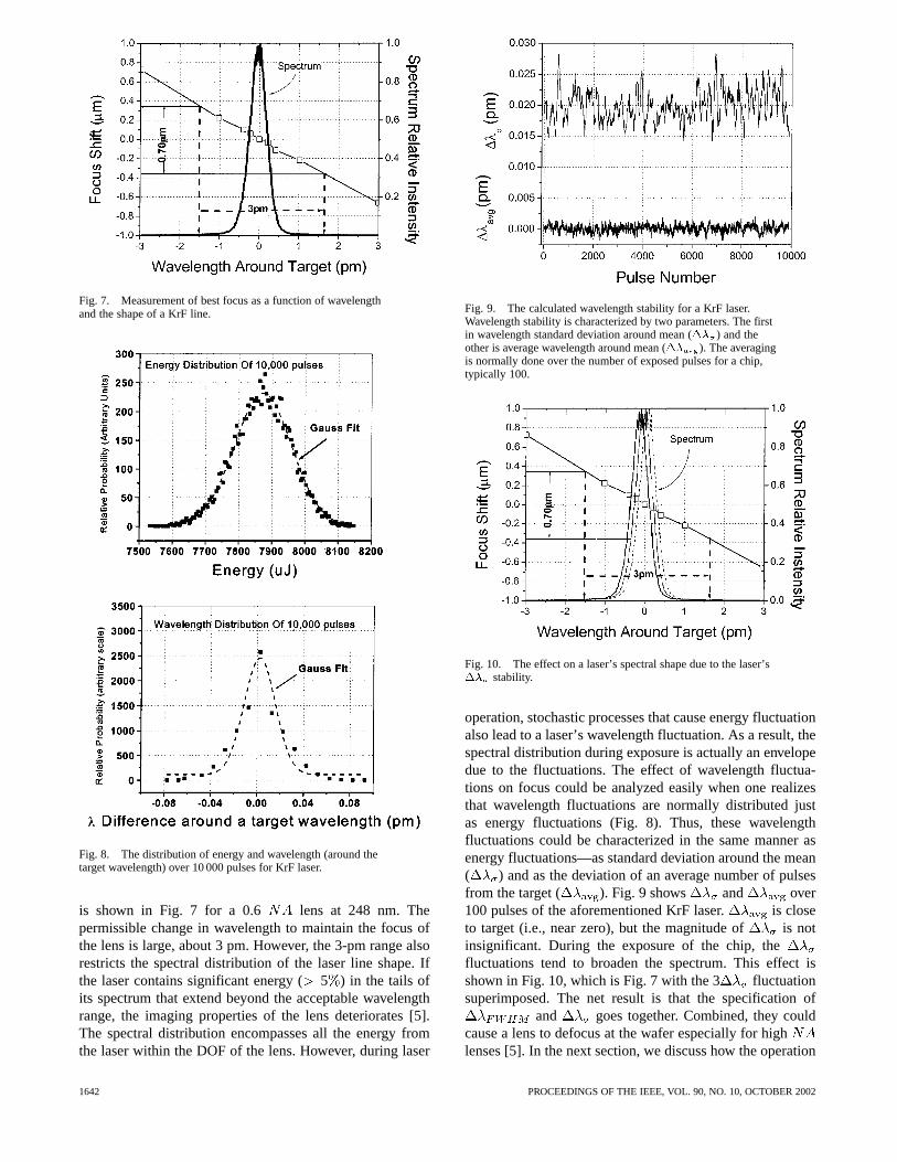
Fig. 7. Measurement of best focus as a function of wavelengthand the shape of a KrF line.
Fig. 8. The distribution of energy and wavelength (around thetarget wavelength) over 10 000 pulses for KrF laser.
is shown in Fig. 7 for a 0.6 lens at 248 nm. Thepermissible change in wavelength to maintain the focus ofthe lens is large, about 3 pm. However, the 3-pm range alsorestricts the spectral distribution of the laser line shape. Ifthe laser contains significant energy (5 ) in the tails ofits spectrum that extend beyond the acceptable wavelengthrange, the imaging properties of the lens deteriorates [5].The spectral distribution encompasses all the energy fromthe laser within the DOF of the lens. However, during laser
Fig. 9. The calculated wavelength stability for a KrF laser.Wavelength stability is characterized by two parameters. The firstin wavelength standard deviation around mean (�� ) and theother is average wavelength around mean (�� ). The averagingis normally done over the number of exposed pulses for a chip,typically 100.
Fig. 10. The effect on a laser’s spectral shape due to the laser’s�� stability.
operation, stochastic processes that cause energy fluctuationalso lead to a laser’s wavelength fluctuation. As a result, thespectral distribution during exposure is actually an envelopedue to the fluctuations. The effect of wavelength fluctua-tions on focus could be analyzed easily when one realizesthat wavelength fluctuations are normally distributed justas energy fluctuations (Fig. 8). Thus, these wavelengthfluctuations could be characterized in the same manner asenergy fluctuations—as standard deviation around the mean( ) and as the deviation of an average number of pulsesfrom the target ( ). Fig. 9 shows and over100 pulses of the aforementioned KrF laser. is closeto target (i.e., near zero), but the magnitude of is notinsignificant. During the exposure of the chip, thefluctuations tend to broaden the spectrum. This effect isshown in Fig. 10, which is Fig. 7 with the 3 fluctuationsuperimposed. The net result is that the specification of
and goes together. Combined, they couldcause a lens to defocus at the wafer especially for highlenses [5]. In the next section, we discuss how the operation
1642 PROCEEDINGS OF THE IEEE, VOL. 90, NO. 10, OCTOBER 2002

of lasers at high repetition rates tends to have dramaticeffects on wavelength stability.
The impact of nonchromatic lenses with high is theirsensitivity to pressure and temperature changes [6]. For the0.6 lens at 248 nm, 1 mm of Hg change in pressure resultsin a focus shift of 0.24 m. Also, a 1 C change in temper-ature induces a focus shift of 5m. This high sensitivity totemperature and pressure increases the precision to which thecorrections need to be made. The shift in focus could be com-pensated for by a shift in laser wavelength. Since these en-vironmental changes can occur during the exposure, a rapidchange in wavelength is required, usually at the start of chipexposure. In other words, the laser’s target wavelength mustbe changed and the laser must rapidly reach the target withinfew pulses ( 10 pulses). The specification of the laser thatrelates to how closely it can maintain its target wavelengthduring exposure is the average wavelength from the target( ). Since rapid pressure changes of a fraction of a mil-limeter of Hg can occur, the laser must respond to changesin wavelength of few tenths of a picometer (as high as 0.5pm). In the next section, we describe how advanced excimerlasers have adopted new technologies to lock the wavelengthto the target to within 0.005 pm.
E. Pulse Duration
Under exposure to ArF radiation [7], fused silica tends todensify, according to
(6)
wheredensity of fused silica;increase in density;number of pulses in million;energy density in mJcm ;sample-dependent constant;integral square pulse duration and is defined by
where is the time-dependent power of thepulse.
The refractive index of fused silica is affected by densifica-tion. After billions of pulses, the fused silica lens would seri-ously affect the image. Experience has shown that the magni-tudes of can vary greatly depending on the fused silica sup-plier, meaning that the details of manufacturing fused silicais important. The other technique to increase lifetime is toreduce the intensity by increasing repetition rate. The thirdtechnique is to stretch the pulse duration. Numerous fusedsilica manufacturers working in conjunction with Interna-tional Sematech [8] are investigating the first solution. Thelaser manufacturers are investigating the other two. The va-lidity of (6) has been questioned [8] at low energy densities( 0.1 mJ cm ), comparable to the density experienced by alens. Despite this ongoing debate on the effect of pulse dura-tion, we expect that long pulse duration could soon become
an ArF laser specification. Densification of fused silica ap-pears to be restricted to ArF wavelengths.
F. Coherence
The requirements for narrower linewidth results in lowerbeam divergence. As a result, the spatial coherence of thebeam improves. A simple relationship [9] between spatialcoherence ( ) and divergence () is
(7)
With narrower linewidths, the coherence lengths have in-creased, and today, for a 0.4-pm KrF laser, the coherencelength is about 1/10th the beam size in the short dimensionand about 1/50th in the tall dimension. At the same time,narrower linewidth increases the temporal coherence of thebeam. A simple relationship between temporal coherence( ) and linewidth is
(8)
Do narrow linewidths make the excimer laser no longer an“incoherent” laser source? If the beam is no longer coherent,the lithography optics must correct for coherence effects. Forthe beam we referred to above, we could perform a simplecalculation to answer this question. Based on the fact thatthe coherence length is 1/10th and 1/50th of the short andtall dimension, respectively, of the excimer beam, there are10 50 (or 500) spatially coherent cells in the beam. Thetemporal coherence of the KrF laser with 0.5-pm linewidthis 123 mm. Combined, we may interpret this as 500 spatiallycoherent cells 123 mm in length exiting form the laser andthen incident upon the chip during the laser pulse. Each ofthese 123-mm-long cells could cause interference effects, asthey are fully spatially coherent. Since the pulse length ofan excimer laser is about 25 ns, the number of temporallycoherent cells during the pulse (product of speed of light andpulse length divided by temporal coherence length) is about60.
Thus, the total numbers of cells that are incident on thechip are 500 60 or 30 000. All these contribute to inter-ference effects or noise at the chip. We could then estimatespeckle to be simply where is the total coherentcells or 30 000 or about 0.6%. This amount of speckle is notnegligible considering the tight tolerance requirements of thefeatures in present day semiconductor devices. This is the sadfact of life—narrow linewidths imply a coherent beam. Thesetwo properties go together, and the lithography optics musthandle the coherent excimer beam [9].
In summary, we see that the requirements of excimerlasers have increased significantly since they were in-troduced for semiconductor R&D and then for volumeproduction. The exponential growth in power requirementsat all wavelengths, in combination with a massive drop in
specification, is spurred by the drive for higherresolution features on wafers and higher wafer throughputsfrom scanners. In Section IV, we will describe the key tech-nologies that comprise an excimer laser and what changeswere required to make these lasers meet the challengingdemands.
DAS AND SANDSTROM: ADVANCES IN EXCIMER LASER TECHNOLOGY FOR SUB-0.25-m LITHOGRAPHY 1643

Fig. 11. The key modules of an excimer laser for lithography.
IV. A DVANCES IN EXCIMER LASER TECHNOLOGY
A. Laser Modules
The lithography excimer laser consists of the followingmajor modules:
1) chamber;2) pulsed power;3) line narrowing;4) energy, wavelength, and linewidth monitoring;5) control;6) support.The control and the support modules have kept up with
the advances in laser technology and will not be discussedhere. Fig. 11 shows the layout of a commercial excimer laserfor lithography. Typical dimensions for a laser at 2 kHz areabout 1.7 m in length, 0.8 m wide, and about 2 m tall. Sincethese lasers occupy clean room space, the laser manufacturesare sensitive to the laser’s footprint. In the last seven years,as the laser’s power increased threefold, the laser’s footprintremained virtually unchanged.
B. Chamber
The discharge chamber is a pressure vessel designed tohold high pressure F( 0.1 of the total) gas in a bufferof krypton and neon. Typical operating pressures of excimerlasers range from 250 to 500 kPa, out of which 99% is neonfor KrF and ArF and helium for F. The chambers are quitemassive, usually greater than 100 kg. One would think thatthe chamber sizes have increased with output power. How-ever, it appears that scientists and engineers have learned
how to get more power from the same chamber. Thus, thesame chamber that produced 2.5 W in 1988 produced 20 Win 1999!
Fig. 12 shows a cross section of the chamber. The con-struction materials of present day chambers are aluminum,nickel, and brass [10]. The only nonmetallic material thatcomes in contact with gas is 99.5% pure ceramic. The elec-trical discharge is initiated between the electrodes. The elec-trode shape and the gap between the electrodes determinethe size and shape of the beam. Typical beam widths are2–3 mm and heights range from 10 to 15 mm. It is advan-tageous to keep the beam size large. A large beam assuresthat the beam is multimode and hence spatially more inco-herent than single-mode lasers. We will discuss the issue ofbeam coherence in the next section.
The energy that is deposited between the electrodes heatsthe gas adiabatically. This heating generates pressure wavesoriginating at the electrodes that travel to the chamber wallsand other structures. These structures could reflect the soundwaves back to the electrode region. At a typical gas operatingtemperature of 45C, the speed of sound in neon is about470 m/s. In 1 ms, the sound wave must travel 47 cm before itcan reach the electrode region coincident with the next pulse.Considering the dimensions of the chamber shown in Fig. 12,the sound wave must have made a few reflections before itreached the electrode region 1 ms later. The reflected waveafter 1 ms is weak. However, at 2 kHz, the sound wave musttravel only 23.5 cm before it is coincident with the next pulse.Although the gas temperature determines the exact timing ofthe arrival waves, the dimension of the chamber and the lo-
1644 PROCEEDINGS OF THE IEEE, VOL. 90, NO. 10, OCTOBER 2002

Fig. 12. The cross section of an excimer laser chamber.
Fig. 13. The increase in wavelength stability�� as a function of repetition rate.
cation of structures within almost guarantees that some re-flected sound wave is coincident with the next 2-kHz pulse.The situation is much worse at 4 kHz, since the sound wavemust only travel less than 12 cm.
Additionally, during burst mode operation of the laser,typical during scanner exposure, the laser gas temperaturechanges over several degrees over a few milliseconds. Thesechanging temperatures change the location of the coincidentpressure waves from pulse to pulse within the dischargeregion. In turn, this affects the index of refraction of thedischarge region, causing the laser beam to change directionevery pulse. The line narrowing technology described belowis sensitive to the angle of the incident beam. A change inangle of the incident beam in the narrowing module wouldinduce a change in wavelength. Fig. 13 shows this wave-length variation in from a chamber (with a line narrowingmodule) at a fixed temperature (45 C) as a function ofrepetition rate. This variation results in a loss of control ofthe target wavelength and also causes an effective broad-ening of the spectrum, as discussed in the previous section.This problem manifests itself at a high repetition rate andworsens as the repetition rate increases. Also, dependingon the gas temperature, the repetition rate, and the locationof structures near the discharge, there is some resonantrepetition rates where stability is much worse.
The effect of these pressure waves can also be seen in alaser’s energy stability, beam pointing stability, beam uni-formity, and linewidth stability. A proper choice in temper-ature and spacing between the discharge and structures maydelay the pressure waves for a particular repetition rate butnot for another. Since excimer lasers in lithography appli-cations do not operate at a fixed repetition rate, tempera-ture optimization is hardly a solution. The other impracticalsolution is to increase the distance of all support structuresaround the discharge—which would lead to a larger chamberfor every increase in repetition rate. This implies that, at4 kHz, the cross section of the chamber would be four timeslarger! Previous attempts in mitigation of such waves uti-lized “sponge-like” materials in the chamber that absorbedthe pressure waves—but at the expense of severely contam-inating the laser gas.
While the presence of these pressure waves does not bodewell for high-repetition-rate excimer lasers for the future,very innovative and practical techniques have been inventedby a group of scientists [11]. They introduced several re-flecting structures in the chamber shown in Fig. 12 such thatthe reflected waves would be directed away from the dis-charge region. The reflecting structures, made from Fcom-patible metals, were designed to scatter the pressure waves.The effect of these so-called “baffles” is shown in Fig. 14.
DAS AND SANDSTROM: ADVANCES IN EXCIMER LASER TECHNOLOGY FOR SUB-0.25-m LITHOGRAPHY 1645

Fig. 14. The improvement in a laser’s wavelength fluctuation (deviation from target wavelength)at 2000 Hz when acoustic damping is introduced in a chamber. The fluctuations reduce by afactor of about 3.
Fig. 15. The line-narrowing module of an excimer laser configured to operate with a chamberand output mirror.
These “baffles” reduce the wavelength variation by a factorof three for most repetition rates.
As the lithography industry continues to strive for higherscanner throughput via higher repetition rates, the excimerlaser designers would face great technical hurdles related tothe presence of pressure waves. Probably, other innovativeways must be investigated to increase scanner throughput.
C. Line Narrowing
The most effective line narrowing technique, implementedon nearly all lithography lasers is shown in Fig. 15 This tech-
nique utilizes a highly dispersive grating in the so-called Lit-trow configuration. In this configuration, that angle of inci-dence of the grating equals the angle of diffraction. Due tothe dispersive nature of the grating, the linewidth is propor-tional to the divergence of the beam incident on the grating.Thus, the beam incident on the grating is magnified usuallyby a factor of 25–30 to fill the width of the grating. Prismsare used for beam expansion as they maintain the beam wave-front during expansion. Due to the fact that the beam attendue(product of beam divergence and beam dimension) is con-stant, the large beam reduces the divergence, which then re-
1646 PROCEEDINGS OF THE IEEE, VOL. 90, NO. 10, OCTOBER 2002

Fig. 16. Wavelength stability (�� ) when the wavelength isadjusted to compensate for any deviation from the target using afast adjustment based on PZT technology.
duces the linewidth of the laser. The beam divergence is alsolimited by the presence of apertures in the line-narrowingmodule and near the output mirror. These apertures effec-tively define the number of transverse modes or the diver-gence of the beam. The combination of high magnification,large gratings, and narrow apertures could be used in the fu-ture to meet the linewidth requirements. We expect that thistechnology could be extended to the 0.2-pm range.
Since the beam expansion prisms are made out of CaFand the grating is reflective, this line narrowing technologyis applicable to all three generations of excimer lasers—KrF,ArF, and F .
The angle of the beam incident on the grating determinesthe wavelength of the laser. Thus, adjusting this angle makesthe wavelength adjustment of the laser. In practice, the mirrorshown in Fig. 15 is adjusted to change the wavelength be-cause it is less massive than the grating. Until recently, simplelinear stepper motors were used to accomplish small wave-length changes. Typically, the minimum change in wave-length that could be accomplished was 0.1 pm over a periodof 10 ms. This means that at 4000 Hz the response to change0.1 pm would take about 40 pulses, which is nearly half thenumber used to expose a chip. Also, 0.1 pm corresponds tonearly 20%–30% of the laser’s linewidth and hence is unac-ceptable. Recent advances made [12] in wavelength controltechnology have significantly reduced the minimum wave-length change to about 0.01 pm over a period of only 1 ms or4 pulses at 4000 Hz. The mirror movement is now done byvia a PZT driven adjustment. The rapid response of the PZTpermits tighter control of the laser’s wavelength stability asshown in Fig. 16. Also, the use of PZT permits rapid changesin wavelength to maintain the focus of the lens during the ex-posure of the chip. Thus, active adjustment of lens focus, dueto pressure or temperature changes in the lens, might now befeasible.
D. Wavelength and Linewidth Metrology
Associated with tight wavelength stability to maintainfocus of the lens is the requirement to the measure wave-
length accurately and quickly (that is, every pulse). In 1995,the precision of wavelength measurements of0.15 pmwas adequate. Now, wavelengths must be measured toa precision of 0.01 pm, consistent with maintainingwavelength stability to within 0.05 pm. In addition, themetrology must be capable of measuring linewidths from0.8 pm in 1995 to 0.4 pm today. The fundamental metrologyto perform these measurements has not changed since 1995.Fig. 17 shows the layout of the metrology tool integratedin the laser. Today such tools can measure wavelengths andlinewidths at 4000 Hz more precisely than in 1995, withoutany significant change in its size.
The grating and the etalon are used to make an approx-imate and an accurate measurement of wavelength, respec-tively. The output from the grating is imaged on a 1024-ele-ment silicon photodiode array (PDA) as shown in Fig. 18.The fringe pattern of the etalon is imaged on one side ofthe grating on the PDA. The central fringe from the etalonis blocked intentionally so that it does not overlap with thegrating signal.
The approximate wavelength is calculated straight fromthe grating equation
(8)
where:grating groove density;angle of incidence on the grating;order of diffraction.
By selecting and appropriately, the knowledge of theangle is sufficient to provide the wavelength. The angle ismeasured from its position on the PDA. In practice, the PDAis calibrated with a known wavelength that encompasses allthe constants of the grating and imaging optics. This equationonly gives an approximate wavelength that is determined bythe focal length of the lens and the location of the gratingsignal on the PDA with respect to the wavelength used forcalibrating the PDA. In practice, it is adjusted to be withinone free spectral range (FSR) of the etalon. This means thatthe grating computes the wavelength to within5 pm.
The knowledge of the approximate wavelength coupledwith the inner and outer fringe diameter of an etalon fringeis used to calculate the exact wavelength from
(9)
where:and defined in Fig. 18;
wavelength corresponding to ;caliberation wavelength;calibration constant depending on the opticsof the setup;FSR of the etalon;integer, .
The magnitudes of , , and the FSR are predeterminedand saved by the tool’s controller. The value ofis selectedsuch that
(10)
DAS AND SANDSTROM: ADVANCES IN EXCIMER LASER TECHNOLOGY FOR SUB-0.25-m LITHOGRAPHY 1647

Fig. 17. The optical layout of a wavelength and spectral linewidth metrology tool.
Fig. 18. The signals from the PDA of the metrology tool. Thecentral etalon fringe is blocked.
where is the approximate wavelength calculated by thegrating.
Similarly, is calculated from . The final wavelengthis the average of and
(11)
Due to the laser’s linewidth, each fringe is broadened. Thelaser’s linewidth at full width at half maximum is calculatedfrom
(12)
Due to the finite finesse of the etalon, its FSR/finesse ratiolimits the resolution of the etalon. Typically, the resolutionis between 0.4–0.8 pm. This finite resolution broadens themeasured linewidth in (12). The common practice to extract
the correct linewidth is subtracting a fixed correction factorfrom (12).
As the linewidths continue to decrease with each gen-eration of laser, practical techniques to extract linewidthmust be refined. An innovative approach [13] uses adouble-pass etalon to improve the etalon’s resolution tomeasure linewidth.
The metrology for KrF and ArF is similar. For Flasers,practical metrology that fits in a laser must be invented. If Flasers are operated at their natural linewidth, the metrologymay be simpler than if they are operated as line-narrowedlasers.
All metrology tools need periodic calibration to compen-sate for drifts in the optics of the tool. Fortunately, atomicreference standards exist for all the three wavelengths, andlaser manufacturers have integrated these standards into themetrology tools. For KrF, the standard is an atomic iron lineat 248.3271 nm (wavelength at STP conditions). For ArF, thestandard is an atomic platinum line at 193.4369 nm (vacuumwavelength). For F, the standard is at 157.531 nm.
E. Pulsed Power
Excimer lasers require their input energies to be switchedin very short times, typically 100 ns. Thus, for a typicalexcimer laser for lithography, at 5 J/p, the peak power intothe laser is 50 MW. This may appear to be trivial untilone considers the repetition rate (1000 Hz) and lifetimerequirements (switch life of 1 B pulses). High-voltageswitched circuits such as those driven by thyratrons haveworked well for excimer lasers in other industries—such asin medical. For lithography, the switching must be preciseand reliable. The precision of input switched energy mustbe within 0.1%–0.2% and the reliability of the switchingmust be 100%. By 1995, it was realized that conventional
1648 PROCEEDINGS OF THE IEEE, VOL. 90, NO. 10, OCTOBER 2002

Fig. 19. A solid-state switched pulsed power circuit capable of operating at 4000 Hz. The primaryswitch is an IGBT, and the secondary switches are saturable magnetics.
switching with a high-voltage switch, such as thyratron,was not appropriate for this industry [14]. Thyratronswere unpredictable (high missed pulses) and limited inlifetime. Instead, solid-state switching, using a combinationof solid-state switches, magnetic switches, and fast pulsetransformers, was adapted. This proved to be worthwhile, asthis same technology that switched lasers at 1 kHz wouldnow be carried forward to all generations of excimer lasers.
Fig. 19 is a schematic of a solid-state switched circuit usedin a 4000-Hz excimer laser [15]. The power supply chargesthe capacitor to within 0.1%. Typical voltages are lessthan 1000 V. Thus, a precision of 0.1% corresponds to 1 V.Typical values of of these lasers are about 50J V.For an output energy of 5000J per pulse, this correspondsto 1% of the energy. If the laser must achieve a dose stabilityof 0.3%, the precision of the supply cannot be greater than0.1%.
When the insulated-gate bipolar transistor (IGBT) com-mutes, the energy is transferred to. The inductor is inseries with the switch to temporarily limit the current throughthe IGBT while it changes states from open to close. Typi-cally, the transfer time between and is 5 s. The sat-urable inductor holds off voltage on capacitor until it sat-urates, allowing the transfer of energy from through astep-up transformer to a capacitor in a transfer timeof about 500–550 ns. The transformer efficiently transfersthe 1000-V, 20 000-A, 500-ns pulse to a 23 000-V, 860-A,550-ns pulse that is stored in . The saturable inductor
holds off the voltage on the capacitor bank forapproximately 500 ns and then allows the charge onto flow onto the laser’s capacitor in about 100 ns. As thecapacitors get charged, the voltage across the electrodesincreases until gas breakdown between the electrodes occurs.The discharge lasts about 50 ns during which the laser pulseoccurs.
The excimer laser manufacturers have lived with the in-creased complexity of a solid-state switched pulsed power.This is because the switches have the capability of recov-ering residual energy in the circuits that are not dissipated inthe discharge so that the subsequent pulse requires less inputenergy [14]. Today, solid-state switching and chamber de-velopments proceed together. The long-term reliability of alithography laser is as much dependent on the chamber as itis on its pulsed power.
F. Pulse Stretching
Previous investigations on long pulses from broadbandArF lasers have been sporadic [16], with the conclusion thata practical long-pulse ArF laser was not feasible. Recently,howere, a simple modification to the circuit shown in Fig. 20was proposed [16]. The simplicity of the technique makesit an attractive technology for stretching ArF pulses. Theother technique, already demonstrated in micro-machiningapplications with ArF lasers, involves a simple optical delayline. Both of these techniques could be commercialized iflong pulses are indeed deemed necessary.
In the pulsed power technique, the capacitorin Fig. 19is replaced with two capacitors and , with a saturableinductor in between. The compression module in Fig. 19charges . The saturable inductor prevents from beingcharged until reaches a voltage close to twice the laser’sdischarge voltage. Once saturates, charge is transferred to
until the discharge breaks down. By adjusting the rela-tive magnitudes of and , two closely spaced pulsesare generated—one driven by and then the next by .Fig. 21 shows the stretched pulse and compares that with anormal ArF pulse.
Due to discharge stability issues, ArF pulses are inherentlyshort ( 20–25 ns). The penalty for a long pulse is a degra-dation of pulse stability by as much as 50%. On the other
DAS AND SANDSTROM: ADVANCES IN EXCIMER LASER TECHNOLOGY FOR SUB-0.25-m LITHOGRAPHY 1649

Fig. 20. A modification to the solid-state switched pulsed power of Fig. 19 where an extra stageof compression is introduced near the chamber. This extends the current pulse to the chamber,resulting in a longer optical pulse.
Fig. 21. A comparison of pulse shapes using the pulsed power in Figs. 19 and 20, respectively.
hand, the optical delay line involves multiple mirrors, andthe total loss in power in such a configuration could be ashigh as 30%–40%.
G. Module Reliability and Lifetimes
When excimer lasers were introduced for volume pro-duction, their reliability was a significant concern. Variouscost-of-operation scenarios were created that potrayedexcimer lasers to be the cost center of the lithographyprocess. The cost of operation is governed by three majorcomponents in the laser—chamber, line-narrowing module,and metrology module. The chamber’s efficiency degradesas a function of lifetime measured in pulses. This is due toerosion of its electrodes. As a result, its operating voltage in-creases until the operating voltage reaches a maximum. Theline-narrowing module’s grating reflectivity degrades withlifetime, which makes the module unusable. The metrology
tool’s etalons and internal optics degrade due to coatingdamage until they cannot measure linewidth correctly. In allcases, end of life is gradual as a function of pulses. Thus, theend of life of the module can be predicted and that modulereplaced before the laser becomes inoperable. Today, mostexcimer lasers in a production environment have an uptimeof 99.8%, which means the laser operates nearly all the time.
The laser manufacturers have combined good physics andengineering in making remarkable strides in lifetime. Fig. 22shows a comparison of chamber lifetime in 1996 to that oftoday. This is remarkable considering that the present-day20-W chamber is slightly smaller in size compared to theone in 1996. Similarly, the optical module lifetimes have im-proved fivefold by a combination of durable coatings andmaterials, understanding the damage mechanisms that limitcoating lifetime, and by systematic studies of interaction ofmatter with DUV light. Initial lifetime estimates of ArF wereof concern, but rapid strides have been made and, by year
1650 PROCEEDINGS OF THE IEEE, VOL. 90, NO. 10, OCTOBER 2002

Fig. 22. The increase in the chamber’s operating voltage as afunction of the number pulses on the chamber. An increase involtage indicates a decrease in laser efficiency. Beyond the laser’soperating range, the output stability of the laser suffers, makingthe chamber unusable.
2003, the lifetimes would be comparable to KrF. Fis ex-pected to match ArF.
H. Limitations in Excimer Technology for FutureRequirements
An examination of technology roadmaps, such as theone published by the International Technology Roadmapfor Semiconductors (ITRS), indicates that the power re-quirements from excimer lasers are expected to increasedramatically to match the throughput requirements of scan-ners. Thus, for ArF, the output power would be 40 W in 2003and 60 W by 2005, as compared to 20 W today. Likewise,the linewidths are expected to decrease with shrinkingfeature size, to about 0.25 pm in 2003 compared with 0.4pm today. Until recently, power increases have been handledby increasing the repetition rate of the lasers while keepingthe energy same. However, this has resulted in increasingblower power to move the gas between the electrodes in thechamber. Given that blower power increases as the cube ofthe laser power everything else being held constant [17],a 40-W ArF laser would consume 28 000 W (37 hp) ofpower compared to present-day consumption of 3500 W( 4.6 hp) for a 20-W laser. Likewise, these increasingpower requirements severely stress the thermal capacity ofline–narrowing technology.
The authors believe that the time has come to con-sider a major shift in laser architecture to achieve higherpowers—freeze repetition rates and increase energy. Asingle chamber laser with associated line narrowing mustbe abandoned. Instead, an increase in energy is achievedby using a master-oscillator power amplifier (MOPA) con-figuration. A low-power, high-performance laser producesthe required low linewidth at low energy (master oscillator)and a high-gain amplifier (power amplifier) boosts theoutput power to the required levels. The so-called MOPAarchitecture has shown extremely promising results andhas been discussed in detail by one of the authors [17].
With this shift in laser architecture, the authors believe thatexcimer technology can continue to support the aggressivetechnology roadmaps of the semiconductor industry.
V. SUMMARY
In this paper, we attempt to inform the reader that much hashappened since excimer lasers became the light source forlithography. Today, excimer laser manufacturers are rapidlyadvancing the state of the technology at all three wavelengths
248, 193, and 157 nm. In the foreseeable future, we see thatthe power requirements could be met. However, we may haveto rethink the scaling laws based purely on repetition rates.Instead, the authors propose a new MOPA architecture wherepower is scaled by increasing energy but freezing repetitionrate.
ACKNOWLEDGMENT
The storage capacity of DRAM or speed of a processoroften measures success in the lithography industry. However,there are scientists and engineers who work diligently behindthe scenes on lasers, resists, and optics to make it all happen.The authors would like to thank Dr. R. Akins, Dr. W. Partlo,Dr. I. Fomenkov, Dr. A. Ershov, Dr. V. Fleurov, Dr. G. G.Padmabandu, Dr. P. Zambon, Dr. T. Hofmann, Dr. W. Gille-spie, and Dr. M. Purohit for their tireless work in advancingthe state of the art of excimer lasers and providing valuabledata for this publication. They are some of the unsung heroesof the microelectronics explosion.
REFERENCES
[1] C. Smith and L. A. Moore, “Fused Silica for 157 nm transmittance,”Proc. SPIE, vol. 3676, pp. 834–841, Mar. 1999.
[2] H. Levinson,Principles of Lithography. Bellingham, WA: SPIE,2001, ch. 5, pp. 160–165.
[3] P. Das and U. Sengupta, “Krypton fluoride excimer laser,” inMicrolithography Science and Technology, J. Sheats and B. Smith,Eds. New York: Marcel Dekker, 1997, ch. 4, pp. 304–306.
[4] B. Smith, “Optics for photolithography,” inMicrolithographyScience and Technology, J. Sheats and B. Smith, Eds. New York:Marcel Dekker, 1997, ch. 3, pp. 263–264.
[5] A. Kroyan, N. Ferrar, J. Bendik, O. Semprez, C. Rowan, and C.Mack, “Modeling the effects of laser bandwidth on lithographic per-formance,”Proc. SPIE, vol. 4000, pp. 658–664, Mar. 2000.
[6] H. Levinson,Principles of Lithography. Bellingham, WA: SPIE,2001, ch. 5, p. 159.
[7] W. Oldham and R. Schenker, “193-nm lithographic system lifetimesas limited by UV compaction,”Solid State Technol., pp. 95–102,Apr. 1997.
[8] R. Morton, R. Sandstrom, G. Blumentock, Z. Bor, and C. Van Peski,“Behavior of fused silica materials for microlithography irradiated at193 nm with low-fluence ArF radiation for tens of billions of pulses,”Proc. SPIE, vol. 4000, pp. 507–510, Mar. 2000.
[9] Y. Ichihara, S. Kawata, I. Hikima, M. Hamatani, Y. Kudoh, and A.Tanimoto, “Illumination system of an excimer laser stepper,”Proc.SPIE, vol. 1138, pp. 137–143, Jan. 1990.
[10] P. Das and U. Sengupta, “Krypton fluoride excimer laser,” inMicrolithography Science and Technology, J. Sheats and B. Smith,Eds. New York: Marcel Dekker, 1997, ch. 4, pp. 287–290.
[11] W. Partlo, I. Fomenkov, J. Hueber, Z. Bor, E. Onkels, M. Cates,R. Ujazdowski, V. Fleurov, and D. Gaidarenko, “Electric dischargelaser with acoustic chirp correction,” U.S. Patent 6 317 447 , 2001.
[12] R. Spangler, R. Jacques, D. Brown, J. Algots, and W. Partlo, “Wave-length stabilization in an excimer laser source using piezoelectric ac-tive vibration control,”Proc. SPIE, vol. 4346, pp. 1190–1201, Feb.2001.
DAS AND SANDSTROM: ADVANCES IN EXCIMER LASER TECHNOLOGY FOR SUB-0.25-m LITHOGRAPHY 1651

[13] A. Ershov, G. Padmabandu, J. Tyler, and P. Das, “Laser spectrum lineshape metrology at 193 nm,” inProc. SPIE, vol. 4000, Mar. 2000,pp. 1405–1417.
[14] P. Das and U. Sengupta, “Krypton fluoride excimer laser,” inMicrolithography Science and Technology, J. Sheats and B. Smith,Eds. New York: Marcel Dekker, 1997, ch. 4, pp. 290–294.
[15] W. Partlo, D. Birx, R. Ness, D. Rothweil, P. Melcher, and B. Smith,“High pulse rate pulse power system,” U.S. Patent 5 936 988 , 1999.
[16] T. Hofmann, B. Johnson, and P. Das, “Prospects for long pulse oper-ation of ArF lasers for 193 nm microlithography,”Proc. SPIE, vol.4000, pp. 511–518, Mar. 2000.
[17] R. Sandstrom, A. Ershov, and V. Fleurov, “MOPA laser architecturefor high power laser light sources,” inProc. SPIE 27th Conf. Mi-crolithography, Mar. 3–8, 2002.
Palash Dasreceived the Ph.D. degree in physicsfrom Ohio State University.
He has been with Cymer, Inc., San Diego, CA,for 12 years and has been the Vice President oftechnology development of the company’s newbusiness since January 2002. Since joining thecompany, he has served under various titles in theareas of research, development, and technology,including Principal Scientist on high-powerexcimer lasers, Program Manager for 1-kHzexcimer laser products, and Vice President of
Technology. He started his commercial career in 1980 and has worked onnumerous gas and solid-state lasers for scientific, industrial, and militaryapplications.
Richard L. Sandstrom received the B.S. degree in physics and the Ph.D.degree in engineering physics from the University of California at SanDiego.
He is a Co-Founder of Cymer, Inc., San Diego, CA, and has served as Se-nior Vice President and Chief Technical Officer since January 1999. Sincethe company’s inception, he has served under various titles in the areas of re-search, development, and technology, including Vice President of AdvancedResearch and Vice President of Technology, and has been instrumental indriving Cymer’s technology forward.
1652 PROCEEDINGS OF THE IEEE, VOL. 90, NO. 10, OCTOBER 2002
Copyright © 2022 FDOKUMEN


![Ratiometry of Monomer/Excimer Emissions of Dipyrenyl Calix[4]arene in Aqueous Media](https://static.fdokumen.com/doc/165x107/63155d5385333559270d17fd/ratiometry-of-monomerexcimer-emissions-of-dipyrenyl-calix4arene-in-aqueous-media.jpg)