Integration of Melting Excimer Laser Annealing in Power MOS Technology
9
852 IEEE TRANSACTIONS ON ELECTRON DEVICES, VOL. 54, NO. 4, APRIL 2007 Integration of Melting Excimer Laser Annealing in Power MOS Technology Vittorio Privitera, Antonino La Magna, Corrado Spinella, Guglielmo Fortunato, Luigi Mariucci, M. Cuscunà, Cateno Marco Camalleri, Angelo Magrì, Giovanna La Rosa, Bengt G. Svensson, Senior Member, IEEE, Eduard V. Monakhov, and Frank Simon Abstract—The integration of excimer laser annealing (ELA) into the power MOS device technology has been studied and eval- uated. The integration issues include patterning effect, extreme nonequilibrium kinetics of dopant and defects, material modifi- cation due to the melting-regrowth phenomena (in the melting regime), and residual implant damage. We demonstrated that ELA can be applied as a reliable, effective, and advantageous process in the context of semiconductor device fabrication. In particular, power MOS field-effect transistors were successfully fabricated with superior electrical characteristics than those fab- ricated according to the standard process. Optimization of the process was achieved through extensive characterization analyses, while an intense research effort was dedicated to the development of a technology computer-aided design tool for the simulation of the laser annealing process in Si-based devices. The electrical characterization of the transistor fabricated by ELA is presented, showing a device yield of 90% on wafer. Index Terms—Device integration, device yield, laser anneal- ing, MOSFET, shallow junction, 2-D dopant profiling, 2-D simu- lation code. I. INTRODUCTION AND STATE OF THE ART S CALING the CMOS technology node below 90 nm will re- quire source/drain (S/D) junction depths that are shallower than 50 nm [1]. Ultrashallow electrically active layers can be formed in Si through a combined process of ultralow energy ion implantation and high-ramp-rate (400 ◦ C/s) short-time (< 1 s) high-temperature (> 1000 ◦ C) “spike” annealing [2]. Although the ions are implanted at low energy and their range is very shallow, nonequilibrium diffusion can lead to increased dif- fusivity during postimplantation annealing (transient-enhanced diffusion) [3], seriously limiting the minimum junction depth. Excimer laser annealing (ELA) in the melting regime of ion- implanted Si [4], [5] has recently attracted renewed interest Manuscript received June 6, 2006; revised December 1, 2006. This work was supported by the Italian Ministry of Research (MIUR) under Project FIRB (Sistemi Miniaturizzati per Elettronica e Fotonica) and the DD1105 Research Program. The review of this paper was arranged by Editor M. A. Shibib. V. Privitera, A. La Magna, and C. Spinella are with the Institute of Microelec- tronics and Microsystems, Consiglio Nazionale delle Ricerche, 95121 Catania, Italy. G. Fortunato, L. Mariucci, and M. Cuscunà are with the Istituto di Fotonica e Nanotecnologie del Consiglio Nazionale delle Ricerche, 00156 Rome, Italy. C. M. Camalleri, A. Magrì, and G. La Rosa are with the R&D Department, STMicroelectronics, 95121 Catania, Italy. B. G. Svensson and E. V. Monakhov are with the Physical Electronics Division, Department of Physics, University of Oslo, 0316 Oslo, Norway. F. Simon is with Coherent GmbH, 37079 Göttingen, Germany. Color versions of one or more of the figures in this paper are available online at http://ieeexplore.ieee.org. Digital Object Identifier 10.1109/TED.2007.892011 within the semiconductor community for its possible applica- tion to the formation of ultrashallow junctions in Si [6]–[9]. The technique also offers many advantages compared to other nonmelting-laser-based methods, such as exact control over the junction depth, higher dopant activation, and profile abruptness. In fact, when irradiating Si by laser light with sufficient energy density, a well-defined melted zone, with sharp transition from liquid to crystal phase, is formed. The diffusivity of dopants is raised in the liquid state (∼ 2 × 10 −4 cm 2 /s, [4]), and the dopants are able to redistribute uniformly within the melted layer, giving rise to boxlike profiles after regrowth. Due to the steep thermal gradient between the liquid and solid phases, im- mediately after irradiation, the liquid-crystal interface advances toward the surface at a rate of ∼3 m/s [6]. As a result of such rapid solidification (low-temperature solid-phase regrowth is typically 1.5 × 10 −10 m/s at 550 ◦ C), less dopant is segre- gated into the liquid phase at the liquid-crystal interface, and enhanced dopant trapping occurs. The fraction of the implant dose, which is retained within the semiconductor during ELA, is governed by segregation (during regrowth), evaporation (dur- ing the melted phase), and ablation (during energy deposition). The electrical activation of the retained dopant in the regrown layer following ELA is eventually limited by morphological instability at the liquid-crystal interface during regrowth, lattice strain, and thermodynamic limit [10]. Based on these premises, an effort has been made world-wide during the last few years for making ELA a reliable process to be used in CMOS technology. ELA allows efficient dopant activation and damage removal, through the melt-regrowth process, while still controlling the junction depth to values well below 100 nm [6]–[9]. However, as ELA has to be performed with the gate stack already defined, a major issue is related to the undesired effects of laser irradiation in the gate regions, with consequences on its device integration. The current state of the art in the field of advanced thermal processing for semiconductor devices is rather complex, includ- ing several proposals of laser- or lamp-based methods. While keeping paced with Moore’s law has been so far accomplished by decreasing processing times, fundamental limits are now projected for the 45-nm node, which requires processing time that is significantly shorter than that available by rapid thermal processing, on the order of 10 ms or even less and with nearly zero diffusion. In this paper, we propose melting ELA as a process solu- tion enabling junction formation in MOSFETs, by showing a complete characterization of the process. In order to validate 0018-9383/$25.00 © 2007 IEEE
-
Upload
independent -
Category
Documents
-
view
1 -
download
0
Transcript of Integration of Melting Excimer Laser Annealing in Power MOS Technology

852 IEEE TRANSACTIONS ON ELECTRON DEVICES, VOL. 54, NO. 4, APRIL 2007
Integration of Melting Excimer Laser Annealingin Power MOS Technology
Vittorio Privitera, Antonino La Magna, Corrado Spinella, Guglielmo Fortunato, Luigi Mariucci, M. Cuscunà,Cateno Marco Camalleri, Angelo Magrì, Giovanna La Rosa, Bengt G. Svensson, Senior Member, IEEE,
Eduard V. Monakhov, and Frank Simon
Abstract—The integration of excimer laser annealing (ELA)into the power MOS device technology has been studied and eval-uated. The integration issues include patterning effect, extremenonequilibrium kinetics of dopant and defects, material modifi-cation due to the melting-regrowth phenomena (in the meltingregime), and residual implant damage. We demonstrated thatELA can be applied as a reliable, effective, and advantageousprocess in the context of semiconductor device fabrication. Inparticular, power MOS field-effect transistors were successfullyfabricated with superior electrical characteristics than those fab-ricated according to the standard process. Optimization of theprocess was achieved through extensive characterization analyses,while an intense research effort was dedicated to the developmentof a technology computer-aided design tool for the simulationof the laser annealing process in Si-based devices. The electricalcharacterization of the transistor fabricated by ELA is presented,showing a device yield of 90% on wafer.
Index Terms—Device integration, device yield, laser anneal-ing, MOSFET, shallow junction, 2-D dopant profiling, 2-D simu-lation code.
I. INTRODUCTION AND STATE OF THE ART
S CALING the CMOS technology node below 90 nm will re-quire source/drain (S/D) junction depths that are shallower
than 50 nm [1]. Ultrashallow electrically active layers can beformed in Si through a combined process of ultralow energy ionimplantation and high-ramp-rate (400 C/s) short-time (< 1 s)high-temperature (> 1000 C) “spike” annealing [2]. Althoughthe ions are implanted at low energy and their range is veryshallow, nonequilibrium diffusion can lead to increased dif-fusivity during postimplantation annealing (transient-enhanceddiffusion) [3], seriously limiting the minimum junction depth.Excimer laser annealing (ELA) in the melting regime of ion-implanted Si [4], [5] has recently attracted renewed interest
Manuscript received June 6, 2006; revised December 1, 2006. This workwas supported by the Italian Ministry of Research (MIUR) under Project FIRB(Sistemi Miniaturizzati per Elettronica e Fotonica) and the DD1105 ResearchProgram. The review of this paper was arranged by Editor M. A. Shibib.
V. Privitera, A. La Magna, and C. Spinella are with the Institute of Microelec-tronics and Microsystems, Consiglio Nazionale delle Ricerche, 95121 Catania,Italy.
G. Fortunato, L. Mariucci, and M. Cuscunà are with the Istituto di Fotonicae Nanotecnologie del Consiglio Nazionale delle Ricerche, 00156 Rome, Italy.
C. M. Camalleri, A. Magrì, and G. La Rosa are with the R&D Department,STMicroelectronics, 95121 Catania, Italy.
B. G. Svensson and E. V. Monakhov are with the Physical ElectronicsDivision, Department of Physics, University of Oslo, 0316 Oslo, Norway.
F. Simon is with Coherent GmbH, 37079 Göttingen, Germany.Color versions of one or more of the figures in this paper are available online
at http://ieeexplore.ieee.org.Digital Object Identifier 10.1109/TED.2007.892011
within the semiconductor community for its possible applica-tion to the formation of ultrashallow junctions in Si [6]–[9].The technique also offers many advantages compared to othernonmelting-laser-based methods, such as exact control over thejunction depth, higher dopant activation, and profile abruptness.In fact, when irradiating Si by laser light with sufficient energydensity, a well-defined melted zone, with sharp transition fromliquid to crystal phase, is formed. The diffusivity of dopantsis raised in the liquid state (∼2 × 10⁻⁴ cm2/s, [4]), and thedopants are able to redistribute uniformly within the meltedlayer, giving rise to boxlike profiles after regrowth. Due to thesteep thermal gradient between the liquid and solid phases, im-mediately after irradiation, the liquid-crystal interface advancestoward the surface at a rate of ∼3 m/s [6]. As a result ofsuch rapid solidification (low-temperature solid-phase regrowthis typically 1.5 × 10⁻¹⁰ m/s at 550 C), less dopant is segre-gated into the liquid phase at the liquid-crystal interface, andenhanced dopant trapping occurs. The fraction of the implantdose, which is retained within the semiconductor during ELA,is governed by segregation (during regrowth), evaporation (dur-ing the melted phase), and ablation (during energy deposition).The electrical activation of the retained dopant in the regrownlayer following ELA is eventually limited by morphologicalinstability at the liquid-crystal interface during regrowth, latticestrain, and thermodynamic limit [10].
Based on these premises, an effort has been made world-wideduring the last few years for making ELA a reliable processto be used in CMOS technology. ELA allows efficient dopantactivation and damage removal, through the melt-regrowthprocess, while still controlling the junction depth to values wellbelow 100 nm [6]–[9]. However, as ELA has to be performedwith the gate stack already defined, a major issue is related tothe undesired effects of laser irradiation in the gate regions, withconsequences on its device integration.
The current state of the art in the field of advanced thermalprocessing for semiconductor devices is rather complex, includ-ing several proposals of laser- or lamp-based methods. Whilekeeping paced with Moore’s law has been so far accomplishedby decreasing processing times, fundamental limits are nowprojected for the 45-nm node, which requires processing timethat is significantly shorter than that available by rapid thermalprocessing, on the order of 10 ms or even less and with nearlyzero diffusion.
In this paper, we propose melting ELA as a process solu-tion enabling junction formation in MOSFETs, by showing acomplete characterization of the process. In order to validate
0018-9383/$25.00 © 2007 IEEE
PRIVITERA et al.: INTEGRATION OF MELTING ELA IN POWER MOS TECHNOLOGY 853
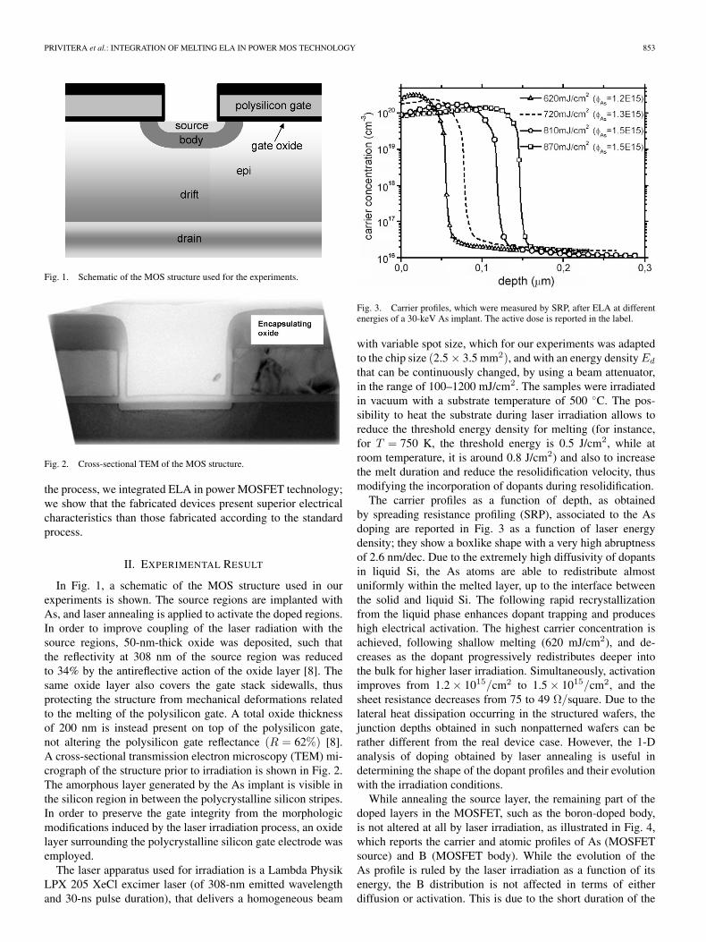
Fig. 1. Schematic of the MOS structure used for the experiments.
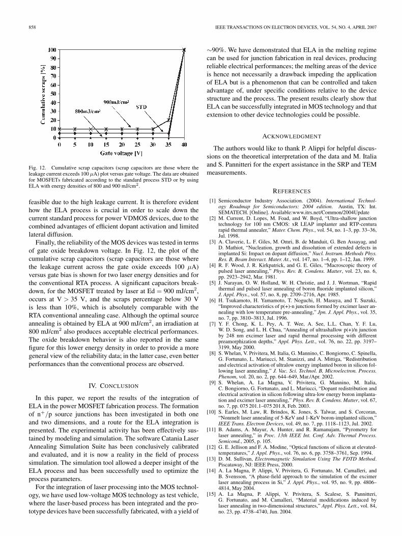
Fig. 2. Cross-sectional TEM of the MOS structure.
the process, we integrated ELA in power MOSFET technology;we show that the fabricated devices present superior electricalcharacteristics than those fabricated according to the standardprocess.
II. EXPERIMENTAL RESULT
In Fig. 1, a schematic of the MOS structure used in ourexperiments is shown. The source regions are implanted withAs, and laser annealing is applied to activate the doped regions.In order to improve coupling of the laser radiation with thesource regions, 50-nm-thick oxide was deposited, such thatthe reflectivity at 308 nm of the source region was reducedto 34% by the antireflective action of the oxide layer [8]. Thesame oxide layer also covers the gate stack sidewalls, thusprotecting the structure from mechanical deformations relatedto the melting of the polysilicon gate. A total oxide thicknessof 200 nm is instead present on top of the polysilicon gate,not altering the polysilicon gate reflectance (R = 62%) [8].A cross-sectional transmission electron microscopy (TEM) mi-crograph of the structure prior to irradiation is shown in Fig. 2.The amorphous layer generated by the As implant is visible inthe silicon region in between the polycrystalline silicon stripes.In order to preserve the gate integrity from the morphologicmodifications induced by the laser irradiation process, an oxidelayer surrounding the polycrystalline silicon gate electrode wasemployed.
The laser apparatus used for irradiation is a Lambda PhysikLPX 205 XeCl excimer laser (of 308-nm emitted wavelengthand 30-ns pulse duration), that delivers a homogeneous beam
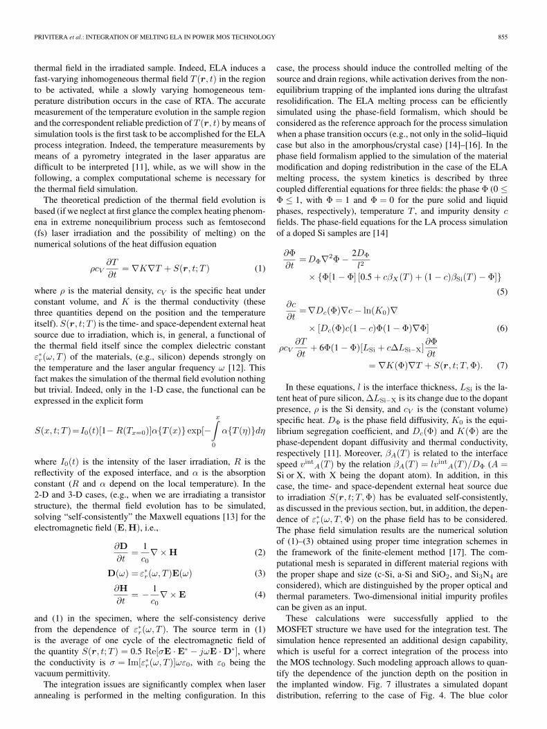
Fig. 3. Carrier profiles, which were measured by SRP, after ELA at differentenergies of a 30-keV As implant. The active dose is reported in the label.
with variable spot size, which for our experiments was adaptedto the chip size (2.5 × 3.5 mm2), and with an energy density Ed
that can be continuously changed, by using a beam attenuator,in the range of 100–1200 mJ/cm2. The samples were irradiatedin vacuum with a substrate temperature of 500 C. The pos-sibility to heat the substrate during laser irradiation allows toreduce the threshold energy density for melting (for instance,for T = 750 K, the threshold energy is 0.5 J/cm2, while atroom temperature, it is around 0.8 J/cm2) and also to increasethe melt duration and reduce the resolidification velocity, thusmodifying the incorporation of dopants during resolidification.
The carrier profiles as a function of depth, as obtainedby spreading resistance profiling (SRP), associated to the Asdoping are reported in Fig. 3 as a function of laser energydensity; they show a boxlike shape with a very high abruptnessof 2.6 nm/dec. Due to the extremely high diffusivity of dopantsin liquid Si, the As atoms are able to redistribute almostuniformly within the melted layer, up to the interface betweenthe solid and liquid Si. The following rapid recrystallizationfrom the liquid phase enhances dopant trapping and produceshigh electrical activation. The highest carrier concentration isachieved, following shallow melting (620 mJ/cm2), and de-creases as the dopant progressively redistributes deeper intothe bulk for higher laser irradiation. Simultaneously, activationimproves from 1.2 × 10¹⁵/cm2 to 1.5 × 10¹⁵/cm2, and thesheet resistance decreases from 75 to 49 Ω/square. Due to thelateral heat dissipation occurring in the structured wafers, thejunction depths obtained in such nonpatterned wafers can berather different from the real device case. However, the 1-Danalysis of doping obtained by laser annealing is useful indetermining the shape of the dopant profiles and their evolutionwith the irradiation conditions.
While annealing the source layer, the remaining part of thedoped layers in the MOSFET, such as the boron-doped body,is not altered at all by laser irradiation, as illustrated in Fig. 4,which reports the carrier and atomic profiles of As (MOSFETsource) and B (MOSFET body). While the evolution of theAs profile is ruled by the laser irradiation as a function of itsenergy, the B distribution is not affected in terms of eitherdiffusion or activation. This is due to the short duration of the

854 IEEE TRANSACTIONS ON ELECTRON DEVICES, VOL. 54, NO. 4, APRIL 2007
Fig. 4. (a) Carrier and (b) chemical profiles of As and B forming the sourceand the body of the MOSFET, before and after the ELA process.
process, which is of the order of tens of nanoseconds, as wellas by the fast dissipation of heat through the Si substrate, whichdetermines a thermal process in the solid phase of the underly-ing doped layers that lasts less than 1 ms, inducing a negligiblediffusion that is not detectable by the analytical techniques.
The integrity of the complete device structure after laserirradiation was carefully controlled by scanning electronmicroscopy (SEM), which provides the analysis over a largescale and, in this case, results to a more severe test than TEM,which indeed guarantees a higher resolution but is limited to asmaller area. The cross-sectional TEM analysis, in combinationwith the chemical selective etch thinning of the doped region,is very useful, however, when the 2-D contour line of the dopedregion has to be measured. An example is reported in Fig. 5after ELA of a 10-keV As implant, where a junction shallowerthan 100 nm is shown (the corresponding doped region isidentified by the white area in the implanted window); a deepermelting occurs in the central region of the implanted window,due to lateral heat loss and to the diffraction of the laser lightthrough the narrow geometries of the patterned sample. Thelateral diffusion underneath the gate oxide is negligible, thusproviding the possibility to shrink the channel length withoutincurring short-channel effects.
Fig. 5. MOSFET cross sections observed by TEM. Selective chemical etchexhibits the source (white region) region obtained by ELA of a 10-keV Asimplant.
Fig. 6. SEM plan view of a MOSFET structure irradiated by laser. Thebrighter stripes correspond to the gate electrode (0.4 µm wide), while the darkerstripes in between (0.3 µm wide) are the implanted windows representing thesource contacts.
The realization of a device implies the reliability ofprocessing and patterning over a large scale, in order to ensurea high yield, which is necessary for real industrialization of themethod under investigation. A SEM image of the plan viewof a MOSFET chip, which is irradiated by laser in the sameconditions as that of Fig. 5, is shown in Fig. 6, attesting theintegrity of the structure subjected to ELA when operating inoptimized conditions.
A. Two-Dimensional Numerical Modeling
The systematic study of the diffusion and activation ofdopants during conventional thermal annealing has providedan extended database that can be used directly as reliablereference or indirectly for the calibration of the simulation mod-els implemented by technology computer-aided design tools.The peculiar modality of heat absorption and diffusion in thecase of laser annealing instead makes useless any reference toknown databases. The support of a computational tool, whichis aimed to predict both the material modifications and thedopant redistribution and activation caused by the irradiation, ismandatory for successful process integration since many relatedaspects remain totally obscure without an adequate modeling.Hence, in order to explain the features observed in the ELA-treated samples, we developed a simulation tool, taking intoaccount the patterning effect in the interaction between the laserbeam and the device structure.
The substantial difference between a standard rapid thermalannealing (RTA) and an ELA process is the evolution of the
PRIVITERA et al.: INTEGRATION OF MELTING ELA IN POWER MOS TECHNOLOGY 855
thermal field in the irradiated sample. Indeed, ELA induces afast-varying inhomogeneous thermal field T (r, t) in the regionto be activated, while a slowly varying homogeneous tem-perature distribution occurs in the case of RTA. The accuratemeasurement of the temperature evolution in the sample regionand the correspondent reliable prediction of T (r, t) by means ofsimulation tools is the first task to be accomplished for the ELAprocess integration. Indeed, the temperature measurements bymeans of a pyrometry integrated in the laser apparatus aredifficult to be interpreted [11], while, as we will show in thefollowing, a complex computational scheme is necessary forthe thermal field simulation.
The theoretical prediction of the thermal field evolution isbased (if we neglect at first glance the complex heating phenom-ena in extreme nonequilibrium process such as femtosecond(fs) laser irradiation and the possibility of melting) on thenumerical solutions of the heat diffusion equation
ρcV∂T
∂t= ∇K∇T + S(r, t;T ) (1)
where ρ is the material density, cV is the specific heat underconstant volume, and K is the thermal conductivity (thesethree quantities depend on the position and the temperatureitself). S(r, t;T ) is the time- and space-dependent external heatsource due to irradiation, which is, in general, a functional ofthe thermal field itself since the complex dielectric constantε∗r(ω, T ) of the materials, (e.g., silicon) depends strongly onthe temperature and the laser angular frequency ω [12]. Thisfact makes the simulation of the thermal field evolution nothingbut trivial. Indeed, only in the 1-D case, the functional can beexpressed in the explicit form
S(x, t;T )=I0(t)[1− R(Tx=0)]αT (x) exp[−x∫
0
αT (η)dη
where I0(t) is the intensity of the laser irradiation, R is thereflectivity of the exposed interface, and α is the absorptionconstant (R and α depend on the local temperature). In the2-D and 3-D cases, (e.g., when we are irradiating a transistorstructure), the thermal field evolution has to be simulated,solving “self-consistently” the Maxwell equations [13] for theelectromagnetic field (E,H), i.e.,
∂D∂t
=1c0
∇× H (2)
D(ω) = ε∗r(ω, T )E(ω) (3)
∂H∂t
= − 1c0
∇× E (4)
and (1) in the specimen, where the self-consistency derivefrom the dependence of ε∗r(ω, T ). The source term in (1)is the average of one cycle of the electromagnetic field ofthe quantity S(r, t;T ) = 0.5 Re[σE · E∗ − jωE · D∗], wherethe conductivity is σ = Im[ε∗r(ω, T )]ωε0, with ε0 being thevacuum permittivity.
The integration issues are significantly complex when laserannealing is performed in the melting configuration. In this
case, the process should induce the controlled melting of thesource and drain regions, while activation derives from the non-equilibrium trapping of the implanted ions during the ultrafastresolidification. The ELA melting process can be efficientlysimulated using the phase-field formalism, which should beconsidered as the reference approach for the process simulationwhen a phase transition occurs (e.g., not only in the solid–liquidcase but also in the amorphous/crystal case) [14]–[16]. In thephase field formalism applied to the simulation of the materialmodification and doping redistribution in the case of the ELAmelting process, the system kinetics is described by threecoupled differential equations for three fields: the phase Φ (0 ≤Φ ≤ 1, with Φ = 1 and Φ = 0 for the pure solid and liquidphases, respectively), temperature T , and impurity density cfields. The phase-field equations for the LA process simulationof a doped Si samples are [14]
∂Φ∂t
= DΦ∇2Φ − 2DΦ
l2
× Φ[1 − Φ] [0.5 + cβX(T ) + (1 − c)βSi(T ) − Φ](5)
∂c
∂t=∇Dc(Φ)∇c − ln(K0)∇
× [Dc(Φ)c(1 − c)Φ(1 − Φ)∇Φ] (6)
ρcV∂T
∂t+ 6Φ(1 − Φ)[LSi + c∆LSi−X]
∂Φ∂t
= ∇K(Φ)∇T + S(r, t;T,Φ). (7)
In these equations, l is the interface thickness, LSi is the la-tent heat of pure silicon, ∆LSi−X is its change due to the dopantpresence, ρ is the Si density, and cV is the (constant volume)specific heat. DΦ is the phase field diffusivity, K0 is the equi-librium segregation coefficient, and Dc(Φ) and K(Φ) are thephase-dependent dopant diffusivity and thermal conductivity,respectively [11]. Moreover, βA(T ) is related to the interfacespeed vint
A(T ) by the relation βA(T ) = lvintA(T )/DΦ (A =
Si or X, with X being the dopant atom). In addition, in thiscase, the time- and space-dependent external heat source dueto irradiation S(r, t;T,Φ) has be evaluated self-consistently,as discussed in the previous section, but, in addition, the depen-dence of ε∗r(ω, T,Φ) on the phase field has to be considered.The phase field simulation results are the numerical solutionof (1)–(3) obtained using proper time integration schemes inthe framework of the finite-element method [17]. The com-putational mesh is separated in different material regions withthe proper shape and size (c-Si, a-Si and SiO2, and Si3N4 areconsidered), which are distinguished by the proper optical andthermal parameters. Two-dimensional initial impurity profilescan be given as an input.
These calculations were successfully applied to theMOSFET structure we have used for the integration test. Thesimulation hence represented an additional design capability,which is useful for a correct integration of the process intothe MOS technology. Such modeling approach allows to quan-tify the dependence of the junction depth on the position inthe implanted window. Fig. 7 illustrates a simulated dopantdistribution, referring to the case of Fig. 4. The blue color

856 IEEE TRANSACTIONS ON ELECTRON DEVICES, VOL. 54, NO. 4, APRIL 2007
Fig. 7. Two-dimensional simulation of Si melting in a MOSFET cross section.The image represents (right) the gate stack and (left) the implanted sourcecontact. The dark area corresponds to melted Si according to the simulation.In the source region, the edge of the melted area represents the As junctioncontour line. The 2-D simulation is obtained by phase field calculation.
represents melting, which in turn means homogeneously re-distributed As. All the main features of the resulting dopingdistribution after ELA are perfectly reproduced by the model,with a deeper doping profile at the center of the window, whichresults from the combined effects of lateral heat diffusion anddiffraction effects. This simulation code not only allowed a pre-cise interpretation of the experimental results but also enabledthe predictive analysis of different gate stack architectures andgeometries and the optimization the ELA conditions.
III. INTEGRATION IN MOS TECHNOLOGY:FABRICATION OF TRANSISTORS
Power MOS devices have been fabricated according to aprocess flowchart sequence, which was defined according to theindications from the experiments and the simulation describedpreviously. In particular, the power MOS device consists ofmulti-MOS basic cells interconnected in parallel on a single die.Each one of this cell (see Fig. 1) consists of a vertical diffusedMOS (VDMOS) silicon gate structure where the current flowsvertically from drain to source. The devices have been fabri-cated on a lightly doped n-doped epitaxial silicon layer with re-sistivity in the range of 0.2–0.3 Ω cm and thickness in the rangeof 3–4 µm. After formation of the gate stack, which consists ofthe polysilicon gate deposited on top of the gate oxide (35 nmthick), and 150-nm-thick tetraethylorthosilicate (TEOS) oxide,the p-type region (body) was formed by B-ion implantationself-aligned to the gate at 80 keV. Prior to the source implanta-tion, the B-doped body layer had been activated by furnace dif-fusion. Then, source regions are ion implanted with As (30 keVand a dose of 2 × 1015 cm−2), followed by laser annealingor conventional RTA for the standard process, to activate thedopants in the source regions. A 50-nm-thick oxide depositedby chemical vapour deposition (VAPOX) oxide was deposited
Fig. 8. MOSFET yield versus oxidation thickness of eventual fractures in theencapsulating oxide, which were caused by the melting of the polycrystallinesilicon gate electrode.
Fig. 9. Body–drain internal diode reverse characteristics for standard processfor two different body diffusions: (a) standard process with larger body diffu-sion (red curve), (b) ELA process with reduced body diffusion (blue curve), and(c) standard process with reduced body diffusion (yellow curve).
onto the entire device, such that the reflectivity at 308 nmof the source region was reduced to 34% by the antireflectiveaction of the oxide layer [8]. The same oxide layer is alsocapping the gate stack sidewalls, thus protecting the structurefrom deformations related to the melting of the polysilicon gate.Since the possibility that a fracture in the surrounding oxidemight occur, hence inducing a liquid polycrystalline siliconoutflow through the aperture of the broken oxide, an oxidationprocess has been added after ELA, in order to safely isolatethe polycrystalline silicon gate from the source metal. However,the thicker the grown oxide, the smaller the contact openings.This means that the source metal (Al) will be not able to fill thecontacts, and then, the MOS ON parameters will be not good.The maximum yield, with respect to the oxide thickness values,is found to range from 50 to 150 Å, as shown in Fig. 8.
In order to scale down the device channel length, both bodydiffusion and source diffusion have to be reduced. On theother hand, due to the high implanted dose used to form thesource contacts, a robust RTA (t > 30 s at T = 1050 C) treat-ment is required to efficiently activate the dopants and removethe implantation damage. In Fig. 9, the body–drain internal

PRIVITERA et al.: INTEGRATION OF MELTING ELA IN POWER MOS TECHNOLOGY 857
TABLE IELECTRICAL PARAMETERS
Fig. 10. Drain current increase for the ELA-treated MOSFET, with respect tothe device processed by conventional thermal processing.
diode reverse characteristic are reported for two different bodydiffusions (normal body diffusion: T = 1000 C for 30 min,reduced body diffusion: T = 900 C for 30 min) and the samesource formation process. For the shorter body diffusion, thebreakdown voltage is reduced, and a higher leakage currentappears. This has a detrimental impact on the device charac-teristics of the scaled devices in terms of yield reduction, whichis due to leakage scraps, and of increased OFF current, resultingin a value that is higher than the high specific limit (10−7 A)for these devices.
Based on the evaluation of the best yield, as well as on thepreviously illustrated process refinements, ELA VDMOS field-effect transistors were fabricated, including a reduced bodydiffusion process, with the latter one allowed by the smallerAs lateral diffusion achievable by ELA. The lateral extent ofthe p-body profile was hence limited with respect to that in thestandard transistor, being the diffusion performed at 900 C in-stead of 1000 C for the same time and thus generating a widerregion in between two contiguous body wells. The main devicecharacteristics are reported in Table I and compared with thoseof devices fabricated with standard process and normal bodydiffusion: The ELA-processed devices have a threshold voltagecomparable with the standard-processed devices with a yield∼90%. In addition, the body–drain leakage current appearsmuch better than that for the standard process with reducedbody diffusion (see Fig. 9). In Fig. 10, the output characteristics,which were measured just above the threshold voltage, forboth ELA process, with reduced body diffusion, and standardprocess, with normal body diffusion, are compared, and it isevident that the ELA-processed devices provide, for a givengate voltage, a much higher current. To explain this result, wehave analyzed by TEM, after selective etching, the junctionsof both devices, which are reported in Fig. 11, showing that,in the case of devices with normal body diffusion and RTAactivation, the As of the source layer diffuses under the gate forabout 80 nm, which is in very good agreement with diffusionsimulations, while in the case of the device with reduced
Fig. 11. MOSFET cross sections observed by TEM relative to (left panel)the standard (1125 C) source diffusion and (right panel) the 900 mJ/cm2
ELA process. Selective chemical etch delineates the source, which is visibleas the bright region in the implanted window. The edge of such bright areacorresponds to the source junction contour line.
body diffusion and ELA activation, As diffuses underneaththe gate for about 50 nm. Considering that the lateral bodydiffusions, which were evaluated from simulations, are 0.24 and0.17 µm for the normal and reduced body diffusion, respec-tively, the estimated effective channel lengths are 0.16 and0.12 µm, with the ELA-treated devices showing shorter channellength. However, the estimated reduced channel length can onlypartly explain the increased drain current for the ELA devicesshown in Fig. 10. The ON-resistance Ron in a power VDMOS isthe sum of different terms, including the channel resistance, theresistance due to the excess of negative charge accumulated inthe n-region under the gate, the junction field-effect transistor(JFET) resistance, and the resistance of the epitaxial layer. Inparticular, the JFET resistance is reduced in the reduced bodydiffusion devices, as the lateral body diffusion is reduced by0.07 µm if compared to the normal body diffusion process.Consequently, we believe that a contribution to the increaseddrain current observed in Fig. 10 also arises from the reducedJFET resistance in the ELA-treated structure.
It should be mentioned that the Ron measured at Vg = 8 Vfor ELA devices was 10% lower than that of standard devices.This is due to the fact that with this scaled-down process, onlychannel resistance and the JFET resistance have been reduced,whereas the Ron in a power VDMOS at high Vg is controlledby the resistance of the epitaxial layer, the substrate resistance,the source and drain metal resistances, and the resistance due tosilicon to package connections. In particular, in these specificdevices, less than one third of Ron is controlled by the channeland JFET resistive components. Therefore, in order to take fulladvantage of the ELA processing, optimization of the otherparasitic resistances is needed.
It is worthy to point out that devices fabricated with stan-dard RTA source process and reduced body diffusion are not
858 IEEE TRANSACTIONS ON ELECTRON DEVICES, VOL. 54, NO. 4, APRIL 2007
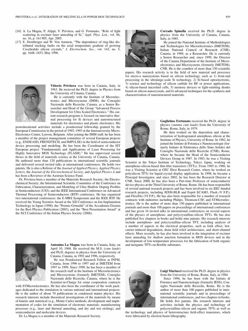
Fig. 12. Cumulative scrap capacitors (scrap capacitors are those where theleakage current exceeds 100 µA) plot versus gate voltage. The data are obtainedfor MOSFETs fabricated according to the standard process STD or by usingELA with energy densities of 800 and 900 mJ/cm2.
feasible due to the high leakage current. It is therefore evidenthow the ELA process is crucial in order to scale down thecurrent standard process for power VDMOS devices, due to thecombined advantages of efficient dopant activation and limitedlateral diffusion.
Finally, the reliability of the MOS devices was tested in termsof gate oxide breakdown voltage. In Fig. 12, the plot of thecumulative scrap capacitors (scrap capacitors are those wherethe leakage current across the gate oxide exceeds 100 µA)versus gate bias is shown for two laser energy densities and forthe conventional RTA process. A significant capacitors break-down, for the MOSFET treated by laser at Ed = 900 mJ/cm2,occurs at V > 35 V, and the scraps percentage below 30 Vis less than 10%, which is absolutely comparable with theRTA conventional annealing case. Although the optimal sourceannealing is obtained by ELA at 900 mJ/cm2, an irradiation at800 mJ/cm2 also produces acceptable electrical performances.The oxide breakdown behavior is also reported in the samefigure for this lower energy density in order to provide a moregeneral view of the reliability data; in the latter case, even betterperformances than the conventional process are observed.
IV. CONCLUSION
In this paper, we report the results of the integration ofELA in the power MOSFET fabrication process. The formationof n+/p source junctions has been investigated in both oneand two dimensions, and a route for the ELA integration ispresented. The experimental activity has been effectively sus-tained by modeling and simulation. The software Catania LaserAnnealing Simulation Suite has been conclusively calibratedand evaluated, and it is now a reality in the field of processsimulation. The simulation tool allowed a deeper insight of theELA process and has been successfully used to optimize theprocess parameters.
For the integration of laser processing into the MOS technol-ogy, we have used low-voltage MOS technology as test vehicle,where the laser-based process has been integrated and the pro-totype devices have been successfully fabricated, with a yield of
∼90%. We have demonstrated that ELA in the melting regimecan be used for junction fabrication in real devices, producingreliable electrical performances; the melting areas of the deviceis hence not necessarily a drawback impeding the applicationof ELA but is a phenomenon that can be controlled and takenadvantage of, under specific conditions relative to the devicestructure and the process. The present results clearly show thatELA can be successfully integrated in MOS technology and thatextension to other device technologies could be possible.
ACKNOWLEDGMENT
The authors would like to thank P. Alippi for helpful discus-sions on the theoretical interpretation of the data and M. Italiaand S. Pannitteri for the expert assistance in the SRP and TEMmeasurements.
REFERENCES
[1] Semiconductor Industry Association. (2004). International Technol-ogy Roadmap for Semiconductors: 2004 edition. Austin, TX: Int.SEMATECH. [Online]. Available:www.itrs.net/Common/2004Update
[2] M. Current, D. Lopes, M. Foad, and W. Boyd, “Ultra-shallow junctiontechnology for 100 nm CMOS: xR LEAP implanter and RTP-centurarapid thermal annealer,” Mater. Chem. Phys., vol. 54, no. 1–3, pp. 33–36,Jul. 1998.
[3] A. Claverie, L. F. Giles, M. Omri, B. de Manduit, G. Ben Assayag, andD. Mathiot, “Nucleation, growth and dissolution of extended defects inimplanted Si: Impact on dopant diffusion,” Nucl. Instrum. Methods Phys.Res. B, Beam Interact. Mater. At., vol. 147, no. 1–4, pp. 1–12, Jan. 1999.
[4] R. F. Wood, J. R. Kirkpatrick, and G. E. Giles, “Macroscopic theory ofpulsed laser annealing,” Phys. Rev. B, Condens. Matter, vol. 23, no. 6,pp. 2923–2942, Mar. 1981.
[5] J. Narayan, O. W. Holland, W. H. Christie, and J. J. Wortman, “Rapidthermal and pulsed laser annealing of boron fluoride implanted silicon,”J. Appl. Phys., vol. 57, no. 8, pp. 2709–2716, Apr. 1985.
[6] H. Tsukamoto, H. Yamamoto, T. Noguchi, H. Masuya, and T. Suzuki,“Improved characteristics of p(+)-n junctions formed by excimer laser an-nealing with low temperature pre-annealing,” Jpn. J. Appl. Phys., vol. 35,no. 7, pp. 3810–3813, Jul. 1996.
[7] Y. F. Chong, K. L. Pey, A. T. Wee, A. See, L.L. Chan, Y. F. Lu,W. D. Song, and L. H. Chua, “Annealing of ultrashallow p(+)/n junctionby 248 nm excimer laser and rapid thermal processing with differentpreamorphization depths,” Appl. Phys. Lett., vol. 76, no. 22, pp. 3197–3199, May 2000.
[8] S. Whelan, V. Privitera, M. Italia, G. Mannino, C. Bongiorno, C. Spinella,G. Fortunato, L. Mariucci, M. Stanizzi, and A. Mittiga, “Redistributionand electrical activation of ultralow energy implanted boron in silicon fol-lowing laser annealing,” J. Vac. Sci. Technol. B, Microelectron. Process.Phenom, vol. 20, no. 2, pp. 644–649, Mar./Apr. 2002.
[9] S. Whelan, A. La Magna, V. Privitera, G. Mannino, M. Italia,C. Bongiorno, G. Fortunato, and L. Mariucci, “Dopant redistribution andelectrical activation in silicon following ultra-low energy boron implanta-tion and excimer laser annealing,” Phys. Rev. B, Condens. Matter, vol. 67,no. 7, pp. 075 201.1–075 201.8, Feb. 2003.
[10] S. Earles, M. Law, R. Brindos, K. Jones, S. Talwar, and S. Corcoran,“Nonmelt laser annealing of 5-KeV and 1-KeV boron-implanted silicon,”IEEE Trans. Electron Devices, vol. 49, no. 7, pp. 1118–1123, Jul. 2002.
[11] B. Adams, A. Mayur, A. Hunter, and R. Ramanujam, “Pyrometry forlaser annealing,” in Proc. 13th IEEE Int. Conf. Adv. Thermal Process.Semicond., 2005, p. 105.
[12] G. E. Jellison and F. A. Modine, “Optical functions of silicon at elevated-temperatures,” J. Appl. Phys., vol. 76, no. 6, pp. 3758–3761, Sep. 1994.
[13] D. M. Sullivan, Electromagnetic Simulation Using The FDTD Method.Piscataway, NJ: IEEE Press, 2000.
[14] A. La Magna, P. Alippi, V. Privitera, G. Fortunato, M. Camalleri, andB. Svensson, “A phase-field approach to the simulation of the excimerlaser annealing process in Si,” J. Appl. Phys., vol. 95, no. 9, pp. 4806–4814, May 2004.
[15] A. La Magna, P. Alippi, V. Privitera, S. Scalese, S. Pannitteri,G. Fortunato, and M. Camalleri, “Material modifications induced bylaser annealing in two-dimensional structures,” Appl. Phys. Lett., vol. 84,no. 23, pp. 4738–4740, Jun. 2004.
PRIVITERA et al.: INTEGRATION OF MELTING ELA IN POWER MOS TECHNOLOGY 859
[16] A. La Magna, P. Alippi, V. Privitera, and G. Fortunato, “Role of fightscattering in excimer laser annealing of Si,” Appl. Phys. Lett., vol. 86,no. 16, p. 161 905, Apr. 2005.
[17] E. Dornberger and W. Von Ammon, “The dependence of ring-like dis-tributed stacking faults on the axial temperature gradient of growingCzochralski silicon crystals,” J. Electrochem. Soc., vol. 143, no. 5,pp. 1648–1653, May 1996.
Vittorio Privitera was born in Catania, Italy, in1963. He recieved the Ph.D. degree in Physics fromthe University of Catania, Catania.
He is currently with the Institute of Microelec-tronics and Microsystems (IMM), the ConsiglioNazionale delle Ricerche, Catania, as a Senior Re-searcher and Head of the Group “Advanced ProcessDevelopment for Ultra Scaled Electronics.” His cur-rent research program is focused on innovative ther-mal processing for Si devices and nanostructuredmaterials for electronics and plastic electronics. His
posteducational activities include a postdoctoral fellowship granted by theEuropean Commission in the period of 1992–1993 at the Interuniversity Micro-Electronics Center, Leuven, Belgium. After joining the IMM staff, he has beena member of the project management committee of several European projects(e.g., ENDEASD, FRENDTECH, and IMPULSE) in the field of semiconductordevice processing and modeling. He has been the Coordinator of the ISTEuropean project “Fundamentals and Applications of Laser Processing forHighly Innovative MOS Technology (FLASH).” He has supervised severaltheses in the field of materials science at the University of Catania, Catania.He authored more than 120 publications in international scientific journalsand delivered several invited talks at international conferences. He holds twopatents. He is also a Referee of the Journal of Applied Physics, Applied PhysicsLetters, the Journal of the Electrochemical Society, and Applied Physics A andhas been a Reviewer of the Austrian Science Fund.
Dr. Privitera been a member of the Materials Research Society; the Electro-chemical Society; the International Scientific Committee of the Conference onFabrication, Characterization, and Modeling of Ultra Shallow Doping Profilesin Semiconductors (USJ); and the IEEE International Conference on AdvancedThermal Processing of Semiconductors (RTP) conference. He has organizedtwo international conferences: the E-MRS Symposium and the IEEE RTP. Hereceived the Young Scientist Award at the XII Conference on Ion ImplantationTechnology in Japan (1998), the “Premio Grimaldi” of the Accademia Gioeniafor the Best Physics Publication (2003), and the “Best Presentation Award” atthe XCI Conference of the Italian Physics Society (2006).
Antonino La Magna was born in Catania, Italy, onApril 10, 1968. He received the M.S. (cum laude)and Ph.D. degrees in physics from the University ofCatania, Catania, in 1992 and 1996, respectively.
He was Postdoctoral Research Fellow at INFM,Catania, from 1996 to 1997 and at IMETEM from1997 to 1999. Since 1999, he has been a member ofthe research staff at the Institute of Microelectronicsand Microsystems (formerly IMETEM), ConsiglioNazionale delle Ricerche, Catania, where he is theScientist-in-Charge for some cooperation contracts
with STMicroelectronics. He has also been the coordinator of the work pack-ages dedicated to the simulation in various national and international projects.He is the author of about 70 publications in condensed matter physics. Hisresearch interests include theoretical investigations of the materials by meansof kinetic and statistical (e.g., Monte Carlo) methods, development and imple-mentation of codes for the simulation of electronic materials, manufacturingprocesses (e.g., laser and thermal annealing, and dry and wet etching), andsemiconductor and molecular devices.
Dr. La Magna is a member of the Materials Research Society.
Corrado Spinella received the Ph.D. degree inphysics from the University of Catania, Catania,Italy, in 1985.
He joined the National Institute of Methodologiesand Technologies for Microelectronics (IMETEM),Italian National Council of Research (CNR),Catania, in 1989, as a Researcher. He is currentlya Senior Researcher and, since 1999, the Directorof the Catania Department of the Institute of Micro-electronics and Microsystems (formerly IMETEM),CNR. He is the coauthor of more than 150 scientific
papers. His research activity is in the field of new material and processesfor micro-e nanosystems based on silicon technology, such as 1) front-endprocessing in the ultralarge-scale Si technology, 2) Si-based optoelectronic,3) science and technology of silicon carbide for RF or power applications,4) silicon-based microfuel cells, 5) memory devices or light-emitting diodesbased on silicon nanocrystals, and 6) advanced techniques for the synthesis andcharacterization of nanostructured materials.
Guglielmo Fortunato received the Ph.D. degree inphysics (summa cum laude) from the University ofRome, Rome, Italy, in 1979.
He then worked on the deposition and charac-terization of hydrogenated amorphous silicon at theInstitute of Physics, University of Rome. In 1982, hejoined the Istituto di Fotonica e Nanotecnologie (for-merly Istituto di Elettronica dello Stato Solido) delConsiglio Nazionale delle Ricerche (CNR), Rome,where he became the Head of the SemiconductorDevices Group in 1987. In 1983, he was a Visiting
Scientist at the Tokyo Institute of Technology, Tokyo, Japan, working onamorphous-silicon-based thin-film transistors (TFTs). From 1985 to 1986, hewas a Visiting Scientist at GEC Hirst Research Centre, where he worked onpolysilicon TFTs for liquid-crystal display application. In 1998, he became aPrincipal Investigator, and since 2002, he has been the Research Director atCNR. Since 2000, he has also been a Part-time Professor of semiconductordevice physics at the Third University of Rome, Rome. He has been responsibleof several national research projects and has been involved in six EEC-fundedresearch projects, including JESSI-BLR and Esprit ECAM3, Flash (V F.P.),and FlexiDis (VI F.P.). He has also been responsible for a number of researchcontracts with industries including Philips, Thomson-CSF, and STMicroelec-tronics. He is the author of more than 150 papers published in internationaljournals and more than 100 papers on proceedings of international conferencesand has given 16 invited talks in international conferences on several aspectsof the physics of amorphous- and polycrystalline-silicon TFTs. He has alsopublished five chapters in books and holds nine patents. His research interestsinclude amorphous- and polycrystalline-silicon TFT, including analysis ofa number of aspects in the electrical properties, such as kink effect, hot-carrier-induced degradation, drain field relief architectures, and short-channeleffects. More recently, he has also been involved in the integration of excimerlaser annealing for shallow junction formation in MOS devices and in thedevelopment of low-temperature processes for the fabrication of both organicand inorganic TFTs on flexible substrates.
Luigi Mariucci received the Ph.D. degree in physicsfrom the University of Rome, Rome, Italy, in 1984.
Since 1996, he has been with the Istituto diFotonica and Nanotecnologie (formerly IESS), Con-siglio Nazionale delle Ricerche, Rome. He is theauthor of more than 100 papers published in inter-national scientific journals and in proceedings ofinternational conferences, and two chapters in books.He holds five patents. His research interests andactivities include the physics and technology ofpolycrystalline-silicon and organic TFTs as well as
the technology and physics of heterostructure field-effect transistors, whichwere fabricated by electron beam lithography.

860 IEEE TRANSACTIONS ON ELECTRON DEVICES, VOL. 54, NO. 4, APRIL 2007
M. Cuscunà was born in Rome, Italy, in 1977. Hereceived the Laurea and Ph.D. degrees in physicsfrom the Third University of Rome, Rome, in 2002and 2005, respectively.
He joined the Istituto di Fotonica e Nanotecnolo-gie del Consiglio Nazionale delle Ricerche, Rome.He has worked in the field of polysilicons. From2001 to 2005, he worked on the polysilicon thin-film transistor fabrication process at high tempera-ture. His current research interests include thin-filmtransistors realized on flexible substrates.
Cateno Marco Camalleri received the Laurea de-gree in physics from University of Palermo, Palermo,Italy, in 1992.
Since 1994, he has been with the R&D De-partment, STMicroelectronics (STM), Catania, Italy,where he deals with bulk processes for their inte-gration on power and RF devices developed andproduced in STM Catania facilities. He is currentlyinvolved in thin-film device development and com-pound semiconductor applications. He is a coauthorof several publications and European and foreignpatents.
Angelo Magrì received the Laurea degree in physicsfrom the University of Catania, Catania, Italy,in 1992.
In 1992, he became a Discrete MOS Devices De-signer at the R&D Department, STMicroelectronics,Catania. Since 1999, he has been the Head of a groupof designers for the development of new technologiesfor low-voltage power MOSFETs. He holds severalU.S. patents about MOSFET structures and methods.
Giovanna La Rosa received the Laurea degree inphysics from the University of Catania, Catania,Italy, in 1998.
Since 1999, she has been a Designer at the R&DDepartment, STMicroelectronics, Italy. She is cur-rently in charge of discrete MOS devices design.
Bengt G. Svensson (SM’97) received the Ph.D.degree in physics from the University of Gothenburg,Sweden, in 1980.
He is currently a Professor at the Physical Elec-tronics Division, Department of Physics, Univer-sity of Oslo (UoO), Oslo, Norway. Since 2004, hehas been a Coordinator of the Micro- and Nano-technology Laboratory, UoO. Twenty-two Ph.D.and licentiate theses have been completed underhis supervision. He has 30 years experience insemiconductor physics, physical electronics, and
the science of semiconductor materials. His current research program isfocused on: 1) doping, defects, and diffusion in silicon-based semiconductors(e.g., SiC, SiGe, Si); 2) functional oxides (e.g., ZnO) as wide-band-gap semi-conductors and nanostructured materials for electronics and photonics; and3) ion beam analysis of solids, with a team of ∼20 people at UoO and anetwork of international collaborators. Particular applications are advancedsemiconductor sensors and radiation detectors, photovoltaics, solid-state light-ening, and high-power electronics. He has Authored or Coauthored more than300 technical papers in refereed scientific journals and delivered more than40 invited/plenary talks at international conferences and meetings. He has alsocontributed to four scientific books and organized and coorganized severalinternational conferences and workshops. He holds three patents (with onepending).
Prof. Svensson has been a member of APS, MRS and The BøhmischePhysical Society.
Eduard V. Monakhov was born on January 31,1970. He received the Ph.D. degree in physicalelectronics from Moscow State University, Moscow,Russia, in 1997.
During 1993–1998, he was with Moscow StateUniversity and the University of Aarhus, Aarhus,Denmark. During 1999–2000, he received Wenner-Gren postdoctoral fellowship at Royal Instituteof Technology (KTH), Stockholm, Sweden. Since2001, he has been a Researcher at the Physical Elec-tronics Division, Department of Physics, University
of Oslo, Oslo, Norway. He has Coauthored more than 60 scientific papers. Hisresearch interests include defects and diffusion in group IV and wide-band-gapsemiconductors.
Frank Simon was born in Bad Salzuflen, Germany,in 1966. He received the Ph.D. degree in physicsin Göttingen, Germany. His diploma thesis was onnonlinear laser optics. In 1994, he was with a man-ufacturer of medical laser systems in assembly anddevelopment, as the Head of R&D. In 2001, hemoved to MicroLas Lasersystem GmbH, which was,at that time, affiliated with Lambda Physik AG andJenoptik AG. In 2004, MicroLas Lasersystem GmbHwas merged with Lambda Physik AG (now CoherentGmbH). He is currently the Group Leader of the
R&D-Group Systems, Coherent GmbH, Göttingen, where he is still focused onthe development and application of optical systems for excimer laser materialprocessing. He is a Coauthor of some papers about excimer laser application,especially about laser crystallization, and a Coinventor of patents in thesame field.