Texture coefficient and Conductivity Dependence on the Annealing
7
International Review of Physics (IREPHY) Contents Detection of Absolute Rest Frame by Measuring Light Wavelength of Light Source in Uniform Rectilinear Motion by Justin C. H. Lee Determination of Microstructure and Mechanical Behaviour of SiC Particle Reinforced Aluminum Matrix Ceramic Composites by Dunia K. M. Al-Nasrawy Zinc Oxide Thin Films Prepared by Atmospheric Pressure Chemical Vapor Deposition Using Zinc Chloride by S. Maifi, M. S. Belkaid, R. Zirmi, L. Escoubas, M. Pasquinelli A New Analytical Solution to the Relativistic Polytropic Fluid Spheres by M. I. Nouh, A. S. Saad Texture Coefficient and Conductivity Dependence on the Annealing and Thicknesses of Thin CdS Films by Eman M. Nasir A Study of Some Environmental Effects for Saw Dust Wood / Phenol–Formaldehyde Composites by Harith I. Jaafer , Zainab R. Muslem, Iqbal S. Naji Microscopic Study of Anode and Cathode Corona in Argon Colliders by R. A. El-Koramy, A. M. A. Amry, A. S. Gabre Polarized Infrared Reflectance Studies for Wurtzite Al0.06Ga0.94N Epilayer on Sapphire Grown by MBE by A. I. Aljameel, H. Abu Hassan, S. S. Ng A Low Temperature Atmospheric Pressure Plasma Jet by Hammad R. Humud, Ahamed S. Wasfi, Wafaa Abd Al-Razaq Correlation between Microscopic and Macroscopic Conductivity Models through Meyer-Neldel Rule by F. Abdel-Wahab, E. M. Ahmed The Nonlinear Dose Response of OTOR-Model Thermoluminescence Glow Peaks in Case of Temperature-Dependent Frequency Factor by M. S. Rasheedy, Gh. S. M. Hassan, E. M. Zahran, A. I. Abd-Elmageed Flash Evaporation of CdS Thin Film by Raad M. S. Al-Haddad, Salah Abdulla Hasoon, Shurooq S. Mahmood, Issam M. Ibrahim Characterization of Argon Plasma Induced by Simple 2.45 GHz Microwave Source by Ahmed S. Wasfi, Hamad R. Humud, Ali H. Muhammad, Mazin S. Al-Ansari Electrical Properties of Thermally Evaporated CdSexS1-x Thin Films by Nada K. Abbas, Iqbal S. Naji , Alaa A. Abdulmajeed Nanostructural ZnO:Al On Porous Silicon Gas Sensor by Raad S. Sabry, Dhaidan kh. Kafi Effect of Secondary Electron Emission on Argon Glow Discharge Characteristics by F. Bouanaka, S. Rebiai Effect of Magnetic Field and Porosity on Peristaltic Flow of Micropolar Fluid by A. M. Abd-Allaa, G. A. Yahya, A. M. Farhan X- Ray Mass Attenuation Coefficients of Some 3d Elements Compounds at Am-241(40mCi) by Farid M. Mohammed, Raed N. Razooqi, Muataz A. Majeed, Y. K. Vijay, Subodh Sirvastava Reverse I-V Behaviour of SiC Schottky Diodes under Various Temperatures and Magnetic Fields by D. Chalabi, Z. Chalabi, A. Saidane, S. Mimouni, M. Ketata Growth and Structure of Silver Oxide Thin Films Using Rapid Thermal Oxidation Method by Ibrahim R. Agool, Marwa Abdul Muhsien, Lamyaa M. Raoof The Effect of Gamma Radiation on the Optical Properties of (PC-PS) Polymer Blend by S. M. Hassan, N. M. Hassan, A. F. Sultan, Q. G. Al-Zaidi Heat and Mass Transfer for a Maxwell Fluid Flow Near a Stagnation Point with Variable Wall Heat and Mass Flux in the Presence of Heat Generation or Absorption by Mostafa A. A. Mahmoud, Shimaa E. Waheed Copy right © 2013 Praise Worthy Prize S.r.l. –All right received
Transcript of Texture coefficient and Conductivity Dependence on the Annealing

International Review of
Physics (IREPHY)
Contents Detection of Absolute Rest Frame by Measuring Light Wavelength of Light Source in Uniform Rectilinear Motion by Justin C. H. Lee
Determination of Microstructure and Mechanical Behaviour of SiC Particle Reinforced Aluminum Matrix Ceramic Composites by Dunia K. M. Al-Nasrawy
Zinc Oxide Thin Films Prepared by Atmospheric Pressure Chemical Vapor Deposition Using Zinc Chloride by S. Maifi, M. S. Belkaid, R. Zirmi, L. Escoubas, M. Pasquinelli
A New Analytical Solution to the Relativistic Polytropic Fluid Spheres by M. I. Nouh, A. S. Saad
Texture Coefficient and Conductivity Dependence on the Annealing and Thicknesses of Thin CdS Films by Eman M. Nasir
A Study of Some Environmental Effects for Saw Dust Wood / Phenol–Formaldehyde Composites by Harith I. Jaafer , Zainab R. Muslem, Iqbal S. Naji
Microscopic Study of Anode and Cathode Corona in Argon Colliders by R. A. El-Koramy, A. M. A. Amry, A. S. Gabre
Polarized Infrared Reflectance Studies for Wurtzite Al0.06Ga0.94N Epilayer on Sapphire Grown by MBE by A. I. Aljameel, H. Abu Hassan, S. S. Ng
A Low Temperature Atmospheric Pressure Plasma Jet by Hammad R. Humud, Ahamed S. Wasfi, Wafaa Abd Al-Razaq
Correlation between Microscopic and Macroscopic Conductivity Models through Meyer-Neldel Rule by F. Abdel-Wahab, E. M. Ahmed
The Nonlinear Dose Response of OTOR-Model Thermoluminescence Glow Peaks in Case of Temperature-Dependent Frequency Factor by M. S. Rasheedy, Gh. S. M. Hassan, E. M. Zahran, A. I. Abd-Elmageed
Flash Evaporation of CdS Thin Film by Raad M. S. Al-Haddad, Salah Abdulla Hasoon, Shurooq S. Mahmood, Issam M. Ibrahim
Characterization of Argon Plasma Induced by Simple 2.45 GHz Microwave Source
by Ahmed S. Wasfi, Hamad R. Humud, Ali H. Muhammad, Mazin S. Al-Ansari
Electrical Properties of Thermally Evaporated CdSexS1-x Thin Films by Nada K. Abbas, Iqbal S. Naji , Alaa A. Abdulmajeed
Nanostructural ZnO:Al On Porous Silicon Gas Sensor by Raad S. Sabry, Dhaidan kh. Kafi
Effect of Secondary Electron Emission on Argon Glow Discharge Characteristics
by F. Bouanaka, S. Rebiai
Effect of Magnetic Field and Porosity on Peristaltic Flow of Micropolar Fluid
by A. M. Abd-Allaa, G. A. Yahya, A. M. Farhan
X- Ray Mass Attenuation Coefficients of Some 3d Elements Compounds at Am-241(40mCi) by Farid M. Mohammed, Raed N. Razooqi, Muataz A. Majeed, Y. K. Vijay, Subodh Sirvastava
Reverse I-V Behaviour of SiC Schottky Diodes under Various Temperatures and Magnetic Fields by D. Chalabi, Z. Chalabi, A. Saidane, S. Mimouni, M. Ketata
Growth and Structure of Silver Oxide Thin Films Using Rapid Thermal Oxidation Method
by Ibrahim R. Agool, Marwa Abdul Muhsien, Lamyaa M. Raoof
The Effect of Gamma Radiation on the Optical Properties of (PC-PS) Polymer Blend
by S. M. Hassan, N. M. Hassan, A. F. Sultan, Q. G. Al-Zaidi
Heat and Mass Transfer for a Maxwell Fluid Flow Near a Stagnation Point with Variable Wall Heat and Mass Flux in the Presence of Heat Generation or Absorption by Mostafa A. A. Mahmoud, Shimaa E. Waheed
Copy right © 2013 Praise Worthy Prize S.r.l. –All right received

2
February 31, 2013
International Review of
Physics
(IREPHY)
Managing Editor:
Santolo Meo
Department of Electrical Engineering
Federico II University
21 Claudio – I80125 Naples, Italy
Editorial Board:
Vladimir M. Agranovich (U.S.A) University Of Texas at Dallas – Nano Tech Institute
Anastasios Anstaslaids (GREECE) National Observatory of Athens - Institute for Space Applications & Remote Sensing Jean-Pierre Badiali (FRANCE) Université Pierre et Marie Curie – Directeur de recherche CNRS
Marcia C. Barbosa (BRASIL) Universidade Federal do Rio Grande do Sul - Instituto de Fisica
Israel Felner (ISRAEL) The Hebrew University - Racah Institute of Physics Peter Hanggi (GERMANY) University of Augsburg - Institute of Physics
Hans Herrmann (BRASIL) Universidade Federal do Ceará - Departamento de Física
Joshua Jortner (ISRAEL) Tel Aviv University – School of Chemistry Vladimir G. Kadyshevsky (RUSSIA) Joint Institute for Nuclear Research
Yuri Kozitsky (POLAND) Maria Curie-Sklodowska University, Lublin
Bo Lehnert (SWEDEN) Royal Institute of Technology- School of Electrical Engineering -Fusion Plasma Physics Jukka Maalampi (FINLAND) University of Jyväskylä - Department of Physics
Tito Mendonca (PORTUGAL) IPFN, Instituto Superior Técnico
Risto M. Nieminen (FINLAND) Helsinki University of Technology - Department of Engineering Physics Dorin Poenaru (ROMANIA) H. H. National Institute of Physics & Nuclear Engineering
Rajeev Kumar Puri (INDIA) Panjab University
Kestutis Pyragas (LITHUANIA) Semiconductor Physics Institute Antoni Roglaski (POLAND) Military University of Technology - Institute of Applied Physics
Padma K. Shukla (GERMANY) Universitaet Bochum - Fakultaet fuer Physik und Astronomie
Gowind Swarup (INDIA) Tata Institute of Fundamental Research - National Centre for Radio Astrophysics - Hugo Thienpont (BELGIUM) Vrije Universiteit Brussel - Department of Applied Physics and Photonics
Sergey Vladimirov (AUSTRALIA) University of Sydney - School of Physics
Christian Von Ferber (U.K.) Coventry University - Applied Mathematics Research Centre
Miki Wadati (JAPAN) University of Tokyo - Department of Physics
Xin-Nian Wang (U.S.A) Lawrence Berkeley National Laboratory - Nuclear Science Division
Copy right © 2013 Praise Worthy Prize S.r.l. –All right received

3
Texture coefficient and Conductivity Dependence on the Annealing
and Thicknesses of Thin CdS Films
Eman M. Nasir Thin Film Labrotary, Department of physics, College of Sciences, University of Baghdad
Aljadriah, Baghdad, Iraq
Corresponding Author: [email protected]
Abstract- Cadmium sulfide thin films prepared by thermal evaporation technique with substrate
temperature of 333 K, the film deposited with different thicknesses (100, 150, 200 and 250 nm), then
annealed at 373, 423 and 473 K. X-ray diffraction spectra of CdS films were hexagonal polycrystalline
structure. The texture coefficient has determined, the highest value of it has observed for the thicker film.
The electrical conductivity display two stages of conductivity through the heating temperature range for
all thicknesses. Conductivities of the films were found to increase with increasing the annealing
temperatures and the thicknesses. Also it can be observed that the conductivity of the film of 250 nm is
higher than other films. The thermal activation energies for as deposited CdS and annealed thin films
increased with increasing the annealing temperature at the lower temperature range, while they
decrease with increasing the thicknesses. Copy right © 2013 Praise Worthy Prize S.r.l. –All right
received
Key World: Thin CdS film, Thermal evaporation, X- ray Diffraction, Electrical Conductivity.
I. Introduction
Cadmium sulfide (CdS) is one of the cheapest
semiconducting material from II-VI group [1], the
deposition and characterization of CdS semiconducting
thin films has been received a considerable amount of
interest due to their potential used in the optoelectronic
application [2]. Polycrystalline CdS thin films are
widely used as window material in several
heterojunction solar cells for their favorable optical
properties [3, 4]. Cadmium Sulfide films have been
established as a viable candidate for the absorbing
material in the visible region [5]. Many techniques
have been reported for the deposition of CdS thin film.
These include evaporation, sputtering, chemical bath
deposition, spray pyrolysis [6], metal organic chemical
vapor deposition; molecular beam epitaxy technique
[3], laser ablation, close space sublimation,
electrochemical deposition technique [4], screen
printing, photochemical deposition [7], brush plating,
pulsed laser deposition, physical vapor deposition,
successive ionic layer adsorption and reaction [8]. In
this paper, thin CdS films have been prepared by
thermal evaporation technique. The main task of this
study is a search for studying the effect of annealing
temperatures and the thicknesses on some structural
and electrical properties.
II. Experimental Works
Thin CdS films have been evaporated by Edward
E306A coating system under vacuum of about 2×10⁻⁵
mbar, with CdS powder purity of about 99.999%
manufacturer by Balzers Switzerland. These films
deposited on 7059 corning glass slides with different
thicknesses (100, 150, 200, 250 nm) at substrate
temperature about 333K. The prepared films have
annealed at 373, 423 and 473 K. Aluminum used as
electrodes. The CdS powder examined by Phillips X-
Ray diffractometer system was used for structural
analysis with CuKα source. The electrical resistance
and the conductivity were measured by using of the
circuit consists of Keithley 616 digital electrometer and
Memert oven.
III. Results and Discussion
III.1. Structural properties
X-ray diffraction spectra of CdS powder, as prepared
and annealed films with different thicknesses are
shown in figure 1. From this figure it can be observed
that the CdS powder, as prepared and annealed films
with different thicknesses are hexagonal polycrystalline
structure. CdS powder indicated a polycrystalline
consists of pure hexagonal phase and display
characteristic diffraction peaks corresponding to
ASTM cards (American standards for Testing
Materials) at (100), (002), (101), (102), (110), (103),
(112), (004), (202) and (220) planes. This result is in
agreement with those of Ikhmayies and Ikhmayies and
Ahmad-Bitar, [6], Elmas et al [9] El-Assali et al [10]
and Punnoose et al [11]. Atomic force microscopy
(AFM) scan image of CdS powder is shown in figures
International Review of Physics (I.Re.Phy.), Vol. 7, N. 1
ISSN 1971-680X February 2013
Manuscript received and revised October 2012, accepted December 2012 Copy right © 2013 Praise Worthy Prize S.r.l. –All right received

4
2, AFM image shows that the powder is well faceted
crystallites, with linear transversal dimensions larger
than 1.76 nm, contains uniformly packed small grains
and the surface roughness is 0.18 nm. The CdS powder
has a root mean square (RMS) roughness of about 0.24
nm.
Figure 1: The XRD spectrum of CdS powder, as deposited and
annealed films at different annealing temperature and thicknesses.
The x-ray diffraction spectra for 100nm thick of the as
deposited film displayed strong reflection at (002)
plane and weaker intensities at (100), (101), (102),
(110), (103), (112), (004), (202) and (220) planes. One
can observe an increasing in the intensity of peaks and
decreasing in full width at half maximum intensity
(FWHM), which means increasing the crystal growth.
The x-ray diffraction spectra for 150, 200 and 250 nm
thick showed preferred orientation at (002) plane, and
the structural improvement is obviously evident. The
increasing of the annealing temperature causes an
increasing in the intensity of peaks and decreasing in
FWHM. Other peaks disappeared consequently except
(004), this result is due to the rearrangement happened
throw the annealing and improve in the crystalline
nature of the films [8]. This result is in agreement with
those of El-Assali et al. [10] and Punnoose et al. [11].
These results indicate that the process of grains
formation is thermally activated [11]. A comparison
among the spectra on the films in figure1 shows that
there is more crystallization and more orientation of the
crystal growth in the case of thicker films. The plane
(002) became stronger than the other planes, similar
results have found by Ikhmayies and Ahmad-Bitar [6].
Figure 2 The AFM image of CdS powder.
The degree of preferred orientation of CdS films can be
estimated from the peak intensities using the method of
Harris for polycrystalline fiber texture analysis [12].
The degree of the preferred orientation, that is, the
orientation parameter of a certain crystal plane (hkl) in
a polycrystalline films can be determined from the
following equation:
n
hklhkl
hklhkl
cII
IInhklT
)()(
)()()(
(1)
Where Tc(hkl) is the texture coefficient, I(hkl) is the
measured intensity of the peak (khl), I0(hkl) is the
relative intensity of the corresponding peak from a
powder reference and n is the number of peaks (here n
=10). When Tc(002) = n, this means that all the grain of
CdS films are oriented in the (002) plane, and lower
values of Tc(002), means random orientation, as shown
in figure 3. With reduction of CdS film thickness,
Tc(002) decreases and become close to 2.
Figure 3 The effect of annealing temperature on the texture
coefficient of as deposited and annealed CdS thin films with different
thicknesses.
The dhkl spacing has also determined for (002) plane,
its value varied between 3.360Ǻ to3.342Ǻ, which it is
effected by increasing the annealing temperature and
increasing the film thicknesses as given in Table 1. The
value of d(002) has decrease with increasing the texture
3.34 nm
0nm
Eman M. Naser

5
coefficient of the prepared films as shown in figure 4.
The decreasing of d(002) may be due to crystal growth or
crystallite formation.
Figure 4. The relation between d(002) and the texture coefficient of
the prepared CdS films with different thicknesses.
III.2. Electrical properties
Figure 5 illustrates electrical conductivity (lnσ/σ0) as a
function of 103/T, there are two stages of conductivity
through the heating temperature range. In this case, the
first activation energy (Ea1) occurs at higher
temperature range [13]. This activation is due to the
carrier excited into the extended states beyond the
mobility edge. While the second activation energy (Ea2)
occurs at lower temperature range and the conduction
mechanism of this stage is due to the carrier transport
to the localized states near the valence and the
conduction bands [13].
Figure 5. The electrical conductivity behaviors (lnσ/σ0 vs 103/T) for as deposited and annealed CdS thin films at different annealing
temperatures and thicknesses.
These two conduction mechanisms mean that the
electrical conductivity is non-linear with temperature. Ea1 behaved like Ea2 fluctuation with increasing the
annealing temperature as given in Table 1. They are
decreased with increased the film thickness and
increased as duration times increased. The increasing
of activation energies may be attributed the removal of
defect states present in the film [14]. The activation
energy (Ea) can be calculated from the following
equation [15]:
)ln()1( TKE Ba
(2)
Where σₒ is constant represents the intrinsic
conductivity. The electrical conductivity represents a
simple way to measure the energy gap between valance
and conduction band, so that, for intrinsic conduction
2Ea is equal to the energy gap (Eg), and kB is
Boltzmann's constant. The conductivities of the as
deposited and annealed CdS thin were found to
increase with increasing the annealing temperature and
thicknesses. This increasing is attributed to decrease in
the dangling bonds and the density of localized states
inside the gap. Also it can be observed that the
conductivity of 250 nm film thickness is higher than
that of the other thicknesses. The conductivity increase
as thickness increased due to structural improvement as
thickness increase. Similar results have fond by
Ikhmayies and Ahmad-Bitar [6] and Desale et al. [14].
Table 1. The values of d(002) spacing, activation energies Ea1, Ea2
and electrical conductivity σ, versus the annealing temperatures Ta,
for as deposited (dep.) and annealed CdS thin films with different
thicknesses, t.
T
(nm)
Ta
(K)
d(002)
(Ǻ)
Ea1
(meV)
Ea2
(meV)
σ×10-3
(.cm)-1
100
dep. 3.360 760 54.3 0.36
373 3.359 829 72.4 0.42
423 3.357 942 77.1 1.34
473 3.356 976 81.6 1.55
150
dep. 3.355 723 70.8 2.86
373 3.354 819 108 3.33
423 3.352 885 112 4.74
473 3.351 914 139 5.41
200
dep. 3.350 626 90.9 12.9
373 3.349 629 98.3 13.2
423 3.347 635 116 18.4
473 3.346 790 119 27.8
250
dep. 3.345 71.8 11.4 267
373 3.344 76.8 17.6 333
423 3.343 80.7 20.2 392
473 3.341 83.5 23.7 456
The relation between the conductivity and the
crystallite orientation (I(002)/Ihkl) is given in figure 6,
Eman M. Naser
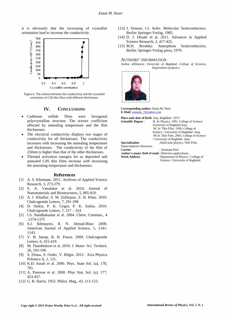
6
it is obviously that the increasing of crystallite
orientation lead to increase the conductivity.
Figure 6. The relation between the conductivity and the crystallite
orientation of CdS thin films with different thicknesses.
IV. CONCLUSIONS
Cadmium sulfide films were hexagonal
polycrystalline structure. The texture coefficient
affected by annealing temperature and the film
thicknesses.
The electrical conductivity displays two stages of
conductivity for all thicknesses. The conductivity
increases with increasing the annealing temperature
and thicknesses. The conductivity of the film of
250nm is higher than that of the other thicknesses.
Thermal activation energies for as deposited and
annealed CdS thin films increase with increasing
the annealing temperature and thicknesses.
References [1] A. S. Khomane. 2011. Archives of Applied Science
Research, 3, 273-279.
[2] S. A. Vanalakar et al. 2010, Journal of
Nanomaterials and Biostructures, 5, 805-810.
[3] A. I. Khudiar, S. M. Zulfequar, Z. H. Khan. 2010.
Chalcogenide Letters, 7, 291-298
[4] D. Saikia, P. K. Gogoi, P. K. Saikia. 2010.
Chalcogenide Letters, 7, 317 – 324
[5] I.S. Nandhakumar et al. 2004. Chem. Comman., 4
,1374-1375
[6] S.J. Ikhmayies, R. N. Ahmad-Bitar. 2008.
American Journal of Applied Science, 5, 1141-
1143.
[7] V. B. Sanap, B. H. Pawar. 2009. Chalcogenide
Letters, 6, 415-419.
[8] M. Thambidurai et al. 2010. J. Mater. Sci. Technol,
26, 193-199.
[9] S. Elmas, S. Ozder, V. Bilgin. 2012. Acta Physica
Polonica A, 1, 121.
[10] K.El Assali et al. 2000. Phys. State Sol. (a), 178,
701.
[11] A. Punoose et al. 2000. Phys Stat. Sol. (a), 177,
453-457.
[12] G. B. Harris. 1952. Philos. Mag., 43, 113-123.
[13] J. Simson, J.J. Aolre. Molecular Semiconductors.
Berlin: Springer-Verlag, 1985.
[14] D. J. Desale el al. 2011. Advances in Applied
Science Research, 2, 417-425.
[15] M.H. Brodsky. Amorphous Semiconductors,
Berlin: Springer-Verlag press, 1979.
AUTHORS’ INFORMATION Author affiliation; University of Baghdad, College of Sciences,
Department of physics
Corresponding author: Eman M. Nasir
E-Mail: [email protected]
Place and/ date of birth: Iraq -Baghdad / 1973
Scientific Degree : B. Sc Physics, 1991, College of Science/
University of Baghdad-Iraq.
M. Sc Thin Film, 1999, College of
Science / University of Baghdad –Iraq.
Ph.D. Thin Film, 2005, College of Science / University of Baghdad –Iraq.
Specialization :Solid state physics, Thin Film,
Semiconductor Detectors. Carrier : Assistant Prof.
Author’s major field of study: Detectors applications.
Work Address : Department of Physics / College of Science / University of Baghdad.
Eman M. Naser
Copy right © 2013 Praise Worthy Prize S.r.l. –All right received
International Reviw of Physics Vol. 7, N. 1
International Review of Physics, Vol. 7, N. 1

7
1971-6796(201302)7:1; 1-A
Copy right © 2013 Praise Worthy Prize S.r.l. –All right received