Transistor-level estimation of worst-case delays in MOS VLSI circuits
Upload
independentCategory
view
5download
0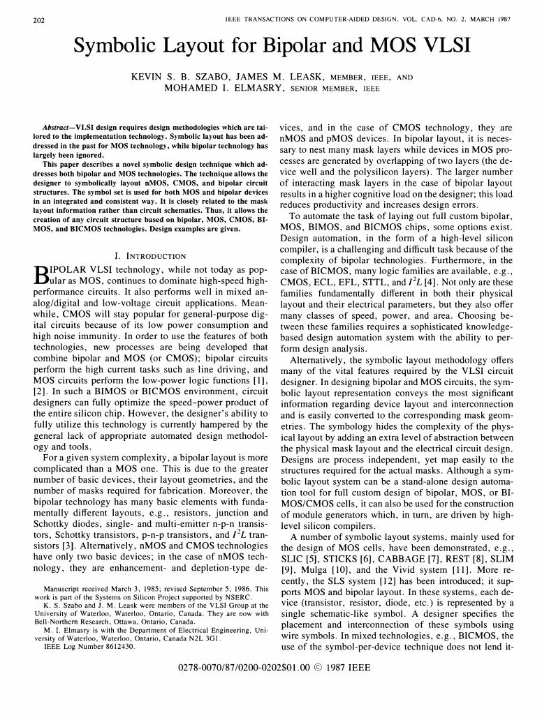
202 IEEE TRANSACTIONS ON COMPUTER-AIDED DESIGN. VOL. CAD-6, NO. 2, MARCH 1987
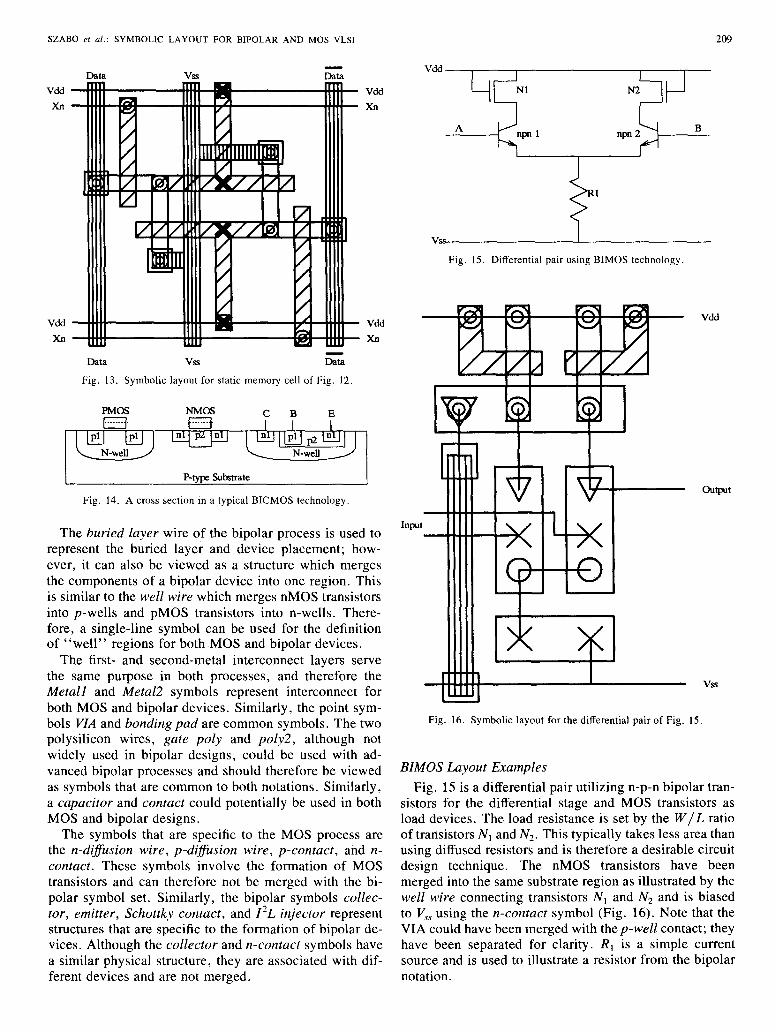
Symbolic Layout for Bipolar and MOS VLSI
KEVIN S, B, SZABO, JAMES M, LEASK, MEMBER, IEEE, AND
MOHAMED I. ELMASRY, SENIOR MEMBER, IEEE
Abstract-VLSI design requires design methodologies which are tailored to the implementation technology. Symbolic layout has been ad
dressed in the past for MOS technology, while bipolar technology has
largely been ignored. This paper describes a novel symbolic design technique which ad
dresses both bipolar and MOS technologies. The technique allows the
designer to symbolically layout nMOS, CMOS, and bipolar circuit
structures. The symbol set is used for both MOS and bipolar devices in an integrated and consistent way. It is closely related to the mask layout information rather than circuit schematics. Thus, it allows the
creation of any circuit structure based on bipolar, MOS, CMOS, BI
MOS, and BICMOS technologies. Design examples are given.
1. INTRODUCTION
BIPOLAR VLSI technology, while not today as popular as MOS, continues to dominate high-speed high
performance circuits. It also performs well in mixed analog/digital and low-voltage circuit applications. Meanwhile, CMOS will stay popular for general-purpose digital circuits because of its low power consumption and high noise immunity. In order to use the features of both technologies, new processes are being developed that combine bipolar and MOS (or CMOS); bipolar circuits perform the high current tasks such as line driving, and MOS circuits perform the low-power logic functions [ 1], [2]. In such a BIMOS or BICMOS environment, circuit designers can fully optimize the speed-power product of the entire silicon chip. However, the designer's ability to fully utilize this technology is currently hampered by the general lack of appropriate automated design methodology and tools.
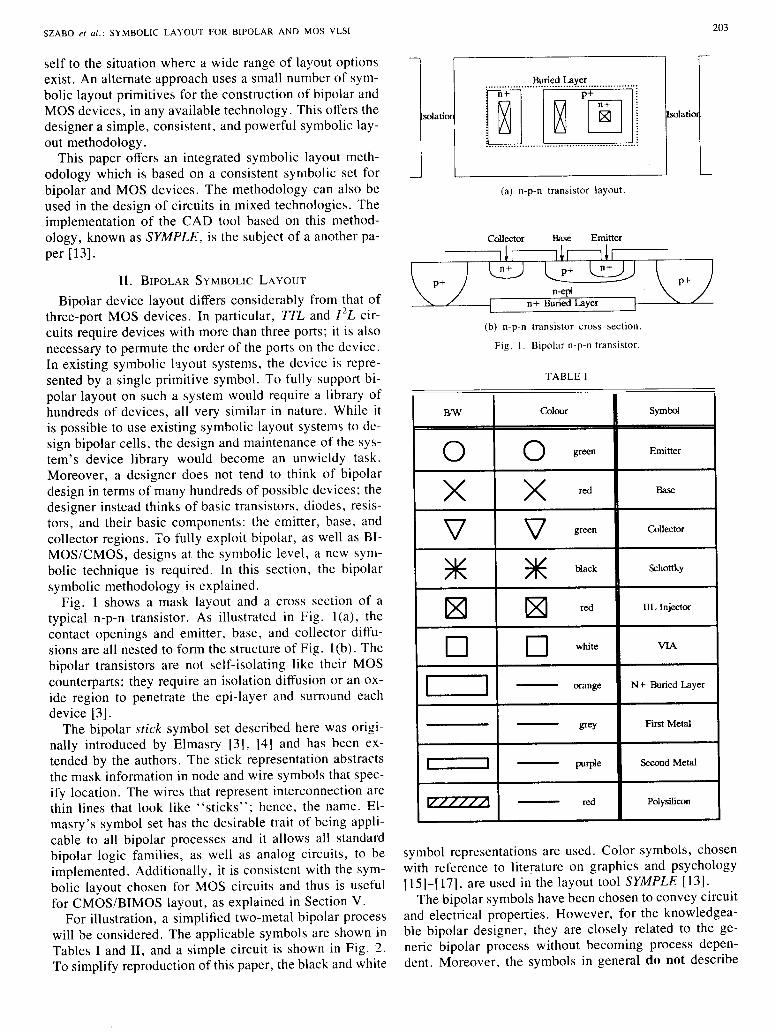
For a given system complexity, a bipolar layout is more complicated than a MOS one. This is due to the greater number of basic devices, their layout geometries, and the number of masks required for fabrication. Moreover, the bipolar technology has many basic elements with fundamentally different layouts, e.g., resistors, junction and Schottky diodes, single- and multi-emitter n-p-n transistors, Schottky transistors, p-n-p transistors, and J2L transistors [3]. Alternatively, nMOS and CMOS technologies have only two basic devices; in the case of nMOS technology, they are enhancement- and depletion-type de-
Manuscript received March 3, 1985; revised September 5, 1986. This work is part of the Systems on Silicon Project supported by NSERC.
K. S. Szabo and 1. M. Leask were members of the VLSI Group at the University of Waterloo, Waterloo, Ontario, Canada. They are now with Bell-Northern Research, Ottawa, Ontario, Canada.
M. I. Elmasry is with the Department of Electrical Engineering, University of Waterloo, Waterloo, Ontario, Canada N2L 3GI.
IEEE Log Number 8612430.
vices, and in the case of CMOS technology, they are nMOS and pMOS devices. In bipolar layout, it is necessary to nest many mask layers while devices in MOS processes are generated by overlapping of two layers (the device well and the polysilicon layers). The larger number of interacting mask layers in the case of bipolar layout results in a higher cognitive load on the designer; this load reduces productivity and increases design errors.
To automate the task of laying out full custom bipolar, MOS, BIMOS, and BICMOS chips, some options exist. Design automation, in the form of a high-level silicon compiler, is a challenging and difficult task because of the complexity of bipolar technologies. Furthermore, in the case of BICMOS, many logic families are available, e,g., CMOS, ECL, EFL, STTL, and J2L [4]. Not only are these families fundamentally different in both their physical layout and their electrical parameters, but they also offer many classes of speed, power, and area. Choosing between these families requires a sophisticated knowledgebased design automation system with the ability to perform design analysis.
Alternatively, the symbolic layout methodology offers many of the vital features required by the VLSI circuit designer. In designing bipolar and MOS circuits, the symbolic layout representation conveys the most significant information regarding device layout and interconnection and is easily converted to the corresponding mask geometries. The symbology hides the complexity of the physical layout by adding an extra level of abstraction between the physical mask layout and the electrical circuit design. Designs are process independent, yet map easily to the structures required for the actual masks. Although a symbolic layout system can be a stand-alone design automation tool for full custom design of bipolar, MOS, or BIMOS/CMOS cells, it can also be used for the construction of module generators which, in tum, are driven by highlevel silicon compilers.
A number of symbolic layout systems, mainly used for the design of MOS cells, have been demonstrated, e.g., SLIC [5], STICKS [6], CABBAGE [7], REST [8], SLIM [9], Mulga [ 10], and the Vivid system [ 1 1]. More recently, the SLS system [12] has been introduced; it supports MOS and bipolar layout. In these systems, each device (transistor, resistor, diode, etc. ) is represented by a single schematic-like symbol. A designer specifies the placement and interconnection of these symbols using wire symbols. In mixed technologies, e. g. , BICMOS, the use of the symbol-per-device technique does not lend it-
0278-0070/87/0200-0202$01.00 © 1987 IEEE


Copyright © 2022 FDOKUMEN